6866539D31 MTM800 Detailed Service Manual A
User Manual: MTM800 Detailed service manual 6866539D31-A
Open the PDF directly: View PDF ![]() .
.
Page Count: 240 [warning: Documents this large are best viewed by clicking the View PDF Link!]
- COPYRIGHT
- SCOPE & WARRANTY INFORMATION
- MODEL INFORMATION & ACCESSORIES
- OVERVIEW
- THEORY OF OPERATION
- THEORY OF OPERATION (TRANSCEIVER)
- THEORY OF OPERATION (ENHANCED CONTROL HEADS)
- PROGRAMMING THE TERMINAL
- TEST SETUP & TESTING
- MAINTENANCE
- Introduction
- Preventive Maintenance
- Safe Handling of CMOS and LDMOS Devices
- General Repair Procedures and Techniques
- Pre-baking of Integrated Circuits
- Repair Procedures and Techniques - General
- Disassembling and Reassembling the Terminal - General
- Terminal Disassembly and Reassembly - Detailed
- Enhanced Control Head Removal
- Top Plastic Cover Removal
- Transceiver Board Removal
- Reassembly the Terminal Chassis And Transceiver Board
- Enhanced Control Head Fitting
- Enhanced Control Head - Disassembly
- Enhanced Control Head - Reassembly
- Remote Head Enhanced - Disassembly
- Remote Head Enhanced - Reassembly
- Remote Mount Enhanced Control Head - Disassembly
- Remote Mount Enhanced Control Head - Reassembly
- Data Expansion Head Enhanced - Disassembly
- Data Expansion Head Enhanced - Reassembly
- Motorcycle Mount Enhanced Control Head - Disassembly
- Motorcycle Mount Enhanced Control Head - Reassembly
- Terminal Disassembly and Reassembly - Detailed
- Service Aids
- EXPLODED VIEWS & PARTS LISTS
- Transceiver - Exploded View and Parts List
- Enhanced Control Head - Exploded View and Parts List
- Data Expansion Head Enhanced - Exploded View and Parts List
- Remote Mount Enhanced Control Head - Exploded View and Parts List
- Remote Mount Configuration - Exploded View and Parts List
- Motorcycle Mount Enhanced Control Head - Exploded View and Parts List
- SCHEMATICS, PCBs and PARTS LISTS
- TRANSCEIVER 450-470MHz: SCHEMATICS, PCBs and PARTS LISTS
- PARTS LISTS
- GPS Sub Module 8466576A01_O / PCB TOP & BOT side
- CHASSIS_OVERVIEW TRANSCEIVER
- GPS Sub Module 8466576A01_O / Schematic
- PCB / Main Board 8466575A01_A / TOP SIDE
- PCB / Main Board 8466575A01_A / BOT SIDE
- Main Board 8466575A01_A / TX-LOW SECTION (JAVELIN)
- Main Board 8466575A01_A / PA SECTION
- Main Board 8466575A01_A / ABACUS Section
- Main Board 8466575A01_A / FRAC-N Section
- Main Board 8466575A01_A / FE and Mixer Section
- Main Board 8466575A01_A / RX VCO Section
- Main Board 8466575A01_A / TX VCO Section
- Main Board 8466575A01_A / Controller Power Supply Section
- Main Board 8466575A01_A / I/O Section
- Main Board 8466575A01_A / Controller Section
- Main Board 8466575A01_A / Port Controller Section
- Main Board 8466575A01_A / PATRIOT Controller Section
- Main Board 8466575A01_A / PATRIOT Memory Section
- Main Board 8466575A01_A / Controller Audio Section
- Main Board 8466575A01_A / Controller USB/ADC Section
- ENHANCED CONTROL HEADS: SCHEMATICS, PCBs and PARTS LISTS
- Enhanced Control Head Main Board - Processor Memory Block: Supply (PCB: 8466580A01_A)
- Enhanced Control Head Main Board - Connectivity Block: GPIO (PCB: 8466580A01_A)
- Remote Back Head Enhanced Main Board - Audio (PCB: 8466583A01_A)
- Remote Back Head Enhanced Main Board - Block Diagram (PCB: 8466583A01_A)
- PCB/ Remote Back Head Enhanced Main Board - Bottom and Top Side (PCB: 8466583A01_A)
- PCB/ Enhanced Control Head Main Board - Bottom and Top Side (PCB: 8466580A01_A)
- Data Expansion Head Enhanced Main Board - Main PCB (PCB: 8466586A01_A)
- Enhanced Control Head Main Board - Control Head (PCB: 8466580A01_A)
- Enhanced Control Head Main Board - Connectivity Block: USB Block (PCB: 8466580A01_A)
- Enhanced Control Head Main Board - User Input Block: Keypad (PCB: 8466580A01_A)
- Data Expansion Head Enhanced Connector Board - Connector Board (PCB: 8464300B06_A)
- PCB/ Data Expansion Head Enhanced Main Board - Bottom and Top Side (PCB: 8466586A01_A)
- Data Expansion Head Enhanced Main Board - DC Power (PCB: 8466586A01_A)
- Data Expansion Head Enhanced Main Board - Gabel Hybrid (PCB: 8466586A01_A)
- PCB/ Remote Head Enhanced Main Board - Bottom and Top Side (PCB: 8471016L01_A)
- Remote Head Enhanced Main Board (PCB: 8471016L01_A)
- PCB/ Data Expansion Head Enhanced Connector Board - Bottom and Top Side (PCB: 8464300B06_A)
- Enhanced Control Head Main Board - Processor Memory Block: LCD (PCB: 8466580A01_A)
- Enhanced Control Head Main Board - Processor Memory Block: Memory (PCB: 8466580A01_A)
- Enhanced Control Head Main Board - Processor Memory Block: Main CPU (PCB: 8466580A01_A)
- Enhanced Control Head Main Board - User Input Block: SBEP (PCB: 8466580A01_A)
- Enhanced Control Head Main Board - DC Block: Power Supply (PCB: 8466580A01_A)
- Enhanced Control Head Main Board - DC Block: Power On/ Off (PCB: 8466580A01_A)
- Enhanced Control Head Main Board - Remote Block (PCB: 8466580A01_A)
- Data Expansion Head Enhanced Main Board - SB9600 Interface (PCB: 8466586A01_A)
- Data Expansion Head Enhanced Main Board - Car Interface (PCB: 8466586A01_A)
- Remote Back Head Enhanced Main Board - USB/ RS232 (PCB: 8466583A01_A)
- Remote Back Head Enhanced Main Board - Interconnect (PCB: 8466583A01_A)
- Remote Back Head Enhanced Main Board - IO (PCB: 8466583A01_A)
- PCB/ Enhanced Control Head Keypad Board - Bottom and Top Side (PCB: 8466581A01_A)
- Enhanced Control Head Keypad Board - Keypad Board (PCB: 8466581A01_A)
- Parts List
- TROUBLESHOOTING
- TROUBLESHOOTING CHARTS: 450-470MHz
- Main Function Test Chart (Sheet 1) >> Start-up Procedure <<
- Main Function Test Chart (Sheet 2)
- Controller Troubleshooting (Sheet 1)
- Controller Troubleshooting (Sheet 2)
- DC Supply Troubleshooting
- GPIO Troubleshooting
- Receiver Audio Troubleshooting
- Transmitter Audio Troubleshooting
- Warping Failure Troubleshooting
- RF Power Amplifier Troubleshooting
- PA Bias Failure Troubleshooting
- JAVELIN Troubleshooting
- Receiver Troubleshooting (Sheet 1)
- Receiver Troubleshooting (Sheet 2)
- Front-End Tuning Troubleshooting
- Tx Frequency Generation Troubleshooting
- Main VCO Troubleshooting
- Main Synthesizer Troubleshooting
- GPS Troubleshooting (Sheet 1)
- GPS Troubleshooting (Sheet 2)
- CONNECTOR PIN FUNCTIONS
- REPLACEMENT PARTS & KITS
- RETROFITTING the GPS and UCM BOARD
- PRODUCT SPECIFIC INFORMATION
- SPEZIELLE PRODUKTINFORMATIONEN

MTM800
with Enhanced Control Head
TETRA Mobile Terminal
450-470 MHz (MT512M)
Part Number: 6866539D31-A
*6866539D31*
6866539D31.book Page i Tuesday, March 20, 2007 6:32 PM

ii COPYRIGHT
COPYRIGHT
Copyrights
© 2006, 2007 Motorola Inc. All rights reserved.
No part of this manual may be reproduced, transmitted, stored in a retrieval system, or
translated into any language or computer language, in any form or by any means, without
the prior written permission of Motorola Inc.
Computer Software Copyrights
The Motorola products described in this manual may include copyrighted Motorola
computer programs stored in semiconductor memories or other media. Laws in the United
States and other countries preserve for Motorola certain exclusive rights for copyrighted
computer programs including, but not limited to, the exclusive right to copy or reproduce in
any form the copyrighted computer program. Accordingly, any copyrighted Motorola
computer programs contained in the Motorola products described in this manual may not
be copied, reproduced, modified, reverse-engineered, or distributed in any manner without
the express written permission of Motorola. Furthermore, the purchase of Motorola
products shall not be deemed to grant either directly or by implication, estoppel, or
otherwise, any license under the copyrights, patents or patent applications of Motorola,
except for the normal non-exclusive royalty-free license to use that arises by operation of
law in the sale of a product.
Trademarks
Motorola, the Motorola Logo and all other trademarks identified as such herein are
trademarks of Motorola Inc. All other product or service names are the property of their
respective owners.
6866539D31.book Page ii Tuesday, March 20, 2007 6:32 PM

DOCUMENT HISTORY iii
DOCUMENT HISTORY
The following major changes have been implemented in this manual since the previous edition:
Edition Description Date
6866539D31_A Initial edition Mar. 2007
6866539D31.book Page iii Tuesday, March 20, 2007 6:32 PM

iv DOCUMENT HISTORY
Notes
6866539D31.book Page iv Tuesday, March 20, 2007 6:32 PM

PRODUCT SAFETY and RF Energy Exposure v
PRODUCT SAFETY and RF Energy Exposure
for Mobile Two-Way Radios
installed in Vehicles or as Fixed Site Control Stations
The information provided in this document supersedes information contained in user guides,
manuals and other documentation published prior to February 2002.
RF Energy Exposure Awareness and Control Information, and Operational
Instructions for FCC Occupational Use Requirements.
Note: This radio is intended for use in occupational / controlled conditions, where users have full
knowledge of their exposure and can exercise control over their exposure to meet FCC/ICNIRP lim-
its. This radio device is NOT authorized for general population, consumer or any other use.
This 2-way radio uses electromagnetic energy in the radio frequency (RF) spectrum to provide
communications between two or more users over a distance. It uses radio frequency (RF) energy or
radio waves to send and receive calls. RF energy is one form of electromagnetic energy. Other
forms include, but are not limited to, sunlight and x-rays. RF energy, however, should not be
confused with these other forms of electromagnetic energy, which when used improperly, can cause
biological damage. Very high levels of x-rays, for example, can damage tissues and genetic
material.
Experts in science, engineering, medicine, health and industry work with organizations to develop
standards for safe exposure to RF energy. These standards provide recommended levels of RF
exposure for both workers and the general public. These recommended RF exposure levels include
substantial margins of protection.
All Motorola 2-way radios are designed, manufactured and tested to ensure they meet government-
established RF exposure levels. In addition, manufacturers also recommend specific operating
instructions to users of 2-way radios. These instructions are important because they inform users
about RF energy exposure and provide simple procedures on how to control it.
Please refer to the following Web sites for more information on what RF energy exposure is and how
to control your exposure to assure compliance with established RF exposure limits.
http://www.fcc.gov/oet/rfsafety/rf-faqs.html
http://www.osha.gov/SLTC/radiofrequencyradiation/index.html
THIS CHAPTER IS AN EXTRACT OF THE MULTI LINGUAL MOBILE SAFETY
BOOKLET PUBLICATION No. 6866537D37_.
FOR THE LATEST SAFETY INFORMATION REFER TO THE SEPARATE SAFETY
BOOKLET DELIVERED WITH YOUR RADIO.
BEFORE USING THIS RADIO READ THIS INFORMATION WHICH CONTAINS
IMPORTANT OPERATING INSTRUCTIONS FOR SAFE USAGE AND RF
ENERGY AWARENESS AND CONTROL INFORMATION FOR COMPLIANCE
WITH RF ENERGY EXPOSURE LIMITS IN APPLICABLE NATIONAL AND
INTERNATIONAL STANDARDS.
!
C
a u t i o
n
6866539D31.book Page v Tuesday, March 20, 2007 6:32 PM

vi PRODUCT SAFETY and RF Energy Exposure
Federal Communications Commission Regulations (US markets only)
The FCC rules require manufacturers to comply with the FCC RF energy exposure limits for mobile
2-way radios before they can be marketed in the U.S. When 2-way radios are used as a
consequence of employment, the FCC requires users to be fully aware of and able to control their
exposure to meet occupational requirements. Exposure awareness can be facilitated by the use of a
label directing users to specific user awareness information. Your Motorola 2-way radio has an RF
exposure product label. Do not remove this RF exposure label from the device. Also, your Motorola
user manual, or separate safety booklet, includes information and operating instructions required to
control your RF exposure and to satisfy compliance requirements.
Compliance with RF Exposure Standard
Your Motorola radio is designed and tested to comply with a number of national and international
standards and guidelines (listed below) regarding human exposure to radio frequency
electromagnetic energy. This radio complies with IEEE and ICNIRP exposure limits for
occupational/controlled RF exposure environments at duty factors of up to 50% talk–50% listen
and is authorized by the IEEE/ICNIRP for occupational use. In terms of measuring RF energy for
compliance with these exposure guidelines, your radio antenna radiates measurable RF energy
only while it is transmitting (during talking), not when it is receiving (listening) or in standby mode.
Your Motorola two-way radio complies with the following RF energy exposure
standards and guidelines:
• United States Federal Communications Commission, Code of Federal Regulations; 47 CFR part
2 sub-part J
• American National Standards Institute (ANSI) / Institute of Electrical and Electronic Engineers
(IEEE) C95. 1-1992
• Institute of Electrical and Electronic Engineers (IEEE) C95.1-1999 Edition
• International Commission on Non-Ionizing Radiation Protection (ICNIRP) 1998
• Ministry of Health (Canada) Safety Code 6. Limits of Human Exposure to Radiofrequency
Electromagnetic Fields in the Frequency Range from 3 kHz to 300 GHz, 1999
• Australian Communications Authority Radiocommunications (Electromagnetic Radiation -
Human Exposure) Standard 2003
• ANATEL, Brasil Regulatory Authority, Resolution 256 (April 11, 2001) “additional requirements for
SMR, cellular and PCS product certification.”
RF Exposure Compliance and Control Guidelines and Operating Instructions
To control exposure to yourself and others and to ensure compliance with the RF exposure limits,
always adhere to the following procedures.
6866539D31.book Page vi Tuesday, March 20, 2007 6:32 PM

PRODUCT SAFETY and RF Energy Exposure vii
Guidelines:
• User awareness instructions should accompany device when transferred to other users.
• Do not use this device if the operational requirements described herein are not met.
Instructions:
•Transmit no more that the rated duty factor of 50% of the time. To transmit (talk), push the
Push-To-Talk (PTT) button. To receive calls, release the PTT button. Transmitting 50% of the
time, or less, is important because this radio generates measurable RF energy exposure only
when transmitting (in terms of measuring for standards compliance).
•Transmit only when people outside the vehicle are at least the recommended minimum
lateral distance away, as shown in Table 1, from the body of a vehicle with a properly
installed antenna. This separation distance will ensure that there is sufficient distance from a
properly installed (according to installation instructions) externally-mounted antenna to satisfy
the RF exposure requirements in the standards listed above.
Note: Table 1 lists the recommended lateral distance for bystanders in an uncontrolled
environment from the body of a vehicle with an approved, properly installed transmitting antenna
(i.e. monopoles over a ground plane, or dipoles) at several different ranges of rated radio power
for mobile radios installed in a vehicle.
Note: If you are not sure of the rated power of your radio, contact your Motorola representative or
dealer and supply the radio model number found on the radio model label. If you cannot determine
the rated power out, then assure 90cms (3 feet) separation from the body of the vehicle.
Mobile Antenna Installation Guidelines
• These mobile antenna installation guidelines are limited to metal body motor vehicles or vehicles
with appropriate ground planes.
• Antennas should be installed in the centre area of the roof or the trunk lid taking into account the
bystander exposure conditions of backseat passengers and according to the specific instructions
and restrictions in the Radio. Installation Manual along with the requirements of the antenna
supplier.
• Trunk lid installations are limited to vehicles with clearly defined flat trunk lids, and in some
cases, to specific radio models and antennas. See the Radio Installation Manual for specific
information on how and where to install specific types of approved antennas to facilitate
recommended operating distances to all potentially exposed persons.
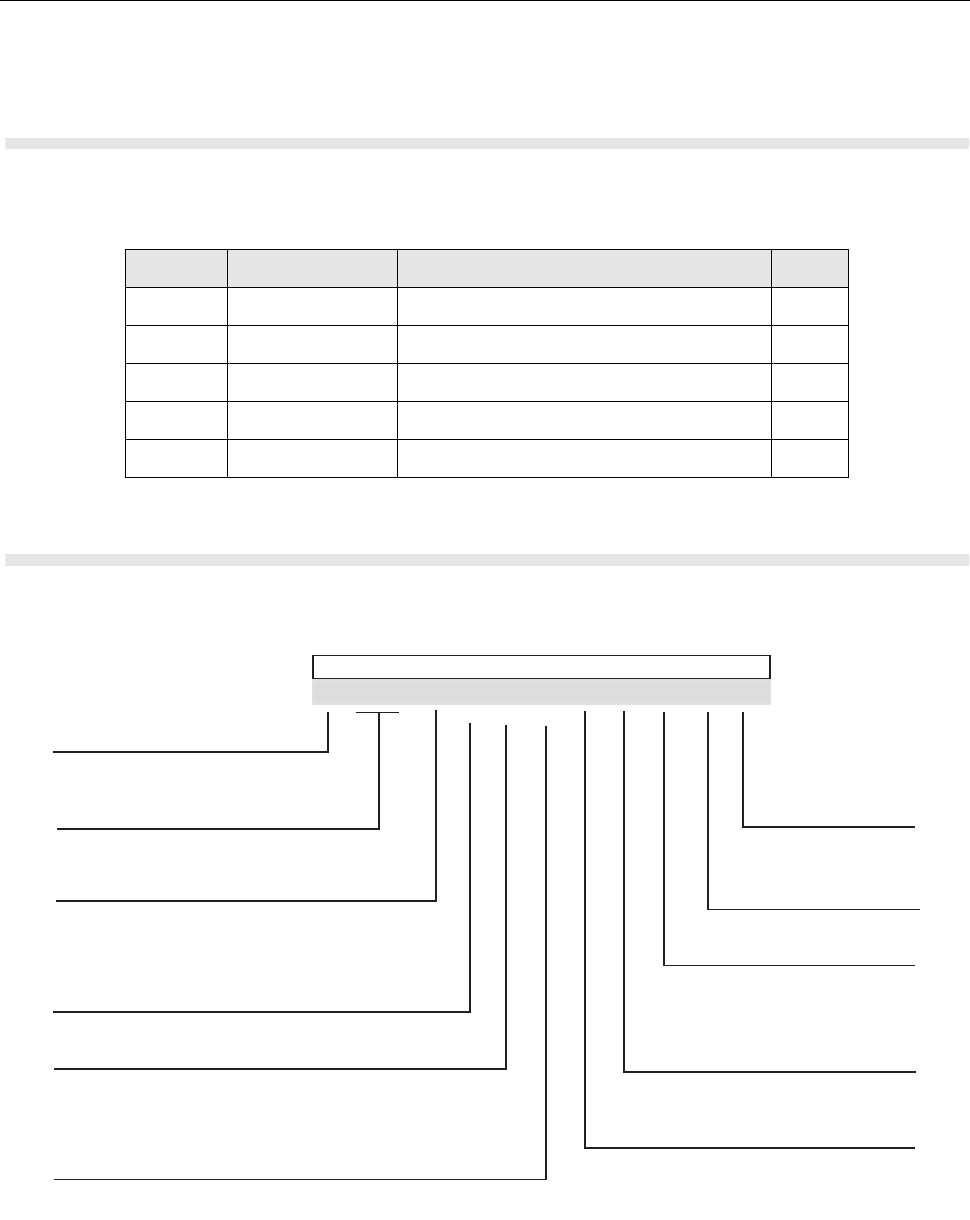
Table 1
Mobile Radio
Rated Power (see
Note below)
Minimum Lateral
Distance From
Vehicle Body
Less than 7 Watts 20 cm (8 Inches)
7 to 15 Watts 30 cm (1 Ft)
16 to 39 Watts 60 cm (2 Ft)
40 to 110 Watts 90 cm (3 Ft)
6866539D31.book Page vii Tuesday, March 20, 2007 6:32 PM

viii PRODUCT SAFETY and RF Energy Exposure
•Use only Motorola-approved supplied antenna or a Motorola approved replacement
antenna. Unauthorized antennas, modifications, or attachments could damage the radio and
may result in non-compliance with RF Safety Standards.
Approved Accessories
• This radio has been tested and meets the RF Safety Standards when used with the Motorola
accessories supplied or designated for this product. Use of other accessories may result in non-
compliance with RF Safety Standards.
• For a list of Motorola approved antennas, please see your dealer or local Motorola contact. Your
nearest dealer can be found at the following web site:
http://www.motorola.com/businessandgovernment/wemea/en-gb/public/functions/dealerlocator/
dealerlocator.aspx
Additional Information
• For additional information on exposure requirements or other training information, visit
http://www.motorola.com/rfhealth
Compliance and Control Guidelines and Operating Instructions for Mobile
Two-Way Radios Installed as Fixed Site Control Stations
If mobile radio equipment is installed at a fixed location and operated as a control station or as a
fixed unit, the antenna installation must comply with the following requirements in order to ensure
optimal performance and compliance with the RF energy exposure limits in the standards and
guidelines listed on previous page:
• The antenna should be mounted outside the building on the roof or a tower if at all possible.
• As with all fixed site antenna installations, it is the responsibility of the licensee to manage the
site in accordance with applicable regulatory requirements and may require additional
compliance actions such as site survey measurements, signage, and site access restrictions in
order to insure that exposure limits are not exceeded.
Electromagnetic Interference/Compatibility
Note: Nearly every electronic device is susceptible to electromagnetic interference (EMI) if inade-
quately shielded, designed or otherwise configured for electromagnetic compatibility. It may be nec-
essary to conduct compatibility testing to determine if any electronic equipment used in or around
vehicles or near fixed site antenna is sensitive to external RF energy or if any procedures need to be
followed to eliminate or mitigate the potential for interaction between the radio transmitter and the
equipment or device.
6866539D31.book Page viii Tuesday, March 20, 2007 6:32 PM

PRODUCT SAFETY and RF Energy Exposure ix
Facilities
To avoid electromagnetic interference and/or compatibility conflicts, turn off your radio in any facility
where posted notices instruct you to do so. Hospitals or health care facilities may be using
equipment that is sensitive to external RF energy.
Vehicles
To avoid possible interaction between the radio transmitter and any vehicle electronic control
modules, such as, ABS, engine, or transmission controls, the radio should be installed only by an
experienced installer and that the following precautions be used when installing the radio:
1. Refer to the manufacturer’s instructions or other technical bulletins for recommendations on radio
installation.
2. Before installing the radio, determine the location of the electronic control modules and their
harnesses in the vehicle.
3. Route all radio wiring, including the antenna transmission line, as far away as possible from the
electronic control units and associated wiring.
Driver Safety
Check the laws and regulations on the use of radios in the area where you drive. Always obey them.
When using your radio while driving, please:
• Give full attention to driving and to the road.
• Pull off the road and park before making or answering a call if driving conditions so require.
6866539D31.book Page ix Tuesday, March 20, 2007 6:32 PM

xPRODUCT SAFETY and RF Energy Exposure
OPERATIONAL WARNINGS
For Vehicles With Air Bags
Do not mount or place a mobile radio in the area over an air bag or in the air bag deployment
area. Air bags inflate with great force. If a radio is placed in the air bag deployment area and the
air bag inflates, the radio may be propelled with great force and cause serious injury to
occupants of the vehicle.
Potentially Explosive Atmospheres
Turn off your radio prior to entering any area with a potentially explosive atmosphere. Sparks in
a potentially explosive atmosphere can cause an explosion or fire resulting in bodily injury or
even death.
The areas with potentially explosive atmospheres referred to above include fuelling areas such
as below decks on boats, fuel or chemical transfer or storage facilities, areas where the air
contains chemicals or particles, such as grain, dust or metal powders. Areas with potentially
explosive atmospheres are often but not always posted.
Blasting Caps And Blasting Areas
To avoid possible interference with blasting operations, turn off your radio when you are near
electrical blasting caps, in a blasting area, or in areas posted:
"Turn off two-way radio". Obey all signs and instructions.
For radios installed in vehicles fueled by liquefied petroleum gas, refer to the (U.S.) National Fire
Protection Association standard, NFPA 58, for storage, handling, and/or container information.
For a copy of the LP-gas standard, NFPA 58, contact the National Fire Protection Association,
One Battery Park, Quincy, MA.
!
W A R N I N G
!
6866539D31.book Page x Tuesday, March 20, 2007 6:32 PM

PRODUCT SAFETY and RF Energy Exposure xi
Only specialized workshops should be contacted for installation, maintenance and repair work.
This unit is equipped with protection fuses in the Power and Ignition Sense Cable.
Replace these fuses only with the original ratings!
Caution: Failure to use correct manufactures approved parts
may result in physical damage to this unit.
Fuse for Power Cable GKN6270/GKN6274: 10A (Motorola Part Number: 65C80283E05)
Fuse for Ignition Sense Cable HKN9327: 4A (Motorola Part Number: 65C80283E02)
ADDITIONAL IMPORTANT INFORMATION
FOR SERVICING AND INSTALLING THE RADIO
!
C
a u t i o
n
Installations, Wartungs- und Reparaturarbeiten dürfen ausschließlich von autorisiertem und geschultem
Personal ausgeführt werden.
Dieses Gerät ist mit einer Schutzsicherung im Stromversorgungskabel ausgestattet.
Bei Austausch ausschließlich den Originalwert verwenden
WARNUNG: Bei Einsetzen von nicht vom Hersteller freigegebenen Ersatzteilen
kann das Gerät zerstört werden.
Sicherung für Stromversorgungskabel GKN6270/GKN6274: 10A (Motorola Best.-Nr.:65C80283E05)
Sicherung für Zündungserkennungskabel HKN9327: 4A (Motorola Best.-Nr.:65C80283E02)
ZUSÄTZLICHE SICHERHEITS INFORMATIONEN
FÜR SERVICE UND INSTALLATION DES FUNKGERÄTES
!
Achtung
6866539D31.book Page xi Tuesday, March 20, 2007 6:32 PM

xii PRODUCT SAFETY and RF Energy Exposure
Notes
6866539D31.book Page xii Tuesday, March 20, 2007 6:32 PM

CONTENTS xiii
CONTENTS
COPYRIGHT
Copyrights . . . . . . . . . . . . . . . . . . . . . . . . . . . . . . . . . . . . . . . . . . . . . . . . . . . . . . . . . . . . . ii
Computer Software Copyrights . . . . . . . . . . . . . . . . . . . . . . . . . . . . . . . . . . . . . . . . . . . . . ii
Trademarks . . . . . . . . . . . . . . . . . . . . . . . . . . . . . . . . . . . . . . . . . . . . . . . . . . . . . . . . . . . . ii
DOCUMENT HISTORY . . . . . . . . . . . . . . . . . . . . . . . . . . . . . . . . . . . . . . . . . . . . . . . . . . . iii
PRODUCT SAFETY and RF Energy Exposure . . . . . . . . . . . . . . . . . . . . . . . . . . . . . . . v
RF Energy Exposure Awareness and Control Information . . . . . . . . . . . . . . . . . . . . . v
Federal Communications Commission Regulations (US markets only) . . . . . . . . . . .vi
Compliance with RF Exposure Standard . . . . . . . . . . . . . . . . . . . . . . . . . . . . . . . . . .vi
RF Exposure Compliance and Control Guidelines and Operating Instructions . . . . . .vi
Mobile Antenna Installation Guidelines . . . . . . . . . . . . . . . . . . . . . . . . . . . . . . . . . . . vii
Approved Accessories . . . . . . . . . . . . . . . . . . . . . . . . . . . . . . . . . . . . . . . . . . . . . . . . viii
Additional Information . . . . . . . . . . . . . . . . . . . . . . . . . . . . . . . . . . . . . . . . . . . . . . . .viii
Compliance and Control Guidelines and Operating Instructions . . . . . . . . . . . . . . . . viii
Electromagnetic Interference/Compatibility . . . . . . . . . . . . . . . . . . . . . . . . . . . . . . . . viii
Facilities . . . . . . . . . . . . . . . . . . . . . . . . . . . . . . . . . . . . . . . . . . . . . . . . . . . . . . . . . . .ix
Vehicles . . . . . . . . . . . . . . . . . . . . . . . . . . . . . . . . . . . . . . . . . . . . . . . . . . . . . . . . . . . .ix
Driver Safety . . . . . . . . . . . . . . . . . . . . . . . . . . . . . . . . . . . . . . . . . . . . . . . . . . . . . . . .ix
OPERATIONAL WARNINGS . . . . . . . . . . . . . . . . . . . . . . . . . . . . . . . . . . . . . . . . . . . . . x
For Vehicles With Air Bags . . . . . . . . . . . . . . . . . . . . . . . . . . . . . . . . . . . . . . . . . . . . . x
Potentially Explosive Atmospheres . . . . . . . . . . . . . . . . . . . . . . . . . . . . . . . . . . . . . . . x
Blasting Caps And Blasting Areas . . . . . . . . . . . . . . . . . . . . . . . . . . . . . . . . . . . . . . . . x
ADDITIONAL IMPORTANT INFORMATION . . . . . . . . . . . . . . . . . . . . . . . . . . . . . . . . . xi
ZUSÄTZLICHE SICHERHEITS INFORMATIONEN . . . . . . . . . . . . . . . . . . . . . . . . . . . . xi
CHAPTER 1 SCOPE & WARRANTY INFORMATION
SCOPE OF THIS MANUAL . . . . . . . . . . . . . . . . . . . . . . . . . . . . . . . . . . . . . . . . . . . . 1-1
EMEA Manuals & User Guides . . . . . . . . . . . . . . . . . . . . . . . . . . . . . . . . . . . . . . . 1-2
LACR Manuals & User Guides . . . . . . . . . . . . . . . . . . . . . . . . . . . . . . . . . . . . . . . 1-3
Warranty and Service Support . . . . . . . . . . . . . . . . . . . . . . . . . . . . . . . . . . . . . . . . . . 1-4
After Warranty Period . . . . . . . . . . . . . . . . . . . . . . . . . . . . . . . . . . . . . . . . . . . 1-4
CHAPTER 2 MODEL INFORMATION & ACCESSORIES
MTM800 Mobile Terminal Model Information . . . . . . . . . . . . . . . . . . . . . . . . . . . . . . . 2-1
Sales Model Nomenclature . . . . . . . . . . . . . . . . . . . . . . . . . . . . . . . . . . . . . . . . . . . . 2-1
Model Specifications* . . . . . . . . . . . . . . . . . . . . . . . . . . . . . . . . . . . . . . . . . . . . . . 2-2
Model Descriptions** . . . . . . . . . . . . . . . . . . . . . . . . . . . . . . . . . . . . . . . . . . . . . . 2-2
Accessories-to-Model Chart . . . . . . . . . . . . . . . . . . . . . . . . . . . . . . . . . . . . . . . . . 2-3
CHAPTER 3 OVERVIEW
General . . . . . . . . . . . . . . . . . . . . . . . . . . . . . . . . . . . . . . . . . . . . . . . . . . . . . . . . . . . 3-1
Digital Modulation Technique . . . . . . . . . . . . . . . . . . . . . . . . . . . . . . . . . . . . . . . . 3-1
Voice Compression Technology . . . . . . . . . . . . . . . . . . . . . . . . . . . . . . . . . . . 3-1
6866539D31.book Page xiii Tuesday, March 20, 2007 6:32 PM

xiv CONTENTS
CHAPTER 4 THEORY OF OPERATION
Section Introduction . . . . . . . . . . . . . . . . . . . . . . . . . . . . . . . . . . . . . . . . . . . . . . . . . . 4-1
CHAPTER 4.1 THEORY OF OPERATION (TRANSCEIVER)
Block Diagram and Overview . . . . . . . . . . . . . . . . . . . . . . . . . . . . . . . . . . . . . . . . . .4.1-1
Receiver Section . . . . . . . . . . . . . . . . . . . . . . . . . . . . . . . . . . . . . . . . . . . . . . . . .4.1-2
Transmitter Section . . . . . . . . . . . . . . . . . . . . . . . . . . . . . . . . . . . . . . . . . . . . . . .4.1-3
Controller Section . . . . . . . . . . . . . . . . . . . . . . . . . . . . . . . . . . . . . . . . . . . . . . . .4.1-3
Frequency Generating Section . . . . . . . . . . . . . . . . . . . . . . . . . . . . . . . . . . . . . .4.1-4
GPS Section . . . . . . . . . . . . . . . . . . . . . . . . . . . . . . . . . . . . . . . . . . . . . . . . . . . .4.1-4
Block Diagrams Descriptions . . . . . . . . . . . . . . . . . . . . . . . . . . . . . . . . . . . . . . . . . .4.1-5
Receiver Path . . . . . . . . . . . . . . . . . . . . . . . . . . . . . . . . . . . . . . . . . . . . . . . . . . .4.1-5
Transmitter Path . . . . . . . . . . . . . . . . . . . . . . . . . . . . . . . . . . . . . . . . . . . . . . . . .4.1-6
Frequency Generating Section . . . . . . . . . . . . . . . . . . . . . . . . . . . . . . . . . . . . . .4.1-7
Main Synthesizer . . . . . . . . . . . . . . . . . . . . . . . . . . . . . . . . . . . . . . . . . . . . . .4.1-8
Transmit Frequency Translation Loop . . . . . . . . . . . . . . . . . . . . . . . . . . . . . .4.1-8
Controller Section . . . . . . . . . . . . . . . . . . . . . . . . . . . . . . . . . . . . . . . . . . . . . . . .4.1-9
Detailed Circuit Description . . . . . . . . . . . . . . . . . . . . . . . . . . . . . . . . . . . . . . . . . .4.1-10
Receiver Path, Detailed Circuit Description . . . . . . . . . . . . . . . . . . . . . . . . . . .4.1-10
Antenna Switch . . . . . . . . . . . . . . . . . . . . . . . . . . . . . . . . . . . . . . . . . . . . . .4.1-10
Pre Selector Filter . . . . . . . . . . . . . . . . . . . . . . . . . . . . . . . . . . . . . . . . . . . .4.1-10
LNA . . . . . . . . . . . . . . . . . . . . . . . . . . . . . . . . . . . . . . . . . . . . . . . . . . . . . . .4.1-10
Second Pre-selector . . . . . . . . . . . . . . . . . . . . . . . . . . . . . . . . . . . . . . . . . .4.1-10
Mixer . . . . . . . . . . . . . . . . . . . . . . . . . . . . . . . . . . . . . . . . . . . . . . . . . . . . . .4.1-10
IF Filter, Amplifier, Dynamic Range Extension . . . . . . . . . . . . . . . . . . . . . .4.1-11
IF Digitizing Subsystem . . . . . . . . . . . . . . . . . . . . . . . . . . . . . . . . . . . . . . . .4.1-11
Transmitter Path, Detailed Circuit Description . . . . . . . . . . . . . . . . . . . . . . . . .4.1-12
ADDAG . . . . . . . . . . . . . . . . . . . . . . . . . . . . . . . . . . . . . . . . . . . . . . . . . . . .4.1-12
Tx LO . . . . . . . . . . . . . . . . . . . . . . . . . . . . . . . . . . . . . . . . . . . . . . . . . . . . . .4.1-12
JAVELIN . . . . . . . . . . . . . . . . . . . . . . . . . . . . . . . . . . . . . . . . . . . . . . . . . . .4.1-12
RF Power Amplifier . . . . . . . . . . . . . . . . . . . . . . . . . . . . . . . . . . . . . . . . . . .4.1-13
Directional Coupler and RF Feedback Path . . . . . . . . . . . . . . . . . . . . . . . .4.1-13
Antenna Switch . . . . . . . . . . . . . . . . . . . . . . . . . . . . . . . . . . . . . . . . . . . . . .4.1-13
Harmonic Filter . . . . . . . . . . . . . . . . . . . . . . . . . . . . . . . . . . . . . . . . . . . . . .4.1-13
Frequency Generating Section Detailed Circuit Description . . . . . . . . . . . . . . .4.1-14
Reference Oscillator - TCXO . . . . . . . . . . . . . . . . . . . . . . . . . . . . . . . . . . . .4.1-14
Main VCO and Main Synthesizer . . . . . . . . . . . . . . . . . . . . . . . . . . . . . . . . .4.1-14
Transmit Frequency Translation Loop . . . . . . . . . . . . . . . . . . . . . . . . . . . . .4.1-15
Controller Section . . . . . . . . . . . . . . . . . . . . . . . . . . . . . . . . . . . . . . . . . . . . . . .4.1-16
DC Power Distribution . . . . . . . . . . . . . . . . . . . . . . . . . . . . . . . . . . . . . . . . .4.1-16
Microprocessor . . . . . . . . . . . . . . . . . . . . . . . . . . . . . . . . . . . . . . . . . . . . . .4.1-18
Host Memories . . . . . . . . . . . . . . . . . . . . . . . . . . . . . . . . . . . . . . . . . . . . . . .4.1-19
Terminal Audio System . . . . . . . . . . . . . . . . . . . . . . . . . . . . . . . . . . . . . . . .4.1-21
General purpose inputs and outputs . . . . . . . . . . . . . . . . . . . . . . . . . . . . . .4.1-23
GPS Sub Module . . . . . . . . . . . . . . . . . . . . . . . . . . . . . . . . . . . . . . . . . . . . . . .4.1-24
CHAPTER 4.2 THEORY OF OPERATION (ENHANCED CONTROL HEADS)
Enhanced Control Head in Dash Mount configuration . . . . . . . . . . . . . . . . . . . . . . .4.2-1
Power Supplies . . . . . . . . . . . . . . . . . . . . . . . . . . . . . . . . . . . . . . . . . . . . . . .4.2-1
Power On / Off . . . . . . . . . . . . . . . . . . . . . . . . . . . . . . . . . . . . . . . . . . . . . . . .4.2-2
Microprocessor Circuit . . . . . . . . . . . . . . . . . . . . . . . . . . . . . . . . . . . . . . . . . .4.2-2
Keypad . . . . . . . . . . . . . . . . . . . . . . . . . . . . . . . . . . . . . . . . . . . . . . . . . . . . . .4.2-3
One Wire interface . . . . . . . . . . . . . . . . . . . . . . . . . . . . . . . . . . . . . . . . . . . . .4.2-3
GCAI GPIOs and USB . . . . . . . . . . . . . . . . . . . . . . . . . . . . . . . . . . . . . . . . . .4.2-3
6866539D31.book Page xiv Tuesday, March 20, 2007 6:32 PM

CONTENTS xv
Backlights . . . . . . . . . . . . . . . . . . . . . . . . . . . . . . . . . . . . . . . . . . . . . . . . . . .4.2-4
Rotary and push button . . . . . . . . . . . . . . . . . . . . . . . . . . . . . . . . . . . . . . . . . 4.2-4
Communication interface . . . . . . . . . . . . . . . . . . . . . . . . . . . . . . . . . . . . . . . . 4.2-4
Accessory Connector . . . . . . . . . . . . . . . . . . . . . . . . . . . . . . . . . . . . . . . . . .4.2-4
Enhanced Control Head in Remote Mount configuration . . . . . . . . . . . . . . . . . . . .4.2-5
Remote Mount Back Head . . . . . . . . . . . . . . . . . . . . . . . . . . . . . . . . . . . . . . 4.2-5
Data Expansion Head Enhanced . . . . . . . . . . . . . . . . . . . . . . . . . . . . . . . . . 4.2-6
Remote Head Enhanced . . . . . . . . . . . . . . . . . . . . . . . . . . . . . . . . . . . . . . . . 4.2-8
Enhanced Control Head in Motorcycle configuration . . . . . . . . . . . . . . . . . . . . . . . . 4.2-9
CHAPTER 5 PROGRAMMING THE TERMINAL
CHAPTER 6 TEST SETUP & TESTING
Typical Test Setup . . . . . . . . . . . . . . . . . . . . . . . . . . . . . . . . . . . . . . . . . . . . . . . . . . . 6-1
Before Testing . . . . . . . . . . . . . . . . . . . . . . . . . . . . . . . . . . . . . . . . . . . . . . . . . 6-1
Test Equipment . . . . . . . . . . . . . . . . . . . . . . . . . . . . . . . . . . . . . . . . . . . . . . . . . . . . . 6-2
Test Check List . . . . . . . . . . . . . . . . . . . . . . . . . . . . . . . . . . . . . . . . . . . . . . . . . . . . . 6-3
Receiver Tests . . . . . . . . . . . . . . . . . . . . . . . . . . . . . . . . . . . . . . . . . . . . . . . . . 6-4
Transmitter Tests . . . . . . . . . . . . . . . . . . . . . . . . . . . . . . . . . . . . . . . . . . . . . . . 6-4
Call Processing Tests . . . . . . . . . . . . . . . . . . . . . . . . . . . . . . . . . . . . . . . . . . . 6-4
Duplex Test . . . . . . . . . . . . . . . . . . . . . . . . . . . . . . . . . . . . . . . . . . . . . . . . . . . 6-4
Configuration of the IFR 2968 System Setup . . . . . . . . . . . . . . . . . . . . . . . . . . . . . . 6-5
Configuration of the IFR 2968 Manual Test Screen . . . . . . . . . . . . . . . . . . . . . . . 6-8
RF Tests . . . . . . . . . . . . . . . . . . . . . . . . . . . . . . . . . . . . . . . . . . . . . . . . . . . . . . . . . . . 6-9
Receiver Tests . . . . . . . . . . . . . . . . . . . . . . . . . . . . . . . . . . . . . . . . . . . . . . . . . . . 6-9
Simulate Base Station (registration) . . . . . . . . . . . . . . . . . . . . . . . . . . . . . . . . 6-9
RSSI Test . . . . . . . . . . . . . . . . . . . . . . . . . . . . . . . . . . . . . . . . . . . . . . . . . . . . 6-9
Transmitter Tests . . . . . . . . . . . . . . . . . . . . . . . . . . . . . . . . . . . . . . . . . . . . . . . . 6-10
Call Processing Test . . . . . . . . . . . . . . . . . . . . . . . . . . . . . . . . . . . . . . . . . . . . . . 6-11
Talk Back . . . . . . . . . . . . . . . . . . . . . . . . . . . . . . . . . . . . . . . . . . . . . . . . . . . . 6-11
Call to Mobile . . . . . . . . . . . . . . . . . . . . . . . . . . . . . . . . . . . . . . . . . . . . . . . . . 6-11
Duplex Test (Phone/Private Mode) . . . . . . . . . . . . . . . . . . . . . . . . . . . . . . . . 6-11
Digital Duplex Test (Tx) . . . . . . . . . . . . . . . . . . . . . . . . . . . . . . . . . . . . . . . . . 6-11
Manual Mode Testing . . . . . . . . . . . . . . . . . . . . . . . . . . . . . . . . . . . . . . . . . . . . . . . . 6-13
Preparation for Testing . . . . . . . . . . . . . . . . . . . . . . . . . . . . . . . . . . . . . . . . . 6-13
Tests . . . . . . . . . . . . . . . . . . . . . . . . . . . . . . . . . . . . . . . . . . . . . . . . . . . . . . . 6-13
Service Flow Chart (Board Level) . . . . . . . . . . . . . . . . . . . . . . . . . . . . . . . . . . . . . . 6-15
Fuses on the Mainboard . . . . . . . . . . . . . . . . . . . . . . . . . . . . . . . . . . . . . . . . . . . . . 6-16
CHAPTER 7 MAINTENANCE
Introduction . . . . . . . . . . . . . . . . . . . . . . . . . . . . . . . . . . . . . . . . . . . . . . . . . . . . . . . . 7-1
Preventive Maintenance . . . . . . . . . . . . . . . . . . . . . . . . . . . . . . . . . . . . . . . . . . . . . . 7-1
Inspection . . . . . . . . . . . . . . . . . . . . . . . . . . . . . . . . . . . . . . . . . . . . . . . . . . . . 7-1
Cleaning . . . . . . . . . . . . . . . . . . . . . . . . . . . . . . . . . . . . . . . . . . . . . . . . . . . . . 7-1
Cleaning External Plastic Surfaces . . . . . . . . . . . . . . . . . . . . . . . . . . . . . . . . . 7-2
Cleaning Internal Circuit Boards and Components . . . . . . . . . . . . . . . . . . . . . 7-2
Safe Handling of CMOS and LDMOS Devices . . . . . . . . . . . . . . . . . . . . . . . . . . . . . 7-3
General Repair Procedures and Techniques . . . . . . . . . . . . . . . . . . . . . . . . . . . . . . . 7-4
Pre-baking of Integrated Circuits . . . . . . . . . . . . . . . . . . . . . . . . . . . . . . . . . . . . . . . . 7-6
Repair Procedures and Techniques - General . . . . . . . . . . . . . . . . . . . . . . . . . . . . . . 7-7
Parts Replacement and Substitution . . . . . . . . . . . . . . . . . . . . . . . . . . . . . . . . . . 7-7
Disassembling and Reassembling the Terminal - General . . . . . . . . . . . . . . . . . . . . 7-7
Terminal Disassembly and Reassembly - Detailed . . . . . . . . . . . . . . . . . . . . . . . . 7-8
Enhanced Control Head Removal . . . . . . . . . . . . . . . . . . . . . . . . . . . . . . . . . . 7-8
6866539D31.book Page xv Tuesday, March 20, 2007 6:32 PM

xvi CONTENTS
Top Plastic Cover Removal . . . . . . . . . . . . . . . . . . . . . . . . . . . . . . . . . . . . . . . 7-9
Transceiver Board Removal . . . . . . . . . . . . . . . . . . . . . . . . . . . . . . . . . . . . . 7-10
Reassembly the Terminal Chassis And Transceiver Board . . . . . . . . . . . . . 7-11
Enhanced Control Head Fitting . . . . . . . . . . . . . . . . . . . . . . . . . . . . . . . . . . . 7-11
Enhanced Control Head - Disassembly . . . . . . . . . . . . . . . . . . . . . . . . . . . . . 7-12
Enhanced Control Head - Reassembly . . . . . . . . . . . . . . . . . . . . . . . . . . . . . 7-13
Remote Head Enhanced - Disassembly . . . . . . . . . . . . . . . . . . . . . . . . . . . . 7-14
Remote Head Enhanced - Reassembly . . . . . . . . . . . . . . . . . . . . . . . . . . . . 7-15
Remote Mount Enhanced Control Head - Disassembly . . . . . . . . . . . . . . . . 7-15
Remote Mount Enhanced Control Head - Reassembly . . . . . . . . . . . . . . . . . 7-16
Data Expansion Head Enhanced - Disassembly . . . . . . . . . . . . . . . . . . . . . . 7-17
Data Expansion Head Enhanced - Reassembly . . . . . . . . . . . . . . . . . . . . . . 7-18
Motorcycle Mount Enhanced Control Head - Disassembly . . . . . . . . . . . . . . 7-19
Motorcycle Mount Enhanced Control Head - Reassembly . . . . . . . . . . . . . . 7-20
Service Aids . . . . . . . . . . . . . . . . . . . . . . . . . . . . . . . . . . . . . . . . . . . . . . . . . . . . . . . 7-20
EXPLODED VIEWS & PARTS LISTS . . . . . . . . . . . . . . . . . . . . . . . . . . . . . . . . . . . 7-21
Transceiver - Exploded View and Parts List . . . . . . . . . . . . . . . . . . . . . . . . . . . . 7-21
Enhanced Control Head - Exploded View and Parts List . . . . . . . . . . . . . . . . . . 7-24
Data Expansion Head Enhanced - Exploded View and Parts List . . . . . . . . . . . 7-26
Remote Mount Enhanced Control Head - Exploded View and Parts List . . . . . . 7-27
Remote Mount Configuration - Exploded View and Parts List . . . . . . . . . . . . . . 7-28
Motorcycle Mount Enhanced Control Head - Exploded View and Parts List . . . 7-29
CHAPTER 8 SCHEMATICS, PCBS AND PARTS LISTS
Section Introduction . . . . . . . . . . . . . . . . . . . . . . . . . . . . . . . . . . . . . . . . . . . . . . . . . . 8-1
CHAPTER 8.1 TRANSCEIVER 450-470MHZ: SCHEMATICS, PCBS AND PARTS
LISTS
CHASSIS_OVERVIEW TRANSCEIVER . . . . . . . . . . . . . . . . . . . . . . . . . . . . . . . . . .8.1-2
PCB / Main Board 8466575A01_A / TOP SIDE . . . . . . . . . . . . . . . . . . . . . . . . . . . . .8.1-3
PCB / Main Board 8466575A01_A / BOT SIDE . . . . . . . . . . . . . . . . . . . . . . . . . . . . .8.1-4
Main Board 8466575A01_A / TX-LOW SECTION (JAVELIN) . . . . . . . . . . . . . . . . .8.1-5
Main Board 8466575A01_A / PA SECTION . . . . . . . . . . . . . . . . . . . . . . . . . . . . . . . .8.1-6
Main Board 8466575A01_A / ABACUS Section . . . . . . . . . . . . . . . . . . . . . . . . . . . . .8.1-7
Main Board 8466575A01_A / FRAC-N Section . . . . . . . . . . . . . . . . . . . . . . . . . . . . .8.1-8
Main Board 8466575A01_A / FE and Mixer Section . . . . . . . . . . . . . . . . . . . . . . . . .8.1-9
Main Board 8466575A01_A / RX VCO Section . . . . . . . . . . . . . . . . . . . . . . . . . . . .8.1-10
Main Board 8466575A01_A / TX VCO Section . . . . . . . . . . . . . . . . . . . . . . . . . . . .8.1-11
Main Board 8466575A01_A / Controller Power Supply Section . . . . . . . . . . . . . . . .8.1-12
Main Board 8466575A01_A / I/O Section . . . . . . . . . . . . . . . . . . . . . . . . . . . . . . . . .8.1-13
Main Board 8466575A01_A / Controller Section . . . . . . . . . . . . . . . . . . . . . . . . . . .8.1-14
Main Board 8466575A01_A / Port Controller Section . . . . . . . . . . . . . . . . . . . . . . .8.1-15
Main Board 8466575A01_A / PATRIOT Controller Section . . . . . . . . . . . . . . . . . . .8.1-16
Main Board 8466575A01_A / PATRIOT Memory Section . . . . . . . . . . . . . . . . . . . .8.1-17
Main Board 8466575A01_A / Controller Audio Section . . . . . . . . . . . . . . . . . . . . . .8.1-18
Main Board 8466575A01_A / Controller USB/ADC Section . . . . . . . . . . . . . . . . . . .8.1-19
GPS Sub Module 8466576A01_O / PCB TOP & BOT side . . . . . . . . . . . . . . . . . . .8.1-20
GPS Sub Module 8466576A01_O / Schematic . . . . . . . . . . . . . . . . . . . . . . . . . . . .8.1-21
PARTS LISTS . . . . . . . . . . . . . . . . . . . . . . . . . . . . . . . . . . . . . . . . . . . . . . . . . . .8.1-22
Parts on the Mainboard (0166501N85) . . . . . . . . . . . . . . . . . . . . . . . . . . . . .8.1-22
Parts on the GPS Board (0166502N65) . . . . . . . . . . . . . . . . . . . . . . . . . . . . .8.1-29
6866539D31.book Page xvi Tuesday, March 20, 2007 6:32 PM

CONTENTS xvii
CHAPTER 8.2 ENHANCED CONTROL HEADS: SCHEMATICS, PCBS AND PARTS
LISTS
PCB/ Enhanced Control Head Main Board - Bottom and Top Side
(PCB: 8466580A01_A) . . . . . . . . . . . . . . . . . . . . . . . . . . . . . . . . . . . . . . . . . . . . . . . . . . 8.2-2
Enhanced Control Head Main Board - Control Head (PCB: 8466580A01_A) . . . . . .8.2-3
Enhanced Control Head Main Board - Processor Memory Block: Main CPU
(PCB: 8466580A01_A) . . . . . . . . . . . . . . . . . . . . . . . . . . . . . . . . . . . . . . . . . . . . . . . . . . 8.2-4
Enhanced Control Head Main Board - Processor Memory Block: Memory
(PCB: 8466580A01_A) . . . . . . . . . . . . . . . . . . . . . . . . . . . . . . . . . . . . . . . . . . . . . . . . . . 8.2-5
Enhanced Control Head Main Board - Processor Memory Block: LCD
(PCB: 8466580A01_A) . . . . . . . . . . . . . . . . . . . . . . . . . . . . . . . . . . . . . . . . . . . . . . . . . . 8.2-6
Enhanced Control Head Main Board - Processor Memory Block: Supply
(PCB: 8466580A01_A) . . . . . . . . . . . . . . . . . . . . . . . . . . . . . . . . . . . . . . . . . . . . . . . . . . 8.2-7
Enhanced Control Head Main Board - Connectivity Block: GPIO
(PCB: 8466580A01_A) . . . . . . . . . . . . . . . . . . . . . . . . . . . . . . . . . . . . . . . . . . . . . . . . . . 8.2-8
Enhanced Control Head Main Board - Connectivity Block: USB Block
(PCB: 8466580A01_A) . . . . . . . . . . . . . . . . . . . . . . . . . . . . . . . . . . . . . . . . . . . . . . . . . . 8.2-9
Enhanced Control Head Main Board - User Input Block: Keypad
(PCB: 8466580A01_A) . . . . . . . . . . . . . . . . . . . . . . . . . . . . . . . . . . . . . . . . . . . . . . . . . 8.2-10
Enhanced Control Head Main Board - User Input Block: SBEP
(PCB: 8466580A01_A) . . . . . . . . . . . . . . . . . . . . . . . . . . . . . . . . . . . . . . . . . . . . . . . . . 8.2-11
Enhanced Control Head Main Board - DC Block: Power Supply
(PCB: 8466580A01_A) . . . . . . . . . . . . . . . . . . . . . . . . . . . . . . . . . . . . . . . . . . . . . . . . . 8.2-12
Enhanced Control Head Main Board - DC Block: Power On/ Off
(PCB: 8466580A01_A) . . . . . . . . . . . . . . . . . . . . . . . . . . . . . . . . . . . . . . . . . . . . . . . . . 8.2-13
Enhanced Control Head Main Board - Remote Block (PCB: 8466580A01_A) . . . .8.2-14
PCB/ Data Expansion Head Enhanced Main Board - Bottom and Top Side
(PCB: 8466586A01_A) . . . . . . . . . . . . . . . . . . . . . . . . . . . . . . . . . . . . . . . . . . . . . . . . . 8.2-15
Data Expansion Head Enhanced Main Board - Main PCB (PCB: 8466586A01_A) . 8.2-16
Data Expansion Head Enhanced Main Board - DC Power (PCB: 8466586A01_A) . 8.2-17
Data Expansion Head Enhanced Main Board - Gabel Hybrid
(PCB: 8466586A01_A) . . . . . . . . . . . . . . . . . . . . . . . . . . . . . . . . . . . . . . . . . . . . . . . . . 8.2-18
Data Expansion Head Enhanced Main Board - SB9600 Interface
(PCB: 8466586A01_A) . . . . . . . . . . . . . . . . . . . . . . . . . . . . . . . . . . . . . . . . . . . . . . . . . 8.2-19
Data Expansion Head Enhanced Main Board - Car Interface
(PCB: 8466586A01_A) . . . . . . . . . . . . . . . . . . . . . . . . . . . . . . . . . . . . . . . . . . . . . . . . . 8.2-20
PCB/ Data Expansion Head Enhanced Connector Board - Bottom and Top Side
(PCB: 8464300B06_A) . . . . . . . . . . . . . . . . . . . . . . . . . . . . . . . . . . . . . . . . . . . . . . . . . 8.2-21
Data Expansion Head Enhanced Connector Board - Connector Board
(PCB: 8464300B06_A) . . . . . . . . . . . . . . . . . . . . . . . . . . . . . . . . . . . . . . . . . . . . . . . . . 8.2-22
PCB/ Remote Head Enhanced Main Board - Bottom and Top Side
(PCB: 8471016L01_A) . . . . . . . . . . . . . . . . . . . . . . . . . . . . . . . . . . . . . . . . . . . . . . . . . 8.2-23
Remote Head Enhanced Main Board (PCB: 8471016L01_A) . . . . . . . . . . . . . . . . . 8.2-24
PCB/ Remote Back Head Enhanced Main Board - Bottom and Top Side
(PCB: 8466583A01_A) . . . . . . . . . . . . . . . . . . . . . . . . . . . . . . . . . . . . . . . . . . . . . . . . . 8.2-25
Remote Back Head Enhanced Main Board - Block Diagram
(PCB: 8466583A01_A) . . . . . . . . . . . . . . . . . . . . . . . . . . . . . . . . . . . . . . . . . . . . . . . . . 8.2-26
Remote Back Head Enhanced Main Board - Audio (PCB: 8466583A01_A) . . . . . . 8.2-27
Remote Back Head Enhanced Main Board - USB/ RS232 (PCB: 8466583A01_A) 8.2-28
Remote Back Head Enhanced Main Board - Interconnect (PCB: 8466583A01_A) .8.2-29
Remote Back Head Enhanced Main Board - IO (PCB: 8466583A01_A) . . . . . . . . . 8.2-30
PCB/ Enhanced Control Head Keypad Board - Bottom and Top Side
(PCB: 8466581A01_A) . . . . . . . . . . . . . . . . . . . . . . . . . . . . . . . . . . . . . . . . . . . . . . . . . 8.2-31
Enhanced Control Head Keypad Board - Keypad Board (PCB: 8466581A01_A) . . 8.2-32
Parts List . . . . . . . . . . . . . . . . . . . . . . . . . . . . . . . . . . . . . . . . . . . . . . . . . . . . . . . 8.2-33
Enhanced Control Head (PCB: 8466580A01) . . . . . . . . . . . . . . . . . . . . . . . . 8.2-33
6866539D31.book Page xvii Tuesday, March 20, 2007 6:32 PM

xviii CONTENTS
Data Expansion Head Enhanced/ Main Board (PCB 8466586A01) . . . . . . .8.2-36
Data Expansion Head Enhanced/ Connector Board (PCB: 8464300B06_A) 8.2-38
Remote Head Enhanced (PCB 8471016L02) . . . . . . . . . . . . . . . . . . . . . . . .8.2-38
Remote Back Head Enhanced (PCB 84966583A01) . . . . . . . . . . . . . . . . . .8.2-38
Keypad (PCB 8466581A01) . . . . . . . . . . . . . . . . . . . . . . . . . . . . . . . . . . . . .8.2-40
CHAPTER 9 TROUBLESHOOTING
Section Introduction . . . . . . . . . . . . . . . . . . . . . . . . . . . . . . . . . . . . . . . . . . . . . . . . . . 9-1
General . . . . . . . . . . . . . . . . . . . . . . . . . . . . . . . . . . . . . . . . . . . . . . . . . . . . . . . . . 9-1
Test Procedures . . . . . . . . . . . . . . . . . . . . . . . . . . . . . . . . . . . . . . . . . . . . . . . 9-1
Troubleshooting Setup . . . . . . . . . . . . . . . . . . . . . . . . . . . . . . . . . . . . . . . . . . . 9-1
Troubleshooting Flowcharts . . . . . . . . . . . . . . . . . . . . . . . . . . . . . . . . . . . . . . . 9-3
TROUBLESHOOTING CHARTS: 450-470MHZ
Main Function Test Chart (Sheet 1) >> Start-up Procedure << . . . . . . . . . . .9.1-2
Main Function Test Chart (Sheet 2) . . . . . . . . . . . . . . . . . . . . . . . . . . . . . . . .9.1-3
Controller Troubleshooting (Sheet 1) . . . . . . . . . . . . . . . . . . . . . . . . . . . . . . .9.1-4
Controller Troubleshooting (Sheet 2) . . . . . . . . . . . . . . . . . . . . . . . . . . . . . . .9.1-5
DC Supply Troubleshooting . . . . . . . . . . . . . . . . . . . . . . . . . . . . . . . . . . . . . .9.1-6
GPIO Troubleshooting . . . . . . . . . . . . . . . . . . . . . . . . . . . . . . . . . . . . . . . . . .9.1-7
Receiver Audio Troubleshooting . . . . . . . . . . . . . . . . . . . . . . . . . . . . . . . . . .9.1-8
Transmitter Audio Troubleshooting . . . . . . . . . . . . . . . . . . . . . . . . . . . . . . . .9.1-9
Warping Failure Troubleshooting . . . . . . . . . . . . . . . . . . . . . . . . . . . . . . . . .9.1-10
RF Power Amplifier Troubleshooting . . . . . . . . . . . . . . . . . . . . . . . . . . . . . .9.1-11
PA Bias Failure Troubleshooting . . . . . . . . . . . . . . . . . . . . . . . . . . . . . . . . .9.1-12
JAVELIN Troubleshooting . . . . . . . . . . . . . . . . . . . . . . . . . . . . . . . . . . . . . .9.1-13
Receiver Troubleshooting (Sheet 1) . . . . . . . . . . . . . . . . . . . . . . . . . . . . . .9.1-14
Receiver Troubleshooting (Sheet 2) . . . . . . . . . . . . . . . . . . . . . . . . . . . . . .9.1-15
Front-End Tuning Troubleshooting . . . . . . . . . . . . . . . . . . . . . . . . . . . . . . .9.1-16
Tx Frequency Generation Troubleshooting . . . . . . . . . . . . . . . . . . . . . . . . .9.1-17
Main VCO Troubleshooting . . . . . . . . . . . . . . . . . . . . . . . . . . . . . . . . . . . . .9.1-18
Main Synthesizer Troubleshooting . . . . . . . . . . . . . . . . . . . . . . . . . . . . . . .9.1-19
GPS Troubleshooting (Sheet 1) . . . . . . . . . . . . . . . . . . . . . . . . . . . . . . . . . .9.1-20
GPS Troubleshooting (Sheet 2) . . . . . . . . . . . . . . . . . . . . . . . . . . . . . . . . . .9.1-21
APPENDIX A CONNECTOR PIN FUNCTIONS
Transceiver Rear - Pin Function . . . . . . . . . . . . . . . . . . . . . . . . . . . . . . . . . . . . . . A-1
Transceiver Front - Pin Function . . . . . . . . . . . . . . . . . . . . . . . . . . . . . . . . . . . . . . A-3
Enhanced Control Head - Pin Function . . . . . . . . . . . . . . . . . . . . . . . . . . . . . . . . A-5
Remote Head Enhanced - Pin Function . . . . . . . . . . . . . . . . . . . . . . . . . . . . . . . . A-6
Data Expansion Head Enhanced - Pin Function . . . . . . . . . . . . . . . . . . . . . . . . . . A-7
Motorcycle & Remote Mount Connection - Pin Functions . . . . . . . . . . . . . . . . . . A-9
APPENDIX B REPLACEMENT PARTS & KITS
Servicing MTM800 With Enhanced Control Head Mobile Units . . . . . . . . . . . . . . . . . B-1
Level 1 and Level 2 Maintenance . . . . . . . . . . . . . . . . . . . . . . . . . . . . . . . . . . B-1
Level 3 Maintenance . . . . . . . . . . . . . . . . . . . . . . . . . . . . . . . . . . . . . . . . . . . . B-1
Replacement Parts . . . . . . . . . . . . . . . . . . . . . . . . . . . . . . . . . . . . . . . . . . . . . . . . . . B-1
SERVICE INFORMATION . . . . . . . . . . . . . . . . . . . . . . . . . . . . . . . . . . . . . . . . . . . . . B-2
Europe, Middle East and Africa Region . . . . . . . . . . . . . . . . . . . . . . . . . . . . . . . . B-2
European Radio Support Centre (ERSC) . . . . . . . . . . . . . . . . . . . . . . . . . . . . B-2
EMEA Systems Support Centre (ESSC) . . . . . . . . . . . . . . . . . . . . . . . . . . . . . B-2
6866539D31.book Page xviii Tuesday, March 20, 2007 6:32 PM

CONTENTS xix
Piece Parts . . . . . . . . . . . . . . . . . . . . . . . . . . . . . . . . . . . . . . . . . . . . . . . . . . . B-2
Parts identification and ordering . . . . . . . . . . . . . . . . . . . . . . . . . . . . . . . . . . . B-2
EMEA Test Equipment Support . . . . . . . . . . . . . . . . . . . . . . . . . . . . . . . . . . . . B-2
Asia, Pacific Region . . . . . . . . . . . . . . . . . . . . . . . . . . . . . . . . . . . . . . . . . . . . . . . B-3
Piece Parts . . . . . . . . . . . . . . . . . . . . . . . . . . . . . . . . . . . . . . . . . . . . . . . . . . . B-3
Technical Support . . . . . . . . . . . . . . . . . . . . . . . . . . . . . . . . . . . . . . . . . . . . . . B-3
Further Assistance From Motorola . . . . . . . . . . . . . . . . . . . . . . . . . . . . . . . . . B-3
Parts identification and ordering . . . . . . . . . . . . . . . . . . . . . . . . . . . . . . . . . . . B-3
Latin America Region . . . . . . . . . . . . . . . . . . . . . . . . . . . . . . . . . . . . . . . . . . . . . . B-4
SERVICE KITS . . . . . . . . . . . . . . . . . . . . . . . . . . . . . . . . . . . . . . . . . . . . . . . . . . . . . B-6
APPENDIX C RETROFITTING THE GPS AND UCM BOARD
Retrofitting the GPS board . . . . . . . . . . . . . . . . . . . . . . . . . . . . . . . . . . . . . . . . . . . . . C-1
GPS Software activation . . . . . . . . . . . . . . . . . . . . . . . . . . . . . . . . . . . . . . . . . . . . C-2
Retrofitting the UCM board . . . . . . . . . . . . . . . . . . . . . . . . . . . . . . . . . . . . . . . . . . . . C-2
UCM Software activation . . . . . . . . . . . . . . . . . . . . . . . . . . . . . . . . . . . . . . . . . . . C-3
APPENDIX D PRODUCT SPECIFIC INFORMATION
Equipment Electrical Ratings . . . . . . . . . . . . . . . . . . . . . . . . . . . . . . . . . . . . . . . . . . . D-1
Normal Load Conditions: . . . . . . . . . . . . . . . . . . . . . . . . . . . . . . . . . . . . . . . . . . . . . . D-1
Fuse Identification . . . . . . . . . . . . . . . . . . . . . . . . . . . . . . . . . . . . . . . . . . . . . . . . . . . D-1
APPENDIX D SPEZIELLE PRODUKTINFORMATIONEN
Nennwerte für das Funkgerät . . . . . . . . . . . . . . . . . . . . . . . . . . . . . . . . . . . . . . . . . . D-2
Betriebsbedingungen . . . . . . . . . . . . . . . . . . . . . . . . . . . . . . . . . . . . . . . . . . . . . . . . . D-2
Sicherungen . . . . . . . . . . . . . . . . . . . . . . . . . . . . . . . . . . . . . . . . . . . . . . . . . . . . . . . . D-2
6866539D31.book Page xix Tuesday, March 20, 2007 6:32 PM

xx CONTENTS
Notes
6866539D31.book Page xx Tuesday, March 20, 2007 6:32 PM

SCOPE & WARRANTY INFORMATION 1 - 1
CHAPTER 1
SCOPE & WARRANTY INFORMATION
SCOPE OF THIS MANUAL
This manual is intended for use by trained service technicians familiar with similar types of equip-
ment only. It contains information required for the installation of the equipment described and is cur-
rent as of the printing date. Changes which occur after the printing date may be incorporated by a
complete Manual revision or alternatively as additions.
This manual is divided into the following sections:
•Copyright
• Document History
• User Safety, Training and General Information
• CHAPTER 1 Scope & Warranty Information
• CHAPTER 2 Model Information & Accessories
• CHAPTER 3 Overview
• CHAPTER 4 Theory of Operation
• CHAPTER 5 Programming
• CHAPTER 6 Test Setup & Testing
• CHAPTER 7 Maintenance
• CHAPTER 8 Schematic Diagrams, PCBs and Parts Lists
• CHAPTER 9 Troubleshooting
• Appendix A Connector Pin Functions
• Appendix B Replacement Parts and Kits
• Appendix C Retrofitting the GPS and UCM board
• Appendix D Product Specific Information
NOTE Before planning or starting the installation, please read the Safety Information
Section in the front of this manual.
6866539D31.book Page 1 Tuesday, March 20, 2007 6:32 PM

1 - 2 SCOPE & WARRANTY INFORMATION
EMEA Manuals & User Guides
Product Information Manual
6866537D87 MTM800/MTM800 ENH Product Information (and programming) Manual
Installation Instructions
6866539D30 MTM800 With Enhanced Control Head Installation Manual (English)
Service Manuals
6866539D29 MTM800 With Enhanced Control Head 380-430MHz Detailed Service Manual (English)
6866539D31 MTM800 With Enhanced Control Head 410-470MHz Detailed Service Manual (English)
6866539D32 MTM800 With Enhanced Control Head 806-870MHz Detailed Service Manual (English)
6866539D28 MTM800 With Enhanced Control Head Basic Service Manual (English)
User Guides
6866539D24 MTM800 With Enhanced Control Head Basic User Guide (EN / DE / FR / ES / NL / AR)
6866539D34 MTM800 With Enhanced Control Head Basic User Guide (EN / RU / IT / PL)
6866539D35 MTM800 With Enhanced Control Head Basic User Guide (EN / SV / PT Braz / NO / DK)
6866539D25 MTM800 With Enhanced Control Head Feature User Guide (English) only available on
MOL: (https://emeaonline.motorola.com)
Safety Leaflets
6864117B25 Mobile Safety Leaflet (EMEA) or
6866537D37 Mobile Safety Leaflet (EMEA) especially for TETRA Mobiles
6866539D31.book Page 2 Tuesday, March 20, 2007 6:32 PM

SCOPE & WARRANTY INFORMATION 1 - 3
LACR Manuals & User Guides
Product Information Manual
6866537D87 MTM800/MTM800 ENH Product Information (and programming) Manual
Installation Instructions
6866539D30 MTM800 With Enhanced Control Head Installation Manual (English)
Service Manuals
6866539D29 MTM800 With Enhanced Control Head 380-430MHz Detailed Service Manual (English)
6866539D31 MTM800 With Enhanced Control Head 410-470MHz Detailed Service Manual (English)
6866539D32 MTM800 With Enhanced Control Head 806-870MHz Detailed Service Manual (English)
6866539D28 MTM800 With Enhanced Control Head Basic Service Manual (English)
User Guides
6866539D24 MTM800 With Enhanced Control Head Basic User Guide (EN / DE / FR / ES / NL / AR)
6866539D34 MTM800 With Enhanced Control Head Basic User Guide (EN / RU / IT / PL)
6866539D35 MTM800 With Enhanced Control Head Basic User Guide (EN / SV / PT Braz / NO / DK)
6866539D25 MTM800 With Enhanced Control Head Feature User Guide (English) only available on
MOL: (https://emeaonline.motorola.com)
CPS Start Up Manual
6802974C10 MTM800 CPS Start Up Manual (English, Spanish, Portuguese)
CD ROM
9964416H09 MTM800 Documentation CD
(includes 6881097C65, 6881097C66, 6881097C67 and 6881097C68)
Safety Leaflets
6804112J96 Mobile Safety Leaflet (APAC & LACR) or
6804113J25 Mobile Safety Leaflet (APAC & LACR) especially for TETRA Mobiles
6866539D31.book Page 3 Tuesday, March 20, 2007 6:32 PM

1 - 4 SCOPE & WARRANTY INFORMATION
Warranty and Service Support
Motorola offers long term support for its products. This support includes full exchange and/or repair
of the product during the warranty period, and service/ repair or spare parts support out of warranty.
Warranty Period and Return Instructions
The terms and conditions of warranty are defined fully in the Motorola Dealer or Distributor or Resel-
ler contract. These conditions may change from time to time and the following notes are for guid-
ance purposes only. In instances where the product is covered under a "return for replacement" or
"return for repair" warranty, a check of the product should be performed prior to shipping the unit
back to Motorola. This is to ensure that the product has been correctly programmed or has not been
subjected to damage outside the terms of the warranty.
Prior to shipping any terminal back to the appropriate Motorola warranty depot, please contact Cus-
tomer Resources or your Motorola dealer, distributor or reseller. All returns must be accompanied by
a Warranty Claim Form, available from your Customer Service representative or Motorola Online
Extranet (MOL) or your Motorola dealer, distributor or reseller (refer to list in Appendix A). Products
should be shipped back in the original packaging, or correctly packaged to ensure no damage
occurs in transit.
After Warranty Period
After the Warranty period, Motorola continues to support its products in two ways.
• Motorola's Regional Radio Support Centres offer a repair service to both end users and dealers
at competitive prices.
• AAD supplies individual parts and modules that can be purchased by dealers who are technically
capable of performing fault analysis and repair.
6866539D31.book Page 4 Tuesday, March 20, 2007 6:32 PM
MODEL INFORMATION & ACCESSORIES 2 - 1
CHAPTER 2
MODEL INFORMATION & ACCESSORIES
MTM800 Mobile Terminal Model Information
This manual applies to the following Mobile Terminal Models
Note: For identifacition of service tanapa numbers please refer to appendix B “REPLACEMENT PARTS & KITS”.
Sales Model Nomenclature
Type No. Sales Model No. Short Description Model
MT512M M80RCS6TZ5AN MTM800 ENH 410-470 Dash M1
MT512M M80RCS6TZ4AN MTM800 ENH 410-470 Desk M2
MT512M M80RCS6TZ6AN MTM800 ENH 410-470 Remote M3
MT512M M80RCS6TZ2AN MTM800 ENH 410-470 M’cycle M4
MT512M M80RCC6TZ5AN MTM800 ENH 410-470 Exp/ Data M5
Typical Model Number: M 8 0 R C N 6 T Z 5 A N
Position:
2 3
1 4 5 7 10 9 11 12
8 6
Type of Unit
M = Mobile Product
Model Series
80 = MTM800 ENH
Frequency Band
R = 410 - 470 MHz
Level
C = 1.0 to 3.9 Watts
Physical Packages
C = Expansion/Data Head
S = Enhanced Control Head
Channel Spacing
6 = 20/25 kHz
Unique Variation
N = Standard Package
Version Letter
Feature Level
5 = Dash/Desk Mount
4 = Desk Mount
2 = Motorcycle Mount
6 = Remote Mount
Primary System Type
Z = TETRA
Primary Operation
T = Trunking
6866539D31.book Page 1 Tuesday, March 20, 2007 6:32 PM

2 - 2 MODEL INFORMATION & ACCESSORIES
Model Specifications*
*) Technical information may be subject to change without further notice.
Model Descriptions**
**) Other combinations are not recommend or not possible.
GENERAL RECEIVER TRANSMITTER
ETSi: ETS 300 394-1 Receiver Type: Superheterodyne Modulation Type: π/4DQPSK
Type Number: Frequency Range: RF Power:
MTM800 ENH 410-470 MHz MT512M MTM800 ENH 410-470 MHz TMO
DMO 3,16 W / 35 dBm
3,16 W / 35 dBm
Temperature Range for Transceiver: Channel Spacing: 25 kHz Frequency Range TMO:
Operating
Storage: -30°C to +60°C
-40°C to +85°C Sensitivity (3.5%) BER: -112 dBm MTM800 ENH 410-470 MHz
Power Supply:
Minimum:
Nominal:
Maximum:
Max. Current
10.8 Vdc
13.2 Vdc
15.6 Vdc
Approx. 3.5 A
Intermodulation:
Blocking (50-100 kHz):
-47 dBm
-40 dBm
Frequency Range DMO:
MTM800 ENH 410-470 MHz
Dimensions (HxWxD) in mm: Spurious Rejection: -45 dBm Frequency Stability:
Transceiver with
Enhanced Control Head,
Dash Mount 60 x 185 x 175
Adjacent Channel
Interference Ratio: -45 dB Locked to Base
Not Locked to Base +/-100 Hz
+/- 1 kHz
Weight in grams: Frequency Stability: Spurious Emissions:
Transceiver with
Enhanced Control Head,
Dash Mount 1430
Locked to Base
Unlocked to Base +/-100 Hz
+/- 1 kHz Conducted/Radiated – 36 dBm <=1GHz
– 30 dBm > 1GHz
Audio Rated (@4 Ohms):
For External Speaker:
Distortion at Rated Audio: 10 W
5% Max.
Adjacent Channel Power Ratio (@ ±
25kHz)
350-390 MHz – 60 dBc
Model Description
M1 Dash Mount with Mobile Terminal with Direct Mount Enhanced Control Head, Speaker, Microphone or
Handset, Standard User Guide, and Installation Accessories.
M2 Desk Mount with Mobile Terminal with Direct Mount Enhanced Control Head, Speaker, Microphone or
Handset, Standard User Guide, and Installation Accessories and tray including with power supply
M3 Remote Mount with Mobile Terminal with Remote Mount Enhanced Control head, optional Remote Head
Enhanced or Data Expansion Head Enhanced, Speaker, Microphone or Handset, Remote Mount cables,
Standard User Guide, and Installation Accesorries.
M4 Motorcycle Mount with Mobile Terminal with Motorcycle Mount Enhanced Control head, optional Remote
Head Enhanced or Data Expansion Head Enhanced, Speaker, Microphone or Handset, Motorcycle cables,
Standard User Guide, and Installation Accesorries.
M5 Mobile Terminal with Data Expansion Head Enhanced, and Installation Accessories.
6866539D31.book Page 2 Tuesday, March 20, 2007 6:32 PM

MODEL INFORMATION & ACCESSORIES 2 - 3
Accessories-to-Model Chart
ACCESSORIES
Control Heads Part Number M1 M2 M3 M4 M5
Enhanced Control Head, English Keypad GMWN4298_ X X
Enhanced Control Head, Chinese Keypad GMWN4299_ X X
Enhanced Control Head, Korean Keypad GMWN4300_ X X
Enhanced Control Head, Arabic Keypad GMWN4301_ X X
Enhanced Control Head Bopomofu Keypad GMWN4302_ X X
Enhanced Control Head Cyrillic Keypad GMWN4303_ X X
Remote Mount Enhanced Control Head, English
Keypad GMWN4304_ X
Remote Mount Enhanced Control Head, Chinese
Keypad GMWN4305_ X
Remote Mount Enhanced Control Head, Korean
Keypad GMWN4306_ X
Remote Mount Enhanced Control Head, Arabic
Keypad GMWN4307_ X
Remote Mount Enhanced Control Head, Bopomofu
Keypad GMWN4308_ X
Remote Mount Enhanced Control Head, Cyrillic
Keypad GMWN4309_ X
Motorcycle Mount Enhanced Control Head, English
Keypad GMWN4600_ X
Motorcycle Mount Enhanced Control Head, Chinese
Keypad GMWN4601_ X
Motorcycle Mount Enhanced Control Head, Korean
Keypad GMWN4602_ X
Motorcycle Mount Enhanced Control Head, Arabic
Keypad GMWN4603_ X
Motorcycle Mount Enhanced Control Head, Bopomofu
Keypad GMWN4604_ X
Motorcycle Mount Enhanced Control Head, Cyrillic
Keypad GMWN4605_ X
Remote Mount Enhanced Control Head, English
Keypad - Hungarian GMWN4606_ X
Motorcycle Mount Enhanced Control Head, English
Keypad - Hungarian GMWN4607_ X
Enhanced Control Head, English Keypad - Hungarian GMWN4608_ X X
Expansion & Remote Head Kits Part Number M1 M2 M3 M4 M5
Data Expansion Head Enhanced PMLN4908_ X X
Data Expansion Head GMCE4053_ X
Remote Head Enhanced PMLN4904_ X X
Microphones Part Number M1 M2 M3 M4 M5
Desktop Microphone, Mobile Microphone Port RMN5106_ X X X X
6866539D31.book Page 3 Tuesday, March 20, 2007 6:32 PM

2 - 4 MODEL INFORMATION & ACCESSORIES
Compact Fist, Mobile Microphone Port RMN5052_ X X X X
Heavy Duty Fist Microphone, Mobile Microphone Port RMN5053_ X X X X
Fist Microphone, Water Resistant HMN1089_ X X X X
Keypad Microphone (Future Release) HMN4079_ X X X X
Visor Microphone GMMN4065_ X X X X X
Loudspeakers Part Number M1 M2 M3 M4 M5
Loudspeaker, 13W GMSN4066_ X X X X X
Small Loudspeaker, 5W GMSN4078_ X X X X X
Loudspeaker Extension Cable GMKN4084_ X X X X X
Handset Part Number M1 M2 M3 M4 M5
Telephone-Style Handset1GMUN1006_ X X X X
PTT Switches Part Number M1 M2 M3 M4 M5
External PTT with Emergency Footswitch RLN4836_ X X X X X
Footswitch with Remote PTT RLN4856_ X X X X X
Pushbutton with Remote PTT RLN4857_ X X X X X
Desktop Mount Part Number M1 M2 M3 M4 M5
Power Cable (For Supply to Desktop Mobile) GKN6266_ X
Desktop Tray without Loudspeaker GLN7318_ X
Desktop Tray with Loudspeaker GLN7326_ X
Desktop Power Supply GPN6145_ X
Power Cable (For Desktop Power Supply GPN6145) Part Number M1 M2 M3 M4 M5
US Linecord (3060665A04) Packed NTN7373_R X X
Euro Linecord (3060665A05) Packed NTN7374_R X X
UK Linecord (3002120F02) Packed NTN7375_R X X
Argentina Linecord NTN9246_ X X
Cables Part Number M1 M2 M3 M4 M5
Remote Mount Cable (Terminal to C/H), 3m RKN4077_ X
Remote Mount Cable (Terminal to C/H), 5m RKN4078_ X
Remote Mount Cable (Terminal to C/H), 7m RKN4079_ X
Remote Mount Cable (Terminal to C/H), 10m PMKN4020_ X
Accessories Expansion Cable PMKN4029_ X X
Motorcycle Mount TELCO Cable, 2.3m PMKN4030_ X
Ferrite Clamp PMLN5148_ X X
Junction Box Part Number M1 M2 M3 M4 M5
Junction Box GMLN3002_ X X X X X
Cable 6m Transceiver to Junction Box GMKN4192_ X X X X X
ACCESSORIES
6866539D31.book Page 4 Tuesday, March 20, 2007 6:32 PM

MODEL INFORMATION & ACCESSORIES 2 - 5
1) Requires Junction Box, GMLN3002.
2) The cable, GMKN1022, is only compatible when a Data Expansion Head Enhanced is not fitted as part of a remote mount
configuration. In this configuration access to the Tetra PEI for IP Packet Data and SDS services is available on the Data
Expansion Head Enhanced and the Active Data Cable GMKN1022 is not required.
Cable 4m Transceiver to Junction Box GMKN4193_ X X X X X
Cable 2m Transceiver to Junction Box GMKN4194_ X X X X X
Power Cables (to Mobile Terminal) Part Number M1 M2 M3 M4 M5
12V Power Cable to Battery, 3m with Fuse (10A) GKN6270_ X X X X
12V Power Cable to Battery, 6m with Fuse (10A) GKN6274_ X X X X
Ignition Sense Cable, 3m with Fuse (4A) HKN9327_ X X X X
Installation Part Number M1 M2 M3 M4 M5
External Alarm Relay GKN6272_ X X X X X
Accessory Connector Kit GMBN1021_ X X X X X
Buzzer Kit GLN7282_ X X X X X
Mounting (Transceiver) Part Number M1 M2 M3 M4 M5
Key Lock Mount RLN4779_ X X X X X
High Profile Mounting Bracket GLN7317_ X X X X X
Low Profile Mounting Bracket GLN7324_ X X X X X
Mounting Frame to Install Transceiver in DIN-A Slot PMLN5094_ X X X X X
Mounting (Control Head) Part Number M1 M2 M3 M4 M5
Remote Mount Trunnion Kit PMLN4912_ X
Motorcycle Mount Trunnion Kit PMLN5092_ X
DIN Mount Bracket PMLN5093_ X
Programming/Data Part Number M1 M2 M3 M4 M5
Programming Cable GMKN4067_ X X X X X
Active Data Cable GMKN1022_ X X2XXX
USB Programming Cable (Mobile Microphone Port) HKN6184_ X X X X
ACCESSORIES
6866539D31.book Page 5 Tuesday, March 20, 2007 6:32 PM

2 - 6
Notes
6866539D31.book Page 6 Tuesday, March 20, 2007 6:32 PM

OVERVIEW 3 - 1
CHAPTER 3
OVERVIEW
General
The MTM800 ENH is Motorola’s latest and most advanced digital mobile TETRA radio. This radio
generation is based on a new digital platform technology which takes care of the linear modulation
type of radios to support the TETRA needs. It covers Trunk Mode Operation (TMO) as well as Direct
Mode Operation (DMO) and among other new features it is supplied with extended code and operat-
ing memory capacity to support all new market requirements. The MTM800 ENH TETRA radio
ensures a high audio quality.
To achieve high spectrum efficiency, the MTM800 ENH uses digital modulation technology and
sophisticated voice-compression algorithm. The voice of the person speaking into the microphone is
converted into a digital bit stream consisting of zeros (0) and ones (1). This stream is then modu-
lated into a radio-frequency (RF) signal, which is transmitted over the air to another MTM800 ENH.
The process is called digital modulation.
Digital Modulation Technique
The MTM800 ENH Mobile Terminal can be operated in dispatch mode. It uses two digital technolo-
gies: π/4 DQPSK and Time Division Multiple Access (TDMA).
π/4 DQPSK is a modulation technique that transmits information by altering the phase of the radio
frequency (RF) signal. Data is converted into complex symbols, which alter the RF signal and trans-
mit the information. When the signal is received, the change in phase is converted back into sym-
bols and then into the original data.
The Tetra system can accommodate 4-voice channels in the standard 25 KHz channel as used in
the two-way radio.
Time Division Multiple Access (TDMA) is used to allocate portions of the RF signal by dividing time
into four slots, one for each unit.
Time allocation enables each unit to transmit its voice information without interference from other
transmitting units. Transmission from a unit or base station is accommodated in time-slot lengths of
15 milliseconds and frame lengths of 60 milliseconds. The TDMA technique requires sophisticated
algorithms and a digital signal processor (DSP) to perform voice compression/decompression and
RF modulation/demodulation.
Voice Compression Technology
Voice is converted into a digital bit stream by sampling the voice at high rate and converting the
samples into numbers, which are represented by bits.
Voice compression reduces the number of bits per second while maintaining the voice at an accept-
able quality level. The Tetra system uses a coding technique called ACELP (Algebraic Code Excited
Linear Prediction). The compressed voice-data bits modulate the RF signal.
6866539D31.book Page 1 Tuesday, March 20, 2007 6:32 PM

3 - 2 OVERVIEW
Notes
6866539D31.book Page 2 Tuesday, March 20, 2007 6:32 PM

THEORY OF OPERATION 4 - 1
CHAPTER 4
THEORY OF OPERATION
Section Introduction
This section provides a block diagram overview of the main Digital/RF Board. This is supplemented
by the detailed block diagram and detailed circuit description.
This Chapter contains the following sections:
4.1 Transceiver 450-470MHz
4.2 Enhanced Control Heads
6866539D31.book Page 1 Tuesday, March 20, 2007 6:32 PM

4 - 2 THEORY OF OPERATION
Notes
6866539D31.book Page 2 Tuesday, March 20, 2007 6:32 PM
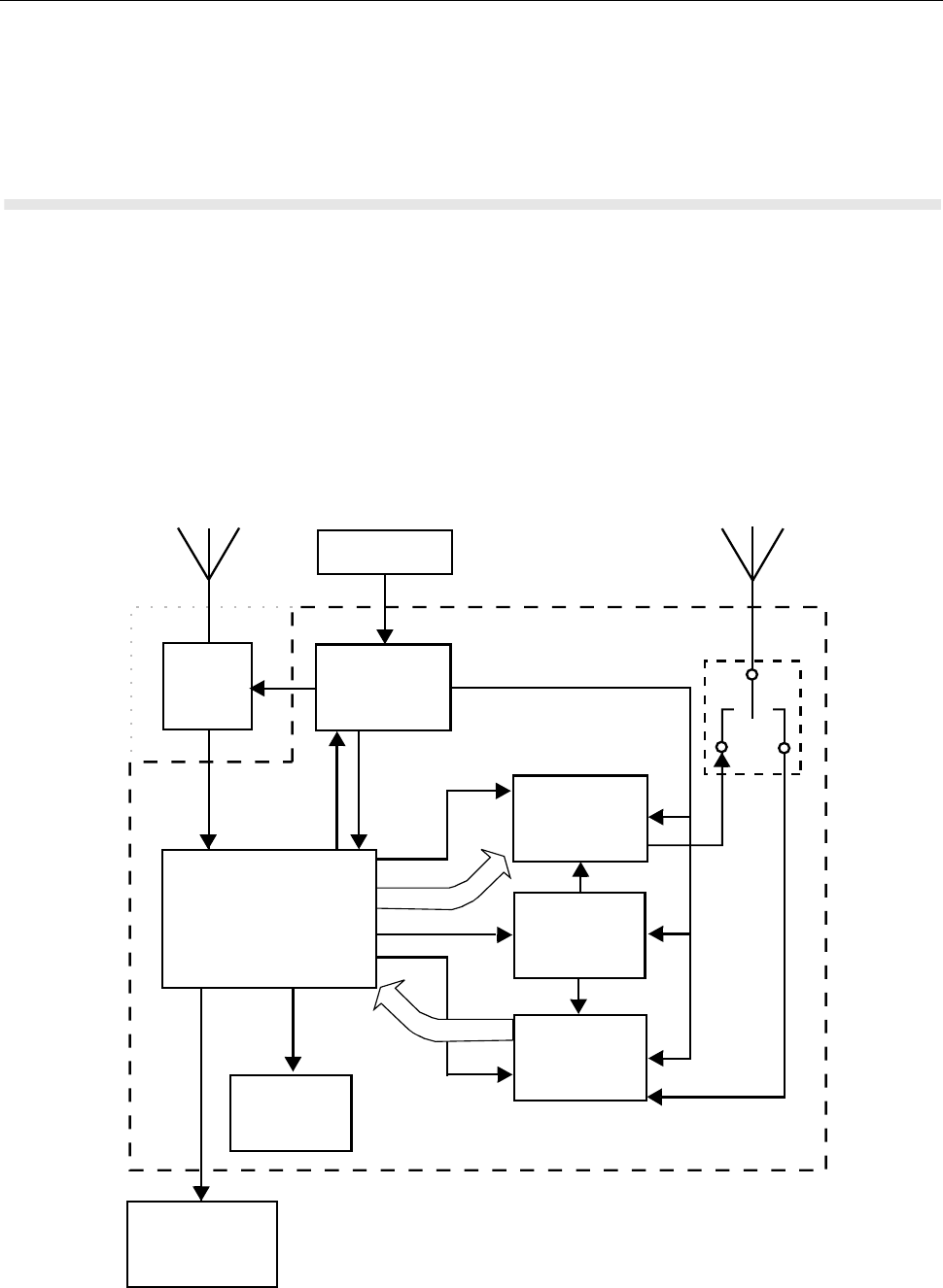
THEORY OF OPERATION (TRANSCEIVER) 4.1 - 1
CHAPTER 4.1
THEORY OF OPERATION (TRANSCEIVER)
Block Diagram and Overview
The main Digital/RF block contains the following five sections:
• Receiver Section
• Transmitter Section
• Frequency Generating Section (Synthesizer)
• Controller Section
• GPS sub module
An overview and a detailed description of these sections is provided in the following paragraphs.
Figure 4.1-1 General Block Diagram
Synthesizer
Transmitter
Receiver
Digital Block
Audio
Control Head
or
Expansion Head
MAIN BOARD
Antenna
Switch
Battery
DC Block
GPS
6866539D31.book Page 1 Tuesday, March 20, 2007 6:32 PM

4.1 - 2 THEORY OF OPERATION (TRANSCEIVER)
Receiver Section
The receiver section includes the following main components:
• Antenna Switch
• AGC_0 Attenuator
• Front End Pre-selector Filter
• Low Noise Amplifier (LNA)
• AGC_1 Attenuator
• Second Pre-selector Filter
•Mixer
• IF Filter
• IF Amplifier
• AGC_2 Attenuator and Buffer
• IF Digitizing Subsystem
The Receiver Path implements an Automatic Gain Control (AGC), which is required to maintain
good receiver linearity over a wide range of incoming signal levels and prevents clipping of high
level signals.
The IF Digitizing Subsystem performs the following functions:
• Carries out amplification and down conversion of the signal into the second IF.
• Performs IF AGC.
• Converts the second IF analog signal into baseband digital I & Q format.
• Transmits the I & Q baseband data to the DSP for further processing.
• Synthesizes the second LO frequency.
• Synthesizes the Sigma-Delta clock
• Calculates the received signal strength.
6866539D31.book Page 2 Tuesday, March 20, 2007 6:32 PM

THEORY OF OPERATION (TRANSCEIVER) 4.1 - 3
Transmitter Section
The transmitter incorporates cartesian feedback circuitry to enhance transmitter linearity to reduce
power splatter into adjacent channels. The transmitter circuitry comprises the following components:
• Modulation digital to analog conversion, performed by:
Analog-to-Digital / Digital-to-Analog IC (ADDAG),
• Modulation up-converter, performed by:
Low Noise Offset Direct Conversion Transmitter integrated circuit (JAVELIN),
• Balun and Attenuator,
• Linear class AB Power Amplifier (PA),
• Directional coupler,
• Isolator (depends on terminal model)
• Antenna switch, and
• Harmonic filter.
The transmitter linearization feedback signal is taken from the forward power port of the directional
coupler, attenuated, and passed to the RF feedback port of the JAVELIN integrated circuit.
Controller Section
This section includes the Patriot Bravo, which controls the transmit, receive and synthesize
operations of the integrated circuits located in the RF section. Within the Patriot Bravo are the DSP
and the serial interfaces.
The controller section contains the following:
• Voltage regulators
• Power On/Off circuitry
• Patriot Bravo
• Host memories (FLASH and SRAM)
• Serial peripheral interface (SPI)
• RS232, USB, SB9600, SBEP serial interfaces
• RX and TX path multiplexer
• Programmable potentiometer
•CODEC
• Audio power amplifier (PA)
6866539D31.book Page 3 Tuesday, March 20, 2007 6:32 PM

4.1 - 4 THEORY OF OPERATION (TRANSCEIVER)
Frequency Generating Section
The frequency generating section comprises the following components:
• Reference Oscillator - TCXO
• Main Synthesizer - consists of the Main Voltage Controlled Oscillator (VCO) and Low Voltage
Fractional-N integrated circuit (LVFRACN). In receive mode, the main synthesizer provides
the local oscillator injection to the receiver first mixer. In transmit mode, this synthesizer
provides the frequency reference for the transmit frequency translation loop.
• Transmit frequency translation loop. Consists of the transmit Voltage Controlled Oscillator
(VCO) and ESCORT Near Unity Divider (NUD) Phase Locked Loop IC.
GPS Section
The GPS Sub module includes the following main components:
• Front End Filter
• LNA matching network
• The Phoenix GPS Acquisition Module (PGAM)
• 26MHz Reference TCXO
• Power supply for PGAM IC
• 5V (20mA) Phantom Power Supply for external LNA
6866539D31.book Page 4 Tuesday, March 20, 2007 6:32 PM
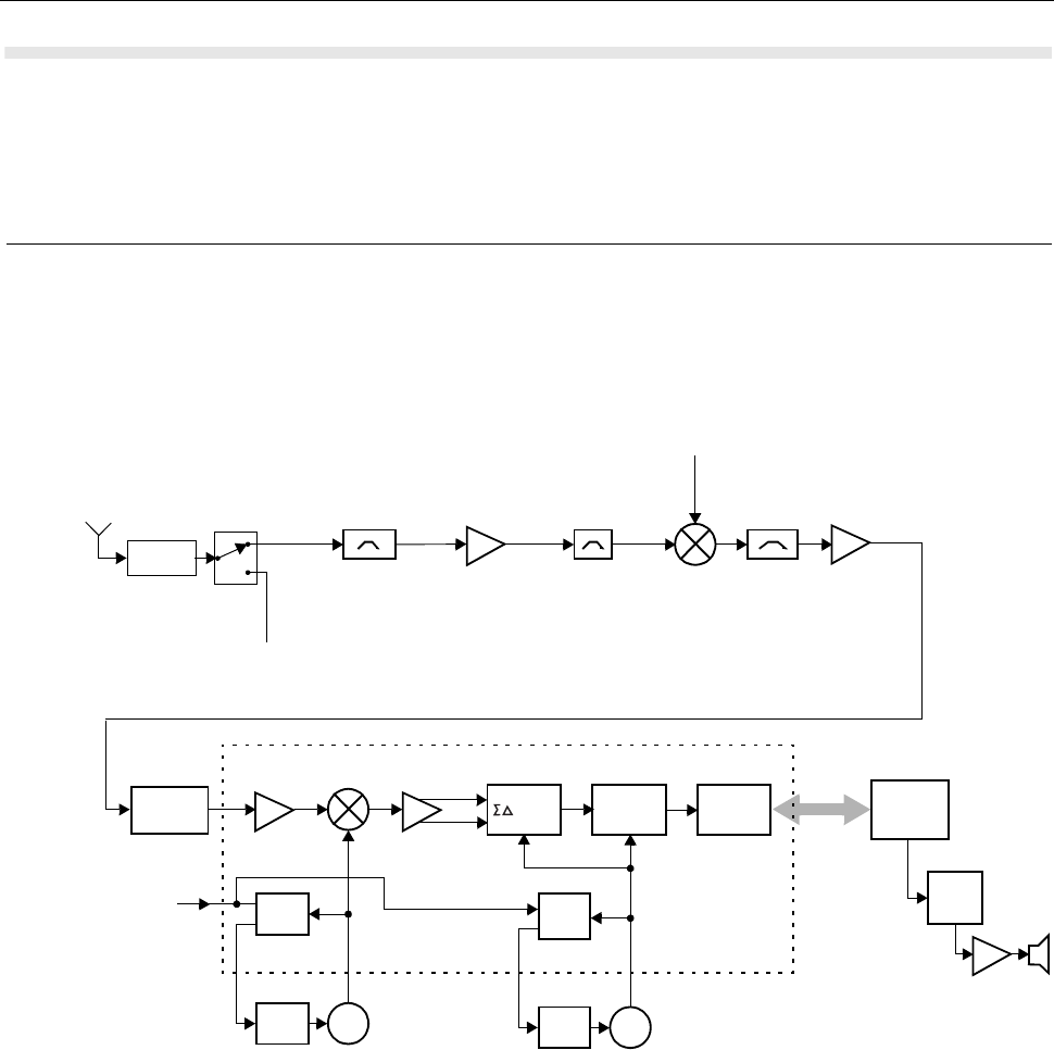
THEORY OF OPERATION (TRANSCEIVER) 4.1 - 5
Block Diagrams Descriptions
The block diagrams descriptions cover Receiver Path, Transmitter Path, Frequency Generation
Section, and Controller Section.
Receiver Path
The received signal (see figure below) from the antenna is directed by the Antenna Switch to the
Front End Pre-selector Filter.
Figure 4.1-2 Receive Path Block Diagram
The receive pre-selector filter performs the following functions:
• passes frequencies in the 851 – 870 MHz receive frequency range, and
• blocks unwanted spurious frequencies like half IF and image frequencies.
The signal is mixed with the low side injection local oscillator signal to create the first IF at 73.35
MHz. The IF signal is filtered by the crystal filter, amplified by the IF amplifier, and sent to the IF
Digitizing IC.
The IF Digitizing Subsystem performs the following functions:
• down conversion to the second IF at 2.25 MHz,
• perform a bandpass sigma-delta analog-to-digital conversion of the second IF signal into in-
phase (I) and quadrature (Q) digital signals.
Antenna
Switch
From Tx PA
DSP (Part of
Controller)
2
nd
Mixer
1
st
LO
From
FGU
LNA
2
nd
LO
ADC
Loop
Filter
Loop
Filter
2
nd
LO
PLL
Variable
Gain
Amplifier
Formatting
SSI
(BBP)
IF Digitizing
Subsystem
16.8 MHz
Reference
from FGU
Sample
Clock
PLL
Tx
Rx
Dynamic
Range
Extension
Decimation
Filter
Image
Filter Mixer 73.35 MHz
First IF Filter
IF
Amplifier
Harmonic
Filter LNA
Pre-selector
CODEC
AUDIO
PA
Sample
Clock
VCO
6866539D31.book Page 5 Tuesday, March 20, 2007 6:32 PM
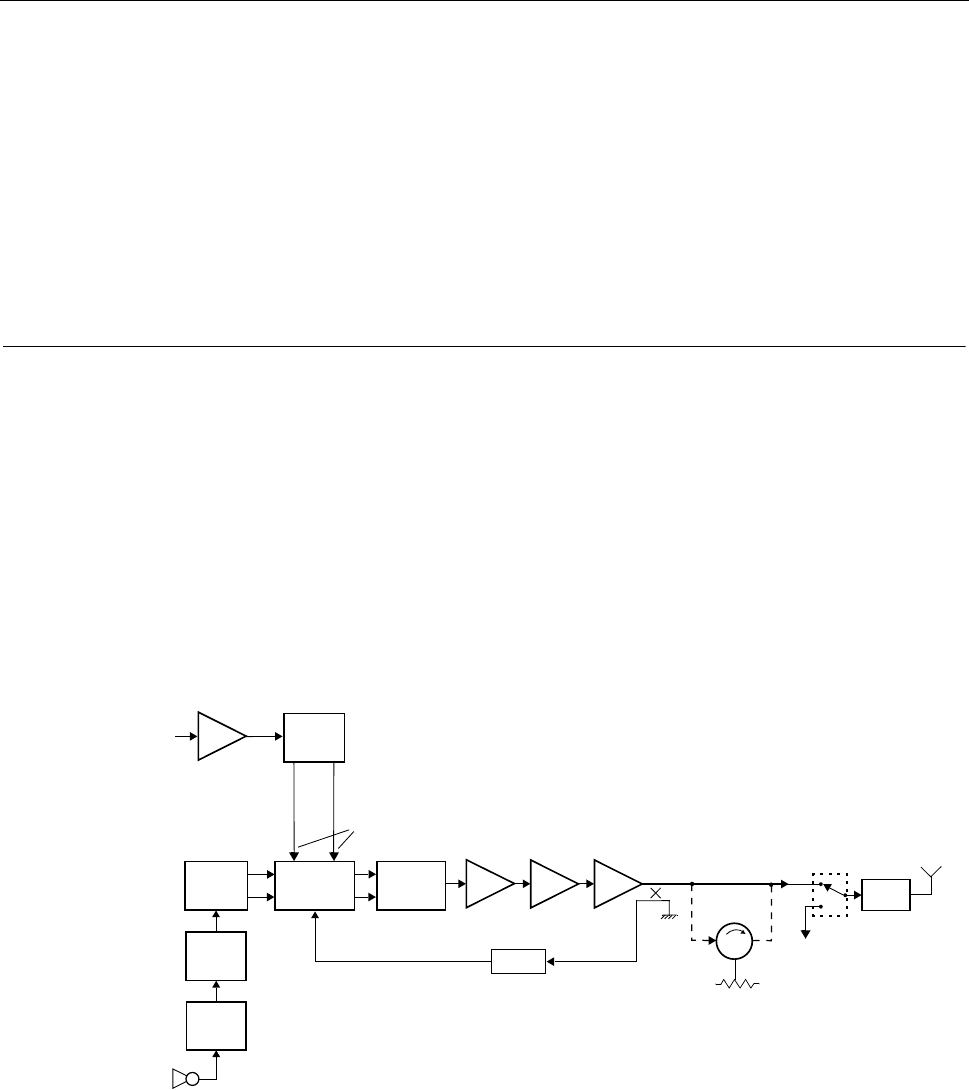
4.1 - 6 THEORY OF OPERATION (TRANSCEIVER)
• Formats the I and Q data streams into a serial bit stream, which is sent for further processing
to the Digital Signal Processor (DSP) (part of the micro controller) over the Synchronous
Serial Interface (SSI) data link.
The DSP performs the following functions:
• Base band filtering,
• Synchronisation
• Demodulation
• Forward Error Correction (FEC)
• other correction algorithms for overcoming channel errors, and
• the decoder procedure for digital speech data decompression.
Transmitter Path
When the terminal is transmitting (see figure below), microphone audio is sent to the CODEC, which
performs analog-to-digital conversion and routes the digital signal to the DSP. The DSP performs
the following functions:
•coding,
• error correction, and
• generation of the baseband modulation waveform.
From the DSP, baseband digital ‘I’ and ‘Q’ modulation waveform samples are sent to the ADDAG IC,
where the digital data is converted into baseband analog ‘I’ and ‘Q’ waveforms and filtered.
Figure 4.1-3 Transmit Path Block Diagram
The analog modulation signal is passed on to the JAVELIN where it is up-converted to the
transmitter operating frequency. The modulated RF output signal from the JAVELIN is converted
from differential to single-ended by a balun, and passed to the attenuator, pre-driver IC, driver
transistor, power amplifier transistor, directional coupler, and isolator (depends on terminal model),
from where it is routed to the antenna via the antenna switch and harmonic filter. An RF feedback
signal is taken from the directional coupler and fed back to the JAVELIN for transmitter power
control and linearization.
ADDAG JAVELIN Balun and
Attenuator
DSP
CODEC
Attenuator
Coupler
Antenna
Switch
To
Receiver
Harmonic
Filter
Tx
Rx
Isolator
(Depends
on Model)
RF Feedback
Pre-driver PA
Mic
Driver
Buffer
Tx LO
Injection
from FGU
Differential
Signal for
Up- and Down
Converter
Balun
6866539D31.book Page 6 Tuesday, March 20, 2007 6:32 PM
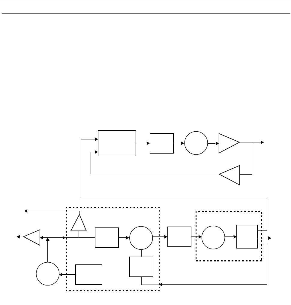
THEORY OF OPERATION (TRANSCEIVER) 4.1 - 7
Frequency Generating Section
The frequency generating section comprises the following components
(see figure below):
• 16.8 MHz TCXO Reference Oscillator.
• Main Synthesizer - consists of the Main Voltage Controlled Oscillator (VCO) and Low Voltage
Fractional-N (LVFRACN) integrated circuit PLL. In receive mode, the main synthesizer
provides the local oscillator injection to the receiver first mixer. In transmit mode, this
synthesizer provides the frequency reference for the transmit frequency translation loop.
• Transmit frequency translation loop - consists of the transmit Voltage Controlled Oscillator
(VCO) and ESCORT Near Unity Divider (NUD) Phase Locked Loop IC.
Figure 4.1-4 Frequency Generating - Block Diagram
The reference oscillator –TCXO is a temperature compensated crystal oscillator producing an
accurate and stable 16.8 MHz master clock, from which all other clocks in the terminal are derived.
It provides the reference frequency for the following components:
• the main frequency synthesizer,
• the IF Digitizing Subsystem,
• the ADDAG, and
• the micro controller
Its operating frequency is fine tuned by means of a warp voltage signal which is controlled by the
controller and generated by the LVFRACN IC
Buffer
Frequency
Translation
PLL
(ESCORT)
Loop
Filter TX
VCO
Buffer
Tx Injection
to JAVELIN
To R
x
1st L
O
Buffer
Main
VCO
Loop
Filter
Phase
Detector
Reference
Divider
Buffer
Warp DAC
16.8 MHz
TCXO
Buffer
16.8 MHz Ref. to
Controller
Prescaler
LVFRACN PLL
16.8 MHz Ref.
to IF Digitizing
Subsystem
VCO BIC
6866539D31.book Page 7 Tuesday, March 20, 2007 6:32 PM

4.1 - 8 THEORY OF OPERATION (TRANSCEIVER)
Main Synthesizer
The Main Synthesizer consists of the main VCO and LVFRACN PLL IC. The main synthesizer
provides the LO signal to the first mixer for down-converting the received signal to the 73.35 MHz
first IF frequency and in transmit mode provides the reference frequency for the ESCORT frequency
translation loop.
Transmit Frequency Translation Loop
The transmitter frequency translation loop consists of the transmit VCO and ESCORT near unity
divider PLL IC. This subsystem generates the carrier frequency injection signal for the JAVELIN.
6866539D31.book Page 8 Tuesday, March 20, 2007 6:32 PM
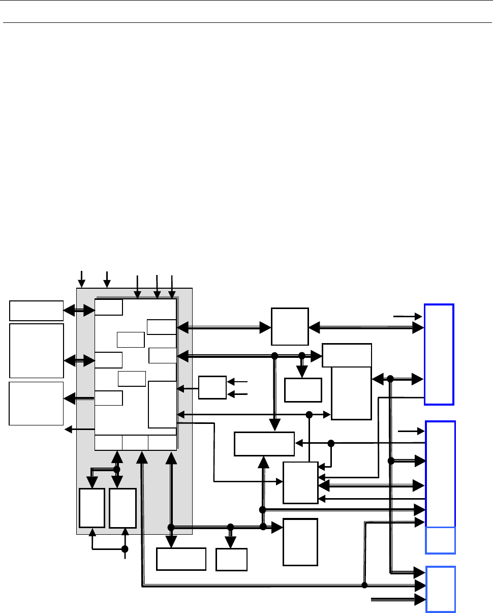
THEORY OF OPERATION (TRANSCEIVER) 4.1 - 9
Controller Section
The controller section contains the Patriot Bravo dual core (DSP / RISC) processor and its external
memory, the TX and RX audio processing, the serial interfaces and I/O circuitry.
The Patriot Bravo controls the receive / transmit frequencies, power levels, Enhanced Control Head
display and keypad, serial interfaces, accessories, MMI, and other terminal functions. This
microprocessor can be operated through the RS232 interface by a personal computer to program
the FLASH.
The TX audio circuitry selects between the different microphone inputs, controls the TX audio level
and converts the analog audio signal to a digital format.
The RX audio circuitry converts the received signal from digital format to an analog audio signal,
performs volume control and amplifies the signal to speaker level.
The DSP performs signalling, and voice encoding and decoding.
Figure 4.1-5 Controller Block Diagram
ABACUS III
ADDAG
ABACUS III
ADDAG
JAVELIN
LVFRACN
ESCORT
PCIC
ADDAG_TXE
AGC_0_FE
AGC_1_FE
AGC_2_IF
LO2 ON
Switched
by internal
Patriot
register
(GPCR
)
BBP
SAP
SPIA
SPIB
UARTB
UARTA
GPIO
EIM
MCU
DSP
L1T
SRAM
4 M Byt
e
1.8V
Option Slot
24-PIN (GPS)
FLASH
16 M Byte
RESET_OUT
RESET_JAV_ADDAG
RESET_ABACUS
GPS_RESET
3V0
CODEC
MC145483
Audio
MUX
/E2POT
AF-PA
Option Slot
40 pin (UCM)
J0550
12
pin
J0400
16
+
4 pin
Mic
ON_OFF_
CTRL
Front
Rear
Level
shifter
& buffer
Level
shifter
& buffer
Mux control / PA enable
SB9600 / JTAG / RS232 / USB
SBEP
A+
SW B+
5V
Mic+RXaudio,
Speaker audio
Key fail / flash
SPIB
SW B+
On/Off
SAP
Soft turn off
On/Off Ctrl
Emergency
Ext. Alarm
Ext. PTT
Ignition
Mic
J0500
40
pin
Front
18 pin FLEX
connection
board
J0570
J0450
S
AP
J0600
4 wire
CESG
Memory
Ignition / Emergeny
8 wire
I/O
PWM
ADC
Battery Voltage
PA Temp
RTC
1.8V
16.8MHz 32.768kHz 1.55V
PATRIOT
6866539D31.book Page 9 Tuesday, March 20, 2007 6:32 PM

4.1 - 10 THEORY OF OPERATION (TRANSCEIVER)
Detailed Circuit Description
Receiver Path, Detailed Circuit Description
For the Receive Path Block Diagram see Figure 4.1-2 on page 4.1-5.
Antenna Switch
The signal coming from the antenna is routed to the receiver section via the harmonic filter, which is
comprised of L5461, L5462, C5461, C5462, C5464 and C5466. The signal continues to flow
through quarter wave transformer L5452 and C5555 to the RX section toward pre-selector filter. The
limiter (D5002) function is to prevent entrance of signals with power higher than 30dBm, which may
damage the receiver front-end.
Pre Selector Filter
The signal is passed to the first pre-selector filter (FL5002) and from there routed to Low Noise
Amplifier (LNA) (U5003). The first pre-selector filter attenuates incoming spurious RF frequencies,
especially the image frequency
LNA
The Low noise amplifier (LNA) U5003 amplifies the incoming received signal. It maintains a large
gain and small Noise Figure. When LNA "enable" (pin 3, VPD) receives a supply of 1.9 V from DC
switch (Q5002), the amplifier is enabled. From the LNA the signal passes to the second pre-selector
filter (FL5001).
Second Pre-selector
The second pre-selector filter (FL5001) provides further attenuation of incoming image and half-IF
spurious response signals, as well as noise at the image frequency that may be generated by the
LNA. From the output of the second pre-selector filter the received signal is sent to the RF input port
of the first mixer.
Mixer
Mixer U5002 down-converts the incoming RF signal to the 73.35 MHz first IF, utilizing a first local
oscillator signal tuned 73.35 MHz below the desired receiver operating frequency. An impedance
matching network (L5012, C5037, C5036, L5201, C5203, L5011, L5018) is placed between the
mixer output and IF filter U5201.
6866539D31.book Page 10 Tuesday, March 20, 2007 6:32 PM

THEORY OF OPERATION (TRANSCEIVER) 4.1 - 11
IF Filter, Amplifier, Dynamic Range Extension
The IF signal is routed via IF filter (FL5201) to IF amplifier Q5201. From there it is routed to the
Dynamic Range Extension circuitry which comprises Q5101, its bias components, and D5121. This
circuitry is required to maintain good receiver linearity over a wide range of incoming signal levels,
and prevent clipping of high level signals. This circuit avoids the use of fixed switchable attenuators
typically used in Automatic Gain Control (AGC) circuits.
IF Digitizing Subsystem
The IF Digitizing Subsystem is comprised of U5101. Here the IF signal is amplified and then mixed
with an internally generated 2nd LO signal to produce the second IF signal.
The 2nd IF signal is first processed by a variable gain amplifier and then converted to in-phase and
quadrature (I and Q) digital data samples by means of a bandpass sigma-delta analog-to-digital
converter.
The I and Q digital signals are formatted into a single serial bit stream and sent for further
processing to the Digital Signal Processor (DSP) (part of micro-processor) over the Synchronous
Serial Interface (SSI) data link.
An internal AGC circuit controls the gain of the variable gain amplifier (VGA) to ensure that the
maximum signal level into the ADC does not exceed a fixed analog ADC clip level and the rms
output level of the ADC is maintained at an established reference level.
An internal phase locked loop control circuit controls the frequency of voltage controlled oscillator
Q5180 which generates the 71.1 MHz 2nd LO injection frequency.
An internal phase locked loop control circuit controls the frequency of voltage controlled oscillator
Q5190 which generates the 18MHz sample clock frequency utilized by the ADC and decimation
filters.
Both phase locked loops derive their frequency reference from the buffered 16.8 MHz TCXO master
clock.
6866539D31.book Page 11 Tuesday, March 20, 2007 6:32 PM

4.1 - 12 THEORY OF OPERATION (TRANSCEIVER)
Transmitter Path, Detailed Circuit Description
For the Transmit Path Block Diagram see Figure 4.1-3 on page 4.1-6.
ADDAG
The Analog to Digital/Digital to Analog IC U5810 (ADDAG) receives the modulation waveform as
serial data transmitted by the DSP at a 48 kbps rate to the SSI port (ball C7, STD). Data is
transmitted as a 16-bit 'I' word followed by a 16-bit 'Q' word. The ADDAG provides a serial clock of
2.4MHz to the DSP (ball B6, SCK) and sends a frame sync signal (ball B7, SFS) at the beginning of
every 'I' word transmission, to instruct the DSP to send data.
In the ADDAG, the received serial I & Q words are converted into parallel I & Q words, and
transferred to an interpolation filter. The interpolation filter increases the sampling rate to reduce in-
band quantization noise, as well as to reduce image at multiples of the input data. The interpolated
samples are rounded to 8 bits, and run through 8-bit D/A converters.
The D/A converters take the digital I & Q words and convert them into analog signals, which are
filtered and amplified. The output is comprised of two separate low-level differential signals, I & Q
(ball E2, OUT1; ball E1, OUT1B; ball D1, OUTQ; ball C1, OUTQB). The output signals are routed to
the JAVELIN IC for up conversion to the transmitter operating frequency. They are also available on
R5841, R5842, R5843 and R5844. The ADDAG sends a 2.4MHz low-level differential reference
clock signal (ball C2, TCLK; ball B1, TCLKB) to the JAVELIN.
It also sends a differential signal (ball A1, TSLOT; ball B2, TSLOTB) that marks the beginning and
end of each transmission slot (whenever a TXE signal {ball B5 TXE} is received from the DSP). After
receiving the TSLOT signal, the JAVELIN toggles the ASW line (ball F2, ASW) which signals the
ADDAG to set VCNTO signal LOW (ball F2, VCNTO) which enables the Antenna Switch during the
transmit slot. The ADDAG starts to receive data from DSP after TXE signal (ball B5, TXE).
Tx LO
The Tx LO signal path processes the signal generated by the Transmit Frequency Translation Loop
(part of the FGU), which determines the operating frequency of the transmitter. The input signal is
amplified by Q5801, and passed to the Balun T5801 which provides the differential signal to the
JAVELIN LO input (balls H5, VCO1 and H6, VCO1B. Internally to the JAVELIN the signal is routed to
the feedback down conversion circuitry and to a 90 degree phase shifter, that provides the I and Q
vectors for up conversion.
JAVELIN
The Low Noise Offset Direct Conversion Transmitter (JAVELIN) U5809 performs the following tasks:
• up converts the baseband I and Q modulation waveform to the transmitter operating
frequency,
• controls power output, and
• cancels power amplifier distortion products created by non-linearities in the RF power
amplifier output stage.
The differential base-band signals from the ADDAG are input into the JAVELIN on balls C1, B1, C3,
B2 (BINQB, BINQ, BINIB and BINI). The baseband I and Q waveforms are passed through a
6866539D31.book Page 12 Tuesday, March 20, 2007 6:32 PM

THEORY OF OPERATION (TRANSCEIVER) 4.1 - 13
variable attenuator and then they are summed with the down-converted I & Q feedback signal. The
base-band signal is then amplified and sent to the up-mixer. The up-mixer consists of two mixers,
one for the I channel and the other for the Q channel.
The split I & Q LO signal is mixed with the base-band I & Q signals to produce an I and Q modulated
signal at RF frequency. The signal is then output differentially on balls E8 and D8 (RFOUT2B,
RFOUT2), where the differential RF signal is converted to a single-ended unbalanced output by
means of BALUN T5802. The output signal from the BALUN is applied to the RF Power Amplifier.
RF Power Amplifier
The RF Power Amplifier consists of attenuator R5413, R5414, R5415, pre-driver IC U5401, driver
transistor Q5421, and output transistor Q5431. The overall RF gain of the power amplifier string is
fine tuned by the BIAS1 voltage from the controller, which is applied to VCNTRL pin 1 on pre- driver
U5401. The BIAS1 signal is buffered by amplifier Q5501. The operating bias point of driver Q5421
and PA Q5431 is set by BIAS2 and BIAS3 respectively, buffered by Q5521 and Q5542.
Directional Coupler and RF Feedback Path
A directional coupler exists at the RF PA output, and is used to pass the signal to the Antenna
Switch via the isolator FL 5451 and to sample the signal thus providing the necessary feedback for
the linearization and feedback correction. The sampled signal is routed via attenuator R5453,
R5454, R5455 and the BALUN L5812 to the JAVELIN (ball D1, RFIN, ball E1, RFINB). Internally to
the JAVELIN, the RF feedback signal is mixed down to base-band in a quadrature down mixer, and
summed with the base-band input signal to provide cancellation of modulation distortion generated
in the power amplifier.
Antenna Switch
The RF signal from the Directional Coupler is applied to PIN diode D5451. This PIN diode is turned
on during the transmission time slot, to route the transmitter output signal to the harmonic filter
(C5455-C5457,C5461-C6467, L5461, and L5462), and from there on to the antenna connector.
During the transmit time slot, pin diode D5551 is also turned on, preventing power from the
transmitter from reaching the receiver LNA. During receive time slots, PIN diodes D5451 and D5551
are OFF, allowing receive signals to pass from the antenna connector through the harmonic filter,
through L5452, and on to the receiver input preselector.
Harmonic Filter
From the antenna switch the signal is routed to the harmonic filter, consisting of C5455-C5457,
C5461-6467, L5461, and L5462. The filter is required to attenuate transmitter harmonics during
transmit mode, and leakage of local oscillator harmonics during receive mode.
6866539D31.book Page 13 Tuesday, March 20, 2007 6:32 PM

4.1 - 14 THEORY OF OPERATION (TRANSCEIVER)
Frequency Generating Section Detailed Circuit Description
For the Frequency Generating Section Block Diagram see Figure 4.1-4 on page 4.1-7.
This section describes the generating circuits that supply all the required frequencies for the
required transmitter and receiver functions. These circuits are described as follows:
• 16.8 MHz Reference Oscillator - TCXO.
• Main VCO and Main Synthesizer.
• Transmit frequency translation loop.
Reference Oscillator - TCXO
16.8 MHz TCXO (Y5363) is a temperature compensated crystal oscillator producing an accurate
and stable 16.8 MHz master clock to the terminal RF circuits. Its operating frequency is fine tuned by
means of a warp voltage signal generated by the LVFRACN IC (U5331, pin 25). On terminal power-
up, an initial warp voltage setting is programmed into the LVFRACN IC by the microprocessor via
the SPI bus, using a stored value programmed into the terminal codeplug during factory tuning.
While the receiver is registered to the terminal system, an automatic frequency control algorithm is
executed by the microprocessor, to fine tune the LVFRACN warp voltage to bring the TCXO
frequency into alignment with the terminal system frequency standard.
The output signal at pin 3 of the TCXO is passed to LVFRACN IC U5331, where it is used as a
reference for the main frequency synthesizer. The TCXO output is also buffered by Q5351, and
passed to other terminal circuits via REF16_8_OSC. The LVFRACN IC buffers the 16.8 MHz
reference, and provides it at FREFOUT (pin 41) for use by other terminal circuits.
Main VCO and Main Synthesizer
The synthesizer components are LVFRACN, Loop Filter, VCO and VCO Buffer IC (VCO BIC). It
produces the receiver first LO signal, as well as serving as the reference for the transmit frequency
translation loop.
The operating frequency of Voltage Controlled Oscillator (VCO) with active element Q5712 is
determined by resonator W5701, in conjunction with C5735, C5737, C5738, C5736, L5733, and
varactors D5731-5734. The operating frequency of the oscillator is varied by means of varactor
tuning voltage VCTRL, supplied by the LVFRACN U5331 IOUT signal (pin 43), and filtered by loop
filter components C5303, R5304, C5305, R5303, R5302, and C5301. The RF output of the VCO is
buffered by U5701
U5701 pin 12 provides a sample of the VCO output to the LVFRACN prescaler input (pin 32), where
the signal is divided down to a lower comparison frequency by means of a programmable frequency
divider. The divided down VCO signal is compared to a signal derived from the 16.8 MHz reference
clock to generate an error signal (IOUT) which is filtered by the loop filter and tunes the VCO to the
programmed operating frequency.
A LOCK_FN signal is available at LVFRACN pin 4 to provide feedback to the microprocessor that
the synthesizer has successfully locked to the programmed frequency.The “RX_OUT” signal from
buffer U5701 pin 8 is amplified by Q5701, and supplied to the first mixer LO port.
The “TX_OUT” signal from buffer U5701 pin 10 provides the frequency reference for the Transmit
Frequency Translation Loop.
6866539D31.book Page 14 Tuesday, March 20, 2007 6:32 PM

THEORY OF OPERATION (TRANSCEIVER) 4.1 - 15
Transmit Frequency Translation Loop
The Transmit Frequency Translation Loop comprises the following components:
• transmit Voltage Controlled Oscillator (VCO) and
• the ESCORT Near Unity Divider (NUD) Phase Locked Loop IC.
The operating frequency of Voltage Controlled Oscillator with active element Q5601 is determined
by resonator W5601 in conjunction with C5603, C5604, C5606, C5607, L5603, and varactors
D5601-5604. The operating frequency of the oscillator is varied by means of a tuning voltage
applied to the varactors.
The translation loop works as follows:
• A sample of the VCO operating frequency is buffered by Q5631 and applied to the FREQA
input of the NUD IC U5702 pin 16 , where it is divided by a programmable divider set to
1.0625, and phase compared to a reference frequency supplied to U5702 FREQB pin 9 from
the main synthesizer
• The result of this comparison is a VCO tuning signal, buffered by charge pump transistors
Q5604, Q5605, and Q5653, filtered by loop filter components C5653, R5652, C5654, C5655,
and L5607and applied to the VCO varactors.
• The action of the feedback loop is to maintain the operating frequency of the Transmit VCO at
1.0625 times the programmed operating frequency of the main synthesizer.
• The loop bandwidth of the transmit frequency translation loop is set to a high value in order for
the corrective feedback action of the loop to suppress re-modulation of the VCO as a result of
leakage of the modulated transmitter signal from the transmitter Power Amplifier output back
into the VCO.
6866539D31.book Page 15 Tuesday, March 20, 2007 6:32 PM
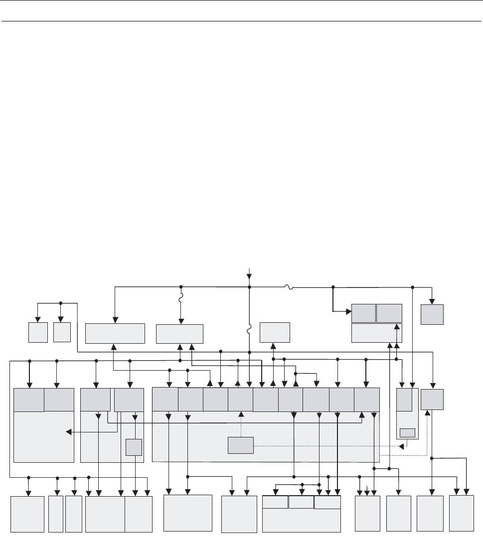
4.1 - 16 THEORY OF OPERATION (TRANSCEIVER)
Controller Section
For the Controller Section Block Diagram see Figure 4.1-5 on page 4.1-9.
This section describes the related circuits as follows:
• DC Power Distribution and RESET
• Microprocessor and Host Memories
• SPI
•RS232/USB
• Terminal Audio System
•RTC
•GPS
• SIM card connectivity
•GPIOs
DC Power Distribution
Figure 4.1-6 DC Power Distribution Diagram
DC Power Input
The DC power of nominal 13.2 volts enters the terminal at connector J0301. Diode VR0300 acts as
protection against transients and wrong polarity of the supply voltage. The supply voltage is fed
directly to the RF PA, through the 3A fuse F0303 to the audio circuitry, through F0302 to the
expansion head and Enhanced Control Head, and through the 4A PCB fuse (F0301) to regulators
U0300, U0301, U0302, and the ON/OFF and VSTBY circuitry. The fuses protect the board from over
current in case of a short on the connector pins or circuit failure.
ABACUS
FracN
Expansion
Head
Controller
RF PA Audio I/O
VCOBIC
RX-VCO
FE + Mixer IF
PATRIOT
FLASH
RAM
ADDAG
TX
Accessory
Connector
20-PI N
13,2V
A+
4.6V
VSF
5V
9,3V
9.3V
9.3V
Escort
TX-VCO
3V_DIG
Head D
5V
Regulator
LP2 951
Option
JAVELIN
3V_TX
U0307
MC33275
5V_TX
U0304
LP2951C
1.55 V
U0306
LP2 951 C
ON/OFF
Circuit
SW B+
U0302
LM2941
9.3V_TX
U0300
LM2941
3.3V_FN
U5321
LP2980
5V_FN
U5322
ADP3300
Digital_3.3V
U5103
LP2980
Analog_3.3V
U5102
LP2980
Ref.
Voltage
9.3V
U0301
LM2941
SW B+
3V_TX
3.3V_DIG
3 V
Regulator
LP2951
SW B+
Regulator
LP2941
5VD
U0303
78M05
9.3V
ON / OF F
9.3V_TX
13,2V
5V_TX
RTC VSTBY
PC I C
3V_DIG
Fuse
F0303
Fuse
F0301
1.8 V
U1105
LP2985
3.3V_DIG
U0305
LP2 951 C
UCM
Option
GPS
Option
ON / OFF
Fuse
F0302
Q0305
9.3V
6866539D31.book Page 16 Tuesday, March 20, 2007 6:32 PM

THEORY OF OPERATION (TRANSCEIVER) 4.1 - 17
9V3 Linear Regulator U0301
Regulator U0301 is connected to the 13.2 volts supply voltage via PCB fuse. The output of this
regulator is controlled by the ON/OFF circuitry. When any of the signals RTC_ON_SW,
ON_OFF_CONTROL_SV, SOFT_TURN_OFF, IGNITION is at high level or EMERGENCY is at low
level the regulator is switched on via transistors Q0302, Q0301, Q0303. In addition, regulators
U0300 and U0302 are also switched on by the same signal. The output voltage of U0301 is set to
9.3 volts with resistors R0307 and R0308.
9V3_TX Linear Regulator U0300
Regulator U0300 is connected to the 13.2 volts supply voltage via PCB fuse. The output of this
regulator is controlled by the ON/OFF circuitry. When any of the signals RTC_ON_SW,
ON_OFF_CONTROL_SV, SOFT_TURN_OFF, IGNITION is at high level or EMERGENCY is at low
level the regulator is switched on via transistors Q0302, Q0301, Q0303. The output voltage of
U0300 is set to 9.3 volts with resistors R0305 and R0306.
SW B+ Current Limit Regulator U0302
Regulator U0302 is connected to the 13.2 volts supply voltage via PCB fuse. The output of this
regulator is controlled by the ON/OFF circuitry. When any of the signals RTC_ON_SW,
ON_OFF_CONTROL_SV, SOFT_TURN_OFF, IGNITION is at high level or EMERGENCY is at low
level the regulator is switched on via transistors Q0302, Q0301, Q0303. The output voltage of
U0302 is set far above the maximum possible input voltage with resistors R0303 and R0304 so that
this regulator acts as a current limiter for the EXT_SWB+ voltage on the 20 pin accessory connector.
5VD Linear Regulator U0303
Regulator U0303 gets its input voltage from the 9.3 volt regulator U0301. The output voltage 5VD is
fixed to 5 volts and is the input voltage for the regulators U0305 and U0306. The voltage 5VD is also
fed to the Enhanced Control Head.
5V_FN Linear Regulator U5322
Regulator U5322 gets its input voltage from the 9.3 volt regulator U0301. The output voltage 5V_FN
is fixed to 5 volts and is mainly used in the frequency generating unit (FGU).
3V3_FN Linear Regulator U5321
Regulator U5321 gets its input voltage from the 9.3 volt regulator U0301. The output voltage
3V3_FN is fixed to 3.3 volts and is mainly used in the frequency generating unit (FGU).
Analog_3V3 Linear Regulator U5102
Regulator U5102 gets its input voltage from the 9.3 volt regulator U0301. The output voltage
ANALOG_3V3 is fixed to 3.3 volts and is mainly used in the receiver section.
Digital_3V3 Linear Regulator U5103
Regulator U5103 gets its input voltage from the 9.3 volt regulator U0301. The output voltage
DIGITAL_3V3 is fixed to 3.3 volts and is mainly used in the receiver section.
3V_TX Linear Regulator U0307
Regulator U0307 gets its input voltage from the 9.3 volt regulator U0300. The output voltage 3V_TX
is fixed to 3 volts and is used in the transmitter TX_LOW section to supply the ADDAG and JAVELIN
IC.
6866539D31.book Page 17 Tuesday, March 20, 2007 6:32 PM

4.1 - 18 THEORY OF OPERATION (TRANSCEIVER)
5V_TX Linear Regulator U0304
Regulator U0304 gets its input voltage from the 9.3 volt regulator U0300. The output voltage 5V_TX
is fixed to 5 volts and is mainly used in the transmitter section.
3V3_DIG Voltage Follower Q0305
Transistor Q0305 is configured as voltage follower and gets its input voltage from the 5 volt regulator
U0303. The output voltage 3V3_DIG is set to 3.3 volts by the reference voltage 3V3_FN from
U5321. Diode D0303 compensates the base to emitter voltage drop of Q0305. The voltage is used
as supply voltage for modules connected to J0570.
3V_DIG Linear Regulator U0305
Regulator U0305 gets its input voltage from the 5 volt regulator U0303. The output voltage is fixed to
3 volts and is mainly used in the controller section to supply the I/O voltage.
1.55 V Linear Regulator U0306
Regulator U0306 gets its input voltage from the 5 volt regulator U0303. The output voltage is set to
1.55 volts with resistors R0318 and R0319 and is used in the controller section for supplying the
Patriot Bravo core.
1.8 V Linear Regulator U1105
Regulator U1105 gets its input voltage from the 3 volt regulator U0305. The output voltage is 1.8
volts and is used in the controller section for supplying the address and data bus voltage of the
patriot Bravo and for supplying the Flash and RAM memory.
4.6V VSF Voltage
The fractional N synthesizer U5331 creates the 4.6 volts super filter voltage (VSF). This voltage is
used for the main VCO.
RESET
The open drain Error outputs of the regulators U0304 (5V_TX), U0305 (3V_DIG), U0306 (1V55) as
well as the 2.8V voltage sense IC U0308 are connected together to create the LV_DETECT signal
which is the RESET_IN signal of Patriot Bravo. Furthermore the circuitry Q0341, Q0342, R0341,
R0342, R0343 generates a reset when a programming cable is disconnected from the terminal. The
reset sources share the pull up resistor R0344
Microprocessor
The Patriot Bravo dual core (DSP / RISC) processor (U1100, block 1 to 5) controls the terminal
hardware, communicates via various interfaces with external equipment or accessories and
performs digital signal processing. Beside its internal memory the Patriot Bravo uses the FLASH
Memory and the SRAM also located near to the controller. The Patriot Bravo exchanges digitized
audio data with the CODEC via its Serial Audio Port (SAP). The Patriot Bravo sends digital
baseband data to the ADDAG and receives digital baseband data from the ABACUS via its
Baseband Port (BBP). To communicate with the RF IC's the Patriot Bravo uses one of its Queued
Serial Peripheral Interfaces - the (QSPIA). A second interface, QSPIB, is used for communication
with external equipment or accessories. The Patriot Bravo has 2 universal asynchronous receiver /
transmitter ports (UARTA and UARTB) for communication with external equipment e.g. a Enhanced
Control Head or a control terminal (PC). UARTA communicates via SB9600, RS232 or USB protocol
and UARTB communicates via SBEP protocol.
6866539D31.book Page 18 Tuesday, March 20, 2007 6:32 PM

THEORY OF OPERATION (TRANSCEIVER) 4.1 - 19
Host Memories
Flash Memory
The 16MByte FLASH Memory (U1102) located near to the micro-controller contains the terminal's
Application Software and the Terminal Code Plug. The Code Plug stores customer related
information and terminal parameters. The Patriot Bravo accesses the data via a 24 bit wide address
bus (A0-A23), a 16 bit wide data bus (DQ0-DQ15), and 8 control lines (EN_CE, EN_OE, EN_WE,
ADV, BURSTCLK, WP, VPP and RESET). When the FLASH Memory has been replaced or the
software needs to be upgraded, the new Code Plug and application software must be programmed
into the FLASH Memory.
SRAM Memory
The 4MByte SRAM (U1103) located near to the micro controller stores data that can change very
frequently, and which is generated and stored by the Application Software during its normal
operation. The information is lost when the terminal is turned off. The Patriot Bravo accesses the
data via a 21 bit wide address bus (A0-A20), a 16 bit wide data bus (IO1-IO16), and 6 control lines
(CS1, CS2, EN_OE, EN_WE, LB, UB).
EEPROM
On the terminal mainboard, an additional 128 kbit serial memory is connected to the SAP interface
of the Patriot Bravo. This EEPROM holds encryption keys and is accessed by the DSP.
Serial Peripheral Interface (SPI)
The Patriot Bravo features two SPI interfaces.
The SPI protocol is used to communicate with the RF IC's ABACUS, ADDAG, JAVELIN, LVFRACN,
ESCORT and PCIC. All these IC's are connected to the Patriot Bravo's QSPIA module. The
interface comprises the lines SPIA_MOSI (TX), SPIA_MISO (RX), SPIA_CS's, and SPIA_CLK. The
SPI bus is a synchronous bus, the timing clock signal CLK is sent while SPI data is transferred.
Therefore, whenever there is activity on either MOSI or MISO, there should be a uniform signal on
CLK.
The Patriot Bravo uses its module QSPIB to communicate with the real time clock (RTC) U0100, the
external UART in the expansion head via the 40 pin connector J0500 and the GPS module via the
24 pin connector J0600.
RS232, USB, SB9600, SBEP Serial Interfaces
The Patriot Bravo uses four serial protocols to communicate with external devices: RS232, USB,
SB9600 and SBEP. The interface lines are available on the rear or front connectors, dependent on
the interface. Not all interfaces can be used at the same time.
SBEP Serial Interface
The Patriot Bravo communicates with the Enhanced Control Head via the SBEP serial interface.
This interface comprises line BUS+ and is available on the 12 pin front connector J0550. Op-amps
U0102-1 and U0102-2 perform buffering and level shifting from 3 volts to 5 volts level. The Patriot
Bravo uses its UARTB for the SBEP serial interface.
6866539D31.book Page 19 Tuesday, March 20, 2007 6:32 PM

4.1 - 20 THEORY OF OPERATION (TRANSCEIVER)
RS232 and SB9600 Serial Interfaces
The configuration of the RS232 and SB9600 serial interfaces depends on the terminal setup. If no
expansion head is connected to the terminal, Patriot Bravo module UARTA provides either a 4-wire
RS232 or an SB9600 interface on the 20 pin accessory connector J0400.
If at power up pin BUSY_OUT on the accessory connector J0400 is connected to pin BUSY_IN, the
Patriot Bravo assumes that SB9600 equipment is connected and configures UARTA for the SB9600
interface. If both pins are not connected to each other at power up, the UARTA will be configured for
RS232 interface. The interface comprises lines RS232_TX, RS232_RX, RS232_CTS, RS232_RTS.
These lines are not buffered and at 0 or 3 volts level.
USB
The terminal is a 1.1 USB device with 12Mb/s. The interface comprises lines RS232_TX,
RS232_RX and RS232_RTS. When a USB cable is connected to the terminal via JB the USB
supply voltage is detected on line RS232_RTS and transferred to the controller via signal USB_INT.
The controller chooses between RS232 and USB interface via the signal USB_RS232 and switches
the IC U0408. When the USB mode is used, the signal line RS232_TX is switched to USB D+ and
the RX signal to D-. The USB signals are driven by the driver IC U0405. The RS232 lines to
expansion head are then disconnected to eliminate the influence of stub lines.
Note
When an expansion head is connected to the terminal, the serial interfaces on the 20 pin accessory
connector J0400 can not be used.
The UARTA is configured for an 8-wire RS232 interface, which is available on the 9 pin connector of
the expansion head. This interface has standard RS232 levels and can be connected to an external
data terminal.
In addition, the Patriot Bravo configures its QSPIB module to provide either a 4-wire RS232 or
SB9600 interface with 5 volts level on the 25 pin expansion head connector. If line MUX_CTRL_1 is
at 0 volt, the interface is switched to RS232 mode.
When the MUX_CTRL_1 line is at 3 volts, the interface is switched to SB9600 mode. The interface
comprises lines BUSY_IN, BUSY_OUT, RESET_OUT, and the QSPIB lines SPIB_MOSI,
SPIB_MISO, SPIB_CLK, SPIB_CS1_UART and is available on the 40 pin front connector J0500
with signals at 3 volts high level.
The Patriot Bravo uses the SB9600 interface to communicate with the motorcycle Enhanced Control
Head. If no motorcycle Enhanced Control Head is connected, the interface can be used to control
the terminal via the SB9600 protocol with an external control terminal.
6866539D31.book Page 20 Tuesday, March 20, 2007 6:32 PM
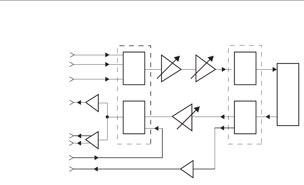
THEORY OF OPERATION (TRANSCEIVER) 4.1 - 21
Terminal Audio System
Figure 4.1-7 Audio Block Diagram
The Audio system consists of the following components:
• RX and TX path multiplexer
• RX and TX programmable potentiometer
•CODEC
•DSP
•Audio PA
TX Path
The speech audio is fed to the internal microphone input (INT_MIC), the external microphone input
(EXT_MIC) or the TX audio input (TX_AUDIO). The internal and external microphone inputs have a
DC bias prepared for connecting a microphone.
The TX audio input has a DC blocking capacitor. Multiplexer U0201 selects one of the possible
inputs and feeds the signal to amplifier U206-4. The gain of this amplifier is switchable via gate
U0202.
The programmable potentiometer U0203 attenuates the signal according to the terminal mode of
operation. Finally, the CODEC FL0200 converts the analog signal into digital format and transfers it
to the DSP via the serial audio port (SAP).
The DSP performs the functions of audio filtering, ACELP speech compression, digital modulation,
and transfers the data to the RF section. When the terminal is operating in the telephone
interconnect mode, the DSP performs the required tasks such as echo and noise reduction.
DSP
A/D
A/D
U0203
U0204
U0206-4
U0202
U0201
U0206-2
U0205
External Mic
I
nternal Mic
Tx Audio
H
andset
A
udio
S
peaker +
S
peaker -
FL0200
MUX
MUX
S
P Audio
R
X Audio
Audio PA
U0206-1
6866539D31.book Page 21 Tuesday, March 20, 2007 6:32 PM

4.1 - 22 THEORY OF OPERATION (TRANSCEIVER)
RX Path
The receiver feeds the digital output signal via the baseband port (BBP) to the DSP which performs
the functions of digital demodulation, ACELP speech de-compression, and audio filtering. After
processing, the DSP feeds the signal via the serial audio port (SAP) to the CODEC FL0200.
The CODEC converts the digital audio format to an analog signal. One of the CODEC's analog
output signals is amplified by U0206-1 and then fed to the RX_AUDIO pin on the 20 pin accessory
connector J0400.
The second output signal from the CODEC is fed to the programmable potentiometer U0204 which
attenuates the analog signal according to the terminal mode of operation or the setting of the
volume control.
The multiplexer U0201 selects between the signal from the potentiometer or the signal SP_AUDIO
from the 40 pin expansion head connector J500 and routes the audio to the audio power amplifier
(PA) U0205 and the amplifier U0206-2.
The amplified audio from U0206-2 is available on the HANDSET_AUDIO pins on the 20 pin
accessory connector J0400 and the 40 pin expansion head connector J0500.
The audio PA has one inverted and one non-inverted output that produces the differential audio
output signals SPEAKER+ and SPEAKER-.
Both signals are available on the 20 pin accessory connector J0400 and the 12 pin Enhanced
Control Head connector J0550.
RTC
The real time clock (RTC) IC U0100 supplies the controller with 32.768kHz clock. When the terminal
is powered off, the RTC is supplied by a 5.1V supply URTC which derives from A+ via the zener
diode VR0325.
After the terminal has been switched on, the IC is supplied from 3V_DIG and URTC is internally
disconnected from the IC supply. When the terminal is disconnected from FLT_A+, the RTC
continues to work for approx.10 minutes.
TEMP_SENSE and BATTERY_VOLTAGE MUX
The controller alternately senses the battery voltage and the temperature on a dedicated input. The
temperature information TEMP_SENSE is generated by the temperature sensor U5501 which is
located close to the PA.
The battery voltage information derives from FLT_A+ via R0312 and R0313. These signals are input
to the analog multiplexer U0104. With the PWM_ADC_SEL line, the controller selects which signal
is routed to the comparator U0103-1.
The comparator compares the voltage from the multiplexer and the filtered (R0115 and C0113)
pulse width modulated signal PWM_ADC_REF from the controller.
This PWM signal is adjusted by the controller until the comparator output changes its state. Thus the
voltage either battery or temp sense can be determined.
GPS connector J0600
On this connector an optional GPS module electrically interfaces to the terminal. Two voltages,
3V_DIG and a protected SWB+, are available to supply the GPS circuitry. The GPS module
6866539D31.book Page 22 Tuesday, March 20, 2007 6:32 PM

THEORY OF OPERATION (TRANSCEIVER) 4.1 - 23
communicates with the controller via the SPIB bus and the module is activated by
SPIB_CS0_UART.
Furthermore a 32.768 kHz clock signal from the terminal is provided to the GPS module on J0600.
The controller ports SIM UART0 and SIM UART1 are also routed to J0600 in order to provide the
signals for a SIM card device.
SIM card connectivity
All SIM card signals are also available on the connectors, J0450, J0570 and J0600.
EMERGENCY
The signal EMERGENCY has an internal 4k7 pull up to FLT_A+. When the EMERGENCY signal
pulls to ground during the "OFF" state of the terminal, the regulators U0300, U0301 and U0302 are
powered on by means of Q0301 and Q0303. INT_SWB+ is supplied to the terminal through Q0301.
The controller reads the EMERGENCY information via Q0158 when it comes out of the POR and
applies a high signal to SOFT_TURN_OFF and thus keeps the terminal powered on.
When EMERGENCY is applied during the "ON" state of the terminal, the controller also reads the
EMERGENCY information via Q0158.
IGNITION
The IGNITION line is accessible on the 20pin accessory connector J0400 on pin 10 and the 40 pin
expansion board connector J0400 on pin 27.
They are routed to a common 4k7 pull down resistor R0404. When the IGNITION signal exceeds
approx. 4V, the regulators U0300, U0301 and U0302 are powered on by means of Q0302, Q0301
and Q0303. INT_SWB+ is supplied to the terminal through Q0301.
The controller reads the IGNITION information via Q0160 when it comes out of the POR.
General purpose inputs and outputs
HOOK
The HOOK GPIO is used as a digital input with a 2k2 pull up resistor R0154 to 5V. The HOOK
function is detected if the signal is active low.
PA_ENABLE
The PA_ENABLE GPIO is used as a digital input with a 2k2 pull up resistor R0155 to 5V. The
PA_ENABLE function is detected if the signal active low.
EXTERNAL_PTT
The EXTERNAL_PTT GPIO is accessible on the 20 pin accessory connector J0400 on pin 3 and the
12 pin Enhanced Control Head connector J0550 pin 5. They are routed to a common 4k7 pull up
resistor R0160 to 5V. EXTERNAL_PTT is detected if the signal active low.
EXT_ALARM
The EXT_ALARM GPIO is used as a digital output with a 4k7 pull up resistor to FLT_A+. When
EXT_ALARM occurs, the transistor Q0159 switches to low.
6866539D31.book Page 23 Tuesday, March 20, 2007 6:32 PM
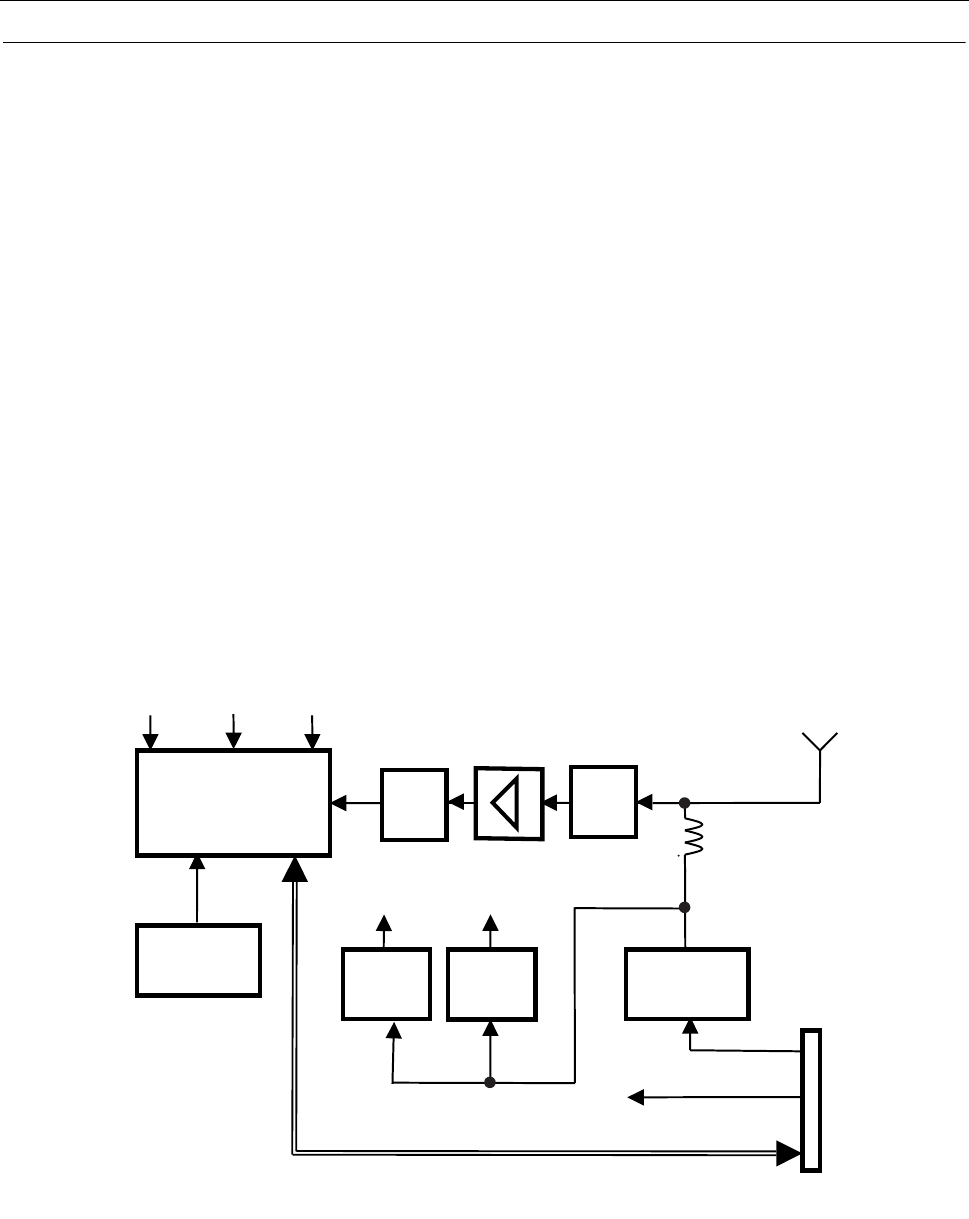
4.1 - 24 THEORY OF OPERATION (TRANSCEIVER)
GPS Sub Module
The MTM800 ENH GPS is based on the Phoenix GAM IC (PGAM), which comprises a custom
mixed mode RF-DSP IC in a single chip FBGA package.
It is a self contained GPS receiver capable of producing a final position including full tracking and
data decode capability.
The GPS signal that applies to the RF cable connector is filtered by two SAW filters FL1 and FL2.
It is amplified by a low noise amplifier (LNA).
The input of the GPS receiver at the RF FME connector is DC coupled.
A voltage regulator on board provides about 20mA at 5V DC voltage to an external antenna low
noise amplifier (LNA).
This phantom voltage is applied to the input by the RF coil L1.
The supply voltages GPS_2V and GPS_3V of the PGAM-IC are derived from two on board voltage
regulators U2 and U3.
A 26MHz TCXO provides the reference clock to the PGAM IC.
Data communication takes place via the serial SPI bus.
Figure 4.1-8 GPS Module Block Diagram
26MHz
TCXO
PGAM-IC
5V Regulator
GPS Antenna
L1
SPI bus
J1
24 pin
connecto
r
Y1
U4 FL1
FL2
U1
GPS_3V GPS_2V 3V_DIG
12V
3V DIG
Volt._Reg.
GPS_2V
U2
Volt._Reg.
GPS_3V
U3
Front
End
Filter
LNA
Front
End
Filter
6866539D31.book Page 24 Tuesday, March 20, 2007 6:32 PM

THEORY OF OPERATION (ENHANCED CONTROL HEADS) 4.2 - 1
CHAPTER 4.2
THEORY OF OPERATION (ENHANCED CONTROL
HEADS)
This chapter contains the descriptions of the different configurations of the Enhanced Control Head:
• Enhanced Control Head in Dash Mount configuration
• Enhanced Control Head in Remote Mount configuration
Remote Back Head
Data Expansion Head Enhanced
Remote Head Enhanced
• Enhanced Control Head in Motorcycle configuration
Enhanced Control Head in Dash Mount configuration
The Enhanced Control Head in dash mount configuration consists of the main board, the liquid crys-
tal display (LCD) module, the keypad board, the keypad, the rotary and push button, the EMER-
GENCY button, the GCAI accessory connector, the 3-colour status LED and the housing.
The display module contains a colour 2.8" VGA TFT display.
The 3 colour status LED informs the user about the radio status
The functions of the Enhanced Control Head are driven by the OMAP1621 microcontroller from
Texas instruments.
Power Supplies
The power supply to the Enhanced Control Head is taken from the host radio's FLT A+ voltage via
connector J101 pin 3. It is used to power up the Enhanced Control Head.
The regulator U513 provides an unswitched stabilized 5V to constantly power some circuits.
The switching regulator U501 produces 5V when the system is switched ON. The output voltage of
U501 feeds the following regulators U503, U504 and U505. Furthermore the VCC_5 voltage is used
to supply the keypad backlight.
The boost regulator U503 generates 23V for the display backlight.
The reset IC U502 enables the regulator U503 when the output voltage of U501 exceeds 2.8V. U503
produces the 1.5V core voltage for the OMAP microcontroller.
Only when the 1.5V is stable, the regulator U504 is enabled and generates 3.3V for USB and as
input voltage for the two regulators U506 and U507. U507 provides 1.8V to the memory block of the
OMAP and to the memories themselves.
U506 generates 2.8V for the I/O section of the OMAP.
The 2.8V also release the clear input of the D-Flip Flop U509. At the same time the crystal oscillator
U515, Y501, R520 - R523 and C530 - C532 starts oscillating at 32.768 kHz and the binary counter
6866539D31.book Page 1 Tuesday, March 20, 2007 6:32 PM

4.2 - 2 THEORY OF OPERATION (ENHANCED CONTROL HEADS)
in U515 starts counting. When the output Q12 of U515 goes to HIGH, the output of the D-Flip Flop
U509 goes to HIGH and the OMAP is coming out of RESET.
In case the error output of U506 goes to LOW, the Flip Flop is cleared and thus the OMAP goes into
RESET. U515 is also held in RESET and the oscillator stops working.
Power On / Off
The Enhanced Control Head in dash mount configuration can be switched ON either by the ON
rotary push button, the ON button in the keypad, the EMERGENCY button or by the radio via the
accessory connector of the radio.
If one of the three buttons on the Enhanced Control Head is pressed, the OR circuitry D510, D511
produces the signal ON_OFF_CONTROL, that switches the radio ON. When the radio powers ON it
delivers a 5V level on the BUS+ and SCI_TX lines. The transistor couple Q508 then sets the signal
BUS_ON to HIGH and the regulator U501 is enabled.
When all regulators are powered and the RESET signal has gone to HIGH, the OMAP controller
starts operating.
The OMAP processor has to program the ON_HOLD line to HIGH in order to maintain the enable
signal for U501, when the BUS+ line is used for communication later on.
Before the first message can be transferred, the interface has to be activated by setting the
RADIO_COM_EN signal to LOW and the BUS_EN signal to HIGH.
RADIO_COM_EN enables the buffer U420-1 and supplies 5V to the operational amplifiers U421
and U422 via the transistors Q411 and Q412.
The BUS_EN signal connects the SCI_TX to the BUS+ line via Q410.
The other possibility to switch ON is when the radio is switched ON from its accessory connector
either by IGNITION or by EMERGENCY. The regulator U501 is also enabled by the BUS+ signal in
this case.
The system can be switched OFF by either the ON/OFF button in the keypad or by the radio via the
IGNITION signal on the accessory connector.
If it is switched OFF by the ON / OFF button, the Enhanced Control Head communicates this to the
radio. After the radio has shut down the OMAP releases the ON_HOLD signal. If it is switched OFF
by the radio it is told by a message from the radio to switch OFF. It has then also to release
ON_HOLD.
Microprocessor Circuit
The Enhanced Control Head uses the TI microcontroller OMAP1621 (U201) to control the functions
of the Enhanced Control Head. The firmware is contained in a flash memory of 16Mbytes (U204).
When the firmware is executed it runs in the SRAM U205. Flash and RAM have a separate data,
address and control bus and operate at a 1.8V level.
The internal clock oscillator with the Xtal Y201 and the components R221 and C204/C205 generate
the system clock of 12MHz.
The 32.768 kHz clock mentioned above is also fed into the OMAP controller.
The power supply design assures that the core is powered first and then the I/O and USB voltages
are supplied to the controller. After this the system comes out of RESET.
6866539D31.book Page 2 Tuesday, March 20, 2007 6:32 PM

THEORY OF OPERATION (ENHANCED CONTROL HEADS) 4.2 - 3
The internal display controller in the OMAP loads the images into the display.
The display module is connected to the main board by the 40 pin connector J201
Keypad
The keypad interface of the OMAP can read the keypad matrix (COL5 - COL0 / ROW4 - ROW0) and
discover which key has been pressed. The reading of the matrix is initiated by an interrupt.
The keypad PCB is connected to the main board by the 24 pin connector J401.
One Wire interface
The One Wire signal from the OMAP is connected via a level shifter Q305, D301 and R309/R310 to
a switch U301. The switch routes the One Wire interface either to the front GCAI connector or to the
rear of the remote back housing connector if present.
The direction of the switch is chosen by the OMAP GPO signal ONE_WIRE_SEL.
GCAI GPIOs and USB
The general purpose I/Os from the GCAI connector GPIO_0_PWR, GPIO_3_PTT and
GPIO_4_HOOK are shifted from a 3.3V level to the OMAP I/O level of 2.8V by the bi-directional
level shifters U302, U303 and U304. The direction of the signal is chosen by the OMAP GPOs
GPIO_0_DIR, GPIO_3_DIR and GPIO_4_DIR.
The general purpose I/Os from the GCAI GPIO_1 and GPIO_2 are also level shifted by U323 and
U325. As the USB signals D+ and D- share the same physical pin of the GCAI connector with the
two GPIOs GPIO_1 and GPIO_2, the two switches U321 and U322 route the respective signals
from the OMAP to the GCAI connector.
With the switches U326 and U327 the signals can be switched between the front GCAI connector
and the rear GCAI connector when a remote back head is present. The two switches are controlled
by the logical signal USB1_GPIO and USB_FRONT_REAR.
The digital signal USB_MODE_SEL switches the resistors R327 and R328 to GROUND when the
Enhanced Control Head USB is required to be host. If the Enhanced Control Head is an USB device
USB1_PUEN activates the pull up resistor R326.
When the Enhanced Control Head is USB host the signal USB_VBUS_ENA enables the power sup-
ply switch U324.
U324 provides 5V for USB to the FET switch and to the remote back head if present. The signal
VBUS_FET_EN activates the FET Q326, which then switches the 5V to the GCAI connector. U324
has an internal over current detection, which will switch OFF the 5V if too much current is drawn. At
the same time the signal VBUS_OC_DET goes to LOW and indicates the over current to the OMAP.
The comparator U328 compares the USB_VBUS signal with 3.3V and delivers a HIGH on
USB1_DET when the VBUS voltage exceeds 3.3V. If the Enhanced Control Head is USB master it
will detect its own voltage. When the Enhanced Control Head is USB device it will detect when a
master is applied.
6866539D31.book Page 3 Tuesday, March 20, 2007 6:32 PM

4.2 - 4 THEORY OF OPERATION (ENHANCED CONTROL HEADS)
Backlights
The PWM output LCD_BL controls the current source Q201 and related circuitry. By this signal the
current through the backlight diodes on the display module is determined. The supply voltage for the
backlight diodes is the 23V source provided at J201 pin 32.
The PWM signal KPD_BL controls the brightness of the 3 colour LED. It is routed via Q324 to the
emitters of the two red/green switches Q404 and Q405. The digital signals LED_GREEN and
LED_RED enable the colour by applying a HIGH to the basis of the respective transis-
tor.Q504/Q505. When both switches are ON the light will be amber.
The digital signal KPD_BL_ON_OFF switches the keypad backlight ON or OFF by means of the
FET Q401.
The PWM signal LED_EMERG is low pass filtered by R414/C410 and controls the brightness of the
EMERGENCY key backlight.
Rotary and push button
The push button S401 connects the LOCK_ON signal to the FILT_A+. LOCK_ON is wired into the
keypad matrix. The rotary S401 produces pulses on the two outputs PULSE_A and PULSE_B of a
different phase when the knob is turned. These pulses are low passed R403 Expansion Head
Enhanced Enhanced - R404 and C405/C406.
The B output is then applied to the D inputs of the two D-Flip Flops U401 and U402. The signal
integrity of output A output is ensured by the two invert Schmitt triggers U403 and U404. The output
pulse of U403 is the clock input for D-Flip Flop U401 and latches the status of the B signal with the
rising edge. The second Schmitt trigger inverts the A signal another time and latches the B output
into the D-Flip Flop U402 with its rising edge. Furthermore it serves as an interrupt RSW_1 for the
OMAP, which is the required to read the outputs of the two D-Flop Flops RSW_2 and RSW_INT.
From the polarity of these two signals the OMAP can determine whether the rotary was turned
clockwise or counter clockwise. The Flip Flops get a reset from the general board-reset POR
Communication interface
In direct mount the radio and the Enhanced Control Head communicate with each other via a two
wire communication interface BUS+ and SCI_TX. This interface needs to be enabled by setting the
RADIO_COM_EN signal to LOW and the BUS_EN signal to HIGH.
RADIO_COM_EN enables the buffer U420-1 and supplies 5V to the operational amplifiers U421
and U422 via the transistors Q411 and Q412.
The BUS_EN signal connects the SCI_TX to the BUS+ line via Q410.
The speed of this interface is 115kBaud/sec.
The physical interface to the radio is J102 with the following signals: GROUND, ON_OFF CON-
TROL, FILT_A+, BUS+, HANDSET_AUDIO, 5VD and SCI_TX.
Accessory Connector
The accessory connector J101 complies to the GCAI standard and provides the following signals:
FRONT_ONE_WIRE, GPIO_3_PTT, HANDSET_AUDIO, USB_D-, GROUND, USB_VBUS,
INT_MIC, USB_D+, GPIO_4_HOOK and GPIO_0_PWR. For further information please refer to the
GCAI specification.
6866539D31.book Page 4 Tuesday, March 20, 2007 6:32 PM

THEORY OF OPERATION (ENHANCED CONTROL HEADS) 4.2 - 5
Enhanced Control Head in Remote Mount configuration
In remote configuration a remote mount back housing is attached to the back of the Enhanced Con-
trol Head.
It is connected to the Enhanced Control Head main board through J603.
A 10 pin Remote Mount cable on P101 connects the Remote Mount Back Housing Board to the
radio transceiver with either Expansion Head Enhanced or remote head.
A 25 pin connector J105 gives access to the GCAI GPIOs, second USB, 4-wire RS232, Rear GCAI
Pins and Audio.
The remote mount back head is detected by the OMAP by sending an I2C Bus request by means of
the I2C clock and data lines I2C_SCL and I2C_SDA.
The routing of the GCAI GPIOs and the first USB is described already in the dash mount chapter.
The 4-wire RS232 is connected to the UART 3 of the OMAP microcontroller. The signals for realiz-
ing the second USB port are directly provided by the OMAP and connected through the 40 pin con-
nector J601 to the remote mount back housing board. The ON_OFF_CONTROL, BUS+, SCI_TX as
well as the HANDSET_AUDIO and MIC lines are also routed via J602 to the rear of the remote
mount back head.
The remote mount back head itself is controlled by I2C messages and the remote mount back head
creates an interrupt to the OMAP when it has an I2C Bus message to deliver.
When the device was switched ON from the rear IGNITION line, the signal RM_ON turns to HIGH
and switches the signal GCAI to HIGH by means of D350 and Q353. Then the same ON procedure
starts as in dash mount configuration. After the device is in ON_HOLD and the OMAP has detected
the ON source on the remote mount back housing it sent a LOW on RM_GCAI_PWR_ON_CLR to
clear the RM_ON.
Remote Mount Back Head
Power supply
The remote mount back head is supplied from the Enhanced Control Head main board with the
FILT_A+ and unswitched 5 V when the device is switched OFF. When the device is switched ON by
either the Enhanced Control Head front panel or from the radio accessory connector, VCC_2.8V,
VCC_3.3V and the switched 5V will be also provided by the Enhanced Control Head main board.
When the device is switched ON from the rear IGNITION on the 25 pin rear connector by pulling
J105 pin 25, to the battery voltage, the Transistor Q401 provides a rising edge to the D-Flip Flop
U401 clock input. This latches the HIGH level on the D-input of U401 and creates an HIGH on
RM_ON. This turns ON the Enhanced Control Head main board as described above. At the same
time a HIGH on IGN_SENSE is applied to the I2C port expander U501 and generates an interrupt to
the OMAP. When the main board has powered ON as described above it clears the Flip Flop by pull-
ing RM_GCAI_PWR_ON_CLR to LOW.
An optional 5V can be turned ON supplying the rear GCAI (U304) even when NGCH is turned OFF.
RS232
The MAX3232E U303 transceiver provides level translation to RS232 levels of the 4 wire RS232
interface connected to UART3 of the OMAP that is internally routed to the camera interface.
6866539D31.book Page 5 Tuesday, March 20, 2007 6:32 PM

4.2 - 6 THEORY OF OPERATION (ENHANCED CONTROL HEADS)
USB
There are 2 USB connections on the Remote Mount Back Housing Board. The first USB is shared
with the front GCAI USB and the D- and D+ lines are switched ON the main board. The second USB
is provided by the ISP1105 USB transceiver U302. It is interfaced to the OMAPs USB1 port. USB
power supply is separately switched for both USBs via Q306 and Q307. Detection and switching is
controlled by the I2C port expanders U501 and U502.
Audio
Audio is on 2 wires for both directions and balanced and is routed from and to the Milan transceiver
via the Gabel Hybrid U201. The Gabel Hybrid serves to transform the audio from unbalanced to bal-
anced in order to reduce noise susceptibility on the remote cable. Receive or Handset Audio is
routed to the main board and via 10uF to the 25 pin connector J105. Transmit or MIC audio is multi-
plexed by U203 and U204. Depending on PTT, these switches determine where the transmit audio
is coming from. There are 3 sources: Front GCAI, Rear GCAI ON 25 pin connector and Rear MIC,
also from the 25 pin connector J105.
1-Wire
The 1-Wire bus is routed from the 25 pin connector to the main board. It is shared between front and
back GCAI and switched ON the main board.
Bus+/SCI_TX
Both BUS+ and SCI-TX serial communication lines have Pull-Ups to 5V. These 5 Volt needs to be
turned ON/OFF by the OMAP in order to detect the ON/OFF status of the radio transceiver. This is
done via the I2C port expander and Q503.
Analogue 4-level Input:
An analogue 4-level input pin is available on the 25 pin connector (U503). The 4 levels are preset by
resistor dividers R540 - R551 and detected by comparators U503. The 4 states can be read by I2C
expander 501.
I2C Port Expander settings and In/Output Matrix:
The heart of the Remote Mount Back Housing Board is the two PCA9535BS port expanders U501
and U502. The GPIOs and most detection and switching circuitry on the Back Housing Board are
provided by these Port Expanders. The PCA9535BS provides 16 general purpose In/Output pins. It
is interfaced to the OMAP’s I2C bus via SDA (data) and SCL (clock) line. Both expanders are shar-
ing the same interrupt, provided by an extra line GPIO_REQ.
Under normal operating condition, the second port expander U502 has only outputs and static
inputs (HW ID) connected to it, so no interrupt is generated by U502. All Inputs that generate an
interrupt are connected to U501.
Data Expansion Head Enhanced
Overview
The Data Expansion Head Enhanced (PMLN4908_) is a hardware interface to the MTM800 TETRA
mobile radio. It gives access to the radio via three front side connectors. The following interfaces
and protocols are provided:
- 8-wire RS232 Interface (9-pin D-type connector)
6866539D31.book Page 6 Tuesday, March 20, 2007 6:32 PM

THEORY OF OPERATION (ENHANCED CONTROL HEADS) 4.2 - 7
- 4-wire RS232 Interface (25-pin D-type connector)
- SB9600 Interface (25-pin D-type connector)
- SBEP Interface (10-pin Telco connector)
- 14 pin JTAG port
General
The 25-pin D-type, the 9-pin D-type connector and the 10-pin Telco connector are mounted on the
Connector Board that is screwed into the Data Expansion Head Enhanced housing. The Milan
Expansion Board is installed at expansion board position. The interconnection between the Connec-
tor Board and the Milan Expansion Board is accomplished by a 40-pin flex connector.
A 12-pin flex and a 40-pin flex achieve the connection between the Expansion Board to the main
radio chassis. A remote mount Enhanced Control Head can be connected in a remote mount config-
uration via the 10-pin Telco connector. External DCE(s) can be connected via the 25 pin and /or 9
pin D type connectors.
Circuit Description
The Data Expansion Head Enhanced Interface consists of several circuits to provide interfaces for
the MTM800 TETRA mobile radio and the "outside world".
The Expansion board has an onboard 3-Volt Regulator U501 that is driven by 5-Volt supply from the
main radio via the 12-pin flex on J1001. The supply voltage FLT_A+ is over current protected by the
2A fuse F101.
A second regulator U503 provides VAG_1 of 9.3V for the Gabel Hybrids U201. This regulator will be
shut down through Q501 when the 5V are detached
The Gabel Hybrid U201 serves to transform the audio from unbalanced to balanced in order to
reduce noise susceptibility on the remote cable.
There are several interfaces on the board but not all of them are available at the same time
The 8 wire RS232 interface consists of the MAX3238 true RS-232 transceiver (U101) that provides
the EIA/TIA-232 and V.28/V.24 communications interface. This interface can be fully accessed
through the 9-pin D-connector.
The circuit comprising ICs U401, U403 and U404 interfaces the MTM800 SPIB bus to an asynchro-
nous serial-data communication port RS232 that is the 4-wire RS232 interface (pins 2, 3, 4, 5).
U401 is a MAX3100 universal asynchronous receiver transmitter (UART) with a baud rate generator
driven by a 3.6864 MHz crystal U402.
U404 is a MAX3232 RS232 transceiver, translating the 3V logic levels to the RS232 levels.
The next interface is an SB9600 interface on the 25-pin connector (pins 8, 13, 15, 17)
(SB9600_INTERFACE). The UART chip U401 also generates the transmit/receive signals of this
interface.
The SBEP interface is provided on the 10-pin Telco remote connector. All signals necessary to con-
nect a remote mount Enhanced Control Head are routed through this connector. Those signals are
fed from the radio via the 12-pin flex (J1001). The SBEP interface is always available on the Telco
connector.
6866539D31.book Page 7 Tuesday, March 20, 2007 6:32 PM

4.2 - 8 THEORY OF OPERATION (ENHANCED CONTROL HEADS)
The Expansion PTT signal on the Telco connector is routed though the Expansion Board via Q102
and Q103. This line signals the radio that PTT is coming from the Data Expansion Head Enhanced
and the audio paths are routed through the Data Expansion Head Enhanced.
The JTAG port is provided on the back of the Expansion board. The pin layout of the connector is
setup in a way that the JTAG connector used for software debugging can be directly connected to
this port. A 14-pin m/m 90° adapter is needed to connect to the test equipment.
To select a specific configuration, pin 23 (SB9600_SW) on the 25 pin D-type connector can be used.
Also the ACC3 pin on the 12-pin flex and pin 19 on the JTAG connector influence which interface is
active in the Data Expansion Head Enhanced at a specific time.Default if nothing is connected to the
radio is that the 8-wire RS232 interface and 4-wire RS232 interface are active.
A high voltage (12V) on pin 23 enables the 8-wire RS232 interface on the 9-pin D-type connector. At
the same time the SB9600 interface on the 25-pin connector is enabled. A low voltage (0V = default)
on pin 23 enables the 8 wire RS232 interface on the 9-pin connector and the 4 wire RS232 interface
on the 25-pin connector.
If a device is connected to the accessory connector of the radio, the 8-wire RS232 interface in the
Data Expansion Head Enhanced is disabled. Also, if the JTAG port is used, a 3-Volt level is applied
to pin 19 of the JTAG, the 8-wire RS232 interface is disabled.
Remote Head Enhanced
General
The Remote Head Enhanced (PMLN4904_) and the radio are connected via 10-pin TELCO connec-
tors. A 12-pin flex connects the radio to one remote mount PCB.
Description
The remote mount board basically routes the signals necessary to drive a Enhanced Control Head
from the radio to the remote mount cable and to the Remote Mount Enhanced Control Head. The
signals (ON_OFF_CONTROL, BUS+, SCI_TX and the supply voltage) are directly routed from the
flex connector J301 to the TELCO connector J302.Microphone and speaker audio are transformed
from unbalanced to balanced by the Gabel Hybrid U202 in order to reduce noise susceptibility on
the remote cable.
The regulator U201 provides VAG_1 of 9.3V for the Gabel Hybrids U202. This regulator will be shut
down through Q101 when the 5V are detached. The supply voltage FLT_A+ is over current pro-
tected by the 2A fuse F101.
VR301 - VR304 protects the board against electrostatic discharge
6866539D31.book Page 8 Tuesday, March 20, 2007 6:32 PM

THEORY OF OPERATION (ENHANCED CONTROL HEADS) 4.2 - 9
Enhanced Control Head in Motorcycle configuration
When the Enhanced Control Head is used on a motor cycle, it is electrically same as remote mount
configuration. The housing of the remote mount back head and the TELCO connector are
mechanically modified to meet the IP67 requirement.
6866539D31.book Page 9 Tuesday, March 20, 2007 6:32 PM

4.2 - 10
Notes
6866539D31.book Page 10 Tuesday, March 20, 2007 6:32 PM

PROGRAMMING THE TERMINAL 5 - 1
CHAPTER 5
PROGRAMMING THE TERMINAL
Note: For programming the terminal, refer to TETRA Customer Programming Software (CPS)
Start-up User Guide, Publication No. 6802974C10_
6866539D31.book Page 1 Tuesday, March 20, 2007 6:32 PM

5 - 2 PROGRAMMING THE TERMINAL
Notes
6866539D31.book Page 2 Tuesday, March 20, 2007 6:32 PM
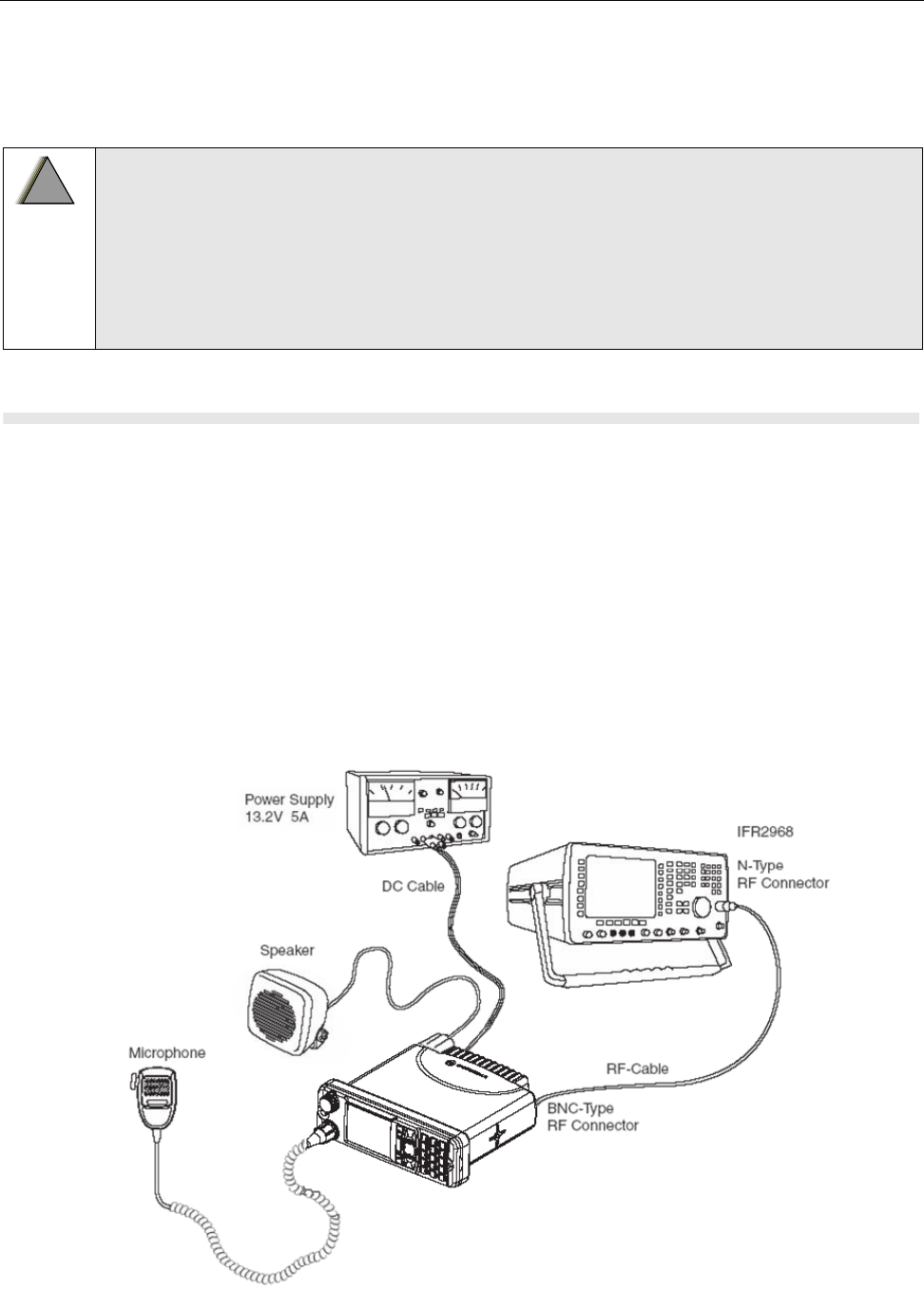
TEST SETUP & TESTING 6 - 1
CHAPTER 6
TEST SETUP & TESTING
Typical Test Setup
Before Testing
Carry out the following instructions before testing:
• Connect the DC cable to the DC connector on the terminal.
• Connect the other side of the DC cable to the DC output connector on the power supply
• Connect an RF cable to the N-type RF Connector of the IFR.
• Connect the other side of the RF cable to the antenna connector on the terminal.
• Set the DC voltage on the power supply to 13.2 Volts.
• Switch on the terminal.
Figure 6-1 Typical Test Setup
Any level 3 repairs can deeply affect the performance of the MTM800 ENH
terminal and may cause a new tuning procedure.
This tuning procedure can only be applied by certain authorized Motorola
depots where the appropriate TEST&TUNE EQUIPMENT is available.
The appropriate TEST&TUNE EQUIPMENT is a special automated test
equipment which is only available at some Motorola factories and Motorola
repair centers.
!
W A R N I N G
!
6866539D31.book Page 1 Tuesday, March 20, 2007 6:32 PM

6 - 2 TEST SETUP & TESTING
Test Equipment
The table below lists the special test equipment required for servicing TETRA mobile terminals.
Table 6-1 Test Equipment
Name Part Number
Digital Multimeter R1072_
220V Power Supply R1011_/220V
TETRA SVC MON. MOBILES ONLY WADN4161A
TETRA SVC MON. MOB.+ DIR.MODE WADN4163A
TETRA SVC MON. MOB.+ BASE ST. WADN4164A
TETRA SVC MON. MOB.+ BASE ST. + DIRECT MODE WADN4173A
TETRA SVC MON. MOB.+ DIR.MODE + MPT1327/1343 WADN4233A
6866539D31.book Page 2 Tuesday, March 20, 2007 6:32 PM

TEST SETUP & TESTING 6 - 3
Test Check List
The following table summarises the required test setups.
Table 6-2 Test setup
No. Test Name Test Setup Terminal Setup Test Conditions Limits
1. IFR System
Setup and Man-
ual Test Screen
Control Channel For 450--470MHz
terminal: 2440
Traffic Channel For 450--470MHz
terminal: 2440
Time Slot 3
Country Code 262
Network Code 75
Base Colour 1
Location Area 224
Min Rx Level -110dBm
Max Tx Level 35dBm (3.2W)
Access
Parameter
-33dBm
Mobile Power 35dBm (3.2W)
Burst Type Normal
2. Base Station
Registration
RF Gen Level For 450--470MHz
terminal:
461.0125MHz
-90dBm
3. Receiver RSSI RF Gen Level 4 Cells Info
RSSI
TRACE
-90dBm
4. Transmitter
Tests
RF Gen Level Range 1
Talk Group 1
-90dBm
Burst Power 33-37dBm
Timing Error <=0.25 Symbols
Frequency
Error
-/+ 100Hz
Vector Error Max 10% RMS,
Max 30% Peak,
Max 5% Residual
5. Call Processing
Talk Back
1KHz Test Signal
Group Mode
Range 1
Talk Group 1
-90dBm
6. Call Processing
Call to Mobile
Private Mode
Private Call
Private Mode
RF Gen Level
Burst Power
-90dBm 33-37dBm
Timing Error <=0.25 Symbols
6866539D31.book Page 3 Tuesday, March 20, 2007 6:32 PM

6 - 4 TEST SETUP & TESTING
Receiver Tests
1. Simulate Base Station (registration)
2. RSSI Test
Transmitter Tests
1. Power Profile
2. Power Burst (Control Range)
3. Tx Burst Timing Error
4. Tx Frequency Error
5. Vector Error RMS, Peak and Residual
Call Processing Tests
1. Talk Back
2. Call to Mobile
Duplex Test
1. Digital Duplex Test (Tx)
Measurement Capabilities:
Bar chart display for Tx Power, Frequency Error, Vector Error RMS, Power Analyzer,
Spectrum Analyzer, Vector Analyzer, Vector Diagrams.
Frequency Error -/+ 100Hz
Vector Error Max 10% RMS,
Max 30% Peak,
Max 5% Residual
7. Digital Duplex
Test (Tx)
RF Gen Level Private Mode -50dBm
Burst Power 10-22dBm
Timing Error <=0.25 Symbols
Frequency
Error
-/+ 100Hz
Vector Error Max 10% RMS,
Max 30% Peak,
Max 5% Residual
Table 6-2 Test setup
No. Test Name Test Setup Terminal Setup Test Conditions Limits
6866539D31.book Page 4 Tuesday, March 20, 2007 6:32 PM

TEST SETUP & TESTING 6 - 5
Configuration of the IFR 2968 System Setup
The setup depends on the firmware version of the IFR 2968, the firmware version of the
terminal and the customer programming of the terminal.
>>The following table should be taken only as an example of how to proceed for setup.<<
Perform the following steps to configure the IFR 2968 System Setup with the terminal
settings.:
1. Turn ON the IFR.
2. Press the “Systems” Mode Key (wait until the digital system is initialised).
3. Press the “Tetra Mobile” soft key.
4. Press the “Setup” soft key and enter the System Parameters Screen.
5. Press the “Channel Plan” or “System Type” soft key.
6. Press the "Tetra 450MS" soft key for 450-470.
7. Press the "More" soft key if the Type cannot be seen.
Note: If the required Mobile soft key in step 6 and step 7 is not displayed, the system
needs to be set up manually as in step 8. If the MS type was chosen in step 6 and
step 7 continue with step 9.
8.
a. Press the "More" soft key until the "User defined" soft key is displayed.
b. Press the "User Defined" soft key in the next menu again.
c. Press the "User Defined" soft key once more.
d. Press the "Frequency Band" soft key and press the "4 (450-470MHz)" soft key.
Press the "More" soft key if the band is not displayed.
e. Press the "Offset" soft key and press the "3 (12.5kHz)" soft key.
f. Press the "Duplex Spacing" soft key and press the "0 (10MHz)" for 450-470MHz
soft key
g. Press the "Reverse Operation" soft key and press the "0 (Normal)" soft key.
h. Press the "Channel Block 1" soft key.
i. Press the "Channel Block" soft key and press the "Include" soft key.
j. Press the "Lowest Channel" soft key and enter"2440" for 450-470MHz using the
data keys followed by the "Lowest Channel" soft key.
k. Press the "Highest Channel" soft key and enter "2799" for 450-470MHz using the
data keys followed by the "Highest Channel" soft key.
l. Press the "Lowest Tx Freq" soft key and enter "461.0125" for 450-470MHz using
the data keys followed by the "MHz" key.
m.Press the "Duplex Offset" soft key and enter "10" for 450-470MHz using the data
keys followed by the "MHz" key.
n. Press the "Channel Spacing" soft key and enter "25" using the data keys followed
by the "kHz" key.
6866539D31.book Page 5 Tuesday, March 20, 2007 6:32 PM

6 - 6 TEST SETUP & TESTING
o. Press the "Return" soft key.
p. Verify that channel block 2 to 8 are excluded.
q. Press the "Return" soft key.
9. Press the "Control Channel" soft key and enter "2440" for 450-470MHz using the
data keys followed by the "Control Channel" soft key.
10. Press the "Traffic Channel" soft key and enter "2440" for 450-470MHz using the data
keys. Press the "Traffic Channel" soft key again and check that the marker goes to
Timeslot. Press data key "3" followed by the "Traffic Channel" soft key, to change to
Timeslot "3".
11. Press the “Country Code” soft key.
Enter “262” and press the “Country Code” soft key.
12. Press the “Network Code” soft key.
Thereafter, enter “75” and press the “Network Code” soft key.
13. Press the “Base Color” soft key.
Thereafter, enter “1” and press the “Base Color” soft key.
14. Press the “Location Area” soft key.
Thereafter, enter “224” and press the “Location Area” soft key.
15. Press the “Min Rx Level” soft key.
Thereafter, enter “-110dBm” and press the “Min Rx Level” soft key.
16. Press the “Max Tx Level” soft key.
Thereafter, enter “35dBm (3.2W)” and press the “Max Tx Level” soft key.
17. Press the “Access Parameter” soft key.
Thereafter, enter “-33dBm” and press the “Access Parameter” soft key.
18. Press the “Test Mode” soft key. Press the “Enable” soft key.
19. Press the “Base Service” soft key.
20. Press the “Suport” soft key if it is displayed
or verify that the following values are displayed:
POWER ON REGISTRATION: REQUIRED
POWER OFF DE-REGISTRATION: REQUIRED
PRIORITY CELL: YES
MINIMUM MODE SERVICE: NEVER USED
MIGRATION: SUPPORTED
SYSTEM WIDE SERVICE: NORMAL MODE
TETRA VOICE SERVICE: SUPPORTED
CIRCUIT MODE DATA SERVICE: SUPPORTED
(RESERVED): NOT AVAILABLE
SNDCP SERVICE: NOT AVAILABLE
AIR INTERFACE ENCRYPTION: NOT AVAILABLE
ADVANCED LINK: NOT SUPPORTED
Note: The displayed values are factory defaults and should not be changed.
6866539D31.book Page 6 Tuesday, March 20, 2007 6:32 PM

TEST SETUP & TESTING 6 - 7
21. Press the “Return” soft key.
22. Press the “Neighbr Cell” soft key.
23. Verify that the following values are displayed:
NEIGHBOUR CELL BROADCAST: NOT REQUIRED
BROADCAST INTERVAL: 10s
NEIGHBOUR CELL CHANNEL: 0000
NEIGHBOUR CELL LOCATION AREA: 00001
NEIGHBOUR CELL IDENTIFIER: 01
SLOW RE-SELECT THRESHOLD: 10dB
SLOW RE-SELECT HYSTERESIS: 10dB
FAST RE-SELECT THRESHOLD: 10dB
FAST RE-SELECT HYSTERESIS: 10dB
Note: The displayed values are factory defaults and should not be changed.
24. Press the “Return” soft key.
25. Verify that “Trunking Type” is set to “Message”.
26. Press the “Call Type” soft key to enter the “Call Type” screen.
27. Press the “Private Call” soft key.
28. Press the “Simplex Duplex” soft key and “Simplex Call” soft key.
29. Press the “Signal Type” soft key and “Direct set –up” soft key.
30. Press the “Priority” soft key. Thereafter, enter “00” and press the “Priority” soft key.
31. Leave “Calling Party SSI” setting to default value.
32. Press the “Return” soft key.
33. This completes the System Setup configuration.
6866539D31.book Page 7 Tuesday, March 20, 2007 6:32 PM

6 - 8 TEST SETUP & TESTING
Configuration of the IFR 2968 Manual Test Screen
The setup depends on the firmware version of the IFR 2968, the firmware version of the
terminal and the customer programming of the terminal. The following procedure is only
an example.
1. To enter “Manual test” screen, press the “Manual” soft key.
2. Press the "Control Channel" soft key. Thereafter, enter the control channel Number
and press the "Control Channel" soft key. The control channel Number is
"2440" = Rx 461.0125MHz.
3. Press the "Traffic Channel" soft key. Enter "2440" for 450-470MHz and press the
"Traffic Channel" soft key. The marker goes to Timeslot. Enter "3" and press the
"Traffic Channel" soft key. (Note that the Traffic Channel number changes automati-
cally after entering the Control Channel number).
4. Press the “RF Gen Level” soft key. Thereafter, enter “-90” and press “dBm” data keys
followed by “RF Gen Level” soft key.
5. Press the “Mobile Power” soft key, enter “35 dBm/3.2W“, using soft key.
6. Press the “Burst Type” soft key and “Normal” soft key.
7. This completes the Manual test equipment configuration setup.
Note: The System Setup Configuration Data is saved even after the power is turned
off. However, the Manual Test Setup is not saved.
6866539D31.book Page 8 Tuesday, March 20, 2007 6:32 PM

TEST SETUP & TESTING 6 - 9
RF Tests
Receiver Tests
Simulate Base Station (registration)
1. Turn the terminal ON
When the terminal is in Trunked Mode, continue with step 2. Otherwise perform steps
a through c.
a. Press "Options" using the Lower (soft) key
b. Press the "Down" navigation key to scroll to "Trunked Mode".
c. Press "Select" using the Lower (soft) key
2. Check that registration and “ITSI: ---/----/01490199” (as example only) is displayed on
the IFR “Manual Test” screen.
Note: The number “01490199“ is the terminal ID (ISSI) which is displayed when the
terminal is switched on.
RSSI Test
Note: To perform procedure below the Test Page field must be enabled using the CPS
Before carrying out the following steps, record the Insertion loss (dB) of the cable loss value
- (X) dB.
1. In the IFR Manual Test Mode, press the “RF Gen Level” Soft Key and enter -90 dBm.
2. Before testing, the terminal should be configured to RSSI mode using the following
sequence. When performing steps 3 through 6, make sure that you press the
Enhanced Control Head keys sequentially (less than a second between every con-
secutive press).
3. Press the “*” key.
4. Press the “#“ key.
5. Press the “Menu“ key.
6. Press the “Right Navigation“ key.
Hereafter, there is no need for quick sequence of pressing the Enhanced Control Head keys.
7. Press the “Down” navigation key to scroll to “Cells Info”.
8. Press “Select” using the Lower (soft) key.
9. Press the “Right” navigation key to scroll to the RSSI monitoring screen.
10. Press “Trace” using the Lower (soft) key.
6866539D31.book Page 9 Tuesday, March 20, 2007 6:32 PM

6 - 10 TEST SETUP & TESTING
Note: RSSI results will flash on the screen every few seconds.
The display shows: SERV: 0/34348
RSSI: -90
CX: 20
CHQ: 99/E0
Disregard the “SERV”, “CX” and “CHQ” results.
Actual RSSI measured
=IFR RF Gen Level - Cable insertion loss +/- other stray losses.
Range of Actual RSSI measured
= -90dBm - XdB (cable) +/- 1 dB.
Terminal RSSI result should be within the range of Actual RSSI.
To stop the “Trace” process, perform the following. When performing steps 11 trough 14,
make sure that you press the Enhanced Control Head keys sequentially (less than a second
between every consecutive press):
11. Press the “*” navigation key.
12. Press the “#“ key.
13. Press the “Menu” key.
14. Press the “Right Navigation“ key.
Hereafter, there is no need for quick sequence of pressing the Enhanced Control Head keys.
15. Press “Select“ using the Lower (soft) key.
16. Press “Stop” using the Lower (soft) key.
17. Press “Back” using the Upper (soft) key twice.
Transmitter Tests
Before you start these tests, make sure that the terminal is in Trunked Mode.
1. Press "Options" using the Lower (soft) key.
2. Press the "Down" navigation key to scroll to "TG by abc".
3. Press "Select" using the Lower (soft) key.
4. Scroll to one of the available groups and press select using the Lower (soft) key.
5. In the IFR Manual Test Mode press the "RF Gen Level" soft key. Enter "-90dBm" by
pressing the data keys and "RF Gen Level" key.
6. Press the "PTT" of the terminal and monitor the IFR "Manual Test" screen which dis-
plays the Power Profile, Burst Power, Timing Error, Frequency Error and Vector Error.
Note: You have to hold the PTT in the pressed position long enough to enable you to
read the results.
- Power Profile: Passed.
6866539D31.book Page 10 Tuesday, March 20, 2007 6:32 PM

TEST SETUP & TESTING 6 - 11
- Burst Power Required Results: 33-37dBm.
- Timing Error: < 0.25 symbols.
- Vector Error: Max 10% RMS,
Max 30% Peak,
Max 5% Residual.
- Frequency Error: +/- 100Hz.
7. Press the “Clear Down” soft key, to proceed with other tests.
Call Processing Test
Before you start these tests, make sure that terminal and test equipment are configured the
same as given in the Transmitter Test.
Talk Back
1. Press "Options" using the Lower (soft) key on the terminal and change to one of the
available groups.
2. In the IFR Manual Test Mode press the “RF Gen Level” soft key. Enter “-90dBm” by
pressing the data keys and “RF Gen Level” key.
3. Press the “PTT”, press the “Talk Back“ soft key on the IFR and speak into the mic of
the terminal for at least 3sec, then release “PTT“. You will hear from the terminal
speaker the last three seconds of the speech frames before the “PTT” has been
released.
4. Press the “Test Sound” soft key to provide the 1kHz signal to the terminal speaker.
5. Press the “Silence” soft key to mute the 1KHz audio signal of the speaker.
6. Press the “Clear Down” soft key and check that the “Cleardown Complete” status
appears on the IFR “Manual Test” screen.
Call to Mobile
1. In the IFR Manual Test Mode press the “RF Gen Level” soft key. Enter “-90dBm” by
pressing the data keys and “RF Gen Level” key.
2. Press the “Call Mobile” soft key and select “Private Call” on the IFR. Verify that two
beeps are heard from the terminal speaker.
3. Press the “Abort Call” soft key.
Duplex Test (Phone/Private Mode)
Digital Duplex Test (Tx)
1. In the IFR Manual Test Mode press the “RF Gen Level” soft key. Enter “-50dBm” by
pressing the data keys and “RF Gen Level” key.
6866539D31.book Page 11 Tuesday, March 20, 2007 6:32 PM

6 - 12 TEST SETUP & TESTING
2. Dial a random 4 digit number (eg "9359") using the alphanumeric keys of the termi-
nal, press "Calltype" using the Lower (soft) key until "Phone #" is displayed and press
the "Send" Key .
The following results are displayed on the IFR “Manual Test” Screen
- Power Profile: Passed
- Burst Power Required Results: 10-22dBm
- Timing Error: < 0.25 Symbols.
- Frequency Error: -/+ 100Hz
- Vector Error: Max 10% RMS,
Max 30% Peak.
Max 5% Residual.
3. Press the “Talk Back” soft key.
4. Speak into the terminal microphone and hear your speech (after a short delay) from
the terminal loudspeaker.
Note: If you need more details, press the “Duplex Test” mode key.
5. Press the “duplex test (Tx)” soft key. The “Digital Duplex test” results will be displayed
on the IFR screen providing you with either one of the following:
- bar charts measurement capabilities showing Tx Power,
Frequency Error and Vector RMS in one screen
- Tx Power (more details in Power Analyser)
- Frequency Error (more details in Spectrum Analyser)
- Vector RMS (more details in Vector Analyser)
For Power Analyser Graph:
6. Press “power ana” soft key.
7. Check that the power frame falls within the limits.
For Spectrum Analyser Graph:
8. Press “spec ana” soft key.
9. Monitor the Tx frequency.
For Vector Analyser Diagram:
10. Press the “vector ana” soft key.
11. Monitor the diagram for the following:
- press “vector error” soft key for vector error.
- press “mag error” soft key for magnitude error.
- press “phase error” soft key for phase error.
- Vector Error
- Magnitude Error
- Phase Error
For Vector Diagram:
6866539D31.book Page 12 Tuesday, March 20, 2007 6:32 PM

TEST SETUP & TESTING 6 - 13
12. Press the “vector diagram” soft key.
13. View the following:
- press “symbol constel” soft key for graphical symbol constellation.
- press “rotated vector” soft key to zoom in on the constellation.
- press “phase traject” soft key to view trajectory of the constellation.
14. Press the terminal "End" key.
Manual Mode Testing
Preparation for Testing
Verify that the radio is turned off.
Press the "1", "2" and "3" keys together and then, press the On/Off key or the Rotary Push
Button to turn the radio on. Keep the "1", "2" and "3" keys pressed until the display turns on.
The display shows "User test mode, Press any key to start, Press SoftKeys to scroll".
Tests
Note: Any key that will be pressed will cause the test to advance from one step to the next.
You can use the soft keys to go to the next or back to the previous test. After a test has
started you can press the upper soft key to go back to the start of the current test. At any
time you can switch off the radio by pressing the On/Off key for 2 seconds.
1. Press any key to start the first test. The display shows "LCD Red-Green-Blue test".
2. Press any key consecutively. First the display shows horizontal red lines that become
thicker with every key press, until it becomes fully red. Then the display shows verti-
cal green lines that become thicker with every key press, until it becomes fully green.
After that the display shows horizontal blue lines that become thicker with every key
press, until it becomes fully blue.
3. Press any key to start the next test. The display shows "LCD Color brightness test"
4. Press any key consecutively. The display shows the color brightness levels "min",
"low", "med" and "max". Verify the color brightness of the display.
5. Press any key to start the next test. The display shows "Display backlight test"
6. Press any key consecutively. The display shows the backlight brightness levels
"min", "low", "med" and "max". Verify the brightness of the display.
Note: At level "min" the display contents is not visible.
7. Press any key to start the next test. The display shows "Keypad backlight test"
8. Press any key again. The display shows "Keypad backlight is off". Verify that the key-
pad backlight is off.
6866539D31.book Page 13 Tuesday, March 20, 2007 6:32 PM

6 - 14 TEST SETUP & TESTING
9. Press any key again. The display shows "Keypad backlight is on". Verify that the key-
pad backlight is on.
10. Press any key to start the next test. The display shows "Emergency backlight test"
11. Press any key consecutively. The display shows the emergency button brightness
levels "min", "low", "med" and "max". Verify the brightness of the emergency button.
12. Press any key to start the next test. The display shows "Status LED test"
13. Press any key again. The display shows "Red LED is on" and the Red LED at the
right side of the radio is lit.
14. Press any key again. The display shows "Green LED is on" and the Green LED at the
right side of the radio is lit.
15. Press any key. The display shows "Orange LED is on" and the orange LED at the
right side of the radio lit.
16. Press any key consecutively. The display shows the LED brightness levels "min",
"low", "med" and "max". Verify the brightness of the orange LED at the right side of
the radio.
17. Press any key to start the next test. The display shows "Keypad test"
18. Press any key again. The display shows all the radio keys.
19. Press every key, one by one. Each key you press causes its respective display to be
highlighted. If you press a highlighted key again, the highlighting is removed. To exit
this test before all keys are highlighted press the rotary push button.
20. Press any key to start the next test. The display shows "Rotary test"
21. Turn the rotary switch clockwise and counter clockwise. Each step causes the
respective displayed arrow sign to be highlighted. Turn the rotary switch until the two
respective "OK" labels are highlighted.
22. Press the rotary push button consecutively until "OK" is highlighted.
23. Press any key to start the next test. The display shows "Fist MIC test"
24. Press any key to continue. Connect a fist microphone. The display shows "Accessory
connected"
25. Press PTT to highlight all "0".
26. Place the microphone on / off hook to highlight all "0".
27. Press any key again. The display shows "End of user tests", "Press any key to power
off or use softkeys to scoll to any previous test".
28. This completes the test. Press any key to turn the radio OFF.
6866539D31.book Page 14 Tuesday, March 20, 2007 6:32 PM
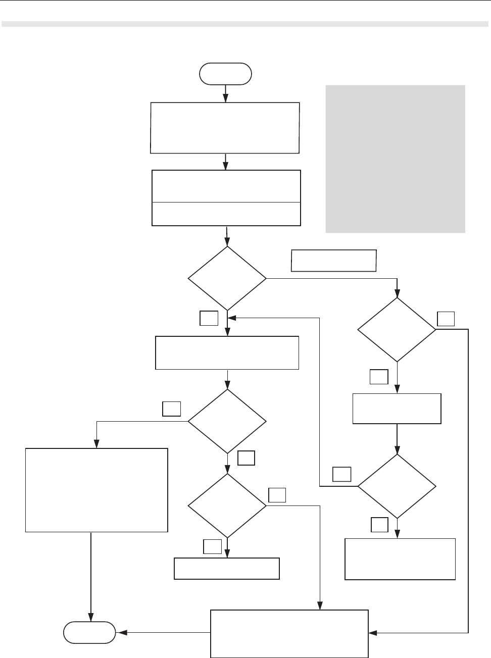
TEST SETUP & TESTING 6 - 15
Service Flow Chart (Board Level)
Figure 6-2 Servicing the MTM800 ENH
No
Yes
No
Yes
If the radio does not have a control head
attached you need to connect a control
head to operate the radio. For a motorcycle
radio use a motorcycle control head. In all
other cases use a standard control head
Switch on the radio and observe the display
at power up. The radio must completely
power up.
NOTE:
Before replacing any kits, check the
flexes to the control head or expansion
head.
If the main board has been replaced:
Send the new TEI number to service
provider. Clone/reprogram customer
details to new radio.
If fuse F0301 or F0302 or F0303 needs
to be replaced use Motorola part No.
6580542Z01
(see figure on following pages).
A list of replacement kits can be found
in the Appendix B (Replmt. Parts & Kits).
For a list of replacement parts refer to
Chapter 7 (Maintenance).
Start
Power up
OK ?
All tests
successful
?
Replacement
kits available
?
Read the codeplug with the CPS. Connect
the radio to the IFR. Perform all RF, call &
manual tests of chapter TESTING.
Replace main board and start
complete procedure again.
If no kits have been replaced,
verify installation integrity:
Check DC cable and connector
Check RF antenna , cable & connector
Check connected accessories
If the main board has been replaced:
Send the new TEI number to service
provider. Clone/reprogram customer
details to new radio.
Replace the costumer's radio
Send the faulty radio to Level 3 maintenance
Clone/reprogram customer details to new radio
Send the TEI number of the new radio to the
service provider.
Incorrect behavior of
LEDs, display or buttons.
Replacement
kits available
?
Replace the control head
or the expansion head.
Switch on the radio again.
Power up
OK ?
Check fuses F0301, F0302
and F0303 on the main board
before you replace main board
and restart complete procedure.
Done
No
No
Yes
Yes
Yes
Use the buttons and volume control and
check for correct display result.
6866539D31.book Page 15 Tuesday, March 20, 2007 6:32 PM
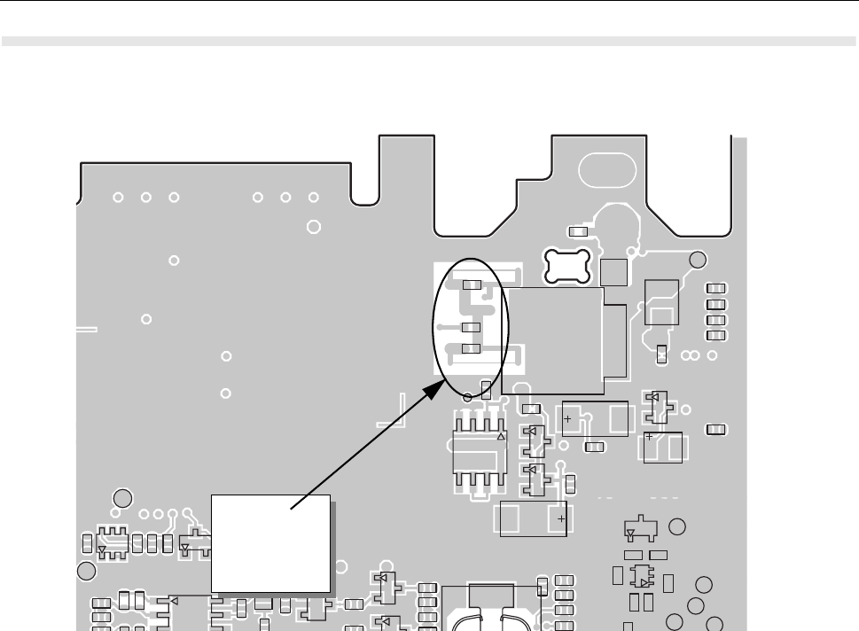
6 - 16 TEST SETUP & TESTING
Fuses on the Mainboard
Figure 6-3 Position of Fuse F0301/2/3 (PCB Mainboard - TOP View)
C0117
C0119
C0122
C0124
C0138
C0151
C0157
C0159
C0164
4
C0221
5
C0226
C0228
C0300
C0301
C0314
C0320
C0322
C0325
C0328
C0330
C0336
C0337
C0338
C0401
C5840
8
67
D0153
D0304
D0325 E0300
F0301
F0302
F0303
M0302
Q0156
2
02
Q0401
Q0600
Q5802
Q5804
R0159
R0160
R0180
R0181
R0222
R0224
0
225
R0238
R0239
R0240
R0311
R0404
R0405
R0406
R0409
R0410
R0427
R0555
R0604
R0605
R5802
R5837
R5840
R5845
R5846
TP0301
TP0302
TP0303
TP0404
TP0405
TP5802
TP5805
T
P5806
TP5807
P
5808
TP5811
TP5841
14
6
1
4
58
U0304
VR0300
VR0301
VR0401
VR0407
Fuses
(Motorola
6580542Z01)
Part Number:
6866539D31.book Page 16 Tuesday, March 20, 2007 6:32 PM

MAINTENANCE 7 - 1
CHAPTER 7
MAINTENANCE
Introduction
This chapter provides details about the following:
• Preventive maintenance (inspection and cleaning)
• Safe handling of CMOS and LDMOS devices
• Pre-baking of Integrated Circuits
• Repair procedures and techniques
• Disassembly and reassembly of the terminal
• Exploded views and parts lists
Preventive Maintenance
The terminals do not require a scheduled preventive maintenance program; however, periodic visual
inspection and cleaning is recommended.
Inspection
Check that the external surfaces of the terminal are clean, and that all external controls and
switches are functional. It is not recommended to inspect the interior electronic circuitry.
Cleaning
The following procedures describe the recommended cleaning agents and methods to be used
when cleaning the external and internal surfaces of the terminal. External surfaces should be
cleaned whenever a periodic visual inspection reveals the presence of smudges, compound, or
grime. Internal surfaces (circuit boards and components) should be cleaned only when the terminal
is disassembled for servicing or repair.
The only recommended agent for cleaning external terminal surfaces is a 0.5% solution (one tea-
spoon of detergent per gallon of water) of mild dishwashing detergent in water. The internal surfaces
should be cleaned only with isopropyl alcohol (70% by volume).
NOTE: Internal surfaces should be cleaned only when the terminal is disassembled for ser-
vice or repair.
6866539D31.book Page 1 Tuesday, March 20, 2007 6:32 PM

7 - 2 MAINTENANCE
Cleaning External Plastic Surfaces
Apply the 0.5% detergent-water solution sparingly with a stiff, non-metallic, short-bristled brush to
work all loose dirt away from the terminal. Use a soft, absorbent, lintless cloth or tissue to remove
the solution and dry the terminal. Make sure that no water remains entrapped near the connectors,
cracks, or crevices.
Cleaning Internal Circuit Boards and Components
Isopropyl alcohol (70%) may be applied with a stiff, non-metallic, short-bristled brush to dislodge
embedded or caked materials located in hard-to-reach areas. The brush stroke should direct the
dislodged material out and away from the inside of the terminal. Make sure that controls or tunable
components are not soaked with alcohol. Do not use high-pressure air to hasten the drying process
since this could cause the liquid to collect in unwanted places. After completing of the cleaning proc-
ess, use a soft, absorbent, lintless cloth to dry the area. Do not brush or apply any isopropyl alcohol
to the frame, front cover, or back cover.
CAUTION: The effects of certain chemicals and their vapors can have harmful
results on certain plastics. Avoid using aerosol sprays, tuner cleaners, and other
chemicals.
NOTE: Always use a fresh supply of alcohol and a clean container to prevent contamination
by dissolved material (from previous usage).
!
C a u t i o n
6866539D31.book Page 2 Tuesday, March 20, 2007 6:32 PM

MAINTENANCE 7 - 3
Safe Handling of CMOS and LDMOS Devices
Complementary metal-oxide semiconductor (CMOS) devices are used in this family of terminals,
and are susceptible to damage by electrostatic or high voltage charges. Damage can be latent,
resulting in failures occurring weeks or months later. Therefore, special precautions must be taken
to prevent device damage during disassembly, troubleshooting, and repair. Handling precautions
are mandatory for CMOS circuits and are especially important in low humidity conditions. DO NOT
attempt to disassemble the terminal without first referring to the following CAUTION statement.
CAUTION: This terminal contains static-sensitive devices. Do not open the terminal unless
you are properly grounded. Take the following precautions when working on this unit:
• Store and transport all CMOS devices in conductive material so that all
exposed leads are shorted together. Do not insert CMOS devices into
conventional plastic “snow” trays used for storage and transportation of
other semiconductor devices.
• Ground the working surface of the service bench to protect the CMOS device.
We recommend using the Motorola Static Protection Assembly (part number
0180386A82), which includes a wrist strap, two ground cords, a table mat, and
a floor mat.
• Wear a conductive wrist strap in series with a 100k resistor to ground.
(Replacement wrist straps that connect to the bench top covering are
Motorola part number RSX4015_).
• Do not wear nylon clothing while handling CMOS devices.
• Do not insert or remove CMOS devices with power applied. Check all power
supplies used for testing CMOS devices to be certain that there are no voltage
transients present.
• When straightening CMOS pins, provide ground straps for the apparatus
used.
• When soldering, use a grounded soldering iron.
• If at all possible, handle CMOS devices by the package and not by the leads.
Prior to touching the unit, touch an electrical ground to remove any static
charge that you may have accumulated. The package and substrate may be
electrically common. If so, the reaction of a discharge to the case would cause
the same damage as touching the leads.
!
C a u t i o n
6866539D31.book Page 3 Tuesday, March 20, 2007 6:32 PM
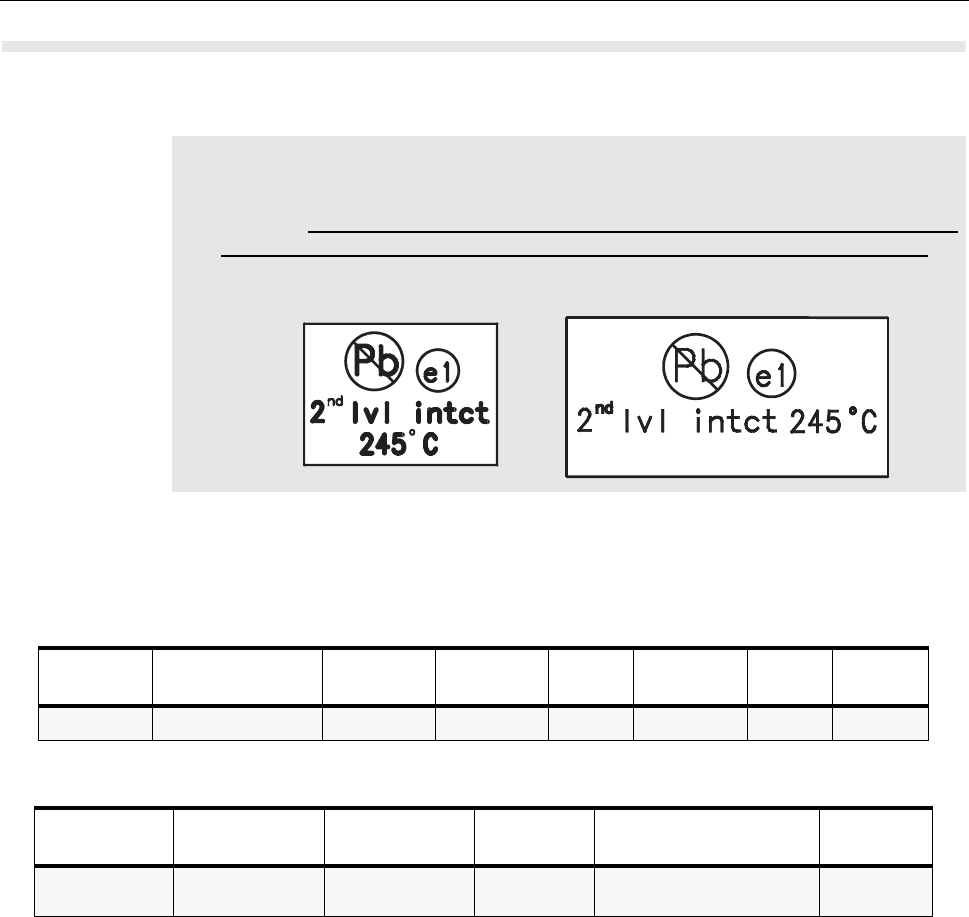
7 - 4 MAINTENANCE
General Repair Procedures and Techniques
Any rework or repair on Environmentally Preferred Products must be done using the appropriate
lead-free solder wire and lead-free solder paste as stated in the following table:
Parts Replacement and Substitution
When damaged parts are replaced, identical parts should be used. If the identical replacement
component is not locally available, check the parts list for the proper Motorola part number and
order the component from the nearest Motorola Communications parts center listed in the “Piece
Parts” section of this manual.
Rigid Circuit Boards
The family of radios uses bonded, multi-layer, printed circuit boards. Since the inner layers are
not accessible, some special considerations are required when soldering and unsoldering
components. The through-plated holes may interconnect multiple layers of the printed circuit.
Therefore, care should be exercised to avoid pulling the plated circuit out of the hole.
When soldering near connector pins:
• avoid accidentally getting solder in the connector.
• be careful not to form solder bridges between the connector pins
• closely examine your work for shorts due to solder bridges.
NOTE Environmentally Preferred Products (EPP) (refer to the marking on the printed circuit
boards — examples shown below) were developed and assembled using environmen-
tally preferred components and solder assembly techniques to comply with the Euro-
pean Union’s Restriction of Hazardous Substances (ROHS) Directive 2002/95/EC
and Waste Electrical and Electronic Equipment (WEEE) Directive 2002/96/EC. To
maintain product compliance and reliability, use only the Motorola specified parts in this
manual.
Table 7-1 Lead Free Solder Wire Part Number List
Motorola
Part Number Alloy Flux Type Flux Content
by Weight
Melting
Point
Supplier Part
number Diameter Weight
1088929Y01 95.5Sn/3.8Ag/0.7Cu RMA Version 2.7-3.2% 217C 52171 0.015” 1lb spool
Table 7-2 Lead Free Solder Paste Part Number List
Motorola Part
Number
Manufacturer Part
Number Viscosity Type Composition & Percent Metal Liquid
Temperature
1085674C03 NC-SMQ230 9001000KCPs
Brookfield (5rpm)
Type 3
(-325/+500)
(95.5%Sn-3.8%Ag-0.7%Cu)
89.3%
217°C
6866539D31.book Page 4 Tuesday, March 20, 2007 6:32 PM

MAINTENANCE 7 - 5
Chip Components
Use the RLN4062 Hot-Air Repair Station for chip component replacement. Adjust the temperature
control to 390 °C (735 °F), and adjust the airflow to a minimum setting. Airflow can vary due to
component density.
•To remove a chip component:
1. Use a hot-air hand piece and position the nozzle of the hand piece approximately 0.3 cm
(1/8) above the component to be removed.
2. Begin applying the hot air. Once the solder reflows, remove the component using a pair
of tweezers.
3. Using a solder wick and a soldering iron or a power desoldering station, remove the
excess solder from the pads.
•To replace a chip component using a soldering iron:
1. Select the appropriate micro-tipped soldering iron and apply fresh solder to one of the
solder pads.
2. Using a pair of tweezers, position the new chip component in place while heating the
fresh solder.
3. Once solder wicks onto the new component, remove the heat from the solder.
4. Heat the remaining pad with the soldering iron and apply solder until it wicks to the
component. If necessary, touch up the first side. All solder joints should be smooth and
shiny.
•To replace a chip component using hot air:
1. Use the hot-air hand piece and reflow the solder on the solder pads to smooth it.
2. Apply a drop of solder paste flux to each pad.
3. Using a pair of tweezers, position the new component in place.
4. Position the hot-air hand piece approximately 0.3 cm (1/8” ) above the component and
begin applying heat.
5. Once the solder wicks to the component, remove the heat and inspect the repair. All
joints should be smooth and shiny.
Shields
Removing and replacing shields is recommended to be done with the Air Blower,
BOSCH GHG 603 or equivalent.
•To remove the shield:
1. Place the circuit board in the circuit board holder.
2. Add solder paste flux around the base of the shield.
3. Position the heat-focus head onto the shield.
4. Turn on the heater and wait until the shield lifts off the circuit board.
5. Once the shield is off, turn off the heat, and grab the part with a pair of tweezers.
6. Remove the circuit board from the circuit board holder.
•To replace the shield:
1. Add solder to the shield if necessary, using a micro-tipped soldering iron.
2. Next, rub the soldering iron tip along the edge of the shield to smooth out any excess
solder. Use solder wick and a soldering iron to remove excess solder from the solder
pads on the circuit board.
3. Place the circuit board back in the circuit board holder.
4. Place the shield on the circuit board using a pair of tweezers.
6866539D31.book Page 5 Tuesday, March 20, 2007 6:32 PM
7 - 6 MAINTENANCE
5. Position the heat-focus head over the shield.
6. Turn on the heater and wait for the solder to reflow.
7. Once complete, turn off the heat, raise the heat-focus head and wait approximately one
minute for the part to cool.
8. Remove the circuit board and inspect the repair. No cleaning should be necessary.
Pre-baking of Integrated Circuits
Electronic components are generally coated with plastic material which has the nature of not being
waterproof. If kept unsealed the components can absorb humidity. When soldered to the board
(especially with reflow techniques) the sudden change in temperature can cause fissure or crack
which can result in malfunction or damage.
To avoid this problem these moisture sensitive components (MS) should be stored and shipped in a
sealed wrapping (dry pack). Processing must take place only with “dry components” when an
uninterrupted dry storage can be guaranteed, otherwise the components have to be pre-baked.
If a reflow procedure takes place close to MS components the whole board must be pre-baked.
*) Out of dry package Moisture Sensitivity Level (MSL) 2 : 1 year
2A : 1 month
3 : 168 hrs
Table 7-3 List of MTM800 ENH moisture sensitive components
Part. No. MSL* Description
5166554A01 3 ADDAG
5109841C71 3 GAM IC (on GPS option board)
5186988J77 3 JAVELIN
5185956E43 2A FLASH 16MB
5185963A85 3 ABACUS AD9874
5166541A01 3 Patriot ROM3
5189233U61 3 PSRAM 4MB
5199434A01 2 Serial SPI EEPROM
6866539D31.book Page 6 Tuesday, March 20, 2007 6:32 PM

MAINTENANCE 7 - 7
Repair Procedures and Techniques - General
Parts Replacement and Substitution
When damaged parts are replaced, identical parts should be used. If the identical replacement part
is not locally available, check the parts list for the proper Motorola part number and order the part
from the nearest Motorola Communications parts center listed in the “SUPPORT CENTRES” section
of this manual.
Disassembling and Reassembling the Terminal - General
Since these terminals may be disassembled and reassembled with the use of only six (board to
casting) screws, it is important to pay particular attention to the snaps and tabs, and how parts align
with each other.
The following tools are required for disassembling the terminal:
• Small flat blade screwdriver
• Dismantling Tool (Motorola Part No.: 6686119B01)
• TORX™ T screwdriver
•TORQUES: Diecast Top Cover (6x): 1.92 Nm … 2.03Nm (17-18 lbin)
GPS Cover (5x), GPS Board (1x): 1.13 Nm +/- 10% (10 lbin +/- 10%)
UCM Board Cover (3x): 1.13 Nm +/- 10% (10 lbin +/- 10%)
Enhanced Control Head Screws: 0.57Nm +/- 0.046Nm (5 lbin +- 0.4 lbin)
NOTE: If a unit requires more complete testing or service than is customarily performed at the
basic level, send this unit to a Motorola Authorized Service Center (refer to Appendix
A: Support Centers). The following described disassembly procedures should be
performed only if necessary.
6866539D31.book Page 7 Tuesday, March 20, 2007 6:32 PM
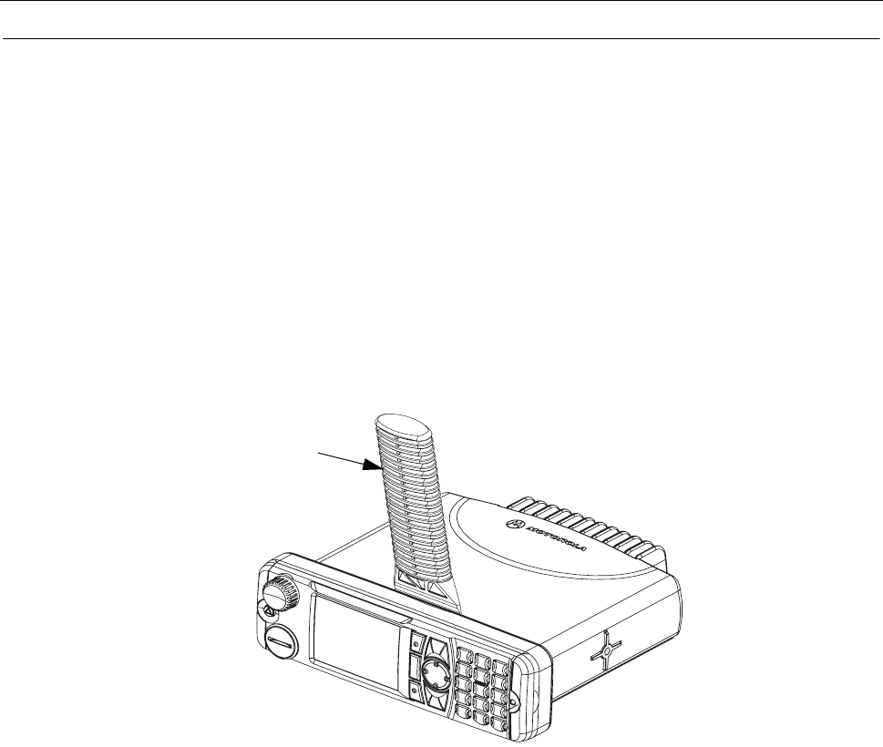
7 - 8 MAINTENANCE
Terminal Disassembly and Reassembly - Detailed
The procedure to remove and replace a Enhanced Control Head, Top Cover or Transceiver Board is
similar for all models of terminal. A typical procedure is therefore shown followed by specific
disassembly procedures for Enhanced Control Heads, Remote Head Enhanced and Data
Expansion Head Enhanced on terminal models.
Enhanced Control Head Removal
1. Insert the dismantling tool in the groove between the Enhanced Control Head and the termi-
nal assembly as shown in the Figure.
2. Press on the dismantling tool until the snap connectors on the side of the Enhanced Control
Head release from the terminal assembly.
3. Pull the Enhanced Control Head away from the terminal assembly as shown below.
Figure 7-1 Typical Enhanced Control Head Removal
Dismantling
Tool
6866539D31.book Page 8 Tuesday, March 20, 2007 6:32 PM
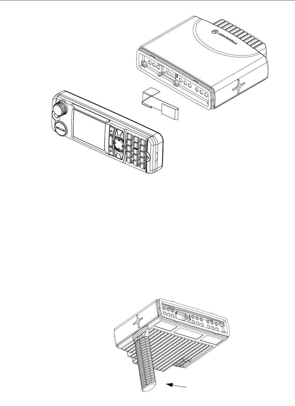
MAINTENANCE 7 - 9
Figure 7-2 Flexible Connection Removal
4. Remove the flexible connection from the socket on the Enhanced Control Head board.
Top Plastic Cover Removal
1. Insert the dismantling tool in the middle of the terminal assembly side groove as shown in
Figure 7-3.
2. Press on the dismantling tool until the snap connectors on the side of the plastic cover release
from the terminal chassis.
3. Lift the plastic cover from the chassis.
Figure 7-3 Top Cover Removal.
Dismantling
ZWG0130211-O
Tool
6866539D31.book Page 9 Tuesday, March 20, 2007 6:32 PM
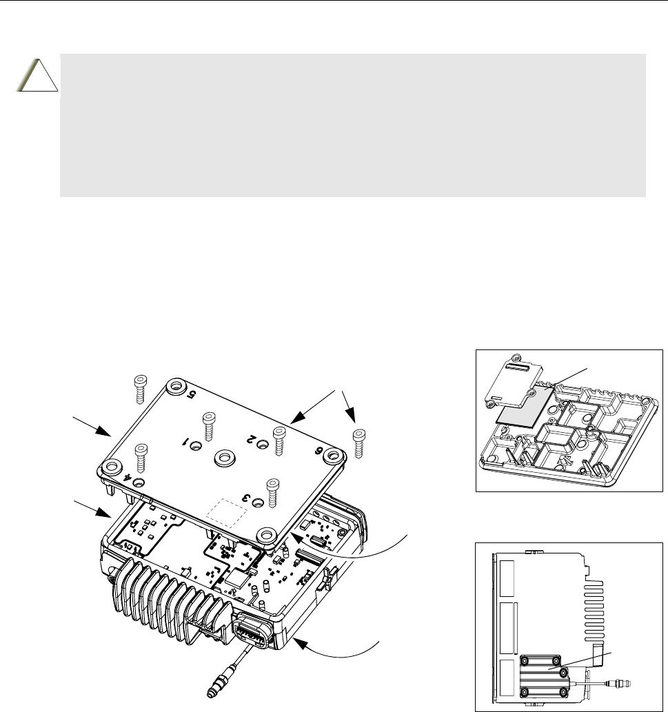
7 - 10 MAINTENANCE
Transceiver Board Removal
1. Remove six screws from the diecast cover using the T20 TORX™ driver as shown in
Figure 7-4.
2. If existing remove the metal GPS cover from the bottom (5 screws, T10 TORX™).
Remove the internal GPS board (one screw) from the transceiver and disconnect the flex
cable from the main board.
3. Lift the cover from the chassis.
Figure 7-4 Diecast Cover Removal
4. Pull out the plastic accessory connector housing to the back.
5. Slowly lift the transceiver board on the edge at the front of the terminal (the edge that mates
with the Enhanced Control Head) and pull gently toward the front of the terminal as shown in
Figure 7-5. Take care to slide the antenna connector and power connector out of the chassis
towards the front.
6. If existing, take extra care of the UCM Board inside the cover plate and disconnect the flex
CAUTION: Some terminals are equipped with a GPS module at the left side bottom of
the transceiver and/or an additional UCM Board inside the transceiver cover plate, refer
to special label at the cover plate (dotted line at the figure below).
There are flex cables installed connecting these boards to the main board. Take extra
care not to tear off the flex when dis-assembling or re-assembling the board from/to the
transceiver or this could damage the GPS/UCM Board and the main board (refer to
chapter explosion views figure 11, 12 for a detailed view).
!
C a u t i o n
Diecast
Cover
Screws (6x)
Terminal
Chassis
ZWG0130212-O
Additional
UCM Board
Optional
GPS Module
Position of UCM board
Position of GPS Module
UCM
GPS
Module
board
6866539D31.book Page 10 Tuesday, March 20, 2007 6:32 PM
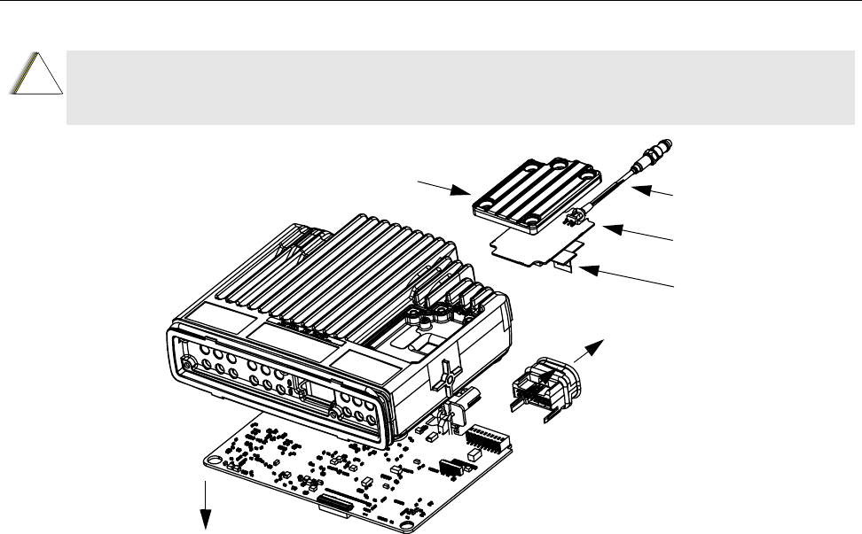
MAINTENANCE 7 - 11
cable from the mainboard.
Figure 7-5 GPS and Mainboard Removal (view from bottom side)
Reassembly the Terminal Chassis And Transceiver Board (torques, see page 7-7)
1. Inspect the transceiver board and ONLY if the surface of the thermal pads show signs of dam-
age, remove the thermal pads and apply thermal grease to the heatsink area on the chassis
and heat dissipating devices.
2. Insert the transceiver board at an angle (approximately 30°) into the chassis taking care to
slide the antenna connector and accessory connector into their cut-outs in the chassis.
3. Lower the transceiver board onto the chassis and align the two locating holes in the board
with the locating pins in the chassis.
4. If a UCM board was mounted, reconnect the flex cable to the mainboard. Take care of the
specific flex bending. Note: After removal the UCM board has to be reprogrammed (App. C).
5. Secure the cover to the chassis with the six screws previously removed.
6. Torque the six screws to 1.9 NM (17 in lbs) using the T20 TORX™ driver. Begin with screw 6
followed by 5 to 1. Since the screws usually take a set, torque the screws a second time (1.9
NM) in the same order.
7. If existing, reconnect the GPS flex cable and reassemble the GPS module and cover plate.
8. Refit top cover over the assembled terminal chassis. Press cover down until it snaps into
place.
Enhanced Control Head Fitting
1. Align the ‘dot’ or ‘O’ marking on the flex with the ‘O’ mark on the chassis to the socket on the
terminal assembly as shown in Figure 7-2.
2. Check that the back housing o-ring seal is undamaged and fitted in the groove. Replace the
seal if it is damaged (refer to the exploded view diagrams and parts list).
CAUTION: The thermal pad can act as an adhesive and cause the leads of the heat
dissipating devices to be over stressed if the board is lifted too quickly.
If the board can't be easily lifted, the chassis must be heated up to 55 degree Celsius.
!
C a u t i o n
Lift
Accessory
Connector
Housing
GPS Board
GPS Flex
GPS Cable
Mainboard
Lift
Pull out
GPS Cover
6866539D31.book Page 11 Tuesday, March 20, 2007 6:32 PM
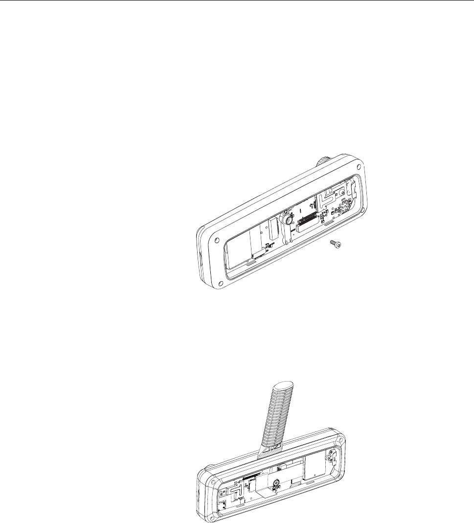
7 - 12 MAINTENANCE
3. Fit the back housing to the Enhanced Control Head. Ensure that the tags on the back housing
align with the snap catch grooves on the Enhanced Control Head. Press the back housing
into place until it snaps into place.
4. Check that the terminal chassis o-ring seal is undamaged and fitted in the groove on the chas-
sis assembly. Replace the seal if it is damaged.
Enhanced Control Head - Disassembly
1. Remove the middle screw from the back of the Enhanced Control Head using a T10 TORX™
as shown in the following figure.
Figure 7-6 Middle Screw Removal
2. To dismount the Enhanced Control Head front housing from the back housing, insert the dis-
mantling tool in the groove between the two housings as shown in the following figure.
Figure 7-7 Enhanced Control Head Back Housing Removal
6866539D31.book Page 12 Tuesday, March 20, 2007 6:32 PM
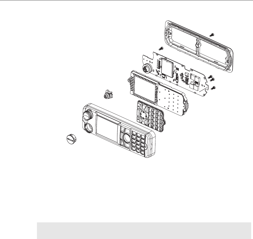
MAINTENANCE 7 - 13
3. Press the dismantling tool until the snap connectors on the side of the back housing release
from the Enhanced Control Head.
Figure 7-8 Enhanced Control Head Board Removal
4. Remove the board from the Enhanced Control Head front housing by unscrewing the screws
using a T10 TORX™ and disassemble the encoder switch flex from the socket on the board.
5. Remove the board from the Enhanced Control Head housing by stretching the Enhanced
Control Head housing and pulling up the board.
6. Remove the keypad by gently pressing the keypad out from the Enhanced Control Head front
housing.
Enhanced Control Head - Reassembly
1. Fit the rubber keypad onto the Enhanced Control Head housing and ensure that the keypad is
correctly aligned and pressed onto the groove on the front housing.
2. Assemble the board to the Enhanced Control Head front housing.
3. Assemble the encoder switch flex to the socket on the board.
4. Screw the two 8mm self tapping screws and one 14mm self tapping screw.
NOTE Care should be taken not to touch or contaminate the conductive pads on the under
side of the keypad or the conductive contacts on the printed circuit board.
ZWG0130215-O
6866539D31.book Page 13 Tuesday, March 20, 2007 6:32 PM
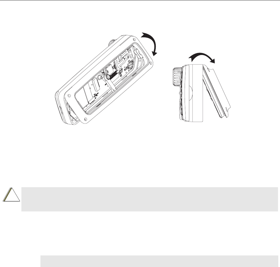
7 - 14 MAINTENANCE
5. Snap the back housing into the Enhanced Control Head front housing in the orientation shown
below.
Figure 7-9 Reassemble Enhanced Control Head Housing
6. Screw the middle screw to the back housing.
Remote Head Enhanced - Disassembly
To Disassemble the Remote Head Enhanced from the Terminal:
1. Remove the Remote Head Enhanced (PMLN4904_) from the Transceiver by inserting the dis-
mantling tool (Motorola part number 6686119B01) in the recess between the Remote Head
Enhanced and the Transceiver.
2. Remove the flex.
CAUTION: The terminal must be disconnected from the power supply before commencing
any disassembly. The Installation Manual should be referred to for more detailed information
on warnings and safety.
NOTE: To minimize cosmetic damage disassemble from the bottom side (label side).
ZWG0130214-O
!
C a u t i o n
6866539D31.book Page 14 Tuesday, March 20, 2007 6:32 PM
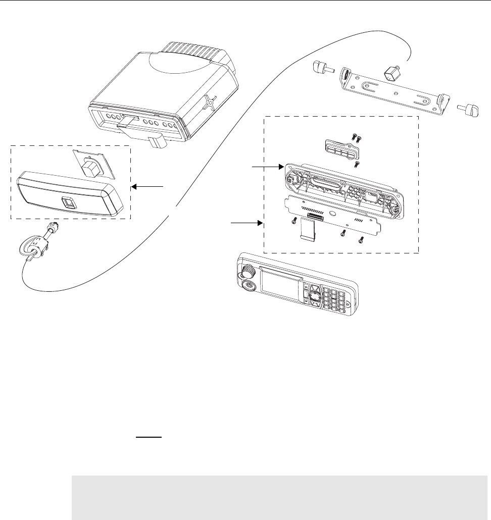
MAINTENANCE 7 - 15
Figure 7-10 Remote Mount Enhanced Control Head with Remote Head Enhanced
Remote Head Enhanced - Reassembly
To Reassemble the Remote Front Housing:
1. Connect the flex from the Remote Head Enhanced to the top small connector in the Trans-
ceiver.
2. Press the Remote Head Enhanced onto the Transceiver chassis until the chassis tabs snap
into place.
Remote Mount Enhanced Control Head - Disassembly
To Disassemble the Remote Mount Enhanced Control Head:
1. Unscrew the wing screws of the remote trunnion and remove the remote trunnion from the
Remote Mount Enhanced Control Head.
2. Unscrew the middle screw from the back housing.
3. Remove the back housing by inserting the dismantling tool (Part No. 6686119B01) in the
recess between the back housing and Remote Mount Enhanced Control Head front housing.
NOTE: For correct orientation of the flex in the Transceiver, the “plastic” tab should be up,
contacts facing down. Align the ‘dot’ or ‘O’ marking on the flex with the ‘O’ mark on
the Transceiver. The flex must be pushed into the connector until it meets the stop.
Remote Head Enhanced
Remote Back Housing
Remote Back Head
6866539D31.book Page 15 Tuesday, March 20, 2007 6:32 PM
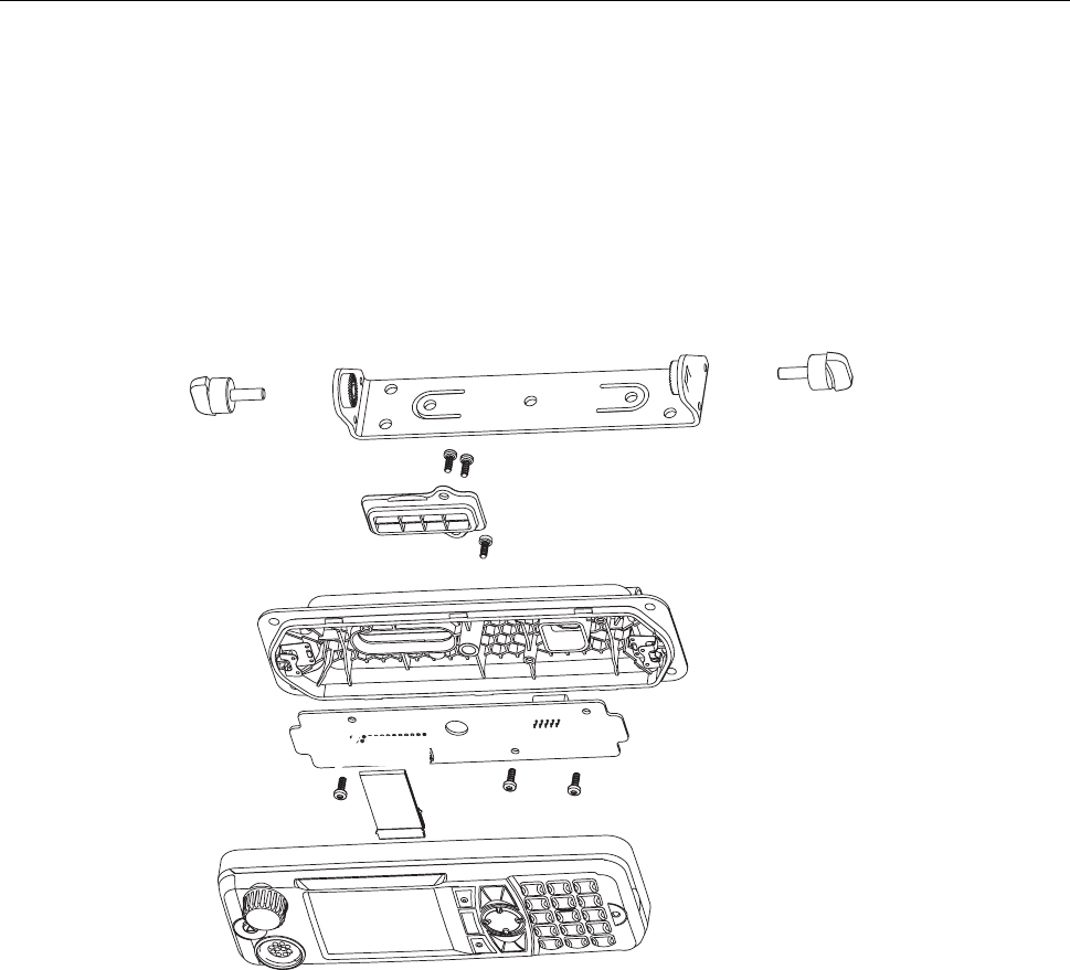
7 - 16 MAINTENANCE
4. Remove the flex between the remote PCB and Main PCB.
5. Remove the board from the Remote Mount Enhanced Control Head front housing by
unscrewing the screws using T10 TORXTM ad disassemble the encoder switch flex from the
socket on the board.
6. Remove the board from the Remote Mount Enhanced Control head front housing by stretch-
ing the Remote Mount Enhanced Control Head front housing and pulling up the board.
7. Remove the keypad by gently pressing the keypad out from the Remote Mount Enhanced
Control Head front housing.
8. Unscrew 3 screws using T10 TORXTM to extract remote PCB from the remote back housing.
Figure 7-11 Remote Mount Enhanced Control Head
Remote Mount Enhanced Control Head - Reassembly
1. Fit the rubber keypad onto the Remote Mount Enhanced Control Head front housing and
ensure that the keypad is correctly aligned and pressed onto the groove of the front housing.
2. Assemble the board to the Remote Mount Enhanced Control Head front housing.
3. Assemble the encoder switch flex to the socket on the board.
4. Screw the two 8mm self tapping screws and one 14mm self tapping screw.
5. Assemble the remote PCB into the remote back housing by screwing the 3 screws.
6. Connect the flex from the remote board on the back housing to the connector on the PCB
board of the Remote Mount Enhanced Control Head front housing.
7. Snap the back housing into the Remote Mount Enhanced Control Head front housing.
8. Screw the middle screw to the back housing.
6866539D31.book Page 16 Tuesday, March 20, 2007 6:32 PM
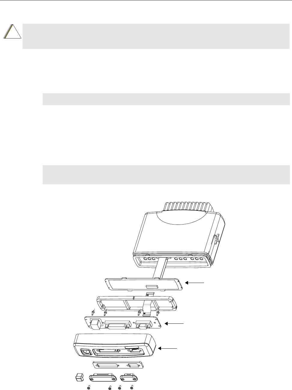
MAINTENANCE 7 - 17
Data Expansion Head Enhanced - Disassembly
To Disassemble the Data Expansion Head Enhanced from the Terminal
1. Remove the Data Expansion Head Enhanced from the transceiver by inserting the dismantling tool
(Part No. 6686119B01) in the recess between the expansion head enhanced and the transceiver.
2. Remove the two flexes from the terminal.
To Disassemble the Expansion Board from Expansion Head Housing
1. Remove the board from the expansion head housing by levering the expansion head housing
and pulling up on the expansion board.
2. Lift the top latch and remove the 40-Pin flex from connector board.
Figure 7-12 Expansion Head Enhanced Exploded View
CAUTION: The terminal must be disconnected from the power supply before commencing
any disassembly. The Terminal Installation Manual should be referred to for more detailed
information warnings and safety.
NOTE: To minimize cosmetic damage disassemble from the bottom side, (label side).
NOTE: The 40 pin connector has a top latch that needs to be lifted before the flex is inserted
and closed after flex insertion.
!
C a u t i o n
Expansion Head Housing
Expansion Board
Connector Board
6866539D31.book Page 17 Tuesday, March 20, 2007 6:32 PM

7 - 18 MAINTENANCE
To Disassemble the Connector Board from Expansion Head Housing
1. Remove the silicon rubber frame
2. Remove the four screws from the connector board.
3. Remove all the protection caps on the front of the expansion head housing.
4. Lift the connector board from the expansion head housing.
Data Expansion Head Enhanced - Reassembly
To Reassemble the Data Expansion Head Enhanced
1. Insert the connector board into the expansion head housing.
2. Secure the connector board with the four screws previously removed.
3. Insert the rubber frame
4. Insert the 40 pin flex from the connector board to the Expansion board, ensuring that the top
latch is firmly closed.
5. Snap the Expansion board into the expansion head housing
6. Connect the 12 line flex to the Terminal, top small connector.
7. Connect the 40 line flex to the Terminal, bottom large connector
8. Close the top latch after flex insertion
9. Push the expansion head housing onto the Transceiver until all 4 tabs snap firmly into place.
NOTE: For correct orientation of the flex align the ‘dot’ or ‘O’ marking on the flex with the ‘O’
mark on the PCB.
NOTE: The Expansion Head has a protection grade of IP54. To maintain IP54 sealing when
connecting a RS232 data cable make sure to use a IP54 specified cable. (example:
ROLINE AT-Modem cable ST-BU 1,8m order no. 11.01.4518)
NOTE: The flex is not designed for continuous insertion, replace after several uses.
6866539D31.book Page 18 Tuesday, March 20, 2007 6:32 PM
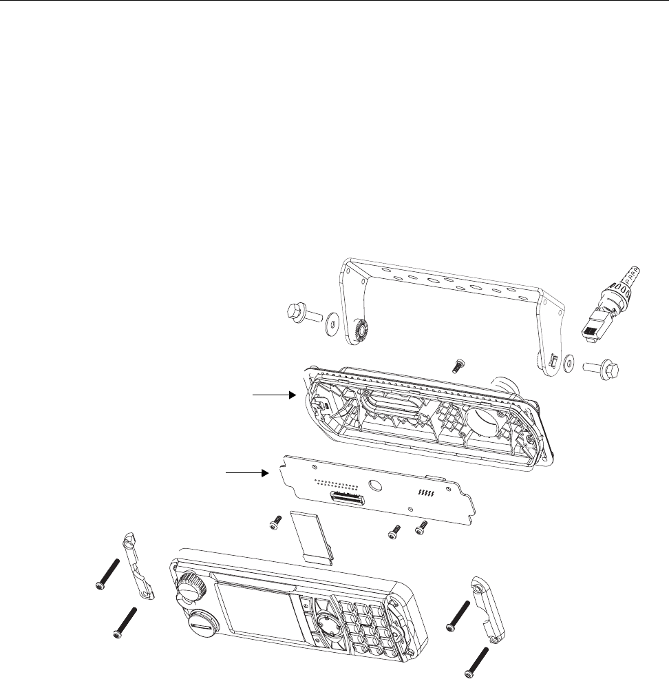
MAINTENANCE 7 - 19
Motorcycle Mount Enhanced Control Head - Disassembly
To disassembly the Motorcycle Mount Enhanced Control Head:
1. Unscrew the screws of the Motorcycle Mount Enhanced Control Head trunnion and remove
the Motorcycle Mount Enhanced Control Head from the trunnion.
2. Twist and pull out the telco cable from the connector.
3. Unscrew the middle screw from the back housing.
4. Unscrew the four screws of the two side caps.
5. Remove the back housing by inserting the dismantling tool (Part No. 6686119B01) in the
recess between the back housing and Motorcycle Mount Enhanced Control Head front hous-
ing.
Figure 7-13 Motorcycle Enhanced Control Head Exploded View
6. Remove the flex between the remote PCB and Main PCB.
7. Remove the board from the Motorcycle Mount Enhanced Control Head front housing by
unscrewing the screws using T10 TORXTM and disassemble the encoder switch flex from the
socket on the board.
8. Remove the board from the Motorcycle Mount Enhanced Control head front housing by
stretching the Motorcycle Mount Enhanced Control Head front housing and pulling up the
board.
9. Remove the keypad by gently pressing the keypad out from the Motorcycle Mount Enhanced
Control Head front housing.
10. Unscrew 3 screws using T10 TORXTM to extract remote PCB from the motorcycle back
housing.
Motorcycle Back Housing
Remote PCB
6866539D31.book Page 19 Tuesday, March 20, 2007 6:32 PM

7 - 20 MAINTENANCE
Motorcycle Mount Enhanced Control Head - Reassembly
1. Fit the rubber keypad onto the Motorcycle Mount Enhanced Control Head front housing and
ensure that the keypad is correctly aligned and pressed onto the groove of the front housing.
2. Assemble the board to the Motorcycle Mount Enhanced Control Head front housing.
3. Assemble the encoder switch flex to the socket on the board.
4. Screw the two 8mm self tapping screws and one 14mm self tapping screw.
5. Assemble the remote PCB into the motorcycle back housing by screwing the 3 screws.
6. Connect the flex from the remote board on the back housing to the connector on the PCB
board of the Motorcycle Mount Enhanced Control Head front housing.
7. Snap the back housing into the Motorcycle Mount Enhanced Control Head front housing.
8. Screw the middle screw to the back housing.
Service Aids
The following table lists the service aids recommended for working on the terminal. While all of
these items are available from Motorola, most are standard workshop equipment items, and any
equivalent item capable of the same performance may be substituted for the item listed.
Table 7-4 Service Aids
Motorola Part No. Description Application
6666500A01 Housing Eliminator Test Fixture used to bench test the terminal
pcb
6686119B01 Dismantling Tool Assists in the removal of terminal Enhanced
Control Head
0180320B16
6680321B81
6680321B56
Torx Screw Driver Kit (T6,8,10,15,25)
Torx Bi t
Insert Bit extra long
T-20 TORX
(or equivalent)
Screwdriver with torque meter
6866539D31.book Page 20 Tuesday, March 20, 2007 6:32 PM
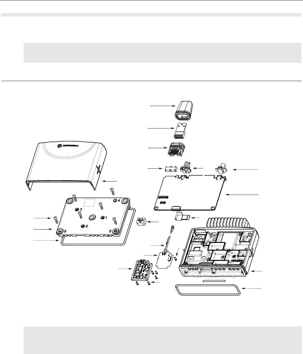
MAINTENANCE 7 - 21
EXPLODED VIEWS & PARTS LISTS
Transceiver - Exploded View and Parts List
Figure 7-14 Transceiver Exploded View
NOTE: For optimum performance, all replacement parts, diodes, transistors and integrated circuits
must be ordered by Motorola part numbers.
NOTE: Terminals with special label OPTION BOARD MOUNTED (see dotted lines on figure above)
are equipped with an additional board inside the transceiver cover plate.
Refer to the figure next page before disassembling such terminals.
11
12
14
9
10
2
3
4
5
8
13
6
1
17c
17b
17a
7
17d
18
15
16
6866539D31.book Page 21 Tuesday, March 20, 2007 6:32 PM

7 - 22 MAINTENANCE
Table 7-5 Transceiver Parts List
Item No. Description Part Number
1 Chassis (item 2 included) 2766532A01
2 Gasket, Enhanced Control Head 3202620Y01
3 Main PCB (items 4 - 7 included) refer to Appendix: Service Kits
4 BNC Antenna Connector 0986166B01
5 Power Connector 0986165B01
6 Accessory Connector 0986105B01
7 Flex to optional GPS 3066541B01
8 Connector Assembly 2886122B02
9 Connector Housing 16Pos. 1580922V01
10 Gasket Accessory Connector 3202606Y02
11 Gasket Cover 3286095B01
12 Cover 1566511A02
13 Screw T20, 6x (M4) 0310911A30
14 Cover, Plastic 1586170B01
15 Silicon Pressurepad for UHF only 7566500A01
16 Silicon Pressurepad for 800MHz only 7566502A01
17 GPS Module Kit: 0166502N65
17a GPS Board with flex 0166502N20
17b Coax Cable 3366540B01
17c GPS Cover 1566548A01
17d Screw, 5x (M3x8) 0310907A19
18 Screw for GPS board, 1x (M3x8) 0310907A19
19 Bushing for IP 54 Protection w/o GPS (not shown) 4366504A02
20 UCM Board Kit: GMLN4210_
20a UCM Board Module CLN8041_
20b UCM Board Cover 0786183B01
20c UCM Board Flex 8485615Z02
20d Screw 3x (M5x8) 0310943R55
6866539D31.book Page 22 Tuesday, March 20, 2007 6:32 PM
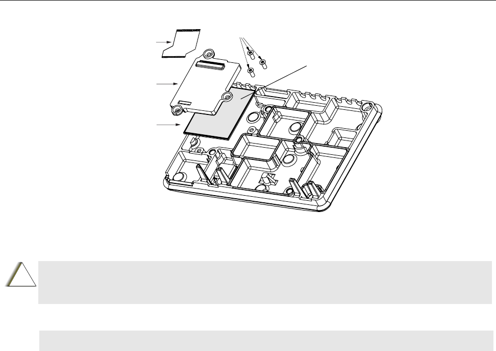
MAINTENANCE 7 - 23
Figure 7-15 Location of additional UCM Board inside the Cover Plate
CAUTION: There is a flex installed connecting the UCM board to the main board. Take extra
care not to tear off the flex when dis-assembling or re-assembling the board from/to the
transceiver cover plate or this could damage the UCM board and the main board.
NOTE: The CLN8041_ UCM board is not repairable. Order a replacement board if necessary.
2
0b
2
0a
2
0c
20d
UCM board inside the cover plate
!
C a u t i o n
6866539D31.book Page 23 Tuesday, March 20, 2007 6:32 PM
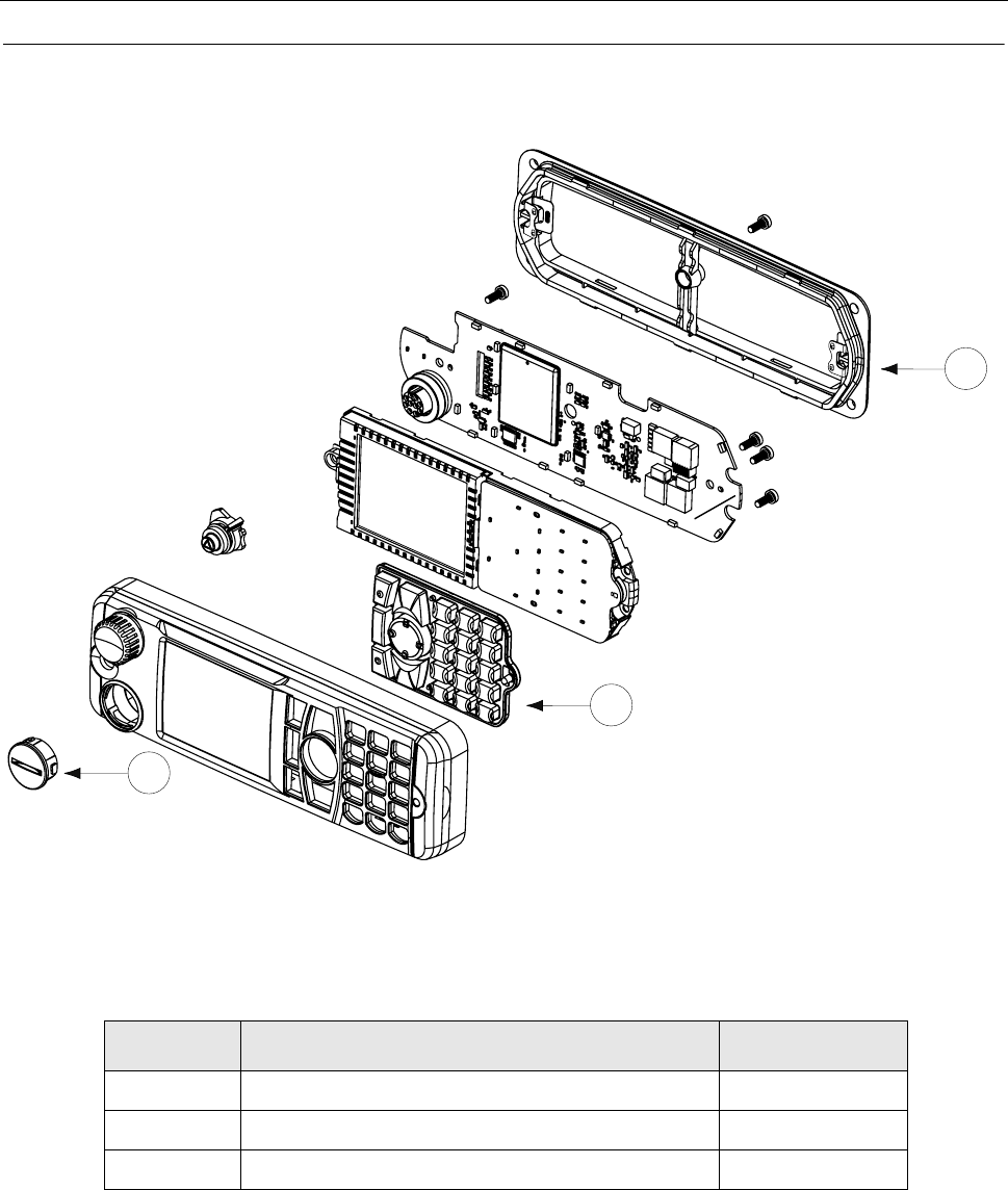
7 - 24 MAINTENANCE
Enhanced Control Head - Exploded View and Parts List
Figure 7-16 Enhanced Control Head - Exploded View 1
Table 7-6 Enhanced Control Head - Parts List 1
Item No Description Part No
1 GCAI Cover 1515048C01
2 KeyPad Assy 7571017L01
3 Head Bridge Assy 0104025J29
ZWG0130201-O
2
1
3
6866539D31.book Page 24 Tuesday, March 20, 2007 6:32 PM
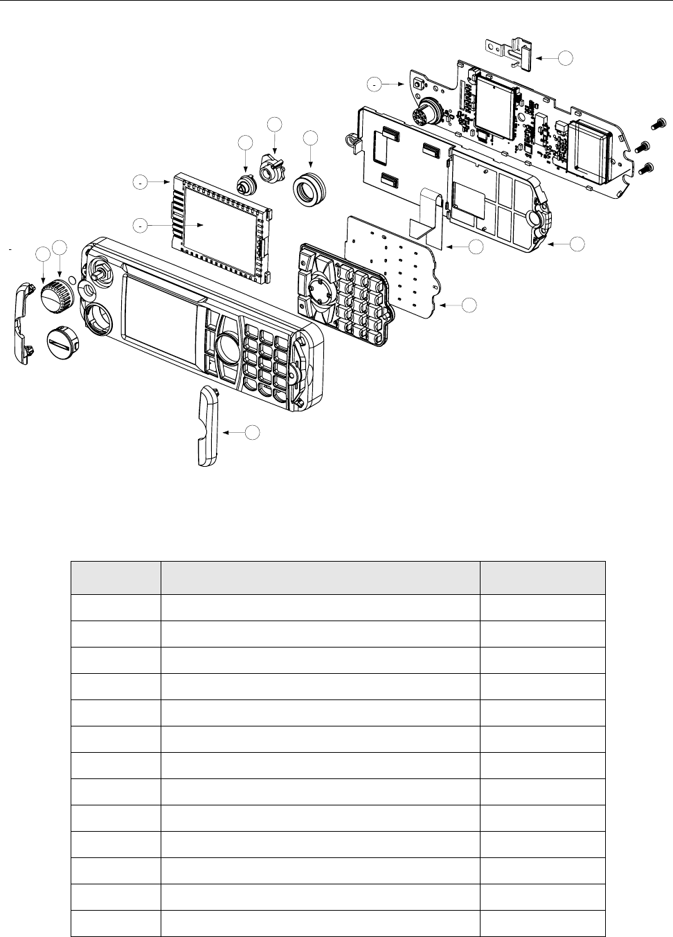
MAINTENANCE 7 - 25
Figure 7-17 Enhanced Control Head - Exploded View 2
Table 7-7 Enhanced Control Head - Parts List 2
Item No Description Part No
1 Encoder Knob 3616898H01
2 Gore Port 3205472M02
3 LCD Module 7271138D01
4 LCD Rubber Jacket 7516954H01
5a Emergency Key 3816953H01
6 Emergency Key Frame 0716944H01
7 GCAI Seal 3264133H01
8 Main PWA Kit 0166500N86
9 LCD Metal Retainer 4216900H01
10 Chassis 2716937H01
11 KeyPad FFC 8471919L01
12 KeyPad PWA Kit 0166501N35
13 Side Cap 3816950H01
ZWG0130201-O
2
13
11
12
10
8
9
1
4
3
5
6
7
6866539D31.book Page 25 Tuesday, March 20, 2007 6:32 PM
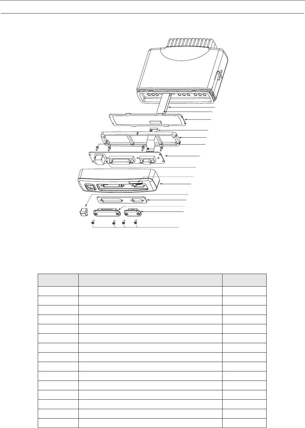
7 - 26 MAINTENANCE
Data Expansion Head Enhanced - Exploded View and Parts List
Figure 7-18 Data Expansion Head Enhanced - Exploded View
Table 7-8 Data Expansion Head Enhanced - Parts List
Item No Description Part No
1 Expansion Head Housing 1564290B01
2 Cover 9 Sub-D 3864326B01
3 Cover 25 Sub-D 3864326B02
4 Protection Caps/Bung, Telco GLN7306_
5 Seal, Expansion Head 3264325B01
6 Screw, Protection Caps/Bung (4 required) 0305137Q02
7 Connector Board PMLN5087A
8 Screw, Connector PCB (4 required) 0385944A02
9 Flex 40 Pin 8415157H01
10 Expansion Board, not part of Housing Kit PMLN4939A
11 Seal for 10 Pin Telco on PCB 3264291B01
12 Flex 12 Pin 8486127B01
13 Flex 40Pin 8466543A01
14 Silicone Pressure Pad 3264337B01
15 Label 5464344B07
1
2
3
4
5
6
7
8
9
10
11
12
13
15
14
6866539D31.book Page 26 Tuesday, March 20, 2007 6:32 PM
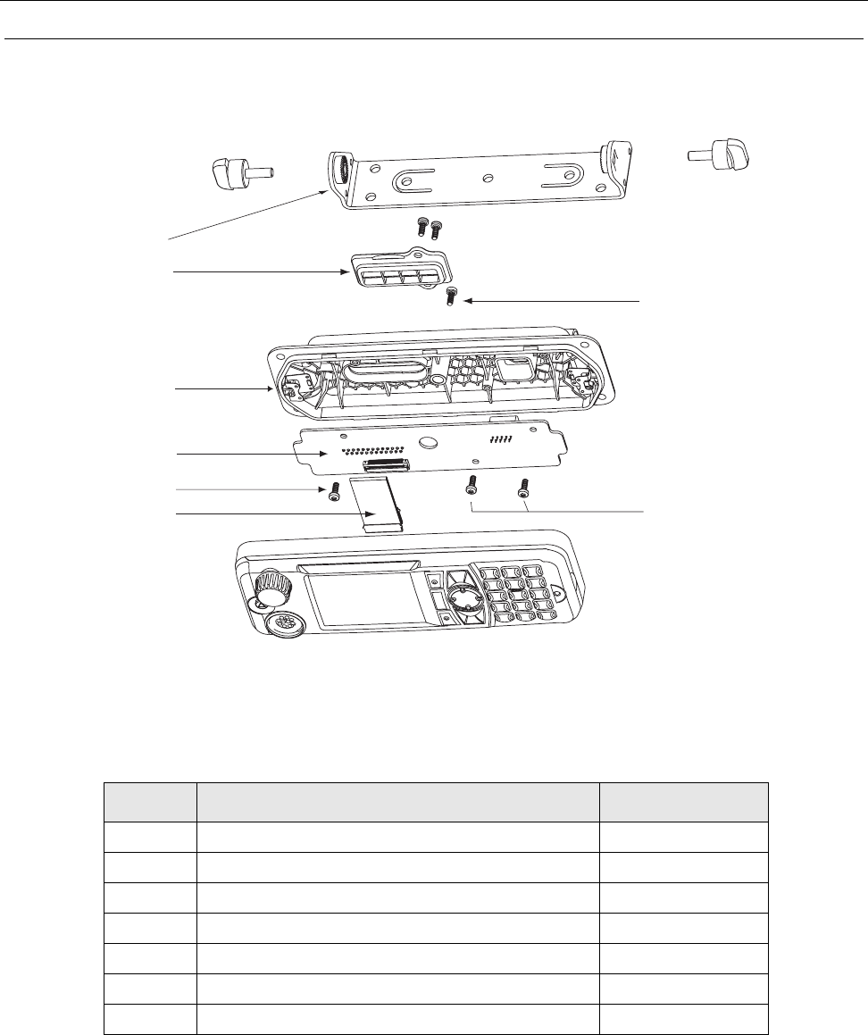
MAINTENANCE 7 - 27
Remote Mount Enhanced Control Head - Exploded View and Parts List
Figure 7-19 Remote Mount Enhanced Control Head - Exploded View
Table 7-9 Remote Mount Enhanced Control Head - Parts List
Item No. Description Part No.
1 Remote FFC (Main to Remote) 8471921L01
2 Remote PWA Kit 0166501N45
3 Remote Back Hsg Assy 0104025J30
4 D Sub Cover 1571012L01
5 Trunnion 0716933H01
6 Middle Screw 0371912L01
7 Self Tapping Screw 0316961H01
1
2
3
4
5
6
7
7
6866539D31.book Page 27 Tuesday, March 20, 2007 6:32 PM
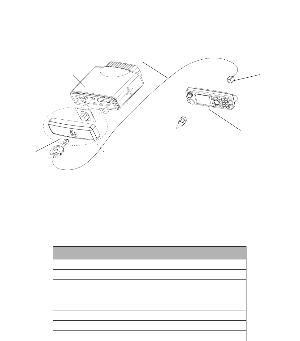
7 - 28 MAINTENANCE
Remote Mount Configuration - Exploded View and Parts List
Figure 7-20 Remote Mount Configuration - Exploded View
Table 7-10 Associated Components for Remote Mount Configuration
No. Description Part Number
1 Remote Mount Cable, 3 m RKN4077_
2 Remote Mount Cable, 5 m RKN4078_
3 Remote Mount Cable, 7 m RKN4079_
4 Remote Mount Cable, 10 m PMKN4020_
5 Speaker Extension Cable GMKN4084_
6 Remote Head Enhanced PMLN4904_
7 Data Expansion Control Head PMLN4908_
8 Ferrite Clamp PMLN5148_
Transceiver
10-pin
Connector
Remote Mount Cable
10-pin
Connector
Flex
Remote Head
or
Data Expansion
Head Enhanced
Enhanced
Remote Mount
Enhanced Control Head
6866539D31.book Page 28 Tuesday, March 20, 2007 6:32 PM
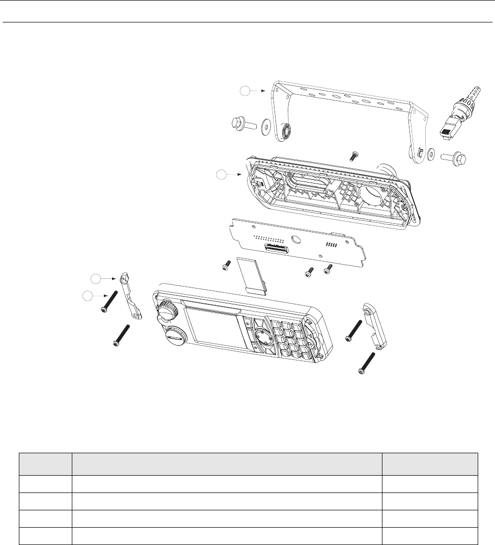
MAINTENANCE 7 - 29
Motorcycle Mount Enhanced Control Head - Exploded View and Parts List
Figure 7-21 Motorcycle Mount Enhanced Control Head - Exploded View
Table 7-11 Motorcycle Mount Enhanced Control Head - Parts List
Item No. Description Part No.
1 Side Cap Screw 0316960H02
2 MC Side Cap 3871547L01
3 MC Back Hsg Assy 0104025J31
4 MC trunnion 0771445L01
1
2
3
4
6866539D31.book Page 29 Tuesday, March 20, 2007 6:32 PM

7 - 30 MAINTENANCE
Notes
6866539D31.book Page 30 Tuesday, March 20, 2007 6:32 PM

SCHEMATICS, PCBs and PARTS LISTS 8 - 1
CHAPTER 8
SCHEMATICS, PCBS AND PARTS LISTS
Section Introduction
This Chapter contains the following Sections:
8.1 Transceiver 450-470MHz: Schematics/PCBs and Parts Lists
8.2 Enhanced Control Heads: Enhanced Control Head
Data Expansion Head Enhanced
Remote Head Enhanced
Remote Back Head Enhanced
Keypad Board for Enhanced Control Head
Any level 3 repairs can deeply affect the performance of the MTM800 ENH
terminal and may cause a new tuning procedure.
This tuning procedure can only be applied by certain authorized Motorola
depots where the appropriate TEST&TUNE EQUIPMENT is available.
The appropriate TEST&TUNE EQUIPMENT is a special automated test
equipment which is only available at some Motorola factories and Motorola
repair centres.
NOTE: For optimum performance, all replacement parts, diodes, transistors and integrated circuits
must be ordered by MOTOROLA part numbers.
!
W A R N I N G
!
6866539D31.book Page 1 Tuesday, March 20, 2007 6:32 PM

8 - 2 SCHEMATICS, PCBs and PARTS LISTS
Notes
6866539D31.book Page 2 Tuesday, March 20, 2007 6:32 PM

TRANSCEIVER 450-470MHz: SCHEMATICS, PCBs and PARTS LISTS 8.1 - 1
CHAPTER 8.1
TRANSCEIVER 450-470MHZ: SCHEMATICS, PCBS AND PARTS LISTS
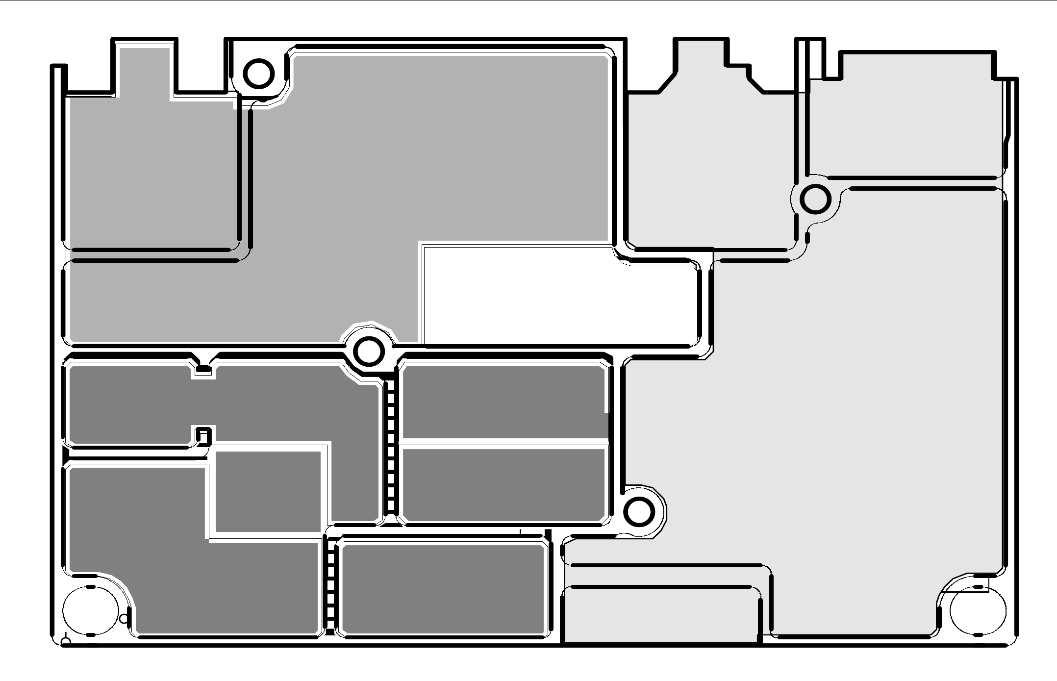
8.1 - 2 TRANSCEIVER 450-470MHz: SCHEMATICS, PCBs and PARTS LISTS
CHASSIS_OVERVIEW TRANSCEIVER
CONTROLLER
NET
PA
DUMMY
RF
DUMMY
JAVELIN
PA
NC
NC
NC
FRACN
NET
TX_VCO
NET
NC
NC
ABACUS
DUMMY
IF
NET
FE
RX_VCO
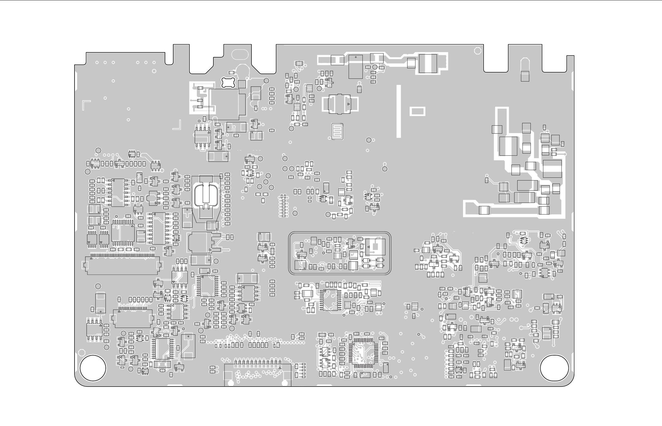
TRANSCEIVER 450-470MHz: SCHEMATICS, PCBs and PARTS LISTS 8.1 - 3
PCB / Main Board 8466575A01_A / TOP SIDE
C0110
C0111
C0113
C0114
C0116
C0117
C0118
C0119
C0120
C0121
C0122
C0123
C0124
C0125
C0127
C0128
C0129
C0130
C0131
C0132
C0133
C0134
C0135
C0136
C0137
C0138
C0139
C0140
C0141
C0142
C0143
C0146
C0151
C0157
C0158
C0159
C0161
C0162
C0163
C0164
C0200
C0201
C0202
C0203
C0204
C0205
C0213
C0219
C0220
C0221
C0222
C0223
C0224
C0225
C0226
C0228
C0229
C0231
C0236
C0300
C0301
C0314
C0315
C0316
C0317
C0318
C0320
C0321
C0322
C0323
C0325
C0326
C0328
C0329
C0330
C0331
C0332
C0333
C0334
C0336
C0337
C0338
C0340
C0341
C0344
C0401
C0459
C0460
C0461
C0462
C0463
C0464
C0509
C0537
C0538
C0539
C0540
C0551
C0552
C0553
C0555
C0556
C0557
C0558
C0559
C0560
C0561
C5001
C5002
C5003
C5004
C5005
C5006
C5009
C5011C5013
C5019
C5020
C5025
C5026
C5071
C5072
C5081
C5082
C5083
C5084
C5085
C5086
C5087
C5088
C5089
C5090
C5121
C5122
C5125
C5126
C5128
C5129
C5131
C5133
C5134
C5135
C5136
C5137
C5139
C5140
C5142
C5144
C5146
C5150
C5152
C5156
C5160
C5161
C5163
C5164
C5166
C5167
C5169
C5171
C5172
C5173
C5174
C5175
C5177
C5178
C5184
C5185 C5188
C5189
C5190
C5191
C5192
C5193
C5197
C5202
C5208
C5209
C5210
C5212
C5213
C5214
C5215
C5216
C5218
C5219
C5220
C5221
C5311
C5312
C5313
C5314
C5315
C5317
C5318
C5319
C5332
C5333
C5334
C5335
C5337
C5338
C5339
C5340
C5341
C5342
C5363
C5400
C5403
C5405
C5406
C5407
C5422
C5431
C5452 C5453
C5454
C5455
C5461
C5462
C5463 C5464 C5467
C5468
C5469 C5470
C5504
C5506
C5521
C5541
C5551
C5552
C5553
C5554
C5555
C5556
C5604
C5606
C5607
C5609
C5621
C5622
C5623
C5625
C5626
C5627
C5628
C5629
C5632
C5681
C5682
C5683
C5704
C5705
C5706
C5707
C5708
C5713
C5714
C5715
C5716
C5721
C5722
C5724
C5726
C5731
C5741
C5743
C5804
C5823
C5825
C5827 C5828
C5831
C5833
C5834
C5836
C5840
C5841
C5843
C5844
C5845
C5846
C5849
C5850
C5852
C5853
C5854
C5855
C5859
C5864
C5865
C5867
C5875
D0101
D0102
D0151
D0153
D0303
D0304
D0325
D1101
D5001
D5025
D5081
D5082
D5121
D5190
D5201
D5202
D5301
D5302
D5451
D5454
D5551
D5601
D5602
D5603
D5604
E0300
F0301
F0302
F0303
1
20
11
10
FL0200
1
40
J0450
12 1
J0550
1
18
J0570
L0301
L5011
L5071
L5082
L5126
L5190
L5202
L5204
L5218
L5219
L5301
L5402
L5403
L5431
L5451
L5452
L5454
L5461
L5501
L5503
L5551
L5603
L5604
L5623
L5627
L5711
L5712
L5721
L5722
L5803
L5814
M0301
M0302
Q0100
Q0101
Q0152
Q0156
Q0158
Q0159
Q0160
Q0163
Q0164
Q0201
Q0202
Q0203
Q0305
Q0341
Q0342
Q0343
Q0401
Q0600
Q5001
Q5002
Q5021
Q5022
Q5081
Q5151
Q5190
Q5202
1
2
3
Q5421
Q5501
Q5521
Q5551
Q5552
Q5621
Q5681
Q5801
Q5802
Q5804
R0102
R0105
R0106
R0107
R0113
R0115
R0117
R0118
R0119
R0120
R0122
R0125
R0127
R0128
R0130
R0131
R0132
R0133 R0134
R0151
R0152
R0153
R0154
R0159
R0160
R0162
R0163
R0165
R0166
R0167
R0173
R0174
R0175
R0176
R0177
R0178
R0179
R0180
R0181
R0182
R0200
R0201
R0202
R0203
R0204
R0205
R0206
R0207
R0208
R0218
R0220
R0221
R0222
R0223
R0224
R0225
R0228
R0238
R0239
R0240
R0242
R0246
R0311
R0314
R0318
R0319
R0324
R0341
R0342
R0343
R0344
R0345
R0346
R0347
R0348
R0404
R0405
R0406
R0409
R0410
R0420 R0421
R0423
R0424
R0427
R0428
R0463
R0464
R0471
R0472
R0505
R0555
R0557
R0559
R0562
R0571
R0600
R0601
R0602
R0603
R0604
R0605
R1101
R1103
R1107
R1108
R1131
R5001
R5002
R5003
R5004
R5005
R5006
R5007
R5009
R5011
R5012
R5015
R5016
R5017
R5021
R5023
R5024
R5025
R5026
R5027
R5028
R5081
R5082
R5083
R5084
R5085
R5086
R5087
R5088
R5089
R5090
R5131
R5132
R5133
R5140
R5141
R5144
R5145
R5146
R5147
R5160
R5163
R5164
R5165
R5168
R5170
R5172
R5177
R5182
R5185 R5186
R5187
R5188
R5189
R5191
R5192
R5193
R5194
R5207
R5208
R5209
R5211
R5212
R5213
R5214
R5215
R5216
R5217
R5218
R5219
R5220
R5221
R5311
R5312
R5313
R5314
R5315
R5316
R5331
R5332
R5333
R5334
R5337
R5338
R5400
R5401
R5407
R5408
R5450
R5462
R5502
R5503 R5504
R5521
R5522
R5523
R5524
R5533
R5541
R5542
R5543 R5544
R5551
R5552
R5553
R5556
R5621
R5623
R5624
R5654
R5655
R5681
R5704
R5706
R5707
R5712
R5713
R5714
R5715
R5716
R5721
R5722
R5723
R5725
R5727
R5728
R5733
R5734
R5802
R5803
R5806
R5807
R5808
R5816
R5819
R5837
R5840
R5845
R5846
R5849
R5850
R5851
R5852
R5853
R5854
R5855
R5856
R5857
R5858
S5802
SH5602
TP0125
TP0127
TP0128
TP0161
TP0200
TP0301
TP0302
TP0303
TP0401
TP0402
TP0403
TP0404
TP0405
TP0406
TP1108
TP4409
TP5001
TP5021
TP5071
TP5204
TP5302
TP5331
TP5401
TP5402
TP5403
TP5451
TP5541
TP5601
TP5701
TP5702
TP5801
TP5802
TP5803
TP5804
TP5805
TP5806
TP5807
TP5808
TP5811
TP5841
1120
10
U0100
1
4
58
U0102
1
4
58
U0103
U0104
16
1
8
9
U0201
U0202
4
58
U0203
4
58
U0204
7
814
U0206
3
2
1
U0303
1
4
58
U0304
1
4
58
U0305
1
4
58
U0306
U0308
11 20
10
U0407
U0409
U1104
U5102
U5104
1
37
25
13
U5331
1
3
U5601
11
1
20
10
U5701
U5808
VR0300
VR0301
VR0401
VR0407
Y0101
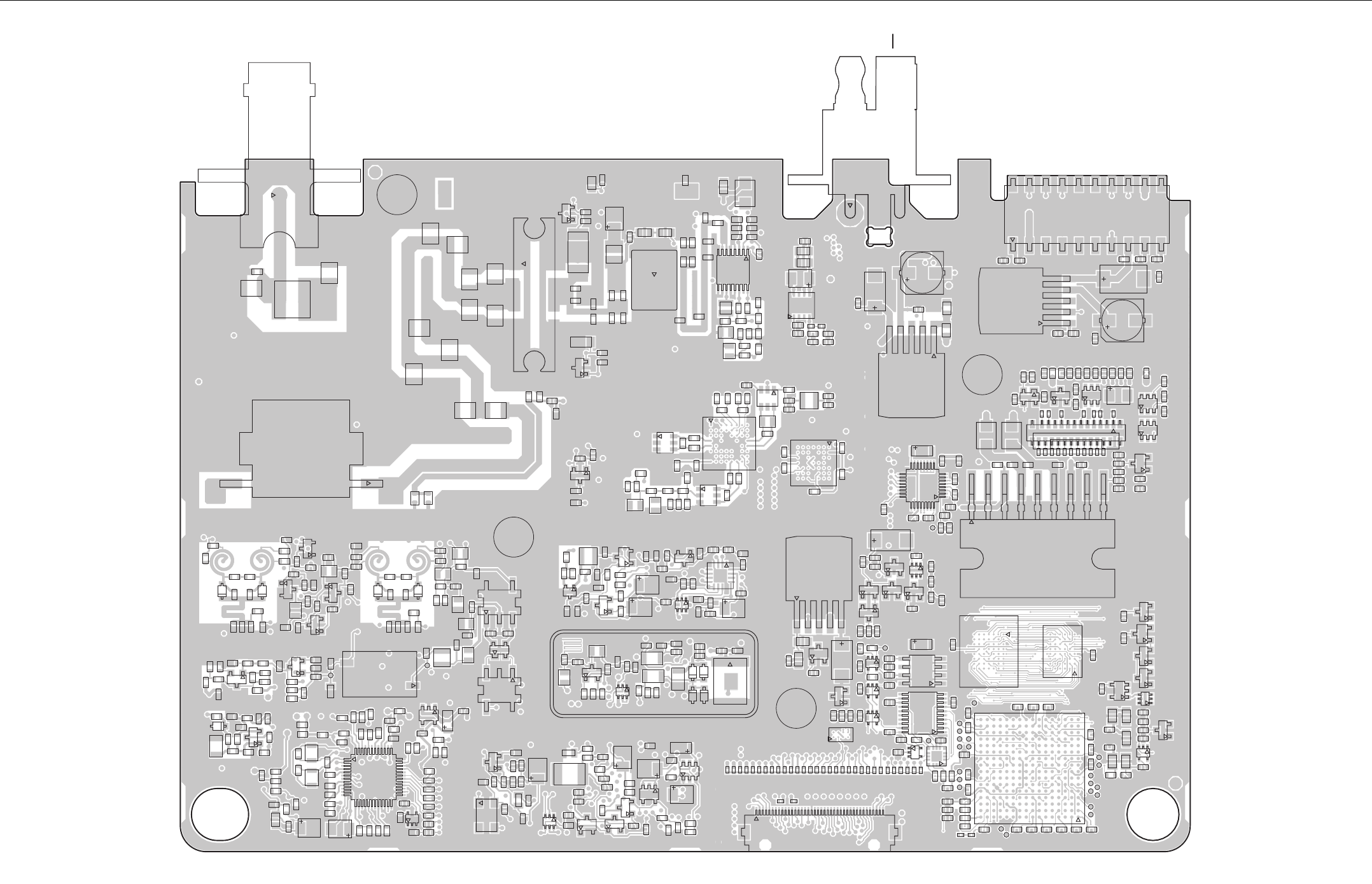
8.1 - 4 TRANSCEIVER 450-470MHz: SCHEMATICS, PCBs and PARTS LISTS
12
3
C0115C0147
C0148
C0150
C0152
C0154
C0155
C0156
C0160
C0170
C0218
C0227
C0230
C0232C0233 C0234C0235C0237
C0302
C0303 C0304
C0305
C0306
C0307
C0308
C0309
C0310
C0311
C0312
C0313
C0319
C0324
C0335
C0339
C0342
C0343
C0345
C0346
C0347
C0348
C0402
C0404
C0405
C0406
C0407
C0408
C0409
C0410
C0411
C0412
C0413
C0414
C0415
C0416
C0417
C0418 C0419 C0420
C0421
C0450
C0451
C0452
C0453
C0454
C0455C0456
C0457
C0458
C0502
C0503
C0504
C0505
C0506
C0507
C0508
C0510
C0511
C0512
C0513
C0515
C0517
C0519
C0520
C0521
C0522
C0523
C0524
C0525
C0526
C0527
C0528
C0529
C0530
C0531
C0532
C0533
C0534
C0535
C0536
C0550C0554
C0601
C0603
C0604
C0605
C0606
C0607
C0608
C0609
C0610
C0611
C0612
C0613
C0614
C0615
C0616
C0617
C0618
C0619
C1100
C1101 C1102
C1103
C1104
C1105
C1106
C1107
C1108
C1109
C1110
C1111
C1112
C1113
C1114
C1115
C1119
C1120 C1121
C1131
C1132
C1133
C5007
C5008
C5010
C5012
C5014
C5015 C5016
C5017
C5018
C5021
C5022
C5023
C5024
C5027
C5028
C5031
C5032
C5033
C5034
C5035
C5036
C5037
C5041
C5042 C5043
C5044
C5045
C5046
C5047
C5048
C5051
C5052
C5053
C5054
C5061
C5062
C5101
C5102
C5103
C5104
C5111
C5112 C5113
C5120
C5123
C5124
C5127
C5130
C5132
C5138
C5141
C5143
C5145
C5147
C5148
C5151
C5153
C5154
C5155
C5157
C5158
C5159
C5162
C5168
C5176
C5179
C5180
C5181
C5182
C5183
C5186
C5187
C5194
C5195
C5198
C5199
C5203
C5204
C5205
C5206
C5211
C5217
C5301
C5303
C5305
C5306
C5307
C5308
C5309
C5316
C5321
C5322
C5323
C5324
C5331
C5336
C5343
C5344
C5345
C5351
C5352 C5353
C5362
C5365
C5366
C5401
C5402
C5404
C5408
C5409
C5410
C5411
C5412
C5413
C5414
C5415
C5416
C5417
C5418
C5419
C5420
C5421
C5423
C5424
C5425
C5426
C5427
C5428
C5429
C5430
C5432C5433
C5434C5435
C5436
C5437
C5438
C5439 C5440
C5441
C5442
C5443
C5444
C5445
C5451
C5465
C5466
C5501
C5502
C5503
C5505
C5557
C5558
C5601
C5602
C5603
C5605
C5610
C5611
C5624
C5631
C5633
C5634
C5635
C5651
C5652
C5653
C5654
C5671
C5672
C5701
C5702
C5703
C5711
C5712
C5732
C5733C5734
C5735
C5736
C5737
C5738
C5739
C5740
C5742
C5803
C5805
C5806
C5807
C5808
C5809
C5810
C5811
C5812
C5813
C5819
C5820
C5822
C5824
C5826
C5829
C5830
C5832
C5837
C5838
C5842
C5847
C5848
C5856 C5857
C5862
C5863
C5868
C5871
C5872
C5873
C5874
C5876
C5877
C5878
D0150
D0152
D0300
D0301
D0305
D0404
D5011
D5012
D5013
D5018
D5031
D5041
D5042
D5061
D5180
D5331
D5731
D5732
D5733
D5734
E1101
E1102E1103
2
1
FL5451
12
3
J0301
20 11
10
1
J0400
1
40
J0500
23
24 2
J0600
23
J5401
L0231
L0232
L5002
L5031 L5041
L5048
L5061
L5062
L5081
L5174
L5175
L5180
L5201
L5203
L5309
L5361
L5401
L5421
L5462
L5502
L5601
L5701
L5702
L5731
1
3
L5732
L5733
L5734
L5804
L5805
64
3
T5802
L5809
L5810
L5811
64
3
L5812
L5813
M0401
M0402
M5001
M5401
1
M5421
Q0150
Q0157
Q0161
Q0200
Q0301
Q0302
Q0303
Q0306
Q5031
Q5101
Q5180
Q5201
Q5301 Q5331
Q5332
Q5351
5
2
64
31
78
Q5431
Q5542
Q5553
Q5601
Q5602
Q5631
Q5651
Q5671
Q5701
Q5711
R0100
R0101
R0108
R0111
R0129
R0135
R0136
R0150
R0155
R0156
R0157
R0161
R0168
R0169
R0170
R0171
R0172
R0237
R0241
R0243
R0244R0245
R0300
R0301
R0302
R0303 R0304
R0305 R0306
R0307
R0308
R0309
R0310
R0312
R0313
R0323
R0325
R0326
R0327
R0328 R0330R0331
R0332
R0400
R0401
R0402 R0403
R0411
R0412
R0413
R0415
R0416
R0417 R0418
R0450
R0451
R0452
R0454
R0455
R0459
R0465
R0466
R0467
R0468
R0469
R0470
R0527
R1104
R1111
R1112
R1132
R5008
R5013
R5014
R5018
R5022
R5031
R5032
R5036
R5041
R5042
R5043
R5044
R5051
R5061R5062
R5063
R5100
R5101
R5102
R5103
R5104
R5105
R5106
R5121
R5122
R5125
R5134
R5142
R5148
R5149
R5150
R5151
R5152
R5153
R5154
R5155
R5157
R5158
R5159
R5161
R5162
R5166
R5167
R5169
R5171
R5176
R5178
R5179
R5180
R5181
R5183
R5184
R5190
R5195
R5196
R5197
R5198
R5199
R5204
R5205
R5206
R5210
R5301
R5302
R5303
R5304
R5321
R5322
R5323
R5330
R5335
R5336
R5339
R5351
R5352
R5353
R5354 R5355
R5364
R5403
R5404
R5405
R5406
R5419R5420
R5431
R5451
R5452
R5453
R5454
R5455
R5461
R5501
R5545
R5546
R5547
R5548
R5601
R5602
R5603
R5604
R5605
R5606
R5607
R5622
R5631
R5632
R5634
R5636
R5637
R5651
R5652
R5653
R5668
R5671
R5701
R5702
R5703
R5711
R5731
R5732
R5804
R5805
R5809
R5810
R5814
R5830R5831 R5832
R5847
RT5551
SH5702
3
46
1
2
T5061
3
46
1
2
T5062
TP0120
TP0150
TP0498
TP0499
TP1101
TP1102
TP1103
TP1104
TP1105
TP1107
TP1109
TP1110
TP1111
TP1112
TP1113
TP1115
TP1117
TP1118
TP1119
TP1122
TP1124
TP1125
TP1126
TP5201
TP5202
TP5843
25
9
17
U0150
9
U0205
1
8
4
5
U0207
1
6
5
U0300
1
6
5
U0301
1
6
5
U0302
4
5
8
U0307
U0401
U0402
U0403
U0404
5
9
13
U0405
1
4
58
U0406
10
20 11
U0408
A1
A16
T1
T16
U1100
A8
G8 G1
U1102
H1
A6 H6
U1103
U1105
1
37
25
13
U5101
U5103
U5105
6
4
3
1
U5201
U5321
U5322
1
16
8
9
U5401
U5501
13
8
516
12
4
9
U5702
64
3
T5801 A1
A8H8
H1
U5809
G1 A1
G7 A7
U5810
VR0163
VR0302
VR0325
VR0402
VR0403
VR0405
VR0406
43
2
Y5363
PCB / Main Board 8466575A01_A / BOT SIDE
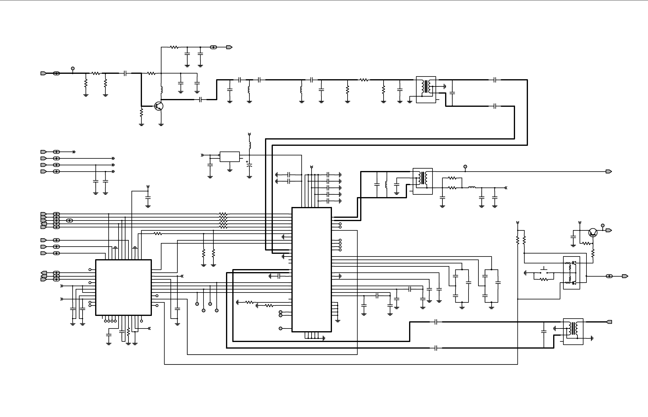
TRANSCEIVER 450-470MHz: SCHEMATICS, PCBs and PARTS LISTS 8.1 - 5
G
G
G
G
G
G
G
G
G
G
G
G
G
G
G
G
G
G
G
G
G
NU
NU NU
NU
NU
NU
NU
NU
NU
180pF
180pF
C5846
C5855
180pF
180pF
C5845
.022uF
C5854
C5852
C5843
C5848
TX_LO
5V_TX
3300pF
ADDAG_CLK
0.1uF
SPIA_CS0_ADDAG
SPIA_CS2_ODCT
ADDAG_TXE
REF16_8_OSC
ADDAG_STD
ADDAG_FS
SPIA_MOSI
FORWARD
SPIA_MISO
SPIA_CLK
RESET_ODCT_ADDAG
180pF
0.1uF
C5822
0.1uF
C5849
C5850
C5841
C5842
0.1uF
C5824
0.1uF
0.1uF
180pF
0.1uF
C5833
C5826
0.1uF
C5827
0.1uF
C5834
0.1uF
C5836
0.1uF
C5823
Q5801
PBR941
C5804
180pF
39
68nH
R5803 2.2K
L5809
1K
R5806
150
R5816
R5807
.022uF
C5844
4.7K
R5846
2.7K
R5845 Q5804
C5863
180pF
8.2pF
BACKWARD
180pF
C5862
4700pF
C5811
C5853
470pF
470pF
C5857
LOAD_DUMP
C5856
330
3V_TX
150
R5808
R5810
180pF
0.1uF
C5820 C5819
R5814
330
C5847
5V_TX_SW
1000pF
560nH
L5813
ADDAG_CLK_LN_1
ADDAG_STD_LN_1
TX_LO_LN_1
C5813
C5803
180pF
180pF
0
R5809
2.4pF
C5810
C5809
2.4pF
L5803
27nH
RESET_ODCT_ADDAG_LN_1
LOAD_DUMP_LN_1
3V_DIG_LN_1
5V_TX_LN_1
3V_TX_LN_1
0.1uF
C5864
470pF
C5865
R5847
75K
C5812
8.2pF
680
4.7K
R5837
3300pF
R5840
C5828 C5831
82
180pF
0
R5802
R5819
PA_DIS_PA_1
3V_DIG
C5808
11.0pF
PA_DIS
15nH
L5805
C5806
2.4pF11.0pF
C5805
L5804
15nH
NC
C5859
4700pF
NC
NC NC
NC
NC
NC
NC
NC
180pF
C5868
1
C5867
180pF
NC
TP5804
ADDAG_FS_LN_1
NC
REF16_8_OSC
ADDAG_TXE_LN_1
SPIA_CS2_ODCT_LN_1
SPIA_CS0_ADDAG_LN_1
SPIA_MOSI_LN_1
SPIA_MISO_LN_1
1
NC
SPIA_CLK_LN_1
TP5811
1
TP5841
TP5801
1
270pF
C5874C5873
270pF
270pF
C5872
270pF
TXH_LN_1
TXH
C5871
2.4pF
C5877
T5802
XFMR_LDB32C_370MHZ
1
3
5NC
24
6
2.2uH
L5814
1
3
NC
5
24
6
SPIA_MOSI_LN_2
XFMR
L5812
0.1uF
C5840
C5807
27pF
Q5802
NC 5
24
6
NC
NC
NC
XFMR_LDB32C_370MHZ
T5801
1
3
R5854
100
100
R5853
R5852
100
100
R5851
R5850
100
R5856
10K 10K
R5855
100
R5849
C5825
0.1uF
C5875
NC 4
VIN
1VOUT 5
NC
NC
1uF
F1
U5808
NCP512
EN
3
GND
2
G4
TCLK C2
TCLKB B1
TSLOT A1
TSLOTB B2
TXE B5
VBLIN
G2
VCNTF G1
VCNTO
B7
SPCK A3
SPI B4
SPO C4
SRD
C5 STD
C7
SUB
F3
TCAPM
F5 TCAPP
G3
D4 NC
OUT1 E1
OUT1B E2
OUTQ D1
OUTQB C1
RSTB A6
SCK
B6 SFS
C6
DVDD3 A2
FMOUT E3
ICLKR A4
INI
G5
INIB
F6
INQ
G6
INQB
G7
IREF
E4
CLKIN A5
CREF
E5
CSB B3
DGND
D7
DGND3 C3
DSPCLK
A7
DVDD1
E7
DVDD2
F7 AGCB
E6
AGND1
D6
AGND2 D2
AGND3
F4
ASW F2
AVDD1
D5
AVDD2 D3
AVDD3
C7
VRFUP
D5
VSSR
U5810
35U79
AGC
A1
VCO1
H5
H6 VCO1B
H7 VCO2
VCO2B
H8
H1
VDD D6
VLO
VQGD D3
E2
VRFDWN
E4
SUBD E5
SUBU
TMROUT
G7
F5
TST1 E7
TST2 F7
TST3 G8
TST4
VCC
RFOUTB C8
SCAN
F6
H4 SLT
G5 SLTB
F2 SPIC
G3 SPII
H2 SPIO
G2 SPISEL
F1 MRSTB
H3 PHCLK
D2
QGND
D1 RFIN
E1 RFINB
B8
RFOUT
D8
RFOUT2
E8
RFOUT2B
A3
LP1I
A4
LP1IB
C5
LP1Q
B4
LP1QB
A5
LP2I
LP2IB A6
C6
LP2Q
B5
LP2QB
G1
A2 GND
E3 GNDDWN
E6 GNDLO
D7 GNDUP
GND_THERM D4
G4 INC_DCR
C2 LCAP
LOGND
G6
B7
CAPM
B3
CAPO C4
CAPOC
A8 CEI
CEQ
B6
CLK
F3
F4 CLKB
DGND
U5809
JAVELIN
AOC
A7
F8
ASW
BINI
B2
C3 BINIB
B1 BINQ
C1 BINQB
S5802
SWITCH
12
R5804 82
82
R5805
1
TP5808
1
TP5807
1
TP5806TP5805
1
TP5802
1
TP5803
1
R5858
10K
10K
R5857
C5878
2.4pF
3V_TX
C5876
180pF
3V_TX
5V_TX
5V_TX
LOAD_DUMP
3V_DIG_LNODCT
3V_TX
3V_TX
5V_TX
3V_TX
3V_DIG_LNODCT
3V_TX
5V_TX
3V_DIG_LNODCT
3V_TX
Main Board 8466575A01_A / TX-LOW SECTION (JAVELIN)
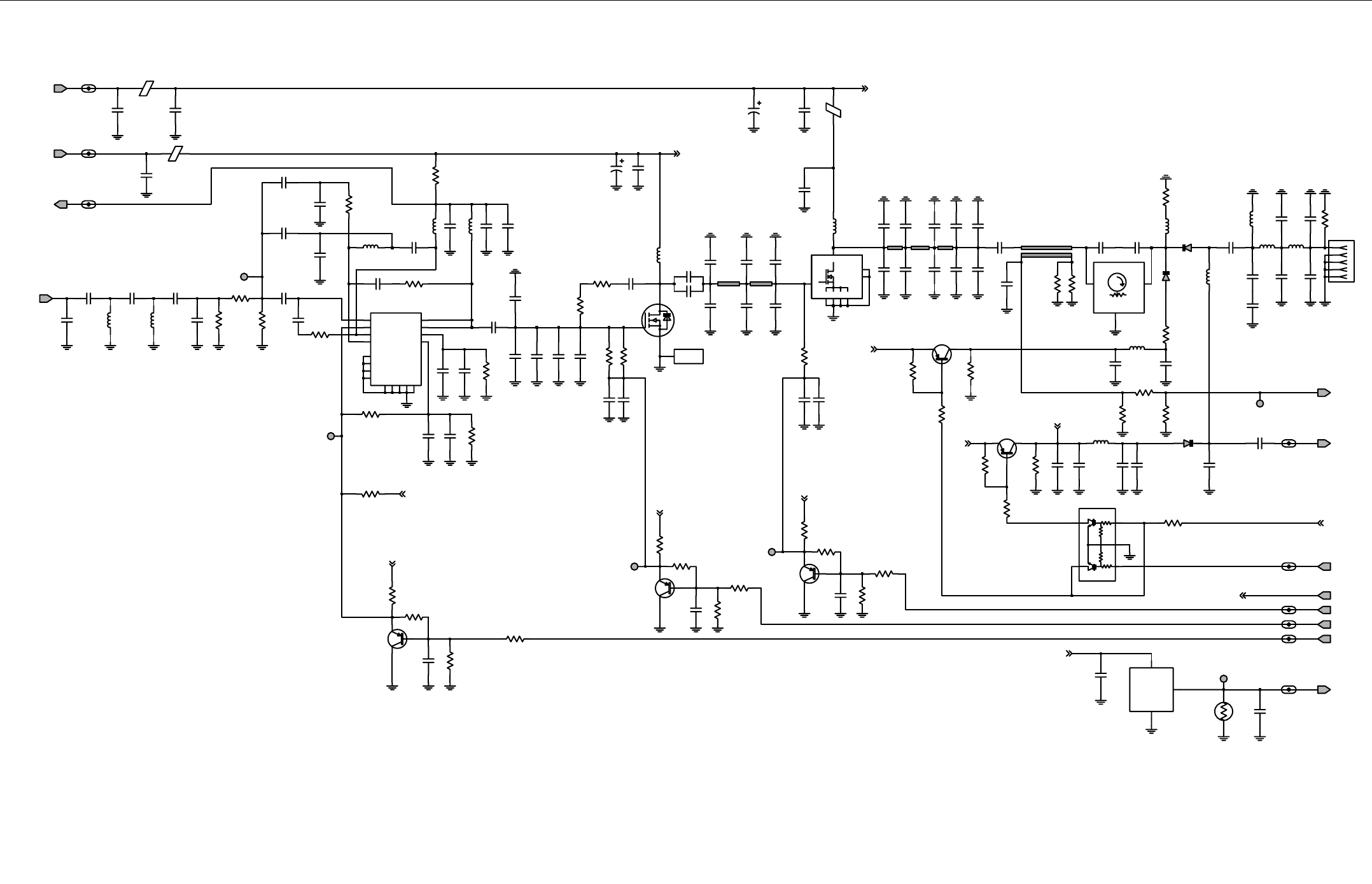
8.1 - 6 TRANSCEIVER 450-470MHz: SCHEMATICS, PCBs and PARTS LISTS
Main Board 8466575A01_A / PA SECTION
ZWG0130870-A
G
G
G
G
G
G
G
G
G
G
G
G
NU
NU
NU
NU
NU
NU
NU
2.216x??
J3401 - BNC
NU
NU NU
NU
NU
NU
NU
NU
NU NU
NU NU
NU
NU
NU
NU
NUNU
NU
NU
NU
NU
NU
NU
15pF
C5451
D5451
D5551
C5413
12pF
FORWARD
C5412
47pF
47pF
68nH
68nH
9V3_TX
.022uF
C5405
L5402
12pF
12pF
C5463
.022uF
.033uF
.033uF
C5503
L5502
57R01 100pF
100pF
C5422C5421
1uF
1uF
4.22nH
4.22nH
L5421
30pF
C5435
C5406
.022uF
.022uF
L5403
180pF
15nH
15nH
C5409
180pF
.022uF
.022uF
C5408
C5410
.022uF
.022uF
PASUPVLTG
C5504
10uF
10uF
R5541
20K
RXIN
20K
180pF
180pF
C5411
R5404
5.6K
5.6K
R5403
1K
1K
180pF
C5407
180pF
C5403
470pF
470pF
1
200
200
R5401
TP5451
10pF
C5438
20pF
C5404
20pF
11.03nH
11.03nH
L5401
6.2pF
C5402
6.2pF
C5401
180pF
15 NC4
16 RFIN
6
RFOUT1 7
RFOUT2
1VCNTRL
14 VD1 VG1 2
3
VG2
11 G2
4GND1
5GND2
12 GND3
13 GND4
8NC1
9NC2
10 NC3
SRFIC5668
U5401
17 EP
560nH
560nH
L5551
R5553
120
120
120
R5454
R5455
68150
R5453
150
R5452
150
R5451
5.6pF
C5553
R5542
47K
47K
3300pF
3300pF
C5428 C5429
180pF
180pF
51
51
C5505
.033uF
R5431
.033uF
L5451
560nH
57R01
L5503
100pF
C5440
39pF
C5427
39pF
C5426
9.1pF
C5425
47pF
C5424
30pF
C5423
100pF
100pF
C5418
3300pF
3300pF
C5417
51
51
R5406
51
51
R5405
180pF
180pF
C5502C5501
100pF
100pF
BIAS3_PA_1
BIAS2
BIAS2_PA_2
BIAS1_PA_1
BIAS3
R5522
39K
BIAS1
30pF
C5432
30pF
C5433
R5461
10K
10K
1000pF
C5551
5V_TX_SW
330pF
C5552
C5557
GND1
GND2
S1
S2
S3
S4
180pF
Q5431
D
G
PASUPVLTG_UHF_PA_1
RXIN_PA_1
9V3_TX_UHF_PA_1
L5501
57R01
Q5521
TP5541 1
R5544
0
17.24nH
C5462
100pF
C5464
100pF
100pF
C5452
C5838
R5830
27
C5832
8.2pF15nH
10pF
C5830
L5811
9.1pF 2.4pF
C5829
C5415
20pF
100
R5419
470pF
C5400
120
R5400
C5443
10pF
C5468
3.9pF
C5441
6.8pF
12pF
C5420
GND1
3
IN
1OUT 2
TP4409 1
FL5451
SI15R0390MP
TP5402 1
10K
R5551
C5521
180pF
180pF
C5541
C5430
20pF
DRIVER_SENSE
DRIVER_SENSE_UHF_PA_1
TEMP_SENSE
R5533
4.7
TEMP_SENSE_PA_1
BACKWARD
RT5551
50K
0
R5524
R5523
2.7K
Q5553
C5445
9.1pF
C5455
180pF
TP5403
1
2.7K
R5543
Q5542
C5467
5.1pF
200
R5832R5831
200
560nH
L5454
51
R5450
D5454
C5454
68pF
39K
R5504
L5810
15nH
C5419
20pF
C5558
180pF
LM50
U5501
GND
3POS 1
VOUT 2
R5462
10
180pF
C5469
10pF
C5470
10pF
R5548
10K
680
R5407
0
100
R5408
C5453
100pF
R5420
9.1pF
C5837
180pF
C5506
2.7K
Q5552
R5552
1K
Q5551
ANT_EN_PA_1
R5556
ANT_EN
R5502
0
680
R5501
33K
Q5501
R5503
10K
R5547
10K
4.7K
R5546
R5545
C5436
20pF
C5437
30pF
30pF
C5434
C5416
22pF
C5414
39pF
POS
1M5421
HEATSINK
C5465
Q5421
R5521
10pF
L5462
33K
18nH
L5461
18nH
18nH
18nH
18nH
9.1pF
C5556
L5452
18nH
0.5pF
9.1pF
56pF
C5554 C5555
0.5pF
470pF
C5461
56pF
4.7pF
4.7pF
470pF
C5444
C5466
15pF
C5442
10pF
1
100pF
TP5401
100pF
C5431
C5439
L5431
18nH
18nH
3.3pF
5V_TX_SW
9V3_TX_SW
5V_TX_SW
9V3FLT
5V_TX_SW
5V_TX_SW
9V3FLT
5V_TX_SW
5V_TX_SW
9V3_TX_SW
9V3FLT
A+
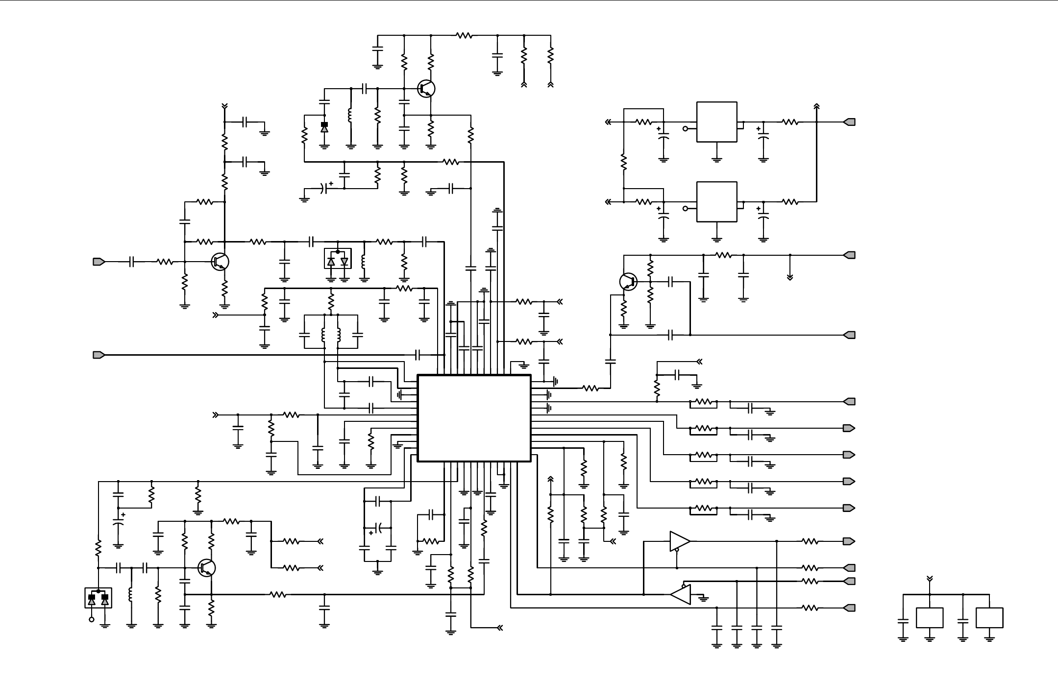
TRANSCEIVER 450-470MHz: SCHEMATICS, PCBs and PARTS LISTS 8.1 - 7
G
G
G
G
G
G
G
G
G
G
G
G
G
G
NU
NU
NU
NU
NU
NU
NU
NU
NU
NU
NU
NU
NU
NU
NU
NU
NU
NU
NU
NU
NU
NU
NU
NU
1000pF
C5160
R5160
1K
C5161
33pF 33pF
C5163
R5170
22
R5140
10
100
VDDI 48
VDDL 40
VDDP 39
VDDQ
14
VREFN
12 VREFP
11
R5146
PE 25
13
RREF
SYNCB 33
VDDA
9
VDDC
17
VDDD 26
VDDF
6
VDDH 27
IOUTC
15
IOUTL 38
LON 42
LOP 43
MXON
2MXOP
1
PC
23
PD
24
GNDL 36
GNDP 37
GNDQ
16
21 GNDS1
34
GNDS2
IF2N
4
IF2P
5
47
IFIN
GCN
8GCP
7
GNDA
10
GNDC
18
22 GNDD
GNDF
3
GNDH 32
GNDI 45
CLKP
19
46
CXIF
CXVL 44
CXVM 41
DOUTA 29
30
DOUTB
FREF 35
FS 31
U5101
AD9874
CLKN
20
CLKOUT 28
R5178
0
1000pF
C5158
R5158
270
C5153 0.1uF
C5146 C5144
100pF
C5145
100pF
.01uF
10uF
C5132
C5150
0.1uF
C5127
.01uFC5156
L5126
330pF
470nH
0.1uF
C5135
0.1uF
C5147
C5159
.01uF
R5134
10
10
R5132
C5185
0.1uF
.01uF
C5184
R5185
22
R5183
100
R5176
33K
0.1uF
C5133
C5131
10
R5131
.01uF
C5148
R5133
10
0.1uF
Q5180
2.2uF 0.22uF
C5188
C5189
10pF
C5187
R5182
0
56K
R5181
3.3K
R5180
1.2K
R5184
R5186
270
R5187
200K
C5172
0.1uF
100pF
C5179
C5178
100pF
C5195
0.1uF
C5194
.01uF
10
R5151
C5134 0.1uF
R5152
10
C5154 0.1uF
C5157 .01uF
0.1uFC5155
C5190
100pF
100pF
C5193
150pF
C5192
Q5190
0.22uF
C5198
C5197
2.2uF
C5199
15pF
R5190
33K
R5191
20K
1.2K
R5194
270
R5197
200K
R5196
10
R5166
R5150
R5155
0
0
0
R5199
0
R5189
R5198
0
0
R5188
R5159
0
C5129
.01uF
C5181
L5180
220nH
15pF
C5183
C5180
68pF
C5182
22pF
D5180
22pF
0.1uF
C5137
.01uF
C5136
R5149
100K
C5142
0
C5143
1000pF
C5130
0.1uF
D5190
8.2pF
C5125
15pF
C5126
9V3
Q5151
270
R5179
C5138
0.1uF
R5142
0
0
R5141
22
R5195
R5193
100
R5192
6.8K
L5190
1uH
100pF
C5191
4.7uF 1uF
C5167
2GND
NC
43
ON_OFF*
1
VIN
5VOUT
C5166
SPIA_CLK
SPIA_CS4_ABA
SPIA_MOSI
REF16_8_OSC
U5102
LP2980
SSI_CLK
SSI_DOUTA
SSI_DOUTB
SSI_FSYNC
SSI_SYNCB
0
R5154
R5153
0
15pF
C5171
C5173
15pF
15pF
C5174
C5175
15pF
C5128
C5151
.01uF
0.1uF
47K
R5157
R5162 22
22R5161
R5163 22
0.1uF
C5152
L5174
10uH
5V_FN
IF_ABA
C5176
180pF
R5168
47K
47K
R5165
1K
R5164
22
R5169
C5122
1000pF
1000pF
C5121 C5124C5123
.01uF .01uF
330pF
C5101
C5102
330pF
22
R5104
820
R5105
R5103
10K
12K
R5102
27K
Q5101
R5101
10K
C5168
R5167
C5169
4.7uF
4NC ON_OFF* 3
VIN 1
VOUT
5
1uF
LP2980
U5103
GND
2
C5139
0.1uF
2.2K
R5144
C5186 1000pF
U5105-2
PWR_GND
3
GND
5
VCC
2
A
1
OE
4
Y
SPIA_MISO
R5171
3.3K
U5105-1
74VHC125
15pF
C5177
470
R5177
0.1uF
C5111
C5112
430pF 430pF
C5113
10uH
L5175
470
R5122
47
R5106
NC
NC
NC
560
R5125
ABA_A
0.1uF
C5104
.01uF
C5103
C5164
33pF
22R5172
33pF
C5162
0.1uF
C5141
R5121
2.2K
D5121
C5120
330pF
R5145
120
GND
3
VCC
5
C5140
0.1uF
74VHC125
U5104-1
2
A
1
OE
4
Y
PWR_GND
U5104-2
68
R5148
68
R5147
2V8
R5100
51
DIGITAL_3V3
9V3
5V_FN
ANALOG_3V3
9V3
ANALOG_3V3
ANALOG_3V3
5V_FN
5V_FN
ANALOG_3V3
ANALOG_3V3
LNA+3V
ANALOG_3V3
LO_CP+5V_FN
DIGITAL_3V3
5V_FN
2V8
LO_SY+3V
DIGITAL_3V3
DIGITAL_3V3
Main Board 8466575A01_A / ABACUS Section
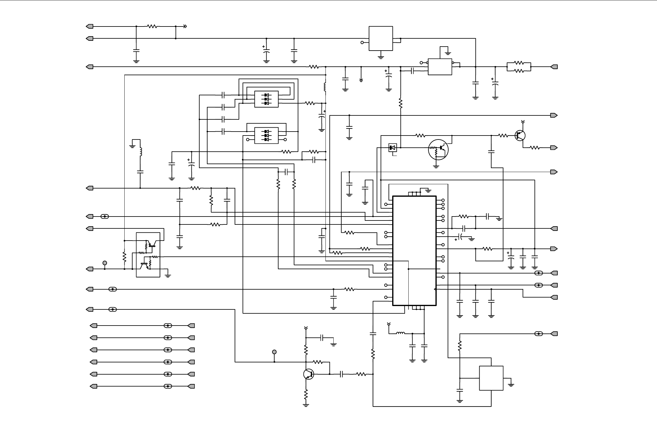
8.1 - 8 TRANSCEIVER 450-470MHz: SCHEMATICS, PCBs and PARTS LISTS
Main Board 8466575A01_A / FRAC-N Section
G
10K
10K
10K
10K
G
G
G
G
G
G
G
G
G
G
G
G
G
G
G
G
G
G
G
G
G
G
G
G
G
G
G
G
G
G
(to ESCORT)
NU
NU
NU
NU
NU
NU NU
NU
NU
NC
(SOURCE)
NC
NC
NC
NC
NC
NC
NC
NC
NC
NC
NC
NC
NC
NC
NC
NC
NC
NC
R5330
330K Q5332
Q5301
16.80MHz
KT19
Y5363
GND 2
OUT
3
VCC
4
VCON 1
8.2K
R5339
ESC_CPB
C5309
2.2uH
L5309
3300pF
SPIA_MOSI_FN_1
3V_REFOSC_FN_1
0.1uF
REF16_8_OSC_FN_1
NC
C5306
3V_AGC
C5307
10uF
R5321
100
0.1uF
C5366
SSI_DOUTA
SSI_DOUTB
SSI_CLK
SPIA_CS4_ABA
SPIA_CS4_ABA_FN_2
SSI_SYNCB
SSI_FSYNC
SSI_DOUTB_FN_2
SSI_CLK_FN_2
SSI_FSYNC_FN_2
SSI_DOUTA_FN_2
SPIA_CS4_ABA
SSI_SYNCB_FN_2
SSI_FSYNC
SSI_DOUTA
SSI_DOUTB
SSI_CLK
NC
3V_REFOSC
SSI_SYNCB
R5351
1K
1000pF
C5352
47K
R5352
100
R5353
Q5351
51
R5364
3V3_FN
4.7K
R5354
RXH
REF16_8_OSC
2.2K
R5301
5
0.1uF
C5303
LP2980
U5321
GND
2
4NC ON_OFF* 3
VIN 1
VOUT
C5314
.01uF
.01uF
C5311
R5313
0
D5302
A1 6
A2 5
A3 4
1
K1
2
K2
3
K3
R5311
0
R5322
68
68
R5323
100K
R5333
2NR
4OUT 3
SD
C5322
.01uF
ADP3300
U5322
6ERR
1
GND
5
IN
R5335
39K
1
TP5302
1
TP5331
C5336
D5331
Q5331
R2
R1
.01uF
68K
TXH
R5338
C5301
.01uF
C5315
.01uF
.01uF
.01uF
C5313
C5312
R5331
47K
VCOBIAS_TX
C5332
0.1uF
4.7uF
C5318
C5365
0.1uF
1K
.01uF
R5355
LOCK_FN_FN_1
C5353
REF16_8_FN_FN_1
SPIA_CS1_FN_1
VCOBIAS_RX
100K
R5337
C5331
47K
0.1uF
11 VMULT4
VRO
13
25 WARP
23 XTAL1
XTAL2
24
R5332
28 SFOUT
37 TEST1
38 TEST2
21
VBPASS
47 VCP
VMULT1
15
14 VMULT2
12 VMULT3
32
33
PRE_GND
34 PRE_VDD
35
PVREF
18
REFSEL
27
SFBASE
26
SFCAP
30
SFIN
4
10
MODIN
41 MODOUT
17
NC1 29
NC2 31
NC3
44
PD_GND
PD_VDD
5
PREIN
8
CLK
7
DATA
DGND 6
36 DVDD
19 FREFOUT
45 IADAPT
16 INDMULT
43 IOUT
LOCK
1AUX2
2AUX3
3AUX4
20 AVDD
40
BIAS1 39
BIAS2
42
CCOMP
9
CEX
AT25016
U5331
46 ADAPTSW
22
AGND
48 AUX1
0.1uF
C5351
56pF
C5337
2.0pF
C5335
REF16_8_FN
VSF
VCTRL
PRESC
SPIA_CLK
SPIA_CS1_FN_PCIC
LOCK_FN
100
R5334
SPIA_MOSI
C5317
22pF
C5334
R5316
0.1uF
100
R5315
100
C5319
0.1uF
100
R5312
1
K2
2
K3
3
9V35V_FN
6
A1
5
A2
4
A3
K1
D5301
0.1uF
C5363
.01uF
C5362
2.2uH
L5361
0.1uF
C5323
10uF
C5324
R5336
30K
C5339
4.7uF
0.1uF
C5308
L5301
0.39uH
33pF
C5333
180pF
C5340 C5341
33pF33pF
C5342
C5343
10uF 1000pF
C5344
.01uF
C5345
C5338
820
R5302
100pF
C5316
10uF
.01uF
C5305R5303
1.8K
330
R5304
47K
R5314
C5321
3V
3V
4.7uF
3V
3V
NC_D3221_2
5V
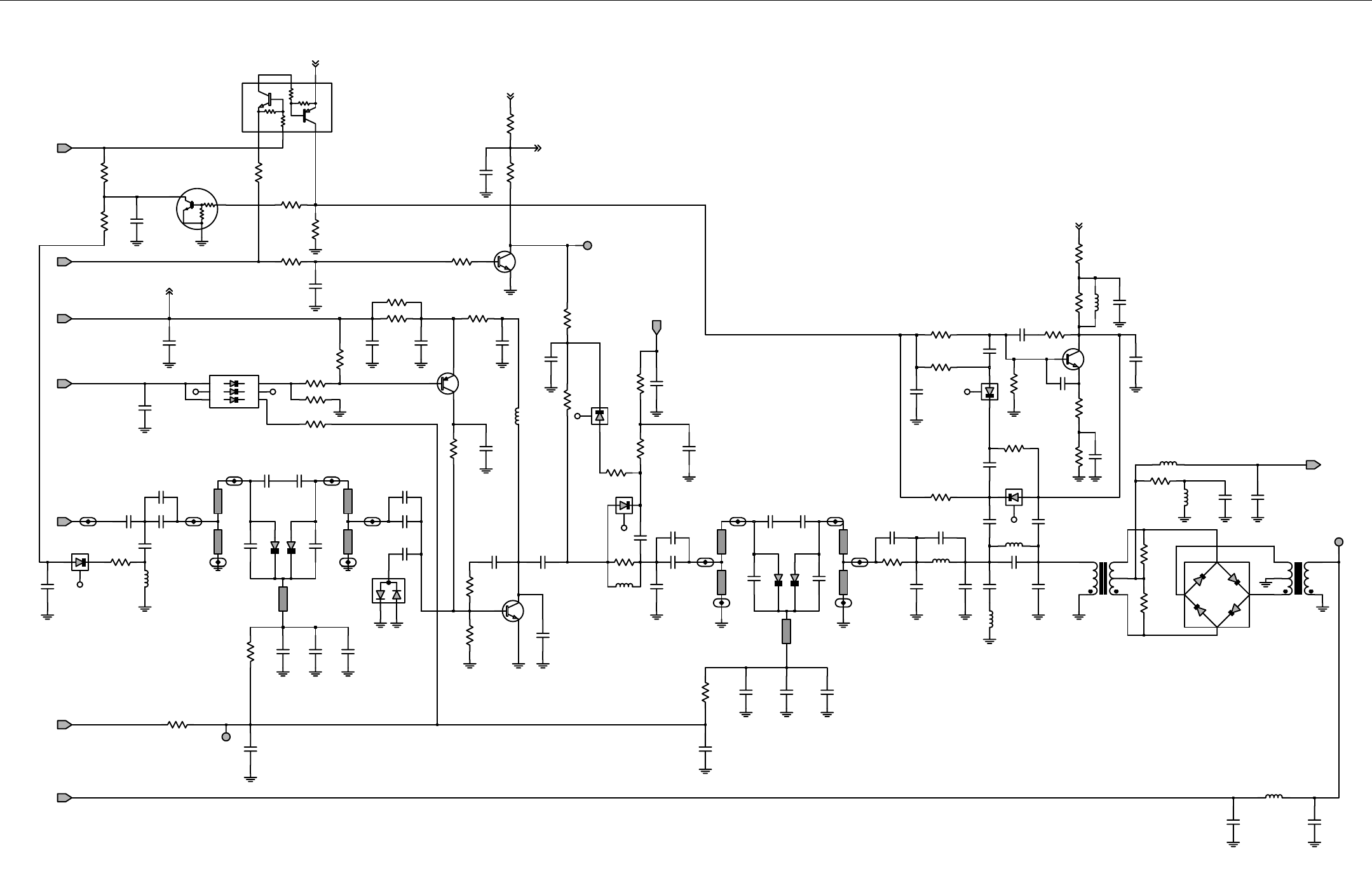
TRANSCEIVER 450-470MHz: SCHEMATICS, PCBs and PARTS LISTS 8.1 - 9
G
G
G
G
G
G
G
G
G
10K
10K
10K
10K
R5042
47pF
NU NU
NU
NU
NU
NU
NU
from PA
NU
NU
NU
NU
NU
NU
NU NU
NU
NU
NU
NU
NUNU
NU
NU
NU
NU
NU
NU
NU
NU
NU
NU
NU
NU
NU
NU NU NU
NU
NU
NU
2.2K
R5032
100pFC5018
D5013
100K
R5022 56pF
C5024C5023
82pF56pF
C5022
Q5001
RXIN
FECNTL_1
RXINJ
IF_FE
RXIN_FE_1
1000pF
9V3
C5054
C5051
C5053
56pF
C5052
56pF 82pF
R5007
C5004
330
3300pF
27pF
C5071
15nH
L5071
51
R5063
10pF
C5047
1.2pF
R5051
C5046
3
1
2
100K
IO3 IO4
XFMR
T5061
4
6
2
D5061
IO1 IO2
XFMR
T5062
4
6
3
1
330
R5006
SP_4_3
SP_4_1SP_3_1
9.1pF
SP_3_2 SP_4_2
33pF
C5032
C5007
330pF
C5005
L5002
68nH
Q5031
330pF
C5031
1.5K
R5031
R5002
2.2K
0.1uF
C5002
C5001
C5013
K9V1
3300pF
33pF
R5003
6.8K
4.7K
R5005
C5006
R5008
3.3K .01uF
3.3pF
C5041
TP5021
1
3.3pF
C5017
R5009
3.3pF
C5014
R5004
51
A3
K1
K2
K3
1K
D5001
A1
A2
D5011
100pF
C5034
.01uF
C5021
220nH
L5062
22pF
C5072
C5061
AGC_1_FE
12pF
R5036
1K
390
R5014
D5031
.01uF
C5003
2.2pF
L5061
220nH
C5062
R5021
47K
47pF
C5028
10pF
C5010
0.1uF
NCNC
SP_3_3
C5025
SP_2_1SP_1_1
SP_2_3
SP_2_2SP_1_2
SP_1_3
D5042
6.2pF
R5041
D5041
27nH
100pF
C5012
L5011
39pF
C5011
D5012
220nH
L5031
1.0pF
C5043
1.0pF
1.0pF
C5042
1.0pF
C5016C5015
1pF
C5035
3.3pF
C5044
D5081
100pF
C5082
R5044
C5081
100pF
10nH
3.3pF
R5024
L5081
100K
R1
R2
Q5021
R5023
4.7K
C5033
1000pF
.01uF
C5009
R5013
390
R5001
10K
C5008
.01uF
R5012
1.5K
C5048
2.2pF
0.1uF
C5020
270
R5011
R5043
0
TP5001
1
3.3K
C5019
0.1uF
22
R5016
4.7K
R5015
Q5002
R5017
100pF
C5036
C5027
12pF
1pF
NC
C5037
R5028
2.7K
68nH
L5082
1000pF
C5088
R5025
1K
R5026
1K
AGC_0_FE
D5025
1K
R5061
R5062
6.2pF
C5045
1K
L5041
15nH
C5084
1000pF
R5088
2.7K
10
R5089
R5084
R5090
51
12K
R5086
470
R5087
330
1K
NC
R5083
C5083
D5082
R5082
2.7K
100pF
R5081
NC
8.2K
R5027
2.7
TP5071
1
Q5022
2.2pF
1pF
C5090
C5089
NC
NC
82pF
C5026
33
R5018
3V_AGC
D5018
L5048
27nH
330
R5085
C5087
100pF
Q5081
100pF
C5085
9V3_FLT
9V3_FLT
9V3_FLT
100pF
C5086
9V3
9V3
Main Board 8466575A01_A / FE and Mixer Section
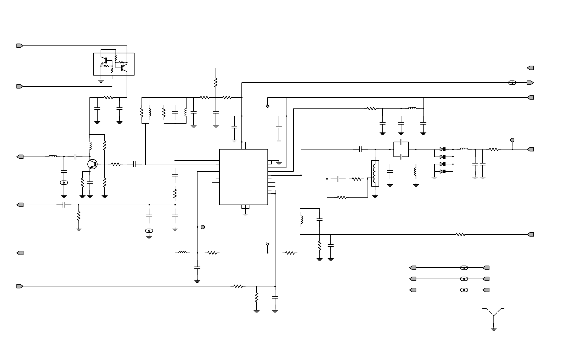
8.1 - 10 TRANSCEIVER 450-470MHz: SCHEMATICS, PCBs and PARTS LISTS
Main Board 8466575A01_A / RX VCO Section
G
G
G
G
G
G
G
G
G
G
G
G
G
G
G
G
G
10K
10K
10K
10K
NU
NU
NU
NU
from Controller
from Controller
from Controller
to Controller
NU
NU
8.2K
1.5pF
R5725
100K
C5726
14
VCC_BUFFERS 18
VCC_LOGIC
VCOBIAS_RX
9V3
5V_FN
R5728
7RX_SWITCH
3
SUPER_FLTR
19
TRB_IN
16
TX_BASE 15
TX_EMITTER
1
TX_IADJ
10 TX_OUT
13 TX_SWITCH
11 GND_BUFFERS
9GND_FLAG
GND_LOGIC
17
12 PRESC_OUT 5
RX_BASE 6
RX_EMITTER
2
RX_IADJ
8RX_OUT
50U54
U5701 4
COLL_RFIN
20
FLIP_IN
R5733
22
R5734
150
47pF
C5741
P3 3
1.5pF
C5735
RESONATOR
L5732
P1 1
P2
2
C5737
2.4pF 220nH
100
VCTRL
L5733
4700pF
R5732
330pF
C5740
220nH
L5734
C5739
D5734
D5733
D5732
D5731
C5715
.022uF
3V3_FN_RXVCO_1
C5724
.022uF
C5731
.01uF
VSF
R5731
100 470nH
L5731
C5733C5732
330pF 0.1uF0.1uF
C5734
R5722
4.7K
R5723
10K
PRESC
TXH
C5722
1000pF
68nH
L5721
C5721
2.0pF
R5721
1K
0.1uF
L5722
470nH
8.2K
C5712
ESC_REF
R5727
C5703
330pF
C5701
8.2pF
L5701
8.2pF
C5702
27nH
15nH
L5702
2.2K
Q5701
R5703
1K
R5702
R5701
68
R5704
22
5.6pF
C5706
100pF
C5705
100pF
C5704
10
10
R5716
180
R5715
330
R5714
330
R5712
27nH
R5713 L5712
15nH
L5711
C5713
1000pF
C5714
0.1uF
3V3_FN
TRL1
Q5711
TP5701
1
C5708
3.3pF
51
R5706
TP5702
1
C5716
5.6pF
C5738
15pF
C5736
22pF
R5707
C5707
100
SHIELD
SH5702
1
100pF
AGC_1_FE
AGC_2_IF_RXVCO_1
AGC_2_IFAGC_2_IF
AGC_0_FEAGC_0_FE
AGC_1_FE_RXVCO_1
AGC_1_FE
TRL2
AGC_0_FE_RXVCO_1
RXH
R5711
100
C5711
330pF
NC_5701_7
RXINJ
VSF
NC_5701_16
NC_5701_15
NC_5701_13
VSF
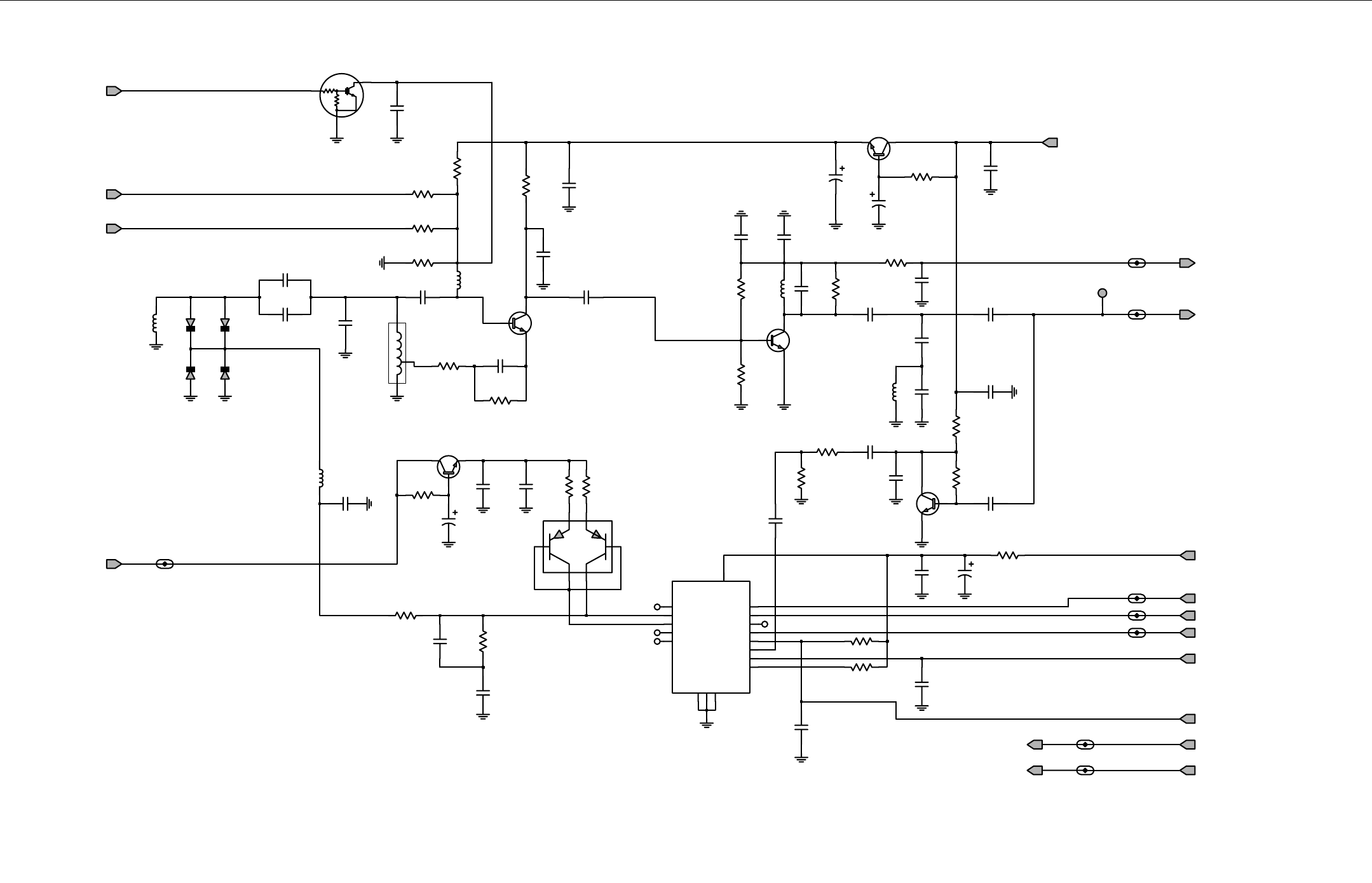
TRANSCEIVER 450-470MHz: SCHEMATICS, PCBs and PARTS LISTS 8.1 - 11
G
G
G
G
G
G
G
G
G
G
G
G
G
G
G
G
G
from FracN
from Controller
from Controller
from Controller
to LNODCT
from Controller
from Controller (PCIC)
from Controller (PCIC)
from FracN
NU
NU
NU
NU
NU
NU
NU NU
100pF
R5636
15 C5633
R5681
16V
C5681
10uF
470
Q5681
MMBT3904
0.1uF
C5682
25V
C5683
330pF 1K
R5655
R5654
1K
Q5651
UMT1NFTN 100pF
330
R5637
C5634
100pF
C5609
R5671
470
L5604
56nH
10uF
16V
C5671
PBR941
C5672
16V
10uF
R5621
10K
Q5621
C5622
100pF
C5611
150
4.7pF
33
R5605
C5602
R5606
BFQ67W
Q5601
47pF
L5603
100nH
22pF
C5607
8.2pF
C5606
SPIA_CLK_ESC_1
SPIA_MOSI_ESC_1
9V3
TX_LO_ESC_1
SPIA_CS3_ESC_ESC_1
5V_FN
SPIA_CS3_ESC
SPIA_CLK
SPIA_MOSI
ESC_REF
0.1uF
TX_LO
0
C5653
.01uF
R5653
1pF
C5604
C5654
U5601
RESONATOR
1P1
2
P2
3P3
3.3pF
4.7K
C5603
R5604
3.9K
C5601
100pF
R5602
0
R5601
R5603
VCOBIAS_RX
VCOBIAS_TX
0
R5632
3.3K
PBR941
Q5631
C5627
8.2pF
C5626
12pF
C5742
0.1uF
R5634
10
C5610
.022uF
Q5602
RXH
R5668
100K
R1
R2
R5651
12K
1SV229
D5601D5602
1SV229
D5604
1SV229
D5603
470
R5624
1SV229 R5622
R5623
2.7K
C5621
100
Q5671
.022uF
9V3_ESC_1
MMBT3904
TP5601
1
TXH_ESC_1
1pF
6.2pF
C5743
L5623
8.2nH
C5623
L5627
8.2nH
C5629
18pF
TXH
C5605
8.2pF
R5607
33
2.2pF
51
R5652
C5635
3V3_FN
C5651
16V
10uF.022uF
C5652
1.5pF
C5632
C5631
100pF
560
R5631
C5628
12pF
C5625
18pF
SPIEN 3
TESTOUT
14
15
VDD
NC
NC
NC
NC
FREQB 9
GND1
4
17 GND2
IDOWN
10
IUP
11
NC
1
RTESTCLK 7
RTESTOUT
5
U5702
BICMO885
8
CEX_A0
CLK_A1 6
CPBIAS 13
CPGND
12
DATA_RTB 2
FREQA 16
K9V1_ESC_2
K9V1
FECNTL_1
K9V1
FECNTL_1_ESC_2
390nH
L5601
FECNTL_1
C5624
.022uF
ESC_CPB
Main Board 8466575A01_A / TX VCO Section
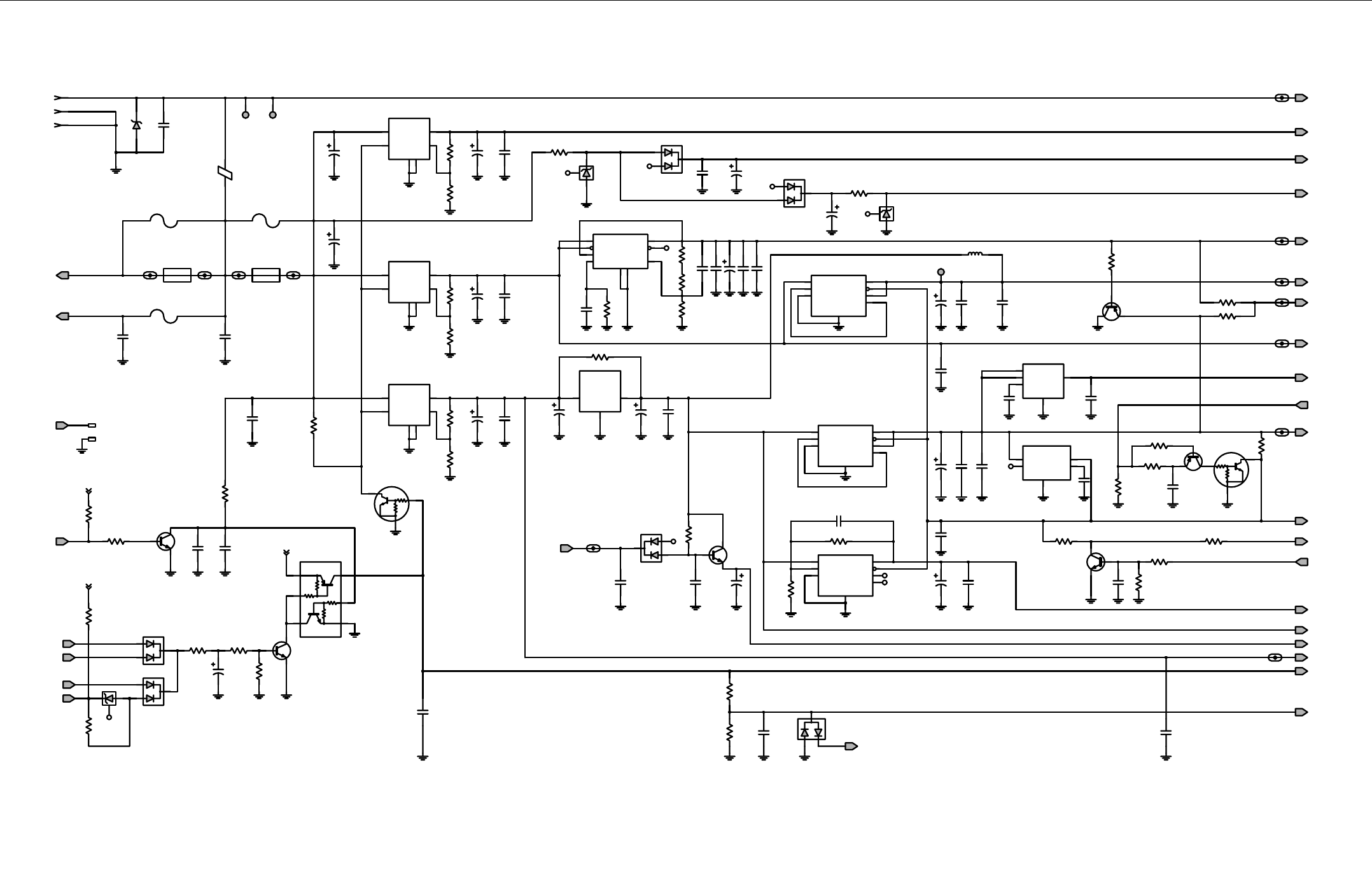
8.1 - 12 TRANSCEIVER 450-470MHz: SCHEMATICS, PCBs and PARTS LISTS
Main Board 8466575A01_A / Controller Power Supply Section
G
G
G
G
10K
10K
10K
10K
G
G
G
G
G
G
G
G
G
G
G
G
G
G
G
G
G
G
G
G
G
G
G
G
G
G
NU
MOTOROLA INTERNAL USE ONLY
from VCO
1%
1%
1%
1%
CELL_CONTACTS
LI_CELL
PART_NO6062884G01
PCB FUSE
PCB FUSE
NU
NU
NU
NU
NU
NU
NU
NU
NU
NU
NU
NU
NU
NU
NU
NU
NU
NU
NU
E0300
57R01
4 1 3 A
NU
NU
NU
NU
J0301-2
J0301-1
ON_OFF_CONTROL_SV
C0301
470pF
D0301
1K
R0300
470pF
C0320
D0304
0.1uF
C0318
C0312
0.1uF
R0302
Q0301
EMERGENCY
FLT_A+
8.2K
C0316
EXT_SWB+
10uF
C0328
47uF
C0322
47uF
ADJ 1
3GND1
6GND2
2ON_OFF
VIN
4VOUT 5
LM2941
U0301
D0305
47.5K
R0312
12.1K
R0313
33uF
C0315
1.21K
R0306
R0305
7.5K
VR0300
33uF
C0308
24V
4.7K
R0304
J0301-3
47K
R0303
0.1uF
R0308
1.21K
C0303
7.5K
R0307
C0304
470pF 33uF
PASUPVLTG
C0309
R2
R1
INT_SWB+
R0311
1.5K
Q0303
SENSESHUTDOWN
3
6
VTAP
D0303 5
ERROR
7FEEDBACK
4GND
8INPUT 1
OUTPUT
2
GND
4
INPUT
8OUTPUT 1
SENSE 2
SHUTDOWN
3
LP2951CD
U0306
U0305
LP2951ACD30R2
5V_TAP 6
ERROR 5
FEEDBACK
7
C0305
10uF
5
VOUT
C0313
0.1uF
LM2941
1
ADJ
3GND1
6GND2
ON_OFF
2
4VIN
22uF
U0302
C0319
C0310
5VD
0.1uF
LV_DETECT
C0326
.022uF
C0329
10uF 0.1uF
1V55
SOFT_TURN_OFF
IGNITION
VSTBY
BATTERY_VOLTAGE
9V3
C0332
C0331
47uF
TP0301
1
5V_TX
SHUTDOWN
8
0.1uF
C0330
1BYPASS
ERROR 7
GND1
3
9GND2
INPUT
4
2
NC
OUTPUT 5
SENSE
6
NC
NC
NC
LP2989
U0307 C0324
3V_TX
NC
C0311
9V3_TX
10uF
GND2
6
ON_OFF
2
4VIN 5
VOUT
0.1uF
U0300
LM2941
1
ADJ
GND1
3
C0317
C0339
470pF
470pF
470pF
470pF
C0338
33uF
C0336
R0301
C0302
75K
Q0306
Q0305
D0300
0.1uF
C0321
R0314
1K
R0341
4.7K
IF_FUSE2_B
24V 3A
IF_FUSE2_A
8INPUT 1
OUTPUT
2
SENSE
3SHUTDOWN 6
VTAP
AUDIO_A+
F0303
LP2951CD
U0304
5
ERROR
7FEEDBACK
4GND
10V
VR0301
3V_DIG_CNTLR_1
9V3_CNTLR_1
5V_TX_CNTLR_1
9V3_TX_CNTLR_1
3V_TX_CNTLR_1
.01uF
C0307
PASUPVLTG_CNTLR_1
GND
3
2INPUT
NC1
4NC2 5
RESET_OUT 1
TP0303
NCP301
U0308
3A24V
F0302
3A24V
F0301
TP0302
C0333
3V_DIG
0.1uF
.01uF
C0334
M0302
LI_CELL
PAT_RST
M0301
NC
47K
R0400
VR0302
5.6V
NC
1V8
C0306
470pF
C0300
10uF
NC
C0323
10uF
C0325
2.2uF
4.7K
NC
URTC
R0325
470pF
MOD
5.1V
VR0325
470pF
C0337
3V3_FN_CNTLR_1
C0335
Q0341
3V3_DIG
3V3_FN
C0341
0.1uF
R0342 100K
R0343 47K
C0346
47pF
NC
51.1K
43K
R0332
IF_FUSE1_B
R0331
470pF
IF_FUSE1_A
C0314
NC
C0340
0.1uF
R0324 0
R0348
00
R0347
R0319 12.1K
PA_DIS
R0318
47.5K
R0326
0
R0401
Q0302
47K
47K
R0310
R0309
10K
C0344
RTC_ON_SW
47K
0.1uF
R0345
R0346
3V_DIG
10K
4.7uF
C0343
5
C1133
.01uF
U1105 LP2985
BYPASS
4
GND
2
ON_OFF*
3
VIN
1VOUT
C0342
0.1uF
22K
D0325
.01uF
R0330
C0345
3V_REFOSC
R0328
0
R0327 0
0
R0323
R2
R1
L0301 390nH
Q0342 47K
R0344
C0348
4.7uF4.7uF
C0347
R0402
4.7K
3V_REFOSC_CNTLR_1
Q0343
Q0344
100
U0303
MC78M05BT
GND
2
IN
1OUT 3
R0349
1V8
FLT_A+
FLT_A+
FLT_A+
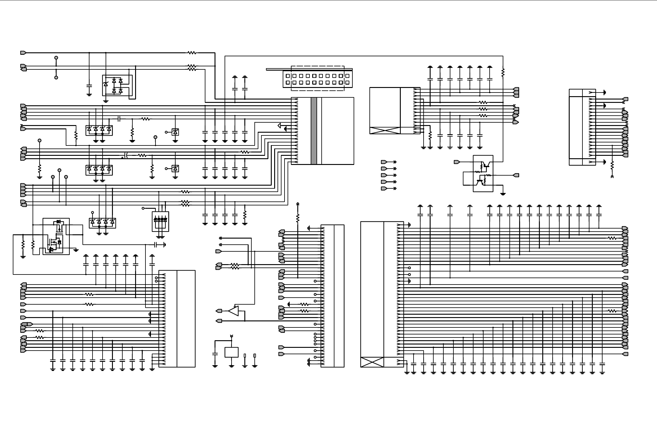
TRANSCEIVER 450-470MHz: SCHEMATICS, PCBs and PARTS LISTS 8.1 - 13
G
G
G
G
G
G
G
G
G
G
G
G
G
G
G
G
G
G
G
G
G
G
G
G
G
G
G
G
G
G
G
G
G
G
G
G
G
G
G
G
G
G
G
G
G
G
G
G
10K
10K
10K
10K
G
G
G
G
G
G
G
G
G
G
G
G
G
G
G
G
G
G
G
G
G
G
G
G
G
G
G
G
G
G
G
G
G
G
G
G
G
G
G
G
G
G
G
G
G
G
G
G
G
G
G
G
G
G
G
G
G
G
G
G
G
G
G
G
G
G
G
G
G
G
G
G
G
G
G
TX_AUDIO
KEYFAIL / FLASH
ANALOG GROUND
DIGITAL GROUND
EMERGENCY
IGNITION
RX_AUDIO
AUDIO_PA_ENABLE
SWB+
HOOK
SCI_DTR
SPEAKER+
SCI_CTS
1
2
10
11
12
13
14
15
16
17
18
J0550
12-PIN CONNECTOR
EXPANSION BOARD
40-PIN CONNECTOR
SPEAKER-
SPEAKER+
GROUND
SCI_TX
EXT_PTT
5VD
J0450
INTERNAL OPTION BOARD
J0500
40-PIN CONNECTOR
EXTERNAL SPEAKER-
J0400
ON_OFF_CONTROL_SV
20-PIN CONNECTOR
27
26
25
24
22
18
6
5
4
NU
NU
SCI_RTS
EXTERNAL MIC AUDIO
EXTERNAL PTT
EXTERNAL ALARM
34
33
32
31
30
29
28
23
3
4
5
6
7
8
9
11
7
17
12
10
8
9
3
2
1
1
SCI_TXD
SCI_RXD19
20
ACCESSORY
CONTROL HEAD
10
11
12
4GROUND
246
HANDSET_AUDIO
BUS+
INT_MIC
FLT_A+
GND
2
3
8 101214161820
1357
40
39
38
37
36
35
GM300
WARIS
REAR VIEW
PCB
J0570
RS232 INTERFACE BOARD
18-PIN CONNECTOR
GND
21
19
20
16
15
14
13
GROUND
21
22
23
24
25
26
27
28
29
30
2
3
6
7
8
9
1
GROUND
4
5
SPIB_CS1_UART
SPIB_CS_BT
SPIB_MISO
NC
SPIB_MOSI
NC
SAP_CLK
GROUND
INT_MIC
MIC
EXPANSION_PTT
91113151719
8
9
10
11
12
13
14
15
16
17
18
19
20
NC
NC
USB+
USB-
NUNU
NU
NU
NU
NU
NU
31
32
33
34
37
38
39
40
NC
GROUND
MUX_CTRL
SPIB_CLK
MUX_CTRL_1
A+
RESET_OUT
BUSY_OUT
BUSY_IN
3V3_DIG
EXP_REQ
SPICS9
GPS_RESET
12V_SWD
SPIB_CLK
GPS_32KHZ
SIM_CLOCK_GP
SIM_DATA_GP
3V_DIG
SPIB_MOSI
SPIB_MISO
SPIB_CS0_UART
BLUE_T_FSYNC
SAP_SRD
SAP_STD
SAP_FSYNC
6
7
EXT_MUTE
RS232_DCD
RS232_TX
RS232_DSR
RS232_RTS
RS232_DTR
RS232_CTS
RS232_RX
RS232_RI
OPTION_DET
9V3
NC
HANDSET_AUDIO
NU
NU
NU
NU
NU
NU
NU
NU
NU
NU
NU
NU
J0600
GPS 24-PIN CONNECTOR
35
36
NU
NU
OPT_SEL
NU
NU
NU
12V_SWD
ONE_PPS
NU
GROUND
GROUND
GROUND
GROUND
NU
NU
NU
NU
GPS_INT
GPS_RX
GPS_TX
NU
NU
NU
NU
SIM_SENSE_GP
SIM_RESET_GP
SIM_PWR_GP
NU
SP_AUDIO
IGNITION
SPICS9
0
R0600
C0557
180pF
82pF
C0609
C0601
180pF 82pF
180pF
C0603 C0605C0604 C0606
180pF
82pF
J0600-28
R0428
10K
J0600-27
J0600-25
J0600-26
3V_DIG
SPIB_MOSI
SPIB_MISO
SPIB_CS0_UART
SIM_SENSE_GP
SIM_RESET_GP
SIM_PWR_GP
GPS_32KHZ
SIM_CLOCK_GP
SIM_DATA_GP
C0619
180pF180pF
C0618
J0600-24
J0600-22
J0600-23
J0600-20
J0600-21
J0600-19
J0600-17
J0600-18
J0600-15
J0600-16
J0600-13
J0600-14
47K
C0421
D0404
0.1uF
NC
3
GND
5
VCC
C0460
3V_DIG
U0409-2
PWR_GND
C0402
VPU
0.1uF
TP0401
TP0402
TP0406
82pF
C0420
R0418
100
100
R0417
C0418 C0419
33pF
R0416
33pF
22
1.5K
R0411
R0412
A2
K1
K2
K3
K4
22
NC
5.6V
VR0405
A1
R0605
10K 47K
R0604
61
4
5
3
2
0.1uF
Q0600
1.2K
C0401
180pF
R0405 C0408
180pF
C0407C0406
180pF
C0404
.01uF 180pF
C0405
0
FLT_A+
DIS_EXPH
SPIB_CLK
R0427
C0612
NC
GPS_INT
GPS_RX
GPS_TX
GPS_RESET
82pF 82pF
C0608
180pF
C0611
0
180pF
C0607
R0603
0
0
R0602
3V_DIG
WAKEUP_UCM_DETECT
R0601
82pF
C0554C0550
82pF
470
R0555
SPICS9
180pF
C0509
82pF
C0559
R0415
100
22
R0505
NC
C0610
82pF
C0613
180pF 82pF
C0615C0614
82pF 180pF
C0616
EXPH_ID
180pF
C0617
R0571
47K
180pF
C0526C0528
180pF
C0537
180pF
C0539
180pF
180pF
C0520
J0600-12
C0512
180pF
J0600-10
J0600-11
J0600-8
J0600-9
J0600-6
J0600-7
J0600-4
J0600-5
J0600-2
J0600-3
J0600-1
2
A
1
OE
4
Y
SPIB_MISO
RS232_DSR
EXPH_RTS
RS232_DTR
U0409-1
74VHC125
4.7K
R0527
RS232_DCD
BLUE_T_FSYNC
SAP_SRD
SAP_STD
SAP_FSYNC
IGNITION
C0521
180pF
180pF
C0519
EXPANSION_PTT
RS232_TX
RS232_RX
INT_MIC
NC
10K
R0406
R0403
10K
33V
EXT_PTT
EXT_ALARM
VR0406
KEYFAIL
TX_AUDIO
20V
VR0401
MUX_CTRL_1
FLT_A+
SPKR-
EXT_MIC
C0522
82pF
82pF
C0513
180pF
C0504 C0503
82pF
C0502
180pF
C0506
180pF
Q0401
0
R0424
0
R0423
R0404
4.7K
TP0403
1
TP0125 TP0405
1
TP0404
1
R0413
10K
NC
PAT_RST
R0420
0
J0450-19
0
R0421
3V_DIG
82pF82pF
C0534C0536 C0535
40
82pF
38
J0500-39 39
J0500-40
J0500-37 37
J0500-38
J0500-36 36
J0500-35 35
J0500-34 34
M0402
SIM_RESET_GP
SIM_SENSE_GP
SIM_CLOCK_GP
SPIB_CS0_UART
SIM_DATA_GP
M0401
SP_AUDIO
MIC
OPT_ID
SIM_PWR_GP
RS232_RTS
RS232_TX
RS232_RX
NC
OPT_ID
SIM_PWR_GP
RS232_RTS
EXT_MUTE
NC
NC
NC
NC
NC
NC
NC
EXP_REQ
SIM_DATA_GP
NC
NC
NC
NC
LI_CELL
RS232_RTS
SIM_RESET_GP
SIM_SENSE_GP
SIM_CLOCK_GP
C0540
180pF
HANDSET_AUDIO
180pF
C0538
RS232_CTS
EXPH_RX
EXPH_RI
9V3
82pF
C0558
C0552
180pF
C0553
180pF
C0556
180pF
C0515
82pF
C0517
82pF
SAP_CLK
EXP_REQ
VSTBY
SPIB_CLK
C0511
180pF 180pF
C0510
EXP_REQ
C0507
BUSY_IN
C0508
180pF
BUSY_OUT
180pF 180pF
C0505
180pF
C0527
SPIB_MISO_1
SPIB_CS0_UART
SPIB_CLK
SPIB_MOSI
J0570-20
J0570-2
J0570-1
J0570-3
J0570-5
J0570-4
J0570-6
82pF
C0525 C0523
82pF82pF
C0524C0530 C0529
82pF
C0531
82pF 82pF82pF
C0533 C0532
SCI_TX
INT_MIC
82pF
VR0403
20V
EXPH_TX
VR0402
20V
J0450-42
SPIB_MOSI
ON_OFF_CONTROL_SV
SPIB_CS1_UART
J0450-41
32
J0500-33 33
RS232_CTS
SPIB_MISO
SPIB_CLK
J0500-31 31
J0500-32
J0500-29 29
J0500-30 30
27
J0500-28 28
25
J0500-26 26
J0500-27
J0500-24 24
J0500-25
22
J0500-23 23
41
J0500-21 21
J0500-22
J0500-42 42
J0500-41
J0400-19
J0400-3
J0400-2
J0400-1
J0400-20
R0559
10
10
R0557
EMERGENCY
IGNITION
HOOK
PA_ENABLE
SPKR+
SPKR-
J0550-4
J0550-9
5VD
3V3_DIG
FLT_A+
82pF
9V3
C0551
C0555
82pF
180pF 180pF
C0561
.01uF
C0560
C0417C0415 C0416
82pF180pF
C0414
180pF
C0413
180pF
C0412
180pF
C0411
VR0407
33V
SAP_CLK
SPIB_MOSI
SPIB_MISO_1
SPIB_CS1_UART
180pF
SAP_STD
SAP_SRD
SAP_FSYNC
ENC_RESET
C0409
2.2uF
R0410
100K
MUX_CTRL
R0409
560
J0500-2 2
J0500-5 5
RESET_OUT
12
J0500-1 1
J0500-13 13
J0500-12
KEYFAIL
J0500-11 11
J0450-1
J0450-2
J0450-18
J0450-16
J0450-17
J0450-36
J0570-7
J0450-40
J0570-8
J0570-10
J0570-9
J0570-12
J0570-11
J0570-13
J0570-15
J0570-14
J0570-16
J0570-18
J0570-17
J0570-19
HANDSET_AUDIO
0
R0562
J0450-22
J0450-26
J0450-28
J0450-37
J0450-32
J0450-23
J0450-33
J0450-29
J0450-34
J0450-30
J0450-15
J0450-35
J0450-24
J0450-31
J0450-3
J0450-25
J0400-11
BUS+
J0400-10
J0400-9
J0400-12
J0400-14
J0400-8
J0400-13
J0400-7
J0400-15
J0400-5
J0400-16
J0400-6
J0400-17
J0400-18
J0400-4
J0450-21
J0450-39
J0450-27
J0450-13
J0450-14
J0450-20
J0450-5
J0450-4
J0450-6
J0450-7
J0450-8
J0450-9
J0450-10
J0450-12
J0450-11
J0550-14
J0450-38
J0550-10
J0550-8
J0550-3
J0550-7
J0550-6
J0550-2
J0550-5
J0550-12
J0550-1
J0550-11
J0550-13
SPKR+
RX_AUDIO
RS232_DTR
EXT_SWB+
9
C0410
180pF
J0500-17 17
J0500-9
J0500-15 15
J0500-18 18
16
J0500-4 4
J0500-14 14
J0500-16
J0500-20 20
J0500-10 10
7
J0500-19 19
J0500-3 3
J0500-7
6
J0500-8 8
3V_DIG
J0500-6
5VD
3V_DIG
3V_DIG
3V_DIG
USB_RX1
USB_TX1
9V3
5VD
3V3_DIG
FLT_A+
USB_TX1
USB_RX1
5VD
FLT_A+
3V3_DIG
3V3_DIG
3V3_DIG
9V3
3V3_DIG
Main Board 8466575A01_A / I/O Section
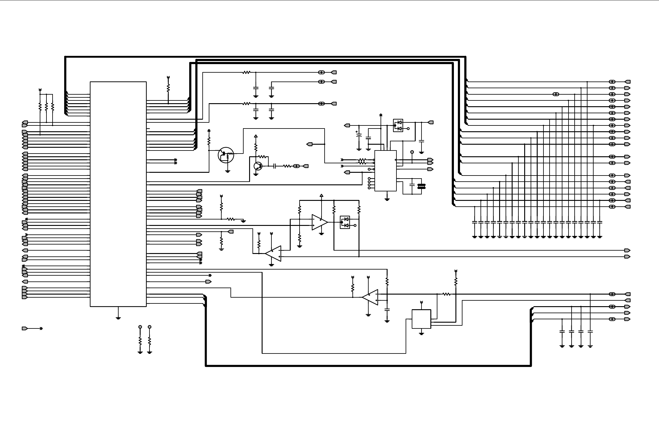
8.1 - 14 TRANSCEIVER 450-470MHz: SCHEMATICS, PCBs and PARTS LISTS
Main Board 8466575A01_A / Controller Section
G
G
G
G
G
G
G
G
G
G
G
G
G
G
G
G
G
G
G
G
G
G
G
G
G
G
G
G
G
G
G
G
G
G
G
G
G
G
G
G
G
G
G
G
G
G
G
G
G
G
G
G
G
G
G
G
G
G
G
G
G
G
G
G
G
G
G
G
G
G
G
G
G
G
G
G
G
G
G
G
G
G
G
G
G
G
G
G
G
G
G
G
G
G
G
G
G
HDW-ID
NU
NU
REALTIME CLOCK
NU
NU
NU
NUNU
NU
NUNU
NU
NU
NU
NU
NU
NUNU
NU
NU
NU
R0125
1.5K
TP0128
1.5K
R0128
TP0127
TP0120
ADC_SARS
D0101
USB_VPIN
3V_DIG
1V8
1V55
ATTN_EN
SPI_CS_ADC
100uF
C0143
USB_VMOUT
R0107
GPS_32KHZ
5VD
5VD
SPIB_CS2_RTC
GP8_IN_ACC14
10
RTC_ON_SW
DIS_EXPH
SIM_DATA_GP
USB_TXENB
URTC
NC
REF_16_8_FN_CNTLR_1
C0148
15pF
15pF
C0147
C0146
15pF
15pF
0
SPICS9
C0115
47K
R0129
R0130
R0135
47K
C0124
R0136
47K
ANT_EN_CNTLR_1
82pF
R0101
4.7K
E2_CS
5VD
Y0101
CC4V
32.768KHz
ANT_EN
EXPH_ID_INV
Q0101
4.7K
R0102
MOD
R2
R1
EXP_REQ
LV_DETECT
BUSY_IN
SAP_SRD
MUX_CTRL_1
BUSY_OUT
WAKEUP_UCM_DETECT
R0127
47K
560
R0132
R0134
1.5K
R0133
33K
NC
NC
NC
NC
USB_RS232USB_TXENB
USB_VMOUT
USB_VPIN
WAKEUP_UCM_DETECT
SPIB_MOSI
SPIB_CLK
SPIB_CS2_RTC
NC
SPIA_MISO
SPIA_MOSI
SPIB_CLK
SPIB_CS0_UART
SPIB_CS1_UART
SPIB_CS2_RTC
SPIB_MISO
SPIB_MOSI
SPICS9
SPI_CS_ADC
SSI_CLOCK
SSI_DATA
SSI_FSYNC
TOUT0
TXD_VPOUT
USB_INT
SAP_CLK
SAP_FSYNC
SAP_SRD
SAP_STD
SIM_CLOCK_GP
SIM_DATA_GP
SIM_PWR_GP
SIM_RESET_GP
SIM_SENSE_GP
SOFT_TURN_OFF
SPIA_CLK
SPIA_CS0_ADDAG
SPIA_CS1_FN_PCIC
SPIA_CS2_JAV
SPIA_CS3_ESC
SPIA_CS4_ABA
ON_OFF_CONTROL
PWM_ADC_IN
PWM_ADC_REF
PWM_ADC_SEL
RESET_ABACUS
RESET_JAV_ADDAG
RESET_OUT
RI_SUSP
RS232_CTS
RS232_DCD
RS232_DSR
RS232_DTR
RTC_ALARM
RTC_ON_SW_INV
RTS_XRXD
RXD_VMIN
GP5_IN_ACC10
GP6_IN_ACC12
GP6_OUT_ACC12
GP8_IN_ACC14 GP8_OUT_ACC14
GROUND
LOAD_DUMP
LOCK_FN
LV_DETECT
MIC_EN1
MIC_EN2
MIC_EN3
MOD
MUTE
MUX_CTRL
MUX_CTRL_1
CKIL
DIS_EXPH
E2POT_CS1
E2POT_CS2
E2POT_INC
E2POT_UD
E2_CS
ENC_RESET
ESBEP_RX
ESBEP_TX
EXPANSION_PTT
EXPH_ID_INV
EXP_REQ
GP1_IN_ACC3
GP2_OUT_ACC4
GP4_IN_ACC9
1V8
3V_DIG
ADC_SARS
ADDAG_CLK
ADDAG_FS
ADDAG_STD
ADDAG_TXE
AGC_0_FE
AGC_1_FE
AGC_2_IF
ANT_EN
ATTN_EN
BLUE_T_FSYNC
BUSY_IN
BUSY_OUT
CKIH
R0108
CONTROLLER
1V55
SIM_RESET_GP
SIM_CLOCK_GP
SIM_SENSE_GP
47K
0.1uF
C0123
SIM_PWR_GP
1
VCC2
17
VCCIF
3
X1
X2 5
LI_CELL
9OSC_1HZ
18 OSC_32KHZ
14
SCLK
15
SDI
16 SDO 11
SERMODE
2
VBAT
20
VCC1
12
CE
10 GND
INT0
7
8INT1
4NC1
6NC2
13 NC3
19 NC4
SPIA_CLK_CNTLR_2
U0100
DS1306
82pF
ADDAG_CLK
C0139
C0117
C0140
82pF
33pF
33pF
82pF
C0125
C0137
82pF
82pF
C0122
C0118
C0119
10K
R0122
82pF
USB_RS232
USB_INT
EXPANSION_PTT
NC
D0102
BUS+
SPIB_CS0_UART
ON_OFF_CONTROL
RS232_DCD
RI_SUSP
4.7K
R0120
SPIB_MISO
2
3
1
8
4
6
5
7
8
4
U0102-1
06A02
LOAD_DUMP
LOAD_DUMP_CNTLR_1
06A02
U0102-2
TEMP_SENSE
TEMP_SENSE_CNTLR_1
BATTERY_VOLTAGE
.022uF
R0115
75K
C0113
R0106
47K
C0142
Q0100
10
47pF
SAP_STD
SAP_CLK
BLUE_T_FSYNC
SAP_FSYNC
R0131
C0110
3.3pF
C0141
0.1uF
RXD_VMIN
TXD_VPOUT
RS232_DTR
RTS_XRXD
RS232_DSR
RS232_CTS
C0133
470pF
SOFT_TURN_OFF
RESET_ODCT_ADDAG
RESET_ODCT_ADDAG_CNTLR_1
ADDAG_TXE
ADDAG_TXE_CNTLR_1
C0138
470pF
SSI_FSYNC
SSI_FSYNC_CNTLR_1
SCI_TX
ADDAG_STD
ADDAG_STD_CNTLR_1
30K
R0117
R0113
15K
R0118
R0119
10K
15pF
C0111
10K
SSI_CLK_CNTLR_1
15pF
C0114
SSI_DOUTB_CNTLR_1
MIC_EN3
E2POT_UD
MUTE
E2POT_CS1
E2POT_CS2
E2POT_INC
SSI_DOUTA_CNTLR_1
RESET_OUT
SSI_DOUTB
SSI_DOUTA
MIC_EN1
MIC_EN2
C0120
15pF
SPIB_CS1_UART
REF16_8_FN
ADDAG_FS
ADDAG_FS_CNTLR_1
470pF
SPIB_MOSI
SPIB_CLK
C0121
B0
B1 1
2GND
6SEL
VCC 5
C0127
470pF
3
1
8
4
NC7SB3157
U0104
4
A3
U0103-1
06A02
2
ENC_RESET
4.7K
R0100
AGC_1_FE_CNTLR_1
AGC_2_IF
AGC_2_IF_CNTLR_1
C0129
AGC_1_FE
AGC_0_FE_CNTLR_1
470pF
470pF
AGC_0_FE
C0131
C0130
470pF
470pF
SPIA_CS4_ABA
SPIA_CS4_ABA_CNTLR_1
C0132
SPIA_CS2_ODCT_CNTLR_1
SPIA_CS3_ESC
SPIA_CS3_ESC_CNTLR_1
ADDAG_CLK_CNTLR_1
SPIA_CS2_ODCT
SPIA_CS1_FN_PCIC_CNTLR_1
15pF
C0116
SPIA_MOSI_CNTLR_1
SPIA_CLK
SPIA_MISO_CNTLR_1
SPIA_MOSI
R0111
SPIA_MISO
10
SSI_CLK
10
R0105
15pF
C0136
SSI_SYNCB
SSI_SYNCB_CNTLR_1
C0128
470pF
LOCK_FN
LOCK_FN_CNTLR_1
470pF
C0135
C0134
SPIA_CS1_FN_PCIC
470pF
SPIA_CLK_CNTLR_1
SPIA_CS0_ADDAG
SPIA_CS0_ADDAG_CNTLR_1
GP1_IN_ACC3
3V_DIG
5VD
3V_DIG
RTC_ALARM
3V_DIG
RTC_ALARM
3V_DIG
3V_DIG
3V_DIG
5VD3V_DIG
3V_DIG
SPIB_MISO
GP2_OUT_ACC4
GP4_IN_ACC9
GP5_IN_ACC10
GP6_OUT_ACC12
GP6_IN_ACC12
GP8_OUT_ACC14
3V_DIG
5VD
LT(7)
HDI_A(1)
HDI_A(3)
HDI_B(2)
HDI_A(2)
HDI_B(1)
LT(2)
HDI_B(1:100)
HDI_B(1)
HDI_A(1:100)
HDI_A(1)
HDI_B(2)
HDI_A(2)
HDI_B(3)
HDI_B(4)
HDI_B(5)
HDI_B(3)
HDI_B(4)
HDI_B(5)
LT(4)
LT(4)
LT(5)
HDI_A(3)
SPIB(2)
LT(5)
LT(7)
LT(0:10)
LT(0)
LT(1)
LT(2)
SPIB(1:8)
SPIB(1)
SPIB(2)
SPIB(3)
SPIB(4)
SPIB(5)
SPIB(6)
SPIB(7)
SPIB(8)
SPIB(1)
SPIB(3)
SPIB(4)
SPIB(5)
SPIB(6)
SPIB(7)
SPIB(8)
LT(0)
LT(1)
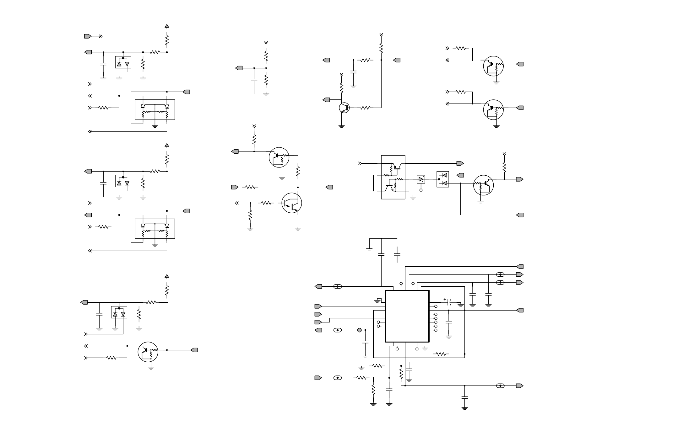
TRANSCEIVER 450-470MHz: SCHEMATICS, PCBs and PARTS LISTS 8.1 - 15
G
G
G
G
G
G
G
G
G
G
G
G
G
G
G
G
G
G
G
G
G
G
G
G
G
G
G
G
G
G
G
G
NU
NU
NU
NU
HW_ID
EXPH_ID
NU
NU
NU
NU
NU NU
NU
NU
NU
NU
NU
NU
NU
NU
NU
NU
IGNITION
R0163
47K
Q0158
47K
R0162
EMERGENCY
R0168
10K
R0157
33K
BIAS3_CNTLR_1
SPIA_MOSI
SPIA_CS1_FN_PCIC
PA_ENABLE
20
VAR1
18
VAR2
24
VAR3
VG 15
6VL 19
VLIM
SPIA_CLK
21
RS
31 RSET
23
RX
2T1
30 TEMP
14
V10
16
V45
17
V5EXT
9
F168
8GND1
25 GND2
4INT
22
NA
11
Q
10
QX
1RFIN
29 CEX
3CI
5CJ
7CL
26 CLK
12
CQ
CQX 1328 DATA
H99S4
U0150
32 ANO
27 BPOS
Q0157
ON_OFF_CONTROL
R0161
47K
47K
R0167
R0169
10K
C0161
470pF
ADC_IN7
0.1uF
NC
C0150
33K
R0179
D0151
0.1uF
C0163
2.2K
ADC_IN2
R0155
R0170
ON_OFF_CONTROL_SV
470pF
10K
R0151
33K
C0170
NC
NC
NC
NC
NC
NC
NC
NC
NC
NC
NC
R0156
100K
Q0152
5VD
Q0160
4.7K
R0160
R0159 Q0156
47K
2.2K
R0154
5VD
BIAS1
BIAS3
D0150
47K
R0150
FLT_A+
Q0150
DRIVER_SENSE_CNTLR_1
10K
R0172
DRIVER_SENSE
R0174
10K
C0156
1uF
R0177
22K
R0176
47K
100K
R0178
EXPH_ID_INV
Q0163
EXPH_ID
10K
R0175
2.2K
R0173
10K
R0166
10K
R0171
33K
R0152
0.1uF
C0162
ADC_IN4
33K
100K
R0180
R0181
D0153
HOOK
470pF
C0151
K9V1_CNTLR_1
EXT_PTT
EXT_ALARM
BIAS2_CNTLR_1
BIAS2
FECNTL_1
K9V1
FECNTL_CNTLR_1
C0155
2200pF
0.1uF
5VD
R0182
100K
C0164
Q0164
C0160
0.1uF
KEYFAIL
G
P8_IN_ACC14
ADC_IN1
NC
D0152
5.6V
VR0163
Q0161
MOD
C0154
GP2_IN_ACC4
ADC_IN3
RESET_OUT
470pF
9V3
3V_DIG
C0159
470pF
C0158
470pF470pF
C0157
C0152
470pF
4.7K
R0153
47K
Q0159
R0165
1
BIAS1_CNTLR_1
3V_DIG
3V_DIG
3V_DIG
3V_DIG
3V_DIG
3V_DIG
3V_DIG
3V_DIG
TP0150
NC_U3501_13
NC_U3501_13
NC_U3501_13
NC_U3501_13
NC_U3501_13
3V_DIG
G
P6_OUT_ACC12
GP6_IN_ACC12
3V_DIG
GP4_IN_ACC9
3V_DIG
GP5_IN_ACC10
3V_DIG
3V_DIG
G
P8_OUT_ACC14
G
P1_IN_ACC3
3V_DIG
GP2_OUT_ACC4
3V_DIG
Main Board 8466575A01_A / Port Controller Section
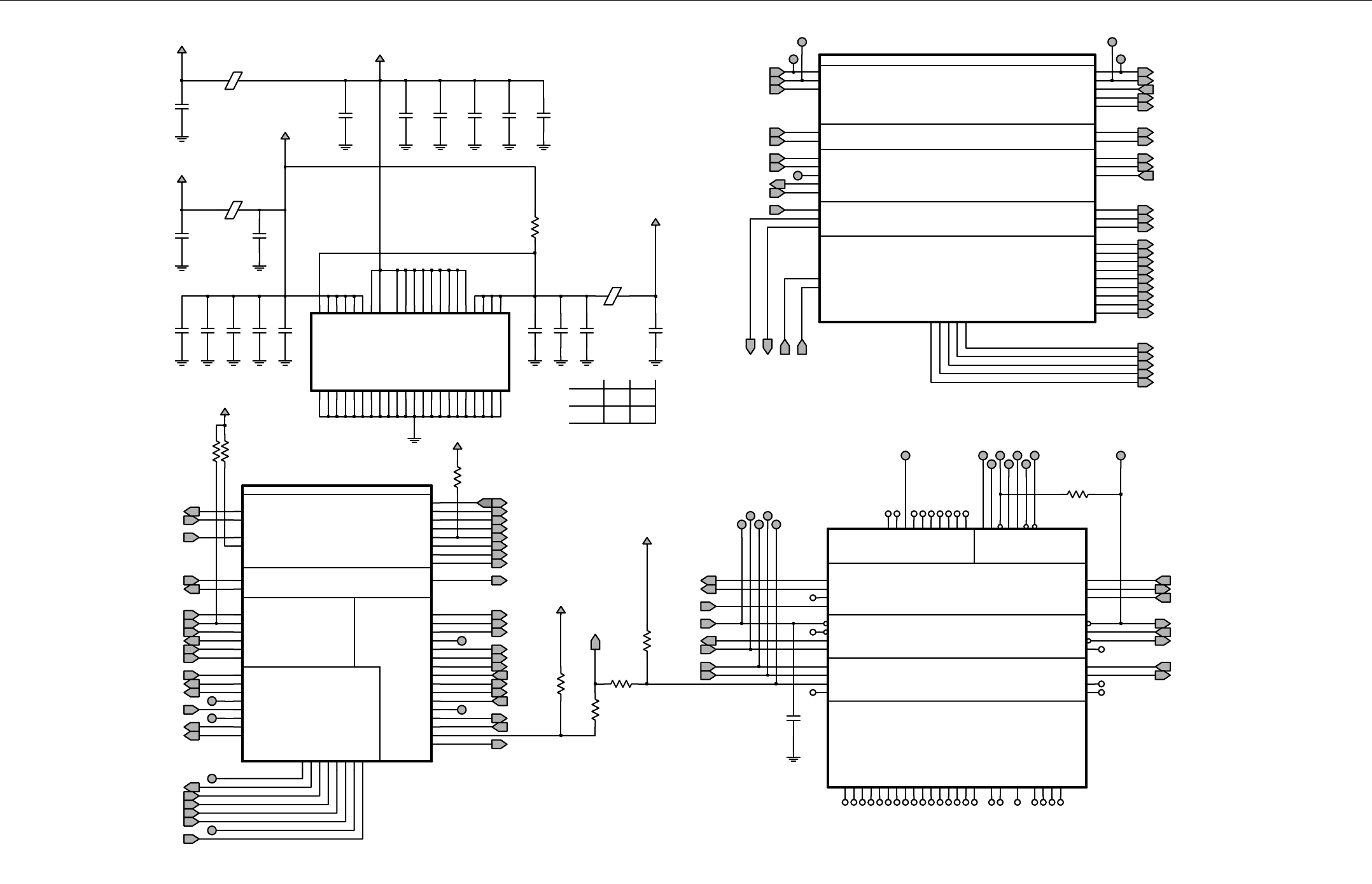
8.1 - 16 TRANSCEIVER 450-470MHz: SCHEMATICS, PCBs and PARTS LISTS
Main Board 8466575A01_A / PATRIOT Controller Section
SIM
DSC AND ONE_WIRE
INTERRUPTS LAYER 1 TIMERS
KEY PAD I/O
G
G
G
G
G
G
G
G
G
G
G
G
G
G
G
G
G
G
PRIMARY UART
SECONDARY UART
BBP
SAP
MQSPI
G
G
G
G
G
G
G
G
G
G
G
G
G
G
G
G
G
G
G
G
G
G
G
G
G
G
G
G
G
G
G
G
GG
G
G
G
G
G
G
G
G
G
G
G
G
G
G
G
G
G
G
G
G
G
G
G
G
G
G
G
G
G
G
JTAG
REAL TIME TRACE
GPIO
CCM/WDOG/EGPT/CLK
MISCELLANEOUS
DSP TRACE
G
G
G
G
G
G
G
G
G
G
G
G
G
G
G
G
G
G
G
G
G
Ext Interupt/Keypad
Clock Amplifier
R1112E1103
RAM 2.2
BRAVO
DNP
DNP0R
0R
NU
NU
NU
NU
EIM(1.8V)
Sim, SAP, Bottom Conn. (3.0V)
UART, SIM (3.0V)
UART, GPIO (3.0V)
GPP (3.0V)
Layer 1 timer, QSPI (3.0V)
Patriot Core(1.8V)
Layer 1 timer, QSPI (3.0V)
Place all 0.1uF caps close to patriot supply pins
TP1103
TP1109
TP1111
TP1104
TP1110
TP1108
SIM_PWR_GP
TP1112
E1101
SIM_SENSE_GP
SIM_RESET_GP
SIM_CLOCK_GP
100pF
1V8
E1102
C1100
100pF
C1107
MUTE
PWM_ADC_IN
PWM_ADC_SEL
GP8_OUT_ACC14
ANT_EN
0.1uF
EXPH_ID_INV
GP4_IN_ACC9
C1104 C1102
0.1uF
C1106
0.1uF
GP1_IN_ACC3
C1111
0.1uF
D4
TOUT9_PD12 AGC_0_FE
ON_OFF_CONTROL
BUSY_IN
USB_INT
AGC_2_IF
TOUT15_PD11 E7
TOUT2 B8
TOUT3 A9
TOUT4_PD0 B4
TOUT5_PD1 B3
TOUT6_PD2 A3
TOUT7_PD3 B2
TOUT8_PD4 A2
SIM_SVEN1_PB14_TIN2_DSP_DBG_XDW D13
TOUT0 A10
TOUT1 B9
TOUT10_PD13 C3
TOUT11_PD7 G8
TOUT12_PD8 E8
TOUT13_PD9 F8
TOUT14_PD10 A8
SIM_D0TX_PB4 H11
C14 SIM_D1RX_PB11 SIM_D1TX_PB10 B15
SIM_PD0_PB9
J14
SIM_PD1_PB15_DSP_DBG_PAW
B14
SIM_RST0_PB6 J12
SIM_RST1_PB12_TIN0 F11
SIM_SVEN0_PB8 J13
ROW3
G2
ROW4
G1
ROW5
G7
ROW6
H7
ROW7
H1
SIM_CLK0_PB7 J16
SIM_CLK1_PB13_TIN1_DSP_DBG_YDW A15
SIM_D0RX_PB5
H10
INT2_PC14
J4
INT3_PC15
J3
INT4_PA6_OPTSEL1
C16
INT5_PA7_OPTSEL2
G11
OWIRE_DAT_PC10
F6
ROW0
F1
ROW1
H4
ROW2
H6
COLUMN4_PE12_IC2B
F2
COLUMN5
E1
COLUMN6
H5
COLUMN7
G3
DSC_RX_PD6
E5
G6
DSC_TX_PD5
INT0_PE8
J6
INT1_PE9
J5
SIM_INT_TOUT_BLOCK
U1100-4
COLUMN0
D1
COLUMN1
G5
COLUMN2
F3
COLUMN3
G4
3V_DIG_FILT
1V8_FILT
C1121
0.1uF
C1112
0.1uF
C1110
0.1uF
C1105
0.1uF
C1103
ADDAG_CLK
ADDAG_FS
SAP_SRD
0.1uF
BUSY_OUT
SPIB_CS1_UART
SPIB_CS0_UART
SSI_DATA
C1109
0.1uF
R8
Q5VDD G15
Q6VDD C10C9 Q6VSS
Q4VSS
T8
Q5VSS
H15
VCCA A7
A4
I1VSS
C2
I2VDD A1
I2VSS
C1
J1VDD_J2VDD H2
J1VSS
H3
J2VSS
K1 Q3VDD K3
Q4VDD
K15
EVDD C12
EVSS
D9
GNDA
A5
H1VDD D8
H1VSS
C8
H2VDD B7
H2VSS
B5
I1VDD
G9
B2VSS
F14
G14 B2VSSA
C1VDD E15
C1VSS
E13
C2VDD A16B13 C2VSS
DVDD K10
DVSS
T9
A3VSS
P11
A4VDD N10
A4VSS
M11
A5VDD R16
A5VSS
L15
B1VDD H9
B1VSS
H16
B2VDD
IC_PWR_GND
U1100-5
A1VDD P3
A1VSS
N6
A2VDD P6
A2VSS
P8
A3VDD
RS232_CTS
RS232_DCD
RI_SUSP
RS232_DSR
3V_DIG
C15
UCTS2_PB2
L16 URTS1_PA13_USBXRXD_IPWR_RESET_N_IC2A
URTS2_PB3
D14
K12 URXD1_PA15_USB_VMIN_IRXD_TDI
B16 URXD2_PB1
K11
UTXD1_PA14_USB_VPOUT_ITXD_TDO
F12
UTXD2_PB0
TXD_VPOUT
F7 SPICS8_PE2
SPICS9_PE3
E6
SRDA
J10
B12 SRDB
B10 SRDB2_PC4_OC2
J11
STDA
E9
STDB
G12
UCTS1_PA12_USB_FSEN_IOE_MCU_DE
F4
SDI_D_C_PE5_SPICS1
B1
SPICS0_PE10
SPICS2_PE4 E3
D2
SPICS3_PE6 E2
SPICS4_PE7
B6 SPICS5_PE11
C5 SPICS6_PE0
D6 SPICS7_PE1
A11
SC0B_PC2
G16
SC1A_PC6
A12
SC1B
K16 SC2A
B11 SC2B_PC3
J15 SCKA
C11 SCKB
D10 SCKB2_PC5_OC3
D7 MISOA
D3 MISOB
C6
MOSIA
F5
MOSIB
C7
QSCKA
E4
QSCKB
D15
RIA_PA9_USBSUSP_IPMODEOTLO_TCK_DSCEN_SCKA
G10
SC0A_PC7
U1100-2
SERIAL_PORTS_BLOCK
E14
DCDA_PA8_IPMODEOTHI_DSP_DE_SC2A
D16
DSRA_PA10_IRE_TRST_INT6_STDA
F13 DTRA_PA11_IPMODEIN_TMS_INT7_SRDA
EXP_REQ
SIM_DATA_GP
GPS_TX
E2POT_UD
E2POT_CS2
MIC_EN1
MIC_EN3
USB_RS232
ADDAG_TXE
LOAD_DUMP
AGC_1_FE
TOUT0
GP6_OUT_ACC12
USB_TXENB
LOCK_FN
USB_VPIN
RESET_OUT
PWM_ADC_REF
ENC_RESET
GP5_IN_ACC10
RTC_ALARM
GP6_IN_ACC12
MIC_EN2
RESET_ABACUS
RESET_JAV_ADDAG
BLUE_T_FSYNC
SPIA_CS0_ADDAG
SPIA_CS1_FN_PCIC
SPIA_CS2_JAV
SPIB_MISO
SPIB_MOSI
MUX_CTRL_1
SPIB_CS2_RTC
RS232_DTR
SPI_CS_ADC
SPICS9
E2_CS
NC
SAP_CLK
SAP_FSYNC
RTS_XRXD
RXD_VMIN
SPIA_MISO
ESBEP_RX
NC
NC
NC
NC
NC
NC
SPIA_CS4_ABA
SPIA_CS3_ESC
SPIA_CLK
ADDAG_STD
SSI_CLOCK
SSI_FSYNC
ESBEP_TX
100pF
E1103
C1115
0.1uF
C1120 C1119
0.1uF
3V_DIG_FILT
10K
R1111
R1104
10K
R1108
3V_DIG_FILT
0
R1107
0
3V_DIG_FILT
10K
R1103
100pF
C1114
EXPANSION_PTT
GP2_OUT_ACC4
CKIL
MUX_CTRL
C1113
1.0uF
TP1102TP1101
USB_VMOUT
R1112
0
A13 TEST
C13
TMS
E11
TRST
WDOG_N
F9
CKIH
MOD LV_DETECT
STROBE P15
TABORT L12
TC0 L11
TC1 M14
TC2 N16
D12
TCK
E12
TDI A14
TDO
PWM_N_PE14 K5
H8
PWM_PE13
RAM_BKUP L13
K4 RESET_IN F16
RESET_OUT
SIZ0 M15
SIZ1 N15
E16
STBY_PD14
PGAD3_PF3_MD19
M5
PGAD4_PF4_MD20
P2
PGAD5_PF5_MD21
P1
PGAD6_PF6_MD22
N1
PGAD7_PF7_MD23
M4
PGAD8_PF8_MD24
M3
PGAD9_PF9_MD25
M2
PSTROBE
T2
PGAD10_PF10_MD26
M1
PGAD11_PF11_MD27
L4
PGAD12_PF12_MD28
L3
PGAD13_PF13_MD29
L1
PGAD14_PF14_MD30
L2
PGAD15_PF15_MD31
K2
PGAD1_PF1_MD17
R1
PGAD2_PF2_MD18
N3
PAGE1
R2
PC0_USB_VMOUT
K14
H14 PC11_OC1_USBCLK
D5 PC12_STO
K13 PC1_USB_TXENB
H13
PC8_UTXD1_UTXD2 H12
PC9_URXD1_URXD2
PGAD0_PF0_MD16
M6
F10
MCU_DE
MLB_TSCA L14
MLB_TSCD M16
J1 MOD
G13 MUX_CTL
J2 OC3_PC13_FRAME_TICK
PA2_USB_VPIN K6
PAGE0
T1
F15
CKOH_SCC_CLK
M12
CKO_PA3
D11
CLKSEL_PD15
E10
DSP_DEK1_2VDD
K7
K1_2VSS
L5 K3VDD
N2
K3VSS
L6
MISC_BLOCK
U1100-3
ANALOG_TEST C4
A6 CKIH
J7 CKIL
NC
NC
NC
NC
NC
SPIB_CLK
SPIA_MOSI
NC
NC
NC
NC
NC
NC
NC
NC
NC
NC
NC
NC
TP1211
1
NC
R1109
0
R1132
10K
E2POT_INC
NC
NC
GPS_INT
GPS_RX
3V_DIG_FILT
DIS_EXPH
1V55
NC
NC
NC
TP1107
NC
RTC_ON_SW_INV
ADC_SARS
GP2_IN_ACC4
TP1117
ATTN_EN
TP1124
TP1119
TP1122
TP1105
TP1118
TP1115
C1101
1.0uF
C1108
4.7uF
TP1213
1
TP1113
TP1216
1
TP1217
1
1
1
TP1214
1
TP1215
NC
NC
SAP_STD
TP1212
GP8_IN_ACC14
GPS_RESET
NC
47K
R1101
E2POT_CS1
SOFT_TURN_OFF
NC
1V8_FILT
3V_DIG_FILT
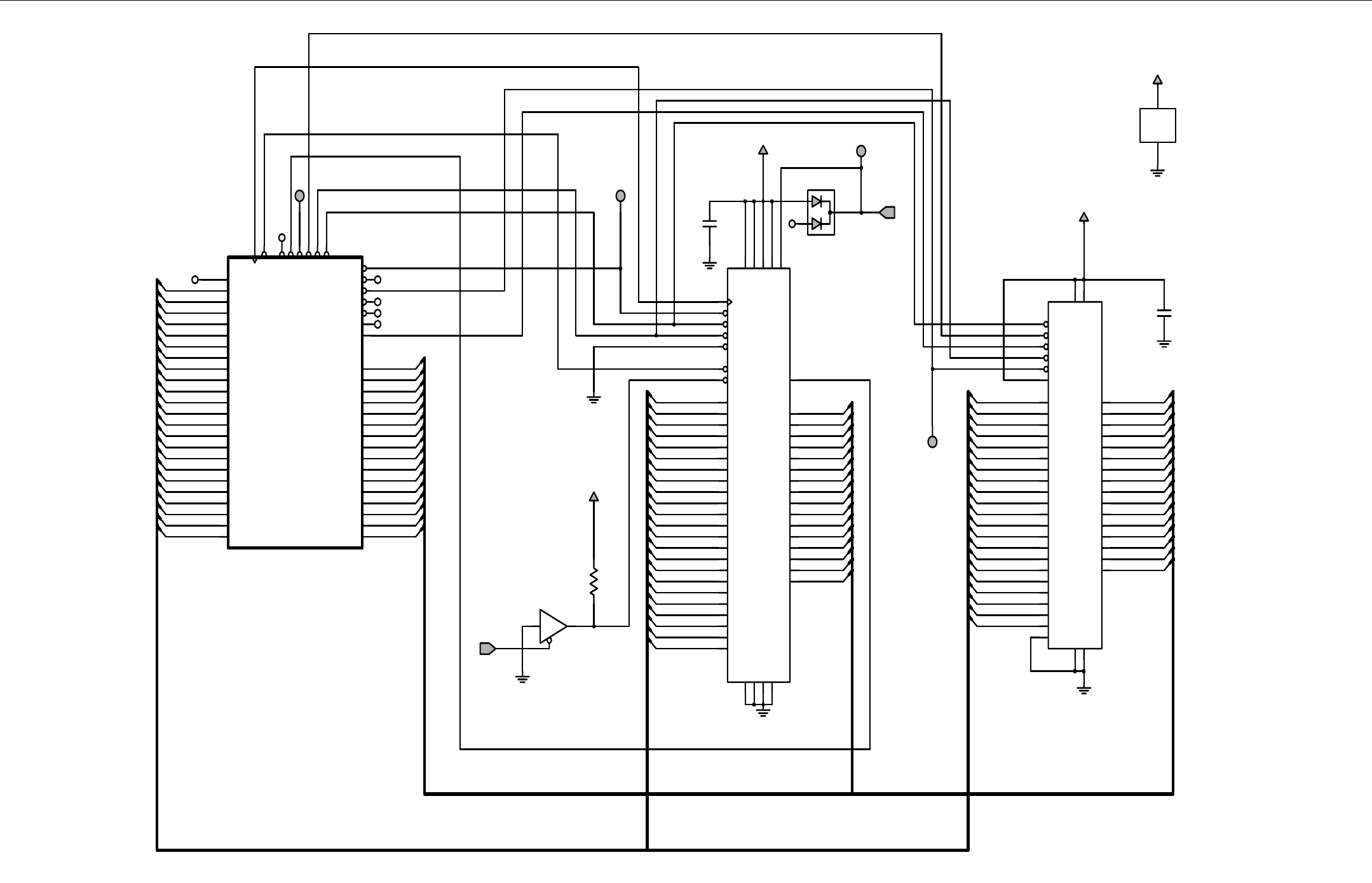
TRANSCEIVER 450-470MHz: SCHEMATICS, PCBs and PARTS LISTS 8.1 - 17
G
G
FLASH_RESET
2M x 16 RAM
Intel 8M x 16 Burst Flash
EIM MODULE
PATRIOT
1M x 16 RAM
9
10
11
12
23
2
3
4
5
6
7
8
9
10
11
12
13
14
15
16
1
2
3
4
5
6
7
8
11
21
20
19
11
12
13
14
10
4
5
6
7
8
9
10
2
3
4
5
6
7
8
9
2
3
4
5
6
7
0
1
1V8_FILT
22
1V8_FILT
13
14
0
1
C1132
0.1uF
1
15
13
14
15
16
17
18
EB1_N M13
ECB_N_PA4 T16
LBA_N N13
P16
OE_N
N11
RW_N
SEB_N_PA5 N14
SOE_N P14
0
D3 T6
R6
D4
D5 T5
D6 R5
P5
D7 N5
D8
D9 T4
EB0_N R13
N7
D1
D10 J8
R4
D11
D12 P4
N4
D13 T3
D14
D15 R3
M7
D2
BURSTCLK T15
R15
CS0_N R11
CS1_N T14
CS2_N N12
CS3_N R14
CS4_N T11
CS5
D0 P7
A23_PA0_DSP_DBG_YDW
R7
A3
T12
A4
P13
A5
M9
P10 A6
A7
P12
A8
N9
A9
R10
A16
J9
A17
L8
A18
M8
A19
N8
A2
M10
A20
K8
A21
L7
T7 A22_PA1_DSP_DBG_XDW
A0
R12
A1
T13
A10
P9
A11
L10
A12
T10
A13
R9
A14
L9
A15
K9
20
21
15
EIM_BLOCK
U1100-1
17
1
2
3
22
17
18
19
1
OE
4
Y
18
12
13
14
15
16
1
U1104-1
74VHC125
2
A
TP5843
1
TP1125
D6 WP
TP1126
1
E1
VCCQ1 G6
VCCQ2 A5
VPP
A3 VSS1
F1 VSS2
G2 VSSQ1
G8 VSSQ2
D3
WAIT
G7
D8 F6
D9
E7 EN_CE
F8 EN_OE
C5 EN_WE
B5 RESET
A4
VCC1 G4
VCC2
F3
F2
D14 E2
D15
E5
D2 G5
D3 E4
D4 G3
D5 E3
D6 G1
D7
C4 ADV
B4 CLK
D0 F7
E6
D1
F5
D10 F4
D11 D5
D12
D13
D7 A22
B8 A3
A8 A4
B7 A5
A7 A6
C7 A7
A2 A8
B2 A9
D1 A15
D4 A16
B6 A17
A6 A18
C6 A19
C8 A2
B3 A20
C3 A21
E8 A0
D8 A1
C2 A10
A1 A11
B1 A12
C1 A13
D2 A14
VCC D6
VCCQ E1
D1 VSS1
E6 VSS2
ZZ
A6
28F128W18BD60
U1102
C6
IO2 D5
IO3 E5
IO4 F5
IO5 F6
IO6 G6
IO7 B1
IO8 C1
IO9
B6
IO0 C5
IO1
C2
IO10
IO11 D2
E2
IO12 F2
IO13 F1
IO14 G1
IO15
D4 A7
H2 A8
H3 A9
B5 EN_CS1
A1 EN_LB
A2 EN_OE
B2 EN_UB
G5 EN_WE
G2 A19
A5 A2
A20
H6
A21
E3
B3 A3
B4 A4
C3 A5
C4 A6
H5 A11
G3 A12
G4 A13
F3 A14
F4 A15
E4 A16
D3 A17
H1 A18
MT45W2MW16PABA
U1103
A3 A0
A4 A1
H4 A10
12
1
2
3
NC
NC
NC
20
NC
8
9
10
11
15
14
13
R1131
RESET_OUT
23
NC
19
1V8_FILT
100K
0.1uF
C1131
7
8
9
10
11
12
TP0161
4
5
6
NC
NC
21
D1101
1
2
VPP
U1104-2
PWR_GND
3
GND
5
VCC
3V_DIG
DATA(15:0)
ADDR(23:0)
Main Board 8466575A01_A / PATRIOT Memory Section
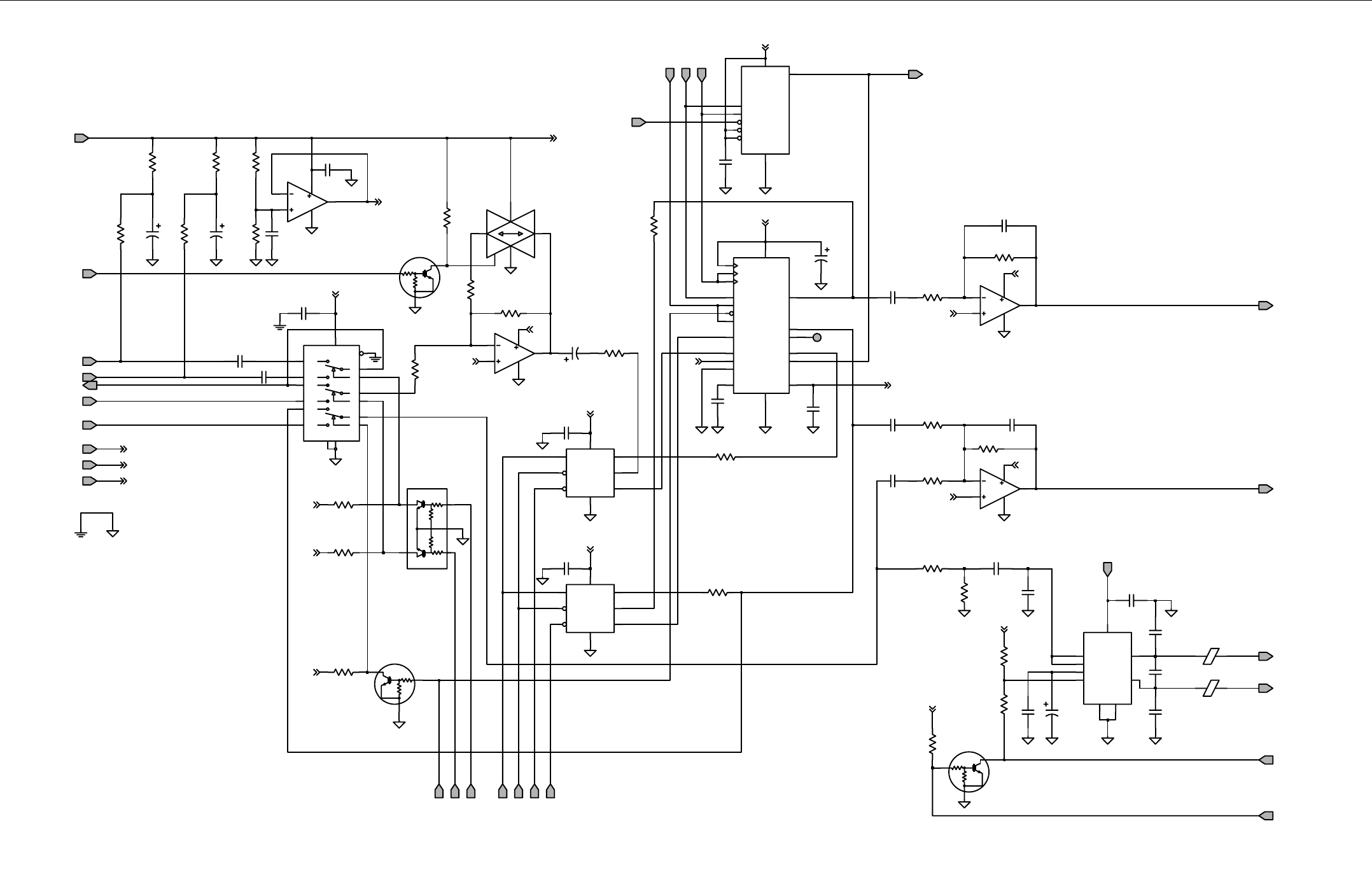
8.1 - 18 TRANSCEIVER 450-470MHz: SCHEMATICS, PCBs and PARTS LISTS
Main Board 8466575A01_A / Controller Audio Section
G
G
G
G
G
G
G
G
G
G
G
G
G
G
G
G
G
G
G
G
G
G
G
G
G
G
G
G
G
NU NU
775mV
80mV
80mV
8
VCC
WP
3
1CS
4GND
7HOLD
6SCK
5SI
2
SO
AT25128-10UU-2_7
U0207
R0246
15K
C0219
AUDIO_A+
0.1uF
C0236
3
VSS
ATTN_EN
.01uF
U0202
TC4S66F
4
CNTL
12
5
VDD
Q0202
R2
R1
4.7K
R0223
10K
R0222
1K
R0220
EXT_MUTE
100
R0221
1000pF
MIC
C0235
L0232
57R01
Q0201
L0231
57R01
C0222
C0220
0.1uF
0.1uF
0.1uF
C0237
R0245
3.3K
R0244
10K
SAP_SRD
47K
47K
R0207
R0206
47K
R2
R1
R0208
Q0203
0.1uF
C0223
E2_CS
FLT_A+
INT_SWB+
C0218
0.1uF
MUTE
C0225
0.1uF
E2POT_UD
E2POT_INC
E2POT_CS1
E2POT_CS2
SAP_CLK
SAP_FSYNC
1uF
3V_DIG
MIC_EN2
MIC_EN1
MIC_EN3
TX_AUDIO
C0221
C0205
0.1uF
R0228
10K
560
R0200
10
8
4
11
TP0200
MC3403
U0206-3
9
15K
R0237
SP_AUDIO
C0204
0.1uF
10uF
SAP_STD
0.1uF
C0224
16V
Y1B
1
3Y1C
ZA 14
ZB 15
ZC 4
C0213
SC 9
VDD 167VEE
VSS
8
YOA
12
Y0B
2
Y0C
5
13 Y1A
U0201
MC14053BD
6
EN
11
SA
SB 10
0.1uF
C0203
200K
R0205
R0204
200K
10uF
C0201
EXT_MIC
100
R0202
16V
560
R0203
C0202
INT_MIC
9V3
0.1uF
C0200
10uF
16V
100
R0201
3
VH
6
VL
4VSS
5
VW
R0225
1K
7CS
1INC
2U_D*
8
VCC
TI_POS
20
VAG
1VAGREF
6
VDDVSS
15
X9315
U0203
MCLK
10 PDI
3PI
PO_NEG 4
5
PO_POS
2
RO_NEG
17
TGTI_NEG
18
19
9BCLKR
12 BCLKT
DR
8
13
DT
7FSR
14 FST
HB
16
11
FL0200
MC145483
3300pF
C0230
10K
R0218
15K
R0241
33uF
C0231
16V
C0232
0.1uF
C0234
1000pF
SPKR+
SPKR-
C0233
1000pF
R0239
12K
HANDSET_AUDIO
C0229
R0242
270K
MC3403
6
5
7
4
11
82pF
RX_AUDIO
U0206-2
R0240
100K
2
3
1
4
11
180pF
C0228
C0226
U0206-1
MC3403
0.1uF
13
12
14
4
11
R0224
15K
R2
R1
MC3403
U0206-4
Q0200
OUT2 6
RR
3
VCC 7
27K
R0238
GND1
2
GND2
5
INV
9
M_SS
8
NINV
1
4
OUT1
VCC 8
VH 3
VL 6
VSS
4
VW 5
TDA1519C
U0205
U0204
X9315
7CS
INC
1
U_D*
2
0.1uF
C0227
3V_DIG
R0243
27K
VAG_1
3V_DIG
FLT_A+
INT_SWB+
9V3
9V3
9V3
3V_DIG
3V_DIG
VAG_2
VAG_2
9V3
9V3
3V_DIG
VAG_1
9V3
VAG_1
9V3
VAG_1
9V3
INT_SWB+
3V_DIG
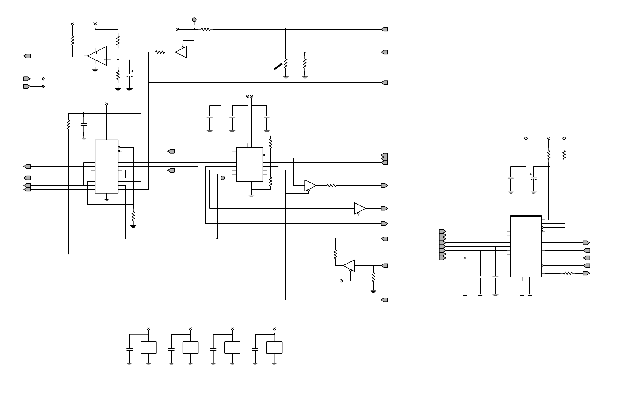
TRANSCEIVER 450-470MHz: SCHEMATICS, PCBs and PARTS LISTS 8.1 - 19
Main Board 8466575A01_A / Controller USB/ADC Section
ZWG0130877-A
G
G
G
G
G
G
G
G
G
G
G
G
G
G
G
G
G
G
G
G
G
G
G
G
G
G
G
G
G
G
G
G
G
G
NU bei Patriot Bravo
NU NU NU
NU
NU
NU NU
NU NU
RS232_RX
EXPH_RX
NU
USB_INT
5VD
3V_DIG
EXPH_RI
VPU
TXD_VPOUT
USB_VMOUT
USB_TXENB
USB_RS232
RI_SUSP
USB_VPIN
1uF
C0450
USB_DET
8
VBUS 14
VCC 7
VM
4VO_VPO 11
VP
3
VPU
15
VREG
13
DPOS
10 ENUMERATE 16
FSE0_VMO 12
GND
17
6
MODE
OE_N 1
RCV
2
SUSPND 5
VCC
U0405
ISP1104
DNEG
9
U0403-2
PWR_GND
3
GND
5
1
Y
4
PWR_GND
U0402-2
GND
3
VCC
5
2
OE
1
Y
4
U0401-1
74VHC125
A
2
OE
GND
5
VCC
74VHC125
U0402-1
A
7Y5
5Y6
3Y7
U0401-2
PWR_GND
3
19
EN_OE2
10 GND 20
VCC
18 Y0
16 Y1
14 Y2
12 Y3
9Y4
4
A1 6
A2 8
A3
11
A4 13
A5 15
A6 17
A7
1
EN_OE1
8
4
MC74LVX244
U0408
2
A0
U0406-2
06A02 6
5
7
0.1uF
C0456
A
2
OE
1
Y
4
USB_RS232
USB_RS232
C0451
U0403-1
74VHC125
0.1uF 0.1uF
C0453C0452
0.1uF
R0459
10K
10K
R0455
0.1uF
C0454
R0450
47K
R0454
33K
10K
R0451
RS232_RTS
EXPH_RTS
2.2K
R0452
SDI 2
SDO 1
VCC 5
RS232_TX
EXPH_TX
ADC_SARS
CSTART 14
EOC 4
FS 17
GND
15
PWDN 16
REFM
18
19
REFP
SCLK 3
7A1
A2
8
A3
9
A4
10
11 A5
12 A6
13 A7
CS 20
U0407
TLV1508
A0
6
TEMP_SENSE
0.1uF
C0462
TP0498
R0465
0
100K
R0470
R0469
2.2K
100K
R0467
4.7K
R046874VHC125
U0404-1
A
2
OE
1
Y
4
TP0499
PWR_GND
U0404-2
GND
3
VCC
5
0.1uF
C0458
RTS_XRXD
RXD_VMIN
C0457
0.1uF
C0455
0.1uF
R0473
270
0
R0472
ADC_IN4
R0471
0
ADC_IN1
ADC_IN2
ADC_IN3
ADC_IN7
BATTERY_VOLTAGE
0.1uF
C0461
OPT_ID
C0463
0.1uF
C0459
0.1uF
100
C0464
4.7uF
R0464
SPIB_MOSI
SPIB_MISO
10K
R0463
0
R0466
SPI_CS_ADC
SPIB_CLK
3V_DIG3V_DIG3V_DIG
3V_DIG
3V_DIG
3V_DIG
EXPH_EN
EXPH_EN
5VD
3V_DIG
3V_DIG 3V_DIG 3V_DIG
5VD 3V_DIG
5VD
8.1 - 20 TRANSCEIVER 450-470MHz: SCHEMATICS, PCBs and PARTS LISTS
R12
C1
C2
C3
C4
C5
C6
C7
C8
C11
C12
C19
C20
C21
C22
C23
C24
C25
C26
C27
C28
C30
C31
C32
C33
C37
C40
D1
E1
E2 E3
1
24
J1
L1
L3
L4
R14
R15
R16
R17
R18
R19
R20
R21
R22
R23
R24
R25
R27
R30
1
6
5
U1
4
5
8
U2
4
5
8
U3
U6
VR1
C29
1
16-12-04
RELEASE FOR PRODUCTIONO
DJ003115
NOSS
P4 RELEASE FOR PROTOTYPE
11-11-04
10-12-04
RELEASE FOR PROTOTYPEP3
NOSS
NOSS
P2 RELEASE FOR PROTOTYPE
07-21-04
GPS-MODUL
SCALE
APPROVED BY
DRAWN BY DATE
APC
DEVELOPMENT IDENTIFICATION CODE
SHEET
CHECKED BY
DESIGNED BY DATE
NPR UNITS
PART NUMBERS
REV DESCRIPTION MEMO
ON.
DO NOT REVISE MANUALLY
COMPUTER GENERATED
H
1
5
6
DRAWING DESCRIPTION
DRAWING NUMBER
DO NOT SCALE DRAWING
8466576A01_P3
MM
NONE 2
OF
BOARD, PC
MILAN II
79D66503N03
E.NOSS 05-17-04 M.BROCKMANN 05-17-04
R.WALSCH
DATE DATE
05-17-0405-17-04 HP.GAERTNER
XXXX-010857
8466576A01
05-17-04
RELEASE FOR PROTOTYPEP1
FORMAT REVISED JULY 98
NOSS
GPS sub modul
8466576A01
_O
Date: Jan/25/2005
PCB TOP VIEW Drawing: Wolfgang Ka/BER, Date: Jan/25/2005
C10
C14
C15
C16
C17
C18
C38
C39
C41
C42
C43
3
4
2
5
FL1
3
4
2
5
FL2
1
J2
L5
L6
L11
L12
R5
R10
R26
R28
R29
TP6
A1
A8
H8
H1
U4
U5
4
3
2
Y1
2
16-12-04
RELEASE FOR PRODUCTIONO DJ003115
NOSS
P4 RELEASE FOR PROTOTYPE 11-11-04
10-12-04
RELEASE FOR PROTOTYPEP3 NOSS
NOSS
P2 RELEASE FOR PROTOTYPE 07-21-04
GPS-MODUL
SCALE
APPROVED BY
DRAWN BY DATE
APC
DEVELOPMENT IDENTIFICATION CODE
SHEET
CHECKED BY
DESIGNED BY DATE
NPR UNITS
PART NUMBERS
REV DESCRIPTION MEMO
ON.
H
1
DRAWING DESCRIPTION
DRAWING NUMBER
DO NOT SCALE DRAWING
8466576A01_P3
MM
NONE 2
OF
BOARD, PC
MILAN II
79D66503N03
E.NOSS 05-17-04 M.BROCKMANN 05-17-04
R.WALSCH
DATE DATE
05-17-0405-17-04 HP.GAERTNER
XXXX-010857
8466576A01
05-17-04
RELEASE FOR PROTOTYPEP1 NOSS
GPS Sub Module 8466576A01_O / PCB TOP & BOT side
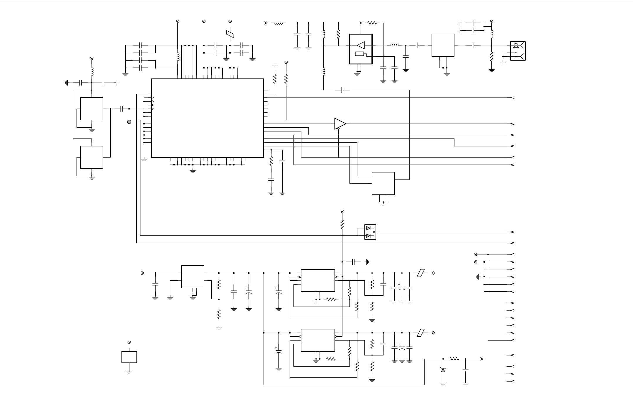
TRANSCEIVER 450-470MHz: SCHEMATICS, PCBs and PARTS LISTS 8.1 - 21
GPS Sub Module 8466576A01_O / Schematic
GND
SIM_DATA_GP
3V_DIG
SIM_PWR_GP
SIM_RESET_GP
12V
12V
SIM_CLOCK_GP
SPIB_MISO
GPS_INT
SPICS9
GND
GPS_32KHZ
ONE_PPS
OPT_SEL
N.C.
N.C.
SPIB_CLK
GND
GPS_TX
SPIB_MOSI
GPS_ON_OFF
GPS_RESET
SPIB_CS0_UART
SIM_SENSE_GP
N.C.
N.C.
GPS_RX
J1-9
J1-21
2COMM
1
GND
3
OUTPUT
4
VCC
150pF
C31
NU
24.5535MHz
IT5305BE
Y2
3
PS
6
VCC
J1-5
UPC8211TK
U5
2
GND1
5
GND2
1
INOUT
4
R19
51.1K
1GND1
GND2
9
4INPUT 5
OUTPUT
6SENSE
8SHUTDOWN
3TAP
U2
LP2986ILDX
7
ERROR 2
FEEDBACK
J1-3
C24
150pF
C40
0.1uF
1.5pF
C42
C41
47pF
C38
18pF
0.1uF
C37
NU
R16
0
C11
1000pF
J1-11
PWR_GND
U6-2
GND
3
VCC
5
E1
IDCTR
J1-14
0
R23
R10
2K
L6
27nH
J1-7
J1-17
C17
560pF
J1-8
C27
33uF
33uF
C23
10uF
C3
C7
TP6
18pF
18pF
C15
OUTPUT
4
VCC
1V_CONT
D1
26MHz
TCO-5871
Y1
2
GND
3
100K
R26R28
100K
51.1K
R25
3.32K
22.0nH
L5
R14
100pF
C33
J1-2
J1-24
C25
0.1uF
1
ADJ
3GND1
6GND2
2ON_OFF
4VIN 5
VOUT
J1-19
LM2941
U1
C4
10uF
G2
L3
27nH
E4
VSS_CORE_3
E5
VSS_CORE_4
E6
VSS_CORE_5
F5
VSS_CORE_6
F6
VSS_IO_1
D2
VSS_IO_2
E8
VSS_IO_3
E1
VTUNE
G8
VEE_MIX
F4
VEE_PLL
G1
VEE_REF
H1
VEE_VCO
F3
VGA_INM G4
VGA_INP H4
VSS_CORE_1
E3
VSS_CORE_2
D4
D5
VDD_CORE_5
VDD_CORE_6 D6
VDD_IO_1 A5
VDD_IO_2 C3
VDD_IO_3 E7
VEE_IF
G5 VEE_LAN2
G7 VEE_LNA1
H7
VCC_MIX H5
VCC_PLL F2
VCC_REF H3
VCC_VCO G3
VDD_CORE_1 C4
VDD_CORE_2 C5
VDD_CORE_3 D3
VDD_CORE_4
H2
SCK_TXD1 D7
TCK
C7
TDI
A8
TDO B8
TEST
D8
TMS
B7
VCC_IF G6
VCC_LAN
E2
MOD_BOOT
A4
MOD_MCLK
C2
MOSI_RXD0 C6
NPSC_RXD1 B5
NRESET
F8
NTRST
C8
ONEPPS B1
REF_CLK
C1
GND_ISQ1
F1
GND_ISQ2
F7
LNA_IN H8
H6
LNA_OUT
LOW_REF_CLK
D1
MCLK_EXT
B4
MISO_TXD0 B6
MOD_ARM
ADC0 B3
ADC1 A3
ADC2 B2
ADC3 A1
BREAKPT
A7
DBGACK A6
DEGRQ
A2
EXT_NIRQ
GPS
U4
L4
75K
R21
C39
27nH
0
47pF
R29
R30
2GND
GND1
3
GND2
5
4
IN
1OUT
750
C28
B39162-B7829-C710
FL1
100pF
C43
C8
18pF
18pF
J1-13
C20
470pF
18pF
C10
1000pF
100pF
C16
0.1uF
C21
J1-10
C2
R5
10K
J1-23
10uF
C26
10uF
C5
4.7nH
L12
C14
0.1uF
13V
VR1
J1-15
NU
J2
18pF
C6
C12
18pF
C19
J1-16
E3
IDCTR
150pF
C32
10uF
J1-12
J1-20
J1-1
R12
20
0.1uF
C29
FEEDBACK 2
GND1
1
9GND2
INPUT
4OUTPUT 5
SENSE
6SHUTDOWN
8
TAP
3
LP2986ILDX
U3
ERROR 7
R15
33K
IDCTR
E2
J1-22
8.2nH
L11
J1-6
J1-18
L1
27nH
C18
2200pF
J1-4
R20
1K
IN 1
OUT1
3
OUT2
4
C22
0.1uF
FL2
B39162-B7840-C710
GND1
2
GND2
5
R17
0
18pF
C1
C30
33uF
NU
R24
0
NU
0
R18
74VHC125
U6-1
A
2
OE
1
Y
4
0
R22
3.32K
R27
NU
GPS_2V 3V_DIG
LNA_BIAS
MILAN_12V
LNA_BIAS
GPS_2V
3V_DIG
MILAN_12V
3V_DIG
3V_DIG
3V_DIG
GPS_3V
GPS_3V
GPS_3V
GPS_3V

8.1 - 22 TRANSCEIVER 450-470MHz: SCHEMATICS, PCBs and PARTS LISTS
PARTS LISTS
Parts on the Mainboard (0166501N85)
Reference Motorola PN Value
C0110 2113944C18 CAP, 3.3pF
C0111 2113944A27 CAP, 15pF
C0113 2113945C04 CAP, .022uF
C0114 2113944A27 CAP, 15pF
C0115 2113944A27 CAP, 15pF
C0116 2113944A27 CAP, 15pF
C0117 2113944C43 CAP, 82pF
C0118 2113944C43 CAP, 82pF
C0119 2113944C43 CAP, 82pF
C0120 2113944A27 CAP, 15pF
C0121 2113944C06 CAP, 470pF
C0122 2113944C43 CAP, 82pF
C0123 2113945D04 CAP, 0.1uF
C0124 2113944C43 CAP, 82pF
C0125 2113944C43 CAP, 82pF
C0127 2113944C06 CAP, 470pF
C0128 2113944C06 CAP, 470pF
C0129 2113944C06 CAP, 470pF
C0130 2113945A05 CAP, 470pF
C0131 2113944C06 CAP, 470pF
C0132 2113944C06 CAP, 470pF
C0133 2113944C06 CAP, 470pF
C0134 2113944C06 CAP, 470pF
C0135 2113944C06 CAP, 470pF
C0136 2113944A27 CAP, 15pF
C0137 2113944C36 CAP, 33pF
C0138 2113944C06 CAP, 470pF
C0139 2113944C36 CAP, 33pF
C0140 2113944C43 CAP, 82pF
C0141 2113945D04 CAP, 0.1uF
C0142 2113944C38 CAP, 47pF
C0143 2313960H07 CAPP, 100uF
C0146 2113944A27 CAP, 15pF
C0147 2113944A27 CAP, 15pF
C0148 2113944C32 CAP, 15pF
C0150 2113944C06 CAP, 470pF
C0151 2113944C06 CAP, 470pF
C0152 2113944C06 CAP, 470pF
C0154 2113944C06 CAP, 470pF
C0155 2113945L33 CAP, 2200pF
C0156 2313960B01 CAPP, 1uF
C0157 2113944C06 CAP, 470pF
C0158 2113944C06 CAP, 470pF
C0159 2113944C06 CAP, 470pF
C0160 2113945D04 CAP, 0.1uF
C0161 2113945D04 CAP, 0.1uF
C0162 2113945D04 CAP, 0.1uF
C0163 2113945D04 CAP, 0.1uF
C0164 2113945D04 CAP, 0.1uF
C0170 2113944C06 CAP, 470pF
C0200 2313960D07 CAPP, 10uF
C0201 2313960D07 CAPP, 10uF
C0202 2113945D04 CAP, 0.1uF
C0203 2113945D04 CAP, 0.1uF
C0204 2113945D04 CAP, 0.1uF
C0205 2113945D04 CAP, 0.1uF
C0213 2113945D04 CAP, 0.1uF
C0218 2113945D04 CAP, 0.1uF
C0219 2113945C02 CAP, .01uF
C0220 2113945D04 CAP, 0.1uF
C0221 2313960B01 CAPP, 1uF
C0222 2113945D04 CAP, 0.1uF
C0223 2113945D04 CAP, 0.1uF
C0224 2313960D07 CAPP, 10uF
C0225 2113945D04 CAP, 0.1uF
C0226 2113945D04 CAP, 0.1uF
C0227 2113945D04 CAP, 0.1uF
C0228 2113944C01 CAP, 180pF
C0229 2113944C43 CAP, 82pF
C0230 2113945L37 CAP, 3300pF
C0231 2313960F04 CAPP, 33uF
C0232 2113945D04 CAP, 0.1uF
C0233 2113945L25 CAP, 1000pF
C0234 2113945L25 CAP, 1000pF
C0235 2113945L25 CAP, 1000pF
C0236 2113945D04 CAP, 0.1uF
C0237 2113945D04 CAP, 0.1uF
C0300 2113944C06 CAP, 470pF
C0301 2113944C06 CAP, 470pF
C0302 2313960F04 CAPP, 33uF
C0303 2113945D04 CAP, 0.1uF
C0304 2113944C06 CAP, 470pF
C0305 2389289U01 CAPP, 10uF
C0306 2389289U01 CAPP, 10uF
C0307 2113945C02 CAP, .01uF
C0308 2313960F04 CAPP, 33uF
C0309 2313960F04 CAPP, 33uF
C0310 2314030J28 CAPP, 22uF
C0311 2113945D04 CAP, 0.1uF
C0312 2113945D04 CAP, 0.1uF
C0313 2113945D04 CAP, 0.1uF
C0314 2113944C06 CAP, 470pF
Reference Motorola PN Value
C0315 2313960F04 CAPP, 33uF
C0316 2313960D07 CAPP, 10uF
C0317 2113944C06 CAP, 470pF
C0318 2113945D04 CAP, 0.1uF
C0319 2113945D04 CAP, 0.1uF
C0320 2113944C06 CAP, 470pF
C0321 2113945D04 CAP, 0.1uF
C0322 2313960F30 CAPP, 47uF
C0323 2313960D07 CAPP, 10uF
C0324 2313960D07 CAPP, 10uF
C0325 2313960C78 CAPP, 2.2uF
C0326 2113945C04 CAP, .022uF
C0328 2313960F30 CAPP, 47uF
C0329 2313960F01 CAPP, 10uF
C0330 2113945D04 CAP, 0.1uF
C0331 2313960F30 CAPP, 47uF
C0332 2113945D04 CAP, 0.1uF
C0333 2113945D04 CAP, 0.1uF
C0334 2113945C02 CAP, .01uF
C0335 2113944C06 CAP, 470pF
C0336 2113944C06 CAP, 470pF
C0337 2113944C06 CAP, 470pF
C0338 2113944C06 CAP, 470pF
C0339 2113944C06 CAP, 470pF
C0340 2113945D04 CAP, 0.1uF
C0341 2113945D04 CAP, 0.1uF
C0342 2113945D04 CAP, 0.1uF
C0343 2113946F03 CAP, 4.7uF
C0344 2113945D04 CAP, 0.1uF
C0345 2113945C02 CAP, .01uF
C0346 2113944C38 CAP, 47pF
C0347 2113946F03 CAP, 4.7uF
C0348 2113946F03 CAP, 4.7uF
C0401 2113945D04 CAP, 0.1uF
C0402 2113945D04 CAP, 0.1uF
C0404 2113945C02 CAP, .01uF
C0405 2113944C01 CAP, 180pF
C0406 2113944C01 CAP, 180pF
C0407 2113944C01 CAP, 180pF
C0408 2113944C01 CAP, 180pF
C0409 2313960C78 CAPP, 2.2uF
C0410 2113944C01 CAP, 180pF
C0411 2113944C01 CAP, 180pF
C0412 2113944C01 CAP, 180pF
C0413 2113944C01 CAP, 180pF
C0414 2113944C01 CAP, 180pF
C0415 2113944C01 CAP, 180pF
Reference Motorola PN Value
C0416 2113944C43 CAP, 82pF
C0417 2113945C02 CAP, .01uF
C0418 2113944C36 CAP, 33pF
C0419 2113944C36 CAP, 33pF
C0420 2113944C43 CAP, 82pF
C0421 0613952J17 RES, 47k
C0450 2313960B01 CAPP, 1uF
C0451 2113945D04 CAP, 0.1uF
C0452 2113945D04 CAP, 0.1uF
C0453 2113945D04 CAP, 0.1uF
C0454 2113945D04 CAP, 0.1uF
C0455 2113945D04 CAP, 0.1uF
C0456 2113945D04 CAP, 0.1uF
C0457 2113945D04 CAP, 0.1uF
C0458 2113945D04 CAP, 0.1uF
C0459 2113945D04 CAP, 0.1uF
C0460 2113945D04 CAP, 0.1uF
C0461 2113945D04 CAP, 0.1uF
C0462 2113945D04 CAP, 0.1uF
C0463 2113945D04 CAP, 0.1uF
C0464 2313960B30 CAPP, 4.7uF
C0502 2113944B01 CAP, 180pF
C0503 2113944A38 CAP, 82pF
C0504 2113944B01 CAP, 180pF
C0505 2113944B01 CAP, 180pF
C0506 2113944B01 CAP, 180pF
C0507 2113944B01 CAP, 180pF
C0508 2113944B01 CAP, 180pF
C0509 2113944B01 CAP, 180pF
C0510 2113944B01 CAP, 180pF
C0511 2113944B01 CAP, 180pF
C0512 2113944B01 CAP, 180pF
C0513 2113944A38 CAP, 82pF
C0515 2113944A38 CAP, 82pF
C0517 2113944A38 CAP, 82pF
C0519 2113944B01 CAP, 180pF
C0520 2113944B01 CAP, 180pF
C0521 2113944B01 CAP, 180pF
C0522 2113944A38 CAP, 82pF
C0523 2113944A38 CAP, 82pF
C0524 2113944A38 CAP, 82pF
C0525 2113944A38 CAP, 82pF
C0526 2113944B01 CAP, 180pF
C0527 2113944B01 CAP, 180pF
C0528 2113944B01 CAP, 180pF
C0529 2113944A38 CAP, 82pF
C0530 2113944A38 CAP, 82pF
Reference Motorola PN Value

TRANSCEIVER 450-470MHz: SCHEMATICS, PCBs and PARTS LISTS 8.1 - 23
C0531 2113944A38 CAP, 82pF
C0532 2113944A38 CAP, 82pF
C0533 2113944A38 CAP, 82pF
C0534 2113944A38 CAP, 82pF
C0535 2113944A38 CAP, 82pF
C0536 2113944A38 CAP, 82pF
C0537 2113944B01 CAP, 180pF
C0538 2113944B01 CAP, 180pF
C0539 2113944B01 CAP, 180pF
C0540 2113944B01 CAP, 180pF
C0550 2113944A38 CAP, 82pF
C0551 2113944C43 CAP, 82pF
C0552 2113944C01 CAP, 180pF
C0553 2113944C01 CAP, 180pF
C0554 2113944A38 CAP, 82pF
C0555 2113944C43 CAP, 82pF
C0556 2113944C01 CAP, 180pF
C0557 2113944C01 CAP, 180pF
C0558 2113944C43 CAP, 82pF
C0559 2113944C43 CAP, 82pF
C0560 2113944C01 CAP, 180pF
C0561 2113944C01 CAP, 180pF
C0601 2113944B01 CAP, 180pF
C0603 2113944B01 CAP, 180pF
C0604 2113944A38 CAP, 82pF
C0605 2113944A38 CAP, 82pF
C0606 2113944B01 CAP, 180pF
C0607 2113944B01 CAP, 180pF
C0608 2113944B01 CAP, 180pF
C0609 2113944A38 CAP, 82pF
C0610 2113944A38 CAP, 82pF
C0611 2113944A38 CAP, 82pF
C0612 2113944A38 CAP, 82pF
C0613 2113944B01 CAP, 180pF
C0614 2113944A38 CAP, 82pF
C0615 2113944A38 CAP, 82pF
C0616 2113944B01 CAP, 180pF
C0617 2113944B01 CAP, 180pF
C0618 2113944B01 CAP, 180pF
C0619 2113944B01 CAP, 180pF
C1100 2113944C45 CAP, 100pF
C1101 2113946M01 CAP, 1.0uF
C1102 2113945D04 CAP, 0.1uF
C1103 2113945D04 CAP, 0.1uF
C1104 2113945D04 CAP, 0.1uF
C1105 2113945D04 CAP, 0.1uF
C1106 2113945D04 CAP, 0.1uF
Reference Motorola PN Value
C1107 2113944C45 CAP, 100pF
C1108 2113946F03 CAP, 4.7uF
C1109 2113945D04 CAP, 0.1uF
C1110 2113945D04 CAP, 0.1uF
C1111 2113945D04 CAP, 0.1uF
C1112 2113945D04 CAP, 0.1uF
C1113 2113946M01 CAP, 1.0uF
C1114 2113944C45 CAP, 100pF
C1115 2113944C45 CAP, 100pF
C1119 2113945D04 CAP, 0.1uF
C1120 2113945D04 CAP, 0.1uF
C1121 2113945D04 CAP, 0.1uF
C1131 2113945D04 CAP, 0.1uF
C1132 2113945D04 CAP, 0.1uF
C1133 2113945C02 CAP, .01uF
C5001 2113945L37 CAP, 3300pF
C5002 2113945D04 CAP, 0.1uF
C5003 2113945C02 CAP, .01uF
C5004 2113945L37 CAP, 3300pF
C5005 2113944C04 CAP, 330pF
C5006 2113945C02 CAP, .01uF
C5007 2113944C36 CAP, 33pF
C5008 2113945C02 CAP, .01uF
C5009 2113945C02 CAP, .01uF
C5010 2113944C30 CAP, 10pF
C5011 2113944C37 CAP, 39pF
C5012 2113944C45 CAP, 100pF
C5013 2113944C36 CAP, 33pF
C5014 2113944M06 CAP, 3.3pF
C5015 2113944C63 CAP, 1pF
C5016 2113944C63 CAP, 1pF
C5017 2113944M06 CAP, 3.3pF
C5018 2113944C45 CAP, 100pF
C5019 2113945D04 CAP, 0.1uF
C5020 2113945D04 CAP, 0.1uF
C5021 2113945C02 CAP, .01uF
C5022 2113944C39 CAP, 56pF
C5023 2113944C43 CAP, 82pF
C5024 2113944C39 CAP, 56pF
C5025 2113945D04 CAP, 0.1uF
C5026 2113944C43 CAP, 82pF
C5027 2113944C31 CAP, 12pF
C5028 2113944C38 CAP, 47pF
C5031 2113944C04 CAP, 330pF
C5032 2113944C29 CAP, 9.1pF
C5033 2113945L25 CAP, 1000pF
C5034 2113944C45 CAP, 100pF
Reference Motorola PN Value
C5035 2113944C63 CAP, 1pF
C5036 2113944C45 CAP, 100pF
C5037 2113944C63 CAP, 1pF
C5041 2113944M06 CAP, 3.3pF
C5042 2113944C63 CAP, 1.0pF
C5043 2113944C63 CAP, 1.0pF
C5044 2113944M06 CAP, 3.3pF
C5045 2113944M13 CAP, 6.2pF
C5046 2113944C65 CAP, 1.2pF
C5047 2113944C30 CAP, 10pF
C5048 2113944C14 CAP, 2.2pF
C5051 2113945L25 CAP, 1000pF
C5052 2113944C39 CAP, 56pF
C5053 2113944C43 CAP, 82pF
C5054 2113944C39 CAP, 56pF
C5061 2113944C34 CAP, 22pF
C5062 2113944C14 CAP, 2.2pF
C5071 2113944C35 CAP, 27pF
C5072 2113944C31 CAP, 12pF
C5081 2113944C45 CAP, 100pF
C5082 2113944C45 CAP, 100pF
C5083 2113944C45 CAP, 100pF
C5084 2113945L25 CAP, 1000pF
C5085 2113944C45 CAP, 100pF
C5086 2113944C45 CAP, 100pF
C5087 2113944C45 CAP, 100pF
C5088 2113945L25 CAP, 1000pF
C5089 2113944C14 CAP, 2.2pF
C5090 2113944C63 CAP, 1pF
C5101 2113944C04 CAP, 330pF
C5102 2113944C04 CAP, 330pF
C5103 2113945C02 CAP, .01uF
C5104 2113945D04 CAP, 0.1uF
C5111 2113945D04 CAP, 0.1uF
C5112 2113944C93 CAP, 430pF
C5113 2113944C93 CAP, 430pF
C5120 2113944C04 CAP, 330pF
C5121 2113945L25 CAP, 1000pF
C5122 2113945L25 CAP, 1000pF
C5123 2113945C02 CAP, .01uF
C5124 2113945C02 CAP, .01uF
C5125 2113944C28 CAP, 8.2pF
C5126 2113944C32 CAP, 15pF
C5127 2113944C04 CAP, 330pF
C5128 2113945D04 CAP, 0.1uF
C5129 2113945C02 CAP, .01uF
C5130 2113945D04 CAP, 0.1uF
Reference Motorola PN Value
C5131 2113945C02 CAP, .01uF
C5132 2113945D04 CAP, 0.1uF
C5133 2113945D04 CAP, 0.1uF
C5134 2113945D04 CAP, 0.1uF
C5135 2113945D04 CAP, 0.1uF
C5136 2113945D04 CAP, 0.1uF
C5137 2113945C02 CAP, .01uF
C5138 2113945D04 CAP, 0.1uF
C5139 2113945D04 CAP, 0.1uF
C5140 2113945D04 CAP, 0.1uF
C5141 2113945D04 CAP, 0.1uF
C5142 2113945L25 CAP, 1000pF
C5143 0613952G67 RES, 0
C5144 2113944C45 CAP, 100pF
C5145 2313960D07 CAPP, 10uF
C5146 2113944C45 CAP, 100pF
C5147 2113945D04 CAP, 0.1uF
C5148 2113945D04 CAP, 0.1uF
C5150 2113945C02 CAP, .01uF
C5151 2113945C02 CAP, .01uF
C5152 2113945D04 CAP, 0.1uF
C5153 2113945D04 CAP, 0.1uF
C5154 2113945D04 CAP, 0.1uF
C5155 2113945D04 CAP, 0.1uF
C5156 2113945C02 CAP, .01uF
C5157 2113945C02 CAP, .01uF
C5158 2113945L25 CAP, 1000pF
C5159 2113945C02 CAP, .01uF
C5160 2113945L25 CAP, 1000pF
C5161 2113944C36 CAP, 33pF
C5162 2113944C36 CAP, 33pF
C5163 2113944C36 CAP, 33pF
C5164 2113944C36 CAP, 33pF
C5166 2313960B01 CAPP, 1uF
C5167 2313960B30 CAPP, 4.7uF
C5168 2313960B30 CAPP, 4.7uF
C5169 2313960B01 CAPP, 1uF
C5171 2113944C32 CAP, 15pF
C5172 2113945D04 CAP, 0.1uF
C5173 2113944C32 CAP, 15pF
C5174 2113944C32 CAP, 15pF
C5175 2113944C32 CAP, 15pF
C5176 2113944C01 CAP, 180pF
C5177 2113944C32 CAP, 15pF
C5178 2113944C45 CAP, 100pF
C5179 2113944C45 CAP, 100pF
C5180 2113944C41 CAP, 68pF
Reference Motorola PN Value

8.1 - 24 TRANSCEIVER 450-470MHz: SCHEMATICS, PCBs and PARTS LISTS
C5181 2113944C32 CAP, 15pF
C5182 2113944C34 CAP, 22pF
C5183 2113944C34 CAP, 22pF
C5184 2113945C02 CAP, .01uF
C5185 2113945D04 CAP, 0.1uF
C5186 2113945L25 CAP, 1000pF
C5187 2113944C30 CAP, 10pF
C5188 2113945G95 CAP, 0.22uF
C5189 2313960C78 CAPP, 2.2uF
C5190 2113944C45 CAP, 100pF
C5191 2113944C45 CAP, 100pF
C5192 2113944C47 CAP, 150pF
C5193 2113944C45 CAP, 100pF
C5194 2113945C02 CAP, .01uF
C5195 2113945D04 CAP, 0.1uF
C5197 2113944C32 CAP, 15pF
C5198 2113945G95 CAP, 0.22uF
C5199 2313960C78 CAPP, 2.2uF
C5202 2113944C32 CAP, 15pF
C5203 2113944C22 CAP, 4.7pF
C5204 2113944C63 CAP, 1pF
C5205 2113944C35 CAP, 27pF
C5206 2113944C04 CAP, 330pF
C5208 2113945D04 CAP, 0.1uF
C5209 2113945D04 CAP, 0.1uF
C5210 2113944C04 CAP, 330pF
C5211 2113944C04 CAP, 330pF
C5212 2113945L25 CAP, 1000pF
C5213 2113945L25 CAP, 1000pF
C5214 2113945C02 CAP, .01uF
C5215 2113945C02 CAP, .01uF
C5216 2113945C02 CAP, .01uF
C5217 2113944C14 CAP, 2.2pF
C5218 2113944C04 CAP, 330pF
C5219 2113945L25 CAP, 1000pF
C5220 2113944M14 CAP, 6.8pF
C5221 2113944M25 CAP, 20pF
C5301 2113945C02 CAP, .01uF
C5303 0804533C37 CAP, 0.1uF
C5305 2113945C02 CAP, .01uF
C5306 2113945D04 CAP, 0.1uF
C5307 2313960D07 CAPP, 10uF
C5308 2113945D04 CAP, 0.1uF
C5309 2113945L37 CAP, 3300pF
C5311 2113945C02 CAP, .01uF
C5312 2113945C02 CAP, .01uF
C5313 2113945C02 CAP, .01uF
Reference Motorola PN Value
C5314 2113945C02 CAP, .01uF
C5315 2113945C02 CAP, .01uF
C5316 2313960D07 CAPP, 10uF
C5317 2113944C34 CAP, 22pF
C5318 2313960B30 CAPP, 4.7uF
C5319 2113945D04 CAP, 0.1uF
C5321 2313960B30 CAPP, 4.7uF
C5322 2113945C02 CAP, .01uF
C5323 2113945D04 CAP, 0.1uF
C5324 2313960D07 CAPP, 10uF
C5331 2113945D04 CAP, 0.1uF
C5332 2113945D04 CAP, 0.1uF
C5333 2113944C01 CAP, 180pF
C5334 2113945D04 CAP, 0.1uF
C5335 2113944C39 CAP, 56pF
C5336 2113945C02 CAP, .01uF
C5337 2113944C13 CAP, 2.0pF
C5338 2113944C45 CAP, 100pF
C5339 2313960B30 CAPP, 4.7uF
C5340 2113944C36 CAP, 33pF
C5341 2113944C36 CAP, 33pF
C5342 2113944C36 CAP, 33pF
C5343 2313960D07 CAPP, 10uF
C5344 2113945L25 CAP, 1000pF
C5345 2113945C02 CAP, .01uF
C5351 2113945D04 CAP, 0.1uF
C5352 2113945L25 CAP, 1000pF
C5353 2113945C02 CAP, .01uF
C5362 2113945C02 CAP, .01uF
C5363 2113945D04 CAP, .1uF
C5365 2113945D04 CAP, 0.1uF
C5366 2113945D04 CAP, 0.1uF
C5400 2113944C06 CAP, 470pF
C5401 2113944C01 CAP, 180pF
C5402 2113944M13 CAP, 6.2pF
C5403 2113944C06 CAP, 470pF
C5404 2113944M25 CAP, 20pF
C5405 2113945C04 CAP, .022uF
C5406 2113945C04 CAP, .022uF
C5407 2113944C01 CAP, 180pF
C5408 2113945C04 CAP, .022uF
C5409 2113944C01 CAP, 180pF
C5410 2113945C04 CAP, .022uF
C5411 2113944C01 CAP, 180pF
C5412 2113944C38 CAP, 47pF
C5413 2113944C31 CAP, 12pF
C5414 2113944C37 CAP, 39pF
Reference Motorola PN Value
C5415 2113944M25 CAP, 20pF
C5416 2113944C34 CAP, 22pF
C5417 2113945L37 CAP, 3300pF
C5418 2113944C45 CAP, 100pF
C5419 2113944M25 CAP, 20pF
C5420 2113944C31 CAP, 12pF
C5421 2313960C26 CAPP, 1uF
C5422 2113944F01 CAP, 100pF
C5423 2113944C82 CAP, 30pF
C5424 2113944C38 CAP, 47pF
C5425 2113944C29 CAP, 9.1pF
C5426 2113944C37 CAP, 39pF
C5427 2113944C37 CAP, 39pF
C5428 2113945L37 CAP, 3300pF
C5429 2113944C01 CAP, 180pF
C5430 2113944C80 CAP, 20pF
C5431 2111078B42 CAP, 100pF
C5432 2111078B27 CAP, 30pF
C5433 2111078B27 CAP, 30pF
C5434 2111078B27 CAP, 30pF
C5435 2111078B27 CAP, 30pF
C5436 2111078B21 CAP, 20pF
C5437 2111078B27 CAP, 30pF
C5438 2111078B13 CAP, 10pF
C5439 2111078B01 CAP, 3.3pF
C5440 2111078B42 CAP, 100pF
C5441 2113944C26 CAP, 6.8pF
C5442 2113944C30 CAP, 10pF
C5443 2113944C30 CAP, 10pF
C5444 2111078B18 CAP, 15pF
C5445 2111078B12 CAP, 9.1pF
C5451 2113944C32 CAP, 15pF
C5452 2111078B42 CAP, 100pF
C5453 2111078B42 CAP, 100pF
C5454 2111078B38 CAP, 68pF
C5455 2113944C01 CAP, 180pF
C5461 2111078B59 CAP, 470pF
C5462 2460591D23 CAP, 17.24nH
C5463 2111078B15 CAP, 12pF
C5464 2111078B42 CAP, 100pF
C5465 2111078B13 CAP, 10pF
C5466 2111078B05 CAP, 4.7pF
C5467 2111078B06 CAP, 5.1pF
C5468 2111078B03 CAP, 3.9pF
C5469 2113944C01 CAP, 180pF
C5470 2113944C30 CAP, 10pF
C5501 2113944C45 CAP, 100pF
Reference Motorola PN Value
C5502 2113944C01 CAP, 180pF
C5503 2113945G57 CAP, .033uF
C5504 2313960J01 CAPP, 10uF
C5505 2113945G57 CAP, .033uF
C5506 2113944C01 CAP, 180pF
C5521 2113944C01 CAP, 180pF
C5541 2113944C01 CAP, 180pF
C5551 2113945L25 CAP, 1000pF
C5552 2113944C04 CAP, 330pF
C5553 2113944M12 CAP, 5.6pF
C5554 2111078B36 CAP, 56pF
C5555 2113944C61 CAP, 0.5pF
C5556 2113944C29 CAP, 9.1pF
C5557 2113944C01 CAP, 180pF
C5558 2113944C01 CAP, 180pF
C5601 2113944C45 CAP, 100pF
C5602 2113944C38 CAP, 47pF
C5603 2113944M06 CAP, 3.3pF
C5604 2113944C63 CAP, 1pF
C5605 2113944M16 CAP, 8.2pF
C5606 2113944M16 CAP, 8.2pF
C5607 2113944C34 CAP, 22pF
C5609 2113944C45 CAP, 100pF
C5610 2113945C04 CAP, .022uF
C5611 2113944C22 CAP, 4.7pF
C5621 2113945C04 CAP, .022uF
C5622 2113944C45 CAP, 100pF
C5623 2113944M13 CAP, 6.2pF
C5624 2113945C04 CAP, .022uF
C5625 2113944M24 CAP, 18pF
C5626 2113944M20 CAP, 12pF
C5627 2113944M16 CAP, 8.2pF
C5628 2113944M20 CAP, 12pF
C5629 2113945C04 CAP, .022uF
C5631 2113944C45 CAP, 100pF
C5632 2113944C67 CAP, 1.5pF
C5633 2113944C45 CAP, 100pF
C5634 2113944C45 CAP, 100pF
C5635 2113944C14 CAP, 2.2pF
C5651 2313960D07 CAPP, 10uF
C5652 2113945C04 CAP, .022uF
C5653 2113945D04 CAP, 0.1uF
C5654 2113945C02 CAP, .01uF
C5671 2313960D07 CAPP, 10uF
C5672 2313960D07 CAPP, 10uF
C5681 2313960D07 CAPP, 10uF
C5682 2113945D04 CAP, 0.1uF
Reference Motorola PN Value

TRANSCEIVER 450-470MHz: SCHEMATICS, PCBs and PARTS LISTS 8.1 - 25
C5683 2113944C04 CAP, 330pF
C5701 2113944M16 CAP, 8.2pF
C5702 2113944C28 CAP, 8.2pF
C5703 2113944C04 CAP, 330pF
C5704 2113944C45 CAP, 100pF
C5705 2113944M12 CAP, 5.6pF
C5706 2113944C45 CAP, 100pF
C5707 2113944C45 CAP, 100pF
C5708 2113944C18 CAP, 3.3pF
C5711 2113944C04 CAP, 330pF
C5712 2113945D04 CAP, 0.1uF
C5713 2113945L25 CAP, 1000pF
C5714 2113945D04 CAP, 0.1uF
C5715 2113945C04 CAP, .022uF
C5716 2113944M12 CAP, 5.6pF
C5721 2113944C13 CAP, 2.0pF
C5722 2113945L25 CAP, 1000pF
C5724 2113945C04 CAP, .022uF
C5726 2113944C67 CAP, 1.5pF
C5731 2113945C02 CAP, .01uF
C5732 2113944C04 CAP, 330pF
C5733 2113945D04 CAP, 0.1uF
C5734 2113945D04 CAP, 0.1uF
C5735 2113944C67 CAP, 1.5pF
C5736 2113944C34 CAP, 22pF
C5737 2113944M03 CAP, 2.4pF
C5738 2113944C32 CAP, 15pF
C5739 2113944C04 CAP, 330pF
C5740 2113945L41 CAP, 4700pF
C5741 2113944C38 CAP, 47pF
C5742 2113945D04 CAP, 0.1uF
C5743 2113944C63 CAP, 1pF
C5803 2113944C01 CAP, 180pF
C5804 2113944C01 CAP, 180pF
C5805 2113951A35 CAP, 11pF
C5806 2113944M03 CAP, 2.4pF
C5807 2113944C35 CAP, 27pF
C5808 2113951A35 CAP, 11pF
C5809 2113944M03 CAP, 2.4pF
C5810 2113944M03 CAP, 2.4pF
C5811 2113944C28 CAP, 8.2pF
C5812 2113944C28 CAP, 8.2pF
C5813 2113944C01 CAP, 180pF
C5819 2113944C01 CAP, 180pF
C5820 2113945D04 CAP, 0.1uF
C5822 2113944C01 CAP, 180pF
C5823 2113945D04 CAP, 0.1uF
Reference Motorola PN Value
C5824 2113944C01 CAP, 180pF
C5825 2113945D04 CAP, 0.1uF
C5826 2113945D04 CAP, 0.1uF
C5827 2113945D04 CAP, 0.1uF
C5828 2113944C01 CAP, 180pF
C5829 2113944C76 CAP, 9,1pF
C5830 2113944M03 CAP, 2.4pF
C5831 2113945L37 CAP, 3300pF
C5832 2113944M18 CAP, 10pF
C5833 2113945D04 CAP, 0.1uF
C5834 2113945D04 CAP, 0.1uF
C5836 2113945D04 CAP, 0.1uF
C5837 2113944C76 CAP, 9.1pF
C5838 2113944C28 CAP, 8.2pF
C5840 2113945D04 CAP, 0.1uF
C5841 2113945D04 CAP, 0.1uF
C5842 2113945D04 CAP, 0.1uF
C5843 2113945C04 CAP, .022uF
C5844 2113945C04 CAP, .022uF
C5845 2113944C01 CAP, 180pF
C5846 2113944C01 CAP, 180pF
C5847 2113945L25 CAP, 1000pF
C5848 2113945D04 CAP, 0.1uF
C5849 2113945D04 CAP, 0.1uF
C5850 2113945D04 CAP, 0.1uF
C5852 2113945L37 CAP, 3300pF
C5853 2113945L41 CAP, 4700pF
C5854 2113944C01 CAP, 180pF
C5855 2113944C01 CAP, 180pF
C5856 2113944C06 CAP, 470pF
C5857 2113944C06 CAP, 470pF
C5859 2113945L41 CAP, 4700pF
C5862 2113944C01 CAP, 180pF
C5863 2113944C01 CAP, 180pF
C5864 2113945D04 CAP, 0.1uF
C5865 2113944C06 CAP, 470pF
C5867 2113944C01 CAP, 180pF
C5868 2113944C01 CAP, 180pF
C5871 2113944C03 CAP, 270pF
C5872 2113944C03 CAP, 270pF
C5873 2113944C03 CAP, 270pF
C5874 2113944C03 CAP, 270pF
C5875 2313960B01 CAPP, 1uF
C5876 2113944C01 CAP, 180pF
C5877 2409377M13 IDCTR, 56nH
C5878 2113944M03 CAP, 2.4pF
D0101 4813978C02 78C02
Reference Motorola PN Value
D0102 4813978C02 78C02
D0150 4813974A21 BAS70-04LT1G
D0151 4813974A21 BAS70-04LT1G
D0152 4813978C02 78C02
D0153 4813974A21 BAS70-04LT1G
D0300 4813978C02 78C02
D0301 4813978C02 78C02
D0303 4813978C02 78C02
D0304 4813978C02 78C02
D0305 4813974A21 BAS70-04LT1G
D0325 4813978C02 78C02
D0404 4866544A01 SR05
D1101 4813978C02 78C02
D5001 4815011H01 IMN10
D5011 4805656W90 1SV304
D5012 4805656W90 1SV304
D5013 4813974A17 MMBD353LT1G
D5018 4813974A06 MMBV3401LT1G
D5025 4813974A06 MMBV3401LT1G
D5031 4813974A06 MMBV3401LT1G
D5041 4805656W90 1SV304
D5042 4805656W90 1SV304
D5061 4886143B01 SMS3927-99
D5081 4813974A06 MMBV3401LT1G
D5082 4813974A06 MMBV3401LT1G
D5121 4813974A17 MMBD353LT1G
D5180 4885055Y01 1SV229
D5190 4813974A01 MMBV609LT1G
D5201 4813974A06 MMBV3401LT1G
D5202 4813974A06 MMBV3401LT1G
D5301 4815011H01 IMN10
D5302 4815011H01 IMN10
D5331 4813974A05 MMBD301LT1G
D5451 4802482J02 MA4P959
D5454 4802482J02 MA4P959
D5551 4802482J02 MA4P959
D5601 4885055Y01 1SV229
D5602 4885055Y01 1SV229
D5603 4885055Y01 1SV229
D5604 4885055Y01 1SV229
D5731 4885055Y01 1SV229
D5732 4885055Y01 1SV229
D5733 4885055Y01 1SV229
D5734 4885055Y01 1SV229
E0300 2415954H01 57R01
E1101 2480067M02 BLM21A121S
E1102 2480067M02 BLM21A121S
Reference Motorola PN Value
E1103 2480067M02 BLM21A121S
F0301 6515076H01 FUSE
F0302 6515076H01 FUSE
F0303 6515076H01 FUSE
FL0200 5185941F33 MC145483
FL5451 5804901K04 SI15R0390MP
J0301 0986165B02 CONN_J
J0400 0966512A01 CONN_J
J0450 0905505Y04 CONN_J
J0500 0905505Y04 CONN_J
J0550 0916162H02 in CONN_J
J0570 0905505Y03 CONN_J
J0600 0980521Z04 pin CONN_J
J5401 0986166B01 CONN_J
L0231 2415954H01 57R01
L0232 2415954H01 57R01
L0301 2414017Q42 IDCTR, 390nH
L5002 2414015B02 IDCTR, 68nH
L5011 2414015B16 IDCTR, 27nH
L5031 2414015B08 IDCTR, 220nH
L5041 2414015B24 IDCTR, 15nH
L5048 2414015B16 IDCTR, 27nH
L5061 2414015B08 IDCTR, 220nH
L5062 2414015B08 IDCTR, 220nH
L5071 2414015B24 IDCTR, 15nH
L5081 2414032F66 IDCTR, 10nH
L5082 2414015B02 IDCTR, 68nH
L5126 2414032D23 IDCTR, 470nH
L5174 2466505A01 IDCTR, 10uH
L5175 2466505A01 IDCTR, 10uH
L5180 2414032D19 IDCTR, 220nH
L5190 2414032D30 IDCTR, 1uH
L5201 2414015A11 IDCTR, 390nH
L5202 2414015A11 IDCTR, 390nH
L5203 2414017Q44 IDCTR, 560nH
L5204 2414015A08 IDCTR, 220nH
L5218 2414015B08 IDCTR, 220nH
L5219 2414015B08 IDCTR, 220nH
L5301 2414017Q42 IDCTR, 390nH
L5309 2414017Q20 IDCTR, 2.2uH
L5361 2414017Q20 IDCTR, 2.2uH
L5401 2460591B04 IDCTR, 11.03uH
L5402 2414015B02 IDCTR, 68nH
L5403 2414015B24 IDCTR, 15nH
L5421 2460591A01 IDCTR, 4.22nH
L5431 2485873L01 IDCTR, 18nH
L5451 2414015A13 IDCTR, 560nH
Reference Motorola PN Value

8.1 - 26 TRANSCEIVER 450-470MHz: SCHEMATICS, PCBs and PARTS LISTS
L5452 2485873L01 IDCTR, 18nH
L5454 2414015A13 IDCTR, 560nH
L5461 2485873L01 IDCTR, 18nH
L5462 2485873L01 IDCTR, 18nH
L5501 2415954H01 57R01
L5502 2415954H01 57R01
L5503 2415954H01 57R01
L5551 2414015A13 IDCTR, 560nH
L5601 2414015A11 IDCTR, 390nH
L5603 2414015A04 IDCTR, 100nH
L5604 2414015A01 IDCTR, 56nH
L5623 2414015B25 IDCTR, 8.2nH
L5627 2414015B25 IDCTR, 8.2nH
L5701 2414015B24 IDCTR, 15nH
L5702 2414015B16 IDCTR, 27nH
L5711 2414015B16 IDCTR, 27nH
L5712 2414015B24 IDCTR, 15nH
L5721 2414015B02 IDCTR, 68nH
L5722 2414032D23 IDCTR, 470nH
L5731 2414032D23 IDCTR, 470nH
L5732 2460593C02 RESONATOR
L5733 2414032D19 IDCTR, 220nH
L5734 2414032D19 IDCTR, 220nH
L5803 2414015B16 IDCTR, 27nH
L5804 2414015B24 IDCTR, 15nH
L5805 2414015B24 IDCTR, 15nH
L5809 2414015B02 IDCTR, 68nH
L5810 2414015B24 IDCTR, 15nH
L5811 2414015B24 IDCTR, 15nH
L5812 2580443L13 XFMR
L5813 2414015A13 IDCTR, 560nH
L5814 2414017Q20 IDCTR, 2.2uH
M0301 3980502Z01 BATTERY_CONTACT
M0302 3980501Z01 BATTERY_CONTACT
M5421 2686201B02 HEATSINK
Q0100 4813973M07 73M07
Q0101 4813973A42 DTC144EKA
Q0150 4815066H01 UMG5
Q0152 4815066H01 UMG5
Q0156 4813973A42 DTC144EKA
Q0157 4813973A42 DTC144EKA
Q0158 4813973A42 DTC144EKA
Q0159 4816147H01 RXT-A28
Q0160 4813973A42 DTC144EKA
Q0161 4813973A81 UMD3N
Q0163 4813973A42 DTC144EKA
Q0164 4813973M07 73M07
Reference Motorola PN Value
Q0200 4813973A42 DTC144EKA
Q0201 4815066H01 UMG5
Q0202 4813973A42 DTC144EKA
Q0203 4813973A42 DTC144EKA
Q0301 4813973A81 UMD3N
Q0302 4813973M07 73M07
Q0303 4813973A42 DTC144EKA
Q0305 4813973M07 73M07
Q0306 4813973M07 73M07
Q0341 4813973A13 73A13
Q0342 4813973A42 DTC144EKA
Q0343 4813973M07 73M07
Q0344 4813973A13 73A13
Q0401 4813973A81 UMD3N
Q0600 5166540A01 FDC6330L
Q5001 4813973A13 73A13
Q5002 4813973M07 73M07
Q5021 4813973A42 DTC144EKA
Q5022 4813973A81 UMD3N
Q5031 4802197J95 PBR941
Q5081 4802197J95 PBR941
Q5101 4802197J95 PBR941
Q5151 4802197J95 PBR941
Q5180 4802197J95 PBR941
Q5190 4802197J95 PBR941
Q5201 4802197J95 PBR941
Q5202 4813973M07 73M07
Q5301 4813973A81 UMD3N
Q5331 4813973A42 DTC144EKA
Q5332 4813973A13 73A13
Q5351 4802197J95 PBR941
Q5421 4813976A04 MRF1518
Q5431 4813976A13 MRF1535
Q5501 4813973A13 73A13
Q5521 4813973A13 73A13
Q5542 4813973A13 73A13
Q5551 4813973A13 73A13
Q5552 4815066H01 UMG5
Q5553 4813973A13 73A13
Q5601 4805218N63 BFQ67W
Q5602 4813973A42 DTC144EKA
Q5621 4802197J95 PBR941
Q5631 4802197J95 PBR941
Q5651 4815267H01 UMT1
Q5671 4813973M07 73M07
Q5681 4813973M07 73M07
Q5701 4802197J95 PBR941
Reference Motorola PN Value
Q5711 4813973A81 UMD3N
Q5801 4802197J95 PBR941
Q5802 4815066H01 UMG5
Q5804 4813973A13 73A13
R0100 0613952H89 RES, 4.7K
R0101 0613952H89 RES, 4.7K
R0102 0613952H89 RES, 4.7K
R0105 0613952H25 RES, 10
R0106 0613952J17 RES, 47K
R0107 0613952H25 RES, 10
R0108 0613952J17 RES, 47K
R0111 0613952H25 RES, 10
R0113 0613952J01 RES, 10K
R0115 0613952J22 RES, 75K
R0117 0613952J12 RES, 30K
R0118 0613952J05 RES, 15K
R0119 0613952J01 RES, 10K
R0120 0613952H89 RES, 4.7K
R0122 0613952J01 RES, 10K
R0125 0613952H77 RES, 1.5K
R0127 0613952J17 RES, 47K
R0128 0613952H77 RES, 1.5K
R0129 0613952J17 RES, 47K
R0130 0613952G67 RES, 0
R0131 0613952H25 RES, 10
R0132 0613952H67 RES, 560
R0133 0613952J13 RES, 33K
R0134 0613952H77 RES, 1.5K
R0135 0613952J17 RES, 47K
R0136 0613952J17 RES, 47K
R0150 0613952J17 RES, 47K
R0151 0613952J13 RES, 33K
R0152 0613952J13 RES, 33K
R0153 0613952J17 RES, 47K
R0154 0613952H81 RES, 2.2K
R0155 0613952H81 RES, 2.2K
R0156 0613952J25 RES, 100K
R0157 0613952J13 RES, 33K
R0159 0613952J17 RES, 47K
R0160 0613952H89 RES, 4.7K
R0161 0613952J17 RES, 47K
R0162 0613952J17 RES, 47K
R0163 0613952J17 RES, 47K
R0165 0613952H89 RES, 4.7K
R0166 0613952J01 RES, 10K
R0167 0613952J17 RES, 47K
R0168 0613952J01 RES, 10K
Reference Motorola PN Value
R0169 0613952J01 RES, 10K
R0170 0613952J01 RES, 10K
R0171 0613952J01 RES, 10K
R0172 0613952J01 RES, 10K
R0173 0613952H81 RES, 2.2K
R0174 0613952J01 RES, 10K
R0175 0613952J01 RES, 10K
R0176 0613952J17 RES, 47K
R0177 0613952J09 RES, 22K
R0178 0613952J25 RES, 100K
R0179 0613952J13 RES, 33K
R0180 0613952J25 RES, 100K
R0181 0613952J13 RES, 33K
R0182 0613952J25 RES, 100K
R0200 0613952H67 RES, 560
R0201 0613952H49 RES, 100
R0202 0613952H49 RES, 100
R0203 0613952H67 RES, 560
R0204 0613952J32 RES, 200K
R0205 0613952J32 RES, 200K
R0206 0613952J17 RES, 47K
R0207 0613952J17 RES, 47K
R0208 0613952J17 RES, 47K
R0218 0613952J01 RES, 10K
R0220 0613952H73 RES, 1K
R0221 0613952H49 RES, 100
R0222 0613952J01 RES, 10K
R0223 0613952H89 RES, 4.7K
R0224 0613952J05 RES, 15K
R0225 0613952H73 RES, 1K
R0228 0613952J01 RES, 10K
R0237 0613952J05 RES, 15K
R0238 0613952J11 RES, 27K
R0239 0613952J03 RES, 12K
R0240 0613952J25 RES, 100K
R0241 0613952J05 RES, 15K
R0242 0613952J35 RES, 270K
R0243 0613952J11 RES, 27K
R0244 0613952J01 RES, 10K
R0245 0613952H85 RES, 3.3K
R0246 0613952J05 RES, 15K
R0300 0613952H73 RES, 1K
R0301 0613952J22 RES, 75K
R0302 0613952H95 RES, 8.2K
R0303 0613952J17 RES, 47K
R0304 0613952H89 RES, 4.7K
R0305 0613958D85 RES, 7.5K
Reference Motorola PN Value

TRANSCEIVER 450-470MHz: SCHEMATICS, PCBs and PARTS LISTS 8.1 - 27
R0306 0613958D09 RES, 1.21K
R0307 0613958D85 RES, 7.5K
R0308 0613958D09 RES, 1.21K
R0309 0613952J01 RES, 10K
R0310 0613952J17 RES, 47K
R0311 0613952H77 RES, 1.5K
R0312 0613952E66 RES, 47.5K
R0313 0613952E09 RES, 12.1K
R0314 0613952H73 RES, 1K
R0318 0613952E66 RES, 47.5K
R0319 0613952E09 RES, 12.1K
R0323 0613952G67 RES, 0
R0324 0613952G67 RES, 0
R0325 0613952H89 RES, 4.7K
R0326 0613952G67 RES, 0
R0327 0613952G67 RES, 0
R0328 0613952G67 RES, 0
R0330 0613952Z58 RES, 22K
R0331 0613952Z65 RES, 43K
R0332 0613952E69 RES, 51.1K
R0341 0613952H89 RES, 4.7K
R0342 0613952J25 RES, 100K
R0343 0613952J17 RES, 47K
R0344 0613952J17 RES, 47K
R0345 0613952J01 RES, 10K
R0346 0613952J17 RES, 47K
R0347 0613952G67 RES, 0
R0348 0613952G67 RES, 0
R0349 0613952H49 RES, 100
R0400 0613952J17 RES, 47K
R0401 0613952J17 RES, 47K
R0402 0613952H89 RES, 4.7K
R0403 0613952J01 RES, 10K
R0404 0613952H89 RES, 4.7K
R0405 0613952H75 RES, 1.2K
R0406 0613952J01 RES, 10K
R0409 0613952H67 RES, 560
R0410 0613952J25 RES, 100K
R0411 0613952H33 RES, 22
R0412 0613952H33 RES, 22
R0413 0613952J01 RES, 10K
R0415 0613952H49 RES, 100
R0416 0613952H77 RES, 1.5K
R0417 0613952H49 RES, 100
R0418 0613952H49 RES, 100
R0420 0613952G67 RES, 0
R0421 0613952G67 RES, 0
Reference Motorola PN Value
R0423 0613952G67 RES, 0
R0424 0613952G67 RES, 0
R0427 0613952G67 RES, 0
R0428 0613952J01 RES, 10K
R0450 0613952J17 RES, 47K
R0451 0613952J01 RES, 10K
R0452 0613952H81 RES, 2.2K
R0454 0613952J13 RES, 33K
R0455 0613952J01 RES, 10K
R0459 0613952J01 RES, 10K
R0463 0613952J01 RES, 10K
R0464 0613952H49 RES, 100
R0465 0613952G67 RES, 0
R0466 0613952G67 RES, 0
R0467 0613952H89 RES, 4.7K
R0468 0613952J25 RES, 100K
R0469 0613952H81 RES, 2.2K
R0470 0613952J25 RES, 100K
R0471 0613952G67 RES, 0
R0472 0613952G67 RES, 0
R0473 0613952H59 RES, 270
R0505 0613952H33 RES, 22
R0527 0613952H89 RES, 4.7K
R0555 0613952H65 RES, 470
R0557 0613952H25 RES, 10
R0559 0613952H25 RES, 10
R0562 0613952G67 RES, 0
R0571 0613952J17 RES, 47K
R0600 0613952G67 RES, 0
R0601 0613952G67 RES, 0
R0602 0613952G67 RES, 0
R0603 0613952G67 RES, 0
R0604 0613952J17 RES, 47K
R0605 0613952J01 RES, 10K
R1101 0613952J17 RES, 47K
R1103 0613952J01 RES, 10K
R1104 0613952J01 RES, 10K
R1107 0613952G67 RES, 0
R1108 0613952G67 RES, 0
R1109 0613952G67 RES, 0
R1111 0613952J01 RES, 10K
R1112 0613952G67 RES, 0
R1131 0613952J25 RES, 100K
R1132 0613952J01 RES, 10K
R5001 0613952J01 RES, 10K
R5002 0613952H81 RES, 2.2K
R5003 0613952H93 RES, 6.8K
Reference Motorola PN Value
R5004 0613952H73 RES, 1K
R5005 0613952H89 RES, 4.7K
R5006 0613952H61 RES, 330
R5007 0613952H61 RES, 330
R5008 0613952H85 RES, 3.3K
R5009 0613952H42 RES, 51
R5011 0613952H59 RES, 270
R5012 0613952H77 RES, 1.5K
R5013 0613952H63 RES, 390
R5014 0613952H63 RES, 390
R5015 0613952H33 RES, 22
R5016 0613952H85 RES, 3.3K
R5017 0613952H89 RES, 4.7K
R5018 0613952H37 RES, 33
R5021 0613952J17 RES, 47K
R5022 0613952J25 RES, 100K
R5023 0613952H89 RES, 4.7K
R5024 0613952J25 RES, 100K
R5025 0613952H73 RES, 1K
R5026 0613952H73 RES, 1K
R5027 0613958H11 RES, 2.7
R5028 0613952H83 RES, 2.7K
R5031 0613952H77 RES, 1.5K
R5032 0613952H81 RES, 2.2K
R5036 0613952H73 RES, 1K
R5041 2113944M13 CAP, 6.2pF
R5042 2113944M34 CAP, 47pF
R5043 0613952G67 RES, 0
R5044 2113944C18 CAP, 3.3pF
R5051 0613952J25 RES, 100K
R5061 0613952H73 RES, 1K
R5062 0613952H73 RES, 1K
R5063 0613952H42 RES, 51
R5081 0613952H95 RES, 8.2K
R5082 0613952H83 RES, 2.7K
R5083 0613952H73 RES, 1K
R5084 0613952J03 RES, 12K
R5085 0613952H61 RES, 330
R5086 0613952H65 RES, 470
R5087 0613952H61 RES, 330
R5088 0613952H83 RES, 2.7K
R5089 0613952H25 RES, 10
R5090 0613952H42 RES, 51
R5100 0613952H42 RES, 51
R5101 0613952J03 RES, 12K
R5102 0613952J11 RES, 27K
R5103 0613952J01 RES, 10K
Reference Motorola PN Value
R5104 0613952H71 RES, 820
R5105 0613952H33 RES, 22
R5106 0613952H41 RES, 47
R5121 0613952H81 RES, 2.2K
R5122 0613952H65 RES, 470
R5125 0613952H67 RES, 560
R5131 0613952H25 RES, 10
R5132 0613952H25 RES, 10
R5133 0613952H25 RES, 10
R5134 0613952H25 RES, 10
R5140 0613952H33 RES, 22
R5141 0613952G67 RES, 0
R5142 0613952G67 RES, 0
R5144 0613952H81 RES, 2.2K
R5145 0613952H51 RES, 120
R5146 0613952H49 RES, 100
R5147 0613952H45 RES, 68
R5148 0613952H45 RES, 68
R5149 0613952J25 RES, 100K
R5150 0613952G67 RES, 0
R5151 0613952H25 RES, 10
R5152 0613952H25 RES, 10
R5153 0613952G67 RES, 0
R5154 0613952G67 RES, 0
R5155 0613952G67 RES, 0
R5157 0613952J17 RES, 47K
R5158 0613952H59 RES, 270
R5159 0613952G67 RES, 0
R5160 0613952H73 RES, 1K
R5161 0613952H33 RES, 22
R5162 0613952H33 RES, 22
R5163 0613952H33 RES, 22
R5164 0613952H73 RES, 1K
R5165 0613952J17 RES, 47K
R5166 0613952H25 RES, 10
R5167 0613952J01 RES, 10K
R5168 0613952J17 RES, 47K
R5169 0613952H33 RES, 22
R5170 0613952H25 RES, 10
R5171 0613952H85 RES, 3.3K
R5172 0613952H33 RES, 22
R5176 0613952J13 RES, 33K
R5177 0613952H65 RES, 470
R5178 0613952G67 RES, 0
R5179 0613952H59 RES, 270
R5180 0613952H85 RES, 3.3K
R5181 0613952J19 RES, 56K
Reference Motorola PN Value

8.1 - 28 TRANSCEIVER 450-470MHz: SCHEMATICS, PCBs and PARTS LISTS
R5182 0613952G67 RES, 0
R5183 0613952H49 RES, 100
R5184 0613952H75 RES, 1.2K
R5185 0613952H33 RES, 22
R5186 0613952J32 RES, 200K
R5187 0613952H59 RES, 270
R5188 0613952G67 RES, 0
R5189 0613952G67 RES, 0
R5190 0613952J08 RES, 20K
R5191 0613952J13 RES, 33K
R5192 0613952H93 RES, 6.8K
R5193 0613952H49 RES, 100
R5194 0613952H75 RES, 1.2K
R5195 0613952H33 RES, 22
R5196 0613952J32 RES, 200K
R5197 0613952H59 RES, 270
R5198 0613952G67 RES, 0
R5199 0613952G67 RES, 0
R5204 0613952J03 RES, 12K
R5205 0613952J11 RES, 27K
R5206 0613952H89 RES, 4.7K
R5207 0613952H59 RES, 270
R5208 0613952H69 RES, 680
R5209 0613952H77 RES, 1.5K
R5210 0613952H29 RES, 15
R5211 0613952H61 RES, 330
R5212 0613952H79 RES, 1.8K
R5213 0613952H89 RES, 4.7K
R5214 0613952H83 RES, 2.7K
R5215 0613952H65 RES, 470
R5216 0613952H59 RES, 270
R5217 0613952J01 RES, 10K
R5218 0613952H42 RES, 51
R5219 0613952H83 RES, 2.7K
R5220 0613952H81 RES, 2.2K
R5221 0613952H61 RES, 330
R5301 0613952H81 RES, 2.2K
R5302 0613952H71 RES, 820
R5303 0613952H79 RES, 1.8K
R5304 0613952H61 RES, 330
R5311 0613952G67 RES, 0
R5312 0613952H49 RES, 100
R5313 0613952G67 RES, 0
R5314 0613952J17 RES, 47K
R5315 0613952H49 RES, 100
R5316 0613952H49 RES, 100
R5321 0613952H49 RES, 100
Reference Motorola PN Value
R5322 0613952H45 RES, 68
R5323 0613952H45 RES, 68
R5330 0613952J37 RES, 330K
R5331 0613952J17 RES, 47K
R5332 0613952J17 RES, 47K
R5333 0613952J25 RES, 100K
R5334 0613952H49 RES, 100
R5335 0613952J15 RES, 39K
R5336 0613952J12 RES, 30K
R5337 0613952J25 RES, 100K
R5338 0613952J21 RES, 68K
R5339 0613952H95 RES, 8.2K
R5351 0613952H73 RES, 1K
R5352 0613952J17 RES, 47K
R5353 0613952H49 RES, 100
R5354 0613952H89 RES, 4.7K
R5355 0613952H73 RES, 1K
R5364 0613952H42 RES, 51
R5400 0613952H51 RES, 120
R5401 0613952H56 RES, 200
R5403 0613952H73 RES, 1K
R5404 0613952H91 RES, 5.6K
R5405 0613952H42 RES, 51
R5406 0613952H42 RES, 51
R5407 0613952H69 RES, 680
R5408 0613952G67 RES, 0
R5419 0613958H49 RES, 100
R5420 0613958H49 RES, 100
R5431 0613959Y42 RES, 51
R5450 0613959Y42 RES, 51
R5451 0613958H53 RES, 150
R5452 0613958H53 RES, 150
R5453 0613952H53 RES, 180
R5454 0613952H51 RES, 100
R5455 0613952H45 RES, 68
R5461 0613952J01 RES, 10K
R5462 0613952H25 RES, 10
R5501 0613952H69 RES, 680
R5502 0613952G67 RES, 0
R5503 0613952J13 RES, 33K
R5504 0613952J15 RES, 39K
R5521 0613952J13 RES, 33K
R5522 0613952J15 RES, 39K
R5523 0613952H83 RES, 2.7K
R5524 0613952G67 RES, 0
R5533 0613958H17 RES, 4.7
R5541 0613952J08 RES, 20K
Reference Motorola PN Value
R5542 0613952J17 RES, 47K
R5543 0613952H83 RES, 2.7K
R5544 0613952G67 RES, 0
R5545 0613952J01 RES, 10K
R5546 0613952H89 RES, 4.7K
R5547 0613952J01 RES, 10K
R5548 0613952J01 RES, 10K
R5551 0613952J01 RES, 10K
R5552 0613952H83 RES, 2.7K
R5553 0613959Y51 RES, 120
R5556 0613952H73 RES, 1K
R5601 0613952H87 RES, 3.9K
R5602 0613952G67 RES, 0
R5603 0613952G67 RES, 0
R5604 0613952H89 RES, 4.7K
R5605 0613952H53 RES, 150
R5606 0613952H37 RES, 33
R5607 0613952H37 RES, 33
R5621 0613952J01 RES, 10K
R5622 0613952H83 RES, 2.7K
R5623 0613952H49 RES, 100
R5624 0613952H65 RES, 470
R5631 0613952H67 RES, 560
R5632 0613952H85 RES, 3.3K
R5634 0613952H25 RES, 10
R5636 0613952H29 RES, 15
R5637 0613952H61 RES, 330
R5651 0613952J03 RES, 12K
R5652 0613952H42 RES, 51
R5653 0613952G67 RES, 0
R5654 0613952H73 RES, 1K
R5655 0613952H73 RES, 1K
R5668 0613952J25 RES, 100K
R5671 0613952H65 RES, 470
R5681 0613952H65 RES, 470
R5701 0613952H45 RES, 68
R5702 0613952H81 RES, 2.2K
R5703 0613952H73 RES, 1K
R5704 0613952H33 RES, 22
R5706 0613952H42 RES, 51
R5707 0613952H49 RES, 100
R5711 0613952H49 RES, 100
R5712 0613952H61 RES, 330
R5713 0613952H61 RES, 330
R5714 0613952H55 RES, 180
R5715 0613952H25 RES, 10
R5716 0613952H25 RES, 10
Reference Motorola PN Value
R5721 0613952H73 RES, 1K
R5722 0613952H89 RES, 4.7K
R5723 0613952J01 RES, 10K
R5725 0613952H95 RES, 8.2K
R5727 0613952H95 RES, 8.2K
R5728 0613952J25 RES, 100K
R5731 0613952H49 RES, 100
R5732 0613952H49 RES, 100
R5733 0613952H33 RES, 22
R5734 0613952H53 RES, 150
R5802 0613952G67 RES, 0
R5803 0613952H39 RES, 39
R5804 0613952H47 RES, 82
R5805 0613952H47 RES, 82
R5806 0613952H81 RES, 2.2K
R5807 0613952H53 RES, 150
R5808 0613952H53 RES, 150
R5809 0613952G67 RES, 0
R5810 0613952H61 RES, 330
R5814 0613952H61 RES, 330
R5816 0613952H73 RES, 1K
R5819 0613952H47 RES, 82
R5830 0613952H35 RES, 27
R5831 0613952H56 RES, 200
R5832 0613952H56 RES, 200
R5837 0613952H69 RES, 680
R5840 0613952H89 RES, 4.7K
R5845 0613952H83 RES, 2.7K
R5846 0613952H89 RES, 4.7K
R5847 0613952J22 RES, 75K
R5849 0613952Q49 RES, 100
R5850 0613952Q49 RES, 100
R5851 0613952Q49 RES, 100
R5852 0613952Q49 RES, 100
R5853 0613952Q49 RES, 100
R5854 0613952Q49 RES, 100
R5855 0613952R01 RES, 10K
R5856 0613952R01 RES, 10K
R5857 0613952R01 RES, 10K
R5858 0613952R01 RES, 10K
RT5551 0605621T02 THERM, 50K
SH5602 2666500A03 SHIELD
SH5702 2666500A03 SHIELD
T5061 2566506A01 46 XFMR
T5062 2566506A02 46 XFMR
T5801 2580443L14 XFMR_LDB32C_370MHZ
T5802 2580443L14 XFMR_LDB32C_370MHZ
Reference Motorola PN Value
TRANSCEIVER 450-470MHz: SCHEMATICS, PCBs and PARTS LISTS 8.1 - 29
Note: For optimum performance, diodes, transistors
and integrated circuits must be ordered by
MOTOROLA part numbers.
Parts on the GPS Board (0166502N65)
U0100 5166537A01 DS1306
U0102 5114006A02 06A02
U0103 5114006A02 06A02
U0104 5188691V01 NC7SB3157
U0150 5185765B26 H99S4
U0201 5114002A17 MC14053BD
U0202 5166544A01 TC4S66F
U0203 5166542A01 X9315
U0204 5166542A01 X9315
U0205 5102463J95 TDA1519C
U0206 5114016A18 MC3403
U0207 5189233U89 75 AT25128-10UI-2_7
U0300 5164015H94 LM2941
U0301 5164015H94 LM2941
U0302 5164015H94 LM2941
U0303 5114014A07 MC78M05BT
U0304 5114014A22 LP2951CD
U0305 5114014M39 LP2951ACD30R2
U0306 5114014A22 LP2951CD
U0307 5166534A01 LP2989ILDX-2.8 NOPB
U0308 5114004A35 NCP301
U0401 5114000B39 74VHC125
U0402 5114000B39 74VHC125
U0403 5114000B39 74VHC125
U0404 5114000B39 74VHC125
U0405 5187970L15 w ISP1104
U0406 5114006A02 06A02
U0407 5166533A01 TLV1508
U0408 5114019M13 MC74LVX244
U0409 5114000B39 74VHC125
U1100 5166541A01 EIM_BLOCK
U1102 5185956E43 _75 28F128W18BD60
U1103 5185941F11 75 MT45W2MW16BFB-70IT
U1104 5114000B39 74VHC125
U1105 5109512F66 LP2985
U5101 5185963A85 AD9874
U5102 5115019H01 LP2980
U5103 5115019H01 LP2980
U5104 5114000B39 74VHC125
U5105 5114000B39 74VHC125
U5201 9166513A01 67C12
U5321 5115019H01 LP2980
U5322 5115026H01 ADP3300
U5331 5185177y01 63A27
U5401 5115678H01 30C65
U5501 5115022H01 LM50
U5601 2460593C01 RESONATOR
Reference Motorola PN Value
U5701 5105750U56 50U54
U5702 5185368C18 BICMO885
U5808 5114014A76 NCP512
U5809 5186988J77 JAVELIN
U5810 5166554A01 35U79
VR0163 4813977M11 77M11
VR0300 4813979C17 MR2835S
VR0301 4813977M19 77M19
VR0302 4813977M11 77M11
VR0325 4813977M10 77M10
VR0401 4813979C11 MMQA20VT1
VR0402 4813979C11 MMQA20VT1
VR0403 4813979C11 MMQA20VT1
VR0405 4813979P10 MMQA5V6T1
VR0406 4813977M36 MMBZ5257BLT1G
VR0407 4813977M36 MMBZ5257BLT1G
Y0101 4809995L05 CC4V
Y5363 5102463J73 KT19
Reference Motorola PN Value
C1 2113944A28 CAP CER CHP 18.0PF 50V 5%
C10 2113944A28 CAP CER CHP 18.0PF 50V 5%
C11 2113741F25 CAP CHIP CL2 X7R REEL 1000
C12 2113944A28 CAP CER CHP 18.0PF 50V 5%
C14 2113945D04 CAP CER CHP 100,000PF 25V
10%
C15 2113944A28 CAP CER CHP 18.0PF 50V 5%
C16 2113741F25 CAP CHIP CL2 X7R REEL 1000
C17 2113944C48 CAP CER CHP 560.OPF 50V 5%
C18 2113944C55 CAP CER CHP 2200.OPF 50V
5%
C19 2113944C47 CAP CER CHP 150.0PF 50V 5%
C2 2113945D04 CAP CER CHP 100,000PF 25V
10%
C20 2113944C06 CAP CER CHP 470.0PF 50V 5%
C21 2113944C45 CAP CER CHP 100.0PF 50V 5%
C22 2113945D04 CAP CER CHP 100,000PF 25V
10%
C23 2313960F04 CAP TANT 33 UF 10% 16V 6032-
28
C24 2113944C47 CAP CER CHP 150.0PF 50V 5%
Reference Motorola PN Value
C25 2113945D04 CAP CER CHP 100,000PF 25V
10%
C26 2313960D07 CAP TANT 10 UF 10% 16V 3528-
21
C27 2313960F04 CAP TANT 33 UF 10% 16V 6032-
28
C28 2113944C45 CAP CER CHP 100.0PF 50V 5%
C29 2113945D04 CAP CER CHP 100,000PF 25V
10%
C3 2113946F05 CAP,CHIP,10UF,+10%,-10%,6.3V-
DC,08
C30 2313960F04 CAP TANT 33 UF 10% 16V 6032-
28
C31 2113944C47 CAP CER CHP 150.0PF 50V 5%
C32 2313960D07 CAP TANT 10 UF 10% 16V 3528-
21
C33 2113944C45 CAP CER CHP 100.0PF 50V 5%
C37 2113945D04 CAP CER CHP 100,000PF 25V
10%
C38 2113944A28 CAP CER CHP 18.0PF 50V 5%
C39 2113944A33 CAP CER CHP 47.0PF 50V 5%
C4 2113946F05 CAP,CHIP,10UF,+10%,-10%,6.3V-
DC,08
C40 2113945D04 CAP CER CHP 100,000PF 25V
10%
C41 2113944A33 CAP CER CHP 47.0PF 50V 5%
C42 2113944A05 CAP CER CHP 1.5PF 50V
0.25PF
C43 2113944A28 CAP CER CHP 18.0PF 50V 5%
C5 2113946F05 CAP,CHIP,10UF,+10%,-10%,6.3V-
DC,08
C6 2113944A28 CAP CER CHP 18.0PF 50V 5%
C7 2113944A28 CAP CER CHP 18.0PF 50V 5%
C8 2113944A28 CAP CER CHP 18.0PF 50V 5%
D1 4813978C02 PB FREE, NOT COMPLETELY
ENRICHED
E1 7686949J08 FERRITE BEAD CHIP-0603 SIZE
E2 7686949J08 FERRITE BEAD CHIP-0603 SIZE
E3 7686949J08 FERRITE BEAD CHIP-0603 SIZE
FL1 9180310L38 PASSIVE FILTER, SAW, BAND-
PASS,1.57542
FL2 9180310L39 PASSIVE FILTER,
SAW,1.57542GHZNOM,1
J1 0986197B01 CONN ZIF HOR 24 PIN BOT
CONT
J2 NOTPLACED GCAM DUMMY PART NUMBER
L1 2414015B16 IDCTR,CHIP,27NH,2%,500MA,.2
5OHM,CER
L11 2414017P12 IND CER CHIP 8.2 NH 5%
L12 2414017P09 IND CER CHIP 4.7 NH +/-0.3NH
L3 2414015B16 IDCTR,CHIP,27NH,2%,500MA,.2
5OHM,CER
Reference Motorola PN Value
L4 2414015B16 IDCTR,CHIP,27NH,2%,500MA,.2
5OHM,CER
L5 2414017P17 IND CER CHIP 22.0 NH 5%
L6 2414015B16 IDCTR,CHIP,27NH,2%,500MA,.2
5OHM,CER
R10 0613952H80 CER CHIP RES 2000 OHM 5%
0603
R12 0613959Y32 CER CHIP RES 20.0 OHM 5%
2512
R14 0613958D51 CER CHIP RES 3320 OHM 1%
0805
R15 0613952J86 RES,MF,33KOHM,1%,.1W,SM,06
03,200PPM
R16 NOTPLACED GCAM DUMMY PART NUMBER
R17 0613952G67 CER CHIP RES 0.0 +/-0.050 OHM
R18 NOTPLACED GCAM DUMMY PART NUMBER
R19 0613952E69 CER CHIP RES 51.1K OHM 1%
0603
R20 0613958D01 CER CHIP RES 1000 OHM 1%
0805
R21 0613952E85 CER CHIP RES 75.0K OHM 1%
0603
R22 NOTPLACED GCAM DUMMY PART NUMBER
R23 0613952G67 CER CHIP RES 0.0 +/-0.050 OHM
R24 NOTPLACED GCAM DUMMY PART NUMBER
R25 0613952E69 CER CHIP RES 51.1K OHM 1%
0603
R26 0613952J25 CER CHIP RES 100K OHM 5%
0603
R27 0613958D51 CER CHIP RES 3320 OHM 1%
0805
R28 0613952J25 CER CHIP RES 100K OHM 5%
0603
R29 0613952Q70 CER CHIP RES 750 OHM 5%
0402
R30 0613952G67 CER CHIP RES 0.0 +/-0.050 OHM
R5 0613952J01 CER CHIP RES 10K OHM 5%
0603
U1 5164015H94 IC LM2941 SX NOPB
U2 5104187K94 IC LP2986ILDX-3.3 VLTG REG
U3 5104187K94 IC LP2986ILDX-3.3 VLTG REG
U4 5109841C71 IC,MICROP,SM,FEATURES
MEMORY &
U5 5164015H55 IC,RF AMPLI-
FIER,UPC8211TK,SM,18.
U6 5114000B39 IC 1 GATE 2-INPUT NOR
VR1 4813977C23 DIODE 13V 'H3' MMSZ5243BT1
Y1 4809718L20 OSC,TCXO,26MHZ,SM,MDL
3.2x2.5x1
Y2 NOTPLACED GCAM DUMMY PART NUMBER
3066540B01 CBL ASSY, RF, .53MMDIA,
1COND, DOUBLE S
Reference Motorola PN Value

8.1 - 30 TRANSCEIVER 450-470MHz: SCHEMATICS, PCBs and PARTS LISTS
Note: For optimum performance, diodes, transistors
and integrated circuits must be ordered by
MOTOROLA part numbers.
8466576A01 PCB,DAUGHTER, GPS SUB-
MODUL
3066541B01 CBL,FLT,.3MMDIA,24COND,UNS
HLD,80MML
Reference Motorola PN Value

ENHANCED CONTROL HEADS: SCHEMATICS, PCBs and PARTS LISTS 8.2 - 1
CHAPTER 8.2
ENHANCED CONTROL HEADS: SCHEMATICS, PCBs and PARTS LISTS
Enhanced Control Head
Data Expansion Head Enhanced
Remote Head Enhanced
Remote Back Head Enhanced
Keypad Board
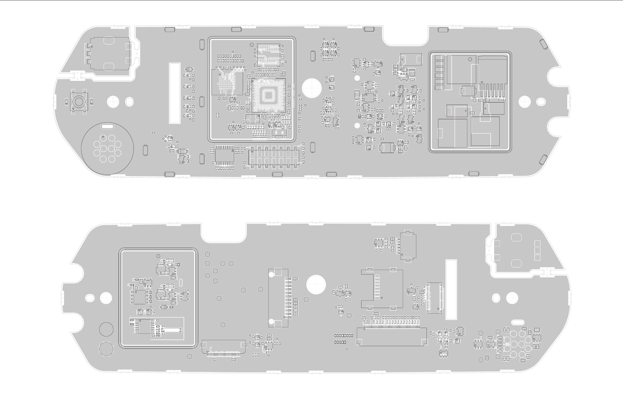
8.2 - 2 ENHANCED CONTROL HEADS: SCHEMATICS, PCBs and PARTS LISTS
PCB/ Enhanced Control Head Main Board - Bottom and Top Side (PCB: 8466580A01_A)
C201
C202 C203
C204
C205
C206
C220
C221
C223
C224
C225
C226
C227
C228
C229
C230
C231
C232
C233 C234
C242
C255
C256
C257
C258
C259
C260
C261
C262
C263
C264
C265
C266
C267
C268
C269
C270
C271
C272
C273
C274
C275
C276
C277
C278
C279
C280
C281
C282
C283
C284
C285
C286
C287
C288
C289
C290
C291
C292
C293
C294
C295
C301
C324
C325
C326
C328
C350
C352
C401C402
C403C404
C409
C421 C422
C501
C502 C503
C504 C505
C506
C507
C508
C509
C510
C511
C512
C513
C514
C515
C516
C533
C534
C540
C541
C542
C544
C545
C546
C547
D301
D302
D304
D350
1
D401
1
D402
D501
D502
D503
D504 D505
D506
D510
D511
D513
6
910
8
4
2
5
7
3
J101
7
11 14
J202
L501
L502
L505
L507
M101 M102 M103 M104
M105
M106
M107
M108
M109
M110
M111
M112 M113 M114
M115
M116
Q301
Q305
Q324
Q326
Q327
Q350
Q351
Q352
Q353
Q410
Q411
Q412
Q500
Q501
Q502
Q503
Q504
Q505
Q506
Q507Q508
R151
R152
R153
R154
R155
R156
R157
R160 R161
R162
R163R164R165R166
R167
R168
R201
R202
R203
R204
R205
R206
R207
R208
R209
R210
R211
R212
R213
R215
R216 R217
R218
R219
R220
R221
R222
R224
R225
R226
R227
R230
R231
R232
R233 R234
R235
R236
R237
R240
R241
R242
R243
R244
R245
R246
R247
R248
R249
R250
R251
R252
R253
R254
R255
R256
R257
R258
R259
R260
R261R262
R265
R266
R267
R268
R269
R270
R271
R272
R273
R274
R275
R276
R277
R278
R279
R280
R281
R282
R283
R284
R285
R286
R296
R297
R301
R303
R304
R305
R306
R307
R308
R309 R310
R311
R312
R313
R317
R318
R319
R320
R321
R322
R323
R324R330 R331
R332
R333
R334
R335
R336
R337
R338
R339
R344
R345
R346
R347
R348
R350
R351R352
R354 R355
R357
R358
R359
R360
R361
R421
R422
R423
R424
R425
R426
R427
R428
R429
R430
R435
R436
R441
R442
R443
R444
R501
R502
R503
R504
R505
R506
R529
R530
R531
R532
R540
R541
R542
R543
R544
R545
R547
R548
R549
R550
R551
5
4
3
2S401
2
3
4
S501
SH201
SH501
TP201
TP202
TP203
TP205
TP230
TP231
TP232
TP233
TP234
TP235
TP236
TP237
TP238
TP239
TP240
TP241
TP242
TP250
TP251
TP302
TP303
TP304
TP305
TP306
TP307
TP308
TP310
TP311
TP404 TP405
TP410
TP411
TP511
TP520
TP521
TP522
TP523
TP524
TP525
TP526
TP527
A21
AA21
AA1
U201
U202
U203
A8
G8
G1
U204
A1
J9 A9
J1
U205
U206U207
U208
10
2011
U209
U301
U302
U303
U304
U323
U324
U325
U328
U350
U352
U401
U402
U403
U404
U420
U421
U422
7
U501
U503
U510
U511
U512
U513
VR501
VR502
2
34
Y201
Y202
C101
C102
C103
C104
C105
C107
C108
C109
C110
C112
C113
C114
C115
C116
C118
C120
C121
C241
C243
C244
C245
C327
C405
C406
C407
C408
C410
C413
C414
C415
C416
C517
C518 C519
C520
C521
C522
C523 C524
C525
C526
C527
C528
C529
C530
C531
C532
C535
C536
C601
C602
C604
C605
C606
C607
C608
C609
C610
C611
C612
C613
C614
C615
C616
C617
C618
C619
C620
C621
C622
C623
C624
C625
C626
C627
C628
C629
C630
C631
C632
C633
C634
C635
C636
C637
D101
D507
12
1
J102
39
240
J201
24
J401
1
6
J403
20
40
G2
G1
J603
L503 L504
8
1
12 11
10
9
M201
Q201
Q202
Q322
Q323
Q325
Q401
Q403
Q404
Q405 R101
R102
R103
R214
R223
R228
R263
R264
R287
R288
R289
R290
R291
R295
R314
R315
R316
R325
R326
R327
R328
R329
R340
R341
R342
R343
R399
R400
R401
R402
R403
R404
R405
R406
R407
R408
R409
R410
R411
R412
R413
R414
R415
R416 R417
R440
R507
R508 R509
R510 R511
R512
R513R514 R515
R520
R521
R522
R523
R524
R533
R534 R535
R536
R537
R538
R539
R602
R603
R604
R605
R606
R607
R608
R609
R610
R611
R612
R613
R614
SH502
TP1
TP2
TP101
TP102
TP104
TP106
TP107
TP204
TP252
TP260
TP261
TP301
TP401
TP402
TP403
TP406
TP407
TP501
TP502TP503
TP504
TP505
TP506
TP508
TP509
TP510
TP512
TP513
U210
U211
U321
U322
U326
U327
U502
U504 U505
4
58
U506
U507
U508
U509
16
8
9
U515
VR101
VR102
VR401
43
2
Y501
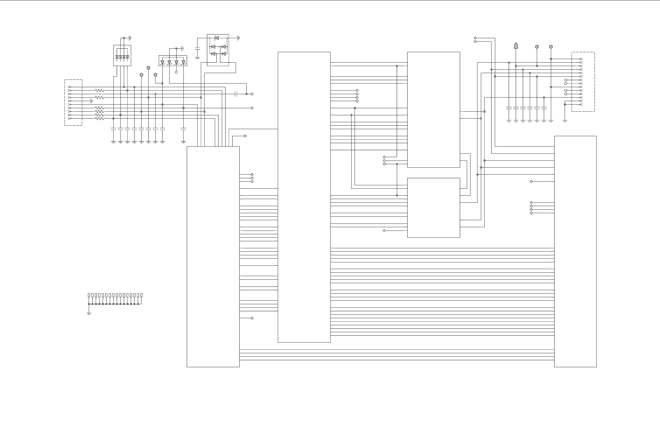
ENHANCED CONTROL HEADS: SCHEMATICS, PCBs and PARTS LISTS 8.2 - 3
Enhanced Control Head Main Board - Control Head (PCB: 8466580A01_A)
G
LO
R
TNOC
_
FFO_
N
O
O
I
D
U
A_TESDN
A
H
D
N
G
O
I
DUA
_TES
D
NA
H
TT
P
_
3_O
I
P
G
D
N
G
+
D
_BS
U
-
D
_
B
SU
E
R
IW
_E
N
O
_
TNORF
CI
M
_T
N
I
KOOH
_
4
_
OI
PG
R
W
P_
0
_O
IPG
.
lo
p
2
1
2
0
1
J
NU
NU
NU
10
1J
ROT
CE
N
NOC CIM
NU
DN
G
D
V5
+SU
B
NU
+
A
_
TL
F
NU
XT
_
ICS
DN
G
D
N
G
NU
NU
NU
S
UBV
_
BSU
NU
CIM
_T
NI
K
LCM
D
LOH_NO
L
O
R
T
NOC_F
FO_NO
OI
D
A
R
_NO
ROP
G
O
R
P
X
T
_I
CS
60
1
PT
kcolB_
C
D
z
H
K
2
3
+
SUB
T
SEU
QER
_
HC
N
I_
LR
TC
F
FO
_
N
O_DN
E
NO
_I
A
CG
)0:
5
(LOC_DAPYEK
)
0
:
4(
WOR_D
A
P
Y
EK
N
O
_KC
O
L
401PT 7
0
1
P
T
+A
_
T
LF 2
01
P
T
0
2
2
613R
5
1
3R
022
0
2
2
41
3
R
12
1C
Fp
0
74
C103
33pF
C113
470pF
470pF
C112
CN
C
N
C116
470pF
2
-
1
0
1
J
1-
1
0
1
J
3-
1
01
J
NE
U
P
_
1
B
SU
V
5
_
BS
U
+
D
_
B
SU
-
D
_
B
S
U
R
A
ER
_
T
N
O
R
F
_
BSU
USB_VBUS
AN
E
_SUBV_B
SU
A
N
E
_
TE
F
_
SU
B
V
TE
D
_C
O
_S
UB
V
4
_OI
PG
R
ID_
4
_OI
P
G
GPIO_4_HOOK
L
B
_
D
P
K
L
B
_
DC
L
ONE_WIRE
LES
_
ERIW
_
ENO
RO
P
G
_R_
M
W
P
+D_RA
ER
-
D
_R
A
E
R
REAR_ONE_WIRE
NO_MR
T
ED_
1B
SU
O
I
PG
_
1
B
SU
L
E
S
_
EDOM
_
1
B
S
U
FRONT_ONE_WIRE
NO
_
I
ACG
N
E
_
V
5
_
T
PO
_
I
A
C
G
TES_V5_TPO_IA
C
G
R
LC
_N
O_
R
W
P
_
IA
CG
E
S
N
E
S
_
N
O_R
W
P
_
I
A
CG
0
_OI
P
G
RID_0
_O
IPG
GPIO_0_PWR
1_OI
P
G
R
ID
_1
_O
I
P
G
2
_O
I
PG
R
ID_
2
_
O
I
PG
3_OI
PG
RID
_
3_OIPG
GPIO_3_PTT
V
CR
_2B
SU
0
E
S
_
2
B
S
U
DE
E
PS_2B
S
U
PS
U
S_2BSU
DXT_2B
S
U
N
EXT_2BSU
M
V
_2B
S
U
PV
_
2BSU
+
D
_BSU
-D_
B
S
U
RAER
_
T
NORF_B
S
U
ANE_SU
B
V
_
B
SU
AN
E
_
T
E
F
_
SU
BV
TED
_
CO
_
SUB
V
kcolB
_
ytivitcennoC
FRONT_D+
FRONT_D-
S
TR
X
R
KLC_
I
PS
2S
C
_
I
P
S
O
SIM_IPS
ISOM_
IP
S
KL
C
_
I
SS
S
F_
I
S
S
D
XR_I
S
S
D
X
T_IS
S
X
T
TE
D
_1BSU
OIPG_1BS
U
LE
S_EDOM
_
1
B
SU
N
E
U
P_1B
SU
N
EU
P
_
2
B
SU
G
REM
E
_DEL
N
E
ERG_D
E
L
DER_DEL
KLCM
ER
I
W
_
E
NO
L
E
S
_
ER
IW_
ENO
D
L
O
H
_
NO
OI
D
AR_
N
O
RO
P
G
OR
P
NE_MOC
_
OID
AR
X
R
_MO
C
_
OI
DAR
X
T
_
MO
C
_O
ID
A
R
1
_
W
S
R
2_
W
S
R
TN
I
_
W
SR
RID_
1
_
OI
PG
2
_O
IPG
RID
_
2
_O
I
PG
3
_OI
P
G
RID_
3
_OI
PG
4
_O
I
P
G
RID_
4
_O
I
PG
QE
R
_O
I
P
G
L
CS
_
C
2
I
ADS_C2I
)0:5
(
LOC_D
A
PYEK
)0:4(WOR_DA
P
YE
K
L
B
_D
P
K
F
F
O_NO_
L
B_DPK
L
B
_D
C
L
k
colB
_
yr
o
m
e
M_r
ossecorP
z
HK
23
2
_
NA
3_
N
A
ELBANE_SUB
TSE
U
QE
R_HC
N
I
_
L
R
T
C
S
TC
M
ER_HSAD
N
E
_
V5
_
TPO_IA
CG
TES_V5_TPO_I
A
CG
R
LC
_
NO
_
R
W
P
_
I
ACG
E
SNE
S_
NO
_R
W
P
_
I
ACG
0
_OI
PG
R
I
D_
0
_O
I
P
G
1
_OI
PG
33pF
C107
2
_
W
SR
TNI_
W
SR
XT_IC
S
C108
470pF
EL
B
ANE_SUB
FFO_
N
O_D
N
E
)
0
:
5(
LO
C
_
DA
P
YE
K
)
0
:
4
(
WO
R
_
DA
P
Y
EK
LB_D
P
K
F
F
O
_N
O
_LB_
DP
K
G
R
EME_DEL
NE
E
RG
_
DEL
D
ER_
D
EL
N
O_KC
O
L
ROP
G_R_MWP
N
E
_M
O
C_OIDA
R
X
R
_MOC
_
OI
D
A
R
X
T
_
MO
C
_O
ID
AR
1
_W
SR
3
3
301R
kcolB
_t
u
pnI_r
e
s
U
+SUB
20
1R
01
9
-
1
0
1
J
1TV
0
2
AQ
M
M
25
6341
7
-1
0
1
J
23
4
2
01RV
1
01D
5
0
RS
1
2
1
-201
J
41-201
J
1
1
-20
1
J
3
1-
20
1
J
9-
20
1J
6-201J
C115
82pF
5-201
J
C
N
1
0
1
PT
C110
82pF
C118
V
61
F
u
01
0
2
1C
82pF
M114
M116
M113
M112
M111
M109
M110
M107
M108
M105
M106
C
N
C102
470pF
470pF
C105
C101
470pF
C109
470pF
3-2
0
1
J
5-10
1
J
8-
1
0
1
J
6
-1
01J
10
1R
CN
01-
1
01
J
33
2
5
A2
1K1
3K2
4K3
6K4
M
V
_
2
B
SU
PV_
2
BSU
V
5
_
B
SU
1
01RV
V
6
.
5
A1
K
LC_I
PS
2
SC_I
PS
O
SI
M
_
I
PS
ISO
M
_I
PS
KLC_IS
S
S
F
_ISS
D
X
R
_I
S
S
D
XT_I
S
S
XT
NE
U
P
_2BS
U
VCR_
2
B
SU
0
ES
_
2B
S
U
D
E
E
P
S
_
2
BSU
P
SU
S
_
2B
S
U
DXT_2
B
S
U
N
E
X
T
_2B
SU
3_NA
+S
U
B
S
T
C
ME
R
_
H
SA
D
QE
R
_
O
IPG
O
IDU
A
_
TE
SD
N
AH
L
CS_C2I
AD
S
_
C
2I
C
I
M
L
O
R
T
N
OC
_
F
FO_NO
+D_R
AER
-
D
_
R
AER
ER
I
W_ENO_RA
E
R
NO
_MR
S
T
R
XR
X
T
_I
C
S
M103
k
c
o
lB_
et
o
m
eR
2_NA
M102
M104
M101
7-201J
0
1-2
0
1J
470pF
8-
2
01
J
C114
4-
20
1
J
M115
C104
470pF
1-201
J
2
-20
1
J
ERIW_
E
NO
_
T
NO
R
F
K
LC
_
I
PS
3
_
NA
2SC
_
I
P
S
IS
OM_
IPS
2
_
N
A
L
B_
D
P
K
4-
101J
XT_ICS
OI
D
U
A_T
E
S
DN
A
H
O
IDU
A_
T
ES
DN
A
H
+
S
U
B
C
IM
C
I
M
L
O
RT
N
O
C_FF
O
_
NO
USB_VBUS
-D
_
R
A
ER
N
E_
V
5
_T
PO
_
IA
C
G
TE
S
_
V
5_
T
P
O
_
I
A
CG
R
L
C
_
N
O
_
R
W
P
_I
A
C
G
ES
N
ES_
N
O
_
RWP
_
IACG
N
O_IACG
N
O
_IA
C
G
CI
M
T
T
P
_3_OI
P
G
END_ON_OFF
T
S
EUQ
E
R
_
HC
T
E
D_CO_
S
U
BV
-
D
_
BS
U
N
EU
P
_1BS
U
LES
_
E
DOM
_1BS
U
O
I
P
G
_
1
B
S
U
T
E
D
_1
B
SU
E
R
I
W
_E
NO
_R
A
E
R
E
R
I
W_E
N
O
4
_
OI
P
G
R
I
D
_
4
_O
I
P
G
K
O
O
H
_
4
_O
I
PG
3
_
O
I
PG
R
I
D
_
3
_
OI
PG
2
_
OI
P
G
R
I
D_
2
_
O
I
P
G
1
_O
I
PG
R
I
D_
1
_
OI
P
G
FRONT_D-
+
D
_T
N
O
R
F
O
I
D
UA
_
T
E
SDNAH
RWP_
0
_O
I
PG
TNI
_
W
SR
2
_
W
S
R
1
_
W
S
R
PV_
2
B
SU
M
V
_
2
B
S
U
N
E
XT
_
2
B
S
U
D
XT
_
2
B
SU
PSUS_2B
S
U
D
E
E
P
S
_
2
B
S
U
0E
S
_2BSU
VC
R
_2BSU
N
E
U
P_2B
S
U
O
S
IM_
I
PS
D
E
R
_
DEL
N
E
ERG_DEL
L
B
_
D
P
K
L
B
_
D
P
K
NI
_
L
RTC
G
O
R
P
ROP
ROP
2
SC
_I
P
S
E
R
I
W
_
E
N
O_
R
AER
X
T_M
O
C
_
OI
DA
R
X
R_
M
O
C
_O
ID
A
R
ST
C
A
D
S_C
2
I
L
CS
_
C
2
I
+
D
_BSU
AN
E
_TEF_SUB
V
N
E
_
M
O
C
_O
I
DA
R
L
E
S_
ER
I
W
_E
NO
GRE
M
E
_DE
L
Q
E
R
_O
IP
G
D
X
T
_
I
S
S
D
XR
_
I
S
S
SF
_
I
S
S
K
LC_
I
SS
IS
OM
_IP
S
O
SI
M
_IPS
K
LC_IP
S
OI
D
AR_NO
MER
_H
S
A
D
ELBA
N
E_SUB
FFO
_N
O
_
LB
_
DPK
NO_
MR
K
L
C
M
z
H
K
2
3
G
_
R_MWP
G
_R
_
MW
P
LB
_
D
CL
LOCK_ON
+
D
_
R
AER
X
T
XR
S
T
R
RAE
R
_TNO
R
F_
BS
U
DLOH
_
N
O
V5_
B
SU
AN
E
_SU
B
V_
B
SU
R
ID
_
0
_OI
P
G
0_
OIP
G
R
O
P
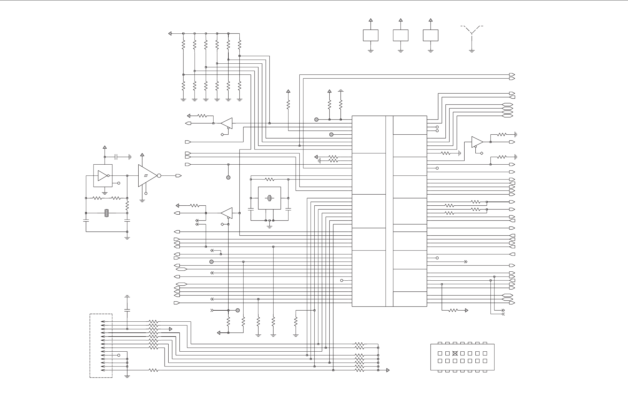
8.2 - 4 ENHANCED CONTROL HEADS: SCHEMATICS, PCBs and PARTS LISTS
Enhanced Control Head Main Board - Processor Memory Block: Main CPU (PCB: 8466580A01_A)
SK
C
OL
C
GATJ
L
A
R
EN
E
G
O
IPG
OI
M
RA
SL
A
NG
I
S
1
TR
A
U
2T
R
AU
3
T
R
A
U
1
P
SBC
M
2P
S
BC
M
3P
S
BC
M
1
I
S
C
M
2I
S
CM
E
R
IW
U
BSU
DNG
DNG
3
BVLZ
WAKE
11
TCK
T
E
R
_
K
CT
UN
TMS
T
S
ET
U
N
01
14
EMU1
U
N
U
N
GND
RESET
TRST-
de
vo
mer
N
I
P
0S
C
UN
41
GND
56
U
N
TDO
UN
UN
U
N
BOOT_USB1
U
N
UN
UN
U
N
U
N
UN
UN
BOOT
D
NG
TCK_RET
UN
KCT
2
1
U
M
E
GATJ
3SC
Pin removed
8
TDI
202
J
U
N
9
GND
UN
31
D
P
GND
I
D
T
TSRT
3
3
x
8
EMU0
S
M
T
UN
7
D
N
G
MRON
0
U
ME
MODE
21
PD
ODT
UN
GATJ
21-202J
23
2R
K
0
1
K0
1
732
R
32
2
R
K0
1
8
.
2_
C
C
V
21
2
R
K0
01
8-202J
0
5
0
2
R
01-
202J
1
6
1R
NI
1
CN
4
TU
O
CCV
5
1
1
-
20
2J
41ZS71
L
N
302U
3
DN
G
2
CN
8.2
_
CCV
502P
T
3
0
2P
T
C
N
8.2_C
C
V
1
0
2PT
K7.4
551R
36
1R
K01
432R
4-20
2
J
3
D
NG
5
C
CV
712R
K0
7
4
C
N
2
-
012
U
DN
G
_R
W
P
2
-
20
2
J
A
2
OE
1
Y
4
K
0
0
1
3
0
2R
5
2
1CH
V
4
7
1-
7
02U
CN
K00
1
0
1
2
R
6
0
2
C
F
u
1.0
CN 1
4
VCC
5
8
61R
D
4
0UG1C
H
47
C
M
202
U
GND
3
2
66
1R
461R
31-202J
5
3
2R
2
6
1R
0
2
A
1
OE
4
Y
K
0
1
F
p81
5
21
CH
V
4
7
1
-60
2
U
8.
2
_
C
CV
8.2
_C
C
V
302
C
7
61R
K
0
1
82
2R
CN
K
0
01
1
5
1
R
3-20
2
J
6
32
R
K
01
2
GND
4
GND1
3T
UO 1
NI
8
.2
_
C
C
V
8
.2_
C
CV
1
02
Y
zHM
2
1
L
AT
X
G
EM0
1
1
-
20
2
J
2
2
2
R
CN
6
-
2
0
2
J
2
0
2
R
K
0
01
10
2
C
Fu1.
0
K
0
0
1
8.
2
_
CCV
4
0
2
R
C
N
0
61
R
9
-
2
0
2
J
2
02C
Fp81
2
51R
K
0
01
K0
0
1
10
2
R
8
.2
_
CCV
K
01
0
32R
K
00
1
651R
K
0
01
4
5
1R
3
12R
0
5.1_CCV
8.
2_
C
C
V
0
2
2
R
0
K
0
01
90
2
R
K01
812
R
GEM01
12
2R
0
5
2
2
R
Fp
8
1
5
0
2
C
74_OIPG 8
1
U
64_O
I
P
G12W
z
HK8
67.
23
20
2Y
V4
CC
71
_
O
I
P
G51Y
0
4
_
O
I
P
G51W
8R
MD_BSU 9P
P
D_BSU
NE
UP
_B
S
U4W
54_OIPG 41N
4
4
_
O
IP
G51
P
K
LCS_ERIW 9
1V
4
1
L
3
X
R
81W KCT
9
1Y I
DT
9
1AA O
DT
S
MT
7
1V
1
X
T41
Y
2X
T6V
8
1M
3
X
T
NI
_K
2
3CSO
3
1
V
T
U
O
_K
2
3CSO
31AA
2
1
PED
O
M_
TE
S
E
R
71
YNACSBN_KCTR
1
S
T
R51
A
A
2
S
T
R5
W
41
V
1
X
R
2
X
R9
R
0
U
MEN
61V
1
U
MEN
7
1W
02AA T
UO_
TES
E
R
N
NO
R
W
P
S
E
R
N
2
1
R
8
1Y TSRTN
21Y F
FO_
NO
NI
_
1
CSO
2
Y
T
UO_
1
CSO
3W
NID
_
1ISCM 5
1V
TUOD_1I
S
C
M4
1W
CNYS_
1
IS
C
M7
1AA
K
L
C
_
2
ISC
M01Y
9AA
N
I
D
_
2ISCM
TUOD_2
I
SCM 9W
CNYS_2ISCM 9V
02
UT
ES
E
R
N
_
U
P
M
R
K
L
C
_2
P
S
B
C
M7
V
XKLC
_
2PSB
CM 6Y
N
I
D
_
2
P
S
B
CM 0
1
P
T
UOD
_2PSB
CM 5
A
A
6W
C
N
Y
SR
_2
P
S
B
CM 7W
C
N
Y
S
X_2
P
S
BC
M
6
1
W
K
L
C
_3
PSBCM
K
L
CB
_1
IS
C
M4
1
P
7
_
OIPG
5
1
M8_OIPG
8
Y9
_OIP
G
8
W
12G
K
L
CB
_1
P
S
B
C
M
SK
L
C
_1PSB
C
M02G
02
H
15
_
OI
P
G
25
_
OI
PG 81
H
35
_
OI
PG 51
H
2
1
_
O
IP
G
8
1N 3
1_OIPG
9
1N 41_OIPG
1
2
N
0
2
M5
1
_OIP
G
2
_OIPG
41M 3_OIP
G
8
1P 4_OIP
G
02P 6
_
O
IPG
91P
QER_K
LCM
_
MO
C
01R
NWO
D
T
U
HS
_MOC
3
1W
F
NOC
8
1
V
41
R
1S
T
C
2S
T
C5Y
0
_O
IPG
8
1
R1_OI
PG
9
1
R
11_
OIP
G
0
2
N
9
1T 5
_
OIUPM
0
2T
0
2
JT
OO
B_
M
R
A
4Y
2KL
C
DB
ZL
V
B
9
1
W
31P NI
_
K23KLC
T
U
O
_K
23K
LC
31
R
TUO_KLCM_MOC
5
V
K
CO
L
B
_
LA
IRE
S
2
-1
0
2
U
1
_
OIUP
M
91U 2
_
OIUP
M
5
1N 3
_
OIUP
M
8V 4
_
OIUPM
612
R
K
0
0
1
6
02
R
G
EM0
1
5
2
1CHV
4
7
2
A
1
OE
4
Y
8
.2
_
CCV
1-
01
2U
0
4
22
R
402PT
8.2_
C
C
V
3
51R
K
00
1
8.2_CCV
7-2
0
2
J
912
R
K
0
1
5
C
CV
62
2R
0
K
0
1
2
-
60
2
U
DN
G
_R
W
P
3
D
N
G
8
.2
_C
CV
51
2R
1
3
2
R
K
0
1
56
1R
Fp81
402C
K001
5
20
2PT
8
02R
D
N
G
_R
W
P
2
-
70
2
U
D
NG
3
C
C
V
5
-202J
K001
7
0
2R
C
N
41-
202J
K
0
1
K
00
1
112R
332R
41
2R
7
5
1
R
K
7.
4
K01
1
0
2
H
S
DLE
IHS
P
S
U
S
_
2
B
S
U
K
L
C
M
zHK
2
3
I
S
OM_
IP
S
I
S
OM
_
I
P
S
OS
I
M
_
I
P
S
O
S
I
M
_
I
P
S
72
2
R
0
L
B
_
D
PK
D
E
EP
S
_2B
S
U
0E
S
_2B
S
U
E
L
BA
NE
_
S
U
B
0
_OIPG
R
I
D
_0_
OI
P
G
R
ID_3
_
OIP
G
DS_
DC
L
N
E_
3.
3
_CCV
L
E
S
_
ED
O
M
_1B
S
U
2
S
C
_
IP
S
2SC
_
IPS
K
LC_I
P
S
KL
C
_I
P
S
LE
S_INI
P
A
WS
_DC
L
V
C
R
_2
B
SU
M
V
_
2B
SU
D
XT_2B
S
U
P
V
_2B
S
U
NE
XT
_2
B
SU
R
I
D
_
1_
O
I
P
G
N
E
U
P
_1B
S
U
T
ED_
1
BS
U
+
D
_B
SU
-D_
B
SU
X
R
_M
O
C
_
O
I
D
AR
XT
_M
O
C
_
O
I
D
A
R
ROP
RA
E
R
_
TNO
R
F
_
B
SU
LES_
I
N
I
DL
O
H_
N
O
N
EE
R
G_D
E
L
1_WSR
LE
S
_INI
L
E
S
_INI
L
B_D
C
L
L
B
_
DC
L
2_
N
A
D
X
R
_
I
SS
D
X
T_
IS
S
S
F_
I
SS
K
L
C
_
ISS
L
E
S
_
E
R
IW_E
N
O
3
_
N
A
Q
E
R
_
O
I
P
G
E
R
IW_E
N
O
2
_WSR
O
I
P
G
_
1
BS
U
R
I
D_
2_
O
IPG
DE
R
_
DEL
ANE
_
SUB
V
_
B
SU
G
R
E
M
E
_
D
EL
T
E
D
_
C
O
_
S
UB
V
R
I
D
_4
_O
IP
G
GOR
P
3
_
O
IPG
OI
D
A
R
_
NO
4
_
O
IPG
2
_
O
IPG
1_
O
I
P
G
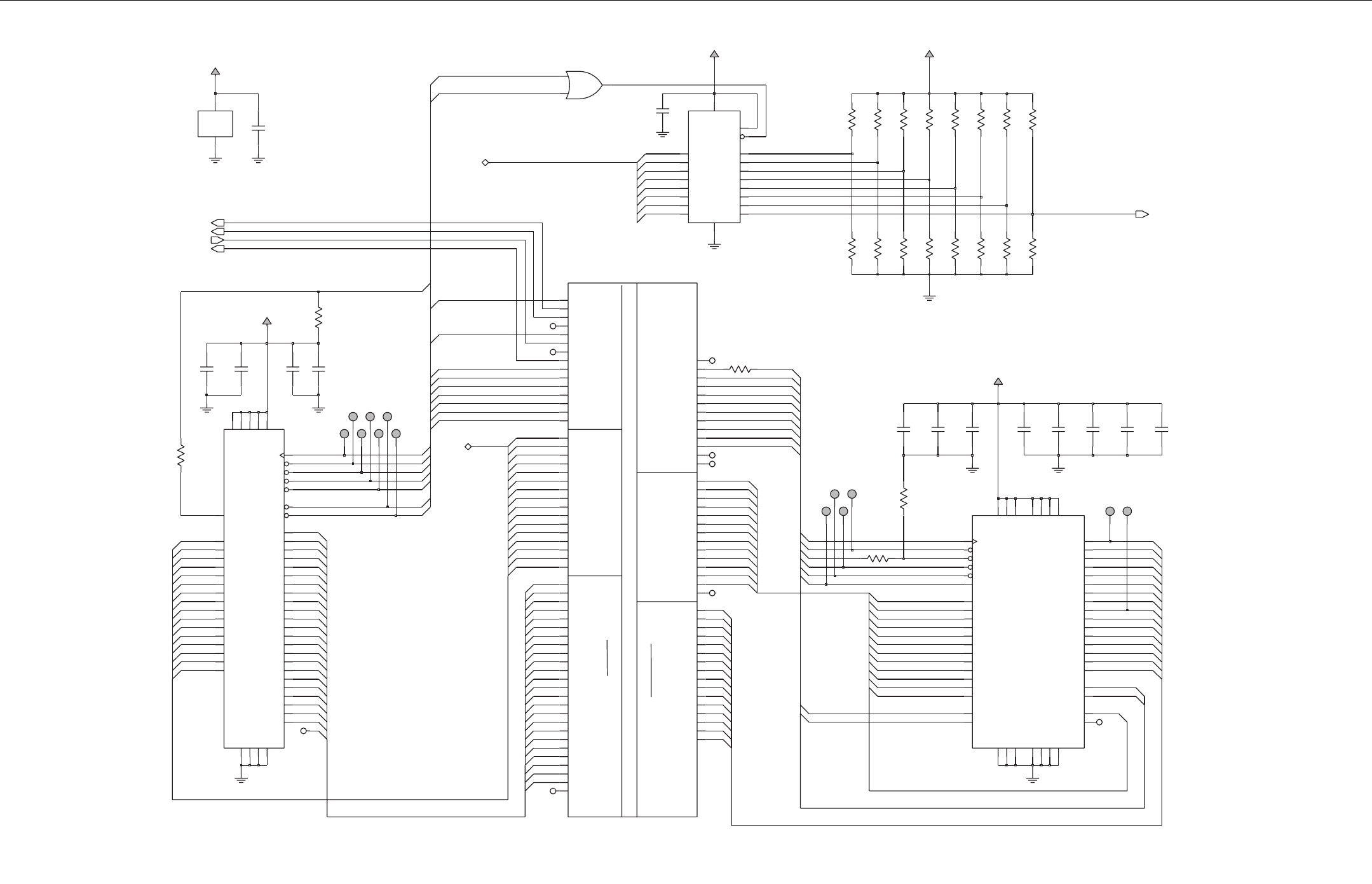
ENHANCED CONTROL HEADS: SCHEMATICS, PCBs and PARTS LISTS 8.2 - 5
Enhanced Control Head Main Board - Processor Memory Block: Memory (PCB: 8466580A01_A)
CONTROL
DATA
ADDRESS ADDRESS
DATA
CONTROL
UN
U
N
UN
U
N
ADDRESS
1
D
I
dr
a
oB
UN
0
CD
I
UN
2
C
D
I
1C
D
I
DATA
UN
UN
MER
/H
S
A
D
1
1
2
UN
2
DI
dr
a
oB
0 D
I
d
r
aoB
542
R
2
1
01
21
CN
2
0
1
8
K0
1
K0
1
052
R
Fu1.0
42
2
C
92
2
C
11
3
5
0
1
9
F
u1
.
0
3
F
u
1
.
0
82
2C
3
2
6
K
0
1
7
42
R
34
2
R
2
3
1
1
2
6
K
0
1
F
u
1
.
0
622C
4
11
11
4
6
6
4
7
0
1
3
5
24
2
R
K
01
4
7
2
2
94
2
R
K
0
1
3
DN
G
5
C
CV
8.
1
_
C
CV
0
1
4
2
0
8.
1_
CC
V
7
3
2
2-
80
2U
DNG_R
WP
9
1
5
1
52
R
K0
1
2
1
01
2
8
1
1
8
5
F
u1.0
0
22C
TP240
3
1
6
1
01
7
TP239
02
0
3
4
0
1
8
7
3
1
7
6
CN
4
1
44
2
R
K0
1
7
4
4
3
7
32
9
95
2
R
5
1
8
3
2
1
0
7
C
5
_AT
A
DS
6
_AT
A
DS 4C
8D
7_ATAD
S
8_ATADS 01C
4
1
D
9
_AT
A
DS
9C
KL
C
DS
9
D
XK
L
CDS
21H
NE
_K
L
C
D
S
31C
11
_ATADS
21
_ATADS 1
1
C
3
1
D
3
1
_
AT
ADS
4
1
_ATADS 21
D
51_
ATA
DS 21C
5C
2
_AT
A
DS
3_ATADS 7D
4_
ATA
DS 5
D
7
_D
DAS 11G
8_DDAS 9G
2
1B
9_D
DA
S
0
_KNABS 3B
1
_
KNABS 3C
6
D
0
_A
TA
DS
1
_AT
A
DS 6
C
0
1
_ATADS 1
1D
0
1
H
11_
D
DAS 9H
2
1
_
D
D
AS 11H
31_DD
AS
2_DDAS 6B
3_DDAS 1A
4
_DDAS 0
1
G
5
_DDA
S9B
6_D
DA
S21G
4B
SA
CSN
L
M
Q
DSN 8C
0
1
D
UM
Q
DSN
SARSN 7H
EW
SN 8H
0
_DDAS 2A
1
_DDA
S2B
01_DDAS 8B
6
1
_
O
IPG
1Y
2
_SCF
N
4M
5_OIPG
3P
3
_S
CFN
8N
EOFN
4U
1
WPR
F
N
EWFN
2W
PWFN
4V
8_ATA
D
F
4R
9
_ATADF
2T
YD
R
F
2V
V
DAFN
4L
0
_EB
F
N
3
L
8M 1
_E
BF
N
0
_S
CFN
7M
3
M1
_S
CFN
4T 4
1
_ATADF
5
1
_A
TADF
3
V
7N 2
_
ATAD
F
3
_A
TA
DF
2
P
4
_ATADF
4P
5
_ATADF
7P
6_ATADF
2R
7
_AT
A
DF
3
R
3F 9
_
D
D
AF
KLCF
3N
4N 0
_ATADF
2N 1_ATADF
01_ATADF
3T
1
1
_ATADF
8
P
1
U21
_ATADF
3
1
_ATADF
3U
7
L4
2
_
D
DA
F
1E 5
2_D
D
AF
3_
DDAF
1C
4E 4_D
D
AF
5
_
D
D
AF
2
D
4F 6_DDAF
7
_
DDAF
3E
8_D
D
AF
7
J
2
J71_DDAF
81
_
D
D
AF
4J
91
_
D
DA
F
3J
2
_
D
DA
F
3
D
02
_
DDAF
2F
1
2_D
D
AF
8L
22_
D
DA
F
4K
3
2
_D
D
A
F
3K
8
J1
_
D
DA
F
01
_D
DAF
4G
3
G1
1_D
D
AF
2G 2
1_D
DAF
3
1
_
D
DA
F
8
K
41
_DDAF
4H
5
1_
D
DA
F
3
H
61_DDA
F
7K
5
1-
1
0
2
U
KC
O
L
B
_
M
IE
8G
MAR
D
S_SC
41C
H_SQ
D
L
_S
QD 4
D
32
2C
K
0
1
1
42
R
Fu1
.
0
Fu
1
.0
2
3
2
C
3
1
1
2
4
4
61
3Q
9
4Q
21
5
Q
51
6
Q
6
1
7
Q
9
1
VCC 20
1
-
80
2
U
2
3
Z
S7C
N
6
D71
7
D81
EL
_
N
E1
1
E
O
_
NE 1
GND
10
0
Q
2
1
Q
5
2
Q
6
0
D3
1
D4
2
D7
3
D8
4
D31
5
D41
0
9
8
21
CN
373
XVL
4
7C
M
9
02
U
1
1
2
8
.1
_
C
CV
1
1
11
7
0
51
4
1
TP230
2
1
3
5
2
R
K
0
1
8
52
R
9
3
1
4
51
4
2
91
8
1
3
3
K
0
1
8
42
R
F
u
1
.
0
03
2
C
8.
1_
C
CV
52
2
C
Fu
1
.0
K
0
1
45
2
R
8
1
01
2
1
11
5
71
722C
F
u1
.
0
0
5
1
41
8
3
9
C
N
TP238
4
01
0
6
TP237
1
2
2
1
8
7
0
7
21
4
1
51
C
N
4
1
8
2
2
TP232
1
81
3
11
TP231
0
C
N
K01
7
52R
1
2
2C
8
.1
_CCV
1
6
5
2
R
2
52
R
F
u1
.
0
1
0
2
2
C
N
0
K
0
1
9
5
9
0
1
9
1
0
42
R
K
0
1
21
1
6
31
6
33
2
C
F
u
1
.
0
41
8
9
4
32
C
F
u
0
.
1
V
3
.
6
5
1
4
1
6
9
8
7
2
0
0
62R
1
32
C
F
u
1.
0
5
TP236
9
5
3
1
TP235
6
5
4
6
5
52
R
K
0
1
4
9
2
6
42
R
K0
1
TP234
7
1
6
VSSQ4
D7
E
W
9
F
TP233
VDDQ3 A7
VDDQ4 C7
VSS1
A1
VSS2
J1
VSS3
E3
VSSQ1
A3
VSSQ2
C3
VSSQ3
B7
2E
2C
N
SA
R
8F
M
Q
DU 1F
VDD1 E7
VDD2 A9
VDD3 J9
VDDQ1 B3
VDDQ2 D3
4Q
D8
C
5Q
D9
D
6Q
D8
D
7Q
D9E
8
Q
D1E
9Q
D2D
M
Q
D
L8
E
1G
1CN
0
1
Q
D1
D
1
1
Q
D2
C
2
1
Q
D1
C
3
1
Q
D2
B
4
1
Q
D1B
5
1
QD 2
A
2Q
D8B
3Q
D9
C
0AB
7G
1A
B
8
G
S
AC
7
F
E
KC
3F
KL
C
2F
SC
9G
0Q
D8
A
1Q
D9
B
2A
8
J
3A
7J
4A
3J
5A
2J
6A
3
H
7A
2H
8A
1H
9A
3G
F
L
61
M
8H8
4
T
M
5
0
2
U
0
A
7H
1A
8H
01
A
9H
11
A
2G
VCCQ2 A5
VPP
A3 VSS1
F1 VSS2
G2 VSSQ1
VSSQ2
G8
TIAW
3D
PW 6
D
9
D
7E
EC_NE 8
F
EO_NE 5C
EW_
NE
5B
TESE
R
A4
VCC1 G4
VCC2 E1
VCCQ1 G6
51D
5E 2
D
3D
5G
4E 4D
3G 5D
3E 6
D
1
G7D
7G 8D
6F
K
L
C
7F 0D
1
D
6E
5
F0
1
D
4F 1
1
D
5
D21
D
3
F3
1
D
2
F4
1
D
2E
3A 8A
4A
5A 7B
7A
6A 7C
7A 2A
8A 2B
9A
4
C
V
D
A
4B
61
A6B
71A
81A 6A
6
C
91
A
8
C
2A
3B
0
2
A3C
1
2A
22A 7D
8B
8E
8
D
1A
0
1
A2C
1A
1
1
A1B
2
1
A1
C
3
1A 2
D
41A 1D
5
1
A4D
8
1
1
01
402
U
0
6D
B
81
W82
1
F82
0A
TP242
1
0
51
C
N
2
1
TP241
9
1
3
7
2
1
C
N
E
C
_
N
E
_
F
EO
_
N
E
_
F
EW_N
E
_F
PW_F
TS
R
_F
VD
A
_F
NE_
KLCDS
S
AR_DS
SAC
_
DS
E
W_DS
SC_D
S
)0
:
51
(
A
TAD_HS
A
LF
RLC_NO_RWP_IAC
G
ESNES_NO_R
W
P
_I
A
C
G
TES_V
5
_
T
P
O
_IACG
N
E_V5
_
T
P
O
_
IACG
FLASH_CONTROL(12:0)
)
0:5
1
(AT
AD_H
SAL
F
)
0:
5
1(AT
A
D
_
H
S
A
LF
M
Q
D
U
_
DS
M
Q
D
L_
D
S
0
AB
_DS
1AB_DS
K
LCDS
)
0
:9(LORTNO
C
_
M
ARDS
)
0:
2
1(SSERDD
A
_
M
A
R
D
S
K
L
C
_
F
)1:42
(
SSE
R
DDA_
HS
A
LF
)0:51(ATAD
_MARDS
ME
R
_
HS
A
D
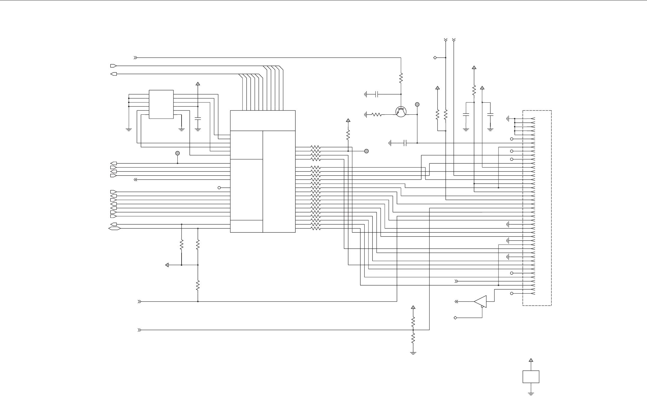
8.2 - 6 ENHANCED CONTROL HEADS: SCHEMATICS, PCBs and PARTS LISTS
Enhanced Control Head Main Board - Processor Memory Block: LCD (PCB: 8466580A01_A)
C
2I
MMC/SDIOCAMERA INTERFACE
LCD INTERFACE
EC
AFRET
NI
DAPYE
K
D
O
S
S
C
K
L
CS
.
l
op
04
102J
DM
T
UN
UN
R
0
x
02
UN
E
DOM
_N
A
C
S
NU
I
D
S
DNG_RWP
2
-
112
U
DNG
3
CCV
5
1-112U
A
2
OE
1
Y
4
2
5
2P
T
521CHV47
2
44
-1
02
J
67
2
R
282R
8.2
_C
C
V
CN
56
2
R
K0
1
Fp
0
7
4
442
C
8
2-
10
2
J
V
3
.6
F
u
0
1
2
4
2
C
92
-
102J
582R
4
4
-102J
0
92R
K01
10K
R264
3
1
-10
2
J
9
1
-10
2
J
6
-1
0
2
J
8
.
2
_
CCV
1
42C
F
u1.0
8
1
-
10
2
J
7
1
-10
2J
1
7
2R
1
-
10
2
J
0
72R
2
4
-1
0
2
J
83
-1
02
J
762R
1
3
-
10
2
J
CN
Fp0
7
4
54
2
C
01
-
102J
21
-
10
2
J
0
2
-
102J
1
11
-
10
2
J
5
1
-
102J
K
0
1
982R
C
N
2
8
.
2_CCV
48
2
R
CN
14
-
10
2
J
3
8
2
R
5
15
2P
T
86
2
R
93
-
1
02J
5
2
-10
2
J
052PT CN
182R
26
2
R
K2
.
2K
2
.2
1
6
2
R
4
0
9
3TB
M
M
102Q
3
3
-
102J
23
-
10
2
J
8
-
102J
22
-1
02J
7
8
2
R
4
3
-
10
2
J
0
01
2
-1
0
2
J
662R
6
1
-1
0
2
J
7
3
-1
0
2
J
34
2
C
F
u0
1
V
3
.
6
6
3
-
10
2
J
572R
0
47
2R
37
2R
C
N
0
4
-
10
2
J
1
1R 0TA
D
_C
MM
1TAD
_
CMM
0
1V
01W 2TAD_CMM
3TAD_CM
M
11W
L
CS
81T
02V A
DS
12
-
1
0
2
J
5_
LE
XI
P
_
D
CL 0
2A
6_
LE
XIP_D
CL 91B
7_LEXIP_DC
L8
1
C
71D
8
_LEX
IP
_
D
C
L
9
_LE
XIP
_
DCL 61D
CNYSV
_
DC
L81B
1
1V KLC_CM
M
DMC_CM
M
1
1P
11_LEXIP
_D
C
L71B
2
1
_LE
XIP_DCL 31G
3
1_LEXIP_
DC
L7
1
A
4
1_LEXIP
_
DCL 6
1C
5
1
_
LEXIP
_D
C
L51D
2
_
LEXI
P_D
C
L91C
3
_
LEXIP
_
DCL 41
G
31H
4_L
EXIP
_
DC
L
KBR_3 E20
E19
KBR_4
CA_DCL 51B
CNYS
H_DCL 02
C
5
1C
K
L
CP_DCL
0_
LEX
IP
_
DCL 81D
1_LEXIP
_
DCL 12B
01_LEXIP_DCL 7
1C
KBC_1 D20
KBC_2 D19
KBC_3 E18
KBC_4 C21
KBC_5 G19
KBR_0 G18
KBR_1 F19
H14
KBR_2
6
_D_
M
AC
91J
7_D_MA
C
8
1J
9
1
HK
LCXE
_MAC
8
3_OIP
G
51L
KLC
L
_MAC
51J
ZTSR_MA
C
91M
41_OIUPM
81L
KBC_0 F18
KC
OLB_EC
A
F
RE
T
NI
2
1
_
O
I
UP
M
91
L
1
_
D
_MAC
41K
2_D_
M
A
C
5
1K
3_D_MA
C
91K
4_D_MAC
8
1K
5
_
D
_MAC
4
1
J
1
92
R
0
3
-
1
0
2
U
972
R
34
-1
02J
0
082R
8.
2_
C
C
V
7
-
10
2
J
K0
1
8
7
2
R
72
-1
0
2
J
88
2R
VCC_2.8
VCC_23
6
2
-
10
2
J
4
2
-10
2
J
3
2
-10
2
J
8.2_
C
C
V
31
9
-
1
02J
962R
53
-1
02
J
8
.2
_CCV
1TAD
1
2TA
D
91DNG
2
DN
G
0
13
DN
G
1
1
2
14
D
NG
4
DDV
6
SS
V
102M
3TAD_DC 2
5
KL
C
DMC 3
0TAD
7
8
4
TC
A
T
N
O
C
77
2
R
27
2
R
K
5
.
1
4
1
-10
2
J
6
82
R
0
3
-
10
2
J
5
-10
2
J
0
R263
P
AWS_DC
L
2S
C
_IPS
SPI_CS2
2
S
C_I
P
S
3
-10
2J
3
D
S
_
DCL
N
E
_M
O
C
_OI
D
AR
ISOM_
IP
S
O
S
IM_IPS
SPI_CLK
ANE_
T
E
F
_
SU
B
V
NEU
P_2B
S
U
N
I_LRTC
X
T
X
R
S
TC
S
T
R
)
0
:
5(LOC
_D
AP
YE
K
)
0:4(WOR_
DAPYEK
F
F
O
_
NO
_
L
B
_
D
PK
LE
S
_I
N
I
LB
_D
C
L
LB
_
D
CL
AD
S
_
C
2I
LCS_C2I
TN
I_WS
R
TSE
U
Q
E
R
_HC
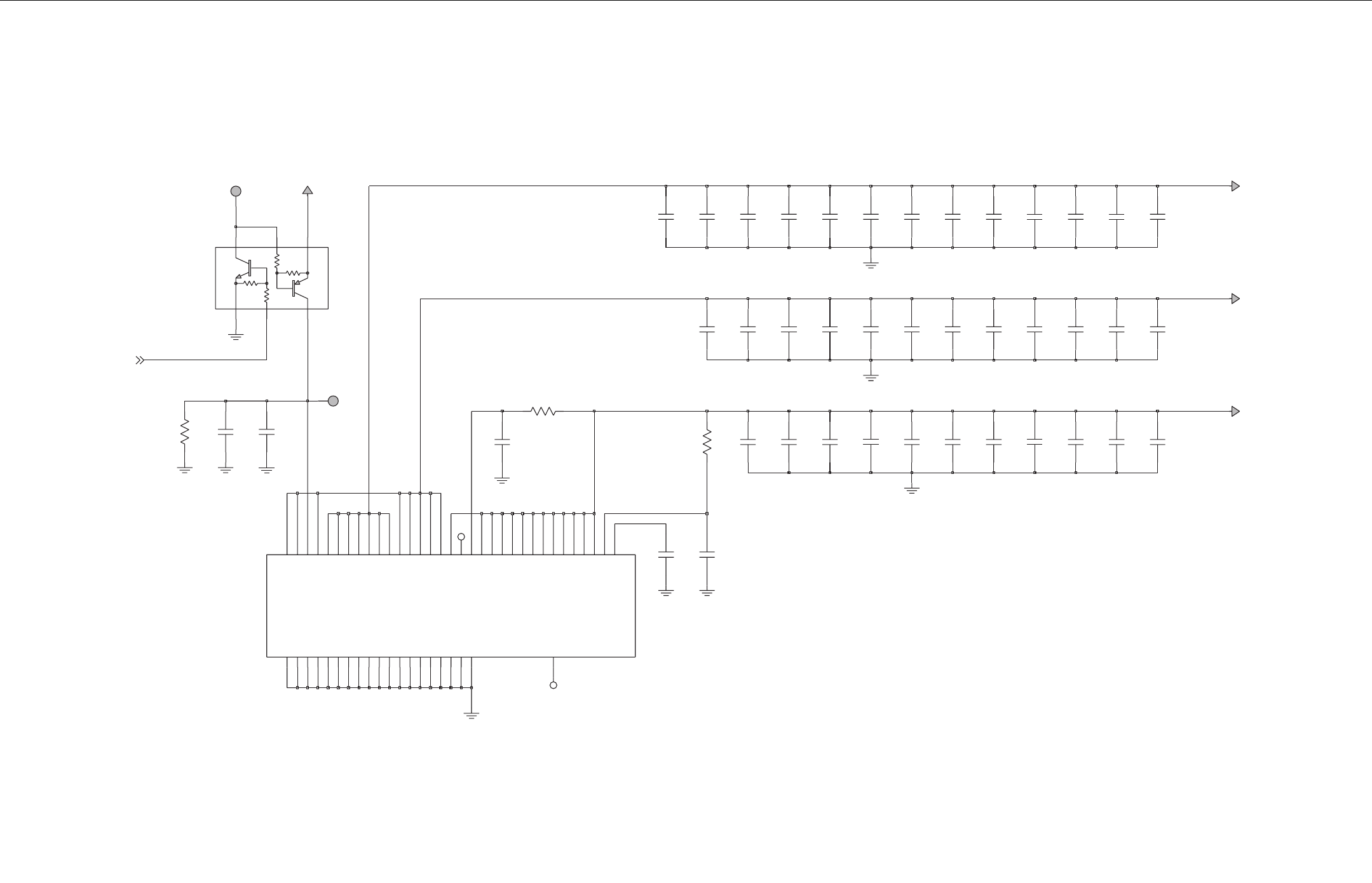
ENHANCED CONTROL HEADS: SCHEMATICS, PCBs and PARTS LISTS 8.2 - 7
Enhanced Control Head Main Board - Processor Memory Block: Supply (PCB: 8466580A01_A)
T
OOB_CAF
F
u
1
.
0
1
7
2
C
F
u
1
.
0
VSS_4
B16
VSS_5
A21
VSS_6
F20
VSS_7
K20
VSS_8
R21
VSS_9
W20
37
2
C
VSS_14
AA1
VSS_15
U2
VSS_16
N1
VSS_17
K2
VSS_18
G1
VSS_19
B1
VSS_2
B7
VSS_3
A13
VDD_DLL A11
VDD_RTC W12
VPP L1
VSS_1
B5
VSS_10
AA21
VSS_11
Y13
VSS_12
AA7
VSS_13
Y3 VDDSHV7 Y16
L21
VDDSHV8
VDDSHV9 U21
VDDSHV_RTC V12
VDD_1 A15
VDD_2 Y20
Y9
VDD_3
VDD_4 M2
VDDSHV4_1 A5
A7
VDDSHV4_2
VDDSHV4_3 B10
VDDSHV4_4 B14
VDDSHV5_1 R1
VDDSHV5_2 H2
VDDSHV5_3 C2
VDDSHV6 AA11
VDD3_1
VDD3_2 B20
J21
VDD3_3
VDD3_4 R20
VDDA Y21
VDDSHV1_1 A19
VDDSHV1_2 E21
VDDSHV2 AA2
VDDSHV3 Y7
4-
1
0
2
U
J1
LDO_FILTER
NC1
E5
VDD1_1 AA3
A9
VDD2
VDD2_1 A3
VDD2_2 E2
B13
F
u
1
.0
DNG_
R
WP
_
CI
0
1
7
9
2
R2
8
2
C
8
.
2
_
C
C
V
06
2C
862
C
F
u
1
.
0
Fp
3
3
85
2
C
F
p33Fp
3
3
F
u1
.
0
5
72
C
952
C
Fu
1
.0
Fu1
.
0
18
2
C
752C 26
2
C
5
9
2
C
F
u1
.
0
2
5
6
3
1
4
Fu0
.1
V3
.
6
R
2TF9
DME
202
Q
V
3
.6
F
u
0
1
5
92R
K
01
Fu1.0
4
9
2
C
0
92
C
16
2
C
V
3
.6
F
u
0
.1
08
2
C
Fu1
.
0
7
82
C
8
.1
_
C
CV
4
8
2C
F
u1.
0
662
C
Fu1.0
4
62
C
V
3
.
6
Fu
0
.1
382
C
F
p
3
3
F
u
1
.
0
Fu1.0
Fp33
0
7
2C 6
72
C
6
9
2
R
01
47
2
C
F
u
1
.
0
F
u
1.
0
1
92C
9
6
2
C
Fu1
.
0
F
u
1.
0
882
C
392
C
F
u
1
.0
2
7
2C
F
p3
3
Fu
1
.
0
55
2
C
292
C
F
p
3
3
F
p33
7
7
2
C
3.3_C
CV
9
72
C
Fu
1
.
0
5
82
C
0
6
2PT
Fu1.0
F
u
1
.
0
Fu1.0
652C
6
82
C
C
N
56
2
C
F
p
3
3
3
6
2
C
F
u
1
.
0Fu
1
.0
7
62
C
16
2PT
V
3
.
6
98
2
C
F
p
3
3
5
.
1
_
C
C
V
C
N
8
72
C
Fu
0
.1
N
E
_3
.
3_CCV
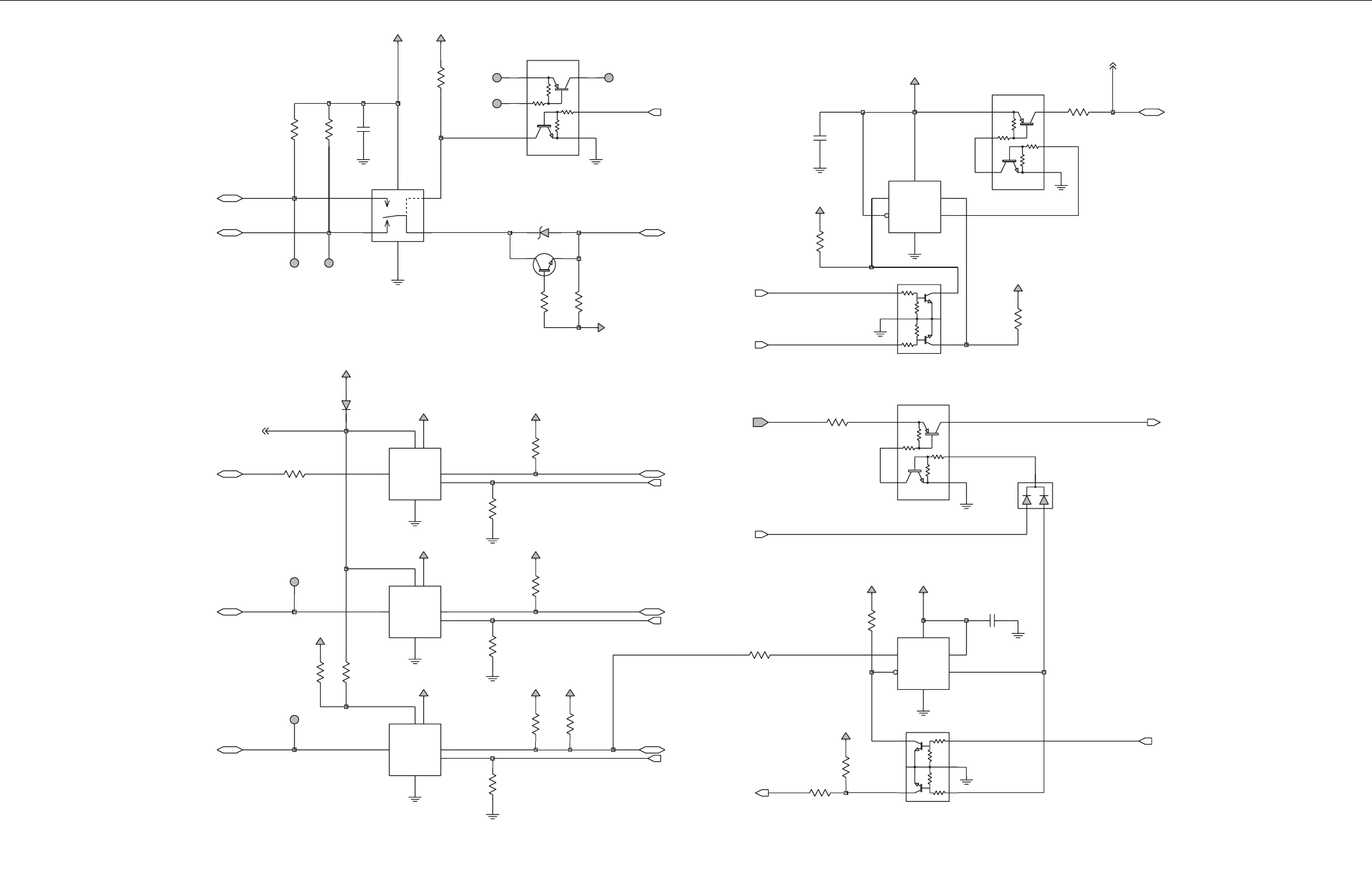
8.2 - 8 ENHANCED CONTROL HEADS: SCHEMATICS, PCBs and PARTS LISTS
Enhanced Control Head Main Board - Connectivity Block: GPIO (PCB: 8466580A01_A)
k
7.
4
k
7.
4
k
74
k
7
4
DTr2
DTr1
G
k
7.
4
k
7.
4
k
7
4
k
74
DTr2
DTr1
U
N
UN
UN
UN
UN
PU
LLUP
ERIW-
E
N
O
UN
U
N
UN
UN
UN
U
N
UN
UN
U
N
K01
0
13R
K5
1
3.3_
C
CV
3.3_CCV
213
R
3.
3
_
CCV
6
03R
K51
5
_C
CV
K51
4
0
3
R
8.
2_C
CV
1
0
3
R
K
0
1
7
1
3
R
00
81
3R
9
5
3
R
0
5
0
3R K0
1
5
_
C
CV
203PT10
3
PT
703
R
K2.
2
2
03D
G
1TH
4
5
T
AB
3.3_CC
V
K
2.2
8
03
R
V5_WSU
2
5
6
3
1
4
6
3
1
4
R
2TF
9DME
253Q
2A
VCCB
R
2
T
F
9D
M
E
1
0
3
Q
2
5
5
4
T
1CVL
47NS
1
CA2C
B2B
RID
1B
GND
1
A
VCCA
15
3
Q
A8
G
M
F
1
2
5
3
4
4
0
3
U
903R
K01
5
6
3
1
4
V5_
WS
U
4
Q
5
VCC
05
3
Q
R
2
T
F
9D
M
E
2
05
3U
X6P5
7
1
ZS7CN
6C
1P
C3
D
2
GND
K7
.
4
4
53R
V
5_WSU
7
5
3
R
K0
01
V
5_WS
U
8.
1
_CCV
K
5
1
V5
_WS
U
1
5
3
R
K
5
1
91
3
R
2
1
3
8
.2
_C
CV V5_WSU
05
3
D
0
016DB
MM
553
R
K
00
1
F
u1
.
0
0
53
C
K00
1
2
53
R
103C
F
u1
.
0
25
3
C
Fu1.0
54T1
CVL47
N
S
1C A2
C
B2B
RI
D
1B
GND
VCCA
1
A
2A
VCCB
61B
5
GND
1
S
VCC
2
20
3U
LN_X6L751
4
ASF
1
0
3
U
3
A
40B
8.2_
C
CV
6
03PT
0
0
53
R
5
0
3
PT
K
1
3
1
3R
4
0
3PT
1TFSL021RBM
103D
V5
_WSU
50
3
Q
4093TBMM
VCCB
2A
703P
T
8.
2
_
CCV
5
4T1
C
V
L4
7NS
3
03
U
A
1
CB2C
RI
D2B
GND
1
B
VCCA
1
A
8
5
3
R
K1
1
2
5
3
4
1D3
GND
2
Q4
VCC
5
+A_TLF
A8G
M
F
35
3Q
3
0
3
P
T
X
6
P
57
1Z
S
7
CN
25
3U
C
6
PC
303R
K01
N
O
_
M
R
1
13R
K0
1
NE_V5_TPO_IACG
T
ES
_
V
5
_TPO_I
A
CG
NO_I
A
C
G
E
S
N
E
S
_
N
O
_
R
W
P
_IA
CG
R
L
C
_N
O
_
R
WP_
IA
C
G
RW
P
_
0
_
O
IPG
0_
OIP
G
4
_O
I
PG
3
_O
IP
G
ERIW_
EN
O
_
T
N
O
RF
ERIW_ENO_RAER
S
UB
V
_
B
S
U
S
UBV_
B
S
U
E
R
IW
_E
NO
RI
D
_
0
_
OI
PG
RID_
4
_OIPG
RID_3_OIPG
KOOH
_
4
_
OI
PG
T
T
P
_3_O
I
P
G
LE
S
_ER
IW
_
E
N
O
2A
_U
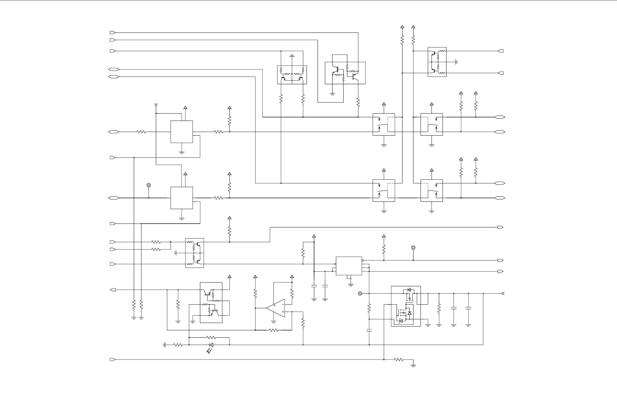
ENHANCED CONTROL HEADS: SCHEMATICS, PCBs and PARTS LISTS 8.2 - 9
Enhanced Control Head Main Board - Connectivity Block: USB Block (PCB: 8466580A01_A)
4.7k
4.7k
47k
47k
2r
T
D
1
rTD
k
7.
4
k7.4
k
7
4
k
7
4
DTr2 DTr1
k
7
.4
k
7
.4
k7
4
k
7
4
DTr2
DTr1
UN
U
N
UN
UN
UN
UN
K
01
333
R
8.
2
_
CCV
823R
K5
1
K
01
5
43R
3.
3
_
C
CV
423R
K51
K
5
1
3.
3
_C
CV
5
_C
C
V
163R 0
723
R
06
3R
433R
0
6
33R
K01
6
3
1
4
K
01
52
3
Q
R2
T
F
9D
ME
2
5
8.2_
C
CV
8.2_
C
CV
14
3
R
K
0
3
3
4
23C
Fu1.0
6
23C
Fu1.0
9
23
R
K0
1
9
33
R
033
5_
C
C
V
Fu01
7
2
3C
V3.6
5727VML
82
3
U
3
1
4
5
2
8.2
_
CCV
3.
3_
C
C
V
043
R
GND
5
S
1
2
VCC
3.
3_
C
CV
K
0
33
7
23
U
LN_
X
6
L7
5
1
4A
S
F
A
30
B4
1B 6
K
01
2
3
3R
3
43
R
3
.3_
C
CV
K
033
7
33R
K0
1
6
4
3R
K
0
7
4
803PT
0
4
0
3D
4
0
M2
1
5
1TUO 6
2TUO 7
3
T
UO 8
833
R
NE
4
GND1
1
9GND2
1
N
I
2
2
N
I
3
C
O
5_C
CV
4
23U
B
14
0
2
S
PT
623Q
L0336
C
D
F
61
4
5
3
2
K
5
.
1
12
53
4
5_
C
C
V
623
R5_
C
CV
A
8
G
M
F
32
3
Q
823C
F
p07
4
5_
C
CV
023R
K1
3A4
0
B
6
1
B
5GND
1S
VCC 2
2
5
6
3
1
4
LN
_
X6
L
7
5
14A
S
F
623
U
R2
T
F9DME
72
3
Q
32
3
RK01
523C
V3.6
Fu
2
2
54T
1C
V
L
4
7
NS
A
1
CB2
C
RID 2B
GND
1B
VCCA
1A
VCCB
2A
5
_
C
C
V
1A
VCCA
2A
VCCB
3
.3
_
C
C
V
5
23
U
54
T
1CVL
4
7N
S
3
2
3U
1C A2C
B2B
RID
1B
GND
K6.5
443R
K
7
4
5_C
C
V
K
0
3
3
533R
123R
24
3
R
K
0
1
K01
2
23R
52
3
R
1
2
5
3
4
K51
8.
2
_
C
C
V
A
8
G
M
F
22
3
Q
3
4
022
133R
VCC
42
3
Q
A8GMF
1
2
5
A3
0B
4
1B
6
GND
5
S1
2
3
A
40B
61B
5GND
1
S
VCC 2
22
3U
L
N
_
X
6L
7
51
4
AS
F
022
L
N_X6L
751
4
AS
F
12
3
U
84
3
R
0
3
3R
1
13PT
K
0
01
3.
3
_
CCV
013PT
TE
D
_
C
O
_S
UBV
S
UB
V
_
BS
U
S
UB
V
_BS
U
L
B
_
D
C
L
LB
_
DPK
7
4
3
R
K
0
01
R
ID_1
_
O
I
PG
RID_
2
_OI
P
G
NEUP
_1BSU
AN
E
_
S
UBV
_
B
S
U
A
N
E
_
T
E
F_SUBV
+
D
_TN
O
RF
+
D
_
RA
ER
LES_EDOM_1BSU
-D_BSU
+D_BSU
ROP
2
_
O
IP
G
G_R_
M
WP
V5
_
BS
U
TED_1BS
U
O
I
P
G
_
1
B
SU
1
_
OIP
G
2A_U
R
A
E
R
_T
NO
RF
_BS
U
-
D
_
T
N
O
R
F
-
D
_
R
AER
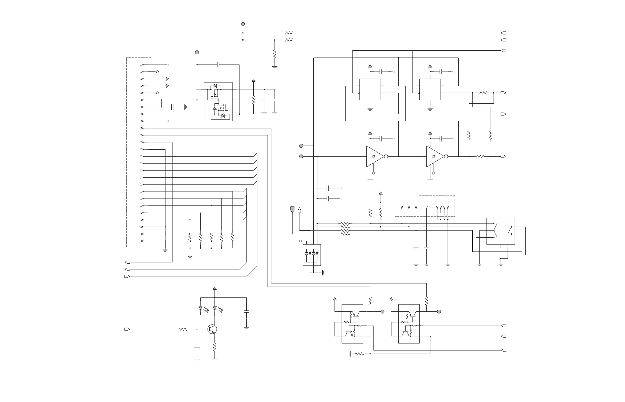
8.2 - 10 ENHANCED CONTROL HEADS: SCHEMATICS, PCBs and PARTS LISTS
Enhanced Control Head Main Board - User Input Block: Keypad (PCB: 8466580A01_A)
G
y
r
a
to
R
3_L
O
C
2_WOR
k
co
L
N
G_
DEL
F
F
O_NO_DN
E
304J
.l
o
p
6
1nip
ot
e
g
dir
b
V5_DWS_DPK
DNG
dapyeK oT
.l
o
p 42
DNG
D
N
G
UN
CN
UN
DNG
D
N
G
V5_DWS_DPK
C
N
1
_
W
O
R
DNG
UN
1
_LOC
0
_
L
O
C
3_WOR
4_L
O
C
2
_LOC
104J
4_WOR
Y
C
NEGR
E
M
E
U
N
UN
0
_
W
O
R
8
.
2
_
C
C
V
D
R
_
DEL
V3
.
3
V
5
00
4
R
0
31
4
R
K
74
8.
2
_
C
C
V
3
.
3
_
CCV
1
0
4D
DU
1
9
S-
TH
K
1
11
4
R
6
1
4
5
3
2
6
2
-1
04J
L0
3
3
6CDF
1
04Q
21-10
4
J
31-1
04J
2-
1
0
4J
K
3
.3
1
0
4R
0
1
4
R
1-104
J
3
0
4
Q
4
093
TBM
M
K
1
3
44
R
0
00
1
4
51
4
R
014C
F
u
01
V
3.6
504PT
7
0
4
P
T
10
4RV
V6
.5
2
1A
5
2A
1
1K
3
2K
4
3K
6
4
K
204
P
T
0
61
4C
F
u
01
3
2
99
3
R
0
2
44
R
CN
1
4
1-
1
0
4
J
F
p
0
74
5
2-
1
04
J
5
_
CCV
2
2-
1
0
4
J
704C
J403-3
01-104J
3
04P
T
0
44R
0
C
N
Fu
1
.0
6
0
4
C
5
2
P
1A_ES
L
U
P
3
B_
E
S
L
U
P
FLT_A+
C
N
8
.
2_C
C
V
HC
T
I
W
S
10
4
S
MMO
C
2
GND1
g1
GND2
g2
4
1
P
81-10
4
J
Fp074
804C
0
F
u
1
.
0
20
4
C
70
4R
0
10
4
C
F
u1
.
0
K1
C
N
8.2_C
CV
9-
1
0
4
J
3
2
-1
0
4
J
5-104J
K33
3
04R
204R
K3.3
1
1-
1
04
J
2
14
R
K
0
1
K1
80
4
R
714
R
6
1-
1
04
J
6
0
4
PT
K1
1
44R
4-
1
0
4J
404PT
0
D
NG
3
2N
I
C
N
1
4
T
U
O
C
CV
5
3
0
4
U
41
ZS
7
1
LN
3
D
2GND
Q4
5
VCC
3
1
4C
Fu1.
0
2
0
4
U
X6
P
57
1
ZS
7
C
N
6C
1P
C
6
04R
K7.
4
02-104J
8-
1
0
4
J
50
4
C
F
u1.0
5
1
-1
04J
3-
1
04J
4
0
4
R
4
8
.2_C
CV
2
K3
3
71
-
10
4
J
J403-8
K1
90
4
R
Fu1.0
90
4C
F
u
1
.
0
30
4
C
44
4R
0
8.2
_
C
C
V
5
6
3
1
4
7-10
4
J
3
404Q
R
2
TF
9D
M
E
2
J403-4
J403-7
J403-5
J403-2
J403-1
J403-6
40
4
C
F
u1
.
0
5
_
CCV
404
U
4
1Z
S7
1
LN
D
N
G
3
2NI
C
N
1
4
T
UO
CC
V
5
4
2
-1
04J
1
5
6
3
1
4
6-104J
504
Q
R2TF9D
M
E
2
K
5
.1
1
2-1
0
4J
Fu
0
1
5
1
4
C
41
4
R
X6P
5
7
1
Z
S
7CN
6C
1P
C3
D
2GND
4
Q
5
VCC
CN
1
04
U
5
_
CC
V
Fp
0
7
4
4
1
4
C
K8.1
61
4
R
5_
C
C
V
5
04R
001
2
0
4
D
5
_
C
C
V
91-10
4
J
L
B
_
D
P
K
F
FO
_
N
O
_
L
B
_
DP
K
NE
E
R
G
_DEL
G_R_
M
W
P
LOCK_ON
1
_
WS
R
TN
I
_
W
SR
DU
1
9
S
-TH
2
_W
SR
GREME_DEL
F
FO_NO
_
DNE
KEYPAD_COL(5:0)
)
0
:5(
LOC
_D
AP
Y
E
K
)
0
:4(WOR_DA
P
Y
E
K
KEYPAD_ROW(4:0)
R
OP
D
E
R
_
D
E
L
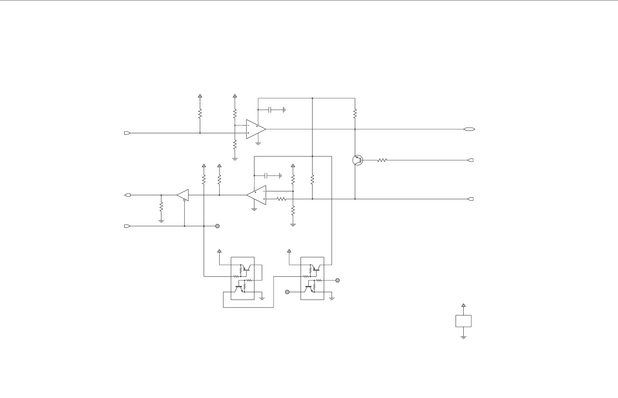
ENHANCED CONTROL HEADS: SCHEMATICS, PCBs and PARTS LISTS 8.2 - 11
Enhanced Control Head Main Board - User Input Block: SBEP (PCB: 8466580A01_A)
5
6
3
1
4
5
_CCV8.
2
_C
CV
R
2TF9D
M
E
1
14Q
2
8.
2
_
CCV
K74
9
24R
K
3.
3
82
4
R
8
.
2_C
CV
8.
2
_
CCV
K
01
12
4
R3
2
4
R
K
0
3
4
5
2
2
2
4
R
K
51
1
4
5
2
5
72
7
VM
L
1
24U
3
1
224U
5
727V
M
L
3
K0
14
2
4
R
Y
524R
K01
8.2_CCV
5
21
CH
V
4
7
1-0
2
4
U
2
A
1
OE
4
62
4R
K01
5
_C
CV
K03
72
4R
2
-024U
D
N
G_R
W
P
3
DNG
5
CCV
1
14PT
4
0
93
TB
MM
5
_
CCV
6
34R
K
0
1
K
7
.
4
0
14Q
5
34
R
224C
F
u1
.0
Fu
1.
0
1
2
4
C
K
5
1
2
5
6
3
1
4
034R
104PT
214Q
R2TF9D
M
E
E
LB
AN
E
_S
U
B
X
T
_
IC
S
+
S
UB
XR
_
MOC_O
ID
A
R
XT
_
MO
C_
OI
DA
R
NE_MOC_OI
D
AR
0
1
4
PT
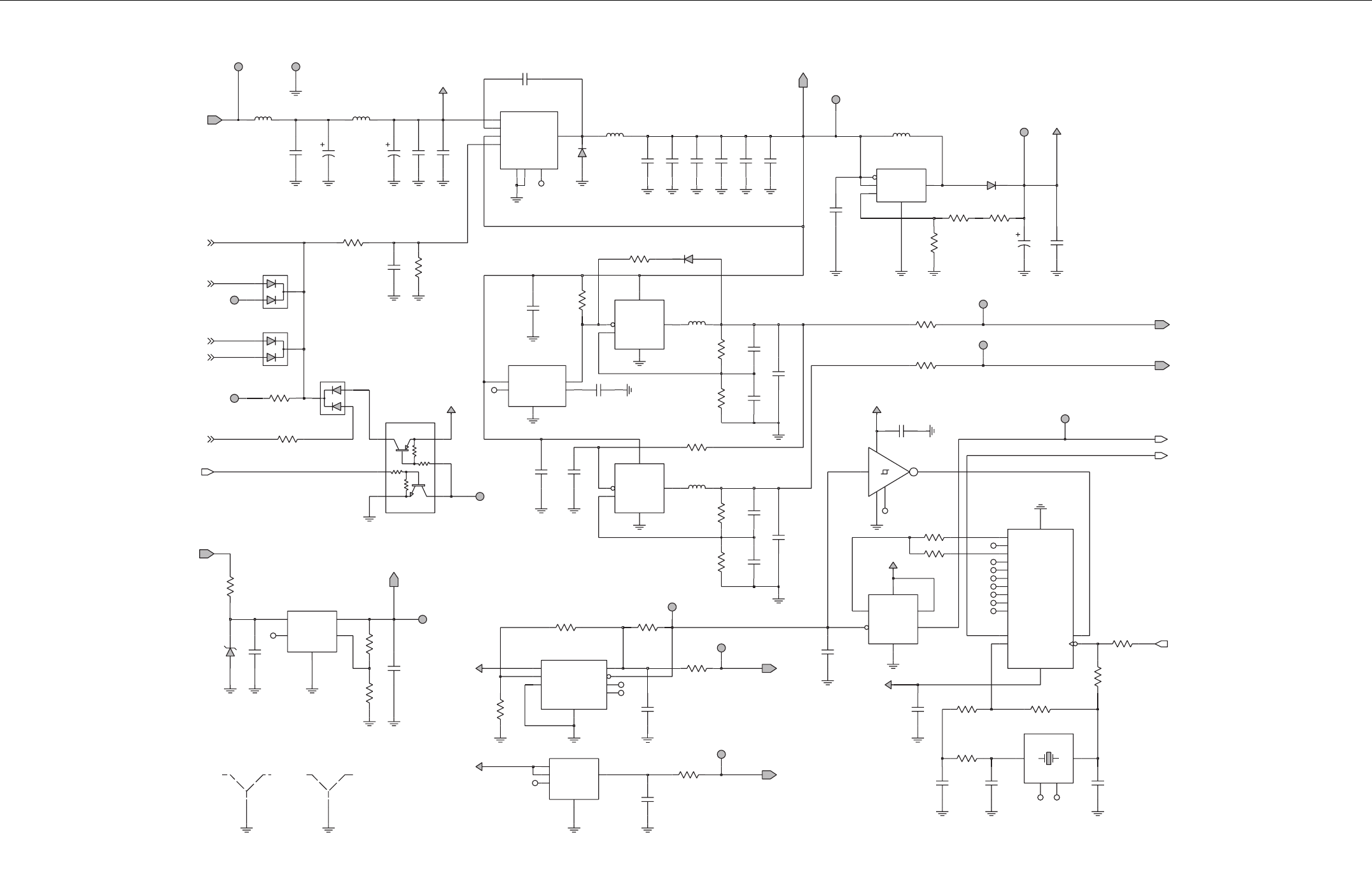
8.2 - 12 ENHANCED CONTROL HEADS: SCHEMATICS, PCBs and PARTS LISTS
Enhanced Control Head Main Board - DC Block: Power Supply (PCB: 8466580A01_A)
G
G
G
G
G
G
G
G
UN
UN
UN
UN
UN
UN
UN
UN
UN
U
N
K1
CN
3.3_C
CV
5
0
5
R
2
GND
5
W
S
1
V1
Fp21
235C
TU
O
_WS 1
0
22
2
6SPT
405U
3NE
4B
F
67
6
2M
L
G1 CTGND
TSO
OB
_
C
3
6B
F
GND
4
T
U
P
NI
2
NC1
5
F
F
O
_N
O
7
1
0
5
U
VCC
5
40
5
D
0
01
6D
B
M
M
9
0
5
U
C
6
PC
1D3
GND
2
Q4
31
5
R
%
1
K
1
.8
6
8
.
2_
CCV
X6P5
7
1Z
S
7CN
H
u
3
3
7
0
5L
3
05
R
0
0
1
5
0
5
L
Hu
3
3
PA
TV 6
V0
5
4
05C
F
p
07
4
R
O
RRE 5
KC
AB
DEEF
7
GND
4
T
UP
NI
8TUPTU
O1
ES
NES 2
N
W
O
DTUHS
3
CN
605U
DC1
5
92PL
215R
K
1
.2
1
%1
405R
CC
V
_T
L
F
CN
K1
Hu
7
.4
4
0
5L
Fu
0
1
525C
V3
.6
F
u1.0
6
15C
F
u
2
2
V
3
.
6
2
15
C
%
1
K
1
.2
1
2
0
5
R
F
p0
7
4
1
0
5
C
V0
5
425
R
0
7
0
5U
58
9
2PL
SSAPYB
4
GND
2
*
F
FO_
NO
3
NIV
1T
U
OV 5
F
u
1.
0
0
835R
6
35C
0
0
43
5
R
53
5
R
0
2
0
5L
6
35R
205
D
G
1
TH
4
5TAB
Hu
2
2
105PT
6
0
5
C
305L
H
u
7.
4
9
0
5
C
Fu1
0
.
V
0
5
8
05
P
T
F
u
22
V
3
.6
F
p
05
1
2PT
42
5
C
8
.2_CCV
1PT
0
3
1
S
R
B
M
1
0
5
D
2
35
R
%1
K3.25
7
0
5
C
V
3
.
6
F
u
2
2
C
N
Fu
0
1
43
5
C
V3.6
RKCD105
17S
P
T
CN_B
F1
2GND
4NI
32C
N
5
TUO
+A_TLF
315U
0
925R
C
N
Fu
0
1
7
15C
V
3.
6
5
3
5C
Fu
1.
0
G1
TH
4
5
T
A
B
7
05
D
C
N
00
1
6DBM
M
6
0
5
D
Fp001
915C
90
5
P
T
8
1
5
C
00
16DBMM
5
05D
C
N
C
N
Fp22
V
3.6
025C
Fu01
V5_
WS
U
01
5PT
Fu
01
3
15
C
V3
.
6
Fu
1
.0
21
5
P
T
V3.
6
625C
Fu01
22
5
C
305
P
T
D
LEIHS
1
05
HS
3
0
5
C
F
u
01
V
0
5
F
u
1
.
0
V
0
5
20
5
C
V
0
5
F
u0
1
5
05C
F
u22
41
5
C
7
391
T
L
3
0
5
U
3B
F
2
GND
4N
D
HS 1
WS
5NI
V
V5
3
0
0
735R
9
3
5
R
605PT
115PT
CN
9
2
5
C
F
u
1.
0
K233
%
1
8
05R
K5
6
1
%
1
1
35R
K
0
1
5
_
CC
V
3.
3
_CC
V
7
05R
325
R
4
0
5PT
0
K
18
6
5
15R
%1
K6
.3
5
Fu
1
.0
0
1
5R
%1
V
3.
6
125C
F
u0
1
8
25
C
3
GND
2T
UPNI
41CN 5
2C
N
1
TUO_TESER
1
CN
1
0
3
PCN
205U
6
4
1C
M
1
05
Y
zHK
86
7.
2
3
NC
2
NC1
3
4
TU
O
NI
C
N
+A_TLF
3.
3_
C
CV
1
1
5
C
V
3
.6
F
u
2
2
10
5
R
K
01
1
0
5
L
H
u
3
3
CN
3
15PT
8.1_CCV
CN
F
u
2
2
V3
.6
0
15
C
3
35R
01
5
V1
1
5
.
1_
CCV
3
2
_
CCV
5
_CCV
5
05U
0
2
2
2
6
S
PT
NE
3
BF
4
GND
2
WS
K561
%1
905R
51
5
C
F
u
1
V
5
2
F
p
81
135
C
74
Q
55
Q
46
Q
67
Q
41 8
Q
31 9
Q
21
TESE
R
61
VCC
8
GND
1
1
N
I
_
CS
O
0
11TU
O
_
CS
O
92
T
UO_CS
O
51 0
1
Q
121Q
23
1
Q
34
1
Q
8
.2_CCV
A
0
60
4CH
4
7
51
5
U
K01
415R
V
3.
6
F
u
0
1
72
5
C
C
N
035C
Fp001
K03
3
0
2
5
R
2
0
5HS
DLEIHS
2
0
5
P
T
5
05
PT
60
5Q
R2TF9DM
E
2
5
6
3
1
4
0
3
5
R
00
1
3
35C
V81
205
RV
Fu
1.
0
GEM01
1
25R
5
C
CV
325C
F
p
0
1
41
Z
S
7
1
LN
8
05
U
3
DN
G
2NI
1
CN
4
T
UO
C
N
CNCN
2
25R
K022
115R
%1
K121
80
5
C
V
3
.
6
Fu
2
2
8
.
2_CCV
605
R
K
33
N
O
_KCOL
N
O
_I
A
C
G
N
O
_SUB
R
OP
K
L
C
M
z
HK
23
Y
CNEG
R
EME
NO
DLO
H_NO
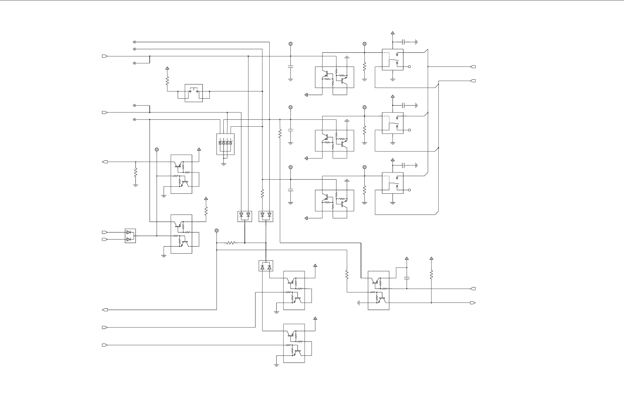
ENHANCED CONTROL HEADS: SCHEMATICS, PCBs and PARTS LISTS 8.2 - 13
Enhanced Control Head Main Board - DC Block: Power On/ Off (PCB: 8466580A01_A)
UN
YCNEGREME
5
_C
C
V
5_
C
CV
1
15D
0016D
B
MM
5
4
Fu1.0
24
5
C
F
u
1.
0
4
45C
8
.
2_C
CV
9
4
5R
K01
4
2
5
P
T 5
2
5P
T
3A4
0B
6
1
B
5
GND
1S
2
VCC
545R
+A_T
LF
5_CCV
LN_
X
6
L7
5
1
4A
S
F
1
15
U
K
1
7
4
5
C
F
u1
.0
C
N
54
5C
F
u
1
.
0
F
u
1
.0
64
5
C
5
K1
1
K2
3
K3
4
K4
6
V6.
5
1
05RV
A1
2
A2
+A
_T
LF
K
0
1
3
4
5
R
6
3
1
4
5_
C
C
V
5_CCV
0
1
4
R2TF9DME
505Q
2
5
305
Q
R2TF
9
DME
2
5
6
3
56
31
4
31
4
R
2TF9
DME
20
5Q
2
1
05Q
R
2TF9D
M
E
2
56
15
5
R
K
7
.4
055
R
K
01
8
0
5
Q
R
2
TF
9
DME
2
5
6
3
1
4
70
5Q
2
5
6
3
1
4
R
2TF9D
M
E
625PT
7
25PT
4
4
5
R
0
405Q
2
5
6
3
1
4
CN
5_
C
CV
CN
R2
T
F9DME
0
3
0
4
5
R
K
0
1
015
U
A
30
B4
1B 6
GND
5
S
1
2
VCC
015D
0016DBM
M
LN
_X6
L75
1
4A
S
F
3
25
P
T
2
2
5
P
T
0
2
5
P
T1
2
5
P
T
K0
1
2
45
R
+A_TLF
8
.2
_
CCV
1
B6
GND
5
S
1
2
VCC
2
15
U
LN
_
X
6
L
7
51
4
AS
F
A
30B 4
5
_
CCV
0
01
6D
B
M
M
31
5D
+A_T
L
F
7
4
5
R
K7.4
145C
Fu
1
.0
145
R
31
4
K7.
4
00
5
Q
R
2
T
F9
D
ME
2
56
1
0
5S
HCTIWS
3
2A
4
1
2B
2
001
6D
BMM
4
845R
305D
F
u
1
.0
K0
1
NO_SUB
OIDA
R
_
N
O
X
T
_ICS
+
SUB
N
I
_
L
R
T
C
N
O
)
0
:
4(WOR_DAPYEK
)
0
:
5
(
L
OC
_
D
AP
Y
EK
F
FO
_
N
O
_
D
N
E
GOR
P
TS
E
U
Q
ER_H
C
Y
CNE
GRE
ME
NO_KC
O
L
NO_KCOL
LORTNOC_
FF
O_NO
NO_
IA
CG
N
O
_
IA
C
G
0
45
C
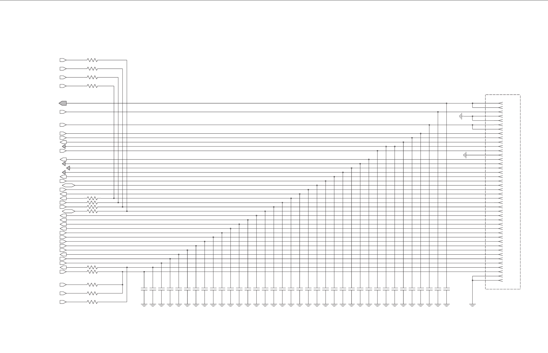
8.2 - 14 ENHANCED CONTROL HEADS: SCHEMATICS, PCBs and PARTS LISTS
Enhanced Control Head Main Board - Remote Block (PCB: 8466580A01_A)
G
UN
UN
.
lo
p
0
4
306J
UN
U
N
U
N
U
N
U
N
0
1
6R 0
C614
470pF
1
1
-3
0
6
J
8
.
2
_
C
CV
33pF
0
1
-3
0
6
J
3
.
3
_
C
C
V
C605
6
2
-
30
6
J
470pF
C611
C619
82pF
2
3
-30
6
J
8
-
3
0
6
J
5
1
-3
0
6
J
4
2
-30
6
J
9
-
30
6
J
2
1
-
30
6
J
7
3
-3
0
6
J
5
-
30
6
J
3
1
-
30
6
J
6-
30
6
J
1
G
-
306J
0
4
-30
6
J
7-
3
0
6
J
4
-
30
6
J
3
2
-
30
6
J
C637
470pF
82pF
C623
C612
470pF
470pF
C613
0
3
-3
0
6
J
82pF
C617
1
3
-30
6
J
33pF
C630
8
2
-30
6
J
0
9
0
6
R
33pF
9
3
-3
0
6
J
C627
116
R
72
-
3
06J
1
-3
06
J
+
A
_
T
LF
0
C615
82pF
8
1
-30
6
J
0
2
-30
6
J
2
2
-
30
6
J
V
5_W
S
U
9
1
-30
6
J
0
6
0
6
R
0
3
16
R
C604
470pF
5
_
CC
V
7
1
-
30
6
J
33pF
C606
0
4
06
R
5
0
6
R
C620
82pF
0
82pF
470pF
C632
C635
82pF
C618
C628
82pF
470pF
C636
9
2
-30
6
J
C602
470pF
470pF
C609
20
6
R0
C633
470pF
82pF
C631
10uF
3
-
3
0
6
J
5
2
-3
0
6
J
C610
3
3
-30
6
J
2
G
-
306J
2
-
30
6
J
6
3
-30
6
J
C622
82pF
C626
33pF
0
2
16R
C625
33pF
0
C624
470pF
30
6R
83
-
30
6
J
41
-
306J
C616
82pF
0
7
06
R0
8
0
6
R
C607
470pF
470pF
82pF
C608
470pF
C621
82pF
C634
C601
C629
33pF
1
2
-
3
0
6
J
6
1
-
3
0
6
J
0
4
3
-30
6
J
4
1
6
R
LCS_
C2
I
2
_N
A
X
T
_
I
CS
D
X
T_
ISS
0
E
S
_
2
B
SU
-
D
_
R
A
ER
ER
IW_E
N
O_R
A
ER
A
D
S
_
C2
I
DXR
_I
S
S
MER
_
HSA
D
NO
_
M
R
3
_
N
A
5
3
-30
6
J
Q
E
R
_
O
IPG
NE
U
P
_
2
B
SU
N
E
X
T
_
2
B
SU
K
L
C
_
IS
S
S
F
_I
SS
P
S
U
S
_
2
B
S
U
X
R
X
T
I
S
O
M
_
IPS
2
SC_
IPS
KLC
_
IPS
O
SIM
_
I
PS
DEE
P
S
_2B
S
U
C
I
M
ST
R
STC
PV_2BSU
LORTN
O
C
_F
F
O
_
N
O
V
5
_
BS
U
+
SUB
+
D
_
R
A
E
R
D
X
T_
2
BSU
MV_
2
BSU
VC
R
_2B
S
U
O
I
D
UA
_TE
S
DN
A
H
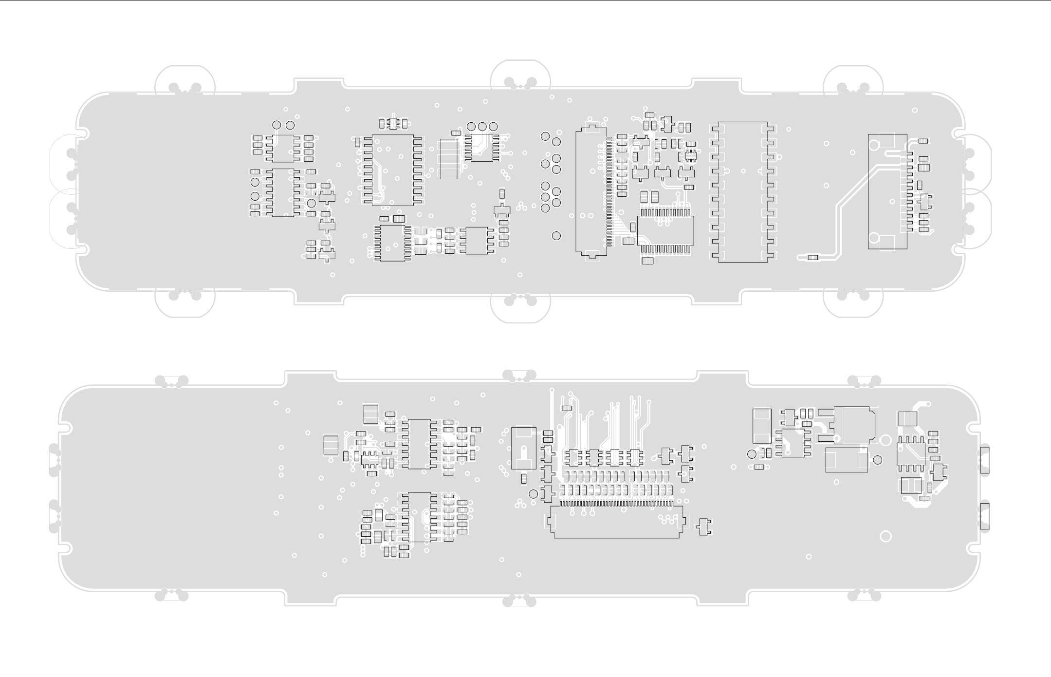
ENHANCED CONTROL HEADS: SCHEMATICS, PCBs and PARTS LISTS 8.2 - 15
PCB/ Data Expansion Head Enhanced Main Board - Bottom and Top Side (PCB: 8466586A01_A)
1
1
1
8466586A01_A
C06
0
0
F
nd
245 C 2 lvl intct
Pb
e1
o
C101
C102
C103
C104
C105
C106
C116
C117
C126
C127
C128
C129
C130
C131
C141
C309
C401
C402
C403
C404
C405 C406
C407
C601
C602
C603
C604
C605
C606
D101
D102
F101
12
1
J1001
20
11
10 1
J1003
1
40
J1022
Q101
23
Q102
Q103
Q104
Q401
Q601
Q602
Q603
Q604
R101
R102
R103
R104
R110
R111
R112
R113
R114
R115
R116
R117
R118
R119
R120
R201
R202
R205
R206
R222
R318
R319
R320
R321
R322
R323
R324
R325
R401
R402
R601
R602
R603
R604 R605
R606
R607
R608
R609
R610
R611
R612
R613
R614
R615
R616
TP1011
TP1012
TP1013
TP1014
TP1015
TP1024
TP1031
TP1032
TP1033
TP1037
TP1062
TP1064
TP1065
TP1071
TP1072
TP1073
TP1074
TP1075
TP1076
114
15
28
U101
14
58
U302
16
8
9
U401
13
U402
110
1120
U403
10
20 11
U404
7
8
14
U601
14
58
U602
VR101
1
nd
245 C
2 lvl intct
Pb e1
o
C107
C108
C109
C110
C111
C112
C113
C114
C118
C119
C120
C121
C122
C123
C124
C125
C132
C133
C134
C135
C136
C137
C138
C139
C140
C142
C143
C145
C202
C203
C303
C304 C305
C306
C307 C308
C501
C502
C503
C505
C506
C507
C508
C607
C608
C610
C611
C612
C613
C614 C615
C616
1
40
J1005
2
3
Q501
3
4Q503
23
Q504
R105
R107
R108
R109
R106
R208
R209
R210
R211
R212
R213
R214R215
R216 R217
R218
R219
R220
R221
R223
R301
R302
R303
R304
R305
R306
R307
R308
R309
R310
R311
R312
R313
R314
R315
R316
R317
R501
R502
R508
R509
R510
R511
R512
R518
R519
R520
R617
R618
R619
R620
R623
R624
R625
R626
R627
TP1061
TP1092
TP1093
7
814
U201
7
814
U301
1
4
58
U501
1
4
58
U503
U603
VR102
VR103
VR104
VR105
VR106
VR108
VR109
VR110
VR111
VR112
VR113
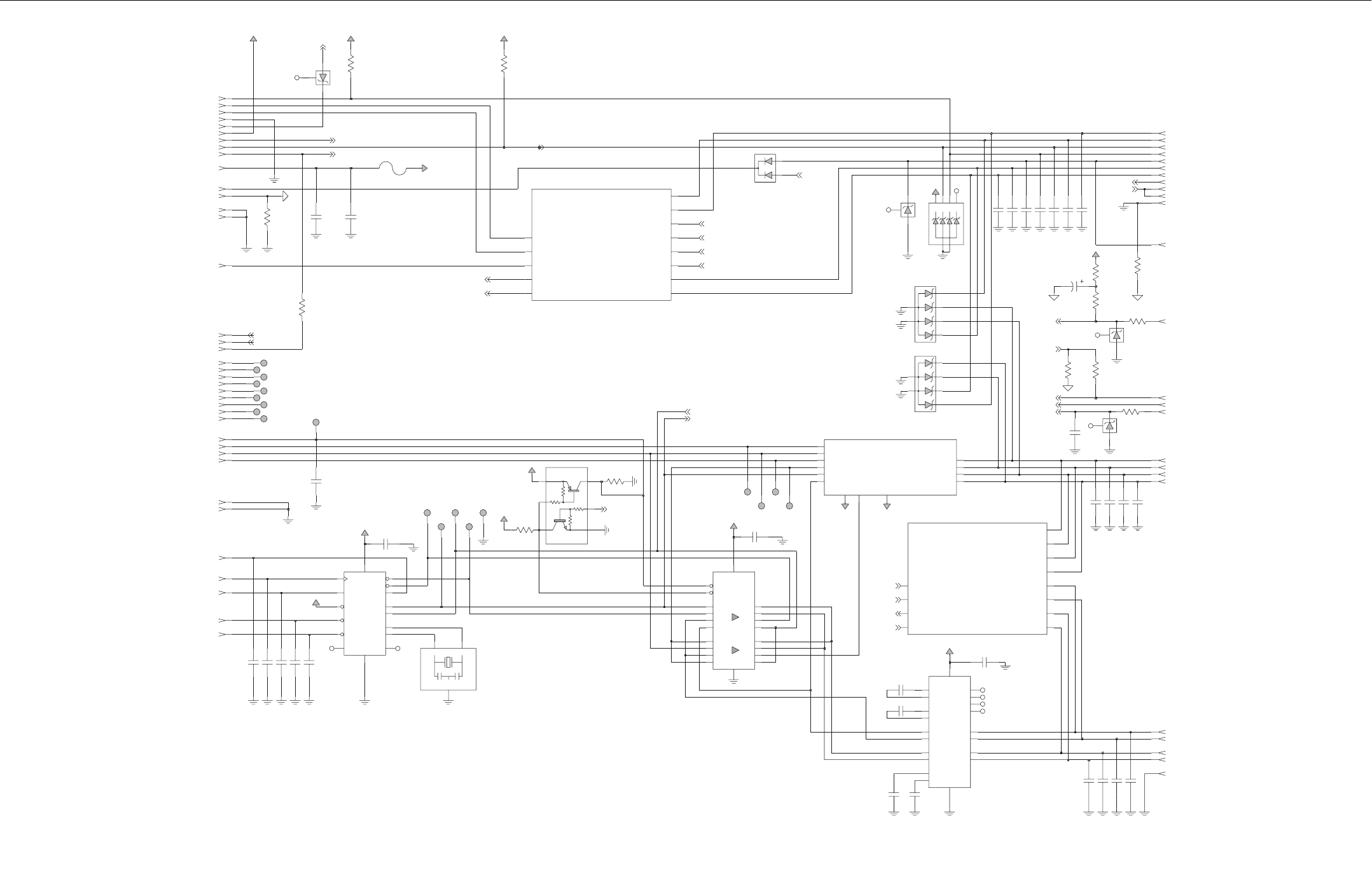
8.2 - 16 ENHANCED CONTROL HEADS: SCHEMATICS, PCBs and PARTS LISTS
Data Expansion Head Enhanced Main Board - Main PCB (PCB: 8466586A01_A)
SPIB_MISO
Flash Mode
PTT/GND
IGNITION (via 4K7)
INT_MIC
NU
NUNU NU
9V3
3V3_DIG
A+ (via 4K7)
RS232_SCI_TX
IGNITION
HANDSET_AUDIO
EXPANSION_PTT
SPIB_CS_BT
SAP_CLK
DGAN_SAP_FSYNC
SAP_STD
SAP_SRD
BLUE_T_FSYNC
INT_MIC
FLT_A+
NUNU NU
5V
HANDSET_AUDIO
BUS+
NU
NU
NUNU
SPKR-
SPKR+
ON_OFF_CONTROL
GND
FLT_A+
NU
UART_B BUS+
HANDSET_AUDIO
UART
GND
ACC3
SPIB_CS1_UART
SPKR-
SPKR+
AUDIO+
ON_OFF_CONTROL
NU NU
UART_B
SPIB_CLK
SCI_TX
MUX_CTRL_1
FLT_A+_REG
FLT_A+_REG
RESET_OUT
SPIB_MOSI
AUDIO-
SCI_TX
GND
SPKR-
SPKR+
EXP_REQ
EXPANSION_PTT
NU
SIGNAL_GND
SB9600_BUS+
SB9600_RESET
SB9600_BUSY
SB9600_BUS-
BUSY_OUT
BUSY_IN
RS232_SCI_RX
INT_MIC
RS232_CTS
RS232_RTS
J1022-16
J1005-31
J1022-18
J1022-24 TP1075
J1022-22
J1022-19
J1022-14
J1022-20
20V
2
5
1
3
4
6
J1022-1
VR104
J1001-13
J1001-8
J1001-6
J1001-10
J1001-7
J1001-9
J1001-12
82pF
C120
5
Y6 3
Y7
5V
J1005-14
01 DNG 02
CCV
18
Y0
Y1 16
14
Y2 12
Y3
9
Y4 7
Y5
6A2
8
A3
11
A4
A5
13
15 A6
17
A7
1
EN_OE1
19
EN_OE2
C119
U403
MC74AC244
2
A0
4A1
470pF470pF
4886061B02
13
2
C118
33V
3.68MHz
CSTCC_MG
U402
82pF
C136
NC
VR105
NC
NC
82pF
C135
J1022-31
NC
J1022-38
J1022-30
J1022-26
0.1uF
C406
J1022-28
0.1uF
C404
C403
0.1uF
J1005-8
J1005-7
J1005-27
3V
J1005-11
TP1073
J1022-32
TP1071
0.1uF
C402
3V
TP1072
TP1062
TP1064
82pF
C131
J1005-22
R108
10
D102
TP1013
TP1033
TP1012
TP1014 R401
0
3V
47K
R106
5V
J1005-19
J1022-41
J1022-42
C405
0.1uF
J1022-29
0.1uF
NC
0
C407
Q401
R107
RS232_TXA
RTSA
SB9600_BUS+
SB9600_BUS-
SB9600_BUSY
SB9600_BUSY_IN
SB9600_BUSY_OUT
SB9600_RESET
SB9600_INTERFACE
3V5V
RESET
RS232_RX
RS232_TX
82pF 82pF
C129C127 C128
82pF82pF
TP1076
C126
TP1074
CN
4.7K
R109
TP1011
5.6V
VR101
C116
C125
470pF
470pF
C124
470pF
J1022-3
J1022-36
J1022-33
J1022-37
J1022-34
TP1065
J1022-35
9
X2
82pF
C122
12 5
NC2
13
RTS
14
RX
3SCLK
7
SHDN
15
TX
6
1
C
C
V
10
X1
MAX3100EEE
U401
4CS
11
CTS
1
DIN
2
DOUT
8D
N
G
6
IRQ
NC1NC NC
VCC
560
R623
R110
0
TP1037
TP1024
TP1031
R624
TP1032
C612
10uF
100
1
6
4
3
3V
5V
20V
VR108
2
5
car_rx_audio
car_rx_audio1
car_rx_audio2
car_rx_data
car_rx_data1
car_rx_data2
car_tx_audio
car_tx_audio1
car_tx_audio2
car_tx_data
car_tx_data1
car_tx_data2
R223
0
0
R222
32V 2A
F101
5V
J1005-12
J1005-10
J1005-15
J1001-14
91
C
CV
VNEG
7VPOS
3
16
R1INR1OUT
15
9
R2IN
12 R2OUT
14
T1IN
17
T1OUT
13 T2IN 8
T2OUT
2C1POS
C2NEG
6
5
C2POS
81 DNG
1
NC1 10
NC2
NC3 11
NC4
20
47K
MAX3232E
U404
4
C1NEG
3V
R402
82pF
C139C138
82pF
C137
82pF
0.1uF VR102
33V
C117
2K
3K
4K
TP1015
VR103
5.6V
1A
2A
1K
AUDIO1
AUDIO2AUDIO_IN
AUDIO_OUT
CAR_RX_AUDIO
CAR_TX_AUDIO
RADIO_EXP_PTT
SPKR1_IN
SPKR1_OUT
SPKR2_IN
SPKR2_OUT
NC
470pF
C123
25PIN_EXP_PTT
25PIN_INT_MIC
J1001-3
J1001-1
J1001-5
J1001-2
J1001-4
J1005-9
J1001-11
J1005-20
J1005-6
J1005-4
J1005-18
3.3K
R202
NC
R201
4.7K
NC
VR113
33V
J1005-2
3V J1005-17
J1005-29
J1005-33
J1005-35
3V
C121
470pF
82pF
C134
82pF
C133C132
82pF
C401
0.1uF
C130
82pF
J1005-16
3V
J1005-13
J1005-39
J1005-5
J1022-17
NET_1
HANDSET_AUDIO
IGNITION
ON_OFF
HANDSET_AUDIO
IGNITION
HANDSET_AUDIO
INT_MIC
HANDSET_AUDIO
FLT_A+
BUS+
car_rx_data
car_tx_data
EXPANSION_PTT
PTT_GND
car_rx_data
car_tx_data
car_tx_audio
car_rx_audio
EXPANSION_PTT
INT_MIC
car_rx_audio
INT_MIC_AUDIO
INT_MIC_AUDIO
PTT_GND
car_tx_audio
NET_2
GABEL HYBRID
22K 22K
22K
22K
CAR INTERFACE
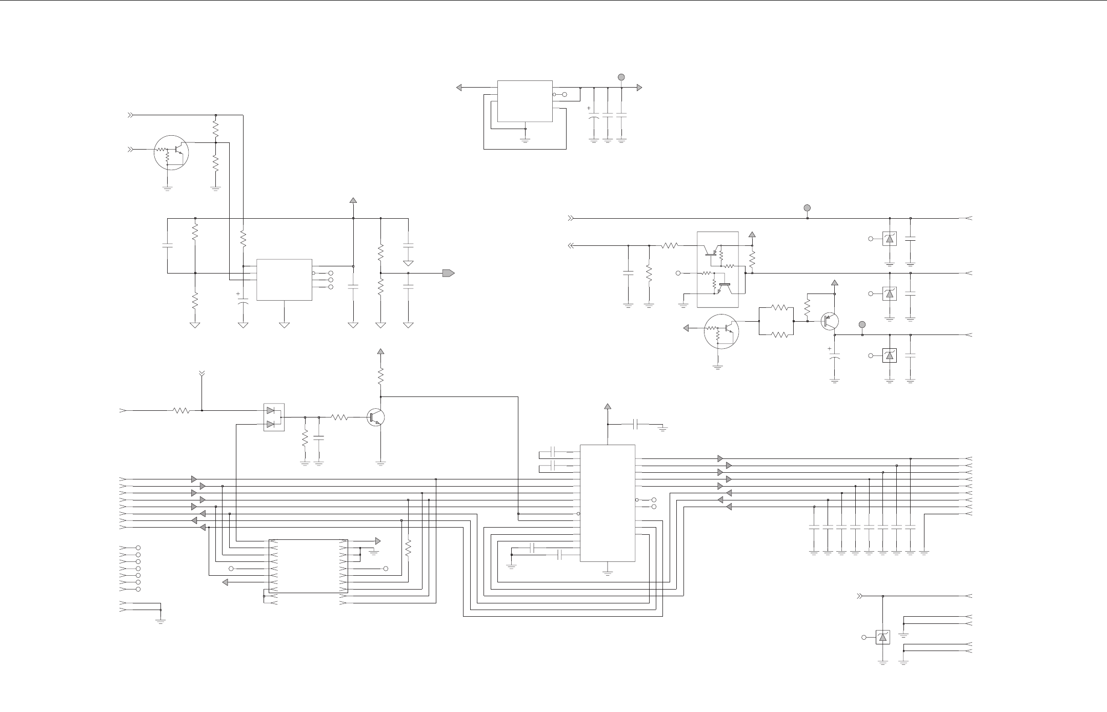
ENHANCED CONTROL HEADS: SCHEMATICS, PCBs and PARTS LISTS 8.2 - 17
Data Expansion Head Enhanced Main Board - DC Power (PCB: 8466586A01_A)
G
GND
RS232_CTSRS232_DCD
JTAG_DSP_DE
RS232_DTR
RS232_RTS
RS232_RI
NU
RS232_DTR
12
RS232_RX
RS232_RI
RS232_DCD
13
NU
7
FLT_A+_REG
JTAG_MCU_DE
NC
RS232_CTS
11
JTAG_TMS
NU NU
19
18
NU
RS232_RTS
9
RS232_TX
SB9600_SW
RS232_DSR
GND
JTAG_TDO
RS232_CTS
RS232_RTS
JTAG_TRST
17
14
GND
NU
16
GND
MUX <- 3V
SW_B+
RS232_DSR
2
JTAG_TDI
RS232_DCD
GND
JTAG_MCU_DE
RS232_DSR
5
NU
JTAG_TCK
1
RS232_RI
GND
RS232_DTR
RS232_DCD
RS232_RI
RS232_TX
RS232_RX
RS232_RTS
RS232_CTS
NU
RS232_TX
RS232_RX
20
RS232_RX
JTAG NU
ON_OFF_GND
RS232_DSR
4
6
8
10
RS232_DTR
NU
15
3
NU
GND
NU
JTAG_RESET_IN
RS232_TX
10
R509
C109
82pF
J1003-10
C111
82pF
J1022-2
82pF
C112
J1005-37
J1022-7
5V
3V
C503
470pF
T4OUT
10
T5IN
17
12
T5OUT
CCV 62
VNEG4
4VPOS
27
J1003-20
R3OUT
18
T1IN
24
5
T1OUT
T2IN
23
T2OUT
6
T3IN
22
T3OUT 7
T4IN
19
DNG
2
INVALID
15
8R1IN
R1OUT
21
R1OUTB 16
R2IN
9R2OUT 20
R3IN
11
MAX3238EEAI
25 C1NEG
C1POS
28
C2NEG
3C2POS
1
FORCEOFF
14
FORCEON
13
R102
NC
NC
U101
NC
NC
FLT_A+
47K
C507
0.1uF
33V
VR111
R1
Q504
VAG_1
0.1uF
C106
R2
C104
NC
0.1uF
12.4K
R510
R502
0
J1022-25
33V
VR110
3.3K
C506
R511
R501
12.4K
10uF
J1003-2
NC
J1003-13
470pF
C142
J1003-14
0.1uF
C101
TP1092
Q104
0.1uF
5V
47uF
C102
J1022-10
C501
J1005-36
Q501
R2
R1
3V
R101 0
C502
0.1uF
NC
33V
VR109
D101
NC
NC
J1022-27
NC
OUTPUT
2
SENSESHUTDOWN
3
VTAP
6
NC
10K
R103
U503
LP2951CD
5
ERROR
7
FEEDBACK
4DN
G
8INPUT 1
4.7K
.012uF
C505
R115
0.1uF
C508
J1005-1
470pF
C140
C108
82pF
0.1uF
C103
C110
82pF
ERROR
5
FEEDBACK
7
4D
NG
INPUT
8OUTPUT 1
SENSE 2
SHUTDOWN
3
TP1061
1
U501
LP2951ACD30R2
5V_TAP
6
82pF
C114
J1022-5
J1005-41
C107
J1022-6
J1022-9
82pF
VR112
33V
R105
0
NC
C143
10uF
3.3K
R512
R520
2.2K
J1005-3
J1003-19
NC
J1005-32
J1003-17
J1005-26
J1003-7
NC
J1005-42
J1003-4
Q101
NC
J1003-15
NC
C105
0.1uF
J1003-5
TP1093
FLT_A+
C607
1uF
NC
Q503
J1003-16
R508
80.6K
J1022-11
J1022-12
J1005-21
J1005-23
R114
47K
NC
3V
VCC
J1022-4
J1022-13
10K
J1003-18
R518
NC
J1003-1
R104
47K
J1022-21
470pF
C145
J1003-3
470pF
J1005-30
C141
82pF
R113
8.2K
J1005-25
C113
J1022-15
J1022-39
3V
NC
J1005-40
3V
J1003-6
J1003-11
J1003-9 J1003-12
R519
J1005-34
2.2K
J1005-24
J1005-38
J1003-8
J1005-28
J1022-40
J1022-8
FLT_A+
J1022-23
ON_OFF
5V
NET_2
FLT_A+
NET_1
22K
22K
22K
22K
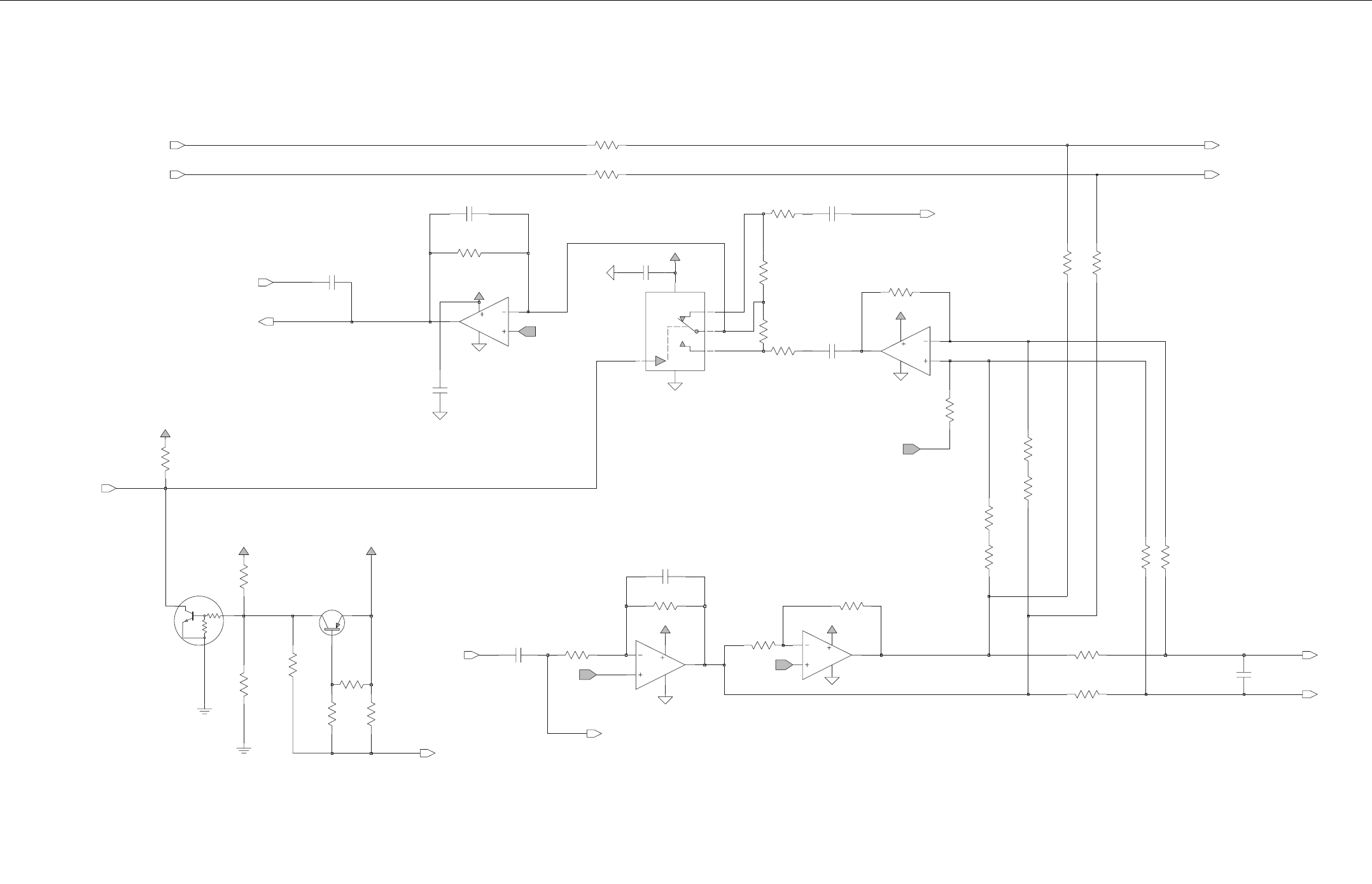
8.2 - 18 ENHANCED CONTROL HEADS: SCHEMATICS, PCBs and PARTS LISTS
Data Expansion Head Enhanced Main Board - Gabel Hybrid (PCB: 8466586A01_A)
G
G
G
G
0
SPKR2_OUT
SPKR1_OUT
RADIO_EXP_PTT
AUDIO_IN
AUDIO2
AUDIO1
SPKR1_IN
SPKR2_IN
CAR_TX_AUDIO
25PIN_INT_MIC
CAR_RX_AUDIO
25PIN_EXP_PTT
AUDIO_OUT
R626
0
R118
R627
5V
10K
10K
R119
R116
10K
Q103
R117
0
4.7K
R120
C616
470pF
82pF
C615
C614
C611
470pF
C613
0.1uF
VCC
VAG_1
10K
10uF
R625
10K
R620
R619
10K
MC3403
11
4
7
5
6
U201-2
1uF
U603
C608
0.1uF
IN
1
3D
N
G
COM
5
MAX4544EUT
VCC
C610 VCC
R618
2
S
OP
V
NO
6
NC 4
12.4K
R617
VAG_1
6.2K
MC3403
0
11
4
1
3
2
U201-1
VAG_1
R206
1uF
C203
0
R212
0
R205
R213
0
R210
R217
47.5K
47.5K
47.5K
C202
10uF
R215
VCC
VCC
U201-4
9
U201-3
392
11
4
14
12
13
MC3403
MC3403
R221
R220
11
4
8
10
392
R209
Q102
R1
R2
NU
NU
NU
NU
NU
NU
NUNU
NU
SPKR+
SPKR-
SPKR+
SPKR-
R111
47K
10K
3V
47.5K
5V
R112
R214
R216
47.5K
R219
47.5K47.5K
R218
R211
47.5K
R208
VAG_1
47.5K
47.5K
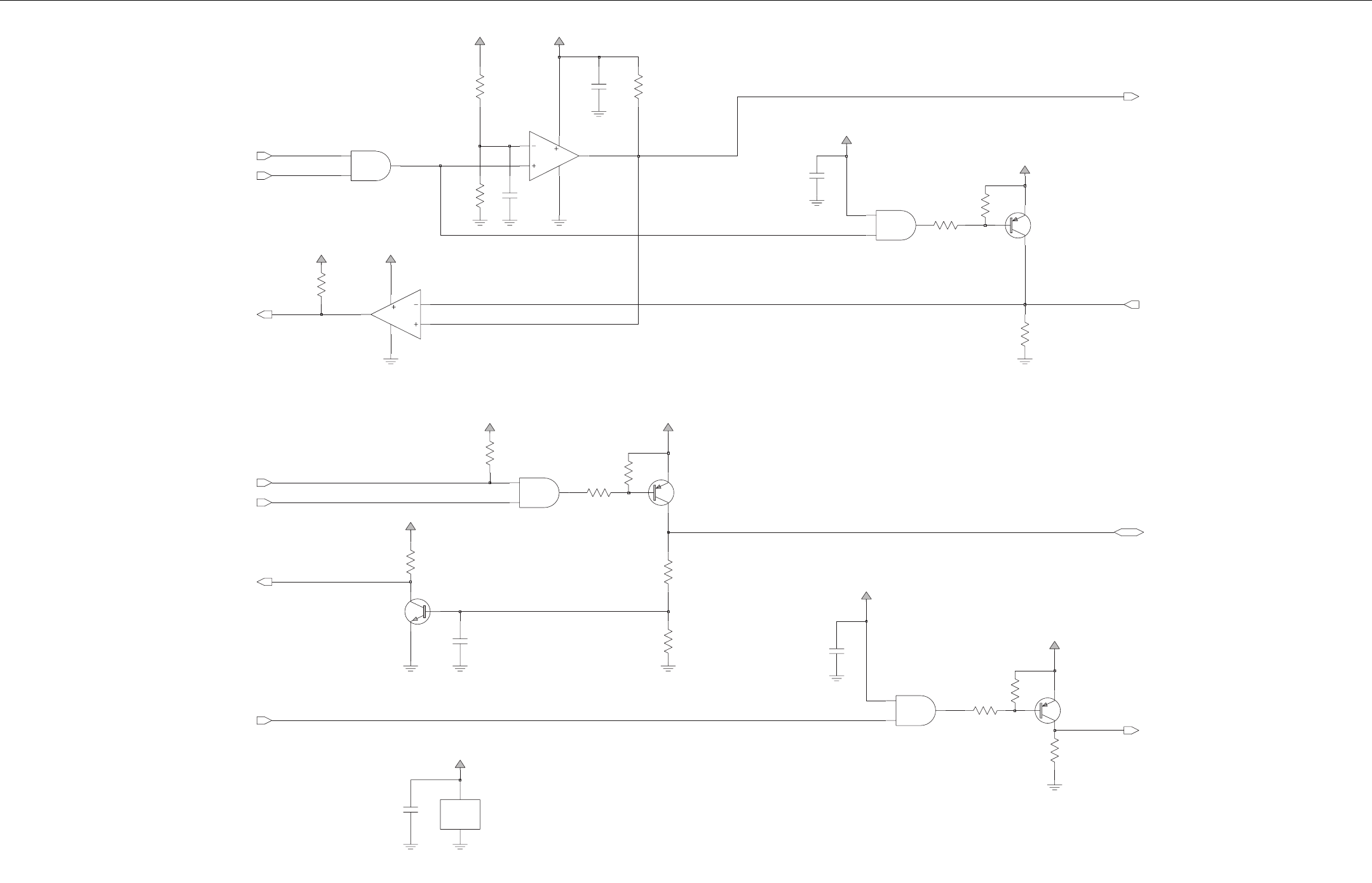
ENHANCED CONTROL HEADS: SCHEMATICS, PCBs and PARTS LISTS 8.2 - 19
Data Expansion Head Enhanced Main Board - SB9600 Interface (PCB: 8466586A01_A)
Q604
2.2K
R612
R611
10K
3V
Q603
4.7K
R610
Q602
10K
R608
C602
0.1uF
3V
5V
5V
3V
R606
4.7K
10K
R607
MC74AC08
U601-1
1
2
3
Q601
R604
10K
4.7K
R602
U601-2
MC74AC08
4
5
6
3V 5V
3V
5V
R601
4.7K
0.1uF
C605
C603
0.1uF
0.1uF
C606
4.7K
R615
4.7K
R603
3V
R614
2.2K
U601-5
PWR_GND
GND
7
VCC
41
R609
2.2K
12
13
11
R605
2.2K
MC74AC08
U601-4
9
10
8
3V
5V
R613
10K
MC74AC08
U601-3
06A02
U602-2
6
5
7
8
4
06A02
U602-1
2
3
1
8
4
C604
470pF
470pF
C601
R616
10K
SB9600_BUS+
SB9600_BUS-
RS232_RX
RTSA
SB9600_BUSY_OUT
SB9600_BUSY
SB9600_BUSY_IN
RESET
SB9600_RESET
RS232_TX
RS232_TXA
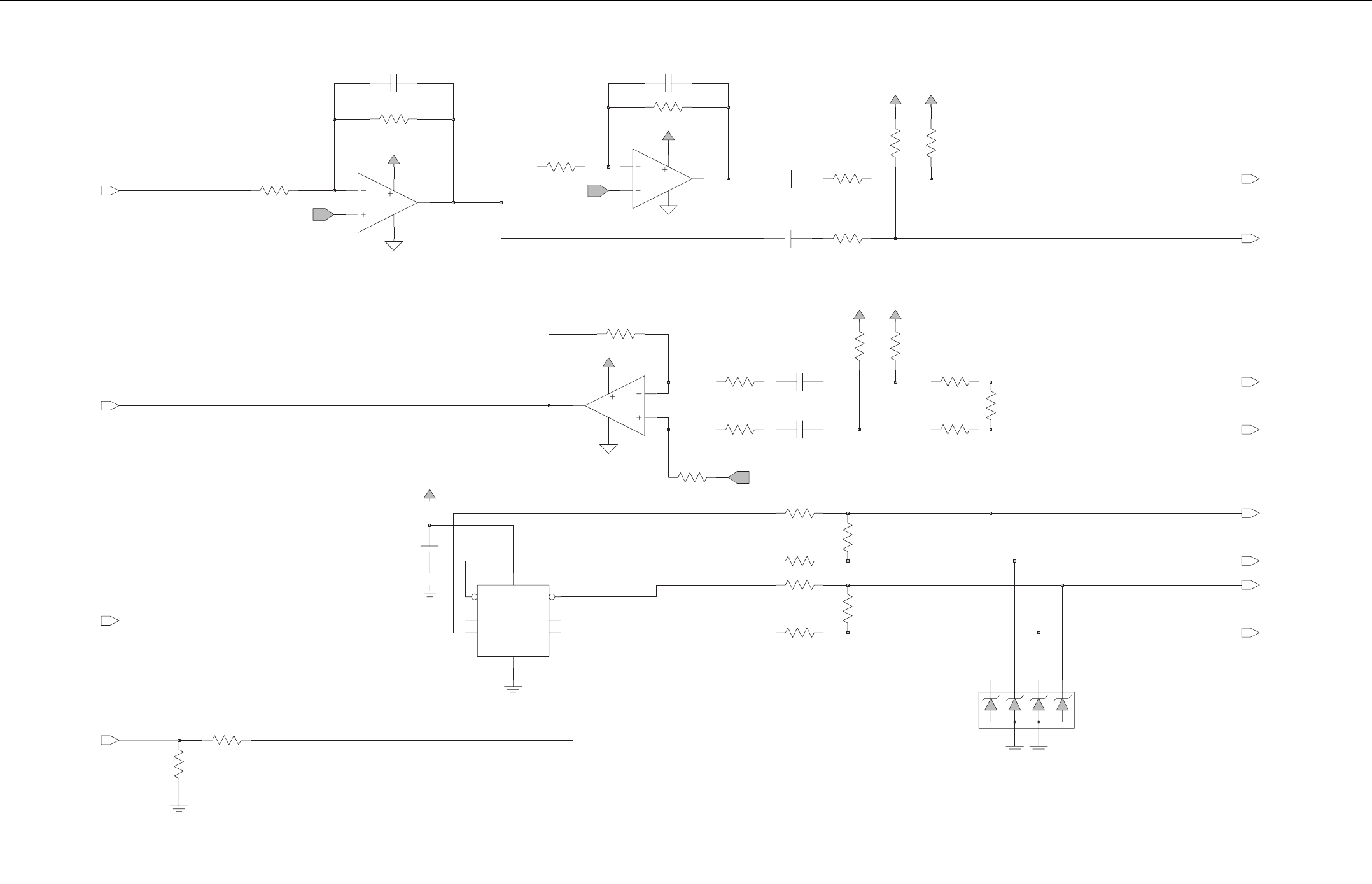
8.2 - 20 ENHANCED CONTROL HEADS: SCHEMATICS, PCBs and PARTS LISTS
Data Expansion Head Enhanced Main Board - Car Interface (PCB: 8466586A01_A)
G
G
G
R308
100K
10K
R303
R304
10K
150
R325
VAG_1
C305
1uF
470pF
C303
R301
10K
VCC
10K
R302
MC3403
U301-4
13
12
14
4
11
470pF
C304
R312
10K
10K
R309
10K
10K
R311
5
7
4
11
R310
C308
U301-2
MC3403 6
0.22uF
0.22uF
C307
68
R315
R316
68
R305
100K
R307
330
C306
1uF
U301-3
9
10
8
4
11
VCC
VCC
2
1
CCV
5
Y
6
Z
VAG_1
MC3403
SN65LBC179
8A
7B
3D
4DNG
R
VAG_1
U302
R320
330
R306
R321
33
33
R322
33
33
R323
2.2K
R319
R318
1.5K
0.1uF
C309
5V
VCC VCC
100K
R314
VCC VCC
R313
100K
R317
470
R324
150
2
5
1
6
3
4
car_tx_audio
car_rx_audio1
car_rx_audio2
car_rx_data1
car_rx_data2
car_tx_data1
car_tx_data2
car_tx_audio1
car_tx_audio2
car_rx_audio
car_tx_data
car_rx_data 20V
VR106
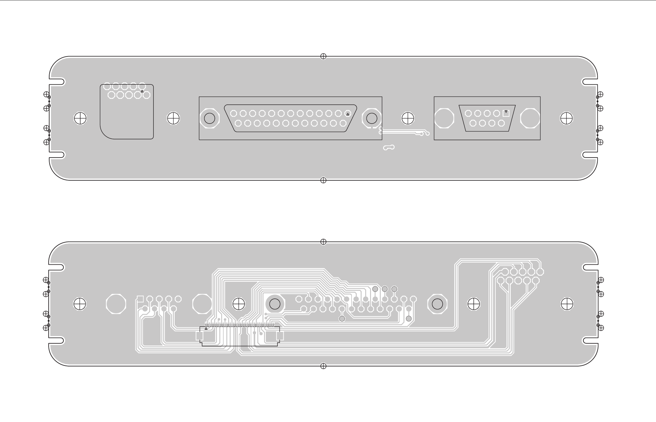
ENHANCED CONTROL HEADS: SCHEMATICS, PCBs and PARTS LISTS 8.2 - 21
PCB/ Data Expansion Head Enhanced Connector Board - Bottom and Top Side (PCB: 8464300B06_A)
2
3579
864 10
J0101
1
14
25
13
J0102
1
6
9
5
J0103
1
1
40
J0104
TP0151
TP0152
TP0153
TP0154 TP0155
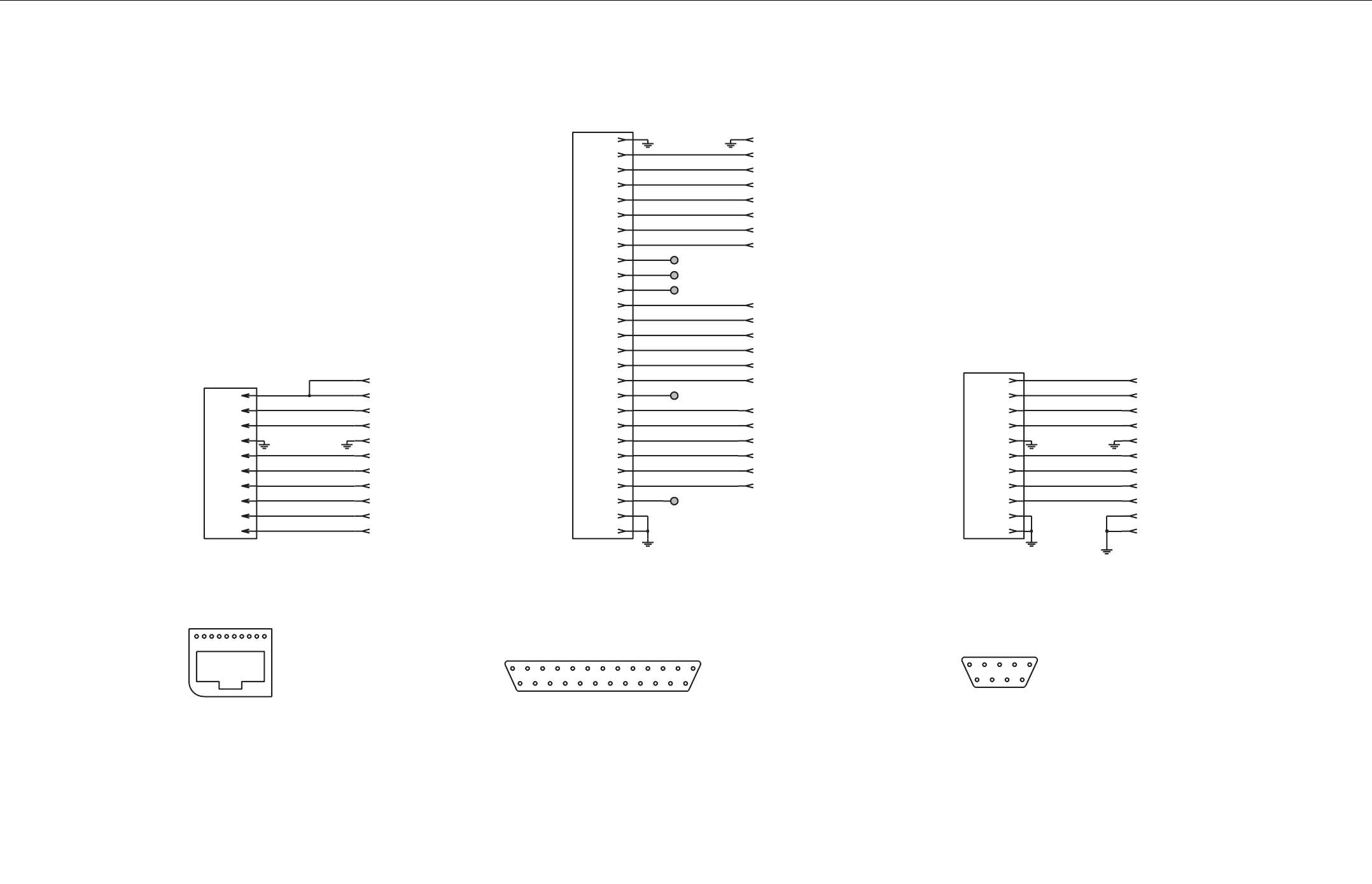
8.2 - 22 ENHANCED CONTROL HEADS: SCHEMATICS, PCBs and PARTS LISTS
19
7
67
89 12345
13
TELCO
CONNECTOR
J0101
12345
17
10
1516
89
101112
SUB-D 25 PIN
CONNECTOR
J0102
SUB-D 9 PIN
CONNECTOR
14
54321
9 Pin
6
J0103
2021222324 18
10 Pin
25 Pin
SUB-D
40 Pin
Part of FlexPart of Flex
40 Pin
9876
25
40 Pin
Part of FlexSUB-D
TELCO
J0103-7
J0104-18
J0104-14
J0104-23
J0101-6
J0102-15
J0102-16
J0102-13
J0102-14
J0104-1
J0102-12
J0104-33
J0104-21
g1 J0104-41
J0103-11 g2
J0103-10
J0104-7
J0104-40
J0104-9J0102-19
1
J0104-13
J0104-5
TP0152
1
TP0153
1
TP0151
1
J0104-36
TP0154
J0101-7
J0104-8
J0101-8
J0102-25
J0101-2
J0104-6
J0102-24
J0104-34
J0104-10
J0104-16
J0104-3
J0101-4
J0102-9
J0101-10
J0102-1
J0102-2
J0101-1
J0104-30
J0102-20
J0104-27
J0101-5 J0102-22
J0101-9
J0102-6
J0102-8
J0104-11
J0103-9
J0103-8
J0103-1
J0103-6 J0104-15
J0103-2
J0104-4
J0104-20
J0104-25
J0104-31
J0104-42
J0104-2
J0104-29
J0101-3
J0102-26
J0102-27
J0102-21
J0102-11
J0102-23
J0103-5
J0102-10
J0102-4
J0102-5 J0104-22
J0104-17
J0102-3
J0104-26
1
J0102-17
J0102-18
J0104-24
TP0155
J0104-12
J0104-28
J0104-19
J0104-37
J0104-39
J0104-35
J0102-7
J0104-38
J0103-3
J0104-32
FLT_A
J0103-4
Data Expansion Head Enhanced Connector Board - Connector Board (PCB: 8464300B06_A)
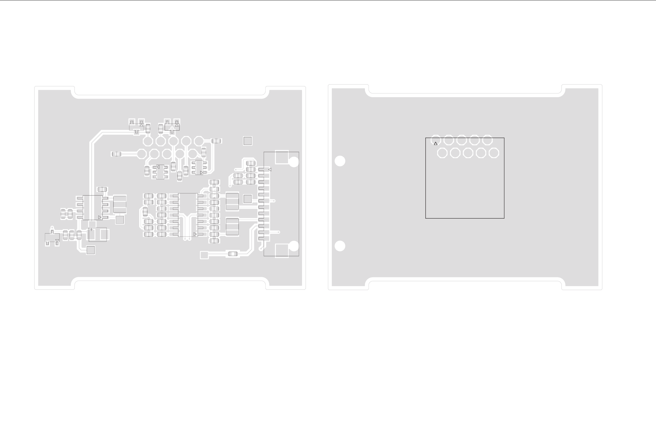
ENHANCED CONTROL HEADS: SCHEMATICS, PCBs and PARTS LISTS 8.2 - 23
PCB/ Remote Head Enhanced Main Board - Bottom and Top Side (PCB: 8471016L01_A)
C201
C202
C203
C204
C206
C301
C302
C303
C304
C305
C306
C307
C308
C309
C310
C311
C313
C314
F300
12 1
J301
2
3
Q101
R101
R102
R201
R202
R203
R204
R205
R301
R302
R303
R304
R306
R307
R308
R309
R310
R311
R312
R313
R314
R315 R316
R317
R318
R321
R322
R323
R324
R325
R326
TP301
TP302
TP303
TP306
1
4
58
U201
7
8
14
U202
VR301
VR302
VR303
VR304
Top View
J302
10
9
Bottom View
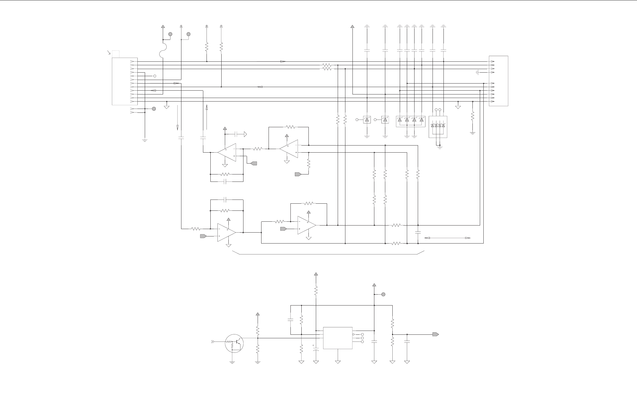
8.2 - 24 ENHANCED CONTROL HEADS: SCHEMATICS, PCBs and PARTS LISTS
Remote Head Enhanced Main Board (PCB: 8471016L01_A)
G
G
G
G
G
SPKR+
Balanced Audio
BUS+
Gabel Hybrid
SPKR-
INTERNAL MIC
ANA GND
SCI_TX
5VD
ON/OFF CONTROL
"BOARD-MARKER"
SCI_TX
AUDIO+
ON/OFF CONTROL
FLT_A+_REG
AUDIO-
BUS+
GND
ANA GND
SPKR+
0
GND
oiduA XT
FLT_A+
NC
ROTCENNOC OIDAR
SPKR-
SPKR+
FLT_A+
ANA GND
ROTCENNOC TNUOM ETOMER
HANDSET AUDIO
ON/OFF CONTROL
oiduA XR
BUS+
J301 - 12-pin Connector
SPKR-
J302 - 10-pin Telco
1
2K
3
3K
4
4
K
6
MMQA5V6T1
VR304
5V6
1A
2
2A
5
1
K
TP306
1
FLT_A+
R323
3.3K
9V3
R324
4.7K
C313
10uF
R322
6.2K
VAG_1
R321
12.4K
0
R318
20V
TP301
1
FLT_A+
MMQA20VT1
VR303
202C
FLT_A+
Fu01
R301
47.5K
R302
VAG_1
47.5K
47.5K
R307
47.5K
R316
47.5K
R317R310
47.5K
NU
VAG_1 47.5K
R312
0
R102
Fp28113C
R325
12.4K
R313
47.5K47.5K
R311
R304 0
0R303
NU
0
R309
NC
NC
NC
NU
R308
0
R201
80.6K
R202
12.4K
Fu210.102C
2A
32V
F300
FLT_A+
9V3
J301-1
J301-2
J302-7
J302-4
J302-9
J302-1
J302-3
J302-6
J302-8
J302-5
J302-10
J302-2
C301
10
R205
Fu1
10uF
9
10
8
4
11
602C
U202-2
6
5
7
4
11
U202-3
U202-4
13
12
14
4
11
2
3
1
4
11
470pFC302
U202-1
Fp28
413C
NU
NU
NU
C303 470pF
VAG_1
9V3
12.4K
R326
R314
R315
392
Fp074803C
392
Fp074703C
Fp074903C
Fp074603C
J301-14
Fp28013C
J301-13
J301-11
J301-12
J301-9
J301-10
J301-7
J301-8
J301-6
5
FEEDBACK
7
DN
G
4
INPUT
8OUTPUT 1
SENSE 2
SHUTDOWN
3
6
VTAP
J301-5
LP2951CD
U201
ERROR
C203 0.1uF
0.1uF
C204
VAG_1
3.3K
R204
R203
3.3K
R306
47.5K
J301-4
9V3
9V3
1
CN
CN
J301-3
NC
TP302
403C Fp074
1
Fp074503C
Q101
TP303
R1
R2
R101
12.4K
33V
VR302
33V
5V 5V
VR301
5V
5V
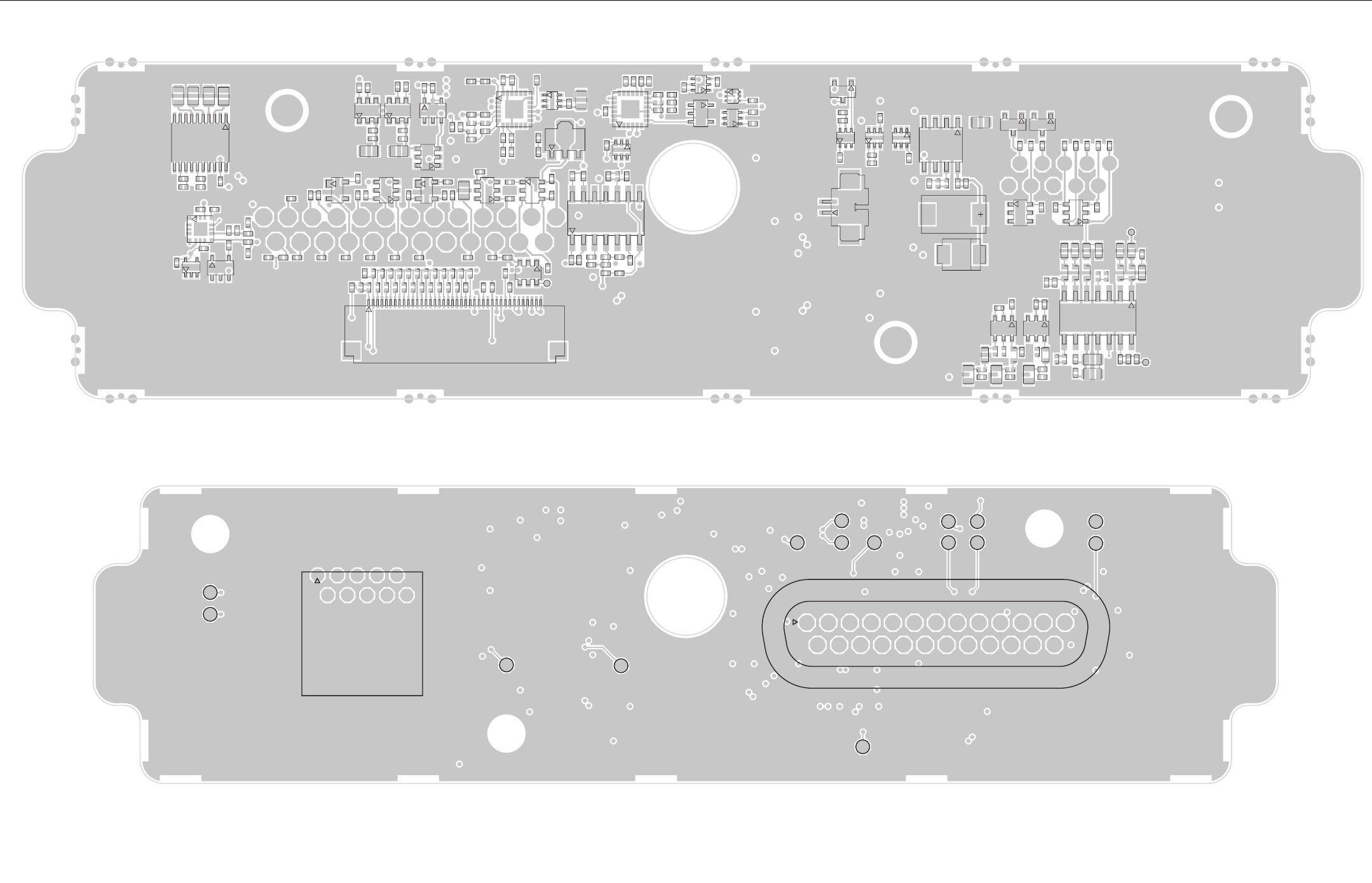
ENHANCED CONTROL HEADS: SCHEMATICS, PCBs and PARTS LISTS 8.2 - 25
PCB/ Remote Back Head Enhanced Main Board - Bottom and Top Side (PCB: 8466583A01_A)
8
14
20
2
13
25
J105
10 9
P101
TP101
TP102
TP103
TP201
TP203
TP204
TP206
TP207
TP208 TP209 TP301
TP302 TP303
TP304
TP305
C101
C102
C103
C104
C105
C106
C107
C108
C201
C202
C203
C204
C205
C206
C207
C208
C209
C210
C211
C212
C213
C214
C215
C216
C217
C301
C302
C303
C304
C305 C306
C307
C308
C309
C310
C311
C312
C313
C314
C315
C316
C317
C401 C402
C403 C404
C405 C406
C407 C408
C409 C410
C411 C412
C413 C414
C415
C416
C417
C418
C419
C420
C421
C422
C423
C424
C425
C426
C427
C428
C429
C430 C431 C432 C433 C434 C435
C436
C437
C438
C439
C440
C441
C442 C443
C444 C445
C446 C447
C448
C449
C450
C451
C452
C453
C454
C455
C501
C502
C503
C504
C505
C506
D301
D401
D402
20
40
G2
G1
J104
2
G1
G2
P201
Q201
Q301
Q302
Q305
Q306Q307 Q308
Q401
Q501
Q502
Q503
R102
R103
R201 R202
R203
R204
R205
R206
R207
R208
R209
R210
R211
R212
R213
R214
R215
R216
R217
R218
R220
R221
R222
R223
R225
R226
R227
R228
R231
R232
R233
R234
R235
R236R237
R238
R239
R240
R241
R242
R243
R301
R302
R303
R304
R305
R306
R311
R312
R313
R315
R316
R317
R318
R319
R320
R321
R322
R323
R324
R423
R424 R425
R426
R427
R428
R429
R430
R431
R501R502
R503R504
R505R506
R507
R508
R510
R511
R512
R513
R514
R515
R516
R518
R519 R520
R521
R522
R523
R530
R531
R532
R533
R534
R535
R536
R537
R538
R539
R540
R541
R542
R547 R548
R549
R550
R551
R552
R554
R555
R556
R557
TP202
TP205
TP401
7
814
U201
U203 U204
1
4
58
U205
U301
5
913
U302
10
2011
U303
U304
U401
6
12 18
U501
6
12
18
U502
7
8
14
U503
U507
VR101VR102
VR103
VR104
VR201
VR401
VR402
VR403
VR405
VR406
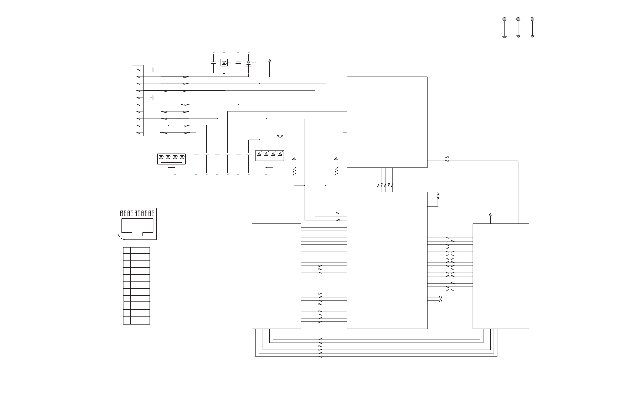
8.2 - 26 ENHANCED CONTROL HEADS: SCHEMATICS, PCBs and PARTS LISTS
Remote Back Head Enhanced Main Board - Block Diagram (PCB: 8466583A01_A)
+S
UB
+
O
IDUA
2
1
0
1
+A_
T
LF
XT
_
IC
S
L
O
R
T
NO
C
_F
F
O
_
NO
+
A_
T
LF
+O
ID
U
A
DNG
1
01P
wei
V
tno
r
F
-RK
P
S
5
D
N
G
-
O
ID
U
A
+R
K
PS
+SU
B
V
5
=
CCV
8
9
8
7
U
N
3
21
6
5
4
3
7
1
01P
01
FFO/NO
46
-
RKPS
+RKPS
-O
I
DUA
TNUOM
ET
OM
E
R
R
O
T
CE
NN
O
C
XT_ICS
TNUOM ETOMER
V02
ROT
C
E
N
N
O
C
9
5
C
N
7
6
1
3
4
6
401RV
2
5
01
101P
9
5_DWS
2
0
1
C
4
F
p
0
7
4
2
3
7
0
1
C
Fp074
K
01
5
0
1C
Fp
33
MV_
2
BSU
P
V
_
2
B
S
U
V5_BSU
+D_BSU
-D_BSU
B
1
_
S
U
B
V
2_SUB
V
201R
STR_
2
3
2
S
R
XR_23
2
S
R
XT
_
2
3
2
S
R
S
T
R
XR
XT_ICS
KL
C
_
I
S
S
SF_I
S
S
XT
NEUP_2BSU
VCR_2BSU
0ES_2BSU
DEEPS_2BSU
PSUS_2BSU
DXT_2B
SU
N
E
XT_2BSU
9_O
I
PG
QER_OIPG
7
_
IPG
HANDSET
HANDSET_AUDIO
L
C
S
_
C
2I
ADS_C2I
NO_NGI
E
S
N
E
S
_
N
GI
MIC
MIC_REAR_1
MIC_REAR_2
LORTNOC_FFO_
N
O
NO_IACG
_
MR
R
L
C
_
N
O
_
R
W
P
_I
A
C
G_M
R
S
T
C_23
2
S
R
Fp
0
74
TCENNOCRETNI
2_NA
+
S
U
B
S
TC
0_
O
I
P
G
3_
O
I
P
G
4
_O
I
PG
5
_OIPG
6_
O
IPG
8
_O
I
P
G
1
5_DWS
60
1C
8
Fp
0
74
GE
R
_+A
_T
LF
N
O_NG
I
E
SN
ES
_
NG
I
MIC_SEL
N
O_I
A
CG
_
M
R
R
L
C
_
N
O
_
R
WP_
I
AC
G
_
M
R
SWD_5
USB1_REAR_DET
USB2_REAR_DET
VBUS1_FET_ENA
VBUS2_FET_ENA
1
0
1C
B
1
_
S
U
B
V
2_SUBV
OI
AUDIO_SEL
GCAI_OPT_5V_EN
GCAI_OPT_5V_SET
0
_
O
IP
G
3
_O
I
P
G
4_OIPG
5_
O
I
PG
6
_
OI
P
G
8_OIP
G
9_OIPG
QER
_
OIP
G
7
_IP
G
L
C
S
_
C
2
I
ADS_C2I
USB1_REAR_DET
+D_2BSU
-D_2BSU
NEUP_2BSU
VCR_2B
S
U
USB2_REAR_DET
0ES_2BSU
D
E
E
P
S
_
2BSU
PSUS_2BSU
DXT
_
2
B
S
U
NEXT_2BSU
MV_2BSU
PV_2BSU
V5_BSU
VBUS1_FET_ENA
VBUS2_FET_ENA
232
S
R-
B
S
U
S
T
C
GCAI_OPT_5V_EN
GCAI_OPT_5V_SET
ST
C
_23
2
SR
ST
R_
23
2
SR
X
R
_23
2
SR
XT_
2
32S
R
S
T
R
X
R
XT
MIC_REAR_1
MIC_REAR_2
L
ES_C
I
M
+R
K
PS
-
RKP
S
V33
10
1
RV
4
0
1C
O
ID
U
A
+
OIDUA
-OI
D
UA
L
ES_
O
I
D
U
A
HANDSET
HANDSET_AUDIO
MIC
3
0
1
P
T
Fp074
2
0
1
P
T
C
C
V
GE
R_
+A
_
TL
F
101P
T
F
p3
3
801C
C
N
2
5
1
3
4
6
3
0
1
RV
Fp
0
74
3
0
1
C
2
0
1
RV
V33
K7.
4
301
R
5_DWS
2
_
NA
2
_
NA
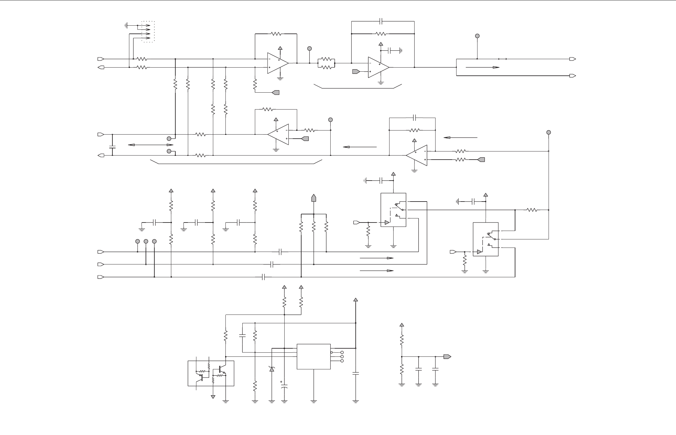
ENHANCED CONTROL HEADS: SCHEMATICS, PCBs and PARTS LISTS 8.2 - 27
Remote Back Head Enhanced Main Board - Audio (PCB: 8466583A01_A)
G
G
K01
K01
K
01
K01
G
G
G
G
oiduA XT
UN
UN
oid
u
A d
e
cnala
B
U
N
U
N
UN
UN
2
=
n
ia
G
dirb
y
H lebaG
ro
tce
n
noC niP 52
m
o
rf
O
CLE
T lop01 o
t
o
i
du
A
XR
UN
UN
OCLET lop01 ot
oidu
A X
T
P
M
M t
n
orF mo
rf
)I
AC
G
(
P
M
M t
no
r
F
o
t
rotce
nno
C
D
-BU
S
n
i
p52 ot
oid
uA
XT
r
o
tce
n
noC niP
52
mo
r
f
90
2
R
K
2
.
3
4
K
5.74
5
2
2
R
29
3
5
1
2
R
11
2
R
K5.7
4
K
01
53
2
R
0
30
2
R
702R
K5.
74
0
CN
402R
1
2
2
R
K7.4
13
2
R
K5.74
402PT 1
K
51
3
22
R
622R
V
9
001
GER_+A_TLF
K5
1
7
1
2
R
V9
342R
F
u01
K01
902C
30
2
C
Fu
1
.0
K5.74
8
02
R5
0
2
R
K
5.74
612
C
Fu01
3
043CM
1
02U
2
3
1
4
11
V9
Fu1
.
0
412
C
K
5
.74
212R
0
202R
K
C
A
B
D
E
EF
7
GND
4
T
UP
N
I
8T
UPTUO 1
E
S
NE
S2
NW
OD
T
UH
S
3
6
P
AT
V
O
N
6
VPOS 2
DC1
592
P
L
50
2
U
RO
RR
E5
TU
E
4
4
54X
A
M
M
O
C
5
3GND
NI
1
C
N4
F
u1.
0
402
U
502
PT
1
1
_G
A
V
51
2
C
K
0
1
022R
1_
G
A
V
00
1
4
32
R
5
7
4
11
K01
3
3
2
R
304
3
C
M1
02U
6
2
22
R
K51
10
2Q
Fu
510.
C
CV
10
2
PT
1
5
0
2C
9
32R
V9
G
ER_
+
A_
TL
F
V9
2
42
R
065
1
VAG_1
1_G
AV
V9
K001
31
2
1
4
1
4
1
1
302P
T
102
U
3
0
4
3
C
M
Fu01
3
12C
602C
F
u1
Fu1
402C
V
9
21
2
C
Fu01
4
12
R
0
01
612R
065
K7.4
8
22R
202C
Fu1.0
V
81
10
2
R
V
F
u
1
.
0
1
_G
A
V
C
N
V
9
V9
112
C
8
3
2R
065
632R
00
1
0
1
2C
Fu01
602R
K5
.
7
4
10
2
R
K5.7
4
K001
04
2
R1
4
2
R
K00
1
2
93
81
2
R
902P
T
80
2PT
702P
T
K
01
6
0
2P
T
7
32R
3
1
2
R
1
02
P
00
1
C
N
V
9
V
9
3
02U
MOC
5
3GND
NI
1
C
N4
ON
6
2
VPOS
Fu1
T
U
E44
5
4XAM
30
43
C
M
9
01
8
4
1
1
10
2C
702C
10
2
U
2
02
P
T
1
F
u0
1
Fu01
71
2C
01
2
R
K5.
74
Fu
1
.0
80
2
C
23
2
R
K
01
72
2
R
K18.6
1
_
G
A
V
OI
D
U
A_
T
E
S
D
N
A
H
2_
RAER_CIM
CIM
1_R
A
ER_
CIM
LES_OIDUA
T
E
S
DN
A
H
-
RKPS
+
RKPS
-OIDU
A
+
OIDUA
LES_CIM
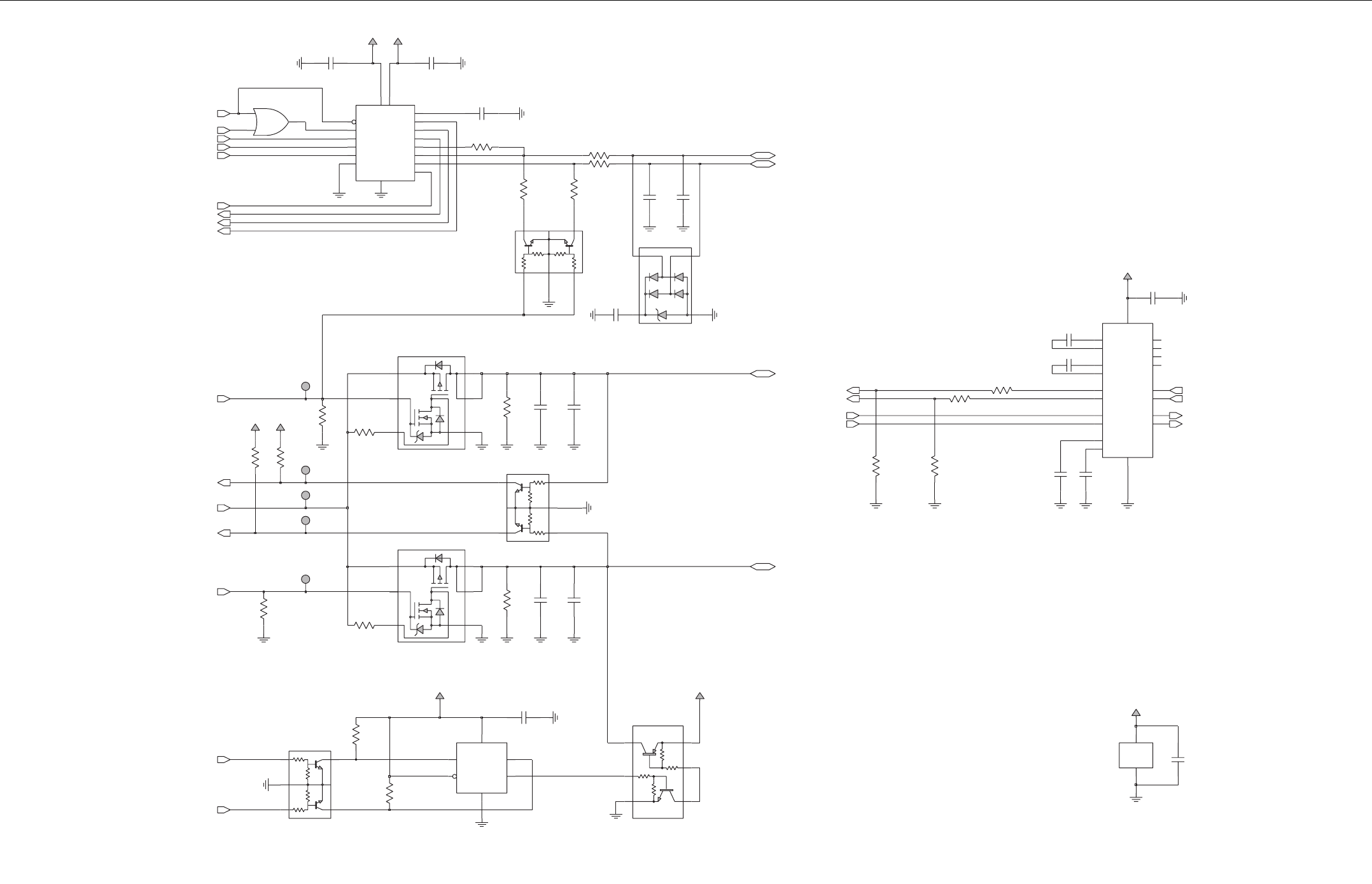
8.2 - 28 ENHANCED CONTROL HEADS: SCHEMATICS, PCBs and PARTS LISTS
Remote Back Head Enhanced Main Board - USB/ RS232 (PCB: 8466583A01_A)
k7
.
4
k7
.
4
k
74
k
74
DTr2
DTr1
4.7k
4.7k
47k
47k
2rTD
1rTD
k
7
.4
k
7
.4
k
74
k
7
4
DTr2 DTr1
OPT_5V
U
N
UN
2
3
2SR E
R
IW
-4
L
E
S_E
D
O
M
_
2
BSU
81
3R
K51
313R
8.2
_
C
CV
K
0
1
K
0
1
5
1
3
R
F
u
1.
0
21
3
C
103PT
503PT
3
03P
T
40
3PT
5
0
3
C
8
.2_CCV
203P
T
3
PV
5
1
UPV
3
1
GERV
Fu1.0
1N_EO 2
VCR
8
DEEPS
5DNPSUS
14
VBUS
7
VCC
4
MV
11 OPV_OV
2
0
3
U
9
GE
N
D
01
S
O
P
D
61 ETA
R
EMUN
E
2
1OMV_
0ES
F
17 GND
E
DOM
6
8
VCC 19
G
E
N
V
7
3SOPV
50
1
1
P
SI
4C
N
NI
1
R6
1
T
UO1
R
5
1
NI
2R 9
TUO2
R
2
1
N
I
1
T
4
1T
UO1
T7
1
N
I
2
T
3
1T
U
O
2
T
4SO
P1
C
2
G
E
N2
C
6SO
P2
C
5
GND
18
1C
N1
2C
N0
1
1
1
3
C
N0
2
8.
2
_C
CV
3
03U
E2
323XA
M
GE
N1
C
K
0
1
15K
12
3
R
4
5
3
2
R322
L
0336
CD
F
70
3
Q
61
Fu
1.
0
F
p0
7
4
61
3C
2
0
3
C
8
0
3
C
F
u
1
.
0
F
u1.
0
6
0
3
C
K00
1
423
R
K
0
0
1
4
V
5
_WS
U
3
23R
103QA
8GM
F
1
2
5
3
203Q
R2
TF
9DME
2
5
6
3
1
4
V5
_W
SU
1PC 3
D
2
GND
4
Q
5
VCC
403
U
X6
P
5
71
Z
S7C
N
6C
Fu1.
0
513
C
6
13
R
K0
1
R317
61
4
5
3
2
15K
1
2
4
60
3
Q
L0336CDF
7
13
C
1
03U
2
3Z
S
7CN
F
u
1
.0
3
0
3
C
2
1
3
R
K
5
1
8.
2
_
C
CV
3
.
3
_
C
C
V
Fu
1
.0
6
0
3
R
3
3
3
3113
R
91
3
R
K
1
K
01
F
p3
3
403R
9
03
C
103
C
Fu
1
.0
50
3Q
3
DN
G
5
C
C
V
1
03
U
103D
Fu
1.
0
3
1
3C
K5
.
1
5
0
3
R
Fu0
1
1
13C
1
2
5
3
4
K
7
.
4
80
3
Q
A8
G
MF
K7.4
30
3
R10
3R
20
3
R
Fu1.0
K
1
Fp3
3
4
0
3
C
01
3
C
Fu0
1
4
13C
K
0
1
0
2
3
R
70
3
C
C
CV
Fu
1
.0
ANE_TEF_1SUBV
A
NE
_TEF_2S
U
BV
T
ED_RAER_2BS
U
V
5
_BSU
TE
D_R
AE
R_1BS
U
N
E
_
V
5_TP
O
_IAC
G
T
ES_V5
_T
P
O_
IA
CG
B1
_
S
U
BV
2_SUB
V
PV
_2
BS
U
N
EXT
_
2BSU
X
T
_
2
32S
R
S
TR
_
2
3
2
S
R
S
T
C
_
2
32
S
R
X
R
_2
3
2
S
R
STC
ST
R
XR
XT
-D
_2
B
S
U
DXT_2BSU
0ES
_
2BS
U
PS
US_2BSU
NE
UP
_2BSU
D
E
E
P
S_2BSU
VCR_
2BSU
+
D_
2
B
S
U
MV
_
2BSU
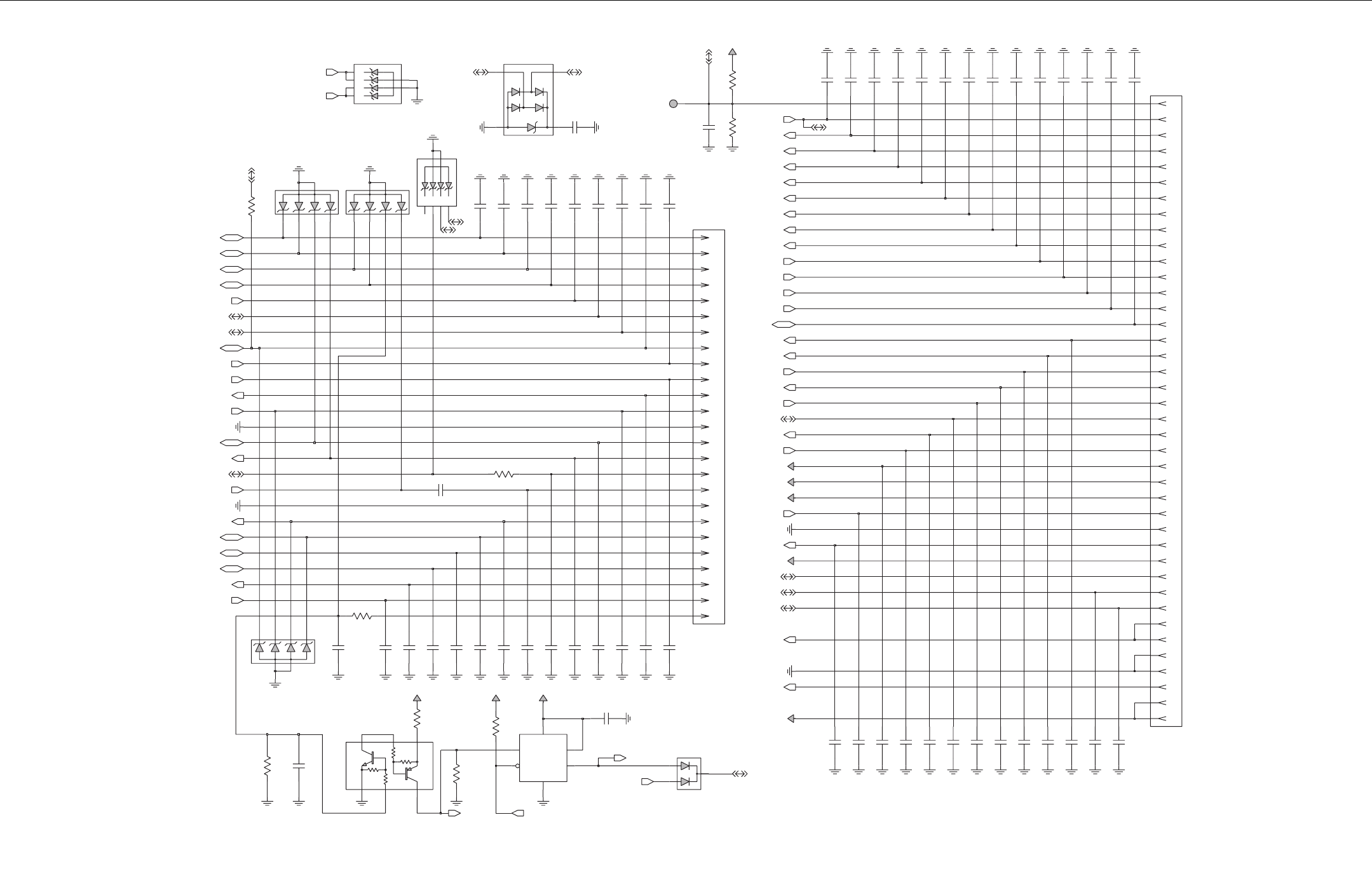
ENHANCED CONTROL HEADS: SCHEMATICS, PCBs and PARTS LISTS 8.2 - 29
Remote Back Head Enhanced Main Board - Interconnect (PCB: 8466583A01_A)
K0
1
K01
K
0
1
K0
1
n
iP
52
UN
U
N
V
0
2
V02V02
V5
=
nno
C
U
N
UN
N
O_R
WP
MER_HS
A
D
U
N
n
iP 04
n
n
o
C
1
0
4
D
3
24
R
3
3
1
2
81
91
F
p3
3
3
14
C
Fp
3
3
9
04
C
51
6
04RV
2
7
F
p
33 Fp
0
7
4
4
14
C
80
4
C
32
4
C
F
p0
7
4
9
1
6
71
9
1
4
C
F
p
07
4
8
2
4R 45
4C
Fu
1
.0
12
K7
.
4
5
VCC
22
1
0
4U
X6P5
71
Z
S
7CN
6C
1PC 3
D
2
GND
4
Q
124C
C
CV
F
p
33
1
F
p
0
74
50
4
C
4
2
401J
6
2
4
C
F
p3
3
8
14C
F
p0
7
4
5
2
4C
Fp
3
3
74
4
C
Fp33
Fp074
0
5
4C
22
9
4
4C
Fp33
Fp3
3
2
34
C
7
0
4
4
C
9
3
Fp33
0
4
63
8
3
10
4
P
T
1
8
1
7
1
6
1
5
1
51
4
C
Fp
33
32
0
2
4C
F
p0
7
4
3
V
5
_WSU
4
3
2
V
5
_WSU
42
4
2
K01 7
24R
52
Fp
07
4
6
3
4
C
Fp
3
3
0
14
C
Fp0
74
24
4
C
Fp33
93
4C
6
1
4C
8
2
4C
F
p074
1
1
Fp074
9
6
2
Fp
33
2
1
4C
92
6
04
C
F
p07
4
03
4C
F
p0
74
4
2
4
R
F
p
3
3
4
0
4
C
33
F
p0
74
GER_+A_TLF
3
5
9
24C
1
3
204D
5
0
1
J
1
8
3
4
C
F
p0
74
02
43
F
p
0
7
4
4
2
4C
44
4
C
Fp33
61
F
p
33
7
04
C
5
24R
K1
2
3
F
p
07
4
7
1
4
C
Fp3
3
53
4
C4
3
4
C
F
p
074
3
1
21
8
0
1
V
5
_WSU
8
.2_
C
CV
K2
K3
K4
4
1
50
4
R
VV
6.
5
A1
A2
K1
204RV
02
1
0
4RV
55
4
C
304
C
F
u
1
.
0
Fp
3
3
F
p
0
7
4
2
5
4C
1
44C
Fp33
72
7
2
4C
Fp074
8
2
Fp3
3
334C
K
00
1
0
34R
8
2
K
3
K
4
K
6
V
6
.5
1
A
2
A
1
K
7
3
3
0
4RV
74
624R
2
1
03
53
3
1
3
3
8.2_C
CV
2
2
4
C
F
p3
3
52
7
3
4C
Fp074
F
p
33
6
4
4C
15
4C
54
4C
Fp
3
3
20
4
C
F
p33
Fp33
F
p
07
4
F
p
33
844C
13
4C
K001
1
0
4
C
V
5_WSU
134
R
Fu01
Fp
0
7
4
3
5
4
C
1
0
4Q
5
K
7
.4
9
24
R
9
1
1
0
1
Fp33
3
44C
41
3
.
3_CCV
11
4
C
Fp
3
3
RL
C_
NO_
RWP_IA
CG
_
M
R
2
_S
U
BV
B
1_SUBV
N
O
_
MR
NO_NGI
N
O
_IA
CG_M
R
ESNES
_
N
GI
E
R
IW
_1
3
_
OI
P
G
4_OIP
G
TESD
NA
H
5_OIP
G
X
R_
23
2SR
X
R
+D_RAER -
D_
R
A
E
R
B1_S
UBV
STC
_2
3
2S
R
+
D_
RAE
R
2_RAER_CIM
0
_
OI
P
G
2_NA
2
_
NA
2
_
NA
7_
IP
G
3_N
A
NO_
MR
C
I
M
OID
UA
_TESDNA
H
STR
ST
C
Q
E
R
_
OIPG
N
EUP
_2
B
S
U
DE
E
P
S_2
B
S
U
L
ORT
N
OC
_FF
O
_N
O
KL
C
_ISS
-D_RAER
+
D_R
AE
R
-D
_
RAER
P
S
US_
2
B
S
U
X
T_
23
2SR
S
T
R
_
2
32S
R
+D_BS
U
-
D_BS
U
V5
_BSU
XT
_ICS
+
S
UB
XT
LCS
_
C2I
A
DS_C2I
P
V
_2BS
U
MV_
2
B
S
U
V
C
R_
2BS
U
NEX
T
_
2BS
U
DX
T_
2BS
U
0ES_
2
B
S
U
S
F_I
SS
3_NA
1
_NA
1
_
RAE
R_
CI
M
8
_O
IPG
6_OIPG
9_OIPG
2_SU
BV
E
R
IW
_
1
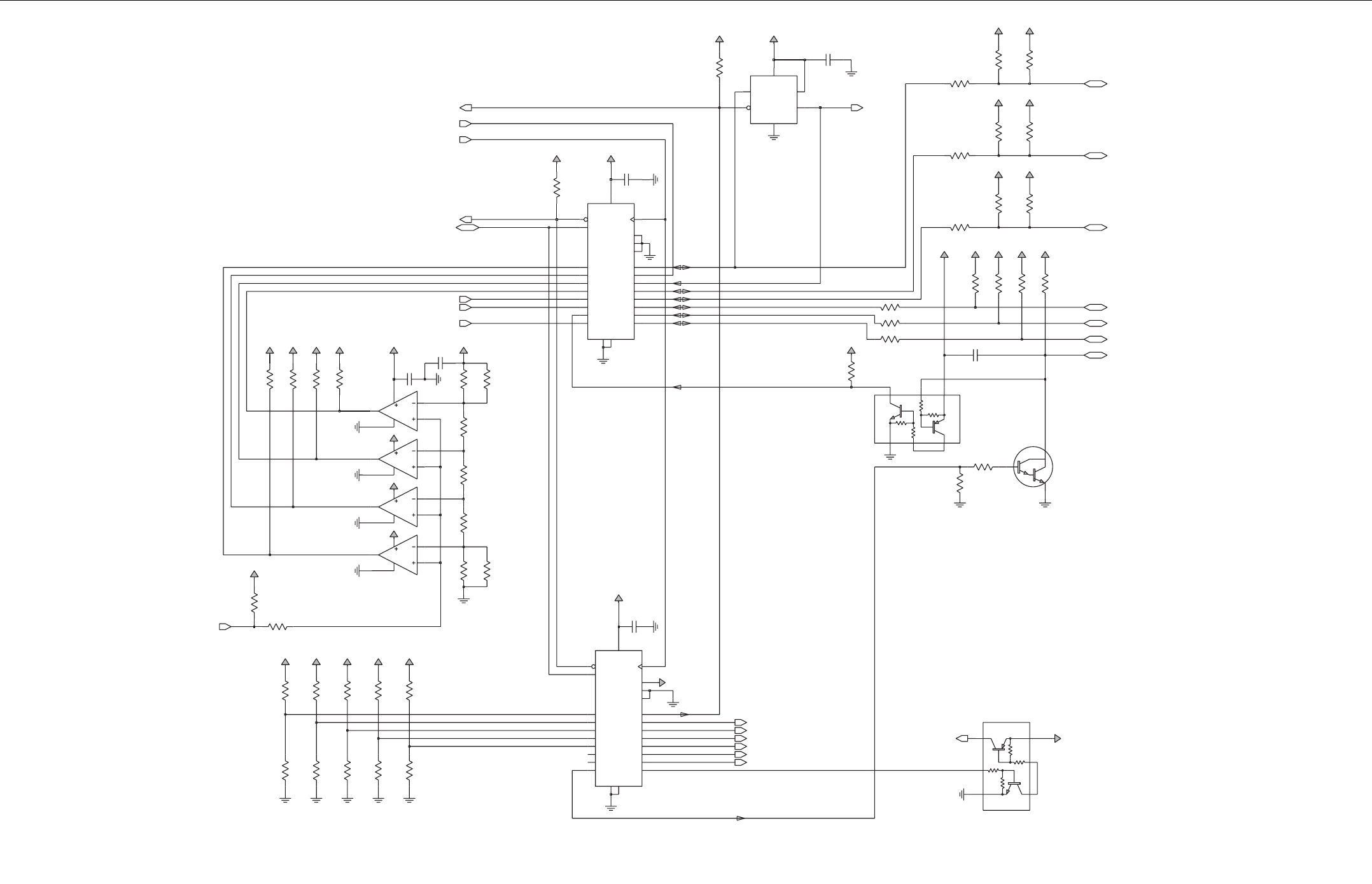
8.2 - 30 ENHANCED CONTROL HEADS: SCHEMATICS, PCBs and PARTS LISTS
Remote Back Head Enhanced Main Board - IO (PCB: 8466583A01_A)
K
0
1
K
0
1
K
0
1
K
01
10K
10K
10K
10K
OI
l
lu
f
osl
a
t
u
b
,N
I
ot
s
t
lu
af
eD
BCP niaM morf
B
SU
h
tiw derahs
s
i
1_O
I
PG
V
5 = CCV
k
o
oH 9 n
iP
IA
C
G
T
UO 9_OIPG
V521.3
raelC nO rwP
IACG
etom
eR
UN
B
CP n
i
aM morf B
SU
h
t
i
w de
r
ahs si 2
_
OI
P
G
n
Or
wP
0
_OIPG
V578
.
1
0
1
niP
IA
CG
e
s
ne
S
n
O
r
wP
IA
C
G
e
t
o
m
e
R
UN
U
N
U
N
OI ll
u
f osl
a
t
u
b
,N
I ot
s
t
l
uaf
eD
UN
V000.0
TTP
2 n
i
P IA
C
G
V
0
00
.
5
UN UN
V
5
26
.
0
UN
D
I
W
H
V573.4
U
P
+
S
U
B
d
n
a XT
_
ICS r
of 5_DWS etareneg
UN
VCC
20
5
R
0
7
2
7
05
U
X
6
P
57
1
Z
S
7CN
6C
1P
C3
D
2
GND
4
Q
5
6
1
P
6
1
71
P
7
1
L
C
S91
ADS
02
VCC 21
CCV
60P 7
70P 8
0
10
1
P
11P
11
2
1
P
2
1
31 31P
41P
41
5
1
P
51
GND2
T
NI
22
1
0
0
P
10P 2
2
0
P3
4
30P
4
0
P5
6
5
0
P
S
B
53
5
9
ACP
0
A8
1
1
A3
2
2A 4
2
GND1
9
25
0
1
1
1
31
3
21
C
CV
8
.2
_C
C
V
20
5
U
8
9
4
1
3
21
1
0
92
M
L
305U
6
7
1
3
2
1
3
05U
1092ML
4
5
2
3
2
1
109
2
ML
3
0
5U
305U
1092ML
K7.4
21
5
R
455
R
305C
Fu1
.
0
K
5
1
3
.
3
_
CC
V
8.
2
_C
C
V8.2_
C
C
V
8
.
2_CCV
K51
5
05R
3
.
3
_CCV
K51
4
35R
8.2
_
C
CV
7
05
R
71P
91
LCS
02 A
D
S
21
VCC
K51
70P
0
1
P
0
1
1
111P
2
121P
3
13
1
P
41 41P
51 51P
6
16
1
P
7
1
T
NI
0
0
P1
2
10P 3
20P 4
3
0
P5
40P
50P 6
7
60P 8
105U
S
B
5359ACP
8
1
0
A32
1
A42
2A
9GND1
GND2
25
2
2
04
5
R
60
5R
0
72
3
0
5R
K2.33
CCV
K
5
1
K
7
.
4
325
R
CCV
K5
1
8
1
5R
2
4
5R
K
2.
3
3
K2.33
7
45
R
K2
.
33
055
R
V
9
80
5
R
Fu1.0
6
05
C
1
55R
3.3_C
C
V
K
0
0
1
93
5R
K2.33
K
5
1
83
5R
K51
8
4
5R
K2.33
3
0
5
Q
K
2.
3
3
945R
255R
K51
K
51
635R
K2.33
10
5
Q
145R
K
51
2
35R
0
7
2
335
R
K51
4
1
5R
8.
2_
C
CV
F
u1
.
0
10
5
C
9
15
R
K
0
1
V
9
G
E
R
_
+
A
_T
L
FGER
_
+A_
T
L
F
F
u1
.
0
V9
V
9
K
5
1
1
0
5R
40
5C
K
51
1
25R
CCV
8
.2
_C
C
V
V
5_
W
S
U
8.2_CCV8.
2
_CCV
K51
0
3
5R
20
5Q
61
5R 0
7
2
8
.
2_CCV
V
5
_
WS
U
8
.
2_C
C
V
K
51
55
5
R
K
51
65
5
R
1
15
R
K
7
.
4
0
7
2
5
1
5R
K
5
1
8
.2_
C
CV
CC
V
535R
K
51
7
55R
505C
V
5_
W
S
U
0
7
2
40
5R
F
u
1.
0
K7
.
4
2
0
5C
225R
8
.2_CCV
VCC
Fu
1
.0
0
2
5R
K
5
1
K7
.
4
0
1
5R
8
.2_C
C
V
CCV
K7.4
315R
1
3
5R
K
51
7
35R
K51
5
_
O
I
PG
8
_
OI
PG
9_OI
PG
6
_OIPG
LCS
_C2I
QER_OIPG
A
D
S_C2
I
A
NE
_TEF
_
2SU
BV
L
ES_CIM
TES_V
5_
TP
O
_IAC
G
ESNES_N
G
I
R
L
C
_N
O
_
RWP
_
IA
C
G
_MR NO
_IA
C
G
_
M
R
LES
_OI
D
UA
ANE_TEF_1S
UBV
TED
_
RAER
_2BSU
NE_V5_TPO_
IA
CG
5_DWS
0
_
OI
P
G
3
_
OI
P
G
4
_
OI
P
G
NO_N
G
I
TE
D_
RA
E
R_1BSU
7_
IP
G
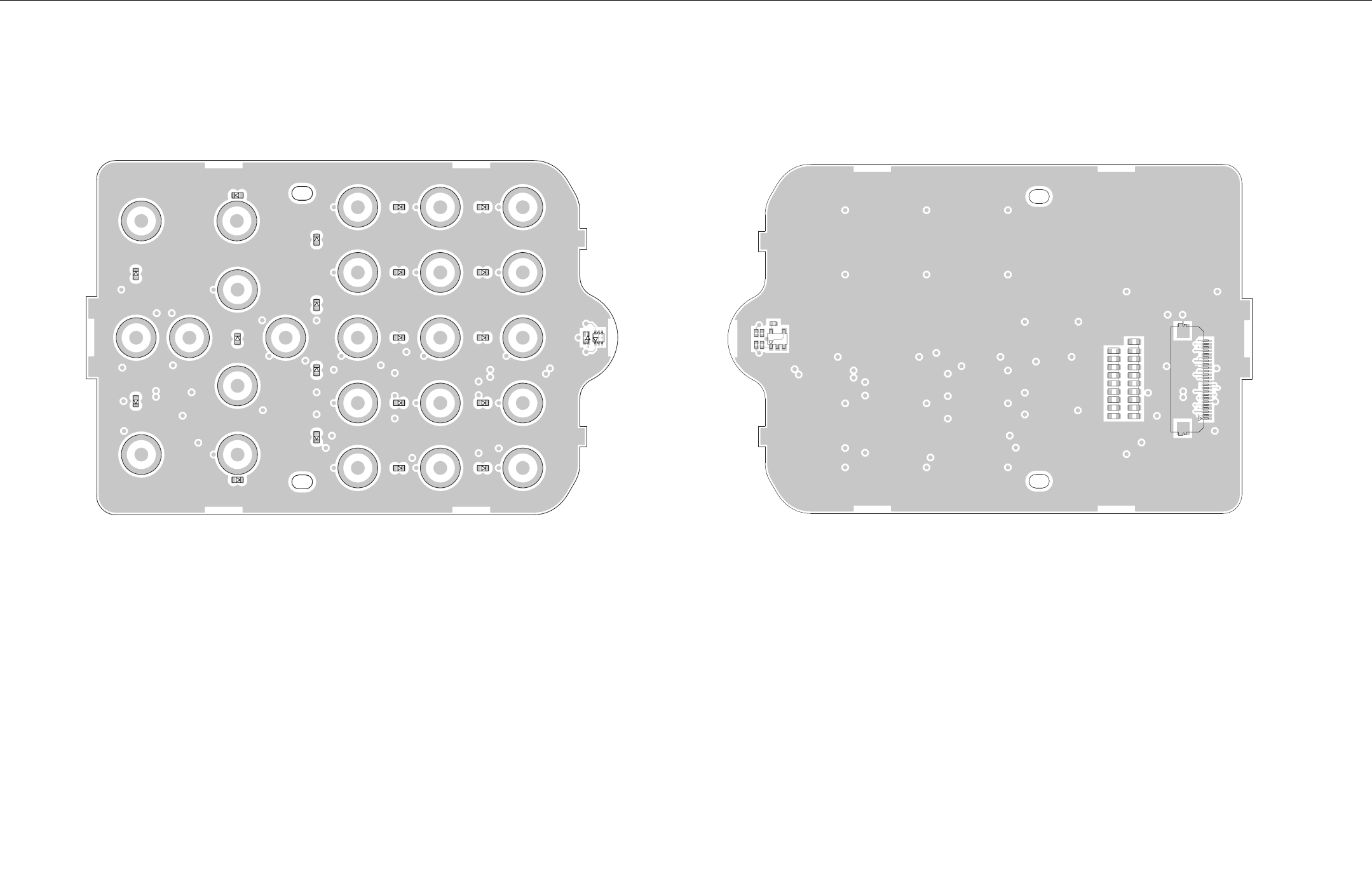
ENHANCED CONTROL HEADS: SCHEMATICS, PCBs and PARTS LISTS 8.2 - 31
PCB/ Enhanced Control Head Keypad Board - Bottom and Top Side (PCB: 8466581A01_A)
D1
D2 D3
D4
D5 D6
D7
D8
D9 D10
D11 D12 D13
D14
D15
D16
D17
D18
D19
D25
DS1
S1
S2
S3
S4
S5
S6
S7
S8
S9
S10
S11
S12
S13
S14
S15
S16
S17
S18
S19
S20 S21
S22
S23
S24
Top View
C1
C2
J1
R1
R2
R3
R4 R5
R6
R7
R8
R9
R10
R11 R12
R13
R14
R15
R16
R17
R18
R19
R20
R21
R22
U1
Bottom View
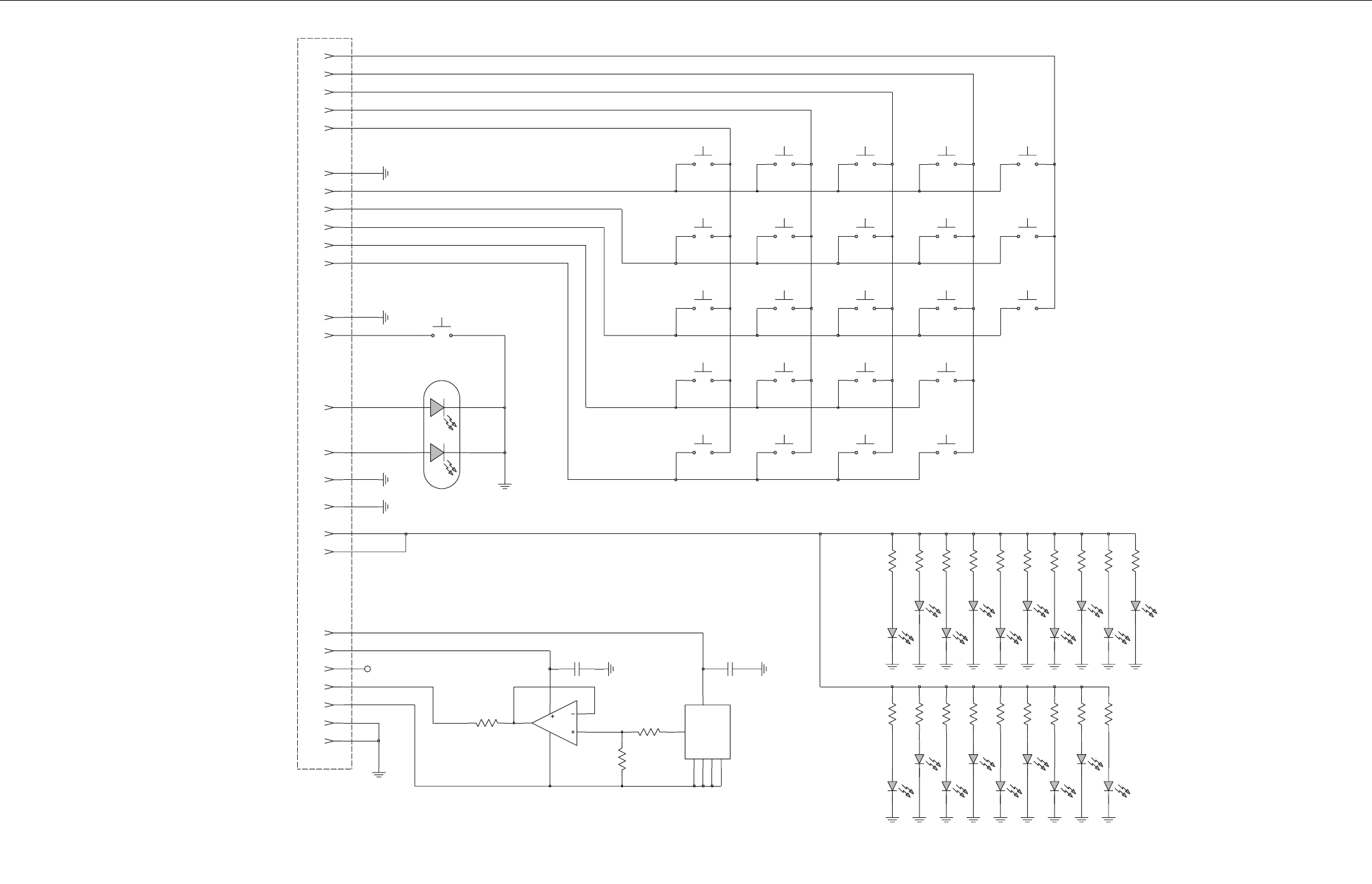
8.2 - 32 ENHANCED CONTROL HEADS: SCHEMATICS, PCBs and PARTS LISTS
Enhanced Control Head Keypad Board - Keypad Board (PCB: 8466581A01_A)
#
3F 96
3
852
741
P
U
EL 1K
S
DNE
1F
2
KS
2
F0
EUNEM
W
D
DNES
UN
U
N
UN
FO
/
N
O
*
V5
_
DWS
_D
P
K
1ni
p
ot
egd
irb
D
R
_
D
E
L
N
G
_
D
E
L
F
F
O
_
N
O
_
D
N
E
D
N
G
4_LOC
3
_LOC
2
_LOC
1
_LO
C
0
_L
O
C
4
_
W
O
R
3
_
W
O
R
2
_
W
O
R
1
_
W
O
R
0_WO
R
D
N
G
DNG
D
N
G
I
R
E
S
NES_C
C
V
P
M
A
_
P
O_C
C
V
ES
N
ES_
T
H
G
IL
E
S
N
E
S
_
D
N
G
V
5_D
W
S
_
DPK
DNG
U
N
U
N
UN
UN
6
2
-1J
42
-
1
J
5
2-
1
J
093
2
2
R
1
2R
093
0
2
R
09
3
0
72
9
1R
022
8
1R
9
1
D
0
1
M2
1
01
M
2
1
81D
0
1M
2
1
7
1
D
01M21
5
1
D
61D
0
1
M
2
1
4
1
D
0
1
M
21
0
22
7
1
R
093
6
1R51R
0
93
41R
072
0
9
3
3
1
R
0
9
3
1
1
S
12
21
R
4
S
12
3
S
12
11R
0
7
2022
0
1R
093
9
R8
R
093
7R
072093
6
R
093
5R
12
4R
072
8
1
S
12
3
2
S
2
R
CN
0
2
C
Fu1.0
4
3
1
2
5
1
R
001
10
3
7
M
L
1U
3
R
K0
7
2
5GND4
T
UO
6
VCC 1
Fu1
.
0
1
C
1SD
25
8
SPT
2GND1
GND2
3
GND3
4
11-1J
01-1
J
52
D
361C-
F
MSH
4
3
D
E
R
2
N
RG
1
0
2-
1
J
32
-
1J
12
-
1
J
2
1-
1
J
0
1M
2
1
2
1
D
3
1
D
01M21
1
1
D
01M21
1-
1
J
7
1
-
1J
02S
12
12
51S
12
12
0
1
S
12
1
S
2
9
1
S
12
5
S
12
4
1
S
1
42S
12
9S
2
2
S
12
12
12S
12
12
7
1
S
3
1
S
12
61
S
2
2
1
S
12
12
2
S
1
12
8
S6S
12
7
S
0
1
M
2
1
0
1
D
9
D
0
1
M2
1
7
D
0
1M
2
1
0
1
M
2
1
8
D
6
D
01
M
2
1
01M21
5
D
01M
2
1
4D
0
1
M
21
2D
0
1M
2
1
3
D1D
01M21
9
1-
1
J
2
2
-1J
8
1-
1
J
6
1
-1
J
41-1J
5
1-
1
J
6
-
1J
3
1-
1
J
4-
1
J
5
-1J
3-
1
J
7-1
J
2
-
1J
9
-1
J
8-
1J
4_LOC
3_LOC
2_LOC
1_LOC
0_LOC
0
_WOR
1
_WOR
2
_
WOR
3
_W
OR
4_
W
O
R

ENHANCED CONTROL HEADS: SCHEMATICS, PCBs AND PARTS LISTS 8.2 - 33
Parts List
Enhanced Control Head (PCB: 8466580A01)
Reference Motorola
PN Value
C101 2113944C06 CAP, 470pF
C102 2113944C06 CAP, 470pF
C103 2113944C36 CAP, 33pF
C104 2113944C06 CAP, 470pF
C105 2113944C06 CAP, 470pF
C107 2113944C36 CAP, 33pF
C108 2113944C06 CAP, 470pF
C109 2113944C06 CAP, 470pF
C110 2113944C43 CAP, 82pF
C112 2113944C06 CAP, 470pF
C113 2113944C06 CAP, 470pF
C114 2113944C06 CAP, 470pF
C115 2113944C43 CAP, 82pF
C116 2113944C06 CAP, 470pF
C118 2113944C43 CAP, 82pF
C120 2113956C37 CAP, 10uF
C121 2113944C06 CAP, 470pF
C201 NOT PLACED GCAM DUMMY PART
NUMBER
C202 NOT PLACED GCAM DUMMY PART
NUMBER
C203 NOT PLACED GCAM DUMMY PART
NUMBER
C204 2113944A28 CAP, 18pF
C205 2113944A28 CAP, 18pF
C206 2113946B04 CAP, 0.1uF
C220 2113946B04 CAP, 0.1uF
C221 2113946B04 CAP, 0.1uF
C223 2113946B04 CAP, 0.1uF
C224 2113946B04 CAP, 0.1uF
C225 2113946B04 CAP, 0.1uF
C226 2113946B04 CAP, 0.1uF
C227 2113946B04 CAP, 0.1uF
C228 2113946B04 CAP, 0.1uF
C229 2113946B04 CAP, 0.1uF
C230 2113946B04 CAP, 0.1uF
C231 2113946B04 CAP, 0.1uF
C232 2113946B04 CAP, 0.1uF
C233 2113946B04 CAP, 0.1uF
C234 2113946D02 CAP, 1.0uF
C241 2113946B04 CAP, 0.1uF
C242 2113956B54 CAP, 10uF
C243 2113956B54 CAP, 10uF
C244 2113945A05 CAP, 470pF
C245 2113945A05 CAP, 470pF
C255 2113946B04 CAP, 0.1uF
C256 2113946B04 CAP, 0.1uF
C257 2113946B04 CAP, 0.1uF
C258 2113944A31 CAP, 33pF
C259 2113944A31 CAP, 33pF
C260 2113944A31 CAP, 33pF
C261 2113946B04 CAP, 0.1uF
C262 2113946B04 CAP, 0.1uF
C263 2113946B04 CAP, 0.1uF
C264 2113944A31 CAP, 33pF
C265 2113944A31 CAP, 33pF
C266 2113946D02 CAP, 1.0uF
C267 2113946B04 CAP, 0.1uF
C268 2113946B04 CAP, 0.1uF
C269 2113946B04 CAP, 0.1uF
C270 2113944A31 CAP, 33pF
C271 2113946B04 CAP, 0.1uF
C272 2113944A31 CAP, 33pF
C273 2113946B04 CAP, 0.1uF
C274 2113946B04 CAP, 0.1uF
C275 2113946B04 CAP, 0.1uF
C276 2113946B04 CAP, 0.1uF
C277 2113944A31 CAP, 33pF
C278 2113946D02 CAP, 1.0uF
C279 2113946B04 CAP, 0.1uF
C280 2113946B04 CAP, 0.1uF
C281 2113946B04 CAP, 0.1uF
C282 2113946B04 CAP, 0.1uF
C283 2113946B04 CAP, 0.1uF
C284 2113946B04 CAP, 0.1uF
C285 2113946B04 CAP, 0.1uF
C286 2113946B04 CAP, 0.1uF
C287 2113946B04 CAP, 0.1uF
C288 2113946B04 CAP, 0.1uF
C289 2113944A31 CAP, 33pF
C290 2113946D02 CAP, 1.0uF
C291 2113946B04 CAP, 0.1uF
C292 2113944A31 CAP, 33pF
C293 2113946B04 CAP, 0.1uF
C294 2113956B54 CAP, 10uF
C295 2113946D02 CAP, 1.0uF
C301 2113946B04 CAP, 0.1uF
C324 2113946B04 CAP, 0.1uF
C325 2113956D58 CAP, 22uF
C326 2113946B04 CAP, 0.1uF
Reference Motorola
PN Value
C327 2113956B54 CAP, 10uF
C328 2113945A05 CAP, 470pF
C350 NOT PLACED GCAM DUMMY PART
NUMBER
C352 NOT PLACED GCAM DUMMY PART
NUMBER
C401 2113946B04 CAP, 0.1uF
C402 2113946B04 CAP, 0.1uF
C403 2113946B04 CAP, 0.1uF
C404 2113946B04 CAP, 0.1uF
C405 2113946B04 CAP, 0.1uF
C406 2113946B04 CAP, 0.1uF
C407 2113944C06 CAP, 470pF
C408 2113944C06 CAP, 470pF
C409 2113946B04 CAP, 0.1uF
C410 2113956B54 CAP, 10uF
C413 2113946B04 CAP, 0.1uF
C414 2113945A05 CAP, 470pF
C415 2113956B54 CAP, 10uF
C416 2113956B54 CAP, 10uF
C421 2113946B04 CAP, 0.1uF
C422 2113946B04 CAP, 0.1uF
C501 2113944C06 CAP, 470pF
C502 2313960J01 CAP, 10uF
C503 2313960J01 CAP, 10uF
C504 2113944C06 CAP, 470pF
C505 2113945C31 CAP, 0.1uF
C506 2113945C02 CAP, .01uF
C507 2113956D58 CAP, 22uF
C508 2113956D58 CAP, 22uF
C509 2113956D58 CAP, 22uF
C510 2113956D58 CAP, 22uF
C511 2113956D58 CAP, 22uF
C512 2113956D58 CAP, 22uF
C513 2113956B54 CAP, 10uF
C514 2314030J28 CAP, 22uF
C515 NOT PLACED GCAM DUMMY PART
NUMBER
C516 2113946B04 CAP, 0.1uF
C517 2113956B54 CAP, 10uF
C518 2113944A29 CAP, 22pF
C519 2113944A40 CAP, 100pF
C520 2113956B54 CAP, 10uF
C521 2113956B54 CAP, 10uF
C522 2113946B04 CAP, 0.1uF
C523 2113944A25 CAP, 10pF
C524 2113944A42 CAP, 150pF
Reference Motorola
PN Value
C525 2113956B54 CAP, 10uF
C526 2113956B54 CAP, 10uF
C527 2113956B54 CAP, 10uF
C528 2113946B04 CAP, 0.1uF
C529 2113946B04 CAP, 0.1uF
C530 NOT PLACED GCAM DUMMY PART
NUMBER
C531 2113944A28 CAP, 18pF
C532 2113944A26 CAP, 12pF
C533 2113946B04 CAP, 0.1uF
C534 2113956B54 CAP, 10uF
C535 NOT PLACED GCAM DUMMY PART
NUMBER
C536 NOT PLACED GCAM DUMMY PART
NUMBER
C540 2113946B04 CAP, 0.1uF
C541 2113946B04 CAP, 0.1uF
C542 2113946B04 CAP, 0.1uF
C544 NOT PLACED GCAM DUMMY PART
NUMBER
C545 2113946B04 CAP, 0.1uF
C546 2113946B04 CAP, 0.1uF
C547 2113946B04 CAP, 0.1uF
C601 2113944C06 CAP, 470pF
C602 2113945A05 CAP, 470pF
C604 2113945A05 CAP, 470pF
C605 2113944A31 CAP, 33pF
C606 2113944A31 CAP, 33pF
C607 2113945A05 CAP, 470pF
C608 2113945A05 CAP, 470pF
C609 2113945A05 CAP, 470pF
C610 2113956B54 CAP, 10uF
C611 2113945A05 CAP, 470pF
C612 2113945A05 CAP, 470pF
C613 2113945A05 CAP, 470pF
C614 2113945A05 CAP, 470pF
C615 2113944A38 CAP, 82pF
C616 2113944A38 CAP, 82pF
C617 2113944A38 CAP, 82pF
C618 2113944A38 CAP, 82pF
C619 2113944A38 CAP, 82pF
C620 2113944A38 CAP, 82pF
C621 2113944A38 CAP, 82pF
C622 2113944A38 CAP, 82pF
C623 2113944A38 CAP, 82pF
C624 2113945A05 CAP, 470pF
C625 2113944A31 CAP, 33pF
Reference Motorola
PN Value

8.2 - 34 ENHANCED CONTROL HEADS: SCHEMATICS, PCBs AND PARTS LISTS
C626 2113944A31 CAP, 33pF
C627 2113944A31 CAP, 33pF
C628 2113944A38 CAP, 82pF
C629 2113944A31 CAP, 33pF
C630 2113944A31 CAP, 33pF
C631 2113944A38 CAP, 82pF
C632 2113945A05 CAP, 470pF
C633 2113945A05 CAP, 470pF
C634 2113944A38 CAP, 82pF
C635 2113944A38 CAP, 82pF
C636 2113945A05 CAP, 470pF
C637 2113945A05 CAP, 470pF
D101 4866544A01 SR05
D301 4813978A19 MBR120LSFT1
D302 4813978A25 BAT54HT1G
D304 NOT PLACED GCAM DUMMY PART
NUMBER
D350 4813978C02 MMBD6100
D401 4815814H01 HT-S91UD
D402 4815814H01 HT-S91UD
D501 4813978N08 MBRS130
D502 4813978A25 BAT54HT1G
D503 4813978C02 MMBD6100
D504 NOT PLACED GCAM DUMMY PART
NUMBER
D505 4813978C02 MMBD6100
D506 NOT PLACED GCAM DUMMY PART
NUMBER
D507 4813978A25 BAT54HT1G
D510 4813978C02 MMBD6100
D511 4813978C02 MMBD6100
D513 4813978C02 MMBD6100
J101 0964501H02 CONN_J
J102 0916162H02 pin CONN_J
J201 0988866N01 pin CONN_J
J202 NOT PLACED GCAM DUMMY PART
NUMBER
J401 0916875H01 pin CONN_J
J403 0971315L01 CONN_J
J603 0971065L01 pin CONN_J
L501 2489932S02 IDCTR, 33uH
L502 2487956V01 IDCTR, 22uH
L503 2589195N04 IDCTR, 4.7uH
L504 2589195N04 IDCTR, 4.7uH
L505 2489932S02 IDCTR, 33uH
L507 2489932S02 IDCTR, 33uH
Reference Motorola
PN Value
M101 NOT PLACED GCAM DUMMY PART
NUMBER
M102 3264646H01 CONTACT
M103 NOT PLACED GCAM DUMMY PART
NUMBER
M104 3264646H01 CONTACT
M105 3264646H01 CONTACT
M106 3264646H01 CONTACT
M107 NOT PLACED GCAM DUMMY PART
NUMBER
M108 NOT PLACED GCAM DUMMY PART
NUMBER
M109 3264646H01 CONTACT
M110 NOT PLACED GCAM DUMMY PART
NUMBER
M111 3264646H01 CONTACT
M112 NOT PLACED GCAM DUMMY PART
NUMBER
M113 NOT PLACED GCAM DUMMY PART
NUMBER
M114 NOT PLACED GCAM DUMMY PART
NUMBER
M115 NOT PLACED GCAM DUMMY PART
NUMBER
M116 NOT PLACED GCAM DUMMY PART
NUMBER
M201 3989655N03 CONTACT
Q201 4813973M07 MMBT3904
Q202 4815272H01 EMD9FT2R
Q301 4815272H01 EMD9FT2R
Q305 4813973M07 MMBT3904
Q322 4805921T28 FMG8A
Q323 4805921T28 FMG8A
Q324 4805921T28 FMG8A
Q325 4815272H01 EMD9FT2R
Q326 5166540A01 FDC6330L
Q327 NOT PLACED GCAM DUMMY PART
NUMBER
Q350 NOT PLACED GCAM DUMMY PART
NUMBER
Q351 NOT PLACED GCAM DUMMY PART
NUMBER
Q352 4815272H01 EMD9FT2R
Q353 NOT PLACED GCAM DUMMY PART
NUMBER
Q401 5166540A01 FDC6330L
Q403 4813973M07 MMBT3904
Q404 4815272H01 EMD9FT2R
Q405 4815272H01 EMD9FT2R
Q410 4813973M07 MMBT3904
Reference Motorola
PN Value
Q411 4815272H01 EMD9FT2R
Q412 4815272H01 EMD9FT2R
Q500 4815272H01 EMD9FT2R
Q501 4815272H01 EMD9FT2R
Q502 4815272H01 EMD9FT2R
Q503 4815272H01 EMD9FT2R
Q504 4815272H01 EMD9FT2R
Q505 4815272H01 EMD9FT2R
Q506 4815272H01 EMD9FT2R
Q507 4815272H01 EMD9FT2R
Q508 4815272H01 EMD9FT2R
R101 0613952H37 RES, 33
R102 0613952H25 RES, 10
R103 0613952H37 RES, 33
R151 0613952R25 RES, 100K
R152 0613952R25 RES, 100K
R153 0613952R25 RES, 100K
R154 0613952R25 RES, 100K
R155 0613952Q89 RES, 4.7K
R156 NOT PLACED GCAM DUMMY PART
NUMBER
R157 0613952Q89 RES, 4.7K
R160 0613952Q37 RES, 33
R161 0613952Q37 RES, 33
R162 0613952R66 RES, 0
R163 0613952Q37 RES, 33
R164 0613952Q37 RES, 33
R165 0613952Q37 RES, 33
R166 0613952Q37 RES, 33
R167 0613952Q37 RES, 33
R168 0613952Q37 RES, 33
R201 NOT PLACED GCAM DUMMY PART
NUMBER
R202 NOT PLACED GCAM DUMMY PART
NUMBER
R203 0613952R25 RES, 100K
R204 NOT PLACED GCAM DUMMY PART
NUMBER
R205 NOT PLACED GCAM DUMMY PART
NUMBER
R206 NOT PLACED GCAM DUMMY PART
NUMBER
R207 0613952R25 RES, 100K
R208 0613952R25 RES, 100K
R209 NOT PLACED GCAM DUMMY PART
NUMBER
R210 0613952R25 RES, 100K
R211 0613952R25 RES, 100K
Reference Motorola
PN Value
R212 0613952R25 RES, 100K
R213 0613952R66 RES, 0
R214 0613952R01 RES, 10K
R215 0613952R01 RES, 10K
R216 NOT PLACED GCAM DUMMY PART
NUMBER
R217 NOT PLACED GCAM DUMMY PART
NUMBER
R218 0613952R01 RES, 10K
R219 0613952R01 RES, 10K
R220 0613952R66 RES, 0
R221 0613952R74 RES, 10MEG
R222 NOT PLACED GCAM DUMMY PART
NUMBER
R223 0613952R01 RES, 10K
R224 0613952R66 RES, 0
R225 0613952R66 RES, 0
R226 NOT PLACED GCAM DUMMY PART
NUMBER
R227 NOT PLACED GCAM DUMMY PART
NUMBER
R228 0613952R01 RES, 10K
R230 0613952R01 RES, 10K
R231 0613952R01 RES, 10K
R232 0613952R01 RES, 10K
R233 0613952R01 RES, 10K
R234 0613952R01 RES, 10K
R235 0613952R01 RES, 10K
R236 NOT PLACED GCAM DUMMY PART
NUMBER
R237 0613952R01 RES, 10K
R240 NOT PLACED GCAM DUMMY PART
NUMBER
R241 NOT PLACED GCAM DUMMY PART
NUMBER
R242 0613952R01 RES, 10K
R243 0613952R01 RES, 10K
R244 0613952R01 RES, 10K
R245 NOT PLACED GCAM DUMMY PART
NUMBER
R246 0613952R01 RES, 10K
R247 NOT PLACED GCAM DUMMY PART
NUMBER
R248 0613952R01 RES, 10K
R249 0613952R01 RES, 10K
R250 NOT PLACED GCAM DUMMY PART
NUMBER
R251 NOT PLACED GCAM DUMMY PART
NUMBER
Reference Motorola
PN Value

ENHANCED CONTROL HEADS: SCHEMATICS, PCBs AND PARTS LISTS 8.2 - 35
R252 NOT PLACED GCAM DUMMY PART
NUMBER
R253 0613952R01 RES, 10K
R254 NOT PLACED GCAM DUMMY PART
NUMBER
R255 0613952R01 RES, 10K
R256 0613952R01 RES, 10K
R257 0613952R66 RES, 0
R258 0613952Q37 RES, 33
R259 NOT PLACED GCAM DUMMY PART
NUMBER
R260 0613952R66 RES, 0
R261 0613952Q81 RES, 2.2K
R262 0613952Q81 RES, 2.2K
R263 NOT PLACED GCAM DUMMY PART
NUMBER
R264 0613952R01 RES, 10K
R265 0613952R01 RES, 10K
R266 0613952R66 RES, 0
R267 0613952R66 RES, 0
R268 0613952R66 RES, 0
R269 0613952R66 RES, 0
R270 0613952R66 RES, 0
R271 0613952R66 RES, 0
R272 0613952R66 RES, 0
R273 0613952R66 RES, 0
R274 0613952R66 RES, 0
R275 0613952R66 RES, 0
R276 0613952R66 RES, 0
R277 0613952R66 RES, 0
R278 0613952R66 RES, 0
R279 0613952R66 RES, 0
R280 0613952R66 RES, 0
R281 0613952R66 RES, 0
R282 0613952R66 RES, 0
R283 0613952R66 RES, 0
R284 0613952R66 RES, 0
R285 0613952R66 RES, 0
R286 0613952Q77 RES, 1.5K
R287 0613952H49 RES, 100
R288 0613952R01 RES, 10K
R289 NOT PLACED GCAM DUMMY PART
NUMBER
R290 0613952R01 RES, 10K
R291 0613952R66 RES, 0
R295 0613952R01 RES, 10K
R296 0613952Q25 RES, 10
Reference Motorola
PN Value
R297 0613952Q25 RES, 10
R301 0613952R01 RES, 10K
R303 0613952R01 RES, 10K
R304 0613952R05 RES, 15K
R305 0613952R01 RES, 10K
R306 0613952R05 RES, 15K
R307 0613952Q81 RES, 2.2K
R308 0613952Q81 RES, 2.2K
R309 0613952R01 RES, 10K
R310 0613952R01 RES, 10K
R311 0613952R01 RES, 10K
R312 0613952R05 RES, 15K
R313 0613952Q73 RES, 1K
R314 0613952H37 RES, 33
R315 0613952H37 RES, 33
R316 0613952H37 RES, 33
R317 NOT PLACED GCAM DUMMY PART
NUMBER
R318 0613952R66 RES, 0
R319 NOT PLACED GCAM DUMMY PART
NUMBER
R320 0613952Q73 RES, 1K
R321 0613952R01 RES, 10K
R322 0613952R05 RES, 15K
R323 0613952R01 RES, 10K
R324 0613952R05 RES, 15K
R325 0613952R01 RES, 10K
R326 0613952Q77 RES, 1.5K
R327 0613952R05 RES, 15K
R328 0613952R05 RES, 15K
R329 0613952R01 RES, 10K
R330 0613952Q57 RES, 220
R331 0613952Q57 RES, 220
R332 NOT PLACED GCAM DUMMY PART
NUMBER
R333 0613952R01 RES, 10K
R334 0613952R01 RES, 10K
R335 0613952R17 RES, 47K
R336 0613952R01 RES, 10K
R337 0613952R01 RES, 10K
R338 NOT PLACED GCAM DUMMY PART
NUMBER
R339 NOT PLACED GCAM DUMMY PART
NUMBER
R340 0613952R37 RES, 330K
R341 0613952R37 RES, 330K
R342 0613952R37 RES, 330K
Reference Motorola
PN Value
R343 0613952R37 RES, 330K
R344 0613952Q91 RES, 5.6K
R345 0613952R01 RES, 10K
R346 0613952R41 RES, 470K
R347 0613952R25 RES, 100K
R348 0613952R25 RES, 100K
R350 NOT PLACED GCAM DUMMY PART
NUMBER
R351 NOT PLACED GCAM DUMMY PART
NUMBER
R352 NOT PLACED GCAM DUMMY PART
NUMBER
R354 0613952Q89 RES, 4.7K
R355 NOT PLACED GCAM DUMMY PART
NUMBER
R357 0613952R05 RES, 15K
R358 0613952Q73 RES, 1K
R359 NOT PLACED GCAM DUMMY PART
NUMBER
R360 NOT PLACED GCAM DUMMY PART
NUMBER
R361 0613952R66 RES, 0
R399 NOT PLACED GCAM DUMMY PART
NUMBER
R400 0613952R66 RES, 0
R401 0613952Q85 RES, 3.3K
R402 0613952Q85 RES, 3.3K
R403 0613952R13 RES, 33K
R404 0613952R13 RES, 33K
R405 0613952Q49 RES, 100
R406 0613952Q89 RES, 4.7K
R407 0613952Q73 RES, 1K
R408 0613952Q73 RES, 1K
R409 0613952Q73 RES, 1K
R410 0613952Q73 RES, 1K
R411 0613952Q73 RES, 1K
R412 0613952R01 RES, 10K
R413 0613952R17 RES, 47K
R414 0613952Q77 RES, 1.5K
R415 0613952H49 RES, 100
R416 0613952Q79 RES, 1.8K
R417 0613952Q73 RES, 1K
R421 0613952R01 RES, 10K
R422 0613952R05 RES, 15K
R423 0613952R12 RES, 30K
R424 0613952R01 RES, 10K
R425 0613952R01 RES, 10K
R426 0613952R01 RES, 10K
Reference Motorola
PN Value
R427 0613952R12 RES, 30K
R428 0613952Q85 RES, 3.3K
R429 0613952R17 RES, 47K
R430 0613952R05 RES, 15K
R435 0613952Q89 RES, 4.7K
R436 0613952R01 RES, 10K
R440 NOT PLACED GCAM DUMMY PART
NUMBER
R441 NOT PLACED GCAM DUMMY PART
NUMBER
R442 0613952R66 RES, 0
R443 0613952R66 RES, 0
R444 NOT PLACED GCAM DUMMY PART
NUMBER
R501 0613952R01 RES, 10K
R502 0613952E09 RES, 12.1K
R503 0613952Q49 RES, 100
R504 0613952E09 RES, 12.1K
R505 0613952Q73 RES, 1K
R506 0613952R13 RES, 33K
R507 0613952R01 RES, 10K
R508 0613952P51 RES, 332K
R509 0613952P22 RES, 165K
R510 0613952P81 RES, 681K
R511 0613952P09 RES, 121K
R512 0613952Q73 RES, 1K
R513 0613952N81 RES, 68.1K
R514 0613952R01 RES, 10K
R515 0613952N71 RES, 53.6K
R520 0613952R37 RES, 330K
R521 0613952R74 RES, 10MEG
R522 0613952R33 RES, 220K
R523 0613952R66 RES, 0
R524 NOT PLACED GCAM DUMMY PART
NUMBER
R529 NOT PLACED GCAM DUMMY PART
NUMBER
R530 0613952H49 RES, 100
R531 0613952P22 RES, 165K
R532 0613952N70 RES, 52.3K
R533 0613952Q25 RES, 10
R534 0613952R66 RES, 0
R535 0613952R66 RES, 0
R536 0613952R66 RES, 0
R537 0613952R66 RES, 0
R538 NOT PLACED GCAM DUMMY PART
NUMBER
R539 0613952R66 RES, 0
Reference Motorola
PN Value
8.2 - 36 ENHANCED CONTROL HEADS: SCHEMATICS, PCBs AND PARTS LISTS
Data Expansion Head Enhanced/
Main Board (PCB 8466586A01)
R540 0613952R01 RES, 10K
R541 0613952Q89 RES, 4.7K
R542 0613952R01 RES, 10K
R543 0613952R01 RES, 10K
R544 0613952R66 RES, 0
R545 0613952Q73 RES, 1K
R547 0613952Q89 RES, 4.7K
R548 0613952R01 RES, 10K
R549 0613952R01 RES, 10K
R550 0613952R01 RES, 10K
R551 0613952Q89 RES, 4.7K
R602 NOT PLACED GCAM DUMMY PART
NUMBER
R603 NOT PLACED GCAM DUMMY PART
NUMBER
R604 NOT PLACED GCAM DUMMY PART
NUMBER
R605 NOT PLACED GCAM DUMMY PART
NUMBER
R606 0613952R66 RES, 0
R607 0613952R66 RES, 0
R608 0613952R66 RES, 0
R609 0613952R66 RES, 0
R610 NOT PLACED GCAM DUMMY PART
NUMBER
R611 NOT PLACED GCAM DUMMY PART
NUMBER
R612 0613952R66 RES, 0
R613 0613952R66 RES, 0
R614 NOT PLACED GCAM DUMMY PART
NUMBER
S501 4015040C01 SWITCH
SH201 NOT PLACED GCAM DUMMY PART
NUMBER
SH501 2616535H01 SHIELD
SH502 NOT PLACED GCAM DUMMY PART
NUMBER
U201 5171423L01 IC OMAP 1621 GP DUAL
CORE PROCESSOR
U202 NOT PLACED GCAM DUMMY PART
NUMBER
U203 NOT PLACED GCAM DUMMY PART
NUMBER
U204 5185956E43 IC,FLSH,,128MB,
U205 5185941F17 IC,SDRAM,128MB
U206 5114000B39 74VHC125
U207 5114000B39 74VHC125
U208 5114007A47 NC7SZ32
U209 5185941F65 IC LATCH, LVC, OCTAL
Reference Motorola
PN Value
U210 5114000B39 74VHC125
U211 NOT PLACED GCAM DUMMY PART
NUMBER
U301 5102836C11 1 FSA4157L6X_NL
U302 5115007H01 0 SN74LVC1T45
U303 5115007H01 0 SN74LVC1T45
U304 5115007H01 0 SN74LVC1T45
U321 5102836C11 1 FSA4157L6X_NL
U322 5102836C11 1 FSA4157L6X_NL
U323 5115007H01 0 SN74LVC1T45
U324 5164015H50 TPS2041B
U325 5115007H01 0 SN74LVC1T45
U326 5102836C11 1 FSA4157L6X_NL
U327 5102836C11 1 FSA4157L6X_NL
U328 5109817F77 LMV7275
U350 NOT PLACED GCAM DUMMY PART
NUMBER
U401 5186311J07 D-FLIP-FLOP NC7SZ175
U402 5186311J07 D-FLIP-FLOP NC7SZ175
U403 5114007A43 NL17SZ14
U404 5114007A43 NL17SZ14
U420 5114000B39 74VHC125
U421 5109817F77 LMV7275
U422 5109817F77 LMV7275
U501 5185941F48 IC, VREG 5V NOPB
U502 5114004A35 NCP301
U503 5109920D44 LT1937
U504 5109920D39 TPS62220
U505 5109920D39 TPS62220
U506 5114014A22 LP2951CD
U507 5109512F66 LP2985
U508 5114007A43 NL17SZ14
U509 5186311J07 D-FLIP-FLOP NC7SZ175
U510 5102836C11 1 FSA4157L6X_NL
U511 5102836C11 1 FSA4157L6X_NL
U512 5102836C11 1 FSA4157L6X_NL
U513 5189263U10 LINEAR VOLTAGE
REGULATOR
U515 5185319Y01 RIPPLE COUNTER, 14
STAGE, WITH OSC
VR101 4813979P10 MMQA5V6T1
VR102 4813979C11 MMQA20VT1
VR401 4813979P10 MMQA5V6T1
VR501 4813979P10 MMQA5V6T1
VR502 4814026A19 1SMB5931B
Y201 4802582S85 XTAL
Reference Motorola
PN Value
Y202 NOT PLACED GCAM DUMMY PART
NUMBER
Y501 4809995L20 MC146
Reference Motorola
PN Value
C101 2113945C31 CAP 0.1uF
C102 2113945C31 CAP 0.1uF
C103 2113945G91 CAP, 0.1uF
C104 2113945G91 CAP, 0.1uF
C105 2113945G91 CAP, 0.1uF
C106 2113945G91 CAP, 0.1uF
C107 NOT PLACED GCAM DUMMY PART
NUMBER
C108 NOT PLACED GCAM DUMMY PART
NUMBER
C109 NOT PLACED GCAM DUMMY PART
NUMBER
C110 NOT PLACED GCAM DUMMY PART
NUMBER
C111 NOT PLACED GCAM DUMMY PART
NUMBER
C112 NOT PLACED GCAM DUMMY PART
NUMBER
C113 NOT PLACED GCAM DUMMY PART
NUMBER
C114 NOT PLACED GCAM DUMMY PART
NUMBER
C116 2113945L17 CAP 470pF
C117 2113945G91 CAP, 0.1uF
C118 2113945L17 CAP 470pF
C119 2113945L17 CAP 470pF
C120 2113944C43 CAP, 82pF
C121 2113945L17 CAP 470pF
C122 2113944C43 CAP, 82pF
C123 2113945L17 CAP 470pF
C124 2113945L17 CAP 470pF
C125 2113945L17 CAP 470pF
C126 NOT PLACED GCAM DUMMY PART
NUMBER
C127 NOT PLACED GCAM DUMMY PART
NUMBER
C128 NOT PLACED GCAM DUMMY PART
NUMBER
C129 NOT PLACED GCAM DUMMY PART
NUMBER
Reference Motorola
PN Value
C130 NOT PLACED GCAM DUMMY PART
NUMBER
C131 2113944C43 CAP, 82pF
C132 NOT PLACED GCAM DUMMY PART
NUMBER
C133 NOT PLACED GCAM DUMMY PART
NUMBER
C134 NOT PLACED GCAM DUMMY PART
NUMBER
C135 NOT PLACED GCAM DUMMY PART
NUMBER
C136 NOT PLACED GCAM DUMMY PART
NUMBER
C137 NOT PLACED GCAM DUMMY PART
NUMBER
C138 NOT PLACED GCAM DUMMY PART
NUMBER
C139 NOT PLACED GCAM DUMMY PART
NUMBER
C140 2113945L17 CAP 470pF
C141 2113945L17 CAP 470pF
C142 2113945L17 CAP 470pF
C143 2313960G04 CAP,3.3UF,+
C145 2113945L17 CAP 470pF
C202 2113955E37 CAP,10UF
C203 2113946S35 CAP 1.0UF
C303 NOT PLACED GCAM DUMMY PART
NUMBER
C304 NOT PLACED GCAM DUMMY PART
NUMBER
C305 NOT PLACED GCAM DUMMY PART
NUMBER
C306 NOT PLACED GCAM DUMMY PART
NUMBER
C307 NOT PLACED GCAM DUMMY PART
NUMBER
C308 NOT PLACED GCAM DUMMY PART
NUMBER
C309 NOT PLACED GCAM DUMMY PART
NUMBER
C401 2113945C31 CAP 0.1uF
C402 2113945C31 CAP 0.1uF
C403 2113945G91 CAP, 0.1uF
C404 2113945G91 CAP, 0.1uF
C405 2113945C31 CAP 0.1uF
C406 2113945G91 CAP, 0.1uF
C407 2113945G91 CAP, 0.1uF
C501 2313960F30 CAP 47UF,
C502 2113945C31 CAP 0.1uF
C503 2113945L17 CAP 470pF
Reference Motorola
PN Value

ENHANCED CONTROL HEADS: SCHEMATICS, PCBs AND PARTS LISTS 8.2 - 37
C505 2113945C18 CAP .012uF
C506 2113955E37 CAP,10UF
C507 2113945C31 CAP 0.1uF
C508 2113945C31 CAP 0.1uF
C601 2113945L17 CAP 470pF
C602 2113945C31 CAP 0.1uF
C603 2113945C31 CAP 0.1uF
C604 2113945L17 CAP 470pF
C605 2113945C31 CAP 0.1uF
C606 2113945C31 CAP 0.1uF
C607 2313960C26 CAP 1.0 UF
C608 2113946S35 CAP 1.0UF
C610 2113945C31 CAP 0.1uF
C611 2113945C31 CAP 0.1uF
C612 2313960G32 CAP, 10uF
C613 2113955E37 CAP,10UF
C614 NOT PLACED GCAM DUMMY PART
NUMBER
C615 NOT PLACED GCAM DUMMY PART
NUMBER
C616 NOT PLACED GCAM DUMMY PART
NUMBER
D101 4813978C02 MMBD6100
D102 4813978C02 MMBD6100
F101 6503566D15 FUSE,THIN FILM,2A,32V,
J1001 0916162H02 12 POS, FLEX CONNECTOR,
J1003 NOT PLACED GCAM DUMMY PART
NUMBER
J1005 0915064H03 CONNECTOR, ZIF (40 PINS)
J1022 0915064H03 CONNECTOR, ZIF (40 PINS)
Q101 4813973M07 TRANSISTOR
Q102 4813973A42 XSTR,BIP GP
SS,NPN,SM,SC-59,
Q103 4813973A13 XSTR,BIP GP SS,PNP,TO-
236,SO
Q104 4813973A87 TRANSISTOR
Q401 4813973A87 TRANSISTOR
Q501 4813973A42 XSTR,BIP GP
SS,NPN,SM,SC-59,
Q503 4813971A08 TSTR PNP 25V 5A
MJD210T4
Q504 4813973A42 XSTR,BIP GP
SS,NPN,SM,SC-59,
Q601 4813973A13 XSTR,BIP GP SS,PNP,TO-
236,SO
Q602 4813973A13 XSTR,BIP GP SS,PNP,TO-
236,SO
Q603 4813973M07 TRANSISTOR
Reference Motorola
PN Value
Q604 4813973A13 XSTR,BIP GP SS,PNP,TO-
236,SO
R101 NOT PLACED GCAM DUMMY PART
NUMBER
R102 0613952J17 RES 47K
R103 0613952J01 RES 10K
R104 0613952J17 RES 47K
R105 NOT PLACED GCAM DUMMY PART
NUMBER
R106 0613952G67 RES 0
R107 NOT PLACED GCAM DUMMY PART
NUMBER
R108 0613952H25 RES, 10
R109 0613952H89 RES 4.7K
R110 NOT PLACED GCAM DUMMY PART
NUMBER
R111 0613952J17 RES 47K
R112 NOT PLACED GCAM DUMMY PART
NUMBER
R113 0613952H95 RES 8.2K
R114 0613952J17 RES 47K
R115 0613952H89 RES 4.7K
R116 0613952J01 RES 10K
R117 NOT PLACED GCAM DUMMY PART
NUMBER
R118 0613952J01 RES 10K
R119 0613952J01 RES 10K
R120 0613952H89 RES 4.7K
R201 0613952H89 RES 4.7K
R202 0613952H85 RES 3.3K
R205 0613952G67 RES 0
R206 0613952G67 RES 0
R208 0614033G66 RES, 47.5K
R209 0614033G66 RES, 47.5K
R210 0614033G66 RES, 47.5K
R211 0614033G66 RES, 47.5K
R212 NOT PLACED GCAM DUMMY PART
NUMBER
R213 NOT PLACED GCAM DUMMY PART
NUMBER
R214 0614033G66 RES, 47.5K
R215 0614033G66 RES, 47.5K
R216 0614033G66 RES, 47.5K
R217 0614033G66 RES, 47.5K
R218 0614033G66 RES, 47.5K
R219 0614033G66 RES, 47.5K
R220 0614033E58 RES, 392
R221 0614033E58 RES, 392
Reference Motorola
PN Value
R222 0613952G67 RES 0
R223 0613952G67 RES 0
R301 NOT PLACED GCAM DUMMY PART
NUMBER
R302 NOT PLACED GCAM DUMMY PART
NUMBER
R303 NOT PLACED GCAM DUMMY PART
NUMBER
R304 NOT PLACED GCAM DUMMY PART
NUMBER
R305 NOT PLACED GCAM DUMMY PART
NUMBER
R306 NOT PLACED GCAM DUMMY PART
NUMBER
R307 NOT PLACED GCAM DUMMY PART
NUMBER
R308 NOT PLACED GCAM DUMMY PART
NUMBER
R309 NOT PLACED GCAM DUMMY PART
NUMBER
R310 NOT PLACED GCAM DUMMY PART
NUMBER
R311 NOT PLACED GCAM DUMMY PART
NUMBER
R312 NOT PLACED GCAM DUMMY PART
NUMBER
R313 NOT PLACED GCAM DUMMY PART
NUMBER
R314 NOT PLACED GCAM DUMMY PART
NUMBER
R315 NOT PLACED GCAM DUMMY PART
NUMBER
R316 NOT PLACED GCAM DUMMY PART
NUMBER
R317 NOT PLACED GCAM DUMMY PART
NUMBER
R318 NOT PLACED GCAM DUMMY PART
NUMBER
R319 NOT PLACED GCAM DUMMY PART
NUMBER
R320 NOT PLACED GCAM DUMMY PART
NUMBER
R321 NOT PLACED GCAM DUMMY PART
NUMBER
R322 NOT PLACED GCAM DUMMY PART
NUMBER
R323 NOT PLACED GCAM DUMMY PART
NUMBER
R324 NOT PLACED GCAM DUMMY PART
NUMBER
R325 NOT PLACED GCAM DUMMY PART
NUMBER
R401 0613952J17 RES 47K
Reference Motorola
PN Value
R402 0613952J17 RES 47K
R501 0613952E10 RES 12.4K
R502 NOT PLACED GCAM DUMMY PART
NUMBER
R508 0613952E88 RES 80.6K
R509 0613952H25 RES, 10
R510 0613952E10 RES 12.4K
R511 0613952H85 RES 3.3K
R512 0613952H85 RES 3.3K
R518 0613952J01 RES 10K
R519 0613952H81 RES 2.2K
R520 0613952H81 RES 2.2K
R601 0613952H89 RES 4.7K
R602 0613952H89 RES 4.7K
R603 0613952H89 RES 4.7K
R604 0613952J01 RES 10K
R605 0613952H81 RES 2.2K
R606 0613952H89 RES 4.7K
R607 0613952J01 RES 10K
R608 0613952J01 RES 10K
R609 0613952H81 RES 2.2K
R610 0613952H89 RES 4.7K
R611 0613952J01 RES 10K
R612 0613952H81 RES 2.2K
R613 0613952J01 RES 10K
R614 0613952H81 RES 2.2K
R615 0613952H89 RES 4.7K
R616 0613952J01 RES 10K
R617 0613952H92 RES 6.2K
R618 0613952E10 RES 12.4K
R619 0613952J01 RES 10K
R620 0613952J01 RES 10K
R623 0613952H67 RES 560
R624 0613952H49 RES, 100
R625 0613952J01 RES 10K
R626 NOT PLACED GCAM DUMMY PART
NUMBER
R627 NOT PLACED GCAM DUMMY PART
NUMBER
U101 5186988J61 IC,XCVR,5 DRIVER 3
RECEIVER
U201 5114016A18 IC,OP AMP,4PER
PKG,GP,SOIC,PB
U301 NOT PLACED GCAM DUMMY PART
NUMBER
U302 NOT PLACED GCAM DUMMY PART
NUMBER
U401 5166552A01 UART MAX3100EEE+
Reference Motorola
PN Value
8.2 - 38 ENHANCED CONTROL HEADS: SCHEMATICS, PCBs AND PARTS LISTS
Data Expansion Head Enhanced/ Connector
Board (PCB: 8464300B06_A)
Remote Head Enhanced (PCB 8471016L02)
Remote Back Head Enhanced
(PCB 84966583A01)
U402 4886061B02 RESONATOR,CERAMIC,3.68
MHZ
U403 5114009A35 IC,XCVR,8PER
PKG,74AC244
U404 5188462T01 MAX3232E
U501 5114014M39 IC,LINEAR VOLTAGE
REGULATOR,
U503 5114014A22 LP2951CD
U601 5114009A07 IC,AND,74AC08,4PER
PKG,SOIC14,6
U602 5114006A02 PB-FREE,
NOTCOMPLETELYENRICHE
D
U603 5175771A10 MAX4544EUT
VR101 4813977M11 DIODE,ZEN,MBZ5232,SM,S
OT-23,5.
VR102 4813977M36 MMBZ5257BLT1G
VR103 4813979P10 MMQA5V6T1
VR104 4813979C11 MMQA20VT1
VR105 4813977M36 MMBZ5257BLT1G
VR106 NOT PLACED GCAM DUMMY PART
NUMBER
VR108 4813979C11 MMQA20VT1
VR109 4813977M36 MMBZ5257BLT1G
VR110 4813977M36 MMBZ5257BLT1G
VR111 4813977M36 MMBZ5257BLT1G
VR112 4813977M36 MMBZ5257BLT1G
VR113 4813977M36 MMBZ5257BLT1G
Reference Motorola
PN Value
J0101 2864287B01 CONN 10 MODULAR JACK
J0102 0909760D04 D SUB JACK RT ANGLE PC
MT
J0103 0909760D02 D SUB JACK RT ANGLE PC
MT
J0104 0915064H03 CONNECTOR, ZIF (40 PINS)
Reference Motorola
PN Value
C201 2113945C18 CAP .012uF
C202 2113955E37 CAP 1.0 UF
C203 2113945C31 CAP 0.1uF
C204 2113945C31 CAP 0.1uF
C206 2313960C26 CAP 1.0 UF
Reference Motorola
PN Value
C301 2113955E37 CAP 1.0 UF
C302 NOT PLACED GCAM DUMMY PART
NUMBER
C303 NOT PLACED GCAM DUMMY PART
NUMBER
C304 2113945L17 CAP 470pF
C305 2113945L17 CAP 470pF
C306 2113945L17 CAP 470pF
C307 2113945L17 CAP 470pF
C308 2113945L17 CAP 470pF
C309 2113945L17 CAP 470pF
C310 2113944C43 CAP 82pF
C311 2113944C43 CAP 82pF
C313 2113955E37 CAP 1.0 UF
C314 NOT PLACED GCAM DUMMY PART
NUMBER
F300 6503566D15 FUSE,THIN FILM,2A,32V,
J301 0916162H02 CONNECTOR,FEMALE,12C
ONT,12
J302 2864287B01 CONN_P
Q101 4813973A42 XSTR,BIP GP
SS,NPN,SM,SC-59,
R101 0613952E10 RES 12.4K
R102 NOT PLACED GCAM DUMMY PART
NUMBER
R201 0613952E88 RES 80.6K
R202 0613952E10 RES 12.4K
R203 0613952H85 CER CHIP RES 3300 OHM
5% 0603
R204 0613952H85 CER CHIP RES 3300 OHM
5% 0603
R205 0613952H25 CER CHIP RES 10.0 OHM 5%
0603
R301 0614033G66 RES 47.5K
R302 0614033G66 RES 47.5K
R303 0613952G67 RES 0
R304 0613952G67 RES 0
R306 0614033G66 RES 47.5K
R307 0614033G66 RES 47.5K
R308 NOT PLACED GCAM DUMMY PART
NUMBER
R309 NOT PLACED GCAM DUMMY PART
NUMBER
R310 0614033G66 RES 47.5K
R311 0614033G66 RES 47.5K
R312 0614033G66 RES 47.5K
R313 0614033G66 RES 47.5K
R314 0614033E58 RES 392
R315 0614033E58 RES 392
Reference Motorola
PN Value
R316 0614033G66 RES 47.5K
R317 0614033G66 RES 47.5K
R318 0613952G67 RES 0
R321 0613952E10 RES 12.4K
R322 0613952H92 RES 6.2K
R323 0613952H85 CER CHIP RES 3300 OHM
5% 0603
R324 0613952H89 CER CHIP RES 4700 OHM
5% 0603
R325 0613952E10 RES 12.4K
R326 0613952E10 RES 12.4K
U201 5114014A22 LP2951CD
U202 5114016A18 MC3403
VR301 4813977M36 MMBZ5257BLT1G
VR302 4813977M36 MMBZ5257BLT1G
VR303 4813979C11 MMQA20VT1
VR304 4813979P10 MMQA5V6T1
Reference Motorola
PN Value
C101 2113945A05 CAP 470PF
C102 2113945A05 CAP 470PF
C103 2113945A05 CAP 470PF
C104 2113945A05 CAP 470PF
C105 2113944A31 CAP 33.0PF
C106 2113945A05 CAP 470PF
C107 2113945A05 CAP 470PF
C108 2113944A31 CAP 33.0PF
C201 2113946S35 CAP 1.0UF
C202 2113946B04 CAP0.10UF
C203 2113946B04 CAP0.10UF
C204 2113946S35 CAP 1.0UF
C205 2113946A01 CAP0.015UF
C206 2113946S35 CAP 1.0UF
C207 2113956C37 CAP, 10uF
C208 2113946B04 CAP0.10UF
C209 2113956C37 CAP, 10uF
C210 2113956C37 CAP, 10uF
C211 NOT PLACED GCAM DUMMY PART
NUMBER
C212 2113956C37 CAP, 10uF
C213 2113956C37 CAP, 10uF
C214 NOT PLACED GCAM DUMMY PART
NUMBER
C215 NOT PLACED GCAM DUMMY PART
NUMBER
Reference Motorola
PN Value
C216 2113956C37 CAP, 10uF
C217 2313960G32 CAP,FXD,10UF,+10%,-
10%,35VDC,
C301 2113946B04 CAP0.10UF
C302 2113945G91 CAP,1UF
C303 2113945G91 CAP,1UF
C304 2113946B04 CAP0.10UF
C305 2113946B04 CAP0.10UF
C306 2113946B04 CAP0.10UF
C307 2113945G91 CAP,1UF
C308 2113945G91 CAP,1UF
C309 NOT PLACED GCAM DUMMY PART
NUMBER
C310 NOT PLACED GCAM DUMMY PART
NUMBER
C311 2113956C37 CAP, 10uF
C312 2113946B04 CAP0.10UF
C313 2113946B04 CAP0.10UF
C314 2113956C37 CAP, 10uF
C315 2113946B04 CAP0.10UF
C316 2113945A05 CAP 470PF
C317 2113946B04 CAP0.10UF
C401 2113945A05 CAP 470PF
C402 2113945A05 CAP 470PF
C403 2113944A31 CAP 33.0PF
C404 2113944A31 CAP 33.0PF
C405 2113945A05 CAP 470PF
C406 2113945A05 CAP 470PF
C407 2113944A31 CAP 33.0PF
C408 2113944A31 CAP 33.0PF
C409 2113944A31 CAP 33.0PF
C410 2113944A31 CAP 33.0PF
C411 2113944A31 CAP 33.0PF
C412 2113944A31 CAP 33.0PF
C413 2113944A31 CAP 33.0PF
C414 2113945A05 CAP 470PF
C415 2113944A31 CAP 33.0PF
C416 2113945A05 CAP 470PF
C417 2113945A05 CAP 470PF
C418 2113945A05 CAP 470PF
C419 2113945A05 CAP 470PF
C420 2113945A05 CAP 470PF
C421 2113944A31 CAP 33.0PF
C422 2113944A31 CAP 33.0PF
C423 2113945A05 CAP 470PF
C424 2113945A05 CAP 470PF
C425 2113944A31 CAP 33.0PF
Reference Motorola
PN Value

ENHANCED CONTROL HEADS: SCHEMATICS, PCBs AND PARTS LISTS 8.2 - 39
C426 2113944A31 CAP 33.0PF
C427 2113945A05 CAP 470PF
C428 2113945A05 CAP 470PF
C429 2113945A05 CAP 470PF
C430 2113945A05 CAP 470PF
C431 2113944A31 CAP 33.0PF
C432 2113944A31 CAP 33.0PF
C433 2113944A31 CAP 33.0PF
C434 2113945A05 CAP 470PF
C435 2113944A31 CAP 33.0PF
C436 2113945A05 CAP 470PF
C437 2113945A05 CAP 470PF
C438 2113945A05 CAP 470PF
C439 2113945A05 CAP 470PF
C440 2113944A31 CAP 33.0PF
C441 2113944A31 CAP 33.0PF
C442 2113944A31 CAP 33.0PF
C443 2113944A31 CAP 33.0PF
C444 2113944A31 CAP 33.0PF
C445 2113944A31 CAP 33.0PF
C446 2113944A31 CAP 33.0PF
C447 2113944A31 CAP 33.0PF
C448 NOT PLACED GCAM DUMMY PART
NUMBER
C449 NOT PLACED GCAM DUMMY PART
NUMBER
C450 2113945A05 CAP 470PF
C451 2113944A31 CAP 33.0PF
C452 2113945A05 CAP 470PF
C453 2113956C37 CAP, 10uF
C454 2113946B04 CAP0.10UF
C455 2113946B04 CAP0.10UF
C501 2113946B04 CAP0.10UF
C502 2113945G91 CAP,1UF
C503 2113946B04 CAP0.10UF
C504 2113946B04 CAP0.10UF
C505 2113946B04 CAP0.10UF
C506 2113946B04 CAP0.10UF
D301 4866544A01 SR05
D401 4866544A01 SR05
D402 4813978C02 MMBD6100
J104 0971065L01 in CONN_J
J105 2871067L01 CONN_P
P101 2864287B01 CONN_P
P201 NOT PLACED GCAM DUMMY PART
NUMBER
Q201 4813973A81 MUN5311DW1T1
Reference Motorola
PN Value
Q301 4805921T28 FMG8A
Q302 4815272H01 EMD9FT2R
Q305 4805921T28 FMG8A
Q306 5166540A01 FDC6330L
Q307 5166540A01 FDC6330L
Q308 4805921T28 FMG8A
Q401 4813973A81 MUN5311DW1T1
Q501 4813973A81 MUN5311DW1T1
Q502 4816147H01 BCV49
Q503 4813973A81 MUN5311DW1T1
R102 0613952R01 RES 10K
R103 0613952Q89 RES 4.7K
R201 0614033G66 RES,47.5K
R202 NOT PLACED GCAM DUMMY PART
NUMBER
R203 NOT PLACED GCAM DUMMY PART
NUMBER
R204 0614033G66 RES,47.5K
R205 0614033G66 RES,47.5K
R206 0614033G66 RES,47.5K
R207 0614033G66 RES,47.5K
R208 0614033G66 RES,47.5K
R209 0614033G66 RES,47.5K
R210 0614033G66 RES,47.5K
R211 0614033G66 RES,47.5K
R212 0614033G66 RES,47.5K
R213 0613952R01 RES 10K
R214 0613952Q49 RES 100
R215 0614033E58 RES, 392
R216 0613952Q67 RES 560
R217 0613952R01 RES 10K
R218 0614033E58 RES, 392
R220 0613952R01 RES 10K
R221 NOT PLACED GCAM DUMMY PART
NUMBER
R222 0613952R05 RES 15K
R223 0613952R05 RES 15K
R225 0613952N62 RES 43.2K
R226 0613952R05 RES 15K
R227 0613952M81 RES 6,81K
R228 0613952Q89 RES 4.7K
R231 0613952Q89 RES 4.7K
R232 0613952R01 RES 10K
R233 0613952R01 RES 10K
R234 0613952Q49 RES 100
R235 0613952R01 RES 10K
R236 0613952Q49 RES 100
Reference Motorola
PN Value
R237 0613952Q49 RES 100
R238 0613952Q67 RES 560
R239 0613952Q67 RES 560
R240 0613952R25 RES 100K
R241 0613952R25 RES 100K
R242 0613952R25 RES 100K
R243 0613952Q49 RES 100
R301 0613952Q89 RES 4.7K
R302 0613952Q73 RES 1K
R303 0613952Q89 RES 4.7K
R304 0613952Q73
R305 0613952Q77 RES 1.5K
R306 0613952Q37 RES 33.0
R311 0613952Q37 RES 33.0
R312 0613952R05 RES 15K
R313 0613952R05 RES 15K
R315 0613952R01 RES 10K
R316 0613952R01 RES 10K
R317 0613952R05 RES 15K
R318 0613952R01 RES 10K
R319 0613952R01 RES 10K
R320 0613952R01 RES 10K
R321 0613952R01 RES 10K
R322 0613952R05 RES 15K
R323 0613952R25 RES 100K
R324 0613952R25 RES 100K
R423 NOT PLACED GCAM DUMMY PART
NUMBER
R424 NOT PLACED GCAM DUMMY PART
NUMBER
R425 NOT PLACED GCAM DUMMY PART
NUMBER
R426 0613952Q41 RES 47.0
R427 0613952R01 RES 10K
R428 0613952Q89 RES 4.7K
R429 0613952Q89 RES 4.7K
R430 0613952R25 RES 100K
R431 0613952R25 RES 100K
R501 0613952R05 RES 15K
R502 0613952Q59 RES 270
R503 0613952R05 RES 15K
R504 0613952Q59 RES 270
R505 0613952R05 RES 15K
R506 0613952Q59 RES 270
R507 0613952R05 RES 15K
R508 0613952R25 RES 100K
R510 0613952Q89 RES 4.7K
Reference Motorola
PN Value
R511 0613952Q89 RES 4.7K
R512 0613952Q89 RES 4.7K
R513 0613952Q89 RES 4.7K
R514 0613952Q59 RES 270
R515 0613952Q59 RES 270
R516 0613952Q59 RES 270
R518 0613952R05 RES 15K
R519 0613952R01 RES 10K
R520 0613952R05 RES 15K
R521 NOT PLACED GCAM DUMMY PART
NUMBER
R522 NOT PLACED GCAM DUMMY PART
NUMBER
R523 NOT PLACED GCAM DUMMY PART
NUMBER
R530 NOT PLACED GCAM DUMMY PART
NUMBER
R531 NOT PLACED GCAM DUMMY PART
NUMBER
R532 NOT PLACED GCAM DUMMY PART
NUMBER
R533 NOT PLACED GCAM DUMMY PART
NUMBER
R534 NOT PLACED GCAM DUMMY PART
NUMBER
R535 0613952R05 RES 15K
R536 0613952R05 RES 15K
R537 0613952R05 RES 15K
R538 0613952R05 RES 15K
R539 0613952R05 RES 15K
R540 0613952N51 RES 33.2K
R541 0613952N51 RES 33.2K
R542 0613952N51 RES 33.2K
R547 0613952N51 RES 33.2K
R548 0613952N51 RES 33.2K
R549 0613952N51 RES 33.2K
R550 0613952N51 RES 33.2K
R551 0613952N51 RES 33.2K
R552 0613952R05 RES 15K
R554 0613952R05 RES 15K
R555 0613952R05 RES 15K
R556 0613952R05 RES 15K
R557 0613952R05 RES 15K
U201 5114016A18 MC3403
U203 5175771A10 MAX4544EUT
U204 5175771A10 MAX4544EUT
U205 5114014A22 LP2951CD
U301 5114007A47 NC7SZ32
Reference Motorola
PN Value

8.2 - 40 ENHANCED CONTROL HEADS: SCHEMATICS, PCBs AND PARTS LISTS
Keypad (PCB 8466581A01)
Note: For optimum performance, diodes, transis-
tors and integrated circuits must be ordered by
MOTOROLA part numbers.
U302 5187970L07 ISP1105
U303 5188462T01 MAX3232E
U304 5186311J07 NC7SZ175P6X
U401 5186311J07 NC7SZ175P6X
U501 5166555A01 PCA9535BS
U502 5166555A01 PCA9535BS
U503 5114006A03 LM2901
U507 NOT PLACED GCAM DUMMY PART
NUMBER
VR101 4813977M36 MMBZ5257BLT1G
VR102 NOT PLACED GCAM DUMMY PART
NUMBER
VR103 4813979C11 MMQA20VT1
VR104 4813979C11 MMQA20VT1
VR201 NOT PLACED GCAM DUMMY PART
NUMBER
VR401 4813979C11 MMQA20VT1
VR402 4813979C11 MMQA20VT1
VR403 4813979P10 MMQA5V6T1
VR405 4813979P10 MMQA5V6T1
VR406 4813979C11 MMQA20VT1
Reference Motorola
PN Value
D01 4888112M10 DIODE, WHITE LED
D02 4888112M10 DIODE, WHITE LED
D03 4888112M10 DIODE, WHITE LED
D04 4888112M10 DIODE, WHITE LED
D05 4888112M10 DIODE, WHITE LED
D06 4888112M10 DIODE, WHITE LED
D07 4888112M10 DIODE, WHITE LED
D08 4888112M10 DIODE, WHITE LED
D09 4888112M10 DIODE, WHITE LED
D10 4888112M10 DIODE, WHITE LED
D11 4888112M10 DIODE, WHITE LED
D12 4888112M10 DIODE, WHITE LED
D13 4888112M10 DIODE, WHITE LED
D14 4888112M10 DIODE, WHITE LED
D15 4888112M10 DIODE, WHITE LED
D16 4888112M10 DIODE, WHITE LED
D17 4888112M10 DIODE, WHITE LED
D18 4888112M10 DIODE, WHITE LED
D19 4888112M10 DIODE, WHITE LED
Reference Motorola
PN Value
D25 4885102C20 LED, CHIP, BICLR, RED/GRN
NOPB
J01 0916875H01 CONN, NON-ZIF, 24 CKT,
BOTTOM CKT
R04 0613952H59 RES, 270
R05 0613952H69 RES, 680
R06 0613952H69 RES, 680
R07 0613952H59 RES, 270
R08 0613952H69 RES, 680
R09 0613952H69 RES, 680
R10 0613952H59 RES, 270
R11 0613952H59 RES, 270
R12 0613952H69 RES, 680
R13 0613952H69 RES, 680
R14 0613952H59 RES, 270
R15 0613952H69 RES, 680
R16 0613952H69 RES, 680
R17 0613952H59 RES, 270
R18 0613952H59 RES, 270
R19 0613952H63 RES, 390
R20 0613952H63 RES, 390
R21 0613952H69 RES, 680
R22 0613952H69 RES, 680
Reference Motorola
PN Value

TROUBLESHOOTING 9 - 1
CHAPTER 9
TROUBLESHOOTING
Section Introduction
General
Troubleshooting faults in the terminal require proper understanding of the different circuitry con-
tained in the terminal. Since the terminal contains a highly integrated system, the software and hard-
ware functions can not be separated easily. Thus, it is also necessary to understand the functioning
of different ICs and the role of the software in the operation of the terminal. This service manual
includes schematic diagrams, circuit board layouts, block diagrams, and troubleshooting proce-
dures, which help a technician to troubleshoot a malfunctioning circuit and detect a defective com-
ponent.
NOTE: The CPS has no capability to tune the terminal. Tuning the terminal can only be performed
at the factory or at the appropriate Motorola Repair Centre.
Components replacement can affect the terminal tuning and must only be performed by
the appropriate Motorola Repair Centre.
The terminal is tuned and tested at the factory. The results of the tuning procedures are stored in a
special area of the Flash PROM. This information includes tuning and other system parameters. The
area of the memory in the terminal where the tuning information is stored is called the “codeplug”. A
terminal codeplug can be read using the CPS programme.
Test Procedures
This section explains the procedures required to troubleshoot an MTM800 ENH terminal. Whenever
possible the terminal should be tested and tuned using the automatic test system PATS before trou-
bleshooting. The PATS result file can provide useful hints to determine the failing circuitry section.
Alternatively, the Main Function Test Procedure can be performed to determine where to start trou-
bleshooting. After disassembling the board from the chassis you should check the board visually for
bad soldering or damaged components.
Troubleshooting Setup
Some of the troubleshooting procedures require an audio signal input or measurement of the audio
at the speaker output. The Test Set RLN4460 provides the correct microphone input and speaker
output circuitry. Figure 1 shows the recommended setup for troubleshooting. Figure 2 shows the
required connections between the terminal's accessory connector, the Test Set and the Interface
Box. The Interface Box GMCN1019_ connects the terminal to the RS232 interface of a PC and is
required to control the terminal during troubleshooting.
If the terminal is connected to the power supply and the Interface Box the green LED at the Interface
Box should light up only. If the red LED lights up as well toggle the switch at the Interface Box and
restart the procedure.
6866539D31.book Page 1 Tuesday, March 20, 2007 6:32 PM
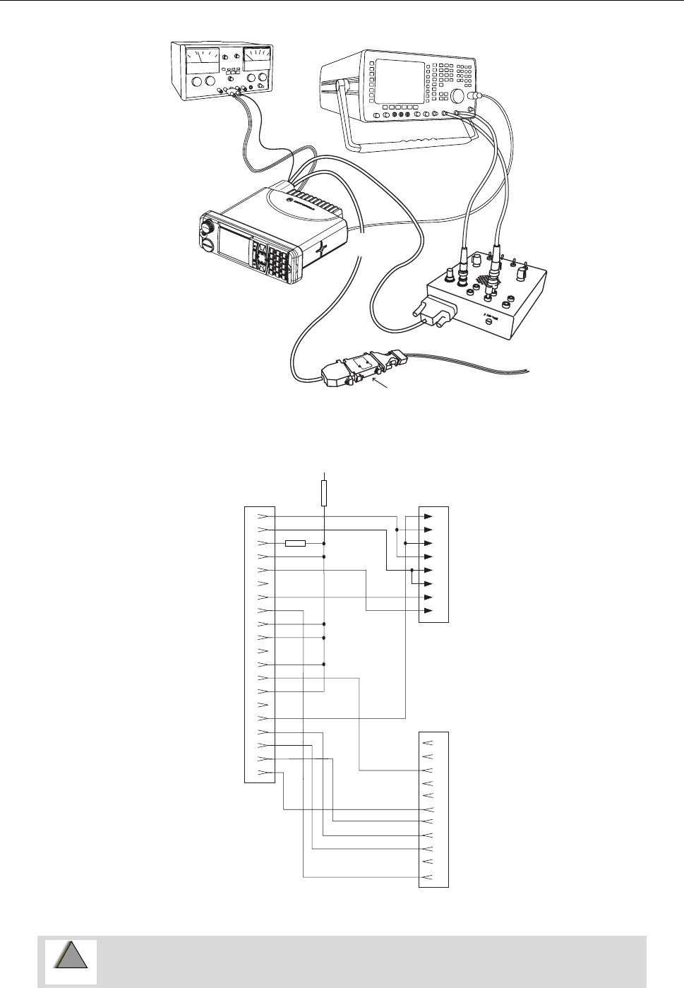
9 - 2 TROUBLESHOOTING
WARNING: By proceeding the GPIO test (see following pages) the above
connections must be set, otherwise the terminal can be damaged.
Figure 9-1 Troubleshooting Setup
Figure 9-2 Required Connections (Accessory Connector / Test Set / Interface Box)
IFR2968
N-Type
RF Connector
RF-Cable
Interface
GMCN1019A
Testbox
RLN4460
P
ower Supply
1
3.2V 5A
DC Cable
BNC-Type
RF Connector
To PC RS232
J0400 Mobile
Radio
Accessory
Connector
SPEAKER -
EXT_MIC_AUDIO
EXTERNAL_PTT
EXTERNAL_ALARM
TX_AUDIO
FLASH / KEYFALL
ANA_GND
DIGITAL GROUND
EMERGENCY
IGNITION
RX_AUDIO
AUDIO_PA_ENABLE
SWB+
HOOK
SCI_DTR
SPEAKER +
SCI_CTS
SCI_RTS
SCI_RXD
SCI_TXD
1
2
3
4
5
6
7
8
9
10
11
12
13
14
15
16
17
18
19
20
AUDIO +
AUDIO -
AUDIO +
AUDIO -
MIC AUDIO
MIC AUDIO
GND
TX_AUDIO
1
2
5
7
10
15
16
18
P1
To Radio
Test Set
RLN4460
EXP_PTT
DTR
SW B +
FLASH
EMERGENCY
RX
TX
BUSY_OUT
BUSY_IN
IGNITION
DIGITAL_GROUN
D
10
11
12
13
14
15
16
17
19
21
24
J1
To Interface Box
GMCN1019
470 Ohm/0,5W
+ pole / Power Supply
4k7
!
W A R N I N G
!
6866539D31.book Page 2 Tuesday, March 20, 2007 6:32 PM
TROUBLESHOOTING 9 - 3
For RF levels, which should be measured with a 50 Ohm RF probe, you can use the following cir-
cuit.
Figure 9-3 Example for 50 Ohm RF Probe
Troubleshooting Flowcharts
Use the following flowcharts to troubleshoot the terminal.
These flowcharts contain procedures which use the TETRA COM SW application to set the
terminal into the appropriate test modes for troubleshooting terminals having digital,
receiver, transmitter, or frequency generation failures.
The terminal performs most of the used TETRA COM commands only in test mode. If not in
test mode, it ignores these commands.
To enter test mode you must enter the command "TEST_ENTER" in TETRA COM.
After about 18 seconds the TETRA COM screen must show the message "Radio HW is
READY" to indicate that the terminal has entered test mode.
Once in test mode, you don't have to use this command again until the test mode is termi-
nated or the terminal performed a reset.
1000pF
1K
R
F + DC Signal
To 50 Ohm Input
To Multimeter
6866539D31.book Page 3 Tuesday, March 20, 2007 6:32 PM

9 - 4 TROUBLESHOOTING
Notes
6866539D31.book Page 4 Tuesday, March 20, 2007 6:32 PM

TROUBLESHOOTING CHARTS: 450-470MHz 9.1 - 1
TROUBLESHOOTING CHARTS: 450-470MHz
6866539D31.book Page 1 Tuesday, March 20, 2007 6:32 PM
9.1 - 2 TROUBLESHOOTING CHARTS: 450-470MHz
Main Function Test Chart (Sheet 1) >> Start-up Procedure <<
"Radio HW is READY"
shown on Tetra Com
Screen
?
Disassemble the main board from the radio
chassis.
Check the main board visually.
Check the supply voltage path of the main
board for a low impedance path to ground.
Check the following components for a low
impedance path to ground: PA FET devices
trans-sorb diode VR0300.
After removing any short to ground or
replacing any faulty component start the
procedure again.
Yes
Start Tetra Com software.
Connect the radio's accessory connector to the Tetra Com interface.
Connect the radio's antenna connector to the RF input on the IFR
Set the power supply to 13.2V and 1A current limit.
Connect the radio's DC connector to the power supply.
Measure the DC current.
Start
Within about 10sec the
Tetra Com screen must
show "Radio HW is
READY"
DC current <1A
?
Yes
No
Setup IFR to :
No System,
TX Test,
Spectrum Analyser
TX Frequency 469.925MHz
Run Tetra Com script for TX test
Controller failure!
Go to Controller Chart
No
Tetra Com Script for TX Test
TEST_ENTER
DELAY 18
Check for "Radio HW is READY"
MODE IDLE
PWRTUNEINTR DIS
FREQ TX 469.925
L1TIMER ON
TXPOW 6
TX_ATT 6
RFTON FRQ 0
RFTON CHN IQ
RFTON ATT 0.65
FEEDBACK CLOSE
MODE RFTONE
Use MODE IDLE to terminate transmit mode
TX power >10W
?
No
Yes
TX frequency
offset stable and within +/-
1kHz
?
No
TX power failure!
Go to RF Power Amplifier Chart
FGU failure!
Go to TX FGU Chart
Yes
A
See Sheet 2
6866539D31.book Page 2 Tuesday, March 20, 2007 6:32 PM
TROUBLESHOOTING CHARTS: 450-470MHz 9.1 - 3
Main Function Test Chart (Sheet 2)
RSSI
reading within -90
and -80dBm
?
Tetra Com Script for RX Test
MODE IDLE
FREQ RX 405.025
L1TIMER ON
AVE 10
MODE RSSI
GO
Use STOP to terminate RSSI reading
Setup IFR to:
No System,
RX Test,
Generator Frequency 460.025MHz
Generator Level -85dBm
Run Tetra Com script for RX test
Yes
No
Tune and test the Radio using
PATS station.
Receiver failure!
Go to Receiver Chart
Connect the speaker output on the radio's accessory connector via
testbox RLN4460B to the audio input on the IFR.
Setup IFR to:
No System,
AF Test,
AF IN/OUT,
Gen 1,2,3 Off,
Distortion On
Run Tetra Com script for RX Audio Test
Tetra Com Script for RX Audio Test
MODE IDLE
DSP_LOOP OFF
GEN_TONE 1000
DSP_VOL -5
VOL_M 27
SPKR INT
Audio level >5V
and distortion < 5%
?
Yes
No
Receiver audio failure!
Go to Receiver Audio Chart
Connect the microphone input on the radio's accessory connector via
testbox RLN4460B to the audio output on the IFR.
Setup IFR to:
No System,
AF Test,
AF IN/OUT,
Gen 1 On,
AF 1 Frequency 1kHz
AF 1 Level 80mV
Distortion On
Run Tetra Com script for TX Audio Test
Tetra Com Script for TX Audio Test
MODE IDLE
GEN_TONE OFF
DSP_LOOP ON
DSP_VOL 0
VOL _M 24
MICGA_M 27
MIC PHF
SPKR INT
Audio level >5V
and distortion < 2%
?
Transmitter audio failure!
Go to Transmitter Audio Chart
No
Yes
A
From Sheet 1
6866539D31.book Page 3 Tuesday, March 20, 2007 6:32 PM
9.1 - 4 TROUBLESHOOTING CHARTS: 450-470MHz
Controller Troubleshooting (Sheet 1)
See Sheet 2
Failure:
No "Radio HW is READY" message on Tetra Com screen 10 sec after
the supply voltage has been applied.
Communication with PATS failed.
Start
Check components and
connections between TP's and
accessory connector.
Yes
Digital DC supply failure!
Go to DC Supply Chart.
No
Disassemble main board from radio chassis.
Check main board visually.
Check fuses F0301and F0302 on the main board.
1.55V DC at
U0306 pin 1
?
3V DC at
U0305 pin 1
?
3V DC at
U0305 pin 5
?
5V DC at
U0303 Pin 3
?
No
Send Tetra Com command "MODE" several times for the followings
test and measure the test point signals with a scope.
Data
activity on
TP0404, TP0405
and TP0401
?
No
Yes
Data
activity on
TP0402
?
Yes
No
Check components and
connections between TP
and accessory connector.
Yes
No
Measure the DC voltages of the
1.8V, 1,55V and 3V regulators.
Yes
No
Before replacing U0306 check
for 5V DC at pin 8 and check
associated components.
Yes
Before replacing U0305 check for
5V DC at pin 8 and check
associated components.
A
1.8V DC at
U1105 pin 5
?
No
Replace U1105
Go to DC supply chart.
5V DC at
U0304 pin 1
(TP0301)
?
No
Yes
Yes
3V DC at
U0308 pin 2
?
No
Check for cold solder
Successively replace:
Q0342, U0308, U0304, U0305, U0306
6866539D31.book Page 4 Tuesday, March 20, 2007 6:32 PM
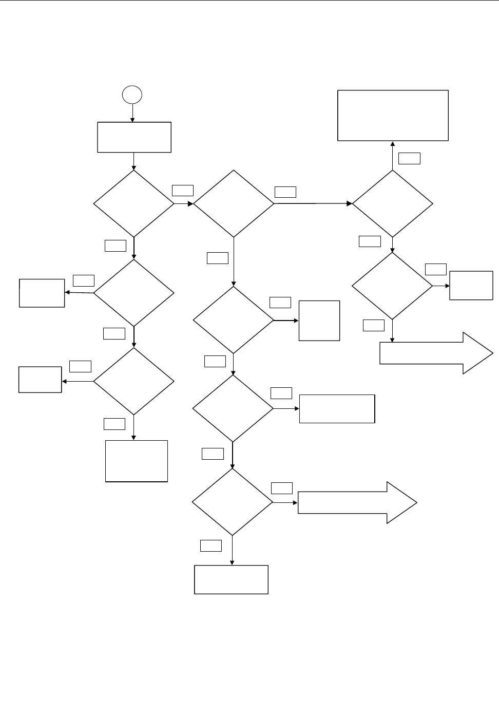
TROUBLESHOOTING CHARTS: 450-470MHz 9.1 - 5
Controller Troubleshooting (Sheet 2)
32.768kHz
signal at U0100
pin 18
?
Yes
16.8MHz
signal at collector
of Q0100
?
No
Yes
No
9.3V DC supply failure!
Go to DC Supply Chart
Measure the 16.8MHz
and the 32.768kHz
signals with a scope
Replace
controller
U1100
16.8MHz
signal at TP5331
?
No
Yes
Before replacing U5331 check
components between collector
Q0100 and U5331 pin 19, check
components between Y5363 and
U5331 pin 23.
5V DC
at U5322 pin 4
?
Yes
32.768kHz
signal at U0100
pin 3
?
No
Replace
Y0101
Before replacing
U0100 check
associated
components
Yes
16.8MHz
signal at Y5363
pin 3
?
Yes
Check
transistor
stage
Q5351
No
2.8V DC
at C0324
?
Yes
No
9.3V DC
at C0308
?
Yes
No
Before replacing
Y5363 check R5364
No
9.3V DC
at U5322 pin 5
?
No
9.3V DC supply failure!
Go to DC Supply Chart
Yes
Replace
U5322
A
Replace
U0307
From Sheet 1
6866539D31.book Page 5 Tuesday, March 20, 2007 6:32 PM
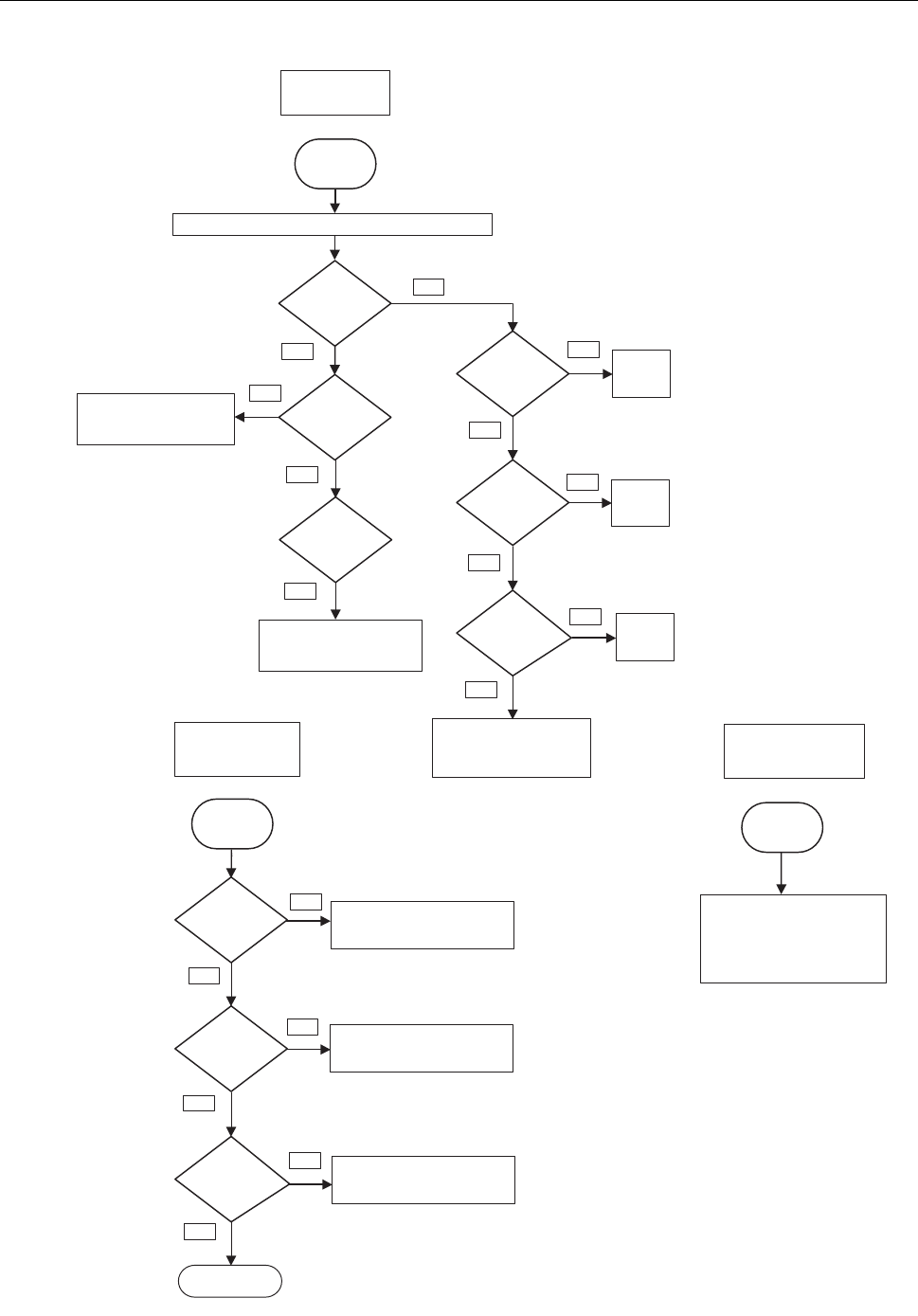
9.1 - 6 TROUBLESHOOTING CHARTS: 450-470MHz
DC Supply Troubleshooting
Failure:
No 9.3V DC supply.
No Digital DC supply.
Yes
No
Before replacing U0301, check
for 13.2V at U0301 pin 4 and
check R0307, R0308
Yes
No
No
Before replacing U0303, check
for 9.3V at U0303 pin 1
Yes
Replace
Q0303
No
Yes
Replace
Q0301
No
Yes
Replace
Q0302
No
Before replacing Q0302 check
components between Q0302
Base and accessory connector
pin 10
Failure:
No EXT SW B+ DC supply.
9.3V supply ok
Before replacing U0302 check for
13.2V at pin 4, 0V at pin 2 and check
resistors R0303, R0304
Failure:
No TX DC supply.
9.3V supply (9V3) ok
Before replacing U0300 check for
13.2V at pin 4, 0V at pin 2 and check
resistors R0305, R0306
9.3V DC at
U0300 pin 5
?
No
Yes
2.8V DC at
C0324
?
Before replacing U0307 check for
9.3V at C0308
No
Yes
5V DC at
U0304 pin 1
(TP 0301)
?
No
Before replacing U0304 check for
9.3V at pin 8
Yes
TX DC supply ok
Short accessory connector pins 10 and 9 to switch on the radio.
Start
0V DC at
U0301 pin 2
?
9.3V DC at
U0301 pin 5
?
5V DC at
U0303 pin 3
?
13.2V DC
at Base of
Q0303
?
0V DC
at Collector of
Q0302
?
0.7V DC
at Base of
Q0302
?
Start
Start
6866539D31.book Page 6 Tuesday, March 20, 2007 6:32 PM
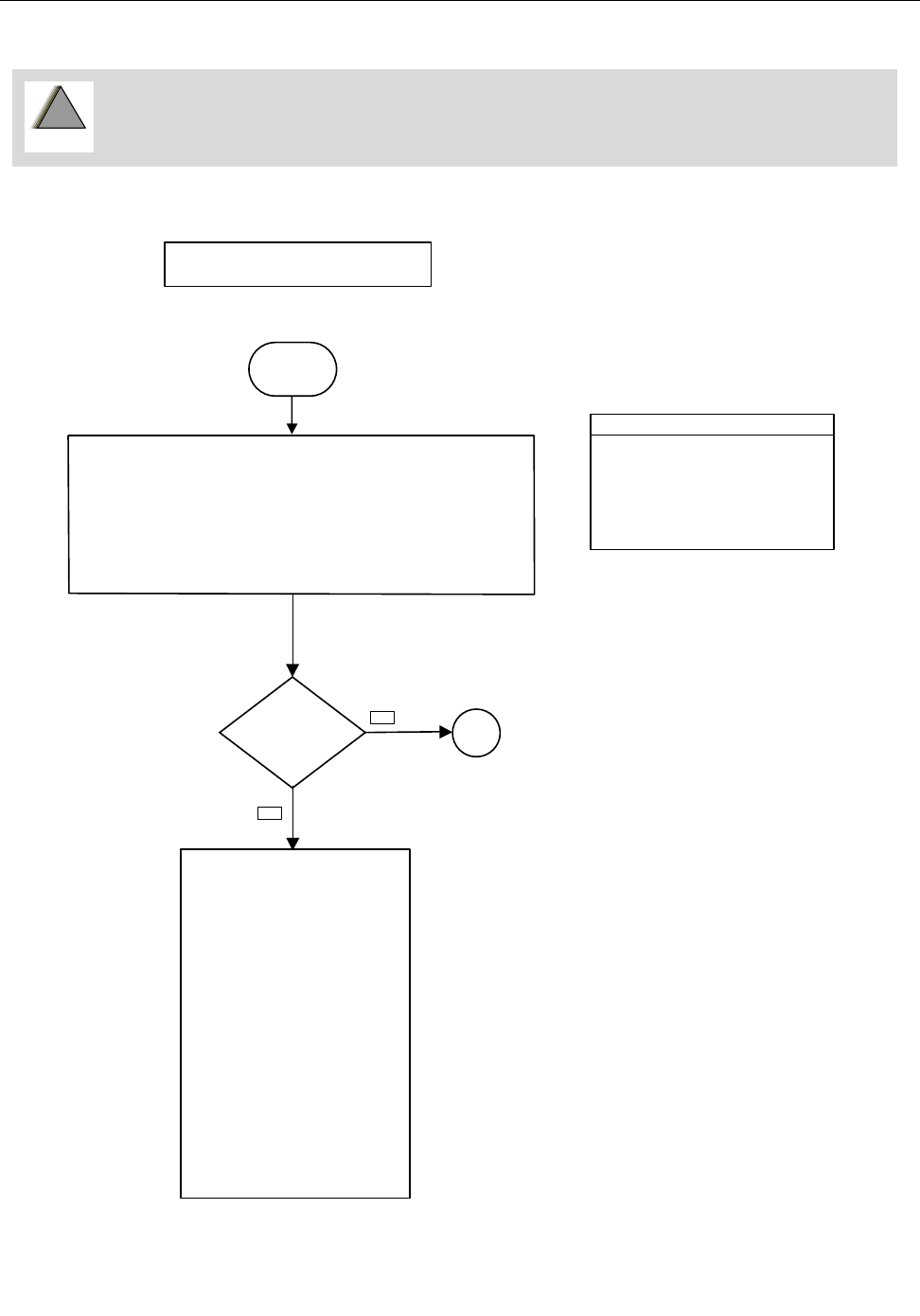
TROUBLESHOOTING CHARTS: 450-470MHz 9.1 - 7
GPIO Troubleshooting
Failure:
PATS parameters HW_CHECK_GPIO failed
Tetra Com Script for GPIO Test
TEST_ENTER
DELAY 18
Check for "Radio HW is READY"
MODE IDLE
HWCHECK_M GPIO_GO
DELAY 0.1
HWCHECK_M GPIO_READ
Connect the radio's accessory connector to the Tetra Com interface.
On the 20 pin accessory connector connect pin 3, 4, 9, 10, 12 and pin 14 together.
After that the radio will be switched on automatically.
Run Tetra Com script for GPIO Test.
Measure DC levels with a multimeter.
The GPIO signals can be monitored with a scope while sending the
Tetra Com command "HWCHECK_M GPIO_GO". If the outputs from
the processor do not change, replace the controller.
Check the following:
For GP 1 IN 0:
Check stage Q0156
For GP 2 OUT 0:
Check stage Q0159
For GP 5 IN 0:
Check stage Q0160
For GP 6 IN 0:
Check stage Q0150
For GP 6 OUT 0:
Check stage Q0150
For GP 8 IN 0:
Check stage Q0152
For GP 8 OUT 0:
Check stage Q0152
If no defective component was found,
replace the controller.
No
Yes
Did the GPIO
test fail
?
Start
OK
Check stage Q0163
For GP 2 IN 0:
Check stage Q0158
For GP 4 IN 0:
By proceeding the GPIO test, the connections as shown in the Troubleshooting
Setup (see previous pages) must be set, otherwise the terminal can be damaged.
!
W A R N I N G
!
6866539D31.book Page 7 Tuesday, March 20, 2007 6:32 PM
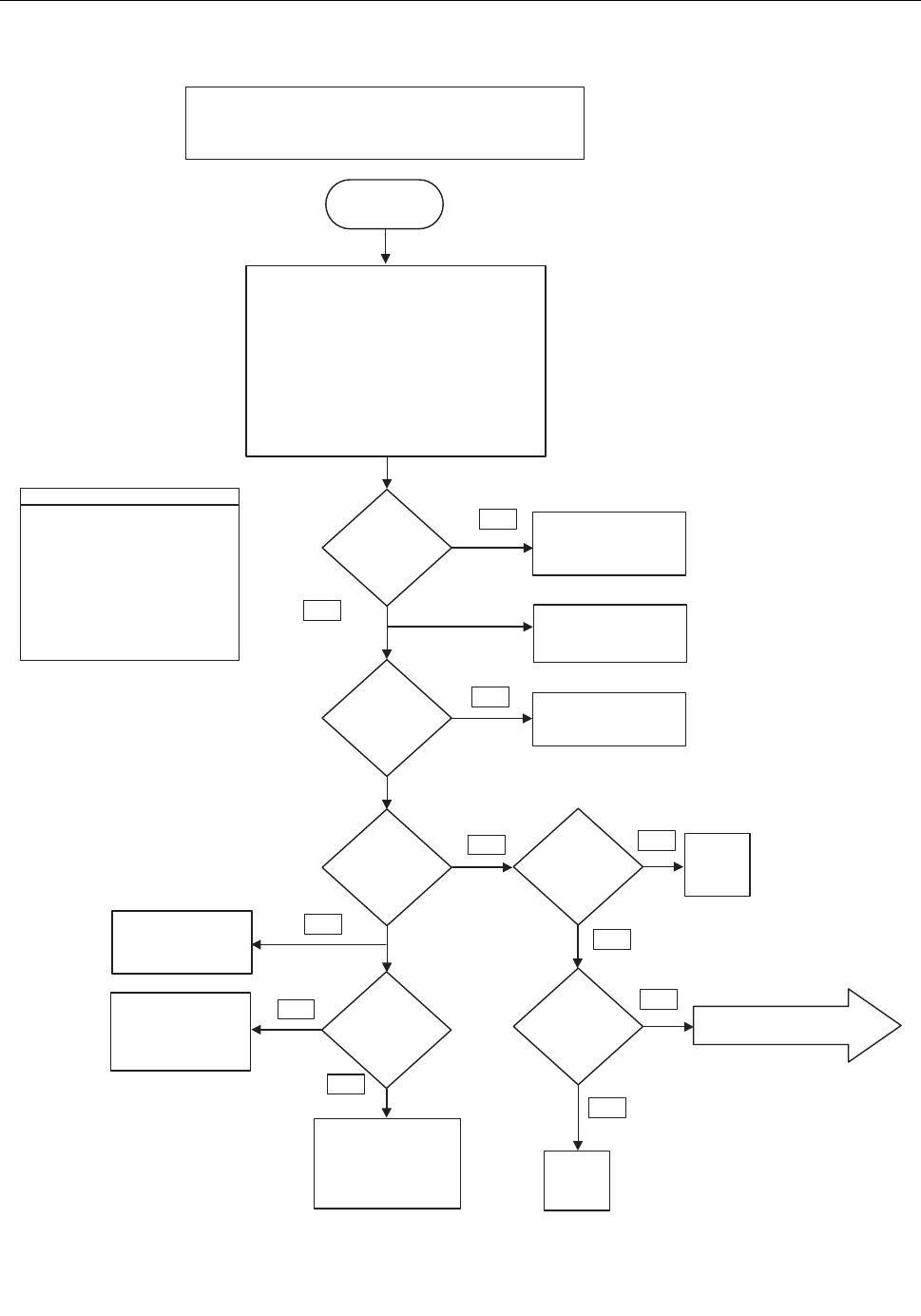
9.1 - 8 TROUBLESHOOTING CHARTS: 450-470MHz
Receiver Audio Troubleshooting
Tetra Com Script for RX Audio Test
MODE IDLE
DSP_LOOP OFF
GEN_TONE 1000
DSP_VOL -5
VOL_M 27
SPKR INT
Yes
Failure:
No audio or low audio level at speaker output or handset audio output.
High distortion at speaker output or handset audio output.
PATS parameters AUD_LBACK_GAIN or AUD_LBACK_DIST failed.
Start
1kHz signal
at U0201 pin 4
?
Yes
No
No
1kHz signal
at FL0200 pin 2
?
0V DC
at U0201 pin 9
?
No
Connect the speaker output on the radio's
accessory connector via testbox RLN4460B to the
audio input on the IFR.
Setup IFR to:
No System,
AF Test,
AF IN/OUT,
Gen 1,2,3 Off,
Distortion On
Run Tetra Com script for RX audio test
Measure the 1kHz audio signal with a scope
No Before replacing
FL0200 check for
activity on pin 7,8,11,13
1kHz signal
at U0201 pin 5
?
If no 1kHz signal at
accessory connector pin
11, check stage U0206-1
Before replacing U0204
check resistors R0221,
R0228 and 3V DC at pin 8
Check
transistor
Q0203
Yes
9.3V DC
at U0201 pin 16
No
9.3V DC supply failure!
Go to DC Supply Chart
Replace
U0201
Yes
If no 1kHz signal at
handset audio output,
check stage U0206-2
> 8.5V DC at
U0205 pin 8
?
Yes
No
Check collector of
transistor Q0200 and
connected resistors.
Before replacing check
mute to low.
If no 1kHz signal at
speaker output, check
R0244, R0245, C0227,
13.2V at pin 7 before
replacing U0205.
?
TEST_ENTER
DELAY 18
Check for "Radio HW is READY"
6866539D31.book Page 8 Tuesday, March 20, 2007 6:32 PM
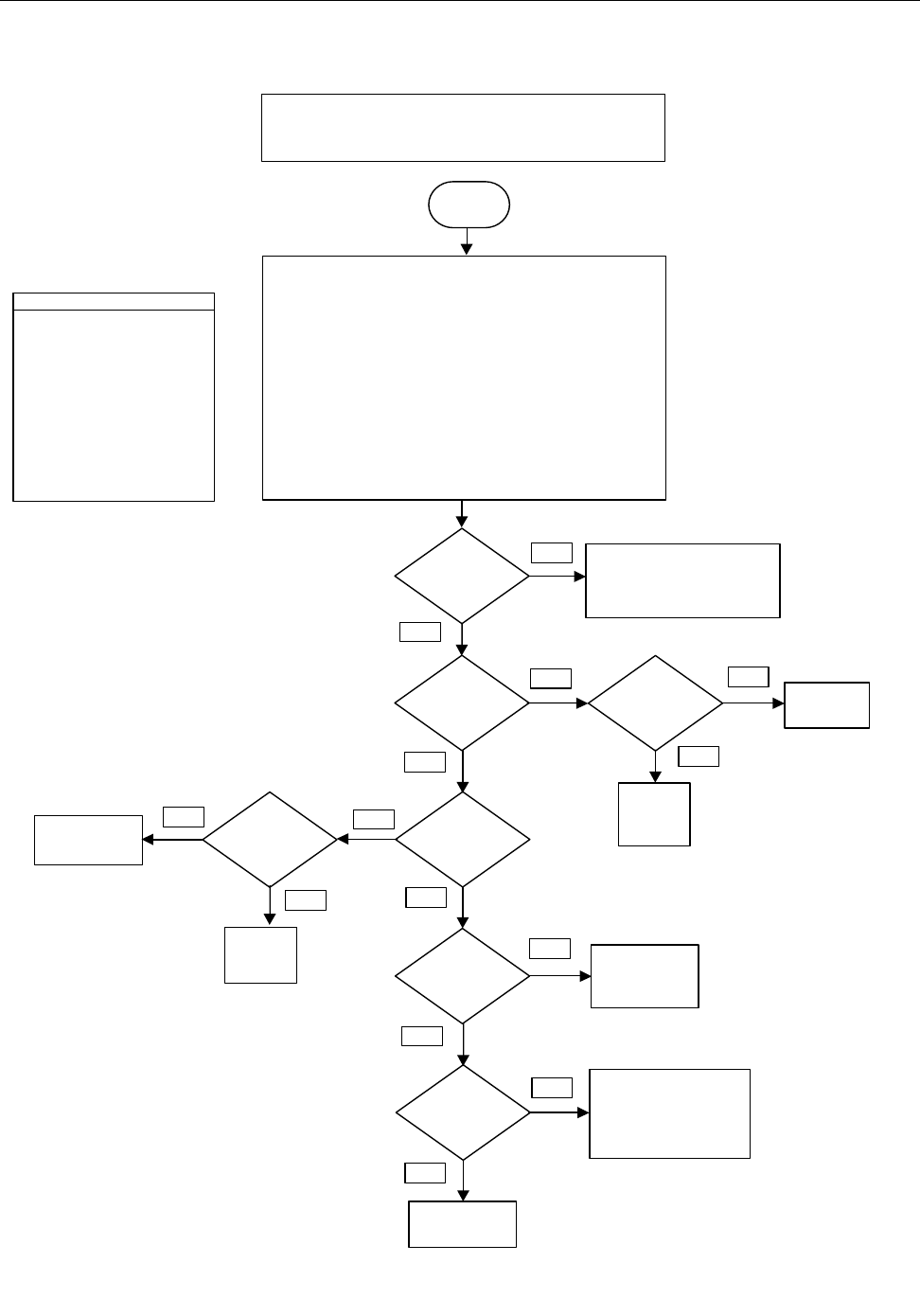
TROUBLESHOOTING CHARTS: 450-470MHz 9.1 - 9
Transmitter Audio Troubleshooting
Check components and connections
between U0201 pin 13 and accessory
connector pin 2
0V DC at
U0201 pin 10
?
Check
transistor
Q0201
Failure:
No audio, low audio level or distortion > 2% at speaker output during
transmitter audio test.
PATS parameters AUD_LBACK_GAIN or AUD_LBACK_DIST failed
If receiver audio has not been checked, go to Receiver Audio Chart first.
Connect the speaker output on the radio's accessory connector via testbox
RLN4460B to the audio input on the IFR.
Connect the microphone input on the radio's accessory connector via testbox
RLN4460B to the audio output on the IFR.
Setup IFR to:
No System,
AF Test,
AF IN/OUT,
Gen 1 On,
AF 1 Frequency 1kHz
AF 1 Level 80mV
Distortion On
Run Tetra Com script for TX audio test
Measure the 1kHz audio signal with a scope
Tetra Com Script for TX Audio Test
TEST_ENTER
DELAY 18
Check for "Radio HW is READY"
MODE IDLE
GEN_TONE OFF
DSP_LOOP ON
DSP_VOL 0
V
OL_M 24
MICGA_M 27
MIC PHF
SPKR INT
Start
Yes
Yes
No
No
No
Yes
No
Yes
Yes
No
No
Yes
Yes
No
1kHz signal at
U0201 pin 14
?
1kHz signal at
U0201 pin 13
?
1kHz signal at
U0201 pin 15
?
1kHz signal at
U0206-4 pin 14
?
1kHz signal at
FL0200 pin 17
?
Replace FL0200
9.3V DC
at U0201 pin 11
?
Check stage
U0206-4
Check
transistor
Q0201
Replace
U0201
Before replacing U0203
check R0220, R0225,
C0221 and 3V DC at pin 8
Check stage
U0206-4
6866539D31.book Page 9 Tuesday, March 20, 2007 6:32 PM
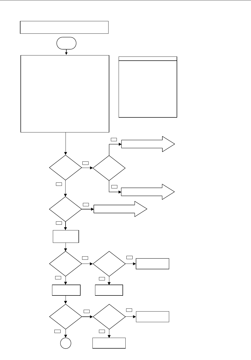
9.1 - 10 TROUBLESHOOTING CHARTS: 450-470MHz
Warping Failure Troubleshooting
OK
Yes
Yes
Yes
Yes Yes
Yes
Yes
No
No
No
No
No
No
No
RF
power at
antenna connector
> 10dBm
?
RF
level at
TP5401 about
-30 dBm
?
No TX Output Power!
Go to RF Power Amplifier Chart.
No JAVELIN Output Power!
Go to JAVELIN Chart.
FGU failure!
Go to Main Synthesizer Chart.
Is frequency
stable at 469.925MHz
+/-7kHz
?
Send Tetra Com
command "PN 0"
Is frequency
about 7kHz above
469.925MHz
?
DC
at Y5363 pin 1 about
2.4V
?
Replace U5331
Send Tetra Com
command "PN 1FF"
Check for 2.7V DC at
Y5363 pin 4 before
replacing Y5363
Is frequency
about 7kHz below
469.925MHz
?
DC
at Y5363 pin 1 about
0.4V
?
Replace U5331
Replace Y5363
Failure:
PATS parameters WARP_RANGE, WARP_RES, FREQ_ERR or
WARP_SP failed
Tetra Com Script for TX FGU Test
TEST_ENTER
DELAY 18
Check for "Radio HW is READY"
MODE IDLE
INTR DIS
FREQ TX 469.925
L1TIMER ON
TX POW 4
RFTON ATT 0.5
RFTON FRQ 0
RFTON CHN I
FEEDBACK OPEN
MODE RFTONE
Use MODE IDLE to terminate transmit mode
Connect the radio's accessory connector to the Tetra Com interface.
Connect the radio's antenna connector to the high power RF output
on the IFR.
Connect the 50 ohms RF probe to the low power RF input on the IFR.
Setup IFR:
Select high power input for measuring power at the antenna connector.
Select low power input for measuring with 50ohms RF probe.
No System,
TX Test,
TX Frequency 469.925MHz
Spectrum Analyser
Set Reference Level to 30dBm.
Run Tetra Com script for TX FGU Test.
Measure RF levels and frequencies with the 50ohms RF probe.
Measure DC levels with a multimeter.
If the cover is removed from the chassis, the RF PA is disabled to
prevent overheating of the FET devices. To measure the power at the
antenna connector, the pressure pad can be used to short the contact
area on the main board. This should be done only for a few seconds.
Start
6866539D31.book Page 10 Tuesday, March 20, 2007 6:32 PM
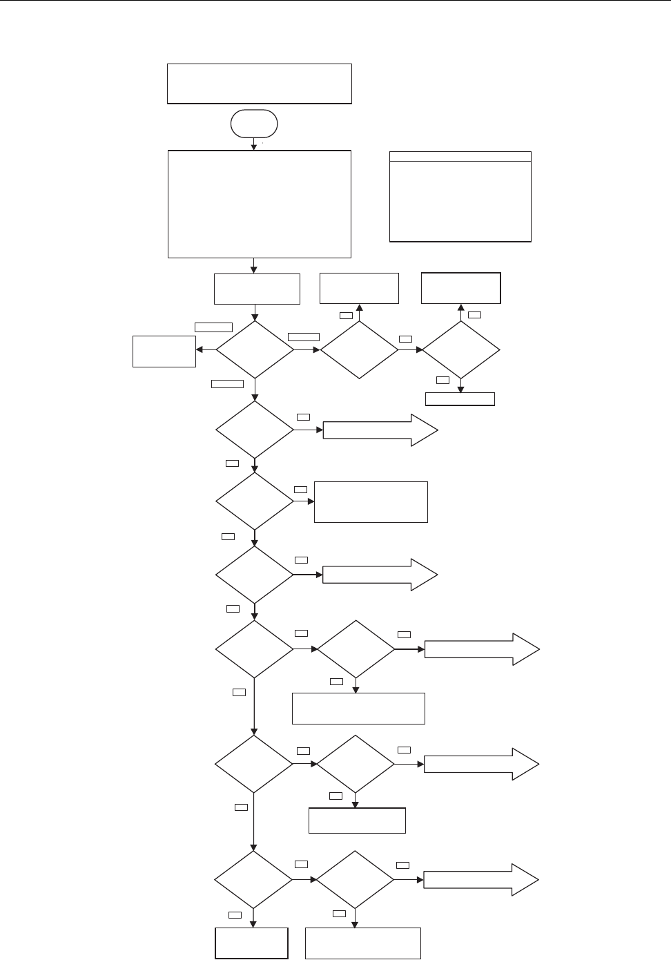
TROUBLESHOOTING CHARTS: 450-470MHz 9.1 - 11
RF Power Amplifier Troubleshooting
Measure the output power
at the antenna connector
Check
R5453, R5454, R5455,
R5451, R5452, C5451 Replace L5812
Tune Radio RF Power at antenna
connector
?
RF level
at TP5451 about
300mV
?
Are both
splitter outputs
measured at C5862
and C5863 about
300mV
?
Replace U5803
Is
DC current
greater than
850mA
?
PA bias problem!
Go to PA Bias Tuning Chart
RF
level at
TP5451 about
300mV
?
Check D5451, D5551 and their DC
path, check components between
C5452 and antenna connector.
RF
level at
TP5401 about
220mV
?
No JAVELIN output signal
Go to JAVELIN Chart
RF
level at
Gate of Q5421 about
160mV
?
DC
at TP5402 about
4.4V
?
PA bias problem!
Go to PA Bias Tuning Chart
Check R5533, L5403, 9.3V DC at R5533.
Check components between TP5401 and
Q5421 before replacing U5401
RF level
at Q5421 Drain
about 2.2V
?
DC
at TP4409 about
2.2V
?
PA bias problem!
Go to PA Bias Tuning Chart
Check components
between
Q5431 and D5451
Check L5431, components between
Q5421 and Q5431, check 13.2V DC
at L5431 before replacing Q5431
DC
at TP5541 about
2.2V
?
RF level
at Q5431 Drain
about 7V
?
Check L5421 and 9.3V DC at
L5421 before replacing Q5421
PA bias problem!
Go to PA Bias Tuning Chart
Failure:
No or low RF output power.
Too high RF output power.
PATS parameters ADJ_PWR1-5, ATT_SP1-5,
DC_CUR1-5, TX_PWR_F1-5 failed.
Tetra Com Script for TX Power Test
TEST_ENTER
DELAY 18
Check for "Radio HW is READY"
MODE IDLE
INTR EN
FREQ TX 429.925
L1TIMER ON
TXPOW 6
MODE TXNDC
Use MODE IDLE to terminate transmit mode
Connect the radio's accessory connector to the Tetra Com
interface. Connect the radio's antenna connector to the
high power RF input on the IFR.
Setup IFR:
Select high power input
No System,
TX Test,
TX Frequency 429.925MHz
Spectrum Analyser
Set Reference Level to 40dBm
Run Tetra Com script for TX Power Test
Measure RF levels with the high impedance RF probe and
millivoltmeter.
Measure DC levels with a multimeter.
No No
No
No
No
No
No No
No
No
No
Yes
34 - 37dBm
> 37dBm
< 34 dBm Yes
Yes
Yes
Yes
Yes
Yes
Yes
Yes
Yes
Yes
Start
6866539D31.book Page 11 Tuesday, March 20, 2007 6:32 PM
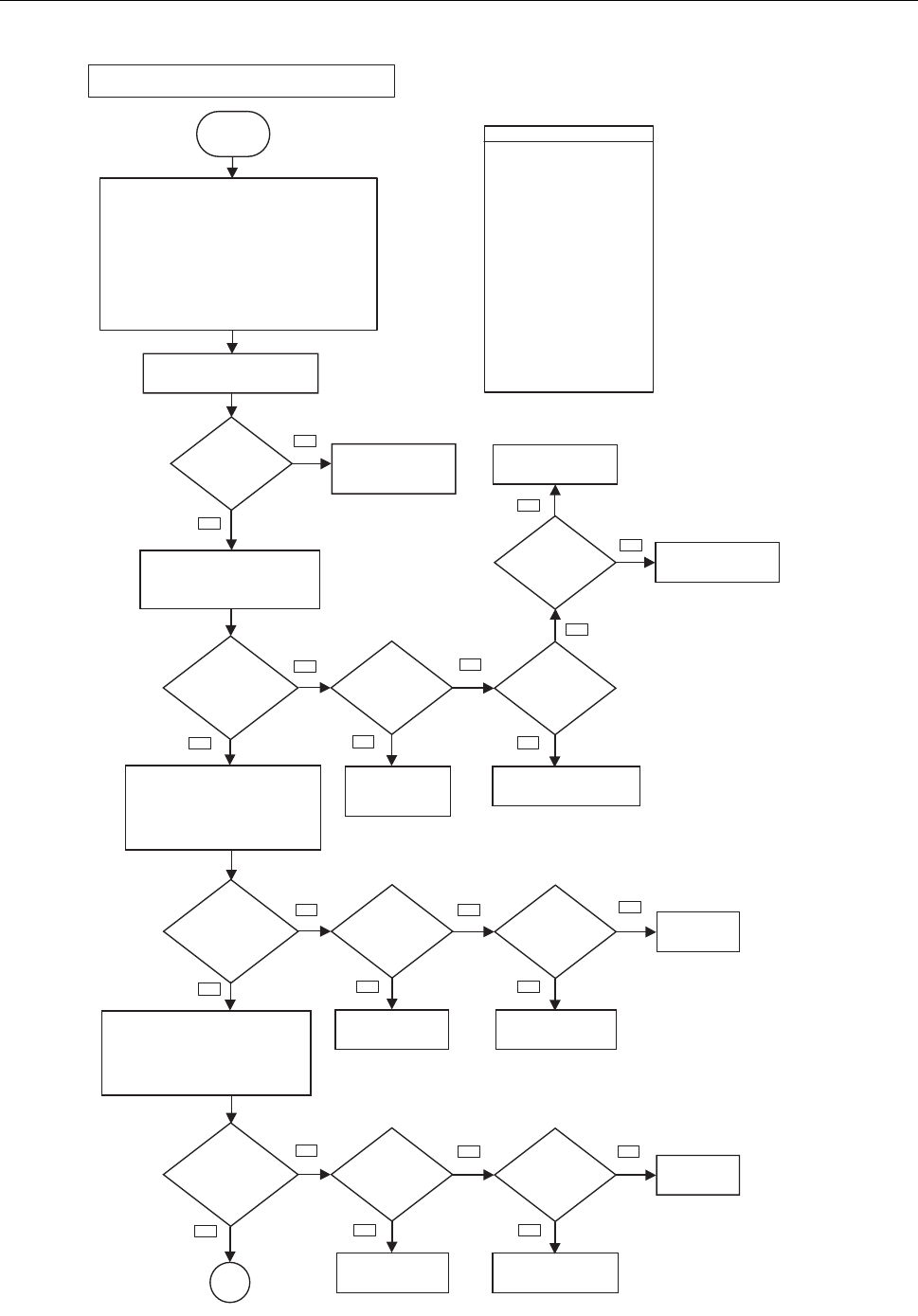
9.1 - 12 TROUBLESHOOTING CHARTS: 450-470MHz
PA Bias Failure Troubleshooting
OK
Measure the DC current of the radio.
Use this as reference current.
Is the
DC current within
420-460mA
?
Check antenna switch
diodes D5451, D5551,
Q5551, Q5552,Q5804,
Q5802, JAVELIN
Check for 9.3V at U0150
pin 15 before replacing
U0150
DC at
U0150 pin 16
about 4.7V
?
Check for 9.3V at U0150
pin 15 before replacing
U0150
Send Tetra Com command
"PA_BIAS_M 1 xx" to set Bias 1 to xx.
Use a value from PA_BIAS_TBL_M 1
for xx.
Measure the DC current of the radio.
Can
the current
be set to 57-85 mA
higher than the reference
current by changing
Bias 1
?
Does
the DC change
at TP5402 if the
Bias 1 setting is
changed
?
Does
the DC change
at U0150 pin 4 if the
Bias 1 setting is
changed
?
Send Tetra Com command
"PA_BIAS_M 1 0".
Send Tetra Com command
"PA_BIAS_M 2 xx" to set Bias 2 to xx.
Use a value from
PA_BIAS_TBL_M 2 for xx.
Measure the DC current of the radio.
Check R5533, L5403,
L5502, 9V3_TX
before replacing
U5401
Check transistor stage Q5501
Can
the current
be set to 90-110 mA
higher than the reference
current by changing
Bias 2
?
Does
the DC
change at TP4409 if
the Bias 2 setting is
changed
?
Does the
DC change at
U0150 pin 18 if the
Bias 2 setting is
changed
?
Replace U0150
Send Tetra Com command
"PA_BIAS_M 2 0".
Send Tetra Com command
"PA_BIAS_M 3 xx" to set Bias 3 to xx.
Use a value from
PA_BIAS_TBL_M 3 for xx.
Measure the DC current of the radio.
Check
R5405, R5406, L5421
before replacing Q5421
Check transistor stage
Q5521
Can
the current
be set to 260-310 mA
higher than the reference
current by changing
Bias 3
?
Does the DC
change at TP5541 if
the Bias 3 setting is
changed
?
Does the
DC change at
U0150 pin 24 if the
Bias 3 setting
is changed
?
Replace U0150
Check
R5431, L5431, L5503
before replacing Q5431
Check transistor stage
Q5542
Yes
Yes Yes Yes
Yes
Yes
YesYes
Yes
Yes
Yes
No
No
No
No
No
No No No
NoNo
No
Failure:
PATS parameters PA_BIAS, BIAS1-3_CUR, BIAS_1-3_SP failed
Tetra Com Script for PA Bias Test
TEST_ENTER
DELAY 18
Check for "Radio HW is READY"
MODE IDLE
INTR DIS
FREQ RX 380.075
L1TIMER ON
TXPOW 1
RFTON ATT 0
RFTON FRQ 10
RFTON CHN IQ
PA OFF
PA_BIAS_M 1 0
PA_BIAS_M 2 0
PA_BIAS_M 3 0
PA_BIAS_TBL_M 1
PA_BIAS_TBL_M 2
PA_BIAS_TBL_M 3
MODE RFTONE
Use MODE IDLE to terminate
RFTONE mode
Connect the radio's accessory connector to the Tetra Com
interface.
Connect the radio's antenna connector to the
high power RF output on the IFR.
Run Tetra Com script for PA Bias Test
Measure DC levels with a multimeter.
Measure the DC current of the radio
If the cover is removed from the chassis, the RF PA is
disabled to prevent overheating of the FET devices.
To measure the power at the antenna connector, the
pressure pad can be used to short the contact area on the
main board. This should be done only for a few seconds.
Start
6866539D31.book Page 12 Tuesday, March 20, 2007 6:32 PM
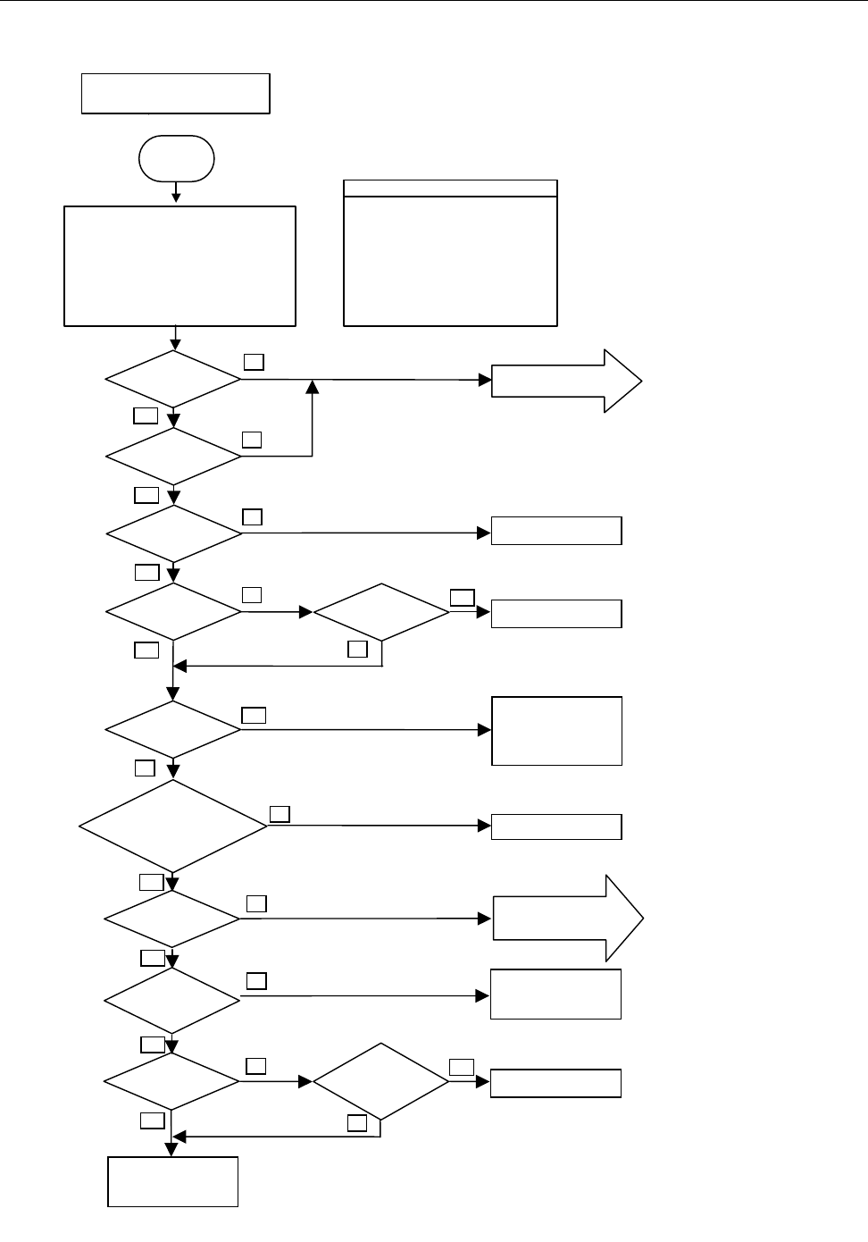
TROUBLESHOOTING CHARTS: 450-470MHz 9.1 - 13
JAVELIN Troubleshooting
Start
Failure:
Tetra Com Script for TX Power Test
TEST_ENTER
DELAY 18
Check for "Radio HW is READY"
MODE IDLE
INTR EN
FREQ TX 429.925
L1TIMER ON
TXPOW 6
MODE TXNDC
Use MODE IDLE to terminate transmit mode.
Connect the radio's accessory connector to the
Tetra Com interface.
Connect the radio's antenna connector to the
high power RF output on the IFR.
Run Tetra Com script for TX Power Test
Measure RF levels with the high impedance
RF probe and millivoltmeter.
Measure DC levels with a multimeter.
No or low JAVELIN output signal level.
2.8V DC at
C5875 ?
No
Yes
TX DC supply failure
Go to DC supply chart
5V DC at
TP5811?
No
Yes
5V DC at
Q5804 p
No
Yes
Check Q5301
5V DC at
TP5841 ?
No
Yes
> 2V DC at
No
Yes
Check Q5802; Q5804
0V DC at
R5855 ?
Yes
No
Re
p
Yes
No
Yes
RF level at
TP5801 about
200mV ?
Check components
between TP5801 and
T5801
No
Yes
Yes
No
RF level at
TP5811 about
200mV ?
No
Before replacing
U5809 check
R5850..R5854
Yes
Change T5802
RF level
bot h s ides of L580
t 130...200mV ?
at 9
abou
RF level at C5803;
C5813 about
400..600mV ?
No TX VCO signal
Go to TX frequency
generation chart
No
Before replacing
U5809
check R5850 to R5854
lace U5810
Is AC about 750m Vp-p
measured with a scope
at TP5805…..TP5808?
And DC 1.9V?
Q5802
Pin 4
in2 ?
6866539D31.book Page 13 Tuesday, March 20, 2007 6:32 PM
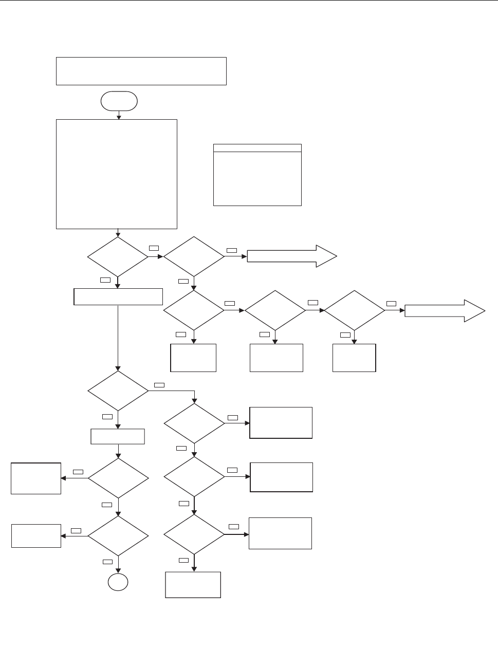
9.1 - 14 TROUBLESHOOTING CHARTS: 450-470MHz
Receiver Troubleshooting (Sheet 1)
No VCO output signal!
Go to Main VCO Chart
0V DC at U5701
pin 19 & 20
?
RF level at
C5704 about -5dBm
?
RF level at
TP5702 about
-5dBm
?
RF
level at
TP5071 about
10dBm and frequency
stable at
331.675MHz
?
RF
level at
TP5071 about 10dBm
but frequency
incorrect
FGU failure!
Go to Main Synthesizer Chart
Set IFR TX Frequency to 405.025MHz
Set IFR Reference Level to 0dBm
Check transitor
stage Q5701,
switch Q5711 and
switch Q5301
Check switch Q5301
and components
between Q5301 and
U5701 pin 19 & 20
Replace U5701
RF level at
T5061 pin 4
about -20dBm
?
Set IFR TX Frequency
to 73.35MHz
RF level at
TP5201 about
-30dBm
?
Check components
between
U5201 and T5061
Check
D5061, T5062
RF level at
TP5202 about
-30dBm
?
Replace U5201
RF level at
Q5031 Collector
about -22dBm
?
4.4V DC at
TP5021
?
Check components
between
Q5031 and antenna
connector.
5.8V DC at
Q5031 Collector
?
Check components
between
Q5031 and T5061
Before replacing U0150
check R5021 and 9.3V
DC at U0150 pin 15
Before replacing Q5031
check: 9.3V DC at C5002,
0V DC at C5001.
Check Q5001 and
associated components.
No Yes
No
No
No
No
Yes
Yes
Yes
Yes
Yes
Yes
Yes
Yes
No
No
No
No
Yes Yes
Failure:
Bit Error Rate @ -114dBm >3.5%
RSSI error >+/- 5dB
PATS parameter GAIN_OFF_L, GAIN_OFF_H and
AGC_SLOPE failed.
Tetra Com Script for RX Test
TEST_ENTER
DELAY 18
Check for "Radio HW is READY"
MODE IDLE
FREQ RX 460.025
L1TIMER ON
AVE 10
MODE RSSI
GO
Use STOP to terminate RSSI reading
Connect the radio's accessory connector to the
Tetra Com interface.
Connect the radio's antenna connector to the high
power RF output on the IFR.
Connect the 50ohms RF probe to the low power
RF input on the IFR
Setup IFR:
Select high power output and low power input
No System,
Duplex Test,
Generator Frequency 460.025MHz,
TX Frequency 386.675MHz
Generator Level -30dBm,
Duplex Test TX,
Spectrum Analyser
Set Reference Level to 10dBm
Run Tetra Com script for RX test
Measure RF levels and frequencies with the
50ohms RF probe.
Measure DC levels with a multimeter.
ZWG0130968-O
Receiver Chart 1
UHF
A
No
No
Start
6866539D31.book Page 14 Tuesday, March 20, 2007 6:32 PM
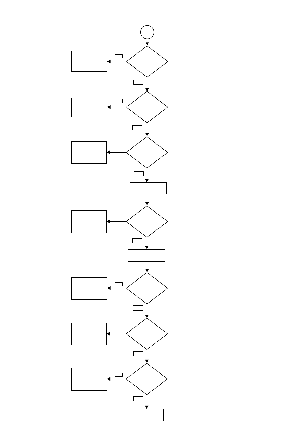
TROUBLESHOOTING CHARTS: 450-470MHz 9.1 - 15
Receiver Troubleshooting (Sheet 2)
No
No
No
No
No
No
No
A
RF
level at
Q5201 Collector
about -10dBm and
DC about
3.2V
?
Check transistor
stage Q5201
Check transistor
stage Q5101
Check components
between Q5101
and C5127
RF
level at
Q5101 Collector
about -2dBm and
DC about 4.4V
?
RF
level at
C5127 about
-30dBm and DC
about 1V
?
Set IFR TX Frequency
to 18MHz
18MHz
RF level
at C5197 about
-13dBm and DC
about 3.1V
?
Check components
of
VCO stage Q5190
Check components
of
VCO stage Q5180
Set IFR TX Frequency
to 71.1MHz
71.1MHz
RF level at
C5187 about -13dBm
and DC about
1.8V
?
Check DC at U5102
fo 9.3V before
replacing U5102
3.3V DC at
U5102 pin 5
?
Check DC at U5103
fo 9.3V before
replacing U5103
Replace U5101
3.3V DC at
U5103 pin 5
?
Yes
Yes
Yes
Yes
Yes
Yes
Yes
6866539D31.book Page 15 Tuesday, March 20, 2007 6:32 PM
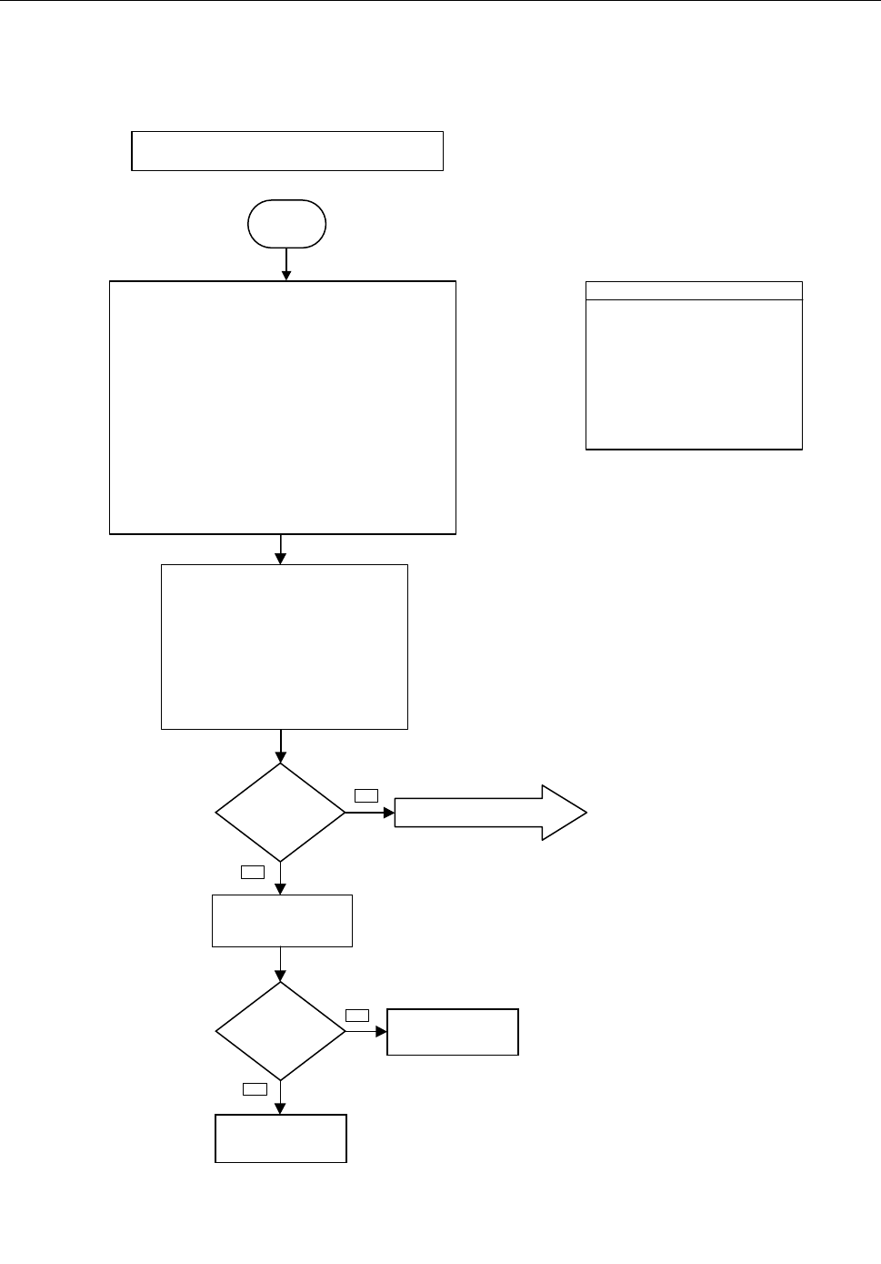
9.1 - 16 TROUBLESHOOTING CHARTS: 450-470MHz
Front-End Tuning Troubleshooting
No
No
Yes
Yes
Did the DC
change
?
Check
R5022, R5051, D5011,
D5012, D5041, D5042
Check R5021, 9.3V DC
at U0150 pin 14
before replacing U0150
Send the above Tetra Com
commands again and
measure the DC at TP5021
Did the RSSI
readings change
at least 5dB
?
Receiver failure!
Go to Receiver Chart
Failure:
PATS parameters FE_FILTER, FE_DAC, FE_OFFSET failed.
Tetra Com Script for RX Test
TEST_ENTER
DELAY 18
Check for "Radio HW is READY"
MODE IDLE
FREQ RX 460.025
L1TIMER ON
AVE 10
MODE RSSI
GO
Use STOP to terminate RSSI reading
Connect the radio's accessory connector to the Tetra Com interface.
Connect the radio's antenna connector to the high power RF output
on the IFR.
Setup IFR:
Select high power output
No System,
RX Test,
Generator Frequency 460.025MHz,
Generator Level -70dBm,
Duplex Test TX,
Spectrum Analyser
Set Reference Level to 10dBm
Run Tetra Com script for RX Test
Measure RF levels and frequencies with the 50ohms RF probe.
Measure DC levels with a multimeter.
Note the RSSI reading.
Enter "STOP" to terminate RSSI reading
Send Tetra Com command "RXFEFLTR_M"
Note the replied setting.
Send Tetra Com command "RXFEFLTR_M 0"
Send Tetra Com command "RSSI" twice
Note the RSSI reading.
Send Tetra Com command "RXFEFLTR_M 7F"
Send Tetra Com command "RSSI" twice
Note the RSSI reading.
Compare the RSSI readings
Start
6866539D31.book Page 16 Tuesday, March 20, 2007 6:32 PM
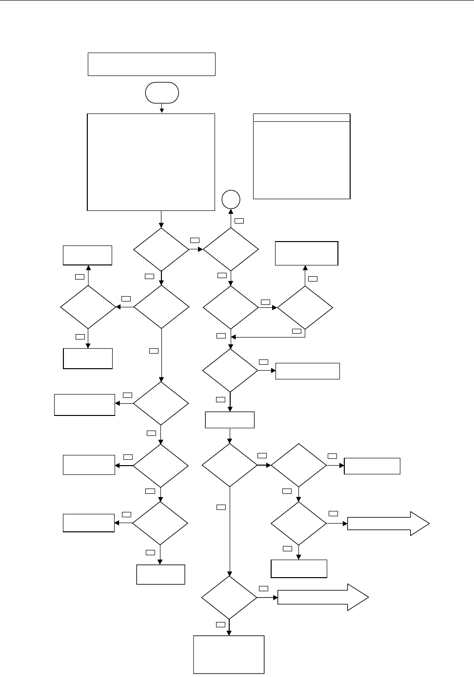
TROUBLESHOOTING CHARTS: 450-470MHz 9.1 - 17
Tx Frequency Generation Troubleshooting
Check transistor stage
Q5621 and switch
Q5301
RF level
at Q5621 Collector
about 0dBm and DC
about 3.9V
?
Check components
between
Q5621 and C5837
Check components
U5601, D5601- D5604 and
associated components
Check transistor stage
Q5671 and 5V source
U5322
Check transistor switch
Q5301 bevor replacing
Q5602
Check DC path of
stage Q5601 before
replacing Q5601
Before replacing U5702 check
transistor stage Q5681, Q5651,
3.3V at U5702 pin 15,
components between Q5631
collector and U5702 pin 16.
FGU failure!
Go to Main Synthesizer Chart
Before replacing U5701
check
R5706, R5707, C5706
Is
frequency correct and
stable
?
RF level at
TP5702 about
-5dBm
?
2.7V DC at
U5701 pin 19 & 20
?
RF
level at R5707 about
0dBm
?
Set IFR TX Frequency
to 469.925 * 0.8 MHz
RF level at
Q5631 Collector
about 0dBm
?
Check transitor stage Q5631
DC
at R5653
<1V and frequency
< 469.925MHz at
C5837
?
DC
at R5653
>7V and frequency
>469.925MHz at
C5837
?
Check components
U5601, D5601- D5604
and associated components.
Is
frequency stable at
469.925MHz
?
RF level
at C5804 about
0dBm
?
RF level at
Q5601 Emitter
about 0dBm
?
1.4V DC at
Q5601 Emitter
?
4.3V DC at
Q5671 Emitter
?
2.1V DC at Q5602
Collector
?
No Main VCO signal
Go to Main VCO Chart
Check transitor switch
Q5301, U5322, U5331
No
No No
No
No
No
No
No
No
No
No
No
No
No
Yes
Yes
Yes
Yes
Yes
Yes
Yes
Yes
Yes
Yes
Yes
Yes
Yes
Yes
Failure:
No or low TX LO signal level.
TX frequency error greater than 2 kHz or unstable after
frequency tuning.
Tetra Com Script for TX FGU Test
TEST_ENTER
DELAY 18
Check for "Radio HW is READY"
MODE IDLE
INTR DIS
FREQ TX 469.925
L1TIMER ON
TX POW 4
RFTON ATT 0.5
RFTON FRQ 0
RFTON CHN I
FEEDBACK OPEN
MODE RFTONE
Use MODE IDLE to terminate transmit mode
Connect the radio's accessory connector to the Tetra Com
interface.
Connect the radio's antenna connector to the high power
RF output on the IFR.
Connect the 50 ohms RF probe to the low power RF input
on the IFR
Setup IFR:
Select high power output and low power input
No System,
TX Test,
TX Frequency 469.925MHz
Spectrum Analyser
Set Reference Level to 10dBm
Run Tetra Com script for TX FGU Test
Measure RF levels and frequencies with the 50ohms RF probe.
Measure DC levels with a multimeter.
Start
OK
ZWG0130967-O
6866539D31.book Page 17 Tuesday, March 20, 2007 6:32 PM
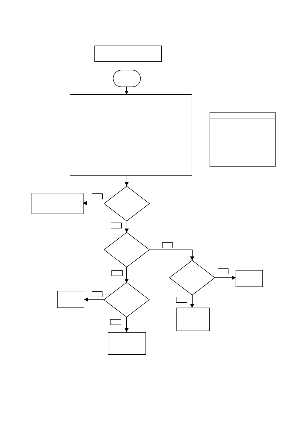
9.1 - 18 TROUBLESHOOTING CHARTS: 450-470MHz
Main VCO Troubleshooting
Failure:
VCO signal level at TP5702 < -5dBm
Yes
Tetra Com Script for RX Test
TEST_ENTER
DELAY 18
Check for "Radio HW is READY"
MODE IDLE
FREQ RX 460.025
L1TIMER ON
AVE 10
MODE RSSI
GO
Use STOP to terminate RSSI readin
g
Connect the radio's accessory connector to the Tetra Com interface.
Connect the radio's antenna connector to the high power RF output
on the IFR.
Connect the 50 ohms RF probe to the low power RF input on the IFR.
Setup IFR:
Select high power output and low power input.
No System,
TX Test,
TX Frequency 386.675MHz
Spectrum Analyser
Set Reference Level to 10dBm.
Run Tetra Com script for RX test.
Measure RF levels and frequencies with the 50ohms RF probe.
Measure DC levels with a multimeter.
0.6V DC at
U5701 pin 6
?
Yes
No
4.6V DC at
C5343
?
No
Yes
Check components between
U5701 pin 5 & 6 and TP5701
3.3V DC at
U5701 pin 14 & 18
?
Yes
No
Replace
U5701
Check for 9.3V at
U5321 pin 1 & 3
before replacing
U5321
5V DC at U5331
pin 30
?
No
Replace
U5331
Check for 9.3V at
U5322 pin 3 &
6 and L5301 before
replacing U5321
Start
6866539D31.book Page 18 Tuesday, March 20, 2007 6:32 PM
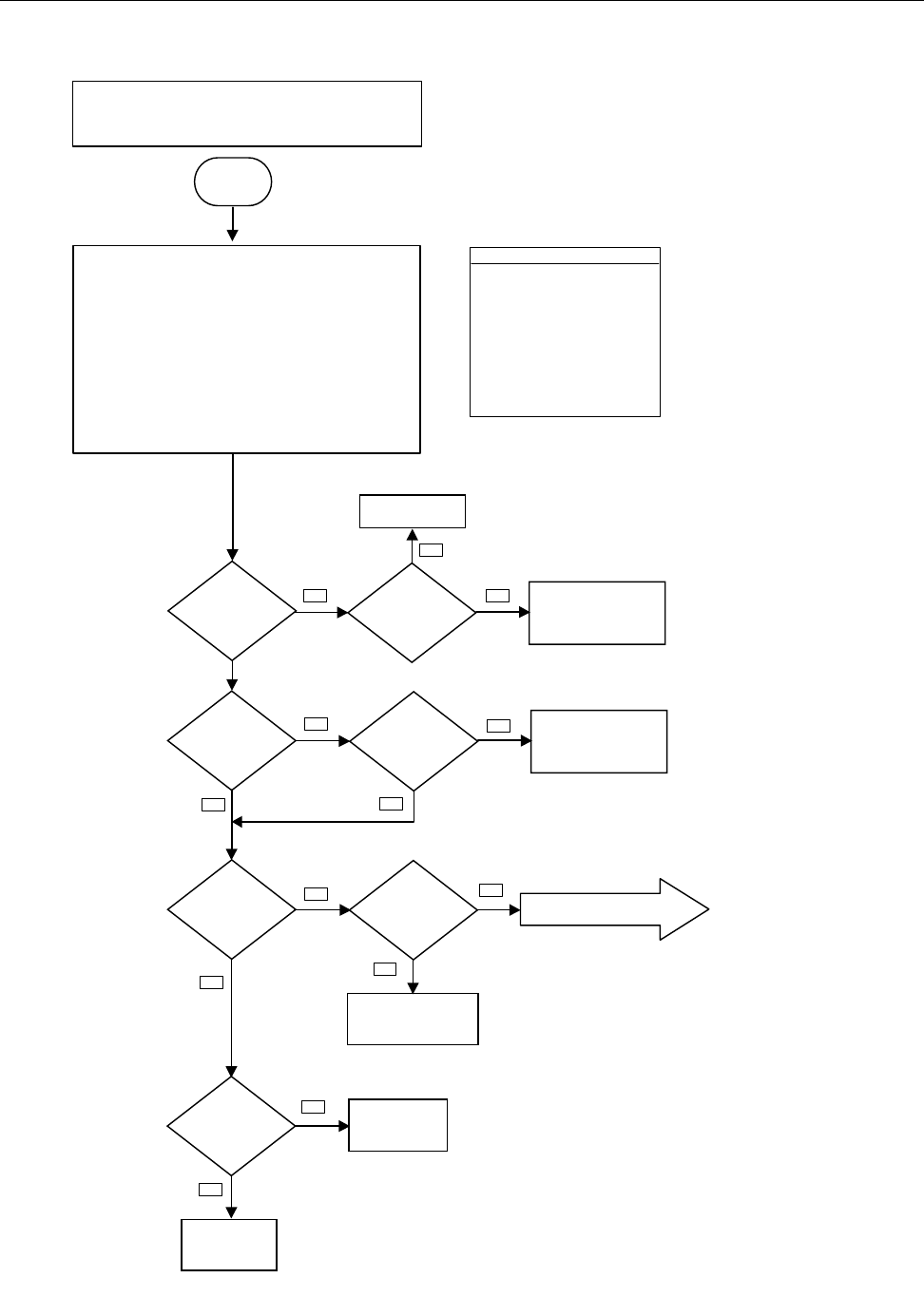
TROUBLESHOOTING CHARTS: 450-470MHz 9.1 - 19
Main Synthesizer Troubleshooting
Start
Failure:
RX injection frequency error greater than 2 kHz or unstable frequency.
Main VCO frequency error at TP5702 greater than 2 kHz or unstable
frequency after frequency tuning.
Tetra Com Script for RX Test
TEST_ENTER
DELAY 18
Check for "Radio HW is READY"
MODE IDLE
FREQ RX 460.025
L1TIMER ON
AVE 10
MODE RSSI
GO
Use STOP to terminate RSSI reading
Connect the radio's accessory connector to the Tetra Com interface.
Connect the radio's antenna connector to the high power RF output
on the IFR.
Connect the 50 ohms RF probe to the low power RF input on the IFR.
Setup IFR:
Select high power output and low power input
No System,
TX Test,
TX Frequency 386.675MHz
Spectrum Analyser
Set Reference Level to 10dBm
Run Tetra Com script for RX Test
Measure RF levels and frequencies with the 50 ohms RF probe.
Measure DC levels with a multimeter.
DC at
C5316 about 13.5V
?
3Vp-p
1.05MHz at
R5315 and R5316
measured with
scope
?
DC
at TP5701
>8V and frequency
at U5331 pin 32
>331.675MHz
?
DC
at TP5701
<1V and frequency at
U5331 pin 32
<331.675MHz
?
RF level at
U5331 pin 32 about
-5dBm
?
RF level at
TP5702 about -5dBm
?
Check components
between TP5702
and U5331 pin 32
Replace U5331
DC at
C5343 about 4.6V
?
Replace U5331
No VCO output signal!
Go to Main VCO Chart.
Check components
between U5701
pin 5 & 6 and TP5701.
Check D5301, D5302,
R5312 and connected
components.
Replace U5331
No
No
No No
No
No
No
Yes
Yes
Yes
Yes
Yes
Yes
6866539D31.book Page 19 Tuesday, March 20, 2007 6:32 PM
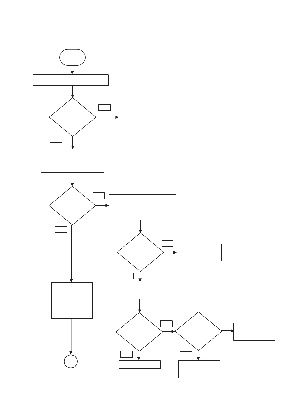
9.1 - 20 TROUBLESHOOTING CHARTS: 450-470MHz
GPS Troubleshooting (Sheet 1)
Move GPS antenna into an
area with a "clear view" to sky.
Yes
Failure: No position fix after 15minutes!
Start
Has the GPS
antenna a "clear view"
to sky??
Disconnect the GPS cable from
the radio and measure the DC
voltage applied to the inner
conductor of the RF cable.
No
No
No
Open GPS cover and check visually
the voltage regulators U1 and its
associated components (including
L1, and R12)
Are U1 and its
associated components
fitted properly?
Yes
A
Does 5.5V DC
apply to the inner
conductor of the
RF cable?
Measure the DC
voltage at U1 Pin 4
See Sheet 2
Replace the missing or
defect component.
No
13V DC at U1
Pin 4 (@nominal
battery voltage of
13.2V)?
No
24 pin flex
cable properly
connected to the
main board?
Re-connect the
24 pin flex connecto
r
Yes
Replace U1
Yes
Go to DC
troubleshooting
Mainboard
Yes
Connect radio's
accessory connector
to TETRACOM
interface, run
TETRACOM
and power on
the radio
6866539D31.book Page 20 Tuesday, March 20, 2007 6:32 PM
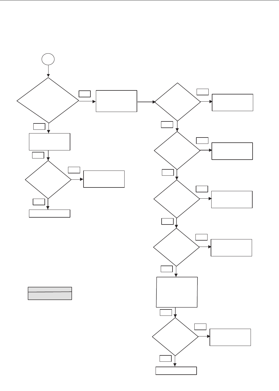
TROUBLESHOOTING CHARTS: 450-470MHz 9.1 - 21
GPS Troubleshooting (Sheet 2)
No
Does
TETRACOM
receive several GPS
monitor responses from radio
during boot mode (among
others:"GPS
ready?")
?
Open the GPS cover
and check the 24 pin
flex-line cable to the
main board
No
24 pin
flex cable properly
connected to the main
board?
Re-connect the
24 pin flex connecto
r
No
2V DC
at U2 Pin 5
?
Before replacing U2
check its associated
components
No
3.0V DC
at U3 Pin5
?
No
26MHz signal
at TP6
?
Replace the
reference TCXO Y1
Test accessory
interface connector
by requesting serial
number.
Run TETRACOM
command.
No
Are all
components fitted
properly
?
Replace the missing
or defect component
Replace GPS unit
Open the GPS cover
and check all
components
No
Yes Yes
Yes
Yes
Yes
Yes
Yes
Yes
Yes
A
From Sheet 1
Before replacing U3
check its associated
components
Radio serial
number displayed
?
Go to Controller
troubleshooting
(sheet 1)
Replace GPS unit
Tetra Com Command
<SERNUM>
6866539D31.book Page 21 Tuesday, March 20, 2007 6:32 PM

9.1 - 22 TROUBLESHOOTING CHARTS: 450-470MHz
Notes
6866539D31.book Page 22 Tuesday, March 20, 2007 6:32 PM
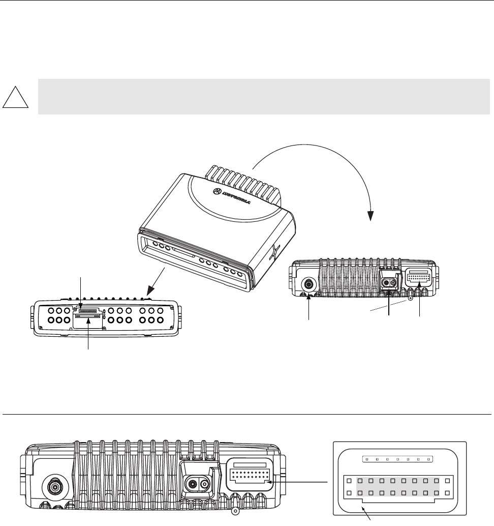
CONNECTOR PIN FUNCTIONS A - 1
APPENDIX A
CONNECTOR PIN FUNCTIONS
Figure A-1 Schematic view of the Connectors / MTM800 ENH Transceiver
Transceiver Rear - Pin Function
Figure A-2 Rear view of the MTM800 ENH
CAUTION: The connections shown are not compatible to some other models of Motorola
terminals. Check the appropriate accessory or technical manual for further information.
!
140
1
12
. . . . . . . . . . . . . . . . . . . . . . . . .
BNC
Antenna
Connector
Power
Connector Accessory
Connector
(20 Pin)
Control Head
Interface
(12 Pin)
Expansion Board
(40 Pin)
FRONT VIEW
REAR VIEW
GPS Connector
SMA female
(Option)
1816141210
1715
13119753
1
19
864220
*Note the location of Pin 1
Accessory Connector
Antenna DC Power Supply GPS (Option)
6866539D31.book Page 1 Tuesday, March 20, 2007 6:32 PM

A - 2 CONNECTOR PIN FUNCTIONS
Pin Function Description
1 EXTERNAL SPEAKER - Speaker – and Speaker + (Pin 16) are used to connect an external speaker. The
audio PA is a bridge amplifier with a minimum load resistance of 3.2 ohms.
2 EXTERNAL MIC AUDIO External-, Emergency-, or Hot-Microphone; depends on CPS programming.
This microphone signal is independent of the microphone signal on the micro-
phone connector. The nominal input level is 80mVRMS. The DC impedance is
660Ohms. The AC impedance is 560Ohms.
3 EXTERNAL PTT This is a digital input to trigger external PTT; active low; non active high
4 EXTERNAL ALARM This is a digital output for External Alarm / Fault Indication; active low; open col-
lector with 4k7 Ohms pull up to B+;
5 TX_AUDIO This input is intended for injecting signals into the transmit path. Input imped-
ance > 10 k Ohms; input level = 775mVRMS
6 KEYFAIL / FLASH This line supports the encryption module.
7 ANALOG GROUND Ground
8 DIGITAL_GROUND Ground
9 EMERGENCY To activate this functionality the pin has to be connected to ground. This will turn
on the terminal, Low active.
10 IGNITION Connecting this pin to the ignition line of the vehicle that will automatically turn
on the terminal if the ignition of the vehicle is turned on, High active.
11 RX_AUDIO This is the received RX signal. Output impedance approximate 600 Ohms
unsymmetrical, output level = 775mVRMS
12 AUDIO_PA_ENABLE This is a digital input. High level or pin open enables the audio PA; Low level dis-
ables the audio PA.
13 SWB + This voltage is available when the terminal is switched on.
The max. current is 1.0A w/o GPS board and 0.8A with GPS board mounted.
14 HOOK This is a high active digital input. Low = on hook; High = off hook
15 SCI_DTR Reserved for service aid.
16 SPEAKER + Positive output of terminal’s audio PA (see Pin 1)
17 * SCI_CTS Terminal OUTPUT: Clear To Send (reserved for service aids)
18 * SCI_RTS Terminal INPUT: Request To Send (reserved for service aids)
19 * SCI_RXD Terminal OUTPUT: Receive Data (reserved for service aids)
20 * SCI_TXD Terminal INPUT: Transmit Data (reserved for service aids)
Table A-1 Transceiver Pin Assignment of the Rear Accessory Connector
NOTE * The 4-wire 3 Volts SCI interface on the accessory connector (pins 17 -20) can only be
used for flashing of terminal firmware and programming software features.
It can NOT be used for communication during normal terminal operation.
6866539D31.book Page 2 Tuesday, March 20, 2007 6:32 PM
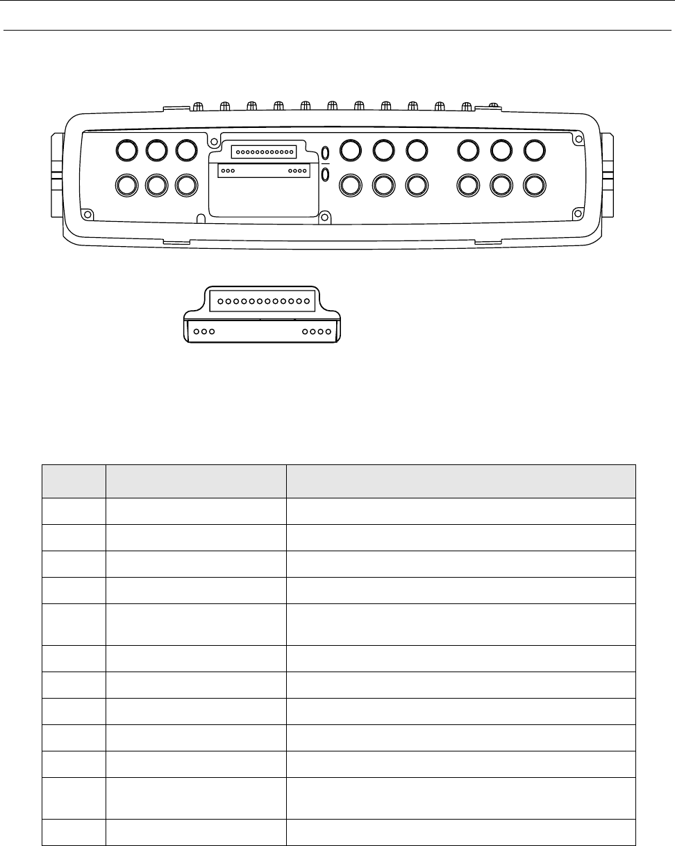
CONNECTOR PIN FUNCTIONS A - 3
Transceiver Front - Pin Function
Figure A-3 Transceiver Front View to the Enhanced Control Head Interface (12pins) and
Expansion Head Connector (40pins)
Pin Function Description
1 SCI_TX Serial Communication Interface TXD
2 SPEAKER + Analogue Speaker output +
3 SPEAKER - Analogue Speaker output -
4 GND Ground
5 DIG_IN1 (Ext. PTT) This is a digital input to trigger external PTT; active low; non
active high
6 5VD + 5V regulated
7 HANDSET_AUDIO Handset audio
8 BUS + Either SBEP or Serial Communication Interface RXD
9 INT_MIC Microphone input
10 FLT_A + Filtered A+
11 ON_OFF_CONTRO_SV Terminal On/Off Control shared with Enhanced Control Head
request
12 GND Ground
Table A-2 Transceiver Pin Assignment of the Enhanced Control Head Interface (12 pins)
140
1
12
12 Pin Connector
40 Pin Connector
140
1
12
J0550
12 Pin Connector (Flex)
J0500
40 Pin Connector (Flex)
. . . . . . . . . . . . . . . . . . . . . . . . .
. . . . . . . . . .
6866539D31.book Page 3 Tuesday, March 20, 2007 6:32 PM

A - 4 CONNECTOR PIN FUNCTIONS
Pin Function Description
1 GND Ground
2 MUX_CTRL TBA for future applications.
3 SPIB_CLK Part of the QSPIB
4 MUX_CTRL_1 To detect RS232 or SB9600 Mode (3V SB9600 / 0V RS232) *
5 A+ (via 22Ohms) Continuous battery voltage for sense via 22Ohms.
6 RESET_OUT Reset; its a output to Reset a SB9600 device.*
7 BUSY_OUT Busy Out for SB9600 Interface Circuit *
8 BUSY_IN Busy In for SB9600 Interface Circuit *
9 3V3_DIG 3.3V Sense Output (max. 10mA)
10 EXP_REQ Request Line from 4Wire/SB9600 UART *
11 SPIB_CS1_UART Part of the QSPIB (ship select) for 4wire RS232 UART
12 SPIB_CS_BT Part of the QSPIB (ship select) for future applications
13 SPIB_MISO Part of the QSPIB
14 NC Not Connected
15 SPIB_MOSI Part of the QSPIB
16 NC Not Connected
17 SAP_CLK Serial Audio Protocol, Clock.
18 GND Ground
19 INT_MIC Microphone Input
20 MIC Microphone Audio; for future applications
21 EXPANSION_PTT Expansion PTT
22 BlUE_T_FSYNC Serial Audio Protocol, Frame Sync.
23 SAP_SRD Serial Audio Protocol, Receive Data
24 SAP_STD Serial Audio Protocol, Transmit Data
25 DGAN_SAP_FSYNC Serial Audio Protocol, Frame Sync.
26 SP_AUDIO Audio PA Input; for future applications
27 TERMINAL ON/OFF (IGNI-
TION)
High active.
28 EXT_MUTE External mute of audio PA; for future applications
29 RS232_DCD Data Carrier Detect
30 RS232_TX TX-Data
31 RS232_DSR Data Set Ready
32 RS232_RTS Request To Send
Table A-3 Transceiver Pin Assignment of the Expansion Board Connector (40 pins)
*) For Expansion Head Connection only.
6866539D31.book Page 4 Tuesday, March 20, 2007 6:32 PM
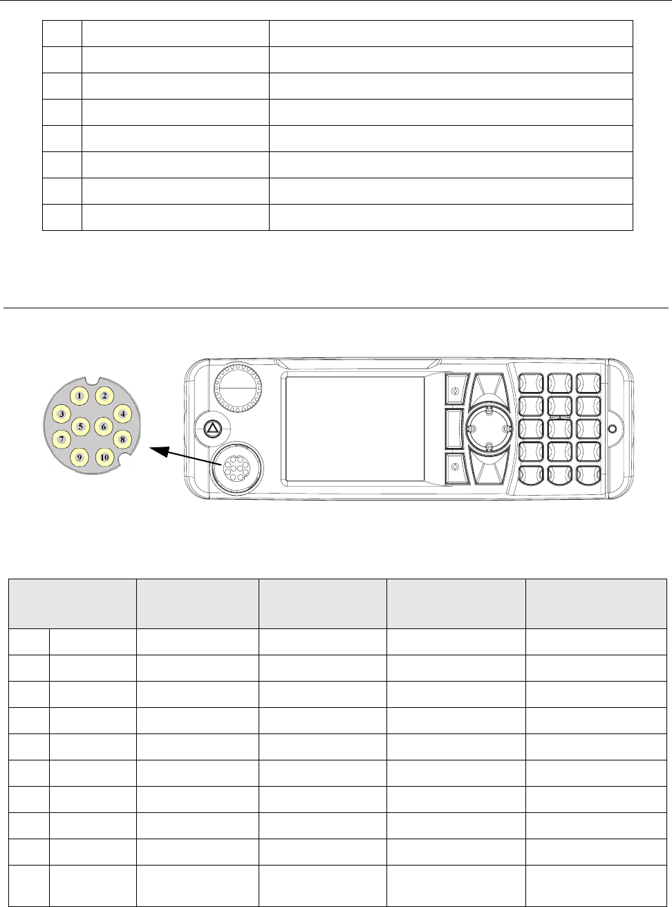
CONNECTOR PIN FUNCTIONS A - 5
Enhanced Control Head - Pin Function
Figure A-4 View of the Enhanced Control Head with GCAI MMP Connector
33 RS232_DTR Data Terminal Ready
34 RS232_CTS Clear To Send
35 RS232_RX RX-Data
36 RS232_RI Ring Indicator
37 OPTION_DET Option Detect; for future applications
38 9V3 Regulated 9V3
39 NC Not Connected
40 HANDSET AUDIO Handset Audio to earpiece
GCAI Pin # Default
Function
Alternative
Functions
Functions
when USB
Functions
when RS232
1 1-WIRE 1-WIRE 1-WIRE 1-WIRE 1-WIRE
2 GPIO_3 PTT GP Input or Output GP Input or Output RS-232-RTS *
3 SPEAKER SPEAKER SPEAKER SPEAKER SPEAKER
4 GPIO_2 GPIO_2 INPUT GP Input or Output DATA - RS-232-RXD *
5GND GND GND GND GND *
6 OPT 5V HIGH Impedance OPT 5V VBUS OPT 5V
7 MIC + MIC + MIC + MIC + MIC +
8 GPIO_1 GPIO_1 INPUT GP Input or Output DATA + RS-232-TXD *
9 GPIO_4 HOOK GP Input or Output GP Input or Output RS-232-CTS *
10 GPIO_0 GPIO_0 INPUT GP Input or Output,
PWR ON
GP Input or Output,
PWR ON
GP Input or Output,
PWR ON
Table A-4 Pin assignment GCAI - FRONT – Mobile Microphone Port (MMP) / *): Optional
Table A-3 Transceiver Pin Assignment of the Expansion Board Connector (40 pins)
*) For Expansion Head Connection only.
MMP top view
6866539D31.book Page 5 Tuesday, March 20, 2007 6:32 PM
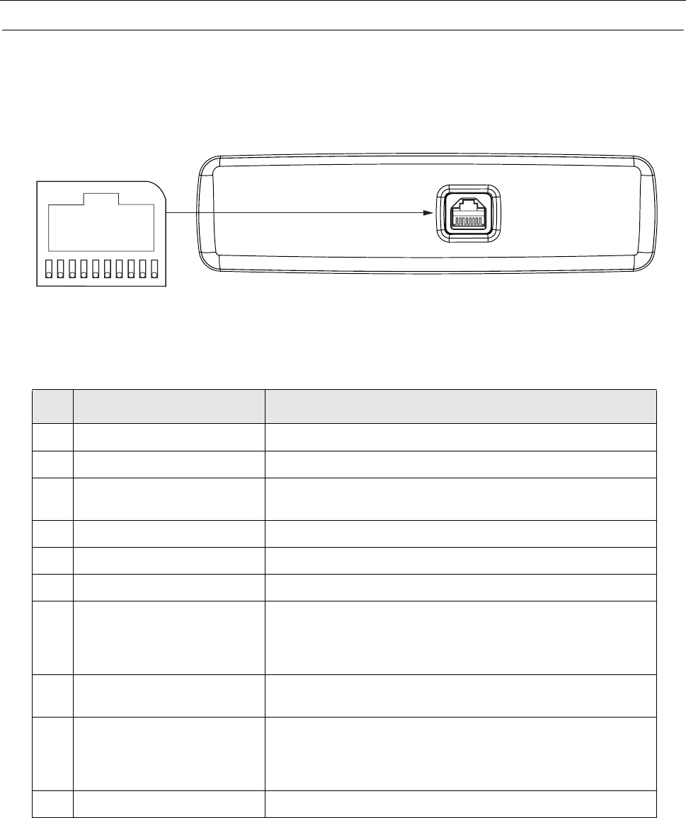
A - 6 CONNECTOR PIN FUNCTIONS
Remote Head Enhanced - Pin Function
Figure A-5 View of the Remote Head Enhanced Connector
Pin Function Description
1 Audio + Balanced Audio + (Bidirectional)
2 Speaker + Positive output of the radio's audio PA.
3 BUS+ This is used for communication between the radio and an
Enhanced Control Head.
4 Audio- Balanced Audio - (Bidirectional)
5 Speaker - Negative output of the radio’s audio PA.
6 Ground Ground
7 Radio On/Off Control This is the Enhanced Control Head service request input. A level of
5 volts indicates that the Enhanced Control Head needs to
communicate with the radio. In addition it switches on the radio's
voltage regulators. The idle state is a level below 0.6V.
8 SCI_TX This if for communication between the radio and the Enhanced
Control Head.
9 FLT_A+ This voltage is at battery voltage level and is available as long as
the radio is connected to the supply voltage. The maximum current
is 300mA. A fuse in the radio prevents further circuit damage in
case of shorting this pin to ground.
10 Analog Ground Analog Ground
Table A-5 Pin Assignment of the 10 Pin TELCO-Connector of the Remote Head Enhanced
Front View
CAUTION:
NOT
NOT
a Microphone Connector
J302
12
345678
910
6866539D31.book Page 6 Tuesday, March 20, 2007 6:32 PM
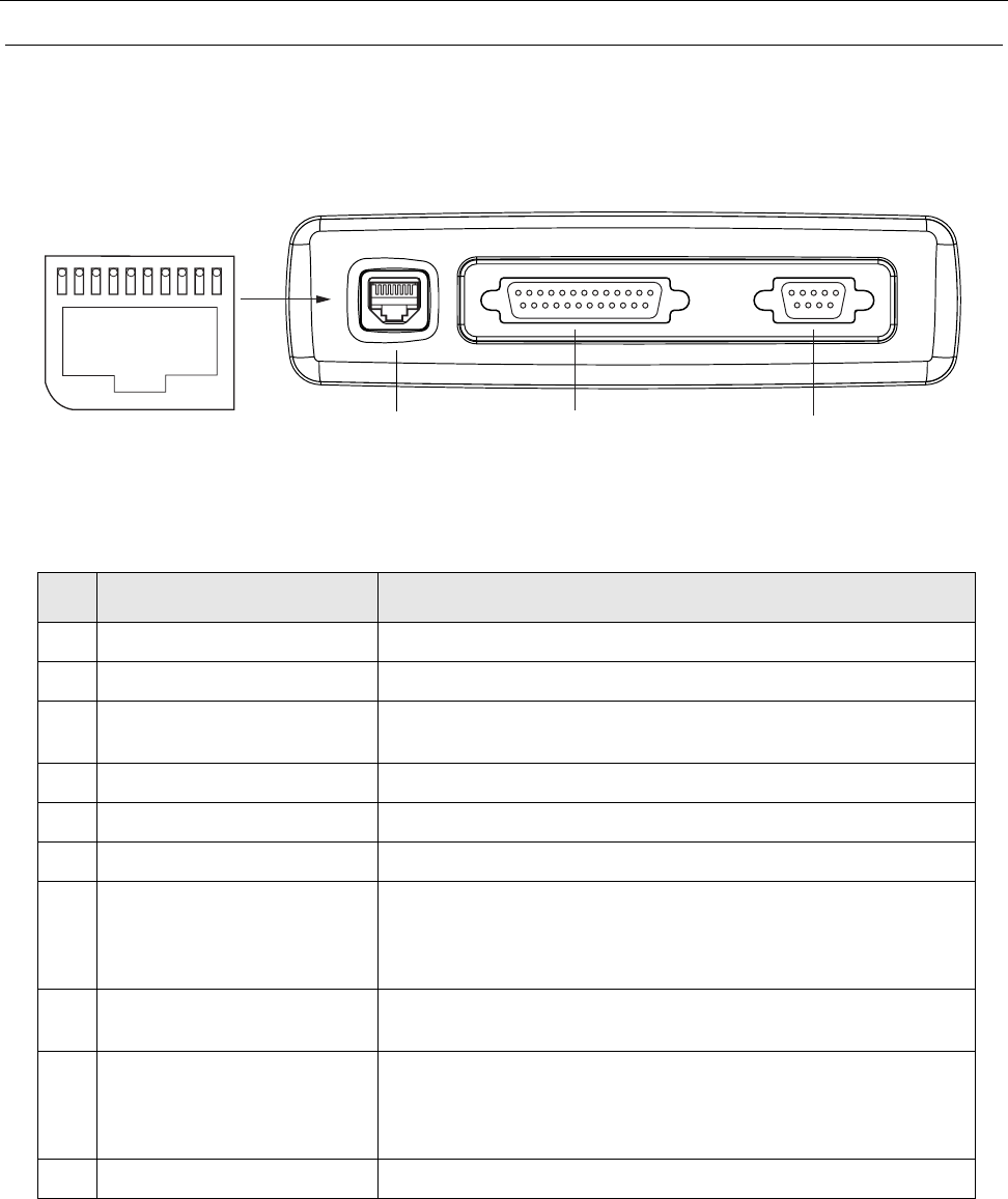
CONNECTOR PIN FUNCTIONS A - 7
Data Expansion Head Enhanced - Pin Function
Figure A-6 View of the Data Expansion Head Enhanced Connectors
Pin Function Description
1 Audio + Balanced Audio + (Bidirectional)
2 Speaker + Positive output of the radio's audio PA.
3 BUS+ This is used for communication between the radio and an Enhanced
Control Head.
4 Audio- Balanced Audio - (Bidirectional)
5 Speaker - Negative output of the radio’s audio PA.
6 Ground Ground
7 Radio On/Off Control This is the Enhanced Control Head service request input. A level of 5
volts indicates that the Enhanced Control Head needs to
communicate with the radio. In addition it switches on the radio's
voltage regulators. The idle state is a level below 0.6V.
8 SCI_TX This if for communication between the radio and the Enhanced Con-
trol Head.
9 FLT_A+ This voltage is at battery voltage level and is available as long as the
radio is connected to the supply voltage. The maximum current is
300mA. A fuse in the radio prevents further circuit damage in case of
shorting this pin to ground.
10 Analog Ground Analog Ground
Table A-6 Pin Assignment of the 10 Pin TELCO Connector of the Data Expansion Head Enhanced
Front View
CAUTION:
NOT
NOT
a Microphone Connector
25-Pin subD
Connector
9-Pin subD
Connector
1
13
14
25
1
5
6
9
10-Pin TELCO
Connector
J302
12345678910
6866539D31.book Page 7 Tuesday, March 20, 2007 6:32 PM

A - 8 CONNECTOR PIN FUNCTIONS
Pin Function Description PC direction
1 DCD Data Carrier Detect Input
2 RXD Received Data Serial IN
3 TXD Transmitted Data Serial OUT
4 DTR Data Terminal Ready Output
5 Ground Ground
6 DSR Data Set Ready Input
7 RTS Request to Send Output
8 CTS Clear to Send Input
9 RI Ring Indicator Input
Table A-7 Pin Assignment of 9 Pin subD Connector of the Data Expansion Head Enhanced
Pin Function Description
1 GND Ground
2 RS232_SCI_TX Transmit Data (4-wire RS232 with RS232 level)
3 RS232_SCI_RX Receive Data (4-wire RS232 with RS232 level)
4 RS232_RTS Request to Send (4-wire RS232 with RS232 level)
5 RS232_CTS Clear to Send (4-wire RS232 with RS232 level)
6 FLT_A+ This voltage is at battery voltage level and is available as long as the
radio is connected to the supply voltage. A fuse in the radio prevents
further circuit damage in case of shorting this pin to ground. This pin is
only used together with the pins 14, 20, and 23 to select flashing and
programming mode, or to switch the radio on.
7 Ground Ground for RS232
8 SB9600_BUSY SB9600 Busy
9 NC Not Connected
10 NC Not Connected
11 NC Not Connected
12 SW_B+ Switched UB +/100mA
13 SB9600_BUS- SB9600 BUS-
14 FLASH_MODE This input is intended to switch the radio into flashing & programming
mode. When the radio is switched off and this pin is connected with pin
6 (FLT A+), the radio switches on and enters flashing & programming
mode.
15 SB9600_BUS+ SB9600 BUS+.
Table A-8 Pin Assignment of the 25 Pin subD Connector of the Data Expansion Head Enhanced
6866539D31.book Page 8 Tuesday, March 20, 2007 6:32 PM
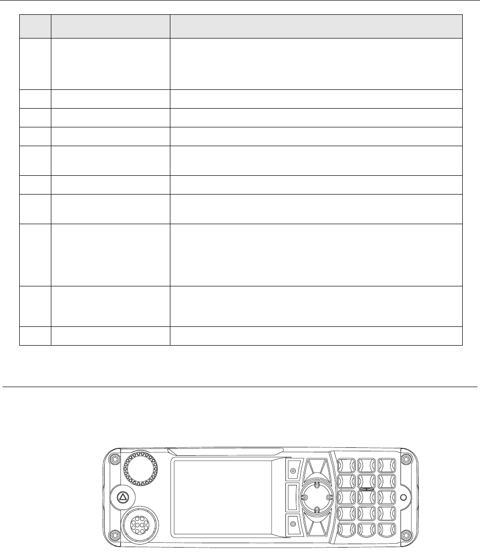
CONNECTOR PIN FUNCTIONS A - 9
Motorcycle & Remote Mount Connection - Pin Functions
Figure A-7 Front View of the Motorcycle Enhanced Control Head
16 Internal Mic Audio This input depends on radio programming mode. This microphone sig-
nal is independent of the microphone signal on the accessory connec-
tor. The nominal input level is 80 mV. The DC impedance is 660 ohms
and the AC impedance is 560 ohms.
17 SB9600-Reset This output can be used to reset a SB9600 device.
18 NC Not Connected
19 GROUND Ground
20 IGNITION The radio can be switched on by connecting this pin with pin 6 (FLT A+).
As long as both pins are connected, the radio will be switched on.
21 ON/OFF On/Off control.
22 EXPANSION-
PTT
When this input is used to key up the transmitter, the internal Mic Audio
input (pin 16) is selected.
23 SB9600_SW This input is intended to switch the 4 wire RS232 interface into SB9600
mode. The radio must be switched off and then this input must be con-
nected to pin 6 (FLT A+). When the radio is switched on again, the 4
wire RS232 interface will be disabled and the SB9600 mode will be
active.
24 HANDSET_AUDIO This is a low power audio output primarily intended for a connected
handset. the Dc level is 4.6 V and the AC level depends on the volume
setting.
25 NC Not Connected
Pin Function Description
Table A-8 Pin Assignment of the 25 Pin subD Connector of the Data Expansion Head Enhanced
6866539D31.book Page 9 Tuesday, March 20, 2007 6:32 PM
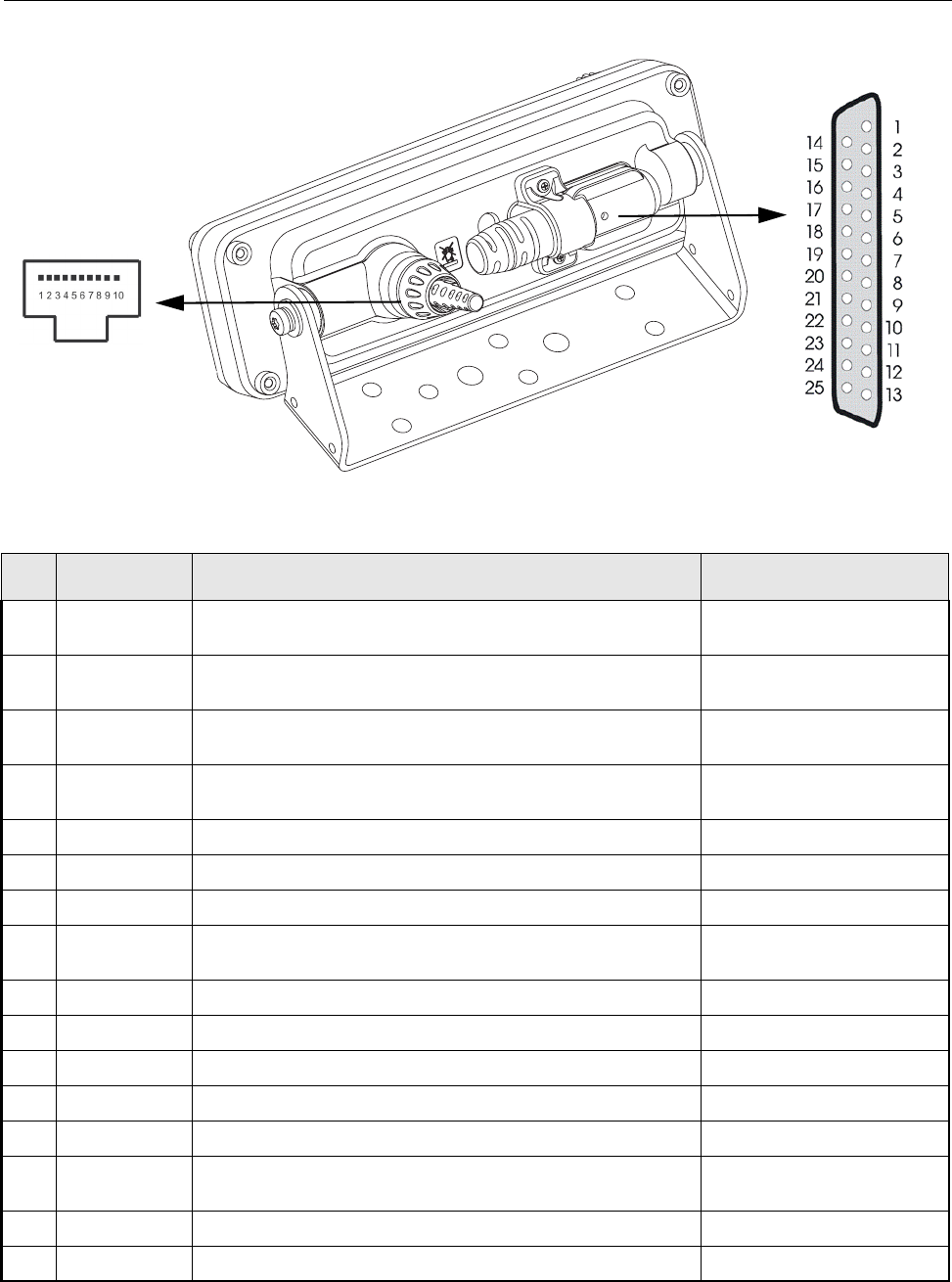
A - 10 CONNECTOR PIN FUNCTIONS
Figure A-8 Rear View of the Motorcycle Enhanced Control Head
Pin Function Description Default
1 GPIO_9 GPIO, open collector, 4.7k to FLT_A+ PU Output: 200mA @ low,
0,5mA @ high Input: high > 2V, low < 0.5V
Output: Active for duration of
call (car radio mute)
2 GPIO_6 GPIO, open collector, 4k7 to 5V PU Output: 1mA @ low, 0,5mA @
high Input: high > 2V, low < 0.5V
PTT Input, TX audio from
MIC_REAR_2
3 GPIO_8 GPIO, open collector, 4k7 to 5V PU Output: 1mA @ low, 0,5mA @
high Input: high > 2V, low < 0.5V
Disabled
4 GPIO_3 GCAI PIN 2: 15k to 3V3 PU, 5V tol. Output: see GCAI spec. 1.20
Input: high > 2V, low < 0.5V
PTT Input, TX audio from
MIC_REAR_1
5 VBUS_1B GCAI PIN 6: 5V Supply Disabled
6 REAR_D- GCAI PIN 4: USB D-, GPIO_2 shared with front MMP Disabled
7 REAR_D+ GCAI PIN 8: USB D+, GPIO_1 shared with front MMP Disabled
8 GPIO_0 GCAI Pin 10 GPIO, open coll., 15k to 3V3 PU, 5V tol. Output: see
GCAI spec. 1.20 Input: high > 2V, low < 0.5V
Input, GCAI etection/Select
Line
9 VBUS_2 Second USB, 5V Supply Disabled
10 TX 4 wire RS232 TX, EIA/TIA-232 level
11 RX 4 wire RS232 RX, EIA/TIA-232 level
12 MIC_REAR_2 2nd REAR MIC Input 80mVrms Bias 9V= / 600Ohm Disabled
13 GND GND
14 GPIO_5 GPIO, open collector, 4k7 to 5V PU Output: 1mA @ low, 0,5mA @
high Input: high > 2V, low < 0.5V
Disabled
15 GPI_7 4 Level Analogue Input, 33k to 5,0V PU (refer to graphic below) Enabled
16 1_WIRE GCAI PIN 1, 1-Wire® bi-directional serial bus Disabled
Table A-9 Pin assignment of the 25pin back connector – for RMC and MCC
6866539D31.book Page 10 Tuesday, March 20, 2007 6:32 PM
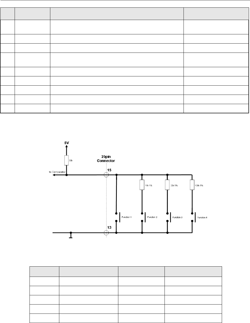
CONNECTOR PIN FUNCTIONS A - 11
Figure A-9 4 Level Analogue Input provided by GPI_7
17 HANDSET GCAI PIN 3, Handset audio output, VOL ontrolled, AC coupled, min.
RL 150Ohm
Parallel to front GCAI
18 GND GCAI PIN 5 GND
19 MIC_REAR_1 GCAI PIN 7 MIC Input 80mVrms Bias 9V= / 600Ohm Disabled
20 GPIO_4 GCAI PIN 9 GPIO open collector, 15k to 3V3 PU, 5V tol. Output: see
GCAI spec. 1.20 Input: high > 2V, low < 0.5V
Hook Input
21 USB_D+ Second USB, D+
22 USB_D- Second USB, D-
23 RTS 4 wire RS232 RTS, EIA/TIA-232 level
24 CTS 4 wire RS232 CTS, EIA/TIA-232 level
25 PWR_ON NGCH Power On input, high active, > 2V
Function Voltage Level (V) Tolerance (V) Default Function
1 0,00 0.000 - 0,625 Volume Up
2 1,25 0,625 - 1,875 Volume Down
3 2,50 1,875 - 3,125 Talk group Up
4 3,75 3,125 - 4,375 Talk group Down
Idle 5,00 4,375 - 5,000
Table A-10 Function of the voltage level at GPI_/
Pin Function Description Default
Table A-9 Pin assignment of the 25pin back connector – for RMC and MCC
6866539D31.book Page 11 Tuesday, March 20, 2007 6:32 PM
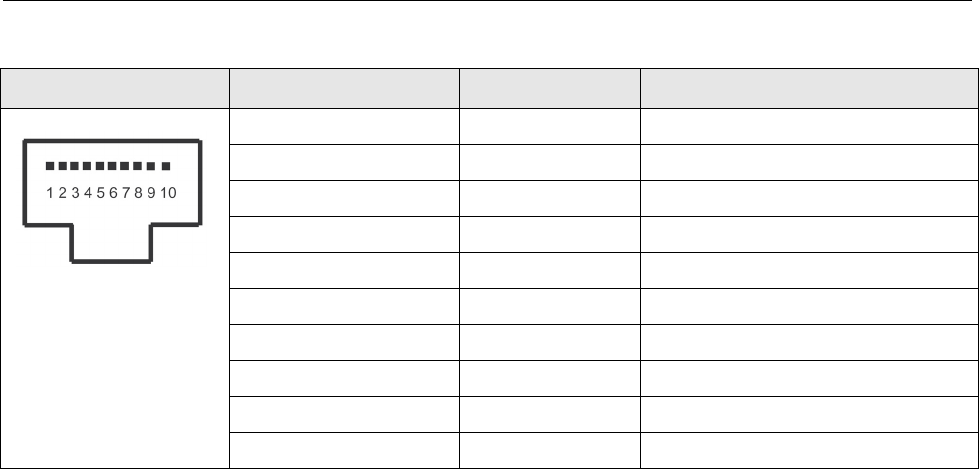
A - 12 CONNECTOR PIN FUNCTIONS
TELCO top view Pin # Function Description
1 Audio + Balanced Audio + (bidirectional)
2 Spkr + Speaker +
3 BUS+ Serial Bus (115 kBd), Data from NGCH
4 Audio - Balanced Audio - (bidirectional)
5 Spkr - Speaker -
6GNDGND
7 ON_OFF_CONTROL Radio “Turn On” Signal
8 SCI_TX Serial Bus (115 kBd), Data to NGCH
9 FLT_A+ Supply voltage
10 GND GND
Table A-11 Pin assignment of the 10pin TELCO back connector for RMC and MCC
6866539D31.book Page 12 Tuesday, March 20, 2007 6:32 PM

REPLACEMENT PARTS & KITS B - 1
APPENDIX B
REPLACEMENT PARTS & KITS
Servicing MTM800 With Enhanced Control Head Mobile
Units
Service for the mobile units is based on the substitution method; a faulty part is replaced by a work-
ing one, providing quicker service to the customer. For example, if the controller board is faulty, it is
replaced. If the mobile requires more complete testing or servicing than that is available at field
level, it is sent to the European Radio Service Centre; where it is serviced, and returned to the
Regional Service Centre.
Level 1 and Level 2 Maintenance
This manual covers Level 1 and Level 2 Maintenance: at Level 1 maintenance you replace the
transceiver and/or accessories and send the faulty transceiver and/or accessories to higher level of
maintenance; at level 2 maintenance a transceiver board is replaced.
The MTM800 With Enhanced Control Head mobiles are programmed at the factory. They cannot be
tuned at the field service level.
Level 3 Maintenance
All Radio Support Depots are level 3 service partners. The depots are capable of performing repairs
down to component level where retuning is required. Contact your local CGISS office for informa-
tion.
Replacement Parts
Damaged parts should be replaced with identical replacement parts.
For complete information on ordering required parts and kits, contact your local customer service
representative (see following pages).
6866539D31.book Page 1 Tuesday, March 20, 2007 6:32 PM

B - 2 REPLACEMENT PARTS & KITS
SERVICE INFORMATION
Europe, Middle East and Africa Region
European Radio Support Centre (ERSC)
Motorola European Radio Support Centre is available at:
Motorola European Radio Support Centre ERSC
Tel.: +49 (0)30 6686 1555
Fax: +49 (0)30 6686 1579
Am Borsigturm 130
13507 Berlin
Germany
EMEA Systems Support Centre (ESSC)
The Systems Support Centre is available at:
Piece Parts
Some replacement parts, spare parts, and/or product information can be ordered directly. If a com-
plete Motorola part number is assigned to the part, it is available from Motorola Radio Aftermarket
and Accessory Division (AAD). If no part number is assigned, the part is not normally available from
Motorola. If a parts list is not included, this generally means that no user-serviceable parts are avail-
able for that kit or assembly.
Note on this digital Tetra Terminal: The CPS has no capability to tune the terminal. Tuning the
terminal can only be performed at the factory or at the appropriate Motorola Repair Centre.
Components replacement can affect the terminal tuning and must only be performed by the
appropriate Motorola Repair Centre.
Parts identification and ordering
Request for help in identification of non-referenced spare parts should be directed to the Customer
Care Organization of Motorola’s local area representation. Orders for replacement parts, kits and
assemblies should be placed directly on Motorola’s local distribution organization or via the Extranet
site Motorola Online at: https://emeaonline.motorola.com.
EMEA Test Equipment Support
Information related to support and service of Motorola Test Equipment is available by calling the
Motorola Test Equipment Service in Germany at +49 (0) 6128 702179, Telefax +49 (0) 6128
951046, through the Customer Care Organization of Motorola’s local area representation, or via the
Internet at: http://www.gd-decisionsystems.com/cte/.
Telephone: +44 (0) 1256 484448
E-mail: ESSC@motorola.com
6866539D31.book Page 2 Tuesday, March 20, 2007 6:32 PM

REPLACEMENT PARTS & KITS B - 3
Asia, Pacific Region
Piece Parts
Some replacement parts, spare parts, and/or product information can be ordered directly. If a com-
plete Motorola part number is assigned to the part, it is available from Motorola Radio Aftermarket
and Accessory Division (AAD). If no part number is assigned, the part is not normally available from
Motorola. If a parts list is not included, this generally means that no user-serviceable parts are avail-
able for that kit or assembly.
Note on this digital TETRA Terminal: The CPS has no capability to tune the terminal. Tuning the
terminal can only be performed at the factory or at the appropriate Motorola Repair Center.
Component replacement can affect the terminal tuning and must only be performed by the
appropriate Motorola Repair Center.
All orders for parts/information should include the complete Motorola identification number. All part
orders should be directed to your local AAD office. Please refer to your latest price pages.
Technical Support
Technical support is available to assist the dealer/distributor in resolving any malfunction which may
be encountered. Initial contact should be by telephone wherever possible.
When contacting Motorola Technical Support, be prepared to provide the product model number
and the unit’s serial number.
Further Assistance From Motorola
You can also contact the Customer Help Desk through the following web address:
http://www.motorola.com/governmentandenterprise/contactus.
Parts identification and ordering
Request for help in identification of non-referenced spare parts should be directed to the Customer
Care Organization of Motorola’s local area representation. Orders for replacement parts, kits and
assemblies should be placed directly on Motorola’s local distribution organization or via Motorola
Online (Extranet).
6866539D31.book Page 3 Tuesday, March 20, 2007 6:32 PM

B - 4 REPLACEMENT PARTS & KITS
Latin America Region
Latin America Radio Support Centres
The Customer Support is available through the following service centres:
Warranty and Repairs:
MOTOROLA DE COLOMBIA SERVICE CENTRE
Torre Banco Ganadero
Carrera 7 No. 71-52
Torre B piso 13
Oficina 1301
Bogota- Colombia
(571) 376-6990
MOTOROLA DE MEXICO SERVICE CENTRE
Bosques de Alisos #125
Col. Bosques de las Lomas
CP 05120 Mexico DF
5252576700
Piece Parts:
To order parts in Latin America and the Caribbean contact your local Motorola CGISS
representative.
MOTOROLA, INC.
Latin American Countries Region
789 International Parkway
Sunrise, FL 33325
USA 954-723-8959
MOTOROLA DE ARGENTINA
Ave. del Libertador 1855
B1638BGE, Vicente Lopez
Buenos Aires, Argentina
5411-4317-5300
MOTOROLA DE LOS ANDES C.A.
Ave. Francisco de Miranda
Centro Lido, Torre A
Piso 15, El Rosal
Caracas, 1060 Venezuela
58212-901-4600
MOTOROLA DO BRASIL LTDA.
Av. Chedid Jafet
222 Bloco D Conjuntos 11,12,21,22 E 41
Condominio Millennium Office Park
04551-065- Vila Olimpia, Sao Paulo
Brasil
5511-3847-668
6866539D31.book Page 4 Tuesday, March 20, 2007 6:32 PM

REPLACEMENT PARTS & KITS B - 5
MOTOROLA CHILE
Ave. Nueva Tajamar 481
Edif. World Trade Center
Of. 1702, Torre Norte
Las Condes
Santiago, Chile
562-338-9000
MOTOROLA DE COLOMBIA, LTDA.
Carrera 7 #71-52
Torre A, Oficina 1301
Bogotá, Colombia
571-376-6990
MOTOROLA DE COSTA RICA
Parque Empresarial Plaza Roble
Edificio El Portico, 1er Piso
Centro de Negocios Internacional
Guachepelin, Escazu
San Jose, Costa Rica
506-201-1480
MOTOROLA DEL ECUADOR
Autopist Gral. Rumiñahui, Puente 2
Conjunto Puerta del Sol Este-Ciudad Jardin
Pasa E, Casa 65
Quito, Ecuador
5932-264-1627
MOTOROLA DE MEXICO, S.A.
Calle Bosques de Alisos #125
Col. Bosques de Las Lomas
05120 México D.F.
México
52-555-257-6700
MOTOROLA DEL PERU, S.A.
Ave. República de Panama 3535
Piso 11, San Isidro
Lima 27, Peru
511-211-0700
Technical Support:
https://businessonline.motorola.com, go to Contact Us to request technical support
Some replacement parts, spare parts, and/or product information can be ordered directly.
If a complete Motorola part number is assigned to the part, it is available from Motorola. If
no part number is assigned, the part is not normally available from Motorola. If the part
number is appended with an asterisk, the part is serviceable by Motorola Depot only. If a
parts list is not included, this generally means that no user-serviceable parts are available
for that kit or assembly.
6866539D31.book Page 5 Tuesday, March 20, 2007 6:32 PM
B - 6 REPLACEMENT PARTS & KITS
SERVICE KITS
Type No. Sales Model No. Short Description Model
MT512M M80RCS6TZ5AN MTM800 ENH 410-470 Dash M1
MT512M M80RCS6TZ4AN MTM800 ENH 410-470 Desk M2
MT512M M80RCS6TZ6AN MTM800 ENH 410-470Remote M3
MT512M M80RCS6TZ2AN MTM800 ENH 410-470 M’cycle M4
MT512M M80RCC6TZ5AN MTM800 ENH 410-470 Exp/ Data M5
Table B-1 Service Kits-To-Model Chart
MTM800 Service Kits
Description Part Number M1 M2 M3 M4 M5
Service Boards PMUE4480AS X X X X X
MTM800 ENH 410-470 CLEAR PMUE4481AS X X X X X
MTM800 ENH 410-470 TEA1*PMUE4482AS X X X X X
MTM800 ENH 410-470 TEA2*PMUE4483AS X X X X X
MTM800 ENH 410-470 GPS CLEAR PMUE4484AS X X X X X
MTM800 ENH 410-470 GPS TEA1*PMUE4485AS X X X X X
MTM800 ENH 410-470 GPS TEA2*PMUE4486AS X X X X X
MTM800 ENH 410-470 UCM AES128 PMUE4487AS X X X X X
MTM800 ENH 410-470 UCM TEA1* AES128 PMUE4488AS X X X X X
MTM800 ENH 410-470 UCM TEA2* AES128 PMUE4489AS X X X X X
MTM800 ENH 410-470 UCM/GPS AES128 PMUE4490AS X X X X X
MTM800 ENH 410-470 UCM/GPS TEA1* AES128 PMUE4491AS X X X X X
MTM800 ENH 410-470 UCM/GPS TEA3* AES128 PMUE4480AS X X X X X
Enhanced Control Head/Kits
Dash/Desk Mount -English Keypad GMWN4298_ X X
Chinese Keypad GMWN4299_ X X
Korean Keypad GMWN4300_ X X
Arabic Keypad GMWN4301_ X X
BoPoMoFo Keypad GMWN4302_ X X
Cyrillic Keypad GMWN4303_ X X
English Keypad - Hungarian GMWN4608_ X X
Remote Mount -English Keypad GMWN4304_ X
Chinese Keypad GMWN4305_ X
Korean Keypad GMWN4306_ X
6866539D31.book Page 6 Tuesday, March 20, 2007 6:32 PM

REPLACEMENT PARTS & KITS B - 7
*) TETRA Encryption Algorithm 1, 2 or 3
Arabic Keypad GMWN4307_ X
BoPoMoFo Keypad GMWN4308_ X
Cyrillic Keypad GMWN4309_ X
English Keypad - Hungarian GMWN4606_ X
Motorcycle -English Keypad GMWN4600_ X
Chinese Keypad GMWN4601_ X
Korean Keypad GMWN4602_ X
Arabic Keypad GMWN4603_ X
BoPoMoFo Keypad GMWN4604_ X
Cyrillic Keypad GMWN4605_ X
English Keypad - Hungarian GMWN4607_ X
Data Expansion Head Enhanced PMLN4908_ X X
Data Expansion Head GMCE4053_ X
Remote Head Enhanced PMLN4904_ X X
Cables/Kits
Remote Mount Cable - 3m RKN4077_ X
Remote Mount Cable - 5m RKN4078_ X
Remote Mount Cable - 7m RKN4079_ X
Remote Mount Cable - 10m PMKN4020_ X
Accessories Expansion Cable PMKN4029_ X X
Motorcycle Mount TELCO Cable - 2.3m PMKN4030_ X
Ferrite Clamp PMLN5148_ X X
Table B-1 Service Kits-To-Model Chart
MTM800 Service Kits
6866539D31.book Page 7 Tuesday, March 20, 2007 6:32 PM

B - 8 REPLACEMENT PARTS & KITS
Notes
6866539D31.book Page 8 Tuesday, March 20, 2007 6:32 PM
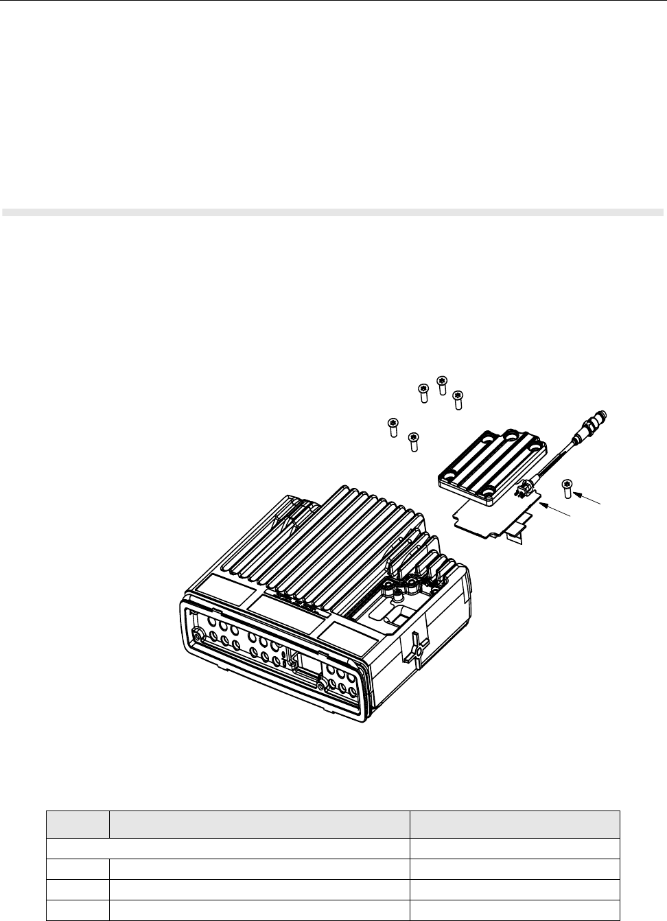
RETROFITTING the GPS and UCM BOARD C - 1
APPENDIX C
RETROFITTING the GPS and UCM BOARD
Retrofitting the UCM and GPS module should only be done by specially authorized and educated
Service Personnel. All operating and safety instructions are to be followed carefully.
Note: Refer to chapter 7 MAINTENANCE for dis-assembling and re-assembling the terminal prop-
erly.
Retrofitting the GPS board
1. Remove the metal blind cover from the bottom (5 screws, T10 TORX™).
2. Pull out the protection bushing.
3. Install the GPS board by starting with the connection of the flex to the mainboard.
4. Take care to fit the gasket of the coax cable in the right position for proper IP54 protection.
5. Fix the GPS board with one T10 TORX™ screw (1.13 Nm +/- 10% or 10 lbin +/- 10%).
6. Fix the GPS cover plate with five T10 TORX™ screws (1.13 Nm +/- 10% or 10 lbin +/- 10%).
Figure C-1 Position of GPS module at the terminal (view from bottom side)
Table C-1 GPS Upgrade Kit Parts List
Item No. Description Part Number
GPS Upgrade Kit GMRG4219_
1 GPS Board (with flex and coax cable) 0166502N65
2 Screw (M3x8) 0310907A19
3 Label (not shown) 5466571B01
1
2
6866539D31.book Page 1 Tuesday, March 20, 2007 6:32 PM
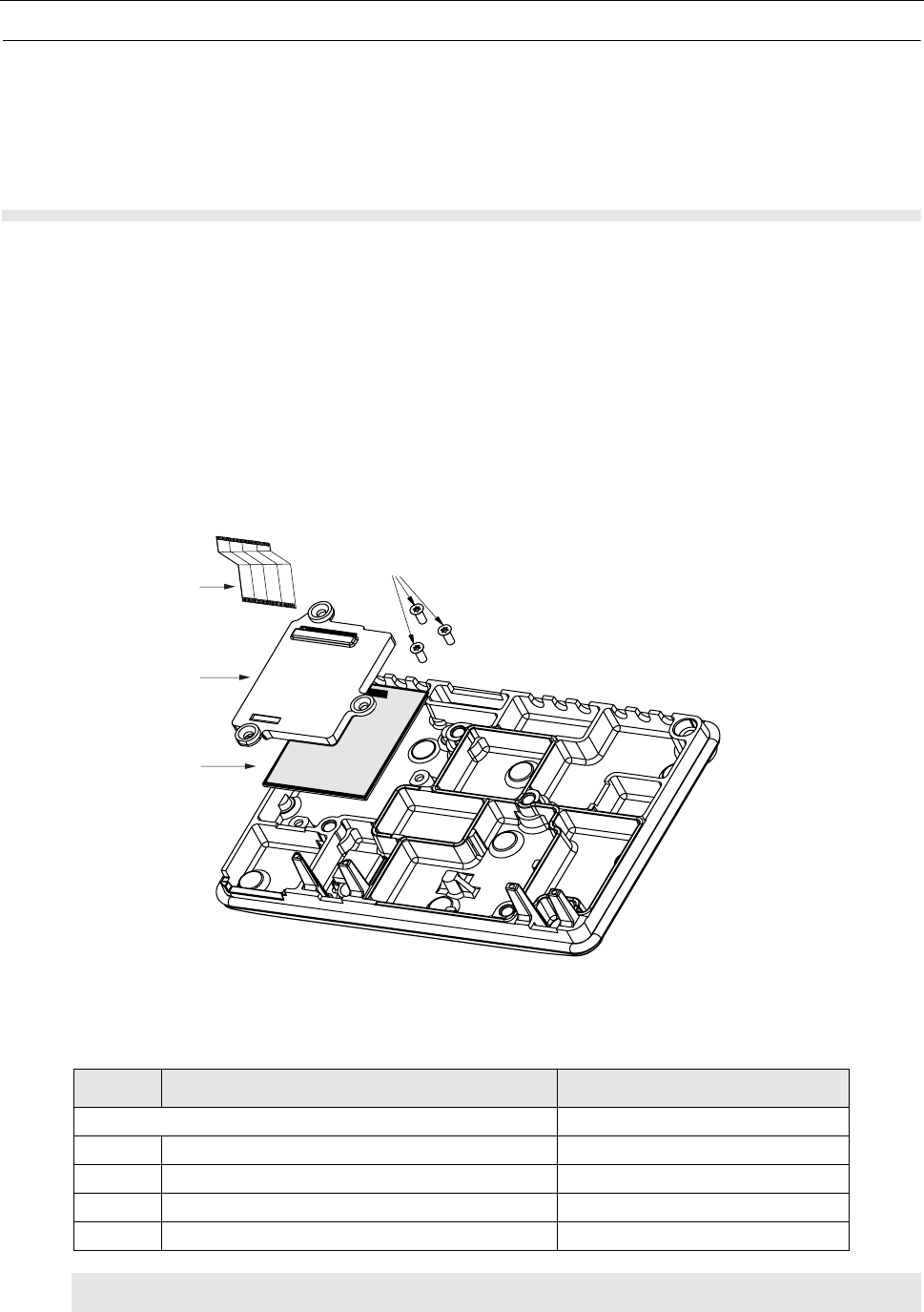
C - 2 RETROFITTING the GPS and UCM BOARD
GPS Software activation
After installing the GPS hardware, a software upgrade for the MTM800 ENH will be necessary.
Please refer to the CPS documentation in the Product Information Manual (P/N: 6866537D87) for
more details or contact your local Customer Support Centre / see Appendix B - Service Information)
Retrofitting the UCM board
1. If attached, remove the Enhanced Control Head from the terminal, refer to chapter 7 (page 7-
5, following).
2. Remove the top plastic cover from the terminal.
3. Remove the six screws from the diecast cover using a T20 TORX™ driver and lift the cover
from the chassis.
4. Fix the flex to the UCM board and place it at the cover plate.
5. Fix the plastic cover with 3 screws starting with the pull-through of the flex.
6. Place the cover plate (UCM at left side) in front of the transceiver front side and carefully
attach the flex to the mainboard at the 40-pin internal option board connector (J0450).
7. Re-assemble the terminal.
Figure C-2 Location of UCM board inside the cover plate
Table C-2 UCM Upgrade Kit parts list
Item No. Description Part Number
UCM Upgrade Kit: GMLN4218_
1 UCM Board Module CLN8041_
2 UCM Board Cover 0786183B01
3 UCM Board Flex 8485615Z02
4 Screw 3x (M5x8) 0310943R55
NOTE: The CLN8041_ UCM board is not repairable. Order a replacement board if necessary.
2
1
3
4 (3x)
6866539D31.book Page 2 Tuesday, March 20, 2007 6:32 PM
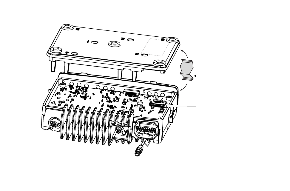
RETROFITTING the GPS and UCM BOARD C - 3
Figure C-3 Location of UCM connector J0450 on the main board
UCM Software activation
After installing the UCM hardware, a software upgrade for the MTM800 ENH will be necessary.
Please refer to the CPS documentation in the Product Information Manual (P/N: 6866537D87) for
more details.
Before use, provision the UCM with E2E Keys and Associations according to your E2E Deployment
Plan. This will require a Key Variable Loader (KVL), and may also require configuration changes to
your system's Key Management Facility (KMF).
Refer to the Dimetra End-to-End Encryption KVL 3000 Plus Key Variable Loader User Guide
(P/N: 6802800U14) for more details. For questions refer to your local Customer Support Centre (see
Appendix B - Service Information).
short bending
to main board
UCM flex
UCM connector
J0450
UCM
board
*
**
contacts on back sid
e
6866539D31.book Page 3 Tuesday, March 20, 2007 6:32 PM

C - 4 RETROFITTING the GPS and UCM BOARD
Notes
6866539D31.book Page 4 Tuesday, March 20, 2007 6:32 PM

PRODUCT SPECIFIC INFORMATION D - 1
APPENDIX D
PRODUCT SPECIFIC INFORMATION
for Digital Terminals Type MT512M
This section gives the Service Personnel an overview about product specific notes. This is neces-
sary to take special precautions to avoid the introduction of hazards when operating, installing, serv-
icing or storing equipment. This terminal meets the applicable safety standards if it is used as
described. All operating and safety instructions are to be followed carefully.
Equipment Electrical Ratings
Rated Voltage: 12 Volt DC
Rated Voltage Range: 10.8 to 15.6 V DC
Rated Current:
3 Amps @ 3Watts RF power
Please be aware when planning the installation that there is a current consumption of approx. 3.5A
during PTT and even 30mA when terminal is switched off.
Transmitter Frequency Range:
TMO: 450 to 470 MHz
DMO: 450 to 470 MHz
Receiver Frequency Range:
450 to 470 MHz
Normal Load Conditions:
Rated RF Power: 3Watts
Rated Audio Power: 10 Watts @ 4 Ohms; 6 Watts @ 8 Ohms
Antenna Impedance: 50 Ohms
Operating Temp. Range: -30 to +60°C
Operating Time*: Continuous / Intermittent
*Note: In general, the terminal transmit and receive time (operating cycle time) is determined by the communi-
cation system. On overload, respectively on extensive use beyond the systems specifications at high ambient
temperatures, the terminal is protected by its thermal control, which cuts down the RF output power, thus reduc-
ing the terminal coverage range.
Fuse Identification
In case of blown fuses during the installation only replace those with identically value. Never insert
different values.
Fuse for Power Cable GKN6270/GKN6274: 10A (Motorola Part Number: 65C80283E05)
Fuse for Ignition Sense Cable HKN9327: 4A (Motorola Part Number: 65C80283E02)
6866539D31.book Page 1 Tuesday, March 20, 2007 6:32 PM

D - 2 PRODUCT SPECIFIC INFORMATION
SPEZIELLE PRODUKTINFORMATIONEN
für Funkgeräte des Typs MT512M
Dieses Kapitel gibt dem geschulten Servicepersonal einen Überblick über wichtige produktspezifi-
sche Informationen. Diese Informationen sind wichtig, um Risiken beim Bedienen, Installieren und
Service zu vermeiden. Dieses Funkgerät erfüllt die allgemeinen Sicherheitsstandards, sofern es so
betrieben wird, wie in der Bedienungsanleitung beschrieben.
Nennwerte für das Funkgerät
Nennspannung: 12 Volt DC
Nennspannungsbereich: 10.8 bis 15.6 V DC
Nennstrom:
3 A @ 3W HF Leistung
Bevor Sie die Installation planen, bedenken Sie, dass das Sprechfunkgerät beim Senden einen
Stromverbrauch von ca. 3,5A hat und auch im ausgeschalteten Zustand einen Strom von ca. 30 mA
verbraucht.
Sender-Nennfrequenzbereich:
TMO: 450 bis 470 MHz
DMO: 450 bis 470 MHz
Empfänger-Nennfrequenzbereich:
450 bis 470 MHz
Betriebsbedingungen
HF Nennleistung: 3 Watt
Lautsprecher Nennleistung:10 Watt an 4 Ohm; 6 Watt an 8 Ohm
Antennenimpedanz: 50 Ohm
Betriebstemperatur Bereich: -30 to +60°C
Betriebszeit*: fortwährend / periodisch
*Hinweis: Im allgemeinen wird die Sende- und Empfangsszeit (Betriebszeit) des Funkgerätes durch das Funk-
system bestimmt. Bei Überlastung bzw. extensivem Betrieb über die Systemsspezifikationen hinaus bei hohen
Umgebungstemperaturen wird das Funkgerät durch eine Temperaturkontrollschaltung geschützt, die die HF-
Leitung reduziert. Daraus kann sich eine Verringerung der Leistungsmerkmale des Gerätes ergeben.
Sicherungen
Sollte während der Installation die Sicherung durchbrennen, darf sie nur durch eine gleichwertige
Sicherung ersetzt werden.
Sicherung für DC Kabel GKN6270/GKN6274: 10A (Motorola Bestellnummer: 65C80283E05)
Sicherung für Ignition Sense Kabel HKN9327: 4A (Motorola Bestellnummer: 65C80283E02)
6866539D31.book Page 2 Tuesday, March 20, 2007 6:32 PM
