MegaAVR 0 Series Manual Mega AVR0 40002015A
User Manual:
Open the PDF directly: View PDF ![]() .
.
Page Count: 483 [warning: Documents this large are best viewed by clicking the View PDF Link!]
- Introduction
- Features
- Table of Contents
- 1. Block Diagram
- 2. megaAVR® 0-series Overview
- 3. Conventions
- 4. Acronyms and Abbreviations
- 5. Memories
- 6. Peripherals and Architecture
- 7. AVR CPU
- 7.1. Features
- 7.2. Overview
- 7.3. Architecture
- 7.4. Arithmetic Logic Unit (ALU)
- 7.5. Functional Description
- 7.6. Register Summary - CPU
- 7.7. Register Description
- 8. Nonvolatile Memory Controller (NVMCTRL)
- 9. Clock Controller (CLKCTRL)
- 10. Sleep Controller (SLPCTRL)
- 11. Reset Controller (RSTCTRL)
- 12. CPU Interrupt Controller (CPUINT)
- 12.1. Features
- 12.2. Overview
- 12.3. Functional Description
- 12.4. Register Summary - CPUINT
- 12.5. Register Description
- 13. Event System (EVSYS)
- 14. Port Multiplexer (PORTMUX)
- 15. I/O Pin Configuration (PORT)
- 16. Brown-Out Detector (BOD)
- 17. Voltage Reference (VREF)
- 18. Watchdog Timer (WDT)
- 19. 16-bit Timer/Counter Type A (TCA)
- 19.1. Features
- 19.2. Overview
- 19.3. Functional Description
- 19.4. Sleep Mode Operation
- 19.5. Register Summary - TCAn in Normal Mode (SPLITM in TCAn.CTRLD=0)
- 19.6. Register Description - Normal Mode
- 19.6.1. Control A
- 19.6.2. Control B - Normal Mode
- 19.6.3. Control C - Normal Mode
- 19.6.4. Control D
- 19.6.5. Control Register E Clear - Normal Mode
- 19.6.6. Control Register E Set - Normal Mode
- 19.6.7. Control Register F Clear
- 19.6.8. Control Register F Set
- 19.6.9. Event Control
- 19.6.10. Interrupt Control Register - Normal Mode
- 19.6.11. Interrupt Flag Register - Normal Mode
- 19.6.12. Debug Control Register
- 19.6.13. Temporary Bits for 16-Bit Access
- 19.6.14. Counter Register - Normal Mode
- 19.6.15. Period Register - Normal Mode
- 19.6.16. Compare n Register - Normal Mode
- 19.6.17. Period Buffer Register
- 19.6.18. Compare n Buffer Register
- 19.7. Register Summary - TCAn in Split Mode (SPLITM in TCAn.CTRLD=1)
- 19.8. Register Description - Split Mode
- 19.8.1. Control A
- 19.8.2. Control B - Split Mode
- 19.8.3. Control C - Split Mode
- 19.8.4. Control D
- 19.8.5. Control Register E Clear - Split Mode
- 19.8.6. Control Register E Set - Split Mode
- 19.8.7. Interrupt Control Register - Split Mode
- 19.8.8. Interrupt Flag Register - Split Mode
- 19.8.9. Debug Control Register
- 19.8.10. Low Byte Timer Counter Register - Split Mode
- 19.8.11. High Byte Timer Counter Register - Split Mode
- 19.8.12. Low Byte Timer Period Register - Split Mode
- 19.8.13. High Byte Period Register - Split Mode
- 19.8.14. Compare Register n For Low Byte Timer - Split Mode
- 19.8.15. High Byte Compare Register n - Split Mode
- 20. 16-bit Timer/Counter Type B (TCB)
- 20.1. Features
- 20.2. Overview
- 20.3. Functional Description
- 20.3.1. Definitions
- 20.3.2. Initialization
- 20.3.3. Operation
- 20.3.3.1. Modes
- 20.3.3.1.1. Periodic Interrupt Mode
- 20.3.3.1.2. Time-Out Check Mode
- 20.3.3.1.3. Input Capture on Event Mode
- 20.3.3.1.4. Input Capture Frequency Measurement Mode
- 20.3.3.1.5. Input Capture Pulse-Width Measurement Mode
- 20.3.3.1.6. Input Capture Frequency and Pulse-Width Measurement Mode
- 20.3.3.1.7. Single-Shot Mode
- 20.3.3.1.8. 8-Bit PWM Mode
- 20.3.3.2. Noise Canceler
- 20.3.3.3. Synchronized with TCAn
- 20.3.3.1. Modes
- 20.3.4. Events
- 20.3.5. Interrupts
- 20.3.6. Sleep Mode Operation
- 20.4. Register Summary - TCB
- 20.5. Register Description
- 21. Real-Time Counter (RTC)
- 21.1. Features
- 21.2. Overview
- 21.3. Clocks
- 21.4. RTC Functional Description
- 21.5. PIT Functional Description
- 21.6. Crystal Error Correction
- 21.7. Events
- 21.8. Interrupts
- 21.9. Sleep Mode Operation
- 21.10. Synchronization
- 21.11. Register Summary - RTC
- 21.12. Register Description
- 21.12.1. Control A
- 21.12.2. Status
- 21.12.3. Interrupt Control
- 21.12.4. Interrupt Flag
- 21.12.5. Temporary
- 21.12.6. Debug Control
- 21.12.7. Calibration
- 21.12.8. Clock Selection
- 21.12.9. Count
- 21.12.10. Period
- 21.12.11. Compare
- 21.12.12. Periodic Interrupt Timer Control A
- 21.12.13. Periodic Interrupt Timer Status
- 21.12.14. PIT Interrupt Control
- 21.12.15. PIT Interrupt Flag
- 21.12.16. Periodic Interrupt Timer Debug Control
- 22. Universal Synchronous and Asynchronous Receiver and Transmitter (USART)
- 22.1. Features
- 22.2. Overview
- 22.3. Functional Description
- 22.3.1. Initialization
- 22.3.2. Operation
- 22.3.2.1. Clock Generation
- 22.3.2.2. Frame Formats
- 22.3.2.3. Data Transmission - USART Transmitter
- 22.3.2.4. Data Reception - USART Receiver
- 22.3.2.5. USART in Master SPI mode
- 22.3.2.6. Half Duplex Operations
- 22.3.2.7. Start Frame Detection
- 22.3.2.8. Break Character Detection and Auto-Baud
- 22.3.2.9. Multiprocessor Communication Mode
- 22.3.2.10. IRCOM Mode of Operation
- 22.3.3. Events
- 22.3.4. Interrupts
- 22.4. Register Summary - USARTn
- 22.5. Register Description
- 22.5.1. Receiver Data Register Low Byte
- 22.5.2. Receiver Data Register High Byte
- 22.5.3. Transmit Data Register Low Byte
- 22.5.4. Transmit Data Register High Byte
- 22.5.5. USART Status Register
- 22.5.6. Control A
- 22.5.7. Control B
- 22.5.8. Control C - Async Mode
- 22.5.9. Control C - Master SPI Mode
- 22.5.10. Baud Register
- 22.5.11. Debug Control Register
- 22.5.12. IrDA Control Register
- 22.5.13. IRCOM Transmitter Pulse Length Control Register
- 22.5.14. IRCOM Receiver Pulse Length Control Register
- 23. Serial Peripheral Interface (SPI)
- 24. Two-Wire Interface (TWI)
- 24.1. Features
- 24.2. Overview
- 24.3. Functional Description
- 24.3.1. Initialization
- 24.3.2. General TWI Bus Concepts
- 24.3.3. TWI Bus State Logic
- 24.3.4. Operation
- 24.3.4.1. Electrical Characteristics
- 24.3.4.2. TWI Master Operation
- 24.3.4.2.1. Clock Generation
- 24.3.4.2.2. Transmitting Address Packets
- 24.3.4.2.2.1. Case M1: Arbitration Lost or Bus Error during Address Packet
- 24.3.4.2.2.2. Case M2: Address Packet Transmit Complete - Address not Acknowledged by Slave
- 24.3.4.2.2.3. Case M3: Address Packet Transmit Complete - Direction Bit Cleared
- 24.3.4.2.2.4. Case M4: Address Packet Transmit Complete - Direction Bit Set
- 24.3.4.2.3. Transmitting Data Packets
- 24.3.4.2.4. Receiving Data Packets
- 24.3.4.2.5. Quick Command Mode
- 24.3.4.3. TWI Slave Operation
- 24.3.4.4. Smart Mode
- 24.3.5. Interrupts
- 24.3.6. Sleep Mode Operation
- 24.4. Register Summary - TWIn
- 24.5. Register Description
- 24.5.1. Control A
- 24.5.2. Dual Mode Control Configuration
- 24.5.3. Debug Control
- 24.5.4. Master Control A
- 24.5.5. Master Control B
- 24.5.6. Master Status
- 24.5.7. Master Baud Rate
- 24.5.8. Master Address
- 24.5.9. Master DATA
- 24.5.10. Slave Control A
- 24.5.11. Slave Control B
- 24.5.12. Slave Status
- 24.5.13. Slave Address
- 24.5.14. Slave Data
- 24.5.15. Slave Address Mask
- 25. Cyclic Redundancy Check Memory Scan (CRCSCAN)
- 26. CCL – Configurable Custom Logic
- 27. Analog Comparator (AC)
- 28. Analog-to-Digital Converter (ADC)
- 28.1. Features
- 28.2. Overview
- 28.3. Functional Description
- 28.3.1. Initialization
- 28.3.2. Operation
- 28.3.3. Events
- 28.3.4. Interrupts
- 28.3.5. Sleep Mode Operation
- 28.4. Register Summary - ADCn
- 28.5. Register Description
- 28.5.1. Control A
- 28.5.2. Control B
- 28.5.3. Control C
- 28.5.4. Control D
- 28.5.5. Control E
- 28.5.6. Sample Control
- 28.5.7. MUXPOS
- 28.5.8. Command
- 28.5.9. Event Control
- 28.5.10. Interrupt Control
- 28.5.11. Interrupt Flags
- 28.5.12. Debug Run
- 28.5.13. Temporary
- 28.5.14. Result
- 28.5.15. Window Comparator Low Threshold
- 28.5.16. Window Comparator High Threshold
- 28.5.17. Calibration
- 29. Unified Program and Debug Interface (UPDI)
- 29.1. Features
- 29.2. Overview
- 29.3. Functional Description
- 29.3.1. Principle of Operation
- 29.3.2. Operation
- 29.3.3. UPDI Instruction Set
- 29.3.3.1. LDS - Load Data from Data Space Using Direct Addressing
- 29.3.3.2. STS - Store Data to Data Space Using Direct Addressing
- 29.3.3.3. LD - Load Data from Data Space Using Indirect Addressing
- 29.3.3.4. ST - Store Data from Data Space Using Indirect Addressing
- 29.3.3.5. LCDS - Load Data from Control and Status Register Space
- 29.3.3.6. STCS (Store Data to Control and Status Register Space)
- 29.3.3.7. REPEAT - Set Instruction Repeat Counter
- 29.3.3.8. KEY - Set Activation KEY
- 29.3.4. System Clock Measurement with UPDI
- 29.3.5. Interbyte Delay
- 29.3.6. System Information Block
- 29.3.7. Enabling of KEY Protected Interfaces
- 29.3.8. Events
- 29.3.9. Sleep Mode Operation
- 29.4. Register Summary - UPDI
- 29.5. Register Description
- 30. Instruction Set Summary
- 31. Data Sheet Revision History
- The Microchip Web Site
- Customer Change Notification Service
- Customer Support
- Product Identification System
- Microchip Devices Code Protection Feature
- Legal Notice
- Trademarks
- Quality Management System Certified by DNV
- Worldwide Sales and Service

megaAVR® 0-Series
Manual
Introduction
The ATmega3208/3209/4808/4809 microcontrollers of the megaAVR® 0-series are using the AVR®
processor with hardware multiplier, running at up to 20 MHz, with a wide range of Flash sizes up to 48
KB, up to 6 KB of SRAM, and 256 bytes of EEPROM in 28-, 32-, or 48-pin package. The series uses the
latest technologies from Microchip with a flexible and low-power architecture including Event System and
SleepWalking, accurate analog features and advanced peripherals.
This Manual contains the general descriptions of the peripherals. While the available peripherals have
identical features and show the same behavior across the series, packages with fewer pins support a
subset of signals. Refer to the Data Sheet of the individual device for available pins and signals.
Features
• AVR® CPU
– Single-cycle I/O access
– Two-level interrupt controller
– Two-cycle hardware multiplier
• Memories
– Up to 48 KB In-system self-programmable Flash memory
– 256B EEPROM
– Up to 6 KB SRAM
– Write/Erase endurance:
• Flash 10,000 cycles
• EEPROM 100,000 cycles
– Data retention: 20 Years at 85°C
• System
– Power-on Reset (POR) circuit
– Brown-out Detection (BOD)
– Clock options:
• Lockable 20 MHz low power internal oscillator
• 32.768 kHz Ultra Low-Power (ULP) internal oscillator
• 32.768 kHz external crystal oscillator
• External clock input
– Single-pin Unified Program Debug Interface (UPDI)
– Three sleep modes:
• Idle with all peripherals running and mode for immediate wake-up time
© 2018 Microchip Technology Inc. Datasheet Preliminary DS40002015A-page 1

• Standby
– Configurable operation of selected peripherals
– SleepWalking peripherals
• Power Down with limited wake-up functionality
• Peripherals
– One 16-bit Timer/Counter type A with dedicated period register, three compare channels (TCA)
– Up to four 16-bit Timer/Counter type B with input capture (TCB)
– One 16-bit Real Time Counter (RTC) running from external crystal or internal RC oscillator
– Up to four USART with fractional baud rate generator, autobaud, and start-of-frame detection
– Master/slave Serial Peripheral Interface (SPI)
– Master/Slave TWI with dual address match
• Can operate simultaneously as master and slave
• Standard mode (Sm, 100 kHz)
• Fast mode (Fm, 400 kHz)
• Fast mode plus (Fm+, 1 MHz)
– Event System for CPU independent and predictable inter-peripheral signaling
– Configurable Custom Logic (CCL) with up to four programmable Lookup Tables (LUT)
– One Analog Comparator (AC) with scalable reference input
– One 10-bit 150 ksps Analog to Digital Converter (ADC)
– Five selectable internal voltage references: 0.55V, 1.1V, 1.5V, 2.5V, and 4.3V
– CRC code memory scan hardware
• Optional automatic scan after reset
– Watchdog Timer (WDT) with Window Mode, with separate on-chip oscillator
– External interrupt on all general purpose pins
• I/O and Packages:
– Up to 41 programmable I/O lines
– 28-pin SSOP
– 32-pin VQFN 5x5 and TQFP 7x7
– 48-pin UQFN 6x6 and TQFP 7x7
• Temperature Range: -40°C to 125°C
• Speed Grades:
– 0-5 MHz @ 1.8V – 5.5V
– 0-10 MHz @ 2.7V – 5.5V
– 0-20 MHz @ 4.5V – 5.5V, -40°C to 105°C
megaAVR® 0-Series
© 2018 Microchip Technology Inc. Datasheet Preliminary DS40002015A-page 2

Table of Contents
Introduction......................................................................................................................1
Features.......................................................................................................................... 1
1. Block Diagram........................................................................................................... 8
2. megaAVR® 0-series Overview................................................................................... 9
2.1. Memory Overview........................................................................................................................ 9
2.2. Peripheral Overview................................................................................................................... 10
3. Conventions.............................................................................................................11
3.1. Numerical Notation..................................................................................................................... 11
3.2. Memory Size and Type...............................................................................................................11
3.3. Frequency and Time...................................................................................................................11
3.4. Registers and Bits...................................................................................................................... 12
4. Acronyms and Abbreviations...................................................................................14
5. Memories.................................................................................................................17
5.1. Overview.................................................................................................................................... 17
5.2. Memory Map.............................................................................................................................. 17
5.3. In-System Reprogrammable Flash Program Memory................................................................18
5.4. SRAM Data Memory.................................................................................................................. 19
5.5. EEPROM Data Memory............................................................................................................. 19
5.6. User Row (USERROW)............................................................................................................. 19
5.7. Signature Row (SIGROW)......................................................................................................... 20
5.8. Fuses (FUSE).............................................................................................................................28
5.9. Memory Section Access from CPU and UPDI on Locked Device..............................................38
5.10. I/O Memory.................................................................................................................................39
6. Peripherals and Architecture................................................................................... 43
6.1. Peripheral Module Address Map................................................................................................ 43
6.2. Interrupt Vector Mapping............................................................................................................45
6.3. System Configuration (SYSCFG)...............................................................................................47
7. AVR CPU.................................................................................................................50
7.1. Features..................................................................................................................................... 50
7.2. Overview.................................................................................................................................... 50
7.3. Architecture................................................................................................................................ 50
7.4. Arithmetic Logic Unit (ALU)........................................................................................................ 52
7.5. Functional Description................................................................................................................52
7.6. Register Summary - CPU...........................................................................................................57
7.7. Register Description................................................................................................................... 57
8. Nonvolatile Memory Controller (NVMCTRL)........................................................... 62
© 2018 Microchip Technology Inc. Datasheet Preliminary DS40002015A-page 3

8.1. Features..................................................................................................................................... 62
8.2. Overview.................................................................................................................................... 62
8.3. Functional Description................................................................................................................63
8.4. Register Summary - NVMCTRL................................................................................................. 69
8.5. Register Description................................................................................................................... 69
9. Clock Controller (CLKCTRL)................................................................................... 77
9.1. Features..................................................................................................................................... 77
9.2. Overview.................................................................................................................................... 77
9.3. Functional Description................................................................................................................79
9.4. Register Summary - CLKCTRL.................................................................................................. 83
9.5. Register Description................................................................................................................... 83
10. Sleep Controller (SLPCTRL)................................................................................... 93
10.1. Features..................................................................................................................................... 93
10.2. Overview.................................................................................................................................... 93
10.3. Functional Description................................................................................................................94
10.4. Register Summary - SLPCTRL.................................................................................................. 97
10.5. Register Description................................................................................................................... 97
11. Reset Controller (RSTCTRL)...................................................................................99
11.1. Features..................................................................................................................................... 99
11.2. Overview.................................................................................................................................... 99
11.3. Functional Description..............................................................................................................100
11.4. Register Summary - RSTCTRL................................................................................................102
11.5. Register Description................................................................................................................. 102
12. CPU Interrupt Controller (CPUINT)....................................................................... 105
12.1. Features................................................................................................................................... 105
12.2. Overview.................................................................................................................................. 105
12.3. Functional Description..............................................................................................................106
12.4. Register Summary - CPUINT................................................................................................... 112
12.5. Register Description................................................................................................................. 112
13. Event System (EVSYS)......................................................................................... 117
13.1. Features................................................................................................................................... 117
13.2. Overview...................................................................................................................................117
13.3. Functional Description.............................................................................................................. 119
13.4. Register Summary - EVSYS.................................................................................................... 123
13.5. Register Description................................................................................................................. 123
14. Port Multiplexer (PORTMUX)................................................................................ 129
14.1. Overview.................................................................................................................................. 129
14.2. Register Summary - PORTMUX.............................................................................................. 130
14.3. Register Description................................................................................................................. 130
15. I/O Pin Configuration (PORT)................................................................................137
15.1. Features................................................................................................................................... 137
megaAVR® 0-Series
© 2018 Microchip Technology Inc. Datasheet Preliminary DS40002015A-page 4

15.2. Overview.................................................................................................................................. 137
15.3. Functional Description..............................................................................................................138
15.4. Register Summary - PORTx.....................................................................................................142
15.5. Register Description - Ports..................................................................................................... 142
15.6. Register Summary - VPORTx.................................................................................................. 155
15.7. Register Description - Virtual Ports.......................................................................................... 155
16. Brown-Out Detector (BOD)....................................................................................160
16.1. Features................................................................................................................................... 160
16.2. Overview.................................................................................................................................. 160
16.3. Functional Description..............................................................................................................161
16.4. Register Summary - BOD.........................................................................................................163
16.5. Register Description................................................................................................................. 163
17. Voltage Reference (VREF)....................................................................................170
17.1. Features................................................................................................................................... 170
17.2. Overview.................................................................................................................................. 170
17.3. Functional Description..............................................................................................................170
17.4. Register Summary - VREF.......................................................................................................172
17.5. Register Description................................................................................................................. 172
18. Watchdog Timer (WDT).........................................................................................175
18.1. Features................................................................................................................................... 175
18.2. Overview.................................................................................................................................. 175
18.3. Functional Description..............................................................................................................176
18.4. Register Summary - WDT........................................................................................................ 180
18.5. Register Description................................................................................................................. 180
19. 16-bit Timer/Counter Type A (TCA)....................................................................... 184
19.1. Features................................................................................................................................... 184
19.2. Overview.................................................................................................................................. 184
19.3. Functional Description..............................................................................................................187
19.4. Sleep Mode Operation............................................................................................................. 196
19.5. Register Summary - TCAn in Normal Mode (SPLITM in TCAn.CTRLD=0)............................. 197
19.6. Register Description - Normal Mode........................................................................................ 198
19.7. Register Summary - TCAn in Split Mode (SPLITM in TCAn.CTRLD=1)..................................218
19.8. Register Description - Split Mode.............................................................................................218
20. 16-bit Timer/Counter Type B (TCB)....................................................................... 234
20.1. Features................................................................................................................................... 234
20.2. Overview.................................................................................................................................. 234
20.3. Functional Description..............................................................................................................235
20.4. Register Summary - TCB......................................................................................................... 243
20.5. Register Description................................................................................................................. 243
21. Real-Time Counter (RTC)......................................................................................255
21.1. Features................................................................................................................................... 255
21.2. Overview.................................................................................................................................. 255
megaAVR® 0-Series
© 2018 Microchip Technology Inc. Datasheet Preliminary DS40002015A-page 5

21.3. Clocks.......................................................................................................................................256
21.4. RTC Functional Description..................................................................................................... 256
21.5. PIT Functional Description....................................................................................................... 257
21.6. Crystal Error Correction............................................................................................................259
21.7. Events...................................................................................................................................... 260
21.8. Interrupts.................................................................................................................................. 260
21.9. Sleep Mode Operation............................................................................................................. 261
21.10. Synchronization........................................................................................................................261
21.11. Register Summary - RTC......................................................................................................... 262
21.12. Register Description.................................................................................................................262
22. Universal Synchronous and Asynchronous Receiver and Transmitter (USART).. 280
22.1. Features................................................................................................................................... 280
22.2. Overview.................................................................................................................................. 280
22.3. Functional Description..............................................................................................................283
22.4. Register Summary - USARTn.................................................................................................. 298
22.5. Register Description................................................................................................................. 298
23. Serial Peripheral Interface (SPI)............................................................................317
23.1. Features................................................................................................................................... 317
23.2. Overview.................................................................................................................................. 317
23.3. Functional Description..............................................................................................................319
23.4. Register Summary - SPIn.........................................................................................................327
23.5. Register Description................................................................................................................. 327
24. Two-Wire Interface (TWI)...................................................................................... 334
24.1. Features................................................................................................................................... 334
24.2. Overview.................................................................................................................................. 334
24.3. Functional Description..............................................................................................................335
24.4. Register Summary - TWIn........................................................................................................349
24.5. Register Description................................................................................................................. 349
25. Cyclic Redundancy Check Memory Scan (CRCSCAN)........................................ 370
25.1. Features................................................................................................................................... 370
25.2. Overview.................................................................................................................................. 370
25.3. Functional Description..............................................................................................................371
25.4. Register Summary - CRCSCAN...............................................................................................374
25.5. Register Description................................................................................................................. 374
26. CCL – Configurable Custom Logic........................................................................378
26.1. Features................................................................................................................................... 378
26.2. Overview.................................................................................................................................. 378
26.3. Functional Description..............................................................................................................380
26.4. Register Summary - CCL......................................................................................................... 388
26.5. Register Description................................................................................................................. 388
27. Analog Comparator (AC).......................................................................................399
27.1. Features................................................................................................................................... 399
megaAVR® 0-Series
© 2018 Microchip Technology Inc. Datasheet Preliminary DS40002015A-page 6

27.2. Overview.................................................................................................................................. 399
27.3. Functional Description..............................................................................................................400
27.4. Register Summary - AC........................................................................................................... 403
27.5. Register Description................................................................................................................. 403
28. Analog-to-Digital Converter (ADC)........................................................................ 410
28.1. Features................................................................................................................................... 410
28.2. Overview.................................................................................................................................. 410
28.3. Functional Description..............................................................................................................413
28.4. Register Summary - ADCn.......................................................................................................421
28.5. Register Description................................................................................................................. 421
29. Unified Program and Debug Interface (UPDI).......................................................439
29.1. Features................................................................................................................................... 439
29.2. Overview.................................................................................................................................. 439
29.3. Functional Description..............................................................................................................441
29.4. Register Summary - UPDI........................................................................................................461
29.5. Register Description................................................................................................................. 461
30. Instruction Set Summary....................................................................................... 472
31. Data Sheet Revision History..................................................................................479
The Microchip Web Site.............................................................................................. 480
Customer Change Notification Service........................................................................480
Customer Support....................................................................................................... 480
Product Identification System......................................................................................481
Microchip Devices Code Protection Feature............................................................... 481
Legal Notice.................................................................................................................481
Trademarks................................................................................................................. 482
Quality Management System Certified by DNV...........................................................482
Worldwide Sales and Service......................................................................................483
megaAVR® 0-Series
© 2018 Microchip Technology Inc. Datasheet Preliminary DS40002015A-page 7
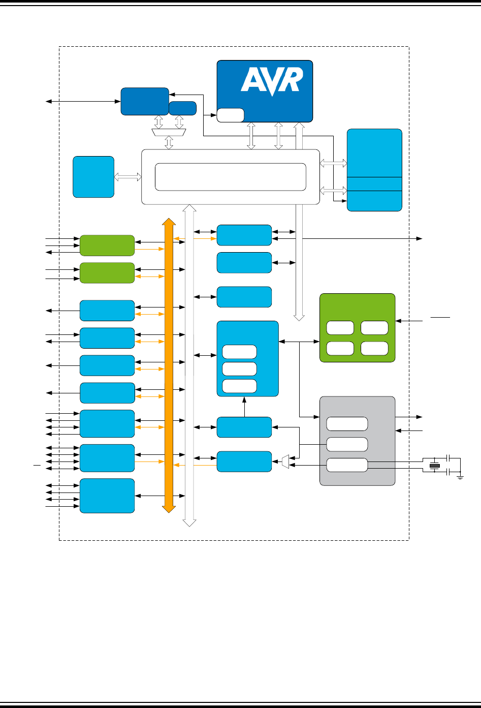
1. Block Diagram
I
N
/
O
U
T
D
A
T
A
B
U
S
Clock generation
BUS Matrix
CPU
USARTn
SPIn
TWIn
CCL
ACn
ADCn
TCAn
TCBn
WOn
RXD
TXD
XCK
XDIR
MISO
MOSI
SCK
SS
SDA (master)
SCL (master)
PORTS
EVSYS
System
Management
SLPCTRL
RSTCTRL
CLKCTRL
E
V
E
N
T
R
O
U
T
I
N
G
N
E
T
W
O
R
K
D
A
T
A
B
U
S
UPDI CRC
SRAM
NVMCTRL
Flash
EEPROM
OSC20M
OSC32K
XOSC32K
Detectors/
references
BOD/
VLM
POR
Bandgap
WDT
RTC
CPUINT
M M
S
MS
S
OCD
UPDI
RST
TOSC2
TOSC1
S
EXTCLK
LUTn-OUT
WO
CLKOUT
PAn
PBn
PCn
PDn
PEn
PFn
RESET
SDA (slave)
SCL (slave)
GPIOR
AINPn
AINNn
OUT
AINn
EVOUTx
VREFA
LUTn-INn
megaAVR® 0-Series
Block Diagram
© 2018 Microchip Technology Inc. Datasheet Preliminary DS40002015A-page 8
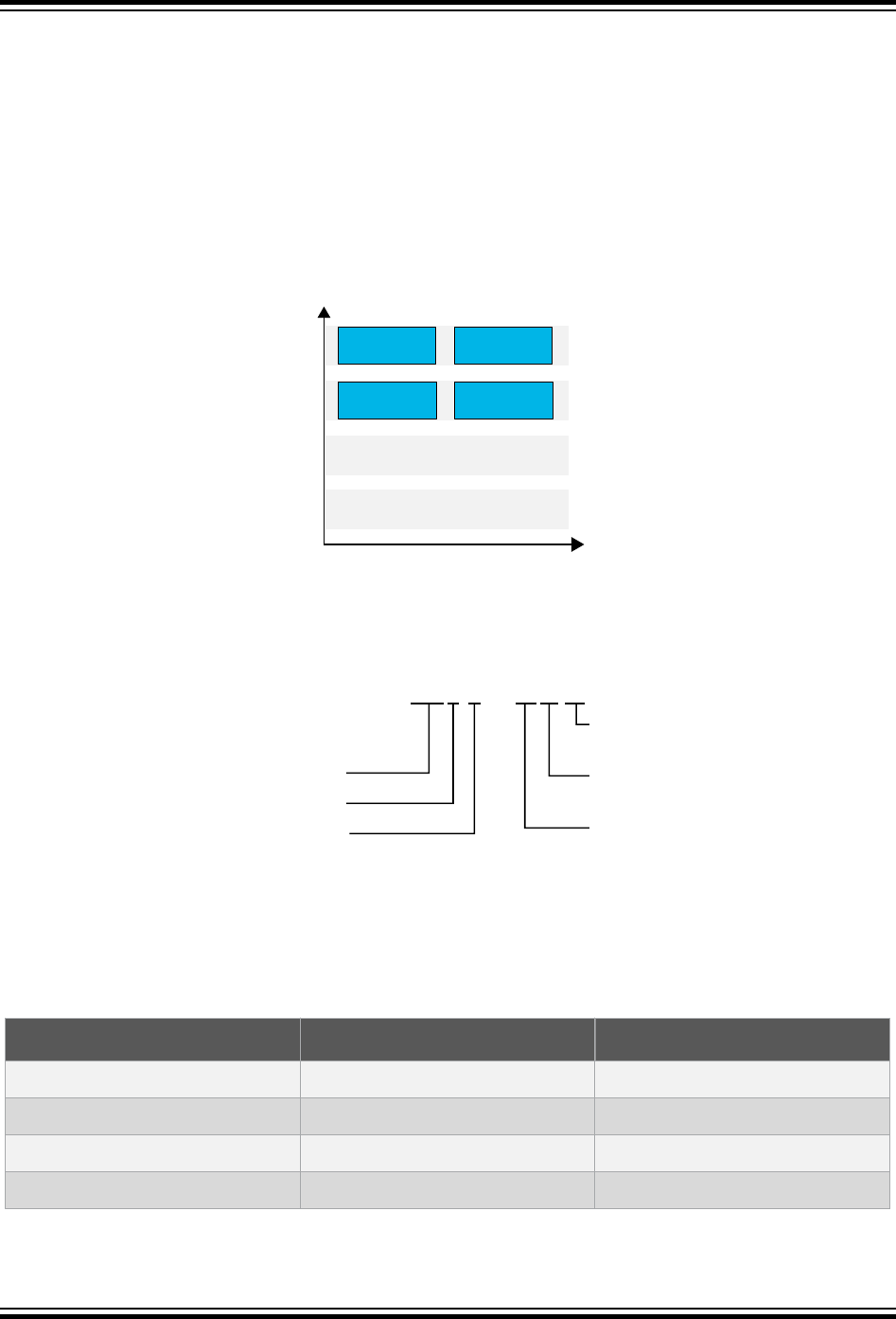
2. megaAVR® 0-series Overview
The figure below shows the megaAVR® 0-series devices, laying out pin count variants and memory sizes:
• Vertical migration is possible without code modification, as these devices are fully pin and feature
compatible.
• Horizontal migration to the left reduces the pin count and therefore the available features.
Figure 2-1. megaAVR® 0-series Overview
48KB
32KB
28/32 48
Pins
Flash
ATmega3208
ATmega4808
ATmega3209
ATmega4809
Devices with different Flash memory size typically also have different SRAM and EEPROM.
The name of a device in the megaAVR® 0-series is decoded as follows:
Figure 2-2. megaAVR® Device Designations
Carrier Type
AT mega 4809 - MFR
Flash size in KB
Series name
Pin count
9=48 pins
8=32 pins (SSOP: 28 pins)
Package Type
A=TQFP
M=QFN
X=SSOP
Temperature Range
F=-40°C to +125°C
R=Tape & Reel
2.1 Memory Overview
Table 2-1. Memory Overview
Memory Type ATmega320x ATmega480x
Flash 32 KB 48 KB
SRAM 4 KB 6 KB
EEPROM 256B 256B
User row 64B 64B
megaAVR® 0-Series
megaAVR® 0-series Overview
© 2018 Microchip Technology Inc. Datasheet Preliminary DS40002015A-page 9

2.2 Peripheral Overview
Table 2-2. Peripheral Overview
Property/Peripheral ATmega 08-X ATmega 08-A/M ATmega 09
Pins 28 32 48
Package SSOP VQFN,TQFP UQFN,TQFP
Max. Frequency (MHz) 20 20 20
16-bit Timer/Counter type A (TCA) 1 1 1
16-bit Timer/Counter type B (TCB) 3 3 4
12-bit Timer/Counter type D (TCD) - - -
Real Time Counter (RTC) 1 1 1
USART 3 3 4
SPI 1 1 1
TWI (I2C) 1(1) 1(1) 1(1)
ADC (channels) 1 (8) 1 (12) 1 (16)
DAC (outputs) - - -
AC (inputs) 1 (12) 1 (12) 1 (16)
Peripheral Touch Controller (PTC) (self-cap/mutual cap
channels)
- - -
Custom Logic (LUTs) 1 (4) 1 (4) 1 (4)
Window Watchdog 1 1 1
Event System channels 6 6 8
General purpose I/O 23 27 41
External interrupts 23 27 41
CRCSCAN 1 1 1
1. TWI can operate as master and slave at the same time on different pins.
megaAVR® 0-Series
megaAVR® 0-series Overview
© 2018 Microchip Technology Inc. Datasheet Preliminary DS40002015A-page 10

3. Conventions
3.1 Numerical Notation
Table 3-1. Numerical Notation
Symbol Description
165 Decimal number
0b0101 Binary number (example 0b0101 = 5 decimal)
'0101' Binary numbers are given without prefix if
unambiguous
0x3B24 Hexadecimal number
X Represents an unknown or don't care value
Z Represents a high-impedance (floating) state for
either a signal or a bus
3.2 Memory Size and Type
Table 3-2. Memory Size and Bit Rate
Symbol Description
KB kilobyte (210 = 1024)
MB megabyte (220 = 1024*1024)
GB gigabyte (230 = 1024*1024*1024)
b bit (binary '0' or '1')
B byte (8 bits)
1 kbit/s 1,000 bit/s rate (not 1,024 bit/s)
1 Mbit/s 1,000,000 bit/s rate
1 Gbit/s 1,000,000,000 bit/s rate
word 16-bit
3.3 Frequency and Time
Table 3-3. Frequency and Time
Symbol Description
kHz 1 kHz = 103 Hz = 1,000 Hz
KHz 1 KHz = 1,024 Hz, 32 KHz = 32,768 Hz
MHz 1 MHz = 106 Hz = 1,000,000 Hz
megaAVR® 0-Series
Conventions
© 2018 Microchip Technology Inc. Datasheet Preliminary DS40002015A-page 11

Symbol Description
GHz 1 GHz = 109 Hz = 1,000,000,000 Hz
s second
ms millisecond
µs microsecond
ns nanosecond
3.4 Registers and Bits
Table 3-4. Register and Bit Mnemonics
Symbol Description
R/W Read/Write accessible register bit. The user can read from and write to this bit.
R Read-only accessible register bit. The user can only read this bit. Writes will be
ignored.
W Write-only accessible register bit. The user can only write this bit. Reading this bit will
return an undefined value.
BITFIELD Bitfield names are shown in uppercase. Example: INTMODE.
BITFIELD[n:m] A set of bits from bit n down to m. Example: PINA[3:0] = {PINA3, PINA2, PINA1,
PINA0}.
Reserved Reserved bits are unused and reserved for future use. Bitfields in the Register
Summary or Register Description chapters that have gray background are Reserved
bits.
For compatibility with future devices, always write reserved bits to zero when the
register is written. Reserved bits will always return zero when read.
Reserved bit field values must not be written to a bit field. A reserved value won't be
read from a read-only bit field.
PERIPHERAL
n
If several instances of the peripheral exist, the peripheral name is followed by a single
number to identify one instance. Example: USARTn is the collection of all instances of
the USART module, while USART3 is one specific instance of the USART module.
PERIPHERALx If several instances of the peripheral exist, the peripheral name is followed by a single
capital letter (A-Z) to identify one instance. Example: PORTx is the collection of all
instances of the PORT module, while PORTB is one specific instance of the PORT
module.
Reset Value of a register after a power Reset. This is also the value of registers in a
peripheral after performing a software Reset of the peripheral, except for the Debug
Control registers.
SET/CLR Registers with SET/CLR suffix allows the user to clear and set bits in a register without
doing a read-modify-write operation. These registers always come in pairs. Writing a ‘1’
to a bit in the CLR register will clear the corresponding bit in both registers, while
megaAVR® 0-Series
Conventions
© 2018 Microchip Technology Inc. Datasheet Preliminary DS40002015A-page 12

Symbol Description
writing a ‘1’ to a bit in the SET register will set the corresponding bit in both registers.
Both registers will return the same value when read. If both registers are written
simultaneously, the write to the CLR register will take precedence.
3.4.1 Addressing Registers from Header Files
In order to address registers in the supplied C header files, the following rules apply:
1. A register is identified by <peripheral_instance_name>.<register_name>, e.g. CPU.SREG,
USART2.CTRLA, or PORTB.DIR.
2. The peripheral name is written in the peripheral's register summary heading, e.g. "Register
Summary - ACn", where "ACn" is the peripheral name.
3. <peripheral_instance_name> is obtained by substituting any n or x in the peripheral name with the
correct instance identifier.
megaAVR® 0-Series
Conventions
© 2018 Microchip Technology Inc. Datasheet Preliminary DS40002015A-page 13

4. Acronyms and Abbreviations
The table below contains acronyms and abbreviations used in this document.
Table 4-1. Acronyms and Abbreviations
Abbreviation Description
AC Analog Comparator
ACK Acknowledge
ADC Analog-to-Digital Converter
ADDR Address
AES Advanced Encryption Standard
ALU Arithmetic Logic Unit
AREF Analog reference voltage, also VREFA
BLB Boot Lock Bit
BOD Brown-out Detector
CAL Calibration
CCMP Compare/Capture
CCL Configurable Custom Logic
CCP Configuration Change Protection
CLK Clock
CLKCTRL Clock Controller
CRC Cyclic Redundancy Check
CTRL Control
DAC Digital-to-Analog Converter
DFLL Digital Frequency Locked Loop
DMAC DMA (Direct Memory Access) Controller
DNL Differential Nonlinearity (ADC characteristics)
EEPROM Electrically Erasable Programmable Read-Only Memory
EVSYS Event System
GND Ground
GPIO General Purpose Input/Output
I2C Inter-Integrated Circuit
IF Interrupt flag
INL Integral Nonlinearity (ADC characteristics)
megaAVR® 0-Series
Acronyms and Abbreviations
© 2018 Microchip Technology Inc. Datasheet Preliminary DS40002015A-page 14

Abbreviation Description
INT Interrupt
IrDA Infrared Data Association
IVEC Interrupt Vector
LSB Least Significant Byte
LSb Least Significant bit
LUT Look Up Table
MBIST Memory Built-in Self-test
MSB Most Significant Byte
MSb Most Significant bit
NACK Not Acknowledge
NMI Non-maskable interrupt
NVM Nonvolatile Memory
NVMCTRL Nonvolatile Memory Controller
OPAMP Operation Amplifier
OSC Oscillator
PC Program Counter
PER Period
POR Power-on Reset
PORT I/O Pin Configuration
PTC Peripheral Touch Controller
PWM Pulse-width Modulation
RAM Random Access Memory
REF Reference
REQ Request
RISC Reduced Instruction Set Computer
RSTCTRL Reset Controller
RTC Real-time Counter
RX Receiver/Receive
SERCOM Serial Communication Interface
SLPCTRL Sleep Controller
SMBus System Management Bus
SP Stack Pointer
megaAVR® 0-Series
Acronyms and Abbreviations
© 2018 Microchip Technology Inc. Datasheet Preliminary DS40002015A-page 15

Abbreviation Description
SPI Serial Peripheral Interface
SRAM Static Random Access Memory
SYSCFG System Configuration
TC Timer/Counter (Optionally superseded by a letter indicating type of TC)
TRNG True Random Number Generator
TWI Two-wire Interface
TX Transmitter/Transmit
ULP Ultra Low Power
UPDI Unified Program and Debug Interface
USART Universal Synchronous and Asynchronous Serial Receiver and Transmitter
USB Universal Serial Bus
VDD Voltage to be applied to VDD
VREF Voltage Reference
VCM Voltage Common mode
WDT Watchdog Timer
XOSC Crystal Oscillator
megaAVR® 0-Series
Acronyms and Abbreviations
© 2018 Microchip Technology Inc. Datasheet Preliminary DS40002015A-page 16

5. Memories
5.1 Overview
The main memories are SRAM data memory, EEPROM data memory, and Flash program memory. In
addition, the peripheral registers are located in the I/O memory space.
5.2 Memory Map
The figure below shows the memory map for the biggest memory derivative in the series. Refer to the
subsequent subsections for details on memory sizes and start addresses for devices with smaller
memory sizes.
megaAVR® 0-Series
Memories
© 2018 Microchip Technology Inc. Datasheet Preliminary DS40002015A-page 17
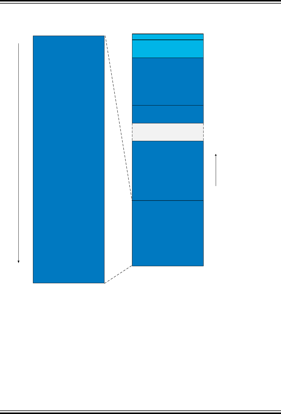
Figure 5-1. Memory Map: Flash 48 KB, Internal SRAM 6 KB, EEPROM 256B
(Reserved)
NVM I/O Registers and
data
64 I/O Registers
960 Ext I/O Registers
0x0000 – 0x003F
0x0040 – 0x0FFF
0x1400
0x1500
EEPROM 256B
Flash code
0x1000 – 0x13FF
Internal SRAM
6KB
48KB
0xFFFF
0x4000
0x3FFF
Flash code
48KB
0x0000
Code space Data space
0x2800
5.3 In-System Reprogrammable Flash Program Memory
The ATmega3208/3209/4808/4809 contains up to 48 KB On-Chip In-System Reprogrammable Flash
memory for program storage. Since all AVR instructions are 16 or 32 bits wide, the Flash is organized
with 16-bit data width. For write protection, the Flash Program memory space can be divided into three
sections: Boot Loader section, Application code section, and Application data section. Code placed in one
section may be restricted from writing to addresses in other sections, see the NVMCTRL documentation
for more details.
megaAVR® 0-Series
Memories
© 2018 Microchip Technology Inc. Datasheet Preliminary DS40002015A-page 18

The program counter is able to address the whole program memory. The procedure for writing Flash
memory is described in detail in the documentation of the Non-Volatile Memory Controller (NVMCTRL)
peripheral.
The Flash memory is mapped into the data space and is accessible with normal LD/ST instructions. For
LD/ST instructions, the Flash is mapped from address 0x4000. The Flash memory can be read with the
LPM instruction. For the LPM instruction, the Flash start address is 0x0000.
The ATmega3208/3209/4808/4809 has a CRC module that is a master on the bus.
Table 5-1. Physical Properties of Flash Memory
Property ATmega320x ATmega480x
Size 32 KB 48 KB
Page size 128 B 128 B
Number of pages 256 384
Start address in Data Space 0x4000 0x4000
Start address in Code Space 0x0 0x0
5.4 SRAM Data Memory
The primary task of the SRAM memory is to store application data. It is not possible to execute code from
SRAM.
Table 5-2. Physical Properties of SRAM
Property ATmega320x ATmega480x
Size 4 KB 6 KB
Start address 0x3000 0x2800
5.5 EEPROM Data Memory
The primary task of the EEPROM memory is to store nonvolatile application data. The EEPROM memory
supports single byte read and write. The EEPROM is controlled by the Non-Volatile Memory Controller
(NVMCTRL).
Table 5-3. Physical Properties of EEPROM
Property ATmega320x ATmega480x
Size 256B 256B
Page size 64B 64B
Number of pages 4 4
Start address 0x1400 0x1400
5.6 User Row (USERROW)
In addition to the EEPROM, the ATmega3208/3209/4808/4809 has one extra page of EEPROM memory
that can be used for firmware settings, the User Row (USERROW). This memory supports single byte
megaAVR® 0-Series
Memories
© 2018 Microchip Technology Inc. Datasheet Preliminary DS40002015A-page 19

read and write as the normal EEPROM. The CPU can write and read this memory as normal EEPROM
and the UPDI can write and read it as a normal EEPROM memory if the part is unlocked. The User Row
can also be written by the UPDI when the part is locked. USERROW is not affected by a chip erase. The
USERROW can be used for final configuration without having programming or debugging capabilities
enabled.
5.7 Signature Row (SIGROW)
The content of the Signature Row fuses (SIGROW) is pre-programmed and cannot be altered. SIGROW
holds information such as device ID, serial number, and calibration values.
All AVR microcontrollers have a three-byte device ID which identifies the device. This device ID can be
read in both serial and parallel mode, also when the device is locked. The three bytes reside in the
Signature Row. The signature bytes are given in the following table.
Table 5-4. Device ID
Device Name Signature Bytes Address
0x00 0x01 0x02
ATmega4809 0x1E 0x96 0x51
ATmega4808 0x1E 0x96 0x50
ATmega3209 0x1E 0x95 0x31
ATmega3208 0x1E 0x95 0x30
megaAVR® 0-Series
Memories
© 2018 Microchip Technology Inc. Datasheet Preliminary DS40002015A-page 20

5.7.1 Signature Row Summary - SIGROW
Offset Name Bit Pos.
0x00 DEVICEID0 7:0 DEVICEID[7:0]
0x01 DEVICEID1 7:0 DEVICEID[7:0]
0x02 DEVICEID2 7:0 DEVICEID[7:0]
0x03 SERNUM0 7:0 SERNUM[7:0]
0x04 SERNUM1 7:0 SERNUM[7:0]
0x05 SERNUM2 7:0 SERNUM[7:0]
0x06 SERNUM3 7:0 SERNUM[7:0]
0x07 SERNUM4 7:0 SERNUM[7:0]
0x08 SERNUM5 7:0 SERNUM[7:0]
0x09 SERNUM6 7:0 SERNUM[7:0]
0x0A SERNUM7 7:0 SERNUM[7:0]
0x0B SERNUM8 7:0 SERNUM[7:0]
0x0C SERNUM9 7:0 SERNUM[7:0]
0x0D
...
0x1F
Reserved
0x20 TEMPSENSE0 7:0 TEMPSENSE[7:0]
0x21 TEMPSENSE1 7:0 TEMPSENSE[7:0]
0x22 OSC16ERR3V 7:0 OSC16ERR3V[7:0]
0x23 OSC16ERR5V 7:0 OSC16ERR5V[7:0]
0x24 OSC20ERR3V 7:0 OSC20ERR3V[7:0]
0x25 OSC20ERR5V 7:0 OSC20ERR5V[7:0]
5.7.2 Signature Row Description
megaAVR® 0-Series
Memories
© 2018 Microchip Technology Inc. Datasheet Preliminary DS40002015A-page 21

5.7.2.1 Device ID n
Name: DEVICEIDn
Offset: 0x00 + n*0x01 [n=0..2]
Reset: [Device ID]
Property: -
Each device has a device ID identifying the device and its properties; such as memory sizes, pin count,
and die revision. This can be used to identify a device and hence, the available features by software. The
Device ID consists of three bytes: SIGROW.DEVICEID[2:0].
Bit 7 6 5 4 3 2 1 0
DEVICEID[7:0]
Access R R R R R R R R
Reset x x x x x x x x
Bits 7:0 – DEVICEID[7:0] Byte n of the Device ID
megaAVR® 0-Series
Memories
© 2018 Microchip Technology Inc. Datasheet Preliminary DS40002015A-page 22

5.7.2.2 Serial Number Byte n
Name: SERNUMn
Offset: 0x03 + n*0x01 [n=0..9]
Reset: [device serial number]
Property: -
Each device has an individual serial number, representing a unique ID. This can be used to identify a
specific device in the field. The serial number consists of ten bytes: SIGROW.SERNUM[9:0].
Bit 7 6 5 4 3 2 1 0
SERNUM[7:0]
Access R R R R R R R R
Reset x x x x x x x x
Bits 7:0 – SERNUM[7:0] Serial Number Byte n
megaAVR® 0-Series
Memories
© 2018 Microchip Technology Inc. Datasheet Preliminary DS40002015A-page 23

5.7.2.3 Temperature Sensor Calibration n
Name: TEMPSENSEn
Offset: 0x20 + n*0x01 [n=0..1]
Reset: [Temperature sensor calibration value]
Property: -
These registers contain correction factors for temperature measurements by the ADC.
SIGROW.TEMPSENSE0 is a correction factor for the gain/slope (unsigned), SIGROW.TEMPSENSE1 is
a correction factor for the offset (signed).
Bit 7 6 5 4 3 2 1 0
TEMPSENSE[7:0]
Access R R R R R R R R
Reset x x x x x x x x
Bits 7:0 – TEMPSENSE[7:0] Temperature Sensor Calibration Byte n
Refer to the ADC chapter for a description on how to use this register.
megaAVR® 0-Series
Memories
© 2018 Microchip Technology Inc. Datasheet Preliminary DS40002015A-page 24

5.7.2.4 OSC16 Error at 3V
Name: OSC16ERR3V
Offset: 0x22
Reset: [Oscillator frequency error value]
Property: -
Bit 7 6 5 4 3 2 1 0
OSC16ERR3V[7:0]
Access R R R R R R R R
Reset x x x x x x x x
Bits 7:0 – OSC16ERR3V[7:0] OSC16 Error at 3V
These registers contain the signed oscillator frequency error value when running at internal 16 MHz at 3V,
as measured during production.
megaAVR® 0-Series
Memories
© 2018 Microchip Technology Inc. Datasheet Preliminary DS40002015A-page 25

5.7.2.5 OSC16 Error at 5V
Name: OSC16ERR5V
Offset: 0x23
Reset: [Oscillator frequency error value]
Property: -
Bit 7 6 5 4 3 2 1 0
OSC16ERR5V[7:0]
Access R R R R R R R R
Reset x x x x x x x x
Bits 7:0 – OSC16ERR5V[7:0] OSC16 Error at 5V
These registers contain the signed oscillator frequency error value when running at internal 16 MHz at 5V,
as measured during production.
megaAVR® 0-Series
Memories
© 2018 Microchip Technology Inc. Datasheet Preliminary DS40002015A-page 26

5.7.2.6 OSC20 Error at 3V
Name: OSC20ERR3V
Offset: 0x24
Reset: [Oscillator frequency error value]
Property: -
Bit 7 6 5 4 3 2 1 0
OSC20ERR3V[7:0]
Access R R R R R R R R
Reset x x x x x x x x
Bits 7:0 – OSC20ERR3V[7:0] OSC20 Error at 3V
These registers contain the signed oscillator frequency error value when running at internal 20 MHz at 3V,
as measured during production.
megaAVR® 0-Series
Memories
© 2018 Microchip Technology Inc. Datasheet Preliminary DS40002015A-page 27

5.7.2.7 OSC20 Error at 5V
Name: OSC20ERR5V
Offset: 0x25
Reset: [Oscillator frequency error value]
Property: -
Bit 7 6 5 4 3 2 1 0
OSC20ERR5V[7:0]
Access R R R R R R R R
Reset x x x x x x x x
Bits 7:0 – OSC20ERR5V[7:0] OSC20 Error at 5V
These registers contain the signed oscillator frequency error value when running at internal 20 MHz at 5V,
as measured during production.
5.8 Fuses (FUSE)
Fuses are part of the nonvolatile memory and hold factory calibration data and device configuration. The
fuses are available from device power-up. The fuses can be read by the CPU or the UPDI, but can only
be programmed or cleared by the UPDI. The configuration and calibration values stored in the fuses are
written to their respective target registers at the end of the start-up sequence.
The fuses are pre-programmed but can be altered by the user. Altered values in the configuration fuse
will be effective only after a Reset.
Note: When writing the fuses write all reserved bits to ‘1’.
megaAVR® 0-Series
Memories
© 2018 Microchip Technology Inc. Datasheet Preliminary DS40002015A-page 28

5.8.1 Fuse Summary - FUSE
Offset Name Bit Pos.
0x00 WDTCFG 7:0 WINDOW[3:0] PERIOD[3:0]
0x01 BODCFG 7:0 LVL[2:0] SAMPFREQ ACTIVE[1:0] SLEEP[1:0]
0x02 OSCCFG 7:0 OSCLOCK FREQSEL[1:0]
0x03
...
0x04
Reserved
0x05 SYSCFG0 7:0 CRCSRC[1:0] RSTPINCFG EESAVE
0x06 SYSCFG1 7:0 SUT[2:0]
0x07 APPEND 7:0 APPEND[7:0]
0x08 BOOTEND 7:0 BOOTEND[7:0]
0x09 Reserved
0x0A LOCKBIT 7:0 LOCKBIT[7:0]
5.8.2 Fuse Description
megaAVR® 0-Series
Memories
© 2018 Microchip Technology Inc. Datasheet Preliminary DS40002015A-page 29

5.8.2.1 Watchdog Configuration
Name: WDTCFG
Offset: 0x00
Reset: -
Property: -
Bit 7 6 5 4 3 2 1 0
WINDOW[3:0] PERIOD[3:0]
Access R R R R R R R R
Reset 0 0 0 0 0 0 0 0
Bits 7:4 – WINDOW[3:0] Watchdog Window Time-out Period
This value is loaded into the WINDOW bit field of the Watchdog Control A register (WDT.CTRLA) during
Reset.
Bits 3:0 – PERIOD[3:0] Watchdog Time-out Period
This value is loaded into the PERIOD bit field of the Watchdog Control A register (WDT.CTRLA) during
Reset.
megaAVR® 0-Series
Memories
© 2018 Microchip Technology Inc. Datasheet Preliminary DS40002015A-page 30
5.8.2.2 BOD Configuration
Name: BODCFG
Offset: 0x01
Reset: -
Property: -
The settings of the BOD will be reloaded from this Fuse after a Power-on Reset. For all other Resets, the
BOD configuration remains unchanged.
Bit 7 6 5 4 3 2 1 0
LVL[2:0] SAMPFREQ ACTIVE[1:0] SLEEP[1:0]
Access R R R R R R R R
Reset 0 0 0 0 0 0 0 0
Bits 7:5 – LVL[2:0] BOD Level
This value is loaded into the LVL bit field of the BOD Control B register (BOD.CTRLB) during Reset.
Value Name Description
0x0 BODLEVEL0 1.8V
0x1 BODLEVEL1 2.15V
0x2 BODLEVEL2 2.60V
0x3 BODLEVEL3 2.95V
0x4 BODLEVEL4 3.30V
0x5 BODLEVEL5 3.70V
0x6 BODLEVEL6 4.00V
0x7 BODLEVEL7 4.30V
Bit 4 – SAMPFREQ BOD Sample Frequency
This value is loaded into the SAMPFREQ bit of the BOD Control A register (BOD.CTRLA) during Reset.
Value Description
0x0 Sample frequency is 1 kHz
0x1 Sample frequency is 125 Hz
Bits 3:2 – ACTIVE[1:0] BOD Operation Mode in Active and Idle
This value is loaded into the ACTIVE bit field of the BOD Control A register (BOD.CTRLA) during Reset.
Value Description
0x0 Disabled
0x1 Enabled
0x2 Sampled
0x3 Enabled with wake-up halted until BOD is ready
Bits 1:0 – SLEEP[1:0] BOD Operation Mode in Sleep
This value is loaded into the SLEEP bit field of the BOD Control A register (BOD.CTRLA) during Reset.
Value Description
0x0 Disabled
0x1 Enabled
megaAVR® 0-Series
Memories
© 2018 Microchip Technology Inc. Datasheet Preliminary DS40002015A-page 31

Value Description
0x2 Sampled
0x3 Reserved
megaAVR® 0-Series
Memories
© 2018 Microchip Technology Inc. Datasheet Preliminary DS40002015A-page 32
5.8.2.3 Oscillator Configuration
Name: OSCCFG
Offset: 0x02
Reset: -
Property: -
Bit 7 6 5 4 3 2 1 0
OSCLOCK FREQSEL[1:0]
Access R R R
Reset 0 0 2
Bit 7 – OSCLOCK Oscillator Lock
This fuse bit is loaded to LOCK in CLKCTRL.OSC20MCALIBB during Reset.
Value Description
0 Calibration registers of the 20 MHz oscillator are accessible
1 Calibration registers of the 20 MHz oscillator are locked
Bits 1:0 – FREQSEL[1:0] Frequency Select
These bits select the operation frequency of the 20 MHz internal oscillator (OSC20M) and determine the
respective factory calibration values to be written to CAL20M in CLKCTRL.OSC20MCALIBA and
TEMPCAL20M in CLKCTRL.OSC20MCALIBB.
Value Description
0x0 Reserved
0x1 Run at 16 MHz
0x2 Run at 20 MHz
0x3 Reserved
megaAVR® 0-Series
Memories
© 2018 Microchip Technology Inc. Datasheet Preliminary DS40002015A-page 33

5.8.2.4 System Configuration 0
Name: SYSCFG0
Offset: 0x05
Reset: 0xC4
Property: -
Bit 7 6 5 4 3 2 1 0
CRCSRC[1:0] RSTPINCFG EESAVE
Access R R R R
Reset 1 1 0 0
Bits 7:6 – CRCSRC[1:0] CRC Source
See the CRC description for more information about the functionality.
Value Name Description
00 FLASH CRC of full Flash (boot, application code, and application data)
01 BOOT CRC of boot section
10 BOOTAPP CRC of application code and boot sections
11 NOCRC No CRC
Bit 3 – RSTPINCFG Reset Pin Configuration
This bit selects the pin configuration for the reset pin.
Value Description
0x0 GPIO
0x1 RESET
Bit 0 – EESAVE EEPROM Save During Chip Erase
If the device is locked the EEPROM is always erased by a chip erase, regardless of this bit.
Value Description
0 EEPROM erased during chip erase
1 EEPROM not erased under chip erase
megaAVR® 0-Series
Memories
© 2018 Microchip Technology Inc. Datasheet Preliminary DS40002015A-page 34

5.8.2.5 System Configuration 1
Name: SYSCFG1
Offset: 0x06
Reset: -
Property: -
Bit 7 6 5 4 3 2 1 0
SUT[2:0]
Access R R R
Reset 1 1 1
Bits 2:0 – SUT[2:0] Start-Up Time Setting
These bits select the start-up time between power-on and code execution.
Value Description
0x0 0 ms
0x1 1 ms
0x2 2 ms
0x3 4 ms
0x4 8 ms
0x5 16 ms
0x6 32 ms
0x7 64 ms
megaAVR® 0-Series
Memories
© 2018 Microchip Technology Inc. Datasheet Preliminary DS40002015A-page 35

5.8.2.6 Application Code End
Name: APPEND
Offset: 0x07
Reset: -
Property: -
Bit 7 6 5 4 3 2 1 0
APPEND[7:0]
Access R R R R R R R R
Reset 0 0 0 0 0 0 0 0
Bits 7:0 – APPEND[7:0] Application Code Section End
These bits set the end of the application code section in blocks of 256 bytes. The end of the application
code section should be set as BOOT size plus application code size. The remaining Flash will be
application data. A value of 0x00 defines the Flash from BOOTEND*256 to end of Flash as application
code. When both FUSE.APPEND and FUSE.BOOTEND are 0x00, the entire Flash is BOOT section.
megaAVR® 0-Series
Memories
© 2018 Microchip Technology Inc. Datasheet Preliminary DS40002015A-page 36

5.8.2.7 Boot End
Name: BOOTEND
Offset: 0x08
Reset: -
Property: -
Bit 7 6 5 4 3 2 1 0
BOOTEND[7:0]
Access R R R R R R R R
Reset 0 0 0 0 0 0 0 0
Bits 7:0 – BOOTEND[7:0] Boot Section End
These bits set the end of the boot section in blocks of 256 bytes. A value of 0x00 defines the whole Flash
as BOOT section. When both FUSE.APPEND and FUSE.BOOTEND are 0x00, the entire Flash is BOOT
section.
megaAVR® 0-Series
Memories
© 2018 Microchip Technology Inc. Datasheet Preliminary DS40002015A-page 37

5.8.2.8 Lockbits
Name: LOCKBIT
Offset: 0x0A
Reset: -
Property: -
Bit 7 6 5 4 3 2 1 0
LOCKBIT[7:0]
Access R/W R/W R/W R/W R/W R/W R/W R/W
Reset 0 0 0 0 0 0 0 0
Bits 7:0 – LOCKBIT[7:0] Lockbits
When the part is locked, UPDI cannot access the system bus, so it cannot read out anything but CS-
space.
Value Description
0xC5 Valid key - the device is open
other Invalid - the device is locked
5.9 Memory Section Access from CPU and UPDI on Locked Device
The device can be locked so that the memories cannot be read using the UPDI. The locking protects both
the Flash (all BOOT, APPCODE, and APPDATA sections), SRAM, and the EEPROM including the FUSE
data. This prevents successful reading of application data or code using the debugger interface. Regular
memory access from within the application still is enabled.
The device is locked by writing any non-valid value to the LOCKBIT bit field in FUSE.LOCKBIT.
Table 5-5. Memory Access in Unlocked Mode (FUSE.LOCKBIT Valid)(1)
Memory Section CPU Access UPDI Access
Read Write Read Write
SRAM Yes Yes Yes Yes
Registers Yes Yes Yes Yes
Flash Yes Yes Yes Yes
EEPROM Yes No Yes Yes
USERROW Yes Yes Yes Yes
SIGROW Yes No Yes No
Other Fuses Yes No Yes Yes
megaAVR® 0-Series
Memories
© 2018 Microchip Technology Inc. Datasheet Preliminary DS40002015A-page 38

Table 5-6. Memory Access in Locked Mode (FUSE.LOCKBIT Invalid)(1)
Memory Section CPU Access UPDI Access
Read Write Read Write
SRAM Yes Yes No No
Registers Yes Yes No No
Flash Yes Yes No No
EEPROM Yes No No No
USERROW Yes Yes No Yes(2)
SIGROW Yes No Yes No
Other Fuses Yes No No No
Note:
1. Read operations marked No in the tables may appear to be successful, but the data is corrupt.
Hence, any attempt of code validation through the UPDI will fail on these memory sections.
2. In Locked mode, the USERROW can be written blindly using the fuse Write command, but the
current USERROW values cannot be read out.
Important: The only way to unlock a device is a CHIPERASE, which will erase all device
memories to factory default so that no application data is retained.
5.10 I/O Memory
All ATmega3208/3209/4808/4809 I/Os and peripherals are located in the I/O space. The I/O address
range from 0x00 to 0x3F can be accessed in a single cycle using IN and OUT instructions. The Extended
I/O space from 0x0040 - 0x0FFF can be accessed by the LD/LDS/LDD and ST/STS/STD instructions,
transferring data between the 32 general purpose working registers and the I/O space.
I/O Registers within the address range 0x00 - 0x1F are directly bit-accessible using the SBI and CBI
instructions. In these registers, the value of single bits can be checked by using the SBIS and SBIC
instructions. Refer to the Instruction Set section for more details.
For compatibility with future devices, reserved bits should be written to zero if accessed. Reserved I/O
memory addresses should never be written.
Some of the interrupt flags are cleared by writing a '1' to them. On ATmega3208/3209/4808/4809 devices,
the CBI and SBI instructions will only operate on the specified bit, and can, therefore, be used on
registers containing such interrupt flags. The CBI and SBI instructions work with registers 0x00 - 0x1F
only.
General Purpose I/O Registers
The ATmega3208/3209/4808/4809 devices provide four General Purpose I/O Registers. These registers
can be used for storing any information, and they are particularly useful for storing global variables and
megaAVR® 0-Series
Memories
© 2018 Microchip Technology Inc. Datasheet Preliminary DS40002015A-page 39

interrupt flags. General Purpose I/O Registers, which reside in the address range 0x1C - 0x1F, are
directly bit-accessible using the SBI, CBI, SBIS, and SBIC instructions.
megaAVR® 0-Series
Memories
© 2018 Microchip Technology Inc. Datasheet Preliminary DS40002015A-page 40


5.10.2.1 General Purpose I/O Register n
Name: GPIOR
Offset: 0x00 + n*0x01 [n=0..3]
Reset: 0x00
Property: -
These are general purpose registers that can be used to store data, such as global variables and flags, in
the bit accessible I/O memory space.
Bit 7 6 5 4 3 2 1 0
GPIOR[7:0]
Access R/W R/W R/W R/W R/W R/W R/W R/W
Reset 0 0 0 0 0 0 0 0
Bits 7:0 – GPIOR[7:0] GPIO Register byte
megaAVR® 0-Series
Memories
© 2018 Microchip Technology Inc. Datasheet Preliminary DS40002015A-page 42

6. Peripherals and Architecture
6.1 Peripheral Module Address Map
The address map shows the base address for each peripheral. For complete register description and
summary for each peripheral module, refer to the respective module chapters.
Table 6-1. Peripheral Module Address Map
Base Address Name Description 28-Pin 32-Pin 48-Pin
0x0000 VPORTA Virtual Port A X X X
0x0004 VPORTB Virtual Port B X
0x0008 VPORTC Virtual Port C X X X
0x000C VPORTD Virtual Port D X X X
0x0010 VPORTE Virtual Port E X
0x0014 VPORTF Virtual Port F X X X
0x001C GPIO General
Purpose IO
registers
XXX
0x0030 CPU CPU X X X
0x0040 RSTCTRL Reset
Controller
XXX
0x0050 SLPCTRL Sleep
Controller
XXX
0x0060 CLKCTRL Clock Controller X X X
0x0080 BOD Brown-Out
Detector
XXX
0x00A0 VREF Voltage
Reference
XXX
0x0100 WDT Watchdog
Timer
XXX
0x0110 CPUINT Interrupt
Controller
XXX
0x0120 CRCSCAN Cyclic
Redundancy
Check Memory
Scan
XXX
0x0140 RTC Real Time
Counter
XXX
megaAVR® 0-Series
Peripherals and Architecture
© 2018 Microchip Technology Inc. Datasheet Preliminary DS40002015A-page 43

Base Address Name Description 28-Pin 32-Pin 48-Pin
0x0180 EVSYS Event System X X X
0x01C0 CCL Configurable
Custom Logic
XXX
0x0400 PORTA Port A
Configuration
XXX
0x0420 PORTB Port B
Configuration
X
0x0440 PORTC Port C
Configuration
XXX
0x0460 PORTD Port D
Configuration
XXX
0x0480 PORTE Port E
Configuration
X
0x04A0 PORTF Port F
Configuration
XXX
0x05E0 PORTMUX Port Multiplexer X X X
0x0600 ADC0 Analog to
Digital
Converter
XXX
0x0680 AC0 Analog
Comparator 0
XXX
0x0800 USART0 Universal
Synchronous
Asynchronous
Receiver
Transmitter 0
X X X
0x0820 USART1 Universal
Synchronous
Asynchronous
Receiver
Transmitter 1
X X X
0x0840 USART2 Universal
Synchronous
Asynchronous
Receiver
Transmitter 2
X X X
0x0860 USART3 Universal
Synchronous
Asynchronous
X
megaAVR® 0-Series
Peripherals and Architecture
© 2018 Microchip Technology Inc. Datasheet Preliminary DS40002015A-page 44

Base Address Name Description 28-Pin 32-Pin 48-Pin
Receiver
Transmitter 3
0x08A0 TWI0 Two Wire
Interface
XXX
0x08C0 SPI0 Serial
Peripheral
Interface
XXX
0x0A00 TCA0 Timer/Counter
Type A instance
0
XXX
0x0A80 TCB0 Timer/Counter
Type B instance
0
XXX
0x0A90 TCB1 Timer/Counter
Type B instance
1
XXX
0x0AA0 TCB2 Timer/Counter
Type B instance
2
XXX
0x0AB0 TCB3 Timer/Counter
Type B instance
3
X
0x0F00 SYSCFG System
Configuration
XXX
0x1000 NVMCTRL Non Volatile
Memory
Controller
XXX
0x1100 SIGROW Signature Row X X X
0x1280 FUSE Device specific
fuses
XXX
0x1300 USERROW User Row X X X
6.2 Interrupt Vector Mapping
Each of the interrupt vectors is connected to one peripheral instance, as shown in the table below. A
peripheral can have one or more interrupt sources. See the 'Interrupts' section in the 'Functional
Description' of the respective peripheral for more details on the available interrupt sources.
When the interrupt condition occurs, an Interrupt Flag is set in the Interrupt Flags register of the
peripheral (peripheral.INTFLAGS).
megaAVR® 0-Series
Peripherals and Architecture
© 2018 Microchip Technology Inc. Datasheet Preliminary DS40002015A-page 45

An interrupt is enabled or disabled by writing to the corresponding Interrupt Enable bit in the peripheral's
Interrupt Control register (peripheral.INTCTRL).
An interrupt request is generated when the corresponding interrupt is enabled and the Interrupt Flag is
set. The interrupt request remains active until the Interrupt Flag is cleared. See the peripheral's
INTFLAGS register for details on how to clear Interrupt Flags.
Note: Interrupts must be enabled globally for interrupt requests to be generated.
Table 6-2. Interrupt Vector Mapping
Vector
Number
Vector Address Peripheral Source 28-Pin 32-Pin 48-Pin
Program
Memory
≤8KB
Program
Memory
>8KB
0 0x00 0x00 RESET X X X
1 0x01 0x02 NMI - Non-Maskable Interrupt from CRC X X X
2 0x02 0x04 VLM - Voltage Level Monitor X X X
3 0x03 0x06 RTC - Overflow or compare match X X X
4 0x04 0x08 PIT - Periodic Interrupt X X X
5 0x05 0x0A CCL - Configurable Custom Logic X X X
6 0x06 0x0C PORTA - External interrupt X X X
7 0x07 0x0E TCA0 - Overflow X X X
8 0x08 0x10 TCA0 - Underflow (Split mode) X X X
9 0x09 0x12 TCA0 - Compare channel 0 X X X
10 0x0A 0x14 TCA0 - Compare channel 1 X X X
11 0x0B 0x16 TCA0 - Compare channel 2 X X X
12 0x0C 0x18 TCB0 - Capture X X X
13 0x0D 0x1A TCB1 - Capture X X X
14 0x0E 0x1C TWI0 - Slave X X X
15 0x0F 0x1E TWI0 - Master X X X
16 0x10 0x20 SPI0 - Serial Peripheral Interface 0 X X X
17 0x11 0x22 USART0 - Receive Complete X X X
18 0x12 0x24 USART0 - Data Register Empty X X X
19 0x13 0x26 USART0 - Transmit Complete X X X
20 0x14 0x28 PORTD - External interrupt X X X
21 0x15 0x2A AC0 – Compare X X X
22 0x16 0x2C ADC0 – Result Ready X X X
23 0x17 0x2E ADC0 - Window Compare X X X
megaAVR® 0-Series
Peripherals and Architecture
© 2018 Microchip Technology Inc. Datasheet Preliminary DS40002015A-page 46

Vector
Number
Vector Address Peripheral Source 28-Pin 32-Pin 48-Pin
Program
Memory
≤8KB
Program
Memory
>8KB
24 0x18 0x30 PORTC - External interrupt X X X
25 0x19 0x32 TCB2 - Capture X X X
26 0x1A 0x34 USART1 - Receive Complete X X X
27 0x1B 0x36 USART1 - Data Register Empty X X X
28 0x1C 0x38 USART1 - Transmit Complete X X X
29 0x1D 0x3A PORTF - External interrupt X X X
30 0x1E 0x3C NVM - Ready X X X
31 0x1F 0x3E USART2 - Receive Complete X X X
32 0x20 0x40 USART2 - Data Register Empty X X X
33 0x21 0x42 USART2 - Transmit Complete X X X
34 0x22 0x44 PORTB - External interrupt X
35 0x23 0x46 PORTE - External interrupt X
36 0x24 0x48 TCB3 - Capture X
37 0x25 0x4A USART3 - Receive Complete X
38 0x26 0x4C USART3 - Data Register Empty X
39 0x27 0x4E USART3 - Transmit Complete X
6.3 System Configuration (SYSCFG)
The system configuration contains the revision ID of the part. The revision ID is readable from the CPU,
making it useful for implementing application changes between part revisions.
megaAVR® 0-Series
Peripherals and Architecture
© 2018 Microchip Technology Inc. Datasheet Preliminary DS40002015A-page 47


6.3.2.1 Device Revision ID Register
Name: REVID
Offset: 0x01
Reset: [revision ID]
Property: -
This register is read-only and displays the device revision ID.
Bit 7 6 5 4 3 2 1 0
REVID[7:0]
Access R R R R R R R R
Reset
Bits 7:0 – REVID[7:0] Revision ID
These bits contain the device revision. 0x00 = A, 0x01 = B, and so on.
megaAVR® 0-Series
Peripherals and Architecture
© 2018 Microchip Technology Inc. Datasheet Preliminary DS40002015A-page 49

7. AVR CPU
7.1 Features
• 8-bit, high-performance AVR RISC CPU
– 135 instructions
– Hardware multiplier
• 32 8-bit registers directly connected to the ALU
• Stack in RAM
• Stack pointer accessible in I/O memory space
• Direct addressing of up to 64 KB of unified memory
• Efficient support for 8-, 16-, and 32-bit arithmetic
• Configuration Change Protection for system-critical features
• Native OCD support
– Two hardware breakpoints
– Change of flow, interrupt and software breakpoints
– Run-time readout of Stack Pointer register, program counter (PC), and Status register
– Register file read- and writable in stopped mode
7.2 Overview
All AVR devices use the 8-bit AVR CPU. The CPU is able to access memories, perform calculations,
control peripherals, and execute instructions in the program memory. Interrupt handling is described in a
separate section.
7.3 Architecture
In order to maximize performance and parallelism, the AVR CPU uses a Harvard architecture with
separate buses for program and data. Instructions in the program memory are executed with single-level
pipelining. While one instruction is being executed, the next instruction is pre-fetched from the program
memory. This enables instructions to be executed on every clock cycle.
megaAVR® 0-Series
AVR CPU
© 2018 Microchip Technology Inc. Datasheet Preliminary DS40002015A-page 50
Figure 7-1. AVR CPU Architecture
Register file
Flash Program
Memory
Data Memory
ALU
R0R1
R2R3
R4R5
R6R7
R8R9
R10R11
R12R13
R14R15
R16R17
R18R19
R20R21
R22R23
R24R25
R26 (XL)R27 (XH)
R28 (YL)R29 (YH)
R30 (ZL)R31 (ZH)
Stack
Pointer
Program
Counter
Instruction
Register
Instruction
Decode
STATUS
Register
The Arithmetic Logic Unit (ALU) supports arithmetic and logic operations between registers or between a
constant and a register. Single-register operations can also be executed in the ALU. After an arithmetic
operation, the status register is updated to reflect information about the result of the operation.
The ALU is directly connected to the fast-access register file. The 32 8-bit general purpose working
registers all have single clock cycle access time. This allows single-cycle arithmetic logic unit operation
between registers or between a register and an immediate operand. Six of the 32 registers can be used
megaAVR® 0-Series
AVR CPU
© 2018 Microchip Technology Inc. Datasheet Preliminary DS40002015A-page 51

as three 16-bit address pointers for program and data space addressing, enabling efficient address
calculations.
For a summary of all AVR instructions, refer to the Instruction Set Summary.
7.4 Arithmetic Logic Unit (ALU)
The Arithmetic Logic Unit (ALU) supports arithmetic and logic operations between registers, or between a
constant and a register. Also, single-register operations can be executed.
The ALU operates in direct connection with all 32 general purpose registers. Arithmetic operations
between general purpose registers or between a register and an immediate are executed in a single clock
cycle, and the result is stored in the register file. After an arithmetic or logic operation, the Status register
(CPU.SREG) is updated to reflect information about the result of the operation.
ALU operations are divided into three main categories – arithmetic, logical, and bit functions. Both 8- and
16-bit arithmetic are supported, and the instruction set allows for efficient implementation of 32-bit
arithmetic. The hardware multiplier supports signed and unsigned multiplication and fractional format.
7.4.1 Hardware Multiplier
The multiplier is capable of multiplying two 8-bit numbers into a 16-bit result. The hardware multiplier
supports different variations of signed and unsigned integer and fractional numbers:
• Multiplication of signed/unsigned integers
• Multiplication of signed/unsigned fractional numbers
• Multiplication of a signed integer with an unsigned integer
• Multiplication of a signed fractional number with an unsigned one
A multiplication takes two CPU clock cycles.
7.5 Functional Description
7.5.1 Program Flow
After Reset, the CPU will execute instructions from the lowest address in the Flash program memory,
0x0000. The Program Counter (PC) addresses the next instruction to be fetched.
Program flow is supported by conditional and unconditional JUMP and CALL instructions, capable of
addressing the whole address space directly. Most AVR instructions use a 16-bit word format, and a
limited number use a 32-bit format.
During interrupts and subroutine calls, the return address PC is stored on the stack as a word pointer.
The stack is allocated in the general data SRAM, and consequently, the stack size is only limited by the
total SRAM size and the usage of the SRAM. After Reset, the Stack Pointer (SP) points to the highest
address in the internal SRAM. The SP is read/write accessible in the I/O memory space, enabling easy
implementation of multiple stacks or stack areas. The data SRAM can easily be accessed through the
five different addressing modes supported by the AVR CPU.
7.5.2 Instruction Execution Timing
The AVR CPU is clocked by the CPU clock: CLK_CPU. No internal clock division is applied. The figure
below shows the parallel instruction fetches and instruction executions enabled by the Harvard
architecture and the fast-access register file concept. This is the basic pipelining concept enabling up to 1
MIPS/MHz performance with high efficiency.
megaAVR® 0-Series
AVR CPU
© 2018 Microchip Technology Inc. Datasheet Preliminary DS40002015A-page 52
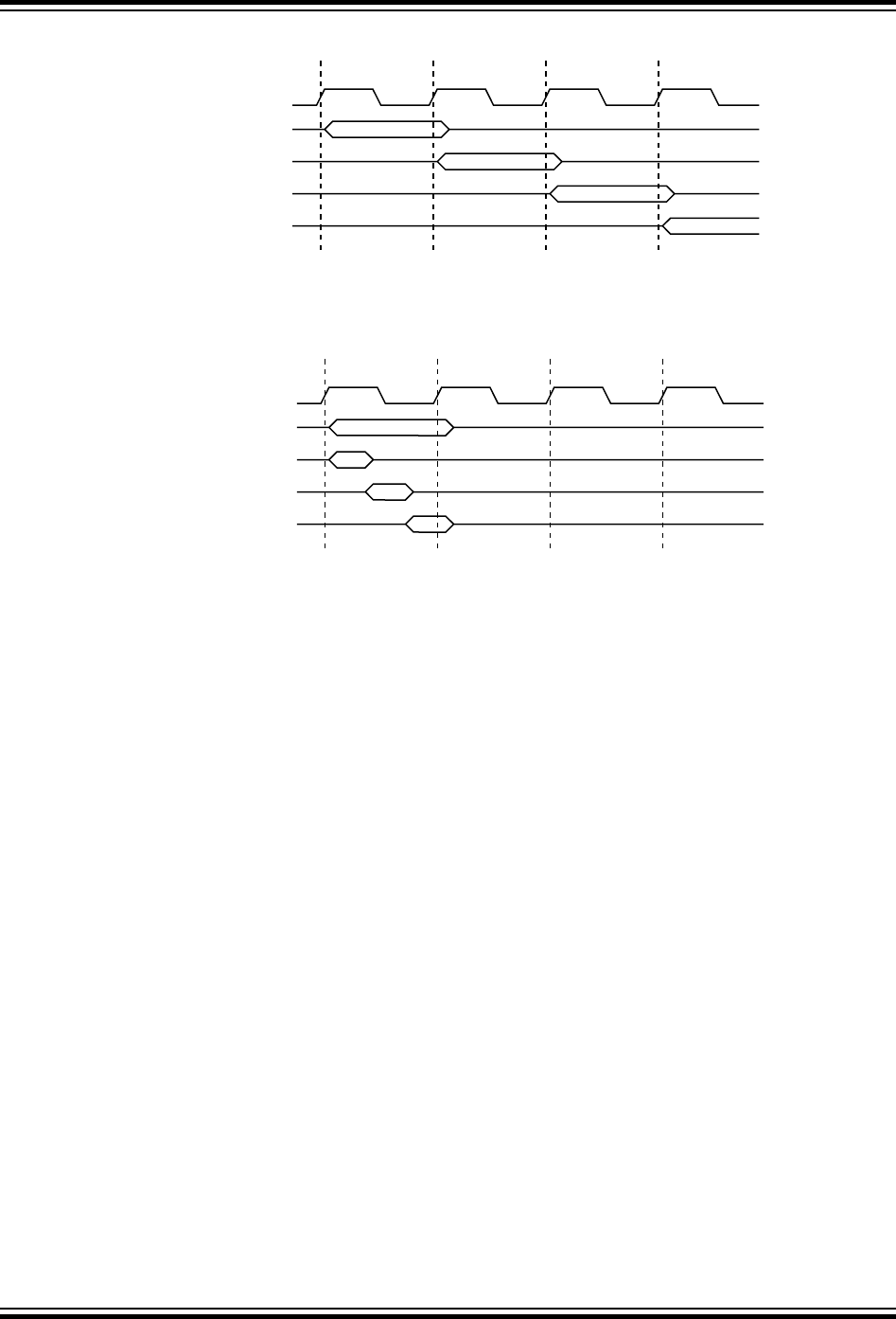
Figure 7-2. The Parallel Instruction Fetches and Instruction Executions
clk
1st Instruction Fetch
1st Instruction Execute
2nd Instruction Fetch
2nd Instruction Execute
3rd Instruction Fetch
3rd Instruction Execute
4th Instruction Fetch
T1 T2 T3 T4
CPU
The following figure shows the internal timing concept for the register file. In a single clock cycle, an ALU
operation using two register operands is executed and the result is stored in the destination register.
Figure 7-3. Single Cycle ALU Operation
Total Execution Time
Register Operands Fetch
ALU Operation Execute
Result Write Back
T1 T2 T3 T4
clkCPU
7.5.3 Status Register
The Status register (CPU.SREG) contains information about the result of the most recently executed
arithmetic or logic instruction. This information can be used for altering program flow in order to perform
conditional operations.
CPU.SREG is updated after all ALU operations, as specified in the Instruction Set Summary. This will in
many cases remove the need for using the dedicated compare instructions, resulting in faster and more
compact code. CPU.SREG is not automatically stored/restored when entering/returning from an Interrupt
Service Routine. Maintaining the Status register between context switches must, therefore, be handled by
user-defined software. CPU.SREG is accessible in the I/O memory space.
7.5.4 Stack and Stack Pointer
The stack is used for storing return addresses after interrupts and subroutine calls. Also, it can be used
for storing temporary data. The Stack Pointer (SP) always points to the top of the stack. The SP is
defined by the Stack Pointer bits in the Stack Pointer register (CPU.SP). The CPU.SP is implemented as
two 8-bit registers that are accessible in the I/O memory space.
Data is pushed and popped from the stack using the PUSH and POP instructions. The stack grows from
higher to lower memory locations. This implies that pushing data onto the stack decreases the SP, and
popping data off the stack increases the SP. The Stack Pointer is automatically set to the highest address
of the internal SRAM after Reset. If the stack is changed, it must be set to point above address 0x2000,
and it must be defined before any subroutine calls are executed and before interrupts are enabled.
During interrupts or subroutine calls the return address is automatically pushed on the stack as a word
pointer and the SP is decremented by '2'. The return address consists of two bytes and the Least
Significant Byte is pushed on the stack first (at the higher address). As an example, a byte pointer return
address of 0x0006 is saved on the stack as 0x0003 (shifted one bit to the right), pointing to the fourth 16-
bit instruction word in the program memory. The return address is popped off the stack with RETI (when
megaAVR® 0-Series
AVR CPU
© 2018 Microchip Technology Inc. Datasheet Preliminary DS40002015A-page 53
returning from interrupts) and RET (when returning from subroutine calls) and the SP is incremented by
two.
The SP is decremented by '1' when data is pushed on the stack with the PUSH instruction, and
incremented by '1' when data is popped off the stack using the POP instruction.
To prevent corruption when updating the Stack Pointer from software, a write to SPL will automatically
disable interrupts for up to four instructions or until the next I/O memory write.
7.5.5 Register File
The register file consists of 32 8-bit general purpose working registers with single clock cycle access time.
The register file supports the following input/output schemes:
• One 8-bit output operand and one 8-bit result input
• Two 8-bit output operands and one 8-bit result input
• Two 8-bit output operands and one 16-bit result input
• One 16-bit output operand and one 16-bit result input
Six of the 32 registers can be used as three 16-bit Address Register Pointers for data space addressing,
enabling efficient address calculations.
Figure 7-4. AVR CPU General Purpose Working Registers
...
...
70
R0
R1
R2
R13
R14
R15
R16
R17
R26
R27
R28
R29
R30
R31
Addr.
0x00
0x01
0x02
0x0D
0x0E
0x0F
0x10
0x11
0x1A
0x1B
0x1C
0x1D
0x1E
0x1F
X-register Low Byte
X-register High Byte
Y-register Low Byte
Y-register High Byte
Z-register Low Byte
Z-register High Byte
The register file is located in a separate address space and is, therefore, not accessible through
instructions operation on data memory.
7.5.5.1 The X-, Y-, and Z-Registers
Registers R26...R31 have added functions besides their general purpose usage.
These registers can form 16-bit Address Pointers for addressing data memory. These three address
registers are called the X-register, Y-register, and Z-register. Load and store instructions can use all X-,
Y-, and Z-registers, while the LPM and SPM instructions can only use the Z-register. Indirect calls and
jumps (ICALL and IJMP ) also use the Z-register.
Refer to the instruction set or Instruction Set Summary for more information about how the X-, Y-, and Z-
registers are used.
megaAVR® 0-Series
AVR CPU
© 2018 Microchip Technology Inc. Datasheet Preliminary DS40002015A-page 54

Figure 7-5. The X-, Y-, and Z-Registers
Bit (individually)
X-register
Bit (X-register)
7070
15 870
R27 R26
XH XL
Bit (individually)
Y-register
Bit (Y-register)
7070
15 870
R29 R28
YH YL
Bit (individually)
Z-register
Bit (Z-register)
7070
15 870
R31 R30
ZH ZL
The lowest register address holds the Least Significant Byte (LSB), and the highest register address
holds the Most Significant Byte (MSB). In the different addressing modes, these address registers
function as fixed displacement, automatic increment, and automatic decrement.
7.5.6 Accessing 16-Bit Registers
The AVR data bus has a width of 8 bit, and so accessing 16-bit registers requires atomic operations.
These registers must be byte accessed using two read or write operations. 16-bit registers are connected
to the 8-bit bus and a temporary register using a 16-bit bus.
For a write operation, the low byte of the 16-bit register must be written before the high byte. The low byte
is then written into the temporary register. When the high byte of the 16-bit register is written, the
temporary register is copied into the low byte of the 16-bit register in the same clock cycle.
For a read operation, the low byte of the 16-bit register must be read before the high byte. When the low
byte register is read by the CPU, the high byte of the 16-bit register is copied into the temporary register
in the same clock cycle as the low byte is read. When the high byte is read, it is then read from the
temporary register.
This ensures that the low and high bytes of 16-bit registers are always accessed simultaneously when
reading or writing the register.
Interrupts can corrupt the timed sequence if an interrupt is triggered and accesses the same 16-bit
register during an atomic 16-bit read/write operation. To prevent this, interrupts can be disabled when
writing or reading 16-bit registers.
The temporary registers can be read and written directly from user software.
7.5.7 Configuration Change Protection (CCP)
System critical I/O register settings are protected from accidental modification. Flash self-programming
(via store to NVM controller) is protected from accidental execution. This is handled globally by the
Configuration Change Protection (CCP) register.
Changes to the protected I/O registers or bits, or execution of protected instructions, are only possible
after the CPU writes a signature to the CCP register. The different signatures are listed in the description
of the CCP register (CPU.CCP).
There are two modes of operation: one for protected I/O registers, and one for the protected self-
programming.
7.5.7.1 Sequence for Write Operation to Configuration Change Protected I/O Registers
In order to write to registers protected by CCP, these steps are required:
megaAVR® 0-Series
AVR CPU
© 2018 Microchip Technology Inc. Datasheet Preliminary DS40002015A-page 55

1. The software writes the signature that enables change of protected I/O registers to the CCP bit field
in the CPU.CCP register.
2. Within four instructions, the software must write the appropriate data to the protected register.
Most protected registers also contain a write enable/change enable/lock bit. This bit must be written
to '1' in the same operation as the data are written.
The protected change is immediately disabled if the CPU performs write operations to the I/O
register or data memory, if load or store accesses to Flash, NVMCTRL, EEPROM are conducted,
or if the SLEEP instruction is executed.
7.5.7.2 Sequence for Execution of Self-Programming
In order to execute self-programming (the execution of writes to the NVM controller's command register),
the following steps are required:
1. The software temporarily enables self-programming by writing the SPM signature to the CCP
register (CPU.CCP).
2. Within four instructions, the software must execute the appropriate instruction. The protected
change is immediately disabled if the CPU performs accesses to the Flash, NVMCTRL, or
EEPROM, or if the SLEEP instruction is executed.
Once the correct signature is written by the CPU, interrupts will be ignored for the duration of the
configuration change enable period. Any interrupt request (including non-maskable interrupts) during the
CCP period will set the corresponding interrupt flag as normal, and the request is kept pending. After the
CCP period is completed, any pending interrupts are executed according to their level and priority.
megaAVR® 0-Series
AVR CPU
© 2018 Microchip Technology Inc. Datasheet Preliminary DS40002015A-page 56


7.7.1 Configuration Change Protection
Name: CCP
Offset: 0x04
Reset: 0x00
Property: -
Bit 7 6 5 4 3 2 1 0
CCP[7:0]
Access R/W R/W R/W R/W R/W R/W R/W R/W
Reset 0 0 0 0 0 0 0 0
Bits 7:0 – CCP[7:0] Configuration Change Protection
Writing the correct signature to this bit field allows changing protected I/O registers or executing protected
instructions within the next four CPU instructions executed.
All interrupts are ignored during these cycles. After these cycles, interrupts will automatically be handled
again by the CPU, and any pending interrupts will be executed according to their level and priority.
When the protected I/O register signature is written, CCP[0] will read as '1' as long as the CCP feature is
enabled.
When the protected self-programming signature is written, CCP[1] will read as '1' as long as the CCP
feature is enabled.
CCP[7:2] will always read as zero.
Value Name Description
0x9D SPM Allow Self-Programming
0xD8 IOREG Un-protect protected I/O registers
megaAVR® 0-Series
AVR CPU
© 2018 Microchip Technology Inc. Datasheet Preliminary DS40002015A-page 58

7.7.2 Stack Pointer
Name: SP
Offset: 0x0D
Reset: Top of stack
Property: -
The CPU.SP holds the Stack Pointer (SP) that points to the top of the stack. After Reset, the Stack
Pointer points to the highest internal SRAM address.
Only the number of bits required to address the available data memory including external memory (up to
64 KB) is implemented for each device. Unused bits will always read as zero.
The CPU.SPL and CPU.SPH register pair represents the 16-bit value, CPU.SP. The low byte [7:0] (suffix
L) is accessible at the original offset. The high byte [15:8] (suffix H) can be accessed at offset + 0x01.
To prevent corruption when updating the SP from software, a write to CPU.SPL will automatically disable
interrupts for the next four instructions or until the next I/O memory write.
Bit 15 14 13 12 11 10 9 8
SP[15:8]
Access R/W R/W R/W R/W R/W R/W R/W R/W
Reset
Bit 7 6 5 4 3 2 1 0
SP[7:0]
Access R/W R/W R/W R/W R/W R/W R/W R/W
Reset
Bits 15:8 – SP[15:8] Stack Pointer High Byte
These bits hold the MSB of the 16-bit register.
Bits 7:0 – SP[7:0] Stack Pointer Low Byte
These bits hold the LSB of the 16-bit register.
megaAVR® 0-Series
AVR CPU
© 2018 Microchip Technology Inc. Datasheet Preliminary DS40002015A-page 59

7.7.3 Status Register
Name: SREG
Offset: 0x0F
Reset: 0x00
Property: -
The Status register contains information about the result of the most recently executed arithmetic or logic
instruction. For details about the bits in this register and how they are affected by the different
instructions, see the Instruction Set Summary.
Bit 7 6 5 4 3 2 1 0
I T H S V N Z C
Access R/W R/W R/W R/W R/W R/W R/W R/W
Reset 0 0 0 0 0 0 0 0
Bit 7 – I Global Interrupt Enable
Writing a '1' to this bit enables interrupts on the device.
Writing a '0' to this bit disables interrupts on the device, independent of the individual interrupt enable
settings of the peripherals.
This bit is not cleared by hardware after an interrupt has occurred.
This bit can be set and cleared by software with the SEI and CLI instructions.
Changing the I flag through the I/O register results in a one-cycle Wait state on the access.
Bit 6 – T Bit Copy Storage
The bit copy instructions bit load (BLD) and bit store (BST) use the T bit as source or destination for the
operated bit.
A bit from a register in the register file can be copied into this bit by the BST instruction, and this bit can
be copied into a bit in a register in the register file by the BLD instruction.
Bit 5 – H Half Carry Flag
This bit indicates a half carry in some arithmetic operations. Half carry is useful in BCD arithmetic.
Bit 4 – S Sign Bit, S = N ⊕ V
The sign bit (S) is always an exclusive or (xor) between the negative flag (N) and the two’s complement
overflow flag (V).
Bit 3 – V Two’s Complement Overflow Flag
The two’s complement overflow flag (V) supports two’s complement arithmetic.
Bit 2 – N Negative Flag
The negative flag (N) indicates a negative result in an arithmetic or logic operation.
Bit 1 – Z Zero Flag
The zero flag (Z) indicates a zero result in an arithmetic or logic operation.
megaAVR® 0-Series
AVR CPU
© 2018 Microchip Technology Inc. Datasheet Preliminary DS40002015A-page 60

Bit 0 – C Carry Flag
The carry flag (C) indicates a carry in an arithmetic or logic operation.
megaAVR® 0-Series
AVR CPU
© 2018 Microchip Technology Inc. Datasheet Preliminary DS40002015A-page 61
8. Nonvolatile Memory Controller (NVMCTRL)
8.1 Features
• Unified Memory
• In-System Programmable
• Self-Programming and Boot Loader Support
• Configurable Sections for Write Protection:
– Boot section for boot loader code or application code
– Application code section for application code
– Application data section for application code or data storage
• Signature Row for Factory-Programmed Data:
– ID for each device type
– Serial number for each device
– Calibration bytes for factory calibrated peripherals
• User Row for Application Data:
– Can be read and written from software
– Can be written from UPDI on locked device
– Content is kept after chip erase
8.2 Overview
The NVM Controller (NVMCTRL) is the interface between the device, the Flash, and the EEPROM. The
Flash and EEPROM are reprogrammable memory blocks that retain their values even when not powered.
The Flash is mainly used for program storage and can be used for data storage. The EEPROM is used
for data storage and can be programmed while the CPU is running the program from the Flash.
8.2.1 Block Diagram
Figure 8-1. NVMCTRL Block Diagram
Flash
EEPROM
NVM Block
Signature Row
User Row
NVMCTRL
Program Memory Bus
Data Memory Bus
megaAVR® 0-Series
Nonvolatile Memory Controller (NVMCTRL)
© 2018 Microchip Technology Inc. Datasheet Preliminary DS40002015A-page 62

8.3 Functional Description
8.3.1 Memory Organization
8.3.1.1 Flash
The Flash is divided into a set of pages. A page is the basic unit addressed when programming the Flash.
It is only possible to write or erase a whole page at a time. One page consists of several words.
The Flash can be divided into three sections in blocks of 256 bytes for different security. The three
different sections are BOOT, Application Code (APPCODE), and Application Data (APPDATA).
Figure 8-2. Flash Sections
FLASHSTART: 0x4000
BOOTEND>0: 0x4000+BOOTEND*256
BOOT
APPEND>0: 0x4000+APPEND*256
APPLICATION
CODE
APPLICATION
DATA
Section Sizes
The sizes of these sections are set by the Boot Section End fuse (FUSE.BOOTEND) and Application
Code Section End fuse (FUSE.APPEND).
The fuses select the section sizes in blocks of 256 bytes. The BOOT section stretches from the start of
the Flash until BOOTEND. The APPCODE section runs from BOOTEND until APPEND. The remaining
area is the APPDATA section. If APPEND is written to 0, the APPCODE section runs from BOOTEND to
the end of Flash (removing the APPDATA section). If BOOTEND and APPEND are written to 0, the entire
Flash is regarded as BOOT section. APPEND should either be set to 0 or a value greater or equal than
BOOTEND.
Table 8-1. Setting Up Flash Sections
BOOTEND APPEND BOOT Section APPCODE Section APPDATA Section
0 0 0 to FLASHEND - -
> 0 0 0 to 256*BOOTEND 256*BOOTEND to
FLASHEND
-
megaAVR® 0-Series
Nonvolatile Memory Controller (NVMCTRL)
© 2018 Microchip Technology Inc. Datasheet Preliminary DS40002015A-page 63

BOOTEND APPEND BOOT Section APPCODE Section APPDATA Section
> 0 ==
BOOTEND
0 to 256*BOOTEND - 256*BOOTEND to
FLASHEND
> 0 >
BOOTEND
0 to 256*BOOTEND 256*BOOTEND to
256*APPEND
256*APPEND to
FLASHEND
Note:
• See also the BOOTEND and APPEND descriptions.
• Interrupt vectors are by default located after the BOOT section. This can be changed in the
interrupt controller.
If FUSE.BOOTEND is written to 0x04 and FUSE.APPEND is written to 0x08, the first
4*256 bytes will be BOOT, the next 4*256 bytes will be APPCODE, and the remaining
Flash will be APPDATA.
Inter-Section Write Protection
Between the three Flash sections, a directional write protection is implemented:
• Code in the BOOT section can write to APPCODE and APPDATA
• Code in APPCODE can write to APPDATA
• Code in APPDATA cannot write to Flash or EEPROM
Boot Section Lock and Application Code Section Write Protection
The two lockbits (APCWP and BOOTLOCK in NVMCTRL.CTRLB) can be set to lock further updates of
the respective APPCODE or BOOT section until the next Reset.
The CPU can never write to the BOOT section. NVMCTRL_CTRLB.BOOTLOCK prevents reads and
execution of code from the BOOT section.
8.3.1.2 EEPROM
The EEPROM is divided into a set of pages where one page consists of multiple bytes. The EEPROM
has byte granularity on erase/write. Within one page only the bytes marked to be updated will be erased/
written. The byte is marked by writing a new value to the page buffer for that address location.
8.3.1.3 User Row
The User Row is one extra page of EEPROM. This page can be used to store various data, such as
calibration/configuration data and serial numbers. This page is not erased by a chip erase. The User Row
is written as normal EEPROM, but in addition, it can be written through UPDI on a locked device.
8.3.2 Memory Access
8.3.2.1 Read
Reading of the Flash and EEPROM is done by using load instructions with an address according to the
memory map. Reading any of the arrays while a write or erase is in progress will result in a bus wait, and
the instruction will be suspended until the ongoing operation is complete.
8.3.2.2 Page Buffer Load
The page buffer is loaded by writing directly to the memories as defined in the memory map. Flash,
EEPROM, and User Row share the same page buffer so only one section can be programmed at a time.
The Least Significant bits (LSb) of the address are used to select where in the page buffer the data is
megaAVR® 0-Series
Nonvolatile Memory Controller (NVMCTRL)
© 2018 Microchip Technology Inc. Datasheet Preliminary DS40002015A-page 64

written. The resulting data will be a binary and operation between the new and the previous content of the
page buffer. The page buffer will automatically be erased (all bits set) after:
• A device Reset
• Any page write or erase operation
• A Clear Page Buffer command
• The device wakes up from any sleep mode
8.3.2.3 Programming
For page programming, filling the page buffer and writing the page buffer into Flash, User Row, and
EEPROM are two separate operations.
Before programming a Flash page with the data in the page buffer, the Flash page must be erased. The
page buffer is also erased when the device enters a sleep mode. Programming an unerased Flash page
will corrupt its content.
The Flash can either be written with the erase and write separately, or one command handling both:
Alternative 1:
• Fill the page buffer
• Write the page buffer to Flash with the Erase/Write Page command
Alternative 2:
• Write to a location in the page to set up the address
• Perform an Erase Page command
• Fill the page buffer
• Perform a Write Page command
The NVM command set supports both a single erase and write operation, and split Page Erase and Page
Write commands. This split commands enable shorter programming time for each command, and the
erase operations can be done during non-time-critical programming execution.
The EEPROM programming is similar, but only the bytes updated in the page buffer will be written or
erased in the EEPROM.
8.3.2.4 Commands
Reading of the Flash/EEPROM and writing of the page buffer is handled with normal load/store
instructions. Other operations, such as writing and erasing the memory arrays, are handled by commands
in the NVM.
To execute a command in the NVM:
1. Confirm that any previous operation is completed by reading the Busy Flags (EEBUSY and
FBUSY) in the NVMCTRL.STATUS register.
2. Write the NVM command unlock to the Configuration Change Protection register in the CPU
(CPU.CCP).
3. Write the desired command value to the CMD bits in the Control A register (NVMCTRL.CTRLA)
within the next four instructions.
Write Command
The Write command of the Flash controller writes the content of the page buffer to the Flash or EEPROM.
If the write is to the Flash, the CPU will stop executing code as long as the Flash is busy with the write
operation. If the write is to the EEPROM, the CPU can continue executing code while the operation is
ongoing.
megaAVR® 0-Series
Nonvolatile Memory Controller (NVMCTRL)
© 2018 Microchip Technology Inc. Datasheet Preliminary DS40002015A-page 65

The page buffer will be automatically cleared after the operation is finished.
Erase Command
The Erase command erases the current page. There must be one byte written in the page buffer for the
Erase command to take effect.
For erasing the Flash, first, write to one address in the desired page, then execute the command. The
whole page in the Flash will then be erased. The CPU will be halted while the erase is ongoing.
For the EEPROM, only the bytes written in the page buffer will be erased when the command is
executed. To erase a specific byte, write to its corresponding address before executing the command. To
erase a whole page all the bytes in the page buffer have to be updated before executing the command.
The CPU can continue running code while the operation is ongoing.
The page buffer will automatically be cleared after the operation is finished.
Erase-Write Operation
The Erase/Write command is a combination of the Erase and Write command, but without clearing the
page buffer after the Erase command: The erase/write operation first erases the selected page, then it
writes the content of the page buffer to the same page.
When executed on the Flash, the CPU will be halted when the operations are ongoing. When executed
on EEPROM, the CPU can continue executing code.
The page buffer will automatically be cleared after the operation is finished.
Page Buffer Clear Command
The Page Buffer Clear command clears the page buffer. The contents of the page buffer will be all 1’s
after the operation. The CPU will be halted when the operation executes (seven CPU cycles).
Chip Erase Command
The Chip Erase command erases the Flash and the EEPROM. The EEPROM is unaltered if the
EEPROM Save During Chip Erase (EESAVE) fuse in FUSE.SYSCFG0 is set. The Flash will not be
protected by Boot Section Lock (BOOTLOCK) or Application Code Section Write Protection (APCWP) in
NVMCTRL.CTRLB. The memory will be all 1’s after the operation.
EEPROM Erase Command
The EEPROM Erase command erases the EEPROM. The EEPROM will be all 1’s after the operation.
The CPU will be halted while the EEPROM is being erased.
Fuse Write Command
The Fuse Write command writes the fuses. It can only be used by the UPDI, the CPU cannot start this
command.
Follow this procedure to use this command:
• Write the address of the fuse to the Address register (NVMCTRL.ADDR)
• Write the data to be written to the fuse to the Data register (NVMCTRL.DATA)
• Execute the Fuse Write command.
• After the fuse is written, a Reset is required for the updated value to take effect.
For reading fuses, use a regular read on the memory location.
8.3.3 Preventing Flash/EEPROM Corruption
During periods of low VDD, the Flash program or EEPROM data can be corrupted if the supply voltage is
too low for the CPU and the Flash/EEPROM to operate properly. These issues are the same as for board
level systems using Flash/EEPROM, and the same design solutions should be applied.
megaAVR® 0-Series
Nonvolatile Memory Controller (NVMCTRL)
© 2018 Microchip Technology Inc. Datasheet Preliminary DS40002015A-page 66

A Flash/EEPROM corruption can be caused by two situations when the voltage is too low:
1. A regular write sequence to the Flash, which requires a minimum voltage to operate correctly.
2. The CPU itself can execute instructions incorrectly when the supply voltage is too low.
See the Electrical Characteristics chapter for Maximum Frequency vs. VDD.
Flash/EEPROM corruption can be avoided by these measures:
• Keep the device in Reset during periods of insufficient power supply voltage. This can be done by
enabling the internal Brown-Out Detector (BOD).
• The voltage level monitor in the BOD can be used to prevent starting a write to the EEPROM close
to the BOD level.
• If the detection levels of the internal BOD don’t match the required detection level, an external low
VDD Reset protection circuit can be used. If a Reset occurs while a write operation is ongoing, the
write operation will be aborted.
8.3.4 Interrupts
Table 8-2. Available Interrupt Vectors and Sources
Offset Name Vector Description Conditions
0x00 EEREADY NVM The EEPROM is ready for new write/erase operations.
When an interrupt condition occurs, the corresponding interrupt flag is set in the Interrupt Flags register of
the peripheral (NVMCTRL.INTFLAGS).
An interrupt source is enabled or disabled by writing to the corresponding bit in the peripheral's Interrupt
Enable register (NVMCTRL.INTEN).
An interrupt request is generated when the corresponding interrupt source is enabled and the interrupt
flag is set. The interrupt request remains active until the interrupt flag is cleared. See the peripheral's
INTFLAGS register for details on how to clear interrupt flags.
8.3.5 Sleep Mode Operation
If there is no ongoing write operation, the NVMCTRL will enter sleep mode when the system enters sleep
mode.
If a write operation is ongoing when the system enters a sleep mode, the NVM block, the NVM Controller,
and the system clock will remain ON until the write is finished. This is valid for all sleep modes, including
Power-Down Sleep mode.
The EEPROM Ready interrupt will wake up the device only from Idle Sleep mode.
The page buffer is cleared when waking up from Sleep.
8.3.6 Configuration Change Protection
This peripheral has registers that are under Configuration Change Protection (CCP). In order to write to
these, a certain key must be written to the CPU.CCP register first, followed by a write access to the
protected bits within four CPU instructions.
It is possible to try writing to these registers at any time, but the values are not altered.
The following registers are under CCP:
megaAVR® 0-Series
Nonvolatile Memory Controller (NVMCTRL)
© 2018 Microchip Technology Inc. Datasheet Preliminary DS40002015A-page 67

Table 8-3. NVMCTRL - Registers under Configuration Change Protection
Register Key
NVMCTRL.CTRLA SPM
megaAVR® 0-Series
Nonvolatile Memory Controller (NVMCTRL)
© 2018 Microchip Technology Inc. Datasheet Preliminary DS40002015A-page 68

8.4 Register Summary - NVMCTRL
Offset Name Bit Pos.
0x00 CTRLA 7:0 CMD[2:0]
0x01 CTRLB 7:0 BOOTLOCK APCWP
0x02 STATUS 7:0 WRERROR EEBUSY FBUSY
0x03 INTCTRL 7:0 EEREADY
0x04 INTFLAGS 7:0 EEREADY
0x05 Reserved
0x06 DATA
7:0 DATA[7:0]
15:8 DATA[15:8]
0x08 ADDR
7:0 ADDR[7:0]
15:8 ADDR[15:8]
8.5 Register Description
megaAVR® 0-Series
Nonvolatile Memory Controller (NVMCTRL)
© 2018 Microchip Technology Inc. Datasheet Preliminary DS40002015A-page 69

8.5.1 Control A
Name: CTRLA
Offset: 0x00
Reset: 0x00
Property: Configuration Change Protection
Bit 7 6 5 4 3 2 1 0
CMD[2:0]
Access R/W R/W R/W
Reset 0 0 0
Bits 2:0 – CMD[2:0] Command
Write this bit field to issue a command. The Configuration Change Protection key for self-programming
(SPM) has to be written within four instructions before this write.
Value Name Description
0x0 - No command
0x1 WP Write page buffer to memory (NVMCTRL.ADDR selects which memory)
0x2 ER Erase page (NVMCTRL.ADDR selects which memory)
0x3 ERWP Erase and write page (NVMCTRL.ADDR selects which memory)
0x4 PBC Page buffer clear
0x5 CHER Chip erase: erase Flash and EEPROM (unless EESAVE in FUSE.SYSCFG is '1')
0x6 EEER EEPROM Erase
0x7 WFU Write fuse (only accessible through UPDI)
megaAVR® 0-Series
Nonvolatile Memory Controller (NVMCTRL)
© 2018 Microchip Technology Inc. Datasheet Preliminary DS40002015A-page 70

8.5.2 Control B
Name: CTRLB
Offset: 0x01
Reset: 0x00
Property: -
Bit 7 6 5 4 3 2 1 0
BOOTLOCK APCWP
Access R/W R/W
Reset 0 0
Bit 1 – BOOTLOCK Boot Section Lock
Writing a ’1’ to this bit locks the boot section from read and instruction fetch.
If this bit is ’1’, a read from the boot section will return ’0’. A fetch from the boot section will also return ‘0’
as instruction.
This bit can be written from the boot section only. It can only be cleared to ’0’ by a Reset.
This bit will take effect only when the boot section is left the first time after the bit is written.
Bit 0 – APCWP Application Code Section Write Protection
Writing a ’1’ to this bit protects the application code section from further writes.
This bit can only be written to ’1’. It is cleared to ’0’ only by Reset.
megaAVR® 0-Series
Nonvolatile Memory Controller (NVMCTRL)
© 2018 Microchip Technology Inc. Datasheet Preliminary DS40002015A-page 71

8.5.3 Status
Name: STATUS
Offset: 0x02
Reset: 0x00
Property: -
Bit 7 6 5 4 3 2 1 0
WRERROR EEBUSY FBUSY
Access R R R
Reset 0 0 0
Bit 2 – WRERROR Write Error
This bit will read '1' when a write error has happened. A write error could be writing to different sections
before doing a page write or writing to a protected area. This bit is valid for the last operation.
Bit 1 – EEBUSY EEPROM Busy
This bit will read '1' when the EEPROM is busy with a command.
Bit 0 – FBUSY Flash Busy
This bit will read '1' when the Flash is busy with a command.
megaAVR® 0-Series
Nonvolatile Memory Controller (NVMCTRL)
© 2018 Microchip Technology Inc. Datasheet Preliminary DS40002015A-page 72

8.5.4 Interrupt Control
Name: INTCTRL
Offset: 0x03
Reset: 0x00
Property: -
Bit 7 6 5 4 3 2 1 0
EEREADY
Access R/W
Reset 0
Bit 0 – EEREADY EEPROM Ready Interrupt
Writing a '1' to this bit enables the interrupt, which indicates that the EEPROM is ready for new write/
erase operations.
This is a level interrupt that will be triggered only when the EEREADY flag in the INTFLAGS register is set
to zero. Thus, the interrupt should not be enabled before triggering an NVM command, as the EEREADY
flag will not be set before the NVM command issued. The interrupt should be disabled in the interrupt
handler.
megaAVR® 0-Series
Nonvolatile Memory Controller (NVMCTRL)
© 2018 Microchip Technology Inc. Datasheet Preliminary DS40002015A-page 73

8.5.5 Interrupt Flags
Name: INTFLAGS
Offset: 0x04
Reset: 0x00
Property: -
Bit 7 6 5 4 3 2 1 0
EEREADY
Access R/W
Reset 0
Bit 0 – EEREADY EEREADY Interrupt Flag
This flag is set continuously as long as the EEPROM is not busy. This flag is cleared by writing a '1' to it.
megaAVR® 0-Series
Nonvolatile Memory Controller (NVMCTRL)
© 2018 Microchip Technology Inc. Datasheet Preliminary DS40002015A-page 74

8.5.6 Data
Name: DATA
Offset: 0x06
Reset: 0x00
Property: -
The NVMCTRL.DATAL and NVMCTRL.DATAH register pair represents the 16-bit value,
NVMCTRL.DATA. The low byte [7:0] (suffix L) is accessible at the original offset. The high byte [15:8]
(suffix H) can be accessed at offset + 0x01.
Bit 15 14 13 12 11 10 9 8
DATA[15:8]
Access R/W R/W R/W R/W R/W R/W R/W R/W
Reset 0 0 0 0 0 0 0 0
Bit 7 6 5 4 3 2 1 0
DATA[7:0]
Access R/W R/W R/W R/W R/W R/W R/W R/W
Reset 0 0 0 0 0 0 0 0
Bits 15:0 – DATA[15:0] Data Register
This register is used by the UPDI for fuse write operations.
megaAVR® 0-Series
Nonvolatile Memory Controller (NVMCTRL)
© 2018 Microchip Technology Inc. Datasheet Preliminary DS40002015A-page 75

8.5.7 Address
Name: ADDR
Offset: 0x08
Reset: 0x00
Property: -
The NVMCTRL.ADDRL and NVMCTRL.ADDRH register pair represents the 16-bit value,
NVMCTRL.ADDR. The low byte [7:0] (suffix L) is accessible at the original offset. The high byte [15:8]
(suffix H) can be accessed at offset + 0x01.
Bit 15 14 13 12 11 10 9 8
ADDR[15:8]
Access R/W R/W R/W R/W R/W R/W R/W R/W
Reset 0 0 0 0 0 0 0 0
Bit 7 6 5 4 3 2 1 0
ADDR[7:0]
Access R/W R/W R/W R/W R/W R/W R/W R/W
Reset 0 0 0 0 0 0 0 0
Bits 15:0 – ADDR[15:0] Address
The Address register contains the address to the last memory location that has been updated.
megaAVR® 0-Series
Nonvolatile Memory Controller (NVMCTRL)
© 2018 Microchip Technology Inc. Datasheet Preliminary DS40002015A-page 76

9. Clock Controller (CLKCTRL)
9.1 Features
• All clocks and clock sources are automatically enabled when requested by peripherals
• Internal Oscillators:
– 20 MHz Oscillator (OSC20M)
– 32 KHz Ultra Low-Power Oscillator (OSCULP32K)
• External Clock Options:
– 32.768 kHz Crystal Oscillator (XOSC32K)
– External clock
• Main Clock Features:
– Safe run-time switching
– Prescaler with 1x to 64x division in 12 different settings
9.2 Overview
The Clock Controller peripheral (CLKCTRL) controls, distributes, and prescales the clock signals from the
available oscillators. The CLKCTRL supports internal and external clock sources.
The CLKCTRL is based on an automatic clock request system, implemented in all peripherals on the
device. The peripherals will automatically request the clocks needed. If multiple clock sources are
available, the request is routed to the correct clock source.
The Main Clock (CLK_MAIN) is used by the CPU, RAM, and the I/O bus. The main clock source can be
selected and prescaled. Some peripherals can share the same clock source as the main clock, or run
asynchronously to the main clock domain.
megaAVR® 0-Series
Clock Controller (CLKCTRL)
© 2018 Microchip Technology Inc. Datasheet Preliminary DS40002015A-page 77
9.2.1 Block Diagram - CLKCTRL
Figure 9-1. CLKCTRL Block Diagram
CPURAMNVM TCDBOD
RTC
OSC20M
int. Oscillator
WDT
32.768 kHz
ext. Crystal Osc.
DIV32
TOSC2 TOSC1
RTC
CLKSEL
CLK_RTC
CLK_PER
CLK_MAIN
CLK_WDT CLK_BOD CLK_TCD
TCD
CLKCSEL
Main Clock Prescaler
Main Clock Switch
INT
PRESCALER
XOSC32K
SEL
CLK_CPU
Other
Peripherals
CLKOUT
OSC20M
XOSC32K
OSCULP32K
32 KHz ULP
Int. Oscillator
EXTCLK
The clock system consists of the main clock and other asynchronous clocks:
• Main Clock
This clock is used by the CPU, RAM, Flash, the I/O bus, and all peripherals connected to the I/O
bus. It is always running in Active and Idle Sleep mode and can be running in Standby Sleep mode
if requested.
The main clock CLK_MAIN is prescaled and distributed by the clock controller:
• CLK_CPU is used by the CPU, SRAM, and the NVMCTRL peripheral to access the
nonvolatile memory
• CLK_PER is used by all peripherals that are not listed under asynchronous clocks.
• Clocks running asynchronously to the main clock domain:
– CLK_RTC is used by the RTC/PIT. It will be requested when the RTC/PIT is enabled. The
clock source for CLK_RTC should only be changed if the peripheral is disabled.
– CLK_WDT is used by the WDT. It will be requested when the WDT is enabled.
megaAVR® 0-Series
Clock Controller (CLKCTRL)
© 2018 Microchip Technology Inc. Datasheet Preliminary DS40002015A-page 78

– CLK_BOD is used by the BOD. It will be requested when the BOD is enabled in Sampled
mode.
The clock source for the for the main clock domain is configured by writing to the Clock Select bits
(CLKSEL) in the Main Clock Control A register (CLKCTRL.MCLKCTRLA). The asynchronous clock
sources are configured by registers in the respective peripheral.
9.2.2 Signal Description
Signal Type Description
CLKOUT Digital output CLK_PER output
9.3 Functional Description
9.3.1 Sleep Mode Operation
When a clock source is not used/requested it will turn OFF. It is possible to request a clock source directly
by writing a '1' to the Run Standby bit (RUNSTDBY) in the respective oscillator's Control A register
(CLKCTRL.[osc]CTRLA). This will cause the oscillator to run constantly, except for Power-Down Sleep
mode. Additionally, when this bit is written to '1' the oscillator start-up time is eliminated when the clock
source is requested by a peripheral.
The main clock will always run in Active and Idle Sleep mode. In Standby Sleep mode, the main clock will
only run if any peripheral is requesting it, or the Run in Standby bit (RUNSTDBY) in the respective
oscillator's Control A register (CLKCTRL.[osc]CTRLA) is written to '1'.
In Power-Down Sleep mode, the main clock will stop after all NVM operations are completed.
9.3.2 Main Clock Selection and Prescaler
All internal oscillators can be used as the main clock source for CLK_MAIN. The main clock source is
selectable from software, and can be safely changed during normal operation.
Built-in hardware protection prevents unsafe clock switching:
Upon selection of an external clock source, a switch to the chosen clock source will only occur if edges
are detected, indicating it is stable. Until a sufficient number of clock edges are detected, the switch will
not occur and it will not be possible to change to another clock source again without executing a Reset.
An ongoing clock source switch is indicated by the System Oscillator Changing flag (SOSC) in the Main
Clock Status register (CLKCTRL.MCLKSTATUS). The stability of the external clock sources is indicated
by the respective status flags (EXTS and XOSC32KS in CLKCTRL.MCLKSTATUS).
CAUTION
If an external clock source fails while used as CLK_MAIN source, only the WDT can provide a
mechanism to switch back via System Reset.
CLK_MAIN is fed into a prescaler before it is used by the peripherals (CLK_PER) in the device. The
prescaler divide CLK_MAIN by a factor from 1 to 64.
megaAVR® 0-Series
Clock Controller (CLKCTRL)
© 2018 Microchip Technology Inc. Datasheet Preliminary DS40002015A-page 79

Figure 9-2. Main Clock and Prescaler
(Div 1, 2, 4, 8, 16, 32,
64, 6, 10, 24, 48)
OSC20M
32 KHz Osc.
32.768 kHz crystal Osc.
External clock
CLK_MAIN CLK_PER
Main Clock Prescaler
The Main Clock and Prescaler configuration registers (CLKCTRL.MCLKCTRLA,
CLKCTRL.MCLKCTRLB) are protected by the Configuration Change Protection Mechanism, employing a
timed write procedure for changing these registers.
9.3.3 Main Clock After Reset
After any Reset, CLK_MAIN is provided by the 20 MHz Oscillator (OSC20M) and with a prescaler division
factor of 6. The actual frequency of the OSC20M is determined by the Frequency Select bits (FREQSEL)
of the Oscillator Configuration fuse (FUSE.OSCCFG). Refer to the description of FUSE.OSCCFG for
details of the possible frequencies after Reset.
9.3.4 Clock Sources
All internal clock sources are enabled automatically when they are requested by a peripheral. The crystal
oscillator, based on an external crystal, must be enabled by writing a '1' to the ENABLE bit in the 32 KHz
Crystal Oscillator Control A register (CLKCTRL.XOSC32KCTRLA) before it can serve as a clock source.
The respective Oscillator Status bits in the Main Clock Status register (CLKCTRL.MCLKSTATUS) indicate
whether the clock source is running and stable.
9.3.4.1 Internal Oscillators
The internal oscillators do not require any external components to run. See the related links for accuracy
and electrical characteristics.
20 MHz Oscillator (OSC20M)
This oscillator can operate at multiple frequencies, selected by the value of the Frequency Select bits
(FREQSEL) in the Oscillator Configuration Fuse (FUSE.OSCCFG).
After a system Reset, FUSE.OSCCFG determines the initial frequency of CLK_MAIN.
During Reset, the calibration values for the OSC20M are loaded from fuses. There are two different
calibration bit fields. The Calibration bit field (CAL20M) in the Calibration A register
(CLKCTRL.OSC20MCALIBA) enables calibration around the current center frequency. The Oscillator
Temperature Coefficient Calibration bit field (TEMPCAL20M) in the Calibration B register
(CLKCTRL.OSC20MCALIBB) enables adjustment of the slope of the temperature drift compensation.
For applications requiring more fine-tuned frequency setting than the oscillator calibration provides,
factory stored frequency error after calibrations are available.
The oscillator calibration can be locked by the Oscillator Lock (OSCLOCK) Fuse (FUSE.OSCCFG). When
this fuse is '1', it is not possible to change the calibration. The calibration is locked if this oscillator is used
as main clock source and the Lock Enable bit (LOCKEN) in the Control B register
(CLKCTRL.OSC20MCALIBB) is '1'.
The calibration bits are protected by the Configuration Change Protection Mechanism, requiring a timed
write procedure for changing the main clock and prescaler settings.
Refer to the Electrical Characteristics section for the start-up time.
megaAVR® 0-Series
Clock Controller (CLKCTRL)
© 2018 Microchip Technology Inc. Datasheet Preliminary DS40002015A-page 80

OSC20M Stored Frequency Error Compensation
This oscillator can operate at multiple frequencies, selected by the value of the Frequency Select bits
(FREQSEL) in the Oscillator Configuration fuse (FUSE.OSCCFG) at Reset. As previously mentioned
appropriate calibration values are loaded to adjust to center frequency (OSC20M), and temperature drift
compensation (TEMPCAL20M), meeting the specifications defined in the internal oscillator
characteristics. For applications requiring wider operating range, the relative factory stored frequency
error after calibrations can be used. The four errors are measured at different settings and are available in
the signature row as signed byte values.
• SIGROW.OSC16ERR3V is the frequency error from 16 MHz measured at 3V
• SIGROW.OSC16ERR5V is the frequency error from 16 MHz measured at 5V
• SIGROW.OSC20ERR3V is the frequency error from 20 MHz measured at 3V
• SIGROW.OSC20ERR5V is the frequency error from 20 MHz measured at 5V
The error is stored as a compressed Q1.10 fixed point 8-bit value, in order not to lose resolution, where
the MSB is the sign bit and the seven LSBs the lower bits of the Q.10.
BAUDact = BAUD +BAUD *
1024
The minimum legal BAUD register value is 0x40, the target BAUD register value should therefore not be
lower than 0x4A to ensure that the compensated BAUD value stays within the legal range, even for parts
with negative compensation values. The example code below, demonstrates how to apply this value for
more accurate USART baud rate:
#include <assert.h>
/* Baud rate compensated with factory stored frequency error */
/* Asynchronous communication without Auto-baud (Sync Field) */
/* 16MHz Clock, 3V and 600 BAUD */
int8_t sigrow_val = SIGROW.OSC16ERR3V; // read signed error
int32_t baud_reg_val = 600; // ideal BAUD register value
assert (baud_reg_val >= 0x4A); // Verify legal min BAUD register
value with max neg comp
baud_reg_val *= (1024 + sigrow_val); // sum resolution + error
baud_reg_val /= 1024; // divide by resolution
USART0.BAUD = (int16_t) baud_reg_val; // set adjusted baud rate
32 KHz Oscillator (OSCULP32K)
The 32 KHz oscillator is optimized for Ultra Low-Power (ULP) operation. Power consumption is
decreased at the cost of decreased accuracy compared to an external crystal oscillator.
This oscillator provides the 1 KHz signal for the Real-Time Counter (RTC), the Watchdog Timer (WDT),
and the Brown-out Detector (BOD).
The start-up time of this oscillator is the oscillator start-up time plus four oscillator cycles. Refer to the
Electrical Characteristics chapter for the start-up time.
9.3.4.2 External Clock Sources
These external clock sources are available:
• External Clock from pin. (EXTCLK).
• The TOSC1 and TOSC2 pins are dedicated to driving a 32.768 kHz Crystal Oscillator (XOSC32K).
• Instead of a crystal oscillator, TOSC1 can be configured to accept an external clock source.
megaAVR® 0-Series
Clock Controller (CLKCTRL)
© 2018 Microchip Technology Inc. Datasheet Preliminary DS40002015A-page 81

32.768 kHz Crystal Oscillator (XOSC32K)
This oscillator supports two input options: Either a crystal is connected to the pins TOSC1 and TOSC2, or
an external clock running at 32 KHz is connected to TOSC1. The input option must be configured by
writing the Source Select bit (SEL) in the XOSC32K Control A register (CLKCTRL.XOSC32KCTRLA).
The XOSC32K is enabled by writing a '1' to its ENABLE bit in CLKCTRL.XOSC32KCTRLA. When
enabled, the configuration of the GPIO pins used by the XOSC32K is overridden as TOSC1, TOSC2 pins.
The Enable bit needs to be set for the oscillator to start running when requested.
The start-up time of a given crystal oscillator can be accommodated by writing to the Crystal Start-up
Time bits (CSUT) in CLKCTRL.XOSC32KCTRLA.
When XOSC32K is configured to use an external clock on TOSC1, the start-up time is fixed to two cycles.
External Clock (EXTCLK)
The EXTCLK is taken directly from the pin. This GPIO pin is automatically configured for EXTCLK if any
peripheral is requesting this clock.
This clock source has a start-up time of two cycles when first requested.
9.3.5 Configuration Change Protection
This peripheral has registers that are under Configuration Change Protection (CCP). In order to write to
these, a certain key must be written to the CPU.CCP register first, followed by a write access to the
protected bits within four CPU instructions.
It is possible to try writing to these registers at any time, but the values are not altered.
The following registers are under CCP:
Table 9-1. CLKCTRL - Registers Under Configuration Change Protection
Register Key
CLKCTRL.MCLKCTRLB IOREG
CLKCTRL.MCLKLOCK IOREG
CLKCTRL.XOSC32KCTRLA IOREG
CLKCTRL.MCLKCTRLA IOREG
CLKCTRL.OSC20MCTRLA IOREG
CLKCTRL.OSC20MCALIBA IOREG
CLKCTRL.OSC20MCALIBB IOREG
CLKCTRL.OSC32KCTRLA IOREG
megaAVR® 0-Series
Clock Controller (CLKCTRL)
© 2018 Microchip Technology Inc. Datasheet Preliminary DS40002015A-page 82

9.4 Register Summary - CLKCTRL
Offset Name Bit Pos.
0x00 MCLKCTRLA 7:0 CLKOUT CLKSEL[1:0]
0x01 MCLKCTRLB 7:0 PDIV[3:0] PEN
0x02 MCLKLOCK 7:0 LOCKEN
0x03 MCLKSTATUS 7:0 EXTS XOSC32KS OSC32KS OSC20MS SOSC
0x04
...
0x0F
Reserved
0x10 OSC20MCTRLA 7:0 RUNSTDBY
0x11 Reserved
0x12 OSC20MCALIBB 7:0 LOCK TEMPCAL20M[3:0]
0x13
...
0x17
Reserved
0x18 OSC32KCTRLA 7:0 RUNSTDBY
0x19
...
0x1B
Reserved
0x1C XOSC32KCTRLA 7:0 CSUT[1:0] SEL RUNSTDBY ENABLE
9.5 Register Description
megaAVR® 0-Series
Clock Controller (CLKCTRL)
© 2018 Microchip Technology Inc. Datasheet Preliminary DS40002015A-page 83

9.5.1 Main Clock Control A
Name: MCLKCTRLA
Offset: 0x00
Reset: 0x00
Property: Configuration Change Protection
Bit 7 6 5 4 3 2 1 0
CLKOUT CLKSEL[1:0]
Access R/W R/W R/W
Reset 0 0 0
Bit 7 – CLKOUT System Clock Out
When this bit is written to '1', the system clock is output to CLKOUT pin.
When the device is in a Sleep mode, there is no clock output unless a peripheral is using the system
clock.
Bits 1:0 – CLKSEL[1:0] Clock Select
This bit field selects the source for the Main Clock (CLK_MAIN).
Value Name Description
0x0 OSC20M 20 MHz internal oscillator
0x1 OSCULP32K 32 KHz internal ultra low-power oscillator
0x2 XOSC32K 32.768 kHz external crystal oscillator
0x3 EXTCLK External clock
megaAVR® 0-Series
Clock Controller (CLKCTRL)
© 2018 Microchip Technology Inc. Datasheet Preliminary DS40002015A-page 84

9.5.2 Main Clock Control B
Name: MCLKCTRLB
Offset: 0x01
Reset: 0x11
Property: Configuration Change Protection
Bit 7 6 5 4 3 2 1 0
PDIV[3:0] PEN
Access R/W R/W R/W R/W R/W
Reset 1 0 0 0 1
Bits 4:1 – PDIV[3:0] Prescaler Division
If the Prescaler Enable (PEN) bit is written to ‘1’, these bits define the division ratio of the main clock
prescaler.
These bits can be written during run-time to vary the clock frequency of the system to suit the application
requirements.
The user software must ensure a correct configuration of input frequency (CLK_MAIN) and prescaler
settings, such that the resulting frequency of CLK_PER never exceeds the allowed maximum (see
Electrical Characteristics).
Value Description
Value Division
0x0 2
0x1 4
0x2 8
0x3 16
0x4 32
0x5 64
0x8 6
0x9 10
0xA 12
0xB 24
0xC 48
other Reserved
Bit 0 – PEN Prescaler Enable
This bit must be written '1' to enable the prescaler. When enabled, the division ratio is selected by the
PDIV bit field.
When this bit is written to '0', the main clock will pass through undivided (CLK_PER=CLK_MAIN),
regardless of the value of PDIV.
megaAVR® 0-Series
Clock Controller (CLKCTRL)
© 2018 Microchip Technology Inc. Datasheet Preliminary DS40002015A-page 85

9.5.3 Main Clock Lock
Name: MCLKLOCK
Offset: 0x02
Reset: Based on OSCLOCK in FUSE.OSCCFG
Property: Configuration Change Protection
Bit 7 6 5 4 3 2 1 0
LOCKEN
Access R/W
Reset x
Bit 0 – LOCKEN Lock Enable
Writing this bit to '1' will lock the CLKCTRL.MCLKCTRLA and CLKCTRL.MCLKCTRLB registers, and, if
applicable, the calibration settings for the current main clock source from further software updates. Once
locked, the CLKCTRL.MCLKLOCK registers cannot be accessed until the next hardware Reset.
This provides protection for the CLKCTRL.MCLKCTRLA and CLKCTRL.MCLKCTRLB registers and
calibration settings for the main clock source from unintentional modification by software.
At Reset, the LOCKEN bit is loaded based on the OSCLOCK bit in FUSE.OSCCFG.
megaAVR® 0-Series
Clock Controller (CLKCTRL)
© 2018 Microchip Technology Inc. Datasheet Preliminary DS40002015A-page 86

9.5.4 Main Clock Status
Name: MCLKSTATUS
Offset: 0x03
Reset: 0x00
Property: -
Bit 7 6 5 4 3 2 1 0
EXTS XOSC32KS OSC32KS OSC20MS SOSC
Access R R R R R
Reset 0 0 0 0 0
Bit 7 – EXTS External Clock Status
Value Description
0 EXTCLK has not started
1 EXTCLK has started
Bit 6 – XOSC32KS XOSC32K Status
The Status bit will only be available if the source is requested as the main clock or by another module. If
the oscillator RUNSTDBY bit is set but the oscillator is unused/not requested, this bit will be 0.
Value Description
0 XOSC32K is not stable
1 XOSC32K is stable
Bit 5 – OSC32KS OSCULP32K Status
The Status bit will only be available if the source is requested as the main clock or by another module. If
the oscillator RUNSTDBY bit is set but the oscillator is unused/not requested, this bit will be 0.
Value Description
0 OSCULP32K is not stable
1 OSCULP32K is stable
Bit 4 – OSC20MS OSC20M Status
The Status bit will only be available if the source is requested as the main clock or by another module. If
the oscillator RUNSTDBY bit is set but the oscillator is unused/not requested, this bit will be 0.
Value Description
0 OSC20M is not stable
1 OSC20M is stable
Bit 0 – SOSC Main Clock Oscillator Changing
Value Description
0 The clock source for CLK_MAIN is not undergoing a switch
1 The clock source for CLK_MAIN is undergoing a switch and will change as soon as the new
source is stable
megaAVR® 0-Series
Clock Controller (CLKCTRL)
© 2018 Microchip Technology Inc. Datasheet Preliminary DS40002015A-page 87

9.5.5 20 MHz Oscillator Control A
Name: OSC20MCTRLA
Offset: 0x10
Reset: 0x00
Property: Configuration Change Protection
Bit 7 6 5 4 3 2 1 0
RUNSTDBY
Access R/W
Reset 0
Bit 1 – RUNSTDBY Run Standby
This bit forces the oscillator ON in all modes, even when unused by the system. In Standby Sleep mode
this can be used to ensure immediate wake-up and not waiting for oscillator start-up time.
When not requested by peripherals, no oscillator output is provided.
It takes four oscillator cycles to open the clock gate after a request but the oscillator analog start-up time
will be removed when this bit is set.
megaAVR® 0-Series
Clock Controller (CLKCTRL)
© 2018 Microchip Technology Inc. Datasheet Preliminary DS40002015A-page 88

9.5.6 20 MHz Oscillator Calibration B
Name: OSC20MCALIBB
Offset: 0x12
Reset: Based on FUSE.OSCCFG
Property: Configuration Change Protection
Bit 7 6 5 4 3 2 1 0
LOCK TEMPCAL20M[3:0]
Access R R/W R/W R/W R/W
Reset x x x x x
Bit 7 – LOCK Oscillator Calibration Locked by Fuse
When this bit is set, the calibration settings in CLKCTRL.OSC20MCALIBA and
CLKCTRL.OSC20MCALIBB cannot be changed.
The Reset value is loaded from the OSCLOCK bit in the Oscillator Configuration Fuse (FUSE.OSCCFG).
Bits 3:0 – TEMPCAL20M[3:0] Oscillator Temperature Coefficient Calibration
These bits tune the slope of the temperature compensation.
At Reset, the factory calibrated values are loaded based on the FREQSEL bits in FUSE.OSCCFG.
megaAVR® 0-Series
Clock Controller (CLKCTRL)
© 2018 Microchip Technology Inc. Datasheet Preliminary DS40002015A-page 89

9.5.7 32 KHz Oscillator Control A
Name: OSC32KCTRLA
Offset: 0x18
Reset: 0x00
Property: Configuration Change Protection
Bit 7 6 5 4 3 2 1 0
RUNSTDBY
Access R/W
Reset 0
Bit 1 – RUNSTDBY Run Standby
This bit forces the oscillator ON in all modes, even when unused by the system. In Standby Sleep mode
this can be used to ensure immediate wake-up and not waiting for the oscillator start-up time.
When not requested by peripherals, no oscillator output is provided.
It takes four oscillator cycles to open the clock gate after a request but the oscillator analog start-up time
will be removed when this bit is set.
megaAVR® 0-Series
Clock Controller (CLKCTRL)
© 2018 Microchip Technology Inc. Datasheet Preliminary DS40002015A-page 90
9.5.8 32.768 kHz Crystal Oscillator Control A
Name: XOSC32KCTRLA
Offset: 0x1C
Reset: 0x00
Property: Configuration Change Protection
The SEL and CSUT bits cannot be changed as long as the ENABLE bit is set or the XOSC32K Stable bit
(XOSC32KS) in CLKCTRL.MCLKSTATUS is high.
To change settings in a safe way: write a '0' to the ENABLE bit and wait until XOSC32KS is '0' before re-
enabling the XOSC32K with new settings.
Bit 7 6 5 4 3 2 1 0
CSUT[1:0] SEL RUNSTDBY ENABLE
Access R/W R/W R/W R/W R/W
Reset 0 0 0 0 0
Bits 5:4 – CSUT[1:0] Crystal Start-Up Time
These bits select the start-up time for the XOSC32K. It is write protected when the oscillator is enabled
(ENABLE=1).
If SEL=1, the start-up time will not be applied.
Value Name Description
0x0 1K 1k cycles
0x1 16K 16k cycles
0x2 32K 32k cycles
0x3 64K 64k cycles
Bit 2 – SEL Source Select
This bit selects the external source type. It is write protected when the oscillator is enabled (ENABLE=1).
Value Description
0 External crystal
1 External clock on TOSC1 pin
Bit 1 – RUNSTDBY Run Standby
Writing this bit to '1' starts the crystal oscillator and forces the oscillator ON in all modes, even when
unused by the system if the ENABLE bit is set. In Standby Sleep mode this can be used to ensure
immediate wake-up and not waiting for oscillator start-up time. When this bit is '0', the crystal oscillator is
only running when requested and the ENABLE bit is set.
The output of XOSC32K is not sent to other peripherals unless it is requested by one or more peripherals.
When the RUNSTDBY bit is set there will only be a delay of two to three crystal oscillator cycles after a
request until the oscillator output is received, if the initial crystal start-up time has already completed.
According to RUNSTBY bit, the oscillator will be turned ON all the time if the device is in Active, Idle, or
Standby Sleep mode, or only be enabled when requested.
This bit is I/O protected to prevent unintentional enabling of the oscillator.
megaAVR® 0-Series
Clock Controller (CLKCTRL)
© 2018 Microchip Technology Inc. Datasheet Preliminary DS40002015A-page 91

Bit 0 – ENABLE Enable
When this bit is written to '1', the configuration of the respective input pins is overridden to TOSC1 and
TOSC2. Also, the Source Select bit (SEL) and Crystal Start-Up Time (CSUT) become read-only.
This bit is I/O protected to prevent unintentional enabling of the oscillator.
megaAVR® 0-Series
Clock Controller (CLKCTRL)
© 2018 Microchip Technology Inc. Datasheet Preliminary DS40002015A-page 92
10. Sleep Controller (SLPCTRL)
10.1 Features
• Power management for adjusting power consumption and functions
• Three sleep modes:
– Idle
– Standby
– Power-Down
• Configurable Standby Sleep mode where peripherals can be configured as ON or OFF.
10.2 Overview
Sleep modes are used to shut down peripherals and clock domains in the device in order to save power.
The Sleep Controller (SLPCTRL) controls and handles the transitions between active and sleep mode.
There are in total four modes available, one active mode in which software is executed, and three sleep
modes. The available sleep modes are; Idle, Standby, and Power-Down.
All sleep modes are available and can be entered from active mode. In active mode, the CPU is
executing application code. When the device enters sleep mode, program execution is stopped and
interrupts or a reset is used to wake the device again. The application code decides which sleep mode to
enter and when.
Interrupts are used to wake the device from sleep. The available interrupt wake-up sources depend on
the configured sleep mode. When an interrupt occurs, the device will wake up and execute the interrupt
service routine before continuing normal program execution from the first instruction after the SLEEP
instruction. Any Reset will take the device out of a sleep mode.
The content of the register file, SRAM and registers are kept during sleep. If a Reset occurs during sleep,
the device will reset, start, and execute from the Reset vector.
10.2.1 Block Diagram
Figure 10-1. Sleep Controller in System
SLPCTRL
SLEEP Instruction
Interrupt Request
Peripheral
Interrupt Request
Sleep State
CPU
megaAVR® 0-Series
Sleep Controller (SLPCTRL)
© 2018 Microchip Technology Inc. Datasheet Preliminary DS40002015A-page 93

10.3 Functional Description
10.3.1 Initialization
To put the device into a sleep mode, follow these steps:
• Configure and enable the interrupts that shall be able to wake the device from sleep. Also, enable
global interrupts.
WARNING
If there are no interrupts enabled when going to sleep, the device cannot wake up again.
Only a Reset will allow the device to continue operation.
• Select the sleep mode to be entered and enable the Sleep Controller by writing to the Sleep Mode
bits (SMODE) and the Enable bit (SEN) in the Control A register (SLPCTRL.CTRLA). A SLEEP
instruction must be run to make the device actually go to sleep.
10.3.2 Operation
10.3.2.1 Sleep Modes
In addition to Active mode, there are three different sleep modes, with decreasing power consumption
and functionality.
Idle The CPU stops executing code, no peripherals are disabled.
All interrupt sources can wake the device.
Standby The user can configure peripherals to be enabled or not, using the respective RUNSTBY
bit. This means that the power consumption is highly dependent on what functionality is
enabled, and thus may vary between the Idle and Power-Down levels.
SleepWalking is available for the ADC module.
Power-
Down
BOD, WDT, and PIT (a component of the RTC) are active.
The only wake-up sources are the pin change interrupt, PIT, VLM, TWI address match and
CCL.
Table 10-1. Sleep Mode Activity Overview
Group Peripheral Active in Sleep Mode
Clock Idle Standby Power-Down
Active Clock
Domain
CPU CLK_CPU
Peripherals CLK_PER X
RTC CLK_RTC X X(1)
CCL CLK_PER(2) X X(1)
ADCn CLK_PER X X(1)
TCBn CLK_PER X X(1)
PIT (RTC) CLK_RTC X X X
BOD (VLM) CLK_BOD X X X
WDT CLK_WDT X X X
megaAVR® 0-Series
Sleep Controller (SLPCTRL)
© 2018 Microchip Technology Inc. Datasheet Preliminary DS40002015A-page 94

Group Peripheral Active in Sleep Mode
Clock Idle Standby Power-Down
Oscillators Main Clock Source X X(1)
PIT and RTC Clock Source X X(1) X(3)
BOD Oscillator X X X
WDT Oscillator X X X
Wake-Up
Sources
INTn and Pin Change X X X
TWI Address Match X X X
Periodic Interrupt Timer X X X
CCL X X(1) X(4)
RTC X X(1)
UART Start-of-Frame X X(1)
TCBn X X(1)
ADCn Window X X(1)
ACn X X(1)
All other Interrupts X
Note:
1. RUNSTBY bit of the corresponding peripheral must be set to enter the active state.
2. CCL can select between multiple clock sources.
3. PIT only
4. CCL can wake up the device if no internal clock source is required.
10.3.2.2 Wake-Up Time
The normal wake-up time for the device is six main clock cycles (CLK_PER), plus the time it takes to start
up the main clock source:
• In Idle Sleep mode, the main clock source is kept running so it will not be any extra wake-up time.
• In Standby Sleep mode, the main clock might be running so it depends on the peripheral
configuration.
• In Power-Down Sleep mode, only the ULP 32 KHz oscillator and RTC clock may be running if it is
used by the BOD or WDT. All other clock sources will be OFF.
Table 10-2. Sleep Modes and Start-Up Time
Sleep Mode Start-Up Time
IDLE 6 CLK
Standby 6 CLK + OSC start-up
Power-Down 6 CLK + OSC start-up
The start-up time for the different clock sources is described in the Clock Controller (CLKCTRL) section.
megaAVR® 0-Series
Sleep Controller (SLPCTRL)
© 2018 Microchip Technology Inc. Datasheet Preliminary DS40002015A-page 95

In addition to the normal wake-up time, it is possible to make the device wait until the BOD is ready
before executing code. This is done by writing 0x3 to the BOD Operation mode in Active and Idle bits
(ACTIVE) in the BOD Configuration fuse (FUSE.BODCFG). If the BOD is ready before the normal wake-
up time, the net wake-up time will be the same. If the BOD takes longer than the normal wake-up time,
the wake-up time will be extended until the BOD is ready. This ensures correct supply voltage whenever
code is executed.
10.3.3 Debug Operation
When run-time debugging, this peripheral will continue normal operation. The SLPCTRL is only affected
by a break in debug operation: If the SLPCTRL is in a sleep mode when a break occurs, the device will
wake up and the SLPCTRL will go to Active mode, even if there are no pending interrupt requests.
If the peripheral is configured to require periodical service by the CPU through interrupts or similar,
improper operation or data loss may result during halted debugging.
megaAVR® 0-Series
Sleep Controller (SLPCTRL)
© 2018 Microchip Technology Inc. Datasheet Preliminary DS40002015A-page 96

10.5.1 Control A
Name: CTRLA
Offset: 0x00
Reset: 0x00
Property: -
Bit 7 6 5 4 3 2 1 0
SMODE[1:0] SEN
Access R R R R R R/W R/W R/W
Reset 0 0 0 0 0 0 0 0
Bits 2:1 – SMODE[1:0] Sleep Mode
Writing these bits selects the sleep mode entered when the Sleep Enable bit (SEN) is written to '1' and
the SLEEP instruction is executed.
Value Name Description
0x0 IDLE Idle Sleep mode enabled
0x1 STANDBY Standby Sleep mode enabled
0x2 PDOWN Power-Down Sleep mode enabled
other - Reserved
Bit 0 – SEN Sleep Enable
This bit must be written to '1' before the SLEEP instruction is executed to make the MCU enter the
selected sleep mode.
megaAVR® 0-Series
Sleep Controller (SLPCTRL)
© 2018 Microchip Technology Inc. Datasheet Preliminary DS40002015A-page 98
11. Reset Controller (RSTCTRL)
11.1 Features
• Reset the device and set it to an initial state.
• Reset Flag register for identifying the Reset source in software.
• Multiple Reset sources:
– Power supply Reset sources: Brown-out Detect (BOD), Power-on Reset (POR)
– User Reset sources: External Reset pin (RESET), Watchdog Reset (WDT), Software Reset
(SW), and UPDI Reset.
11.2 Overview
The Reset Controller (RSTCTRL) manages the Reset of the device. It issues a device Reset, sets the
device to its initial state, and allows the Reset source to be identified by software.
11.2.1 Block Diagram
Figure 11-1. Reset System Overview
RESET SOURCES
POR
BOD
WDT
CPU (SW)
RESET CONTROLLER
UPDI
UPDI
All other
Peripherals
RESET External Reset
FILTER
VDD
Pull-up
Resistor
11.2.2 Signal Description
Signal Description Type
RESET External Reset (active-low) Digital input
megaAVR® 0-Series
Reset Controller (RSTCTRL)
© 2018 Microchip Technology Inc. Datasheet Preliminary DS40002015A-page 99

11.3 Functional Description
11.3.1 Initialization
The Reset Controller (RSTCTRL) is always enabled, but some of the Reset sources must be enabled
(either by fuses or by software) before they can request a Reset.
After any Reset, the Reset source that caused the Reset is found in the Reset Flag register
(RSTCTRL.RSTFR).
After a Power-on Reset, only the POR flag will be set.
The flags are kept until they are cleared by writing a '1' to them.
After Reset from any source, all registers that are loaded from fuses are reloaded.
11.3.2 Operation
11.3.2.1 Reset Sources
There are two kinds of sources for Resets:
• Power supply Resets, which are caused by changes in the power supply voltage: Power-on Reset
(POR) and Brown-out Detector (BOD).
• User Resets, which are issued by the application, by the debug operation, or by pin changes
(Software Reset, Watchdog Reset, UPDI Reset, and external Reset pin RESET).
Power-On Reset (POR)
A Power-on-Reset (POR) is generated by an on-chip detection circuit. The POR is activated when the
VDD rises until it reaches the POR threshold voltage. The POR is always enabled and will also detect
when the VDD falls below the threshold voltage.
Brown-Out Detector (BOD) Reset
The on-chip Brown-out Detection circuit will monitor the VDD level during operation by comparing it to a
fixed trigger level. The trigger level for the BOD can be selected by fuses. If BOD is unused in the
application it is forced to a minimum level in order to ensure a safe operation during internal Reset and
chip erase.
Software Reset
The software Reset makes it possible to issue a system Reset from software. The Reset is generated by
writing a '1' to the Software Reset Enable bit (SWRE) in the Software Reset register (RSTCTRL.SWRR).
The Reset will take place immediately after the bit is written and the device will be kept in reset until the
Reset sequence is completed.
External Reset
The external Reset is enabled by a fuse, see the RSTPINCFG field in FUSE.SYSCFG0.
When enabled, the external Reset requests a Reset as long as the RESET pin is low. The device will stay
in Reset until RESET is high again.
Watchdog Reset
The Watchdog Timer (WDT) is a system function for monitoring correct program operation. If the WDT is
not reset from software according to the programmed time-out period, a Watchdog Reset will be issued.
See the WDT documentation for further details.
megaAVR® 0-Series
Reset Controller (RSTCTRL)
© 2018 Microchip Technology Inc. Datasheet Preliminary DS40002015A-page 100

Universal Program Debug Interface (UPDI) Reset
The UPDI contains a separate Reset source that is used to reset the device during external programming
and debugging. The Reset source is accessible only from external debuggers and programmers. See the
UPDI chapter on how to generate a UPDI Reset request.
Domains Affected By Reset
The following logic domains are affected by the various resets:
Table 11-1. Logic Domains Affected by Various Resets
Reset Type Fuses are
Reloaded
TCD Pin
Override
Functionality
Available
Reset of TCD
Pin Override
Settings
Reset of
BOD
Configuratio
n
Reset of
UPDI
Reset of
Other Volatile
Logic
POR X X X X X
BOD X X X X
Software
Reset
X X X
External
Reset
X X X
Watchdog
Reset
X X X
UPDI Reset X X X
11.3.2.2 Reset Time
The Reset time can be split in two.
The first part is when any of the Reset sources are active. This part depends on the input to the Reset
sources. The external Reset is active as long as the RESET pin is low, the Power-on Reset (POR) and
Brown-out Detector (BOD) is active as long as the supply voltage is below the Reset source threshold.
When all the Reset sources are released, an internal Reset initialization of the device is done. This time
will be increased with the start-up time given by the start-up time fuse setting (SUT in FUSE.SYSCFG1).
The internal Reset initialization time will also increase if the CRCSCAN is configured to run at start-up
(CRCSRC in FUSE.SYSCFG0).
11.3.3 Sleep Mode Operation
The Reset Controller continues to operate in all active and sleep modes.
11.3.4 Configuration Change Protection
This peripheral has registers that are under Configuration Change Protection (CCP). In order to write to
these, a certain key must be written to the CPU.CCP register first, followed by a write access to the
protected bits within four CPU instructions.
It is possible to try writing to these registers at any time, but the values are not altered.
The following registers are under CCP:
Table 11-2. RSTCTRL - Registers Under Configuration Change Protection
Register Key
RSTCTRL.SWRR IOREG
megaAVR® 0-Series
Reset Controller (RSTCTRL)
© 2018 Microchip Technology Inc. Datasheet Preliminary DS40002015A-page 101


11.5.1 Reset Flag Register
Name: RSTFR
Offset: 0x00
Reset: 0xXX
Property: -
All flags are cleared by writing a '1' to them. They are also cleared by a Power-On Reset, with the
exception of the Power-On Reset Flag (PORF).
Bit 7 6 5 4 3 2 1 0
UPDIRF SWRF WDRF EXTRF BORF PORF
Access R/W R/W R/W R/W R/W R/W
Reset x x x x x x
Bit 5 – UPDIRF UPDI Reset Flag
This bit is set if a UPDI Reset occurs.
Bit 4 – SWRF Software Reset Flag
This bit is set if a Software Reset occurs.
Bit 3 – WDRF Watchdog Reset Flag
This bit is set if a Watchdog Reset occurs.
Bit 2 – EXTRF External Reset Flag
This bit is set if an External reset occurs.
Bit 1 – BORF Brownout Reset Flag
This bit is set if a Brownout Reset occurs.
Bit 0 – PORF Power-On Reset Flag
This bit is set if a Power-On Reset occurs.
This flag is only cleared by writing a '1' to it.
After a POR, only the POR flag is set and all the other flags are cleared. No other flags can be set before
a full system boot is run after the POR.
megaAVR® 0-Series
Reset Controller (RSTCTRL)
© 2018 Microchip Technology Inc. Datasheet Preliminary DS40002015A-page 103

11.5.2 Software Reset Register
Name: SWRR
Offset: 0x01
Reset: 0x00
Property: Configuration Change Protection
Bit 7 6 5 4 3 2 1 0
SWRE
Access R/W
Reset 0
Bit 0 – SWRE Software Reset Enable
When this bit is written to '1', a software reset will occur.
This bit will always read as '0'.
megaAVR® 0-Series
Reset Controller (RSTCTRL)
© 2018 Microchip Technology Inc. Datasheet Preliminary DS40002015A-page 104

12. CPU Interrupt Controller (CPUINT)
12.1 Features
• Short and Predictable Interrupt Response Time
• Separate Interrupt Configuration and Vector Address for Each Interrupt
• Interrupt Prioritizing by Level and Vector Address
• Non-Maskable Interrupts (NMI) for Critical Functions
• Two Interrupt Priority Levels: 0 (normal) and 1 (high)
• – One of the Interrupt Requests can optionally be assigned as a Priority Level 1 interrupt
– Optional Round Robin Priority Scheme for Priority Level 0 Interrupts
• Interrupt Vectors Optionally Placed in the Application Section or the Boot Loader Section
• Selectable Compact Vector Table
12.2 Overview
An interrupt request signals a change of state inside a peripheral and can be used to alter program
execution. Peripherals can have one or more interrupts, and all are individually enabled and configured.
When an interrupt is enabled and configured, it will generate an interrupt request when the interrupt
condition occurs.
The CPU Interrupt Controller (CPUINT) handles and prioritizes interrupt requests. When an interrupt is
enabled and the interrupt condition occurs, the CPUINT will receive the interrupt request. Based on the
interrupt's priority level and the priority level of any ongoing interrupts, the interrupt request is either
acknowledged or kept pending until it has priority. When an interrupt request is acknowledged by the
CPUINT, the Program Counter is set to point to the interrupt vector. The interrupt vector is normally a
jump to the interrupt handler (i.e., the software routine that handles the interrupt). After returning from the
interrupt handler, program execution continues from where it was before the interrupt occurred. One
instruction is always executed before any pending interrupt is served.
The CPUINT Status register (CPUINT.STATUS) contains state information that ensures that the CPUINT
returns to the correct interrupt level when the RETI (interrupt return) instruction is executed at the end of
an interrupt handler. Returning from an interrupt will return the CPUINT to the state it had before entering
the interrupt. CPUINT.STATUS is not saved automatically upon an interrupt request.
By default, all peripherals are priority level 0. It is possible to set one single interrupt vector to the higher
priority level 1. Interrupts are prioritized according to their priority level and their interrupt vector address.
Priority level 1 interrupts will interrupt level 0 interrupt handlers. Among priority level 0 interrupts, the
priority is determined from the interrupt vector address, where the lowest interrupt vector address has the
highest interrupt priority.
Optionally, a round robin scheduling scheme can be enabled for priority level 0 interrupts. This ensures
that all interrupts are serviced within a certain amount of time.
Interrupt generation must be globally enabled by writing a '1' to the Global Interrupt Enable bit (I) in the
CPU Status register (CPU.SREG). This bit is not cleared when an interrupt is acknowledged.
megaAVR® 0-Series
CPU Interrupt Controller (CPUINT)
© 2018 Microchip Technology Inc. Datasheet Preliminary DS40002015A-page 105
12.2.1 Block Diagram
Figure 12-1. CPUINT Block Diagram
INT REQ
INT LEVEL
INT ACK
Peripheral 1
Peripheral n
Interrupt Controller
Sleep
Controller
CPU
Priority
Decoder
STATUS
CPU.SREG
INT REQ
INT REQ
Global
Interrupt
Enable
CPU "RETI"
CPU INT ACK
CPU INT REQ
Wake-up
LVL0PRI
LVL1VEC
12.3 Functional Description
12.3.1 Initialization
An interrupt must be initialized in the following order:
1. Configure the CPUINT if the default configuration is not adequate (optional):
– Vector handling is configured by writing to the respective bits (IVSEL and CVT) in the Control
A register (CPUINT.CTRLA).
– Vector prioritizing by round robin is enabled by writing a '1' to the Round Robin Priority Enable
bit (LVL0RR) in CPUINT.CTRLA.
– Select the priority level 1 vector by writing its address to the Interrupt Vector (LVL1VEC) in the
Level 1 Priority register (CPUINT.LVL1VEC).
2. Configure the interrupt conditions within the peripheral, and enable the peripheral's interrupt.
3. Enable interrupts globally by writing a '1' to the Global Interrupt Enable bit (I) in the CPU Status
register (CPU.SREG).
12.3.2 Operation
12.3.2.1 Enabling, Disabling, and Resetting
Global enabling of interrupts is done by writing a '1' to the Global Interrupt Enable bit (I) in the CPU Status
register (CPU.SREG). To disable interrupts globally, write a '0' to the I bit in CPU.SREG.
The desired interrupt lines must also be enabled in the respective peripheral, by writing to the peripheral's
Interrupt Control register (peripheral.INTCTRL).
Interrupt flags are not automatically cleared after the interrupt is executed. The respective INTFLAGS
register descriptions provide information on how to clear specific flags.
12.3.2.2 Interrupt Vector Locations
The Interrupt vector placement is dependent on the value of Interrupt Vector Select bit (IVSEL) in the
Control A register (CPUINT.CTRLA). Refer to the IVSEL description in CPUINT.CTRLA for the possible
locations.
megaAVR® 0-Series
CPU Interrupt Controller (CPUINT)
© 2018 Microchip Technology Inc. Datasheet Preliminary DS40002015A-page 106

If the program never enables an interrupt source, the Interrupt Vectors are not used, and regular program
code can be placed at these locations.
12.3.2.3 Interrupt Response Time
The minimum interrupt response time for all enabled interrupts is three CPU clock cycles: one cycle to
finish the ongoing instruction, two cycles to store the Program Counter to the stack, and three cycles(1) to
jump to the interrupt handler (JMP).
After the Program Counter is pushed on the stack, the program vector for the interrupt is executed. See
Figure 12-2, first diagram.
The jump to the interrupt handler takes three clock cycles(1). If an interrupt occurs during execution of a
multicycle instruction, this instruction is completed before the interrupt is served. See Figure 12-2, second
diagram.
If an interrupt occurs when the device is in sleep mode, the interrupt execution response time is
increased by five clock cycles. In addition, the response time is increased by the start-up time from the
selected sleep mode. See Figure 12-2, third diagram.
A return from an interrupt handling routine takes four to five clock cycles, depending on the size of the
Program Counter. During these clock cycles, the Program Counter is popped from the stack and the
Stack Pointer is incremented.
megaAVR® 0-Series
CPU Interrupt Controller (CPUINT)
© 2018 Microchip Technology Inc. Datasheet Preliminary DS40002015A-page 107
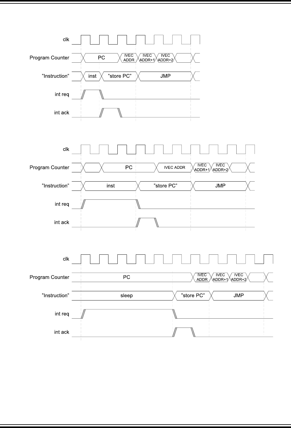
Figure 12-2. Interrupt Execution of a Single-Cycle Instruction, Multicycle Instruction, and From
Sleep(1)
Single-Cycle Instruction
Multicycle Instruction
Sleep
Note:
1. Devices with 8 KB of Flash or less use RJMP instead of JMP, which takes only two clock cycles.
12.3.2.4 Interrupt Priority
All interrupt vectors are assigned to one of three possible priority levels, as shown in the table. An
interrupt request from a high priority source will interrupt any ongoing interrupt handler from a normal
priority source. When returning from the high priority interrupt handler, the execution of the normal priority
interrupt handler will resume.
megaAVR® 0-Series
CPU Interrupt Controller (CPUINT)
© 2018 Microchip Technology Inc. Datasheet Preliminary DS40002015A-page 108

Table 12-1. Interrupt Priority Levels
Priority Level Source
Highest Non Maskable Interrupt (NMI) Device-dependent and statically
assigned
... High Priority (Level 1) One vector is optionally user
selectable as Level 1
Lowest Normal Priority (Level 0) The remaining interrupt vectors
Non-Maskable Interrupts (NMI)
An NMI will be executed regardless of the setting of the I bit in CPU.SREG, and it will never change the I
bit. No other interrupt can interrupt an NMI handler. If more than one NMI is requested at the same time,
priority is static according to the interrupt vector address, where the lowest address has the highest
priority.
Which interrupts are non-maskable is device-dependent and not subject to configuration. Non-maskable
interrupts must be enabled before they can be used. Refer to the Interrupt Vector Mapping of the device
for available NMI lines.
High Priority Interrupt
It is possible to assign one interrupt request to level 1 (high priority) by writing its interrupt vector number
to the CPUINT.LVL1VEC register. This interrupt request will have higher priority than the other (normal
priority) interrupt requests.
Normal Priority Interrupts
All interrupt vectors other than NMI are assigned to priority level 0 (normal) by default. The user may
override this by assigning one of these vectors as a high priority vector. The device will have many
normal priority vectors, and some of these may be pending at the same time. Two different scheduling
schemes are available to choose which of the pending normal priority interrupts to service first: Static and
round robin.
The following sections use the ordered sequence IVEC to explain these scheduling schemes. IVEC is the
Interrupt Vector Mapping as listed in the Peripherals and Architecture chapter. IVEC0 is the reset vector,
IVEC1 is the NMI vector, and so on. In a vector table with n+1 elements, the vector with the highest
vector number is denoted IVECn. Reset, non-maskable interrupts and high-level interrupts are included in
the IVEC map, but will be disregarded by the normal priority interrupt scheduler as they are not normal
priority interrupts.
Scheduling of Normal Priority Interrupts
Static Scheduling
If several level 0 interrupt requests are pending at the same time, the one with the highest priority is
scheduled for execution first. The CPUINT.LVL0PRI register makes it possible to change the default
priority. The reset value for CPUINT.LVL0PRI is zero, resulting in a default priority as shown in Figure
12-3. As the figure shows, IVEC0 has the highest priority, and IVECn has the lowest priority.
The default priority can be changed by writing to the CPUINT.LVL0PRI register. The value written to the
register will identify the vector number with the lowest priority. The next interrupt vector in IVEC will have
the highest priority, see Figure 12-4. In this figure, the value Y has been written to CPUINT.LVL0PRI, so
that interrupt vector Y+1 has the highest priority. Note that in this case, the priorities will "wrap" so that
IVEC0 has lower priority than IVECn.
Refer to the Interrupt Vector Mapping of the device for available interrupt requests and their interrupt
vector number.
megaAVR® 0-Series
CPU Interrupt Controller (CPUINT)
© 2018 Microchip Technology Inc. Datasheet Preliminary DS40002015A-page 109
Figure 12-3. Static Scheduling when CPUINT.LVL0PRI is zero
:
:
:
:
:
:
Lowest Priority
Highest Priority
IVEC 0
IVEC Y
IVEC Y+1
IVEC n
Lowest Address
Highest Address
IVEC 1
Figure 12-4. Static Scheduling when CPUINT.LVL0PRI is Different From Zero
:
:
:
:
:
:
IVEC 0
IVEC Y
IVEC Y+1
IVEC n
Lowest Priority
Highest Priority
IVEC 1
Lowest Address
Highest Address
Round Robin Scheduling
Static scheduling may cause starvation, i.e. some interrupts might never be serviced. To avoid this, the
CPUINT offers round robin scheduling for normal priority (LVL0) interrupts. In round robin scheduling,
CPUINT.LVL0PRI contains the number of the vector number in IVEC with the lowest priority. This register
is automatically updated by hardware with the interrupt vector number for the last acknowledged LVL0
interrupt. This interrupt vector will, therefore, have the lowest priority next time one or more LVL0
interrupts are pending. Figure 12-5 explains the new priority ordering after IVEC Y was the last interrupt
to be acknowledged, and after IVEC Y+1 was the last interrupt to be acknowledged.
Round robin scheduling for LVL0 interrupt requests is enabled by writing a ‘1’ to the Round Robin Priority
Enable bit (LVL0RR) in the Control A register (CPUINT.CTRLA).
megaAVR® 0-Series
CPU Interrupt Controller (CPUINT)
© 2018 Microchip Technology Inc. Datasheet Preliminary DS40002015A-page 110
Figure 12-5. Round Robin Scheduling
:
:
:
:
:
:
:
:
:
:
:
:
IVEC Y was last acknowledged
interrupt
IVEC Y+1 was last acknowledged
interrupt
IVEC 0
IVEC Y
IVEC Y+1
IVEC n
IVEC Y+2
IVEC Y+1
IVEC Y
IVEC 0
IVEC n
Lowest Priority
Highest Priority Lowest Priority
Highest Priority
12.3.2.5 Compact Vector Table
The Compact Vector Table (CVT) is a feature to allow writing of compact code.
When CVT is enabled by writing a '1' to the CVT bit in the Control A register (CPUINT.CTRLA), the vector
table contains these three interrupt vectors:
1. The non-maskable interrupts (NMI) at vector address 1.
2. The priority level 1 (LVL1) interrupt at vector address 2.
3. All priority level 0 (LVL0) interrupts share vector address 3.
This feature is most suitable for applications using a small number of interrupt generators.
12.3.3 Configuration Change Protection
This peripheral has registers that are under Configuration Change Protection (CCP). In order to write to
these, a certain key must be written to the CPU.CCP register first, followed by a write access to the
protected bits within four CPU instructions.
It is possible to try writing to these registers at any time, but the values are not altered.
The following registers are under CCP:
Table 12-2. INTCTRL - Registers under Configuration Change Protection
Register Key
IVSEL in CPUINT.CTRLA IOREG
CVT in CPUINT.CTRLA IOREG
megaAVR® 0-Series
CPU Interrupt Controller (CPUINT)
© 2018 Microchip Technology Inc. Datasheet Preliminary DS40002015A-page 111

12.4 Register Summary - CPUINT
Offset Name Bit Pos.
0x00 CTRLA 7:0 IVSEL CVT LVL0RR
0x01 STATUS 7:0 NMIEX LVL1EX LVL0EX
0x02 LVL0PRI 7:0 LVL0PRI[7:0]
0x03 LVL1VEC 7:0 LVL1VEC[7:0]
12.5 Register Description
megaAVR® 0-Series
CPU Interrupt Controller (CPUINT)
© 2018 Microchip Technology Inc. Datasheet Preliminary DS40002015A-page 112

12.5.1 Control A
Name: CTRLA
Offset: 0x00
Reset: 0x00
Property: Configuration Change Protection
Bit 7 6 5 4 3 2 1 0
IVSEL CVT LVL0RR
Access R/W R/W R/W
Reset 0 0 0
Bit 6 – IVSEL Interrupt Vector Select
If the boot section is defined, it will be placed before the application section. The actual start address of
the application section is determined by the BOOTEND Fuse.
This bit is protected by the Configuration Change Protection mechanism.
Value Description
0 Interrupt vectors are placed at the start of the application section of the Flash.
1 Interrupt vectors are placed at the start of the boot section of the Flash.
Bit 5 – CVT Compact Vector Table
This bit is protected by the Configuration Change Protection mechanism.
Value Description
0 Compact Vector Table function is disabled
1 Compact Vector Table function is enabled
Bit 0 – LVL0RR Round-Robin Priority Enable
This bit is not protected by the Configuration Change Protection mechanism.
Value Description
0 Priority is fixed for priority level 0 interrupt requests: The lowest interrupt vector address has
the highest priority.
1 Round Robin priority scheme is enabled for priority level 0 interrupt requests.
megaAVR® 0-Series
CPU Interrupt Controller (CPUINT)
© 2018 Microchip Technology Inc. Datasheet Preliminary DS40002015A-page 113

12.5.2 Status
Name: STATUS
Offset: 0x01
Reset: 0x00
Property: -
Bit 7 6 5 4 3 2 1 0
NMIEX LVL1EX LVL0EX
Access R R R
Reset 0 0 0
Bit 7 – NMIEX Non-Maskable Interrupt Executing
This flag is set if a non-maskable interrupt is executing. The flag is cleared when returning (RETI) from
the interrupt handler.
Bit 1 – LVL1EX Level 1 Interrupt Executing
This flag is set when a priority level 1 interrupt is executing, or when the interrupt handler has been
interrupted by an NMI. The flag is cleared when returning (RETI) from the interrupt handler.
Bit 0 – LVL0EX Level 0 Interrupt Executing
This flag is set when a priority level 0 interrupt is executing, or when the interrupt handler has been
interrupted by a priority level 1 interrupt or an NMI. The flag is cleared when returning (RETI) from the
interrupt handler.
megaAVR® 0-Series
CPU Interrupt Controller (CPUINT)
© 2018 Microchip Technology Inc. Datasheet Preliminary DS40002015A-page 114

12.5.3 Interrupt Priority Level 0
Name: LVL0PRI
Offset: 0x02
Reset: 0x00
Property: -
Bit 7 6 5 4 3 2 1 0
LVL0PRI[7:0]
Access R/W R/W R/W R/W R/W R/W R/W R/W
Reset 0 0 0 0 0 0 0 0
Bits 7:0 – LVL0PRI[7:0] Interrupt Priority Level 0
This register is used to modify the priority of the LVL0 interrupts. See Scheduling of Normal Priority
Interrupts for more information.
megaAVR® 0-Series
CPU Interrupt Controller (CPUINT)
© 2018 Microchip Technology Inc. Datasheet Preliminary DS40002015A-page 115

12.5.4 Interrupt Vector with Priority Level 1
Name: LVL1VEC
Offset: 0x03
Reset: 0x00
Property: -
Bit 7 6 5 4 3 2 1 0
LVL1VEC[7:0]
Access R/W R/W R/W R/W R/W R/W R/W R/W
Reset 0 0 0 0 0 0 0 0
Bits 7:0 – LVL1VEC[7:0] Interrupt Vector with Priority Level 1
This bit field contains the address of the single vector with increased priority level 1 (LVL1).
If this bit field has the value 0x00, no vector has LVL1. Consequently, the LVL1 interrupt is disabled.
megaAVR® 0-Series
CPU Interrupt Controller (CPUINT)
© 2018 Microchip Technology Inc. Datasheet Preliminary DS40002015A-page 116

13. Event System (EVSYS)
13.1 Features
• System for direct peripheral-to-peripheral signaling
• Peripherals can directly produce, use, and react to peripheral events
• Short and guaranteed response time
• Up to 8 parallel Event channels available
• Each channel is driven by one event generator and can have multiple event users
• Events can be sent and/or received by most peripherals, and by software
• The event system works in active, idle, and standby sleep mode
13.2 Overview
The Event System (EVSYS) enables direct peripheral-to-peripheral signaling. It allows a change in one
peripheral (the Event Generator) to trigger actions in other peripherals (the Event Users) through Event
channels, without using the CPU. It is designed to provide short and predictable response times between
peripherals, allowing for autonomous peripheral control and interaction, and also for synchronized timing
of actions in several peripheral modules. It is thus a powerful tool for reducing the complexity, size, and
execution time of the software.
A change of the Event Generator's state is referred to as an Event and usually corresponds to one of the
peripheral's interrupt conditions. Events can be directly forwarded to other peripherals using the
dedicated Event routing network. The routing of each channel is configured in software, including event
generation and use.
Only one Event signal can be routed on each channel. Multiple peripherals can use events from the same
channel.
The Event System can directly connect peripherals such as ADCs, analog comparators, I/O port pins, the
real-time counter, timer/counters, and the configurable custom logic peripheral. Events can also be
generated from software.
megaAVR® 0-Series
Event System (EVSYS)
© 2018 Microchip Technology Inc. Datasheet Preliminary DS40002015A-page 117
13.2.1 Block Diagram
Figure 13-1. Block Diagram
Event channel n
.
.
.
CHANNELn
DQDQ
STROBE[n] To channel
mux for async
event user
0
1
Is
async?
From event
generators
To channel
mux for sync
event user
The block diagram shows the operation of an event channel. A multiplexer controlled by
EVSYS.CHANNELn at the input selects which of the event sources to route onto the event channel. Each
event channel has two subchannels; One asynchronous subchannel and one synchronous subchannel. A
synchronous user will listen to the synchronous subchannel, an asynchronous user will listen to the
asynchronous subchannel.
An event signal from an asynchronous source will be synchronized by the event system before being
routed to the synchronous subchannel. An asynchronous event signal to be used by a synchronous
consumer must last for at least one peripheral clock cycle to guarantee that it will propagate through the
synchronizer. The synchronizer will delay such an event by 2-3 clock cycles depending on when the
event occurs.
Figure 13-2. Example of Event Source, Generator, User, and Action
|
Event
Routing
Network Single
Conversion
Channel Sweep
Compare Match
Over-/Underflow
Error
Event Generator Event User
Event Source Event Action
Event Action Selection
Timer/Counter ADC
megaAVR® 0-Series
Event System (EVSYS)
© 2018 Microchip Technology Inc. Datasheet Preliminary DS40002015A-page 118

13.2.2 Signal Description
Signal Type Description
EVOUTn Digital output Event output, one output per I/O Port
13.3 Functional Description
13.3.1 Initialization
To use events, both the event system, the generating peripheral and peripheral(s) using the event must
be set up appropriately.
1. Configure the generating peripheral appropriately. As an example, if the generating peripheral is a
timer, set the prescaling, compare register, etc. so that the desired event is generated.
2. Configure the event user peripheral(s) appropriately. As an example, if the ADC is the event user,
set the ADC prescaler, resolution, conversion time, etc. as desired, and configure ADC conversion
to start on the reception of an event.
3. Configure the event system to route the desired source, in this example the timer compare match,
to the desired event channel. This may, for example, be channel 0, which is accomplished by
writing to EVSYS.CHANNEL0. Configure the ADC to listen to this channel, by writing to
EVSYS.USERn, where n is the index allocated to the ADC.
13.3.2 Operation
13.3.2.1 Event User Multiplexer Setup
Each Event User has one dedicated Event User multiplexer selecting which event channel to listen to.
The application configures these multiplexers by writing to the corresponding User Channel Input
Selection n (EVSYS.USERn) register.
13.3.2.2 Event System Channel
An Event channel can be connected to one of the Event generators. Event channels can be connected to
either asynchronous generators or synchronous generators.
The source for each Event channel is configured by writing to the respective Channel n Input Selection
register (EVSYS.CHANNELn).
13.3.2.3 Event Generators
Each Event channel has several possible Event generators, only one of which can be selected at a time.
The Event generator trigger for a channel is selected by writing to the respective channel register
(EVSYS.CHANNELn). By default, the channels are not connected to any Event generator. For details on
Event generation, refer to the documentation of the corresponding peripheral.
A generated event is either synchronous or asynchronous to clocks in the device, depending on the
generator. An asynchronous event can be generated in sleep modes when clocks are not running. Such
events can also be generated outside the normal edges of the (prescaled) clocks in the system, making
the system respond faster than the selected clock frequency would suggest.
Generator Event Generating
Clock Domain
Length of event Constraints for
synchronous user
PDI SYNC character CLK_PDI Waveform: SYNC char
on PDI RX input
Synchronizing clock in
user must be fast enough
megaAVR® 0-Series
Event System (EVSYS)
© 2018 Microchip Technology Inc. Datasheet Preliminary DS40002015A-page 119

Generator Event Generating
Clock Domain
Length of event Constraints for
synchronous user
synchronized to
CLK_PDI
to guarantee that the
event is seen by the user
RTC Overflow CLK_RTC Pulse: 1 * CLK_RTC None
Compare Match CLK_RTC Pulse: 1 * CLK_RTC
PIT RTC Prescaled
clock
CLK_RTC Pulse: ≥1 * CLK_RTC
CCL-LUT Asynchronous Depends on CCL
configuration
Clock source used for
CCL must be slower or
equal to CLK_PER or
input signals to CCL are
stable for at least Tclk_per
AC Comparator result Asynchronous Level: Typically ≥1 us Frequency of input signals
to AC must be ≤fclk_per
to guarantee that the
event is seen by the
synchronous user
ADC Result ready CLK_ADC Pulse: 1 * CLK_PER None
Window compare
match
CLK_ADC Pulse: 1 * CLK_PER
PORT Pin input Asynchronous Level: Externally
controlled
Input signal must be
stable for longer than
fclk_per
USART USART Baud
clock
TXCLK Pulse: ≥2 * CLK_PER None
SPI SPI Master clock SCK Pulse: ≥2 * CLK_PER None
TCA Overflow CLK_PER Pulse: 1 * CLK_PER None
Underflow in split
mode
CLK_PER Pulse: 1 * CLK_PER
Compare match
ch 0
CLK_PER Pulse: 1 * CLK_PER
Compare match
ch 1
CLK_PER Pulse: 1 * CLK_PER
Compare match
ch 2
CLK_PER Pulse: 1 * CLK_PER
TCB Compare match,
timeout or when
counting
CLK_PER Pulse: ≥1 * CLK_PER None
megaAVR® 0-Series
Event System (EVSYS)
© 2018 Microchip Technology Inc. Datasheet Preliminary DS40002015A-page 120

13.3.2.4 Event Users
Each Event User must be configured to select the event channel to listen to. An event user may require
the event signal to be either synchronous or asynchronous to the system clock. An asynchronous event
user can respond to events in sleep modes when clocks are not running, Such events can also be
responded to outside the normal edges of the (prescaled) clocks in the system, making the event user
respond faster than the clock frequency would suggest. For details on the requirements of each
peripheral, refer to the documentation of the corresponding peripheral.
User Event Input Module/Event Mode Input Format Asynchronous
TCA CNTEI CNT_POSEDGE Pulse No
CNT_ANYEDGE Pulse No
CNT_HIGHLVL Level No
UPDOWN Level No
TCB TRIGEI Timeout check Level No
Input Capture on Event Pulse No
Input Capture Frequency Measurement Pulse No
Input Capture Pulse-Width Measurement Level No
Input Capture Frequency and Pulse Width
Measurement
Pulse and Level No
Single-Shot Pulse Yes
USART IrDA Mode Level No
CCL STARTEI Level Yes
ADC Pulse Yes
PORT Event output Level Yes
13.3.2.5 Synchronization
Events can be either synchronous or asynchronous to the system clock. Each event system channel has
two subchannels; one asynchronous and one synchronous. Both subchannels are available to all event
users, each user is hardwired to listen to one or the other.
The asynchronous subchannel is identical to the event output from the generator. If the event generator
generates a signal that is asynchronous to the system clock, the signal on the asynchronous subchannel
will be asynchronous. If the event generator generates a signal that is synchronous to the system clock,
the signal on the asynchronous subchannel will also be synchronous.
The synchronous subchannel is identical to the event output from the generator if the event generator
generates a signal that is synchronous to the system clock. If the event generator generates a signal that
is asynchronous to the system clock, this signal is first synchronized before being routed onto the
synchronous subchannel. Synchronization will delay the event by two system cycles. The event system
automatically performs this synchronization if an asynchronous generator is selected for an event
channel, no explicit configuration is needed.
megaAVR® 0-Series
Event System (EVSYS)
© 2018 Microchip Technology Inc. Datasheet Preliminary DS40002015A-page 121

13.3.2.6 Software Event
The application can generate a Software Event. Software Events on channel n are issued by writing a '1'
to the EVSYS.STROBE[n] bit. A software event appears as pulse on the event system channel, inverting
the current event system value for one clock cycle.
Event users see Software Events as no different from those produced by event generating peripherals.
When the EVSYS.STROBE[n] bit is written to '1', an Event will be generated on the respective channel,
and received and processed by the Event User.
13.3.3 Sleep Mode Operation
When configured, the Event System will work in all sleep modes. One exception is software Events which
require a system clock.
Asynchronous event users are able to respond to an event without their clock running, i.e. in Standby
sleep mode. Synchronous event users require their clock to be running to be able to respond to events.
Such users will only work in Idle sleep mode or in Standby sleep mode if configured to run in Standby
mode by setting the RUNSTBY bit in the appropriate register.
Asynchronous event generators are able to generate an event without their clock running, i.e. in Standby
sleep mode. Synchronous event generators require their clock to be running to be able to generate
events. Such generators will only work in Idle sleep mode or in Standby sleep mode if configured to run in
Standby mode by setting the RUNSTBY bit in the appropriate register.
13.3.4 Debug Operation
This peripheral is unaffected by entering Debug mode.
megaAVR® 0-Series
Event System (EVSYS)
© 2018 Microchip Technology Inc. Datasheet Preliminary DS40002015A-page 122

13.4 Register Summary - EVSYS
Offset Name Bit Pos.
0x00 STROBEA 7:0 STROBE[7:0]
0x01 STROBEB 7:0 STROBE[7:0]
0x02
...
0x0F
Reserved
0x10 CHANNEL0 7:0 GENERATOR[7:0]
0x11 CHANNEL1 7:0 GENERATOR[7:0]
0x12 CHANNEL2 7:0 GENERATOR[7:0]
0x13 CHANNEL3 7:0 GENERATOR[7:0]
0x14 CHANNEL4 7:0 GENERATOR[7:0]
0x15 CHANNEL5 7:0 GENERATOR[7:0]
0x16 CHANNEL6 7:0 GENERATOR[7:0]
0x17 CHANNEL7 7:0 GENERATOR[7:0]
0x18
...
0x1F
Reserved
0x20 USER0 7:0 CHANNEL[7:0]
0x21 USER1 7:0 CHANNEL[7:0]
0x22 USER2 7:0 CHANNEL[7:0]
0x23 USER3 7:0 CHANNEL[7:0]
0x24 USER4 7:0 CHANNEL[7:0]
0x25 USER5 7:0 CHANNEL[7:0]
0x26 USER6 7:0 CHANNEL[7:0]
0x27 USER7 7:0 CHANNEL[7:0]
0x28 USER8 7:0 CHANNEL[7:0]
0x29 USER9 7:0 CHANNEL[7:0]
0x2A USER10 7:0 CHANNEL[7:0]
0x2B USER11 7:0 CHANNEL[7:0]
0x2C USER12 7:0 CHANNEL[7:0]
0x2D USER13 7:0 CHANNEL[7:0]
0x2E USER14 7:0 CHANNEL[7:0]
0x2F USER15 7:0 CHANNEL[7:0]
0x30 USER16 7:0 CHANNEL[7:0]
0x31 USER17 7:0 CHANNEL[7:0]
0x32 USER18 7:0 CHANNEL[7:0]
0x33 USER19 7:0 CHANNEL[7:0]
0x34 USER20 7:0 CHANNEL[7:0]
0x35 USER21 7:0 CHANNEL[7:0]
0x36 USER22 7:0 CHANNEL[7:0]
0x37 USER23 7:0 CHANNEL[7:0]
13.5 Register Description
megaAVR® 0-Series
Event System (EVSYS)
© 2018 Microchip Technology Inc. Datasheet Preliminary DS40002015A-page 123

13.5.1 Channel Strobe
Name: STROBEA
Offset: 0x00
Reset: 0x00
Property: -
Software Events
Write bits in this register in order to create software events.
Bit 7 6 5 4 3 2 1 0
STROBE[7:0]
Access R/W R/W R/W R/W R/W R/W R/W R/W
Reset 0 0 0 0 0 0 0 0
Bits 7:0 – STROBE[7:0] Channel Strobe
If the strobe register location is written, each Event channel will be inverted for one system clock cycle,
i.e. a single Event is generated.
megaAVR® 0-Series
Event System (EVSYS)
© 2018 Microchip Technology Inc. Datasheet Preliminary DS40002015A-page 124

13.5.2 Channel Strobe
Name: STROBEB
Offset: 0x01
Reset: 0x00
Property: -
Software events
Write bits in this register in order to create software events.
Bit 7 6 5 4 3 2 1 0
STROBE[7:0]
Access R/W R/W R/W R/W R/W R/W R/W R/W
Reset 0 0 0 0 0 0 0 0
Bits 7:0 – STROBE[7:0] Channel Strobe
If the strobe register location is written, each Event channel will be inverted for one system clock cycle,
i.e. a single Event is generated.
megaAVR® 0-Series
Event System (EVSYS)
© 2018 Microchip Technology Inc. Datasheet Preliminary DS40002015A-page 125

13.5.3 Channel n Generator Selection
Name: CHANNEL
Offset: 0x10 + n*0x01 [n=0..7]
Reset: 0x00
Property: -
Each channel can be connected to one event generator. Not all generators can be connected to all
channels. Refer to the table below to see which generator sources that can be routed onto each channel,
and the generator value that must be written to EVSYS.CHANNELn to achieve this routing. The value
0x00 in EVSYS.CHANNELn turns the channel OFF.
Bit 7 6 5 4 3 2 1 0
GENERATOR[7:0]
Access R/W R/W R/W R/W R/W R/W R/W R/W
Reset 0 0 0 0 0 0 0 0
Bits 7:0 – GENERATOR[7:0] Channel Generator Selection
GENERATOR INPUT Async/Sync CH0 CH1 CH2 CH3 CH4 CH5 CH6 CH7
binary hex
0000_0001 0x01 PDI Sync PDI
0000_0110 0x06 RTC_OVF Async OVF
0000_0111 0x07 RTC_CMP Async CMP
0000_1000 0x08 RTC_PIT0 Async DIV64 DIV1024 DIV64 DIV1024 DIV64 DIV1024 DIV64 DIV1024
0000_1001 0x09 RTC_PIT1 Async DIV128 DIV2048 DIV128 DIV2048 DIV128 DIV2048 DIV128 DIV2048
0000_1010 0x0A RTC_PIT2 Async DIV256 DIV4096 DIV256 DIV4096 DIV256 DIV4096 DIV256 DIV4096
0000_1011 0x0B RTC_PIT3 Async DIV512 DIV8192 DIV512 DIV8192 DIV512 DIV8192 DIV512 DIV8192
0001_00nn 0x10-0x13 CCL_LUTn Async LUTn
0010_0000 0x20 AC0 Async OUT
0010_0100 0x24 ADC0 Sync COMP
0100_0nnn 0x40-0x47 PORT0_PINn Async PORTA_PINn PORTC_PINn PORTE_PINn
0100_1nnn 0x48-0x4F PORT1_PINn Async PORTB_PINn PORTD_PINn PORTF_PINn
0110_0nnn 0x60-0x67 USARTn Sync XCK
0110_1000 0x68 SPI0 Sync SCK
1000_0000 0x80 TCA0_OVF Sync OVF
1000_0001 0x81 TCA0_ERR Sync ERR
1000_0100 0x84 TCA0_CMP0 Sync CMP0
1000_0101 0x85 TCA0_CMP1 Sync CMP1
1000_0110 0x86 TCA0_CMP2 Sync CMP2
1010_nnn0 0xA0-0xAE TCBn Sync CMP0
megaAVR® 0-Series
Event System (EVSYS)
© 2018 Microchip Technology Inc. Datasheet Preliminary DS40002015A-page 126

13.5.4 User Channel Mux
Name: USER
Offset: 0x20 + n*0x01 [n=0..23]
Reset: 0x00
Property: -
Each event user can be connected to one channel. Several users can be connected to the same channel.
The following table lists all event system users, with their corresponding user ID number. This ID number
corresponds to the USER register index, e.g. the user with ID 2 is controlled by the EVSYS.USER2
register.
USER # User Name Async/Sync Description
0 CCL-LUT00 Async LUT0 Event 0 in
1 CCL-LUT01 Async LUT0 Event 1 in
2 CCL-LUT10 Async LUT1 Event 0 in
3 CCL-LUT11 Async LUT1 Event 1 in
4 CCL-LUT20 Async LUT2 Event 0 in
5 CCL-LUT21 Async LUT2 Event 1 in
6 CCL-LUT30 Async LUT3 Event 0 in
7 CCL-LUT31 Async LUT3 Event 1 in
8 ADC0 Async ADC Trigger
9 EVOUTA Async Event out A
10 EVOUTB Async Event out B
11 EVOUTC Async Event out C
12 EVOUTD Async Event out D
13 EVOUTE Async Event out E
14 EVOUTF Async Event out F
15 USART0 Sync USART0 Event in
16 USART1 Sync USART1 Event in
17 USART2 Sync USART2 Event in
18 USART3 Sync USART3 Event in
19 TCA Sync TCA Event in
20 TCB0 Async TCB0 Event in
21 TCB1 Async TCB1 Event in
22 TCB2 Async TCB2 Event in
23 TCB3 Async TCB3 Event in
megaAVR® 0-Series
Event System (EVSYS)
© 2018 Microchip Technology Inc. Datasheet Preliminary DS40002015A-page 127

Bit 7 6 5 4 3 2 1 0
CHANNEL[7:0]
Access R/W R/W R/W R/W R/W R/W R/W R/W
Reset 0 0 0 0 0 0 0 0
Bits 7:0 – CHANNEL[7:0] User Channel Selection
Describes which event system channel the user is connected to.
Value Description
0 OFF, no channel is connected to this event system user
n Event user is connected to CHANNEL(n-1)
megaAVR® 0-Series
Event System (EVSYS)
© 2018 Microchip Technology Inc. Datasheet Preliminary DS40002015A-page 128

14. Port Multiplexer (PORTMUX)
14.1 Overview
The Port Multiplexer (PORTMUX) can either enable or disable functionality of pins, or change between
default and alternative pin positions. Available options are described in detail in the PORTMUX register
map and depend on the actual pin and its properties.
For available pins and functionalities, refer to the “I/O Multiplexing and Considerations” chapter in the
Device Data Sheet.
megaAVR® 0-Series
Port Multiplexer (PORTMUX)
© 2018 Microchip Technology Inc. Datasheet Preliminary DS40002015A-page 129

14.2 Register Summary - PORTMUX
Offset Name Bit Pos.
0x00 EVSYSROUTEA 7:0 EVOUTF EVOUTE EVOUTD EVOUTC EVOUTB EVOUTA
0x01 CCLROUTEA 7:0 LUT3 LUT2 LUT1 LUT0
0x02 USARTROUTEA 7:0 USART3[1:0] USART2[1:0] USART1[1:0] USART0[1:0]
0x03 TWISPIROUTEA 7:0 TWI0[1:0] SPI0[1:0]
0x04 TCAROUTEA 7:0 TCA0[2:0]
0x05 TCBROUTEA 7:0 TCB3 TCB2 TCB1 TCB0
14.3 Register Description
megaAVR® 0-Series
Port Multiplexer (PORTMUX)
© 2018 Microchip Technology Inc. Datasheet Preliminary DS40002015A-page 130

14.3.1 PORTMUX Control for Event System
Name: EVSYSROUTEA
Offset: 0x00
Reset: 0x00
Property: -
Bit 7 6 5 4 3 2 1 0
EVOUTF EVOUTE EVOUTD EVOUTC EVOUTB EVOUTA
Access R/W R/W R/W R/W R/W R/W
Reset 0 0 0 0 0 0
Bits 0, 1, 2, 3, 4, 5 – EVOUT Event Output x
Write this bit to '1' to select alternative pin location for Enable Event Output x.
megaAVR® 0-Series
Port Multiplexer (PORTMUX)
© 2018 Microchip Technology Inc. Datasheet Preliminary DS40002015A-page 131

14.3.2 PORTMUX Control for CCL
Name: CCLROUTEA
Offset: 0x01
Reset: 0x00
Property: -
Bit 7 6 5 4 3 2 1 0
LUT3 LUT2 LUT1 LUT0
Access R/W R/W R/W R/W
Reset 0 0 0 0
Bit 3 – LUT3 CCL LUT 3 output
Write this bit to '1' to select alternative pin location for CCL LUT 3.
Value Name Description
0x0 DEFAULT CCL LUT3 on PF[3]
0x1 ALT1 CCL LUT3 on PF[6]
Bit 2 – LUT2 CCL LUT 2 output
Write this bit to '1' to select alternative pin location for CCL LUT 2.
Value Name Description
0x0 DEFAULT CCL LUT2 on PD[3]
0x1 ALT1 CCL LUT2 on PD[6]
Bit 1 – LUT1 CCL LUT 1 output
Write this bit to '1' to select alternative pin location for CCL LUT 1.
Value Name Description
0x0 DEFAULT CCL LUT1 on PC[3]
0x1 ALT1 CCL LUT1 on PC[6]
Bit 0 – LUT0 CCL LUT 0 output
Write this bit to '1' to select alternative pin location for CCL LUT 0.
Value Name Description
0x0 DEFAULT CCL LUT0 on PA[3]
0x1 ALT1 CCL LUT0 on PA[6]
megaAVR® 0-Series
Port Multiplexer (PORTMUX)
© 2018 Microchip Technology Inc. Datasheet Preliminary DS40002015A-page 132
14.3.3 PORTMUX Control for USART
Name: USARTROUTEA
Offset: 0x02
Reset: 0x00
Property: -
Bit 7 6 5 4 3 2 1 0
USART3[1:0] USART2[1:0] USART1[1:0] USART0[1:0]
Access R/W R/W R/W R/W R/W R/W R/W R/W
Reset 0 0 0 0 0 0 0 0
Bits 7:6 – USART3[1:0] USART 3 communication
Write these bits to select alternative communication pins for USART 3.
Value Name Description
0x0 DEFAULT USART3 on PB[3:0]
0x1 ALT1 USART3 on PB[5:4]
0x2 - Reserved
0x3 NONE Not connected to any pins
Bits 5:4 – USART2[1:0] USART 2 communication
Write these bits to select alternative communication pins for USART 2.
Value Name Description
0x0 DEFAULT USART2 on PF[3:0]
0x1 ALT1 USART2 on PF[6:4]
0x2 - Reserved
0x3 NONE Not connected to any pins
Bits 3:2 – USART1[1:0] USART 1 communication
Write these bits to select alternative communication pins for USART 1.
Value Name Description
0x0 DEFAULT USART1 on PC[3:0]
0x1 ALT1 USART1 on PC[7:4]
0x2 - Reserved
0x3 NONE Not connected to any pins
Bits 1:0 – USART0[1:0] USART 0 communication
Write these bits to select alternative communication pins for USART 0.
Value Name Description
0x0 DEFAULT USART0 on PA[3:0]
0x1 ALT1 USART0 on PA[7:4]
0x2 - Reserved
0x3 NONE Not connected to any pins
megaAVR® 0-Series
Port Multiplexer (PORTMUX)
© 2018 Microchip Technology Inc. Datasheet Preliminary DS40002015A-page 133
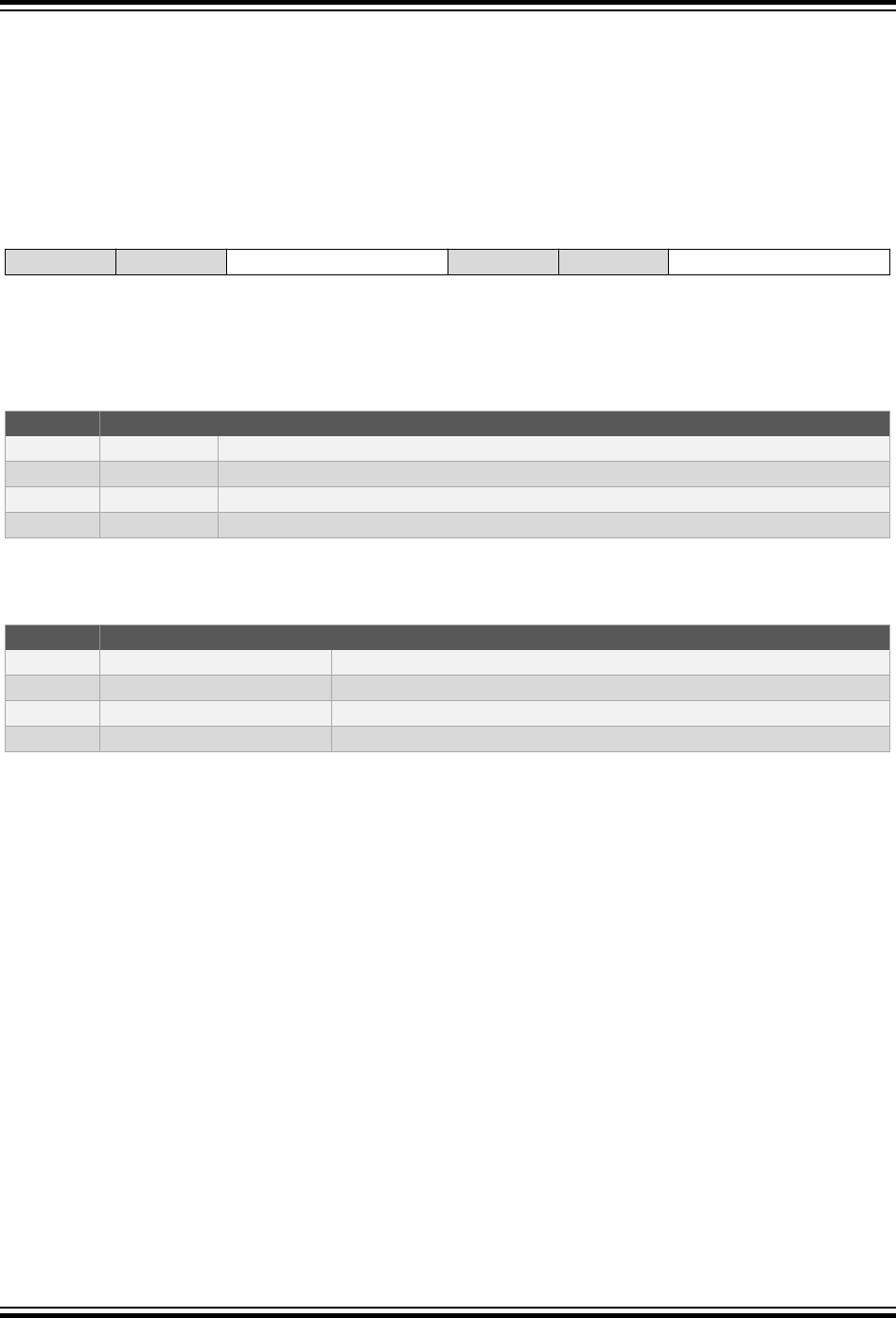
14.3.4 PORTMUX Control for TWI and SPI
Name: TWISPIROUTEA
Offset: 0x03
Reset: 0x00
Property: -
Bit 7 6 5 4 3 2 1 0
TWI0[1:0] SPI0[1:0]
Access R/W R/W R/W R/W
Reset 0 0 0 0
Bits 5:4 – TWI0[1:0] TWI 0 communication
Write these bits to select alternative communication pins for TWI 0.
Value Name Description
0x0 DEFAULT SCL/SDA on PA[3:2], Slave mode on PC[3:2] in dual TWI mode
0x1 ALT1 SCL/SDA on PA[3:2], Slave mode on PF[3:2] in dual TWI mode
0x2 ALT2 SCL/SDA on PC[3:2], Slave mode on PF[3:2] in dual TWI mode
0x3 - Reserved
Bits 1:0 – SPI0[1:0] SPI 0 communication
Write these bits to select alternative communication pins for SPI 0.
Value Name Description
0x0 DEFAULT SPI on PA[7:4]
0x1 ALT1 SPI on PC[3:0]
0x2 ALT2 SPI on PE[3:0]
0x3 NONE Not connected to any pins
megaAVR® 0-Series
Port Multiplexer (PORTMUX)
© 2018 Microchip Technology Inc. Datasheet Preliminary DS40002015A-page 134

14.3.5 PORTMUX Control for TCA
Name: TCAROUTEA
Offset: 0x04
Reset: 0x00
Property: -
Bit 7 6 5 4 3 2 1 0
TCA0[2:0]
Access R/W R/W R/W
Reset 0 0 0
Bits 2:0 – TCA0[2:0] TCA0
Write these bits to select alternative output pins for TCA0.
Value Name Description
0x0 PORTA TCA0 pins on PA[5:0]
0x1 PORTB TCA0 pins on PB[5:0]
0x2 PORTC TCA0 pins on PC[5:0]
0x3 PORTD TCA0 pins on PD[5:0]
0x4 PORTE TCA0 pins on PE[5:0]
0x5 PORTF TCA0 pins on PF[5:0]
Other - Reserved
megaAVR® 0-Series
Port Multiplexer (PORTMUX)
© 2018 Microchip Technology Inc. Datasheet Preliminary DS40002015A-page 135

14.3.6 PORTMUX Control for TCB
Name: TCBROUTEA
Offset: 0x05
Reset: 0x00
Property: -
Bit 7 6 5 4 3 2 1 0
TCB3 TCB2 TCB1 TCB0
Access R/W R/W R/W R/W
Reset 0 0 0 0
Bit 3 – TCB3 TCB3 output
Write this bit to '1' to select alternative output pin for 16-bit timer/counter B 3.
Value Name Description
0x0 DEFAULT TCB3 on PB5
0x1 ALT1 TCB3 on PC1
Bit 2 – TCB2 TCB2 output
Write this bit to '1' to select alternative output pin for 16-bit timer/counter B 2.
Value Name Description
0x0 DEFAULT TCB2 on PC0
0x1 ALT1 TCB2 on PB4
Bit 1 – TCB1 TCB1 output
Write this bit to '1' to select alternative output pin for 16-bit timer/counter B 1.
Value Name Description
0x0 DEFAULT TCB1 on PA3
0x1 ALT1 TCB1 on PF5
Bit 0 – TCB0 TCB0 output
Write this bit to '1' to select alternative output pin for 16-bit timer/counter B 0.
Value Name Description
0x0 DEFAULT TCB0 on PA2
0x1 ALT1 TCB0 on PF4
megaAVR® 0-Series
Port Multiplexer (PORTMUX)
© 2018 Microchip Technology Inc. Datasheet Preliminary DS40002015A-page 136

15. I/O Pin Configuration (PORT)
15.1 Features
• General Purpose Input and Output Pins with Individual Configuration
• Output Driver with Configurable Inverted I/O and Pullup
• Input with Interrupts and Events:
– Sense both edges
– Sense rising edges
– Sense falling edges
– Sense low level
• Optional Slew Rate Control per I/O Port
• Asynchronous Pin Change Sensing That Can Wake the Device From all Sleep Modes
• Efficient and Safe Access to Port Pins
– Hardware read-modify-write through dedicated toggle/clear/set registers
– Mapping of often-used PORT registers into bit-accessible I/O memory space (virtual ports)
15.2 Overview
The I/O pins of the device are controlled by instances of the PORT peripheral registers. Each PORT
instance has up to eight I/O pins. The PORTs are named PORTA, PORTB, PORTC, etc. Refer to the “I/O
Multiplexing and Considerations” chapter in the device Data Sheet to see which pins are controlled by
what instance of PORT. The offsets of the PORT instances and of the corresponding Virtual PORT
instances are listed in the “Peripherals and Architecture” section.
Each of the port pins has a corresponding bit in the Data Direction (PORTx.DIR) and Data Output Value
(PORTx.OUT) registers to enable that pin as an output and to define the output state. For example, pin
PA3 is controlled by DIR[3] and OUT[3] of the PORTA instance.
The input value of a PORT pin is synchronized to the main clock and then made accessible as the data
input value (PORTx.IN). To reduce power consumption, these input synchronizers are not clocked if the
Input Sense Configuration bit field (ISC) in PORTx.PINnCTRL is INPUT_DISABLE. The value of the pin
can always be read, whether the pin is configured as input or output.
The PORT also supports synchronous and asynchronous input sensing with interrupts and events for
selectable pin change conditions. Asynchronous pin-change sensing means that a pin change can wake
the device from all sleep modes, including the modes where no clocks are running.
All pin functions are configurable individually per pin. The pins have hardware read-modify-write (RMW)
functionality for a safe and correct change of drive value and/or pull resistor configuration. The direction
of one port pin can be changed without unintentionally changing the direction of any other pin.
The PORT pin configuration also controls input and output selection of other device functions.
megaAVR® 0-Series
I/O Pin Configuration (PORT)
© 2018 Microchip Technology Inc. Datasheet Preliminary DS40002015A-page 137
15.2.1 Block Diagram
Figure 15-1. PORT Block Diagram
D
Q
R
D
Q
R
Synchronizer
DQ
R
DIRn
OUTn
INn
Pxn
DQ
R
Input Disable
Digital Input /
Asynchronous Event
Invert Enable
Pullup Enable
Input
Disable
Override
OUT Override
DIR
Override
Analog Input/Output
Synchronized
Input
Interrupt
Generator
Interrupt
15.2.2 Signal Description
Signal Type Description
Pxn I/O pin I/O pin n on PORTx
15.3 Functional Description
15.3.1 Initialization
After Reset, all standard function device I/O pads are connected to the port with outputs tri-stated and
input buffers enabled, even if there is no clock running.
megaAVR® 0-Series
I/O Pin Configuration (PORT)
© 2018 Microchip Technology Inc. Datasheet Preliminary DS40002015A-page 138

For best power consumption, disable the input of unused pins and pins that are used as analog inputs or
outputs.
Specific pins, such as those used for connecting a debugger, may be configured differently, as required
by their special function.
15.3.2 Operation
15.3.2.1 Basic Functions
Each I/O pin Pxn can be controlled by the registers in PORTx. Each pin group x has its own set of PORT
registers. The base address of the register set for pin n is at the byte address PORT + 0x10 + . The
index within that register set is n.
To use pin number n as an output only, write bit n of the PORTx.DIR register to '1'. This can be done by
writing bit n in the PORTx.DIRSET register to '1', which will avoid disturbing the configuration of other pins
in that group. The nth bit in the PORTx.OUT register must be written to the desired output value.
Similarly, writing a PORTx.OUTSET bit to '1' will set the corresponding bit in the PORTx.OUT register to
'1'. Writing a bit in PORTx.OUTCLR to '1' will clear that bit in PORTx.OUT to zero. Writing a bit in
PORTx.OUTTGL or PORTx.IN to '1' will toggle that bit in PORTx.OUT.
To use pin n as an input, bit n in the PORTx.DIR register must be written to '0' to disable the output driver.
This can be done by writing bit n in the PORTx.DIRCLR register to '1', which will avoid disturbing the
configuration of other pins in that group. The input value can be read from bit n in register PORTx.IN as
long as the ISC bit is not set to INPUT_DISABLE.
Writing a bit to '1' in PORTx.DIRTGL will toggle that bit in PORTx.DIR and toggle the direction of the
corresponding pin.
15.3.2.2 Pin Configuration
The Pin n Configuration register (PORTx.PINnCTRL) is used to configure inverted I/O, pullup, and input
sensing of a pin.
All input and output on the respective pin n can be inverted by writing a '1' to the Inverted I/O Enable bit
(INVEN) in PORTx.PINnCTRL.
Toggling the INVEN bit causes an edge on the pin, which can be detected by all peripherals using this
pin, and is seen by interrupts or Events if enabled.
Pullup of pin n is enabled by writing a '1' to the Pullup Enable bit (PULLUPEN) in PORTx.PINnCTRL.
Changes of the signal on a pin can trigger an interrupt. The exact conditions are defined by writing to the
Input/Sense bit field (ISC) in PORTx.PINnCTRL.
When setting or changing interrupt settings, take these points into account:
• If an INVEN bit is toggled in the same cycle as the interrupt setting, the edge caused by the
inversion toggling may not cause an interrupt request.
• If an input is disabled while synchronizing an interrupt, that interrupt may be requested on re-
enabling the input, even if it is re-enabled with a different interrupt setting.
• If the interrupt setting is changed while synchronizing an interrupt, that interrupt may not be
accepted.
• Only a few pins support full asynchronous interrupt detection, see I/O Multiplexing and
Considerations. These limitations apply for waking the system from sleep:
megaAVR® 0-Series
I/O Pin Configuration (PORT)
© 2018 Microchip Technology Inc. Datasheet Preliminary DS40002015A-page 139

Interrupt Type Fully Asynchronous Pins Other Pins
BOTHEDGES Will wake system Will wake system
RISING Will wake system Will not wake system
FALLING Will wake system Will not wake system
LEVEL Will wake system Will wake system
15.3.2.3 Virtual Ports
The Virtual PORT registers map the most frequently used regular PORT registers into the bit-accessible
I/O space. Writing to the Virtual PORT registers has the same effect as writing to the regular registers, but
allows for memory-specific instructions, such as bit-manipulation instructions, which are not valid for the
extended I/O memory space where the regular PORT registers reside.
Table 15-1. Virtual Port Mapping
Regular PORT Register Mapped to Virtual PORT Register
PORT.DIR VPORT.DIR
PORT.OUT VPORT.OUT
PORT.IN VPORT.IN
PORT.INTFLAG VPORT.INTFLAG
15.3.2.4 Peripheral Override
Peripherals such as USARTs and timers may be connected to I/O pins. Such peripherals will usually have
a primary and optionally also alternate I/O pin connection, selectable by PORTMUX. By configuring and
enabling such peripherals, the general-purpose I/O pin behavior normally controlled by PORT will be
overridden by the peripheral in a peripheral-dependent way. Some peripherals may not override all of the
PORT registers, leaving the PORT module to control some aspects of the I/O pin operation. Refer to the
description of each peripheral for information on the peripheral override. Any pin in a PORT which is not
overridden by a peripheral will continue to operate as a general-purpose I/O pin.
15.3.3 Interrupts
Table 15-2. Available Interrupt Vectors and Sources
Name Vector Description Conditions
PORTx PORT interrupt INTn in PORTx.INTFLAGS is raised as configured by ISC bit in
PORTx.PINnCTRL.
Each PORT pin n can be configured as an interrupt source. Each interrupt can be individually enabled or
disabled by writing to ISC in PORTx.PINnCTRL.
When an interrupt condition occurs, the corresponding Interrupt Flag is set in the Interrupt Flags register
of the peripheral (peripheral.INTFLAGS).
An interrupt request is generated when the corresponding interrupt source is enabled and the Interrupt
Flag is set. The interrupt request remains active until the Interrupt Flag is cleared. See the peripheral's
INTFLAGS register for details on how to clear Interrupt Flags.
megaAVR® 0-Series
I/O Pin Configuration (PORT)
© 2018 Microchip Technology Inc. Datasheet Preliminary DS40002015A-page 140

Asynchronous Sensing Pin Properties
PORT supports synchronous and asynchronous input sensing with interrupts for selectable pin change
conditions. Asynchronous pin change sensing means that a pin change can wake the device from all
sleep modes, including modes where no clocks are running.
Table 15-3. Behavior Comparison of Fully/Partly Asynchronous Sense Pin
Property Synchronous or Partly Asynchronous
Sense Support
Full Asynchronous Sense
Support
Minimum pulse
width to trigger
interrupt
Minimum one system clock cycle Less than a system clock cycle
Waking the device
from sleep
From all interrupt sense configurations from
sleep modes with Main Clock running. Only
from BOTHEDGES or LEVEL interrupt sense
configuration from sleep modes with Main
Clock stopped.
From all interrupt sense
configurations from all sleep
modes
Interrupt “dead time” No new interrupt for three cycles after the
previous
Less than a system clock cycle
Minimum Wake-up
pulse length
Value on pad must be kept until the system
clock has restarted
Less than a system clock cycle
15.3.4 Events
All PORT pins are asynchronous event system generators. PORT has as many event generators as there
are PORT pins in the device. Each event system output from PORT is the value present on the
corresponding pin if the digital input driver is enabled. If a pin input driver is disabled, the corresponding
event system output is zero.
PORT has no event inputs.
15.3.5 Sleep Mode Operation
With the exception of interrupts and input synchronization, all pin configurations are independent of sleep
mode. Peripherals connected to the Ports can be affected by sleep modes, described in the respective
peripherals' documentation.
The PORT peripheral will always use the Main Clock. Input synchronization will halt when this clock
stops.
megaAVR® 0-Series
I/O Pin Configuration (PORT)
© 2018 Microchip Technology Inc. Datasheet Preliminary DS40002015A-page 141

15.4 Register Summary - PORTx
Offset Name Bit Pos.
0x00 DIR 7:0 DIR[7:0]
0x01 DIRSET 7:0 DIRSET[7:0]
0x02 DIRCLR 7:0 DIRCLR[7:0]
0x03 DIRTGL 7:0 DIRTGL[7:0]
0x04 OUT 7:0 OUT[7:0]
0x05 OUTSET 7:0 OUTSET[7:0]
0x06 OUTCLR 7:0 OUTCLR[7:0]
0x07 OUTTGL 7:0 OUTTGL[7:0]
0x08 IN 7:0 IN[7:0]
0x09 INTFLAGS 7:0 INT[7:0]
0x0A PORTCTRL 7:0 SRL
0x0B
...
0x0F
Reserved
0x10 PIN0CTRL 7:0 INVEN PULLUPEN ISC[2:0]
0x11 PIN1CTRL 7:0 INVEN PULLUPEN ISC[2:0]
0x12 PIN2CTRL 7:0 INVEN PULLUPEN ISC[2:0]
0x13 PIN3CTRL 7:0 INVEN PULLUPEN ISC[2:0]
0x14 PIN4CTRL 7:0 INVEN PULLUPEN ISC[2:0]
0x15 PIN5CTRL 7:0 INVEN PULLUPEN ISC[2:0]
0x16 PIN6CTRL 7:0 INVEN PULLUPEN ISC[2:0]
0x17 PIN7CTRL 7:0 INVEN PULLUPEN ISC[2:0]
15.5 Register Description - Ports
megaAVR® 0-Series
I/O Pin Configuration (PORT)
© 2018 Microchip Technology Inc. Datasheet Preliminary DS40002015A-page 142

15.5.1 Data Direction
Name: DIR
Offset: 0x00
Reset: 0x00
Property: -
Bit 7 6 5 4 3 2 1 0
DIR[7:0]
Access R/W R/W R/W R/W R/W R/W R/W R/W
Reset 0 0 0 0 0 0 0 0
Bits 7:0 – DIR[7:0] Data Direction
This bit field controls output enable for the individual pins of the Port.
Writing a ‘1’ to PORTx.DIR[n] configures and enables pin n as an output pin.
Writing a ‘0’ to PORTx.DIR[n] configures pin n as an input-only pin. Its properties can be configured by
writing to the ISC bit in PORTx.PINnCTRL.
PORTx.DIRn controls only the output enable. Setting PORTx.DIR[n] to ‘1’ does not disable the pin input.
megaAVR® 0-Series
I/O Pin Configuration (PORT)
© 2018 Microchip Technology Inc. Datasheet Preliminary DS40002015A-page 143

15.5.2 Data Direction Set
Name: DIRSET
Offset: 0x01
Reset: 0x00
Property: -
Bit 7 6 5 4 3 2 1 0
DIRSET[7:0]
Access R/W R/W R/W R/W R/W R/W R/W R/W
Reset 0 0 0 0 0 0 0 0
Bits 7:0 – DIRSET[7:0] Data Direction Set
This bit field can be used instead of a read-modify-write to set individual pins as output.
Writing a '1' to DIRSET[n] will set the corresponding PORTx.DIR[n] bit.
Reading this bit field will always return the value of PORTx.DIR.
megaAVR® 0-Series
I/O Pin Configuration (PORT)
© 2018 Microchip Technology Inc. Datasheet Preliminary DS40002015A-page 144

15.5.3 Data Direction Clear
Name: DIRCLR
Offset: 0x02
Reset: 0x00
Property: -
Bit 7 6 5 4 3 2 1 0
DIRCLR[7:0]
Access R/W R/W R/W R/W R/W R/W R/W R/W
Reset 0 0 0 0 0 0 0 0
Bits 7:0 – DIRCLR[7:0] Data Direction Clear
This register can be used instead of a read-modify-write to configure individual pins as input-only.
Writing a '1' to DIRCLR[n] will clear the corresponding bit in PORTx.DIR.
Reading this bit field will always return the value of PORTx.DIR.
megaAVR® 0-Series
I/O Pin Configuration (PORT)
© 2018 Microchip Technology Inc. Datasheet Preliminary DS40002015A-page 145

15.5.4 Data Direction Toggle
Name: DIRTGL
Offset: 0x03
Reset: 0x00
Property: -
Bit 7 6 5 4 3 2 1 0
DIRTGL[7:0]
Access R/W R/W R/W R/W R/W R/W R/W R/W
Reset 0 0 0 0 0 0 0 0
Bits 7:0 – DIRTGL[7:0] Data Direction Toggle
This bit field can be used instead of a read-modify-write to toggle the direction of individual pins.
Writing a '1' to DIRTGL[n] will toggle the corresponding bit in PORTx.DIR.
Reading this bit field will always return the value of PORTx.DIR.
megaAVR® 0-Series
I/O Pin Configuration (PORT)
© 2018 Microchip Technology Inc. Datasheet Preliminary DS40002015A-page 146

15.5.5 Output Value
Name: OUT
Offset: 0x04
Reset: 0x00
Property: -
Bit 7 6 5 4 3 2 1 0
OUT[7:0]
Access R/W R/W R/W R/W R/W R/W R/W R/W
Reset 0 0 0 0 0 0 0 0
Bits 7:0 – OUT[7:0] Output Value
This bit field defines the data output value for the individual pins of the port.
If OUT[n] is written to '1', pin n is driven high.
If OUT[n] is written to '0', pin n is driven low.
In order to have any effect, the pin direction must be configured as output.
megaAVR® 0-Series
I/O Pin Configuration (PORT)
© 2018 Microchip Technology Inc. Datasheet Preliminary DS40002015A-page 147

15.5.6 Output Value Set
Name: OUTSET
Offset: 0x05
Reset: 0x00
Property: -
Bit 7 6 5 4 3 2 1 0
OUTSET[7:0]
Access R/W R/W R/W R/W R/W R/W R/W R/W
Reset 0 0 0 0 0 0 0 0
Bits 7:0 – OUTSET[7:0] Output Value Set
This bit field can be used instead of a read-modify-write to set the output value of individual pins to '1'.
Writing a '1' to OUTSET[n] will set the corresponding bit in PORTx.OUT.
Reading this bit field will always return the value of PORTx.OUT.
megaAVR® 0-Series
I/O Pin Configuration (PORT)
© 2018 Microchip Technology Inc. Datasheet Preliminary DS40002015A-page 148

15.5.7 Output Value Clear
Name: OUTCLR
Offset: 0x06
Reset: 0x00
Property: -
Bit 7 6 5 4 3 2 1 0
OUTCLR[7:0]
Access R/W R/W R/W R/W R/W R/W R/W R/W
Reset 0 0 0 0 0 0 0 0
Bits 7:0 – OUTCLR[7:0] Output Value Clear
This register can be used instead of a read-modify-write to clear the output value of individual pins to '0'.
Writing a '1' to OUTCLR[n] will clear the corresponding bit in PORTx.OUT.
Reading this bit field will always return the value of PORTx.OUT.
megaAVR® 0-Series
I/O Pin Configuration (PORT)
© 2018 Microchip Technology Inc. Datasheet Preliminary DS40002015A-page 149

15.5.8 Output Value Toggle
Name: OUTTGL
Offset: 0x07
Reset: 0x00
Property: -
Bit 7 6 5 4 3 2 1 0
OUTTGL[7:0]
Access R/W R/W R/W R/W R/W R/W R/W R/W
Reset 0 0 0 0 0 0 0 0
Bits 7:0 – OUTTGL[7:0] Output Value Toggle
This register can be used instead of a read-modify-write to toggle the output value of individual pins.
Writing a '1' to OUTTGL[n] will toggle the corresponding bit in PORTx.OUT.
Reading this bit field will always return the value of PORTx.OUT.
megaAVR® 0-Series
I/O Pin Configuration (PORT)
© 2018 Microchip Technology Inc. Datasheet Preliminary DS40002015A-page 150

15.5.9 Input Value
Name: IN
Offset: 0x08
Reset: 0x00
Property: -
Bit 7 6 5 4 3 2 1 0
IN[7:0]
Access R/W R/W R/W R/W R/W R/W R/W R/W
Reset 0 0 0 0 0 0 0 0
Bits 7:0 – IN[7:0] Input Value
This register shows the value present on the pins if the digital input driver is enabled. IN[n] shows the
value of pin n of the Port. If the digital input buffers are disabled, the input is not sampled and cannot be
read.
Writing to a bit of PORTx.IN will toggle the corresponding bit in PORTx.OUT.
megaAVR® 0-Series
I/O Pin Configuration (PORT)
© 2018 Microchip Technology Inc. Datasheet Preliminary DS40002015A-page 151

15.5.10 Interrupt Flags
Name: INTFLAGS
Offset: 0x09
Reset: 0x00
Property: -
Bit 7 6 5 4 3 2 1 0
INT[7:0]
Access R/W R/W R/W R/W R/W R/W R/W R/W
Reset 0 0 0 0 0 0 0 0
Bits 7:0 – INT[7:0] Interrupt Pin Flag
The INT Flag is set when a pin change/state matches the pin's input sense configuration.
Writing a '1' to a flag's bit location will clear the flag.
For enabling and executing the interrupt, refer to ISC bit description in PORTx.PINnCTRL.
megaAVR® 0-Series
I/O Pin Configuration (PORT)
© 2018 Microchip Technology Inc. Datasheet Preliminary DS40002015A-page 152

15.5.11 Port Control
Name: PORTCTRL
Offset: 0x0A
Reset: 0x00
Property: -
This register contains the slew rate limit enable bit for this port.
Bit 7 6 5 4 3 2 1 0
SRL
Access R/W
Reset 0
Bit 0 – SRL Slew Rate Limit Enable
Writing a '1' to this bit enables slew rate limitation for all pins on this port.
megaAVR® 0-Series
I/O Pin Configuration (PORT)
© 2018 Microchip Technology Inc. Datasheet Preliminary DS40002015A-page 153

15.5.12 Pin n Control
Name: PINCTRL
Offset: 0x10 + n*0x01 [n=0..7]
Reset: 0x00
Property: -
Bit 7 6 5 4 3 2 1 0
INVEN PULLUPEN ISC[2:0]
Access R/W R/W R/W R/W R/W
Reset 0 0 0 0 0
Bit 7 – INVEN Inverted I/O Enable
Value Description
0 Input and output values are not inverted
1 Input and output values are inverted
Bit 3 – PULLUPEN Pullup Enable
Value Description
0 Pullup disabled for pin n
1 Pullup enabled for pin n
Bits 2:0 – ISC[2:0] Input/Sense Configuration
These bits configure the input and sense configuration of pin n. The sense configuration determines how
a port interrupt can be triggered. If the input buffer is disabled, the input cannot be read in the IN register.
Value Name Description
0x0 INTDISABLE Interrupt disabled but input buffer enabled
0x1 BOTHEDGES Interrupt enabled with sense on both edges
0x2 RISING Interrupt enabled with sense on rising edge
0x3 FALLING Interrupt enabled with sense on falling edge
0x4 INPUT_DISABLE Interrupt and digital input buffer disabled
0x5 LEVEL Interrupt enabled with sense on low level
other - Reserved
megaAVR® 0-Series
I/O Pin Configuration (PORT)
© 2018 Microchip Technology Inc. Datasheet Preliminary DS40002015A-page 154

15.6 Register Summary - VPORTx
Offset Name Bit Pos.
0x00 DIR 7:0 DIR[7:0]
0x01 OUT 7:0 OUT[7:0]
0x02 IN 7:0 IN[7:0]
0x03 INTFLAGS 7:0 INT[7:0]
15.7 Register Description - Virtual Ports
megaAVR® 0-Series
I/O Pin Configuration (PORT)
© 2018 Microchip Technology Inc. Datasheet Preliminary DS40002015A-page 155

15.7.1 Data Direction
Name: DIR
Offset: 0x00
Reset: 0x00
Property: -
Writing to the Virtual PORT registers has the same effect as writing to the regular registers, but allows for
memory-specific instructions, such as bit-manipulation instructions, which are not valid for the extended
I/O memory space where the regular PORT registers reside.
Bit 7 6 5 4 3 2 1 0
DIR[7:0]
Access R/W R/W R/W R/W R/W R/W R/W R/W
Reset 0 0 0 0 0 0 0 0
Bits 7:0 – DIR[7:0] Data Direction
This bit field controls output enable for the individual pins of the Port.
megaAVR® 0-Series
I/O Pin Configuration (PORT)
© 2018 Microchip Technology Inc. Datasheet Preliminary DS40002015A-page 156

15.7.2 Output Value
Name: OUT
Offset: 0x01
Reset: 0x00
Property: -
Writing to the Virtual PORT registers has the same effect as writing to the regular registers, but allows for
memory-specific instructions, such as bit-manipulation instructions, which are not valid for the extended
I/O memory space where the regular PORT registers reside.
Bit 7 6 5 4 3 2 1 0
OUT[7:0]
Access R/W R/W R/W R/W R/W R/W R/W R/W
Reset 0 0 0 0 0 0 0 0
Bits 7:0 – OUT[7:0] Output Value
This bit field selects the data output value for the individual pins in the Port.
megaAVR® 0-Series
I/O Pin Configuration (PORT)
© 2018 Microchip Technology Inc. Datasheet Preliminary DS40002015A-page 157

15.7.3 Input Value
Name: IN
Offset: 0x02
Reset: 0x00
Property: -
Writing to the Virtual PORT registers has the same effect as writing to the regular registers, but allows for
memory-specific instructions, such as bit-manipulation instructions, which are not valid for the extended
I/O memory space where the regular PORT registers reside.
Bit 7 6 5 4 3 2 1 0
IN[7:0]
Access R/W R/W R/W R/W R/W R/W R/W R/W
Reset 0 0 0 0 0 0 0 0
Bits 7:0 – IN[7:0] Input Value
This bit field holds the value present on the pins if the digital input buffer is enabled.
Writing to a bit of VPORTx.IN will toggle the corresponding bit in VPORTx.OUT.
megaAVR® 0-Series
I/O Pin Configuration (PORT)
© 2018 Microchip Technology Inc. Datasheet Preliminary DS40002015A-page 158

15.7.4 Interrupt Flag
Name: INTFLAGS
Offset: 0x03
Reset: 0x00
Property: -
Writing to the Virtual PORT registers has the same effect as writing to the regular registers, but allows for
memory-specific instructions, such as bit-manipulation instructions, which are not valid for the extended
I/O memory space where the regular PORT registers reside.
Bit 7 6 5 4 3 2 1 0
INT[7:0]
Access R R R R R R R R
Reset 0 0 0 0 0 0 0 0
Bits 7:0 – INT[7:0] Interrupt Pin Flag
The INT flag is set when a pin change/state matches the pin's input sense configuration, and the pin is
configured as source for port interrupt.
Writing a '1' to this flag's bit location will clear the flag.
For enabling and executing the interrupt, refer to the ISC bits in PORTx.PINnCTRL.
megaAVR® 0-Series
I/O Pin Configuration (PORT)
© 2018 Microchip Technology Inc. Datasheet Preliminary DS40002015A-page 159

16. Brown-Out Detector (BOD)
16.1 Features
• Brown-out Detection monitors the power supply to avoid operation below a programmable level
• There are three modes:
– Enabled
– Sampled
– Disabled
• Separate selection of mode for Active and Sleep modes
• Voltage Level Monitor (VLM) with Interrupt
• Programmable VLM Level Relative to the BOD Level
16.2 Overview
The Brown-out Detector (BOD) monitors the power supply and compares the voltage with two
programmable brown-out threshold levels. The brown-out threshold level defines when to generate a
Reset. A Voltage Level Monitor (VLM) monitors the power supply and compares it to a threshold higher
than the BOD threshold. The VLM can then generate an interrupt request as an "early warning" when the
supply voltage is about to drop below the VLM threshold. The VLM threshold level is expressed as a
percentage above the BOD threshold level.
The BOD is mainly controlled by fuses. The mode used in Standby Sleep mode and Power-Down Sleep
mode can be altered in normal program execution. The VLM part of the BOD is controlled by I/O registers
as well.
When activated, the BOD can operate in Enabled mode, where the BOD is continuously active, and in
Sampled mode, where the BOD is activated briefly at a given period to check the supply voltage level.
megaAVR® 0-Series
Brown-Out Detector (BOD)
© 2018 Microchip Technology Inc. Datasheet Preliminary DS40002015A-page 160
16.2.1 Block Diagram
Figure 16-1. BOD Block Diagram
+
-
+
-
Bandgap
Bandgap
BOD Level
and
Calibration
VLM Interrupt Level
Brown-out
Detection
VDD
VLM Interrupt
Detection
16.3 Functional Description
16.3.1 Initialization
The BOD settings are loaded from fuses during Reset. The BOD level and operating mode in Active and
Idle Sleep mode are set by fuses and cannot be changed by the CPU. The operating mode in Standby
and Power-Down Sleep mode is loaded from fuses and can be changed by software.
The Voltage Level Monitor function can be enabled by writing a '1' to the VLM Interrupt Enable bit
(VLMIE) in the Interrupt Control register (BOD.INTCTRL). The VLM interrupt is configured by writing the
VLM Configuration bits (VLMCFG) in BOD.INTCTRL. An interrupt is requested when the supply voltage
crosses the VLM threshold either from above, from below, or from any direction.
The VLM functionality will follow the BOD mode. If the BOD is turned OFF, the VLM will not be enabled,
even if the VLMIE is '1'. If the BOD is using Sampled mode, the VLM will also be sampled. When enabling
VLM interrupt, the interrupt flag will always be set if VLMCFG equals 0x2 and may be set if VLMCFG is
configured to 0x0 or 0x1.
The VLM threshold is defined by writing the VLM Level bits (VLMLVL) in the Control A register
(BOD.VLMCTRLA).
megaAVR® 0-Series
Brown-Out Detector (BOD)
© 2018 Microchip Technology Inc. Datasheet Preliminary DS40002015A-page 161

16.3.2 Interrupts
Table 16-1. Available Interrupt Vectors and Sources
Name Vector Description Conditions
VLM Voltage Level Monitor Supply voltage crossing the VLM threshold as configured by VLMCFG in
BOD.INTCTRL
The VLM interrupt will not be executed if the CPU is halted in debug mode.
When an interrupt condition occurs, the corresponding interrupt flag is set in the Interrupt Flags register of
the peripheral (peripheral.INTFLAGS).
An interrupt source is enabled or disabled by writing to the corresponding enable bit in the peripheral's
Interrupt Control register (peripheral.INTCTRL).
An interrupt request is generated when the corresponding interrupt source is enabled and the interrupt
flag is set. The interrupt request remains active until the interrupt flag is cleared. See the peripheral's
INTFLAGS register for details on how to clear interrupt flags.
16.3.3 Sleep Mode Operation
There are two separate fuses defining the BOD configuration in different sleep modes; One fuse defines
the mode used in Active mode and Idle Sleep mode (ACTIVE in FUSE.BODCFG) and is written to the
ACTIVE bits in the Control A register (BOD.CTRLA). The second fuse (SLEEP in FUSE.BODCFG)
selects the mode used in Standby Sleep mode and Power-Down Sleep mode and is loaded into the
SLEEP bits in the Control A register (BOD.CTRLA).
The operating mode in Active mode and Idle Sleep mode (i.e., ACTIVE in BOD.CTRLA) cannot be
altered by software. The operating mode in Standby Sleep mode and Power-Down Sleep mode can be
altered by writing to the SLEEP bits in the Control A register (BOD.CTRLA).
When the device is going into Standby Sleep mode or Power-Down Sleep mode, the BOD will change
operation mode as defined by SLEEP in BOD.CTRLA. When the device is waking up from Standby or
Power-Down Sleep mode, the BOD will operate in the mode defined by the ACTIVE bit field in
BOD.CTRLA.
16.3.4 Configuration Change Protection
This peripheral has registers that are under Configuration Change Protection (CCP). In order to write to
these, a certain key must be written to the CPU.CCP register first, followed by a write access to the
protected bits within four CPU instructions.
It is possible to try writing to these registers at any time, but the values are not altered.
The following registers are under CCP:
Table 16-2. Registers Under Configuration Change Protection
Register Key
SLEEP in BOD.CTRLA IOREG
megaAVR® 0-Series
Brown-Out Detector (BOD)
© 2018 Microchip Technology Inc. Datasheet Preliminary DS40002015A-page 162

16.4 Register Summary - BOD
Offset Name Bit Pos.
0x00 CTRLA 7:0 SAMPFREQ ACTIVE[1:0] SLEEP[1:0]
0x01 CTRLB 7:0 LVL[2:0]
0x02
...
0x07
Reserved
0x08 VLMCTRLA 7:0 VLMLVL[1:0]
0x09 INTCTRL 7:0 VLMCFG[1:0] VLMIE
0x0A INTFLAGS 7:0 VLMIF
0x0B STATUS 7:0 VLMS
16.5 Register Description
megaAVR® 0-Series
Brown-Out Detector (BOD)
© 2018 Microchip Technology Inc. Datasheet Preliminary DS40002015A-page 163

16.5.1 Control A
Name: CTRLA
Offset: 0x00
Reset: Loaded from fuse
Property: Configuration Change Protection
Bit 7 6 5 4 3 2 1 0
SAMPFREQ ACTIVE[1:0] SLEEP[1:0]
Access R R R R/W R/W
Reset x x x x x
Bit 4 – SAMPFREQ Sample Frequency
This bit selects the BOD sample frequency.
The Reset value is loaded from the SAMPFREQ bit in FUSE.BODCFG. This bit is under Configuration
Change Protection (CCP).
Value Description
0x0 Sample frequency is 1 kHz
0x1 Sample frequency is 125 Hz
Bits 3:2 – ACTIVE[1:0] Active
These bits select the BOD operation mode when the device is in Active or Idle mode.
The Reset value is loaded from the ACTIVE bits in FUSE.BODCFG.
Value Description
0x0 Disabled
0x1 Enabled
0x2 Sampled
0x3 Enabled with wake-up halted until BOD is ready
Bits 1:0 – SLEEP[1:0] Sleep
These bits select the BOD operation mode when the device is in Standby or Power-Down Sleep mode.
The Reset value is loaded from the SLEEP bits in FUSE.BODCFG.
These bits are under Configuration Change Protection (CCP).
Value Description
0x0 Disabled
0x1 Enabled
0x2 Sampled
0x3 Reserved
megaAVR® 0-Series
Brown-Out Detector (BOD)
© 2018 Microchip Technology Inc. Datasheet Preliminary DS40002015A-page 164
16.5.2 Control B
Name: CTRLB
Offset: 0x01
Reset: Loaded from fuse
Property: -
Bit 7 6 5 4 3 2 1 0
LVL[2:0]
Access R R R R R R R R
Reset 0 0 0 0 0 x x x
Bits 2:0 – LVL[2:0] BOD Level
These bits select the BOD threshold level.
The Reset value is loaded from the BOD Level bits (LVL) in the BOD Configuration Fuse
(FUSE.BODCFG).
Value Name Description
0x0 BODLEVEL0 1.8V
0x1 BODLEVEL1 2.15V
0x2 BODLEVEL2 2.60V
0x3 BODLEVEL3 2.95V
0x4 BODLEVEL4 3.30V
0x5 BODLEVEL5 3.70V
0x6 BODLEVEL6 4.00V
0x7 BODLEVEL7 4.30V
megaAVR® 0-Series
Brown-Out Detector (BOD)
© 2018 Microchip Technology Inc. Datasheet Preliminary DS40002015A-page 165

16.5.3 VLM Control A
Name: VLMCTRLA
Offset: 0x08
Reset: 0x00
Property: -
Bit 7 6 5 4 3 2 1 0
VLMLVL[1:0]
Access R/W R/W
Reset 0 0
Bits 1:0 – VLMLVL[1:0] VLM Level
These bits select the VLM threshold relative to the BOD threshold (LVL in BOD.CTRLB).
Value Description
0x0 VLM threshold 5% above BOD threshold
0x1 VLM threshold 15% above BOD threshold
0x2 VLM threshold 25% above BOD threshold
other Reserved
megaAVR® 0-Series
Brown-Out Detector (BOD)
© 2018 Microchip Technology Inc. Datasheet Preliminary DS40002015A-page 166

16.5.4 Interrupt Control
Name: INTCTRL
Offset: 0x09
Reset: 0x00
Property: -
Bit 7 6 5 4 3 2 1 0
VLMCFG[1:0] VLMIE
Access R/W R/W R/W
Reset 0 0 0
Bits 2:1 – VLMCFG[1:0] VLM Configuration
These bits select which incidents will trigger a VLM interrupt.
Value Description
0x0 Voltage crosses VLM threshold from above
0x1 Voltage crosses VLM threshold from below
0x2 Either direction is triggering an interrupt request
Other Reserved
Bit 0 – VLMIE VLM Interrupt Enable
Writing a '1' to this bit enables the VLM interrupt.
megaAVR® 0-Series
Brown-Out Detector (BOD)
© 2018 Microchip Technology Inc. Datasheet Preliminary DS40002015A-page 167

16.5.5 VLM Interrupt Flags
Name: INTFLAGS
Offset: 0x0A
Reset: 0x00
Property: -
Bit 7 6 5 4 3 2 1 0
VLMIF
Access R/W
Reset 0
Bit 0 – VLMIF VLM Interrupt Flag
This flag is set when a trigger from the VLM is given, as configured by the VLMCFG bit in the
BOD.INTCTRL register. The flag is only updated when the BOD is enabled.
megaAVR® 0-Series
Brown-Out Detector (BOD)
© 2018 Microchip Technology Inc. Datasheet Preliminary DS40002015A-page 168

16.5.6 VLM Status
Name: STATUS
Offset: 0x0B
Reset: 0x00
Property: -
Bit 7 6 5 4 3 2 1 0
VLMS
Access R
Reset 0
Bit 0 – VLMS VLM Status
This bit is only valid when the BOD is enabled.
Value Description
0 The voltage is above the VLM threshold level
1 The voltage is below the VLM threshold level
megaAVR® 0-Series
Brown-Out Detector (BOD)
© 2018 Microchip Technology Inc. Datasheet Preliminary DS40002015A-page 169
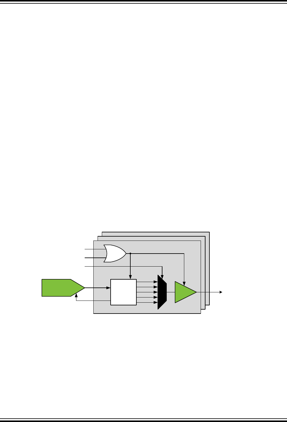
17. Voltage Reference (VREF)
17.1 Features
• Programmable voltage reference sources:
– For ADC0 peripheral
– For AC0 peripheral
• Each reference source supports different voltages:
– 0.55V
– 1.1V
– 1.5V
– 2.5V
– 4.3V
– AVDD
17.2 Overview
The Voltage Reference buffer (VREF) provides control registers for selecting between multiple internal
reference levels. The internal references are generated from the internal bandgap.
When a peripheral that requires a voltage reference is enabled the corresponding voltage reference
buffer and bandgap is automatically enabled.
17.2.1 Block Diagram
Figure 17-1. VREF Block Diagram
Reference select
Bandgap Reference
Generator
Internal
Reference
BUF
1.1V
1.5V
2.5V
4.3V
0.55V
Reference enable
Reference request
Bandgap
enable
17.3 Functional Description
17.3.1 Initialization
The output level from the reference buffer should be selected (ADC0REFSEL and AC0REFSEL in
VREF.CTRLA) before the respective modules are enabled. The reference buffer is then automatically
enabled when requested by a peripheral. Changing the reference while these modules are enabled could
lead to unpredictable behavior.
megaAVR® 0-Series
Voltage Reference (VREF)
© 2018 Microchip Technology Inc. Datasheet Preliminary DS40002015A-page 170

The VREF module and reference voltage sources can be forced to be ON, independent of being required
by a peripheral, by writing to the respective Force Enable bits (ADC0REFEN, AC0REFEN) in the Control
B register (VREF.CTRLB). This can be used to remove the reference start-up time, at the cost of
increased power consumption.
megaAVR® 0-Series
Voltage Reference (VREF)
© 2018 Microchip Technology Inc. Datasheet Preliminary DS40002015A-page 171

17.5.1 Control A
Name: CTRLA
Offset: 0x00
Reset: 0x00
Property: -
Bit 7 6 5 4 3 2 1 0
ADC0REFSEL[2:0] AC0REFSEL[2:0]
Access R/W R/W R/W R/W R/W R/W
Reset 0 0 0 0 0 0
Bits 6:4 – ADC0REFSEL[2:0] ADC0 Reference Select
These bits select the reference voltage for ADC0.
Value Name Description
0x0 0V55 0.55V
0x1 1V1 1.1V
0x2 2V5 2.5V
0x3 4V3 4.3V
0x4 1V5 1.5V
Other - Reserved
Bits 2:0 – AC0REFSEL[2:0] AC0 Reference Select
These bits select reference voltage for AC0.
Value Name Description
0x0 0V55 0.55V
0x1 1V1 1.1V
0x2 2V5 2.5V
0x3 4V3 4.3V
0x4 1V5 1.5V
0x5 - Reserved
0x6 - Reserved
0x7 AVDD AVDD
megaAVR® 0-Series
Voltage Reference (VREF)
© 2018 Microchip Technology Inc. Datasheet Preliminary DS40002015A-page 173

17.5.2 Control B
Name: CTRLB
Offset: 0x01
Reset: 0x00
Property: -
Bit 7 6 5 4 3 2 1 0
ADC0REFEN AC0REFEN
Access R/W R/W
Reset 0 0
Bit 1 – ADC0REFEN ADC0 Reference Force Enable
Writing a '1' to this bit forces the voltage reference for ADC0 to be enabled, even if it is not requested.
Writing a '0' to this bit allows to automatic enable/disable of the reference source when not requested.
Bit 0 – AC0REFEN AC0 DACREF Reference Force Enable
Writing a '1' to this bit forces the voltage reference for AC0 DACREF to be enabled, even if it is not
requested.
Writing a '0' to this bit allows to automatic enable/disable of the reference source when not requested.
megaAVR® 0-Series
Voltage Reference (VREF)
© 2018 Microchip Technology Inc. Datasheet Preliminary DS40002015A-page 174

18. Watchdog Timer (WDT)
18.1 Features
• Issues a System Reset if the Watchdog Timer is not Cleared Before its Time-out Period
• Operating Asynchronously from System Clock Using an Independent Oscillator
• Using the 1 KHz Output of the 32 KHz Ultra Low-Power Oscillator (OSCULP32K)
• 11 Selectable Time-out Periods, from 8 ms to 8s
• Two Operation modes:
– Normal mode
– Window mode
• Configuration Lock to Prevent Unwanted Changes
• Closed Period Timer Activation After First WDT Instruction for Easy Setup
18.2 Overview
The Watchdog Timer (WDT) is a system function for monitoring correct program operation. It allows the
system to recover from situations such as runaway or deadlocked code, by issuing a Reset. When
enabled, the WDT is a constantly running timer configured to a predefined time-out period. If the WDT is
not reset within the time-out period, it will issue a system Reset. The WDT is reset by executing the WDR
(Watchdog Timer Reset) instruction from software.
The WDT has two modes of operation; Normal mode and Window mode. The settings in the Control A
register (WDT.CTRLA) determine the mode of operation.
A Window mode defines a time slot or "window" inside the time-out period during which the WDT must be
reset. If the WDT is reset outside this window, either too early or too late, a system Reset will be issued.
Compared to the Normal mode, the Window mode can catch situations where a code error causes
constant WDR execution.
When enabled, the WDT will run in Active mode and all Sleep modes. It is asynchronous (i.e., running
from a CPU independent clock source). For this reason, it will continue to operate and be able to issue a
system Reset even if the main clock fails.
The CCP mechanism ensures that the WDT settings cannot be changed by accident. For increased
safety, a configuration for locking the WDT settings is available.
megaAVR® 0-Series
Watchdog Timer (WDT)
© 2018 Microchip Technology Inc. Datasheet Preliminary DS40002015A-page 175
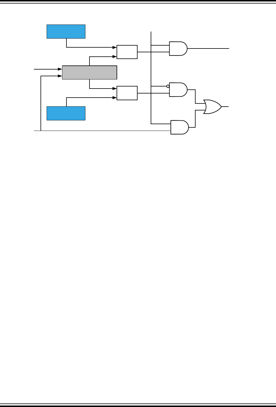
18.2.1 Block Diagram
Figure 18-1. WDT Block Diagram
COUNT
=
=
"Inside closed window"
"Enable
open window
and clear count"
CLK_WDT
WDR
(instruction)
System
Reset
CTRLA
CTRLA
WINDOW
PERIOD
18.2.2 Signal Description
Not applicable.
18.3 Functional Description
18.3.1 Initialization
• The WDT is enabled when a non-zero value is written to the Period bits (PERIOD) in the Control A
register (WDT.CTRLA).
• Optional: Write a non-zero value to the Window bits (WINDOW) in WDT.CTRLA to enable Window
mode operation.
All bits in the Control A register and the Lock bit (LOCK) in the STATUS register (WDT.STATUS) are write
protected by the Configuration Change Protection mechanism.
The Reset value of WDT.CTRLA is defined by a fuse (FUSE.WDTCFG), so the WDT can be enabled at
boot time. If this is the case, the LOCK bit in WDT.STATUS is set at boot time.
18.3.2 Clocks
A 1 KHz Oscillator Clock (CLK_WDT_OSC) is sourced from the internal Ultra Low-Power Oscillator,
OSCULP32K. Due to the ultra low-power design, the oscillator is not very accurate, and so the exact
time-out period may vary from device to device. This variation must be kept in mind when designing
software that uses the WDT to ensure that the time-out periods used are valid for all devices.
The Counter Clock CLK_WDT_OSC is asynchronous to the system clock. Due to this asynchronicity,
writing to the WDT Control register will require synchronization between the clock domains.
18.3.3 Operation
18.3.3.1 Normal Mode
In Normal mode operation, a single time-out period is set for the WDT. If the WDT is not reset from
software using the WDR any time before the time-out occurs, the WDT will issue a system Reset.
A new WDT time-out period will be started each time the WDT is reset by WDR.
megaAVR® 0-Series
Watchdog Timer (WDT)
© 2018 Microchip Technology Inc. Datasheet Preliminary DS40002015A-page 176
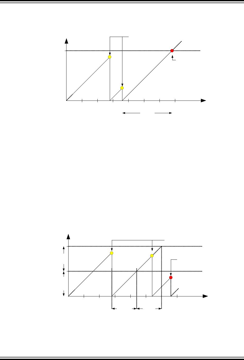
There are 11 possible WDT time-out periods (TOWDT), selectable from 8 ms to 8s by writing to the Period
bit field (PERIOD) in the Control A register (WDT.CTRLA).
Figure 18-2. Normal Mode Operation
t [ms]
WDT Count
5 10 15 20 25 30 35
Timely WDT Reset (WDR)
TOWDT
WDT Timeout
System Reset
TO WDT = 16 ms
Here:
Normal mode is enabled as long as the WINDOW bit field in the Control A register (WDT.CTRLA) is 0x0.
18.3.3.2 Window Mode
In Window mode operation, the WDT uses two different time-out periods; a closed Window Time-out
period (TOWDTW) and the normal time-out period (TOWDT):
• The closed window time-out period defines a duration from 8 ms to 8s where the WDT cannot be
reset. If the WDT is reset during this period, the WDT will issue a system Reset.
• The normal WDT time-out period, which is also 8 ms to 8s, defines the duration of the open period
during which the WDT can (and should) be reset. The open period will always follow the closed
period, so the total duration of the time-out period is the sum of the closed window and the open
window time-out periods.
When enabling Window mode or when going out of Debug mode, the first closed period is activated after
the first WDR instruction.
If a second WDR is issued while a previous WDR is being synchronized, the second one will be ignored.
Figure 18-3. Window Mode Operation
t [ms]
WDT Count
5 10 15 20 25 30 35
Timely WDT Reset (WDR)
Closed
TOWDTW
Open
TOWDT
System Reset
WDR too early:
TOWDTW =TOWDT = 8 ms
Here:
The Window mode is enabled by writing a non-zero value to the WINDOW bit field in the Control A
register (WDT.CTRLA), and disabled by writing WINDOW=0x0.
megaAVR® 0-Series
Watchdog Timer (WDT)
© 2018 Microchip Technology Inc. Datasheet Preliminary DS40002015A-page 177

18.3.3.3 Configuration Protection and Lock
The WDT provides two security mechanisms to avoid unintentional changes to the WDT settings:
The first mechanism is the Configuration Change Protection mechanism, employing a timed write
procedure for changing the WDT control registers.
The second mechanism locks the configuration by writing a '1' to the LOCK bit in the STATUS register
(WDT.STATUS). When this bit is '1', the Control A register (WDT.CTRLA) cannot be changed.
Consequently, the WDT cannot be disabled from software.
LOCK in WDT.STATUS can only be written to '1'. It can only be cleared in Debug mode.
If the WDT configuration is loaded from fuses, LOCK is automatically set in WDT.STATUS.
18.3.4 Sleep Mode Operation
The WDT will continue to operate in any sleep mode where the source clock is active.
18.3.5 Debug Operation
When run-time debugging, this peripheral will continue normal operation. Halting the CPU in Debugging
mode will halt normal operation of the peripheral.
When halting the CPU in Debug mode, the WDT counter is reset.
When starting the CPU again and the WDT is operating in Window mode, the first closed window time-
out period will be disabled, and a Normal mode time-out period is executed.
18.3.6 Synchronization
Due to asynchronicity between the main clock domain and the peripheral clock domain, the Control A
register (WDT.CTRLA) is synchronized when written. The Synchronization Busy flag (SYNCBUSY) in the
STATUS register (WDT.STATUS) indicates if there is an ongoing synchronization.
Writing to WDT.CTRLA while SYNCBUSY=1 is not allowed.
The following registers are synchronized when written:
• PERIOD bits in Control A register (WDT.CTRLA)
• Window Period bits (WINDOW) in WDT.CTRLA
The WDR instruction will need two to three cycles of the WDT clock in order to be synchronized. Issuing a
new WDR instruction while a WDR instruction is being synchronized will be ignored.
18.3.7 Configuration Change Protection
This peripheral has registers that are under Configuration Change Protection (CCP). In order to write to
these, a certain key must be written to the CPU.CCP register first, followed by a write access to the
protected bits within four CPU instructions.
It is possible to try writing to these registers at any time, but the values are not altered.
The following registers are under CCP:
Table 18-1. WDT - Registers Under Configuration Change Protection
Register Key
WDT.CTRLA IOREG
LOCK bit in WDT.STATUS IOREG
List of bits/registers protected by CCP:
megaAVR® 0-Series
Watchdog Timer (WDT)
© 2018 Microchip Technology Inc. Datasheet Preliminary DS40002015A-page 178

• Period bits in Control A register (CTRLA.PERIOD)
• Window Period bits in Control A register (CTRLA.WINDOW)
• LOCK bit in STATUS register (STATUS.LOCK)
megaAVR® 0-Series
Watchdog Timer (WDT)
© 2018 Microchip Technology Inc. Datasheet Preliminary DS40002015A-page 179


18.5.1 Control A
Name: CTRLA
Offset: 0x00
Reset: From FUSE.WDTCFG
Property: Configuration Change Protection
Bit 7 6 5 4 3 2 1 0
WINDOW[3:0] PERIOD[3:0]
Access R/W R/W R/W R/W R/W R/W R/W R/W
Reset x x x x x x x x
Bits 7:4 – WINDOW[3:0] Window
Writing a non-zero value to these bits enables the Window mode, and selects the duration of the closed
period accordingly.
The bits are optionally lock-protected:
• If LOCK bit in WDT.STATUS is '1', all bits are change-protected (Access = R)
• If LOCK bit in WDT.STATUS is '0', all bits can be changed (Access = R/W)
Value Name Description
0x0 OFF -
0x1 8CLK 0.008s
0x2 16CLK 0.016s
0x3 32CLK 0.032s
0x4 64CLK 0.064s
0x5 128CLK 0.128s
0x6 256CLK 0.256s
0x7 512CLK 0.512s
0x8 1KCLK 1.024s
0x9 2KCLK 2.048s
0xA 4KCLK 4.096s
0xB 8KCLK 8.192s
other - Reserved
Bits 3:0 – PERIOD[3:0] Period
Writing a non-zero value to this bit enables the WDT, and selects the time-out period in Normal mode
accordingly. In Window mode, these bits select the duration of the open window.
The bits are optionally lock-protected:
• If LOCK in WDT.STATUS is '1', all bits are change-protected (Access = R)
• If LOCK in WDT.STATUS is '0', all bits can be changed (Access = R/W)
Value Name Description
0x0 OFF -
0x1 8CLK 0.008s
0x2 16CLK 0.016s
0x3 32CLK 0.032s
megaAVR® 0-Series
Watchdog Timer (WDT)
© 2018 Microchip Technology Inc. Datasheet Preliminary DS40002015A-page 181

Value Name Description
0x4 64CLK 0.064s
0x5 128CLK 0.128s
0x6 256CLK 0.256s
0x7 512CLK 0.512s
0x8 1KCLK 1.0s
0x9 2KCLK 2.0s
0xA 4KCLK 4.1s
0xB 8KCLK 8.2s
other - Reserved
megaAVR® 0-Series
Watchdog Timer (WDT)
© 2018 Microchip Technology Inc. Datasheet Preliminary DS40002015A-page 182

18.5.2 Status
Name: STATUS
Offset: 0x01
Reset: 0x00
Property: Configuration Change Protection
Bit 7 6 5 4 3 2 1 0
LOCK SYNCBUSY
Access R/W R
Reset 0 0
Bit 7 – LOCK Lock
Writing this bit to '1' write-protects the WDT.CTRLA register.
It is only possible to write this bit to '1'. This bit can be cleared in Debug mode only.
If the PERIOD bits in WDT.CTRLA are different from zero after boot code, the lock will automatically be
set.
This bit is under CCP.
Bit 0 – SYNCBUSY Synchronization Busy
This bit is set after writing to the WDT.CTRLA register while the data is being synchronized from the
system clock domain to the WDT clock domain.
This bit is cleared by the system after the synchronization is finished.
This bit is not under CCP.
megaAVR® 0-Series
Watchdog Timer (WDT)
© 2018 Microchip Technology Inc. Datasheet Preliminary DS40002015A-page 183

19. 16-bit Timer/Counter Type A (TCA)
19.1 Features
• 16-Bit Timer/Counter
• Three Compare Channels
• Double Buffered Timer Period Setting
• Double Buffered Compare Channels
• Waveform Generation:
– Frequency generation
– Single-slope PWM (pulse-width modulation)
– Dual-slope PWM
• Count on Event
• Timer Overflow Interrupts/Events
• One Compare Match per Compare Channel
• Two 8-Bit Timer/Counters in Split Mode
19.2 Overview
The flexible 16-bit PWM Timer/Counter type A (TCA) provides accurate program execution timing,
frequency and waveform generation, and command execution.
A TCA consists of a base counter and a set of compare channels. The base counter can be used to count
clock cycles or events, or let events control how it counts clock cycles. It has direction control and period
setting that can be used for timing. The compare channels can be used together with the base counter to
do compare match control, frequency generation, and pulse width waveform modulation.
Depending on the mode of operation, the counter is cleared, reloaded, incremented, or decremented at
each timer/counter clock or event input.
A timer/counter can be clocked and timed from the peripheral clock with optional prescaling or from the
event system. The event system can also be used for direction control or to synchronize operations.
By default, the TCA is a 16-bit timer/counter. The timer/counter has a Split mode feature that splits it into
two 8-bit timer/counters with three compare channels each.
A block diagram of the 16-bit timer/counter with closely related peripheral modules (in grey) is shown in
the figure below.
megaAVR® 0-Series
16-bit Timer/Counter Type A (TCA)
© 2018 Microchip Technology Inc. Datasheet Preliminary DS40002015A-page 184
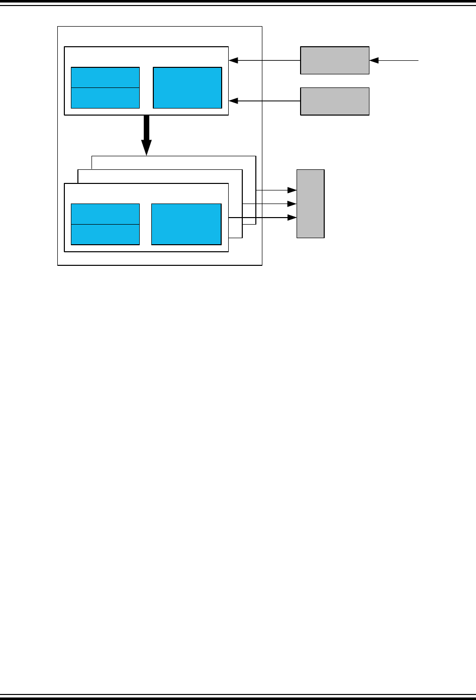
Figure 19-1. 16-bit Timer/Counter and Closely Related Peripherals
Counter
Control Logic
Timer Period
Timer/Counter
Base Counter Prescaler
Event
System
CLK_PER
PORTS
Comparator
Buffer
Compare Channel 2
Compare Channel 1
Compare Channel 0
Waveform
Generation
19.2.1 Block Diagram
The figure below shows a detailed block diagram of the timer/counter.
megaAVR® 0-Series
16-bit Timer/Counter Type A (TCA)
© 2018 Microchip Technology Inc. Datasheet Preliminary DS40002015A-page 185

Figure 19-2. Timer/Counter Block Diagram
Base Coun ter
Compare
(Unit x = {A,B,C})
Counter
=
CMPn
CMPnBUF
Waveform
Generation
BV
=
PERB
PER
CNT
BV
= 0
"count"
"clear"
"direction"
"load" Control Logi c
EVCTRL
CTRLA
OVF/UNF
(INT Req.)
TOP
"match" CMPn
(INT Req.)
Control Logi c
Clock Select
"ev"
UPDATE
BOTTOM
WOn Out
Event
Select
The counter register (TCAn.CNT), period registers with buffer (TCAn.PER and TCAn.PERBUF), and
compare registers with buffers (TCAn.CMPx and TCAn.CMPBUFx) are 16-bit registers. All buffer
registers have a buffer valid (BV) flag that indicates when the buffer contains a new value.
During normal operation, the counter value is continuously compared to zero and the period (PER) value
to determine whether the counter has reached TOP or BOTTOM.
The counter value is also compared to the TCAn.CMPx registers. These comparisons can be used to
generate interrupt requests. The Waveform Generator modes use these comparisons to set the waveform
period or pulse width.
A prescaled peripheral clock and events from the event system can be used to control the counter.
megaAVR® 0-Series
16-bit Timer/Counter Type A (TCA)
© 2018 Microchip Technology Inc. Datasheet Preliminary DS40002015A-page 186

Figure 19-3. Timer/Counter Clock Logic
CKSEL
CNTEI
CLK_PER
event
Event SystemPrescaler
CNT
(Encoding)
EVACT
CLK_TCA
19.2.2 Signal Description
Signal Description Type
WOn Digital output Waveform output
19.3 Functional Description
19.3.1 Definitions
The following definitions are used throughout the documentation:
Table 19-1. Timer/Counter Definitions
Name Description
BOTTOM The counter reaches BOTTOM when it becomes zero.
MAX The counter reaches MAXimum when it becomes all ones.
TOP The counter reaches TOP when it becomes equal to the highest value in the count
sequence.
UPDATE The update condition is met when the timer/counter reaches BOTTOM or TOP, depending on
the Waveform Generator mode.
CNT Counter register value.
CMP Compare register value.
In general, the term timer is used when the timer/counter is counting periodic clock ticks. The term
counter is used when the input signal has sporadic or irregular ticks.
19.3.2 Initialization
To start using the timer/counter in a basic mode, follow these steps:
• Write a TOP value to the Period register (TCAn.PER)
• Enable the peripheral by writing a '1' to the ENABLE bit in the Control A register (TCAn.CTRLA).
megaAVR® 0-Series
16-bit Timer/Counter Type A (TCA)
© 2018 Microchip Technology Inc. Datasheet Preliminary DS40002015A-page 187
The counter will start counting clock ticks according to the prescaler setting in the Clock Select bit
field (CLKSEL) in TCAn.CTRLA.
• Optional: By writing a '1' to the Enable Count on Event Input bit (CNTEI) in the Event Control
register (TCAn.EVCTRL), event inputs are counted instead of clock ticks.
• The counter value can be read from the Counter bit field (CNT) in the Counter register
(TCAn.CNT).
19.3.3 Operation
19.3.3.1 Normal Operation
In normal operation, the counter is counting clock ticks in the direction selected by the Direction bit (DIR)
in the Control E register (TCAn.CTRLE), until it reaches TOP or BOTTOM. The clock ticks are from the
peripheral clock CLK_PER, optionally prescaled, depending on the Clock Select bit field (CLKSEL) in the
Control A register (TCAn.CTRLA).
When up-counting and TOP are reached, the counter will wrap to zero at the next clock tick. When down-
counting, the counter is reloaded with the Period register value (TCAn.PER) when BOTTOM is reached.
Figure 19-4. Normal Operation
CNT written
"update"
CNT
DIR
MAX
TOP
BOTTOM
It is possible to change the counter value in the Counter register (TCAn.CNT) when the counter is
running. The write access to TCAn.CNT has higher priority than count, clear, or reload, and will be
immediate. The direction of the counter can also be changed during normal operation by writing to DIR in
TCAn.CTRLE.
19.3.3.2 Double Buffering
The Period register value (TCAn.PER) and the Compare n register values (TCAn.CMPn) are all double
buffered (TCAn.PERBUF and TCAn.CMPnBUF).
Each buffer register has a Buffer Valid flag (PERBV, CMPnBV) in the Control F register (TCAn.CTRLF),
which indicates that the buffer register contains a valid, i.e. new, value that can be copied into the
corresponding Period or Compare register. When the Period register and Compare n registers are used
for a compare operation, the BV flag is set when data is written to the buffer register and cleared on an
UPDATE condition. This is shown for a Compare register (CMPn) below.
megaAVR® 0-Series
16-bit Timer/Counter Type A (TCA)
© 2018 Microchip Technology Inc. Datasheet Preliminary DS40002015A-page 188
Figure 19-5. Period and Compare Double Buffering
UPDATE
"write enable" "data write"
CNT
"match"
EN
EN
CMPnBUF
CMPn
BV
=
Both the TCAn.CMPn and TCAn.CMPnBUF registers are available as I/O registers. This allows
initialization and bypassing of the buffer register and the double buffering function.
19.3.3.3 Changing the Period
The Counter period is changed by writing a new TOP value to the Period register (TCAn.PER).
No Buffering: If double buffering is not used, any period update is immediate.
Figure 19-6. Changing the Period Without Buffering
CNT
MAX
BOTTOM
Counter wraparound
"update"
"write"
New TOP written to
PER that is higher
than current CNT.
New TOP written to
PER that is lower
than current CNT.
A counter wraparound can occur in any mode of operation when up-counting without buffering. This is
due to the fact that the TCAn.CNT and TCAn.PER registers are continuously compared: if a new TOP
value is written to TCAn.PER that is lower than current TCAn.CNT, the counter will wrap first, before a
compare match happens.
Figure 19-7. Unbuffered Dual-Slope Operation
Counter wraparound
"update"
"write"
MAX
BOTTOM
CNT
New TOP written to
PER that is higher
than current CNT.
New TOP written to
PER that is lower
than current CNT.
megaAVR® 0-Series
16-bit Timer/Counter Type A (TCA)
© 2018 Microchip Technology Inc. Datasheet Preliminary DS40002015A-page 189

With Buffering: When double buffering is used, the buffer can be written at any time and still maintain
correct operation. The TCAn.PER is always updated on the UPDATE condition, as shown for dual-slope
operation in the figure below. This prevents wraparound and the generation of odd waveforms.
Figure 19-8. Changing the Period Using Buffering
CNT
BOTTOM
MAX
"update"
"write"
New Period written to
PERB that is higher
than current CNT.
New Period written to
PERB that is lower
than current CNT.
New PER is updated
with PERB value.
19.3.3.4 Compare Channel
Each Compare Channel n continuously compares the counter value (TCAn.CNT) with the Compare n
register (TCAn.CMPn). If TCAn.CNT equals TCAn.CMPn, the comparator n signals a match. The match
will set the Compare Channel's interrupt flag at the next timer clock cycle, and the optional interrupt is
generated.
The Compare n Buffer register (TCAn.CMPnBUF) provides double buffer capability equivalent to that for
the period buffer. The double buffering synchronizes the update of the TCAn.CMPn register with the
buffer value to either the TOP or BOTTOM of the counting sequence, according to the UPDATE condition.
The synchronization prevents the occurrence of odd-length, non-symmetrical pulses for glitch-free output.
Waveform Generation
The compare channels can be used for waveform generation on the corresponding port pins. To make
the waveform visible on the connected port pin, the following requirements must be met:
1. A Waveform Generation mode must be selected by writing the WGMODE bit field in TCAn.CTRLB.
2. The TCA is counting clock ticks, not events (CNTEI=0 in TCAn.EVCTRL).
3. The compare channels used must be enabled (CMPnEN=1 in TCAn.CTRLB). This will override the
corresponding port pin output register. An alternative pin can be selected by writing to the
respective TCA Waveform Output n bit (TCA0n) in the Control C register of the Port Multiplexer
(PORTMUX.CTRLC).
4. The direction for the associated port pin n must be configured as an output (PORTx.DIR[n]=1).
5. Optional: Enable inverted waveform output for the associated port pin n (INVEN=1 in PORTx.PINn).
Frequency (FRQ) Waveform Generation
For frequency generation, the period time (T) is controlled by a TCAn.CMPn register instead of the Period
register (TCAn.PER). The waveform generation output WG is toggled on each compare match between
the TCAn.CNT and TCAn.CMPn registers.
megaAVR® 0-Series
16-bit Timer/Counter Type A (TCA)
© 2018 Microchip Technology Inc. Datasheet Preliminary DS40002015A-page 190
Figure 19-9. Frequency Waveform Generation
CNT
WG Output
MAX
TOP
BOTTOM
Period (T) Direction change CNT written
"update"
The waveform frequency (fFRQ) is defined by the following equation:
FRQ =fCLK_PER
2CMPn+1
where N represents the prescaler divider used (CLKSEL in TCAn.CTRLA), and fCLK_PER is the system
clock for the peripherals.
The maximum frequency of the waveform generated is half of the peripheral clock frequency (fCLK_PER/2)
when TCAn.CMPn is written to zero (0x0000) and no prescaling is used (N=1, CLKSEL=0x0 in
TCAn.CTRLA).
Single-Slope PWM Generation
For single-slope Pulse-Width Modulation (PWM) generation, the period (T) is controlled by TCAn.PER,
while the values of TCAn.CMPn control the duty-cycle of the WG output. The figure below shows how the
counter counts from BOTTOM to TOP and then restarts from BOTTOM. The waveform generator (WO)
output is set at TOP and cleared on the compare match between the TCAn.CNT and TCAn.CMPn
registers.
Figure 19-10. Single-Slope Pulse-Width Modulation
CNT
Output WOn
MAX
TOP
CMPn
BOTTOM
Period (T) CMPn=BOTTOM CMPn=TOP "update"
"match"
The TCAn.PER register defines the PWM resolution. The minimum resolution is 2 bits
(TCA.PER=0x0003), and the maximum resolution is 16 bits (TCA.PER=MAX).
The following equation calculates the exact resolution for single-slope PWM (RPWM_SS):
PWM_SS =log PER+1
log 2
The single-slope PWM frequency (fPWM_SS) depends on the period setting (TCA_PER), the system's
peripheral clock frequency fCLK_PER, and the TCA prescaler (CLKSEL in TCAn.CTRLA). It is calculated by
the following equation where N represents the prescaler divider used:
megaAVR® 0-Series
16-bit Timer/Counter Type A (TCA)
© 2018 Microchip Technology Inc. Datasheet Preliminary DS40002015A-page 191
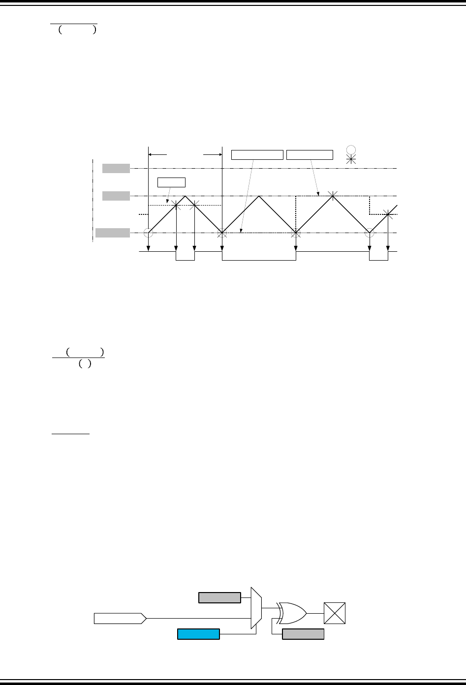
PWM_SS =CLK_PER
PER+1
Dual-Slope PWM
For dual-slope PWM generation, the period (T) is controlled by TCAn.PER, while the values of
TCAn.CMPn control the duty-cycle of the WG output.
The figure below shows how for dual-slope PWM the counter counts repeatedly from BOTTOM to TOP
and then from TOP to BOTTOM. The waveform generator output is set on BOTTOM, cleared on compare
match when up-counting, and set on compare match when down-counting.
Figure 19-11. Dual-Slope Pulse-Width Modulation
MAX
TOP
BOTTOM
CNT
Waveform Output WOn
Period (T) CMPn=BOTTOM CMPn=TOP "update"
"match"
CMPn
Using dual-slope PWM results in a lower maximum operation frequency compared to the single-slope
PWM operation.
The period register (TCAn.PER) defines the PWM resolution. The minimum resolution is 2 bits
(TCAn.PER=0x0003), and the maximum resolution is 16 bits (TCAn.PER=MAX).
The following equation calculates the exact resolution for dual-slope PWM (RPWM_DS):
PWM_DS =log PER+1
log 2
The PWM frequency depends on the period setting (TCAn.PER), the peripheral clock frequency
(fCLK_PER), and the prescaler divider used (CLKSEL in TCAn.CTRLA). It is calculated by the following
equation:
PWM_DS =CLK_PER
2 PER
N represents the prescaler divider used.
Port Override for Waveform Generation
To make the waveform generation available on the port pins, the corresponding port pin direction must be
set as output (PORTx.DIR[n]=1). The TCA will override the port pin values when the compare channel is
enabled (CMPnEN=1 in TCAn.CTRLB) and a Waveform Generation mode is selected.
The figure below shows the port override for TCA. The timer/counter compare channel will override the
port pin output value (OUT) on the corresponding port pin. Enabling inverted I/O on the port pin
(INVEN=1 in PORT.PINn) inverts the corresponding WG output.
Figure 19-12. Port Override for Timer/Counter Type A
Waveform
OUT
CMPnEN INVEN
WOn
megaAVR® 0-Series
16-bit Timer/Counter Type A (TCA)
© 2018 Microchip Technology Inc. Datasheet Preliminary DS40002015A-page 192

19.3.3.5 Timer/Counter Commands
A set of commands can be issued by software to immediately change the state of the peripheral. These
commands give direct control of the UPDATE, RESTART, and RESET signals. A command is issued by
writing the respective value to the Command bit field (CMD) in the Control E register (TCAn.CTRLESET).
An Update command has the same effect as when an update condition occurs, except that the Update
command is not affected by the state of the Lock Update bit (LUPD) in the Control E register
(TCAn.CTRLE).
The software can force a restart of the current waveform period by issuing a Restart command. In this
case, the counter, direction, and all compare outputs are set to zero.
A Reset command will set all timer/counter registers to their initial values. A Reset can be issued only
when the timer/counter is not running (ENABLE=0 in TCAn.CTRLA).
19.3.3.6 Split Mode - Two 8-Bit Timer/Counters
Split Mode Overview
To double the number of timers and PWM channels in the TCA, a Split mode is provided. In this Split
mode, the 16-bit timer/counter acts as two separate 8-bit timers, which each have three compare
channels for PWM generation. The Split mode will only work with single-slope down-count. Split mode
does not support event action controlled operation.
Split Mode Differences to Normal Mode
• Count:
– Down-count only
– Timer/counter Counter high byte and Counter low byte are independent (TCAn.LCNT,
TCAn.HCNT)
• Waveform Generation:
– Single-slope PWM only (WGMODE=SINGLESLOPE in TCAn.CTRLB)
• Interrupt:
– No change for low byte Timer/Counter (TCAn.LCNT)
– Underflow interrupt for high byte Timer/Counter (TCAn.HCNT)
– No compare interrupt or flag for High-byte Compare n registers (TCAn.HCMPn)
• Event Actions: Not Compatible
• Buffer registers and Buffer Valid Flags: Unused
• Register Access: Byte Access to all registers
• Temp register: Unused, 16-bit register of the Normal mode are Accessed as 8-bit 'TCA_H' and
'TCA_L', Respectively
megaAVR® 0-Series
16-bit Timer/Counter Type A (TCA)
© 2018 Microchip Technology Inc. Datasheet Preliminary DS40002015A-page 193
Block Diagram
Figure 19-13. Timer/Counter Block Diagram Split Mode
Base Counter
Compare
(Unit n = {0,1,2})
Counter
= 0
Control Logic
HUNF
(INT Req.)
BOTTOML
Compare
(Unit n = {0,1,2})
Waveform
Generation
LCMPn
(INT Req.)
WOn Out
=
"match"
BOTTOMH
"count low"
"load low"
=
Waveform
Generation
"match"
WO[n+3] Out
= 0
"count high"
"load high"
Clock Select
LUNF
(INT Req.)
HPER CTRLALPER
LCMPn
LCNTHCNT
HCMPn
Split Mode Initialization
When shifting between Normal mode and Split mode, the functionality of some registers and bits
changes, but their values do not. For this reason, disabling the peripheral (ENABLE=0 in TCAn.CTRLA)
and doing a hard Reset (CMD=RESET in TCAn.CTRLESET) is recommended when changing the mode
to avoid unexpected behavior.
To start using the timer/counter in basic Split mode after a hard Reset, follow these steps:
• Enable Split mode by writing a '1' to the Split mode enable bit in the Control D register (SPLITM in
TCAn.CTRLD)
• Write a TOP value to the Period registers (TCAn.PER)
• Enable the peripheral by writing a '1' to the ENABLE bit in the Control A register (TCAn.CTRLA).
The counter will start counting clock ticks according to the prescaler setting in the Clock Select bit
field (CLKSEL) in TCAn.CTRLA.
• The counter values can be read from the Counter bit field in the Counter registers (TCAn.CNT)
Activating Split mode results in changes to the functionality of some registers and register bits. The
modifications are described in a separate register map.
megaAVR® 0-Series
16-bit Timer/Counter Type A (TCA)
© 2018 Microchip Technology Inc. Datasheet Preliminary DS40002015A-page 194

19.3.4 Events
The TCA is an event generator. The following events will generate a one-cycle strobe on the event
channel outputs:
• Timer overflow
• Timer underflow in Split mode
• Compare match channel 0
• Compare match channel 1
• Compare match channel 2
The peripheral can take the following actions on an input event:
• The counter counts positive edges of the event signal.
• The counter counts both positive and negative edges of the event signal.
• The counter counts prescaled clock cycles as long as the event signal is high.
• The counter counts prescaled clock cycles. The event signal controls the direction of counting. Up-
counting when the event signal is low and down-counting when the event signal is high.
The specific action is selected by writing to the Event Action bits (EVACT) in the Event Control register
(TCAn.EVCTRL). Events as input are enabled by writing a '1' to the Enable Count on Event Input bit
(CNTEI in TCAn.EVCTRL).
Event-controlled inputs are not used in Split mode.
19.3.5 Interrupts
Table 19-2. Available Interrupt Vectors and Sources in Normal Mode
Name Vector Description Conditions
OVF Overflow and Compare match
interrupt
The counter has reached its top value and wrapped to
zero.
CMP0 Compare channel 0 interrupt Match between the counter value and the Compare 0
register.
CMP1 Compare channel 1 interrupt Match between the counter value and the Compare 1
register.
CMP2 Compare channel 2 interrupt Match between the counter value and the Compare 2
register.
Table 19-3. Available Interrupt Vectors and Sources in Split Mode
Name Vector Description Conditions
LUNF Low-byte Underflow interrupt Low-byte timer reaches BOTTOM.
HUNF High-byte Underflow interrupt High-byte timer reaches BOTTOM.
LCMP0 Compare channel 0 interrupt Match between the counter value and the low-byte of Compare
0 register.
megaAVR® 0-Series
16-bit Timer/Counter Type A (TCA)
© 2018 Microchip Technology Inc. Datasheet Preliminary DS40002015A-page 195

Name Vector Description Conditions
LCMP1 Compare channel 1 interrupt Match between the counter value and the low-byte of Compare
1 register.
LCMP2 Compare channel 2 interrupt Match between the counter value and the low-byte of the
Compare 2 register.
When an interrupt condition occurs, the corresponding interrupt flag is set in the Interrupt Flags register of
the peripheral (peripheral.INTFLAGS).
An interrupt source is enabled or disabled by writing to the corresponding enable bit in the peripheral's
Interrupt Control register (peripheral.INTCTRL).
An interrupt request is generated when the corresponding interrupt source is enabled and the interrupt
flag is set. The interrupt request remains active until the interrupt flag is cleared. See the peripheral's
INTFLAGS register for details on how to clear interrupt flags.
19.4 Sleep Mode Operation
The timer/counter will continue operation in Idle Sleep mode.
megaAVR® 0-Series
16-bit Timer/Counter Type A (TCA)
© 2018 Microchip Technology Inc. Datasheet Preliminary DS40002015A-page 196

19.5 Register Summary - TCAn in Normal Mode (SPLITM in TCAn.CTRLD=0)
Offset Name Bit Pos.
0x00 CTRLA 7:0 CLKSEL[2:0] ENABLE
0x01 CTRLB 7:0 CMP2EN CMP1EN CMP0EN ALUPD WGMODE[2:0]
0x02 CTRLC 7:0 CMP2OV CMP1OV CMP0OV
0x03 CTRLD 7:0 SPLITM
0x04 CTRLECLR 7:0 CMD[1:0] LUPD DIR
0x05 CTRLESET 7:0 CMD[1:0] LUPD DIR
0x06 CTRLFCLR 7:0 CMP2BV CMP1BV CMP0BV PERBV
0x07 CTRLFSET 7:0 CMP2BV CMP1BV CMP0BV PERBV
0x08 Reserved
0x09 EVCTRL 7:0 EVACT[1:0] CNTEI
0x0A INTCTRL 7:0 CMP2 CMP1 CMP0 OVF
0x0B INTFLAGS 7:0 CMP2 CMP1 CMP0 OVF
0x0C
...
0x0D
Reserved
0x0E DBGCTRL 7:0 DBGRUN
0x0F TEMP 7:0 TEMP[7:0]
0x10
...
0x1F
Reserved
0x20 CNT
7:0 CNT[7:0]
15:8 CNT[15:8]
0x22
...
0x25
Reserved
0x26 PER
7:0 PER[7:0]
15:8 PER[15:8]
0x28 CMP0
7:0 CMP[7:0]
15:8 CMP[15:8]
0x2A CMP1
7:0 CMP[7:0]
15:8 CMP[15:8]
0x2C CMP2
7:0 CMP[7:0]
15:8 CMP[15:8]
0x2E
...
0x35
Reserved
0x36 PERBUF
7:0 PERBUF[7:0]
15:8 PERBUF[15:8]
0x38 CMP0nBUF
7:0 CMPBUF[7:0]
15:8 CMPBUF[15:8]
0x3A CMP1nBUF
7:0 CMPBUF[7:0]
15:8 CMPBUF[15:8]
0x3C CMP2nBUF
7:0 CMPBUF[7:0]
15:8 CMPBUF[15:8]
megaAVR® 0-Series
16-bit Timer/Counter Type A (TCA)
© 2018 Microchip Technology Inc. Datasheet Preliminary DS40002015A-page 197

19.6 Register Description - Normal Mode
megaAVR® 0-Series
16-bit Timer/Counter Type A (TCA)
© 2018 Microchip Technology Inc. Datasheet Preliminary DS40002015A-page 198
19.6.1 Control A
Name: CTRLA
Offset: 0x00
Reset: 0x00
Property: -
Bit 7 6 5 4 3 2 1 0
CLKSEL[2:0] ENABLE
Access R/W R/W R/W R/W
Reset 0 0 0 0
Bits 3:1 – CLKSEL[2:0] Clock Select
These bits select the clock frequency for the timer/counter.
Value Name Description
0x0 DIV1 fTCA = fCLK_PER/1
0x1 DIV2 fTCA = fCLK_PER/2
0x2 DIV4 fTCA = fCLK_PER/4
0x3 DIV8 fTCA = fCLK_PER/8
0x4 DIV16 fTCA = fCLK_PER/16
0x5 DIV64 fTCA = fCLK_PER/64
0x6 DIV256 fTCA = fCLK_PER/256
0x7 DIV1024 fTCA = fCLK_PER/1024
Bit 0 – ENABLE Enable
Value Description
0 The peripheral is disabled
1 The peripheral is enabled
megaAVR® 0-Series
16-bit Timer/Counter Type A (TCA)
© 2018 Microchip Technology Inc. Datasheet Preliminary DS40002015A-page 199

19.6.2 Control B - Normal Mode
Name: CTRLB
Offset: 0x01
Reset: 0x00
Property: -
Bit 7 6 5 4 3 2 1 0
CMP2EN CMP1EN CMP0EN ALUPD WGMODE[2:0]
Access R/W R/W R/W R/W R/W R/W R/W
Reset 0 0 0 0 0 0 0
Bits 4, 5, 6 – CMPEN Compare n Enable
In the FRQ or PWM Waveform Generation mode, these bits will override the PORT output register for the
corresponding pin.
Value Description
0 Port output settings for the pin with WOn output respected
1 Port output settings for pin with WOn output overridden in FRQ or PWM Waveform
Generation mode
Bit 3 – ALUPD Auto-Lock Update
The Auto-Lock Update feature controls the Lock Update (LUPD) bit in the TCAn.CTRLE register. When
ALUPD is written to ‘1’, LUPD will be set to ‘1’ until the Buffer Valid (CMPnBV) bits of all enabled compare
channels are ‘1’. This condition will clear LUPD.
It will remain cleared until the next UPDATE condition, where the buffer values will be transferred to the
CMPn registers and LUPD will be set to ‘1’ again. This makes sure that CMPnBUF register values are not
transferred to the CMPn registers until all enabled compare buffers are written.
Value Description
0 LUPD in TCA.CTRLE not altered by system
1 LUPD in TCA.CTRLE set and cleared automatically
Bits 2:0 – WGMODE[2:0] Waveform Generation Mode
These bits select the Waveform Generation mode and control the counting sequence of the counter, TOP
value, UPDATE condition, interrupt condition, and type of waveform that is generated.
No waveform generation is performed in the Normal mode of operation. For all other modes, the result
from the waveform generator will only be directed to the port pins if the corresponding CMPnEN bit has
been set to enable this. The port pin direction must be set as output.
Table 19-4. Timer Waveform Generation Mode
WGMODE[2:0] Group Configuration Mode of Operation Top Update OVF
000 NORMAL Normal PER TOP TOP
001 FRQ Frequency CMP0 TOP TOP
010 - Reserved - - -
011 SINGLESLOPE Single-slope PWM PER BOTTOM BOTTOM
megaAVR® 0-Series
16-bit Timer/Counter Type A (TCA)
© 2018 Microchip Technology Inc. Datasheet Preliminary DS40002015A-page 200

WGMODE[2:0] Group Configuration Mode of Operation Top Update OVF
100 - Reserved - - -
101 DSTOP Dual-slope PWM PER BOTTOM TOP
110 DSBOTH Dual-slope PWM PER BOTTOM TOP and BOTTOM
111 DSBOTTOM Dual-slope PWM PER BOTTOM BOTTOM
Value Name Description
0x0 NORMAL Normal operation mode
0x1 FRQ Frequency mode
0x3 SINGLESLOPE Single-slope PWM mode
0x5 DSTOP Dual-slope PWM mode
0x6 DSBOTH Dual-slope PWM mode
0x7 DSBOTTOM Dual-slope PWM mode
Other - Reserved
megaAVR® 0-Series
16-bit Timer/Counter Type A (TCA)
© 2018 Microchip Technology Inc. Datasheet Preliminary DS40002015A-page 201

19.6.3 Control C - Normal Mode
Name: CTRLC
Offset: 0x02
Reset: 0x00
Property: -
Bit 7 6 5 4 3 2 1 0
CMP2OV CMP1OV CMP0OV
Access R/W R/W R/W
Reset 0 0 0
Bit 2 – CMP2OV Compare Output Value 2
See CMP0OV.
Bit 1 – CMP1OV Compare Output Value 1
See CMP0OV.
Bit 0 – CMP0OV Compare Output Value 0
The CMPnOV bits allow direct access to the waveform generator's output compare value when the timer/
counter is not enabled. This is used to set or clear the WG output value when the timer/counter is not
running.
megaAVR® 0-Series
16-bit Timer/Counter Type A (TCA)
© 2018 Microchip Technology Inc. Datasheet Preliminary DS40002015A-page 202

19.6.4 Control D
Name: CTRLD
Offset: 0x03
Reset: 0x00
Property: -
Bit 7 6 5 4 3 2 1 0
SPLITM
Access R/W
Reset 0
Bit 0 – SPLITM Enable Split Mode
This bit sets the timer/counter in Split mode operation. It will then work as two 8-bit timer/counters. The
register map will change compared to normal 16-bit mode.
megaAVR® 0-Series
16-bit Timer/Counter Type A (TCA)
© 2018 Microchip Technology Inc. Datasheet Preliminary DS40002015A-page 203

19.6.5 Control Register E Clear - Normal Mode
Name: CTRLECLR
Offset: 0x04
Reset: 0x00
Property: -
The individual Status bit can be cleared by writing a one to its bit location. This allows each bit to be
cleared without the use of a read-modify-write operation on a single register.
Each Status bit can be read out either by reading TCAn.CTRLESET or TCAn.CTRLECLR.
Bit 7 6 5 4 3 2 1 0
CMD[1:0] LUPD DIR
Access R/W R/W R/W R/W
Reset 0 0 0 0
Bits 3:2 – CMD[1:0] Command
These bits are used for software control of update, restart, and reset of the timer/counter. The command
bits are always read as zero.
Value Name Description
0x0 NONE No command
0x1 UPDATE Force update
0x2 RESTART Force restart
0x3 RESET Force hard Reset (ignored if TC is enabled)
Bit 1 – LUPD Lock Update
Lock update can be used to ensure that all buffers are valid before an update is performed.
Value Description
0 The buffered registers are updated as soon as an UPDATE condition has occurred.
1 No update of the buffered registers is performed, even though an UPDATE condition has
occurred.
Bit 0 – DIR Counter Direction
Normally this bit is controlled in hardware by the Waveform Generation mode or by event actions, but this
bit can also be changed from software.
Value Description
0 The counter is counting up (incrementing)
1 The counter is counting down (decrementing)
megaAVR® 0-Series
16-bit Timer/Counter Type A (TCA)
© 2018 Microchip Technology Inc. Datasheet Preliminary DS40002015A-page 204

19.6.6 Control Register E Set - Normal Mode
Name: CTRLESET
Offset: 0x05
Reset: 0x00
Property: -
The individual Status bit can be set by writing a '1' to its bit location. This allows each bit to be set without
the use of a read-modify-write operation on a single register.
Each Status bit can be read out either by reading TCAn.CTRLESET or TCAn.CTRLECLR.
Bit 7 6 5 4 3 2 1 0
CMD[1:0] LUPD DIR
Access R/W R/W R/W R/W
Reset 0 0 0 0
Bits 3:2 – CMD[1:0] Command
These bits are used for software control of update, restart, and reset the timer/counter. The command bits
are always read as zero.
Value Name Description
0x0 NONE No command
0x1 UPDATE Force update
0x2 RESTART Force restart
0x3 RESET Force hard Reset (ignored if TC is enabled)
Bit 1 – LUPD Lock Update
Locking the update ensures that all buffers are valid before an update is performed.
Value Description
0 The buffered registers are updated as soon as an UPDATE condition has occurred.
1 No update of the buffered registers is performed, even though an UPDATE condition has
occurred.
Bit 0 – DIR Counter Direction
Normally this bit is controlled in hardware by the Waveform Generation mode or by event actions, but this
bit can also be changed from software.
Value Description
0 The counter is counting up (incrementing)
1 The counter is counting down (decrementing)
megaAVR® 0-Series
16-bit Timer/Counter Type A (TCA)
© 2018 Microchip Technology Inc. Datasheet Preliminary DS40002015A-page 205

19.6.7 Control Register F Clear
Name: CTRLFCLR
Offset: 0x06
Reset: 0x00
Property: -
The individual Status bit can be cleared by writing a '1' to its bit location. This allows each bit to be
cleared without the use of a read-modify-write operation on a single register.
Bit 7 6 5 4 3 2 1 0
CMP2BV CMP1BV CMP0BV PERBV
Access R/W R/W R/W R/W
Reset 0 0 0 0
Bit 3 – CMP2BV Compare 2 Buffer Valid
See CMP0BV.
Bit 2 – CMP1BV Compare 1 Buffer Valid
See CMP0BV.
Bit 1 – CMP0BV Compare 0 Buffer Valid
The CMPnBV bits are set when a new value is written to the corresponding TCAn.CMPnBUF register.
These bits are automatically cleared on an UPDATE condition.
Bit 0 – PERBV Period Buffer Valid
This bit is set when a new value is written to the TCAn.PERBUF register. This bit is automatically cleared
on an UPDATE condition.
megaAVR® 0-Series
16-bit Timer/Counter Type A (TCA)
© 2018 Microchip Technology Inc. Datasheet Preliminary DS40002015A-page 206

19.6.8 Control Register F Set
Name: CTRLFSET
Offset: 0x07
Reset: 0x00
Property: -
The individual status bit can be set by writing a one to its bit location. This allows each bit to be set
without the use of a read-modify-write operation on a single register.
Bit 7 6 5 4 3 2 1 0
CMP2BV CMP1BV CMP0BV PERBV
Access R/W R/W R/W R/W
Reset 0 0 0 0
Bit 3 – CMP2BV Compare 2 Buffer Valid
See CMP0BV.
Bit 2 – CMP1BV Compare 1 Buffer Valid
See CMP0BV.
Bit 1 – CMP0BV Compare 0 Buffer Valid
The CMPnBV bits are set when a new value is written to the corresponding TCAn.CMPnBUF register.
These bits are automatically cleared on an UPDATE condition.
Bit 0 – PERBV Period Buffer Valid
This bit is set when a new value is written to the TCAn.PERBUF register. This bit is automatically cleared
on an UPDATE condition.
megaAVR® 0-Series
16-bit Timer/Counter Type A (TCA)
© 2018 Microchip Technology Inc. Datasheet Preliminary DS40002015A-page 207

19.6.9 Event Control
Name: EVCTRL
Offset: 0x09
Reset: 0x00
Property: -
Bit 7 6 5 4 3 2 1 0
EVACT[1:0] CNTEI
Access R/W R/W R/W
Reset 0 0 0
Bits 2:1 – EVACT[1:0] Event Action
These bits define what type of event action the counter will increment or decrement.
Value Name Description
0x0 EVACT_POSEDGE Count on positive edge event
0x1 EVACT_ANYEDGE Count on any edge event
0x2 EVACT_HIGHLVL Count on prescaled clock while event line is 1.
0x3 EVACT_UPDOWN Count on prescaled clock. The Event controls the count direction. Up-
counting when the event line is 0, down-counting when the event line is
1.
Bit 0 – CNTEI Enable Count on Event Input
Value Description
0 Counting on Event input is disabled
1 Counting on Event input is enabled according to EVACT bit field
megaAVR® 0-Series
16-bit Timer/Counter Type A (TCA)
© 2018 Microchip Technology Inc. Datasheet Preliminary DS40002015A-page 208

19.6.10 Interrupt Control Register - Normal Mode
Name: INTCTRL
Offset: 0x0A
Reset: 0x00
Property: -
Bit 7 6 5 4 3 2 1 0
CMP2 CMP1 CMP0 OVF
Access R/W R/W R/W R/W
Reset 0 0 0 0
Bit 6 – CMP2 Compare Channel 2 Interrupt Enable
See CMP0.
Bit 5 – CMP1 Compare Channel 1 Interrupt Enable
See CMP0.
Bit 4 – CMP0 Compare Channel 0 Interrupt Enable
Writing CMPn bit to '1' enables compare interrupt from channel n.
Bit 0 – OVF Timer Overflow/Underflow Interrupt Enable
Writing OVF bit to '1' enables overflow interrupt.
megaAVR® 0-Series
16-bit Timer/Counter Type A (TCA)
© 2018 Microchip Technology Inc. Datasheet Preliminary DS40002015A-page 209

19.6.11 Interrupt Flag Register - Normal Mode
Name: INTFLAGS
Offset: 0x0B
Reset: 0x00
Property: -
The individual Status bit can be cleared by writing a '1' to its bit location. This allows each bit to be set
without the use of a read-modify-write operation on a single register.
Bit 7 6 5 4 3 2 1 0
CMP2 CMP1 CMP0 OVF
Access R/W R/W R/W R/W
Reset 0 0 0 0
Bit 6 – CMP2 Compare Channel 2 Interrupt Flag
See CMP0 flag description.
Bit 5 – CMP1 Compare Channel 1 Interrupt Flag
See CMP0 flag description.
Bit 4 – CMP0 Compare Channel 0 Interrupt Flag
The Compare Interrupt flag (CMPn) is set on a compare match on the corresponding compare channel.
For all modes of operation, the CMPn flag will be set when a compare match occurs between the Count
register (TCAn.CNT) and the corresponding Compare register (TCAn.CMPn). The CMPn flag is not
cleared automatically, only by writing a ‘1’ to its bit location.
Bit 0 – OVF Overflow/Underflow Interrupt Flag
This flag is set either on a TOP (overflow) or BOTTOM (underflow) condition, depending on the
WGMODE setting. The OVF flag is not cleared automatically, only by writing a ‘1’ to its bit location.
megaAVR® 0-Series
16-bit Timer/Counter Type A (TCA)
© 2018 Microchip Technology Inc. Datasheet Preliminary DS40002015A-page 210

19.6.12 Debug Control Register
Name: DBGCTRL
Offset: 0x0E
Reset: 0x00
Property: -
Bit 7 6 5 4 3 2 1 0
DBGRUN
Access R/W
Reset 0
Bit 0 – DBGRUN Run in Debug
Value Description
0 The peripheral is halted in Break Debug mode and ignores events
1 The peripheral will continue to run in Break Debug mode when the CPU is halted
megaAVR® 0-Series
16-bit Timer/Counter Type A (TCA)
© 2018 Microchip Technology Inc. Datasheet Preliminary DS40002015A-page 211

19.6.13 Temporary Bits for 16-Bit Access
Name: TEMP
Offset: 0x0F
Reset: 0x00
Property: -
The Temporary register is used by the CPU for single-cycle, 16-bit access to the 16-bit registers of this
peripheral. It can be read and written by software. Refer to 16-bit access in the AVR CPU chapter. There
is one common Temporary register for all the 16-bit registers of this peripheral.
Bit 7 6 5 4 3 2 1 0
TEMP[7:0]
Access R/W R/W R/W R/W R/W R/W R/W R/W
Reset 0 0 0 0 0 0 0 0
Bits 7:0 – TEMP[7:0] Temporary Bits for 16-bit Access
megaAVR® 0-Series
16-bit Timer/Counter Type A (TCA)
© 2018 Microchip Technology Inc. Datasheet Preliminary DS40002015A-page 212

19.6.14 Counter Register - Normal Mode
Name: CNT
Offset: 0x20
Reset: 0x00
Property: -
The TCAn.CNTL and TCAn.CNTH register pair represents the 16-bit value, TCAn.CNT. The low byte [7:0]
(suffix L) is accessible at the original offset. The high byte [15:8] (suffix H) can be accessed at offset
+ 0x01.
CPU and UPDI write access has priority over internal updates of the register.
Bit 15 14 13 12 11 10 9 8
CNT[15:8]
Access R/W R/W R/W R/W R/W R/W R/W R/W
Reset 0 0 0 0 0 0 0 0
Bit 7 6 5 4 3 2 1 0
CNT[7:0]
Access R/W R/W R/W R/W R/W R/W R/W R/W
Reset 0 0 0 0 0 0 0 0
Bits 15:8 – CNT[15:8] Counter High Byte
These bits hold the MSB of the 16-bit counter register.
Bits 7:0 – CNT[7:0] Counter Low Byte
These bits hold the LSB of the 16-bit counter register.
megaAVR® 0-Series
16-bit Timer/Counter Type A (TCA)
© 2018 Microchip Technology Inc. Datasheet Preliminary DS40002015A-page 213

19.6.15 Period Register - Normal Mode
Name: PER
Offset: 0x26
Reset: 0xFFFF
Property: -
TCAn.PER contains the 16-bit TOP value in the timer/counter.
The TCAn.PERL and TCAn.PERH register pair represents the 16-bit value, TCAn.PER. The low byte
[7:0] (suffix L) is accessible at the original offset. The high byte [15:8] (suffix H) can be accessed at offset
+ 0x01.
Bit 15 14 13 12 11 10 9 8
PER[15:8]
Access R/W R/W R/W R/W R/W R/W R/W R/W
Reset 1 1 1 1 1 1 1 1
Bit 7 6 5 4 3 2 1 0
PER[7:0]
Access R/W R/W R/W R/W R/W R/W R/W R/W
Reset 1 1 1 1 1 1 1 1
Bits 15:8 – PER[15:8] Periodic High Byte
These bits hold the MSB of the 16-bit period register.
Bits 7:0 – PER[7:0] Periodic Low Byte
These bits hold the LSB of the 16-bit period register.
megaAVR® 0-Series
16-bit Timer/Counter Type A (TCA)
© 2018 Microchip Technology Inc. Datasheet Preliminary DS40002015A-page 214

19.6.16 Compare n Register - Normal Mode
Name: CMPn
Offset: 0x28 + n*0x02 [n=0..2]
Reset: 0x00
Property: -
This register is continuously compared to the counter value. Normally, the outputs from the comparators
are then used for generating waveforms.
TCAn.CMPn registers are updated with the buffer value from their corresponding TCAn.CMPnBUF
register when an UPDATE condition occurs.
The TCAn.CMPnL and TCAn.CMPnH register pair represents the 16-bit value, TCAn.CMPn. The low
byte [7:0] (suffix L) is accessible at the original offset. The high byte [15:8] (suffix H) can be accessed at
offset + 0x01.
Bit 15 14 13 12 11 10 9 8
CMP[15:8]
Access R/W R/W R/W R/W R/W R/W R/W R/W
Reset 0 0 0 0 0 0 0 0
Bit 7 6 5 4 3 2 1 0
CMP[7:0]
Access R/W R/W R/W R/W R/W R/W R/W R/W
Reset 0 0 0 0 0 0 0 0
Bits 15:8 – CMP[15:8] Compare High Byte
These bits hold the MSB of the 16-bit compare register.
Bits 7:0 – CMP[7:0] Compare Low Byte
These bits hold the LSB of the 16-bit compare register.
megaAVR® 0-Series
16-bit Timer/Counter Type A (TCA)
© 2018 Microchip Technology Inc. Datasheet Preliminary DS40002015A-page 215

19.6.17 Period Buffer Register
Name: PERBUF
Offset: 0x36
Reset: 0xFFFF
Property: -
This register serves as the buffer for the period register (TCAn.PER). Accessing this register using the
CPU or UPDI will affect the PERBV flag.
The TCAn.PERBUFL and TCAn.PERBUFH register pair represents the 16-bit value, TCAn.PERBUF. The
low byte [7:0] (suffix L) is accessible at the original offset. The high byte [15:8] (suffix H) can be accessed
at offset + 0x01.
Bit 15 14 13 12 11 10 9 8
PERBUF[15:8]
Access R/W R/W R/W R/W R/W R/W R/W R/W
Reset 1 1 1 1 1 1 1 1
Bit 7 6 5 4 3 2 1 0
PERBUF[7:0]
Access R/W R/W R/W R/W R/W R/W R/W R/W
Reset 1 1 1 1 1 1 1 1
Bits 15:8 – PERBUF[15:8] Period Buffer High Byte
These bits hold the MSB of the 16-bit period buffer register.
Bits 7:0 – PERBUF[7:0] Period Buffer Low Byte
These bits hold the LSB of the 16-bit period buffer register.
megaAVR® 0-Series
16-bit Timer/Counter Type A (TCA)
© 2018 Microchip Technology Inc. Datasheet Preliminary DS40002015A-page 216

19.6.18 Compare n Buffer Register
Name: CMPnBUF
Offset: 0x38 + n*0x02 [n=0..2]
Reset: 0x00
Property: -
This register serves as the buffer for the associated compare registers (TCAn.CMPn). Accessing any of
these registers using the CPU or UPDI will affect the corresponding CMPnBV status bit.
The TCAn.CMPnBUFL and TCAn.CMPnBUFH register pair represents the 16-bit value, TCAn.CMPnBUF.
The low byte [7:0] (suffix L) is accessible at the original offset. The high byte [15:8] (suffix H) can be
accessed at offset + 0x01.
Bit 15 14 13 12 11 10 9 8
CMPBUF[15:8]
Access R/W R/W R/W R/W R/W R/W R/W R/W
Reset 0 0 0 0 0 0 0 0
Bit 7 6 5 4 3 2 1 0
CMPBUF[7:0]
Access R/W R/W R/W R/W R/W R/W R/W R/W
Reset 0 0 0 0 0 0 0 0
Bits 15:8 – CMPBUF[15:8] Compare High Byte
These bits hold the MSB of the 16-bit compare buffer register.
Bits 7:0 – CMPBUF[7:0] Compare Low Byte
These bits hold the LSB of the 16-bit compare buffer register.
megaAVR® 0-Series
16-bit Timer/Counter Type A (TCA)
© 2018 Microchip Technology Inc. Datasheet Preliminary DS40002015A-page 217

19.7 Register Summary - TCAn in Split Mode (SPLITM in TCAn.CTRLD=1)
Offset Name Bit Pos.
0x00 CTRLA 7:0 CLKSEL[2:0] ENABLE
0x01 CTRLB 7:0 HCMP2EN HCMP1EN HCMP0EN LCMP2EN LCMP1EN LCMP0EN
0x02 CTRLC 7:0 HCMP2OV HCMP1OV HCMP0OV LCMP2OV LCMP1OV LCMP0OV
0x03 CTRLD 7:0 SPLITM
0x04 CTRLECLR 7:0 CMD[1:0] CMDEN[1:0]
0x05 CTRLESET 7:0 CMD[1:0] CMDEN[1:0]
0x06
...
0x09
Reserved
0x0A INTCTRL 7:0 LCMP2 LCMP1 LCMP0 HUNF LUNF
0x0B INTFLAGS 7:0 LCMP2 LCMP1 LCMP0 HUNF LUNF
0x0C
...
0x0D
Reserved
0x0E DBGCTRL 7:0 DBGRUN
0x0F
...
0x1F
Reserved
0x20 LCNT 7:0 LCNT[7:0]
0x21 HCNT 7:0 HCNT[7:0]
0x22
...
0x25
Reserved
0x26 LPER 7:0 LPER[7:0]
0x27 HPER 7:0 HPER[7:0]
0x28 LCMP0 7:0 LCMP[7:0]
0x29 HCMP0 7:0 HCMP[7:0]
0x2A LCMP1 7:0 LCMP[7:0]
0x2B HCMP1 7:0 HCMP[7:0]
0x2C LCMP2 7:0 LCMP[7:0]
0x2D HCMP2 7:0 HCMP[7:0]
19.8 Register Description - Split Mode
megaAVR® 0-Series
16-bit Timer/Counter Type A (TCA)
© 2018 Microchip Technology Inc. Datasheet Preliminary DS40002015A-page 218

19.8.1 Control A
Name: CTRLA
Offset: 0x00
Reset: 0x00
Property: -
Bit 7 6 5 4 3 2 1 0
CLKSEL[2:0] ENABLE
Access R/W R/W R/W R/W
Reset 0 0 0 0
Bits 3:1 – CLKSEL[2:0] Clock Select
These bits select the clock frequency for the timer/counter.
Value Name Description
0x0 DIV1 fTCA = fCLK_PER/1
0x1 DIV2 fTCA = fCLK_PER/2
0x2 DIV4 fTCA = fCLK_PER/4
0x3 DIV8 fTCA = fCLK_PER/8
0x4 DIV16 fTCA = fCLK_PER/16
0x5 DIV64 fTCA = fCLK_PER/64
0x6 DIV256 fTCA = fCLK_PER/256
0x7 DIV1024 fTCA = fCLK_PER/1024
Bit 0 – ENABLE Enable
Value Description
0 The peripheral is disabled
1 The peripheral is enabled
megaAVR® 0-Series
16-bit Timer/Counter Type A (TCA)
© 2018 Microchip Technology Inc. Datasheet Preliminary DS40002015A-page 219

19.8.2 Control B - Split Mode
Name: CTRLB
Offset: 0x01
Reset: 0x00
Property: -
Bit 7 6 5 4 3 2 1 0
HCMP2EN HCMP1EN HCMP0EN LCMP2EN LCMP1EN LCMP0EN
Access R/W R/W R/W R/W R/W R/W
Reset 0 0 0 0 0 0
Bit 6 – HCMP2EN High byte Compare 2 Enable
See LCMP0EN.
Bit 5 – HCMP1EN High byte Compare 1 Enable
See LCMP0EN.
Bit 4 – HCMP0EN High byte Compare 0 Enable
See LCMP0EN.
Bit 2 – LCMP2EN Low byte Compare 2 Enable
See LCMP0EN.
Bit 1 – LCMP1EN Low byte Compare 1 Enable
See LCMP0EN.
Bit 0 – LCMP0EN Low byte Compare 0 Enable
Setting the LCMPnEN/HCMPnEN bits in the FRQ or PWM Waveform Generation mode of operation will
override the port output register for the corresponding WOn pin.
megaAVR® 0-Series
16-bit Timer/Counter Type A (TCA)
© 2018 Microchip Technology Inc. Datasheet Preliminary DS40002015A-page 220

19.8.3 Control C - Split Mode
Name: CTRLC
Offset: 0x02
Reset: 0x00
Property: -
Bit 7 6 5 4 3 2 1 0
HCMP2OV HCMP1OV HCMP0OV LCMP2OV LCMP1OV LCMP0OV
Access R/W R/W R/W R/W R/W R/W
Reset 0 0 0 0 0 0
Bit 6 – HCMP2OV High byte Compare 2 Output Value
See LCMP0OV.
Bit 5 – HCMP1OV High byte Compare 1 Output Value
See LCMP0OV.
Bit 4 – HCMP0OV High byte Compare 0 Output Value
See LCMP0OV.
Bit 2 – LCMP2OV Low byte Compare 2 Output Value
See LCMP0OV.
Bit 1 – LCMP1OV Low byte Compare 1 Output Value
See LCMP0OV.
Bit 0 – LCMP0OV Low byte Compare 0 Output Value
The LCMPnOV/HCMPn bits allow direct access to the waveform generator's output compare value when
the timer/counter is not enabled. This is used to set or clear the WOn output value when the timer/counter
is not running.
megaAVR® 0-Series
16-bit Timer/Counter Type A (TCA)
© 2018 Microchip Technology Inc. Datasheet Preliminary DS40002015A-page 221

19.8.4 Control D
Name: CTRLD
Offset: 0x03
Reset: 0x00
Property: -
Bit 7 6 5 4 3 2 1 0
SPLITM
Access R/W
Reset 0
Bit 0 – SPLITM Enable Split Mode
This bit sets the timer/counter in Split mode operation. It will then work as two 8-bit timer/counters. The
register map will change compared to normal 16-bit mode.
megaAVR® 0-Series
16-bit Timer/Counter Type A (TCA)
© 2018 Microchip Technology Inc. Datasheet Preliminary DS40002015A-page 222
19.8.5 Control Register E Clear - Split Mode
Name: CTRLECLR
Offset: 0x04
Reset: 0x00
Property: -
The individual Status bit can be cleared by writing a '1' to its bit location. This allows each bit to be
cleared without the use of a read-modify-write operation on a single register.
Bit 7 6 5 4 3 2 1 0
CMD[1:0] CMDEN[1:0]
Access R/W R/W R/W R/W
Reset 0 0 0 0
Bits 3:2 – CMD[1:0] Command
These bits are used for software control of update, restart, and reset of the timer/counter. The command
bits are always read as zero.
Value Name Description
0x0 NONE No command
0x1 - Reserved
0x2 RESTART Force restart
0x3 RESET Force hard Reset (ignored if TC is enabled)
Bits 1:0 – CMDEN[1:0] Command enable
These bits are used to indicate for which timer/counter the command (CMD) is valid.
Value Name Description
0x0 NONE None
0x1 - Reserved
0x2 - Reserved
0x3 BOTH Command valid for both low-byte and high-byte T/C
megaAVR® 0-Series
16-bit Timer/Counter Type A (TCA)
© 2018 Microchip Technology Inc. Datasheet Preliminary DS40002015A-page 223
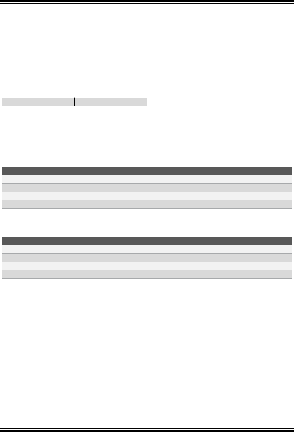
19.8.6 Control Register E Set - Split Mode
Name: CTRLESET
Offset: 0x05
Reset: 0x00
Property: -
The individual Status bit can be set by writing a '1' to its bit location. This allows each bit to be set without
the use of a read-modify-write operation on a single register.
Bit 7 6 5 4 3 2 1 0
CMD[1:0] CMDEN[1:0]
Access R/W R/W R/W R/W
Reset 0 0 0 0
Bits 3:2 – CMD[1:0] Command
These bits are used for software control of update, restart, and reset of the timer/counter. The command
bits are always read as zero. The CMD bits must be used together with CMDEN. Using the reset
command requires that both low-byte and high-byte timer/counter is selected.
Value Name Description
0x0 NONE No command
0x1 - Reserved
0x2 RESTART Force restart
0x3 RESET Force hard Reset (ignored if TC is enabled)
Bits 1:0 – CMDEN[1:0] Command enable
These bits are used to indicate for which timer/counter the command (CMD) is valid.
Value Name Description
0x0 NONE None
0x1 - Reserved
0x2 - Reserved
0x3 BOTH Command valid for both low-byte and high-byte T/C
megaAVR® 0-Series
16-bit Timer/Counter Type A (TCA)
© 2018 Microchip Technology Inc. Datasheet Preliminary DS40002015A-page 224

19.8.7 Interrupt Control Register - Split Mode
Name: INTCTRL
Offset: 0x0A
Reset: 0x00
Property: -
Bit 7 6 5 4 3 2 1 0
LCMP2 LCMP1 LCMP0 HUNF LUNF
Access R/W R/W R/W R/W R/W
Reset 0 0 0 0 0
Bit 6 – LCMP2 Low byte Compare Channel 0 Interrupt Enable
See LCMP0.
Bit 5 – LCMP1 Low byte Compare Channel 1 Interrupt Enable
See LCMP0.
Bit 4 – LCMP0 Low byte Compare Channel 0 Interrupt Enable
Writing LCMPn bit to '1' enables low byte compare interrupt from channel n.
Bit 1 – HUNF High byte Underflow Interrupt Enable
Writing HUNF bit to '1' enables high byte underflow interrupt.
Bit 0 – LUNF Low byte Underflow Interrupt Enable
Writing HUNF bit to '1' enables low byte underflow interrupt.
megaAVR® 0-Series
16-bit Timer/Counter Type A (TCA)
© 2018 Microchip Technology Inc. Datasheet Preliminary DS40002015A-page 225

19.8.8 Interrupt Flag Register - Split Mode
Name: INTFLAGS
Offset: 0x0B
Reset: 0x00
Property: -
The individual Status bit can be cleared by writing a ‘1’ to its bit location. This allows each bit to be set
without the use of a read-modify-write operation on a single register.
Bit 7 6 5 4 3 2 1 0
LCMP2 LCMP1 LCMP0 HUNF LUNF
Access R/W R/W R/W R/W R/W
Reset 0 0 0 0 0
Bit 6 – LCMP2 Low byte Compare Channel 0 Interrupt Flag
See LCMP0 flag description.
Bit 5 – LCMP1 Low byte Compare Channel 0 Interrupt Flag
See LCMP0 flag description.
Bit 4 – LCMP0 Low byte Compare Channel 0 Interrupt Flag
The Compare Interrupt flag (LCMPn) is set on a compare match on the corresponding compare channel.
For all modes of operation, the LCMPn flag will be set when a compare match occurs between the Low
Byte Count register (TCAn.LCNT) and the corresponding compare register (TCAn.LCMPn). The LCMPn
flag will not be cleared automatically and has to be cleared by software. This is done by writing a ‘1’ to its
bit location.
Bit 1 – HUNF High byte Underflow Interrupt Flag
This flag is set on a high byte timer BOTTOM (underflow) condition. HUNF is not automatically cleared
and needs to be cleared by software. This is done by writing a ‘1’ to its bit location.
Bit 0 – LUNF Low byte Underflow Interrupt Flag
This flag is set on a low byte timer BOTTOM (underflow) condition. LUNF is not automatically cleared and
needs to be cleared by software. This is done by writing a ‘1’ to its bit location.
megaAVR® 0-Series
16-bit Timer/Counter Type A (TCA)
© 2018 Microchip Technology Inc. Datasheet Preliminary DS40002015A-page 226

19.8.9 Debug Control Register
Name: DBGCTRL
Offset: 0x0E
Reset: 0x00
Property: -
Bit 7 6 5 4 3 2 1 0
DBGRUN
Access R/W
Reset 0
Bit 0 – DBGRUN Run in Debug
Value Description
0 The peripheral is halted in Break Debug mode and ignores events
1 The peripheral will continue to run in Break Debug mode when the CPU is halted
megaAVR® 0-Series
16-bit Timer/Counter Type A (TCA)
© 2018 Microchip Technology Inc. Datasheet Preliminary DS40002015A-page 227

19.8.10 Low Byte Timer Counter Register - Split Mode
Name: LCNT
Offset: 0x20
Reset: 0x00
Property: -
TCAn.LCNT contains the counter value in low byte timer. CPU and UPDI write access has priority over
count, clear, or reload of the counter.
Bit 7 6 5 4 3 2 1 0
LCNT[7:0]
Access R/W R/W R/W R/W R/W R/W R/W R/W
Reset 0 0 0 0 0 0 0 0
Bits 7:0 – LCNT[7:0] Counter Value for Low Byte Timer
These bits define the counter value of the low byte timer.
megaAVR® 0-Series
16-bit Timer/Counter Type A (TCA)
© 2018 Microchip Technology Inc. Datasheet Preliminary DS40002015A-page 228

19.8.11 High Byte Timer Counter Register - Split Mode
Name: HCNT
Offset: 0x21
Reset: 0x00
Property: -
TCAn.HCNT contains the counter value in high byte timer. CPU and UPDI write access has priority over
count, clear, or reload of the counter.
Bit 7 6 5 4 3 2 1 0
HCNT[7:0]
Access R/W R/W R/W R/W R/W R/W R/W R/W
Reset 0 0 0 0 0 0 0 0
Bits 7:0 – HCNT[7:0] Counter Value for High Byte Timer
These bits define the counter value in high byte timer.
megaAVR® 0-Series
16-bit Timer/Counter Type A (TCA)
© 2018 Microchip Technology Inc. Datasheet Preliminary DS40002015A-page 229

19.8.12 Low Byte Timer Period Register - Split Mode
Name: LPER
Offset: 0x26
Reset: 0x00
Property: -
The TCAn.LPER register contains the TOP value of low byte timer.
Bit 7 6 5 4 3 2 1 0
LPER[7:0]
Access R/W R/W R/W R/W R/W R/W R/W R/W
Reset 1 1 1 1 1 1 1 1
Bits 7:0 – LPER[7:0] Period Value Low Byte Timer
These bits hold the TOP value of low byte timer.
megaAVR® 0-Series
16-bit Timer/Counter Type A (TCA)
© 2018 Microchip Technology Inc. Datasheet Preliminary DS40002015A-page 230

19.8.13 High Byte Period Register - Split Mode
Name: HPER
Offset: 0x27
Reset: 0x00
Property: -
The TCAn.HPER register contains the TOP value of high byte timer.
Bit 7 6 5 4 3 2 1 0
HPER[7:0]
Access R/W R/W R/W R/W R/W R/W R/W R/W
Reset 1 1 1 1 1 1 1 1
Bits 7:0 – HPER[7:0] Period Value High Byte Timer
These bits hold the TOP value of high byte timer.
megaAVR® 0-Series
16-bit Timer/Counter Type A (TCA)
© 2018 Microchip Technology Inc. Datasheet Preliminary DS40002015A-page 231

19.8.14 Compare Register n For Low Byte Timer - Split Mode
Name: LCMP
Offset: 0x28 + n*0x02 [n=0..2]
Reset: 0x00
Property: -
The TCAn.LCMPn register represents the compare value of compare channel n for low byte Timer. This
register is continuously compared to the counter value of the low byte timer, TCAn.LCNT. Normally, the
outputs from the comparators are then used for generating waveforms.
Bit 7 6 5 4 3 2 1 0
LCMP[7:0]
Access R/W R/W R/W R/W R/W R/W R/W R/W
Reset 0 0 0 0 0 0 0 0
Bits 7:0 – LCMP[7:0] Compare Value of Channel n
These bits hold the compare value of channel n that is compared to TCAn.LCNT.
megaAVR® 0-Series
16-bit Timer/Counter Type A (TCA)
© 2018 Microchip Technology Inc. Datasheet Preliminary DS40002015A-page 232

19.8.15 High Byte Compare Register n - Split Mode
Name: HCMP
Offset: 0x29 + n*0x02 [n=0..2]
Reset: 0x00
Property: -
The TCAn.HCMPn register represents the compare value of compare channel n for high byte timer. This
register is continuously compared to the counter value of the high byte timer, TCAn.HCNT. Normally, the
outputs from the comparators are then used for generating waveforms.
Bit 7 6 5 4 3 2 1 0
HCMP[7:0]
Access R/W R/W R/W R/W R/W R/W R/W R/W
Reset 0 0 0 0 0 0 0 0
Bits 7:0 – HCMP[7:0] Compare Value of Channel n
These bits hold the compare value of channel n that is compared to TCAn.HCNT.
megaAVR® 0-Series
16-bit Timer/Counter Type A (TCA)
© 2018 Microchip Technology Inc. Datasheet Preliminary DS40002015A-page 233

20. 16-bit Timer/Counter Type B (TCB)
20.1 Features
• 16-Bit Counter Operation Modes:
– Periodic interrupt
– Time-out check
– Input capture
• On event
• Frequency measurement
• Pulse-width measurement
• Frequency and pulse-width measurement
– Single shot
– 8-bit Pulse-Width Modulation (PWM)
• Noise Canceler on Event Input
• Synchronize operation with TCAn
20.2 Overview
The capabilities of the 16-bit Timer/Counter type B (TCB) include frequency and waveform generation,
and input capture on Event with time and frequency measurement of digital signals. The TCB consists of
a base counter and control logic which can be set in one of eight different modes, each mode providing
unique functionality. The base counter is clocked by the peripheral clock with optional prescaling.
megaAVR® 0-Series
16-bit Timer/Counter Type B (TCB)
© 2018 Microchip Technology Inc. Datasheet Preliminary DS40002015A-page 234
20.2.1 Block Diagram
Figure 20-1. Timer/Counter Type B Block Diagram
Counter
=
CNT
= 0
"count"
"clear" Control
EVCTRL
CTRLA
IF
(INT Req.)
TOP
ClockSelect
BOTTOM
Edge Select
CTRLB Mode
CCMP
Output control
and
logic
Asynchronous
Synchronous
output
Asynchronous
output
Mode, Output enable, initial value
CLK_PER
Logic
Event System
TCB
DIV2
CLK_TCA
20.2.2 Signal Description
Signal Description Type
WO Digital Asynchronous Output Waveform Output
20.3 Functional Description
20.3.1 Definitions
The following definitions are used throughout the documentation:
Table 20-1. Timer/Counter Definitions
Name Description
BOTTOM The counter reaches BOTTOM when it becomes zero.
MAX The counter reaches MAXimum when it becomes all ones.
TOP The counter reaches TOP when it becomes equal to the highest value in the count
sequence.
UPDATE The update condition is met when the timer/counter reaches BOTTOM or TOP, depending on
the Waveform Generator mode.
CNT Counter register value.
CCMP Capture/Compare register value.
megaAVR® 0-Series
16-bit Timer/Counter Type B (TCB)
© 2018 Microchip Technology Inc. Datasheet Preliminary DS40002015A-page 235
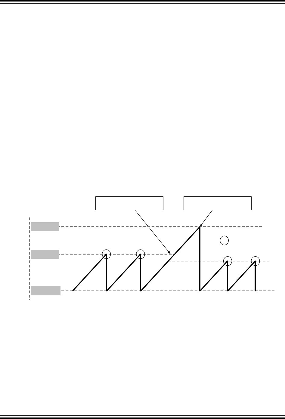
In general, the term timer is used when the timer/counter is counting periodic clock ticks. The term
counter is used when the input signal has sporadic or irregular ticks.
20.3.2 Initialization
By default, the TCB is in Periodic Interrupt mode. Follow these steps to start using it:
• Write a TOP value to the Compare/Capture register (TCBn.CCMP).
• Enable the counter by writing a '1' to the ENABLE bit in the Control A register (TCBn.CTRLA).
The counter will start counting clock ticks according to the prescaler setting in the Clock Select bit
field (CLKSEL in TCBn.CTRLA).
• The counter value can be read from the Count register (TCBn.CNT). The peripheral will generate
an interrupt when the CNT value reaches TOP.
20.3.3 Operation
20.3.3.1 Modes
The timer can be configured to run in one of the eight different modes listed below. The event pulse
needs to be longer than one system clock cycle in order to ensure edge detection.
Periodic Interrupt Mode
In the Periodic Interrupt mode, the counter counts to the capture value and restarts from zero. An
interrupt is generated when the counter is equal to TOP. If TOP is updated to a value lower than count,
the counter will continue until MAX and wrap around without generating an interrupt.
Figure 20-2. Periodic Interrupt Mode
BOTTOM
MAX
"Interrupt"
TOP
TOP changed to a value
lower than CNT
CNT
Counter wraps around
Time-Out Check Mode
In this mode, the counter counts to MAX and wraps around. On the first edge the counter is restarted and
on the second edge, the counter is stopped. If the count register (TCBn.CNT) reaches TOP before the
second edge, an interrupt will be generated. In Freeze state, the counter will restart on a new edge.
Reading count (TCBn.CNT) or compare/capture (TCBn.CCMP) register, or writing run bit (RUN in
TCBn.STATUS) in Freeze state will have no effect.
megaAVR® 0-Series
16-bit Timer/Counter Type B (TCB)
© 2018 Microchip Technology Inc. Datasheet Preliminary DS40002015A-page 236
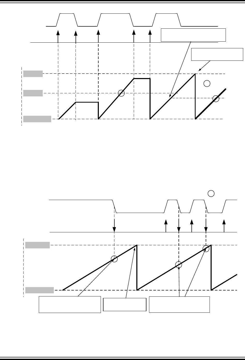
Figure 20-3. Time-Out Check Mode
CNT
BOTTOM
MAX
“ Interrupt”
TOP
TOP changed to a value
lower than CNT
Counter wraps
around
Event Input
Edge detector
Input Capture on Event Mode
The counter will count from BOTTOM to MAX continuously. When an event is detected the counter value
will be transferred to the Compare/Capture register (TCBn.CCMP) and interrupt is generated. The module
has an edge detector that can be configured to trigger count capture on either rising or falling edges.
The figure below shows the input capture unit configured to capture on falling edge on the event input
signal. The interrupt flag is automatically cleared after the high byte of the Capture register has been
read.
Figure 20-4. Input Capture on Event
CNT
MAX
BOTTOM
" Interrupt"
Wraparound
Copy CNT to CCMP
and interrupt
Copy CNT to CCMP
and interrupt
Event Input
Edge detector
It is recommended to write zero to the TCBn.CNT register when entering this mode from any other mode.
megaAVR® 0-Series
16-bit Timer/Counter Type B (TCB)
© 2018 Microchip Technology Inc. Datasheet Preliminary DS40002015A-page 237
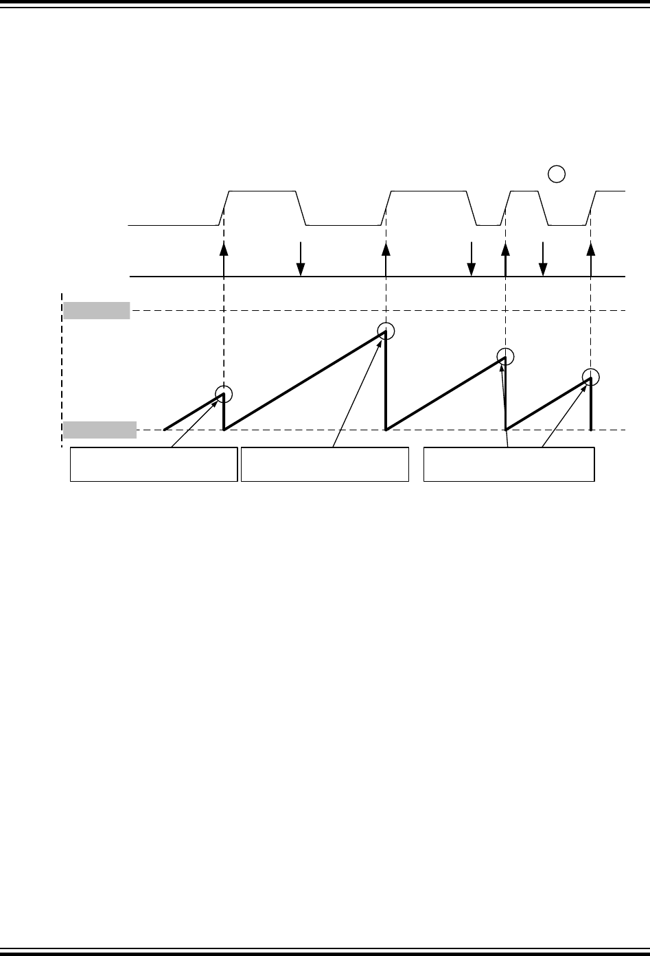
Input Capture Frequency Measurement Mode
In this mode, the TCB captures the counter value and restarts on either a positive or negative edge of the
event input signal.
The interrupt flag is automatically cleared after the high byte of the Compare/Capture register
(TCBn.CCMP) has been read, and an interrupt request is generated.
The figure below illustrates this mode when configured to act on rising edge.
Figure 20-5. Input Capture Frequency Measurement
CNT
MAX
BOTTOM
" Interrupt "
Copy CNT to CCMP,
interrupt and restart
Copy CNT to CCMP,
interrupt and restart
Copy CNT to CCMP,
interrupt and restart
Event Input
Edge detector
Input Capture Pulse-Width Measurement Mode
The input capture pulse-width measurement will restart the counter on a positive edge and capture on the
next falling edge before an interrupt request is generated. The interrupt flag is automatically cleared when
the high byte of the capture register is read. The timer will automatically switch between rising and falling
edge detection, but a minimum edge separation of two clock cycles is required for correct behavior.
megaAVR® 0-Series
16-bit Timer/Counter Type B (TCB)
© 2018 Microchip Technology Inc. Datasheet Preliminary DS40002015A-page 238
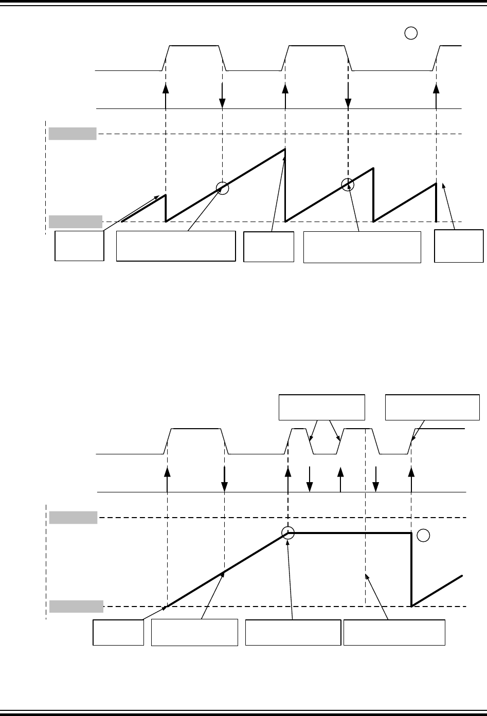
Figure 20-6. Input Capture Pulse-Width Measurement
CNT
MAX
BOTTOM
" Interrupt "
Restart
counter
Copy CNT to CCMP
and interrupt
Restart
counter
Copy CNT to CCMP
and give interrupt
Restart
counter
Event Input
Edge detector
Input Capture Frequency and Pulse-Width Measurement Mode
In this mode, the timer will start counting when a positive edge is detected on the even input signal. On
the following falling edge, the count value is captured. The counter stops when the second rising edge of
the event input signal is detected and this will set the interrupt flag.
Reading the capture will clear the interrupt flag. When the capture register is read or the interrupt flag is
cleared the TC is ready for a new capture sequence. Therefore, read the counter register before the
capture register since it is reset to zero at the next positive edge.
Figure 20-7. Input Capture Frequency and Pulse-Width Measurement
CNT
MAX
BOTTOM
" Interrupt"
Start
counter
Copy CNT to
CCMP
Stop counter and
interrupt
CPU reads the
Ignore till
Capture is read
Trigger next
capture sequence
Event Input
Edge detector
CCMP register
megaAVR® 0-Series
16-bit Timer/Counter Type B (TCB)
© 2018 Microchip Technology Inc. Datasheet Preliminary DS40002015A-page 239
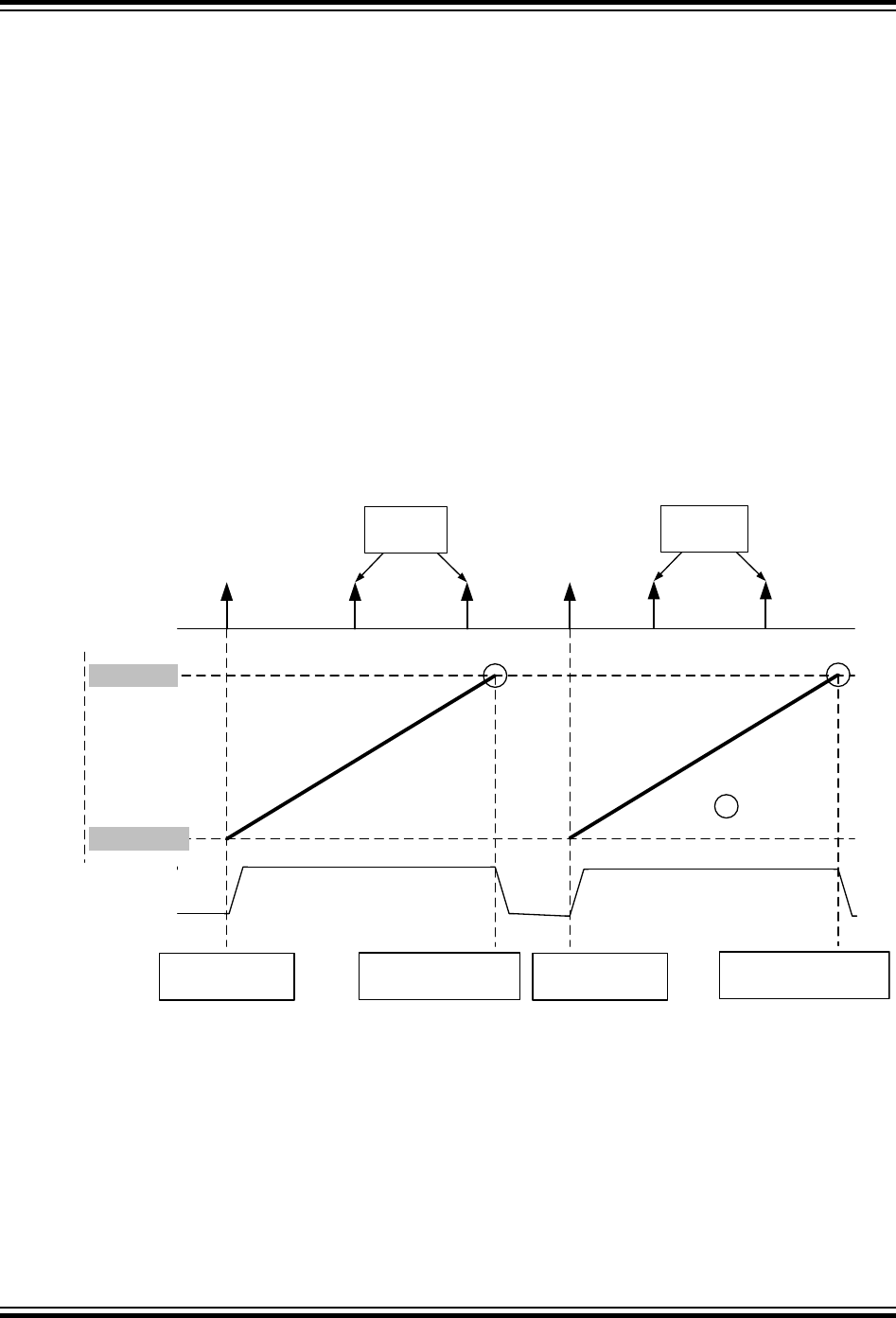
Single-Shot Mode
This mode can be used to generate a pulse with a duration that is defined by the Compare register
(TCBn.CCMP), every time a rising or falling edge is observed on a connected event channel.
When the counter is stopped, the output pin is driven to low. If an event is detected on the connected
event channel, the timer will reset and start counting from zero to TOP while driving its output high. The
RUN bit in the STATUS register can be read to see if the counter is counting or not. When the counter
register reaches the CCMP register value, the counter will stop and the output pin will go low for at least
one prescaler cycle. If a new event arrives during this time, that event will be ignored. The following figure
shows an example waveform. There is a two clock cycle delay from when the event is received until the
output is set high.
The counter will start counting as soon as the module is enabled, even without triggering an event. This is
prevented by writing TOP to the counter register. Similar behavior is seen if the EDGE bit in the
TCBn.EVCTRL register is '1' while the module is enabled. Writing TOP to the Counter register prevents
this as well.
If the ASYNC bit in TCBn.CTRLB is written to '1', the timer is reacting asynchronously to an incoming
event. An edge on the event will immediately cause the output signal to be set. The counter will still start
counting two clock cycles after the event is received.
Figure 20-8. Single-Shot Mode
CNT
TOP
BOTTOM
" Interrupt"
Event starts
counter
Counter reaches
TOP value
Output
Ignored Ignored
Event starts
counter
Counter reaches
TOP value
Edge detector
8-Bit PWM Mode
This timer can be configured to run in 8-bit PWM mode where each of the register pairs in the 16-bit
Compare/Capture register (TCBn.CCMPH and TCBn.CCMPL) are used as individual compare registers.
The counter will continuously count from zero to CCMPL and the output will be set at BOTTOM and
cleared when the counter reaches CCMPH.
When this peripheral is enabled and in PWM mode, changing the value of the Compare/Capture register
will change the output, but the transition may output invalid values. It is hence recommended to:
1. Disable the peripheral.
megaAVR® 0-Series
16-bit Timer/Counter Type B (TCB)
© 2018 Microchip Technology Inc. Datasheet Preliminary DS40002015A-page 240
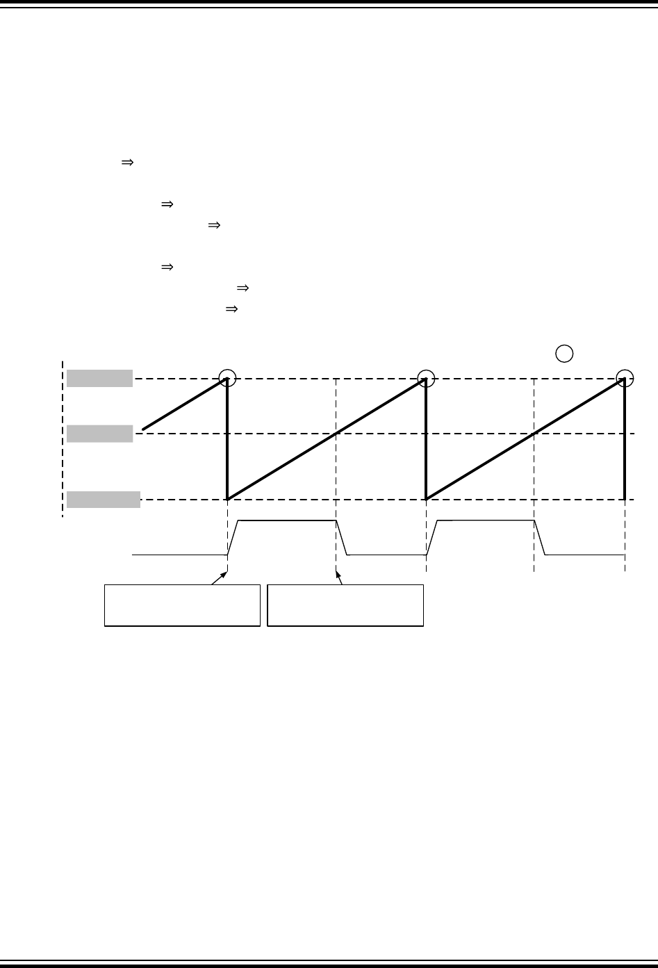
2. Write Compare/Capture register to {CCMPH, CCMPL}.
3. Write 0x0000 to count register.
4. Re-enable the module.
CCMPH is the number of cycles for which the output will be driven high, CCMPL+1 is the period of the
output pulse.
For different capture register values the output values are:
• CCMPL = 0 Output = 0
• CCMPL = 0xFF
• CCMPH = 0 Output = 0
• 0 < CCMPH ≤ 0xFF Output = 1 for CCMPH cycles, low for the rest of the period
• For 0 < CCMPL < 0xFF
• CCMPH = 0 Output = 0
• If 0 < CCMPH ≤ CCMPL Output = 1 for CCMPH cycles, low for the rest of the period
• CCMPH = CCMPL + 1 Output = 1
Figure 20-9. 8-Bit PWM Mode
CNT
CCMPL
BOTTOM
" Interrupt "
(CNT == CCMPL) and
output goes high
(CNT == CCMPH) and
output goes low
Output
CCMPH
20.3.3.2 Noise Canceler
The noise canceler improves noise immunity by using a simple digital filter scheme. When the noise filter
is enabled, the peripheral monitors the event channel and keeps a record of the last four observed
samples. If four consecutive samples are equal, the input is considered to be stable and the signal is fed
to the edge detector.
When enabled, the noise canceler introduces an additional delay of four system clock cycles between a
change applied to the input and the update of the input compare register.
The noise canceler uses the system clock and is, therefore, not affected by the prescaler.
20.3.3.3 Synchronized with TCAn
TCB can be configured to use the clock (CLK_TCA) of the Timer/Counter type A (TCAn) by writing to the
Clock Select bit field (CLKSEL) in the Control A register (TCBn.CTRLA). In this setting, the TCB will count
on the exact same clock source as selected in TCA.
megaAVR® 0-Series
16-bit Timer/Counter Type B (TCB)
© 2018 Microchip Technology Inc. Datasheet Preliminary DS40002015A-page 241

When the Synchronize Update bit (SYNCUPD) in the Control A register (TCBn.CTRLA) is written to ‘1’,
the TCB counter will restart when the TCA counter restarts.
20.3.4 Events
The TCB is an event generator. Any condition that causes the CAPT flag in TCBn.INTFLAGS to be set
will also generate a one-cycle strobe on the event channel output.
The peripheral accepts one event input. If the Capture Event Input Enable bit (CAPTEI) in the Event
Control register (TCBn.EVCTRL) is written to '1', incoming events will result in an event action as defined
by the Event Edge bit (EDGE) in TCBn.EVCTRL. The event needs to last for at least one CLK_PER cycle
to guarantee that it is recognized.
If the asynchronous mode is enabled for Single-Shot mode, the event is edge triggered and will capture
changes on the event input shorter than one system clock cycle.
20.3.5 Interrupts
Table 20-2. Available Interrupt Vectors and Sources
Name Vector Description Conditions
CAPT TCB interrupt Depending on operating mode. See the description of CAPT in
TCBn.INTFLAGS.
When an interrupt condition occurs, the corresponding interrupt flag is set in the Interrupt Flags register of
the peripheral (peripheral.INTFLAGS).
An interrupt source is enabled or disabled by writing to the corresponding enable bit in the peripheral's
Interrupt Control register (peripheral.INTCTRL).
An interrupt request is generated when the corresponding interrupt source is enabled and the interrupt
flag is set. The interrupt request remains active until the interrupt flag is cleared. See the peripheral's
INTFLAGS register for details on how to clear interrupt flags.
20.3.6 Sleep Mode Operation
TCBn is by default disabled in Standby sleep mode. It will be halted as soon as the sleep mode is
entered.
The module can stay fully operational in the Standby sleep mode if the Run In Standby (RUNSTDBY) bit
in the TCBn.CTRLA register is written to '1'.
All operations are halted in Power Down sleep mode.
megaAVR® 0-Series
16-bit Timer/Counter Type B (TCB)
© 2018 Microchip Technology Inc. Datasheet Preliminary DS40002015A-page 242

20.4 Register Summary - TCB
Offset Name Bit Pos.
0x00 CTRLA 7:0 RUNSTDBY SYNCUPD CLKSEL[1:0] ENABLE
0x01 CTRLB 7:0 ASYNC CCMPINIT CCMPEN CNTMODE[2:0]
0x02
...
0x03
Reserved
0x04 EVCTRL 7:0 FILTER EDGE CAPTEI
0x05 INTCTRL 7:0 CAPT
0x06 INTFLAGS 7:0 CAPT
0x07 STATUS 7:0 RUN
0x08 DBGCTRL 7:0 DBGRUN
0x09 TEMP 7:0 TEMP[7:0]
0x0A CNT
7:0 CNT[7:0]
15:8 CNT[15:8]
0x0C CCMP
7:0 CCMP[7:0]
15:8 CCMP[15:8]
20.5 Register Description
megaAVR® 0-Series
16-bit Timer/Counter Type B (TCB)
© 2018 Microchip Technology Inc. Datasheet Preliminary DS40002015A-page 243

20.5.1 Control A
Name: CTRLA
Offset: 0x00
Reset: 0x00
Property: -
Bit 7 6 5 4 3 2 1 0
RUNSTDBY SYNCUPD CLKSEL[1:0] ENABLE
Access R/W R/W R/W R/W R/W
Reset 0 0 0 0 0
Bit 6 – RUNSTDBY Run in Standby
Writing a '1' to this bit will enable the peripheral to run in Standby Sleep mode. Not applicable when
CLKSEL is set to 0x2 (CLK_TCA).
Bit 4 – SYNCUPD Synchronize Update
When this bit is written to '1', the TCB will restart whenever the TCA0 counter is restarted.
Bits 2:1 – CLKSEL[1:0] Clock Select
Writing these bits selects the clock source for this peripheral.
Value Description
0x0 CLK_PER
0x1 CLK_PER / 2
0x2 Use CLK_TCA from TCA0
0x3 Reserved
Bit 0 – ENABLE Enable
Writing this bit to '1' enables the Timer/Counter type B peripheral.
megaAVR® 0-Series
16-bit Timer/Counter Type B (TCB)
© 2018 Microchip Technology Inc. Datasheet Preliminary DS40002015A-page 244
20.5.2 Control B
Name: CTRLB
Offset: 0x01
Reset: 0x00
Property: -
Bit 7 6 5 4 3 2 1 0
ASYNC CCMPINIT CCMPEN CNTMODE[2:0]
Access R/W R/W R/W R/W R/W R/W
Reset 0 0 0 0 0 0
Bit 6 – ASYNC Asynchronous Enable
Writing this bit to '1' will allow asynchronous updates of the TCB output signal in Single-Shot mode.
Value Description
0 The output will go HIGH when the counter actually starts
1 The output will go HIGH when an event arrives
Bit 5 – CCMPINIT Compare/Capture Pin Initial Value
This bit is used to set the initial output value of the pin when a pin output is used.
Value Description
0 Initial pin state is LOW
1 Initial pin state is HIGH
Bit 4 – CCMPEN Compare/Capture Output Enable
This bit is used to enable the output signal of the Compare/Capture.
Value Description
0 Compare/Capture Output is zero
1 Compare/Capture Output has a valid value
Bits 2:0 – CNTMODE[2:0] Timer Mode
Writing these bits selects the Timer mode.
Value Description
0x0 Periodic Interrupt mode
0x1 Time-out Check mode
0x2 Input Capture on Event mode
0x3 Input Capture Frequency Measurement mode
0x4 Input Capture Pulse-Width Measurement mode
0x5 Input Capture Frequency and Pulse-Width Measurement mode
0x6 Single-Shot mode
0x7 8-Bit PWM mode
megaAVR® 0-Series
16-bit Timer/Counter Type B (TCB)
© 2018 Microchip Technology Inc. Datasheet Preliminary DS40002015A-page 245

20.5.3 Event Control
Name: EVCTRL
Offset: 0x04
Reset: 0x00
Property: -
Bit 7 6 5 4 3 2 1 0
FILTER EDGE CAPTEI
Access R/W R/W R/W
Reset 0 0 0
Bit 6 – FILTER Input Capture Noise Cancellation Filter
Writing this bit to '1' enables the input capture noise cancellation unit.
Bit 4 – EDGE Event Edge
This bit is used to select the event edge. The effect of this bit is dependent on the selected Count Mode
(CNTMODE) in TCBn.CTRLB. "-" means that an event or edge has no effect in this mode.
Count Mode EDGE Positive Edge Negative Edge
Periodic Interrupt mode 0 - -
1 - -
Timeout Check mode 0 Start counter Stop counter
1 Stop counter Start counter
Input Capture on Event mode 0 Input Capture, interrupt -
1 - Input Capture, interrupt
Input Capture Frequency
Measurement mode
0 Input Capture, clear and
restart counter, interrupt
-
1 - Input Capture, clear and
restart counter, interrupt
Input Capture Pulse-Width
Measurement mode
0 Clear and restart counter Input Capture, interrupt
1 Input Capture, interrupt Clear and restart counter
Input Capture Frequency and
Pulse Width Measurement mode
0 On 1st Positive: Clear and restart counter
On following Negative: Input Capture
2nd Positive: Stop counter, interrupt
1 On 1st Negative: Clear and restart counter
On following Positive: Input Capture
2nd Negative: Stop counter, interrupt
Single-Shot mode 0 Start counter -
megaAVR® 0-Series
16-bit Timer/Counter Type B (TCB)
© 2018 Microchip Technology Inc. Datasheet Preliminary DS40002015A-page 246

Count Mode EDGE Positive Edge Negative Edge
1 Start counter Start counter
8-Bit PWM mode 0 - -
1 - -
Bit 0 – CAPTEI Capture Event Input Enable
Writing this bit to '1' enables the input capture event.
megaAVR® 0-Series
16-bit Timer/Counter Type B (TCB)
© 2018 Microchip Technology Inc. Datasheet Preliminary DS40002015A-page 247

20.5.4 Interrupt Control
Name: INTCTRL
Offset: 0x05
Reset: 0x00
Property: -
Bit 7 6 5 4 3 2 1 0
CAPT
Access R/W
Reset 0
Bit 0 – CAPT Capture Interrupt Enable
Writing this bit to '1' enables the Capture interrupt.
megaAVR® 0-Series
16-bit Timer/Counter Type B (TCB)
© 2018 Microchip Technology Inc. Datasheet Preliminary DS40002015A-page 248

20.5.5 Interrupt Flags
Name: INTFLAGS
Offset: 0x06
Reset: 0x00
Property: -
Bit 7 6 5 4 3 2 1 0
CAPT
Access R/W
Reset 0
Bit 0 – CAPT Interrupt Flag
This bit is set when an interrupt occurs. The interrupt conditions are dependent on the Counter Mode
(CNTMODE) in TCBn.CTRLB.
This bit is cleared by writing a '1' to it or when the Capture register is read in Capture mode.
Counter Mode Interrupt Flag Behavior
Periodic Interrupt mode Set when the counter reaches TOP
Timeout Check mode Set when the counter reaches TOP
Input Capture on Event mode Set when an event occurs and the Capture register is loaded,
cleared when Capture is read
Input Capture Frequency
Measurement mode
Set on an edge when the Capture register is loaded and count
initialized, cleared when Capture is read
Input Capture Pulse-Width
Measurement mode
Set on an edge when the Capture register is loaded, the previous
edge initialized the count, cleared when Capture is read
Input Capture Frequency and Pulse-
Width Measurement mode
Set on second (positive or negative) edge when the counter is
stopped, cleared when Capture is read
Single-Shot mode Set when counter reaches TOP
8-Bit PWM mode Set when the counter reaches CCMPL
megaAVR® 0-Series
16-bit Timer/Counter Type B (TCB)
© 2018 Microchip Technology Inc. Datasheet Preliminary DS40002015A-page 249

20.5.6 Status
Name: STATUS
Offset: 0x07
Reset: 0x00
Property: -
Bit 7 6 5 4 3 2 1 0
RUN
Access R
Reset 0
Bit 0 – RUN Run
When the counter is running, this bit is set to '1'. When the counter is stopped, this bit is cleared to '0'.
The bit is read-only and cannot be set by UPDI.
megaAVR® 0-Series
16-bit Timer/Counter Type B (TCB)
© 2018 Microchip Technology Inc. Datasheet Preliminary DS40002015A-page 250

20.5.7 Debug Control
Name: DBGCTRL
Offset: 0x08
Reset: 0x00
Property: -
Bit 7 6 5 4 3 2 1 0
DBGRUN
Access R/W
Reset 0
Bit 0 – DBGRUN Debug Run
Value Description
0 The peripheral is halted in Break Debug mode and ignores events
1 The peripheral will continue to run in Break Debug mode when the CPU is halted
megaAVR® 0-Series
16-bit Timer/Counter Type B (TCB)
© 2018 Microchip Technology Inc. Datasheet Preliminary DS40002015A-page 251

20.5.8 Temporary Value
Name: TEMP
Offset: 0x09
Reset: 0x00
Property: -
The Temporary register is used by the CPU for single-cycle, 16-bit access to the 16-bit registers of this
peripheral. It can be read and written by software. Refer to 16-bit access in the AVR CPU chapter. There
is one common Temporary register for all the 16-bit registers of this peripheral.
Bit 7 6 5 4 3 2 1 0
TEMP[7:0]
Access R/W R/W R/W R/W R/W R/W R/W R/W
Reset 0 0 0 0 0 0 0 0
Bits 7:0 – TEMP[7:0] Temporary Value
megaAVR® 0-Series
16-bit Timer/Counter Type B (TCB)
© 2018 Microchip Technology Inc. Datasheet Preliminary DS40002015A-page 252

20.5.9 Count
Name: CNT
Offset: 0x0A
Reset: 0x00
Property: -
The TCBn.CNTL and TCBn.CNTH register pair represents the 16-bit value TCBn.CNT. The low byte [7:0]
(suffix L) is accessible at the original offset. The high byte [15:8] (suffix H) can be accessed at offset
+ 0x01.
CPU and UPDI write access has priority over internal updates of the register.
Bit 15 14 13 12 11 10 9 8
CNT[15:8]
Access R/W R/W R/W R/W R/W R/W R/W R/W
Reset 0 0 0 0 0 0 0 0
Bit 7 6 5 4 3 2 1 0
CNT[7:0]
Access R/W R/W R/W R/W R/W R/W R/W R/W
Reset 0 0 0 0 0 0 0 0
Bits 15:8 – CNT[15:8] Count Value High
These bits hold the MSB of the 16-bit Counter register.
Bits 7:0 – CNT[7:0] Count Value Low
These bits hold the LSB of the 16-bit Counter register.
megaAVR® 0-Series
16-bit Timer/Counter Type B (TCB)
© 2018 Microchip Technology Inc. Datasheet Preliminary DS40002015A-page 253

20.5.10 Capture/Compare
Name: CCMP
Offset: 0x0C
Reset: 0x00
Property: -
The TCBn.CCMPL and TCBn.CCMPH register pair represents the 16-bit value TCBn.CCMP. The low
byte [7:0] (suffix L) is accessible at the original offset. The high byte [15:8] (suffix H) can be accessed at
offset + 0x01.
This register has different functions depending on the mode of operation:
• For capture operation, these registers contain the captured value of the counter at the time the
capture occurs
• In periodic interrupt/time-out and Single-Shot mode, this register acts as the TOP value
• In 8-bit PWM mode, TCBn.CCMPL and TCBn.CCMPH act as two independent registers
Bit 15 14 13 12 11 10 9 8
CCMP[15:8]
Access R/W R/W R/W R/W R/W R/W R/W R/W
Reset 0 0 0 0 0 0 0 0
Bit 7 6 5 4 3 2 1 0
CCMP[7:0]
Access R/W R/W R/W R/W R/W R/W R/W R/W
Reset 0 0 0 0 0 0 0 0
Bits 15:8 – CCMP[15:8] Capture/Compare Value High Byte
These bits hold the MSB of the 16-bit compare, capture, and top value.
Bits 7:0 – CCMP[7:0] Capture/Compare Value Low Byte
These bits hold the LSB of the 16-bit compare, capture, and top value.
megaAVR® 0-Series
16-bit Timer/Counter Type B (TCB)
© 2018 Microchip Technology Inc. Datasheet Preliminary DS40002015A-page 254

21. Real-Time Counter (RTC)
21.1 Features
• 16-bit resolution
• Selectable clock sources
• Programmable 15-bit clock prescaling
• One compare register
• One period register
• Clear timer on period overflow
• Optional interrupt/Event on overflow and compare match
• Periodic interrupt and Event
• Crystal Error Correction
21.2 Overview
The RTC peripheral offers two timing functions: the Real-Time Counter (RTC) and a Periodic Interrupt
Timer (PIT).
The PIT functionality can be enabled independently of the RTC functionality.
RTC - Real-Time Counter
The RTC counts (prescaled) clock cycles in a Counter register, and compares the content of the Counter
register to a Period register and a Compare register.
The RTC can generate both interrupts and events on compare match or overflow. It will generate a
compare interrupt and/or event at the first count after the counter equals the Compare register value, and
an overflow interrupt and/or event at the first count after the counter value equals the Period register
value. The overflow will also reset the counter value to zero.
The RTC peripheral typically runs continuously, including in Low-Power Sleep modes, to keep track of
time. It can wake up the device from Sleep modes and/or interrupt the device at regular intervals.
The reference clock is typically the 32 KHz output from an external crystal. The RTC can also be clocked
from an external clock signal, the 32 KHz internal Ultra Low-Power Oscillator (OSCULP32K), or the
OSCULP32K divided by 32.
The RTC peripheral includes a 15-bit programmable prescaler that can scale down the reference clock
before it reaches the counter. A wide range of resolutions and time-out periods can be configured for the
RTC. With a 32.768 kHz clock source, the maximum resolution is 30.5 μs, and timeout periods can be up
to two seconds. With a resolution of 1s, the maximum timeout period is more than 18 hours (65536
seconds).
The RTC also supports correction when operated using external crystal selection. An externally calibrated
value will be used for correction. The RTC can be adjusted by software to an accuracy of ±1PPM. The
RTC correction operation will either speed up (by skipping count) or slow down (by adding extra count)
the prescaler to account for the crystal error.
megaAVR® 0-Series
Real-Time Counter (RTC)
© 2018 Microchip Technology Inc. Datasheet Preliminary DS40002015A-page 255
PIT - Periodic Interrupt Timer
Using the same clock source as the RTC function, the PIT can request an interrupt or trigger an output
event on every nth clock period. n can be selected from {4, 8, 16,.. 32768} for interrupts, and from {64,
128, 256,... 8192} for events.
The PIT uses the same clock source (CLK_RTC) as the RTC function.
21.2.1 Block Diagram
Figure 21-1. Block Diagram
RTC
32.768 kHz Crystal Osc
32.768 kHz Int. Osc
TOSC1
TOSC2
External Clock
DIV32
CLKSEL
15-bit
prescaler
CLK_RTC
CNT
PER
CMP
=
=
Compare
Overflow
PIT
EXTCLK
Correction
counter
Period
21.3 Clocks
System clock (CLK_PER) is required to be at least four times faster than RTC clock (CLK_RTC) for
reading counter value, and this is regardless of the RTC_PRESC setting.
A 32.768 kHz crystal can be connected to the TOSC1 or TOSC2 pins, along with any required load
capacitors. An external clock can be used on the TOSC1 pin.
21.4 RTC Functional Description
The RTC peripheral offers two timing functions: the Real-Time Counter (RTC) and a Periodic Interrupt
Timer (PIT). This subsection describes the RTC.
megaAVR® 0-Series
Real-Time Counter (RTC)
© 2018 Microchip Technology Inc. Datasheet Preliminary DS40002015A-page 256

21.4.1 Initialization
To operate the RTC, the source clock for the RTC counter must be configured before enabling the RTC
peripheral, and the desired actions (interrupt requests, output Events).
21.4.1.1 Configure the Clock CLK_RTC
To configure CLK_RTC, follow these steps:
1. Configure the desired oscillator to operate as required, in the Clock Controller peripheral
(CLKCTRL).
2. Write the Clock Select bits (CLKSEL) in the Clock Selection register (RTC.CLKSEL) accordingly.
The CLK_RTC clock configuration is used by both RTC and PIT functionality.
21.4.1.2 Configure RTC
To operate the RTC, follow these steps:
1. Set the Compare value in the Compare register (RTC.CMP), and/or the Overflow value in the Top
register (RTC.PER).
2. Enable the desired Interrupts by writing to the respective Interrupt Enable bits (CMP, OVF) in the
Interrupt Control register (RTC.INTCTRL).
3. Configure the RTC-internal prescaler and enable the RTC by writing the desired value to the
PRESCALER bit field and a '1' to the RTC Enable bit (RTCEN) in the Control A register
(RTC.CTRLA).
Note: The RTC peripheral is used internally during device start-up. Always check the Busy bits in the
RTC.STATUS and RTC.PITSTATUS registers, also on initial configuration.
21.4.2 Operation - RTC
21.4.2.1 Enabling, Disabling, and Resetting
The RTC is enabled by setting the Enable bit in the Control A register (ENABLE bit in RTC.CTRLA to 1).
The RTC is disabled by writing ENABLE bit in RTC.CTRLA to 0.
21.5 PIT Functional Description
The RTC peripheral offers two timing functions: the Real-Time Counter (RTC) and a Periodic Interrupt
Timer (PIT). This subsection describes the PIT.
21.5.1 Initialization
To operate the PIT, follow these steps:
1. Configure the RTC clock CLK_RTC as described in Configure the Clock CLK_RTC.
2. Enable the interrupt by writing a '1' to the Periodic Interrupt bit (PI) in the PIT Interrupt Control
register (RTC.PITINTCTRL).
3. Select the period for the interrupt and enable the PIT by writing the desired value to the PERIOD bit
field and a '1' to the PIT Enable bit (PITEN) in the PIT Control A register (RTC.PITCTRLA).
Note: The RTC peripheral is used internally during device start-up. Always check the Busy bits in the
RTC.STATUS and RTC.PITSTATUS registers, also on initial configuration.
21.5.2 Operation - PIT
21.5.2.1 Enabling, Disabling, and Resetting
The PIT is enabled by setting the Enable bit in the PIT Control A register (the PITEN bit in
RTC.PITCTRLA to 1). The PIT is disabled by writing the PITEN bit in RTC.PITCTRLA to 0.
megaAVR® 0-Series
Real-Time Counter (RTC)
© 2018 Microchip Technology Inc. Datasheet Preliminary DS40002015A-page 257

21.5.2.2 PIT Interrupt Timing
Timing of the First Interrupt
The PIT function and the RTC function are running off the same counter inside the prescaler, but both
functions’ periods can be configured independently:
• The RTC period is configured by writing the PRESCALER bit field in RTC.CTRLA.
• The PIT period is configured by writing the PERIOD bit field in RTC.PITCTRLA.
The prescaler is OFF when both functions are OFF (RTC Enable bit (RTCEN) in RTC.CTRLA and PIT
Enable bit (PITEN) in RTC.PITCTRLA are zero), but it is running (i.e. its internal counter is counting)
when either function is enabled.
For this reason, the timing of the first PIT interrupt output is depending on whether the RTC function is
already enabled or not:
• When RTCEN in RTC.CTRLA is zero and PITEN in RTC.PITCTRLA is written to ‘1’, the prescaler
will start operating at the next edge of CLK_RTC, counting from zero. The PIT interrupt output will
then toggle from ‘0’ to ‘1’ after a ½ period.
• When the RTC function is already enabled (RTCEN is ‘1’), the prescaler is already running. The
timing of the first interrupt output from the PIT depends on the value of the counter when the
prescaler is enabled. Since the application can’t access that value, the first interrupt output may
occur anytime between writing PITEN to ‘1’ and up to a full PIT period after.
Continuous Operation
After the first interrupt output, the PIT will continue toggling every ½ PIT period, resulting in a full PIT
period signal.
PIT Timing Diagram for PERIOD=CYC16
For PERIOD=CYC16 in RTC.PITCTRLA, the PIT output effectively follows the state of
prescaler counter bit 3, so the resulting interrupt output has a period of 16 CLK_RTC
cycles.
When both RTC and PIT functions are disabled, the prescaler is OFF. The delay between
writing PITEN to ‘1’ and the first interrupt output is always ½ PIT period, with an
uncertainty of one leading CLK_RTC cycle.
When the RTC and hence the prescaler are already enabled with any
PRESCALER=DIVn, the time between writing PITEN to ‘1’ and the first PIT interrupt can
vary between virtually 0 and a full PIT period of 16 CLK_RTC cycles. The precise delay
between enabling the PIT and its first output is depending on the prescaler’s counting
phase: the depicted first interrupt in the lower figure is produced by writing PITEN to ‘1’ at
any time inside the leading time window.
megaAVR® 0-Series
Real-Time Counter (RTC)
© 2018 Microchip Technology Inc. Datasheet Preliminary DS40002015A-page 258
Figure 21-2. Timing Between PIT Enable and First Interrupt
PITENABLE=0
CLK_RTC
prescaler
counter
value (LSb)
PIT output
Continuous Operation
time window for writing
PITENABLE=1
first PIT output
Enabling PIT with RTC/Prescaler Enabled
..000000
..000001
..000010
..000011
..000100
..000101
..000110
..000111
..001000
..001001
..001010
..001011
..001100
..001101
..001110
..001111
..010000
..010001
..010010
..010011
..010100
..010101
..010110
..010111
..011000
..011001
..011010
..011011
..011100
..011101
..011110
..011111
..100000
..100001
..100010
..100011
..100100
..100101
..100110
..100111
..101000
..101001
..101010
..101011
..101100
..101101
..101110
..101111
prescaler bit 3
(CYC16)
PITENABLE=0
CLK_RTC
prescaler
counter
value (LSb)
PIT output
Continuous Operation
first PIT output
Enabling PIT with RTC/Prescaler Disabled
..000000
..000001
..000010
..000011
..000100
..000101
..000110
..000111
..001000
..001001
..001010
..001011
..001100
..001101
..001110
..001111
..010000
..010001
..010010
..010011
..010100
..010101
..010110
..010111
..011000
..011001
..011010
..011011
..011100
..011101
..011110
..011111
..100000
..100001
..100010
..100011
..100100
..100101
prescaler bit 3
(CYC16)
1/2 PIT period
(8 CLK_RTC)
write PITENABLE=1
21.6 Crystal Error Correction
The prescaler for the RTC and PIT can do internal correction (when CORREN bit in RTC.CTRLA is 1) on
the crystal clock by taking the PPM error value from the CALIB Register.
The CALIB register will be written by software after external calibration or temperature corrections.
Correction is done within an interval of approximately 1 million input clock cycles. The correction
operation is performed as a single cycle operation – adding or removing one cycle, depending on the
nature of error. These single cycle operations will be performed repeatedly the error number of times
(ERROR bits in RTC.CALIB) spread throughout the 1 million cycle correction interval. The correction
spread over this correction interval is based on the error value.
The final correction of the clock will be reflected in the RTC count value available through the RTC.CNTx
registers or in the PIT intervals.
megaAVR® 0-Series
Real-Time Counter (RTC)
© 2018 Microchip Technology Inc. Datasheet Preliminary DS40002015A-page 259

At disable of the correction feature, the ongoing correction cycle will be completed before the function is
disabled.
21.7 Events
The RTC, when enabled, will generate the following output events:
• Overflow (OVF): Generated when the counter has reached its top value and wrapped to zero. The
generated strobe is synchronous with CLK_RTC and lasts one CLK_RTC cycle.
• Compare (CMP): Indicates a match between the counter value and the Compare register. The
generated strobe is synchronous with CLK_RTC and lasts one CLK_RTC cycle.
When enabled, the PIT generates the following 50% duty cycle clock signals on its event outputs:
• Event 0: Clock period = 8192 RTC clock cycles
• Event 1: Clock period = 4096 RTC clock cycles
• Event 2: Clock period = 2048 RTC clock cycles
• Event 3: Clock period = 1024 RTC clock cycles
• Event 4: Clock period = 512 RTC clock cycles
• Event 5: Clock period = 256 RTC clock cycles
• Event 6: Clock period = 128 RTC clock cycles
• Event 7: Clock period = 64 RTC clock cycles
The event users are configured by the Event System (EVSYS).
21.8 Interrupts
Table 21-1. Available Interrupt Vectors and Sources
Name Vector Description Conditions
RTC Real-time counter overflow
and compare match interrupt
• Overflow (OVF): The counter has reached its top value
and wrapped to zero.
• Compare (CMP): Match between the counter value and
the compare register.
PIT Periodic Interrupt Timer
interrupt
A time period has passed, as configured by the PERIOD bits in
RTC.PITCTRLA.
When an interrupt condition occurs, the corresponding interrupt flag is set in the Interrupt Flags register of
the peripheral (peripheral.INTFLAGS).
An interrupt source is enabled or disabled by writing to the corresponding enable bit in the peripheral's
Interrupt Control register (peripheral.INTCTRL).
An interrupt request is generated when the corresponding interrupt source is enabled and the interrupt
flag is set. The interrupt request remains active until the interrupt flag is cleared. See the peripheral's
INTFLAGS register for details on how to clear interrupt flags.
Note that:
• The RTC has two INTFLAGS registers: RTC.INTFLAGS and RTC.PITINTFLAGS.
• The RTC has two INTCTRL registers: RTC.INTCTRL and RTC.PITINTCTRL.
megaAVR® 0-Series
Real-Time Counter (RTC)
© 2018 Microchip Technology Inc. Datasheet Preliminary DS40002015A-page 260

21.9 Sleep Mode Operation
The RTC will continue to operate in Idle Sleep mode. It will run in Standby Sleep mode if the RUNSTDBY
bit in RTC.CTRLA is set.
The PIT will continue to operate in any sleep mode.
21.10 Synchronization
Both the RTC and the PIT are asynchronous, operating from a different clock source (CLK_RTC)
independently of the main clock (CLK_PER). For Control and Count register updates, it will take a
number of RTC clock and/or peripheral clock cycles before an updated register value is available in a
register or until a configuration change has an effect on the RTC or PIT, respectively. This synchronization
time is described for each register in the Register Description section.
For some RTC registers, a Synchronization Busy flag is available (CMPBUSY, PERBUSY, CNTBUSY,
CTRLABUSY) in the STATUS register (RTC.STATUS).
For the RTC.PITCTRLA register, a Synchronization Busy flag (SYNCBUSY) is available in the PIT
STATUS register (RTC.PITSTATUS).
Check for busy should be performed before writing to the mentioned registers.
megaAVR® 0-Series
Real-Time Counter (RTC)
© 2018 Microchip Technology Inc. Datasheet Preliminary DS40002015A-page 261

21.11 Register Summary - RTC
Offset Name Bit Pos.
0x00 CTRLA 7:0 RUNSTDBY PRESCALER[3:0] CORREN RTCEN
0x01 STATUS 7:0 CMPBUSY PERBUSY CNTBUSY CTRLABUSY
0x02 INTCTRL 7:0 CMP OVF
0x03 INTFLAGS 7:0 CMP OVF
0x04 TEMP 7:0 TEMP[7:0]
0x05 DBGCTRL 7:0 DBGRUN
0x06 CALIB 7:0 SIGN ERROR[6:0]
0x07 CLKSEL 7:0 CLKSEL[1:0]
0x08 CNT
7:0 CNT[7:0]
15:8 CNT[15:8]
0x0A PER
7:0 PER[7:0]
15:8 PER[15:8]
0x0C CMP
7:0 CMP[7:0]
15:8 CMP[15:8]
0x0E
...
0x0F
Reserved
0x10 PITCTRLA 7:0 PERIOD[3:0] PITEN
0x11 PITSTATUS 7:0 CTRLBUSY
0x12 PITINTCTRL 7:0 PI
0x13 PITINTFLAGS 7:0 PI
0x14 Reserved
0x15 PITDBGCTRL 7:0 DBGRUN
21.12 Register Description
megaAVR® 0-Series
Real-Time Counter (RTC)
© 2018 Microchip Technology Inc. Datasheet Preliminary DS40002015A-page 262
21.12.1 Control A
Name: CTRLA
Offset: 0x00
Reset: 0x00
Property: -
Bit 7 6 5 4 3 2 1 0
RUNSTDBY PRESCALER[3:0] CORREN RTCEN
Access R/W R/W R/W R/W R/W R/W R/W
Reset 0 0 0 0 0 0 0
Bit 7 – RUNSTDBY Run in Standby
Value Description
0 RTC disabled in Standby sleep mode
1 RTC enabled in Standby sleep mode
Bits 6:3 – PRESCALER[3:0] Prescaler
These bits define the prescaling of the CLK_RTC clock signal. Due to synchronization between the RTC
clock and system clock domains, there is a latency of two RTC clock cycles from updating the register
until this has an effect. Application software needs to check that the CTRLABUSY flag in RTC.STATUS is
cleared before writing to this register.
Value Name Description
0x0 DIV1 RTC clock/1 (no prescaling)
0x1 DIV2 RTC clock/2
0x2 DIV4 RTC clock/4
0x3 DIV8 RTC clock/8
0x4 DIV16 RTC clock/16
0x5 DIV32 RTC clock/32
0x6 DIV64 RTC clock/64
0x7 DIV128 RTC clock/128
0x8 DIV256 RTC clock/256
0x9 DIV512 RTC clock/512
0xA DIV1024 RTC clock/1024
0xB DIV2048 RTC clock/2048
0xC DIV4096 RTC clock/4096
0xD DIV8192 RTC clock/8192
0xE DIV16384 RTC clock/16384
0xF DIV32768 RTC clock/32768
Bit 2 – CORREN Correction Enable
Value Description
0 Correction is disabled
1 Correction is enabled
Bit 0 – RTCEN RTC Enable
megaAVR® 0-Series
Real-Time Counter (RTC)
© 2018 Microchip Technology Inc. Datasheet Preliminary DS40002015A-page 263

Value Description
0 RTC disabled
1 RTC enabled
megaAVR® 0-Series
Real-Time Counter (RTC)
© 2018 Microchip Technology Inc. Datasheet Preliminary DS40002015A-page 264

21.12.2 Status
Name: STATUS
Offset: 0x01
Reset: 0x00
Property: -
Bit 7 6 5 4 3 2 1 0
CMPBUSY PERBUSY CNTBUSY CTRLABUSY
Access R R R R
Reset 0 0 0 0
Bit 3 – CMPBUSY Compare Synchronization Busy
This bit is indicating whether the RTC is busy synchronizing the Compare register (RTC.CMP) in RTC
clock domain.
Bit 2 – PERBUSY Period Synchronization Busy
This bit is indicating whether the RTC is busy synchronizing the Period register (RTC.PER) in RTC clock
domain.
Bit 1 – CNTBUSY Counter Synchronization Busy
This bit is indicating whether the RTC is busy synchronizing the Count register (RTC.CNT) in RTC clock
domain.
Bit 0 – CTRLABUSY Control A Synchronization Busy
This bit is indicating whether the RTC is busy synchronizing the Control A register (RTC.CTRLA) in RTC
clock domain.
megaAVR® 0-Series
Real-Time Counter (RTC)
© 2018 Microchip Technology Inc. Datasheet Preliminary DS40002015A-page 265

21.12.3 Interrupt Control
Name: INTCTRL
Offset: 0x02
Reset: 0x00
Property: -
Bit 7 6 5 4 3 2 1 0
CMP OVF
Access R/W R/W
Reset 0 0
Bit 1 – CMP Compare Match Interrupt Enable
Enable interrupt-on-compare match (i.e., when the Counter value (CNT) matches the Compare value
(CMP)).
Bit 0 – OVF Overflow Interrupt Enable
Enable interrupt-on-counter overflow (i.e., when the Counter value (CNT) matched the Period value
(PER) and wraps around to zero).
megaAVR® 0-Series
Real-Time Counter (RTC)
© 2018 Microchip Technology Inc. Datasheet Preliminary DS40002015A-page 266

21.12.4 Interrupt Flag
Name: INTFLAGS
Offset: 0x03
Reset: 0x00
Property: -
Bit 7 6 5 4 3 2 1 0
CMP OVF
Access R R
Reset 0 0
Bit 1 – CMP Compare Match Interrupt Flag
This flag is set when the Counter value (CNT) matches the Compare value (CMP).
Writing a '1' to this bit clears the flag.
Bit 0 – OVF Overflow Interrupt Flag
This flag is set when the Counter value (CNT) has reached the Period value (PER) and wrapped to zero.
Writing a '1' to this bit clears the flag.
megaAVR® 0-Series
Real-Time Counter (RTC)
© 2018 Microchip Technology Inc. Datasheet Preliminary DS40002015A-page 267

21.12.5 Temporary
Name: TEMP
Offset: 0x4
Reset: 0x00
Property: -
The Temporary register is used by the CPU for single-cycle, 16-bit access to the 16-bit registers of this
peripheral. It can be read and written by software. Refer to 16-bit access in the AVR CPU chapter. There
is one common Temporary register for all the 16-bit registers of this peripheral.
Bit 7 6 5 4 3 2 1 0
TEMP[7:0]
Access R/W R/W R/W R/W R/W R/W R/W R/W
Reset 0 0 0 0 0 0 0 0
Bits 7:0 – TEMP[7:0] Temporary
Temporary register for read/write operations in 16-bit registers.
megaAVR® 0-Series
Real-Time Counter (RTC)
© 2018 Microchip Technology Inc. Datasheet Preliminary DS40002015A-page 268

21.12.6 Debug Control
Name: DBGCTRL
Offset: 0x05
Reset: 0x00
Property: -
Bit 7 6 5 4 3 2 1 0
DBGRUN
Access R/W
Reset 0
Bit 0 – DBGRUN Debug Run
Value Description
0 The peripheral is halted in Break Debug mode and ignores events
1 The peripheral will continue to run in Break Debug mode when the CPU is halted
megaAVR® 0-Series
Real-Time Counter (RTC)
© 2018 Microchip Technology Inc. Datasheet Preliminary DS40002015A-page 269

21.12.7 Calibration
Name: CALIB
Offset: 0x06
Reset: 0x00
Property: -
This register stores the error value and the type of correction to be done. This register is written by
software with any error value based on external calibration and/or temperature correction/s.
Bit 7 6 5 4 3 2 1 0
SIGN ERROR[6:0]
Access R/W R/W R/W R/W R/W R/W R/W R/W
Reset 0 0 0 0 0 0 0 0
Bit 7 – SIGN Error Correction Sign Bit
This bit is used to indicate the direction of the correction.
Value Description
0x0 Positive correction causing prescaler to count slower.
0x1 Negative correction causing prescaler to count faster. Requires that prescaler
configuration is set to minimum DIV2.
Bits 6:0 – ERROR[6:0] Error Correction Value
The number of correction clocks for each million RTC clock cycles interval (ppm).
megaAVR® 0-Series
Real-Time Counter (RTC)
© 2018 Microchip Technology Inc. Datasheet Preliminary DS40002015A-page 270
21.12.8 Clock Selection
Name: CLKSEL
Offset: 0x07
Reset: 0x00
Property: -
Bit 7 6 5 4 3 2 1 0
CLKSEL[1:0]
Access R/W R/W
Reset 0 0
Bits 1:0 – CLKSEL[1:0] Clock Select
Writing these bits select the source for the RTC clock (CLK_RTC).
When configuring the RTC to use either XOSC32K or the external clock on TOSC1, XOSC32K needs to
be enabled and the Source Select bit (SEL) and Run Standby bit (RUNSTDBY) in the XOSC32K Control
A register of the Clock Controller (CLKCTRL.XOSC32KCTRLA) must be configured accordingly.
Value Name Description
0x0 INT32K 32.768 kHz from OSCULP32K
0x1 INT1K 1.024 kHz from OSCULP32K
0x2 TOSC32K 32.768 kHz from XOSC32K or external clock from TOSC1
0x3 EXTCLK External clock from EXTCLK pin
megaAVR® 0-Series
Real-Time Counter (RTC)
© 2018 Microchip Technology Inc. Datasheet Preliminary DS40002015A-page 271

21.12.9 Count
Name: CNT
Offset: 0x08
Reset: 0x00
Property: -
The RTC.CNTL and RTC.CNTH register pair represents the 16-bit value, CNT. The low byte [7:0] (suffix
L) is accessible at the original offset. The high byte [15:8] (suffix H) can be accessed at offset + 0x01. For
more details on reading and writing 16-bit registers, refer to Accessing 16-bit Registers in the CPU
chapter.
Due to synchronization between the RTC clock and system clock domains, there is a latency of two RTC
clock cycles from updating the register until this has an effect. Application software needs to check that
the CNTBUSY flag in RTC.STATUS is cleared before writing to this register.
Bit 15 14 13 12 11 10 9 8
CNT[15:8]
Access R/W R/W R/W R/W R/W R/W R/W R/W
Reset 0 0 0 0 0 0 0 0
Bit 7 6 5 4 3 2 1 0
CNT[7:0]
Access R/W R/W R/W R/W R/W R/W R/W R/W
Reset 0 0 0 0 0 0 0 0
Bits 15:8 – CNT[15:8] Counter High Byte
These bits hold the MSB of the 16-bit Counter register.
Bits 7:0 – CNT[7:0] Counter Low Byte
These bits hold the LSB of the 16-bit Counter register.
megaAVR® 0-Series
Real-Time Counter (RTC)
© 2018 Microchip Technology Inc. Datasheet Preliminary DS40002015A-page 272

21.12.10 Period
Name: PER
Offset: 0x0A
Reset: 0xFF
Property: -
The RTC.PERL and RTC.PERH register pair represents the 16-bit value, PER. The low byte [7:0] (suffix
L) is accessible at the original offset. The high byte [15:8] (suffix H) can be accessed at offset + 0x01. For
more details on reading and writing 16-bit registers, refer to Accessing 16-bit Registers in the CPU
chapter.
Due to synchronization between the RTC clock and system clock domains, there is a latency of two RTC
clock cycles from updating the register until this has an effect. Application software needs to check that
the PERBUSY flag in RTC.STATUS is cleared before writing to this register.
Bit 15 14 13 12 11 10 9 8
PER[15:8]
Access R/W R/W R/W R/W R/W R/W R/W R/W
Reset 1 1 1 1 1 1 1 1
Bit 7 6 5 4 3 2 1 0
PER[7:0]
Access R/W R/W R/W R/W R/W R/W R/W R/W
Reset 1 1 1 1 1 1 1 1
Bits 15:8 – PER[15:8] Period High Byte
These bits hold the MSB of the 16-bit Period register.
Bits 7:0 – PER[7:0] Period Low Byte
These bits hold the LSB of the 16-bit Period register.
megaAVR® 0-Series
Real-Time Counter (RTC)
© 2018 Microchip Technology Inc. Datasheet Preliminary DS40002015A-page 273

21.12.11 Compare
Name: CMP
Offset: 0x0C
Reset: 0x00
Property: -
The RTC.CMPL and RTC.CMPH register pair represents the 16-bit value, CMP. The low byte [7:0] (suffix
L) is accessible at the original offset. The high byte [15:8] (suffix H) can be accessed at offset + 0x01. For
more details on reading and writing 16-bit registers, refer to Accessing 16-bit Registers in the CPU
chapter.
Bit 15 14 13 12 11 10 9 8
CMP[15:8]
Access R/W R/W R/W R/W R/W R/W R/W R/W
Reset 0 0 0 0 0 0 0 0
Bit 7 6 5 4 3 2 1 0
CMP[7:0]
Access R/W R/W R/W R/W R/W R/W R/W R/W
Reset 0 0 0 0 0 0 0 0
Bits 15:8 – CMP[15:8] Compare High Byte
These bits hold the MSB of the 16-bit Compare register.
Bits 7:0 – CMP[7:0] Compare Low Byte
These bits hold the LSB of the 16-bit Compare register.
megaAVR® 0-Series
Real-Time Counter (RTC)
© 2018 Microchip Technology Inc. Datasheet Preliminary DS40002015A-page 274

21.12.12 Periodic Interrupt Timer Control A
Name: PITCTRLA
Offset: 0x10
Reset: 0x00
Property: -
Bit 7 6 5 4 3 2 1 0
PERIOD[3:0] PITEN
Access R/W R/W R/W R/W R/W
Reset 0 0 0 0 0
Bits 6:3 – PERIOD[3:0] Period
Writing this bit field selects the number of RTC clock cycles between each interrupt.
Value Name Description
0x0 OFF No interrupt
0x1 CYC4 4 cycles
0x2 CYC8 8 cycles
0x3 CYC16 16 cycles
0x4 CYC32 32 cycles
0x5 CYC64 64 cycles
0x6 CYC128 128 cycles
0x7 CYC256 256 cycles
0x8 CYC512 512 cycles
0x9 CYC1024 1024 cycles
0xA CYC2048 2048 cycles
0xB CYC4096 4096 cycles
0xC CYC8192 8192 cycles
0xD CYC16384 16384 cycles
0xE CYC32768 32768 cycles
0xF - Reserved
Bit 0 – PITEN Periodic Interrupt Timer Enable
Writing a '1' to this bit enables the Periodic Interrupt Timer.
megaAVR® 0-Series
Real-Time Counter (RTC)
© 2018 Microchip Technology Inc. Datasheet Preliminary DS40002015A-page 275

21.12.13 Periodic Interrupt Timer Status
Name: PITSTATUS
Offset: 0x11
Reset: 0x00
Property: -
Bit 7 6 5 4 3 2 1 0
CTRLBUSY
Access R
Reset 0
Bit 0 – CTRLBUSY PITCTRLA Synchronization Busy
This bit indicates whether the RTC is busy synchronizing the Periodic Interrupt Timer Control A register
(RTC.PITCTRLA) in the RTC clock domain.
megaAVR® 0-Series
Real-Time Counter (RTC)
© 2018 Microchip Technology Inc. Datasheet Preliminary DS40002015A-page 276

21.12.14 PIT Interrupt Control
Name: PITINTCTRL
Offset: 0x12
Reset: 0x00
Property: -
Bit 7 6 5 4 3 2 1 0
PI
Access R/W
Reset 0
Bit 0 – PI Periodic interrupt
Value Description
0 The periodic interrupt is disabled
1 The periodic interrupt is enabled
megaAVR® 0-Series
Real-Time Counter (RTC)
© 2018 Microchip Technology Inc. Datasheet Preliminary DS40002015A-page 277

21.12.15 PIT Interrupt Flag
Name: PITINTFLAGS
Offset: 0x13
Reset: 0x00
Property: -
Bit 7 6 5 4 3 2 1 0
PI
Access R
Reset 0
Bit 0 – PI Periodic interrupt Flag
This flag is set when a periodic interrupt is issued.
Writing a '1' clears the flag.
megaAVR® 0-Series
Real-Time Counter (RTC)
© 2018 Microchip Technology Inc. Datasheet Preliminary DS40002015A-page 278

21.12.16 Periodic Interrupt Timer Debug Control
Name: PITDBGCTRL
Offset: 0x15
Reset: 0x00
Property: -
Bit 7 6 5 4 3 2 1 0
DBGRUN
Access R/W
Reset 0
Bit 0 – DBGRUN Debug Run
Writing this bit to '1' will enable the PIT to run in Debug mode while the CPU is halted.
Value Description
0 The peripheral is halted in Break Debug mode and ignores events
1 The peripheral will continue to run in Break Debug mode when the CPU is halted
megaAVR® 0-Series
Real-Time Counter (RTC)
© 2018 Microchip Technology Inc. Datasheet Preliminary DS40002015A-page 279

22. Universal Synchronous and Asynchronous Receiver and Transmitter
(USART)
22.1 Features
• Full-Duplex or One-Wire Half-Duplex Operation
• Asynchronous or Synchronous Operation:
– Synchronous clock rates up to 1/2 of the device clock frequency
– Asynchronous clock rates up to 1/8 of the device clock frequency
• Supports Serial Frames with:
– 5, 6, 7, 8, or 9 data bits
– Optionally even and odd parity bits
– 1 or 2 Stop bits
• Fractional Baud Rate Generator:
– Can generate desired baud rate from any system clock frequency
– No need for external oscillator with certain frequencies
• Built-In Error Detection and Correction Schemes:
– Odd or even parity generation and parity check
– Data overrun and framing error detection
– Noise filtering includes false Start bit detection and digital low-pass filter
• Separate Interrupts for:
– Transmit complete
– Transmit Data register empty
– Receive complete
• Multiprocessor Communication mode:
– Addressing scheme to address specific devices on a multi-device bus
– Enable unaddressed devices to automatically ignore all frames
• Start Frame Detection in UART mode
• Master SPI mode:
– Double buffered operation
– Configurable data order
– Operation up to 1/2 of the peripheral clock frequency
• IRCOM Module for IrDA Compliant Pulse Modulation/Demodulation
• LIN Slave Support:
– Auto-baud and Break character detection
• RS-485 Support
22.2 Overview
The Universal Synchronous and Asynchronous serial Receiver and Transmitter (USART) peripheral is a
fast and flexible serial communication module. The USART supports full-duplex communication,
asynchronous and synchronous operation and one-wire configurations. The USART can be set in SPI
master mode and used for SPI communication.
megaAVR® 0-Series
Universal Synchronous and Asynchronous Recei...
© 2018 Microchip Technology Inc. Datasheet Preliminary DS40002015A-page 280

The USART uses three communication lines for data transfer:
• RxD for receiving
• TxD for transmitting
• XCK for the transmission clock in synchronous operation
In addition, the USART has XDIR-Transmit Enable for RS485.
Communication is frame based, and the frame format can be customized to support a wide range of
standards. One frame can be directly followed by a new frame, or the communication line can return to
the idle (high) state. A serial frame consists of:
• 1 start bit
• 5, 6, 7, 8, or 9 data bits (MSB or LSB first)
• Parity bit: Even, odd, or none
• 1 or 2 stop bits
The USART is buffered in both directions, enabling continued data transmission without any delay
between frames. Separate interrupts for receive and transmit completion allow fully interrupt driven
communication. Frame error and buffer overflow are detected in hardware and indicated with separate
status flags. Even or odd parity generation and parity check can also be enabled.
The main functional blocks are the clock generator, the transmitter, and the receiver:
• The clock generator includes a fractional baud rate generator that is able to generate a wide range
of USART baud rates from any system clock frequencies. This removes the need to use an
oscillator with a specific frequency to achieve a required baud rate. It also supports external clock
input in synchronous slave operation.
• The transmitter consists of a single write buffer (DATA), a shift register, and a parity generator. The
write buffer allows continuous data transmission without any delay between frames.
• The receiver consists of a two-level receive buffer (DATA) and a Shift Register. Data and clock
recovery units ensure robust synchronization and noise filtering during asynchronous data
reception. It includes frame error, buffer overflow, and parity error detection.
When the USART is set in one-wire mode, the transmitter and the receiver share the same RxD/TxD (xD)
I/O pin.
When the USART is set in master SPI mode, all USART-specific logic is disabled, leaving the transmit
and receive buffers, shift registers, and baud rate generator enabled. Pin control and interrupt generation
are identical in both modes. The registers are used in both modes, but their functionality differs for some
control settings.
An IRCOM module can be enabled for one USART to support IrDA 1.4 physical compliant pulse
modulation and demodulation for baud rates up to 115.2 kbps.
The USART can be linked to the Configurable Custom Logic unit (CCL). When used with the CCL, the
RxD data can be decoded before the signal is fed into the USART receiver. TxD data can be encoded
after the signal has been output from the USART transmitter.
megaAVR® 0-Series
Universal Synchronous and Asynchronous Recei...
© 2018 Microchip Technology Inc. Datasheet Preliminary DS40002015A-page 281
22.2.1 Block Diagram
Figure 22-1. USART Block Diagram
Clock Generator
Transmitter
Receiver
Transmit Shift Register
TXDATA
Parity
Pin
Clock
Data
Parity
TX
RX
Receive Shift Register
RXDATA Buffer
Sync Logic
XCK
XDIR
TxD
RxD
Fractional Baud Rate
RXDATA
OSC
BAUD
Generator
Generator
Pin
Control
Control
Control
Control
Pin
Control
Recovery
Recovery
Checker
22.2.2 Signal Description
Signal Type Description
RxD Input/output Receiving line
TxD Output Transmitting line
XCK Input/output Clock for synchronous operation
XDIR Output Transmit Enable for RS485
megaAVR® 0-Series
Universal Synchronous and Asynchronous Recei...
© 2018 Microchip Technology Inc. Datasheet Preliminary DS40002015A-page 282

22.3 Functional Description
22.3.1 Initialization
For setting the USART in Full-Duplex mode, the following initialization sequence is recommended:
1. Set the TxD pin value high, and optionally set the XCK pin low (OUT[n] in PORTx.OUT).
2. Set the TxD and optionally the XCK pin as an output (DIR[n] in PORTx.DIR).
3. Set the baud rate (in the USARTn.BAUD register) and frame format.
4. Set the mode of operation (enables XCK pin output in Synchronous mode).
5. Enable the transmitter or the receiver, depending on the usage.
For interrupt-driven USART operation, global interrupts should be disabled during the initialization.
Before doing a re-initialization with a changed baud rate or frame format, be sure that there are no
ongoing transmissions while the registers are changed.
For setting the USART in One-Wire mode, the following initialization sequence is recommended:
1. Set the TxD/RxD pin value high, and optionally set the XCK pin low.
2. Optionally, write the ODME bit in the USARTn.CTRLB register to '1' for Wired-AND functionality.
3. Set the TxD/RxD and optionally the XCK pin as an output.
4. Select the baud rate and frame format.
5. Select the mode of operation (enables XCK pin output in Synchronous mode).
6. Enable the transmitter or the receiver, depending on the usage.
For interrupt-driven USART operation, global interrupts should be disabled during the initialization.
Before doing a re-initialization with a changed baud rate or frame format, be sure that there are no
ongoing transmissions while the registers are changed.
22.3.2 Operation
22.3.2.1 Clock Generation
The clock used for baud rate generation and for shifting and sampling data bits is generated internally by
the fractional Baud Rate Generator or externally from the transfer clock (XCK) pin. Five modes of clock
generation are supported; Normal and Double-Speed Asynchronous mode, Master and Slave
Synchronous mode, and Master SPI mode.
megaAVR® 0-Series
Universal Synchronous and Asynchronous Recei...
© 2018 Microchip Technology Inc. Datasheet Preliminary DS40002015A-page 283
Figure 22-2. Clock Generation Logic Block Diagram
BAUD
BAUD Rate
Generator
Sync
Register
XCK
Pin
DDR_XCK
PORT_INV
Edge
Detector
0
1
0
1
/2/4/2
xcki
xcko
DDR_XCK
CMODE[0]
txclk
rxclk
fBAUD
CLK_PER
0
1
1
0
RXMODE
Internal Clock Generation - The Fractional Baud Rate Generator
The Baud Rate Generator is used for internal clock generation for Asynchronous modes, Asynchronous
Master mode, and Master SPI mode operation. The output frequency generated (fBAUD) is determined by
the baud register value (USARTn.BAUD) and the peripheral clock frequency (fCLK_PER). The following
table contains equations for calculating the baud rate (in bits per second) and for calculating the
USARTn.BAUD value for each mode of operation. It also shows the maximum baud rate versus
peripheral clock frequency. For asynchronous operation, the USARTn.BAUD register value is 16 bits. The
10 MSb (BAUD[15:6]) hold the integer part, while the six LSb (BAUD[5:0]) hold the fractional part. In
Synchronous mode, only the integer part of the BAUD register determine the baud rate.
Table 22-1. Equations for Calculating Baud Rate Register Setting
Operating Mode Conditions Baud Rate (Bits Per Seconds) USART.BAUD Register Value
Calculation
Asynchronous _
=64 × _
× =64 × _
×
Synchronous _
2 =_
2 × 15: 6 15:6 = _
2 ×
S is the number of samples per bit. In Asynchronous operating mode (CMODE[0]=0), it could be set as
16 (NORMAL mode) or 8 (CLK2X mode) by RXMODE in USARTn.CTRLB. For Synchronous operating
mode (CMODE[0]=1), S equals 2.
External Clock
An External clock (XCK) is used in Synchronous Slave mode operation. The XCK clock input is sampled
on the peripheral clock frequency and the maximum XCK clock frequency (fXCK) is limited by the
following:
<_
4
megaAVR® 0-Series
Universal Synchronous and Asynchronous Recei...
© 2018 Microchip Technology Inc. Datasheet Preliminary DS40002015A-page 284
For each high and low period, the XCK clock cycles must be sampled twice by the peripheral clock. If the
XCK clock has jitter, or if the high/low period duty cycle is not 50/50, the maximum XCK clock speed must
be reduced accordingly.
Double Speed Operation
Double speed operation allows for higher baud rates under asynchronous operation with lower peripheral
clock frequencies. This operation mode is enabled by writing the RXMODE bit in the Control B register
(USARTn.CTRLB) to CLK2X.
When enabled, the baud rate for a given asynchronous baud rate setting shown in Table 22-1 will be
doubled. In this mode, the receiver will use half the number of samples (reduced from 16 to 8) for data
sampling and clock recovery. This requires a more accurate baud rate setting and peripheral clock. See
Asynchronous Data Reception for more details.
Synchronous Clock Operation
When Synchronous mode is used, the XCK pin controls whether the transmission clock is input (Slave
mode) or output (Master mode). The corresponding port pin must be set to output for Master mode or to
input for Slave mode (PORTx.DIR[n]). The normal port operation of the XCK pin will be overridden. The
dependency between the clock edges and data sampling or data change is the same. Data input (on
RxD) is sampled at the XCK clock edge which is opposite the edge where data output (TxD) is changed.
Figure 22-3. Synchronous Mode XCK Timing
RxD / TxD
XCK
RxD / TxD
XCK
INVEN = 0
INVEN = 1
Sample
Sample
The I/O pin can be inverted by writing a '1' to the Inverted I/O Enable bit (INVEN) in the Pin n Control
register of the port peripheral (PORTx.PINnCTRL). Using the inverted I/O setting for the corresponding
XCK port pin, the XCK clock edges used for data sampling and data change can be selected. If inverted
I/O is disabled (INVEN=0), data will be changed at the rising XCK clock edge and sampled at the falling
XCK clock edge. If inverted I/O is enabled (INVEN=1), data will be changed at the falling XCK clock edge
and sampled at the rising XCK clock edge.
Master SPI Mode Clock Generation
For Master SPI mode operation, only internal clock generation is supported. This is identical to the
USART Synchronous Master mode, and the baud rate or BAUD setting is calculated using the same
equations (see Table 22-1).
There are four combinations of the SPI clock (SCK) phase and polarity with respect to the serial data, and
these are determined by the Clock Phase bit (UCPHA) in the Control C register (USARTn.CTRLC) and
the Inverted I/O Enable bit (INVEN) in the Pin n Control register of the port peripheral
(PORTx.PINnCTRL). The data transfer timing diagrams are shown in Figure 22-4.
Data bits are shifted out and latched in on opposite edges of the XCK signal, ensuring sufficient time for
data signals to stabilize. The settings are summarized in the table below. Changing the setting of any of
these bits during transmission will corrupt both the receiver and transmitter.
megaAVR® 0-Series
Universal Synchronous and Asynchronous Recei...
© 2018 Microchip Technology Inc. Datasheet Preliminary DS40002015A-page 285
Table 22-2. Functionality of INVEN in PORTx.PINnCTRL and UCPHA in USARTn.CTRLC
SPI Mode INVEN UCPHA Leading Edge Trailing Edge
0 0 0 Rising, sample Falling, setup
1 0 1 Rising, setup Falling, sample
2 1 0 Falling, sample Rising, setup
3 1 1 Falling, setup Rising, sample
The leading edge is the first clock edge of a clock cycle. The trailing edge is the last clock edge of a clock
cycle.
Figure 22-4. UCPHA and INVEN Data Transfer Timing Diagrams
XCK
Data setup (TXD)
Data sample (RXD)
XCK
Data setup (TXD)
Data sample (RXD)
XCK
Data setup (TXD)
Data sample (RXD)
XCK
Data setup (TXD)
Data sample (RXD)
INVEN=0 INVEN=1
UCPHA=0 UCPHA=1
SPI Mode 1
SPI Mode 2
SPI Mode 3
SPI Mode 0
22.3.2.2 Frame Formats
Data transfer is frame based, where a serial frame consists of one character of data bits with
synchronization bits (Start and Stop bits) and an optional parity bit for error checking. This does not apply
to master SPI operation (see SPI Frame Formats.) The USART accepts all combinations of the following
as valid frame formats:
• 1 Start bit
• 5, 6, 7, 8, or 9 Data bits
• No, even, or odd Parity bit
• 1 or 2 Stop bits
Figure 22-5 illustrates the possible combinations of frame formats. Bits inside brackets are optional.
Figure 22-5. Frame Formats
megaAVR® 0-Series
Universal Synchronous and Asynchronous Recei...
© 2018 Microchip Technology Inc. Datasheet Preliminary DS40002015A-page 286

Table 22-3. Frame Format Nomenclature
Symbol Meaning
St Start bit, always low
(n) Data bits (0 to 8)
P Parity bit, may be odd or even
Sp Stop bit, always high
IDLE No transfer on the communication line (RxD or TxD). The IDLE state is always high
Parity
Even or odd parity can be selected for error checking by writing the Parity Mode bits (PMODE) in the
Control C register (USARTn.CTRLC). If even parity is selected, the parity bit is set to ‘1’ if the number of
logical one data bits is odd (making the total number of logical ones even). If odd parity is selected, the
parity bit is set to ‘1’ if the number of logical one data bits is even (making the total number of ones odd).
When enabled, the parity checker calculates the parity of the data bits in incoming frames and compares
the result with the parity bit of the corresponding frame. If a parity error is detected, the parity error flag is
set.
SPI Frame Formats
The serial frame in SPI mode is defined to be one character of eight data bits. The USART in master SPI
mode has two valid frame formats:
• 8-bit data, MSb first
• 8-bit data, LSb first
The data order is selected by writing to the Data Order bit (UDORD) in the Control C register
(USARTn.CTRLC).
After a complete frame is transmitted, a new frame can directly follow it, or the communication line can
return to the idle (high) state.
22.3.2.3 Data Transmission - USART Transmitter
When the transmitter has been enabled, the normal port operation of the TxD pin is overridden by the
USART and given the function as the transmitter's serial output. The direction of the pin n must be
configured as output by writing the Direction register for the corresponding port (PORTx.DIR[n]). If the
USART is configured for one-wire operation, the USART will automatically override the RxD/TxD pin to
output, when the transmitter is enabled.
Sending Frames
A data transmission is initiated by loading the Transmit buffer (DATA in USARTn.TXDATA) with the data
to be sent. The data in the transmit buffer is moved to the Shift register when the Shift register is empty
and ready to send a new frame. The Shift register is loaded if it is in Idle state (no ongoing transmission)
or immediately after the last Stop bit of the previous frame is transmitted. When the Shift register is
loaded with data, it will transfer one complete frame.
When the entire frame in the Shift register has been shifted out and there is no new data present in the
transmit buffer, the Transmit Complete Interrupt Flag (TXCIF in USARTn.STATUS) is set and the optional
interrupt is generated.
TXDATA can only be written when the Data Register Empty Flag (DREIF in USARTn.STATUS) is set,
indicating that the register is empty and ready for new data.
megaAVR® 0-Series
Universal Synchronous and Asynchronous Recei...
© 2018 Microchip Technology Inc. Datasheet Preliminary DS40002015A-page 287

When using frames with fewer than eight bits, the Most Significant bits written to TXDATA are ignored. If
9-bit characters are used, DATA[8] in USARTn.TXDATAH has to be written before DATA[7:0] in
USARTn.TXDATAL.
Disabling the Transmitter
A disabling of the transmitter will not become effective until ongoing and pending transmissions are
completed; i.e. when the Transmit Shift register and Transmit Buffer register do not contain data to be
transmitted. When the transmitter is disabled, it will no longer override the TxDn pin, and the pin direction
is set as input automatically by hardware, even if it was configured as output by the user.
22.3.2.4 Data Reception - USART Receiver
When the receiver is enabled, the RxD pin functions as the receiver's serial input. The direction of the pin
n must be set as an input in the Direction register of the Port (PORTx.DIR[n]=0), which is the default pin
setting.
Receiving Frames
The receiver starts data reception when it detects a valid Start bit. Each bit that follows the Start bit will be
sampled at the baud rate or XCK clock, and shifted into the Receive Shift register until the first Stop bit of
a frame is received. A second Stop bit will be ignored by the receiver. When the first Stop bit is received
and a complete serial frame is present in the Receive Shift register, the contents of the Shift register will
be moved into the receive buffer. The receive complete interrupt flag (RXCIF in USARTn.STATUS) is set,
and the optional interrupt is generated.
The receiver buffer can be read by reading RXDATA, comprising of DATA[7:0] in USARTn.RXDATAL, and
DATA[8] in USARTn.RXDATAH. RXDATA should not be read unless the Receive Complete Interrupt Flag
(RXCIF in USARTn.STATUS) is set. When using frames with fewer than eight bits, the unused Most
Significant bits are read as zero. If 9-bit characters are used, the ninth bit (DATA[8] in
USARTn.RXDATAH) must be read before the low byte (DATA[7.0] in USARTn.RXDATAL).
Receiver Error Flags
The USART receiver has three error flags in the Receiver Data Register High Byte register
(USARTn.RXDATAH):
• Frame Error (FERR)
• Buffer Overflow (BUFOVF)
• Parity Error (PERR)
The error flags are located in the receive FIFO buffer together with their corresponding frame. Due to the
buffering of the error flags, the USARTn.RXDATAH must be read before the USARTn.RXDATAL, since
reading the USARTn.RXDATAL changes the FIFO buffer.
Parity Checker
When enabled, the parity checker calculates the parity of the data bits in incoming frames and compares
the result with the parity bit of the corresponding frame. If a parity error is detected, the Parity Error flag
(PERR in USARTn.RXDATAH) is set.
If USART LIN mode is enabled (by writing RXMODE to '1' in USARTn.CTRLB), a parity check is only
performed on the protected identifier field. A parity error is detected if one of the equations below is not
true which sets PERR in USARTn.RXDATAH.
0 = 0 XOR 1 XOR 2 XOR 4
1 = NOT 1 XOR 3 XOR 4 XOR 5
megaAVR® 0-Series
Universal Synchronous and Asynchronous Recei...
© 2018 Microchip Technology Inc. Datasheet Preliminary DS40002015A-page 288
Figure 22-6. Protected Identifier Field and Mapping of Identifier and Parity Bits
St ID0 ID1 ID2 ID3 ID4 ID5 P0 P1 Sp
Protected identifier field
Disabling the Receiver
A disabling of the receiver will be immediate. The receiver buffer will be flushed, and data from ongoing
receptions will be lost.
Flushing the Receive Buffer
If the receive buffer has to be flushed during normal operation, read the DATA location
(USARTn.RXDATAH and USARTn.RXDATAL registers) until the Receive Complete Interrupt Flag (RXCIF
in USARTn.RXDATAH) is cleared.
Asynchronous Data Reception
The USART includes a clock recovery and a data recovery unit for handling asynchronous data reception.
The clock recovery unit is used for synchronizing the incoming asynchronous serial frames at the RxD pin
to the internally generated baud rate clock. It samples and low-pass filters each incoming bit, thereby
improving the noise immunity of the receiver. The asynchronous reception operational range depends on
the accuracy of the internal baud rate clock, the rate of the incoming frames, and the frame size in a
number of bits.
Asynchronous Clock Recovery
The clock recovery unit synchronizes the internal clock to the incoming serial frames. Figure 22-7
illustrates the sampling process for the Start bit of an incoming frame:
• In Normal mode, the sample rate is 16 times the baud rate.
• In Double-Speed mode, the sample rate is eight times the baud rate.
• The horizontal arrows illustrate the synchronization variation due to the sampling process. Note that
in Double-Speed mode, the variation is larger.
• Samples denoted as zero are sampled with the RxD line idle (i.e., when there is no communication
activity).
Figure 22-7. Start Bit Sampling
1 2 3 4 5 6 7 8 9 10 11 12 13 14 15 16 1 2
STARTIDLE
00
BIT 0
3
1 2 3 4 5 6 7 8 1 20
RxD
Sample
(RXMODE = 0x0)
Sample
(RXMODE = 0x1)
When the clock recovery logic detects a high-to-low (i.e., idle-to-start) transition on the RxD line, the Start
bit detection sequence is initiated. Sample 1 denotes the first zero-sample, as shown in the figure. The
clock recovery logic then uses three subsequent samples (samples 8, 9, and 10 in Normal mode,
samples 4, 5, and 6 in Double-Speed mode) to decide if a valid Start bit is received:
• If two or three samples have a low level, the Start bit is accepted. The clock recovery unit is
synchronized, and the data recovery can begin.
• If two or three samples have a high level, the Start bit is rejected as a noise spike, and the receiver
looks for the next high-to-low transition.
megaAVR® 0-Series
Universal Synchronous and Asynchronous Recei...
© 2018 Microchip Technology Inc. Datasheet Preliminary DS40002015A-page 289
The process is repeated for each Start bit.
Asynchronous Data Recovery
The data recovery unit uses sixteen samples in Normal mode and eight samples in Double-Speed mode
for each bit. The following figure shows the sampling process of data and parity bits.
Figure 22-8. Sampling of Data and Parity Bits
1 2 3 4 5 6 7 8 9 10 11 12 13 14 15 16 1
BIT n
1 2 3 4 5 6 7 8 1
RxD
Sample
(CLK2X = 0)
Sample
(CLK2X = 1)
As for Start bit detection, an identical majority voting technique is used on the three center samples for
deciding of the logic level of the received bit. The process is repeated for each bit until a complete frame
is received. It includes the first Stop bit but excludes additional ones. If the sampled Stop bit is a '0' value,
the Frame Error (FERR in USARTn.RXDATAH) flag will be set. The next figure shows the sampling of the
Stop bit in relation to the earliest possible beginning of the next frame's Start bit.
Figure 22-9. Stop Bit and Next Start Bit Sampling
1 2 3 4 5 6 7 8 9 10 0/1 0/1 0/1
STOP 1
1 2 3 4 5 6 0/1
RxD
Sample
(CLK2X = 0)
Sample
(CLK2X = 1)
(A) (B) (C)
A new high-to-low transition indicating the Start bit of a new frame can come right after the last of the bits
used for majority voting. For Normal-Speed mode, the first low-level sample can be at the point marked
(A) in Stop Bit Sampling and Next Start Bit Sampling. For Double-Speed mode, the first low level must be
delayed to point (B). Point (C) marks a Stop bit of full length at the nominal baud rate. The early Start bit
detection influences the operational range of the receiver.
Asynchronous Operational Range
The operational range of the receiver is dependent on the mismatch between the received bit rate and
the internally generated baud rate. If an external transmitter is sending using bit rates that are too fast or
too slow, or if the internally generated baud rate of the receiver does not match the external source’s base
frequency, the receiver will not be able to synchronize the frames to the Start bit.
The following equations can be used to calculate the ratio of the incoming data rate and internal receiver
baud rate.
=16 + 1
16 + 1 + 6 =16 + 2
16 + 1 + 8
megaAVR® 0-Series
Universal Synchronous and Asynchronous Recei...
© 2018 Microchip Technology Inc. Datasheet Preliminary DS40002015A-page 290

Table 22-4. Formula Nomenclature
Symbol Meaning
D Sum of character size and parity size (D = 5 to 10 bit)
Rslow The ratio of the slowest incoming data rate that can be accepted in relation to the
receiver baud rate
Rfast The ratio of the fastest incoming data rate that can be accepted in relation to the
receiver baud rate
The following tables list the maximum receiver baud rate error that can be tolerated. Normal Speed mode
has higher toleration of baud rate variations.
Table 22-5. Recommended Maximum Receiver Baud Rate Error for Normal Speed Mode (CLK2X =
0)
D #(Data + Parity Bit) Rslow [%] Rfast [%] Maximum Total Error [%] Receiver Max. Receiver
Error [%]
5 93.20 106.67 +6.67/-6.80 ±3.0
6 94.12 105.79 +5.79/-5.88 ±2.5
7 94.81 105.11 +5.11/-5.19 ±2.0
8 95.36 104.58 +4.58/-4.54 ±2.0
9 95.81 104.14 +4.14/-4.19 ±1.5
10 96.17 103.78 +3.78/-3.83 ±1.5
Table 22-6. Recommended Maximum Receiver Baud Rate Error for Double Speed Mode (CLK2X =
1)
D #(Data + Parity Bit) Rslow [%] Rfast [%] Maximum Total Error [%] Receiver Max. Receiver
Error [%]
5 94.12 105.66 +5.66/-5.88 ±2.5
6 94.92 104.92 +4.92/-5.08 ±2.0
7 95.52 104.35 +4.35/-4.48 ±1.5
8 96.00 103.90 +3.90/-4.00 ±1.5
9 96.39 103.53 +3.53/-3.61 ±1.5
10 96.70 103.23 +3.23/-3.30 ±1.0
The recommendations of the maximum receiver baud rate error were made under the assumption that
the receiver and transmitter equally divide the maximum total error.
22.3.2.5 USART in Master SPI mode
Using the USART in Master SPI mode requires the transmitter to be enabled. The receiver can optionally
be enabled to serve as the serial input. The XCK pin will be used as the transfer clock.
As for the USART, a data transfer is initiated by writing to the USARTn.DATA register. This is the case for
both sending and receiving data since the transmitter controls the transfer clock. The data written to
megaAVR® 0-Series
Universal Synchronous and Asynchronous Recei...
© 2018 Microchip Technology Inc. Datasheet Preliminary DS40002015A-page 291

USARTn.DATA are moved from the transmit buffer to the Shift register when the Shift register is ready to
send a new frame.
The transmitter and receiver interrupt flags and corresponding USART interrupts used in Master SPI
mode are identical in function to their use in normal USART operation. The receiver error status flags are
not in use and are always read as zero.
Disabling of the USART transmitter or receiver in Master SPI mode is identical to their disabling in normal
USART operation.
USART SPI vs. SPI
The USART in Master SPI mode is fully compatible with the stand-alone SPI module in that:
• Timing diagrams are the same
• UCPHA bit functionality is identical to that of the SPI CPHA bit
• UDORD bit functionality is identical to that of the SPI DORD bit
When the USART is set in Master SPI mode, configuration and use are in some cases different from
those of the stand-alone SPI module. In addition, the following difference exists:
• The USART in Master SPI mode does not include the SPI Write Collision feature
The USART in Master SPI mode does not include the SPI Double-Speed mode feature, but this can be
achieved by configuring the Baud Rate Generator accordingly:
• Interrupt timing is not compatible
• Pin control differs due to the master-only operation of the USART in SPI Master mode
A comparison of the USART in Master SPI mode and the SPI pins is shown in Table 22-7.
Table 22-7. Comparison of USART in Master SPI Mode and SPI Pins
USART SPI Comment
TxD MOSI Master out only
RxD MISO Master in only
XCK SCK Functionally identical
- SS Not supported by USART in Master SPI mode
22.3.2.6 Half Duplex Operations
The USART can be configured to operate in the following half-duplex modes:
1. One-Wire mode.
2. RS-485 mode.
The standard One-Wire mode is enabled by writing LBME in USARTn.CTRLA to ‘1’. This will enable an
internal loop-back from the TxD pin to the RxD pin. The TxD pin can then be used as the only pin in One-
Wire mode.
When the USART is transmitting, the data goes out on the TxD pin. At the same time, the USART will
also receive its own transmission on its internal RxD signal. This can be used to check that no-one else is
trying to transmit since the received data will then not be the same as the transmitted data.
When the USART is not transmitting, its internal RxD signal will receive input data from the external
USART through the TxD pin.
megaAVR® 0-Series
Universal Synchronous and Asynchronous Recei...
© 2018 Microchip Technology Inc. Datasheet Preliminary DS40002015A-page 292
To transmit, write TXEN in USARTn.CTRLB to ‘1’. Thereafter, write data to be transmitted to the
USARTn.TXDATA register. After the last byte to transmit has been written to USARTn.TXDATA, write
TXEN in USARTn.CTRLB to ‘0’ to reverse the transmission direction. The USART hardware will not
reverse the direction until the last bit has been transmitted. After the last bit has been transmitted, the
TxD pin direction is controlled by:
• In non-RS-485 Mode: If RS485[1] in USARTn.CTRLA is ‘0’, the PORTx.DDR[n] bit for the pin Pxn
where TxD is located controls the direction.
• In RS-485 Mode: If RS485[1] in USARTn.CTRLA is ‘1’, internal control of TxD direction is provided
as dictated by the RS-485 standard.
For non-RS-485 operation, write PORTx.DDR[n] to ‘0’ prior to starting USART communication. The TXEN
bit in USARTn.CTRLB will then determine the direction as either output driver or input.
The RS-485 mode requires the support of external components to comply with the RS-485 standard.
Either an external line driver is supported as shown in the figure below (the RS485 bit field in
USARTn.CTRLA = 0x1), or control of the transmitter driving the TxD pin is provided (the RS485 bit field in
USARTn.CTRLA = 0x2).
While operating in RS-485 mode, the Transmit Direction pin (XDIR) is driven high when the transmitter is
active.
Figure 22-10. RS-485 Bus Connection
USART
RxD
TxD
XDIR
VDD
Differential
bus
The XDIR pin goes high one baud clock cycle in advance of data being shifted out, to allow some guard
time to enable the external line driver. The XDIR pin will remain high for the complete frame including
Stop bit(s).
Figure 22-11. XDIR Drive Timing
St 0 1 2 3 4 5 6 7 Sp1
Guard
time
XDIR
Stop
TxD
Related Links
Signal Description
22.3.2.7 Start Frame Detection
The start frame detection is supported in UART mode only. The UART start frame detector is limited to
Standby Sleep mode only and can wake up the system when a Start bit is detected.
megaAVR® 0-Series
Universal Synchronous and Asynchronous Recei...
© 2018 Microchip Technology Inc. Datasheet Preliminary DS40002015A-page 293
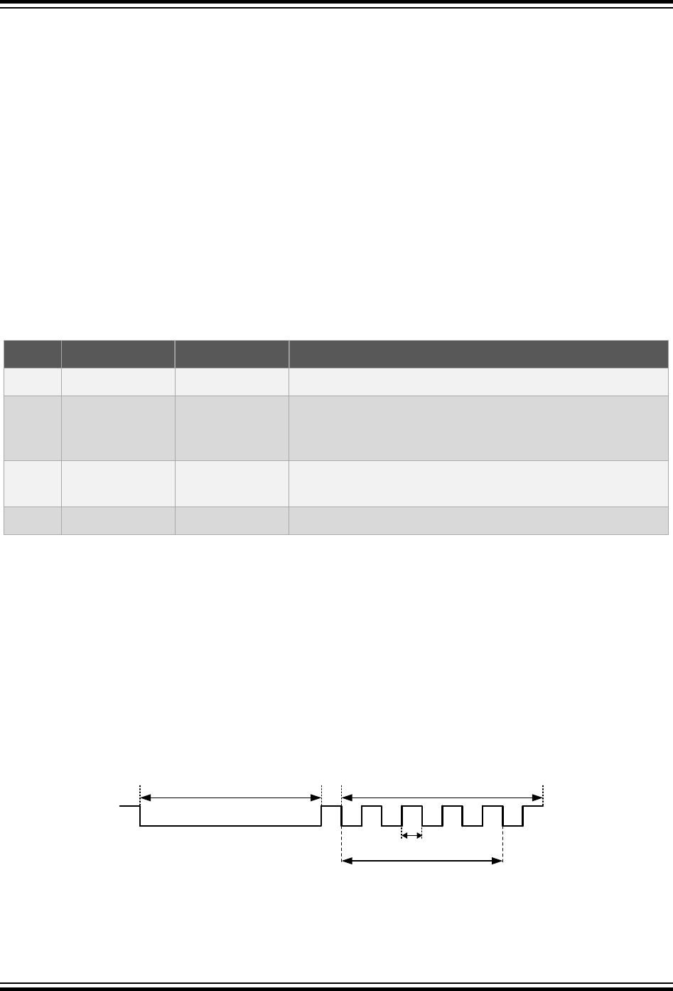
When a high-to-low transition is detected on RxDn, the oscillator is powered up and the UART clock is
enabled. After start-up, the rest of the data frame can be received, provided that the baud rate is slow
enough in relation to the oscillator start-up time. Start-up time of the oscillators varies with supply voltage
and temperature. For details on oscillator start-up time characteristics, refer to the Electrical
Characteristics.
If a false Start bit is detected and if the system has not been woken up by another source, the clock will
automatically be turned OFF and the UART waits for the next transition.
The UART start frame detection works in Asynchronous mode only. It is enabled by writing the Start
Frame Detection bit (SFDEN) in USARTn.CTLB. If the Start bit is detected while the device is in Standby
Sleep mode, the UART Start Interrupt Flag (RXSIF) bit is set.
In Active, Idle, and Power-Down Sleep modes, the asynchronous detection is automatically disabled.
The UART receive complete flag and UART start interrupt flag share the same interrupt line, but each has
its dedicated interrupt settings. Table 21-5 shows the USART start frame detection modes, depending on
interrupt setting.
Table 22-8. USART Start Frame Detection Modes
SFDEN RXSIF Interrupt RXCIF Interrupt Comment
0 x x Standard mode.
1 Disabled Disabled Only the oscillator is powered during the frame reception.
If the interrupts are disabled and buffer overflow is
ignored, all incoming frames will be lost.
1 (1) Disabled Enabled System/all clocks are awakened on Receive Complete
interrupt.
1 (1) Enabled x System/all clocks are awakened on UART Start Detection.
Note:
1. The SLEEP instruction will not shut down the oscillator if there is ongoing communication.
22.3.2.8 Break Character Detection and Auto-Baud
When USART receive mode is set to LINAUTO mode (RXMODE in USARTn.CTRLB), it follows the LIN
format. All LIN frames start with a break field followed by a sync field. The USART uses a break detection
threshold of greater than 11 nominal bit times at the configured baud rate. At any time, if more than 11
consecutive dominant bits are detected on the bus, the USART detects a break field. When a break field
has been detected, the USART expects the sync field character to be 0x55. This field is used to update
the actual baud rate in order to stay synchronized. If the received sync character is not 0x55, then the
Inconsistent Sync Field Error flag (ISFIF in USARTn.STATUS) is set and the baud rate is unchanged.
Figure 22-12. LIN Break and Sync Fields
Sync Field
Break Field
8 Tbit
Tbit
After a break field is detected and the Start bit of the sync field is detected, a counter is started. The
counter is then incremented for the next eight Tbit of the sync field. At the end of these 8-bit times, the
counter is stopped. At this moment, the ten Most Significant bits of the counter (value divided by 64) gives
megaAVR® 0-Series
Universal Synchronous and Asynchronous Recei...
© 2018 Microchip Technology Inc. Datasheet Preliminary DS40002015A-page 294

the new clock divider and the six Least Significant bits of this value (the remainder) gives the new
fractional part. When the sync field has been received and all bits are found valid, the clock divider and
the fractional part are updated in the Baud Rate Generator register (USARTn.BAUD). After the break and
sync fields, n characters of data can be received.
When the USART receive mode is set to GENAUTO mode, a generic Auto-baud mode is enabled. In this
mode, there are no checks of the sync character to equal 0x55. After detection of a break field, the
USART expects the next character to be a sync field, counting eight low and high bit times. If the
measured sync field results in a valid BAUD value (0x0064-0xffff), the BAUD register is updated. Setting
the Wait for Break bit (WFB in USARTn.STATUS) before receiving the next break character, the next
negative plus positive edge of RxD line is detected as a break. This makes it possible to set an arbitrary
new baud rate without knowing the current baud rate.
22.3.2.9 Multiprocessor Communication Mode
The Multiprocessor Communication mode (MCPM) effectively reduces the number of incoming frames
that have to be handled by the receiver in a system with multiple microcontrollers communicating via the
same serial bus. This mode is enabled by writing a '1' to the MCPM bit in the Control B register
(USARTn.CTRLB). In this mode, a dedicated bit in the frames is used to indicate whether the frame is an
address or data frame type.
If the receiver is set up to receive frames that contain five to eight data bits, the first Stop bit is used to
indicate the frame type. If the receiver is set up for frames with nine data bits, the ninth bit is used to
indicate frame type. When the frame type bit is one, the frame contains an address. When the frame type
bit is zero, the frame is a data frame. If 5- to 8-bit character frames are used, the transmitter must be set
to use two Stop bits, since the first Stop bit is used for indicating the frame type.
If a particular slave MCU has been addressed, it will receive the following data frames as usual, while the
other slave MCUs will ignore the frames until another address frame is received.
Using Multiprocessor Communication Mode
The following procedure should be used to exchange data in Multiprocessor Communication mode
(MPCM):
1. All slave MCUs are in Multiprocessor Communication mode.
2. The master MCU sends an address frame, and all slaves receive and read this frame.
3. Each slave MCU determines if it has been selected.
4. The addressed MCU will disable MPCM and receive all data frames. The other slave MCUs will
ignore the data frames.
5. When the addressed MCU has received the last data frame, it must enable MPCM again and wait
for a new address frame from the master.
The process then repeats from step 2.
Using any of the 5- to 8-bit character frame formats is impractical, as the receiver must change between
using n and n+1 character frame formats. This makes full-duplex operation difficult since the transmitter
and receiver must use the same character size setting.
22.3.2.10 IRCOM Mode of Operation
The IRCOM mode enables IrDA® 1.4 compliant modulation and demodulation for baud rates up to 115.2
kbps. When IRCOM mode is enabled, Double-Speed mode cannot be used for the USART.
megaAVR® 0-Series
Universal Synchronous and Asynchronous Recei...
© 2018 Microchip Technology Inc. Datasheet Preliminary DS40002015A-page 295
Overview
A USART can be configured in infrared communication mode (IRCOM) that is IrDA compatible with baud
rates up to 115.2 kbps. When enabled, the IRCOM mode enables infrared pulse encoding/decoding for
the USART.
A USART is set in IRCOM mode by writing 0x2 to the CMODE bits in USARTn.CTRLC. The data on the
TX/RX pins are the inverted value of the transmitted/received infrared pulse. It is also possible to select
an event channel from the Event System as an input for the IRCOM receiver. This will disable the RX
input from the USART pin.
For transmission, three pulse modulation schemes are available:
• 3/16 of the baud rate period
• Fixed programmable pulse time based on the peripheral clock frequency
• Pulse modulation disabled
For the reception, a fixed programmable minimum high-level pulse width for the pulse to be decoded as a
logical ‘0’ is used. Shorter pulses will then be discarded, and the bit will be decoded to logical ‘1’ as if no
pulse was received.
Block Diagram
Figure 22-13. Block Diagram
IRCOM
Pulse
Decoding
Pulse
Encoding
Encoded RXD
Decoded RXD
Decoded RXD
Encoded RXD
Event System Events
USART RXD
TXD
IRCOM and Event System
The Event System can be used as the receiver input. This enables the IRCOM or USART input from the
I/O pins or sources other than the corresponding RX pin. If the Event System input is enabled, input from
the USART's RX pin is automatically disabled.
22.3.3 Events
The USART can accept the following input event:
• IREI - IrDA Event Input
The Event is enabled by writing a '1' to the IrDA Event Input bit (IREI) in the Event Control register
(USARTn.EVCTRL).
The USART generates the following event:
• In SPI master mode: If USART is enabled and transmitting, the generated XCK clock is output on
the USARTs event output. Otherwise, the event output is zero.
megaAVR® 0-Series
Universal Synchronous and Asynchronous Recei...
© 2018 Microchip Technology Inc. Datasheet Preliminary DS40002015A-page 296

• In synchronous USART master mode: If USART is enabled and transmitting, the generated XCK
clock is output on the USARTs event output. Otherwise, the event output is zero.
• In other modes and configurations, the event output is zero.
22.3.4 Interrupts
Table 22-9. Available Interrupt Vectors and Sources
Name Vector Description Conditions
RXC Receive Complete
interrupt
• There are unread data in the receive buffer (RXCIE)
• Receive of Start-of-Frame detected (RXSIE)
• Auto-Baud Error/ISFIF flag set (ABEIE)
DRE Data Register Empty
interrupt
The transmit buffer is empty/ready to receive new data (DREIE).
TXC Transmit Complete
interrupt
The entire frame in the Transmit Shift Register has been shifted out
and there are no new data in the transmit buffer (TXCIE).
When an interrupt condition occurs, the corresponding Interrupt Flag is set in the Status register
(USARTn.STATUS).
An interrupt source is enabled or disabled by writing to the corresponding bit in the Control A register
(USARTn.CTRLA).
An interrupt request is generated when the corresponding interrupt source is enabled and the Interrupt
Flag is set. The interrupt request remains active until the Interrupt Flag is cleared. See the
USARTn.STATUS register for details on how to clear Interrupt Flags.
megaAVR® 0-Series
Universal Synchronous and Asynchronous Recei...
© 2018 Microchip Technology Inc. Datasheet Preliminary DS40002015A-page 297

22.4 Register Summary - USARTn
Offset Name Bit Pos.
0x00 RXDATAL 7:0 DATA[7:0]
0x01 RXDATAH 7:0 RXCIF BUFOVF FERR PERR DATA[8]
0x02 TXDATAL 7:0 DATA[7:0]
0x03 TXDATAH 7:0 DATA[8]
0x04 STATUS 7:0 RXCIF TXCIF DREIF RXSIF ISFIF BDF WFB
0x05 CTRLA 7:0 RXCIE TXCIE DREIE RXSIE LBME ABEIE RS485[1:0]
0x06 CTRLB 7:0 RXEN TXEN SFDEN ODME RXMODE[1:0] MPCM
0x07 CTRLC 7:0 CMODE[1:0] PMODE[1:0] SBMODE CHSIZE[2:0]
0x07 CTRLC 7:0 CMODE[1:0] UDORD UCPHA
0x08 BAUD
7:0 BAUD[7:0]
15:8 BAUD[15:8]
0x0A Reserved
0x0B DBGCTRL 7:0 DBGRUN
0x0C EVCTRL 7:0 IREI
0x0D TXPLCTRL 7:0 TXPL[7:0]
0x0E RXPLCTRL 7:0 RXPL[6:0]
22.5 Register Description
megaAVR® 0-Series
Universal Synchronous and Asynchronous Recei...
© 2018 Microchip Technology Inc. Datasheet Preliminary DS40002015A-page 298

22.5.1 Receiver Data Register Low Byte
Name: RXDATAL
Offset: 0x00
Reset: 0x00
Property: R
Reading the USARTn.RXDATAL Register will return the contents of the Receive Data Buffer register
(RXB).
The receive buffer consists of a two-level FIFO. The FIFO and the corresponding flags in the high byte of
RXDATA will change state whenever the receive buffer is accessed (read). If CHSIZE in USARTn.CTRLC
is set to 9BIT Low byte first, read USARTn.RXDATAL before USARTn.RXDATAH. Otherwise, always read
USARTn.RXDATAH before USARTn.RXDATAL in order to get the correct flags.
Bit 7 6 5 4 3 2 1 0
DATA[7:0]
Access R R R R R R R R
Reset 0 0 0 0 0 0 0 0
Bits 7:0 – DATA[7:0] Receiver Data Register
megaAVR® 0-Series
Universal Synchronous and Asynchronous Recei...
© 2018 Microchip Technology Inc. Datasheet Preliminary DS40002015A-page 299

22.5.2 Receiver Data Register High Byte
Name: RXDATAH
Offset: 0x01
Reset: 0x00
Property: -
Reading the USARTn.RXDATAH register location will return the contents of the ninth DATA bit plus Status
bits.
The receive buffer consists of a two-level FIFO. The FIFO and the corresponding flags in the high byte of
USARTn.RXDATAH will change state whenever the receive buffer is accessed (read). If CHSIZE in
USARTn.CTRLC is set to 9BIT Low byte first, read USARTn.RXDATAL before USARTn.RXDATAH.
Otherwise, always read USARTn.RXDATAH before USARTn.RXDATAL in order to get the correct flags.
Bit 7 6 5 4 3 2 1 0
RXCIF BUFOVF FERR PERR DATA[8]
Access R R R R R
Reset 0 0 0 0 0
Bit 7 – RXCIF USART Receive Complete Interrupt Flag
This flag is set when there is unread data in the receive buffer and cleared when the receive buffer is
empty (i.e. does not contain any unread data). When the receiver is disabled, the receive buffer will be
flushed and consequently, the RXCIF will become zero.
Bit 6 – BUFOVF Buffer Overflow
The BUFOVF flag indicates data loss due to a receiver buffer full condition. This flag is set if a Buffer
Overflow condition is detected. A Buffer Overflow occurs when the receive buffer is full (two characters), it
is a new character waiting in the Receive Shift register, and a new Start bit is detected. This flag is valid
until the receive buffer (USARTn.RXDATAL) is read.
This flag is not used in Master SPI mode of operation.
Bit 2 – FERR Frame Error
The FERR flag indicates the state of the first Stop bit of the next readable frame stored in the receive
buffer. The bit is set if the received character had a Frame Error (i.e. when the first Stop bit was zero and
cleared when the Stop bit of the received data is '1'. This bit is valid until the receive buffer
(USARTn.RXDATAL) is read. The FERR is not affected by the SBMODE bit in USARTn.CTRLC since the
receiver ignores all, except for the first Stop bit.
This flag is not used in Master SPI mode of operation.
Bit 1 – PERR Parity Error
If parity checking is enabled and the next character in the receive buffer has a Parity Error this flag is set.
If Parity Check is not enabled the PERR will always be read as zero. This bit is valid until the receive
buffer (USARTn.RXDATAL) is read. For details on parity calculation refer to Parity. If USART is set to
LINAUTO mode, this bit will be a Parity Check of the protected identifier field and will be valid when
DATA[8] in USARTn.RXDATAH reads low.
This flag is not used in Master SPI mode of operation.
megaAVR® 0-Series
Universal Synchronous and Asynchronous Recei...
© 2018 Microchip Technology Inc. Datasheet Preliminary DS40002015A-page 300

Bit 0 – DATA[8] Receiver Data Register
When USART receiver is set to LINAUTO mode, this bit indicates if the received data is within the
response space of a LIN frame. If the received data is the protected identifier field, this bit will be read as
zero. Otherwise, the bit will be read as one. For Receiver mode other than LINAUTO mode, DATA[8]
holds the ninth data bit in the received character when operating with serial frames with nine data bits.
megaAVR® 0-Series
Universal Synchronous and Asynchronous Recei...
© 2018 Microchip Technology Inc. Datasheet Preliminary DS40002015A-page 301

22.5.3 Transmit Data Register Low Byte
Name: TXDATAL
Offset: 0x02
Reset: 0x00
Property: R/W
The Transmit Data Buffer (TXB) register will be the destination for data written to the USARTn.TXDATAL
register location.
For 5-, 6-, or 7-bit characters the upper unused bits will be ignored by the transmitter and set to zero by
the receiver.
The transmit buffer can only be written when the DREIF flag in the USARTn.STATUS register is set. Data
written to DATA when the DREIF flag is not set will be ignored by the USART transmitter. When data is
written to the transmit buffer, and the transmitter is enabled, the transmitter will load the data into the
Transmit Shift register when the Shift register is empty. The data is then transmitted on the TxD pin.
Bit 7 6 5 4 3 2 1 0
DATA[7:0]
Access R/W R/W R/W R/W R/W R/W R/W R/W
Reset 0 0 0 0 0 0 0 0
Bits 7:0 – DATA[7:0] Transmit Data Register
megaAVR® 0-Series
Universal Synchronous and Asynchronous Recei...
© 2018 Microchip Technology Inc. Datasheet Preliminary DS40002015A-page 302

22.5.4 Transmit Data Register High Byte
Name: TXDATAH
Offset: 0x03
Reset: 0x00
Property: -
USARTn.TXDATAH holds the ninth data bit in the character to be transmitted when operating with serial
frames with nine data bits. When used this bit must be written before writing to USARTn.TXDATAL except
if CHSIZE in USARTn.CTRLC is set to 9BIT Low byte first where USARTn.TXDATAL should be written
first.
This bit is unused in Master SPI mode of operation.
Bit 7 6 5 4 3 2 1 0
DATA[8]
Access W
Reset 0
Bit 0 – DATA[8] Transmit Data Register
This bit is used when CHSIZE=9BIT in USARTn.CTRLC.
megaAVR® 0-Series
Universal Synchronous and Asynchronous Recei...
© 2018 Microchip Technology Inc. Datasheet Preliminary DS40002015A-page 303

22.5.5 USART Status Register
Name: STATUS
Offset: 0x04
Reset: 0x00
Property: -
Bit 7 6 5 4 3 2 1 0
RXCIF TXCIF DREIF RXSIF ISFIF BDF WFB
Access R R/W R R/W R/W R/W R/W
Reset 0 0 0 0 0 0 0
Bit 7 – RXCIF USART Receive Complete Interrupt Flag
This flag is set to ‘1’ when there is unread data in the receive buffer and cleared when the receive buffer
is empty (i.e. does not contain any unread data). When the receiver is disabled, the receive buffer will be
flushed and consequently, the RXCIF will become zero.
When interrupt-driven data reception is used, the receive complete interrupt routine must read the
received data from RXDATA in order to clear the RXCIF. If not, a new interrupt will occur directly after the
return from the current interrupt.
Bit 6 – TXCIF USART Transmit Complete Interrupt Flag
This flag is set when the entire frame in the Transmit Shift register has been shifted out and there are no
new data in the transmit buffer (TXDATA).
This flag is automatically cleared when the transmit complete interrupt vector is executed. The flag can
also be cleared by writing a ‘1’ to its bit location.
Bit 5 – DREIF USART Data Register Empty Flag
The DREIF indicates if the transmit buffer (TXDATA) is ready to receive new data. The flag is set to ‘1’
when the transmit buffer is empty and is ‘0’ when the transmit buffer contains data to be transmitted that
has not yet been moved into the Shift register. DREIF is set after a Reset to indicate that the transmitter is
ready. Always write this bit to ‘0’ when writing the STATUS register.
DREIF is cleared to ‘0’ by writing TXDATAL. When interrupt-driven data transmission is used, the Data
Register Empty interrupt routine must either write new data to TXDATA in order to clear DREIF or disable
the Data Register Empty interrupt. If not, a new interrupt will occur directly after the return from the
current interrupt.
Bit 4 – RXSIF USART Receive Start Interrupt Flag
The RXSIF flag indicates a valid Start condition on RxD line. The flag is set when the system is in
standby modes and a high (IDLE) to low (START) valid transition is detected on the RxD line. If the start
detection is not enabled, the RXSIF will always be read as zero. This flag can only be cleared by writing a
‘1’ to its bit location. This flag is not used in the Master SPI mode operation.
Bit 3 – ISFIF Inconsistent Sync Field Interrupt Flag
This bit is set when the auto-baud is enabled and the sync field bit time is too fast or too slow to give a
valid baud setting. It will also be set when USART is set to LINAUTO mode and the SYNC character differ
from data value 0x55.
Writing a ‘1’ to this bit will clear the flag and bring the USART back to Idle state.
megaAVR® 0-Series
Universal Synchronous and Asynchronous Recei...
© 2018 Microchip Technology Inc. Datasheet Preliminary DS40002015A-page 304

Bit 1 – BDF Break Detected Flag
This bit is intended for USART configured to LINAUTO receive mode. The break detector has a fixed
threshold of 11 bits low for a Break to be detected. The BDF bit is set after a valid BREAK and SYNC
character is detected. The bit is automatically cleared when next data is received. The bit will behave
identically when USART is set to GENAUTO mode. In NORMAL or CLK2X receive mode, the BDF bit is
unused.
This bit is cleared by writing a ‘1’ to it.
Bit 0 – WFB Wait For Break
Writing this bit to ‘1’ will register the next low and high transition on RxD line as a Break character. This
can be used to wait for a Break character of arbitrary width. Combined with USART set to GENAUTO
mode, this allows the user to set any BAUD rate through BREAK and SYNC as long as it falls within the
valid range of the USARTn.BAUD register. This bit will always read ‘0’.
megaAVR® 0-Series
Universal Synchronous and Asynchronous Recei...
© 2018 Microchip Technology Inc. Datasheet Preliminary DS40002015A-page 305

22.5.6 Control A
Name: CTRLA
Offset: 0x05
Reset: 0x00
Property: -
Bit 7 6 5 4 3 2 1 0
RXCIE TXCIE DREIE RXSIE LBME ABEIE RS485[1:0]
Access R/W R/W R/W R/W R/W R/W R/W R/W
Reset 0 0 0 0 0 0 0 0
Bit 7 – RXCIE Receive Complete Interrupt Enable
The bit enables the Receive Complete Interrupt (interrupt vector RXC). The enabled interrupt will be
triggered when RXCIF in the USARTn.STATUS register is set.
Bit 6 – TXCIE Transmit Complete Interrupt Enable
This bit enables the Transmit Complete Interrupt (interrupt vector TXC). The enabled interrupt will be
triggered when the TXCIF in the USARTn.STATUS register is set.
Bit 5 – DREIE Data Register Empty Interrupt Enable
This bit enables the Data Register Empty Interrupt (interrupt vector DRE). The enabled interrupt will be
triggered when the DREIF in the USART.STATUS register is set.
Bit 4 – RXSIE Receiver Start Frame Interrupt Enable
Writing a '1' to this bit enables the Start Frame Detector to generate an interrupt on interrupt vector RXC
when a start-of-frame condition is detected.
Bit 3 – LBME Loop-back Mode Enable
Writing this bit to '1' enables an internal connection between the TxD and RxD pin.
Bit 2 – ABEIE Auto-baud Error Interrupt Enable
Writing this bit to '1' enables the auto-baud error interrupt on interrupt vector RXC. The enabled interrupt
will trigger for conditions where the ISFIF flag is set.
Bits 1:0 – RS485[1:0] RS-485 Mode
These bits enable the RS-485 and select the operation mode.
Value Name Description
0x0 OFF Disabled.
0x1 EXT Enables RS-485 mode with control of an external line driver through a dedicated
Transmit Enable (TE) pin.
0x2 INT Enables RS-485 mode with control of the internal USART transmitter.
0x3 - Reserved.
megaAVR® 0-Series
Universal Synchronous and Asynchronous Recei...
© 2018 Microchip Technology Inc. Datasheet Preliminary DS40002015A-page 306

22.5.7 Control B
Name: CTRLB
Offset: 0x06
Reset: 0x00
Property: -
Bit 7 6 5 4 3 2 1 0
RXEN TXEN SFDEN ODME RXMODE[1:0] MPCM
Access R/W R/W R/W R/W R/W R/W R/W
Reset 0 0 0 0 0 0 0
Bit 7 – RXEN Receiver Enable
Writing this bit to ‘1’ enables the USART receiver. The receiver will override normal port operation for the
RxD pin when enabled. Disabling the receiver will flush the receive buffer invalidating the FERR,
BUFOVF, and PERR flags. In GENAUTO and LINAUTO mode, disabling the receiver will reset the auto-
baud detection logic.
Bit 6 – TXEN Transmitter Enable
Writing this bit to ‘1’ enables the USART transmitter. The transmitter will override normal port operation
for the TxD pin when enabled. Disabling the transmitter (writing TXEN to zero) will not become effective
until ongoing and pending transmissions are completed (i.e. when the Transmit Shift register and
Transmit Buffer register does not contain data to be transmitted). When the transmitter is disabled, it will
no longer override the TxDn pin, and the pin direction is set as input automatically by hardware, even if it
was configured as output by the user.
Bit 4 – SFDEN Start Frame Detection Enable
Writing this bit to ‘1’ enables the USART Start Frame Detection mode. The Start Frame detector is able to
wake up the system from Idle or Standby Sleep modes when a high (IDLE) to low (START) transition is
detected on the RxD line.
Bit 3 – ODME Open Drain Mode Enable
Writing this bit to ‘1’ makes the TxD pin to have open-drain functionality. A pull-up resistor is needed to
prevent the line from floating when a logic one is output to the TxD pin.
Bits 2:1 – RXMODE[1:0] Receiver Mode
In CLK2X mode, the divisor of the baud rate divider will be reduced from 16 to 8 effectively doubling the
transfer rate for asynchronous communication modes. For synchronous operation, the CLK2X mode has
no effect and RXMODE should always be written to zero. RXMODE must be zero when the USART
Communication mode is configured to IRCOM. Setting RXMODE to GENAUTO enables generic auto-
baud where the SYNC character is valid when eight low and high bits have been registered. In this mode,
any SYNC character that gives a valid BAUD rate will be accepted. In LINAUTO mode the SYNC
character is constrained and found valid if every two bits falls within 32 ±6 baud samples of the internal
baud rate and match data value 0x55. The GENAUTO and LINAUTO mode is only supported for USART
operated in Asynchronous Slave mode.
Value Name Description
0x0 NORMAL Normal USART mode, Standard Transmission Speed
0x1 CLK2X Normal USART mode, Double Transmission Speed
megaAVR® 0-Series
Universal Synchronous and Asynchronous Recei...
© 2018 Microchip Technology Inc. Datasheet Preliminary DS40002015A-page 307

Value Name Description
0x2 GENAUTO Generic Auto-baud mode
0x3 LINAUTO LIN Constrained Auto-baud mode
Bit 0 – MPCM Multi-Processor Communication Mode
Writing a ‘1’ to this bit enables the Multi-Processor Communication mode: the USART receiver ignores all
the incoming frames that do not contain address information. The transmitter is unaffected by the MPCM
setting. For more detailed information see Multiprocessor Communication Mode.
megaAVR® 0-Series
Universal Synchronous and Asynchronous Recei...
© 2018 Microchip Technology Inc. Datasheet Preliminary DS40002015A-page 308
22.5.8 Control C - Async Mode
Name: CTRLC
Offset: 0x07
Reset: 0x03
Property: -
This register description is valid for all modes except Master SPI mode. When the USART
Communication mode bits (CMODE) in this register are written to 'MSPI', see Control C - Master SPI
Mode for the correct description.
Bit 7 6 5 4 3 2 1 0
CMODE[1:0] PMODE[1:0] SBMODE CHSIZE[2:0]
Access R/W R/W R/W R/W R/W R/W R/W R/W
Reset 0 0 0 0 0 0 1 1
Bits 7:6 – CMODE[1:0] USART Communication Mode
Writing these bits select the Communication mode of the USART.
Writing a 0x3 to these bits alters the available bit fields in this register, see Control C - Master SPI Mode.
Value Name Description
0x0 ASYNCHRONOUS Asynchronous USART
0x1 SYNCHRONOUS Synchronous USART
0x2 IRCOM Infrared Communication
0x3 MSPI Master SPI
Bits 5:4 – PMODE[1:0] Parity Mode
Writing these bits enable and select the type of parity generation.
When enabled, the transmitter will automatically generate and send the parity of the transmitted data bits
within each frame. The receiver will generate a parity value for the incoming data, compare it to the
PMODE setting, and set the Parity Error flag (PERR) in the STATUS register (USARTn.STATUS) if a
mismatch is detected.
Value Name Description
0x0 DISABLED Disabled
0x1 - Reserved
0x2 EVEN Enabled, Even Parity
0x3 ODD Enabled, Odd Parity
Bit 3 – SBMODE Stop Bit Mode
Writing this bit selects the number of Stop bits to be inserted by the transmitter.
The receiver ignores this setting.
Value Description
0 1 Stop bit
1 2 Stop bits
megaAVR® 0-Series
Universal Synchronous and Asynchronous Recei...
© 2018 Microchip Technology Inc. Datasheet Preliminary DS40002015A-page 309

Bits 2:0 – CHSIZE[2:0] Character Size
Writing these bits select the number of data bits in a frame. The receiver and transmitter use the same
setting. For 9BIT character size, the order of which byte to read or write first, low or high byte of RXDATA
or TXDATA is selectable.
Value Name Description
0x0 5BIT 5-bit
0x1 6BIT 6-bit
0x2 7BIT 7-bit
0x3 8BIT 8-bit
0x4 - Reserved
0x5 - Reserved
0x6 9BITL 9-bit (Low byte first)
0x7 9BITH 9-bit (High byte first)
megaAVR® 0-Series
Universal Synchronous and Asynchronous Recei...
© 2018 Microchip Technology Inc. Datasheet Preliminary DS40002015A-page 310
22.5.9 Control C - Master SPI Mode
Name: CTRLC
Offset: 0x07
Reset: 0x00
Property: -
This register description is valid only when the USART is in Master SPI mode (CMODE written to MSPI).
For other CMODE values, see Control C - Async Mode.
See USART in Master SPI mode for a full description of the Master SPI mode operation.
Bit 7 6 5 4 3 2 1 0
CMODE[1:0] UDORD UCPHA
Access R/W R/W R/W R/W
Reset 0 0 0 0
Bits 7:6 – CMODE[1:0] USART Communication Mode
Writing these bits select the communication mode of the USART.
Writing a value different than 0x3 to these bits alters the available bit fields in this register, see Control C -
Async Mode.
Value Name Description
0x0 ASYNCHRONOUS Asynchronous USART
0x1 SYNCHRONOUS Synchronous USART
0x2 IRCOM Infrared Communication
0x3 MSPI Master SPI
Bit 2 – UDORD Data Order
Writing this bit selects the frame format.
The receiver and transmitter use the same setting. Changing the setting of UDORD will corrupt all
ongoing communication for both the receiver and the transmitter.
Value Description
0 MSB of the data word is transmitted first
1 LSB of the data word is transmitted first
Bit 1 – UCPHA Clock Phase
The UCPHA bit setting determines if data is sampled on the leading (first) edge or tailing (last) edge of
XCKn. Refer to the Master SPI Mode Clock Generation for details.
megaAVR® 0-Series
Universal Synchronous and Asynchronous Recei...
© 2018 Microchip Technology Inc. Datasheet Preliminary DS40002015A-page 311

22.5.10 Baud Register
Name: BAUD
Offset: 0x08
Reset: 0x00
Property: -
The USARTn.BAUDL and USARTn.BAUDH register pair represents the 16-bit value, USARTn.BAUD.
The low byte [7:0] (suffix L) is accessible at the original offset. The high byte [15:8] (suffix H) can be
accessed at offset + 0x01.
Ongoing transmissions of the transmitter and receiver will be corrupted if the baud rate is changed.
Writing this register will trigger an immediate update of the baud rate prescaler. For more information on
how to set the baud rate, see Table 22-1.
Bit 15 14 13 12 11 10 9 8
BAUD[15:8]
Access R/W R/W R/W R/W R/W R/W R/W R/W
Reset 0 0 0 0 0 0 0 0
Bit 7 6 5 4 3 2 1 0
BAUD[7:0]
Access R/W R/W R/W R/W R/W R/W R/W R/W
Reset 0 0 0 0 0 0 0 0
Bits 15:8 – BAUD[15:8] USART Baud Rate High Byte
These bits hold the MSB of the 16-bit Baud register.
Bits 7:0 – BAUD[7:0] USART Baud Rate Low Byte
These bits hold the LSB of the 16-bit Baud register.
megaAVR® 0-Series
Universal Synchronous and Asynchronous Recei...
© 2018 Microchip Technology Inc. Datasheet Preliminary DS40002015A-page 312

22.5.11 Debug Control Register
Name: DBGCTRL
Offset: 0x0B
Reset: 0x00
Property: -
Bit 7 6 5 4 3 2 1 0
DBGRUN
Access R/W
Reset 0
Bit 0 – DBGRUN Debug Run
Value Description
0 The peripheral is halted in Break Debug mode and ignores events
1 The peripheral will continue to run in Break Debug mode when the CPU is halted
megaAVR® 0-Series
Universal Synchronous and Asynchronous Recei...
© 2018 Microchip Technology Inc. Datasheet Preliminary DS40002015A-page 313

22.5.12 IrDA Control Register
Name: EVCTRL
Offset: 0x0C
Reset: 0x00
Property: -
Bit 7 6 5 4 3 2 1 0
IREI
Access R/W
Reset 0
Bit 0 – IREI IrDA Event Input Enable
This bit enables the event source for the IRCOM Receiver. If event input is selected for the IRCOM
Receiver, the input from the USART’s RX pin is automatically disabled.
megaAVR® 0-Series
Universal Synchronous and Asynchronous Recei...
© 2018 Microchip Technology Inc. Datasheet Preliminary DS40002015A-page 314

22.5.13 IRCOM Transmitter Pulse Length Control Register
Name: TXPLCTRL
Offset: 0x0D
Reset: 0x00
Property: -
Bit 7 6 5 4 3 2 1 0
TXPL[7:0]
Access R/W R/W R/W R/W R/W R/W R/W R/W
Reset 0 0 0 0 0 0 0 0
Bits 7:0 – TXPL[7:0] Transmitter Pulse Length
The 8-bit value sets the pulse modulation scheme for the transmitter. Setting this register will have effect
only if IRCOM mode is selected by a USART. By leaving this register value to zero, 3/16 of the baud rate
period pulse modulation is used. Setting this value from 1 to 254 will give a fixed pulse length coding. The
8-bit value sets the number of system clock periods for the pulse. The start of the pulse will be
synchronized with the rising edge of the baud rate clock. Setting the value to 255 (0xFF) will disable pulse
coding, letting the RX and TX signals pass through the IRCOM module unaltered. This enables other
features through the IRCOM module, such as half-duplex USART, Loop-back testing, and USART RX
input from an event channel.
TXPL must be configured before the USART transmitter is enabled (TXEN).
megaAVR® 0-Series
Universal Synchronous and Asynchronous Recei...
© 2018 Microchip Technology Inc. Datasheet Preliminary DS40002015A-page 315

22.5.14 IRCOM Receiver Pulse Length Control Register
Name: RXPLCTRL
Offset: 0x0E
Reset: 0x00
Property: -
Bit 7 6 5 4 3 2 1 0
RXPL[6:0]
Access R/W R/W R/W R/W R/W R/W R/W
Reset 0 0 0 0 0 0 0
Bits 6:0 – RXPL[6:0] Receiver Pulse Length
The 8-bit value sets the filter coefficient for the IRCOM transceiver. Setting this register will only have
effect if IRCOM mode is selected by a USART.
By leaving this register value to zero, filtering is disabled. Setting this value between 0x01 and 0xFF will
enable filtering, where x+1 equal samples are required for the pulse to be accepted.
RXPL must be configured before USART receiver is enabled (RXEN).
megaAVR® 0-Series
Universal Synchronous and Asynchronous Recei...
© 2018 Microchip Technology Inc. Datasheet Preliminary DS40002015A-page 316

23. Serial Peripheral Interface (SPI)
23.1 Features
• Full-Duplex, Three-Wire Synchronous Data Transfer
• Master or Slave Operation
• LSB First or MSB First Data Transfer
• Seven Programmable Bit Rates
• End of Transmission Interrupt Flag
• Write Collision Flag Protection
• Wake-up from Idle Mode
• Double-Speed (CK/2) Master SPI Mode
23.2 Overview
The Serial Peripheral Interface (SPI) is a high-speed synchronous data transfer interface using three or
four pins. It allows full duplex communication between an AVR device and peripheral devices or between
several microcontrollers. The SPI peripheral can be configured as either Master or Slave. The master
initiates and controls all data transactions.
The interconnection between master and slave devices with SPI is shown in the block diagram. The
system consists of two shift registers and a master clock generator. The SPI master initiates the
communication cycle by pulling the desired slave's slave select (SS) signal low. Master and slave prepare
the data to be sent to their respective shift registers, and the master generates the required clock pulses
on the SCK line to exchange data. Data is always shifted from master to slave on the master output,
slave input (MOSI) line, and from slave to master on the master input, slave output (MISO) line.
megaAVR® 0-Series
Serial Peripheral Interface (SPI)
© 2018 Microchip Technology Inc. Datasheet Preliminary DS40002015A-page 317
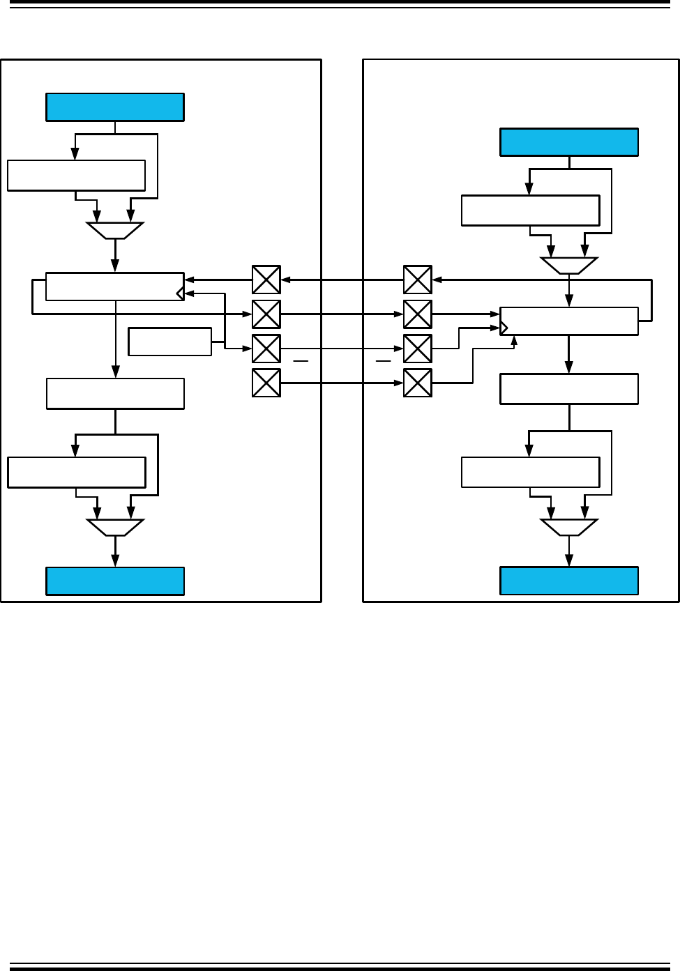
23.2.1 Block Diagram
Figure 23-1. SPI Block Diagram
8-bit Shift Register
MSb
Transmit Data Register
(DATA)
Receive Data Register
(DATA)
MOSI
MISO
SCK
SS
SLAVE
8-bit Shift Register
MSb
MOSI
MISO
SCK
SS
MASTER
SPI CLOCK
GENERATOR
Transmit Buffer
Register
Receive Buffer
Register
Transmit Data Register
(DATA)
Transmit Buffer
Register
Receive Data Register
(DATA)
Second Receive Buffer
Register
First Receive Buffer
Register
First Receive Buffer
Register
LSb
LSb
The SPI is built around an 8-bit Shift register that will shift data out and in at the same time. The Transmit
Data register and the Receive Data register are not physical registers but are mapped to other registers
when written or read: Writing the Transmit Data register (SPIn.DATA) will write the Shift register in Normal
mode and the Transmit Buffer register in Buffer mode. Reading the Receive Data register (SPIn.DATA)
will read the First Receive Buffer register in normal mode and the Second Receive Data register in Buffer
mode.
In Master mode, the SPI has a clock generator to generate the SCK clock. In Slave mode, the received
SCK clock is synchronized and sampled to trigger the shifting of data in the Shift register.
megaAVR® 0-Series
Serial Peripheral Interface (SPI)
© 2018 Microchip Technology Inc. Datasheet Preliminary DS40002015A-page 318

23.2.2 Signal Description
Table 23-1. Signals in Master and Slave Mode
Signal Description Pin Configuration
Master Mode Slave Mode
MOSI Master Out Slave In User defined Input
MISO Master In Slave Out Input User defined
SCK Slave clock User defined Input
SS Slave select User defined Input
When the SPI module is enabled, the data direction of the MOSI, MISO, SCK, and SS pins is overridden
according to Table 23-1.
The data direction of the pins with "User defined" pin configuration is not controlled by the SPI: The data
direction is controlled by the application software configuring the port peripheral. If these pins are
configured with data direction as input, they can be used as regular I/O pin inputs. If these pins are
configured with data direction as output, their output value is controlled by the SPI. The MISO pin has a
special behavior: When the SPI is in Slave mode and the MISO pin is configured as an output, the SS pin
controls the output buffer of the pin: If SS is low, the output buffer drives the pin, if SS is high, the pin is
tri-stated.
The data direction of the pins with "Input" pin configuration is controlled by the SPI hardware.
23.3 Functional Description
23.3.1 Initialization
Initialize the SPI to a basic functional state by following these steps:
1. Configure the SS pin in the port peripheral.
2. Select SPI Master/Slave operation by writing the Master/Slave Select bit (MASTER) in the Control
A register (SPIn.CTRLA).
3. In Master mode, select the clock speed by writing the Prescaler bits (PRESC) and the Clock
Double bit (CLK2X) in SPIn.CTRLA.
4. Optional: Select the Data Transfer mode by writing to the MODE bits in the Control B register
(SPIn.CTRLB).
5. Optional: Write the Data Order bit (DORD) in SPIn.CTRLA.
6. Optional: Setup Buffer mode by writing BUFEN and BUFWR bits in the Control B register
(SPIn.CTRLB).
7. Optional: To disable the multi-master support in Master mode, write ‘1’ to the Slave Select Disable
bit (SSD) in SPIn.CTRLB.
8. Enable the SPI by writing a ‘1’ to the ENABLE bit in SPIn.CTRLA.
23.3.2 Operation
23.3.2.1 Master Mode Operation
When the SPI is configured in Master mode, a write to the SPIn.DATA register will start a new transfer.
The SPI clock generator starts and the hardware shifts the eight bits into the selected slave. After the
megaAVR® 0-Series
Serial Peripheral Interface (SPI)
© 2018 Microchip Technology Inc. Datasheet Preliminary DS40002015A-page 319

byte is shifted out the interrupt flag is set (IF flag in SPIn.INTFLAGS). The SPI master can operate in two
modes, Normal and Buffered, as explained below.
SS Pin Functionality in Master Mode - Multi-Master Support
In Master mode, the Slave Select Disable bit in Control Register B (SSD bit in SPIn.CTRLB) controls how
the SPI uses the SS line.
• If SSD in SPIn.CTRLB is zero, the SPI can use the SS pin to transition from Master to Slave mode.
This allows multiple SPI masters on the same SPI bus.
• If SSD in SPIn.CTRLB is one, the SPI does not use the SS pin, and it can be used as a regular I/O
pin, or by other peripheral modules.
If SSD in SPIn.CTRLB is zero and the SS is configured as an output pin, it can be used as a regular I/O
pin, or by other peripheral modules, and will not affect the SPI system.
If the SSD bit in SPIn.CTRLB is zero and the SS is configured as an input pin, the SS pin must be held
high to ensure master SPI operation. A low level will be interpreted as another master is trying to take
control of the bus. This will switch the SPI into Slave mode and the hardware of the SPI will perform the
following actions:
1. The master bit in the SPI Control A Register (MASTER bit in SPIn.CTRLA) is cleared and the SPI
system becomes a slave. The direction of the pins will be switched according to Table 23-2.
2. The interrupt flag in the Interrupt Flags register (IF flag in SPIn.INTFLAGS) will be set. If the
interrupt is enabled and the global interrupts are enabled the interrupt routine will be executed.
Table 23-2. Overview of the SS Pin Functionality when the SSD Bit in SPIn.CTRLB is Zero
SS Configuration SS Pin-Level Description
Input High Master activated (selected)
Low Master deactivated, switched to
Slave mode
Output High Master activated (selected)
Low
Note:
If the AVR device is configured for Master mode and it cannot be ensured that the SS pin will stay high
between two transmissions, the status of the Master bit (the MASTER bit in SPIn.CTRLA) has to be
checked before a new byte is written. After the Master bit has been cleared by a low level on the SS line,
it must be set by the application to re-enable the SPI Master mode.
Normal Mode
In Normal mode, the system is single buffered in the transmit direction and double buffered in the receive
direction. This influences the data handling in the following ways:
1. New bytes to be sent cannot be written to the Data register (SPIn.DATA) before the entire transfer
has completed. A premature write will cause corruption of the transmitted data, and the hardware
will set the Write Collision Flag (WRCOL flag in SPIn.INTFLAGS).
2. Received bytes are written to First Receive Buffer register immediately after the transmission is
completed.
3. The First Receive Buffer register has to be read before the next transmission is completed or data
will be lost. This register is read by reading SPIn.DATA.
4. The Transmit Buffer register and Second Receive Buffer register are not used in Normal mode.
megaAVR® 0-Series
Serial Peripheral Interface (SPI)
© 2018 Microchip Technology Inc. Datasheet Preliminary DS40002015A-page 320

After a transfer has completed, the Interrupt Flag will be set in the Interrupt Flags register (IF flag in
SPI.INTFLAGS). This will cause the corresponding interrupt to be executed if this interrupt and the global
interrupts are enabled. Setting the Interrupt Enable (IE) bit in the Interrupt Control register
(SPIn.INTCTRL) will enable the interrupt.
Buffer Mode
The Buffer mode is enabled by setting the BUFEN bit in SPIn.CTRLB. The BUFWR bit in SPIn.CTRLB
has no effect in Master mode. In Buffer mode, the system is double buffered in the transmit direction and
triple buffered in the receive direction. This influences the data handling the following ways:
1. New bytes to be sent can be written to the Data register (SPIn.DATA) as long as the Data Register
Empty Interrupt Flag (DREIF) in the Interrupt Flag Register (SPIn.INTFLAGS) is set. The first write
will be transmitted right away and the following write will go to the Transmit Buffer register.
2. A received byte is placed in a two-entry RX FIFO comprised of the First and Second Receive Buffer
registers immediately after the transmission is completed.
3. The Data register is used to read from the RX FIFO. The RX FIFO must be read at least every
second transfer to avoid any loss of data.
If both the Shift register and the Transmit Buffer register becomes empty, the Transfer Complete Interrupt
Flag (TXCIF) in the Interrupt Flags register (SPIn.INTFLAGS) will be set. This will cause the
corresponding interrupt to be executed if this interrupt and the global interrupts are enabled. Setting the
Transfer Complete Interrupt Enable (TXCIE) in the Interrupt Control register (SPIn.INTCTRL) enables the
Transfer Complete Interrupt.
23.3.2.2 Slave Mode
In Slave mode, the SPI peripheral receives SPI clock and Slave Select from a Master. Slave mode
supports three operational modes: One unbuffered mode and two buffered modes. In Slave mode, the
control logic will sample the incoming signal on the SCK pin. To ensure correct sampling of this clock
signal, the minimum low and high periods must each be longer than two peripheral clock cycles.
SS Pin Functionality in Slave Mode
The Slave Select (SS) pin plays a central role in the operation of the SPI. Depending on the mode the
SPI is in and the configuration of this pin, it can be used to activate or deactivate devices. The SS pin is
used as a Chip Select pin.
In Slave mode, SS, MOSI, and SCK are always inputs. The behavior of the MISO pin depends on the
configured data direction of the pin in the port peripheral and the value of SS: When SS is driven low, the
SPI is activated and will respond to received SCK pulses by clocking data out on MISO if the user has
configured the data direction of the MISO pin as an output. When SS is driven high the SPI is
deactivated, meaning that it will not receive incoming data. If the MISO pin data direction is configured as
an output, the MISO pin will be tristated. The following table shows an overview of the SS pin
functionality.
Table 23-3. Overview of the SS Pin Functionality
SS Configuration SS Pin-Level Description MISO Pin Mode
Port Direction =
Output
Port Direction =
Input
Always Input High Slave deactivated
(deselected)
Tri-stated Input
Low Slave activated
(selected)
Output Input
megaAVR® 0-Series
Serial Peripheral Interface (SPI)
© 2018 Microchip Technology Inc. Datasheet Preliminary DS40002015A-page 321
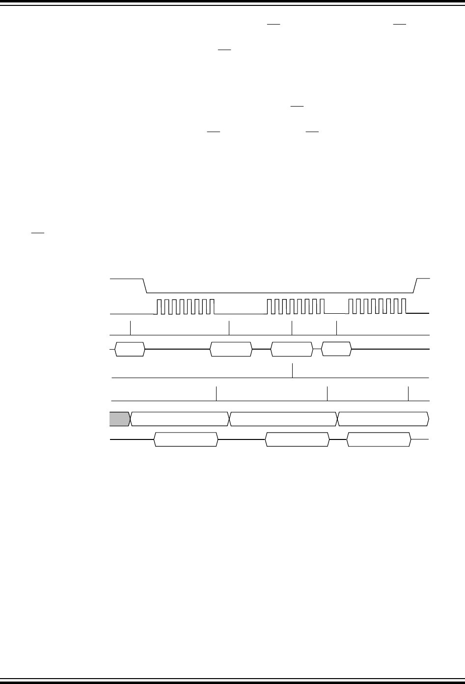
Note:
In Slave mode, the SPI state machine will be reset when the SS pin is brought high. If the SS is brought
high during a transmission, the SPI will stop sending and receiving immediately and both data received
and data sent must be considered as lost. As the SS pin is used to signal the start and end of a transfer, it
is useful for achieving packet/byte synchronization, and keeping the Slave bit counter synchronized with
the master clock generator.
Normal Mode
In Normal mode, the SPI peripheral will remain idle as long as the SS pin is driven high. In this state, the
software may update the contents of the SPIn.DATA register, but the data will not be shifted out by
incoming clock pulses on the SCK pin until the SS pin is driven low. If SS is driven low, the slave will start
to shift out data on the first SCK clock pulse. When one byte has been completely shifted, the SPI
Interrupt flag (IF) in SPIn.INTFLAGS is set.
The user application may continue placing new data to be sent into the SPIn.DATA register before
reading the incoming data. New bytes to be sent cannot be written to SPIn.DATA before the entire
transfer has completed. A premature write will be ignored, and the hardware will set the Write Collision
Flag (WRCOL in SPIn.INTFLAGS).
When SS is driven high, the SPI logic is halted, and the SPI slave will not receive any new data. Any
partially received packet in the shift register will be lost.
Figure 23-2. SPI Timing Diagram in Normal Mode (Buffer Mode Not Enabled)
0x43
Data sent 0x43 0x44
0x44 0x45
0x46
SS
SCK
Write DATA
Write value
WRCOL
0x43 0x44 0x46
Shift Register
IF
0x46
The figure shows three transfers and one write to the DATA register while the SPI is busy with a transfer.
This write will be ignored and the Write Collision Flag (WRCOL in SPIn.INTFLAGS) is set.
Buffer Mode
To avoid data collisions, the SPI peripheral can be configured in buffered mode by writing a '1' to the
Buffer Mode Enable bit in the Control B register (BUFEN in SPIn.CTRLB). In this mode, the SPI has
additional interrupt flags and extra buffers. The extra buffers are shown in Figure 23-1. There are two
different modes for the Buffer mode, selected with the Buffer mode Wait for Receive bit (BUFWR). The
two different modes are described below with timing diagrams.
megaAVR® 0-Series
Serial Peripheral Interface (SPI)
© 2018 Microchip Technology Inc. Datasheet Preliminary DS40002015A-page 322

Figure 23-3. SPI Timing Diagram in Buffer Mode with BUFWR in SPIn.CTRLB Set to Zero
0x43
Data sent
0x44
Dummy 0x43
0x44
0x45 0x46
0x44 0x46
0x46
SS
SCK
Write DATA
Write value
DREIF
Transmit Buffer
TXCIF
Dummy 0x43 0x46
Shift Register 0x44
0x43
RXCIF
All writes to the Data register goes to the Transmit Buffer register. The figure above shows that the value
0x43 is written to the Data register, but it is not immediately transferred to the shift register so the first
byte sent will be a dummy byte. The value of the dummy byte is whatever was in the shift register at the
time, usually the last received byte. After the first dummy transfer is completed the value 0x43 is
transferred to the Shift register. Then 0x44 is written to the Data register and goes to the Transmit Buffer
register. A new transfer is started and 0x43 will be sent. The value 0x45 is written to the Data register, but
the Transmit Buffer register is not updated since it is already full containing 0x44 and the Data Register
Empty Interrupt Flag (DREIF in SPIn.INTFLAGS) is low. The value 0x45 will be lost. After the transfer, the
value 0x44 is moved to the Shift register. During the next transfer, 0x46 is written to the Data register and
0x44 is sent out. After the transfer is complete 0x46 is copied into the Shift register and sent out in the
next transfer.
The Data Register Empty Interrupt Flag (DREIF in SPIn.INTFLAGS) goes low every time the Transmit
Buffer register is written and goes high after a transfer when the previous value in the Transmit Buffer
register is copied into the Shift register. The Receive Complete Interrupt Flag (RXCIF in SPIn.INTFLAGS)
is set one cycle after the Data Register Empty Interrupt Flag goes high. The Transfer Complete Interrupt
Flag is set one cycle after the Receive Complete Interrupt Flag is set when both the value in the shift
register and the Transmit Buffer register have been sent.
megaAVR® 0-Series
Serial Peripheral Interface (SPI)
© 2018 Microchip Technology Inc. Datasheet Preliminary DS40002015A-page 323

Figure 23-4. SPI Timing Diagram in Buffer Mode with CTRLB.BUFWR Set to One
0x43
Data sent
0x43
0x43 0x44
0x44
0x45 0x46
0x46
0x46
SS
SCK
Write DATA
Write value
DREIF
Transmit Buffer
TXCIF
0x44
0x43 0x44 0x46
Shift Register
RXCIF
All writes to the Data register goes to the transmit buffer. The figure above shows that the value 0x43 is
written to the Data register and since the Slave Select pin is high it is copied to the Shift register the next
cycle. Then the next write (0x44) will go to the Transmit Buffer register. During the first transfer, the value
0x43 will be shifted out. In the figure, the value 0x45 is written to the Data register, but the Transmit Buffer
register is not updated since the Data Register Empty Interrupt Flag is low. After the transfer is completed
the value 0x44 from the Transmit Buffer register is copied over to the Shift register. The value 0x46 is
written to the Transmit Buffer register. During the next two transfers, 0x44 and 0x46 are shifted out. The
flags behave the same as with Buffer mode Wait for Receive Bit (BUFWR in SPIn.CTRLB) set to zero.
23.3.2.3 Data Modes
There are four combinations of SCK phase and polarity with respect to serial data. The desired
combination is selected by writing to the MODE bits in the Control B register (SPIn.CTRLB).
The SPI data transfer formats are shown below. Data bits are shifted out and latched in on opposite
edges of the SCK signal, ensuring sufficient time for data signals to stabilize.
The leading edge is the first clock edge of a clock cycle. The trailing edge is the last clock edge of a clock
cycle.
megaAVR® 0-Series
Serial Peripheral Interface (SPI)
© 2018 Microchip Technology Inc. Datasheet Preliminary DS40002015A-page 324
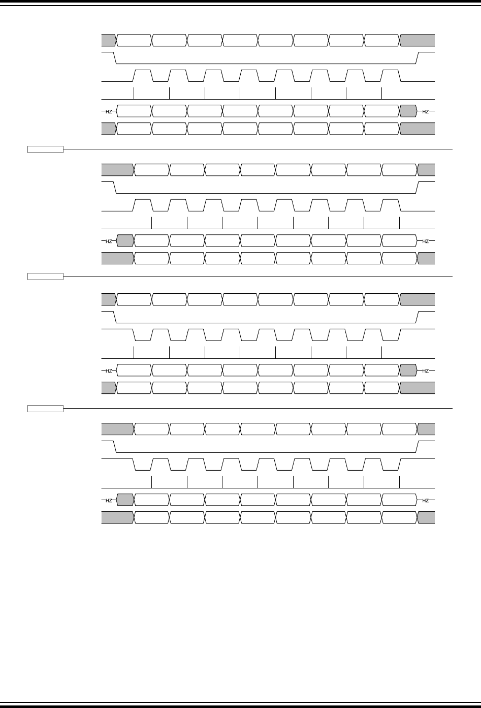
Figure 23-5. SPI Data Transfer Modes
SPI Mode 3 SPI Mode 2 SPI Mode 1 SPI Mode 0
Cycle #
SS
SCK
sampling
MISO
MOSI
Cycle #
SS
SCK
sampling
MISO
MOSI
Cycle #
SS
SCK
sampling
MISO
MOSI
Cycle #
SS
SCK
sampling
MISO
MOSI
1 2 3 4 5 6 7 8
1 2 345678
1 2 345678
1 2 345678
1 2 345678
1 2 345678
1 2 345678
1 2 345678
1 2 345678
1 2 345678
1 2 345678
1 2 345678
23.3.2.4 Events
The event system output from SPI is SPI SCK value generated by the SPI. The SCK toggles only when
the SPI is enabled, in master mode and transmitting. Otherwise, the SCK is not toggling. Refer to the SPI
transfer modes as configured in SPIn.CTRLB for the idle state of SCK.
SPI has no event inputs.
megaAVR® 0-Series
Serial Peripheral Interface (SPI)
© 2018 Microchip Technology Inc. Datasheet Preliminary DS40002015A-page 325

23.3.2.5 Interrupts
Table 23-4. Available Interrupt Vectors and Sources
Name Vector Description Conditions
SPI SPI interrupt • SSI: Slave Select Trigger Interrupt
• DRE: Data Register Empty Interrupt
• TXC: Transfer Complete Interrupt
• RXC: Receive Complete Interrupt
When an interrupt condition occurs, the corresponding interrupt flag is set in the Interrupt Flags register of
the peripheral (peripheral.INTFLAGS).
An interrupt source is enabled or disabled by writing to the corresponding enable bit in the peripheral's
Interrupt Control register (peripheral.INTCTRL).
An interrupt request is generated when the corresponding interrupt source is enabled and the interrupt
flag is set. The interrupt request remains active until the interrupt flag is cleared. See the peripheral's
INTFLAGS register for details on how to clear interrupt flags.
megaAVR® 0-Series
Serial Peripheral Interface (SPI)
© 2018 Microchip Technology Inc. Datasheet Preliminary DS40002015A-page 326

23.4 Register Summary - SPIn
Offset Name Bit Pos.
0x00 CTRLA 7:0 DORD MASTER CLK2X PRESC[1:0] ENABLE
0x01 CTRLB 7:0 BUFEN BUFWR SSD MODE[1:0]
0x02 Reserved
0x03 INTFLAGS 7:0 IF WRCOL
0x03 INTFLAGS 7:0 RXCIF TXCIF DREIF SSIF BUFOVF
0x04 DATA 7:0 DATA[7:0]
23.5 Register Description
megaAVR® 0-Series
Serial Peripheral Interface (SPI)
© 2018 Microchip Technology Inc. Datasheet Preliminary DS40002015A-page 327

23.5.1 Control A
Name: CTRLA
Offset: 0x00
Reset: 0x00
Property: -
Bit 7 6 5 4 3 2 1 0
DORD MASTER CLK2X PRESC[1:0] ENABLE
Access R/W R/W R/W R/W R/W R/W
Reset 0 0 0 0 0 0
Bit 6 – DORD Data Order
Value Description
0 The MSB of the data word is transmitted first
1 The LSB of the data word is transmitted first
Bit 5 – MASTER Master/Slave Select
This bit selects the desired SPI mode.
If SS is configured as input and driven low while this bit is ’1’, this bit is cleared, and the IF flag in
SPIn.INTFLAGS is set. The user has to write MASTER=1 again to re-enable SPI Master mode.
This behavior is controlled by the Slave Select Disable bit (SSD) in SPIn.CTRLB.
Value Description
0 SPI Slave mode selected
1 SPI Master mode selected
Bit 4 – CLK2X Clock Double
When this bit is written to ’1’ the SPI speed (SCK frequency, after internal prescaler) is doubled in Master
mode.
Value Description
0 SPI speed (SCK frequency) is not doubled
1 SPI speed (SCK frequency) is doubled in Master mode
Bits 2:1 – PRESC[1:0] Prescaler
This bit field controls the SPI clock rate configured in Master mode. These bits have no effect in Slave
mode. The relationship between SCK and the peripheral clock frequency (fCLK_PER) is shown below.
The output of the SPI prescaler can be doubled by writing the CLK2X bit to ’1’.
Value Name Description
0x0 DIV4 CLK_PER/4
0x1 DIV16 CLK_PER/16
0x2 DIV64 CLK_PER/64
0x3 DIV128 CLK_PER/128
Bit 0 – ENABLE SPI Enable
megaAVR® 0-Series
Serial Peripheral Interface (SPI)
© 2018 Microchip Technology Inc. Datasheet Preliminary DS40002015A-page 328

Value Description
0 SPI is disabled
1 SPI is enabled
megaAVR® 0-Series
Serial Peripheral Interface (SPI)
© 2018 Microchip Technology Inc. Datasheet Preliminary DS40002015A-page 329
23.5.2 Control B
Name: CTRLB
Offset: 0x01
Reset: 0x00
Property: -
Bit 7 6 5 4 3 2 1 0
BUFEN BUFWR SSD MODE[1:0]
Access R/W R/W R/W R/W R/W
Reset 0 0 0 0 0
Bit 7 – BUFEN Buffer Mode Enable
Writing this bit to '1' enables Buffer mode, meaning two buffers in receive direction, one buffer in transmit
direction, and separate interrupt flags for both transmit complete and receive complete.
Bit 6 – BUFWR Buffer Mode Wait for Receive
When writing this bit to '0' the first data transferred will be a dummy sample.
Value Description
0 One SPI transfer must be completed before the data is copied into the Shift register.
1 When writing to the data register when the SPI is enabled and SS is high, the first write will
go directly to the Shift register.
Bit 2 – SSD Slave Select Disable
When this bit is set and when operating as SPI Master (MASTER=1 in SPIn.CTRLA), SS does not
disable Master mode.
Value Description
0 Enable the Slave Select line when operating as SPI Master
1 Disable the Slave Select line when operating as SPI Master
Bits 1:0 – MODE[1:0] Mode
These bits select the Transfer mode. The four combinations of SCK phase and polarity with respect to the
serial data are shown in the table below. These bits decide whether the first edge of a clock cycle (leading
edge) is rising or falling and whether data setup and sample occur on the leading or trailing edge. When
the leading edge is rising, the SCK signal is low when idle, and when the leading edge is falling, the SCK
signal is high when idle.
Value Name Description
0x0 0 Leading edge: Rising, sample
Trailing edge: Falling, setup
0x1 1 Leading edge: Rising, setup
Trailing edge: Falling, sample
0x2 2 Leading edge: Falling, sample
Trailing edge: Rising, setup
0x3 3 Leading edge: Falling, setup
Trailing edge: Rising, sample
megaAVR® 0-Series
Serial Peripheral Interface (SPI)
© 2018 Microchip Technology Inc. Datasheet Preliminary DS40002015A-page 330

23.5.3 Interrupt Flags - Normal Mode
Name: INTFLAGS
Offset: 0x03
Reset: 0x00
Property: -
Bit 7 6 5 4 3 2 1 0
IF WRCOL
Access R/W R/W
Reset 0 0
Bit 7 – IF Receive Complete Interrupt Flag/Interrupt Flag
This flag is set when a serial transfer is complete and one byte is completely shifted in/out of the
SPIn.DATA register. If SS is configured as input and is driven low when the SPI is in Master mode, this
will also set this flag. IF is cleared by hardware when executing the corresponding interrupt vector.
Alternatively, the IF flag can be cleared by first reading the SPIn.INTFLAGS register when IF is set, and
then accessing the SPIn.DATA register.
Bit 6 – WRCOL Transfer Complete Interrupt Flag/Write Collision Flag
The WRCOL flag is set if the SPIn.DATA register is written to before a complete byte has been shifted
out. This flag is cleared by first reading the SPIn.INTFLAGS register when WRCOL is set, and then
accessing the SPIn.DATA register.
megaAVR® 0-Series
Serial Peripheral Interface (SPI)
© 2018 Microchip Technology Inc. Datasheet Preliminary DS40002015A-page 331

23.5.4 Interrupt Flags - Buffer Mode
Name: INTFLAGS
Offset: 0x03
Reset: 0x00
Property: -
Bit 7 6 5 4 3 2 1 0
RXCIF TXCIF DREIF SSIF BUFOVF
Access R/W R/W R/W R/W R/W
Reset 0 0 0 0 0
Bit 7 – RXCIF Receive Complete Interrupt Flag
This flag is set when there is unread data in the receive buffer and cleared when the receive buffer is
empty (i.e., does not contain any unread data).
When interrupt-driven data reception is used, the receive complete interrupt routine must read the
received data from SPIn.DATA in order to clear RXCIF. If not, a new interrupt will occur directly after the
return from the current interrupt. This flag can also be cleared by writing a ‘1’ to its bit location.
Bit 6 – TXCIF Transfer Complete Interrupt Flag/Write Collision Flag
This flag is set when all the data in the transmit shift register has been shifted out and there is no new
data in the transmit buffer (SPIn.DATA). The flag is cleared by writing a ‘1’ to its bit location.
Bit 5 – DREIF Data Register Empty Interrupt Flag
This flag indicates whether the transmit buffer (SPIn.DATA) is ready to receive new data. The flag is ‘1’
when the transmit buffer is empty and ‘0’ when the transmit buffer contains data to be transmitted that has
not yet been moved into the Shift register. DREIF is cleared after a Reset to indicate that the transmitter
is ready.
DREIF is cleared by writing SPIn.DATA. When interrupt-driven data transmission is used, the Data
register empty interrupt routine must either write new data to SPIn.DATA in order to clear DREIF or
disable the Data register empty interrupt. If not, a new interrupt will occur directly after the return from the
current interrupt.
Bit 4 – SSIF Slave Select Trigger Interrupt Flag
This flag indicates that the SPI has been in Master mode and the SS line has been pulled low externally
so the SPI is now working in Slave mode. The flag will only be set if the Slave Select Disable bit (SSD) is
not ‘1’. The flag is cleared by writing a ‘1’ to its bit location.
Bit 0 – BUFOVF Buffer Overflow
This flag indicates data loss due to a receiver buffer full condition. This flag is set if a buffer overflow
condition is detected. A buffer overflow occurs when the receive buffer is full (two characters) and a third
byte has been received in the Shift register. If there is no transmit data the buffer overflow will not be set
before the start of a new serial transfer. This flag is valid until the receive buffer (SPIn.DATA) is read.
Always write this bit location to ‘0’ when writing the SPIn.INTFLAGS register.
megaAVR® 0-Series
Serial Peripheral Interface (SPI)
© 2018 Microchip Technology Inc. Datasheet Preliminary DS40002015A-page 332

23.5.5 Data
Name: DATA
Offset: 0x04
Reset: 0x00
Property: -
Bit 7 6 5 4 3 2 1 0
DATA[7:0]
Access R/W R/W R/W R/W R/W R/W R/W R/W
Reset 0 0 0 0 0 0 0 0
Bits 7:0 – DATA[7:0] SPI Data
The SPIn.DATA register is used for sending and receiving data. Writing to the register initiates the data
transmission, and the byte written to the register will be shifted out on the SPI output line.
Reading this register in Buffer mode will read the second receive buffer and the contents of the first
receive buffer will be moved to the second receive buffer.
megaAVR® 0-Series
Serial Peripheral Interface (SPI)
© 2018 Microchip Technology Inc. Datasheet Preliminary DS40002015A-page 333

24. Two-Wire Interface (TWI)
24.1 Features
• Bidirectional, Two-Wire Communication Interface
• Philips I2C compatible
– Standard-mode (Sm / 100 kHz with Slew-Rate Limited Output)
– Fast-mode (Fm / 400 kHz with Slew-Rate Limited Output)
– Fast-mode Plus (Fm+ / 1 MHz with ×10 Output Drive Strength)
• System Management Bus (SMBus) compatible (100 kHz with Slew-Rate Limited Output)
– Support Arbitration between Start/Repeated Start and Data Bit
– Slave Arbitration allows support for the Address Resolution Protocol (ARP)
– Configurable SMBus Layer 1 Timeouts in Hardware
– Independent Timeouts for Dual Mode
• Independent Master and Slave Operation
– Combined (same pins) or Dual Mode (separate pins)
– Single or Multi-Master Bus Operation with Full Arbitration Support
• Flexible Slave Address Match Hardware operating in all Sleep Modes, including Power-Down
– 7-bit and General Call Address Recognition
– 10-bit Addressing Support in Collaboration with Software
– Address Mask Register allows Address Range Masking, alternatively it can be used as a
secondary Address Match
– Optional Software Address Recognition for Unlimited Number of Addresses
• Input Filter For Bus Noise Suppression
24.2 Overview
The Two-Wire Interface (TWI) peripheral is a bidirectional, two-wire communication interface peripheral.
The only external hardware needed to implement the bus are two pull-up resistors, one for each bus line.
TWI is Philips/NXP Inter-IC (I²C) v2.1 and v.3 and System Management Bus (SMBus) compatible, though
it does not include support for High-speed-mode (Hs) or Ultra-Fast-mode (UFm in revision v.6 of the I²C
specification).
Any device connected to the TWI bus can act as a master, a slave, or both. The master generates the
serial clock (SCL) and initiates data transactions by addressing one slave and telling whether it wants to
transmit or receive data. One TWI bus connects many slaves to one or several masters. An arbitration
scheme handles the case where more than one master tries to transmit data at the same time. The
mechanisms for resolving bus contention are inherent in the protocol standards.
The TWI peripheral supports concurrent master and slave functionality, which are implemented as
independent units with separate enabling and configuration. The master module supports multi-master
bus operation and arbitration. It also generates the serial clock (SCL) by using a baud rate generator
capable of generating the standard (Sm) and fast (Fm, Fm+) bus frequencies from 100 kHz up to 1 MHz.
A “smart mode” is added that can be enabled to auto-trigger operations and thus reduce software
complexity.
megaAVR® 0-Series
Two-Wire Interface (TWI)
© 2018 Microchip Technology Inc. Datasheet Preliminary DS40002015A-page 334
The slave module implements a 7-bit address match and general address call recognition in hardware.
10-bit addressing is also supported. It also incorporates an address mask register that can be used as a
second address match register or as a register for address range masking. The address recognition
hardware continues to operate in all sleep modes, including Power Down mode. This enables the slave to
wake up the device even from the deepest sleep modes where all oscillators are turned OFF when it
detects address match. Address matching can optionally be fully handled by software.
The TWI peripheral will detect START and STOP conditions, bus collisions, and bus errors. Arbitration
lost, errors, collision, and clock hold on the bus are also detected and indicated in separate status flags
available in both master and slave modes.
It is also possible to enable the Dual mode. In this case, the slave I/O pins are selected from an
alternative port, enabling fully independent and simultaneous master and slave operation.
24.2.1 Block Diagram
Figure 24-1. TWI Block Diagram
BAUD TxDATA
RxDATA
baud rate generator SCL hold low
shift register
TxDATA
RxDATA
shift register
0 0
0 0
SCL hold low
ADDR/ADDRMASK
==
SDA
SCL
Master Slave
24.2.2 Signal Description
Signal Description Type
SCL Serial clock line Digital I/O
SDA Serial data line Digital I/O
24.3 Functional Description
24.3.1 Initialization
Before enabling the master or the slave unit, ensure that the correct settings for SDASETUP, SDAHOLD,
and, if used, Fast-mode plus (FMPEN) are stored in TWI.CTRLA. If alternate pins are to be used for the
slave, this must be specified in the TWIn.DUALCTRL register as well. Note that for dual mode the master
enables the primary SCL/SDA pins, while the ENABLE bit in TWIn.DUALCTRL enables the secondary
pins.
Master Operation
It is recommended to write the Master Baud Rate register (TWIn.BAUD) before enabling the TWI master
since TIMEOUT is dependent on the baud rate setting. To start the TWI master, write a ‘1’ to the ENABLE
bit and configure an appropriate TIMEOUT if using the TWI in an SMBus environment. The ENABLE and
TIMEOUT bits are all located in the Master Control A register (TWIn.MCTRLA). If no TIMEOUT value is
set, which is the case for I²C operation, the bus state must be manually set to IDLE by writing 0x1 to
megaAVR® 0-Series
Two-Wire Interface (TWI)
© 2018 Microchip Technology Inc. Datasheet Preliminary DS40002015A-page 335
BUSSTATE in TWIn.MSTATUS at a “safe” point in time. Note that unlike the SMBus specification, the I²C
specification does not specify when it is safe to assume that the bus is IDLE in a multi-master system.
The application can solve this by ensuring that after all masters connected to the bus are enabled, one
supervising master performs a transfer before any of the other masters. The stop condition of this initial
transfer will indicate to the Bus State Monitor logic that the bus is IDLE and ready.
Slave Operation
To start the TWI slave, write the Slave Address (TWIn.SADDR), and write a '1' to the ENABLE bit in the
Slave Control A register (TWIn.SCTRLA). The TWI peripheral will wait to receive a byte addressed to it.
24.3.2 General TWI Bus Concepts
The TWI provides a simple, bidirectional, two-wire communication bus consisting of a serial clock line
(SCL) and a serial data line (SDA). The two lines are open-collector lines (wired-AND), and pull-up
resistors (Rp) are the only external components needed to drive the bus. The pull-up resistors provide a
high level on the lines when none of the connected devices are driving the bus.
The TWI bus is a simple and efficient method of interconnecting multiple devices on a serial bus. A device
connected to the bus can be a master or slave, where the master controls the bus and all communication.
Figure 24-2 illustrates the TWI bus topology.
Figure 24-2. TWI Bus Topology
TWI
DEVICE #1
RPRP
RSRS
SDA
SCL
VCC
TWI
DEVICE #2
RSRS
TWI
DEVICE #N
RSRS
Note: RS is optional
A unique address is assigned to all slave devices connected to the bus, and the master will use this to
address a slave and initiate a data transaction.
Several masters can be connected to the same bus, called a multi-master environment. An arbitration
mechanism is provided for resolving bus ownership among masters, since only one master device may
own the bus at any given time.
A device can contain both master and slave logic and can emulate multiple slave devices by responding
to more than one address.
A master indicates the start of a transaction by issuing a Start condition (S) on the bus. An address
packet with a slave address (ADDRESS) and an indication whether the master wishes to read or write
data (R/W) are then sent. After all data packets (DATA) are transferred, the master issues a Stop
condition (P) on the bus to end the transaction. The receiver must acknowledge (A) or not-acknowledge
(A) each byte received.
Figure 24-3 shows a TWI transaction.
megaAVR® 0-Series
Two-Wire Interface (TWI)
© 2018 Microchip Technology Inc. Datasheet Preliminary DS40002015A-page 336
Figure 24-3. Basic TWI Transaction Diagram Topology for a 7-bit Address Bus
PS ADDRESS
6 ... 0
R/W ACK ACK
7 ... 0
DATA ACK/NACK
7 ... 0
DATA
SDA
SCL
SAA/AR/W
ADDRESS DATA P
ADATA
Address Packet Data Packet #0
Transaction
Data Packet #1
Direction
The slave provides data on the bus
The master provides data on the bus
The master or slave can provide data on the bus
The master provides the clock signal for the transaction, but a device connected to the bus is allowed to
stretch the low-level period of the clock to decrease the clock speed.
24.3.2.1 Start and Stop Conditions
Two unique bus conditions are used for marking the beginning (Start) and end (Stop) of a transaction.
The master issues a Start condition (S) by indicating a high-to-low transition on the SDA line while the
SCL line is kept high. The master completes the transaction by issuing a Stop condition (P), indicated by
a low-to-high transition on the SDA line while the SCL line is kept high.
Figure 24-4. Start and Stop Conditions
SDA
SCL
START
Condition
STOP
Condition
S P
Multiple Start conditions can be issued during a single transaction. A Start condition that is not directly
following a Stop condition is called a repeated Start condition (Sr).
24.3.2.2 Bit Transfer
As illustrated by Figure 24-5, a bit transferred on the SDA line must be stable for the entire high period of
the SCL line. Consequently, the SDA value can only be changed during the low period of the clock. This
is ensured in hardware by the TWI module.
megaAVR® 0-Series
Two-Wire Interface (TWI)
© 2018 Microchip Technology Inc. Datasheet Preliminary DS40002015A-page 337
Figure 24-5. Data Validity
SDA
SCL
DATA
Valid
Change
Allowed
Combining bit transfers result in the formation of address and data packets. These packets consist of
eight data bits (one byte) with the Most Significant bit transferred first, plus a single-bit not-Acknowledge
(NACK) or Acknowledge (ACK) response. The addressed device signals ACK by pulling the SCL line low
during the ninth clock cycle, and signals NACK by leaving the line SCL high.
24.3.2.3 Address Packet
After the Start condition, a 7-bit address followed by a read/write (R/W) bit is sent. This is always
transmitted by the master. A slave recognizing its address will ACK the address by pulling the data line
low for the next SCL cycle, while all other slaves should keep the TWI lines released and wait for the next
Start and address. The address, R/W bit, and Acknowledge bit combined is the address packet. Only one
address packet for each Start condition is allowed, also when 10-bit addressing is used.
The R/W bit specifies the direction of the transaction. If the R/W bit is low, it indicates a master write
transaction, and the master will transmit its data after the slave has acknowledged its address. If the R/W
bit is high, it indicates a master read transaction, and the slave will transmit its data after acknowledging
its address.
24.3.2.4 Data Packet
An address packet is followed by one or more data packets. All data packets are nine bits long, consisting
of one data byte and one Acknowledge bit. The direction bit in the previous address packet determines
the direction in which the data is transferred.
24.3.2.5 Transaction
A transaction is the complete transfer from a Start to a Stop condition, including any repeated Start
conditions in between. The TWI standard defines three fundamental transaction modes: Master write,
master read, and a combined transaction.
Figure 24-6 illustrates the master write transaction. The master initiates the transaction by issuing a Start
condition (S) followed by an address packet with the direction bit set to zero (ADDRESS+W).
Figure 24-6. Master Write Transaction
S A A A/A PWADDRESS DATA DATA
Address Packet Data Packet
Transaction
N data packets
Assuming the slave acknowledges the address, the master can start transmitting data (DATA) and the
slave will ACK or NACK (A/A) each byte. If no data packets are to be transmitted, the master terminates
the transaction by issuing a Stop condition (P) directly after the address packet. There are no limitations
to the number of data packets that can be transferred. If the slave signals a NACK to the data, the master
must assume that the slave cannot receive any more data and terminate the transaction.
megaAVR® 0-Series
Two-Wire Interface (TWI)
© 2018 Microchip Technology Inc. Datasheet Preliminary DS40002015A-page 338
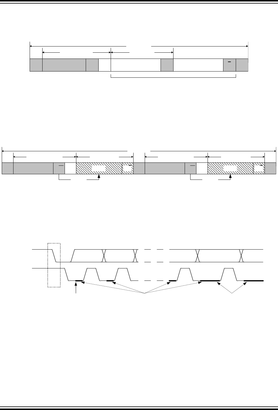
Figure 24-7 illustrates the master read transaction. The master initiates the transaction by issuing a Start
condition followed by an address packet with the direction bit set to one (ADDRESS+R). The addressed
slave must acknowledge the address for the master to be allowed to continue the transaction.
Figure 24-7. Master Read Transaction
SRA A AADDRESS DATA DATA P
Transaction
Address Packet Data Packet
N data packets
Assuming the slave acknowledges the address, the master can start receiving data from the slave. There
are no limitations to the number of data packets that can be transferred. The slave transmits the data
while the master signals ACK or NACK after each data byte. The master terminates the transfer with a
NACK before issuing a Stop condition.
Figure 24-8 illustrates a combined transaction. A combined transaction consists of several read and write
transactions separated by repeated Start conditions (Sr).
Figure 24-8. Combined Transaction
S A SrA/AR/W DATA A/A P
ADDRESS DATA R/WADDRESS
Transaction
Address Packet #1 N Data Packets M Data Packets
Address Packet #2
Direction Direction
A
24.3.2.6 Clock and Clock Stretching
All devices connected to the bus are allowed to stretch the low period of the clock to slow down the
overall clock frequency or to insert Wait states while processing data. A device that needs to stretch the
clock can do this by holding/forcing the SCL line low after it detects a low level on the line.
Three types of clock stretching can be defined, as shown in Figure 24-9.
Figure 24-9. Clock Stretching (1)
SDA
SCL
S
ACK/NACK
bit 0bit 7 bit 6
Periodic clock
stretching
Random clock
stretching
Wakeup clock
stretching
Note: Clock stretching is not supported by all I2C slaves and masters.
If a slave device is in Sleep mode and a Start condition is detected, the clock stretching normally works
during the wake-up period. For AVR devices, the clock stretching will be either directly before or after the
ACK/NACK bit, as AVR devices do not need to wake-up for transactions that are not addressed to it.
A slave device can slow down the bus frequency by stretching the clock periodically on a bit level. This
allows the slave to run at a lower system clock frequency. However, the overall performance of the bus
will be reduced accordingly. Both the master and slave device can randomly stretch the clock on a byte
level basis before and after the ACK/NACK bit. This provides time to process incoming or prepare
outgoing data or perform other time-critical tasks.
megaAVR® 0-Series
Two-Wire Interface (TWI)
© 2018 Microchip Technology Inc. Datasheet Preliminary DS40002015A-page 339
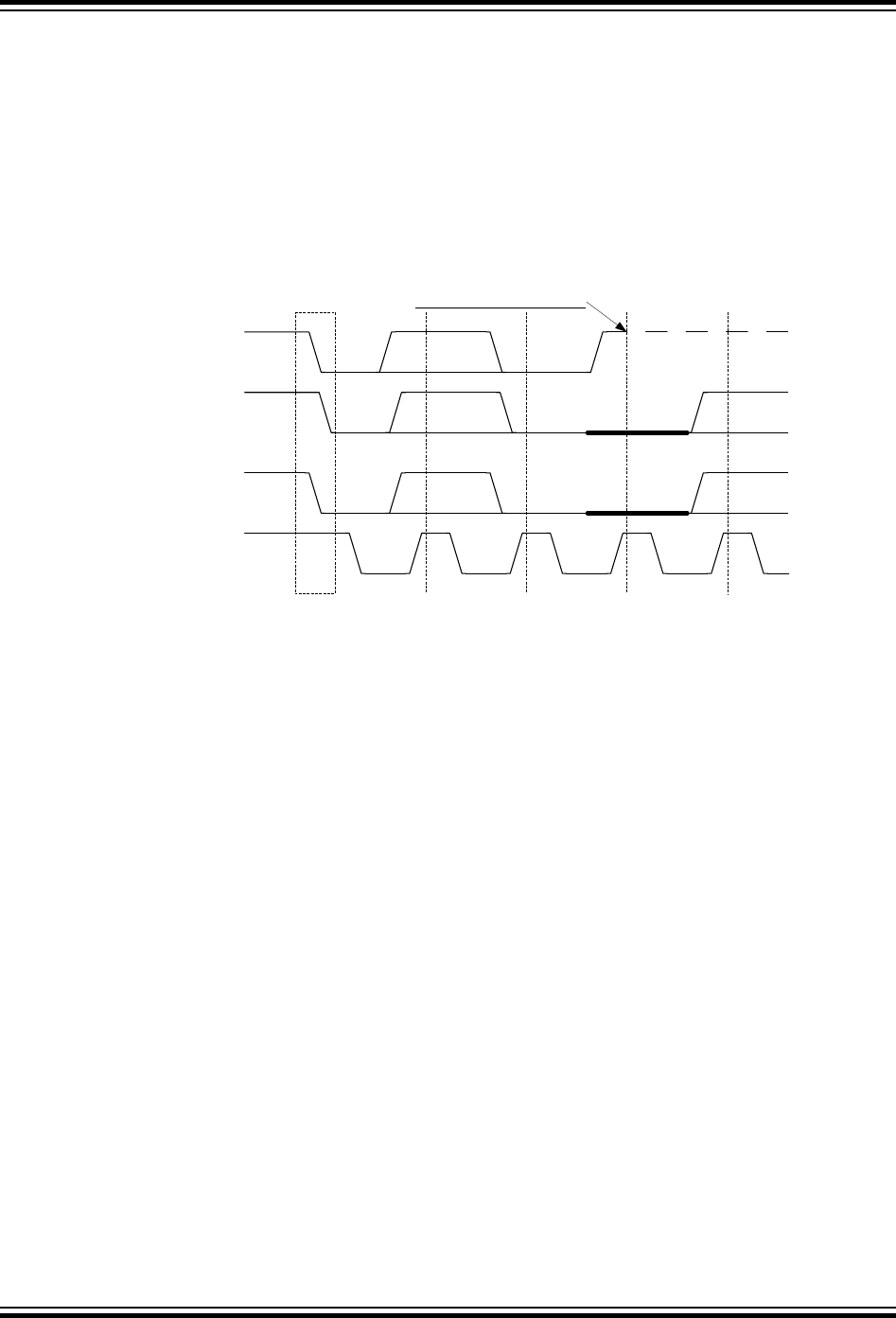
In the case where the slave is stretching the clock, the master will be forced into a Wait state until the
slave is ready, and vice versa.
24.3.2.7 Arbitration
A master can start a bus transaction only if it has detected that the bus is idle. As the TWI bus is a multi-
master bus, it is possible that two devices may initiate a transaction at the same time. This results in
multiple masters owning the bus simultaneously. This is solved using an arbitration scheme where the
master loses control of the bus if it is not able to transmit a high level on the SDA line. The masters who
lose arbitration must then wait until the bus becomes idle (i.e., wait for a Stop condition) before attempting
to reacquire bus ownership. Slave devices are not involved in the arbitration procedure.
Figure 24-10. TWI Arbitration
DEVICE1_SDA
SDA
(wired-AND)
DEVICE2_SDA
SCL
S
bit 7 bit 6 bit 5 bit 4
DEVICE1 Loses arbitration
Figure 24-10 shows an example where two TWI masters are contending for bus ownership. Both devices
are able to issue a Start condition, but DEVICE1 loses arbitration when attempting to transmit a high level
(bit 5) while DEVICE2 is transmitting a low level.
Arbitration between a repeated start condition and a data bit, a Stop condition and a data bit, or a
repeated Start condition and a Stop condition are not allowed and will require special handling by
software.
24.3.2.8 Synchronization
A clock synchronization algorithm is necessary for solving situations where more than one master is
trying to control the SCL line at the same time. The algorithm is based on the same principles used for
the clock stretching previously described. Figure 24-11 shows an example where two masters are
competing for control over the bus clock. The SCL line is the wired-AND result of the two masters clock
outputs.
megaAVR® 0-Series
Two-Wire Interface (TWI)
© 2018 Microchip Technology Inc. Datasheet Preliminary DS40002015A-page 340
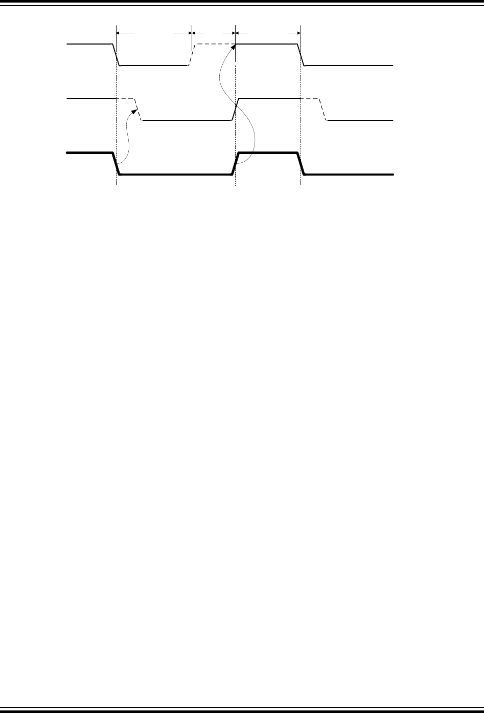
Figure 24-11. Clock Synchronization
DEVICE1_SCL
SCL
(wired-AND)
Wait
State
DEVICE2_SCL
High Period
Count
Low Period
Count
A high-to-low transition on the SCL line will force the line low for all masters on the bus, and they will start
timing their low clock period. The timing length of the low clock period can vary among the masters.
When a master (DEVICE1 in this case) has completed its low period, it releases the SCL line. However,
the SCL line will not go high until all masters have released it. Consequently, the SCL line will be held low
by the device with the longest low period (DEVICE2). Devices with shorter low periods must insert a wait
state until the clock is released. All masters start their high period when the SCL line is released by all
devices and has gone high. The device, which first completes its high period (DEVICE1), forces the clock
line low, and the procedure is then repeated. The result is that the device with the shortest clock period
determines the high period, while the low period of the clock is determined by the device with the longest
clock period.
24.3.3 TWI Bus State Logic
The bus state logic continuously monitors the activity on the TWI bus lines when the master is enabled. It
continues to operate in all Sleep modes, including power-down.
The bus state logic includes Start and Stop condition detectors, collision detection, inactive bus time-out
detection, and a bit counter. These are used to determine the bus state. The software can get the current
bus state by reading the Bus State bits in the master STATUS register. The bus state can be unknown,
idle, busy, or owner, and is determined according to the state diagram shown in Figure 24-12. The values
of the Bus State bits according to state, are shown in binary in the figure below.
megaAVR® 0-Series
Two-Wire Interface (TWI)
© 2018 Microchip Technology Inc. Datasheet Preliminary DS40002015A-page 341
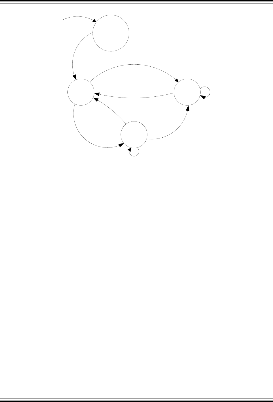
Figure 24-12. Bus State, State Diagram
P + Timeout
Write ADDRESS
IDLE
(0b01)
S
BUSY
(0b11)
UNKNOWN
(0b00)
OWNER
(0b10)
Arbitration
Lost
Command P
Write
ADDRESS(Sr)
Sr
(S)
RESET
P + Timeout
After a system Reset and/or TWI master enable, the bus state is unknown. The bus state machine can be
forced to enter idle by writing to the Bus State bits accordingly. If no state is set by the application
software, the bus state will become idle when the first Stop condition is detected. If the master inactive
bus timeout is enabled, the bus state will change to idle on the occurrence of a timeout. After a known
bus state is established, only a system Reset or disabling of the TWI master will set the state to unknown.
When the bus is idle, it is ready for a new transaction. If a Start condition generated externally is
detected, the bus becomes busy until a Stop condition is detected. The Stop condition will change the
bus state to idle. If the master inactive bus timeout is enabled, the bus state will change from busy to idle
on the occurrence of a timeout.
If a Start condition is generated internally while in an Idle state, the owner state is entered. If the complete
transaction was performed without interference (i.e., no collisions are detected), the master will issue a
Stop condition and the bus state will change back to idle. If a collision is detected, the arbitration is
assumed lost and the bus state becomes busy until a Stop condition is detected. A repeated Start
condition will only change the bus state if arbitration is lost during the issuing of the repeated Start.
Arbitration during repeated Start can be lost only if the arbitration has been ongoing since the first Start
condition. This happens if two masters send the exact same ADDRESS+DATA before one of the masters'
issues a repeated Start (Sr).
24.3.4 Operation
24.3.4.1 Electrical Characteristics
The TWI module in AVR devices follows the electrical specifications and timing of I2C bus and SMBus.
These specifications are not 100% compliant, and so to ensure correct behavior, the inactive bus time-out
period should be set in TWI Master mode. Refer to TWI Master Operation for more details.
24.3.4.2 TWI Master Operation
The TWI master is byte-oriented, with an optional interrupt after each byte. There are separate interrupt
flags for master write and master read. Interrupt flags can also be used for polled operation. There are
megaAVR® 0-Series
Two-Wire Interface (TWI)
© 2018 Microchip Technology Inc. Datasheet Preliminary DS40002015A-page 342
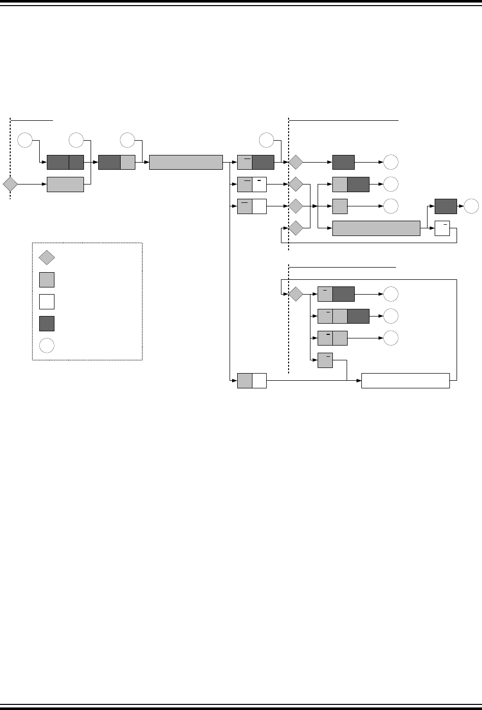
dedicated status flags for indicating ACK/NACK received, bus error, arbitration lost, clock hold, and bus
state.
When an interrupt flag is set, the SCL line is forced low. This will give the master time to respond or
handle any data, and will in most cases require software interaction. Figure 24-13 shows the TWI master
operation. The diamond-shaped symbols (SW) indicate where software interaction is required. Clearing
the interrupt flags releases the SCL line.
Figure 24-13. TWI Master Operation
IDLE SBUSYBUSY P
Sr
P
M3
M3
M2
M2
M1
M1
RDATA
ADDRESS
W
A/A
DATA
Wait for
IDLE
APPLICATION
SW
SW
Sr
P
M3
M2
BUSY M4
A
SW
A/A
A/A
A/A
M4
A
IDLE
IDLE
MASTER READ INTERRUPT + HOLD
MASTER WRITE INTERRUPT + HOLD
SW
SW
SW
BUSY
R/W
SW Driver software
The master provides data
on the bus
Slave provides data on
the bus
A
A
R/W
BUSY M4
Bus state
Mn Diagram connections
The number of interrupts generated is kept to a minimum by an automatic handling of most conditions.
Clock Generation
The TWIn.MBAUD register must be set to a value that results in a TWI bus clock frequency (fSCL) equal
or less than 100 kHz/400 kHz/1 MHz, dependent on the mode used by the application (Standard mode
Sm/Fast mode Fm/Fast mode plus Fm+).
The low (TLOW) and high (THIGH) times are determined by the Baud Rate register (TWIn.MBAUD), while
the rise (TRISE) and fall (TFALL) times are determined by the bus topology. Because of the wired-AND logic
of the bus, TFALL will be considered as part of TLOW. Likewise, TRISE will be in a state between TLOW and
THIGH until a high state has been detected.
megaAVR® 0-Series
Two-Wire Interface (TWI)
© 2018 Microchip Technology Inc. Datasheet Preliminary DS40002015A-page 343
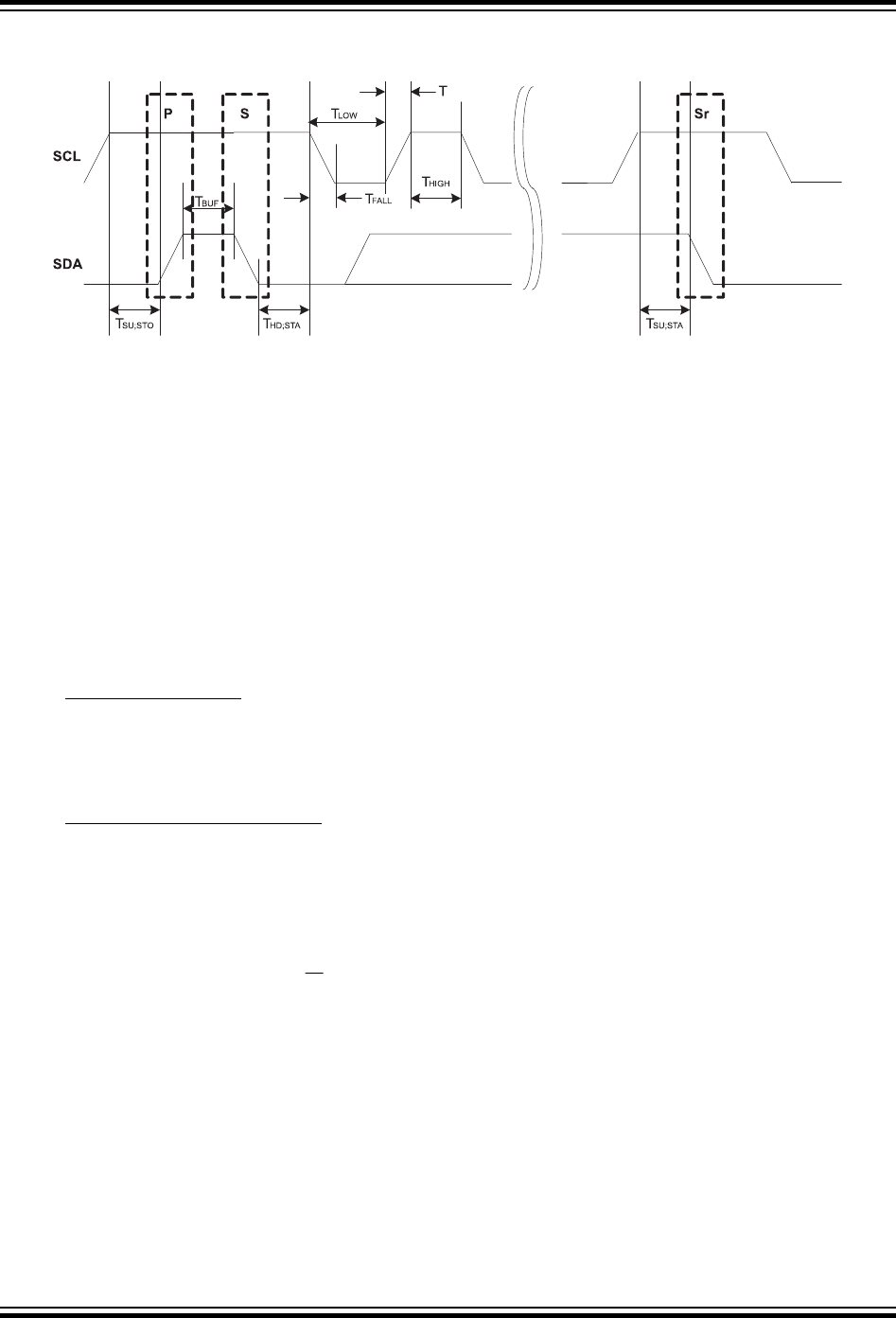
Figure 24-14. SCL Timing
RISE
• TLOW – Low period of SCL clock
• TSU;STO – Set-up time for stop condition
• TBUF – Bus-free time between stop and start conditions
• THD;STA – Hold time (repeated) start condition
• TSU;STA – Set-up time for repeated start condition
• THIGH is timed using the SCL high time count from TWIn.MBAUD
• TRISE is determined by the bus impedance; for internal pull-ups. Refer to Electrical Characteristics.
• TFALL is determined by the open-drain current limit and bus impedance; can typically be regarded
as zero. Refer to Electrical Characteristics for details.
The SCL frequency is given by:
SCL =1
LOW +HIGH +RISE
The BAUD field in TWIn.MBAUD value is used to time both SCL high and SCL low which gives the
following formula of SCL frequency:
SCL =CLK_PER
10 + 2 +CLK_PER RISE
Transmitting Address Packets
After issuing a Start condition, the master starts performing a bus transaction when the Master Address
register is written with the 7-bit slave address and direction bit. If the bus is busy, the TWI master will wait
until the bus becomes idle before issuing the Start condition.
Depending on arbitration and the R/W direction bit, one of four distinct cases (M1 to M4) arises following
the address packet. The different cases must be handled in software.
Case M1: Arbitration Lost or Bus Error during Address Packet
If arbitration is lost during the sending of the address packet, both the Master Write Interrupt Flag (WIF in
TWIn.MSTATUS) and Arbitration Lost Flag (ARBLOST in TWIn.MSTATUS) are set. Serial data output to
the SDA line is disabled, and the SCL line is released. The master is no longer allowed to perform any
operation on the bus until the bus state has changed back to idle.
A bus error will behave in the same way as an arbitration lost condition, but the Bus Error Flag (BUSERR
in TWIn.MSTATUS) is set in addition to the write interrupt and arbitration lost flags.
megaAVR® 0-Series
Two-Wire Interface (TWI)
© 2018 Microchip Technology Inc. Datasheet Preliminary DS40002015A-page 344

Case M2: Address Packet Transmit Complete - Address not Acknowledged by Slave
If no slave device responds to the address, the Master Write Interrupt Flag (WIF in TWIn.MSTATUS) and
the Master Received Acknowledge Flag (RXACK in TWIn.MSTATUS) are set. The RXACK flag reflects
the physical state of the ACK bit (i.e.< no slave did pull the ACK bit low). The clock hold is active at this
point, preventing further activity on the bus.
Case M3: Address Packet Transmit Complete - Direction Bit Cleared
If the master receives an ACK from the slave, the Master Write Interrupt Flag (WIF in TWIn.MSTATUS) is
set and the Master Received Acknowledge Flag (RXACK in TWIn.MSTATUS) is cleared. The clock hold
is active at this point, preventing further activity on the bus.
Case M4: Address Packet Transmit Complete - Direction Bit Set
If the master receives an ACK from the slave, the master proceeds to receive the next byte of data from
the slave. When the first data byte is received, the Master Read Interrupt Flag (RIF in TWIn.MSTATUS) is
set and the Master Received Acknowledge Flag (RXACK in TWIn.MSTATUS) is cleared. The clock hold
is active at this point, preventing further activity on the bus.
Transmitting Data Packets
Assuming the above M3 case, the master can start transmitting data by writing to the Master Data
(TWIn.MDATA) register, which will also clear the Write Interrupt Flag (WIF). During data transfer, the
master is continuously monitoring the bus for collisions and errors. The WIF will be set anew after the full
data packet transfer has been completed, the arbitration is lost (ARBLOST), or if a bus error (BUSERR)
occur during the transfer.
The WIF, ARBLOST, and BUSERR flags together with the value of the last acknowledge bit (RXACK) are
all located in the Master Status (TWIn.MSTATUS) register. The RXACK status is only valid if WIF is set
and not valid if ARBLOST or BUSERR is set, so the software driver must check this first. The RXACK will
be zero if the slave responds to the data with an ACK, which indicates that the slave is ready for more
data (if any). A NACK received from the slave indicates that the slave is not able to or does not need to
receive more data after the last byte. The master must then either issue a Repeated Start (Sr) (write a
new value to TWIn.MADDR) or complete the transaction by issuing a Stop condition (MCMD field in
TWIn.MCTRLB = MCMD_STOP).
In I²C slaves, the use of Repeated Start conditions (Sr) entirely depends on how each slave interprets the
protocol. In SMBus slaves, interpretation of a Repeated Start condition is defined by higher levels of the
protocol specification.
Receiving Data Packets
Assuming case M4 above, the master has already received one byte from the slave. The master read
interrupt flag is set, and the master must prepare to receive new data. The master must respond to each
byte with ACK or NACK. A NACK response might not be successfully executed, as arbitration can be lost
during the transmission. If a collision is detected, the master loses arbitration and the arbitration lost flag
is set.
Quick Command Mode
With Quick Command enabled (QCEN in TWIn.MCTRLA), the R/W# bit of the slave address denotes the
command. This is a SMBus specific command where the R/W bit may be used to simply turn a device
function ON or OFF, or enable/disable a low-power Standby mode. There is no data sent or received.
After the master receives an acknowledge from the slave, either RIF or WIF flag in TWIn.MSTATUS will
be set depending on the polarity of R/W. When either RIF or WIF flag is set after issuing a Quick
Command, the TWI will accept a stop command through writing the CMD bits in TWIn.MCTRLB.
megaAVR® 0-Series
Two-Wire Interface (TWI)
© 2018 Microchip Technology Inc. Datasheet Preliminary DS40002015A-page 345
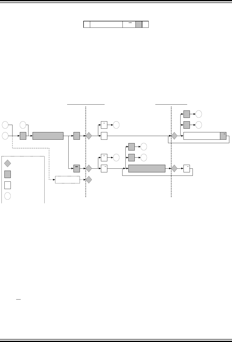
Figure 24-15. Quick Command Frame Format
PAR/WAddressS
24.3.4.3 TWI Slave Operation
The TWI slave is byte-oriented with optional interrupts after each byte. There are separate slave data and
address/stop interrupt flags. Interrupt flags can also be used for polled operation. There are dedicated
status flags for indicating ACK/NACK received, clock hold, collision, bus error, and read/write direction.
When an interrupt flag is set, the SCL line is forced low. This will give the slave time to respond or handle
data, and will in most cases require software interaction. Figure 24-16 shows the TWI slave operation.
The diamond shaped symbols (SW) indicate where software interaction is required.
Figure 24-16. TWI Slave Operation
S
S3
ADDRESS
S2 A
S1
R
W
DATA A/A
DATA
PS2
Sr S3
PS2
Sr S3
SLAVE ADDRESS INTERRUPT SLAVE DATA INTERRUPT
A
SW
SW SW
SW
A/A A/A
AS1
SW
Interrupton STOP
ConditionEnabled
S1
SW Driversoftware
The master provides data
on the bus
Slave provides data on
the bus
Sn Diagramconnections
The number of interrupts generated is kept to a minimum by automatic handling of most conditions. Quick
command can be enabled to auto-trigger operations and reduce software complexity.
Address Recognition mode can be enabled to allow the slave to respond to all received addresses.
Receiving Address Packets
When the TWI slave is properly configured, it will wait for a Start condition to be detected. When this
happens, the successive address byte will be received and checked by the address match logic, and the
slave will ACK a correct address and store the address in the TWIn.DATA register. If the received address
is not a match, the slave will not acknowledge and store the address, but wait for a new Start condition.
The slave address/stop interrupt flag is set when a Start condition succeeded by a valid address byte is
detected. A general call address will also set the interrupt flag.
A Start condition immediately followed by a Stop condition is an illegal operation and the bus error flag is
set.
The R/W direction flag reflects the direction bit received with the address. This can be read by software to
determine the type of operation currently in progress.
megaAVR® 0-Series
Two-Wire Interface (TWI)
© 2018 Microchip Technology Inc. Datasheet Preliminary DS40002015A-page 346

Depending on the R/W direction bit and bus condition, one of four distinct cases (S1 to S4) arises
following the address packet. The different cases must be handled in software.
Case S1: Address Packet Accepted - Direction Bit Set
If the R/W direction flag is set, this indicates a master read operation. The SCL line is forced low by the
slave, stretching the bus clock. If ACK is sent by the slave, the slave hardware will set the data interrupt
flag indicating data is needed for transmit. Data, repeated Start, or Stop can be received after this. If
NACK is sent by the slave, the slave will wait for a new Start condition and address match.
Case S2: Address Packet Accepted - Direction Bit Cleared
If the R/W direction flag is cleared, this indicates a master write operation. The SCL line is forced low,
stretching the bus clock. If ACK is sent by the slave, the slave will wait for data to be received. Data,
repeated Start, or Stop can be received after this. If NACK is sent, the slave will wait for a new Start
condition and address match.
Case S3: Collision
If the slave is not able to send a high level or NACK, the collision flag is set, and it will disable the data
and acknowledge output from the slave logic. The clock hold is released. A Start or repeated Start
condition will be accepted.
Case S4: STOP Condition Received
When the Stop condition is received, the slave address/stop flag will be set, indicating that a Stop
condition, and not an address match, occurred.
Receiving Data Packets
The slave will know when an address packet with R/W direction bit cleared has been successfully
received. After acknowledging this, the slave must be ready to receive data. When a data packet is
received, the data interrupt flag is set and the slave must indicate ACK or NACK. After indicating a NACK,
the slave must expect a Stop or repeated Start condition.
Transmitting Data Packets
The slave will know when an address packet with R/W direction bit set has been successfully received. It
can then start sending data by writing to the slave data register. When a data packet transmission is
completed, the data interrupt flag is set. If the master indicates NACK, the slave must stop transmitting
data and expect a Stop or repeated Start condition.
24.3.4.4 Smart Mode
The TWI interface has a Smart mode that simplifies application code and minimizes the user interaction
needed to adhere to the I2C protocol. For TWI Master, Smart mode accomplishes this by automatically
sending an ACK as soon as data register TWI.MDATA is read. This feature is only active when the
ACKACT bit in TWIn.MCTRLA register is set to ACK. If ACKACT is set to NACK, the TWI Master will not
generate a NACK bit followed by reading the Data register.
With Smart mode enabled for TWI Slave (SMEN bit in TWIn.SCTRLA), DIF (Data Interrupt Flag) will
automatically be cleared if Data register (TWIn.SDATA) is read or written.
24.3.5 Interrupts
Table 24-1. Available Interrupt Vectors and Sources
Name Vector Description Conditions
Slave TWI Slave interrupt • DIF: Data Interrupt Flag in TWIn.SSTATUS set
megaAVR® 0-Series
Two-Wire Interface (TWI)
© 2018 Microchip Technology Inc. Datasheet Preliminary DS40002015A-page 347

Name Vector Description Conditions
• APIF: Address or Stop Interrupt Flag in TWIn.SSTATUS set
Master TWI Master interrupt • RIF: Read Interrupt Flag in TWIn.MSTATUS set
• WIF: Write Interrupt Flag in TWIn.MSTATUS set
When an interrupt condition occurs, the corresponding Interrupt Flag is set in the Master register
(TWIn.MSTATUS) or Slave Status register (TWIn.SSTATUS).
When several interrupt request conditions are supported by an interrupt vector, the interrupt requests are
ORed together into one combined interrupt request to the interrupt controller. The user must read the
peripheral's INTFLAGS register to determine which of the interrupt conditions are present.
24.3.6 Sleep Mode Operation
The bus state logic and slave continue to operate in all Sleep modes, including Power-Down Sleep mode.
If a slave device is in Sleep mode and a Start condition is detected, clock stretching is active during the
wake-up period until the system clock is available. The master will stop operation in all Sleep modes.
megaAVR® 0-Series
Two-Wire Interface (TWI)
© 2018 Microchip Technology Inc. Datasheet Preliminary DS40002015A-page 348
24.4 Register Summary - TWIn
Offset Name Bit Pos.
0x00 CTRLA 7:0 SDASETUP SDAHOLD[1:0] FMPEN
0x01 DUALCTRL 7:0 SDAHOLD[1:0] FMPEN ENABLE
0x02 DBGCTRL 7:0 DBGRUN
0x03 MCTRLA 7:0 RIEN WIEN QCEN TIMEOUT[1:0] SMEN ENABLE
0x04 MCTRLB 7:0 FLUSH ACKACT MCMD[1:0]
0x05 MSTATUS 7:0 RIF WIF CLKHOLD RXACK ARBLOST BUSERR BUSSTATE[1:0]
0x06 MBAUD 7:0 BAUD[7:0]
0x07 MADDR 7:0 ADDR[7:0]
0x08 MDATA 7:0 DATA[7:0]
0x09 SCTRLA 7:0 DIEN APIEN PIEN PMEN SMEN ENABLE
0x0A SCTRLB 7:0 ACKACT SCMD[1:0]
0x0B SSTATUS 7:0 DIF APIF CLKHOLD RXACK COLL BUSERR DIR AP
0x0C SADDR 7:0 ADDR[7:0]
0x0D SDATA 7:0 DATA[7:0]
0x0E SADDRMASK 7:0 ADDRMASK[6:0] ADDREN
24.5 Register Description
megaAVR® 0-Series
Two-Wire Interface (TWI)
© 2018 Microchip Technology Inc. Datasheet Preliminary DS40002015A-page 349

24.5.1 Control A
Name: CTRLA
Offset: 0x00
Reset: 0x00
Property: -
Bit 7 6 5 4 3 2 1 0
SDASETUP SDAHOLD[1:0] FMPEN
Access R/W R/W R/W R/W
Reset 0 0 0 0
Bit 4 – SDASETUP SDA Setup Time
By default, there are four clock cycles of setup time on SDA out signal while reading from the slave part
of the TWI module. Writing this bit to '1' will change the setup time to eight clocks.
Value Name Description
0 4CYC SDA setup time is four clock cycles
1 8CYC SDA setup time is eight clock cycle
Bits 3:2 – SDAHOLD[1:0] SDA Hold Time
Writing these bits selects the SDA hold time.
Table 24-2. SDA Hold Time
SDAHOLD[1:0] Nominal Hold Time Hold Time Range Across
All Corners [ns]
Description
0x0 OFF 0 Hold time OFF.
0x1 50 ns 36 - 131 Backward compatible setting.
0x2 300 ns 180 - 630 Meets SMBus specification under
typical conditions.
0x3 500 ns 300 - 1050 Meets SMBus specification across
all corners.
Bit 1 – FMPEN FM Plus Enable
Writing these bits selects the 1 MHz bus speed (Fast mode plus, Fm+) for the TWI in default configuration
or for TWI Master in dual mode configuration.
Value Description
0 Fm+ disabled
1 Fm+ enabled
megaAVR® 0-Series
Two-Wire Interface (TWI)
© 2018 Microchip Technology Inc. Datasheet Preliminary DS40002015A-page 350

24.5.2 Dual Mode Control Configuration
Name: DUALCTRL
Offset: 0x01
Reset: 0x00
Property: -
Bit 7 6 5 4 3 2 1 0
SDAHOLD[1:0] FMPEN ENABLE
Access R/W R/W R/W R/W
Reset 0 0 0 0
Bits 3:2 – SDAHOLD[1:0] SDA Hold Time
These bits select the SDA hold time for the TWI Slave.
The configuration is ignored if the TWI is not selected in bridge configuration.
Table 24-3. SDA Hold Time
SDAHOLD[1:0] Nominal Hold
Time [ns]
Hold Time Range Across
all Corners [ns]
Description
0x0 0 0 Hold time OFF.
0x1 50 36 - 131 Backward compatible setting.
0x2 300 180 - 630 Meets SMBus specification under
typical conditions.
0x3 500 300 - 1050 Meets SMBus specification across
all corners.
Bit 1 – FMPEN FM Plus Enable
This bit selects the 1 MHz bus speed for the TWI Slave. This bit is ignored if the TWI is not selected in
bridge configuration.
Bit 0 – ENABLE Enable
This bit selects the bridge mode configuration.
megaAVR® 0-Series
Two-Wire Interface (TWI)
© 2018 Microchip Technology Inc. Datasheet Preliminary DS40002015A-page 351

24.5.3 Debug Control
Name: DBGCTRL
Offset: 0x02
Reset: 0x00
Property: -
Bit 7 6 5 4 3 2 1 0
DBGRUN
Access R/W
Reset 0
Bit 0 – DBGRUN Debug Run
Value Description
0 The peripheral is halted in Break Debug mode and ignores events.
1 The peripheral will continue to run in Break Debug mode when the CPU is halted.
megaAVR® 0-Series
Two-Wire Interface (TWI)
© 2018 Microchip Technology Inc. Datasheet Preliminary DS40002015A-page 352

24.5.4 Master Control A
Name: MCTRLA
Offset: 0x03
Reset: 0x00
Property: -
Bit 7 6 5 4 3 2 1 0
RIEN WIEN QCEN TIMEOUT[1:0] SMEN ENABLE
Access R/W R/W R/W R/W R/W R/W R/W
Reset 0 0 0 0 0 0 0
Bit 7 – RIEN Read Interrupt Enable
Writing this bit to '1' enables interrupt on the Master Read Interrupt Flag (RIF) in the Master Status
register (TWIn.MSTATUS). A TWI Master read interrupt would be generated only if this bit, the RIF, and
the Global Interrupt Flag (I) in CPU.SREG are all '1'.
Bit 6 – WIEN Write Interrupt Enable
Writing this bit to '1' enables interrupt on the Master Write Interrupt Flag (WIF) in the Master Status
register (TWIn.MSTATUS). A TWI Master write interrupt will be generated only if this bit, the WIF, and the
Global Interrupt Flag (I) in CPU.SREG are all '1'.
Bit 4 – QCEN Quick Command Enable
Writing this bit to '1' enables Quick Command. When Quick Command is enabled, the corresponding
interrupt flag is set immediately after the slave acknowledges the address. At this point, the software can
either issue a Stop command or a repeated Start by writing either the Command bits (CMD) in the Master
Control B register (TWIn.MCTRLB) or the Master Address register (TWIn.MADDR).
Bits 3:2 – TIMEOUT[1:0] Inactive Bus Timeout
Setting the inactive bus timeout (TIMEOUT) bits to a non-zero value will enable the inactive bus time-out
supervisor. If the bus is inactive for longer than the TIMEOUT setting, the bus state logic will enter the Idle
state.
Value Name Description
0x0 DISABLED Bus timeout disabled. I2C.
0x1 50US 50 µs - SMBus (assume baud is set to 100 kHz)
0x2 100US 100 µs (assume baud is set to 100 kHz)
0x3 200US 200 µs (assume baud is set to 100 kHz)
Bit 1 – SMEN Smart Mode Enable
Writing this bit to '1' enables the Master Smart mode. When Smart mode is enabled, the acknowledge
action is sent immediately after reading the Master Data (TWIn.MDATA) register.
Bit 0 – ENABLE Enable TWI Master
Writing this bit to '1' enables the TWI as master.
megaAVR® 0-Series
Two-Wire Interface (TWI)
© 2018 Microchip Technology Inc. Datasheet Preliminary DS40002015A-page 353

24.5.5 Master Control B
Name: MCTRLB
Offset: 0x04
Reset: 0x00
Property: -
Bit 7 6 5 4 3 2 1 0
FLUSH ACKACT MCMD[1:0]
Access R/W R/W R/W R/W
Reset 0 0 0 0
Bit 3 – FLUSH Flush
Writing a '1' to this bit generates a strobe for one clock cycle disabling and then enabling the master.
Writing '0' has no effect.
The purpose is to clear the internal state of master: For TWI master to transmit successfully, it is
recommended to write the Master Address register (TWIn.MADDR) first and then the Master Data
register (TWIn.MDATA).
The peripheral will transmit invalid data if TWIn.MDATA is written before TWIn.MADDR. To avoid this
invalid transmission, write '1' to this bit to clear both registers.
Bit 2 – ACKACT Acknowledge Action
This bit defines the master’s behavior under certain conditions defined by the bus protocol state and
software interaction. The acknowledge action is performed when DATA is read, or when an execute
command is written to the CMD bits.
The ACKACT bit is not a flag or strobe, but an ordinary read/write accessible register bit. The default
ACKACT for master read interrupt is “Send ACK” (0). For master write, the code will know that no
acknowledge should be sent since it is itself sending data.
Value Description
0 Send ACK
1 Send NACK
Bits 1:0 – MCMD[1:0] Command
The master command bits are strobes. These bits are always read as zero.
Writing to these bits triggers a master operation as defined by the table below.
Table 24-4. Command Settings
MCMD[1:0] DIR Description
0x0 X NOACT - No action
0x1 X REPSTART - Execute Acknowledge Action succeeded by repeated Start.
0x2 0 RECVTRANS - Execute Acknowledge Action succeeded by a byte read operation.
megaAVR® 0-Series
Two-Wire Interface (TWI)
© 2018 Microchip Technology Inc. Datasheet Preliminary DS40002015A-page 354

MCMD[1:0] DIR Description
1 Execute Acknowledge Action (no action) succeeded by a byte send operation.(1)
0x3 X STOP - Execute Acknowledge Action succeeded by issuing a Stop condition.
Note:
1. For a master being a sender, it will normally wait for new data written to the Master Data register
(TWIn.MDATA).
The acknowledge action bits and command bits can be written at the same time.
megaAVR® 0-Series
Two-Wire Interface (TWI)
© 2018 Microchip Technology Inc. Datasheet Preliminary DS40002015A-page 355

24.5.6 Master Status
Name: MSTATUS
Offset: 0x05
Reset: 0x00
Property: -
Normal TWI operation dictates that this register is regarded purely as a read-only register. Clearing any of
the status flags is done indirectly by accessing the Master Transmits Address (TWIn.MADDR), Master
Data register (TWIn.MDATA), or the Command bits (CMD) in the Master Control B register
(TWIn.MCTRLB).
Bit 7 6 5 4 3 2 1 0
RIF WIF CLKHOLD RXACK ARBLOST BUSERR BUSSTATE[1:0]
Access R/W R/W R/W R R/W R/W R/W R/W
Reset 0 0 0 0 0 0 0 0
Bit 7 – RIF Read Interrupt Flag
This bit is set to '1' when the master byte read operation is successfully completed (i.e., no arbitration lost
or bus error occurred during the operation). The read operation is triggered by software reading DATA or
writing to ADDR registers with bit ADDR[0] written to '1'. A slave device must have responded with an
ACK to the address and direction byte transmitted by the master for this flag to be set.
Writing a '1' to this bit will clear the RIF. However, normal use of the TWI does not require the flag to be
cleared by this method.
Clearing the RIF bit will follow the same software interaction as the CLKHOLD flag.
The RIF flag can generate a master read interrupt (see description of the RIEN control bit in the
TWIn.MCTRLA register).
Bit 6 – WIF Write Interrupt Flag
This bit is set when a master transmit address or byte write is completed, regardless of the occurrence of
a bus error or an arbitration lost condition.
Writing a '1' to this bit will clear the WIF. However, normal use of the TWI does not require the flag to be
cleared by this method.
Clearing the WIF bit will follow the same software interaction as the CLKHOLD flag.
The WIF flag can generate a master write interrupt (see description of the WIEN control bit in the
TWIn.MCTRLA register).
Bit 5 – CLKHOLD Clock Hold
If read as '1', this bit indicates that the master is currently holding the TWI clock (SCL) low, stretching the
TWI clock period.
Writing a '1' to this bit will clear the CLKHOLD flag. However, normal use of the TWI does not require the
CLKHOLD flag to be cleared by this method, since the flag is automatically cleared when accessing
several other TWI registers. The CLKHOLD flag can be cleared by:
1. Writing a '1' to it.
2. Writing to the TWIn.MADDR register.
megaAVR® 0-Series
Two-Wire Interface (TWI)
© 2018 Microchip Technology Inc. Datasheet Preliminary DS40002015A-page 356

3. Writing to the TWIn.MDATA register.
4. Reading the TWIn.DATA register while the ACKACT control bits in TWIn.MCTRLB are set to either
send ACK or NACK.
5. Writing a valid command to the TWIn.MCTRLB register.
Bit 4 – RXACK Received Acknowledge
This bit is read-only and contains the most recently received Acknowledge bit from the slave. When read
as zero, the most recent acknowledge bit from the slave was ACK. When read as one, the most recent
acknowledge bit was NACK.
Bit 3 – ARBLOST Arbitration Lost
If read as '1' this bit indicates that the master has lost arbitration while transmitting a high data or NACK
bit, or while issuing a Start or repeated Start condition (S/Sr) on the bus.
Writing a '1' to it will clear the ARBLOST flag. However, normal use of the TWI does not require the flag to
be cleared by this method. However, as for the CLKHOLD flag, clearing the ARBLOST flag is not required
during normal use of the TWI.
Clearing the ARBLOST bit will follow the same software interaction as the CLKHOLD flag.
Given the condition where the bus ownership is lost to another master, the software must either abort
operation or resend the data packet. Either way, the next required software interaction is in both cases to
write to the TWIn.MADDR register. A write access to the TWIn.MADDR register will then clear the
ARBLOST flag.
Bit 2 – BUSERR Bus Error
The BUSERR flag indicates that an illegal bus condition has occurred. An illegal bus condition is detected
if a protocol violating Start (S), repeated Start (Sr), or Stop (P) is detected on the TWI bus lines. A Start
condition directly followed by a Stop condition is one example of protocol violation.
Writing a '1' to this bit will clear the BUSERR. However, normal use of the TWI does not require the
BUSERR to be cleared by this method.
A robust TWI driver software design will treat the bus error flag similarly to the ARBLOST flag, assuming
the bus ownership is lost when the bus error flag is set. As for the ARBLOST flag, the next software
operation of writing the TWIn.MADDR register will consequently clear the BUSERR flag. For bus error to
be detected, the bus state logic must be enabled and the system frequency must be 4x the SCL
frequency.
Bits 1:0 – BUSSTATE[1:0] Bus State
These bits indicate the current TWI bus state as defined in the table below. After a System Reset or re-
enabling, the TWI master bus state will be unknown. The change of bus state is dependent on bus
activity.
Writing 0x1 to the BUSSTATE bits forces the bus state logic into its Idle state. However, the bus state
logic cannot be forced into any other state. When the master is disabled, the bus state is 'unknown'.
Value Name Description
0x0 UNKNOWN Unknown bus state
0x1 IDLE Bus is idle
0x2 OWNER This TWI controls the bus
0x3 BUSY The bus is busy
megaAVR® 0-Series
Two-Wire Interface (TWI)
© 2018 Microchip Technology Inc. Datasheet Preliminary DS40002015A-page 357

24.5.7 Master Baud Rate
Name: MBAUD
Offset: 0x06
Reset: 0x00
Property: -
Bit 7 6 5 4 3 2 1 0
BAUD[7:0]
Access R/W R/W R/W R/W R/W R/W R/W R/W
Reset 0 0 0 0 0 0 0 0
Bits 7:0 – BAUD[7:0] Baud Rate
This bit field is used to derive the SCL high and low time and should be written while the master is
disabled (ENABLE bit in TWIn.MCTRLA is '0').
For more information on how to calculate the frequency, see the section on Clock Generation.
megaAVR® 0-Series
Two-Wire Interface (TWI)
© 2018 Microchip Technology Inc. Datasheet Preliminary DS40002015A-page 358

24.5.8 Master Address
Name: MADDR
Offset: 0x07
Reset: 0x00
Property: -
Bit 7 6 5 4 3 2 1 0
ADDR[7:0]
Access R/W R/W R/W R/W R/W R/W R/W R/W
Reset 0 0 0 0 0 0 0 0
Bits 7:0 – ADDR[7:0] Address
When this bit field is written, a Start condition and slave address protocol sequence is initiated dependent
on the bus state.
If the bus state is unknown the Master Write Interrupt Flag (WIF) and Bus Error flag (BUSERR) in the
Master Status register (TWIn.MSTATUS) are set and the operation is terminated.
If the bus is busy the master awaits further operation until the bus becomes idle. When the bus is or
becomes idle, the master generates a Start condition on the bus, copies the ADDR value into the Data
Shift register (TWIn.MDATA) and performs a byte transmit operation by sending the contents of the Data
register onto the bus. The master then receives the response (i.e., the Acknowledge bit from the slave).
After completing the operation the bus clock (SCL) is forced and held low only if arbitration was not lost.
The CLKHOLD bit in the Master Setup register (TWIn.MSETUP) is set accordingly. Completing the
operation sets the WIF in the Master Status register (TWIn.MSTATUS).
If the bus is already owned, a repeated Start (Sr) sequence is performed. In two ways the repeated Start
(Sr) sequence deviates from the Start sequence. Firstly, since the bus is already owned by the master, no
wait for idle bus state is necessary. Secondly, if the previous transaction was a read, the acknowledge
action is sent before the Repeated Start bus condition is issued on the bus.
The master receives one data byte from the slave before the master sets the Master Read Interrupt Flag
(RIF) in the Master Status register (TWIn.MSTATUS). All TWI Master flags are cleared automatically
when this bit field is written. This includes bus error, arbitration lost, and both master interrupt flags.
This register can be read at any time without interfering with ongoing bus activity, since a read access
does not trigger the master logic to perform any bus protocol related operations.
The master control logic uses bit 0 of the TWIn.MADDR register as the bus protocol’s Read/Write flag
(R/W).
megaAVR® 0-Series
Two-Wire Interface (TWI)
© 2018 Microchip Technology Inc. Datasheet Preliminary DS40002015A-page 359

24.5.9 Master DATA
Name: MDATA
Offset: 0x08
Reset: 0x00
Property: -
Bit 7 6 5 4 3 2 1 0
DATA[7:0]
Access R/W R/W R/W R/W R/W R/W R/W R/W
Reset 0 0 0 0 0 0 0 0
Bits 7:0 – DATA[7:0] Data
The bit field gives direct access to the master's physical Shift register which is used both to shift data out
onto the bus (write) and to shift in data received from the bus (read).
The direct access implies that the Data register cannot be accessed during byte transmissions. Built-in
logic prevents any write access to this register during the shift operations. Reading valid data or writing
data to be transmitted can only be successfully done when the bus clock (SCL) is held low by the master
(i.e., when the CLKHOLD bit in the Master Status register (TWIn.MSTATUS) is set). However, it is not
necessary to check the CLKHOLD bit in software before accessing this register if the software keeps
track of the present protocol state by using interrupts or observing the interrupt flags.
Accessing this register assumes that the master clock hold is active, auto-triggers bus operations
dependent of the state of the Acknowledge Action Command bit (ACKACT) in TWIn.MSTATUS and type
of register access (read or write).
A write access to this register will, independent of ACKACT in TWIn.MSTATUS, command the master to
perform a byte transmit operation on the bus directly followed by receiving the Acknowledge bit from the
slave. When the Acknowledge bit is received, the Master Write Interrupt Flag (WIF) in TWIn.MSTATUS is
set regardless of any bus errors or arbitration. If operating in a multi-master environment, the interrupt
handler or application software must check the Arbitration Lost Status Flag (ARBLOST) in
TWIn.MSTATUS before continuing from this point. If the arbitration was lost, the application software must
decide to either abort or to resend the packet by rewriting this register. The entire operation is performed
(i.e., all bits are clocked), regardless of winning or losing arbitration before the write interrupt flag is set.
When arbitration is lost, only '1's are transmitted for the remainder of the operation, followed by a write
interrupt with ARBLOST flag set.
Both TWI Master Interrupt Flags are cleared automatically when this register is written. However, the
Master Arbitration Lost and Bus Error flags are left unchanged.
Reading this register triggers a bus operation, dependent on the setting of the Acknowledge Action
Command bit (ACKACT) in TWIn.MSTATUS. Normally the ACKACT bit is preset to either ACK or NACK
before the register read operation. If ACK or NACK action is selected, the transmission of the
acknowledge bit precedes the release of the clock hold. The clock is released for one byte, allowing the
slave to put one byte of data on the bus. The Master Read Interrupt flag RIF in TWIn.MSTATUS is then
set if the procedure was successfully executed. However, if arbitration was lost when sending NACK, or a
bus error occurred during the time of operation, the Master Write Interrupt flag (WIF) is set instead.
Observe that the two Master Interrupt Flags are mutually exclusive (i.e., both flags will not be set
simultaneously).
megaAVR® 0-Series
Two-Wire Interface (TWI)
© 2018 Microchip Technology Inc. Datasheet Preliminary DS40002015A-page 360

Both TWI Master Interrupt Flags are cleared automatically if this register is read while ACKACT is set to
either ACK or NACK. However, arbitration lost and bus error flags are left unchanged.
megaAVR® 0-Series
Two-Wire Interface (TWI)
© 2018 Microchip Technology Inc. Datasheet Preliminary DS40002015A-page 361

24.5.10 Slave Control A
Name: SCTRLA
Offset: 0x09
Reset: 0x00
Property: -
Bit 7 6 5 4 3 2 1 0
DIEN APIEN PIEN PMEN SMEN ENABLE
Access R/W R/W R/W R/W R/W R/W
Reset 0 0 0 0 0 0
Bit 7 – DIEN Data Interrupt Enable
Writing this bit to '1' enables interrupt on the Slave Data Interrupt Flag (DIF) in the Slave Status register
(TWIn.SSTATUS). A TWI slave data interrupt will be generated only if this bit, the DIF, and the Global
Interrupt Flag (I) in CPU.SREG are all '1'.
Bit 6 – APIEN Address or Stop Interrupt Enable
Writing this bit to '1' enables interrupt on the Slave Address or Stop Interrupt Flag (APIF) in the Slave
Status register (TWIn.SSTATUS). A TWI slave address or stop interrupt will be generated only if the this
bit, APIF, PIEN in this register, and the Global Interrupt Flag (I) in CPU.SREG are all '1'.
The slave stop interrupt shares the interrupt vector with the slave address interrupt. The AP bit
determines what caused the interrupt.
Bit 5 – PIEN Stop Interrupt Enable
Writing this bit to '1' enables APIF to be set when a Stop condition occurs. To use this feature the system
frequency must be 4x the SCL frequency.
Bit 2 – PMEN Address Recognition Mode
If this bit is written to '1', the slave address match logic responds to all received addresses.
If this bit is written to '0', the address match logic uses the Slave Address register (TWIn.SADDR) to
determine which address to recognize as the slaves own address.
Bit 1 – SMEN Smart Mode Enable
Writing this bit to '1' enables the slave Smart mode. When the Smart mode is enabled, issuing a
command with CMD or reading/writing DATA resets the interrupt and operation continues. If the Smart
mode is disabled, the slave always waits for a CMD command before continuing.
Bit 0 – ENABLE Enable TWI Slave
Writing this bit to '1' enables the TWI slave.
megaAVR® 0-Series
Two-Wire Interface (TWI)
© 2018 Microchip Technology Inc. Datasheet Preliminary DS40002015A-page 362

24.5.11 Slave Control B
Name: SCTRLB
Offset: 0x0A
Reset: 0x00
Property: -
Bit 7 6 5 4 3 2 1 0
ACKACT SCMD[1:0]
Access R/W R/W R/W
Reset 0 0 0
Bit 2 – ACKACT Acknowledge Action
This bit defines the slave’s behavior under certain conditions defined by the bus protocol state and
software interaction. The table below lists the acknowledge procedure performed by the slave if action is
initiated by software. The acknowledge action is performed when TWIn.SDATA is read or written, or when
an execute command is written to the CMD bits in this register.
The ACKACT bit is not a flag or strobe, but an ordinary read/write accessible register bit.
Value Name Description
0 ACK Send ACK
1 NACK Send NACK
Bits 1:0 – SCMD[1:0] Command
Unlike the acknowledge action bits, the Slave command bits are strobes. These bits always read as zero.
Writing to these bits trigger a slave operation as defined in the table below.
Table 24-5. Command Settings
SCMD[1:0] DIR Description
0x0 X NOACT - No action
0x1 X Reserved
0x2 - COMPTRANS Used to complete a transaction.
0 Execute Acknowledge Action succeeded by waiting for any Start (S/Sr)
condition.
1 Wait for any Start (S/Sr) condition.
0x3 - RESPONSE Used in response to an address interrupt (APIF).
0 Execute Acknowledge Action succeeded by reception of next byte.
1 Execute Acknowledge Action succeeded by slave data interrupt.
Used in response to a data interrupt (DIF).
0 Execute Acknowledge Action succeeded by reception of next byte.
1 Execute a byte read operation followed by Acknowledge Action.
megaAVR® 0-Series
Two-Wire Interface (TWI)
© 2018 Microchip Technology Inc. Datasheet Preliminary DS40002015A-page 363

The acknowledge action bits and command bits can be written at the same time.
megaAVR® 0-Series
Two-Wire Interface (TWI)
© 2018 Microchip Technology Inc. Datasheet Preliminary DS40002015A-page 364

24.5.12 Slave Status
Name: SSTATUS
Offset: 0x0B
Reset: 0x00
Property: -
Normal TWI operation dictates that the Slave Status register should be regarded purely as a read-only
register. Clearing any of the status flags will indirectly be done when accessing the Slave Data
(TWIn.SDATA) register or the CMD bits in the Slave Control B register (TWIn.SCTRLB).
Bit 7 6 5 4 3 2 1 0
DIF APIF CLKHOLD RXACK COLL BUSERR DIR AP
Access R/W R/W R R R/W R/W R R
Reset 0 0 0 0 0 0 0 0
Bit 7 – DIF Data Interrupt Flag
This flag is set when a slave byte transmit or byte receive operation is successfully completed without any
bus error. The flag can be set with an unsuccessful transaction in case of collision detection (see the
description of the COLL Status bit). Writing a '1' to its bit location will clear the DIF. However, normal use
of the TWI does not require the DIF flag to be cleared by using this method, since the flag is automatically
cleared when:
1. Writing to the Slave DATA register.
2. Reading the Slave DATA register.
3. Writing a valid command to the CTRLB register.
The DIF flag can be used to generate a slave data interrupt (see the description of the DIEN control bit in
TWIn.CTRLA).
Bit 6 – APIF Address or Stop Interrupt Flag
This flag is set when the slave address match logic detects that a valid address has been received or by
a Stop condition. Writing a '1' to its bit location will clear the APIF. However, normal use of the TWI does
not require the flag to be cleared by this method since the flag is cleared using the same software
interactions as described for the DIF flag.
The APIF flag can be used to generate a slave address or stop interrupt (see the description of the AIEN
control bit in TWIn.CTRLA). Take special note of that the slave stop interrupt shares the interrupt vector
with the slave address interrupt.
Bit 5 – CLKHOLD Clock Hold
If read as '1', the slave clock hold flag indicates that the slave is currently holding the TWI clock (SCL)
low, stretching the TWI clock period. This is a read-only bit that is set when an address or data interrupt is
set. Resetting the corresponding interrupt will indirectly reset this flag.
Bit 4 – RXACK Received Acknowledge
This bit is read-only and contains the most recently received Acknowledge bit from the master. When
read as zero, the most recent acknowledge bit from the master was ACK. When read as one, the most
recent acknowledge bit was NACK.
megaAVR® 0-Series
Two-Wire Interface (TWI)
© 2018 Microchip Technology Inc. Datasheet Preliminary DS40002015A-page 365

Bit 3 – COLL Collision
If read as '1', the transmit collision flag indicates that the slave has not been able to transmit a high data
or NACK bit. If a slave transmit collision is detected, the slave will commence its operation as normal,
except no low values will be shifted out onto the SDA line (i.e., when the COLL flag is set to '1' it disables
the data and acknowledge output from the slave logic). The DIF flag will be set to '1' at the end as a result
of the internal completion of an unsuccessful transaction. Similarly, when a collision occurs because the
slave has not been able to transmit NACK bit, it means the address match already happened and APIF
flag is set as a result. APIF/DIF flags can only generate interrupt whose handlers can be used to check
for the collision. Writing a '1' to its bit location will clear the COLL flag. However, the flag is automatically
cleared if any Start condition (S/Sr) is detected.
This flag is intended for systems where address resolution protocol (ARP) is employed. However, a
detected collision in non-ARP situations indicates that there has been a protocol violation and should be
treated as a bus error.
Bit 2 – BUSERR Bus Error
The BUSERR flag indicates that an illegal bus condition has occurred. An illegal bus condition is detected
if a protocol violating Start (S), Repeated Start (Sr), or Stop (P) is detected on the TWI bus lines. A Start
condition directly followed by a Stop condition is one example of protocol violation. Writing a '1' to its bit
location will clear the BUSERR flag. However, normal use of the TWI does not require the BUSERR to be
cleared by this method. A robust TWI driver software design will assume that the entire packet of data
has been corrupted and restart by waiting for a new Start condition (S). The TWI bus error detector is part
of the TWI Master circuitry. For bus errors to be detected, the TWI Master must be enabled (ENABLE bit
in TWIn.MCTRLA is '1'), and the system clock frequency must be at least four times the SCL frequency.
Bit 1 – DIR Read/Write Direction
This bit is read-only and indicates the current bus direction state. The DIR bit reflects the direction bit
value from the last address packet received from a master TWI device. If this bit is read as '1', a master
read operation is in progress. Consequently, a '0' indicates that a master write operation is in progress.
Bit 0 – AP Address or Stop
When the TWI slave address or Stop Interrupt Flag (APIF) is set, this bit determines whether the interrupt
is due to address detection or a Stop condition.
Value Name Description
0 STOP A Stop condition generated the interrupt on APIF
1 ADR Address detection generated the interrupt on APIF
megaAVR® 0-Series
Two-Wire Interface (TWI)
© 2018 Microchip Technology Inc. Datasheet Preliminary DS40002015A-page 366

24.5.13 Slave Address
Name: SADDR
Offset: 0x0C
Reset: 0x00
Property: -
Bit 7 6 5 4 3 2 1 0
ADDR[7:0]
Access R/W R/W R/W R/W R/W R/W R/W R/W
Reset 0 0 0 0 0 0 0 0
Bits 7:0 – ADDR[7:0] Address
The Slave Address register in combination with the Slave Address Mask register (TWIn.SADDRMASK) is
used by the slave address match logic to determine if a master TWI device has addressed the TWI slave.
The Slave Address Interrupt Flag (APIF) is set to 1 if the received address is recognized. The slave
address match logic supports recognition of 7- and 10-bits addresses, and general call address.
When using 7-bit or 10-bit Address Recognition mode, the upper seven bits of the Address register
(ADDR[7:1]) represents the slave address and the Least Significant bit (ADDR[0]) is used for general call
address recognition. Setting the ADDR[0] bit, in this case, enables the general call address recognition
logic. The TWI slave address match logic only supports recognition of the first byte of a 10-bit address
(i.e., by setting ADDRA[7:1] = “0b11110aa” where “aa” represents bit 9 and 8, or the slave address). The
second 10-bit address byte must be handled by software.
megaAVR® 0-Series
Two-Wire Interface (TWI)
© 2018 Microchip Technology Inc. Datasheet Preliminary DS40002015A-page 367

24.5.14 Slave Data
Name: SDATA
Offset: 0x0D
Reset: 0x00
Property: -
Bit 7 6 5 4 3 2 1 0
DATA[7:0]
Access R/W R/W R/W R/W R/W R/W R/W R/W
Reset 0 0 0 0 0 0 0 0
Bits 7:0 – DATA[7:0] Data
The Slave Data register I/O location (DATA) provides direct access to the slave's physical Shift register,
which is used both to shift data out onto the bus (transmit) and to shift in data received from the bus
(receive). The direct access implies that the Data register cannot be accessed during byte transmissions.
Built-in logic prevents any write accesses to the Data register during the shift operations. Reading valid
data or writing data to be transmitted can only be successfully done when the bus clock (SCL) is held low
by the slave (i.e., when the slave CLKHOLD bit is set). However, it is not necessary to check the
CLKHOLD bit in software before accessing the slave DATA register if the software keeps track of the
present protocol state by using interrupts or observing the interrupt flags. Accessing the slave DATA
register, assumed that clock hold is active, auto-trigger bus operations dependent of the state of the
Slave Acknowledge Action Command bits (ACKACT) and type of register access (read or write).
megaAVR® 0-Series
Two-Wire Interface (TWI)
© 2018 Microchip Technology Inc. Datasheet Preliminary DS40002015A-page 368

24.5.15 Slave Address Mask
Name: SADDRMASK
Offset: 0x0E
Reset: 0x00
Property: -
Bit 7 6 5 4 3 2 1 0
ADDRMASK[6:0] ADDREN
Access R/W R/W R/W R/W R/W R/W R/W R/W
Reset 0 0 0 0 0 0 0 0
Bits 7:1 – ADDRMASK[6:0] Address Mask
The ADDRMASK register acts as a second address match register, or an address mask register
depending on the ADDREN setting.
If ADDREN is written to '0', ADDRMASK can be loaded with a 7-bit Slave Address mask. Each of the bits
in the TWIn.SADDRMASK register can mask (disable) the corresponding address bits in the TWI slave
Address Register (TWIn.SADDR). If the mask bit is written to '1' then the address match logic ignores the
compare between the incoming address bit and the corresponding bit in slave TWIn.SADDR register. In
other words, masked bits will always match.
If ADDREN is written to '1', the TWIn.SADDRMASK can be loaded with a second slave address in
addition to the TWIn.SADDR register. In this mode, the slave will match on two unique addresses, one in
TWIn.SADDR and the other in TWIn.SADDRMASK.
Bit 0 – ADDREN Address Mask Enable
If this bit is written to '1', the slave address match logic responds to the two unique addresses in slave
TWIn.SADDR and TWIn.SADDRMASK.
If this bit is '0', the TWIn.SADDRMASK register acts as a mask to the TWIn.SADDR register.
megaAVR® 0-Series
Two-Wire Interface (TWI)
© 2018 Microchip Technology Inc. Datasheet Preliminary DS40002015A-page 369

25. Cyclic Redundancy Check Memory Scan (CRCSCAN)
25.1 Features
• CRC-16-CCITT
• Check of the entire Flash section, application code, and/or boot section
• Selectable NMI trigger on failure
• User configurable check during internal reset initialization
25.2 Overview
A Cyclic Redundancy Check (CRC) takes a data stream of bytes from the NVM (either the entire Flash,
only the Boot section, or both application code and Boot section) and generates a checksum. The CRC
peripheral (CRCSCAN) can be used to detect errors in the program memory:
The last location in the section to check has to contain the correct pre-calculated 16-bit checksum for
comparison. If the checksum calculated by the CRCSCAN and the pre-calculated checksums match, a
status bit in the CRCSCAN is set. If they do not match, the status register will indicate that it failed. The
user can choose to let the CRCSCAN generate a non-maskable interrupt (NMI) if the checksums do not
match.
An n-bit CRC, applied to a data block of arbitrary length, will detect any single alteration (error burst) up to
n bits in length. For longer error bursts, a fraction 1-2-n will be detected.
The CRC-generator supports CRC-16-CCITT.
Polynomial:
• CRC-16-CCITT: x16 + x12 + x5 + 1
The CRC reads in byte-by-byte of the content of the section(s) it is set up to check, starting with byte 0,
and generates a new checksum per byte. The byte is sent through a shift register as depicted below,
starting with the most significant bit. If the last bytes in the section contain the correct checksum, the CRC
will pass. See Checksum for how to place the checksum. The initial value of the checksum register is
0xFFFF.
Figure 25-1. CRC Implementation Description
Q D Q D Q D Q D Q D Q D Q D Q D Q D Q D Q D Q D Q D Q D Q D Q D
x15 x14 x13 x12 x11 x10 x9x8x7x6x5x4x3x2x1x0
data
megaAVR® 0-Series
Cyclic Redundancy Check Memory Scan (CRCSCAN...
© 2018 Microchip Technology Inc. Datasheet Preliminary DS40002015A-page 370
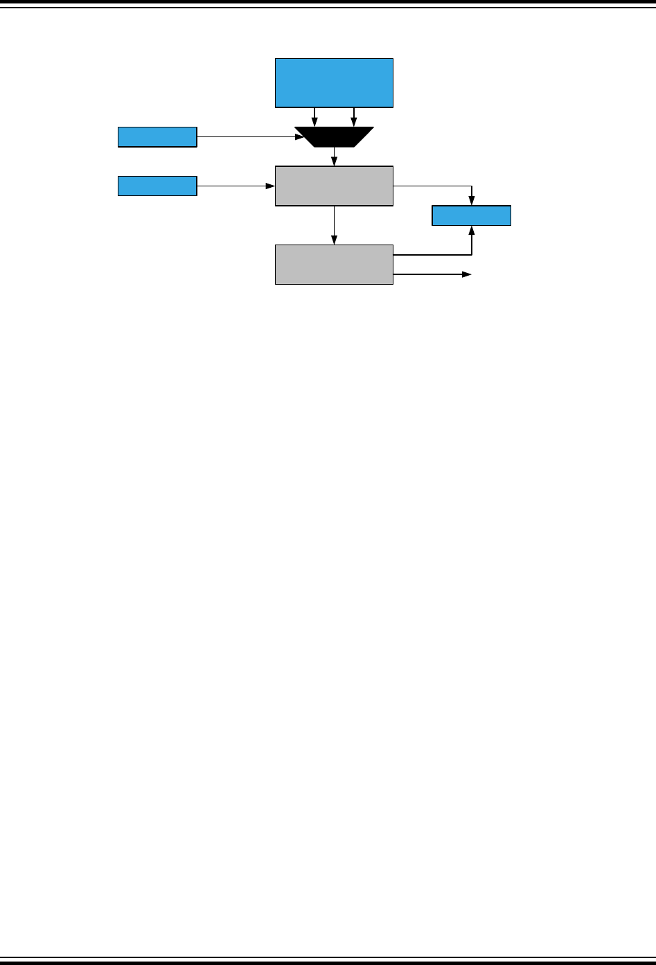
25.2.1 Block Diagram
Figure 25-2. Cyclic Redundancy Check Block Diagram
CHECKSUM
CRC
calculation
STATUS
CTRLA
CTRLB
Memory
(Boot, App,
Flash)
BUSY
Source
Enable,
Reset
NMI Req
CRC OK
25.3 Functional Description
25.3.1 Initialization
To enable a CRC in software (or via the debugger):
1. Write the Source (SRC) bit field of the Control B register (CRCSCAN.CTRLB) to select the desired
mode and source settings.
2. Enable the CRCSCAN by writing a ‘1’ to the ENABLE bit in the Control A register
(CRCSCAN.CTRLA).
3. The CRC will start after three cycles. The CPU will continue executing during these three cycles.
The CRCSCAN can be configured to perform a code memory scan before the device leaves reset. If this
check fails, the CPU is not allowed to start normal code execution. This feature is enabled and controlled
by the CRCSRC field in FUSE.SYSCFG0, see the “Fuses” chapter for more information.
If this feature is enabled, a successful CRC check will have the following outcome:
• Normal code execution starts
• The ENABLE bit in CRCSCAN.CTRLA will be ‘1’
• The SRC bit field in CRCSCAN.CTRLB will reflect the checked section(s)
• The OK flag in CRCSCAN.STATUS will be ‘1’
If this feature is enabled, a non-successful CRC check will have the following outcome:
• Normal code execution does not start, the CPU will hang executing no code
• The ENABLE bit in CRCSCAN.CTRLA will be ‘1’
• The SRC bit field in CRCSCAN.CTRLB will reflect the checked section(s)
• The OK flag in CRCSCAN.STATUS will be ‘0’
• This condition can be observed using the debug interface
25.3.2 Operation
The CRC is operating in Priority mode: the CRC peripheral has priority access to the Flash and will stall
the CPU until completed.
In Priority mode, the CRC fetches a new word (16-bit) on every third main clock cycle, or when the CRC
peripheral is configured to do a scan from startup.
megaAVR® 0-Series
Cyclic Redundancy Check Memory Scan (CRCSCAN...
© 2018 Microchip Technology Inc. Datasheet Preliminary DS40002015A-page 371

25.3.2.1 Checksum
The pre-calculated checksum must be present in the last location of the section to be checked. If the
BOOT section should be checked, the checksum must be saved in the last bytes of the BOOT section,
and similarly for APPLICATION and entire Flash. Table 25-1 shows explicitly how the checksum should
be stored for the different sections. Also, see the CRCSCAN.CTRLB register description for how to
configure which section to check and the device fuse description for how to configure the BOOTEND and
APPEND fuses.
Table 25-1. Placement the Pre-Calculated Checksum in Flash
Section to Check CHECKSUM[15:8] CHECKSUM[7:0]
BOOT FUSE_BOOTEND*256-2 FUSE_BOOTEND*256-1
BOOT and APPLICATION FUSE_APPEND*256-2 FUSE_APPEND*256-1
Full Flash FLASHEND-1 FLASHEND
25.3.3 Interrupts
Table 25-2. Available Interrupt Vectors and Sources
Name Vector Description Conditions
NMI Non-Maskable Interrupt Generated on CRC failure
When the interrupt condition occurs, the OK flag in the Status register (CRCSCAN.STATUS) is cleared to
'0'.
An interrupt is enabled by writing a '1' to the respective Enable bit (NMIEN) in the Control A register
(CRCSCAN.CTRLA), but can only be disabled with a system Reset. An NMI is generated when the OK
flag in CRCSCAN.STATUS is cleared and the NMIEN bit is '1'. The NMI request remains active until a
system Reset, and cannot be disabled.
A non-maskable interrupt can be triggered even if interrupts are not globally enabled.
25.3.4 Sleep Mode Operation
CTCSCAN is halted in all sleep modes. In all CPU Sleep modes, the CRCSCAN peripheral is halted and
will resume operation when the CPU wakes up.
The CRCSCAN starts operation three cycles after writing the EN bit in CRCSCAN.CTRLA. During these
three cycles, it is possible to enter Sleep mode. In this case:
1. The CRCSCAN will not start until the CPU is woken up.
2. Any interrupt handler will execute after CRCSCAN has finished.
25.3.5 Debug Operation
Whenever the debugger accesses the device, for instance, reading or writing a peripheral or memory
location, the CRCSCAN peripheral will be disabled.
If the CRCSCAN is busy when the debugger accesses the device, the CRCSCAN will restart the ongoing
operation when the debugger accesses an internal register or when the debugger disconnects.
The BUSY bit in the Status register (CRCSCAN.STATUS) will read '1' if the CRCSCAN was busy when
the debugger caused it to disable, but it will not actively check any section as long as the debugger keeps
it disabled. There are synchronized CRC Status bits in the debugger's internal register space, which can
megaAVR® 0-Series
Cyclic Redundancy Check Memory Scan (CRCSCAN...
© 2018 Microchip Technology Inc. Datasheet Preliminary DS40002015A-page 372

be read by the debugger without disabling the CRCSCAN. Reading the debugger's internal CRC status
bits will make sure that the CRCSCAN is enabled.
It is possible to write the CRCSCAN.STATUS register directly from the debugger:
• BUSY bit in CRCSCAN.STATUS:
– Writing the BUSY bit to '0' will stop the ongoing CRC operation (so that the CRCSCAN does
not restart its operation when the debugger allows it).
– Writing the BUSY bit to '1' will make the CRC start a single check with the settings in the
Control B register (CRCSCAN.CTRLB), but not until the debugger allows it.
As long as the BUSY bit in CRCSCAN.STATUS is '1', CRCSCAN.CRCTRLB and the Non-
Maskable Interrupt Enable bit (NMIEN) in the Control A register (CRCSCAN.CTRLA) cannot be
altered.
• OK bit in CRCSCAN.STATUS:
– Writing the OK bit to '0' can trigger a Non-Maskable Interrupt (NMI) if the NMIEN bit in
CRCSCAN.CTRLA is '1'. If an NMI has been triggered, no writes to the CRCSCAN are
allowed.
– Writing the OK bit to '1' will make the OK bit read as '1' when the BUSY bit in
CRCSCAN.STATUS is '0'.
Writes to CRCSCAN.CTRLA and CRCSCAN.CTRLB from the debugger are treated in the same way as
writes from the CPU.
megaAVR® 0-Series
Cyclic Redundancy Check Memory Scan (CRCSCAN...
© 2018 Microchip Technology Inc. Datasheet Preliminary DS40002015A-page 373


25.5.1 Control A
Name: CTRLA
Offset: 0x00
Reset: 0x00
Property: -
If an NMI has been triggered, this register is not writable.
Bit 7 6 5 4 3 2 1 0
RESET NMIEN ENABLE
Access R/W R/W R/W
Reset 0 0 0
Bit 7 – RESET Reset CRCSCAN
Writing this bit to ’1’ resets the CRCSCAN peripheral: The CRCSCAN Control registers and Status
register (CRCSCAN.CTRLA, CRCSCAN.CTRLB, CRCSCAN.STATUS) will be cleared one clock cycle
after the RESET bit was written to ’1’.
If NMIEN is ’0’, this bit is writable both when the CRCSCAN is busy (the BUSY bit in CRCSCAN.STATUS
is ’1’) and not busy (the BUSY bit is ’0’) and will take effect immediately.
If NMIEN is ’1’, this bit is only writable when the CRCSCAN is not busy (the BUSY bit in
CRCSCAN.STATUS is ’0’).
The RESET bit is a strobe bit.
Bit 1 – NMIEN Enable NMI Trigger
When this bit is written to ’1’, any CRC failure will trigger an NMI.
This can only be cleared by a system Reset - it is not cleared by a write to the RESET bit.
This bit can only be written to ’1’ when the CRCSCAN is not busy (the BUSY bit in CRCSCAN.STATUS
is ’0’).
Bit 0 – ENABLE Enable CRCSCAN
Writing this bit to ’1’ enables the CRCSCAN peripheral with the current settings. It will stay ’1’ even after a
CRC check has completed, but writing it to ‘1’ again will start a new check.
Writing the bit to ’0’ will disable the CRCSCAN after the ongoing check is completed (after reaching the
end of the section it is set up to check). This is the preferred way to stop a continuous background check.
A failure in the ongoing check will still be detected and can cause an NMI if the NMIEN bit is ’1’.
The CRCSCAN can be configured to run a scan during the MCU startup sequence to verify Flash
sections before letting the CPU start normal code execution (see the “Initialization” section). If this feature
is enabled, the ENABLE bit will read as ’1’ when normal code execution starts.
To see whether the CRCSCAN peripheral is busy with an ongoing check, poll the Busy bit (BUSY) in the
Status register (CRCSCAN.STATUS).
megaAVR® 0-Series
Cyclic Redundancy Check Memory Scan (CRCSCAN...
© 2018 Microchip Technology Inc. Datasheet Preliminary DS40002015A-page 375

25.5.2 Control B
Name: CTRLB
Offset: 0x01
Reset: 0x00
Property: -
The CRCSCAN.CTRLB register contains the mode and source settings for the CRC. It is not writable
when the CRC is busy or when an NMI has been triggered.
Bit 7 6 5 4 3 2 1 0
SRC[1:0]
Access R/W R/W
Reset 0 0
Bits 1:0 – SRC[1:0] CRC Source
The SRC bit field selects which section of the Flash the CRC module should check. To set up section
sizes, refer to the fuse description.
The CRC can be enabled during internal reset initialization to verify Flash sections before letting the CPU
start (see the “Fuses” chapter). If the CRC is enabled during internal reset initialization, the SRC bit field
will read out as FLASH, BOOTAPP, or BOOT when normal code execution starts (depending on the
configuration).
Value Name Description
0x0 FLASH The CRC is performed on the entire Flash (boot, application code, and
application data sections).
0x1 BOOTAPP The CRC is performed on the boot and application code sections of Flash.
0x2 BOOT The CRC is performed on the boot section of Flash.
0x3 - Reserved.
megaAVR® 0-Series
Cyclic Redundancy Check Memory Scan (CRCSCAN...
© 2018 Microchip Technology Inc. Datasheet Preliminary DS40002015A-page 376

25.5.3 Status
Name: STATUS
Offset: 0x02
Reset: 0x02
Property: -
The status register contains the busy and OK information. It is not writable, only readable.
Bit 7 6 5 4 3 2 1 0
OK BUSY
Access R R
Reset 1 0
Bit 1 – OK CRC OK
When this bit is read as ‘1’, the previous CRC completed successfully. The bit is set to ’1’ from Reset but
is cleared to ‘0’ when enabling the CRCSCAN. As long as the CRC module is busy, it will read ‘0’. When
running continuously, the CRC status must be assumed OK until it fails or is stopped by the user.
Bit 0 – BUSY CRC Busy
When this bit is read as ‘1’, the CRC module is busy. As long as the module is busy, the access to the
control registers is limited.
megaAVR® 0-Series
Cyclic Redundancy Check Memory Scan (CRCSCAN...
© 2018 Microchip Technology Inc. Datasheet Preliminary DS40002015A-page 377

26. CCL – Configurable Custom Logic
26.1 Features
• Glue logic for general purpose PCB design
• 4 Programmable LookUp Tables (LUTs)
• Combinatorial Logic Functions: Any logic expression which is a function of up to three inputs.
• Sequential Logic Functions:
Gated D Flip-Flop, JK Flip-Flop, gated D Latch, RS Latch
• Flexible LUT Input Selection:
– I/Os
– Events
– Subsequent LUT Output
– Internal Peripherals such as
• Analog Comparator
• Timer/Counters
• USART
• SPI
• Clocked by system clock or other peripherals
• Output can be connected to I/O pins or Event System
• Optional synchronizer, filter, or edge detector available on each LUT output
• Optional interrupt generation from each LUT output
• – Rising edge
– Falling edge
– Both edges
26.2 Overview
The Configurable Custom Logic (CCL) is a programmable logic peripheral which can be connected to the
device pins, to events, or to other internal peripherals. The CCL can serve as "glue logic" between the
device peripherals and external devices. The CCL can eliminate the need for external logic components,
and can also help the designer to overcome real-time constraints by combining core independent
peripherals to handle the most time-critical parts of the application independent of the CPU.
The CCL peripheral groups adjacent Lookup Tables (LUTs) into pairs. The LUTs in a pair can be
combined to perform specific operations. Each LUT consists of three inputs, a truth table, and a filter/
edge detector. The inputs can be individually masked.
Each LUT can generate an output as a user programmable logic expression with three inputs. The output
is generated from the inputs using combinatorial logic and can be filtered to remove spikes. The CCL can
be configured to generate an interrupt request on changes in the LUT outputs.
An optional Sequential module can be enabled. The inputs to the Sequential module are individually
controlled by two independent, adjacent LUT outputs, enabling complex waveform generation.
megaAVR® 0-Series
CCL – Configurable Custom Logic
© 2018 Microchip Technology Inc. Datasheet Preliminary DS40002015A-page 378
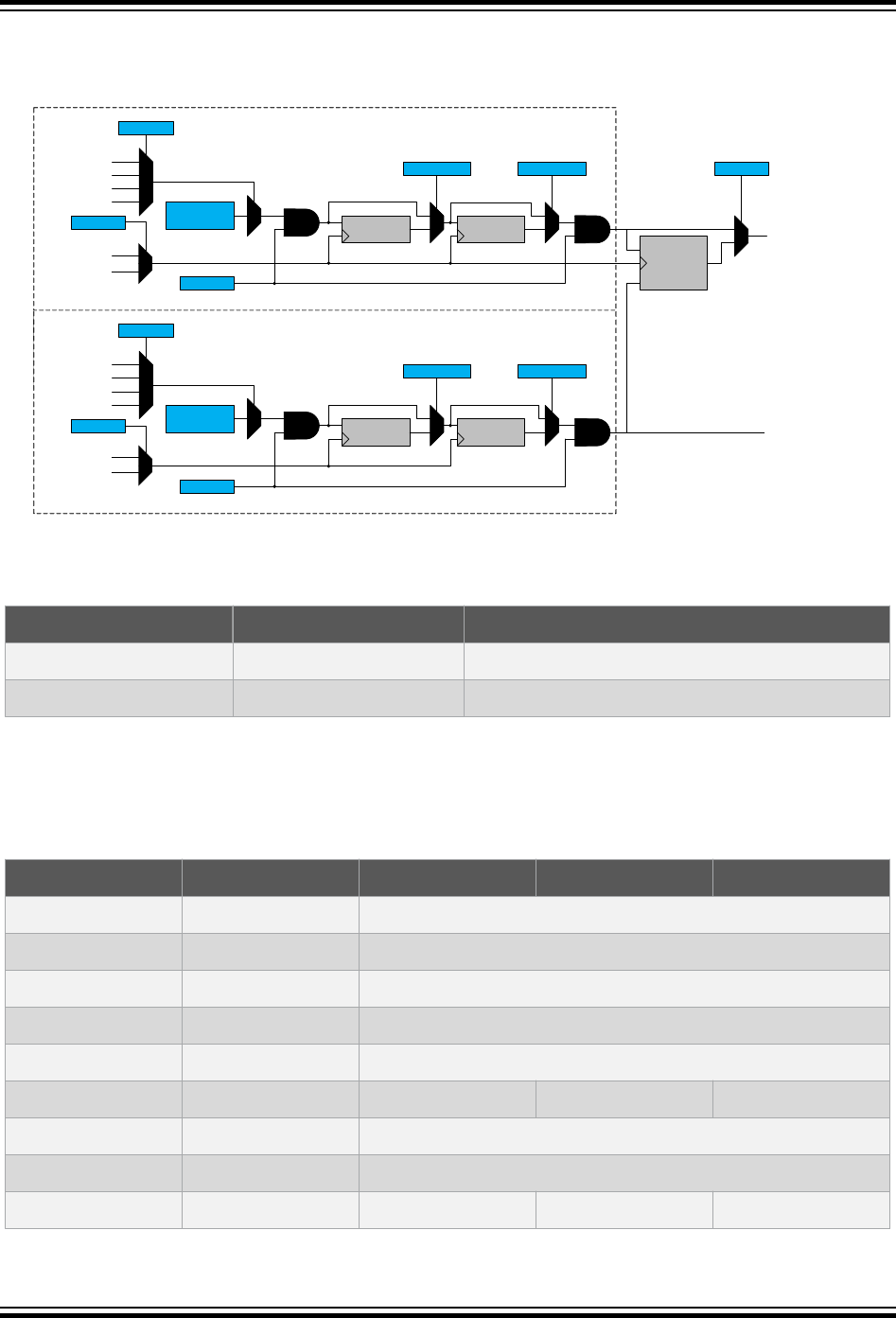
26.2.1 Block Diagram
Figure 26-1. Configurable Custom Logic
LUTn
LUTn+1
Internal
Events
I/O
Peripherals
TRUTH Filter/
Synch
Edge
Detector
Sequential
LUTn-IN[2]
Internal
Events
I/O
Peripherals
TRUTH Filter/
Synch
Edge
Detector
LUTn-OUT
LUTn+1-OUT
ENABLE
INSEL
CLKSRC
FILTSEL EDGEDET
CLKSRC
ENABLE
FILTSEL
INSEL
EDGEDET
SEQSEL
CLK_MUX_OUT
CLK_MUX_OUT
LUTn+1-IN[2]
LUTn-IN[2:0]
LUTn+1-IN[2:0]
Clock Sources
Clock Sources
26.2.2 Signal Description
Pin Name Type Description
LUTn-OUT Digital output Output from look-up table
LUTn-IN[2:0] Digital input Input to look-up table
Refer to I/O Multiplexing and Considerations for details on the pin mapping for this peripheral. One signal
can be mapped to several pins.
26.2.2.1 CCL Input Selection MUX
The following peripherals outputs are available as inputs into the CCL LUT.
Value Input source INSEL0 INSEL1 INSEL2
0x00 MASK None
0x01 FEEDBACK LUTn
0x02 LINK LUT(n+1)
0x03 EVENTA EVENTA
0x04 EVENTB EVENTB
0x05 IO IN0 IN1 IN2
0x06 AC AC0 OUT
0x07 -
0x08 USART USART0 TXD USART1 TXD USART2 TXD
megaAVR® 0-Series
CCL – Configurable Custom Logic
© 2018 Microchip Technology Inc. Datasheet Preliminary DS40002015A-page 379

Value Input source INSEL0 INSEL1 INSEL2
0x09 SPI SPI0 MOSI SPI0 MOSI SPI0 SCK
0x0A TCA0 WO0 WO1 WO2
0x0B -
0x0C TCB TCB0 WO TCB1 WO TCB2 WO
Other -
Note:
• SPI connections to the CCL work only in master SPI mode
• USART connections to the CCL work only in asynchronous/synchronous USART master mode.
26.3 Functional Description
26.3.1 Initialization
The following bits are enable-protected, meaning that they can only be written when the corresponding
even LUT is disabled (ENABLE=0 in CCL.LUT0CTRLA):
• Sequential Selection (SEQSEL) in Sequential Control 0 register (CCL.SEQCTRL0)
The following registers are enable-protected, meaning that they can only be written when the
corresponding LUT is disabled (ENABLE=0 in CCL.LUT0CTRLA):
• LUT n Control x register, except ENABLE bit (CCL.LUTnCTRLx)
Enable-protected bits in the CCL.LUTnCTRLx registers can be written at the same time as ENABLE in
CCL.LUTnCTRLx is written to '1', but not at the same time as ENABLE is written to '0'.
Enable-protection is denoted by the Enable-Protected property in the register description.
26.3.2 Operation
26.3.2.1 Enabling, Disabling, and Resetting
The CCL is enabled by writing a '1' to the ENABLE bit in the Control register (CCL.CTRLA). The CCL is
disabled by writing a '0' to that ENABLE bit.
Each LUT is enabled by writing a '1' to the LUT Enable bit (ENABLE) in the LUT n Control A register
(CCL.LUTnCTRLA). Each LUT is disabled by writing a '0' to the ENABLE bit in CCL.LUTnCTRLA.
26.3.2.2 Look-Up Table Logic
The look-up table in each LUT unit can generate a combinational logic output as a function of up to three
inputs IN[2:0]. Unused inputs can be masked (tied low). The truth table for the combinational logic
expression is defined by the bits in the CCL.TRUTHn registers. Each combination of the input bits
(IN[2:0]) corresponds to one bit in the TRUTHn register, as shown in the table below.
Table 26-1. Truth Table of LUT
IN[2] IN[1] IN[0] OUT
0 0 0 TRUTH[0]
0 0 1 TRUTH[1]
megaAVR® 0-Series
CCL – Configurable Custom Logic
© 2018 Microchip Technology Inc. Datasheet Preliminary DS40002015A-page 380
IN[2] IN[1] IN[0] OUT
0 1 0 TRUTH[2]
0 1 1 TRUTH[3]
1 0 0 TRUTH[4]
1 0 1 TRUTH[5]
1 1 0 TRUTH[6]
1 1 1 TRUTH[7]
26.3.2.3 Truth Table Inputs Selection
Input Overview
The inputs can be individually:
• Masked
• Driven by peripherals
• Driven by internal events from Event System
• Driven by other CCL sub-modules
The Input Selection for each input y of LUT n is configured by writing the Input y Source Selection bit in
the LUT n Control x=[B,C] registers:
• INSEL0 in LUTnCTRLB
• INSEL1 in LUTnCTRLB
• INSEL2 in LUTnCTRLC.
Internal Feedback Inputs (FEEDBACK)
When selected (INSELy=FEEDBACK in LUTnCTRLx), the Sequential (SEQ) output is used as input for
the corresponding LUT.
The output from an internal sequential module can be used as input source for the LUT, see the figure
below for an example for LUT0 and LUT1. The sequential selection for each LUT follows the formula:
IN 2N = SEQ
IN 2N+1 = SEQ
With N representing the sequencer number and i representing the index of the input LUT.
megaAVR® 0-Series
CCL – Configurable Custom Logic
© 2018 Microchip Technology Inc. Datasheet Preliminary DS40002015A-page 381
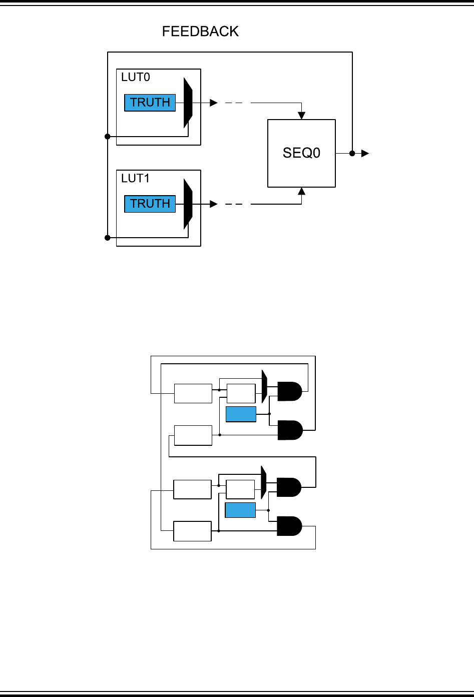
Figure 26-2. Feedback Input Selection
Linked LUT (LINK)
When selecting the LINK input option, the next LUT's direct output is used as the LUT input. In general,
LUT[n+1] is linked to the input of LUT[n]. As an example, LUT1 is the input for LUT0. For the last LUT, the
link wraps so that LUT[0] is linked to the input of LUT[3].
Figure 26-3. Linked LUT Input Selection
CTRLA
(ENABLE)
LUT2 SEQ 1
LUT3
CTRLA
(ENABLE)
LUT0 SEQ 0
LUT1
Internal Events Inputs Selection (EVENT)
Asynchronous events from the Event System can be used as input to the LUT. Two event input lines
(EVENTA and EVENTB) are available, and can be selected as LUT input. Before selecting the EVENT
input option by writing to the LUT CONTROL A or B register (CCL.LUTnCTRLB or LUTnCTRLC), the
Event System must be configured.
megaAVR® 0-Series
CCL – Configurable Custom Logic
© 2018 Microchip Technology Inc. Datasheet Preliminary DS40002015A-page 382
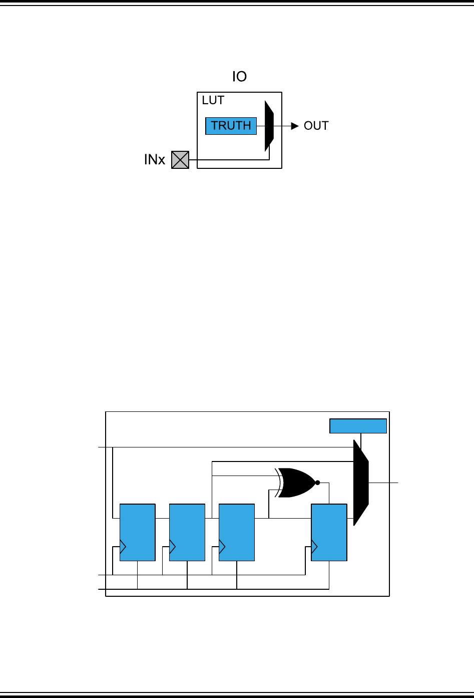
I/O Pin Inputs (IO)
When selecting the IO option, the LUT input will be connected to its corresponding I/O pin. Refer to the
I/O Multiplexing section in the Data Sheet for more details about where the LUTnINy pins are located.
Figure 26-4. I/O Pin Input Selection
Peripherals
The different peripherals on the three input lines of each LUT are selected by writing to the respective
LUT n Input y bit fields in the LUT n Control B and C registers:
• INSEL0 in CCL.LUTnCTRLB
• INSEL1 in CCL.LUTnCTRLB
• INSEL2 in CCL.LUTnCTRLC.
26.3.2.4 Filter
By default, the LUT output is a combinational function of the LUT inputs. This may cause some short
glitches when the inputs change the value. These glitches can be removed by clocking through filters if
demanded by application needs.
The Filter Selection bits (FILTSEL) in the LUT Control registers (CCL.LUTnCTRLA) define the digital filter
options. When a filter is enabled, the output will be delayed by two to five CLK cycles (peripheral clock or
alternative clock). One clock cycle after the corresponding LUT is disabled, all internal filter logic is
cleared.
Figure 26-5. Filter
DQ
R
DQ
R
DQ
R
DQ
R
FILTSEL
OUT
Input
CLK_MUX_OUT
CLR
G
26.3.2.5 Edge Detector
The edge detector can be used to generate a pulse when detecting a rising edge on its input. To detect a
falling edge, the TRUTH table should be programmed to provide inverted output.
megaAVR® 0-Series
CCL – Configurable Custom Logic
© 2018 Microchip Technology Inc. Datasheet Preliminary DS40002015A-page 383
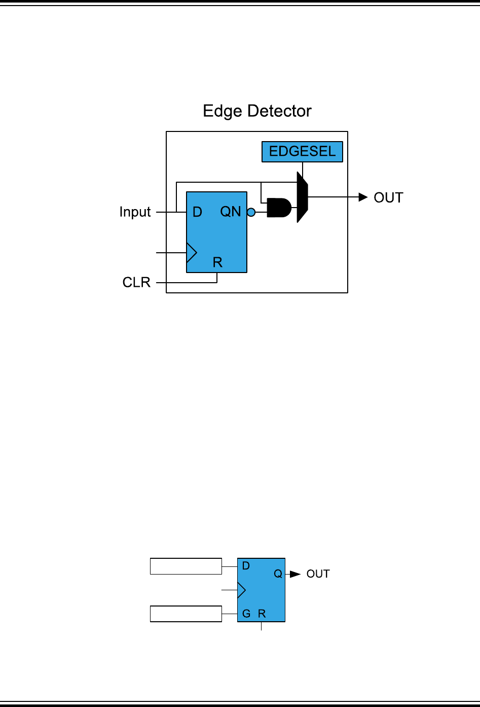
The edge detector is enabled by writing '1' to the Edge Selection bit (EDGEDET) in the LUT n Control A
register (CCL.LUTnCTRLA). In order to avoid unpredictable behavior, a valid filter option must be enabled
as well.
Edge detection is disabled by writing a '0' to EDGEDET in CCL.LUTnCTRLA. After disabling an LUT, the
corresponding internal Edge Detector logic is cleared one clock cycle later.
Figure 26-6. Edge Detector
CLK_MUX_OUT
26.3.2.6 Sequential Logic
Each LUT pair can be connected to an internal Sequential block. A Sequential block can function as
either D flip-flop, JK flip-flop, gated D-latch, or RS-latch. The function is selected by writing the Sequential
Selection bits (SEQSEL) in the Sequential Control register (SEQCTRLn).
The Sequential block receives its input from the either LUT, filter, or edge detector, depending on the
configuration.
The Sequential block is clocked by the same clock as the corresponding LUT. The clock source is
selected by the Clock Source field (CLKSRC) in the LUT n Control A register (LUTnCTRLA).
When the even LUT (LUT2n) is disabled, the latch is asynchronously cleared, during which the flip-flop
reset signal (R) is kept enabled for one clock cycle. In all other cases, the flip-flop output (OUT) is
refreshed on the rising edge of the clock, as shown in the respective “Electrical Characteristics” section in
the device Data Sheet.
Gated D Flip-Flop (DFF)
The D-input is driven by the even LUT output (LUT2n), and the G-input is driven by the odd LUT output
(LUT2n+1).
Figure 26-7. D Flip-Flop
CLK_MUX_OUT
even LUT
odd LUT
megaAVR® 0-Series
CCL – Configurable Custom Logic
© 2018 Microchip Technology Inc. Datasheet Preliminary DS40002015A-page 384
Table 26-2. DFF Characteristics
R G D OUT
1 X X Clear
0 1 1 Set
0 Clear
0 X Hold state (no change)
JK Flip-Flop (JK)
The J-input is driven by the even LUT output (LUT2n), and the K-input is driven by the odd LUT output
(LUT2n+1).
Figure 26-8. JK Flip-Flop
CLK_MUX_OUT
even LUT
odd LUT
Table 26-3. JK Characteristics
R J K OUT
1 X X Clear
0 0 0 Hold state (no change)
0 0 1 Clear
0 1 0 Set
0 1 1 Toggle
Gated D-Latch (DLATCH)
The D-input is driven by the even LUT output (LUT2n), and the G-input is driven by the odd LUT output
(LUT2n+1).
Figure 26-9. D-Latch
DQ
G
OUT
even LUT
odd LUT
Table 26-4. D-Latch Characteristics
G D OUT
0 X Hold state (no change)
1 0 Clear
1 1 Set
megaAVR® 0-Series
CCL – Configurable Custom Logic
© 2018 Microchip Technology Inc. Datasheet Preliminary DS40002015A-page 385
RS-Latch (RS)
The S-input is driven by the even LUT output (LUT2n), and the R-input is driven by the odd LUT output
(LUT2n+1).
Figure 26-10. RS-Latch
SQ
R
OUT
even LUT
odd LUT
Table 26-5. RS-Latch Characteristics
S R OUT
0 0 Hold state (no change)
0 1 Clear
1 0 Set
1 1 Forbidden state
26.3.2.7 Clock Source Settings
The Filter, Edge Detector, and Sequential logic are, by default, clocked by the system clock (CLK_PER).
It is also possible to use other clock inputs to clock these blocks (CLK_MUX_OUT in the figure below).
This is configured by writing the Clock Source bits (CLKSRC) in the LUT Control A register.
Figure 26-11. Clock Source Settings
LUTn
Edge
detector Filter
OSCULP1K
OSCULP32K
IN[2]
OSC20M
CLK_PER
Sequential
logic
CLKSRC
When the Clock Source (CLKSRC) is set to 0x1, IN[2] is used to clock the corresponding Filter and Edge
Detector (CLK_MUX_OUT). The Sequential logic is clocked by CLK_MUX_OUT of the even LUT in the
pair. When CLKSRC is set to 0x1, IN[2] is treated as MASKed (low) in the TRUTH table.
The CCL peripheral must be disabled while changing the clock source to avoid undefined outputs from
the peripheral.
26.3.3 Interrupts
Table 26-6. Available Interrupt Vectors and Sources
Name Vector Description Conditions
CCL CCL interrupt INTn in INTFLAG is raised as configured by INTMODEn bits in
CCL.INTCTRLn
megaAVR® 0-Series
CCL – Configurable Custom Logic
© 2018 Microchip Technology Inc. Datasheet Preliminary DS40002015A-page 386

When an interrupt condition occurs, the corresponding interrupt flag is set in the Interrupt Flags register of
the peripheral (peripheral.INTFLAGS).
An interrupt source is enabled or disabled by writing to the corresponding enable bit in the peripheral's
Interrupt Control register (peripheral.INTCTRL).
An interrupt request is generated when the corresponding interrupt source is enabled and the interrupt
flag is set. The interrupt request remains active until the interrupt flag is cleared. See the peripheral's
INTFLAGS register for details on how to clear interrupt flags.
When several interrupt request conditions are supported by an interrupt vector, the interrupt requests are
ORed together into one combined interrupt request to the interrupt controller. The user must read the
peripheral's INTFLAGS register to determine which of the interrupt conditions are present.
26.3.4 Events
The CCL can generate the following output events:
• LUTnOUT: Look-Up Table Output Value
The CCL can take the following actions on an input event:
• INx: The event is used as input for the TRUTH table
26.3.5 Sleep Mode Operation
Writing the Run In Standby bit (RUNSTDBY) in the Control A register (CCL.CTRLA) to '1' will allow the
system clock to be enabled in Standby Sleep mode.
If RUNSTDBY is '0' the system clock will be disabled in Standby Sleep mode. If the Filter, Edge Detector,
or Sequential logic is enabled, the LUT output will be forced to zero in Standby Sleep mode. In Idle sleep
mode, the TRUTH table decoder will continue operation and the LUT output will be refreshed accordingly,
regardless of the RUNSTDBY bit.
If the Clock Source bit (CLKSRC) in the LUT n Control A register (CCL.LUTnCTRLA) is written to '1', the
LUT input 2 (IN[2]) will always clock the Filter, Edge Detector, and Sequential block. The availability of the
IN[2] clock in sleep modes will depend on the sleep settings of the peripheral employed.
megaAVR® 0-Series
CCL – Configurable Custom Logic
© 2018 Microchip Technology Inc. Datasheet Preliminary DS40002015A-page 387

26.4 Register Summary - CCL
Offset Name Bit Pos.
0x00 CTRLA 7:0 RUNSTDBY ENABLE
0x01 SEQCTRL0 7:0 SEQSEL1[3:0] SEQSEL0[3:0]
0x02
...
0x04
Reserved
0x05 INTCTRL0 7:0 INTMODE3[1:0] INTMODE2[1:0] INTMODE1[1:0] INTMODE0[1:0]
0x06 Reserved
0x07 INTFLAGS 7:0 INT3 INT2 INT1 INT0
0x08 LUT0CTRLA 7:0 EDGEDET OUTEN FILTSEL[1:0] CLKSRC[2:0] ENABLE
0x09 LUT0CTRLB 7:0 INSEL1[3:0] INSEL0[3:0]
0x0A LUT0CTRLC 7:0 INSEL2[3:0]
0x0B TRUTH0 7:0 TRUTH[7:0]
0x0C LUT1CTRLA 7:0 EDGEDET OUTEN FILTSEL[1:0] CLKSRC[2:0] ENABLE
0x0D LUT1CTRLB 7:0 INSEL1[3:0] INSEL0[3:0]
0x0E LUT1CTRLC 7:0 INSEL2[3:0]
0x0F TRUTH1 7:0 TRUTH[7:0]
26.5 Register Description
megaAVR® 0-Series
CCL – Configurable Custom Logic
© 2018 Microchip Technology Inc. Datasheet Preliminary DS40002015A-page 388

26.5.1 Control A
Name: CTRLA
Offset: 0x00
Reset: 0x00
Property: -
Bit 7 6 5 4 3 2 1 0
RUNSTDBY ENABLE
Access R/W R/W
Reset 0 0
Bit 6 – RUNSTDBY Run in Standby
This bit indicates if the peripheral clock (CLK_PER) is kept running in Standby Sleep mode. The setting is
ignored for configurations where the CLK_PER is not required.
Value Description
0 System clock is not required in Standby Sleep mode
1 System clock is required in Standby Sleep mode
Bit 0 – ENABLE Enable
Value Description
0 The peripheral is disabled
1 The peripheral is enabled
megaAVR® 0-Series
CCL – Configurable Custom Logic
© 2018 Microchip Technology Inc. Datasheet Preliminary DS40002015A-page 389

26.5.2 Sequential Control 0
Name: SEQCTRL0
Offset: 0x01
Reset: 0x00
Property: Enable-Protected
Bit 7 6 5 4 3 2 1 0
SEQSEL1[3:0] SEQSEL0[3:0]
Access R/W R/W R/W R/W R/W R/W R/W R/W
Reset 0 0 0 0 0 0 0 0
Bits 0:3, 4:7 – SEQSEL Sequential Selection
The bits in SEQSELn select the sequential configuration for LUT[2n] and LUT[2n+1].
Value Name Description
0x0 DISABLE Sequential logic is disabled
0x1 DFF D flip flop
0x2 JK JK flip flop
0x3 LATCH D latch
0x4 RS RS latch
Other - Reserved
megaAVR® 0-Series
CCL – Configurable Custom Logic
© 2018 Microchip Technology Inc. Datasheet Preliminary DS40002015A-page 390
26.5.3 Interrupt Control 0
Name: INTCTRL0
Offset: 0x05
Reset: 0x00
Property: R/W
Bit 7 6 5 4 3 2 1 0
INTMODE3[1:0] INTMODE2[1:0] INTMODE1[1:0] INTMODE0[1:0]
Access
Reset 0 0 0 0 0 0 0 0
Bits 0:1, 2:3, 4:5, 6:7 – INTMODE The bits in INTMODEn select the interrupt sense configuration for
LUTn-OUT.
Value Name Description
3 BOTH Sense both edges
2 FALLING Sense falling edge
1 RISING Sense rising edge
0 INTDISABLE Interrupt disabled
megaAVR® 0-Series
CCL – Configurable Custom Logic
© 2018 Microchip Technology Inc. Datasheet Preliminary DS40002015A-page 391

26.5.4 Interrupt Flag
Name: INTFLAGS
Offset: 0x07
Reset: 0
Property: R/W
Bit 7 6 5 4 3 2 1 0
INT3 INT2 INT1 INT0
Access
Reset 0 0 0 0
Bits 0, 1, 2, 3 – INT Interrupt Flag
The INTn flag is set when LUTn output change matches the interrupt sense mode as defined in
CCL.INTCTRLn. Writing a '1' to this flag's bit location will clear the flag.
megaAVR® 0-Series
CCL – Configurable Custom Logic
© 2018 Microchip Technology Inc. Datasheet Preliminary DS40002015A-page 392

26.5.5 LUT n Control A
Name: LUTCTRLA
Offset: 0x08 + n*0x04 [n=0..1]
Reset: 0x00
Property: Enable-Protected
Bit 7 6 5 4 3 2 1 0
EDGEDET OUTEN FILTSEL[1:0] CLKSRC[2:0] ENABLE
Access R/W R/W R/W R/W R/W R/W R/W R/W
Reset 0 0 0 0 0 0 0 0
Bit 7 – EDGEDET Edge Detection
Value Description
0 Edge detector is disabled.
1 Edge detector is enabled.
Bit 6 – OUTEN Output Enable
This bit enables the LUT output to the LUTnOUT pin. When written to '1', the pin configuration of the
PORT I/O-Controller is overridden.
Value Description
0 Output to pin disabled.
1 Output to pin enabled.
Bits 5:4 – FILTSEL[1:0] Filter Selection
These bits select the LUT output filter options:
Filter Selection
Value Name Description
0x0 DISABLE Filter disabled
0x1 SYNCH Synchronizer enabled
0x2 FILTER Filter enabled
0x3 - Reserved
Bits 3:1 – CLKSRC[2:0] Clock Source Selection
This bit selects between various clock sources to be used as the clock (CLK_MUX_OUT) for a LUT.
The CLK_MUX_OUT of the even LUT is used for clocking the Sequential block of a LUT pair.
Value Name Description
0x0 CLKPER None (masked)
0x1 IN2 LUT input 2
0x2 - Reserved
0x3 - Reserved
0x4 OSC20M 20MHz internal oscillator
megaAVR® 0-Series
CCL – Configurable Custom Logic
© 2018 Microchip Technology Inc. Datasheet Preliminary DS40002015A-page 393

Value Name Description
0x5 OSCULP32K 32.768kHz internal oscillator
0x6 OSCULP1K 1.024kHz from internal oscillator
0x7 - Reserved
Bit 0 – ENABLE LUT Enable
Value Description
0 The LUT is disabled.
1 The LUT is enabled.
megaAVR® 0-Series
CCL – Configurable Custom Logic
© 2018 Microchip Technology Inc. Datasheet Preliminary DS40002015A-page 394

26.5.6 LUT n Control B
Name: LUTCTRLB
Offset: 0x09 + n*0x04 [n=0..1]
Reset: 0x00
Property: Enable-Protected
Note:
• SPI connections to the CCL work in master SPI mode only.
• USART connections to the CCL work only when the USART is in one of the following modes:
– Asynchronous USART
– Synchronous USART master
Bit 7 6 5 4 3 2 1 0
INSEL1[3:0] INSEL0[3:0]
Access R/W R/W R/W R/W R/W R/W R/W R/W
Reset 0 0 0 0 0 0 0 0
Bits 7:4 – INSEL1[3:0] LUT n Input 1 Source Selection
These bits select the source for input 1 of LUT n:
Value Name Description
0x0 MASK None (masked)
0x1 FEEDBACK Feedback input
0x2 LINK Output from LUTn+1
0x3 EVENTA Event CCL-LUTnA
0x4 EVENTB Event CCL-LUTnB
0x5 IO I/O-pin LUTn-IN1
0x6 AC0 AC0 out
0x7 - Reserved
0x8 USART1 USART0 TXD
0x9 SPI0 SPI0 MOSI
0xA TCA0 TCA0 WO1
0xB - Reserved
0xC TCB1 TCB1 WO
Other - Reserved
Bits 3:0 – INSEL0[3:0] LUT n Input 0 Source Selection
These bits select the source for input 0 of LUT n:
megaAVR® 0-Series
CCL – Configurable Custom Logic
© 2018 Microchip Technology Inc. Datasheet Preliminary DS40002015A-page 395

Value Name Description
0x0 MASK None (masked)
0x1 FEEDBACK Feedback input
0x2 LINK Output from LUTn+1
0x3 EVENTA Event CCL-LUTnA
0x4 EVENTB Event CCL-LUTnB
0x5 IO I/O-pin LUTn-IN0
0x6 AC0 AC0 out
0x7 - Reserved
0x8 USART0 USART0 TXD
0x9 SPI0 SPI0 MOSI
0xA TCA0 TCA0 WO1
0xB - Reserved
0xC TCB0 TCB0 WO
Other - Reserved
megaAVR® 0-Series
CCL – Configurable Custom Logic
© 2018 Microchip Technology Inc. Datasheet Preliminary DS40002015A-page 396

26.5.7 LUT n Control C
Name: LUTCTRLC
Offset: 0x0A + n*0x04 [n=0..1]
Reset: 0x00
Property: Enable-Protected
Bit 7 6 5 4 3 2 1 0
INSEL2[3:0]
Access R/W R/W R/W R/W
Reset 0 0 0 0
Bits 3:0 – INSEL2[3:0] LUT n Input 2 Source Selection
These bits select the source for input 2 of LUT n:
Value Name Description
0x0 MASK None (masked)
0x1 FEEDBACK Feedback input
0x2 LINK Output from LUTn+1
0x3 EVENTA Event CCL-LUTnA
0x4 EVENTB Event CCL-LUTnB
0x5 IO I/O-pin LUTn-IN0
0x6 AC0 AC0 out
0x7 - Reserved
0x8 USART2 USART0 TXD
0x9 SPI0 SPI0 SCK
0xA TCA0 TCA0 WO1
0xB - Reserved
0xC TCB2 TCB2 WO
Other - Reserved
megaAVR® 0-Series
CCL – Configurable Custom Logic
© 2018 Microchip Technology Inc. Datasheet Preliminary DS40002015A-page 397

26.5.8 TRUTHn
Name: TRUTH
Offset: 0x0B + n*0x04 [n=0..1]
Reset: 0x00
Property: Enable-Protected
Bit 7 6 5 4 3 2 1 0
TRUTH[7:0]
Access R/W R/W R/W R/W R/W R/W R/W R/W
Reset 0 0 0 0 0 0 0 0
Bits 7:0 – TRUTH[7:0] Truth Table
These bits define the value of truth logic as a function of inputs IN[2:0].
megaAVR® 0-Series
CCL – Configurable Custom Logic
© 2018 Microchip Technology Inc. Datasheet Preliminary DS40002015A-page 398

27. Analog Comparator (AC)
27.1 Features
• Selectable response time
• Selectable hysteresis
• Analog comparator output available on pin
• Comparator output inversion available
• Flexible input selection:
– 4 Positive pins
– 3 Negative pins
– Internal reference voltage generator (DACREF)
• Interrupt generation on:
– Rising edge
– Falling edge
– Both edges
• Event generation:
– Comparator output
27.2 Overview
The Analog Comparator (AC) compares the voltage levels on two inputs and gives a digital output based
on this comparison. The AC can be configured to generate interrupt requests and/or Events upon several
different combinations of input change.
The dynamic behavior of the AC can be adjusted by a hysteresis feature. The hysteresis can be
customized to optimize the operation for each application.
The input selection includes analog port pins and internally generated inputs. The analog comparator
output state can also be output on a pin for use by external devices.
An AC has one positive input and one negative input. The digital output from the comparator is '1' when
the difference between the positive and the negative input voltage is positive, and '0' otherwise.
megaAVR® 0-Series
Analog Comparator (AC)
© 2018 Microchip Technology Inc. Datasheet Preliminary DS40002015A-page 399
27.2.1 Block Diagram
Figure 27-1. Analog Comparator
+
AC
-
Hysteresis
AINN0
AINNn
Invert
Enable
AINP0
Controller
logic OUT
Voltage
divider
AINPn
.
.
.
.
.
.
Event out
CTRLA
MUXCTRL
CMP
(Int. Req)
DACREF
VREF
27.2.2 Signal Description
Signal Description Type
AINNn Negative Input n Analog
AINPn Positive Input n Analog
OUT Comparator Output for AC Digital
27.3 Functional Description
27.3.1 Initialization
For basic operation, follow these steps:
• Configure the desired input pins in the port peripheral
• Select the positive and negative input sources by writing the Positive and Negative Input MUX
Selection bit fields (MUXPOS and MUXNEG) in the MUX Control A register (AC.MUXCTRLA)
• Optional: Enable the output to pin by writing a '1' to the Output Pad Enable bit (OUTEN) in the
Control A register (AC.CTRLA)
• Enable the AC by writing a '1' to the ENABLE bit in AC.CTRLA
During the start-up time after enabling the AC, the output of the AC may be invalid.
The start-up time of the AC by itself is at most 2.5 µs. If an internal reference is used, the reference start-
up time is normally longer than the AC start-up time.
To avoid the pin being tri-stated when the AC is disabled, the OUT pin must be configured as output in
PORTx.DIR
27.3.2 Operation
27.3.2.1 Input Hysteresis
Applying an input hysteresis helps to prevent constant toggling of the output when the noise-afflicted input
signals are close to each other.
The input hysteresis can either be disabled or have one of three levels. The hysteresis is configured by
writing to the Hysteresis Mode Select bit field (HYSMODE) in the Control A register (ACn.CTRLA).
megaAVR® 0-Series
Analog Comparator (AC)
© 2018 Microchip Technology Inc. Datasheet Preliminary DS40002015A-page 400

27.3.2.2 Input Sources
An AC has one positive and one negative input. The inputs can be pins and internal sources, such as a
voltage reference.
Each input is selected by writing to the Positive and Negative Input MUX Selection bit field (MUXPOS and
MUXNEG) in the MUX Control A register (ACn.MUXTRLA).
Pin Inputs
The following Analog input pins on the port can be selected as input to the analog comparator:
• AINN0
• AINN1
• AINN2
• AINP0
• AINP1
• AINP2
• AINP3
Internal Inputs
The DAC has the following internal inputs:
• Internal reference voltage generator (DACREF)
27.3.2.3 Power Modes
For power sensitive applications, the AC provides multiple power modes with balance power consumption
and propagation delay. A mode is selected by writing to the Mode bits (MODE) in the Control A register
(ACn.CTRLA).
27.3.2.4 Signal Compare and Interrupt
After successful initialization of the AC, and after configuring the desired properties, the result of the
comparison is continuously updated and available for application software, the Event system, or on a pin.
The AC can generate a comparator Interrupt, COMP. The AC can request this interrupt on either rising,
falling, or both edges of the toggling comparator output. This is configured by writing to the Interrupt
Modes bit field in the Control A register (INTMODE bits in ACn.CTRLA).
The Interrupt is enabled by writing a ‘1’ to the Analog Comparator Interrupt Enable bit in the Interrupt
Control register (COMP bit in ACn.INTCTRL).
27.3.3 Events
The AC will generate the following event automatically when the AC is enabled:
• The digital output from the AC (OUT in the block diagram) is available as an Event System source.
The events from the AC are asynchronous to any clocks in the device.
The AC has no event inputs.
27.3.4 Interrupts
Table 27-1. Available Interrupt Vectors and Sources
Name Vector Description Conditions
COMP Analog comparator interrupt AC output is toggling as configured by INTMODE in ACn.CTRLA
When an interrupt condition occurs, the corresponding Interrupt Flag is set in the Status register
(ACn.STATUS).
megaAVR® 0-Series
Analog Comparator (AC)
© 2018 Microchip Technology Inc. Datasheet Preliminary DS40002015A-page 401

An interrupt source is enabled or disabled by writing to the corresponding bit in the peripheral's Interrupt
Control register (ACn.INTCTRL).
An interrupt request is generated when the corresponding interrupt source is enabled and the Interrupt
Flag is set. The interrupt request remains active until the Interrupt Flag is cleared. See the ACn.STATUS
register description for details on how to clear Interrupt Flags.
27.3.5 Sleep Mode Operation
In Idle sleep mode, the AC will continue to operate as normal.
In Standby sleep mode, the AC is disabled by default. If the Run in Standby Sleep Mode bit
(RUNSTDBY) in the Control A register (ACn.CTRLA) is written to '1', the AC will continue to operate as
normal with Event, Interrupt, and AC output on pad even if the CLK_PER is not running in Standby sleep
mode.
In Power Down sleep mode, the AC and the output to the pad are disabled.
megaAVR® 0-Series
Analog Comparator (AC)
© 2018 Microchip Technology Inc. Datasheet Preliminary DS40002015A-page 402

27.4 Register Summary - AC
Offset Name Bit Pos.
0x00 CTRLA 7:0 RUNSTDBY OUTEN INTMODE[1:0] LPMODE HYSMODE[1:0] ENABLE
0x01 Reserved
0x02 MUXCTRL 7:0 INVERT MUXPOS[1:0] MUXNEG[1:0]
0x03 Reserved
0x04 DACREF 7:0 DACREF[7:0]
0x05 Reserved
0x06 INTCTRL 7:0 CMP
0x07 STATUS 7:0 STATE CMP
27.5 Register Description
megaAVR® 0-Series
Analog Comparator (AC)
© 2018 Microchip Technology Inc. Datasheet Preliminary DS40002015A-page 403
27.5.1 Control A
Name: CTRLA
Offset: 0x00
Reset: 0x00
Property: -
Bit 7 6 5 4 3 2 1 0
RUNSTDBY OUTEN INTMODE[1:0] LPMODE HYSMODE[1:0] ENABLE
Access R/W R/W R/W R/W R/W R/W R/W R/W
Reset 0 0 0 0 0 0 0 0
Bit 7 – RUNSTDBY Run in Standby Mode
Writing a '1' to this bit allows the AC to continue operation in Standby sleep mode. Since the clock is
stopped, interrupts and status flags are not updated.
Value Description
0 In Standby sleep mode, the peripheral is halted
1 In Standby sleep mode, the peripheral continues operation
Bit 6 – OUTEN Analog Comparator Output Pad Enable
Writing this bit to '1' makes the OUT signal available on the pin.
Bits 5:4 – INTMODE[1:0] Interrupt Modes
Writing to these bits selects what edges of the AC output triggers an interrupt request.
Value Name Description
0x0 BOTHEDGE Both negative and positive edge
0x1 - Reserved
0x2 NEGEDGE Negative edge
0x3 POSEDGE Positive edge
Bit 3 – LPMODE Low-Power Mode
Writing a '1' to this bit reduces the current through the comparator. This reduces the power consumption
but increases the reaction time of the AC.
Value Description
0 Low-Power mode disabled
1 Low-Power mode enabled
Bits 2:1 – HYSMODE[1:0] Hysteresis Mode Select
Writing these bits select the hysteresis mode for the AC input.
Value Name Description
0x0 NONE No hysteresis
0x1 SMALL Small hysteresis
0x2 MEDIUM Medium hysteresis
0x3 LARGE Large hysteresis
megaAVR® 0-Series
Analog Comparator (AC)
© 2018 Microchip Technology Inc. Datasheet Preliminary DS40002015A-page 404

Bit 0 – ENABLE Enable AC
Writing this bit to '1' enables the AC.
megaAVR® 0-Series
Analog Comparator (AC)
© 2018 Microchip Technology Inc. Datasheet Preliminary DS40002015A-page 405

27.5.2 Mux Control
Name: MUXCTRL
Offset: 0x02
Reset: 0x00
Property: -
Bit 7 6 5 4 3 2 1 0
INVERT MUXPOS[1:0] MUXNEG[1:0]
Access R/W R/W R/W R/W R/W
Reset 0 0 0 0 0
Bit 7 – INVERT Invert AC Output
Writing a ‘1’ to this bit enables inversion of the output of the AC. This effectively inverts the input to all the
peripherals connected to the signal, and also affects the internal status signals.
Bits 4:3 – MUXPOS[1:0] Positive Input MUX Selection
Writing to this bit field selects the input signal to the positive input of the AC.
Value Name Description
0x0 AINP0 Positive Pin 0
0x1 AINP1 Positive Pin 1
0x2 AINP2 Positive Pin 2
0x3 AINP3 Positive Pin 3
Bits 1:0 – MUXNEG[1:0] Negative Input MUX Selection
Writing to this bit field selects the input signal to the negative input of the AC.
Value Name Description
0x0 AINN0 Negative pin 0
0x1 AINN1 Negative pin 1
0x2 AINN2 Negative pin 2
0x3 DACREF Internal DAC reference
megaAVR® 0-Series
Analog Comparator (AC)
© 2018 Microchip Technology Inc. Datasheet Preliminary DS40002015A-page 406

27.5.3 DAC Voltage Reference
Name: DACREF
Offset: 0x04
Reset: 0xFF
Property: R/W
Bit 7 6 5 4 3 2 1 0
DACREF[7:0]
Access R/W R/W R/W R/W R/W R/W R/W R/W
Reset 1 1 1 1 1 1 1 1
Bits 7:0 – DACREF[7:0] DACREF Data Value
These bits define the output voltage from the internal voltage divider. The DAC reference is divided from
on the selections in the VREF module and the output voltage is defined by:
DACREF =DACREF
256 ×REF
megaAVR® 0-Series
Analog Comparator (AC)
© 2018 Microchip Technology Inc. Datasheet Preliminary DS40002015A-page 407

27.5.4 Interrupt Control
Name: INTCTRL
Offset: 0x06
Reset: 0x00
Property: -
Bit 7 6 5 4 3 2 1 0
CMP
Access R/W
Reset 0
Bit 0 – CMP Analog Comparator Interrupt Enable
Writing this bit to '1' enables Analog Comparator Interrupt.
megaAVR® 0-Series
Analog Comparator (AC)
© 2018 Microchip Technology Inc. Datasheet Preliminary DS40002015A-page 408

27.5.5 Status
Name: STATUS
Offset: 0x07
Reset: 0x00
Property: -
Bit 7 6 5 4 3 2 1 0
STATE CMP
Access R R/W
Reset 0 0
Bit 4 – STATE Analog Comparator State
This shows the current status of the OUT signal from the AC. This will have a synchronizer delay to get
updated in the I/O register (three cycles).
Bit 0 – CMP Analog Comparator Interrupt Flag
This is the interrupt flag for AC. Writing a ‘1’ to this bit will clear the Interrupt flag.
megaAVR® 0-Series
Analog Comparator (AC)
© 2018 Microchip Technology Inc. Datasheet Preliminary DS40002015A-page 409

28. Analog-to-Digital Converter (ADC)
28.1 Features
• 10-Bit Resolution
• 0V to VDD Input Voltage Range
• Multiple Internal ADC Reference Voltages
• External Reference Input
• Free-running and Single Conversion mode
• Interrupt Available on Conversion Complete
• Optional Interrupt on Conversion Results
• Temperature Sensor Input Channel
• Optional Event triggered conversion
• Window Comparator Function for accurate monitoring or defined Thresholds
• Accumulation up to 64 Samples per Conversion
28.2 Overview
The Analog-to-Digital Converter (ADC) peripheral produces 10-bit results. The ADC input can either be
internal (e.g. a voltage reference) or external through the analog input pins. The ADC is connected to an
analog multiplexer, which allows selection of multiple single-ended voltage inputs. The single-ended
voltage inputs refer to 0V (GND).
The ADC supports sampling in bursts where a configurable number of conversion results are
accumulated into a single ADC result (Sample Accumulation). Further, a sample delay can be configured
to tune the ADC sampling frequency associated with a single burst. This is to tune the sampling
frequency away from any harmonic noise aliased with the ADC sampling frequency (within the burst) from
the sampled signal. An automatic sampling delay variation feature can be used to randomize this delay to
slightly change the time between samples.
The ADC input signal is fed through a sample-and-hold circuit that ensures that the input voltage to the
ADC is held at a constant level during sampling.
Selectable voltage references from the internal Voltage Reference (VREF) peripheral, VDD supply
voltage, or external VREF pin (VREFA).
A window compare feature is available for monitoring the input signal and can be configured to only
trigger an interrupt on user-defined thresholds for under, over, inside, or outside a window, with minimum
software intervention required.
megaAVR® 0-Series
Analog-to-Digital Converter (ADC)
© 2018 Microchip Technology Inc. Datasheet Preliminary DS40002015A-page 410
28.2.1 Block Diagram
Figure 28-1. Block Diagram
ADC
.
.
.
AIN0
AIN1
AINn
DACREF0
RES
"accumulate"
Temp.Sense
Internal reference
VREFA
AVDD
MUXPOS
Control logic
>
<
WINLT
WINHT
"convert"
"enable"
WCOMP
(Int. Req)
RESRDY
(Int. Req)
VREF
ACC
The analog input channel is selected by writing to the MUXPOS bits in the MUXPOS register
(ADCn.MUXPOS). Any of the ADC input pins, GND, internal Voltage Reference (VREF), or temperature
sensor, can be selected as single-ended input to the ADC. The ADC is enabled by writing a '1' to the ADC
ENABLE bit in the Control A register (ADCn.CTRLA). Voltage reference and input channel selections will
not go into effect before the ADC is enabled. The ADC does not consume power when the ENABLE bit in
ADCn.CTRLA is zero.
The ADC generates a 10-bit result that can be read from the Result Register (ADCn.RES). The result is
presented right adjusted.
28.2.2 Signal Description
Pin Name Type Description
AIN[n:0] Analog input Analog input pin
VREFA Analog input External voltage reference pin
28.2.2.1 Definitions
An ideal n-bit single-ended ADC converts a voltage linearly between GND and VREF in 2n steps (LSBs).
The lowest code is read as 0, and the highest code is read as 2n-1. Several parameters describe the
deviation from the ideal behavior:
Offset Error The deviation of the first transition (0x000 to 0x001) compared to the ideal
transition (at 0.5 LSB). Ideal value: 0 LSB.
megaAVR® 0-Series
Analog-to-Digital Converter (ADC)
© 2018 Microchip Technology Inc. Datasheet Preliminary DS40002015A-page 411

Figure 28-2. Offset Error
Output Code
VREF Input Voltage
Ideal ADC
Actual ADC
Offset
Error
Gain Error After adjusting for offset, the gain error is found as the deviation of the last
transition (0x3FE to 0x3FF) compared to the ideal transition (at 1.5 LSB below
maximum). Ideal value: 0 LSB.
Figure 28-3. Gain Error
Output Code
VREF Input Voltage
Ideal ADC
Actual ADC
Gain
Error
Integral Non-
Linearity (INL)
After adjusting for offset and gain error, the INL is the maximum deviation of an
actual transition compared to an ideal transition for any code. Ideal value: 0 LSB.
megaAVR® 0-Series
Analog-to-Digital Converter (ADC)
© 2018 Microchip Technology Inc. Datasheet Preliminary DS40002015A-page 412
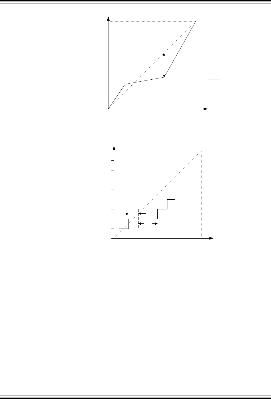
Figure 28-4. Integral Non-Linearity
Output Code
VREF Input Voltage
Ideal ADC
Actual ADC
INL
Differential Non-
Linearity (DNL)
The maximum deviation of the actual code width (the interval between two
adjacent transitions) from the ideal code width (1 LSB). Ideal value: 0 LSB.
Figure 28-5. Differential Non-Linearity
Output Code
0x3FF
0x000
0VREF Input Voltage
DNL
1 LSB
Quantization Error Due to the quantization of the input voltage into a finite number of codes, a range
of input voltages (1 LSB wide) will code to the same value. Always ±0.5 LSB.
Absolute
Accuracy
The maximum deviation of an actual (unadjusted) transition compared to an ideal
transition for any code. This is the compound effect of all aforementioned errors.
Ideal value: ±0.5 LSB.
28.3 Functional Description
28.3.1 Initialization
The following steps are recommended in order to initialize ADC operation:
1. Configure the resolution by writing to the Resolution Selection bit (RESSEL) in the Control A
register (ADCn.CTRLA).
2. Optional: Enable the Free-Running mode by writing a ’1’ to the Free-Running bit (FREERUN) in
ADCn.CTRLA.
megaAVR® 0-Series
Analog-to-Digital Converter (ADC)
© 2018 Microchip Technology Inc. Datasheet Preliminary DS40002015A-page 413

3. Optional: Configure the number of samples to be accumulated per conversion by writing the
Sample Accumulation Number Select bits (SAMPNUM) in the Control B register (ADCn.CTRLB).
4. Configure a voltage reference by writing to the Reference Selection bit (REFSEL) in the Control C
register (ADCn.CTRLC). The default is the internal voltage reference of the device (VREF, as
configured there).
5. Configure the CLK_ADC by writing to the Prescaler bit field (PRESC) in the Control C register
(ADCn.CTRLC).
6. Configure an input by writing to the MUXPOS bit field in the MUXPOS register (ADCn.MUXPOS).
7. Optional: Enable Start Event input by writing a ’1’ to the Start Event Input bit (STARTEI) in the
Event Control register (ADCn.EVCTRL). Configure the Event System accordingly.
8. Enable the ADC by writing a ’1’ to the ENABLE bit in ADCn.CTRLA.
Following these steps will initialize the ADC for basic measurements, which can be triggered by an event
(if configured) or by writing a ’1’ to the Start Conversion bit (STCONV) in the Command register
(ADCn.COMMAND).
28.3.1.1 I/O Lines and Connections
The I/O pins AINx and VREF are configured by the port - I/O Pin Controller.
The digital input buffer should be disabled on the pin used as input for the ADC to disconnect the digital
domain from the analog domain to obtain the best possible ADC results. This is configured by the PORT
peripheral.
28.3.2 Operation
28.3.2.1 Starting a Conversion
Once the input channel is selected by writing to the MUXPOS register (ADCn.MUXPOS), a conversion is
triggered by writing a '1' to the ADC Start Conversion bit (STCONV) in the Command register
(ADCn.COMMAND). This bit is one as long as the conversion is in progress. In Single Conversion mode,
STCONV is cleared by hardware when the conversion is completed.
If a different input channel is selected while a conversion is in progress, the ADC will finish the current
conversion before changing the channel.
Depending on the accumulator setting, the conversion result is from a single sensing operation, or from a
sequence of accumulated samples. Once the triggered operation is finished, the Result Ready flag
(RESRDY) in the Interrupt Flag register (ADCn.INTFLAG) is set. The corresponding interrupt vector is
executed if the Result Ready Interrupt Enable bit (RESRDY) in the Interrupt Control register
(ADCn.INTCTRL) is one and the Global Interrupt Enable bit is one.
A single conversion can be started by writing a '1' to the STCONV bit in ADCn.COMMAND. The STCONV
bit can be used to determine if a conversion is in progress. The STCONV bit will be set during a
conversion and cleared once the conversion is complete.
The RESRDY interrupt flag in ADCn.INTFLAG will be set even if the specific interrupt is disabled,
allowing software to check for finished conversion by polling the flag. A conversion can thus be triggered
without causing an interrupt.
Alternatively, a conversion can be triggered by an event. This is enabled by writing a '1' to the Start Event
Input bit (STARTEI) in the Event Control register (ADCn.EVCTRL). Any incoming event routed to the ADC
through the Event System (EVSYS) will trigger an ADC conversion. This provides a method to start
conversions at predictable intervals or at specific conditions.
megaAVR® 0-Series
Analog-to-Digital Converter (ADC)
© 2018 Microchip Technology Inc. Datasheet Preliminary DS40002015A-page 414
The event trigger input is edge sensitive. When an event occurs, STCONV in ADCn.COMMAND is set.
STCONV will be cleared when the conversion is complete.
In Free-Running mode, the first conversion is started by writing the STCONV bit to '1' in
ADCn.COMMAND. A new conversion cycle is started immediately after the previous conversion cycle has
completed. A conversion complete will set the RESRDY flag in ADCn.INTFLAGS.
28.3.2.2 Clock Generation
Figure 28-6. ADC Prescaler
8-bit PRESCALER
Reset
CLK_PER
"START"
ENABLE
PRESC
CLK_PER/2
CLK_PER/4
CLK_PER/8
CLK_PER/16
CLK_PER/32
CLK_PER/64
CLK_PER/128
CLK_PER/256
ADC clock source
(CLK_ADC)
CTRLC
The ADC requires an input clock frequency between 50 kHz and 1.5 MHz for maximum resolution. If a
lower resolution than 10 bits is selected, the input clock frequency to the ADC can be higher than 1.5
MHz to get a higher sample rate.
The ADC module contains a prescaler which generates the ADC clock (CLK_ADC) from any CPU clock
(CLK_PER) above 100 kHz. The prescaling is selected by writing to the Prescaler bits (PRESC) in the
Control C register (ADCn.CTRLC). The prescaler starts counting from the moment the ADC is switched
on by writing a ’1’ to the ENABLE bit in ADCn.CTRLA. The prescaler keeps running as long as the
ENABLE bit is one. The prescaler counter is reset to zero when the ENABLE bit is zero.
When initiating a conversion by writing a ’1’ to the Start Conversion bit (STCONV) in the Command
register (ADCn.COMMAND) or from an event, the conversion starts at the following rising edge of the
CLK_ADC clock cycle. The prescaler is kept reset as long as there is no ongoing conversion. This
assures a fixed delay from the trigger to the actual start of a conversion in CLK_PER cycles as:
StartDelay = PRESCfactor
2+ 2
megaAVR® 0-Series
Analog-to-Digital Converter (ADC)
© 2018 Microchip Technology Inc. Datasheet Preliminary DS40002015A-page 415
Figure 28-7. Start Conversion and Clock Generation
CLK_PER
CLK_PER/2
STCONV
CLK_PER/4
CLK_PER/8
28.3.2.3 Conversion Timing
A normal conversion takes 13 CLK_ADC cycles. The actual sample-and-hold takes place two CLK_ADC
cycles after the start of a conversion. Start of conversion is initiated by writing a ’1’ to the STCONV bit in
ADCn.COMMAND. When a conversion is complete, the result is available in the Result register
(ADCn.RES), and the Result Ready interrupt flag is set (RESRDY in ADCn.INTFLAG). The interrupt flag
will be cleared when the result is read from the Result registers, or by writing a ’1’ to the RESRDY bit in
ADCn.INTFLAG.
Figure 28-8. ADC Timing Diagram - Single Conversion
ADC clock
ADC enable
STCONV
RESRDY IF
RESL
RESH
12 3 4 5678910 11 12 13
Result MSB
Result LSB
Cycle Number
sample conversion
complete
Both sampling time and sampling length can be adjusted using the Sample Delay bit field in Control D
(ADCn.CTRLD) and sampling Sample Length bit field in the Sample Control register (ADCn.SAMPCTRL).
Both of these control the ADC sampling time in a number of CLK_ADC cycles. This allows sampling high-
impedance sources without relaxing conversion speed. See register description for further information.
Total sampling time is given by:
SampleTime = 2 + SAMPDLY + SAMPLEN
CLK_ADC
Figure 28-9. ADC Timing Diagram - Single Conversion With Delays
CLK_ADC
ENABLE
STCONV
RES
1 2 3 4 5 6 7 8 9 10 11 12 13
Result
INITDLY
(0 – 256
CLK_ADC cycles)
SAMPDLY
(0 – 15
CLK_ADC cycles)
SAMPLEN
(0 – 31
CLK_ADC cycles)
In Free-Running mode, a new conversion will be started immediately after the conversion completes,
while the STCONV bit is one. The sampling rate RS in free-running mode is calculated by:
megaAVR® 0-Series
Analog-to-Digital Converter (ADC)
© 2018 Microchip Technology Inc. Datasheet Preliminary DS40002015A-page 416

S=CLK_ADC
13 + SAMPDLY + SAMPLEN
Figure 28-10. ADC Timing Diagram - Free-Running Conversion
ADC clock
ADC enable
STCONV
RESRDY IF
RESL
RESH
12 3 4 5678910 11 12 13
Result MSB
Result LSB
Cycle Number
conversion
complete
sample
Input event
12
28.3.2.4 Changing Channel or Reference Selection
The MUXPOS bits in the ADCn.MUXPOS register and the REFSEL bits in the ADCn.CTRLC register are
buffered through a temporary register to which the CPU has random access. This ensures that the
channel and reference selections only take place at a safe point during the conversion. The channel and
reference selections are continuously updated until a conversion is started.
Once the conversion starts, the channel and reference selections are locked to ensure sufficient sampling
time for the ADC. Continuous updating resumes in the last CLK_ADC clock cycle before the conversion
completes (RESRDY in ADCn.INTFLAGS is set). The conversion starts on the following rising CLK_ADC
clock edge after the STCONV bit is written to '1'.
ADC Input Channels
When changing channel selection, the user should observe the following guidelines to ensure that the
correct channel is selected:
In Single Conversion mode: The channel should be selected before starting the conversion. The channel
selection may be changed one ADC clock cycle after writing '1' to the STCONV bit.
In Free-Running mode: The channel should be selected before starting the first conversion. The channel
selection may be changed one ADC clock cycle after writing '1' to the STCONV bit. Since the next
conversion has already started automatically, the next result will reflect the previous channel selection.
Subsequent conversions will reflect the new channel selection.
The ADC requires a settling time after switching the input channel - refer to the Electrical Characteristics
section for details.
ADC Voltage Reference
The reference voltage for the ADC (VREF) controls the conversion range of the ADC. Input voltages that
exceed the selected VREF will be converted to the maximum result value of the ADC. For an ideal 10-bit
ADC this value is 0x3FF.
VREF can be selected by writing the Reference Selection bits (REFSEL) in the Control C register
(ADCn.CTRLC) as either VDD, external reference VREFA, or an internal reference from the VREF
peripheral. VDD is connected to the ADC through a passive switch.
When using the external reference voltage VREFA, configure ADCnREFSEL[0:2] in the corresponding
VREF.CTRLn register to the value that is closest, but above the applied reference voltage. For external
references higher than 4.3V, use ADCnREFSEL[0:2] = 0x3.
megaAVR® 0-Series
Analog-to-Digital Converter (ADC)
© 2018 Microchip Technology Inc. Datasheet Preliminary DS40002015A-page 417
The internal reference is generated from an internal bandgap reference through an internal amplifier, and
is controlled by the Voltage Reference (VREF) peripheral.
Analog Input Circuitry
The analog input circuitry is illustrated in Figure 28-11. An analog source applied to ADCn is subjected to
the pin capacitance and input leakage of that pin (represented by IH and IL), regardless of whether that
channel is selected as input for the ADC. When the channel is selected, the source must drive the S/H
capacitor through the series resistance (combined resistance in the input path).
The ADC is optimized for analog signals with an output impedance of approximately 10 kΩ or less. If such
source is used, the sampling time will be negligible. If a source with higher impedance is used, the
sampling time will depend on how long the source needs to charge the S/H capacitor, which can vary
substantially.
Figure 28-11. Analog Input Schematic
ADCn
IIH
Rin
Cin
VDD/2
IIL
28.3.2.5 ADC Conversion Result
After the conversion is complete (RESRDY is '1'), the conversion result RES is available in the ADC
Result Register (ADCn.RES). The result for a 10-bit conversion is given as:
RES = 1023 × IN
REF
where VIN is the voltage on the selected input pin and VREF the selected voltage reference (see
description for REFSEL in ADCn.CTRLC and ADCn.MUXPOS).
28.3.2.6 Temperature Measurement
The temperature measurement is based on an on-chip temperature sensor. For a temperature
measurement, follow these steps:
1. Configure the internal voltage reference to 1.1V by configuring the VREF peripheral.
2. Select the internal voltage reference by writing the REFSEL bits in ADCn.CTRLC to 0x0.
3. Select the ADC temperature sensor channel by configuring the MUXPOS register
(ADCn.MUXPOS). This enables the temperature sensor.
4. In ADCn.CTRLD select INITDLY 32 µs × CLK_ADC
5. In ADCn.SAMPCTRL select SAMPLEN 32 µs × CLK_ADC
6. In ADCn.CTRLC select SAMPCAP = 1
7. Acquire the temperature sensor output voltage by starting a conversion.
8. Process the measurement result as described below.
The measured voltage has a linear relationship to the temperature. Due to process variations, the
temperature sensor output voltage varies between individual devices at the same temperature. The
individual compensation factors are determined during the production test and saved in the Signature
Row:
• SIGROW.TEMPSENSE0 is a gain/slope correction
megaAVR® 0-Series
Analog-to-Digital Converter (ADC)
© 2018 Microchip Technology Inc. Datasheet Preliminary DS40002015A-page 418

• SIGROW.TEMPSENSE1 is an offset correction
In order to achieve accurate results, the result of the temperature sensor measurement must be
processed in the application software using factory calibration values. The temperature (in Kelvin) is
calculated by this rule:
Temp = (((RESH << 8) | RESL) - TEMPSENSE1) * TEMPSENSE0) >> 8
RESH and RESL are the high and low bytes of the Result register (ADCn.RES), and TEMPSENSEn are
the respective values from the Signature row.
It is recommended to follow these steps in user code:
int8_t sigrow_offset = SIGROW.TEMPSENSE1; // Read signed value from signature row
uint8_t sigrow_gain = SIGROW.TEMPSENSE0; // Read unsigned value from signature row
uint16_t adc_reading = 0; // ADC conversion result with 1.1 V internal reference
uint32_t temp = adc_reading - sigrow_offset;
temp *= sigrow_gain; // Result might overflow 16 bit variable (10bit+8bit)
temp += 0x80; // Add 1/2 to get correct rounding on division below
temp >>= 8; // Divide result to get Kelvin
uint16_t temperature_in_K = temp;
28.3.2.7 Window Comparator Mode
The ADC can raise the WCOMP flag in the Interrupt and Flag register (ADCn.INTFLAG) and request an
interrupt (WCOMP) when the result of a conversion is above and/or below certain thresholds. The
available modes are:
• The result is under a threshold
• The result is over a threshold
• The result is inside a window (above a lower threshold, but below the upper one)
• The result is outside a window (either under the lower or above the upper threshold)
The thresholds are defined by writing to the Window Comparator Threshold registers (ADCn.WINLT and
ADCn.WINHT). Writing to the Window Comparator mode bit field (WINCM) in the Control E register
(ADCn.CTRLE) selects the conditions when the flag is raised and/or the interrupt is requested.
Assuming the ADC is already configured to run, follow these steps to use the Window Comparator mode:
1. Choose which Window Comparator to use (see the WINCM description in ADCn.CTRLE), and set
the required threshold(s) by writing to ADCn.WINLT and/or ADCn.WINHT.
2. Optional: enable the interrupt request by writing a '1' to the Window Comparator Interrupt Enable bit
(WCOMP) in the Interrupt Control register (ADCn.INTCTRL).
3. Enable the Window Comparator and select a mode by writing a non-zero value to the WINCM bit
field in ADCn.CTRLE.
When accumulating multiple samples, the comparison between the result and the threshold will happen
after the last sample was acquired. Consequently, the flag is raised only once, after taking the last sample
of the accumulation.
28.3.3 Events
An ADC conversion can be triggered automatically by an event input if the Start Event Input bit
(STARTEI) in the Event Control register (ADCn.EVCTRL) is written to '1'.
See also the description of the Asynchronous User Channel n Input Selection in the Event System
(EVSYS.ASYNCUSERn).
megaAVR® 0-Series
Analog-to-Digital Converter (ADC)
© 2018 Microchip Technology Inc. Datasheet Preliminary DS40002015A-page 419

28.3.4 Interrupts
Table 28-1. Available Interrupt Vectors and Sources
Name Vector Description Conditions
RESRDY Result Ready interrupt The conversion result is available in the Result register
(ADCn.RES).
WCOMP Window Comparator interrupt As defined by WINCM in ADCn.CTRLE.
When an interrupt condition occurs, the corresponding interrupt flag is set in the Interrupt Flags register of
the peripheral (peripheral.INTFLAGS).
An interrupt source is enabled or disabled by writing to the corresponding enable bit in the peripheral's
Interrupt Control register (peripheral.INTCTRL).
An interrupt request is generated when the corresponding interrupt source is enabled and the interrupt
flag is set. The interrupt request remains active until the interrupt flag is cleared. See the peripheral's
INTFLAGS register for details on how to clear interrupt flags.
28.3.5 Sleep Mode Operation
The ADC is by default disabled in Standby Sleep mode.
The ADC can stay fully operational in Standby Sleep mode if the Run in Standby bit (RUNSTDBY) in the
Control A register (ADCn.CTRLA) is written to '1'.
When the device is entering Standby Sleep mode when RUNSTDBY is ‘1’, the ADC will stay active,
hence any ongoing conversions will be completed and interrupts will be executed as configured.
In Standby Sleep mode an ADC conversion must be triggered via the Event System (EVSYS), or the
ADC must be in free-running mode with the first conversion triggered by software before entering sleep.
The peripheral clock is requested if needed and is turned OFF after the conversion is completed.
When an input event trigger occurs, the positive edge will be detected, the Start Conversion bit
(STCONV) in the Command register (ADCn.COMMAND) is set, and the conversion will start. When the
conversion is completed, the Result Ready Flag (RESRDY) in the Interrupt Flags register
(ADCn.INTFLAGS) is set and the STCONV bit in ADCn.COMMAND is cleared.
The reference source and supply infrastructure need time to stabilize when activated in Standby Sleep
mode. Configure a delay for the start of the first conversion by writing a non-zero value to the Initial Delay
bits (INITDLY) in the Control D register (ADCn.CTRLD).
In Power-Down Sleep mode, no conversions are possible. Any ongoing conversions are halted and will
be resumed when going out of sleep. At the end of conversion, the Result Ready Flag (RESRDY) will be
set, but the content of the result registers (ADCn.RES) is invalid since the ADC was halted in the middle
of a conversion.
megaAVR® 0-Series
Analog-to-Digital Converter (ADC)
© 2018 Microchip Technology Inc. Datasheet Preliminary DS40002015A-page 420

28.4 Register Summary - ADCn
Offset Name Bit Pos.
0x00 CTRLA 7:0 RUNSTBY RESSEL FREERUN ENABLE
0x01 CTRLB 7:0 SAMPNUM[2:0]
0x02 CTRLC 7:0 SAMPCAP REFSEL[1:0] PRESC[2:0]
0x03 CTRLD 7:0 INITDLY[2:0] ASDV SAMPDLY[3:0]
0x04 CTRLE 7:0 WINCM[2:0]
0x05 SAMPCTRL 7:0 SAMPLEN[4:0]
0x06 MUXPOS 7:0 MUXPOS[4:0]
0x07 Reserved
0x08 COMMAND 7:0 STCONV
0x09 EVCTRL 7:0 STARTEI
0x0A INTCTRL 7:0 WCOMP RESRDY
0x0B INTFLAGS 7:0 WCOMP RESRDY
0x0C DBGCTRL 7:0 DBGRUN
0x0D TEMP 7:0 TEMP[7:0]
0x0E
...
0x0F
Reserved
0x10 RES
7:0 RES[7:0]
15:8 RES[15:8]
0x12 WINLT
7:0 WINLT[7:0]
15:8 WINLT[15:8]
0x14 WINHT
7:0 WINHT[7:0]
15:8 WINHT[15:8]
0x16 CALIB 7:0 DUTYCYC
28.5 Register Description
megaAVR® 0-Series
Analog-to-Digital Converter (ADC)
© 2018 Microchip Technology Inc. Datasheet Preliminary DS40002015A-page 421

28.5.1 Control A
Name: CTRLA
Offset: 0x00
Reset: 0x00
Property: -
Bit 7 6 5 4 3 2 1 0
RUNSTBY RESSEL FREERUN ENABLE
Access R/W R/W R/W R/W
Reset 0 0 0 0
Bit 7 – RUNSTBY Run in Standby
This bit determines whether the ADC needs to run when the chip is in Standby Sleep mode.
Bit 2 – RESSEL Resolution Selection
This bit selects the ADC resolution.
Value Description
0 Full 10-bit resolution. The 10-bit ADC results are accumulated or stored in the ADC Result
register (ADC.RES).
1 8-bit resolution. The conversion results are truncated to eight bits (MSBs) before they are
accumulated or stored in the ADC Result register (ADC.RES). The two Least Significant bits
are discarded.
Bit 1 – FREERUN Free-Running
Writing a '1' to this bit will enable the Free-Running mode for the data acquisition. The first conversion is
started by writing the STCONV bit in ADC.COMMAND high. In the Free-Running mode, a new conversion
cycle is started immediately after or as soon as the previous conversion cycle has completed. This is
signaled by the RESRDY flag in ADCn.INTFLAGS.
Bit 0 – ENABLE ADC Enable
Value Description
0 ADC is disabled
1 ADC is enabled
megaAVR® 0-Series
Analog-to-Digital Converter (ADC)
© 2018 Microchip Technology Inc. Datasheet Preliminary DS40002015A-page 422

28.5.2 Control B
Name: CTRLB
Offset: 0x01
Reset: 0x00
Property: -
Bit 7 6 5 4 3 2 1 0
SAMPNUM[2:0]
Access R/W R/W R/W
Reset 0 0 0
Bits 2:0 – SAMPNUM[2:0] Sample Accumulation Number Select
These bits select how many consecutive ADC sampling results are accumulated automatically. When this
bit is written to a value greater than 0x0, the according number of consecutive ADC sampling results are
accumulated into the ADC Result register (ADC.RES) in one complete conversion.
Value Name Description
0x0 NONE No accumulation.
0x1 ACC2 2 results accumulated.
0x2 ACC4 4 results accumulated.
0x3 ACC8 8 results accumulated.
0x4 ACC16 16 results accumulated.
0x5 ACC32 32 results accumulated.
0x6 ACC64 64 results accumulated.
0x7 - Reserved.
megaAVR® 0-Series
Analog-to-Digital Converter (ADC)
© 2018 Microchip Technology Inc. Datasheet Preliminary DS40002015A-page 423
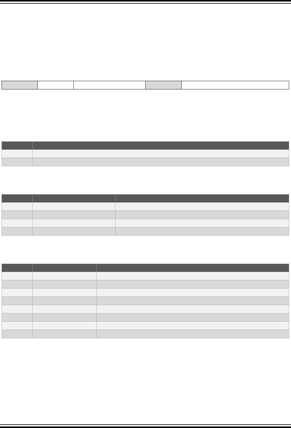
28.5.3 Control C
Name: CTRLC
Offset: 0x02
Reset: 0x00
Property: -
Bit 7 6 5 4 3 2 1 0
SAMPCAP REFSEL[1:0] PRESC[2:0]
Access R R/W R/W R/W R R/W R/W R/W
Reset 0 0 0 0 0 0 0 0
Bit 6 – SAMPCAP Sample Capacitance Selection
This bit selects the sample capacitance, and hence, the input impedance. The best value is dependent on
the reference voltage and the application's electrical properties.
Value Description
0 Recommended for reference voltage values below 1V.
1 Reduced size of sampling capacitance. Recommended for higher reference voltages.
Bits 5:4 – REFSEL[1:0] Reference Selection
These bits select the voltage reference for the ADC.
Value Name Description
0x0 INTERNAL Internal reference
0x1 VDD VDD
0x2 VREFA External reference VREFA
Other - Reserved.
Bits 2:0 – PRESC[2:0] Prescaler
These bits define the division factor from the peripheral clock (CLK_PER) to the ADC clock (CLK_ADC).
Value Name Description
0x0 DIV2 CLK_PER divided by 2
0x1 DIV4 CLK_PER divided by 4
0x2 DIV8 CLK_PER divided by 8
0x3 DIV16 CLK_PER divided by 16
0x4 DIV32 CLK_PER divided by 32
0x5 DIV64 CLK_PER divided by 64
0x6 DIV128 CLK_PER divided by 128
0x7 DIV256 CLK_PER divided by 256
megaAVR® 0-Series
Analog-to-Digital Converter (ADC)
© 2018 Microchip Technology Inc. Datasheet Preliminary DS40002015A-page 424

28.5.4 Control D
Name: CTRLD
Offset: 0x03
Reset: 0x00
Property: -
Bit 7 6 5 4 3 2 1 0
INITDLY[2:0] ASDV SAMPDLY[3:0]
Access R/W R/W R/W R/W R/W R/W R/W R/W
Reset 0 0 0 0 0 0 0 0
Bits 7:5 – INITDLY[2:0] Initialization Delay
These bits define the initialization/start-up delay before the first sample when enabling the ADC or
changing to an internal reference voltage. Setting this delay will ensure that the reference, MUXes, etc.
are ready before starting the first conversion. The initialization delay will also take place when waking up
from deep sleep to do a measurement.
The delay is expressed as a number of CLK_ADC cycles.
Value Name Description
0x0 DLY0 Delay 0 CLK_ADC cycles.
0x1 DLY16 Delay 16 CLK_ADC cycles.
0x2 DLY32 Delay 32 CLK_ADC cycles.
0x3 DLY64 Delay 64 CLK_ADC cycles.
0x4 DLY128 Delay 128 CLK_ADC cycles.
0x5 DLY256 Delay 256 CLK_ADC cycles.
Other - Reserved
Bit 4 – ASDV Automatic Sampling Delay Variation
Writing this bit to ’1’ enables automatic sampling delay variation between ADC conversions. The purpose
of varying sampling instant is to randomize the sampling instant and thus avoid standing frequency
components in the frequency spectrum. The value of the SAMPDLY bits is automatically incremented by
one after each sample.
When the Automatic Sampling Delay Variation is enabled and the SAMPDLY value reaches 0xF, it wraps
around to 0x0.
Value Name Description
0 ASVOFF The Automatic Sampling Delay Variation is disabled.
1 ASVON The Automatic Sampling Delay Variation is enabled.
Bits 3:0 – SAMPDLY[3:0] Sampling Delay Selection
These bits define the delay between consecutive ADC samples. The programmable Sampling Delay
allows modifying the sampling frequency during hardware accumulation, to suppress periodic noise
sources that may otherwise disturb the sampling. The SAMPDLY field can be also modified automatically
from one sampling cycle to another, by setting the ASDV bit. The delay is expressed as CLK_ADC cycles
and is given directly by the bitfield setting. The sampling cap is kept open during the delay.
megaAVR® 0-Series
Analog-to-Digital Converter (ADC)
© 2018 Microchip Technology Inc. Datasheet Preliminary DS40002015A-page 425

28.5.5 Control E
Name: CTRLE
Offset: 0x4
Reset: 0x00
Property: -
Bit 7 6 5 4 3 2 1 0
WINCM[2:0]
Access R/W R/W R/W
Reset 0 0 0
Bits 2:0 – WINCM[2:0] Window Comparator Mode
This field enables and defines when the interrupt flag is set in Window Comparator mode. RESULT is the
16-bit accumulator result. WINLT and WINHT are 16-bit lower threshold value and 16-bit higher threshold
value, respectively.
Value Name Description
0x0 NONE No Window Comparison (default)
0x1 BELOW RESULT < WINLT
0x2 ABOVE RESULT > WINHT
0x3 INSIDE WINLT < RESULT < WINHT
0x4 OUTSIDE RESULT < WINLT or RESULT >WINHT)
Other - Reserved
megaAVR® 0-Series
Analog-to-Digital Converter (ADC)
© 2018 Microchip Technology Inc. Datasheet Preliminary DS40002015A-page 426

28.5.6 Sample Control
Name: SAMPCTRL
Offset: 0x5
Reset: 0x00
Property: -
Bit 7 6 5 4 3 2 1 0
SAMPLEN[4:0]
Access R/W R/W R/W R/W R/W
Reset 0 0 0 0 0
Bits 4:0 – SAMPLEN[4:0] Sample Length
These bits extend the ADC sampling length in a number of CLK_ADC cycles. By default, the sampling
time is two CLK_ADC cycles. Increasing the sampling length allows sampling sources with higher
impedance. The total conversion time increases with the selected sampling length.
megaAVR® 0-Series
Analog-to-Digital Converter (ADC)
© 2018 Microchip Technology Inc. Datasheet Preliminary DS40002015A-page 427

28.5.7 MUXPOS
Name: MUXPOS
Offset: 0x06
Reset: 0x00
Property: -
Bit 7 6 5 4 3 2 1 0
MUXPOS[4:0]
Access R/W R/W R/W R/W R/W
Reset 0 0 0 0 0
Bits 4:0 – MUXPOS[4:0] MUXPOS
This bit field selects which single-ended analog input is connected to the ADC. If these bits are changed
during a conversion, the change will not take effect until this conversion is complete.
MUXPOS Name Input
0x00-0x0F AIN0-AIN15 ADC input pin 0 - 15
0x10-0x1B - Reserved
0x1C DACREF0 DAC reference in AC0
0x1D - Reserved
0x1E TEMPSENSE Temperature Sensor
0x1F GND GND
Other - Reserved
megaAVR® 0-Series
Analog-to-Digital Converter (ADC)
© 2018 Microchip Technology Inc. Datasheet Preliminary DS40002015A-page 428

28.5.8 Command
Name: COMMAND
Offset: 0x08
Reset: 0x00
Property: -
Bit 7 6 5 4 3 2 1 0
STCONV
Access R/W
Reset 0
Bit 0 – STCONV Start Conversion
Writing a '1' to this bit will start a single measurement. If in Free-Running mode this will start the first
conversion. STCONV will read as '1' as long as a conversion is in progress. When the conversion is
complete, this bit is automatically cleared.
megaAVR® 0-Series
Analog-to-Digital Converter (ADC)
© 2018 Microchip Technology Inc. Datasheet Preliminary DS40002015A-page 429

28.5.9 Event Control
Name: EVCTRL
Offset: 0x09
Reset: 0x00
Property: -
Bit 7 6 5 4 3 2 1 0
STARTEI
Access R/W
Reset 0
Bit 0 – STARTEI Start Event Input
This bit enables using the event input as trigger for starting a conversion.
megaAVR® 0-Series
Analog-to-Digital Converter (ADC)
© 2018 Microchip Technology Inc. Datasheet Preliminary DS40002015A-page 430

28.5.10 Interrupt Control
Name: INTCTRL
Offset: 0x0A
Reset: 0x00
Property: -
Bit 7 6 5 4 3 2 1 0
WCOMP RESRDY
Access R/W R/W
Reset 0 0
Bit 1 – WCOMP Window Comparator Interrupt Enable
Writing a '1' to this bit enables window comparator interrupt.
Bit 0 – RESRDY Result Ready Interrupt Enable
Writing a '1' to this bit enables result ready interrupt.
megaAVR® 0-Series
Analog-to-Digital Converter (ADC)
© 2018 Microchip Technology Inc. Datasheet Preliminary DS40002015A-page 431

28.5.11 Interrupt Flags
Name: INTFLAGS
Offset: 0x0B
Reset: 0x00
Property: -
Bit 7 6 5 4 3 2 1 0
WCOMP RESRDY
Access R/W R/W
Reset 0 0
Bit 1 – WCOMP Window Comparator Interrupt Flag
This window comparator flag is set when the measurement is complete and if the result matches the
selected Window Comparator mode defined by WINCM (ADCn.CTRLE). The comparison is done at the
end of the conversion. The flag is cleared by either writing a '1' to the bit position or by reading the Result
register (ADCn.RES). Writing a '0' to this bit has no effect.
Bit 0 – RESRDY Result Ready Interrupt Flag
The result ready interrupt flag is set when a measurement is complete and a new result is ready. The flag
is cleared by either writing a '1' to the bit location or by reading the Result register (ADCn.RES). Writing a
'0' to this bit has no effect.
megaAVR® 0-Series
Analog-to-Digital Converter (ADC)
© 2018 Microchip Technology Inc. Datasheet Preliminary DS40002015A-page 432

28.5.12 Debug Run
Name: DBGCTRL
Offset: 0x0C
Reset: 0x00
Property: -
Bit 7 6 5 4 3 2 1 0
DBGRUN
Access R/W
Reset 0
Bit 0 – DBGRUN Debug Run
Value Description
0 The peripheral is halted in Break Debug mode and ignores events
1 The peripheral will continue to run in Break Debug mode when the CPU is halted
megaAVR® 0-Series
Analog-to-Digital Converter (ADC)
© 2018 Microchip Technology Inc. Datasheet Preliminary DS40002015A-page 433

28.5.13 Temporary
Name: TEMP
Offset: 0x0D
Reset: 0x00
Property: -
The Temporary register is used by the CPU for single-cycle, 16-bit access to the 16-bit registers of this
peripheral. It can be read and written by software. Refer to 16-bit access in the AVR CPU chapter. There
is one common Temporary register for all the 16-bit registers of this peripheral.
Bit 7 6 5 4 3 2 1 0
TEMP[7:0]
Access R/W R/W R/W R/W R/W R/W R/W R/W
Reset 0 0 0 0 0 0 0 0
Bits 7:0 – TEMP[7:0] Temporary
Temporary register for read/write operations in 16-bit registers.
megaAVR® 0-Series
Analog-to-Digital Converter (ADC)
© 2018 Microchip Technology Inc. Datasheet Preliminary DS40002015A-page 434

28.5.14 Result
Name: RES
Offset: 0x10
Reset: 0x00
Property: -
The ADCn.RESL and ADCn.RESH register pair represents the 16-bit value, ADCn.RES. The low byte
[7:0] (suffix L) is accessible at the original offset. The high byte [15:8] (suffix H) can be accessed at offset
+ 0x01.
If the analog input is higher than the reference level of the ADC, the 10-bit ADC result will be equal the
maximum value of 0x3FF. Likewise, if the input is below 0V, the ADC result will be 0x000. As the ADC
cannot produce a result above 0x3FF values, the accumulated value will never exceed 0xFFC0 even
after the maximum allowed 64 accumulations.
Bit 15 14 13 12 11 10 9 8
RES[15:8]
Access R R R R R R R R
Reset 0 0 0 0 0 0 0 0
Bit 7 6 5 4 3 2 1 0
RES[7:0]
Access R R R R R R R R
Reset 0 0 0 0 0 0 0 0
Bits 15:8 – RES[15:8] Result high byte
These bits constitute the MSB of the ADCn.RES register, where the MSb is RES[15]. The ADC itself has
a 10-bit output, ADC[9:0], where the MSb is ADC[9]. The data format in ADC and Digital Accumulation is
1’s complement, where 0x0000 represents the zero and 0xFFFF represents the largest number (full
scale).
Bits 7:0 – RES[7:0] Result low byte
These bits constitute the LSB of ADC/Accumulator Result, (ADCn.RES) register. The data format in ADC
and Digital Accumulation is 1’s complement, where 0x0000 represents the zero and 0xFFFF represents
the largest number (full scale).
megaAVR® 0-Series
Analog-to-Digital Converter (ADC)
© 2018 Microchip Technology Inc. Datasheet Preliminary DS40002015A-page 435

28.5.15 Window Comparator Low Threshold
Name: WINLT
Offset: 0x12
Reset: 0x00
Property: -
This register is the 16-bit low threshold for the digital comparator monitoring the ADCn.RES register. The
ADC itself has a 10-bit output, RES[9:0], where the MSb is RES[9]. The data format in ADC and Digital
Accumulation is one’s complement, where 0x0000 represents the zero and 0xFFFF represents the
largest number (full scale).
The ADCn.WINLTH and ADCn.WINLTL register pair represents the 16-bit value, ADCn.WINLT. The low
byte [7:0] (suffix L) is accessible at the original offset. The high byte [15:8] (suffix H) can be accessed at
offset + 0x01.
When accumulating samples, the window comparator thresholds are applied to the accumulated value
and not on each sample.
Bit 15 14 13 12 11 10 9 8
WINLT[15:8]
Access R/W R/W R/W R/W R/W R/W R/W R/W
Reset 0 0 0 0 0 0 0 0
Bit 7 6 5 4 3 2 1 0
WINLT[7:0]
Access R/W R/W R/W R/W R/W R/W R/W R/W
Reset 0 0 0 0 0 0 0 0
Bits 15:8 – WINLT[15:8] Window Comparator Low Threshold High Byte
These bits hold the MSB of the 16-bit register.
Bits 7:0 – WINLT[7:0] Window Comparator Low Threshold Low Byte
These bits hold the LSB of the 16-bit register.
megaAVR® 0-Series
Analog-to-Digital Converter (ADC)
© 2018 Microchip Technology Inc. Datasheet Preliminary DS40002015A-page 436

28.5.16 Window Comparator High Threshold
Name: WINHT
Offset: 0x14
Reset: 0x00
Property: -
This register is the 16-bit high threshold for the digital comparator monitoring the ADCn.RES register. The
ADC itself has a 10-bit output, RES[9:0], where the MSb is RES[9]. The data format in ADC and Digital
Accumulation is one’s complement, where 0x0000 represents the zero and 0xFFFF represents the
largest number (full scale).
The ADCn.WINHTH and ADCn.WINHTL register pair represents the 16-bit value, ADCn.WINHT. The low
byte [7:0] (suffix L) is accessible at the original offset. The high byte [15:8] (suffix H) can be accessed at
offset + 0x01.
Bit 15 14 13 12 11 10 9 8
WINHT[15:8]
Access R/W R/W R/W R/W R/W R/W R/W R/W
Reset 0 0 0 0 0 0 0 0
Bit 7 6 5 4 3 2 1 0
WINHT[7:0]
Access R/W R/W R/W R/W R/W R/W R/W R/W
Reset 0 0 0 0 0 0 0 0
Bits 15:8 – WINHT[15:8] Window Comparator High Threshold High Byte
These bits hold the MSB of the 16-bit register.
Bits 7:0 – WINHT[7:0] Window Comparator High Threshold Low Byte
These bits hold the LSB of the 16-bit register.
megaAVR® 0-Series
Analog-to-Digital Converter (ADC)
© 2018 Microchip Technology Inc. Datasheet Preliminary DS40002015A-page 437

28.5.17 Calibration
Name: CALIB
Offset: 0x16
Reset: 0x01
Property: -
Bit 7 6 5 4 3 2 1 0
DUTYCYC
Access R/W
Reset 1
Bit 0 – DUTYCYC Duty Cycle
This bit determines the duty cycle of the ADC clock.
ADCclk > 1.5 MHz requires a minimum operating voltage of 2.7V
Value Description
0 50% Duty Cycle must be used if ADCclk > 1.5 MHz
1 25% Duty Cycle (high 25% and low 75%) must be used for ADCclk ≤ 1.5 MHz
megaAVR® 0-Series
Analog-to-Digital Converter (ADC)
© 2018 Microchip Technology Inc. Datasheet Preliminary DS40002015A-page 438

29. Unified Program and Debug Interface (UPDI)
29.1 Features
• Programming:
– External programming through UPDI 1-wire (1W) interface
• Uses a dedicated pin of the device for programming
• No GPIO pins occupied during operation
• Asynchronous Half-Duplex UART protocol towards the programmer
• Debugging:
– Memory mapped access to device address space (NVM, RAM, I/O)
– No limitation on device clock frequency
– Unlimited number of user program breakpoints
– Two hardware breakpoints
– Run-time readout of CPU Program Counter (PC), Stack Pointer (SP), and Status register
(SREG) for code profiling
– Program flow control
• Go, Stop, Reset, Step Into
– Non-intrusive run-time chip monitoring without accessing system registers
• Monitor CRC status and sleep status
• Unified Programming and Debug Interface (UPDI):
– Built-in error detection with error signature readout
– Frequency measurement of internal oscillators using the Event System
29.2 Overview
The Unified Program and Debug Interface (UPDI) is a proprietary interface for external programming and
on-chip debugging of a device.
The UPDI supports programming of nonvolatile memory (NVM) space; FLASH, EEPROM, fuses, lockbits,
and the user row. In addition, the UPDI can access the entire I/O and data space of the device. See the
NVM controller documentation for programming via the NVM controller and executing NVM controller
commands.
Programming and debugging are done through the UPDI Physical interface (UPDI PHY), which is a 1-
wire UART-based half duplex interface using a dedicated pin for data reception and transmission.
Clocking of UPDI PHY is done by an internal oscillator. The UPDI access layer grants access to the bus
matrix, with memory mapped access to system blocks such as memories, NVM, and peripherals.
The Asynchronous System Interface (ASI) provides direct interface access to On-Chip Debugging (OCD),
NVM, and System Management features. This gives the debugger direct access to system information,
without requesting bus access.
megaAVR® 0-Series
Unified Program and Debug Interface (UPDI)
© 2018 Microchip Technology Inc. Datasheet Preliminary DS40002015A-page 439
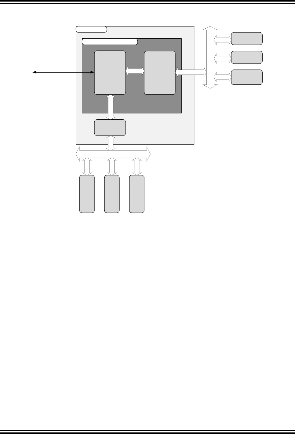
29.2.1 Block Diagram
Figure 29-1. UPDI Block Diagram
UPDI
Physical
layer
UPDI
Access
layer
Bus Matrix
ASI Access
UPDI Controller
ASI
UPDI PAD
(RX/TX Data)
Memories
NVM
Peripherals
ASI Internal Interfaces
OCD
NVM
Controller
System
Management
29.2.2 Clocks
The UPDI Physical (UPDI PHY) layer and UPDI Access (UPDI ACC) layer can operate on different clock
domains. The UPDI PHY layer clock is derived from an internal oscillator, and the UPDI ACC layer clock
is the same as the system clock. There is a synchronization boundary between the UPDI PHY layer and
the UPDI ACC layer, which ensures correct operation between the clock domains. The UPDI clock output
frequency is selected through the ASI, and the default UPDI clock start-up frequency is 4 MHz after
enabling the UPDI. The UPDI clock frequency is changed by writing the UPDICLKSEL bits in the
ASI_CTRLA register.
megaAVR® 0-Series
Unified Program and Debug Interface (UPDI)
© 2018 Microchip Technology Inc. Datasheet Preliminary DS40002015A-page 440
Figure 29-2. UPDI Clock Domains
UPDI
Physical
layer
UPDI Controller
ASI
~ ~
UPDI clk
source Clk_sys
UPDI
CLKSEL
Clock
Controller
Clock
Controller
Clk_UPDI
Clk_sys
SYNCH
UPDI
Access
layer
29.2.3 Power Management
The UPDI physical layer continues to operate in any Sleep mode and is always accessible for a
connected debugger, but read/write access to the system bus is restricted in Sleep modes where the
CPU clock is switched off. The UPDI can be enabled at any time, independent of the system Sleep state.
See Sleep Mode Operation for details on UPDI operation during Sleep modes.
29.3 Functional Description
29.3.1 Principle of Operation
Communication through the UPDI is based on standard UART communication, using a fixed frame
format, and automatic baud rate detection for clock and data recovery. In addition to the data frame, there
are several control frames which are important to the communication. The supported frame formats are
presented in Figure 29-3.
megaAVR® 0-Series
Unified Program and Debug Interface (UPDI)
© 2018 Microchip Technology Inc. Datasheet Preliminary DS40002015A-page 441
Figure 29-3. Supported UPDI Frame Formats
DATA
0 1 2 3 4 5 6 7
IDLE
StP
BREAK
SYNCH (0x55)
StP S1S2
S1S2
Synch Part
End_synch
StP
ACK (0x40)
S1S2
Data
Frame
Data frame consists of one Start bit (always low), eight data bits, one parity bit (even parity),
and two Stop bits (always high). If the Start bit, parity bit, or Stop bits have an incorrect value,
an error will be detected and signalized by the UPDI. The parity bit-check in the UPDI can be
disabled by writing the PARD bit in UPDI.CTRLA, in which case the parity generation from the
debugger can be ignored.
IDLE
Frame
Special frame that consists of 12 high bits. This is the same as keeping the transmission line
in an Idle state.
BREAK Special frame that consists of 12 low bits. The BREAK frame is used to reset the UPDI back
to its default state and is typically used for error recovery.
SYNCH The SYNCH frame (0x55) is used by the Baud Rate Generator to set the baud rate for the
coming transmission. A SYNCH character is always expected by the UPDI in front of every
new instruction, and after a successful BREAK has been transmitted.
ACK The Acknowledge (ACK) character is transmitted from the UPDI whenever an ST or STS
instruction has successfully crossed the synchronization boundary and have gained bus
access. When an ACK is received by the debugger, the next transmission can start.
29.3.1.1 UPDI UART
All transmission and reception of serial data on the UPDI is achieved using the UPDI frames presented in
Figure 29-3. Communication is initiated from the master (debugger) side, and every transmission must
start with a SYNCH character upon which the UPDI can recover the transmission baud rate, and store
this setting for the coming data. The baud rate set by the SYNCH character will be used for both
reception and transmission for the instruction byte received after the SYNCH. See UPDI Instruction Set
for details on when the next SYNCH character is expected in the instruction stream.
There is no writable baud rate register in the UPDI, so the baud rate sampled from the SYNCH character
is used for data recovery by sampling the Start bit, and performing a majority vote on the middle samples.
megaAVR® 0-Series
Unified Program and Debug Interface (UPDI)
© 2018 Microchip Technology Inc. Datasheet Preliminary DS40002015A-page 442
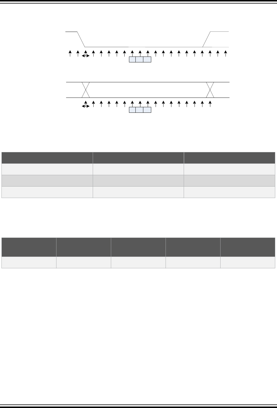
This process is repeated for all bits in the frame, including the parity bit and two Stop bits. The baud
generator uses 16 samples, and the majority voting is done on sample 7, 8, and 9.
Figure 29-4. UPDI UART Start Bit and Data/Parity/Stop Bit Sampling
1 2 3 4 5 6 700 10 11 12 13 14 15 1698 1 2 3
IDLE BIT 0STARTRxD
Sample
1 2 3 4 5 6 7 10 11 12 13 14 15 1698 1
RxD
Sample
BIT n
The transmission baud rate must be set up in relation to the selected UPDI clock, which can be adjusted
by UPDICLKSEL in UPDI.ASI_CTRLA. See Table 29-1 for recommended maximum and minimum baud
rate settings.
Table 29-1. Recommended UART Baud Rate Based on UPDICLKSEL Setting
UPDICLKSEL[1:0] MAX Recommended Baud Rate MIN Recommended Baud Rate
0x1 (16 MHz) 0.9 Mbps 0.300 kbps
0x2 (8 MHz) 450 kbps 0.150 kbps
0x3 (4 MHz) - Default 225 kbps 0.075 kbps
The UPDI Baud Rate Generator utilizes fractional baud counting to minimize the transmission error. With
the fixed frame format used by the UPDI, the maximum and recommended receiver transmission error
limits can be seen in the following table:
Table 29-2. Receiver Baud Rate Error
Data + Parity Bits Rslow Rfast Max. Total Error
[%]
Recommended
Max. RX Error [%]
9 96.39 104.76 +4.76/-3.61 +1.5/-1.5
29.3.1.2 BREAK Character
The BREAK character is used to reset the internal state of the UPDI to the default setting. This is useful if
the UPDI enters an error state due to a communication error, or when the synchronization between the
debugger and the UPDI is lost.
A single BREAK character is enough to reset the UPDI, but in some special cases where the BREAK
character is sent when the UPDI has not yet entered the error state, a double BREAK character might be
needed. A double BREAK is ensured to reset the UPDI from any state. When sending a double BREAK it
is required to have at least one Stop bit between the BREAK characters.
No SYNCH character is required before the BREAK because the BREAK is used to reset the UPDI from
any state. This means that the UPDI will sample the BREAK based on the last stored baud rate setting,
derived from the last received valid SYNCH character. If the communication error was due to an incorrect
sampling of the SYNCH character, the baud rate is unknown to the connected debugger. For this reason,
megaAVR® 0-Series
Unified Program and Debug Interface (UPDI)
© 2018 Microchip Technology Inc. Datasheet Preliminary DS40002015A-page 443
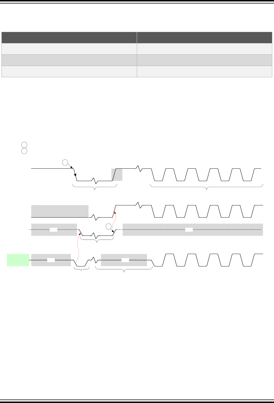
the BREAK character should be transmitted at the slowest recommended baud rate setting for the
selected UPDI clock according to Table 29-3:
Table 29-3. Recommended BREAK Character Duration
UPDICLKSEL[1:0] Recommended BREAK Character Duration
0x1 (16 MHz) 6.15 ms
0x2 (8 MHz) 12.30 ms
0x3 (4 MHz) - Default 24.60 ms
29.3.2 Operation
The UPDI must be enabled before the UART communication can start.
29.3.2.1 UPDI Enable
The dedicated UPDI pad is configured as an input with pull-up.When the pull-up is detected by a
connected debugger, the UPDI enable sequence, as depicted below, is started.
Figure 29-5. UPDI Enable Sequence
(Ignore)
1
UPDIPAD St SpD0 D1 D2 D3 D4 D5 D6 D7
SYNC (0x55)
(Autobaud)
UPDI.txd Hi-Z 2Hi-Z
UPDI.rxd
debugger.
UPDI.txd Hi-Z
Drive low from debugger to request UPDI clock
2 UPDI clock ready; Communication channel ready.
1
Handshake / BREAK
Tmin10us
Tmax200us
Debugger.txd = 0
Tmin200ns
Tmax1us
UPDI.txd = 0
Tmin10us,
Tmax200us
Hi-Z
Debugger.txd = z.
Tmin200us,
Tmax14ms
When the pull-up is detected, the debugger initiates the enable sequence by driving the line low for a
duration of TDeb0 to ensure that the line is released from the debugger before the UPDI enable sequence
is done.
The negative edge is detected by the UPDI, which requests the UPDI clock. The UPDI will continue to
drive the line low until the clock is stable and ready for the UPDI to use. The duration of this TUPDI will
vary, depending on the status of the oscillator when the UPDI is enabled. After this duration, the data line
will be released by the UPDI and pulled high.
When the debugger detects that the line is high, the initial SYNCH character (0x55) must be sent to
properly enable the UPDI for communication. If the Start bit of the SYNCH character is not sent well
within maximum TDebZ, the UPDI will disable itself, and the enable sequence must be repeated. This time
megaAVR® 0-Series
Unified Program and Debug Interface (UPDI)
© 2018 Microchip Technology Inc. Datasheet Preliminary DS40002015A-page 444

is based on counted cycles on the 4 MHz UPDI clock, which is the default when enabling the UPDI. The
disable is performed to avoid the UPDI being enabled unintentionally.
After successful SYNCH character transmission, the first instruction frame can be transmitted.
29.3.2.2 UPDI Disable
Any programming or debug session should be terminated by writing the UPDIDIS bit in UPDI.CTRLB.
Writing this bit will reset the UPDI including any decoded KEYs and disable the oscillator request for the
module. If the disable operation is not performed the UPDI will stay enabled and request its oscillator,
causing increased power consumption for the application.
During the enable sequence the UPDI can disable itself in case of a faulty enable sequence. There are
two cases that will cause an automatic disable:
• A SYNCH character is not sent within 13.5 ms after the initial enable pulse described in UPDI
Enable.
• The first SYNCH character after an initiated enable is too short or too long to register as a valid
SYNCH character. See Table 29-1 for recommended baud rate operating ranges.
29.3.2.3 UPDI Communication Error Handling
The UPDI contains a comprehensive error detection system that provides information to the debugger
when recovering from an error scenario. The error detection consists of detecting physical transmission
errors like start bit error, parity error, contention error, and frame error, to more high-level errors like
access timeout error. See the PESIG bits in UPDI_STATUSB for an overview of the available error
signatures.
Whenever the UPDI detects an error, it will immediately transfer to an internal error state to avoid
unwanted system communication. In the error state, the UPDI will ignore all incoming data requests,
except if a BREAK character is transmitted. The following procedure should always be applied when
recovering from an error condition.
• Send a BREAK character. See BREAK Character for recommended BREAK character handling.
• Send a SYNCH character at the desired baud rate for the next data transfer. Upon receiving a
BREAK the UPDI oscillator setting in UPDI.ASI_CTRLA is reset to the 4 MHz default UPDI clock
selection. This affects the baud rate range of the UPDI according to Table 29-1.
• Do a Load Control Status (LDCS) to UPDI.STATUSB register to read the PESIG field. PESIG gives
information about the occurred error, and the error signature will be cleared when read.
• The UPDI is now recovered from the error state and ready to receive the next SYNCH character
and instruction.
29.3.2.4 Direction Change
In order to ensure correct timing for half duplex UART operation, the UPDI has a built-in Guard Time
mechanism to relax the timing when changing direction from RX mode to TX mode. The Guard Time is a
number of IDLE bits inserted before the next Start bit is transmitted. The number of IDLE bits can be
configured through GTVAL in UPDI.CTRLA. The duration of each IDLE bit is given by the baud rate used
by the current transmission.
It is not recommended to use GTVAL setting 0x7, with no additional IDLE bits.
megaAVR® 0-Series
Unified Program and Debug Interface (UPDI)
© 2018 Microchip Technology Inc. Datasheet Preliminary DS40002015A-page 445
Figure 29-6. UPDI Direction Change by Inserting IDLE Bits
StR X D a ta F r a m e P S 1S2T X D a ta F ra m eID L E b its S tP S 1S2
RX Data Frame Dir Change TX Data Frame
Data from
debugger to UPDI
Guard Time #
IDLE bits inserted
Data from UPDI to
debugger
The UPDI Guard Time is the minimum IDLE time that the connected debugger will experience when
waiting for data from the UPDI. Because of the asynchronous interface to the system, as presented in
Clocks, the ratio between the UPDI clock and the system clock will affect the synchronization time, and
how long it takes before the UPDI can transmit data. In the cases where the synchronization delay is
shorter than the current Guard Time setting, the Guard Time will be given by GTVAL directly.
29.3.3 UPDI Instruction Set
Communication through the UPDI is based on a small instruction set. The instructions are used to access
the internal UPDI and ASI Control and Status (CS) space, as well as the memory mapped system space.
All instructions are byte instructions and must be preceded by a SYNCH character to determine the baud
rate for the communication. See UPDI UART for information about setting the baud rate for the
transmission. The following figure gives an overview of the UPDI instruction set.
megaAVR® 0-Series
Unified Program and Debug Interface (UPDI)
© 2018 Microchip Technology Inc. Datasheet Preliminary DS40002015A-page 446
Figure 29-7. UPDI Instruction Set Overview
0 0
L DS 0
Size A Size BOpcode
0 1 0
STS
1 0 0
L DCS
CS Address
1 1 0
STCS
1 1 0 0
K EY 1
Size C
1 0 0 0 0
REPEA T 1
Size B
L D S
S T S
S T
0
10
0
0
1
1 1
L D
0
0
0
0
O P C O D E
L D C S ( L D S C o n tr o l/ S ta tu s )
S T C S ( S T S C o n tr o l/ S ta tu s )
K E Y
10
01
1 1
R E P E A T
1
1
1
1
0 0
S i z e B - D a t a s i z e
B y t e
R e s e r v e d
R e s e r v e d
0
10
0
0
1
1 1
W o r d ( 2 B y te s )
C S A d d r e s s ( C S - C o n t r o l /S t a t u s r e g .)
0 00 R e g 0
R e g 2
R e g 3
R e g 1
0
0 00 1
0 10 0
0 10 1
1 11 1
......
1 00 0
S i z e C - K e y s i z e
6 4 b its ( 8 B y te s )0
10
0
0
1
1 2 8 b its ( 1 6 B y te s )
1 1
0
0
S i z e A - A d d r e s s s i z e
B y t e
R e s e rv e d
R e s e rv e d
0
10
0
0
1
1 1
W o r d ( 2 B y t e s )
0 0
L D 1
Ptr Size A/BOpcode
0 1 1
ST 0
0
0
0
P t r - P o i n t e r a c c e s s
* ( p t r )
p tr
R e s e rv e d
0
10
0
0
1
1 1
* ( p t r + + )
S I B – S y s t e m In f o r m a t i o n B l o c k s e l .
R e c e iv e K E Y0
1S e n d S I B
SIB
R e g 4 ( A S I C S s p a c e )
R e s e rv e d
R e s e rv e d
R e s e rv e d
megaAVR® 0-Series
Unified Program and Debug Interface (UPDI)
© 2018 Microchip Technology Inc. Datasheet Preliminary DS40002015A-page 447
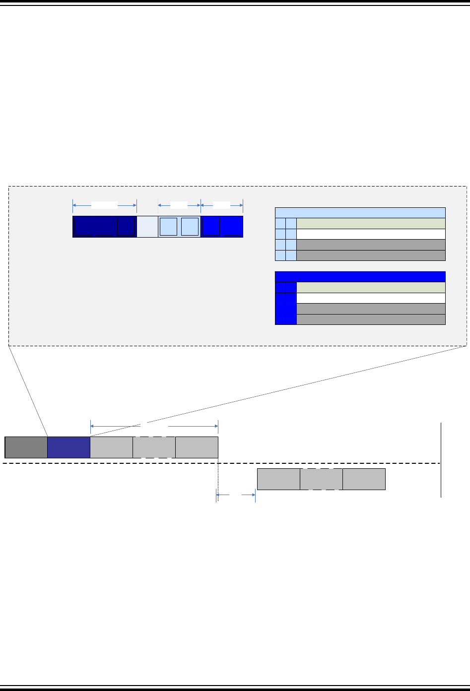
29.3.3.1 LDS - Load Data from Data Space Using Direct Addressing
The LDS instruction is used to load data from the bus matrix and into the serial shift register for serial
readout. The LDS instruction is based on direct addressing, and the address must be given as an
operand to the instruction for the data transfer to start. Maximum supported size for address and data is
16 bits. LDS instruction supports repeated memory access when combined with the REPEAT instruction.
As shown in Figure 29-8, after issuing the SYNCH character followed by the LDS instruction, the number
of desired address bytes, as indicated by the SizeA field in the instruction, must be transmitted. The
output data size is selected by the SizeB field and is issued after the specified Guard Time. When
combined with the REPEAT instruction, the address must be sent in for each iteration of the repeat,
meaning after each time the output data sampling is done. There is no automatic address increment
when using REPEAT with LDS, as it uses a direct addressing protocol.
Figure 29-8. LDS Instruction Operation
0 0
L DS 0
Size A Size BOPCODE
0
S i z e A - A d d r e s s s i z e
B y te
R e s e r v e d
R e s e r v e d
0
10
0
0
1
1 1
W o r d ( 2 B y t e s )
S i z e B - D a t a s i z e
B y te
R e s e r v e d
R e s e r v e d
0
10
0
0
1
1 1
W o r d ( 2 B y t e s )
R x
T x
Synch
(0x55) L D S A d r _ 0 A d r _ n
ADR SIZE
D a t a _ 0 D a ta _ n
ΔGT
29.3.3.2 STS - Store Data to Data Space Using Direct Addressing
The STS instruction is used to store data that is shifted serially into the PHY layer to the bus matrix
address space. The STS instruction is based on direct addressing, where the address is the first set of
operands, and data is the second set. The size of the address and data operands are given by the size
fields presented in the figure below. The maximum size for both address and data is 16 bits.
STS supports repeated memory access when combined with the REPEAT instruction.
megaAVR® 0-Series
Unified Program and Debug Interface (UPDI)
© 2018 Microchip Technology Inc. Datasheet Preliminary DS40002015A-page 448
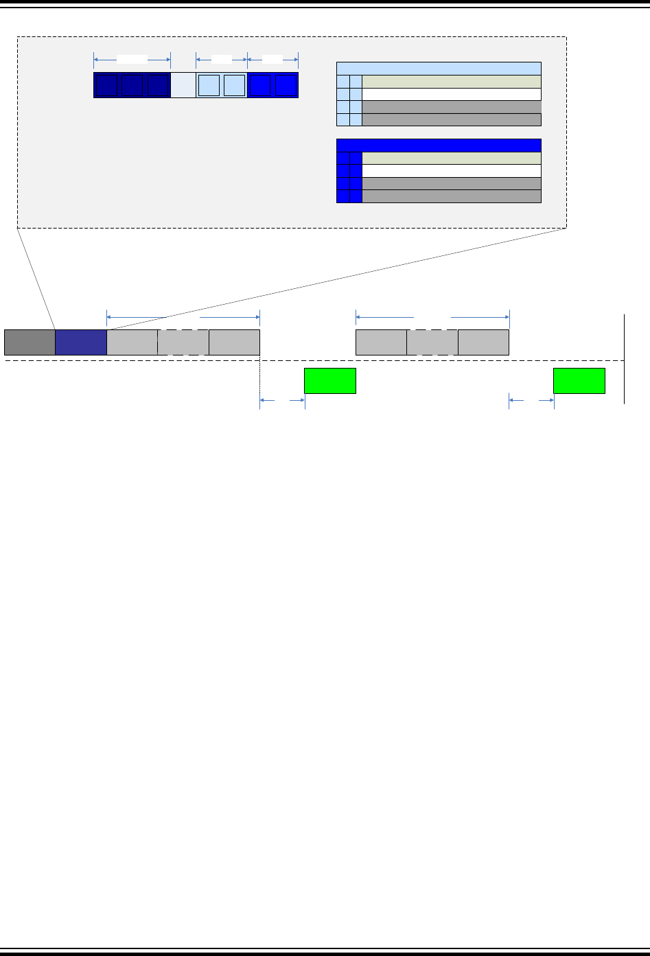
Figure 29-9. STS Instruction Operation
0 1
STS 0
Size A Size BOPCODE
0
S i z e A - A d d r e s s s i z e
B y te
R e s e r v e d
R e s e r v e d
0
10
0
0
1
1 1
W o r d ( 2 B y t e s )
S i z e B - D a t a s i z e
B y te
R e s e r v e d
R e s e r v e d
0
10
0
0
1
1 1
W o r d ( 2 B y t e s )
R x
T x
Synch
(0x55) S T S A d r _ 0 A d r _ n
ADR SIZE
D a t a _ 0 D a ta _ n
A C K A C K
DATA SIZE
ΔGT ΔGT
The transfer protocol for an STS instruction is depicted in the figure as well, following this sequence:
1. The address is sent.
2. An Acknowledge (ACK) is sent back from the UPDI if the transfer was successful.
3. The number of bytes as specified in the STS instruction is sent.
4. A new ACK is received after the data has been successfully transferred.
29.3.3.3 LD - Load Data from Data Space Using Indirect Addressing
The LD instruction is used to load data from the bus matrix and into the serial shift register for serial
readout. The LD instruction is based on indirect addressing, which means that the Address Pointer in the
UPDI needs to be written prior to bus matrix access. Automatic pointer post-increment operation is
supported and is useful when the LD instruction is used with REPEAT. It is also possible to do an LD of the
UPDI Pointer register. The maximum supported size for address and data load is 16 bits.
megaAVR® 0-Series
Unified Program and Debug Interface (UPDI)
© 2018 Microchip Technology Inc. Datasheet Preliminary DS40002015A-page 449
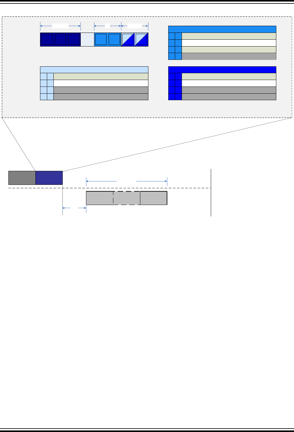
Figure 29-10. LD Instruction Operation
Ptr Size A/BOPCODE
0 0 1
L D 0
P t r - P o i n t e r a c c e s s
* ( p t r )
p tr
R e s e r v e d
0
10
0
0
1
1 1
* ( p t r + + )
S i z e B - D a t a s i z e
B y te
R e s e r v e d
R e s e r v e d
0
10
0
0
1
1 1
W o r d ( 2 B y t e s )
S i z e A - A d d r e s s s i z e
B y te
R e s e r v e d
R e s e r v e d
0
10
0
0
1
1 1
W o r d ( 2 B y t e s )
R x
T x
Synch
(0x55) L D
D a t a _ 0 D a ta _ n
ΔGT
DATA SIZE
The figure above shows an example of a typical LD sequence, where data is received after the Guard
Time period. Loading data from the UPDI Pointer register follows the same transmission protocol.
29.3.3.4 ST - Store Data from Data Space Using Indirect Addressing
The ST instruction is used to store data that is shifted serially into the PHY layer to the bus matrix address
space. The ST instruction is based on indirect addressing, which means that the Address Pointer in the
UPDI needs to be written prior to bus matrix access. Automatic pointer post-increment operation is
supported, and is useful when the ST instruction is used with REPEAT. ST is also used to store the UPDI
Address Pointer into the Pointer register. The maximum supported size for storing address and data is 16
bits.
megaAVR® 0-Series
Unified Program and Debug Interface (UPDI)
© 2018 Microchip Technology Inc. Datasheet Preliminary DS40002015A-page 450
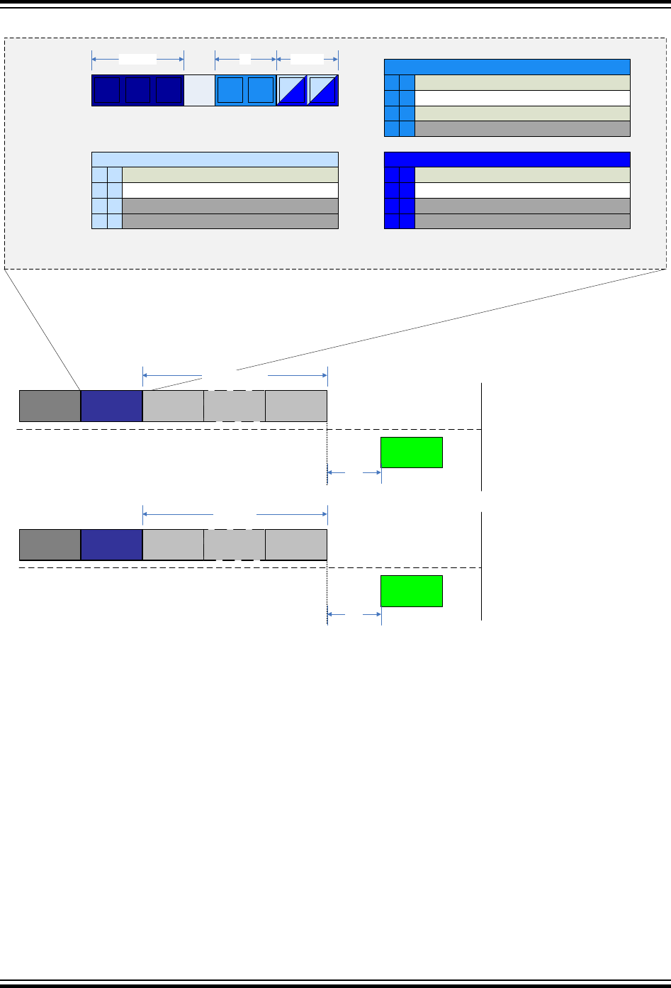
Figure 29-11. ST Instruction Operation
Ptr Size A/BOPCODE
0 1 1
ST 0
P t r - P o i n t e r a c c e s s
* ( p t r )
p tr
R e s e r v e d
0
10
0
0
1
1 1
* ( p t r + + )
S i z e B - D a t a s i z e
B y te
R e s e r v e d
R e s e r v e d
0
10
0
0
1
1 1
W o r d ( 2 B y t e s )
S i z e A - A d d r e s s s i z e
B y te
R e s e r v e d
R e s e r v e d
0
10
0
0
1
1 1
W o r d ( 2 B y t e s )
R x
T x
Synch
(0x55) S T D a ta _ 0 D a t a _ n
Block SIZE
A C K
R x
T x
Synch
(0x55) S T A D R _ 0 A D R _ n
ADDRESS_SIZE
A C K
ΔGT
ΔGT
The figure above gives an example of ST to the UPDI Pointer register and store of regular data. In both
cases, an Acknowledge (ACK) is sent back by the UPDI if the store was successful and a SYNCH
character is sent before each instruction. To write the UPDI Pointer register, the following procedure
should be followed.
• Set the PTR field in the ST instruction to the signature 0x2
• Set the address size field SizeA to the desired address size
• After issuing the ST instruction, send SizeA bytes of address data
• Wait for the ACK character, which signifies a successful write to the Address register
After the Address register is written, sending data is done in a similar fashion.
• Set the PTR field in the ST instruction to the signature 0x0 to write to the address specified by the
UPDI Pointer register. If the PTR field is set to 0x1, the UPDI pointer is automatically updated to the
next address according to the data size SizeD field of the instruction after the write is executed
• Set the SizeD field in the instruction to the desired data size
• After sending the ST instruction, send SizeD bytes of address data
megaAVR® 0-Series
Unified Program and Debug Interface (UPDI)
© 2018 Microchip Technology Inc. Datasheet Preliminary DS40002015A-page 451
• Wait for the ACK character which signifies a successful write to the bus matrix
When used with the REPEAT, it is recommended to set up the address register with the start address for
the block to be written and use the Pointer Post Increment register to automatically increase the address
for each repeat cycle. When using REPEAT, the data frame of SizeD data bytes can be sent after each
received ACK.
29.3.3.5 LCDS - Load Data from Control and Status Register Space
The LCDS instruction is used to load data from the UPDI and ASI CS-space. LCDS is based on direct
addressing, where the address is part of the instruction opcode. The total address space for LCDS is 16
bytes and can only access the internal UPDI register space. This instruction only supports byte access
and the data size is not configurable.
Figure 29-12. LCDS Instruction Operation
1 0 0
L DC S
CS Address CS Address (CS - Control/Status reg.)
0 00 Reg 0
Reg 2
Reg 3
Reg 1
0
0 00 1
0 10 0
0 10 1
Reserved1 11 1
......
1 00 0
0
Reg 4 (ASI CS Space)
OPCODE
Rx
Tx
Synch
(0x55) LDCS
Data
Δgt
The figure above shows a typical example of LCDS data transmission. A data byte from the LCDS space is
transmitted from the UPDI after the Guard Time is completed.
29.3.3.6 STCS (Store Data to Control and Status Register Space)
The STCS instruction is used to store data to the UPDI and ASI CS-space. STCS is based on direct
addressing, where the address is part of the instruction opcode. The total address space for STCS is 16
bytes, and can only access the internal UPDI register space. This instruction only supports byte access,
and data size is not configurable.
megaAVR® 0-Series
Unified Program and Debug Interface (UPDI)
© 2018 Microchip Technology Inc. Datasheet Preliminary DS40002015A-page 452
Figure 29-13. STCS Instruction Operation
1 1 0
STC S
CS Address C S A d d r e s s ( C S - C o n t r o l /S t a t u s r e g . )
0 00 R e g 0
R e g 2
R e g 3
R e g 1
0
0 00 1
0 10 0
0 10 1
R e s e r v e d1 11 1
......
1 00 0
0
R e g 4 (A S I C S S p a c e )
OPCODE
R x
T x
Synch
(0x55) S T C S D a ta
Figure 29-13 shows the data frame transmitted after the SYNCH and instruction frames. There is no
response generated from the STCS instruction, as is the case for ST and STS.
29.3.3.7 REPEAT - Set Instruction Repeat Counter
The REPEAT instruction is used to store the repeat count value into the UPDI Repeat Counter register.
When instructions are used with REPEAT, protocol overhead for SYNCH and Instruction Frame can be
omitted on all instructions except the first instruction after the REPEAT is issued. REPEAT is most useful
for memory instructions (LD,ST,LDS,STS), but all instructions can be repeated, except the REPEAT
instruction itself.
The DATA_SIZE opcode field refers to the size of the repeat value. Only byte size (up to 255 repeats) is
supported. The instruction that is loaded directly after the REPEAT instruction will be repeated RPT_0
times. The instruction will be issued a total of RPT_0 + 1 times. An ongoing repeat can only be aborted
by sending a BREAK character.
megaAVR® 0-Series
Unified Program and Debug Interface (UPDI)
© 2018 Microchip Technology Inc. Datasheet Preliminary DS40002015A-page 453
Figure 29-14. REPEAT Instruction Operation
1 0 0 0 0
REP EA T 1
Size B S i z e B - D a t a s i z e
B y te
R e s e r v e d
R e s e r v e d
0
10
0
0
1
1 1
R e s e r v e d
OPCODE
Synch
(0x55) R E P E A T R P T _ 0
REPEAT SIZE
R x
T x
Synch
(0x55)
S T
( p t r + + ) D a t a _ 0 D a t a _ n
DATA_SIZE
D a t a B _ 1 D a t a B _ n
A C K
Δd Δd ΔdΔd Δd
A C K
DATA_SIZE DATA_SIZE
Rpt nr of Blocks of DATA_SIZE
The figure above gives an example of repeat operation with an ST instruction using pointer post-
increment operation. After the REPEAT instruction is sent with RPT_0 = n, the first ST instruction is
issued with SYNCH and Instruction frame, while the next n ST instructions are executed by only sending
in data bytes according to the ST operand DATA_SIZE, and maintaining the Acknowledge (ACK)
handshake protocol.
If using indirect addressing instructions (LD/ST) it is recommended to always use the pointer post
increment option when combined with REPEAT. Otherwise, the same address will be accessed in all
repeated access operations. For direct addressing instructions (LDS/STS), the address must always be
transmitted as specified in the instruction protocol, before data can be received (LDS) or sent (STS).
29.3.3.8 KEY - Set Activation KEY
The KEY instruction is used for communicating KEY bytes to the UPDI, opening up for executing
protected features on the device. See Table 29-4 for an overview of functions that are activated by KEYs.
For the KEY instruction, only 64-bit KEY size is supported. If the System Information Block (SIB) field of
the KEY instruction is set, the KEY instruction returns the SIB instead of expecting incoming KEY bytes.
Maximum supported size for SIB is 128 bits.
megaAVR® 0-Series
Unified Program and Debug Interface (UPDI)
© 2018 Microchip Technology Inc. Datasheet Preliminary DS40002015A-page 454
Figure 29-15. KEY Instruction Operation
S i z e C - K e y s i z e
6 4 b i ts ( 8 B y te s )
R e s e r v e d
0
10
0
0
1
1 2 8 b its ( 1 6 B y te s ) ( S IB o n ly )
1 1
1 1 0 0
K EY 1
Size C
S IB – S y s t e m In f o r m a t i o n B l o c k s e l .
S e n d K E Y0
1R e c e i v e S IB
SIB
R x
T x
Synch
(0x55) K E Y K E Y _ 0 K E Y _ n
KEY SIZE
R x
T x
Synch
(0x55) K E Y
S IB _ 0 S I B _ n
SIB SIZE
Δgt
R e s e r v e d
The figure above shows the transmission of a KEY and the reception of a SIB. In both cases, the SIZE_C
field in the opcode determines the number of frames being sent or received. There is no response after
sending a KEY to the UPDI. When requesting the SIB, data will be transmitted from the UPDI according to
the current Guard Time setting.
29.3.4 System Clock Measurement with UPDI
It is possible to use the UPDI to get an accurate measurement of the system clock frequency, by using
the UPDI event connected to TCB with Input Capture capabilities. A recommended setup flow for this
feature is given by the following steps:
• Set up TCBn.CTRLB with setting CNTMODE=0x3, Input Capture Frequency Measurement mode.
• Write CAPTEI=1 in TCBn.EVCTRL to enable Event Interrupt. Keep EDGE = 0 in TCBn.EVCTRL.
• Configure the Event System as described in Events.
• For the SYNCH character used to generate the UPDI events, it is recommended to use a slow
baud rate in the range of 10 kbps - 50 kbps to get a more accurate measurement on the value
captured by the timer between each UPDI event. One particular thing is that if the capture is set up
to trigger an interrupt, the first captured value should be ignored. The second captured value based
megaAVR® 0-Series
Unified Program and Debug Interface (UPDI)
© 2018 Microchip Technology Inc. Datasheet Preliminary DS40002015A-page 455
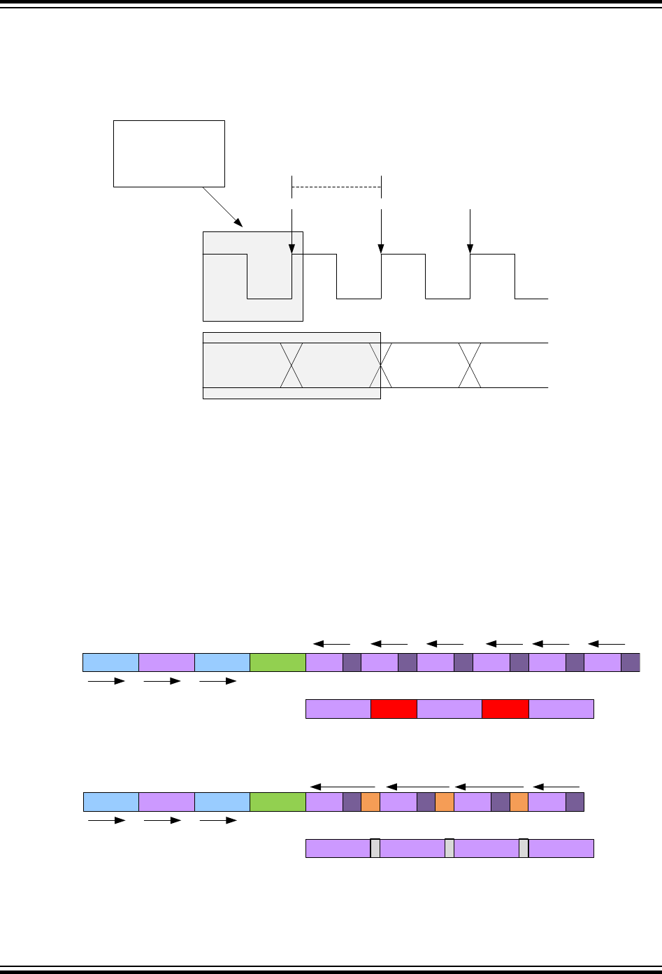
on the input event should be used for the measurement. See the figure below for an example using
10 kbps UPDI SYNCH character pulses, giving a capture window of 200 µs for the timer.
• It is possible to read out the captured value directly after the SYNCH character by reading the
TCBn.CCMP register or the value can be written to memory by the CPU once the capture is done.
Figure 29-16. UPDI System Clock Measurement Events
CAPT_1 CAPT_2 CAPT_3
200us
TCB_CCMP
UPD I_
Input
Ignore first
capture event
29.3.5 Interbyte Delay
When loading data with the UPDI, or reading out the System Information Block, the output data will
normally come out with two IDLE bits between each transmitted byte for a multibyte transfer. Depending
on the application on the receiver side, data might be coming out too fast when there are no extra IDLE
bits between each byte. By enabling the IBDLY feature in UPDI.CTRLB, two extra Stop bits will be
inserted between each byte to relax the sampling time for the debugger. Interbyte delay works in the
same way as a guard time, by inserting extra IDLE bits, but only a fixed number of IDLE bits and only for
multibyte transfers. The first transmitted byte after a direction change will be subject to the regular Guard
Time before it is transmitted, and the interbyte delay is not added to this time.
Figure 29-17. Interbyte Delay Example with LD and RPT
Too fast transmission, no interbyte delay
RPT CNT LD*(ptr) D0 D1
RX
TX
Debugger
Data S
BS
BD2 D3
S
BS
BD4 D5
S
BS
B
Debugger
Processing D1lots D1lost
D0 D2 D4
RPT CNT LD*(ptr)
RX
TX
Debugger
Data
Debugger
Processing D0 D1 D2
D0 D1 D2 D3
S
BS
BS
BS
B
IB IB IB
D3
Data sam pling ok w ith interbyte delay
GT
GT
In Figure 29-17, GT denotes the Guard Time insertion, SB is for Stop Bit and IB is the inserted interbyte
delay. The rest of the frames are data and instructions.
megaAVR® 0-Series
Unified Program and Debug Interface (UPDI)
© 2018 Microchip Technology Inc. Datasheet Preliminary DS40002015A-page 456

29.3.6 System Information Block
The System Information Block (SIB) can be read out at any time by setting the SIB bit in the KEY
instruction from KEY - Set Activation KEY. The SIB provides a compact form of providing information for
the debugger, which is vital in identifying and setting up the proper communication channel with the part.
The output of the SIB should be interpreted as ASCII symbols. The KEY size field should be set to 16
bytes when reading out the complete SIB, and an 8-byte size can be used to read out only the Family_ID.
See Figure 29-18 for SIB format description, and which data is available at different readout sizes.
Figure 29-18. System Information Block Format
16 8 [Byte][Bits] Field Name
Family_ID
Reserved
NVM_VERSION
OCD_VERSION
RESERVED
DBG_OSC_FREQ
[6:0] [55:0]
[7][7:0]
[10:8][23:0]
[13:11][23:0]
[14][7:0]
[15][7:0]
29.3.7 Enabling of KEY Protected Interfaces
Access to some internal interfaces and features are protected by the UPDI KEY mechanism. To activate
a KEY, the correct KEY data must be transmitted by using the KEY instruction as described in KEY
instruction. Table 29-4 describes the available KEYs, and the condition required when doing the operation
with the KEY active. There is no requirement when shifting in the KEY, but you would, for instance,
normally run a Chip Erase before enabling the NVMPROG KEY to unlock the device for debugging. But if
the NVMPROGKEY is shifted in first, it will not be reset by shifting in the Chip Erase KEY afterwards.
Table 29-4. KEY Activation Overview
KEY Name Description Requirements for
Operation
Reset
Chip Erase Start NVM Chip erase.
Clear Lockbits
None UPDI Disable/UPDI
Reset
NVMPROG Activate NVM
Programming
Lockbits Cleared.
ASI_SYS_STATUS.NVM
PROG set.
Programming Done/
UPDI Reset
USERROW-Write Program User Row on
Locked part
Lockbits Set.
ASI_SYS_STATUS.URO
WPROG set.
Write to KEY status bit/
UPDI Reset
Table 29-5 gives an overview of the available KEY signatures that must be shifted in to activate the
interfaces.
Table 29-5. KEY Activation Signatures
KEY Name KEY Signature (LSB Written
First)
Size
Chip Erase 0x4E564D4572617365 64 bits
NVMPROG 0x4E564D50726F6720 64 bits
USERROW-Write 0x4E564D5573267465 64 bits
megaAVR® 0-Series
Unified Program and Debug Interface (UPDI)
© 2018 Microchip Technology Inc. Datasheet Preliminary DS40002015A-page 457

29.3.7.1 Chip Erase
The following steps should be followed to issue a Chip Erase.
1. Enter the CHIPERASE KEY by using the KEY instruction. See Table 29-5 for the CHIPERASE
signature.
2. Optional: Read the Chip Erase bit in the AS Key Status register (CHIPERASE in
UPDI.ASI_KEY_STATUS) to see that the KEY is successfully activated.
3. Write the Reset signature into the UPDI.ASI_RESET_REQ register. This will issue a System Reset.
4. Write 0x00 to the ASI Reset Request register (UPDI.ASI_RESET_REQ) to clear the System Reset.
5. Read the Lock Status bit in the ASI System Status register (LOCKSTATUS in
UPDI.ASI_SYS_STATUS).
6. Chip Erase is done when LOCKSTATUS == 0 in UPDI.ASI_SYS_STATUS. If LOCKSTATUS == 1,
go to point 5 again.
After a successful Chip Erase, the Lockbits will be cleared, and the UPDI will have full access to the
system. Until Lockbits are cleared, the UPDI cannot access the system bus, and only CS-space
operations can be performed.
CAUTION
During Chip Erase, the BOD is forced ON (ACTIVE=0x1 in BOD.CTRLA) and uses the BOD
Level from the BOD Configuration fuse (LVL in BOD.CTRLB = LVL in FUSE.BODCFG). If the
supply voltage VDD is below that threshold level, the device is unserviceable until VDD is
increased adequately.
29.3.7.2 NVM Programming
If the device is unlocked, it is possible to write directly to the NVM Controller using the UPDI. This will
lead to unpredictable code execution if the CPU is active during the NVM programming. To avoid this, the
following NVM Programming sequence should be executed.
1. Follow the Chip erase procedure as described in Chip Erase. If the part is already unlocked, this
point can be skipped.
2. Enter the NVMPROG KEY by using the KEY instruction. See Table 29-5 for the NVMPROG
signature.
3. Optional: Read the NVMPROG field in the KEY_STATUS register to see that the KEY has been
activated.
4. Write the Reset signature into the ASI_RESET_REQ register. This will issue a System Reset.
5. Write 0x00 to the Reset signature in the ASI_RESET_REQ register to clear the System Reset.
6. Read NVMPROG in ASI_SYS_STATUS.
7. NVM Programming can start when NVMPROG == 1 in the ASI_SYS_STATUS register. If
NVMPROG == 0, go to point 6 again.
8. Write data to NVM through the UPDI.
9. Write the Reset signature into the ASI_RESET_REQ register. This will issue a System Reset.
10. Write 0x00 to the Reset signature in ASI_RESET_REQ register to clear the System Reset.
11. Programming is complete.
29.3.7.3 User Row Programming
The User Row Programming feature allows the user to program new values to the User Row
(USERROW) on a locked device. To program with this functionality enabled, the following sequence
should be followed.
megaAVR® 0-Series
Unified Program and Debug Interface (UPDI)
© 2018 Microchip Technology Inc. Datasheet Preliminary DS40002015A-page 458

1. Enter the USERROW-Write KEY located in Table 29-5 by using the KEY instruction. See Table 29-5
for the UROWWRITE signature.
2. Optional: Read the UROWWRITE bit field in UPDI.ASI_KEY_STATUS to see that the KEY has
been activated.
3. Write the Reset signature into the UPDI.ASI_RESET_REQ register. This will issue a System Reset.
4. Write 0x00 to the Reset signature in UPDI.ASI_RESET_REQ register to clear the System Reset.
5. Read UROWPROG bit in UPDI.ASI_SYS_STATUS.
6. User Row Programming can start when UROWPROG == 1. If UROWPROG == 0, go to point 5
again.
7. The writable area has a size of one EEPROM page (64 bytes), and it is only possible to write User
Row data to the first 64 byte addresses of the RAM. Addressing outside this memory range will
result in a non-executed write. The data will map 1:1 with the User Row space when the data is
copied into the User Row upon completion of the Programming sequence.
8. When all User Row data has been written to the RAM, write the UROWWRITEFINAL bit in
UPDI.ASI_SYS_CTRLA.
9. Read the UROWPROG bit in UPDI.ASI_SYS_STATUS.
10. The User Row Programming is completed when UROWPROG == 0. If UROWPROG == 1, go to
point 9 again.
11. Write the UROWWRITE bit in UPDI.ASI_KEY_STATUS.
12. Write the Reset signature into the UPDI.ASI_RESET_REQ register. This will issue a System Reset.
13. Write 0x00 to the Reset signature in UPDI.ASI_RESET_REQ register to clear the System Reset.
14. User Row Programming is complete.
It is not possible to read back data from the SRAM in this mode. Only writes to the first 64 bytes of the
SRAM is allowed.
29.3.8 Events
The UPDI is connected to the Event System (EVSYS) as described in the register Asynchronous Channel
n Generator Selection.
The UPDI can generate the following output events:
• SYNCH Character Positive Edge Event
This event is set on the UPDI clock for each detected positive edge in the SYNCH character, and it is not
possible to disable this event from the UPDI. The recommended application for this event is system clock
frequency measurement through the UPDI. Section System Clock Measurement with UPDI provides the
details on how to set up the system for this operation.
29.3.9 Sleep Mode Operation
The UPDI physical layer runs independently of all Sleep modes and the UPDI is always accessible for a
connected debugger independent of the device Sleep mode. If the system enters a Sleep mode that turns
the CPU clock OFF, the UPDI will not be able to access the system bus and read memories and
peripherals. The UPDI physical layer clock is unaffected by the Sleep mode settings, as long as the UPDI
is enabled. By reading the INSLEEP bit in UPDI.ASI_SYS_STATUS it is possible to monitor if the system
domain is in Sleep mode. The INSLEEP bit is set if the system is in IDLE Sleep mode or deeper.
It is possible to prevent the system clock from stopping when going into Sleep mode, by writing the
CLKREQ bit in UPDI.ASI_SYS_CTRL to '1'. If this bit is set, the system Sleep mode state is emulated,
megaAVR® 0-Series
Unified Program and Debug Interface (UPDI)
© 2018 Microchip Technology Inc. Datasheet Preliminary DS40002015A-page 459

and it is possible for the UPDI to access the system bus and read the peripheral registers even in the
deepest Sleep modes.
CLKREQ in UPDI.ASI_SYS_CTRL is by default '1', which means that the default operation is keeping the
system clock on during Sleep modes.
megaAVR® 0-Series
Unified Program and Debug Interface (UPDI)
© 2018 Microchip Technology Inc. Datasheet Preliminary DS40002015A-page 460

29.4 Register Summary - UPDI
Offset Name Bit Pos.
0x00 STATUSA 7:0 UPDIREV[3:0]
0x01 STATUSB 7:0 PESIG[2:0]
0x02 CTRLA 7:0 IBDLY PARD DTD RSD GTVAL[2:0]
0x03 CTRLB 7:0 NACKDIS CCDETDIS UPDIDIS
0x04
...
0x06
Reserved
0x07 ASI_KEY_STATUS 7:0 UROWWRITE NVMPROG CHIPERASE
0x08 ASI_RESET_REQ 7:0 RSTREQ[7:0]
0x09 ASI_CTRLA 7:0 UPDICLKSEL[1:0]
0x0A ASI_SYS_CTRLA 7:0 UROWWRITE
_FINAL CLKREQ
0x0B ASI_SYS_STATUS 7:0 RSTSYS INSLEEP NVMPROG UROWPROG LOCKSTATUS
0x0C ASI_CRC_STATUS 7:0 CRC_STATUS[2:0]
29.5 Register Description
These registers are readable only through the UPDI with special instructions and are NOT readable
through the CPU.
Registers at offset addresses 0x0-0x3 are the UPDI Physical configuration registers.
Registers at offset addresses 0x4-0xC are the ASI level registers.
megaAVR® 0-Series
Unified Program and Debug Interface (UPDI)
© 2018 Microchip Technology Inc. Datasheet Preliminary DS40002015A-page 461

29.5.1 Status A
Name: STATUSA
Offset: 0x00
Reset: 0x10
Property: -
Bit 7 6 5 4 3 2 1 0
UPDIREV[3:0]
Access R R R R
Reset 0 0 0 1
Bits 7:4 – UPDIREV[3:0] UPDI Revision
These bits are read-only and contain the revision of the current UPDI implementation.
megaAVR® 0-Series
Unified Program and Debug Interface (UPDI)
© 2018 Microchip Technology Inc. Datasheet Preliminary DS40002015A-page 462

29.5.2 Status B
Name: STATUSB
Offset: 0x01
Reset: 0x00
Property: -
Bit 7 6 5 4 3 2 1 0
PESIG[2:0]
Access R R R
Reset 0 0 0
Bits 2:0 – PESIG[2:0] UPDI Error Signature
These bits describe the UPDI Error Signature and are set when an internal UPDI error condition occurs.
The PESIG field is cleared on a read from the debugger.
Table 29-6. Valid Error Signatures
PESIG[2:0] Error Type Error Description
0x0 No error No error detected (Default)
0x1 Parity error Wrong sampling of the parity bit
0x2 Frame error Wrong sampling of frame Stop bits
0x3 Access Layer Time-out Error UPDI can get no data or response from the Access layer.
Examples of error cases are system domain in Sleep or
system domain Reset.
0x4 Clock Recovery error Wrong sampling of frame Start bit
0x5 - Reserved
0x6 Reserved Reserved
0x7 Contention error Signalize Driving Contention on the UPDI RXD/TXD line
megaAVR® 0-Series
Unified Program and Debug Interface (UPDI)
© 2018 Microchip Technology Inc. Datasheet Preliminary DS40002015A-page 463

29.5.3 Control A
Name: CTRLA
Offset: 0x02
Reset: 0x00
Property: -
Bit 7 6 5 4 3 2 1 0
IBDLY PARD DTD RSD GTVAL[2:0]
Access R/W R/W R/W R/W R/W R/W R/W
Reset 0 0 0 0 0 0 0
Bit 7 – IBDLY Inter-Byte Delay Enable
Writing a '1' to this bit enables a fixed inter-byte delay between each data byte transmitted from the UPDI
when doing multi-byte LD(S). The fixed length is two IDLE characters. Before the first transmitted byte,
the regular GT delay used for direction change will be used.
Bit 5 – PARD Parity Disable
Writing this bit to '1' will disable parity detection in the UPDI by ignoring the Parity bit. This feature is
recommended only during testing.
Bit 4 – DTD Disable Time-out Detection
Setting this bit disables the time-out detection on the PHY layer, which requests a response from the ACC
layer within a specified time (65536 UPDI clock cycles).
Bit 3 – RSD Response Signature Disable
Writing a '1' to this bit will disable any response signatures generated by the UPDI. This is to reduce the
protocol overhead to a minimum when writing large blocks of data to the NVM space. Disabling the
Response Signature should be used with caution, and only when the delay experienced by the UPDI
when accessing the system bus is predictable, otherwise loss of data may occur.
Bits 2:0 – GTVAL[2:0] Guard Time Value
This bit field selects the Guard Time Value that will be used by the UPDI when the transmission mode
switches from RX to TX.
Value Description
0x0 UPDI Guard Time: 128 cycles (default)
0x1 UPDI Guard Time: 64 cycles
0x2 UPDI Guard Time: 32 cycles
0x3 UPDI Guard Time: 16 cycles
0x4 UPDI Guard Time: 8 cycles
0x5 UPDI Guard Time: 4 cycles
0x6 UPDI Guard Time: 2 cycles
0x7 GT off (no extra Idle bits inserted)
megaAVR® 0-Series
Unified Program and Debug Interface (UPDI)
© 2018 Microchip Technology Inc. Datasheet Preliminary DS40002015A-page 464

29.5.4 Control B
Name: CTRLB
Offset: 0x03
Reset: 0x00
Property: -
Bit 7 6 5 4 3 2 1 0
NACKDIS CCDETDIS UPDIDIS
Access R R R
Reset 0 0 0
Bit 4 – NACKDIS Disable NACK Response
Writing this bit to '1' disables the NACK signature sent by the UPDI if a System Reset is issued during an
ongoing LD(S) and ST(S) operation.
Bit 3 – CCDETDIS Collision and Contention Detection Disable
If this bit is written to '1', contention detection is disabled.
Bit 2 – UPDIDIS UPDI Disable
Writing a '1' to this bit disables the UPDI PHY interface. The clock request from the UPDI is lowered, and
the UPDI is reset. All UPDI PHY configurations and KEYs will be reset when the UPDI is disabled.
megaAVR® 0-Series
Unified Program and Debug Interface (UPDI)
© 2018 Microchip Technology Inc. Datasheet Preliminary DS40002015A-page 465

29.5.5 ASI Key Status
Name: ASI_KEY_STATUS
Offset: 0x07
Reset: 0x00
Property: -
Bit 7 6 5 4 3 2 1 0
UROWWRITE NVMPROG CHIPERASE
Access R R R
Reset 0 0 0
Bit 5 – UROWWRITE User Row Write Key Status
This bit is set to '1' if the UROWWRITE KEY is active. Otherwise, this bit reads as zero.
Bit 4 – NVMPROG NVM Programming
This bit is set to '1' if the NVMPROG KEY is active. This bit is automatically reset after the programming
sequence is done. Otherwise, this bit reads as zero.
Bit 3 – CHIPERASE Chip Erase
This bit is set to '1' if the CHIPERASE KEY is active. This bit will automatically be reset when the Chip
Erase sequence is completed. Otherwise, this bit reads as zero.
megaAVR® 0-Series
Unified Program and Debug Interface (UPDI)
© 2018 Microchip Technology Inc. Datasheet Preliminary DS40002015A-page 466

29.5.6 ASI Reset Request
Name: ASI_RESET_REQ
Offset: 0x08
Reset: 0x00
Property: -
Bit 7 6 5 4 3 2 1 0
RSTREQ[7:0]
Access R/W R/W R/W R/W R/W R/W R/W R/W
Reset 0 0 0 0 0 0 0 0
Bits 7:0 – RSTREQ[7:0] Reset Request
A Reset is signalized to the System when writing the Reset signature 0x59h to this address.
Writing any other signature to this register will clear the Reset.
When reading this register, reading bit RSTREQ[0] will tell if the UPDI is holding an active Reset on the
system. If this bit is '1', the UPDI has an active Reset request to the system. All other bits will read as '0'.
The UPDI will not be reset when issuing a System Reset from this register.
megaAVR® 0-Series
Unified Program and Debug Interface (UPDI)
© 2018 Microchip Technology Inc. Datasheet Preliminary DS40002015A-page 467

29.5.7 ASI Control A
Name: ASI_CTRLA
Offset: 0x09
Reset: 0x02
Property: -
Bit 7 6 5 4 3 2 1 0
UPDICLKSEL[1:0]
Access R/W R/W
Reset 1 1
Bits 1:0 – UPDICLKSEL[1:0] UPDI Clock Select
Writing these bits select the UPDI clock output frequency. Default setting after Reset and enable is 4
MHz. Any other clock output selection is only recommended when the BOD is at the highest level. For all
other BOD settings, the default 4 MHz selection is recommended.
Value Description
0x0 Reserved
0x1 16 MHz UPDI clock
0x2 8 MHz UPDI clock
0x3 4 MHz UPDI clock (Default Setting)
megaAVR® 0-Series
Unified Program and Debug Interface (UPDI)
© 2018 Microchip Technology Inc. Datasheet Preliminary DS40002015A-page 468

29.5.8 ASI System Control A
Name: ASI_SYS_CTRLA
Offset: 0x0A
Reset: 0x00
Property: -
Bit 7 6 5 4 3 2 1 0
UROWWRITE_
FINAL
CLKREQ
Access R R R R R R R/W R/W
Reset 0 0 0 0 0 0 0 0
Bit 1 – UROWWRITE_FINAL User Row Programming Done
This bit should be written through the UPDI when the user row data has been written to the RAM. Writing
this bit will start the process of programming the user row data to the Flash.
If this bit is written before the User Row code is written to RAM by the UPDI, the CPU will progress
without the written data.
This bit is only writable if the Userrow-write KEY is successfully decoded.
Bit 0 – CLKREQ Request System Clock
If this bit is written to '1', the ASI is requesting the system clock, independent of system Sleep modes.
This makes it possible for the UPDI to access the ACC layer, also if the system is in Sleep mode.
Writing a zero to this bit will lower the clock request.
This bit will be reset when the UPDI is disabled.
This bit is set by default when the UPDI is enabled.
megaAVR® 0-Series
Unified Program and Debug Interface (UPDI)
© 2018 Microchip Technology Inc. Datasheet Preliminary DS40002015A-page 469

29.5.9 ASI System Status
Name: ASI_SYS_STATUS
Offset: 0x0B
Reset: 0x01
Property: -
Bit 7 6 5 4 3 2 1 0
RSTSYS INSLEEP NVMPROG UROWPROG LOCKSTATUS
Access R R R R R
Reset 0 0 0 0 1
Bit 5 – RSTSYS System Reset Active
If this bit is set, there is an active Reset on the system domain. If this bit is cleared, the system is not in
Reset.
This bit is cleared on read.
A Reset held from the ASI_RESET_REQ register will also affect this bit.
Bit 4 – INSLEEP System Domain in Sleep
If this bit is set, the system domain is in IDLE or deeper Sleep mode. If this bit is cleared, the system is
not in Sleep.
Bit 3 – NVMPROG Start NVM Programming
If this bit is set, NVM Programming can start from the UPDI.
When the UPDI is done, it must reset the system through the UPDI Reset register.
Bit 2 – UROWPROG Start User Row Programming
If this bit is set, User Row Programming can start from the UPDI.
When the UPDI is done, it must write the UROWWRITE_FINAL bit in ASI_SYS_CTRLA.
Bit 0 – LOCKSTATUS NVM Lock Status
If this bit is set, the device is locked. If a Chip Erase is done, and the Lockbits are cleared, this bit will
read as zero.
megaAVR® 0-Series
Unified Program and Debug Interface (UPDI)
© 2018 Microchip Technology Inc. Datasheet Preliminary DS40002015A-page 470

29.5.10 ASI CRC Status
Name: ASI_CRC_STATUS
Offset: 0x0C
Reset: 0x00
Property: -
Bit 7 6 5 4 3 2 1 0
CRC_STATUS[2:0]
Access R R R
Reset 0 0 0
Bits 2:0 – CRC_STATUS[2:0] CRC Execution Status
These bits signalize the status of the CRC conversion. The bits are one-hot encoded.
Value Description
0x0 Not enabled
0x1 CRC enabled, busy
0x2 CRC enabled, done with OK signature
0x4 CRC enabled, done with FAILED signature
Other Reserved
megaAVR® 0-Series
Unified Program and Debug Interface (UPDI)
© 2018 Microchip Technology Inc. Datasheet Preliminary DS40002015A-page 471

30. Instruction Set Summary
Table 30-1. Status Register (SREG)
Terminology Meaning
SREG Status register
C Carry flag in status register
Z Zero flag in status register
N Negative flag in status register
V Two’s complement overflow indicator
S N⊕V, for signed tests
H Half Carry flag in status register
T Transfer bit used by BLD and BST instructions
I Global interrupt enable/disable flag
Table 30-2. Registers and Operands
Operand Meaning
Rd Destination (and source) register in the register file
Rr Source register in the register file
R Result after instruction is executed
K Constant literal or byte data (8-bit)
k Constant address data for program counter
b Bit in the register file (3-bit)
s Bit in the status register (3-bit)
X,Y,Z Indirect address register (X=R27:R26, Y=R29:R28
and Z=R31:R30)
P I/O port address
q Displacement for direct addressing (6-bit)
UU Unsigned × Unsigned operands
SS Signed × Signed operands
SU Signed × Unsigned operands
Table 30-3. Stack
Terminology Meaning
STACK Stack for return address and pushed registers
SP Stack Pointer to STACK
megaAVR® 0-Series
Instruction Set Summary
© 2018 Microchip Technology Inc. Datasheet Preliminary DS40002015A-page 472

Table 30-4. Memory Space Identifiers
Terminology Meaning
DS(X) X-pointer points to address in Data Space
DS(Y) Y-pointer points to address in Data Space
DS(Z) Z-pointer points to address in Data Space
DS(k) Constant k points to address in Data Space
PS(Z) Z-pointer points to address in Program Space
I/O(A) A is an address in I/O Space
Table 30-5. Operator
Operator Meaning
× Arithmetic multiplication
+ Arithmetic addition
- Arithmetic subtraction
∧Logical AND
∨Logical OR
⊕Logical XOR
>> Shift right
<< Shift left
== Comparison
Rd(n) Bit n in register Rd
Table 30-6. Arithmetic and Logic Instructions
Mnemonic Opera
nds Description Op Flags #Clock
s
ADD Rd, Rr Add without Carry Rd ← Rd + Rr Z,C,N,V,S,H 1
ADC Rd, Rr Add with Carry Rd ← Rd + Rr + C Z,C,N,V,S,H 1
ADIW Rd, K Add Immediate to Word Rd + 1:Rd ← Rd + 1:Rd + K Z,C,N,V,S 2
SUB Rd, Rr Subtract without Carry Rd ← Rd - Rr Z,C,N,V,S,H 1
SUBI Rd, K Subtract Immediate Rd ← Rd - K Z,C,N,V,S,H 1
SBC Rd, Rr Subtract with Carry Rd ← Rd - Rr - C Z,C,N,V,S,H 1
SBCI Rd, K Subtract Immediate with Carry Rd ← Rd - K - C Z,C,N,V,S,H 1
SBIW Rd, K Subtract Immediate from Word Rd + 1:Rd ← Rd + 1:Rd - K Z,C,N,V,S 2
AND Rd, Rr Logical AND Rd ← Rd ∧ Rr Z,N,V,S 1
ANDI Rd, K Logical AND with Immediate Rd ← Rd ∧ K Z,N,V,S 1
OR Rd, Rr Logical OR Rd ← Rd ∨ Rr Z,N,V,S 1
ORI Rd, K Logical OR with Immediate Rd ← Rd ∨ K Z,N,V,S 1
megaAVR® 0-Series
Instruction Set Summary
© 2018 Microchip Technology Inc. Datasheet Preliminary DS40002015A-page 473

Mnemonic Opera
nds Description Op Flags #Clock
s
EOR Rd, Rr Exclusive OR Rd ← Rd ⊕ Rr Z,N,V,S 1
COM Rd One’s Complement Rd ← 0xFF - Rd Z,C,N,V,S 1
NEG Rd Two’s Complement Rd ← 0x00 - Rd Z,C,N,V,S,H 1
SBR Rd,K Set Bit(s) in Register Rd ← Rd ∨ K Z,N,V,S 1
CBR Rd,K Clear Bit(s) in Register Rd ← Rd ∧ (0xFF - K) Z,N,V,S 1
INC Rd Increment Rd ← Rd + 1 Z,N,V,S 1
DEC Rd Decrement Rd ← Rd - 1 Z,N,V,S 1
TST Rd Test for Zero or Minus Rd ← Rd ∧ Rd Z,N,V,S 1
CLR Rd Clear Register Rd ← Rd ⊕ Rd Z,N,V,S 1
SER Rd Set Register Rd ← 0xFF None 1
MUL Rd,Rr Multiply Unsigned R1:R0 ← Rd × Rr (UU) Z,C 2
MULS Rd,Rr Multiply Signed R1:R0 ← Rd × Rr (SS) Z,C 2
MULSU Rd,Rr Multiply Signed with Unsigned R1:R0 ← Rd × Rr (SU) Z,C 2
FMUL Rd,Rr Fractional Multiply Unsigned R1:R0 ← Rd × Rr<<1 (UU) Z,C 2
FMULS Rd,Rr Fractional Multiply Signed R1:R0 ← Rd × Rr<<1 (SS) Z,C 2
FMULSU Rd,Rr Fractional Multiply Signed with Unsigned R1:R0 ← Rd × Rr<<1 (SU) Z,C 2
Table 30-7. Branch Instructions
Mnemonic Opera
nds Description Op Flags #Clock
s
RJMP k Relative Jump PC ← PC + k + 1 None 2
IJMP Indirect Jump to (Z) PC ← Z None 2
JMP k Jump PC ← k None 3
RCALL k Relative Call Subroutine PC ← PC + k + 1 None 2/3
ICALL Indirect Call to (Z) PC ← Z None 2/3
CALL k Call Subroutine PC ← k None 3/4
RET Subroutine Return PC ← STACK None 4/5
RETI Interrupt Return PC ← STACK I 4/5
CPSE Rd,Rr Compare, skip if Equal if (Rd == Rr) PC ← PC + 2 or 3 None 1/2/3
CP Rd,Rr Compare Rd - Rr Z,C,N,V,S,H 1
CPC Rd,Rr Compare with Carry Rd - Rr - C Z,C,N,V,S,H 1
CPI Rd,K Compare with Immediate Rd - K Z,C,N,V,S,H 1
SBRC Rr, b Skip if Bit in Register Cleared if (Rr(b) == 0) PC ← PC + 2 or 3 None 1/2/3
SBRS Rr, b Skip if Bit in Register Set if (Rr(b) == 1) PC ← PC + 2 or 3 None 1/2/3
SBIC A, b Skip if Bit in I/O Register Cleared if (I/O(A,b) == 0) PC ← PC + 2 or 3 None 1/2/3
SBIS A, b Skip if Bit in I/O Register Set If (I/O(A,b) == 1) PC ← PC + 2 or 3 None 1/2/3
BRBS s, k Branch if Status Flag Set if (SREG(s) == 1) then PC ← PC + k + 1 None 1/2
BRBC s, k Branch if Status Flag Cleared if (SREG(s) == 0) then PC ← PC + k + 1 None 1/2
BREQ k Branch if Equal if (Z == 1) then PC ← PC + k + 1 None 1/2
BRNE k Branch if Not Equal if (Z == 0) then PC ← PC + k + 1 None 1/2
megaAVR® 0-Series
Instruction Set Summary
© 2018 Microchip Technology Inc. Datasheet Preliminary DS40002015A-page 474

Mnemonic Opera
nds Description Op Flags #Clock
s
BRCS k Branch if Carry Set if (C == 1) then PC ← PC + k + 1 None 1/2
BRCC k Branch if Carry Cleared if (C == 0) then PC ← PC + k + 1 None 1/2
BRSH k Branch if Same or Higher if (C == 0) then PC ← PC + k + 1 None 1/2
BRLO k Branch if Lower if (C == 1) then PC ← PC + k + 1 None 1/2
BRMI k Branch if Minus if (N == 1) then PC ← PC + k + 1 None 1/2
BRPL k Branch if Plus if (N == 0) then PC ← PC + k + 1 None 1/2
BRGE k Branch if Greater or Equal, Signed if (N ⊕ V == 0) then PC ← PC + k + 1 None 1/2
BRLT k Branch if Less Than, Signed if (N ⊕ V == 1) then PC ← PC + k + 1 None 1/2
BRHS k Branch if Half Carry Flag Set if (H == 1) then PC ← PC + k + 1 None 1/2
BRHC k Branch if Half Carry Flag Cleared if (H == 0) then PC ← PC + k + 1 None 1/2
BRTS k Branch if T Flag Set if (T == 1) then PC ← PC + k + 1 None 1/2
BRTC k Branch if T Flag Cleared if (T == 0) then PC ← PC + k + 1 None 1/2
BRVS k Branch if Overflow Flag is Set if (V == 1) then PC ← PC + k + 1 None 1/2
BRVC k Branch if Overflow Flag is Cleared if (V == 0) then PC ← PC + k + 1 None 1/2
BRIE k Branch if Interrupt Enabled if (I == 1) then PC ← PC + k + 1 None 1/2
BRID k Branch if Interrupt Disabled if (I == 0) then PC ← PC + k + 1 None 1/2
Table 30-8. Data Transfer Instructions
Mnemonic Opera
nds Description Op Flags #Clock
s
MOV Rd, Rr Copy Register Rd ← Rr None 1
MOVW Rd, Rr Copy Register Pair Rd+1:Rd ← Rr+1:Rr None 1
LDI Rd, K Load Immediate Rd ← K None 1
LDS Rd, k Load Direct from data space Rd ← DS(k) None 3(1)
LD Rd, X Load Indirect Rd ← DS(X) None 2(1)
LD Rd, X+ Load Indirect and Post-Increment Rd
X
←
←
DS(X)
X + 1
None 2(1)
LD Rd, -X Load Indirect and Pre-Decrement X
Rd
←
←
X - 1
DS(X)
None 2(1)
LD Rd, Y Load Indirect Rd ← DS(Y) None 2(1)
LD Rd, Y+ Load Indirect and Post-Increment Rd
Y
←
←
DS(Y)
Y + 1
None 2(1)
LD Rd, -Y Load Indirect and Pre-Decrement Y
Rd
←
←
Y - 1
DS(Y)
None 2(1)
LDD Rd, Y
+q
Load Indirect with Displacement Rd ← DS(Y + q) None 2(1)
LD Rd, Z Load Indirect Rd ← DS(Z) None 2(1)
LD Rd, Z+ Load Indirect and Post-Increment Rd
Z
←
←
DS(Z)
Z+1
None 2(1)
LD Rd, -Z Load Indirect and Pre-Decrement Z
Rd
←
←
Z - 1
DS(Z)
None 2(1)
megaAVR® 0-Series
Instruction Set Summary
© 2018 Microchip Technology Inc. Datasheet Preliminary DS40002015A-page 475

Mnemonic Opera
nds Description Op Flags #Clock
s
LDD Rd, Z
+q
Load Indirect with Displacement Rd ← DS(Z + q) None 2(1)
STS k, Rr Store Direct to Data Space DS(k) ← Rd None 2(1)(2)
ST X, Rr Store Indirect DS(X) ← Rr None 1(1)(2)
ST X+, Rr Store Indirect and Post-Increment DS(X)
X
←
←
Rr
X + 1
None 1(1)(2)
ST -X, Rr Store Indirect and Pre-Decrement X
DS(X)
←
←
X - 1
Rr
None 1(1)(2)
ST Y, Rr Store Indirect DS(Y) ← Rr None 1(1)(2)
ST Y+, Rr Store Indirect and Post-Increment DS(Y)
Y
←
←
Rr
Y + 1
None 1(1)(2)
ST -Y, Rr Store Indirect and Pre-Decrement Y
DS(Y)
←
←
Y - 1
Rr
None 1(1)(2)
STD Y+q,
Rr
Store Indirect with Displacement DS(Y + q) ← Rr None 1(1)(2)
ST Z, Rr Store Indirect DS(Z) ← Rr None 1(1)(2)
ST Z+, Rr Store Indirect and Post-Increment DS(Z)
Z
←
←
Rr
Z + 1
None 1(1)(2)
ST -Z, Rr Store Indirect and Pre-Decrement Z
DS(Z)
←
←
Z - 1
Rr
None 1(1)(2)
STD Z+q,Rr Store Indirect with Displacement DS(Z + q) ← Rr None 1(1)(2)
LPM Load Program Memory R0 ← PS(Z) None 3
LPM Rd, Z Load Program Memory Rd ← PS(Z) None 3
LPM Rd, Z+ Load Program Memory and Post-Increment Rd
Z
←
←
PS(Z)
Z + 1
None 3
SPM Store Program Memory PS(Z) ← R1:R0 None 4
SPM Z+ Store Program Memory and Post- Increment
by 2
PS(Z)
Z
←
←
R1:R0
Z + 2
None 4
IN Rd, A In From I/O Location Rd ← I/O(A) None 1
OUT A, Rr Out To I/O Location I/O(A) ← Rr None 1
PUSH Rr Push Register on Stack STACK ← Rr None 1
POP Rd Pop Register from Stack Rd ← STACK None 2
Table 30-9. Bit and Bit-Test Instructions
Mnemonic Operan
ds Description Op Flags #Clock
s
LSL Rd Logical Shift Left Rd(n+1)
Rd(0)
C
←
←
←
Rd(n)
, n=0..6
0
Rd(7)
Z,C,N,V,H 1
LSR Rd Logical Shift Right Rd(n)
Rd(7)
C
←
←
←
Rd(n+1)
, n=0..6
0
Z,C,N,V 1
megaAVR® 0-Series
Instruction Set Summary
© 2018 Microchip Technology Inc. Datasheet Preliminary DS40002015A-page 476

Mnemonic Operan
ds Description Op Flags #Clock
s
Rd(0)
ROL Rd Rotate Left Through Carry Rd(0)
Rd(n+1)
C
←
←
←
C
Rd(n), n=0..6
Rd(7)
Z,C,N,V,H 1
ROR Rd Rotate Right Through Carry Rd(7)
Rd(n)
C
←
←
←
C
Rd(n+1), n=0..6
Rd(0)
Z,C,N,V 1
ASR Rd Arithmetic Shift Right Rd(n)
C
Rd(7)
←
←
←
Rd(n+1), n=0..6
Rd(0)
Rd(7)
Z,C,N,V 1
SWAP Rd Swap Nibbles Rd(3..0) ↔ Rd(7..4) None 1
SBI A, b Set Bit in I/O Register I/O(A, b) ← 1 None 1
CBI A, b Clear Bit in I/O Register I/O(A, b) ← 0 None 1
BST Rr, b Bit Store from Register to T T ← Rr(b) T 1
BLD Rd, b Bit load from T to Register Rd(b) ← T None 1
BSET s Flag Set SREG(s) ← 1 SREG(s) 1
BCLR s Flag Clear SREG(s) ← 0 SREG(s) 1
SEC Set Carry C ← 1 C 1
CLC Clear Carry C ← 0 C 1
SEN Set Negative Flag N ← 1 N 1
CLN Clear Negative Flag N ← 0 N 1
SEZ Set Zero Flag Z ← 1 Z 1
CLZ Clear Zero Flag Z ← 0 Z 1
SEI Global Interrupt Enable I ← 1 I 1
CLI Global Interrupt Disable I ← 0 I 1
SES Set Signed Test Flag S ← 1 S 1
CLS Clear Signed Test Flag S ← 0 S 1
SEV Set Two’s Complement Overflow V ← 1 V 1
CLV Clear Two’s Complement Overflow V ← 0 V 1
SET Set T in SREG T ← 1 T 1
CLT Clear T in SREG T ← 0 T 1
SEH Set Half Carry Flag in SREG H ← 1 H 1
CLH Clear Half Carry Flag in SREG H ← 0 H 1
Table 30-10. MCU Control Instructions
Mnemonic Operands Description Operation Flags #Clocks
BREAK Break (See also in Debug
interface description)
None 1
NOP No Operation None 1
megaAVR® 0-Series
Instruction Set Summary
© 2018 Microchip Technology Inc. Datasheet Preliminary DS40002015A-page 477

Mnemonic Operands Description Operation Flags #Clocks
SLEEP Sleep (see also power
management and sleep
description)
None 1
WDR Watchdog Reset (see also Watchdog
Controller description)
None 1
Note:
1. Cycle time for data memory accesses assume internal RAM access and are not valid for accesses
to the NVM. A minimum of one extra cycle must be added when reading Flash and EEPROM.
2. One extra cycle must be added when accessing lower (64 bytes of) I/O space.
megaAVR® 0-Series
Instruction Set Summary
© 2018 Microchip Technology Inc. Datasheet Preliminary DS40002015A-page 478

31. Data Sheet Revision History
Note: The data sheet revision is independent of the die revision and the device variant (last letter of the
ordering number).
megaAVR® 0-Series
Data Sheet Revision History
© 2018 Microchip Technology Inc. Datasheet Preliminary DS40002015A-page 479

The Microchip Web Site
Microchip provides online support via our web site at http://www.microchip.com/. This web site is used as
a means to make files and information easily available to customers. Accessible by using your favorite
Internet browser, the web site contains the following information:
•Product Support – Data sheets and errata, application notes and sample programs, design
resources, user’s guides and hardware support documents, latest software releases and archived
software
•General Technical Support – Frequently Asked Questions (FAQ), technical support requests,
online discussion groups, Microchip consultant program member listing
•Business of Microchip – Product selector and ordering guides, latest Microchip press releases,
listing of seminars and events, listings of Microchip sales offices, distributors and factory
representatives
Customer Change Notification Service
Microchip’s customer notification service helps keep customers current on Microchip products.
Subscribers will receive e-mail notification whenever there are changes, updates, revisions or errata
related to a specified product family or development tool of interest.
To register, access the Microchip web site at http://www.microchip.com/. Under “Support”, click on
“Customer Change Notification” and follow the registration instructions.
Customer Support
Users of Microchip products can receive assistance through several channels:
• Distributor or Representative
• Local Sales Office
• Field Application Engineer (FAE)
• Technical Support
Customers should contact their distributor, representative or Field Application Engineer (FAE) for support.
Local sales offices are also available to help customers. A listing of sales offices and locations is included
in the back of this document.
Technical support is available through the web site at: http://www.microchip.com/support
megaAVR® 0-Series
© 2018 Microchip Technology Inc. Datasheet Preliminary DS40002015A-page 480

Product Identification System
To order or obtain information, e.g., on pricing or delivery, refer to the factory or the listed sales office.
Carrier Type
AT mega 4809 - MFR
Flash size in KB
Series name
Pin count
9=48 pins
8=32 pins (SSOP: 28 pins)
Package Type
A=TQFP
M=QFN
X=SSOP
Temperature Range
F=-40°C to +125°C
R=Tape & Reel
Note: Tape and Reel identifier only appears in the catalog part number description. This identifier is
used for ordering purposes and is not printed on the device package. Check with your Microchip Sales
Office for package availability with the Tape and Reel option.
Microchip Devices Code Protection Feature
Note the following details of the code protection feature on Microchip devices:
• Microchip products meet the specification contained in their particular Microchip Data Sheet.
• Microchip believes that its family of products is one of the most secure families of its kind on the
market today, when used in the intended manner and under normal conditions.
• There are dishonest and possibly illegal methods used to breach the code protection feature. All of
these methods, to our knowledge, require using the Microchip products in a manner outside the
operating specifications contained in Microchip’s Data Sheets. Most likely, the person doing so is
engaged in theft of intellectual property.
• Microchip is willing to work with the customer who is concerned about the integrity of their code.
• Neither Microchip nor any other semiconductor manufacturer can guarantee the security of their
code. Code protection does not mean that we are guaranteeing the product as “unbreakable.”
Code protection is constantly evolving. We at Microchip are committed to continuously improving the
code protection features of our products. Attempts to break Microchip’s code protection feature may be a
violation of the Digital Millennium Copyright Act. If such acts allow unauthorized access to your software
or other copyrighted work, you may have a right to sue for relief under that Act.
Legal Notice
Information contained in this publication regarding device applications and the like is provided only for
your convenience and may be superseded by updates. It is your responsibility to ensure that your
application meets with your specifications. MICROCHIP MAKES NO REPRESENTATIONS OR
WARRANTIES OF ANY KIND WHETHER EXPRESS OR IMPLIED, WRITTEN OR ORAL, STATUTORY
OR OTHERWISE, RELATED TO THE INFORMATION, INCLUDING BUT NOT LIMITED TO ITS
CONDITION, QUALITY, PERFORMANCE, MERCHANTABILITY OR FITNESS FOR PURPOSE.
Microchip disclaims all liability arising from this information and its use. Use of Microchip devices in life
support and/or safety applications is entirely at the buyer’s risk, and the buyer agrees to defend,
indemnify and hold harmless Microchip from any and all damages, claims, suits, or expenses resulting
megaAVR® 0-Series
© 2018 Microchip Technology Inc. Datasheet Preliminary DS40002015A-page 481

from such use. No licenses are conveyed, implicitly or otherwise, under any Microchip intellectual
property rights unless otherwise stated.
Trademarks
The Microchip name and logo, the Microchip logo, AnyRate, AVR, AVR logo, AVR Freaks, BeaconThings,
BitCloud, CryptoMemory, CryptoRF, dsPIC, FlashFlex, flexPWR, Heldo, JukeBlox, KeeLoq, KeeLoq logo,
Kleer, LANCheck, LINK MD, maXStylus, maXTouch, MediaLB, megaAVR, MOST, MOST logo, MPLAB,
OptoLyzer, PIC, picoPower, PICSTART, PIC32 logo, Prochip Designer, QTouch, RightTouch, SAM-BA,
SpyNIC, SST, SST Logo, SuperFlash, tinyAVR, UNI/O, and XMEGA are registered trademarks of
Microchip Technology Incorporated in the U.S.A. and other countries.
ClockWorks, The Embedded Control Solutions Company, EtherSynch, Hyper Speed Control, HyperLight
Load, IntelliMOS, mTouch, Precision Edge, and Quiet-Wire are registered trademarks of Microchip
Technology Incorporated in the U.S.A.
Adjacent Key Suppression, AKS, Analog-for-the-Digital Age, Any Capacitor, AnyIn, AnyOut, BodyCom,
chipKIT, chipKIT logo, CodeGuard, CryptoAuthentication, CryptoCompanion, CryptoController,
dsPICDEM, dsPICDEM.net, Dynamic Average Matching, DAM, ECAN, EtherGREEN, In-Circuit Serial
Programming, ICSP, Inter-Chip Connectivity, JitterBlocker, KleerNet, KleerNet logo, Mindi, MiWi,
motorBench, MPASM, MPF, MPLAB Certified logo, MPLIB, MPLINK, MultiTRAK, NetDetach, Omniscient
Code Generation, PICDEM, PICDEM.net, PICkit, PICtail, PureSilicon, QMatrix, RightTouch logo, REAL
ICE, Ripple Blocker, SAM-ICE, Serial Quad I/O, SMART-I.S., SQI, SuperSwitcher, SuperSwitcher II, Total
Endurance, TSHARC, USBCheck, VariSense, ViewSpan, WiperLock, Wireless DNA, and ZENA are
trademarks of Microchip Technology Incorporated in the U.S.A. and other countries.
SQTP is a service mark of Microchip Technology Incorporated in the U.S.A.
Silicon Storage Technology is a registered trademark of Microchip Technology Inc. in other countries.
GestIC is a registered trademark of Microchip Technology Germany II GmbH & Co. KG, a subsidiary of
Microchip Technology Inc., in other countries.
All other trademarks mentioned herein are property of their respective companies.
© 2018, Microchip Technology Incorporated, Printed in the U.S.A., All Rights Reserved.
ISBN: 978-1-5224-2712-4
Quality Management System Certified by DNV
ISO/TS 16949
Microchip received ISO/TS-16949:2009 certification for its worldwide headquarters, design and wafer
fabrication facilities in Chandler and Tempe, Arizona; Gresham, Oregon and design centers in California
and India. The Company’s quality system processes and procedures are for its PIC® MCUs and dsPIC®
DSCs, KEELOQ® code hopping devices, Serial EEPROMs, microperipherals, nonvolatile memory and
analog products. In addition, Microchip’s quality system for the design and manufacture of development
systems is ISO 9001:2000 certified.
megaAVR® 0-Series
© 2018 Microchip Technology Inc. Datasheet Preliminary DS40002015A-page 482

AMERICAS ASIA/PACIFIC ASIA/PACIFIC EUROPE
Corporate Office
2355 West Chandler Blvd.
Chandler, AZ 85224-6199
Tel: 480-792-7200
Fax: 480-792-7277
Technical Support:
http://www.microchip.com/
support
Web Address:
www.microchip.com
Atlanta
Duluth, GA
Tel: 678-957-9614
Fax: 678-957-1455
Austin, TX
Tel: 512-257-3370
Boston
Westborough, MA
Tel: 774-760-0087
Fax: 774-760-0088
Chicago
Itasca, IL
Tel: 630-285-0071
Fax: 630-285-0075
Dallas
Addison, TX
Tel: 972-818-7423
Fax: 972-818-2924
Detroit
Novi, MI
Tel: 248-848-4000
Houston, TX
Tel: 281-894-5983
Indianapolis
Noblesville, IN
Tel: 317-773-8323
Fax: 317-773-5453
Tel: 317-536-2380
Los Angeles
Mission Viejo, CA
Tel: 949-462-9523
Fax: 949-462-9608
Tel: 951-273-7800
Raleigh, NC
Tel: 919-844-7510
New York, NY
Tel: 631-435-6000
San Jose, CA
Tel: 408-735-9110
Tel: 408-436-4270
Canada - Toronto
Tel: 905-695-1980
Fax: 905-695-2078
Australia - Sydney
Tel: 61-2-9868-6733
China - Beijing
Tel: 86-10-8569-7000
China - Chengdu
Tel: 86-28-8665-5511
China - Chongqing
Tel: 86-23-8980-9588
China - Dongguan
Tel: 86-769-8702-9880
China - Guangzhou
Tel: 86-20-8755-8029
China - Hangzhou
Tel: 86-571-8792-8115
China - Hong Kong SAR
Tel: 852-2943-5100
China - Nanjing
Tel: 86-25-8473-2460
China - Qingdao
Tel: 86-532-8502-7355
China - Shanghai
Tel: 86-21-3326-8000
China - Shenyang
Tel: 86-24-2334-2829
China - Shenzhen
Tel: 86-755-8864-2200
China - Suzhou
Tel: 86-186-6233-1526
China - Wuhan
Tel: 86-27-5980-5300
China - Xian
Tel: 86-29-8833-7252
China - Xiamen
Tel: 86-592-2388138
China - Zhuhai
Tel: 86-756-3210040
India - Bangalore
Tel: 91-80-3090-4444
India - New Delhi
Tel: 91-11-4160-8631
India - Pune
Tel: 91-20-4121-0141
Japan - Osaka
Tel: 81-6-6152-7160
Japan - Tokyo
Tel: 81-3-6880- 3770
Korea - Daegu
Tel: 82-53-744-4301
Korea - Seoul
Tel: 82-2-554-7200
Malaysia - Kuala Lumpur
Tel: 60-3-7651-7906
Malaysia - Penang
Tel: 60-4-227-8870
Philippines - Manila
Tel: 63-2-634-9065
Singapore
Tel: 65-6334-8870
Taiwan - Hsin Chu
Tel: 886-3-577-8366
Taiwan - Kaohsiung
Tel: 886-7-213-7830
Taiwan - Taipei
Tel: 886-2-2508-8600
Thailand - Bangkok
Tel: 66-2-694-1351
Vietnam - Ho Chi Minh
Tel: 84-28-5448-2100
Austria - Wels
Tel: 43-7242-2244-39
Fax: 43-7242-2244-393
Denmark - Copenhagen
Tel: 45-4450-2828
Fax: 45-4485-2829
Finland - Espoo
Tel: 358-9-4520-820
France - Paris
Tel: 33-1-69-53-63-20
Fax: 33-1-69-30-90-79
Germany - Garching
Tel: 49-8931-9700
Germany - Haan
Tel: 49-2129-3766400
Germany - Heilbronn
Tel: 49-7131-67-3636
Germany - Karlsruhe
Tel: 49-721-625370
Germany - Munich
Tel: 49-89-627-144-0
Fax: 49-89-627-144-44
Germany - Rosenheim
Tel: 49-8031-354-560
Israel - Ra’anana
Tel: 972-9-744-7705
Italy - Milan
Tel: 39-0331-742611
Fax: 39-0331-466781
Italy - Padova
Tel: 39-049-7625286
Netherlands - Drunen
Tel: 31-416-690399
Fax: 31-416-690340
Norway - Trondheim
Tel: 47-7289-7561
Poland - Warsaw
Tel: 48-22-3325737
Romania - Bucharest
Tel: 40-21-407-87-50
Spain - Madrid
Tel: 34-91-708-08-90
Fax: 34-91-708-08-91
Sweden - Gothenberg
Tel: 46-31-704-60-40
Sweden - Stockholm
Tel: 46-8-5090-4654
UK - Wokingham
Tel: 44-118-921-5800
Fax: 44-118-921-5820
Worldwide Sales and Service
© 2018 Microchip Technology Inc. Datasheet Preliminary DS40002015A-page 483
