II Computer Graphics Service Manual
User Manual:
Open the PDF directly: View PDF ![]() .
.
Page Count: 30
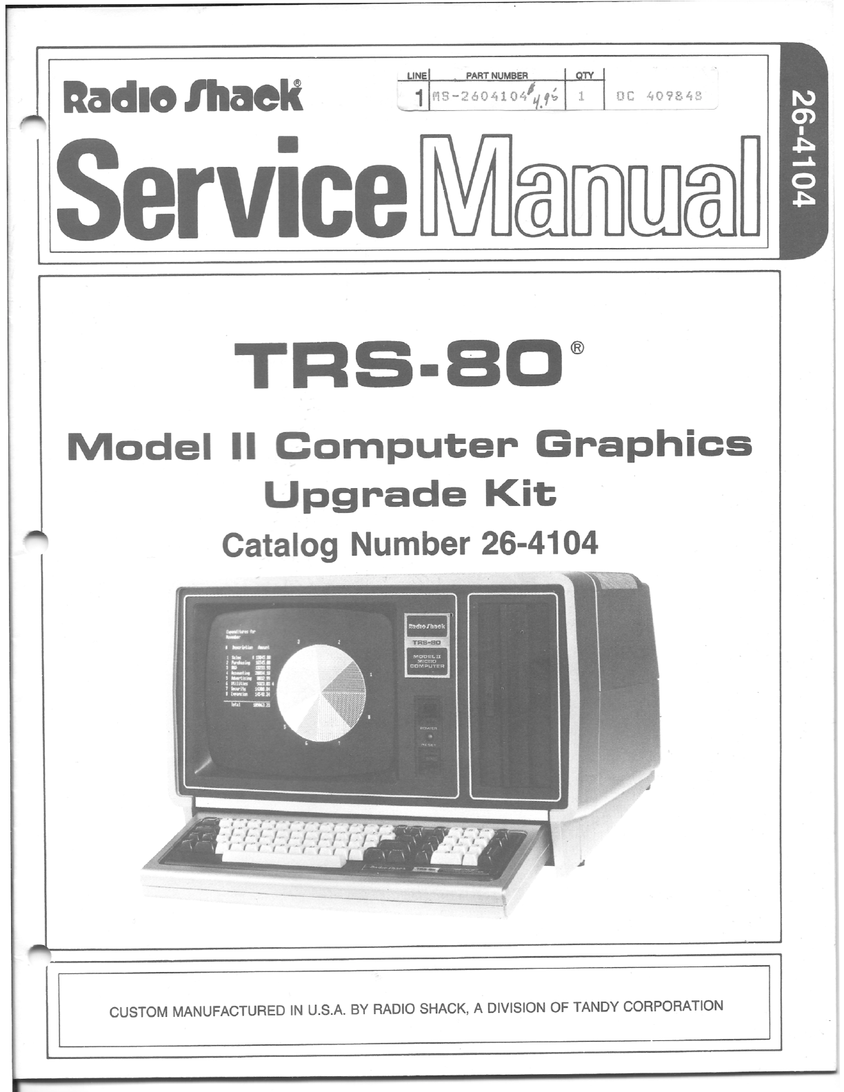
Model IIComputerGraphics
UpgradeKit
Catalog Number 26-4104
‘CUSTOM MANUFACTURED IN USA.BY RADIO SHACK, ADIVISION OF TANDY CORPORATION ‘
TRS-BD ®
Contents
l/Specifications...........................................3
2/Installation Instructions................................5
3/lek DiagramOOOOO0.00.0.0...U...IIOOOOICCOOOOOOIQOCOIIIll
4/Troubleshooting.........................................l3
S/Timing Crlart.O...OI.D0..OO..O'...II.O'COOOOOICOCCOOIIOOOlS
6/Printed Circuit Board Layout............................l6
7/Parts List..............................................18
B/mharatic Diagrm.‘II.I000...0.....00.000DOCOOCCICOIIOOZl
9/Theory of Operation.....................................23
RadloIhael?
TRS-BD ®
'IRS‐Bfl" Graphics Board Service mnual: Copyright" 1982
Tandy Corporation, Fort Worth, Texas 761162 U. S. A.
All Rights Reserved.
Reproduction or use, without express written permission from
Tandy Corporation, of any portion of this manual is ‑
prohibited. While reasonable efforts have been taken in the
preparation of this nanual to assure its accuracy, Tandy
Corporation assumes no liability resulting from any errors
or omissions in this manual, or from the use of the
informtion obtained herein.
Radlo1'hack”
Graphics Board Service Manual
TRS‐BO ®
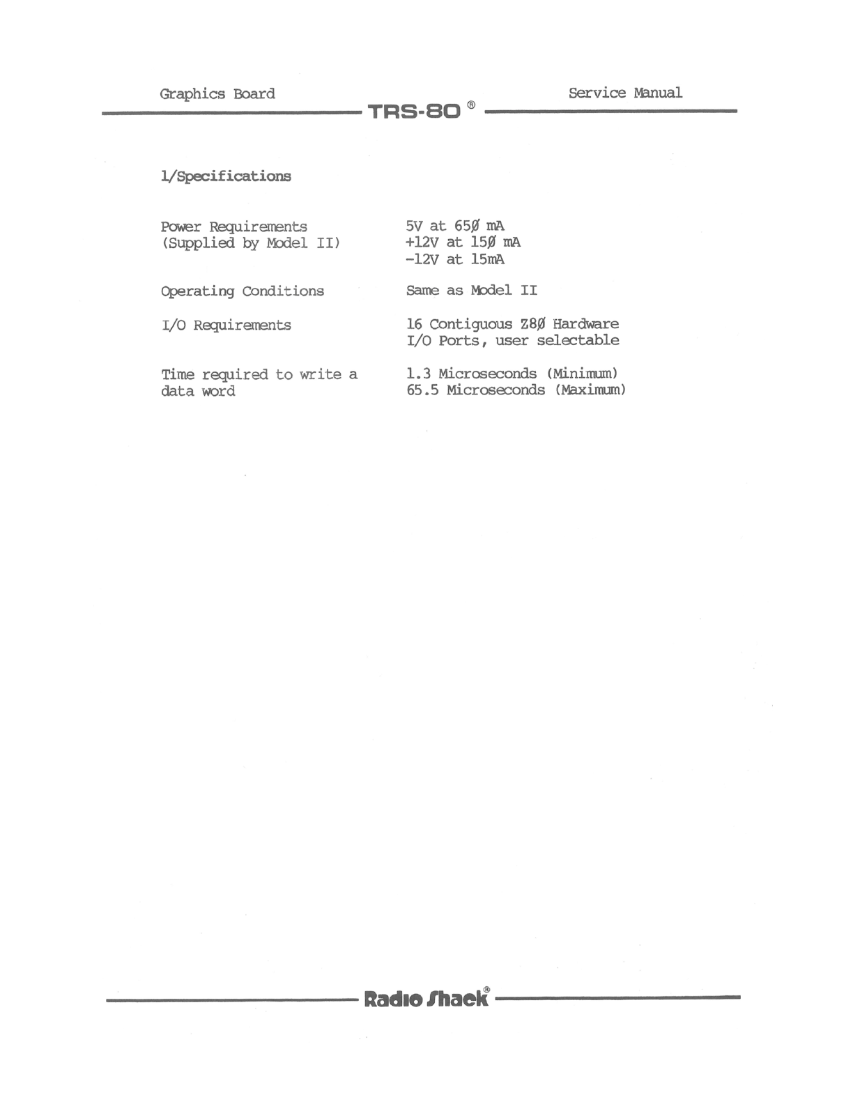
1/8pecifications
Power Requirements 5V at 659! mA
(Supplied by Model II) +12V at 15¢ mA
-12V at lSmA
Operating Conditions Same as Model II
I/O Requirements 16 Contiguous Z8IJ Hardware
I/O Ports, user selectable
Time required to write a1.3 Microseconds (Minimum)
data word 65.5 Microseconds (Maximum)
Radiolhaelf’
Graphics Board Service Manual
Tns-Bo ®
2/Insta11ation Instructions
Installation
Before the Graphics Board can be installed, the CPU board of
the Model II must be fitted with the DMA WAIT Modification.
This modification consists of aROM IC and aseries of cuts
and jumps which is also used for the Hard Disk system.
Look at the CPU Board. REV A, B, and CBoards trust be
modified. REV DBoards do not need to be modified. If the
Model II is fitted with this modification, proceed to the
next section.
Modifying the CPU Board
Follow the procedure below carefully:
1. Disconnect the cables connecting the CPU Board and
remove the board.
2. Remove and discard U11. Install the new Boot ROM in its
place. Besure to position the ROM correctly (marked
end toward U12).
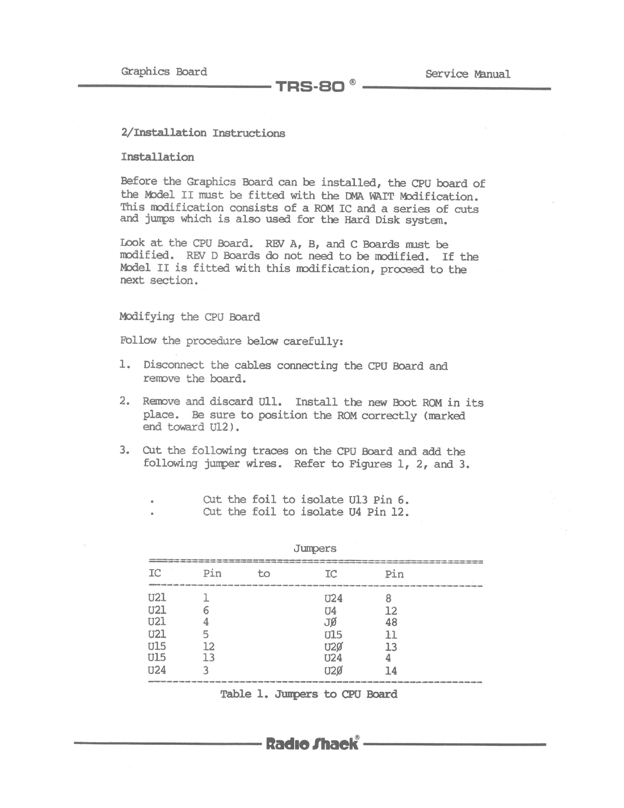
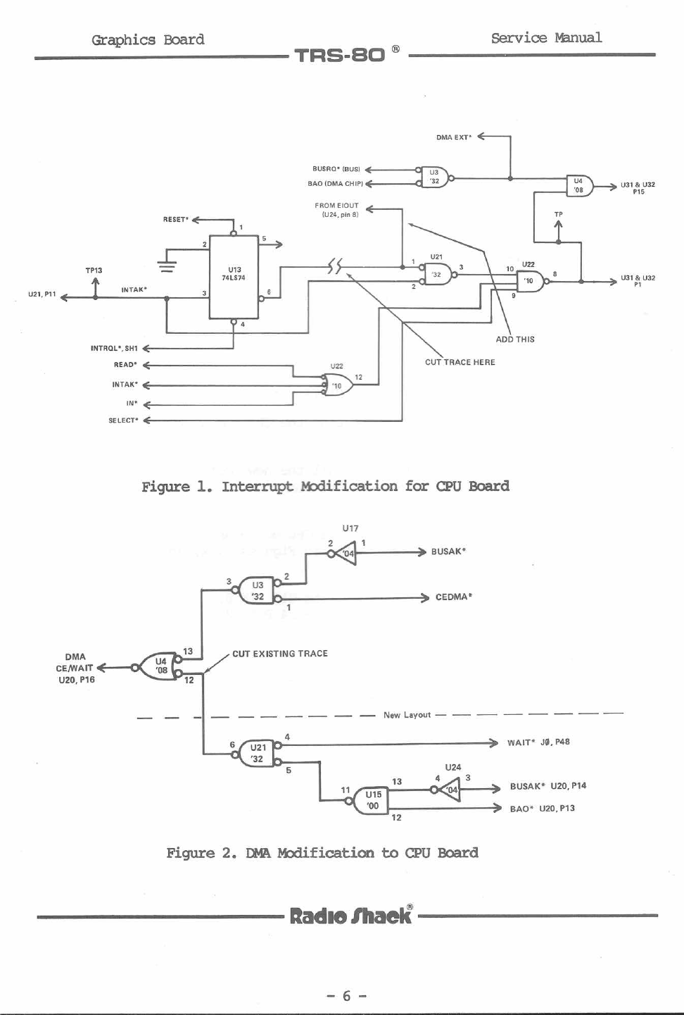
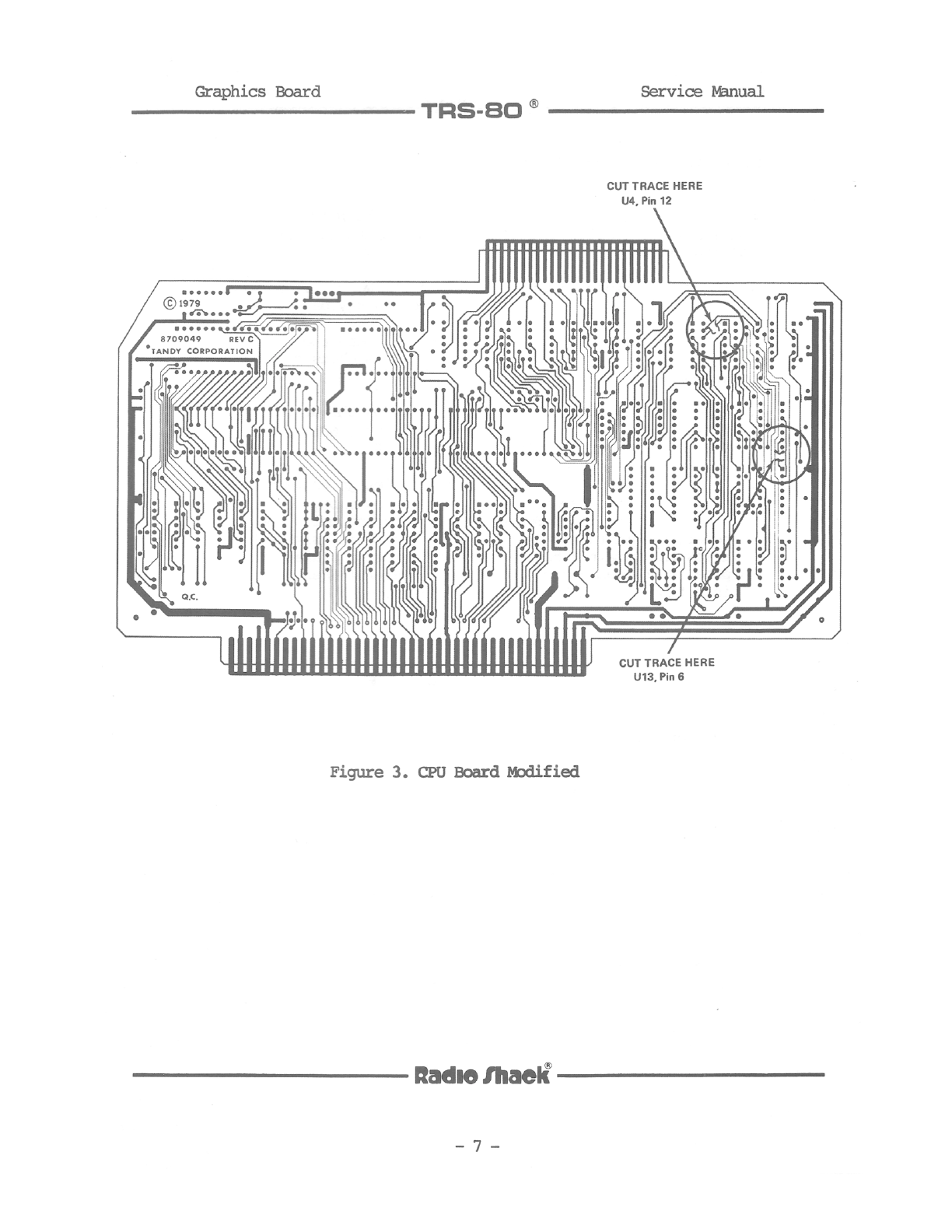
3. Cut the following traces on the CPU Board and add the
following jumper wires. Refer to Figures 1, 2, and 3.
.Cut the foil to isolate U13 Pin 6.
.Cut the foil to isolate U4Pin 12.
J ImIperS
IC Pin to IC Pin
U21 1024 8
U21 6U4 12
U21 4J” 48
U21 5U15 ll
U15 12 UZIJ l3
U15 l3 U24 4
U24 3U215 14
‐‐-‐‐-‐.~‐---._-.._-__‐‐--‐‐_‐‐______-____‐‐‐‐‐___--_‐._..‐‑
Radiolhael?
Graphics Board Service Manual
TRS-BO ®
DMA EXT'
P15
BUSRO' (BUS) 0U3
BAO (DMA CHIP) ‘- -U31 81U32
'08
FROM EIOUT
“ESE.” (U24, pin 3) TP
1
TP13 '‐_. U13 ' 3 1o ”22
K. 74LS74 . ' _n.8U315.1 U32
U21,P11 "“A 3 5 ‐9
Inmansm ADD THIS
READ“ U22 CUT TRACE HERE
INTAK' j» ‘2
m~ .
SELECT'
Figure l. Interrupt Modification for CPU Board
BUSAK‘I
CEDMA“
DMA CUT EXISTING TRACE
CE/WAIT
U20,P16
WAIT’ J0. P48
BUSAK‘r U20, P14
BAO’ U20. P13
Figure 2. DMA Modification to CPU Board
Radio.l'llalek®
Graphics Board ®Service bhnual
TRS-BO
Installing the Circuit Board
Once the Nbdel II is working normally with the WAIT
modification installed, set the Power Switch to the OFF
position. Then:
1. Remove the Video/Keyboard card from the Model II. Be
sure to remove the two cables (video and keyboard).
2. CAREFULLY renove the m6845 VDG IC (U11) and the
character generator ROM (U9) from their sockets on the
Video/Keyboard card.
3. Insert those two IC's into the sockets on the Graphics
board. The VDG goes in U38, the ROM in U25. NOTE THAT
'I‘HEROMISREVERSEDFWTHEO‘I‘HERCHIPS.
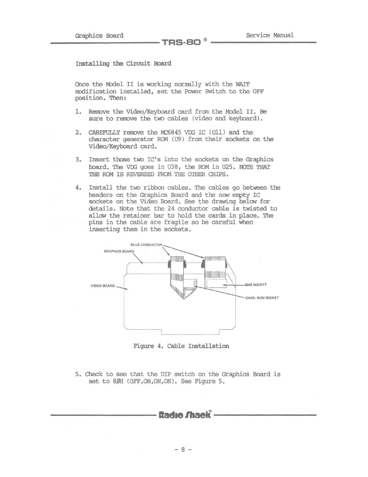
4. Install the two ribbon cables. The cables gobetween the
headers on the Graphics Board and the now empty IC
sockets on the Video Board. See the drawing below for
details. Note that the 24 conductor cable is twisted to
allow the retainer bar to hold the cards in place. The
pins in the cable are fragile so be careful when
inserting them in the sockets.
BLUE CONDUCTOR
GRAPHICS BOARD \\‘
E ‘ ‘
llllllllllllllHlWlIH|||l
D 4‘17‐
VIDEO BOARD 6845 SOCKET
CHAR. ROM SOCKET
Figure 4. Cable Installation
5. Check to see that the DIP switch on the Graphics Board is
set to 89H (OFF,ON,ON,ON). See Figure 5.
RadioIhaek®
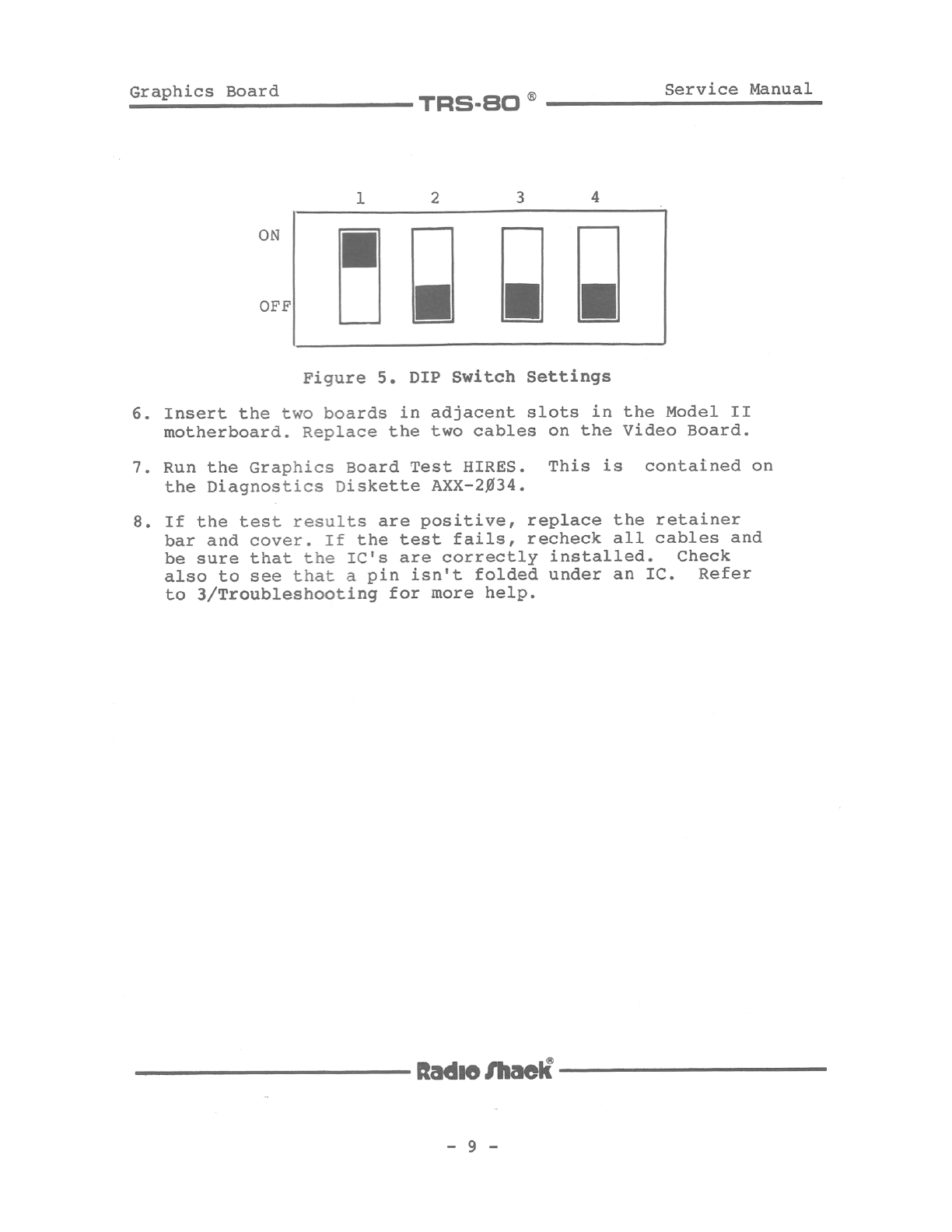
Graphics Board Service Manual
TRS-BD ®
1 2 3 4
ON
OFF
Figure 5. DIP Switch Settings
6. Insert the two boards in adjacent slots in the Model II
motherboard. Replace the two cables on the Video Board.
7. Run the Graphics Board Tes t HIRES. This is contained on
the Diagnostics Diskette AXX‐2fl34.
8. If the test results are positive, replace the retainer
bar and cover. If the test fails, recheck all cables and
be sure that the IC's are correctly installed. Check
also to see that apin isn't folded under an IC. Refer
to 3/Troubleshooting for more help.
RadioIhaek®
®Service Nanual
TRS-BD
Graphics Board
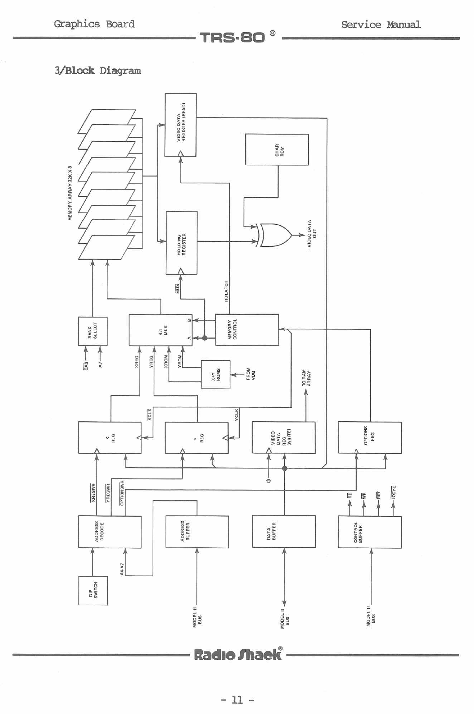
U>QO_
E
0mmmam
mZOr‐hOKB :.3005.
I.ImmuamAJOKFZOD
E
#30
(hdnOwn;.
EEK):3
0m: wm
5.45
Own_>
405.200>¢oEmE
tu_(mw:zmhwammIwbEUwI
__1_mDOE
mmmksme<53
mam
__JwQOE
mwmuam
Awmwzoo<
«.52...39>025.8:
11111122.
ESWZOEKOh<.<<
0mm
V 2
NQOOND
mmmznn<robin
humgmmEsumxxm_o
v.Z<m
v:
u
mxgum>5...z<)zoEmE
3/Block Diagram
Radiolhaeli")
-11‑
Graphics Board Service Manual
Tns-Bo ®
4/Troubleshooting
First isolate the problem to the Graphics Board. Then run
the Graphic Board Test HIRES, contained on the Diagnostic
Diskette AXX‐29134.
Some specific symptoms and suggestions.
Computer "hangs up", won't respond to <RESET>
(DNA has seized the bus.)
.Insure "wait mod" is installed on CPU board.
.Check the M1* Mod (cuts and junps on Rev "A" boards)
Won't read or write to Screen
(U28 not receiving proper commands)
.Check address decoding (U22,U23,DIP Switch)
Check signals on U28
Places dots erratically on the screen.
(Linear Address Generator malfunction)
. X and YROMS reversed, or malfunctioning
.Check shorts and opens near Xand YmMS
Writes but won't read
(U18 and related circuitry)
.Check for proper signals at pins 1and 11 of U18
After board warms up, dots seem to fade in and out, or wont
erase .
(RAM Problems)
RadioIllael?
-13‑
Graphics Board ®Service Manual
TRS-BO
.Some dynamic RAMs (narked MK4315) my need to be replaced
(he to this problem.
Radio.I'haek®
_14‑
.m.._<20_wawrhomlhO...
mDOZOI I UZ>m<w. SEED;.ZBOIm
w.L_Ingbfimz02.5.:4<0E>h<.N
.munm02.4.‐<uX3:20Dw10h<4(Pad._.
umw._.oz
K12.59.
I r;
Uhx0\>x
Service Manual
TRS-BO ®
to
<
O
x35.
«(z
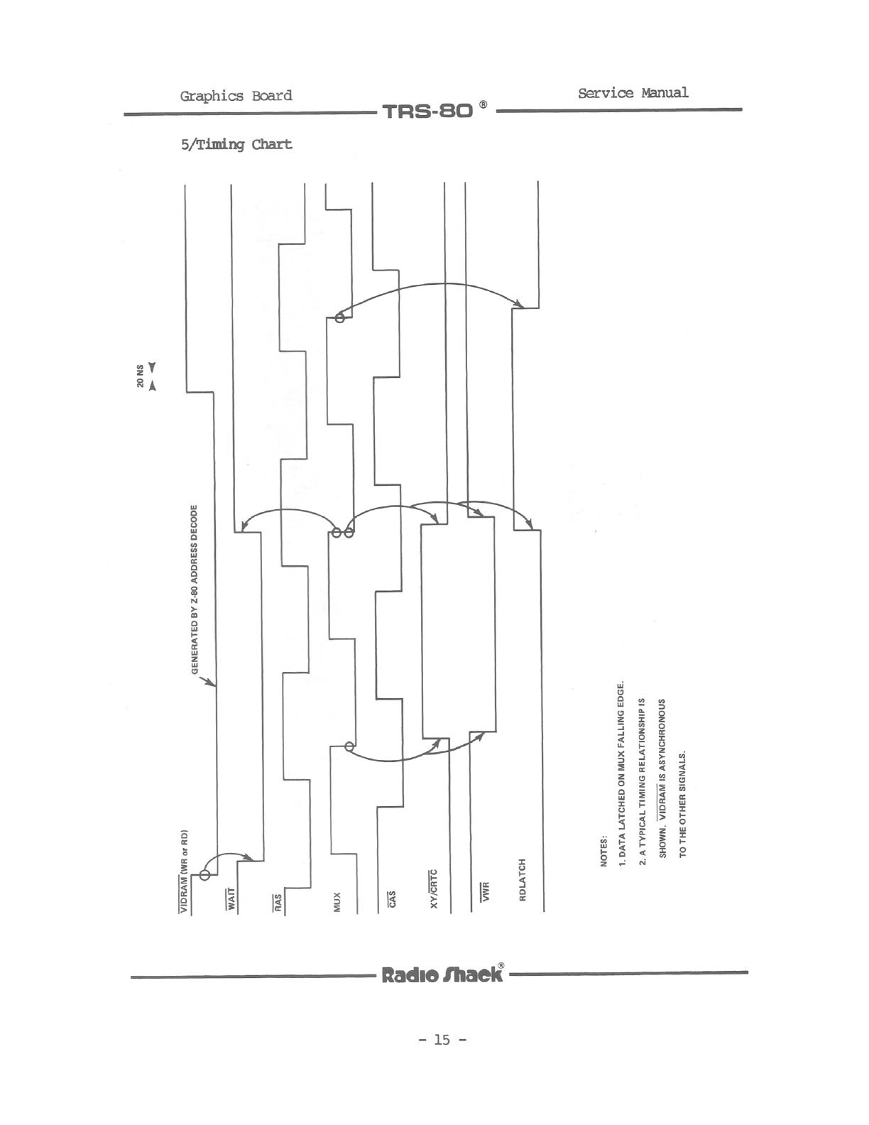
Chart
ming
:
<
3
magmammwt nn<8.N>mth<¢w2m0
Graphics Board
5/T
Em.512:52:03
-15..
RadioIllaek®
.._WcEEI
rigul.3352:2225.7 .52.222222223222222222252.
r..._\x:V.,
F,,.”22222222”2222.._E2 .._ 22222222._______=_2J
......122222222222._ ..2.....2V2.5.:
Service Manual
.lwfifiwm_..2,m‘ISIqxl_Ifi H...Wmfifik=
2222‘@%§2.22.222...£22222.22%2
9F.<m.\.lnawxxxxxxtElmHQ‘N\NI\I_H‐wn‐V._I!
$22.222222222222.“.
22222222 A_2222222.222.222.
TRS-BD ®
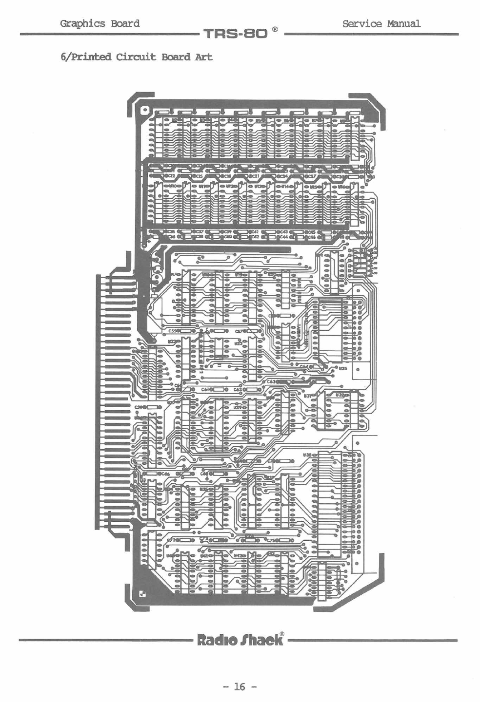
6/Printed Circuit Board Art
Graphics Board
~16‑
Radlo.rllaek®
Graphics Board
7/Parts List
Electrical Parts
to
C7
C8
C9
to
C33
C34
C35
C52
C53
C54
C55
C56
C57
CS8
to
C76
to
R6
RPl
RP2
'TFRES-EBCD ®
Capacitors
lUF SWVDIWD AXIAL
lUF 5¢V MONO AXIAL
$.1UF SWVIWNWD AXIAL
lflUF 25V ELEUTR. RADIAL
fl.lUF 5¢V MONO AXIAL
fl.lUF 5¢V MONO AXIAL
lflUF 25V ELECTR. RADIAL
fl.lUF 5W IVDNO AXIAL
¢.1UF 59v MONO AXIAL
1¢UF 25v ELaaTR. RADIAL
1¢UF 25v ELEUTR. RADIAL
1¢¢UF 16v ELECTR. AXIAL
fl.lUF SflV'bIn«) AXIAL
fl.lUF 5¢v MONO AXIAL
1¢¢UF 16V ELECTR. AXIAL
fl.lUF 5¢v MONO AXIAL
$.1UF SflV'NDNO AXIAL
Resistors
33 OHM l/4WKPT 5%
33 OHM l/4WHPT 5%
PAK 16-PIN DIP 27 OHM
PAK 6-PIN SIP 1K OHM
PAK 6-PIN SIP 1K OHM
Integrated Circuit
RadioIhael?
_18 _
Service Manual
837-4lfl4
837-4lfl4
837-4lfi4
832-6lfl2
837‐4lfl4
837‐4lfl4
832-61fl2
837-4lfl4
837-4lfl4
832-61fl2
832-6lfl2
831-71”?
837-4lfl4
837‐4lfl4
83l-7lfi7
837-4lfl4
837-4lfl4
82fl-7fl33
azg-7a33
829‐n¢27
829-fl21g
829-fl21fi
Graphics Board
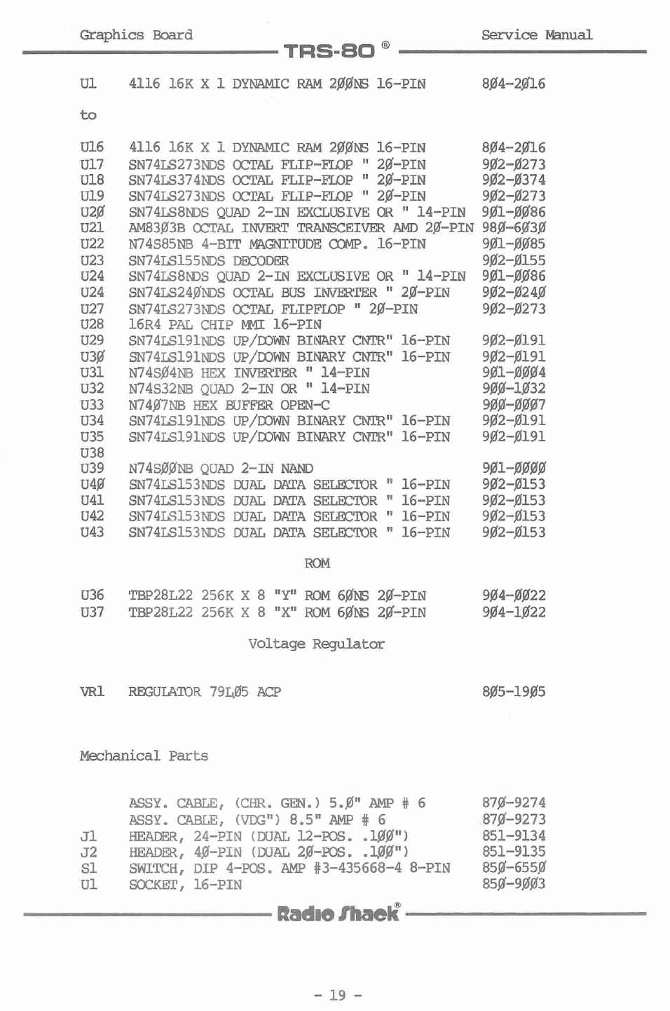
U1
to
U16
Ul7
U18
U19
U21]
U21
U22
023
U24
U24
U27
U28
U29
03¢
U31
U32
U33
U34
U35
U38
U39
U413
U41
U42
U43
U36
U37
Tns-ao ®
4116 16K X 1 DYNAMIC RAM 21mm 16‑
4116 16K X l DYNAMIC RAM 213616 16‑
PIN
PIN
SN74ISZ73NDS OCTAL FLIP-FIDP "2¢-PIN
SN74LS374NDS OCTAL FLIP-FIDP "2fl-PIN
SN74ISZ73NDS OCTAL FLIP-FIOP "ZU-PIN
SN74LSBI\DS QUAD 2-IN EXCLUSIVE OR "l4‐PIN
AM83¢3B OCTAL INVERT TRANSCEIVER AMD za-PIN
N74885NB 4-BIT MAGNITUDE COMP. l6‑
SN74L8155NDS DECODER
SN74LSBDDS QUAD Z‐IN E(CLUSIVE OR "l4-PIN
SN74LSZ4JJNDS OCTAL BUS INVERTER "
PIN
ZIJ-PIN
SN74ISZ73NDS OCTAL FLIPFIDP "2fl-PIN
16R4 PAL CHIP NMI l6-PIN
SN74LSl91NDS UP/mWN BINARY CNTR"
SN74LSl91NDS UP/IDWN BINARY CNTR"
N74Sfl4NB HEX INVERTER "l4-PIN
N74832NB QUAD 2-IN OR "14-PIN
N74fl7NB HEX HJFFER OPEN-C
SN7415191NDS UP/mWN BINARY CNTR"
SN74LSl91NDS UP/mWN BINARY CNTR"
N74SHQ'NB QUAD 2-IN NAND
SN74LSlS3bDS HJAL DATA SELECIUR "
SN74L8153NDS DUAL DATA SELECTOR "
8117418153st DUAL DATA SELECTOR "
SN74L9153NDS DUAL DATA SELECTOR "
ROM
16-PIN
16-PIN
l6-PIN
16 -PIN
16 -PIN
16 -PIN
16 -PIN
16-PIN
'I‘BP28L22 256K X 8 "Y" ROM 6le Zfi-PIN
TBPZSLZZ 256K X 8 "X" ROM 6MB 2¢-PIN
Voltage Regulator
REGULATOR 79Lfl5 ACP
Mechanical Parts
J1
J 2
81
U1
ASSY. CABLE, (CHR. GEN.) 5.6" AMP
ASSY. CABLE, (VDG") 8.5" AMP # 6
HEADER, 24‐PIN (DUAL lZ-POS. .lflfl"
HEADER, 4J3-PIN (DUAL ZH-POS. .169“
#6
)
)
SWITCH, DIP 4-POS. AMP #3-435668-4 8‐PIN
SOCKET ,16-PIN
Radio:haelf’
-19...
Service Manual
8134-21516
8134-2616
962-6273
96241374
9fi2-flZ73
9fll-flfi86
98fl-611391
9151-11685
962-6155
9131-6686
9fl2-flZ4E
9,02-fl273
9152-16191
91252‐125191
9161-1615154
9a¢~1¢32
9aa-ma7
915241191
9112‐16191
9fll‐WW
9132‐15153
9152‐16153
91212-15153
9912-16153
9214-1251622
9134-1622
8155-19155
87fi-9274
.87IJ-9273
851-9134
851-9135
8513-65515
8551-92163
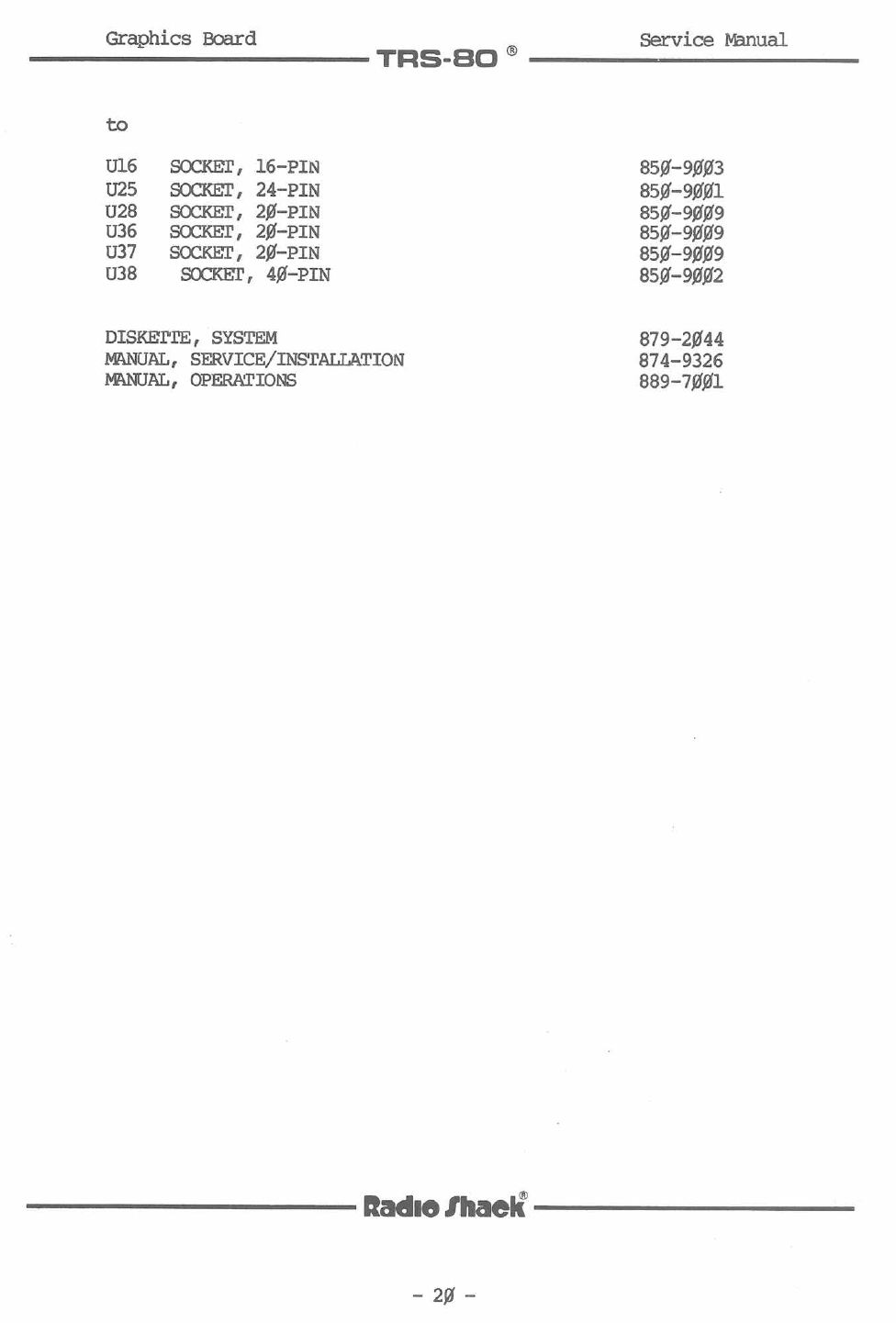
Graphics Board
to
U16
U25
U28
U36
U37
U38
SOCKET, l6-PIN
SOCKET, 24-PIN
SOCKET, 2fl-PIN
SOCKET, 2fl-PIN
SOCKET, Zfl-PIN
SOCKET, 4fl-PIN
DISKEI‘TE,SYSTEM
MANUAL, SERVICE/INSTALLATION
NENUAL, OPERATIONS
TFIS-BD ®
Radlothaol?
_2g _
Service Nanual
85fl-9flfl3
85fl‐9flfil
85fi-9flfi9
85fi‐9flfl9
85g‐9flfl9
85fl‐9flfl2
879-2fl44
874-9326
889-7flfll
XLINE DRAWMG REGISTER +XLSI°H
ADDRESS DECODE .
um XREGWK }
50+ 4
EDSEL
3
DIP SWITCH ‘
BDSEL ‘
EDD
7415155 FXREGDo
Icuuvog‐Wxasewn XREGD:
BM [6 Y. rés‐YREGWK PXREGD'L
Yr 5VIDRAMWK XREGDJ
oPTIonswk
- _
me DEc/mc
__ -804 XREGD4‑
‐' ‘ III XREGDS
BIOCYC VlDRhM RD 806
BDSEL XREGDG
‘XREGD7
MODEL. IE INTERFACE mom {i H ’
YCLK BUSS G
INTERNAL g M
DATA u '
AMSSOS a55 300 AV“ Q0 3YREGDO
z
5 Q YREeDI
c02 YREGDZ
Mn 0Q3 7 Y RFGDB
' LD
- 6
RCO
0.11 V:3
2.322 wait:
DEC/TKC.
BD4 vamo‘
h- 1VREGDE
- I . m YKEEDE
omens w: ‘
€
BAG v‐mwx v v LINE DRAWIM': “
REE: ISTEK I
3A1 \
|
.NC
IV 11 “3
, . SE55 BAA‐a
5A5 /
BAG tau:2‑
NET ‘1
MODE MATERI
BA"! CONTROL mm:1.0
3055
REHD H
FINISH
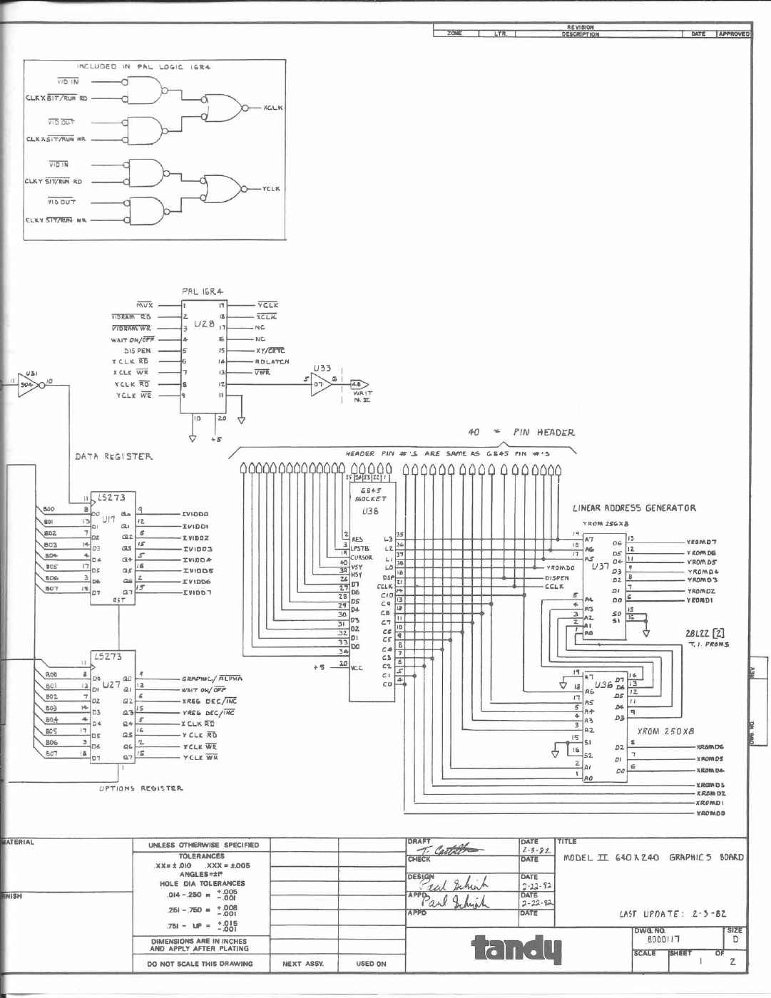
‘NCLUDED \N PM. LOMC MEL
HDIN
<.kaBIT7RUH ID
‐0
PHL IBRA»
wan ou/fi'
D15 PEN XYm
xch.E A loLn-cn
xch T: m
YCLK ’RF
YCL! vfi
4'0 '- PIN HEADER
DATA RKGlSTEK /HEADER VIN #25 ARE SNVIEAS (3345 "N «'5 \
25 7.41312 1
55‘s
SOCKET
IMMIIMI “I IOIOO Illillt Hun“?
LINEAR ADDRESS GENERATOR
rvuouo
IVIDDI VKOM ZSGXB
IWDDZ YIDMD"
IVIDDJ YKDMM
IVIDDA’ VRDM D:
Ivmns ,”m“ vkamnt
:vunm -mum ymo,
IVIDD" DE: YROMD‘L
VROIDI
28m[2]
T. I. PROMS
Gme/m
um?an/E‘T'
xua Dtc/Wr.
viz“. n:n/fi
xchEB
,cuEb XRDM ZSOXB
rcuW‘k a
vcufi
OPTIONS RCGIETEK XIIIID!
lull”.
XRDMDI
IMMDD
mess mw'seW‐‐ -‘
_W; V
TOLERANCES
.XX= t.OIO .XXX =2005
ANGLES=2P
HOLE DIA YOLERANCES
o‘oos
Vou-zso =-.om
25I-.750- :gg? ~LAST UPDATE: 2-3-51.
m _ up‘.ms
-.oon . . . ,
DIMENSIONS ARE IN mcues 8000! I‘I E
AND APPLY AFTER PLATING _,7
00 nor SCALE rms Dsuwme . w I Z
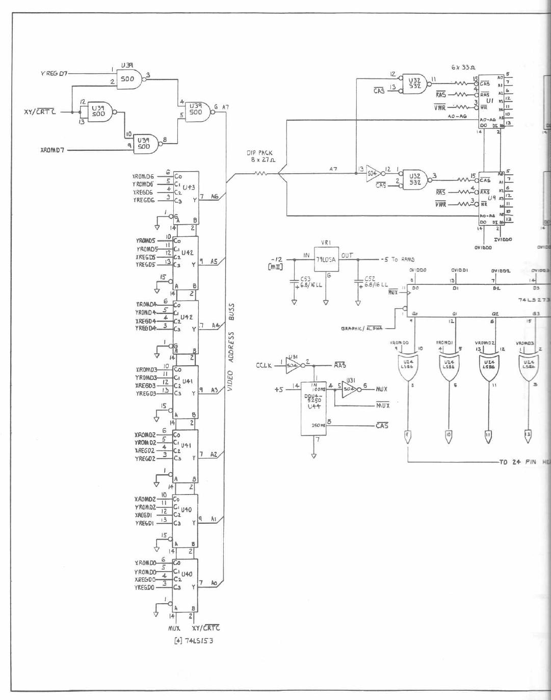
XY/CRT L
XROMD7 DIP PACK
8 x 27.0.
XROMD6
YROMDG'
XREGDS
YRMDS
mom uvmno
mans
mm; ‘ DVID DI UV000?.
C52
$5.6m, LL_ .'3
GnMnm/ 1L5»
W
V)
Lu
Q:
8
Y
o
m
9
>
man: :2: C:
mew C:
W F
|_TD2+PIN
mux xY/CRTC
[4] 741.515 3
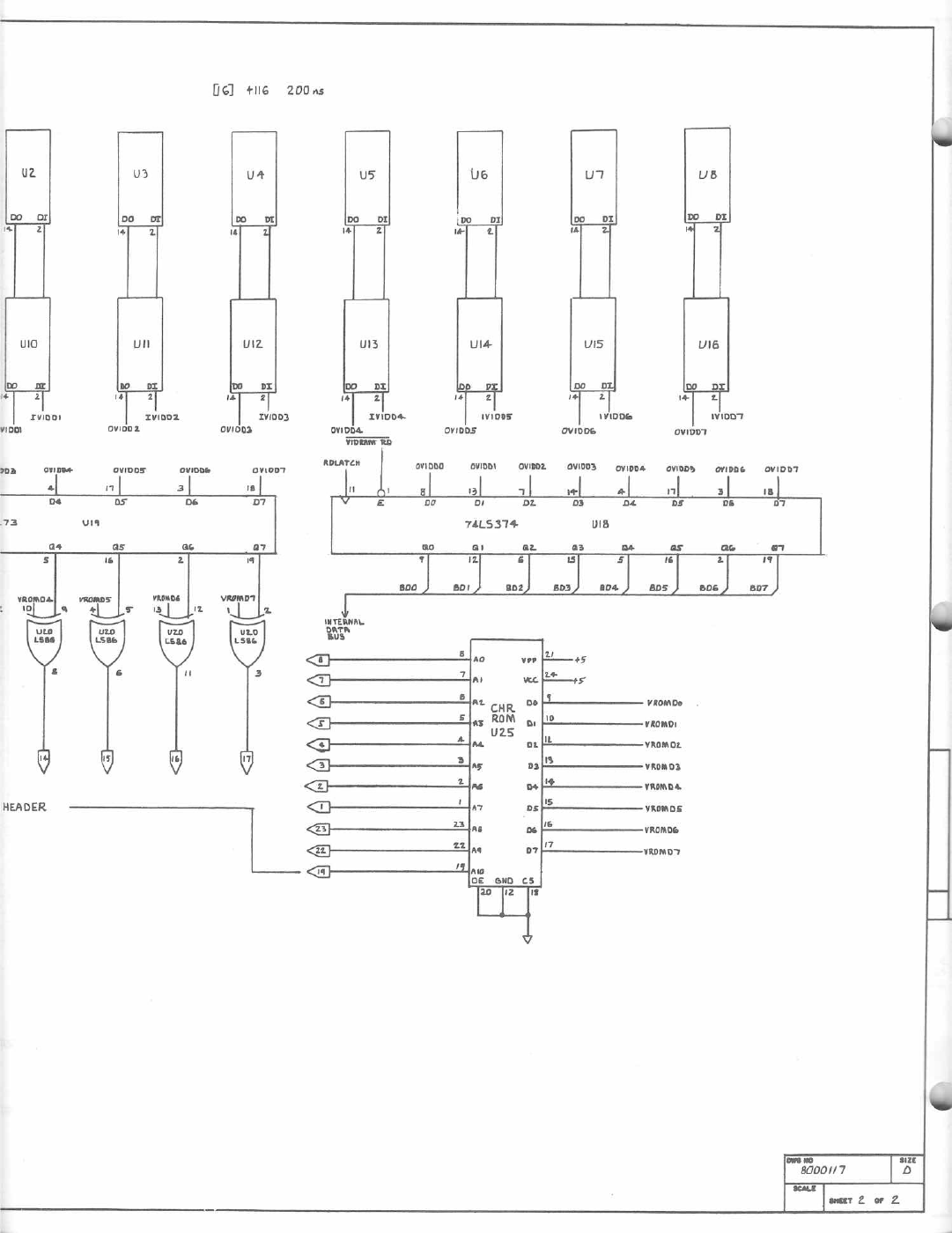
[16] +116 200 ns
:vmnl zvmnz xvmna Inooc. moss \VlDDb WIDD‘I
mam ovuooz. owoua ovum». ownos avmos ava-r
mum“
mun»
ma ounu ovum): avmna ovwm 9'1““ °‘“°°‘ °V'"°’- °V'W3 ovum» anon» anon DVIDD‘I
DI DL
74LS374‑
El EL
(I 4-;
I 5 II 3 {I g
43 VlomDo
4] wmv‑
(l VKDMDL
c v v V a noun:
G"mo;
HEADER avxmns
amanna
<33 vaD-I
(fl
mm
3000/I7 w
E m7 2 0' Z
Graphics Board Service Manual
TRS-BD ®
9/Theory of Operation
Introduction
The Model II Graphics Board provides 640 horizontal dots and
240 vertical dots on the video screen for high‐resolution
graphics. This is the same number of dots used by the
character generator: 80 characters each using 8dots or 640
dots per line. Each character is 10 dots vertically, so 24
lines uses 240 dots. The graphics dots are accessed through
the I/O port specified by the DIP switch setting.
The Graphics Board attaches to the Video/Keyboard card using
two ribbon cables.
Theory of Operation
Refer to the Block Diagram and Schematic Diagram for the
following discussion.
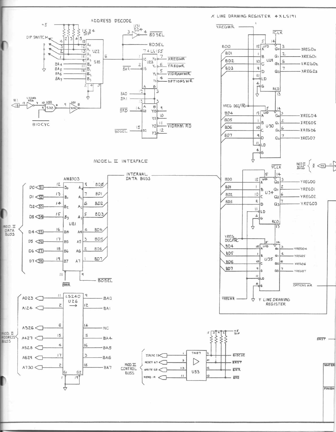
Bus Interface and Address Decoding
The Graphics Board is fully buffered from the CPU. The lower
eight address lines (A0‐A7) are buffered by U26, and the Z80
control lines by U33. Since U33 is an open collector device,
RP4 pulls the outputs up. The Model II data bus is inverted
on the motherboard so an inverting bi‐directional buffer
(021) is used on the data lines. This buffer has two control
lines, DIR (direction, pin 11) and aTRI‐STATE control
(DISable,pin 9). The DIR line is connected to BWR* (buffered
write) which tells the buffer if we wish to read from or
write to the data bus. When BWR* is LOW, we are writing to
the Graphics Board.
The disable line is controlled by BSEL* (board select). With
any access to the Graphics board I/O port, this line goes
LOW which turns the buffer on. When the board is not being
accessed, this line is HIGH and the buffer is off.
I/O decoding is done by high speed 4-bit comparator U22 and
dual decoder U23. The comparator scans address lines A4-A7
and the setting of the DIP switch 81. When the two are equal
AND an I/O instruction is requested (signified by BIOCYC*
RadloIliad? '
_23 _
Graphics Board ®Service Manual
TRS-BO
going 10W) then BSEL* will go LOW. The equals output of the
74885 turns on decoder U23 which uses the lower two address
lines (AG and Al), BMR", and BRD* to produce the proper
strobes for the registers.
The CR gate on BIOCYC* is shut off when Ml is active,
preventing Graphic Board access when external devices are
acknowledging interrupts. M1 is inverted and ANDed with the
I/O cycle to disable the board on Interrupt Acknowledge.
Since only the lower two address lines are 'being used, the
Graphics Board is "mirrored" four times within the 16 byte
boundary defined by the DIP switch setting. Also, the same
address is used for reads and writes to the data register.
Table 1shows how the addresses are decoded:
ADDRESS FUMION
8¢H XRegister Write
81H YRegister Write
82H Video Data Write or Read
83H Options Write
84H XRegister Write
etc etc
‐_...__‐.‐____._‐‐‐.-___‐_____.___‐‐‐___..__
Table 2. Address Decoding
If astarting address other than 8¢H is desired, any 16
byte boundary from MJH to FIJH may be selected using 81.
However, allRadio Shack software is compatible with the 8flH
I/O port address. When the switch is ON, the bit in the
boundary definition will be 16. For exaxrple, to select I/O
port boundary 39H, the switches will be ON, ON, OFF, OFF
(flflll).
Registers (X Address, YAddress, Data, and Options)
Since the Graphics Board is asynchronous with the Model II
(this is explained in detail later) the are several octal
registers which hold data until the Graphics Board is ready
to use it.
The two address registers are actually bi‐directional binary
counters. U29 and U35 are for the Xaddress, and U34 and U35
RadloIhaek®
-24‑
Graphics Board ®Service Manual
TRS-BD
are for the Yaddress. Each pair of counters has three
control lines; write (XREEWR*, YREGWR*) ,count direction
(XREG DEXZ/INC*, YREK; DEC/INC*), and count clock (XCLK*,
YCLK*) .The write strobes are generated by the address
decoding circuitry. Anegative pulse will load the registers
with the data on the bus.
The two other signals are generated from the custom logic
array (called the "Mallory Controller") U28. The count
control lines are used to automatically increment or
decrement the address registers after aread or write. This
greatly speeds up the software in many applications.
The Options register U27 is used to select the user
programable options. These are described below. See Table
2.
,0 GRAPHICS/ALPHA*
Turns on and off the graphics. A"1" will turn graphics ON.
1WAITS ON/OFF*
If WAITS are ONthe screen will not "hash" when reading or
writing to graphics. A"l" selects WAITS.
2mm DEC/INC"
Selects whether the Xregister will decrement or increment.
"1" will select decrement.
3YREG DEC/INC*
Selects whether the Yregister will decrement or increment.
"1" will select decrement.
4XCLK RD*
If address clocking desired, a"£5" will clock the xaddress
up or down AFTER aread depending on the status of BIT 2.
5YCLK RD*
If address clocking desired, a"[5" will clock the Yaddress
up or down AFTER aread depending on the status of BIT 2.
6XCLK V\R*
A"fl" will clock AFTER awrite.
RadloIhaeli"
-25..
Graphics Board ®Service Manual
TRS-BO
7YCLK WR*
A"16" will clock AFTER awrite.
mmm_‐_fl
I5 Graph/Alpha
lWait/No Wait
2 x Dec/Inc
3 y Dec/Inc
4 x Read Set/Run
5 y Read Set/Run
6 x Write Set/Run
7 y Write Set/Run
Table 3Options Progranming
If clocking of the addresses is not needed, the upper four
bits will then all be 1's (Fx hex).
There are two separate data registers; one for writing data
to the graphics memory (U17) and one for reading data from
the graphics memory (018). Both are accessed through the
same I/O port. AZ‐Sfl OUT will write data, and an IN will
read data.
The write register is clocked on each falling edge of the
system 4MHz clock. This is to guarantee that the data will
always be valid when the Merrory Controller IC begins awrite
to RAM.
The read register is an octal latch with 'IRI‐STATE outputs.
Men the Memory Controller detects aread cycle, it will
first latch the RAM data using the RDLATCH control line.
When the *WAIT line from the Memory Controller is released
the Z‐8fl executes the IN instruction and reads the data.
CRl'C and Address Translation
The 6845 is aVideo Display Generator (VDG) which normally
provides monitor sync signals and addresses to scan a
character generator ROM. These addresses are referred to as
"Line" and "Column" addresses, corresponding to the
horizontal lines on the CRT and the vertical columns of the
characters. Since these addresses are seaming aROM which
is set up for acertain character size (in this case 8 X
lfl),they do not map to the graphic coordinates directly.
RadioJ'haek®
-26‑
Graphics Board ®Service Manual
TFIS-BD
The Graphics Board uses two very fast (613 ns) bipolar PROMS
(U36 and U37) to translate the 'Line‐Column" addresses to
"Absolute X-Y" addresses. After the addresses emerge from
the PROMS, they will map to the addresses in the Xand Y
registers.
Graphics Mamry
The matrory section of the Graphics Board is the most
complex, and the Host likely to nalfunction. It consists of
four parts: the Menory Controller IC, the address
multiplexers, menory timing, and the holding register.
Sixteen Zfifl ns 16K dynamic memories are used to store the
graphics data, providing atotal of 32K, although only 19.2K
(8,05 X24¢) is used.
To understand how the memory section works, refer to the
system timing diagram.
It is important to note that the graphics memory is
asynchronous with respect to the CPU. In order to sync up,
the Memory Controller IC uses the WAIT* line on the Z‐8fl.
This is not to be confused with the WAIT option of the
Options register, which uses the DISPEN signal from the 6845
to suspend memory access until the beam of the CRT is being
blanked. Refer to the Model II Technical Reference Manual
for more details.
The brain of the memory section is the Menory Controller,
U28. This is acustom IC whose functions are:
Monitor the VID RAM RD* and VID RAM WR* lines to detect a
graphics memory access.
.Monitor the Options register and send the proper signals
to the Xand Yregisters.
.Sync the Graphics board to the Nbdel II using the WAIT*
line.
.Generate the signals to read and write to the graphics
RAM.
The memory ICs have multiplexed address lines, and must be
provided the proper timing signals (RAS* and CAS*) and make
sure the addresses are at the RAMS at the proper time. This
RadioIhaek®
-27‑
Graphics Board ®Service Manual
TFIS-BO
is accomplished by taking the character clock (CCLK) from
the VDG and using adigital delay line (U44) to derive the
timing signals.
The VDG addresses are stable 16¢ as after the falling edge
of CCLK. OCLK is inverted by U31 producing RAS*. RAS* is
delayed 11” ns and inverted to form MUX. The MUX signal is
used to switch between the upper and lower RAM addresses.
The inverse of MUX, MUX*, is used by the Maer Controller
as atiming reference. MUX is then delayed 15% ns to form
CAS*.
There are two ways to address graphics RAM:
.Use the Xand Yregisters to read and write dots.
.Use the VDG to scan memory and display the contents on
the CRT.
Certainly, the VDG has control most of the time. The VDG
scanning time is used to refresh the dynamic memories.
The contention problem is solved by using two sets of
addresses, the XREGDJJ-XREGD6 and YREGDfl‐YREGD7 set for the
registers and the XROMDIJ-XROMD6 and YROMDfl‐YROMD7 set for
the VDG. Normally, the VDG has control of the RAM and these
addresses are incremented in alinear fashion (fl-79 out of
the XROM and 15‐239 out of the YROM) each CCLK cycle.
The Memory Controller assumes the VDG has the RAM addresses
and keeps the XY/VDG* line LOW. This selects the VDG '
addresses in the four dual 4:1multiplexers U4IJ‐43. The
other multiplexer control line is connected to MUX, so the
addresses switch between RAS* and CAS*.
Since there are two RAM banks, Yaddress line D7 splits the
screen into two halves at the 128th line. The top half of
screen RAM is in RAMS Ul‐U8 while the lower half of the
screen is contained in RAMS U9‐U16. High speed NAND gate U34
is used to select between the two banks of RAM.
The 4116 RAMS used do not have aseparate chip select input
so atechnique called "gated CAS*" is used to turn on each
RAM bank. AMultiplexer consisting of a748m] NAND gate
(which doesn't use the MUX as the other multiplexers do) and
apair of ORgates (U32) gate CAS* to the RAMS.
The RAMS provide TRI‐STA'IE outputs and have on-chip latches
for the outputs, which are configured in parallel. The
outputs go to aholding register to delay the graphic data
one CCLK period from reaching the Video Board. This is done
RadloIhaeli)
-28‑
Graphics Board ®Service Manual
TRS-BO
by octal latch U19. The clear input of the latch turns the
graphics on and off and the GRAPHIC/ALPHA* line from the
options register is connected here.
It is important to note that while the VDG is scanning the
graphics RAM, it is simultaneously seaming the regular
screen RAM on the Video Board. This means that the Graphics
Board mast be able to do amemory access in one CCLK period,
which is 641 ms. The time for amemory access is
approximately:
VDG address stable +ROM delay +Mux delay +RAM delay =
Access time.
16¢ns +12flns +3¢ns +26¢ns =
57¢ns
which is plenty of time. This does not take into account the
time the 2-813 is in aWAIT state, which at worst case is 64¢
ns with the MIT option off and 64.6 uS with the WAIT (ption
on.
Byusing the holding register, the graphics data is
available at the same time as the video data (from the
character generator U25).The separate data is EXCLUSIVE
OR-ed together by U213 and U24 to form the composite video
data sent to the Video Board to be Shifted out to the CRT.
RadioIhaek®
-29‑

RADIO SHACK, ADIVISION OF TANDY CORPORATION
U.S.A.: FORT WORTH, TEXAS 76102
CANADA: BARBIE, ONTARIO L4M 4W5
TANDY CORPORATION
AUSTRALIA BELGIUM u. K.
280-316 VICTORIA ROAD PARC INDUSTRIEL DE NANINNE BILSTON ROAD WEDNESBURY
RYDALMERE, N.S.W. 2116 5140 NANINNE WEST MIDLANDS ws1o 7JN
8749326 PRINTED IN U.S.A.
