Radio Shack Hardware Manual II Technical Reference 1980 Text
User Manual: manual pdf -FilePursuit
Open the PDF directly: View PDF ![]() .
.
Page Count: 204 [warning: Documents this large are best viewed by clicking the View PDF Link!]
TRS-80 MODEL II
TECHNICAL REFERENCE
MANUAL
Catalog Number 26-4921
Radio /hack
jy? ADIVISION OF TANDY CORPORATION
One Tandy Center
Fort Worth, Texas 76102
All rights reserved. Reproduction or use, without express
permission, of editorial or pictorial content, in any manner
is prohibited. No patent liability is assumed with respect to
the use of the information contained herein.
©Copyright 1980, Radio Shack
ADivision of Tandy Corporation
Fort Worth, Texas 76102,
Printed in the United States of America
IMPORTANT NOTICE
This Technical Reference Manual is written for owners of the TRS-80
Model II Microcomputer who have athorough understanding of electronics
and computer circuitry. It is not written to the beginner's level of
comprehension.
Radio Shack will not be liable for any damage caused, or alleged to be
caused, by the customer or any other person using this technical manual to
repair, modify, or alter the TRS-80 Model II Computer in any manner.
Many parts of the computer electronics are very sensitive ana" can be easily
damaged by improper servicing. We strongly suggest that for proper
servicing, the computer be returned to Radio Shack.
While this technical manual has been carefully prepared. Radio Shack will
not be responsible for any errors or omissions and will not be liable for
damages resulting from the use of information contained herein.
Because of the sensitivity of computer equipment, and the potential
problems which can result from improper servicing, the following limitations
apply to services offered by Radio Shack:
1
.
If any of the warranty seals on any Radio Shack computer products are
broken. Radio Shack reserves the right to refuse to service the equipment
or to void any remaining warranty on the equipment.
2. If any Radio Shack computer equipment has been modified so that it is
not within manufacturer's specifications, including, but not limited to,
the installation of any non- Radio Shack parts, components, or replace-
ment boards, then Radio Shack reserves the right to refuse to service the
equipment, void any remaining warranty, remove and replace any
non- Radio Shack part found in the equipment, and perform whatever
modifications are necessary to return the equipment to original factory
manufacturer's specifications.
3. The cost for the labor and parts required to return the Radio Shack
computer equipment to its original manufacturer's specifications will be
charged to the customer in addition to the normal repair charges.

An Overview
This Technical Reference Manual presents acomprehensive theory of
operation for the CPU Module, the FDC, Video/Keyboard, Video Display,
Disk Drives and the Power Supplies. There are also general checkout
procedures to aid you the user in tracing problems down to aspecific sub-
assembly or P. C. Board —but no lower.
This Manual limits repair procedures to replacement of subassemblies only.
Aparts list containing part numbers for major subassemblies may be found
at the end of the Troubleshooting and Replacement section. Adetailed parts
list for each subassembly may be found at the end of the section describing
that particualr subassembly. Individual components may be ordered through
your local Radio Shack store using the Radio Shack Part Number or the
Manufacturer's Part Number if the Radio Shack Part Number is not
available.
We have included in this Manual —for reference only —the Shugart Diskette
Storage Drive Manual, 800/801 and the CDC Flexible Disk Drive Manual,
9404B. Data sheets on several of the Integrated Circuit chips used in this
system are also included to provide the user with additional data concerning
the operation of these devices.
To aid you in recognizing problem areas, you may purchase aSoftware
Diagnostics Diskette from your Computer Center or Radio Shack Store.
If you have any further problems with the TRS-80 Model II Microcomputer
System, contact your Radio Shack Store or Computer Center.
TABLE OF CONTENTS
Section Page
Number Number
TRS-80 Model II Microcomputer System
ISYSTEM DESCRIPTION 1
A. Introduction 3
Video Display Console 3
Keyboard Unit 4
Peripheral Interfaces 4
TROUBLESHOOTING/REPLACEMENT PROCEDURES 7
A. Troubleshooting Procedure 9
Synopsis of Power-On Diagnostics 9
Detailed Troubleshooting Instructions 9
B. Replacement Procedures ,11
System Disassembly 11
System Reassembly 12
Replacement Parts List -Subassemblies 15
III CPUMODULE 17
A. Functional Specifications 19
B. Theory of Operation 19
Decoding Logic 19
Bus Steering Logic 20
Wait State Generation Logic 20
Manual and Power-On Reset Logic 20
System Clock Generation Logic 21
Interrupt Priority Logic 21
El ABuffers 21
Connector Jl Signal Descriptions 22
Replacement Parts List -CPU Module ••25
IV FLOPPY DISK CONTROLLER BOARD 33
A. Functional Specifications 35
B. Theory of Operation 35
Decoding Logic 35
Bus Interface Logic 36
Z-80 -PIO Interface Logic 36
FD1791 -Floppy Disk Controller IC 36
FD1 791 Organization 37
Processor Interface 38
Floppy Disk Interface 38
Head Positioning 38
Disk Read Operations 39
Disk Write Operations 40
FDC and FDD Interface Logic 40
Recording Codes 40
Read Clock Recovery 41
Write Compensation 42
Write Compensation Logic 43
Port Allocation -Table 44
Bit Allocation, Port EFH -Table 44
Bit Allocation, Port E0H -Table 45
J1 Signal Descriptions 46
J2 Signal Descriptions 47
Replacement Parts List -FDC Board 50
TABLE OF CONTENTS (Cont'd)
Section
Number Number
VVIDEO/KEYBOARD INTERFACE 55
A. Functional Specifications 57
B. Theory of Operation 58
High Speed Timing 58
Cathode Ray Tube Controller (CRTC) 58
Multiplexers 63
RAM/Video RAM Select Logic 63
Video Board Select Logic 63
Other Logic Blocks 64
Connector J2 Signal Descriptions 66
Connector J3 Signal Descriptions 66
Replacement Parts List -Video/Keyboard Interface 69
VI MEMORY BOARD (32K RAM and 64K RAM) 73
A. Functional Specifications 75
B. Theory of Operation 75
System Bus Interface 75
Memory Array 75
Address Multiplexers 75
Timing 75
Memory Select Logic 75
Memory Disable Logic 75
I/O Port FF and Select Logic 76
C. Jumper Options 77
D. Verification Procedures 77
Replacement Parts List -Memory Board 81
VII VIDEO MONITOR (CRT) 87
VIDEO MONITOR (MOTOROLA) 89
A. Functional Specifications 89
B. Service Notes 91
Circuit Tracing 91
CRT Replacement 91
C. Adjustments 91
D. Troubleshooting Guide 92
E. Theory of Operation 94
Video Amplifier 94
Horizontal Driver 94
Horizontal Output Transformer 95
Vertical Deflection 95
F. Installation 98
Preliminary Checkout 98
Cathode Ray Tube 98
Monitor Circuit Card 99
G. General Servicing Precautions ...100
Video Monitor Parts List (Motorola) 101
VIDEO MONITOR (RCA) 105
H. Functional Specifications 105
General Information 105
Specifications 105
J. Service Adjustments 106
Replacement Parts (RCA) 108

TABLE OF CONTENTS (Cont'd)
Section Page
Number Number
VIII FLOPPY DISK DRIVE 111
A. Theory of Operation 113
B. Jumper Configurations 113
Replacement Parts List -Disk Drive 114
IX AA11080 POWER SUPPLY 117
A. Functional Specifications 119
B. Troubleshooting 119
Equipment for Test Set-Up 119
Set -Up Procedure 119
Visual Inspection 120
Start-Up 120
Bracket Removal 120
C. No Output 120
D. Performance Test 121
Operating Characteristics 122
XCARD CAGE AND MOTHERBOARD 125
A. Description 127
Replacement Parts List -Card Cage and Motherboard 127
Motherboard Signal Descriptions 128
XI KEYBOARD UNIT 133
A. Introduction 135
Replacement Parts List -Keyboard Unit 137
XII PERIPHERAL INTERFACES 141
A. Serial Interface Connections 143
B. Parallel Interface 144
Parallel Interface Signal Descriptions 145
C. Disk Expansion Connector 146
TRS-80 Model II Disk Expansion System
XIII DISK EXPANSION UNIT 147
A. Introduction 149
Subassembly Description 149
B. Switch Configurations 150
C. Test Points 150
XIV TROUBLESHOOTING -DISK SYSTEM 153
A. Troubleshooting Procedure 155
AC or DC Power Failures 155
Operational Failures '. ..155
Read or Write Error 155
B. Replacement Procedures 157
System Disassembly 157
Subassembly Replacement 158
Replacement Parts List -Expansion Unit 159
Replacement Parts List- 9404B Disk Drive, Mechanical 161
Replacement Parts List -9404B Disk Drive, Electrical 163
iii
TABLE OF CONTENTS (Cont'd)
Section
Number Number
XV AA11100 POWER SUPPLY 167
A. Functional Specifications 169
B. Troubleshooting 169
Equipment for Test Set -Up 169
Set-Up Procedure 169
Visual Inspection 169
Start-Up 169
Disassembly 170
C. No Output 170
D. Performance Test 171
Operating Characteristics 172
XVI ILLUSTRATED PARTS BREAKDOWN 175
Case Assembly Parts List 177
Chassis Assembly Parts List 179
XVII APPENDIXES 183
Z80A-CPU -Zilog Product Specifications
Z80A-SIO -Zilog Product Specifications
Z80-CTC —Zilog Product Specifications
Z80-DMA -Zilog Product Specifications
Z80A-PIO -Zilog Product Specifications
FD1791 -Western Digital Product Specifications
MC6845, CRTC -Motorola Product Specifications
SA800/801 Disk Drive -Shugart Maintenance Manual
SA800/801 Illustrated Parts Catalog
9404B Disk Drive —Control Data Maintenance Manual
IV
LIST OF ILLUSTRATIONS
Figure Page
Number Number
SECTION I-SYSTEM DESCRIPTION
1Block Diagram 5
2Power Distribution 5
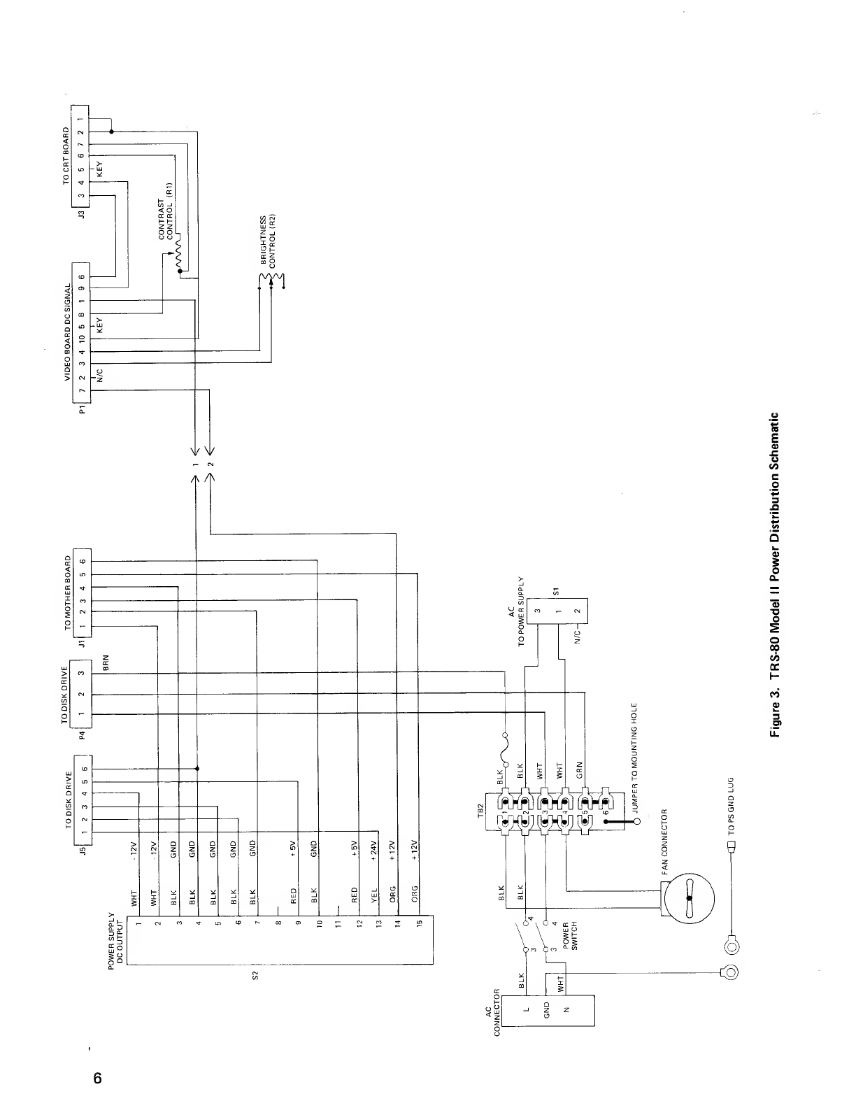
3Power Distribution Schematic 6
SECTION II -TROUBLESHOOTING AND REPLACEMENT
1Synchronization Signals 10
2Keyboard Disassembly 13
SECTION III -CPU MODULE
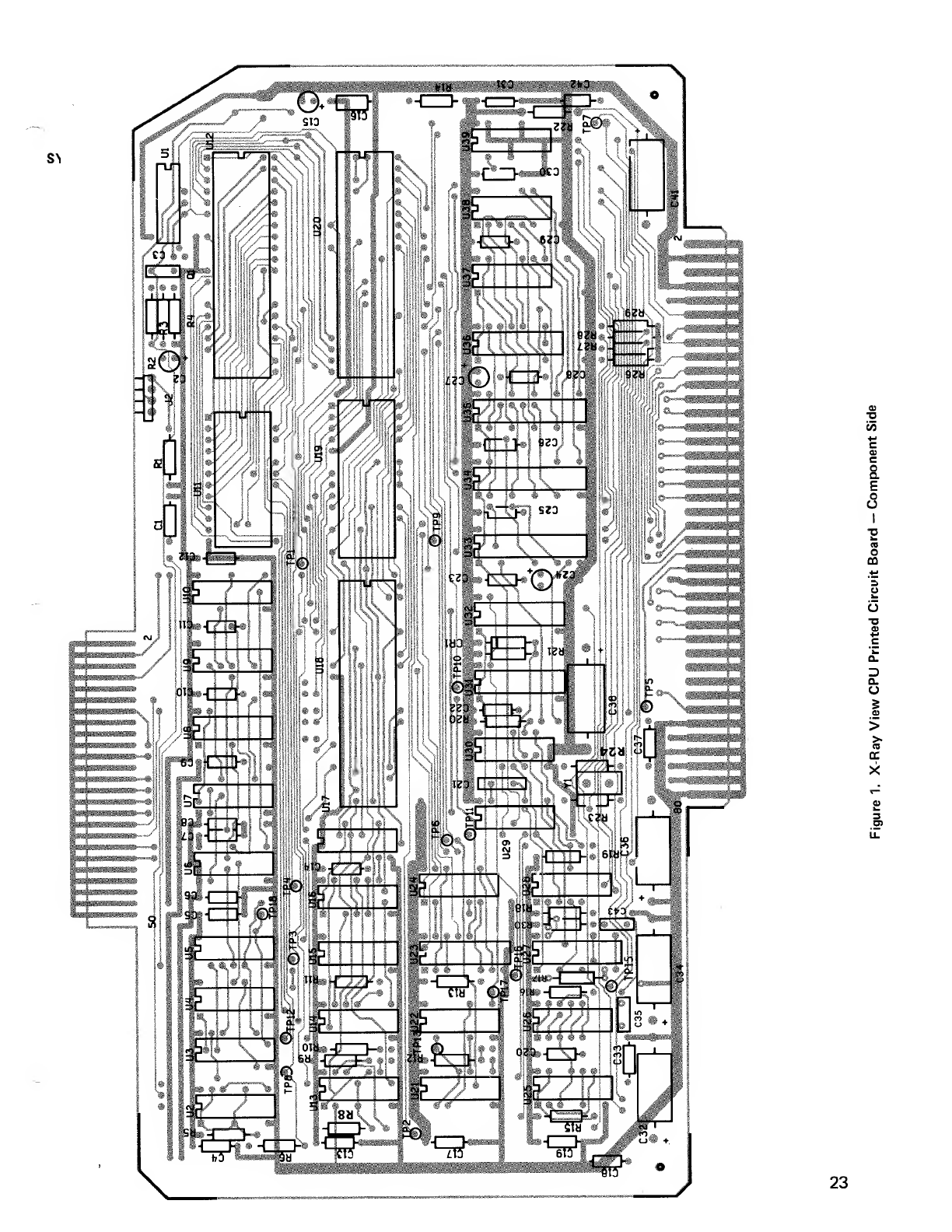
1X-Ray View of CPU Printed Circuit Board -Component Side 23
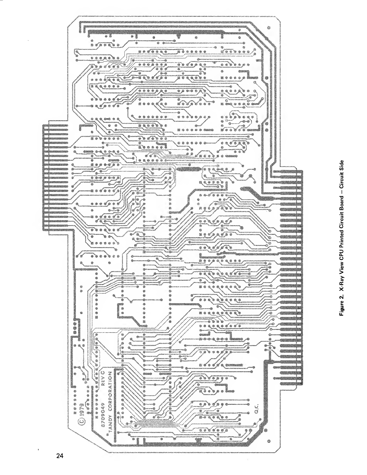
2X-Ray View of CPU Printed Circuit Board -Circuit Side 24
3CPU Schematic Diagram (Sheet 1) 29
3CPU Schematic Diagram (Sheet 2) .30
3CPU Schematic Diagram (Sheet 3) 31
SECTION IV -FLOPPY DISK CONTROLLER
1FD1791 Block Diagram 37
2Clock Recovery Block Diagram 41
3Interacting Clock/Data Pulses 42
4FDC Printed Circuit Board -Component Side 48
5FDC Printed Circuit Board -Circuit Side 49
6Floppy Disk Controller Board Schematic Diagram (Sheet 1) 53
6Floppy Disk Controller Board Schematic Diagram (Sheet 2) 54
SECTION V-VIDEO/KEYBOARD INTERFACE
1Video/Keyboard Block Diagram 57
2Timing Diagram 59
3MC6845 CRTC Pin Identification 60
4Character Dot Pattern 62
5Keyboard Timing Diagram 65
6X-Ray View of Video Keyboard Printed Circuit Board —Component Side .67
7X-Ray View of Video Keyboard Printed Circuit Board -Circuit Side 68
8Video/Keyboard Interface Schematic Diagram (Sheet 1) 71
8Video/Keyboard Interface Schematic Diagram (Sheet 2) 72
SECTION VI -MEMORY BOARD (64K and 32K RAM)
1Memory Board Block Diagram 76
2Jumper Locations and Address/Bit RAM Identification 78
3X-Ray View of Memory Printed Circuit Board —Component Side 79
4X-Ray View of Memory Printed Circuit Board -Circuit Side 80
5Memory Board Schematic Diagram 85

LIST OF ILLUSTRATIONS (Cont'd)
Figure Page
Number Number
SECTION VII -VIDEO MONITOR (CRT)
1Block Diagram (Motorola and RCA) 94
2Horizontal Drive Signal (Motorola and RCA) 95
3Model II Monitor[Display] P.C. Board -Component Location (Motorola) .96
4Model II Monitor [Display] P.C. Board -X-Ray View (Motorola) 97
5Model M3970 -Series Kits, Rear View (Motorola) 98
6Monitor Circuit Card -Edge Connector (Motorola and RCA) 99
7Video Wiring Harness (Motorola and RCA) 100
8Model II Monitor [Display] Schematic Diagram (Motorola) 103
9Deflection Yoke Assembly (RCA) 106
10 Model II Monitor [Display] P.C. Board -X-Ray View (RCA) 107
11 Model II Monitor [Display] Schematic Diagram (RCA) 109
SECTION VIII -FLOPPY DISK DRIVE
1SA 800/801 PCB Test Points and Component Locations 113
SECTION IX -AA11080 POWER SUPPLY
1Test Layout ,120
2Output Connector (S2) 120
3Q1 Collector Waveform 121
4Q1 Base Waveform 121
5AA11080 Power Supply Schematic Diagram 124
SECTION X-CARD CAGE and MOTHERBOARD
1Motherboard Printed Circuit Board -Component Side 130
2Motherboard Printed Circuit Board -Circuit Side 131
SECTION XI -KEYBOARD UNIT
1Keyboard Internal Cable 135
2Keyboard External Cable 135
3Keyboard Code Map 136
4Keyboard Schematic Diagram 140
SECTION XII -PERIPHERAL INTERFACES
1Serial Interface Connector 143
250-Conductor Ribbon Cable -Serial Cable 143
3Parallel Interface Connector 144
434-Conductor Ribbon Cable -Parallel Cable 144
5Rear View, TRS-80 Model II Computer 146
LIST OF ILLUSTRATIONS (Cont'd)
Figure pa9e
Number Number
SECTION XIII -DISK EXPANSION UNIT
1CDC Model 9404B PCB Test Points and Component Locations 151
SECTION XIV -TROUBLESHOOTING -DISK SYSTEM
1Disk Expansion Unit Wiring Diagram 156
SECTION XV -AA1 11000 POWER SUPPLY
1Line Voltage Selection 169
2Test Set-Up 169
3Q1 Collector Waveforms 170
4Q1 Base Waveforms 170
5AA111000 Power Supply Schematic Diagram 173
SECTION XVI -ILLUSTRATED PARTS BREAKDOWN
1Case Assembly 178
2Chassis Assembly 181
VII
SECTION I
SYSTEM DESCRIPTION

A. INTRODUCTION
The TRS-80 Model II Microcomputer is adisk-based
computer system consisting of three major components,
the third of which is optional. They are: aVideo Dis-
play Console with built-in Disk Drive, aseparate Key-
board Unit and the optional Disk Expansion Unit.
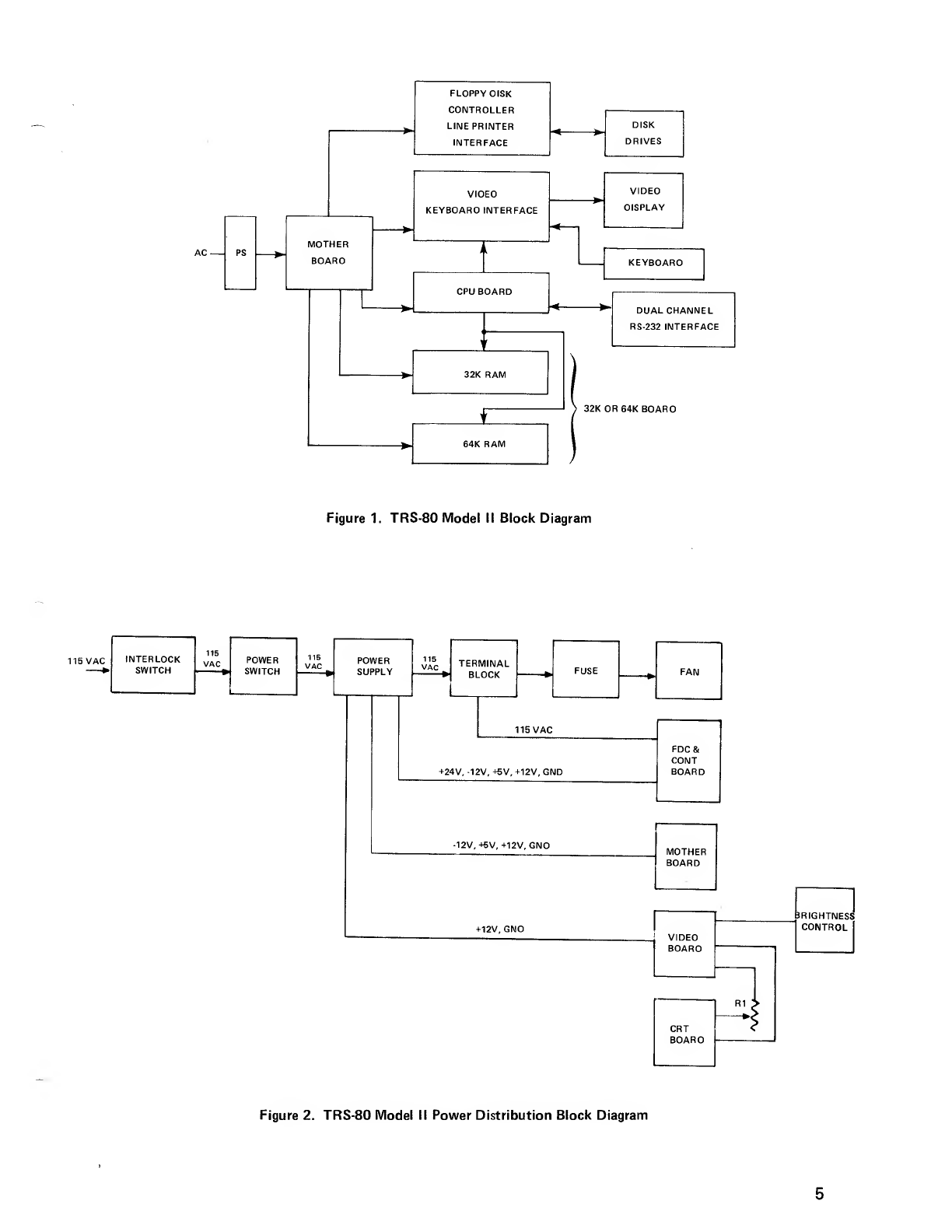
Video Display Console
The Video Display console is made up of ten major
subassemblies: (Refer to Figure 1.)
1. Case:
The case subassembly has three major parts, the
bottom tray, the top cover and the front bezel.
These parts provide the attractive housing for the
TRS-80 Model II. Care should be exercised during
service operations so that the painted case parts
are not marred or scratched.
2. Chassis:
The metal chassis is mounted to the bottom tray
of the case. The chassis has mounting provisions
for the other subassemblies in the TRS-80 Model
II.
3. Power Supply: (Refer to Figure 2.)
The power supply subassembly in the TRS-80
Model II is an open frame, 150 watt, switching
power supply. It has four outputs with the fol-
lowing ratings:
Never test the power supply without asuitable
load. The minimum currents required by the
power supply are:
5 Volts
12 Volts
24 Volts
-12 Volts
@8.6 Amps
@4.5 Amps
@1.7 Amps
@0.2 Amps
The power supply rectifies the AC line to DC,
chops it at 20 kHz, then transforms the chopped
DC to the required output voltages and finally
rectifies the transformed output to low voltage
isolated DC. Feedback loops are provided for volt-
age regulation and over current protection.
The power supply may be jumper selected for
either 95 to 135 VAC or 190 to 270 VAC. It will
operate at either 50Hz or 60Hz input frequency.
**»CAUTION***
This power supply must have aload present, i.e., the
computer and CRT, or damaging oscillations may
5Volts @2.15 Amps
12 Volts @1.25 Amps
24 Volts @0.00 Amps
-12 Volts @0.05 Amps
Card Cage:
The card cage provides mechanical support for
and electrical connections to the digital elec-
tronics boards. Up to eight boards can be accom-
modated in the card cage. The main component
of the card cage subassembly is the "Mother-
board". The Motherboard holds the eight 80
pin card edge connectors and has the printed
wiring defining the TRS-80 Model II bus.
As shipped from the factory, the cards should
be in the following order: (slot one being the
one closest to the power supply).
CPU
FDC
Memory
Video
Expansion Mem
CPU Card:
Slot 1
Slot 2
Slot 3
Slot 4
Slot 5(ie. the 32K memory
add on board)
The CPU card in the TRS-80 Model II has several
powerful features. The first of these is, of course,
the CPU itself, a4MHz Z80A Microprocessor,
running at its full rated speed.
The bootstrap ROM on the CPU card provides
the necessary instructions to the Microprocessor
for the required initialization of the computer
system on power-up or after afront panel reset.
The ROM then "disappears", allowing the user to
take full advantage of the memory space as RAM.
The DMA (Direct Memory Access) circuit on the
CPU board allows memory to peripheral or periph-
eral to memory data transfers without CPU inter-
vention. This allows for amuch greater program
and I/O throughput. One of the most often used
applications of the DMA is in data transfers to and
from the Floppy Disk Controller. The dual serial
interface is also on the CPU card. The baud rate
is fully user programmable (refer to your Owner's
Manual.
6. Floppy Disk Controller Card: 10. Floppy Disk Drive:
The floppy disk controller card provides all the
circuitry necessary to read and write in both single
density (FM) and double density (MFM) formats
on an eight-inch floppy disk drive. The board uses
an FD1791 floppy disk controller chip to generate
the proper write signals. The read signals from the
drive are passed through aphase-locked loop data
separator before going on to the FD1791 to insure
high reliability reads.
***CAUTIOIM**»
The phase-locked loop is factory adjusted for opti-
mum performance. Do not adjust any of the potent-
iometers on the FDC board).
The parallel printer interface is also on the floppy
disk controller card.
7. Memory Card:
The memory card in the TRS-80 Model II uses
16K dynamic RAMs to give either 32K bytes or
64K bytes of read/write memory. The necessary
refresh signals for the memory come from the
CPU board.
8. Video Card:
The video card supports both 80 character and 40
character lines, with 24 lines displayed. The char-
acter set includes upper and lower case alpha-
betic and numeric symbols (t .. . #, etc.) and aset
of forms drawing characters. Reverse video can be
selected on acharacter-by-character basis.
The heart of the video controller is a6845 CRT
controller chip, which is software programmable
for various formats.
The floppy disk drive is astandard eight inch
drive capable of supporting both single and double
density recording formats. All of the disk drive
control signals come from the floppy disk con-
troller card. The drive contains two motors; one
rotates the media at aconstant speed while the
other positions the read/write head over one of
the 77 tracks. Electronics on the disk drive convert
digital signals into read/write head signals and
vice-versa.
NOTE
Models for overseas shipment may be configured
with an AC Moter for the line voltage available in
that country and may be fitted with adifferent
drive pulley for 50 Hz line frequency.
Adetailed description and theory of operation of each
subassembly, with the exception of the Case and Chas-
sis, may be found in later sections of this manual.
Keyboard Unit
The keyboard of the TRS-80 Model II is a76-key
microcomputer controlled capacitive keyboard. The
microcomputer and its associated electronics scans the
key matrix, converts switch closures to an eight bit
digital code and transmits it serially to the keyboard
interface on the video card. The keyboard is connected
to the main console via acable from the front bezel of
the computer
Peripheral Interfaces
There are four interface connections on back of the
Video Display Console:
1. Two serial (RS-232-C) Input/Output (I/O) chan-
nels.
The video card also contains the logic for the key-
board interface. This serial handshake interface
receives data and clock signals from the keyboard
and issues an interrupt when the entire character
has been received.
9. Video Monitor (CRT):
The 12 inch CRT (Cathode Ray Tube) and associ-
ated electronics form the video rrronitor for the
TRS-80 Model II. This subassembly receives video,
horizontal drive, and vertical drive signals from
the video card and +12 volts from the power
supply. The CRT's high resolution complements
the upper/lower case character set of the video
card.
2. Aparallel I/O channel, e.g. for connection to
TRS-80 standard parallel-interface line printers.
3. Floppy Disk I/O channel for connection of the
Model II Disk Expansion Unit.
The Video Display Console also provides connectors
and slots for future expansion. (See Operator's Manual).
MOTHER
BOARD
FLOPPY DISK
CONTROLLER
LINE PRINTER
INTERFACE
VIDEO
KEYBOARD INTERFACE
CPU BOARD
DISK
DRIVES
VIDEO
DISPLAY
DUAL CHANNEL
RS-232 INTERFACE
32K OR 64K BOARD
Figure 1. TRS-80 Model II Block Diagram
INTERLOCK
SWITCH
115
VAC POWER
SWITCH
115
VAC POWER
SUPPLY
115
VAC TERMINAL
BLOCK FUSE
+24V, -12V, +6V, +12V, GND
-12V, +6V, +12V, GND
+12V, GND
FDC&
CONT
BOARD
MOTHER
BOARD
VIDEO
BOARD
CRT
BOARD
ri ;
—».
TIGHTNESS
CONTROL
Figure 2. TRS-80 Model II Power Distribution Block Diagram
1
CN l
rr
<r*.
o
CU
rr >
O
l-
)=C
** ~
CO cc
V) -J
cc cc
oo egg
2_J
~< So
Vu
iO)
,
<
<£ r-
to
n
atn
cc O
o
on
a
>CM ~z
a.
^/\ /
*/N
<LU
(0
E
0)
jC
o
CO
3
.fl
S
o
T5
O
O
00
GO
DC
I-
co"
0)
SECTION II
TROUBLESHOOTING/REPLACEMENT

A. TROUBLESHOOTING PROCEDURE
General
This section of the manual will guide service personnel
through the system checkout procedure. The trouble-
shooting steps are organized in aflowchart manner.
Following these steps will guide you to the possible
failing board or boards.
Connect the power cord and keyboard as described in
the Operator's Manual.
Remove the top cover of the display console by remov-
ing the two screws at the rear of the unit. Carefully
set the top cover aside to prevent accidental scratch-
ing. If the unit has an interlock switch, enable the test
mode by pulling up on the interlock switch plunger.
At this point, there should be no diskette in the drive,
and the disk terminator should be installed as des-
cribed in the Operator's Manual.
Synopsis of Power-On Diagnostics
When the power switch on the TRS-80 Model II is
raised to the "ON" position, the Z80 microprocessor
automatically starts executing the program in the
bootstrap ROM on the CPU board. The program per-
forms the following functions in order:
1. The initialization parameters are sent to the CRT
controller and the screen memory is set to the
value 0A0H. This causes the CRT to come on
with asolid white screen.
2. The ROM checksum is verified to assure that the
ROM is present and functioning properly. If the
checksum indicates that the ROM data is bad,
"CK ERROR" will be outputted to the CRT and
the computer will halt.
3. ACPU test program is run to verify proper data
transfers between registers in the Z80 CPU. Any
failure of this test will cause "Z8 ERROR" to be
output to the CRT and the computer will halt.
4. The RAM memory from 1000H to 7FFFH is then
tested with asimple read-complement-write-com-
pare-complement-write routine. Any faulty mem-
ory locations in this 28K byte range will cause
"MF ERROR" to be output to the CRT and the
computer will halt.
5. The keyboard will be "flushed" of any characters
input up until this time.
6. The message "INSERT DISKETTE" is displayed
on the CRT.
Bootstrap Sequence
7. Wait until diskette is inserted and door is closed.
8. Screen is cleared to spaces (all black).
9. Track seek command is sent to floppy disk
controller.
10. Wait three seconds and check disk status.
11. "DC ERROR" if floppy disk controller is still
busy or seek error is indicated or drive not re-
stored to track 0.
12. "D0 ERROR" if drive indicates not ready.
13. "SC ERROR" if there is aCRC error in the
track ID field.
14. Read track into RAM.
15. "TK ERROR" if program not found on track 0.
16. "SC ERROR" if there is aCRC error in the
record ID.
17. "LD ERROR" if alost data error occurs.
18. "RS ERROR" if the data loaded in is not in Radio
Shack boot record format.
19. Call system diagnostic routine.
20. Jump to TRSDOS.
Detailed Troubleshooting Instructions
1. Turn on the Model II Computer by raising the
power switch to "ON". Wait afew seconds for
the CRT to warm up. Adjust brightness and con-
trast controls at the front of the console. If the
video display comes on, go to 10. If not, go to 2.
NOTE: For overseas models configured for 50 Hz
operation, the "HERZ50" programs on the TRS-
DOS diskette must be called to prevent "jittering"
of the video display and to provide accuracy of the
real time clock.
2. If the pilot light is on, go to 4. If the pilot light/
reset switch connector is seated correctly on the
CPU board, go to 3. If not, reposition the connec-
tor and go to 2.
3. Check for +5 volts on one of the P.C. boards. If
this is not in the range from 4.8 to 5.2 volts, go
to 5. If the voltage is incorrect, the LED must be
burned out. Replace and go to 1
.
4. Check the filament of the CRT. If it is lit, go to 7.
If it is not:
Check the +12 volt supply at the CRT electronics
board (pin 1is ground, pin 7is +12V).
If +12 volts is present, go to 6.
5. Switch off power. Check the power supply fuse
and replace if necessary. Check for shorts across
the power supplies. If shorts are found, remove
cards from card cage until the shorts disappear,
then replace the offending card. Reassemble and
go to 1
.
Otherwise, power supply may have malfunctioned.
Remove and replace the power supply. Go to 1.
6. CRT has burned out filament. Replace and go to
1. (Refer to Section VII for installation proced-
ures.)
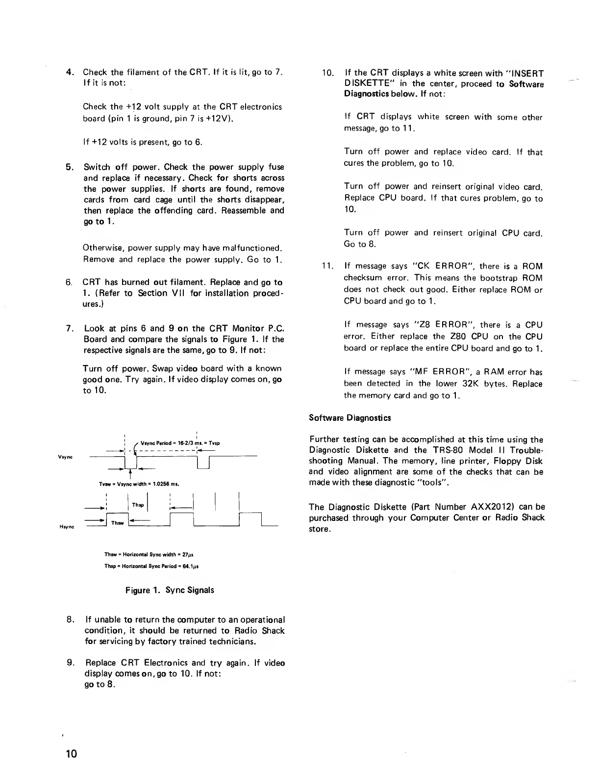
7. Look at pins 6 and 9on the CRT Monitor P.C.
Board and compare the signals to Figure 1. If the
respective signals are the same, go to 9. If not:
Turn off power. Swap video board with aknown
good one. Try again. If video display comes on, go
to 10.
10. If the CRT displays awhite screen with "INSERT
DISKETTE" in the center, proceed to Software
Diagnostics below. If not:
If CRT displays white screen with some other
message, go to 11
.
Turn off power and replace video card. If that
cures the problem, go to 10.
Turn off power and reinsert original video card.
Replace CPU board. If that cures problem, go to
10.
Turn off power and reinsert original CPU card.
Go to 8.
11. If message says "CK ERROR", there is aROM
checksum error. This means the bootstrap ROM
does not check out good. Either replace ROM or
CPU board and go to 1.
If message says "Z8 ERROR", there is aCPU
error. Either replace the Z80 CPU on the CPU
board or replace the entire CPU board and go to 1
.
If message says "MF ERROR", aRAM error has
been detected in the lower 32K bytes. Replace
the memory card and go to 1.
Vsync
Hjync
•Vsync Period =16-2/3 mi. =Tvsp
-T~
Tvsw =Vsync width =1.0256 ms.
Thip
*
Thsw I
* *
L
Software Diagnostics
Further testing can be accomplished at this time using the
Diagnostic Diskette and the TRS-80 Model II Trouble-
shooting Manual. The memory, line printer. Floppy Disk
and video alignment are some of the checks that can be
made with these diagnostic "tools".
The Diagnostic Diskette (Part Number AXX2012) can be
purchased through your Computer Center or Radio Shack
store.
Thtw =Horizontal Sync width =27/is
Thip =Horizontal Sync Period s64.1jus
Figure 1. Sync Signals
8. If unable to return the computer to an operational
condition, it should be returned to Radio Shack
for servicing by factory trained technicians.
9. Replace CRT Electronics and try
display comes on, go to 10. If not:
goto 8.
sin. If video
10
B. REPLACEMENT PROCEDURES f. Remove chassis from the bottom case.
Replacement procedures contained in this manual are
limited to system disassembly, removal and replacement
of subassemblies and system assembly.
There are potentially hazardous areas inside the case,
so use caution during disassembly and be sure to read
and observe the warning and caution notes.
Disconnect all external cables from the rear connector
panel before beginning repair.
System Disassembly
1. Case:
a. Remove the two machine screws from the back
of the case.
b. Lift up on the rear of the top case and angle it
toward the front panel; then lift the top case
away from the bottom.
c. Remove the two screws from the video display
mounting bracket and bezel.
d. Remove the screw that secures the mounting
bracket on top of the disk drive to the bezel
(inside of front panel).
e. Pull out the keyboard cable only as far as
necessary to allow the front panel to lay flat
(face down).
f. Pull the front panel forward to clear the chassis
and lay it face down.
2. Chassis:
a. Remove five #8 screws, flat washers and lock
washers from locations illustrated. Notice that
one of the screws is used to help mount the
power supply.
b. Lift up chassis slightly (to clear ribs in the bot-
tom case) and slide it forward.
c. Remove screws holding the AC power connec-
tor to the connector panel and remove the con-
nector from the panel.
d. Disconnect two wires from the fuseholder.
e. Disconnect all I/O cables from disk drive, CPU
card and FDC card.
3. Power Supply:
''" ;^"~-'^ A~'*-p&ijiM-'~'
""""" :-/^/v \.- >j
If the power supply is faulty, the large heat sink
may have apotential of 330 volts above line com-
mon. Use extreme caution when handling the power
a. Remove the three-wire AC plug and the thir-
teen-wire DC plug from the power supply PCB.
b. Remove two #8 thread forming screws from
the power supply mounting bracket.
c. Tilt the power supply toward the outside of the
chassis and remove four screws, nuts and spacers
that mount the video board to the power sup-
ply mounting bracket.
d. Remove five screws, nuts, flat washers and
spacers that secure the power supply to its
mounting bracket.
e. Remove the power supply from the chassis.
4. Card Cage:
a. If not previously done, disconnect the signal
and control cables from the video/keyboard
card and I/O cables from the floppy disk con-
troller and CPU cards.
b. Disconnect the DC cable on the lower right
front of the mother board.
c. Remove four #8 thread forming screws from
the card cage mounting bracket.
d. Remove card cage from the chassis.
5. Removal of Cards from Card Cage:
a. Remove two thread forming screws that con-
nect the PCB stabilizer to the card cage mount-
ing brackets and remove the stabilizer.
b. Notice the location of the CPU, FDC, video/
keyboard and memory cards. Ensure that the
replacement cards are inserted in the same loca-
tions.
c. Remove and replace cards as necessary for
repair.
d. Remove six screws, nuts and flat washers that
mount the mother board to its mounting brack-
ets and remove the mother board.
11
6. Video Display (CRT) and Video Board:
CAUTION
The CRT and video board are matched sets.
Do not remove and replace individual pieces.
Remove one matched set and replace with
another matched set.
a. If the video board is not free from the power
supply mounting bracket, perform the steps for
removal of the power supply down to removal
of the video board.
b. Disconnect four color coded wires with spade
lugs from the CRT yoke.
c. Disconnect the connector on the rear of the
CRT neck.
WARNING
There may be ahigh voltage charge on the
high voltage anode. To discharge, connect
one end of awire to aknown good ground
and connect the other end of the wire to the
blade of acommon screwdriver. Insert the
screwdriver blade under the suction cup and
touch it to the clip holding the wire to the
d. Insert acommon screwdriver under the rubber
grommet on the high-voltage anode wire on
the side of the CRT. Use the screwdriver to
compress the clip holding the wire to the tube
and pull the wire free.
e. Remove the upper right and lower left screws,
nuts and washers from the video display mount-
ing bracket.
CAUTION
If dropped, the CRT will implode. To avoid
this kind of accident, support the CRT
while performing the next step.
f. Remove the lower right and upper left screws,
nuts and washers from the video display mount-
ing bracket.
g. Lift the CRT and PCB out of the chassis.
7. Disk Drive
a. Disconnect two power connectors from the
disk drive PCB.
b. Disconnect the large (50 pin) card edge con-
nector from the disk drive PCB.
c. Remove four screws from the disk drive mount-
ing bracket.
d. Lift the drive and mounting brackets out of the
chassis.
e. Lay the drive on its side (PCB up) and remove
two screws from the bottom of the mounting
bracket.
f. Separate the drive from the bracket.
8. Fan
NOTE: The following steps can only be performed
with the chassis removed from the case.
a. Position the chassis so that the four nuts on the
bottom of the chassis are accessible.
b. Disconnect the power cable on the fan.
c. Secure the screw heads while removing the nuts
from the bottom of the chassis and remove four
nuts.
d. Raise the fan away from the chassis to provide
clearance for the screws while removing the fan.
9. Keyboard (See Figure 2):
a. Disconnect the keyboard external cable from
the keyboard (DIN plug.)
b. Place the keyboard with keys down on asoft
surface.
c. Remove four thread forming screws and two
machine screws.
d. Place the keyboard with keys up and remove
the bezel.
e. Disconnect the five-pin connector at J1 on the
PCB.
f. Lift the keyboard with PCB out of the case.
Reassembly
1. Keyboard:
Reassemble the keyboard in reverse order of dis-
assembly.
2. Fan:
a. When installing anew fan, insert the screws into
the screw holes before positioning the fan.
b. Ensure that the fan is oriented so that air will
flow in from the bottom and out through the
top and so that the power connector is acces-
sible.
CAUTION
Do not put stress on the fan mounting ears.
Tighten the screws and nuts only enough to
secure the fan to the chassis.
12
UPPER KEYBOARD CASE
KEYBOARD MODULE
-LOWER KEYBOARD CASE
-SCREW, 6-19 x3/4" (19.05 mm) (6)
Figure 2. Disassembly of Keyboard
13
c. Position the chassis so that the fan mounting
screws are accessible from the bottom of the
chassis.
d. Secure the screw heads while installing the nuts.
e. Tighten the nuts only enough to ensure that the
fan is secure.
3. Disk Drive:
a. Lay the disk drive on its side (PCB up) and
position its chassis mounting bracket (wide end
forward) to align holes in bracket with the
holes in the drive base plate.
b. Install two screws that secure the drive to the
mounting bracket.
c. Place the drive with mounting bracket into
the chassis and align the screw holes in the
bracket and in the chassis.
d. Install four screws loosely so that the drive's
position can be properly adjusted. Then tighten
the screws that secure the bracket to the chassis.
e. Install two power connectors and the card edge
connector on the drive.
4. Video Display (CRT) and Video Board
a. Position the CRT and align its mounting holes
with its mounting bracket.
b. Install the upper left and lower right screws and
mounting hardware.
c. Install the lower left and upper right screws and
mounting hardware.
d. Position the CRT matched video board inside
of the chassis.
e. Install the plug on the rear of the CRT neck.
f. Install the four color coded wires with spade
lugs to their associated terminals (as determined
by acolored dot on the yoke near each term-
inal).
g. The video board will be installed on the power
supply mounting bracket, (see the procedures
for installation of the power supply).
5. Card Cage:
a. Align the mother board mounting holes with
the holes in the left and right PCB mounting
brackets. (The left bracket has aleft 90° bend
at the rear and the right bracket has aright
90° bend at the rear).
b. Install six screws, nuts and flat washers that
secure the mother board to the brackets.
c. Install the CPU, FDC, video/keyboard and
memory cards to the mother board. Be sure of
proper orientation in the card cage.
d. Align the holes in the PCB stabilizer with the
holes in the left and right PCB bracket and in-
stall two thread forming screws.
e. Position the card cage inside of the chassis and
align the holes in the brackets with the holes
in the chassis.
f. Install four screws that secure the card cage to
the chassis.
g. Connect the DC cables to the connector on the
lower right front of the mother board.
h. Connect the I/O cables to the FDC and CPU
cards and connect the control cables to the
video/keyboard card.
6. Power Supply:
a. Align the power supply mounting holes with
the holes in its bracket mounting plate.
b. Individually, position five spacers to align with
the mounting holes between the power supply
board and its mounting plate.
c. Install five screws, nuts and flat washers that
secure the power supply to the bracket.
d. Position the power supply in the chassis and
tilt it toward the outside of the chassis.
e. Align the video board mounting holes with its
mounting holes on the power supply bracket
mounting plate.
f. Position four spacers to align with the mount-
ing holes.
g. Install four screws, nuts and flat washers that
secure the video board to the bracket.
h. Position the holes in the mounting bracket to
the holes in the chassis and install two thread
forming screws that secure the bracket to the
chassis.
7. Chassis:
a. Position the chassis inside the bottom case so
that the two wires can be connected to the
terminals on the fuse holder and the AC power
input connector can be installed on the connec-
tor panel.
b. Install the two wires to the fuse holder.
c. Install two screws that secure the AC power
input connector to the connector panel.
14
d. Lift up the chassis (to clear the ribs on the case
bottom) and position it so that its mounting
holes align with those in the case.
e. Install five screws, flat washers and lockwashers
that secure the chassis to the bottom case.
8. Case:
a. Position the front panel (bezel) on the chassis.
b. Install one screw that secures the bezel to the
top bracket on the disk drive.
c. Install the two screws that secure the bezel to
the video display mounting bracket.
d. Position the top case at the lip of the bottom
case and angle it downward (toward the back)
until the top case is properly seated.
e. Install two machine screws that secure the top
case to the bottom case.
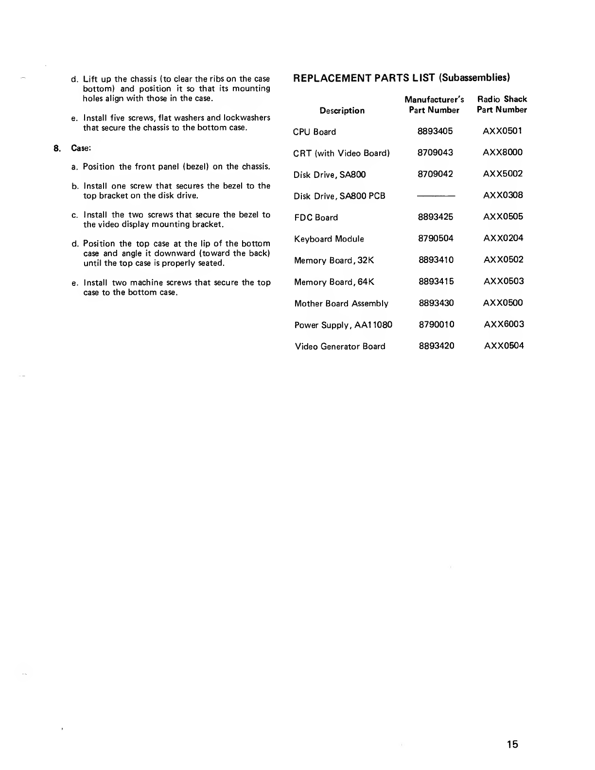
REPLACEMENT PARTS LIST (Subassemblies)
Manufacturer's Radio Shack
Description Part Number Part Numbei
CPU Board 8893405 AXX0501
CRT (with Video Board) 8709043 AXX8000
Disk Drive, SA800 8709042 AXX5002
Disk Drive, SA800 PCB AXX0308
FDC Board 8893425 AXX0505
Keyboard Module 8790504 AXX0204
Memory Board, 32K 8893410 AXX0502
Memory Board, 64K 8893415 AXX0503
Mother Board Assembly 8893430 AXX0500
Power Supply, AA1 1080 8790010 AXX6003
Video Generator Board 8893420 AXX0504
15

SECTION
CPU MODULE
17

A. FUNCTIONAL SPECIFICATIONS
The TRS-80 MODEL II CPU Board provides the following
hardware resources for the system:
1. Performs data processing activities.
a. Supports DMA operations, both on the CPU Board
or on an external system board.
b. Supports mode 2vectored interrupts.
2. Provides primary DMA channel.
3. Provides dual serial I/O channels.
a. RS-232C standard signals.
b. Asynchronous and synchronous schemes support-
ed. Bisync, SDLC, and HDLC protocols are sup-
ported.
4. Provides timing signals needed by the system.
a. 2or 4M Hz system clock option.
b. Programmable serial I/O baud rate clocks.
c. 8MHz clock for write precomp on FDC Board.
d. Real time clock
e. Control signals for system boards.
f. Flexible on and off board wait state generation.
5. System bootstrap firmware (2716 compatible).
a. Resides in low memory if enabled (location 0000H
to0FFFH).
b. Software switchable enable.
c. Self test diagnostic software included.
6. Power on and manual reset logic.
The major components employed include the following:
1. Z80A CPU Chip (Central Processing Unit)
2. Z80A DMA Chip (Direct Memory Access)
3. Z80ASIO Chip (Serial Input/Output)
4. Z80A CTC Chip (Counter Timer Circuit)
5. 2716 Compatible ROM (Read Only Memory)
B. THEORY OF OPERATION
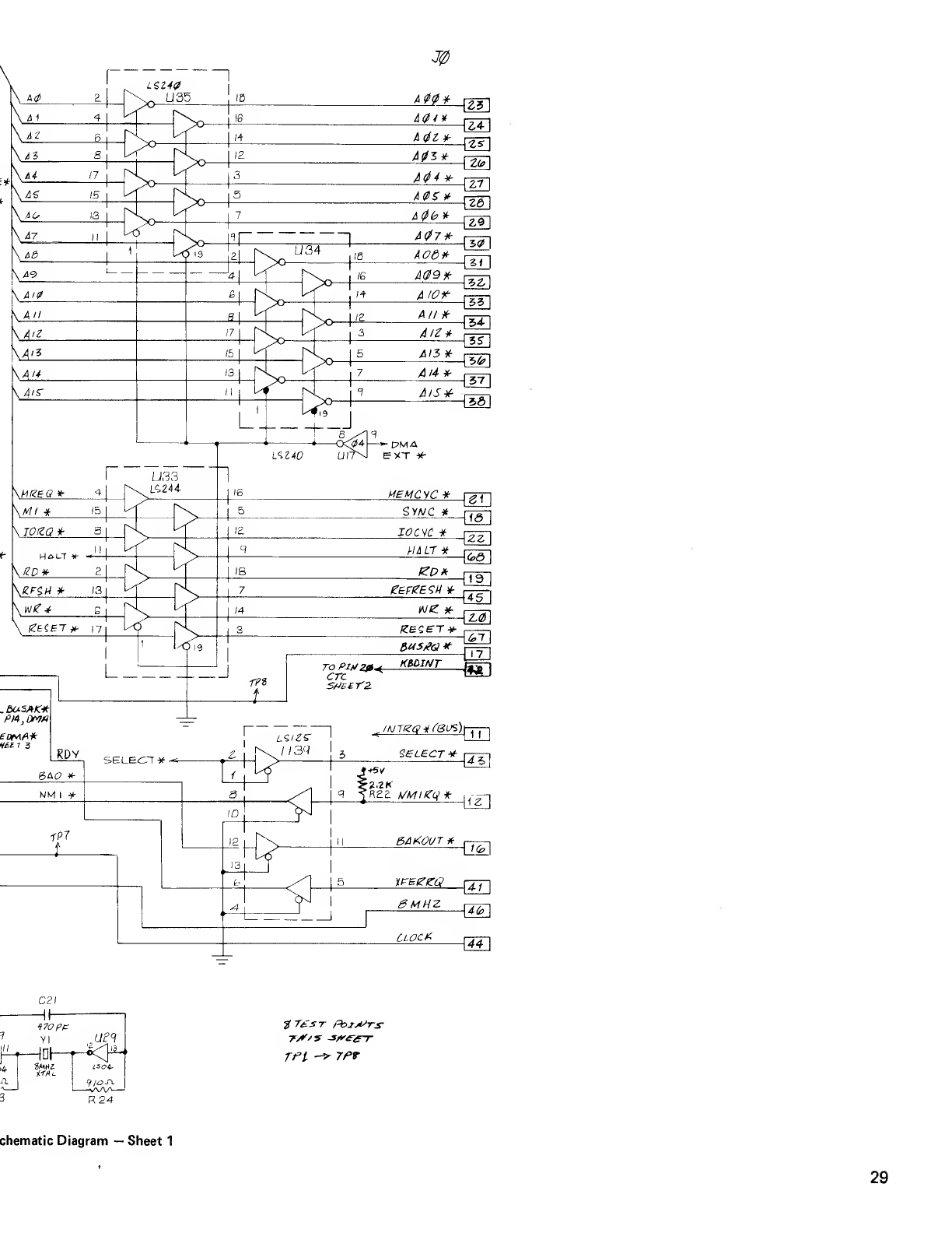
Decoding Logic
The peripheral devices on the CPU Board are I/O mapped,
with the exception of the BOOT ROM. The port addresses
used are F0H through F9H. Port mapped devices use the
lower eight address bits only to specify which port is being
addressed. The upper eight address bits are ignored com-
pletely and are not relevant to port mapped devices. Three
other signals (WR\ RD*, and IOCYC*) are used by port
mapped devices to determine whether an input or output
operation is to occur. If RD* and IOCYC* are both low,
this condition specifies that an input operation is in prog-
ress. If WR* and IOCYC* are both low, this condition
specifies that an output operation to the addressed port is
in progress.
Sheet 3of the CPU schematic should now be referred to.
U36, U37, and one half of U38 are used to decode the I/O
addresses required for the CPU Board. U36 is an open col-
lector output BCD to decimal decoder which brings one of
its outputs low, dependent upon the binary combination
presented to the inputs Athrough D. These outputs be-
come the chip enables for the peripheral devices used.
One half of U37 (4-input NAND gate) is used to detect
when any of the ports used are being addressed. This output
is inverted and presented to pin 1of U16. One half of U5
and one sixth of U14 detect an input or output operation
in progress, based on the state of RD*, WR *, or IORQ*.
This output is presented to pin 2of U16. Alow is produced
at pin 3of U16 when any of the valid ports are addressed
and an input or output operation is in progress.
This output is combined at pin 13 of U14 with the signal
labeled RDROM* at pin 12 of U14 to produce alow going
strobe labeled SELECT*. RDROM* goes low if aRead
from the BOOT ROM is in progress.
Therefore, if SELECT* is low, this indicates that an input
or output operation to the valid ports is occurring or that a
Read from the BOOT ROM is in progress. SELECT* is
gated to pin 43 of the system bus via atri-state buffer (1/6
of U39). This signal may be monitored with ascope while
executing adiagnostic program, to verify proper operation
of the decoding logic.
The BOOT ROM is amemory mapped device which, when
enabled, occupies the lower 4K of the system address space
(addresses 0000H through 0FFFH). Half of U38 and one
fourth of U5 decode the upper address bits (A12 through
A15) to detect an address within this range. The output
produced from this logic (U5 pin 11) is gated with ROM*/
RAM to produce alow at U5 pin 8if the BOOT ROM is
enabled. One half of U16 combines the output of A1 1and
its logical inverse to produce two ROM chip enables
(ROM0CE* and ROM1CE*). ROM0CE* is active for the
address range 0000H through 07FFH, while ROM1CE*
is active for addresses 0800H through 0FFFH. (ROM1CE*
is not currently used and is not connected to any other
logic). RD* and MREQ* are decoded by one sixth of
U3 to detect amemory read in progress. When this signal
(U3, pin 8and ROM0CE*) is low, the BOOT ROM is al-
lowed to gate out the data pattern corresponding to the
byte being addressed to the internal data bus.
IORQ* and WR* are decoded by one sixth of U5 to produce
the signal labeledOUT* (U5 pin 3). This output, when com-
bined with the signal F9* (U36 pin 11) by one fourth of
U3, produces alow going strobe at pin 11of U3. This sig-
nal indicates that an output operation is occurring to port
F9H. The rising edge of this signal latches the state of D0
into one fourth of U13, "D" FMp-Flop (see sheet 2of CPU
schematics). The Q* output of this Flip-Flop is fed back to
U5 pin 9and enablesor disables the BOOT ROM. An output
operation to port F9H with DD set, enables the BOOT
ROM. If D0 is reset the BOOT ROM will be disabled. The
set. input of this Flip-Flop is tied to RESET. Therefore
power on or manual reset will automatically enable the
BOOT ROM. Below is atable which outlines the port ad-
dress allocation for the CPU Board.
19
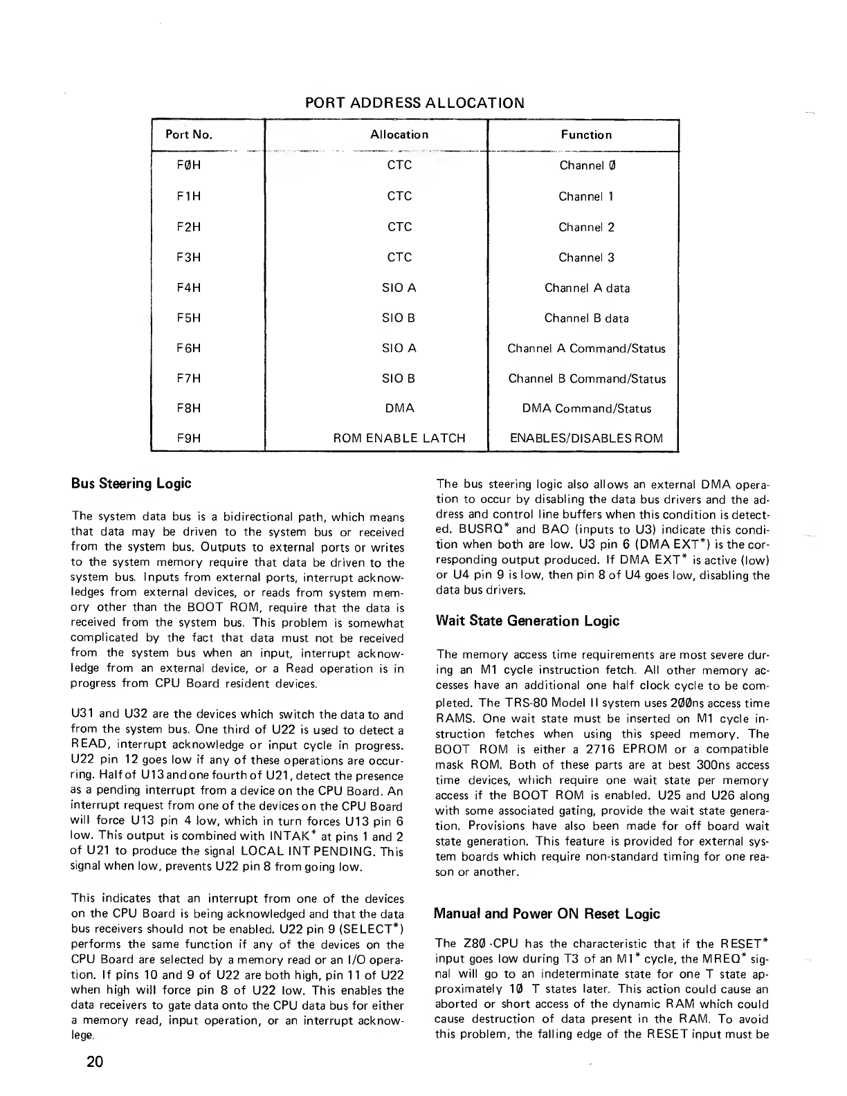
PORT ADDRESS ALLOCATION
Port No. Allocation Function
F0H CTC Channel
F1H CTC Channel 1
F2H CTC Channel 2
F3H CTC Channel 3
F4H SIO AChannel Adata
F5H SIO BChannel Bdata
F6H SIO AChannel ACommand/Status
F7H SIOB Channel BCommand/Status
F8H DMA DMA Command/Status
F9H ROM ENABLE LATCH ENABLES/DISABLES ROM
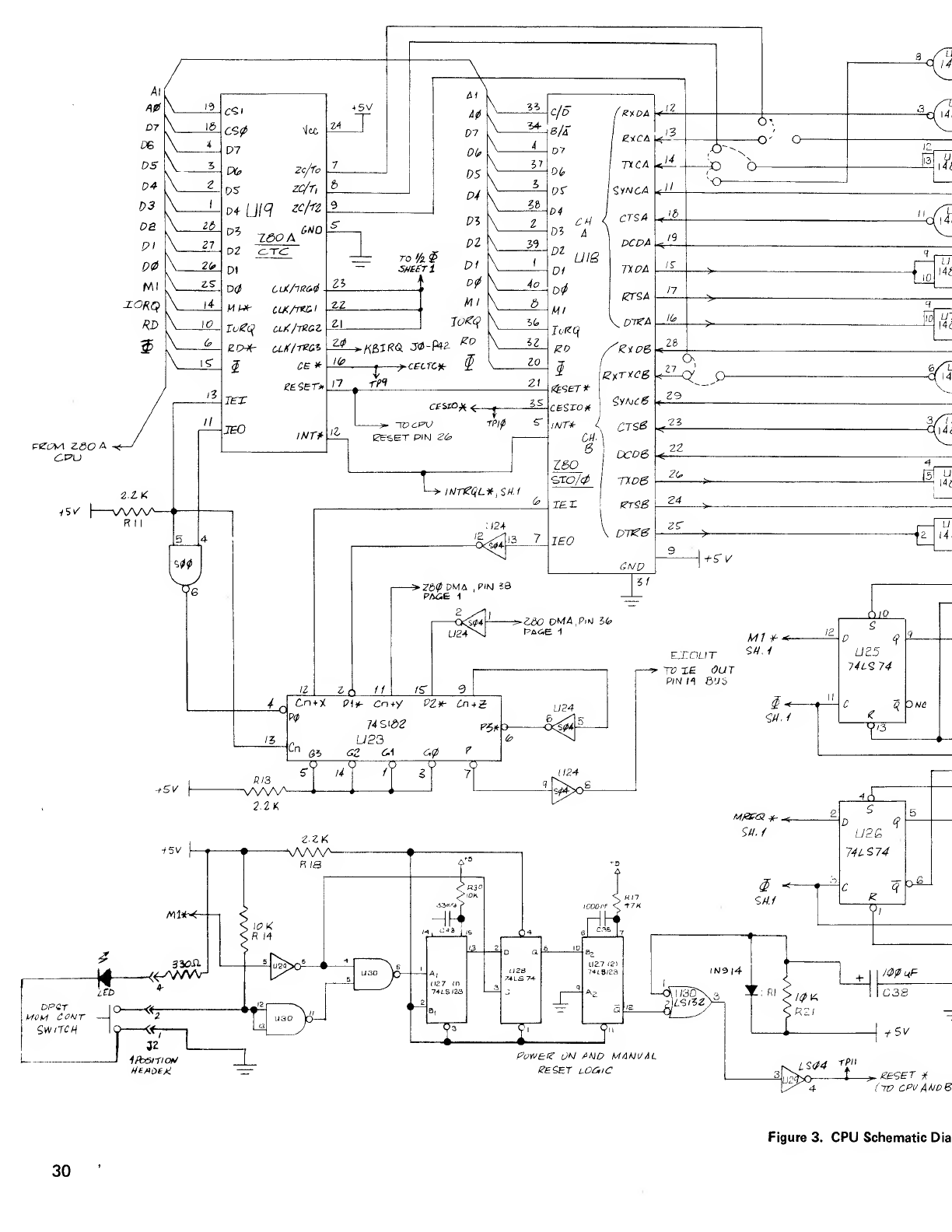
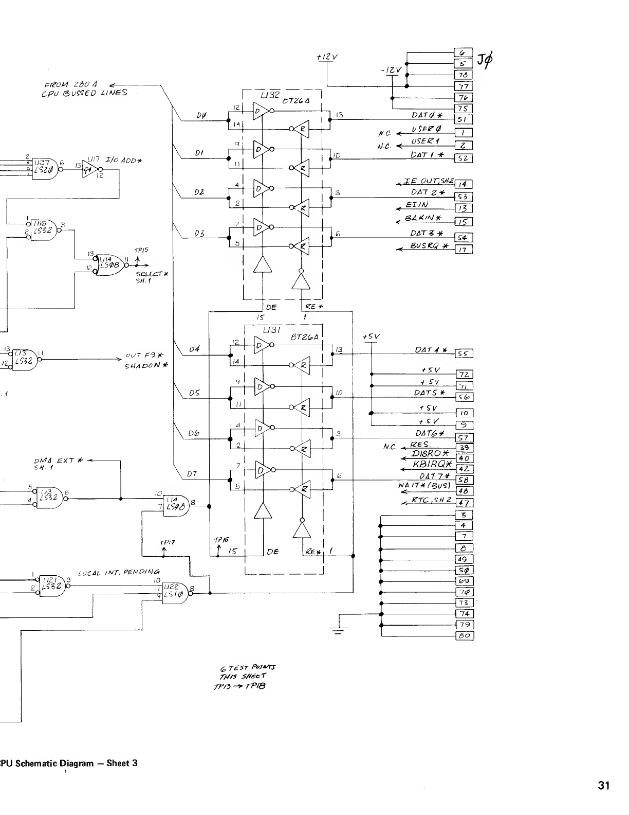
Bus Steering Logic
The system data bus is abidirectional path, which means
that data may be driven to the system bus or received
from the system bus. Outputs to external ports or writes
to the system memory require that data be driven to the
system bus. Inputs from external ports, interrupt acknow-
ledges from external devices, or reads from system mem-
ory other than the BOOT ROM, require that the data is
received from the system bus. This problem is somewhat
complicated by the fact that data must not be received
from the system bus when an input, interrupt acknow-
ledge from an external device, or aRead operation is in
progress from CPU Board resident devices.
U31 and U32 are the devices which switch the data to and
from the system bus. One third of U22 is used to detect a
READ, interrupt acknowledge or input cycle in progress.
U22 pin 12 goes low if any of these operations are occur-
ring. Half of U13 and one fourth of U21 ,detect the presence
as apending interrupt from adevice on the CPU Board. An
interrupt request from one of the devices on the CPU Board
will force U13 pin 4low, which in turn forces U13 pin 6
low. This output is combined with INTAK* at pins 1and 2
of U21 to produce the signal LOCAL INT PENDING. This
signal when low, prevents U22 pin 8from going low.
This indicates that an interrupt from one of the devices
on the CPU Board is being acknowledged and that the data
bus receivers should not be enabled. U22 pin 9(SELECT*)
performs the same function if any of the devices on the
CPU Board are selected by amemory read or an I/O opera-
tion. If pins 10 and 9of U22 are both high, pin 1 1 of U22
when high will force pin 8of U22 low. This enables the
data receivers to gate data onto the CPU data bus for either
amemory read, input operation, or an interrupt acknow-
lege.
The bus steering logic also allows an external DMA opera-
tion to occur by disabling the data bus drivers and the ad-
dress and control line buffers when this condition is detect-
ed. BUSRQ* and BAO (inputs to U3) indicate this condi-
tion when both are low. U3 pin 6(DMA EXT*) is the cor-
responding output produced. If DMA EXT* is active (low)
or U4 pin 9is low, then pin 8of U4 goes low, disabling the
data bus drivers.
Wait State Generation Logic
The memory access time requirements are most severe dur-
ing an M1 cycle instruction fetch. All other memory ac-
cesses have an additional one half clock cycle to be com-
pleted. The TRS-80 Model II system uses 200ns access time
RAMS. One wait state must be inserted on M1 cycle in-
struction fetches when using this speed memory. The
BOOT ROM is either a2716 EPROM or acompatible
mask ROM. Both of these parts are at best 300ns access
time devices, which require one wait state per memory
access if the BOOT ROM is enabled. U25 and U26 along
with some associated gating, provide the wait state genera-
tion. Provisions have also been made for off board wait
state generation. This feature is provided for external sys-
tem boards which require non-standard timing for one rea-
son or another.
Manual and Power ON Reset Logic
The Z80-CPU has the characteristic that if the RESET*
input goes low during T3 of an Ml* cycle, the MREQ* sig-
nal will go to an indeterminate state for one Tstate ap-
proximately 10 Tstates later. This action could cause an
aborted or short access of the dynamic RAM which could
cause destruction of data present in the RAM. To avoid
this problem, the falling edge of the RESET input must be
20
synchronized with the falling edge of M1 *. One half of U28
and U27 perform this sychronization as well as provide a
one-shot to limit the duration of the CPU RESET pulse.
The one-shot duration is approximately 70ns per switch de-
pression, and is required to avoid suspending CPU refresh of
dynamic memory for aperiod long enough to destroy
RAM contents. Without the one-shot this could occur if
the reset switch were held closed for along period. The
connector J2 connects the reset switch to this logic and also
provides the current limited +5 volts for the "Power-On"
indicator on the front panel.
System Clock Generation Logic
The heart of the clock generation logic is an 8MHz crystal
oscillator formed by Y1 ,C21 ,R23, R24, and three 74LS74
Flip-Flops (page 1of the CPU schematics). The output of
U29, pin 8should be an 8MHz square wave. The 8MHz
signal is divided down by one half of U28 and U2 to pro-
duce the 4MHz, 2MHz, and 1MHz clocks needed by the
system. The 8MHz signal is buffered by one fourth of U30
and fed directly to pin 46 of the system bus. This clock is
utilized by the write compensation circuitry of the FDC
Board. Ajumper option is provided to select either a4MHz
or 2MHz main system clock for the Z80 family parts. This
output is divided by 2, to provide the clock inputs for the
Z80-CTC when operating in the counter mode. Normal
system operation requires that the main system clock run
at 4MHz and should be used at 2MHz only under unusual
circumstances. The output of U28pin 9(main system clock)
is conditioned by the clock buffer circuitry implemented
with Q1, C3, R2, R3, R4, and a74S04 inverter. The clock
buffer circuitry insures fast rise and fall times and close to
5volts peak to peak amplitude transitions. These clock
characteristics are important to the Z80A family of com-
ponents when operating at maximum frequency (4 MHz).
terrupting by pulling low on its IEO line. The next device in
the chain, sensing alow at the IEI input, will pass this pri-
ority signal on to the next device by pulling low on its IEO
line.
This priority scheme works fine as long as no more than
four Z80 family devices are connected to the chain. If more
than four devices are used, the delays through each MOS
part get excessive and not enough time will be allowed to
resolve interrupt contention. The Model II system currently
uses four Z80 family parts in the daisy chain. To allow for
expansion of the system, acarry look ahead scheme was
employed using U23 (74S182) and four 74S04 inverters.
This scheme anticipates IEO low condition at any of the
three devices on the CPU Board and generates alook-ahead
signal to the propagate output (U23 pin 7). This signal is in-
verted and fed to IEO (pin 14) of the system bus. This sig-
nal when low, prevents downstream devices from generat-
ing an interrupt and results in a25ns maximum ripple time
for any IEO to propagate out for the devices on the CPU
Board. This allows up to four more family devices (eight
total) to be used in the system without additional logic.
El ABuffers
The logic internal to the CPU Board (SIO inputs and out-
puts in this discussion) operate with TTL logic levels (3.5V
or more =Logic 1, and 0.8V or less =Logic 0). The logic
convention used for interfacing two RS-232-C devices is
EIA levels (-3V or less =logic 1, +3V or more =Logic 0).
The logic levels must therefore be converted from one con-
vention to the other when interfacing to an external device.
U10, U9, and U8 provide the EIA to TTL conversion
while U7 and U6 provide the TTL to EIA conversion.
Interrupt Priority Logic
The Z80 interrupt structure allows up to four Z80 family
parts to be connected in adaisy chain fashion without any
additional logic. Priority is set by the location of the device
in adaisy chain configuration with each device tied to the
INTRQL* line. The diagram below illustrates the relative
priority of the devices on the CPU Board.
CTC SIO
INTRQL" ^-
DMA
IEO
-> IEO TO
THE BUS
The IEI of the CTC is tied to +5 volts to indicate that it
has the highest priority. The second highest priority device
is the SIO with its IEI tied to the IEO of the CTC. The IEO
of the SIO is tied to the IEI of the DMA. The IEO of the
DMA is routed to the system bus where it is tied to the IEI
of the next physical board in the system (FDC Board).
The priority string insures that adevice with higher priority
will be serviced before alower priority device when two or
more INTRQL* requests occur at the same time. For ade-
vice to have priority, its IEI must be high. When adevice
needs service, it will prevent down stream devices from in-
21
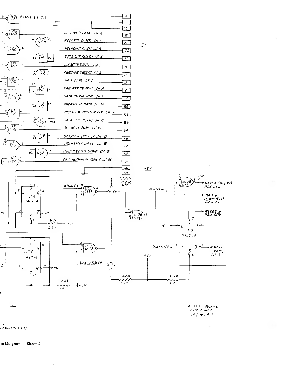
CONNECTOR J1 SIGNAL DESCRIPTIONS
PIN SIGNAL DESCRIPTION
1Power Ground
2Not Connected
3Transmit Data Channel A
4Transmit S.E.T.
5Received Data Channel A
6Not Connected
7Request to Send Channel A
8Receiver Clock Channel A
9Clear to Send Channel A
10 Not Connected
1
1
Data Set Ready Channel A
12 Not Connected
13 Power Ground
14 Data Terminal Ready Channel A
15 Carrier Detect Channel A
16-21 Not Connected
22 Transmit Clock Channel A
23 Not Connected
24 Not Connected
25 Not Connected
26 Power Ground
27 Not Connected
28 Transmit Data Channel B
29 Not Connected
30 Received Data Channel B
31 Not Connected
32 Request to Send Channel B
33 Receiver/Transmitter Clock Channel B
34 Clear to Send Channel B
35 Data Set Ready Channel B
36 Not Connected
37 Not Connected
38 Power Ground
39 Data Terminal Ready Channel B
40 Carrier Detect Channel B
22
s>
010
^iII
63 -CZJ-
L1Ji11
fer
ll"?P!
fill
-&
IJ-r~rif 2
m
W8:-tea --' z+o
i{2Z>«-*3
%6|H
£
s5^
m^i it-it in ii mi i«yjip
•tttl» PJ
~">L_
M' frkm sz3
nl jfe 4^\
v?B *sHO#ZJi
Fl
Jail |-
o
o
a
E
o
o
(0
o
CQ
+^
'5
o
a
a)
D
Q.
o
>
>-
CO
DC
x
23
a
3
o
re
O
O
D
Q.
D
Q.
o
91
>•
n
0)
3
24 'J
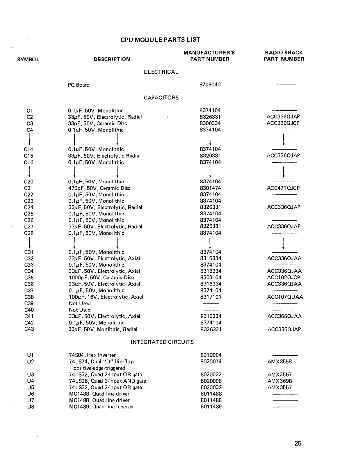
CPU MODULE PARTS LIST
SYMBOL DESCRIPTION
MANUFACTURER'S
PART NUMBER RADIO SHACK
PART NUMBER
ELECTRICAL
PC Board 8709040
CAPACITORS
C1
C2
C3
C4
C14
C15
C16
C20
C21
C22
C23
C24
C25
C26
C27
C28
C31
C32
C33
C34
C35
C36
C37
C38
C39
C40
C41
C42
C43
0.1/uF, 50V, Monolithic
33;uF, 50V, Electrolytic, Radial
33pF, 50V, Ceramic Disc
0.1juF, 50V, Monolithic
0.1;iiF, 50V, Monolithic
33/iF, 50V, Electrolytic Radial
0.1/iF, 50V, Monolithic
0.1juF, 50V, Monolithic
470pF, 50V, Ceramic Disc
O.ljuF, 50V, Monolithic
0.1/nF- 50V, Monolithic
33juF, 50V, Electrolytic, Radial
0.1/zF, 50V, Monolithic
0.1/xF, 50V, Monolithic
33/xF, 50V, Electrolytic, Radial
0.1/zF, 50V, Monolithic
0.1juF, 50V, Monolithic
33juF, 50V, Electrolytic, Axial
0.1//F, 50V, Monolithic
33/zF, 50V, Electrolytic, Axial
1000pF, 50V, Ceramic Disc
33;uF, 50V, Electrolytic, Axial
O.ljuF, 50V, Monolithic
100juF, 16V, Electrolytic, Axial
Not Used
Not Used
33jUF, 50V, Electrolytic, Axial
0.1#F, 50V, Monolithic
33/iF, 50V, Monlithic, Radial
8374104
8326331
8300334
8374104
8374104
8326331
8374104
8374104
8301474
8374104
8374104
8326331
8374104
8374104
8326331
8374104
8374104
8316334
8374104
8316334
8303104
8316334
8374104
8317101
8316334
8374104
8326331
ACC336QJAP
ACC330QJCP
ACC336QJAP
ACC471QJCP
ACC336QJAP
ACC336QJAP
ACC336QJAA
ACC336QJAA
ACC102QJCP
ACC336QJAA
ACC107QDAA
ACC366QJAA
ACC336QJAP
INTEGRATED CIRCUITS
U1
U2
U3
U4
U5
U6
U7
U8
74S04,Hex inverter
74LS74,Dual "D" flip-flop
positive-edge-triggered
74LS32, Quad 2-input OR gate
74LS08, Quad 2-input AND gate
74LS32, Quad 2-input OR gate
MC1488, Quad line driver
MC1488, Quad line driver
MC1489, Quad line receiver
8010004
8020074
8020032
8020008
8020032
8011488
8011488
8011489
AMX3558
AMX3557
AMX3698
AMX3557
25
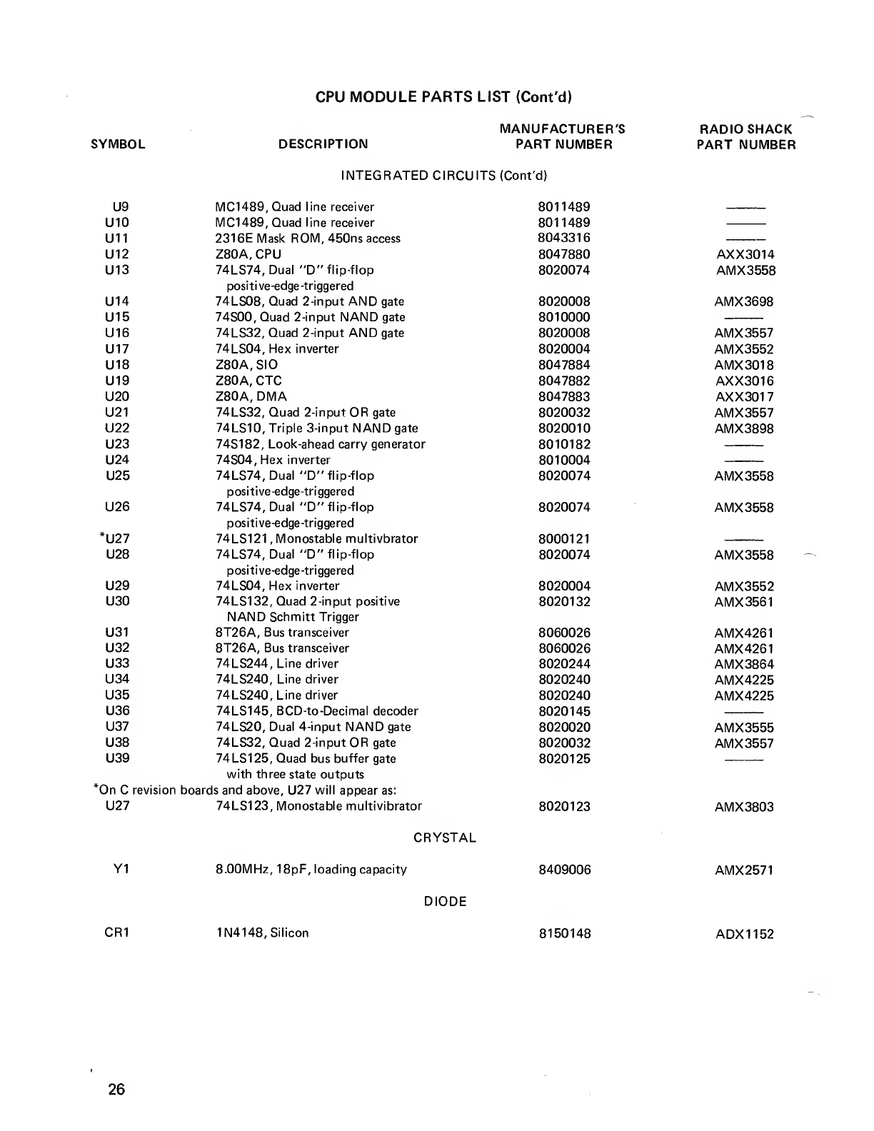
CPU MODULE PARTS LIST (Cont'd)
SYMBOL DESCRIPTION
MANUFACTURER'S
PART NUMBER RADIO SHACK
PART NUMBER
INTEGRATED CIRCUITS (Cont'd)
U9 MC1489, Quad line receiver
U10 MC1489, Quad line receiver
U11 231 6E Mask ROM, 450ns access
U12 Z80A, CPU
U13 74LS74,Dual "D" flip-flop
positive -edge-triggered
U14 74LS08, Quad 2-input AND gate
U15 74S00, Quad 2-input NAND gate
U16 74LS32, Quad 2-input AND gate
U17 74LS04, Hex inverter
U18 Z80A,SIO
U19 Z80A, CTC
U20 Z80A, DMA
U21 74LS32, Quad 2-input OR gate
U22 74LS10, Triple 3-input NAND gate
U23 74S182, Look-ahead carry generator
U24 74S04, Hex inverter
U25 74LS74,Dual "D" flip-flop
positive -edge-triggered
U26 74LS74,Dual "D" flip-flop
positive-edge-triggered
*U27 74LS121 ,Monostable multivbrator
U28 74LS74,Dual "D" flip-flop
positive-edge-triggered
U29 74LS04, Hex inverter
U30 74LS132, Quad 2-input positive
NAND Schmitt Trigger
U31 8T26A, Bus transceiver
U32 8T26A, Bus transceiver
U33 74LS244, Line driver
U34 74LS240, Line driver
U35 74LS240, Line driver
U36 74LS145, BCD-to-Decimal decoder
U37 74LS20, Dual 4-input NAND gate
U38 74LS32, Quad 2-input OR gate
U39 74LS125, Quad bus buffer gate
with three state outputs
On Crevision boards and above, U27 will appear as:
U27 74LS123, Monostable multivibrator
8011489
8011489
8043316
8047880
8020074
8020008
8010000
8020008
8020004
8047884
8047882
8047883
8020032
8020010
8010182
8010004
8020074
8020074
8000121
8020074
8020004
8020132
8060026
8060026
8020244
8020240
8020240
8020145
8020020
8020032
8020125
8020123
AXX3014
AMX3558
AMX3698
AMX3557
AMX3552
AMX3018
AXX3016
AXX301
7
AMX3557
AMX3898
AMX3558
AMX3558
AMX3558
AMX3552
AMX3561
AMX4261
AMX4261
AMX3864
AMX4225
AMX4225
AMX3555
AMX3557
AMX3803
CRYSTAL
Y1 8.00MHz, 18pF, loading capacity 8409006 AMX2571
DIODE
CR1 1N4148, Silicon 8150148 ADX1152
26
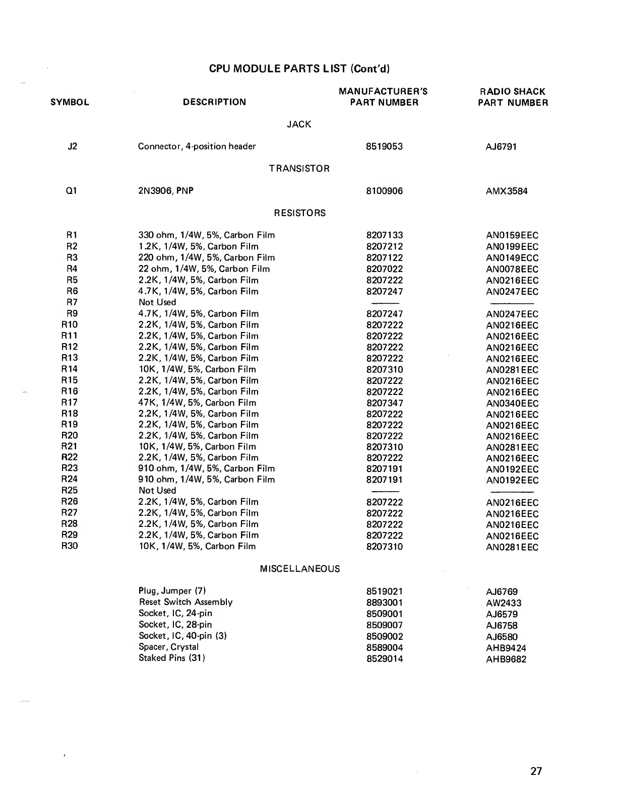
CPU MODULE PARTS LIST (Cont'd)
SYMBOL DESCRIPTION
MANUFACTURER'S
PART NUMBER RADIO SHACK
PART NUMBER
JACK
J2 Connector, 4-position header 8519053 AJ6791
TRANSISTOR
Q1 2N3906, PNP 8100906 AMX3584
RESISTORS
R1
R2
R3
R4
R5
R6
R7
R9
R10
R11
R12
R13
R14
R15
R16
R17
R18
R19
R20
R21
R22
R23
R24
R25
R26
R27
R28
R29
R30
330 ohm, 1/4W, 5%, Carbon Film
1.2K, 1/4W, 5%, Carbon Film
220 ohm, 1/4W, 5%, Carbon Film
22 ohm, 1/4W, 5%, Carbon Film
2.2K, 1/4W, 5%, Carbon Film
4.7K, 1/4W, 5%, Carbon Film
Not Used
4.7K, 1/4W, 5%, Carbon Film
2.2K, 1/4W, 5%, Carbon Film
2.2K, 1/4W, 5%, Carbon Film
2.2K, 1/4W, 5%, Carbon Film
2.2K, 1/4W, 5%, Carbon Film
10K, 1/4W, 5%, Carbon Film
2.2K, 1/4W, 5%, Carbon Film
2.2K, 1/4W, 5%, Carbon Film
47K, 1/4W, 5%, Carbon Film
2.2K, 1/4W, 5%, Carbon Film
2.2K, 1/4W, 5%, Carbon Film
2.2K, 1/4W, 5%, Carbon Film
10K, 1/4W, 5%, Carbon Film
2.2K, 1/4W, 5%, Carbon Film
910 ohm, 1/4W, 5%, Carbon Film
910 ohm, 1/4W, 5%, Carbon Film
Not Used
2.2K, 1/4W, 5%, Carbon Film
2.2K, 1/4W, 5%, Carbon Film
2.2K, 1/4W, 5%, Carbon Film
2.2K, 1/4W, 5%, Carbon Film
10K, 1/4W, 5%, Carbon Film
8207133
8207212
8207122
8207022
8207222
8207247
8207247
8207222
8207222
8207222
8207222
8207310
8207222
8207222
8207347
8207222
8207222
8207222
8207310
8207222
8207191
8207191
8207222
8207222
8207222
8207222
8207310
AN0159EEC
AN0199EEC
AN0149ECC
AN0078EEC
AN0216EEC
AN0247EEC
AN0247EEC
AN0216EEC
AN0216EEC
AN0216EEC
AN0216EEC
AN0281EEC
AN0216EEC
AN0216EEC
AN0340EEC
AN0216EEC
AN0216EEC
AN0216EEC
AN0281EEC
AN0216EEC
AN0192EEC
AN0192EEC
AN0216EEC
AN0216EEC
AN0216EEC
AN0216EEC
AN0281EEC
MISCELLANEOUS
Plug, Jumper (7)
Reset Switch Assembly
Socket, IC, 24-pin
Socket, IC, 28-pin
Socket, IC, 40-pin (3)
Spacer, Crystal
Staked Pins (31
)
8519021
8893001
8509001
8509007
8509002
8589004
8529014
AJ6769
AW2433
AJ6579
AJ6758
AJ6580
AHB9424
AHB9682
27

iSV
2<3
UIZ
zeoA
WAIT* -t-
I4ALT ¥-*
(ews.)
Z4 WAIT*
HALT*
6u$izq *
us
Ai4
Ali
Alt
All
AW
A°>
At
AT
A6>
45
A4
A2
Al
**
Dl
D(s
PS
D4
OS
DZ
PI
40
39
30
36
3?
S4
J5
5c?
Ii_
INT*
gFSH*
IO&Q*
fZD*
HZ*
\
V
V
\
V
V
IS
14
Z6 /
27
19
Zl
zz
z^ BusaK-*-
lo
11
11
24
l°>
4c
\
\
\
UZD
V
z&
l°i
Jk 1
3*
34
$£_
zo>
\0
\t
\
20
17
-Z60, CTC+S.I0,
-»- int^l.*-, SMEET ;
-> IMTI%? */BUSl
clock l£?<z-icz
33 pP
\|C3
I.ZK
RE
220-Q Z2i2
WW «-AAAA-
R3
2rJ590<&
aiPNP
5USAK y-
/'3
in
no
A9
A3
AT
lib
AS
A4
AS
AZ
Al
A0
Dl
Db
DS
04
PS
DZ
Dl
D0
M4 *
lozq*
Maaq *
tzo*
Niz *
$>*
en*
zb>oa
DK/IA
INT*
lex
IE0
C£*
&A0*
busizq*
Vic
&ND
37
Id
hU>
zs
lie
12
IS
io
-isv
\- i9
,\ ZZ
?.*>
\I
\z
\5
\4
s
Vb
\7
\&
\17
\\(,
\Iff
\14
\13
\II
\10
\<5
M<f
A?
AS
A7
Ai
AS
A*
Al
At
A'
At
Dl
Db
DS
94
DS
DZ
Dl
Vcc
Vpp
Ce*
OB*
till
£HD.
24
Z\
h<p
r?3
•A
zd
SAX. I
KOU$C£*
>1?EAD *
V
1?+
-* ZBo,CTC +SIOiP/*J 12, ZA\"P iNTZlfL*-
-y 74-ildt, Cn-hV PinI ^HEBTZ
^to sjz4, piisneerz.
+5V
i-Sv
-^TPxe
AH
All
\AI±
\AI±
A'S
,IZD
\ZFC,
\WI?
IZE
£LL bUSAK
$2.2K
H+SV
S&4
fP5
J-
2/A MHZ CLOC£
muz
-^s,—4/8 MHZ
O1PReCOfAPoPTloU
U23„
^-<p
iS^4-
as ^4-
-W."
—
R23
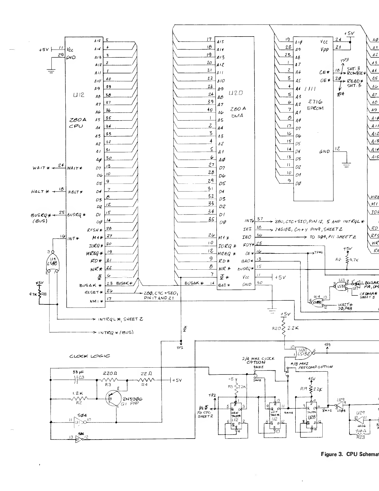
Figure 3. CPU Schemal
chematic Diagram —Sheet 1
29
V
V
19
lb
FdOVA Z.SO A
CPU
g.£K
yS/ I^AAAA-
RII
+5/
Ml*-<-
ice
330H
IDPCT
Switch
32
1fb5iTicW
iiL
CTC
WO
INT*
*5V
TA
-^cecrcpr
3+
5?
39
4o
56
52
lo
rfi 2\
EesET PIN Z&>
iS
IHT£QL*,SU.t
IZ
15
c/o fR*DA
B/S \
'gxcA
07
DC ™A
pr KywcA
04 CACTSA
Dl A\PCPA
DZ uie
Dl TtDA
o4 ersA
Ml VDm*
luizq
£0 /Z^OS.
3'
mg%TXCS
&<;eT*
CZZTO* <Zim6
CCD6
STO/<Z)
.12
.13
n
it*
28
o-
o- MJt
*o
27
Z9
-jT 14
+S"/
//
-^760 DMA ,P'NJ 3S
PA£6 1
pfi^e -l
Cn +X
Cn
74SI&2
U23
Gi GZ (5.1
it
~TT
1124
EX-OUT
TO I£ OUT
PIN 11 8'JS
M1 **r-
c.H.1
<SlQ
q
UE5
74CS 74
Hqohc
LIZ7 12)
74t8l23 IN9I4
POWEZ ON />AJO MANUAL
ZES.ET LOCiC
3L.RI
luF
IC3S
-tSv
IS<?4 T£"
Xo 1—^upset #
A- (to cpv A^c6
Figure 3. CPU Schematic Dia
30
ftAIT* flVCPo)
P24 CPU
(FiZoM SOS)
70, P43
RIB
4T£st fbi/urs
/AtJoS^s.pa 1)
:ic Diagram -Sheet 2

BUSSED DATA UKJES
-*
peoM Z&O A<Zf\J
Select* •*
Figure 3. CPU Schema
FIZOM ZdO A<=
CpO SUSSED LlhJBS
U37\£ 13
un x/o AoDi
our P3X-
St-IADON *
St/. /
4ZS?2)o- I0>
t>C
Di
D2.
Di
04
DZ
D(a
D7
114
J—
+iZv
Y~ U32
f^> 612CA
I•-
$r
f^r -4i
l
-
LOCAL INT. PENPINt*
TizT\3 io
dizp nL'HC
-IZV -un
-Q3
-T7*l
zf
DATtf'*\1S
5/
«.c < useei CO
-fsF|
Pat /-*-
El/fJ
S3
PI
P/iTg -*
gl^Sgt? *- -t^:
-DE]
•/SV
O/dTV *
/5^
Vs"y
P/3T5~*
•^S"/
/SV
DAT6*
~{5D
-cei
~9
*.C. -_£!£ 57
-|~ie~
14Z.
P477* \S3
NA IT* {BUS) ,
<[46
-m
4^n
-R5
-tia
-IfoQ
-[7£]
-|<9o
PU Schematic Diagram —Sheet 3
tp/3 -* rPie
31

SECTION IV
FLOPPY DISK CONTROLLER
33

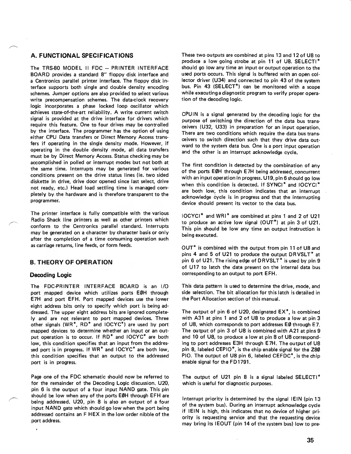
A. FUNCTIONAL SPECIFICATIONS
The TRS-80 MODEL II FDC -PRINTER INTERFACE
BOARD provides astandard 8" floppy disk interface and
aCentronics parallel printer interface. The floppy disk in-
terface supports both single and double density encoding
schemes. Jumper options are also provided to select various
write precompensation schemes. The data-clock recovery
logic incorporates aphase locked loop oscillator which
achieves state-of-the-art reliability. Awrite current switch
signal is provided at the drive interface for drivers which
require this feature. One to four drives may be controlled
by the interface. The programmer has the option of using
either CPU Data transfers or Direct Memory Access trans-
fers if operating in the single density mode. However, if
operating in the double density mode, all data transfers
must be by Direct Memory Access. Status checking may be
accomplished in polled or interrupt modes but not both at
the same time. Interrupts may be generated for various
conditions present on the drive status lines (ie. two sided
diskette in drive, drive door opened since last select, drive
not ready, etc.) Head load settling time is managed com-
pletely by the hardware and is therefore transparent to the
programmer.
The printer interface is fully compatible with the various
Radio Shack line printers as well as other printers which
conform to the Centronics parallel standard. Interrupts
may be generated on acharacter by character basis or only
after the completion of atime consuming operation such
as carriage returns, line feeds, or form feeds.
B. THEORY OF OPERATION
Decoding Logic
The FDC-PR INTER INTERFACE BOARD is an I/O
port mapped device which utilizes ports E0H through
E7H and port EFH. Port mapped devices use the lower
eight address bits only to specify which port is being ad-
dressed. The upper eight address bits are ignored complete-
ly and are not relevant to port mapped devices. Three
other signals (WR*, RD* and IOCYC*) are used by port
mapped devices to determine whether an input or an out-
put operation is to occur. If RD* and IOCYC* are both
low, this condition specifies that an input from the addres-
sed port is in progress. If WR* and IOCYC* are both low,
this condition specifies that an output to the addressed
port is in progress.
These two outputs are combined at pins 13 and 12 of U8 to
produce alow going strobe at pin 11 of U8. SELECTI*
should go low any time an input or output operation to the
used ports occurs. This signal is buffered with an open col-
lector driver (U34) and connected to pin 43 of the system
bus. Pin 43 (SELECT*) can be monitored with ascope
while executing adiagnostic program to verify proper opera-
tion of the decoding logic.
CPUIN is asignal generated by the decoding logic for the
purpose of switching the direction of the data bus trans-
ceivers (U32, U33) in preparation for an input operation.
There are two conditions which require the data bus trans-
ceivers to switch direction such that they drive data out-
ward to the system data bus. One is aport input operation
and the other is an interrupt acknowledge cycle.
The first condition is detected by the combination of any
of the ports E0H through E7H being addressed, concurrent
with an input operation in progress. U19, pin 6should go low
when this condition is detected. If SYNCI* and IOCYCI*
are both low, this condition indicates that an interrupt
acknowledge cycle is in progress and that the interrupting
device should present its vector to the data bus.
IOCYCI* and WRI* are combined at pins 1and 2of U21
to produce an active low signal (OUT*) at pin 3of U21.
This pin should be low any time an output instruction is
being executed.
OUT* is combined with the output from pin 11 of U8 and
pins 4and 5 of U21 to produce the output DRVSLT* at
pin 6of U21 .The rising edge of DRVSLT* is used by pin 9
of U17 to latch the data present on the internal data bus
corresponding to an output to port EFH.
This data pattern is used to determine the drive, mode, and
side selection. The bit allocation for this latch is detailed in
the Port Allocation section of this manual.
The output of pin 6of U20, designated EX*, is combined
with A31 at pins 1and 2of U8 to produce alow at pin 3
of U8, which corresponds to port addresses E0 through E7.
The output of pin 3of U8 is combined with A21 at pins 9
and 10 of U8, to produce alow at pin 8of U8 correspond-
ing to port addresses E3H through E7H. The output of U8
pin 8, labeled CEPIO*, is the chip enable signal for the Z80
PIO. The output of U8 pin 6, labeled CEFDC*, is the chip
enable signal for the FD 1791
.
Page one of the FDC schematic should now be referred to
for the remainder of the Decoding Logic discussion. U20,
pin 6is the output of afour input NAND gate. This pin
should be low when any of the ports E0H through EFH are
being addressed. U20, pin 8is also an output of afour
input NAND gate which should go low when the port being
addressed contains an FHEX in the low order nibble of the
port address.
The output of U21 pin 8is asignal labeled SELECTI*
which is useful for diagnostic purposes.
Interrupt priority is determined by the signal IEIN (pin 13
of the system bus). During an interrupt acknowledge cycle
if IEIN is high, this indicates that no device of higher pri-
ority is requesting service and that the requesting device
may bring its IEOUT (pin 14 of the system bus) low to pre-
35
vent devices of lower priority from receiving service. A
high on pin 1of U13 indicates that an interrupt acknow-
ledge cycle is in progress. Ahigh on pin 2of U13 indicates
that no higher priority device is requesting service. A
high on pin 13, U13 indicates that adevice on this board
is requesting service. If all of these conditions are true, pin
12 of U13 should go low. This output is combined with
the output from pin 6of U19 and pins 4 and 5of U10. If
either pin 4or pin 5of U10 goes low, then pin 6of U10
will also go low. U18 inverts the signal from pin 6of U10
and causes pin 8of U18 to go high (CPUIN). Ahigh on
CPU IN forces the data bus transceivers (U32, U33) to dis-
able its receivers and enable its drivers to gate data onto
the system bus. This allows the PIO to transfer its interrupt
vector to the CPU.
Bus Interface Logic
Good design practice dictates that most signals to and
from the system bus must be buffered so that only one
TTL Load is presented to each signal line. Page one of
the FDC schematic shows the logic required to implement
this. U35 is an octal inverting buffer for the address lines.
U36 is an octal non-inverting buffer for the Z80 control
lines. Note that the enables for both these parts are tied
low, allowing these signals to be gated onto the board at
all times. U34 is an open collector buffer used to drive the
board outputs which may be driven by other boards in the
system. It also buffers the system clock (2 or 4MHz) to the
board. U14 is V? of a"D" Flip-Flop configured as adivide
by two counter. This divider should be jumpered Ato Bif
the system clock is 4MHz (normal connection), or Bto C
if a2MHz system clock is used.
There is abasic problem with using aZ80-PIO with the
FDI791. The PIO has anon-inverting data bus while the
FDI791 utilizes an inverting data bus. Thus, one extra stage
of inversion is required for the PIO. U23, U11, and U12
accomplish this extra inversion.
Z80 -PIO Interface Logic
The Z80 parallel I/O (PIO) interface controller is ageneral
purpose, programmable, two port device which provides
TTL compatible interfacing between peripheral devices
and the Z80 —CPU. Any of the following modes can be
selected for either port.
BYTE OUTPUT
BYTE INPUT
BYTE BIDIRECTIONAL (PORT AONLY)
BYTE OR CONTROL MODE
In addition the PIO provides aclean and minimal logic
method for generating mode 2interrupts to the Z80 CPU.
Port Ais used in the control mode which allows the eight
I/O lines (A0 through A7) to be configured as either inputs
or outputs. An 8-bit mask register and a2-bit mask control
register allow interrupts to be generated dependent upon
the logic states of the I/O lines. Port Ais primarily used
for status checking and generating interrupts. One I/O line
is configured as an output and provides the prime signal
for the printer interface. The bit allocations for this port
are detailed in the Port Allocations section of this manual.
Port Bis used in the output mode for the purpose of out-
putting characters to the printer. The outputs of port B
(B0 through B7) are isolated from the printer with an octal
noninverting buffer (U24). Note that the enables are tied
low, gating whatever data is presented to the inputs of U24
directly to its outputs. The cable to the printer allows this
parallel data to be routed to the printer. Pin 21 of the PIO,
labeled BRDY, produces ahigh going pulse which indi-
cates that valid data is present on the port Boutputs. The
rising edge of this signal provides atrigger for pin 3of U37.
U37 is aone-shot which produces a1.5/xs low going pulse
when triggered. The rising edge of the 1.5jUs strobe is used
by the printer to latch the 8bits of information present on
the output of U24. The BRDY signal stays active until the
rising edge of PACK* which indicates that the printer has
accepted the data. This rising edge may also generate an in-
terrupt if the interrupt enable Flip-Flop is set and the PIO
has the highest priority. This provides aclean and efficient
method for determining when the printer can accept anew
character without using status checking loops.
The PIO interfaces directly to the system bus with amini-
mum of external components. D0 through D7 form abi-
directional data path to the system bus. A0I and A1I deter-
mine which port is addressed and whether the operation is
intended for the command register or the data register. If
CEPIO*, IORQI* and RDI* are all low, this indicates an
input operation is in progress. If CEPIO* and IORQI* are
low with RDI* high, this indicates an output operation is
in progress. If IEIN is high, and INTRQI*, SYNCI*,
IORQI* and IEO are low, an interrupt acknowledge cycle
for the PIO is in progress. If SYNCI* is high and RESETI*
is low, alow is generated on pin 3of U10. If this sequence
occurs without RDI* or IORQI* low, the PIO logic enters a
reset state. For amore detailed discussion of the PIO opera-
tion, consult the ZILOG Z80 -PIO Technical Manual.
FD1791 -Floppy Disk Controller IC
The FD1791 is an MOS LSI device which performs the
functions of aFloppy Disk format/controller in a single
chip implementation. The FD1791 contains all the features
of its predecessor, the FD1771, plus the added features
necessary to read, write, and format adouble density disk-
ette. These include address mask detection, FM and MFM
encode and decode logic, window extension, and write
precompensation.
36

FD1791 Organization
The Floppy Disk Formatter block diagram is illustrated in
Figure 1. The primary sections include the parallel Proces-
sor Interface and the Floppy Disk Interface.
Data Shift Register —This 8-bit register assembles serial
data from the Read Data input (RAW READ) during
Read operations and transfers serial data to the Write Data
output during Write operations.
Data Register -This 8-bit register is used as a holding
register during Disk Read and Write operations. In Disk
Read operations, the assembled data byte is transferred in
parallel to the Data Register from the Data Shift Register.
In Disk Write operations, information is transferred in
parallel from the Data Register to the Data Shift Register.
When executing the Seek command the Data Register
holds the address of the desired Track position. This Regis-
ter can be loaded from the DAL and gated onto the DAL
under processor control.
Track Register —This 8-bit register holds the track num-
ber of the current Read/Write head position. It is incre-
mented by one every time the head is stepped in (towards
track 76) and decremented by one when the head is stepped
out (towards track ). The contents of the register are
compared with the recorded track number in the ID field
during disk Read, Write, and Verify operations. The Track
Register can be loaded from or transferred to the DAL .
This Register should not be loaded when the FDC is busy.
Sector Register (SR) -This 8-bit register holds the add-
ress of the desired sector position. The contents of the
register are compared with the recorded sector number in
the ID field during disk Read or Write operations. The
Sector Register contents can be loaded from or transfer-
red to the DAL. This register should not be loaded when
the FDC is busy.
Command Register (CR) -This 8-bit register holds the
command presently being executed. This register should
not be loaded when the FDC is busy unless the execu-
tion of the current command is to be overridden. This
latter action results in aninte rrupt. The command registe r
can be loaded from the DAL ,but not read onto the DAL .
Status Register (STR) -This 8-bit register holds device
Status information. The meaning of the Status bits is a
function of the contents of the Command Register. This
register can be read onto the DAL, but not loaded from
the DAL.
CRC Logic -This logic is used to check or to generate
the 16-bit Cyclic Redundancy Check (CRC). The CRC
includes all information starting with the address mark
and up to the CRC characters. The CRC register is preset
r~ SECTOR -t
If
DP.Q
COMPUTER
INTERFACE
CONTROL
CONTROL PL A
CONTROL
(230 X16)
CONTROL __ DISK
INTERFACE
CONTROL
TG43
INTRO
WPRT
MR w7
c5 m!P
mTROO
wf "REAOY
AO STEP _
Al *OIRC
iZOP. 1MH
6ARLV
LATt
CtK RG
HID
DDEN HLT
*
Figure 1. FD1791 Block Diagram
37
to ones (1's) prior to data being shifted through the cir-
cuit.
Arithmetic/Logic Unit (ALU) -The ALU is aserial com-
parator, incrementer, and decrementer and is used for
register modification and comparisons with the disk re-
corded ID field.
Timing and Control -All computer and Floppy Disk
Interface controls are generated through this logic. The
internal device timing is generated from an external crystal
clock.
The FD1791 has two different modes of operation ac-
cording to the state of DDEN. When DDEN =0, double
density (MFM) is assumed. When DDEN =1, single density
(FM) is assumed.
AM Detector -The address mark detector detects ID,
data and index address marks during read and write opera-
tions.
Processor Interface
The interface to the processor is accomplished through the
eight Data Access Lines (DAL )and associated control sig-
nals. The DAL are used to transfer Data, Status, and Con-
trol words out of, or into the FD 1791 .The DAL are three-
state buffers that are enabled as output drivers when Chip
Enable (CE*) and Read Enable (RE*) are active (low logic
state) or act as input receivers when CE* and Write Enable
(WE*) are active.
When transfer of data to the Floppy Disk Controller is re-
quired by the host processor, the device address is decoded
and CE* is made low. The least-significant address bits A1
and A0, combined with the signals RE* during aRead oper-
ation or WE* during aWrite operation, are interpreted as
selecting the following registers:
Table 1.Register Select
PORT
ADDRESS A1 -A0 READ (RE*) WRITE (WE*)
E4H
E5H
E6H
E7H
1
1
1 1
Status Register Command Register
Track Register Track Register
Sector Register Sector Register
Data Register Data Register
On Disk Read operation, the Data Request is activated (set
high) when an assembled serial input byte is transferred in
parallel to the Data Register. This bit is cleared when the
Data Register is read by the processor or DMA Controller.
If the Data Register is read after one or more characters
are lost (by having new data transferred into the register
prior to processor readout) the Lost Data bit is set in the
Status Register. The Read operation continues until the end
of the sector is reached.
On Disk Write operation, the Data Request is activated
when the Data Register transfers its contents to the Data
Shift Register and requires anew data byte. It is reset when
the Data Register is loaded with new data by the processor
or DMA controller. If new data is not loaded at the time
the next serial byte is required by the Floppy Disk, abyte
of zeroes is written on the diskette and the Lost Data bit is
set in the Status Register.
At the completion of every command an INTRO is gener-
ated. INTRO is reset by either reading the status register
or by loading the command register with anew command.
In addition, INTRO is generated if aForce Interrupt
command condition is met.
Floppy Disk Interface
The FD1791 has two modes of operation according to the
state of DDEN (pin 37). When DDEN =1,single density is
selected. When DDEN =0, double density is selected. In
either case, the CLK input (pin 24) is at 2MHz. When the
clock is at 2MHz, the stepping rates of 3, 6, 10, and 15ms
are obtainable.
Head Positioning
Four commands cause positioning of the Read-Write head
(see Comand Section). The period of each positioning step
is specified by the rfield in bits 1and of the command
word. After the last directional step, an additional 15
milliseconds of head settling time takes place if the Verify
flag is set in Type Icommands. Note that this time doubles
to 30ms for a1MHz clock. If TEST =,there is zero set-
tling time. There is also a15ms head settling time if the E
flag is set in any Type II or III command.
The rates (shown in Table 2) can be applied to aStep-
Direction Motor through the device interface.
During Direct Memory Access (DMA) types of data trans-
fers between the Data Register of the FD1791 and the pro-
cessor, the Data Request (DRQ) output is used in Data
Transfer control. This signal also appears as status bit 1
during Read and Write operations.
Step -A2/ns (MFM) or 4/zs (FM) pulse is provided as an
output to the drive. For every step pulse issued, the drive
moves one track location in adirection determined by the
direction output.
Direction (DIRC) -The Direction signal is active high
when stepping in and low when stepping out. The Direc-
tion signal is valid 12ms before the first stepping pulse is
generated.
38
When aSeek, Step, or Restore command is executed an
optional verification of Read/Write head position can be
performed by setting bit 2(V =1) in the command word
to alogic 1. The verification operation begins at the end of
the 15 millisecond settling time after the head is loaded
against the media. The track number from the first encount-
ered ID Field is compared against the contents of the Track
Register. If the track numbers compare and the ID Field
Cyclic Redundancy Check (CRC) is correct, the verify
operation is complete and an INTRQ is generated with no
errors. The FD1791 must find an ID field with correct
track number and correct CRC within 5revolutions of the
media; otherwise the seek error is set and an INTRQ is
generated.
When both HLD and HLT are true, the FD1791 will then
read from or write to the media. The "and" of HLD and
HLT appears as astatus bit in Type Istatus.
In summary for the Type Icommands: if h=and V=0,
HLD is reset. If h=1and V=0, HLD is set at the begin-
ning of the command and HLT is not sampled nor is there
an internal 15ms delay. If h=and V=1,HLD is set near
the end of the command, an internal 15ms delay occurs,
and the FD1791 waits for HLT to be true. If h=1and
V=1, HLD is set at the beginning of the command. Near
the end of the command, after all the steps have been is-
sued, an internal 15ms delay occurs and the FD1791 then
waits for H LT to occur.
/"
The following example explains the use of the Stepping
Rates Table:
If Clock is 2MHz and DDEN (double density
not) is high (1) and if bitR1 islow (0) while
bit R0 is high (1) and TEST =1, then the
stepping time will be 6milliseconds.
Table 2. Stepping Rates
CLK 2MHz 2MHz
1
1MHz 1MHz
1
2MHz
X
1MHz
X
DDEN
R1 R0 TEST=1 TEST=1 TEST=1 TEST=1 TEST=0 TEST=0
3ms 3ms 6ms 6ms Approx. Approx.
16ms 6ms 12ms 12ms 200mS 400mS
110 ms 10ms 20 ms 20 ms
1 1 15 ms 15 ms 30 ms 30 ms
The Head Load (HLD) output controls the movement of
the read/write head against the media. HLD is activated at
the beginning of aType Icommand if the hflag is set
(h =1), at the end of the Type Icommand if the verify
flag is set (V =1), or upon receipt of any Type II or III
command. Once HLD is active it remains active until either
aType Icommand is received with (h =and V=0); or
if the FD1791 is in an idle state (non-busy) and 15 index
pulses have occurred, it is reset.
Head Load Timing (HLT) is an input to the FD1791
which is used for the head engage time. When HLT =1,
the FD1791 assumes the head is completely engaged. The
head engage time is typically 30 to 100 ms depending on
drive. The low to high transition on HLD is used to fire a
one shot (Va of U31). The output of the one shot is then
used for HLT and supplied as an input to the FD1791.
HLD ("
-50 TO 100mS-
J-
HLT (FROM ONE SHOT)
For Type II and III commands with Eflag off, HLD is
made active and HLT is sampled until true. With Eflag on,
HLD is made active, an internal 15ms delay occurs and then
HLT is sampled until true.
Disk Read Operations
Sector lengths of 128, 256, 512, or 1024are obtainable in
either FM or MFM formats. For FM, DDEN should be
placed to logical 1. For MFM formats, DDEN should be
placed to alogical 0. Sector lengths are determined at for-
mat time by aspecial byte in the ID field. If this Sector
Length byte in the ID field is zero, then the sector length
is 128 bytes. If 01, then 256 bytes. If 02, then 512 bytes.
If 03, then the sector length is 1024 bytes. The number of
sectors per track as far as the FD1791 is concerned can be
from 1to 255 sectors. The number of tracks as far as the
FD1791 is concerned is from to 255 tracks. For IBM
3740 compatibility, sector lengths are 128 bytes with 26
sectors per track. For System 34 compatibility (MFM),
sector lengths are 256 bytes/sector with 26 sectors/track;
or lengths of 1024 bytes/sector with 8sectors/track.
For read operation, the FD1791 requires aRAW READ
Data (Pin 27) signal which is a250ns pulse per flux trans-
ition and aRead clock (RCLK) signal to indicate flux trans-
ition spacings. The RCLK (Pin 26) signal is provided by a
Phase locked loop or counter techniques. In addition, a
Read Gate Signal is provided as an output (Pin 25) which
informs some phase locked loops when to acquire synch-
ronization. When reading from the media in FM, RG is
made true when 2 bytes of zeroes are detected. The FD1791
must find an address mark within the next 10 bytes; other-
wise RG is reset and the search for 2bytes of zeroes begins
all over again. If an address mark is found within 10 bytes,
RG remains true as long as the FD1791 is deriving any use-
ful information from the data stream. Similarly for MFM,
RG is made active true when 4bytes of "00" or "FF" are
detected. The FD1791 must find an address mark within
the next 16 bytes, otherwise RG is reset and search re-
sumes.
Head Load Timing 39
Disk Write Operations
When writing is to take place on the diskette, the Write
Gate (WG) output is activated. This allows current to flow
into the Read/Write head. As aprecaution to erroneous
writing the first data byte must be loaded into the Data
Register in response to aData Request from the FD1791
before the Write Gate signal can be activated.
Writing is inhibited when the Write Protect input is alogic
low, in which case any Write command is immediately
terminated, an interrupt is generated, and the Write Protect
status bit is set. The Write Fault input, when activated,
signifies awriting fault condition detected in disk drive
electronics such as failure to detect Write current flow
when the Write Gate is activated. On detection of this fault
the FD1791 terminates the current command, and sets the
Write Fault bit (bit 5) in the Status Word. The Write Fault
input should be made inactive when the Write Gate output
becomes inactive.
For Write operation, the FD1791 provides Write Gate (pin
30) and Write Data (pin 31) outputs. Write Data consists of
aseries of 500ns pul ses in FM (DDEN =1) and 250ns
pulses in MFM (DDEN =0). Write Data provides the unique
address marks in both formats.
Also during write, two additional signals are provided for
write precompensation. These are EARLY (Pin 17) and
LATE (Pin 18). EARLY is active true when the WD pulse
appearing on (Pin 30) is to be written early. EARLY is valid
for the duration of the pulse. LATE is active true when the
WD pulse is to be written late. If both are low when aWD
pulse is present, the WD pulse is to be written at nominal.
Since write precompensation values vary from disk manu-
facturer to disk manufacturer, the actual value is deter-
mined by several one shots or delay lines which are located
external to the FD1791 .The write precompensation signals
EARLY and LATE are valid in both FM and MFM formats.
Whenever aRead or Write command (Type II or III) is re-
ceived the FD1791 samples the Ready input. If this input
is logic low the command is not executed and an interrupt
is generated. This also applies to Type Icommands.
FDC and FDD Interface Logic
Drive, side, and mode selection must be accomplished ex-
ternal to the FD1791. Asix-bit latched output port (U21)
provides the outputs which control these functions. Note
that the outputs from the FD1791 to the floppy drive in-
terface are buffered with high current open collector invert-
ing drivers (U4, U5, U16). This is required because the out-
puts of the FD1791 will directly drive only one standard
TTL load.
Recording Codes
Information is stored on adisk using acode that takes the
desired information and converts it to pulses that the re-
cording system can write and recover from the disk. The
ideal system requires that all the pulses written on the disk
be information. The problem with this type of system is
when the data is recovered it is not self-clocking. Self-
clocking codes include Frequency Modulation (FM) and
Modified Frequency Modulation (MFM). The actual flux
reversal rate of the two codes is the same; the Table below
shows the differences.
Table 3. Self-Clocking Codes
DOUBLE FREQUENCY MODIFIED FREQUENCY MODULATION
Bit Density 1836 3672 (outer track)
3268 6536 (inner track)
Data Transfer Rate 249,984 Hz 499,968 Hz
Bits/Track 42,664 83,328
Bits/Disk 3,208,128 6,416,256
Cell Time 4/js 2ms
Flux Density (inner track) 6536 6536
40
Frequency Modulation (FM): Information is always record-
ed by inserting aclock between each data bit. A"1" bit is
defined as aflux transition between clocks while a
is defined as the absence of this flux transition. Clocks are
always flux transitions.
Read Clock Recovery Logic
The read clock recovery logic is shown in Sheet 1of the
Floppy Disk Schematic (Figure 6). The block diagram be-
low is included for reference.
Modified Frequency Modulation (MFM): Information is en-
coded using data and clocks such that the longest time be-
tween flux transitions is the same as in FM code but clocks
are not recorded between data bits.
Definition:
1. "1" is defined as aflux transition occuring at the half
cell time.
2. "0" is defined as aflux transition occuring at the start of
the cell time. Apulse at the beginning of the cell is a
clock; however, aclock is not always written. Clock is
suppressed if there will be a"1" in this cell or if there
was a"1" in the preceding cell.
Athree input NAND gate (U13) insures that data and clock
pulses are not allowed to enter the recovery circuit unless
the FDD head is loaded and the settling time required has
elapsed. The rising edge of these gated pulses triggers aone-
shot (1/2 of U25).
The duty cycle of the output of this one-shot is determined
by the adjustments performed on R36 and R37. R36 deter-
mines the timing for the FM mode, while R37 determines
the timing for the MFM mode.
The other half of U25 is triggered by the falling edge of the
pulses at pin 13 (U25), which produces a150 ns pulse per
flux transition at pin 12of U25. This signal consists of both
data and clock transitions and is fed directly to pin 27 of
U6(FD1791).
READ
DATA-READ DATA
GATING ONE SHOT
PHASE
DETECTOR
ONE SHOT CLOCK AND DATA
150 ns PULSE PER
FLUX TRANSITION
FILTER -,
11FM/MFM*
READ CLOCK
Figure 2. Clock Recovery Block Diagram
41
The phase locked loop oscillator circuit takes the pulses
from pin 13 of U25 in either FM or MFM mode and devel-
ops aclock that is phase locked to the data. The main com-
ponents of the circuitry include aphase detector, afilter/
amplifier, avoltage controlled oscillator, and several stages
of divide-by-two Flip-Flops. U28 is the phase detector
which compares the phase of the pulse width shaped signal
from pin 13 of U25 to the counted down VCO output.
The output of pin 5of U28 directs the VCO to increase the
frequency while the output from pin 9of U28 decreases
the VCO frequency. U26, along with the associated feed-
back and filter components, combines, filters, and amplifies
these two outputs, and produces aDC error voltage for the
VCO. The VCO (U27) is an MC4024 of which only 1
/2 is be-
ing used. The error signal from the amplifier is applied to
pin 2of U27 and the output (pin 6, U27) is applied to the
divider circuit (U29) which is either adivide by 2or adiv-
ide by 4, depending on whether MFM or FM mode is select-
ed. The resulting signal is fedback to the phase detector to
close the loop. This signal is presented to pin 3, U14 and
is again divided by two and fed to adelay circuit imple-
mented with two inverters (U4) and aNAND gate (U7).
The output of pin 3, U7, is then fed to pin 26 of U6 which
forms the read clock for the FDC.
Write Compensation
The write compensation circuit compensates for head/
media peak shift. Peak shift is an effect that degrades read
accuracy by distorting the waveform.
is shown in Figure 3. Peak shift is the result of the inter-
action of the pulses. Because two pulses tend to have apor-
tion of their individual signals superimposed on each other,
the actual readback voltage is the algebraic summation of
the pulses.
TE TOGGLE—
I
I
ZERO
PEAK -*
SHIFT
4- RESULTANT
(ACTUAL)
READBACK
>VOLTAGE
EARLY
•"PEAK
SHIFT
LATE
«-PEAK
SHIFT
Figure 3. Interacting Clock/Data Pulses
When all 1's or all 's are being recorded, the data fre-
quency is constant. Pulses are spaced apart by one cell. As
aresult, the pulse spacing causes the overlap errors to be
equal and opposite. The negative-going and positive-going
errors cancel each other. This is a"zero peak shift" con-
dition.
Ideally, the flux reversal command by the write toggle
would be instantaneous. Current would immediately switch
from one polarity to the other. However, it takes time for
the current to reverse and the fields to decay and build up
in the opposite direction. The resulting read back voltage
is more or less sinusoidal with peaks less easily defined in
time or amplitude.
With current recording techniques, adjacent clock/data
pulses are close enough to interact with each other. This
phenomenon is particularly noticeable at inner tracks. This
Peak shift occurs when there is achange in frequency. A
011 pattern represents afrequency increase since there is a
delay of about 1.5 cells between the 01 and only 1cell be-
tween the 11. As aresult, the squeezing of cells cause the
mathematical average (the actual readback voltage) to shift
the apparent peak to the left. This is early peak shift.
A110 pattern represents afrequency decrease since apulse
is not written at all in the third cell.
42
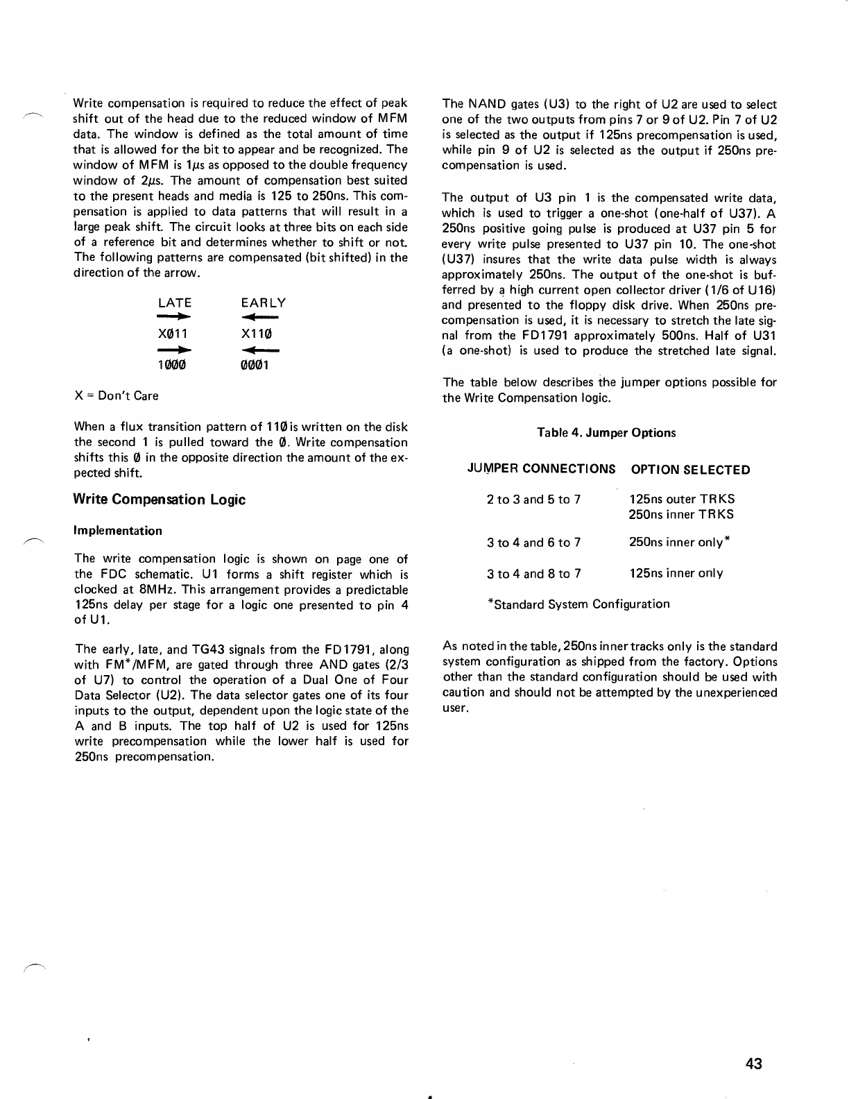
Write compensation is required to reduce the effect of peak
shift out of the head due to the reduced window of MFM
data. The window is defined as the total amount of time
that is allowed for the bit to appear and be recognized. The
window of MFM is 1ms as opposed to the double frequency
window of 2jus. The amount of compensation best suited
to the present heads and media is 125 to 250ns. This com-
pensation is applied to data patterns that will result in a
large peak shift. The circuit looks at three bits on each side
of areference bit and determines whether to shift or not.
The following patterns are compensated (bit shifted) in the
direction of the arrow.
LATE EARLY
X=Don't Care
When aflux transition pattern of 110 is written on the disk
the second 1is pulled toward the 0. Write compensation
shifts this in the opposite direction the amount of the ex-
pected shift.
Write Compensation Logic
Implementation
The write compensation logic is shown on page one of
the FDC schematic. U1 forms ashift register which is
clocked at 8MHz. This arrangement provides apredictable
125ns delay per stage for alogic one presented to pin 4
of U1.
The early, late, and TG43 signals from the FD1791, along
with FM*/MFM, are gated through three AND gates (2/3
of U7) to control the operation of aDual One of Four
Data Selector (U2). The data selector gates one of its four
inputs to the output, dependent upon the logic state of the
Aand B inputs. The top half of U2 is used for 125ns
write precompensation while the lower half is used for
250hs precompensation.
The NAND gates (U3) to the right of U2 are used to select
one of the two outputs from pins 7or 9of U2. Pin 7of U2
is selected as the output if 125ns precompensation is used,
while pin 9of U2 is selected as the output if 250ns pre-
compensation is used.
The output of U3 pin 1is the compensated write data,
which is used to trigger aone-shot (one-half of U37). A
250ns positive going pulse is produced at U37 pin 5for
every write pulse presented to U37 pin 10. The one-shot
(U37) insures that the write data pulse width is always
approximately 250ns. The output of the one-shot is buf-
fered by ahigh current open collector driver (1/6 of U16)
and presented to the floppy disk drive. When 250ns pre-
compensation is used, it is necessary to stretch the late sig-
nal from the FD1791 approximately 500ns. Half of U31
(a one-shot) is used to produce the stretched late signal.
The table below describes the jumper options possible for
the Write Compensation logic.
Table 4. Jumper Options
JUMPER CONNECTIONS OPTION SELECTED
2to 3and 5to 7 125ns outer TRKS
250ns inner TRKS
3to 4and 6 to 7250ns inner only*
3to 4and 8 to 7125ns inner only
*Standard System Configuration
As noted in the table, 250ns inner tracks only is the standard
system configuration as shipped from the factory. Options
other than the standard configuration should be used with
caution and should not be attempted by the unexperienced
user.
43
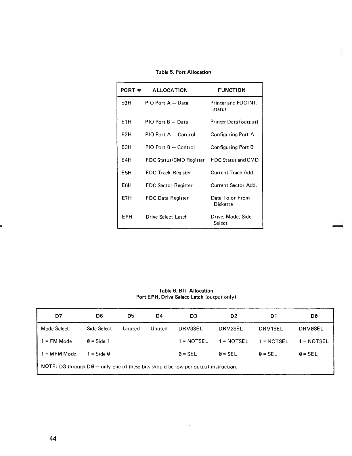
Table 5. Port Allocation
PORT* ALLOCATION FUNCTION
E0H PIO Port A-Data PrinterandFDCINT.
status
E1H PIO Port B-Data Printer Data (output)
E2H PIO Port A- Control Configuring Port A
E3H PIO Port B- Control Configuring Port B
E4H FDCStatus/CMD Register FDC Status and CM
D
E5H FDC Track Register Current Track Add.
E6H FDC Sector Register Current Sector Add.
E7H FDC Data Register Data To or From
Diskette
EFH Drive Select Latch Drive, Mode, Side
Select
Table 6. BIT Allocation
Port EFH, Drive Select Latch (output only)
D7 D6 D5 D4 D3 D2 D1 D0
Mode Select Side Select Unused Unused DRV3SEL DRV2SEL DRV1SEL DRV0SEL
1=FM Mode =Side 1 1 =NOTSEL 1=NOTSEL 1=NOTSEL 1=NOTSEL
1=MFMMode 1=Side0 =SEL =SEL 0=SEL 0= SEL
NOTE: D3 through D0 -only one of these bits should be ow per output instruction.
44
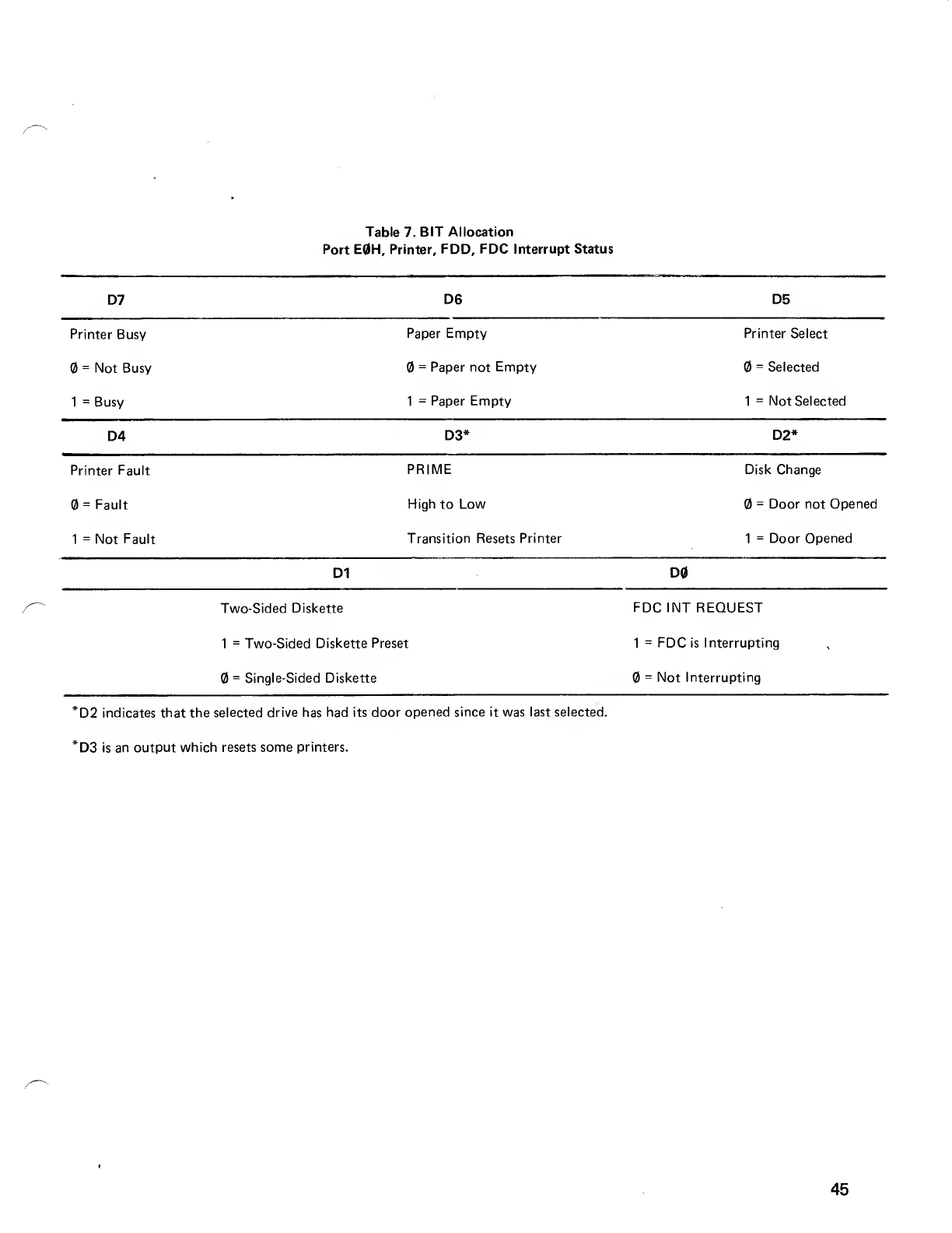
Table 7. BIT Allocation
Port E0H, Printer, FDD, FDC Interrupt Status
D7 D6 D5
Printer Busy
=Not Busy
1=Busy
Paper Empty
=Paper not Empty
1=Paper Empty
Printer Select
=Selected
1=Not Selected
D4 D3* D2*
Printer Fault
=Fault
1=Not Fault
PRIME
High to Low
Transition Resets Printer
Disk Change
=Door not Opened
1=Door Opened
D1 D0
Two-Sided Diskette
1=Two-Sided Diskette Preset
=Single-Sided Diskette
FDC INT REQUEST
1=FDC is Interrupting
=Not Interrupting
*D2 indicates that the selected drive has had its door opened since it was last selected.
*D3 is an output which resets some printers.
45

J1 (FDC Board to Floppy Disk) SIGNAL DESCRIPTIONS
PIN
SIGNAL
NAME DESCRIPTION
1
2
3
4
5
6
7
8
9
10
11
12
13
14
15
16
17
18
19
20
21
22
23
24
25
26
27
28
29
30
31
32
33
34
35
36
37
38
39
40
41
42
43
44
45
46
47
48
49
50
GND
WRTCRT*
GND
NC
GND
NC
GND
NC
GND
TWOSID*
GND
DSKCHG*
GND
SDSEL
GND
NC
GND
HLD*
GND
IP*
GND
RDY
GND
NC
GND
DS1*
GND
DS2*
GND
DS3*
GND
DS4*
GND
DIR*
GND
STEP*
GND
CPWD*
GND
WG*
GND
TRK0*
GND
WPRT*
GND
RD*
GND
NC
GND
NC
Power Ground
Reduced Write Current
Power Ground
Not Connected
Power Ground
Not Connected
Power Ground
Not Connected
Power Ground
Two Sided Diskette Installed
Power Ground
Drive Door Opened Since Last Select
Power Ground
Side Select; low =side ,high =side 1
Power Ground
Not Connected
Power Ground
Head Load
Power Ground
Index Pusle
Power Ground
Drive Ready
Power Ground
Not Connected
Power Ground
Drive Select One
Power Ground
Drive Select Two
Power Ground
Drive Select Three
Power Ground
Drive Select Four
Power Ground
Step Direction
Power Ground
Step Head One Track
Power Ground
Write Data
Power Ground
Write Gate
Power Ground
Track Zero Indication
Power Ground
Write Protected Diskette
Power Ground
Read Data
Power Ground
Not Connected
Power Ground
Not Connected
*Indicates an inverted signal or an active low signal.
46
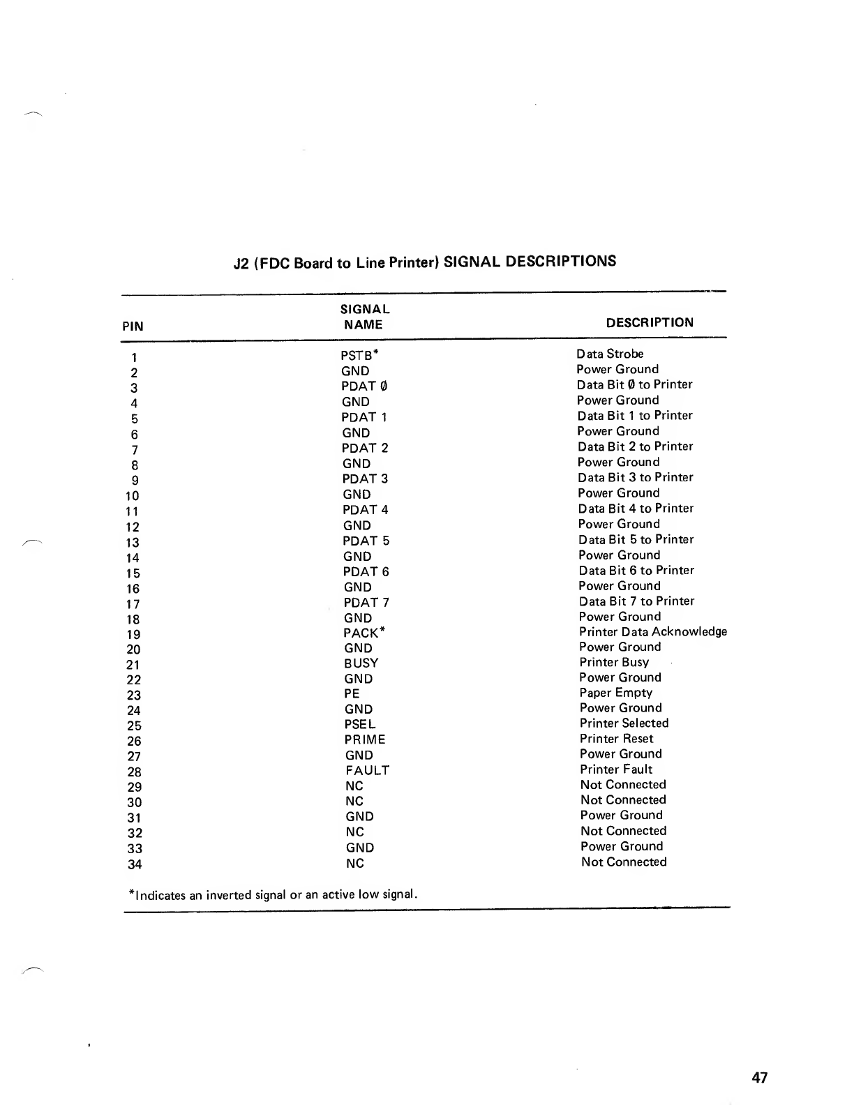
J2 (FDC Board to Line Printer) SIGNAL DESCRIPTIONS
PIN
SIGNAL
NAME DESCRIPTION
1
2
3
4
5
6
7
8
9
10
11
12
13
14
15
16
17
18
19
20
21
22
23
24
25
26
27
28
29
30
31
32
33
34
PSTB*
GND
PDAT0
GND
PDAT 1
GND
PDAT 2
GND
PDAT 3
GND
PDAT 4
GND
PDAT 5
GND
PDAT 6
GND
PDAT 7
GND
PACK*
GND
BUSY
GND
PE
GND
PSEL
PRIME
GND
FAULT
NC
NC
GND
NC
GND
NC
Data Strobe
Power Ground
Data Bit to Printer
Power Ground
Data Bit 1to Printer
Power Ground
Data Bit 2to Printer
Power Ground
Data Bit 3to Printer
Power Ground
Data Bit 4to Printer
Power Ground
Data Bit 5to Printer
Power Ground
Data Bit 6to Printer
Power Ground
Data Bit 7to Printer
Power Ground
Printer Data Acknowledge
Power Ground
Printer Busy
Power Ground
Paper Empty
Power Ground
Printer Selected
Printer Reset
Power Ground
Printer Fault
Not Connected
Not Connected
Power Ground
Not Connected
Power Ground
Not Connected
indicates an inverted signal or an active low signal.
47
<
«5L T:§£
-nf iiJC
V
o
(A
C
0)
c
o
a
E
o
o
I
O
00
u
D
a.
o
Q
u.
g
>
>-
<C
X
3
iT
48
0)
a
o
I
"D
O
O
o
Ql
o
o
LL
S
i>
s»
in
0)
3
49
FLOPPY DISK CONTROLLER PARTS LIST
SYMBOL DESCRIPTION MANUFACTURER'S
PART NUMBER RADIO SHACK
PART NUMBER
ELECTRICAL
PC Board 8709063
CAPACITORS
C1
C2
250pF, 50V, 20%, Ceramic Disc
O.ljuF, 50V, Monolithic
8321251
8374104
C8
C9
C10
C11
C12
C15
C16
C17
C18
C19
C20
C21
C22
C23
C24
C25
C26
C27
C28
C29
C30
C31
C32
C33
C34
C35
0.1/xF, 50V, Monolithic
33pF, 50V, Ceramic Disc
OAfxF, 50V, Monolithic
1300pF, 12V, 2%, Ceramic Disc
0.1juF, 50V, Monolithic
0.1;uF, 50V, Monolithic
0.047mF, 25V, 20%, Ceramic Disc
0.47^uF, 35V, 20%, Tantalum
33/uF, 50V, Electrolytic, Axial
33mF, 50V, Electrolytic, Axial
0.1juF, 50V, Monolithic
0.1juF, 50V, Monolithic
1300pF, 12V, 2%, Ceramic Disc
0.047/iF, 25V, 20%, Ceramic Disc
110pF,50V,2%,Mylar
0.001/zF, 50V, 20%, Ceramic Disc
0.1juF, 50V, Monolithic
68juF, 35V, Tantalum, PC
0.1juF, 50V, Monolithic
100pF, 50V, 20%, Ceramic Disc
33juF, 50V, Electrolytic, Axial
0.1juF, 50V, Monolithic
0.1/LiF, 50V, Monolithic
200pF, 50V, Ceramic Disc
33/iF, 50V, Electrolytic, Axial
33/zF, 50V, Ceramic Disc
8374104
8300334
8374104
8322131
8374104
8374104
8323471
8324471
8316334
8316334
8374104
8374104
8322131
8323471
8321111
8302104
8374104
8334683
8374104
8321101
8316334
8374104
8374104
8301204
8316334
8300334
ACC330QJCP
ACC336QJAA
ACC336QJAA
ACC336QJAA
ACC201QJCP
ACC336QJAA
ACC330QJCP
DIODES
CR1 Zener,5.6V,5% 8150232
CR2 1N4148 8150148
CR3 1N4148 8150148
CR4 1N4148 8150148
CR5 Zener, 6.2V, 5%
TRANSISTORS
8150234
Q1 2N2222A, NPN, TO-18 case 8110222
Q2 2N2907,PNP, TO-18 case 8100907
ADX1350
ADX1152
ADX1152
ADX1152
ADX1279
AMX4263
AMX4187
50
FLOPPY DISK CONTROLLER PARTS LIST (Cont'd)
SYMBOL DESCRIPTION
MANUFACTURER'S
PART NUMBER RADIO SHACK
PART NUMBER
RESISTORS
R1
R2
R3
R4
R5
R6
R7
R8
R9
R10
R11
R12
R13
R14
R15
R16
R17
R18
R19
R20
R21
R22
R23
R24
R25
R26
R27
R28
R29
R30
R31
R32
R33
R34
R35
R36
R37
R38
R39
R40
R41
R42
R43
R44
R45
R46
R47
R48
R49
2.2K, 1/4W, 5%, Carbon Film
2.2K, 1/4W, 5%, Carbon Film
2.2K, 1/4W, 5%, Carbon Film
2.2K, 1/4W, 5%, Carbon Film
50K, 10%, multi-turn potentiometer
2.2K, 1/4W, 5%, Carbon Film
150 ohm, 1/4W, 5%, Carbon Film
150 ohm, 1/4W, 5%, Carbon Film
150 ohm, 1/4W, 5%, Carbon Film
10K, 1/4W, 5%, Carbon Film
150 ohm, 1/4W, 5%, Carbon Film
2.2K, 1/4W, 5%, Carbon Film
2.2K, 1/4W, 5%, Carbon Film
10K, 1/4W, 5%, Carbon Film
2.2K, 1/4W, 5%, Carbon Film
1.5K, 1/4W, 5%, Carbon Film
8.2K, 1/4W, 5%, Carbon Film
2.2K, 1/4W, 5%, Carbon Film
2.2K, 1/4W, 5%, Carbon Film
150 ohm, 1/4W, 5%, Carbon Film
150 ohm, 1/4W, 5%, Carbon Film
2.2K, 1/4W, 5%, Carbon Film
2.2K, 1/4W, 5%, Carbon Film
1.1K, 1/4W, 1%, Carbon Film
10K, 1/4W, 5%, Carbon Film
270 ohm, 1/2W, 5%, Carbon Film
3.48K, 1/4W, 1%, Carbon Film
3.48K, 1/4W, 1%, Carbon Film
5.1 K, 1/4W, 5%, Carbon Film
1.1K, 1/4W, 1%, Carbon Film
10K, 1/4W, 1%, Carbon Film
10K, 20% potentiometer
160 ohm, 1/2W, 5%, Carbon Film
1.2K, 1/4W, 5%, Carbon Film
1K, 1/4W, 5%, Carbon Film
10K, 20% potentiometer
10K, 20% potentiometer
2.2K, 1/4W, 5%, Carbon Film
2.2K, 1/4W, 5%, Carbon Film
2.2K, 1/4W, 5%, Carbon Film
2.2K, 1/4W, 5%, Carbon Film
806 ohm, 1/4W, 1%, Carbon Film
140 ohm, 1/4W, 1%, Carbon Film
Omitted
4.7K, 1/4W, 5%, Carbon Film
4.7K, 1/4W, 5%, Carbon Film
390K, 1/4W, 5%, Carbon Film
2.2K, 1/4W, 5%, Carbon Film
10K, 1/4W, 5%, Carbon Film
8207222
8207222
8207222
8207222
8289350
8207222
8207115
8207115
8207115
8207310
8207115
8207222
8207222
8207310
8207222
8207215
8207282
8207222
8207222
8207115
8207115
8207222
8207222
8201211
8201310
8217127
8201234
8201234
8207251
8201211
8201310
8269310
8217116
8207212
8207210
8269310
8269310
8207222
8207222
8207222
8207222
8201180
8201114
AN0216EEC
AN0216EEC
AN0216EEC
AN0216EEC
AP7029
AN0216EEC
AN0142EEC
AN0142EEC
AN0142EEC
AN0281EEC
AN0142EEC
AN0216EEC
AN0216EEC
ACC0281EEC
AN0216EEC
AN0206EEC
AN0271EEC
AN0216EEC
AN0216EEC
AN0142EEC
AN0142EEC
AN0216EEC
AN0216EEC
ACC0198EEC
AN0281EEC
AN0155EFC
AN0232BEC
AN0232BEC
AN0252EEC
AN0198BEC
AN0281BEC
AP7028
AN0143EFC
AN0196EEC
AN0196EEC
AP7028
AP7028
AN0216EEC
AN0216EEC
AN0216EEC
AN0216EEC
8207247
8207247
8207439
8207222
8207310
AN0141BEC
AN0247EEC
AN0247EEC
AN0414EEC
AN0216EEC
AN0281EEC
51
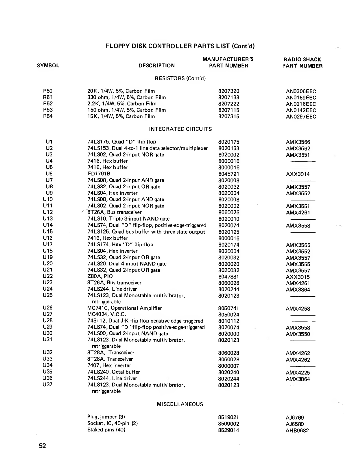
FLOPPY DISK CONTROLLER PARTS LIST (Cont'd)
SYMBOL DESCRIPTION
MANUFACTURER'S
PART NUMBER RADIO SHACK
PART NUMBER
RESISTORS (Cont'd)
R50
R51
R52
R53
R54
U1
U2
U3
U4
U5
U6
U7
U8
U9
U10
U11
U12
U13
U14
U15
U16
U17
U18
U19
U20
U21
U22
U23
U24
U25
U26
U27
U28
U29
U30
U31
U32
U33
U34
U35
U36
U37
20K, 1/4W, 5%, Carbon Film
330 ohm, 1/4W, 5%, Carbon Film
2.2K, 1/4W, 5%, Carbon Film
150 ohm, 1/4W, 5%, Carbon Film
15K, 1/4W, 5%, Carbon Film
INTEGRATED CIRCUITS
74LS175, Quad "D" flip-flop
74LS153, Dual 4-to-1 line data selector/multiplexer
74LS02, Quad 2-input NOR gate
7416, Hex buffer
7416, Hex buffer
FD1791B
74LS08, Quad 2-input AND gate
74LS32, Quad 2-input OR gate
74LS04, Hex inverter
74LS08, Quad 2-input AND gate
74LS02, Quad 2-input NOR gate
/"~8T26A, Bus transceiver
74LS10, Triple 3-input NAND gate
74LS74, Dual "D" flip-flop, positive-edge-triggered
74LS125, Quad bus buffer with three state output
7416, Hex buffer
74LS174, Hex "D" flip-flop
74LS04,Hex inverter
74LS32, Quad 2-input OR gate
74LS20, Dual 4-input NAND gate
74LS32, Quad 2-input Rgate
Z80A, PIO
8T26A, Bus transceiver
74LS244, Line driver
74LS123, Dual Monostable multivibrator,
retriggerable
MC741C, Operational Amplifier
MC4024, V.C.O.
74S1 12, Dual J-K flip-flop negative-edge-triggered
74LS74, Dual "D" flip-flop positive-edge-triggered
74LS00, Quad 2-input NAND gate
74LS123, Dual Monostable multivibrator,
retriggerable
8T28A, Transceiver
8T28A, Transceiver
7407, Hex inverter
74 LS240, Octal buffer
74LS244, Line driver
74LS123, Dual Monostable multivibrator,
retriggerable
8207320
8207133
8207222
8207115
8207315
8020175
8020153
8020002
8000016
8000016
8045791
8020008
8020032
8020004
8020008
8020002
8060026
8020010
8020074
8020125
8000016
8020174
8020004
8020032
8020020
8020032
8047881
8060026
8020244
8020123
8050741
8050024
8010112
8020074
8020000
8020123
8060028
8060028
8000007
8020240
8020244
8020123
AN0306EEC
AN0159EEC
AN0216EEC
AN0142EEC
AN0297EEC
AMX3566
AMX3562
AMX3551
AXX3014
AMX3557
AMX3552
AMX3551
AMX4261
AMX3558
AMX3565
AMX3552
AMX3557
AMX3555
AMX3557
AXX3015
AMX4261
AMX3864
AMX4258
AMX3558
AMX3550
AMX4262
AMX4262
AMX4225
AMX3864
MISCELLANEOUS
Plug, jumper (3)
Socket, IC, 40-pin (2)
Staked pins (40)
8519021
8509002
8529014
AJ6769
AJ6580
AHB9682
52
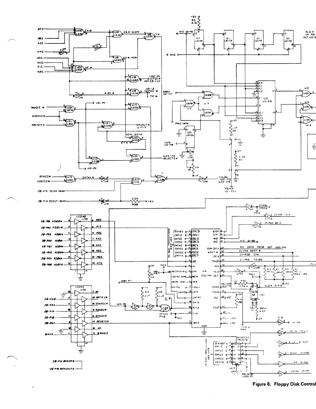
HLO *
U+-PIO'
HLT UG-P
if-tti not
34-mi Koto*
J0-PZ0-
J0-P2.2 —
J^-PI"? -
Jt-rie —
J$-»67—
rt-pa a*KiM»
H4-P» OAKOUT
I
I]
«xocyci*
5HQiBUt
aSYncx*
Figure 6. Floppy Disk Control
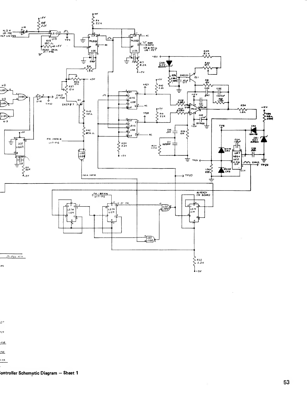
HLD #
hlt ue->gs ^
r
»4
U37
J.S/2S
_1_C55
U-IB ^
uii-piz
yFW\ /fflFM*
LS74 LS74
L/29
ALREADY
ON BOARD
IS 7+
fl22
2.ZK
ontroller Schematic Diagram -Sheet 1
53
JO -PM
HZ3
2.2.K
*-SVO VW"
aoua
'PA '3*
JUMPER ATO BIF CPU CLOCK -4MHZ
JL/MPEP BTO CJF CPU CLOCK ^2MHZ
<V\AA-«*
30-P5I DATOX &
JJ»- P62. IAT/#
J<p'P5& DATZX
H0-P5* BAT3-tt
J-$ -pSS. T>AT 4*
iTtp-PSG. DAT5*
J0-P57 JJAT6*
J-0 -P3S B<ir7#
CPUIN
uib -&e
uin-ps 4-
Figure 6. Floppy Disk Controller Schem;
54
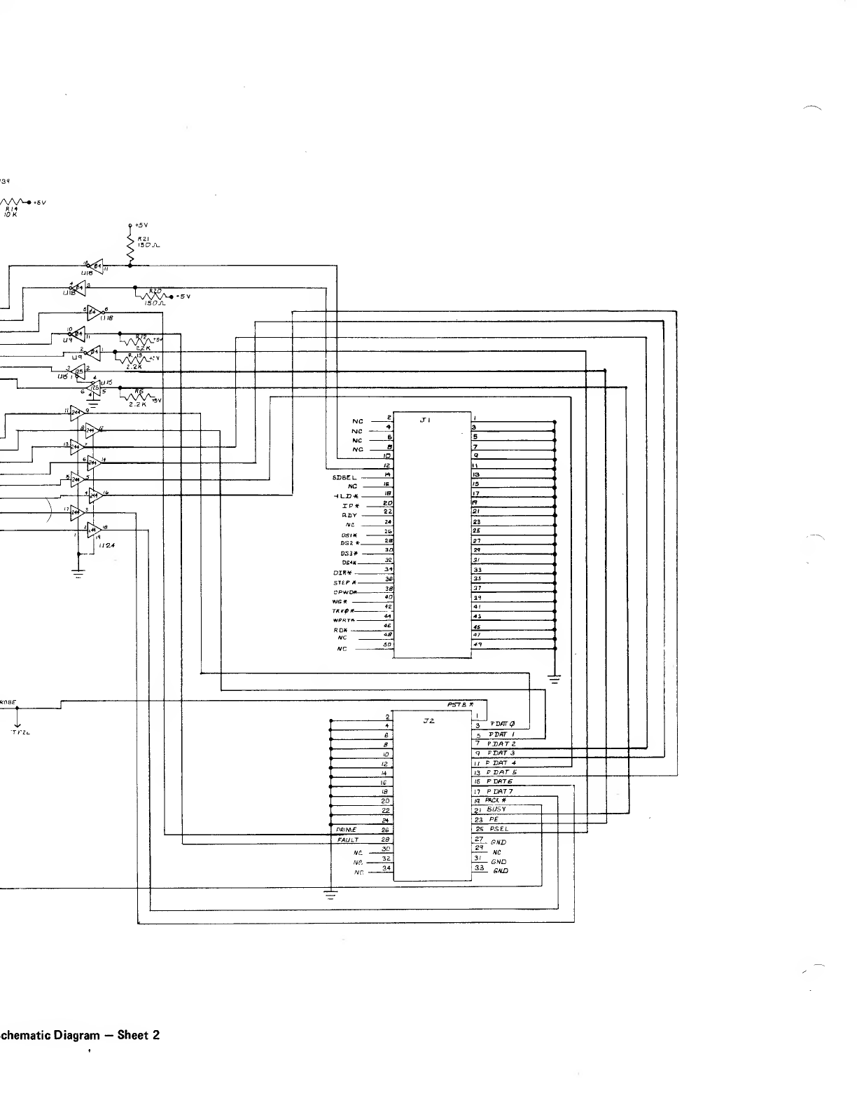
10 K
chematic Diagram —Sheet 2
SECTION V
VIDEO/KEYBOARD INTERFACE
55

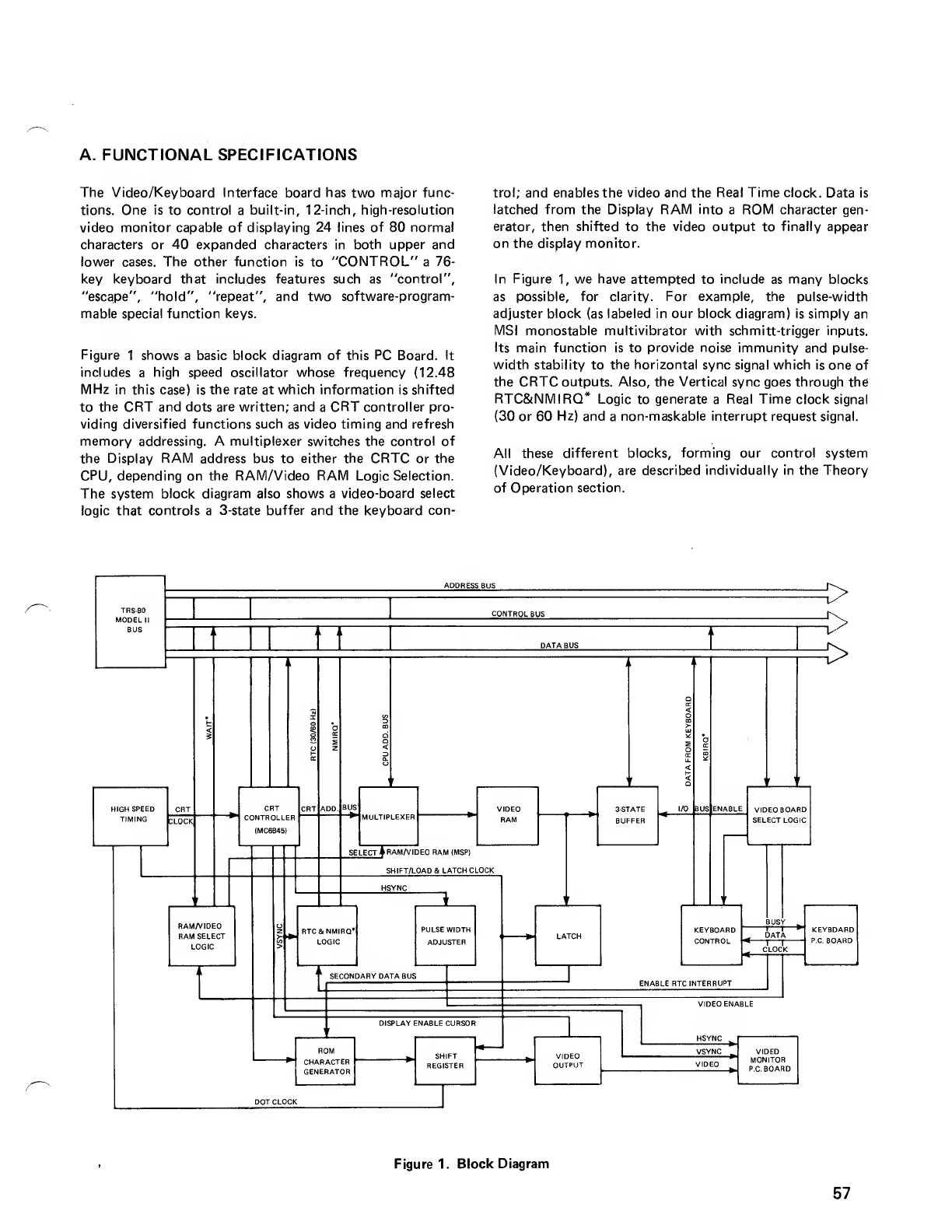
A. FUNCTIONAL SPECIFICATIONS
The Video/Keyboard Interface board has two major func-
tions. One is to control abuilt-in, 12-inch, high-resolution
video monitor capable of displaying 24 lines of 80 normal
characters or 40 expanded characters in both upper and
lower cases. The other function is to "CONTROL" a76-
key keyboard that includes features such as "control",
"escape", "hold", "repeat", and two software-program-
mable special function keys.
Figure 1shows abasic block diagram of this PC Board. It
includes ahigh speed oscillator whose frequency (12.48
MHz in this case) is the rate at which information is shifted
to the CRT and dots are written; and aCRT controller pro-
viding diversified functions such as video timing and refresh
memory addressing. Amultiplexer switches the control of
the Display RAM address bus to either the CRTC or the
CPU, depending on the RAM/Video RAM Logic Selection.
The system block diagram also shows avideo-board select
logic that controls a3-state buffer and the keyboard con-
trol; and enables the video and the Real Time clock. Data is
latched from the Display RAM into aROM character gen-
erator, then shifted to the video output to finally appear
on the display monitor.
In Figure 1, we have attempted to include as many blocks
as possible, for clarity. For example, the pulse-width
adjuster block (as labeled in our block diagram) is simply an
MSI monostable multivibrator with schmitt-trigger inputs.
Its main function is to provide noise immunity and pulse-
width stability to the horizontal sync signal which is one of
the CRTC outputs. Also, the Vertical sync goes through the
RTC&NMIRQ* Logic to generate aReal Time clock signal
(30 or 60 Hz) and anon-maskable interrupt request signal.
All these different blocks, forming our control system
(Video/Keyboard), are described individually in the Theory
of Operation section.
TRS-80
MODEL II
BUS
ADDRESS BUS
CONTROL BUS
HIGH SPEED
TIMING
CRT
CONTROLLER
RAM/VIDEO
RAM SELECT
LOGIC
MULTIPLEXER VIDEO
RAM
SELECT ^RAM/VIDEO RAM (MSP!
SHIFT/LOAD &LATCH CLOCK
RTC&NMIRQ'
LOGIC
PULSE WIDTH
ADJUSTER
SECONDARY DATA BUS
DISPLAY ENABLE CURSOR
ROM
CHARACTER
GENERATOR
SHIFT
REGISTER
3-STATE
BUFFER
£>
£>
£>
VIDEO BOARD
SELECT LOGIC
KEYBOARD
CONTROL _DATA
*,p-
ENABLE RTC INTERRUPT
VIDEO
OUTPUT
VIDEO ENABLE
KEYBOARD
P.C. BOARD
VIDEO
MONITOR
P.C. BOARD
Figure 1. Block Diagram
57
THEORY OF OPERATION
High Speed Timing
Refer to the Video/Keyboard Schematic.
The timing for the system is derived from adot-clock
crystal oscillator. This system clock is shown in the upper
left corner of the schematic. It consist of a12.48 MHz,
fundamental-cut crystal in parallel with aresonant circuit
that is composed of two inverters (part of U1) that are
driven into their linear region by resistors R2 and R3 (470
ohms each).
The waveform at pin 4of U1 resembles a"raw" square
wave at about 12.48 MHz.
At pin 6of the same chip, the signal looks more like a
"clean" square wave. It is labeled RCLOCK. It goes
through inverter U1 pin 9and comes out of pin 8as
RCLOCK*. Notice that we are using the asterisk throughout
the entire text as follows: if, for. example, the signal
RCLOCK is active high, then RCLOCK* which means
"NOT RCLOCK" is active low.
At this point,, that is at pin 13 of U1, RCLOCK* goes
through an inverter to give RCLOCKP (RCLOCK prime)
and again through asecond inverter to yield RCLOCKP*.
Up to this point all these clocks still have the same
frequency (12.48MHz), but they are at different phases.
The reason for generating all these different clocks is that
different timing is needed to synchronize the various
activities of our system. That is, one activity that should
take p)ace before another, or should occur 3or 4times
while another one happens just once. RCLOCK is divided
by 2by a"D" Flip-Flop, pins 11and 9of U17. That is, its
frequency is halved (12.48 MHz/2 =6.24 MHz). It is then
NANDed with the 80*/40 character Enable. When this
signal is low (active), 80 characters per line will be dis-
played on the screen; only 40 characters would appear
otherwise (when high). This signal will be described in
detail in later sections of the text.
CLOCK, at pin 8of LS00 (test point 26, TP26), is at either
12.48 MHz (for 80 characters) or at 6.24 MHz (for 40
characters). Note that the NAND gate, U28 (pins 1,2, and
3), is used here as an inverter. CLOCK goes through inverter
U33 (pins 11 and 10) to become DCLK, which is the DOT
CLOCK. Its frequency (either 6.24 or 12.48 MHz) is the
rate at which information is shifted to the CRT and dots
are written.
CLOCK, which is aphase shifted DOT CLOCK, is divided
down by a4-bit counter (U26) to produce the character-
rate clock labeled here as CCLK with afrequency of 12,48/
8=1.56MHz (for 80 characters) or 6.24/8=0.78MHz (40
characters).
This 4-bit counter (LS163) is synchronous. That is, all its
Flip-Flops are clocked simultaneously so that the outputs
change coincident with each other when instructed by the
count-enable inputs and internal gating. The DOT CLOCK
triggers the four Flip-Flops on the rising edge of its wave
form. The count is done as follows" (in HEX)
0, 9, A, B, C, D, E, F, 0, 9, A, B, C, . . . etc. This is best
described by the Timing diagrams of Figure 2. Notice that
both 80 and 40 character modes are represented here. Also
the signals TCLK* and PLCLK* are shown on these Timing
diagrams.
These diagrams are fairly reliable for comprehension pur-
poses since the propagation delay times, due to the different
gates, were not neglected.
We need all these different signals because each of these
signals is doing its own "specific job" just like any member
in aworking team.
How? Well, for example the CCLK triggers the MC6845
CRT controller which, if enabled, would send an address to
the video RAM requesting data to be sent to the Latch (U8)
inputs. TCLK* will then latch it into the character ROM,
which at its turn would send the appropriate dots to the
shift register U10. PLCLK* will shift load them in aparallel
fashion into the 8-bit shift register (U10) and DCLK will
shift them out of it serially toward the Video.
Further explanation of the different parts of the system
that need to be clocked will provide more clarity to this
subject of Timing Coordination. One of these parts is the
CRT controller.
Cathode Ray Tube Controller (CRTC)
For our video monitor display, we are using the Motorola
Controller MC6845, areliable processor that controls the
monitor with no CPU intervention, until the video memory
receives new data to be processed.
The MC6845 simplifies not only the design and the archi-
tecture, but also the trouble-shooting of the video control
board. It sharply reduces the number of I.C. chips it would
have taken otherwise. This CRTC commands the interface
to raster scan CRT displays. It also provides video timing
and refresh memory addressing. The CRTC is acollection
of registers, counters and comparators that time all logic
activities as the interfaced raster scan proceeds. Its logic
consists of programmable horizontal and vertical timing
generators, linear register, cursor logic, light-pen capture
register and control circuitry for interfacing to aprocessor
bus. The CRTC permits easy timing and synchronization
of signals. It also handles raster graphics as well as alphanu-
meric applications.
58
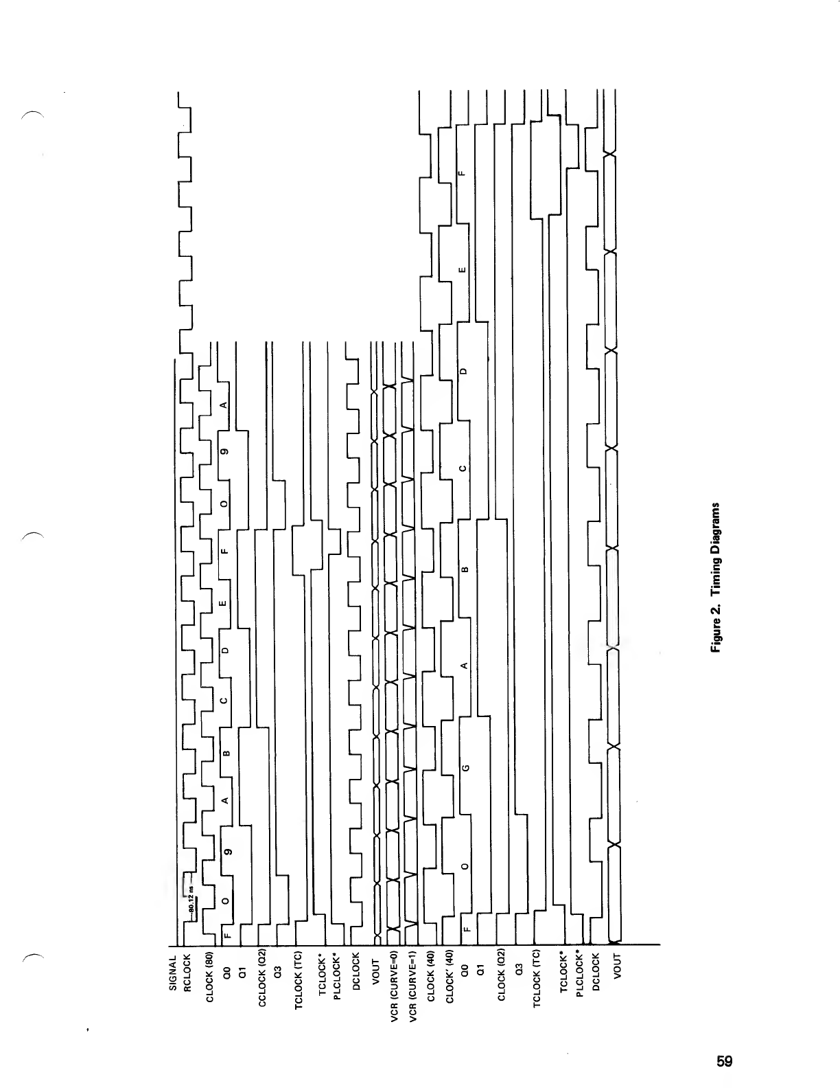
LMMl [LI J
]
]
Jx
iUJ '
1
kL^x
1|at
^
Q—
1
nhii
Jr" nil 1><
—1°
"
IM
1O*~~|
Hrl i
(A
i—1JJL £
rnrr^r i—1
1
—
win
if M
n°
,-1 <o I.£
^rin -i
i-
ini
.i
11—' 1 1—'»
Xi 113
Wl >1°>
nE
\*-\ J> |U<
?ol
>
IJ~=» i—,i \
jpEl
1
L- Fl 1
ri1— °1
p?3L L" ri 1
r1— 11 \ r
ill >bx
Ss 1
.1o1
nrln
ilr11JJ
IrVrr nnr HnrFrrrr IT-
UJUJO 1"~~ CO —ux n *-»
ocecoO o"do"
Ojj H0. D3qo 3qPria
--oo«o
t— oo
>>
59
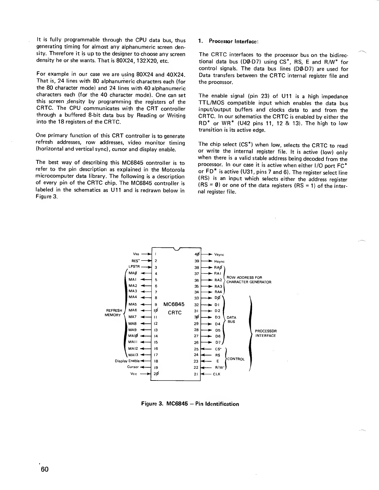
It is fully programmable through the CPU data bus, thus
generating timing for almost any alphanumeric screen den-
sity. Therefore it is up to the designer to choose any screen
density he or she wants. That is 80X24, 132X20, etc.
For example in our case we are using 80X24 and 40X24.
That is, 24 lines with 80 alphanumeric characters each (for
the 80 character mode) and 24 lines with 40 alphanumeric
characters each (for the 40 character mode). One can set
this screen .density by programming the registers of the
CRTC. The CPU communicates with the CRT controller
through abuffered 8-bit data bus by Reading or Writing
into the 18 registers of the CRTC.
One primary function of this CRT controller is to generate
refresh addresses, row addresses, video monitor timing
(horizontal and vertical sync), cursor and display enable.
The best way of describing this MC6845 controller is to
refer to the pin description as explained in the Motorola
microcomputer data library. The following is adescription
of every pin of the CRTC chip. The MC6845 controller is
labeled in the schematics as U11 and is redrawn below in
Figure 3.
1.Processor Interface:
The CRTC interfaces to the processor bus on the bidirec-
tional data bus (D0-D7) using CS*, RS, Eand R/W* for
control signals. The data bus lines (D0-D7) are used for
Data transfers between the CRTC internal register file and
the processor.
The enable signal (pin 23) of U11 is ahigh impedance
TTL/MOS compatible input which enables the data bus
input/output buffers and clocks data to and from the
CRTC. In our schematics the CRTC is enabled by either the
RD* or WR* (U42 pins 11, 12 &13). The high to low
transition is its active edge.
The chip select (CS*) when low, selects the CRTC to read
or write the internal register file. It is active (low) only
when there is avalid stable address being decoded from the
processor. In our case it is active when either I/O port FC*
or FD* is active (U31, pins 7and 6). The register select line
(RS) is an input which selects either the address register
(RS =0) or one of the data registers (RS =1) of the inter-
nal register file.
REFRESH
MEMORY
Vss
RES"
LPSTR -
/MA0
MAI
MA2
MA3
MA4
MA5
MA6
MA7
MA8
MA9
MAI0
MAI I
MAI2
MAI3
Display Enable
Cursor
Vcc
w
I4J2f fc
m
239 *•
—». 338
-*—
'
437 ^
^S
6
7
36
35
34
833
*—9MC6845 32 *.
<—'* CRTC 31 *~
II ¥*
•*—12 29 >
-*—13 28 *-
14 27
-*
—
15 26
-*—16 25
-*—17 24
-*—18 23
-*—19 22
—* 20 21 ^
Vsync
Hsync
RA^
RAI
RA2
RA3
RA4
D|Zf
Dl
D2
D3
D4
D5
D6
D?
cs-
RS
E
R/W
CLK
ROW ADDRESS FOR
CHARACTER GENERATOR
DATA
BUS
PROCESSOR
INTERFACE
CONTROL
Figure 3. MC6845 -Pin Identification
60
The Read/Write (R/W*) signal determines whether the
internal register file gets written or read. It is written when
low and read when high.
2. CRT Control:
The CRTC provides Horizontal Sync (HS), Vertical Sync
(VS) and Display Enable signals.
The Vertical Sync is an active high signal which drives the
monitor. It determines the vertical position of the display-
ed data. The Horizontal Sync is also an active high signal
which drives the monitor. It determines the' horizontal posi-
tion of the displayed data.
The Display Enable is an active high signal which indicates
the CRTC is providing addressing in the active display area.
3. Refresh Memory/Character Generator Addressing:
The CRTC provides Memory addresses (MA0-MA13) which
scan the Refresh RAM. In our case only MA0 through
MA10 are used, since our video memory capacity is only
2K bytes big. Also provided are Raster addresses
(RA0-RA4) for the character ROM. The Refresh Memory
addresses (MA0-MA10) are used to refresh the CRT screen
with pages of data located in the 2K block of Display RAM.
The Raster addresses (RA0-RA4) determine the row of a
character in the character ROM.
4. Other Pins:
The clock input is used to synchronize all CRT control
signals. In our design this signal is the character-rate clock
CCLK (1.56/0.78 MHz). The active transition is high to
low.
The Light Pen Strobe (LPSTR) is not used in our design.
The cursor, which is an active high signal, indicates cursor
display to external video processing logic.
The Reset (RES*) input is used to reset the CRTC. It is
active low. When this signal is active, the CRTC is forced
into the following status:
a) All the counters in CRTC are cleared and the device
stops the display operation.
b) All the outputs go down to low level.
As you may know, everything that is displayed on the
screen should be continuously refreshed, otherwise it will
fade away and disappear. Every character is adot matrix of
8x10 cells and every cell is refreshed about 60 times in one
second. (Refer to Figure 4.) The CRT beam is repetitively
scanning the screen from top to bottom, refreshing every
dot whose location is indicated by the coordinates that the
display memory and the character ROM receive from the
CRTC (Memory refresh address and Row address).
The CRTC takes care of this particular chore and the CPU
would therefore do amore "smart" activity, rather than
waste its "valuable" time with this refreshing routine.
However, every time the CPU addresses its upper 2K bytes
of memory, it automatically takes control of the Video
RAM. The reason is that these 2K bytes, starting at address
locations F800H through FFFFH, overlap the video memory
in its entirety. Thus this display RAM can be accessed by
either the CPU or the CRTC, but not by both at the same
time.
Our approach for solving contentions for the refresh
memory is that the processor (CPU) gets priority access
anytime, but is synchronized by an interrupt to perform
accesses only during the vertical retrace time. The vertical
retrace time is defined as the time it takes the CRT beam to
return from the end of the very last scan line, back to the
start of the very first one. Of course the CRT beam is shut
off during the retrace time.
The CRTC sends its addresses as follows: The first set of
address lines consisting of MA0 through MA10, cycles
binarily through the display memory and is incremented
with each clock pulse (CCLK); one per character displayed.
The second set (RA0-RA4) addresses the row-address select
lines of the character generator. These also cycle binarily,
but are incremented with each horizontal retrace time.
Again the horizontal retrace time is the period in which the
CRT beam returns from the end of ascan line back to the
beginning of the next one.
The CRTC's linear address generator repeats the same
sequence of character addresses for each scan line within
the same character row.
The character block in our case is 10 rows high, so it takes
10 separate accesses of agiven character to write its 10 dot-
rows on the screen. So putting 80X24, or 1920, characters
on the screen calls for 10X1920, or 19200, character
accesses 60 times every second.
c) The control registers of the CRTC are not affected.
Now that we have an overview of the CRTC chip itself, let's
try to clarify what is meant by memory refreshing. The way
we programmed our CRTC internal register file would
permit adisplay of 24X80/24X40 alphanumeric characters.
The address of each one of these characters is stored in the
display memory. That is the reason we are using only 2K of
Video RAM (just enough to store the entire screen density).
61
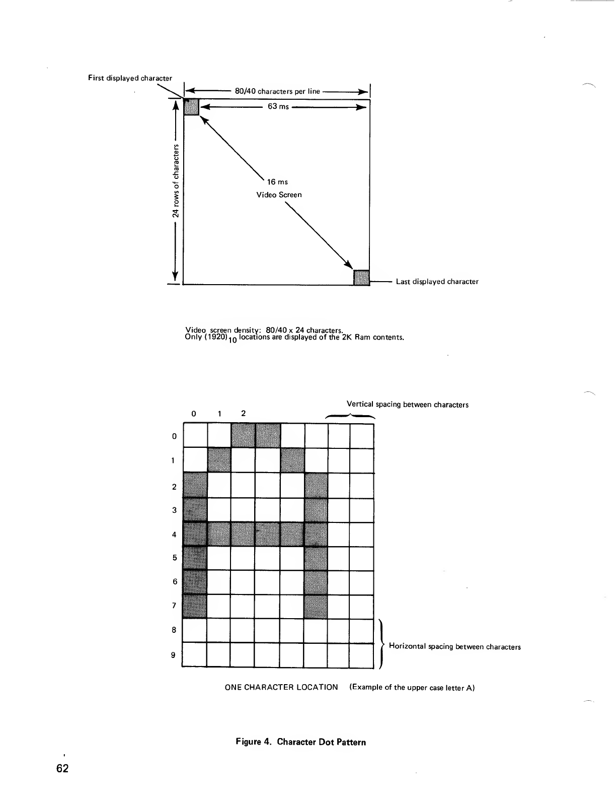
First displayed character
Last displayed character
Video screen density: 80/40 x24 characters.
Only (1920) 1f
jlocations are displayed of the 2K Ram contents.
Vertical spacing between characters
12
1
2
3
4-
5
6
7
8
9
'Horizontal spacing between characters
ONE CHARACTER LOCATION (Example of the upper case letter A)
Figure 4. Character Dot Pattern
62
Multiplexers
As you can see in the schematics, LS157 multiplexers (U23,
U24 and U25), are used for multiplexing refresh memory
addresses between the processor and the CRTC.
The processor is in control when the select inputs (pin 1of
each chip) are high. When these inputs are low the control
of the display is switched to the CRTC.
MSP, the signal that controls the multiplexing is derived
from the RAM/VIDEO RAM Select Logic block.
RAM/Video RAM Select Logic
The block, labeled RAM/VIDEO RAM Select Logic, on the
diagram of Figure 1, is actually asort of decoder. That
is, when the CPU is addressing its upper 2K bytes of
memory, located at F800H through FFFFH, address lines
AD 11 through AD 15 become high (active). Also the
Memory request signal or memory cycle (MEMCYC) is
activated by the CPU. As you may know by now, this signal
is activated everytime the CPU addresses any part of its
memory. Another important signal is the input to pin 11of
NAND gate LS30, U41. This signal is used to enable the
CPU to access the Video RAM if, and only if, our software
says so. That time is when Port FFWR* is activated and bit
7(D2 of LS175) is set to 1. If all these conditions are met,
then pin 8of U41 goes low and MSEL becomes high (U30
pin 6).
MSEL is ANDed with MSLP (U13 pins 4, 5&6) to finally
give us MSP, the select input to the multiplexers. When this
MSP signal is high, the Video RAM is under the processor
control. Note that when the Reset* button is hit (U32 pin
8), the CPU loses that control (MSP becomes low).
The refresh cycle, that is the period in which the CRT beam
is "within the screen", is additionally protected by the
generation of await cycle. As is shown on the schematics,
MSEL* clocks ahigh (U32 pin 15) that is inverted by U14
pins 2and 3to give an active WAIT* state. This WAIT*
state is interrupted whenever we have aRESET* or MSELP
NANDed with Q, as shown by U2 pins 8, 9, 10, and U29
pins 8, 9, and 10. Note that when MSELP is high, the CPU
is accepting the diaplay RAM (U13 pins 4, 5, and 6).
Video Board Select Logic
This part of our system could be called the port addressing
block.
It is using the lower eight lines of the address bus, as shown
by U27 LS30,for the dual 2to 4line decoder (U31 LS155).
One of the decoders is enabled only by Read NANDed
with I/O Cycle signal (IOCYC) to give 3Read ports (FCRD*,
FERD*, and FFRD*; pins 9, 11, and 12). The other is en-
abled only by the IOCYC signal and its outputs could act-
ually be used for Read or Write ports. In our design either
one of the FC* or FD* ports could chip select the MC6845
controller. Port FF* NANDed with WR* gives FFWR* (U3
pins8,9,and 10). Also the Input/Output address select (U27
pin 8and U30 pins 12 and 13) is ANDed with IOCYC to
give the I/O Select (IOSEL) to enable the 3-state buffers
(U34and U35) to either Read from the CRTC(IOBIE: I/O
Bus Input Enable) or Write into it (IOBIE*: I/O Bus Out-
put Enable). Note that test points TP22 (U13 pin 3) and
TP21 (U2 pin3) will show us if we are reading from or writ-
ing into the CRTC. The following table shows the port ad-
dressing and the functions of every port.
Table 1. Port Addressing
PORTADDR.
FC
FD
FE
FF
READ FUNCTION
Read Keyboard data
Clear Keyboard Interrupt
Read CRTC Data Register
Clear Real Time clock
(RTC) interrupt
Read Non-maskable Interrupt
Register and Non-maskable In-
terrupt Mask Register.
WRITE FUNCTION
Load CRTC address Register
Load CRTC data Register
Load Memory Bank Select
Register and load Non-mask-
able Interrupt Mask Register
and Video enable.
63
For Example, Port FF is used as follows:
a) Non-maskable Interrupt Mask Register and Bank Select
Register: Write only
D7 D6 D5 D4 D3 D2 D1 D0
Bit7(D7)
-if set (1), enables the 2K bytes RAM, disables the upper
2K bytes of the Bank's RAM (F800H to FFFFH)
-if Reset (0), disables Video RAM, enables Bank RAM
F800Hto FFFFH.
Bit6(D6)
-if 0, enables Video display (on)
-if 1, Video display off
Bit5(D5)
-Set (1), enables the Real Time clock (RTC) interrupt
-Reset (0), disables the RTC interrupts
Bit4(D4)
-1, enables the 40 character mode and disables the 80 char-
acter mode
-0, enables the 80 character mode, disables the 40 charac-
ter mode
Bits 3through (D3 -D0)
-Selects 1of 16 memory banks. Note that if we hit
the Reset, the RTC interrupt is disabled
b) Non-maskable Interrupt Mask Register:
Read only
D7 D6 D5 D4 D3 D2 D1 D0
*80* /40 character mode
RTC interrupt enable
Video display enable*
Keyboard Interrupt Request (KB IRQ)
Bit7(D7)
—1, Keyboard interrupting
—0, No Keyboard interrupting
Bit6(D6)
—1, Video Display disabled
—0, Video Display enabled
Bit5(D5)
—RTC interrupt enable
64
Bit4(D4)
-80*/40 character mode*
Bits 3through 0(D3-D0)
-They are "don't care" bits (not used)
Now that we know how these different ports will be used,
we can set the control bits, say in Port FF, the way we
want to. This means we will be writing into Port FF.
Therefore the FFWR* signal is activated. If, for example,
we set bit 7to 1, bit 6to 0, bit 5to 1and bit 4to 0, FFWR*
will latch this data vector into our system and the follow-
ing results will be obtained:
Pin 11 of U41 will be high, thus enabling the 2K byte
Video RAM. BLNKVID*, Q3 (pin 14 of U18) will go high
and disable the blank Video (Video on).
The Real Time clock (RTC), pin 3of U18, is enabled. And
finally we will get alow (0) at pin 7of U18. This generated
signal is what we previously called the 80*/40 character
mode. In this case the 80* character mode is enabled (low).
It is inverted at U30 pins 1, 2, and 3and then NANDed
with RCLOCK* to appear at the output of the NAND gate
U28, pins 8, 9, and 10, as CLOCK (TP26).
Note how the OR gate U3 pins 4, 5, and 6is drawn as a
NAND gate.
AA
This gate HjJ^C is the same as this gate H~_^°-C
B"B01
We sometimes show the OR gates as above, because we are
using mostly active low signals. We can go from one gate to
another just by using DeMorgan's Theorem. For the above
example, we have:
AB= A+B=A+B=C
Now if we want to Read the Status of Port FF, we'll acti-
vate the FFRD* signal to enable the 3-state buffers LS240,
U38. This will produce the status of the KBIRQ*, the
BLNKVID*, the 80*/40 character mode* and the ENABLE
RTC INT* as shown at the inputs 2, 4, 6and 8of U38.
Other Blocks
The 3-state Buffers (U37) are enabled by either the Video
Read (VRD) or Video Write* (VWR*). VRD is the result
of the RD signal ANDed with MSP (U13 pins 11, 12, and
13). VWR* is the output of WR NANDed with MSP (U2
pins 4, 5, and 6).
When the CPU wants to write data into the Video RAM,
VWR* goes low (pin 1of U37). When it does areading
from the Video RAM, VRD (high) is active (pin 15 of U37).
Test points TP2 and TP24 will help us detect if data is read
from or written into the Display RAM by the CPU.
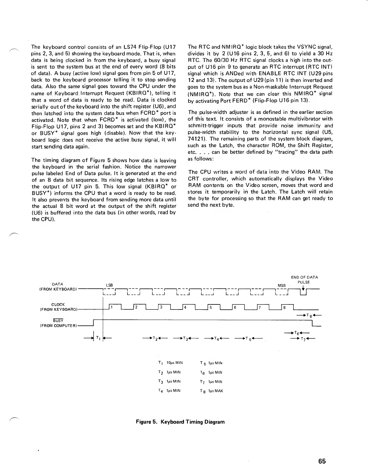
The keyboard control consists of an LS74 Flip-Flop (U17
pins 2, 3, and 5) showing the keyboard mode. That is, when
data is being clocked in from the keyboard, abusy signal
is sent to the system bus at the end of every word (8 bits
of data). Abusy (active low) signal goes from pin 5of U17,
back to the keyboard processor telling it to stop sending
data. Also the same signal goes toward the CPU under the
name of Keyboard. Interrupt Request (KBIRQ*), telling it
that aword of data is ready to be read. Data is clocked
serially out of the keyboard into the shift register (U6), and
then latched into the system data bus when FCRD* port is
activated. Note that when FCRD* is activated (low), the
Flip-Flop U17, pins 2and 3) becomes set and the KBIRQ*
or BUSY* signal goes high (disable). Now that the key-
board logic does not receive the active busy signal, it will
start sending data again.
The timing diagram of Figure 5shows how data is leaving
the keyboard in the serial fashion. Notice the narrower
pulse labeled End of Data pulse. It is generated at the end
of an 8data bit sequence. Its rising edge latches alow to
the output of U17 pin 5. This low signal (KBIRQ* or
BUSY*) informs the CPU that aword is ready to be read.
It also prevents the keyboard from sending more data until
the actual 8bit word at the output of the shift register
(U6) is buffered into the data bus (in other words, read by
the CPU).
The RTC and NMIRQ* logic block takes the VSYNC signal,
divides it by 2(U16 pins 2, 3, 5, and 6) to yield a30 Hz
RTC. The 60/30 Hz RTC signal clocks ahigh into the out-
put of U16 pin 9to generate an RTC interrupt (RTC INT)
signal which is ANDed with ENABLE RTC INT (U29pins
12 and 13). The output of U29 (pin 11) is then inverted and
goes to the system bus as aNon-maskable Interrupt Request
(NMIRQ*). Note that we can clear this NMIRQ* signal
by activating Port FERD* (Flip-Flop U16 pin 13).
The pulse-width adjuster is as defined in the earlier section
of this text. It consists of amonostable multivibrator with
schmitt-trigger inputs that provide noise immunity and
pulse-width stability to the horizontal sync signal (U5,
74121). The remaining parts of the system block diagram,
such as the Latch, the character ROM, the Shift Register,
etc. ...can be better defined by "tracing" the data path
as follows:
The CPU writes aword of data into the Video RAM. The
CRT controller, which automatically displays the Video
RAM contents on the Video screen, moves that word and
stores it temporarily in the Latch. The Latch will retain
the byte for processing so that the RAM can get ready to
send the next byte.
DATA LSB
{FROM KEYBOARD) 1r
CLOCK
(from keyboard)-
bDsy
(fromcomputer)-
IIIIII
END OF DATA
PULSE
t:_t~ii
MSB
-U
J5"
T, 10/isMIN
T21/isMIN
T3IjUsMIN
T41/jsMIN
T5IfjsMIN
T61/isMIN
T7IjusMIN
T81/js MAX
Figure 5. Keyboard Timing Diagram
65
The Latch (U8) is an LS273. When activated (byTCLK*),
U8 would latch the data word into the character ROM (U9)
in ASCII form. Note that the 8th bit is used as aReverse
Video signal (REVID). U9 is the character generator. The
seven bit ASCII Word applied to its inputs would address a
certain area in it. These ASCII inputs are considered the
higher seven bits of an address. The lower part of the ad-
dress comes from the CRTC (RA0-RA4). This lower part
selects the row position of the addressed dot pattern.
Each character consists of adot matrix, 8dots wide and 10
dots deep. Since each character consists of apattern of dots,
there must be some method to determine which dot should
be on and which dot should be off to form any one charac-
ter. The character generator controls the dot patterns on
the screen.
U9 outputs 8dots (on or off) at the same time. RA0
through RA4 would of course select the row of the ad-
dressed pattern. The character generator must output 10
times to build one character.
Here is how atypical character line is written:
Assume an ASCII word is in the Latch. The electron beam
is on the first scan line of the character. Hence, the row ad-
dress is binary "0". That is, RA0 through RA4 are low. U9
outputs the first dot pattern for that particular ASCII char-
acter. The next ASCII character is applied to U9. At the
same time, the row address is incremented. It is now binary
"1" pointing to the second scan line. Keep in mind that
the electron beam doesn't stop at the last dot of the first
pattern, but goes on scanning the rest of the entire scan line.
By the time the second dot pattern goes out, the third
ASCII word comes in. This process goes on until the entire
character (10 rows) is written on the screen.
These various dot patterns are loaded into the shift register
U10, in aparallel fashion and are shifted out of it serially.
Of course all this is done so fast that it seems that the en-
tire character is displayed not "in pieces" but as an entity.
After the eight dot scans are outputted, the electron beam
is turned off and two rows (the 9th and 10th) of blank dots
are outputted. We now are ready to output the first row of
the second character line. Following the path data goes
through before being outputted at pin 9of U10 (V out),
one can see that the Vout signal is delayed quite abit with
respect to the Display Enable and Cursor signals. For this
reason, these two signals are delayed by two TADCLK
cycles and Reverse Video (REVID) is delayed by one
TADCLK cycle with respect to the VOUT signal. This is
shown by U12. Note how the delayed cursor and DREVID
are Exclusive ORed (U4 pins 12 and 13). The resulting
signal at pin 11 of U4 is also Exclusive ORed with VOUT
(U4 pins 9and 10).
This is to say that either the cursor, the Reverse Video or
the Video would be displayed in acharacter location, but
not two of them at the same time. The signal outputted
at pin 8of U4 is finally enabled by the Display enable and
either one of the RCLOCK, RCLOCK*, RCLOCKP and
RCLOCKP* signals. We gave ourselves the option of choos-
ing one of the four clock signals to achieve abetter result.
The final signal we get at pin 12 of U15 is what we simply
call VIDEO. The VIDEO, HSYNC, and VSYNC signals are
separately shielded and sent to the CRT Logic board.
(Ground signals are wrapped around them.)
CONNECTOR J2 SIGNAL DESCRIPTIONS
PIN SIGNAL DESCRIPTION
Data from Keyboard
Key -No Connection
Clock from Keyboard
Busy to Keyboard
+5V to Keyboard
Ground to Keyboard
CONNECTOR J3 SIGNAL DESCRIPTIONS
DESCRIPTION
Horizontal Synchronization Ground
Vertical Synchronization Ground
Horizontal Synchronization (prime)
Vertical Synchronization (prime)
No Connection
Video Signal
Video Ground
SIGNAL
'IN NAME
1HSGND
2VSGND
3HSYNC
4VSYNC
5KEY
6VIDEO
7VIDGND
6o
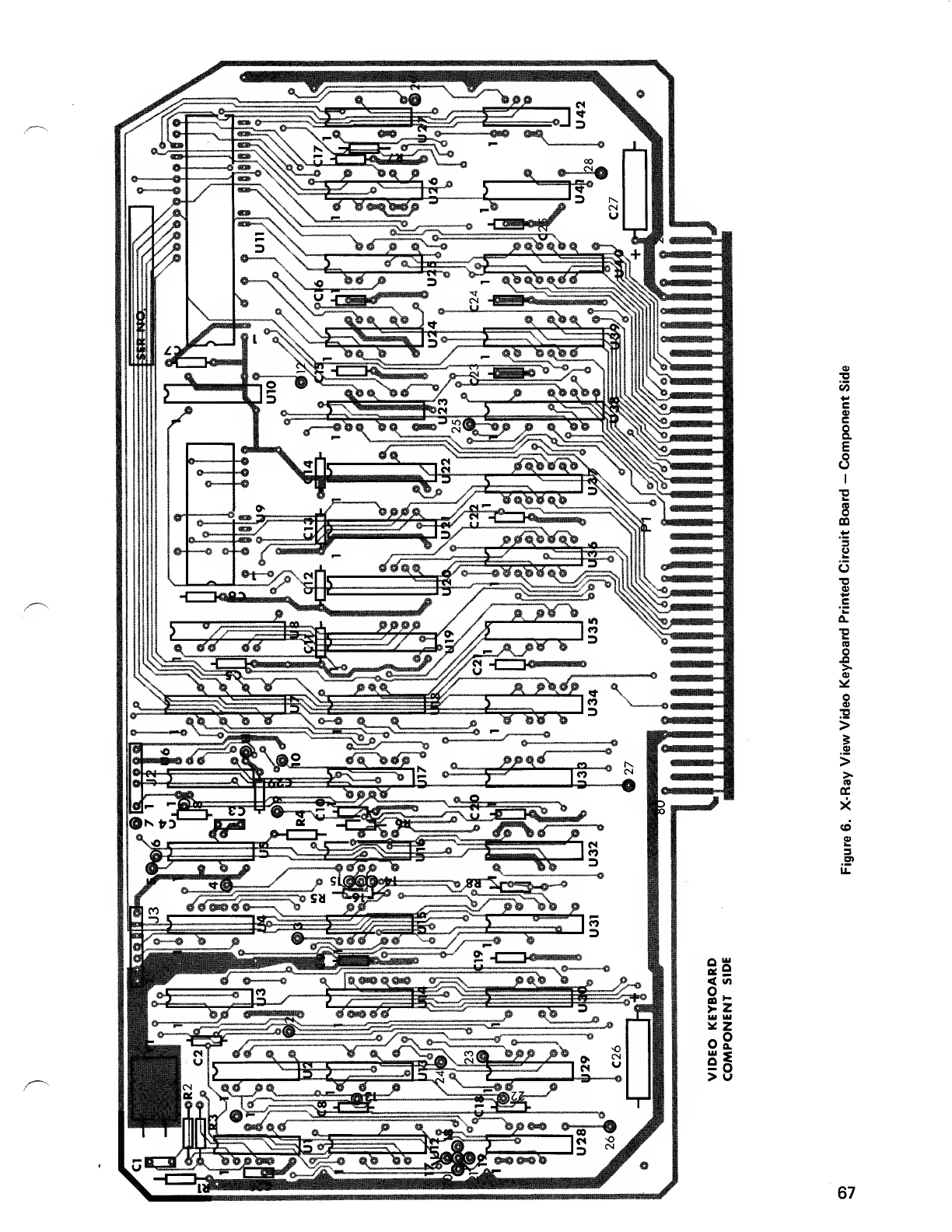
E
8
i
o
S
>
1
>
67
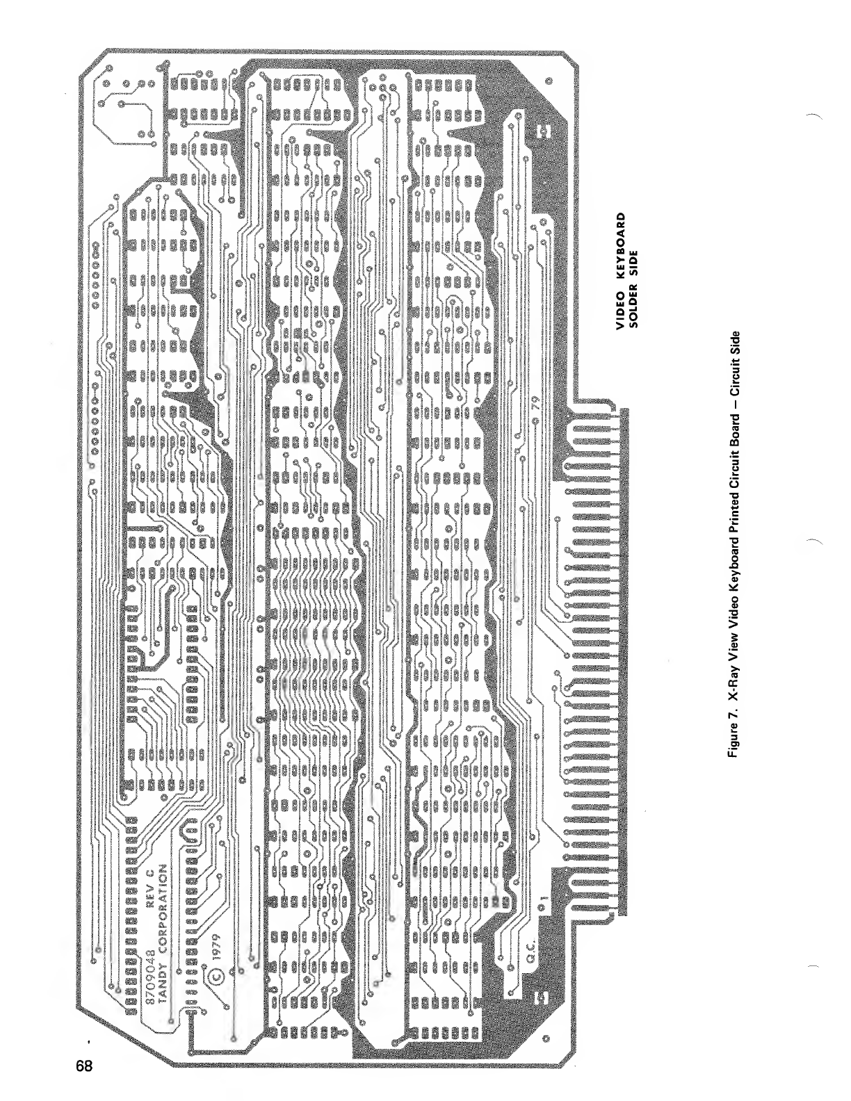
"N
1*•;
lifiM ,J ~j* 111 A
|| m
JMfe 18b HuoBk
-- ^3"-. •*
Q
at
<
00 „,
>-Q
ui —
^i/t
Q£
mQ
9o
><«
CO
o
I
"E
3
a.
1
s
>
1
>-
to
.1
k
68
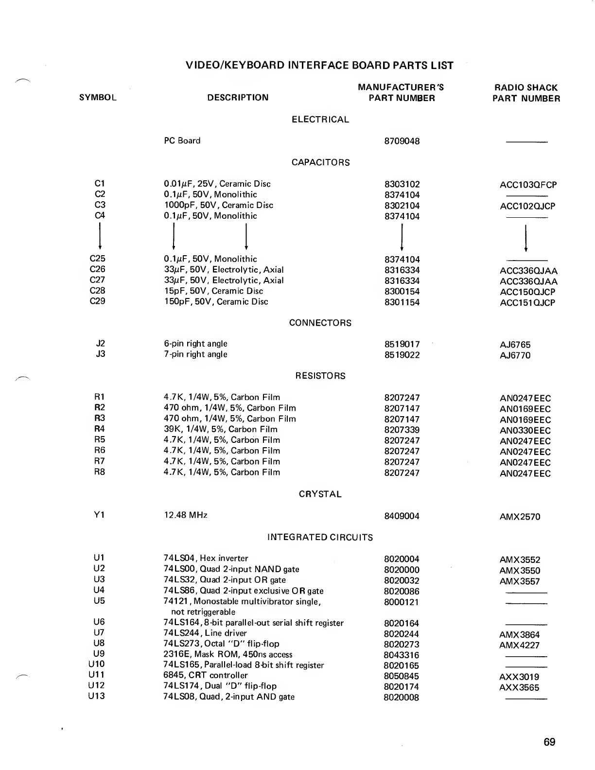
VIDEO/KEYBOARD INTERFACE BOARD PARTS LIST
SYMBOL DESCRIPTION
MANUFACTURER'S
PART NUMBER RADIO SHACK
PART NUMBER
ELECTRICAL
PC Board 8709048
CAPACITORS
C1
C2
C3
C4
C25
C26
C27
C28
C29
0.01/xF, 25V, Ceramic Disc
0.1/iF, 50V, Monolithic
1000pF, 50V, Ceramic Disc
0A(iF, 50V, Monolithic
O.ljixF, 50V, Monolithic
33/uF, 50V, Electrolytic, Axial
33juF, 50V, Electrolytic, Axial
15pF, 50V, Ceramic Disc
150pF, 50V, Ceramic Disc
8303102
8374104
8302104
8374104
8374104
8316334
8316334
8300154
8301154
ACC103QFCP
ACC102QJCP
ACC336QJAA
ACC336QJAA
ACC150QJCP
ACC151QJCP
J2
J3
CONNECTORS
6-pin right angle
7-pin right angle
8519017
8519022
AJ6765
AJ6770
RESISTORS
R1
R2
R3
R4
R5
R6
R7
R8
4.7K, 1/4W, 5%, Carbon Film
470 ohm, 1/4W, 5%, Carbon Film
470 ohm, 1/4W, 5%, Carbon Film
39K, 1/4W, 5%, Carbon Film
4.7K, 1/4W, 5%, Carbon Film
4.7K, 1/4W, 5%, Carbon Film
4.7K, 1/4W, 5%, Carbon Film
4.7 K, 1/4W, 5%, Carbon Film
8207247
8207147
8207147
8207339
8207247
8207247
8207247
8207247
AN0247EEC
AN0169EEC
AN0169EEC
AN0330EEC
AN0247EEC
AN0247EEC
AN0247EEC
AN0247EEC
CRYSTAL
Y1 12.48 MHz 8409004 AMX2570
INTEGRATED CIRCUITS
U1
U2
U3
U4
U5
U6
U7
U8
U9
U10
U11
U12
U13
74LS04, Hex inverter 8020004
74LS00, Quad 2-input NAN Dgate 8020000
74LS32, Quad 2-input OR gate 8020032
74LS86, Quad 2-input exclusive OR gate 8020086
74121 ,Monostable multivibrator single, 8000121
not retriggerable
74LS164, 8-bit parallel-out serial shift register 8020164
74LS244, Line driver 8020244
74LS273, Octal "D" flip-flop 8020273
231 6E, Mask ROM, 450ns access 8043316
74LS165, Parallel-load 8-bit shift register 8020165
6845, CRT controller 8050845
74LS174, Dual "D" flip-flop 8020174
74LS08, Quad, 2-input AND gate 8020008
AMX3552
AMX3550
AMX3557
AMX3864
AMX4227
AXX3019
AXX3565
69
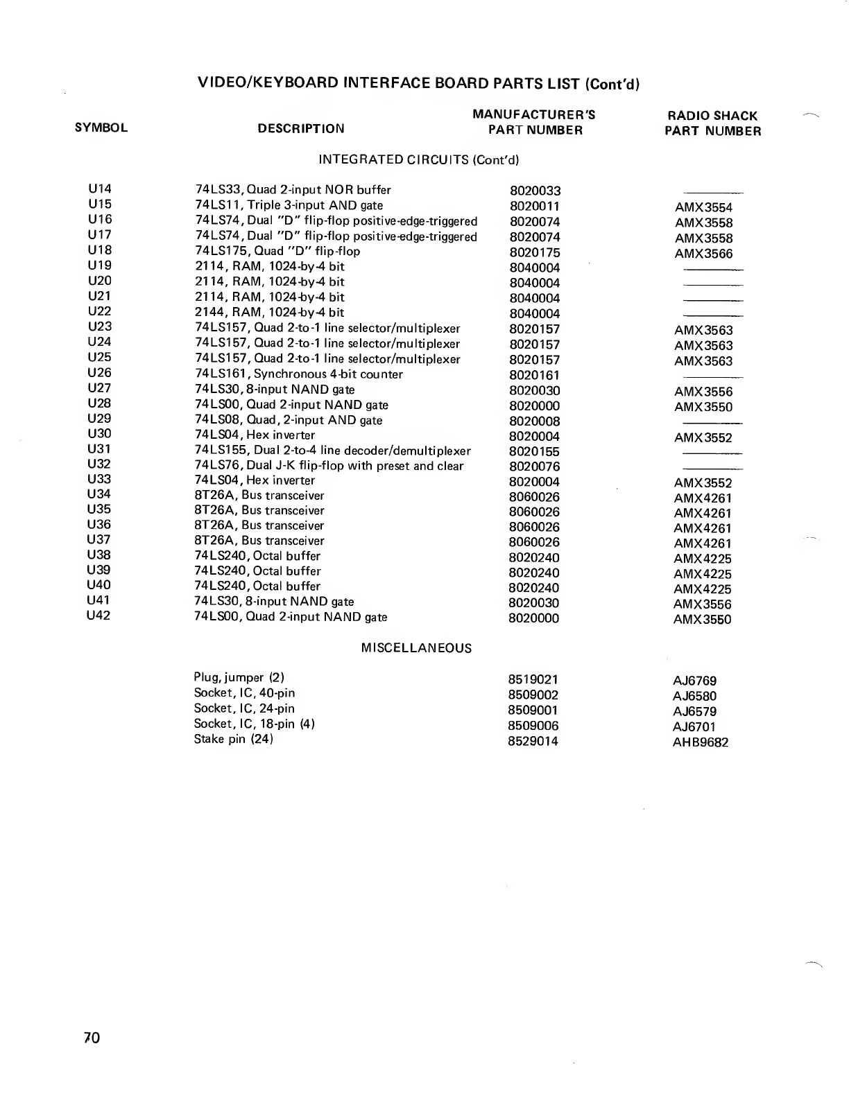
SYMBOL
U14
U15
U16
U17
U18
U19
U20
U21
U22
U23
U24
U25
U26
U27
U28
U29
U30
U31
U32
U33
U34
U35
U36
U37
U38
U39
U40
U41
U42
VIDEO/KEYBOARD INTERFACE BOARD PARTS LIST (Cont'd)
DESCRIPTION MANUFACTURER'S
PART NUMBER RADIO SHACK
PART NUMBER
INTEGRATED CIRCUITS (Cont'd)
74LS33,Quad 2-input NOR buffer
74LS1 1,Triple 3-input AND gate
74LS74, Dual "D" flip-flop positive-edge-triggered
74LS74, Dual "D" flip-flop positive-edge-triggered
74LS175, Quad "D" flip-flop
2114, RAM, 1024-by-4bit
2114, RAM, 1024-by-4bit
2114, RAM, 1024-by-4bit
2144, RAM, 1024-by-4 bit
74LS157, Quad 2-to-1 line selector/multiplexer
74LS157, Quad 2-to-1 line selector/multiplexer
74LS157, Quad 2-to-1 line selector/multiplexer
74LS161 ,Synchronous 4-bit counter
74LS30, 8-input NAND gate
74LS00, Quad 2-input NAND gate
74LS08, Quad, 2-input AND gate
74LS04, Hex inverter
74LS155, Dual 2-to-4 line decoder/demultiplexer
74LS76, Dual J-K flip-flop with preset and clear
74LS04,Hex inverter
8T26A, Bus transceiver
8T26A, Bus transceiver
8T26A, Bus transceiver
8T26A, Bus transceiver
74LS240, Octal buffer
74LS240, Octal buffer
74LS240, Octal buffer
74LS30, 8-input NAND gate
74LS00, Quad 2-input NAND gate
MISCELLANEOUS
Plug, jumper (2)
Socket, IC, 40-pin
Socket, IC, 24-pin
Socket, IC, 18-pin (4)
Stake pin (24)
8020033
8020011
8020074
8020074
8020175
8040004
8040004
8040004
8040004
8020157
8020157
8020157
8020161
8020030
8020000
8020008
8020004
8020155
8020076
8020004
8060026
8060026
8060026
8060026
8020240
8020240
8020240
8020030
8020000
8519021
8509002
8509001
8509006
8529014
AMX3554
AMX3558
AMX3558
AMX3566
AMX3563
AMX3563
AMX3563
AMX3556
AMX3550
AMX3552
AMX3552
AMX4261
AMX4261
AMX4261
AMX4261
AMX4225
AMX4225
AMX4225
AMX3556
AMX3550
AJ6769
AJ6580
AJ6579
AJ6701
AHB9682
70
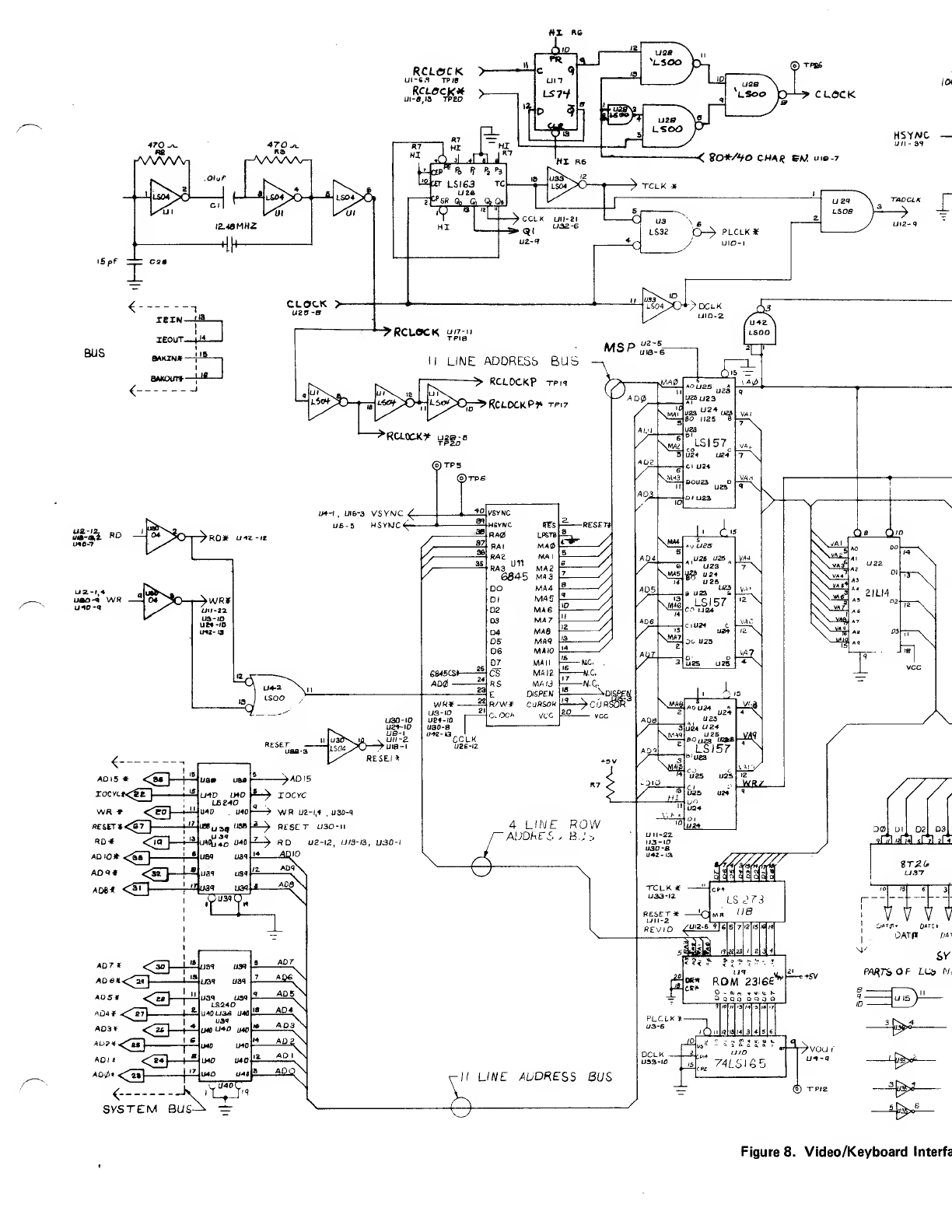
SVSTEM BUS-^ -=
Figure 8. Video/Keyboard Interfa
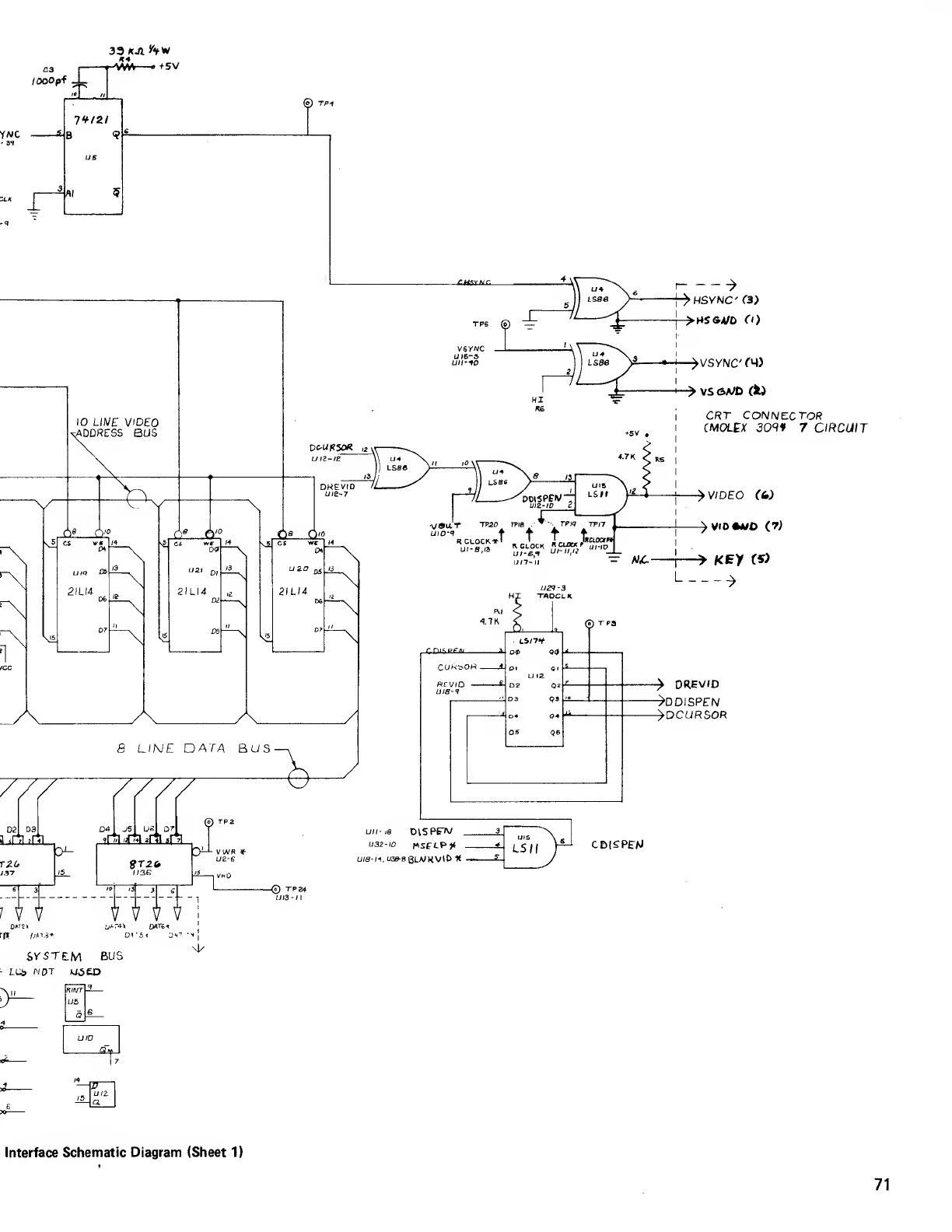
looopf _L
YNC
©TP-f
>vio**/o (7;
>HSVNC'C3)
>VSYNC'(M)
>VS <3A/D (fc)
CRT CONNECTOR
CMOLfX 309* 7CIRCUIT
>DDISPEN
>DCURSOR
CDISPEM
SYSTEM BU
IU> NOT USED
RfWT ?
US
e
UIO a«
Interface Schematic Diagram (Sheet 1)
71
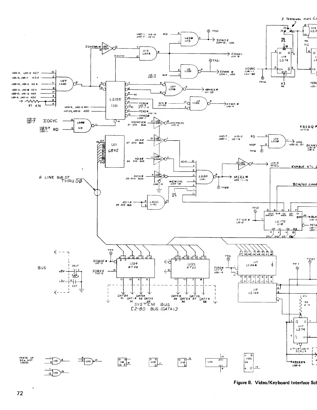
U4P-7 ,U2-I2.
U25-3, uai-s A07 -
UZ4-/3, U3P-7 AQ6 -
uea-ia, UM-q ad 5
U23-C, U40-* 4D4 ~
U2S-/0, U40-lfc A03 —
U24-6, U40-<4 ADZ —
•5 -WW—
R7 4.7K
U£7
LS30
uza-6, u40-teADi -
UM'24 U26-ID ADO
uia-io
U40-5
uai-
1
IOCYC LS0C
UZ
3LINE BUS D7
THRU
<--
BUS +Sv-
'-4HH
P«fTB OF
IC« WOT
U6EO
UI3
Lsoa
LSOS
U/3 1^iosie:
U34-/5, /J35
-^ XOSCt.
©TP2I
ua-* -; ,Lias
vsywc
U4 -I
3TtRwvAt ?/*/*> Of
S
Ai
UI6
LS74
>CK Q
0^-
LSI5? ^
3^
HI
uou
LS
CK
FERC
LSOS -^ senses *
FCRD*
U3I yaKu,7:7n
-FERO*UI6-/3
-FFRQ*
/dq
"\
Ull
AD! I* -
34 srs BUS
?-Q 1-532. "^FFWfi *
LMO-7 ,UI3-Z
USD- 1ua-ia
MSP
TP13
u/a
LSOS
ADIB !2-
M£T«CYC
U3B [19 iJ3^ "IS
L$30
Li A)
\UIVi
"7 msf
U32 -I ,12.
FFWR #
UJ"7-5
VRD
U3G-/S, "57 3X.A/M
CAM61C RTC 1
tO*/HO CM+*
QO* Qi#- Ql dO Qi
IVMIWT M*5K RFC
LS 175
DO PI P£ J)
I* "I "I '« "I -ll 7l "'
US4
ST2S
In4/ st,' \i/ \i/
IDATfil CMT2*
.SI DAn* 53 MT3*
\1/ 52 54
svs ttm BUS
/°4/ OT-X Ofc/
->>BLJJ,
UI5-3
RES£
^UB-t
U3D-I
\/ \[/ \l/ \/
CWT4* OUTS* ,
55 CMTS« 57 0*77* I
56 58 M/
TP 7
©
TP2.1
©
C2-S0 BUS <r04T/>;J
tie
CK Q
Ja
il 32.
CK
ft (?
U/7
L£7f
Q(>.<
uae-e
Figure 8. Video/Keyboard Interface Scr
72
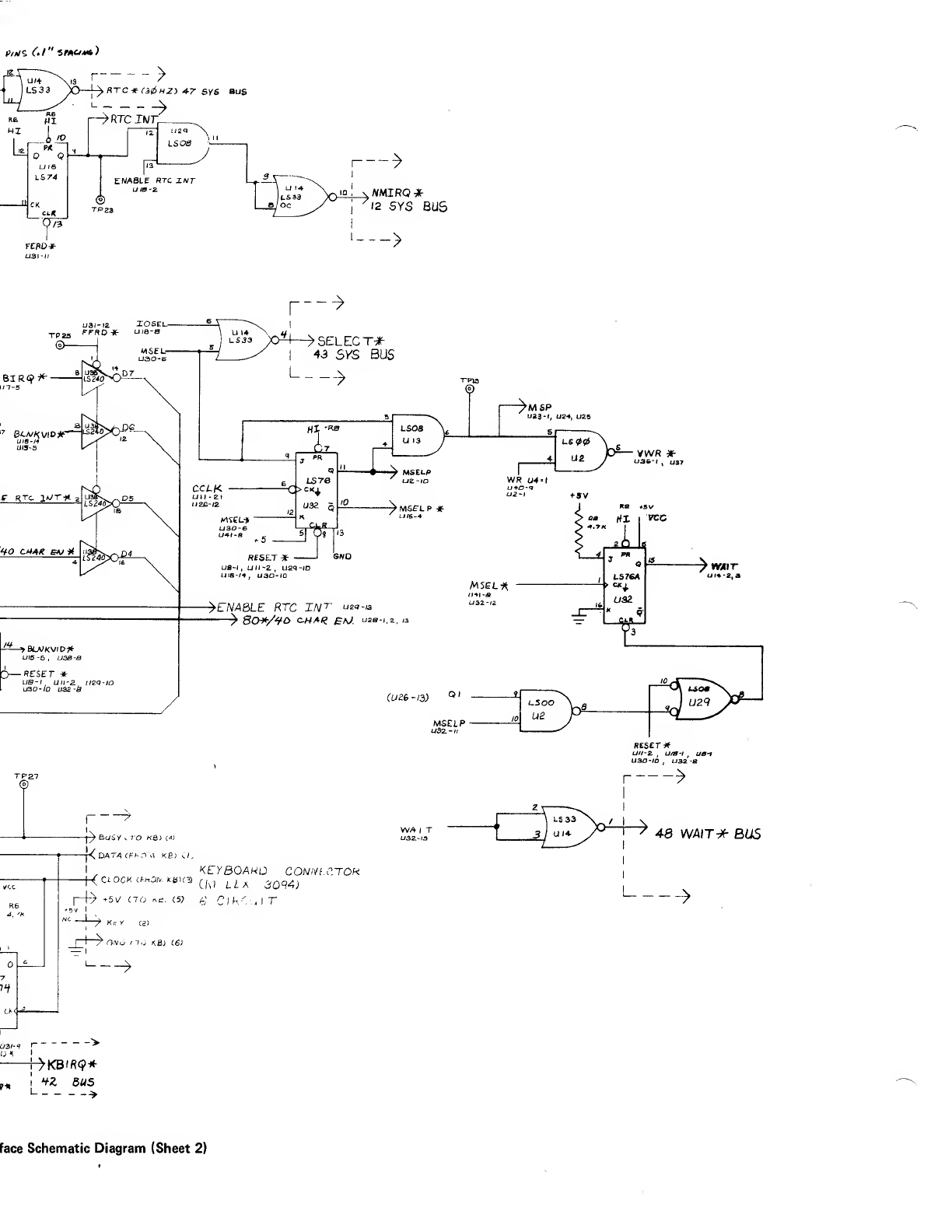
xKMIRQ #
712 SYS BUS
r—
>
U3I-I2 XOSEL--
TP25 "7»D* U,a -S
©>SELECT*
43 SKS BUS
^MSELP
-^ENABLE RTC INT u2»-a
-^ 80*/4C> CAM* EK). U2s-i,z, u
3—RESET *
US-/ iJ/l-2 112Q-IO
USD -10 U32 -a
TPia
©
?MSP
U23-I, U24, U25
LS00
WR 04 =1
VWR #
U36-I ,U37
KB +SV
ui«-2 a
MSEL*
U32-<2
ft/26 -13) Q'
TP27
©
-^ easy *7-0 «ej ;j>
-r^DAT/t (FhO.1 KB) </,
WA IT
U32.-I3
I_KEYBOAhtO CONK/l.CTOK
"—*-^Key C2>
[I7/1NO 'In KB) («J
RESET*
U//-2 ,U/B-l ,</«-*
U30 -/O ,U32 -a
LS33
->
48 WAIT* BUS
I
->KBfR<?*
1*
face Schematic Diagram (Sheet 2)
SECTION VI
MEMORY BOARD (64K and 32K RAM)
73

A. FUNCTIONAL SPECIFICATIONS
1. Interface —The interface between the memory board
and the Model II bus is fully buffered. Any line used
by the memory board presents only one unit load on
that particular line. (One unit load being the load pre-
sented by an LS-TTL device.)
2. Memory array —The memory array uses 16K dynamic
memory chips. The board comes with either 32K bytes
of RAM or 64K bytes of RAM.
3. Timing —The generation of MUX and CAS for the
memory array is accomplished by the use of adelay
line which allows precise memory timing.
4. Paging —The memory is logically divided into 32K
byte pages. Page zero consists of all memory from
0000 to 7FFF Hexadecimal addresses and pages 1to
15 consist of all memory from 8000 Hex to FFFF Hex.
Only one of the memory pages 1to 15 is enabled at
one time. The state of the lower four bits of Port FF
determines which one of these pages is enabled.
5. Bank Select —Each memory board has the option of
being selected as one of eight banks by using the bank
select option in conjunction with the bank select bits
in Port FF. Each bank contains two 32K byte pages.
Therefore it is theoretically possible to have 51 2K
bytes of random access memory in asystem.
B. THEORY OF OPERATION
Refer to Memory Board Schematic
1. Interface —The interface to the Model II system bus
consists of:
A) Data Bus Buffers
B) Address Buffers
C) Control Line Buffers
The data bus buffer-drivers buffer input data from the
CPU and output data to the CPU. They consist of chips
U53 and U52. Gating logic is performed by U26, U14,
U27and U12.
The address buffers buffer and invert the address signals
and present them to the multiplexers (U39 and U40),
to the port select logic (U41) and to the memory select
logic (U10,U11,U14 and U29).
The control line buffers provide the following signals
to the memory board -SYNC*, CLOCK, MEMCYC*,
RD*, REFRSH*, WR*, IOCYC* and RESET* which
are used by the RAS precharge extender circuit (U14,
U18). This insures that the minimum precharge time
will be provided by the 4MHz CPU to the memory
chips. RD* is used by U27 to gate data onto the bus.
REFRSH* is used by U14 and U24 in generating the
memory refresh pulse; WR*is buffered directly into
the memory array and to U41 for the I/O port write
pulse. IOCYC* is also used by U41 for the same pur-
pose. RESET* is used to clear port FF.
2. Memory Array —The memory array consists of 16 or
32 chips. The chips are 16K by 1bit MOS dynamic
memory circuits. Thus, one will have either a32K byte
memory board or a64K byte memory board. All the
power supply voltages are bypassed on every other chip
to provide good noise immunity. The RAM chips are
U1 -U8, U15-U22, U30-U37andU44-U51. 12
volt bulk capacitance is provided on the memory array
since this is the supply voltage most heavily used.
These are -C13, C25, C39 and C57.
3. Address Multiplexers —The address multiplexers U39
and U40 take the buffered address and drive the mem-
ory array through damping resistors U38 (dip resistor
array). The MUX signal provided by the timing section
switches between the row address and the column
address. The damping resistors minimize the under-
shoot on the signal lines which further enhances error
free operation.
4. Timing —The timing consists of circuits U13, U14
(precharge extender), U42 (delay line), U57 (delay line
buffer), U28 (CAS and MUX buffers) and U9 (CAS
and write drivers). When MEMCYC* is active, indicat-
ing that the CPU is going to do aread or awrite, RAS
is generated by the precharge circuitry and is gated
with REFRSH* at U14 (i.e., no RAS pulse is passed to
.the delay line during Refresh). The resulting pulse
propagates down the delay line; generating first, MUX
which switches the address multiplexers from Row
address to Column address, and second, it generates
CAS which provides (through drivers) the signal of the
same name to the memory array.
RAS is also buffered by U24 to provide RAS to the
memory array. If WR* was present on the bus then it
is appropriately buffered into the memory array and
signals awrite cycle; otherwise, the data from the
memory array is available for aread cycle. Note also
that all RAS, CAS, and WR signals are damped into
the memory array just as the address lines are and for
the same reason. The damping resistor package is U23.
5. Memory select logic —The memory select logic con-
sists of packages U29, U43 and U24. The buffered
address lines A14 and A15 and bits to 3of Port FF
are combined to produce select signals for pages 1to
15. The memory select signal is then OR'd with Re-
fresh and the resulting signal gates RAS into the mem-
ory array through NAND gates U24.
6. Memory disable logic —This logic is used to disable
memory from F800 to- FFFF when one wishes to ac-
cess video memory that is mapped into the same
physical address space. Only memory pages 1to 15 are
affected. Circuit U11 decodes the memory address
range, the memory page being accessed, and the video
RAM enable bit (bit 7) from I/O port FF. It also pro-
duces the gate signal for 74S139 decoder controlling
75
the memory select signals for pages 1to 15. If the
gate signal is not present (pin 1of the 74S139) then no
memory access is allowed.
I/O Port FF and Select logic -I/O port FF is package
U58 which is an 8-bit register and is selected by the
strobe IOFFWR which is generated by U41. U41 de-
codes the lower 8address lines, IOCYC and the WR
line to generate the select. The RESET line clears Port
FF on power-up or manual reset. The lower four bits
of this register drive the Bank select logic which selects
one of memory pages 1to 15. Bit 7of this register is
the Video RAM enable bit which feeds the Memory
disable logic.
(FROM ADDRESS BUFFERS)
IO PORT LOGIC
-- TOMEM.DIS. LOGIC
MODEL II
BUS
DATA BUS GATING
CONTROL LINE
BUFFERS
DATA BUFFERS
MEMORY SELECT
LOGIC
/l A
ADDRESS BUFFERS
TIMING
-> IO PORT
LOGIC
MEMORY DISABLE
LOGIC
D
A
M
P
I
N
G
MEMORY ARRAY
(160R 32 16Kx1 HIT
DYNAMIC RAM CHIPS)
DAMPING
MULTIPLEXERS
•IOPORT LOGIC
Figure 1. Block Diagram
76
C. JUMPER OPTIONS
The following table lists all the jumper options. Also refer to Figure 2.
Memory Page Memory Bank Memory Page Jumpers Memory Bank Jumpers
J16-J17, J15-J18
1J9-J13.J10-J14 J19-J27
rJ9-J11, J10-J12 J19-J27
21J7-J11, J8-J12 J20-J28
31J9-J13,J10-J14 J20-J28
42J7-J11, J8-J12 J21-J29
52J9-J13,J10-J14 J21-J29
63J7-J11, J8-J12 J22-J30
73 J9-J13,J10-J14 J22-J30
84J7-J11, J8-J12 J23-J27
94J9-J13,J10-J14 J23-J27
10 5J7-J11, J8-J12 J24-J28
11 5J9-J13,J10-J14 J24-J28
12 6 J7-J11, J8-J12 J25-J29
13 6J9-J13,J10-J14 J25-J29
14 7J7-J11, J8-J12 J26-J30
15 7J9-J13,J10-J14 J26-J30
'Jumper configuration for add-on 32K memory board.
For example: A32K memory board will have Page and jumpers as above.
The first 64K memory board will have Page and Page 1and jumpers as
above.
D. VERIFICATION PROCEDURES
1. Automatic RAM verification is performed on the
memories during the boot procedures. If an error
is encountered, an MF error is displayed in the
center of the CRT screen.
IMPORTANT NOTE
The test procedures below should never be attempted
by an unqualified technician. If the diagnostic instruc-
tions are not followed correctly the computer video
can and probably will be damaged. We strongly suggest
that if these procedures are necessary, you should re-
turn your unit to Radio Shack.
2. Further testing can be done on the system mem-
ories by using the Diagnostic Diskette and the
TRS-80 Model II Troubleshooting Manual.
WARNING
When performing atest that includes turning the CRT
on and off, do not leave it off for more than three
seconds or damage to the circuitry may occur.
77
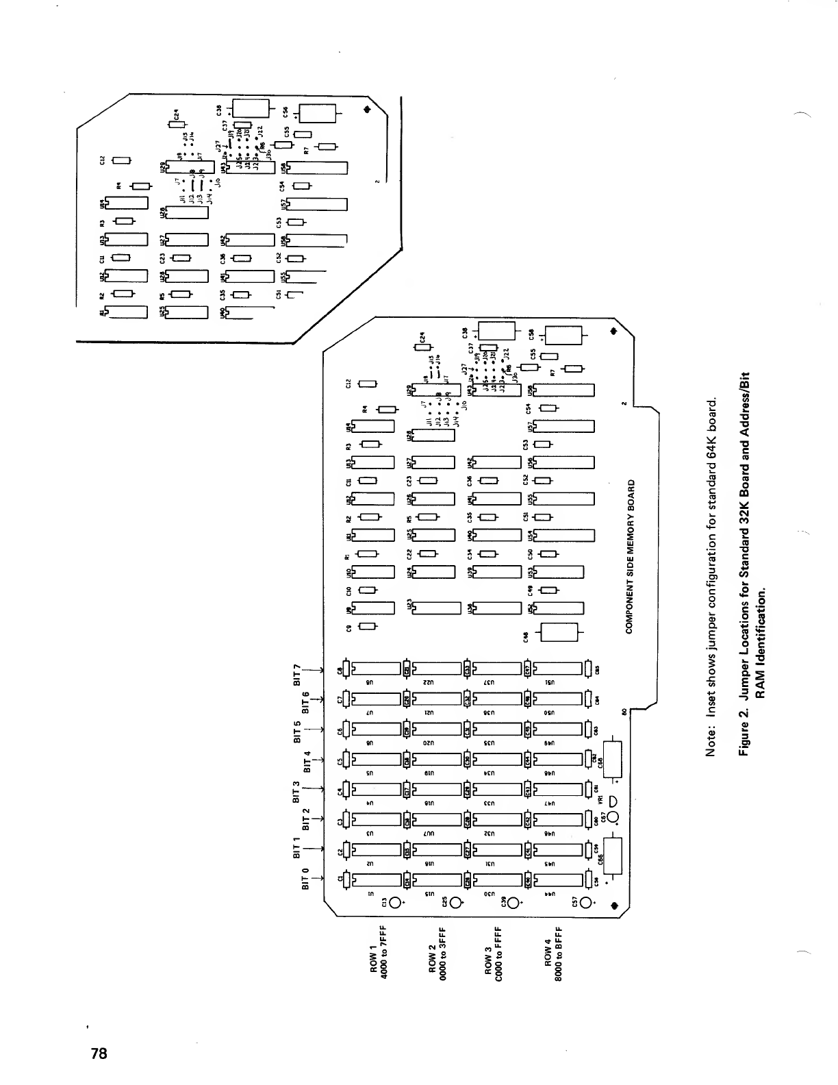
s_
"»"» r» ?* • *.
•IJr- £•»•* m
-> =^ *-lrf> Jt*t —t
C=D
3<=>
£zz
S-c=>
szz
3c_
c
£
£
£so-
ld
8-cz>
iSZZ s:
£
8-[
£
£J-CZD-
SZZ
CD-
4>ije:
•n
in
sQzzzzifc
*[>igEzzzjife
sn am
$ijezz
zn sin
#igEzzzpij
in sin
so- so-
y
<
o
o
s
5
UJ
O
z
o
Q.
s
o
o
]g E|Q»
isn
]ggzzz:Di
osn
]j {= H>
6t.fl
izziDs
dSezzziO8
D
s[>IJEigEigEZZHQiSQ
en inn zen »n
zz:@zzzdQ
—lg siQ»
tfcn
SO' SO-
m
OD
D
<
<* o
CO CO
ao
"D
cm
nIB
a
CD c
CD
3CO
c
o
o
a
£
(M
CO
»> o
C*S
OCO
9=
-I <B
_2
CD
i<
—<N
3
C!
ll °9
Kg
•a- u.
oS
DC O
S
00
78
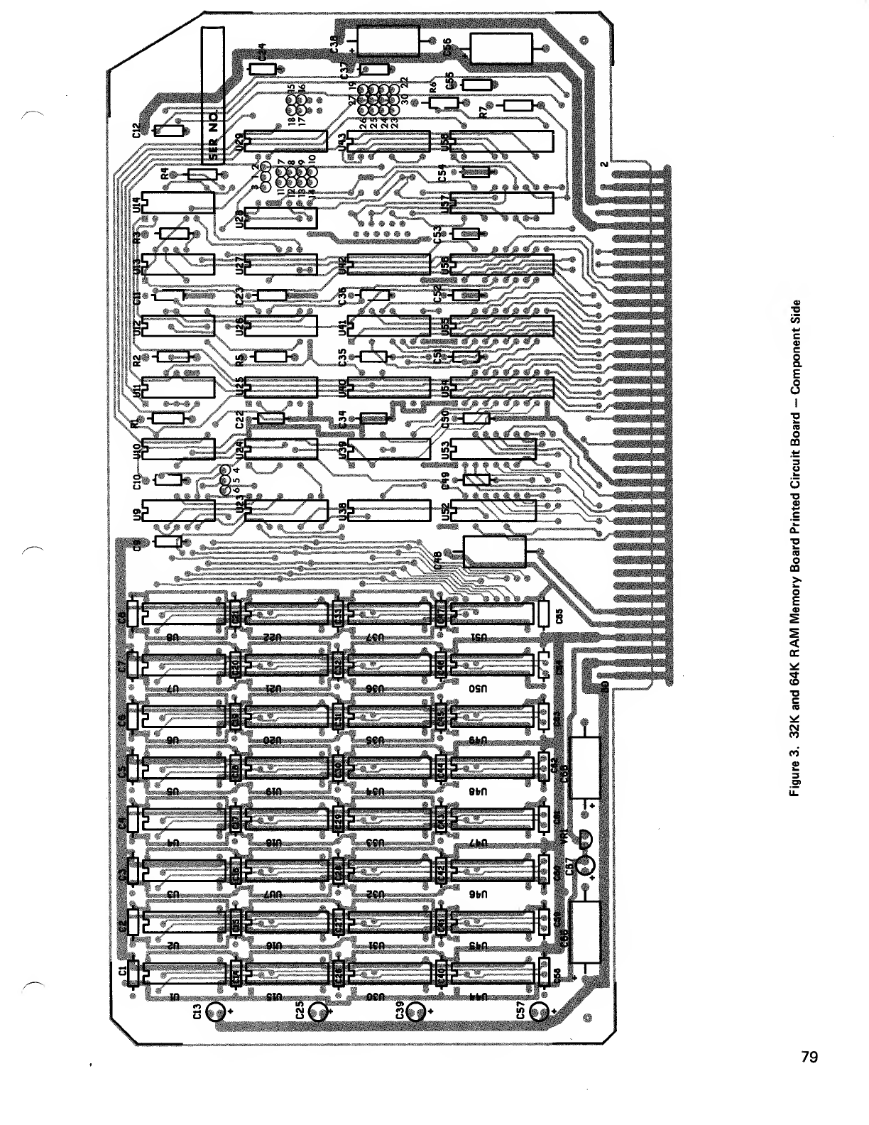
5E
^y
^w,
--fta»
'S^t3!.„.-.\
£""
—
JV
^^
^v V
11111111 ^e< .tbm m•maf» m»a---—'Of*—*
:«.„,. rS/*
«f~=«
13d 13d 13d 1
*—-4KB
^{•"Hi wn
IS<=5 >r«H
5, ife jfe ifl ji |fl i
riioir 'Mr iioir mi<->
Zp^Z. ~WmTZ ^m SiT**!! •X—
i.i i
aifc
r————
iT
•«•
:'i
ii
i1^Sir.»i".^-i^S*a
w>
I
1
en
=0£
irll ifi i
|S
b
|?lb
um rIlot r
IDL " ' '
iCT r
J*
f
1!! JML iCIl '
'""' iml
°Qsigs'8s'Is
"bo- "SO- K*S0ri '* S
3
o
s
1
.1
79
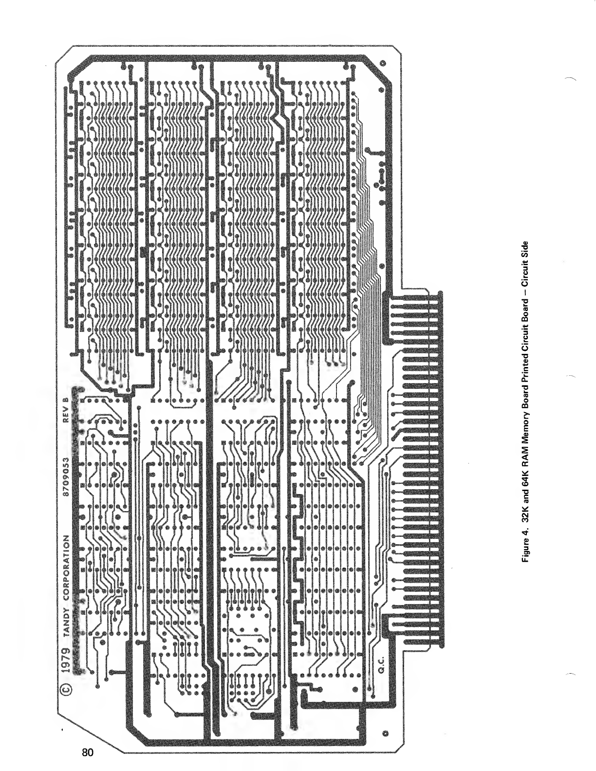
8
CO
I
.E
D
s
1
.1
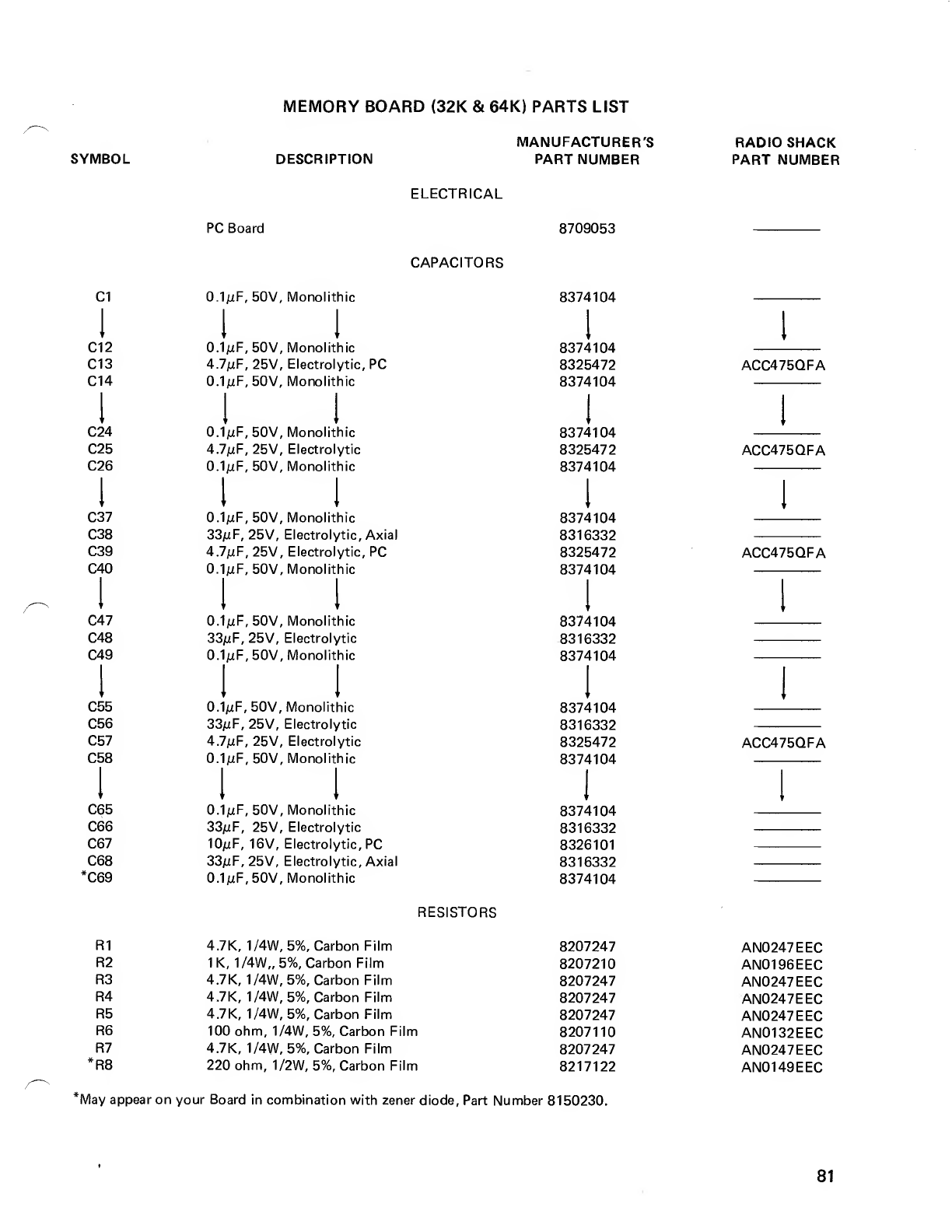
MEMORY BOARD (32K &64K) PARTS LIST
SYMBOL DESCRIPTION
MANUFACTURER'S
PART NUMBER RADIO SHACK
PART NUMBER
ELECTRICAL
PC Board 8709053
CAPACITORS
C1 0.1/iF, 50V, Monolithic 8374104
C12
C13
C14
C24
C25
C26
C37
C38
C39
C40
C47
C48
C49
C55
C56
C57
C58
C65
C66
C67
C68
*C69
0.1aiF,50V,
4.7juF, 25V,
0.1mF,50V,
0.1mF,50V,
4.7(j.F, 25V,
0.1juF,50V,
0.1aiF,50V,
33;uF, 25V,
4.7mF,25V ;
0.1juF, 50V,
0.1juF,50V,
33/uF, 25V,
0.1juF,50V,
Monolithic
Electrolytic, PC
Monolithic
Monolithic
Electrolytic
Monolithic
Monolithic
Electrolytic, Axial
Electrolytic, PC
Monolithic
Monolithic
Electrolytic
Monolithic
0.1/uF, 50V, Monolithic
33mF, 25V, Electrolytic
4.7juF, 25V, Electrolytic
0.1mF, 50V, Monolithic
0.1/iF, 50V, Monolithic
33juF, 25V, Electrolytic
10mF, 16V, Electrolytic, PC
33/zF, 25V, Electrolytic, Axial
0.1/zF, 50V, Monolithic
8374104
8325472
8374104
83741 04
8325472
8374104
8374104
8316332
8325472
8374104
8374104
8316332
8374104
8374104
8316332
8325472
8374104
8374104
8316332
8326101
8316332
8374104
ACC475QFA
ACC475QFA
ACC475QFA
ACC475QFA
RESISTORS
R1
R2
R3
R4
R5
R6
R7
fR8
4.7K, 1/4W, 5%, Carbon Film
1K, 1/4W„ 5%, Carbon Film
4.7K, 1/4W, 5%, Carbon Film
4.7K, 1/4W, 5%, Carbon Film
4.7K, 1/4W, 5%, Carbon Film
100 ohm, 1/4W, 5%, Carbon Fi
4.7K, 1/4W, 5%, Carbon Film
220 ohm, 1/2W, 5%, Carbon Fi
Im
Im
8207247
8207210
8207247
8207247
8207247
8207110
8207247
8217122
AN0247EEC
AN0196EEC
AN0247EEC
AN0247EEC
AN0247EEC
AN0132EEC
AN0247EEC
AN0149EEC
*May appear on your Board in combination with zener diode. Part Number 8150230.
81
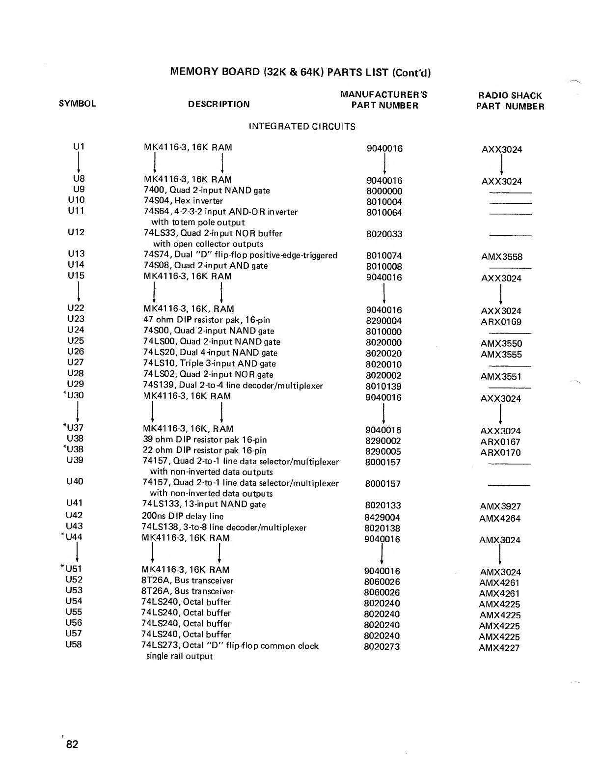
SYMBOL
U1
MEMORY BOARD (32K &64K) PARTS LIST (Cont'd)
DESCRIPTION MANUFACTURER'S
PART NUMBER
U8
U9
U10
U11
U12
U13
U14
U15
U22
U23
U24
U25
U26
U27
U28
U29
*U30
*U37
U38
*U38
U39
U40
U41
U42
U43
>U44
*U51
U52
U53
U54
U55
U56
U57
U58
MK4116-3, 16K RAM
7400, Quad 2-input NAND gate
74S04, Hex inverter
74S64, 4-2-3-2 input AND-OR inverter
with totem pole output
74LS33, Quad 2-input NOR buffer
with open collector outputs
74S74, Dual "D" flip-flop positive-edge-triggered
74S08, Quad 2-input AND gate
MK4116-3, 16K RAM
MK4116-3, 16K, RAM
47 ohm DIP resistor pak, 16-pin
74S00, Quad 2-input NAND gate
74LS00, Quad 2-input NAND gate
74LS20, Dual 4-input NAND gate
74LS10, Triple 3-input AND gate
74LS02, Quad 2-input NOR gate
74S139, Dual 2-to4 line decoder/multiplexer
MK4116-3, 16K RAM
MK4116-3, 16K, RAM
39 ohm DIP resistor pak 16-pin
22 ohm DIP resistor pak 16-pin
74157, Quad 2-to-1 line data selector/multiplexer
with non-inverted data outputs
74157, Quad 2-to-1 line data selector/multiplexer
with non-inverted data outputs
74LS133, 13-input NAND gate
200ns DIP delay line
74LS138, 3-to-8 line decoder/multiplexer
MK4116-3, 16K RAM
MK4116-3, 16K RAM
8T26A, Bus transceiver
8T26A, Bus transceiver
74LS240, Octal buffer
74LS240, Octal buffer
74LS240, Octal buffer
74LS240, Octal buffer
74LS273, Octal "D" flip-flop common clock
single rail output
INTEGRATED CIRCUITS
MK41 16-3, 16K RAM 9040016
9040016
8000000
8010004
8010064
8020033
8010074
8010008
9040016
9040016
8290004
8010000
8020000
8020020
8020010
8020002
8010139
9040016
9040016
8290002
8290005
8000157
8000157
8020133
8429004
8020138
9040016
9040016
8060026
8060026
8020240
8020240
8020240
8020240
8020273
RADIO SHACK
PART NUMBER
AXX3024
I
AXX3024
AMX3558
AXX3024
AXX3024
ARX0169
AMX3550
AMX3555
AMX3551
AXX3024
AXX3024
ARX0167
ARX0170
AMX3927
AMX4264
AMX3024
AMX3024
AMX4261
AMX4261
AMX4225
AMX4225
AMX4225
AMX4225
AMX4227
82
MEMORY BOARD (32K &64K) PARTS LIST (Cont'd)
SYMBOL DESCRIPTION
MANUFACTURER'S
PART NUMBER RADIO SHACK
PART NUMBER
VOLTAGE REGULATOR
tVR1 MC79L05AC, -5V, 5%, TO-92 case
tMay also appear as:
VR1 1N5231,Zener diode
Plug, Jumper (5)
Socket, IC, 16-pin (16)
*Socket,IC, 16-pin (32)
Stake Pin (52)
'Used only on the 64K RAM Memory Board.
MISCELLANEOUS
8051905
8150230
8519021
8509003
8509003
8529014
AMX4260
ADX1211
AJ6769
AJ6581
AJ6581
AHB9682
83

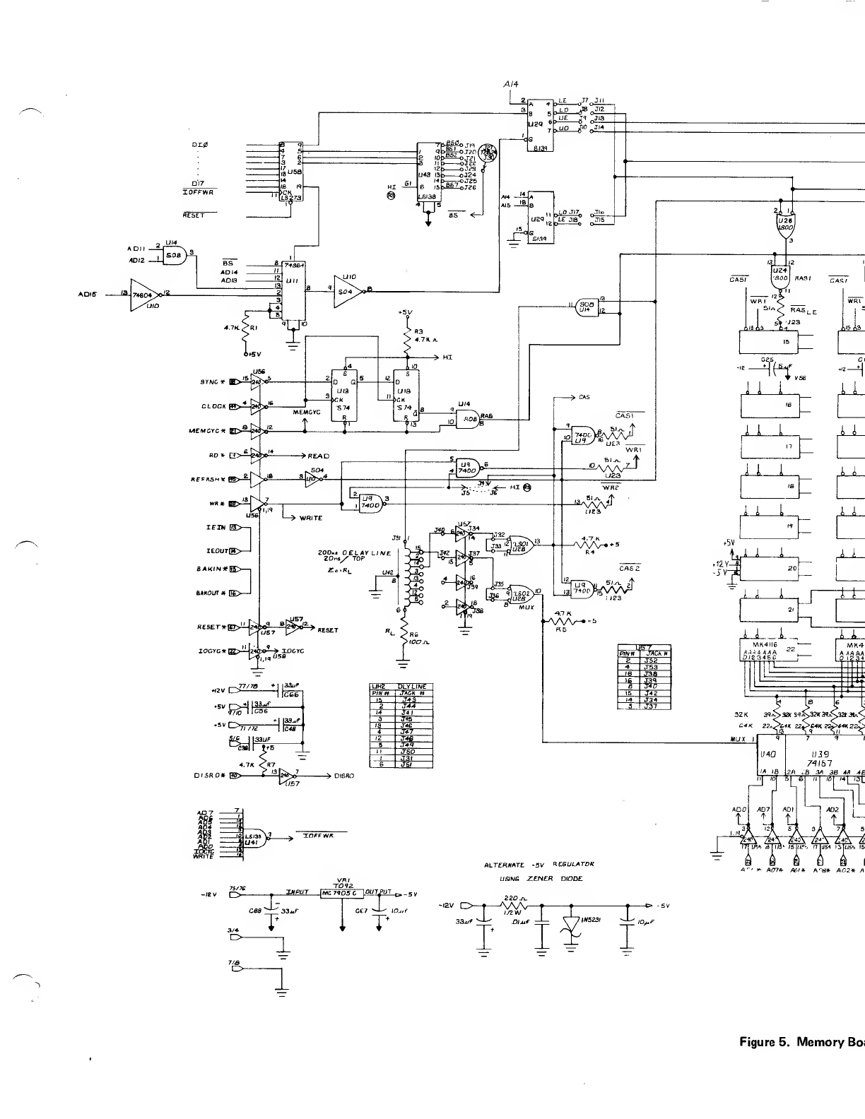
/4/4
Figure 5. Memory Bo<

ffi>SeLECT V
cz ,c-*, ce, cs, c14,
cis ,cia ,czo ,C27 ,cat
,
C33 ,C40 ,C2Q ,C12 ,C44,
ces, ceo.c&.CBZ, ce,* ,cs*
CIS ,CI/ '
c«, a?/, o.?e ,cse ,czo,
C32 C4I C*3. C« ,C47
CI .C3 ,C5. C7. C<J, CtO,
Clt, CIZ. C22, C23 ,C24,
C34, C35. C3£, C37 ,C49,
CSO .CSZ, C53 .CS4,
C55, C3**, C6/ ,CCS.CSB
A?tf* A02* *^7* AD3* AID* AR4-X /111* >«I0«* AlS.* AfiZX AI3* AM* ^J.^-K
mory Board Schematic Diagram
85

SECTION VII
VIDEO MONITOR (CRT)
87

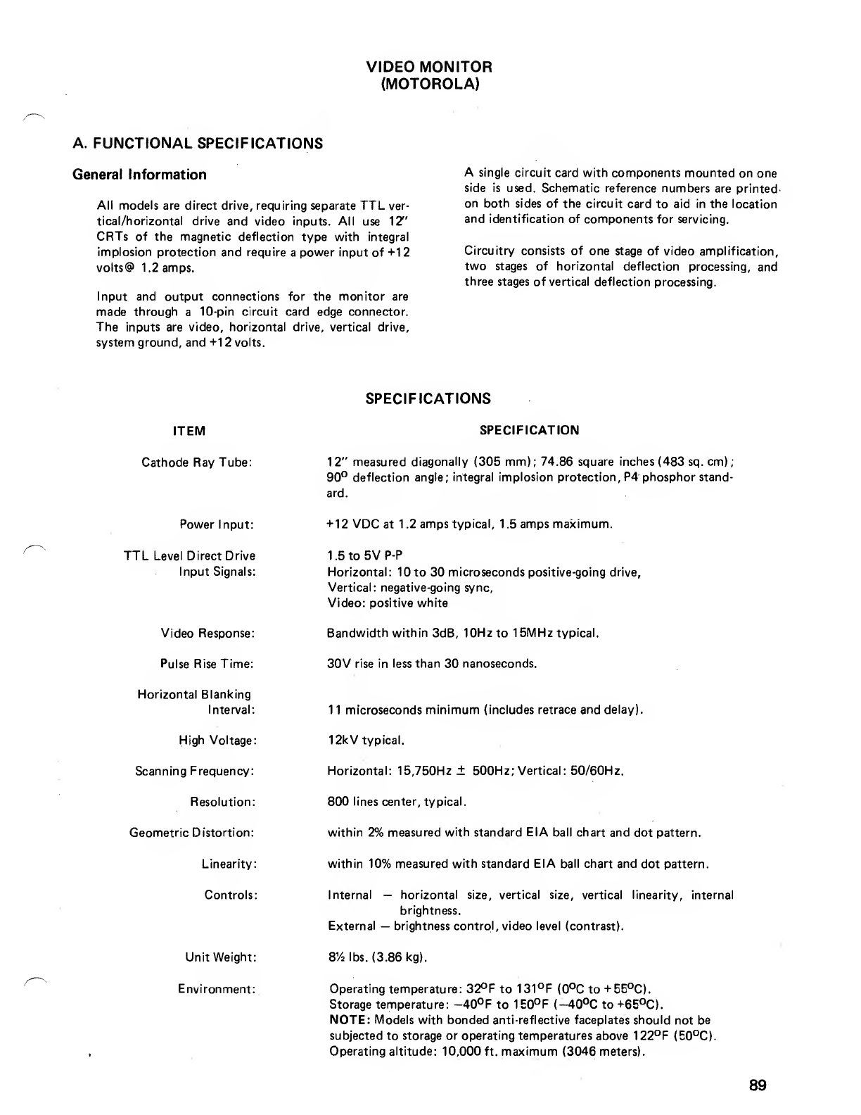
VIDEO MONITOR
(MOTOROLA)
A. FUNCTIONAL SPECIFICATIONS
General Information
All models are direct drive, requiring separate TTL ver-
tical/horizontal drive and video inputs. All use 12"
CRTs of the magnetic deflection type with integral
implosion protection and require apower input of +12
volts@ 1.2 amps.
Input and output connections for the monitor are
made through a10-pin circuit card edge connector.
The inputs are video, horizontal drive, vertical drive,
system ground, and +1 2volts.
Asingle circuit card with components mounted on one
side is used. Schematic reference numbers are printed,
on both sides of the circuit card to aid in the location
and identification of components for servicing.
Circuitry consists of one stage of video amplification,
two stages of horizontal deflection processing, and
three stages of vertical deflection processing.
ITEM
Cathode Ray Tube:
Power Input:
TTL Level Direct Drive
Input Signals:
Video Response:
Pulse Rise Time:
Horizontal Blanking
Interval:
High Voltage:
Scanning Frequency:
Resolution:
Geometric Distortion:
Linearity:
Controls:
Unit Weight:
Environment:
SPECIFICATIONS
SPECIFICATION
12" measured diagonally (305 mm); 74.86 square inches (483 sq. cm);
90° deflection angle; integral implosion protection, P4 phosphor stand-
ard.
+12 VDC at 1.2 amps typical, 1.5 amps maximum.
1.5 to 5V P-P
Horizontal: 10 to 30 microseconds positive-going drive.
Vertical: negative-going sync.
Video: positive white
Bandwidth within 3dB, 10Hzto 15MHz typical.
30V rise in less than 30 nanoseconds.
11microseconds minimum (includes retrace and delay).
12kV typical.
Horizontal: 15,750Hz+ 500Hz; Vertical: 50/60Hz.
800 lines center, typical.
within 2% measured with standard EIA ball chart and dot pattern.
within 10% measured with standard EIA ball chart and dot pattern.
Internal —horizontal size, vertical size, vertical linearity, internal
brightness.
External —brightness control, video level (contrast).
8% lbs. (3.86 kg).
Operating temperature: 32°F to 131°F (0°C to +5E°C).
Storage temperature: -40°F to 1E0°F (-40°C to +6E°C).
NOTE: Models with bonded anti-reflective faceplates should not be
subjected to storage or operating temperatures above 122°F (E0°C).
Operating altitude: 10,000 ft. maximum (3046 meters).
89
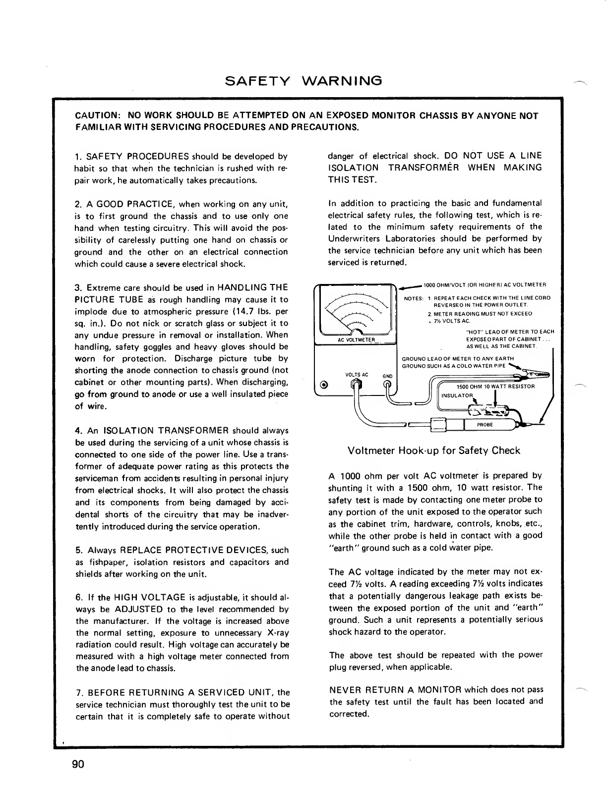
SAFETY WARNING
CAUTION: NO WORK SHOULD BE ATTEMPTED ON AN EXPOSED MONITOR CHASSIS BY ANYONE NOT
FAMILIAR WITH SERVICING PROCEDURES AND PRECAUTIONS.
1. SAFETY PROCEDURES should be developed by
habit so that when the technician is rushed with re-
pair work, he automatically takes precautions.
2. AGOOD PRACTICE, when working on any unit,
is to first ground the chassis and to use only one
hand when testing circuitry. This will avoid the pos-
sibility of carelessly putting one hand on chassis or
ground and the other on an electrical connection
which could cause asevere electrical shock.
danger of electrical shock. DO NOT USE ALINE
ISOLATION TRANSFORMER WHEN MAKING
THIS TEST.
In addition to practicing the basic and fundamental
electrical safety rules, the following test, which is re-
lated to the minimum safety requirements of the
Underwriters Laboratories should be performed by
the service technician before any unit which has been
serviced is returned.
3. Extreme care should be used in HANDLING THE
PICTURE TUBE as rough handling may cause it to
implode due to atmospheric pressure (14.7 lbs. per
sq. in.). Do not nick or scratch glass or subject it to
any undue pressure in removal or installation. When
handling, safety goggles and heavy gloves should be
worn for protection. Discharge picture tube by
shorting the anode connection to chassis ground (not
cabinet or other mounting parts). When discharging,
go from ground to anode or use awell insulated piece
of wire.
4. An ISOLATION TRANSFORMER should always
be used during the servicing of aunit whose chassis is
connected to one side of the power line. Use atrans-
former of adequate power rating as this protects the
serviceman from accidents resulting in personal injury
from electrical shocks. It will also protect the chassis
and its components from being damaged by acci-
dental shorts of the circuitry that may be inadver-
tently introduced during the service operation.
5. Always REPLACE PROTECTIVE DEVICES, such
as fishpaper, isolation resistors and capacitors and
shields after working on the unit.
6. If the HIGH VOLTAGE is adjustable, it should al-
ways be ADJUSTED to the level recommended by
the manufacturer. If the voltage is increased above
the normal setting, exposure to unnecessary X-ray
radiation could result. High voltage can accurately be
measured with ahigh voltage meter connected from
the anode lead to chassis.
-1000 OHM/VOLT (OR HIGHFRI AC VOLTMETER
NOTES: 1. REPEAT EACH CHECK WITH THE LINE CORD
REVERSED IN THE POWER OUTLET.
2. METER READING MUST NOT EXCEED
,7'/. VOLTS AC.
"HOT" LEAD OF METER TO EACH
EXPOSED PART OF CABINET .. .
AS WELL AS THE CABINET
GROUND LEAD OF METER TO ANY EARTH
GROUND SUCH AS ACOLD WATER PIPE '
Voltmeter Hook-up for Safety Check
A1000 ohm per volt AC voltmeter is prepared by
shunting it with a1500 ohm, 10 watt resistor. The
safety test is made by contacting one meter probe to
any portion of the unit exposed to the operator such
as the cabinet trim, hardware, controls, knobs, etc.,
while the other probe is held in contact with agood
"earth" ground such as a cold water pipe.
The AC voltage indicated by the meter may not ex-
ceed Th volts. Areading exceeding 7V4 volts indicates
that apotentially dangerous leakage path exists be-
tween the exposed portion of the unit and "earth"
ground. Such aunit represents apotentially serious
shock hazard to the operator.
The above test should be repeated with the power
plug reversed, when applicable.
7. BEFORE RETURNING ASERVICED UNIT, the
service technician must thoroughly test the unit to be
certain that it is completely safe to operate without
NEVER RETURN AMONITOR which does not pass
the safety test until the fault has been located and
corrected.
90
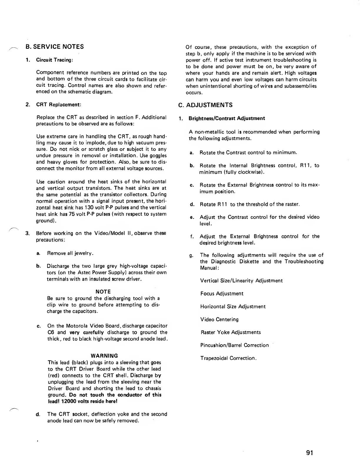
B. SERVICE NOTES
1. Circuit Tracing:
Component reference numbers are printed on the top
and bottom of the three circuit cards to facilitate cir-
cuit tracing. Control names are also shown and refer-
enced on the schematic diagram.
2. CRT Replacement:
Replace the CRT as described in section F. Additional
precautions to be observed are as follows:
Use extreme care in handling the CRT, as rough hand-
ling may cause it to implode, due to high vacuum pres-
sure. Do not nick or scratch glass or subject it to any
undue pressure in removal or installation. Use goggles
and heavy gloves for protection. Also, be sure to dis-
connect the monitor from all external voltage sources.
Use caution around the heat sinks of the horizontal
and vertical output transistors. The heat sinks are at
the same potential as the transistor collectors. During
normal operation with asignal input present, the hori-
zontal heat sink has 130 volt P-P pulses and the vertical
heat sink has 75 volt P-P pulses (with respect to system
ground).
3. Before working on the Video/Model II, observe these
precautions:
a. Remove all jewelry.
b. Discharge the two large grey high-voltage capaci-
tors (on the Astec Power Supply) across their own
terminals with an insulated screw driver.
NOTE
Be sure to ground the discharging tool with a
clip wire to ground before attempting to dis-
charge the capacitors.
c. On the Motorola Video Board, discharge capacitor
C6 and very carefully discharge to ground the
thick, red to black high-voltage second anode lead.
WARNING
This lead (black) plugs into asleeving that goes
to the CRT Driver Board while the other lead
(red) connects to the CRT shell. Discharge by
unplugging the lead from the sleeving near the
Driver Board and shorting the lead to chassis
ground. Do not touch the conductor of this
lead! 12000 volts reside here!
The CRT socket, deflection yoke and the second
anode lead can now be safely removed.
Of course, these precautions, with the exception of
step b, only apply if the machine is to be serviced with
power off. If active test instrument troubleshooting is
to be done and power must be on, be very aware of
where your hands are and remain alert. High voltages
can harm you and even low voltages can harm circuits
when unintentional shorting of wires and subassemblies
occurs.
C. ADJUSTMENTS
1. Brightness/Contrast Adjustment
Anon-metallic tool is recommended when performing
the following adjustments.
a. Rotate the Contrast control to minimum.
b. Rotate the Internal Brightness control, R11, to
minimum (fully clockwise).
c. Rotate the External Brightness control to its max-
imum position.
d. Rotate R11 to the threshold of the raster.
e. Adjust the Contrast control for the desired video
level.
f. Adjust the External Brightness control for the
desired brightness level.
g. The following adjustments will require the use of
the Diagnostic Diskette and the Troubleshooting
Manual:
Vertical Size/Linearity Adjustment
Focus Adjustment
Horizontal Size Adjustment
Video Centering
Raster Yoke Adjustments
Pincushion/Barrel Correction
Trapezoidal Correction.
91

D. TROUBLESHOOTING GUIDE
A. There are basically six areas that may cause the loss, dis-
tortion or non-adjustment of video. These areas are:
1
.
System Power Supply
2. Video Generator Module
3. Motorola Video Board
4. Cathode Ray Tube
5. CRT Deflection Coil
6. High voltage leads from the CRT
(Don't overlook any of the interconnecting wiring
between these assemblies.)
B. Listed below are some of the symptoms and their possibles causes and remedies:
SYMPTOM POSSIBLE CAUSE REMEDY
No video at all Video Generator Module
or Motorola Video Board
or Power Supply or any
combination of the above
Check voltage from Power Supply at pin 7
of the plug connecting at the top of the
Motorola Video Board. NOTE: Pin 1is to
the back of the system. Voltage should be
approximately 12 VDC.
No voltage indicates abad Power Supply.
Check pin 6of the same plug for a2volt
peak-to-peak signal 1of approximately
15,750 Hz. If no signal is there, replace
the Video Generator Module2.
Check pin 8of the same plug for approx-
imately 1.5 volts peak-to-peak signal 1
.If
no signal is present, replace the Video
Generator Module.
Thin horizontal or
vertical line on video
screen; no video else-
where on screen
Deflection coil Replace Deflection Yoke.
Thin horizontal line Q7 on Motorola Video
Board
Replace Q7 and, with power off and green
and blue wires disconnected, check conti-
nuity across deflection coil where green
and blue wires are hooked up. An open,
or high resistance, indicates adefective
deflector coil.
Thin vertical line 0.4 on Motorola Video
Board
Replace Q4 and, with power off and red
and black wires disconnected, check con-
tinuity between the points that the red
and black wires are connected to. An
open, or high resistance, indicates a
defective deflector coil.
Video is off center on
screen
Video Centering magnets
on deflection coil need to
be adjusted
Adjust Video Centering Magnets for best
centering of video on screen (remove all
jewelry and use caution, remember, the
system is on!).
Bad focus R30 of the Motorola
Video Board needs to be
adjusted
Adjust R30 as necessary for sharpest
focus. NOTE: Be careful not to short the
adjustment tool to other components.
92
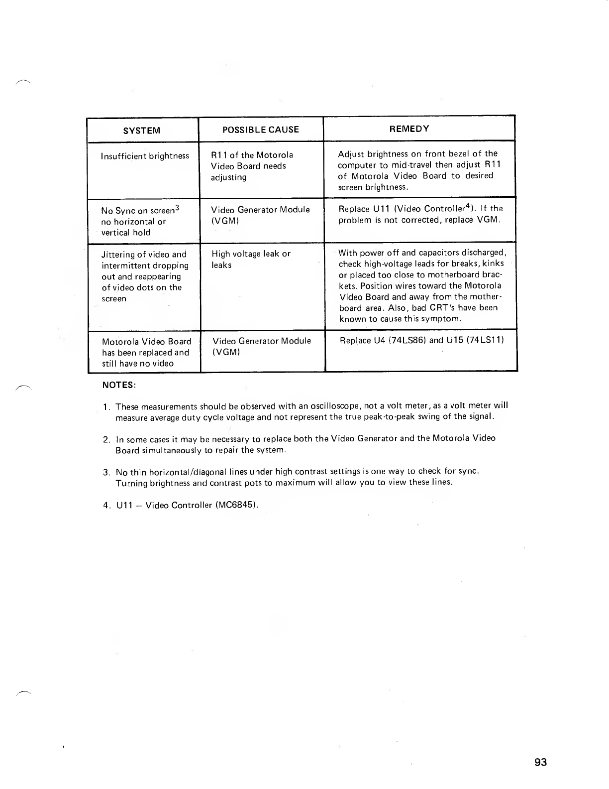
SYSTEM POSSIBLE CAUSE REMEDY
Insufficient brightness R11 of the Motorola
Video Board needs
adjusting
Adjust brightness on front bezel of the
computer to mid-travel then adjust R11
of Motorola Video Board to desired
screen brightness.
No Sync on screen 3
no horizontal or
vertical hold
Video Generator Module
(VGM)
Replace U11 (Video Controller4). If the
problem is not corrected, replace VGM.
Jittering of video and
intermittent dropping
out and reappearing
of video dots on the
screen
High voltage leak or
leaks
With power off and capacitors discharged,
check high-voltage leads for breaks, kinks
or placed too close to motherboard brac-
kets. Position wires toward the Motorola
Video Board and away from the mother-
board area. Also, bad CRT's have been
known to cause this symptom.
Motorola Video Board
has been replaced and
still have no video
Video Generator Module
(VGM)
Replace U4 (74LS86) and U15 (74LS11)
NOTES:
1
.
These measurements should be observed with an oscilloscope, not avolt meter, as avolt meter will
measure average duty cycle voltage and not represent the true peak-to-peak swing of the signal.
2. In some cases it may be necessary to replace both the Video Generator and the Motorola Video
Board simultaneously to repair the system.
3. No thin horizontal/diagonal lines under high contrast settings is one way to check for sync.
Turning brightness and contrast pots to maximum will allow you to view these lines.
4. U11- Video Controller (MC6845).
93
E. THEORY OF OPERATION
The M3970 Series monitors are direct drive units requir-
ing separate video, horizontal sync and vertical sync in-
puts. All are TTL compatible. Power supplied to the
monitor is +12 V.
The monitor consists of aVideo Amplifier, aHorizon-
tal Driver, AHorizontal Output stage and two stages of
Vertical Deflection (see Figure 1. Block Diagram).
Video Amplifier
The TTL compatible video signal, input at pin 8of
edge connector P1 ,is direct coupled via R2 to the base
of the Video Amplifier Q1. R1 is used as the load resis-
tor for the video signal source. The RC network (R4,
R5 and C1) provides Q1 with increased gain at high fre-
quencies by altering the collector-emitter load resistance
ratio. At low frequencies, C1 appears as an "open" and
only R4 is in the circuit. At higher frequencies, C1
"shorts", thereby shunting R4 with R5, lowering the
emitter load resistance and increasing the emitter-col-
lector resistance ratio. Therefore, the gain of 0.1 in-
creases. Approximate voltage gain of this stage is 25 V.
Resistor R'3 provides the collector load for the video
output signal. The amplified video is fed forward and
direct coupled via R34 to the cathode of the CRT.
Horizontal Driver
The horizontal drive signal, input at pin 6of P1, must
be TTL compatible and aseries of positive-going pulses
of approximately 27.5 Msec duration (see Figure 2). In
addition, the leading edge of the pulse may be coinci-
dent with the end of the video. If desired, the user may
decide to delay the horizontal pulses (approximately
1.3 Msec) to attain centering of the video within the
raster.
At the end of the video period, the horizontal drive sig-
nal goes positive and is coupled through C2 and R6 to
the base of Horizontal Driver No. 2(Q3). Q3 "turns
on" drawing current through D1, R10 and C3. This
action pulls the base of the Horizontal Output stage
(Q4) low, forcing it into "cut-off". Approximately 27
Msec later, the negative-going trailing edge of the hori-
zontal drive pulse switches Q3 off, which then allows
Q2 to conduct. Base current is now provided to Q4 via
the network R9, R10 and C3. The RC network, R10
and C3, is aspeed-up network in the base circuit of
Q4. It is used to increase the collector switching time
of Q4.
VIDEO P1-8
IN <4-
VERTICAL PI -9 /A
DRIVE \T"
SYS. GIMP. P1-1
SYSTEM PI -10
GND.
<4-
«-
P1-5
HORIZ. P1-6
DRIVE <4-
POWER P1-7 /A *.„„ IIU
IN (B+) ~^\1 °+12V IN
P1-2
P1-3
P1-4
<4
<4
VERTICAL
DISCHARGE
CIRCUITRY
SYSTEM GROUND
1.
ZL
NOT
CONNECTED
HIGH
LOW TO
EXTERNAL
BRIGHT
WIPER
VIDEO
OUTPUT CRT
VERTICAL
DRIVER/OUTPUT
CIRCUITRY on
HORIZONTAL
DRIVER/OUTPUT
CIRCUITRY
_J
YOKE
HIGH
VOLTAGE
Figure 1. Block Diagram (Motorola and RCA)
94
At the end of the video period (horizontal drive going
positive), the drive pulse at the base of Q4 goes low,
forcing Q4 to cut off. This produces aretrace pulse
occurring at the end of each line or sweep period that
quickly drives the electron beam from the right to the
left side of the screen.
Coincident with the retrace pulse, is the dissipation of
the yoke current as determined by the LR time con-
stant of the yoke, the primary windings of T1, and the
action of D9. When the electron beam travels to about
the center of the screen, Q4 turns on to form acurrent
path from the +12V supply through the yoke (L2B).,
the Horizontal Size (L3), and the Horizontal Linearity
(L4) coils, to complete the raster line.
The retrace tuning capacitor, C4, forms atuned circuit
with the inductive components of the yoke, L2B. The
linearity coil, L4, provides optimum horizontal linear-
ity by shaping the deflection current per the amount of
magnetic biasing as determined by the position of its
core. The two RC networks, C17 and R39, and C16
and R38, provide damping for the coils L4 and L3,
respectively, which eliminates any ringing effects in the
circuits.
Horizontal Output Transformer
Transformer T1 produces secondary voltages via the
auto transformer action of the primary winding. The
transformer produces +60V, -110V, +300V and
+12kV. The +60V supply is used as B+ for transistor
Q1. At Q7, this voltage limits the peak voltage that
appears at the collector, utilizing the electrical path
through D5 and R27. The +60V and the -110V are
applied across the brightness pot, R11. In addition,
these voltages provide enough range to allow the blank-
ing pulses to turn off the CRT beam during retrace.
The +300V source supplies the second grid, G2, of the
CRT, in addition to the variable focus bleeder resistor.
The +12kV supplies the second anode of the CRT with
B+.
Vertical Deflection
The vertical drive signal, anegative-going short dura-
tion spike, is supplied to the unit via pin 9of edge con-
nector P1 .This drive signal is direct coupled to the base
of Q5 via R15. When the vertical drive signal is false or
high, Q5 is cut off allowing C8 and C9 to charge to-
ward +12V through the network of R17, R18, and D4.
This charging action generates alinear positive-going
ramp (sawtooth waveform) applied to the base of Q6,
the Vertical Driver stage. When the vertical drive signal
goes true or negative, Q5 conducts, discharging C8 and
C9 to nearly zero volts* This action forms the retrace
portion of the sawtooth waveform. Q6, an emitter
follower configuration, transforms the high impedance
of the sawtooth waveform into alow impedance drive
for Q7, the vertical output stage.
The vertical output transistor, Q7, provides the required
sawtooth waveform of current through vertical choke
L1 and vertical yoke L2A. When Q7 is at minimum
current flow during retrace, alarge pulse voltage is de-
veloped as the yoke field collapses. The high voltage
pulse is limited by D5 and R27 connected to the +60V
source. The yoke coupling capacitor, C10, blocks any
DC voltage to the yoke which can cause de-centering
of the raster. The resistors R25 and R21 couple the
emitter voltage of Q7 to the junction of C8 and C9.
Because this path is resistive, the waveform coupled
back will be integrated into aparabola by C8. This
action pre-distorts the drive sawtooth and allows op-
timization of the vertical linearity adjustment.
HORIZ. DRIVE PULSE
HORIZ. DRIVE PULSE
at BASE OF CM
Figure 2. Horizontal Drive Signal (Motorola and RCA)
95
t«. I- w
<- CC N
*£5;
CO
O
CO
p." 2
„o
*i
CA
5§
oo
.t; o
c-1
is
—c
=I
£
3
.21
iZ
96
2
o
B
o
3
<u
(0
CC
X
I
o
ID
o
CO
o*
a!
>
(0
>Z
e
o
-6 I
D
O
2
«*
3
cn
97
F. INSTALLATION Cathode Ray Tube
Preliminary Checkout
The 12-inch CRT and associated components, which
make upthe basic M3970 video monitor kit, are mount-
ed and shipped in acardboard shipping carton. All
components are properly interconnected for operation.
Simply fabricate the mating plug for the edge connec-
tor on the rear of the monitor circuit card (refer to
Figure 6).
To pretest the kit before final installation, remove the
kit from the shipping carton or remove the kit from
the pallet and open the cardboard shipping housing,
(see Figure 5).
WARNING
Afire hazard exists if the monitor is operated in
the shipping carton or on the cardboard shipping
board for any length of time. Be sure that adequate
ventilation is available to keep the ambient tempera-
ture in the monitor housing below +131°F (+55°C>.
As with any glass envelope vacuum tube, the danger of
implosion is always present if dropped or mishandled.
Even though the CRT used in this kit has integral im-
plosion protection, handle the CRT with extreme care,
and wear safety glasses. Do not carry the CRT by its
neck or apply excessive pressure.
The CRT may be positioned with its high voltage cap
(second anode connection) either left or right; however,
be sure that the cap has aminimum of 1-inch clear-
ance from any metal shield, bracket, etc.
To mount the CRT in its final operating location, use
No. 8type hardware and the holes in each corner of
the CRT. After final installation, check to be sure that
the CRT aquadag spring is positioned properly and
grounded via a black wire to the monitor circuit card.
Check to be sure that the bleeder resistor, R14, is con-
nected to the ground lug (see Figure 4).
ANODE
CONNECTOR
L2A/B
DEFLECTION
YOKE
D3
(IN LEAD)
R14
(IN LEAD)
CRT AQUADAG
GROUNDING SPRING
YOKE MOUNTING PIN FOR
RASTER ADJUSTING MAGNETS
L1
VERT.
CHOKE
T1
H.V. XFMR
P1
MONITOR
CIRCUIT CARD
EDGE CONNECTOR
Figure 5. Model M3970 -Series Kits, Rear View (Motorola)
98
Monitor Circuit Card
The monitor circuit card is mounted vertically on the
power supply bracket. Use four No. 6type screws and
hardware to secure the circuit card.
Do not allow any wires to lay on top of, or alongside
any power transistor heat sinks on the circuit card.
High heat dissipation could melt the wire insulation.
In addition, be sure the yellow wire (CRT cathode
connection) from the circuit card to pin 2of the CRT
socket does not lay near any metal or horizontal cir-
cuitry.
After final installation, be sure the CRT aquadag spring
is connected via ablack wire to the circuit card (refer
to Figure 4).
Refer to section C. ADJUSTMENTS, and perform the
steps as necessary.
-NOTE -
At the time of the initial installation proce-
dure, it will be necessary to perform the Ras-
ter (Yoke) Adjustment Procedure.
P1
MONITOR CIRCUIT CARD EDGE CONNECTOR
(FOIL SIDE SHOWN)
KEYWAY
SLOT
10 98 765 4 321
^HllWlll
SYSTEM GROUND
TTL VERT. DRIVE INPUT
VIDEO INPUT
+12V DC B+
TTL HORIZ. DRIVE INPUT
_t t_ SYSTEM GROUND
(NO CONNECTION)
EXTERNAL
BRIGHTNESS
CONTROL
(NO CONNECTION)
DIRECT DRIVE MODELS V
AEPC-01005-O rPOSITION KEYWAY INSERT
BETWEEN PINS 9AND 10
FROM PIN SIDE
cQIfflgWWglCfr I
(WIRING SIDE SHOWN)
MATING PLUG FOR CIRCUIT
CARD EDGE CONNECTOR -
AMPHENOL PART NO. A-MP 583299-1
Figure 6. Monitor Circuit Card —Edge Connector (Motorola and RCA)
99
G. GENERAL SERVICING PRECAUTIONS
*»*CAUTtON**«
Before attempting to service the monitor,
disonnect (or turn off) the external power
supply; then, as an added precaution, dis-
charge the CRT second anode before handling
any high voltage components. In addition, be
sure to observe all safety warnings and service
notes in the front of this manual.
When disconnecting the H.V. rectifier, D3, pull it out
of the high voltage lead holder slowly and carefully to
prevent breaking or deforming the short rectifier lead.
Use caution around the heat sinks of the horizontal
and vertical output transistors. The heat sinks are at
the same potential as the transistor collectors. During
normal operation with asignal input present, the hori-
zontal heat sink has 130 volt P-P pulses and the vertical
heat sink has 75 volt P-P pulses (with respect to system
ground).
When it is necessary to disconnect the deflection yoke
and/or the CRT socket leads, pull the small female pins
straight out, with no back and forth rocking motion.
This action will prevent, or at least, minimize the pos-
sibility of bending the male pins on the components
and/or breaking the solder connections.
VIDEO MONITOR (CRT)
EDGE CONNECTOR -J1 POWER SUPPLY
+12V RET.
H. SYNC
H. S. GND.
V. S. GND.
V. SYNC
VIDEO
VIDEO GND.
KEY
VIDEO/KEYBOARD
EDGE CONNECTOR
Figure 7. Video Wiring Harness (Motorola and RCA)
100
VIDEO MONITOR {MOTOROLA)
PARTS LIST
SYMBOL
C1
C2
C3
C4
C5
C6
C7
C8
C9
C10
C11
C12
C13
C14
C15
C16
C17
C18
C19
L1
L2A/B
L3
L4
DESCRIPTION
0.001/iF, Z5F, 100V, Disc
5/iF, 15V, Tantalum
0.68/zF, 35V, Tantalum
0047/iF, 200V, 10%, Poly
0.047/uF,400V, 10%, Film
2000/iF, 35V, Electrolytic
22/iF, 160V, Electrolytic
5/xF, 15V, Tantalum
5juF, 15V, Tantalum
470juF, 16V, Electrolytic
0.01juF,400V, 10%, Film
22juF, 160V, Electrolytic
0.0027MF, Z5F, 500V, 20%, Disc
0.01//F, 400V, 10%, Film
0.01/xF,400V, 10%, Film
0.0022/zF, Z5F, 500V, 10%, Disc
0.0022aiF, Z5F, 500V, 10%, Disc
0.047MF, 400V, 10%, Film
100juF, 16V, Electrolytic
MANUFACTURER'S
PART NUMBER
21S180B07
23S10218A31
23R29976A01
8S10072A44
8R29959A02
23S10255A11
23S10255A74
23S10218A31
23S10218A31
23S1 02255A29
8R29959A01
23S10255A74
21S180C41
8R29959A01
8R29959A01
21S180C39
21S180C39
8R29959A02
23S10255A06
Coil, Vertical choke
Yoke, Deflection
Coil, Width
Coil, Linear
COILS/CHOKES
25D25221A01
24D25830A01
24D25603A16
24D25600A15
RADIO SHACK
PART NUMBER
ACC102NCLP
ACC505QPTP
ACC684QGTP
ACC473QDEP
ACC473QTGP
ACC208QGAP
ACC226QNAP
ACC505QPTP
ACC505QPTP
ACC477QDAP
ACC103QTGP
ACC226QNAP
ACC272QUCP
ACC103QTGP
ACC103QTGP
ACC222QUCP
ACC222QUCP
ACC473QTGP
ACC107QDAP
ACA8030
ATA0770
ACA8031
ACA8022
DIODES/RECTIFIERS
D1
D2
D3
D4
D5
D6
D7
D8
D9
Rectifier,
Rectifier,
Rectifier,
Diode, Sil
Rectifier,
Rectifier,
Rectifier,
Rectifier,
Rectifier,
Silicon, 91 A02
Silicon, 91 A02
H.V.,D9H
icon, 2054
Silicon, 91 A02
Silicon, 91 A02
Silicon, 91 A02
Silicon, 91 A05
Silicon, 91 A05
48R191A02
48R191A02
48S1 37608
48R02054A00
48R191A02
48R191A02
48R191A02
48R191A05
48R191A05
ADX1330
ADX1330
ADX1331
ADX1332
ADX1330
ADX1330
ADX1330
ADX1333
ADX1333
RESISTORS
Note: Only power or special resistors are listed. Use the description when
ordering standard values of fixed carbon resistors up to 2Watts.
R3
R6
R7
R8
R9
R10
R11
R12
R14
1.5K,5W, 5%, Wire Wound
470 ohms,0.5W, 10%, Composition
10K,0.5W,5%, Film
1.5K,0.5W,5%, Film
47ohms,0.5W,5%, Film
100 ohms, 0.5W, 5%, Film
500K, Potentiometer
100K,0.5W,5%, Film
240M,2W, 20%, Ceramic
17-136062
6-125C41
6-101 64B32
6-101 64B01
6-10164A78
18D25245A07
6-101 64A80
6R29978A01
AN0206FKB
AN0169EFB
AN0281EFB
AN0206EFB
AN0099EFB
AN0132EFB
AP-7038
AN0371EFB
ARX0173
101
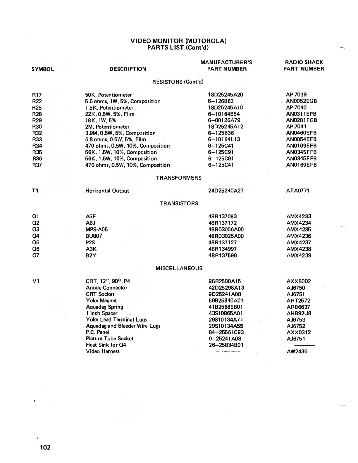
VIDEO MONITOR (MOTOROLA)
PARTS LIST (Cont'd)
SYMBOL DESCRIPTION
MANUFACTURER'S
PART NUMBER RADIO SHACK
PART NUMBER
RESISTORS (Cont'd)
R17
R22
R25
R28
R29
R30
R32
R33
R34
R35
R36
R37
50K, Potentiometer
5.6 ohms, 1W, 5%, Composition
1.5K, Potentiometer
22K,0.5W,5%, Film
18K, 1W,5%
2M, Potentiometer
3.9M, 0.5W, 5%, Composition
6.8 ohms, 0.5W, 5%, Film
470 ohms, 0.5W, 10%, Composition
56K, 1.5W, 10%, Composition
56K, 1.5W, 10%, Composition
470 ohms, 0.5W, 10%, Composition
18D25245A20
6-126B63
18D25245A10
6-10164B54
6-001 26A79
18D25245A12
6-125B36
6-101 64L1
3
6-125C41
6-125C91
6-125C91
6-125C41
AP-7039
AN0052EGB
AP-7040
AN0311EFB
AN0281 FGB
AP-7041
AN0460EFB
AN0054EFB
AN0169EFB
AN0345FFB
AN0345FFB
AN0169EFB
TRANSFORMERS
T1 Horizontal Output 24D25240A27 ATA0771
TRANSISTORS
Q1
Q2
Q3
Q4
Q5
Q6
Q7
A5F
A6J
MPS-A05
BU807
P2S
A3K
B2Y
48R 137093
48R137172
48R03006A00
48R03025A00
48R137127
48R 134997
48 R137598
AMX4233
AMX4234
AMX4235
AMX4236
AMX4237
AMX4238
AMX4239
MISCELLANEOUS
VI CRT, 12", 90°, P4
Anode Connector
CRT Socket
Yoke Magnet
Aquadag Spring
1inch Spacer
Yoke Lead Terminal Lugs
Aquadag and Bleeder Wire Lugs
P.C. Panel
Picture Tube Socket
Heat Sink for Q4
Video Harness
96R2500A15
42D25298A13
9D25241A08
59B25840A01
41B25685B01
43S10865A01
29S10134A71
29S10134A55
84-25561 C93
9-25241 A08
26-25834B01
AXX8002
AJ6750
AJ6751
ART2572
ARB6637
AHB92U8
AJ6753
AJ6752
AXX0312
AJ6751
AW2436
102
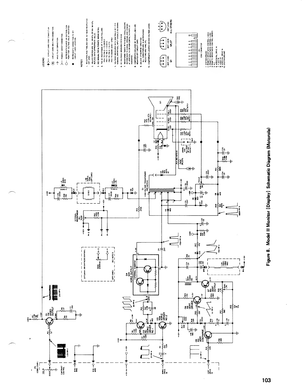
s5s
sȤ;
A®Tki
£1
IS
*~S*"- Ii*52" ss«-o
>*K 3 <"<or *5Ipeg
;'5 <Sa £"Si "ft l<!t "
?eg a! s2s5s iS sss j
;;; S3 5s-SS Is s^I 1
:**^1 S1Ssi §1 §"" *
5
8
o
E
S
O)
5
o
'£
E
o
CO
s
c
o
0)
O
od
3
103

VIDEO MONITOR
(RCA)
H. FUNCTIONAL SPECIFICATIONS
General Information
The RCA Video Monitor uses the same interface circuitry
as the Motorola Video Monitor. The Video Monitor is a12"
solid state monitor designed to display alphanumeric dot
characters. It uses a12-voIt DC power input with an aver-
age power consumption of 12 watts. The monitor accepts
separate video and vertical drive TTL level inputs.
Input and output connections for the monitor are made
through a10-pin circuit card edge connector. The inputs
are video, horizontal drive, vertical drive, system ground
and +12 volts.
Asingle circuit card with components mounted on one side
is used. Schematic reference numbers are printed on both
sides of the circuit card to aid in locating and identifying
components for servicing.
Circuitry consists of one stage of video amplification, two
stages of horizontal deflection processing, and three stages
of vertical deflection processing.
SPECIFICATIONS
Cathode Ray Tube: 12" (305 mm) diagonal, 90° deflection angle, 4x5 aspect ratio,
P4 phosphor, integral implosion protection.
Environment:
Operating Temperature:
Humidity:
Operating Altitude:
Power Input:
TTL Level
41°F to 131° F (5°C to 55°C) ambient
95% non -condensing at 41°F to 104°F (5°C to 40°C)
10,000 ft. (3048 meters) maximum
+1 2VDC @1amp, nominal
4volts ±1 .5 volts
Input Signals:
Horizontal:
Vertical:
Video:
4to 25 fxsec, positive going
100 to 1400 jusec, negative going
positive white
Video Response:
Bandwidth: 15MHz,3dB
Pulse rise time less than 30 nsec
Scanning Frequency:
Horizontal
:
Vertical:
15,600 Hz ±500 Hz
50/60 Hz
Horizontal Retrace:
Vertical Retrace:
10.5 /xsec maximum
850 /^sec maximum
105
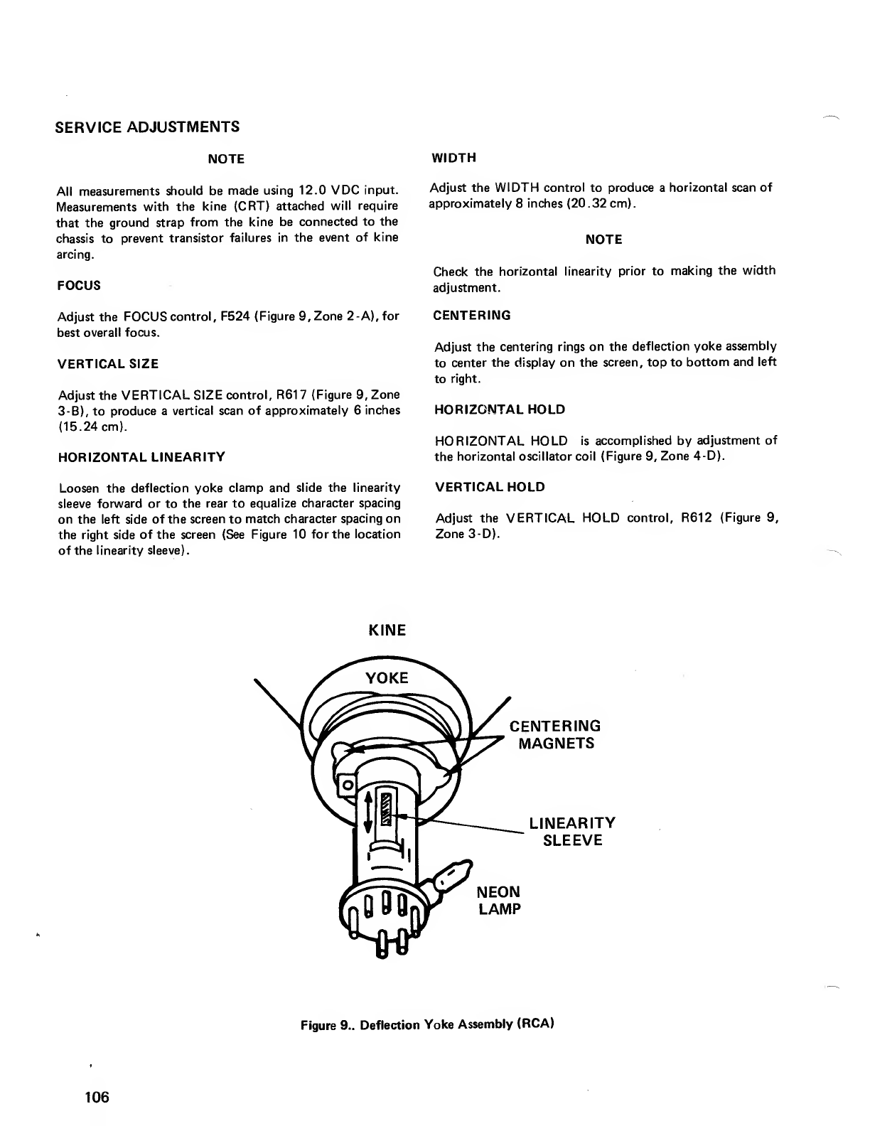
SERVICE ADJUSTMENTS
NOTE
All measurements should be made using 12.0 VDC input.
Measurements with the kine (CRT) attached will require
that the ground strap from the kine be connected to the
chassis to prevent transistor failures in the event of kine
arcing.
FOCUS
Adjust the FOCUS control, F524 (Figure 9, Zone 2-A),for
best overall focus.
VERTICAL SIZE
Adjust the VERTICAL SIZE control, R617 (Figure 9, Zone
3-B), to produce avertical scan of approximately 6inches
(15.24 cm).
HORIZONTAL LINEARITY
WIDTH
Adjust the WIDTH control to produce ahorizontal scan of
approximately 8inches (20.32 cm).
NOTE
Check the horizontal linearity prior to making the width
adjustment.
CENTERING
Adjust the centering rings on the deflection yoke assembly
to center the display on the screen, top to bottom and left
to right.
HORIZONTAL HOLD
HORIZONTAL HOLD is accomplished by adjustment of
the horizontal oscillator coil (Figure 9, Zone 4-D).
Loosen the deflection yoke clamp and slide the linearity
sleeve forward or to the rear to equalize character spacing
on the left side of the screen to match character spacing on
the right side of the screen (See Figure 10 for the location
of the linearity sleeve).
VERTICAL HOLD
Adjust the VERTICAL HOLD control, R612 (Figure 9,
Zone 3-D).
CENTERING
MAGNETS
LINEARITY
SLEEVE
NEON
LAMP
Figure 9.. Deflection Yoke Assembly (RCA)
106
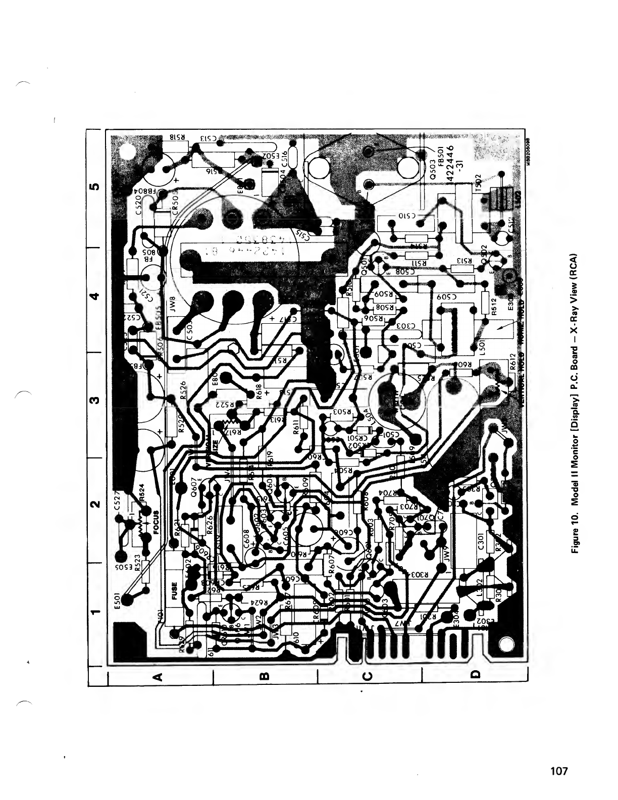
<
o
cc
3
09
OC
X
I
"E
to
O
m
6
a.'
IS
c
o
2
0)
o
o
107
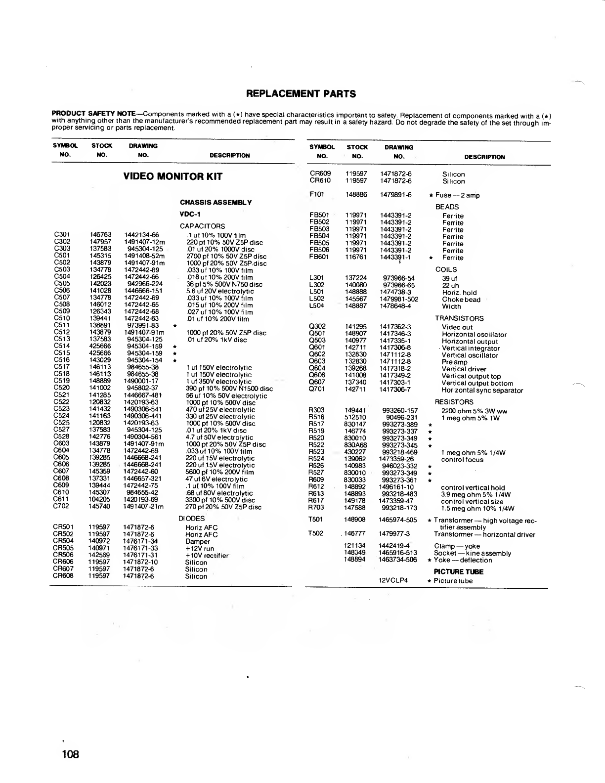
REPLACEMENT PARTS
PRODUCT SAFETY NOTE—Components marked with a(*) have special characteristics important to safety. Replacement of components marked with a(*)
with anything other than the manufacturer's recommended replacement part may result in asafety hazard. Do not degrade the safety of the set through im-
proper servicing or parts replacement.
SYMBOL
NO.
STOCK
NO.
DRAWING
NO. DESCRIPTION
C301
C302
C303
C501
C502
C503
C504
C505
C506
C507
C508
C509
C510
C511
C512
C513
C514
C515
C516
C517
C518
C519
C520
C521
C522
C523
C524
C525
C527
C528
C603
C604
C605
C606
C607
C608
C609
C610
C611
C702
CR501
CR502
CR504
CR505
CR506
CR606
CR607
CR608
VIDEO MONITOR KIT
146763
147957
137583
145315
143879
134778
126425
142023
141028
134778
146012
126343
139441
138891
143879
137583
425666
425666
143029
146113
146113
148889
141002
141285
120832
141432
141163
120832
137583
142776
143879
134778
139285
139285
145359
137331
139444
145307
104205
145740
119597
119597
140972
140971
142569
119597
119597
119597
1442134-66
1491407-12m
945304-125
1491408-52m
1491407-91
m
1472442-69
1472442-66
942966-224
1446666-151
1472442-69
1472442-65
1472442-68
1472442-63
973991-83
1491407-91 m
945304-125
945304-159
945304-159
945304-154
984655-38
984655-38
1490001-17
945802-37
1446667^181
1420193-63
1490306-541
1490306-441
1420193-63
945304-125
1490304-561
1491407-91m
1472442-69
1446668-241
1446668-241
1472442-60
1446657-321
1472442-75
984655-42
1420193-69
1491407-21m
1471872-6
1471872-6
1476171-34
1476171-33
1476171-31
1471872-10
1471872-6
1471872-6
CHASSIS ASSEMBLY
VDC-1
CAPACITORS
.1uf 10% 100V film
220pf10%50VZ5Pdisc
.01 uf 20% 1000V disc
2700 pf 10% 50V Z5P disc
1000 pf 20% 50V Z5P,disc
.033 uf 10% 100V film
.018 uf 10% 200V film
36pf5%500VN750disc
5.6 uf 20V electrolytic
.033 uf 10% 100V film
.015 uf 10% 200V film
.027 uf 10% 100V film
.01 uf 10% 200V film
1000 pf 20% 50V Z5P disc
.01uf20%1kVdisc
1uf 150V electrolytic
1uf 150V electrolytic
1uf 350Velectro lytic
390 pf 10% 500V N1500 disc
56 uf 10% 50V electrolytic
1000 pf 10% 500V disc
470 uf25V electrolytic
330 uf 25V electrolytic
1000 pf 10% 500V disc
,01uf20%1kVdisc
4.7 uf 50V electrolytic
1000 pf 20% 50V Z5P disc
.033 uf 10% 100V film
220 uf 15V electrolytic
220 uf 15V electrolytic
5600 pf 10% 200V film
47 uf6V electrolytic
.1uf 10% 100V film
.68 uf 80V electrolytic
3300 pf 10% 500V disc
270 pf 20% 50V Z5P disc
DIODES
Horiz AFC
Horiz AFC
Damper
+12V run
+10V rectifier
Silicon
Silicon
Silicon
SYMBOL STOCK DRAWING
NO. NO. NO. DESCRIPTION
CR609 119597 1471872-6 Silicon
CR610 119597 1471872-6 Si licon
F101 148886 1479891-6 *Fuse —2amp
BEADS
FB501 119971 1443391-2 Ferrite
FB502 119971 1443391-2 Ferrite
FB503 119971 1443391-2 Ferrite
FB504 119971 1443391-2 Ferrite
FB505 119971 1443391-2 Ferrite
FB506 119971 1443391-2 Ferrite
FB601 116761 1443391-1
i*Ferrite
COILS
L301 137224 973966-54 39 uf
L302 140080 973966-65 22 uh
L501 148888 1474738-3 Horiz. hold
L502 145567 1479981-502 Choke bead
L504 148887 1478648-4 Width
TRANSISTORS
Q302 141295 1417362-3 Video out
Q501 148907 1417346-3 Horizontal oscillator
Q503 140977 1417335-1 Horizontal output
Q601 142711 1417306-8 Vertical integrator
Q602 132830 1471112-8 Vertical oscillator
Q603 132830 1471112-8 Pre amp
Q604 139268 1417318-2 Vertical driver
Q606 141008 1417349-2 Vertical output top
Q607 137340 1417303-1 Vertical output bottom
Q701 142711 1417306-7 Horizontal sync separator
RESISTORS
R303 149441 993260-157 2200 ohm 5% 3W ww
R516 512510 90496-231 1meg ohm 5% 1
W
R517 830147 993273-389 *
R519 146774 993273-337 *
R520 830010 993273-349 *
R522 830A68 993273-345 *
R523 430227 993218-469 1meg ohm 5% 1/4W
R524 139062 1473359-26 control focus
R526 140983 946023-332 *
R527 830010 993273-349 *
R609 830033 993273-361 *
R612 148892 1496161-10 control vertical hold
R613 148893 993218-483 3.9megohm5%1/4W
R617 149178 1473359^17 control vertical size
R703 147588 993218-173 1,5megohm10%1/4W
T5Q1 148908 1465974-505 *Transformer —high voltage rec-
tifier assembly
T502 .146777 1479977-3 Transformer —horizontal driver
121134 1442419^1 Clamp —yoke
148349 1465916-513 Socket —kine assembly
148894 1463734-506 *Yoke —deflection
PICTURE TUBE
12VCLP4 *Picture tube
108
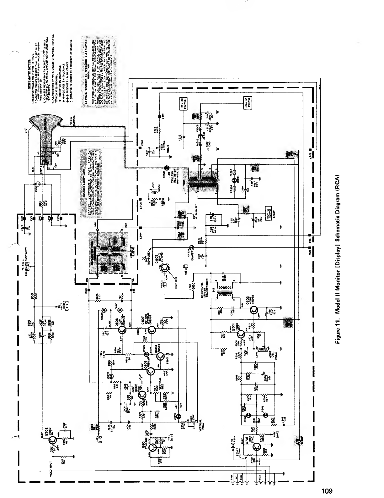
-b ,°-Q
.fc.-frS is
Si 5° 8§ -.SS
ill:* Hi ilii
sjs; si hp' !
;*-
1
"''X QZKUt-OTU
:
;»- _,t z5t- xj?
.?.<(* t4-o»=j-o££^ <
n*i ££*5£zsuiS :
if Pip:l
o
oc
E
re
Q
u
«
E
re
a
c
o
2
o
3
en
109


SECTION VIII
FLOPPY DISK DRIVE
111

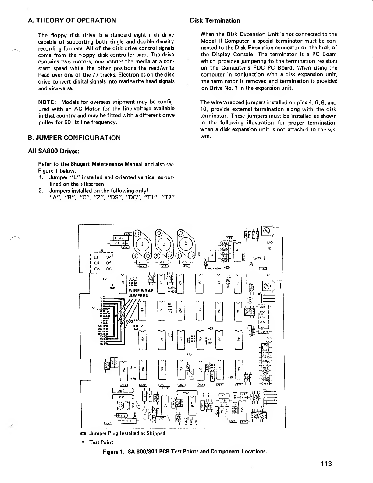
A. THEORY OF OPERATION Disk Termination
The floppy disk drive is astandard eight inch drive
capable of supporting both single and double density
recording formats. All of the disk drive control signals
come from the floppy disk controller card. The drive
contains two motors; one rotates the media atacon-
stant speed while the other positions the read/write
head over one of the 77 tracks. Electronics on the disk
drive convert digital signals into read/write head signals
and vice-versa.
When the Disk Expansion Unit is not connected to the
Model II Computer, aspecial terminator must be con-
nected to the Disk Expansion connector on the back of
the Display Console. The terminator is aPC Board
which provides jumpering to the termination resistors
on the Computer's FDC PC Board. When using the
computer in conjunction with adisk expansion unit,
the terminator is removed and termination is provided
on Drive No. 1in the expansion unit.
NOTE: Models for overseas shipment may be config-
ured with an AC Motor for the line voltage available
in that country and may be fitted with adifferent drive
pulley for 50 Hz line frequency.
B. JUMPER CONFIGURATION
All SA800 Drives:
Refer to the Shugart Maintenance Manual and also see
Figure 1below.
1. Jumper "L" installed and oriented vertical as out-
lined on the silkscreen.
2. Jumpers installed on the following only!
"A", "B", "C", "Z", "DS", "DC", "T1", "12"
The wire wrapped jumpers installed on pins 4, 6, 8, and
10, provide external termination along with the disk
terminator. These jumpers must be installed as shown
in the following illustration for proper termination
when adisk expansion unit is not attached to the sys-
tem.
Jumper Plug Installed as Shipped
Test Point
Figure 1. SA 800/801 PCB Test Points and Component Locations.
113
SA800/801 DISK DRIVE MECHANICAL PARTS LIST
To find the Radio Shack Part Numbers of mechanical parts for the Disk Drive, find the required
part using the illustrations and parts lists shown in the Shugart Illustrated Parts Catalog located
in the back of this Technical Reference Manual. Using the appropriate part name and reference
number, locate that part in the list below. You will note that in the first column below, the
Figure Number and the Reference Number are listed, respectively.
Fig. &
Ref.
Number Description
Radio Shack
Part Number
3-15
1-6
1-9
1-47
1-16
1-13
4-3
2-11
3-10
1-1
1-31
1-23
1-45
1-46
2-3
1-53
1-49
1-14
1-39
1-25
3-1
4-0
1-34
2-7
3-3
3-9
3-11
1-10
4-4
3-16
3-14
2-10
1-20
2-1
2-12
1-2
1-44
2-4
1-21
1-4
4-2
4-10
1-37
1-27
1-50
1-24
3-5
4-6
Actuator, Head Load
Bearing, Spindle
Bearing, Spindle, Flanged
Belt
Boot, Rubber (for Motor Capacitor)
Bracket, Capacitor
Bumper
Carriage Spring Plate
Cartridge Guide
Catridge Guide Assembly
Cartridge Guide Pivot
Clamp, Cable, 1/8" (3 mm)
Clamp, Cable, 3/16" (4.7 mm)
Clamp, Cable, 3/8" (9.5 mm)
Clamp, Mounting (for Stepper Motor)
Clip, Face Plate Mounting
Block, PCB Connector
Connector, 3-pin Amp 7808
Deflector
Dust Cover Kit
Ejector Assembly
Front Plate Assembly
Handle, Door
Head Carriage Assembly
Hook, Spring
Hub Clamp Assembly
Hub Clamp Plate
Hub Assembly, Spindle
Latch Door
Latch Plate
LED Assembly
Load Button Assembly
Motor, Drive (Motor and Capacitor Assembly
Motor, Stepper Assembly
Nut, Carriage Load with cogs
Nut, 8-32
Photo Transistor and Cable Assembly
Plate, Stepper Motor
Plug, Jumper or Shorting
Pulley, Drive Motor
Pulley, Spindle
Push Bar Assembly
Screw, 440 x1/4" (6.35mm) F/H
Screw, 4-40 x1/4" (6.35mm) SH/Hex
Screw, 4-40 x3/8" (9.5mm)
Screw, 440 x3/8" (9.5mm) R/H
Screw, 6-32 x5/16" (7.9mm)
Screw, 6-32 x5/16" (7.9mm)
Screw, 6-32 x5/16" (7.9mm)
AS-9109
ART-2298
ART-2295
AB-6410
ART-2294
ART-2291
ART-2304
ARB-6511
ART-2293
ART-2288
ART-2439
ART-2299
ART-2300
ART-2301
ART-2309
ART-2438
AJ-6726
AS-6727
ART-2306
ART-2296
ART-231
1
AZ-5074
AH-6257
AXX-0902
ART-2305
ART-2286
ART-2289
ART-2308
ART-2435
ART-2436
ART-2307
ART-2302
AXX-4006
AXX4005
ART-231
4
AHD-7146
AL-1042
ART-2292
AJ6731
ARA1338
ARA-2730
ART-2440
AHD-1488
AHD-1489
AHD-1490
AHD-1487
AHD-1493
AHD-1493
AHD-1493
114
SA800/801 DISK DRIVE MECHANICAL PARTS LIST (cont'd)
Fig.&
Ref.
Number Description
Radio Shack
Part Number
4-6
1-51
1-19
2-6
1-33
1-25
1-22
1-42
4-8
1-41
1-7
1-5
2-15
1-30
1-32
3-2
1-26
3-8
4-5
2-13
1-8
1-28
2-8
2-5
2-17
1-3
3-17
Screw, 6-32 x5/16" (7.9mm)
Screw, 8-32 x3/8" (9.5mm) SL/Hex/Wash
Screw, 8-32 x3/4" (19mm)
Screw, Cap 2-56 x1/4" (6.35mm)
Screw, Cartridge Guide Assembly
Screw, Dust Cover
Screw, Set, 6-32 x1/8" (3mm)
Screw, Tapping, 8x1/2" (12.7mm)
Snatch
Spacer
Spacer, Spindle-Long
Spacer, Spindle-Short
Spacer, Stepper Plate
Spring Assembly
Spring, Bias
Spring, Clamp Ejector
Spring, Guide Assembly
Spring, Hub Clamp
Spring, Latch Interlock
Spring, Pre-load
Spring, Spindle
Track Detector
Track Flag
Track Stop
Washer, Spring, #6
Washer, Spring, #8
Write Protect Assembly
AHD-1493
AHD-1492
AHD-1491
AHD-1495
AHD-1494
AHD-1496
AHD-0031
AHD-3252
ART-2437
ART-2310
ART-2297
ART-2290
ART-2313
ARB-6513
ARB-6510
ARB-6512
ART-2285
ARB-6507
ART-2312
ARB-6508
ARB-6509
AL-1041
ART-2287
ART-2303
AHD-8445
AHD-8444
ART-2284
115

SECTION IX
AA11080 POWER SUPPLY
117


A. FUNCTIONAL SPECIFICATIONS B. TROUBLESHOOTING
The power supply for the TRS-80 Model II is a150
watt, switching power supply. The Printed Circuit
Board is mounted to an open L-shaped bracket which
provides heatsinking as well as mounting surfaces.
Line input to the power supply module is made through
an amp wafer with locking 3-pin PCB socket header.
Pin 1Line -Neutral
Pin 2Blank
Pin 3Line -Live
Outputs are taken from an amp wafer with locking
15-pin PCB socket header.
Pin 1-12V
Pin 2-12V
Pin 3Common
Pin 4'Common
Pin 5Common
Pin 6Common
Pin 7Common
Pin 8+5V
Pin 9+5V
Pin 10 Common
Pin 11 +5V
Pin 12 +5V
Pin 13 +24V
Pin 14 +12V
Pin 15 +12V
In theory, the power supply rectifies the AC line to DC
then chops it at 20 kHz. The chopped DC voltage is
then transformed to the required output voltages and
rectified to low voltage isolated DC. Feedback loops
are provided for voltage regulation and over current
protection.
The power supply may be jumper selected for either of
the following ratings:
Vin -95 to 135VAC @47 to 63Hz input frequency
or -190 to 270VAC @47 to 63Hz input frequency
The power supply module can withstand the following
maximum ratings:
Vin (AC continuous) -MOV input select 115V
or -280V input select 230V
1.Equipment for Test Set-Up:
a. Isolation Transformer (minimum of 500 VA
rating) —
***CAUTIOIM*»»
Dangerously high voltages are present
in this power supply. For the safety of
the individual doing the testing, please
use an isolation transformer. The 500
VA rating is needed to keep the AC wave-
form from being clipped off at the peaks.
These power supplies have peak charging
capacitors and draw full power at the peak
of the AC waveform.
b. 0-140V Variable Transformer (Variac) —Used to
vary input voltage. Recommend 10 amp, 1.4 KVA
rating, minimum.
c. Voltmeter —Need to measure DC voltages to 50
VDC and AC voltages to 200 VAC. Recommend
two digital multimeters.
d. Oscilloscope -Need X10 and X100 probes.
e. Load board with Connectors —See Table 1for
values of loads required. The entry on the table for
Safe Load Power is the minimum power ratings for
the load resistors used.
NOTE: Because of its design, this power supply
must have aload present or damaging oscillations
may result. Never test the power supply without
asuitable load!
f. Ohmmeter
2. Set-Up Procedure:
Set-up as shown in Figure 1. You will want to monitor
the input voltage and the output voltage of the regulated
bus, which is the +5 output, with DVM's. Also monitor
the +5 output with the oscilloscope using 50mv/div
sensitivity. The DVM monitoring the +5 output can
also be used to check the other outputs. See text of
section C. for test points within the power supply.
Short Circuit, any output -indefinite
119
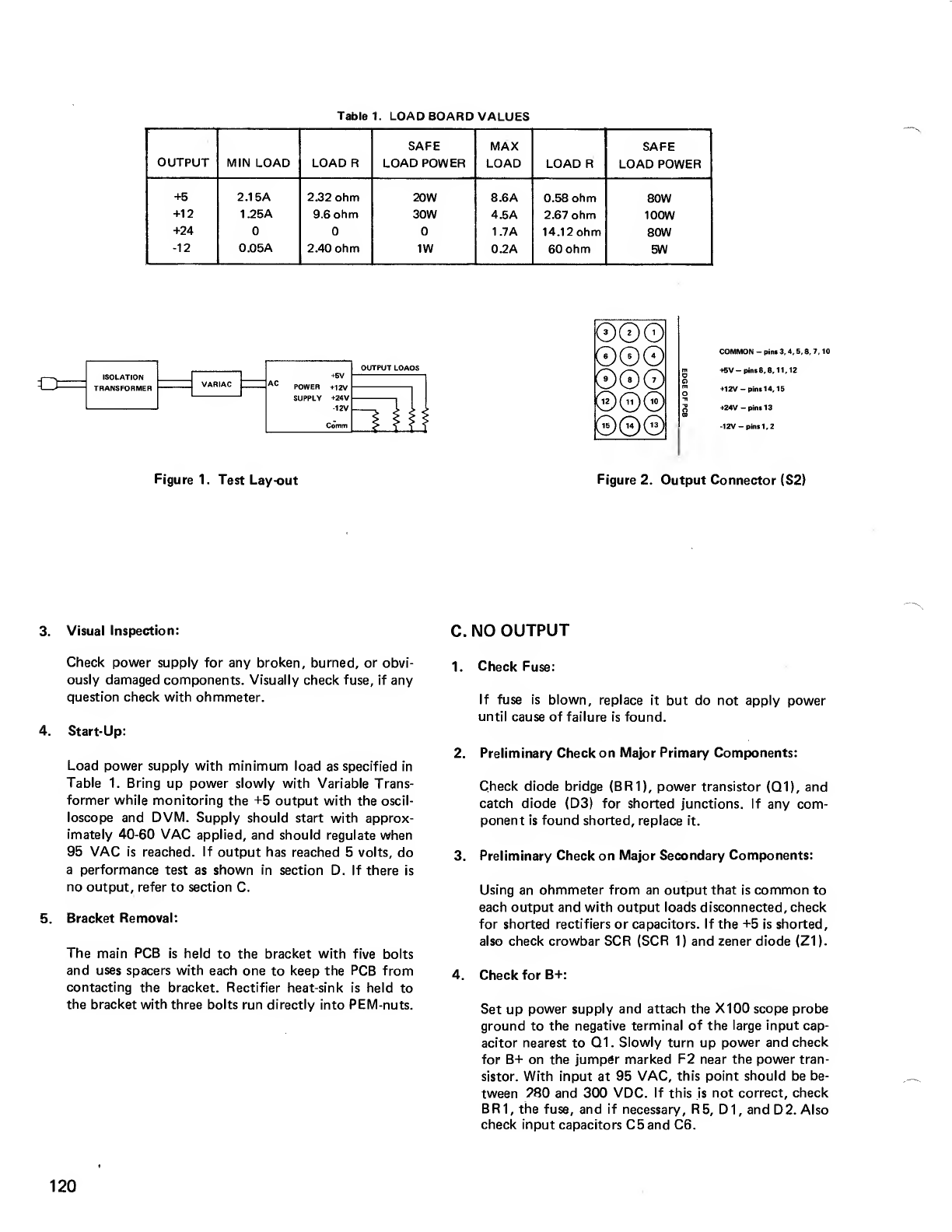
Table 1. LOAD BOARD VALUES
SAFE MAX SAFE
OUTPUT MIN LOAD LOADR LOAD POWER LOAD LOAD RLOAD POWER
+5 2.1 5A 2.32 ohm 20W 8.6A0.58 ohm 80W
+12 1.25A 9.6 ohm 30W 4.5A2.67 ohm 100W
+24 1.7A 14.12ohm 80W
-12 0.05A 2.40 ohm 1W 0.2A60 ohm 5W
Efc ISOLATION
TRANSFORMER
+6V
POWER +12V
SUPPLY +24V
-12V
Comm
OUTPUT LOADS
Q.
Figure 1. Test Lay-out
COMMON -pint 3. 4, 5, 6. 7, 10
+5V-pins8,9.11.12
412V -pins 14, 15
+24V -pins 13
-12V -pins 1,
2
Figure 2. Output Connector (S2)
3. Visual Inspection:
Check power supply for any broken, burned, or obvi-
ously damaged components. Visually check fuse, if any
question check with ohmmeter.
4. Start-Up:
Load power supply with minimum load as specified in
Table 1. Bring up power slowly with Variable Trans-
former while monitoring the +5 output with the oscil-
loscope and DVM. Supply should start with approx-
imately 40-60 VAC applied, and should regulate when
95 VAC is reached. If output has reached 5volts, do
aperformance test as shown in section D. If there is
no output, refer to section C.
5. Bracket Removal:
The main PCB is held to the bracket with five bolts
and uses spacers with each one to keep the PCB from
contacting the bracket. Rectifier heat-sink is held to
the bracket with three bolts run directly into PEM-nuts.
C. NO OUTPUT
1. Check Fuse:
If fuse is blown, replace it but do not apply power
until cause of failure is found.
2. Preliminary Check on Major Primary Components:
Check diode bridge (BR1), power transistor (Q1), and
catch diode (D3) for shorted junctions. If any com-
ponent is found shorted, replace it.
3. Preliminary Check on Major Secondary Components:
Using an ohmmeter from an output that is common to
each output and with output loads disconnected, check
for shorted rectifiers or capacitors. If the +5 is shorted,
also check crowbar SCR (SCR 1) and zener diode (Z1).
4. Check for B+:
Set up power supply and attach the X100 scope probe
ground to the negative terminal of the large input cap-
acitor nearest to Q1. Slowly turn up power and check
for B+ on the jumper marked F2 near the power tran-
sistor. With input at 95 VAC, this point should be be-
tween ?80 and 300 VDC. If this is not correct, check
BR1, the fuse, and if necessary, R5, D1, and D2. Also
check input capacitors C5 and C6.
120

5. Check Q1 Waveforms
Using X100 probe on case of TO-3 package of Q1,
check collector waveform. Transistor should be switch-
ing. The correct waveform is shown in Figure 3. If
switching is not present, check for shorted junctions
on Q1. If OK, check the base waveform.
The base of Q1 (looking under the PCB) is the pin
from the center of Q1 ,closest to the PCB corner. The
correct waveform is shown in Figure 4. If the wave-
form is not there, check for clock pulses which will
show as spikes of approximately 2volts magnitude
every 50 /xsec. If these spikes are not there, then con-
trol module should be replaced, especially if no other
component failures can be found.
K
lOOV/Dh
lOpMc/Div
INPUT -96 VAC
LOAD MINIMUM
Figure 3. Q1 Collector Waveforms
V
*SOjiMC
—
¥•
^i
f2V/Dh>
10ptec/Div
Figure 4. Q1 Base Waveforms
D. PERFORMANCE TEST
Each of these test conditions should be set-up and noted
to be within the limits specified in Table 2.
Test Input +5 Load +12 Load +24 Load -12 Load
195VAC Max Max Max Max
2135VAC Max Max Max Max
3*135VAC Max Max Max Max
4135VAC Min Min Min Min
595VAC Min Min Min Min
*On test 3, input voltage should be varied over full range to search for instability
after correct outputs are noted at 135 VAC.
TABLE 2. VOLTAGE AND RIPPLE SPECIFICATIONS
OUTPUT MIN MAX NO LOAD RIPPLE
+5 4.90V 5.10V -50mV P-P
+12 11.40V 12.60V -100mV P-P
+24 21 .20V 26.40V 30.0V250m VP-P
-12 -1 1.40V -1 2.60V -50mV P-P
121
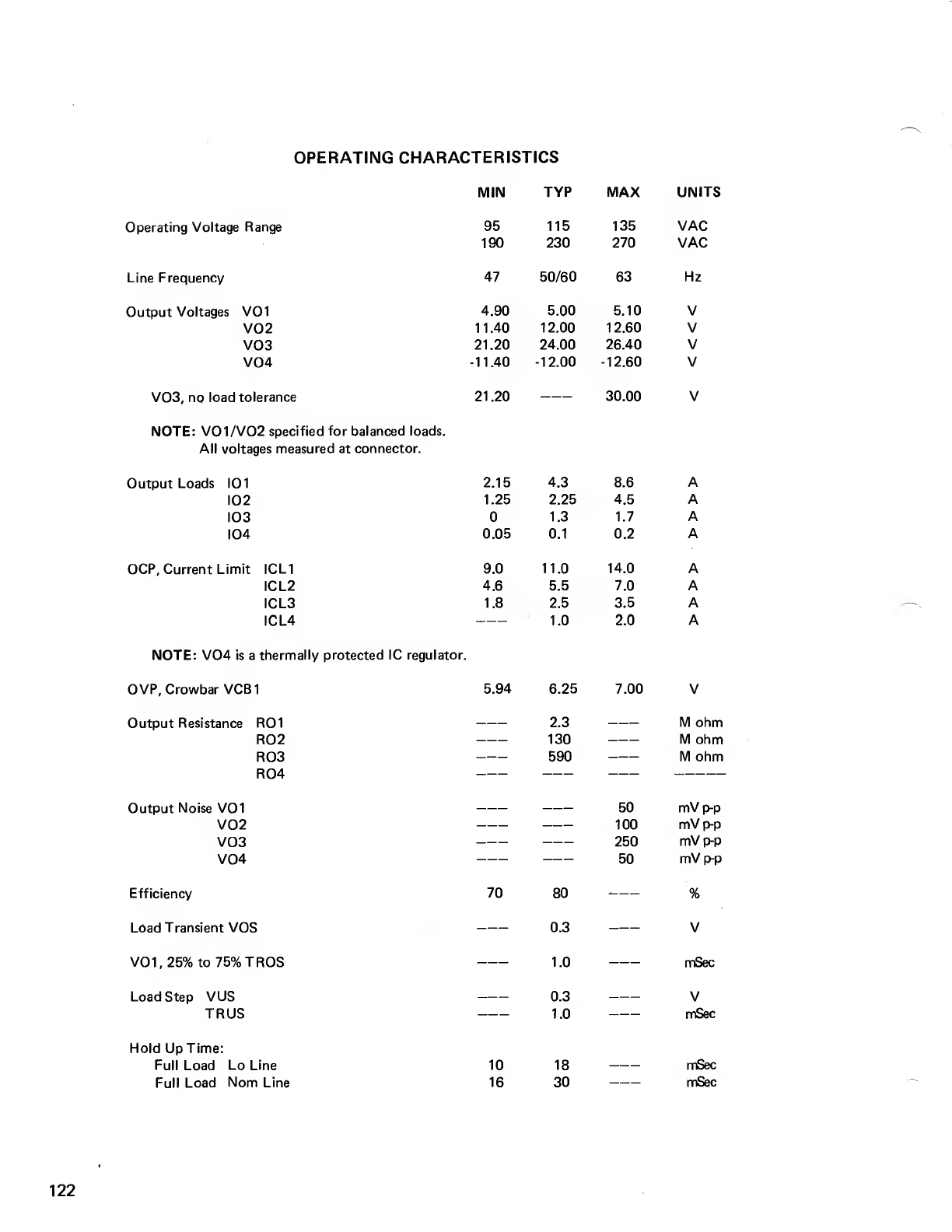
OPERATING CHARACTERISTICS
Operating Voltage Range
Line Frequency
Output Voltages V01
V02
V03
V04
V03, no load tolerance
NOTE: V01/V02 specified for balanced loads.
All voltages measured at connector.
Output Loads 101
I02
103
104
OCP, Current Limit ICL1
ICL2
ICL3
ICL4
NOTE: V04 is athermally protected IC regulator.
OVP, Crowbar VCB1
Output Resistance R01
R02
R03
R04
Output Noise V01
V02
V03
V04
Efficiency
Load Transient VOS
V01,25%to75%TROS
Load Step VUS
TRUS
Hold Up Time:
Full Load Lo Line
Full Load Nom Line
MIN
95
190
47
21.20
5.94
70
TYP
115
230
50/60
6.25
2.3
130
590
10
16
80
0.3
1.0
0.3
1.0
18
30
MAX
135
270
63
30.00
7.00
50
100
250
50
UNITS
VAC
VAC
Hz
4.90 5.00 5.10 V
11.40 12.00 12.60 V
21.20 24.00 26.40 V
11.40 -12.00 -12.60 V
V
2.15 4.3 8.6 A
1.25 2.25 4.5 A
1.3 1.7 A
0.05 0.1 0.2 A
9.0 11.0 14.0 A
4.6 5.5 7.0 A
1.8 2.5 3.5 A
1.0 2.0 A
Mohm
Mohm
Mohm
mVp-p
mVp-p
mVp-p
mVp-p
%
mSec
V
mSec
mSec
mSec
122
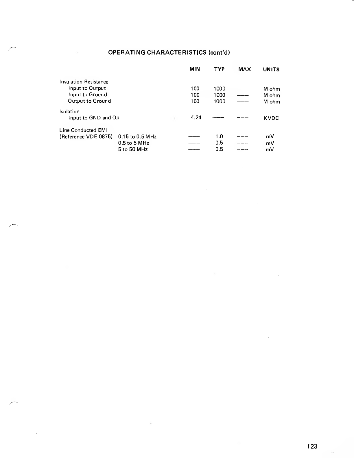
OPERATING CHARACTERISTICS (cont'd)
MIN TYP MAX UNITS
Insulation Resistance
Input to Output
Input to Ground
Output to Ground
Isolation
Input to GND and Op
100 1000 Mohm
100 1000 Mohm
100 1000 Mohm
4.24 KVDC
Line Conducted EMI
(Reference VDE 0875) 0.15 to 0.5 MHz
0.5 to 5MHz
5to 50 MHz
1.0
0.5
0.5
mV
mV
mV
123
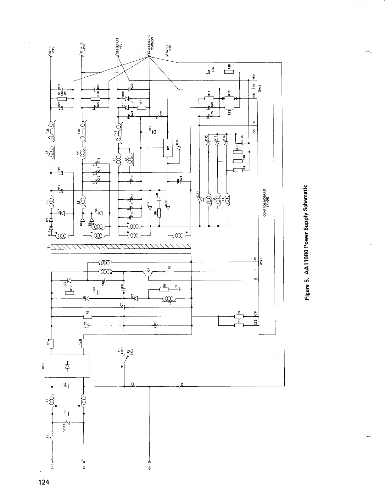
rtt-
-JSKF -%]-
-CZ3-
-CZh -cz>
/'
re
E
u
CO
>
"a
a
3
CO
a)
O
a
o
CO
o
<
<
124
SECTION X
CARD CAGE and MOTHERBOARD
125

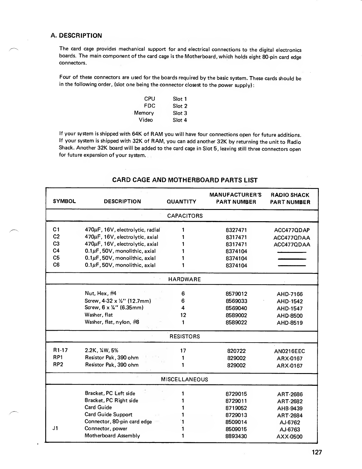
A. DESCRIPTION
The card cage provides mechanical support for and electrical connections to the digital electronics
boards. The main component of the card cage is the Motherboard, which holds eight 80-pin card edge
connectors.
Four of these connectors are used for the boards required by the basic system. These cards should be
in the following order, (slot one being the connector closest to the power supply)
:
CPU Slot 1
FDC Slot 2
Memory Slot 3
Video Slot 4
If your system is shipped with 64K of RAM you will have four connections open for future additions.
If your system is shipped with 32K of RAM, you can add another 32K by returning the unit to Radio
Shack. Another 32K board will be added to the card cage in Slot 5, leaving still three connectors open
for future expansion of your system.
CARD CAGE AND MOTHERBOARD PARTS LIST
MANUFACTURER'S RADIO SHACK
SYMBOL DESCRIPTION QUANTITY PART NUMBER PART NUMBER
CAPACITORS
C1 470/LtF, 16V, electrolytic, radial 8327471 ACC477QDAP
C2 470//F, 16V, electrolytic, axial 8317471 ACC477QDAA
C3 470juF, 16V, electrolytic, axial 8317471 ACC477QDAA
C4 0.1/uF, 50V, monolithic, axial 8374104
C5 0.1;uF, 50V, monolithic, axial
0.1 mF, 50V, monolithic, axial
8374104
C6 8374104
HARDWARE
Nut, Hex, #4 68579012 AHD-7166
Screw, 4-32 x%" (1 2.7mm) 68569033 AHD- 1542
Screw, 6x%" (6.35mm) 48569040 AHD-1547
Washer, flat 12 8589002 AHD-8500
Washer, flat, nylon, #8 18589022 AHD-8519
RESISTORS
R1-17 2.2K,y4W,5% 17 820722 AN0216EEC
RP1 Resistor Pak, 390 ohm 1829002 ARX-0167
RP2 Resistor Pak, 390 ohm 1829002 ARX-0167
MISCELLANEOUS
Bracket, PC Left side 8729015 ART-2686
Bracket, PC Right side 8729011 ART-2682
Card Guide 8719052 AHB-9439
Card Guide Support 8729013 ART-2684
Connector, 80-pin card edge 8509014 AJ-6762
J1 Connector, power 8509015 AJ-6763
Motherboard Assembly 8893430 AXX-0500
127
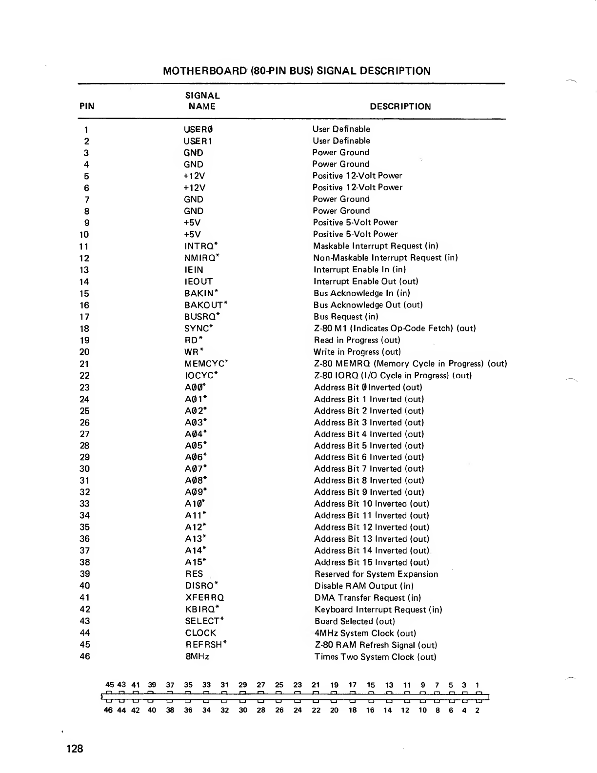
MOTHERBOARD (80-PIN BUS) SIGNAL DESCRIPTION
PIN
SIGNAL
NAME DESCRIPTION
1
2
3
4
5
6
7
8
9
10
11
12
13
14
15
16
17
18
19
20
21
22
23
24
25
26
27
28
29
30
31
32
33
34
35
36
37
38
39
40
41
42
43
44
45
46
USER0
USER1
GNO
GND
+12V
+12V
GND
GND
+5V
+5V
INTRQ*
NMIRQ*
IEIN
IEOUT
BAKIN*
BAKOUT*
BUSRQ*
SYNC*
RD*
WR*
MEMCYC*
IOCYC*
A00*
A01*
A02*
A03*
A04*
A05*
A06*
A07*
A08*
A09*
A10*
A11*
A12*
A13*
A14*
A15*
RES
DISRO*
XFERRQ
KBIRQ*
SELECT*
CLOCK
REFRSH*
8MHz
User Definable
User Definable
Power Ground
Power Ground
Positive 12-Volt Power
Positive 12-Volt Power
Power Ground
Power Ground
Positive 5-Volt Power
Positive 5-Volt Power
Maskable Interrupt Request (in)
Non-Maskable Interrupt Request (in)
Interrupt Enable In (in)
Interrupt Enable Out (out)
Bus Acknowledge In (in)
Bus Acknowledge Out (out)
Bus Request (in)
Z-80M1 (Indicates Op-Code Fetch) (out)
Read in Progress (out)
Write in Progress (out)
Z-80 MEMRQ (Memory Cycle in Progress) (out)
Z-80 IORQ (I/O Cycle in Progress) (out)
Address Bit Inverted (out)
Address Bit 1Inverted (out)
Address Bit 2Inverted (out)
Address Bit 3Inverted (out)
Address Bit 4Inverted (out)
Address Bit 5Inverted (out)
Address Bit 6Inverted (out)
Address Bit 7Inverted (out)
Address Bit 8Inverted (out)
Address Bit 9Inverted (out)
Address Bit 10 Inverted (out)
Address Bit 11Inverted (out)
Address Bit 12 Inverted (out)
Address Bit 13 Inverted (out)
Address Bit 14 Inverted (out)
Address Bit 15 Inverted (out)
Reserved for System Expansion
Disable RAM Output (in)
DMA Transfer Request (in)
Keyboard Interrupt Request (in)
Board Selected (out)
4MHz System Clock (out)
Z-80 RAM Refresh Signal (out)
Times Two System Clock (out)
r-» i—
i
I—
i
i—i
*I
LJ 1—
I
LJ LJ LJ LJ "CT- TTncr u
128
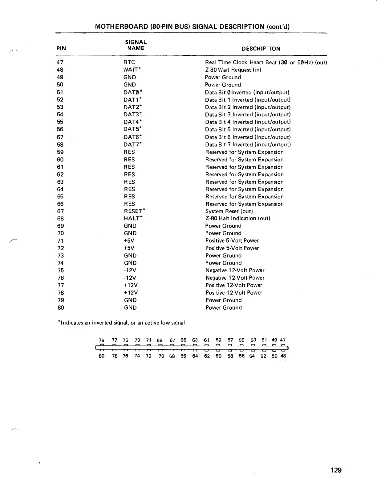
MOTHERBOARD {80-PIN BUS) SIGNAL DESCRIPTION (cont'd)
PIN
SIGNAL
NAME DESCRIPTION
47
48
49
50
51
52
53
54
55
56
57
58
59
60
61
62
63
64
65
66
67
68
69
70
71
72
73
74
75
76
77
78
79
80
RTC
WAIT*
GND
GND
DAT0*
DAT1*
DAT2*
DAT3*
DAT4*
DAT5*
DAT6*
DAT7*
RES
RES
RES
RES
RES
RES
RES
RES
RESET*
HALT*
GND
GND
+5V
+5V
GND
GND
-12V
-12V
+12V
+12V
GND
GND
Real Time Clock Heart Beat (30 or 60Hz) (out)
Z-80Wait Request (in)
Power Ground
Power Ground
Data Bit ©Inverted (input/output)
Data Bit 1Inverted (input/output)
Data Bit 2Inverted (input/output)
Data Bit 3Inverted (input/output)
Data Bit 4Inverted (input/output)
Data Bit 5Inverted (input/output)
Data Bit 6Inverted (input/output)
Data Bit 7Inverted (input/output)
Reserved for System Expansion
Reserved for System Expansion
Reserved for System Expansion
Reserved for System Expansion
Reserved for System Expansion
Reserved for System Expansion
Reserved for System Expansion
Reserved for System Expansion
System Reset (out)
Z-80 Halt Indication (out)
Power Ground
Power Ground
Positive 5-Volt Power
Positive 5-Volt Power
Power Ground
Power Ground
Negative 12-Volt Power
Negative 12-Volt Power
Positive 12-Volt Power
Positive 12-Volt Power
Power Ground
Power Ground
'Indicates an inverted signal, or an active low signal.
r
79
n77 75 73 71 69 67 65 63 61 59 57 55 53 51 49 47
-CD O O _
-E3-
72
80 78 76 74 70 68 66 64 62 60 58 56 54 52 50 48
129
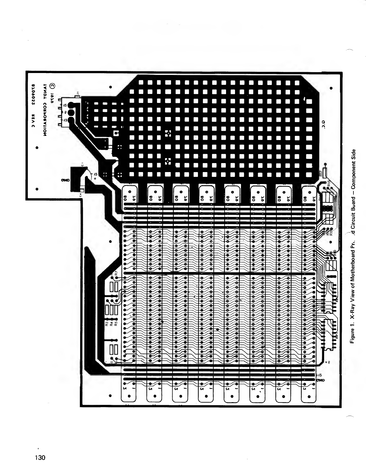
0)
o
R
E
n
3
QQ
3
U
O
Q.
o
IS
O
.
0)
DC
130
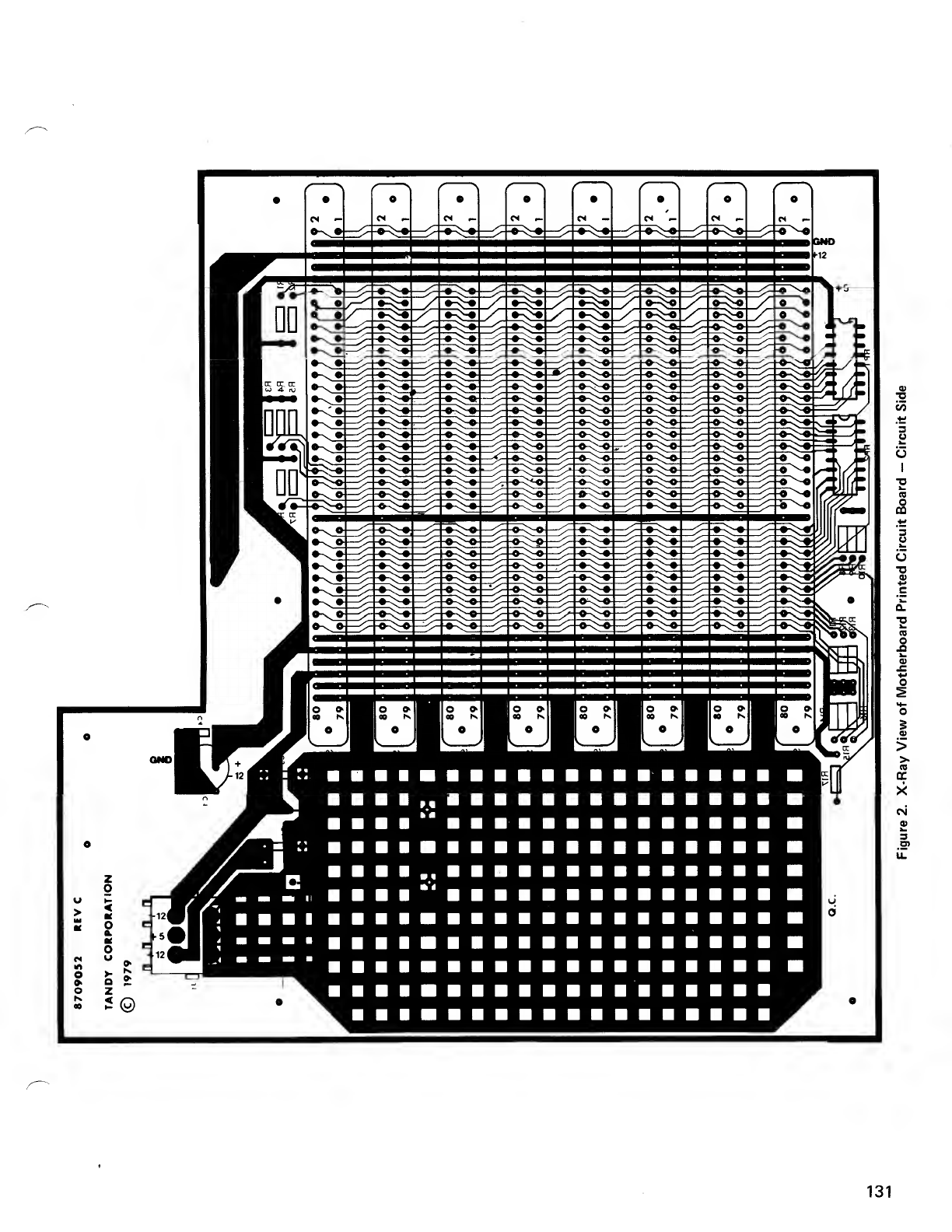
131

SECTION XI
KEYBOARD UNIT
133

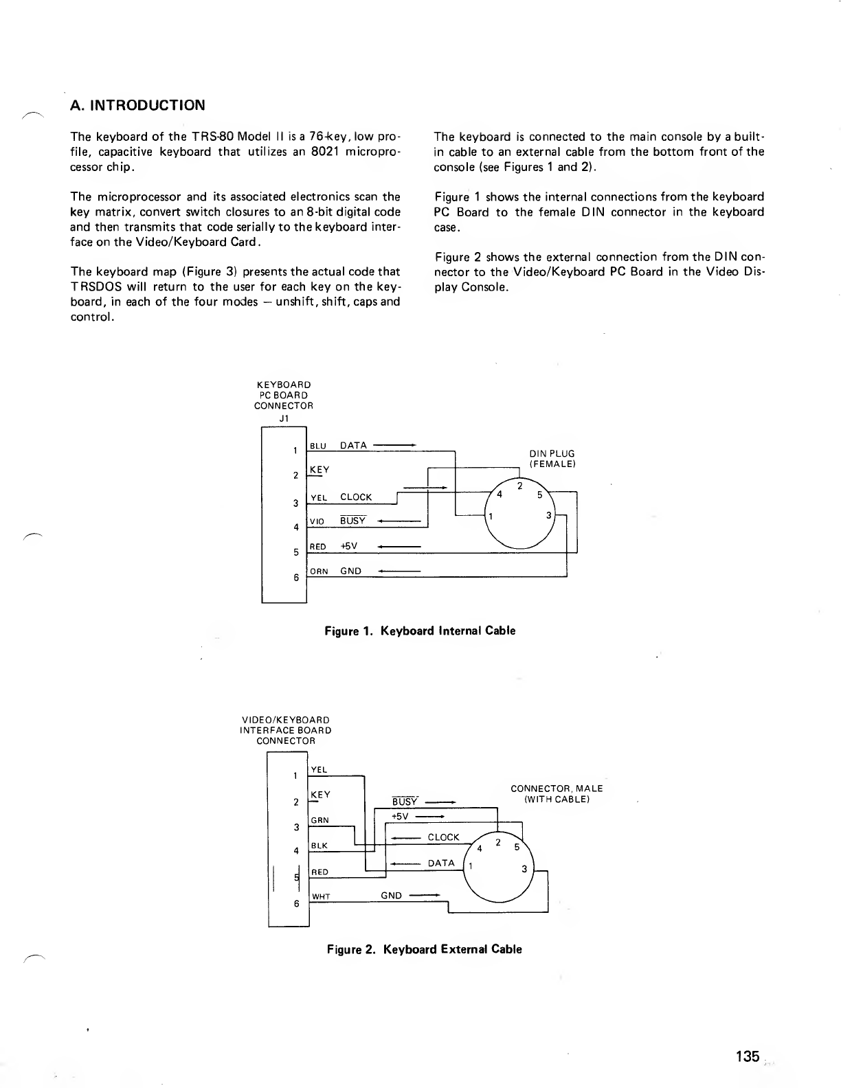
A. INTRODUCTION
The keyboard of the TRS-80 Model II is a76-key, low pro-
file, capacitive keyboard that utilizes an 8021 micropro-
cessor chip.
The microprocessor and its associated electronics scan the
key matrix, convert switch closures to an 8-bit digital code
and then transmits that code serially to the keyboard inter-
face on the Video/ Keyboard Card.
The keyboard map (Figure 3) presents the actual code that
TRSDOS will return to the user for each key on the key-
board, in each of the four modes —unshift, shift, caps and
control.
The keyboard is connected to the main console by abuilt-
in cable to an external cable from the bottom front of the
console (see Figures 1and 2).
Figure 1shows the internal connections from the keyboard
PC Board to the female DIN connector in the keyboard
case.
Figure 2shows the external connection from the DIN con-
nector to the Video/Keyboard PC Board in the Video Dis-
play Console.
KEYBOARD
PC BOARD
CONNECTOR
J1
BLU DATA
KE Y
YEL CLOCK
VIO BUSY
RED +5V
ORN GND
Figure 1. Keyboard Internal Cable
VIDEO/KEYBOARD
INTERFACE BOARD
CONNECTOR
CONNECTOR, MALE
(WITH CABLE)
Figure 2. Keyboard External Cable
135
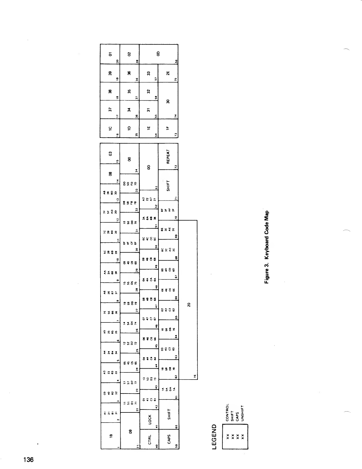
o
o
CM
O
<•>
o
o
os
0»
8UJ
CM
s
«D
in
8
A
oOLU LL
n
o
8
D
o
t-
<
UJ
a.
UJ
QC
s
LL.
X
9Q O O
Ot/1 U. *-
*a> QO
< m n
<S<S
o(o am
Qio u. f-
m « <<n
o
M. U. OO
i- m<tM
5aSS
2S§S
o n <r.
en
<o
O
CM
IO
Ogi Oo
r» F* sr>
OUO{J
O«O(0
o
O«U16
oa&<!=i
OS
in
U«01 01
o09 10 (S CD
o»oe
Ok
ai o> ot ai
o«Oip
0t QOOO
5*o<o
<o
5<«00
<«9«
0> <<<<
OS
OD O«UIO
o
10
<Sos
OB 8S8S
01 01 £91
—ift Or-
O»U(O
IO
Ml UJ IO 10
O•* U<0
IO
;t«•
10 IO ID g«
<2 mio m
<in tn n
8S 88
=SSR
0*0(0
IO
3S23
***. ^
O»UIO
ao oo 2oa
—ui Qf.
10
<•» nMpi
<im os n
££oC
IO
oo2f w
O*»<*>
O*UIS
-m5-
H
u.
I
w
o
IO
<ws«
o
o
o
CD -J
cc
h-
oo
V)
a.
<
oen
a
IB
1
U
s
a
>.
CO
0)
3
o
(T u.
KI
^w
o<t z
u w u 3
Q
2
UJ XX X X
aXX X X
UJ
.-I
136
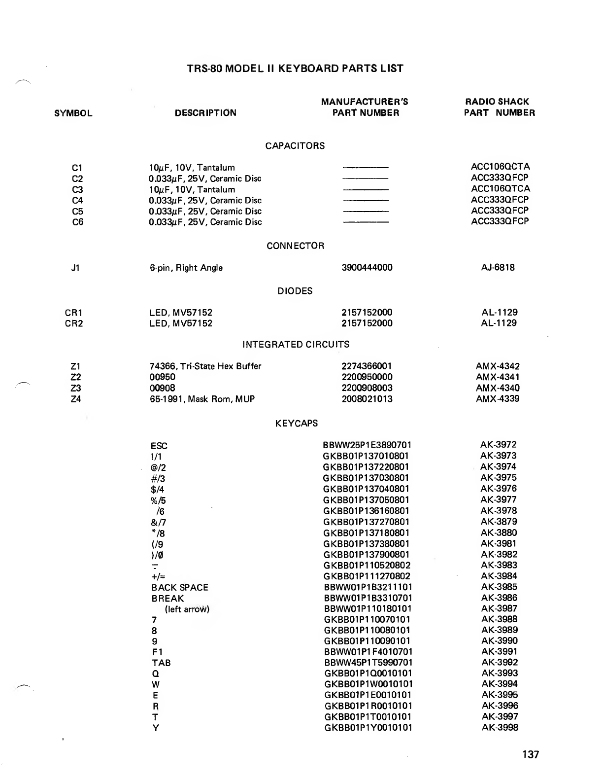
TRS-80 MODEL II KEYBOARD PARTS LIST
SYMBOL DESCRIPTION
MANUFACTURER'S
PART NUMBER RADIO SHACK
PART NUMBER
CAPACITORS
C1
C2
C3
C4
C5
C6
10juF, 10V, Tantalum
0.033juF, 25V, Ceramic Disc
10/xF, 10V, Tantalum
0.033juF, 25V, Ceramic Disc
0.033juF, 25V, Ceramic Disc
0.033juF, 25V, Ceramic Disc
ACC106QCTA
ACC333QFCP
ACC106QTCA
ACC333QFCP
ACC333QFCP
ACC333QFCP
CONNECTOR
J1 6-pin, Right Angle 3900444000 AJ-6818
DIODES
CR1 LED, MV57152 2157152000
CR2 LED, MV57152 2157152000
INTEGRATED CIRCUITS
Z1 74366, Tri-State Hex Buffer 2274366001
Z2 00950 2200950000
Z3 00908 2200908003
Z4 65-1991, Mask Rom, MUP 2008021013
KEYCAPS
AL-1129
AL-1129
AMX-4342
AMX-4341
AMX-4340
AMX4339
ESC
1/1
@/2
#/3
$/4
%/5
/6
&/7
*/8
(/9
)/0
+/=
BACK SPACE
BREAK
(left arrow)
7
8
9
F1
TAB
Q
W
E
R
T
Y
BBWW25P1E3890701
GKBB01P137010801
GKBB01P1 37220801
GKBB01P1 37030801
GKBB01P137040801
GKBB01P1 37050801
GKBB01P136160801
GKBB01P137270801
GKBB01P137180801
GKBB01P137380801
GKBB01P137900801
GKBB01P1 10520802
GKBB01P1 11270802
BBWW01P1B3211101
BBWW01P1B3310701
BBWW01P1 10180101
GKBB01P1 10070101
GKBB01P1 10080101
GKBB01P1 10090101
BBWW01P1F4010701
BBWW45P1T5990701
GKBB01P1Q0010101
GKBB01P1W0010101
GKBB01P1E0010101
GKBB01P1R0010101
GKBB01P1T0010101
GKBB01P1Y0010101
AK-3972
AK-3973
AK-3974
AK-3975
AK-3976
AK-3977
AK-3978
AK-3879
AK-3880
AK-3981
AK-3982
AK-3983
AK-3984
AK-3985
AK-3986
AK-3987
AK-3988
AK-3989
AK-3990
AK-3991
AK-3992
AK-3993
AK-3994
AK-3995
AK-3996
AK-3997
AK-3998
137
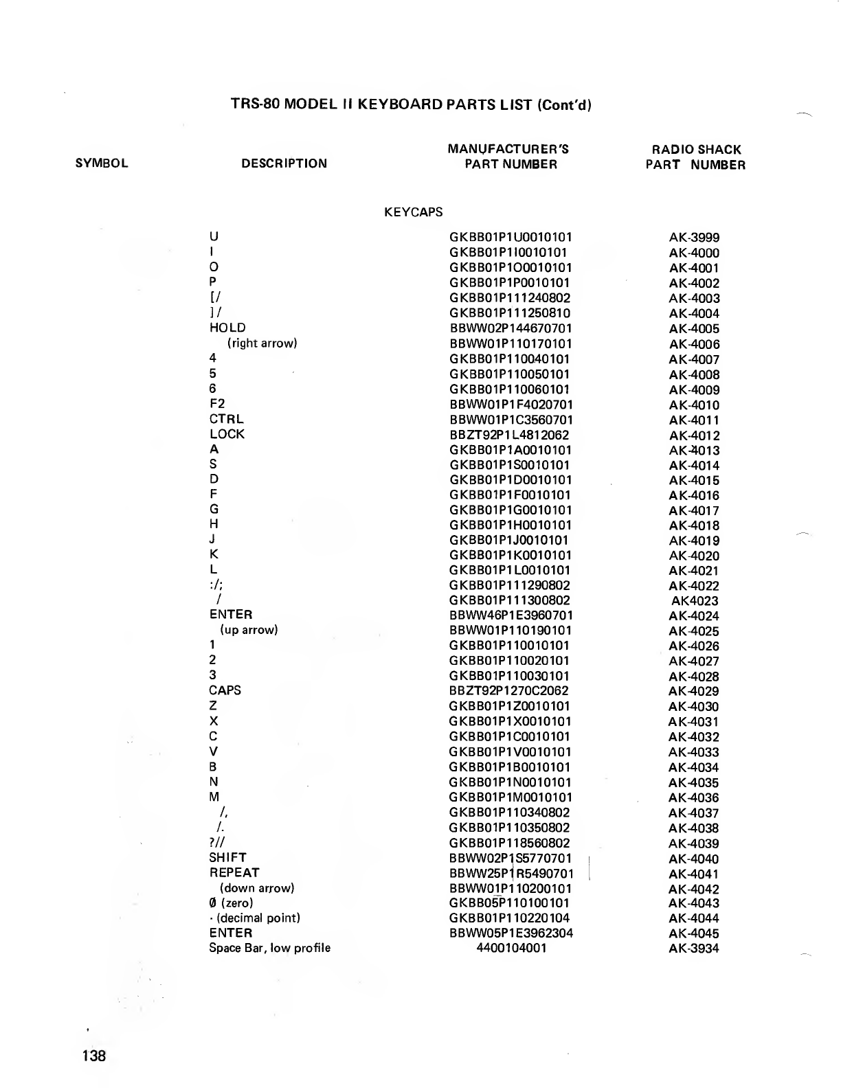
TRS-80 MODEL II KEYBOARD PARTS LIST (Cont'd)
SYMBOL DESCRIPTION
MANUFACTURER'S
PART NUMBER RADIO SHACK
PART NUMBER
KEYCAPS
U
I
P
[/
]/
HOLD
(right arrow)
4
5
6
F2
CTRL
LOCK
A
S
D
F
G
H
J
K
L
:/;
/
ENTER
(up arrow)
1
2
3
CAPS
Z
X
c
V
B
N
M
/,
/.
VI
SHIFT
REPEAT
(down arrow)
(zero)
•(decimal point)
ENTER
Space Bar, low profile
GKBB01P1U0010101
GKBB01P1 10010101
GKBB01P1O0010101
GKBB01P1P0010101
GKBB01P1 11240802
GKBB01P1 11250810
BBWW02P 144670701
BBWW01P1 10170101
GKBB01P1 10040101
GKBB01P1 10050101
GKBB01P1 10060101
BBWW01P1F4020701
BBWW01P1C3560701
BBZT92P1 L4812062
GKBB01P1A0010101
GKBB01P1S0010101
GKBB01P1D0010101
GKBB01P1F0010101
GKBB01P1G0010101
GKBB01P1H0010101
GKBB01P1J0010101
GKBB01P1K0010101
GKBB01P1L0010101
GKBB01P1 11290802
GKBB01P1 11300802
BBWW46P1E3960701
BBWW01P1 10190101
GKBB01P1 10010101
GKBB01P1 10020101
GKBB01P1 10030101
BBZT92P1270C2062
GKBB01P1Z0010101
GKBB01P1X0010101
GKBB01P1C0010101
GKBB01P1V0010101
GKBB01P1B0010101
GKBB01P1N0010101
GKBB01P1M0010101
GKBB01P1 10340802
GKBB01P1 10350802
GKBB01P1 18560802
BBWW02P1S5770701
BBWW25PJR5490701
BBWW01P1 10200101
GKBB05P1 10100101
GKBB01P1 10220104
BBWW05P1E3962304
4400104001
AK-3999
AK-4000
AK-4001
AK-4002
AK-4003
AK-4004
AK-4005
AK-4006
AK-4007
AK-4008
AK-4009
AK-4010
AK-401
1
AK-401
2
AK-401
3
AK-401
4
AK-401
5
AK-401
6
AK-401
7
AK-401
8
AK-401
9
AK-4020
AK-4021
AK-4022
AK4023
AK-4024
AK-4025
AK-4026
AK-4027
AK-4028
AK-4029
AK-4030
AK-4031
AK-4032
AK-4033
AK-4034
AK-4035
AK-4036
AK4037
AK-4038
AK-4039
AK-4040
AK-4041
AK-4042
AK-4043
AK-4044
AK-4045
AK-3934
138
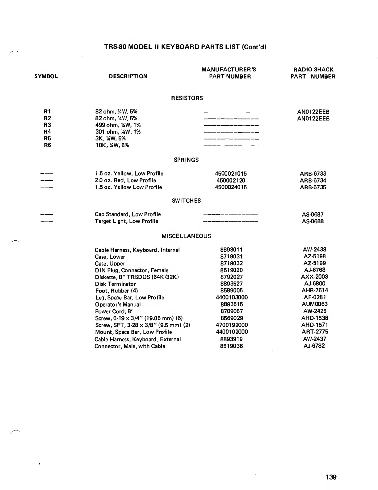
TRS-80 MODEL II KEYBOARD PARTS LIST (Cont'd)
SYMBOL DESCRIPTION
MANUFACTURER'S
PART NUMBER RADIO SHACK
PART NUMBER
RESISTORS
R1
R2
R3
R4
R5
R6
82 ohm, 1
/*W, 5%
82 ohm, 1
/4W, 5%
499 ohm, %W, 1%
301 ohm, %W, 1%
3K, 14W, 5%
10K, 1
/iW,5%
AN0122EEB
AN0122EEB
SPRINGS
1.5 oz. Yellow, Low Profile
2.0 oz. Red, Low Profile
1.5 oz. Yellow Low Profile
4500021015
450002120
4500024015
ARB-6733
ARB-6734
ARB-6735
SWITCHES
Cap Standard, Low Profile
Target Light, Low Profile
AS-0687
AS-0688
MISCELLANEOUS
Cable Harness, Keyboard, Internal 889301
1
Case, Lower 8719031
Case, Upper 8719032
DIN Plug, Connector, Female 8519020
Diskette, 8" TRSDOS (64K/32K) 8792027
Disk Terminator 8893527
Foot, Rubber (4) 8589005
Leg, Space Bar, Low Profile 4400103000
Operator's Manual 8893515
Power Cord, 8' 8709057
Screw, 6-19 x3/4" (19.05 mm) (6) 8569029
Screw, SFT, 3-28 x3/8" (9.5 mm) (2) 4700192000
Mount, Space Bar, Low Profile 4400102000
Cable Harness, Keyboard, External 8893919
Connector, Male, with Cable 8519036
AW-2438
AZ-5198
AZ-5199
AJ-6768
AXX-2003
AJ-6800
AHB-7614
AF-0281
AUM0063
AW-2425
AHD- 1538
AHD-1571
ART-2775
AW-2437
AJ-6782
139
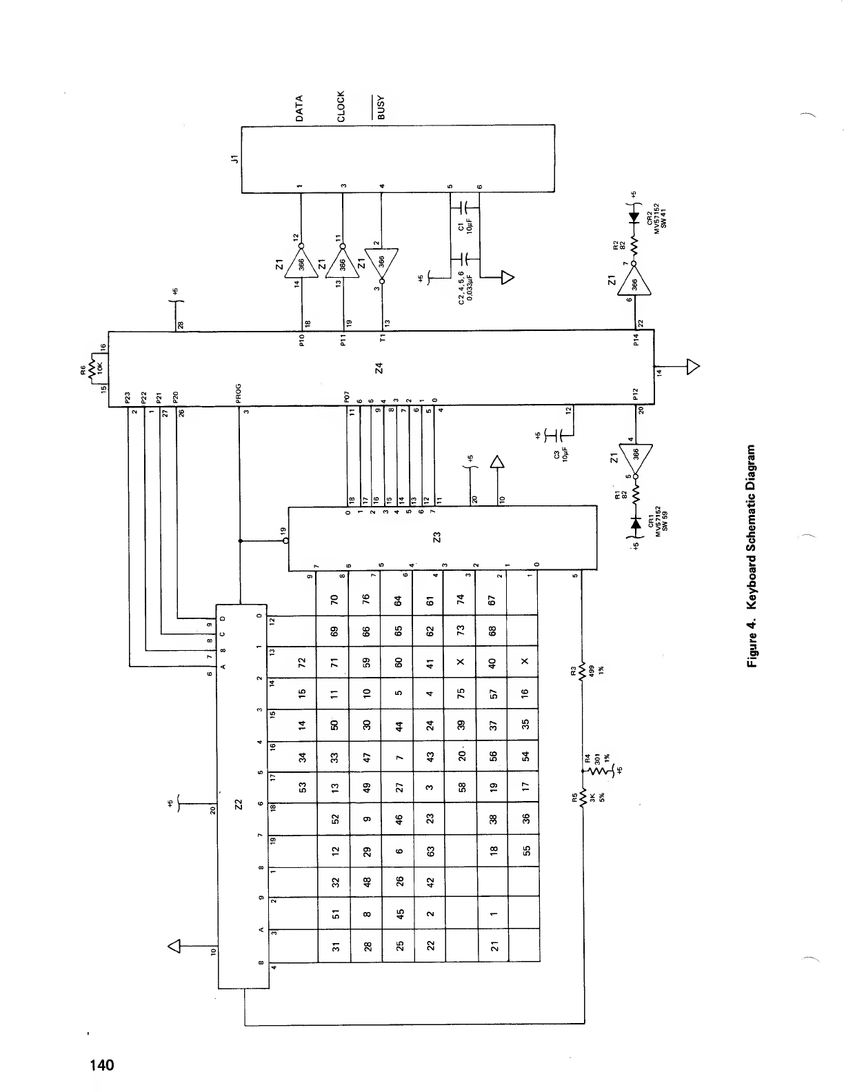
<
Do>
in
3
a- o. a. a.
H(-
H(-
H=:» L—1>
E' to
cj m«r in to r»
A
oO
*HH
>
E
n
at
a
5
o
'^
<B
E
a
JZ
o
to
<h
~WV-fi?
n
.Q
3
Ol
140
SECTION XII
PERIPHERAL INTERFACES
141

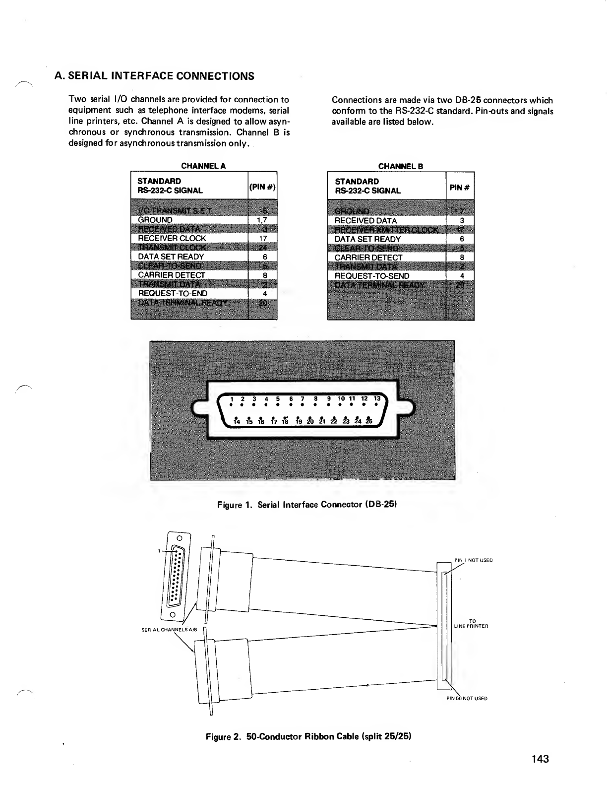
A. SERIAL INTERFACE CONNECTIONS
Two serial I/O channels are provided for connection to
equipment such as telephone interface modems, serial
line printers, etc. Channel Ais designed to allow asyn-
chronous or synchronous transmission. Channel Bis
designed for asynchronous transmission only.
CHANNEL
A
STANDARD
RS-232-C SIGNAL (PIN #)
I/O TRANSMIT SET
GROUND
RECEIVED DATA
RECEIVER CLOCK
TRANSMIT CLOCK
DATA SET READY
CLEAR-TO-SEND
CARRIER DETECT
TRANSMIT DATA
REQUEST-TO-END
DATA TERMINAL READY ;
15
1.7
24
6
mi
i.
20
Connections are made via two DB-25 connectors which
conform to the RS-232-C standard. Pin-outs and signals
available are listed below.
CHANNEL B
STANDARD
RS-232-C SIGNAL PIN#
GROUND 1.7
3
17
RECEIVED DATA
RECEIVER XMITTER CLOCK
DATA SET READY
CLEAR-TO-SEND
CARRIER DETECT
TRANSMITDATA
I
8
i
4
REQUEST-TO-SEND
DATA TERMINAL READY 20
^V1*4 1*5 1*6 h&f9ft fl &h?4 ft JW^J
Figure 1. Serial Interface Connector (DB-25)
PIN 1NOT USED
SERIAL CHANNELS A/B
TO
LINE PRINTER
PIN 50 NOT USED.
Figure 2. 50-Conductor Ribbon Cable (split 25/25)
143

B. PARALLEL INTERFACE
The Model II provides one parallel I/O channel for con-
nection to aline printer via the 34-pin connector on
the back panel of the Display Console. Eight data bits
are output in parallel and four data bits are input. All
levels are TTL compatible.
Connector pin-outs and available signals are listed on
the following page.
i246810 12 14 16 18 20 22 24 26 28 30 32 34
13 57911 1*3 1*5 17 19 21 23 25 27 29 31 33 ^
Figure 3. Parallel Interface 34-pin Connector
TO
CPU
PERIPHERAL DEVICES
Figure 4. Parallel Interface 34-pin Ribbon Cable
144
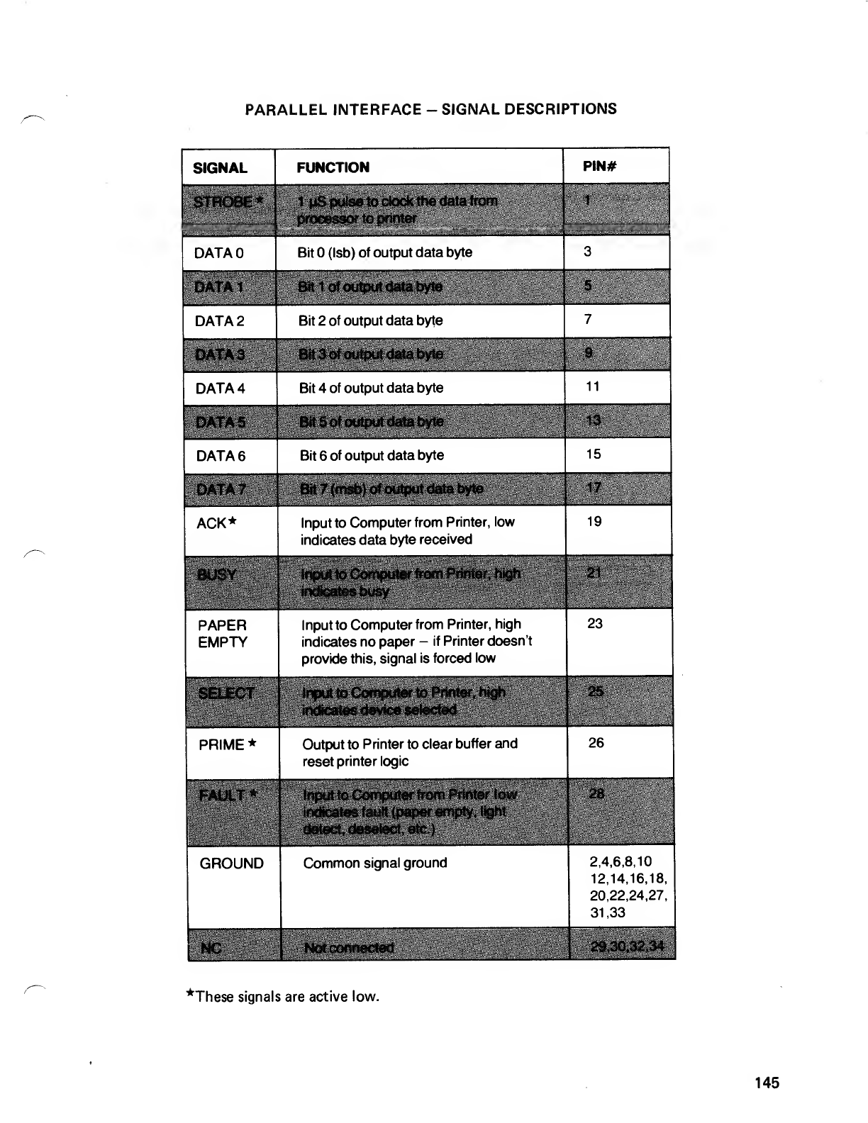
PARALLEL INTERFACE -SIGNAL DESCRIPTIONS
SIGNAL FUNCTION PIN#
STROBE* 1|jS pulse to clock the data from
processor to printer ^^^^^H
DATAO Bit (Isb) of output data byte 3
DATA1 Bit 1of output data byte H1HIHI
DATA 2Bit 2of output data byte 7
DATA3 Bit 3of output data byte 9
DATA 4Bit 4of output data byte 11
DATA5 Bit 5of output data byte 13
DATA 6Bit 6of output data byte 15
DATA 7Bit 7(msb) of output data byte 17
ACK* Input to Computer from Printer, low
indicates data byte received
19
BUSY Input to Computer from Printer, high
indicates busy
21
PAPER
EMPTY
Input to Computer from Printer, high
indicates no paper -if Printer doesn't
provide this, signal is forced low
23
SELECT Input to Computer to Printer, high
indicates device selected
25
PRIME* Output to Printer to clear buffer and
reset printer logic
26
FAULT* Input to Computer from Printer low
indicates fault (paper empty, light
detect, deselect, etc.)
28
GROUND Common signal ground 2,4,6,8,10
12,14,16,18,
20,22,24,27,
31,33
NC Not connected 29,30,32,34
*These signals are active low.
145
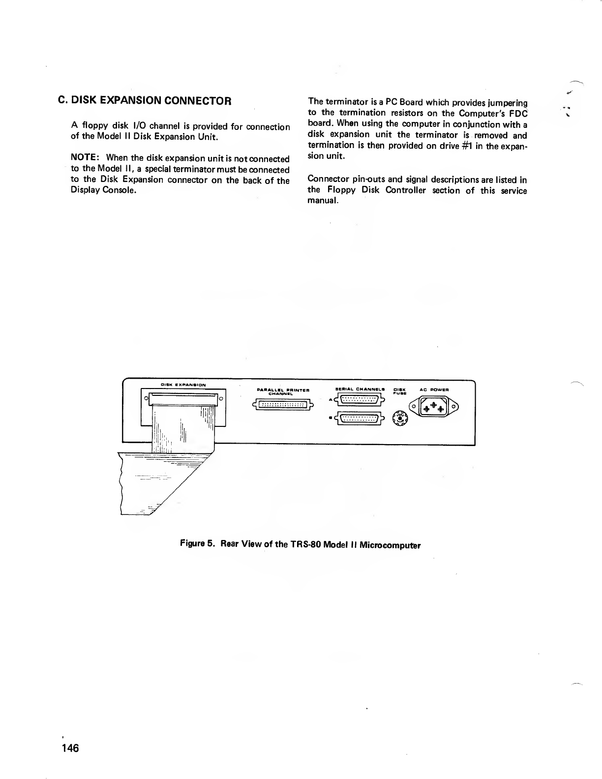
C. DISK EXPANSION CONNECTOR
Afloppy disk I/O channel is provided for connection
of the Model II Disk Expansion Unit.
NOTE :When the disk expansion unit is not connected
to the Model II, aspecial terminator must be connected
to the Disk Expansion connector on the back of the
Display Console.
The terminator is aPC Board which provides jumpering
to the termination resistors on the Computer's FDC
board. When using the computer in conjunction with a
disk expansion unit the terminator is removed and
termination is then provided on drive #1 in the expan-
sion unit.
Connector pin-outs and signal descriptions are listed in
the Floppy Disk Controller section of this service
manual.
DISK EXPANSION SERIAL CHANNELS DISK AC POWER
I:1FUSE
a> 'Pit A#
Figure 5. Rear View of the TRS-80 Model II Microcomputer
146
SECTION XIII
DISK EXPANSION UNIT
147

A. INTRODUCTION
The TRS-80 Model II Disk Expansion Unit is amass
storage device designed to interface with the TRS-80
Model II Computer to provide the user with an addi-
tional storage capacity of up to 1.5 Megabytes for a
total system capacity of 2 Megabytes on line.
The Disk Expansion Unit is available in a1, 2, or 3
drive configuration. The 1and 2 drive units may be
upgraded with additional drives from your Radio
Shack dealer.
The Disk Expansion Unit consists of up to three
flexible disk drives, apower supply and acooling fan.
It connects to the Computer through aflat ribbon
cable.
Standard 115/120 VAC is applied to the expansion
unit through apower switch where it is distributed to
the three disk drives, the internal power supply and to
its cooling fan.
The power supply converts the AC input to three levels
of DC which is routed to the disk drives for their logic
signals. The DC voltages are +24, +5 and -12. ALED
on the fron panel "lights up" when the power switch is
in the "ON" position.
Subassembly Description
The disk expansion unit consists of seven major sub-
assemblies. Each subassembly may be considered as a
single component of the disk expansion system. If a
subassembly is determined to be faulty, the entire
subassembly should be replaced.
The power Supply is regulated and has overcurrent
protection. It will operate at either 50Hz or 60Hz
input and may be jumpered for either 95VAC to
135 VAC or 190V AC to 270VAC. The Power Sup-
ply is located in the rear and to the left of the
CRT.
3. Disk Drive:
The disk drive is an 8" flexible disk unit capable
of supporting both single and double density re-
cording formats. All of the disk drive control sig-
nals come from the Floppy Disk Controller PC
board in the computer. The drive contains two
motors; one is an AC motor which rotates the
diskette at constant speed, the other motor is a
DC stepping motor which positions the read/
write head over one of 77 tracks on the diskette.
The electronics on the disk drive control the step-
ping motor and convert the signals from and to the
read/write head into correct format.
NOTE: Models for overseas shipment may be con-
figured with an AC Motor for the line voltage
available in that country and may be fitted with a
different drive pulley for 50 Hz line frequency.
4. Wiring Harness:
All internal wiring of the disk expansion unit is
accomplished with one wiring harness assembly.
It includes both AC and DC wiring for the system
as well as providing proper grounding.
Fan:
1
.
Chassis:
The Chassis assembly consists of ametal chassis
which forms the bottom and back panel of the
unit. Also included in the chassis assembly are the
line cord and three fuse holders. The bottom of
the chassis has two raised supports for attaching
the disk drive mounting brackets.
2. Power Supply:
The power supply assembly is a60 watt, switching
power supply which provides the following volt-
ages to the disk drives:
+5 Volts DC @3.00 Amps
-12 Volts DC @0.17 Amps
+24 Volts DC @1.70 Amps
NOTE: The —12 volt output is not used.
Cooling for the system is provided by asingle
rotary fan which is mounted in the bottom of the
chassis assembly and is protected by afinger guard
on the outside of the chassis.
6. Bezel:
The bezel assembly consists of the plastic front
bezel, the AC power switch, power indicator LED,
and blank hole cover for unused drive positions.
It is mounted to the top cover with seven plas-
tite screws.
7. Top Cover:
The top cover is aformed sheet metal cover with
air slots for cooling. It mounts with thread form-
ing screws in the back and on both sides.
149
B. SWITCH CONFIGURATIONS C. TEST POINTS
9404A (Discreet Logic) CDC Drives All CDC Drives:
1
.
PC Board #75890770. See CDC Hardware Main- Refer to the CDC Maintenance Manual and to Figure 1
tenance Manual, page 9, Figure 5-3A. on the following page.
a) S1 -5 -"ON" Position 1. Figure 1shows suggested locations to be used as
b) Drive #1 -S1-2 -"ON" Position test points. The arrows point to acomponent lead
Drive #2 -S1 -3 -"ON" Position or plate through hole that may be used for the
Drive #3 -S1-4 -"ON" Position corresponding signals.
c) All other positions on S1 should be "OFF".
2. PC Board #75881970. See CDC Hardware Main-
tenance Manual, page 10, Figure 5-3A.
a) S1-5-S1-2- "ON" Position
b) Drive #1 -S1-2 -"ON" Position
Drive #2 -S1 -3 -"ON" Position
Drive #3 -S1-4 -"ON" Position
c) All other positions of S1 -"OFF" Positon.
d) S3-4 -"ON" Position
e) All other positions of S3 -"OFF" Position.
9404B (LSI Logic) CDC Drives
1. PC Board #77643120. See CDC Hardware Main-
tenance Manual, page 12, Figure 5-3B.
a) Drive #1 -S1 -2 -"ON" Position
Drive #2 -S1-3 -"ON" Position
Drive #3 -S1-4 -"ON" Position
Drive #1 Only, All Boards (Discreet and LSI)
1. DIP Terminator Pak installed in "RMI" (see Board
diagrams, section 5-3, CDC Hardware Maintenance
Manual).
150
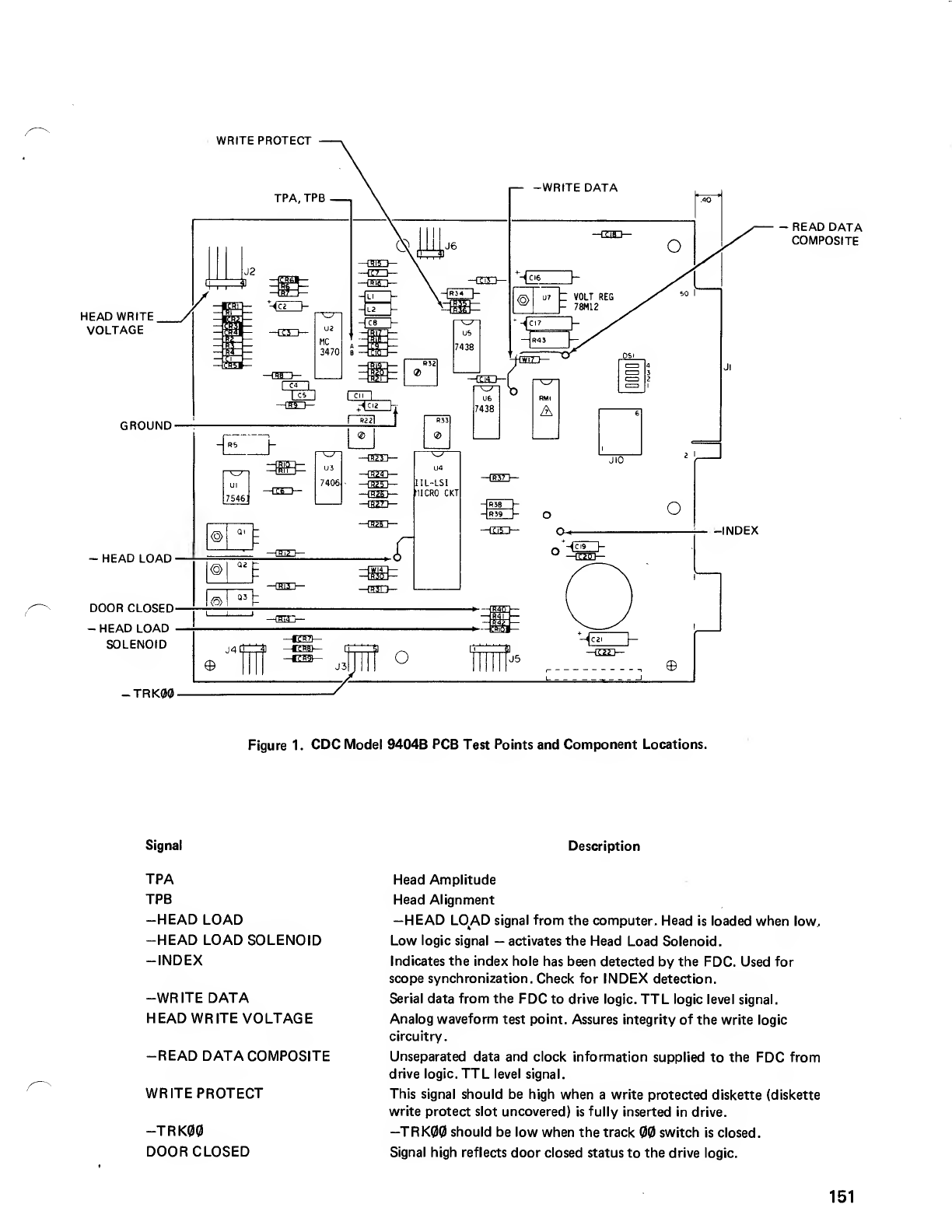
WRITE PROTECT
HEAD WRITE
VOLTAGE
GROUND
-HEAD LOAD
DOOR CLOSED
-HEAD LOAD
SOLENOID
-TRK00
-READ DATA
COMPOSITE
Figure 1. CDC Model 9404B PCB Test Points and Component Locations.
Signal
TPA
TPB
-HEAD LOAD
-HEAD LOAD SOLENOID
-INDEX
-WRITE DATA
HEAD WRITE VOLTAGE
-READ DATA COMPOSITE
WRITE PROTECT
-TRK00
DOOR CLOSED
Description
Head Amplitude
Head Alignment
—HEAD LO|AD signal from the computer. Head is loaded when low.
Low logic signal —activates the Head Load Solenoid.
Indicates the index hole has been detected by the FDC. Used for
scope synchronization. Check for INDEX detection.
Serial data from the FDC to drive logic. TTL logic level signal.
Analog waveform test point. Assures integrity of the write logic
circuitry.
Unseparated data and clock information supplied to the FDC from
drive logic. TTL level signal
.
This signal should be high when awrite protected diskette (diskette
write protect slot uncovered) is fully inserted in drive.
—TRK00 should be low when the track 00 switch is closed.
Signal high reflects door closed status to the drive logic.
151

SECTION XIV
TROUBLESHOOTING -DISK SYSTEM
153

A. TROUBLESHOOTING PROCEDURE
This section of the manual will guide service personnel
through asubassembly check-out procedure which
should locate afaulty subassembly. That subassembly
may then be removed and replaced.
AC or DC Power Failures:
1. Remove Cover/Bezel Assembly (see System Dis-
assembly in Section B. Replacement Procedures).
2. Plug the power cord into an AC outlet and turn
the power switch on (front bezel). Check for the
following:
NOTE: The +24 volt terminal will usually read
high under this condition (up to 30 volts). In-
correct voltage readings at this point indicate
afaulty power supply. If voltage readings are
OK with the dummy load, then an overcurrent
condition in the" system is indicated. Check
for shorted LED circuit. Reconnect wiring
harness to power supply and disconnect DC
plugs to disk drives (see schematic). If power
supply still fails then afaulty wiring harness
or short on TB1 is indicated. If LED is lit then
reinstall DC plugs on drives one by one until
unit causing failure is found. Adisk drive
causing the power supply to fail should be
replaced.
a) Fan is running, AC spindle Motor on disk
drive is running, and power LED is lit.
b) In case of failure: If none of these conditions
are met, then check the AC input terminals to
the power supply with avoltmeter. If no volt-
age is measured here then check for voltage
at the power switch. No voltage at the power
switch indicates afaulty power cord.
c) If fan isn't running, check that fan cord is
plugged securely on fan terminals. Check for
AC at fan cord plug and trace backwards with
avoltmeter to terminal block (TB2) if no volt-
age is found. (See Wiring Diagram, Figure 1.)
d) If disk drive motor isn't running, check the
fuse for that unit on the back of the chassis.
Next trace the wiring back to TB2 with a
voltmeter.
e) If fuse continues to blow, check for ashort on
TB2. Next disconnect AC plugs on disk drives
and check harness for shorts. Next, reconnect
AC plugs to drives one by one until unit
causing failure is found. Replace the faulty
disk drive.
f) If LED does not light, it indicates either a
bad LED or a+5 volt circuit failure. First,
check all DC voltages (+5V±2%; -12V ±5%;
+12V ±10%) at the power supply output
terminals (see Figure 1). If the correct volt-
ages are not present then disconnect the
wiring harness from the output terminals,
install a4ohm, 5watt resistor between +5
and COM and check voltages again.
Operational Failures:
1.
2.
Check for the correct switch position on the CDC
drive PC Board (see B. Switch Configurations in
the Disk Expansion Unit section).
Install the Diagnostic Diskette in drive and refer
to the Troubleshooting Manual. This test will exer-
cise all disk drives in the system by doing seeks,
reads and writes.
Read or Write Error:
First, replace the System diskette in the failing
drive with aknown good Media. Next, check the
jumpers on all drives. Then, check voltages on the
DC connector to the failing drive. Now, replace
the signal cable with aknown good cable. If the
failure persists, then replace the drive.
NOTE: Afailure may appear on any drive because
of incorrect termination on drive 1. Be sure termi-
nation resistor pack (on CDC drive) or jumper
plugs (on Shugart drive in Computer) are correctly
installed on drive 1.See B. Switch Configurations
in the Disk Expansion Unit section for the CDC
drive and B. Jumper Configuration in the Floppy
Disk Drive section for the Computer disk drive.
155
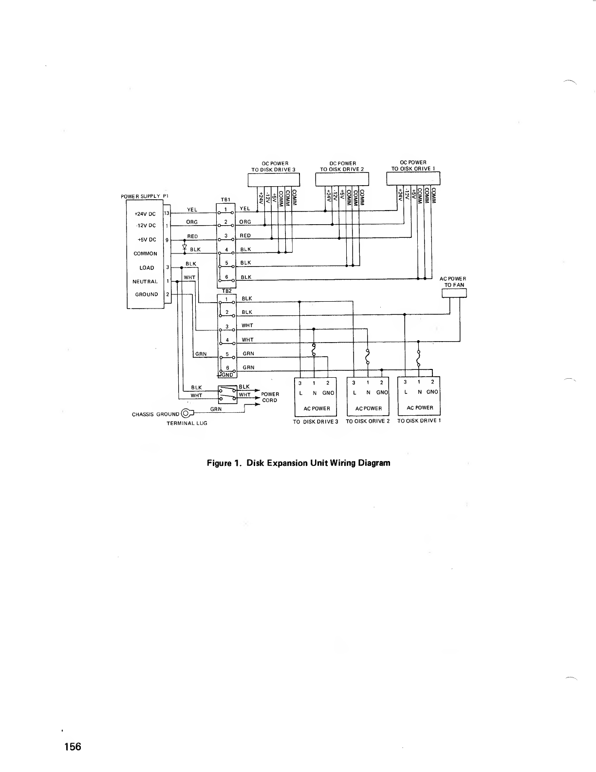
POWER SUPPLY P1
+24V DC
-12V DC
+5V DC
COMMON
LOAD
NEUTRAL
GROUND
DC POWER
TO DISK DRIVE 3
6——
o
.JGNDC
DC POWER
TO DISK DRIVE 2
CHASSIS GROUND ©3
TERMINAL LUG
POWER
'CORD
12
NGND
DC POWER
TO DISK DRIVE 1
12
NGND
AC POWER
TO FAN
12
NGND
TO DISK DRIVE 3TO DISK DRIVE 2TO DISK DRIVE!
Figure 1. Disk Expansion Unit Wiring Diagram
156
B. REPLACEMENT PROCEDURES Fan
NOTE: Be sure that the power cord is unplugged while
any assembly or disassembly is in progress.
System Disassembly
1. Cover &Bezel Assembly
a) Remove four screws from each side of cover
and seven screws from rear edges of chassis.
b) Slide the cover/bezel assembly forward about
1inch then tilt the rear of the cover up so
that the bezel lays face down in front of the
chassis. NOTE: Be careful that the cover
doesn't hang on the signal cable or wiring
harness when lifting it. The length of the wir-
ing harness to the bezel does not permit any
other procedure for removing the cover/
bezel assembly..
2. Power Supply
a) Remove Cover/Bezel Assembly.
b) Disconnect all AC, DC, and ground terminals
from power supply.
c) Remove four Mounting Screws from back of
chassis.
d) Remove power supply.
3. Disk Drive
NOTE: When replacing aCDC 9404A drive with a
9404B drive, the DC adapter cable must be discon-
nected from the end of the harness in order to
plug the DC connector onto J10 on the drive. If
the drive being replaced is in the Drive #1 posi-
tion, then the DC adapter must be replaced with
the 9404B DC adapter and plugged into J7 (card
edge connector) on the drive. The 9404B DC
adapter is available from National Parts as no.
AW2460. The 9404B drive may be identified by a
40-pin LSI chip near the center of the PC Board
on the drive.
a) Remove Cover/Bezel Assembly.
b) Disconnect Signal Cable from drive.
c) Disconnect AC and DC connectors from drive.
d) Turn complete expansion unit on its side and
remove the two disk drive mounting screws
(front and rear). These screws are accessible
through holes in the bottom of the chassis.
Support the drive so it doesn't fall out of the
assembly when mounting screws are removed.
a)
b)
c)
d)
Remove Cover/Bezel Assembly.
Turn expansion unit on its side and remove
the four Fan mounting screws and the finger
guard. NOTE: Be careful to retrieve all nuts
and washers inside chassis to prevent possible
shorting.
Turn chassis back to its normal position and
lift fan so that the cable may be unplugged.
Remove Fan.
5. Wiring Harness
a) Remove Cover/Bezel Assembly.
b) Disconnect AC and DC Connectors from
drives.
c) Disconnect plug-on terminals from fuse
holders.
d) Remove two mounting screws for power switch
on the bezel. The power cord must be discon-
nected from switch.
e) Slit shrink tubing on LED leads and discon-
nect push-on terminals from LED. Note
polarity.
f) Remove two mounting screws for each of the
terminal blocks.
g) Note the location of all tie wraps then cut
them loose.
h) Remove wiring harness.
6. Signal Cable
a)
b)
c)
d)
Remove Cover/Bezel Assembly.
Remove top screw from cable clamp on the
rear of the chassis and loosen the bottom
screw.
Disconnect signal cable from disk drives.
Remove signal cable.
Power Cord
a) Remove Cover/Bezel Assembly.
b) Disconnect Black &White power cord wires
from switch on bezel and the green wire from
chassis. NOTE: Some models require de-
soldering.
c) Snap strain relief out of hole in rear of chassis.
NOTE: Ascrewdriver may be used on the in-
side of one side of the strain relief then the
other side to pop it out of the hole.
8. LED
a)
b)
Remove Cover/Bezel Assembly
Slit shrink tubing and remove the push-on
terminal from the LED
c) Press the LED out of its socket from the front.
NOTE: The eraser end of apencil works well
for this.
157
Subassembly Replacement 4. Fan
1. Cover/Bezel Assembly
NOTE: The cover and the bezel may be purchased
separately (see Parts List). The bezel mounts to the
cover with seven plastite screws from the inside.
a) Be sure that the power switch wires are not
shorting and that the LED polarity is correct.
Also check the routing of all harness wires,
especially along the right hand side where the
cover mounting screws could interfere.
b) Tilt the cover/bezel assembly down over the
chassis. Be careful not to snag any cables.
Slide toward the rear of the chassis.
c) Insert two screws in the top rear corners of
the chassis but do not tighten. NOTE: Be sure
that the bezel is properly centered around the
disk drives.
d) Insert two screws in the bottom rear corners
of the chassis. Snug the four rear screws.
e) Insert four screws in each side of the cover.
NOTE: The chassis may sag in the middle, in
which case the chassis should be supported in
the middle. An extra foot is handy for this.
An awl may be used to help line up the holes.
f) Insert the remaining screws in the rear and
tighten all screws.
2. Power Supply
a) Follow disassembly procedure in reverse.
b) The Disk Wiring Diagram, Figure 1,may be
used for correct hookup of the harness to the
power supply.
3. Disk Drive
a) Follow the disassembly procedures in reverse.
NOTE: Due to possible warp in the chassis, it
may be necessary to loosen the screws that se-
cure the disk drive mounting bracket to the
chassis. These screws may be reached with a
long handled screwdriver between the disk
drives.
b) Be sure that all wiring is routed away from
both of the disk drive motors and the stepping
motor shaft.
a) Follow disassembly procedure in reverse.
NOTE: Be sure that the plug is pushed secure-
ly onto the fan terminals. Also, see that the
large harness of wires running in front of the
fan is below the bottom of the #2 disk drive.
b) Route all wires for best air flow while keeping
them away from drive motors.
5. Wiring Harness
a) Follow disassembly procedure in reverse.
NOTE: Tie wraps should be reinstalled where
they were before and as needed.
6. Signal Cable
a) Follow disassembly procedure in reverse.
NOTE: Be sure the cable is centered in the
cable clamp before tightening it.
b) Be sure the signal cable is bowed away from
the disk drives between connectors.
7. Power Cord
a) Insert cord through hole in right rear of
chassis.
b) Connect the black and white wires to the
power switch and the green wire directly to
the metal chassis next to TB1
.
c) Leave alittle slack in the cord with the bezel
laying face down in front of the chassis and
install the strain relief in the chassis hole.
8. LED
a) Press the LED into its mounting socket from
the rear. It will snap into place. NOTE: A
phillips head screwdriver is handy for this.
b) Slip apiece of shrink tubing on each of the
LED wires and connect the push-on terminals
to the LED
c) Turn power on to check for correct polarity.
If LED doesn't light, reverse leads.
d) Slip shrink tubing down to where it contacts
the LED body and heat the tubing to com-
plete the installation.
158
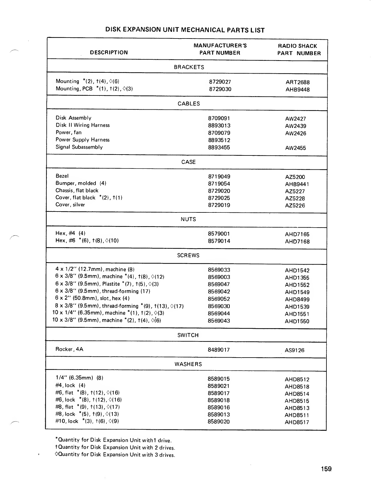
DISK EXPANSION UNIT MECHANICAL PARTS LIST
MANUFACTURER'S RADIO SHACK
DESCRIPTION PART NUMBER PART NUMBER
BRACKETS
Mounting *(2), t{4), 0(6) 8729027 ART2688
Mounting, PCB *(1), t(2), 0(3) 8729030 AHB9448
CABLES
Disk Assembly 8709091 AW2427
Disk II Wiring Harness 8893013 AW2439
Power, fan 8709079 AW2426
Power Supply Harness 8893512
Signal Subassembly 8893455 AW2455
CASE
Bezel 8719049 AZ5200
Bumper, molded (4) 8719054 AHB9441
Chassis, flat black 8729020 AZ5227
Cover, flat black *(2),t(1) 8729025 AZ5228
Cover, silver 8729019 AZ5226
NUTS
Hex, #4 (4) 8579001 AHD7165
Hex, #6 *(6),t<8),0(10) 8579014 AHD7168
SCREWS
4x1/2" (12.7mm), machine (8) 8569033 AHD1542
6x3/8" (9.5mm), machine *(4), t(8),0(12) 8569003 AH D1355
6x3/8" (9.5mm), Plastite *(7), t(5), 0(3) 8569047 AHD1552
6x3/8" (9.5mm), thread-forming (17) 8569042 AH D1549
6x2" (50.8mm), slot, hex (4) 8569052 AHD8499
8x3/8" (9.5mm), thread-forming *(9), t(13) 0(17) 8569030 AH D1539
10 x1/4" (6.35mm), machine *(1 ), t(2), 0(3) 8569044 AHD1551
10x3/8" (9.5mm), machine *(2), t(4), 0(6) 8569043 AHD1550
SWITCH
Rocker, 4A 8489017 AS9126
WASHERS
1/4" (6.35mm) (8) 8589015 AHD8512
#4, lock (4) 8589021 AHD8518
#6, flat *(8), t(12),0(16) 8589017 AHD8514
#6, lock *(8), t(12),0(16) 8589018 AHD8515
#8, flat *(9), t(13), 0(17) 8589016 AHD8513
#8, lock *(5), t(9),0(13) 8589013 AHD8511
#10, lock *(3), t(6),0(9) 8589020 AHD8517
*Quantity for Disk Expansion Unit withl drive.
tQuantity for Disk Expansion Unit with 2drives.
OQuantity for Disk Expansion Unit with 3drives.
159
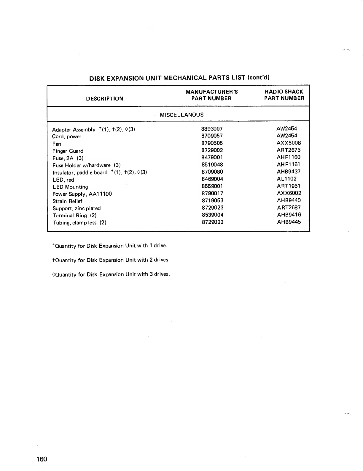
DISK EXPANSION UNIT MECHANICAL PARTS LIST (cont'd)
MANUFACTURER'S RADIO SHACK
DESCRIPTION PART NUMBER PART NUMBER
MISCELLANOUS
Adapter Assembly *(1), t(2), 0(3) 8893007 AW2454
Cord, power 8709057 AW2454
Fan 8790505 AXX5008
Finger Guard 8729002 ART2676
Fuse,2A (3) 8479001 AHF1160
Fuse Holder w/hardware (3) 8519048 AHF1161
Insulator, paddle board *(1), t{2). 0(3) 8709080 AHB9437
LED, red 8469004 AL1102
LED Mounting 8559001 ART1951
Power Supply, AA1 1100 8790017 AXX6002
Strain Relief 8719053 AHB9440
Support, zinc plated 8729023 ART2687
Terminal Ring (2) 8539004 AHB9416
Tubing, clamp-less (2) 8729022 AHB9445
*Quantity for Disk Expansion Unit with 1drive.
tQuantity for Disk Expansion Unit with 2drives.
OQuantity for Disk Expansion Unit with 3drives.
160
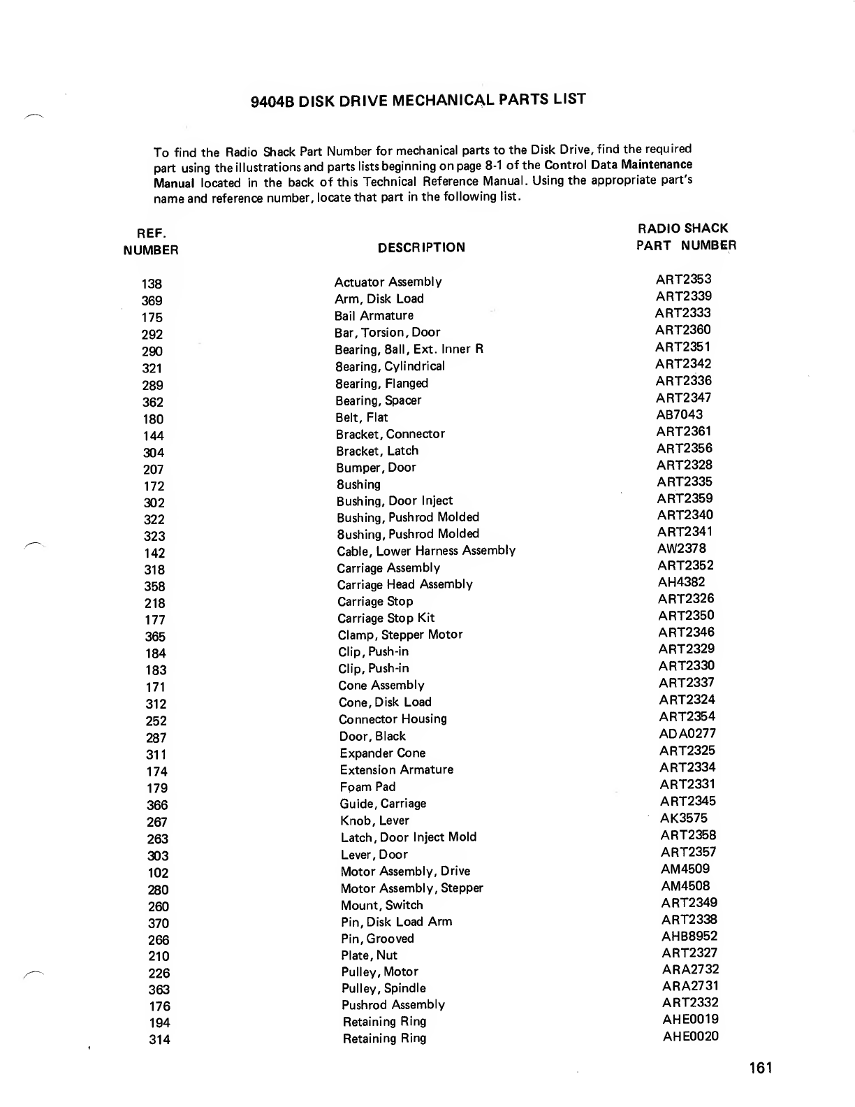
9404B DISK DRIVE MECHANICAL PARTS LIST
To find the Radio Shack Part Number for mechanical parts to the Disk Drive, find the required
part using the illustrations and parts lists beginning on page 8-1 of the Control Data Maintenance
Manual located in the back of this Technical Reference Manual. Using the appropriate part's
name and reference number, locate that part in the following list.
REF.
NUMBER DESCRIPTION
RADIO SHACK
PART NUMBER
138
369
175
292
290
321
289
362
180
144
304
207
172
302
322
323
142
318
358
218
177
365
184
183
171
312
252
287
311
174
179
366
267
263
303
102
280
260
370
266
210
226
363
176
194
314
Actuator Assembly
Arm, Disk Load
Bail Armature
Bar, Torsion, Door
Bearing, Ball, Ext. Inner R
Bearing, Cylindrical
Bearing, Flanged
Bearing, Spacer
Belt, Flat
Bracket, Connector
Bracket, Latch
Bumper, Door
Bushing
Bushing, Door Inject
Bushing, Pushrod Molded
Bushing, Pushrod Molded
Cable, Lower Harness Assembly
Carriage Assembly
Carriage Head Assembly
Carriage Stop
Carriage Stop Kit
Clamp, Stepper Motor
Clip, Push-in
Clip, Push-in
Cone Assembly
Cone, Disk Load
Connector Housing
Door, Black
Expander Cone
Extension Armature
Foam Pad
Guide, Carriage
Knob, Lever
Latch, Door Inject Mold
Lever, Door
Motor Assembly, Drive
Motor Assembly, Stepper
Mount, Switch
Pin, Disk Load Arm
Pin, Grooved
Plate, Nut
Pulley, Motor
Pulley, Spindle
Pushrod Assembly
Retaining Ring
Retaining Ring
ART2353
ART2339
ART2333
ART2360
ART2351
ART2342
ART2336
ART2347
AB7043
ART2361
ART2356
ART2328
ART2335
ART2359
ART2340
ART2341
AW2378
ART2352
AH4382
ART2326
ART2350
ART2346
ART2329
ART2330
ART2337
ART2324
ART2354
ADA0277
ART2325
ART2334
ART2331
ART2345
AK3575
ART2358
ART2357
AM4509
AM4508
ART2349
ART2338
AHB8952
ART2327
ARA2732
ARA2731
ART2332
AHE0019
AHE0020
161

9404B DISK DRIVE MECHANCIAL PARTS LIST (cont'd)
REF.
NUMBER
310
173
361
182
181
313
315
217
368
353
251
261
147
248
189
317
316
335
178
192
291
125
DESCRIPTION
Shaft, Disk Load
Solenoid
Spindle
Spring, Compression
Spring, Compression
Spring, Cone
Spring, Garter
Spring, Leaf
Support, Assembled
Switch, Actuator
Switch, Optical
Switch, Sub-mini
Switch, Track
Washer
Washer, Nylon
Washer, Special
Washer, Special
Washer, Special
Washer, Spring Lock
Washer, Spring Wave
Washer, Spring Wave
Write Protect Assembly
RADIO SHACK
PART NUMBER
ART2362
AS9111
ART2348
ARB6521
ARB6522
ARB6524
ARB6523
ARB6525
ART2344
AS0965
AS0968
AS0966
AS0967
AHD8448
AHD8450
AHD8447
AHD8452
AHD8453
AHD8451
AHD8449
AHD8454
ART2355
162
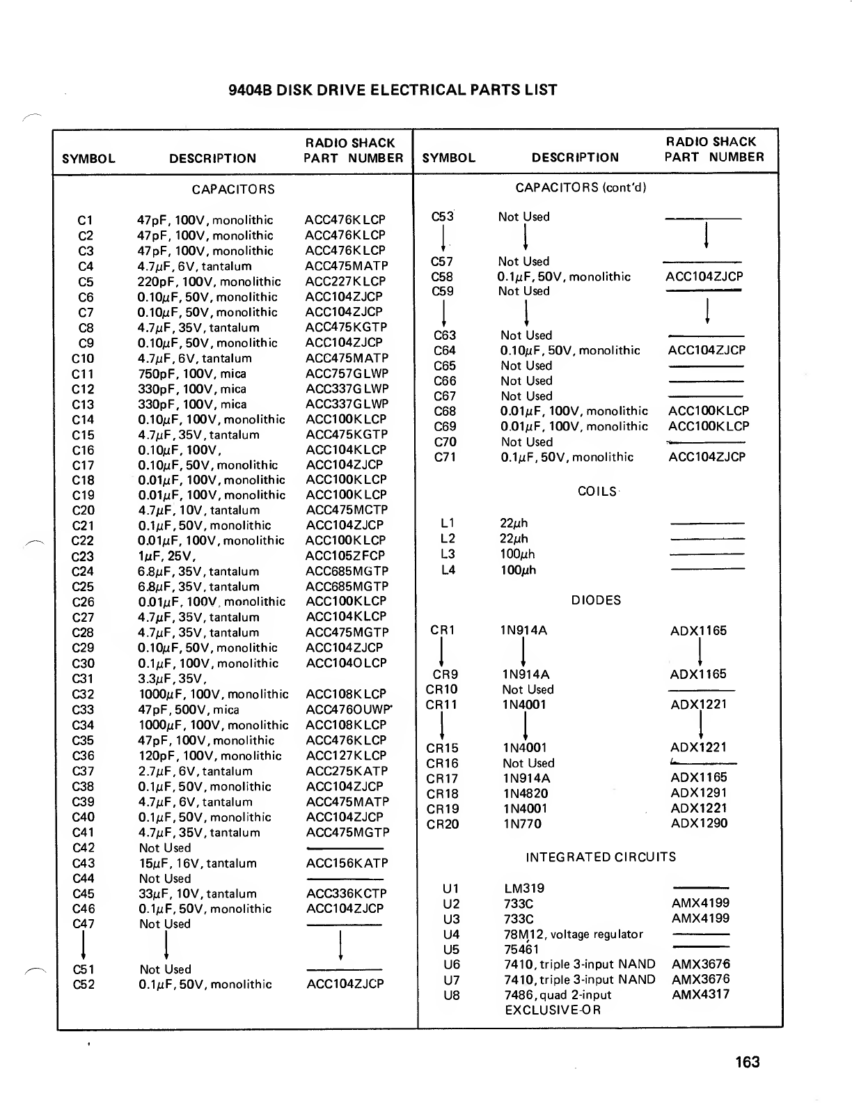
9404B DISK DRIVE ELECTRICAL PARTS LIST
SYMBOL DESCRIPTION
RADIO SHACK
PART NUMBER SYMBOL DESCRIPTION
RADIO SHACK
PART NUMBER
CAPACITORS
C1 47pF, 100V, monolithic
C2 47pF, 100V, monolithic
C3 47pF, 100V, monolithic
C4 4.7juF,6V, tantalum
C5 220pF, 100V, monolithic
C6 0.10/xF, 50V, monolithic
C7 0.10/iF, 50V, monolithic
C8 4.7jliF, 35V, tantalum
C9 0.10juF, 50V, monolithic
C10 4.7juF, 6V, tantalum
C11 750pF, 100V, mica
C12 330pF, 100V, mica
C13 330pF, 100V, mica
C14 0.10/uF, 100V, monolithic
C15 4.7juF, 35V, tantalum
C16 0.10juF, 100V,
C17 0.10/iF, 50V, monolithic
C18 0.01/zF, 100V, monolithic
C19 0.01//F, 100V, monolithic
C20 4.7/iF, 10V, tantalum
C21 0.1/iF, 50V, monolithic
C22 0.01/zF, 100V, monolithic
C23 1/xF. 25V,
C24 6.8/iF, 35V, tantalum
C25 63uF, 35V, tantalum
C26 0.01/iF, 100V, monolithic
C27 4.7/iF, 35V, tantalum
C28 4.7fiF, 35V, tantalum
C29 O.IOjuF, 50V, monolithic
C30 O.ljiF, 100V, monolithic
C31 3.3/uF,35V,
C32 1000mF, 100V, monolithic
C33 47pF, 500V, mica
C34 IOOOjuF, 100V, monolithic
C35 47pF, 100V, monolithic
C36 120pF, 100V, monolithic
C37 2.7/zF,6V, tantalum
C38 0.1;uF, 50V, monolithic
C39 4.7juF,6V, tantalum
C40 O.ljuF, 50V, monolithic
C41 4.7juF, 35V, tantalum
C42 Not Used
C43 15;uF, 16V, tantalum
C44 Not Used
C45 33/uF, 10V, tantalum
C46 0.1/iF, 50V, monolithic
C47 Not Used
I I
C51 Not Used
C52 0.1/zF, 50V, monolithic
ACC476KLCP
ACC476KLCP
ACC476KLCP
ACC475MATP
ACC227KLCP
ACC104ZJCP
ACC104ZJCP
ACC475KGTP
ACC104ZJCP
ACC475MATP
ACC757GLWP
ACC337G LWP
ACC337GLWP
ACC100KLCP
ACC475KGTP
ACC104KLCP
ACC104ZJCP
ACC100KLCP
ACC100KLCP
ACC475MCTP
ACC104ZJCP
ACC100KLCP
ACC105ZFCP
ACC685MGTP
ACC685MGTP
ACC100KLCP
ACC104KLCP
ACC475MGTP
ACC104ZJCP
ACC104OLCP
ACC108KLCP
ACC4760UWP*
ACC108KLCP
ACC476KLCP
ACC127KLCP
ACC275KATP
ACC104ZJCP
ACC475MATP
ACC104ZJCP
ACC475MGTP
ACC156KATP
ACC336KCTP
ACC104ZJCP
ACC104ZJCP
C53
C57
C58
C59
C63
C64
C65
C66
C67
C68
C69
C70
C71
CR1
CR9
CR10
CR11
CR15
CR16
CR17
CR18
CR19
CR20
CAPACITORS (cont'd)
Not Used
Not Used
0.1/xF- 50V, monolithic
Not Used
Not Used
O.IOjuF, 50V, monolithic
Not Used
Not Used
Not Used
0.01/jF, 100V, monolithic
0.01juF, 100V, monolithic
Not Used
0.1;uF, 50V, monolithic
COILS
L1 22juh
L2 22^h
L3 100juh
L4 100juh
DIODES
1N914A
1N914A
Not Used
1N4001
1N4001
Not Used
1N914A
1N4820
1N4001
1N770
ACC104ZJCP
ACC104ZJCP
ACC100KLCP
ACC100KLCP
ACC104ZJCP
ADX1165
I
ADX1165
ADX1221
ADX1221
L
ADX1165
ADX1291
ADX1221
ADX1290
INTEGRATED CIRCUITS
U1 LM319
U2 733C AMX4199
U3 733C AMX4199
U4 78M12, voltage regulator
U5 75461
U6 7410, triple 3-input NAND AMX3676
U7 7410, triple 3-input NAND AMX3676
U8 7486, quad 2-input
EXCLUSIVE-OR
AMX4317
163
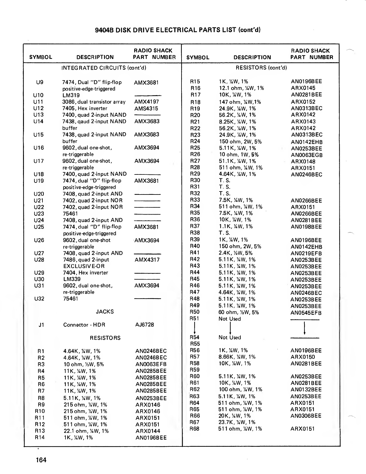
9404B DISK DRIVE ELECTRICAL PARTS LIST (cont'd)
RADIO SHACK RADIO SHACK
SYMBOL DESCRIPTION PART NUMBER SYMBOL DESCRIPTION PART NUMBER
INTEGRATED CIRCUITS (:ont'd) RESISTORS (cont'd)
U9 7474, Dual "D" flip-flop AMX3681 R15 iK,y
4w, 1% AN0196BEE
positive-edge-triggered R16 12.1 ohm, 'AW, 1% ARX0145
U10
U11
LM319
3086, dual transistor array
R17 iok, y4\/v, 1% AN0281BEE
AMX4197 R18 147ohm,%W,1% ARX0152
U12 7405, Hex inverter AMS4315 R19 24.9K,%W, 1% AN0313BEC
U13 7400, quad 2-input NAND R20 56.2K,y4W, 1% ARX0142
U14 7438, qaud 2-input NAND AMX3683 R21 8.25K, 1
/4W, 1% ARX0143
buffer R22 56.2K,y4W, 1% ARX0142
U15 7438, quad 2-input NAND AMX3683 R23 24.9K, 1
/4W, 1% AN0313BEC
buffer R24 150 ohm, 2W, 5% AN0142EHB
U16 9602, dual one-shot, AMX3694 R25 5.11K,%W,1% AN0253BEE
re-triggerable R26 10 ohm, 1W, 5% AN0063EGB
U17 9602, dual one-shot, AMX3694 R27 51.1K, 1
/4W, 1% ARX0148
re-triggerable R28 511 ohm, 1
/4W, 1% ARX0151
U18
U19
7400, quad 2-input NAND
7474, dual "D" flip-flop
R29 4.64K, 1
/4W, 1%
T.S.
AN0246BEC
AMX3681 R30
positive-edge-triggered R31 T. S.
U20 7408, quad 2-input AND R32 T.S.
U21
U22
7402, quad 2-input NOR
7402, quad 2-input NOR
R33 75K %W 1% AN0266BEE
ARX0151
R34
/•*/!>/ ft* VVf1/U
511 ohm, 1
/4W, 1%
U23
U24
U25
75461 R35 7.5K,%W, 1% AN0266BEE
7408, quad 2-input AND
7474, dual "D" flip-flop
R36 10K, %W, 1% AN0281BEE
AN0198BEE
AMX3681 R37 1.1K, 1
/4W, 1%
positive-edge-triggered R38 T.S.
U26 9602, dual one-shot AMX3694 R39 iK,y
4w, 1% AN0196BEE
re-triggerable R40 150 ohm, 2W, 5% AN0142EHB
U27 7408, quad 2-input AND
7486, quad 2-input
R41 2.4K, 1
/
2W, 5% AN0219EFB
U28 AMX4317 R42 5.11K,y
4W, 1% AN0253BEE
EXCLUSIVE-OR R43 5.11K, 1
/4W, 1% AN0253BEE
U29 7404 Hpx inx/prtpr R44 511KVa\N 1%AN0253BEE
AN0253BEE
U30
/^WT f1ICA IIIVCI ICI
LM339 R45
*i» •1 1 !»( /4 VVJ1/O
5.11K,%W, 1%
U31 9602, dual one-shot, AMX3694 R46 5.11K,y
4W, 1% AN0253BEE
re-triggerable R47 4.64K, 1
/4W, 1% AN0246BEC
U32 75461 R48 5.11K,y
4W, 1% AN0253BEE
R49 5.11K,y
4W, 1% AN0253BEE
JACKS R50
R51
60 ohm, 1
/2W, 5%
Not Used
AN0545EFB
J1 Connector -HDR AJ6728
I
R54
I1
RESISTORS Not Used
R55
R1 4.64K,y
4W, 1% AN0246BEC R56 ik/aw, 1% AN0196BEE
R2 4.64K, 1
/4W, 1% AN0246BEC R57 8.66K, 'AW, 1% ARX0150
R3 10ohm, 1
/2W,5% AN0063EFB R58 10K, 1
/4W, 1% AN0281BEE
R4 11K,%W, 1% AN0285BEE R59
R5 11K,!4W,1% AN0285BEE R60 5.11K, 1
/4W, 1% AN0253BEE
R6 11K, 1
/4W, 1% AN0285BEE R61 i0K,y4W, 1% AN0281BEE
R7 11K, 1
/4W, 1% AN0285BEE R62 100 ohm, %W, 1% AN0132BEE
R8 5.11K,%W, 1% AN0253BEE R63 5.11K, 1
/4W, 1% AN0253BEE
R9 215ohm,y
4W, 1% ARX0146 R64 511 ohm,y
4W, 1% ARX0151
R10 215ohm, 1
/4W, 1% ARX0146 R65 511 ohm, 1
/4W, 1% ARX0151
R11 511 ohm, 1
/4W, 1% ARX0151 R66 20K,y4W, 1% AN0306BEE
R12 511ohm, 1
/4W, 1% ARX0151 R67 23.7K, 1
/4W, 1%
R13 22.1 ohm, 1
/4W, 1% ARX0144 R68 511 ohm, 1
/4W, 1% ARX0151
R14 1K, 1
/4W, 1% AN0196BEE
164
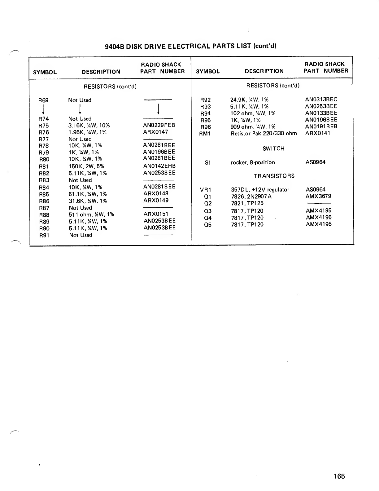
9404B DISK DRIVE ELECTRICAL PARTS LIST (cont'd)
RADIO SHACK RADIO SHACK
SYMBOL DESCRIPTION PART NUMBER SYMBOL DESCRIPTION PART NUMBER
RESISTORS (cont'd) RESISTORS (cont'd)
R69
1
Not Used
I
R92
R93
24.9K, 1
/4W, 1%
5.11K,y
4W, 1%
AN0313BEC
AN0253BEE
IR94 102ohm,y4W, 1% AN0133BEE
R74 Not Used R95 1K, 1
/4W, 1% AN0196BEE
R75 3.16K,y
4W, 10% AN0229FEB R96 909ohm,y4W, 1% AN0191BEB
R76 1.96K,y4W, 1% ARX0147 RM1 Resistor Pak 220/330 ohm ARX0141
R77
R78
Not Used
10K, 1
/4W, 1% AN0281BEE SWITCH
R79 1K,y4W, 1% AN0196BEE
R80
R81
10K, 1
/4W, 1%
150K,2W,5%
AN0281BEE
AN0142EHB S1 rocker, 8-position AS0964
R82
R83
R84
R85
R86
R87
R88
R89
R90
5.11K,y4W, 1%
Not Used
10K, 1
/4W, 1%
51.1K, 1
/4W, 1%
31.6K, 'AW, 1%
Not Used
511 ohm,y4W, 1%
5.11K, 1
/4W,1%
5.11K, 1
/4W, 1%
AN0253BEE TRANSISTORS
AN0281BEE
ARX0148
ARX0149
VR1
Q1
Q2
Q3
Q4
Q5
357DL.+12V regulator
7826,2N2907A
7821.TP125
7817,TP120
7817,TP12Q
7817,TP120
AS0964
AMX3679
AMX4195
AMX4195
AMX4195
ARX0151
AN0253BEE
AN0253BEE
R91 Not Used
165

SECTION XV
AA11100 POWER SUPPLY
167

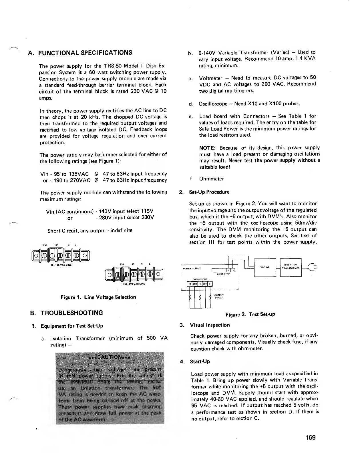
A. FUNCTIONAL SPECIFICATIONS
The power supply for the TRS-80 Model II Disk Ex-
pansion System is a60 watt switching power supply.
Connections to the power supply module are made via
astandard feed-through barrier terminal block. Each
circuit of the terminal block is rated 230 VAC @10
amps.
In theory, the power supply rectifies the AC line to DC
then chops it at 20 kHz. The chopped DC voltage is
then transformed to the required output voltages and
rectified to low voltage isolated DC. Feedback loops
are provided for voltage regulation and over current
protection.
The power supply may be jumper selected for either of
the following ratings (see Figure 1):
Vin
or
95 to 135VAC
190to270VAC
@47 to 63Hz input frequency
@47 to 63Hz input frequency
The power supply module can withstand the following
maximum ratings:
Vin (AC continuous) -MOV input select 115V
or -280V input select 230V
Short Circuit, any output -indefinite
230 115 NL
CD (U) ®-s.
O
96 -135 VAC LINE
O
230 115 NL
£o
;190 -270 VAC LINE
Figure 1. Line Voltage Selection
B. TROUBLESHOOTING
1. Equipment for Test Set-Up
a. Isolation Transformer (minimum of 500 VA
rating) —
,. .CAUTION..*
Dangerously high voltages are present
in this power supply. For the safety of
the individual doing the testing, please
use an isolation transformer. The 500
VA rating is needed to keep the AC wave-
form from being clipped off at the peaks.
These power supplies have peak charging
capacitors and draw full power at the peak
of the AC waveform.
b. 0-140V Variable Transformer (Variac) -Used to
vary input voltage. Recommend 10 amp, 1.4 KVA
rating, minimum.
c. Voltmeter -Need to measure DC voltages to 50
VDC and AC voltages to 200 VAC. Recommend
two digital multimeters.
d. Oscilloscope -Need X10 and X100 probes.
e. Load board with Connectors —See Table 1for
values of loads required. The entry on the table for
Safe Load Power is the minimum power ratings for
the load resistors used.
NOTE: Because of its design, this power supply
must have aload present or damaging oscillations
may result. Never test the power supply without a
suitable load!
fOhmmeter
2. Set-Up Procedure
Set-up as shown in Figure 2. You will want to monitor
theinputvoltageandtheoutputvoltage of the regulated
bus, which is the +5 output, with DVM's. Also monitor
the +5 output with the oscilloscope using 50mv/div
sensitivity. The DVM monitoring the +5 output can
also be used to check the other outputs. See text of
section III for test points within the power supply.
POWER SUPPLY ED
OUTPUT STRIP
13 1c6m| *5 fcOMJ-M
ISOLATION
TRANSFORMER =o
Figure 2. Test Set-up
3. Visual Inspection
Check power supply for any broken, burned, or obvi-
ously damaged components. Visually check fuse, if any
question check with ohmmeter.
4. Start-Up
Load power supply with minimum load as specif ied in
Table 1. Bring up power slowly with Variable Trans-
former while monitoring the +5 output with the oscil-
loscope and DVM. Supply should start with approx-
imately 40-60 VAC applied, and should regulate when
95 VAC is reached. If output has reached 5volts, do
aperformance test as shown in section D. If there is
no output, refer to section C.
169
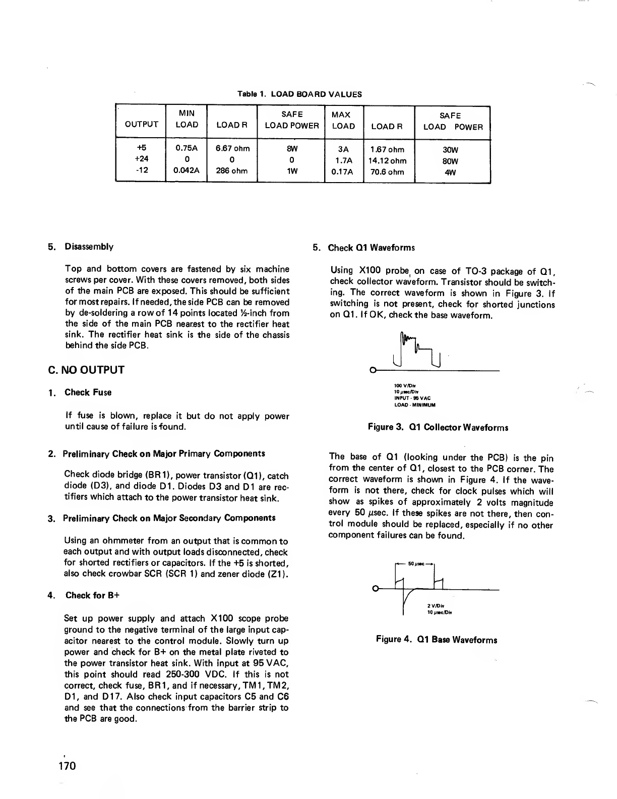
Table 1. LOAD BOARD VALUES
OUTPUT
MIN
LOAD LOADR SAFE
LOAD POWER
MAX
LOAD LOADR
SAFE
LOAD POWER
+5
+24
-12
0.75A
0.042A
6.67 ohm
286 ohm
8W
1W
3A
1.7A
0.17A
1.67 ohm
14.12ohm
70.6 ohm
30W
80W
4W
5. Disassembly
Top and bottom covers are fastened by six machine
screws per cover. With these covers removed, both sides
of the main PCB are exposed. This should be sufficient
for most repairs. If needed, the side PCB can be removed
by de-soldering arow of 14 points located 1
/a-inch from
the side of the main PCB nearest to the rectifier heat
sink. The rectifier heat sink is the side of the chassis
behind the side PCB.
C. NO OUTPUT
1. Check Fuse
If fuse is blown, replace it but do not apply power
until cause of failure is-found.
5. Check Q1 Waveforms
Using X100 probe on case of TO-3 package of Q1,
check collector waveform. Transistor should be switch-
ing. The correct waveform is shown in Figure 3. If
switching is not present, check for shorted junctions
on Q1. If OK, check the base waveform.
u
100 V/Dii
10/iHc/Div
INPUT 95 VAC
LOAD MINIMUM
Figure 3. Q1 Collector Waveforms
2. Preliminary Check on Major Primary Components
Check diode bridge (BR1), power transistor (Q1), catch
diode (D3), and diode D1. Diodes D3 and D1 are rec-
tifiers which attach to the power transistor heat sink.
3. Preliminary Check on Major Secondary Components
Using an ohmmeter from an output that is common to
each output and with output loads disconnected, check
for shorted rectifiers or capacitors. If the +5 is shorted,
also check crowbar SCR (SCR 1) and zener diode (Z1).
4. Check for B+
Set up power supply and attach X100 scope probe
ground to the negative terminal of the large input cap-
acitor nearest to the control module. Slowly turn up
power and check for B+ on the metal plate riveted to
the power transistor heat sink. With input at 95 VAC,
this point should read 250-300 VDC. If this is not
correct, check fuse, BR1, and if necessary, TM1,TM 2,
D1, and D17. Also check input capacitors C5 and C6
and see that the connections from the barrier strip to
the PCB are good.
The base of Q1 (looking under the PCB) is the pin
from the center of Q1 ,closest to the PCB corner. The
correct waveform is shown in Figure 4. If the wave-
form is not there, check for clock pulses which will
show as spikes of approximately 2volts magnitude
every 50 ^sec. If these spikes are not there, then con-
trol module should be replaced, especially if no other
component failures can be found.
2V/Div
10*lttc/Div
Figure 4. Q1 Base Waveforms
170
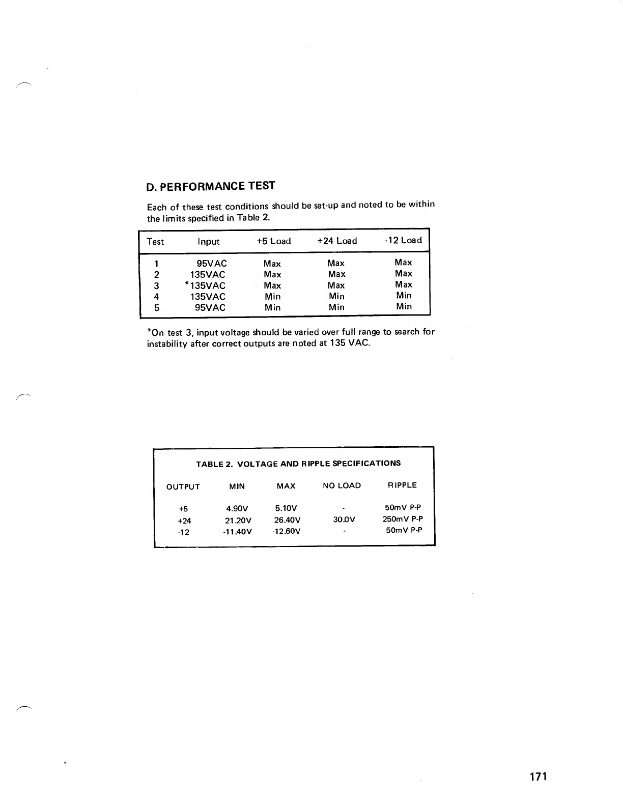
D. PERFORMANCE TEST
Each of these test conditions should be set-up and noted to be within
the limits specified in Table 2.
Test Input +5 Load +24 Load -12 Load
195VAC Max Max Max
2135VAC Max Max Max
3*135VAC Max Max Max
4135VAC Min Min Min
595VAC Min Min Min
*0n test 3, input voltage should be varied over full range to search for
instability after correct outputs are noted at 135 VAC.
TABLE 2. VOLTAGE AND RIPPLE SPECIFICATIONS
OUTPUT MIN MAX NO LOAD RIPPLE
+5
+24
-12
4.90V
21 .20V
-1 1.40V
5.10V
26.40V
-12.60V
30.0V
50mV P-P
250m VP-P
50mV P-P
171
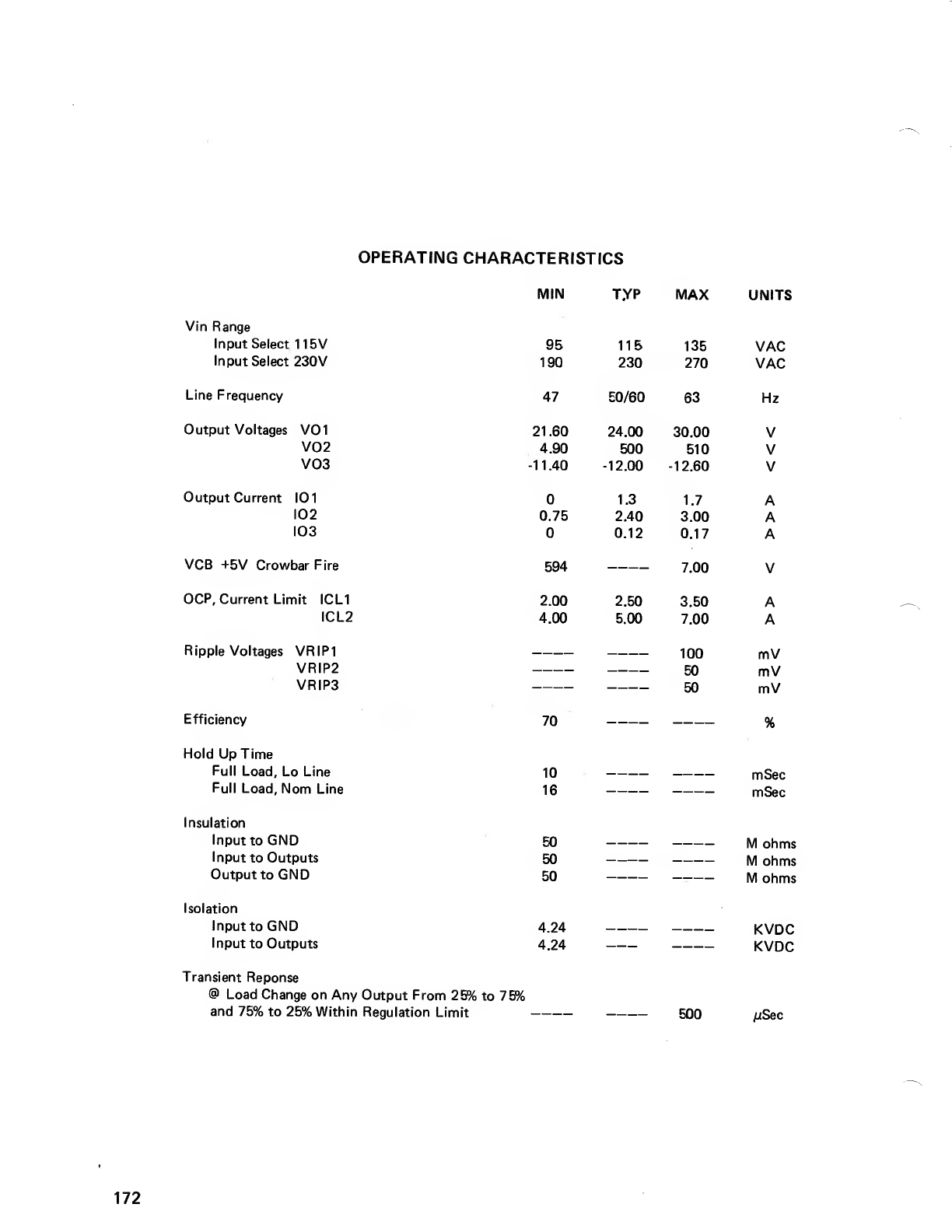
OPERATING CHARACTERISTICS
MIN t.yp MAX UNITS
Vin Range
Input Select 115V
Input Select 230V
Line Frequency
Output Voltages V01
V02
V03
Output Current 101
I02
I03
VCB +5V Crowbar Fire
OCP, Current Limit ICL1
ICL2
Ripple Voltages VRIP1
VRIP2
VRIP3
95
190
47
594
115
230
EO/60
135
270
63
7.00
VAC
VAC
Hz
21.60 24.00 30.00 V
4.90 500 510 V
-11.40 -12.00 -12.60 V
1.3 1.7 A
0.75 2.40 3.00 A
0.12 0.17 A
2.00 2.50 3.50 A
4.00 5.00 7.00 A
100 mV
50 mV
50 mV
Efficiency 70
Hold Up Time
Full Load, Lo Line 10
Full Load, Nom Line 16
Insulation
Input to GND 50
Input to Outputs 50
Output to GND 50
Isolation
Input to GND 4.24
Input to Outputs 4.24
Transient Reponse
@Load Change on Any Output From 25% to 75%
and 75% to 25% Within Regulation Limit 500
%
mSec
mSec
Mohms
Mohms
Mohms
KVDC
KVDC
//Sec
172
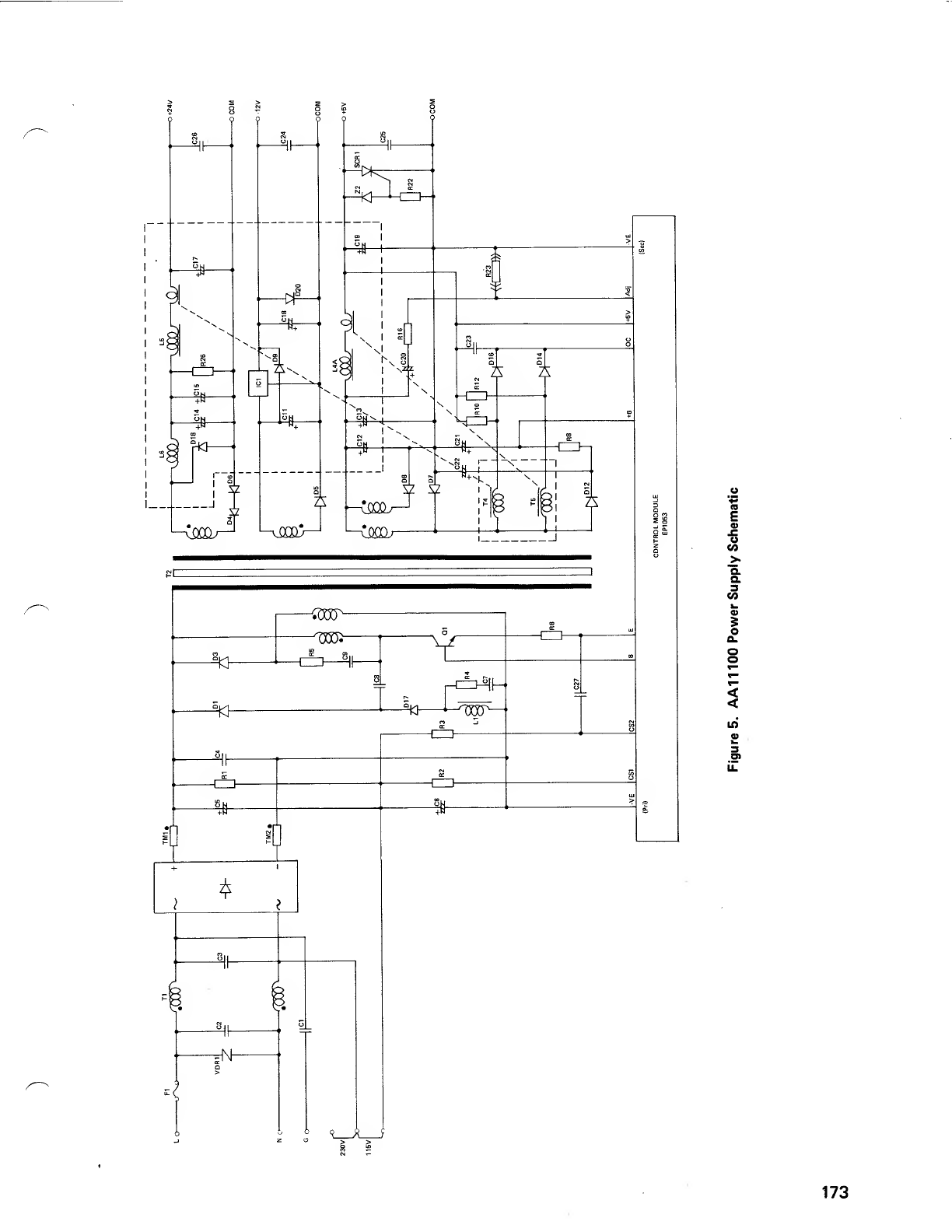
n
E
O
CO
a
a
3
o
a.
o
o
<
<
in
3
173

SECTION XVI
ILLUSTRATED PARTS BREAKDOWN
175

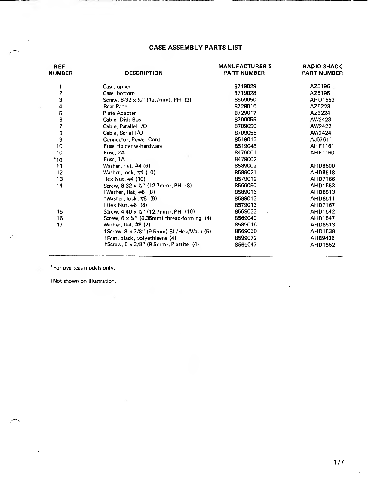
CASE ASSEMBLY PARTS LIST
REF MANUFACTURER'S RADIO SHACK
NUMBER DESCRIPTION PART NUMBER PART NUMBER
1Case, upper 8719029 AZ5196
2Case/bottom 8719028 AZ5195
3Screw, 8-32 x1
/2"(12.7mm), PH (2) 8569050 AH D1553
4Rear Panel 8729016 AZ5223
5Plate Adapter 8729017 AZ5224
6Cable, Disk Bus 8709055 AW2423
7Cable, Parallel I/O 8709050 AW2422
8Cable, Serial I/O 8709056 AW2424
9Connector, Power Cord 8519013 AJ6761
'
10 Fuse Holder w/hardware 8519048 AHF1161
10 Fuse,2A 8479001 AHF1160
*10 Fuse, 1
A
8479002
11 Washer, flat, #4 (6) 8589002 AHD8500
12 Washer, lock, #4 (10) 8589021 AHD8518
13 Hex Nut, #4 (10) 8579012 AHD7166
14 Screw, 8-32 xV (12.7mm), PH (8) 8569050 AH D1553
tWasher,flat,#8 (8) 8589016 AHD8513
tWasher,lock,#8 (8) 8589013 AHD8511
tHexNut,#8 (8) 8579013 AHD7167
15 Screw, 4-40 x1
/2"(12.7mm), PH (10) 8569033 AH D1542
16 Screw, 6xVi" (6.35mm) thread-forming (4) 8569040 AH D1547
17 Washer, flat, #8 (2) 8589016 AHD8513
tScrew, 8x3/8" (9.5mm) SL/Hex/Wash (5) 8569030 AHD1539
tFeet, black, polvethleene (4) 8599072 AHB9436
tScrew, 6x3/8" (9.5mm), Plastite (4) 8569047 AHD1552
*For overseas models only.
tNot shown on illustration.
177
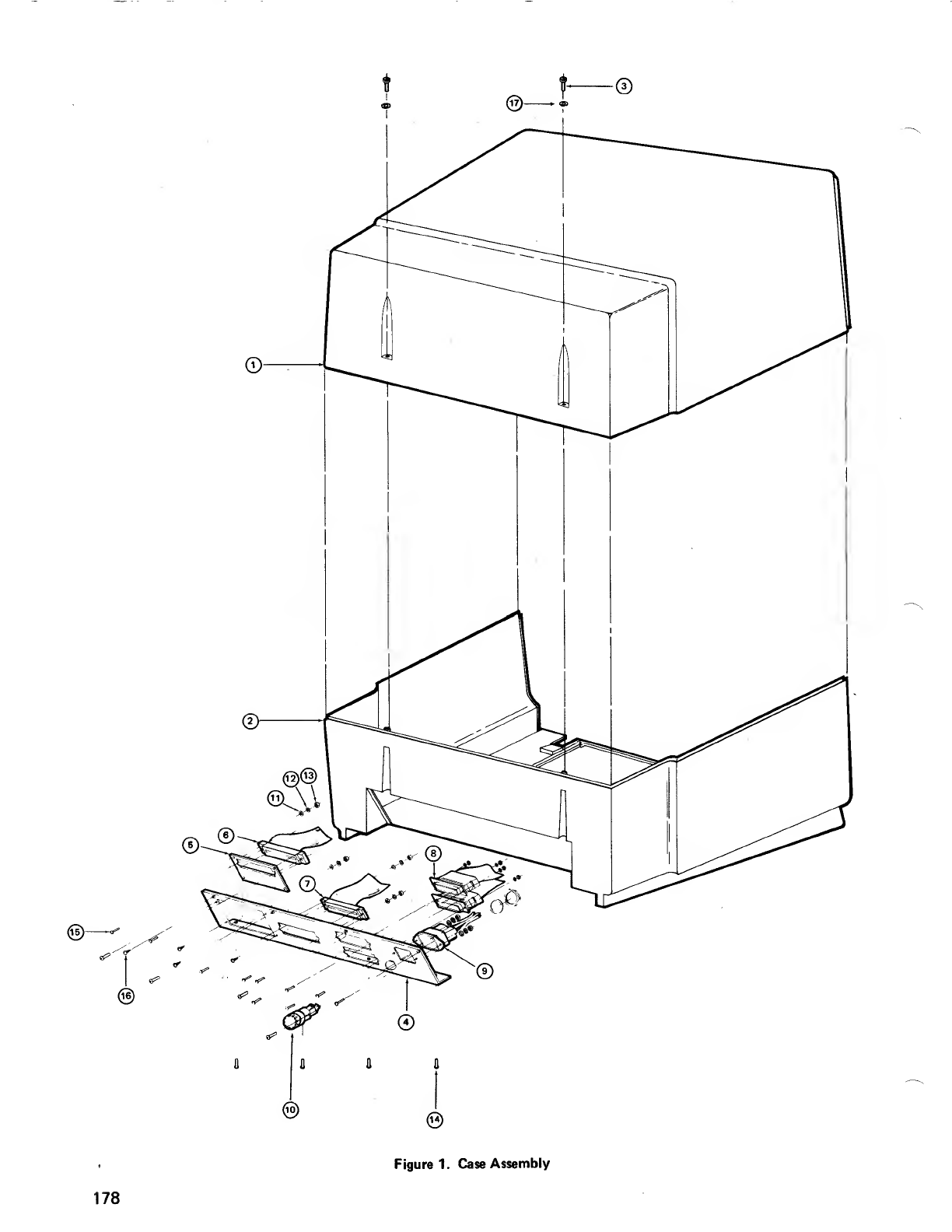
Figure 1. Case Assembly
178
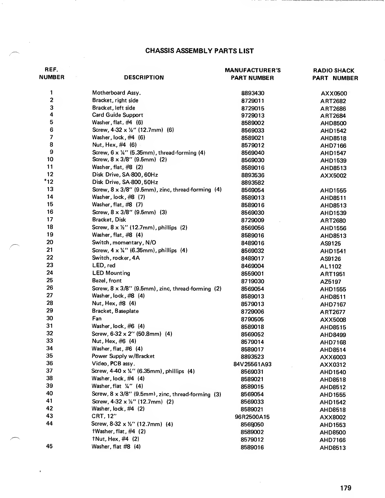
CHASSIS ASSEMBLY PARTS LIST
REF. MANUFACTURER'S RADIO SHACK
UMBER DESCRIPTION PART NUMBER PART NUMBER
1Motherboard Assy. 8893430 AXX0500
2Bracket, right side 872901
1
ART2682
3Bracket, left side 8729015 ART2686
4Card Guide Support 9729013 ART2684
5Washer, flat, #4 (6) 8589002 AHD8500
6Screw, 4-32 x1
/2"(12.7mm) (6) 8569033 AH D1542
7Washer, lock, #4 (6) 8589021 AHD8518
8Nut, Hex, #4 (6) 8579012 AHD7166
9Screw, 6x%" (5.35mm), thread-forming (4) 8569040 AHD1547
10 Screw, 8x3/8" (9.5mm) (2) 8569030 AH D1539
11 Washer, flat, #8 (2) 8589016 AHD8513
12 Disk Drive, SA-800,60Hz 8893536 AXX5002
*12 Disk Drive, SA-800,50Hz 8893582
13 Screw, 8x3/8" (9.5mm), zinc, thread-forming (4) 8569054 AHD1555
14 Washer, lock, #8 (7) 8589013 AHD8511
15 Washer, flat, #8 (7) 858901
6
AHD8513
16 Screw, 8x3/8" (9.5mm) (3) 8569030 AHD1539
17 Bracket, Disk 8729009 ART2680
18 Screw, 8 x W(12.7mm), phillips (2) 8569056 AH D1556
19 Washer, flat, #8 (4) 8589016 AHD8513
20 Switch, momentary, N/O 8489016 AS9125
21 Screw, 4x%" (8.35mm), phillips (4) 8569032 AHD1541
22 Switch, rocker, 4A8489017 AS9126
23 LED, red 8469004 AL1102
24 LED Mounting 8559001 ART1951
25 Bezel, front 8719030 AZ5197
26 Screw, 8x3/8" (9.5mm), zinc, thread-forming (2) 8569054 AHD1555
27 Washer, lock, #8 (4) 8589013 AHD8511
28 Nut, Hex, #8 (4) 8579013 AHD7167
29 Bracket, Baseplate 8729006 ART2677
30 Fan 8790505 AXX5008
31 Washer, lock, #6 (4) 8589018 AHD8515
32 Screw, 6-32 x2" (50.8mm) (4) 8569052 AHD8499
33 Nut, Hex, #6 (4) 8579014 AHD7168
34 Washer, flat, #6 (4) 8589017 AHD8514
35 Power Supply w/Bracket 8893523 AXX6003
36 Video, PCB assy. 84V25561A93 AXX0312
37 Screw, 4-40 x%" (6.35mm), philli ps (4) 8569031 AH D1540
38 Washer, lock, #4 (4) 8589021 AHD8518
39 Washer, flat %" (4) 8589015 AHD8512
40 Screw, 8x3/8" (9.5mm), zinc, thread-forming (3) 8569054 AHD1555
41 Screw, 4-32 x1
/a"(12.7mm) (2) 8569033 AHD1542
42 Washer, lock, #4 (2) 8589021 AHD8518
43 CRT, 12" 96R2500A15 AXX8002
44 Screw, 8-32 x1
/2"(12.7mm) (4) 8569,050 AH D1553
tWasher, f lat, #4 (2) 8589002 AHD8500
tNut, Hex, #4 (2) 8579012 AHD7166
45 Washer, flat #8 (4) 8589016 AHD8513
179
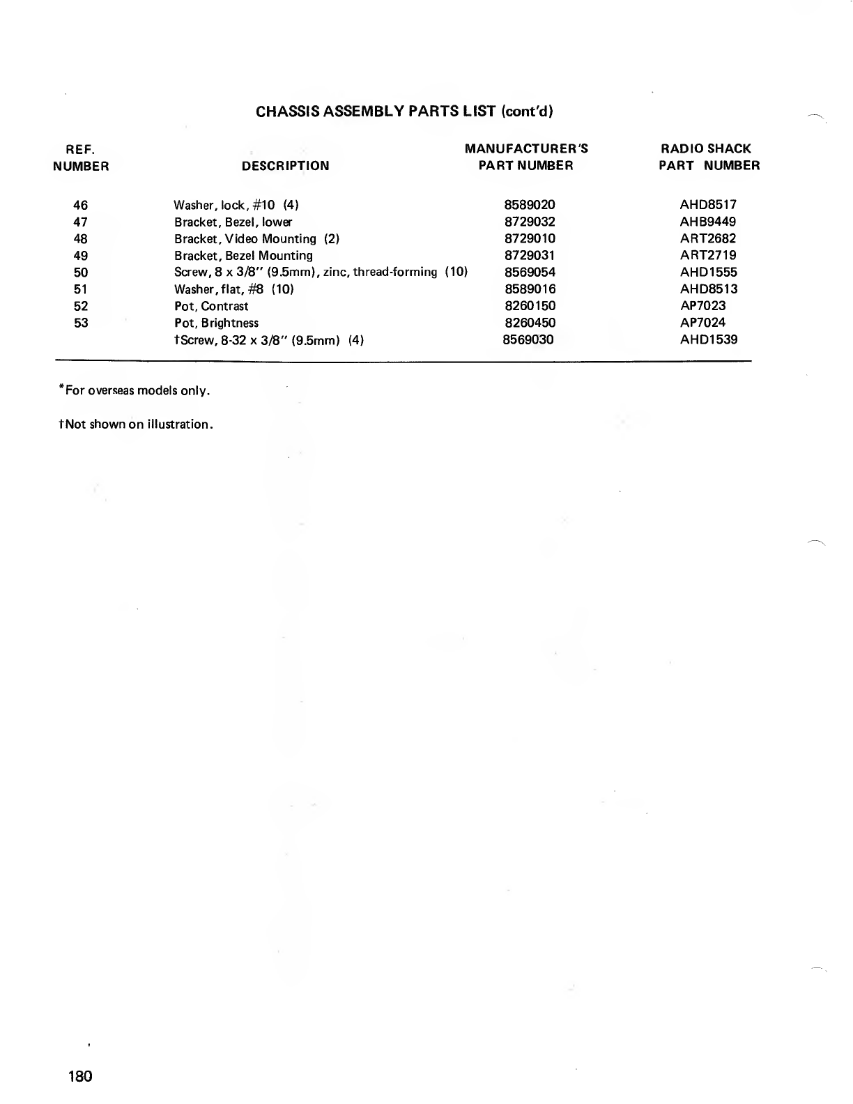
CHASSIS ASSEMBLY PARTS LIST (cont'd)
REF. IVIANUFACTUR
NUMBER DESCRIPTION PART NUMBI
46 Washer, lock, #10 (4) 8589020
47 Bracket, Bezel, lower 8729032
48 Bracket, Video Mounting (2) 8729010
49 Bracket, Bezel Mounting 8729031
50 Screw, 8x3/8" (9.5mm), zinc .thread-forming (10) 8569054
51 Washer, flat, #8 (10) 8589016
52 Pot, Contrast 8260150
53 Pot, Brightness 8260450
tScrew, 8-32 x3/8" (9.5mm) (4) 8569030
RADIO SHACK
PART NUMBER
AHD8517
AHB9449
ART2682
ART2719
AHD1555
AHD8513
AP7023
AP7024
AHD1539
*For overseas models only.
tNot shown on illustration.
180

©L

18

SECTION XVII
APPENDIXES
183
LIMITED WARRANTY
For aperiod of 90 days from the date of delivery, Radio Shack war-
rants to the original purchaser that the computer hardware described
herein shall be free from defects in material and workmanship under
normal use and service. This warranty is only applicable to purchases
from Radio Shack company-owned retail outlets and through duly
authorized franchisees and dealers. The warranty shall be void if this
unit's case or cabinet is opened or if the unit is altered or modified.
During this period, if adefect should occur, the product must be re-
turned to aRadio Shack store or dealer for repair, and proof of pur-
chase must be presented. Purchaser's sole and exclusive remedy in the
event of defect is expressly limited to the correction of the defect by
adjustment, repair or replacement at Radio Shack's election and sole
expense, except there shall be no obligation to replace or repair items
which by their nature are expendable. No representation or other affir-
mation of fact, including, but not limited to, statements regarding
capacity, suitability for use, or performance of the equipment, shall
be or be deemed to be awarranty or representation by Radio Shack,
for any purpose, nor give rise to any liability or obligation of Radio
Shack whatsoever.
EXCEPT AS SPECIFICALLY PROVIDED IN THIS AGREEMENT,
THERE ARE NO OTHER WARRANTIES, EXPRESS OR IMPLIED,
INCLUDING, BUT NOT LIMITED TO, ANY IMPLIED WARRAN-
TIES OF MERCHANTABILITY OR FITNESS FOR APARTICULAR
PURPOSE AND IN NO EVENT SHALL RADIO SHACK BE LIABLE
FOR LOSS OF PROFITS OR BENEFITS, INDIRECT, SPECIAL,
CONSEQUENTIAL OR OTHER SIMILAR DAMAGES ARISING OUT
OF ANY BREACH OF THIS WARRANTY OR OTHERWISE.
-~>
sasa
sS8jS^i&*&K&: j^USv '&&
RADIO SHACK MADIVISION OF TANDY CORPORATION
U.S.A.: FORT WORTH, TEXAS 76102
CANADA: BARRIE, ONTARIO L4M 4W5
TANDY CORPORATION
AUSTRALIA
280-316 VICTORIA ROAD
RYDALMERE,N.S.W. 2116
BELGIUM
PARC INDUSTRIEL DE NANINNE
5140NANINNE
U.K.
BILSTON ROADWEDNESBURY
WEST MIDLANDS WS10 7JN
PRINTED IN U.S.A.
