NTC GR8 User Manual V1.0
User Manual:
Open the PDF directly: View PDF ![]() .
.
Page Count: 528 [warning: Documents this large are best viewed by clicking the View PDF Link!]
Copyright © 2017 Next Thing Co. All Rights Reserved.
GR8 User
Manual
Version 1.0
2017-2-15

Declaration
Copyright © 2017 Next Thing Co. All Rights Reserved.

Revision HIstory
Copyright © 2017 Next Thing Co. All Rights Reserved.
Revision History
Revision
Date
Description
v0.1
Sep.01, 2016
Initial Internal Release
v1.0
Feb.15, 2017
Initial Public Release

Copyright © 2017 Next Thing Co. All Rights Reserved.
Declaration
This page left intentionally blank. \(•◡•)/

Copyright © 2017 Next Thing Co. All Rights Reserved.
Contents
Chapter 1. About This Documentation ...................................................................................................................... 5
1.1. Purpose ....................................................................................................................................................... 5
1.2. Acronyms and Abbreviations ...................................................................................................................... 5
Chapter 2. Overview .................................................................................................................................................. 7
2.1. Processor Overview .................................................................................................................................... 8
2.2. Processor Features ...................................................................................................................................... 9
2.2.1. CPU .................................................................................................................................................. 9
2.2.2. GPU .................................................................................................................................................. 9
2.2.3. Memory ........................................................................................................................................... 9
2.2.3.1. Boot ROM ............................................................................................................................. 9
2.2.3.2. SDRAM .................................................................................................................................. 9
2.2.3.3. NAND Flash ........................................................................................................................... 9
2.2.3.4. SD/MMC ............................................................................................................................. 10
2.2.4. System Peripherals ......................................................................................................................... 10
2.2.4.1. CCM ..................................................................................................................................... 10
2.2.4.2. DMA .................................................................................................................................... 10
2.2.4.3. PWM ................................................................................................................................... 10
2.2.4.4. Asynchronous Timer ........................................................................................................... 10
2.2.4.5. Synchronic Timer ................................................................................................................ 11
2.2.4.6. Interrupt Controller............................................................................................................. 11
2.2.4.7. LRADC.................................................................................................................................. 11
2.2.4.8. Touch Panel ......................................................................................................................... 11
2.2.4.9. Crypto Engine ...................................................................................................................... 11
2.2.5. Video Engine .................................................................................................................................. 12
2.2.6. Display Processing .......................................................................................................................... 12
2.2.7. Display Output ............................................................................................................................... 12
2.2.8. Image Input .................................................................................................................................... 12
2.2.9. Audio Subsystem ............................................................................................................................ 12
2.2.9.1. Audio Codec ........................................................................................................................ 12
2.2.9.2. I2S/PCM .............................................................................................................................. 13
2.2.9.3. OWA .................................................................................................................................... 13
2.2.10. External Peripherals ..................................................................................................................... 13

Contents
Copyright © 2017 Next Thing Co. All Rights Reserved.
2.2.10.1. USB .................................................................................................................................... 13
2.2.10.2. TWI .................................................................................................................................... 14
2.2.10.3. UART ................................................................................................................................. 14
2.2.10.4. SPI ..................................................................................................................................... 14
2.2.10.5. CIR ..................................................................................................................................... 14
2.2.11. Package ........................................................................................................................................ 14
2.3. Block Diagram ........................................................................................................................................... 15
Chapter 3. System .................................................................................................................................................... 17
3.1. Memory Mapping ..................................................................................................................................... 18
3.2. Boot System .............................................................................................................................................. 21
3.2.1. Overview ........................................................................................................................................ 21
3.2.2. Boot Diagram ................................................................................................................................. 21
3.3. PMU .......................................................................................................................................................... 22
3.3.1. Overview ........................................................................................................................................ 22
3.3.2. PMU Register List ........................................................................................................................... 22
3.3.3. PMU Register Description .............................................................................................................. 23
3.3.3.1. PMU DVFS Control Register 0 (Default Value: 0x0000_0000) ............................................. 23
3.3.3.2. PMU DVFS Control Register 1(Default Value: 0x0000_1010) .............................................. 25
3.3.3.3. PMU DVFS Control Register 2 (Default Value: 0x0000_0000) ............................................. 25
3.3.3.4. PMU AXI Clock Range Register0 (Default Value: 0x0000_0000) ......................................... 25
3.3.3.5. PMU AXI Clock Range Register1 (Default Value: 0x0000_0000) ......................................... 25
3.3.3.6. PMU DVFS Control Register 3 ............................................................................................. 26
3.3.3.7. PMU DVFS Timeout Control Register(Default Value: 0x0000_0027) .................................. 26
3.3.3.8. PMU IRQ En Register (Default Value: 0x0000_0000) .......................................................... 26
3.3.3.9. PMU IRQ Status Register (Default Value: 0x00000000) ...................................................... 28
3.3.3.10. PMU Status Register (Default Value: 0x0000_0000) ......................................................... 30
3.3.3.11. PMU CPUVDD DCDC Control Register Address(Default Value: 0x0000_0023) ................. 30
3.3.3.12. PMU TWI Address(Default Value: 0x0000_0068) ............................................................. 30
3.3.3.13. PMU CPUVDD Value(Default Value: 0x0000_0016) .......................................................... 30
3.3.3.14. PMU CPUVDD Voltage Ramp Control in DVM (Default Value: 0x0000_0000) .................. 31
3.3.3.15. PMU 32KHz CPUVDD Minimum Value(Default Value: 0x0000_000C) .............................. 32
3.3.3.16. PMU VF Table Register 0 ................................................................................................... 32
3.3.3.17. PMU VF Table Register 1 ................................................................................................... 33
3.3.3.18. PMU VF Table Register 2 ................................................................................................... 33
3.3.3.19. PMU VF Table Register 3 ................................................................................................... 33

Contents
Copyright © 2017 Next Thing Co. All Rights Reserved.
3.3.3.20. PMU VF Table Register 4 ................................................................................................... 33
3.3.3.21. PMU VF Table Register 5 ................................................................................................... 33
3.3.3.22. PMU VF Table Register 6 ................................................................................................... 34
3.3.3.23. PMU VF Table Register 7 ................................................................................................... 34
3.3.3.24. PMU VF Table Register 8 ................................................................................................... 34
3.3.3.25. PMU VF Table Register 9 ................................................................................................... 34
3.3.3.26. PMU VF Table Register 10 ................................................................................................. 35
3.3.3.27. PMU VF Table Register 11 ................................................................................................. 35
3.3.3.28. PMU VF Table Register 12 ................................................................................................. 35
3.3.3.29. PMU VF Table Register 13 ................................................................................................. 35
3.3.3.30. PMU VF Table Register 14 ................................................................................................. 36
3.3.3.31. PMU VF Table Register 15 ................................................................................................. 36
3.3.3.32. PMU VF Table Register 16 ................................................................................................. 36
3.3.3.33. PMU VF Table Register 17 ................................................................................................. 36
3.3.3.34. PMU VF Table Register 18 ................................................................................................. 36
3.3.3.35. PMU VF Table Valid Register (Default Value: 0x0000_003C) ............................................ 37
3.3.3.36. PMU VF Table Index Register (Default Value: 0x0000_0000) ........................................... 38
3.3.3.37. PMU VF Table Range Register (Default Value: 0x0000_0000) .......................................... 38
3.3.3.38. PMU Speed Factor Register 0 (Default Value: 0x0000_0000) ........................................... 38
3.3.3.39. PMU Speed Factor Register 1 (Default Value: 0x0000_0000) ........................................... 39
3.3.3.40. PMU Speed Factor Register 2 (Default Value: 0x0000_0000) ........................................... 40
3.3.3.41. CPU Idle Counter Low Register (Default Value: 0x0000_0000) ......................................... 41
3.3.3.42. CPU Idle Counter High Register (Default Value: 0x0000_0000) ........................................ 41
3.3.3.43. CPU Idle Control Register (Default Value: 0x0000_0000) ................................................. 42
3.3.3.44. CPU Idle Status Register (Default Value: 0x0000_0000) ................................................... 43
3.4. Clock Control Module (CCM) .................................................................................................................... 44
3.4.1. Overview ........................................................................................................................................ 44
3.4.2. Clock Tree Diagram ........................................................................................................................ 45
3.4.3. CCM Register List ........................................................................................................................... 47
3.4.4. CCM Register Description .............................................................................................................. 49
3.4.4.1. PLL1-Core Register (Default Value: 0x2100_5000) ............................................................. 49
3.4.4.2. PLL1-Tuning Register (Default Value: 0x0A10_1000) .......................................................... 50
3.4.4.3. PLL2-Audio Register (Default Value: 0x0810_0010) ........................................................... 51
3.4.4.4. PLL2-Tuning Register (Default Value: 0x0000_0000) .......................................................... 52
3.4.4.5. PLL3-Video Register (Default Value: 0x0010_D063) ........................................................... 52

Contents
Copyright © 2017 Next Thing Co. All Rights Reserved.
3.4.4.6. PLL4-VE Register (Default Value: 0x2108_1000) ................................................................. 53
3.4.4.7. PLL5-DDR Register (Default Value: 0x1104_9280) .............................................................. 54
3.4.4.8. PLL5-Tuning Register (Default Value: 0x1488_0000) .......................................................... 56
3.4.4.9. PLL6 Register (Default Value: 0x2100_9931) ...................................................................... 56
3.4.4.10. PLL7 Register (Default Value: 0x0010_D063) .................................................................... 57
3.4.4.11. PLL1-Tuning2 Register (Default Value: 0x0000_0000) ...................................................... 58
3.4.4.12. PLL5-Tuning2 Register (Default Value: 0x0000_0000) ...................................................... 58
3.4.4.13. OSC24M Register (Default Value: 0x0013_8013).............................................................. 59
3.4.4.14. CPU/AHB/APB0 Clock Ratio Register (Default Value: 0x0001_0010) ................................ 60
3.4.4.15. APB1 Clock Divide Ratio Register (Default Value: 0x0000_0000) ..................................... 61
3.4.4.16. AXI Module Clock Gating Register (Default Value: 0x0000_0000) .................................... 62
3.4.4.17. AHB Module Clock Gating Register 0(Default Value: 0x0000_0000) ................................ 62
3.4.4.18. AHB Module Clock Gating Register 1(Default Value: 0x0000_0000) ................................ 63
3.4.4.19. APB0 Module Clock Gating Register (Default Value: 0x0000_0000) ................................. 64
3.4.4.20. APB1 Module Clock Gating Register (Default Value: 0x0000_0000) ................................. 64
3.4.4.21. NAND Clock Register (Default Value: 0x0000_0000) ........................................................ 65
3.4.4.22. SD0 Clock Register (Default Value: 0x0000_0000) ............................................................ 66
3.4.4.23. SD1 Clock Register (Default Value: 0x0000_0000) ............................................................ 67
3.4.4.24. SD2 Clock Register (Default Value: 0x0000_0000) ............................................................ 68
3.4.4.25. CE Clock Register (Default Value: 0x0000_0000) .............................................................. 68
3.4.4.26. SPI0 Clock Register (Default Value: 0x0000_0000) ........................................................... 69
3.4.4.27. SPI2 Clock Register (Default Value: 0x0000_0000) ........................................................... 70
3.4.4.28. IR Clock Register (Default Value: 0x0000_0000) ............................................................... 71
3.4.4.29. I2S/PCM Clock Register (Default Value: 0x0000_0000) .................................................... 72
3.4.4.30. I2S/PCM Clock Register (Default Value: 0x0001_0000) .................................................... 72
3.4.4.31. USB PHY Clock Register (Default Value: 0x0000_0000) .................................................... 73
3.4.4.32. DRAM Clock Register (Default Value: 0x0000_0000) ........................................................ 73
3.4.4.33. DE-BE Clock Register (Default Value: 0x0000_0000) ........................................................ 74
3.4.4.34. DE-FE Clock Register (Default Value: 0x0000_0000) ......................................................... 75
3.4.4.35. LCD CH0 Clock Register (Default Value: 0x0000_0000) .................................................... 76
3.4.4.36. LCD CH1 Clock Register (Default Value: 0x0000_0000) .................................................... 77
3.4.4.37. CSI Clock Register (Default Value: 0x0000_0000) ............................................................. 78
3.4.4.38. VE Clock Register (Default Value: 0x0000_0000) .............................................................. 79
3.4.4.39. Audio Codec Clock Register (Default Value: 0x0000_0000) .............................................. 79
3.4.4.40. AVS Clock Register (Default Value: 0x0000_0000) ............................................................ 80

Contents
Copyright © 2017 Next Thing Co. All Rights Reserved.
3.4.4.41. Mali-400 Clock Register(Default Value: 0x0000_0000)..................................................... 80
3.4.4.42. MBUS Clock Control Register (Default Value: 0x0000_0000) ........................................... 81
3.4.4.43. IEP Clock Control Register (Default Value: 0x0000_0000) ................................................ 82
3.5. System Control .......................................................................................................................................... 83
3.5.1. Overview ........................................................................................................................................ 83
3.5.2. System Control Register List ........................................................................................................... 83
3.5.3. System Control Register Description .............................................................................................. 83
3.5.3.1. SRAM Configuration Register 0(Default Value: 0x7FFF_FFFF) ............................................ 83
3.5.3.2. SRAM Configuration Register 1(Default Value: 0x0000_1000) ........................................... 84
3.6. CPU Control ............................................................................................................................................... 85
3.6.1. CPU Register List ............................................................................................................................ 85
3.6.2. CPU Control Register Description .................................................................................................. 85
3.6.2.1. CPU Control Register(Default Value:0x0000_0002) ............................................................ 85
3.7. PWM ......................................................................................................................................................... 86
3.7.1. Overview ........................................................................................................................................ 86
3.7.2. PWM Register List .......................................................................................................................... 86
3.7.3. PWM Register Description ............................................................................................................. 86
3.7.3.1. PWM Control Register (Default Value: 0x0000_0000) ........................................................ 86
3.7.3.2. PWM Channel 0 Period Register ......................................................................................... 90
3.7.3.3. PWM Channel 1 Period Register ......................................................................................... 90
3.8. Asynchronous Timer ................................................................................................................................. 92
3.8.1. Overview ........................................................................................................................................ 92
3.8.2. ASYNC Timer Register List .............................................................................................................. 92
3.8.3. ASYNC Timer Register Description ................................................................................................. 93
3.8.3.1. ASYNC Timer IRQ Enable Register (Default Value: 0x0000_0000) ...................................... 93
3.8.3.2. ASYNC Timer IRQ Status Register(Default Value: 0x0000_0000) ........................................ 94
3.8.3.3. ASYNC Timer 0 Control Register (Default Value: 0x0000_0004) ......................................... 95
3.8.3.4. ASYNC Timer 0 Interval Value Register ............................................................................... 97
3.8.3.5. ASYNC Timer 0 Current Value Register (Default Value: 0x0000_0000) ............................... 97
3.8.3.6. ASYNC Timer 1 Control Register (Default Value: 0x0000_0004) ......................................... 97
3.8.3.7. ASYNC Timer 1 Interval Value Register ............................................................................... 99
3.8.3.8. ASYNC Timer 1 Current Value Register ............................................................................... 99
3.8.3.9. ASYNC Timer 2 Control Register (Default Value: 0x0000_0004) ......................................... 99
3.8.3.10. ASYNC Timer 2 Interval Value Register ........................................................................... 100
3.8.3.11. ASYNC Timer 2 Current Value Register ........................................................................... 101

Contents
Copyright © 2017 Next Thing Co. All Rights Reserved.
3.8.3.12. ASYNC Timer 3 Control Register (Default Value: 0x0000_0000) ..................................... 101
3.8.3.13. ASYNC Timer 3 Interval Value ......................................................................................... 102
3.8.3.14. ASYNC Timer 4 Control Register (Default Value: 0x0000_0004) ..................................... 102
3.8.3.15. ASYNC Timer 4 Interval Value Register ........................................................................... 103
3.8.3.16. ASYNC Timer 4 Current Value Register ........................................................................... 104
3.8.3.17. ASYNC Timer 5 Control Register (Default Value: 0x0000_0004) ..................................... 104
3.8.3.18. ASYNC Timer 5 Interval Value Register ........................................................................... 105
3.8.3.19. ASYNC Timer 5 Current Value Register ........................................................................... 106
3.8.3.20. AVS Counter Control Register (Default Value: 0x0000_0000) ......................................... 106
3.8.3.21. AVS Counter 0 Register (Default Value: 0x0000_0000) ................................................... 107
3.8.3.22. AVS Counter 1 Register (Default Value: 0x0000_0000) ................................................... 107
3.8.3.23. AVS Counter Divisor Register (Default Value: 0x05DB_05DB) ........................................ 107
3.8.3.24. Watchdog Control Register ............................................................................................. 108
3.8.3.25. Watchdog Mode Register (Default Value: 0x0000_0000) ............................................... 108
3.8.3.26. 64-bit Counter Low Register (Default Value: 0x0000_0000) ........................................... 110
3.8.3.27. 64-bit Counter High Register (Default Value: 0x0000_0000) .......................................... 110
3.8.3.28. 64-bit Counter Control Register (Default Value: 0x0000_0000) ..................................... 110
3.8.3.29. CPU Config Register (Default Value: 0x0000_0000) ........................................................ 111
3.9. Synchronic Timer .................................................................................................................................... 112
3.9.1. Overview ...................................................................................................................................... 112
3.9.2. Sync Timer Register List ............................................................................................................... 112
3.9.3. Sync Timer Register Description .................................................................................................. 112
3.9.3.1. Sync Timer IRQ Enable Register (Default Value: 0x0000_0000) ....................................... 112
3.9.3.2. Sync Timer IRQ Status Register(Default Value: 0x0000_0000) ......................................... 113
3.9.3.3. Sync Timer 0 Control Register (Default Value: 0x0000_0004) .......................................... 113
3.9.3.4. Sync Timer 0 Interval Value Low Register ......................................................................... 114
3.9.3.5. Sync Timer 0 Interval Value High Register ........................................................................ 115
3.9.3.6. Sync Timer 0 Current Value Lo Register ............................................................................ 115
3.9.3.7. Sync Timer 0 Current Value Hi Register ............................................................................ 115
3.9.3.8. Sync Timer 1 Control Register (Default Value: 0x0000_0004) .......................................... 115
3.9.3.9. Sync Timer 1 Interval Value Low Register ......................................................................... 117
3.9.3.10. Sync Timer 1 Interval Value High Register ...................................................................... 117
3.9.3.11. Sync Timer 1 Current Value Low Register ....................................................................... 117
3.9.3.12. Sync Timer 1 Current Value High Register ...................................................................... 117
3.10. Interrupt Controller .............................................................................................................................. 119

Contents
Copyright © 2017 Next Thing Co. All Rights Reserved.
3.10.1. Overview .................................................................................................................................... 119
3.10.2. Interrupt Source ......................................................................................................................... 119
3.10.3. Interrupt Register List ................................................................................................................ 122
3.10.4. Interrupt Register Description ................................................................................................... 123
3.10.4.1. Interrupt Vector Register (Default Value: 0x0000_0000) ................................................ 123
3.10.4.2. Interrupt Base Address Register (Default Value: 0x0000_0000) ..................................... 123
3.10.4.3. Interrupt Protection Register (Default Value: 0x0000_0000) ......................................... 123
3.10.4.4. NMI Interrupt Control Register (Default Value: 0x0000_0000) ...................................... 124
3.10.4.5. Interrupt IRQ Pending Register 0(Default Value: 0x0000_0000) .................................... 124
3.10.4.6. Interrupt IRQ Pending Register 1(Default Value: 0x0000_0000) .................................... 124
3.10.4.7. Interrupt IRQ Pending Register 2(Default Value: 0x0000_0000) .................................... 125
3.10.4.8. Interrupt FIQ Pending/Clear Register 0 (Default Value: 0x0000_0000) .......................... 125
3.10.4.9. Interrupt FIQ Pending/Clear Register 1(Default Value: 0x0000_0000) ........................... 125
3.10.4.10. Interrupt FIQ Pending/Clear Register 2(Default Value: 0x0000_0000) ......................... 125
3.10.4.11. Interrupt Select Register 0(Default Value: 0x0000_0000) ............................................ 126
3.10.4.12. Interrupt Select Register 1(Default Value: 0x0000_0000) ............................................ 126
3.10.4.13. Interrupt Select Register 2(Default Value: 0x0000_0000) ............................................ 126
3.10.4.14. Interrupt Enable Register 0(Default Value: 0x0000_0000) ........................................... 127
3.10.4.15. Interrupt Enable Register 1(Default Value: 0x0000_0000) ........................................... 127
3.10.4.16. Interrupt Enable Register 2(Default Value: 0x0000_0000) ........................................... 127
3.10.4.17. Interrupt Mask Register 0(Default Value: 0x0000_0000) ............................................. 127
3.10.4.18. Interrupt Mask Register 1(Default Value: 0x0000_0000) ............................................. 128
3.10.4.19. Interrupt Mask Register 2(Default Value: 0x0000_0000) ............................................. 128
3.10.4.20. Interrupt Response Register 0(Default Value: 0x0000_0000) ....................................... 128
3.10.4.21. Interrupt Response Register 1(Default Value: 0x0000_0000) ....................................... 129
3.10.4.22. Interrupt Response Register 2(Default Value: 0x0000_0000) ....................................... 129
3.10.4.23. Interrupt Fast Forcing Register 0(Default Value: 0x0000_0000) ................................... 129
3.10.4.24. Interrupt Fast Forcing Register 1(Default Value: 0x0000_0000) ................................... 129
3.10.4.25. Interrupt Fast Forcing Register 2(Default Value: 0x0000_0000) ................................... 130
3.10.4.26. Interrupt Source Priority 0 Register (Default Value: 0x0000_0000) ............................. 130
3.10.4.27. Interrupt Source Priority 1 Register (Default Value: 0x0000_0000) ............................. 134
3.10.4.28. Interrupt Source Priority 2 Register (Default Value: 0x0000_0000) ............................. 138
3.10.4.29. Interrupt Source Priority 3 Register (Default Value: 0x0000_0000) ............................. 141
3.10.4.30. Interrupt Source Priority 4 Register (Default Value: 0x0000_0000) ............................. 145
3.10.4.31. Interrupt Source Priority 5 Register (Default Value: 0x0000_0000) ............................. 149

Contents
Copyright © 2017 Next Thing Co. All Rights Reserved.
3.11. DMA ...................................................................................................................................................... 154
3.11.1. Overview .................................................................................................................................... 154
3.11.2. DMA Description ........................................................................................................................ 154
3.11.3. DMA Register List ....................................................................................................................... 154
3.11.4. DMA Register Description .......................................................................................................... 155
3.11.4.1. DMA IRQ Enable Register (Default Value: 0x0000_0000) ............................................... 155
3.11.4.2. DMA IRQ Pending Status Register (Default Value: 0x0000_0000) .................................. 159
3.11.4.3. Normal DMA Configuration Register (Default Value: 0x0000_0000) .............................. 165
3.11.4.4. Normal DMA Source Address Register............................................................................ 169
3.11.4.5. Normal DMA Destination Address Register .................................................................... 169
3.11.4.6. Normal DMA Byte Counter Register ............................................................................... 169
3.11.4.7. Dedicated DMA Configuration Register (Default Value: 0x0000_0000) ......................... 169
3.11.4.8. Dedicated DMA Source Start Address Register ............................................................... 173
3.11.4.9. Dedicated DMA Destination Start Address Register ....................................................... 174
3.11.4.10. Dedicated DMA Byte Counter Register ......................................................................... 174
3.11.4.11. Dedicated DMA Parameter Register ............................................................................. 174
3.12. LRADC ................................................................................................................................................... 175
3.12.1. Overview .................................................................................................................................... 175
3.12.2. Block Diagram ............................................................................................................................ 175
3.12.3. LRADC Control Logic................................................................................................................... 176
3.12.4. LRADC Register List .................................................................................................................... 176
3.12.5. LRADC Register Description ....................................................................................................... 177
3.12.5.1. LRADC Control Register(Default Value: 0x0100_0168) ................................................... 177
3.12.5.2. LRADC Interrupt Control Register(Default Value: 0x0000_0000) ................................... 178
3.12.5.3. LRADC Interrupt Status Register(Default Value: 0x0000_0000) ..................................... 180
3.12.5.4. LRADC Data 0 Register(Default Value: 0x0000_0000) .................................................... 183
3.12.5.5. LRADC Data 1 Register(Default Value: 0x0000_0000) .................................................... 183
3.13. Touch Panel ........................................................................................................................................... 184
3.13.1. Overview .................................................................................................................................... 184
3.13.2. Typical Application Circuit .......................................................................................................... 184
3.13.3. Clock Tree and ADC Time ........................................................................................................... 185
3.13.3.1. Clock Tree ........................................................................................................................ 185
3.13.3.2. A/D Conversion Time ...................................................................................................... 185
3.13.4. Principle of Operation ................................................................................................................ 186
3.13.4.1. The Basic Principle .......................................................................................................... 186

Contents
Copyright © 2017 Next Thing Co. All Rights Reserved.
3.13.4.2. Single-ended Mode ......................................................................................................... 186
3.13.4.3. Differential Mode ............................................................................................................ 187
3.13.4.4. Single Touch Detection ................................................................................................... 188
3.13.4.5. Touch-Pressure Measurement ........................................................................................ 188
3.13.4.6. Pen Down Detection ....................................................................................................... 189
3.13.4.7. Median and Averaging Filter ........................................................................................... 190
3.13.5. TP Register List ........................................................................................................................... 191
3.13.6. TP Register Description .............................................................................................................. 191
3.13.6.1. TP Control Register 0(Default Value: 0x0F80_0000) ....................................................... 191
3.13.6.2. TP Control Register 1(Default Value: 0x0000_0008) ....................................................... 192
3.13.6.3. TP Control Register 2(Default Value: 0x8000_0FFF) ....................................................... 194
3.13.6.4. Median Filter Control Register(Default Value: 0x0000_0001) ........................................ 194
3.13.6.5. TP Interrupt& FIFO Control Register(Default Value: 0x0000_0F00) ............................... 195
3.13.6.6. TP Interrupt& FIFO Status Register(Default Value: 0x0000_0000) ................................. 196
3.13.6.7. Common Data Register(Default Value: 0x0000_0000) ................................................... 198
3.13.6.8. TP Data Register(Default Value: 0x0000_0000) .............................................................. 198
3.13.6.9. TP Port IO Configure Register(Default Value: 0x0000_2222) .......................................... 198
3.13.6.10. TP Port Data Register(Default Value: 0x0000_0000) .................................................... 199
3.14. Crypto Engine ........................................................................................................................................ 200
3.14.1. Overview .................................................................................................................................... 200
3.14.2. Crypto Engine Block Diagram ..................................................................................................... 200
3.14.3. Crypto Engine Register List ........................................................................................................ 200
3.14.4. Crypto Engine Register Description ........................................................................................... 201
3.14.4.1. Crypto Engine Control Register(Default Value: 0x0000_0000) ....................................... 201
3.14.4.2. Crypto Engine Key [n] Register(Default Value: 0x0000_0000) ........................................ 203
3.14.4.3. Crypto Engine IV[n] Register(Default Value: 0x0000_0000) ........................................... 203
3.14.4.4. Crypto Engine FIFO Control/ Status Register(Default Value: 0x6000_0F0F) ................... 203
3.14.4.5. Crypto Engine Interrupt Control/Status Register(Default Value: 0x0000_0000) ............ 204
3.14.4.6. Crypto Engine Message Digest[n] Register(Default Value: 0x0000_0000) ..................... 205
3.14.4.7. Crypto Engine RX FIFO Register(Default Value: 0x0000_0000) ....................................... 205
3.14.4.8. Crypto Engine TX FIFO Register(Default Value: 0x0000_0000) ....................................... 205
3.14.5. Crypto Engine Clock Requirement ............................................................................................. 205
3.15. Security ID ............................................................................................................................................. 207
3.15.1. Overview .................................................................................................................................... 207
3.16. Port Controller ...................................................................................................................................... 208

Contents
Copyright © 2017 Next Thing Co. All Rights Reserved.
3.16.1. Overview .................................................................................................................................... 208
3.16.2. Port Configuration Table ............................................................................................................ 208
3.16.3. Port Register List ........................................................................................................................ 210
3.16.4. Port Register Description ........................................................................................................... 210
3.16.4.1. PB Configure Register 0(Default Value: 0x0000_0000) ................................................... 210
3.16.4.2. PB Configure Register 1(Default Value: 0x0000_0000) ................................................... 212
3.16.4.3. PB Configure Register 2(Default Value: 0x0000_0000) ................................................... 214
3.16.4.4. PB Configure Register 3(Default Value: 0x0000_0000) ................................................... 215
3.16.4.5. PB Data Register(Default Value: 0x00000000) ................................................................ 215
3.16.4.6. PB Multi-Driving Register 0(Default Value: 0x5555_5555) ............................................. 215
3.16.4.7. PB Multi-Driving Register 1(Default Value: 0x0000_0155) ............................................. 215
3.16.4.8. PB Pull Register 0(Default Value: 0x0000_0000) ............................................................ 216
3.16.4.9. PB Pull Register 1(Default Value: 0x0000_0000) ............................................................ 216
3.16.4.10. PC Configure Register 0(Default Value: 0x0000_0000) ................................................. 216
3.16.4.11. PC Configure Register 1(Default Value: 0x0000_0000) ................................................. 218
3.16.4.12. PC Configure Register 2(Default Value: 0x0000_0000) ................................................. 220
3.16.4.13. PC Configure Register 3(Default Value: 0x0000_0000) ................................................. 220
3.16.4.14. PC Data Register(Default Value: 0x0000_0000) ............................................................ 220
3.16.4.15. PC Multi-Driving Register 0(Default Value: 0x5555_5555) ........................................... 220
3.16.4.16. PC Multi-Driving Register 1(Default Value: 0x0000_0055) ........................................... 221
3.16.4.17. PC Pull Register 0(Default Value: 0x0000_5140) .......................................................... 221
3.16.4.18. PC Pull Register 1(Default Value: 0x0000_0016) .......................................................... 221
3.16.4.19. PD Configure Register 0(Default Value: 0x0000_0000) ................................................ 221
3.16.4.20. PD Configure Register 1(Default Value: 0x0000_0000) ................................................ 223
3.16.4.21. PD Configure Register 2(Default Value: 0x0000_0000) ................................................ 224
3.16.4.22. PD Configure Register 3(Default Value: 0x00000000) .................................................. 226
3.16.4.23. PD Data Register(Default Value: 0x0000_0000)............................................................ 227
3.16.4.24. PD Multi-Driving Register 0(Default Value: 0x5555_5555) ........................................... 227
3.16.4.25. PD Multi-Driving Register 1(Default Value: 0x0055_5555) ........................................... 227
3.16.4.26. PD Pull Register 0(Default Value: 0x0000_0000) .......................................................... 227
3.16.4.27. PD Pull Register 1(Default Value: 0x0000_0000) .......................................................... 228
3.16.4.28. PE Configure Register 0(Default Value: 0x0000_0000) ................................................. 228
3.16.4.29. PE Configure Register 1(Default Value: 0x0000_0000) ................................................. 230
3.16.4.30. PE Configure Register 2(Default Value: 0x0000_0000) ................................................. 231
3.16.4.31. PE Configure Register 3(Default Value: 0x0000_0000) ................................................. 231

Contents
Copyright © 2017 Next Thing Co. All Rights Reserved.
3.16.4.32. PE Data Register(Default Value: 0x0000_0000) ............................................................ 231
3.16.4.33. PE Multi-Driving Register 0(Default Value: 0x0055_5555) ........................................... 231
3.16.4.34. PE Multi-Driving Register 1(Default Value: 0x0000_0000) ........................................... 231
3.16.4.35. PE Pull Register 0(Default Value: 0x0000_0000) ........................................................... 231
3.16.4.36. PE Pull Register 1(Default Value: 0x0000_0000) ........................................................... 232
3.16.4.37. PF Configure Register 0(Default Value: 0x0040_4044) ................................................. 232
3.16.4.38. PF Configure Register 1(Default Value: 0x0000_0000) ................................................. 233
3.16.4.39. PF Configure Register 2(Default Value: 0x0000_0000) ................................................. 233
3.16.4.40. PF Configure Register 3(Default Value: 0x0000_0000) ................................................. 234
3.16.4.41. PF Data Register(Default Value: 0x0000_0000) ............................................................ 234
3.16.4.42. PF Multi-Driving Register 0(Default Value: 0x0000_0555)............................................ 234
3.16.4.43. PF Multi-Driving Register 1(Default Value: 0x0000_0000)............................................ 234
3.16.4.44. PF Pull Register 0(Default Value: 0x0000_0000) ........................................................... 234
3.16.4.45. PF Pull Register 1(Default Value: 0x0000_0000) ........................................................... 235
3.16.4.46. PG Configure Register 0(Default Value: 0x0000_0000) ................................................ 235
3.16.4.47. PG Configure Register 1(Default Value: 0x0000_0000) ................................................ 236
3.16.4.48. PG Configure Register 2(Default Value: 0x0000_0000) ................................................ 238
3.16.4.49. PG Configure Register 3(Default Value: 0x0000_0000) ................................................ 238
3.16.4.50. PG Data Register(Default Value: 0x0000_0000) ........................................................... 238
3.16.4.51. PG Multi-Driving Register 0(Default Value: 0x0555_5555) ........................................... 238
3.16.4.52. PG Multi-Driving Register 1(Default Value: 0x0000_0000) ........................................... 239
3.16.4.53. PG Pull Register 0(Default Value: 0x0000_0000) .......................................................... 239
3.16.4.54. PG Pull Register 1(Default Value: 0x0000_0000) .......................................................... 239
3.16.4.55. PIO Interrupt Configure Register 0(Default Value: 0x0000_0000) ................................ 239
3.16.4.56. PIO Interrupt Configure Register 1(Default Value: 0x0000_0000) ................................ 240
3.16.4.57. PIO Interrupt Configure Register 2(Default Value: 0x0000_0000) ................................ 240
3.16.4.58. PIO Interrupt Configure Register 3(Default Value: 0x0000_0000) ................................ 240
3.16.4.59. PIO Interrupt Control Register(Default Value: 0x0000_0000) ...................................... 241
3.16.4.60. PIO Interrupt Status Register(Default Value: 0x0000_0000) ........................................ 241
3.16.4.61. PIO Interrupt Debounce Register(Default Value: 0x0000_0000) .................................. 241
Chapter 4. Memory................................................................................................................................................ 242
4.1. SDRAM Controller ................................................................................................................................... 243
4.1.1. Overview ...................................................................................................................................... 243
4.2. NAND Flash ............................................................................................................................................. 244
4.2.1. Overview ...................................................................................................................................... 244

Contents
Copyright © 2017 Next Thing Co. All Rights Reserved.
4.2.2. Block Diagram .............................................................................................................................. 245
4.2.3. NFC Timing Diagram .................................................................................................................... 245
4.2.4. NFC Read and Write Diagram ...................................................................................................... 250
4.3. SD/MMC Controller ................................................................................................................................ 252
4.3.1. Overview ...................................................................................................................................... 252
4.3.2. SD/MMC Timing Diagram ............................................................................................................ 252
Chapter 5. Image.................................................................................................................................................... 253
5.1. CSI ........................................................................................................................................................... 254
5.1.1. Overview ...................................................................................................................................... 254
5.1.2. CSI Block Diagram ........................................................................................................................ 254
5.1.3. CCIR656 Format ........................................................................................................................... 254
5.1.3.1. Header Data Bit Definition ................................................................................................ 254
5.1.3.2. CCIR656 Header Decode ................................................................................................... 255
5.1.4. CSI Timing Diagram ...................................................................................................................... 255
5.1.5. CSI Register List ............................................................................................................................ 255
5.1.6. CSI Register Description ............................................................................................................... 256
5.1.6.1. CSI Enable Register(Default Value: 0x0000_0000) ............................................................ 256
5.1.6.2. CSI Configuration Register(Default Value: 0x0000_0200) ................................................ 256
5.1.6.3. CSI Capture Control Register(Default Value: 0x0000_0000) ............................................. 258
5.1.6.4. CSI FIFO0 Buffer A Register(Default Value: 0x0000_0000) ............................................... 259
5.1.6.5. CSI FIFO0 Buffer B Register(Default Value: 0x0000_0000) ............................................... 259
5.1.6.6. CSI FIFO1 Buffer A Register(Default Value: 0x0000_0000) ............................................... 259
5.1.6.7. CSI FIFO1 Buffer B Register(Default Value: 0x0000_0000) ............................................... 260
5.1.6.8. CSI Buffer Control Register(Default Value: 0x0000_0000) ................................................ 260
5.1.6.9. CSI Status Register(Default Value: 0x0000_0000) ............................................................ 260
5.1.6.10. CSI Interrupt Enable Register(Default Value: 0x0000_0000) .......................................... 261
5.1.6.11. CSI Interrupt Status Register(Default Value: 0x0000_0000) ........................................... 262
5.1.6.12. CSI Window Width Control Register(Default Value: 0x0500_0000) ............................... 263
5.1.6.13. CSI Window Height Control Register(Default Value: 0x01E0_0000) .............................. 263
5.1.6.14. CSI Buffer Length Register(Default Value: 0x0000_0280)............................................... 263
Chapter 6. Display .................................................................................................................................................. 264
6.1. Display Engine Front End (DEFE) ............................................................................................................. 265
6.1.1. Overview ...................................................................................................................................... 265
6.1.2. DEFE Block Diagram ..................................................................................................................... 265
6.1.3. DEFE Register List ......................................................................................................................... 266

Contents
Copyright © 2017 Next Thing Co. All Rights Reserved.
6.1.4. DEFE Register Description ............................................................................................................ 267
6.1.4.1. DEFE_EN_REG(Default Value: 0x0000_0000) ................................................................... 267
6.1.4.2. DEFE_FRM_CTRL_REG(Default Value: 0x0000_0000) ...................................................... 268
6.1.4.3. DEFE_BYPASS_REG(Default Value: 0x0000_0000) ............................................................ 269
6.1.4.4. DEFE_AGTH_SEL_REG(Default Value: 0x0000_0000) ....................................................... 269
6.1.4.5. DEFE_LINT_CTRL_REG(Default Value: 0x0000_0000) ....................................................... 270
6.1.4.6. DEFE_BUF_ADDR0_REG(Default Value: 0x0000_0000) .................................................... 270
6.1.4.7. DEFE_BUF_ADDR1_REG(Default Value: 0x0000_0000) .................................................... 271
6.1.4.8. DEFE_BUF_ADDR2_REG(Default Value: 0x0000_0000) .................................................... 271
6.1.4.9. DEFE_FIELD_CTRL_REG(Default Value: 0x0000_0000) ..................................................... 271
6.1.4.10. DEFE_TB_OFF0_REG(Default Value: 0x0000_0000) ....................................................... 272
6.1.4.11. DEFE_TB_OFF1_REG(Default Value: 0x0000_0000) ....................................................... 272
6.1.4.12. DEFE_TB_OFF2_REG(Default Value: 0x0000_0000) ....................................................... 272
6.1.4.13. DEFE_LINESTRD0_REG(Default Value: 0x0000_0000) .................................................... 273
6.1.4.14. DEFE_LINESTRD1_REG(Default Value: 0x0000_0000) .................................................... 273
6.1.4.15. DEFE_LINESTRD2_REG(Default Value: 0x0000_0000) .................................................... 273
6.1.4.16. DEFE_INPUT_FMT_REG(Default Value: 0x0000_0000) .................................................. 274
6.1.4.17. DEFE_WB_ADDR0_REG(Default Value: 0x0000_0000) ................................................... 276
6.1.4.18. DEFE_OUTPUT_FMT_REG(Default Value: 0x0000_0000) ............................................... 276
6.1.4.19. DEFE_INT_EN_REG(Default Value: 0x0000_0000) .......................................................... 278
6.1.4.20. DEFE_INT_STATUS_REG(Default Value: 0x0000_0000) .................................................. 278
6.1.4.21. DEFE_STATUS_REG(Default Value: 0x0000_0000) ......................................................... 278
6.1.4.22. DEFE_CSC_COEF00_REG(Default Value: 0x0000_0000) ................................................. 280
6.1.4.23. DEFE_CSC_COEF01_REG(Default Value: 0x0000_0000) ................................................. 280
6.1.4.24. DEFE_CSC_COEF02_REG(Default Value: 0x0000_0000) ................................................. 281
6.1.4.25. DEFE_CSC_COEF03_REG(Default Value: 0x0000_0000) ................................................. 281
6.1.4.26. DEFE_CSC_COEF10_REG(Default Value: 0x0000_0000) ................................................. 281
6.1.4.27. DEFE_CSC_COEF11_REG(Default Value: 0x0000_0000) ................................................. 281
6.1.4.28. DEFE_CSC_COEF12_REG(Default Value: 0x0000_0000) ................................................. 282
6.1.4.29. DEFE_CSC_COEF13_REG(Default Value: 0x0000_0000) ................................................. 282
6.1.4.30. DEFE_CSC_COEF20_REG(Default Value: 0x0000_0000) ................................................. 282
6.1.4.31. DEFE_CSC_COEF21_REG(Default Value: 0x0000_0000) ................................................. 282
6.1.4.32. DEFE_CSC_COEF22_REG(Default Value: 0x0000_0000) ................................................. 283
6.1.4.33. DEFE_CSC_COEF23_REG(Default Value: 0x0000_0000) ................................................. 283
6.1.4.34. DEFE_WB_LINESTRD_EN_REG(Default Value: 0x0000_0000) ........................................ 283

Contents
Copyright © 2017 Next Thing Co. All Rights Reserved.
6.1.4.35. DEFE_WB_LINESTRD0_REG(Default Value: 0x0000_0000) ............................................ 283
6.1.4.36. DEFE_CH0_INSIZE_REG(Default Value: 0x0000_0000) ................................................... 284
6.1.4.37. DEFE_CH0_OUTSIZE_REG(Default Value: 0x0000_0000) ............................................... 284
6.1.4.38. DEFE_CH0_HORZFACT_REG(Default Value: 0x0000_0000) ............................................ 284
6.1.4.39. DEFE_CH0_VERTFACT_REG(Default Value: 0x0000_0000) ............................................. 285
6.1.4.40. DEFE_CH0_HORZPHASE_REG(Default Value: 0x0000_0000) ......................................... 285
6.1.4.41. DEFE_CH0_VERTPHASE0_REG(Default Value: 0x0000_0000) ........................................ 285
6.1.4.42. DEFE_CH0_VERTPHASE1_REG(Default Value: 0x0000_0000) ........................................ 285
6.1.4.43. DEFE_CH1_INSIZE_REG(Default Value: 0x0000_0000) ................................................... 286
6.1.4.44. DEFE_CH1_OUTSIZE_REG(Default Value: 0x0000_0000) ............................................... 286
6.1.4.45. DEFE_CH1_HORZFACT_REG(Default Value: 0x0000_0000) ............................................ 286
6.1.4.46. DEFE_CH1_VERTFACT_REG(Default Value: 0x0000_0000) ............................................. 287
6.1.4.47. DEFE_CH1_HORZPHASE_REG(Default Value: 0x0000_0000) ......................................... 287
6.1.4.48. DEFE_CH1_VERTPHASE0_REG(Default Value: 0x0000_0000) ........................................ 287
6.1.4.49. DEFE_CH1_VERTPHASE1_REG(Default Value: 0x0000_0000) ........................................ 288
6.1.4.50. DEFE_CH0_HORZCOEF0_REGN (N=0:31) (Default Value: 0x0000_0000) ....................... 288
6.1.4.51. DEFE_CH0_VERTCOEF_REGN (N=0:31) (Default Value: 0x0000_0000) .......................... 288
6.1.4.52. DEFE_CH1_HORZCOEF0_REGN (N=0:31) (Default Value: 0x0000_0000) ....................... 289
6.1.4.53. DEFE_CH1_VERTCOEF_REGN (N=0:31) (Default Value: 0x0000_0000) .......................... 289
6.2. Display Engine Back End (DEBE).............................................................................................................. 291
6.2.1. Overview ...................................................................................................................................... 291
6.2.2. DEBE Block Diagram ..................................................................................................................... 291
6.2.3. DEBE Register list ......................................................................................................................... 292
6.2.4. DEBE Register Description ........................................................................................................... 293
6.2.4.1. DEBE Mode Control Register (Default Value: 0x0000_0000) ............................................ 293
6.2.4.2. DE-Back Color Control Register ......................................................................................... 295
6.2.4.3. DE-Back Display Size Setting Register ............................................................................... 295
6.2.4.4. DE-Layer Size Register ....................................................................................................... 295
6.2.4.5. DE-Layer Coordinate Control Register .............................................................................. 296
6.2.4.6. DE-Layer Frame Buffer Line Width Register ...................................................................... 296
6.2.4.7. DE-Layer Frame Buffer Low 32 Bit Address Register ......................................................... 297
6.2.4.8. DE-Layer Frame Buffer High 4 Bit Address Register .......................................................... 297
6.2.4.9. DE-Register Buffer Control Register (Default Value: 0x0000_0000) ................................. 298
6.2.4.10. DE-Color Key MAX Register ............................................................................................. 298
6.2.4.11. DE-Color Key MIN Register .............................................................................................. 299

Contents
Copyright © 2017 Next Thing Co. All Rights Reserved.
6.2.4.12. DE-Color Key Configuration Register .............................................................................. 299
6.2.4.13. DE-Layer Attribute Control Register0 .............................................................................. 300
6.2.4.14. DE-Layer Attribute Control Register1 .............................................................................. 302
6.2.4.15. Pixels Sequence Table ..................................................................................................... 304
6.2.4.16. DE-HWC Coordinate Control Register ............................................................................. 308
6.2.4.17. DE-HWC Frame Buffer Format Register .......................................................................... 309
6.2.4.18. DEBE Write Back Control Register ................................................................................... 309
6.2.4.19. DEBE Write Back Address Register .................................................................................. 311
6.2.4.20. DEBE Write Back Buffer Line Width Register .................................................................. 311
6.2.4.21. DEBE Input YUV Channel Control Register ...................................................................... 311
6.2.4.22. DEBE YUV Channel Frame Buffer Address Register ........................................................ 313
6.2.4.23. DEBE YUV Channel Buffer Line Width Register ............................................................... 313
6.2.4.24. DEBE Y/G Coefficient Register ......................................................................................... 314
6.2.4.25. DEBE Y/G Constant Register ............................................................................................ 314
6.2.4.26. DEBE U/R Coefficient Register ........................................................................................ 314
6.2.4.27. DEBE U/R Constant Register ........................................................................................... 315
6.2.4.28. DEBE V/B Coefficient Register ......................................................................................... 315
6.2.4.29. DEBE V/B Constant Register ............................................................................................ 315
6.2.4.30. DEBE Output Color Control Register ............................................................................... 316
6.2.4.31. DEBE Output Color R Coefficient Register ...................................................................... 316
6.2.4.32. DEBE Output Color R Constant Register ......................................................................... 317
6.2.4.33. DEBE Output Color G Coefficient Register ...................................................................... 317
6.2.4.34. DEBE Output Color G Constant Register ......................................................................... 317
6.2.4.35. DEBE Output Color B Coefficient Register ...................................................................... 318
6.2.4.36. DEBE Output Color B Constant Register ......................................................................... 318
6.2.4.37. DE-HWC Pattern Memory Block ..................................................................................... 318
6.2.4.38. DE-HWC Palette Table ..................................................................................................... 319
6.2.4.39. Palette Mode .................................................................................................................. 320
6.2.4.40. Internal Frame Buffer Mode ........................................................................................... 321
6.2.4.41. Internal Frame Buffer Mode Palette Table ...................................................................... 322
6.2.4.42. Gamma Correction Mode ............................................................................................... 323
6.3. TCON ....................................................................................................................................................... 325
6.3.1. Block Diagram .............................................................................................................................. 325
6.3.2. TCON Register List ........................................................................................................................ 325
6.3.3. TCON Register Description ........................................................................................................... 327

Contents
Copyright © 2017 Next Thing Co. All Rights Reserved.
6.3.3.1. TCON Global Control Register(Default Value: 0x0000_0000) ........................................... 327
6.3.3.2. TCON Global Interrupt Register0(Default Value: 0x0000_0000) ...................................... 327
6.3.3.3. TCON Global Interrupt Register1(Default Value: 0x0000_0000) ...................................... 328
6.3.3.4. TCON FRM Control Register(Default Value: 0x0000_0000) .............................................. 329
6.3.3.5. TCON FRM Pixel Seed Register(Default Value: 0x0000_0000) .......................................... 329
6.3.3.6. TCON FRM Line Seed Register(Default Value: 0x0000_0000) ........................................... 330
6.3.3.7. TCON FRM Table Register(Default Value: 0x0000_0000) .................................................. 330
6.3.3.8. TCON0 Control Register(Default Value: 0x0000_0000) .................................................... 330
6.3.3.9. TCON0 Data Clock Register(Default Value: 0x0000_0000) ............................................... 332
6.3.3.10. TCON0 Basic Timing Register0(Default Value: 0x0000_0000) ........................................ 332
6.3.3.11. TCON0 Basic Timing Register1(Default Value: 0x0000_0000) ........................................ 332
6.3.3.12. TCON0 Basic Timing Register2(Default Value: 0x0000_0000) ........................................ 333
6.3.3.13. TCON0 Basic Timing Register3(Default Value: 0x0000_0000) ........................................ 333
6.3.3.14. TCON0 HV Panel Interface Register(Default Value: 0x0000_0000) ................................. 333
6.3.3.15. TCON0 CPU Panel Interface Register(Default Value: 0x0000_0000) ............................... 335
6.3.3.16. TCON0 CPU Panel Write Data Register(Default Value: 0x0000_0000) ............................ 336
6.3.3.17. TCON0 CPU Panel Read Data Register0(Default Value: 0x0000_0000)........................... 336
6.3.3.18. TCON0 CPU Panel Read Data Register1(Default Value: 0x0000_0000)........................... 336
6.3.3.19. TCON0 IO Polarity Register(Default Value: 0x0000_0000) .............................................. 336
6.3.3.20. TCON0 IO Control Register(Default Value: 0x0FFF_FFFF) ............................................... 337
6.3.3.21. TCON1 Control Register(Default Value: 0x0000_0000) .................................................. 338
6.3.3.22. TCON1 Basic Timing Register0(Default Value: 0x0000_0000) ........................................ 339
6.3.3.23. TCON1 Basic Timing Register1(Default Value: 0x0000_0000) ........................................ 339
6.3.3.24. TCON1 Basic Timing Register2(Default Value: 0x0000_0000) ........................................ 339
6.3.3.25. TCON1 Basic Timing Register3(Default Value: 0x0000_0000) ........................................ 339
6.3.3.26. TCON1 Basic Timing Register4(Default Value: 0x0000_0000) ........................................ 340
6.3.3.27. TCON1 Basic Timing Register5(Default Value: 0x0000_0000) ........................................ 340
6.3.3.28. TCON1 IO Polarity Register(Default Value: 0x0000_0000) .............................................. 341
6.3.3.29. TCON1 IO Control Register(Default Value: 0x0FFF_FFFF) ............................................... 341
6.3.3.30. TCON CEU Control Register(Default Value: 0x0000_0000) ............................................. 342
6.3.3.31. TCON CEU Multiplier Coefficient Register(Default Value: 0x0000_0000) ....................... 342
6.3.3.32. TCON CEU Add Coefficient Register(Default Value: 0x0000_0000) ................................ 343
6.3.3.33. TCON CEU Range Coefficient Register(Default Value: 0x0000_0000) ............................. 343
6.3.3.34. TCON1 Fill Data Control Register(Default Value: 0x0000_0000) ..................................... 343
6.3.3.35. TCON1 Fill Data Begin Register(Default Value: 0x0000_0000)........................................ 343

Contents
Copyright © 2017 Next Thing Co. All Rights Reserved.
6.3.3.36. TCON1 Fill Data End Register(Default Value: 0x0000_0000) .......................................... 344
6.3.3.37. TCON1 Fill Data Value Register(Default Value: 0x0000_0000) ........................................ 344
6.4. IEP ........................................................................................................................................................... 345
6.4.1. Overview ...................................................................................................................................... 345
6.4.2. IEP Register List ............................................................................................................................ 345
6.4.3. IEP Register Description ............................................................................................................... 346
6.4.3.1. General Control Register(Default Value: 0x0000_0000) ................................................... 346
6.4.3.2. DRC Size Setting Register(Default Value: 0x0000_0000)................................................... 346
6.4.3.3. DRC Control Register(Default Value: 0x0000_0000) ......................................................... 347
6.4.3.4. DRC External LGC Start Address Register(Default Value: 0x0000_0000) .......................... 347
6.4.3.5. DRC Setting Register(Default Value: 0x0000_8000) .......................................................... 348
6.4.3.6. DRC Window Position Register0(Default Value: 0x0000_0000) ....................................... 348
6.4.3.7. DRC Window Position Register1(Default Value: 0x0000_0000) ....................................... 349
6.4.3.8. DRC Write Back Control Register(Default Value: 0x0000_0000) ....................................... 349
6.4.3.9. DRC Write Back Address Register(Default Value: 0x0000_0000) ...................................... 350
6.4.3.10. DRC Write Back Buffer Line Width Register(Default Value: 0x0000_0000) .................... 350
6.4.3.11. Luminance Histogram Control Register(Default Value: 0x0000_0000) ........................... 351
6.4.3.12. Luminance Histogram Threshold Setting Register 0(Default Value: 0x8060_4020) ....... 351
6.4.3.13. Luminance Histogram Threshold Setting Register 1(Default Value: 0x00E0_C0A0) ....... 351
6.4.3.14. Luminance Histogram Statistics Lum Recording Register(Default Value: 0x0000_0000) 352
6.4.3.15. Luminance Histogram Statistics Counter Recording Register(Default Value: 0x0000_0000)
....................................................................................................................................................... 352
6.4.3.16. CSC Y/G Coefficient Register ........................................................................................... 353
6.4.3.17. CSC Y/G Constant Register(Default Value: 0x0000_0877) .............................................. 353
6.4.3.18. CSC U/R Coefficient Register ........................................................................................... 353
6.4.3.19. CSC U/R Constant Register(Default Value: 0x0000_3211) .............................................. 353
6.4.3.20. CSC V/B Coefficient Register ........................................................................................... 354
6.4.3.21. CSC V/B Constant Register(Default Value: 0x0000_2EB1) .............................................. 354
6.4.3.22. DRC Spatial Coefficient Register(Default Value: 0x0000_0000) ...................................... 354
6.4.3.23. DRC Intensity Coefficient Register(Default Value: 0x0000_0000) ................................... 355
6.4.3.24. DRC Luminance Gain Coefficient Register(Default Value: 0x0000_0000) ....................... 355
Chapter 7. Audio .................................................................................................................................................... 356
7.1. Audio Codec ............................................................................................................................................ 357
7.1.1. Overview ...................................................................................................................................... 357
7.1.2. Audio Codec Block Diagram ......................................................................................................... 357
7.1.3. Audio Codec Register List ............................................................................................................. 358

Contents
Copyright © 2017 Next Thing Co. All Rights Reserved.
7.1.4. Audio Codec Register Description ................................................................................................ 358
7.1.4.1. DAC Digital Part Control Register(Default Value: 0x0000_0000) ...................................... 358
7.1.4.2. DAC FIFO Control Register(Default Value: 0x0000_0000) ................................................. 359
7.1.4.3. DAC FIFO Status Register(Default Value: 0x0080_8008) ................................................... 361
7.1.4.4. DAC TX DATA Register(Default Value: 0x0000_0000) ........................................................ 362
7.1.4.5. DAC Analog Control Register(Default Value: 0x05B0_0000) ............................................. 363
7.1.4.6. ADC FIFO Control Register(Default Value: 0x0000_0F00) ................................................. 366
7.1.4.7. ADC FIFO Status Register(Default Value: 0x0000_0000) ................................................... 368
7.1.4.8. ADC RX DATA Register(Default Value: 0x0000_0000) ....................................................... 369
7.1.4.9. ADC Analog Control Register(Default Value: 0x0534_814C) ............................................. 369
7.1.4.10. DAC TX Counter Register(Default Value: 0x0000_0000) ................................................. 372
7.1.4.11. ADC RX Counter Register(Default Value: 0x0000_0000) ................................................. 372
7.2. I2S/PCM .................................................................................................................................................. 374
7.2.1. Overview ...................................................................................................................................... 374
7.2.2. I2S/PCM Block Diagram ............................................................................................................... 374
7.2.3. I2S/PCM Timing Diagram ............................................................................................................. 375
7.2.4. I2S/PCM Register List ................................................................................................................... 376
7.2.5. I2S/PCM Register Description ...................................................................................................... 377
7.2.5.1. I2S/PCM Control Register(Default Value: 0x0000_0000) .................................................. 377
7.2.5.2. I2S/PCM Format Register0(Default Value: 0x0000_000C) ................................................ 378
7.2.5.3. I2S/PCM Format Register1(Default Value: 0x0000_4020) ................................................ 379
7.2.5.4. I2S/PCM TX FIFO Register(Default Value: 0x0000_0000) ................................................. 381
7.2.5.5. I2S/PCM RX FIFO Register(Default Value: 0x0000_0000) ................................................. 381
7.2.5.6. I2S/PCM FIFO Control Register(Default Value: 0x0004_00F0) .......................................... 382
7.2.5.7. I2S/PCM FIFO Status Register(Default Value: 0x1080_0000)............................................ 383
7.2.5.8. I2S/PCM DMA&Interrupt Control Register(Default Value: 0x0000_0000) ....................... 384
7.2.5.9. I2S/PCM Interrupt Status Register(Default Value: 0x0000_0010) .................................... 385
7.2.5.10. I2S/PCM Clock Divide Register(Default Value: 0x0000_0000) ........................................ 386
7.2.5.11. I2S/PCM TX Counter Register(Default Value: 0x0000_0000) .......................................... 387
7.2.5.12. I2S/PCM RX Counter Register(Default Value: 0x0000_0000) ......................................... 387
7.2.5.13. I2S/PCM TX Channel Select Register(Default Value: 0x0000_0001) ............................... 388
7.2.5.14. I2S/PCM TX Channel Mapping Register(Default Value: 0x7654_3210) .......................... 388
7.2.5.15. I2S/PCM RX Channel Select Register(Default Value: 0x0000_0001) ............................... 389
7.2.5.16. I2S/PCM RX Channel Mapping Register(Default Value: 0x0000_3210) .......................... 389
7.3. OWA ........................................................................................................................................................ 390

Contents
Copyright © 2017 Next Thing Co. All Rights Reserved.
7.3.1. Overview ...................................................................................................................................... 390
7.3.2. OWA Block Diagram ..................................................................................................................... 390
7.3.3. OWA Frame Format ..................................................................................................................... 391
7.3.4. OWA Register List ......................................................................................................................... 392
7.3.5. OWA Register Description ............................................................................................................ 392
7.3.5.1. OWA General Control Register(Default Value: 0x0000_0080) .......................................... 392
7.3.5.2. OWA TX Configure Register(Default Value: 0x0000_00F0) ............................................... 393
7.3.5.3. OWA TX FIFO Register(Default Value: 0x0000_0000) ....................................................... 394
7.3.5.4. OWA FIFO Control Register(Default Value: 0x0000_1078) ............................................... 394
7.3.5.5. OWA FIFO Status Register(Default Value: 0x0000_6000) ................................................. 395
7.3.5.6. OWA Interrupt Control Register(Default Value: 0x0000_0000) ........................................ 396
7.3.5.7. OWA Interrupt Status Register(Default Value: 0x0000_0010) .......................................... 396
7.3.5.8. OWA TX Counter Register(Default Value: 0x0000_0000) ................................................. 397
7.3.5.9. OWA TX Channel Status Register0(Default Value: 0x0000_0000) .................................... 397
7.3.5.10. OWA TX Channel Status Register1(Default Value: 0x0000_0000) .................................. 399
Chapter 8. Interfaces ............................................................................................................................................. 402
8.1. TWI .......................................................................................................................................................... 403
8.1.1. Overview ...................................................................................................................................... 403
8.1.2. TWI Timing Diagram .................................................................................................................... 403
8.1.3. TWI Controller Special Requirement ........................................................................................... 404
8.1.3.1. TWI Pin List ....................................................................................................................... 404
8.1.3.2. TWI Controller Operation ................................................................................................. 404
8.1.4. TWI Controller Register List ......................................................................................................... 404
8.1.5. TWI Controller Register Description ............................................................................................ 405
8.1.5.1. TWI Slave Address Register(Default Value: 0x0000_0000) ............................................... 405
8.1.5.2. TWI Extend Address Register(Default Value: 0x0000_0000) ............................................ 406
8.1.5.3. TWI Data Register(Default Value: 0x0000_0000) .............................................................. 406
8.1.5.4. TWI Control Register(Default Value: 0x0000_0000) ......................................................... 406
8.1.5.5. TWI Status Register(Default Value: 0x0000_00F8) ........................................................... 408
8.1.5.6. TWI Clock Register(Default Value: 0x0000_0000) ............................................................ 409
8.1.5.7. TWI Soft Reset Register(Default Value: 0x0000_0000) ..................................................... 410
8.1.5.8. TWI Enhance Feature Register(Default Value: 0x0000_0000) .......................................... 410
8.1.5.9. TWI Line Control Register(Default Value: 0x0000_003A) ................................................. 410
8.1.5.10. TWI DVFS Control Register(Default Value: 0x0000_0000) .............................................. 411
8.2. SPI ........................................................................................................................................................... 413

Contents
Copyright © 2017 Next Thing Co. All Rights Reserved.
8.2.1. Overview ...................................................................................................................................... 413
8.2.2. SPI Timing Diagram ...................................................................................................................... 413
8.2.3. Functional Descriptions ............................................................................................................... 414
8.2.3.1. SPI Pin List ......................................................................................................................... 414
8.2.3.2. SPI Module Clock Source and Frequency .......................................................................... 415
8.2.4. SPI Register List ............................................................................................................................ 415
8.2.5. SPI Register Description ............................................................................................................... 415
8.2.5.1. SPI RX Data Register(Default Value: 0x0000_0000) .......................................................... 415
8.2.5.2. SPI TX Data Register(Default Value: 0x0000_0000) .......................................................... 415
8.2.5.3. SPI Control Register(Default Value: 0x0002_001C) ........................................................... 416
8.2.5.4. SPI Interrupt Control Register(Default Value: 0x0000_0000) ........................................... 419
8.2.5.5. SPI Interrupt Status Register(Default Value: 0x0000_1B00) ............................................. 421
8.2.5.6. SPI DMA Control Register(Default Value: 0x0000_0000) .................................................. 424
8.2.5.7. SPI Wait Clock Register(Default Value: 0x0000_0000) ...................................................... 425
8.2.5.8. SPI Clock Control Register(Default Value: 0x0000_0002) ................................................. 426
8.2.5.9. SPI Burst Counter Register(Default Value: 0x0000_0000) ................................................ 426
8.2.5.10. SPI Transmit Counter Register(Default Value: 0x0000_0000) ......................................... 427
8.2.5.11. SPI FIFO Status Register(Default Value: 0x0000_0000) ................................................... 427
8.3. UART ....................................................................................................................................................... 429
8.3.1. Overview ...................................................................................................................................... 429
8.3.2. UART Timing Diagram .................................................................................................................. 429
8.3.3. UART Special Requirement .......................................................................................................... 430
8.3.4. UART Register List ........................................................................................................................ 430
8.3.5. UART Register Description ........................................................................................................... 431
8.3.5.1. UART Receiver Buffer Register(Default Value: 0x0000_0000) .......................................... 431
8.3.5.2. UART Transmit Holding Register(Default Value: 0x0000_0000) ....................................... 431
8.3.5.3. UART Divisor Latch Low Register(Default Value: 0x0000_0000) ....................................... 431
8.3.5.4. UART Divisor Latch High Register(Default Value: 0x0000_0000) ...................................... 432
8.3.5.5. UART Interrupt Enable Register(Default Value: 0x0000_0000) ........................................ 432
8.3.5.6. UART Interrupt Identity Register(Default Value: 0x0000_0000) ....................................... 434
8.3.5.7. UART FIFO Control Register(Default Value: 0x0000_0000) ............................................... 435
8.3.5.8. UART Line Control Register(Default Value: 0x0000_0000) ............................................... 436
8.3.5.9. UART Modem Control Register(Default Value: 0x0000_0000) ......................................... 438
8.3.5.10. UART Line Status Register(Default Value: 0x0000_0060) ............................................... 440
8.3.5.11. UART Modem Status Register(Default Value: 0x0000_0000) ......................................... 442

Contents
Copyright © 2017 Next Thing Co. All Rights Reserved.
8.3.5.12. UART Scratch Register(Default Value: 0x0000_0000) ..................................................... 444
8.3.5.13. UART Status Register(Default Value: 0x0000_0006) ....................................................... 445
8.3.5.14. UART Transmit FIFO Level Register(Default Value: 0x0000_0000) ................................. 446
8.3.5.15. UART Receive FIFO Level Register(Default Value: 0x0000_0000) ................................... 446
8.3.5.16. UART Halt TX Register(Default Value: 0x0000_0000) ..................................................... 446
8.4. CIR ........................................................................................................................................................... 448
8.4.1. Overview ...................................................................................................................................... 448
8.4.2. CIR Register List ............................................................................................................................ 448
8.4.3. CIR Regsiter Description ............................................................................................................... 448
8.4.3.1. CIR Control Register(Default Value: 0x0000_0000) .......................................................... 448
8.4.3.2. CIR Receiver Configure Register(Default Value: 0x0000_0004) ........................................ 449
8.4.3.3. CIR Receiver FIFO Register(Default Value: 0x0000_0000) ................................................ 450
8.4.3.4. CIR Receiver Interrupt Control Register(Default Value: 0x0000_0000) ............................ 450
8.4.3.5. CIR Receiver Status Register(Default Value: 0x0000_0000) .............................................. 451
8.4.3.6. CIR Configure Register(Default Value: 0x0000_1828) ....................................................... 452
8.5. USB OTG .................................................................................................................................................. 454
8.5.1. Overview ...................................................................................................................................... 454
8.5.2. USB OTG Timing Diagram ............................................................................................................. 454
8.6. USB Host ................................................................................................................................................. 455
8.6.1. Overview ...................................................................................................................................... 455
8.6.2. USB Host Block Diagram .............................................................................................................. 455
8.6.3. USB Host Timing Diagram ............................................................................................................ 456
8.6.4. USB Host Special Requirement .................................................................................................... 456
8.6.5. USB Host Register List .................................................................................................................. 456
8.6.6. EHCI Register Description ............................................................................................................ 457
8.6.6.1. EHCI Identification Register(Default Value: Implementation Dependent)........................ 457
8.6.6.2. EHCI Host Interface Version Number Register(Default Value:0x0000_0100) ................... 457
8.6.6.3. EHCI Host Control Structural Parameter Register(Default Value: Implementation
Dependent) .................................................................................................................................... 457
8.6.6.4. EHCI Host Control Capability Parameter Register(Default Value: Implementation
Dependent) .................................................................................................................................... 458
8.6.6.5. EHCI Companion Port Route Description .......................................................................... 459
8.6.6.6. EHCI USB Command Register(Default Value: 0x0008_0000) ............................................ 460
8.6.6.7. EHCI USB Status Register(Default Value: 0x0000_1000) ................................................... 463
8.6.6.8. EHCI USB Interrupt Enable Register(Default Value: 0x0000_0000) .................................. 465
8.6.6.9. EHCI Frame Index Register(Default Value: 0x0000_0000) ................................................ 466

Contents
Copyright © 2017 Next Thing Co. All Rights Reserved.
8.6.6.10. EHCI Periodic Frame List Base Address Register ............................................................. 466
8.6.6.11. EHCI Current Asynchronous List Address Register .......................................................... 467
8.6.6.12. EHCI Configure Flag Register(Default Value: 0x0000_0000) ........................................... 467
8.6.6.13. EHCI Port Status and Control Register(Default Value: 0x00002000(w/PPC set to one)) 467
8.6.7. OHCI Register Description ............................................................................................................ 472
8.6.7.1. HcRevision Register(Default Value: 0x0000_0010) ........................................................... 472
8.6.7.2. HcControl Register(Default Value: 0x0000_0000) ............................................................ 472
8.6.7.3. HcCommandStatus Register(Default Value: 0x0000_0000) .............................................. 474
8.6.7.4. HcInterruptStatus Register(Default Value: 0x0000_0000) ................................................ 475
8.6.7.5. HcInterruptEnable Register(Default Value: 0x0000_0000) ............................................... 476
8.6.7.6. HcInterruptDisable Register(Default Value: 0x0000_0000) .............................................. 477
8.6.7.7. HcHCCA Register(Default Value: 0x0000_0000) ............................................................... 478
8.6.7.8. HcPeriodCurrentED Register(Default Value: 0x0000_0000) ............................................. 478
8.6.7.9. HcControlHeadED Register(Default Value: 0x0000_0000) ................................................ 479
8.6.7.10. HcControlCurrentED Register(Default Value: 0x0000_0000) .......................................... 479
8.6.7.11. HcBulkHeadED Register(Default Value: 0x0000_0000) .................................................. 480
8.6.7.12. HcBulkCurrentED Register(Default Value: 0x0000_0000) ............................................... 480
8.6.7.13. HcDoneHead Register(Default Value: 0x0000_0000) ..................................................... 480
8.6.7.14. HcFmInterval Register(Default Value: 0x0000_2EDF) ..................................................... 481
8.6.7.15. HcFmRemaining Register(Default Value: 0x0000_0000) ................................................ 481
8.6.7.16. HcFmNumber Register(Default Value: 0x0000_0000) .................................................... 482
8.6.7.17. HcPeriodicStart Register(Default Value: 0x0000_0000).................................................. 482
8.6.7.18. HcLSThreshold Register(Default Value: 0x0000_0628) ................................................... 482
8.6.7.19. HcRhDescriptorA Register(Default Value: 0x0200_1201) ............................................... 483
8.6.7.20. HcRhDescriptorB Register(Default Value: 0x0000_0000) ............................................... 484
8.6.7.21. HcRhStatus Register(Default Value: 0x0000_0000) ........................................................ 485
8.6.7.22. HcRhPortStatus Register(Default Value: 0x0000_0100) ................................................. 486

Copyright © 2017 Next Thing Co. All Rights Reserved.
Figures
Figure 2-1. GR8 Block Diagram ................................................................................................................................ 15
Figure 2-2. GR8 Typical Application Diagram .......................................................................................................... 16
Figure 3-1. Boot Diagram ......................................................................................................................................... 21
Figure 3-2. Clock Generation from PLL Outputs ...................................................................................................... 45
Figure 3-3. Bus Clock Generation Part 1 .................................................................................................................. 46
Figure 3-4. Bus Clock Generation Part 2 .................................................................................................................. 47
Figure 3-5. LRADC Block Diagram .......................................................................................................................... 175
Figure 3-6. LRADC Control Logic Diagram .............................................................................................................. 176
Figure 3-7. TP Typical Application Circuit .............................................................................................................. 184
Figure 3-8. TP Clock Tree ....................................................................................................................................... 185
Figure 3-9. Single Touch and Pressure Measurement ........................................................................................... 185
Figure 3-10. Single Touch No Pressure Measurement Mode ................................................................................ 186
Figure 3-11. General ADC Mode ............................................................................................................................ 186
Figure 3-12. Simplified Diagram of Single-Ended Reference ................................................................................. 187
Figure 3-13. Simplified Diagram of Differential Reference .................................................................................... 187
Figure 3-14. Single Touch X-Position Measurement.............................................................................................. 188
Figure 3-15. Pressure Measurement Block Diagram ............................................................................................. 189
Figure 3-16. Example of Pen Touch Interrupt via Pen Down IRQ .......................................................................... 189
Figure 3-17. Median and Averaging Filter Example ............................................................................................... 190
Figure 3-18. Crypto Engine Block Diagram ............................................................................................................ 200
Figure 4-1. NFC Block Diagram .............................................................................................................................. 245
Figure 4-2. Conventional Serial Access Cycle Diagram (SAM0) ............................................................................. 246
Figure 4-3. EDO Type Serial Access after Read Cycle (SAM1) ................................................................................ 246
Figure 4-4. Extending EDO Type Serial Access Mode (SAM2) ............................................................................... 247
Figure 4-5. Command Latch Cycle ......................................................................................................................... 247
Figure 4-6. Address Latch Cycle ............................................................................................................................. 248
Figure 4-7. Write Data to Flash Cycle .................................................................................................................... 248
Figure 4-8. Waiting R/B# Ready Diagram .............................................................................................................. 249
Figure 4-9. WE # High to RE# Low Timing Diagram ............................................................................................... 249
Figure 4-10. RE # High to WE# Low Timing Diagram ............................................................................................. 249
Figure 4-11. Address to Data Loading Timing Diagram ......................................................................................... 249
Figure 4-12. Page Read Command Diagram .......................................................................................................... 250

Copyright © 2017 Next Thing Co. All Rights Reserved.
Figure 4-13. Page Program Diagram ...................................................................................................................... 251
Figure 4-14. EF-NAND Page Read Diagram ............................................................................................................ 251
Figure 4-15. Interleave Page Read Diagram .......................................................................................................... 251
Figure 5-1. CSI Block Diagram ................................................................................................................................ 254
Figure 5-2. Vref= Positive; Href= Positive .............................................................................................................. 255
Figure 5-3. Vertical Size Setting ............................................................................................................................. 255
Figure 5-4. Horizontal Size Setting and Pixel Clock Timing (Href= positive) .......................................................... 255
Figure 6-1. DEFE Block Diagram ............................................................................................................................. 265
Figure 6-2. Display Engine Block Diagram ............................................................................................................. 292
Figure 6-3. LCD/TV Timing Controller Block Diagram ............................................................................................ 325
Figure 7-1. Audio Codec Block Diagram................................................................................................................. 358
Figure 7-2. I2S/PCM Block Diagram ....................................................................................................................... 375
Figure 7-3. I2S Timing Diagram .............................................................................................................................. 375
Figure 7-4. I2S Left-justified Timing Diagram ........................................................................................................ 375
Figure 7-5. I2S Right-justified Timing Diagram ...................................................................................................... 375
Figure 7-6. PCM Long Frame SYNC Timing Diagram .............................................................................................. 376
Figure 7-7. PCM Short Frame SYNC Timing Diagram ............................................................................................. 376
Figure 7-8. OWA Block Diagram ............................................................................................................................ 391
Figure 7-9. Sub-Frame Format ............................................................................................................................... 391
Figure 7-10. Frame/Block Format .......................................................................................................................... 391
Figure 7-11. Biphase-Mark Encoding ..................................................................................................................... 392
Figure 8-1. TWI Timing Diagram ............................................................................................................................ 404
Figure 8-2. SPI Phase 0 Timing Diagram ................................................................................................................ 414
Figure 8-3. SPI Phase 1 Timing Diagram ................................................................................................................ 414
Figure 8-4. UART Serial Data Format ..................................................................................................................... 429
Figure 8-5. Serial IrDA Data Format ....................................................................................................................... 430
Figure 8-6. USB Host Block Diagram ...................................................................................................................... 455


GR8 User Manual(Version1.0) Copyright © 2017 Next Thing Co. All Rights Reserved. Page 5
Chapter 1. About This Documentation
1.1. Purpose
This documentation provides an overall description of Allwinner’s GR8 application processor. It describes the
overview, features, logical structures, functions and register listings of each module. This documentation is
intended to provide guidance to programmers writing code for the GR8 processor. This documentation assumes
that the reader has a background in computer engineering and/or software engineering, with the goal to aid
anyone in understanding and potentially modifying the provided code.
1.2. Acronyms and Abbreviations
NO.
Abbreviation
Full Name
Description
1
ARM Cortex™-A8
ARM Cortex™-A8
A processor core designed by ARM Holdings
implementing the ARM v7 instruction set
architecture.
2
Audio Codec
Audio Codec
A computer program implementing an
algorithm that compresses and
decompresses digital audio data according to
a given audio file format or streaming media
audio format.
3
CSI
CMOS Sensor Interface
The hardware block that interfaces with
different image sensor interfaces and
provides a standard output that can be used
for subsequent image processing.
4
DMA
Direct Memory Access
A feature of modern computers that allow
certain hardware subsystems within the
computer to access system memory
independently of the CPU.
5
EHCI
Enhanced Host Controller
Interface
A high-speed controller standard that is
publicly specified
6
I2S
Inter IC Sound
An electrical serial bus interface standard
used for connecting digital audio devices
together.
7
LRADC
Low Resolution Analog to Digital
Converter
A module which can transfer analog signal to
digital signal.

About This Documentation
GR8 User Manual(Version1.0) Copyright © 2017 Next Thing Co. All Rights Reserved. Page 6
8
Mali-400
Mali-400
A 2D/3D graphic processor unit designed by
ARM Holdings.
9
OHCI
Open Host Controller Interface
A register-level interface that enables a host
controller for USB or FireWire hardware to
communicate with a host controller driver in
software.
10
PCM
Pulse Code Modulation
Method used to digitally represent sampled
analog signals.
11
PWM
Pulse Width Modulator
A commonly used technique for controlling
power to inertial electrical devices, made
practical by modern electronic power
switches.
12
SDRAM
Synchronous Dynamic Random
Access Memory
Dynamic random access memory (DRAM)
that is synchronized with the system bus.
13
SPI
Serial Peripheral Interface
A synchronous serial data link standard
named by Motorola that operates in full
duplex mode. Devices communicate in
master/slave mode where the master device
initiates the data frame.
14
SD 3.0
Security Digital 3.0
A non-volatile memory card format
developed by the SD Card Association for use
in portable devices.
15
TP
Touch Panel
A human-machine interactive interface.
16
UART
Universal Asynchronous Receiver
/ Transmitter
Used for serial communication with a
peripheral, modem (data carrier equipment,
DCE) or data set.
17
USB OTG
USB On-The-Go
A dual-role controller which supports both
host and device functions and is fully
compliant with the On-The-Go Supplement
to the USB 2.0 Specification, Revision 1.0a.


Overview
GR8 User Manual(Version1.0) Copyright © 2017 Next Thing Co. All Rights Reserved. Page 8
2.1. Processor Overview
The GR8 is designed to provide low-power capabilities and high performance. All within an FBGA252 package
which integrates an ARM CortexTM-A8 implementing the ARM V7-A architecture with supporting numerous
popular peripherals.
The processor has a fully hardware implemented video engine which supports H.264 MP encoding up to
720p@30fps and multi-format decoding up to 1080p@30fps. It also includes a graphic engine that provides 3-D
graphics acceleration, as well as an audio codec that supports 44.1kHz, 48 kHz, 96 kHz, and 192 kHz sample rates.
Has on-chip 24-bit DAC for playback and ADC for recording, stereo microphone input and supports analog/digital
volume control.
GR8 comes with internal DDR3 memory and is packed with connectivity options including UART, SPI, USB, CIR, a
CMOS sensor interface and an LCD controller. All of these features make GR8 an ideal platform to develop a
portfolio of smart devices with.
Applications:
● IoT Intelligent Computing

Overview
GR8 User Manual(Version1.0) Copyright © 2017 Next Thing Co. All Rights Reserved. Page 9
2.2. Processor Features
2.2.1. CPU
● 1GHz
● ARM CortexTM-A8 Core
● ARMv7 Instruction set plus Thumb-2 Instruction Set
● 32 KB Instruction Cache and 32 KB Data Cache
● 256 KB L2 Cache
● NEONTM SIMD Coprocessor
● Jazelle RCT Acceleration
2.2.2. GPU
● Mali400
● Supports OpenGL ES 1.1/ 2.0 and OpenVG 1.1
2.2.3. Memory
2.2.3.1. Boot ROM
● On-chip boot ROM
● Supports boot from NAND Flash, SPI NOR Flash, SD Card and USB OTG
2.2.3.2. SDRAM
● Embedded 16-bit DDR3 memory
2.2.3.3. NAND Flash
● Compliant with ONFI 2.3 and Toggle 1.0
● Up to 8-bit data bus width
● Supports 2 chip selects, and 2 ready/busy signals
● Up to 64-bit ECC per 512 bytes or 1024 bytes
● Supports 1K/2K/4K/8K/16KB page size
● Supports SLC/MLC NAND and EF-NAND
● Supports SDR/Toggle DDR/ONFI DDR NAND interface

Overview
GR8 User Manual(Version1.0) Copyright © 2017 Next Thing Co. All Rights Reserved. Page 10
2.2.3.4. SD/MMC
● 3 SD/MMC Host Controllers(SMHC)
● Compatible with eMMC standard specification V4.4, SD physical layer specification V2.0, SDIO card
specification V2.0
● 1-/4-/8-bit bus width
● Supports block size of 1 to 65535 bytes
● Embedded special DMA to do data transfer
2.2.4. System Peripherals
2.2.4.1. CCM
● 7 PLLs, a main external oscillator and an on-chip RC oscillator
● Supports clock configuration and clock generation for corresponding modules
● Supports software-controlled clock gating and software-controlled reset for corresponding modules
2.2.4.2. DMA
● 8 channels normal DMA and 8 channels dedicated DMA
● Supports data transfer types with memory-to-memory, memory-to-peripheral, peripheral-to-memory
● Transfer data width of 8/16/32-bit
● Programs the DMA burst size
2.2.4.3. PWM
● Supports outputting two kinds of waveforms: continuous waveform and pulse waveform
● 0% to 100% adjustable duty cycle
● Up to 24 MHz output frequency
2.2.4.4. Asynchronous Timer
● 6 Asynchronous Timers with interrupt-based operation
● 1 Watchdog to generate reset signal or interrupt
● Two 33-bit Audio/Video Sync(AVS) Counter to synchronize video and audio in the player
● One 64-bit Counter

Overview
GR8 User Manual(Version1.0) Copyright © 2017 Next Thing Co. All Rights Reserved. Page 11
2.2.4.5. Synchronic Timer
● 2 Synchronic timers with interrupt-based operation
2.2.4.6. Interrupt Controller
● Controls the nIRQ and FIQ of a RISC processor
● Supports 96 interrupt sources
● 4-Level priority controller
● External sources of edge-sensitive or level-sensitive
2.2.4.7. LRADC
● Analog to digital converter with 6-bit resolution for key application
● Supports general key, hold key and already hold key
● Supports single, normal and continuous work mode
● Maximum sampling frequency up to 250 Hz
2.2.4.8. Touch Panel
● 12-bit SAR type A/D converter
● 4-wire I/F
● Touch-pressure measurement
● Maximum sampling frequency: 2 MHz
● Single-ended conversion of touch screen inputs and ratiometric conversion of touch screen inputs
● TACQ up to 262 ms
● Median and averaging filter to reduce noise
● Pen down detection, with programmable sensitivity
● Support X, Y change
2.2.4.9. Crypto Engine
● Supports AES, DES, 3DES, SHA-1, MD5
● Supports ECB, CBC modes for AES/DES/3DES
● 128 bits, 192 bits and 256 bits key size for AES
● 160 bits hardware PRNG with 175 bits seed

Overview
GR8 User Manual(Version1.0) Copyright © 2017 Next Thing Co. All Rights Reserved. Page 12
2.2.5. Video Engine
● Video Decoding
➢ Supports multi-format video decoding, including VP6/8, AVS, H.264, H.263, MPEG-1/2/4, etc.
➢ Up to 1080p@30fps resolution in all formats
● Video Encoding
➢ Supports encoding in H.264 MP format
➢ Up to 720p@30fps resolution
2.2.6. Display Processing
● Four moveable and size-adjustable layers
● Supports multi-format image input
● Supports image enhancement processor
● Supports alpha blending /anti-flicker
● Supports hardware cursor
● Supports output color correction (luminance/hue/saturation)
2.2.7. Display Output
● LCD interface (CPU/Sync RGB)
● Supports CVBS output
2.2.8. Image Input
● Supports 8-bit CMOS sensor parallel interface
● Supports BT656 interface
● Maximum still capture resolution for parallel interface up to 5M
● Maximum video capture resolution for parallel interface up to 1080p@30fps
● Maximum pixel clock up to 150MHz
2.2.9. Audio Subsystem
2.2.9.1. Audio Codec
● On-chip 24-bit DAC for play-back

Overview
GR8 User Manual(Version1.0) Copyright © 2017 Next Thing Co. All Rights Reserved. Page 13
● On-chip 24-bit ADC for recorder
● Supports analog/digital volume control
● Supports 48 kHz and 44.1 kHz sample family
● Supports 192 kHz and 96 kHz sample
● Supports microphone recorder
● Stereo headphone amplifier that can be operated in capless headphone mode
2.2.9.2. I2S/PCM
● I2S or PCM configured by software
● Full-duplex synchronous serial interface
● Master/slave mode operation configured by software
● Audio data resolutions of 16, 20, 24
● I2S Audio data sample rate from 8 kHz to 192 kHz
● I2S data format for standard I2S, left justified and right justified
● PCM supports linear sample (8-bit or 16-bit), 8-bit Mu-law and A-law companding sample
● One 128x24 bits FIFO for data transmit, one 64x24 bits FIFO for data receive
● Programmable FIFO thresholds
2.2.9.3. OWA
● IEC-60958 transmitter functionality
● Supports channel status insertion for the transmitter
● Hardware parity generation on the transmitter
● One 32×24 bits FIFO (TX) for audio data transfer
● Programmable FIFO thresholds
● S/PDIF compatible
2.2.10. External Peripherals
2.2.10.1. USB
● One USB 2.0 OTG controller
➢ Complies with USB2.0 Specification
➢ Supports High-Speed (HS,480 Mbit/s), Full-Speed (FS,12 Mbit/s) and Low-Speed (LS,1.5 Mbit/s) in host
mode
➢ Supports High-Speed (HS, 480 Mbit/s), Full-Speed (FS, 12 Mbit/s) in device mode

Overview
GR8 User Manual(Version1.0) Copyright © 2017 Next Thing Co. All Rights Reserved. Page 14
➢ Up to 10 user-configurable endpoints in device mode
● One USB Host controller
➢ Complies with Enhanced Host Controller Interface(EHCI)Specification, Version 1.0, and the Open Host
Controller Interface(OHCI) Specification, Version 1.0a
➢ Supports High-Speed (HS, 480 Mbit/s), Full-Speed (FS, 12 Mbit/s), and Low-Speed (LS, 1.5 Mbit/s) Device
2.2.10.2. TWI
● Three TWI (Two-Wire Interface) controllers
● Supports Standard mode (up to 100 kbit/s) and Fast mode (up to 400 kbit/s)
● Master/slave configurable
● Allows 10-bit addressing transactions
2.2.10.3. UART
● Four UART controllers, UART0 with 2 wires, UART1 with 4 wires, UART2 with 4 wires, UART3 with 4 wires
● Compatible with industry-standard 16550 UARTs
● Supports word length from 5 to 8 bits, an optional parity bit, and 1, 1.5 or 2 stop bits
● Programmable parity (even, odd and no parity)
2.2.10.4. SPI
● Two SPI controllers, each SPI controller with one CS signal
● Full-duplex synchronous serial interface
● Master/slave configurable
● Polarity and phase are configurable
● SPI clock is configurable
2.2.10.5. CIR
● One flexible receiver for consumer IR remote control
● Programmable FIFO thresholds
2.2.11. Package
● FBGA 252 balls, 14 mm x 14 mm, 0.8 mm pitch
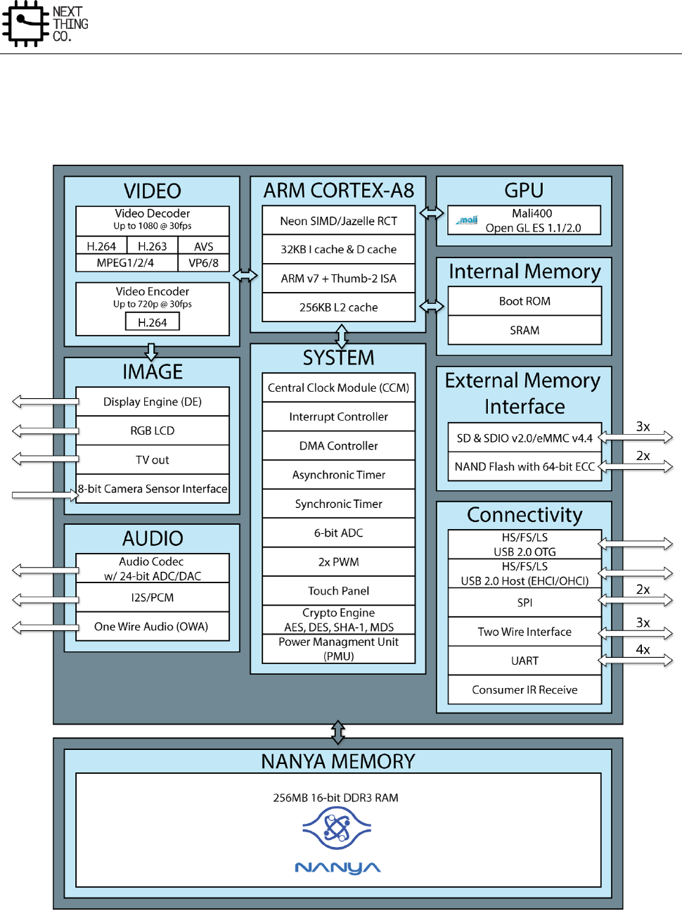
Overview
GR8 User Manual(Version1.0) Copyright © 2017 Next Thing Co. All Rights Reserved. Page 15
2.3. Block Diagram
Figure 2-1 shows the block diagram of GR8 processor.
Figure 2-1. GR8 Block Diagram
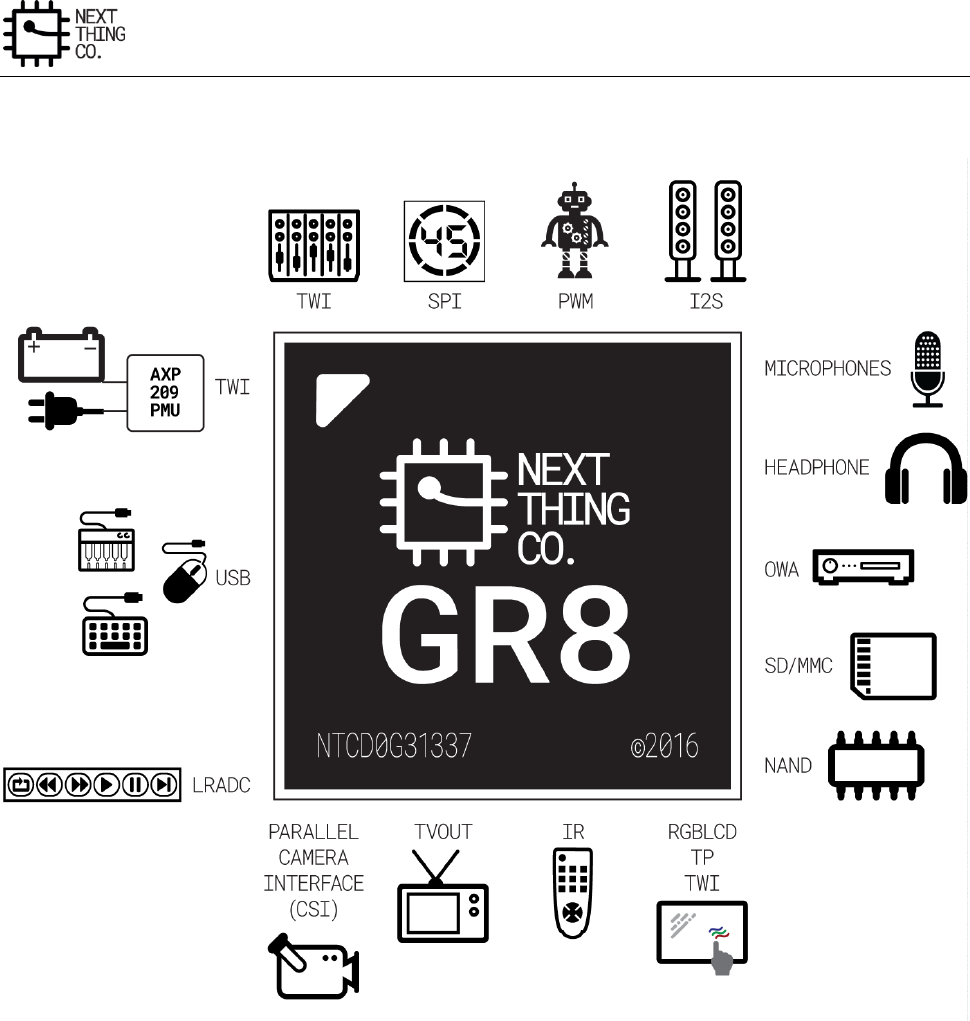
Overview
GR8 User Manual(Version1.0) Copyright © 2017 Next Thing Co. All Rights Reserved. Page 16
Figure 2-2 shows the typical application diagram of GR8 processor.
Figure 2-2. GR8 Typical Application Diagram

GR8 User Manual(Version1.0) Copyright © 2017 Next Thing Co. All Rights Reserved. Page 17
Chapter 3. System
This chapter describes the GR8 system broken out in the following sections:
Memory Mapping
Boot System
PMU
Clock Control Module (CCM)
System Control
CPU Control
PWM
Asynchronous Timer
Synchronic Timer
Interrupt Controller
DMA
LRADC
Touch Panel
Crypto Engine
Security ID
Port Controller

System
GR8 User Manual(Version1.0) Copyright © 2017 Next Thing Co. All Rights Reserved. Page 18
3.1. Memory Mapping
Module
Address
Size(Bytes)
SRAM A1
0x0000 0000---0x0000 3FFF
16K
SRAM A2
0x0000 4000---0x0000 7FFF
16K
SRAM A3
0x0000 8000---0x0000 B3FF
13K
SRAM A4
0x0000 B400---0x0000 BFFF
3K
SRAM NAND
/
2K
SRAM D
0x0001 0000---0x0001 0FFF
4K
SRAM Controller
0x01C0 0000---0x01C0 0FFF
4K
DRAM Controller
0x01C0 1000---0x01C0 1FFF
4K
DMA
0x01C0 2000---0x01C0 2FFF
4K
NFC
0x01C0 3000---0x01C0 3FFF
4K
/
0x01C0 4000---0x01C0 4FFF
4K
SPI 0
0x01C0 5000---0x01C0 5FFF
4K
/
0x01C0 6000---0x01C0 6FFF
4K
/
0x01C0 7000---0x01C0 7FFF
4K
/
0x01C0 8000---0x01C0 8FFF
4K
CSI
0x01C0 9000---0x01C0 9FFF
4K
/
0x01C0 A000---0x01C0 AFFF
/
EMAC
0x01C0 B000---0x01C0 BFFF
/
LCD
0x01C0 C000---0x01C0 CFFF
4K
/
0x01C0 D000---0x01C0 DFFF
4K
VE
0x01C0 E000---0x01C0 EFFF
4K
SD/MMC 0
0x01C0 F000---0x01C0 FFFF
4K
SD/MMC 1
0x01C1 0000---0x01C1 0FFF
4K
SD/MMC 2
0x01C1 1000---0x01C1 1FFF
4K
/
0x01C1 2000---0x01C1 2FFF
4K
USB OTG
0x01C1 3000---0x01C1 3FFF
4K
USB HCI
0x01C1 4000---0x01C1 4FFF
4K
CE
0x01C1 5000---0x01C1 5FFF
4K
/
0x01C1 6000---0x01C1 6FFF
/
SPI 2
0x01C1 7000---0x01C1 7FFF
4K
/
0x01C1 8000---0x01C1 8FFF
4K
/
0x01C1 9000---0x01C1 9FFF
4K
/
0x01C1 A000---0x01C1 AFFF
4K
/
0x01C1 B000---0x01C1 BFFF
4K
/
0x01C1 C000---0x01C1 CFFF
4K
/
0x01C1 D000---0x01C1 DFFF
4K
/
0x01C1 E000---0x01C1 EFFF
4K
/
0x01C1 F000---0x01C1 FFFF
4K
CCM
0x01C2 0000---0x01C2 03FF
1K
INTC
0x01C2 0400---0x01C2 07FF
1K
PIO
0x01C2 0800---0x01C2 0BFF
1K
ASYNC Timer
0x01C2 0C00---0x01C2 0FFF
1K
OWA
0x01C2 1000---0x01C2 13FF
1K
/
0x01C2 1400---0x01C2 17FF
1K
IR
0x01C2 1800---0x01C2 1BFF
1K
/
0x01C2 1C00---0x01C2 1FFF
1K
/
0x01C2 2000---0x01C2 23FF
1K

System
GR8 User Manual(Version1.0) Copyright © 2017 Next Thing Co. All Rights Reserved. Page 19
I2S/PCM
0x01C2 2400---0x01C2 27FF
1K
LRADC
0x01C2 2800---0x01C2 2BFF
1K
Audio Codec
0x01C2 2C00---0x01C2 2FFF
1K
KEYPAD
0x01C2 3000---0x01C2 33FF
/
CPU Control
0x01C2 3400---0x01C2 37FF
1K
SID
0x01C2 3800---0x01C2 3BFF
1K
/
0x01C2 3C00---0x01C2 3FFF
1K
/
0x01C2 4000---0x01C2 43FF
1K
/
0x01C2 4400---0x01C2 47FF
1K
/
0x01C2 4800---0x01C2 4BFF
1K
/
0x01C2 4C00---0x01C2 4FFF
1K
TP
0x01C2 5000---0x01C2 53FF
1K
PMU
0x01C2 5400---0x01C2 57FF
1K
/
0x01C2 5800---0x01C2 5BFF
1K
/
0x01C2 5C00---0x01C2 5FFF
1K
/
0x01C2 6000---0x01C2 63FF
1K
/
0x01C2 6400---0x01C2 67FF
1K
/
0x01C2 6800---0x01C2 6BFF
1K
/
0x01C2 6C00---0x01C2 6FFF
1K
/
0x01C2 7000---0x01C2 73FF
1K
/
0x01C2 7400---0x01C2 77FF
1K
/
0x01C2 7800---0x01C2 7BFF
1K
/
0x01C2 7C00---0x01C2 7FFF
1K
UART 0
0x01C2 8000---0x01C2 83FF
1K
UART 1
0x01C2 8400---0x01C2 87FF
1K
UART 2
0x01C2 8800---0x01C2 8BFF
1K
UART 3
0x01C2 8C00---0x01C2 8FFF
1K
/
0x01C2 9000---0x01C2 93FF
1K
/
0x01C2 9400---0x01C2 97FF
1K
/
0x01C2 9800---0x01C2 9BFF
1K
/
0x01C2 9C00---0x01C2 9FFF
1K
/
0x01C2 A000---0x01C2 A3FF
1K
/
0x01C2 A300---0x01C2 A7FF
1K
/
0x01C2 A800---0x01C2 ABFF
1K
TWI 0
0x01C2 AC00---0x01C2 AFFF
1K
TWI 1
0x01C2 B000---0x01C2 B3FF
1K
TWI 2
0x01C2 B400---0x01C2 B7FF
1K
/
0x01C2 B800---0x01C2 BBFF
1K
/
0x01C2 BC00---0x01C2 BFFF
1K
/
0x01C2 C000---0x01C2 C3FF
1K
/
0x01C2 C400---0x01C2 C7FF
1K
/
0x01C2 C800---0x01C2 CBFF
1K
/
0x01C2 CC00---0x01C2 CFFF
1K
/
0x01C3 0000---0x01C3 FFFF
64K
Mali-400
0x01C4 0000---0x01C4 FFFF
64K
Sync Timer
0x01C6 0000—0x01C6 0FFF
4K
SRAM C
0x01D0 0000---0x01DF FFFF
Module SRAM
DE_FE
0x01E0 0000---0x01E1 FFFF
128K
/
0x01E2 0000---0x01E3 FFFF
128K
DE_BE
0x01E6 0000---0x01E6 FFFF
64K

System
GR8 User Manual(Version1.0) Copyright © 2017 Next Thing Co. All Rights Reserved. Page 20
IEP
0x01E7 0000---0x01E7 FFFF
64K
/
0x01E4 0000---0x01E5 FFFF
128K
/
0x01E8 0000---0x01E9 FFFF
128K
/
0x01EA 0000---0x01EB FFFF
128K
/
0x3F50 0000---0x3F50 FFFF
64K
DDR-II/DDR-III
0x4000 0000---0xBFFF FFFF
2G
BROM
0xFFFF 0000—0xFFFF 7FFF
32K
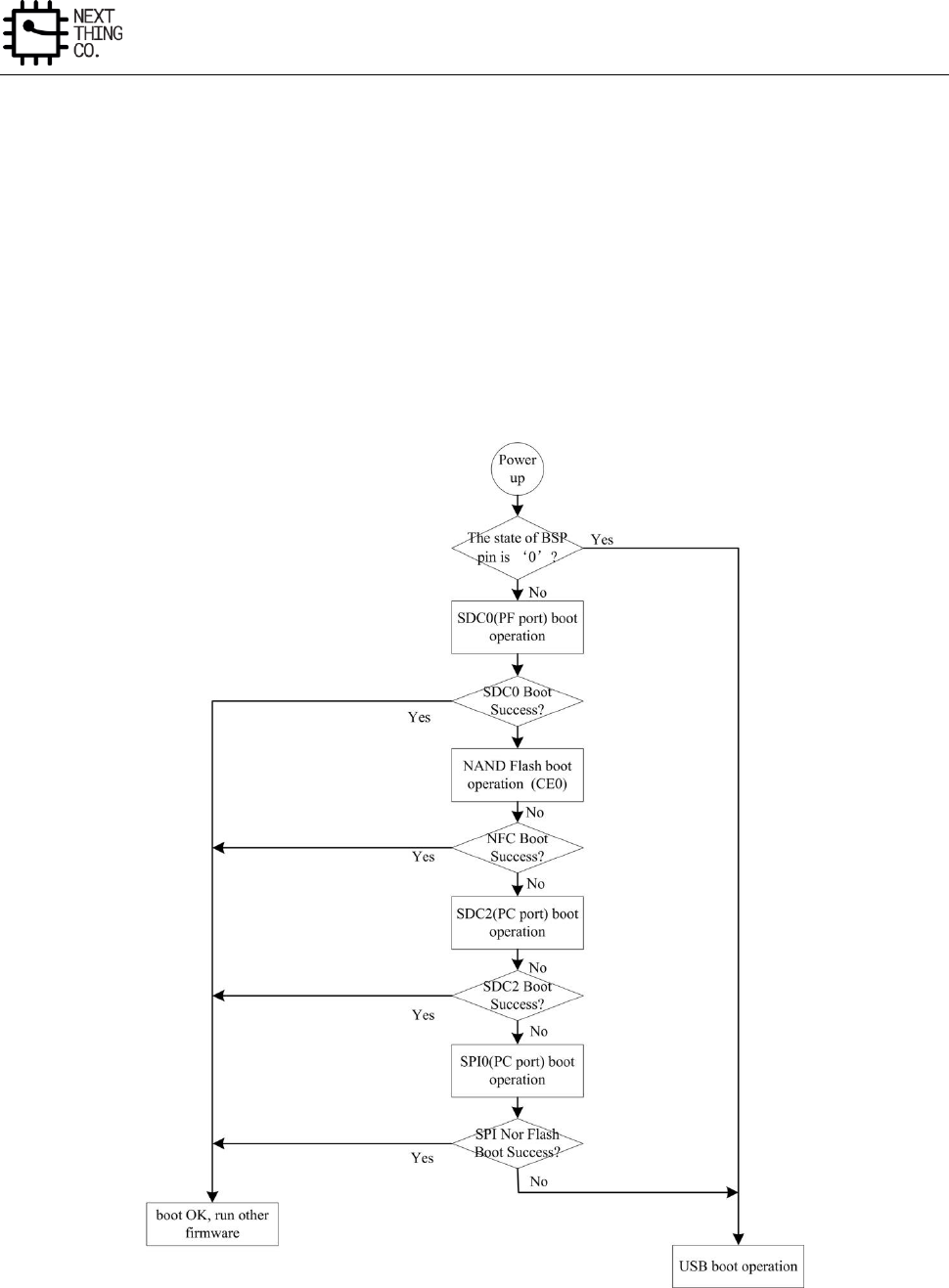
System
GR8 User Manual(Version1.0) Copyright © 2017 Next Thing Co. All Rights Reserved. Page 21
3.2. Boot System
3.2.1. Overview
With one 32KB ROM, the GR8 supports five boot methods. The system can boot sequentially from NAND Flash,
SPI NOR Flash, SD Card and USB. However, if the external boot select pin, which is pulled up by an internal 50K
resistor in normal state, is checked by boot code to be on low-level state after system power-on, the system will
directly jump to boot from USB.
3.2.2. Boot Diagram
Figure 3-1. Boot Diagram

System
GR8 User Manual(Version1.0) Copyright © 2017 Next Thing Co. All Rights Reserved. Page 22
3.3. PMU
3.3.1. Overview
The Power Management Unit (PMU) aims to reduce dynamic power consumption and static leakage current to
extend the life of batteries in end products. This module is the central control module for the CPU clock and power
management signals.
3.3.2. PMU Register List
Module Name
Base Address
PMU
0x01C25400
Register Name
Offset
Description
PMU_DVFS_CTRL_REG0
0x0000
PMU Control Register 0
PMU_DVFS_CTRL_REG1
0x0004
PMU Control Register 1
/
0x0008
/
PMU_DVFS_CTRL_REG2
0x000C
PMU Control Register 2
/
0x0010
/
/
0x0014
/
PMU_DVFS_CTRL_REG3
0x0018
PMU Control Register 3
PMU_DVFS_TIMEOUT_CTRL_REG
0x001C
PMU Timeout Control Register
PMU_AXI_AUTO_SWT_REG0
0x0020
PMU AXI Auto Switch CLK Register0
PMU_AXI_AUTO_SWT_REG1
0x0024
PMU AXI Auto Switch CLK Register1
PMU_IRQ_EN_REG
0x0040
PMU IRQ Enable Register
PMU_IRQ_STATUS_REG
0x0044
PMU IRQ Status Register
PMU_STATUS_REG
0x0048
PMU Status Register
PMU_CPUVDD_CTRL_REG_ADDR
0x004C
PMU CPUVDD Register Address
PMU_TWI_ADDR_REG
0x0050
PMU TWI Address
PMU_CPUVDD_VALUE_REG
0x0054
PMU CPUVDD Value
PMU_CPUVDD_RAMP_CTRL_REG
0x0058
PMU CPUVDD Voltage Ramp Control
PMU_32K_CPUVDD_MIN_REG
0x005C
PMU 32KHz CPUVDD Minimum Value
PMU_VF_TABLE_REG0
0x0080
CPU Speed Max if VDDCPU=0.70V
PMU_VF_TABLE_REG1
0x0084
CPU Speed Max if VDDCPU =0.75V
PMU_VF_TABLE_REG2
0x0088
CPU Speed Max if VDDCPU =0.80V
PMU_VF_TABLE_REG3
0x008C
CPU Speed Max if VDDCPU =0.85V
PMU_VF_TABLE_REG4
0x0090
CPU Speed Max if VDDCPU =0.90V
PMU_VF_TABLE_REG5
0x0094
CPU Speed Max if VDDCPU =0.95V
PMU_VF_TABLE_REG6
0x0098
CPU Speed Max if VDDCPU =1.00 V
PMU_VF_TABLE_REG7
0x009C
CPU Speed Max if VDDCPU =1.05V
PMU_VF_TABLE_REG8
0x00A0
CPU Speed Max if VDDCPU =1.10V
PMU_VF_TABLE_REG9
0x00A4
CPU Speed Max if VDDCPU =1.15 v
PMU_VF_TABLE_REG10
0x00A8
CPU Speed Max if VDDCPU =1.20V
System
GR8 User Manual(Version1.0) Copyright © 2017 Next Thing Co. All Rights Reserved. Page 23
PMU_VF_TABLE_REG11
0x00AC
CPU Speed Max if VDDCPU =1.25V
PMU_VF_TABLE_REG12
0x00B0
CPU Speed Max if VDDCPU =1.30 V
PMU_VF_TABLE_REG13
0x00B4
CPU Speed Max if VDDCPU =1.35V
PMU_VF_TABLE_REG14
0x00B8
CPU Speed Max if VDDCPU =1.40V
PMU_VF_TABLE_REG15
0x00BC
CPU Speed Max if VDDCPU =1.45V
PMU_VF_TABLE_REG16
0x00C0
CPU Speed Max if VDDCPU =1.50V
PMU_VF_TABLE_REG17
0x00C4
CPU Speed Max if VDDCPU =1.55V
PMU_VF_TABLE_REG18
0x00C8
CPU Speed Max if VDDCPU =1.60V
PMU_VF_TABLE_VALID_REG
0x00CC
PMU VF Table Valid Control
PMU_VF_TABLE_INDEX_REG
0x00D0
PMU VF Table Index
PMU_VF_TABLE_RANGE_REG
0x00D4
PMU VF Table Range
PMU_SPEED_FACTOR_REG0
0x00E0
PMU Speed Factor Register 0
PMU_SPEED_FACTOR_REG1
0x00E4
PMU Speed Factor Register 1
PMU_SPEED_FACTOR_REG2
0x00E8
PMU Speed Factor Register 2
CPU_IDLE_CNT_LOW_REG
0x00F0
CPU Idle Counter Low
CPU_IDLE_CNT_HIGH_REG
0x00F4
CPU Idle Counter High
CPU_IDLE_COUNTER_CTRL_REG
0x00F8
CPU Idle Counter Control
CPU_IDLE_STATUS_REG
0x00FC
CPU Idle Status Register
3.3.3. PMU Register Description
3.3.3.1. PMU DVFS Control Register 0 (Default Value: 0x0000_0000)
Offset: 0x0000
Register Name: PMU_DVFS_CTRL_REG0
Bit
Read/Write
Default/Hex
Description
31:18
/
/
/
17:16
R/W
0x0
DVFS_MODE_SEL
DVFS Mode Select
00: Mode 0
01: Mode 1
10: Mode 2
11: /
15
R/W
0x0
AXI_DIV_AUTO_SWITCH
AXICLK Auto Switch Enable
0: Disable
1: Enable
14:13
/
/
/
12
R/W
0x0
VOLT_CHANGE_MODE
Voltage Change Mode

System
GR8 User Manual(Version1.0) Copyright © 2017 Next Thing Co. All Rights Reserved. Page 24
0: Normal mode
1: Maximum mode
11:9
/
/
/
8
R/W
0x0
CLK_CHANGE_SM_MODE
Clock Change Smooth Mode
0: Divide mode
1: Gating mode
7
R/W
0x0
SM_EN
Smooth Enable
0: Disable
1: Enable
6
R/W
0x0
CLK_SWTH_EN
Clock Switch Enable
0: Disable
1: Enable
5
R/W
0x0
VOLT_CHANGE_EN
Voltage Change Enable
0: Disable
1: Enable
4
R/W
0x0
SPD_DET_EN
Speed Detect Enable
0: Disable
1: Enable
3:1
/
/
/
0
R/W
0x0
DVFS_EN
PMU DVFS Enable
0: Disable
1: Enable
System
GR8 User Manual(Version1.0) Copyright © 2017 Next Thing Co. All Rights Reserved. Page 25
3.3.3.2. PMU DVFS Control Register 1(Default Value: 0x0000_1010)
Offset: 0x0004
Register Name: PMU_DVFS_CTRL_REG1
Bit
Read/Write
Default/Hex
Description
31:24
/
/
/
23:8
R/W
0x10
PLL_STAB_TIME
PLL stable time.
7:0
R/W
0x10
SM_INTV_VALUE
Smooth interval value
3.3.3.3. PMU DVFS Control Register 2 (Default Value: 0x0000_0000)
Offset: 0x000C
Register Name: PMU_DVFS_CTRL_REG2
Bit
Read/Write
Default/Hex
Description
31:1
/
/
/
0
R/W
0x0
VOLT_SET_EN.
Voltage Set Enable.
It will be automatically cleared after the voltage setting command is
sent successfully.
Setting this bit to 1 will start the voltage setting (set the CPUVDD
register value to the external PMU IC through the TWI interface).
Note: This bit cannot be set to one if the Voltage Change Enable bit in the PMU_DVFS_CTRL_REG0 is set to 1.
3.3.3.4. PMU AXI Clock Range Register0 (Default Value: 0x0000_0000)
Offset: 0x0020
Register Name: PMU_AXI_AUTO_SWT_REG0
Bit
Read/Write
Default/Hex
Description
31:27
/
/
/
26:16
R/W
0x0
AXI_CLK_LEVEL1
AXICLK Level 1
15:11
/
/
/
10:0
R/W
0x0
AXI_CLK_LEVEL0
AXICLK Level 0
3.3.3.5. PMU AXI Clock Range Register1 (Default Value: 0x0000_0000)
Offset: 0x0024
Register Name: PMU_AXI_AUTO_SWT_REG1
System
GR8 User Manual(Version1.0) Copyright © 2017 Next Thing Co. All Rights Reserved. Page 26
Bit
Read/Write
Default/Hex
Description
31:27
/
/
/
26:16
R/W
0x0
AXI_CLK_LEVE3
AXICLK Level 3
15:11
/
/
/
10:0
R/W
0x0
AXI_CLK_LEVEL2
AXICLK Level 2
3.3.3.6. PMU DVFS Control Register 3
Offset: 0x0018
Register Name: PMU_DVFS_CTRL_REG3
Bit
Read/Write
Default/Hex
Description
31:0
/
/
/
3.3.3.7. PMU DVFS TimeOut Control Register(Default Value: 0x0000_0027)
Offset: 0x001C
Register Name: PMU_DVFS_TIMEOUT_CTRL_REG
Bit
Read/Write
Default/Hex
Description
31:6
/
/
/
5:0
R/W
0x27
DVFS_TIMEOUT.
DVFS operate on TWI timeout cycles in TWI peripheral clock.
000000: 1 cycle
……
100111: 40 cycles
……
111111: 64 cycles
3.3.3.8. PMU IRQ En Register (Default Value: 0x0000_0000)
Offset: 0x0040
Register Name: PMU_IRQ_EN_REG
Bit
Read/Write
Default/Hex
Description
31:13
/
/
/
12
R/W
0x0
VOLT_DET_ERR_IRQ_EN
Voltage Detect Error IRQ Enable
0: Disable
1: Enable

System
GR8 User Manual(Version1.0) Copyright © 2017 Next Thing Co. All Rights Reserved. Page 27
11
R/W
0x0
DVFS_CLK_SWTH_ERR_IRQ_EN
DVFS Clock Switch Operation Error IRQ Enable
0: Disable
1: Enable
10
R/W
0x0
DVFS_VOLT_CHANGE_ERR_EN
DVFS Voltage Change Error Enable
0: Disable
1: Enable
9
R/W
0x0
DVFS_SPD_DET_ERR_IRQ_EN
DVFS Speed Detect Error IRQ Enable
0: Disable
1: Enable
8:5
/
/
/
4
R/W
0x0
VOLT_DET_FIN_IRQ_EN
Voltage Detect Finished IRQ Enable
0: Disable
1: Enable
3
R/W
0x0
DVFS_CLK_SWT_FIN_IRQ_EN
DVFS Clock Switch Operation Finished IRQ Enable
0: Disable
1: Enable
2
R/W
0x0
DVFS_VOLT_CHANGE_FIN_EN
DVFS Voltage Change Finished Enable
0: Disable
1: Enable
1
R/W
0x0
DVFS_SPD_DET_FIN_IRQ_EN
DVFS Speed Detect Finished IRQ Enable
0: Disable

System
GR8 User Manual(Version1.0) Copyright © 2017 Next Thing Co. All Rights Reserved. Page 28
1: Enable
0
R/W
0x0
DVFS_FIN_IRQ_EN
DVFS Finished IRQ Enable
0: Disable
1: Enable
3.3.3.9. PMU IRQ Status Register (Default Value: 0x00000000)
Offset: 0x0044
Register Name: PMU_IRQ_STATUS_REG
Bit
Read/Write
Default/Hex
Description
31:13
/
/
/
12
R/W
0x0
VOLT_DET_ERR_IRQ_PEND.
Voltage Detect Error IRQ Pending.
0: No effect
1: Pending.
Setting 1 to this bit will clear it.
11
R/W
0x0
DVFS_CLK_SWT_ERR_IRQ_PEND.
DVFS Clock Switch Operation Error IRQ Pending.
0: No effect
1: Pending
Setting 1 to this bit will clear it.
10
R/W
0x0
DVFS_VOLT_CHANGE_ERR_PEND.
DVFS Voltage Change Error Pending.
0: No effect
1: Pending.
Setting 1 to this bit will clear it.
9
R/W
0x0
DVFS_SPD_DET_ERR_IRQ_PEND.
DVFS Speed Detect Error IRQ Pending.

System
GR8 User Manual(Version1.0) Copyright © 2017 Next Thing Co. All Rights Reserved. Page 29
0: No effect
1: Pending.
Setting 1 to this bit will clear it.
8:5
/
/
/
4
R/W
0x0
VOLT_DET_FIN_IRQ_PEND.
Voltage Detect Finished IRQ Pending.
0: No effect
1: Pending.
Setting 1 to this bit will clear it.
3
R/W
0x0
DVFS_CLK_SWT_FIN_IRQ_PEND.
DVFS Clock Switch Operation Finished IRQ Pending.
0: No effect
1: Pending.
Setting 1 to this bit will clear it.
2
R/W
0x0
DVFS_VOLT_CHANGE_FIN_PEND.
DVFS Voltage Change Finished Pending.
0: No effect
1: Pending.
Setting 1 to this bit will clear it.
1
R/W
0x0
DVFS_SPD_DET_FIN_IRQ_PEND.
DVFS Speed Detect Finished IRQ Pending.
0: No effect
1: Pending.
Setting 1 to this bit will clear it.
0
R/W
0x0
DVFS_FIN_IRQ_PEND.
DVFS Finished IRQ Pending.

System
GR8 User Manual(Version1.0) Copyright © 2017 Next Thing Co. All Rights Reserved. Page 30
0: No effect
1: Pending.
Setting 1 to this bit will clear it.
3.3.3.10. PMU Status Register (Default Value: 0x0000_0000)
Offset: 0x0048
Register Name: PMU_STATUS_REG
Bit
Read/Write
Default/Hex
Description
31:1
/
/
/
0
R/W
0x0
DVFS_BUSY.
DVFS Busy.
0: No effect
1: DVFS is busy.
3.3.3.11. PMU CPUVDD DCDC Control Register Address(Default Value: 0x0000_0023)
Offset: 0x004C
Register Name: PMU_CPUVDD_CTRL_REG_ADDR
Bit
Read/Write
Default/Hex
Description
31:8
/
/
/.
7:0
R/W
0x23
CPUVDD_CTRL_REG_ADDR.
PMU CPUVDD DCDC Control Register Address.
3.3.3.12. PMU TWI Address(Default Value: 0x0000_0068)
Offset: 0x0050
Register Name: PMU_TWI_ADDR_REG
Bit
Read/Write
Default/Hex
Description
31:8
/
/
/.
7:0
R/W
0x68
PMU_TWI_ADDR.
PMU TWI address set.
3.3.3.13. PMU CPUVDD Value(Default Value: 0x0000_0016)
Offset: 0x0054
Register Name: PMU_CPUVDD_VALUE_REG
Bit
Read/Write
Default/Hex
Description
31:8
/
/
/.

System
GR8 User Manual(Version1.0) Copyright © 2017 Next Thing Co. All Rights Reserved. Page 31
7:0
R/W
0x16
CPUVDD_DEFAULT.
PMU CPUVDD Default Value
0x00 : 0.70V
0x02 : 0.75V
0x04 : 0.80V
0x06 : 0.85V
0x08 : 0.90V
0x0A : 0.95V
0x0C : 1.00V
0x0E : 1.05V
0x10 : 1.10V
0x12 : 1.15V
0x14 : 1.20V
0x16 : 1.25V
0x18 : 1.30V
0x1A : 1.35V
0x1C : 1.40V
0x1E : 1.45V
0x20 : 1.50V
0x22 : 1.55V
0x24 : 1.60V
Note: This register can be modified by PMU DVFS.
3.3.3.14. PMU CPUVDD Voltage Ramp Control in DVM (Default Value: 0x0000_0000)
Offset: 0x0058
Register Name: PMU_CPUVDD_RAMP_CTRL_REG
Bit
Read/Write
Default/Hex
Description
31:1
/
/
/.
0
R/W
0x0
CPUVDD_VOLT_RAMP_CTRL.
CPUvdd voltage ramp control in DVM
0 : 15.625us
1 : 31.25us
Note: If the CPUVDD voltage ramp control in the external PMU is changed by the CPU, the CPU should also modify
this to be the same in the PMU.

System
GR8 User Manual(Version1.0) Copyright © 2017 Next Thing Co. All Rights Reserved. Page 32
3.3.3.15. PMU 32KHz CPUVDD Minimum Value(Default Value: 0x0000_000C)
Offset: 0x005C
Register Name: PMU_32K_CPUVDD_MIN_REG
Bit
Read/Write
Default/Hex
Description
31:8
/
/
/.
7:0
R/W
0xc
CPUVDD_32K_MIN_VALUE.
PMU CPUVDD Default Value
0x00 : 0.70V
0x02 : 0.75V
0x04 : 0.80V
0x06 : 0.85V
0x08 : 0.90V
0x0A : 0.95V
0x0C : 1.00V
0x0E : 1.05V
0x10 : 1.10V
0x12 : 1.15V
0x14 : 1.20V
0x16 : 1.25V
0x18 : 1.30V
0x1A : 1.35V
0x1C : 1.40V
0x1E : 1.45V
0x20 : 1.50V
0x22 : 1.55V
0x24 : 1.60V
3.3.3.16. PMU VF Table Register 0
Offset: 0x0080
Register Name: PMU_VF_TABLE_REG0
Bit
Read/Write
Default/Hex
Description
31:11
/
/
/
10:0
R/W
UDF
CPU_MAX_FREQ_070.
CPU max frequency if cpuvdd=0.7V (unit: MHz)
This register can only be written if the DVFS function is disabled.

System
GR8 User Manual(Version1.0) Copyright © 2017 Next Thing Co. All Rights Reserved. Page 33
3.3.3.17. PMU VF Table Register 1
Offset: 0x0084
Register Name: PMU_VF_TABLE_REG1
Bit
Read/Write
Default/Hex
Description
31:11
/
/
/
10:0
R/W
UDF
CPU_MAX_FREQ_075.
CPU max frequency if cpuvdd=0.75V (unit: MHz).
This register can only be written if the DVFS function is disabled.
3.3.3.18. PMU VF Table Register 2
Offset: 0x0088
Register Name: PMU_VF_TABLE_REG2
Bit
Read/Write
Default/Hex
Description
31:11
/
/
/
10:0
R/W
UDF
CPU_MAX_FREQ_080.
CPU max frequency if cpuvdd=0.8V (unit: MHz).
This register can only be written if the DVFS function is disabled.
3.3.3.19. PMU VF Table Register 3
Offset: 0x008C
Register Name: PMU_VF_TABLE_REG3
Bit
Read/Write
Default/Hex
Description
31:11
/
/
/
10:0
R/W
UDF
CPU_MAX_FREQ_085.
CPU max frequency if cpuvdd=0.85V (unit: MHz).
This register can only be written if the DVFS function is disabled.
3.3.3.20. PMU VF Table Register 4
Offset: 0x0090
Register Name: PMU_VF_TABLE_REG4
Bit
Read/Write
Default/Hex
Description
31:11
/
/
/
10:0
R/W
UDF
CPU_MAX_FREQ_090.
CPU max frequency if vddcpu=0.9V (unit: MHz).
This register can only be written if the DVFS function is disabled.
3.3.3.21. PMU VF Table Register 5
Offset: 0x0094
Register Name: PMU_VF_TABLE_REG5
Bit
Read/Write
Default/Hex
Description
31:11
/
/
/
System
GR8 User Manual(Version1.0) Copyright © 2017 Next Thing Co. All Rights Reserved. Page 34
10:0
R/W
UDF
CPU_MAX_FREQ_095.
CPU max frequency if cpuvdd=0.95V (unit: MHz).
This register can only be written if the DVFS function is disabled.
3.3.3.22. PMU VF Table Register 6
Offset: 0x0098
Register Name: PMU_VF_TABLE_REG6
Bit
Read/Write
Default/Hex
Description
31:11
/
/
/
10:0
R/W
UDF
CPU_MAX_FREQ_100.
CPU max frequency if cpuvdd=1.0V (unit: MHz).
This register can only be written if the DVFS function is disabled.
3.3.3.23. PMU VF Table Register 7
Offset: 0x009C
Register Name: PMU_VF_TABLE_REG7
Bit
Read/Write
Default/Hex
Description
31:11
/
/
/
10:0
R/W
UDF
CPU_MAX_FREQ_105.
CPU max frequency if cpuvdd=1.05V (unit: MHz).
This register can only be written if the DVFS function is disabled.
3.3.3.24. PMU VF Table Register 8
Offset: 0x00A0
Register Name: PMU_VF_TABLE_REG8
Bit
Read/Write
Default/Hex
Description
31:11
/
/
/
10:0
R/W
UDF
CPU_MAX_FREQ_110.
CPU max frequency if cpuvdd=1.1V (unit: MHz).
This register can only be written if the DVFS function is disabled.
3.3.3.25. PMU VF Table Register 9
Offset: 0x00A4
Register Name: PMU_VF_TABLE_REG9
Bit
Read/Write
Default/Hex
Description
31:11
/
/
/
10:0
R/W
UDF
CPU_MAX_FREQ_115.
CPU max frequency if cpuvdd=1.15V (unit: MHz).
This register can only be written if the DVFS function is disabled.

System
GR8 User Manual(Version1.0) Copyright © 2017 Next Thing Co. All Rights Reserved. Page 35
3.3.3.26. PMU VF Table Register 10
Offset: 0x00A8
Register Name: PMU_VF_TABLE_REG10
Bit
Read/Write
Default/Hex
Description
31:11
/
/
/
10:0
R/W
UDF
CPU_MAX_FREQ_120.
CPU max frequency if cpuvdd=1.2V (unit: MHz).
This register can only be written if the DVFS function is disabled.
3.3.3.27. PMU VF Table Register 11
Offset: 0x00AC
Register Name: PMU_VF_TABLE_REG11
Bit
Read/Write
Default/Hex
Description
31:11
/
/
/
10:0
R/W
UDF
CPU_MAX_FREQ_125.
CPU max frequency if cpuvdd=1.25V (unit: MHz).
This register can only be written if the DVFS function is disabled.
3.3.3.28. PMU VF Table Register 12
Offset: 0x00B0
Register Name: PMU_VF_TABLE_REG12
Bit
Read/Write
Default/Hex
Description
31:11
/
/
/
10:0
R/W
UDF
CPU_MAX_FREQ_130.
CPU max frequency if cpuvdd=1.3V (unit: MHz).
This register can only be written if the DVFS function is disabled.
3.3.3.29. PMU VF Table Register 13
Offset: 0x00B4
Register Name: PMU_VF_TABLE_REG13
Bit
Read/Write
Default/Hex
Description
31:11
/
/
/.
10:0
R/W
UDF
CPU_MAX_FREQ_135.
CPU max frequency if cpuvdd=1.35V (unit: MHz).
This register can only be written if the DVFS function is disabled.
System
GR8 User Manual(Version1.0) Copyright © 2017 Next Thing Co. All Rights Reserved. Page 36
3.3.3.30. PMU VF Table Register 14
Offset: 0x00B8
Register Name: PMU_VF_TABLE_REG14
Bit
Read/Write
Default/Hex
Description
31:11
/
/
/.
10:0
R/W
UDF
CPU_MAX_FREQ_140.
CPU max frequency if cpuvdd=1.4V (unit: MHz).
This register can only be written if the DVFS function is disabled.
3.3.3.31. PMU VF Table Register 15
Offset: 0x00BC
Register Name: PMU_VF_TABLE_REG15
Bit
Read/Write
Default/Hex
Description
31:11
/
/
/.
10:0
R/W
UDF
CPU_MAX_FREQ_145.
CPU max frequency if cpuvdd=1.45V (unit: MHz).
This register can only be written if the DVFS function is disabled.
3.3.3.32. PMU VF Table Register 16
Offset: 0x00C0
Register Name: PMU_VF_TABLE_REG16
Bit
Read/Write
Default/Hex
Description
31:11
/
/
/
10:0
R/W
UDF
CPU_MAX_FREQ_150.
CPU max frequency if cpuvdd=1.5V (unit: MHz).
This register can only be written if the DVFS function is disabled.
3.3.3.33. PMU VF Table Register 17
Offset: 0x00C4
Register Name: PMU_VF_TABLE_REG17
Bit
Read/Write
Default/Hex
Description
31:11
/
/
/
10:0
R/W
UDF
CPU_MAX_FREQ_155.
CPU max frequency if cpuvdd=1.55V (unit: MHz).
This register can only be written if the DVFS function is disabled.
3.3.3.34. PMU VF Table Register 18
Offset: 0x00C8
Register Name: PMU_VF_TABLE_REG18
Bit
Read/Write
Default/Hex
Description

System
GR8 User Manual(Version1.0) Copyright © 2017 Next Thing Co. All Rights Reserved. Page 37
31:11
/
/
/
10:0
R/W
UDF
CPU_MAX_FREQ_160.
CPU max frequency if cpuvdd=1.6V (unit: MHz).
This register can only be written if the DVFS function is disabled.
3.3.3.35. PMU VF Table Valid Register (Default Value: 0x0000_003C)
Offset: 0x00CC
Register Name: PMU_VF_TABLE_VALID_REG
Bit
Read/Write
Default/Hex
Description
31:6
/
/
/
5
R/W
0x1
VF_TABLE_18_VALID.
PMU V-F Table Register 18 Valid.
0: Valid
1: Invalid
4
R/W
0x1
VF_TABLE_17_VALID.
PMU V-F Table Register 17 Valid.
0: Valid
1: Invalid
3
R/W
0x1
VF_TABLE_16_VALID.
PMU V-F Table Register 16 Valid.
0: Valid
1: Invalid
2
R/W
0x1
VF_TABLE_15_VALID.
PMU V-F Table Register 15 Valid.
0: Valid
1: Invalid
1
R/W
0x0
VF_TABLE_14_VALID.
PMU V-F Table Register 14 Valid.
0: Valid
1: Invalid
0
R/W
0x0
VF_TABLE_13_VALID.

System
GR8 User Manual(Version1.0) Copyright © 2017 Next Thing Co. All Rights Reserved. Page 38
PMU V-F Table Register 13 Valid.
0: Valid
1: Invalid
3.3.3.36. PMU VF Table Index Register (Default Value: 0x0000_0000)
Offset: 0x00D0
Register Name: PMU_VF_TABLE_INDEX_REG
Bit
Read/Write
Default/Hex
Description
31:2
/
/
/
1:0
R/W
0x0
VF_TABLE_IDX.
PMU V-F Table Index.
3.3.3.37. PMU VF Table Range Register (Default Value: 0x0000_0000)
Offset: 0x00D4
Register Name: PMU_VF_TABLE_RANGE_REG
Bit
Read/Write
Default/Hex
Description
31:24
/
/
/
23:16
R/W
0x0
VF_TABLE_RNG2.
PMU V-F Table Range 2.
15:8
R/W
0x0
VF_TABLE_RNG1.
PMU V-F Table Range 1.
7:0
R/W
0x0
VF_TABLE_RNG0.
PMU V-F Table Range 0.
3.3.3.38. PMU Speed Factor Register 0 (Default Value: 0x0000_0000)
Offset: 0x00E0
Register Name: PMU_SPEED_FACTOR_REG0
Bit
Read/Write
Default/Hex
Description
31
R/W
0x0
SPD_DET_EN
Speed Detect Enable
0: Disable
1: Enable
30
R/W
0x0
SPD_DET_MODE
Speed Detect Mode
0: Single mode

System
GR8 User Manual(Version1.0) Copyright © 2017 Next Thing Co. All Rights Reserved. Page 39
1: Continuous mode
29:28
R/W
0x0
SPD_DET_SPDUP_FACTOR
Speed Detect Speed Up Factor
Setting these bits to non-zero value can speed up the scan operation.
00: lowest
…
11: fastest
27:17
/
/
/
16
R
0x0
SPD_DET_SCN_FIN
Speed Detect Scan Finished
0: No effect
1: Scan finished
15:8
R
0x0
SPD_DET_FACTOR1
Speed Detect Factor 1
This number indicates the delay length equivalent to input clock
period x2
7:0
R
0x0
SPD_DET_FACTOR0
Speed Detect Factor 0
This number indicates the delay length equivalent to input clock
period x1
3.3.3.39. PMU Speed Factor Register 1 (Default Value: 0x0000_0000)
Offset: 0x00E4
Register Name: PMU_SPEED_FACTOR_REG1
Bit
Read/Write
Default/Hex
Description
31
R/W
0x0
SPD_DET_EN
Speed Detect Enable
0: Disable
1: Enable
30
R/W
0x0
SPD_DET_MODE
Speed Detect Mode
0: Single mode
1: Continuous mode

System
GR8 User Manual(Version1.0) Copyright © 2017 Next Thing Co. All Rights Reserved. Page 40
29:28
R/W
0x0
SPD_DET_SPDUP_FACTOR
Speed Detect Speed Up Factor
Setting these bits to non-zero value can speed up the scan operation
00: lowest
…
11: fastest
27:17
/
/
/
16
R
0x0
SPD_DET_SCN_FIN
Speed Detect Scan Finished
0: No effect
1: Scan finished
15:8
R
0x0
SPD_DET_FACTOR1
Speed Detect Factor 1
This number indicates the delay length equivalent to input clock
period x2
7:0
R
0x0
SPD_DET_FACTOR0
Speed Detect Factor 0
This number indicates the delay length equivalent to input clock
period x1
3.3.3.40. PMU Speed Factor Register 2 (Default Value: 0x0000_0000)
Offset: 0x00E8
Register Name: PMU_SPEED_FACTOR_REG2
Bit
Read/Write
Default/Hex
Description
31
R/W
0x0
SPD_DET_EN
Speed Detect Enable
0: Disable
1: Enable
30
R/W
0x0
SPD_DET_MODE
Speed Detect Mode
0: Single mode
1: Continuous mode
29:28
R/W
0x0
SPD_DET_SPDUP_FACTOR

System
GR8 User Manual(Version1.0) Copyright © 2017 Next Thing Co. All Rights Reserved. Page 41
Speed Detect Speed Up Factor
Setting these bits to non-zero value can speed up the scan operation
00: lowest
…
11: fastest
27:17
/
/
/
16
R
0x0
SPD_DET_SCN_FIN
Speed Detect Scan Finished
0: No effect
1: Scan finished.
15:8
R
0x0
SPD_DET_FACTOR1
Speed Detect Factor 1
This number indicates the delay length equivalent to input clock
period x2
7:0
R
0x0
SPD_DET_FACTOR0
Speed Detect Factor 0
This number indicates the delay length equivalent to input clock
period x1
3.3.3.41. CPU Idle Counter Low Register (Default Value: 0x0000_0000)
Offset: 0x00F0
Register Name: CPU_IDLE_CNT_LOW_REG
Bit
Read/Write
Default/Hex
Description
31:0
R/W
0x0
CPU_IDLE_CNT_LO
CPU Idle Counter [31:0]
This counter clock source is 24 MHz. If CPU is in idle state, the
counter will count up in the clock of 24 MHz.
Any write to this register will clear this register and the CPU idle
counter high register.
3.3.3.42. CPU Idle Counter High Register (Default Value: 0x0000_0000)
Offset: 0x00F4
Register Name: CPU_IDLE_CNT_HIGH_REG
Bit
Read/Write
Default/Hex
Description
31:0
R/W
0x0
CPU_IDLE_CNT_HI
CPU Idle Counter [63:32]

System
GR8 User Manual(Version1.0) Copyright © 2017 Next Thing Co. All Rights Reserved. Page 42
Any write to this register will clear this register and the CPU idle
counter low register.
3.3.3.43. CPU Idle Control Register (Default Value: 0x0000_0000)
Offset: 0x00F8
Register Name: CPU_IDLE_COUNTER_CTRL_REG
Bit
Read/Write
Default/Hex
Description
31:8
/
/
/
7
R/W
0x0
CPU_IDLE_AUTO_SWTH_EN
CPU idle enter/exit, clk auto switch enable
0: Disable
1: Enable
If the CPU enter the idle mode and this bit is set, the CCU will auto
switch the CPU clock divide ratio to /8.
If the CPU exit the idle mode and this bit is set, the CCU will auto
switch the CPU clock divide ratio from /8 to /1 with 4 steps.
6:3
/
/
/
2
R/W
0x0
CPU_IDLE_CNT_EN
CPU idle counter enable
0: Disable
1: Enable.
1
R/W
0x0
CPU_IDLE_RL_EN
CPU idle counter read latch enable
0: No effect
1: To latch the idle Counter to the Low/Hi registers and it will change
to zero after the registers are latched.
0
R/W
0x0
CPU_IDLE_CNT_CLR_EN
CPU idle Counter Clear Enable
0: No effect
1: To clear the idle Counter Low/Hi registers and it will change to zero
after the registers are cleared.
System
GR8 User Manual(Version1.0) Copyright © 2017 Next Thing Co. All Rights Reserved. Page 43
3.3.3.44. CPU Idle Status Register (Default Value: 0x0000_0000)
Offset: 0x00FC
Register Name: CPU_IDLE_STATUS_REG
Bit
Read/Write
Default/Hex
Description
31:1
/
/
/
0
R/W
0x0
CPU_IDLE_STA
CPU idle exit finished pending
0: No effect
1: Idle exit finished
Setting 1 to this bit will clear it.
System
GR8 User Manual(Version1.0) Copyright © 2017 Next Thing Co. All Rights Reserved. Page 44
3.4. Clock Control Module (CCM)
3.4.1. Overview
The Clock Control Module (CCM) is made up of 7 PLLs, a main oscillator and an on-chip RC oscillator. The 24 MHz
crystal is mandatory to generate an input clock source for PLLs and main digital blocks.
In order to provide high performance, low-power consumption and user-friendly interfaces, the chip includes
several clock domains: CPU clock, AHB clock, APB clock and special clock. See details in the following table.
CLK Domain
Module
Speed Range
Description
OSC24M
Most Clock Generator
24 MHz
Root clock for most of the chip
RC_OSC
Timer,key
32 KHz
Source for the timer
CPU32_clk
CPU32
2 kHz~1200 MHz
Divided from CPU32_clk or OSC24M
AHB_clk
AHB Devices
8 kHz~276 MHz
Divided from CPU32_clk
APB_clk
Peripheral
0.5 kHz~138 MHz
Divided from AHB_clk
SDRAM_clk
SDRAM
0~400 MHz
Sourced from the PLL
USB_clk
USB
480 MHz
Sourced from the PLL
Audio_clk
A/D,D/A
24.576 MHz
/22.5792 MHz
Sourced from the PLL
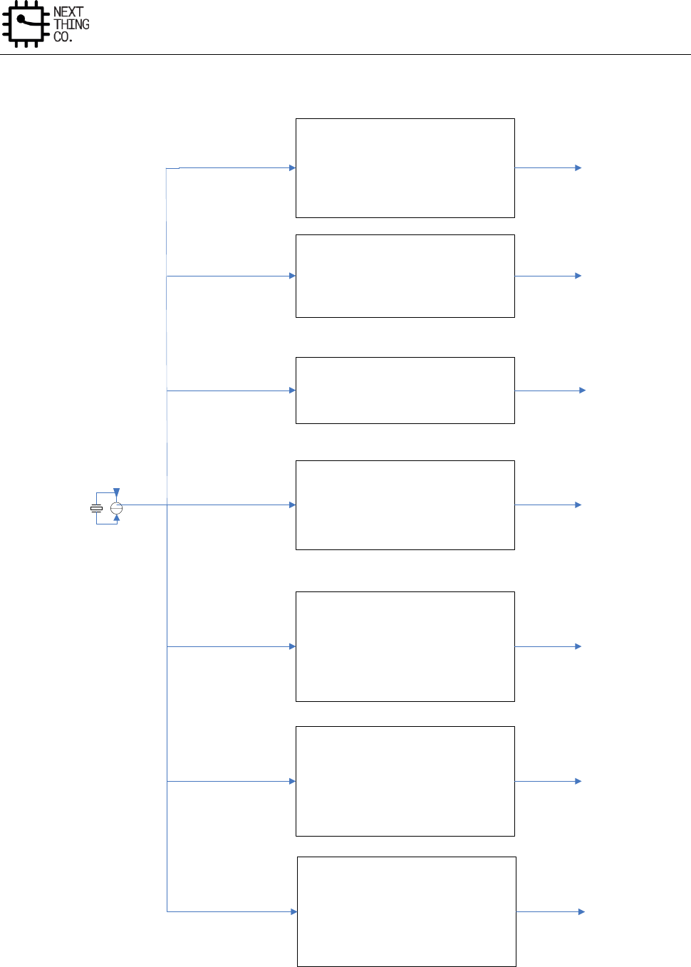
System
GR8 User Manual(Version1.0) Copyright © 2017 Next Thing Co. All Rights Reserved. Page 45
3.4.2. Clock Tree Diagram
PLL 2
OUT = 22.5792MHz/24.576MHz
PLL 1(240MHz-2GHz)
OUT =( 24MHz*N*K)/(M*P)
N:0-31
K:1-4
M:1-4
P:1/2/4/8
PLL 3(27MHz-381MHz)
OUT = 3MHz*M (Integer mode)
OUT = 270MHz/297MHz(Fractional)
M:9-127
PLL 4(240MHz-2GHz)
OUT = (24MHz*N*K)/(M*P)
N:0-31
K:1-4
M:1-4
P:1/2/4/8
PLL 5(240MHz-2GHz)
OUT = ( 24MHz*N*K)/M
OUT = (24MHz*N*K)/P
N:0-31
K:1-4
M:1-4
P:1/2/4/8
PLL 6
Fixed To 1.2GHZ
PLL 7(27MHz-381MHz)
OUT = 3MHz*M (Integer mode)
OUT = 270MHz/297MHz(Fractional)
M:9-127
24MHz X
PLL1OUT
PLL2OUT
PLL3OUT
PLL4OUT
PLL5OUT
PLL6OUT
PLL7OUT
Figure 3-2. Clock Generation from PLL Outputs
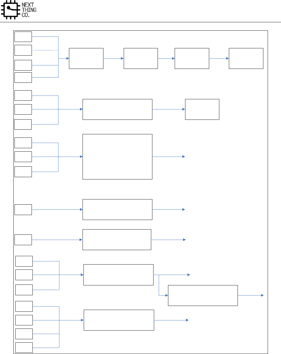
System
GR8 User Manual(Version1.0) Copyright © 2017 Next Thing Co. All Rights Reserved. Page 46
CPU-CLK
32KHZ
OSC24M
PLL1
PLL6/6
APB0-CLKAHB-CLKAXI-CLK
OSC24M
PLL6
32KHZ
APB1-CLK
CLK_OUT= CLK_IN/(M*N)
M:1-32
N:1/2/4/8
APB1-CLK-OUT
OSC24M
PLL6
PLL5
NAND-CLK
SD0/1/2-CLK
CE-CLK
SPI0/1/2-CLK
IR-CLK
CLK_OUT= CLK_IN/(M*N)
M:1-16
N:1/2/4/8
NAND-CLK-OUT
SD0/1/2-CLK-OUT
CE-CLK-OUT
SPI0/1/2-CLK-OUT
IR-CLK-OUT
PLL2
8X CLK_OUT= CLK_IN/*N
N:1/2/4/8
USB-PLL USB-CLK
USB-CLK-OUT
PLL3
PLL7
PLL5
DE-BE/FE-CLK
CLK_OUT= CLK_IN/M
M:1-16
DE-BE/FE-CLK-OUT
PLL3x1
PLL7x1
PLL3x2
LCD-CH0-CLK
CLK_OUT = CLK_IN
LCD-CH0-CLK-OUT
PLL7x2
IEP-CLK
Divider
00:/1
01:/2
10:/3
11:/4
Divider
00:/1
01:/2
10:/4
11:/8
Divider
00:/2
01:/2
10:/4
11:/8
TWI/UART//SCR
BE-CLK-OUT
Figure 3-3. Bus Clock Generation Part 1
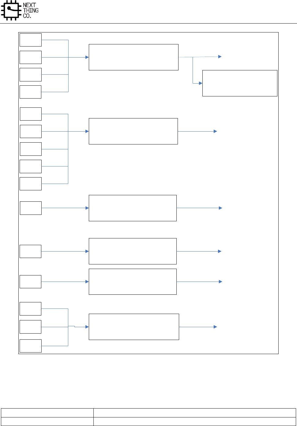
System
GR8 User Manual(Version1.0) Copyright © 2017 Next Thing Co. All Rights Reserved. Page 47
PLL3x1
PLL7x1
PLL3x2
LCD-CH1-CLK2
CLK_OUT= CLK_IN/M
M:1-16
PLL7x2
LCD-CH1-CLK2
OSC24M
PLL3x1
PLL7x1
CSI-CLK
CLK_OUT= CLK_IN/M
M:1-32
PLL3x2
PLL7x2
CSI-CLK-OUT
PLL4 VE-CLK
VE-CLK-OUT
PLL2 AUDIOCODEC-CLK AUDIOCODEC-CLK-OUT
OSC24M AVS-CLK AVS-CLK-OUT
OSC24M
PLL6
PLL5
MBUS-CLK(Max 300MHz)
CLK_OUT= CLK_IN/(M*N)
M:1-16
N:1/2/4/8
MBUS-CLK-OUT
LCD-CH1-CLK1
CLK_OUT = CLK_IN/M
M:1/2
Figure 3-4. Bus Clock Generation Part 2
3.4.3. CCM Register List
Module Name
Base Address
CCM
0x01C20000

System
GR8 User Manual(Version1.0) Copyright © 2017 Next Thing Co. All Rights Reserved. Page 48
Register Name
Offset
Description
PLL1_CFG_REG
0x0000
PLL1 Control
PLL1_TUN_REG
0x0004
PLL1 Tuning
PLL2_CFG_REG
0x0008
PLL2 Control
PLL2_TUN_REG
0x000C
PLL2 Tuning
PLL3_CFG_REG
0x0010
PLL3 Control
/
0x0014
/
PLL4_CFG_REG
0x0018
PLL4 Control
/
0x001C
/
PLL5_CFG_REG
0x0020
PLL5 Control
PLL5_TUN_REG
0x0024
PLL5 Tuning
PLL6_CFG_REG
0x0028
PLL6 Control
/
0x002C
PLL6 Tuning
PLL7_CFG_REG
0x0030
/
/
0x0034
/
PLL1_TUN2_REG
0x0038
PLL1 Tuning2
PLL5_TUN2_REG
0x003C
PLL5 Tuning2
/
0x004C
/
OSC24M_CFG_REG
0x0050
OSC24M control
CPU_AHB_APB0_CFG_REG
0x0054
CPU, AHB And APB0 Divide Ratio
APB1_CLK_DIV_REG
0x0058
APB1 Clock Divider
AXI_GATING_REG
0x005C
AXI Module Clock Gating
AHB_GATING_REG0
0x0060
AHB Module Clock Gating 0
AHB_GATING_REG1
0x0064
AHB Module Clock Gating 1
APB0_GATING_REG
0x0068
APB0 Module Clock Gating
APB1_GATING_REG
0x006C
APB1 Module Clock Gating
NAND_SCLK_CFG_REG
0x0080
NAND Flash Clock
/
0x0084
/
SD0_SCLK_CFG_REG
0x0088
SD0 Clock
SD1_SCLK_CFG_REG
0x008C
SD1 Clock
SD2_SCLK_CFG_REG
0x0090
SD2 Clock
/
0x0094
/
/
0x0098
/
CE_SCLK_CFG_REG
0x009C
Crypto Engine Clock
SPI 0_SCLK_CFG_REG
0x00A0
SPI0 Clock
/
0x00A4
/
SPI 2_SCLK_CFG_REG
0x00A8
SPI2 Clock
/
0x00AC
/
IR_SCLK_CFG_REG
0x00B0
IR Clock
/
0x00B4
/
I2S_SCLK_CFG_REG
0x00B8
I2S Clock
/
0x00BC
/
OWA_SCLK_CFG_REG
0x00C0
OWA Clock

System
GR8 User Manual(Version1.0) Copyright © 2017 Next Thing Co. All Rights Reserved. Page 49
/
0x00C4
/
/
0x00C8
/
USBPHY_CFG_REG
0x00CC
USBPHY Clock
/
0x00D0
/
/
0x00D4
/
DRAM_SCLK_CFG_REG
0x0100
DRAM Clock
BE_CFG_REG
0x0104
Display Engine Backend Clock
/
0x0108
FE_CFG_REG
0x010C
Display Engine Front End Clock
/
0x0110
/
/
0x0114
/
LCD_CH0_CFG_REG
0x0118
LCD Channel0 Clock
/
0x011C
/
/
0x0120
/
/
0x0124
/
/
0x0128
/
LCD_CH1_CFG_REG
0x012C
LCD Channel1 Clock
/
0x0130
/
CSI_CFG_REG
0x0134
CSI Clock
/
0x0138
/
VE_CFG_REG
0x013C
Video Engine Clock
AUDIO_CODEC_SCLK_CFG_REG
0x0140
Audio Codec Gating Special Clock
AVS_SCLK_CFG_REG
0x0144
AVS Gating Special Clock
/
0x0148
/
/
0x014C
/
/
0x0150
/
MALI_CLOCK_CFG_REG
0x0154
Mali400 Gating Special Clock
/
0x0158
/
MBUS_SCLK_CFG_REG
0x015C
MBUS Gating Clock
IEP_SCLK_CFG_REG
0x0160
IEP Gating Clock
3.4.4. CCM Register Description
3.4.4.1. PLL1-Core Register (Default Value: 0x2100_5000)
Offset: 0x0000
Register Name: PLL1_CFG_REG
Bit
Read/Write
Default/Hex
Description
31
R/W
0x0
PLL1_Enable.
0: Disable
1: Enable.
The PLL1 output= (24 MHz*N*K)/ (M*P).

System
GR8 User Manual(Version1.0) Copyright © 2017 Next Thing Co. All Rights Reserved. Page 50
The PLL1 output is for the CORECLK.
Note: The output 24 MHz*N*K clock must be in the range of 240
MHz~2 GHz if the bypass is disabled.
Its default is 384 MHz.
30:18
/
/
/
17:16
R/W
0x0
PLL1_OUT_EXT_DIVP.
PLL1 Output external divider P.
The range is 1/2/4/8.
15:13
/
/
/.
12:8
R/W
0x10
PLL1_FACTOR_N
PLL1 Factor N.
Factor=0, N=0;
Factor=1, N=1;
Factor=2, N=2
……
Factor=31, N=31
7:6
/
/
/
5:4
R/W
0x0
PLL1_FACTOR_K.
PLL1 Factor K. (K=Factor + 1)
The range is from 1 to 4.
3
R/W
0x0
/
2
R/W
0x0
/
1:0
R/W
0x0
PLL1_FACTOR_M.
PLL1 Factor M. (M=Factor + 1)
The range is from 1 to 4.
3.4.4.2. PLL1-Tuning Register (Default Value: 0x0A10_1000)
Offset: 0x0004
Register Name: PLL1_TUN_REG
Bit
Read/Write
Default/Hex
Description
31:28
/
/
/
27
R/W
0x1
/
26
R/W
0x0
/
25:23
R/W
0x4
/
22:16
R/W
0x10
/
15
R/W
0x0
/

System
GR8 User Manual(Version1.0) Copyright © 2017 Next Thing Co. All Rights Reserved. Page 51
14:8
R/W
0x10
/
7
R/W
0x0
/
6:0
R
0x0
/
3.4.4.3. PLL2-Audio Register (Default Value: 0x0810_0010)
Offset: 0x0008
Register Name: PLL2_CFG_REG
Bit
Read/Write
Default/Hex
Description
31
R/W
0x0
PLL2_Enable.
0: Disable
1: Enable.
The PLL2 is for Audio.
PLL2 Output = 24 MHz*N/PLL2_PRE_DIV/PLL2_POST_DIV.
1X = 48*N/PreDiv/PostDiv/2 (not 50% duty)
2X = 48*N/PreDiv/4 (8X/4 50% duty)
4X = 48*N/PreDiv/2 (8X/2 50% duty)
8X = 48*N/PreDiv (not 50% duty)
30
/
/
/
29:26
R/W
0x2
PLL2_POST_DIV.
PLL2 post-divider [3:0].
0000: 0x1
……
1111: 0x10
25:21
R/W
0x0
/
20:16
R/W
0x10
/
15
/
/
/
14:8
R/W
0x0
PLL2_Factor_N.
PLL2 Factor N.
Factor=0, N=1;
Factor=1, N=1;
……
Factor=0x7F, N=0x7F
7:5
/
/
/
System
GR8 User Manual(Version1.0) Copyright © 2017 Next Thing Co. All Rights Reserved. Page 52
4:0
R/W
0x10
PLL2_PRE_DIV.
PLL2 pre-divider [4:0].
00000: 0x1
……
11111: 0x20
3.4.4.4. PLL2-Tuning Register (Default Value: 0x0000_0000)
Offset: 0x000C
Register Name: PLL2_TUN_REG
Bit
Read/Write
Default/Hex
Description
31
R/W
0x0
/
30:29
R/W
0x0
/
28:20
R/W
0x0
/
19
/
/
/
18:17
R/W
0x0
/
16:0
R/W
0x0
/
3.4.4.5. PLL3-Video Register (Default Value: 0x0010_D063)
Offset: 0x0010
Register Name: PLL3_CFG_REG
Bit
Read/Write
Default/Hex
Description
31
R/W
0x0
PLL3_Enable.
0: Disable
1: Enable.
In the integer mode, The PLL3 output=3 MHz*M.
In the fractional mode, the PLL3 output is selected by bit 14.
The PLL3 output range is 27 MHz~381 MHz.
30:27
/
/
/
26:24
R/W
0x0
/
23:21
/
/
/
20:16
R/W
0x10
/
15
R/W
0x1
PLL3_MODE_SEL.
PLL3 mode select.

System
GR8 User Manual(Version1.0) Copyright © 2017 Next Thing Co. All Rights Reserved. Page 53
0: Fractional mode
1: Integer mode.
14
R/W
0x1
PLL3_FUNC_SET.
PLL3 fractional setting.
0: 270 MHz
1: 297 MHz
13
/
/
/
12:8
R/W
0x10
/
7
/
/
/
6:0
R/W
0x63
PLL3_FACTOR_M.
PLL3 Factor M.
The range is from 9 to 127.
3.4.4.6. PLL4-VE Register (Default Value: 0x2108_1000)
Offset: 0x0018
Register Name: PLL4_CFG_REG
Bit
Read/Write
Default/Hex
Description
31
R/W
0x0
PLL4_Enable.
0: Disable
1: Enable.
The PLL4 output= (24 MHz*N*K)/ (M*P).
The PLL4 output is for the VE.
Note: The output 24 MHz*N*K clock must be in the range of
240 MHz~2 GHz if the bypass is disabled.
30
R/W
0x0
PLL4_OUT_BYPASS_EN.
PLL4 Output Bypass Enable.
0: Disable
1: Enable.
If the bypass is enabled, the PLL4 output is 24 MHz.
29:25
R/W
0x10
/

System
GR8 User Manual(Version1.0) Copyright © 2017 Next Thing Co. All Rights Reserved. Page 54
24:20
R/W
0x10
/
19
R/W
0x1
/
18
/
/
/
17:16
R/W
0x0
PLL4_OUT_EXT_DIV_P.
PLL4 Output external divider P.
The range is 1/2/4/8.
15:13
/
/
/
12:8
R/W
0x10
PLL4_FACTOR_N.
PLL4 Factor N.
Factor=0, N=0;
Factor=1, N=1;
Factor=2, N=2
……
Factor=31, N=31
7:6
/
/
/
5:4
R/W
0x0
PLL4_FACTOR_K.
PLL4 Factor K. (K=Factor + 1)
The range is from 1 to 4.
3:2
/
/
/
1:0
R/W
0x0
PLL4_FACTOR_M.
PLL4 Factor M. (M = Factor + 1)
The range is from 1 to 4.
3.4.4.7. PLL5-DDR Register (Default Value: 0x1104_9280)
Offset: 0x0020
Register Name: PLL5_CFG_REG
Bit
Read/Write
Default/Hex
Description
31
R/W
0x0
PLL5_Enable.
0: Disable
1: Enable.
The PLL5 output for DDR = (24 MHz*N*K)/M.
The PLL5 output for another module = (24 MHz*N*K)/P.
The PLL5 output is for the DDR.
Note: The output 24 MHz*N*K clock must be in the range of

System
GR8 User Manual(Version1.0) Copyright © 2017 Next Thing Co. All Rights Reserved. Page 55
240 MHz~2 GHz if the bypass is disabled.
30
R/W
0x0
PLL5_OUT_BYPASS_EN.
PLL5 Output Bypass Enable.
0: Disable
1: Enable.
If the bypass is enabled, the PLL6 output is 24 MHz.
29
R/W
0x0
DDR_CLK_OUT_EN.
DDR clock output en.
28:25
R/W
0x8
/
24:20
R/W
0x10
/
19
R/W
0x0
/
18
R/W
0x1
/
17:16
R/W
0x0
PLL5_OUT_EXT_DIV_P.
PLL5 Output External Divider P.
The range is 1/2/4//8.
15:13
R/W
0x4
/
12:8
R/W
0x12
PLL5_FACTOR_N.
PLL5 Factor N.
Factor=0, N=0;
Factor=1, N=1;
Factor=2, N=2
……
Factor=31, N=31
7
R/W
0x1
LDO_EN.
LDO Enable.
6
/
/
/
5:4
R/W
0x0
PLL5_FACTOR_K.
PLL5 Factor K. (K=Factor + 1)
The range is from 1 to 4.
3:2
R/W
0x0
PLL5_FACTOR_M1.
PLL5 Factor M1.
1:0
R/W
0x0
PLL5_FACTOR_M.
PLL5 Factor M. (M = Factor + 1)

System
GR8 User Manual(Version1.0) Copyright © 2017 Next Thing Co. All Rights Reserved. Page 56
The range is from 1 to 4.
3.4.4.8. PLL5-Tuning Register (Default Value: 0x1488_0000)
Offset: 0x0024
Register Name: PLL5_TUN_REG
Bit
Read/Write
Default/Hex
Description
31:0
/
/
/
3.4.4.9. PLL6 Register (Default Value: 0x2100_9931)
Offset: 0x0028
Register Name: PLL6_CFG_REG
Bit
Read/Write
Default/Hex
Description
31
R/W
0x0
PLL6_Enable.
0: Disable
1: Enable.
Output = (24 MHz*N*K)/M/2
Note: The output 24 MHz*N*K clock must be in the range of
240 MHz~3 GHz if the bypass is disabled.
Its default is 1200 MHz.
30
R/W
0x0
PLL6_BYPASS_EN.
PLL6 Output Bypass Enable.
0: Disable
1: Enable.
If the bypass is enabled, the PLL6 output is 24 MHz.
29:13
/
/
/
12:8
R/W
0x19
PLL6_FACTOR_N.
PLL6 Factor N.
Factor=0, N=0;
Factor=1, N=1;
Factor=2, N=2;
……
Factor=31, N=31
7:6
/
/
PLL6 damping factor control [1:0].

System
GR8 User Manual(Version1.0) Copyright © 2017 Next Thing Co. All Rights Reserved. Page 57
5:4
/
/
PLL6_FACTOR_K.
PLL6 Factor K. (K=Factor + 1)
The range is from 1 to 4.
3:2
/
/
/
1:0
R/W
0x1
PLL6_FACTOR_M.
PLL6 Factor M. (M = Factor + 1)
The range is from 1 to 4.
3.4.4.10. PLL7 Register (Default Value: 0x0010_D063)
Offset: 0x0030
Register Name: PLL7_CFG_REG
Bit
Read/Write
Default/Hex
Description
31
R/W
0x0
PLL7_Enable.
0: Disable
1: Enable.
In the integer mode, The PLL7 output=3 MHz*M.
In the fractional mode, the PLL7 output is selected by bit 14.
The PLL7 output range is 27 MHz~381 MHz.
30:16
/
/
/
15
R/W
0x1
PLL7_MODE_SEL.
PLL7 mode select.
0: Fractional mode
1: Integer mode.
14
R/W
0x1
PLL7_FRAC_SET.
PLL7 fractional setting.
0: 270 MHz
1: 297 MHz
13:7
/
/
/
6:0
R/W
0x63
PLL7_FACTOR_M.
PLL7 Factor M.
The range is from 9 to 127.

System
GR8 User Manual(Version1.0) Copyright © 2017 Next Thing Co. All Rights Reserved. Page 58
3.4.4.11. PLL1-Tuning2 Register (Default Value: 0x0000_0000)
Offset: 0x0038
Register Name: PLL1_TUN2_REG
Bit
Read/Write
Default/Hex
Description
31
R/W
0x0
SIG_DELT_PAT_EN.
Sigma-delta pattern enable.
30:29
R/W
0x0
SPR_FREQ_MODE.
Spread Frequency Mode.
00: DC=0
01: DC=1
10: Triangular
11: awmode
28:20
R/W
0x0
WAVE_STEP.
Wave step.
19
/
/
/
18:17
R/W
0x0
FREQ.
Frequency.
00: 31.5 kHz
01: 32 kHz
10: 32.5 kHz
11: 33 kHz
16:0
R/W
0x0
WAVE_BOT.
Wave Bottom.
3.4.4.12. PLL5-Tuning2 Register (Default Value: 0x0000_0000)
Offset: 0x003C
Register Name: PLL5_TUN2_REG
Bit
Read/Write
Default/Hex
Description
31
R/W
0x0
SIG_DELT_PAT_EN.
Sigma-delta pattern enable.
30:29
R/W
0x0
SPR_FREQ_MODE.
Spread Frequency Mode.
00: DC=0
01: DC=1

System
GR8 User Manual(Version1.0) Copyright © 2017 Next Thing Co. All Rights Reserved. Page 59
10: Triangular
11: awmode
28:20
R/W
0x0
WAVE_STEP.
Wave step.
19
/
/
/
18:17
R/W
0x0
FREQ.
Frequency.
00: 31.5 kHz
01: 32 kHz
10: 32.5 kHz
11: 33 kHz
16:0
R/W
0x0
WAVE_BOT.
Wave Bottom.
3.4.4.13. OSC24M Register (Default Value: 0x0013_8013)
Offset: 0x0050
Register Name: OSC24M_CFG_REG
Bit
Read/Write
Default/Hex
Description
31:24
R/W
0x0
/
23:18
/
/
/
17
R/W
0x1
PLL_IN_PWR_SEL.
PLL Input Power Select.
0: 2.5V
1: 3.3V
16
R/W
0x1
LDO_EN.
LDO Enable.
0: Disable
1: Enable.
15
R/W
0x1
PLL_BIAS_EN.
PLL Bias Enable.
0: Disable
1: Enable.

System
GR8 User Manual(Version1.0) Copyright © 2017 Next Thing Co. All Rights Reserved. Page 60
14:2
/
/
/
1
R/W
0x1
OSC24M_GSM.
OSC24M GSM.
0
R/W
0x1
OSC24M_EN.
OSC24M Enable.
0: Disable
1: Enable.
3.4.4.14. CPU/AHB/APB0 Clock Ratio Register (Default Value: 0x0001_0010)
Offset: 0x0054
Register Name: CPU_AHB_APB0_CFG_REG
Bit
Read/Write
Default/Hex
Description
31:18
/
/
/
17:16
R/W
0x1
CPU_CLK_SRC_SEL.
CPU Clock Source Select.
00: 32 KHz OSC( Internal )
01: OSC24M
10: PLL1
11: 200 MHz (source from the PLL6).
If the clock source is changed, at most to wait for 8 present running
clock cycles.
15:10
/
/
/
9:8
R/W
0x0
APB0_CLK_RATIO.
APB0 Clock divide ratio. APB0 clock source is AHB2 clock.
00: /2
01: /2
10: /4
11: /8
7:6
R/W
0x0
AHB_CLK_SRC_SEL.
00: AXI
01: CPUCLK

System
GR8 User Manual(Version1.0) Copyright © 2017 Next Thing Co. All Rights Reserved. Page 61
10: PLL6/2
11:
5:4
R/W
0x1
AHB_CLK_DIV_RATIO.
AHB Clock divide ratio.
AHB clock source is AXI Clock.
00: /1
01: /2
10: /4
11: /8
3:2
/
/
/
1:0
R/W
0x0
AXI_CLK_DIV_RATIO.
AXI Clock divide ratio.
AXI Clock source is CPU clock.
00: /1
01: /2
10: /3
11: /4
3.4.4.15. APB1 Clock Divide Ratio Register (Default Value: 0x0000_0000)
Offset: 0x0058
Register Name: APB1_CLK_DIV_REG
Bit
Read/Write
Default/Hex
Description
31:26
/
/
/
25:24
R/W
0x0
APB1_CLK_SRC_SEL.
APB1 Clock Source Select
00: OSC24M
01: PLL6 (set to 1.2 GHz)
10: 32 KHz
11: /
This clock is used for some special module apbclk (TWI,UART).
Because these modules need special clock rate even if the apbclk
changes.
23:18
/
/
/
System
GR8 User Manual(Version1.0) Copyright © 2017 Next Thing Co. All Rights Reserved. Page 62
17:16
R/W
0x0
CLK_RAT_N
Clock pre-divide ratio (n)
The select clock source is pre-divided by 2^n. The divider is 1/2/4/8.
15:5
/
/
/
4:0
R/W
0x0
CLK_RAT_M.
Clock divide ratio (m)
The pre-divided clock is divided by (m+1). The divider is from 1 to 32.
3.4.4.16. AXI Module Clock Gating Register (Default Value: 0x0000_0000)
Offset: 0x005C
Register Name: AXI_GATING_REG
Bit
Read/Write
Default/Hex
Description
31:1
/
/
/
0
R/W
0x0
DRAM_AXI_GATING.
Gating AXI Clock for SDRAM (0: mask, 1: pass).
3.4.4.17. AHB Module Clock Gating Register 0(Default Value: 0x0000_0000)
Offset: 0x0060
Register Name: AHB_GATING_REG0
Bit
Read/Write
Default/Hex
Description
31:29
/
/
/
28
R/W
0x0
STIMER_AHB_GATING.
Gating AHB Clock for Sync timer (0: mask, 1: pass).
27
/
/
/
26
R/W
0x0
/
25:23
/
/
/
22
R/W
0x0
SPI2_AHB_GATING.
Gating AHB Clock for SPI2 (0: mask, 1: pass).
21
R/W
0x0
/
20
R/W
0x0
SPI0_AHB_GATING.
Gating AHB Clock for SPI0 (0: mask, 1: pass).
19
/
/
/
18
R/W
0x0
/
17
R/W
0x0
/
16:15
/
/
/
14
R/W
0x0
SDRAM_AHB_GATING.
Gating AHB Clock for SDRAM (0: mask, 1: pass).

System
GR8 User Manual(Version1.0) Copyright © 2017 Next Thing Co. All Rights Reserved. Page 63
13
R/W
0x0
NAND_AHB_GATING.
Gating AHB Clock for NAND (0: mask, 1: pass).
12
R/W
0x0
/
11
/
/
/
10
R/W
0x0
SD2_AHB_GATING.
Gating AHB Clock for SD/MMC2 (0: mask, 1: pass).
9
R/W
0x0
SD1_AHB_GATING.
Gating AHB Clock for SD/MMC1 (0: mask, 1: pass).
8
R/W
0x0
SD0_AHB_GATING.
Gating AHB Clock for SD/MMC0 (0: mask, 1: pass).
7
R/W
0x0
BIST_AHB_GATING.
Gating AHB Clock for BIST (0: mask, 1: pass).
6
R/W
0x0
DMA_AHB_GATING.
Gating AHB Clock for DMA (0: mask, 1: pass).
5
R/W
0x0
CE_AHB_GATING.
Gating AHB Clock for CE (0: mask, 1: pass).
4:3
/
/
/
2
R/W
0x0
OHCI_AHB_GATING.
Gating AHB Clock for USB OHCI (0: mask, 1: pass).
1
R/W
0x0
EHCI_AHB_GATING.
Gating AHB Clock for USB EHCI (0: mask, 1: pass).
0
R/W
0x0
USBOTG_AHB_GATING.
Gating AHB Clock for USB OTG (0: mask, 1: pass).
3.4.4.18. AHB Module Clock Gating Register 1(Default Value: 0x0000_0000)
Offset: 0x0064
Register Name: AHB_GATING_REG1
Bit
Read/Write
Default/Hex
Description
31:21
/
/
/
20
R/W
0x0
Gating AHB Clock for Mali-400(0: mask, 1: pass).
19
R/W
0x0
IEP_AHB_GATING.
Gating AHB Clock for IEP (0: mask, 1: pass).
18:15
/
/
/
14
R/W
0x0
FE_AHB_GATING.
Gating AHB Clock for DE-FE (0: mask, 1: pass).
13
/
/
/
System
GR8 User Manual(Version1.0) Copyright © 2017 Next Thing Co. All Rights Reserved. Page 64
12
R/W
0x0
BE_AHB_GATING.
Gating AHB Clock for DE-BE (0: mask, 1: pass).
11
R/W
0x0
/
10:9
/
/
/
8
R/W
0x0
CSI_AHB_GATING.
Gating AHB Clock for CSI (0: mask, 1: pass).
7:5
/
/
/
4
R/W
0x0
LCD_AHB_GATING.
Gating AHB Clock for LCD (0: mask, 1: pass).
3
/
/
/
2
R/W
0x0
/
1
/
/
/
0
R/W
0x0
VE_AHB_GATING.
Gating AHB Clock for VE (0: mask, 1: pass).
3.4.4.19. APB0 Module Clock Gating Register (Default Value: 0x0000_0000)
Offset: 0x0068
Register Name: APB0_GATING_REG
Bit
Read/Write
Default/Hex
Description
31:11
/
/
/
10
R/W
0x0
/
9:7
/
/
/
6
R/W
0x0
IR_APB_GATING.
Gating APB Clock for IR (0: mask, 1: pass).
5
R/W
0x0
PIO_APB_GATING.
Gating APB Clock for PIO (0: mask, 1: pass).
4
/
/
/
3
R/W
0x0
/
2
/
/
/
1
R/W
0x0
/
0
R/W
0x0
CODEC_APB_GATING.
Gating APB Clock for Audio CODEC (0: mask, 1: pass).
3.4.4.20. APB1 Module Clock Gating Register (Default Value: 0x0000_0000)
Offset: 0x006C
Register Name: APB1_GATING_REG

System
GR8 User Manual(Version1.0) Copyright © 2017 Next Thing Co. All Rights Reserved. Page 65
Bit
Read/Write
Default/Hex
Description
31:24
/
/
/
23
/
/
/
22
/
/
/
21
/
/
/
20
/
/
/
19
R/W
0x0
UART3_APB_GATING.
Gating APB Clock for UART3 (0: mask, 1: pass).
18
R/W
0x0
UART2_APB_GATING.
Gating APB Clock for UART2 (0: mask, 1: pass).
17
R/W
0x0
UART1_APB_GATING.
Gating APB Clock for UART1 (0: mask, 1: pass).
16
R/W
0x0
UART0_APB_GATING.
Gating APB Clock for UART0 (0: mask, 1: pass).
15:8
/
/
/
7
/
/
/
6
/
/
/
5
/
/
/
4
/
/
/
3
/
/
/
2
R/W
0x0
TWI2_APB_GATING.
Gating APB Clock for TWI2 (0: mask, 1: pass).
1
R/W
0x0
TWI1_APB_GATING.
Gating APB Clock for TWI1 (0: mask, 1: pass).
0
R/W
0x0
TWI0_APB_GATING.
Gating APB Clock for TWI0 (0: mask, 1: pass).
3.4.4.21. NAND Clock Register (Default Value: 0x0000_0000)
Offset: 0x0080
Register Name: NAND_SCLK_CFG_REG
Bit
Read/Write
Default/Hex
Description
31
R/W
0x0
SCLK_GATING.
Gating Special Clock(Max Clock = 200 MHz)
0: Clock is OFF
1: Clock is ON

System
GR8 User Manual(Version1.0) Copyright © 2017 Next Thing Co. All Rights Reserved. Page 66
This special clock = Clock Source/Divider N/Divider M.
30:26
/
/
/
25:24
R/W
0x0
CLK_SRC_SEL.
Clock Source Select
00: OSC24M
01: PLL6
10: PLL5
11: /
23:18
/
/
/
17:16
R/W
0x0
CLK_DIV_RATIO_N.
Clock pre-divide ratio (n)
The select clock source is pre-divided by 2^n. The divider is 1/2/4/8.
15:4
/
/
/
3:0
R/W
0x0
CLK_DIV_RATIO_M
Clock divide ratio (m)
The pre-divided clock is divided by (m+1). The divider is from 1 to 16.
Note: In application, the module clock frequency always switches off.
3.4.4.22. SD0 Clock Register (Default Value: 0x0000_0000)
Offset: 0x0088
Register Name: SD0_SCLK_CFG_REG
Bit
Read/Write
Default/Hex
Description
31
R/W
0x0
SCLK_GATING.
Gating Special Clock(Max Clock = 200 MHz)
0: Clock is OFF
1: Clock is ON
This special clock = Clock Source/Divider N/Divider M.
30:26
/
/
/
25:24
R/W
0x0
CLK_SRC_SEL.
Clock Source Select
00: OSC24M

System
GR8 User Manual(Version1.0) Copyright © 2017 Next Thing Co. All Rights Reserved. Page 67
01: PLL6
10: PLL5
11: /.
23:18
/
/
/
17:16
R/W
0x0
CLK_DIV_RATIO_N.
Clock pre-divide ratio (n)
The select clock source is pre-divided by 2^n. The divider is 1/2/4/8.
15:4
/
/
/
3:0
R/W
0x0
CLK_DIV_RATIO_M.
Clock divide ratio (m)
The pre-divided clock is divided by (m+1). The divider is from 1 to 16.
3.4.4.23. SD1 Clock Register (Default Value: 0x0000_0000)
Offset: 0x008C
Register Name: SD1_SCLK_CFG_REG
Bit
Read/Write
Default/Hex
Description
31
R/W
0x0
SCLK_GATING.
Gating Special Clock(Max Clock = 200 MHz)
0: Clock is OFF
1: Clock is ON
This special clock = Clock Source/Divider N/Divider M.
30:26
/
/
/
25:24
R/W
0x0
CLK_SRC_SEL.
Clock Source Select
00: OSC24M
01: PLL6
10: PLL5
11: /
23:18
/
/
/
17:16
R/W
0x0
CLK_DIV_RATIO_N.
Clock pre-divide ratio (n)
The select clock source is pre-divided by 2^n. The divider is 1/2/4/8.
15:4
/
/
/

System
GR8 User Manual(Version1.0) Copyright © 2017 Next Thing Co. All Rights Reserved. Page 68
3:0
R/W
0x0
CLK_DIV_RATIO_M.
Clock divide ratio (m)
The pre-divided clock is divided by (m+1). The divider is from 1 to 16.
3.4.4.24. SD2 Clock Register (Default Value: 0x0000_0000)
Offset: 0x0090
Register Name: SD2_SCLK_CFG_REG
Bit
Read/Write
Default/Hex
Description
31
R/W
0x0
SCLK_GATING.
Gating Special Clock(Max Clock = 200 MHz)
0: Clock is OFF
1: Clock is ON
This special clock = Clock Source/Divider N/Divider M.
30:26
/
/
/
25:24
R/W
0x0
CLK_SRC_SEL.
Clock Source Select
00: OSC24M
01: PLL6
10: PLL5
11: /.
23:18
/
/
/
17:16
R/W
0x0
CLK_DIV_RATIO_N.
Clock pre-divide ratio (n)
The select clock source is pre-divided by 2^n. The divider is 1/2/4/8.
15:4
/
/
/
3:0
R/W
0x0
CLK_DIV_RATIO_M.
Clock divide ratio (m)
The pre-divided clock is divided by (m+1). The divider is from 1 to 16.
3.4.4.25. CE Clock Register (Default Value: 0x0000_0000)
Offset: 0x009C
Register Name: CE_SCLK_CFG_REG
Bit
Read/Write
Default/Hex
Description
31
R/W
0x0
SCLK_GATING.

System
GR8 User Manual(Version1.0) Copyright © 2017 Next Thing Co. All Rights Reserved. Page 69
Gating Special Clock(Max Clock = 200 MHz)
0: Clock is OFF
1: Clock is ON
This special clock = Clock Source/Divider N/Divider M.
30:26
/
/
/
25:24
R/W
0x0
CLK_SRC_SEL.
Clock Source Select
00: OSC24M
01: PLL6
10: PLL5
11: /
23:18
/
/
/
17:16
R/W
0x0
CLK_DIV_RATIO_N.
Clock pre-divide ratio (n)
The select clock source is pre-divided by 2n. The divider is 1/2/4/8.
15:4
/
/
/
3:0
R/W
0x0
CLK_DIV_RATIO_M.
Clock divide ratio (m)
The pre-divided clock is divided by (m+1). The divider is from 1 to 16.
3.4.4.26. SPI0 Clock Register (Default Value: 0x0000_0000)
Offset: 0x00A0
Register Name: SPI 0_SCLK_CFG_REG
Bit
Read/Write
Default/Hex
Description
31
R/W
0x0
SCLK_GATING.
Gating Special Clock(Max Clock = 200 MHz)
0: Clock is OFF
1: Clock is ON
This special clock = Clock Source/Divider N/Divider M.
30:26
/
/
/
25:24
R/W
0x0
CLK_SRC_SEL.

System
GR8 User Manual(Version1.0) Copyright © 2017 Next Thing Co. All Rights Reserved. Page 70
Clock Source Select
00: OSC24M
01: PLL6
10: PLL5
11: /
23:18
/
/
/
17:16
R/W
0x0
CLK_DIV_RATIO_N.
Clock pre-divide ratio (n)
The select clock source is pre-divided by 2n. The divider is 1/2/4/8.
15:4
/
/
/
3:0
R/W
0x0
CLK_DIV_RATIO_M.
Clock divide ratio (m)
The pre-divided clock is divided by (m+1). The divider is from 1 to 16.
3.4.4.27. SPI2 Clock Register (Default Value: 0x0000_0000)
Offset: 0x00A8
Register Name: SPI2_SCLK_CFG_REG
Bit
Read/Write
Default/Hex
Description
31
R/W
0x0
SCLK_GATING.
Gating Special Clock(Max Clock = 200 MHz)
0: Clock is OFF
1: Clock is ON
This special clock = Clock Source/Divider N/Divider M.
30:26
/
/
/
25:24
R/W
0x0
CLK_SRC_SEL.
Clock Source Select
00: OSC24M
01: PLL6
10: PLL5
11: /
23:18
/
/
/
17:16
R/W
0x0
CLK_DIV_RATIO_M.

System
GR8 User Manual(Version1.0) Copyright © 2017 Next Thing Co. All Rights Reserved. Page 71
Clock pre-divide ratio (n)
The select clock source is pre-divided by 2n. The divider is 1/2/4/8.
15:4
/
/
/
3:0
R/W
0x0
CLK_DIV_RATIO_M.
Clock divide ratio (m)
The pre-divided clock is divided by (m+1). The divider is from 1 to 16.
3.4.4.28. IR Clock Register (Default Value: 0x0000_0000)
Offset: 0x00B0
Register Name: IR_SCLK_CFG_REG
Bit
Read/Write
Default/Hex
Description
31
R/W
0x0
SCLK_GATING.
Gating Special Clock(Max Clock = 100 MHz)
0: Clock is OFF
1: Clock is ON
This special clock = Clock Source/Divider N/Divider M.
30:26
/
/
/
25:24
R/W
0x0
CLK_SRC_SEL
Clock Source Select
00: OSC24M
01: PLL6
10: PLL5
11: /
23:18
/
/
/
17:16
R/W
0x0
CLK_DIV_RATIO.
Clock pre-divide ratio (n)
The select clock source is pre-divided by 2n. The divider is 1/2/4/8.
15:4
/
/
/
3:0
R/W
0x0
CLK_DIV_RATIO_M.
Clock divide ratio (m)
The pre-divided clock is divided by (m+1). The divider is from 1 to 16.

System
GR8 User Manual(Version1.0) Copyright © 2017 Next Thing Co. All Rights Reserved. Page 72
3.4.4.29. I2S/PCM Clock Register (Default Value: 0x0000_0000)
Offset: 0x00B8
Register Name: I2S/PCM_SCLK_CFG_REG
Bit
Read/Write
Default/Hex
Description
31
R/W
0x0
SCLK_GATING.
Gating Special Clock(Max Clock = 100 MHz)
0: Clock is OFF
1: Clock is ON
This special clock = Clock Source/Divider N/Divider M.
30:18
/
/
/
17:16
R/W
0x0
CLK_DIV_RATIO_N.
Clock pre-divide ratio (n)
The select clock source is pre-divided by 2^n. The divider is 1/2/4/8.
The clock source is PLL2 (8x).
15:0
/
/
/
3.4.4.30. I2S/PCM Clock Register (Default Value: 0x0001_0000)
Offset: 0x00C0
Register Name: OWA_SCLK_CFG_REG
Bit
Read/Write
Default/Hex
Description
31
R/W
0x0
SCLK_GATING.
Gating Special Clock(Max Clock = 100MHz)
0: Clock is OFF
1: Clock is ON
This special clock = Clock Source/Divider N.
30:18
/
/
/
17:16
R/W
0x1
CLK_DIV_RATIO_N.
Clock pre-divide ratio (n)
The select clock source is pre-divided by 2^n. The divider is 1/2/4/8.
The clock source is PLL2 (8x).
15:4
/
/
/
3:0
/
/
/

System
GR8 User Manual(Version1.0) Copyright © 2017 Next Thing Co. All Rights Reserved. Page 73
3.4.4.31. USB PHY Clock Register (Default Value: 0x0000_0000)
Offset: 0x00CC
Register Name: USBPHY_CFG_REG
Bit
Read/Write
Default/Hex
Description
31:10
/
/
/
9
R/W
0x0
USBPHY1_CLK_GATING.
Gating Special Clock for USB PHY1
0: Clock is OFF
1: Clock is ON
8
R/W
0x0
USBPHY0_CLK_GATING.
Gating Special Clock for USB PHY0
0: Clock is OFF
1: Clock is ON
7
/
/
/
6
R/W
0x0
OHCI_SCLK_GATING.
Gating Special Clock for OHCI
0: Clock is OFF
1: Clock is ON
5:2
/
/
/
1
R/W
0x0
USBPHY1_RST_CTRL.
USB PHY1 Reset Control
0: Reset valid
1: Reset invalid
0
R/W
0x0
USBPHY0_RST_CTRL.
USB PHY0 Reset Control
0: Reset valid
1: Reset invalid
3.4.4.32. DRAM Clock Register (Default Value: 0x0000_0000)
Offset: 0x0100
Register Name: DRAM_SCLK_CFG_REG
Bit
Read/Write
Default/Hex
Description
31
R/W
0x0
IEP_DCLK_GATING.

System
GR8 User Manual(Version1.0) Copyright © 2017 Next Thing Co. All Rights Reserved. Page 74
Gating DRAM Clock for IEP (0: mask, 1: pass).
30
/
/
/
29
R/W
0x0
ACE_DCLK_GATING.
Gating DRAM Clock for ACE (0: mask, 1: pass).
28
/
/
/
27
/
/
/
26
R/W
0x0
BE_DCLK_GATING.
Gating DRAM Clock for DE_BE (0: mask, 1: pass).
25
R/W
0x0
FE_DCLK_GATING.
Gating DRAM Clock for DE_FE (0: mask, 1: pass).
24
/
/
/
23:16
/
/
/
15
/
/
/
14:7
/
/
/
6
/
/
/
5
R/W
0x0
/
4
/
/
/
3
R/W
0x0
/
2
/
/
/
1
R/W
0x0
CSI_DCLK_GATING.
Gating DRAM Clock for CSI (0: mask, 1: pass).
0
R/W
0x0
VE_DCLK_GATING.
Gating DRAM Clock for VE (0: mask, 1: pass).
3.4.4.33. DE-BE Clock Register (Default Value: 0x0000_0000)
Offset: 0x0104
Register Name: BE_CFG_REG
Bit
Read/Write
Default/Hex
Description
31
R/W
0x0
SCLK_GATING.
Gating Special Clock
0: Clock is OFF
1: Clock is ON
This special clock = Clock Source/Divider M.
30
R/W
0x0
BE_RST.

System
GR8 User Manual(Version1.0) Copyright © 2017 Next Thing Co. All Rights Reserved. Page 75
DE-BE Reset.
0: Reset valid
1: Reset invalid.
29:26
/
/
/
25:24
R/W
0x0
CLK_SRC_SEL.
Clock Source Select
00: PLL3
01: PLL7
10: PLL5
11: /.
23:18
/
/
/
17:16
/
/
/
15:4
/
/
/
3:0
R/W
0x0
CLK_DIV_RATIO_M.
Clock divide ratio (m)
The pre-divided clock is divided by (m+1). The divider is from 1 to 16.
3.4.4.34. DE-FE Clock Register (Default Value: 0x0000_0000)
Offset: 0x010C
Register Name: FE_CFG_REG
Bit
Read/Write
Default/Hex
Description
31
R/W
0x0
SCLK_GATING.
Gating Special Clock
0: Clock is OFF
1: Clock is ON
This special clock = Clock Source/Divider M.
30
R/W
0x0
FE_RST.
DE-FE Reset.
0: Reset valid
1: Reset invalid.
29:26
/
/
/

System
GR8 User Manual(Version1.0) Copyright © 2017 Next Thing Co. All Rights Reserved. Page 76
25:24
R/W
0x0
CLK_SRC_SEL.
Clock Source Select
00: PLL3
01: PLL7
10: PLL5
11: /.
23:18
/
/
/
17:16
/
/
/
15:4
/
/
/
3:0
R/W
0x0
CLK_DIV_RATIO_M.
Clock divide ratio (m)
The pre-divided clock is divided by (m+1). The divider is from 1 to 16.
3.4.4.35. LCD CH0 Clock Register (Default Value: 0x0000_0000)
Offset: 0x0118
Register Name: LCD_CH0_CFG_REG
Bit
Read/Write
Default/Hex
Description
31
R/W
0x0
SCLK_GATING.
Gating Special Clock
0: Clock is OFF
1: Clock is ON
This special clock = Clock Source
30
R/W
0x0
LCD_RST.
LCD Reset.
0: Reset valid
1: Reset invalid
29
R/W
0x0
TVE_RST.
TV Encoder Reset.
0: Reset valid
1: Reset invalid
28:26
/
/
/

System
GR8 User Manual(Version1.0) Copyright © 2017 Next Thing Co. All Rights Reserved. Page 77
25:24
R/W
0x0
CLK_SRC_SEL.
Clock Source Select
00: PLL3(1X)
01: PLL7(1X)
10: PLL3(2X)
11: PLL7(2X)
23:0
/
/
/
3.4.4.36. LCD CH1 Clock Register (Default Value: 0x0000_0000)
Offset: 0x012C
Register Name: LCD_CH1_CFG_REG
Bit
Read/Write
Default/Hex
Description
31
R/W
0x0
SCLK2_GATING.
Gating Special Clock 2
0: Clock is OFF
1: Clock is ON
This special clock 2= Special Clock 2 Source/Divider M.
30:26
/
/
/
25:24
R/W
0x0
SCLK2_SRC_SEL.
Special Clock 2 Source Select
00: PLL3(1X)
01: PLL7(1X)
10: PLL3(2X)
11: PLL7(2X)
23:18
/
/
/
17:16
R/W
0x0
/
15
/
/
SCLK1_GATING.
Gating Special Clock 1
0: Clock is OFF
1: Clock is ON

System
GR8 User Manual(Version1.0) Copyright © 2017 Next Thing Co. All Rights Reserved. Page 78
This special clock 1= Special Clock 1 Source.
14:12
/
/
/
11
R/W
0x0
SCLK1_SRC_SEL.
Special Clock 1 Source Select.
0: Special Clock 2
1: Special Clock 2 divide by 2
10:4
/
/
/
3:0
R/W
0x0
CLK_DIV_RATIO_M.
Clock divide ratio (m)
The pre-divided clock is divided by (m+1). The divider is from 1 to 16.
3.4.4.37. CSI Clock Register (Default Value: 0x0000_0000)
Offset: 0x0134
Register Name: CSI_CFG_REG
Bit
Read/Write
Default/Hex
Description
31
R/W
0x0
SCLK_GATING.
Gating Special Clock
0: Clock is OFF
1: Clock is ON
This special clock = Clock Source/Divider M.
30
R/W
0x0
CSI_RST.
CSI Reset.
0: Reset valid
1: Reset invalid.
29:27
/
/
/
26:24
R/W
0x0
CLK_SRC_SEL.
Clock Source Select
000: OSC24M
001: PLL3(1X)
010: PLL7(1X)
011: /

System
GR8 User Manual(Version1.0) Copyright © 2017 Next Thing Co. All Rights Reserved. Page 79
100: /
101: PLL3(2X)
110: PLL7(2X)
111: /
23:18
/
/
/
17:16
/
/
/
15:5
/
/
/
4:0
R/W
0x0
CLK_DIV_RATIO_M.
Clock divide ratio (m)
The pre-divided clock is divided by (m+1). The divider is from 1 to 32.
3.4.4.38. VE Clock Register (Default Value: 0x0000_0000)
Offset: 0x013C
Register Name: VE_CFG_REG
Bit
Read/Write
Default/Hex
Description
31
R/W
0x0
SCLK_GATING.
Gating the Special clock for VE (0: mask, 1: pass).
0: Clock is OFF
1: Clock is ON
This special clock is PLL4.
25:24
/
/
/
30:20
/
/
/
19:16
/
/
/
15:1
/
/
/
0
R/W
0x0
VE_RST.
VE Reset.
0: Reset valid
1: Reset invalid.
3.4.4.39. Audio Codec Clock Register (Default Value: 0x0000_0000)
Offset: 0x0140
Register Name: AUDIO_CODEC_SCLK_CFG_REG
Bit
Read/Write
Default/Hex
Description

System
GR8 User Manual(Version1.0) Copyright © 2017 Next Thing Co. All Rights Reserved. Page 80
31
R/W
0x0
SCLK_GATING.
Gating Special Clock
0: Clock is OFF
1: Clock is ON
This special clock = PLL2 output.
30:0
/
/
/
3.4.4.40. AVS Clock Register (Default Value: 0x0000_0000)
Offset: 0x0144
Register Name: AVS_SCLK_CFG_REG
Bit
Read/Write
Default/Hex
Description
31
R/W
0x0
SCLK_GATING.
Gating Special Clock
0: Clock is OFF
1: Clock is ON
This special clock = OSC24M.
30:0
/
/
/
3.4.4.41. Mali-400 Clock Register(Default Value: 0x0000_0000)
Offset: 0x0154
Register Name: MALI_CLOCK_CFG_REG
Bit
Read/Write
Default/Hex
Description
31
R/W
0x0
SCLK_GATING.
Gating Special Clock(Max Clock = 381 MHz)
0: Clock is OFF
1: Clock is ON
This special clock = Clock Source/Divider M.
30
R/W
0x0
MALI400_RST.
Mali400 Reset.
0: Reset valid

System
GR8 User Manual(Version1.0) Copyright © 2017 Next Thing Co. All Rights Reserved. Page 81
1: Reset invalid
29:27
/
/
/
26:24
R/W
0x0
CLK_SRC_SEL.
Clock Source Select
000: PLL3(1X)
001: PLL4
010: PLL5
011: PLL7 (1X).
100: PLL7(2X)
23:18
/
/
/
17:16
/
/
/
15:4
/
/
/.
3:0
R/W
0x0
CLK_DIV_RATIO_M
Clock divide ratio (m)
The pre-divided clock is divided by (m+1). The divider is from 1 to 16.
3.4.4.42. MBUS Clock Control Register (Default Value: 0x0000_0000)
Offset: 0x015C
Register Name: MBUS_SCLK_CFG_REG
Bit
Read/Write
Default/Hex
Description
31
R/W
0x0
MBUS_SCLK_GATING.
Gating Clock for MBUS (Max Clock = 300 MHz)
0: Clock is OFF
1: Clock is ON
MBUS_CLOCK = Clock Source/Divider N/Divider M
30:26
/
/
/
25:24
R/W
0x0
MBUS_SCLK_SRC
Clock Source Select
00: OSC24M
01: PLL6
10: PLL5
11: Reserved

System
GR8 User Manual(Version1.0) Copyright © 2017 Next Thing Co. All Rights Reserved. Page 82
23:18
/
/
/
17:16
R/W
0x0
MBUS_SCLK_RATIO_N
Clock Pre-divide Ratio (N)
The select clock source is pre-divided by 2^N. The divider is 1/2/4/8.
15:4
/
/
/
3:0
R/W
0x0
MBUS_SCLK_RATIO_M
Clock Divide Ratio (M)
The divided clock is divided by (M+1). The divider is from 1 to 16.
3.4.4.43. IEP Clock Control Register (Default Value: 0x0000_0000)
Offset: 0x0160
Register Name: IEP_SCLK_CFG_REG
Bit
Read/Write
Default/Hex
Description
31
R/W
0x0
IEP_SCLK_GATING.
Gating Clock for IEP (Max Clock = 300 MHz)
0: Clock is OFF
1: Clock is ON
IEP_CLOCK = BE Clock
30
R/W
0x0
IEP_RST.
IEP Reset.
0: Reset valid
1: Reset invalid.
29:0
/
/
/
System
GR8 User Manual(Version1.0) Copyright © 2017 Next Thing Co. All Rights Reserved. Page 83
3.5. System Control
3.5.1. Overview
The chip embeds a high-speed SRAM, which is split into five areas. Its memory mapping is detailed in the following
table:
Area
Address
Size(Bytes)
A1
0x00000000--0x00003FFF
16K
A2
0x00004000--0x00007FFF
16K
A3
0x00008000--0x0000B3FF
13K
A4
0x0000B400--0x0000BFFF
3K
C1
0x01D00000-0x01D7FFFF
VE
C3
0x01DC0000-0x01DCFFFF
ISP
NAND
2K
D( USB )
0x00010000—0x00010FFF
4K
CPU I-Cache
32K
CPU D-Cache
32K
CPU L2 Cache
128K
3.5.2. System Control Register List
Module Name
Base Address
SRAM Controller
0x01C00000
Register Name
Offset
Description
SRAM_CFG_REG0
0x0000
SRAM Configuration
SRAM_CFG_REG1
0x0004
SRAM Control
3.5.3. System Control Register Description
3.5.3.1. SRAM Configuration Register 0(Default Value: 0x7FFF_FFFF)
Offset: 0x0000
Register Name: SRAM_CFG_REG0
Bit
Read/Write
Default/Hex
Description
31
/
/
/
30:0
R/W
0x7fffffff
SRAM_C1_MAP.
SRAM Area C1 50K Bytes Configuration by AHB.
0: Map to CPU/DMA
1: Map to VE

System
GR8 User Manual(Version1.0) Copyright © 2017 Next Thing Co. All Rights Reserved. Page 84
3.5.3.2. SRAM Configuration Register 1(Default Value: 0x0000_1000)
Offset: 0x0004
Register Name: SRAM_CFG_REG1
Bit
Read/Write
Default/Hex
Description
31
R/W
0x0
/
30:18
/
/
/
17
R/W
0x0
/
16
R/W
0x0
/
15:14
R/W
0x0
/
13
/
/
/
12
R/W
0x1
SRAM_C3_MAP.
SRAM C3 Map Config.
0: Map to CPU/BIST
1: Map to ISP
11:6
/
/
/
5:4
R/W
0x0
SRAM_A3_A4_MAP.
SRAM Area A3/A4 Configuration by AHB.
00: Map to CPU/DMA
01: /
10: /
11: /
3:1
/
/
/
0
R/W
0x0
SRAM_D_MAP.
SRAM D Area Config.
0: Map to CPU/DMA
1: Map to USB-OTG
System
GR8 User Manual(Version1.0) Copyright © 2017 Next Thing Co. All Rights Reserved. Page 85
3.6. CPU Control
3.6.1. CPU Register List
Module Name
Base Address
CPU CTL
0x01C23400
Register Name
Offset
Description
CPU_CTRL_REG
0x0020
CPU Control Register
3.6.2. CPU Control Register Description
3.6.2.1. CPU Control Register(Default Value:0x0000_0002)
Offset: 0x0020
Register Name: CPU_CTRL_REG
Bit
Read/Write
Default/Hex
Description
31:9
/
/
/
8
R/W
0x0
CPU_ID.
CPU ID Option.
7:2
/
/
/
1
R/W
0x1
/
0
R/W
0x0
CP15_WRITE_DISABLE.
Disable write access to certain CP15 registers.
0: Enable
1: Disable
System
GR8 User Manual(Version1.0) Copyright © 2017 Next Thing Co. All Rights Reserved. Page 86
3.7. PWM
3.7.1. Overview
The output of the PWM is a toggling signal whose frequency and duty cycle can be modulated by its programmable
registers. Each channel has a dedicated internal 16-bit up counter. If the counter reaches the value stored in the
channel period register, it resets. At the beginning of a count period cycle, the PWMOUT is set to activate state and
count from 0x0000.
The PWM divider divides the clock (24 MHz) by 1-4096 according to the pre-scalar bits in the PWM control register.
In PWM cycle mode, the output will be a square waveform; the frequency is set to the period register. In PWM
pulse mode, the output will be a positive pulse or a negative pulse.
3.7.2. PWM Register List
Module Name
Base Address
PWM
0x01C20C00
Register Name
Offset
Description
PWM_CTRL_REG
0x0200
PWM Control Register
PWM_CH0_PERIOD_REG
0x0204
PWM Channel 0 Period Register
PWM_CH1_PERIOD_REG
0x0208
PWM Channel 1 Period Register
3.7.3. PWM Register Description
3.7.3.1. PWM Control Register (Default Value: 0x0000_0000)
Offset: 0x0200
Register Name: PWM_CTRL_REG
Bit
Read/Write
Default/Hex
Description
31:30
/
/
/
29
R/W
0x0
PWM1_RDY.
PWM1 period register ready.
0: PWM1 period register is ready to write
1: PWM1 period register is busy
28
R/W
0x0
PWM0_RDY.
PWM0 period register ready.
0: PWM0 period register is ready to write
1: PWM0 period register is busy

System
GR8 User Manual(Version1.0) Copyright © 2017 Next Thing Co. All Rights Reserved. Page 87
27:25
/
/
/
24
R/W
0x0
PWM1_BYPASS.
PWM CH1 bypass enable.
If the bit is set to 1, the output of PWM1 is OSC24M.
0: Disable
1: Enable.
23
R/W
0x0
PWM_CH1_PULSE_OUT_START.
PWM Channel 1 pulse output start.
0: No effect
1: Output 1 pulse.
The pulse width should be according to the period 1 register[15:0],
and the pulse state should be according to the active state.
After the pulse is finished, the bit will be cleared automatically.
22
R/W
0x0
PWM_CH1_MODE.
PWM Channel 1 mode.
0: Cycle mode
1: Pulse mode
21
R/W
0x0
PWM_CH1_CLK_GATING
Gating the Special Clock for PWM1(0: mask, 1: pass).
20
R/W
0x0
PWM_CH1_ACT_STATE.
PWM Channel 1 Active State.
0: Low Level
1: High Level
19
R/W
0x0
PWM_CH1_EN.
PWM Channel 1 Enable.
0: Disable
1: Enable
18:15
R/W
0x0
PWM_CH1_PRESCAL.
PWM Channel 1 Prescaler.

System
GR8 User Manual(Version1.0) Copyright © 2017 Next Thing Co. All Rights Reserved. Page 88
These bits should be setting before the PWM Channel 1 clock gate on.
0000: /120
0001: /180
0010: /240
0011: /360
0100: /480
0101: /
0110: /
0111: /
1000: /12k
1001: /24k
1010: /36k
1011: /48k
1100: /72k
1101: /
1110: /
1111: /1
14:10
/
/
/
9
R/W
0x0
PWM0_BYPASS.
PWM CH0 bypass enable.
If the bit is set to 1, the output of PWM0 is OSC24M.
0: Disable
1: Enable.
8
R/W
0x0
PWM_CH0_PUL_START.
PWM Channel 0 pulse output start.
0: No effect
1: Output 1 pulse.
The pulse width should be according to the period 0 register [15:0],
and the pulse state should be according to the active state.
After the pulse is finished, the bit will be cleared automatically.
7
R/W
0x0
PWM_CHANNEL0_MODE.

System
GR8 User Manual(Version1.0) Copyright © 2017 Next Thing Co. All Rights Reserved. Page 89
0: Cycle mode
1: Pulse mode.
6
R/W
0x0
SCLK_CH0_GATING.
Gating the Special Clock for PWM0 (0: mask, 1: pass).
5
R/W
0x0
PWM_CH0_ACT_STA.
PWM Channel 0 Active State.
0: Low Level
1: High Level.
4
R/W
0x0
PWM_CH0_EN.
PWM Channel 0 Enable.
0: Disable
1: Enable.
3:0
R/W
0x0
PWM_CH0_PRESCAL.
PWM Channel 0 Prescaler.
These bits should be setting before the PWM Channel 0 clock gate on.
0000: /120
0001: /180
0010: /240
0011: /360
0100: /480
0101: /
0110: /
0111: /
1000: /12k
1001: /24k
1010: /36k
1011: /48k
1100: /72k
1101: /
1110: /
1111: /1

System
GR8 User Manual(Version1.0) Copyright © 2017 Next Thing Co. All Rights Reserved. Page 90
3.7.3.2. PWM Channel 0 Period Register
Offset: 0x0204
Register Name: PWM_CH0_PERIOD_REG
Bit
Read/Write
Default/Hex
Description
31:16
R/W
UDF
PWM_ENT_CYC.
Number of the entire cycles in the PWM clock.
0 : 1 cycle
1 : 2 cycles
……
N : N+1 cycles.
15:0
R/W
UDF
PWM_ACT_CYC.
Number of the active cycles in the PWM clock.
0 : 0 cycle
1 : 1 cycles
……
N : N cycles
Note: The active cycles should be no larger than the period cycles.
3.7.3.3. PWM Channel 1 Period Register
Offset: 0x0208
Register Name: PWM_CH1_PERIOD_REG
Bit
Read/Write
Default/Hex
Description
31:16
R/W
UDF
PWM_ENT_CYC.
Number of the entire cycles in the PWM clock.
0 : 1 cycle
1 : 2 cycles
……
N : N+1 cycles.
15:0
R/W
UDF
PWM_ACT_CYC.
Number of the active cycles in the PWM clock.
0 : 0 cycle
1 : 1 cycles
……

System
GR8 User Manual(Version1.0) Copyright © 2017 Next Thing Co. All Rights Reserved. Page 91
N : N cycles
System
GR8 User Manual(Version1.0) Copyright © 2017 Next Thing Co. All Rights Reserved. Page 92
3.8. Asynchronous Timer
3.8.1. Overview
The chip implements 6 async timers.
Timer 0/1/2 can take their inputs from the PLL6/6 or OSC24M. They provide the scheduler interrupt of the
operating system. It is designed to offer maximum accuracy and efficient management, even for systems with a
long or short response time. They provide 32-bit programmable overflow counter and work in auto-reload mode
or no-reload mode.
Timer 3 is used by the OS to generate a periodic interrupt.
The watchdog is used to resume controller operation by generating a general reset or an interrupt request when
it is disturbed by malfunctions such as noise and system errors. It features a down counter that allows a watchdog
period of up to 16 seconds.
3.8.2. ASYNC Timer Register List
Module Name
Base Address
ASYNC Timer
0x01C20C00
Register Name
Offset
Description
ASYNC_TMR_IRQ_EN_REG
0x0000
Timer IRQ Enable Register
ASYNC_TMR_IRQ_STAS_REG
0x0004
Timer Status Register
ASYNC_TMR0_CTRL_REG
0x0010
Timer 0 Control Register
ASYNC_TMR0_INTV_VALUE_REG
0x0014
Timer 0 Interval Value Register
ASYNC_TMR0_CURNT_VALUE_REG
0x0018
Timer 0 Current Value Register
ASYNC_TMR1_CTRL_REG
0x0020
Timer 1 Control Register
ASYNC_TMR1_INTV_VALUE_REG
0x0024
Timer 1 Interval Value Register
ASYNC_TMR1_CURNT_VALUE_REG
0x0028
Timer 1 Current Value Register
ASYNC_TMR2_CTRL_REG
0x0030
Timer 2 Control Register
ASYNC_TMR2_INTV_VALUE_REG
0x0034
Timer 2 Interval Value Register
ASYNC_TMR2_CURNT_VALUE_REG
0x0038
Timer 2 Current Value Register
ASYNC_TMR3_CTRL_REG
0x0040
Timer 3 Control Register
ASYNC_TMR3_INTV_VALUE_REG
0x0044
Timer 3 Interval Value Register
ASYNC_TMR4_CTRL_REG
0x0050
Timer 4 Control Register
ASYNC_TMR4_INTV_VALUE_REG
0x0054
Timer 4 Interval Value Register
ASYNC_TMR4_CURNT_VALUE_REG
0x0058
Timer 4 Current Value Register
ASYNC_TMR5_CTRL_REG
0x0060
Timer 5 Control Register
ASYNC_TMR5_INTV_VALUE_REG
0x0064
Timer 5 Interval Value Register
ASYNC_TMR5_CURNT_VALUE_REG
0x0068
Timer 5 Current Value Register
AVS_CNT_CTL_REG
0x0080
AVS Control Register
AVS_CNT0_REG
0x0084
AVS Counter 0 Register

System
GR8 User Manual(Version1.0) Copyright © 2017 Next Thing Co. All Rights Reserved. Page 93
AVS_CNT1_REG
0x0088
AVS Counter 1 Register
AVS_CNT_DIVISOR_REG
0x008C
AVS Divisor Register
WDOG_CTRL_REG
0x0090
Watchdog Control Register
WDOG_MODE_REG
0x0094
Watchdog Mode Register
COUNTER64_CTRL_REG
0x00A0
64-bit Counter Control Register
COUNTER64_LOW_REG
0x00A4
64-bit Counter Low Register
COUNTER64_HI_REG
0x00A8
64-bit Counter High Register
CPU_CFG_REG
0x0140
CPU Configuration Register
3.8.3. ASYNC Timer Register Description
3.8.3.1. ASYNC Timer IRQ Enable Register (Default Value: 0x0000_0000)
Offset: 0x0000
Register Name: ASYNC_TMR_IRQ_EN_REG
Bit
Read/Write
Default/Hex
Description
31:9
/
/
/
8
R/W
0x0
WDOG_INT_EN.
Watchdog Interrupt Enable.
0: No effect
1: Watchdog Interval Value reached interrupt enable.
7:6
/
/
/
5
R/W
0x0
TMR5_INT_EN.
Timer 5 Interrupt Enable.
0: No effect
1: Timer 5 Interval Value reached interrupt enable.
4
R/W
0x0
TMR4_INT_EN.
Timer 4 Interrupt Enable.
0: No effect
1: Timer 4 Interval Value reached interrupt enable.
3
R/W
0x0
TMR3_INT_EN.
Timer 3 Interrupt Enable.
0: No effect
1: Timer 3 Interval Value reached interrupt enable.
2
R/W
0x0
TMR2_INT_EN.

System
GR8 User Manual(Version1.0) Copyright © 2017 Next Thing Co. All Rights Reserved. Page 94
Timer 2 Interrupt Enable.
0: No effect
1: Timer 2 Interval Value reached interrupt enable.
1
R/W
0x0
TMR1_INT_EN.
Timer 1 Interrupt Enable.
0: No effect
1: Timer 1 Interval Value reached interrupt enable.
0
R/W
0x0
TMR0_INT_EN.
Timer 0 Interrupt Enable.
0: No effect
1: Timer 0 Interval Value reached interrupt enable.
3.8.3.2. ASYNC Timer IRQ Status Register(Default Value: 0x0000_0000)
Offset: 0x0004
Register Name: ASYNC_TMR_IRQ_STAS_REG
Bit
Read/Write
Default/Hex
Description
31:9
/
/
/
8
R/W
0x0
WDOG_IRQ_PEND.
Watchdog IRQ Pending. Setting 1 to the bit will clear it.
0: No effect
1: Pending, watchdog counter value is reached.
7:6
/
/
/
5
R/W
0x0
TMR5_IRQ_PEND.
Timer 5 IRQ Pending. Setting 1 to the bit will clear it.
0: No effect
1: Pending, timer 5 counter value is reached.
4
R/W
0x0
TMR4_IRQ_PEND.
Timer 4 IRQ Pending. Setting 1 to the bit will clear it.
0: No effect
1: Pending, timer 4 counter value is reached.

System
GR8 User Manual(Version1.0) Copyright © 2017 Next Thing Co. All Rights Reserved. Page 95
3
R/W
0x0
TMR3_IRQ_PEND.
Timer 3 IRQ Pending. Setting 1 to the bit will clear it.
0: No effect
1: Pending, timer 3 counter value is reached.
2
R/W
0x0
TMR2_IRQ_PEND.
Timer 2 IRQ Pending. Setting 1 to the bit will clear it.
0: No effect
1: Pending, timer 2 counter value is reached.
1
R/W
0x0
TMR1_IRQ_PEND.
Timer 1 IRQ Pending. Setting 1 to the bit will clear it.
0: No effect
1: Pending, timer 1 interval value is reached.
0
R/W
0x0
TMR0_IRQ_PEND.
Timer 0 IRQ Pending. Setting 1 to the bit will clear it.
0: No effect
1: Pending, timer 0 interval value is reached.
3.8.3.3. ASYNC Timer 0 Control Register (Default Value: 0x0000_0004)
Offset: 0x0010
Register Name: ASYNC_TMR0_CTRL_REG
Bit
Read/Write
Default/Hex
Description
31:8
/
/
/
7
R/W
0x0
TMR0_MODE.
Timer0 mode.
0: Continuous mode. When reaches the internal value, the timer will
not be disabled automatically.
1: Single mode. When reaches the internal value, the timer will be
disabled automatically.
6:4
R/W
0x0
TMR0_CLK_PRES
Select the pre-scale of timer 0 clock source.
000: /1

System
GR8 User Manual(Version1.0) Copyright © 2017 Next Thing Co. All Rights Reserved. Page 96
001: /2
010: /4
011: /8
100: /16
101: /32
110: /64
111: /128
3:2
R/W
0x1
TMR0_CLK_SRC.
Timer 0 Clock Source.
00:/
01: OSC24M.
10: PLL6/6
11: /
1
R/W
0x0
TMR0_RELOAD.
Timer 0 Reload.
0: No effect
1: Reload timer 0 Interval value.
After the bit is set, it cannot be written again before it’s cleared
automatically.
0
R/W
0x0
TMR0_EN.
Timer 0 Enable.
0: Stop/Pause
1: Start.
If the timer is started, it will reload the interval value to internal
register, and the current counter will count from interval value to 0.
If the current counter does not reach the zero, the timer enable bit
is set to “0”; the current value counter will pause. At least wait for 2
Tcycles, the start bit can be set to 1.
In timer pause state, the interval value register can be modified. If
the timer is started again, and the Software hope the current value
register to down-count from the new interval value, the reload bit
and the enable bit should be set to 1 at the same time.
Note: Time between the timer disabled and enabled should be larger than 2*Tcycles (Tcycles= Timer clock
System
GR8 User Manual(Version1.0) Copyright © 2017 Next Thing Co. All Rights Reserved. Page 97
source/pre-scale).
3.8.3.4. ASYNC Timer 0 Interval Value Register
Offset: 0x0014
Register Name: ASYNC_TMR0_INTV_VALUE_REG
Bit
Read/Write
Default/Hex
Description
31:0
R/W
UDF
TMR0_INTV_VALUE.
Timer 0 Interval Value.
Note: The value setting should consider the system clock and the timer clock source.
3.8.3.5. ASYNC Timer 0 Current Value Register (Default Value: 0x0000_0000)
Offset: 0x0018
Register Name: ASYNC_TMR0_CURNT_VALUE_REG
Bit
Read/Write
Default/Hex
Description
31:0
R/W
0x0
TMR0_CUR_VALUE.
Timer 0 Current Value.
Note: Timer 0 current value is a 32-bit down-counter (from interval value to 0). This register can be read correctly
if the PCLK is faster than 2*TimerFreq (TimerFreq = TimerClkSource/pre-scale).
3.8.3.6. ASYNC Timer 1 Control Register (Default Value: 0x0000_0004)
Offset: 0x0020
Register Name: ASYNC_TMR1_CTRL_REG
Bit
Read/Write
Default/Hex
Description
31:8
/
/
/
7
R/W
0x0
TMR1_MODE.
Timer1 Mode.
0: Continuous mode. When reaches the internal value, the timer will
not be disabled automatically.
1: Single mode. When reaches the internal value, the timer will be
disabled automatically.
6:4
R/W
0x0
TMR1_CLK_PRES.
Select the pre-scale of timer 1 clock source.
000: /1
001: /2
010: /4
011: /8

System
GR8 User Manual(Version1.0) Copyright © 2017 Next Thing Co. All Rights Reserved. Page 98
100: /16
101: /32
110: /64
111: /128
3:2
R/W
0x1
TMR1_CLK_SRC.
Timer 1 Clock Source.
00:/
01: OSC24M.
10: PLL6/6
11: /
1
R/W
0x0
TMR1_RELOAD.
Timer 1 Reload.
0: No effect
1: Reload timer 1 Interval value.
After the bit is set, it cannot be written again before it’s cleared
automatically.
0
R/W
0x0
TMR1_EN.
Timer 1 Enable.
0: Stop/Pause
1: Start.
If the timer is started, it will reload the interval value to internal
register, and the current counter will count from interval value to 0.
If the current counter does not reach the zero, the timer enable bit
is set to “0”; the current value counter will pause. At least wait for 2
Tcylces, the start bit can be set to 1.
In timer pause state, the interval value register can be modified. If
the timer is started again, and the Software hope the current value
register to down-count from the new interval value, the reload bit
and the enable bit should be set to 1 at the same time.
Note: Time between the timer disabled and enabled should be larger than 2*Tcycles (Tcycles= Timer clock
source/pre-scale).

System
GR8 User Manual(Version1.0) Copyright © 2017 Next Thing Co. All Rights Reserved. Page 99
3.8.3.7. ASYNC Timer 1 Interval Value Register
Offset: 0x0024
Register Name: ASYNC_TMR1_INTV_VALUE_REG
Bit
Read/Write
Default/Hex
Description
31:0
R/W
UDF
TMR1_INTV_VALUE.
Timer 1 Interval Value.
Note: The value setting should consider the system clock and the timer clock source.
3.8.3.8. ASYNC Timer 1 Current Value Register
Offset: 0x0028
Register Name: ASYNC_TMR1_CURNT_VALUE_REG
Bit
Read/Write
Default/Hex
Description
31:0
R/W
UDF
TMR1_CUR_VALUE.
Timer 1 Current Value.
Note: Timer 1 current value is a 32-bit down-counter (from interval value to 0). This register can be read correctly
if the PCLK is faster than 2*TimerFreq (TimerFreq = TimerClkSource/pre-scale).
3.8.3.9. ASYNC Timer 2 Control Register (Default Value: 0x0000_0004)
Offset: 0x0030
Register Name: ASYNC_TMR2_CTRL_REG
Bit
Read/Write
Default/Hex
Description
31:8
/
/
/
7
R/W
0x0
TMR2_EN.
Timer2 Mode.
0: Continuous mode. When reaches the internal value, the timer will
not be disabled automatically.
1: Single mode. When reaches the internal value, the timer will be
disabled automatically.
6:4
R/W
0x0
TMR2_CLK_PRESCALE.
Select the pre-scale of timer 2 clock source.
000: /1
001: /2
010: /4
011: /8
100: /16
101: /32
110: /64

System
GR8 User Manual(Version1.0) Copyright © 2017 Next Thing Co. All Rights Reserved. Page 100
111: /128
3:2
R/W
0x1
TMR2_CLK_SRC.
Timer 2 Clock Source.
00:/
01: OSC24M.
1x: /.
1
R/W
0x0
TMR2_RELOAD.
Timer 2 Reload.
0: No effect
1: Reload timer 2 Interval value.
After the bit is set, it cannot be written again before it’s cleared
automatically.
0
R/W
0x0
TMR2_EN.
Timer 2 Enable.
0: Stop/Pause
1: Start.
If the timer is started, it will reload the interval value to internal
register, and the current counter will count from interval value to 0.
If the current counter does not reach the zero, the timer enable bit
is set to “0”; the current value counter will pause. At least wait for 2
Tcylces, the start bit can be set to 1.
In timer pause state, the interval value register can be modified. If
the timer is started again, and the Software hope the current value
register to down-count from the new interval value, the reload bit
and the enable bit should be set to 1 at the same time.
Note: Time between the timer disabled and enabled should be larger than 2*Tcycles (Tcycles= Timer clock
source/pre-scale).
3.8.3.10. ASYNC Timer 2 Interval Value Register
Offset: 0x0034
Register Name: ASYNC_TMR2_INTV_VALUE_REG
Bit
Read/Write
Default/Hex
Description
31:0
R/W
UDF
TMR2_INTV_VALUE.
Timer 2 Interval Value.

System
GR8 User Manual(Version1.0) Copyright © 2017 Next Thing Co. All Rights Reserved. Page 101
Note: The value setting should consider the system clock and the timer clock source.
3.8.3.11. ASYNC Timer 2 Current Value Register
Offset: 0x0038
Register Name: ASYNC_TMR2_CURNT_VALUE_REG
Bit
Read/Write
Default/Hex
Description
31:0
R/W
UDF
TMR2_CUR_VALUE.
Timer 2 Current Value.
Note: Timer current value is a 32-bit down-counter (from interval value to 0). This register can be read correctly if
the PCLK is faster than 2*TimerFreq (TimerFreq = TimerClkSource/pre-scale).
3.8.3.12. ASYNC Timer 3 Control Register (Default Value: 0x0000_0000)
Offset: 0x0040
Register Name: ASYNC_TMR3_CTRL_REG
Bit
Read/Write
Default/Hex
Description
31:8
/
/
/
7
R/W
0x0
TMR3_CLK_SRC.
Timer 3 Clock Source.
0: Internal 32k
1: OSC24M.
6:5
/
/
/
4
R/W
0x0
TMR3_MODE.
Timer 3 Mode.
0: Continuous mode. When reaches the internal value, the timer will
not be disabled automatically.
1: Single mode. When reaches the internal value, the timer will be
disabled automatically.
3:2
R/W
0x0
TMR3_CLK_PRESCALE.
Select the pre-scale of timer 3 clock source.
00: /16
01: /32
10: /64
11: /1
1
/
/
/
0
R/W
0x0
TMR3_EN.
System
GR8 User Manual(Version1.0) Copyright © 2017 Next Thing Co. All Rights Reserved. Page 102
Timer 3 Enable.
0: Disable
1: Enable.
Note: The time between the timer disabled and enabled should be larger than 2*Tcycles (Tcycles= Timer clock
source/pre-scale).
3.8.3.13. ASYNC Timer 3 Interval Value
Offset: 0x0044
Register Name: ASYNC_TMR3_INTV_VALUE_REG
Bit
Read/Write
Default/Hex
Description
31:0
R/W
UDF
TMR3_INTV_VALUE.
Timer 3 Interval Value.
3.8.3.14. ASYNC Timer 4 Control Register (Default Value: 0x0000_0004)
Offset: 0x0050
Register Name: ASYNC_TMR4_CTRL_REG
Bit
Read/Write
Default/Hex
Description
31:8
/
/
/
7
R/W
0x0
TMR4_MODE.
Timer4 Mode.
0: Continuous mode. When reaches the internal value, the timer will
not be disabled automatically.
1: Single mode. When reaches the internal value, the timer will be
disabled automatically.
6:4
R/W
0x0
TMR4_CLK_PRESCALE.
Select the pre-scale of timer 4 clock source.
000: /1
001: /2
010: /4
011: /8
100: /16
101: /32
110: /64
111: /128
3:2
R/W
0x1
TMR4_CLK_SRC.

System
GR8 User Manual(Version1.0) Copyright © 2017 Next Thing Co. All Rights Reserved. Page 103
Timer 4 Clock Source.
00: /
01: OSC24M.
10: External CLKIN0
11: /.
1
R/W
0x0
TMR4_RELOAD.
Timer 4 Reload.
0: No effect
1: Reload timer 0 Interval value.
After the bit is set, it cannot be written again before it’s cleared
automatically.
0
R/W
0x0
TMR4_EN.
Timer 4 Enable.
0: Stop/Pause
1: Start.
If the timer is started, it will reload the interval value to internal
register, and the current counter will count from interval value to 0.
If the current counter does not reach the zero, the timer enable bit
is set to “0”; the current value counter will pause. At least wait for 2
Tcylces, the start bit can be set to 1.
In timer pause state, the interval value register can be modified. If
the timer is started again, and the Software hope the current value
register to down-count from the new interval value, the reload bit
and the enable bit should be set to 1 at the same time.
Note:
If the clock source is External CLKIN, the interval value register is not used, the current value register is an up
counter that counts from 0.
The time between the timer disabled and enabled should be larger than 2*Tcycles (Tcycles= Timer clock
source/pre-scale).
3.8.3.15. ASYNC Timer 4 Interval Value Register
Offset: 0x0054
Register Name: ASYNC_TMR4_INTV_VALUE_REG
Bit
Read/Write
Default/Hex
Description

System
GR8 User Manual(Version1.0) Copyright © 2017 Next Thing Co. All Rights Reserved. Page 104
31:0
R/W
UDF
TMR4_INTV_VALUE.
Timer 4 Interval Value.
Note: The value setting should consider the system clock and the timer clock source.
3.8.3.16. ASYNC Timer 4 Current Value Register
Offset: 0x0058
Register Name: ASYNC_TMR4_CURNT_VALUE_REG
Bit
Read/Write
Default/Hex
Description
31:0
R/W
UDF
TMR4_CUR_VALUE.
Timer 4 Current Value.
Note:
Timer current value is a 32-bit down-counter (from interval value to 0). This register can be read correctly if the
PCLK is faster than 2*TimerFreq (TimerFreq = TimerClkSource/pre-scale).
Before the timer 4 is enabled, its current value register needs to be written with zero.
3.8.3.17. ASYNC Timer 5 Control Register (Default Value: 0x0000_0004)
Offset: 0x0060
Register Name: ASYNC_TMR5_CTRL_REG
Bit
Read/Write
Default/Hex
Description
31:8
/
/
/
7
R/W
0x0
TMR5_MODE.
Timer5 Mode.
0: Continuous mode. When reaches the internal value, the timer will
not be disabled automatically.
1: Single mode. When reaches the internal value, the timer will be
disabled automatically.
6:4
R/W
0x0
TMR5_CLK_PRESCALE.
Select the pre-scale of timer 5 clock source.
000: /1
001: /2
010: /4
011: /8
100: /16
101: /32
110: /64
111: /128

System
GR8 User Manual(Version1.0) Copyright © 2017 Next Thing Co. All Rights Reserved. Page 105
3:2
R/W
0x1
TMR5_CLK_SRC.
Timer 5 Clock Source.
00: /
01: OSC24M.
10: External CLKIN1
11: /.
1
R/W
0x0
TMR5_RELOAD.
Timer 5 Reload.
0: No effect
1: Reload timer 0 Interval value.
After the bit is set, it cannot be written again before it is cleared
automatically.
0
R/W
0x0
TMR5_EN.
Timer 5 Enable.
0: Stop/Pause
1: Start.
If the timer is started, it will reload the interval value to internal
register, and the current counter will count from interval value to 0.
If the current counter does not reach the zero, the timer enable bit
is set to “0”; the current value counter will pause. At least wait for 2
Tcylces, the start bit can be set to 1.
In timer pause state, the interval value register can be modified. If
the timer is started again, and the Software hope the current value
register to down-count from the new interval value, the reload bit
and the enable bit should be set to 1 at the same time.
Note:
If the clock source is External CLKIN, the interval value register is not used, the current value register is an up
counter that counting from 0.
The time between the timer disabled and enabled should be larger than 2*Tcycles (Tcycles= Timer clock
source/pre-scale).
3.8.3.18. ASYNC Timer 5 Interval Value Register
Offset: 0x0064
Register Name: ASYNC_TMR5_INTV_VALUE_REG

System
GR8 User Manual(Version1.0) Copyright © 2017 Next Thing Co. All Rights Reserved. Page 106
Bit
Read/Write
Default/Hex
Description
31:0
R/W
UDF
TMR5_INTV_VALUE.
Timer 5 Interval Value.
Note: The value setting should consider the system clock and the timer clock source.
3.8.3.19. ASYNC Timer 5 Current Value Register
Offset: 0x0068
Register Name: ASYNC_TMR5_CURNT_VALUE_REG
Bit
Read/Write
Default/Hex
Description
31:0
R/W
UDF
TMR5_CUR_VALUE.
Timer 5 Current Value.
Note:
Timer 1 current value is a 32-bit down-counter (from interval value to 0). This register can be read correctly if the
PCLK is faster than 2*TimerFreq (TimerFreq = TimerClkSource/pre-scale).
Before timer 5 is enabled, its current value register needs to be written with zero.
3.8.3.20. AVS Counter Control Register (Default Value: 0x0000_0000)
Offset: 0x0080
Register Name: AVS_CNT_CTL_REG
Bit
Read/Write
Default/Hex
Description
31:10
/
/
/
9
R
0x0
AVS_CNT1_PS
Audio/Video Sync Counter 1 Pause Control
0: Not pause
1: Pause Counter 1
8
R/W
0x0
AVS_CNT0_PS
Audio/Video Sync Counter 0 Pause Control
0: Not pause
1: Pause Counter 0
7:2
/
/
/
1
R/W
0x0
AVS_CNT1_EN
Audio/Video Sync Counter 1 Enable/ Disable. The counter source is
OSC24M.
0: Disable

System
GR8 User Manual(Version1.0) Copyright © 2017 Next Thing Co. All Rights Reserved. Page 107
1: Enable
0
R/W
0x0
AVS_CNT0_EN
Audio/Video Sync Counter 1 Enable/ Disable. The counter source is
OSC24M.
0: Disable
1: Enable
3.8.3.21. AVS Counter 0 Register (Default Value: 0x0000_0000)
Offset: 0x0084
Register Name: AVS_CNT0_REG
Bit
Read/Write
Default/Hex
Description
31:0
R/W
0x0
AVS_CNT0
Counter 0 for Audio/ Video Sync Application
The high 32 bits of the internal 33-bit 90 kHz counter register. The
initial value of the internal 33-bit counter register can be set by
software. The LSB bit of the 33-bit counter register should be zero
when the initial value is updated. It will count from the initial value.
The initial value can be updated at any time. It can also be paused by
setting AVS_CNT0_PS to ‘1’. When it is paused, the counter won’t
increase.
3.8.3.22. AVS Counter 1 Register (Default Value: 0x0000_0000)
Offset: 0x0088
Register Name: AVS_CNT1_REG
Bit
Read/Write
Default/Hex
Description
31:0
R/W
0x0
AVS_CNT1
Counter 1 for Audio/ Video Sync Application
The high 32 bits of the internal 33-bit 90kHz counter register. The
initial value of the internal 33-bit counter register can be set by
software. The LSB bit of the 33-bit counter register should be zero
when the initial value is updated. It will count from the initial value.
The initial value can be updated at any time. It can also be paused by
setting AVS_CNT1_PS to ‘1’. When it is paused, the counter won’t
increase.
3.8.3.23. AVS Counter Divisor Register (Default Value: 0x05DB_05DB)
Offset: 0x008C
Register Name: AVS_CNT_DIVISOR_REG
Bit
Read/Write
Default/Hex
Description
31:28
/
/
/

System
GR8 User Manual(Version1.0) Copyright © 2017 Next Thing Co. All Rights Reserved. Page 108
27:16
R/W
0x5DB
AVS_CNT1_D
Divisor N for AVS Counter1
The number N is from 1 to 0x7ff. The zero value is reserved.
The internal 33-bit counter engine will maintain another 12-bit
counter. The 12-bit counter is used for counting the cycle number of
one 24 MHz clock. When the 12-bit counter reaches (>= N) the divisor
value, the internal 33-bit counter register will increase 1 and the 12-
bit counter will reset to zero and restart again.
Note: It can be configured by software at any time.
15:12
/
/
/
11:0
R/W
0x5DB
AVS_CNT0_D
Divisor N for AVS Counter0
The number N is from 1 to 0x7ff. The zero value is reserved.
The internal 33-bit counter engine will maintain another 12-bit
counter. The 12-bit counter is used for counting the cycle number of
one 24MHz clock. When the 12-bit counter reaches (>= N) the divisor
value, the internal 33-bit counter register will increase 1 and the 12-
bit counter will reset to zero and restart again.
Note: It can be configured by software at any time.
3.8.3.24. Watchdog Control Register
Offset: 0x0090
Register Name: WDOG_CTRL_REG
Bit
Read/Write
Default/Hex
Description
31:13
/
/
/
12:1
R/W
0x333
KEY_FIELD.
0
R/W
UDF
WDOG_RESTART.
Watchdog Restart.
0: No effect
1: Restart the Watchdog.
3.8.3.25. Watchdog Mode Register (Default Value: 0x0000_0000)
Offset: 0x0094
Register Name: WDOG_MODE_REG
Bit
Read/Write
Default/Hex
Description
31
R/W
0x0
WDOG_TEST_MODE.
0: Normal mode

System
GR8 User Manual(Version1.0) Copyright © 2017 Next Thing Co. All Rights Reserved. Page 109
1: Test mode.
30:7
/
/
/
6:3
R/W
0x0
WDOG_INTV_VALUE.
Watchdog Interval Value
Watchdog clock source is OSC24M. If the OSC24M is turned off, the
watchdog will not work.
0000: 0.5sec
0001: 1sec
0010: 2sec
0011: 3sec
0100: 4sec
0101: 5sec
0110: 6sec
0111: 8sec
1000: 10sec
1001: 12sec
1010: 14sec
1011: 16sec
1100: /
1101: /
1110: /
1111: /
2
/
/
/
1
R/W
0x0
WDOG_RST_EN.
Watchdog Reset Enable.
0: No effect on the resets,
1: Enables the Watchdog to activate the system reset.
0
R/W
0x0
WDOG_EN.
Watchdog Enable.
0: No effect
1: Enable the Watchdog.

System
GR8 User Manual(Version1.0) Copyright © 2017 Next Thing Co. All Rights Reserved. Page 110
3.8.3.26. 64-bit Counter Low Register (Default Value: 0x0000_0000)
Offset: 0x00A4
Register Name: COUNTER64_LOW_REG
Bit
Read/Write
Default/Hex
Description
31:0
R/W
0x0
CONT64_LO.
64-bit Counter [31:0].
3.8.3.27. 64-bit Counter High Register (Default Value: 0x0000_0000)
Offset: 0x00A8
Register Name: COUNTER64_HI_REG
Bit
Read/Write
Default/Hex
Description
31:0
R/W
0x0
CONT64_HI.
64-bit Counter [63:32].
3.8.3.28. 64-bit Counter Control Register (Default Value: 0x0000_0000)
Offset: 0x00A0
Register Name: COUNTER64_CTRL_REG
Bit
Read/Write
Default/Hex
Description
31:3
/
/
/
2
R/W
0x0
CONT64_CLK_SRC_SEL.
64-bit Counter Clock Source Select.
0: OSC24M
1: PLL6/6
1
R/W
0x0
CONT64_RLATCH_EN.
64-bit Counter Read Latch Enable.
0: No effect
1: To latch the 64-bit Counter to the Low/Hi registers and it will change
to zero after the registers are latched.
0
R/W
0x0
CONT64_CLR_EN.
64-bit Counter Clear Enable.
0: No effect
1: To clear the 64-bit Counter Low/Hi registers and it will change to
zero after the registers are cleared.

System
GR8 User Manual(Version1.0) Copyright © 2017 Next Thing Co. All Rights Reserved. Page 111
3.8.3.29. CPU Config Register (Default Value: 0x0000_0000)
Offset: 0x013C
Register Name: CPU_CFG_REG
Bit
Read/Write
Default/Hex
Description
31:2
/
/
/
1
R/W
0x0
L1_INVALID_RST_EN.
Enable L1 data cache invalidation at reset.
For L1 data cache, the cycles are up to 512 CPU clock cycles
0: Enable
1: Disable
0
R/W
0x0
L2_INVALID_RST_EN.
Enable L2 data cache invalidation at reset.
For L1 data cache, the cycles are up to 1024 CPU clock cycles
0: Enable
1: Disable
Note: The bit [1:0] can be set to 0 by software.
System
GR8 User Manual(Version1.0) Copyright © 2017 Next Thing Co. All Rights Reserved. Page 112
3.9. Synchronic Timer
3.9.1. Overview
The chip implements 2 sync timers providing a high-speed counter.
3.9.2. Sync Timer Register List
Module Name
Base Address
Sync Timer
0x01C60000
Register Name
Offset
Description
SYNC_TMR_IRQ_EN_REG
0x0000
Timer IRQ Enable Register
SYNC_TMR_IRQ_STAS_REG
0x0004
Timer Status Register
SYNC_TMR0_CTRL_REG
0x0010
Timer 0 Control Register
SYNC_TMR0_INTV_LO_REG
0x0014
Timer 0 Interval Value Low Register
SYNC_TMR0_INTV_HI_REG
0x0018
Timer 0 Interval Value High Register
SYNC_TMR0_CURNT_LO_REG
0x001C
Timer 0 Current Value Low Register
SYNC_TMR0_CURNT_HI_REG
0x0020
Timer 0 Current Value High Register
SYNC_TMR1_CTRL_REG
0x0030
Timer 1 Control Register
SYNC_TMR1_INTV_LO_REG
0x0034
Timer 1 Interval Value Low Register
SYNC_TMR1_INTV_HI_REG
0x0038
Timer 1 Interval Value High Register
SYNC_TMR1_CURNT_LO_REG
0x003C
Timer 1 Current Value Low Register
SYNC_TMR1_CURNT_HI_REG
0x0040
Timer 1 Current Value High Register
3.9.3. Sync Timer Register Description
3.9.3.1. Sync Timer IRQ Enable Register (Default Value: 0x0000_0000)
Offset: 0x0000
Register Name: SYNC_TMR_IRQ_EN_REG
Bit
Read/Write
Default/Hex
Description
31:2
/
/
/
1
R/W
0x0
STMR1_INT_EN.
Sync Timer 1 Interrupt Enable.
0: No effect
1: Timer 1 Interval Value reached interrupt enable.
0
R/W
0x0
STMR0_INT_EN.
Sync Timer 0 Interrupt Enable.

System
GR8 User Manual(Version1.0) Copyright © 2017 Next Thing Co. All Rights Reserved. Page 113
0: No effect
1: Timer 0 Interval Value reached interrupt enable.
3.9.3.2. Sync Timer IRQ Status Register(Default Value: 0x0000_0000)
Offset: 0x0004
Register Name: SYNC_TMR_IRQ_STAS_REG
Bit
Read/Write
Default/Hex
Description
31:2
/
/
/
1
R/W
0x0
STMR1_IRQ_PEND.
Sync Timer 1 IRQ Pending. Setting 1 to the bit will clear it.
0: No effect
1: Pending, timer 1 interval value is reached.
0
R/W
0x0
STMR0_IRQ_PEND.
Sync Timer 0 IRQ Pending. Setting 1 to the bit will clear it.
0: No effect
1: Pending, timer 0 interval value is reached.
3.9.3.3. Sync Timer 0 Control Register (Default Value: 0x0000_0004)
Offset: 0x0010
Register Name: SYNC_TMR0_CTRL_REG
Bit
Read/Write
Default/Hex
Description
31
R/W
0x0
SYNC_TMR0_TEST.
Sync timer0 test mode. In test mode, the low register should be set
to 0x1, the high register will down count. The counter needs to be
reloaded.
0: Normal mode
1: Test mode.
30:8
/
/
/
7
R/W
0x0
STMR0_MODE.
Sync Timer0 mode.
0: Continuous mode. When reaches the internal value, the timer will
not be disabled automatically.
1: Single mode. When reaches the internal value, the timer will be
disabled automatically.

System
GR8 User Manual(Version1.0) Copyright © 2017 Next Thing Co. All Rights Reserved. Page 114
The clock source of Timer 0 is fixed to AHBCLK.
6:4
R/W
0x0
STMR0_CLK_
Select the pre-scale of the sync timer 0 clock source.
000: /1
001: /2
010: /4
011: /8
100: /16
101: /
110: /
111: /
3:2
/
/
/
1
R/W
0x0
STMR0_RELOAD.
Sync Timer 0 Reload.
0: No effect
1: Reload timer 0 Interval value.
0
R/W
0x0
STMR0_EN.
Sync Timer 0 Enable.
0: Stop/Pause
1: Start.
If the timer is started, it will reload the interval value to internal
register, and the current counter will count from interval value to 0.
If the current counter does not reach the zero, the timer enable bit
is set to “0”; the current value counter will pause. At least wait for 2
Tcylces, the start bit can be set to 1.
In timer pause state, the interval value register can be modified. If
the timer is started again, and the Software hope the current value
register to down-count from the new interval value, the reload bit
and the enable bit should be set to 1 at the same time.
3.9.3.4. Sync Timer 0 Interval Value Low Register
Offset: 0x0014
Register Name: SYNC_TMR0_INTV_LO_REG
Bit
Read/Write
Default/Hex
Description
System
GR8 User Manual(Version1.0) Copyright © 2017 Next Thing Co. All Rights Reserved. Page 115
31:0
R/W
UDF
STMR0_INTV_VALUE_LO.
Sync Timer 0 Interval Value [31:0].
3.9.3.5. Sync Timer 0 Interval Value High Register
Offset: 0x0018
Register Name: SYNC_TMR0_INTV_HI_REG
Bit
Read/Write
Default/Hex
Description
31:24
/
/
/
23:0
R/W
UDF
STMR0_INTV_VALUE_HI.
Sync Timer 0 Interval Value [55:32].
Note: The interval value register is a 56-bit register. When read or write the interval value, the Low register should
be read or written first. And the High register should be written after the Low register.
3.9.3.6. Sync Timer 0 Current Value Lo Register
Offset: 0x001C
Register Name: SYNC_TMR0_CURNT_LOW_REG
Bit
Read/Write
Default/Hex
Description
31:0
R/W
UDF
STMR0_CUR_VALUE_LOW.
Sync Timer 0 Current Value [31:0].
3.9.3.7. Sync Timer 0 Current Value Hi Register
Offset: 0x0020
Register Name: SYNC_TMR0_CURNT_HI_REG
Bit
Read/Write
Default/Hex
Description
31:24
/
/
/
23:0
R/W
UDF
STMR0_CUR_VALUE_HI.
Sync Timer 0 Current Value [55:32].
Note:
Timer 0 current value is a 56-bit down-counter (from interval value to 0).
The current value register is a 56-bit register. When read or write the current value, the Low register should be
read or written firstly.
3.9.3.8. Sync Timer 1 Control Register (Default Value: 0x0000_0004)
Offset: 0x0030
Register Name: SYNC_TMR1_CTRL_REG
Bit
Read/Write
Default/Hex
Description
31
R/W
0x0
SYNC_TMR1_TEST.
Sync Timer1 Test Mode.
In test mode, the low register should be set to 0x1, the high register

System
GR8 User Manual(Version1.0) Copyright © 2017 Next Thing Co. All Rights Reserved. Page 116
will down count. The counter needs to be reloaded.
0: Normal mode
1: Test mode.
30:8
/
/
/
7
R/W
0x0
STMR1_MODE.
Sync Timer1 Mode.
0: Continuous mode. When reaches the internal value, the timer will
not be disabled automatically.
1: Single mode. When reaches the internal value, the timer will be
disabled automatically.
Sync Timer 1 Clock Source is fixed to AHBCLK.
6:4
R/W
0x0
STMR1_CLK_SRC.
Select the pre-scale of the sync timer 1 clock source.
000: /1
001: /2
010: /4
011: /8
100: /16
101: /
110: /
111: /
3:2
/
/
/
1
R/W
0x0
STMR1_RELOAD.
Sync Timer 1 Reload.
0: No effect
1: Reload timer 1 Interval value.
0
R/W
0x0
STMR1_EN.
Sync Timer 1 Enable.
0: Stop/Pause
1: Start.
System
GR8 User Manual(Version1.0) Copyright © 2017 Next Thing Co. All Rights Reserved. Page 117
If the timer is started, it will reload the interval value to internal
register, and the current counter will count from interval value to 0.
If the current counter does not reach the zero, the timer enable bit
is set to “0”; the current value counter will pause. At least wait for 2
Tcylces, the start bit can be set to 1.
In timer pause state, the interval value register can be modified. If
the timer is started again, and the Software hope the current value
register to down-count from the new interval value, the reload bit
and the enable bit should be set to 1 at the same time.
3.9.3.9. Sync Timer 1 Interval Value Low Register
Offset: 0x0034
Register Name: SYNC_TMR1_INTV_LOW_REG
Bit
Read/Write
Default/Hex
Description
31:0
R/W
UDF
STMR1_INTV_VALUE_LOW.
Sync Timer 1 Interval Value [31:0].
3.9.3.10. Sync Timer 1 Interval Value High Register
Offset: 0x0038
Register Name: SYNC_TMR1_INTV_HI_REG
Bit
Read/Write
Default/Hex
Description
31:24
/
/
/
23:0
R/W
UDF
STMR1_INTV_VALUE_HI.
Sync Timer 1 Interval Value [55:32].
Note: The interval value register is a 56-bit register. When read or write the interval value, the Low register should
be read or written firstly. And the High register should be written after the Low register.
3.9.3.11. Sync Timer 1 Current Value Low Register
Offset: 0x003C
Register Name: SYNC_TMR1_CURNT_LOW_REG
Bit
Read/Write
Default/Hex
Description
31:0
R/W
UDF
STMR1_CUR_VALUE_LOW.
Sync Timer 1 Current Value [31:0].
3.9.3.12. Sync Timer 1 Current Value High Register
Offset: 0x0040
Register Name: SYNC_TMR1_CURNT_HI_REG
Bit
Read/Write
Default/Hex
Description
31:24
/
/
/
23:0
R/W
UDF
STMR1_CUR_VALUE_HI.

System
GR8 User Manual(Version1.0) Copyright © 2017 Next Thing Co. All Rights Reserved. Page 118
Sync Timer 1 Current Value [55:32].
Note: Timer 0 current value is a 56-bit down-counter (from interval value to 0). The current value register is a 56-
bit register. When read or write the current value, the Low register should be read or written firstly.

System
GR8 User Manual(Version1.0) Copyright © 2017 Next Thing Co. All Rights Reserved. Page 119
3.10. Interrupt Controller
3.10.1. Overview
The interrupt controller features:
● Controls the nIRQ and FIQ of a RISC Processor
● Supports 96 interrupt sources
● 4-Level priority controller
● External sources of Edge-sensitive or Level-sensitive
The 4-level Priority Controller allows users to define the priority of each interrupt source, so higher priority
interrupts can be serviced even if a lower priority interrupt is being treated.
3.10.2. Interrupt Source
The interrupt source 0 is always located at FIQ. The interrupt sources 1 to 83 are located at System Interrupt and
user peripheral.
Interrupt Source
SRC
Vector
FIQ
Description
External NMI
0
0x0000
YES
External Non-Mask Interrupt.
UART 0
1
0x0004
UART 0 interrupt
UART 1
2
0x0008
UART 1 interrupt
UART 2
3
0x000C
UART 2 interrupt
UART 3
4
0x0010
UART 3 interrupt
IR
5
0x0014
IR 0 interrupt
/
6
0x0018
/
TWI 0
7
0x001C
TWI 0 interrupt
TWI 1
8
0x0020
TWI 1 interrupt
TWI 2
9
0x0024
TWI 2 interrupt
SPI 0
10
0x0028
SPI 0 interrupt
/
11
0x002C
/
SPI 2
12
0x0030
SPI 2 interrupt
/
13
0x0034
/
/
14
0x0038
/
/
15
0x003C
/
/
16
0x0040
/

System
GR8 User Manual(Version1.0) Copyright © 2017 Next Thing Co. All Rights Reserved. Page 120
Interrupt Source
SRC
Vector
FIQ
Description
/
17
0x0044
/
/
18
0x0048
/
/
19
0x004C
/
/
20
0x0050
/
/
21
0x0054
/
Timer 0
22
0x0058
Timer 0 interrupt
Timer 1
23
0x005C
Timer 1 interrupt
Timer 2/Alarm/WD
24
0x0060
Timer 2, Alarm, Watchdog
Timer 3
25
0x0064
Timer 3 interrupt
/
26
0x0068
/
DMA
27
0x006C
DMA channel interrupt
PIO
28
0x0070
PIO interrupt
Touch Panel
29
0x0074
Touch Panel interrupt.
Audio Codec
30
0x0078
Analog Audio Codec interrupt
LRADC
31
0x007C
LRADC interrupt
SD/MMC 0
32
0x0080
SD/MMC Host Controller 0 interrupt
SD/MMC 1
33
0x0084
SD/MMC Host Controller 1 interrupt
SD/MMC 2
34
0x0088
SD/MMC Host Controller 2 interrupt
/
35
0x008C
/
/
36
0x0090
/
NAND
37
0x0094
NAND Flash Controller (NFC) interrupt
USB-OTG
38
0x0098
USB OTG wakeup, connect, disconnect interrupt
USB-EHCI
39
0x009C
USB EHCI wakeup, connect, disconnect interrupt
USB-OHCI
40
0x00A0
USB OHCI wakeup, connect, disconnect interrupt
/
41
0x00A4
/
CSI
42
0x00A8
CSI interrupt
/
43
0x00AC
/
LCD Controller
44
0x00B0
LCD Controller interrupt
/
45
0x00B4
/
/
46
0x00B8
/
DE-FE/DE-BE
47
0x00BC
DE-FE/DE-BE interrupt
/
48
0x00C0
/
PMU
49
0x00C4
PMU interrupt

System
GR8 User Manual(Version1.0) Copyright © 2017 Next Thing Co. All Rights Reserved. Page 121
Interrupt Source
SRC
Vector
FIQ
Description
/
50
0x00C8
/
/
51
0x00CC
/
/
52
0x00D0
/
VE
53
0x00D4
VE interrupt
CE
54
0x00D8
Crypto Engine interrupt
/
55
0x00DC
/
/
56
0x00E0
/
/
57
0x00E4
/
/
58
0x00E8
/
/
59
0x00EC
/
/
60
0x00F0
/
/
61
0x00F4
/
/
62
0x00F8
/
/
63
0x00FC
/
/
64
0x100
/
/
65
0x104
/
PLE/PERFMU
66
0x108
PLE on non-secure transfers interrupt
PLE on secure transfer interrupt
PLE error interrupt
Performance monitor interrupt
Timer 4
67
0x010C
Timer 4 interrupt
Timer 5
68
0x0110
Timer 5 interrupt
GPU-GP
69
0x0114
GPU-GPMMU
70
0x0118
GPU-PP0
71
0x011C
GPU-PPMMU0
72
0x0120
GPU-PMU
73
0x0124
GPU-RSV0
74
0x0128
GPU-RSV1
75
0x012C
GPU-RSV2
76
0x0130
GPU-RSV3
77
0x0134
GPU-RSV4
78
0x0138
GPU-RSV5
79
0x013C

System
GR8 User Manual(Version1.0) Copyright © 2017 Next Thing Co. All Rights Reserved. Page 122
Interrupt Source
SRC
Vector
FIQ
Description
GPU-RSV6
80
0x0140
/
81
0x0144
Sync timer 0
82
0x0148
Sync timer 1
83
0x014C
3.10.3. Interrupt Register List
Module Name
Base Address
INTC
0x01C20400
Register Name
Offset
Description
INTC_VECTOR_REG
0x0000
Interrupt Vector
INTC_BASE_ADDR_REG
0x0004
Interrupt Base Address
INC_PROTEC_REG
0x0008
Interrupt Protection
INTC_NMIl_CTRL_REG
0x000C
Interrupt Control
INTC_IRQ_PEND_REG0
0x0010
Interrupt IRQ Pending 0 Status
INTC_IRQ_PEND_REG1
0x0014
Interrupt IRQ Pending 1 Status
INTC_IRQ_PEND_REG2
0x0018
Interrupt IRQ Pending 2 Status
/
0x001C
/
INTC_FIQ_PEND_REG0
0x0020
Interrupt FIQ Pending 0 Status
INTC_FIQ_PEND_REG1
0x0024
Interrupt FIQ Pending 1 Status
INTC_FIQ_PEND_REG2
0x0028
Interrupt FIQ Pending 2 Status
/
0x002C
/
INTC_SEL_REG0
0x0030
Interrupt Select 0
INTC_SEL_REG1
0x0034
Interrupt Select 1
INTC_SEL_REG2
0x0038
Interrupt Select 2
/
0x003C
/
INTC_EN_REG0
0x0040
Interrupt Enable 0
INTC_EN_REG1
0x0044
Interrupt Enable 1
INTC_EN_REG2
0x0048
Interrupt Enable 2
/
0x004C
/
INTC_MASK_REG0
0x0050
Interrupt Mask 0
INTC_MASK_REG1
0x0054
Interrupt Mask 1
INTC_MASK_REG2
0x0058
Interrupt Mask 2
/
0x005C
/
INTC_RESP_REG0
0x0060
Interrupt Response 0
INTC_RESP_REG1
0x0064
Interrupt Response 1
INTC_RESP_REG2
0x0068
Interrupt Response 2
/
0x006C
/
INTC_FORCE_REG0
0x0070
Interrupt Fast Forcing 0
System
GR8 User Manual(Version1.0) Copyright © 2017 Next Thing Co. All Rights Reserved. Page 123
INTC_FORCE_REG1
0x0074
Interrupt Fast Forcing 1
INTC_FORCE_REG2
0x0078
Interrupt Fast Forcing 2
/
0x007C
/
INTC_SRC_PRIO_REG0
0x0080
Interrupt Source Priority 0
INTC_SRC_PRIO_REG1
0x0084
Interrupt Source Priority 1
INTC_SRC_PRIO_REG2
0x0088
Interrupt Source Priority 2
INTC_SRC_PRIO_REG3
0x008C
Interrupt Source Priority 3
INTC_SRC_PRIO_REG4
0x0090
Interrupt Source Priority 4
INTC_SRC_PRIO_REG5
0x0094
Interrupt Source Priority 5
3.10.4. Interrupt Register Description
3.10.4.1. Interrupt Vector Register (Default Value: 0x0000_0000)
Offset:0x0000
Register Name: INTC_VECTOR_REG
Bit
Read/Write
Default/Hex
Description
31:2
R
0x0
VECTOR_ADDR.
This register presents the vector address for the interrupt currently
active on the CPU IRQ input.
1:0
R
0x0
ZERO.
Always return zero to this field.
3.10.4.2. Interrupt Base Address Register (Default Value: 0x0000_0000)
Offset:0x0004
Register Name: INTC_BASE_ADDR_REG
Bit
Read/Write
Default/Hex
Description
31:2
R/W
0x0
BASE_ADDR.
This bit-field holds the upper 30 bits of the base address of the vector
table.
1:0
R
0x0
ZERO.
Always return zero to this field.
3.10.4.3. Interrupt Protection Register (Default Value: 0x0000_0000)
Offset:0x0008
Register Name: INC_PROTEC_REG
Bit
Read/Write
Default/Hex
Description
31:1
/
/
/
0
R/W
0x0
PROTECT_EN.
Enables or disables protected register access

System
GR8 User Manual(Version1.0) Copyright © 2017 Next Thing Co. All Rights Reserved. Page 124
0: Disable protection mode
1: Enable protection mode
If enabled, only privileged mode access can access the interrupt
controller registers.
If disabled, both user mode and privileged mode can access the
registers.
This register can only be accessed in privileged mode.
3.10.4.4. NMI Interrupt Control Register (Default Value: 0x0000_0000)
Offset:0x000C
Register Name: INTC_NMIl_CTRL_REG
Bit
Read/Write
Default/Hex
Description
31:2
/
/
/
1:0
R/W
0x0
NMI_SRC_TYPE.
External NMI Interrupt Source Type.
00 : Low level sensitive
01 : Negative edge trigged
10 : High level sensitive
11 : Positive edge sensitive
3.10.4.5. Interrupt IRQ Pending Register 0(Default Value: 0x0000_0000)
Offset:0x0010
Register Name: INTC_IRQ_PEND_REG0
Bit
Read/Write
Default/Hex
Description
31:0
R
0x0
INT_IRQ_SRC_PEND0.
Interrupt IRQ Source [31:0] Pending/Clear Bit.
0: Corresponding interrupt is not pending.
1: Corresponding interrupt is pending
3.10.4.6. Interrupt IRQ Pending Register 1(Default Value: 0x0000_0000)
Offset:0x0014
Register Name: INTC_PEND_REG1
Bit
Read/Write
Default/Hex
Description
31:0
R
0x0
INT_IRQ_SRC_PEND1.
Interrupt IRQ Source [63:32] Pending/Clear Bit.

System
GR8 User Manual(Version1.0) Copyright © 2017 Next Thing Co. All Rights Reserved. Page 125
0: Corresponding interrupt is not pending.
1: Corresponding interrupt is pending
3.10.4.7. Interrupt IRQ Pending Register 2(Default Value: 0x0000_0000)
Offset:0x0018
Register Name: INTC_PEND_REG2
Bit
Read/Write
Default/Hex
Description
31:0
R
0x0
INT_IRQ_SRC_PEND2.
Interrupt IRQ Source [95:64] Pending/Clear Bit.
0: Corresponding interrupt is not pending.
1: Corresponding interrupt is pending
3.10.4.8. Interrupt FIQ Pending/Clear Register 0 (Default Value: 0x0000_0000)
Offset:0x0020
Register Name: INTC_FIQ_PEND_REG0
Bit
Read/Write
Default/Hex
Description
31:0
R
0x0
INT_FIQ_SRC_PEND0.
Interrupt FIQ Source [31:0] Pending/Clear Bit.
0: Corresponding interrupt is not pending.
1: Corresponding interrupt is pending
3.10.4.9. Interrupt FIQ Pending/Clear Register 1(Default Value: 0x0000_0000)
Offset:0x0024
Register Name: INTC_FIQ_PEND_REG1
Bit
Read/Write
Default/Hex
Description
31:0
R
0x0
INT_FIQ_SRC_PEND1.
Interrupt Source [63:32] Pending/Clear Bit.
0: Corresponding interrupt is not pending.
1: Corresponding interrupt is pending
3.10.4.10. Interrupt FIQ Pending/Clear Register 2(Default Value: 0x0000_0000)
Offset:0x0028
Register Name: INTC_FIQ_PEND_REG2
Bit
Read/Write
Default/Hex
Description

System
GR8 User Manual(Version1.0) Copyright © 2017 Next Thing Co. All Rights Reserved. Page 126
31:0
R
0x0
INT_FIQ_SRC_PEND2.
Interrupt Source [95:64] Pending/Clear Bit.
0: Corresponding interrupt is not pending.
1: Corresponding interrupt is pending
3.10.4.11. Interrupt Select Register 0(Default Value: 0x0000_0000)
Offset:0x0030
Register Name: INTC_SEL_REG0
Bit
Read/Write
Default/Hex
Description
31:0
R/W
0x0
INT_SRC_TYPE0
Interrupt Source [31:0] IRQ Type Select.
0: IRQ.
1: FIQ
3.10.4.12. Interrupt Select Register 1(Default Value: 0x0000_0000)
Offset:0x0034
Register Name: INTC_SEL_REG1
Bit
Read/Write
Default/Hex
Description
31:0
R/W
0x0
INT_SRC_TYPE1.
Interrupt Source [63:32] IRQ Type Select.
0: IRQ.
1: FIQ
3.10.4.13. Interrupt Select Register 2(Default Value: 0x0000_0000)
Offset:0x0038
Register Name: INTC_SEL_REG2
Bit
Read/Write
Default/Hex
Description
31:0
R/W
0x0
INT_SRC_TYPE2.
Interrupt Source [95:64] IRQ Type Select.
0: IRQ.
1: FIQ

System
GR8 User Manual(Version1.0) Copyright © 2017 Next Thing Co. All Rights Reserved. Page 127
3.10.4.14. Interrupt Enable Register 0(Default Value: 0x0000_0000)
Offset:0x0040
Register Name: INTC_EN_REG0
Bit
Read/Write
Default/Hex
Description
31:0
R/W
0x0
INT_SRC_EN0.
Interrupt Source [31:0] Enable Bits.
0: Corresponding interrupt is disabled.
1: Corresponding interrupt is enabled.
3.10.4.15. Interrupt Enable Register 1(Default Value: 0x0000_0000)
Offset:0x0044
Register Name: INTC_EN_REG1
Bit
Read/Write
Default/Hex
Description
31:0
R/W
0x0
INT_SRC_EN1.
Interrupt Source [63:32] Enable Bits.
0: Corresponding interrupt is disabled.
1: Corresponding interrupt is enabled.
3.10.4.16. Interrupt Enable Register 2(Default Value: 0x0000_0000)
Offset:0x0048
Register Name: INTC_EN_REG2
Bit
Read/Write
Default/Hex
Description
31:0
R/W
0x0
INT_SRC_EN2.
Interrupt Source [95:64] Enable Bits.
0: Corresponding interrupt is disabled.
1: Corresponding interrupt is enabled.
3.10.4.17. Interrupt Mask Register 0(Default Value: 0x0000_0000)
Offset:0x0050
Register Name: INTC_MASK_REG0
Bit
Read/Write
Default/Hex
Description
31:0
R/W
0x0
INT_MASK0.
Interrupt Source [31:0] Mask Bits.
0: No effect.
1: interrupt is masked.

System
GR8 User Manual(Version1.0) Copyright © 2017 Next Thing Co. All Rights Reserved. Page 128
If interrupt is enabled and the interrupt occurred, the interrupt
pending bit will be set whether the corresponding interrupt mask bit
is set.
3.10.4.18. Interrupt Mask Register 1(Default Value: 0x0000_0000)
Offset:0x0054
Register Name: INTC_MASK_REG1
Bit
Read/Write
Default/Hex
Description
31:0
R/W
0x0
INT_MASK1.
Interrupt Source [63:32] Mask Bits.
0: No effect.
1: interrupt is masked.
If interrupt is enabled and the interrupt occurred, the interrupt
pending bit will be set whether the corresponding interrupt mask bit
is set.
3.10.4.19. Interrupt Mask Register 2(Default Value: 0x0000_0000)
Offset:0x0058
Register Name: INTC_MASK_REG2
Bit
Read/Write
Default/Hex
Description
31:0
R/W
0x0
INT_MASK2.
Interrupt Source [95:64] Mask Bits.
0: No effect.
1: interrupt is masked.
If interrupt is enabled and the interrupt occurred, the interrupt
pending bit will be set whether the corresponding interrupt mask bit
is set.
3.10.4.20. Interrupt Response Register 0(Default Value: 0x0000_0000)
Offset:0x0060
Register Name: INTC_RESP_REG0
Bit
Read/Write
Default/Hex
Description
31:0
R/W
0x0
INT_RESP0.
Interrupt Source [31:0] Response Bit.

System
GR8 User Manual(Version1.0) Copyright © 2017 Next Thing Co. All Rights Reserved. Page 129
If the corresponding bit is set, the interrupt with the lower or the same
priority level is masked.
3.10.4.21. Interrupt Response Register 1(Default Value: 0x0000_0000)
Offset:0x0064
Register Name: INTC_RESP_REG1
Bit
Read/Write
Default/Hex
Description
31:0
R/W
0x0
INT_RESP1.
Interrupt Source [63:32] Response Bit.
If the corresponding bit is set, the interrupt with the lower or the same
priority level is masked.
3.10.4.22. Interrupt Response Register 2(Default Value: 0x0000_0000)
Offset:0x0068
Register Name: INTC_RESP_REG2
Bit
Read/Write
Default/Hex
Description
31:0
R/W
0x0
INT_RESP2.
Interrupt Source [95:64] Response Bit.
If the corresponding bit is set, the interrupt with the lower or the same
priority level is masked.
3.10.4.23. Interrupt Fast Forcing Register 0(Default Value: 0x0000_0000)
Offset:0x0070
Register Name: INTC_FORCE_REG0
Bit
Read/Write
Default/Hex
Description
31:0
W
0x0
INT_FF0
Enables the fast forcing feature on the corresponding interrupt source
[31:0].
0: No effect.
1: Forcing the corresponding interrupt.
Setting this bit can be valid only when the corresponding interrupt
enable bit is set.
3.10.4.24. Interrupt Fast Forcing Register 1(Default Value: 0x0000_0000)
Offset:0x0074
Register Name: INTC_FORCE_REG1
Bit
Read/Write
Default/Hex
Description

System
GR8 User Manual(Version1.0) Copyright © 2017 Next Thing Co. All Rights Reserved. Page 130
31:0
W
0x0
INT_FF1.
Enables the fast forcing feature on the corresponding interrupt source
[63:32].
0: No effect.
1: Forcing the corresponding interrupt.
Setting this bit can be valid only when the corresponding interrupt
enable bit is set.
3.10.4.25. Interrupt Fast Forcing Register 2(Default Value: 0x0000_0000)
Offset:0x0078
Register Name: INTC_FORCE_REG2
Bit
Read/Write
Default/Hex
Description
31:0
W
0x0
INT_FF2.
Enables the fast forcing feature on the corresponding interrupt source
[95:64].
0: No effect.
1: Forcing the corresponding interrupt.
Setting this bit can be valid only when the corresponding interrupt
enable bit is set.
3.10.4.26. Interrupt Source Priority 0 Register (Default Value: 0x0000_0000)
Offset:0x0080
Register Name: INTC_SRC_PRIO_REG0
Bit
Read/Write
Default/Hex
Description
31:30
R/W
0x0
IRQ15_PRIO.
IRQ 15 Priority.
Set priority level for IRQ bit 15
Level0 = 0x0 level 0, lowest priority
Level1 = 0x1 level 1
Level2 = 0x2 level 2
Level3 = 0x3 level 3, highest priority
29:28
R/W
0x0
IRQ14_PRIO.
IRQ 14 Priority.

System
GR8 User Manual(Version1.0) Copyright © 2017 Next Thing Co. All Rights Reserved. Page 131
Offset:0x0080
Register Name: INTC_SRC_PRIO_REG0
Set priority level for IRQ bit 14
Level0 = 0x0 level 0, lowest priority
Level1 = 0x1 level 1
Level2 = 0x2 level 2
Level3 = 0x3 level 3, highest priority
27:26
R/W
0x0
IRQ13_PRIO.
IRQ 13 Priority.
Set priority level for IRQ bit 13
Level0 = 0x0 level 0, lowest priority
Level1 = 0x1 level 1
Level2 = 0x2 level 2
Level3 = 0x3 level 3, highest priority
25:24
R/W
0x0
IRQ12_PRIO.
IRQ 12 Priority.
Set priority level for IRQ bit 12
Level0 = 0x0 level 0, lowest priority
Level1 = 0x1 level 1
Level2 = 0x2 level 2
Level3 = 0x3 level 3, highest priority
23:22
R/W
0x0
IRQ11_PRIO.
IRQ 11 Priority.
Set priority level for IRQ bit 11
Level0 = 0x0 level 0, lowest priority
Level1 = 0x1 level 1
Level2 = 0x2 level 2
Level3 = 0x3 level 3, highest priority
21:20
R/W
0x0
IRQ10_PRIO.
IRQ 10 Priority.
Set priority level for IRQ bit 10
Level0 = 0x0 level 0, lowest priority

System
GR8 User Manual(Version1.0) Copyright © 2017 Next Thing Co. All Rights Reserved. Page 132
Offset:0x0080
Register Name: INTC_SRC_PRIO_REG0
Level1 = 0x1 level 1
Level2 = 0x2 level 2
Level3 = 0x3 level 3, highest priority
19:18
R/W
0x0
IRQ9_PRIO.
IRQ 9 Priority.
Set priority level for IRQ bit 9
Level0 = 0x0 level 0, lowest priority
Level1 = 0x1 level 1
Level2 = 0x2 level 2
Level3 = 0x3 level 3, highest priority
17:16
R/W
0x0
IRQ8_PRIO.
IRQ 8 Priority.
Set priority level for IRQ bit 8
Level0 = 0x0 level 0, lowest priority
Level1 = 0x1 level 1
Level2 = 0x2 level 2
Level3 = 0x3 level 3, highest priority
15:14
R/W
0x0
IRQ7_PRIO.
IRQ 7 Priority.
Set priority level for IRQ bit 7
Level0 = 0x0 level 0, lowest priority
Level1 = 0x1 level 1
Level2 = 0x2 level 2
Level3 = 0x3 level 3, highest priority
13:12
R/W
0x0
IRQ6_PRIO.
IRQ 6 Priority.
Set priority level for IRQ bit 6
Level0 = 0x0 level 0, lowest priority
Level1 = 0x1 level 1
Level2 = 0x2 level 2
Level3 = 0x3 level 3, highest priority

System
GR8 User Manual(Version1.0) Copyright © 2017 Next Thing Co. All Rights Reserved. Page 133
Offset:0x0080
Register Name: INTC_SRC_PRIO_REG0
11:10
R/W
0x0
IRQ5_PRIO.
IRQ 5 Priority.
Set priority level for IRQ bit 5
Level0 = 0x0 level 0, lowest priority
Level1 = 0x1 level 1
Level2 = 0x2 level 2
Level3 = 0x3 level 3, highest priority
9:8
R/W
0x0
IRQ4_PRIO.
IRQ 4 Priority.
Set priority level for IRQ 4
Level0 = 0x0 level 0, lowest priority
Level1 = 0x1 level 1
Level2 = 0x2 level 2
Level3 = 0x3 level 3, highest priority
7:6
R/W
0x0
IRQ3_PRIO.
IRQ 3 Priority.
Set priority level for IRQ bit 3
Level0 = 0x0 level 0, lowest priority
Level1 = 0x1 level 1
Level2 = 0x2 level 2
Level3 = 0x3 level 3, highest priority
5:4
R/W
0x0
IRQ2_PRIO.
IRQ 2 Priority.
Set priority level for IRQ bit 2
Level0 = 0x0 level 0, lowest priority
Level1 = 0x1 level 1
Level2 = 0x2 level 2
Level3 = 0x3 level 3, highest priority
3:2
R/W
0x0
IRQ1_PRIO.
IRQ 1 Priority.
Set priority level for IRQ bit 1

System
GR8 User Manual(Version1.0) Copyright © 2017 Next Thing Co. All Rights Reserved. Page 134
Offset:0x0080
Register Name: INTC_SRC_PRIO_REG0
Level0 = 0x0 level 0, lowest priority
Level1 = 0x1 level 1
Level2 = 0x2 level 2
Level3 = 0x3 level 3, highest priority
1:0
/
/
/
Note: Programs the priority level for all sources except FIQ source (source 0). The priority level ranges from
0(lowest) to 3(highest).
3.10.4.27. Interrupt Source Priority 1 Register (Default Value: 0x0000_0000)
Offset:0x0084
Register Name: INTC_SRC_PRIO_REG1
Bit
Read/Write
Default/Hex
Description
31:30
R/W
0x0
IRQ31_PRIO.
IRQ 31 Priority.
Set priority level for IRQ bit 31
Level0 = 0x0 level 0, lowest priority
Level1 = 0x1 level 1
Level2 = 0x2 level 2
Level3 = 0x3 level 3, highest priority
29:28
R/W
0x0
IRQ30_PRIO.
IRQ 30 Priority.
Set priority level for IRQ bit 30
Level0 = 0x0 level 0, lowest priority
Level1 = 0x1 level 1
Level2 = 0x2 level 2
Level3 = 0x3 level 3, highest priority
27:26
R/W
0x0
IRQ29_PRIO.
IRQ 29 Priority.
Set priority level for IRQ bit 29
Level0 = 0x0 level 0, lowest priority
Level1 = 0x1 level 1
Level2 = 0x2 level 2

System
GR8 User Manual(Version1.0) Copyright © 2017 Next Thing Co. All Rights Reserved. Page 135
Offset:0x0084
Register Name: INTC_SRC_PRIO_REG1
Level3 = 0x3 level 3, highest priority
25:24
R/W
0x0
IRQ28_PRIO.
IRQ 28 Priority.
Set priority level for IRQ bit 28
Level0 = 0x0 level 0, lowest priority
Level1 = 0x1 level 1
Level2 = 0x2 level 2
Level3 = 0x3 level 3, highest priority
23:22
R/W
0x0
IRQ27_PRIO.
IRQ 27 Priority.
Set priority level for IRQ bit 27
Level0 = 0x0 level 0, lowest priority
Level1 = 0x1 level 1
Level2 = 0x2 level 2
Level3 = 0x3 level 3, highest priority
21:20
R/W
0x0
IRQ26_PRIO.
IRQ 26 Priority.
Set priority level for IRQ bit 26
Level0 = 0x0 level 0, lowest priority
Level1 = 0x1 level 1
Level2 = 0x2 level 2
Level3 = 0x3 level 3, highest priority
19:18
R/W
0x0
IRQ25_PRIO.
IRQ 25 Priority.
Set priority level for IRQ bit 25
Level0 = 0x0 level 0, lowest priority
Level1 = 0x1 level 1
Level2 = 0x2 level 2
Level3 = 0x3 level 3, highest priority
17:16
R/W
0x0
IRQ24_PRIO.
IRQ 24 Priority.

System
GR8 User Manual(Version1.0) Copyright © 2017 Next Thing Co. All Rights Reserved. Page 136
Offset:0x0084
Register Name: INTC_SRC_PRIO_REG1
Set priority level for IRQ bit 24
Level0 = 0x0 level 0, lowest priority
Level1 = 0x1 level 1
Level2 = 0x2 level 2
Level3 = 0x3 level 3, highest priority
15:14
R/W
0x0
IRQ23_PRIO.
IRQ 23 Priority.
Set priority level for IRQ bit 23
Level0 = 0x0 level 0, lowest priority
Level1 = 0x1 level 1
Level2 = 0x2 level 2
Level3 = 0x3 level 3, highest priority
13:12
R/W
0x0
IRQ22_PRIO.
IRQ 22 Priority.
Set priority level for IRQ bit 22
Level0 = 0x0 level 0, lowest priority
Level1 = 0x1 level 1
Level2 = 0x2 level 2
Level3 = 0x3 level 3, highest priority
11:10
R/W
0x0
IRQ21_PRIO.
IRQ 21 Priority.
Set priority level for IRQ bit 21
Level0 = 0x0 level 0, lowest priority
Level1 = 0x1 level 1
Level2 = 0x2 level 2
Level3 = 0x3 level 3, highest priority
9:8
R/W
0x0
IRQ20_PRIO.
IRQ 20 Priority.
Set priority level for IRQ bit 20
Level0 = 0x0 level 0, lowest priority

System
GR8 User Manual(Version1.0) Copyright © 2017 Next Thing Co. All Rights Reserved. Page 137
Offset:0x0084
Register Name: INTC_SRC_PRIO_REG1
Level1 = 0x1 level 1
Level2 = 0x2 level 2
Level3 = 0x3 level 3, highest priority
7:6
R/W
0x0
IRQ19_PRIO.
IRQ 19 Priority.
Set priority level for IRQ bit 19
Level0 = 0x0 level 0, lowest priority
Level1 = 0x1 level 1
Level2 = 0x2 level 2
Level3 = 0x3 level 3, highest priority
5:4
R/W
0x0
IRQ18_PRIO.
IRQ 18 Priority.
Set priority level for IRQ bit 18
Level0 = 0x0 level 0, lowest priority
Level1 = 0x1 level 1
Level2 = 0x2 level 2
Level3 = 0x3 level 3, highest priority
3:2
R/W
0x0
IRQ17_PRIO.
IRQ 17 Priority.
Set priority level for IRQ bit 17
Level0 = 0x0 level 0, lowest priority
Level1 = 0x1 level 1
Level2 = 0x2 level 2
Level3 = 0x3 level 3, highest priority
1:0
R/W
0x0
IRQ16_PRIO.
IRQ 16 Priority.
Set priority level for IRQ bit 16
Level0 = 0x0 level 0, lowest priority
Level1 = 0x1 level 1
Level2 = 0x2 level 2
Level3 = 0x3 level 3, highest priority

System
GR8 User Manual(Version1.0) Copyright © 2017 Next Thing Co. All Rights Reserved. Page 138
3.10.4.28. Interrupt Source Priority 2 Register (Default Value: 0x0000_0000)
Offset:0x0088
Register Name: INTC_SRC_PRIO_REG2
Bit
Read/Write
Default/Hex
Description
31:30
R/W
0x0
IRQ47_PRIO.
IRQ 47 Priority.
Set priority level for IRQ bit 47
Level0 = 0x0 level 0, lowest priority
Level1 = 0x1 level 1
Level2 = 0x2 level 2
Level3 = 0x3 level 3, highest priority
29:28
R/W
0x0
IRQ46_PRIO.
IRQ 46 Priority.
Set priority level for IRQ bit 46
Level0 = 0x0 level 0, lowest priority
Level1 = 0x1 level 1
Level2 = 0x2 level 2
Level3 = 0x3 level 3, highest priority
27:26
R/W
0x0
IRQ45_PRIO.
IRQ 45 Priority.
Set priority level for IRQ bit 45
Level0 = 0x0 level 0, lowest priority
Level1 = 0x1 level 1
Level2 = 0x2 level 2
Level3 = 0x3 level 3, highest priority
25:24
R/W
0x0
IRQ44_PRIO.
IRQ 44 Priority.
Set priority level for IRQ bit 44
Level0 = 0x0 level 0, lowest priority
Level1 = 0x1 level 1
Level2 = 0x2 level 2

System
GR8 User Manual(Version1.0) Copyright © 2017 Next Thing Co. All Rights Reserved. Page 139
Offset:0x0088
Register Name: INTC_SRC_PRIO_REG2
Level3 = 0x3 level 3, highest priority
23:22
R/W
0x0
IRQ43_PRIO.
IRQ 43 Priority.
Set priority level for IRQ bit 43
Level0 = 0x0 level 0, lowest priority
Level1 = 0x1 level 1
Level2 = 0x2 level 2
Level3 = 0x3 level 3, highest priority
21:20
R/W
0x0
IRQ42_PRIO.
IRQ 42 Priority.
Set priority level for IRQ bit 42
Level0 = 0x0 level 0, lowest priority
Level1 = 0x1 level 1
Level2 = 0x2 level 2
Level3 = 0x3 level 3, highest priority
19:18
R/W
0x0
IRQ41_PRIO.
IRQ 41 Priority.
Set priority level for IRQ bit 41
Level0 = 0x0 level 0, lowest priority
Level1 = 0x1 level 1
Level2 = 0x2 level 2
Level3 = 0x3 level 3, highest priority
17:16
R/W
0x0
IRQ40_PRIO.
IRQ 40 Priority.
Set priority level for IRQ bit 40
Level0 = 0x0 level 0, lowest priority
Level1 = 0x1 level 1
Level2 = 0x2 level 2
Level3 = 0x3 level 3, highest priority
15:14
R/W
0x0
IRQ39_PRIO.
IRQ 39 Priority.

System
GR8 User Manual(Version1.0) Copyright © 2017 Next Thing Co. All Rights Reserved. Page 140
Offset:0x0088
Register Name: INTC_SRC_PRIO_REG2
Set priority level for IRQ bit 39
Level0 = 0x0 level 0, lowest priority
Level1 = 0x1 level 1
Level2 = 0x2 level 2
Level3 = 0x3 level 3, highest priority
13:12
R/W
0x0
IRQ38_PRIO.
IRQ 38 Priority.
Set priority level for IRQ bit 38
Level0 = 0x0 level 0, lowest priority
Level1 = 0x1 level 1
Level2 = 0x2 level 2
Level3 = 0x3 level 3, highest priority
11:10
R/W
0x0
IRQ37_PRIO.
IRQ 37 Priority.
Set priority level for IRQ bit 37
Level0 = 0x0 level 0, lowest priority
Level1 = 0x1 level 1
Level2 = 0x2 level 2
Level3 = 0x3 level 3, highest priority
9:8
R/W
0x0
IRQ36_PRIO.
IRQ 36 Priority.
Set priority level for IRQ bit 36
Level0 = 0x0 level 0, lowest priority
Level1 = 0x1 level 1
Level2 = 0x2 level 2
Level3 = 0x3 level 3, highest priority
7:6
R/W
0x0
IRQ35_PRIO.
IRQ 35 Priority.
Set priority level for IRQ bit 35
Level0 = 0x0 level 0, lowest priority

System
GR8 User Manual(Version1.0) Copyright © 2017 Next Thing Co. All Rights Reserved. Page 141
Offset:0x0088
Register Name: INTC_SRC_PRIO_REG2
Level1 = 0x1 level 1
Level2 = 0x2 level 2
Level3 = 0x3 level 3, highest priority
5:4
R/W
0x0
IRQ34_PRIO.
IRQ 34 Priority.
Set priority level for IRQ bit 34
Level0 = 0x0 level 0, lowest priority
Level1 = 0x1 level 1
Level2 = 0x2 level 2
Level3 = 0x3 level 3, highest priority
3:2
R/W
0x0
IRQ33_PRIO.
IRQ 33 Priority.
Set priority level for IRQ bit 33
Level0 = 0x0 level 0, lowest priority
Level1 = 0x1 level 1
Level2 = 0x2 level 2
Level3 = 0x3 level 3, highest priority
1:0
R/W
0x0
IRQ32_PRIO.
IRQ 32 Priority.
Set priority level for IRQ bit 32
Level0 = 0x0 level 0, lowest priority
Level1 = 0x1 level 1
Level2 = 0x2 level 2
Level3 = 0x3 level 3, highest priority
3.10.4.29. Interrupt Source Priority 3 Register (Default Value: 0x0000_0000)
Offset:0x008C
Register Name: INTC_SRC_PRIO_REG3
Bit
Read/Write
Default/Hex
Description
31:30
R/W
0x0
IRQ63_PRIO.
IRQ 63 Priority.
Set priority level for IRQ bit 63

System
GR8 User Manual(Version1.0) Copyright © 2017 Next Thing Co. All Rights Reserved. Page 142
Offset:0x008C
Register Name: INTC_SRC_PRIO_REG3
Level0 = 0x0 level 0, lowest priority
Level1 = 0x1 level 1
Level2 = 0x2 level 2
Level3 = 0x3 level 3, highest priority
29:28
R/W
0x0
IRQ62_PRIO.
IRQ 62 Priority.
Set priority level for IRQ bit 62
Level0 = 0x0 level 0, lowest priority
Level1 = 0x1 level 1
Level2 = 0x2 level 2
Level3 = 0x3 level 3, highest priority
27:26
R/W
0x0
IRQ61_PRIO.
IRQ 61 Priority.
Set priority level for IRQ bit 61
Level0 = 0x0 level 0, lowest priority
Level1 = 0x1 level 1
Level2 = 0x2 level 2
Level3 = 0x3 level 3, highest priority
25:24
R/W
0x0
IRQ60_PRIO.
IRQ 60 Priority.
Set priority level for IRQ bit 60
Level0 = 0x0 level 0, lowest priority
Level1 = 0x1 level 1
Level2 = 0x2 level 2
Level3 = 0x3 level 3, highest priority
23:22
R/W
0x0
IRQ59_PRIO.
IRQ 59 Priority.
Set priority level for IRQ bit 59
Level0 = 0x0 level 0, lowest priority
Level1 = 0x1 level 1

System
GR8 User Manual(Version1.0) Copyright © 2017 Next Thing Co. All Rights Reserved. Page 143
Offset:0x008C
Register Name: INTC_SRC_PRIO_REG3
Level2 = 0x2 level 2
Level3 = 0x3 level 3, highest priority
21:20
R/W
0x0
IRQ58_PRIO.
IRQ 58 Priority.
Set priority level for IRQ bit 58
Level0 = 0x0 level 0, lowest priority
Level1 = 0x1 level 1
Level2 = 0x2 level 2
Level3 = 0x3 level 3, highest priority
19:18
R/W
0x0
IRQ57_PRIO.
IRQ 57 Priority.
Set priority level for IRQ bit 57
Level0 = 0x0 level 0, lowest priority
Level1 = 0x1 level 1
Level2 = 0x2 level 2
Level3 = 0x3 level 3, highest priority
17:16
R/W
0x0
IRQ56_PRIO.
IRQ 56 Priority.
Set priority level for IRQ bit 56
Level0 = 0x0 level 0, lowest priority
Level1 = 0x1 level 1
Level2 = 0x2 level 2
Level3 = 0x3 level 3, highest priority
15:14
R/W
0x0
IRQ55_PRIO.
IRQ 55 Priority.
Set priority level for IRQ bit 55
Level0 = 0x0 level 0, lowest priority
Level1 = 0x1 level 1
Level2 = 0x2 level 2
Level3 = 0x3 level 3, highest priority
13:12
R/W
0x0
IRQ54_PRIO.

System
GR8 User Manual(Version1.0) Copyright © 2017 Next Thing Co. All Rights Reserved. Page 144
Offset:0x008C
Register Name: INTC_SRC_PRIO_REG3
IRQ 54 Priority.
Set priority level for IRQ bit 54
Level0 = 0x0 level 0, lowest priority
Level1 = 0x1 level 1
Level2 = 0x2 level 2
Level3 = 0x3 level 3, highest priority
11:10
R/W
0x0
IRQ53_PRIO.
IRQ 53 Priority.
Set priority level for IRQ bit 53
Level0 = 0x0 level 0, lowest priority
Level1 = 0x1 level 1
Level2 = 0x2 level 2
Level3 = 0x3 level 3, highest priority
9:8
R/W
0x0
IRQ52_PRIO.
IRQ 52 Priority.
Set priority level for IRQ bit 52
Level0 = 0x0 level 0, lowest priority
Level1 = 0x1 level 1
Level2 = 0x2 level 2
Level3 = 0x3 level 3, highest priority
7:6
R/W
0x0
IRQ51_PRIO.
IRQ 51 Priority.
Set priority level for IRQ bit 51
Level0 = 0x0 level 0, lowest priority
Level1 = 0x1 level 1
Level2 = 0x2 level 2
Level3 = 0x3 level 3, highest priority
5:4
R/W
0x0
IRQ50_PRIO.
IRQ 50 Priority.
Set priority level for IRQ bit 50

System
GR8 User Manual(Version1.0) Copyright © 2017 Next Thing Co. All Rights Reserved. Page 145
Offset:0x008C
Register Name: INTC_SRC_PRIO_REG3
Level0 = 0x0 level 0, lowest priority
Level1 = 0x1 level 1
Level2 = 0x2 level 2
Level3 = 0x3 level 3, highest priority
3:2
R/W
0x0
IRQ49_PRIO.
IRQ 49 Priority.
Set priority level for IRQ bit 49
Level0 = 0x0 level 0, lowest priority
Level1 = 0x1 level 1
Level2 = 0x2 level 2
Level3 = 0x3 level 3, highest priority
1:0
R/W
0x0
IRQ48_PRIO.
IRQ 48 Priority.
Set priority level for IRQ bit 48
Level0 = 0x0 level 0, lowest priority
Level1 = 0x1 level 1
Level2 = 0x2 level 2
Level3 = 0x3 level 3, highest priority
3.10.4.30. Interrupt Source Priority 4 Register (Default Value: 0x0000_0000)
Offset:0x0090
Register Name: INTC_SRC_PRIO_REG4
Bit
Read/Write
Default/Hex
Description
31:30
R/W
0x0
IRQ79_PRIO.
IRQ 79 Priority.
Set priority level for IRQ bit 79
Level0 = 0x0 level 0, lowest priority
Level1 = 0x1 level 1
Level2 = 0x2 level 2
Level3 = 0x3 level 3, highest priority
29:28
R/W
0x0
IRQ78_PRIO.
IRQ 78 Priority.

System
GR8 User Manual(Version1.0) Copyright © 2017 Next Thing Co. All Rights Reserved. Page 146
Offset:0x0090
Register Name: INTC_SRC_PRIO_REG4
Set priority level for IRQ bit 78
Level0 = 0x0 level 0, lowest priority
Level1 = 0x1 level 1
Level2 = 0x2 level 2
Level3 = 0x3 level 3, highest priority
27:26
R/W
0x0
IRQ77_PRIO.
IRQ 77 Priority.
Set priority level for IRQ bit 77
Level0 = 0x0 level 0, lowest priority
Level1 = 0x1 level 1
Level2 = 0x2 level 2
Level3 = 0x3 level 3, highest priority
25:24
R/W
0x0
IRQ76_PRIO.
IRQ 76 Priority.
Set priority level for IRQ bit 76
Level0 = 0x0 level 0, lowest priority
Level1 = 0x1 level 1
Level2 = 0x2 level 2
Level3 = 0x3 level 3, highest priority
23:22
R/W
0x0
IRQ75_PRIO.
IRQ 75 Priority.
Set priority level for IRQ bit 75
Level0 = 0x0 level 0, lowest priority
Level1 = 0x1 level 1
Level2 = 0x2 level 2
Level3 = 0x3 level 3, highest priority
21:20
R/W
0x0
IRQ74_PRIO.
IRQ 74 Priority.
Set priority level for IRQ bit 74
Level0 = 0x0 level 0, lowest priority

System
GR8 User Manual(Version1.0) Copyright © 2017 Next Thing Co. All Rights Reserved. Page 147
Offset:0x0090
Register Name: INTC_SRC_PRIO_REG4
Level1 = 0x1 level 1
Level2 = 0x2 level 2
Level3 = 0x3 level 3, highest priority
19:18
R/W
0x0
IRQ73_PRIO.
IRQ 73 Priority.
Set priority level for IRQ bit 73
Level0 = 0x0 level 0, lowest priority
Level1 = 0x1 level 1
Level2 = 0x2 level 2
Level3 = 0x3 level 3, highest priority
17:16
R/W
0x0
IRQ72_PRIO.
IRQ 72 Priority.
Set priority level for IRQ bit 72
Level0 = 0x0 level 0, lowest priority
Level1 = 0x1 level 1
Level2 = 0x2 level 2
Level3 = 0x3 level 3, highest priority
15:14
R/W
0x0
IRQ71_PRIO.
IRQ 71 Priority.
Set priority level for IRQ bit 71
Level0 = 0x0 level 0, lowest priority
Level1 = 0x1 level 1
Level2 = 0x2 level 2
Level3 = 0x3 level 3, highest priority
13:12
R/W
0x0
IRQ70_PRIO.
IRQ 70 Priority.
Set priority level for IRQ bit 70
Level0 = 0x0 level 0, lowest priority
Level1 = 0x1 level 1
Level2 = 0x2 level 2
Level3 = 0x3 level 3, highest priority

System
GR8 User Manual(Version1.0) Copyright © 2017 Next Thing Co. All Rights Reserved. Page 148
Offset:0x0090
Register Name: INTC_SRC_PRIO_REG4
11:10
R/W
0x0
IRQ69_PRIO.
IRQ 69 Priority.
Set priority level for IRQ bit 69
Level0 = 0x0 level 0, lowest priority
Level1 = 0x1 level 1
Level2 = 0x2 level 2
Level3 = 0x3 level 3, highest priority
9:8
R/W
0x0
IRQ68_PRIO.
IRQ 68 Priority.
Set priority level for IRQ bit 68
Level0 = 0x0 level 0, lowest priority
Level1 = 0x1 level 1
Level2 = 0x2 level 2
Level3 = 0x3 level 3, highest priority
7:6
R/W
0x0
IRQ67_PRIO.
IRQ 67 Priority.
Set priority level for IRQ bit 67
Level0 = 0x0 level 0, lowest priority
Level1 = 0x1 level 1
Level2 = 0x2 level 2
Level3 = 0x3 level 3, highest priority
5:4
R/W
0x0
IRQ66_PRIO.
IRQ 66 Priority.
Set priority level for IRQ bit 66
Level0 = 0x0 level 0, lowest priority
Level1 = 0x1 level 1
Level2 = 0x2 level 2
Level3 = 0x3 level 3, highest priority
3:2
R/W
0x0
IRQ65_PRIO.
IRQ 65 Priority.
Set priority level for IRQ bit 65

System
GR8 User Manual(Version1.0) Copyright © 2017 Next Thing Co. All Rights Reserved. Page 149
Offset:0x0090
Register Name: INTC_SRC_PRIO_REG4
Level0 = 0x0 level 0, lowest priority
Level1 = 0x1 level 1
Level2 = 0x2 level 2
Level3 = 0x3 level 3, highest priority
1:0
R/W
0x0
IRQ64_PRIO.
IRQ 64 Priority.
Set priority level for IRQ bit 64
Level0 = 0x0 level 0, lowest priority
Level1 = 0x1 level 1
Level2 = 0x2 level 2
Level3 = 0x3 level 3, highest priority
3.10.4.31. Interrupt Source Priority 5 Register (Default Value: 0x0000_0000)
Offset:0x0094
Register Name: INTC_SRC_PRIO_REG5
Bit
Read/Write
Default/Hex
Description
31:30
R/W
0x0
IRQ95_PRIO.
IRQ 95 Priority.
Set priority level for IRQ bit 95
Level0 = 0x0 level 0, lowest priority
Level1 = 0x1 level 1
Level2 = 0x2 level 2
Level3 = 0x3 level 3, highest priority
29:28
R/W
0x0
IRQ94_PRIO.
IRQ 94 Priority.
Set priority level for IRQ bit 94
Level0 = 0x0 level 0, lowest priority
Level1 = 0x1 level 1
Level2 = 0x2 level 2
Level3 = 0x3 level 3, highest priority
27:26
R/W
0x0
IRQ93_PRIO.

System
GR8 User Manual(Version1.0) Copyright © 2017 Next Thing Co. All Rights Reserved. Page 150
Offset:0x0094
Register Name: INTC_SRC_PRIO_REG5
IRQ 93 Priority.
Set priority level for IRQ bit 93
Level0 = 0x0 level 0, lowest priority
Level1 = 0x1 level 1
Level2 = 0x2 level 2
Level3 = 0x3 level 3, highest priority
25:24
R/W
0x0
IRQ92_PRIO.
IRQ 92 Priority.
Set priority level for IRQ bit 92
Level0 = 0x0 level 0, lowest priority
Level1 = 0x1 level 1
Level2 = 0x2 level 2
Level3 = 0x3 level 3, highest priority
23:22
R/W
0x0
IRQ91_PRIO.
IRQ 91 Priority.
Set priority level for IRQ bit 91
Level0 = 0x0 level 0, lowest priority
Level1 = 0x1 level 1
Level2 = 0x2 level 2
Level3 = 0x3 level 3, highest priority
21:20
R/W
0x0
IRQ90_PRIO.
IRQ 90 Priority.
Set priority level for IRQ bit 90
Level0 = 0x0 level 0, lowest priority
Level1 = 0x1 level 1
Level2 = 0x2 level 2
Level3 = 0x3 level 3, highest priority
19:18
R/W
0x0
IRQ89_PRIO.
IRQ 89 Priority.
Set priority level for IRQ bit 89

System
GR8 User Manual(Version1.0) Copyright © 2017 Next Thing Co. All Rights Reserved. Page 151
Offset:0x0094
Register Name: INTC_SRC_PRIO_REG5
Level0 = 0x0 level 0, lowest priority
Level1 = 0x1 level 1
Level2 = 0x2 level 2
Level3 = 0x3 level 3, highest priority
17:16
R/W
0x0
IRQ88_PRIO.
IRQ 88 Priority.
Set priority level for IRQ bit 88
Level0 = 0x0 level 0, lowest priority
Level1 = 0x1 level 1
Level2 = 0x2 level 2
Level3 = 0x3 level 3, highest priority
15:14
R/W
0x0
IRQ87_RPIO.
IRQ 87 Priority.
Set priority level for IRQ bit 87
Level0 = 0x0 level 0, lowest priority
Level1 = 0x1 level 1
Level2 = 0x2 level 2
Level3 = 0x3 level 3, highest priority
13:12
R/W
0x0
IRQ86_RPIO.
IRQ 86 Priority.
Set priority level for IRQ bit 86
Level0 = 0x0 level 0, lowest priority
Level1 = 0x1 level 1
Level2 = 0x2 level 2
Level3 = 0x3 level 3, highest priority
11:10
R/W
0x0
IRQ85_PRIO.
IRQ 85 Priority.
Set priority level for IRQ bit 85
Level0 = 0x0 level 0, lowest priority
Level1 = 0x1 level 1
Level2 = 0x2 level 2

System
GR8 User Manual(Version1.0) Copyright © 2017 Next Thing Co. All Rights Reserved. Page 152
Offset:0x0094
Register Name: INTC_SRC_PRIO_REG5
Level3 = 0x3 level 3, highest priority
9:8
R/W
0x0
IRQ84_PRIO.
IRQ 84 Priority.
Set priority level for IRQ bit 84
Level0 = 0x0 level 0, lowest priority
Level1 = 0x1 level 1
Level2 = 0x2 level 2
Level3 = 0x3 level 3, highest priority
7:6
R/W
0x0
IRQ83_PRIO.
IRQ 83 Priority.
Set priority level for IRQ bit 83
Level0 = 0x0 level 0, lowest priority
Level1 = 0x1 level 1
Level2 = 0x2 level 2
Level3 = 0x3 level 3, highest priority
5:4
R/W
0x0
IRQ82_PRIO.
IRQ 82 Priority.
Set priority level for IRQ bit 82
Level0 = 0x0 level 0, lowest priority
Level1 = 0x1 level 1
Level2 = 0x2 level 2
Level3 = 0x3 level 3, highest priority
3:2
R/W
0x0
IRQ81_PRIO.
IRQ 81 Priority.
Set priority level for IRQ bit 81
Level0 = 0x0 level 0, lowest priority
Level1 = 0x1 level 1
Level2 = 0x2 level 2
Level3 = 0x3 level 3, highest priority
1:0
R/W
0x0
IRQ80_PRIO.
IRQ 80 Priority.

System
GR8 User Manual(Version1.0) Copyright © 2017 Next Thing Co. All Rights Reserved. Page 153
Offset:0x0094
Register Name: INTC_SRC_PRIO_REG5
Set priority level for IRQ bit 80
Level0 = 0x0 level 0, lowest priority
Level1 = 0x1 level 1
Level2 = 0x2 level 2
Level3 = 0x3 level 3, highest priority
System
GR8 User Manual(Version1.0) Copyright © 2017 Next Thing Co. All Rights Reserved. Page 154
3.11. DMA
3.11.1. Overview
There are two kinds of DMA implemented within GR8. One is Normal DMA (NDMA) with 8 channels, and the other
is Dedicated DMA (DDMA) with 8 channels.
For NDMA, only one channel can be active and the sequence is in accordance with the priority level. For DDMA,
at most 8 channels can be active at the same time if their source or destination does not conflict.
3.11.2. DMA Description
DMA can support 8-bit/16-bit/32-bit data width. The data width of Source and Destination can be different, but
the address should be aligned.
3.11.3. DMA Register List
Module Name
Base Address
DMA
0x01C02000
Register Name
Offset
Description
DMA_IRQ_EN_REG
0x0000
DMA IRQ Enable
DMA_IRQ_PEND_STAS_REG
0x0004
DMA IRQ Pending Status
NDMA_CTRL_REG
0x100+N*0x20
Normal DMA Configuration
(N=0,1,2,3,4,5,6,7)
NDMA_SRC_ADDR_REG
0x100+0x04+N*0x20
Normal DMA Source Address
NDMA_DEST_ADDR_REG
0x100+0x08+N*0x20
Normal DMA Destination Address
NDMA_BC_REG
0x100+N*0x20
Normal DMA Byte Counter
DDMA_CFG_REG
0x300+N*0x20
Dedicated DMA Configuration
(N=0,1,2,3,4,5,6,7)
DDMA_SRC_ADDR_REG
0x300+0x04+N*0x20
Dedicated DMA Source Start Address
DDMA_DEST_ADDR_REG
0x300+0x08+N*0x20
Dedicated DMA Destination Start Address
DDMA_BC_REG
0x300+0x0C +N*0x20
Dedicated DMA Byte Counter
DDMA_PARA_REG
0x300+0x18+N*0x20
Dedicated DMA Parameter

System
GR8 User Manual(Version1.0) Copyright © 2017 Next Thing Co. All Rights Reserved. Page 155
3.11.4. DMA Register Description
3.11.4.1. DMA IRQ Enable Register (Default Value: 0x0000_0000)
Offset: 0x0000
Register Name: DMA_IRQ_EN_REG
Bit
Read/Write
Default/Hex
Description
31
R/W
0x0
DDMA7_END_IRQ_EN.
Dedicated DMA 7 End Transfer Interrupt Enable.
0: Disable
1: Enable.
30
R/W
0x0
DDMA7_HF_IRQ_EN.
Dedicated DMA 7 Half Transfer Interrupt Enable.
0: Disable
1: Enable.
29
R/W
0x0
DDMA6_END_IRQ_EN.
Dedicated DMA 6 End Transfer Interrupt Enable.
0: Disable
1: Enable.
28
R/W
0x0
DDMA6_HF_IRQ_EN.
Dedicated DMA 6 Half Transfer Interrupt Enable.
0: Disable
1: Enable.
27
R/W
0x0
DDMA5_END_IRQ_EN.
Dedicated DMA 5 End Transfer Interrupt Enable.
0: Disable
1: Enable.
26
R/W
0x0
DDMA5_HF_IRQ_EN.
Dedicated DMA 5 Half Transfer Interrupt Enable.
0: Disable
1: Enable.
25
R/W
0x0
DDMA4_END_IRQ_EN.

System
GR8 User Manual(Version1.0) Copyright © 2017 Next Thing Co. All Rights Reserved. Page 156
Dedicated DMA 4 End Transfer Interrupt Enable.
0: Disable
1: Enable.
24
R/W
0x0
DDMA4_HF_IRQ_EN.
Dedicated DMA 4 Half Transfer Interrupt Enable.
0: Disable
1: Enable.
23
R/W
0x0
DDMA3_END_IRQ_EN.
Dedicated DMA 3 End Transfer Interrupt Enable.
0: Disable
1: Enable.
22
R/W
0x0
DDMA3_HF_IRQ_EN.
Dedicated DMA 3 Half Transfer Interrupt Enable.
0: Disable
1: Enable.
21
R/W
0x0
DDMA2_END_IRQ_EN.
Dedicated DMA 2 End Transfer Interrupt Enable.
0: Disable
1: Enable.
20
R/W
0x0
DDMA2_HF_IRQ_EN.
Dedicated DMA 2 Half Transfer Interrupt Enable.
0: Disable
1: Enable.
19
R/W
0x0
DDMA1_END_IRQ_EN.
Dedicated DMA 1 End Transfer Interrupt Enable.
0: Disable
1: Enable.
18
R/W
0x0
DDMA1_HF_IRQ_EN.

System
GR8 User Manual(Version1.0) Copyright © 2017 Next Thing Co. All Rights Reserved. Page 157
Dedicated DMA 1 Half Transfer Interrupt Enable.
0: Disable
1: Enable.
17
R/W
0x0
DDMA0_END_IRQ_EN.
Dedicated DMA 0 End Transfer Interrupt Enable.
0: Disable
1: Enable.
16
R/W
0x0
DDMA0_HF_IRQ_EN.
Dedicated DMA 0 Half Transfer Interrupt Enable.
0: Disable
1: Enable.
15
R/W
0x0
NDMA7_END_IRQ_EN.
Normal DMA 7 End Transfer Interrupt Enable.
0: Disable
1: Enable.
14
R/W
0x0
NDMA7_HF_IRQ_EN.
Normal DMA 7 Half Transfer Interrupt Enable.
0: Disable
1: Enable.
13
R/W
0x0
NDMA6_END_IRQ_EN.
Normal DMA 6 End Transfer Interrupt Enable.
0: Disable
1: Enable.
12
R/W
0x0
NDMA6_HF_IRQ_EN.
Normal DMA 6 Half Transfer Interrupt Enable.
0: Disable
1: Enable.
11
R/W
0x0
NDMA5_END_IRQ_EN.

System
GR8 User Manual(Version1.0) Copyright © 2017 Next Thing Co. All Rights Reserved. Page 158
Normal DMA 5 End Transfer Interrupt Enable.
0: Disable
1: Enable.
10
R/W
0x0
NDMA5_HF_IRQ_EN.
Normal DMA 5 Half Transfer Interrupt Enable.
0: Disable
1: Enable.
9
R/W
0x0
NDMA4_END_IRQ_EN.
Normal DMA 4 End Transfer Interrupt Enable.
0: Disable
1: Enable.
8
R/W
0x0
NDMA4_HF_IRQ_EN.
Normal DMA 4 Half Transfer Interrupt Enable.
0: Disable
1: Enable.
7
R/W
0x0
NDMA3_END_IRQ_EN.
Normal DMA 3 End Transfer Interrupt Enable.
0: Disable
1: Enable.
6
R/W
0x0
NDMA3_HF_IRQ_EN.
Normal DMA 3 Half Transfer Interrupt Enable.
0: Disable
1: Enable.
5
R/W
0x0
NDMA2_END_IRQ_EN.
Normal DMA 2 End Transfer Interrupt Enable.
0: Disable
1: Enable.
4
R/W
0x0
NDMA2_HF_IRQ_EN.

System
GR8 User Manual(Version1.0) Copyright © 2017 Next Thing Co. All Rights Reserved. Page 159
Normal DMA 2 Half Transfer Interrupt Enable.
0: Disable
1: Enable.
3
R/W
0x0
NDMA1_END_IRQ_EN.
Normal DMA 1 End Transfer Interrupt Enable.
0: Disable
1: Enable.
2
R/W
0x0
NDMA1_HF_IRQ_EN.
Normal DMA 1 Half Transfer Interrupt Enable.
0: Disable
1: Enable.
1
R/W
0x0
NDMA0_END_IRQ_EN.
Normal DMA 0 End Transfer Interrupt Enable.
0: Disable
1: Enable.
0
R/W
0x0
NDMA0_HF_IRQ_EN.
Normal DMA 0 Half Transfer Interrupt Enable.
0: Disable
1: Enable.
3.11.4.2. DMA IRQ Pending Status Register (Default Value: 0x0000_0000)
Offset: 0x0004
Register Name: DMA_IRQ_PEND_STAS_REG
Bit
Read/Write
Default/Hex
Description
31
R/W
0x0
DDMA7_END_IRQ_PEND.
Dedicated DMA 7 End Transfer Interrupt Pending. Setting 1 to the bit
will clear it.
0: No effect
1: Pending.
30
R/W
0x0
DDMA7_HF_IRQ_PEND.
Dedicated DMA 7 Half Transfer Interrupt Pending. Setting 1 to the bit

System
GR8 User Manual(Version1.0) Copyright © 2017 Next Thing Co. All Rights Reserved. Page 160
will clear it.
0: No effect
1: Pending.
29
R/W
0x0
DDMA6_END_IRQ_PEND.
Dedicated DMA 6 End Transfer Interrupt Pending. Setting 1 to the bit
will clear it.
0: No effect
1: Pending.
28
R/W
0x0
DDMA6_HF_IRQ_PEND.
Dedicated DMA 6 Half Transfer Interrupt Pending. Setting 1 to the bit
will clear it.
0: No effect
1: Pending.
27
R/W
0x0
DDMA5_END_IRQ_PEND.
Dedicated DMA 5 End Transfer Interrupt Pending. Setting 1 to the bit
will clear it.
0: No effect
1: Pending.
26
R/W
0x0
DDMA5_HF_IRQ_PEND.
Dedicated DMA 5 Half Transfer Interrupt Pending. Setting 1 to the bit
will clear it.
0: No effect
1: Pending.
25
R/W
0x0
DDMA4_END_IRQ_PEND.
Dedicated DMA 4 End Transfer Interrupt Pending. Setting 1 to the bit
will clear it.
0: No effect
1: Pending.
24
R/W
0x0
DDMA4_HF_IRQ_PEND.
Dedicated DMA 4 Half Transfer Interrupt Pending. Setting 1 to the bit
will clear it.

System
GR8 User Manual(Version1.0) Copyright © 2017 Next Thing Co. All Rights Reserved. Page 161
0: No effect
1: Pending.
23
R/W
0x0
DDMA3_END_IRQ_PEND.
Dedicated DMA 3 End Transfer Interrupt Pending. Setting 1 to the bit
will clear it.
0: No effect
1: Pending.
22
R/W
0x0
DDMA3_HF_IRQ_PEND.
Dedicated DMA 3 Half Transfer Interrupt Pending. Setting 1 to the bit
will clear it.
0: No effect
1: Pending.
21
R/W
0x0
DDMA2_END_IRQ_PEND.
Dedicated DMA 2 End Transfer Interrupt Pending. Setting 1 to the bit
will clear it.
0: No effect
1: Pending.
20
R/W
0x0
DDMA2_HF_IRQ_PEND.
Dedicated DMA 2 Half Transfer Interrupt Pending. Setting 1 to the bit
will clear it.
0: No effect
1: Pending.
19
R/W
0x0
DDMA1_END_IRQ_PEND.
Dedicated DMA 1 End Transfer Interrupt Pending. Setting 1 to the bit
will clear it.
0: No effect
1: Pending.
18
R/W
0x0
DDMA1_HF_IRQ_PEND.
Dedicated DMA 1 Half Transfer Interrupt Pending. Setting 1 to the bit
will clear it.

System
GR8 User Manual(Version1.0) Copyright © 2017 Next Thing Co. All Rights Reserved. Page 162
0: No effect
1: Pending.
17
R/W
0x0
DDMA0_END_IRQ_PEND.
Dedicated DMA 0 End Transfer Interrupt Pending. Setting 1 to the bit
will clear it.
0: No effect
1: Pending.
16
R/W
0x0
DDMA0_HF_IRQ_PEND.
Dedicated DMA 0 Half Transfer Interrupt Pending. Setting 1 to the bit
will clear it.
0: No effect
1: Pending.
15
R/W
0x0
NDMA7_END_IRQ_PEND.
Normal DMA 7 End Transfer Interrupt Pending. Setting 1 to the bit will
clear it.
0: No effect
1: Pending.
14
R/W
0x0
NDMA7_HF_IRQ_PEND.
Normal DMA 7 Half Transfer Interrupt Pending. Setting 1 to the bit will
clear it.
0: No effect
1: Pending.
13
R/W
0x0
NDMA6_END_IRQ_PEND.
Normal DMA 6 End Transfer Interrupt Pending. Setting 1 to the bit will
clear it.
0: No effect
1: Pending.
12
R/W
0x0
NDMA6_HF_IRQ_PEND.
Normal DMA 6 Half Transfer Interrupt Pending. Setting 1 to the bit will
clear it.
0: No effect

System
GR8 User Manual(Version1.0) Copyright © 2017 Next Thing Co. All Rights Reserved. Page 163
1: Pending.
11
R/W
0x0
NDMA5_END_IRQ_PEND.
Normal DMA 5 End Transfer Interrupt Pending. Setting 1 to the bit will
clear it.
0: No effect
1: Pending.
10
R/W
0x0
NDMA5_HF_IRQ_PEND.
Normal DMA 5 Half Transfer Interrupt Pending. Setting 1 to the bit will
clear it.
0: No effect
1: Pending.
9
R/W
0x0
NDMA4_END_IRQ_PEND.
Normal DMA 4 End Transfer Interrupt Pending. Setting 1 to the bit will
clear it.
0: No effect
1: Pending.
8
R/W
0x0
NDMA4_HF_IRQ_PEND.
Normal DMA 4 Half Transfer Interrupt Pending. Setting 1 to the bit will
clear it.
0: No effect
1: Pending.
7
R/W
0x0
NDMA3_END_IRQ_PEND.
Normal DMA 3 End Transfer Interrupt Pending. Setting 1 to the bit will
clear it.
0: No effect
1: Pending.
6
R/W
0x0
NDMA3_HF_IRQ_PEND.
Normal DMA 3 Half Transfer Interrupt Pending. Setting 1 to the bit will
clear it.
0: No effect
1: Pending.

System
GR8 User Manual(Version1.0) Copyright © 2017 Next Thing Co. All Rights Reserved. Page 164
5
R/W
0x0
NDMA2_END_IRQ_PEND.
Normal DMA 2 End Transfer Interrupt Pending. Setting 1 to the bit will
clear it.
0: No effect
1: Pending.
4
R/W
0x0
NDMA2_HF_IRQ_PEND.
Normal DMA 2 Half Transfer Interrupt Pending. Setting 1 to the bit will
clear it.
0: No effect
1: Pending.
3
R/W
0x0
NDMA1_END_IRQ_PEND.
Normal DMA 1 End Transfer Interrupt Pending. Setting 1 to the bit will
clear it.
0: No effect
1: Pending.
2
R/W
0x0
NDMA1_HF_IRQ_PEND.
Normal DMA 1 Half Transfer Interrupt Pending. Setting 1 to the bit will
clear it.
0: No effect
1: Pending.
1
R/W
0x0
NDMA0_END_IRQ_PEND.
Normal DMA 0 End Transfer Interrupt Pending. Setting 1 to the bit will
clear it.
0: No effect
1: Pending.
0
R/W
0x0
NDMA0_HF_IRQ_PEND.
Normal DMA 0 Half Transfer Interrupt Pending. Setting 1 to the bit will
clear it.
0: No effect
1: Pending.

System
GR8 User Manual(Version1.0) Copyright © 2017 Next Thing Co. All Rights Reserved. Page 165
3.11.4.3. Normal DMA Configuration Register (Default Value: 0x0000_0000)
Offset: 0x100+N*0x20
(N=0,1,2,3,4,5,6,7)
Register Name: NDMA_CTRL_REG
Bit
Read/Write
Default/Hex
Description
31
R/W
0x0
NDMA_LOAD.
DMA Loading.
If set to 1, DMA will start and load the DMA registers to the shadow
registers. The bit will hold on until the DMA finishes. It will be cleared
automatically.
Setting 0 to the bit will reset the corresponding DMA channel.
30
R/W
0x0
NDMA_CONTI_EN.
DMA Continuous Mode Enable.
0: Disable
1: Enable.
29:27
R/W
0x0
NDMA_WAIT_STATE.
DMA Wait State.
000: wait for 0 DMA clock to request
…
111: wait for 2(n+1) DMA clock to request.
26:25
R/W
0x0
NDMA_DST_DATA_WIDTH.
Normal DMA Destination Data Width.
00: 8-bit
01: 16-bit
10: 32-bit
11: /
24:23
R/W
0x0
NDMA_DST_BST_LEN.
DMA Destination Burst Length.
00: 1
01: 4
10: 8
11: /

System
GR8 User Manual(Version1.0) Copyright © 2017 Next Thing Co. All Rights Reserved. Page 166
22
/
/
/
21
R/W
0x0
NDMA_DST_ADDR_TYPE.
Normal DMA Destination Address Type.
0: Increment
1: No Change.
20:16
R/W
0x0
NDMA_DST_DRQ_TYPE.
Normal DMA Destination DRQ Type.
00000 : IR-TX
00001 : /
00010 : OWA-TX
00011 : I2S/PCM-TX
00100 : /
00101 : /
00110 : /
00111 : /
01000 : UART0 TX
01001 : UART1 TX
01010 : UART2 TX
01011 : UART3 TX
01100 : /
01101 : /
01110 : /
01111 : /
10000 : /
10001 : /
10010 : /
10011 : Audio Codec D/A
10100 : /
10101 : SRAM
10110 : SDRAM
10111 : /
11000 : SPI0 TX
11001 : /

System
GR8 User Manual(Version1.0) Copyright © 2017 Next Thing Co. All Rights Reserved. Page 167
11010 : SPI2 TX
11011 : USB EP1
11100 : USB EP2
11101 : USB EP3
11110 : USB EP4
11111 : USB EP5
15
R/W
0x0
BC_MODE_SEL.
BC Mode Select.
0: Normal mode (the value read back equals to the value that is
written)
1: Remain mode (the value read back equals to the remain counter to
be transferred).
14:10
/
/
/
10:9
R/W
0x0
NDMA_SRC_DATA_WIDTH.
Normal DMA Source Data Width.
00: 8-bit
01: 16-bit
10: 32-bit
11: /
8:7
R/W
0x0
NDMA_SRC_BST_LEN.
DMA Source Burst Length.
00: 1
01: 4
10: 8
11: /.
6
/
/
/
5
R/W
0x0
NDMA_SRC_ADDR_TYPE.
Normal DMA Source Address Type.
0: Increment
1: No Change
4:0
R/W
0x0
NDMA_SRC_DRQ_TYPE.
Normal DMA Source DRQ Type.

System
GR8 User Manual(Version1.0) Copyright © 2017 Next Thing Co. All Rights Reserved. Page 168
00000 : IR-RX
00001 : /
00010 :
00011 : I2S/PCM-RX
00100 : /
00101 : /
00110 :
00111 : /
01000 : UART0 RX
01001 : UART1 RX
01010 : UART2 RX
01011 : UART3 RX
01100 : /
01101 : /
01110 : /
01111 : /
10000 : /
10001 : /
10010 : /
10011 : Audio Codec A/D
10100 : /
10101 : SRAM
10110 : SDRAM
10111 : TP A/D
11000 : SPI0 RX
11001 : /
11010 : SPI2 RX
11011 : USB EP1
11100 : USB EP2
11101 : USB EP3
11110 : USB EP4
11111 : USB EP5

System
GR8 User Manual(Version1.0) Copyright © 2017 Next Thing Co. All Rights Reserved. Page 169
3.11.4.4. Normal DMA Source Address Register
Offset: 0x100+0x04+N*0x20
(N=0,1,2,3,4,5,6,7)
Register Name: NDMA_SRC_ADDR_REG
Bit
Read/Write
Default/Hex
Description
31:0
R/W
UDF
NDMA_SRC_ADDR.
Normal DMA Source Address.
3.11.4.5. Normal DMA Destination Address Register
Offset: 0x0100+0x08+N*0x20
(N=0,1,2,3,4,5,6,7)
Register Name: NDMA_DEST_ADDR_REG
Bit
Read/Write
Default/Hex
Description
31:0
R/W
UDF
NDMA_DST_ADDR.
Normal DMA Destination Address.
3.11.4.6. Normal DMA Byte Counter Register
Offset: 0x0100+N*0x20+0xC
(N=0,1,2,3,4,5,6,7)
Register Name: NDMA_BC_REG
Bit
Read/Write
Default/Hex
Description
31:24
/
/
/
23:0
R/W
UDF
NDMA_BC.
Normal DMA Byte Counter.
Note: If ByteCounter=0, DMA will transfer no byte. The maximum value is 128k.
3.11.4.7. Dedicated DMA Configuration Register (Default Value: 0x0000_0000)
Offset: 0x0300+N*0x20
(N=0,1,2,3,4,5,6,7)
Register Name: DDMA_CFG_REG
Bit
Read/Write
Default/Hex
Description
31
R/W
0x0
DDMA_LOAD.
DMA Loading.
If setting to 1, DMA will start and load the DMA registers to the
shadow registers. The bit will hold on until the DMA finishes. It will be
cleared automatically.
Setting 0 to the bit will stop the corresponding DMA channel and reset

System
GR8 User Manual(Version1.0) Copyright © 2017 Next Thing Co. All Rights Reserved. Page 170
its state machine.
30
R
0x0
DDMA_BSY_STA.
DMA Busy Status.
0: DMA idle
1: DMA busy.
29
R/W
0x0
DDMA_CONTI_MODE_EN.
DMA Continuous Mode Enable.
0: Disable
1: Enable.
28
/
/
/
27
/
/
/
26:25
R/W
0x0
DDMA_DST_DATA_WIDTH.
DMA Destination Data Width.
00: 8-bit
01: 16-bit
10: 32-bit
11: /
24:23
R/W
0x0
DDMA_DST_BST_LEN.
DMA Destination Burst Length.
00: 1
01: 4.
10: 8
11: /
22:21
R/W
0x0
DDMA_ADDR_MODE.
DMA Destination Address Mode
DMA Source Address Mode
00: Linear Mode
01: IO Mode
10: Horizontal Page Mode
11: Vertical Page Mode

System
GR8 User Manual(Version1.0) Copyright © 2017 Next Thing Co. All Rights Reserved. Page 171
20:16
R/W
0x0
DDMA_DST_DRQ_SEL.
Dedicated DMA Destination DRQ Type
00000: SRAM memory
00001: SDRAM memory
00010: /
00011: NAND Flash Controller (NFC)
00100: USB0
00101: /
00110: /
00111: /
01000: /
01001: /
01010: Crypto Engine TX
01011: /
01100: /
01101: /
01110: TCON0
01111: /
10000: /
10001: /
10010: /
10011: /
10100: /
10101: /
10110: /
10111: /
11000: /
11001: /
11010: SPI0 TX
11011: /.
11100: SPI2 TX
11101: /
11110: /
11111: /

System
GR8 User Manual(Version1.0) Copyright © 2017 Next Thing Co. All Rights Reserved. Page 172
15
R/W
0x0
BC_MODE_SEL.
BC Mode Select.
0: Normal mode (the value read back equals to the value that is
written)
1: Remain mode (the value read back equals to the remain counter to
be transferred).
14:11
/
/
/
10:9
R/W
0x0
DDMA_SRC_DATA_WIDTH.
DMA Source Data Width.
00: 8-bit
01: 16-bit
10: 32-bit
11: /
8:7
R/W
0x0
DDMA_SRC_BST_LEN.
DMA Source Burst Length.
00: 1
01: 4
10: 8
11: /
6:5
R/W
0x0
DDMA_SRC_ADDR_MODE.
DMA Source Address Mode
00: Linear Mode
01: IO Mode
10: Horizontal Page Mode
11: Vertical Page Mode
4:0
R/W
0x0
DDMA_SRC_DRQ_TYPE.
Dedicated DMA Source DRQ Type
00000: SRAM memory
00001: SDRAM memory
00010: /
00011: NAND Flash Controller (NFC)

System
GR8 User Manual(Version1.0) Copyright © 2017 Next Thing Co. All Rights Reserved. Page 173
00100: USB0
00101: /
00110: /
00111: /
01000: /
01001: /
01010: /
01011: Crypto Engine RX
01100: /
01101: /
01110: /
01111: /
10000: /
10001: /
10010: /
10011: /
10100: /
10101: /
10110: /
10111: /
11000: /
11001: /
11010: /
11011: SPI0 RX.
11100: /
11101: SPI2 RX
11110: /
11111: /
3.11.4.8. Dedicated DMA Source Start Address Register
Offset: 0x0300+0x04+N*0x20
(N=0,1,2,3,4,5,6,7)
Register Name: DDMA_SRC_ADDR_REG
Bit
Read/Write
Default/Hex
Description
31:0
R/W
UDF
DDMA_SRC_START_ADDR.
Dedicated DMA Source Start Address.
System
GR8 User Manual(Version1.0) Copyright © 2017 Next Thing Co. All Rights Reserved. Page 174
3.11.4.9. Dedicated DMA Destination Start Address Register
Offset: 0x0300+0x08+N*0x20
(N=0,1,2,3,4,5,6,7)
Register Name: DDMA_DEST_ADDR_REG
Bit
Read/Write
Default/Hex
Description
31:0
R/W
UDF
DDMA_DST_START_ADDR.
Dedicated DMA Destination Start Address.
3.11.4.10. Dedicated DMA Byte Counter Register
Offset: 0x0300+0x0C +N*0x20
(N=0,1,2,3,4,5,6,7)
Register Name: DDMA_BC_REG
Bit
Read/Write
Default/Hex
Description
31:25
/
/
/
24:0
R/W
UDF
DDMA_BC.
Dedicated DMA Byte Counter.
Note: If ByteCounter=0, DMA will transfer no byte. The maximum value is 0x1000000.
3.11.4.11. Dedicated DMA Parameter Register
Offset: 0x300+0x18+N*0x20
(N=0,1,2,3,4,5,6,7)
Register Name: DDMA_PARA_REG
Bit
Read/Write
Default/Hex
Description
31:24
R/W
0x0
DEST_DATA_BLK_SIZE.
Destination Data Block Size n.
23:16
R/W
0x0
DEST_WAIT_CLK_CYC.
Destination Wait Clock Cycles n
15:8
R/W
0x0
SRC_DATA_BLK_SIZE.
Source Data Block Size n.
7:0
R/W
UDF
SRC_WAIT_CLK_CYC.
Source Wait Clock Cycles n.
Note: If the counter is N, the value is N+1.
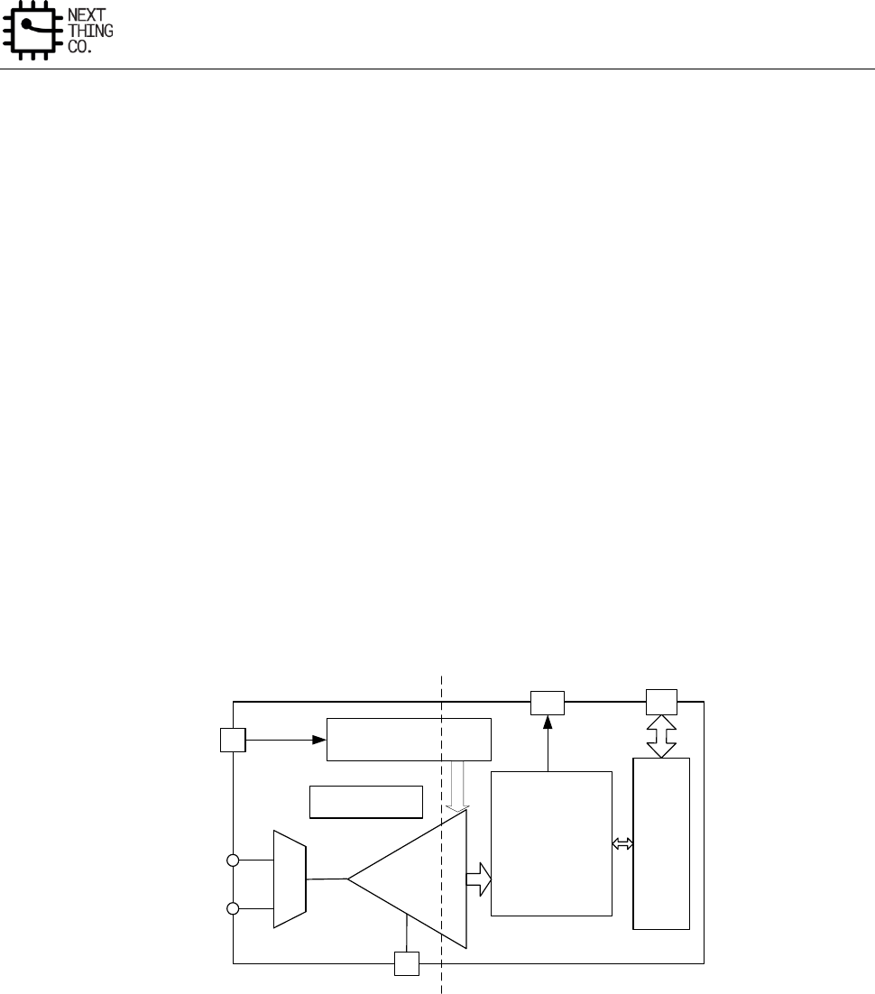
System
GR8 User Manual(Version1.0) Copyright © 2017 Next Thing Co. All Rights Reserved. Page 175
3.12. LRADC
3.12.1. Overview
LRADC is a 6-bit resolution ADC for a 6-key application.
Features:
● Supports APB 32-bit bus width
● Supports interrupt
● Supports general key, hold key and already hold key
● Supports normal, single and continue work mode
● 6-bit resolution
● Voltage input range between 0 to 0.667*AVCC
● Sample rate up to 250Hz
3.12.2. Block Diagram
The block diagram of LRADC is shown in Figure 3-5.
ADC
LRADC0
LRADC1
Analog Control
Digital Logic
Process
Clock Div
IRQ
Register
APB
m
u
x
32K
Vrf
Figure 3-5. LRADC Block Diagram
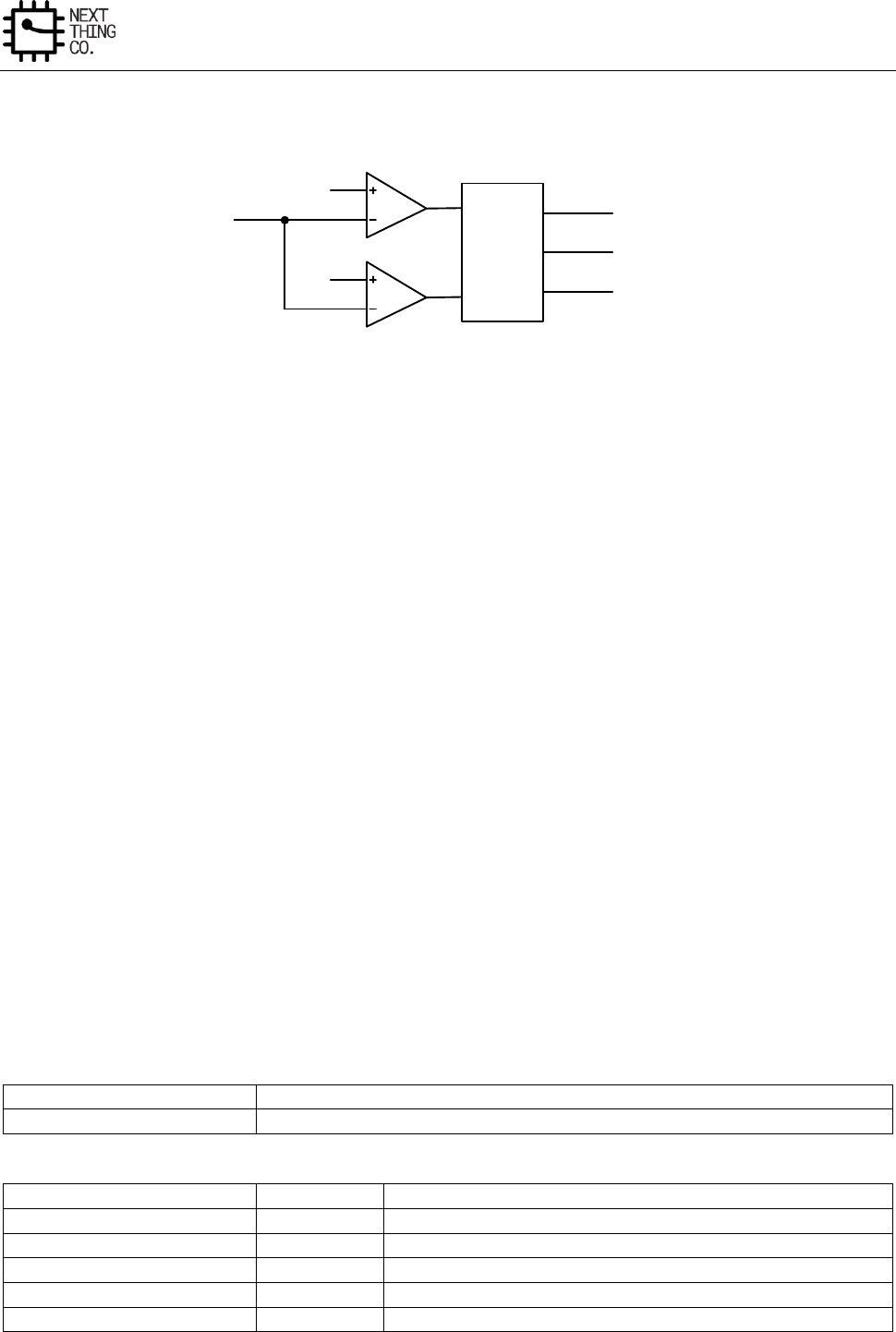
System
GR8 User Manual(Version1.0) Copyright © 2017 Next Thing Co. All Rights Reserved. Page 176
3.12.3. LRADC Control Logic
Level A
Level B
ADC_IN
Control
Logic
KEY_DOWN_IRQ
HOLD_KEY_IRQ
ALREADY_HOLD_IRQ
Figure 3-6. LRADC Control Logic Diagram
Level A: 0.667*AVCC
Level B: Configurable by LEVELB_VOL
When the ADC_IN signal is less than Level A and Level B, the key down interrupt will be generated. When ADC_IN
signal is only less than Level A, the hold key interrupt will generate. When the ADC_IN signal is only less than Level
B, the already hold key interrupt will be generated.
If the ADC_IN signal is less than Level A, and in a certain time range (configurable by LEVELA_B_CNT) ADC_IN signal
is not less than Level B, the hold key interrupt will be generated. If the ADC_IN signal is less than Level A , and in a
certain time range (configurable by LEVELA_B_CNT) ADC_IN signal is less than Level B, the key down interrupt will
be generated. If the ADC_IN signal is less than Level B, and ADC_IN signal is not less than Level A, the already hold
key interrupt will be generated.
The LRADC has three modes: Normal Mode, Single Mode and Continue Mode. Normal Mode means the LRADC
will report the converted result data all the time when the key is down. Single Mode is when the LRADC will only
report the first converted result data when the key is down. Continue Mode is when the LRADC will report the
converted result data every other 8*(N+1) sample when the key is down.
The LRADC supports four sample rates: 250 Hz, 125 Hz, 62.5 Hz, and 31.25 Hz. You can configure the value of
LRADC_SAMPLE_RATE to select the desired sample rate.
3.12.4. LRADC Register List
Module Name
Base Address
LRADC
0x01C22800
Register Name
Offset
Description
LRADC_CTRL
0x0000
LRADC Control Register
LRADC_INTC
0x0004
LRADC Interrupt Control Register
LRADC_INTS
0x0008
LRADC Interrupt Status Register
LRADC_DATA0
0x000C
LRADC Data Register 0
LRADC_DATA1
0x0010
LRADC Data Register 1

System
GR8 User Manual(Version1.0) Copyright © 2017 Next Thing Co. All Rights Reserved. Page 177
3.12.5. LRADC Register Description
3.12.5.1. LRADC Control Register(Default Value: 0x0100_0168)
Offset: 0x0000
Register Name: LRADC_CTRL
Bit
Read/Write
Default/Hex
Description
31: 24
R/W
0x1
FIRST_CONCERT_DLY.
ADC First Convert Delay setting, ADC conversion is delayed by n
samples
23:22
R/W
0x0
ADC_CHAN_SELECT.
ADC Channel Select
00: ADC0 channel
01: ADC1 channel
1x: ADC0&ADC1 channel
21:20
/
/
/
19:16
R/W
0x0
CONTINUE_TIME_SELECT.
Continue Mode time select, one of 8*(N+1) sample as a valuable
sample data
15:14
/
/
/
13:12
R/W
0x0
LRADC_MODE_SELECT.
LRADC Mode Select
00: Normal Mode
01: Single Mode
10: Continue Mode
11:8
R/W
0x1
LEVELA_B_CNT.
Level A to Level B time threshold select, judge ADC convert value in
level A to level B in n+1 samples
7
/
/
/
6
R/W
0x1
LRADC_HOLD_EN.
LRADC Sample Hold Enable
0: Disable
1: Enable
5:4
R/W
0x2
LEVELB_VOL.

System
GR8 User Manual(Version1.0) Copyright © 2017 Next Thing Co. All Rights Reserved. Page 178
Level B Corresponding Data Value Setting
00: 0x3C
01: 0x39
10: 0x36
11: 0x33
Note: Voltage value = Data value/63 *(0.667*AVCC)
If data value is 0x3C, voltage value is about 1.9V.
3: 2
R/W
0x2
LRADC_SAMPLE_RATE.
LRADC Sample Rate
00: 250 Hz
01: 125 Hz
10: 62.5 Hz
11: 31.25 Hz
1
/
/
/
0
R/W
0x0
LRADC_EN.
LRADC Enable
0: Disable
1: Enable
3.12.5.2. LRADC Interrupt Control Register(Default Value: 0x0000_0000)
Offset: 0x0004
Register Name: LRADC_INTC
Bit
Read/Write
Default/Hex
Description
31:16
/
/
/
12
R/W
0x0
ADC1_KEYUP_IRQ_EN.
ADC 1 Key Up IRQ Enable
0: Disable
1: Enable
11
R/W
0x0
ADC1_ALRDY_HOLD_IRQ_EN.
ADC 1 Already Hold Key IRQ Enable

System
GR8 User Manual(Version1.0) Copyright © 2017 Next Thing Co. All Rights Reserved. Page 179
0: Disable
1: Enable
10
R/W
0x0
ADC1_HOLD_IRQ_EN.
ADC 1 Hold Key IRQ Enable
0: Disable
1: Enable
9
R/W
0x0
ADC1_KEYIRQ_EN.
ADC 1 Key IRQ Enable
0: Disable
1: Enable
8
R/W
0x0
ADC1_DATA_IRQ_EN.
ADC 1 DATA IRQ Enable
0: Disable
1: Enable
7:5
/
/
/
4
R/W
0x0
ADC0_KEYUP_IRQ_EN.
ADC 0 Key Up IRQ Enable
0: Disable
1: Enable
3
R/W
0x0
ADC0_ALRDY_HOLD_IRQ_EN.
ADC 0 Already Hold IRQ Enable
0: Disable
1: Enable
2
R/W
0x0
ADC0_HOLD_IRQ_EN.
ADC 0 Hold Key IRQ Enable
0: Disable
1: Enable
1
R/W
0x0
ADC0_KEYDOWN_EN
ADC 0 Key Down Enable

System
GR8 User Manual(Version1.0) Copyright © 2017 Next Thing Co. All Rights Reserved. Page 180
0: Disable
1: Enable
0
R/W
0x0
ADC0_DATA_IRQ_EN.
ADC 0 Data IRQ Enable
0: Disable
1: Enable
3.12.5.3. LRADC Interrupt Status Register(Default Value: 0x0000_0000)
Offset: 0x0008
Register Name: LRADC_INT
Bit
Read/Write
Default/Hex
Description
31:13
/
/
/
12
R/W
0x0
ADC1_KEYUP_PENDING.
ADC 1 Key up Pending Bit
When General key pull up, it the corresponding interrupt is enabled.
0: No IRQ
1: IRQ Pending
Note: Writing 1 to the bit will clear it and its corresponding interrupt
if the interrupt is enabled
11
R/W
0x0
ADC1_ALRDY_HOLD_PENDING.
ADC 1 Already Hold Pending Bit
When Hold key pull down and pull the General key down, if the
corresponding interrupt is enabled.
0: No IRQ
1: IRQ Pending
Note: Writing 1 to the bit will clear it and its corresponding interrupt
if the interrupt is enabled
10
R/W
0x0
ADC1_HOLDKEY_PENDING.
ADC 1 Hold Key Pending Bit
When Hold, key pull down, the status bit is set and the interrupt line
is set if the corresponding interrupt is enabled.

System
GR8 User Manual(Version1.0) Copyright © 2017 Next Thing Co. All Rights Reserved. Page 181
0: NO IRQ
1: IRQ Pending
Note: Writing 1 to the bit will clear it and its corresponding interrupt
if the interrupt is enabled.
9
R/W
0x0
ADC1_KEYDOWN_IRQ_PENDING.
ADC 1 Key Down IRQ Pending Bit
When General key pull down, the status bit is set and the interrupt line
is set if the corresponding interrupt is enabled.
0: No IRQ
1: IRQ Pending
Note: Writing 1 to the bit will clear it and its corresponding interrupt
if the interrupt is enabled.
8
R/W
0x0
ADC1_DATA_IRQ_PENDING.
ADC 1 Data IRQ Pending Bit
0: No IRQ
1: IRQ Pending
Note: Writing 1 to the bit will clear it and its corresponding interrupt
if the interrupt is enabled
7:5
/
/
/
4
R/W
0x0
ADC0_KEYUP_PENDING.
ADC 0 Key up Pending Bit
When general key pull up, it the corresponding interrupt is enabled.
0: No IRQ
1: IRQ Pending
Note: Writing 1 to the bit will clear it and its corresponding interrupt
if the interrupt is enabled.
3
R/W
0x0
ADC0_ALRDY_HOLD_PENDING.
ADC 0 Already Hold Pending Bit
When Hold key pull down and pull the General key down, if the

System
GR8 User Manual(Version1.0) Copyright © 2017 Next Thing Co. All Rights Reserved. Page 182
corresponding interrupt is enabled.
0: No IRQ
1: IRQ Pending
Note: Writing 1 to the bit will clear it and its corresponding interrupt
if the interrupt is enabled.
2
R/W
0x0
ADC0_HOLDKEY_PENDING.
ADC 0 Hold Key Pending Bit
When Hold key pull down, the status bit is set and the interrupt line is
set if the corresponding interrupt is enabled.
0: NO IRQ
1: IRQ Pending
Note: Writing 1 to the bit will clear it and its corresponding interrupt
if the interrupt is enabled.
1
R/W
0x0
ADC0_KEYDOWN_PENDING.
ADC 0 Key Down IRQ Pending Bit
When General key pull down, the status bit is set and the interrupt line
is set if the corresponding interrupt is enabled.
0: No IRQ
1: IRQ Pending
Note: Writing 1 to the bit will clear it and its corresponding interrupt
if the interrupt is enabled.
0
R/W
0x0
ADC0_DATA_PENDING.
ADC 0 Data IRQ Pending Bit
0: No IRQ
1: IRQ Pending
Note: Writing 1 to the bit will clear it and its corresponding interrupt
if the interrupt is enabled.
System
GR8 User Manual(Version1.0) Copyright © 2017 Next Thing Co. All Rights Reserved. Page 183
3.12.5.4. LRADC Data 0 Register(Default Value: 0x0000_0000)
Offset: 0x000C
Register Name: LRADC_DATA0
Bit
Read/Write
Default/Hex
Description
31:6
/
/
/
5:0
R
0x0
LRADC0_DATA.
LRADC 0 Data
3.12.5.5. LRADC Data 1 Register(Default Value: 0x0000_0000)
Offset: 0x0010
Register Name: LRADC_DATA1
Bit
Read/Write
Default/Hex
Description
31:6
/
/
/
5:0
R
0x0
LRADC1_DATA.
LRADC 1 Data
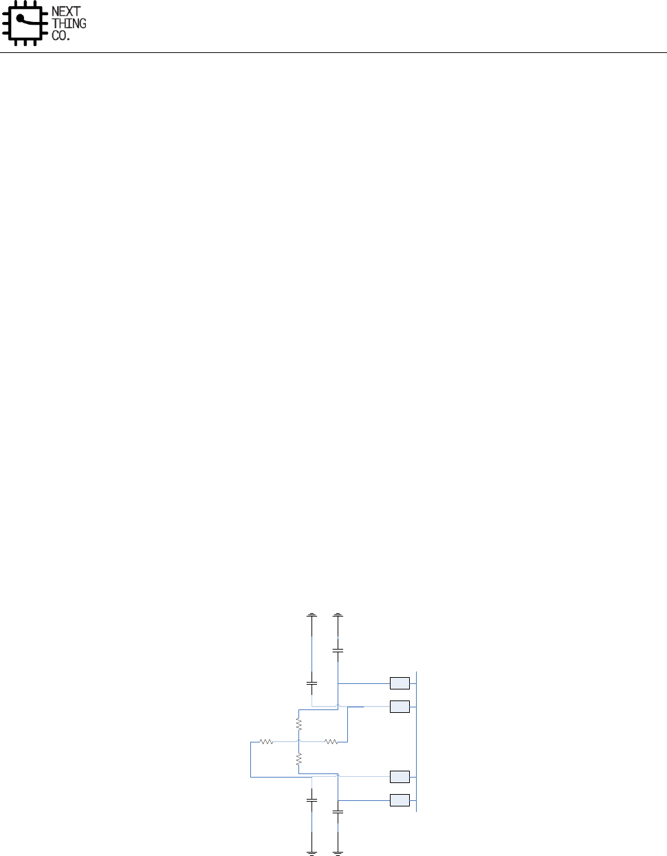
System
GR8 User Manual(Version1.0) Copyright © 2017 Next Thing Co. All Rights Reserved. Page 184
3.13. Touch Panel
3.13.1. Overview
The controller is a 4-wire resistive touch screen controller, it includes a 12-bit resolution A/D converter. The
controller, through the implementation of the two A/D conversion, can identify the location of a single touch and
detect an increase in pressure on the touch screen.
Features:
● 12-bit SAR type A/D converter
● 4-wire I/F
● Touch-pressure measurement
● Maximum sampling frequency: 2 MHz
● Single-ended conversion of touch screen inputs and ratiometric conversion of touch screen inputs
● TACQ up to 262ms
● Median and averaging filter to reduce noise
● Pen down detection, with programmable sensitivity
● Supports X, Y change
3.13.2. Typical Application Circuit
X-
X+
Y+
Y-
Figure 3-7. TP Typical Application Circuit
System
GR8 User Manual(Version1.0) Copyright © 2017 Next Thing Co. All Rights Reserved. Page 185
3.13.3. Clock Tree and ADC Time
3.13.3.1. Clock Tree
HOSC24M
AUDIO PLL
CLK_IN
PRESCALER
00:/2
01:/3
10:/6
11:/1
Figure 3-8. TP Clock Tree
3.13.3.2. A/D Conversion Time
When the clock source is 24 MHz and the prescaler value is 6, total 12-bit conversion time is:
CLK_IN = 24MHz/6 = 4MHz
Conversion Time = 1/(4MHz/13Cycles) = 3.25us
Touch acquire time divider is 16
TACQ = 16*16*1/4us = 64us
FS_TIME is based on TACQ and Touch Mode:
FS_TIME >= M*(TACQ + Conversion Time)
Y1-DATA
FS_TIME
Conversion Time
X1-DATA
TACQ
Z1-DATA Z2-DATA
Figure 3-9. Single Touch and Pressure Measurement
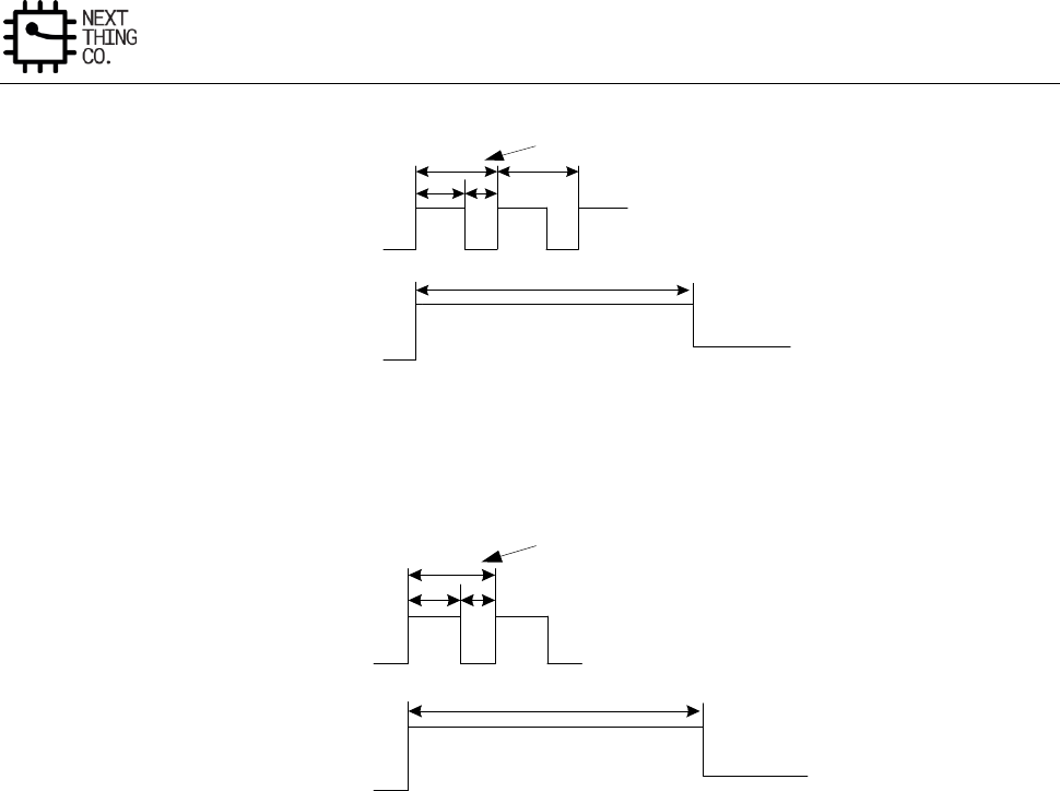
System
GR8 User Manual(Version1.0) Copyright © 2017 Next Thing Co. All Rights Reserved. Page 186
FS_TIME
X1-DATA Y1-DATA
Conversion Time
TACQ
Figure 3-10. Single Touch No Pressure Measurement Mode
FS_TIME
ADC-DATA
Conversion Time
TACQ
Figure 3-11. General ADC Mode
3.13.4. Principle of Operation
3.13.4.1. The Basic Principle
The controller is a typical type of successive approximation ADC (SAR ADC), it contains a sample/hold, analog-to-
digital conversion, and serial data output functions. The analog inputs (X+, X-, Y+, Y-) via control register enter the
ADC, ADC can be configured as single-ended or differential mode. Selecting Aux ADC or temperature should be
configured for single-ended mode; as a touch screen application, it should be configured as a differential mode,
which can effectively eliminate the parasitic resistance of the driver switch and external interference caused by
measurement error and impact conversion accuracy.
3.13.4.2. Single-ended Mode
When the Bit12(ADC Mode Select) of TP Control Register 0 is high, the controller is in the measurement mode of
AUX, Temp, the internal ADC reference voltage source is the single-ended mode, using the AVCC reference source
as the ADC reference voltage, application of the principle of single-ended mode is shown in Figure 3-12.
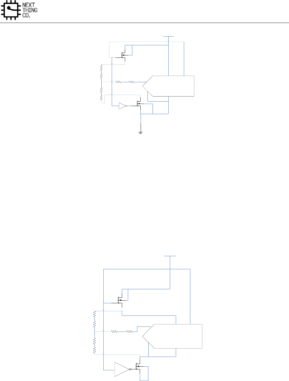
System
GR8 User Manual(Version1.0) Copyright © 2017 Next Thing Co. All Rights Reserved. Page 187
+IN
-IN
Converter
+REF
-REF
AVCC/REF
Figure 3-12. Simplified Diagram of Single-Ended Reference
3.13.4.3. Differential Mode
When the Bit12(ADC Mode Select) of TP Control Register 0 is low, the controller is in the measurement mode of
X,Y,Z, the internal ADC reference voltage source is the differential mode, is shown in Figure 3-13. The advantage of
differential mode: +REF and –REF input directly to the Y+, Y-, which can eliminate measurement error because of
the switch on-resistance. The disadvantage is that: both the ample or conversion process, the driver needs to be
on, relative to single-ended mode, the power consumption increases.
+IN
-IN
Converter
+REF
-REF
AVCC/REF
Figure 3-13. Simplified Diagram of Differential Reference
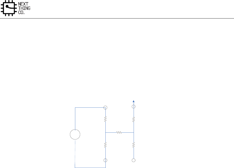
System
GR8 User Manual(Version1.0) Copyright © 2017 Next Thing Co. All Rights Reserved. Page 188
3.13.4.4. Single Touch Detection
The principle of operation is illustrated below, For an X co-ordinate measurement, the X+ pin is internally switched
to AVCC and X- to GND. The X plate becomes a potential divider, and the voltage at the point of contact is
proportional to its X co-ordinate. This voltage is measured on the Y+, which carry no current (hence there is no
voltage drop in RY+ or RY-). Due to the ratiometric measurement method, the supply voltage does not affect
measurement accuracy. The voltage references VREF+ and VREF- are taken from after the matrix switches, so that
any voltage drop in these switches has no effect on the ADC measurement. Y co-ordinate measurements are similar
to X co-ordinate measurements, with the X and Y plates interchanged. In Single Touch mode, only need to test X+,
Y+ signal.
X+
X-
MEASURE
X-POSITION
X-POSITION
TOUCH
Figure 3-14. Single Touch X-Position Measurement
3.13.4.5. Touch-Pressure Measurement
The pressure applied to the touch screen by a pen or finger to filter unavailable can also be measurement with the
controller using some simple calculations. The contact resistance between the X and Y plates is measured,
providing a good indication of the size of the depressed area and, therefore, the applied pressure. The area of the
spot that is touched is proportional to the size of the object touching it. The size of this resistance (Rtouch) can be
calculated using two different methods.
First Method:
The first method requires the user to know the total resistance of the X-plate tablet (RX). Three touch screen
conversions are required: measurement of the X position, XPOSITION (Y+ input); measurement of the X+ input
with the excitation voltage applied to Y+ and X− (Z1 measurement); and measurement of the Y− input with the
excitation voltage applied to Y+ and X− (Z2 measurement). These three measurements are illustrated in Figure 3-
15. The controller has two special ADC channel settings that configure the X and Y switches for the Z1 and Z2
measurements and store the results in the Z1 and Z2 result registers. The touch resistance (RTOUCH) can then be
calculated using the following equation:
RTOUCH = (RXPLATE) × (XPOSITION /4096) × [(Z2/Z1) − 1] (1)
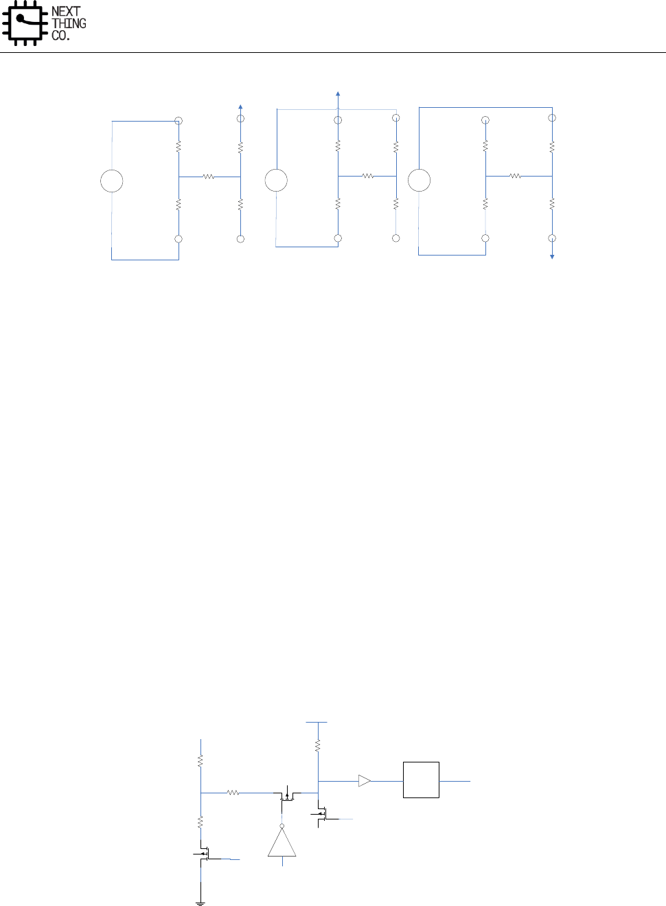
System
GR8 User Manual(Version1.0) Copyright © 2017 Next Thing Co. All Rights Reserved. Page 189
X+
X- Y-
Y+
TOUCH TOUCH
X+
X-
Y+
Y-
X-POSITION Z1-POSITION Z2-POSITION
MEASURE
X-POSITION MEASURE
Z1-POSITION
X+
X- MEASURE
Z2-POSITION
Y+
Y-
Figure 3-15. Pressure Measurement Block Diagram
Second Method:
The second method requires the user to know the resistance of the X-plate and Y-plate tablets. Three touch screen
conversions are required: a measurement of the X position (XPOSITION), the Y position (YPOSITION), and the Z1 position.
The following equation also calculates the touch resistance (RTOUCH):
RTOUCH = RXPLATE × (XPOSITION/4096) × [(4096/Z1) − 1] − RYPLATE × [1 − (YPOSITION/4096)] (2)
3.13.4.6. Pen Down Detection
Pen down detection is used as an interrupt to the host. RIRQ is an internal pull-up resistor with a programmable
value of 6~96 kΩ (default 48kΩ). The PENIRQ output is pulled high by an internal pull-up. the Y– driver is on and
connected to GND, and the PENIRQ output is connected to the X+ input. When the panel is touched, the X+ input
is pulled to ground through the touch screen, and the PENIRQ output goes low because of the current path through
the panel to GND, initiating an interrupt to the processor. During the measurement cycle for X-, Y-, and Z-position,
the X+ input is disconnected from the PENIRQ pull-down transistor to eliminate any pull-up resistor leakage
current from flowing through the touch screen, thus causing no errors.
Control
Logic
AVCC
RIRQ
Y+
Y-
X+
ON
High when X+ or Y+ driver
is on
High when X+ or Y+ driver
is on
Figure 3-16. Example of Pen Touch Interrupt via Pen Down IRQ
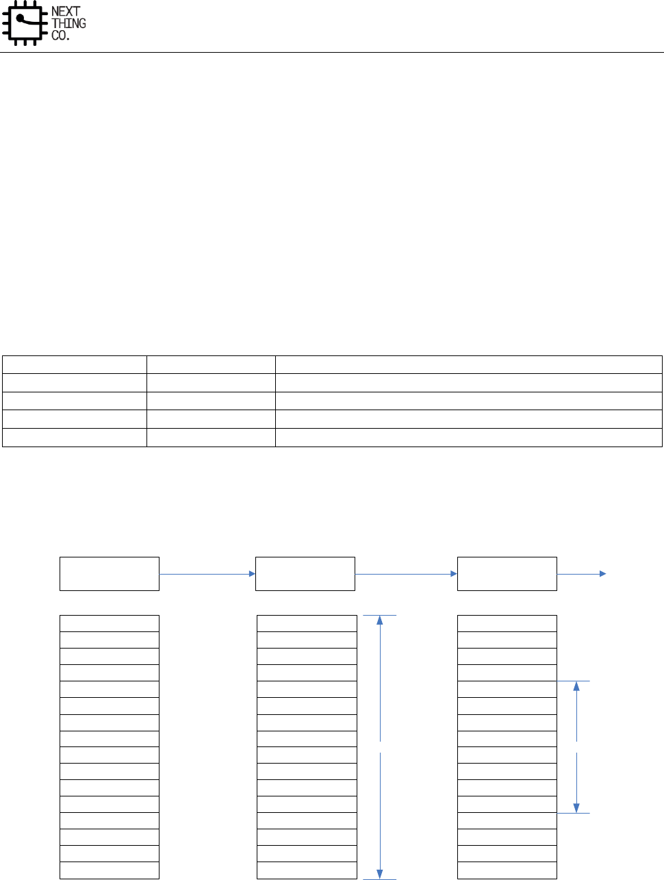
System
GR8 User Manual(Version1.0) Copyright © 2017 Next Thing Co. All Rights Reserved. Page 190
3.13.4.7. Median and Averaging Filter
As explained in the Touch Screen Principles section, touch screens are composed of two resistive layers, normally
placed over an LCD screen. Because these layers are in close proximity to the LCD screen, noise can be coupled
from the screen onto these resistive layers, causing errors in the touch screen positional measurements. The
controller contains a filtering block to process the data and discard the spurious noise before sending the
information to the host. The purpose of this block is not only the suppression of noise; the on-chip filtering also
greatly reduces the host processing loading. The processing function consists of two filters that are applied to the
converted results: the median filter and the averaging filter. The median filter suppresses the isolated out-of-range
noise and sets the number of measurements to be taken. These measurements are arranged in a temporary array,
where the first value is the smallest measurement and the last value is the largest measurement. The bit1 and bit0
(MED1 and MED0) in Median Filter Control Register set the window of the median filter and the number of
measurements taken.
Table 3-1. Median Filter Size
MED1
MED0
Median Filter Size
0
0
4
0
1
5
1
0
8
1
1
16
In this example, MED1=1, MED0=1, the median filter has a window size of 16. This means that 16 measurements
are taken and arranged in descending order in a temporary array. The averaging window size in this example is 8.
The output is the average of the middle eight values of the 16 measurements taken with the median filter.
12-BIT
SAR ADC MEDIAN
FILTER AVERAGING
FILTER
2
3
5
1
6
7
8
9
10
12
11
15
13
4
14
16
1
2
3
4
5
6
8
7
9
10
11
12
13
14
16
15
1
2
3
4
5
6
8
7
9
10
11
12
13
14
16
15
M=16 A=8
Converted Results 16 Measurements
Arranged
Average Of Middle
8 Values
FIFO
Figure 3-17. Median and Averaging Filter Example
System
GR8 User Manual(Version1.0) Copyright © 2017 Next Thing Co. All Rights Reserved. Page 191
3.13.5. TP Register List
Module Name
Base Address
TP
0x01C25000
Register Name
Offset
Description
TP_CTRL0
0x0000
TP Control Register0
TP_CTRL1
0x0004
TP Control Register1
TP_CTRL2
0x0008
TP Pressure Measurement and Touch Sensitive Control Register
TP_MFCR
0x000C
Median Filter Controller Register
TP_INT_FIFOC
0x0010
TP Interrupt FIFO Control Register
TP_INT_FIFOS
0x0014
TP Interrupt FIFO Status Register
TP_CDAT
0x001C
TP Common Data Register
TP_DATA
0x0024
TP Data Register
TP_IO_CONFIG
0x0028
TP PORT IO Configure Register
TP_PORT_DATA
0x002C
TP Port Data Register
3.13.6. TP Register Description
3.13.6.1. TP Control Register 0(Default Value: 0x0F80_0000)
Offset: 0x0000
Register Name: TP_CTRL0
Bit
Read/Write
Default /Hex
Description
31:24
R/W
0xF
ADC_FIRST_DLY.
ADC First Convert Delay Setting
Based on ADC First Convert Delay Mode select
23
R/W
0x1
ADC_FIRST_DLY_MODE.
ADC First Convert Delay Mode Select
0: CLK_IN/16
1: CLK_IN/16*256
22
R/W
0x0
ADC_CLK_SELECT.
ADC Clock Source Select
0: HOSC(24 MHz)
1: Audio PLL

System
GR8 User Manual(Version1.0) Copyright © 2017 Next Thing Co. All Rights Reserved. Page 192
21:20
R/W
0x0
ADC_CLK_DIVIDER.
ADC Clock Divider(CLK_IN)
00: CLK/2
01: CLK/3
10: CLK/6
11: CLK/1
In TP mode, these two bits must set 1x
19:16
R/W
0x0
FS_DIV.
ADC Sample Frequency Divider
0000: CLK_IN/2(20-n)
0001: CLK_IN/2(20-n)
0010: CLK_IN/2(20-n)
….
1111: CLK_IN/32
15:0
R/W
0x0
T_ACQ.
Touch Panel ADC Acquire Time
CLK_IN/(16*N)
3.13.6.2. TP Control Register 1(Default Value: 0x0000_0008)
Offset: 0x0004
Register Name: TP_CTRL1
Bit
Read/Write
Default /Hex
Description
31:20
/
/
/
19:12
R/W
0x0
STYLUS_UP_DEBOUNCE.
Stylus Up De-bounce Time Setting
0x00: 0
….
0xff: 2N*(CLK_IN/16*256)
11:10
/
/
/
9
R/W
0x0
STYLUS_UP_DEBOUCE_EN.
Stylus Up Debounce Function Select

System
GR8 User Manual(Version1.0) Copyright © 2017 Next Thing Co. All Rights Reserved. Page 193
0: Disable
1: Enable
8:7
/
/
/
6
R/W
0x0
TOUCH_PAN_CALI_EN.
Touch Panel Calibration
1: start Calibration, it is cleared to 0 after calibration
5
R/W
0x0
TP_DUAL_EN.
Touch Panel Double Point Enable
0: Disable
1: Enable
4
R/W
0x0
TP_MODE_EN.
TP Mode Function Enable
0: Disable
1: Enable
3
R/W
0x1
TP_ADC_SELECT.
Touch Panel and ADC Select
0: TP
1: ADC
2:0
R/W
0x0
ADC_CHAN_SELECT.
Analog Input Channel Select in Normal mode
000: X1 channel
001: X2 Channel
010: Y1 Channel
011: Y2 Channel
1xx : 4-channel robin-round
FIFO Access Mode, based on this setting. Selecting one channel, FIFO
will access that channel data; Selecting four channels FIFO will access
each channel data in successive turn, first is X1 data.

System
GR8 User Manual(Version1.0) Copyright © 2017 Next Thing Co. All Rights Reserved. Page 194
3.13.6.3. TP Control Register 2(Default Value: 0x8000_0FFF)
Offset: 0x0008
Register Name: TP_CTRL2
Bit
Read/Write
Default/Hex
Description
31:28
R/W
0x8
TP_SENSITIVE_ADJUST.
Internal Pull-up Resistor Control
0000: least sensitive
0011
……
1111: most sensitive
Note: Used to adjust sensitivity of pen down detection
27:26
R/W
0x0
TP_MODE_SELECT.
TP Mode Select
00: FIFO store X,Y data with Z-filter
01: FIFO store X,Y, △X, △Y data with Z-filter
10: FIFO store X,Y, X2,Y2 data with Z-filter
11: Debug Mode, FIFO store X1,Y1, X2,Y2,Z1,Z2 data
25
/
/
/
24
R/W
0x0
PRE_MEA_EN.
TP Pressure Measurement Enable Control
0: Disable
1: Enable
23:0
R/W
0xFFF
PRE_MEA_THRE_CNT.
TP Pressure Measurement threshold Control
0x000000: least sensitive
0xFFFFFF: most sensitive
Note: Used to adjust sensitivity of touch
3.13.6.4. Median Filter Control Register(Default Value: 0x0000_0001)
Offset: 0x000C
Register Name: TP_MFCR

System
GR8 User Manual(Version1.0) Copyright © 2017 Next Thing Co. All Rights Reserved. Page 195
Bit
Read/Write
Default/Hex
Description
31:3
/
/
/
2
R/W
0x0
FILTER_EN.
Filter Enable
0: Disable
1: Enable
1:0
R/W
0x1
FILTER_TYPE.
Filter Type
00: 4/2
01: 5/3
10: 8/4
11: 16/8
3.13.6.5. TP Interrupt& FIFO Control Register(Default Value: 0x0000_0F00)
Offset: 0x0010
Register Name: TP_INT
Bit
Read/Write
Default/Hex
Description
31:19
/
/
18
R/W
0x0
/
17
R/W
0x0
TP_OVERRUN_IRQ_EN.
TP FIFO Over Run IRQ Enable
0: Disable
1: Enable
16
R/W
0x0
TP_DATA_IRQ_EN.
TP FIFO Data Available IRQ Enable
0: Disable
1: Enable
15:14
/
/
/
13
R/W
0x0
TP_DATA_XY_CHANGE.
TP FIFO X,Y Data interchange Function Select
0: Disable

System
GR8 User Manual(Version1.0) Copyright © 2017 Next Thing Co. All Rights Reserved. Page 196
1: Enable
12:8
R/W
0xF
TP_FIFO_TRIG_LEVEL.
TP FIFO Data Available Trigger Level
Interrupt and DMA request trigger level for TP or Auxiliary ADC
Trigger Level = TXTL + 1
7
R/W
0x0
TP_DATA_DRQ_EN.
TP FIFO Data Available DRQ Enable
0: Disable
1: Enable
6:5
/
/
/
4
R/W
0x0
TP_FIFO_FLUSH.
TP FIFO Flush
Write ‘1’ to flush TX FIFO, self clear to ‘0’
3:2
/
/
/
1
R/W
0x0
TP_UP_IRQ_EN.
Touch Panel Last Touch (Stylus Up) IRQ Enable
0: Disable
1: Enable
0
R/W
0x0
TP_DOWN_IRQ_EN.
Touch Panel First Touch (Stylus Down) IRQ Enable
0: Disable
1: Enable
3.13.6.6. TP Interrupt& FIFO Status Register(Default Value: 0x0000_0000)
Offset: 0x0014
Register Name: TP_FIFOCS
Bit
Read/Write
Default/Hex
Description
31:19
/
/
/
18
R/W
0x0
/
17
R/W
0x0
FIFO_OVERRUN_PENDING.
TP FIFO Over Run IRQ Pending
0: No Pending IRQ

System
GR8 User Manual(Version1.0) Copyright © 2017 Next Thing Co. All Rights Reserved. Page 197
1: FIFO Overrun Pending IRQ
Write ‘1’ to clear this interrupt or automatically clear if interrupt
condition fails.
16
R/W
0x0
FIFO_DATA_PENDING.
TP FIFO Data Available Pending Bit
0: NO Pending IRQ
1: FIFO Available Pending IRQ
Write ‘1’ to clear this interrupt or automatically clear if interrupt
condition fails.
15:13
/
/
/
12:8
R
0x0
RXA_CNT.
TP FIFO Available Sample Word Counter
7:3
/
/
/
2
R
0x0
TP_IDLE_FLG.
Touch Panel Idle Flag
0: Idle
1: Not idle
1
R/W
0x0
TP_UP_PENDING.
Touch Panel Last Touch (Stylus Up) IRQ Pending bit
0: No IRQ
1: IRQ
Note: Writing 1 to the bit will clear it and its corresponding interrupt
if the interrupt is enabled.
0
R/W
0x0
TP_DOWN_PENDING.
Touch Panel First Touch (Stylus Down) IRQ Pending bit
0: No IRQ
1: IRQ
Note: Writing 1 to the bit will clear it and its corresponding interrupt
System
GR8 User Manual(Version1.0) Copyright © 2017 Next Thing Co. All Rights Reserved. Page 198
if the interrupt is enabled.
3.13.6.7. Common Data Register(Default Value: 0x0000_0000)
Offset: 0x001C
Register Name: TP_CDAT
Bit
Read/Write
Default/Hex
Description
31:12
/
/
/
11:0
R/W
0x0
TP_CDAT.
TP Common Data
3.13.6.8. TP Data Register(Default Value: 0x0000_0000)
Offset: 0x0024
Register Name: TP_DATA
Bit
Read/Write
Default/Hex
Description
31:12
/
/
/
11:0
R
0x0
TP_DATA
Touch Panel X,Y data or Auxiliary analog input data
3.13.6.9. TP Port IO Configure Register(Default Value: 0x0000_2222)
Offset: 0x0028
Register Name: TP_IO_CONFIG
Bit
Read/Write
Default/Hex
Description
31:15
/
/
/
14:12
R/W
0x2
TY_N_SELECT
TY_N Port Function Select
000:Input 001:Output
010: TP_YN 011:/
100: / 101:/
110: / 111:/
11
/
/
/
10:8
R/W
0x2
TY_P_SELECT
TY_P Port Function Select
000:Input 001:Output
010: TP_YP 011:/
100: / 101:/
110: / 111:/
System
GR8 User Manual(Version1.0) Copyright © 2017 Next Thing Co. All Rights Reserved. Page 199
7
/
/
/
6:4
R/W
0x2
TX_N_SELECT
TX_P Port Function Select
000:Input 001:Output
010: TP_XP 011:/
100: / 101:/
110: / 111:/
3
/
/
/
2:0
R/W
0x2
TX_P_SELECT
TX_P Port Function Select
000:Input 001:Output
010: TP_XP 011:/
100: / 101:/
110: / 111:/
3.13.6.10. TP Port Data Register(Default Value: 0x0000_0000)
Offset: 0x002C
Register Name: TP_PORT_DATA
Bit
Read/Write
Default/Hex
Description
31:12
/
/
/
3:0
R/W
0x0
TP_PORT_DATA
TP Port Data Value,TP_XP,TP_XN,TP_YP,TP_YN
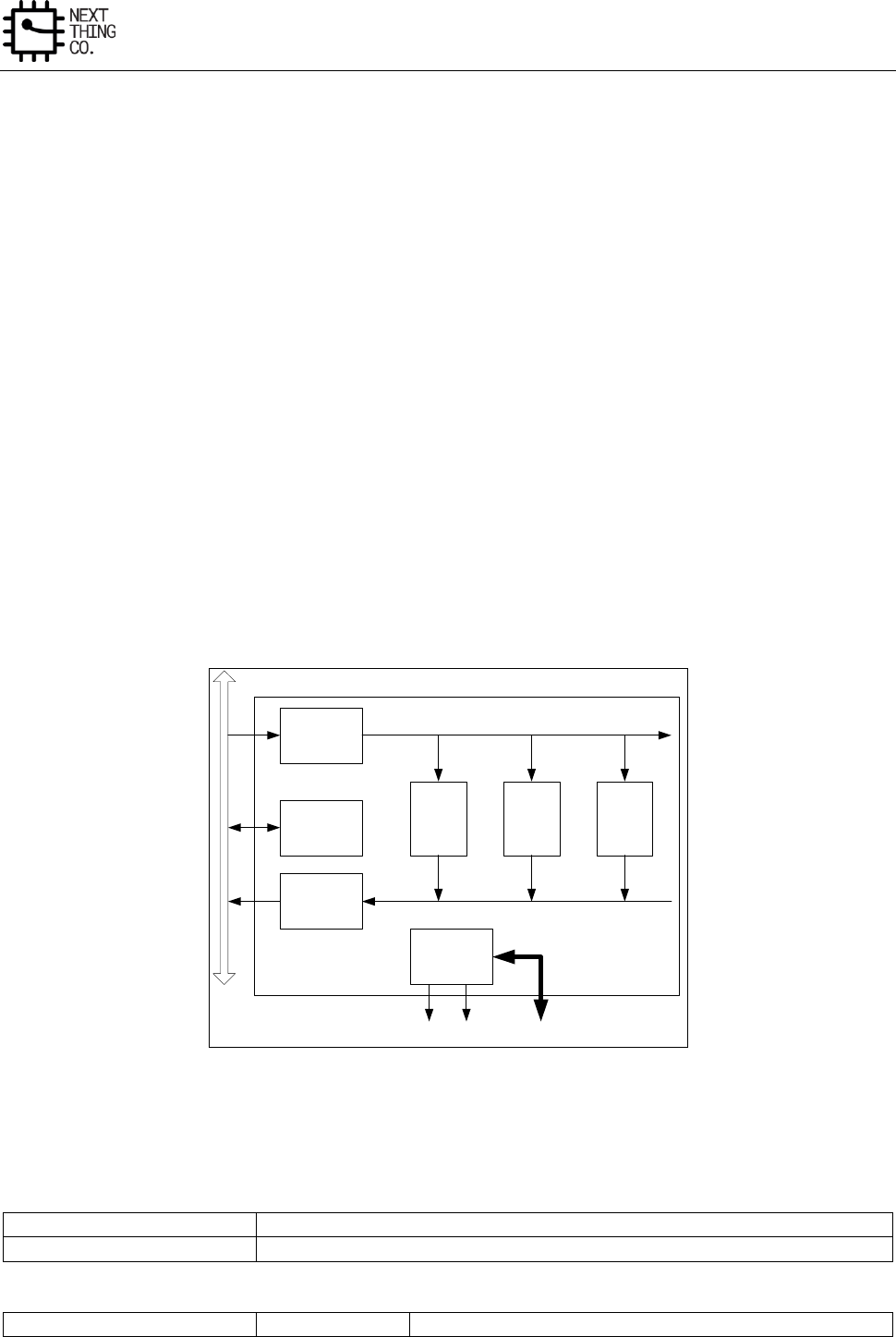
System
GR8 User Manual(Version1.0) Copyright © 2017 Next Thing Co. All Rights Reserved. Page 200
3.14. Crypto Engine
3.14.1. Overview
The Crypto Engine is one encrypt/ decrypt function accelerator suitable for a variety of applications. It supports
both encryption and decryption and several modes. Besides, both CPU mode and DMA method are supported for
different applications.
Features:
● Supports AES, DES, 3DES, SHA-1, MD5
● Supports ECB, CBC modes for AES/DES/3DES
● 128-bit, 192-bit and 256-bit key size for AES
● 160-bit hardware PRNG with 175-bit seed
● Supports 32 words RX FIFO and 32 words TX FIFO for high speed application
● Supports CPU mode and DMA mode
3.14.2. Crypto Engine Block Diagram
32-words
RX FIFO
32-words
TX FIFO
AES DES/
3DES
SHA-1/
MD5/
PRNG
Register
File
Interrupt &
DMA
RX FIFO
DRQ TX FIFO
DRQ
AHB
Bus
D-DMA
Figure 3-18. Crypto Engine Block Diagram
3.14.3. Crypto Engine Register List
Module Name
Base Address
Crypto Engine
0x01C15000
Register Name
Offset
Description
System
GR8 User Manual(Version1.0) Copyright © 2017 Next Thing Co. All Rights Reserved. Page 201
CE_CTL
0x0000
Control Register
CE_KEY0
0x0004
Input Key 0/ PRNG Seed 0
CE_KEY1
0x0008
Input Key 1/ PRNG Seed 1
…
…
…
CE_KEY7
0x0020
Input Key 7
CE_IV0
0x0024
Initialization Vector 0
CE_IV1
0x0028
Initialization Vector 1
…
…
…
CE_IV7
0x0040
Initialization Vector 7
CE_FCSR
0x0044
FIFO Control/ Status Register
CE_ICSR
0x0048
Interrupt Control/ Status Register
CE_MD0
0x004C
SHA1/MD5 Message Digest 0/PRNG Data0
CE_MD1
0x0050
SHA1/MD5 Message Digest 1/PRNG Data1
CE_MD2
0x0054
SHA1/MD5 Message Digest 2/PRNG Data2
CE_MD3
0x0058
SHA1/MD5 Message Digest 3/PRNG Data3
CE_MD4
0x005C
SHA1/MD5 Message Digest 4/PRNG Data4
CE_RXFIFO
0x0200
RX FIFO input port
CE_TXFIFO
0x0204
TX FIFO output port
3.14.4. Crypto Engine Register Description
3.14.4.1. Crypto Engine Control Register(Default Value: 0x0000_0000)
Offset: 0x0000
Register Name: CE_CTL
Bit
Read/Write
Default/Hex
Description
31:28
/
/
/
27:24
R/W
0x0
AES/DES/3DES key select
0000: Select input CE_KEYx (Normal Mode)
0001: Select SID_RKEYx from Security ID
0011: Reserved
0011~1010: Select internal Key n (n from 0 to 7)
Others: Reserved
18:16
R
UDF
Reserved
15
R/W
0x0
PRNG generator mode
0: One-shot mode
1: Continue mode
14
R/W
0x0
IV Steady of SHA-1/MD5 constants
0: Constants

System
GR8 User Manual(Version1.0) Copyright © 2017 Next Thing Co. All Rights Reserved. Page 202
1: Arbitrary IV
Note: It is only used for SHA-1/MD5 engine. If the number of IV word is
beyond of 4, Counter 0 register is used for IV4.
13:12
R/W
0x0
CE Operation Mode
00: Electronic Code Book (ECB) mode
01: Cipher Block Chaining (CBC) mode
Others: Reserved
11:10
/
/
/
9:8
R/W
0x0
Key Size for AES
00: 128-bit
01: 192-bit
10: 256-bit
11: Reserved
7
R/W
0x0
CE Operation Direction
0: Encryption
1: Decryption
6:4
R/W
0x0
CE Method
000: AES
001: DES
010: Triple DES (3DES)
011: SHA-1
100: MD5
101: PRNG
Others: Reserved
3
/
/
/
2
R/W
0x0
SHA-1/MD5 Data End bit
Write ‘1’ to tell SHA-1/MD5 engine that the text data ends. If there is some
data in FIFO, the engine will fetch these data and process them. After
finishing message digest, this bit is cleared to ‘0’ by hardware and message
digest can be read out from digest registers.
Note: It is only used for SHA-1/MD5 engine.
System
GR8 User Manual(Version1.0) Copyright © 2017 Next Thing Co. All Rights Reserved. Page 203
1
R/W
0x0
PRNG start bit
In PRNG one-shot mode, write ‘1’ to start PRNG. After generating one
group random data (5 words), this bit is cleared to ‘0’ by hardware.
0
R/W
0x0
CE Enable
A disable on this bit overrides any other block and flushes all FIFOs.
0: Disable
1: Enable
3.14.4.2. Crypto Engine Key [n] Register(Default Value: 0x0000_0000)
Offset: 0x0004 +N*0x04
Register Name: CE_KEY[n]
Bit
Read/Write
Default/Hex
Description
31:0
R/W
0x0
Key[n] Input Value (n= 0~7)/PRNG Seed[n] (n= 0~5)
3.14.4.3. Crypto Engine IV[n] Register(Default Value: 0x0000_0000)
Offset: 0x0024 +N*0x08
Register Name: CE_IV[n]
Bit
Read/Write
Default/Hex
Description
31:0
R/W
0x0
Initialization Vector (IV[n]) Input Value (n= 0~7)
3.14.4.4. Crypto Engine FIFO Control/ Status Register(Default Value: 0x6000_0F0F)
Offset: 0x0044
Register Name: CE_FCSR
Bit
Read/Write
Default/Hex
Description
31
/
/
/
30
R
0x1
RX FIFO Empty
0: No room for new word in RX FIFO
1: More than one room for new word in RX FIFO (>= 1 word)
29:24
R
0x20
RX FIFO Empty Space Word Counter
23
/
/
/
22
R
0x0
TX FIFO Data Available Flag
0: No available data in TX FIFO
1: More than one data in TX FIFO (>= 1 word)
21:16
R
0x0
TX FIFO Available Word Counter

System
GR8 User Manual(Version1.0) Copyright © 2017 Next Thing Co. All Rights Reserved. Page 204
15:13
/
/
/
12:8
R/W
0xF
RX FIFO Empty Trigger Level
Interrupt and DMA request trigger level for RXFIFO normal condition
Trigger Level = RXTL + 1
Note: RX FIFO is used for input the data.
7:5
/
/
/
4:0
R/W
0xF
TX FIFO Trigger Level
Interrupt and DMA request trigger level for TXFIFO normal condition
Trigger Level = TXTL + 1
Note: TX FIFO is used to output the result data.
3.14.4.5. Crypto Engine Interrupt Control/Status Register(Default Value: 0x0000_0000)
Offset: 0x0048
Register Name: CE_ICSR
Bit
Read/Write
Default/Hex
Description
31:11
/
/
/
10
R/W
0x0
RX FIFO Empty Pending bit
0: No pending
1: RX FIFO Empty pending
Note: Write ‘1’ to clear or automatically clear if interrupt condition fails.
9
/
/
/
8
R/W
0x0
TX FIFO Data Available Pending bit
0: No TX FIFO pending
1: TX FIFO pending
Note: Write ‘1’ to clear or automatically clear if interrupt condition fails.
7:5
/
/
/
4
R/W
0x0
DRQ Enable
0: Disable DRQ (CPU polling mode)
1: Enable DRQ (DMA mode)
3
/
/
/
2
R/W
0x0
RX FIFO Empty Interrupt Enable
System
GR8 User Manual(Version1.0) Copyright © 2017 Next Thing Co. All Rights Reserved. Page 205
0: Disable
1: Enable
Note: If it is set to ‘1’, when the number of empty room is no smaller than
(>=) the preset threshold, the interrupt is triggered and the correspond flag
is set.
1
/
/
/
0
R/W
0x0
TX FIFO Data Available Interrupt Enable
0: Disable
1: Enable
Note: If it is set to ‘1’, when available data number is no smaller than (>=)
the preset threshold, the interrupt is triggered and the correspond flag is
set.
3.14.4.6. Crypto Engine Message Digest[n] Register(Default Value: 0x0000_0000)
Offset: 0x004C +N*0x04
Register Name: CE_MD[N]
Bit
Read/Write
Default/Hex
Description
31:0
R
0x0
SHA1/MD5 message digest MD[N] for SHA1/MD5 (N= 0~4)
3.14.4.7. Crypto Engine RX FIFO Register(Default Value: 0x0000_0000)
Offset: 0x0200
Register Name: CE_RX
Bit
Read/Write
Default/Hex
Description
31:0
W
0x0
32-bit RX FIFO for Input
3.14.4.8. Crypto Engine TX FIFO Register(Default Value: 0x0000_0000)
Offset: 0x0204
Register Name: CE_TX
Bit
Read/Write
Default/Hex
Description
31:0
R
0x0
32-bit TX FIFO for Output
3.14.5. Crypto Engine Clock Requirement
Clock Name
Description
Requirement
ahb_clk
AHB bus clock
>=24 MHz

System
GR8 User Manual(Version1.0) Copyright © 2017 Next Thing Co. All Rights Reserved. Page 206
ce_clk
CE serial clock
<= 150 MHz

System
GR8 User Manual(Version1.0) Copyright © 2017 Next Thing Co. All Rights Reserved. Page 207
3.15. Security ID
3.15.1. Overview
GR8 supports an 128-bit EFUSE security key which can also be used as root key or for other purposes.
Features:
● 128-bit electrical fuses for root key
System
GR8 User Manual(Version1.0) Copyright © 2017 Next Thing Co. All Rights Reserved. Page 208
3.16. Port Controller
3.16.1. Overview
GR8 has 6 ports for multi-functional input/out pins. They are:
● Port B(PB): 19 input/output port
● Port C(PC): 17 input/output port
● Port D(PD): 22 input/output port
● Port E(PE): 12 input/output port
● Port F(PF): 6 input/output port
● Port G(PG): 14 input/output port
These ports can be easily configured by software for various system configurations.
3.16.2. Port Configuration Table
PIO
Name
Multiplex Function Select
M0
M1
M2
M3
M4
M5
M6
PB0
Input
Output
TWI0-SCK
PB1
Input
Output
TWI0-SDA
PB2
Input
Output
PWM0
EINT16
PB3
Input
Output
EINT17
PB4
Input
Output
IR-RX
EINT18
PB5
Input
Output
I2S-MCLK
EINT19
PB6
Input
Output
I2S-BCLK
EINT20
PB7
Input
Output
I2S-LRCK
EINT21
PB8
Input
Output
I2S-DO
EINT22
PB9
Input
Output
I2S-DI
EINT23
PB10
Input
Output
OWA-DO
EINT24
PB11
Input
Output
SPI2-CS0
JTAG-MS0
EINT25
PB12
Input
Output
SPI2-CLK
JTAG-CK0
EINT26
PB13
Input
Output
SPI2-MOSI
JTAG-DO0
EINT27
PB14
Input
Output
SPI2-MISO
JTAG-DI0
EINT28
PB15
Input
Output
TWI1-SCK
PB16
Input
Output
TWI1-SDA
PB17
Input
Output
TWI2-SCK
PB18
Input
Output
TWI2-SDA
PC0
Input
Output
NWE
SPI0-MOSI
PC1
Input
Output
NALE
SPI0-MISO
PC2
Input
Output
NCLE
SPI0-CLK
PC3
Input
Output
NCE1
SPI0-CS0
PC4
Input
Output
NCE0
PC5
Input
Output
NRE
PC6
Input
Output
NRB0
SDC2-CMD

System
GR8 User Manual(Version1.0) Copyright © 2017 Next Thing Co. All Rights Reserved. Page 209
PC7
Input
Output
NRB1
SDC2-CLK
PC8
Input
Output
NDQ0
SDC2-D0
PC9
Input
Output
NDQ1
SDC2-D1
PC10
Input
Output
NDQ2
SDC2-D2
PC11
Input
Output
NDQ3
SDC2-D3
PC12
Input
Output
NDQ4
SDC2-D4
PC13
Input
Output
NDQ5
SDC2-D5
PC14
Input
Output
NDQ6
SDC2-D6
PC15
Input
Output
NDQ7
SDC2-D7
PC19
Input
Output
NDQS
PD2
Input
Output
LCD-D2
UART2-TX
PD3
Input
Output
LCD-D3
UART2-RX
PD4
Input
Output
LCD-D4
UART2-CTS
PD5
Input
Output
LCD-D5
UART2-RTS
PD6
Input
Output
LCD-D6
PD7
Input
Output
LCD-D7
PD10
Input
Output
LCD-D10
PD11
Input
Output
LCD-D11
PD12
Input
Output
LCD-D12
PD13
Input
Output
LCD-D13
PD14
Input
Output
LCD-D14
PD15
Input
Output
LCD-D15
PD18
Input
Output
LCD-D18
PD19
Input
Output
LCD-D19
PD20
Input
Output
LCD-D20
PD21
Input
Output
LCD-D21
PD22
Input
Output
LCD-D22
PD23
Input
Output
LCD-D23
PD24
Input
Output
LCD-CLK
PD25
Input
Output
LCD-DE
PD26
Input
Output
LCD-HSYNC
PD27
Input
Output
LCD-VSYNC
PE0
Input
CSI-PCLK
SPI2-CS0
EINT14
PE1
Input
CSI-MCLK
SPI2-CLK
EINT15
PE2
Input
CSI-HSYNC
SPI2-MOSI
PE3
Input
Output
CSI-VSYNC
SPI2-MISO
PE4
Input
Output
CSI-D0
SDC2-D0
PE5
Input
Output
CSI-D1
SDC2-D1
PE6
Input
Output
CSI-D2
SDC2-D2
PE7
Input
Output
CSI-D3
SDC2-D3
PE8
Input
Output
CSI-D4
SDC2-CMD
PE9
Input
Output
CSI-D5
SDC2-CLK
PE10
Input
Output
CSI-D6
UART1-TX
PE11
Input
Output
CSI-D7
UART1-RX
PF0
Input
Output
SDC0-D1
JTAG-MS1
PF1
Input
Output
SDC0-D0
JTAG-DI1
PF2
Input
Output
SDC0-CLK
UART0-TX
PF3
Input
Output
SDC0-CMD
JTAG-DO1
PF4
Input
Output
SDC0-D3
UART0-RX
PF5
Input
Output
SDC0-D2
JTAG-CK1

System
GR8 User Manual(Version1.0) Copyright © 2017 Next Thing Co. All Rights Reserved. Page 210
PG0
Input
EINT0
PG1
Input
EINT1
PG2
Input
EINT2
PG3
Input
Output
SDC1-CMD
UART1-TX
EINT3
PG4
Input
Output
SDC1-CLK
UART1-RX
EINT4
PG5
Input
Output
SDC1-D0
UART1-CTS
EINT5
PG6
Input
Output
SDC1-D1
UART1-RTS
EINT6
PG7
Input
Output
SDC1-D2
EINT7
PG8
Input
Output
SDC1-D3
EINT8
PG9
Input
Output
UART3-TX
EINT9
PG10
Input
Output
UART3-RX
EINT10
PG11
Input
Output
UART3-CTS
EINT11
PG12
Input
Output
UART3-RTS
EINT12
PG13
Input
Output
PWM1
EINT13
3.16.3. Port Register List
Module Name
Base Address
PIO
0x01C20800
Register Name
Offset
Description
Pn_CFG0
0x0000+n*0x24
Port n Configure Register 0 (n from 1 to 6)
Pn_CFG1
0x0004+n*0x24
Port n Configure Register 1 (n from 1 to 6)
Pn_CFG2
0x0008+n*0x24
Port n Configure Register 2 (n from 1 to 6)
Pn_CFG3
0x000C+n*0x24
Port n Configure Register 3 (n from 1 to 6)
Pn_DAT
0x0010+n*0x24
Port n Data Register (n from 1 to 6)
Pn_DRV0
0x0014+n*0x24
Port n Multi-Driving Register 0 (n from 1 to 6)
Pn_DRV1
0x0018+n*0x24
Port n Multi-Driving Register 1 (n from 1 to 6)
Pn_PUL0
0x001C+n*0x24
Port n Pull Register 0 (n from 1 to 6)
Pn_PUL1
0x0020+n*0x24
Port n Pull Register 1 (n from 1 to 6)
PIO_INT_CFG0
0x0200
PIO Interrupt Configure Register 0
PIO_INT_CFG1
0x0204
PIO Interrupt Configure Register 1
PIO_INT_CFG2
0x0208
PIO Interrupt Configure Register 2
PIO_INT_CFG3
0x020C
PIO Interrupt Configure Register 3
PIO_INT_CTL
0x0210
PIO Interrupt Control Register
PIO_INT_STA
0x0214
PIO Interrupt Status Register
PIO_INT_DEB
0x0218
PIO Interrupt Debounce Register
3.16.4. Port Register Description
3.16.4.1. PB Configure Register 0(Default Value: 0x0000_0000)
Offset: 0x0024
Register Name: PB_CFG0
Bit
Read/Write
Default/Hex
Description

System
GR8 User Manual(Version1.0) Copyright © 2017 Next Thing Co. All Rights Reserved. Page 211
31
/
/
/
30:28
R/W
0x0
PB7 Select
000: Input 001: Output
010: I2S-LRCK 011: /
100: / 101: /
110: EINT21 111: /
27
/
/
/
26:24
R/W
0x0
PB6 Select
000: Input 001: Output
010: I2S-BCLK 011: /
100: / 101: /
110: EINT20 111: /
23
/
/
/
22:20
R/W
0x0
PB5 Select
000: Input 001: Output
010: I2S-MCLK 011: /
100: / 101: /
110: EINT19 111: /
19
/
/
/
18:16
R/W
0x0
PB4 Select
000: Input 001: Output
010: IR-RX 011: /
100: / 101: /
110: EINT18 111: /
15
/
/
/
14:12
R/W
0x0
PB3 Select
000: Input 001: Output
010: / 011: /
100: / 101: /
110: EINT17 111: /

System
GR8 User Manual(Version1.0) Copyright © 2017 Next Thing Co. All Rights Reserved. Page 212
11
/
/
/
10:8
R/W
0x0
PB2 Select
000: Input 001: Output
010: PWM0 011: /
100: / 101: /
110: EINT16 111: /
7
/
/
/
6:4
R/W
0x0
PB1 Select
000: Input 001: Output
010: TWI0-SDA 011: /
100: / 101: /
110: / 111: /
3
/
/
/
2:0
R/W
0x0
PB0 Select
000: Input 001: Output
010: TWI0-SCK 011: /
100: / 101: /
110: / 111: /
3.16.4.2. PB Configure Register 1(Default Value: 0x0000_0000)
Offset: 0x0028
Register Name: PB_CFG1
Bit
Read/Write
Default/Hex
Description
31
/
/
/
30:28
R/W
0x0
PB15 Select
000: Input 001: Output
010: TWI1-SCK 011: /
100: / 101: /
110: / 111: /
27
/
/
/
26:24
R/W
0x0
PB14 Select

System
GR8 User Manual(Version1.0) Copyright © 2017 Next Thing Co. All Rights Reserved. Page 213
000: Input 001: Output
010: SPI2-MISO 011: JTAG-DI0
100: / 101: /
110: EINT28 111: /
23
/
/
/
22:20
R/W
0x0
PB13 Select
000: Input 001: Output
010: SPI2-MOSI 011: JTAG-DO0
100: / 101: /
110: EINT27 111: /
19
/
/
/
18:16
R/W
0x0
PB12 Select
000: Input 001: Output
010: SPI2-CLK 011: JTAG-CK0
100: / 101: /
110: EINT26 111: /
15
/
/
/
14:12
R/W
0x0
PB11 Select
000: Input 001: Output
010: SPI2-CS0 011: JTAG-MS0
100: / 101: /
110: EINT25 111: /
11
/
/
/
10:8
R/W
0x0
PB10 Select
000: Input 001: Output
010: / 011: OWA-DO
100: / 101: /
110: EINT24 111: /
7
/
/
/
6:4
R/W
0x0
PB9 Select

System
GR8 User Manual(Version1.0) Copyright © 2017 Next Thing Co. All Rights Reserved. Page 214
000: Input 001: Output
010: I2S-DI 011: /
100: / 101: /
110: EINT23 111: /
3
/
/
/
2:0
R/W
0x0
PB8 Select
000: Input 001: Output
010: I2S-DO 011: /
100: / 101: /
110: EINT22 111: /
3.16.4.3. PB Configure Register 2(Default Value: 0x0000_0000)
Offset: 0x002C
Register Name: PB_CFG2
Bit
Read/Write
Default/Hex
Description
31:11
/
/
/
10:8
R/W
0x0
PB18 Select
000: Input 001: Output
010: TWI2-SDA 011: /
100: / 101: /
110: / 111: /
7
/
/
/
6:4
R/W
0x0
PB17 Select
000: Input 001: Output
010: TWI2-SCK 011: /
100: / 101: /
110: / 111: /
3
/
/
/
2:0
R/W
0x0
PB16 Select
000: Input 001: Output
010: TWI1-SDA 011: /
100: / 101: /

System
GR8 User Manual(Version1.0) Copyright © 2017 Next Thing Co. All Rights Reserved. Page 215
110: / 111: /
3.16.4.4. PB Configure Register 3(Default Value: 0x0000_0000)
Offset: 0x0030
Register Name: PB_CFG3
Bit
Read/Write
Default/Hex
Description
31:0
/
/
/
3.16.4.5. PB Data Register(Default Value: 0x00000000)
Offset: 0x34
Register Name: PB_DAT
Bit
Read/Write
Default/Hex
Description
31:19
/
/
/
18:0
R/W
0x0
If the port is configured as input, the corresponding bit is the pin state. If
the port is configured as output, the pin state is the same as the
corresponding bit. The read bit value is the value setup by software. If the
port is configured as functional pin, the undefined value will be read.
3.16.4.6. PB Multi-Driving Register 0(Default Value: 0x5555_5555)
Offset: 0x0038
Register Name: PB_DRV0
Bit
Read/Write
Default/Hex
Description
[2i+1:2i]
(i=0~15)
R/W
0x1
PB[n] Multi-Driving Select (n = 0~15)
00: Level 0 01: Level 1
10: Level 2 11: Level 3
3.16.4.7. PB Multi-Driving Register 1(Default Value: 0x0000_0155)
Offset: 0x003C
Register Name: PB_DRV1
Bit
Read/Write
Default/Hex
Description
31:10
/
/
/
9:8
R/W
0x1
Reserved
7:6
R/W
0x1
Reserved
[2i+1:2i]
(i=0~2)
R/W
0x1
PB[n] Multi-Driving Select (n = 16~18)
00: Level 0 01: Level 1
10: Level 2 11: Level 3

System
GR8 User Manual(Version1.0) Copyright © 2017 Next Thing Co. All Rights Reserved. Page 216
3.16.4.8. PB Pull Register 0(Default Value: 0x0000_0000)
Offset: 0x0040
Register Name: PB_PULL0
Bit
Read/Write
Default/Hex
Description
[2i+1:2i]
(i=0~15)
R/W
0x0
PB[n] Pull-up/down Select (n = 0~15)
00: Pull-up/down disable 01: Pull-up
10: Pull-down 11: Reserved
3.16.4.9. PB Pull Register 1(Default Value: 0x0000_0000)
Offset: 0x0044
Register Name: PB_PULL1
Bit
Read/Write
Default/Hex
Description
31:6
/
/
/
[2i+1:2i]
(i=0~2)
R/W
0x0
PB[n] Pull-up/down Select (n = 16~18)
00: Pull-up/down disable 01: Pull-up enable
10: Pull-down 11: Reserved
3.16.4.10. PC Configure Register 0(Default Value: 0x0000_0000)
Offset: 0x0048
Register Name: PC_CFG0
Bit
Read/Write
Default/Hex
Description
31
/
/
/
30:28
R/W
0x0
PC7 Select
000: Input 001: Output
010: NRB1 011: SDC2-CLK
100: / 101: /
110: / 111: /
27
/
/
/
26:24
R/W
0x0
PC6 Select
000: Input 001: Output
010: NRB0 011: SDC2-CMD
100: / 101: /
110: / 111: /

System
GR8 User Manual(Version1.0) Copyright © 2017 Next Thing Co. All Rights Reserved. Page 217
23
/
/
/
22:20
R/W
0x0
PC5 Select
000: Input 001: Output
010: NRE 011: /
100: / 101: /
110: / 111: /
19
/
/
/
18:16
R/W
0x0
PC4 Select
000: Input 001: Output
010: NCE0 011: /
100: / 101: /
110: / 111: /
15
/
/
/
14:12
R/W
0x0
PC3 Select
000: Input 001: Output
010: NCE1 011: SPI0-CS0
100: / 101: /
110: / 111: /
11
/
/
/
10:8
R/W
0x0
PC2 Select
000: Input 001: Output
010: NCLE 011: SPI0-CLK
100: / 101: /
110: / 111: /
7
/
/
/
6:4
R/W
0x0
PC1 Select
000: Input 001: Output
010: NALE 011: SPI0-MISO
100: / 101: /
110: / 111: /

System
GR8 User Manual(Version1.0) Copyright © 2017 Next Thing Co. All Rights Reserved. Page 218
3
/
/
/
2:0
R/W
0x0
PC0 Select
000: Input 001: Output
010: NWE 011: SPI0-MOSI
100: / 101: /
110: / 111: /
3.16.4.11. PC Configure Register 1(Default Value: 0x0000_0000)
Offset: 0x004C
Register Name: PC_CFG1
Bit
Read/Write
Default/Hex
Description
31
/
/
/
30:28
R/W
0x0
PC15 Select
000: Input 001: Output
010: NDQ7 011: SDC2-D7
100: / 101: /
110: / 111: /
27
/
/
/
26:24
R/W
0x0
PC14 Select
000: Input 001: Output
010: NDQ6 011: SDC2-D6
100: / 101: /
110: / 111: /
23
/
/
/
22:20
R/W
0x0
PC13 Select
000: Input 001: Output
010: NDQ5 011: SDC2-D5
100: / 101: /
110: / 111: /
19
/
/
/
18:16
R/W
0x0
PC12 Select

System
GR8 User Manual(Version1.0) Copyright © 2017 Next Thing Co. All Rights Reserved. Page 219
000: Input 001: Output
010: NDQ4 011: SDC2-D4
100: / 101: /
110: / 111: /
15
/
/
/
14:12
R/W
0x0
PC11 Select
000: Input 001: Output
010: NDQ3 011: SDC2-D3
100: / 101: /
110: / 111: /
11
/
/
/
10:8
R/W
0x0
PC10 Select
000: Input 001: Output
010: NDQ2 011: SDC2-D2
100: / 101: /
110: / 111: /
7
/
/
/
6:4
R/W
0x0
PC9 Select
000: Input 001: Output
010: NDQ1 011: SDC2-D1
100: / 101: /
110: / 111: /
3
/
/
/
2:0
R/W
0x0
PC8 Select
000: Input 001: Output
010: NDQ0 011: SDC2-D0
100: / 101: /
110: / 111: /
System
GR8 User Manual(Version1.0) Copyright © 2017 Next Thing Co. All Rights Reserved. Page 220
3.16.4.12. PC Configure Register 2(Default Value: 0x0000_0000)
Offset: 0x0050
Register Name: PC_CFG2
Bit
Read/Write
Default/Hex
Description
31:16
/
/
/
15
/
/
/
14:12
R/W
0x0
PC19 Select
000: Input 001: Output
010: NDQS 011: /
100: / 101: /
110: / 111: /
11:0
/
/
/
3.16.4.13. PC Configure Register 3(Default Value: 0x0000_0000)
Offset: 0x0054
Register Name: PC_CFG3
Bit
Read/Write
Default/Hex
Description
31:0
/
/
/
3.16.4.14. PC Data Register(Default Value: 0x0000_0000)
Offset: 0x0058
Register Name: PC_DAT
Bit
Read/Write
Default/Hex
Description
31:20
/
/
/
19:0
R/W
0x0
If the port is configured as input, the corresponding bit is the pin state. If
the port is configured as output, the pin state is the same as the
corresponding bit. The read bit value is the value setup by software. If the
port is configured as functional pin, the undefined value will be read.
3.16.4.15. PC Multi-Driving Register 0(Default Value: 0x5555_5555)
Offset: 0x005C
Register Name: PC_DRV0
Bit
Read/Write
Default/Hex
Description
[2i+1:2i]
(i=0~15)
R/W
0x1
PC[n] Multi-Driving Select (n = 0~15)
00: Level 0 01: Level 1
10: Level 2 11: Level 3

System
GR8 User Manual(Version1.0) Copyright © 2017 Next Thing Co. All Rights Reserved. Page 221
3.16.4.16. PC Multi-Driving Register 1(Default Value: 0x0000_0055)
Offset: 0x0060
Register Name: PC_DRV1
Bit
Read/Write
Default/Hex
Description
31:8
/
/
/
[2i+1:2i]
(i=0~3)
R/W
0x1
PC[n] Multi-Driving Select (n = 16~19)
00: Level 0 01: Level 1
10: Level 2 11: Level 3
3.16.4.17. PC Pull Register 0(Default Value: 0x0000_5140)
Offset: 0x0064
Register Name: PC_PULL0
Bit
Read/Write
Default/Hex
Description
[2i+1:2i]
(i=0~15)
R/W
0x5140
PC[n] Pull-up/down Select (n = 0~15)
00: Pull-up/down disable 01: Pull-up
10: Pull-down 11: Reserved
3.16.4.18. PC Pull Register 1(Default Value: 0x0000_0016)
Offset: 0x0068
Register Name: PC_PULL1
Bit
Read/Write
Default/Hex
Description
31:8
/
/
/
[2i+1:2i]
(i=0~3)
R/W
0x16
PC[n] Pull-up/down Select (n = 16~19)
00: Pull-up/down disable 01: Pull-up
10: Pull-down 11: Reserved
3.16.4.19. PD Configure Register 0(Default Value: 0x0000_0000)
Offset: 0x006C
Register Name: PD_CFG0
Bit
Read/Write
Default/Hex
Description
31
/
/
/
30:28
R/W
0x0
PD7 Select
000: Input 001: Output

System
GR8 User Manual(Version1.0) Copyright © 2017 Next Thing Co. All Rights Reserved. Page 222
010: LCD_D7 011: /
100: / 101: /
110: / 111: /
27
/
/
/
26:24
R/W
0x0
PD6 Select
000: Input 001: Output
010: LCD-D6 011: /
100: / 101: /
110: / 111: /
23
/
/
/
22:20
R/W
0x0
PD5 Select
000: Input 001: Output
010: LCD-D5 011: UART2-RTS
100: / 101: /
110: / 111: /
19
/
/
/
18:16
R/W
0x0
PD4 Select
000: Input 001: Output
010: LCD-D4 011: UART2-CTS
100: / 101: /
110: / 111: /
15
/
/
/
14:12
R/W
0x0
PD3 Select
000: Input 001: Output
010: LCD-D3 011: UART2-RX
100: / 101: /
110: / 111: /
11
/
/
/
10:8
R/W
0x0
PD2 Select
000: Input 001: Output

System
GR8 User Manual(Version1.0) Copyright © 2017 Next Thing Co. All Rights Reserved. Page 223
010: LCD-D2 011: UART2-TX
100: / 101: /
110: / 111: /
7
/
/
/
6:4
R/W
0x0
/
3
/
/
/
2:0
R/W
0x0
/
3.16.4.20. PD Configure Register 1(Default Value: 0x0000_0000)
Offset: 0x0070
Register Name: PD_CFG1
Bit
Read/Write
Default/Hex
Description
31
/
/
/
30:28
R/W
0x0
PD15 Select
000: Input 001: Output
010: LCD-D15 011: /
100: / 101: /
110: / 111: /
27
/
/
/
26:24
R/W
0x0
PD14 Select
000: Input 001: Output
010: LCD-D14 011: /
100: / 101: /
110: / 111: /
23
/
/
/
22:20
R/W
0x0
PD13 Select
000: Input 001: Output
010: LCD-D13 011: /
100: / 101: /
110: / 111: /
19
/
/
/
18:16
R/W
0x0
PD12 Select

System
GR8 User Manual(Version1.0) Copyright © 2017 Next Thing Co. All Rights Reserved. Page 224
000: Input 001: Output
010: LCD-D12 011: /
100: / 101: /
110: / 111: /
15
/
/
/
14:12
R/W
0x0
PD11 Select
000: Input 001: Output
010: LCD-D11 011: /
100: / 101: /
110: / 111: /
11
/
/
/
10:8
R/W
0x0
PD10 Select
000: Input 001: Output
010: LCD-D10 011: /
100: / 101: /
110: / 111: /
7
/
/
/
6:4
R/W
0x0
Reserved
3
/
/
/
2:0
R/W
0x0
Reserved
3.16.4.21. PD Configure Register 2(Default Value: 0x0000_0000)
Offset: 0x0074
Register Name: PD_CFG2
Bit
Read/Write
Default/Hex
Description
31
/
/
/
30:28
R/W
0x0
PD23 Select
000: Input 001: Output
010: LCD-D23 011: /
100: / 101: /
110: / 111: /
27
/
/
/
26:24
R/W
0x0
PD22 Select

System
GR8 User Manual(Version1.0) Copyright © 2017 Next Thing Co. All Rights Reserved. Page 225
000: Input 001: Output
010: LCD-D22 011: /
100: / 101: /
110: / 111: /
23
/
/
/
22:20
R/W
0x0
PD21 Select
000: Input 001: Output
010: LCD-D21 011: /
100: / 101: /
110: / 111: /
19
/
/
/
18:16
R/W
0x0
PD20 Select
000: Input 001: Output
010: LCD-D20 011: /
100: / 101: /
110: / 111: /
15
/
/
/
14:12
R/W
0x0
PD19 Select
000: Input 001: Output
010: LCD-D19 011: /
100: / 101: /
110: / 111: /
11
/
/
/
10:8
R/W
0x0
PD18 Select
000: Input 001: Output
010: LCD-D18 011: /
100: / 101: /
110: / 111: /
7
/
/
/
6:4
R/W
0x0
Reserved

System
GR8 User Manual(Version1.0) Copyright © 2017 Next Thing Co. All Rights Reserved. Page 226
3
/
/
/
2:0
R/W
0x0
Reserved
3.16.4.22. PD Configure Register 3(Default Value: 0x00000000)
Offset: 0x0078
Register Name: PD_CFG3
Bit
Read/Write
Default/Hex
Description
31:16
/
/
/
15
/
/
/
14:12
R/W
0x0
PD27 Select
000: Input 001: Output
010: LCD_VSYNC 011: /
100: / 101: /
110: / 111: /
11
/
/
/
10:8
R/W
0x0
PD26 Select
000: Input 001: Output
010: LCD_HSYNC 011: /
100: / 101: /
110: / 111: /
7
/
/
/
6:4
R/W
0x0
PD25 Select
000: Input 001: Output
010: LCD_DE 011: /
100: / 101: /
110: / 111: /
3
/
/
/
2:0
R/W
0x0
PD24 Select
000: Input 001: Output
010: LCD_CLK 011: /
100: / 101: /
110: / 111: /

System
GR8 User Manual(Version1.0) Copyright © 2017 Next Thing Co. All Rights Reserved. Page 227
3.16.4.23. PD Data Register(Default Value: 0x0000_0000)
Offset: 0x007C
Register Name: PD_DAT
Bit
Read/Write
Default/Hex
Description
31:28
/
/
/
27:0
R/W
0x0
If the port is configured as input, the corresponding bit is the pin state. If
the port is configured as output, the pin state is the same as the
corresponding bit. The read bit value is the value setup by software. If the
port is configured as functional pin, the undefined value will be read.
3.16.4.24. PD Multi-Driving Register 0(Default Value: 0x5555_5555)
Offset: 0x0080
Register Name: PD_DRV0
Bit
Read/Write
Default/Hex
Description
[2i+1:2i]
(i=0~15)
R/W
0x1
PD[n] Multi-Driving Select (n = 0~15)
00: Level 0 01: Level 1
10: Level 2 11: Level 3
3.16.4.25. PD Multi-Driving Register 1(Default Value: 0x0055_5555)
Offset: 0x0084
Register Name: PD_DRV1
Bit
Read/Write
Default/Hex
Description
31:24
/
/
/
[2i+1:2i]
(i=0~11)
R/W
0x1
PD[n] Multi-Driving Select (n = 16~27)
00: Level 0 01: Level 1
10: Level 2 11: Level 3
3.16.4.26. PD Pull Register 0(Default Value: 0x0000_0000)
Offset: 0x0088
Register Name: PD_PULL0
Bit
Read/Write
Default/Hex
Description
[2i+1:2i]
(i=0~15)
R/W
0x0
PD[n] Pull-up/down Select (n = 0~15)
00: Pull-up/down disable 01: Pull-up
10: Pull-down 11: Reserved

System
GR8 User Manual(Version1.0) Copyright © 2017 Next Thing Co. All Rights Reserved. Page 228
3.16.4.27. PD Pull Register 1(Default Value: 0x0000_0000)
Offset: 0x008C
Register Name: PD_PULL1
Bit
Read/Write
Default/Hex
Description
31:24
/
/
/
[2i+1:2i]
(i=0~11)
R/W
0x0
PD[n] Pull-up/down Select (n = 16~27)
00: Pull-up/down disable 01: Pull-up enable
10: Pull-down 11: Reserved
3.16.4.28. PE Configure Register 0(Default Value: 0x0000_0000)
Offset: 0x0090
Register Name: PE_CFG0
Bit
Read/Write
Default/Hex
Description
31
/
/
/
30:28
R/W
0x0
PE7 Select
000: Input 001: Output
010: / 011: CSI-D3
100: SDC2-D3 101: /
110: / 111: /
27
/
/
/
26:24
R/W
0x0
PE6 Select
000: Input 001: Output
010: / 011: CSI-D2
100: SDC2-D2 101: /
110: / 111: /
23
/
/
/
22:20
R/W
0x0
PE5 Select
000: Input 001: Output
010: / 011: CSI-D1
100: SDC2-D1 101: /
110: / 111: /
19
/
/
/
18:16
R/W
0x0
PE4 Select

System
GR8 User Manual(Version1.0) Copyright © 2017 Next Thing Co. All Rights Reserved. Page 229
000: Input 001: Output
010: / 011: CSI-D0
100: SDC2-D0 101: /
110: / 111: /
15
/
/
/
14:12
R/W
0x0
PE3 Select
000: Input 001:Output
010: / 011: CSI-VSYNC
100: SPI2-MISO 101: /
110: / 111: /
11
/
/
/
10:8
R/W
0x0
PE2 Select
000: Input 001: Reserved
010: / 011:CSI-HSYNC
100: SPI2-MOSI 101: /
110: / 111: /
7
/
/
/
6:4
R/W
0x0
PE1 Select
000: Input 001: Reserved
010: / 011: CSI-MCLK
100: SPI2-CLK 101: /
110: EINT15 111: /
3
/
/
/
2:0
R/W
0x0
PE0 Select
000: Input 001: Reserved
010: / 011: CSI-PCLK
100: SPI2-CS0 101: /
110: EINT14 111: /

System
GR8 User Manual(Version1.0) Copyright © 2017 Next Thing Co. All Rights Reserved. Page 230
3.16.4.29. PE Configure Register 1(Default Value: 0x0000_0000)
Offset: 0x0094
Register Name: PE_CFG1
Bit
Read/Write
Default/Hex
Description
31:16
/
/
/
15
/
/
/
14:12
R/W
0x0
PE11 Select
000: Input 001: Output
010: / 011: CSI-D7
100: UART1-RX 101: /
110: / 111: /
11
/
/
/
10:8
R/W
0x0
PE10 Select
000: Input 001: Output
010: / 011: CSI-D6
100: UART1-TX 101: /
110: / 111: /
7
/
/
/
6:4
R/W
0x0
PE9 Select
000: Input 001: Output
010: / 011: CSI-D5
100: SDC2-CLK 101: /
110: / 111: /
3
/
/
/
2:0
R/W
0x0
PE8 Select
000: Input 001: Output
010: / 011: CSI-D4
100: SDC2-CMD 101: /
110: / 111: /
System
GR8 User Manual(Version1.0) Copyright © 2017 Next Thing Co. All Rights Reserved. Page 231
3.16.4.30. PE Configure Register 2(Default Value: 0x0000_0000)
Offset: 0x0098
Register Name: PE_CFG2
Bit
Read/Write
Default/Hex
Description
31:0
/
/
/
3.16.4.31. PE Configure Register 3(Default Value: 0x0000_0000)
Offset: 0x009C
Register Name: PE_CFG3
Bit
Read/Write
Default/Hex
Description
31:0
/
/
/
3.16.4.32. PE Data Register(Default Value: 0x0000_0000)
Offset: 0x00A0
Register Name: PE_DAT
Bit
Read/Write
Default/Hex
Description
31:12
/
/
/
11:0
R/W
0x0
If the port is configured as input, the corresponding bit is the pin state. If
the port is configured as output, the pin state is the same as the
corresponding bit. The read bit value is the value setup by software. If the
port is configured as functional pin, the undefined value will be read.
3.16.4.33. PE Multi-Driving Register 0(Default Value: 0x0055_5555)
Offset: 0x00A4
Register Name: PE_DRV0
Bit
Read/Write
Default/Hex
Description
31:24
/
/
/
[2i+1:2i]
(i=0~11)
R/W
0x1
PE[n] Multi-Driving Select (n = 0~11)
00: Level 0 01: Level 1
10: Level 2 11: Level 3
3.16.4.34. PE Multi-Driving Register 1(Default Value: 0x0000_0000)
Offset: 0x00A8
Register Name: PE_DRV1
Bit
Read/Write
Default
Description
31:0
/
/
/
3.16.4.35. PE Pull Register 0(Default Value: 0x0000_0000)
Offset: 0x00AC
Register Name: PE_PULL0

System
GR8 User Manual(Version1.0) Copyright © 2017 Next Thing Co. All Rights Reserved. Page 232
Bit
Read/Write
Default/Hex
Description
31:24
/
/
/
[2i+1:2i]
(i=0~11)
R/W
0x0
PE[n] Pull-up/down Select (n = 0~11)
00: Pull-up/down disable 01: Pull-up
10: Pull-down 11: Reserved
3.16.4.36. PE Pull Register 1(Default Value: 0x0000_0000)
Offset: 0x00B0
Register Name: PE_PULL1
Bit
Read/Write
Default/Hex
Description
31:0
/
/
/
3.16.4.37. PF Configure Register 0(Default Value: 0x0040_4044)
Offset: 0x00B4
Register Name: PF_CFG0
Bit
Read/Write
Default/Hex
Description
31:24
/
/
/
23
/
/
/
22:20
R/W
0x4
PF5 Select
000: Input 001: Output
010: SDC0-D2 011: /
100: JTAG-CK1 101: /
110: / 111: /
19
/
/
/
18:16
R/W
0x0
PF4 Select
000: Input 001: Output
010: SDC0-D3 011: /
100: UART0-RX 101: /
110: / 111: /
15
/
/
/
14:12
R/W
0x4
PF3 Select
000: Input 001: Output
010: SDC0-CMD 011: /

System
GR8 User Manual(Version1.0) Copyright © 2017 Next Thing Co. All Rights Reserved. Page 233
100: JTAG-DO1 101: /
110: / 111: /
11
/
/
/
10:8
R/W
0x0
PF2 Select
000: Input 001: Output
010: SDC0-CLK 011: /
100: UART0-TX 101: /
110: / 111: /
7
/
/
/
6:4
R/W
0x4
PF1 Select
000: Input 001: Output
010: SDC0-D0 011: /
100: JTAG-DI1 101: /
110: / 111: /
3
/
/
/
2:0
R/W
0x4
PF0 Select
000: Input 001: Output
010: SDC0-D1 011: /
100: JTAG-MS1 101: /
110: / 111: /
3.16.4.38. PF Configure Register 1(Default Value: 0x0000_0000)
Offset: 0x00B8
Register Name: PF_CFG1
Bit
Read/Write
Default/Hex
Description
31:0
/
/
/
3.16.4.39. PF Configure Register 2(Default Value: 0x0000_0000)
Offset: 0x00BC
Register Name: PF_CFG2
Bit
Read/Write
Default/Hex
Description
31:0
/
/
/
System
GR8 User Manual(Version1.0) Copyright © 2017 Next Thing Co. All Rights Reserved. Page 234
3.16.4.40. PF Configure Register 3(Default Value: 0x0000_0000)
Offset: 0x00C0
Register Name: PF_CFG3
Bit
Read/Write
Default/Hex
Description
31:0
/
/
/
3.16.4.41. PF Data Register(Default Value: 0x0000_0000)
Offset: 0x00C4
Register Name: PF_DAT
Bit
Read/Write
Default/Hex
Description
31:6
/
/
/
5:0
R/W
0x0
If the port is configured as input, the corresponding bit is the pin state. If
the port is configured as output, the pin state is the same as the
corresponding bit. The read bit value is the value setup by software. If the
port is configured as functional pin, the undefined value will be read.
3.16.4.42. PF Multi-Driving Register 0(Default Value: 0x0000_0555)
Offset: 0x00C8
Register Name: PF_DRV0
Bit
Read/Write
Default/Hex
Description
31:12
/
/
/
[2i+1:2i]
(i=0~5)
R/W
0x1
PF[n] Multi-Driving Select (n = 0~5)
00: Level 0 01: Level 1
10: Level 2 11: Level 3
3.16.4.43. PF Multi-Driving Register 1(Default Value: 0x0000_0000)
Offset: 0x00CC
Register Name: PF_DRV1
Bit
Read/Write
Default/Hex
Description
31:0
/
/
/
3.16.4.44. PF Pull Register 0(Default Value: 0x0000_0000)
Offset: 0x00D0
Register Name: PF_PULL0
Bit
Read/Write
Default/Hex
Description
31:12
/
/
/
[2i+1:2i]
(i=0~5)
R/W
0x0
PF[n] Pull-up/down Select (n = 0~5)
00: Pull-up/down disable 01: Pull-up

System
GR8 User Manual(Version1.0) Copyright © 2017 Next Thing Co. All Rights Reserved. Page 235
10: Pull-down 11: Reserved
3.16.4.45. PF Pull Register 1(Default Value: 0x0000_0000)
Offset: 0x00D4
Register Name: PF_PULL1
Bit
Read/Write
Default/Hex
Description
31:0
/
/
/
3.16.4.46. PG Configure Register 0(Default Value: 0x0000_0000)
Offset: 0x00D8
Register Name: PG_CFG0
Bit
Read/Write
Default/Hex
Description
31
/
/
/
30:28
R/W
0x0
PG7 Select
000: Input 001: Output
010: SDC1-D2 011: /
100: / 101: /
110: EINT7 111: /
27
/
/
/
26:24
R/W
0x0
PG6 Select
000: Input 001: Output
010: SDC1-D1 011: /
100: UART1-RTS 101: /
110: EINT6 111: /
23
/
/
/
22:20
R/W
0x0
PG5 Select
000: Input 001: Output
010: SDC1-D0 011: /
100: UART1-CTS 101: /
110: EINT5 111: /
19
/
/
/
18:16
R/W
0x0
PG4 Select

System
GR8 User Manual(Version1.0) Copyright © 2017 Next Thing Co. All Rights Reserved. Page 236
000: Input 001: Output
010: SDC1-CLK 011: /
100: UART1-RX 101: /
110: EINT4 111: /
15
/
/
/
14:12
R/W
0x0
PG3 Select
000: Input 001: Output
010: SDC1-CMD 011: /
100: UART1-TX 101: /
110: EINT3 111: /
11
/
/
/
10:8
R/W
0x0
PG2 Select
000: Input 001: Reserved
010: / 011: /
100: / 101: /
110: EINT2 111: /
7
/
/
/
6:4
R/W
0x0
PG1 Select
000: Input 001: Reserved
010: / 011: /
100: / 101: /
110: EINT1 111: /
3
/
/
/
2:0
R/W
0x0
PG0 Select
000: Input 001: Reserved
010: / 011: /
100: / 101: /
110: EINT0 111: /
3.16.4.47. PG Configure Register 1(Default Value: 0x0000_0000)
Offset: 0x00DC
Register Name: PG_CFG1

System
GR8 User Manual(Version1.0) Copyright © 2017 Next Thing Co. All Rights Reserved. Page 237
Bit
Read/Write
Default/Hex
Description
31:24
/
/
/
23
/
/
/
22:20
R/W
0x0
PG13 Select
000: Input 001: Output
010: / 011: PWM1
100: / 101: /
110: EINT13 111: /
19
/
/
/
18:16
R/W
0x0
PG12 Select
000: Input 001: Output
010: / 011: UART3-RTS
100: / 101: /
110: EINT12 111: /
15
/
/
/
14:12
R/W
0x0
PG11 Select
000: Input 001: Output
010: / 011: UART3-CTS
100: / 101: /
110: EINT11 111: /
11
/
/
/
10:8
R/W
0x0
PG10 Select
000: Input 001: Output
010: / 011: UART3-RX
100: / 101: /
110: EINT10 111: /
7
/
/
/
6:4
R/W
0x0
PG9 Select
000: Input 001: Output
010: / 011: UART3-TX
System
GR8 User Manual(Version1.0) Copyright © 2017 Next Thing Co. All Rights Reserved. Page 238
100: / 101: /
110: EINT9 111: /
3
/
/
/
2:0
R/W
0x0
PG8 Select
000: Input 001: Output
010: SDC1-D3 011: /
100: / 101: /
110: EINT8 111: /
3.16.4.48. PG Configure Register 2(Default Value: 0x0000_0000)
Offset: 0x00E0
Register Name: PG_CFG2
Bit
Read/Write
Default/Hex
Description
31:0
/
/
/
3.16.4.49. PG Configure Register 3(Default Value: 0x0000_0000)
Offset: 0x00E4
Register Name: PG_CFG3
Bit
Read/Write
Default/Hex
Description
31:0
/
/
/
3.16.4.50. PG Data Register(Default Value: 0x0000_0000)
Offset: 0x00E8
Register Name: PG_DAT
Bit
Read/Write
Default/Hex
Description
31:14
/
/
/
13:0
R/W
0x0
If the port is configured as input, the corresponding bit is the pin state. If
the port is configured as output, the pin state is the same as the
corresponding bit. The read bit value is the value setup by software. If the
port is configured as functional pin, the undefined value will be read.
3.16.4.51. PG Multi-Driving Register 0(Default Value: 0x0555_5555)
Offset: 0x00EC
Register Name: PG_DRV0
Bit
Read/Write
Default/Hex
Description
31:28
/
/
/
[2i+1:2i]
(i=0~13)
R/W
0x1
PG[n] Multi-Driving Select (n = 0~13)
System
GR8 User Manual(Version1.0) Copyright © 2017 Next Thing Co. All Rights Reserved. Page 239
00: Level 0 01: Level 1
10: Level 2 11: Level 3
3.16.4.52. PG Multi-Driving Register 1(Default Value: 0x0000_0000)
Offset: 0x00F0
Register Name: PG_DRV1
Bit
Read/Write
Default/Hex
Description
31:0
/
/
/
3.16.4.53. PG Pull Register 0(Default Value: 0x0000_0000)
Offset: 0x00F4
Register Name: PG_PULL0
Bit
Read/Write
Default/Hex
Description
31:28
/
/
/
[2i+1:2i]
(i=0~13)
R/W
0x0
PG[n] Pull-up/down Select (n = 0~13)
00: Pull-up/down disable 01: Pull-up
10: Pull-down 11: Reserved
3.16.4.54. PG Pull Register 1(Default Value: 0x0000_0000)
Offset: 0x00F8
Register Name: PG_PULL1
Bit
Read/Write
Default/Hex
Description
31:0
/
/
/
3.16.4.55. PIO Interrupt Configure Register 0(Default Value: 0x0000_0000)
Offset: 0x0200
Register Name: PIO_INT_CFG0
Bit
Read/Write
Default/Hex
Description
[4i+3:4i]
(i=0~7)
R/W
0x0
External INTn Mode (n = 0~7)
0000: Positive Edge
0001: Negative Edge
0010: High Level
0011: Low Level
0100: Double Edge (Positive/ Negative)
Others: Reserved

System
GR8 User Manual(Version1.0) Copyright © 2017 Next Thing Co. All Rights Reserved. Page 240
3.16.4.56. PIO Interrupt Configure Register 1(Default Value: 0x0000_0000)
Offset: 0x0204
Register Name: PIO_INT_CFG1
Bit
Read/Write
Default/Hex
Description
[4i+3:4i]
(i=0~7)
R/W
0x0
External INTn Mode (n = 8~15)
0000: Positive Edge
0001: Negative Edge
0010: High Level
0011: Low Level
0100: Double Edge (Positive/ Negative)
Others: Reserved
3.16.4.57. PIO Interrupt Configure Register 2(Default Value: 0x0000_0000)
Offset: 0x0208
Register Name: PIO_INT_CFG2
Bit
Read/Write
Default/Hex
Description
[4i+3:4i]
(i=0~7)
R/W
0x0
External INTn Mode (n = 16~23)
0000: Positive Edge
0001: Negative Edge
0010: High Level
0011: Low Level
0100: Double Edge (Positive/ Negative)
Others: Reserved
3.16.4.58. PIO Interrupt Configure Register 3(Default Value: 0x0000_0000)
Offset: 0x020C
Register Name: PIO_INT_CFG3
Bit
Read/Write
Default/Hex
Description
[4i+3:4i]
(i=0~7)
R/W
0x0
External INTn Mode (n = 24~31)
0000: Positive Edge
0001: Negative Edge
0010: High Level
0011: Low Level
0100: Double Edge (Positive/ Negative)
System
GR8 User Manual(Version1.0) Copyright © 2017 Next Thing Co. All Rights Reserved. Page 241
Others: Reserved
3.16.4.59. PIO Interrupt Control Register(Default Value: 0x0000_0000)
Offset: 0x0210
Register Name: PIO_INT_CTL
Bit
Read/Write
Default/Hex
Description
[n]
(n=0~31)
R/W
0x0
External INTn Enable (n = 0~31)
0: Disable
1: Enable
3.16.4.60. PIO Interrupt Status Register(Default Value: 0x0000_0000)
Offset: 0x0214
Register Name: PIO_INT_STATUS
Bit
Read/Write
Default/Hex
Description
[n]
(n=0~31)
R/W
0x0
External INTn Pending Bit (n = 0~31)
0: No IRQ pending
1: IRQ pending
Write ‘1’ to clear it.
3.16.4.61. PIO Interrupt Debounce Register(Default Value: 0x0000_0000)
Offset: 0x0218
Register Name: PIO_INT_DEB
Bit
Read/Write
Default/Hex
Description
31:7
/
/
/
6:4
R/W
0x0
Debounce Clock Pre-scale n
The selected clock source is pre-scaled by 2n.
3:1
/
/
/
0
R/W
0x0
PIO Interrupt Clock Select
0: 32 KHz
1: 24 MHz


Memory
GR8 User Manual(Version1.0) Copyright © 2017 Next Thing Co. All Rights Reserved. Page 243
4.1. SDRAM Controller
4.1.1. Overview
256MB of Nanya DDR3 SDRAM memory is embedded in the GR8 processor. The GR8 has no external ports to
connect an additional SDRAM device.

Memory
GR8 User Manual(Version1.0) Copyright © 2017 Next Thing Co. All Rights Reserved. Page 244
4.2. NAND Flash
4.2.1. Overview
The NAND Flash(NFC) supports all SLC/MLC NAND flash memory available in the market and new types can be
supported by software re-configuration as well. It can support 2 NAND flash. There are 2 separate chip select lines
(CE#) to connect up to 2 flash chips with 2 R/B signals.
The On-the-fly error correction code (ECC) is built in NFC to enhance reliability. BCH is implemented to detect and
correct up to 64 bits error per 512 or 1024 bytes data. The on chip ECC and parity checking circuitry of NFC frees
CPU for other tasks. The ECC function can be disabled by software.
The data can be transferred by DMA or by a CPU memory-mapped IO method. The NFC provides automatic timing
control to read or writeto the external Flash. The NFC maintains the proper relativity for the CLE, CE# and ALE
control signal lines. Three modes are supported for serial read access: Mode 0 is the conventional serial access,
Mode 1 for EDO type, and Mode 2 is for the extension EDO type. In addition, NFC can monitor the status of the
R/B# signal line.
Block management and wear leveling management are implemented in software.
Features:
● Supports SLC/MLC flash and EF-NAND memory
● Software configure seed to randomize engine
● Software configure method for adaptability to a variety of system and memory types
● Supports 8-bit data bus width
● Supports 1024, 2048, 4096, 8192, 16384 bytes size per page
● Up to 2 flash chips which are controlled by NFC_CEx#
● Supports Conventional and EDO serial access method for serial reading Flash
● On-the-fly BCH error correction code which correcting up to 64 bits per 512 or 1024 bytes
● Corrected Error bits number information report
● ECC automatic disable function for all 0xff data
● NFC status information is reported by its registers
● Supports interrupt
● One Command FIFO
● Supports external DMA for data transfer
● Two 256x32-bit RAM for Pipeline Procession
● Supports SDR, DDR and Toggle 1.0 NAND
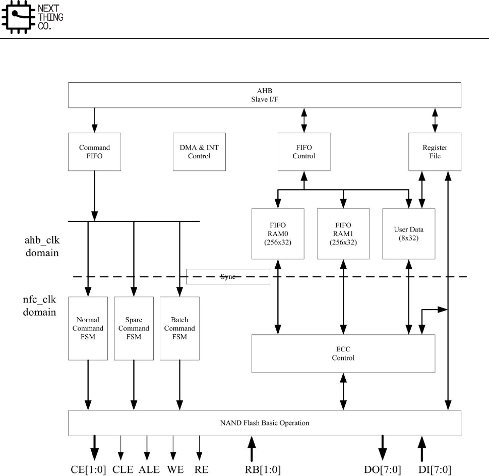
Memory
GR8 User Manual(Version1.0) Copyright © 2017 Next Thing Co. All Rights Reserved. Page 245
4.2.2. Block Diagram
Figure 4-1. NFC Block Diagram
4.2.3. NFC Timing Diagram
Typically, there are two kinds of the serial access method. One is the conventional method that fetches data on
the rising edge of an NFC_RE# signal line, and the other is the EDO type that fetches data at the next falling edge
of an NFC_RE# signal line.
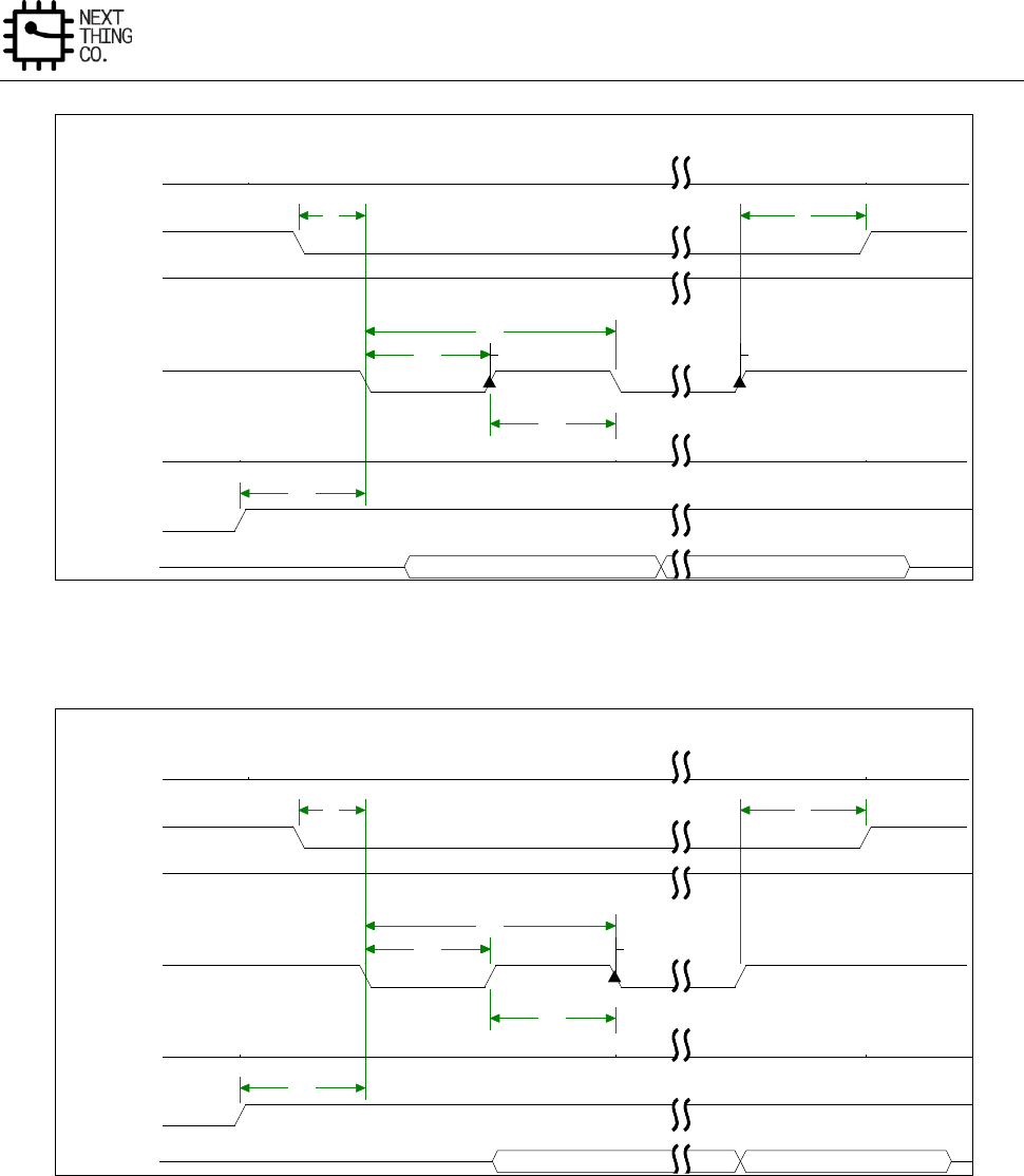
Memory
GR8 User Manual(Version1.0) Copyright © 2017 Next Thing Co. All Rights Reserved. Page 246
Figure 4-2. Conventional Serial Access Cycle Diagram (SAM0)
Figure 4-3. EDO Type Serial Access after Read Cycle (SAM1)
Data(0)
Data(n-1)
sample n-1sample 0
t10
t13
t14
t12
t14
t12
t4t3
NFC_CLE
NFC_CE#
NFC_WE#
NFC_RE#
NFC_ALE
NFC_RB#
NFC_IOx
Data(0)
Data(n-1)
sample 0
t10
t13
t14
t12
t14
t12
t4t3
NFC_CLE
NFC_CE#
NFC_WE#
NFC_RE#
NFC_ALE
NFC_RB#
NFC_IOx
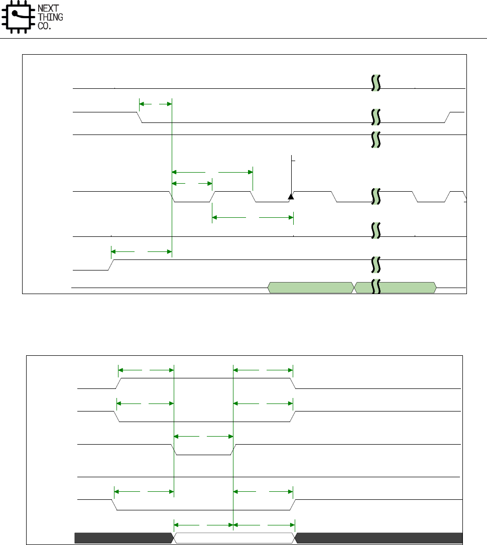
Memory
GR8 User Manual(Version1.0) Copyright © 2017 Next Thing Co. All Rights Reserved. Page 247
Figure 4-4. Extending EDO Type Serial Access Mode (SAM2)
Figure 4-5. Command Latch Cycle
Data(0)
Data(n-1)
sample
t10
t13
t14
t12
t14
t12
t3
NFC_CLE
NFC_CE#
NFC_WE#
NFC_RE#
NFC_ALE
NFC_RB#
NFC_IOx
COMMAND
t9t8
t11t7
t5t5
t4t3
t2t1
NFC_CLE
NFC_CE#
NFC_WE#
NFC_RE#
NFC_ALE
NFC_IOx
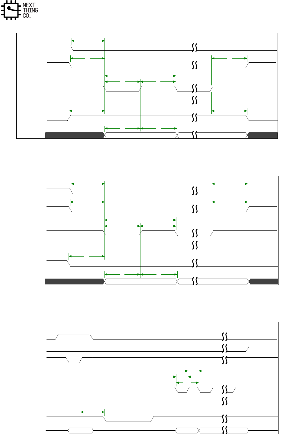
Memory
GR8 User Manual(Version1.0) Copyright © 2017 Next Thing Co. All Rights Reserved. Page 248
Figure 4-6. Address Latch Cycle
Figure 4-7. Write Data to Flash Cycle
Addr(0)
Addr(n-1)
t9t8
t11t7
t15
t6t6t5
t15
t5
t4t3
t1
NFC_CLE
NFC_CE#
NFC_WE#
NFC_RE#
NFC_ALE
NFC_IOx
Data(0)
Data(n-1)
t9t8
t7
t15
t6t6t5
t15
t5
t4t3
t2t1
NFC_CLE
NFC_CE#
NFC_WE#
NFC_RE#
NFC_ALE
NFC_IOx
cmd
d(0)
d(1)
d(n-1)
t16
t14
t13t13
t12
t14
t12
NFC_CLE
NFC_CE#
NFC_WE#
NFC_RE#
NFC_ALE
NFC_RB#
NFC_IOx
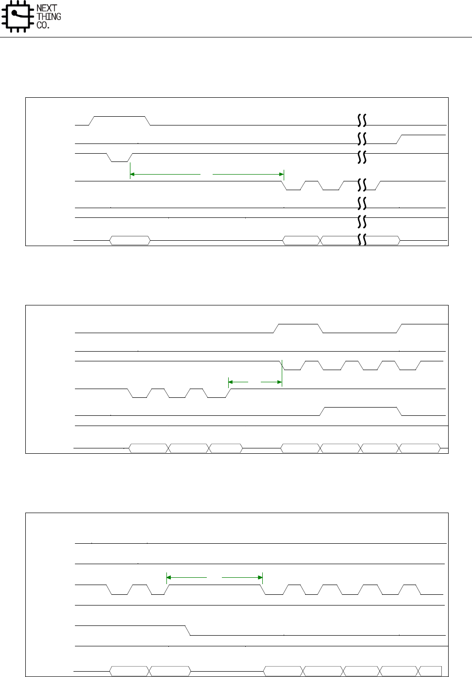
Memory
GR8 User Manual(Version1.0) Copyright © 2017 Next Thing Co. All Rights Reserved. Page 249
Figure 4-8. Waiting R/B# Ready Diagram
Figure 4-9. WE # High to RE# Low Timing Diagram
Figure 4-10. RE # High to WE# Low Timing Diagram
Figure 4-11. Address to Data Loading Timing Diagram
cmd
d(0)
d(1)
d(n-1)
t17
NFC_CLE
NFC_CE#
NFC_WE#
NFC_RE#
NFC_ALE
NFC_RB#
NFC_IOx
d(0)
d(1)
d(n-1)
05h
col1
col2
E0h
t18
NFC_CLE
NFC_CE#
NFC_WE#
NFC_RE#
NFC_ALE
NFC_RB#
NFC_IOx
addr2
addr3
d(0)
d(1)
d(2)
d(n-1)
T19T19
NFC_CLE
NFC_CE#
NFC_WE#
NFC_RE#
NFC_ALE
NFC_RB#
NFC_IOx
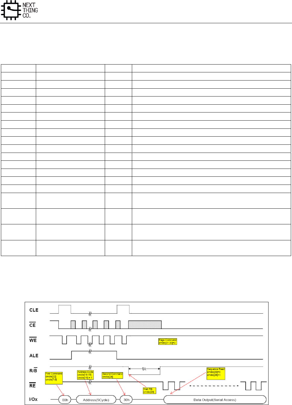
Memory
GR8 User Manual(Version1.0) Copyright © 2017 Next Thing Co. All Rights Reserved. Page 250
Timing Cycle List:
ID
Parameter
Timing
Notes
T1
NFC_CLE setup time
T
T2
NFC_CLE hold time
T
T3
NFC_CE setup time
T
T4
NFC_CE hold time
T
T5
NFC_WE# pulse width
T
T6
NFC_WE# hold time
T
T7
NFC_ALE setup time
T
T8
Data setup time
T
T9
Data hold time
T
T10
Ready to NFC_RE# low
3T
T11
NFC_ALE hold time
T
T12
NFC_RE# pulse width
T
T13
NFC_RE# hold time
T
T14
Read cycle time
2T
T15
Write cycle time
2T
T16
NFC_WE# high to R/B#
busy
tWB
Specified by timing configure register(NFC_TIMING_CFG)
T17
NFC_WE# high to
NFC_RE# low
tWHR
Specified by timing configure register(NFC_TIMING_CFG)
T18
NFC_RE# high to
NFC_WE# low
tRHW
Specified by timing configure register(NFC_TIMING_CFG)
T19
Address to Data Loading
time
tADL
Specified by timing configure register(NFC_TIMING_CFG)
Note: T is the clock period duration of NFC_CLK (x2).
4.2.4. NFC Read and Write Diagram
Figure 4-12. Page Read Command Diagram
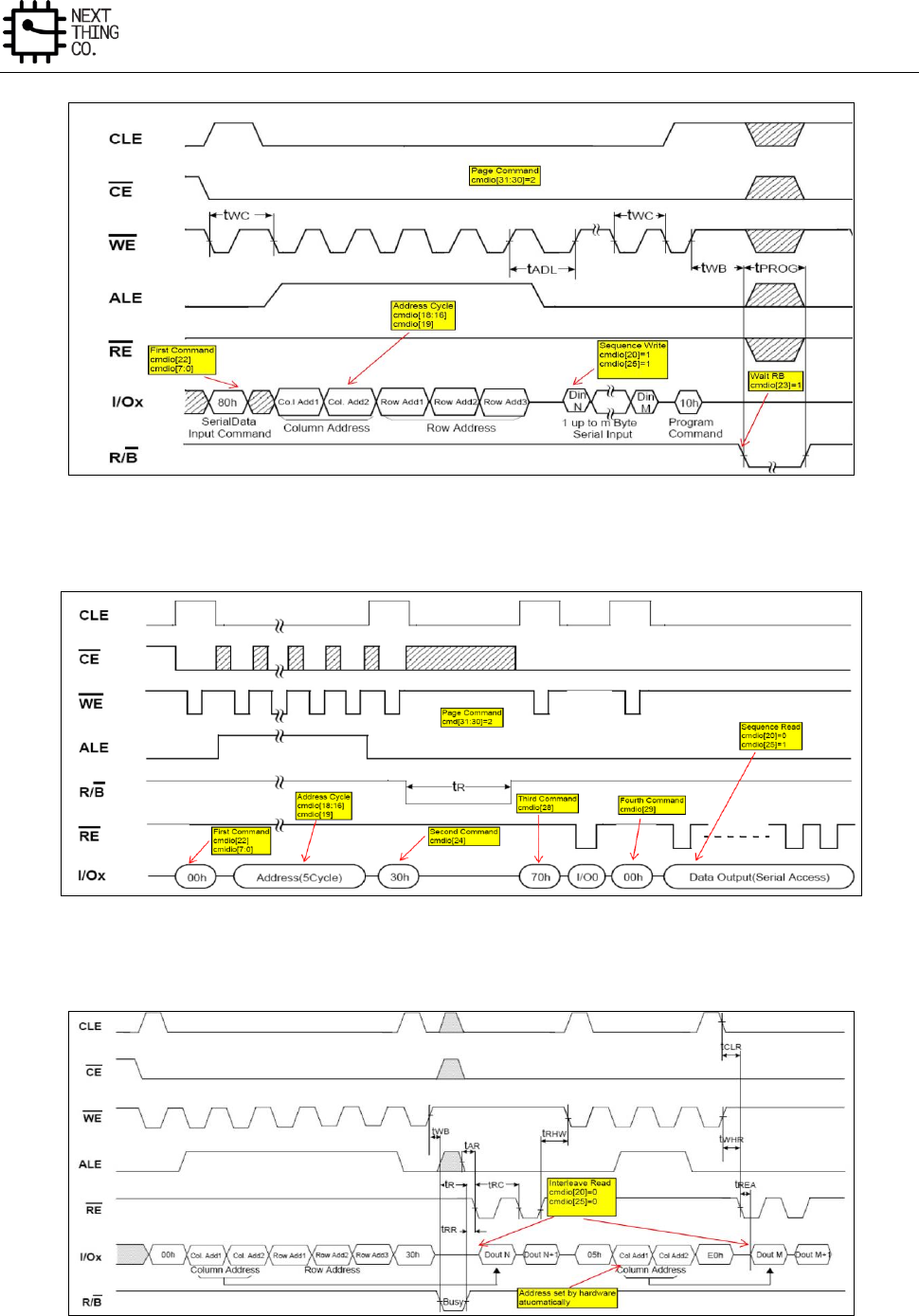
Memory
GR8 User Manual(Version1.0) Copyright © 2017 Next Thing Co. All Rights Reserved. Page 251
Figure 4-13. Page Program Diagram
Figure 4-14. EF-NAND Page Read Diagram
Figure 4-15. Interleave Page Read Diagram

Memory
GR8 User Manual(Version1.0) Copyright © 2017 Next Thing Co. All Rights Reserved. Page 252
4.3. SD/MMC Controller
4.3.1. Overview
The SD/MMC Host Controller(SMHC) provides three controllers including SD card, MMC and SDIO device. SMHC
controls the read/write operations on the secure digital(SD) card, multimedia card(MMC), and supports extended
Wi-Fi devices based on the secure digital input/output(SDIO) protocol.
Features:
● Supports Secure Digital memory protocol commands (up to SD2.0)
● Supports Secure Digital I/O protocol commands(up to SDIO2.0)
● Supports Multimedia Card protocol commands (up to MMC4.4)
● 1-bit,4-bit,8-bit data bus width
● Supports block size of 1 to 65535 bytes
● Supports hardware CRC generation and error detection
● Supports descriptor-based internal DMA controller
● Internal 16x32-bit (64 bytes total) FIFO for data transfer
4.3.2. SD/MMC Timing Diagram
Please refer to relative specifications listed below:
● Physical Layer Specification Ver2.00 Final
● SDIO Specification Ver2.00
● Multimedia Cards (MMC – version 4.2)
● JEDEC Standard – JESD84-44, Embedded Multimedia Card (eMMC) Card Product Standard

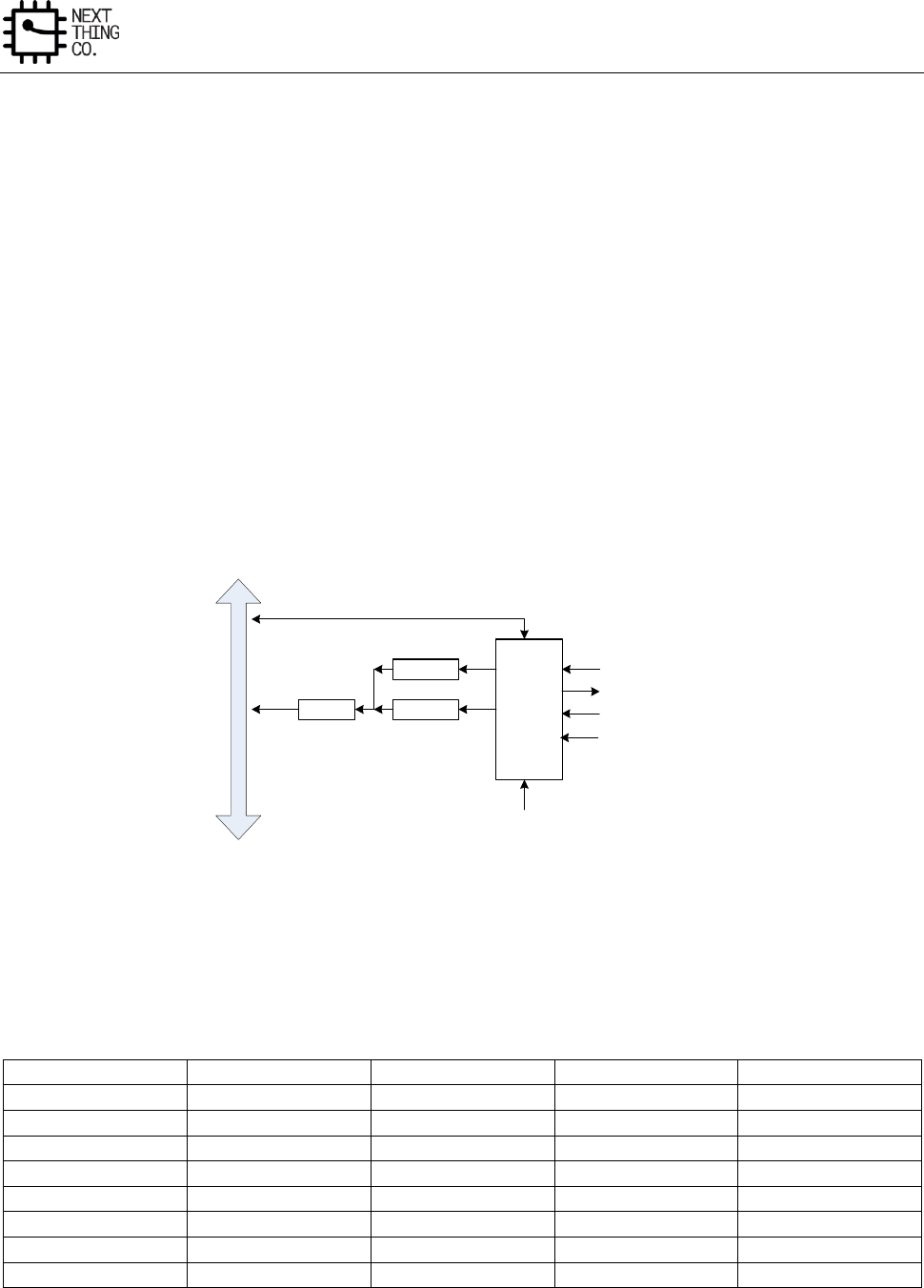
Image
GR8 User Manual(Version1.0) Copyright © 2017 Next Thing Co. All Rights Reserved. Page 254
5.1. CSI
5.1.1. Overview
The CMOS Sensor Interface (CSI) is an image or video input control module which can receive image or video data
by a digital camera interface and high speed serial interface.
● Supports 8-bit digital camera interface
● Supports BT656 interface
● Maximum still capture resolution for parallel interface to 5M
● Maximum video capture resolution for parallel interface to 1080p@30fps
● Maximum pixel clock to 150MHz
5.1.2. CSI Block Diagram
CSI
Control
Module
System BUS
FIFO 2
FIFO 1DMA
Data[7:0]
PCLK
HS
VS
MCLK
Figure 5-1. CSI Block Diagram
5.1.3. CCIR656 Format
5.1.3.1. Header Data Bit Definition
Data Bit
First Word
Second Word
Third Word
Fourth Word
CS D[7] (MSB)
1
0
0
1
CS D[6]
1
0
0
F
CS D[5]
1
0
0
V
CS D[4]
1
0
0
H
CS D[3]
1
0
0
P3
CS D[2]
1
0
0
P2
CS D[1]
1
0
0
P1
CS D[0]
1
0
0
P0
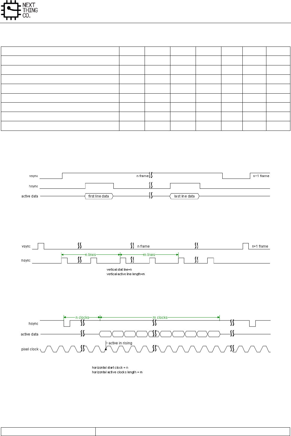
Image
GR8 User Manual(Version1.0) Copyright © 2017 Next Thing Co. All Rights Reserved. Page 255
5.1.3.2. CCIR656 Header Decode
Decode
F
V
H
P3
P2
P1
P0
Field 1 start of active video (SAV)
0
0
0
0
0
0
0
Field 1 end of active video (EAV)
0
0
1
1
1
0
1
Field 1 SAV (digital blanking)
0
1
0
1
0
1
1
Field 1 EAV (digital blanking)
0
1
1
0
1
1
0
Field 2 SAV
1
0
0
0
1
1
1
Field 2 EAV
1
0
1
1
0
1
0
Field 2 SAV (digital blanking)
1
1
0
1
1
0
0
Field 2 EAV (digital blanking)
1
1
1
0
0
0
1
5.1.4. CSI Timing Diagram
Figure 5-2. Vref= Positive; Href= Positive
Figure 5-3. Vertical Size Setting
Figure 5-4. Horizontal Size Setting and Pixel Clock Timing (Href= positive)
5.1.5. CSI Register List
Module Name
Base Address
Image
GR8 User Manual(Version1.0) Copyright © 2017 Next Thing Co. All Rights Reserved. Page 256
CSI
0x01C09000
Register Name
Offset
Description
CSI_EN_REG
0x0000
CSI Enable Register
CSI_CFG_REG
0x0004
CSI Configuration Register
CSI_CPT_CTRL_REG
0x0008
CSI Capture Control Register
CSI_FIFO0_BUF_A_ADDR_REG
0x0010
CSI FIFO0 Buffer A Register
CSI_FIFO0_ BUF_B_ADDR_REG
0x0014
CSI FIFO0 Buffer B Register
CSI_FIFO1_ BUF_A_ADDR_REG
0x0018
CSI FIFO1 Buffer A Register
CSI_FIFO1_ BUF_B_ADDR_REG
0x001C
CSI FIFO1 Buffer B Register
CSI_BUF_CTRL_REG
0x0028
CSI Buffer Control Register
CSI_STA_REG
0x002C
CSI Status Register
CSI_INT_EN_REG
0x0030
CSI Interrupt Enable Register
CSI_INT_STA_REG
0x0034
CSI Interrupt Status Register
CSI_WIN_CTRL_W_REG
0x0040
CSI Window Width Control Register
CSI_WIN_CTRL_H_REG
0x0044
CSI Window Height Control Register
CSI_BUF_LEN_REG
0x0048
CSI Buffer Length Register
5.1.6. CSI Register Description
5.1.6.1. CSI Enable Register(Default Value: 0x0000_0000)
Offset: 0x0000
Name: CSI_EN_REG
Bit
Read/Write
Default/Hex
Description
31:1
/
/
Reserved
0
R/W
0x0
EN
CSI Enable
0: Reset and disable
1: Enable
5.1.6.2. CSI Configuration Register(Default Value: 0x0000_0200)
Offset: 0x0004
Register Name: CSI_CFG_REG
Bit
Read/Write
Default/Hex
Description
31:23
/
/
Reserved
22:20
R/W
0x0
IN_FMT
Input data format
000: RAW stream

Image
GR8 User Manual(Version1.0) Copyright © 2017 Next Thing Co. All Rights Reserved. Page 257
010: CCIR656
011: YUV422
others: reserved
19:16
R/W
0x0
OUT_FMT
Output data format
When the input format is set RAW stream
0000: pass-through
When the input format is set CCIR656 interface
0000: field planar YCbCr 422
0001: field planar YCbCr 420
0010: frame planar YCbCr 420
0011: frame planar YCbCr 422
0100: field planar YCbCr 422 UV combined
0101: field planar YCbCr 420 UV combined
0110: frame planar YCbCr 420 UV combined
0111: frame planar YCbCr 422 UV combined
1111: interlaced interleaved YCbCr422. In this mode, capturing
interlaced input and output the interlaced fields from individual ports.
Field 1 data will be written to FIFO0 output buffer and field 2 data will
be written to FIFO1 output buffer.
1000: field MB YCbCr 422
1001: field MB YCbCr 420
1010: frame MB YCbCr 420
1011: frame MB YCbCr 422
When the input format is set YUV422
0000: planar YUV 422
0001: planar YUV 420
0100: planar YUV 422 UV combined
0101: planar YUV 420 UV combined
1000: MB YUV 422
1001: MB YUV 420
15:12
/
/
Reserved
11:10
R/W
0x0
FIELD_SEL
Field selection. Applies to CCIR656 interface only.

Image
GR8 User Manual(Version1.0) Copyright © 2017 Next Thing Co. All Rights Reserved. Page 258
00: start capturing with field odd.
01: start capturing with field even.
10: start capturing with either field.
11: reserved
9:8
R/W
0x2
DATA_SEQ
Input data sequence, only valid for YUV422 mode.
00: YUYV
01: YVYU
10: UYVY
11: VYUY
7:3
/
/
Reserved
2
R/W
0
VSYNC_POL
Vref polarity
0: negative
1: positive
This register is not applied to CCIR656 interface.
1
R/W
0
HSYNC_POL
Href polarity
0: negative
1: positive
This register is not applied to CCIR656 interface.
0
R/W
0
PCLK_POL
Data clock type
0: active in falling edge
1: active in rising edge
5.1.6.3. CSI Capture Control Register(Default Value: 0x0000_0000)
Offset: 0x0008
Register Name: CSI_CPT_CTRL_REG

Image
GR8 User Manual(Version1.0) Copyright © 2017 Next Thing Co. All Rights Reserved. Page 259
Bit
Read/Write
Default/Hex
Description
31:2
/
/
/
1
R/W
0x0
VIDEO_CAP_CTRL
Video capture control: Capture the video image data stream.
0: Disable video capture
If video capture is in progress, the CSI stops capturing image data at
the end of the current frame, and all of the current frame data is
written to output FIFO.
1: Enable video capture
The CSI starts capturing image data at the start of the next frame.
0
W
0x0
STILL_CAP_CTRL
Still capture control: Capture a single still image frame.
0: Disable still capture.
1: Enable still capture
The CSI module starts capturing image data at the start of the next
frame. The CSI module captures only one frame of image data. This bit
is self cleared and always reads as a 0.
5.1.6.4. CSI FIFO0 Buffer A Register(Default Value: 0x0000_0000)
Offset: 0x0010
Register Name: CSI_FIFO0_BUF_A_ADDR_REG
Bit
Read/Write
Default/Hex
Description
31:0
R/W
0x0
FIFO0_BUF_A
FIFO0 output buffer-A address
5.1.6.5. CSI FIFO0 Buffer B Register(Default Value: 0x0000_0000)
Offset: 0x0014
Register Name: CSI_FIFO0_BUF_B_ADDR_REG
Bit
Read/Write
Default/Hex
Description
31:0
R/W
0x0
FIFO0_BUF_B
FIFO0 output buffer-B address
5.1.6.6. CSI FIFO1 Buffer A Register(Default Value: 0x0000_0000)
Offset: 0x0018
Register Name: CSI_FIFO1_BUF_A_ADDR_REG

Image
GR8 User Manual(Version1.0) Copyright © 2017 Next Thing Co. All Rights Reserved. Page 260
Bit
Read/Write
Default/Hex
Description
31:0
R/W
0x0
FIFO1_BUF_A
FIFO1 output buffer-A address
5.1.6.7. CSI FIFO1 Buffer B Register(Default Value: 0x0000_0000)
Offset: 0x001C
Register Name: CSI_FIFO1_BUF_B_ADDR_REG
Bit
Read/Write
Default/Hex
Description
31:00
R/W
0x0
FIFO1_BUF_B
FIFO1 output buffer-B address
5.1.6.8. CSI Buffer Control Register(Default Value: 0x0000_0000)
Offset: 0x0028
Register Name: CSI_BUF_CTRL_REG
Bit
Read/Write
Default/Hex
Description
31:2
/
/
/
1
R
0x0
DBS
output buffer selected status
0: Selected output buffer-A
1: Selected output buffer-B
0
R/W
0x0
DBE
Double buffer mode enable
0: disable
1: enable
If the double buffer mode is disabled, the buffer-A will be always
selected by CSI module.
5.1.6.9. CSI Status Register(Default Value: 0x0000_0000)
Offset: 0x002C
Register Name: CSI_STA_REG
Bit
Read/Write
Default/Hex
Description
31:8
R
0x0
LUM_STAT_VALUE
luminance statistical value
When frame done interrupt flag come, value is ready and will last until
next frame done.
For raw data, value = (G>>1+R+G)>>8

Image
GR8 User Manual(Version1.0) Copyright © 2017 Next Thing Co. All Rights Reserved. Page 261
For yuv422, value = Y>>8
7:2
/
/
Reserved
1
R
0x0
VIDEO_CAP_ON
Video capture in progress
Indicates the CSI is capturing video image data (multiple frames). The
bit is set at the start of the first frame after enabling video capture.
When software disables video capture, it clears itself after the last
pixel of the current frame is captured.
0
R
0x0
STILL_CPT_ON
Still capture in progress
Indicates the CSI is capturing still image data (single frame). The bit is
set at the start of the first frame after enabling still frame capture. It
is self-cleared after the last pixel of the first frame is captured.
For CCIR656 interface, if the output format is frame planar YCbCr 420
mode, the frame end means the field2 end, and the other frame end
means filed end.
5.1.6.10. CSI Interrupt Enable Register(Default Value: 0x0000_0000)
Offset: 0x0030
Register Name: CSI_INT_EN_REG
Bit
Read/Write
Default/Hex
Description
31:8
/
/
/
7
R/W
0x0
VSYNC_FLAG
vsync flag
The bit is set when vsync comes. Now load the buffer address for the
coming frame. So, after this irq comes, changes to the buffer address
can only affect next frame.
6
R/W
0x0
HB_OF
Hblank FIFO overflow
The bit is set when 3 FIFOs still overflow after the hblank.
5
R/W
0x0
PRT_ERR
Protection error
Indicates a protection error has been detected. Applies only when the
656 protocol is selected.
4
/
/
Reserved
3
R/W
0x0
FIFO0_OF
FIFO1 overflow
The bit is set when the FIFO 1 overflows.
2
R/W
0x0
FIFO0 overflow

Image
GR8 User Manual(Version1.0) Copyright © 2017 Next Thing Co. All Rights Reserved. Page 262
The bit is set when the FIFO 0 overflows.
1
R/W
0x0
FRM_DONE
Frame done
Indicates the CSI finishes capturing an image frame. Applied to video
capture mode. The bit is set after each completed frame capturing
data is written to buffer as long as video capture remains enabled.
0
R/W
0x0
CPT_DONE
Capture done
Indicates the CSI has completed capturing the image data.
For still capture, the bit is set when one frame data has been written
to buffer.
For video capture, the bit is set when the last frame has been written
to buffer after video capture is disabled.
For CCIR656 interface, if the output format is frame planar YCbCr 420
mode, the frame end means the field2 end, and the other frame end
means field end.
5.1.6.11. CSI Interrupt Status Register(Default Value: 0x0000_0000)
Offset: 0x0034
Register Name: CSI_INT_STA_REG
Bit
Read/Write
Default/Hex
Description
31:8
/
/
/
7
R/W
0x0
VSYNC_FLAG
vsync flag
6
R/W
0x0
HB_OF
Hblank FIFO overflow
5
R/W
0x0
PRT_ERR
Protection error
4
/
/
/
3
R/W
0x0
FIFO1 OF
FIFO1 overflow
2
R/W
0x0
FIFO0_OF
FIFO0 overflow
1
R/W
0x0
FRM_DONE
Frame done
0
R/W
0x0
CPT_DONE
Capture done
Image
GR8 User Manual(Version1.0) Copyright © 2017 Next Thing Co. All Rights Reserved. Page 263
5.1.6.12. CSI Window Width Control Register(Default Value: 0x0500_0000)
Offset: 0x0040
Register Name: CSI_WIN_CTRL_W_REG
Bit
Read/Write
Default/Hex
Description
31:29
/
/
/
28:16
R/W
0x500
ACTIVE_LEN
Horizontal pixel clock length. Valid pixel clocks of a line.
15:13
/
/
/
12:0
R/W
0x0
ACTIVE_START
Horizontal pixel clock start. Pixel data is valid from this clock.
5.1.6.13. CSI Window Height Control Register(Default Value: 0x01E0_0000)
Offset: 0x0044
Register Name: CSI_WIN_CTRL_H_REG
Bit
Read/Write
Default/Hex
Description
31:29
/
/
/
28:16
R/W
0x1E0
ACTIVE_LEN
Vertical line length. Valid line number of a frame.
15:13
/
/
Reserved
12:0
R/W
0x0
ACTIVE_START
Vertical line start. Data is valid from this line.
5.1.6.14. CSI Buffer Length Register(Default Value: 0x0000_0280)
Offset: 0x0048
Register Name: CSI_BUF_LEN_REG
Bit
Read/Write
Default/Hex
Description
31:13
/
/
/
12:0
R/W
0x280
BUFF_LEN
Buffer Length
Buffer length of a line. The unit is byte.

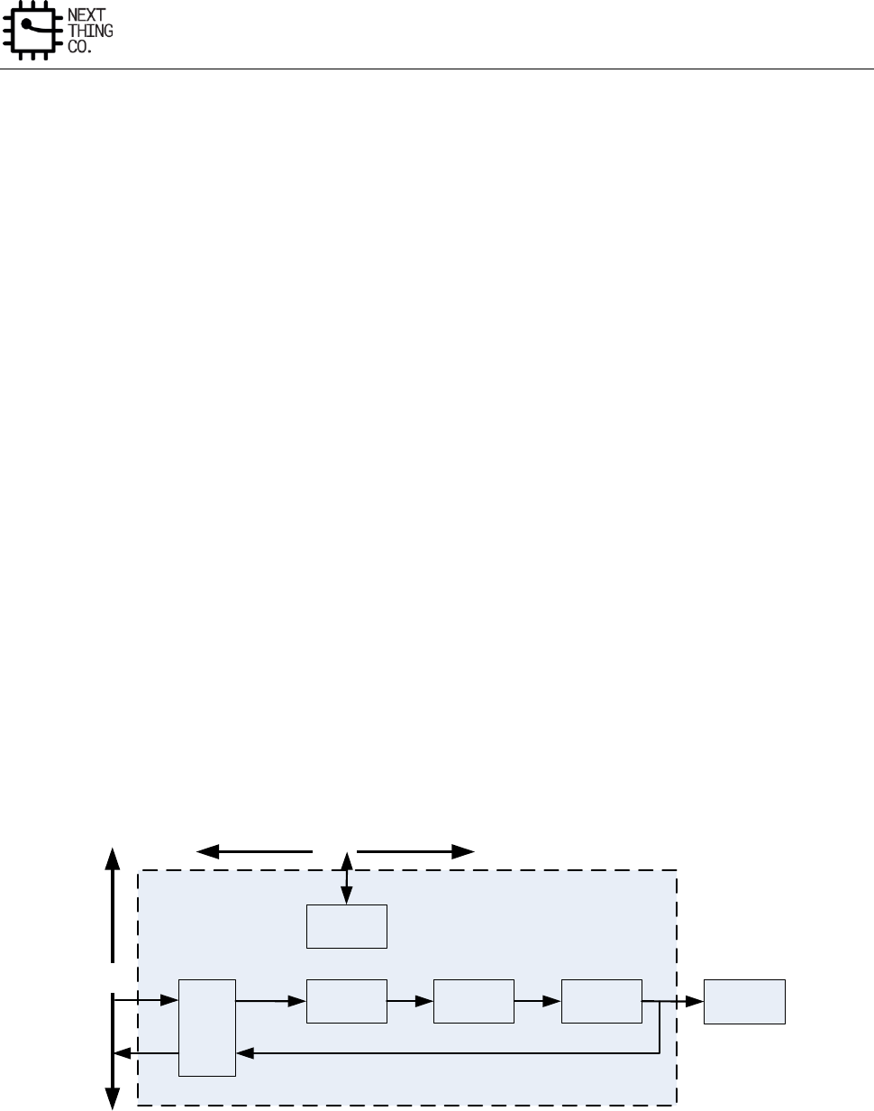
Display
GR8 User Manual(Version1.0) Copyright © 2017 Next Thing Co. All Rights Reserved. Page 265
6.1. Display Engine Front End (DEFE)
6.1.1. Overview
The Display Engine Front End (DEFE) performs image capture/driver, video/graphic scale, format conversion and
color space conversion. It is composed of a DMA controller, input controller, scaler, color space converter and
output controller.
Features:
● Output scan type: interlace/progressive
● Input format: YUV444/YUV422/YUV420/YUV411/RGB
● Direct display output format: RGB
● Write back output format: RGB/YUV444/YUV420/YUV422/YUV411
● 3 channel scaling pipelines for scaling up/down
● Programmable source image size from 8x4 to 2048x2048 resolution
● Programmable destination image size from 8x4 to 2048x2048 resolution
● 4 tap scale filter in horizontal and vertical direction
● 32 Programmable coefficients for each tap
● Color space conversion between YUV and RGB
● Supports direct display and write back to memory
6.1.2. DEFE Block Diagram
DMAC
scaler CSC
Register file
Output
control display
Ahb bus
Mbus
Figure 6-1. DEFE Block Diagram

Display
GR8 User Manual(Version1.0) Copyright © 2017 Next Thing Co. All Rights Reserved. Page 266
6.1.3. DEFE Register List
Module Name
Base Address
DEFE0
0x01E00000
Register Name
Offset
Description
DEFE_EN_REG
0x0000
DEFE Module Enable Register
DEFE_FRM_CTRL_REG
0x0004
DEFE Frame Process Control Register
DEFE_BYPASS_REG
0x0008
DEFE CSC By-Pass Register
DEFE_AGTH_SEL_REG
0x000C
DEFE Algorithm Selection Register
DEFE_LINT_CTRL_REG
0x0010
DEFE Line Interrupt Control Register
DEFE_BUF_ADDR0_REG
0x0020
DEFE Input Channel 0 Buffer Address Register
DEFE_BUF_ADDR1_REG
0x0024
DEFE Input Channel 1 Buffer Address Register
DEFE_BUF_ADDR1_REG
0x0028
DEFE Input Channel 2 Buffer Address Register
DEFE_FIELD_CTRL_REG
0x002C
DEFE Field Sequence Register
DEFE_TB_OFF0_REG
0x0030
DEFE Channel 0 Tile-Based Offset Register
DEFE_TB_OFF1_REG
0x0034
DEFE Channel 1 Tile-Based Offset Register
DEFE_TB_OFF2_REG
0x0038
DEFE Channel 2 Tile-Based Offset Register
DEFE_LINESTRD0_REG
0x0040
DEFE Channel 0 Line Stride Register
DEFE_LINESTRD1_REG
0x0044
DEFE Channel 1 Line Stride Register
DEFE_LINESTRD2_REG
0x0048
DEFE Channel 2 Line Stride Register
DEFE_INPUT_FMT_REG
0x004C
DEFE Input Format Register
DEFE_WB_ADDR0_REG
0x0050
DEFE Channel 3 Write Back Address Register
DEFE_OUTPUT_FMT_REG
0x005C
DEFE Output Format Register
DEFE_INT_EN_REG
0x0060
DEFE Interrupt Enable Register
DEFE_INT_STATUS_REG
0x0064
DEFE Interrupt Status Register
DEFE_STATUS_REG
0x0068
DEFE Status Register
DEFE_CSC_COEF00_REG
0x0070
DEFE CSC Coefficient 00 Register
DEFE_CSC_COEF01_REG
0x0074
DEFE CSC Coefficient 01 Register
DEFE_CSC_COEF02_REG
0x0078
DEFE CSC Coefficient 02 Register
DEFE_CSC_COEF03_REG
0x007C
DEFE CSC Coefficient 03 Register
DEFE_CSC_COEF10_REG
0x0080
DEFE CSC Coefficient 10 Register
DEFE_CSC_COEF11_REG
0x0084
DEFE CSC Coefficient 11 Register
DEFE_CSC_COEF12_REG
0x0088
DEFE CSC Coefficient 12 Register
DEFE_CSC_COEF13_REG
0x008C
DEFE CSC Coefficient 13 Register
DEFE_CSC_COEF20_REG
0x0090
DEFE CSC Coefficient 20 Register
DEFE_CSC_COEF21_REG
0x0094
DEFE CSC Coefficient 21 Register
DEFE_CSC_COEF22_REG
0x0098
DEFE CSC Coefficient 22 Register
DEFE_CSC_COEF23_REG
0x009C
DEFE CSC Coefficient 23 Register
DEFE_WB_LINESTRD_EN_REG
0x00D0
DEFE Write Back Line Stride Enable Register
DEFE_WB_LINESTRD0_REG
0x00D4
DEFE Write Back Channel Line Stride Register
DEFE_CH0_INSIZE_REG
0x0100
DEFE Channel 0 Input Size Register
DEFE_CH0_OUTSIZE_REG
0x0104
DEFE Channel 0 Output Size Register
DEFE_CH0_HORZFACT_REG
0x0108
DEFE Channel 0 Horizontal Factor Register

Display
GR8 User Manual(Version1.0) Copyright © 2017 Next Thing Co. All Rights Reserved. Page 267
DEFE_CH0_VERTFACT_REG
0x010C
DEFE Channel 0 Vertical factor Register
DEFE_CH0_HORZPHASE_REG
0x0110
DEFE Channel 0 Horizontal Initial Phase Register
DEFE_CH0_VERTPHASE0_REG
0x0114
DEFE Channel 0 Vertical Initial Phase 0 Register
DEFE_CH0_VERTPHASE1_REG
0x0118
DEFE Channel 0 Vertical Initial Phase 1 Register
DEFE_CH1_INSIZE_REG
0x0200
DEFE Channel 1 Input Size Register
DEFE_CH1_OUTSIZE_REG
0x0204
DEFE Channel 1 Output Size Register
DEFE_CH1_HORZFACT_REG
0x0208
DEFE Channel 1 Horizontal Factor Register
DEFE_CH1_VERTFACT_REG
0x020C
DEFE Channel 1 Vertical factor Register
DEFE_CH1_HORZPHASE_REG
0x0210
DEFE Channel 1 Horizontal Initial Phase Register
DEFE_CH1_VERTPHASE0_REG
0x0214
DEFE Channel 1 Vertical Initial Phase 0 Register
DEFE_CH1_VERTPHASE1_REG
0x0218
DEFE Channel 1 Vertical Initial Phase 1 Register
DEFE_CH0_HORZCOEF_REGN
0x0400+N*0x04
(N=0:31)
DEFE Channel 0 Horizontal Filter Coefficient Register
DEFE_CH0_VERTCOEF_REGN
0x0500+N*0x04
(N=0:31)
DEFE Channel 0 Vertical Filter Coefficient Register
DEFE_CH1_HORZCOEF_REGN
0x0600+N*0x04
(N=0:31)
DEFE Channel 1 Horizontal Filter Coefficient Register
DEFE_CH1_VERTCOEF_REGN
0x0700+N*0x04
(N=0:31)
DEFE Channel 1 Vertical Filter Coefficient Register
Note: Registers 0x0008~0x0218 except status registers are double buffered. when a new frame process starts and
the buffered register configuration ready bit in frame process control register is set, the value of corresponding
internal configuration register will be refreshed by this register, and programmers always cannot read the value
of corresponding internal register.
6.1.4. DEFE Register Description
6.1.4.1. DEFE Module Enable Register(Default Value: 0x0000_0000)
Offset: 0x0000
Register Name: DEFE_EN_REG
Bit
Read/Write
Default/Hex
Description
31:1
/
/
/
0
R/W
0x0
EN
DEFE enable
0: Disable
1: Enable
When DEFE enable bit is disabled, the clock of DEFE module will be
disabled.
If this bit transits is from 0 to 1, the frame process control register and
the interrupt enable register will be initialized to default value, and the

Display
GR8 User Manual(Version1.0) Copyright © 2017 Next Thing Co. All Rights Reserved. Page 268
state machine of the module is reset.
6.1.4.2. DEFE Frame Process Control Register(Default Value: 0x0000_0000)
Offset: 0x0004
Register Name: DEFE_FRM_CTRL_REG
Bit
Read/Write
Default/Hex
Description
31:24
/
/
/
23
R/W
0x0
COEF_ACCESS_CTRL
Fir coef ram access control
0: CPU does not access fir coef ram
1: CPU will access fir coef ram
This bit will be set to 1 before CPU accesses fir coef ram
22:17
/
/
/
16
R/W
0x0
FRM_START
Frame start & reset control
0: reset
1: start
If the bit is written to zero, the whole state machine and data paths of
DEFE module will be reset.
When the bit is written to 1, DEFE will start a new frame process.
15:12
/
/
/
11
R/W
0x0
OUT_CTRL
DEFE output control
0: enable DEFE output to DEBE
1: disable DEFE output to DEBE
If DEFE write back function is enabled, DEFE output to DEBE is not
recommended.
10:3
/
/
/
2
R/W
0x0
WB_EN
Write back enable

Display
GR8 User Manual(Version1.0) Copyright © 2017 Next Thing Co. All Rights Reserved. Page 269
0: Disable
1: Enable
If output to DEBE is enabled, the writing back process will start when
write back enable bit is set and a new frame processing begins. The bit
will be self-cleared when writing-back frame process starts.
1
/
/
/
0
R/W
0x0
REG_RDY_EN
Register ready enable
0: not ready
1: registers configuration ready
Just as filter coefficients configuration, in order to ensure the display
to be correct, the correlative display configuration registers are
buffered too, and programmers also can change the value of
correlative registers in any time. When the registers setting is finished,
the programmer should set the bit if the new configuration is needed
in next scaling frame.
When the new frame starts, the bit will also be self-cleared.
6.1.4.3. DEFE CSC By-Pass Register(Default Value: 0x0000_0000)
Offset: 0x0008
Register Name: DEFE_BYPASS_REG
Bit
Read/Write
Default/Hex
Description
31:2
/
/
/
1
R/W
0x0
CSC_BYPASS_EN
CSC by-pass enable
0: CSC enable
1: CSC will be by-passed
Actually, in order to ensure the module working to be correct, this bit
only can be set when input data format is the same as output data
format (both YUV or both RGB)
0
/
/
/
6.1.4.4. DEFE Algorithm Selection Register(Default Value: 0x0000_0000)
Offset: 0x000C
Register Name: DEFE_AGTH_SEL_REG

Display
GR8 User Manual(Version1.0) Copyright © 2017 Next Thing Co. All Rights Reserved. Page 270
Bit
Read/Write
Default/Hex
Description
31:9
/
/
/
8
R/W
0x0
LINEBUF_AGTH
DEFE line buffer algorithm select
0: horizontal filtered result
1: original data
7:0
/
/
/
6.1.4.5. DEFE Line Interrupt Control Register(Default Value: 0x0000_0000)
Offset: 0x0010
Register Name: DEFE_LINT_CTRL_REG
Bit
Read/Write
Default/Hex
Description
31:28
/
/
/
27:16
R
0x0
CURRENT_LINE
15
R/W
0x0
FIELD_SEL
Field select
0: each field
1: end field(field counter in reg0x2c)
14:13
/
/
/
12:0
R/W
0x0
TRIG_LINE
Trigger line number of line interrupt
6.1.4.6. DEFE Input Channel 0 Buffer Address Register(Default Value: 0x0000_0000)
Offset: 0x0020
Register Name: DEFE_BUF_ADDR0_REG
Bit
Read/Write
Default/Hex
Description
31:0
R/W
0x0
BUF_ADDR
DEFE frame buffer address
In tile-based type:
The address is the start address of the line in the first tile used to
generate output frame.
In non-tile-based type:
The address is the start address of the first line.

Display
GR8 User Manual(Version1.0) Copyright © 2017 Next Thing Co. All Rights Reserved. Page 271
6.1.4.7. DEFE Input Channel 1 Buffer Address Register(Default Value: 0x0000_0000)
Offset: 0x0024
Register Name: DEFE_BUF_ADDR1_REG
Bit
Read/Write
Default/Hex
Description
31:0
R/W
0x0
BUF_ADDR
DEFE frame buffer address
In tile-based type:
The address is the start address of the line in the first tile used to
generate output frame.
In non-tile-based type:
The address is the start address of the first line.
6.1.4.8. DEFE Input Channel 2 Buffer Address Register(Default Value: 0x0000_0000)
Offset: 0x0028
Register Name: DEFE_BUF_ADDR2_REG
Bit
Read/Write
Default/Hex
Description
31:0
R/W
0x0
BUF_ADDR
DEFE frame buffer address
In tile-based type:
The address is the start address of the line in the first tile used to
generate output frame.
In non-tile-based type:
The address is the start address of the first line.
6.1.4.9. DEFE Field Sequence Register(Default Value: 0x0000_0000)
Offset: 0x002C
Register Name: DEFE_FIELD_CTRL_REG
Bit
Read/Write
Default/Hex
Description
31:13
/
/
/
12
R/W
0x0
FIELD_LOOP_MOD
Field loop mode
0: the last field
1: the full frame
11
/
/
/
10:8
R/W
0x0
VALID_FIELD_CNT
Valid field counter bit
the valid value = this value + 1
7:0
R/W
0x0
FIELD_CNT
Display
GR8 User Manual(Version1.0) Copyright © 2017 Next Thing Co. All Rights Reserved. Page 272
Field counter
each bit specifies a field to display
0: top field
1: bottom field
6.1.4.10. DEFE Channel 0 Tile-Based Offset Register(Default Value: 0x0000_0000)
Offset: 0x0030
Register Name: DEFE_TB_OFF0_REG
Bit
Read/Write
Default/Hex
Description
31:21
/
/
/
20:16
R/W
0x0
X_OFFSET1
The x offset of the bottom-right point in the end tile
15:13
/
/
/
12:8
R/W
0x0
Y_OFFSET0
The y offset of the top-left point in the first tile
7:5
/
/
/
4:0
R/W
0x0
X_OFFSET0
The x offset of the top-left point in the first tile
6.1.4.11. DEFE Channel 1 Tile-Based Offset Register(Default Value: 0x0000_0000)
Offset: 0x0034
Register Name: DEFE_TB_OFF1_REG
Bit
Read/Write
Default/Hex
Description
31:21
/
/
/
20:16
R/W
0x0
X_OFFSET1
The x offset of the bottom-right point in the end tile
15:13
/
/
/
12:8
R/W
0x0
Y_OFFSET0
The y offset of the top-left point in the first tile
7:5
/
/
/
4:0
R/W
0x0
X_OFFSET0
The x offset of the top-left point in the first tile
6.1.4.12. DEFE Channel 2 Tile-Based Offset Register(Default Value: 0x0000_0000)
Offset: 0x0038
Register Name: DEFE_TB_OFF2_REG

Display
GR8 User Manual(Version1.0) Copyright © 2017 Next Thing Co. All Rights Reserved. Page 273
Bit
Read/Write
Default/Hex
Description
31:21
/
/
/
20:16
R/W
0x0
X_OFFSET1
The x offset of the bottom-right point in the end tile
15:13
/
/
/
12:8
R/W
0x0
Y_OFFSET0
The y offset of the top-left point in the first tile
7:5
/
/
/
4:0
R/W
0x0
X_OFFSET0
The x offset of the top-left point in the first tile
6.1.4.13. DEFE Channel 0 Line Stride Register(Default Value: 0x0000_0000)
Offset: 0x0040
Register Name: DEFE_LINESTRD0_REG
Bit
Read/Write
Default/Hex
Description
31:0
R/W
0x0
LINE_STRIDE
In tile-based type, the stride length is the distance from the start of
the end line in one tile to the start of the first line in next tile (here
next tile is in vertical direction).
In non-tile-based type, the stride length is the distance from the start
of one line to the start of the next line.
6.1.4.14. DEFE Channel 1 Line Stride Register(Default Value: 0x0000_0000)
Offset: 0x0044
Register Name: DEFE_LINESTRD1_REG
Bit
Read/Write
Default/Hex
Description
31:0
R/W
0x0
LINE_STRIDE
In tile-based type, the stride length is the distance from the start of
the end line in one tile to the start of the first line in next tile (here
next tile is in vertical direction).
In non- tile-based type, the stride length is the distance from the start
of one line to the start of the next line.
6.1.4.15. DEFE Channel 2 Line Stride Register(Default Value: 0x0000_0000)
Offset: 0x0048
Register Name: DEFE_LINESTRD2_REG
Bit
Read/Write
Default/Hex
Description

Display
GR8 User Manual(Version1.0) Copyright © 2017 Next Thing Co. All Rights Reserved. Page 274
31:0
R/W
0x0
LINE_STRIDE
In tile-based type, the stride length is the distance from the start of
the end line in one tile to the start of the first line in next tile (here
next tile is in vertical direction).
In non- tile-based type, the stride length is the distance from the
start of one line to the start of the next line.
6.1.4.16. DEFE Input Format Register(Default Value: 0x0000_0000)
Offset: 0x004C
Register Name: DEFE_INPUT_FMT_REG
Bit
Read/Write
Default/Hex
Description
31:17
/
/
/
16
R/W
0x0
BYTE_SEQ
Input data byte sequence selection
0: P3P2P1P0(word)
1: P0P1P2P3(word)
15:13
/
/
/
12
R/W
0x0
SCAN_MOD
Scanning Mode selection
0: non-interlace
1: interlace
11
/
/
/
10:8
R/W
0x0
DATA_MOD
Input data mode selection
000: non-tile-based planar data
001: interleaved data
010: non- tile-based UV combined data
100: tile-based planar data
110: tile-based UV combined data
other: reserved
7
/
/
/
6:4
R/W
0x0
DATA_FMT
Input component data format

Display
GR8 User Manual(Version1.0) Copyright © 2017 Next Thing Co. All Rights Reserved. Page 275
In non-tile-based planar data mode:
000: YUV 4:4:4
001: YUV 4:2:2
010: YUV 4:2:0
011: YUV 4:1:1
100: CSI RGB data
101: RGB888
Other: Reserved
In interleaved data mode:
000: YUV 4:4:4
001: YUV 4:2:2
101: ARGB8888
Other: reserved
In non-tile-based UV combined data mode:
001: YUV 4:2:2
010: YUV 4:2:0
011: YUV 4:1:1
Other: reserved
In tile-based planar data mode:
001: YUV 4:2:2
010: YUV 4:2:0
011: YUV 4:1:1
Other: Reserved
In tile-based UV combined data mode:
001: YUV 4:2:2
010: YUV 4:2:0
011: YUV 4:1:1
Other: reserved
3:2
/
/
/
1:0
R/W
0x0
DATA_PS

Display
GR8 User Manual(Version1.0) Copyright © 2017 Next Thing Co. All Rights Reserved. Page 276
Pixel sequence
In interleaved YUV422 data mode:
00: Y1V0Y0U0
01: V0Y1U0Y0
10: Y1U0Y0V0
11: U0Y1V0Y0
In interleaved YUV444 data mode:
00: VUYA
01: AYUV
Other: reserved
In UV combined data mode: (UV component)
00: V1U1V0U0
01: U1V1U0V0
Other: reserved
In interleaved ARGB8888 data mode:
00: BGRA
01: ARGB
Other: reserved
6.1.4.17. DEFE Channel 3 Write Back Address Register(Default Value: 0x0000_0000)
Offset: 0x0050
Register Name: DEFE_WB_ADDR0_REG
Bit
Read/Write
Default/Hex
Description
31:0
R/W
0x0
WB_ADDR
Write-back address setting for scaled data.
6.1.4.18. DEFE Output Format Register(Default Value: 0x0000_0000)
Offset: 0x5C
Register Name: DEFE_OUTPUT_FMT_REG
Bit
Read/Write
Default/Hex
Description
31:18
/
/
/
17:16
R/W
0x0
WB_Ch_Sel
Write back channel select(chsel)

Display
GR8 User Manual(Version1.0) Copyright © 2017 Next Thing Co. All Rights Reserved. Page 277
00~01: Ch3
10: Ch4
11: Ch5
15:9
/
/
/
8
R/W
0x0
BYTE_SEQ
Output data byte sequence selection
0: P3P2P1P0(word)
1: P0P1P2P3(word)
For ARGB, when this bit is 0, the byte sequence is BGRA, and when
this bit is 1, the byte sequence is ARGB;
7:5
/
/
/
4
R/W
0x0
SCAN_MOD
Output interlace enable
0: disable
1: enable
When output interlace enable, scaler selects YUV initial phase
according to LCD field signal
3
/
/
/
2:0
R/W
0x0
DATA_FMT
Data format
000: planar RGB888 conversion data format
001: interleaved BGRA8888 conversion data format(A component
always be pad 0xff)
010: interleaved ARGB8888 conversion data format(A component
always be pad 0xff)
100: planar YUV 444
101: planar YUV 420(only support YUV input and not interleaved
mode)
110: planar YUV 422(only support YUV input)
111: planar YUV 411(only support YUV input)
Other: reserved
Display
GR8 User Manual(Version1.0) Copyright © 2017 Next Thing Co. All Rights Reserved. Page 278
6.1.4.19. DEFE Interrupt Enable Register(Default Value: 0x0000_0000)
Offset: 0x0060
Register Name: DEFE_INT_EN_REG
Bit
Read/Write
Default/Hex
Description
31:11
/
/
/
10
R/W
0x0
REG_LOAD_EN
Register ready load interrupt enable
9
R/W
0x0
LINE_EN
Line interrupt enable
8
/
/
/
7
R/W
0x0
WB_EN
Write-back end interrupt enable
0: Disable
1: Enable
6:0
/
/
/
6.1.4.20. DEFE Interrupt Status Register(Default Value: 0x0000_0000)
Offset: 0x0064
Register Name: DEFE_INT_STATUS_REG
Bit
Read/Write
Default/Hex
Description
31:11
/
/
/
10
R/W
0x0
REG_LOAD_STATUS
Register ready load interrupt status
9
R/W
0x0
LINE_STATUS
Line interrupt status
8
/
/
/
7
R/W
0x0
WB_STATUS
Write-back end interrupt status
6:0
/
/
/
6.1.4.21. DEFE Status Register(Default Value: 0x0000_0000)
Offset: 0x0068
Register Name: DEFE_STATUS_REG
Bit
Read/Write
Default/Hex
Description
31:29
/
/
/

Display
GR8 User Manual(Version1.0) Copyright © 2017 Next Thing Co. All Rights Reserved. Page 279
28:16
R
0x0
LINE_ON_SYNC
Line number(when sync reached)
15
R/W
0x0
WB_ERR_SYNC
Sync reach flag when capture in process
14
R/W
0x0
WB_ERR_LOSEDATA
Lose data flag when capture in process
13
/
/
/
12
R
0x0
WB_ERR_STATUS
write-back error status
0: valid write back
1: un-valid write back
This bit is cleared through writing 0 to reset/start bit in frame control
register
11
R
0x0
COEF_ACCESS_STATUS
FIR coef access status
0: scaler module can access FIR coef RAM
1: CPU can access FIR coef ram
This bit must be 1 before CPU accesses FIR coef RAM. When this bit
is 1, scaler module will fetch 0x00004000 from RAM.
10:6
/
/
/
5
R
0x0
LCD_FIELD
LCD field status
0: top field
1: bottom field
4
R
0x0
DRAM_STATUS
Access dram status
0: idle
1: busy
This flag indicates whether DEFE is accessing dram

Display
GR8 User Manual(Version1.0) Copyright © 2017 Next Thing Co. All Rights Reserved. Page 280
3
/
/
/
2
R
0x0
CFG_PENDING
Register configuration pending
0: no pending
1: configuration pending
This bit indicates the registers for the next frame has been
configured. This bit will be set when configuration ready bit is set
and this bit will be cleared when a new frame process begins.
1
R
0x0
WB_STATUS
Write-back process status
0: write-back end or write-back disable
1: write-back in process
This flag indicates that a full frame has not been written back to
memory. The bit will be set when write-back enable bit is set, and be
cleared when write-back process ends.
0
R
0x0
FRM_BUSY
Frame busy.
This flag indicates that the frame is being processed.
The bit will be set when frame process reset & start is set, and be
cleared when frame process is reset or disabled.
6.1.4.22. DEFE CSC Coefficient 00 Register(Default Value: 0x0000_0000)
Offset: 0x0070
Register Name: DEFE_CSC_COEF00_REG
Bit
Read/Write
Default/Hex
Description
31:13
/
/
/
12:0
R/W
0x0
COEF
the Y/G coefficient
the value equals to coefficient*210
6.1.4.23. DEFE CSC Coefficient 01 Register(Default Value: 0x0000_0000)
Offset: 0x0074
Register Name: DEFE_CSC_COEF01_REG
Bit
Read/Write
Default/Hex
Description

Display
GR8 User Manual(Version1.0) Copyright © 2017 Next Thing Co. All Rights Reserved. Page 281
31:13
/
/
/
12:0
R/W
0x0
COEF
the Y/G coefficient
the value equals to coefficient*210
6.1.4.24. DEFE CSC Coefficient 02 Register(Default Value: 0x0000_0000)
Offset: 0x0078
Register Name: DEFE_CSC_COEF02_REG
Bit
Read/Write
Default/Hex
Description
31:13
/
/
/
12:0
R/W
0x0
COEF
the Y/G coefficient
the value equals to coefficient*210
6.1.4.25. DEFE CSC Coefficient 03 Register(Default Value: 0x0000_0000)
Offset: 0x007C
Register Name: DEFE_CSC_COEF03_REG
Bit
Read/Write
Default/Hex
Description
31:14
/
/
/
13:0
R/W
0x0
CONT
the Y/G constant
the value equals to coefficient*24
6.1.4.26. DEFE CSC Coefficient 10 Register(Default Value: 0x0000_0000)
Offset: 0x0080
Register Name: DEFE_CSC_COEF10_REG
Bit
Read/Write
Default/Hex
Description
31:13
/
/
/
12:0
R/W
0x0
COEF
the U/R coefficient
the value equals to coefficient*210
6.1.4.27. DEFE CSC Coefficient 11 Register(Default Value: 0x0000_0000)
Offset: 0x0084
Register Name: DEFE_CSC_COEF11_REG
Bit
Read/Write
Default/Hex
Description
31:13
/
/
/
12:0
R/W
0x0
COEF
Display
GR8 User Manual(Version1.0) Copyright © 2017 Next Thing Co. All Rights Reserved. Page 282
the U/R coefficient
the value equals to coefficient*210
6.1.4.28. DEFE CSC Coefficient 12 Register(Default Value: 0x0000_0000)
Offset: 0x0088
Register Name: DEFE_CSC_COEF12_REG
Bit
Read/Write
Default/Hex
Description
31:13
/
/
/
12:0
R/W
0x0
COEF
the U/R coefficient
the value equals to coefficient*210
6.1.4.29. DEFE CSC Coefficient 13 Register(Default Value: 0x0000_0000)
Offset: 0x008C
Register Name: DEFE_CSC_COEF13_REG
Bit
Read/Write
Default/Hex
Description
31:14
/
/
/
13:0
R/W
0x0
CONT
the U/R constant
the value equals to coefficient*24
6.1.4.30. DEFE CSC Coefficient 20 Register(Default Value: 0x0000_0000)
Offset: 0x0090
Register Name: DEFE_CSC_COEF20_REG
Bit
Read/Write
Default/Hex
Description
31:13
/
/
/
12:0
R/W
0x0
COEF
the V/B coefficient
the value equals to coefficient*210
6.1.4.31. DEFE CSC Coefficient 21 Register(Default Value: 0x0000_0000)
Offset: 0x0094
Register Name: DEFE_CSC_COEF21_REG
Bit
Read/Write
Default/Hex
Description
31:13
/
/
/
12:0
R/W
0x0
COEF
the V/B coefficient
Display
GR8 User Manual(Version1.0) Copyright © 2017 Next Thing Co. All Rights Reserved. Page 283
the value equals to coefficient*210
6.1.4.32. DEFE CSC Coefficient 22 Register(Default Value: 0x0000_0000)
Offset: 0x0098
Register Name: DEFE_CSC_COEF22_REG
Bit
Read/Write
Default/Hex
Description
31:13
/
/
/
12:0
R/W
0x0
COEF
the V/B coefficient
the value equals to coefficient*210
6.1.4.33. DEFE CSC Coefficient 23 Register(Default Value: 0x0000_0000)
Offset: 0x009C
Register Name: DEFE_CSC_COEF23_REG
Bit
Read/Write
Default/Hex
Description
31:14
/
/
/
13:0
R/W
0x0
CONT
the V/B constant
the value equals to coefficient*24
6.1.4.34. DEFE Write Back Line Stride Enable Register(Default Value: 0x0000_0000)
Offset: 0x00D0
Register Name: DEFE_WB_LINESTRD_EN_REG
Bit
Read/Write
Default/Hex
Description
31:1
/
/
/
0
R/W
0x0
EN
Write back line-stride enable
0: disable
1: enable
6.1.4.35. DEFE Write Back Channel Line Stride Register(Default Value: 0x0000_0000)
Offset: 0x00D4
Register Name: DEFE_WB_LINESTRD0_REG
Bit
Read/Write
Default/Hex
Description
31:0
R/W
0x0
LINE_STRD
Ch3 write back line-stride

Display
GR8 User Manual(Version1.0) Copyright © 2017 Next Thing Co. All Rights Reserved. Page 284
6.1.4.36. DEFE Channel 0 Input Size Register(Default Value: 0x0000_0000)
Offset: 0x0100
Register Name: DEFE_CH0_INSIZE_REG
Bit
Read/Write
Default/Hex
Description
31:29
/
/
/
28:16
R/W
0x0
IN_HEIGHT
Input image Y/G component height
Input image height = The value of these bits add 1
15:13
/
/
/
12:0
R/W
0x0
IN_WIDTH
Input image Y/G component width
The image width = The value of these bits add 1
When line buffer result selection is original data, the maximum
width is 2048.
6.1.4.37. DEFE Channel 0 Output Size Register(Default Value: 0x0000_0000)
Offset: 0x0104
Register Name: DEFE_CH0_OUTSIZE_REG
Bit
Read/Write
Default/Hex
Description
31:29
/
/
/
28:16
R/W
0x0
OUT_HEIGHT
Output layer Y/G component height
The output layer height = The value of these bits add 1
15:13
/
/
/
12:0
R/W
0x0
OUT_WIDTH
Output layer Y/G component width
The output layer width = The value of these bits add 1
When line buffer result selection is horizontal filtered result, the
maximum width is 2048
6.1.4.38. DEFE Channel 0 Horizontal Factor Register(Default Value: 0x0000_0000)
Offset: 0x0108
Register Name: DEFE_CH0_HORZFACT_REG
Bit
Read/Write
Default/Hex
Description
31:24
/
/
/
23:16
R/W
0x0
FACTOR_INT
The integer part of the horizontal scaling ratio
The horizontal scaling ratio = input width/output width
Display
GR8 User Manual(Version1.0) Copyright © 2017 Next Thing Co. All Rights Reserved. Page 285
15:0
R/W
0x0
FACTOR_FRAC
The fractional part of the horizontal scaling ratio
The horizontal scaling ratio = input width/output width
6.1.4.39. DEFE Channel 0 Vertical factor Register(Default Value: 0x0000_0000)
Offset: 0x010C
Register Name: DEFE_CH0_VERTFACT_REG
Bit
Read/Write
Default/Hex
Description
31:24
/
/
/
23:16
R/W
0x0
FACTOR_INT
The integer part of the vertical scaling ratio
The vertical scaling ratio = input height/output height
15:0
R/W
0x0
FACTOR_FRAC
The fractional part of the vertical scaling ratio
The vertical scaling ratio = input height /output height
6.1.4.40. DEFE Channel 0 Horizontal Initial Phase Register(Default Value: 0x0000_0000)
Offset: 0x0110
Register Name: DEFE_CH0_HORZPHASE_REG
Bit
Read/Write
Default/Hex
Description
31:20
/
/
/
19:0
R/W
0x0
PHASE
Y/G component initial phase in horizontal (complement)
This value equals to initial phase * 216
6.1.4.41. DEFE Channel 0 Vertical Initial Phase 0 Register(Default Value: 0x0000_0000)
Offset: 0x0114
Register Name: DEFE_CH0_VERTPHASE0_REG
Bit
Read/Write
Default/Hex
Description
31:20
/
/
/
19:0
R/W
0x0
PHASE
Y/G component initial phase in vertical for top field (complement)
This value equals to initial phase * 216
6.1.4.42. DEFE Channel 0 Vertical Initial Phase 1 Register(Default Value: 0x0000_0000)
Offset: 0x0118
Register Name: DEFE_CH0_VERTPHASE1_REG
Bit
Read/Write
Default/Hex
Description

Display
GR8 User Manual(Version1.0) Copyright © 2017 Next Thing Co. All Rights Reserved. Page 286
31:20
/
/
/
19:0
R/W
0x0
PHASE
Y/G component initial phase in vertical for bottom field
(complement)
This value equals to initial phase * 216
6.1.4.43. DEFE Channel 1 Input Size Register(Default Value: 0x0000_0000)
Offset: 0x0200
Register Name: DEFE_CH1_INSIZE_REG
Bit
Read/Write
Default/Hex
Description
31:29
/
/
/
28:16
R/W
0x0
IN_HEIGHT
Input image U/R component height
Input image height = The value of these bits add 1
15:13
/
/
/
12:0
R/W
0x0
IN_WIDTH
Input image U/R component width
The image width = The value of these bits add 1
When line buffer result selection is original data, the maximum
width is 2048
6.1.4.44. DEFE Channel 1 Output Size Register(Default Value: 0x0000_0000)
Offset: 0x0204
Register Name: DEFE_CH1_OUTSIZE_REG
Bit
Read/Write
Default/Hex
Description
31:29
/
/
/
28:16
R/W
0x0
OUT_HEIGHT
Output layer U/R component height
The output layer height = The value of these bits add 1
15:13
/
/
/
12:0
R/W
0x0
OUT_WIDTH
Output layer U/R component width
The output layer width = The value of these bits add 1
When line buffer result selection is horizontal filtered result, the
maximum width is 2048
6.1.4.45. DEFE Channel 1 Horizontal Factor Register(Default Value: 0x0000_0000)
Offset: 0x0208
Register Name: DEFE_CH1_HORZFACT_REG

Display
GR8 User Manual(Version1.0) Copyright © 2017 Next Thing Co. All Rights Reserved. Page 287
Bit
Read/Write
Default/Hex
Description
31:24
/
/
/
23:16
R/W
0x0
FACTOR_INT
The integer part of the horizontal scaling ratio
The horizontal scaling ratio = input width/output width
15:0
R/W
0x0
FACTOR_FRAC
The fractional part of the horizontal scaling ratio
The horizontal scaling ratio = input width/output width
6.1.4.46. DEFE Channel 1 Vertical factor Register(Default Value: 0x0000_0000)
Offset: 0x020C
Register Name: DEFE_CH1_VERTFACT_REG
Bit
Read/Write
Default/Hex
Description
31:24
/
/
/
23:16
R/W
0x0
FACTOR_INT
The integer part of the vertical scaling ratio
The vertical scaling ratio = input height/output height
15:0
R/W
0x0
FACTOR_FRAC
The fractional part of the vertical scaling ratio
The vertical scaling ratio = input height /output height
6.1.4.47. DEFE Channel 1 Horizontal Initial Phase Register(Default Value: 0x0000_0000)
Offset: 0x0210
Register Name: DEFE_CH1_HORZPHASE_REG
Bit
Read/Write
Default/Hex
Description
31:20
/
/
/
19:0
R/W
0x0
PHASE
U/R component initial phase in horizontal (complement)
This value equals to initial phase * 216
6.1.4.48. DEFE Channel 1 Vertical Initial Phase 0 Register(Default Value: 0x0000_0000)
Offset: 0x0214
Register Name: DEFE_CH1_VERTPHASE0_REG
Bit
Read/Write
Default/Hex
Description
31:20
/
/
/
19:0
R/W
0x0
PHASE
U/R component initial phase in vertical for top field (complement)

Display
GR8 User Manual(Version1.0) Copyright © 2017 Next Thing Co. All Rights Reserved. Page 288
This value equals to initial phase * 216
6.1.4.49. DEFE Channel 1 Vertical Initial Phase 1 Register(Default Value: 0x0000_0000)
Offset: 0x0218
Register Name: DEFE_CH1_VERTPHASE1_REG
Bit
Read/Write
Default/Hex
Description
31:20
/
/
/
19:0
R/W
0x0
PHASE
U/R component initial phase in vertical for bottom field
(complement)
This value equals to initial phase * 216
6.1.4.50. DEFE Channel 0 Horizontal Filter Coefficient Register(Default Value: 0x0000_0000)
Offset: 0x0400+N*0x04(N=0~31)
Register Name: DEFE_CH0_HORZCOEF0_REGN
Bit
Read/Write
Default/Hex
Description
31:24
R/W
0x0
TAP3
Horizontal tap3 coefficient
The value equals to coefficient*26
23:16
R/W
0x0
TAP2
Horizontal tap2 coefficient
The value equals to coefficient*26
15:8
R/W
0x0
TAP1
Horizontal tap1 coefficient
The value equals to coefficient*26
7:0
R/W
0x0
TAP0
Horizontal tap0 coefficient
The value equals to coefficient*26
6.1.4.51. DEFE Channel 0 Vertical Filter Coefficient Register(Default Value: 0x0000_0000)
Offset: 0x0500+N*0x04(N=0~31)
Register Name: DEFE_CH0_VERTCOEF_REGN
Bit
Read/Write
Default/Hex
Description
31:24
R/W
0x0
TAP3
Vertical tap3 coefficient
The value equals to coefficient*26
23:16
R/W
0x0
TAP2

Display
GR8 User Manual(Version1.0) Copyright © 2017 Next Thing Co. All Rights Reserved. Page 289
Vertical tap2 coefficient
The value equals to coefficient*26
15:8
R/W
0x0
TAP1
Vertical tap1 coefficient
The value equals to coefficient*26
7:0
R/W
0x0
TAP0
Vertical tap0 coefficient
The value equals to coefficient*26
6.1.4.52. DEFE Channel 1 Horizontal Filter Coefficient Register(Default Value: 0x0000_0000)
Offset: 0x0600+N*0x04(N=0~31)
Register Name: DEFE_CH1_HORZCOEF0_REGN
Bit
Read/Write
Default/Hex
Description
31:24
R/W
0x0
TAP3
Horizontal tap3 coefficient
The value equals to coefficient*26
23:16
R/W
0x0
TAP2
Horizontal tap2 coefficient
The value equals to coefficient*26
15:8
R/W
0x0
TAP1
Horizontal tap1 coefficient
The value equals to coefficient*26
7:0
R/W
0x0
TAP0
Horizontal tap0 coefficient
The value equals to coefficient*26
6.1.4.53. DEFE Channel 1 Vertical Filter Coefficient Register(Default Value: 0x0000_0000)
Offset: 0x0700+N*0x04(N=0~31)
Register Name: DEFE_CH1_VERTCOEF_REGN
Bit
Read/Write
Default/Hex
Description
31:24
R/W
0x0
TAP3
Vertical tap3 coefficient
The value equals to coefficient*26
23:16
R/W
0x0
TAP2
Vertical tap2 coefficient
The value equals to coefficient*26

Display
GR8 User Manual(Version1.0) Copyright © 2017 Next Thing Co. All Rights Reserved. Page 290
15:8
R/W
0x0
TAP1
Vertical tap1 coefficient
The value equals to coefficient*26
7:0
R/W
0x0
TAP0
Vertical tap0 coefficient
The value equals to coefficient*26

Display
GR8 User Manual(Version1.0) Copyright © 2017 Next Thing Co. All Rights Reserved. Page 291
6.2. Display Engine Back End (DEBE)
6.2.1. Overview
The Display Engine Back End (DEBE) including the following features:
● 4 moveable & size-adjustable layers
● Layer size up to 2048x2048 pixels
● Supports Alpha blending
● Supports color key
● Supports write back function
● Supports 1/2/4/8 bpp mono / palette
● Supports 16/24/32 bpp color (external frame buffer)
– 5/6/5
– 1/5/5/5
– 0/8/8/8
– 8/8/8
– 8/8/8/8
– 4/4/4/4
● Supports on-chip SRAM
– 256 entry 32-bpp palette
– 1/2/4/8 bpp internal frame buffer
– Supports Gamma correction
● Supports hardware cursor
– 32x32 @8-bpp
– 64x64 @2-bpp
– 64x32 @4-bpp
– 32x64 @4-bpp
● Supports YUV input channel
● Output color correction
6.2.2. DEBE Block Diagram
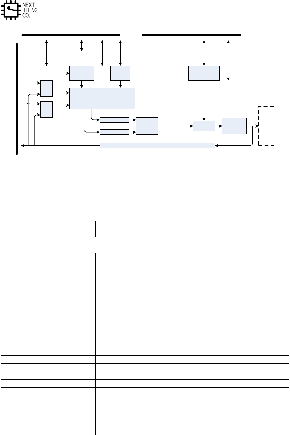
Display
GR8 User Manual(Version1.0) Copyright © 2017 Next Thing Co. All Rights Reserved. Page 292
PIPE 1 FIFO
PIPE 0 FIFO
On Chip
Frame
SRAM
Normal/YUV/Palette/Gamma/
Internal frame buffer Controller
Alpha
Blender 1 Alpha
Blender 0
H W Cursor
pattern buffer
Intelligent
Ext DMA
Controller
DEFE DEBE
LCD Controller
TV Encoder
Write back channel
Color
Correction
AHB BUS
FE0
FE1
Figure 6-2. Display Engine Block Diagram
6.2.3. DEBE Register list
Module name
Base address
DEBE
0x01E60000
Register name
Offset
Description
DEBE_MODCTL_REG
0x0800
DEBE Mode Control Register
DEBE_BACKCOLOR_REG
0x0804
DE-back Color Control Register
DEBE_DISSIZE_REG
0x0808
DE-back Display Size Setting Register
DEBE_LAYSIZE_REG
0x0810 –
0x081C
DE-layer Size Register
DEBE_LAYCOOR_REG
0x0820 –
0x082C
DE-layer Coordinate Control Register
DEBE_LAYLINEWIDTH_REG
0x0840 –
0x084C
DE-layer Frame Buffer Line Width Register
DEBE_LAYFB_L32ADD_REG
0x0850 –
0x085C
DE-layer Frame Buffer Low 32 bit Address Register
DEBE_LAYFB_H4ADD_REG
0x0860
DE-layer Frame Buffer High 4 bit Address Register
DEBE_REGBUFFCTL_REG
0x0870
DE-Register Buffer Control Register
DEBE_CKMAX_REG
0x0880
DE-color Key MAX Register
DEBE_CKMIN_REG
0x0884
DE-color Key MIN Register
DEBE_CKCFG_REG
0x0888
DE-color Key Configuration Register
DEBE_ATTCTL_REG0
0x0890 –
0x089C
DE-layer Attribute Control Register0
DEBE_ATTCTL_REG1
0x08A0 –
0x08AC
DE-layer Attribute Control Register1
DEBE_HWCCTL_REG
0x08D8
DE-HWC Coordinate Control Register
DEBE_HWCFBCTL_REG
0x08E0
DE-HWC Frame Buffer Format Register
Display
GR8 User Manual(Version1.0) Copyright © 2017 Next Thing Co. All Rights Reserved. Page 293
DEBE_WBCTL_REG
0x08F0
DEBE Write Back Control Register
DEBE_WBADD_REG
0x08F4
DEBE Write Back Address Register
DEBE_WBLINEWIDTH_REG
0x08F8
DEBE Write Back Buffer Line Width Register
DEBE_IYUVCTL_REG
0x0920
DEBE Input YUV Channel Control Register
DEBE_IYUVADD_REG
0x0930 – 0x0938
DEBE YUV Channel Frame Buffer Address Register
DEBE_IYUVLINEWIDTH_REG
0x0940 – 0x0948
DEBE YUV Channel Buffer Line Width Register
DEBE_YGCOEF_REG
0x0950 – 0x0958
DEBE Y/G Coefficient Register
DEBE_YGCONS_REG
0x095C
DEBE Y/G Constant Register
DEBE_URCOEF_REG
0x0960 – 0x0968
DEBE U/R Coefficient Register
DEBE_URCONS_REG
0x096C
DEBE U/R Constant Register
DEBE_VBCOEF_REG
0x0970 – 0x0978
DEBE V/B Coefficient Register
DEBE_VBCONS_REG
0x097C
DEBE V/B Constant Register
DEBE_OCCTL_REG
0x09C0
DEBE Output Color Control Register
DEBE_OCRCOEF_REG
0x09D0-0x09D8
DEBE Output Color R Coefficient Register
DEBE_OCRCONS_REG
0x09DC
DEBE Output Color R Constant Register
DEBE_OCGCOEF_REG
0x09E0-0x09E8
DEBE Output Color G Coefficient Register
DEBE_OCGCONS_REG
0x09EC
DEBE Output Color G Constant Register
DEBE_OCBCOEF_REG
0x09F0-0x09F8
DEBE Output Color B Coefficient Register
DEBE_OCBCONS_REG
0x09FC
DEBE Output Color B Constant Register
/
Memories
/
/
0x4400-0x47FF
Gamma Table
0x4800-0x4BFF
DE-HWC Pattern Memory Block
0x4C00-0x4FFF
DE-HWC Color Palette Table
0x5000-0x53FF
Pipe0 Palette Table
0x5400-0x57FF
Pipe1 Palette Table
6.2.4. DEBE Register Description
6.2.4.1. DEBE Mode Control Register (Default Value: 0x0000_0000)
Offset: 0x0800
Register Name: DEBE_MODCTL_REG
Bit
Read/Write
Default/Hex
Description
31:30
/
/
/
29
R/W
0x0
LINE_SEL
Start top/bottom line selection in interlace mode
28
R/W
0x0
ITLMOD_EN
Interlace mode enable
0:Disable
1:Enable
27:17
/
/
/
16
R/W
0x0
HWC_EN
Hardware cursor enabled/disabled control

Display
GR8 User Manual(Version1.0) Copyright © 2017 Next Thing Co. All Rights Reserved. Page 294
0: Disable
1: Enable
Hardware cursor has the highest priority, in the alpha blender0, the
alpha value of cursor will be selected
15:12
/
/
/
11
R/W
0x0
LAY3_EN
Layer3 Enable/Disable
0: Disable
1: Enable
10
R/W
0x0
LAY2_EN
Layer2 Enable/Disable
0: Disable
1: Enable
9
R/W
0x0
LAY1_EN
Layer1 Enable/Disable
0: Disable
1: Enable
8
R/W
0x0
LAY0_EN
Layer0 Enable/Disable
0: Disable
1: Enable
7:2
/
/
/
1
R/W
0x0
START_CTL
Normal output channel Start & Reset control
0: Reset
1: Start
0
R/W
0x0
DEBE_EN
DEBE Enable/Disable

Display
GR8 User Manual(Version1.0) Copyright © 2017 Next Thing Co. All Rights Reserved. Page 295
0: Disable
1: Enable
6.2.4.2. DE-Back Color Control Register
Offset: 0x0804
Register Name: DEBE_BACKCOLOR_REG
Bit
Read/Write
Default/Hex
Description
31:24
/
/
/
23:16
R/W
UDF
BK_RED
Red
Red screen background color value
15:8
R/W
UDF
BK_GREEN
Green
Green screen background color value
7:0
R/W
UDF
BK_BLUE
Blue
Blue screen background color value
6.2.4.3. DE-Back Display Size Setting Register
Offset: 0x0808
Register Name: DEBE_DISSIZE_REG
Bit
Read/Write
Default/Hex
Description
31:16
R/W
UDF
DIS_HEIGHT
Display height
The real display height = The value of these bits add 1
15:0
R/W
UDF
DIS_WIDTH
Display width
The real display width = The value of these bits add 1
6.2.4.4. DE-Layer Size Register
Offset:
Layer 0: 0x0810
Layer 1: 0x0814
Layer 2: 0x0818
Layer 3: 0x081C
Register Name: DEBE_LAYSIZE_REG

Display
GR8 User Manual(Version1.0) Copyright © 2017 Next Thing Co. All Rights Reserved. Page 296
Bit
Read/Write
Default/Hex
Description
31:29
/
/
/
28:16
R/W
UDF
LAY_HEIGHT
Layer Height
The Layer Height = The value of these bits add 1
15:13
/
/
/
12:0
R/W
UDF
LAY_WIDTH
Layer Width
The Layer Width = The value of these bits add 1
6.2.4.5. DE-Layer Coordinate Control Register
Offset:
Layer 0: 0x0820
Layer 1: 0x0824
Layer 2: 0x0828
Layer 3: 0x082C
Register Name: DEBE_LAYCOOR_REG
Bit
Read/Write
Default/Hex
Description
31:16
R/W
UDF
LAY_YCOOR
Y coordinate
Y is the left-top y coordinate of layer on screen in pixels
The Y represents the two’s complement
15:0
R/W
UDF
LAY_XCOOR
X coordinate
X is left-top x coordinate of the layer on screen in pixels
The X represents the two’s complement
Note: Setting the layer0-layer3 the coordinate (left-top) on screen control information
6.2.4.6. DE-Layer Frame Buffer Line Width Register
Offset:
Layer 0: 0x0840
Layer 1: 0x0844
Layer 2: 0x0848
Layer 3: 0x084C
Register Name: DEBE_LAYLINEWIDTH_REG
Display
GR8 User Manual(Version1.0) Copyright © 2017 Next Thing Co. All Rights Reserved. Page 297
Bit
Read/Write
Default/Hex
Description
31:0
R/W
UDF
LAY_LINEWIDTH
Layer frame buffer line width in bits
Note: If the layer is selected by video channel or YUV channel, the setting of this register will be ignored.
6.2.4.7. DE-Layer Frame Buffer Low 32 Bit Address Register
Offset:
Layer 0: 0x0850
Layer 1: 0x0854
Layer 2: 0x0858
Layer 3: 0x085C
Register Name: DEBE_LAYFB_L32ADD_REG
Bit
Read/Write
Default/Hex
Description
31:0
R/W
UDF
LAYFB_L32ADD
Buffer start Address
Layer Frame start Buffer Address in bit
Note: If the layer is selected by video channel or YUV channel, the setting of this register will be ignored.
6.2.4.8. DE-Layer Frame Buffer High 4 Bit Address Register
Offset: 0x0860
Register Name: DEBE_LAYFB_H4ADD_REG
Bit
Read/Write
Default/Hex
Description
31:28
/
/
/
27:24
R/W
UDF
LAY3FB_H4ADD
Layer3
Layer Frame Buffer Address in bit
23:20
/
/
/
19:16
R/W
UDF
LAY2FB_H4ADD
Layer2
Layer Frame Buffer Address in bit
15:12
/
/
/
11:8
R/W
UDF
LAY1FB_H4ADD
Layer1
Layer Frame Buffer Address in bit
7:4
/
/
/

Display
GR8 User Manual(Version1.0) Copyright © 2017 Next Thing Co. All Rights Reserved. Page 298
3:0
R/W
UDF
LAY0FB_H4ADD
Layer0
Layer Frame Buffer Address in bit
Note: If the layer is selected by video channel or YUV channel, the setting of this register will be ignored.
6.2.4.9. DE-Register Buffer Control Register (Default Value: 0x0000_0000)
Offset: 0x0870
Register Name: DEBE_REGBUFFCTL_REG
Bit
Read/Write
Default/Hex
Description
31:2
/
/
/
1
R/W
0x0
REGAUTOLOAD_DIS
Module registers loading auto mode disable control
0: registers auto loading mode
1: disable registers auto loading mode, the registers will be loaded by
writing 1 to bit0 of this register
0
R/W
0x0
REGLOADCTL
Register load control
When the Module registers loading auto mode disable control bit is set,
the registers will be loaded by writing 1 to the bit, and the bit will be
self cleared after the registers is loaded.
6.2.4.10. DE-Color Key MAX Register
Offset: 0x0880
Register Name: DEBE_CKMAX_REG
Bit
Read/Write
Default/Hex
Description
31:24
/
/
/
23:16
R/W
UDF
CKMAX_R
Red
Red color key max
15:8
R/W
UDF
CKMAX_G
Green
Green color key max
7:0
R/W
UDF
CKMAX_B
Blue
Blue color key max

Display
GR8 User Manual(Version1.0) Copyright © 2017 Next Thing Co. All Rights Reserved. Page 299
6.2.4.11. DE-Color Key MIN Register
Offset: 0x0884
Register Name: DEBE_CKMIN_REG
Bit
Read/Write
Default/Hex
Description
31:24
/
/
/
23:16
R/W
UDF
CKMIN_R
Red
Red color key min
15:8
R/W
UDF
CKMIN_G
Green
Green color key min
7:0
R/W
UDF
CKMIN_B
Blue
Blue color key min
6.2.4.12. DE-Color Key Configuration Register
Offset: 0x0888
Register Name: DEBE_CKCFG_REG
Bit
Read/Write
Default/Hex
Description
31:06
/
/
/
5:4
R/W
UDF
CKR_MATCH
Red Match Rule
00: always match
01: always match
10: match if (Color Min=<Color<=Color Max)
11: match if (Color>Color Max or Color<Color Min)
3:2
R/W
UDF
CKG_MATCH
Green Match Rule
00: always match
01: always match
10: match if (Color Min=<Color<=Color Max)
11: match if (Color>Color Max or Color<Color Min)
1:0
R/W
UDF
CKB_MATCH
Blue Match Rule

Display
GR8 User Manual(Version1.0) Copyright © 2017 Next Thing Co. All Rights Reserved. Page 300
00: always match
01: always match
10: match if (Color Min=<Color<=Color Max)
11: match if (Color>Color Max or Color<Color Min)
6.2.4.13. DE-Layer Attribute Control Register0
Offset:
Layer0: 0x0890
Layer1: 0x0894
Layer2: 0x0898
Layer3: 0x089C
Register Name: DEBE_ATTCTL_REG0
Bit
Read/Write
Default/Hex
Description
31:24
R/W
UDF
LAY_GLBALPHA
Alpha value
Alpha value is used for this layer
23:22
R/W
UDF
LAY_WORKMOD
Layer working mode selection
00: normal mode (Non-Index mode)
01: palette mode (Index mode)
10: internal frame buffer mode
11: gamma correction
Except the normal mode, if the other working mode is selected, the on-
chip SRAM will be enabled.
21:20
R/W
UDF
PREMUL
0: normal input layer
1: pre-multiply input layer
Other: reserved
19:18
R/W
UDF
CKEN
Color key Mode
00: disabled color key

Display
GR8 User Manual(Version1.0) Copyright © 2017 Next Thing Co. All Rights Reserved. Page 301
01: The layer color key matches another channel pixel data in Alpha
Blender1.
1x: Reserved
Only 2 channels pixel data can get to Alpha Blender1 at the same screen
coordinate.
17:16
/
/
/
15
R/W
UDF
LAY_PIPESEL
Pipe Select
0: select Pipe 0
1: select Pipe 1
14:12
/
/
/
11:10
R/W
UDF
LAY_PRISEL
Priority
The rule is: 11>10>01>00
When more than 2 layers are enabled, the priority value of each layer
must be different, so designers must keep the condition.
If more than 1 layers select the same pipe, in the overlapping area, only
the pixel of highest priority layer can pass the pipe to blender1.
If both 2 pipes are selected by layers, in the overlapping area, the alpha
value will use the alpha value of higher priority layer in the blender1.
9:3
/
/
/
2
R/W
UDF
LAY_YUVEN
YUV channel selection
0: disable
1: enable
Setting 2 or more layers YUV channel mode is illegal, so programmers
should confirm it.
1
R/W
UDF
LAY_VDOEN
Layer video channel selection enable control

Display
GR8 User Manual(Version1.0) Copyright © 2017 Next Thing Co. All Rights Reserved. Page 302
0: disable
1: enable
Normally, one layer cannot be set both video channel and YUV channel
mode. If both 2 mode are set, the layer will work in video channel mode,
and YUV channel mode will be ignored, so programmers should confirm
it.
Setting 2 or more layers video channel mode is illegal, and programmers
should confirm it.
0
R/W
UDF
LAY_GLBALPHAEN
Alpha Enable
0: Disable the alpha value of this register
1: Enable the alpha value of this register for the layer
6.2.4.14. DE-Layer Attribute Control Register1
Offset:
Layer0: 0x08A0
Layer1: 0x08A4
Layer2: 0x08A8
Layer3: 0x08AC
Register Name: DEBE_ATTCTL_REG1
Bit
Read/Write
Default/Hex
Description
31:16
/
/
/
15:14
R/W
UDF
LAY_HSCAFCT
Setting the internal frame buffer scaling factor, only valid in internal
frame buffer mode
SH
Height scale factor
00: no scaling
01: *2
10: *4
11: Reserved
13:12
R/W
UDF
LAY_WSCAFCT
Setting the internal frame buffer scaling factor, only valid in internal
frame buffer mode
SW

Display
GR8 User Manual(Version1.0) Copyright © 2017 Next Thing Co. All Rights Reserved. Page 303
Width scale factor
00: no scaling
01: *2
10: *4
11: Reserved
11:8
R/W
UDF
LAY_FBFMT
Frame buffer format
Normal mode data format
0000: mono 1-bpp
0001: mono 2-bpp
0010: mono 4-bpp
0011: mono 8-bpp
0100: color 16-bpp (R:6/G:5/B:5)
0101: color 16-bpp (R:5/G:6/B:5)
0110: color 16-bpp (R:5/G:5/B:6)
0111: color 16-bpp (Alpha:1/R:5/G:5/B:5)
1000: color 16-bpp (R:5/G:5/B:5/Alpha:1)
1001: color 24-bpp (Padding:8/R:8/G:8/B:8)
1010: color 32-bpp (Alpha:8/R:8/G:8/B:8)
1011: color 24-bpp (R:8/G:8/B:8)
1100: color 16-bpp (Alpha:4/R:4/G:4/B:4)
1101: color 16-bpp (R:4/G:4/B:4/Alpha:4)
Other: Reserved
Palette Mode data format
In palette mode, the data of external frame buffer is regarded as
pattern.
0000: 1-bpp
0001: 2-bpp
0010: 4-bpp
0011: 8-bpp
other: Reserved
Internal Frame buffer mode data format
Display
GR8 User Manual(Version1.0) Copyright © 2017 Next Thing Co. All Rights Reserved. Page 304
0000: 1-bpp
0001: 2-bpp
0010: 4-bpp
0011: 8-bpp
Other: Reserved
7:3
/
/
/
2
R/W
UDF
LAY_BRSWAPEN
B R channel swap
0: RGB. Follow the bit[11:8]----RGB
1: BGR. Swap the B R channel in the data format.
1:0
R/W
UDF
LAY_FBPS
PS
Pixels Sequence
See the follow table “Pixels Sequence”
6.2.4.15. Pixels Sequence Table
DE-layer attribute control register1 [11:08] = FBF (frame buffer format)
DE-layer attribute control register1 [01:00] = PS (pixels sequence)
Mono or Internal Frame Buffer 1-Bpp Or Palette 1-Bpp Mode : FBF = 0000
PS=00
Bit
31 30 29 28 27 26 25 24 23 22 21 20 19 18 17 16
P31
P30
P29
P28
P27
P26
P25
P24
P23
P22
P21
P20
P19
P18
P17
P16
P15
P14
P13
P12
P11
P10
P09
P08
P07
P06
P05
P04
P03
P02
P01
P00
15 14 13 12 11 10 09 08 07 06 05 04 03 02 01 00
PS=01
Bit
31 30 29 28 27 26 25 24 23 22 21 20 19 18 17 16
P24
P25
P26
P27
P28
P29
P30
P31
P16
P17
P18
P19
P20
P21
P22
P23
Display
GR8 User Manual(Version1.0) Copyright © 2017 Next Thing Co. All Rights Reserved. Page 305
P08
P09
P10
P11
P12
P13
P14
P15
P00
P01
P02
P03
P04
P05
P06
P07
15 14 13 12 11 10 09 08 07 06 05 04 03 02 01 00
PS=10
Bit
31 30 29 28 27 26 25 24 23 22 21 20 19 18 17 16
P07
P06
P05
P04
P03
P02
P01
P00
P15
P14
P13
P12
P11
P10
P09
P08
P23
P22
P21
P20
P19
P18
P17
P16
P31
P30
P29
P28
P27
P26
P25
P24
15 14 13 12 11 10 09 08 07 06 05 04 03 02 01 00
PS=11
Bit
31 30 29 28 27 26 25 24 23 22 21 20 19 18 17 16
P00
P01
P02
P03
P04
P05
P06
P07
P08
P09
P10
P11
P12
P13
P14
P15
P16
P17
P18
P19
P20
P21
P22
P23
P24
P25
P26
P27
P28
P29
P30
P31
15 14 13 12 11 10 09 08 07 06 05 04 03 02 01 00
Mono or Internal Frame Buffer 2-Bpp Or Palette 2-Bpp Mode : FBF = 0001
PS=00
Bit
31 30 29 28 27 26 25 24 23 22 21 20 19 18 17 16
P15
P14
P13
P12
P11
P10
P09
P08
P07
P06
P05
P04
P03
P02
P01
P00
15 14 13 12 11 10 09 08 07 06 05 04 03 02 01 00
PS=01
Bit
31 30 29 28 27 26 25 24 23 22 21 20 19 18 17 16
P12
P13
P14
P15
P08
P09
P10
P11
P04
P05
P06
P07
P00
P01
P02
P03
15 14 13 12 11 10 09 08 07 06 05 04 03 02 01 00
PS=10
Bit
Display
GR8 User Manual(Version1.0) Copyright © 2017 Next Thing Co. All Rights Reserved. Page 306
31 30 29 28 27 26 25 24 23 22 21 20 19 18 17 16
P03
P02
P01
P00
P07
P06
P05
P04
P11
P10
P09
P08
P15
P14
P13
P12
15 14 13 12 11 10 09 08 07 06 05 04 03 02 01 00
PS=11
Bit
31 30 29 28 27 26 25 24 23 22 21 20 19 18 17 16
P00
P01
P02
P03
P04
P05
P06
P07
P08
P09
P10
P11
P12
P13
P14
P15
15 14 13 12 11 10 09 08 07 06 05 04 03 02 01 00
Mono 4-bpp or palette 4-bpp mode : FBF = 0010
PS=00
Bit
31 30 29 28 27 26 25 24 23 22 21 20 19 18 17 16
P07
P06
P05
P04
P03
P02
P01
P00
15 14 13 12 11 10 09 08 07 06 05 04 03 02 01 00
PS=01
Bit
31 30 29 28 27 26 25 24 23 22 21 20 19 18 17 16
P06
P07
P04
P05
P02
P03
P00
P01
15 14 13 12 11 10 09 08 07 06 05 04 03 02 01 00
PS=10
Bit
31 30 29 28 27 26 25 24 23 22 21 20 19 18 17 16
P01
P00
P03
P02
P05
P04
P07
P06
15 14 13 12 11 10 09 08 07 06 05 04 03 02 01 00
Display
GR8 User Manual(Version1.0) Copyright © 2017 Next Thing Co. All Rights Reserved. Page 307
PS=11
Bit
31 30 29 28 27 26 25 24 23 22 21 20 19 18 17 16
P00
P01
P02
P03
P04
P05
P06
P07
15 14 13 12 11 10 09 08 07 06 05 04 03 02 01 00
Mono 8-bpp mode or palette 8-bpp mode : FBF = 0011
PS=00/11
Bit
31 30 29 28 27 26 25 24 23 22 21 20 19 18 17 16
P3
P2
P1
P0
15 14 13 12 11 10 09 08 07 06 05 04 03 02 01 00
PS=01/10
Bit
31 30 29 28 27 26 25 24 23 22 21 20 19 18 17 16
P0
P1
P2
P3
15 14 13 12 11 10 09 08 07 06 05 04 03 02 01 00
Color 16-bpp mode : FBF = 0100 or 0101 or 0110 or 0111 or 1000
PS=00
Bit
31 30 29 28 27 26 25 24 23 22 21 20 19 18 17 16
P1
P0
15 14 13 12 11 10 09 08 07 06 05 04 03 02 01 00
PS=01
Bit
Display
GR8 User Manual(Version1.0) Copyright © 2017 Next Thing Co. All Rights Reserved. Page 308
31 30 29 28 27 26 25 24 23 22 21 20 19 18 17 16
P0
P1
15 14 13 12 11 10 09 08 07 06 05 04 03 02 01 00
PS=10/11
Invalid
Color 24-bpp or 32-bpp mode : FBF = 1001 or 1010
PS=00/01
Bit
31 30 29 28 27 26 25 24 23 22 21 20 19 18 17 16
P0
15 14 13 12 11 10 09 08 07 06 05 04 03 02 01 00
The bytes sequence is ARGB
PS=10/11
Bit
31 30 29 28 27 26 25 24 23 22 21 20 19 18 17 16
P0
15 14 13 12 11 10 09 08 07 06 05 04 03 02 01 00
The bytes sequence is BGRA
6.2.4.16. DE-HWC Coordinate Control Register
Offset: 0x08D8
Register Name: DEBE_HWCCTL_REG
Bit
Read/Write
Default/Hex
Description
31:16
R/W
UDF
HWC_YCOOR
Hardware cursor Y coordinate
15:0
R/W
UDF
HWC_XCOOR
Hardware cursor X coordinate

Display
GR8 User Manual(Version1.0) Copyright © 2017 Next Thing Co. All Rights Reserved. Page 309
6.2.4.17. DE-HWC Frame Buffer Format Register
Offset: 0x08E0
Register Name: DEBE_HWCFBCTL_REG
Bit
Read/Write
Default/Hex
Description
31:24
R/W
UDF
HWC_YCOOROFF
Y coordinate offset
The hardware cursor is 32*32 2-bpp pattern, this value represents the
start position of the cursor in Y coordinate
23:16
R/W
UDF
HWC_XCOOROFF
X coordinate offset
The hardware cursor is 32*32 2-bpp pattern, this value represent the
start position of the cursor in X coordinate
15:6
/
/
/
5:4
R/W
UDF
HWC_YSIZE
Y size control
00: 32pixels per line
01: 64pixels per line
Other: reserved
3:2
R/W
UDF
HWC_XSIZE
X size control
00: 32pixels per row
01: 64pixels per row
Other: reserved
1:0
R/W
UDF
HWC_FBFMT
Pixels format control
00: 1bpp
01: 2bpp
10: 4bpp
11: 8bpp
6.2.4.18. DEBE Write Back Control Register
Offset: 0x08F0
Register Name: DEBE_WBCTL_REG
Bit
Read/Write
Default/Hex
Description

Display
GR8 User Manual(Version1.0) Copyright © 2017 Next Thing Co. All Rights Reserved. Page 310
31:13
/
/
/
12
R/W
UDF
WB_FMT
Write back data format setting
0:ARGB (little endian system)
1:BGRA (little endian system)
11:10
/
/
/
9
R/W
UDF
WB_EFLAG
Error flag
0:/
1: write back error
8
R/W
UDF
WB_STATUS
Write-back process status
0: write-back end or write-back disable
1: write-back in process
This flag indicates that a full frame has not been written back to
memory. The bit will be set when write-back enable bit is set, and be
cleared when write-back process ends.
7:2
/
/
/
1
R/W
UDF
WB_WOC
Write back only control
0: disable the write back only control, the normal channel data of back
end will transfer to LCD/TV controller too.
1: enable the write back only function, and the all output data will
bypass the LCD/TV controller.
0
R/W
UDF
WB_EN
Write back enable
0: Disable
1: Enable
If normal channel of back-end is selected by LCD/TV controller (write
back only function is disabled), the writing back process will start

Display
GR8 User Manual(Version1.0) Copyright © 2017 Next Thing Co. All Rights Reserved. Page 311
when write back enable bit is set and a new frame processing begins.
The bit will be cleared when the new writing-back frame starts to
process.
6.2.4.19. DEBE Write Back Address Register
Offset: 0x08F4
Register Name: DEBE_WBADD_REG
Bit
Read/Write
Default/Hex
Description
31:0
R/W
UDF
WB_ADD
The start address of write back data in WORD
6.2.4.20. DEBE Write Back Buffer Line Width Register
Offset: 0x08F8
Register Name: DEBE_WBLINEWIDTH_REG
Bit
Read/Write
Default/Hex
Description
31:0
R/W
UDF
WB_LINEWIDTH
Write back image buffer line width in bits
6.2.4.21. DEBE Input YUV Channel Control Register
Offset: 0x0920
Register Name: DEBE_IYUVCTL_REG
Bit
Read/Write
Default/Hex
Description
31:15
/
/
/
14:12
R/W
UDF
IYUV_FBFMT
Input data format
000: planar YUV 411
001: planar YUV 422
010: planar YUV 444
011: interleaved YUV 422
100: interleaved YUV 444
Other: illegal
11:10
/
/
/
9:8
R/W
UDF
IYUV_FBPS
Pixel sequence
In planar data format mode:

Display
GR8 User Manual(Version1.0) Copyright © 2017 Next Thing Co. All Rights Reserved. Page 312
00: Y3Y2Y1Y0
01: Y0Y1Y2Y3 (the other 2 components are same)
Other: illegal
In interleaved YUV 422 data format mode:
00: UYVY
01: YUYV
10: VYUY
11: YVYU
In interleaved YUV 444 data format mode:
00: AYUV
01: VUYA
Other: illegal
7:5
/
/
/
4
R/W
UDF
IYUV_LINNEREN
0: liner
1:
3:1
/
/
/
0
R/W
UDF
IYUV_EN
YUV channel enable control
0: disable
1: enable
Source Data Input Data Ports:
Input buffer channel
Planar YUV
Interleaved YUV
Channel0
Y
YUV
Channel1
U
-
Channel2
V
-

Display
GR8 User Manual(Version1.0) Copyright © 2017 Next Thing Co. All Rights Reserved. Page 313
6.2.4.22. DEBE YUV Channel Frame Buffer Address Register
Offset:
Channel 0 : 0x0930
Channel 1 : 0x0934
Channel 2 : 0x0938
Register Name: DEBE_IYUVADD_REG
Bit
Read/Write
Default/Hex
Description
31:0
R/W
UDF
IYUV_ADD
Buffer Address
Frame buffer address in BYTE
6.2.4.23. DEBE YUV Channel Buffer Line Width Register
Offset:
Channel 0 : 0x0940
Channel 1 : 0x0944
Channel 2 : 0x0948
Register Name: DEBE_IYUVLINEWIDTH_REG
Bit
Read/Write
Default/Hex
Description
31:0
R/W
UDF
IYUV_LINEWIDTH
Line width
The width is the distance from the start of one line to the start of the
next line.
Description in bits
YUV to RGB conversion algorithm formula:
R =
(R Y component coefficient * Y) +
(R U component coefficient * U) +
(R V component coefficient * V) +
R constant
G =
(G Y component coefficient * Y) +
(G U component coefficient * U) +
(G V component coefficient * V) +
Display
GR8 User Manual(Version1.0) Copyright © 2017 Next Thing Co. All Rights Reserved. Page 314
G constant
B =
(B Y component coefficient * Y) +
(B U component coefficient * U) +
(B V component coefficient * V) +
B constant
6.2.4.24. DEBE Y/G Coefficient Register
Offset:
G/Y component: 0x0950
R/U component: 0x0954
B/V component: 0x0958
Register Name: DEBE_YGCOEF_REG
Bit
Read/Write
Default/Hex
Description
31:13
/
/
/
12:0
R/W
UDF
IYUV_YGCOEF
The Y/G coefficient
The value equals to coefficient*210
6.2.4.25. DEBE Y/G Constant Register
Offset: 0x095C
Register Name: DEBE_YGCONS_REG
Bit
Read/Write
Default/Hex
Description
31:14
/
/
/
13:0
R/W
UDF
IYUV_YGCONS
The Y/G constant
The value equals to coefficient*24
6.2.4.26. DEBE U/R Coefficient Register
Offset:
G/Y component: 0x0960
R/U component: 0x0964
B/V component: 0x0968
Register Name: DEBE_URCOEF_REG
Bit
Read/Write
Default/Hex
Description

Display
GR8 User Manual(Version1.0) Copyright © 2017 Next Thing Co. All Rights Reserved. Page 315
31:13
/
/
/
12:0
R/W
UDF
IYUV_URCOEF
The U/R coefficient
The value equals to coefficient*210
6.2.4.27. DEBE U/R Constant Register
Offset: 0x096C
Register Name: DEBE_URCONS_REG
Bit
Read/Write
Default/Hex
Description
31:14
/
/
/
13:0
R/W
UDF
IYUV_URCONS
The U/R constant
The value equals to coefficient*24
6.2.4.28. DEBE V/B Coefficient Register
Offset:
G/Y component: 0x0970
R/U component: 0x0974
B/V component: 0x0978
Register Name: DEBE_VBCOEF_REG
Bit
Read/Write
Default/Hex
Description
31:13
/
/
/
12:0
R/W
UDF
IYUV_VBCOEF
The V/B coefficient
The value equals to coefficient*210
6.2.4.29. DEBE V/B Constant Register
Offset: 0x097C
Register Name: DEBE_VBCONS_REG
Bit
Read/Write
Default/Hex
Description
31:14
/
/
/
13:0
R/W
UDF
IYUV_VBCONS
The V/B constant
The value equals to coefficient*24

Display
GR8 User Manual(Version1.0) Copyright © 2017 Next Thing Co. All Rights Reserved. Page 316
6.2.4.30. DEBE Output Color Control Register
Offset: 0x09C0
Register Name: DEBE_OCCTL_REG
Bit
Read/Write
Default/Hex
Description
31:1
/
/
/
0
R/W
UDF
OC_EN
Color control module enable control
0: disable
1: enable
Color correction conversion algorithm formula:
R =
(R R component coefficient * R) +
(R G component coefficient * G) +
(R B component coefficient * B) +
R constant
G =
(G R component coefficient * R) +
(G G component coefficient * G) +
(G B component coefficient * B) +
G constant
B =
(B R component coefficient * R) +
(B G component coefficient * G) +
(B B component coefficient * B) +
B constant
6.2.4.31. DEBE Output Color R Coefficient Register
Offset:
R component: 0x09D0
G component: 0x09D4
Register Name: DEBE_OCRCOEF_REG
Display
GR8 User Manual(Version1.0) Copyright © 2017 Next Thing Co. All Rights Reserved. Page 317
B component: 0x09D8
Bit
Read/Write
Default/Hex
Description
31:14
/
/
/
13:0
R/W
UDF
OC_RCOEF
The R coefficient
The value equals to coefficient*210
6.2.4.32. DEBE Output Color R Constant Register
Offset: 0x09DC
Register Name: DEBE_OCRCONS_REG
Bit
Read/Write
Default/Hex
Description
31:15
/
/
/
14:0
R/W
UDF
OC_RCONS
The R constant
The value equals to coefficient*24
6.2.4.33. DEBE Output Color G Coefficient Register
Offset:
R component: 0x09E0
G component: 0x09E4
B component: 0x09E8
Register Name: DEBE_OCGCOEF_REG
Bit
Read/Write
Default/Hex
Description
31:14
/
/
/
13:0
R/W
UDF
OC_GCOEF
The G coefficient
The value equals to coefficient*210
6.2.4.34. DEBE Output Color G Constant Register
Offset: 0x09EC
Register Name: DEBE_OCGCONS_REG
Bit
Read/Write
Default/Hex
Description
31:15
/
/
/
14:0
R/W
UDF
OC_GCONS
The G constant
The value equals to coefficient*24
Display
GR8 User Manual(Version1.0) Copyright © 2017 Next Thing Co. All Rights Reserved. Page 318
6.2.4.35. DEBE Output Color B Coefficient Register
Offset:
G/Y component: 0x09F0
R/U component: 0x09F4
B/V component: 0x09F8
Register Name: DEBE_OCBCOEF_REG
Bit
Read/Write
Default/Hex
Description
31:14
/
/
/
13:0
R/W
UDF
OC_BCOEF
The B coefficient
The value equals to coefficient*210
6.2.4.36. DEBE Output Color B Constant Register
Offset: 0x09FC
Register Name: DEBE_OCBCONS_REG
Bit
Read/Write
Default/Hex
Description
31:15
/
/
/
14:0
R/W
UDF
OC_BCONS
The B constant
The value equals to coefficient*24
6.2.4.37. DE-HWC Pattern Memory Block
Function:
1bpp:
Bit
31 30 29 28 27 26 25 24 23 22 21 20 19 18 17 16
P31
P30
P29
P28
P27
P26
P25
P24
P23
P22
P21
P20
P19
P18
P17
P16
P15
P14
P13
P12
P11
P10
P09
P08
P07
P06
P05
P04
P03
P02
P01
P00
15 14 13 12 11 10 09 08 07 06 05 04 03 02 01 00
2bpp:
Bit
31 30 29 28 27 26 25 24 23 22 21 20 19 18 17 16
Display
GR8 User Manual(Version1.0) Copyright © 2017 Next Thing Co. All Rights Reserved. Page 319
P15
P14
P13
P12
P11
P10
P09
P08
P07
P06
P05
P04
P03
P02
P01
P00
15 14 13 12 11 10 09 08 07 06 05 04 03 02 01 00
4bpp:
Bit
31 30 29 28 27 26 25 24 23 22 21 20 19 18 17 16
P07
P06
P05
P04
P03
P02
P01
P00
15 14 13 12 11 10 09 08 07 06 05 04 03 02 01 00
8bpp:
Bit
31 30 29 28 27 26 25 24 23 22 21 20 19 18 17 16
P3
P2
P1
P0
15 14 13 12 11 10 09 08 07 06 05 04 03 02 01 00
Offset:
0x4800-0x4BFF
DE-HW cursor pattern memory block
Bit
Read/Write
Default/Hex
Description
31:00
R/W
UDF
Hardware cursor pixel pattern
Specify the color displayed for each of the hardware cursor pixels.
6.2.4.38. DE-HWC Palette Table
Offset:
0x4C00-0x4FFF
DE-HW palette table
Bit
Read/Write
Default/Hex
Description
31:24
R/W
UDF
Alpha value
23:16
R/W
UDF
Red value
15:08
R/W
UDF
Green value
07:00
R/W
UDF
Blue value
Display
GR8 User Manual(Version1.0) Copyright © 2017 Next Thing Co. All Rights Reserved. Page 320
The following figure (only with 2bpp mode) shows the RAM array used for hardware cursor palette lookup and the
corresponding colors output.
6.2.4.39. Palette Mode
Offset:
Pipe0:0x5000-0x53FF
Pipe1:0x5400-0x57FF
Pipe palette color table SRAM block
Bit
Read/Write
Default/Hex
Description
31:24
R/W
UDF
Alpha value
23:16
R/W
UDF
Red value
15:08
R/W
UDF
Green value
07:00
R/W
UDF
Blue value
In this mode, RAM array is used for palette lookup table; each pixel in the layer frame buffer is treated as an index
into the RAM array to select the actual color.
The following figure shows the RAM array used for palette lookup and the corresponding colors output.
HWC Index memory
array
Output color
Hardware cursor index memory
& palette
HWC palette table
Color1
Color0
Color254
Color255
2bpp mode
0 R0 G0 B0
1 R1 G1 B1
254 R254 G254 B254
255 R255 G255 B255
3 2 0 2
1 3 2 2
3 3 0 1
bit7 bit0
2 R2 G2 B2
0 R0 G0 B0
2 R2 G2 B2
3 R3 G3 B3
1 R1 G1 B1
0 R0 G0 B0
3 R3 G3 B3
3 R3 G3 B3
2 R2 G2 B2
2 R2 G2 B2
3 R3 G3 B3
1 R1 G1 B1
Display
GR8 User Manual(Version1.0) Copyright © 2017 Next Thing Co. All Rights Reserved. Page 321
6.2.4.40. Internal Frame Buffer Mode
In internal frame buffer mode, the RAM array is used as an on-chip frame buffer; each pixel in the RAM array is
used to select one of the palette 32-bit colors.
1bpp:
Bit
31 30 29 28 27 26 25 24 23 22 21 20 19 18 17 16
P31
P30
P29
P28
P27
P26
P25
P24
P23
P22
P21
P20
P19
P18
P17
P16
P15
P14
P13
P12
P11
P10
P09
P08
P07
P06
P05
P04
P03
P02
P01
P00
15 14 13 12 11 10 09 08 07 06 05 04 03 02 01 00
2bpp:
Bit
31 30 29 28 27 26 25 24 23 22 21 20 19 18 17 16
P15
P14
P13
P12
P11
P10
P09
P08
P07
P06
P05
P04
P03
P02
P01
P00
15 14 13 12 11 10 09 08 07 06 05 04 03 02 01 00
4bpp:
Bit
31 30 29 28 27 26 25 24 23 22 21 20 19 18 17 16
P07
P06
P05
P04
P03
P02
P01
P00
15 14 13 12 11 10 09 08 07 06 05 04 03 02 01 00
8bpp:
0 R0 G0 B0
1 R1 G1 B1
254 R254 G254 B254
255 R255 G255 B255
n Rn Gn Bn
On chip SRAM array
5 38 133 28
Inputting external
frame buffer data
(8bpp) Output color
5 R5 G5 B5
38 R38 G38 B38
133 R133 G133 B133
28 R28 G28 B28
On chip SRAM for palette lookup
Display
GR8 User Manual(Version1.0) Copyright © 2017 Next Thing Co. All Rights Reserved. Page 322
Bit
31 30 29 28 27 26 25 24 23 22 21 20 19 18 17 16
P3
P2
P1
P0
15 14 13 12 11 10 09 08 07 06 05 04 03 02 01 00
Offset:
0x4000-0x57FF
DE-on chip SRAM block
Bit
Read/Write
Default/Hex
Description
31:00
R/W
UDF
Internal frame buffer pixel pattern
Specify the color displayed for each of the internal frame buffer pixels.
6.2.4.41. Internal Frame Buffer Mode Palette Table
Offset:
Pipe0:0x5000-0x53FF
Pipe1:0x5400-0x57FF
Pipe palette table
Bit
Read/Write
Default/Hex
Description
31:24
R/W
UDF
Alpha value
23:16
R/W
UDF
Red value
15:08
R/W
UDF
Green value
07:00
R/W
UDF
Blue value
The following figure shows the RAM array used for internal frame buffer mode and the corresponding colors output.
Display
GR8 User Manual(Version1.0) Copyright © 2017 Next Thing Co. All Rights Reserved. Page 323
6.2.4.42. Gamma Correction Mode
Offset:
0x4400-0x47FF
DE-on chip SRAM block
Bit
Read/Write
Default/Hex
Description
31:24
R/W
UDF
Alpha channel intensity
23:16
R/W
UDF
Red channel intensity
15:08
R/W
UDF
Green channel intensity
07:00
R/W
UDF
Blue channel intensity
In gamma correction mode, the RAM array is used for gamma correction; each pixel’s alpha, red, green, and blue
color component is treated as an index into the SRAM array. The corresponding
Alpha, red, green, or blue channel intensity value at that index is used in the actual color.
The following figure shows the RAM array used for gamma correction and the corresponding colors output.
On chip SRAM array
Output color
On chip SRAM for internal
frame buffer
Internal frame buffer
Palette table
2bpp mode
3 2 0 2
1 3 2 2
3 3 0 1
bit7 bit0
2 R2 G2 B2
0 R0 G0 B0
2 R2 G2 B2
3 R3 G3 B3
1 R1 G1 B1
0 R0 G0 B0
3 R3 G3 B3
3 R3 G3 B3
2 R2 G2 B2
2 R2 G2 B2
3 R3 G3 B3
1 R1 G1 B1
Color1
Color0
Color254
Color255
0 R0 G0 B0
1 R1 G1 B1
254 R254 G254 B254
255 R255 G255 B255
Display
GR8 User Manual(Version1.0) Copyright © 2017 Next Thing Co. All Rights Reserved. Page 324
0 R0 G0 B0
1 R1 G1 B1
254 R254 G254 B254
255 R255 G255 B255
n Rn Gn Bn
On chip SRAM array
5 38 133 28
Inputting external
frame buffer data Output color
5 R38 G133 B28
On chip SRAM for gamma correction
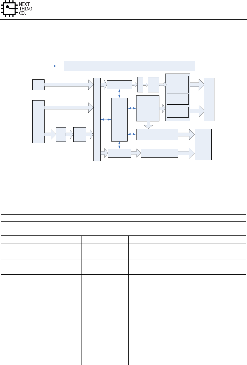
Display
GR8 User Manual(Version1.0) Copyright © 2017 Next Thing Co. All Rights Reserved. Page 325
6.3. TCON
6.3.1. Block Diagram
Async FIFO1
DMA
DE
OUT1
CONTROL LOGIC
HV TIMING
CPU TIMING
TV DATA
BASIC
TIMING
GENERATOR
LCDdata
CEU
OUT2
OUT0
3
To
2
M
U
X
Async FIFO2
FIFO Flag
&
CLOCK
GEN
MAX
700MHz
DATA
FORMATTER
RGB
2
YUV
(444)
F
R
M
Gamma TV TIMING GENERATOR
LCD ctlr
TV ctlr
TV data
LCD
TV
Figure 6-3. LCD/TV Timing Controller Block Diagram
6.3.2. TCON Register List
Module Name
Base Address
TCON
0x01C0C000
Register Name
Offset
Description
TCON_GCTL_REG
0x0000
TCON Global Control Register
TCON_GINT0_REG
0x0004
TCON Global Interrupt Register0
TCON_GINT1_REG
0x0008
TCON Global Interrupt Register1
TCON0_FRM_CTL_REG
0x0010
TCON FRM Control Register
TCON0_FRM_SEED0_REG
0x0014
TCON FRM Seed Register0
TCON0_FRM_SEED1_REG
0x0018
TCON FRM Seed Register1
TCON0_FRM_SEED2_REG
0x001C
TCON FRM Seed Register2
TCON0_FRM_SEED3_REG
0x0020
TCON FRM Seed Register3
TCON0_FRM_SEED4_REG
0x0024
TCON FRM Seed Register4
TCON0_FRM_SEED5_REG
0x0028
TCON FRM Seed Register5
TCON0_FRM_TAB0_REG
0x002C
TCON FRM Table Register0
TCON0_FRM_TAB1_REG
0x0030
TCON FRM Table Register1
TCON0_FRM_TAB2_REG
0x0034
TCON FRM Table Register2
TCON0_FRM_TAB3_REG
0x0038
TCON FRM Table Register3
TCON0_CTL_REG
0x0040
TCON0 Control Register
TCON0_DCLK_REG
0x0044
TCON0 Data Clock Register

Display
GR8 User Manual(Version1.0) Copyright © 2017 Next Thing Co. All Rights Reserved. Page 326
TCON0_BASIC0_REG
0x0048
TCON0 Basic Timing Register0
TCON0_BASIC1_REG
0x004C
TCON0 Basic Timing Register1
TCON0_BASIC2_REG
0x0050
TCON0 Basic Timing Register2
TCON0_BASIC3_REG
0x0054
TCON0 Basic Timing Register3
TCON0_HV_IF_REG
0x0058
TCON0 Hv Panel Interface Register
TCON0_CPU_IF_REG
0x0060
TCON0 CPU Panel Interface Register
TCON0_CPU_WR_REG
0x0064
TCON0 CPU Panel Write Data Register
TCON0_CPU_RD0_REG
0x0068
TCON0 CPU Panel Read Data Register0
TCON0_CPU_RD1_REG
0x006C
TCON0 CPU Panel Read Data Register1
TCON0_IO_POL_REG
0x0088
TCON0 IO Polarity Register
TCON0_IO_TRI_REG
0x008C
TCON0 IO Control Register
TCON1_CTL_REG
0x0090
TCON1 Control Register
TCON1_BASIC0_REG
0x0094
TCON1 Basic Timing Register0
TCON1_BASIC1_REG
0x0098
TCON1 Basic Timing Register1
TCON1_BASIC2_REG
0x009C
TCON1 Basic Timing Register2
TCON1_BASIC3_REG
0x00A0
TCON1 Basic Timing Register3
TCON1_BASIC4_REG
0x00A4
TCON1 Basic Timing Register4
TCON1_BASIC5_REG
0x00A8
TCON1 Basic Timing Register5
TCON1_IO_POL_REG
0x00F0
TCON1 IO Polarity Register
TCON1_IO_TRI_REG
0x00F4
TCON1 IO Control Register
TCON_CEU_CTL_REG
0x0100
TCON CEU Control Register
TCON_CEU_COEF0_REG
0x0110
TCON CEU Coefficient Register0
TCON_CEU_COEF1_REG
0x0114
TCON CEU Coefficient Register1
TCON_CEU_COEF2_REG
0x0118
TCON CEU Coefficient Register2
TCON_CEU_COEF3_REG
0x011C
TCON CEU Coefficient Register3
TCON_CEU_COEF4_REG
0x0120
TCON CEU Coefficient Register4
TCON_CEU_COEF5_REG
0x0124
TCON CEU Coefficient Register5
TCON_CEU_COEF6_REG
0x0128
TCON CEU Coefficient Register6
TCON_CEU_COEF7_REG
0x012C
TCON CEU Coefficient Register7
TCON_CEU_COEF8_REG
0x0130
TCON CEU Coefficient Register8
TCON_CEU_COEF9_REG
0x0134
TCON CEU Coefficient Register9
TCON_CEU_COEF10_REG
0x0138
TCON CEU Coefficient Register10
TCON_CEU_COEF11_REG
0x013C
TCON CEU Coefficient Register11
TCON_CEU_COEF12_REG
0x0140
TCON CEU Coefficient Register12
TCON_CEU_COEF13_REG
0x0144
TCON CEU Coefficient Register13
TCON_CEU_COEF14_REG
0x0148
TCON CEU Coefficient Register14
TCON1_ FILL_CTL_REG
0x0300
TCON1 Fill Data Control Register
TCON1_ FILL_BEGIN0_REG
0x0304
TCON1 Fill Data Begin Register0
TCON1_ FILL_END0_REG
0x0308
TCON1 Fill Data End Register0
TCON1_ FILL_DATA0_REG
0x030C
TCON1 Fill Data Value Register0
TCON1_ FILL_BEGIN1_REG
0x0310
TCON1 Fill Data Begin Register1
TCON1_ FILL_END1_REG
0x0314
TCON1 Fill Data End Register1
TCON1_ FILL_DATA1_REG
0x0318
TCON1 Fill Data Value Register1
TCON1_ FILL_BEGIN2_REG
0x031C
TCON1 Fill Data Begin Register2
TCON1_ FILL_END2_REG
0x0320
TCON1 Fill Data End Register2

Display
GR8 User Manual(Version1.0) Copyright © 2017 Next Thing Co. All Rights Reserved. Page 327
TCON1_ FILL_DATA2_REG
0x0324
TCON1 Fill Data Value Register2
TCON1_GAMMA_TABLE_REG
0x400-0x7FF
TCON1 Gama Table Register
6.3.3. TCON Register Description
6.3.3.1. TCON Global Control Register(Default Value: 0x0000_0000)
Offset: 0x0000
Register Name: TCON_GCTL_REG
Bit
Read/Write
Default/Hex
Description
31
R/W
0x0
TCON_EN
0: disable
1: enable
When it is disabled, the module will be reset to idle state.
30
R/W
0x0
TCON_GAMMA_EN
0: disable
1: enable
29:1
/
/
/
0
R/W
0x0
IO_MAP_SEL
0: TCON0
1: TCON1
Note: This bit determines which IO_INV/IO_TRI is valid
6.3.3.2. TCON Global Interrupt Register0(Default Value: 0x0000_0000)
Offset: 0x0004
Register Name: TCON_GINT0_REG
Bit
Read/Write
Default/Hex
Description
31
R/W
0x0
TCON0_VB_INT_EN
0: disable
1: enable
30
R/W
0x0
TCON1_VB_INT_EN

Display
GR8 User Manual(Version1.0) Copyright © 2017 Next Thing Co. All Rights Reserved. Page 328
0: disable
1: enable
29
R/W
0x0
TCON0_LINE_INT_EN
0: disable
1: enable
28
R/W
0x0
TCON1_LINE_INT_EN
0: disable
1: enable
27:16
/
/
/
15
R/W
0x0
TCON0_VB_INT_FLAG
Asserted during vertical no-display period every frame.
Write 0 to clear it.
14
R/W
0x0
TCON1_VB_INT_FLAG
Asserted during vertical no-display period every frame.
Write 0 to clear it.
13
R/W
0x0
TCON0_LINE_INT_FLAG
Trigger when SY0 matches the current TCON0 scan line
Write 0 to clear it.
12
R/W
0x0
TCON1_LINE_INT_FLAG
Trigger when SY1 matches the current TCON1 scan line
Write 0 to clear it.
11:0
/
/
/
6.3.3.3. TCON Global Interrupt Register1(Default Value: 0x0000_0000)
Offset: 0x0008
Register Name: TCON_GINT1_REG
Bit
Read/Write
Default/Hex
Description
31:27
/
/
/
26:16
R/W
0x0
TCON0_Line_Int_Num
scan line for TCON0 line trigger(including inactive lines)
Setting it for the specified line for trigger0.
Note: SY0 is writable only when LINE_TRG0 is disabled.
15:11
/
/
/
10:0
R/W
0x0
TCON1_Line_Int_Num

Display
GR8 User Manual(Version1.0) Copyright © 2017 Next Thing Co. All Rights Reserved. Page 329
scan line for TCON1 line trigger(including inactive lines)
Setting it for the specified line for trigger 1.
Note: SY1 is writable only when LINE_TRG1 is disabled.
6.3.3.4. TCON FRM Control Register(Default Value: 0x0000_0000)
Offset: 0x0010
Register Name: TCON0_FRM_CTL_REG
Bit
Read/Write
Default/Hex
Description
31
R/W
0x0
TCON0_FRM_EN
0:disable
1:enable
30:12
/
/
/
6
R/W
0x0
TCON0_FRM_MODE_R
0: 6bit frm output
1: 5bit frm output
5
R/W
0x0
TCON0_FRM_MODE_G
0: 6bit frm output
1: 5bit frm output
4
R/W
0x0
TCON0_FRM_MODE_B
0: 6bit frm output
1: 5bit frm output
1:0
R/W
0x0
TCON0_FRM_TEST
00: FRM
01: half 5/6bit, half FRM
10: half 8bit, half FRM
11: half 8bit, half 5/6bit
6.3.3.5. TCON FRM Pixel Seed Register(Default Value: 0x0000_0000)
Offset: 0x0014-0x001C
Register Name: TCON0_FRM_PIXEL_SEED_REG
Bit
Read/Write
Default/Hex
Description
Display
GR8 User Manual(Version1.0) Copyright © 2017 Next Thing Co. All Rights Reserved. Page 330
31:25
/
/
/
24:0
R/W
0x0
PIXEL_SEED_VALUE
Note: Avoid set it to 0
6.3.3.6. TCON FRM Line Seed Register(Default Value: 0x0000_0000)
Offset: 0x0020-0x0028
Register Name: TCON0_FRM_LINE_SEED_REG
Bit
Read/Write
Default/Hex
Description
31:25
/
/
/
12:0
R/W
0x0
LINE_SEED_VALUE
Note: Avoid set it to 0
6.3.3.7. TCON FRM Table Register(Default Value: 0x0000_0000)
Offset: 0x002C-0x0038
Register Name: TCON0_FRM_TAB_REG
Bit
Read/Write
Default/Hex
Description
31:0
R/W
0x0
FRM_TABLE_VALUE
6.3.3.8. TCON0 Control Register(Default Value: 0x0000_0000)
Offset: 0x0040
Register Name: TCON0_CTL_REG
Bit
Read/Write
Default/Hex
Description
31
R/W
0x0
TCON0_EN
0: Disable
1: Enable
Note: It executes at the beginning of the first blank line of TCON0
timing.
30:26
/
/
/
25:24
R/W
0x0
TCON0_IF
00: HV(Sync+DE)
01: 8080 I/F
10: TTL I/F
11: reserved
23
R/W
0x0
TCON0_RG_SWAP

Display
GR8 User Manual(Version1.0) Copyright © 2017 Next Thing Co. All Rights Reserved. Page 331
0: Default
1: Swap RED and BLUE data at FIFO1
22
R/W
0x0
TCON0_TEST_VALUE
0:All 0s
1:All 1s
21
R/W
0x0
TCON0_FIFO1_RST
Writing 1 and then 0 to this bit will reset FIFO 1
Note: 1 holding time must be more than 1 DCLK
20
R/W
0x0
TCON0_INTERLACE_EN
0:Disable
1:Enable
Note: This flag is valid only when TCON0_EN == 1
19:9
/
/
/
8:4
R/W
0x0
TCON0_STATE_DELAY
STA delay
Note: Valid only when TCON0_EN == 1
3:2
/
/
/
1:0
R/W
0x0
TCON0_SRC_SEL
00: DE CH1(FIFO1 enable)
01: DE CH2(FIFO1 enable)
10: DMA 565 input(FIFO1 enable)
11: Test intput(FIFO1 disable)
Note: These bits are sampled only at the beginning of the first blank
line of TCON0 timing. Generally, when input source changes, it will
change at the beginning of the first blank line of TCON0 timing.
When FIFO1 and FIFO2 select the same source and FIFO2 is enabled,
it executes at the beginning of the first blank line of TV timing. Also,
TCON0 timing generator will reset to the beginning of the first blank
line.

Display
GR8 User Manual(Version1.0) Copyright © 2017 Next Thing Co. All Rights Reserved. Page 332
6.3.3.9. TCON0 Data Clock Register(Default Value: 0x0000_0000)
Offset: 0x0044
Register Name: TCON0_DCLK REG
Bit
Read/Write
Default/Hex
Description
31
R/W
0x0
TCON0_DCLK_EN
30:7
/
/
/
6:0
R/W
0x0
TCON0_DCLK_DIV
Tdclk = Tsclk * DCLKDIV
Note:
1.If dclk1&dclk2 used, DCLKDIV >=6
2.If dclk only, DCLKDIV >=4
6.3.3.10. TCON0 Basic Timing Register0(Default Value: 0x0000_0000)
Offset: 0x0048
Register Name: TCON0_BASIC0_REG
Bit
Read/Write
Default/Hex
Description
31:27
/
/
/
26:16
R/W
0x0
TCON0_X
Panel width is X+1
15:11
/
/
/
10:0
R/W
0x0
TCON0_Y
Panel height is Y+1
6.3.3.11. TCON0 Basic Timing Register1(Default Value: 0x0000_0000)
Offset: 0x004C
Register Name: TCON0_BASIC1_REG
Bit
Read/Write
Default/Hex
Description
31:28
/
/
/
27:16
R/W
0x0
HT
Thcycle = (HT+1) * Tdclk
Note:1) parallel :HT >= (HBP +1) + (X+1) +2
2) serial 1: HT >= (HBP +1) + (X+1) *3+2
3) serial 2: HT >= (HBP +1) + (X+1) *3/2+2
15:10
/
/
/

Display
GR8 User Manual(Version1.0) Copyright © 2017 Next Thing Co. All Rights Reserved. Page 333
6.3.3.12. TCON0 Basic Timing Register2(Default Value: 0x0000_0000)
Offset: 0x0050
Register Name: TCON0_BASIC2_REG
Bit
Read/Write
Default/Hex
Description
31:21
/
/
/
27:16
R/W
0x0
VT
TVT = (VT)/2 * Thsync
Note: VT/2 >= (VBP+1 ) + (Y+1) +2
15:10
/
/
/
9:0
R/W
0x0
VBP
Tvbp = (VBP +1) * Thsync
6.3.3.13. TCON0 Basic Timing Register3(Default Value: 0x0000_0000)
Offset: 0x0054
Register Name: TCON0_BASIC3_REG
Bit
Read/Write
Default/Hex
Description
31:22
/
/
/
25:16
R/W
0x0
HSPW
Thspw = (HSPW+1) * Tdclk
Note: HT> (HSPW+1)
15:10
/
/
/
9:0
R/W
0x0
VSPW
Tvspw = (VSPW+1) * Thsync
Note: VT/2 > (VSPW+1)
6.3.3.14. TCON0 HV Panel Interface Register(Default Value: 0x0000_0000)
Offset: 0x0058
Register Name: TCON0_HV_IF_REG
Bit
Read/Write
Default/Hex
Description
31
R/W
0x0
HV_MODE
0: 24bit parallel mode
1: 8bit serial mode
30
R/W
0x0
SERIAL_MODE

Display
GR8 User Manual(Version1.0) Copyright © 2017 Next Thing Co. All Rights Reserved. Page 334
0: 8bit/3cycle RGB serial mode(RGB888)
1: 8bit/2cycle YUV serial mode(CCIR656)
29:28
/
/
/
27:26
R/W
0x0
RGB888_SM0
Serial RGB888 mode Output sequence at odd lines of the panel (line
1, 3, 5, 7…)
00: R→G→B
01: B→R→G
10: G→B→R
11: R→G→B
25:24
R/W
0x0
RGB888_SM1
Serial RGB888 mode Output sequence at even lines of the panel (line
2, 4, 6, 8…)
00: R→G→B
01: B→R→G
10: G→B→R
11: R→G→B
23:22
R/W
0x0
YUV_SM
serial YUV mode Output sequence 2-pixel-pair of every scan line
00: YUYV
01: YVYU
10: UYVY
11: VYUY
21:20
R/W
0x0
YUV EAV/SAV F LINE DELAY
00:F toggle right after active video line
01:delay 2 line(CCIR NTSC)
10:delay 3 line(CCIR PAL)
11:reserved
19:0
/
/
/

Display
GR8 User Manual(Version1.0) Copyright © 2017 Next Thing Co. All Rights Reserved. Page 335
6.3.3.15. TCON0 CPU Panel Interface Register(Default Value: 0x0000_0000)
Offset: 0x0060
Register Name: TCON0_CPU_IF_REG
Bit
Read/Write
Default/Hex
Description
31:29
R/W
0x0
CPU_MOD
000: 18bit/256K mode
001: 16bit mode0
010: 16bit mode1
011: 16bit mode2
100: 16bit mode3
101: 9bit mode
110: 8bit 256K mode
111: 8bit 65K mode
28
R/W
0x0
AUTO
Auto Transfer Mode:
If it’s 1, all valid data during this frame is written to panel.
Note: This bit is sampled by Vsync
27
R/W
0x0
FLUSH
direct transfer mode:
If it’s enabled, FIFO1 is irrelevant to the HV timing, and pixels data
keeps being transferred unless the input FIFO is empty.
Data output rate control by DCLK.
26
R/W
0x0
DA
pin A1 value in 8080 mode auto/flash states
25
R/W
0x0
CA
pin A1 value in 8080 mode WR/RD execute
24
R/W
0x0
VSYNC_CS_SEL
0:CS
1:VSYNC
23
R
0x0
WR_FLAG
0:write operation ends
1:write operation is pending
22
R
0x0
RD_FLAG
Display
GR8 User Manual(Version1.0) Copyright © 2017 Next Thing Co. All Rights Reserved. Page 336
0:read operation ends
1:read operation is pending
21:0
/
/
/
6.3.3.16. TCON0 CPU Panel Write Data Register(Default Value: 0x0000_0000)
Offset: 0x0064
Register Name: TCON0_CPU_WR_REG
Bit
Read/Write
Default/Hex
Description
31:0
/
/
/
23:0
W
0x0
DATA_WR
data write on 8080 bus, launch a write operation on 8080 bus
6.3.3.17. TCON0 CPU Panel Read Data Register0(Default Value: 0x0000_0000)
Offset: 0x0068
Register Name: TCON0_CPU_RD0_REG
Bit
Read/Write
Default/Hex
Description
31:24
/
/
/
23:0
R
/
DATA_RD0
data read on 8080 bus, launch a new read operation on 8080 bus
6.3.3.18. TCON0 CPU Panel Read Data Register1(Default Value: 0x0000_0000)
Offset: 0x006C
Register Name: TCON0_CPU_RD1_REG
Bit
Read/Write
Default/Hex
Description
31:24
/
/
/
23:0
R
/
DATA_RD1
data read on 8080 bus, without a new read operation on 8080 bus
6.3.3.19. TCON0 IO Polarity Register(Default Value: 0x0000_0000)
Offset: 0x0088
Register Name: TCON0_IO_POL_REG
Bit
Read/Write
Default/Hex
Description
31:30
/
/
/
29:28
R/W
0x0
DCLK_SEL
00: used DCLK0(normal phase offset)
01: used DCLK1(1/3 phase offset)

Display
GR8 User Manual(Version1.0) Copyright © 2017 Next Thing Co. All Rights Reserved. Page 337
10: used DCLK2(2/3 phase offset)
11: reserved
27
R/W
0x0
IO3_INV
0: not invert
1: invert
26
R/W
0x0
IO2_INV
0: not invert
1: invert
25
R/W
0x0
IO1_INV
0: not invert
1: invert
24
R/W
0x0
IO0_INV
0: not invert
1: invert
23:0
R/W
0x0
DATA_INV
TCON0 output port D[23:0] polarity control, with independent bit
control:
0s: normal polarity
1s: invert the specify output
6.3.3.20. TCON0 IO Control Register(Default Value: 0x0FFF_FFFF)
Offset: 0x008C
Register Name: TCON0_IO_TRI_REG
Bit
Read/Write
Default/Hex
Description
31:28
/
/
/
27
R/W
0x1
IO3_OUTPUT_TRI_EN
1: disable
0: enable
26
R/W
0x1
IO2_OUTPUT_TRI_EN

Display
GR8 User Manual(Version1.0) Copyright © 2017 Next Thing Co. All Rights Reserved. Page 338
1: disable
0: enable
25
R/W
0x1
IO1_OUTPUT_TRI_EN
1: disable
0: enable
24
R/W
0x1
IO0_OUTPUT_TRI_EN
1: disable
0: enable
23:0
R/W
0xFFFFFF
DATA_OUTPUT_TRI_EN
TCON0 output port D[23:0] output enable, with independent bit
control:
1s: disable
0s: enable
6.3.3.21. TCON1 Control Register(Default Value: 0x0000_0000)
Offset: 0x0090
Register Name: TCON1_CTL_REG
Bit
Read/Write
Default/Hex
Description
31
R/W
0x0
TCON1_EN
0: disable
1: enable
30:21
/
/
/
20
R/W
0x0
INTERLACE_EN
0:disable
1:enable
19:9
/
/
/
8:4
R/W
0x0
Start_Delay
This is for DE1 and DE2
3:0
/
/
/
Display
GR8 User Manual(Version1.0) Copyright © 2017 Next Thing Co. All Rights Reserved. Page 339
6.3.3.22. TCON1 Basic Timing Register0(Default Value: 0x0000_0000)
Offset: 0x0094
Register Name: TCON1_BASIC0_REG
Bit
Read/Write
Default/Hex
Description
31:27
/
/
/
27:16
R/W
0x0
TCON1_XI
source width is X+1
15:12
/
/
/
11:0
R/W
0x0
TCON1_YI
source height is Y+1
6.3.3.23. TCON1 Basic Timing Register1(Default Value: 0x0000_0000)
Offset: 0x0098
Register Name: TCON1_BASIC1_REG
Bit
Read/Write
Default/Hex
Description
31:27
/
/
/
27:16
R/W
0x0
LS_XO
width is LS_XO+1
15:12
/
/
/
11:0
R/W
0x0
LS_YO
width is LS_YO+1
Note: This version LS_YO = TCON1_YI
6.3.3.24. TCON1 Basic Timing Register2(Default Value: 0x0000_0000)
Offset: 0x009C
Register Name: TCON1_BASIC2_REG
Bit
Read/Write
Default/Hex
Description
31:27
/
/
/
27:16
R/W
0x0
TCON1_XO
width is TCON1_XO+1
15:12
/
/
/
11:0
R/W
0x0
TCON1_YO
height is TCON1_YO+1
6.3.3.25. TCON1 Basic Timing Register3(Default Value: 0x0000_0000)
Offset: 0x00A0
Register Name: TCON1_BASIC3_REG
Bit
Read/Write
Default/Hex
Description

Display
GR8 User Manual(Version1.0) Copyright © 2017 Next Thing Co. All Rights Reserved. Page 340
31:28
/
/
/
28:16
R/W
0x0
HT
horizontal total time
Thcycle = (HT+1) * Thdclk
15:12
/
/
/
11:0
R/W
0x0
HBP
horizontal back porch
Thbp = (HBP +1) * Thdclk
6.3.3.26. TCON1 Basic Timing Register4(Default Value: 0x0000_0000)
Offset: 0x00A4
Register Name: TCON1_BASIC4_REG
Bit
Read/Write
Default/Hex
Description
31:28
/
/
/
28:16
R/W
0x0
VT
horizontal total time (in HD line)
Tvt = VT/2 * Th
15:12
/
/
/
11:0
R/W
0x0
VBP
horizontal back porch (in HD line)
Tvbp = (VBP +1) * Th
6.3.3.27. TCON1 Basic Timing Register5(Default Value: 0x0000_0000)
Offset: 0x00A8
Register Name: TCON1_BASIC5_REG
Bit
Read/Write
Default/Hex
Description
31:26
/
/
/
25:16
R/W
0x0
HSPW
horizontal Sync Pulse Width (in dclk)
Thspw = (HSPW+1) * Tdclk
Note: HT> (HSPW+1)
15:10
/
/
/
9:0
R/W
0x0
VSPW
vertical Sync Pulse Width (in lines)
Tvspw = (VSPW+1) * Th
Note: VT/2 > (VSPW+1)

Display
GR8 User Manual(Version1.0) Copyright © 2017 Next Thing Co. All Rights Reserved. Page 341
6.3.3.28. TCON1 IO Polarity Register(Default Value: 0x0000_0000)
Offset: 0x00F0
Register Name: TCON1_IO_POL_REG
Bit
Read/Write
Default/Hex
Description
31:28
/
/
/
27
R/W
0x0
IO3_INV
0: not invert
1: invert
26
R/W
0x0
IO2_INV
0: not invert
1: invert
25
R/W
0x0
IO1_INV
0: not invert
1: invert
24
R/W
0x0
IO0_INV
0: not invert
1: invert
23:0
R/W
0x0
DATA_INV
TCON1 output port D[23:0] polarity control, with independent bit
control:
0s: normal polarity
1s: invert the specify output
6.3.3.29. TCON1 IO Control Register(Default Value: 0x0FFF_FFFF)
Offset: 0x00F4
Register Name: TCON1_IO_TRI_REG
Bit
Read/Write
Default/Hex
Description
31:28
/
/
/
27
R/W
0x1
IO3_OUTPUT_TRI_EN
1: disable
0: enable

Display
GR8 User Manual(Version1.0) Copyright © 2017 Next Thing Co. All Rights Reserved. Page 342
26
R/W
0x1
IO2_OUTPUT_TRI_EN
1: disable
0: enable
25
R/W
0x1
IO1_OUTPUT_TRI_EN
1: disable
0: enable
24
R/W
0x1
IO0_OUTPUT_TRI_EN
1: disable
0: enable
27:0
R/W
0xFFFFFF
DATA_OUTPUT_TRI_EN
TCON1 output port D[23:0] output enable, with independent bit
control:
1s: disable
0s: enable
6.3.3.30. TCON CEU Control Register(Default Value: 0x0000_0000)
Offset: 0x0100
Register Name: TCON_CEU_CTL_REG
Bit
Read/Write
Default/Hex
Description
31
R/W
0x0
CEU_EN
0: bypass
1: enable
30:0
/
/
/
6.3.3.31. TCON CEU Multiplier Coefficient Register(Default Value: 0x0000_0000)
Offset: 0x0110-0x0118,
0x0120-0x0128, 0x0130-0x0138
Register Name: TCON_CEU_MUL_COEF_REG
Bit
Read/Write
Default/Hex
Description
31:13
/
/
/
12:0
R/W
0x0
CEU_COEF_MUL_VALUE
Display
GR8 User Manual(Version1.0) Copyright © 2017 Next Thing Co. All Rights Reserved. Page 343
signed 13bit value, range of (-16,16)
6.3.3.32. TCON CEU Add Coefficient Register(Default Value: 0x0000_0000)
Offset: 0x011C,0x012C,0x013C
Register Name: TCON_CEU_ADD_COEF_REG
Bit
Read/Write
Default/Hex
Description
31:19
/
/
/
18:0
R/W
0x0
CEU_COEF_ADD_VALUE
signed 19bit value, range of (-16384, 16384)
6.3.3.33. TCON CEU Range Coefficient Register(Default Value: 0x0000_0000)
Offset: 0x0140,0x0144,0x0148
Register Name: TCON_CEU_RANGE_COEF_REG
Bit
Read/Write
Default/Hex
Description
31:24
/
/
/
23:16
R/W
0x0
CEU_COEF_RANGE_MIN
unsigned 8bit value, range of [0,255]
15:8
/
/
/
7:0
R/W
0x0
CEU COEF_RANGE_MAX
unsigned 8bit value, range of [0,255]
6.3.3.34. TCON1 Fill Data Control Register(Default Value: 0x0000_0000)
Offset: 0x0300
Register Name: TCON1_FILL_CTL_REG
Bit
Read/Write
Default/Hex
Description
31
R/W
0x0
TCON1_FILL_EN
0: bypass
1: enable
30:0
/
/
/
6.3.3.35. TCON1 Fill Data Begin Register(Default Value: 0x0000_0000)
Offset: 0x0304,0x0310,0x031C
Register Name: TCON1_FILL_BEGIN_REG
Bit
Read/Write
Default/Hex
Description
31:24
/
/
/
23:0
R/W
0x0
FILL_BEGIN
Display
GR8 User Manual(Version1.0) Copyright © 2017 Next Thing Co. All Rights Reserved. Page 344
6.3.3.36. TCON1 Fill Data End Register(Default Value: 0x0000_0000)
Offset: 0x0308,0x0314,0x0320
Register Name: TCON1_FILL_END_REG
Bit
Read/Write
Default/Hex
Description
31:24
/
/
/
23:0
R/W
0x0
FILL_END
6.3.3.37. TCON1 Fill Data Value Register(Default Value: 0x0000_0000)
Offset: 0x030C,0x0318,0x0324
Register Name: TCON1_FILL_DATA_REG
Bit
Read/Write
Default/Hex
Description
31:24
/
/
/
23:0
R/W
0x0
FILL_VALUE

Display
GR8 User Manual(Version1.0) Copyright © 2017 Next Thing Co. All Rights Reserved. Page 345
6.4. IEP
6.4.1. Overview
The Image Enhancement Processor (IEP) is capable of adjusting the dynamic range of pictures according to
statistics.
6.4.2. IEP Register List
Module Name
Base Address
IEP
0x01E70000
Register Name
Offset
Description
IMGEHC_GNECTL_REG
0x0000
General Control Register
IMGEHC_DRCSIZE_REG
0x0004
DRC Size Setting Register
IMGEHC_DRCCTL_REG
0x0010
DRC Control Register
IMGEHC_DRCLGC_STAADD_REG
0x0014
DRC External LGC Start Address Register
IMGEHC_DRC_SET_REG
0x0018
DRC Setting Register
IMGEHC_DRC_WP_REG0
0x001C
DRC Window Position Register0
IMGEHC_DRC_WP_REG1
0x0020
DRC Window Position Register1
IMGEHC_WBCTL_REG
0x0024
DRC Write Back Control Register
IMGEHC_WBADD_REG
0x0028
DRC Write Back Address Register
IMGEHC_WBLINEWIDTH_REG
0x002C
DRC Write Back Buffer Line Width Register
IMGEHC_LHC_REG
0x0030
Luminance Histogram Control Register
IMGEHC_LHT_REG0
0x0034
Luminance Histogram Threshold Setting Register 0
IMGEHC_LHT_REG1
0x0038
Luminance Histogram Threshold Setting Register 1
IMGEHC_LHSLUM_REG
0x0040~0x005C
Luminance Histogram Statistics Lum Recording Register
IMGEHC_CSCYGCOFF_REG
0x00C0,0x00C4,
0x00C8
CSC Y/G Coefficient Register
IMGEHC_CSCYGCON_REG
0x00CC
CSC Y/G Constant Register
IMGEHC_CSCURCOFF_REG
0x00D0,0x00D4,
0x00D8
CSC U/R Coefficient Register
IMGEHC_CSCURCON_REG
0x00DC
CSC U/R Constant Register
IMGEHC_CSCVBCOFF_REG
0x00E0,0x00E4,
0x00E8
CSC V/B Coefficient Register
IMGEHC_CSCVBCON_REG
0x00EC
CSC V/B Constant Register
IMGEHC_DRCSPACOFF
0x00F0~0x00F8
DRC Spatial Coefficient Register
IMGEHC_DRCINTCOFF
0x0100~0x01FC
DRC Intensity Coefficient Register
IMGEHC_DRCLGCOFF
0x0200~0x03FC
DRC Luminance Gain Coefficient Register

Display
GR8 User Manual(Version1.0) Copyright © 2017 Next Thing Co. All Rights Reserved. Page 346
6.4.3. IEP Register Description
6.4.3.1. General Control Register(Default Value: 0x0000_0000)
Offset: 0x0000
Register Name: IMGEHC_GNECTL_REG
Bit
Read/Write
Default/Hex
Description
31
R/W
0x0
BIST_EN
BIST enable
0: Disable
1: Enable
30:10
/
/
/
9:8
R/W
0x0
MOD
Work mode selection.
If bit 0 of the register is set ZERO, the following setting will be ignored.
00: Output FIFO mode
01: De-flicker mode
10: DRC mode
11: Reserved
7:1
/
/
/
0
R/W
0x0
EN
0: Disable the module, and the whole module will be bypassed
1: Enable
6.4.3.2. DRC Size Setting Register(Default Value: 0x0000_0000)
Offset: 0x0004
Register Name: IMGEHC_DRCSIZE_REG
Bit
Read/Write
Default/Hex
Description
31:28
/
/
/
27:16
R/W
0x0
DRC_HEIGHT
Display height
The real display height = The value of these bits + 1.
15:12
/
/
/
11:0
R/W
0x0
DRC_WIDTH

Display
GR8 User Manual(Version1.0) Copyright © 2017 Next Thing Co. All Rights Reserved. Page 347
Display width
The real display width = The value of these bits + 1.
6.4.3.3. DRC Control Register(Default Value: 0x0000_0000)
Offset: 0x0010
Register Name: IMGEHC_DRCCTL_REG
Bit
Read/Write
Default/Hex
Description
31:09
/
/
/
08
R/W
0x0
DRC_WIN_EN
Output window function enable
0: Disable
1: Enable
07:02
/
/
/
01
R/W
0x0
DRC_DBRDY_CTL
Only valid when DRC_DB_EN bit is set.
If the bit is set, when the SYNC signal is coming, the all double buffered
DRC registers will be loaded, and the loading is done, the bit will be
cleared automatically
00
R/W
0x0
DRC_DB_EN
DRC double buffer function enable control
0: Disable
1: Enable
(LGC = Luminance Gain Coefficient)
6.4.3.4. DRC External LGC Start Address Register(Default Value: 0x0000_0000)
Offset: 0x0014
Register Name: IMGEHC_DRCLGC_STAADD_REG
Bit
Read/Write
Default/Hex
Description
31:0
R/W
0x0
DRC_LGC_STAADD
Start address in byte
Note: Double buffered register of DRC, double buffer function is controlled by DRC_DB_EN and DRC_DBRDY_CTL
bits.

Display
GR8 User Manual(Version1.0) Copyright © 2017 Next Thing Co. All Rights Reserved. Page 348
6.4.3.5. DRC Setting Register(Default Value: 0x0000_8000)
Offset: 0x0018
Register Name: IMGEHC_DRC_SET_REG
Bit
Read/Write
Default/Hex
Description
31:25
/
/
/
24
R/W
0x0
DRC_GAIN_AUTOLOAD_DIS
Only valid when the module is enabled and MOD is DRC mode, or the
bit is ignored.
If the auto load function is enabled, the DRC luminance gain coefficient
will be auto loaded from the external appointed memory address when
the SYNC signal (LCD SYNC signal) is coming, otherwise ignore the auto
load function.
About the calculating way of the external appointed memory address,
refer to the DRC external LGC start address register.
0: Enable the auto load function
1: Disable the auto load function
23:16
/
/
/
15:8
R/W
0x80
DRC_LGC_ABSLUMPERVAL
Abs luminance percent value
7:2
/
/
/
1
R/W
0x0
DRC_ADJUST_EN
0: Disable
1: Enable
0
R/W
0x0
DRC_LGC_ABSLUMSHF
Abs luminance shift bits
0: Shift 8bits
1: Shift 9bits
Note: Double buffered register of DRC, double buffer function is controlled by DRC_DB_EN and DRC_DBRDY_CTL
bits.
6.4.3.6. DRC Window Position Register0(Default Value: 0x0000_0000)
Offset: 0x001C
Register Name: IMGEHC_DRC_WP_REG0
Bit
Read/Write
Default/Hex
Description
31:28
/
/
/
27:16
R/W
0x0
DRC_WIN_TOP

Display
GR8 User Manual(Version1.0) Copyright © 2017 Next Thing Co. All Rights Reserved. Page 349
Window Top position
Top position is the left-top y coordinate of display window in pixels
15:12
/
/
/
11:0
R/W
0x0
DRC_WIN_LEFT
Window Left position
Left position is left-top x coordinate of display window in pixels
6.4.3.7. DRC Window Position Register1(Default Value: 0x0000_0000)
Offset: 0x0020
Register Name: IMGEHC_DRC_WP_REG1
Bit
Read/Write
Default/Hex
Description
31:28
/
/
/
27:16
R/W
0x0
DRC_WIN_BOT
Window Bottom position
Bottom position is the right-bottom y coordinate of display window in
pixels
15:12
/
/
/
11:0
R/W
0x0
DRC_WIN_RIGHT
Window Right position
Right position is the right-bottom x coordinate of display window in
pixels
6.4.3.8. DRC Write Back Control Register(Default Value: 0x0000_0000)
Offset: 0x0024
Register Name: IMGEHC_WBCTL_REG
Bit
Read/Write
Default/Hex
Description
31
R/W
0x0
WB_STATUS
Write back process status
0: Write back end or write back disable
1: Write back in process
30:25
/
/
/
24
R/W
0x0
WB_FIELD
Write back field setting for de-flicker
0: Top field
1: Bottom field

Display
GR8 User Manual(Version1.0) Copyright © 2017 Next Thing Co. All Rights Reserved. Page 350
23:17
/
/
/
16
R/W
0x0
WB_FMT
Write back data format setting
0: ARGB
1: BGRA
15:9
/
/
/
8
R/W
0x0
WB_WOC
Write back only control
0: Disable the write back only control, the data will transfer to LCD
controller too.
1: Enable the write back only control, the data will not transfer to LCD
controller.
7:1
/
/
/
0
R/W
0x0
WB_EN
Write back enable
0: Disable
1: Enable
The bit will be cleared when write back ends.
6.4.3.9. DRC Write Back Address Register(Default Value: 0x0000_0000)
Offset: 0x0028
Register Name: IMGEHC_WBADD_REG
Bit
Read/Write
Default/Hex
Description
31:0
R/W
0x0
WB_ADD
The start address of write back data in BYTE
6.4.3.10. DRC Write Back Buffer Line Width Register(Default Value: 0x0000_0000)
Offset: 0x002C
Register Name: IMGEHC_WBLINEWIDTH_REG
Bit
Read/Write
Default/Hex
Description
31:0
R/W
0x0
WB_LINEWIDTH
Write back image buffer line width in BYTE

Display
GR8 User Manual(Version1.0) Copyright © 2017 Next Thing Co. All Rights Reserved. Page 351
6.4.3.11. Luminance Histogram Control Register(Default Value: 0x0000_0000)
Offset: 0x0030
Register Name: IMGEHC_LHC_REG
Bit
Read/Write
Default/Hex
Description
31:2
/
/
/
1
R/W
0x0
LH_MOD
0: Current frame case
1: Average case
0
R/W
0x0
LH_REC_CLR
If the bit is set, all of the luminance statistics recording registers will be
cleared, and the bit will self-clear when the recording registers is
cleared.
6.4.3.12. Luminance Histogram Threshold Setting Register 0(Default Value: 0x8060_4020)
Offset: 0x0034
Register Name: IMGEHC_LHT_REG0
Bit
Read/Write
Default/Hex
Description
31:24
R/W
0x80
LH_THRES_VAL4
Step4 threshold value
23:16
R/W
0x60
LH_THRES_VAL3
Step3 threshold value
15:8
R/W
0x40
LH_THRES_VAL2
Step2 threshold value
7:0
R/W
0x20
LH_THRES_VAL1
Step1 threshold value
6.4.3.13. Luminance Histogram Threshold Setting Register 1(Default Value: 0x00E0_C0A0)
Offset: 0x0038
Register Name: IMGEHC_LHT_REG1
Bit
Read/Write
Default/Hex
Description
31:24
/
/
/
23:16
R/W
0xe0
LH_THRES_VAL7
Step7 threshold value
15:8
R/W
0xc0
LH_THRES_VAL6
Step6 threshold value
7:0
R/W
0xa0
LH_THRES_VAL5
Display
GR8 User Manual(Version1.0) Copyright © 2017 Next Thing Co. All Rights Reserved. Page 352
Step5 threshold value
Note: When set IMGEHC_LHT_REG0 and IMGEHC_LHT_REG1, make sure that
THRES_VAL1<THRES_VAL2<…<THRES_VAL7.
6.4.3.14. Luminance Histogram Statistics Lum Recording Register(Default Value: 0x0000_0000)
Offset: 0x0040 ~ 0x005C
Register Name: IMGEHC_LHSLUM_REG
Bit
Read/Write
Default/Hex
Description
31:0
R/W
0x0
LH_LUM_DATA
Luminance statistics data
6.4.3.15. Luminance Histogram Statistics Counter Recording Register(Default Value: 0x0000_0000)
Offset: 0x0060 ~ 0x007C
Register Name: IMGEHC_LHSCNT_REG
Bit
Read/Write
Default/Hex
Description
31:0
R/W
0x0
LH_CNT_DATA
Luminance statistics data
YUV to RGB conversion algorithm formula:
R =
(R Y component coefficient * Y) +
(R U component coefficient * U) +
(R V component coefficient * V) +
R constant
G =
(G Y component coefficient * Y) +
(G U component coefficient * U) +
(G V component coefficient * V) +
G constant
B =
(B Y component coefficient * Y) +
(B U component coefficient * U) +
(B V component coefficient * V) +
B constant
Display
GR8 User Manual(Version1.0) Copyright © 2017 Next Thing Co. All Rights Reserved. Page 353
6.4.3.16. CSC Y/G Coefficient Register
Offset:
G/Y component: 0x00C0
R/U component: 0x00C4
B/V component: 0x00C8
Register Name: IMGEHC_CSCYGCOFF_REG
Bit
Read/Write
Default/Hex
Description
31:13
/
/
/
12:0
R/W
0x4a7
0x1e6f
0x1cbf
CSC_YG_COFF
the Y/G coefficient
the value equals to coefficient*210
6.4.3.17. CSC Y/G Constant Register(Default Value: 0x0000_0877)
Offset: 0x00CC
Register Name: IMGEHC_CSCYGCON_REG
Bit
Read/Write
Default/Hex
Description
31:14
/
/
/
13:0
R/W
0x877
CSC_YG_CON
the Y/G constant
the value equals to coefficient*24
6.4.3.18. CSC U/R Coefficient Register
Offset:
G/Y component: 0x00D0
R/U component: 0x00D4
B/V component: 0x00D8
Register Name: IMGEHC_CSCURCOFF_REG
Bit
Read/Write
Default/Hex
Description
31:13
/
/
/
12:0
R/W
0x4a7
0x000
0x662
CSC_UR_COFF
the U/R coefficient
the value equals to coefficient*210
6.4.3.19. CSC U/R Constant Register(Default Value: 0x0000_3211)
Offset: 0x00DC
Register Name: IMGEHC_CSCURCON_REG
Bit
Read/Write
Default/Hex
Description
Display
GR8 User Manual(Version1.0) Copyright © 2017 Next Thing Co. All Rights Reserved. Page 354
31:14
/
/
/
13:0
R/W
0x3211
CSC_UR_CON
the U/R constant
the value equals to coefficient*24
6.4.3.20. CSC V/B Coefficient Register
Offset:
G/Y component: 0x00E0
R/U component: 0x00E4
B/V component: 0x00E8
Register Name: IMGEHC_CSCVBCOFF_REG
Bit
Read/Write
Default/Hex
Description
31:13
/
/
/
12:0
R/W
0x4a7
0x812
0x000
CSC_VB_COFF
the V/B coefficient
the value equals to coefficient*210
6.4.3.21. CSC V/B Constant Register(Default Value: 0x0000_2EB1)
Offset: 0x00EC
Register Name: IMGEHC_CSCVBCON_REG
Bit
Read/Write
Default/Hex
Description
31:14
/
/
/
13:0
R/W
0x2eb1
CSC_VB_CON
the V/B constant
the value equals to coefficient*24
6.4.3.22. DRC Spatial Coefficient Register(Default Value: 0x0000_0000)
Offset: 0x00F0 ~ 0x00F8
Register Name: IMGEHC_DRCSPACOFF
Bit
Read/Write
Default/Hex
Description
31:24
/
/
/
23:16
R/W
0x0
8 bits unsigned spatial coefficient data
15:8
R/W
0x0
8 bits unsigned spatial coefficient data
7:0
R/W
0x0
8 bits unsigned spatial coefficient data
Display
GR8 User Manual(Version1.0) Copyright © 2017 Next Thing Co. All Rights Reserved. Page 355
6.4.3.23. DRC Intensity Coefficient Register(Default Value: 0x0000_0000)
Offset: 0x0100 ~ 0x01FC
Register Name: IMGEHC_DRCINTCOFF
Bit
Read/Write
Default/Hex
Description
31:24
R/W
0x0
8 bits unsigned intensity coefficient data
23:16
R/W
0x0
8 bits unsigned intensity coefficient data
15:8
R/W
0x0
8 bits unsigned intensity coefficient data
7:0
R/W
0x0
8 bits unsigned intensity coefficient data
6.4.3.24. DRC Luminance Gain Coefficient Register(Default Value: 0x0000_0000)
Offset: 0x0200 ~ 0x03FC
Register Name: IMGEHC_DRCLGCOFF
Bit
Read/Write
Default/Hex
Description
31:16
R/W
0x0
16bits luminance gain coefficient, unsigned data
The high 5 bits is the integer part
The low 11 bits is the decimal part
15:0
R/W
0x0
16bits luminance gain coefficient, unsigned data
The high 5 bits is the integer part
The low 11 bits is the decimal part

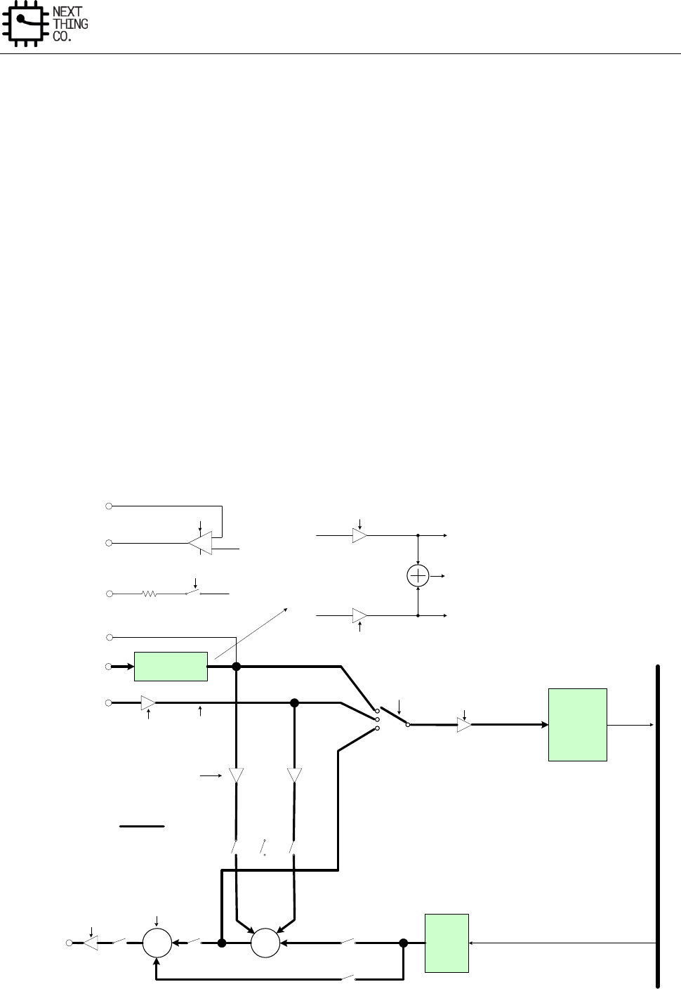
Audio
GR8 User Manual(Version1.0) Copyright © 2017 Next Thing Co. All Rights Reserved. Page 357
7.1. Audio Codec
7.1.1. Overview
The embedded Audio Codec is a high-quality stereo audio codec with headphone amplifier.
Features:
● On-chip 24-bit DAC for play-back
● On-chip 24-bit ADC for recorder
● Supports analog/digital volume control
● Supports 48 kHz and 44.1 kHz sample family
● Supports 192 kHz and 96 kHz sample
● Supports Microphone recorder
● Stereo headphone amplifier that can be operated in capless headphone mode
7.1.2. Audio Codec Block Diagram
+
ADC
DAC
MIC1/2
LINEINL/R
63 STEP VOLUME:
From 0dB to -62dB
HPCOM
SYSTEM
BUS
HPCOM_FB
HPOUTL/R
-4.5dB, -3dB, -1.5dB, 0dB,
1.5dB, 3dB, 4.5dB, 6dB
-4.5dB, -3dB, -1.5dB, 0dB, 1.5dB,
3dB, 4.5dB, 6dB
+
VMIC 2.5V
G
G
G
G
DDE
VMICEN
MICOG LNOG
LNOS
MIC1LS
MIXPAS
DACPAS
DACMIXS
ADCG
PAVOL
PAEN
MIXEN
PAMUTE
STEREO
200 ohm
GAIN & MIX
MIC1
MIC2
MICO1
MICO2
32dB, 35dB, 38dB, 41dB
G
PREG1
G
PREG2
MICO1+MICO2
MIC1RS
MIC2LS
MIC2RS
When ADCIS=000, ADCINL=LINEINL, ADCINR=LINEINR; or,
ADCINL=ADCINR=LINEINL-LINEINR, depending on LNRDF
When ADCIS=010, ADCINL=ADCINR=MICO1
When ADCIS=011, ADCINL=ADCINR=MICO2
When ADCIS=100, ADCINL=MICO1, ADCINR=MICO2
When ADCIS=101, ADCINL=ADCINR=MICO1+MICO2
When ADCIS=110, ADCINL=MIXOUTL, ADCINR=MIXOUTR
When ADCIS=111, ADCINL=LINEINL or LINEINL-LINEINR,
depending on LNRDF, ADCINR=MICO1
32dB, 35dB, 38dB, 41dB
G
LNPREG
-12dB to 9dB, 3dB/step
-1.5dB, 0dB
=lineinL-lineinR when
LNRDF=1 for differential
application
MIC1OUTP/N
Audio
GR8 User Manual(Version1.0) Copyright © 2017 Next Thing Co. All Rights Reserved. Page 358
Figure 6-4. Audio Codec Block Diagram
7.1.3. Audio Codec Register List
Module Name
Base Address
Audio Codec
0x01C22C00
Register Name
Offset
Description
AC_DAC_DPC
0x0000
DAC Digital Part Control Register
AC_DAC_FIFOC
0x0004
DAC FIFO Control Register
AC_DAC_FIFOS
0x0008
DAC FIFO Status Register
AC_DAC_TXDATA
0x000C
DAC TX Data Register
AC_DAC_ACTL
0x0010
DAC Analog Control Register
AC_ADC_FIFOC
0x001C
ADC FIFO Control Register
AC_ADC_FIFOS
0x0020
ADC FIFO Status Register
AC_ADC_RXDATA
0x0024
ADC RX Data Register
AC_ADC_ACTL
0x0028
ADC Analog Control Register
AC_DAC_CNT
0x0030
DAC TX FIFO Counter Register
AC_ADC_CNT
0x0034
ADC RX FIFO Counter Register
7.1.4. Audio Codec Register Description
7.1.4.1. DAC Digital Part Control Register(Default Value: 0x0000_0000)
Offset: 0x0000
Register Name: AC_DAC_DPC
Bit
Read/Write
Default/Hex
Description
31
R/W
0x0
EN_DA.
DAC Digital Part Enable
0: Disable
1: Enable
30:29
/
/
/
28:25
R/W
0x0
MODQU.
Internal DAC Quantization Levels
Levels=[7*(21+MODQU[3:0])]/128
Default levels=7*21/128=1.15
24
R/W
0x0
DWA.
DWA Function Disable
0: Enable

Audio
GR8 User Manual(Version1.0) Copyright © 2017 Next Thing Co. All Rights Reserved. Page 359
1: Disable
23:19
/
/
/
18
R/W
0x0
HPF_EN.
High Pass Filter Enable
0: Disable
1: Enable
17:12
R/W
0x0
DVOL.
Digital volume control: dvc, ATT=(DVC[5:0]-2)*(-1.16dB)
62 steps, -1.16dB/step
11:0
/
/
/
7.1.4.2. DAC FIFO Control Register(Default Value: 0x0000_0000)
Offset: 0x0004
Register Name: AC_DAC_FIFOC
Bit
Read/Write
Default/Hex
Description
31:29
R/W
0x0
DAC_FS.
Sample Rate of DAC
000: 48 kHz
010: 24 kHz
100: 12 kHz
110: 192 kHz
001: 32 kHz
011: 16 kHz
101: 8 kHz
111: 96 kHz
44.1 kHz/22.05 kHz/11.025 kHz can be supported by Audio PLL
Configure Bit
28
R/W
0x0
FIR Version
0:64-Tap FIR
1:32-Tap FIR
27
/
/
/
26
R/W
0x0
SEND_LASAT.

Audio
GR8 User Manual(Version1.0) Copyright © 2017 Next Thing Co. All Rights Reserved. Page 360
Audio sample select when TX FIFO underrun
0: Sending zero
1: Sending last audio sample
25
/
/
/
24
R/W
0x0
For 24-bits transmitted audio sample:
0: FIFO_I[23:0] = {TXDATA[31:8]}
1: Reserved
For 16-bits transmitted audio sample:
0: FIFO_I[23:0] = {TXDATA[31:16], 8’b0}
1: FIFO_I[23:0] = {TXDATA[15:0], 8’b0}
23
/
/
/
22:21
R/W
0x0
DAC_DRQ_CLR_CNT.
When TX FIFO available room less than or equal N, DRQ Request will
be de-asserted. N is defined here:
000: IRQ/DRQ Deasserted when WLEVEL > TXTL
01: 4
10: 8
11: 16
20:15
/
/
/
14:8
R/W
0x10
TX FIFO Empty Trigger Level (TXTL[6:0])
Interrupt and DMA request trigger level for TX FIFO normal condition.
IRQ/DRQ Generated when WLEVEL ≤ TXTL
7
R/W
0x0
ADDA_LOOP_EN.
ADDA Loop Enable
0: Disable
1: Enable
6
R/W
0x0
DAC_MONO_EN.
DAC Mono Enable
0: Stereo, 64 levels FIFO
1: mono, 128 levels FIFO

Audio
GR8 User Manual(Version1.0) Copyright © 2017 Next Thing Co. All Rights Reserved. Page 361
When enabled, L & R channel send same data
5
R/W
0x0
TX_SAMPLE_BITS.
Transmitting Audio Sample Resolution
0: 16 bits
1: 24 bits
4
R/W
0x0
DAC_DRQ_EN.
DAC FIFO Empty DRQ Enable
0: Disable
1: Enable
3
R/W
0x0
DAC_IRQ_EN.
DAC FIFO Empty IRQ Enable
0: Disable
1: Enable
2
R/W
0x0
FIFO_UNDERRUN_IRQ_EN.
DAC FIFO Underrun IRQ Enable
0: Disable
1: Enable
1
R/W
0x0
FIFO_OVERRUN_IRQ_EN.
DAC FIFO Overrun IRQ Enable
0: Disable
1: Enable
0
R/W
0x0
FIFO_FLUSH.
DAC FIFO Flush
Write ‘1’ to flush TX FIFO, self clear to ‘0’
7.1.4.3. DAC FIFO Status Register(Default Value: 0x0080_8008)
Offset: 0x0008
Register Name: AC_DAC_FIFOS
Bit
Read/Write
Default/Hex
Description
31:24
/
/
/

Audio
GR8 User Manual(Version1.0) Copyright © 2017 Next Thing Co. All Rights Reserved. Page 362
23
R
0x1
TX_EMPTY.
TX FIFO Empty
0: No room for new sample in TX FIFO
1: More than one room for new sample in TX FIFO (>= 1 word)
22:8
R
0x80
TXE_CNT.
TX FIFO Empty Space Word Counter
7:4
/
/
/
3
R/W
0x1
TXE_INT.
TX FIFO Empty Pending Interrupt
0: No Pending IRQ
1: FIFO Empty Pending Interrupt
Write ‘1’ to clear this interrupt or automatically clear if interrupt
condition fails.
2
R/W
0x0
TXU_INT.
TX FIFO Underrun Pending Interrupt
0: No Pending Interrupt
1: FIFO Under run Pending Interrupt
Write ‘1’ to clear this interrupt
1
R/W
0x0
TXO_INT.
TX FIFO Overrun Pending Interrupt
0: No Pending Interrupt
1: FIFO Overrun Pending Interrupt
Write ‘1’ to clear this interrupt
0
/
/
/
7.1.4.4. DAC TX DATA Register(Default Value: 0x0000_0000)
Offset: 0x000C
Register Name: AC_DAC_TXDATA
Bit
Read/Write
Default/Hex
Description

Audio
GR8 User Manual(Version1.0) Copyright © 2017 Next Thing Co. All Rights Reserved. Page 363
31:0
W
0x0
TX_DATA.
Transmitting left, right channel sample data should be written this
register one by one. The left channel sample data is first and then the
right channel sample.
7.1.4.5. DAC Analog Control Register(Default Value: 0x05B0_0000)
Offset:0x0010
Register Name: AC_DAC_ACTRL
Bit
Read/Write
Default/Hex
Description
31
R/W
0x0
DACAREN.
Internal DAC Analog Right channel Enable
0:Disable
1:Enable
30
R/W
0x0
DACALEN.
Internal DAC Analog Left channel Enable
0:Disable
1:Enable
29
R/W
0x0
MIXEN.
Analog Output Mixer Enable
0:Disable
1:Enable
28:27
/
/
/
26
R/W
0x1
LNG.
Line-in gain stage to output mixer Gain Control
0: -1.5dB
1: 0dB
25:23
R/W
0x3
Reserved
22:20
R/W
0x3
MICG.
MIC1/2 gain stage to output mixer Gain Control
From -4.5dB to 6dB, 1.5dB/step, default is 0dB
19
R/W
0x0
LLNS.
Left LINEIN gain stage to left output mixer mute

Audio
GR8 User Manual(Version1.0) Copyright © 2017 Next Thing Co. All Rights Reserved. Page 364
0: Mute
1: Not mute
When LNRDF is 0, left select LINEINL
When LNRDF is 1, left select LINEINL-LINEINR
18
R/W
0x0
RLNS.
Right LINEIN gain stage to right output mixer mute
0: Mute
1: Not mute
When LNRDF is 0, right select LINEINR
When LNRDF is 1, right select LINEINL-LINEINR
17
R/W
0x0
LFMS.
Left FM to left output mixer mute
0:Mute
1:Not mute
16
R/W
0x0
RFMS.
right FM to right output mixer mute
0:Mute
1:Not mute
15
R/W
0x0
LDACLMIXS.
Left DAC to left output mixer mute
0:Mute
1:Not mute
14
R/W
0x0
RDACRMIXS.
Right DAC to right output mixer mute
0:Mute
1:Not mute
13
R/W
0x0
LDACRMIXS.
Left DAC to right output mixer mute

Audio
GR8 User Manual(Version1.0) Copyright © 2017 Next Thing Co. All Rights Reserved. Page 365
0:Mute
1:Not mute
12
R/W
0x0
MIC1 LS.
MIC1 to output mixer left channel mute
0: Mute
1: Not mute
11
R/W
0x0
MIC1 RS.
MIC1 to output mixer right channel mute
0: Mute
1: Not mute
10
R/W
0x0
MIC2 LS.
MIC2 to output mixer left channel mute
0: Mute
1: Not mute
9
R/W
0x0
MIC2 RS.
MIC2 to output mixer right channel mute
0: Mute
1: Not mute
8
R/W
0x0
DACPAS.
DAC to PA Mute
0: Mute
1: Not mute
7
R/W
0x0
MIXPAS.
Output Mixer to PA mute
0: Mute
1: Not mute
6
R/W
0x0
PAMUTE.
All input source to PA mute, including Output mixer and Internal DAC,

Audio
GR8 User Manual(Version1.0) Copyright © 2017 Next Thing Co. All Rights Reserved. Page 366
0:Mute
1: Not mute
5:0
R/W
0x0
PAVOL.
PA Volume Control, (PAVOL): Total 64 level, from 0dB to -62dB,
1dB/step,mute when 000000
7.1.4.6. ADC FIFO Control Register(Default Value: 0x0000_0F00)
Offset: 0x001C
Register Name: AC_ADC_FIFOC
Bit
Read/Write
Default/Hex
Description
31:29
R/W
0x0
ADFS.
Sample Rate of ADC
000: 48 kHz
010: 24 kHz
100: 12 kHz
110: Reserved
001: 32 kHz
011: 16 kHz
101: 8 kHz
111: Reserved
28
R/W
0x0
EN_AD.
ADC Digital Part Enable
0: Disable
1: Enable
27:25
/
/
/
24
R/W
0x0
RX_FIFO_MODE.
RX FIFO Output Mode (Mode 0, 1)
0: Expanding ‘0’ at LSB of TX FIFO register
1: Expanding received sample sign bit at MSB of TX FIFO register
For 24-bits received audio sample:
Mode 0: RXDATA[31:0] = {FIFO_O[23:0], 8’h0}

Audio
GR8 User Manual(Version1.0) Copyright © 2017 Next Thing Co. All Rights Reserved. Page 367
Mode 1: Reserved
For 16-bits received audio sample:
Mode 0: RXDATA[31:0] = {FIFO_O[23:8], 16’h0}
Mode 1: RXDATA[31:0] = {16{FIFO_O[23]}, FIFO_O[23:8]}
23:13
/
/
/
12:8
R/W
0xF
RX_FIFO_TRG_LEVEL.
RX FIFO Trigger Level (RXTL[4:0])
Interrupt and DMA request trigger level for TX FIFO normal condition
IRQ/DRQ Generated when WLEVEL > RXTL[4:0]
Note:
WLEVEL represents the number of valid samples in the RX FIFO
7
R/W
0x0
ADC_MONO_EN.
ADC Mono Enable.
0: Stereo, 16 levels FIFO
1: mono, 32 levels FIFO
When set to ‘1’, Only left channel samples are recorded
6
R/W
0x0
RX_SAMPLE_BITS.
Receiving Audio Sample Resolution
0: 16 bits
1: 24 bits
5
/
/
/
4
R/W
0x0
ADC_DRQ_EN.
ADC FIFO Data Available DRQ Enable.
0: Disable
1: Enable
3
R/W
0x0
ADC_IRQ_EN.
ADC FIFO Data Available IRQ Enable.
0: Disable
1: Enable

Audio
GR8 User Manual(Version1.0) Copyright © 2017 Next Thing Co. All Rights Reserved. Page 368
2
/
/
/
1
R/W
0x0
ADC_OVERRUN_IRQ_EN.
ADC FIFO Over Run IRQ Enable
0: Disable
1: Enable
0
R/W
0x0
ADC_FIFO_FLUSH.
ADC FIFO Flush.
Write ‘1’ to flush TX FIFO, self clear to ‘0’.
7.1.4.7. ADC FIFO Status Register(Default Value: 0x0000_0000)
Offset: 0x0020
Register Name: AC_ADC_FIFOS
Bit
Read/Write
Default/Hex
Description
31:24
/
/
/
23
R
0x0
RXA.
RX FIFO Available
0: No available data in RX FIFO
1: More than one sample in RX FIFO (>= 1 word)
22:14
/
/
/
13:8
R
0x0
RXA_CNT.
RX FIFO Available Sample Word Counter
7:4
/
/
/
3
R/W
0x0
RXA_INT.
RX FIFO Data Available Pending Interrupt
0: No Pending IRQ
1: Data Available Pending IRQ
Write ‘1’ to clear this interrupt or automatically clear if interrupt
condition fails.
2
/
/
/
1
R/W
0x0
RXO_INT.
RX FIFO Overrun Pending Interrupt

Audio
GR8 User Manual(Version1.0) Copyright © 2017 Next Thing Co. All Rights Reserved. Page 369
0: No Pending IRQ
1: FIFO Overrun Pending IRQ
Write ‘1’ to clear this interrupt
0
/
/
/
7.1.4.8. ADC RX DATA Register(Default Value: 0x0000_0000)
Offset: 0x0024
Register Name: AC_ADC_RXDATA
Bit
Read/Write
Default/Hex
Description
31:0
R
0x0
RX_DATA.
RX Sample
Host can get one sample by reading this register. The left channel
sample data is first and then the right channel sample.
7.1.4.9. ADC Analog Control Register(Default Value: 0x0534_814C)
Offset:0x0028
Register Name: AC_PA_ADC_ACTRL
Bit
Read/Write
Default/Hex
Description
31
R/W
0x0
ADCREN.
ADC Right Channel Enable
0: Disable
1: Enable
30
R/W
0x0
ADCLEN.
ADC Left Channel Enable
0: Disable
1: Enable
29
R/W
0x0
PREG1EN.
MIC1 Pre-amplifier Enable
0: Disable
1: Enable
28
R/W
0x0
PREG2EN.
MIC2 Pre-amplifier Enable

Audio
GR8 User Manual(Version1.0) Copyright © 2017 Next Thing Co. All Rights Reserved. Page 370
0: Disable
1: Enable
27
R/W
0x0
VMICEN.
VMIC Pin Voltage Enable
0: Disable
1: Enable
26:25
R/W
0x2
PREG1.
MIC1 Pre-Amplifier Gain Control
00: 0dB
01: 35dB
10: 38dB
11: 41dB
24:23
R/W
0x2
PREG2.
MIC2 Pre-Amplifier Gain Control
00: 0dB
01: 35dB
10: 38dB
11: 41dB
22:20
R/W
0x3
ADCG.
ADC Input Gain Control
000: -4.5dB
001: -3dB
010: -1.5dB
011: 0dB
100: 1.5dB
101: 3dB
110: 4.5dB
111: 6dB
19:17
R/W
0x2
ADCIS.
ADC Input Source Select
000: left select LINEINL, right select LINEINR; or, both select LINEINL-

Audio
GR8 User Manual(Version1.0) Copyright © 2017 Next Thing Co. All Rights Reserved. Page 371
LINEINR, depending on LNRDF (bit 16)
001: Reserved
010: left and right channel both select MIC1 gain stage output
011: left and right channel both select MIC2 gain stage output
100: left select MIC1 gain stage output & right select MIC2 gain stage
output
101: left and right both select MIC1 gain stage plus MIC2 gain stage
output
110: left select output mixer L & right select output Mixer right
111: left select LINEINL or LINEINL-LINEINR, depending on LNRDF (bit
16), right select MIC1 gain stage
16
R/W
0x0
LNRDF.
Line-in-r Function Define
0: Line-in right channel which is independent of line-in left channel
1: Negative input of line-in left channel for fully differential
application
15:13
R/W
0x4
LNPREG.
Line-in Pre-amplifier Gain Control
From -12dB to 9dB, 3dB/step, default is 0dB
12
R/W
0x0
MIC1NEN.
Mic1Outn Enable
0: Disable
1: Enable
11:9
/
/
/
8
R/W
0x1
DITHER.
ADC Dither On/Off Control
0: Dither off
1: Dither on
7:6
R/W
0x1
/
5
/
/
/
4
R/W
0x0
PA_EN.
PA Enable

Audio
GR8 User Manual(Version1.0) Copyright © 2017 Next Thing Co. All Rights Reserved. Page 372
0: Disable
1: Enable
3
R/W
0x1
DDE.
Headphone Direct-Drive Enable (DDE)
0: Disable
1: Enable
2
R/W
0x1
COMPTEN.
HPCOM Output Protection Enable
0: Protection disable
1: Protection enable
1:0
R/W
0x0
PTDBS.
HPCOM Protect De-bounce Time Setting
00: 2-3ms
01: 4-6ms
10: 8-12ms
11: 16-24ms
7.1.4.10. DAC TX Counter Register(Default Value: 0x0000_0000)
Offset: 0x0030
Register Name: AC_DAC_CNT
Bit
Read/Write
Default/Hex
Description
31:0
R/W
0x0
TX_CNT.
TX Sample Counter
The audio sample number of sending into TXFIFO. When one sample
is put into TXFIFO by DMA or by host IO, the TX sample counter
register increases by one. The TX sample counter register can be set
to any initial valve at any time. After been updated by the initial value,
the counter register should count on base of this initial value.
Note: It is used for Audio/ Video Synchronization
7.1.4.11. ADC RX Counter Register(Default Value: 0x0000_0000)
Offset: 0x0034
Register Name: AC_ADC_CNT
Bit
Read/Write
Default/Hex
Description
31:0
R/W
0x0
RX_CNT.

Audio
GR8 User Manual(Version1.0) Copyright © 2017 Next Thing Co. All Rights Reserved. Page 373
RX Sample Counter
The audio sample number of writing into RXFIFO. When one sample
is written by Digital Audio Engine, the RX sample counter register
increases by one. The RX sample counter register can be set to any
initial valve at any time. After been updated by the initial value, the
counter register should count on base of this initial value.
Note: It is used for Audio/Video Synchronization
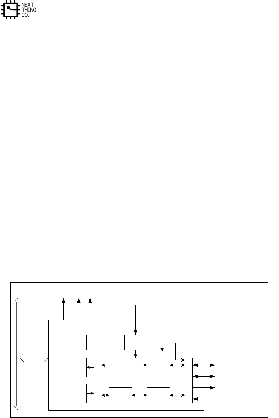
Audio
GR8 User Manual(Version1.0) Copyright © 2017 Next Thing Co. All Rights Reserved. Page 374
7.2. I2S/PCM
7.2.1. Overview
The I2S/PCM can be configured as an I2S interface or PCM interface through software. When configured as an I2S
interface, it can support the industry standard format for I2S, left-justified, or right-justified. PCM is a standard
method used to transmit digital audio over digital communication channels. It supports 13 or 16-bits linear, 8-bit
Mu-law or A-law companding sample formats at 8K samples/s and can receive and transmit on any of the first four
slots following PCM_SYNC.
Features:
● I2S or PCM configured by software
● Full-duplex synchronous serial interface
● Master/slave mode operation configured by software
● Audio data resolutions of 16, 20, 24
● I2S Audio data sample rate from 8 kHz to 192 kHz
● I2S data format for standard I2S, Left Justified and Right Justified
● PCM supports linear sample (8-bit or 16-bit), 8-bit u-law and A-law companding sample
● One 128x24 bits FIFO for data transmit, one 64x24-bits FIFO for data receive
● Programmable FIFO thresholds
● Interrupt and DMA Support
7.2.2. I2S/PCM Block Diagram
The I2S/PCM block diagram is shown below.
Register
128x24-
bits
RX FIFO
I2S
Engine
PCM
Engine
PCM
Codec
Clock
Divide
M
U
X
S
Y
N
C
MCLK
BCLK
I2S_SCLK/PCM_CLK
I2S_LRC/PCM_SYNC
I2S_SDO/PCM_OUT
I2S_SDI/PCM_IN
TX_DRQ
RX_DRQ
Audio_PLL
DA_INT
APB
64x24-bits
TX FIFO
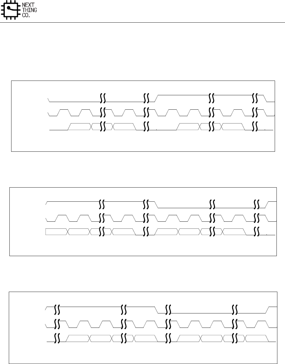
Audio
GR8 User Manual(Version1.0) Copyright © 2017 Next Thing Co. All Rights Reserved. Page 375
Figure 6-5. I2S/PCM Block Diagram
7.2.3. I2S/PCM Timing Diagram
Figure 6-6. I2S Timing Diagram
Figure 6-7. I2S Left-justified Timing Diagram
Figure 6-8. I2S Right-justified Timing Diagram
Left Channel
Right Channel
MSB
LSB
MSB
LSB
Standard I2S Timing Diagram
I2S_LRC
I2S_SCLK
I2S_SDO/SDI
Left Channel
Right Channel
MSB
LSB
MSB
LSB
Left-justified I2S Timing Diagram
I2S_LRC
I2S_SCLK
I2S_SDO/SDI
Left Channel
Right Channel
MSB
LSB
MSB
LSB
Right-justified I2S Timing Diagram
I2S_LRC
I2S_SCLK
I2S_SDO/SDI
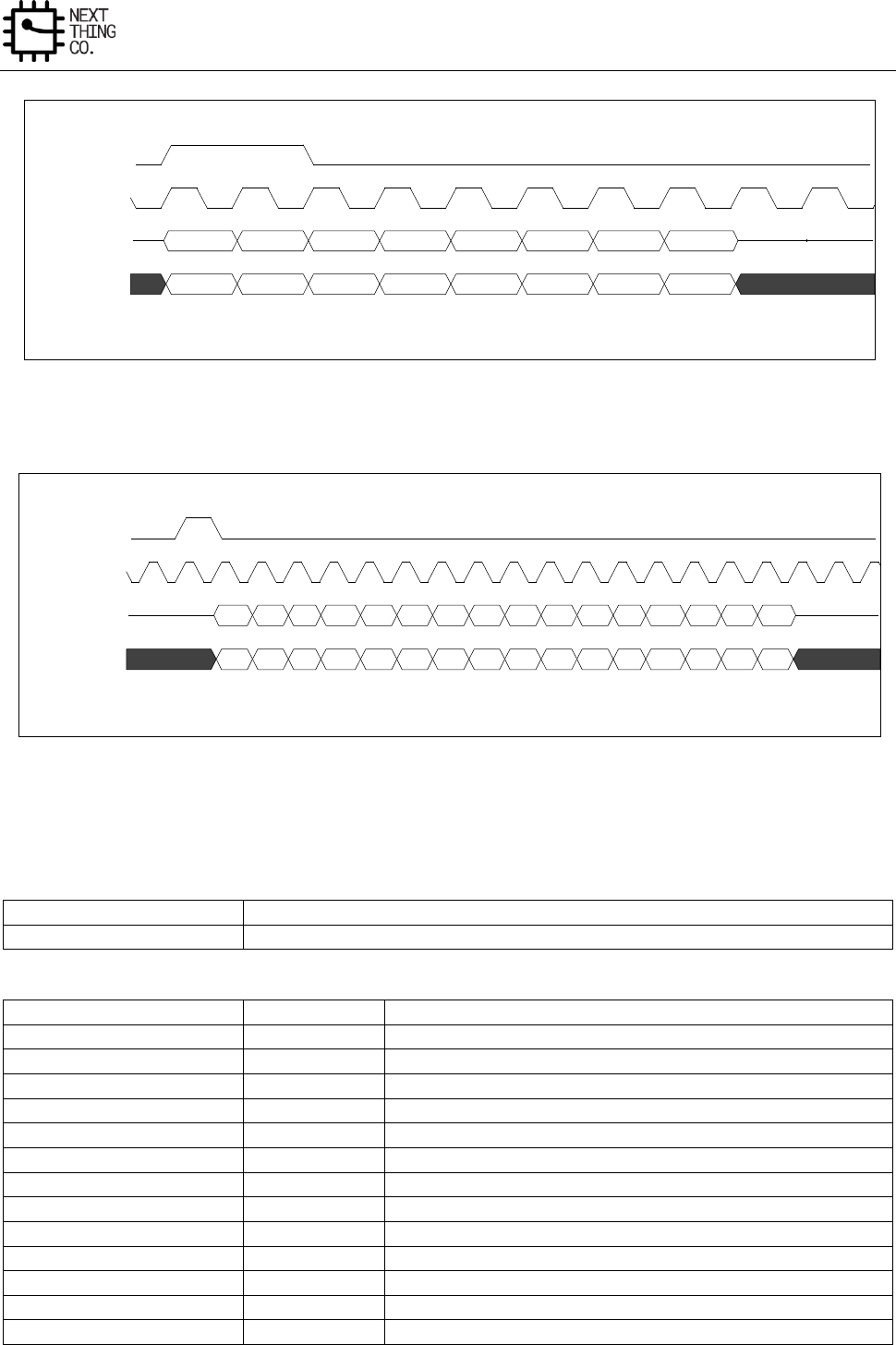
Audio
GR8 User Manual(Version1.0) Copyright © 2017 Next Thing Co. All Rights Reserved. Page 376
Figure 6-9. PCM Long Frame SYNC Timing Diagram
Figure 6-10. PCM Short Frame SYNC Timing Diagram
7.2.4. I2S/PCM Register List
Module Name
Base Address
I2S/PCM
0x01C22400
Register Name
Offset
Description
I2S/PCM_CTL
0x0000
I2S/PCM Control Register
I2S/PCM_FAT0
0x0004
I2S/PCM Format Register 0
I2S/PCM_FAT1
0x0008
I2S/PCM Format Register 1
I2S/PCM_TXFIFO
0x000C
I2S/PCM TX FIFO Register
I2S/PCM_RXFIFO
0x0010
I2S/PCM RX FIFO Register
I2S/PCM_FCTL
0x0014
I2S/PCM FIFO Control Register
I2S/PCM_FSTA
0x0018
I2S/PCM FIFO Status Register
I2S/PCM_INT
0x001C
I2S/PCM Interrupt Control Register
I2S/PCM_ISTA
0x0020
I2S/PCM Interrupt Status Register
I2S/PCM_CLKD
0x0024
I2S/PCM Clock Divide Register
I2S/PCM_TXCNT
0x0028
I2S/PCM RX Sample Counter Register
I2S/PCM_RXCNT
0x002C
I2S/PCM TX Sample Counter Register
I2S/PCM_TXCHSEL
0x0030
I2S/PCM TX Channel Select register
2 Clocks
1
2
3
4
5
6
7
8
Undefined
1
2
3
4
5
6
7
8
Undefined
PCM Long Frame SYNC Timing Diagram (8-bits Companded Sample Example)
PCM_SYNC
PCM_CLK
PCM_OUT
PCM_IN
1
2
3
4
5
6
7
8
9
10
11
12
13
14
15
16
Undefined
1
2
3
4
5
6
7
8
9
10
11
12
13
14
15
16
Undefined
PCM Short Frame SYNC Timing Diagram (16-bits sample example)
PCM_SYNC
PCM_CLK
PCM_OUT
PCM_IN

Audio
GR8 User Manual(Version1.0) Copyright © 2017 Next Thing Co. All Rights Reserved. Page 377
I2S/PCM_TXCHMAP
0x0034
I2S/PCM TX Channel Mapping Register
7.2.5. I2S/PCM Register Description
7.2.5.1. I2S/PCM Control Register(Default Value: 0x0000_0000)
Offset: 0x0000
Register Name: I2S/PCM_CTL
Bit
Read/Write
Default/Hex
Description
31:9
/
/
/
8
R/W
0x0
SDO_EN
0: Disable
1: Enable
7
/
/
/
6
R/W
0x0
ASS
Audio sample select when TX FIFO under run
0: Sending zero
1: Sending last audio sample
5
R/W
0x0
MS
Master Slave Select
0: Master
1: Slave
4
R/W
0x0
PCM
0: I2S Interface
1: PCM Interface
3
R/W
0x0
LOOP
Loop Back Test
0: Normal mode
1: Loop back test
When set ‘1’, connecting the SDO with the SDI in Master mode.
2
R/W
0x0
TXEN

Audio
GR8 User Manual(Version1.0) Copyright © 2017 Next Thing Co. All Rights Reserved. Page 378
Transmitter Block Enable
0: Disable
1: Enable
1
R/W
0x0
RXEN
Receiver Block Enable
0: Disable
1: Enable
0
R/W
0x0
GEN
Globe Enable
A disable on this bit overrides any other block or channel enables.
0: Disable
1: Enable
7.2.5.2. I2S/PCM Format Register0(Default Value: 0x0000_000C)
Offset: 0x0004
Register Name: I2S/PCM_FAT0
Bit
Read/Write
Default/Hex
Description
31:8
/
/
/
7
R/W
0x0
LRCP
Left/ Right Clock Parity
0: Normal
1: Inverted
In DSP/ PCM mode
0: MSB is available on 2nd BCLK rising edge after LRC rising edge
1: MSB is available on 1st BCLK rising edge after LRC rising edge
6
R/W
0x0
BCP
BCLK Parity
0: Normal
1: Inverted
5:4
R/W
0x0
SR
Sample Resolution

Audio
GR8 User Manual(Version1.0) Copyright © 2017 Next Thing Co. All Rights Reserved. Page 379
00: 16-bit
01: 20-bit
10: 24-bit
11: Reserved
3:2
R/W
0x3
WSS
Word Select Size
00: 16 BCLK
01: 20 BCLK
10: 24 BCLK
11: 32 BCLK
1:0
R/W
0x0
FMT
Serial Data Format
00: Standard I2S Format
01: Left Justified Format
10: Right Justified Format
11: Reserved
7.2.5.3. I2S/PCM Format Register1(Default Value: 0x0000_4020)
Offset: 0x0008
Register Name: I2S/PCM_FAT1
Bit
Read/Write
Default/Hex
Description
31:15
/
/
/
14:12
R/W
0x4
PCM SYNC Period Clock Number
000: 16 BCLK period
001: 32 BCLK period
010: 64 BCLK period
011: 128 BCLK period
100: 256 BCLK period
Others : Reserved
11
R/W
0x0
PCM Sync Out
0: Enable PCM_SYNC output in Master mode

Audio
GR8 User Manual(Version1.0) Copyright © 2017 Next Thing Co. All Rights Reserved. Page 380
1: Suppress PCM_SYNC whilst keeping PCM_CLK running. Some Codec
utilize this to enter a low power state.
10
R/W
0x0
PCM Out Mute
Write 1 force PCM_OUT to 0
9
R/W
0x0
MLS
MSB/LSB First Select
0: MSB First
1: LSB First
8
R/W
0x0
SEXT
Sign Extend (only for 16 bits slot)
0: Zeros or audio gain padding at LSB position
1: Sign extension at MSB position
When writing, the bit is 0, the unused bits are audio gain for 13-bit linear
sample and zeros padding for 8-bit companding sample.
When writing, the bit is 1, the unused bits are both sign extension.
7:6
R/W
0x0
SI
Slot Index
00: the 1st slot
01: the 2nd slot
10: the 3rd slot
11: the 4th slot
5
R/W
0x1
SW
Slot Width
0: 8 clocks width
1: 16 clocks width
Note: For A-law or u-law PCM sample, if this bit is set to 1, eight zero bits
are following with PCM sample.
4
R/W
0x0
SSYNC
Short Sync Select

Audio
GR8 User Manual(Version1.0) Copyright © 2017 Next Thing Co. All Rights Reserved. Page 381
0: Long Frame Sync
1: Short Frame Sync
It should be set ‘1’ for 8 clocks width slot.
3:2
R/W
0x0
RX PDM
PCM Data Mode
00: 16-bit Linear PCM
01: 8-bit Linear PCM
10: 8-bit u-law
11: 8-bit A-law
1:0
R/W
0x0
TX PDM
PCM Data Mode
00: 16-bit Linear PCM
01: 8-bit Linear PCM
10: 8-bit u-law
11: 8-bit A-law
7.2.5.4. I2S/PCM TX FIFO Register(Default Value: 0x0000_0000)
Offset: 0x000C
Register Name: I2S/PCM_TXFIFO
Bit
Read/Write
Default/Hex
Description
31:0
W
0x0
TX Sample
Transmitting left, right channel sample data should be written this
register one by one. The left channel sample data is first and then the
right channel sample.
7.2.5.5. I2S/PCM RX FIFO Register(Default Value: 0x0000_0000)
Offset: 0x0010
Register Name: I2S/PCM_RXFIFO
Bit
Read/Write
Default/Hex
Description
31:0
R
0x0
RX Sample
Host can get one sample by reading this register. The left channel sample
data is first and then the right channel sample.

Audio
GR8 User Manual(Version1.0) Copyright © 2017 Next Thing Co. All Rights Reserved. Page 382
7.2.5.6. I2S/PCM FIFO Control Register(Default Value: 0x0004_00F0)
Offset: 0x0014
Register Name: I2S/PCM_FCTL
Bit
Read/Write
Default/Hex
Description
31
R/W
0x0
FIFOSRC
TX FIFO source select
0: APB bus
1: Analog Audio Codec
30:26
/
/
/
25
R/W
0x0
FTX
Write ‘1’ to flush TX FIFO, self clear to ‘0’.
24
R/W
0x0
FRX
Write ‘1’ to flush RX FIFO, self clear to ‘0’.
23:19
/
/
/
18:12
R/W
0x40
TXTL
TX FIFO Empty Trigger Level
Interrupt and DMA request trigger level for TXFIFO normal condition
Trigger Level = TXTL
11:10
/
/
/
9:4
R/W
0xF
RXTL
RX FIFO Trigger Level
Interrupt and DMA request trigger level for RXFIFO normal condition
Trigger Level = RXTL + 1
3
/
/
/
2
R/W
0x0
TXIM
TX FIFO Input Mode (Mode 0, 1)
0: Valid data at the MSB of TXFIFO register
1: Valid data at the LSB of TXFIFO register
Example for 20-bit transmitted audio sample:
Mode 0: FIFO_I[23:0] = {4’h0, TXFIFO[31:12]}
Mode 1: FIFO_I[23:0] = {4’h0, TXFIFO[19:0]}
1:0
R/W
0x0
RXOM
RX FIFO Output Mode (Mode 0, 1, 2, 3)

Audio
GR8 User Manual(Version1.0) Copyright © 2017 Next Thing Co. All Rights Reserved. Page 383
00: Expanding ‘0’ at LSB of DA_RXFIFO register.
01: Expanding received sample sign bit at MSB of DA_RXFIFO register.
10: Truncating received samples at high half-word of DA_RXFIFO register
and low half-word of DA_RXFIFO register is filled by ‘0’.
11: Truncating received samples at low half-word of DA_RXFIFO register
and high half-word of DA_RXFIFO register is expanded by its sign bit.
Example for 20-bit received audio sample:
Mode 0: RXFIFO[31:0] = {FIFO_O[19:0], 12’h0}
Mode 1: RXFIFO[31:0] = {12{FIFO_O[19]}, FIFO_O[19:0]}
Mode 2: RXFIFO[31:0] = {FIFO_O[19:4], 16’h0}
Mode 3: RXFIFO[31:0] = {16{FIFO_O[19], FIFO_O[19:4]}
7.2.5.7. I2S/PCM FIFO Status Register(Default Value: 0x1080_0000)
Offset: 0x0018
Register Name: I2S/PCM_FSTA
Bit
Read/Write
Default/Hex
Description
31:29
/
/
/
28
R
0x1
TXE
TX FIFO Empty
0: No room for new sample in TX FIFO
1: More than one room for new sample in TX FIFO (>= 1 word)
27:24
/
/
/
23:16
R
0x80
TXE_CNT
TX FIFO Empty Space Word Counter
15:9
/
/
/
8
R
0x0
RXA
RX FIFO Available
0: No available data in RX FIFO
1: More than one sample in RX FIFO (>= 1 word)
7
/
/
/
6:0
R
0x0
RXA_CNT
RX FIFO Available Sample Word Counter

Audio
GR8 User Manual(Version1.0) Copyright © 2017 Next Thing Co. All Rights Reserved. Page 384
7.2.5.8. I2S/PCM DMA&Interrupt Control Register(Default Value: 0x0000_0000)
Offset: 0x001C
Register Name: I2S/PCM_INT
Bit
Read/Write
Default/Hex
Description
31:8
/
/
/
7
R/W
0x0
TX_DRQ
TX FIFO Empty DRQ Enable
0: Disable
1: Enable
6
R/W
0x0
TXUI_EN
TX FIFO Underrun Interrupt Enable
0: Disable
1: Enable
5
R/W
0x0
TXOI_EN
TX FIFO Overrun Interrupt Enable
0: Disable
1: Enable
When set to ‘1’, an interrupt happens when writing new audio data if TX
FIFO is full.
4
R/W
0x0
TXEI_EN
TX FIFO Empty Interrupt Enable
0: Disable
1: Enable
3
R/W
0x0
RX_DRQ
RX FIFO Data Available DRQ Enable
0: Disable
1: Enable
When set to ‘1’, RXFIFO DMA Request line is asserted if Data is available
in RX FIFO.
2
R/W
0x0
RXUI_EN

Audio
GR8 User Manual(Version1.0) Copyright © 2017 Next Thing Co. All Rights Reserved. Page 385
RX FIFO Underrun Interrupt Enable
0: Disable
1: Enable
1
R/W
0x0
RXOI_EN
RX FIFO Overrun Interrupt Enable
0: Disable
1: Enable
0
R/W
0x0
RXAI_EN
RX FIFO Data Available Interrupt Enable
0: Disable
1: Enable
7.2.5.9. I2S/PCM Interrupt Status Register(Default Value: 0x0000_0010)
Offset: 0x0020
Register Name: I2S/PCM_ISTA
Bit
Read/Write
Default/Hex
Description
31:7
/
/
/
6
R/W
0x0
TXU_INT
TX FIFO Underrun Pending Interrupt
0: No Pending Interrupt
1: FIFO Underrun Pending Interrupt
5
R/W
0x0
TXO_INT
TX FIFO Overrun Pending Interrupt
0: No Pending Interrupt
1: FIFO Overrun Pending Interrupt
Write ‘1’ to clear this interrupt
4
R/W
0x1
TXE_INT
TX FIFO Empty Pending Interrupt
0: No Pending IRQ

Audio
GR8 User Manual(Version1.0) Copyright © 2017 Next Thing Co. All Rights Reserved. Page 386
1: FIFO Empty Pending Interrupt
Write ‘1’ to clear this interrupt or automatic clear if interrupt condition
fails.
3:2
/
/
/
1
R/W
0x0
RXO_INT
RX FIFO Overrun Pending Interrupt
0: No Pending IRQ
1: FIFO Overrun Pending IRQ
Write ‘1’ to clear this interrupt
0
R/W
0x0
RXA_INT
RX FIFO Data Available Pending Interrupt
0: No Pending IRQ
1: Data Available Pending IRQ
Write ‘1’ to clear this interrupt or automatically clear if interrupt
condition fails.
7.2.5.10. I2S/PCM Clock Divide Register(Default Value: 0x0000_0000)
Offset: 0x0024
Register Name: I2S/PCM_CLKD
Bit
Read/Write
Default/Hex
Description
31:8
/
/
/
7
R/W
0x0
MCLKO_EN
0: Disable MCLK Output
1: Enable MCLK Output
Note: Whether in Slave or Master mode, when this bit is set to 1, MCLK
should be output.
6:4
R/W
0x0
BCLKDIV
BCLK Divide Ratio from MCLK
000: Divide by 2 (BCLK = MCLK/2)

Audio
GR8 User Manual(Version1.0) Copyright © 2017 Next Thing Co. All Rights Reserved. Page 387
001: Divide by 4
010: Divide by 6
011: Divide by 8
100: Divide by 12
101: Divide by 16
110: Divide by 32
111: Divide by 64
3:0
R/W
0x0
MCLKDIV
MCLK Divide Ratio from Audio PLL Output
0000: Divide by 1
0001: Divide by 2
0010: Divide by 4
0011: Divide by 6
0100: Divide by 8
0101: Divide by 12
0110: Divide by 16
0111: Divide by 24
1000: Divide by 32
1001: Divide by 48
1010: Divide by 64
Others : Reserved
7.2.5.11. I2S/PCM TX Counter Register(Default Value: 0x0000_0000)
Offset: 0x0028
Register Name: I2S/PCM_TXCNT
Bit
Read/Write
Default/Hex
Description
31:0
R/W
0x0
TX Sample Counter
The audio sample number of sending into TXFIFO. When one sample is
put into TXFIFO by DMA or by host IO, the TX sample counter register
increases by one. The TX sample counter register can be set to any initial
valve at any time. After been updated by the initial value, the counter
register should count on base of this initial value.
7.2.5.12. I2S/PCM RX Counter Register(Default Value: 0x0000_0000)
Offset: 0x002C
Register Name: I2S/PCM_RXCNT

Audio
GR8 User Manual(Version1.0) Copyright © 2017 Next Thing Co. All Rights Reserved. Page 388
Bit
Read/Write
Default/Hex
Description
31:0
R/W
0x0
RX Sample Counter
The audio sample number of writing into RXFIFO. When one sample is
written by Digital Audio Engine, the RX sample counter register increases
by one. The RX sample counter register can be set to any initial valve at
any time. After been updated by the initial value, the counter register
should count on base of this initial value.
7.2.5.13. I2S/PCM TX Channel Select Register(Default Value: 0x0000_0001)
Offset: 0x0030
Register Name: I2S/PCM_TXCHSEL
Bit
Read/Write
Default/Hex
Description
31:3
/
/
/
2:0
R/W
0x1
Channel_Select
0: 1-ch
1: 2-ch
Others: Reserved
7.2.5.14. I2S/PCM TX Channel Mapping Register(Default Value: 0x7654_3210)
Offset: 0x0034
Register Name: I2S/PCM_TXCHMAP
Bit
Read/Write
Default/Hex
Description
31:7
/
/
/
6:4
R/W
0x1
CH1_MAP
000: 1st sample
001: 2nd sample
Others: Reserved
3
/
/
/
2:0
R/W
0x0
CH0_MAP
000: 1st sample
001: 2nd sample
Others: Reserved

Audio
GR8 User Manual(Version1.0) Copyright © 2017 Next Thing Co. All Rights Reserved. Page 389
7.2.5.15. I2S/PCM RX Channel Select Register(Default Value: 0x0000_0001)
Offset: 0x0038
Register Name: I2S/PCM_RXCHSEL
Bit
Read/Write
Default/Hex
Description
31:3
/
/
/
2:0
R/W
0x1
Channel_Select
000: 1-ch
001: 2-ch
010: 3-ch
011: 4-ch
Others: Reserved
7.2.5.16. I2S/PCM RX Channel Mapping Register(Default Value: 0x0000_3210)
Offset: 0x003C
Register Name: I2S/PCM_RXCHMAP
Bit
Read/Write
Default/Hex
Description
31:15
/
/
/
14:12
R/W
0x3
CH3_MAP
000: 1st sample
001: 2nd sample
010: 3rd sample
011: 4th sample
Others: Reserved
11
/
/
/
10:8
R/W
0x2
CH2_MAP
000: 1st sample
001: 2nd sample
010: 3rd sample
011: 4th sample
Others: Reserved
7
/
/
/
6:4
R/W
0x1
CH1_MAP
000: 1st sample

Audio
GR8 User Manual(Version1.0) Copyright © 2017 Next Thing Co. All Rights Reserved. Page 390
001: 2nd sample
010: 3rd sample
011: 4th sample
Others: Reserved
3
/
/
/
2:0
R/W
0x0
CH0_MAP
000: 1st sample
001: 2nd sample
010: 3rd sample
011: 4th sample
Others: Reserved
7.3. OWA
7.3.1. Overview
The OWA (One Wire Audio) provides a serial bus interface between the system and the codec chip. This interface
is widely used for consumer audio connections.
Features:
IEC-60958 transmitter functionality
Complies with S/PDIF Interface
Supports channel status insertion for the transmitter
Hardware parity generation on the transmitter
One 32×24 bits TX FIFO for audio data transfer
Programmable FIFO thresholds
Interrupt and DMA support
7.3.2. OWA Block Diagram
Figure 7-8 shows a block diagram of the OWA.
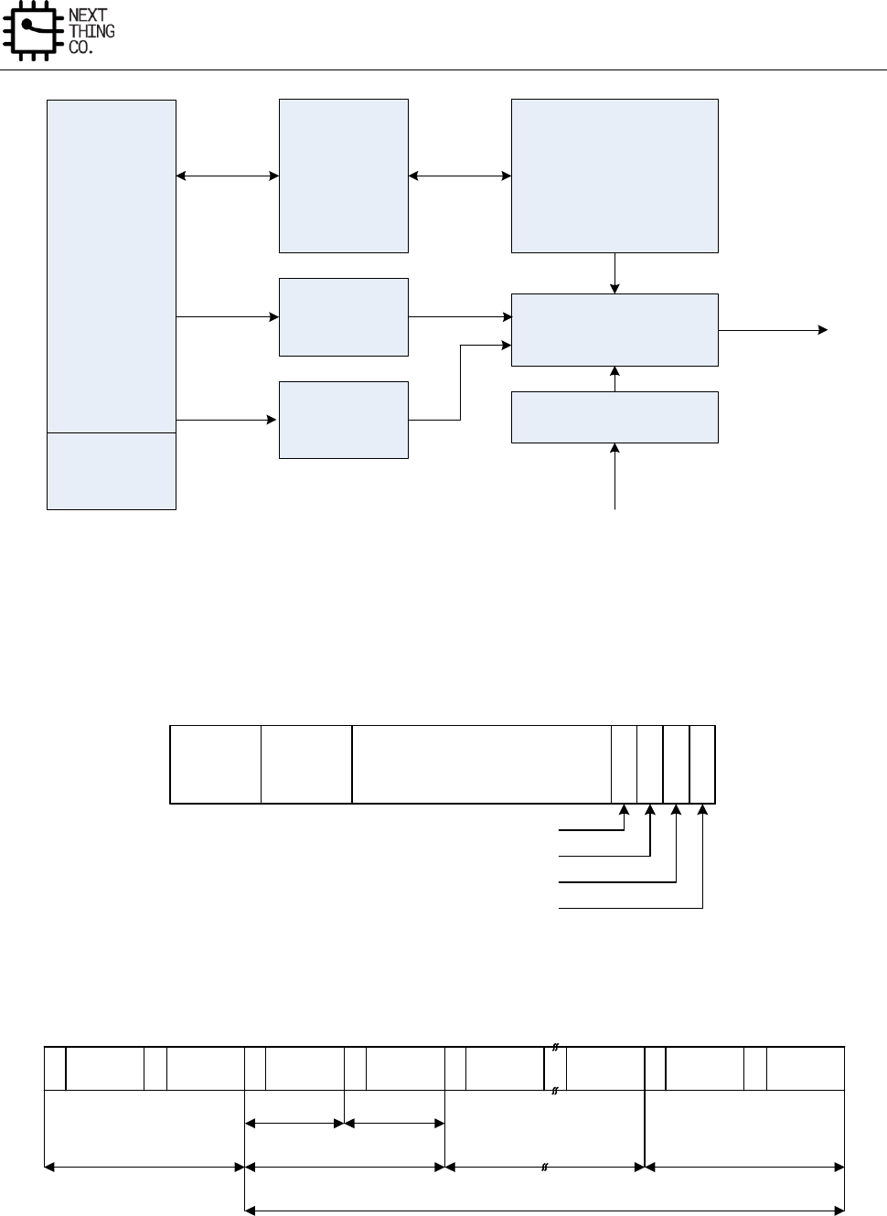
Audio
GR8 User Manual(Version1.0) Copyright © 2017 Next Thing Co. All Rights Reserved. Page 391
APB
I/F
Registers
TX FIFO
Channel status
& user data
buffers
DMA & INT
OWA_OUT
Transmitter
FSM & Control
Clock Divider
Figure 6-11. OWA Block Diagram
7.3.3. OWA Frame Format
Sync
preamble Aux
L
S
B
Audio sample word
M
S
B
V U C P
Validity flag
User data
Channel status
Parity bit
03 4 7 8 27 28 31
Figure 6-12. Sub-Frame Format
M Channel 1 W Channel 2 B W Channel 2
Channel 1 MChannel 2
Channel 1 M W Channel 2
Channel 1
Sub-frame Sub-frame
Frame 0Frame 191 Frame 191
Block
Figure 6-13. Frame/Block Format
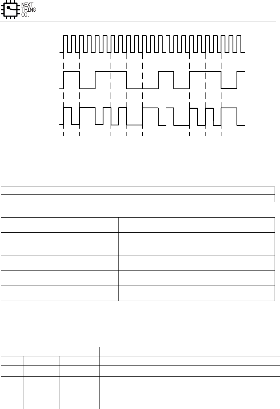
Audio
GR8 User Manual(Version1.0) Copyright © 2017 Next Thing Co. All Rights Reserved. Page 392
10110010110
1 0 1 1 0 1 0 1 0 0 0 0 0 1 0 1 1 0 1 0 1 1
Clock
128×FS
Data
BMC
Figure 6-14. Biphase-Mark Encoding
7.3.4. OWA Register List
Module Name
Base Address
OWA
0x01C21000
Register Name
Offset
Description
OWA_GEN_CTL
0x0000
OWA General Control
OWA_TX_CFIG
0x0004
OWA TX Configuration Register
OWA_ISTA
0x000C
OWA Interrupt Status Register
OWA_FCTL
0x0014
OWA FIFO Control Register
OWA_FSTA
0x0018
OWA FIFO Status Register
OWA_INT
0x001C
OWA Interrupt Control Register
OWA_ISTA
0x0020
OWA Interrupt Status Register
OWA_TX_CNT
0x0024
OWA TX Counter Register
OWA_TX_CHSTA0
0x002C
OWA TX Channel Status Register0
OWA_TX_CHSTA1
0x0030
OWA TX Channel Status Register1
7.3.5. OWA Register Description
7.3.5.1. OWA General Control Register(Default Value: 0x0000_0080)
Offset: 0x0000
Register Name: OWA_CTL
Bit
Read/Write
Default/Hex
Description
31:10
/
/
/
9:4
R/W
0x08
MCLK_DIV_RATIO
Mclk divide Ratio
Note: Only support 2n divide ratio (n=1~31)

Audio
GR8 User Manual(Version1.0) Copyright © 2017 Next Thing Co. All Rights Reserved. Page 393
3
/
/
/
2
R/W
0x0
MCLK_OUT_EN
Mclk Output Enable
0: Disable
1: Enable
1
R/W
0x0
GEN
Globe Enable
A disable on this bit overrides any other block or channel enables and
flushes all FIFOs.
0: Disable
1: Enable
0
R/W
0x0
Reset
0: N 0: Normal
1: Reset
Self clear to 0
7.3.5.2. OWA TX Configure Register(Default Value: 0x0000_00F0)
Offset: 0x0004
Register Name: OWA_TX_CFG
Bit
Read/Write
Default/Hex
Description
31
R/W
0x0
TX_SINGLE_MODE
Tx Single Channel Mode
0: Disable
1: Enable
30:18
/
/
/
17
R/W
0x0
ASS
Audio sample select with TX FIFO under run when
0: Sending 0
1: Sending the last audio

Audio
GR8 User Manual(Version1.0) Copyright © 2017 Next Thing Co. All Rights Reserved. Page 394
Note: This bit is only valid in PCM mode
16
R/W
0x0
TX_AUDIO
TX Data Type
0: Linear PCM (Valid bit of both sub-frame set to 0)
1: Non-audio(Valid bit of both sub-frame set to 1)
15:9
/
/
/
8:4
R/W
0xF
TX RATIO
TX Clock Divide Ratio
Note: clock divide ratio = TX TATIO +1
3:2
R/W
0x0
TX Sample Format
00: 16-bit
01: 20-bit
10: 24-bit
11: Reserved
1
R/W
0x0
CHSTMODE
0: Channel status A&B set to 0
1: Channel status A&B generated form TX_CHSTA
0
R/W
0x0
TXEN
0: Disable
1: Enable
7.3.5.3. OWA TX FIFO Register(Default Value: 0x0000_0000)
Offset: 0x000C
Register Name: OWA_TX_FIFO
Bit
Read/Write
Default/Hex
Description
31:0
W
0x0
Transmitting A, B channel data should be written this register one by one.
The A channel data is first and then the B channel data.
7.3.5.4. OWA FIFO Control Register(Default Value: 0x0000_1078)
Offset: 0x0014
Register Name: OWA_FCTL
Bit
Read/Write
Default/Hex
Description

Audio
GR8 User Manual(Version1.0) Copyright © 2017 Next Thing Co. All Rights Reserved. Page 395
31
R/W
0x0
FIFOSRC
TX FIFO source select
0: APB bus
1: Analog Audio CODEC
30:18
/
/
/
17
R/W
0x0
FTX
Write “1” to flush TX FIFO, self clear to “0”
16:13
/
/
/
12:8
R/W
0x10
TXTL
TX FIFO Empty Trigger Level
Interrupt and DMA request trigger level for TX FIFO normal condition
Trigger Level = TXTL
7:3
R/W
0xF
Reserved
2
R/W
0x0
TXIM
TX FIFO Input Mode(Mode0, 1)
0: Valid data at the MSB of SPDIF_TXFIFO register
1: Valid data at the LSB of SPDIF_TXFIFO register
Example for 20-bit transmitted audio sample:
Mode 0: FIFO_I[23:0] = {TXFIFO[31:12], 4’h0}
Mode 1: FIFO_I[23:0] = {TXFIFO[19:0], 4’h0}
1:0
R/W
0x0
Reserved
7.3.5.5. OWA FIFO Status Register(Default Value: 0x0000_6000)
Offset: 0x0018
Register Name: OWA_FSTA
Bit
Read/Write
Default/Hex
Description
31:15
/
/
/
14
R
0x1
TXE
TX FIFO Empty
0: No room for new sample in TX FIFO
1: More than one room for new sample in TX FIFO ( >=1 word )
13:8
R
0x20
TXE_CNT

Audio
GR8 User Manual(Version1.0) Copyright © 2017 Next Thing Co. All Rights Reserved. Page 396
TX FIFO Empty Space Word counter
7:0
/
/
/
7.3.5.6. OWA Interrupt Control Register(Default Value: 0x0000_0000)
Offset: 0x001C
Register Name: OWA_INT
Bit
Read/Write
Default/Hex
Description
31:8
/
/
/
7
R/W
0x0
TX_DRQ
TX FIFO Empty DRQ Enable
0: Disable
1: Enable
6
R/W
0x0
TXUI_EN
TX FIFO Underrun Interrupt Enable
0: Disable
1: Enable
5
R/W
0x0
TXOI_EN
TX FIFO Overrun Interrupt Enable
0: Disable
1: Enable
4
R/W
0x0
TXEI_EN
TX FIFO Empty Interrupt Enable
0: Disable
1: Enable
3:0
/
/
/
7.3.5.7. OWA Interrupt Status Register(Default Value: 0x0000_0010)
Offset: 0x0020
Register Name: OWA_ISTA
Bit
Read/Write
Default/Hex
Description
31:7
/
/
/
6
R/W
0x0
TXU_INT

Audio
GR8 User Manual(Version1.0) Copyright © 2017 Next Thing Co. All Rights Reserved. Page 397
TX FIFO Underrun Pending Interrupt
0: No pending IRQ
1: FIFO Under run Pending Interrupt
Write “1” to clear this interrupt
5
R/W
0x0
TXO_INT
TX FIFO Overrun Pending Interrupt
0: No Pending IRQ
1: FIFO Overrun Pending Interrupt
Write “1” to clear this interrupt
4
R/W
0x1
TXE_INT
TX FIFO Empty Pending Interrupt
0: No Pending IRQ
1: FIFO Empty Pending Interrupt
Write “1” to clear this interrupt or automatically clear if interrupt
condition fails.
3:0
/
/
/
7.3.5.8. OWA TX Counter Register(Default Value: 0x0000_0000)
Offset: 0x0024
Register Name: OWA_TX_CNT
Bit
Read/Write
Default/Hex
Description
31:0
R/W
0x0
TX Sample Counter
The audio sample number of writing into TX FIFO. When one sample is
written by DMA or by host IO, the TX sample counter register increases
by one. The TX Counter register can be set to any initial value at any time.
After been updated by the initial value, the counter register should count
on base of this value.
7.3.5.9. OWA TX Channel Status Register0(Default Value: 0x0000_0000)
Offset: 0x002C
Register Name: OWA_TX_CHSTA0

Audio
GR8 User Manual(Version1.0) Copyright © 2017 Next Thing Co. All Rights Reserved. Page 398
Bit
Read/Write
Default/Hex
Description
31: 30
/
/
/
29:28
R/W
0x0
Clock Accuracy
00: Level 2
01: Level 1
10: Level 3
11: not matched
27:24
R/W
0x0
Sampling Frequency
0000: 44.1kHz 1000: Reserved
0001: not indicated 1001: 768kHz
0010: 48kHz 1010: 96kHz
0011: 32kHz 1011: Reserved
0100: 22.05kHz 1100:176.4kHz
0101: Reserved 1101: Reserved
0110: 24kHz 1110: 192kHz
0111: Reserved 1111: Reserved
23:20
R/W
0x0
Channel Number
19:16
R/W
0x0
Source Number
15:8
R/W
0x0
Category Code
Indicates the kind of equipment that generates the digital audio interface
signal.
7:6
R/W
0x0
Mode
00: Default Mode
01~11: Reserved
5:3
R/W
0x0
Emphasis
Additional Format Information
For bit 1 = “0”, Linear PCM audio mode:
000: 2 audio channels without pre-emphasis
001: 2 audio channels with 50 μs / 15 μs pre-emphasis
010: Reserved (for 2 audio channels with pre-emphasis)
011: Reserved (for 2 audio channels with pre-emphasis)
100~111: Reserved

Audio
GR8 User Manual(Version1.0) Copyright © 2017 Next Thing Co. All Rights Reserved. Page 399
For bit 1 = “1”, other than Linear PCM applications:
000: Default state
001~111: Reserved
2
R/W
0x0
CP
Copyright
0: Copyright is asserted
1: No copyright is asserted
1
R/W
0x0
Audio
Data Type
0: Linear PCM Samples
1: For none-linear PCM audio such as AC3, DTS, MPEG audio
0
R/W
0x0
PRO
Application Type
0: Consumer Application
1: Professional Application
Note: This bit must be fixed to “0”
7.3.5.10. OWA TX Channel Status Register1(Default Value: 0x0000_0000)
Offset: 0x0030
Register Name: OWA_TX_CHSTA1
Bit
Read/Write
Default/Hex
Description
31:10
/
/
/
9:8
R/W
0x0
CGMS-A
00: Copying is permitted without restriction
01: One generation of copies may be made
10: Condition not be used
11: No copying is permitted
7:4
R/W
0x0
Original Sampling Frequency
0000: not indicated

Audio
GR8 User Manual(Version1.0) Copyright © 2017 Next Thing Co. All Rights Reserved. Page 400
0001: 192kHz
0010: 12kHz
0011: 176.4kHz
0100: Reserved
0101: 96kHz
0110: 8kHz
0111: 88.2kHz
1000: 16kHz
1001: 24kHz
1010: 11.025kHz
1011: 22.05kHz
1100: 32kHz
1101: 48kHz
1110: Reserved
1111: 44.1kHz
3:1
R/W
0x0
Sample Word Length
For bit 0 = “0”:
000: not indicated
001: 16 bits
010: 18 bits
100: 19 bits
101: 20 bits
110: 17 bits
111: Reserved
For bit 0 = “1”:
000: not indicated
001: 20 bits
010: 22 bits
100: 23 bits
101: 24 bits
110: 21 bits
111: Reserved
0
R/W
0
Max Word Length

Audio
GR8 User Manual(Version1.0) Copyright © 2017 Next Thing Co. All Rights Reserved. Page 401
0: Maximum audio sample word length is 20 bits
1: Maximum audio sample word length is 24 bits


Interfaces
GR8 User Manual(Version1.0) Copyright © 2017 Next Thing Co. All Rights Reserved. Page 403
8.1. TWI
8.1.1. Overview
The Two Wire Interface (TWI) controller is designed to be used as an interface between the CPU host and the serial
2-wire bus. It can support all the standard 2-wire transfer, including slave and master. The communication of the
2-wire bus is carried out by a byte-wise mode based on interrupted or polled handshaking. This TWI controller can
be operated in standard mode (100 kbit/s) or fast-mode, supporting data rates up to 400 kbit/s. Multi-masters and
10-bit addressing mode are supported for this specified application. General call addressing is also supported in
slave mode.
Features:
● Software-programmable for Slave or Master
● Supports Repeated START signal
● Supports 10-bit addressing with 2-Wire bus
● Perform arbitration and clock synchronization
● Own address and General Call address detection
● Interrupt on address detection
● Supports speed up to 400 kbit/s (‘fast mode’)
● Supports operation from a wide range of input clock frequencies
8.1.2. TWI Timing Diagram
Data is always transferred:
1) In unit of byte (8-bit);
2) Each byte followed by an acknowledge bit;
3) Unlimited number of byte in each data transfer;
4) Data is transferred in serial, with MSB first;
5) The receiver will hold SCL low to force the transmitter to enter a wait state while it is waiting for responses
from the microprocessor after every byte transfer.
An acknowledge signal is indispensable in data transfer, and a related acknowledge clock pulse is generated by the
master. After sending a byte, the transmitter will release the SDA line, and one of the following two cases will occur:
The SDA is pulled down by the receiver and an acknowledge signal is sent back;
The SDA is left high, and a “not acknowledged” signal is sent back;
When the slave receiver does not acknowledge the slave address (because of resource deficiency), the SDA will be
left high for the master to generate a STOP condition to abort the transfer.
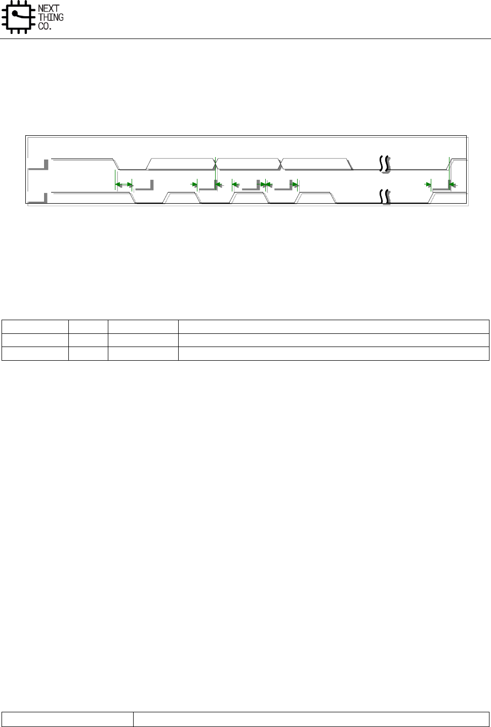
Interfaces
GR8 User Manual(Version1.0) Copyright © 2017 Next Thing Co. All Rights Reserved. Page 404
When the slave receiver acknowledges the slave address, but not ready to receive more during a data transfer, the
SDA will be left high for the master to generate a STOP condition to abort the transfer.
The following diagram provides an illustration to the relation between SDA signal line and SCL signal line on the 2-
Wire serial bus.
Figure 8-1. TWI Timing Diagram
8.1.3. TWI Controller Special Requirement
8.1.3.1. TWI Pin List
Port Name
Width
Direction
Description
TWI_SCL
1
IN/OUT
TWI Clock line
TWI_SDA
1
IN/OUT
TWI Serial Data line
8.1.3.2. TWI Controller Operation
There are four operation modes on the two-wire bus which dictate the communication method: Master Transmit,
Master Receive, Slave Transmit and Slave Receive. In general, the CPU host controls TWI by writing commands and
data to its registers. The TWI interrupts the CPU host for the attention each time a byte transfer is done or a
START/STOP condition is detected. The CPU host can also poll the status register for the current status if the
interrupt mechanism is not disabled by the CPU host.
When the CPU host wants to start a bus transfer, it initiates a bus START to enter the master mode by setting
IM_STA bit in the 2WIRE_CNTR register to high (before it must be low). The TWI will assert INT line and INT_FLAG
to indicate a completion for the START condition and each consequent byte transfer. At each interrupt, the micro-
processor needs to check the 2WIRE_STAT register for the current status. A transfer has to be concluded with a
STOP condition by setting the M_STP bit high.
In Slave Mode, the TWI also constantly samples the bus and looks for its own slave address during addressing
cycles. Once a match is found, it is addressed and interrupts the CPU host with the corresponding status. Upon
request, the CPU host should read the status, read/write 2WIRE_DATA data register, and set the 2WIRE_CNTR
control register. After each byte transfer, a slave device always halts the operation of the remote master by holding
the next low pulse on the SCL line until the microprocessor responds to the status of the previous byte transfer or
START condition.
8.1.4. TWI Controller Register List
Module Name
Base Address
IIC2IIC5IIC5IIC4IIC4IIC3IIC1
SDA
SCL
Interfaces
GR8 User Manual(Version1.0) Copyright © 2017 Next Thing Co. All Rights Reserved. Page 405
TWI0
0x01C2AC00
TWI1
0x01C2B000
TWI2
0x01C2B400
Register Name
Offset
Description
TWI_ADDR
0x0000
TWI Slave Address
TWI_XADDR
0x0004
TWI Extended Slave Address
TWI_DATA
0x0008
TWI Data Byte
TWI_CNTR
0x000C
TWI Control Register
TWI_STAT
0x0010
TWI Status Register
TWI_CCR
0x0014
TWI Clock Control Register
TWI_SRST
0x0018
TWI Software Reset
TWI_EFR
0x001C
TWI Enhance Feature Register
TWI_LCR
0x0020
TWI Line Control Register
8.1.5. TWI Controller Register Description
8.1.5.1. TWI Slave Address Register(Default Value: 0x0000_0000)
Offset: 0x0000
Register Name: TWI_ADDR
Bit
Read/Write
Default/Hex
Description
31:8
/
/
/
7:1
R/W
0x0
SLA
Slave address
7-bit addressing
SLA6, SLA5, SLA4, SLA3, SLA2, SLA1, SLA0
10-bit addressing
1, 1, 1, 1, 0, SLAX[9:8]
0
R/W
0x0
GCE
General call address enable
0: Disable
1: Enable
Note:
For 7-bit addressing:
SLA6 – SLA0 is the 7-bit address of TWI in slave mode. When TWI receives this address after a START condition, it
will generate an interrupt and enter slave mode. (SLA6 corresponds to the first bit received from the two wire bus.)
If GCE is set to ‘1’, the TWI will also recognize the general call address (00h).
Interfaces
GR8 User Manual(Version1.0) Copyright © 2017 Next Thing Co. All Rights Reserved. Page 406
For 10-bit addressing:
When the address received starts with 11110b, the TWI recognizes this as the first part of a 10-bit address and if
the next two bits match ADDR[2:1] (i.e. SLAX9 and SLAX8 of the device’s extended address), it sends an ACK. (The
device does not generate an interrupt at this point.) If the next byte of the address matches the XADDR register
(SLAX7 – SLAX0), the TWI generates an interrupt and goes into slave mode.
8.1.5.2. TWI Extend Address Register(Default Value: 0x0000_0000)
Offset: 0x0004
Register Name: TWI_XADDR
Bit
Read/Write
Default/Hex
Description
31:8
/
/
/
7:0
R/W
0x0
SLAX
Extend Slave Address
SLAX[7:0]
8.1.5.3. TWI Data Register(Default Value: 0x0000_0000)
Offset: 0x0008
Register Name: TWI_DATA
Bit
Read/Write
Default/Hex
Description
31:8
/
/
/
7:0
R/W
0x0
Data byte for transmitting or receiving
8.1.5.4. TWI Control Register(Default Value: 0x0000_0000)
Offset: 0x000C
Register Name: TWI_CNTR
Bit
Read/Write
Default/Hex
Description
31:8
/
/
/
7
R/W
0x0
INT_EN
Interrupt Enable
0: The interrupt line always low
1: The interrupt line will go high when INT_FLAG is set.
6
R/W
0x0
BUS_EN
two-wire bus Enable
0: The two-wire bus inputs ISDA/ISCL are ignored and the 2-Wire
Controller will not respond to any address on the bus
1: The TWI will respond to calls to its slave address – and to the general

Interfaces
GR8 User Manual(Version1.0) Copyright © 2017 Next Thing Co. All Rights Reserved. Page 407
call address if the GCE bit in the ADDR register is set.
Note: In master operation mode, this bit should be set to ‘1’
5
R/W
0x0
M_STA
Master Mode Start
When M_STA is set to ‘1’, TWI controller enters master mode and will
transmit a START condition on the bus when the bus is free. If the M_STA
bit is set to ‘1’ when the 2-Wire Controller is already in master mode and
one or more bytes have been transmitted, then a repeated START
condition will be sent. If the M_STA bit is set to ‘1’ when the TWI is being
accessed in slave mode, the TWI will complete the data transfer in slave
mode then enter master mode when the bus has been released.
The M_STA bit is cleared automatically after a START condition is sent:
writing a ‘0’ to this bit has no effect.
4
R/W
0x0
M_STP
Master Mode Stop
If M_STP is set to ‘1’ in master mode, a STOP condition is transmitted on
the two-wire bus. If the M_STP bit is set to ‘1’ in slave mode, the TWI will
behave as if a STOP condition has been received, but no STOP condition
will be transmitted on the two-wire bus. If both M_STA and M_STP bits
are set, the TWI will first transmit the STOP condition (if in master mode),
and then transmit the START condition.
The M_STP bit is cleared automatically: writing a ‘0’ to this bit has no
effect.
3
R/W
0x0
INT_FLAG
Interrupt Flag
INT_FLAG is automatically set to ‘1’ when any of 28 (out of the possible
29) states is entered (see ‘STAT Register’ below). The only state that does
not set INT_FLAG is state F8h. If the INT_EN bit is set, the interrupt line
goes high when IFLG is set to ‘1’. If the TWI is operating in slave mode,
data transfer is suspended when INT_FLAG is set and the low period of
the two-wire bus clock line (SCL) is stretched until ‘0’ is written to
INT_FLAG. The 2-wire clock line is then released and the interrupt line
goes low.
2
R/W
0x0
A_ACK
Assert Acknowledge
When A_ACK is set to ‘1’, an Acknowledge (low level on SDA) will be sent
during the acknowledge clock pulse on the two-wire bus if:
(1). Either the whole of a matching 7-bit slave address or the first or the
second byte of a matching 10-bit slave address has been received.

Interfaces
GR8 User Manual(Version1.0) Copyright © 2017 Next Thing Co. All Rights Reserved. Page 408
(2). The general call address has been received and the GCE bit in the
ADDR register is set to ‘1’.
(3). A data byte has been received in master or slave mode.
When A_ACK is ‘0’, a Not Acknowledge (high level on SDA) will be sent
when a data byte is received in master or slave mode.
If A_ACK is cleared to ‘0’ in slave transmitter mode, the byte in the DATA
register is assumed to be the ‘last byte’. After this byte is transmitted,
the TWI will enter state C8h then return to the idle state (status code
F8h) when INT_FLAG is cleared.
The TWI will not respond as a slave unless A_ACK is set.
1:0
/
/
/
8.1.5.5. TWI Status Register(Default Value: 0x0000_00F8)
Offset: 0x0010
Register Name: TWI_STAT
Bit
Read/Write
Default/Hex
Description
31:8
/
/
/
7:0
R
0xF8
Status Information Byte
Code Status
0x00: Bus error
0x08: START condition transmitted
0x10: Repeated START condition transmitted
0x18: Address + Write bit transmitted, ACK received
0x20: Address + Write bit transmitted, ACK not received
0x28: Data byte transmitted in master mode, ACK received
0x30: Data byte transmitted in master mode, ACK not received
0x38: Arbitration lost in address or data byte
0x40: Address + Read bit transmitted, ACK received
0x48: Address + Read bit transmitted, ACK not received
0x50: Data byte received in master mode, ACK transmitted
0x58: Data byte received in master mode, not ACK transmitted
0x60: Slave address + Write bit received, ACK transmitted
0x68: Arbitration lost in address as master, slave address + Write bit

Interfaces
GR8 User Manual(Version1.0) Copyright © 2017 Next Thing Co. All Rights Reserved. Page 409
received, ACK transmitted
0x70: General Call address received, ACK transmitted
0x78: Arbitration lost in address as master, General Call address
received, ACK transmitted
0x80: Data byte received after slave address received, ACK transmitted
0x88: Data byte received after slave address received, not ACK
transmitted
0x90: Data byte received after General Call received, ACK transmitted
0x98: Data byte received after General Call received, not ACK
transmitted
0xA0: STOP or repeated START condition received in slave mode
0xA8: Slave address + Read bit received, ACK transmitted
0xB0: Arbitration lost in address as master, slave address + Read bit
received, ACK transmitted
0xB8: Data byte transmitted in slave mode, ACK received
0xC0: Data byte transmitted in slave mode, ACK not received
0xC8: Last byte transmitted in slave mode, ACK received
0xD0: Second Address byte + Write bit transmitted, ACK received
0xD8: Second Address byte + Write bit transmitted, ACK not received
0xF8: No relevant status information, INT_FLAG=0
Others: Reserved
8.1.5.6. TWI Clock Register(Default Value: 0x0000_0000)
Offset: 0x0014
Register Name: TWI_CCR
Bit
Read/Write
Default/Hex
Description
31:7
/
/
/
6:3
R/W
0x0
CLK_M
2:0
R/W
0x0
CLK_N
The two-wire bus is sampled by the TWI at the frequency defined by F0:
Fsamp = F0 = Fin / 2^CLK_N
The TWI OSCL output frequency, in master mode, is F1 / 10:
F1 = F0 / (CLK_M + 1)
Foscl = F1 / 10 = Fin / (2^CLK_N * (CLK_M + 1)*10)
For Example:
Fin = 48 MHz (APB clock input)

Interfaces
GR8 User Manual(Version1.0) Copyright © 2017 Next Thing Co. All Rights Reserved. Page 410
For 400 kHz full speed 2Wire, CLK_N = 2, CLK_M=2
F0 = 48 MHz/2^2=12 MHz, F1= F0/(10*(2+1)) = 0.4 MHz
For 100 kHz standard speed 2 Wire, CLK_N=2, CLK_M=11
F0=48 MHz/2^2=12 MHz, F1=F0/(10*(11+1)) = 0.1 MHz
8.1.5.7. TWI Soft Reset Register(Default Value: 0x0000_0000)
Offset: 0x0018
Register Name: TWI_SRST
Bit
Read/Write
Default/Hex
Description
31:1
/
/
/
0
R/W
0x0
Soft Reset
Write ‘1’ to this bit to reset the TWI and clear to ‘0’ when complete Soft
Reset operation.
8.1.5.8. TWI Enhance Feature Register(Default Value: 0x0000_0000)
Offset: 0x001C
Register Name: TWI_EFR
Bit
Read/Write
Default/Hex
Description
31:2
/
/
/
0:1
R/W
0x0
Data Byte follow Read Command Control
No Data Byte to be written after read command
Only 1 byte data to be written after read command
2 bytes data can be written after read command
3 bytes data can be written after read command
8.1.5.9. TWI Line Control Register(Default Value: 0x0000_003A)
Offset: 0x0020
Register Name: TWI_LCR
Bit
Read/Write
Default/Hex
Description
31:6
/
/
/
5
R
0x1
Current state of TWI_SCL
0: Low
1: High
4
R
0x1
Current state of TWI_SDA

Interfaces
GR8 User Manual(Version1.0) Copyright © 2017 Next Thing Co. All Rights Reserved. Page 411
0: Low
1: High
3
R/W
0x1
TWI_SCL line state control bit
When line control mode is enabled (bit[2] set), value of this bit decides
the output level of TWI_SCL
0: Output low level
1: Output high level
2
R/W
0x0
TWI_SCL line state control enable
When this bit is set, the state of TWI_SCL is controlled by the value of
bit[3].
0: Disable TWI_SCL line control mode
1: Enable TWI_SCL line control mode
1
R/W
0x1
TWI_SDA line state control bit
When line control mode is enabled (bit[0] set), value of this bit decides
the output level of TWI_SDA
0: Output low level
1: Output high level
0
R/W
0x0
TWI_SDA line state control enable
When this bit is set, the state of TWI_SDA is controlled by the value of
bit[1].
0: Disable TWI_SDA line control mode
1: Enable TWI_SDA line control mode
8.1.5.10. TWI DVFS Control Register(Default Value: 0x0000_0000)
Offset: 0x0024
Register Name: TWI_DVFSCR
Bit
Read/Write
Default/Hex
Description
31:2
/
/
/
2
R/W
0x0
CPU and DVFS BUSY set priority select
0: CPU has higher priority
1: DVFS has higher priority
1
R/W
0x0
CPU Busy set

Interfaces
GR8 User Manual(Version1.0) Copyright © 2017 Next Thing Co. All Rights Reserved. Page 412
0
R/W
0x0
DVFS Busy set
Note: This register is only implemented in TWI0.

Interfaces
GR8 User Manual(Version1.0) Copyright © 2017 Next Thing Co. All Rights Reserved. Page 413
8.2. SPI
8.2.1. Overview
The Serial Peripheral Interface (SPI) allows rapid data communication with less software interrupts. The SPI
module contains one 8x64-bit receiver buffer (RXFIFO) and one 8x64-bit transmit buffer (TXFIFO). It can work in
two modes: Master mode and Slave mode.
Features:
● Full-duplex synchronous serial interface
● Configurable Master/Slave
● 8x64-bit FIFO for data transmit and 8x64-bit FIFO for data receive
● Configurable polarity and phase of the Chip Select (SPI_SS) and SPI Clock (SPI_SCLK)
● Supports Dedicated DMA
8.2.2. SPI Timing Diagram
The SPI master uses the SPI_SCLK signal to transfer data in and out of the shift register. Data is clocked using one
of four programmable clock phase and polarity combinations.
During Phase 0, Polarity 0 and Phase 1, Polarity 1 operations, output data changes on the falling clock edge and
input data is shifted in on the rising edge.
During Phase 1, Polarity 0 and Phase 0, Polarity 1 operations, output data changes on the rising edges of the
clock and is shifted in on the falling edges.
The POL defines the signal polarity when SPI_SCLK is in an idle state. The SPI_SCLK is high level when POL is ‘1’
and it is low level when POL is ‘0’. The PHA decides whether the leading edge of SPI_SCLK is used to setup or
sample data. The leading edge is used to setup data when PHA is ‘1’ and to sample data when PHA is ‘0’. The
four modes are listed below:
SPI Mode
POL
PHA
Leading Edge
Trailing Edge
0
0
0
Rising, Sample
Falling, Setup
1
0
1
Rising, Setup
Falling, Sample
2
1
0
Falling, Sample
Rising, Setup
3
1
1
Failing, Setup
Rising, Sample
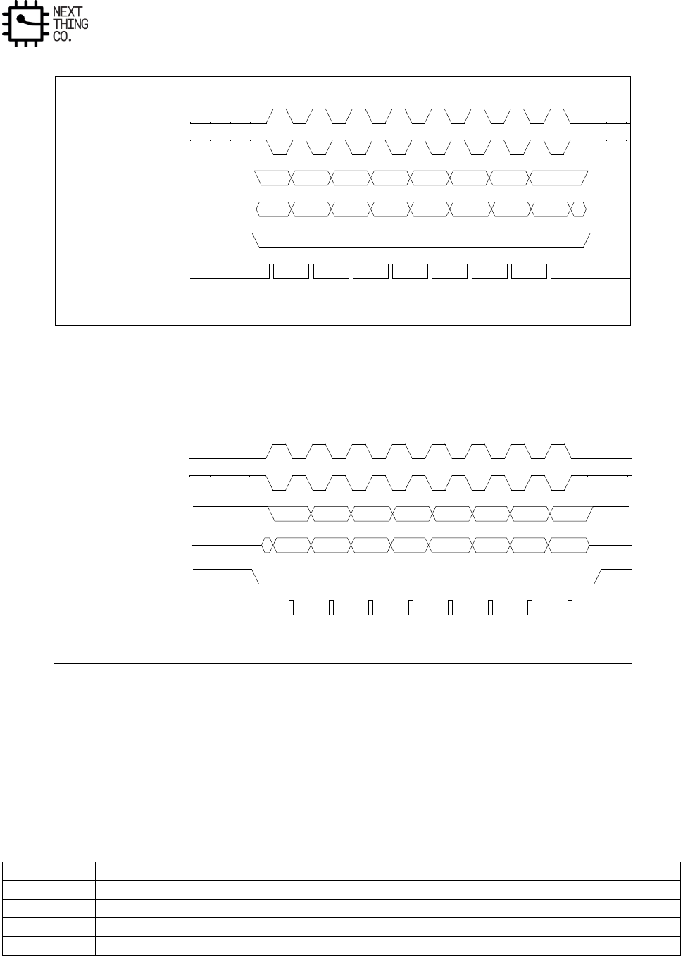
Interfaces
GR8 User Manual(Version1.0) Copyright © 2017 Next Thing Co. All Rights Reserved. Page 414
Figure 8-2. SPI Phase 0 Timing Diagram
Figure 8-3. SPI Phase 1 Timing Diagram
8.2.3. Functional Descriptions
8.2.3.1. SPI Pin List
The direction of the SPI pin is different in two work modes: Master Mode and Slave Mode.
Port Name
Width
Direction(M)
Direction(S)
Description
SPI-CLK
1
OUT
IN
SPI Clock
SPI-MOSI
1
OUT
IN
SPI Master Output Slave Input Data Signal
SPI-MISO
1
IN
OUT
SPI Master Input Slave Output Data Signal
SPI-CS
1
OUT
IN
SPI Chip Select Signal
Phase 0
SPI_SCLK (Mode 0)
SPI_SCLK (Mode 2)
SPI_MOSI
SPI_MISO
SPI_SS
Sample MOSI/ MISO pin
Phase 1
SPI_SCLK (Mode 1)
SPI_SCLK (Mode 3)
SPI_MOSI
SPI_MISO
SPI_SS
Sample MOSI/ MISO pin
Interfaces
GR8 User Manual(Version1.0) Copyright © 2017 Next Thing Co. All Rights Reserved. Page 415
8.2.3.2. SPI Module Clock Source and Frequency
The SPI module uses two clock sources: AHB_CLK and SPI_CLK. The SPI_SCLK can in the range from 3 kHz to 100
MHz and AHB_CLK>= 2x SPI_SCLK.
Clock Name
Description
Requirement
AHB_CLK
AHB Bus Clock, as the clock source of SPI module
AHB_CLK >= 2xSPI_SCLK
SPI_CLK
SPI Serial Input Clock
8.2.4. SPI Register List
Module Name
Base Address
SPI0
0x01C05000
SPI2
0x01C17000
Register Name
Offset
Description
SPI_RXDATA
0x0000
SPI RX Data Register
SPI_TXDATA
0x0004
SPI TX Data Register
SPI_CTL
0x0008
SPI Control Register
SPI_INTCTL
0x000C
SPI Interrupt Control Register
SPI_ST
0x0010
SPI Status Register
SPI_DMACTL
0x0014
SPI DMA Control Register
SPI_WAIT
0x0018
SPI Wait Clock Counter Register
SPI_CCTL
0x001C
SPI Clock Rate Control Register
SPI_BC
0x0020
SPI Burst Counter Register
SPI_TC
0x0024
SPI Transmit Counter Register
SPI_FIFO_STA
0x0028
SPI FIFO Status Register
8.2.5. SPI Register Description
8.2.5.1. SPI RX Data Register(Default Value: 0x0000_0000)
Offset: 0x0000
Register Name: SPI_RXDATA
Bit
Read/Write
Default/hex
Description
31:0
R
0x0
Receive Data
In 8-bits SPI bus width, this register can be accessed in byte, half-word
or word unit by AHB. In byte accessing method, if there are words in
RXFIFO, the top word is returned and the RXFIFO depth is decreased by
1. In half-word accessing method, the two SPI bursts are returned and
the RXFIFO depth decreases by 2. In word accessing method, the four
SPI bursts are returned and the RXFIFO depth decreases by 4.
8.2.5.2. SPI TX Data Register(Default Value: 0x0000_0000)
Offset: 0x0004
Register Name: SPI_TXDAT

Interfaces
GR8 User Manual(Version1.0) Copyright © 2017 Next Thing Co. All Rights Reserved. Page 416
Bit
Read/Write
Default/Hex
Description
31:0
W
0x0
Transmit Data
8.2.5.3. SPI Control Register(Default Value: 0x0002_001C)
Offset: 0x0008
Register Name: SPI_CTL
Bit
Read/Write
Default/Hex
Description
31:20
/
/
/
19
R/W
0x0
Master Sample Data Control
Set this bit to ‘1’ to make the internal read sample point with a delay of
half cycle of SPI_CLK. It is used in high speed read operation to reduce
the error caused by the time delay of SPI_CLK propagating between
master and slave.
1: Delay internal read sample point
0: Normal operation, do not delay internal read sample point
18
R/W
0x0
Transmit Pause Enable
In master mode, it is used to control transmit state machine to stop
smart burst sending when RX FIFO is full.
1: Stop transmit data when RXFIFO full
0: Normal operation, ignore RXFIFO status
17
R/W
0x1
SS_LEVEL
When control SS signal manually (SPI_CTRL_REG.SS_CTRL==1), set this
bit to ‘1’ or ‘0’ to control the level of SS signal.
1: Set SS to high
0: Set SS to low
16
R/W
0x0
SS_CTRL
SS Output Mode Select
Usually, the controller sends SS signal automatically with data together.
When this bit is set to 1, software must manually write
SPI_CTRL_REG.SS_LEVEL (bit [17]) to 1 or 0 to control the level of SS
signal.
1: Manual output SS
0: Automatic output SS
15
R/W
0x0
DHB
Discard Hash Burst

Interfaces
GR8 User Manual(Version1.0) Copyright © 2017 Next Thing Co. All Rights Reserved. Page 417
In master mode, it controls whether discarding unused SPI bursts.
0: Receiving all SPI bursts in BC period
1: Discard unused SPI bursts, only fetching the SPI bursts during dummy
burst period. The bursts number is specified by WTC.
14
R/W
0x0
DDB
Dummy Burst Type
0: The bit value of dummy SPI burst is zero
1: The bit value of dummy SPI burst is one
13:12
R/W
0x0
SS
SPI Chip Select
Select one of four external SPI Master/Slave Devices
00: SPI_SS0 will be asserted
01: SPI_SS1 will be asserted
10: SPI_SS2 will be asserted
11: SPI_SS3 will be asserted
11
R/W
0x0
RPSM
Rapids Mode Select
Select Rapids operation mode for high speed read.
0: Normal read mode
1: Rapids read mode
10
R/W
0x0
XCH
Exchange Burst
In master mode, it is used to start to SPI burst.
0: Idle
1: Initiates exchange. After finishing the SPI bursts transfer specified by
BC, this bit is cleared to zero by SPI Controller.
9
R/W
0x0
RXFIFO Reset
Write ‘1’ to reset the control portion of the receiver FIFO and treats the
FIFO as empty.
It is 'self-clearing'. It is not necessary to clear this bit.
8
R/W
0x0
TXFIFO Reset
Write ‘1’ to reset the control portion of the transmit FIFO and treats the

Interfaces
GR8 User Manual(Version1.0) Copyright © 2017 Next Thing Co. All Rights Reserved. Page 418
FIFO as empty.
It is 'self-clearing'. It is not necessary to clear this bit.
7
R/W
0x0
SSCTL
In master mode, this bit selects the output wave form for the SPI_SSx
signal.
0: SPI_SSx remains asserted between SPI bursts
1: Negate SPI_SSx between SPI bursts
6
R/W
0x0
LMTF
LSB/ MSB Transfer First Select
0: MSB first
1: LSB first
5
R/W
0x0
DMAM
DMA Mode Control
0: Normal dma
1: Dedicate dma
4
R/W
0x1
SSPOL
SPI Chip Select Signal Polarity Control
0: Active high polarity (0 = Idle)
1: Active low polarity (1 = Idle)
3
R/W
0x1
POL
SPI Clock Polarity Control
0: Active high polarity (0 = Idle)
1: Active low polarity (1 = Idle)
2
R/W
0x1
PHA
SPI Clock/Data Phase Control
0: Phase 0 (Leading edge for sample data)
1: Phase 1 (Leading edge for setup data)
1
R/W
0x0
MODE
SPI Function Mode Select

Interfaces
GR8 User Manual(Version1.0) Copyright © 2017 Next Thing Co. All Rights Reserved. Page 419
0: Slave Mode
1: Master Mode
0
R/W
0x0
EN
SPI Module Enable Control
0: Disable
1: Enable
8.2.5.4. SPI Interrupt Control Register(Default Value: 0x0000_0000)
Offset: 0x000C
Register Name: SPI_INTCTL
Bit
Read/Write
Default/Hex
Description
31:18
/
/
/
17
R/W
0x0
SSI Interrupt Enable
Chip Select Signal (SSx) from valid state to invalid state
0: Disable
1: Enable
16
R/W
0x0
Transfer Completed Interrupt Enable
0: Disable
1: Enable
15
/
/
/
14
R/W
0x0
TXFIFO underrun Interrupt Enable
0: Disable
1: Enable
13
R/W
0x0
TX FIFO Overflow Interrupt Enable
0: Disable
1: Enable
12
R/W
0x0
TX FIFO 3/4 Empty Interrupt Enable
0: Disable
1: Enable
11
R/W
0x0
TX FIFO 1/4 Empty Interrupt Enable

Interfaces
GR8 User Manual(Version1.0) Copyright © 2017 Next Thing Co. All Rights Reserved. Page 420
0: Disable
1: Enable
10
R/W
0x0
TX FIFO Full Interrupt Enable
0: Disable
1: Enable
9
R/W
0x0
TX FIFO Half Empty Interrupt Enable
0: Disable
1: Enable
8
R/W
0x0
TX FIFO Empty Interrupt Enable
0: Disable
1: Enable
7
/
/
/
6
R/W
0x0
RXFIFO underrun Interrupt Enable
0: Disable
1: Enable
5
R/W
0x0
RX FIFO Overflow Interrupt Enable
0: Disable
1: Enable
4
R/W
0x0
RXFIFO 3/4 Full Interrupt Enable
0: Disable
1: Enable
3
R/W
0x0
RX FIFO 1/4 Full Interrupt Enable
0: Disable
1: Enable
2
R/W
0x0
RX FIFO Full Interrupt Enable
0: Disable
1: Enable

Interfaces
GR8 User Manual(Version1.0) Copyright © 2017 Next Thing Co. All Rights Reserved. Page 421
1
R/W
0x0
RX FIFO Half Full Interrupt Enable
0: Disable
1: Enable
0
R/W
0x0
RX FIFO Ready Interrupt Enable
0: Disable
1: Enable
8.2.5.5. SPI Interrupt Status Register(Default Value: 0x0000_1B00)
Offset: 0x0010
Register Name: SPI_INT_STA
Bit
Read/Write
Default/Hex
Description
31
R
0x0
Clear interrupt busy flag
0: clearing interrupt is done
1: clearing interrupt is busy
30:24
/
/
/
23:20
/
/
/
19:18
/
/
/
17
R/W
0x0
SSI
SS Invalid Interrupt
When SSI is 1, it indicates that SS has changed from valid state to invalid
state. Writing 1 to this bit clears it.
16
R/W
0x0
TC
Transfer Completed
In master mode, it indicates that all bursts specified by BC have been
exchanged. In other condition, when set, this bit indicates that all the
data in TXFIFO has been loaded in the Shift register, and the Shift
register has shifted out all the bits. Writing 1 to this bit clears it.
0: Busy
1: Transfer Completed
15
/
/
/
14
R/W
0x0
TU
TXFIFO underrun
This bit is set when if the TXFIFO is underrun. Writing 1 to this bit clears

Interfaces
GR8 User Manual(Version1.0) Copyright © 2017 Next Thing Co. All Rights Reserved. Page 422
it.
0: TXFIFO is not underrun
1: TXFIFO is underrun
13
R/W
0x0
TO
TXFIFO Overflow
This bit is set when the TXFIFO overflows. Writing 1 to this bit clears it.
0: TXFIFO is not overflowed
1: TXFIFO is overflowed
12
R/W
0x1
TXFIFO 3/4 empty
This bit is set if the TXFIFO is more than 3/4 empty. Writing 1 to this bit
clears it.
11
R/W
0x1
TXFIFO 1/4 empty
This bit is set if the TXFIFO is more than 1/4 empty. Writing 1 to this bit
clears it.
10
R/W
0x0
TF
TXFIFO Full
This bit is set when the TXFIFO is full. Writing 1 to this bit clears it.
0: TXFIFO is not Full
1: TXFIFO is Full
9
R/W
0x1
THE
TXFIFO Half empty
This bit is set if the TXFIFO is more than half empty. Writing 1 to this bit
clears it.
0: TXFIFO holds more than half words
1: TXFIFO holds half or fewer words
8
R/W
0x1
TE
TXFIFO Empty
This bit is set if the TXFIFO is empty. Writing 1 to this bit clears it.
0: TXFIFO contains one or more words.
1: TXFIFO is empty
7
/
/
/

Interfaces
GR8 User Manual(Version1.0) Copyright © 2017 Next Thing Co. All Rights Reserved. Page 423
6
R/W
0x0
RU
RXFIFO Underrun
When set, this bit indicates that RXFIFO has underrun. Writing 1 to this
bit clears it.
5
R/W
0x0
RO
RXFIFO Overflow
When set, this bit indicates that RXFIFO has overflowed. Writing 1 to
this bit clears it.
0: RXFIFO is available.
1: RXFIFO has overflowed.
4
R/W
0x0
RXFIFO 3/4 Full
This bit is set when the RXFIFO is 3/4 full. Writing 1 to this bit clears it.
0: Not 3/4 Full
1: 3/4 Full
3
R/W
0x0
RXFIFO 1/4 Full
This bit is set when the RXFIFO is 1/4 full. Writing 1 to this bit clears it.
0: Not 1/4 Full
1: 1/4 Full
2
R/W
0x0
RF
RXFIFO Full
This bit is set when the RXFIFO is full. Writing 1 to this bit clears it.
0: Not Full
1: Full
1
R/W
0x0
RHF
RXFIFO Half Full. This bit is set if the RXFIFO is half full (≥ 4 words in
RXFIFO) . Writing 1 to this bit clears it.
0: Less than 4 words are stored in RXFIFO.
1: Four or more words are available in RXFIFO.
0
R/W
0x0
RR
RXFIFO Ready
This bit is set any time there is one or more words stored in RXFIFO (≥

Interfaces
GR8 User Manual(Version1.0) Copyright © 2017 Next Thing Co. All Rights Reserved. Page 424
1 words). Writing 1 to this bit clears it.
0: No valid data in RXFIFO
1: More than 1 word in RXFIFO
8.2.5.6. SPI DMA Control Register(Default Value: 0x0000_0000)
Offset: 0x0014
Register Name: SPI_DMACTL
Bit
Read/Write
Default/Hex
Description
31:13
/
/
/
12
R/W
0x0
TXFIFO3/4 Empty DMA Request Enable
0: Disable
1: Enable
11
R/W
0x0
TXFIFO 1/4 Empty DMA Request Enable
0: Disable
1: Enable
10
R/W
0x0
TXFIFO Not Full DMA Request Enable
When enabled, if more than one free room for burst, DMA request is
asserted, otherwise, it’s de-asserted.
0: Disable
1: Enable
9
R/W
0x0
TXFIFO Half Empty DMA Request Enable
0: Disable
1: Enable
8
R/W
0x0
TXFIFO Empty DMA Request Enable
0: Disable
1: Enable
7:5
/
/
/
4
R/W
0x0
RXFIFO 3/4 Full DMA Request Enable
This bit enables/disables the RXFIFO 3/4 Full DMA Request.

Interfaces
GR8 User Manual(Version1.0) Copyright © 2017 Next Thing Co. All Rights Reserved. Page 425
0: Disable
1: Enable
3
R/W
0x0
RXFIFO 1/4 Full DMA Request Enable
This bit enables/disables the RXFIFO 1/4 Full DMA Request.
0: Disable
1: Enable
2
R/W
0x0
RXFIFO Full DMA Request Enable
This bit enables/disables the RXFIFO Half Full DMA Request.
0: Disable
1: Enable
1
R/W
0x0
RXFIFO Half Full DMA Request Enable
This bit enables/disables the RXFIFO Half Full DMA Request.
0: Disable
1: Enable
0
R/W
0x0
RXFIFO Ready Request Enable
This bit enables/disables the RXFIFO Ready DMA Request when one or
more than one words in RXFIFO.
0: Disable
1: Enable
8.2.5.7. SPI Wait Clock Register(Default Value: 0x0000_0000)
Offset: 0x0018
Register Name: SPI_WAIT
Bit
Read/Write
Default/Hex
Description
31:16
/
/
/
15:0
R/W
0x0
WCC
Wait Clock Counter (In Master mode)
These bits control the number of wait states to be inserted in data
transfers. The SPI module counts SPI_SCLK by WCC for delaying next
word data transfer.
0: No wait states inserted
N: N SPI_SCLK wait states inserted

Interfaces
GR8 User Manual(Version1.0) Copyright © 2017 Next Thing Co. All Rights Reserved. Page 426
8.2.5.8. SPI Clock Control Register(Default Value: 0x0000_0002)
Offset: 0x001C
Register Name: SPI_CCTL
Bit
Read/Write
Default/Hex
Description
31:13
/
/
/
12
R/W
0x0
DRS
Divide Rate Select (Master Mode Only)
0: Select Clock Divide Rate 1
1: Select Clock Divide Rate 2
11:8
R/W
0x0
CDR1
Clock Divide Rate 1 (Master Mode Only)
This field selects the baud rate of the SPI_SCLK based on a division of
the AHB_CLK. These bits allow SPI to synchronize with different external
SPI devices. The max frequency is one quarter of AHB_CLK. The divide
ratio is determined according to the following table using the equation:
2^(n+1). The SPI_SCLK is determined according to the following
equation: SPI_CLK = AHB_CLK / 2^(n+1).
7:0
R/W
0x2
CDR2
Clock Divide Rate 2 (Master Mode Only)
The SPI_SCLK is determined according to the following equation:
SPI_CLK = AHB_CLK / (2*(n + 1)).
8.2.5.9. SPI Burst Counter Register(Default Value: 0x0000_0000)
Offset: 0x0020
Register Name: SPI_BC
Bit
Read/Write
Default/Hex
Description
31:24
/
/
/
23:0
R/W
0x0
BC
Burst Counter
In master mode, this field specifies the total burst number.
0: 0 burst
1: 1 burst
…
N: N bursts

Interfaces
GR8 User Manual(Version1.0) Copyright © 2017 Next Thing Co. All Rights Reserved. Page 427
8.2.5.10. SPI Transmit Counter Register(Default Value: 0x0000_0000)
Offset: 0x0024
Register Name: SPI_TC
Bit
Read/Write
Default/Hex
Description
31:24
/
/
/
23:0
R/W
0x0
WTC
Write Transmit Counter
In master mode, this field specifies the burst number that should be
sent to TXFIFO before automatically sending dummy burst. For saving
bus bandwidth, the dummy burst (all zero bits or all one bits) is sent
by SPI Controller automatically.
0: 0 burst
1: 1 burst
…
N: N bursts
8.2.5.11. SPI FIFO Status Register(Default Value: 0x0000_0000)
Offset: 0x0028
Register Name: SPI_FIFO_STA
Bit
Read/Write
Default/Hex
Description
31:25
/
/
/
22:16
R
0x0
TXFIFO Counter
These bits indicate the number of words in TXFIFO
0: 0 byte in TXFIFO
1: 1 byte in TXFIFO
…
…
63: 63 bytes in TXFIFO
64: 64 bytes in TXFIFO
15:7
/
/
/
6:0
R
0x0
RXFIFO Counter
These bits indicate the number of words in RXFIFO
0: 0 byte in RXFIFO
1: 1 byte in RXFIFO
…

Interfaces
GR8 User Manual(Version1.0) Copyright © 2017 Next Thing Co. All Rights Reserved. Page 428
…
63: 63 bytes in RXFIFO
64: 64 bytes in RXFIFO
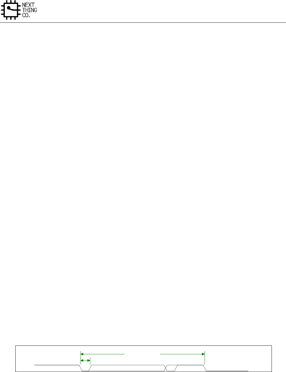
Interfaces
GR8 User Manual(Version1.0) Copyright © 2017 Next Thing Co. All Rights Reserved. Page 429
8.3. UART
8.3.1. Overview
The UART is used for serial communication with a peripheral, modem (data carrier equipment, DCE) or data set.
Data is written from a master (CPU) over the APB bus to the UART and it is converted to serial form and transmitted
to the destination device. Serial data is also received by the UART and stored for the master (CPU) to read back.
The UART contains registers to control the character length, baud rate, parity generation/checking, and interrupt
generation. Although there is only one interrupt output signal from the UART, there are several prioritized
interrupt types responsible for its assertion. Each of the interrupt types can be separately enabled/disabled with
the control registers.
The UART has 16450 and 16550 modes of operation, which are compatible with a range of standard software
drivers. In 16550 mode, transmit and receive operations are both buffered by FIFOs. In 16450 mode, these FIFOs
are disabled.
The UART supports word lengths from five to eight bits, an optional parity bit and 1, 1.5 or 2 stop bits, and is fully
programmable by an AMBA APB CPU interface. A 16-bit programmable baud rate generator and an 8-bit scratch
register are included, together with separate transmit and receive FIFOs. Eight modem control lines and a
diagnostic loop-back mode are provided.
Interrupts can be generated for a range of TX Buffer/FIFO, RX Buffer/FIFO, Modem Status and Line Status
conditions.
Features:
● Compatible with industry-standard 16550 UARTs
● 64 bytes transmit and receive data FIFOs
● DMA controller interface
● Software/hardware flow control
● Programmable transmit holding register empty interrupt
● Interrupt support for FIFOs, Status Change
8.3.2. UART Timing Diagram
Figure 8-4. UART Serial Data Format
Serial Data
S
Data bits 5-8
P
S 1,1.5,2
One Character
Bit TimeBit Time
One Character
TX/RX
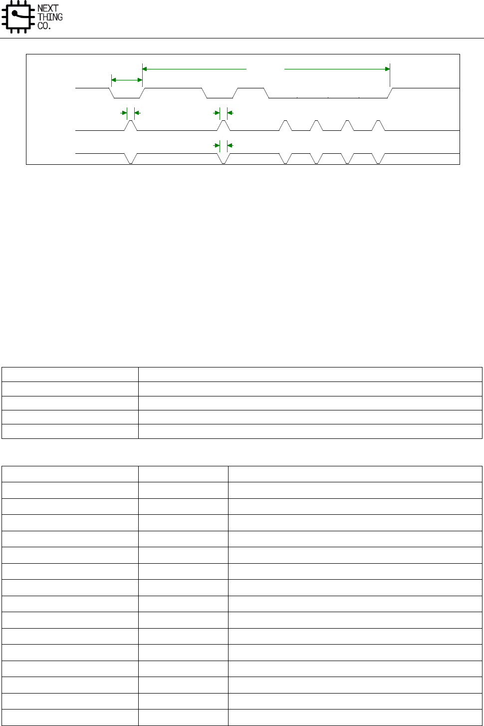
Interfaces
GR8 User Manual(Version1.0) Copyright © 2017 Next Thing Co. All Rights Reserved. Page 430
Figure 8-5. Serial IrDA Data Format
8.3.3. UART Special Requirement
When the UART is working in IrDA mode (MCR[6]=’1’), if HALT[4] is set to ‘1’, the signal is inverted before
transferring to SOUT, and if HALT[5] is set to ‘1’, the signal is inverted after receiving from pin SIN.
8.3.4. UART Register List
There are 3 UART controllers that can be configured as Serial IrDA.
Module Name
Base Address
UART0
0x01C28000
UART1
0x01C28400
UART2
0x01C28800
UART3
0x01C28C00
Register Name
Offset
Description
UART_RBR
0x0000
UART Receive Buffer Register
UART_THR
0x0000
UART Transmit Holding Register
UART_DLL
0x0000
UART Divisor Latch Low Register
UART_DLH
0x0004
UART Divisor Latch High Register
UART_IER
0x0004
UART Interrupt Enable Register
UART_IIR
0x0008
UART Interrupt Identity Register
UART_FCR
0x0008
UART FIFO Control Register
UART_LCR
0x000C
UART Line Control Register
UART_MCR
0x0010
UART Modem Control Register
UART_LSR
0x0014
UART Line Status Register
UART_MSR
0x0018
UART Modem Status Register
UART_SCH
0x001C
UART Scratch Register
UART_USR
0x007C
UART Status Register
UART_TFL
0x0080
UART Transmit FIFO Level
UART_RFL
0x0084
UART Receive FIFO Level
S
Stop
3/16 Bit Time3/16 Bit Time
3/16 Bit Time3/16 Bit Time3/16 Bit Time3/16 Bit Time
Data Bits
Bit Time
Data Bits
Bit Time
SIN/SOUT
SIR_OUT
SIR_IN
Interfaces
GR8 User Manual(Version1.0) Copyright © 2017 Next Thing Co. All Rights Reserved. Page 431
UART_HALT
0x00A4
UART Halt TX Register
8.3.5. UART Register Description
8.3.5.1. UART Receiver Buffer Register(Default Value: 0x0000_0000)
Offset: 0x0000
Register Name: UART_RBR
Bit
Read/Write
Default/Hex
Description
31:8
/
/
/
7:0
R
0x0
RBR
Receiver Buffer Register
Data byte received on the serial input port (sin) in UART mode, or the
serial infrared input (sir_in) in infrared mode. The data in this register is
valid only if the Data Ready (DR) bit in the Line Status Register (LCR) is set.
If in FIFO mode and FIFOs are enabled (FCR[0] set to one), this register
accesses the head of the receive FIFO. If the receive FIFO is full and this
register is not read before the next data character arrives, the data
already in the FIFO is preserved, but all incoming data are lost and an
overrun error occurs.
8.3.5.2. UART Transmit Holding Register(Default Value: 0x0000_0000)
Offset: 0x0000
Register Name: UART_THR
Bit
Read/Write
Default/Hex
Description
31:8
/
/
/
7:0
W
0x0
THR
Transmit Holding Register
Data to be transmitted on the serial output port (sout) in UART mode or
the serial infrared output (sir_out_n) in infrared mode. Data should only
be written to the THR when the THR Empty (THRE) bit (LSR[5]) is set.
If in FIFO mode and FIFOs are enabled (FCR[0] = 1) and THRE is set, 16
number of characters of data may be written to the THR before the FIFO
is full. Any attempt to write data when the FIFO is full results the write
data lost.
8.3.5.3. UART Divisor Latch Low Register(Default Value: 0x0000_0000)
Offset: 0x0000
Register Name: UART_DLL
Bit
Read/Write
Default/Hex
Description

Interfaces
GR8 User Manual(Version1.0) Copyright © 2017 Next Thing Co. All Rights Reserved. Page 432
31:8
/
/
/
7:0
R/W
0x0
DLL
Divisor Latch Low
Lower 8 bits of a 16-bit, read/write, Divisor Latch register that contains
the baud rate divisor for the UART. This register may only be accessed
when the DLAB bit (LCR[7]) is set and the UART is not busy (USR[0] is
zero).
The output baud rate equals to the serial clock (sclk) frequency divided
by sixteen times the value of the baud rate divisor, as follows: baud rate
= (serial clock freq) / (16 * divisor).
Note that with the Divisor Latch Registers (DLL and DLH) set to zero, the
baud clock is disabled and no serial communications occur. Also, once the
DLL is set, at least 8 clock cycles of the slowest UART clock should be
allowed to pass before transmitting or receiving data.
8.3.5.4. UART Divisor Latch High Register(Default Value: 0x0000_0000)
Offset: 0x0004
Register Name: UART_DLH
Bit
Read/Write
Default/Hex
Description
31:8
/
/
/
7:0
R/W
0x0
DLH
Divisor Latch High
Upper 8 bits of a 16-bit, read/write, Divisor Latch register that contains
the baud rate divisor for the UART. This register may only be accessed
when the DLAB bit (LCR[7]) is set and the UART is not busy (USR[0] is
zero).
The output baud rate equals to the serial clock (sclk) frequency divided
by sixteen times the value of the baud rate divisor, as follows: baud rate
= (serial clock freq) / (16 * divisor).
Note that with the Divisor Latch Registers (DLL and DLH) set to zero, the
baud clock is disabled and no serial communications occur. Also, once the
DLH is set, at least 8 clock cycles of the slowest UART clock should be
allowed to pass before transmitting or receiving data.
8.3.5.5. UART Interrupt Enable Register(Default Value: 0x0000_0000)
Offset: 0x0004
Register Name: UART_IER
Bit
Read/Write
Default/Hex
Description
31:8
/
/
/
7
R/W
0x0
PTIME
Programmable THRE Interrupt Mode Enable

Interfaces
GR8 User Manual(Version1.0) Copyright © 2017 Next Thing Co. All Rights Reserved. Page 433
This is used to enable/disable the generation of THRE Interrupt.
0: Disable
1: Enable
6:4
/
/
/
3
R/W
0x0
EDSSI
Enable Modem Status Interrupt
This is used to enable/disable the generation of Modem Status Interrupt.
This is the fourth highest priority interrupt.
0: Disable
1: Enable
2
R/W
0x0
ELSI
Enable Receiver Line Status Interrupt
This is used to enable/disable the generation of Receiver Line Status
Interrupt. This is the highest priority interrupt.
0: Disable
1: Enable
1
R/W
0x0
ETBEI
Enable Transmit Holding Register Empty Interrupt
This is used to enable/disable the generation of Transmitter Holding
Register Empty Interrupt. This is the third highest priority interrupt.
0: Disable
1: Enable
0
R/W
0x0
ERBFI
Enable Received Data Available Interrupt
This is used to enable/disable the generation of Received Data Available
Interrupt and the Character Timeout Interrupt (if in FIFO mode and FIFOs
enabled). These are the second highest priority interrupts.
0: Disable
1: Enable

Interfaces
GR8 User Manual(Version1.0) Copyright © 2017 Next Thing Co. All Rights Reserved. Page 434
8.3.5.6. UART Interrupt Identity Register(Default Value: 0x0000_0000)
Offset: 0x0008
Register Name: UART_IIR
Bit
Read/Write
Default/Hex
Description
31:8
/
/
/
7:6
R
0x0
FEFLAG
FIFOs Enable Flag
This is used to indicate whether the FIFOs are enabled or disabled.
00: Disable
11: Enable
5:4
/
/
/
3:0
R
0x1
IID
Interrupt ID
This indicates the highest priority pending interrupt which can be one of
the following types
0000: modem status
0001: no interrupt pending
0010: THR empty
0100: received data available
0110: receiver line status
0111: busy detect
1100: character timeout
Bit 3 indicates an interrupt can only occur when the FIFOs are enabled
and used to distinguish a Character Timeout condition interrupt.
Interrupt
ID
Priority
Level
Interrupt Type
Interrupt Source
Interrupt Reset
0001
-
None
None
-
0110
Highest
Receiver Line
Status
Overrun/parity/ framing errors
or break interrupt
Reading the line status register
0100
Second
Received Data
Available
Receiver data available (non-
FIFO mode or FIFOs disabled) or
RCVR FIFO trigger level reached
(FIFO mode and FIFOs enabled)
Reading the receiver buffer
register (non-FIFO mode or
FIFOs disabled) or the FIFO
drops below the trigger level
(FIFO mode and FIFOs enabled)
1100
Second
Character
Timeout
No characters in or out of the
RCVR FIFO during the last 4
Reading the receiver buffer
register

Interfaces
GR8 User Manual(Version1.0) Copyright © 2017 Next Thing Co. All Rights Reserved. Page 435
Indication
character times and there is at
least 1character in it during this
time
0010
Third
Transmit Holding
Register Empty
Transmitter holding register
empty (Program THRE Mode
disabled) or XMIT FIFO at or
below threshold (Program THRE
Mode enabled)
Reading the IIR register (if
source of interrupt); or, writing
into THR (FIFOs or THRE Mode
not selected or disabled) or
XMIT FIFO above threshold
(FIFOs and THRE Mode selected
and enabled).
0000
Fourth
Modem Status
Clear to send or data set ready
or ring indicator or data carrier
detect. Note that if auto flow
control mode is enabled, a
change in CTS (that is, DCTS set)
does not cause an interrupt.
Reading the Modem status
Register
0111
Fifth
Busy Detect
Indication
UART_16550_COMPATIBLE =
NO and master has tried to
write to the Line Control
Register while the UART is busy
(USR[0] is set to one).
Reading the UART status
register
8.3.5.7. UART FIFO Control Register(Default Value: 0x0000_0000)
Offset: 0x0008
Register Name: UART_FCR
Bit
Read/Write
Default/Hex
Description
31:8
/
/
/
7:6
W
0x0
RT
RCVR Trigger
This is used to select the trigger level in the receiver FIFO at which the
Received Data Available Interrupt is generated. In auto flow control
mode, it is used to determine when the rts_n signal is de-asserted. It also
determines when the dma_rx_req_n signal is asserted in certain modes
of operation.
00: 1 character in the FIFO
01: FIFO ¼ full
10: FIFO ½ full
11: FIFO-2 less than full
5:4
W
0x0
TFT
TX Empty Trigger
Writes have no effect when THRE_MODE_USER = Disabled. This is used
to select the empty threshold level at which the THRE Interrupts are
generated when the mode is active. It also determines when the
dma_tx_req_n signal is asserted when in certain modes of operation.

Interfaces
GR8 User Manual(Version1.0) Copyright © 2017 Next Thing Co. All Rights Reserved. Page 436
00: FIFO empty
01: 2 characters in the FIFO
10: FIFO ¼ full
11: FIFO ½ full
3
W
0x0
DMAM
DMA Mode
0: Mode 0
1: Mode 1
2
W
0x0
XFIFOR
XMIT FIFO Reset
This resets the control portion of the transmit FIFO and treats the FIFO as
empty. This also de-asserts the DMA TX request.
It is 'self-clearing'. It is not necessary to clear this bit.
1
W
0x0
RFIFOR
RCVR FIFO Reset
This resets the control portion of the receive FIFO and treats the FIFO as
empty. This also de-asserts the DMA RX request.
It is 'self-clearing'. It is not necessary to clear this bit.
0
W
0x0
FIFOE
Enable FIFOs
This enables/disables the transmit (XMIT) and receive (RCVR) FIFOs.
Whenever the value of this bit is changed both the XMIT and RCVR
controller portion of FIFOs is reset.
8.3.5.8. UART Line Control Register(Default Value: 0x0000_0000)
Offset: 0x000C
Register Name: UART_LCR
Bit
Read/Write
Default/Hex
Description
31:8
/
/
/
7
R/W
0x0
DLAB
Divisor Latch Access Bit
It is writeable only when UART is not busy (USR[0] is zero) and always
readable. This bit is used to enable reading and writing of the Divisor
Latch register (DLL and DLH) to set the baud rate of the UART. This bit
must be cleared after initial baud rate setup in order to access other
registers.

Interfaces
GR8 User Manual(Version1.0) Copyright © 2017 Next Thing Co. All Rights Reserved. Page 437
0: Select RX Buffer Register (RBR) / TX Holding Register(THR) and
Interrupt Enable Register (IER)
1: Select Divisor Latch LS Register (DLL) and Divisor Latch MS Register
(DLM)
6
R/W
0x0
BC
Break Control Bit
This is used to cause a break condition to be transmitted to the receiving
device. If set to one, the serial output is forced to the spacing (logic 0)
state. When not in Loopback Mode, as determined by MCR[4], the sout
line is forced low until the Break bit is cleared. If SIR_MODE = Enabled
and active (MCR[6] set to one) the sir_out_n line is continuously pulsed.
When in Loopback Mode, the break condition is internally looped back to
the receiver and the sir_out_n line is forced low.
5
/
/
/
4
R/W
0x0
EPS
Even Parity Select
It is writeable only when UART is not busy (USR[0] is zero) and always
writable readable. This is used to select between even and odd parity,
when parity is enabled (PEN set to one).
0: Odd Parity
1: Even Parity
3
R/W
0x0
PEN
Parity Enable
It is writeable only when UART is not busy (USR[0] is zero) and always
readable. This bit is used to enable and disable parity generation and
detection in transmitted and received serial character respectively.
0: parity disabled
1: parity enabled
2
R/W
0x0
STOP
Number of stop bits
It is writeable only when UART is not busy (USR[0] is zero) and always
readable. This is used to select the number of stop bits per character that
the peripheral transmits and receives. If set to zero, one stop bit is
transmitted in the serial data. If set to one and the data bits are set to 5
(LCR[1:0] set to zero) one and a half stop bits is transmitted. Otherwise,
two stop bits are transmitted. Note that regardless of the number of stop
bits selected, the receiver checks only the first stop bit.

Interfaces
GR8 User Manual(Version1.0) Copyright © 2017 Next Thing Co. All Rights Reserved. Page 438
0: 1 stop bit
1: 1.5 stop bits when DLS (LCR[1:0]) is zero, else 2 stop bit
1:0
R/W
0x0
DLS
Data Length Select
It is writeable only when UART is not busy (USR[0] is zero) and always
readable. This is used to select the number of data bits per character that
the peripheral transmits and receives. The number of bit that may be
selected areas follows.
00: 5 bits
01: 6 bits
10: 7 bits
11: 8 bits
8.3.5.9. UART Modem Control Register(Default Value: 0x0000_0000)
Offset: 0x0010
Register Name: UART_MCR
Bit
Read/Write
Default/Hex
Description
31:7
/
/
/
6
R/W
0x0
SIRE
SIR Mode Enable
0: IrDA SIR Mode disabled
1: IrDA SIR Mode enabled
5
R/W
0x0
AFCE
Auto Flow Control Enable
When FIFOs are enabled and the Auto Flow Control Enable (AFCE) bit is
set, Auto Flow Control features are enabled.
0: Auto Flow Control Mode disabled
1: Auto Flow Control Mode enabled
4
R/W
0x0
LOOP
Loop Back Mode
0: Normal Mode
1: Loop Back Mode

Interfaces
GR8 User Manual(Version1.0) Copyright © 2017 Next Thing Co. All Rights Reserved. Page 439
This is used to put the UART into a diagnostic mode for test purposes. If
operating in UART mode (SIR_MODE != Enabled or not active, MCR[6] set
to zero), data on the sout line is held high, while serial data output is
looped back to the sin line, internally. In this mode, all the interrupts are
fully functional. Also, in loopback mode, the modem control inputs
(dsr_n, cts_n, ri_n, dcd_n) are disconnected and the modem control
outputs (dtr_n, rts_n, out1_n, out2_n) are looped back to the inputs,
internally. If operating in infrared mode (SIR_MODE == Enabled AND
active, MCR[6] set to one), data on the sir_out_n line is held low, while
serial data output is inverted and looped back to the sir_in line.
3
/
/
/
2
/
/
/
1
R/W
0x0
RTS
Request to Send
This is used to directly control the Request to Send (rts_n) output. The
Request to Send (rts_n) output is used to inform the modem or data set
that the UART is ready to exchange data. When Auto RTS Flow Control is
not enabled (MCR[5] set to zero), the rts_n signal is set low by
programming MCR[1] (RTS) to high. In Auto Flow Control, AFCE_MODE
== Enabled and active (MCR[5] set to one) and FIFOs enable (FCR[0] set
to one), the rts_n output is controlled in the same
way, but is also gated with the receiver FIFO threshold trigger (rts_n is
inactive high when above the threshold). The rts_n signal is de-asserted
when MCR[1] is set low.
0: rts_n de-asserted (logic 1)
1: rts_n asserted (logic 0)
Note that in Loopback mode (MCR[4] set to one), the rts_n output is held
inactive high while the value of this location is internally looped back to
an input.
0
R/W
0x0
DTR
Data Terminal Ready
This is used to directly control the Data Terminal Ready (dtr_n) output.
The value written to this location is inverted and driven out on dtr_n.
0: dtr_n de-asserted (logic 1)
1: dtr_n asserted (logic 0)
The Data Terminal Ready output is used to inform the modem or data set
that the UART is ready to establish communications.
Note that in Loopback mode (MCR[4] set to one), the dtr_n output is held

Interfaces
GR8 User Manual(Version1.0) Copyright © 2017 Next Thing Co. All Rights Reserved. Page 440
inactive high while the value of this location is internally looped back to
an input.
8.3.5.10. UART Line Status Register(Default Value: 0x0000_0060)
Offset: 0x0014
Register Name: UART_LSR
Bit
Read/Write
Default/Hex
Description
31:8
/
/
/
7
R
0x0
FIFOERR
RX Data Error in FIFO
When FIFOs are disabled, this bit is always 0. When FIFOs are enabled,
this bit is set to 1 when there is at least one PE, FE, or BI in the RX FIFO. It
is cleared by a read from the LSR register provided there are no
subsequent errors in the FIFO.
6
R
0x1
TEMT
Transmitter Empty
If the FIFOs are disabled, this bit is set to "1" whenever the TX Holding
Register and the TX Shift Register are empty. If the FIFOs are enabled, this
bit is set whenever the TX FIFO and the TX Shift Register are empty. In
both cases, this bit is cleared when a byte is written to the TX data
channel.
5
R
0x1
THRE
TX Holding Register Empty
If the FIFOs are disabled, this bit is set to "1" whenever the TX Holding
Register is empty and ready to accept new data and it is cleared when the
CPU writes to the TX Holding Register.
If the FIFOs are enabled, this bit is set to "1" whenever the TX FIFO is
empty and it is cleared when at least one byte is written to the TX FIFO.
4
R
0x0
BI
Break Interrupt
This is used to indicate the detection of a break sequence on the serial
input data.
If in UART mode (SIR_MODE == Disabled), it is set whenever the serial
input, sin, is held in a logic '0' state for longer than the sum of start time
+ data bits + parity + stop bits.
If in infrared mode (SIR_MODE == Enabled), it is set whenever the serial
input, sir_in, is continuously pulsed to logic '0' for longer than the sum of
start time + data bits + parity + stop bits. A break condition on serial input
causes one and only one character, consisting of all zeros, to be received
by the UART.
In the FIFO mode, the character associated with the break condition is
carried through the FIFO and is revealed when the character is at the top

Interfaces
GR8 User Manual(Version1.0) Copyright © 2017 Next Thing Co. All Rights Reserved. Page 441
of the FIFO. Reading the LSR clears the BI bit. In the non-FIFO mode, the
BI indication occurs immediately and persists until the LSR is read.
3
R
0x0
FE
Framing Error
This is used to indicate the occurrence of a framing error in the receiver.
A framing error occurs when the receiver does not detect a valid STOP bit
in the received data.
In the FIFO mode, since the framing error is associated with a character
received, it is revealed when the character with the framing error is at
the top of the FIFO. When a framing error occurs, the UART tries to
resynchronize. It does this by assuming the error occurs due to the start
bit of the next character and then continues receiving the other bit i.e.
data, and/or parity and stop. It should be noted that the Framing Error
(FE) bit (LSR[3]) is set if a break interrupt has occurred, as indicated by
Break Interrupt (BI) bit (LSR[4]).
0: no framing error
1:framing error
Reading the LSR clears the FE bit.
2
R
0x0
PE
Parity Error
This is used to indicate the occurrence of a parity error in the receiver if
the Parity Enable (PEN) bit (LCR[3]) is set. In the FIFO mode, since the
parity error is associated with a character received, it is revealed when
the character with the parity error arrives at the top of the FIFO. It should
be noted that the Parity Error (PE) bit (LSR[2]) is set if a break interrupt
has occurred, as indicated by Break Interrupt (BI) bit (LSR[4]).
0: no parity error
1: parity error
Reading the LSR clears the PE bit.
1
R
0x0
OE
Overrun Error
This occurs if a new data character is received before the previous data is
read. In the non-FIFO mode, the OE bit is set when a new character
arrives in the receiver before the previous character is read from the RBR.
When this happens, the data in the RBR is overwritten. In the FIFO mode,
an overrun error occurs when the FIFO is full and a new character arrives
at the receiver. The data in the FIFO is retained and the data in the receive
shift register is lost.

Interfaces
GR8 User Manual(Version1.0) Copyright © 2017 Next Thing Co. All Rights Reserved. Page 442
0: no overrun error
1: overrun error
Reading the LSR clears the OE bit.
0
R
0x0
DR
Data Ready
This is used to indicate that the receiver contains at least one character
in the RBR or the receiver FIFO.
0: no data ready
1: data ready
This bit is cleared when the RBR is read in non-FIFO mode, or when the
receiver FIFO is empty in FIFO mode.
8.3.5.11. UART Modem Status Register(Default Value: 0x0000_0000)
Offset: 0x0018
Register Name: UART_MSR
Bit
Read/Write
Default/Hex
Description
31:8
/
/
/
7
R
0x0
DCD
Line State of Data Carrier Detect
This is used to indicate the current state of the modem control line
dcd_n. This bit is the complement of dcd_n. When the Data Carrier
Detect input (dcd_n) is asserted it is an indication that the carrier has
been detected by the modem or data set.
0: dcd_n input is de-asserted (logic 1)
1: dcd_n input is asserted (logic 0)
6
R
0x0
RI
Line State of Ring Indicator
This is used to indicate the current state of the modem control line ri_n.
This bit is the complement of ri_n. When the Ring Indicator input (ri_n)
is asserted it is an indication that a telephone ringing signal has been
received by the modem or data set.
0: ri_n input is de-asserted (logic 1)

Interfaces
GR8 User Manual(Version1.0) Copyright © 2017 Next Thing Co. All Rights Reserved. Page 443
1: ri_n input is asserted (logic 0)
5
R
0x0
DSR
Line State of Data Set Ready
This is used to indicate the current state of the modem control line dsr_n.
This bit is the complement of dsr_n. When the Data Set Ready input
(dsr_n) is asserted it is an indication that the modem or data set is ready
to establish communications with UART.
0: dsr_n input is de-asserted (logic 1)
1: dsr_n input is asserted (logic 0)
In Loopback Mode (MCR[4] set to one), DSR is the same as MCR[0] (DTR).
4
R
0x0
CTS
Line State of Clear to Send
This is used to indicate the current state of the modem control line cts_n.
This bit is the complement of cts_n. When the Clear to Send input (cts_n)
is asserted, it is an indication that the modem or data set is ready to
exchange data with UART.
0: cts_n input is de-asserted (logic 1)
1: cts_n input is asserted (logic 0)
In Loopback Mode (MCR[4] = 1), CTS is the same as MCR[1] (RTS).
3
R
0x0
DDCD
Delta Data Carrier Detect
This is used to indicate that the modem control line dcd_n has changed
since the last time the MSR was read.
0: no change on dcd_n since last read of MSR
1: change on dcd_n since last read of MSR
Reading the MSR clears the DDCD bit.
Note: If the DDCD bit is not set and the dcd_n signal is asserted (low) and
a reset occurs (software or otherwise), then the DDCD bit is set when
the reset is removed if the dcd_n signal remains asserted.
2
R
0x0
TERI
Trailing Edge Ring Indicator
This is used to indicate that a change on the input ri_n (from an active-
low to an inactive-high state) has occurred since the last time the MSR is

Interfaces
GR8 User Manual(Version1.0) Copyright © 2017 Next Thing Co. All Rights Reserved. Page 444
read.
0: no change on ri_n since last read of MSR
1: change on ri_n since last read of MSR
Reading the MSR clears the TERI bit.
1
R
0x0
DDSR
Delta Data Set Ready
This is used to indicate that the modem control line dsr_n has changed
since the last time the MSR was read.
0: no change on dsr_n since last read of MSR
1: change on dsr_n since last read of MSR
Reading the MSR clears the DDSR bit. In Loopback Mode (MCR[4] = 1),
DDSR reflects changes on MCR[0] (DTR).
Note: If the DDSR bit is not set and the dsr_n signal is asserted (low) and
a reset occurs (software or otherwise), the DDSR bit is set when the reset
is removed if the dsr_n signal remains asserted.
0
R
0x0
DCTS
Delta Clear to Send
This is used to indicate that the modem control line cts_n has changed
since the last time the MSR was read.
0: no change on ctsdsr_n since last read of MSR
1: change on ctsdsr_n since last read of MSR
Reading the MSR clears the DCTS bit. In Loopback Mode (MCR[4] = 1),
DCTS reflects changes on MCR[1] (RTS).
Note: If the DCTS bit is not set and the cts_n signal is asserted (low) and
a reset occurs (software or otherwise), the DCTS bit is set when the reset
is removed if the cts_n signal remains asserted.
8.3.5.12. UART Scratch Register(Default Value: 0x0000_0000)
Offset: 0x001C
Register Name: UART_SCH
Bit
Read/Write
Default/Hex
Description
31:8
/
/
/

Interfaces
GR8 User Manual(Version1.0) Copyright © 2017 Next Thing Co. All Rights Reserved. Page 445
7:0
R/W
0x0
Scratch Register
This register is used by programmers as a temporary storage space. It has
no defined purpose in the UART.
8.3.5.13. UART Status Register(Default Value: 0x0000_0006)
Offset: 0x007C
Register Name: UART_USR
Bit
Read/Write
Default/Hex
Description
31:5
/
/
/
4
R
0x0
RFF
Receive FIFO Full
This is used to indicate that the receive FIFO is completely full.
0: Receive FIFO not full
1: Receive FIFO Full
This bit is cleared when the RX FIFO is no longer full.
3
R
0x0
RFNE
Receive FIFO Not Empty
This is used to indicate that the receive FIFO contains one or more
entries.
0: Receive FIFO is empty
1: Receive FIFO is not empty
This bit is cleared when the RX FIFO is empty.
2
R
0x1
TFE
Transmit FIFO Empty
This is used to indicate that the transmit FIFO is completely empty.
0: Transmit FIFO is not empty
1: Transmit FIFO is empty
This bit is cleared when the TX FIFO is no longer empty.
1
R
0x1
TFNF
Transmit FIFO Not Full
Interfaces
GR8 User Manual(Version1.0) Copyright © 2017 Next Thing Co. All Rights Reserved. Page 446
This is used to indicate that the transmit FIFO is not full.
0: Transmit FIFO is full
1: Transmit FIFO is not full
This bit is cleared when the TX FIFO is full.
0
R
0x0
BUSY
UART Busy Bit
0: Idle or inactive
1: Busy
8.3.5.14. UART Transmit FIFO Level Register(Default Value: 0x0000_0000)
Offset: 0x0080
Register Name: UART_TFL
Bit
Read/Write
Default/Hex
Description
31:7
/
/
/
6:0
R
0x0
Transmit FIFO Level
This indicates the number of data entries in the transmit FIFO.
8.3.5.15. UART Receive FIFO Level Register(Default Value: 0x0000_0000)
Offset: 0x0084
Register Name: UART_RFL
Bit
Read/Write
Default/Hex
Description
31:7
/
/
/
6:0
R
0x0
Receive FIFO Level
This indicates the number of data entries in the receive FIFO.
8.3.5.16. UART Halt TX Register(Default Value: 0x0000_0000)
Offset: 0x00A4
Register Name: UART_HALT
Bit
Read/Write
Default/Hex
Description
31:6
/
/
/
5
R/W
0x0
SIR Receiver Pulse Polarity Invert
0: Not invert receiver signal
1: Invert receiver signal

Interfaces
GR8 User Manual(Version1.0) Copyright © 2017 Next Thing Co. All Rights Reserved. Page 447
4
R/W
0x0
SIR Transmit Pulse Polarity Invert
0: Not invert transmit pulse
1: Invert transmit pulse
3:1
/
/
/
0
R/W
0x0
Halt TX
This register is use to halt transmissions for testing, so that the transmit
FIFO can be filled by the master when FIFOs are implemented and
enabled.
0 : Halt TX disabled
1 : Halt TX enabled
Note: If FIFOs are not enabled, the setting of the halt TX register has no
effect on operation.
Interfaces
GR8 User Manual(Version1.0) Copyright © 2017 Next Thing Co. All Rights Reserved. Page 448
8.4. CIR
8.4.1. Overview
The CIR (Consumer IR) interface is used for remote control through infra-red light.
The CIR receiver is implemented in hardware to save CPU resources. It samples the input signals on the
programmable frequency and records these samples into RX FIFO when one CIR signal is found on the air. The CIR
receiver uses Run-Length Code (RLC) to encode pulse width, and the encoded data is buffered in 64 levels and 8-
bit width RX FIFO: the MSB bit is used to record the polarity of the receiving CIR signal (The high level is represented
as 1 and the low level is represented as 0), and the rest of the 7 bits are used for the length of the RLC. The
maximum length is 128. If the duration of one level (high or low) is more than 128, another byte is used. Since
there are always some noises in the air, a threshold can be set to filter the noises to reduce system loading and
improve system stability.
Features:
● Full physical layer implementation
● Support CIR for remote control or wireless keyboard
● 64x8 bits FIFO for data transfer
● Programmable FIFO thresholds
● Supports Interrupt and DMA
8.4.2. CIR Register List
Module Name
Base Address
CIR
0x01C21800
Register Name
Offset
Description
CIR_CTL
0x0000
CIR Control Register
CIR_RXCTL
0x0010
CIR Receiver Configure Register
CIR_RXFIFO
0x0020
CIR Receiver FIFO Register
CIR_RXINT
0x002C
CIR Receiver Interrupt Control Register
CIR_RXSTA
0x0030
CIR Receiver Status Register
CIR_CONFIG
0x0034
CIR Configure Register
8.4.3. CIR Register Description
8.4.3.1. CIR Control Register(Default Value: 0x0000_0000)
Offset: 0x0000
Register Name: CIR_CTL
Bit
Read/Write
Default/Hex
Description
31:9
/
/
/

Interfaces
GR8 User Manual(Version1.0) Copyright © 2017 Next Thing Co. All Rights Reserved. Page 449
8
R/W
0x0
CGPO
General Program Output (GPO) Control in CIR mode for TX Pin
0: Low level
1: High level
7:6
/
/
/
5:4
R/W
0x0
CIR ENABLE
00~10: /
11: CIR mode enable
3:2
/
/
/
1
R/W
0x0
RXEN
Receiver Block Enable
0: Disable
1: Enable
0
R/W
0x0
GEN
Global Enable
A disable on this bit overrides any other block or channel enables and
flushes all FIFOs.
0: Disable
1: Enable
8.4.3.2. CIR Receiver Configure Register(Default Value: 0x0000_0004)
Offset: 0x0010
Register Name: IR_RXCTL
Bit
Read/Write
Default/Hex
Description
31:3
/
/
/
2
R/W
0x1
RPPI
Receiver Pulse Polarity Invert
0: Not invert receiver signal
1: Invert receiver signal
1:0
/
/
/

Interfaces
GR8 User Manual(Version1.0) Copyright © 2017 Next Thing Co. All Rights Reserved. Page 450
8.4.3.3. CIR Receiver FIFO Register(Default Value: 0x0000_0000)
Offset: 0x0020
Register Name: IR_RXFIFO
Bit
Read/Write
Default/Hex
Description
31:8
/
/
/
7:0
R
0x0
Receiver Byte FIFO
8.4.3.4. CIR Receiver Interrupt Control Register(Default Value: 0x0000_0000)
Offset: 0x002C
Register Name: IR_RXINT
Bit
Read/Write
Default/Hex
Description
31:12
/
/
/
11:6
R/W
0x0
RAL
RX FIFO Available Received Byte Level for interrupt and DMA request
TRIGGER_LEVEL = RAL + 1
5
R/W
0x0
DRQ_EN
RX FIFO DMA Enable
0: Disable
1: Enable
When set to ‘1’, the Receiver FIFO DRQ is asserted if reaching RAL. The
DRQ is de-asserted when condition fails.
4
R/W
0x0
RAI_EN
RX FIFO Available Interrupt Enable
0: Disable
1: Enable
When set to ‘1’, the Receiver FIFO IRQ is asserted if reaching RAL. The IRQ
is de-asserted when condition fails.
3:2
/
/
/
1
R/W
0x0
RPEI_EN
Receiver Packet End Interrupt Enable
0: Disable
1: Enable

Interfaces
GR8 User Manual(Version1.0) Copyright © 2017 Next Thing Co. All Rights Reserved. Page 451
0
R/W
0x0
ROI_EN
Receiver FIFO Overrun Interrupt Enable
0: Disable
1: Enable
8.4.3.5. CIR Receiver Status Register(Default Value: 0x0000_0000)
Offset: 0x0030
Register Name: IR_RXSTA
Bit
Read/Write
Default/Hex
Description
31:13
/
/
/
12:6
R
0x0
RAC
RX FIFO Available Counter
0000000: No available data in RX FIFO
0000001: 1 byte available data in RX FIFO
0000010: 2 byte available data in RX FIFO
…
1000000: 64 byte available data in RX FIFO
5
/
/
/
4
R/W
0x0
RA
RX FIFO Available
0: RX FIFO not available according its level
1: RX FIFO available according its level
This bit is cleared by writing a ‘1’.
3:2
/
/
/
1
R/W
0x0
RPE
Receiver Packet End Flag
0: STO was not detected. In CIR mode, one CIR symbol is receiving or not
detected.
1: STO field or packet abort symbol (7’b0000,000 and 8’b0000,0000 for
MIR and FIR) is detected. In CIR mode, one CIR symbol is received.

Interfaces
GR8 User Manual(Version1.0) Copyright © 2017 Next Thing Co. All Rights Reserved. Page 452
This bit is cleared by writing a ‘1’.
0
R/W
0x0
ROI
Receiver FIFO Overrun
0: Receiver FIFO not overrun
1: Receiver FIFO overrun
This bit is cleared by writing a ‘1’.
8.4.3.6. CIR Configure Register(Default Value: 0x0000_1828)
Offset: 0x0034
Register Name: IR_CIR
Bit
Read/Write
Default/Hex
Description
31:16
/
/
/
15:8
R/W
0x18
ITHR
Idle Threshold for CIR
The Receiver uses it to decide whether the CIR command has been
received. If there is no CIR signal on the air, the receiver is staying in IDLE
status. One active pulse will bring the receiver from IDLE status to
Receiving status. After the CIR is end, the inputting signal will keep the
specified level (high or low level) for a long time. The receiver can use this
idle signal duration to decide that it has received the CIR command. The
corresponding flag is asserted. If the corresponding interrupt is enabled,
the interrupt line is asserted to CPU.
When the duration of signal keeps one status (high or low level) for the
specified duration ((ITHR + 1)*128 sample_clk), this means that the
previous CIR command has been finished.
7:2
R/W
0xa
NTHR
Noise Threshold for CIR
When the duration of signal pulse (high or low level) is less than NTHR,
the pulse is taken as noise and should be discarded by hardware.
0: all samples are recorded into RX FIFO
1: If the signal is only one sample duration, it is taken as noise and
discarded.
2: If the signal is less than (<=) two sample duration, it is taken as noise
and discarded.
…
61: if the signal is less than (<=) sixty-one sample duration, it is taken as
noise and discarded.

Interfaces
GR8 User Manual(Version1.0) Copyright © 2017 Next Thing Co. All Rights Reserved. Page 453
1:0
R/W
0
SCS
Sample Clock Select for CIR
00: CIR sample_clk is ir_clk/64
01: CIR sample_clk is ir_clk/128
10: CIR sample_clk is ir_clk/256
11: CIR sample_clk is ir_clk/512

Interfaces
GR8 User Manual(Version1.0) Copyright © 2017 Next Thing Co. All Rights Reserved. Page 454
8.5. USB OTG
8.5.1. Overview
The USB OTG controller supports host and device functions. It can also be configured as a Host-only or Device-only
controller, full compliant with the USB 2.0 Specification. The USB2.0 OTG can support high-speed (HS, 480 Mbit/s),
full-speed (FS, 12 Mbit/s), and low-speed (LS, 1.5 Mbit/s) transfers in Host mode and support high-speed (HS, 480
Mbit/s) and full-speed (FS, 12 Mbit/s) in Device mode.
Features:
● 64-byte Endpoint 0 for Control Transfer
● Supports up to 10 User-Configurable Endpoints for Bulk, Isochronous, Control and Interrupt bi-directional
transfers
● Supports High-Bandwidth Isochronous & Interrupt transfers
● Supports point-to-point and point-to-multipoint transfer in both Host and Peripheral mode
8.5.2. USB OTG Timing Diagram
Please refer to USB2.0 Specification.
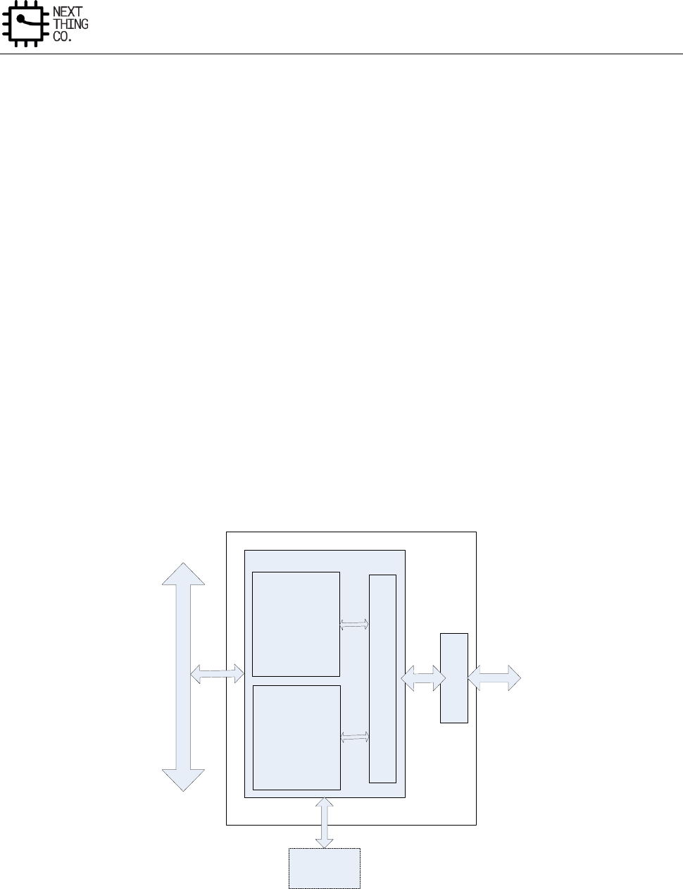
Interfaces
GR8 User Manual(Version1.0) Copyright © 2017 Next Thing Co. All Rights Reserved. Page 455
8.6. USB Host
8.6.1. Overview
The USB Host Controller is fully compliant with the following specifications: USB 2.0 Enhanced Host Controller
Interface (EHCI) 1.0, and the Open Host Controller Interface (OHCI) 1.0a release. The controller supports high-
speed, 480 Mbit/s transfers (40 times faster than USB 1.1 full-speed mode) using an EHCI Host Controller, as well
as full and low speeds through one or more integrated OHCI Host Controllers.
Features:
● An internal DMA controller for data transfer with memory.
● Complies with Enhanced Host Controller Interface (EHCI) Specification, Version 1.0, and the Open Host
Controller Interface (OHCI) Specification, Version 1.0a.
● Supports High-Speed (HS, 480 Mbit/s), Full-Speed (FS, 12 Mbit/s), and Low-Speed (LS, 1.5 Mbit/s) Device.
● Supports only one USB Root Port shared between EHCI and OHCI
8.6.2. USB Host Block Diagram
The system-level block diagram of USB host controller is shown below.
USB
PHY USB Port
USB HCI
EHCI
OHCI
Port Control
UTMI/FS
AHB
Slave
AHB
Master
DRAM
Memory
System AHB BUS
Figure 8-6. USB Host Block Diagram
Interfaces
GR8 User Manual(Version1.0) Copyright © 2017 Next Thing Co. All Rights Reserved. Page 456
8.6.3. USB Host Timing Diagram
Please refer to USB2.0 Enhanced Host Controller Interface (EHCI) Specification 1.0, and the Open Host Controller
Interface (OHCI) Specification 1.0a.
8.6.4. USB Host Special Requirement
Name
Description
HCLK
System clock (provided by AHB bus clock). This clock needs to be >30 MHz.
CLK60M
Clock from PHY for HS SIE, is constant to be 60 MHz.
CLK48M
Clock from PLL for FS/LS SIE, is constant to be 48 MHz.
8.6.5. USB Host Register List
Module Name
Base Address
USB_HCI
0x01C14000
Register Name
Offset
Description
EHCI Capability Register
E_CAPLENGTH
0x000
EHCI Capability Register Length
E_HCIVERSION
0x002
EHCI Host Interface Version Number Register
E_HCSPARAMS
0x004
EHCI Host Control Structural Parameter Register
E_HCCPARAMS
0x008
EHCI Host Control Capability Parameter Register
E_HCSPPORTROUTE
0x00c
EHCI Companion Port Route Description
EHCI Operational Register
E_USBCMD
0x010
EHCI USB Command Register
E_USBSTS
0x014
EHCI USB Status Register
E_USBINTR
0x018
EHCI USB Interrupt Enable Register
E_FRINDEX
0x01C
EHCI USB Frame Index Register
E_CTRLDSSEGMENT
0x020
EHCI 4G Segment Selector Register
E_PERIODICLISTBASE
0x024
EHCI Frame List Base Address Register
E_ASYNCLISTADDR
0x028
EHCI Next Asynchronous List Address Register
E_CONFIGFLAG
0x050
EHCI Configured Flag Register
E_PORTSC
0x054
EHCI Port Status/Control Register
OHCI Control and Status Partition Register
O_HcRevision
0x400
OHCI Revision Register
O_HcControl
0x404
OHCI Control Register
O_HcCommandStatus
0x408
OHCI Command Status Register
O_HcInterruptStatus
0x40C
OHCI Interrupt Status Register
O_HcInterruptEnable
0x410
OHCI Interrupt Enable Register
O_HcInterruptDisable
0x414
OHCI Interrupt Disable Register
OHCI Memory Pointer Partition Register
O_HcHCCA
0x418
OHCI HCCA Base
O_HcPeriodCurrentED
0x41c
OHCI Period Current ED Base
O_HcControlHeadED
0x420
OHCI Control Head ED Base
O_HcControlCurrentED
0x424
OHCI Control Current ED Base
Interfaces
GR8 User Manual(Version1.0) Copyright © 2017 Next Thing Co. All Rights Reserved. Page 457
O_HcBulkHeadED
0x428
OHCI Bulk Head ED Base
O_HcBulkCurrentED
0x42C
OHCI Bulk Current ED Base
O_HcDoneHead
0x430
OHCI Done Head Base
OHCI Frame Counter Partition Register
O_HcFmInterval
0x434
OHCI Frame Interval Register
O_HcFmRemaining
0x438
OHCI Frame Remaining Register
O_HcFmNumber
0x43C
OHCI Frame Number Register
O_HcPerioddicStart
0x440
OHCI Periodic Start Register
O_HcLSThreshold
0x444
OHCI LS Threshold Register
OHCI Root Hub Partition Register
O_HcRhDescriptorA
0x448
OHCI Root Hub Descriptor Register A
O_HcRhDesriptorB
0x44C
OHCI Root Hub Descriptor Register B
O_HcRhStatus
0x450
OHCI Root Hub Status Register
O_HcRhPortStatus
0x454
OHCI Root Hub Port Status Register
8.6.6. EHCI Register Description
8.6.6.1. EHCI Identification Register(Default Value: Implementation Dependent)
Offset:0x00
Register Name: CAPLENGTH
Bit
Read/Write
Default/Hex
Description
7:0
R
0x10
CAPLENGTH
The value in these bits indicates an offset to add to register base to find
the beginning of the Operational Register Space.
8.6.6.2. EHCI Host Interface Version Number Register(Default Value:0x0000_0100)
Offset: 0x02
Register Name: HCIVERSION
Bit
Read/Write
Default/Hex
Description
15:0
R
0x0100
HCIVERSION
This is a 16-bits register containing a BCD encoding of the EHCI revision
number supported by this host controller. The most significant byte of this
register represents a major revision and the least significant byte is the
minor revision.
8.6.6.3. EHCI Host Control Structural Parameter Register(Default Value: Implementation Dependent)
Offset: 0x04
Register Name: HCSPARAMS
Bit
Read/Write
Default/Hex
Description
31:24
/
0x0
Reserved.
These bits are reserved and should be set to zero.
23:20
R
0x0
Debug Port Number
This register identifies which of the host controller ports is the debug

Interfaces
GR8 User Manual(Version1.0) Copyright © 2017 Next Thing Co. All Rights Reserved. Page 458
port. The value is the port number (one based) of the debug port.
This field will always be ‘0’.
19:16
/
0x0
Reserved.
These bits are reserved and should be set to zero.
15:12
R
0x0
Number of Companion Controller (N_CC)
This field indicates the number of companion controllers associated with
this USB2.0 host controller. A zero in this field indicates there are no
companion host controllers. And a value larger than zero in this field
indicates there are companion USB1.1 host controller(s).
This field will always be ‘0’.
11:8
R
0x0
Number of Port per Companion Controller(N_PCC)
This field indicates the number of ports supported per companion host
controller host controller. It is used to indicate the port routing
configuration to system software.
This field will always fix with ‘0’.
7
R
0x0
Port Routing Rules
This field indicates the method used by this implementation for how all
ports are mapped to companion controllers. The value of this field has
the following interpretation:
Value
Meaning
0
The first N_PCC ports are routed to the lowest numbered
function companion host controller, the next N_PCC port
are routed to the next lowest function companion
controller, and so on.
1
The port routing is explicitly enumerated by the first
N_PORTS elements of the HCSP-PORTTOUTE array.
This field will always be ‘0’.
6:4
/
0x0
Reserved.
These bits are reserved and should be set to zero.
3:0
R
0x1
N_PORTS
This field specifies the number of physical downstream ports
implemented on this host controller. The value of this field determines
how many port registers are addressable in the Operational Register
Space. Valid values are in the range of 0x1 to 0x0f.
This field is always 1.
8.6.6.4. EHCI Host Control Capability Parameter Register(Default Value: Implementation Dependent)
Offset: 0x08
Register Name: HCCPARAMS
Bit
Read/Write
Default/Hex
Description

Interfaces
GR8 User Manual(Version1.0) Copyright © 2017 Next Thing Co. All Rights Reserved. Page 459
31:16
/
0x0
Reserved
These bits are reserved and should be set to zero.
15:18
R
0x0
EHCI Extended Capabilities Pointer (EECP)
This optional field indicates the existence of a capabilities list. A value of
00b indicates no extended capabilities are implemented. A non-zero
value in this register indicates the offset in PCI configuration space of the
first EHCI extended capability. The pointer value must be 40h or greater if
implemented to maintain to consistency of the PCI header defined for this
class of device.
The value of this field is always ‘00b’.
7:4
R
UDF
Isochronous Scheduling Threshold
This field indicates, relative to the current position of the executing host
controller, where software can reliably update the isochronous schedule.
When bit[7] is zero, the value of the least significant 3 bits indicates the
number of micro-frames a host controller can hold a set of isochronous
data structures(one or more) before flushing the state. When bit[7] is a
one, then host software assumes the host controller may cache an
isochronous data structure for an entire frame.
3
R
0x0
Reserved
These bits are reserved and should be set to zero.
2
R
UDF
Asynchronous Schedule Park Capability
If this bit is set to a one, then the host controller supports the park feature
for high-speed queue heads in the Asynchronous Schedule. The feature
can be disabled or enabled and set to a specific level by using the
Asynchronous Schedule Park Mode Enable and Asynchronous Schedule
Park Mode Count fields in the USBCMD register.
1
R
UDF
Programmable Frame List Flag
If this bit is set to a zero, then system software must use a frame list length
of 1024 elements with this host controller. The USBCMD register
Frame List Size field is a read-only register and should be set to zero.
If set to 1, then system software can specify and use the frame list in the
USBCMD register Frame List Size field to configure the host controller.
The frame list must always align on a 4K page boundary. This requirement
ensures that the frame list is always physically contiguous.
0
R
0x0
Reserved
These bits are reserved for future use and should return a value of zero
when read.
8.6.6.5. EHCI Companion Port Route Description
Offset: 0x0C
Register Name: HCSP-PORTROUTE

Interfaces
GR8 User Manual(Version1.0) Copyright © 2017 Next Thing Co. All Rights Reserved. Page 460
Bit
Read/Write
Default/Hex
Description
31:0
R
UDF
HCSP-PORTROUTE
This optional field is valid only if Port Routing Rules field in HCSPARAMS
register is set to a one.
This field is used to allow a host controller implementation to explicitly
describe to which companion host controller each implemented port is
mapped. This field is a 15-element nibble array (each 4 bit is one array
element). Each array location corresponds one-to-one with a physical
port provided by the host controller (e.g. PORTROUTE [0] corresponds to
the first PORTSC port, PORTROUTE [1] to the second PORTSC port, etc.).
The value of each element indicates to which of the companion host
controllers this port is routed. Only the first N_PORTS elements have valid
information. A value of zero indicates that the port is routed to the lowest
numbered function companion host controller. A value of one indicates
that the port is routed to the next lowest numbered function companion
host controller, and so on.
8.6.6.6. EHCI USB Command Register(Default Value: 0x0008_0000)
The default value is 0x00080B00 if Asynchronous Schedule Park Capability is a one.
Offset: 0x10
Register Name: USBCMD
Bit
Read/Write
Default/Hex
Description
31:24
/
0x0
Reserved
These bits are reserved and should be set to zero.
23:16
R/W
0x08
Interrupt Threshold Control
The value in this field is used by system software to select the maximum
rate at which the host controller will issue interrupts. The only valid values
are defined below:
Value
Minimum Interrupt Interval
0x00
Reserved
0x01
1 micro-frame
0x02
2 micro-frame
0x04
4 micro-frame
0x08
8 micro-frame(default, equates to 1 ms)
0x10
16 micro-frame(2ms)
0x20
32 micro-frame(4ms)
0x40
64 micro-frame(8ms)
Any other value in this register yields undefined results.
The default value in this field is 0x08.
Software modifications to this bit while HC Halted bit equals to zero

Interfaces
GR8 User Manual(Version1.0) Copyright © 2017 Next Thing Co. All Rights Reserved. Page 461
results in undefined behavior.
15:12
/
0x0
Reserved
These bits are reserved and should be set to zero.
11
R/W or R
0x0
Asynchronous Schedule Park Mode Enable(OPTIONAL)
If the Asynchronous Park Capability bit in the HCCPARAMS register is a
one, then this bit defaults to a 1 and is R/W. Otherwise the bit must be a
zero and is Read Only. Software uses this bit to enable or disable Park
mode. When this bit is one, Park mode is enabled. When this bit is zero,
Park mode is disabled.
10
/
0x0
Reserved
These bits are reserved and should be set to zero.
9:8
R/W or R
0x0
Asynchronous Schedule Park Mode Count(OPTIONAL)
Asynchronous Park Capability bit in the HCCPARAMS register is a one,
Then this field defaults to 0x3 and is W/R. Otherwise it defaults to zero
and is R. It contains a count of the number of successive transactions the
host controller is allowed to execute from a high-speed queue head on
the Asynchronous schedule before continuing traversal of the
Asynchronous schedule.
Valid values are 0x1 to 0x3.Software must not write a zero to this bit when
Park Mode Enable is a one as it will result in undefined behavior.
7
R/W
0x0
Light Host Controller Reset(OPTIONAL)
This control bit is not required.
If implemented, it allows the driver to reset the EHCI controller without
affecting the state of the ports or relationship to the companion host
controllers. For example, the PORSTC registers should not be reset to their
default values and the CF bit setting should not go to zero (retaining port
ownership relationships).
A host software read of this bit as zero indicates the Light Host Controller
Reset has completed and it is safe for software to re-initialize the host
controller. A host software read of this bit as a one indicates the Light Host
6
R/W
0x0
Interrupt on Async Advance Doorbell
This bit is used as a doorbell by software to tell the host controller to issue
an interrupt the next time it advances asynchronous schedule. Soft-
Ware must write a 1 to this bit to ring the doorbell.
When the host controller has evicted all appropriate cached schedule
state, it sets the Interrupt on Async Advance status bit in the USBSTS. if
the Interrupt on Async Advance Enable bit in the USBINTR register is a one
then the host controller will assert an interrupt at the next interrupt
threshold.
The host controller sets this bit to a zero after it has set the Interrupt on
Async Advance status bit in the USBSTS register to a one.
Software should not write a one to this bit when the asynchronous
Interfaces
GR8 User Manual(Version1.0) Copyright © 2017 Next Thing Co. All Rights Reserved. Page 462
schedule is disabled. Doing so will yield undefined results.
5
R/W
0x0
Asynchronous Schedule Enable
This bit controls whether the host controller skips processing the
Asynchronous Schedule. Values mean:
Bit Value
Meaning
0
Do not process the Asynchronous Schedule.
1
Use the ASYNLISTADDR register to access the
Asynchronous Schedule.
The default value of this field is ‘0b’.
4
R/W
0x0
Periodic Schedule Enable
This bit controls whether the host controller skips processing the Periodic
Schedule. Values mean:
Bit Value
Meaning
0
Do not process the Periodic Schedule.
1
Use the PERIODICLISTBASE register to access the Periodic
Schedule.
The default value of this field is ‘0b’.
3:2
R/W or R
0x0
Frame List Size
This field is R/W only if Programmable Frame List Flag in the HCCPARAMS
registers is set to a one. This field specifies the size of the
Frame list. The size the frame list controls which bits in the Frame Index
Register should be used for the Frame List Current index. Values mean:
Bits
Meaning
00b
1024 elements(4096bytes)Default value
01b
512 elements(2048byts)
10b
256 elements(1024bytes)For resource-constrained condition
11b
Reserved
The default value is ‘00b’.
1
R/W
0x0
Host Controller Reset
This control bit is used by software to reset the host controller. The effects
of this on Root Hub registers are similar to a Chip Hardware Reset.
When software writes a one to this bit, the Host Controller resets its
internal pipelines, timers, counters, state machines, etc. to their initial
value. Any transaction currently in progress on USB is immediately
terminated. A USB reset is not driven on downstream ports.
All operational registers, including port registers and port state machines
are set to their initial values. Port ownership reverts to the companion
host controller(s). Software must reinitialize the host controller as
described in Section 4.1 of the CHEI Specification in order to return the

Interfaces
GR8 User Manual(Version1.0) Copyright © 2017 Next Thing Co. All Rights Reserved. Page 463
host controller to an operational state.
This bit is set to zero by the Host Controller when the reset process is
complete. Software cannot terminate the reset process early by writing a
zero to this register.
Software should not set this bit to a one when the HC Halted bit in the
USBSTS register is a zero. Attempting to reset an actively running host
controller will result in undefined behavior.
0
R/W
0x0
Run/Stop
When set to a 1, the Host Controller proceeds with execution of the
schedule. When set to 0, the Host Controller completes the current and
any actively pipelined transactions on the USB and then halts. The Host
Controller must halt within 16 micro-frames after software clears this bit.
The HC Halted bit indicates when the Host Controller has finished its
pending pipelined transactions and has entered the stopped state.
Software must not write a one to this field unless the Host Controller is in
the Halt State.
The default value is 0x0.
8.6.6.7. EHCI USB Status Register(Default Value: 0x0000_1000)
Offset: 0x14
Register Name: USBSTS
Bit
Read/Write
Default/Hex
Description
31:16
/
0x0
Reserved
These bits are reserved and should be set to zero.
15
R
0x0
Asynchronous Schedule Status
The bit reports the current real status of Asynchronous Schedule. If this
bit is a zero, then the status of the Asynchronous Schedule is disabled. If
this bit is a one, then the status of the Asynchronous Schedule is enabled.
The Host Controller is not required to immediately disable or enable the
Asynchronous Schedule when software transitions the Asynchronous
Schedule Enable bit in the USBCMD register. When this bit and the
Asynchronous Schedule Enable bit are the same value, the Asynchronous
Schedule is either enabled (1) or disabled (0).
14
R
0x0
Periodic Schedule Status
The bit reports the current real status of the Periodic Schedule. If this bit
is a zero, then the status of the Periodic Schedule is disabled. If this bit is
a one, then the status of the Periodic Schedule is enabled. The Host
Controller is not required to immediately disable or enable the Periodic
Schedule when software transitions the Periodic Schedule Enable bit in
the USBCMD register. When this bit and the Periodic Schedule Enable bit
are the same value, the Periodic Schedule is either enabled (1) or disabled
(0).
13
R
0x0
Reclamation

Interfaces
GR8 User Manual(Version1.0) Copyright © 2017 Next Thing Co. All Rights Reserved. Page 464
This is a read-only status bit, which is used to detect an empty
asynchronous schedule.
12
R
0x1
HC Halted
This bit is a zero whenever the Run/Stop bit is a one. The Host Controller
Sets this bit to one after it has stopped executing as a result of the
Run/Stop bit being set to 0, either by software or by the Host Controller
Hardware (e.g. internal error).
The default value is ‘1’.
11:6
/
0x0
Reserved
These bits are reserved and should be set to zero.
5
R/WC
0x0
Interrupt on Async Advance
System software can force the host controller to issue an interrupt the
next time the host controller advances the asynchronous schedule by
writing a one to the Interrupt on Async Advance Doorbell bit in the
USBCMD register. This status bit indicates the assertion of that interrupt
source.
4
R/WC
0x0
Host System Error
The Host Controller set this bit to 1 when a serious error occurs during a
host system access involving the Host Controller module. When this error
occurs, the Host Controller clears the Run/Stop bit in the Command
register to prevent further execution of the scheduled TDs.
3
R/WC
0x0
Frame List Rollover
The Host Controller sets this bit to a one when the Frame List Index rolls
over from its maximum value to zero. The exact value at which the
rollover occurs depends on the frame list size. For example, if the frame
list size is 1024, the Frame Index Register rolls over every time FRINDEX
[13] toggles. Similarly, if the size is 512, the Host Controller sets this bit to
a one every time FRINDEX [12] toggles.
2
R/WC
0x0
Port Change Detect
The Host Controller sets this bit to a one when any port for which the Port
Owner bit is set to zero has a change bit transition from a zero to a one or
a Force Port Resume bit transition from a zero to a one as a result of a J-
K transition detected on a suspended port. This bit will also be set as a
result of the Connect Status Chang being set to a one after system
software has relinquished ownership of a connected port by writing a one
to a port’s Port Owner bit.
1
R/WC
0x0
USB Error Interrupt(USBERRINT)
The Host Controller sets this bit to 1 when completion of USB transaction
results in an error condition (e.g. error counter underflow). If the TD on
which the error interrupt occurred also had its IOC bit set, both.
This bit and USBINT bit are set.
0
R/WC
0x0
USB Interrupt(USBINT)
The Host Controller sets this bit to a one on the completion of a USB

Interfaces
GR8 User Manual(Version1.0) Copyright © 2017 Next Thing Co. All Rights Reserved. Page 465
transaction, which results in the retirement of a Transfer Descriptor that
had its IOC bit set.
The Host Controller also sets this bit to 1 when a short packet is detected
(actual number of bytes received was less than the expected number of
bytes)
8.6.6.8. EHCI USB Interrupt Enable Register(Default Value: 0x0000_0000)
Offset: 0x18
Register Name: USBINTR
Bit
Read/Write
Default/Hex
Description
31:6
/
0x0
Reserved
These bits are reserved and should be zero.
5
R/W
0x0
Interrupt on Async Advance Enable
When this bit is 1, and the Interrupt on Async Advance bit in the USBSTS
register is 1, the host controller will issue an interrupt at the next interrupt
threshold. The interrupt is acknowledged by software clearing the
Interrupt on Async Advance bit.
4
R/W
0x0
Host System Error Enable
When this bit is 1, and the Host System Error Status bit in the USBSTS
register is 1, the host controller will issue an interrupt. The interrupt is
acknowledged by software clearing the Host System Error bit.
3
R/W
0x0
Frame List Rollover Enable
When this bit is 1, and the Frame List Rollover bit in the USBSTS register
is 1, the host controller will issue an interrupt. The interrupt is
acknowledged by software clearing the Frame List Rollover bit.
2
R/W
0x0
Port Change Interrupt Enable
When this bit is 1, and the Port Chang Detect bit in the USBSTS register is
1, the host controller will issue an interrupt. The interrupt is
acknowledged by software clearing the Port Chang Detect bit.
1
R/W
0x0
USB Error Interrupt Enable
When this bit is 1, and the USBERRINT bit in the USBSTS register is 1, the
host controller will issue an interrupt at the next interrupt threshold.
The interrupt is acknowledged by software clearing the USBERRINT bit.
0
R/W
0x0
USB Interrupt Enable
When this bit is 1, and the USBINT bit in the USBSTS register is 1, the host
controller will issue an interrupt at the next interrupt threshold.
The interrupt is acknowledged by software clearing the USBINT bit
Interfaces
GR8 User Manual(Version1.0) Copyright © 2017 Next Thing Co. All Rights Reserved. Page 466
8.6.6.9. EHCI Frame Index Register(Default Value: 0x0000_0000)
Offset: 0x1C
Register Name: FRINDEX
Bit
Read/Write
Default/Hex
Description
31:14
/
0x0
Reserved
These bits are reserved and should be zero.
13:0
R/W
0x0
Frame Index
The value in this register increment at the end of each time frame
(e.g. micro-frame).Bits[N:3] are used for the Frame List current index. It
Means that each location of the frame list is accessed 8 times (frames or
Micro-frames) before moving to the next index. The following illustrates
Values of N based on the value of the Frame List Size field in the USBCMD
register.
USBCMD[Frame List Size]
Number Elements
N
00b
1024
12
01b
512
11
10b
256
10
11b
Reserved
Note: This register must be written as a DWord. Byte writes produce undefined results.
8.6.6.10. EHCI Periodic Frame List Base Address Register
Offset: 0x24
Register Name: PERIODICLISTBASE
Bit
Read/Write
Default/Hex
Description
31:12
R/W
UDF
Base Address
These bits correspond to memory address signals [31:12], respectively.
This register contains the beginning address of the Periodic Frame List in
the system memory.
System software loads this register prior to starting the schedule
execution by the Host Controller. The memory structure referenced by
this physical memory pointer is assumed to be 4-K byte aligned. The
contents of this register are combined with the Frame Index Register
(FRINDEX) to enable the Host Controller to step through the Periodic
Frame List in sequence.
11:0
/
UDF
Reserved
Must be written as 0x0 during runtime, the values of these bits are
undefined.
Note: Writes must be Dword Writes.

Interfaces
GR8 User Manual(Version1.0) Copyright © 2017 Next Thing Co. All Rights Reserved. Page 467
8.6.6.11. EHCI Current Asynchronous List Address Register
Offset: 0x28
Register Name: ASYNCLISTADDR
Bit
Read/Write
Default/Hex
Description
31:5
R/W
UDF
Link Pointer (LP)
This field contains the address of the next asynchronous queue head to
be executed.
These bits correspond to memory address signals [31:5], respectively.
4:0
/
/
Reserved
These bits are reserved and their value has no effect on operation.
Bits in this field cannot be modified by system software and will always
return a zero when read.
Note: Write must be DWord Writes.
8.6.6.12. EHCI Configure Flag Register(Default Value: 0x0000_0000)
Offset: 0x50
Register Name: CONFIGFLAG
Bit
Read/Write
Default/Hex
Description
31:1
/
0x0
Reserved
These bits are reserved and should be set to zero.
0
R/W
0x0
Configure Flag(CF)
Host software sets this bit as the last action in its process of configuring
the Host Controller. This bit controls the default port-routing control logic
as follow:
Value
Meaning
0
Port routing control logic default-routs each port to an
implementation dependent classic host controller.
1
Port routing control logic default-routs all ports to this host
controller.
The default value of this field is ‘0’.
Note: This register is not used in the normal implementation.
8.6.6.13. EHCI Port Status and Control Register(Default Value: 0x00002000(w/PPC set to one))
The default value is 0x00003000 when w/PPC set to zero.
Offset: 0x54
Register Name: PORTSC
Bit
Read/Write
Default/Hex
Description
31:22
/
0x0
Reserved
These bits are reserved for future use and should return a value of zero
Interfaces
GR8 User Manual(Version1.0) Copyright © 2017 Next Thing Co. All Rights Reserved. Page 468
when read.
21
R/W
0x0
Wake on Disconnect Enable(WKDSCNNT_E)
Writing this bit to a one enables the port to be sensitive to device
disconnects as wake-up events.
This field is zero if Port Power is zero.
The default value in this field is ‘0’.
20
R/W
0x0
Wake on Connect Enable(WKCNNT_E)
Writing this bit to a one enable the port to be sensitive to device connects
as wake-up events.
This field is zero if Port Power is zero.
The default value in this field is ‘0’.
19:16
R/W
0x0
Port Test Control
The value in this field specifies the test mode of the port. The encoding
of the test mode bits are as follow:
Bits
Test Mode
0000b
The port is NOT operating in a test mode.
0001b
Test J_STATE
0010b
Test K_STATE
0011b
Test SE0_NAK
0100b
Test Packet
0101b
Test FORCE_ENABLE
0110b-
1111b
Reserved
The default value in this field is ‘0000b’.
15:14
R/W
0x0
Reserved
These bits are reserved for future use and should return a value of zero
when read.
13
R/W
0x1
Port Owner
This bit unconditionally goes to a 0b when the Configured bit in the
CONFIGFLAG register makes a 0b to 1b transition. This bit unconditionally
goes to 1b whenever the Configured bit is zero.
System software uses this field to release ownership of the port to
selected host controller (in the event that the attached device is not a
high-speed device). Software writes a one to this bit when the attached
device is not a high-speed device. A one in this bit means that a
companion host controller owns and controls the port.
Default Value = 1b.
12
/
0x0
Reserved
Interfaces
GR8 User Manual(Version1.0) Copyright © 2017 Next Thing Co. All Rights Reserved. Page 469
These bits are reserved for future use and should return a value of zero
when read.
11:10
R
0x0
Line Status
These bits reflect the current logical levels of the D+ (bit11) and D-(bit10)
signal lines. These bits are used for detection of low-speed USB devices
prior to port reset and enable sequence. This read-only field is valid only
when the port enable bit is zero and the current connect status bit is set
to a one.
The encoding of the bits are:
Bit[11:10]
USB State
Interpretation
00b
SE0
Not Low-speed device, perform EHCI
reset.
10b
J-state
Not Low-speed device, perform EHCI
reset.
01b
K-state
Low-speed device, release ownership of
port.
11b
Undefined
Not Low-speed device, perform EHCI
reset.
This value of this field is undefined if Port Power is zero.
9
/
0x0
Reserved
This bit is reserved for future use, and should return a value of zero when
read.
8
R/W
0x0
Port Reset
1=Port is in Reset. 0=Port is not in Reset. Default value = 0.
When software writes a one to this bit (from a zero), the bus reset
sequence as defined in the USB Specification Revision 2.0 is started.
Software writes a zero to this bit to terminate the bus reset sequence.
Software must keep this bit at a one long enough to ensure the reset
sequence, as specified in the USB Specification Revision 2.0, completes.
Notes: when software writes this bit to a one, it must also write a zero to
the Port Enable bit.
Note that when software writes a zero to this bit there may be a delay
before the bit status changes to a zero. The bit status will not read as a
zero until after the reset has completed. If the port is in high-speed mode
after reset is complete, the host controller will automatically enable this
port (e.g. set the Port Enable bit to a one). A host controller must
terminate the reset and stabilize the state of the port within 2
milliseconds of software transitioning this bit from a one to a zero. For
example: if the port detects that the attached device is high-speed during
reset, then the host controller must have the port in the enabled state
with 2ms of software writing this bit to a zero.
The HC Halted bit in the USBSTS register should be a zero before software
attempts to use this bit. The host controller may hold Port Reset asserted
to a one when the HC Halted bit is a one.

Interfaces
GR8 User Manual(Version1.0) Copyright © 2017 Next Thing Co. All Rights Reserved. Page 470
This field is zero if Port Power is zero.
7
R/W
0x0
Suspend
Port Enabled Bit and Suspend bit of this register define the port states as
follows:
Bits[Port Enables, Suspend]
Port State
0x
Disable
10
Enable
11
Suspend
When in suspend state, downstream propagation of data is blocked on
this port, except for port reset. The blocking occurs at the end of the
current transaction, if a transaction was in progress when this bit was
written to 1. In the suspend state, the port is sensitive to resume
detection. Not that the bit status does not change until the port is
suspend and that there may be a delay in suspending a port if there is a
transaction currently in progress on the USB.
A write of zero to this bit is ignored by the host controller. The host
controller will unconditionally set this bit to a zero when:
① Software sets the Force Port Resume bit to a zero(from a one).
② Software sets the Port Reset bit to a one(from a zero).
If host software sets this bit to a one when the port is not enabled (i.e.
Port enabled bit is a zero), the results are undefined.
This field is zero if Port Power is zero.
The default value in this field is ‘0’.
6
R/W
0x0
Force Port Resume
1 = Resume detected/driven on port. 0 = No resume (K-state) detected/
driven on port. Default value = 0.
This functionality defined for manipulating this bit depends on the value
of the Suspend bit. For example, if the port is not suspended and software
transitions this bit to a one, then the effects on the bus are undefined.
Software sets this bit to a 1 drive resume signaling. The Host Controller
sets this bit to a 1 if a J-to-K transition is detected while the port is in the
Suspend state. When this bit transitions to a one because a J-to-K
transition is detected, the Port Change Detect bit in the USBSTS register
is also set to a one. If software sets this bit to a one, the host controller
must not set the Port Change Detect bit.
Note that when the EHCI controller owns the port, the resume sequence
follows the defined sequence documented in the USB Specification
Revision 2.0. The resume signal (Full-speed ‘K’) is driven on the port as
long as this remains a one. Software must appropriately time the Resume
and set this bit to a zero when the appropriate amount of time has
elapsed. Writing a zero (from one) causes the port to return high-speed
mode (forcing the bus below the port into a high-speed idle). This bit will
remain a one until the port has switched to high-speed idle. The host

Interfaces
GR8 User Manual(Version1.0) Copyright © 2017 Next Thing Co. All Rights Reserved. Page 471
controller must complete this transition within 2 milliseconds of software
setting this bit to a zero.
This field is zero if Port Power is zero.
5
R/WC
0x0
Over-current Change
Default = 0. This bit gets set to a one when there is a change to Over-
current Active. Software clears this bit by writing a one to this bit position.
4
R
0x0
Over-current Active
0 = This port does not have an over-current condition. 1 = This port
currently has an over-current condition. This bit will automatically
transition from a one to a zero when the over current condition is
removed.
The default value of this bit is ‘0’.
3
R/WC
0x0
Port Enable/Disable Change
Default = 0. 1 = Port enabled/disabled status has changed. 0 = No change.
For the root hub, this bit gets set to a one only when a port is disabled
due to the appropriate conditions existing at the EOF2 point (See Chapter
11 of the USB Specification for the definition of a Port Error). Software
clears this bit by writing a 1 to it.
This field is zero if Port Power is zero.
2
R/W
0x0
Port Enabled/Disabled
1=Enable, 0=Disable. Ports can only be enabled by the host controller as
a part of the reset and enable. Software cannot enable a port by writing
a one to this field. The host controller will only set this bit to a one when
the reset sequence determines that the attached device is a high-speed
device.
Ports can be disabled by either a fault condition (disconnect event or
other fault condition) or by host software. Note that the bit status does
not change until the port state changes. There may be a delay in disabling
or enabling a port due to other host controller and bus events.
When the port is disabled, downstream propagation of data is blocked on
this port except for reset.
The default value of this field is ‘0’.
This field is zero if Port Power is zero.
1
R/WC
0x0
Connect Status Change
1=Change in Current Connect Status, 0=No change, Default=0.
Indicates a change has occurred in the port’s Current Connect Status. The
host controller sets this bit for all changes to the port device connect
status, even if system software has not cleared an existing connect status
change. For example, the insertion status changes twice before system
software has cleared the changed condition, hub hardware will be
“setting” an already-set bit. Software sets this bit to 0 by writing a 1 to it.
This field is zero if Port Power is zero.

Interfaces
GR8 User Manual(Version1.0) Copyright © 2017 Next Thing Co. All Rights Reserved. Page 472
0
R
0x0
Current Connect Status
Device is present on port when the value of this field is a one, and no
device is present on port when the value of this field is a zero. This value
reflects the current state of the port, and may not correspond directly to
the event that caused the Connect Status Change (Bit 1) to be set.
This field is zero if Port Power zero.
Note: This register is only reset by hardware or in response to a host controller reset.
8.6.7. OHCI Register Description
8.6.7.1. HcRevision Register(Default Value: 0x0000_0010)
Offset: 0x400
Register Name: HcRevision
Bit
Read/Write
Default/Hex
Description
HCD
HC
31:8
/
/
0x00
Reserved
7:0
R
R
0x10
Revision
This read-only field contains the BCD representation of the version of
the HCI specification that is implemented by this HC. For example, a
value of 0x11 corresponds to version 1.1. All of the HC implementations
that are compliant with this specification will have a value of 0x10.
8.6.7.2. HcControl Register(Default Value: 0x0000_0000)
Offset: 0x404
Register Name: HcRevision
Bit
Read/Write
Default/Hex
Description
HCD
HC
31:11
/
/
0x00
Reserved
10
R/W
R
0x0
RemoteWakeupEnable
This bit is used by HCD to enable or disable the remote wakeup feature
upon the detection of upstream resume signaling. When this bit is set
and the ResumeDetected bit in HcInterruptStatus is set, a remote
wakeup is signaled to the host system. Setting this bit has no impact on
the generation of hardware interrupt.
9
R/W
R/W
0x0
RemoteWakeupConnected
This bit indicates whether HC supports remote wakeup signaling. If
remote wakeup is supported and used by the system, it is the
responsibility of system firmware to set this bit during POST. HC clear
the bit upon a hardware reset but does not alter it upon a software
reset. Remote wakeup signaling of the host system is host-bus-specific
and is not described in this specification.
8
R/W
R
0x0
InterruptRouting

Interfaces
GR8 User Manual(Version1.0) Copyright © 2017 Next Thing Co. All Rights Reserved. Page 473
This bit determines the routing of interrupts generated by events
registered in HcInterruptStatus. If clear, all interrupts are routed to the
normal host bus interrupt mechanism. If set interrupts are routed to
the System Management Interrupt. HCD clears this bit upon a hardware
reset, but it does not alter this bit upon a software reset. HCD uses this
bit as a tag to indicate the ownership of HC.
7:6
R/W
R/W
0x0
HostControllerFunctionalState for USB
00b
USBReset
01b
USBResume
10b
USBOperational
11b
USBSuspend
A transition to USBOperational from another state causes SOF
generation to begin 1 ms later. HCD may determine whether HC has
begun sending SOFs by reading the StartoFrame field of
HcInterruptStatus.
This field may be changed by HC only when in the USBSUSPEND state.
HC may move from the USBSUSPEND state to the USBRESUME state
after detecting the resume signaling from a downstream port.
HC enters USBSUSPEND after a software reset, whereas it enters
USBRESET after a hardware reset. The latter also resets the Root
Hub and asserts subsequent reset signaling to downstream ports.
5
R/W
R
0x0
BulkListEnable
This bit is set to enable the processing of the Bulk list in the next
Frame. If cleared by HCD, processing of the Bulk list does not occur after
the next SOF. HC checks this bit whenever it determines to process the
list. When disabled, HCD may modify the list. If HcBulkCurrentED is
pointing to an ED to be removed, HCD must advance the pointer by
updating HcBulkCurrentED before re-enabling processing of the list.
4
R/W
R
0x0
ControlListEnable
This bit is set to enable the processing of the Control list in the next
Frame. If cleared by HCD, processing of the Control list does not occur
after the next SOF. HC must check this bit whenever it determines to
process the list. When disabled, HCD may modify the list. If
HcControlCurrentED is pointing to an ED to be removed, HCD must
advance the pointer by updating HcControlCurrentED before re-
enabling processing of the list.
3
R/W
R
0x0
IsochronousEnable
This bit is used by HCD to enable/disable processing of isochronous
EDs. While processing the periodic list in a Frame, HC checks the status
of this bit when it finds an Isochronous ED (F=1). If set (enabled), HC
continues processing the EDs. If cleared (disabled), HC halts processing
of the periodic list (which now contains only isochronous EDs) and
begins processing the Bulk/Control lists.
Interfaces
GR8 User Manual(Version1.0) Copyright © 2017 Next Thing Co. All Rights Reserved. Page 474
Setting this bit is guaranteed to take effect in the next Frame (not the
current Frame).
2
R/W
R
0x0
PeriodicListEnable
This bit is set to enable the processing of periodic list in the next Frame.
If cleared by HCD, processing of the periodic list does not occur after
the next SOF. HC must check this bit before it starts processing the list.
1:0
R/W
R
0x0
ControlBulkServiceRatio
This specifies the service ratio between Control and Bulk EDs. Before
processing any of the non-periodic lists, HC must compare the ratio
specified with its internal count on how many nonempty Control EDs
have been processed, in determining whether to continue serving
another Control ED or switching to Bulk EDs. The internal count will be
retained when crossing the frame boundary. In case of reset, HCD is
responsible for restoring this value.
CBSR
No. of Control EDs Over Bulk EDs Served
0
1:1
1
2:1
2
3:1
3
4:1
The default value is 0x0.
8.6.7.3. HcCommandStatus Register(Default Value: 0x0000_0000)
Offset: 0x408
Register Name: HcCommandStatus
Bit
Read/Write
Default/Hex
Description
HCD
HC
31:18
/
/
0x0
Reserved
17:16
R
R/W
0x0
SchedulingOverrunCount
These bits are incremented on each scheduling overrun error. It is
initialized to 00b and wraps around at 11b. This will be incremented
when a scheduling overrun is detected even if SchedulingOverrun in
HcInterruptStatus has already been set. This is used by HCD to monitor
any persistent scheduling problem.
15:4
/
/
0x0
Reserved
3
R/W
R/W
0x0
OwershipChangeRequest
This bit is set by an OS HCD to request a change of control of the HC.
When set, HC will set the OwnershipChange field in HcInterruptStatus.
After the changeover, this bit is cleared and remains so until the next
request from OS HCD.
2
R/W
R/W
0x0
BulklListFilled
This bit is used to indicate whether there are any TDs on the Bulk list.

Interfaces
GR8 User Manual(Version1.0) Copyright © 2017 Next Thing Co. All Rights Reserved. Page 475
It is set by HCD whenever it adds a TD to an ED in the Bulk list.
When HC begins to process the head of the Bulk list, it checks BLF. If
BulkListFilled is 0, HC will not start processing the Bulk list. If
BulkListFilled is 1, HC will start processing the Bulk list and will set BF to
0. If HC finds a TD on the list, then HC will set BulkListFilled to 1 causing
the Bulk list processing to continue. If no TD is found on the Bulk list,
and if HCD does not set BulkListFilled, then BulkListFilled will still be 0
when HC completes processing the Bulk list and Bulk list processing will
stop.
1
R/W
R/W
0x0
ControlListFilled
This bit is used to indicate whether there are any TDs on the Control
list. It is set by HCD whenever it adds a TD to an ED in the Control list.
When HC begins to process the head of the Control list, it checks CLF. If
ControlListFilled is 0, HC will not start processing the Control list. If CF
is 1, HC will start processing the Control list and will set ControlListFilled
to 0. If HC finds a TD on the list, then HC will set ControlListFilled to 1
causing the Control list processing to continue. If no TD is found on the
Control list, and if the HCD does not set ControlListFilled, then
ControlListFilled will still be 0 when HC completes processing the
Control list and Control list processing will stop.
0
R/W
R/E
0x0
HostControllerReset
This bit is by HCD to initiate a software reset of HC. Regardless of the
functional state of HC, it moves to the USBSuspend state in which most
of the operational registers are reset except those stated otherwise;
e.g, the InterruptRouting field of HcControl, and no Host bus accesses
are allowed. This bit is cleared by HC upon the completion of the reset
operation. The reset operation must be completed within 10 ms. This
bit,
when set, should not cause a reset to the Root Hub and no subsequent
reset signaling should be asserted to its downstream ports.
8.6.7.4. HcInterruptStatus Register(Default Value: 0x0000_0000)
Offset: 0x40C
Register Name: HcInterruptStatus
Bit
Read/Write
Default/Hex
Description
HCD
HC
31:7
/
/
0x0
Reserved
6
R/W
R/W
0x0
RootHubStatusChange
This bit is set when the content of HcRhStatus or the content of any of
HcRhPortStatus[NumberofDownstreamPort] has changed.
5
R/W
R/W
0x0
FrameNumberOverflow
This bit is set when the MSb of HcFmNumber (bit 15) changes value,
from 0 to 1 or from 1 to 0, and after HccaFrameNumber has been
updated.
Interfaces
GR8 User Manual(Version1.0) Copyright © 2017 Next Thing Co. All Rights Reserved. Page 476
4
R/W
R/W
0x0
UnrecoverableError
This bit is set when HC detects a system error not related to USB. HC
should not proceed with any processing nor signaling before the system
error has been corrected. HCD clears this bit after HC has been reset.
3
R/W
R/W
0x0
ResumeDetected
This bit is set when HC detects that a device on the USB is asserting
resume signaling. It is the transition from no resume signaling to
resume signaling causing this bit to be set. This bit is not set when HCD
sets the USBRseume state.
2
R/W
R/W
0x0
StartofFrame
This bit is set by HC at each start of frame and after the update of
HccaFrameNumber. HC also generates a SOF token at the same time.
1
R/W
R/W
0x0
WritebackDoneHead
This bit is set immediately after HC has written HcDoneHead to
HccaDoneHead. Further updates of the HccaDoneHead will not occur
until this bit has been cleared. HCD should only clear this bit after it has
saved the content of HccaDoneHead.
0
R/W
R/W
0x0
SchedulingOverrun
This bit is set when the USB schedule for the current Frame overruns
and after the update of HccaFrameNumber. A scheduling overrun will
also cause the SchedulingOverrunCount of HcCommandStatus to be
Incremented.
8.6.7.5. HcInterruptEnable Register(Default Value: 0x0000_0000)
Offset: 0x410
Register Name: HcInterruptEnable Register
Bit
Read/Write
Default/Hex
Description
HCD
HC
31
R/W
R
0x0
MasterInterruptEnable
A ‘0’ written to this field is ignored by HC. A ‘1’ written to this field
enables interrupt generation due to events specified in the other bits
of this register. This is used by HCD as Master Interrupt Enable.
30:7
/
/
0x0
Reserved
6
R/W
R
0x0
RootHubStatusChange Interrupt Enable
0
Ignore;
1
Enable interrupt generation due to Root Hub Status Change;
5
R/W
R
0x0
FrameNumberOverflow Interrupt Enable
0
Ignore;
1
Enable interrupt generation due to Frame Number Over Flow;
Interfaces
GR8 User Manual(Version1.0) Copyright © 2017 Next Thing Co. All Rights Reserved. Page 477
4
R/W
R
0x0
UnrecoverableError Interrupt Enable
0
Ignore;
1
Enable interrupt generation due to Unrecoverable Error;
3
R/W
R
0x0
ResumeDetected Interrupt Enable
0
Ignore;
1
Enable interrupt generation due to Resume Detected;
2
R/W
R
0x0
StartofFrame Interrupt Enable
0
Ignore;
1
Enable interrupt generation due to Start of Frame;
1
R/W
R
0x0
WritebackDoneHead Interrupt Enable
0
Ignore;
1
Enable interrupt generation due to Write-back Done Head;
0
R/W
R
0x0
SchedulingOverrun Interrupt Enable
0
Ignore;
1
Enable interrupt generation due to Scheduling Overrun;
8.6.7.6. HcInterruptDisable Register(Default Value: 0x0000_0000)
Offset: 0x414
Register Name: HcInterruptDisable Register
Bit
Read/Write
Default/Hex
Description
HCD
HC
31
R/W
R
0x0
MasterInterruptEnable
A written ‘0’ to this field is ignored by HC. A ‘1’ written to this field
disables interrupt generation due events specified in the other bits of
this register. This field is set after a hardware or software reset.
30:7
/
/
0x0
Reserved
6
R/W
R
0x0
RootHubStatusChange Interrupt Disable
0
Ignore;
1
Disable interrupt generation due to Root Hub Status Change;
5
R/W
R
0x0
FrameNumberOverflow Interrupt Disable
0
Ignore;
1
Disable interrupt generation due to Frame Number Over Flow;
4
R/W
R
0x0
UnrecoverableError Interrupt Disable
0
Ignore;
1
Disable interrupt generation due to Unrecoverable Error;
Interfaces
GR8 User Manual(Version1.0) Copyright © 2017 Next Thing Co. All Rights Reserved. Page 478
3
R/W
R
0x0
ResumeDetected Interrupt Disable
0
Ignore;
1
Disable interrupt generation due to Resume Detected;
2
R/W
R
0x0
StartofFrame Interrupt Disable
0
Ignore;
1
Disable interrupt generation due to Start of Flame;
1
R/W
R
0x0
WritebackDoneHead Interrupt Disable
0
Ignore;
1
Disable interrupt generation due to Write-back Done Head;
0
R/w
R
0x0
SchedulingOverrun Interrupt Disable
0
Ignore;
1
Disable interrupt generation due to Scheduling Overrun;
8.6.7.7. HcHCCA Register(Default Value: 0x0000_0000)
Offset: 0x418
Register Name: HcHCCA
Bit
Read/Write
Default/Hex
Description
HCD
HC
31:8
R/W
R
0x0
HCCA[31:8]
This is the base address of the Host Controller Communication Area.
This area is used to hold the control structures and the Interrupt table
that are accessed by both the Host Controller and the Host Controller
Driver.
7:0
R
R
0x0
HCCA[7:0]
The alignment restriction in HcHCCA register is evaluated by examining
the number of zeros in the lower order bits. The minimum alignment is
256 bytes, therefore, bits 0 through 7 must always return 0 when read.
8.6.7.8. HcPeriodCurrentED Register(Default Value: 0x0000_0000)
Offset: 0x41C
Register Name: HcPeriodCurrentED(PCED)
Bit
Read/Write
Default/Hex
Description
HCD
HC
31:4
R
R/W
0x0
PCED[31:4]
This is used by HC to point to the head of one of the periodic list which
will be processed in the current Frame. The content of this register is
updated by HC after a periodic ED has been processed. HCD may read
the content in determining which ED is currently being processed at the
time of reading.

Interfaces
GR8 User Manual(Version1.0) Copyright © 2017 Next Thing Co. All Rights Reserved. Page 479
3:0
R
R
0x0
PCED[3:0]
Because the general TD length is 16 bytes, the memory structure for
the TD must be aligned to a 16-byte boundary. So, the lower bits in the
PCED, through bit 0 to bit 3 must be zero in this field.
8.6.7.9. HcControlHeadED Register(Default Value: 0x0000_0000)
Offset: 0x420
Register Name: HcControlHeadED[CHED]
Bit
Read/Write
Default/Hex
Description
HCD
HC
31:4
R/W
R
0x0
EHCD[31:4]
The HcControlHeadED register contains the physical address of the first
Endpoint Descriptor of the Control list. HC traverse the Control list
starting with the HcControlHeadED pointer. The content is loaded from
HCCA during the initialization of HC.
3:0
R
R
0x0
EHCD[3:0]
Because the general TD length is 16 bytes, the memory structure for
the TD must be aligned to a 16-byte boundary. So, the lower bits in the
PCED, through bit 0 to bit 3 must be zero in this field.
8.6.7.10. HcControlCurrentED Register(Default Value: 0x0000_0000)
Offset: 0x424
Register Name: HcControlCurrentED[CCED]
Bit
Read/Write
Default/Hex
Description
HCD
HC
31:4
R/W
R/W
0x0
CCED[31:4]
The pointer is advanced to the next ED after serving the present one.
HC will continue processing the list from where it left off in the last
Frame. When it reaches the end of the Control list, HC checks the
ControlListFilled of in HcCommandStatus. If set, it copies the content of
HcControlHeadED to HcControlCurrentED and clears the bit. If not set,
it does nothing.
HCD is allowed to modify this register only when the ControlListEnable
of HcControl is cleared. When set, HCD only reads the instantaneous
value of this register. Initially, this is set to zero to indicate the end of
the Control list.
3:0
R
R
0x0
CCED[3:0]
Because the general TD length is 16 bytes, the memory structure for
the TD must be aligned to a 16-byte boundary. So, the lower bits in the
PCED, bit 0 to bit 3, must be zero in this field.

Interfaces
GR8 User Manual(Version1.0) Copyright © 2017 Next Thing Co. All Rights Reserved. Page 480
8.6.7.11. HcBulkHeadED Register(Default Value: 0x0000_0000)
Offset: 0x428
Register Name: HcBulkHeadED[BHED]
Bit
Read/Write
Default/Hex
Description
HCD
HC
31:4
R/W
R
0x0
BHED[31:4]
The HcBulkHeadED register contains the physical address of the first
Endpoint Descriptor of the Bulk list. HC traverses the Bulk list starting
with the HcBulkHeadED pointer. The content is loaded from HCCA
during the initialization of HC.
3:0
R
R
0x0
BHED[3:0]
Because the general TD length is 16 bytes, the memory structure for
the TD must be aligned to a 16-byte boundary. So, the lower bits in the
PCED, bit 0 to bit 3, must be zero in this field.
8.6.7.12. HcBulkCurrentED Register(Default Value: 0x0000_0000)
Offset: 0x42C
Register Name: HcBulkCurrentED [BCED]
Bit
Read/Write
Default/Hex
Description
HCD
HC
31:4
R/W
R/W
0x0
BulkCurrentED[31:4]
This is advanced to the next ED after the HC has served the present
one. HC continues processing the list from where it left off in the last
Frame. When it reaches the end of the Bulk list, HC checks the
ControlListFilled of HcControl. If set, it copies the content of
HcBulkHeadED to HcBulkCurrentED and clears the bit. If it is not set, it
does nothing. HCD is only allowed to modify this register when the
BulkListEnable of HcControl is cleared. When set, the HCD only reads
the instantaneous value of this register. This is initially set to zero to
indicate the end of the Bulk list.
3:0
R
R
0x0
BulkCurrentED [3:0]
Because the general TD length is 16 bytes, the memory structure for
the TD must be aligned to a 16-byte boundary. So, the lower bits in the
PCED, through bit 0 to bit 3 must be zero in this field.
8.6.7.13. HcDoneHead Register(Default Value: 0x0000_0000)
Offset: 0x430
Register Name: HcDoneHead
Bit
Read/Write
Default/Hex
Description
HCD
HC
31:4
R
R/W
0x0
HcDoneHead[31:4]
When a TD is completed, HC writes the content of HcDoneHead to the
NextTD field of the TD. HC then overwrites the content of HcDoneHead

Interfaces
GR8 User Manual(Version1.0) Copyright © 2017 Next Thing Co. All Rights Reserved. Page 481
with the address of this TD. This is set to zero whenever HC writes the
content of this register to HCCA. It also sets the WritebackDoneHead of
HcInterruptStatus.
3:0
R
R
0x0
HcDoneHead[3:0]
Because the general TD length is 16 bytes, the memory structure for
the TD must be aligned to a 16-byte boundary. So, the lower bits in the
PCED, bit 0 to bit 3, must be zero in this field.
8.6.7.14. HcFmInterval Register(Default Value: 0x0000_2EDF)
Offset: 0x434
Register Name: HcFmInterval Register
Bit
Read/Write
Default/Hex
Description
HCD
HC
31
R/W
R
0x0
FrameIntervalToggler
HCD toggles this bit whenever it loads a new value to FrameInterval.
30:16
R/W
R
0x0
FSLargestDataPacket
This field specifies a value which is loaded into the Largest Data Packet
Counter at the beginning of each frame. The counter value represents
the largest amount of data in bits which can be sent or received by the
HC in a single transaction at any given time without causing scheduling
overrun. The field value is calculated by the HCD.
15:14
/
/
0x0
Reserved
13:0
R/W
R
0x2edf
FrameInterval
This specifies the interval between two consecutive SOFs in bit times.
The nominal value is set to be 11,999. HCD should store the current
value of this field before resetting HC. By setting the
HostControllerReset field of HcCommandStatus as this will cause the
HC to reset this field to its nominal value. HCD may choose to restore
the stored value upon the completion of the Reset sequence.
8.6.7.15. HcFmRemaining Register(Default Value: 0x0000_0000)
Offset: 0x438
Register Name: HcFmRemaining
Bit
Read/Write
Default/Hex
Description
HCD
HC
31
R
R/W
0x0
FrameRemaining Toggle
This bit is loaded from the FrameIntervalToggle field of HcFmInterval
whenever FrameRemaining reaches 0. This bit is used by HCD for the
synchronization between FrameInterval and FrameRemaining.
30:14
/
/
0x0
Reserved

Interfaces
GR8 User Manual(Version1.0) Copyright © 2017 Next Thing Co. All Rights Reserved. Page 482
13:0
R
RW
0x0
FramRemaining
This counter is decremented at each bit time. When it reaches zero, it
is reset by loading the FrameInterval value specified in HcFmInterval at
the next bit time boundary. When entering the USBOPERATIONAL
state, HC re-loads the content with the FrameInterval of HcFmInterval
and uses the updated value from the next SOF.
8.6.7.16. HcFmNumber Register(Default Value: 0x0000_0000)
Offset: 0x43c
Register Name: HcFmNumber
Bit
Read/Write
Default/Hex
Description
HCD
HC
31:16
/
/
/
Reserved
15:0
R
R/W
0x0
FrameNumber
This is incremented when HcFmRemaining is re-loaded. It will be rolled
over to 0x0 after 0x0ffff. When entering the USBOPERATIONAL state,
this will be incremented automatically. The content will be written to
HCCA after HC has incremented the FrameNumber at each frame
boundary and sent a SOF but before HC reads the first ED in that Frame.
After writing to HCCA, HC will set the StartofFrame in
HcInterruptStatus.
8.6.7.17. HcPeriodicStart Register(Default Value: 0x0000_0000)
Offset: 0x440
Register Name: HcPeriodicStatus
Bit
Read/Write
Default/Hex
Description
HCD
HC
31:14
/
/
/
Reserved
13:0
R/W
R
0x0
PeriodicStart
After hardware reset, this field is cleared. This is then set by HCD during
the HC initialization. The value is calculated roughly as 10% off from
HcFmInterval. A typical value will be 0x2A3F. When HcFmRemaining
reaches the value specified, processing of the periodic lists will have
priority over Control/Bulk processing. HC will therefore start processing
the Interrupt list after completing the current Control or Bulk
transaction that is in progress.
8.6.7.18. HcLSThreshold Register(Default Value: 0x0000_0628)
Offset: 0x444
Register Name: HcLSThreshold
Bit
Read/Write
Default/Hex
Description
HCD
HC
Interfaces
GR8 User Manual(Version1.0) Copyright © 2017 Next Thing Co. All Rights Reserved. Page 483
31:12
/
/
/
Reserved
11:0
R/W
R
0x0628
LSThreshold
This field contains a value which is compared to the FrameRemaining
field prior to initiating a Low Speed transaction. The transaction is
started only if FrameRemaining ³ this field. The value is calculated by
HCD with the consideration of transmission and setup overhead.
8.6.7.19. HcRhDescriptorA Register(Default Value: 0x0200_1201)
Offset: 0x448
Register Name: HcRhDescriptorA
Bit
Read/Write
Default/Hex
Description
HCD
HC
31:24
R/W
R
0x2
PowerOnToPowerGoodTime[POTPGT]
This byte specifies the duration HCD must wait before accessing a
powered-on port of the Root Hub. It is implementation-specific. The
unit of time is 2 ms. The duration is calculated as POTPGT * 2ms.
23:13
Reserved
12
R/W
R
0x1
NoOverCurrentProtection
This bit describes how the overcurrent status for the Root Hub ports
are reported. When this bit is cleared, the OverCurrentProtectionMode
field specifies global or per-port reporting.
0
Over-current status is reported collectively for all downstream
ports.
1
No overcurrent protection supported.
11
R/W
R
0x0
OverCurrentProtectionMode
This bit describes how the overcurrent status for the Root Hub ports
are reported. At reset, these fields should reflect the same mode as
PowerSwitchingMode. This field is valid only if the
NoOverCurrentProtection field is cleared.
0
Over-current status is reported collectively for all downstream
ports.
1
Over-current status is reported on per-port basis.
10
R
R
0x0
Device Type
This bit specifies that the Root Hub is not a compound device. The Root
Hub is not permitted to be a compound device. This field should always
read/write 0.
9
R/W
R
0x1
PowerSwitchingMode
This bit is used to specify how the power switching of the Root Hub
ports is controlled. It is implementation-specific. This field is only valid
when the NoPowerSwitching field is cleared.
Interfaces
GR8 User Manual(Version1.0) Copyright © 2017 Next Thing Co. All Rights Reserved. Page 484
0
All ports are powered at the same time.
1
Each port is powered individually. This mode allows port power
to be controlled by either the global switch or per-port
switch. If the PortPowerControlMask bit is set, the port
responds only to port power commands (Set/ClearPortPower).
If the port mask is cleared, then the port is controlled only by
the global power switch (Set/ClearGlobalPower).
8
R/W
R
0x0
NoPowerSwitching
These bits are used to specify whether power switching is supported or
ports are always powered. It is implementation-specific. When this bit
is cleared, the PowerSwitchingMode specifies global or per-port
switching.
0
Ports are power switched.
1
Ports are always powered on when the HC is powered on.
7:0
R
R
0x1
NumberDownstreamPorts
These bits specify the number of downstream ports supported by the
Root Hub. It is implementation-specific. The minimum number of ports
is 1.
8.6.7.20. HcRhDescriptorB Register(Default Value: 0x0000_0000)
Offset: 0x44C
Register Name: HcRhDescriptorB Register
Bit
Read/Write
Default/Hex
Description
HCD
HC
31:16
R/W
R
0x0
PortPowerControlMask
Each bit indicates if a port is affected by a global power control
command when PowerSwitchingMode is set. When set, the port's
power state is only affected by per-port power control
(Set/ClearPortPower). When cleared, the port is controlled by the
global power switch (Set/ClearGlobalPower). If the device is configured
to global switching mode (PowerSwitchingMode = 0), this field is not
valid.
Bit0
Reserved
Bit1
Ganged-power mask on Port #1.
Bit2
Ganged-power mask on Port #2.
…
Bit15
Ganged-power mask on Port #15.
15:0
R/W
R
0x0
DeviceRemovable
Each bit is dedicated to a port of the Root Hub. When cleared, the
attached device is removable. When set, the attached device is not
removable.
Interfaces
GR8 User Manual(Version1.0) Copyright © 2017 Next Thing Co. All Rights Reserved. Page 485
Bit0
Reserved
Bit1
Device attached to Port #1.
Bit2
Device attached to Port #2.
…
Bit15
Device attached to Port #15.
8.6.7.21. HcRhStatus Register(Default Value: 0x0000_0000)
Offset: 0x450
Register Name: HcRhStatus Register
Bit
Read/Write
Default/Hex
Description
HCD
HC
31
W
R
0x0
(write)ClearRemoteWakeupEnable
Write a ‘1’ clears DeviceRemoteWakeupEnable. Writing a ‘0’ has no
effect.
30:18
/
/
0x0
Reserved
17
R/W
R
0x0
OverCurrentIndicatorChange
This bit is set by hardware when a change has occurred to the
OverCurrentIndicator field of this register. The HCD clears this bit by
writing a ‘1’. Writing a ‘0’ has no effect.
16
R/W
R
0x0
(read)LocalPowerStatusChange
The Root Hub does not support the local power status features, thus,
this bit is always read as ‘0’.
(write)SetGlobalPower
In global power mode (PowerSwitchingMode=0), this bit is written to
‘1’ to turn on power to all ports (clear PortPowerStatus). In per-port
power mode, it sets PortPowerStatus only on ports whose
PortPowerControlMask bit is not set. Writing a ‘0’ has no effect.
15
R/W
R
0x0
(read)DeviceRemoteWakeupEnable
This bit enables a ConnectStatusChange bit as a resume event, causing
a USBSUSPEND to USBRESUME state transition and setting the
ResumeDetected interrupt.
0
ConnectStatusChange is not a remote wakeup event.
1
ConnectStatusChange is a remote wakeup event.
(write)SetRemoteWakeupEnable
Writing a ‘1’ sets DeviceRemoveWakeupEnable. Writing a ‘0’ has no
effect.
14:2
/
/
0x0
Reserved
1
R
R/W
0x0
OverCurrentIndicator
Interfaces
GR8 User Manual(Version1.0) Copyright © 2017 Next Thing Co. All Rights Reserved. Page 486
This bit reports overcurrent conditions when the global reporting is
implemented. When set, an overcurrent condition exists. When
cleared, all power operations are normal.
If per-port overcurrent protection is implemented this bit is always ‘0’
0
R/W
R
0x0
(Read)LocalPowerStatus
When read, this bit returns the LocalPowerStatus of the Root Hub. The
Root Hub does not support the local power status feature; thus, this bit
is always read as ‘0’.
(Write)ClearGlobalPower
When write, this bit is operated as the ClearGlobalPower. In global
power mode (PowerSwitchingMode=0), This bit is written to ‘1’ to turn
off power to all ports (clear PortPowerStatus). In per-port power mode,
it clears PortPowerStatus only on ports whose PortPowerControlMask
bit is not set. Writing a ‘0’ has no effect.
8.6.7.22. HcRhPortStatus Register(Default Value: 0x0000_0100)
Offset: 0x454
Register Name: HcRhPortStatus
Bit
Read/Write
Default/Hex
Description
HCD
HC
31:21
/
/
0x0
Reserved
20
R/W
R/W
0x0
PortResetStatusChange
This bit is set at the end of the 10-ms port reset signal. The HCD writes
a ‘1’ to clear this bit. Writing a ‘0’ has no effect.
0
port reset is not complete
1
port reset is complete
19
R/W
R/W
0x0
PortOverCurrentIndicatorChange
This bit is valid only if overcurrent conditions are reported on a per-port
basis. This bit is set when Root Hub changes the
PortOverCurrentIndicator bit. The HCD writes a ‘1’ to clear this bit.
Writing a ‘0’ has no effect.
0
no change in PortOverCurrentIndicator
1
PortOverCurrentIndicator has changed
18
R/W
R/W
0x0
PortSuspendStatusChange
This bit is set when the full resume sequence has been completed. This
sequence includes the 20-s resume pulse, LS EOP, and 3-ms
resynchronization delay. The HCD writes a ‘1’ to clear this bit. Writing a
‘0’ has no effect. This bit is also cleared when ResetStatusChange is set.
0
resume is not completed
1
resume completed
Interfaces
GR8 User Manual(Version1.0) Copyright © 2017 Next Thing Co. All Rights Reserved. Page 487
17
R/W
R/W
0x0
PortEnableStatusChange
This bit is set when hardware events cause the PortEnableStatus bit to
be cleared. Changes from HCD writes do not set this bit. The HCD writes
a ‘1’ to clear this bit. Writing a ‘0’ has no effect.
0
no change in PortEnableStatus
1
change in PortEnableStatus
16
R/W
R/W
0x0
ConnectStatusChange
This bit is set whenever a connect or disconnect event occurs. The HCD
writes a ‘1’ to clear this bit. Writing a ‘0’ has no effect. If
CurrentConnectStatus is cleared when a SetPortReset, SetPortEnable,
or SetPortSuspend write occurs, this bit is set to force the driver to re-
evaluate the connection status since these writes should not occur if
the port is disconnected.
0
no change in PortEnableStatus
1
change in PortEnableStatus
Note: If the DeviceRemovable[NDP] bit is set, this bit is set only after a
Root Hub reset to inform the system that the device is attached.
15:10
/
/
0x0
Reserved
9
R/W
R/W
-
(read)LowSpeedDeviceAttached
This bit indicates the speed of the device attached to this port. When
set, a Low Speed device is attached to this port. When cleared, a Full
Speed device is attached to this port. This field is valid only when the
CurrentConnectStatus is set.
0
full speed device attached
1
low speed device attached
(write)ClearPortPower
The HCD clears the PortPowerStatus bit by writing a ‘1’ to this bit.
Writing a ‘0’ has no effect.
8
R/W
R/W
0x1
(read)PortPowerStatus
This bit reflects the port’s power status, irrelevant of the type of power
switching implemented. This bit is cleared if an overcurrent condition
is detected. HCD sets this bit by writing SetPortPower or
SetGlobalPower. HCD clears this bit by writing ClearPortPower or
ClearGlobalPower. Which power control switches are enabled is
determined by PowerSwitchingMode and
PortPortControlMask[NumberDownstreamPort]. In global switching
mode(PowerSwitchingMode=0), only Set/ClearGlobalPower controls
this bit. In per-port power switching (PowerSwitchingMode=1), if the
PortPowerControlMask[NDP] bit for the port is set, only
Interfaces
GR8 User Manual(Version1.0) Copyright © 2017 Next Thing Co. All Rights Reserved. Page 488
Set/ClearPortPower commands are enabled. If the mask is not set, only
Set/ClearGlobalPower commands are enabled. When port power is
disabled, CurrentConnectStatus, PortEnableStatus, PortSuspendStatus,
and PortResetStatus should be reset.
0
port power is off
1
port power is on
(write)SetPortPower
The HCD writes a ‘1’ to set the PortPowerStatus bit. Writing a ‘0’ has no
effect.
Note: This bit is always read as ‘1b’ if power switching is not supported.
7:5
/
/
0x0
Reserved
4
R/W
R/W
0x0
(read)PortResetStatus
When this bit is set by writing to SetPortReset, port reset signaling is
asserted. When reset is completed, this bit is cleared when
PortResetStatusChange is set. This bit cannot be set if
CurrentConnectStatus is cleared.
0
port reset signal is not active
1
port reset signal is active
(write)SetPortReset
The HCD sets the port reset signaling by writing a ‘1’ to this bit. Writing
a ‘0’ has no effect. If CurrentConnectStatus is cleared, this write does
not set PortResetStatus, but instead sets ConnectStatusChange. This
informs the driver that it attempted to reset a disconnected port.
3
R/W
R/W
0x0
(read)PortOverCurrentIndicator
This bit is only valid when the Root Hub is configured in such a way that
overcurrent conditions are reported on a per-port basis. If per-port
overcurrent reporting is not supported, this bit is set to 0. If cleared, all
power operations are normal for this port. If set, an overcurrent
condition exists on this port. This bit always reflects the overcurrent
input signal.
0
no overcurrent condition.
1
overcurrent condition detected.
(write)ClearSuspendStatus
The HCD writes a ‘1’ to initiate a resume. Writing a ‘0’ has no effect. A
resume is initiated only if PortSuspendStatus is set.
2
R/W
R/W
0x0
(read)PortSuspendStatus
This bit indicates the port is suspended or in the resume sequence. It is
Interfaces
GR8 User Manual(Version1.0) Copyright © 2017 Next Thing Co. All Rights Reserved. Page 489
set by a SetSuspendState write and cleared when
PortSuspendStatusChange is set at the end of the resume interval. This
bit cannot be set if CurrentConnectStatus is cleared. This bit is also
cleared when PortResetStatusChange is set at the end of the port reset
or when the HC is placed in the USBRESUME state. If an upstream
resume is in progress, it should propagate to the HC.
0
port is not suspended
1
port is suspended
(write)SetPortSuspend
The HCD sets the PortSuspendStatus bit by writing a ‘1’ to this bit.
Writing a ‘0’ has no effect. If CurrentConnectStatus is cleared, this write
does not set PortSuspendStatus; instead it sets ConnectStatusChange.
This informs the driver that it attempted to suspend a disconnected
port.
1
R/W
R/W
0x0
(read)PortEnableStatus
This bit indicates whether the port is enabled or disabled. The Root Hub
may clear this bit when an overcurrent condition, disconnect event,
switched-off power, or operational bus error such as babble is
detected. This change also causes PortEnabledStatusChange to be set.
HCD sets this bit by writing SetPortEnable and clears it by writing
ClearPortEnable. This bit cannot be set when CurrentConnectStatus is
cleared. This bit is also set, if not already, at the completion of a port
reset when ResetStatusChange is set or port suspend when
SuspendStatusChange is set.
0
port is disabled
1
port is enabled
(write)SetPortEnable
The HCD sets PortEnableStatus by writing a ‘1’. Writing a ‘0’ has no
effect. If CurrentConnectStatus is cleared, this write does not set
PortEnableStatus, and sets ConnectStatusChange instead. This informs
the driver that it attempts to enable a disconnected Port.
0
R/W
R/W
0x0
(read)CurrentConnectStatus
This bit reflects the current state of the downstream port.
0
No device connected
1
Device connected
(write)ClearPortEnable
The HCD writes a ‘1’ to clear the PortEnableStatus bit. Writing ‘0’ has
no effect. The CurrentConnectStatus is not affected by any write.
Note: This bit is always read as ‘1’ when the attached device is non-
removable(DeviceRemoveable[NumberDownstreamPort]).

Interfaces
GR8 User Manual(Version1.0) Copyright © 2017 Next Thing Co. All Rights Reserved. Page 490

GR8 User Manual(Version1.0) Copyright © 2017 Next Thing Co. All Rights Reserved. Page 491
Chapter 9. Reference Design
This chapter shows C.H.I.P. Pro, a reference design using the GR8.SiP.
CHIP Pro board
Pinout Diagram
Block Diagram
Schematic
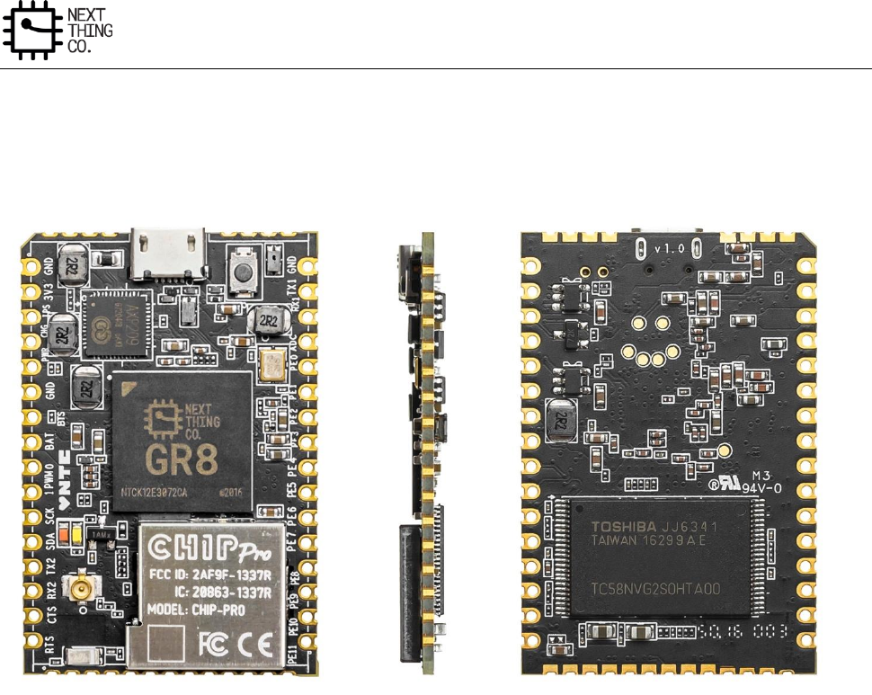
Reference Design
GR8 User Manual(Version1.0) Copyright © 2017 Next Thing Co. All Rights Reserved. Page 492
9.1. C.H.I.P. Pro Board
The following image is of the CHIP Pro single board computer.
Figure 9-1: C.H.I.P. Pro
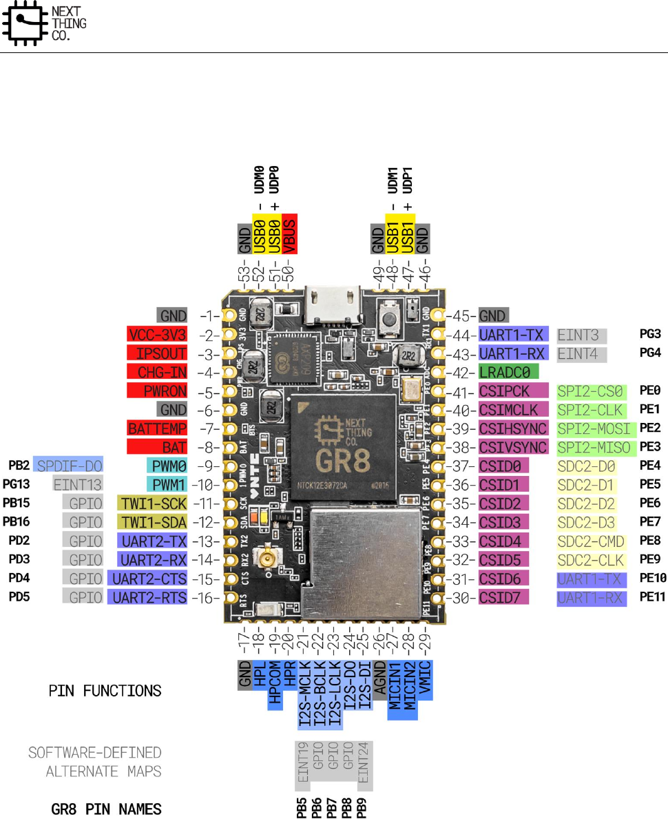
Reference Design
GR8 User Manual(Version1.0) Copyright © 2017 Next Thing Co. All Rights Reserved. Page 493
9.2. Pinout Diagram
The Following pin map demonstrates some of the common alternate pin mux configurations, overlaid on C.HIP Pro.
Figure 9-2: Pinout Diagram
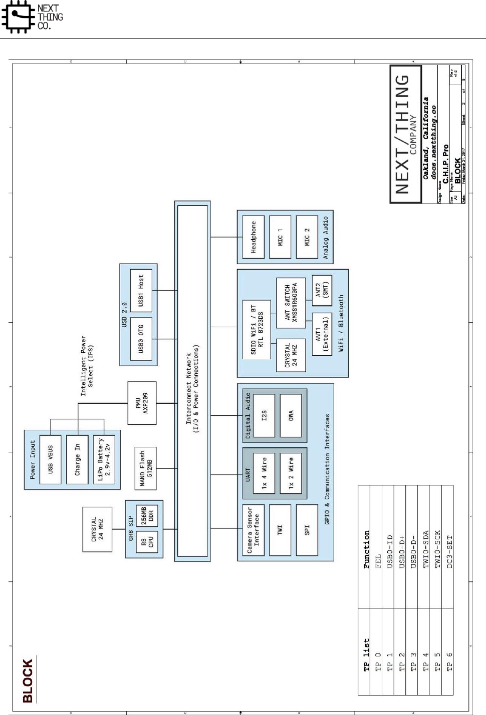
Reference Design
GR8 User Manual(Version1.0) Copyright © 2017 Next Thing Co. All Rights Reserved. Page 495
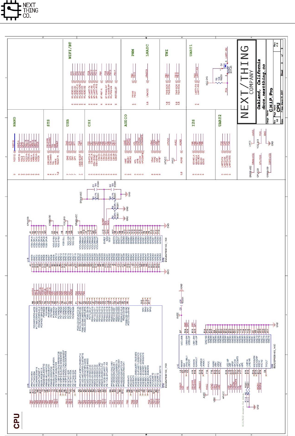
Reference Design
GR8 User Manual(Version1.0) Copyright © 2017 Next Thing Co. All Rights Reserved. Page 496
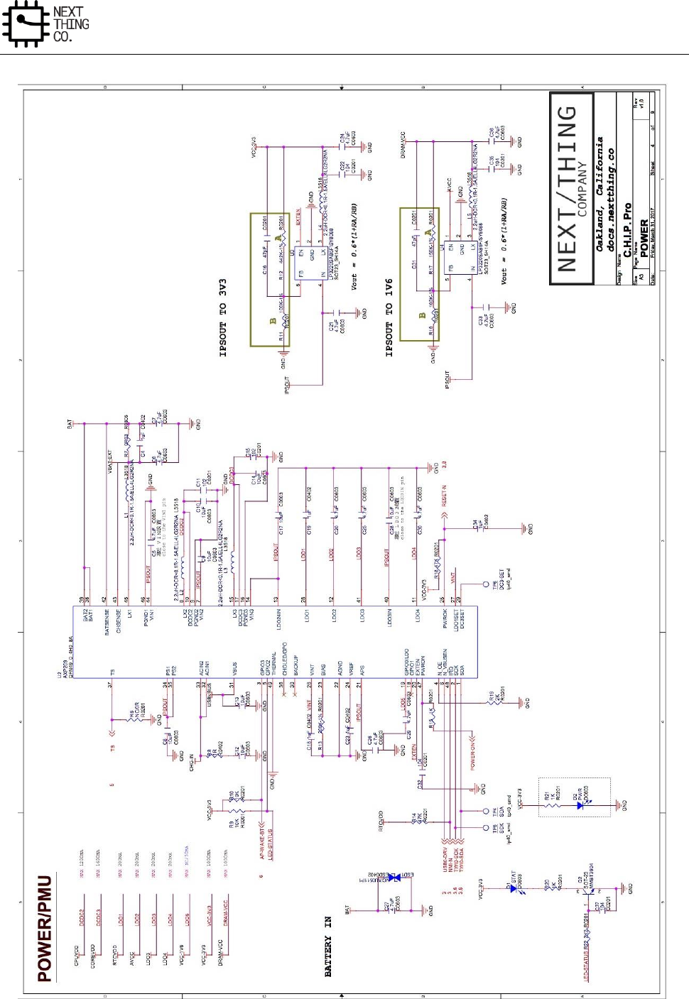
Reference Design
GR8 User Manual(Version1.0) Copyright © 2017 Next Thing Co. All Rights Reserved. Page 497
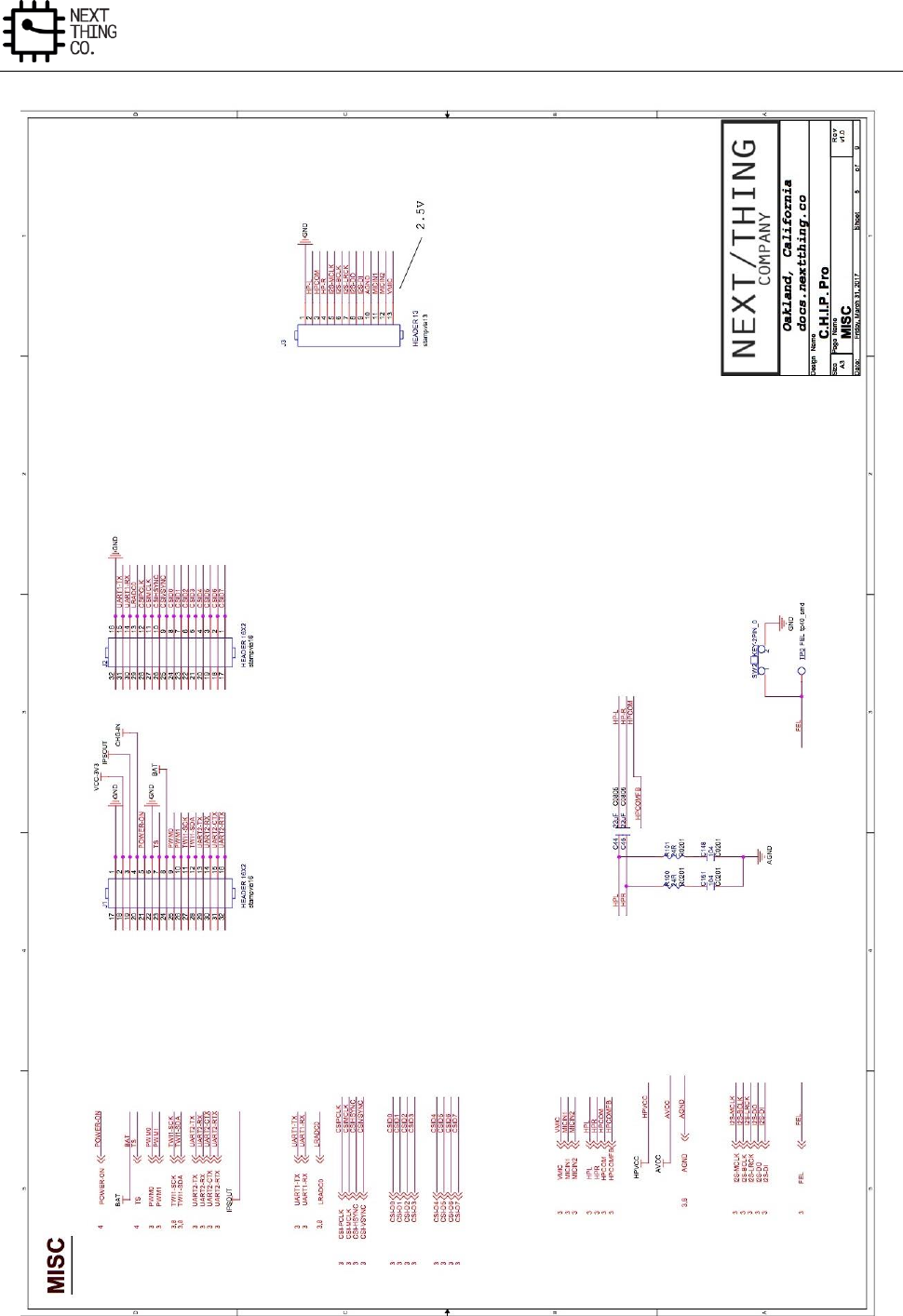
Reference Design
GR8 User Manual(Version1.0) Copyright © 2017 Next Thing Co. All Rights Reserved. Page 498
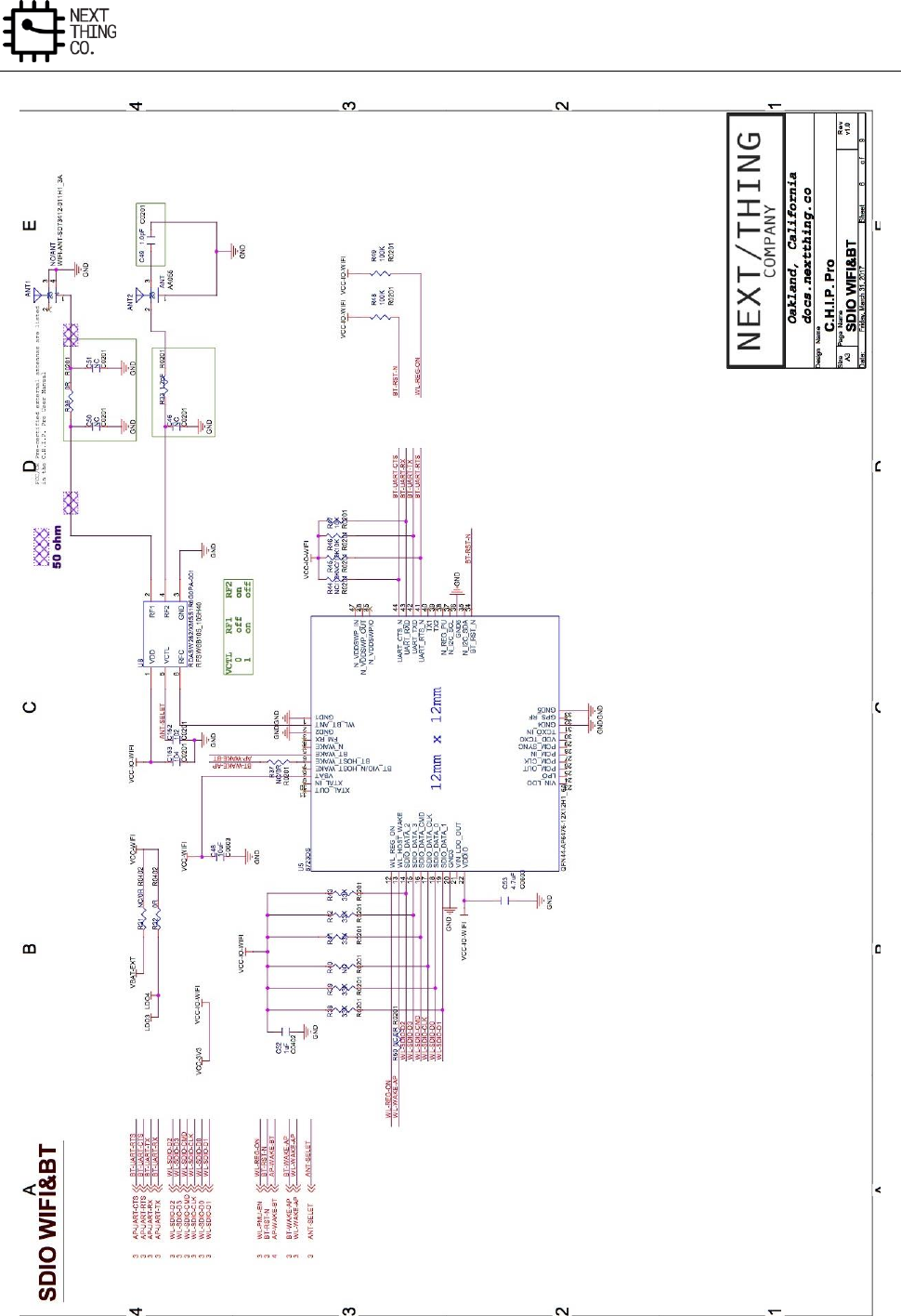
Reference Design
GR8 User Manual(Version1.0) Copyright © 2017 Next Thing Co. All Rights Reserved. Page 499
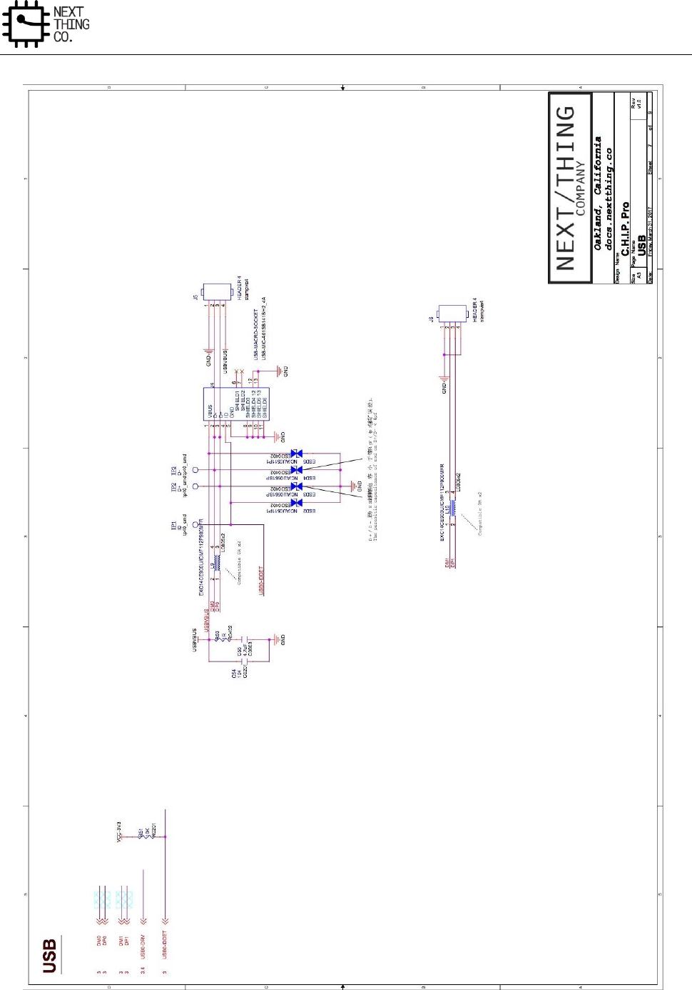
Reference Design
GR8 User Manual(Version1.0) Copyright © 2017 Next Thing Co. All Rights Reserved. Page 500
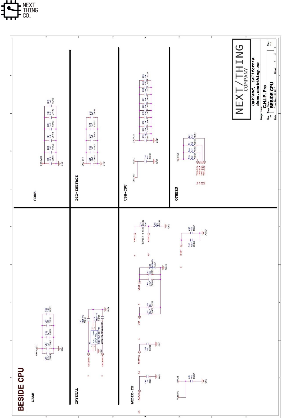
Reference Design
GR8 User Manual(Version1.0) Copyright © 2017 Next Thing Co. All Rights Reserved. Page 501
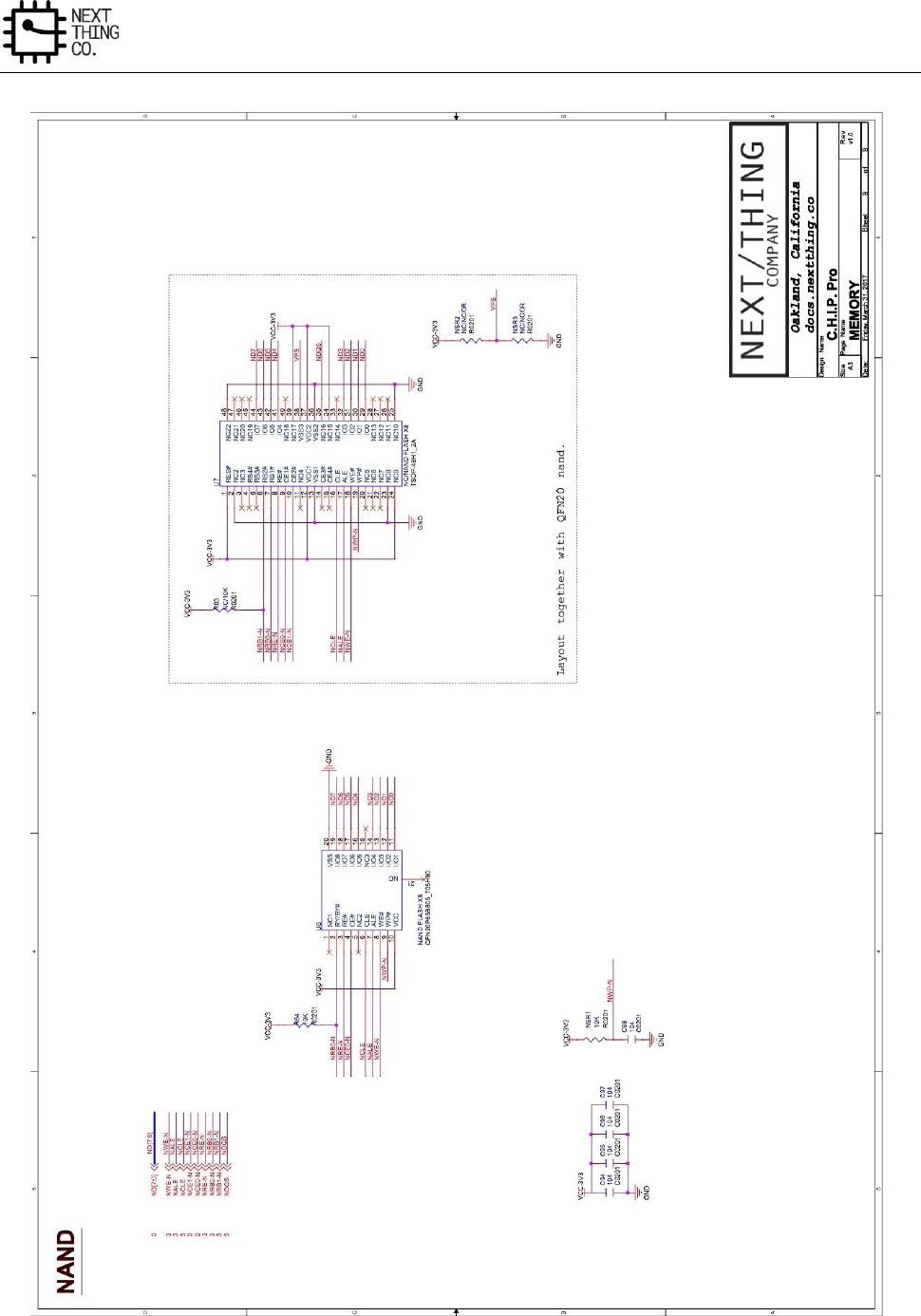
Reference Design
GR8 User Manual(Version1.0) Copyright © 2017 Next Thing Co. All Rights Reserved. Page 502