PIC32MX1XX/2XX 28/36/44 Pin Family Data Sheet PIC32Family Guide
User Manual:
Open the PDF directly: View PDF ![]() .
.
Page Count: 346 [warning: Documents this large are best viewed by clicking the View PDF Link!]
- TABLE 1: PIC32MX1XX 28/36/44-Pin General Purpose Family Features
- TABLE 2: PIC32MX2XX 28/36/44-pin USB Family Features
- TABLE 3: Pin Names for 28-pin General Purpose Devices
- TABLE 4: Pin Names for 28-pin USB Devices
- TABLE 5: Pin Names for 28-Pin General Purpose Devices
- TABLE 6: Pin Names for 28-Pin USB Devices
- TABLE 7: Pin Names for 36-Pin General Purpose Devices
- TABLE 8: Pin Names for 36-Pin USB Devices
- TABLE 9: Pin Names for 44-Pin General Purpose Devices
- TABLE 10: Pin Names for 44-Pin USB Devices
- TABLE 11: Pin Names for 44-Pin General Purpose Devices
- TABLE 12: Pin Names for 44-Pin USB Devices
- TABLE 13: Pin Names for 44-Pin General Purpose Devices
- TABLE 14: Pin Names for 44-Pin USB Devices
- 1.0 Device Overview
- 2.0 Guidelines for Getting Started with 32-bit MCUs
- 2.1 Basic Connection Requirements
- 2.2 Decoupling Capacitors
- 2.3 Capacitor on Internal Voltage Regulator (Vcap)
- 2.4 Master Clear (MCLR) Pin
- 2.5 ICSP Pins
- 2.6 JTAG
- 2.7 External Oscillator Pins
- 2.8 Unused I/Os
- 2.9 Typical Application Connection Examples
- 2.10 Considerations When Interfacing To Remotely Powered Circuits
- 3.0 CPU
- 4.0 Memory Organization
- 4.1 PIC32MX1XX/2XX 28/36/44-pin Family Memory Layout
- FIGURE 4-1: Memory Map on Reset for PIC32MX110/210 Devices (4 KB RAM, 16 KB Flash)
- FIGURE 4-2: Memory Map on Reset for PIC32MX120/220 Devices (8 KB RAM, 32 KB Flash)
- FIGURE 4-3: Memory Map on Reset for PIC32MX130/230 Devices (16 KB RAM, 64 KB Flash)
- FIGURE 4-4: Memory Map on Reset for PIC32MX150/250 Devices (32 KB RAM, 128 KB Flash)
- FIGURE 4-5: Memory Map on Reset for PIC32MX170/270 Devices (64 KB RAM, 256 KB Flash)
- FIGURE 4-6: Memory Map on Reset for PIC32MX130/230 Devices (16 KB RAM, 256 KB Flash)
- Table 4-1: SFR Memory Map
- 4.2 Bus Matrix Control Registers
- TABLE 4-2: Bus Matrix Register Map
- Register 4-1: BMXCON: Bus Matrix Configuration Register
- Register 4-2: BMXDKPBA: Data RAM Kernel Program Base Address Register
- Register 4-3: BMXDUDBA: Data RAM User Data Base Address Register
- Register 4-4: BMXDUPBA: Data RAM User Program Base Address Register
- Register 4-5: BMXDRMSZ: Data RAM Size Register
- Register 4-6: BMXPUPBA: Program Flash (PFM) User Program Base Address Register
- Register 4-7: BMXPFMSZ: Program Flash (PFM) Size Register
- Register 4-8: BMXBOOTSZ: Boot Flash (IFM) Size Register
- 4.1 PIC32MX1XX/2XX 28/36/44-pin Family Memory Layout
- 5.0 Flash Program Memory
- 6.0 Resets
- 7.0 Interrupt Controller
- FIGURE 7-1: Interrupt Controller Module Block Diagram
- Table 7-1: Interrupt IRQ, Vector and Bit Location (Continued)
- 7.1 Interrupt Control Registers
- TABLE 7-2: Interrupt Register Map (Continued)
- Register 7-1: INTCON: Interrupt Control Register
- Register 7-2: INTSTAT: Interrupt Status Register
- Register 7-3: IPTMR: Interrupt Proximity Timer Register
- Register 7-4: IFSx: Interrupt Flag Status Register
- Register 7-5: IECx: Interrupt Enable Control Register
- Register 7-6: IPCx: Interrupt Priority Control Register (Continued)
- 8.0 Oscillator Configuration
- 9.0 Direct Memory Access (DMA) Controller
- FIGURE 9-1: DMA Block Diagram
- 9.1 DMA Control Registers
- TABLE 9-1: DMA Global Register Map
- TABLE 9-2: DMA CRC Register Map
- TABLE 9-3: DMA Channels 0-3 Register Map (Continued)
- Register 9-1: DMACON: DMA Controller Control Register
- Register 9-2: DMASTAT: DMA Status Register
- Register 9-3: DMAADDR: DMA Address Register
- Register 9-4: DCRCCON: DMA CRC Control Register (Continued)
- Register 9-5: DCRCDATA: DMA CRC Data Register
- Register 9-6: DCRCXOR: DMA CRCXOR Enable Register
- Register 9-7: DCHxCON: DMA Channel ‘x’ Control Register
- Register 9-8: DCHxECON: DMA Channel ‘x’ Event Control Register
- Register 9-9: DCHxINT: DMA Channel ‘x’ Interrupt Control Register (Continued)
- Register 9-10: DCHxSSA: DMA Channel ‘x’ Source Start Address Register
- Register 9-11: DCHxDSA: DMA Channel ‘x’ Destination Start Address Register
- Register 9-12: DCHxSSIZ: DMA Channel ‘x’ Source Size Register
- Register 9-13: DCHxDSIZ: DMA Channel ‘x’ Destination Size Register
- Register 9-14: DCHxSPTR: DMA Channel ‘x’ Source Pointer Register
- Register 9-15: DCHxDPTR: DMA Channel ‘x’ Destination Pointer Register
- Register 9-16: DCHxCSIZ: DMA Channel ‘x’ Cell-Size Register
- Register 9-17: DCHxCPTR: DMA Channel ‘x’ Cell Pointer Register
- Register 9-18: DCHxDAT: DMA Channel ‘x’ Pattern Data Register
- 10.0 USB On-The-Go (OTG)
- FIGURE 10-1: PIC32MX1XX/2XX 28/36/44-pin Family Family USB Interface Diagram
- 10.1 USB Control Registers
- TABLE 10-1: USB Register Map (Continued)
- Register 10-1: U1OTGIR: USB OTG Interrupt Status Register
- Register 10-2: U1OTGIE: USB OTG Interrupt Enable Register
- Register 10-3: U1OTGSTAT: USB OTG Status Register
- Register 10-4: U1OTGCON: USB OTG Control Register
- Register 10-5: U1PWRC: USB Power Control Register
- Register 10-6: U1IR: USB Interrupt Register
- Register 10-7: U1IE: USB Interrupt Enable Register
- Register 10-8: U1EIR: USB Error Interrupt Status Register (Continued)
- Register 10-9: U1EIE: USB Error Interrupt Enable Register
- Register 10-10: U1STAT: USB Status Register
- Register 10-11: U1CON: USB Control Register (Continued)
- Register 10-12: U1ADDR: USB Address Register
- Register 10-13: U1FRML: USB Frame Number Low Register
- Register 10-14: U1FRMH: USB Frame Number High Register
- Register 10-15: U1TOK: USB Token Register
- Register 10-16: U1SOF: USB SOF Threshold Register
- Register 10-17: U1BDTP1: USB Buffer Descriptor Table Page 1 Register
- Register 10-18: U1BDTP2: USB Buffer Descriptor Table PAGE 2 Register
- Register 10-19: U1BDTP3: USB Buffer Descriptor Table PAGE 3 Register
- Register 10-20: U1CNFG1: USB Configuration 1 Register
- Register 10-21: U1EP0-U1EP15: USB Endpoint Control Register
- 11.0 I/O Ports
- FIGURE 11-1: Block Diagram of a Typical Multiplexed Port Structure
- 11.1 Parallel I/O (PIO) Ports
- 11.2 CLR, SET and INV Registers
- 11.3 Peripheral Pin Select
- 11.4 Ports Control Registers
- TABLE 11-3: PORTA Register Map
- TABLE 11-4: PORTB Register Map
- TABLE 11-5: PORTC Register Map
- Table 11-6: Peripheral Pin Select Input Register Map (Continued)
- Table 11-7: Peripheral Pin Select Output Register Map (Continued)
- Register 11-1: [pin name]R: Peripheral Pin Select Input Register
- Register 11-2: RPnR: Peripheral Pin Select Output Register
- Register 11-3: CNCONx: Change Notice control for PORTx Register (x = A, B, C)
- 12.0 Timer1
- 13.0 Timer2/3, Timer4/5
- 14.0 Watchdog Timer (WDT)
- 15.0 Input Capture
- 16.0 Output Compare
- 17.0 Serial Peripheral Interface (SPI)
- 18.0 Inter-Integrated Circuit (I2C)
- 19.0 Universal Asynchronous Receiver Transmitter (UART)
- 20.0 Parallel Master Port (PMP)
- FIGURE 20-1: PMP Module Pinout and Connections to External Devices
- 20.1 PMP Control Registers
- TABLE 20-1: Parallel Master Port Register Map
- Register 20-1: PMCON: Parallel Port Control Register (Continued)
- Register 20-2: PMMODE: Parallel Port Mode Register (Continued)
- Register 20-3: PMADDR: Parallel Port Address Register
- Register 20-4: PMAEN: Parallel Port Pin Enable Register
- Register 20-5: PMSTAT: Parallel Port Status Register (Slave modes only)
- 21.0 Real-Time Clock and Calendar (RTCC)
- FIGURE 21-1: RTCC Block Diagram
- 21.1 RTCC Control Registers
- TABLE 21-1: RTCC Register Map
- Register 21-1: RTCCON: RTC Control Register (Continued)
- Register 21-2: RTCALRM: RTC ALARM Control Register (Continued)
- Register 21-3: RTCTIME: RTC Time Value Register
- Register 21-4: RTCDATE: RTC Date Value Register
- Register 21-5: ALRMTIME: Alarm Time Value Register
- Register 21-6: ALRMDATE: Alarm Date Value Register
- 22.0 10-bit Analog-to-Digital Converter (ADC)
- 23.0 Comparator
- 24.0 Comparator Voltage Reference (CVref)
- 25.0 Charge Time Measurement Unit (CTMU)
- 26.0 Power-Saving Features
- 27.0 Special Features
- 27.1 Configuration Bits
- 27.2 Configuration Registers
- TABLE 27-1: DEVCFG: Device Configuration Word Summary
- TABLE 27-2: Device ID, Revision, and Configuration Summary
- Register 27-1: DEVCFG0: Device Configuration Word 0 (Continued)
- Register 27-2: DEVCFG1: Device Configuration Word 1 (Continued)
- Register 27-3: DEVCFG2: Device Configuration Word 2 (Continued)
- Register 27-4: DEVCFG3: Device Configuration Word 3
- Register 27-5: CFGCON: Configuration Control Register
- Register 27-6: DEVID: Device and Revision ID Register
- 27.3 On-Chip Voltage Regulator
- 27.4 Programming and Diagnostics
- 28.0 Instruction Set
- 29.0 Development Support
- 29.1 MPLAB X Integrated Development Environment Software
- 29.2 MPLAB XC Compilers
- 29.3 MPASM Assembler
- 29.4 MPLINK Object Linker/ MPLIB Object Librarian
- 29.5 MPLAB Assembler, Linker and Librarian for Various Device Families
- 29.6 MPLAB X SIM Software Simulator
- 29.7 MPLAB REAL ICE In-Circuit Emulator System
- 29.8 MPLAB ICD 3 In-Circuit Debugger System
- 29.9 PICkit 3 In-Circuit Debugger/ Programmer
- 29.10 MPLAB PM3 Device Programmer
- 29.11 Demonstration/Development Boards, Evaluation Kits, and Starter Kits
- 29.12 Third-Party Development Tools
- 30.0 Electrical Characteristics
- 30.1 DC Characteristics
- Table 30-1: Operating MIPS vs. Voltage
- Table 30-2: Thermal Operating Conditions
- Table 30-3: Thermal Packaging Characteristics
- Table 30-4: DC Temperature and Voltage Specifications
- Table 30-5: DC Characteristics: Operating Current (Idd)
- Table 30-6: DC Characteristics: Idle Current (Iidle)
- Table 30-7: DC Characteristics: Power-Down Current (Ipd)
- Table 30-8: DC Characteristics: I/O Pin Input Specifications
- Table 30-9: DC Characteristics: I/O Pin Input Injection current Specifications
- TABLE 30-10: DC Characteristics: I/O Pin Output Specifications
- Table 30-11: Electrical Characteristics: BOR
- Table 30-12: DC Characteristics: Program Memory
- Table 30-13: Comparator Specifications
- Table 30-14: Comparator Voltage Reference Specifications
- Table 30-15: Internal Voltage Regulator Specifications
- 30.2 AC Characteristics and Timing Parameters
- Figure 30-1: Load Conditions for Device Timing Specifications
- Table 30-16: Capacitive Loading Requirements on Output Pins
- Figure 30-2: External Clock Timing
- Table 30-17: External Clock Timing Requirements
- Table 30-18: PLL Clock Timing Specifications
- Table 30-19: Internal FRC Accuracy
- Table 30-20: Internal LPRC Accuracy
- Figure 30-3: I/O Timing Characteristics
- Table 30-21: I/O Timing Requirements
- Figure 30-4: Power-On Reset Timing Characteristics
- Figure 30-5: External Reset Timing Characteristics
- Table 30-22: Resets Timing
- Figure 30-6: Timer1, 2, 3, 4, 5 External Clock Timing Characteristics
- Table 30-23: Timer1 External Clock Timing Requirements
- Table 30-24: Timer2, 3, 4, 5 External Clock Timing Requirements
- Figure 30-7: Input Capture (CAPx) Timing Characteristics
- Table 30-25: Input Capture Module Timing Requirements
- Figure 30-8: Output Compare Module (OCx) Timing Characteristics
- Table 30-26: Output Compare Module Timing Requirements
- Figure 30-9: OCx/PWM Module Timing Characteristics
- Table 30-27: Simple OCx/PWM Mode Timing Requirements
- Figure 30-10: SPIx Module Master Mode (CKE = 0) Timing Characteristics
- Table 30-28: SPIx Master Mode (CKE = 0) Timing Requirements
- Figure 30-11: SPIx Module Master Mode (CKE = 1) Timing Characteristics
- Table 30-29: SPIx Module Master Mode (CKE = 1) Timing Requirements
- Figure 30-12: SPIx Module Slave Mode (CKE = 0) Timing Characteristics
- Table 30-30: SPIx Module Slave Mode (CKE = 0) Timing Requirements
- Figure 30-13: SPIx Module Slave Mode (CKE = 1) Timing Characteristics
- Table 30-31: SPIx Module Slave Mode (CKE = 1) Timing Requirements (Continued)
- Figure 30-14: I2Cx Bus Start/Stop Bits Timing Characteristics (Master Mode)
- Figure 30-15: I2Cx Bus Data Timing Characteristics (Master Mode)
- Table 30-32: I2Cx Bus Data Timing Requirements (Master Mode) (Continued)
- Figure 30-16: I2Cx Bus Start/Stop Bits Timing Characteristics (Slave Mode)
- Figure 30-17: I2Cx Bus Data Timing Characteristics (Slave Mode)
- Table 30-33: I2Cx Bus Data Timing Requirements (Slave Mode) (Continued)
- Table 30-34: ADC Module Specifications
- Table 30-35: 10-bit Conversion Rate Parameters
- Table 30-36: Analog-to-Digital Conversion Timing Requirements
- Figure 30-18: Analog-to-Digital Conversion (10-bit Mode) Timing Characteristics (ASAM = 0, SSRC<2:0> = 000)
- Figure 30-19: Analog-to-Digital Conversion (10-bit mode) Timing Characteristics (ASAM = 1, SSRC<2:0> = 111, SAMC<4:0> = 00001)
- Figure 30-20: Parallel Slave Port Timing
- Table 30-37: Parallel Slave Port Requirements
- Figure 30-21: Parallel Master Port Read Timing Diagram
- Table 30-38: Parallel Master Port Read Timing Requirements
- Figure 30-22: Parallel Master Port Write Timing Diagram
- Table 30-39: Parallel Master Port Write Timing Requirements
- Table 30-40: OTG Electrical Specifications
- TABLE 30-41: CTMU Current Source Specifications
- Figure 30-23: EJTAG Timing Characteristics
- Table 30-42: EJTAG Timing Requirements
- 30.1 DC Characteristics
- 31.0 50 MHz Electrical Characteristics
- 31.1 DC Characteristics
- Table 31-1: Operating MIPS vs. Voltage
- Table 31-2: DC Characteristics: Operating Current (Idd)
- Table 31-3: DC Characteristics: Idle Current (Iidle)
- Table 31-4: DC Characteristics: Power-Down Current (Ipd)
- Table 31-5: External Clock Timing Requirements
- Table 31-6: SPIx Master Mode (CKE = 0) Timing Requirements
- Table 31-7: SPIx Module Master Mode (CKE = 1) Timing Requirements
- Table 31-8: SPIx Module Slave Mode (CKE = 0) Timing Requirements
- Table 31-9: SPIx Module Slave Mode (CKE = 1) Timing Requirements
- 31.1 DC Characteristics
- 32.0 DC and AC Device Characteristics Graphs
- FIGURE 32-1: I/O Output Voltage High (Voh)
- FIGURE 32-2: I/O Output Voltage Low (Vol)
- FIGURE 32-3: Typical Ipd Current @ Vdd = 3.3V
- FIGURE 32-4: Typical Idd Current @ Vdd = 3.3V
- FIGURE 32-5: Typical Iidle Current @ Vdd = 3.3V
- FIGURE 32-6: Typical FRC Frequency @ Vdd = 3.3V
- FIGURE 32-7: Typical LPRC Frequency @ Vdd = 3.3V
- FIGURE 32-8: Typical CTMU Temperature DIODE Forward Voltage
- 33.0 Packaging Information
- Appendix A: Revision History
- TABLE A-1: Major Section Updates (Continued)
- TABLE A-2: Major Section Updates
- TABLE A-3: Major Section Updates
- TABLE A-4: Major Section Updates
- TABLE A-5: Major Section Updates
- TABLE A-6: Major Section Updates
- TABLE A-7: Major Section Updates
- TABLE A-8: Major Section Updates
- TABLE A-9: Major Section Updates
- INDEX
- The Microchip Web Site
- Customer Change Notification Service
- Customer Support
- Product Identification System
2011-2018 Microchip Technology Inc. DS60001168K-page 1
PIC32MX1XX/2XX 28/36/44-PIN
Operating Conditions
• 2.3V to 3.6V, -40ºC to +105ºC, DC to 40 MHz
• 2.3V to 3.6V, -40ºC to +85ºC, DC to 50 MHz
Core: 50 MHz/83 DMIPS MIPS32
®
M4K
®
•MIPS16e
®
mode for up to 40% smaller code size
• Code-efficient (C and Assembly) architecture
• Single-cycle (MAC) 32x16 and two-cycle 32x32 multiply
Clock Management
• 0.9% internal oscillator
• Programmable PLLs and oscillator clock sources
• Fail-Safe Clock Monitor (FSCM)
• Independent Watchdog Timer
• Fast wake-up and start-up
Power Management
• Low-power management modes (Sleep and Idle)
• Integrated Power-on Reset and Brown-out Reset
• 0.5 mA/MHz dynamic current (typical)
•44 μA I
PD
current (typical)
Audio Interface Features
• Data communication: I
2
S, LJ, RJ, and DSP modes
• Control interface: SPI and I
2
C
• Master clock:
- Generation of fractional clock frequencies
- Can be synchronized with USB clock
- Can be tuned in run-time
Advanced Analog Features
• ADC Module:
- 10-bit 1.1 Msps rate with one S&H
- Up to 10 analog inputs on 28-pin devices and 13
analog inputs on 44-pin devices
• Flexible and independent ADC trigger sources
• Charge Time Measurement Unit (CTMU):
- Supports mTouch™ capacitive touch sensing
- Provides high-resolution time measurement (1 ns)
- On-chip temperature measurement capability
• Comparators:
- Up to three Analog Comparator modules
- Programmable references with 32 voltage points
Timers/Output Compare/Input Capture
• Five General Purpose Timers:
- Five 16-bit and up to two 32-bit Timers/Counters
• Five Output Compare (OC) modules
• Five Input Capture (IC) modules
• Peripheral Pin Select (PPS) to allow function remap
• Real-Time Clock and Calendar (RTCC) module
Communication Interfaces
• USB 2.0-compliant Full-speed OTG controller
• Two UART modules (12.5 Mbps):
- Supports LIN 2.0 protocols and IrDA
®
support
• Two 4-wire SPI modules (25 Mbps)
•Two I
2
C modules (up to 1 Mbaud) with SMBus support
• PPS to allow function remap
• Parallel Master Port (PMP)
Direct Memory Access (DMA)
• Four channels of hardware DMA with automatic data
size detection
• Two additional channels dedicated for USB
• Programmable Cyclic Redundancy Check (CRC)
Input/Output
• 10 mA source/sink on all I/O pins and up to 14 mA on
non-standard V
OH
• 5V-tolerant pins
• Selectable open drain, pull-ups, and pull-downs
• External interrupts on all I/O pins
Qualification and Class B Support
• AEC-Q100 REVG (Grade 2 -40ºC to +105ºC) planned
• Class B Safety Library, IEC 60730
Debugger Development Support
• In-circuit and in-application programming
•4-wire MIPS
®
Enhanced JTAG interface
• Unlimited program and six complex data breakpoints
• IEEE 1149.2-compatible (JTAG) boundary scan
Packages
Type SOIC SSOP SPDIP QFN VTLA TQFP
Pin Count 28 28 28 28 44 36 44 44
I/O Pins (up to) 21 21 21 21 34 25 34 34
Contact/Lead Pitch 1.27 0.65 0.100'' 0.65 0.65 0.50 0.50 0.80
Dimensions 17.90x7.50x2.65 10.2x5.3x2 1.365''x.285''x.135'' 6x6x0.9 8x8x0.9 5x5x0.9 6x6x0.9 10x10x1
Note: All dimensions are in millimeters (mm) unless specified.
32-bit Microcontrollers (up to 256 KB Flash and 64 KB SRAM) with
Audio and Graphics Interfaces, USB, and Advanced Analog

PIC32MX1XX/2XX 28/36/44-PIN FAMILY
DS60001168K-page 2 2011-2018 Microchip Technology Inc.
TABLE 1: PIC32MX1XX 28/36/44-PIN GENERAL PURPOSE FAMILY FEATURES
Device
Pins
Program Memory (KB)
(1)
Data Memory (KB)
Remappable Peripherals
Analog Comparators
USB On-The-Go (OTG)
I
2
C
PMP
DMA Channels
(Programmable/Dedicated)
CTMU
10-bit 1 Msps ADC (Channels)
RTCC
I/O Pins
JTAG
Packages
Remappable Pins
Timers
(2)
/Capture/Compare
UART
SPI/I
2
S
External Interrupts
(3)
PIC32MX110F016B 28 16+3 4 20 5/5/5 2 2 5 3 N 2 Y 4/0 Y 10 Y 21 Y
SOIC,
SSOP,
SPDIP,
QFN
PIC32MX110F016C 36 16+3 4 24 5/5/5 2 2 5 3 N 2 Y 4/0 Y 12 Y 25 Y VTLA
PIC32MX110F016D 44 16+3 4 32 5/5/5 2 2 5 3 N 2 Y 4/0 Y 13 Y 35 Y
VTLA,
TQFP,
QFN
PIC32MX120F032B 28 32+3 8 20 5/5/5 2 2 5 3 N 2 Y 4/0 Y 10 Y 21 Y
SOIC,
SSOP,
SPDIP,
QFN
PIC32MX120F032C 36 32+3 8 24 5/5/5 2 2 5 3 N 2 Y 4/0 Y 12 Y 25 Y VTLA
PIC32MX120F032D 44 32+3 8 32 5/5/5 2 2 5 3 N 2 Y 4/0 Y 13 Y 35 Y
VTLA,
TQFP,
QFN
PIC32MX130F064B 28 64+3 16 20 5/5/5 2 2 5 3 N 2 Y 4/0 Y 10 Y 21 Y
SOIC,
SSOP,
SPDIP,
QFN
PIC32MX130F064C 36 64+3 16 24 5/5/5 2 2 5 3 N 2 Y 4/0 Y 12 Y 25 Y VTLA
PIC32MX130F064D 44 64+3 16 32 5/5/5 2 2 5 3 N 2 Y 4/0 Y 13 Y 35 Y
VTLA,
TQFP,
QFN
PIC32MX150F128B 28 128+3 32 20 5/5/5 2 2 5 3 N 2 Y 4/0 Y 10 Y 21 Y
SOIC,
SSOP,
SPDIP,
QFN
PIC32MX150F128C 36 128+3 32 24 5/5/5 2 2 5 3 N 2 Y 4/0 Y 12 Y 25 Y VTLA
PIC32MX150F128D 44 128+3 32 32 5/5/5 2 2 5 3 N 2 Y 4/0 Y 13 Y 35 Y
VTLA,
TQFP,
QFN
PIC32MX130F256B 28 256+3 16 20 5/5/5 2 2 5 3 N 2 Y 4/0 Y 10 Y 21 Y
SSOP,
SPDIP,
QFN
PIC32MX130F256D 44 256+3 16 32 5/5/5 2 2 5 3 N 2 Y 4/0 Y 13 Y 35 Y
VTLA,
TQFP,
QFN
PIC32MX170F256B 28 256+3 64 20 5/5/5 2 2 5 3 N 2 Y 4/0 Y 10 Y 21 Y
SOIC,
SSOP,
SPDIP,
QFN
PIC32MX170F256D 44 256+3 64 32 5/5/5 2 2 5 3 N 2 Y 4/0 Y 13 Y 35 Y
VTLA,
TQFP,
QFN
Note 1: This device features 3 KB of boot Flash memory.
2: Four out of five timers are remappable.
3: Four out of five external interrupts are remappable.

2011-2018 Microchip Technology Inc. DS60001168K-page 3
PIC32MX1XX/2XX 28/36/44-PIN FAMILY
TABLE 2: PIC32MX2XX 28/36/44-PIN USB FAMILY FEATURES
Device
Pins
Program Memory (KB)
(1)
Data Memory (KB)
Remappable Peripherals
Analog Comparators
USB On-The-Go (OTG)
I
2
C
PMP
DMA Channels
(Programmable/Dedicated)
CTMU
10-bit 1 Msps ADC (Channels)
RTCC
I/O Pins
JTAG
Packages
Remappable Pins
Timers
(2)
/Capture/Compare
UART
SPI/I
2
S
External Interrupts
(3)
PIC32MX210F016B 28 16+3 4 19 5/5/5 2 2 5 3 Y 2 Y 4/2 Y 9 Y 19 Y
SOIC,
SSOP,
SPDIP,
QFN
PIC32MX210F016C 36 16+3 4 23 5/5/5 2 2 5 3 Y 2 Y 4/2 Y 12 Y 25 Y VTLA
PIC32MX210F016D 44 16+3 4 31 5/5/5 2 2 5 3 Y 2 Y 4/2 Y 13 Y 33 Y
VTLA,
TQFP,
QFN
PIC32MX220F032B 28 32+3 8 19 5/5/5 2 2 5 3 Y 2 Y 4/2 Y 9 Y 19 Y
SOIC,
SSOP,
SPDIP,
QFN
PIC32MX220F032C 36 32+3 8 23 5/5/5 2 2 5 3 Y 2 Y 4/2 Y 12 Y 23 Y VTLA
PIC32MX220F032D 44 32+3 8 31 5/5/5 2 2 5 3 Y 2 Y 4/2 Y 13 Y 33 Y
VTLA,
TQFP,
QFN
PIC32MX230F064B 28 64+3 16 19 5/5/5 2 2 5 3 Y 2 Y 4/2 Y 9 Y 19 Y
SOIC,
SSOP,
SPDIP,
QFN
PIC32MX230F064C 36 64+3 16 23 5/5/5 2 2 5 3 Y 2 Y 4/2 Y 12 Y 23 Y VTLA
PIC32MX230F064D 44 64+3 16 31 5/5/5 2 2 5 3 Y 2 Y 4/2 Y 13 Y 33 Y
VTLA,
TQFP,
QFN
PIC32MX250F128B 28 128+3 32 19 5/5/5 2 2 5 3 Y 2 Y 4/2 Y 9 Y 19 Y
SOIC,
SSOP,
SPDIP,
QFN
PIC32MX250F128C 36 128+3 32 23 5/5/5 2 2 5 3 Y 2 Y 4/2 Y 12 Y 23 Y VTLA
PIC32MX250F128D 44 128+3 32 31 5/5/5 2 2 5 3 Y 2 Y 4/2 Y 13 Y 33 Y
VTLA,
TQFP,
QFN
PIC32MX230F256B 28 256+3 16 20 5/5/5 2 2 5 3 Y 2 Y 4/2 Y 9 Y 19 Y
SSOP,
SPDIP,
QFN
PIC32MX230F256D 44 256+3 16 31 5/5/5 2 2 5 3 Y 2 Y 4/2 Y 13 Y 33 Y
VTLA,
TQFP,
QFN
PIC32MX270F256B 28 256+3 64 19 5/5/5 2 2 5 3 Y 2 Y 4/2 Y 9 Y 19 Y
SOIC,
SSOP,
SPDIP,
QFN
PIC32MX270F256D 44 256+3 64 31 5/5/5 2 2 5 3 Y 2 Y 4/2 Y 13 Y 33 Y
VTLA,
TQFP,
QFN
Note 1: This device features 3 KB of boot Flash memory.
2: Four out of five timers are remappable.
3: Four out of five external interrupts are remappable.
PIC32MX1XX/2XX 28/36/44-PIN FAMILY
DS60001168K-page 4 2011-2018 Microchip Technology Inc.
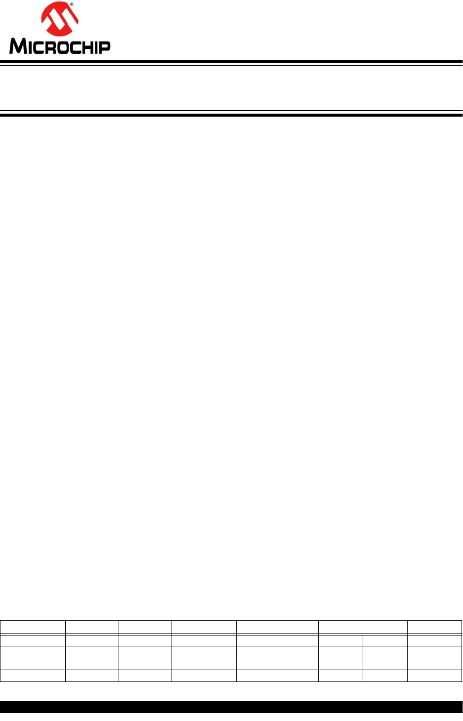
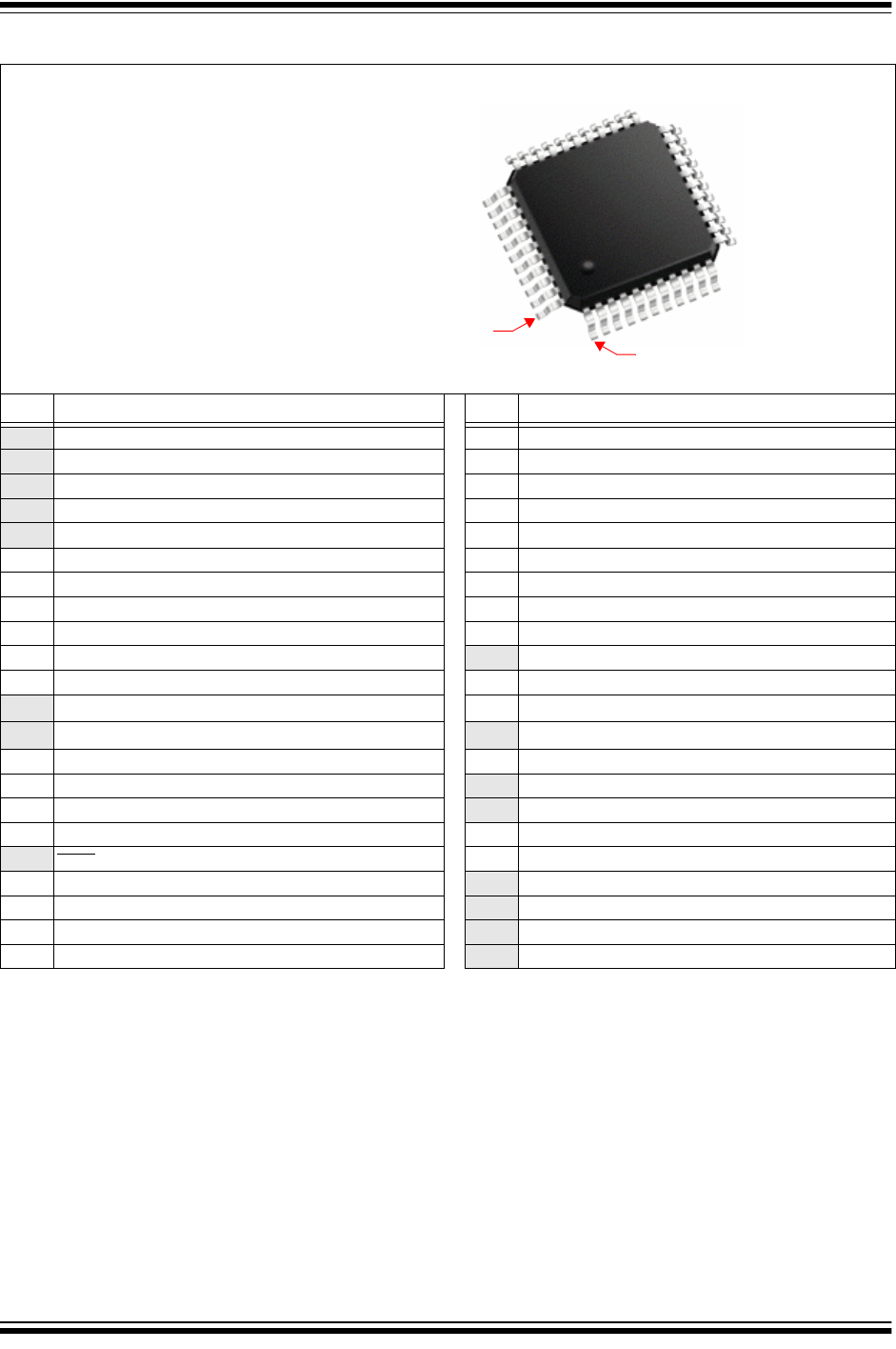
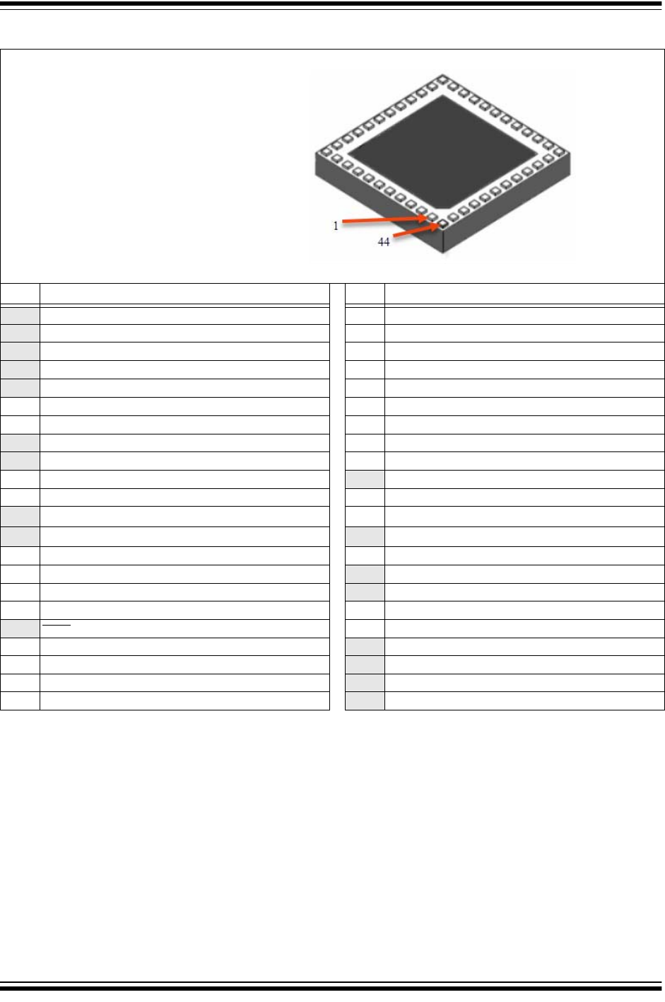
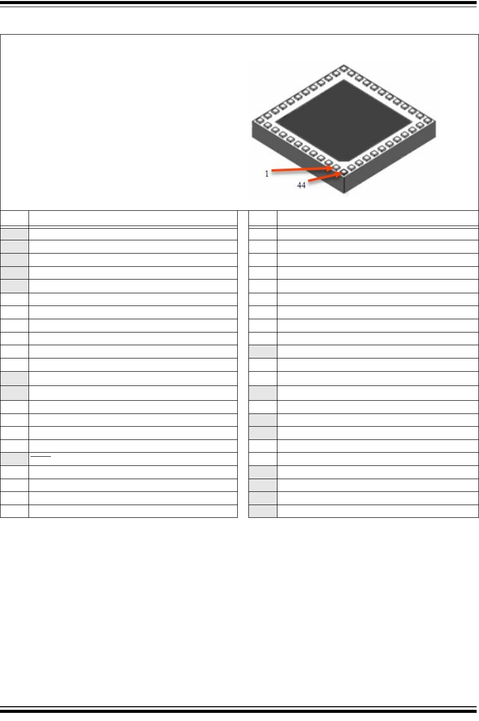
Pin Diagrams
TABLE 3: PIN NAMES FOR 28-PIN GENERAL PURPOSE DEVICES
Pin # Full Pin Name Pin # Full Pin Name
1MCLR 15 PGEC3/RPB6/PMD6/RB6
2V
REF
+/CV
REF
+/AN0/C3INC/RPA0/CTED1/RA0 16 TDI/RPB7/CTED3/PMD5/INT0/RB7
3V
REF
-/CV
REF
-/AN1/RPA1/CTED2/RA1 17 TCK/RPB8/SCL1/CTED10/PMD4/RB8
4PGED1/AN2/C1IND/C2INB/C3IND/RPB0/RB0 18 TDO/RPB9/SDA1/CTED4/PMD3/RB9
5PGEC1/AN3/C1INC/C2INA/RPB1/CTED12/RB1 19 V
SS
6AN4/C1INB/C2IND/RPB2/SDA2/CTED13/RB2 20 V
CAP
7AN5/C1INA/C2INC/RTCC/RPB3/SCL2/RB3 21 PGED2/RPB10/CTED11/PMD2/RB10
8V
SS
22 PGEC2/TMS/RPB11/PMD1/RB11
9OSC1/CLKI/RPA2/RA2 23 AN12/PMD0/RB12
10 OSC2/CLKO/RPA3/PMA0/RA3 24 AN11/RPB13/CTPLS/PMRD/RB13
11 SOSCI/RPB4/RB4 25 CV
REFOUT
/AN10/C3INB/RPB14/SCK1/CTED5/PMWR/RB14
12 SOSCO/RPA4/T1CK/CTED9/PMA1/RA4 26 AN9/C3INA/RPB15/SCK2/CTED6/PMCS1/RB15
13 V
DD
27 AV
SS
14 PGED3/RPB5/PMD7/RB5 28 AV
DD
Note 1: The RPn pins can be used by remappable peripherals. See Table 1 for the available peripherals and Section 11.3 “Peripheral Pin
Select” for restrictions.
2: Every I/O port pin (RAx-RCx) can be used as a change notification pin (CNAx-CNCx). See Section 11.0 “I/O Ports” for more information.
3: Shaded pins are 5V tolerant.
PIC32MX110F016B
PIC32MX120F032B
PIC32MX130F064B
PIC32MX130F256B
PIC32MX150F128B
28-PIN SOIC, SPDIP, SSOP (TOP VIEW)
(1,2,3)
28
SPDIPSOIC
PIC32MX170F256B
SSOP
1
28
1281
2011-2018 Microchip Technology Inc. DS60001168K-page 5
PIC32MX1XX/2XX 28/36/44-PIN FAMILY
TABLE 4: PIN NAMES FOR 28-PIN USB DEVICES
Pin # Full Pin Name Pin # Full Pin Name
1MCLR 15 V
BUS
2PGED3/V
REF
+/CV
REF
+/AN0/C3INC/RPA0/CTED1/PMD7/RA0 16 TDI/RPB7/CTED3/PMD5/INT0/RB7
3PGEC3/V
REF
-/CV
REF
-/AN1/RPA1/CTED2/PMD6/RA1 17 TCK/RPB8/SCL1/CTED10/PMD4/RB8
4PGED1/AN2/C1IND/C2INB/C3IND/RPB0/PMD0/RB0 18 TDO/RPB9/SDA1/CTED4/PMD3/RB9
5PGEC1/AN3/C1INC/C2INA/RPB1/CTED12/PMD1/RB1 19 V
SS
6AN4/C1INB/C2IND/RPB2/SDA2/CTED13/PMD2/RB2 20 V
CAP
7AN5/C1INA/C2INC/RTCC/RPB3/SCL2/PMWR/RB3 21 PGED2/RPB10/D+/CTED11/RB10
8V
SS
22 PGEC2/RPB11/D-/RB11
9OSC1/CLKI/RPA2/RA2 23 V
USB
3
V
3
10 OSC2/CLKO/RPA3/PMA0/RA3 24 AN11/RPB13/CTPLS/PMRD/RB13
11 SOSCI/RPB4/RB4 25 CV
REFOUT
/AN10/C3INB/RPB14/V
BUSON
/SCK1/CTED5/RB14
12 SOSCO/RPA4/T1CK/CTED9/PMA1/RA4 26 AN9/C3INA/RPB15/SCK2/CTED6/PMCS1/RB15
13 V
DD
27 AV
SS
14 TMS/RPB5/USBID/RB5 28 AV
DD
Note 1: The RPn pins can be used by remappable peripherals. See Table 1 for the available peripherals and Section 11.3 “Peripheral Pin
Select” for restrictions.
2: Every I/O port pin (RAx-RCx) can be used as a change notification pin (CNAx-CNCx). See Section 11.0 “I/O Ports” for more informa-
tion.
3: Shaded pins are 5V tolerant.
PIC32MX210F016B
PIC32MX220F032B
PIC32MX230F064B
PIC32MX230F256B
PIC32MX250F128B
28-PIN SOIC, SPDIP, SSOP (TOP VIEW)
(1,2,3)
PIC32MX270F256B
28
SPDIPSOICSSOP
1
28
1281

PIC32MX1XX/2XX 28/36/44-PIN FAMILY
DS60001168K-page 6 2011-2018 Microchip Technology Inc.
TABLE 5: PIN NAMES FOR 28-PIN GENERAL PURPOSE DEVICES
Pin # Full Pin Name Pin # Full Pin Name
1PGED1/AN2/C1IND/C2INB/C3IND/RPB0/RB0 15 TDO/RPB9/SDA1/CTED4/PMD3/RB9
2PGEC1/AN3/C1INC/C2INA/RPB1/CTED12/RB1 16 V
SS
3AN4/C1INB/C2IND/RPB2/SDA2/CTED13/RB2 17 V
CAP
4AN5/C1INA/C2INC/RTCC/RPB3/SCL2/RB3 18 PGED2/RPB10/CTED11/PMD2/RB10
5V
SS
19 PGEC2/TMS/RPB11/PMD1/RB11
6OSC1/CLKI/RPA2/RA2 20 AN12/PMD0/RB12
7OSC2/CLKO/RPA3/PMA0/RA3 21 AN11/RPB13/CTPLS/PMRD/RB13
8SOSCI/RPB4/RB4 22 CV
REFOUT
/AN10/C3INB/RPB14/SCK1/CTED5/PMWR/RB14
9SOSCO/RPA4/T1CK/CTED9/PMA1/RA4 23 AN9/C3INA/RPB15/SCK2/CTED6/PMCS1/RB15
10 V
DD
24 AV
SS
11 PGED3/RPB5/PMD7/RB5 25 AV
DD
12 PGEC3/RPB6/PMD6/RB6 26 MCLR
13 TDI/RPB7/CTED3/PMD5/INT0/RB7 27 V
REF
+/CV
REF
+/AN0/C3INC/RPA0/CTED1/RA0
14 TCK/RPB8/SCL1/CTED10/PMD4/RB8 28 V
REF
-/CV
REF
-/AN1/RPA1/CTED2/RA1
Note 1: The RPn pins can be used by remappable peripherals. See Table 1 for the available peripherals and Section 11.3 “Peripheral Pin
Select” for restrictions.
2: Every I/O port pin (RAx-RCx) can be used as a change notification pin (CNAx-CNCx). See Section 11.0 “I/O Ports” for more information.
3: The metal plane at the bottom of the device is not connected to any pins and is recommended to be connected to V
SS
externally.
4: Shaded pins are 5V tolerant.
PIC32MX110F016B
PIC32MX120F032B
PIC32MX130F064B
PIC32MX130F256B
PIC32MX150F128B
1
28
28-PIN QFN (TOP VIEW)
(1,2,3.4)
PIC32MX170F256B
2011-2018 Microchip Technology Inc. DS60001168K-page 7
PIC32MX1XX/2XX 28/36/44-PIN FAMILY
TABLE 6: PIN NAMES FOR 28-PIN USB DEVICES
Pin # Full Pin Name Pin # Full Pin Name
1PGED1/AN2/C1IND/C2INB/C3IND/RPB0/PMD0/RB0 15 TDO/RPB9/SDA1/CTED4/PMD3/RB9
2PGEC1/AN3/C1INC/C2INA/RPB1/CTED12/PMD1/RB1 16 V
SS
3AN4/C1INB/C2IND/RPB2/SDA2/CTED13/PMD2/RB2 17 V
CAP
4AN5/C1INA/C2INC/RTCC/RPB3/SCL2/PMWR/RB3 18 PGED2/RPB10/D+/CTED11/RB10
5V
SS
19 PGEC2/RPB11/D-/RB11
6OSC1/CLKI/RPA2/RA2 20 V
USB
3
V
3
7OSC2/CLKO/RPA3/PMA0/RA3 21 AN11/RPB13/CTPLS/PMRD/RB13
8SOSCI/RPB4/RB4 22 CV
REFOUT
/AN10/C3INB/RPB14/V
BUSON
/SCK1/CTED5/RB14
9SOSCO/RPA4/T1CK/CTED9/PMA1/RA4 23 AN9/C3INA/RPB15/SCK2/CTED6/PMCS1/RB15
10 V
DD
24 AV
SS
11 TMS/RPB5/USBID/RB5 25 AV
DD
12 V
BUS
26 MCLR
13 TDI/RPB7/CTED3/PMD5/INT0/RB7 27 PGED3/V
REF
+/CV
REF
+/AN0/C3INC/RPA0/CTED1/PMD7/RA0
14 TCK/RPB8/SCL1/CTED10/PMD4/RB8 28 PGEC3/V
REF
-/CV
REF
-/AN1/RPA1/CTED2/PMD6/RA1
Note 1: The RPn pins can be used by remappable peripherals. See Table 1 for the available peripherals and Section 11.3 “Peripheral Pin
Select” for restrictions.
2: Every I/O port pin (RAx-RCx) can be used as a change notification pin (CNAx-CNCx). See Section 11.0 “I/O Ports” for more information.
3: The metal plane at the bottom of the device is not connected to any pins and is recommended to be connected to V
SS
externally.
4: Shaded pins are 5V tolerant.
28-PIN QFN (TOP VIEW)
(1,2,3,4)
PIC32MX210F016B
PIC32MX220F032B
PIC32MX230F064B
PIC32MX230F256B
PIC32MX250F128B
PIC32MX270F256B
1
28
PIC32MX1XX/2XX 28/36/44-PIN FAMILY
DS60001168K-page 8 2011-2018 Microchip Technology Inc.
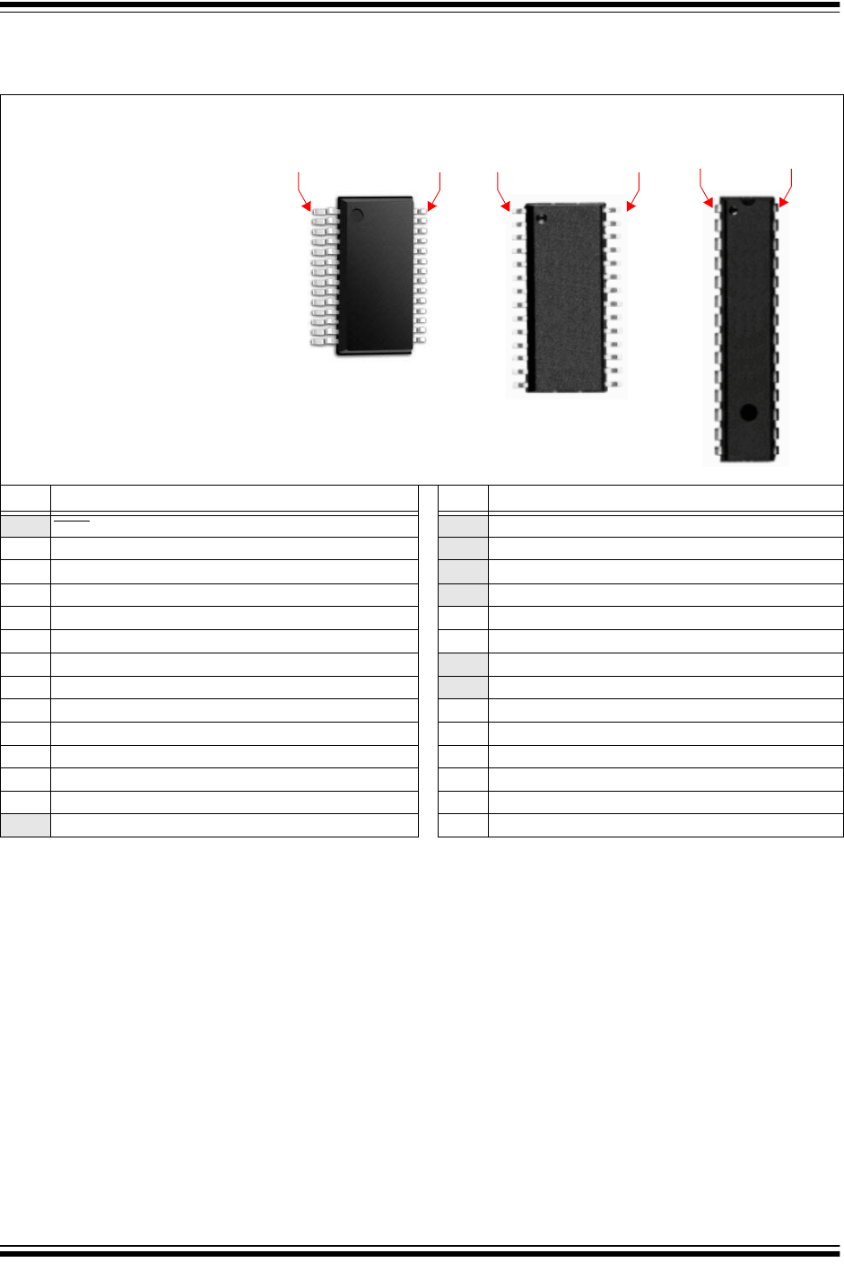
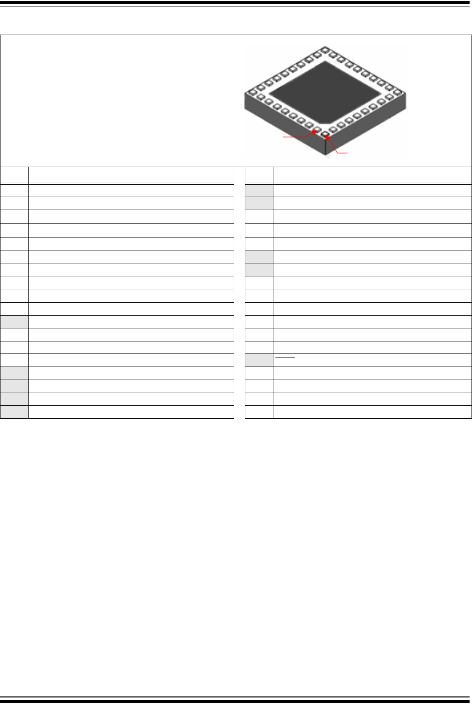
TABLE 7: PIN NAMES FOR 36-PIN GENERAL PURPOSE DEVICES
Pin # Full Pin Name Pin # Full Pin Name
1AN4/C1INB/C2IND/RPB2/SDA2/CTED13/RB2 19 TDO/RPB9/SDA1/CTED4/PMD3/RB9
2AN5/C1INA/C2INC/RTCC/RPB3/SCL2/RB3 20 RPC9/CTED7/RC9
3PGED4
(4)
/AN6/RPC0/RC0 21 V
SS
4PGEC4
(4)
/AN7/RPC1/RC1 22 V
CAP
5V
DD
23 V
DD
6V
SS
24 PGED2/RPB10/CTED11/PMD2/RB10
7OSC1/CLKI/RPA2/RA2 25 PGEC2/TMS/RPB11/PMD1/RB11
8OSC2/CLKO/RPA3/PMA0/RA3 26 AN12/PMD0/RB12
9SOSCI/RPB4/RB4 27 AN11/RPB13/CTPLS/PMRD/RB13
10 SOSCO/RPA4/T1CK/CTED9/PMA1/RA4 28 CV
REFOUT
/AN10/C3INB/RPB14/SCK1/CTED5/PMWR/RB14
11 RPC3/RC3 29 AN9/C3INA/RPB15/SCK2/CTED6/PMCS1/RB15
12 V
SS
30 AV
SS
13 V
DD
31 AV
DD
14 V
DD
32 MCLR
15 PGED3/RPB5/PMD7/RB5 33 V
REF
+/CV
REF
+/AN0/C3INC/RPA0/CTED1/RA0
16 PGEC3/RPB6/PMD6/RB6 34 V
REF
-/CV
REF
-/AN1/RPA1/CTED2/RA1
17 TDI/RPB7/CTED3/PMD5/INT0/RB7 35 PGED1/AN2/C1IND/C2INB/C3IND/RPB0/RB0
18 TCK/RPB8/SCL1/CTED10/PMD4/RB8 36 PGEC1/AN3/C1INC/C2INA/RPB1/CTED12/RB1
Note 1: The RPn pins can be used by remappable peripherals. See Table 1 for the available peripherals and Section 11.3 “Peripheral Pin
Select” for restrictions.
2: Every I/O port pin (RAx-RCx) can be used as a change notification pin (CNAx-CNCx). See Section 11.0 “I/O Ports” for more information.
3: The metal plane at the bottom of the device is not connected to any pins and is recommended to be connected to V
SS
externally.
4: This pin function is not available on PIC32MX110F016C and PIC32MX120F032C devices.
5: Shaded pins are 5V tolerant.
PIC32MX110F016C
PIC32MX120F032C
PIC32MX130F064C
PIC32MX150F128C
36-PIN VTLA (BOTTOM VIEW)
(1,2,3,5)
36
1

2011-2018 Microchip Technology Inc. DS60001168K-page 9
PIC32MX1XX/2XX 28/36/44-PIN FAMILY
TABLE 8: PIN NAMES FOR 36-PIN USB DEVICES
Pin # Full Pin Name Pin # Full Pin Name
1AN4/C1INB/C2IND/RPB2/SDA2/CTED13/PMD2/RB2 19 TDO/RPB9/SDA1/CTED4/PMD3/RB9
2AN5/C1INA/C2INC/RTCC/RPB3/SCL2/PMWR/RB3 20 RPC9/CTED7/RC9
3PGED4
(4)
/AN6/RPC0/RC0 21 V
SS
4PGEC4
(4)
/AN7/RPC1/RC1 22 V
CAP
5V
DD
23 V
DD
6V
SS
24 PGED2/RPB10/D+/CTED11/RB10
7OSC1/CLKI/RPA2/RA2 25 PGEC2/RPB11/D-/RB11
8OSC2/CLKO/RPA3/PMA0/RA3 26 V
USB
3
V
3
9SOSCI/RPB4/RB4 27 AN11/RPB13/CTPLS/PMRD/RB13
10 SOSCO/RPA4/T1CK/CTED9/PMA1/RA4 28 CV
REFOUT
/AN10/C3INB/RPB14/V
BUSON
/SCK1/CTED5/RB14
11 AN12/RPC3/RC3 29 AN9/C3INA/RPB15/SCK2/CTED6/PMCS1/RB15
12 V
SS
30 AV
SS
13 V
DD
31 AV
DD
14 V
DD
32 MCLR
15 TMS/RPB5/USBID/RB5 33 PGED3/V
REF
+/CV
REF
+/AN0/C3INC/RPA0/CTED1/PMD7/RA0
16 V
BUS
34 PGEC3/V
REF
-/CV
REF
-/AN1/RPA1/CTED2/PMD6/RA1
17 TDI/RPB7/CTED3/PMD5/INT0/RB7 35 PGED1/AN2/C1IND/C2INB/C3IND/RPB0/PMD0/RB0
18 TCK/RPB8/SCL1/CTED10/PMD4/RB8 36 PGEC1/AN3/C1INC/C2INA/RPB1/CTED12/PMD1/RB1
Note 1: The RPn pins can be used by remappable peripherals. See Table 1 for the available peripherals and Section 11.3 “Peripheral Pin
Select” for restrictions.
2: Every I/O port pin (RAx-RCx) can be used as a change notification pin (CNAx-CNCx). See Section 11.0 “I/O Ports” for more information.
3: The metal plane at the bottom of the device is not connected to any pins and is recommended to be connected to V
SS
externally.
4: This pin function is not available on PIC32MX210F016C and PIC32MX120F032C devices.
5: Shaded pins are 5V tolerant.
PIC32MX210F016C
PIC32MX220F032C
PIC32MX230F064C
PIC32MX250F128C
36-PIN VTLA (BOTTOM VIEW)
(1,2,3,5)
36
1
PIC32MX1XX/2XX 28/36/44-PIN FAMILY
DS60001168K-page 10 2011-2018 Microchip Technology Inc.
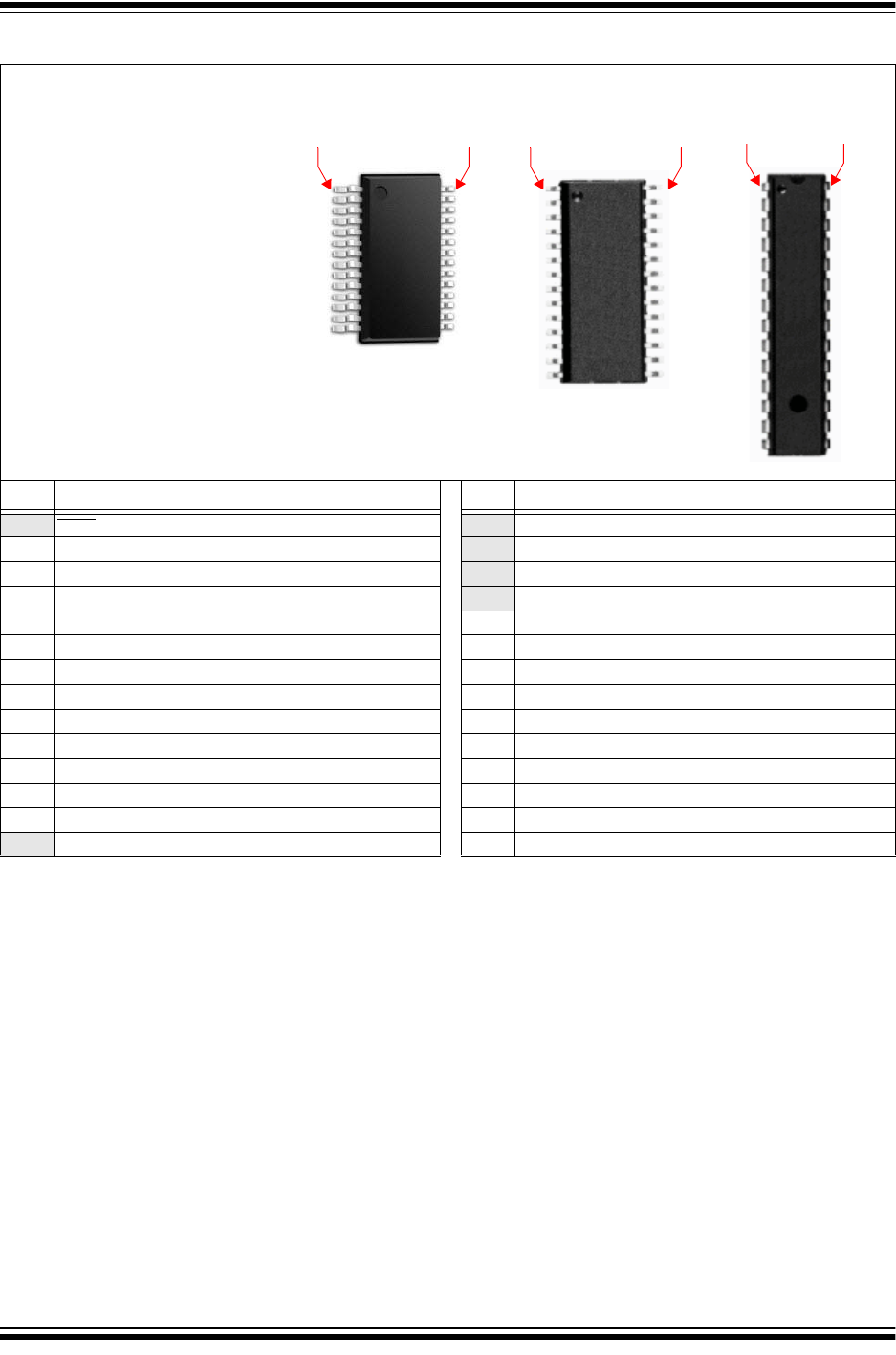
TABLE 9: PIN NAMES FOR 44-PIN GENERAL PURPOSE DEVICES
Pin # Full Pin Name Pin # Full Pin Name
1RPB9/SDA1/CTED4/PMD3/RB9 23 AN4/C1INB/C2IND/RPB2/SDA2/CTED13/RB2
2RPC6/PMA1/RC6 24 AN5/C1INA/C2INC/RTCC/RPB3/SCL2/RB3
3RPC7/PMA0/RC7 25 AN6/RPC0/RC0
4RPC8/PMA5/RC8 26 AN7/RPC1/RC1
5RPC9/CTED7/PMA6/RC9 27 AN8/RPC2/PMA2/RC2
6V
SS
28 V
DD
7V
CAP
29 V
SS
8PGED2/RPB10/CTED11/PMD2/RB10 30 OSC1/CLKI/RPA2/RA2
9PGEC2/RPB11/PMD1/RB11 31 OSC2/CLKO/RPA3/RA3
10 AN12/PMD0/RB12 32 TDO/RPA8/PMA8/RA8
11 AN11/RPB13/CTPLS/PMRD/RB13 33 SOSCI/RPB4/RB4
12 PGED4
(4)
/TMS/PMA10/RA10 34 SOSCO/RPA4/T1CK/CTED9/RA4
13 PGEC4
(4)
/TCK/CTED8/PMA7/RA7 35 TDI/RPA9/PMA9/RA9
14 CV
REFOUT
/AN10/C3INB/RPB14/SCK1/CTED5/PMWR/RB14 36 RPC3/RC3
15 AN9/C3INA/RPB15/SCK2/CTED6/PMCS1/RB15 37 RPC4/PMA4/RC4
16 AV
SS
38 RPC5/PMA3/RC5
17 AV
DD
39 V
SS
18 MCLR 40 V
DD
19 V
REF
+/CV
REF
+/AN0/C3INC/RPA0/CTED1/RA0 41 PGED3/RPB5/PMD7/RB5
20 V
REF
-/CV
REF
-/AN1/RPA1/CTED2/RA1 42 PGEC3/RPB6/PMD6/RB6
21 PGED1/AN2/C1IND/C2INB/C3IND/RPB0/RB0 43 RPB7/CTED3/PMD5/INT0/RB7
22 PGEC1/AN3/C1INC/C2INA/RPB1/CTED12/RB1 44 RPB8/SCL1/CTED10/PMD4/RB8
Note 1: The RPn pins can be used by remappable peripherals. See Table 1 for the available peripherals and Section 11.3 “Peripheral Pin
Select” for restrictions.
2: Every I/O port pin (RAx-RCx) can be used as a change notification pin (CNAx-CNCx). See Section 11.0 “I/O Ports” for more information.
3: The metal plane at the bottom of the device is not connected to any pins and is recommended to be connected to V
SS
externally.
4: This pin function is not available on PIC32MX110F016D and PIC32MX120F032D devices.
5: Shaded pins are 5V tolerant.
PIC32MX110F016D
PIC32MX120F032D
PIC32MX130F064D
PIC32MX130F256D
PIC32MX150F128D
1
44
44-PIN QFN (TOP VIEW)
(1,2,3,5)
PIC32MX170F256D
2011-2018 Microchip Technology Inc. DS60001168K-page 11
PIC32MX1XX/2XX 28/36/44-PIN FAMILY
TABLE 10: PIN NAMES FOR 44-PIN USB DEVICES
Pin # Full Pin Name Pin # Full Pin Name
1RPB9/SDA1/CTED4/PMD3/RB9 23 AN4/C1INB/C2IND/RPB2/SDA2/CTED13/PMD2/RB2
2RPC6/PMA1/RC6 24 AN5/C1INA/C2INC/RTCC/RPB3/SCL2/PMWR/RB3
3RPC7/PMA0/RC7 25 AN6/RPC0/RC0
4RPC8/PMA5/RC8 26 AN7/RPC1/RC1
5RPC9/CTED7/PMA6/RC9 27 AN8/RPC2/PMA2/RC2
6V
SS
28 V
DD
7V
CAP
29 V
SS
8PGED2/RPB10/D+/CTED11/RB10 30 OSC1/CLKI/RPA2/RA2
9PGEC2/RPB11/D-/RB11 31 OSC2/CLKO/RPA3/RA3
10 V
USB
3
V
3
32 TDO/RPA8/PMA8/RA8
11 AN11/RPB13/CTPLS/PMRD/RB13 33 SOSCI/RPB4/RB4
12 PGED4/TMS/PMA10/RA10 34 SOSCO/RPA4/T1CK/CTED9/RA4
13 PGEC4/TCK/CTED8/PMA7/RA7 35 TDI/RPA9/PMA9/RA9
14 CV
REFOUT
/AN10/C3INB/RPB14/V
BUSON
/SCK1/CTED5/RB14 36 AN12/RPC3/RC3
15 AN9/C3INA/RPB15/SCK2/CTED6/PMCS1/RB15 37 RPC4/PMA4/RC4
16 AV
SS
38 RPC5/PMA3/RC5
17 AV
DD
39 V
SS
18 MCLR 40 V
DD
19 PGED3/V
REF
+/CV
REF
+/AN0/C3INC/RPA0/CTED1/PMD7/RA0 41 RPB5/USBID/RB5
20 PGEC3/V
REF
-/CV
REF
-/AN1/RPA1/CTED2/PMD6/RA1 42 V
BUS
21 PGED1/AN2/C1IND/C2INB/C3IND/RPB0/PMD0/RB0 43 RPB7/CTED3/PMD5/INT0/RB7
22 PGEC1/AN3/C1INC/C2INA/RPB1/CTED12/PMD1/RB1 44 RPB8/SCL1/CTED10/PMD4/RB8
Note 1: The RPn pins can be used by remappable peripherals. See Table 1 for the available peripherals and Section 11.3 “Peripheral Pin
Select” for restrictions.
2: Every I/O port pin (RAx-RCx) can be used as a change notification pin (CNAx-CNCx). See Section 11.0 “I/O Ports” for more information.
3: The metal plane at the bottom of the device is not connected to any pins and is recommended to be connected to V
SS
externally.
4: This pin function is not available on PIC32MX110F016D and PIC32MX120F032D devices.
5: Shaded pins are 5V tolerant.
44-PIN QFN (TOP VIEW)
(1,2,3,5)
PIC32MX210F016D
PIC32MX220F032D
PIC32MX230F064D
PIC32MX230F256D
PIC32MX250F128D
PIC32MX270F256D
1
44
PIC32MX1XX/2XX 28/36/44-PIN FAMILY
DS60001168K-page 12 2011-2018 Microchip Technology Inc.
TABLE 11: PIN NAMES FOR 44-PIN GENERAL PURPOSE DEVICES
Pin # Full Pin Name Pin # Full Pin Name
1RPB9/SDA1/CTED4/PMD3/RB9 23 AN4/C1INB/C2IND/RPB2/SDA2/CTED13/RB2
2RPC6/PMA1/RC6 24 AN5/C1INA/C2INC/RTCC/RPB3/SCL2/RB3
3RPC7/PMA0/RC7 25 AN6/RPC0/RC0
4RPC8/PMA5/RC8 26 AN7/RPC1/RC1
5RPC9/CTED7/PMA6/RC9 27 AN8/RPC2/PMA2/RC2
6V
SS
28 V
DD
7V
CAP
29 V
SS
8PGED2/RPB10/CTED11/PMD2/RB10 30 OSC1/CLKI/RPA2/RA2
9PGEC2/RPB11/PMD1/RB11 31 OSC2/CLKO/RPA3/RA3
10 AN12/PMD0/RB12 32 TDO/RPA8/PMA8/RA8
11 AN11/RPB13/CTPLS/PMRD/RB13 33 SOSCI/RPB4/RB4
12 PGED4
(4)
/TMS/PMA10/RA10 34 SOSCO/RPA4/T1CK/CTED9/RA4
13 PGEC4
(4)
/TCK/CTED8/PMA7/RA7 35 TDI/RPA9/PMA9/RA9
14 CV
REFOUT
/AN10/C3INB/RPB14/SCK1/CTED5/PMWR/RB14 36 RPC3/RC3
15 AN9/C3INA/RPB15/SCK2/CTED6/PMCS1/RB15 37 RPC4/PMA4/RC4
16 AV
SS
38 RPC5/PMA3/RC5
17 AV
DD
39 V
SS
18 MCLR 40 V
DD
19 V
REF
+/CV
REF
+/AN0/C3INC/RPA0/CTED1/RA0 41 PGED3/RPB5/PMD7/RB5
20 V
REF
-/CV
REF
-/AN1/RPA1/CTED2/RA1 42 PGEC3/RPB6/PMD6/RB6
21 PGED1/AN2/C1IND/C2INB/C3IND/RPB0/RB0 43 RPB7/CTED3/PMD5/INT0/RB7
22 PGEC1/AN3/C1INC/C2INA/RPB1/CTED12/RB1 44 RPB8/SCL1/CTED10/PMD4/RB8
Note 1: The RPn pins can be used by remappable peripherals. See Table 1 for the available peripherals and Section 11.3 “Peripheral Pin
Select” for restrictions.
2: Every I/O port pin (RAx-RCx) can be used as a change notification pin (CNAx-CNCx). See Section 11.0 “I/O Ports” for more information.
3: The metal plane at the bottom of the device is not connected to any pins and is recommended to be connected to V
SS
externally.
4: This pin function is not available on PIC32MX110F016D and PIC32MX120F032D devices.
5: Shaded pins are 5V tolerant.
PIC32MX110F016D
PIC32MX120F032D
PIC32MX130F064D
PIC32MX130F256D
PIC32MX150F128D
44-PIN TQFP (TOP VIEW)
(1,2,3,5)
PIC32MX170F256D
1
44
2011-2018 Microchip Technology Inc. DS60001168K-page 13
PIC32MX1XX/2XX 28/36/44-PIN FAMILY
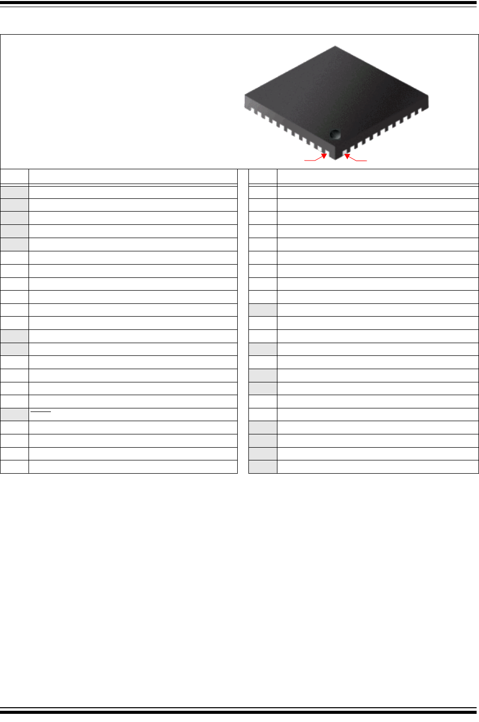
TABLE 12: PIN NAMES FOR 44-PIN USB DEVICES
Pin # Full Pin Name Pin # Full Pin Name
1RPB9/SDA1/CTED4/PMD3/RB9 23 AN4/C1INB/C2IND/RPB2/SDA2/CTED13/PMD2/RB2
2RPC6/PMA1/RC6 24 AN5/C1INA/C2INC/RTCC/RPB3/SCL2/PMWR/RB3
3RPC7/PMA0/RC7 25 AN6/RPC0/RC0
4RPC8/PMA5/RC8 26 AN7/RPC1/RC1
5RPC9/CTED7/PMA6/RC9 27 AN8/RPC2/PMA2/RC2
6V
SS
28 V
DD
7V
CAP
29 V
SS
8PGED2/RPB10/D+/CTED11/RB10 30 OSC1/CLKI/RPA2/RA2
9PGEC2/RPB11/D-/RB11 31 OSC2/CLKO/RPA3/RA3
10 V
USB
3
V
3
32 TDO/RPA8/PMA8/RA8
11 AN11/RPB13/CTPLS/PMRD/RB13 33 SOSCI/RPB4/RB4
12 PGED4
(4)
/TMS/PMA10/RA10 34 SOSCO/RPA4/T1CK/CTED9/RA4
13 PGEC4
(4)
/TCK/CTED8/PMA7/RA7 35 TDI/RPA9/PMA9/RA9
14 CV
REFOUT
/AN10/C3INB/RPB14/V
BUSON
/SCK1/CTED5/RB14 36 AN12/RPC3/RC3
15 AN9/C3INA/RPB15/SCK2/CTED6/PMCS1/RB15 37 RPC4/PMA4/RC4
16 AV
SS
38 RPC5/PMA3/RC5
17 AV
DD
39 V
SS
18 MCLR 40 V
DD
19 PGED3/V
REF
+/CV
REF
+/AN0/C3INC/RPA0/CTED1/PMD7/RA0 41 RPB5/USBID/RB5
20 PGEC3/V
REF
-/CV
REF
-/AN1/RPA1/CTED2/PMD6/RA1 42 V
BUS
21 PGED1/AN2/C1IND/C2INB/C3IND/RPB0/PMD0/RB0 43 RPB7/CTED3/PMD5/INT0/RB7
22 PGEC1/AN3/C1INC/C2INA/RPB1/CTED12/PMD1/RB1 44 RPB8/SCL1/CTED10/PMD4/RB8
Note 1: The RPn pins can be used by remappable peripherals. See Table 1 for the available peripherals and Section 11.3 “Peripheral Pin
Select” for restrictions.
2: Every I/O port pin (RAx-RCx) can be used as a change notification pin (CNAx-CNCx). See Section 11.0 “I/O Ports” for more information.
3: The metal plane at the bottom of the device is not connected to any pins and is recommended to be connected to V
SS
externally.
4: This pin function is not available on PIC32MX210F016D and PIC32MX220F032D devices.
5: Shaded pins are 5V tolerant.
44-PIN TQFP (TOP VIEW)
(1,2,3,5)
PIC32MX210F016D
PIC32MX220F032D
PIC32MX230F064D
PIC32MX230F256D
PIC32MX250F128D
PIC32MX270F256D
1
44
PIC32MX1XX/2XX 28/36/44-PIN FAMILY
DS60001168K-page 14 2011-2018 Microchip Technology Inc.
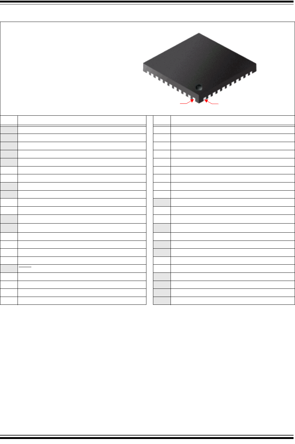
TABLE 13: PIN NAMES FOR 44-PIN GENERAL PURPOSE DEVICES
Pin # Full Pin Name Pin # Full Pin Name
1RPB9/SDA1/CTED4/PMD3/RB9 23 AN4/C1INB/C2IND/RPB2/SDA2/CTED13/RB2
2RPC6/PMA1/RC6 24 AN5/C1INA/C2INC/RTCC/RPB3/SCL2/RB3
3RPC7/PMA0/RC7 25 AN6/RPC0/RC0
4RPC8/PMA5/RC8 26 AN7/RPC1/RC1
5RPC9/CTED7/PMA6/RC9 27 AN8/RPC2/PMA2/RC2
6V
SS
28 V
DD
7V
CAP
29 V
SS
8PGED2/RPB10/CTED11/PMD2/RB10 30 OSC1/CLKI/RPA2/RA2
9PGEC2/RPB11/PMD1/RB11 31 OSC2/CLKO/RPA3/RA3
10 AN12/PMD0/RB12 32 TDO/RPA8/PMA8/RA8
11 AN11/RPB13/CTPLS/PMRD/RB13 33 SOSCI/RPB4/RB4
12 PGED4
(4)
/TMS/PMA10/RA10 34 SOSCO/RPA4/T1CK/CTED9/RA4
13 PGEC4
(4)
/TCK/CTED8/PMA7/RA7 35 TDI/RPA9/PMA9/RA9
14 CV
REFOUT
/AN10/C3INB/RPB14/SCK1/CTED5/PMWR/RB14 36 RPC3/RC3
15 AN9/C3INA/RPB15/SCK2/CTED6/PMCS1/RB15 37 RPC4/PMA4/RC4
16 AV
SS
38 RPC5/PMA3/RC5
17 AV
DD
39 V
SS
18 MCLR 40 V
DD
19 V
REF
+/CV
REF
+/AN0/C3INC/RPA0/CTED1/RA0 41 PGED3/RPB5/PMD7/RB5
20 V
REF
-/CV
REF
-/AN1/RPA1/CTED2/RA1 42 PGEC3/RPB6/PMD6/RB6
21 PGED1/AN2/C1IND/C2INB/C3IND/RPB0/RB0 43 RPB7/CTED3/PMD5/INT0/RB7
22 PGEC1/AN3/C1INC/C2INA/RPB1/CTED12/RB1 44 RPB8/SCL1/CTED10/PMD4/RB8
Note 1: The RPn pins can be used by remappable peripherals. See Table 1 for the available peripherals and Section 11.3 “Peripheral Pin
Select” for restrictions.
2: Every I/O port pin (RAx-RCx) can be used as a change notification pin (CNAx-CNCx). See Section 11.0 “I/O Ports” for more information.
3: The metal plane at the bottom of the device is not connected to any pins and is recommended to be connected to V
SS
externally.
4: This pin function is not available on PIC32MX110F016D and PIC32MX120F032D devices.
5: Shaded pins are 5V tolerant.
44
PIC32MX110F016D
PIC32MX120F032D
PC32MX130F064D
PIC32MX130F256D
PIC32MX150F128D
44-PIN VTLA (BOTTOM VIEW)
(1,2,3,5)
PIC32MX170F256D
1
2011-2018 Microchip Technology Inc. DS60001168K-page 15
PIC32MX1XX/2XX 28/36/44-PIN FAMILY
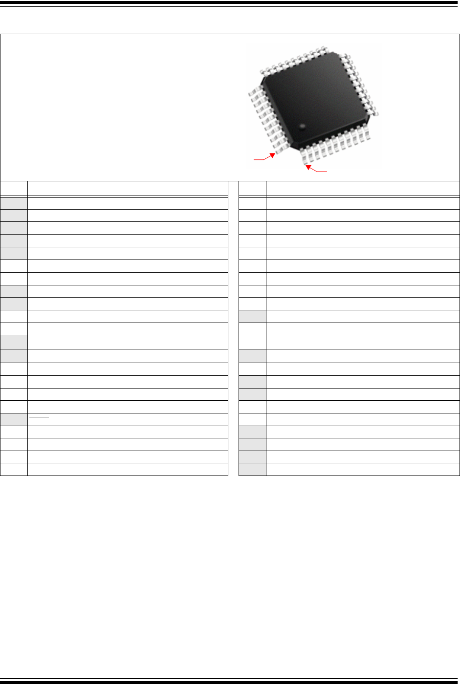
TABLE 14: PIN NAMES FOR 44-PIN USB DEVICES
Pin # Full Pin Name Pin # Full Pin Name
1RPB9/SDA1/CTED4/PMD3/RB9 23 AN4/C1INB/C2IND/RPB2/SDA2/CTED13/PMD2/RB2
2RPC6/PMA1/RC6 24 AN5/C1INA/C2INC/RTCC/RPB3/SCL2/PMWR/RB3
3RPC7/PMA0/RC7 25 AN6/RPC0/RC0
4RPC8/PMA5/RC8 26 AN7/RPC1/RC1
5RPC9/CTED7/PMA6/RC9 27 AN8/RPC2/PMA2/RC2
6V
SS
28 V
DD
7V
CAP
29 V
SS
8PGED2/RPB10/D+/CTED11/RB10 30 OSC1/CLKI/RPA2/RA2
9PGEC2/RPB11/D-/RB11 31 OSC2/CLKO/RPA3/RA3
10 V
USB
3
V
3
32 TDO/RPA8/PMA8/RA8
11 AN11/RPB13/CTPLS/PMRD/RB13 33 SOSCI/RPB4/RB4
12 PGED4
(4)
/TMS/PMA10/RA10 34 SOSCO/RPA4/T1CK/CTED9/RA4
13 PGEC4
(4)
/TCK/CTED8/PMA7/RA7 35 TDI/RPA9/PMA9/RA9
14 CV
REFOUT
/AN10/C3INB/RPB14/V
BUSON
/SCK1/CTED5/RB14 36 AN12/RPC3/RC3
15 AN9/C3INA/RPB15/SCK2/CTED6/PMCS1/RB15 37 RPC4/PMA4/RC4
16 AV
SS
38 RPC5/PMA3/RC5
17 AV
DD
39 V
SS
18 MCLR 40 V
DD
19 PGED3/V
REF
+/CV
REF
+/AN0/C3INC/RPA0/CTED1/PMD7/RA0 41 RPB5/USBID/RB5
20 PGEC3/V
REF
-/CV
REF
-/AN1/RPA1/CTED2/PMD6/RA1 42 V
BUS
21 PGED1/AN2/C1IND/C2INB/C3IND/RPB0/PMD0/RB0 43 RPB7/CTED3/PMD5/INT0/RB7
22 PGEC1/AN3/C1INC/C2INA/RPB1/CTED12/PMD1/RB1 44 RPB8/SCL1/CTED10/PMD4/RB8
Note 1: The RPn pins can be used by remappable peripherals. See Table 1 for the available peripherals and Section 11.3 “Peripheral Pin
Select” for restrictions.
2: Every I/O port pin (RAx-RCx) can be used as a change notification pin (CNAx-CNCx). See Section 11.0 “I/O Ports” for more information.
3: The metal plane at the bottom of the device is not connected to any pins and is recommended to be connected to V
SS
externally.
4: This pin function is not available on PIC32MX210F016D and PIC32MX220F032D devices.
5: Shaded pins are 5V tolerant.
44-PIN VTLA (BOTTOM VIEW)
(1,2,3,5)
PIC32MX210F016D
PIC32MX220F032D
PIC32MX230F064D
PIC32MX230F256D
PIC32MX250F128D
PIC32MX270F256D
44

PIC32MX1XX/2XX 28/36/44-PIN FAMILY
DS60001168K-page 16 2011-2018 Microchip Technology Inc.
Table of Contents
1.0 Device Overview ........................................................................................................................................................................ 19
2.0 Guidelines for Getting Started with 32-bit MCUs........................................................................................................................ 27
3.0 CPU............................................................................................................................................................................................ 35
4.0 Memory Organization ................................................................................................................................................................. 39
5.0 Flash Program Memory.............................................................................................................................................................. 55
6.0 Resets ........................................................................................................................................................................................ 61
7.0 Interrupt Controller ..................................................................................................................................................................... 65
8.0 Oscillator Configuration .............................................................................................................................................................. 75
9.0 Direct Memory Access (DMA) Controller ................................................................................................................................... 85
10.0 USB On-The-Go (OTG)............................................................................................................................................................ 105
11.0 I/O Ports ................................................................................................................................................................................... 129
12.0 Timer1 ...................................................................................................................................................................................... 145
13.0 Timer2/3, Timer4/5 ................................................................................................................................................................... 149
14.0 Watchdog Timer (WDT) ........................................................................................................................................................... 155
15.0 Input Capture............................................................................................................................................................................ 159
16.0 Output Compare....................................................................................................................................................................... 163
17.0 Serial Peripheral Interface (SPI)............................................................................................................................................... 167
18.0 Inter-Integrated Circuit (I
2
C) ..................................................................................................................................................... 175
19.0 Universal Asynchronous Receiver Transmitter (UART) ........................................................................................................... 183
20.0 Parallel Master Port (PMP)....................................................................................................................................................... 191
21.0 Real-Time Clock and Calendar (RTCC)................................................................................................................................... 201
22.0 10-bit Analog-to-Digital Converter (ADC) ................................................................................................................................. 211
23.0 Comparator .............................................................................................................................................................................. 221
24.0 Comparator Voltage Reference (CV
REF
).................................................................................................................................. 225
25.0 Charge Time Measurement Unit (CTMU) ............................................................................................................................... 229
26.0 Power-Saving Features ........................................................................................................................................................... 235
27.0 Special Features ...................................................................................................................................................................... 241
28.0 Instruction Set .......................................................................................................................................................................... 253
29.0 Development Support............................................................................................................................................................... 255
30.0 Electrical Characteristics .......................................................................................................................................................... 259
31.0 50 MHz Electrical Characteristics............................................................................................................................................. 303
32.0 DC and AC Device Characteristics Graphs.............................................................................................................................. 309
33.0 Packaging Information.............................................................................................................................................................. 313
The Microchip Web Site..................................................................................................................................................................... 343
Customer Change Notification Service .............................................................................................................................................. 343
Customer Support .............................................................................................................................................................................. 343
Product Identification System............................................................................................................................................................. 344

2011-2018 Microchip Technology Inc. DS60001168K-page 17
PIC32MX1XX/2XX 28/36/44-PIN FAMILY
TO OUR VALUED CUSTOMERS
It is our intention to provide our valued customers with the best documentation possible to ensure successful use of your Microchip
products. To this end, we will continue to improve our publications to better suit your needs. Our publications will be refined and
enhanced as new volumes and updates are introduced.
If you have any questions or comments regarding this publication, please contact the Marketing Communications Department via
E-mail at docerrors@microchip.com. We welcome your feedback.
Most Current Data Sheet
To obtain the most up-to-date version of this data sheet, please register at our Worldwide Web site at:
http://www.microchip.com
You can determine the version of a data sheet by examining its literature number found on the bottom outside corner of any page.
The last character of the literature number is the version number, (e.g., DS30000000A is version A of document DS30000000).
Errata
An errata sheet, describing minor operational differences from the data sheet and recommended workarounds, may exist for current
devices. As device/documentation issues become known to us, we will publish an errata sheet. The errata will specify the revision
of silicon and revision of document to which it applies.
To determine if an errata sheet exists for a particular device, please check with one of the following:
• Microchip’s Worldwide Web site; http://www.microchip.com
• Your local Microchip sales office (see last page)
When contacting a sales office, please specify which device, revision of silicon and data sheet (include literature number) you are
using.
Customer Notification System
Register on our web site at www.microchip.com to receive the most current information on all of our products.

PIC32MX1XX/2XX 28/36/44-PIN FAMILY
DS60001168K-page 18 2011-2018 Microchip Technology Inc.
Referenced Sources
This device data sheet is based on the following
individual chapters of the “PIC32 Family Reference
Manual”. These documents should be considered as
the general reference for the operation of a particular
module or device feature.
•Section 1. “Introduction” (DS60001127)
•Section 2. “CPU” (DS60001113)
•Section 3. “Memory Organization” (DS60001115)
•Section 5. “Flash Program Memory” (DS60001121)
•Section 6. “Oscillator Configuration” (DS60001112)
•Section 7. “Resets” (DS60001118)
•Section 8. “Interrupt Controller” (DS60001108)
•Section 9. “Watchdog Timer and Power-up Timer” (DS60001114)
•Section 10. “Power-Saving Features” (DS60001130)
•Section 12. “I/O Ports” (DS60001120)
•Section 13. “Parallel Master Port (PMP)” (DS60001128)
•Section 14. “Timers” (DS60001105)
•Section 15. “Input Capture” (DS60001122)
•Section 16. “Output Compare” (DS60001111)
•Section 17. “10-bit Analog-to-Digital Converter (ADC)” (DS60001104)
•Section 19. “Comparator” (DS60001110)
•Section 20. “Comparator Voltage Reference (CV
REF
)” (DS60001109)
•Section 21. “Universal Asynchronous Receiver Transmitter (UART)” (DS60001107)
•Section 23. “Serial Peripheral Interface (SPI)” (DS60001106)
•Section 24. “Inter-Integrated Circuit (I
2
C)” (DS60001116)
•Section 27. “USB On-The-Go (OTG)” (DS60001126)
•Section 29. “Real-Time Clock and Calendar (RTCC)” (DS60001125)
•Section 31. “Direct Memory Access (DMA) Controller” (DS60001117)
•Section 32. “Configuration” (DS60001124)
•Section 33. “Programming and Diagnostics” (DS60001129)
•Section 37. “Charge Time Measurement Unit (CTMU)” (DS60001167)
Note: To access the following documents, refer
to the Documentation > Reference
Manuals section of the Microchip PIC32
website: http://www.microchip.com/pic32
2011-2018 Microchip Technology Inc. DS60001168K-page 19
PIC32MX1XX/2XX 28/36/44-PIN FAMILY
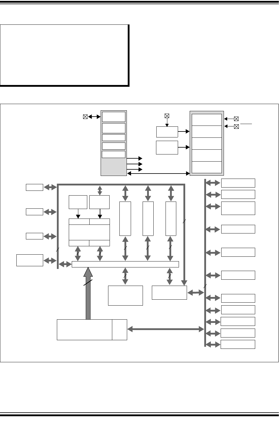
1.0 DEVICE OVERVIEW
This document contains device-specific information for
PIC32MX1XX/2XX 28/36/44-pin Family of devices.
Figure 1-1 illustrates a general block diagram of the
core and peripheral modules in the PIC32MX1XX/2XX
28/36/44-pin Family of devices.
Table 1-1 lists the functions of the various pins shown
in the pinout diagrams.
FIGURE 1-1: BLOCK DIAGRAM
Note: This data sheet summarizes the features
of the PIC32MX1XX/2XX 28/36/44-pin
Family of devices. It is not intended to be
a comprehensive reference source. To
complement the information in this data
sheet, refer to documents listed in the
Documentation > Reference Manual
section of the Microchip PIC32 web site
(www.microchip.com/pic32).
Note: Some features are not available on all devices. Refer to the family features tables (Ta b l e 1 and Table 2) for availability.
UART1-UART2
Comparators 1-3
PORTA
Remappable
PORTB
CTMU
JTAG Priority
DMAC
ICD
MIPS32
®
M4K
®
IS DS
EJTAG INT
Bus Matrix
Data RAM Peripheral Bridge
32
32-bit Wide
Flash
32 32
32 32
Peripheral Bus Clocked by PBCLK
Program Flash Memory
Controller
32
32 32
Interrupt
Controller
BSCAN
PORTC
PMP
I2C1-I2C2
SPI1-SPI2
IC1-IC5
PWM
OC1-OC5
OSC1/CLKI
OSC2/CLKO
V
DD
, V
SS
Timing
Generation
MCLR
Power-up
Timer
Oscillator
Start-up Timer
Power-on
Reset
Watchdog
Timer
Brown-out
Reset
Precision
Reference
Band Gap
FRC/LPRC
Oscillators Regulator
Voltage
V
CAP
OSC/S
OSC
Oscillators
PLL
Dividers
SYSCLK
PBCLK
Peripheral Bus Clocked by SYSCLK
USB
PLL-USB USBCLK
32
RTCC
10-bit ADC
Timer1-Timer5
32
32
CPU Core
Pins

PIC32MX1XX/2XX 28/36/44-PIN FAMILY
DS60001168K-page 20 2011-2018 Microchip Technology Inc.
TABLE 1-1: PINOUT I/O DESCRIPTIONS
Pin Name
Pin Number
(1)
Pin
Type Buffer
Type Description
28-pin
QFN
28-pin
SSOP/
SPDIP/
SOIC
36-pin
VTLA
44-pin
QFN/
TQFP/
VTLA
AN0 27 2 33 19 I Analog Analog input channels.
AN1 28 3 34 20 I Analog
AN2 1 4 35 21 I Analog
AN3 2 5 36 22 I Analog
AN4 3 6 1 23 I Analog
AN5 4 7 2 24 I Analog
AN6 — — 3 25 I Analog
AN7 — — 4 26 I Analog
AN8 — — — 27 I Analog
AN9 23262915IAnalog
AN10 22 25 28 14 I Analog
AN11 21 24 27 11 I Analog
AN12 20
(2)
23
(2)
26
(2)
10
(2)
IAnalog
11
(3)
36
(3)
CLKI 6 9 7 30 I ST/CMOS External clock source input. Always
associated with OSC1 pin function.
CLKO 7 10 8 31 O — Oscillator crystal output. Connects to
crystal or resonator in Crystal Oscillator
mode. Optionally functions as CLKO in
RC and EC modes. Always associated
with OSC2 pin function.
OSC1 6 9 7 30 I ST/CMOS Oscillator crystal input. ST buffer when
configured in RC mode; CMOS
otherwise.
OSC2 7 10 8 31 O — Oscillator crystal output. Connects to
crystal or resonator in Crystal Oscillator
mode. Optionally functions as CLKO in
RC and EC modes.
SOSCI 8 11 9 33 I ST/CMOS 32.768 kHz low-power oscillator crystal
input; CMOS otherwise.
SOSCO 9 12 10 34 O — 32.768 kHz low-power oscillator crystal
output.
REFCLKI PPS PPS PPS PPS I ST Reference Input Clock
REFCLKO PPS PPS PPS PPS O — Reference Output Clock
IC1 PPS PPS PPS PPS I ST Capture Inputs 1-5
IC2 PPS PPS PPS PPS I ST
IC3 PPS PPS PPS PPS I ST
IC4 PPS PPS PPS PPS I ST
IC5 PPS PPS PPS PPS I ST
Legend: CMOS = CMOS compatible input or output Analog = Analog input P = Power
S T = S c h m i t t Tr i g g e r i n p u t w i t h C M O S l e v e l s O = O u t p u t I = I n p u t
TTL = TTL input buffer PPS = Peripheral Pin Select — = N/A
Note 1: Pin numbers are provided for reference only. See the “Pin Diagrams” section for device pin availability.
2: Pin number for PIC32MX1XX devices only.
3: Pin number for PIC32MX2XX devices only.

2011-2018 Microchip Technology Inc. DS60001168K-page 21
PIC32MX1XX/2XX 28/36/44-PIN FAMILY
OC1 PPS PPS PPS PPS O — Output Compare Output 1
OC2 PPS PPS PPS PPS O — Output Compare Output 2
OC3 PPS PPS PPS PPS O — Output Compare Output 3
OC4 PPS PPS PPS PPS O — Output Compare Output 4
OC5 PPS PPS PPS PPS O — Output Compare Output 5
OCFA PPS PPS PPS PPS I ST Output Compare Fault A Input
OCFB PPS PPS PPS PPS I ST Output Compare Fault B Input
INT0 13 16 17 43 I ST External Interrupt 0
INT1 PPS PPS PPS PPS I ST External Interrupt 1
INT2 PPS PPS PPS PPS I ST External Interrupt 2
INT3 PPS PPS PPS PPS I ST External Interrupt 3
INT4 PPS PPS PPS PPS I ST External Interrupt 4
RA0 27 2 33 19 I/O ST PORTA is a bidirectional I/O port
RA1 28 3 34 20 I/O ST
RA2 6 9 7 30 I/O ST
RA3 710831I/OST
RA4 9 12 10 34 I/O ST
RA7 — — — 13 I/O ST
RA8 — — — 32 I/O ST
RA9 — — — 35 I/O ST
RA10 — — — 12 I/O ST
RB0 1 4 35 21 I/O ST PORTB is a bidirectional I/O port
RB1 2 5 36 22 I/O ST
RB2 3 6 1 23 I/O ST
RB3 4 7 2 24 I/O ST
RB4 8 11 9 33 I/O ST
RB5 11 141541I/OST
RB6 12
(2)
15
(2)
16
(2)
42
(2)
I/O ST
RB7 13161743I/OST
RB8 14171844I/OST
RB9 15 18 19 1 I/O ST
RB10 18 21 24 8 I/O ST
RB11 19 22 25 9 I/O ST
RB12 20
(2)
23
(2)
26
(2)
10
(2)
I/O ST
RB13 21 24 27 11 I/O ST
RB14 22 25 28 14 I/O ST
RB15 23 26 29 15 I/O ST
TABLE 1-1: PINOUT I/O DESCRIPTIONS (CONTINUED)
Pin Name
Pin Number
(1)
Pin
Type Buffer
Type Description
28-pin
QFN
28-pin
SSOP/
SPDIP/
SOIC
36-pin
VTLA
44-pin
QFN/
TQFP/
VTLA
Legend: CMOS = CMOS compatible input or output Analog = Analog input P = Power
S T = S c h m i t t Tr i g g e r i n p u t w i t h C M O S l e v e l s O = O u t p u t I = I n p u t
TTL = TTL input buffer PPS = Peripheral Pin Select — = N/A
Note 1: Pin numbers are provided for reference only. See the “Pin Diagrams” section for device pin availability.
2: Pin number for PIC32MX1XX devices only.
3: Pin number for PIC32MX2XX devices only.

PIC32MX1XX/2XX 28/36/44-PIN FAMILY
DS60001168K-page 22 2011-2018 Microchip Technology Inc.
RC0 — — 3 25 I/O ST PORTC is a bidirectional I/O port
RC1 — — 4 26 I/O ST
RC2 — — — 27 I/O ST
RC3 — — 11 36 I/O ST
RC4 — — — 37 I/O ST
RC5 — — — 38 I/O ST
RC6 — — — 2 I/O ST
RC7 — — — 3 I/O ST
RC8 — — — 4 I/O ST
RC9 — — 20 5 I/O ST
T1CK 9 12 10 34 I ST Timer1 external clock input
T2CK PPS PPS PPS PPS I ST Timer2 external clock input
T3CK PPS PPS PPS PPS I ST Timer3 external clock input
T4CK PPS PPS PPS PPS I ST Timer4 external clock input
T5CK PPS PPS PPS PPS I ST Timer5 external clock input
U1CTS PPS PPS PPS PPS I ST UART1 clear to send
U1RTS PPS PPS PPS PPS O — UART1 ready to send
U1RX PPS PPS PPS PPS I ST UART1 receive
U1TX PPS PPS PPS PPS O—UART1 transmit
U2CTS PPS PPS PPS PPS I ST UART2 clear to send
U2RTS PPS PPS PPS PPS O — UART2 ready to send
U2RX PPS PPS PPS PPS IST
UART2 receive
U2TX PPS PPS PPS PPS O—
UART2 transmit
SCK1 22 25 28 14 I/O ST Synchronous serial clock input/output for
SPI1
SDI1 PPS PPS PPS PPS IST
SPI1 data in
SDO1 PPS PPS PPS PPS O—
SPI1 data out
SS1 PPS PPS PPS PPS I/O ST SPI1 slave synchronization or frame
pulse I/O
SCK2 23 26 29 15 I/O ST Synchronous serial clock input/output for
SPI2
SDI2 PPS PPS PPS PPS IST
SPI2 data in
SDO2 PPS PPS PPS PPS O—
SPI2 data out
SS2 PPS PPS PPS PPS I/O ST SPI2 slave synchronization or frame
pulse I/O
SCL1 14 17 18 44 I/O ST Synchronous serial clock input/output for
I2C1
TABLE 1-1: PINOUT I/O DESCRIPTIONS (CONTINUED)
Pin Name
Pin Number
(1)
Pin
Type Buffer
Type Description
28-pin
QFN
28-pin
SSOP/
SPDIP/
SOIC
36-pin
VTLA
44-pin
QFN/
TQFP/
VTLA
Legend: CMOS = CMOS compatible input or output Analog = Analog input P = Power
S T = S c h m i t t Tr i g g e r i n p u t w i t h C M O S l e v e l s O = O u t p u t I = I n p u t
TTL = TTL input buffer PPS = Peripheral Pin Select — = N/A
Note 1: Pin numbers are provided for reference only. See the “Pin Diagrams” section for device pin availability.
2: Pin number for PIC32MX1XX devices only.
3: Pin number for PIC32MX2XX devices only.

2011-2018 Microchip Technology Inc. DS60001168K-page 23
PIC32MX1XX/2XX 28/36/44-PIN FAMILY
SDA1 15 18 19 1 I/O ST Synchronous serial data input/output for
I2C1
SCL2 4 7 2 24 I/O ST Synchronous serial clock input/output for
I2C2
SDA2 3 6 1 23 I/O ST Synchronous serial data input/output for
I2C2
TMS 19
(2)
22
(2)
25
(2)
12 I ST JTAG Test mode select pin
11
(3)
14
(3)
15
(3)
TCK 14171813ISTJTAG test clock input pin
TDI 13 16 17 35 O — JTAG test data input pin
TDO 15 18 19 32 O — JTAG test data output pin
RTCC 4 7 2 24 O ST Real-Time Clock alarm output
C
VREF
- 28 3 34 20 I Analog Comparator Voltage Reference (low)
C
VREF
+ 27 2 33 19 I Analog Comparator Voltage Reference (high)
C
VREFOUT
22 25 28 14 O Analog Comparator Voltage Reference output
C1INA 4 7 2 24 I Analog Comparator Inputs
C1INB 3 6 1 23 I Analog
C1INC 2 5 36 22 I Analog
C1IND 1 4 35 21 I Analog
C2INA 2 5 36 22 I Analog
C2INB 1 4 35 21 I Analog
C2INC 4 7 2 24 I Analog
C2IND 3 6 1 23 I Analog
C3INA 23262915IAnalog
C3INB 22252814IAnalog
C3INC 27 2 33 19 I Analog
C3IND 1 4 35 21 I Analog
C1OUT PPS PPS PPS PPS O — Comparator Outputs
C2OUT PPS PPS PPS PPS O —
C3OUT PPS PPS PPS PPS O —
TABLE 1-1: PINOUT I/O DESCRIPTIONS (CONTINUED)
Pin Name
Pin Number
(1)
Pin
Type Buffer
Type Description
28-pin
QFN
28-pin
SSOP/
SPDIP/
SOIC
36-pin
VTLA
44-pin
QFN/
TQFP/
VTLA
Legend: CMOS = CMOS compatible input or output Analog = Analog input P = Power
S T = S c h m i t t Tr i g g e r i n p u t w i t h C M O S l e v e l s O = O u t p u t I = I n p u t
TTL = TTL input buffer PPS = Peripheral Pin Select — = N/A
Note 1: Pin numbers are provided for reference only. See the “Pin Diagrams” section for device pin availability.
2: Pin number for PIC32MX1XX devices only.
3: Pin number for PIC32MX2XX devices only.

PIC32MX1XX/2XX 28/36/44-PIN FAMILY
DS60001168K-page 24 2011-2018 Microchip Technology Inc.
PMA0 7 10 8 3 I/O TTL/ST Parallel Master Port Address bit 0 input
(Buffered Slave modes) and output
(Master modes)
PMA1 9 12 10 2 I/O TTL/ST Parallel Master Port Address bit 1 input
(Buffered Slave modes) and output
(Master modes)
PMA2 — — 27 O — Parallel Master Port address
(Demultiplexed Master modes)
PMA3 — — 38 O —
PMA4 — — 37 O —
PMA5 — — 4 O —
PMA6 — — 5 O —
PMA7 — — 13 O —
PMA8 — — 32 O —
PMA9 — — 35 O —
PMA10 — — 12 O —
PMCS1 23 26 29 15 O — Parallel Master Port Chip Select 1 strobe
PMD0 20
(2)
23
(2)
26
(2)
10
(2)
I/O TTL/ST Parallel Master Port data (Demultiplexed
Master mode) or address/data
(Multiplexed Master modes)
1
(3)
4
(3)
35
(3)
21
(3)
PMD1 19
(2)
22
(2)
25
(2)
9
(2)
I/O TTL/ST
2
(3)
5
(3)
36
(3)
22
(3)
PMD2 18
(2)
21
(2)
24
(2)
8
(2)
I/O TTL/ST
3
(3)
6
(3)
1
(3)
23
(3)
PMD3 15 18 19 1 I/O TTL/ST
PMD4 14 17 18 44 I/O TTL/ST
PMD5 13 16 17 43 I/O TTL/ST
PMD6 12
(2)
15
(2)
16
(2)
42
(2)
I/O TTL/ST
28
(3)
3
(3)
34
(3)
20
(3)
PMD7 11
(2)
14
(2)
15
(2)
41
(2)
I/O TTL/ST
27
(3)
2
(3)
33
(3)
19
(3)
PMRD 21 24 27 11 O — Parallel Master Port read strobe
PMWR 22
(2)
25
(2)
28
(2)
14
(2)
O — Parallel Master Port write strobe
4
(3)
7
(3)
2
(3)
24
(3)
V
BUS
12
(3)
15
(3)
16
(3)
42
(3)
I Analog USB bus power monitor
V
USB
3
V
3
20
(3)
23
(3)
26
(3)
10
(3)
P — USB internal transceiver supply. This pin
must be connected to V
DD
.
V
BUSON
22
(3)
25
(3)
28
(3)
14
(3)
O — USB Host and OTG bus power control
output
D+ 18
(3)
21
(3)
24
(3)
8
(3)
I/O Analog USB D+
D- 19
(3)
22
(3)
25
(3)
9
(3)
I/O Analog USB D-
TABLE 1-1: PINOUT I/O DESCRIPTIONS (CONTINUED)
Pin Name
Pin Number
(1)
Pin
Type Buffer
Type Description
28-pin
QFN
28-pin
SSOP/
SPDIP/
SOIC
36-pin
VTLA
44-pin
QFN/
TQFP/
VTLA
Legend: CMOS = CMOS compatible input or output Analog = Analog input P = Power
S T = S c h m i t t Tr i g g e r i n p u t w i t h C M O S l e v e l s O = O u t p u t I = I n p u t
TTL = TTL input buffer PPS = Peripheral Pin Select — = N/A
Note 1: Pin numbers are provided for reference only. See the “Pin Diagrams” section for device pin availability.
2: Pin number for PIC32MX1XX devices only.
3: Pin number for PIC32MX2XX devices only.

2011-2018 Microchip Technology Inc. DS60001168K-page 25
PIC32MX1XX/2XX 28/36/44-PIN FAMILY
USBID 11
(3)
14
(3)
15
(3)
41
(3)
I ST USB OTG ID detect
CTED1 27 2 33 19 I ST CTMU External Edge Input
CTED2 28 3 34 20 I ST
CTED313161743IST
CTED4 15 18 19 1 I ST
CTED522252814IST
CTED623262915IST
CTED7 — — 20 5 I ST
CTED8 — — — 13 I ST
CTED9 9 12 10 34 I ST
CTED10 14 17 18 44 I ST
CTED11 18 21 24 8 I ST
CTED12 2 5 36 22 I ST
CTED13 3 6 1 23 I ST
CTPLS 21 24 27 11 O — CTMU Pulse Output
PGED1 1 4 35 21 I/O ST Data I/O pin for Programming/Debugging
Communication Channel 1
PGEC1 2 5 36 22 I ST Clock input pin for
Programming/Debugging
Communication Channel 1
PGED2 18 21 24 8 I/O ST Data I/O pin for Programming/Debugging
Communication Channel 2
PGEC2 19 22 25 9 I ST Clock input pin for
Programming/Debugging
Communication Channel 2
PGED3 11
(2)
14
(2)
15
(2)
41
(2)
I/O ST Data I/O pin for Programming/Debugging
Communication Channel 3
27
(3)
2
(3)
33
(3)
19
(3)
PGEC3 12
(2)
15
(2)
16
(2)
42
(2)
IST
Clock input pin for Programming/
Debugging Communication Channel 3
28
(3)
3
(3)
34
(3)
20
(3)
PGED4 — — 3 12 I/O ST Data I/O pin for Programming/Debugging
Communication Channel 4
PGEC4 — — 4 13 IST
Clock input pin for Programming/
Debugging Communication Channel 4
TABLE 1-1: PINOUT I/O DESCRIPTIONS (CONTINUED)
Pin Name
Pin Number
(1)
Pin
Type Buffer
Type Description
28-pin
QFN
28-pin
SSOP/
SPDIP/
SOIC
36-pin
VTLA
44-pin
QFN/
TQFP/
VTLA
Legend: CMOS = CMOS compatible input or output Analog = Analog input P = Power
S T = S c h m i t t Tr i g g e r i n p u t w i t h C M O S l e v e l s O = O u t p u t I = I n p u t
TTL = TTL input buffer PPS = Peripheral Pin Select — = N/A
Note 1: Pin numbers are provided for reference only. See the “Pin Diagrams” section for device pin availability.
2: Pin number for PIC32MX1XX devices only.
3: Pin number for PIC32MX2XX devices only.
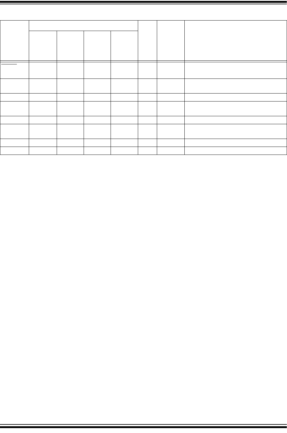
PIC32MX1XX/2XX 28/36/44-PIN FAMILY
DS60001168K-page 26 2011-2018 Microchip Technology Inc.
MCLR 26 1 32 18 I/P ST Master Clear (Reset) input. This pin is an
active-low Reset to the device.
AV
DD
25 28 31 17 P — Positive supply for analog modules. This
pin must be connected at all times.
AV
SS
24 27 30 16 P — Ground reference for analog modules
V
DD
10 13 5, 13, 14,
23
28, 40 P — Positive supply for peripheral logic and
I/O pins
V
CAP
17 20 22 7 P — CPU logic filter capacitor connection
V
SS
5, 16 8, 19 6, 12, 21 6, 29, 39 P — Ground reference for logic and I/O pins.
This pin must be connected at all times.
V
REF
+ 27 2 33 19 I Analog Analog voltage reference (high) input
V
REF
- 28 3 34 20 I Analog Analog voltage reference (low) input
TABLE 1-1: PINOUT I/O DESCRIPTIONS (CONTINUED)
Pin Name
Pin Number
(1)
Pin
Type Buffer
Type Description
28-pin
QFN
28-pin
SSOP/
SPDIP/
SOIC
36-pin
VTLA
44-pin
QFN/
TQFP/
VTLA
Legend: CMOS = CMOS compatible input or output Analog = Analog input P = Power
S T = S c h m i t t Tr i g g e r i n p u t w i t h C M O S l e v e l s O = O u t p u t I = I n p u t
TTL = TTL input buffer PPS = Peripheral Pin Select — = N/A
Note 1: Pin numbers are provided for reference only. See the “Pin Diagrams” section for device pin availability.
2: Pin number for PIC32MX1XX devices only.
3: Pin number for PIC32MX2XX devices only.

2011-2018 Microchip Technology Inc. DS60001168K-page 27
PIC32MX1XX/2XX 28/36/44-PIN FAMILY
2.0 GUIDELINES FOR GETTING
STARTED WITH 32-BIT MCUs
2.1 Basic Connection Requirements
Getting started with the PIC32MX1XX/2XX 28/36/44-
pin Family of 32-bit Microcontrollers (MCUs) requires
attention to a minimal set of device pin connections
before proceeding with development. The following is a
list of pin names, which must always be connected:
•All V
DD
and V
SS
pins (see 2.2 “Decoupling
Capacitors”)
•All AV
DD
and AV
SS
pins, even if the ADC module
is not used (see 2.2 “Decoupling Capacitors”)
•V
CAP
pin (see 2.3 “Capacitor on Internal
Voltage Regulator (V
CAP
)”)
•MCLR pin (see 2.4 “Master Clear (MCLR) Pin”)
• PGECx/PGEDx pins, used for In-Circuit Serial
Programming™ (ICSP™) and debugging pur-
poses (see 2.5 “ICSP Pins”)
• OSC1 and OSC2 pins, when external oscillator
source is used (see 2.7 “External Oscillator
Pins”)
The following pins may be required:
•V
REF
+/V
REF
- pins – used when external voltage
reference for the ADC module is implemented
2.2 Decoupling Capacitors
The use of decoupling capacitors on power supply
pins, such as V
DD
, V
SS
, AV
DD
and AV
SS
is required.
See Figure 2-1.
Consider the following criteria when using decoupling
capacitors:
•Value and type of capacitor: A value of 0.1 µF
(100 nF), 10-20V is recommended. The capacitor
should be a low Equivalent Series Resistance
(low-ESR) capacitor and have resonance fre-
quency in the range of 20 MHz and higher. It is
further recommended that ceramic capacitors be
used.
•Placement on the printed circuit board: The
decoupling capacitors should be placed as close
to the pins as possible. It is recommended that
the capacitors be placed on the same side of the
board as the device. If space is constricted, the
capacitor can be placed on another layer on the
PCB using a via; however, ensure that the trace
length from the pin to the capacitor is within one-
quarter inch (6 mm) in length.
•Handling high frequency noise: If the board is
experiencing high frequency noise, upward of
tens of MHz, add a second ceramic-type capacitor
in parallel to the above described decoupling
capacitor. The value of the second capacitor can
be in the range of 0.01 µF to 0.001 µF. Place this
second capacitor next to the primary decoupling
capacitor. In high-speed circuit designs, consider
implementing a decade pair of capacitances as
close to the power and ground pins as possible.
For example, 0.1 µF in parallel with 0.001 µF.
•Maximizing performance: On the board layout
from the power supply circuit, run the power and
return traces to the decoupling capacitors first,
and then to the device pins. This ensures that the
decoupling capacitors are first in the power chain.
Equally important is to keep the trace length
between the capacitor and the power pins to a
minimum thereby reducing PCB track inductance.
Note: This data sheet summarizes the features
of the PIC32MX1XX/2XX 28/36/44-pin
Family of devices. It is not intended to be
a comprehensive reference source. To
complement the information in this data
sheet, refer to the documents listed in the
Documentation > Reference Manual
section of the Microchip PIC32 web site
(www.microchip.com/pic32).
Note: The AV
DD
and AV
SS
pins must be con-
nected, regardless of ADC use and the
ADC voltage reference source.
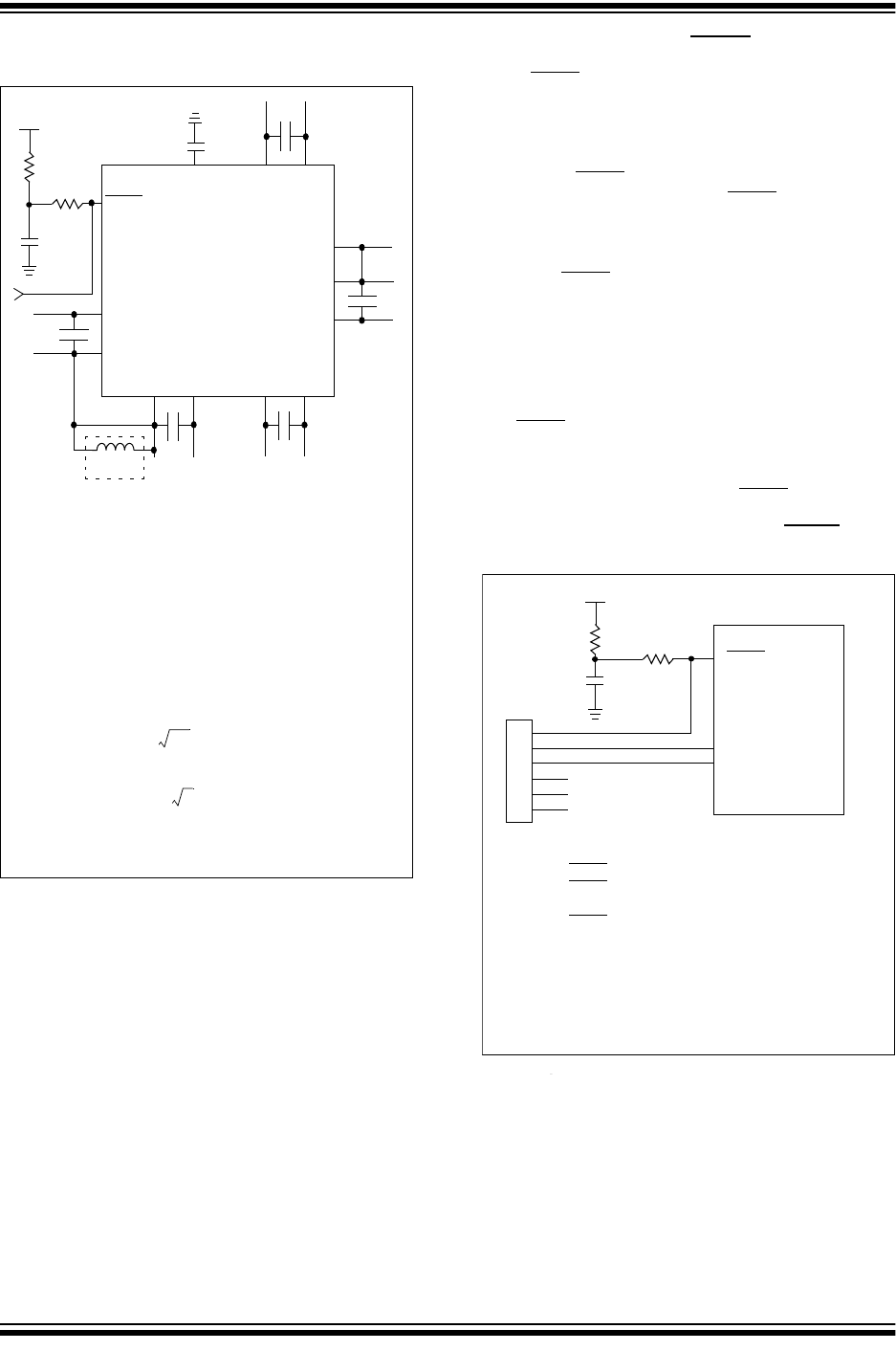
PIC32MX1XX/2XX 28/36/44-PIN FAMILY
DS60001168K-page 28 2011-2018 Microchip Technology Inc.
FIGURE 2-1: RECOMMENDED
MINIMUM CONNECTION
2.2.1 BULK CAPACITORS
The use of a bulk capacitor is recommended to improve
power supply stability. Typical values range from 4.7 µF
to 47 µF. This capacitor should be located as close to
the device as possible.
2.3 Capacitor on Internal Voltage
Regulator (V
CAP
)
2.3.1 INTERNAL REGULATOR MODE
A low-ESR (3 ohm) capacitor is required on the V
CAP
pin, which is used to stabilize the internal voltage
regulator output. The V
CAP
pin must not be connected
to V
DD
, and must have a C
EFC
capacitor, with at least a
6V rating, connected to ground. The type can be
ceramic or tantalum. Refer to 30.0 “Electrical
Characteristics” for additional information on C
EFC
specifications.
2.4 Master Clear (MCLR) Pin
The MCLR pin provides two specific device
functions:
• Device Reset
• Device programming and debugging
Pulling The MCLR pin low generates a device Reset.
Figure 2-2 illustrates a typical MCLR circuit. During
device programming and debugging, the resistance
and capacitance that can be added to the pin must
be considered. Device programmers and debuggers
drive the MCLR pin. Consequently, specific voltage
levels (V
IH
and V
IL
) and fast signal transitions must
not be adversely affected. Therefore, specific values
of R and C will need to be adjusted based on the
application and PCB requirements.
For example, as illustrated in Figure 2-2, it is
recommended that the capacitor C, be isolated from
the MCLR pin during programming and debugging
operations.
Place the components illustrated in Figure 2-2 within
one-quarter inch (6 mm) from the MCLR pin.
FIGURE 2-2: EXAMPLE OF MCLR PIN
CONNECTIONS
2.5 ICSP Pins
The PGECx and PGEDx pins are used for ICSP and
debugging purposes. It is recommended to keep the
trace length between the ICSP connector and the ICSP
pins on the device as short as possible. If the ICSP con-
nector is expected to experience an ESD event, a
series resistor is recommended, with the value in the
range of a few tens of Ohms, not to exceed 100 Ohms.
PIC32
V
DD
V
SS
V
DD
V
SS
V
SS
V
DD
AV
DD
AV
SS
V
DD
V
SS
0.1 µF
Ceramic
0.1 µF
Ceramic
0.1 µF
Ceramic
0.1 µF
Ceramic
C
10K
V
DD
MCLR
0.1 µF
Ceramic
L1
(2)
R1
Note 1: If the USB module is not used, this pin must be
connected to V
DD
.
2: As an option, instead of a hard-wired connection, an
inductor (L1) can be substituted between V
DD
and
AV
DD
to improve ADC noise rejection. The inductor
impedance should be less than 3 and the inductor
capacity greater than 10 mA.
Where:
fF
CNV
2
--------------
f1
2LC
-----------------------
L1
2fC
----------------------
2
(i.e., ADC conversion rate/2)
Connect
(2)
V
USB
3
V
3
(1)
V
CAP
Tantalum or
ceramic 10 µF
ESR 3
(3)
1: Aluminum or electrolytic capacitors should not be
used. ESR 3 from -40ºC to 125ºC @ SYSCLK
frequency (i.e., MIPS).
1K
0.1 µF
Note 1: 470R1 1 will limit any current flowing into
MCLR from the external capacitor C, in the event of
MCLR pin breakdown, due to Electrostatic Discharge
(ESD) or Electrical Overstress (EOS). Ensure that the
MCLR pin V
IH
and V
IL
specifications are met without
interfering with the Debug/Programmer tools.
2: The capacitor can be sized to prevent unintentional
Resets from brief glitches or to extend the device
Reset period during POR.
3: No pull-ups or bypass capacitors are allowed on
active debug/program PGECx/PGEDx pins.
R1
(1)
10k
V
DD
MCLR
PIC32
1 k
0.1 µF
(2)
PGECx
(3)
PGEDx
(3)
ICSP™
1
5
4
2
3
6
V
DD
V
SS
NC
R
C
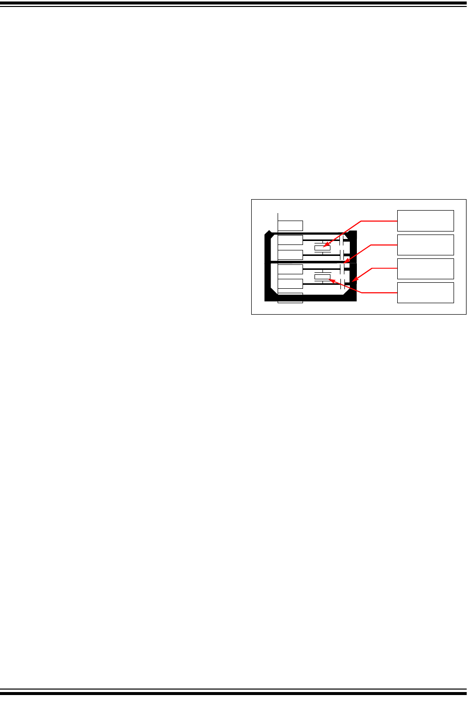
2011-2018 Microchip Technology Inc. DS60001168K-page 29
PIC32MX1XX/2XX 28/36/44-PIN FAMILY
Pull-up resistors, series diodes and capacitors on the
PGECx and PGEDx pins are not recommended as they
will interfere with the programmer/debugger communi-
cations to the device. If such discrete components are
an application requirement, they should be removed
from the circuit during programming and debugging.
Alternatively, refer to the AC/DC characteristics and
timing requirements information in the respective
device Flash programming specification for information
on capacitive loading limits and pin input voltage high
(V
IH
) and input low (V
IL
) requirements.
Ensure that the “Communication Channel Select” (i.e.,
PGECx/PGEDx pins) programmed into the device
matches the physical connections for the ICSP to
MPLAB
®
ICD 3 or MPLAB REAL ICE™.
For more information on ICD 3 and REAL ICE
connection requirements, refer to the following
documents that are available on the Microchip web
site:
•“Using MPLAB
®
ICD 3” (poster) (DS50001765)
•“MPLAB
®
ICD 3 Design Advisory” (DS50001764)
•“MPLAB
®
REAL ICE™ In-Circuit Debugger
User’s Guide” (DS50001616)
•“Using MPLAB
®
REAL ICE™ Emulator” (poster)
(DS50001749)
2.6 JTAG
The TMS, TDO, TDI and TCK pins are used for testing
and debugging according to the Joint Test Action
Group (JTAG) standard. It is recommended to keep the
trace length between the JTAG connector and the
JTAG pins on the device as short as possible. If the
JTAG connector is expected to experience an ESD
event, a series resistor is recommended with the value
in the range of a few tens of Ohms, not to exceed 100
Ohms.
Pull-up resistors, series diodes and capacitors on the
TMS, TDO, TDI and TCK pins are not recommended
as they will interfere with the programmer/debugger
communications to the device. If such discrete compo-
nents are an application requirement, they should be
removed from the circuit during programming and
debugging. Alternatively, refer to the AC/DC character-
istics and timing requirements information in the
respective device Flash programming specification for
information on capacitive loading limits and pin input
voltage high (V
IH
) and input low (V
IL
) requirements.
2.7 External Oscillator Pins
Many MCUs have options for at least two oscillators: a
high-frequency primary oscillator and a low-frequency
secondary oscillator (refer to Section 8.0 “Oscillator
Configuration” for details).
The oscillator circuit should be placed on the same side
of the board as the device. Also, place the oscillator cir-
cuit close to the respective oscillator pins, not exceed-
ing one-half inch (12 mm) distance between them. The
load capacitors should be placed next to the oscillator
itself, on the same side of the board. Use a grounded
copper pour around the oscillator circuit to isolate them
from surrounding circuits. The grounded copper pour
should be routed directly to the MCU ground. Do not
run any signal traces or power traces inside the ground
pour. Also, if using a two-sided board, avoid any traces
on the other side of the board where the crystal is
placed. A suggested layout is illustrated in Figure 2-3.
FIGURE 2-3: SUGGESTED OSCILLATOR
CIRCUIT PLACEMENT
2.8 Unused I/Os
Unused I/O pins should not be allowed to float as
inputs. They can be configured as outputs and driven
to a logic-low state.
Alternatively, inputs can be reserved by connecting the
pin to V
SS
through a 1k to 10k resistor and configuring
the pin as an input.
Main Oscillator
Guard Ring
Guard Trace
Secondary
Oscillator
PIC32MX1XX/2XX 28/36/44-PIN FAMILY
DS60001168K-page 30 2011-2018 Microchip Technology Inc.
2.8.1 CRYSTAL OSCILLATOR DESIGN
CONSIDERATION
The following example assumptions are used to
calculate the Primary Oscillator loading capacitor
values:
•C
IN
= PIC32_OSC2_Pin Capacitance = ~4-5 pF
•C
OUT
= PIC32_OSC1_Pin Capacitance = ~4-5 pF
• C1 and C2 = XTAL manufacturing recommended
loading capacitance
• Estimated PCB stray capacitance, (i.e.,12 mm
length) = 2.5 pF
EXAMPLE 2-1: CRYSTAL LOAD CAPACITOR
CALCULATION
The following tips are used to increase oscillator gain,
(i.e., to increase peak-to-peak oscillator signal):
• Select a crystal with a lower “minimum” power drive
rating
• Select an crystal oscillator with a lower XTAL
manufacturing “ESR” rating.
• Add a parallel resistor across the crystal. The smaller
the resistor value the greater the gain. It is recom-
mended to stay in the range of 600k to 1M
• C1 and C2 values also affect the gain of the oscillator.
The lower the values, the higher the gain.
• C2/C1 ratio also affects gain. To increase the gain,
make C1 slightly smaller than C2, which will also help
start-up performance.
2.8.1.1 Additional Microchip References
• AN588 “PICmicro
®
Microcontroller Oscillator
Design Guide”
• AN826 “Crystal Oscillator Basics and Crystal
Selection for rfPIC™ and PICmicro
®
Devices”
• AN849 “Basic PICmicro
®
Oscillator Design”
FIGURE 2-4: PRIMARY CRYSTAL
OSCILLATOR CIRCUIT
RECOMMENDATIONS
Note: Do not add excessive gain such that the
oscillator signal is clipped, flat on top of
the sine wave. If so, you need to reduce
the gain or add a series resistor, RS, as
shown in circuit “C” in Figure 2-4. Failure
to do so will stress and age the crystal,
which can result in an early failure. Adjust
the gain to trim the max peak-to-peak to
~V
DD
-0.6V. When measuring the oscilla-
tor signal you must use a FET scope
probe or a probe with 1.5 pF or the
scope probe itself will unduly change the
gain and peak-to-peak levels.
Crystal manufacturer recommended: C1 = C2 = 15 pF
Therefore:
C
LOAD
= {( [C
IN
+ C1] * [C
OUT
+ C2]) / [C
IN
+ C1 + C2 + C
OUT
]}
+ estimated oscillator PCB stray capacitance
= {( [5 + 15][5 + 15] ) / [5 + 15 + 15 + 5] } + 2.5 pF
= {( [20][20]) / [40] } + 2.5
= 10 + 2.5 = 12.5 pF
Rounded to the nearest standard value or 12 pF in this example for
Primary Oscillator crystals “C1” and “C2”.
OSC2 OSC1
1M
Typical XT
(4-10 MHz)
Circuit A
C1
C2
OSC2 OSC1
Typical HS
(10-25 MHz)
Circuit B
C1
C2
Rs
OSC2 OSC1
1M
Typical XT/HS
(4-25 MHz)
Circuit C
C1
C2
1M
Rs
OSC2 OSC1
Not Recommended
Circuit D
Not Recommended
1M
Rs
OSC2 OSC1
Circuit E
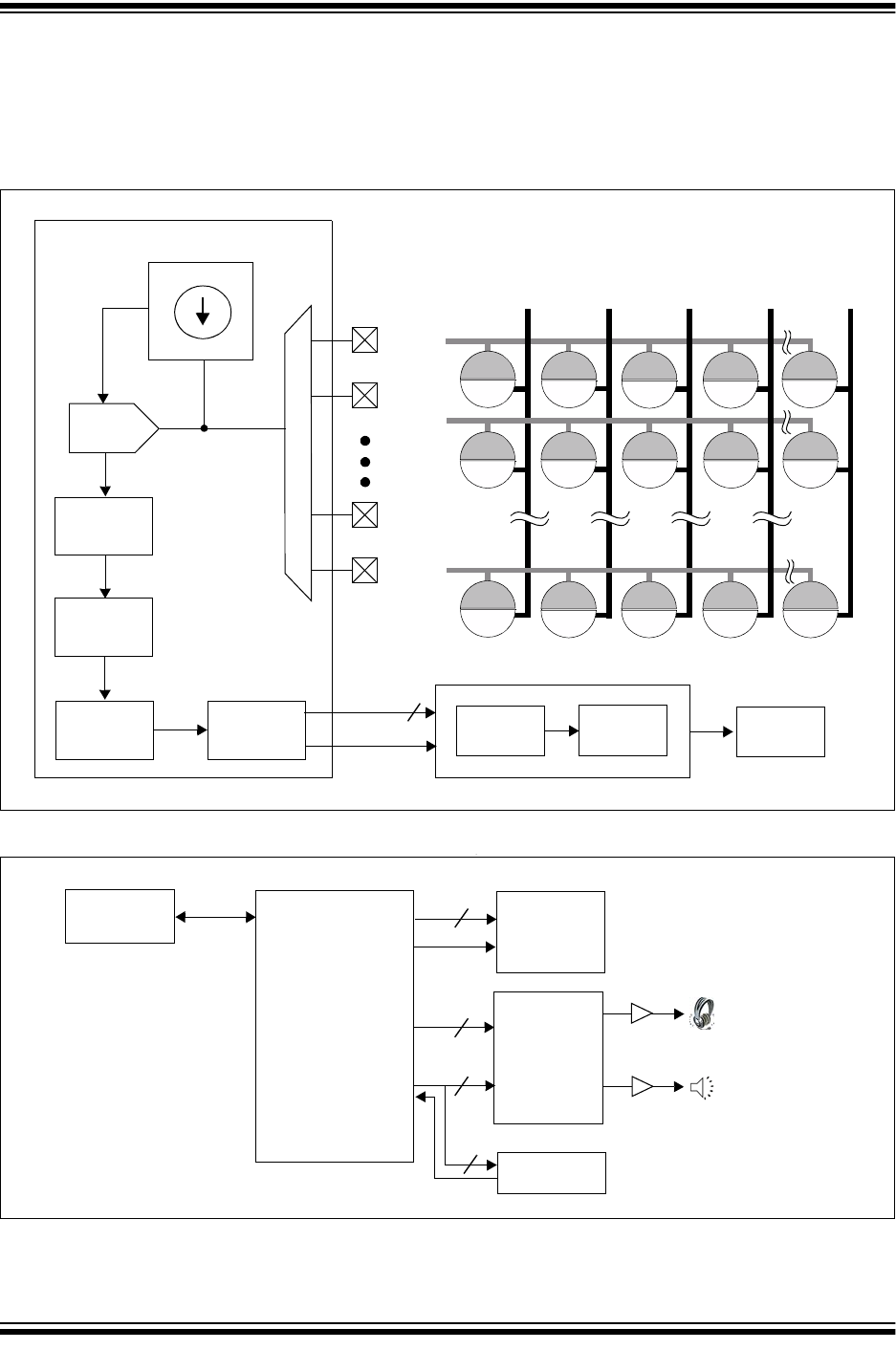
2011-2018 Microchip Technology Inc. DS60001168K-page 31
PIC32MX1XX/2XX 28/36/44-PIN FAMILY
2.9 Typical Application Connection
Examples
Examples of typical application connections are shown
in Figure 2-5 and Figure 2-6.
FIGURE 2-5: CAPACITIVE TOUCH SENSING WITH GRAPHICS APPLICATION
FIGURE 2-6: AUDIO PLAYBACK APPLICATION
CTMU
Current Source
ADC
Microchip
mTouch™
Library
User
Application
Microchip
Graphics
Library
Read the Touch Sensors
Process Samples
Display Data
Parallel
Master
Port
LCD Controller
Frame
Buffer
Display
Controller
PMPD<7:0>
LCD
Panel
PIC32MX120F032D
To AN6 To AN7 To AN8 To AN11
C1
R3
C2
R2
R3
R1
C5
C5
C5
C1
R1 R1 R1
C3
R2
C3
R2
C1
R2
C2
R3
C2
R3
C3
AN0
AN1
AN11
To AN0
To A N 1
To AN5
AN9
PMPWR
To AN9
R1
C4
R2
C4
R3
C4
Audio
Codec
Display
PMP
I
2
S
SPI
USB
USB
PMPD<7:0>
3
3
Stereo Headphones
Speaker
PIC32MX220F032D
Host
PMPWR
MMC SD
3
SDI
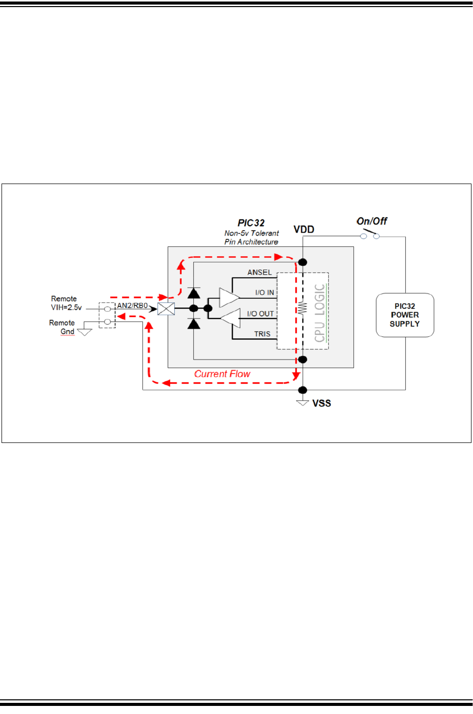
PIC32MX1XX/2XX 28/36/44-PIN FAMILY
DS60001168K-page 32 2011-2018 Microchip Technology Inc.
2.10 Considerations When Interfacing
To Remotely Powered Circuits
2.10.1 NON-5V TOLERANT INPUT PINS
A quick review of the maximum rating section in the
Section 30.0 “Electrical Characteristics” will
indicate that the voltage on any non-5V tolerant pin
should not exceed AVDD/VDD+0.3V. Figure 2-7
illustrates a remote circuit using an independent power
source that is powered while connected to a PIC32
non-5V tolerant circuit which is not powered.
FIGURE 2-7: REMOTE CIRCUIT WITH AN INDEPENDENT POWER SOURCE
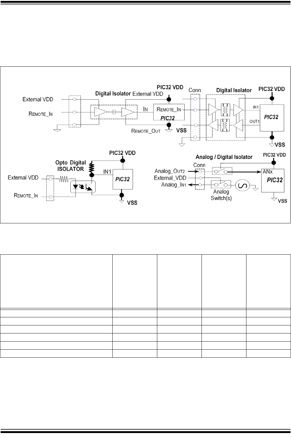
2011-2018 Microchip Technology Inc. DS60001168K-page 33
PIC32MX1XX/2XX 28/36/44-PIN FAMILY
Without proper signal isolation on non-5V tolerant
pins, the remote signal can power the PIC32 through
the high side ESD protection diodes. This violates the
maximum rating specification and can cause improper
initialization of internal PIC32 logic circuits. In this
case, it is recommended that users can implement a
digital or analog signal isolation, as shown in Figure 2-
8.
FIGURE 2-8: DIGITAL AND ANALOG SIGNAL ISOLATION
Digital signal isolators along with optional level
translation examples are provided in Ta bl e 2 - 1 .
TABLE 2-1: EXAMPLES OF DIGITAL ISOLATORS WITH OPTIONAL LEVEL TRANSLATION
Inductive Coupling
Capacitive Coupling
Optional Coupling
Analog/Digital Switch
ADuM7241 / 40 ARZ (1Mbps) X - - -
ADuM7241 / 40 CRZ (25 Mbps) X - - -
ISO721 - X - -
LTV-829S (2 Chan) - - X -
LTV-849S (4 Chan) ----
FSA266 / NC7WB66 - - - X
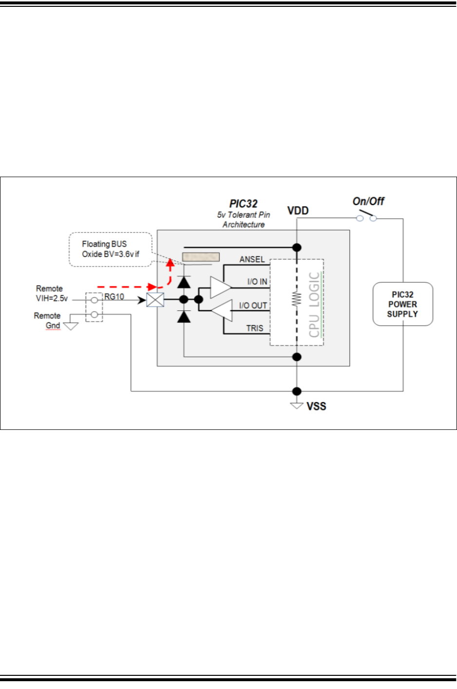
PIC32MX1XX/2XX 28/36/44-PIN FAMILY
DS60001168K-page 34 2011-2018 Microchip Technology Inc.
2.10.2 5V-TOLERANT INPUT PINS
The internal high-side diode on 5V-tolerant pins, rather
than being connected to VDD, are bussed to an
internal floating node, as shown in Figure 2-9.
Voltages on these pins, if VDD < 2.3V, should not
exceed roughly 3.2V relative to PIC32 VSS. At 3.6V or
above, it will violate the absolute maximum
specification and impact the device reliability.
If a remotely powered digital only signal can be
guaranteed to always be ≤ 3.2V relative to PIC32 VSS,
then a 5V-tolerant pin can be used without a digital
isolator. This can be assumed when the following is
applicable:
• No ground loop issue
• The logic ground of the two circuits is not at the
same absolute level
• No remote logic low inputs are less than VSS -
0.3V
FIGURE 2-9: 5V-TOLERANT INPUT PINS BUSSED TO AN INTERNAL FLOATING NODE
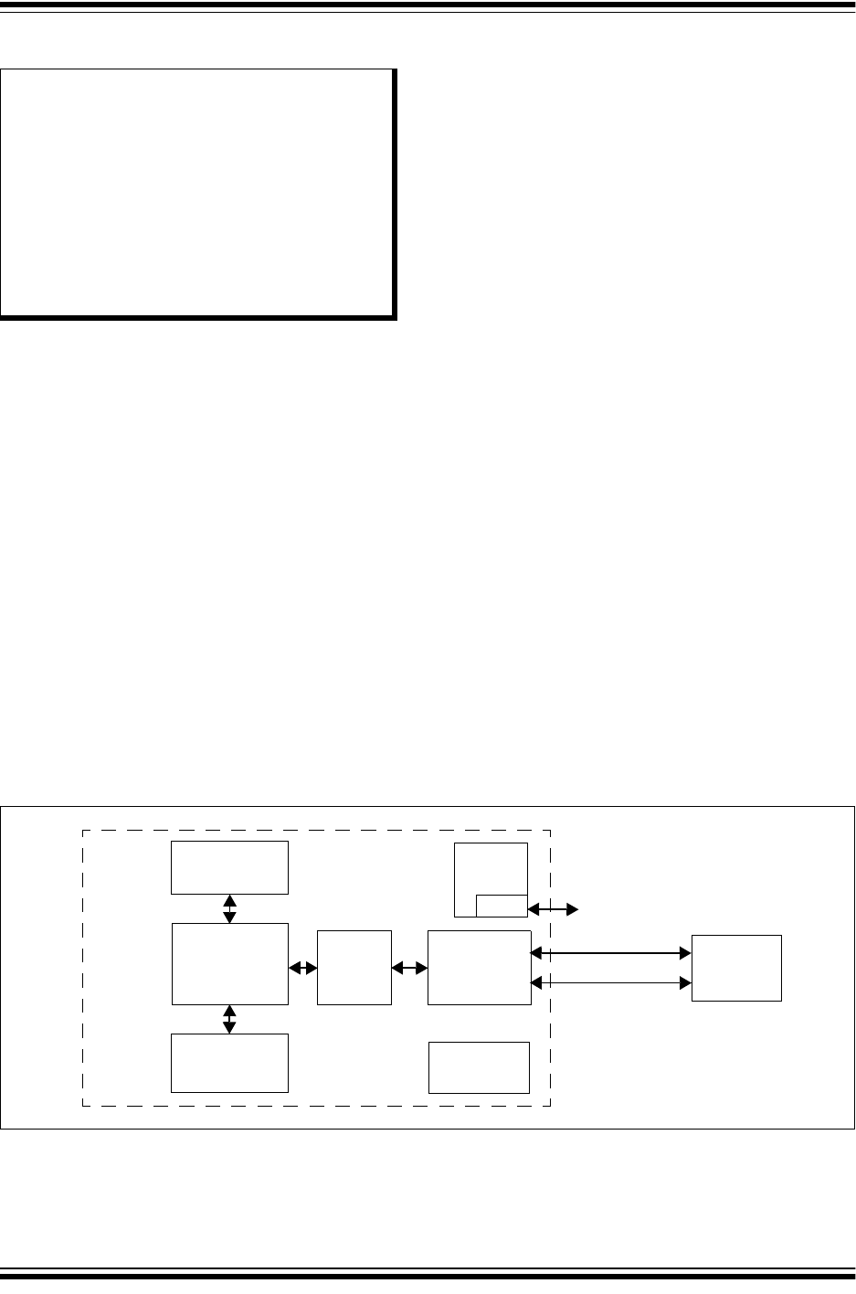
2011-2018 Microchip Technology Inc. DS60001168K-page 35
PIC32MX1XX/2XX 28/36/44-PIN FAMILY
3.0 CPU
The MIPS32
®
M4K
®
Processor Core is the heart of the
PIC32MX1XX/2XX family processor. The CPU fetches
instructions, decodes each instruction, fetches source
operands, executes each instruction and writes the
results of instruction execution to the destinations.
3.1 Features
• 5-stage pipeline
• 32-bit address and data paths
• MIPS32 Enhanced Architecture (Release 2)
- Multiply-accumulate and multiply-subtract
instructions
- Targeted multiply instruction
- Zero/One detect instructions
-WAIT instruction
- Conditional move instructions (MOVN, MOVZ)
- Vectored interrupts
- Programmable exception vector base
- Atomic interrupt enable/disable
- Bit field manipulation instructions
• MIPS16e
®
code compression
- 16-bit encoding of 32-bit instructions to
improve code density
- Special PC-relative instructions for efficient
loading of addresses and constants
-SAVE and RESTORE macro instructions for
setting up and tearing down stack frames
within subroutines
- Improved support for handling 8 and 16-bit
data types
• Simple Fixed Mapping Translation (FMT)
mechanism
• Simple dual bus interface
- Independent 32-bit address and data buses
- Transactions can be aborted to improve
interrupt latency
• Autonomous multiply/divide unit
- Maximum issue rate of one 32x16 multiply
per clock
- Maximum issue rate of one 32x32 multiply
every other clock
- Early-in iterative divide. Minimum 11 and
maximum 33 clock latency (dividend (rs) sign
extension-dependent)
• Power control
- Minimum frequency: 0 MHz
- Low-Power mode (triggered by WAIT
instruction)
- Extensive use of local gated clocks
• EJTAG debug and instruction trace
- Support for single stepping
- Virtual instruction and data address/value
-Breakpoints
FIGURE 3-1: MIPS32
®
M4K
®
PROCESSOR CORE
BLOCK DIAGRAM
Note: This data sheet summarizes the features
of the PIC32MX1XX/2XX 28/36/44-pin
Family of devices. It is not intended to be
a comprehensive reference source. To
complement the information in this data
sheet, refer to Section 2. “CPU”
(DS60001113), which is available from the
Documentation > Reference Manual
section of the Microchip PIC32 web site
(www.microchip.com/pic32). Resources
for the MIPS32
®
M4K
®
Processor Core
are available at: www.imgtec.com.
CPU
MDU
Execution Core
(RF/ALU/Shift) FMT
TAP
EJTAG
Bus Interface
Power
Management
System
Co-processor
Off-chip Debug Interface
Bus Matrix
Dual Bus Interface

PIC32MX1XX/2XX 28/36/44-PIN FAMILY
DS60001168K-page 36 2011-2018 Microchip Technology Inc.
3.2 Architecture Overview
The MIPS32 M4K processor core contains several
logic blocks working together in parallel, providing an
efficient high-performance computing engine. The
following blocks are included with the core:
• Execution Unit
• Multiply/Divide Unit (MDU)
• System Control Coprocessor (CP0)
• Fixed Mapping Translation (FMT)
• Dual Internal Bus interfaces
• Power Management
• MIPS16e
®
Support
• Enhanced JTAG (EJTAG) Controller
3.2.1 EXECUTION UNIT
The MIPS32 M4K processor core execution unit imple-
ments a load/store architecture with single-cycle ALU
operations (logical, shift, add, subtract) and an autono-
mous multiply/divide unit. The core contains thirty-two
32-bit General Purpose Registers (GPRs) used for
integer operations and address calculation. The regis-
ter file consists of two read ports and one write port and
is fully bypassed to minimize operation latency in the
pipeline.
The execution unit includes:
• 32-bit adder used for calculating the data address
• Address unit for calculating the next instruction
address
• Logic for branch determination and branch target
address calculation
• Load aligner
• Bypass multiplexers used to avoid stalls when
executing instruction streams where data
producing instructions are followed closely by
consumers of their results
• Leading Zero/One detect unit for implementing
the CLZ and CLO instructions
• Arithmetic Logic Unit (ALU) for performing bitwise
logical operations
• Shifter and store aligner
3.2.2 MULTIPLY/DIVIDE UNIT (MDU)
The MIPS32 M4K processor core includes a Multi-
ply/Divide Unit (MDU) that contains a separate pipeline
for multiply and divide operations. This pipeline oper-
ates in parallel with the Integer Unit (IU) pipeline and
does not stall when the IU pipeline stalls. This allows
MDU operations to be partially masked by system stalls
and/or other integer unit instructions.
The high-performance MDU consists of a 32x16 booth
recoded multiplier, result/accumulation registers (HI
and LO), a divide state machine, and the necessary
multiplexers and control logic. The first number shown
(‘32’ of 32x16) represents the rs operand. The second
number (‘16’ of 32x16) represents the rt operand. The
PIC32 core only checks the value of the latter (rt) oper-
and to determine how many times the operation must
pass through the multiplier. The 16x16 and 32x16
operations pass through the multiplier once. A 32x32
operation passes through the multiplier twice.
The MDU supports execution of one 16x16 or 32x16
multiply operation every clock cycle; 32x32 multiply
operations can be issued every other clock cycle.
Appropriate interlocks are implemented to stall the
issuance of back-to-back 32x32 multiply operations.
The multiply operand size is automatically determined
by logic built into the MDU.
Divide operations are implemented with a simple 1 bit
per clock iterative algorithm. An early-in detection
checks the sign extension of the dividend (rs) operand.
If rs is 8 bits wide, 23 iterations are skipped. For a 16-bit
wide rs, 15 iterations are skipped and for a 24-bit wide
rs, 7 iterations are skipped. Any attempt to issue a sub-
sequent MDU instruction while a divide is still active
causes an IU pipeline stall until the divide operation is
completed.
Table 3-1 lists the repeat rate (peak issue rate of cycles
until the operation can be reissued) and latency (num-
ber of cycles until a result is available) for the PIC32
core multiply and divide instructions. The approximate
latency and repeat rates are listed in terms of pipeline
clocks.
TABLE 3-1: MIPS32
®
M4K
®
PROCESSOR CORE HIGH-PERFORMANCE INTEGER
MULTIPLY/DIVIDE UNIT LATENCIES AND REPEAT RATES
Opcode Operand Size (mul rt) (div rs) Latency Repeat Rate
MULT/MULTU, MADD/MADDU,
MSUB/MSUBU
16 bits 1 1
32 bits 2 2
MUL 16 bits 2 1
32 bits 3 2
DIV/DIVU 8 bits 12 11
16 bits 19 18
24 bits 26 25
32 bits 33 32

2011-2018 Microchip Technology Inc. DS60001168K-page 37
PIC32MX1XX/2XX 28/36/44-PIN FAMILY
The MIPS architecture defines that the result of a
multiply or divide operation be placed in the HI and LO
registers. Using the Move-From-HI (MFHI) and Move-
From-LO (MFLO) instructions, these values can be
transferred to the General Purpose Register file.
In addition to the HI/LO targeted operations, the
MIPS32
®
architecture also defines a multiply instruc-
tion, MUL, which places the least significant results in
the primary register file instead of the HI/LO register
pair. By avoiding the explicit MFLO instruction
required when using the LO register, and by support-
ing multiple destination registers, the throughput of
multiply-intensive operations is increased.
Two other instructions, Multiply-Add (MADD) and
Multiply-Subtract (MSUB), are used to perform the
multiply-accumulate and multiply-subtract operations.
The MADD instruction multiplies two numbers and then
adds the product to the current contents of the HI and
LO registers. Similarly, the MSUB instruction multiplies
two operands and then subtracts the product from the
HI and LO registers. The MADD and MSUB operations
are commonly used in DSP algorithms.
3.2.3 SYSTEM CONTROL
COPROCESSOR (CP0)
In the MIPS architecture, CP0 is responsible for the
virtual-to-physical address translation, the exception
control system, the processor’s diagnostics capability,
the operating modes (Kernel, User and Debug) and
whether interrupts are enabled or disabled. Configura-
tion information, such as presence of options like
MIPS16e, is also available by accessing the CP0
registers, listed in Tabl e 3-2.
TABLE 3-2: COPROCESSOR 0 REGISTERS
Register
Number Register
Name Function
0-6 Reserved Reserved in the PIC32MX1XX/2XX family core.
7 HWREna Enables access via the RDHWR instruction to selected hardware registers.
8 BadVAddr
(1)
Reports the address for the most recent address-related exception.
9 Count
(1)
Processor cycle count.
10 Reserved Reserved in the PIC32MX1XX/2XX family core.
11 Compare
(1)
Timer interrupt control.
12 Status
(1)
Processor status and control.
12 IntCtl
(1)
Interrupt system status and control.
12 SRSCtl
(1)
Shadow register set status and control.
12 SRSMap
(1)
Provides mapping from vectored interrupt to a shadow set.
13 Cause
(1)
Cause of last general exception.
14 EPC
(1)
Program counter at last exception.
15 PRId Processor identification and revision.
15 EBASE Exception vector base register.
16 Config Configuration register.
16 Config1 Configuration Register 1.
16 Config2 Configuration Register 2.
16 Config3 Configuration Register 3.
17-22 Reserved Reserved in the PIC32MX1XX/2XX family core.
23 Debug
(2)
Debug control and exception status.
24 DEPC
(2)
Program counter at last debug exception.
25-29 Reserved Reserved in the PIC32MX1XX/2XX family core.
30 ErrorEPC
(1)
Program counter at last error.
31 DESAVE
(2)
Debug handler scratchpad register.
Note 1: Registers used in exception processing.
2: Registers used during debug.

PIC32MX1XX/2XX 28/36/44-PIN FAMILY
DS60001168K-page 38 2011-2018 Microchip Technology Inc.
Coprocessor 0 also contains the logic for identifying
and managing exceptions. Exceptions can be caused
by a variety of sources, including alignment errors in
data, external events or program errors. Ta b l e 3 - 3 lists
the exception types in order of priority.
TABLE 3-3: MIPS32
®
M4K
®
PROCESSOR CORE EXCEPTION TYPES
3.3 Power Management
The MIPS M4K processor core offers many power man-
agement features, including low-power design, active
power management and power-down modes of opera-
tion. The core is a static design that supports slowing or
Halting the clocks, which reduces system power con-
sumption during Idle periods.
3.3.1 INSTRUCTION-CONTROLLED
POWER MANAGEMENT
The mechanism for invoking Power-Down mode is
through execution of the WAIT instruction. For more
information on power management, see Section 26.0
“Power-Saving Features”.
3.4 EJTAG Debug Support
The MIPS M4K processor core provides an Enhanced
JTAG (EJTAG) interface for use in the software debug
of application and kernel code. In addition to standard
User mode and Kernel modes of operation, the M4K
core provides a Debug mode that is entered after a
debug exception (derived from a hardware breakpoint,
single-step exception, etc.) is taken and continues until
a Debug Exception Return (DERET) instruction is
executed. During this time, the processor executes the
debug exception handler routine.
The EJTAG interface operates through the Test Access
Port (TAP), a serial communication port used for trans-
ferring test data in and out of the core. In addition to the
standard JTAG instructions, special instructions
defined in the EJTAG specification define which
registers are selected and how they are used.
Exception Description
Reset Assertion MCLR or a Power-on Reset (POR).
DSS EJTAG debug single step.
DINT EJTAG debug interrupt. Caused by the assertion of the external EJ_DINT input or by setting the
EjtagBrk bit in the ECR register.
NMI Assertion of NMI signal.
Interrupt Assertion of unmasked hardware or software interrupt signal.
DIB EJTAG debug hardware instruction break matched.
AdEL Fetch address alignment error.
Fetch reference to protected address.
IBE Instruction fetch bus error.
DBp EJTAG breakpoint (execution of SDBBP instruction).
Sys Execution of SYSCALL instruction.
Bp Execution of BREAK instruction.
RI Execution of a reserved instruction.
CpU Execution of a coprocessor instruction for a coprocessor that is not enabled.
CEU Execution of a CorExtend instruction when CorExtend is not enabled.
Ov Execution of an arithmetic instruction that overflowed.
Tr Execution of a trap (when trap condition is true).
DDBL/DDBS EJTAG Data Address Break (address only) or EJTAG data value break on store (address + value).
AdEL Load address alignment error.
Load reference to protected address.
AdES Store address alignment error.
Store to protected address.
DBE Load or store bus error.
DDBL EJTAG data hardware breakpoint matched in load data compare.

2011-2018 Microchip Technology Inc. DS60001168K-page 39
PIC32MX1XX/2XX 28/36/44-PIN FAMILY
4.0 MEMORY ORGANIZATION
PIC32MX1XX/2XX 28/36/44-pin Family microcontrol-
lers provide 4 GB unified virtual memory address
space. All memory regions, including program, data
memory, Special Function Registers (SFRs), and Con-
figuration registers, reside in this address space at their
respective unique addresses. The program and data
memories can be optionally partitioned into user and
kernel memories. In addition, the data memory can be
made executable, allowing PIC32MX1XX/2XX
28/36/44-pin Family devices to execute from data
memory.
Key features include:
• 32-bit native data width
• Separate User (KUSEG) and Kernel
(KSEG0/KSEG1) mode address space
• Flexible program Flash memory partitioning
• Flexible data RAM partitioning for data and
program space
• Separate boot Flash memory for protected code
• Robust bus exception handling to intercept
runaway code
• Simple memory mapping with Fixed Mapping
Translation (FMT) unit
• Cacheable (KSEG0) and non-cacheable (KSEG1)
address regions
4.1 PIC32MX1XX/2XX 28/36/44-pin
Family Memory Layout
PIC32MX1XX/2XX 28/36/44-pin Family microcontrol-
lers implement two address schemes: virtual and phys-
ical. All hardware resources, such as program memory,
data memory and peripherals, are located at their
respective physical addresses. Virtual addresses are
exclusively used by the CPU to fetch and execute
instructions as well as access peripherals. Physical
addresses are used by bus master peripherals, such as
DMA and the Flash controller, that access memory
independently of the CPU.
The memory maps for the PIC32MX1XX/2XX
28/36/44-pin Family devices are illustrated in
Figure 4-1 through Figure 4-6.
Table 4-1 provides SFR memory map details.
Note: This data sheet summarizes the features
of the PIC32MX1XX/2XX 28/36/44-pin
Family of devices. It is not intended to be
a comprehensive reference source.For
detailed information, refer to Section 3.
“Memory Organization” (DS60001115),
which is available from the
Documentation > Reference Manual
section of the Microchip PIC32 web site
(www.microchip.com/pic32).
PIC32MX1XX/2XX 28/36/44-PIN FAMILY
DS60001168K-page 40 2011-2018 Microchip Technology Inc.
FIGURE 4-1: MEMORY MAP ON RESET FOR PIC32MX110/210 DEVICES (4 KB RAM, 16 KB FLASH)
Virtual
Memory Map
(1)
Physical
Memory Map
(1)
0xFFFFFFFF Reserved
Reserved
0xFFFFFFFF
0xBFC00C00
0xBFC00BFF Device
Configuration
Registers
0xBFC00BF0
0xBFC00BEF
Boot Flash
0xBFC00000
Reserved
0xBF900000
0xBF8FFFFF
SFRs
0xBF800000
Reserved
0xBD004000
0xBD003FFF
Program Flash
(2)
0xBD000000
Reserved
0xA0001000
0xA0000FFF
RAM
(2)
0xA0000000 0x1FC00C00
Reserved Device
Configuration
Registers
0x1FC00BFF
0x9FC00C00
0x9FC00BFF Device
Configuration
Registers
0x1FC00BF0
Boot Flash
0x1FC00BEF
0x9FC00BF0
0x9FC00BEF
Boot Flash
0x1FC00000
Reserved
0x9FC00000 0x1F900000
Reserved SFRs
0x1F8FFFFF
0x9D004000 0x1F800000
0x9D003FFF
Program Flash
(2)
Reserved
0x9D000000 0x1D004000
Reserved Program Flash
(2)
0x1D003FFF
0x80001000
0x80000FFF
RAM
(2)
0x1D000000
Reserved
0x80000000 0x00001000
Reserved RAM
(2)
0x00000FFF
0x00000000 0x00000000
Note 1: Memory areas are not shown to scale.
2: The size of this memory region is programmable (see Section 3. “Memory Organization”
(DS60001115) in the “PIC32 Family Reference Manual”) and can be changed by initializa-
tion code provided by end-user development tools (refer to the specific development tool
documentation for information).
KSEG1KSEG0
2011-2018 Microchip Technology Inc. DS60001168K-page 41
PIC32MX1XX/2XX 28/36/44-PIN FAMILY
FIGURE 4-2: MEMORY MAP ON RESET FOR PIC32MX120/220 DEVICES (8 KB RAM, 32 KB FLASH)
Virtual
Memory Map
(1)
Physical
Memory Map
(1)
0xFFFFFFFF Reserved
Reserved
0xFFFFFFFF
0xBFC00C00
0xBFC00BFF Device
Configuration
Registers
0xBFC00BF0
0xBFC00BEF
Boot Flash
0xBFC00000
Reserved
0xBF900000
0xBF8FFFFF
SFRs
0xBF800000
Reserved
0xBD008000
0xBD007FFF
Program Flash
(2)
0xBD000000
Reserved
0xA0002000
0xA0001FFF
RAM
(2)
0xA0000000 0x1FC00C00
Reserved Device
Configuration
Registers
0x1FC00BFF
0x9FC00C00
0x9FC00BFF Device
Configuration
Registers
0x1FC00BF0
Boot Flash
0x1FC00BEF
0x9FC00BF0
0x9FC00BEF
Boot Flash
0x1FC00000
Reserved
0x9FC00000 0x1F900000
Reserved SFRs
0x1F8FFFFF
0x9D008000 0x1F800000
0x9D007FFF
Program Flash
(2)
Reserved
0x9D000000 0x1D008000
Reserved Program Flash
(2)
0x1D007FFF
0x80002000
0x80001FFF
RAM
(2)
0x1D000000
Reserved
0x80000000 0x00002000
Reserved RAM
(2)
0x00001FFF
0x00000000 0x00000000
Note 1: Memory areas are not shown to scale.
2: The size of this memory region is programmable (see Section 3. “Memory Organization”
(DS60001115) in the “PIC32 Family Reference Manual”) and can be changed by initializa-
tion code provided by end-user development tools (refer to the specific development tool
documentation for information).
KSEG1KSEG0

PIC32MX1XX/2XX 28/36/44-PIN FAMILY
DS60001168K-page 42 2011-2018 Microchip Technology Inc.
FIGURE 4-3: MEMORY MAP ON RESET FOR PIC32MX130/230 DEVICES (16 KB RAM, 64 KB FLASH)
Virtual
Memory Map
(1)
Physical
Memory Map
(1)
0xFFFFFFFF Reserved
Reserved
0xFFFFFFFF
0xBFC00C00
0xBFC00BFF Device
Configuration
Registers
0xBFC00BF0
0xBFC00BEF
Boot Flash
0xBFC00000
Reserved
0xBF900000
0xBF8FFFFF
SFRs
0xBF800000
Reserved
0xBD010000
0xBD00FFFF
Program Flash
(2)
0xBD000000
Reserved
0xA0004000
0xA0003FFF
RAM
(2)
0xA0000000 0x1FC00C00
Reserved Device
Configuration
Registers
0x1FC00BFF
0x9FC00C00
0x9FC00BFF Device
Configuration
Registers
0x1FC00BF0
Boot Flash
0x1FC00BEF
0x9FC00BF0
0x9FC00BEF
Boot Flash
0x1FC00000
Reserved
0x9FC00000 0x1F900000
Reserved SFRs
0x1F8FFFFF
0x9D010000 0x1F800000
0x9D00FFFF
Program Flash
(2)
Reserved
0x9D000000 0x1D010000
Reserved Program Flash
(2)
0x1D00FFFF
0x80004000
0x80003FFF
RAM
(2)
0x1D000000
Reserved
0x80000000 0x00004000
Reserved RAM
(2)
0x00003FFF
0x00000000 0x00000000
Note 1: Memory areas are not shown to scale.
2: The size of this memory region is programmable (see Section 3. “Memory Organization”
(DS60001115) in the “PIC32 Family Reference Manual”) and can be changed by initializa-
tion code provided by end-user development tools (refer to the specific development tool
documentation for information).
KSEG1KSEG0

2011-2018 Microchip Technology Inc. DS60001168K-page 43
PIC32MX1XX/2XX 28/36/44-PIN FAMILY
FIGURE 4-4: MEMORY MAP ON RESET FOR PIC32MX150/250 DEVICES (32 KB RAM, 128 KB FLASH)
Virtual
Memory Map
(1)
Physical
Memory Map
(1)
0xFFFFFFFF Reserved
Reserved
0xFFFFFFFF
0xBFC00C00
0xBFC00BFF Device
Configuration
Registers
0xBFC00BF0
0xBFC00BEF
Boot Flash
0xBFC00000
Reserved
0xBF900000
0xBF8FFFFF
SFRs
0xBF800000
Reserved
0xBD020000
0xBD01FFFF
Program Flash
(2)
0xBD000000
Reserved
0xA0008000
0xA0007FFF
RAM
(2)
0xA0000000 0x1FC00C00
Reserved Device
Configuration
Registers
0x1FC00BFF
0x9FC00C00
0x9FC00BFF Device
Configuration
Registers
0x1FC00BF0
Boot Flash
0x1FC00BEF
0x9FC00BF0
0x9FC00BEF
Boot Flash
0x1FC00000
Reserved
0x9FC00000 0x1F900000
Reserved SFRs
0x1F8FFFFF
0x9D020000 0x1F800000
0x9D01FFFF
Program Flash
(2)
Reserved
0x9D000000 0x1D020000
Reserved Program Flash
(2)
0x1D01FFFF
0x80008000
0x80007FFF
RAM
(2)
0x1D000000
Reserved
0x80000000 0x00008000
Reserved RAM
(2)
0x00007FFF
0x00000000 0x00000000
Note 1: Memory areas are not shown to scale.
2: The size of this memory region is programmable (see Section 3. “Memory Organization”
(DS60001115) in the “PIC32 Family Reference Manual”) and can be changed by initializa-
tion code provided by end-user development tools (refer to the specific development tool
documentation for information).
KSEG1KSEG0

PIC32MX1XX/2XX 28/36/44-PIN FAMILY
DS60001168K-page 44 2011-2018 Microchip Technology Inc.
FIGURE 4-5: MEMORY MAP ON RESET FOR PIC32MX170/270 DEVICES (64 KB RAM, 256 KB FLASH)
Virtual
Memory Map
(1)
Physical
Memory Map
(1)
0xFFFFFFFF Reserved
Reserved
0xFFFFFFFF
0xBFC00C00
0xBFC00BFF Device
Configuration
Registers
0xBFC00BF0
0xBFC00BEF
Boot Flash
0xBFC00000
Reserved
0xBF900000
0xBF8FFFFF
SFRs
0xBF800000
Reserved
0xBD040000
0xBD03FFFF
Program Flash
(2)
0xBD000000
Reserved
0xA0010000
0xA000FFFF
RAM
(2)
0xA0000000 0x1FC00C00
Reserved Device
Configuration
Registers
0x1FC00BFF
0x9FC00C00
0x9FC00BFF Device
Configuration
Registers
0x1FC00BF0
Boot Flash
0x1FC00BEF
0x9FC00BF0
0x9FC00BEF
Boot Flash
0x1FC00000
Reserved
0x9FC00000 0x1F900000
Reserved SFRs
0x1F8FFFFF
0x9D040000 0x1F800000
0x9D03FFFF
Program Flash
(2)
Reserved
0x9D000000 0x1D040000
Reserved Program Flash
(2)
0x1D03FFFF
0x80010000
0x8000FFFF
RAM
(2)
0x1D000000
Reserved
0x80000000 0x00010000
Reserved RAM
(2)
0x0000FFFF
0x00000000 0x00000000
Note 1: Memory areas are not shown to scale.
2: The size of this memory region is programmable (see Section 3. “Memory Organization”
(DS60001115) in the “PIC32 Family Reference Manual”) and can be changed by initializa-
tion code provided by end-user development tools (refer to the specific development tool
documentation for information).
KSEG1KSEG0
2011-2018 Microchip Technology Inc. DS60001168K-page 45
PIC32MX1XX/2XX 28/36/44-PIN FAMILY
FIGURE 4-6: MEMORY MAP ON RESET FOR PIC32MX130/230 DEVICES (16 KB RAM, 256 KB FLASH)
Virtual
Memory Map
(1)
Physical
Memory Map
(1)
0xFFFFFFFF Reserved
Reserved
0xFFFFFFFF
0xBFC00C00
0xBFC00BFF Device
Configuration
Registers
0xBFC00BF0
0xBFC00BEF
Boot Flash
0xBFC00000
Reserved
0xBF900000
0xBF8FFFFF
SFRs
0xBF800000
Reserved
0xBD040000
0xBD03FFFF
Program Flash
(2)
0xBD000000
Reserved
0xA0004000
0xA0003FFF
RAM
(2)
0xA0000000 0x1FC00C00
Reserved Device
Configuration
Registers
0x1FC00BFF
0x9FC00C00
0x9FC00BFF Device
Configuration
Registers
0x1FC00BF0
Boot Flash
0x1FC00BEF
0x9FC00BF0
0x9FC00BEF
Boot Flash
0x1FC00000
Reserved
0x9FC00000 0x1F900000
Reserved SFRs
0x1F8FFFFF
0x9D040000 0x1F800000
0x9D03FFFF
Program Flash
(2)
Reserved
0x9D000000 0x1D040000
Reserved Program Flash
(2)
0x1D03FFFF
0x80004000
0x80003FFF
RAM
(2)
0x1D000000
Reserved
0x80000000 0x00004000
Reserved RAM
(2)
0x00003FFF
0x00000000 0x00000000
Note 1: Memory areas are not shown to scale.
2: The size of this memory region is programmable (see Section 3. “Memory Organization”
(DS60001115) in the “PIC32 Family Reference Manual”) and can be changed by initializa-
tion code provided by end-user development tools (refer to the specific development tool
documentation for information).
KSEG1KSEG0
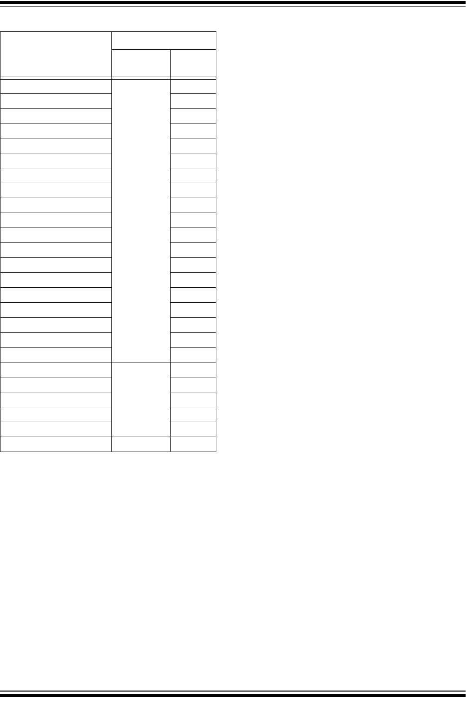
PIC32MX1XX/2XX 28/36/44-PIN FAMILY
DS60001168K-page 46 2011-2018 Microchip Technology Inc.
TABLE 4-1: SFR MEMORY MAP
Peripheral
Virtual Address
Base Offset
Start
Watchdog Timer
0xBF80
0x0000
RTCC 0x0200
Timer1-5 0x0600
Input Capture 1-5 0x2000
Output Compare 1-5 0x3000
IC1 and IC2 0x5000
SPI1 and SPI2 0x5800
UART1 and UART2 0x6000
PMP 0x7000
ADC 0x9000
CV
REF
0x9800
Comparator 0xA000
CTMU 0xA200
Oscillator 0xF000
Device and Revision ID 0xF220
Peripheral Module Disable 0xF240
Flash Controller 0xF400
Reset 0xF600
PPS 0xFA04
Interrupts
0xBF88
0x1000
Bus Matrix 0x2000
DMA 0x3000
USB 0x5050
PORTA-PORTC 0x6000
Configuration 0xBFC0 0x0BF0
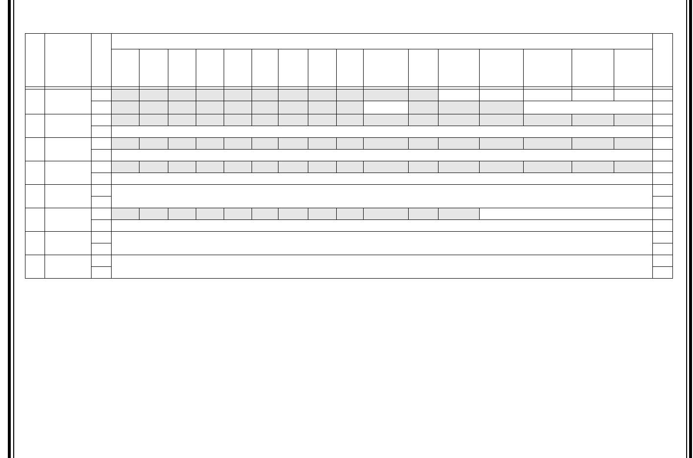
2011-2018 Microchip Technology Inc. DS60001168K-page 47
PIC32MX1XX/2XX 28/36/44-PIN FAMILY
4.2 Bus Matrix Control Registers
TABLE 4-2: BUS MATRIX REGISTER MAP
Virtual Address
(BF88_#)
Register
Name
Bit Range
Bits
All
Resets
31/15 30/14 29/13 28/12 27/11 26/10 25/9 24/8 23/7 22/6 21/5 20/4 19/3 18/2 17/1 16/0
2000 BMXCON
(1)
31:16 — — — — — — — — — — — BMXERRIXI BMXERRICD BMXERRDMA BMXERRDS BMXERRIS 001F
15:0 — — — — — — — — — BMXWSDRM — — — BMXARB<2:0> 0041
2010 BMXDKPBA
(1)
31:16 — — — — — — — — — — — — — — — — 0000
15:0 BMXDKPBA<15:0> 0000
2020 BMXDUDBA
(1)
31:16 — — — — — — — — — — — — — — — — 0000
15:0 BMXDUDBA<15:0> 0000
2030 BMXDUPBA
(1)
31:16 — — — — — — — — — — — — — — — — 0000
15:0 BMXDUPBA<15:0> 0000
2040 BMXDRMSZ 31:16 BMXDRMSZ<31:0> xxxx
15:0 xxxx
2050 BMXPUPBA
(1)
31:16 — — — — — — — — — — — — BMXPUPBA<19:16> 0000
15:0 BMXPUPBA<15:0> 0000
2060 BMXPFMSZ 31:16 BMXPFMSZ<31:0> xxxx
15:0 xxxx
2070 BMXBOOTSZ 31:16 BMXBOOTSZ<31:0> 0000
15:0 0C00
Legend: x = unknown value on Reset; — = unimplemented, read as ‘0’. Reset values are shown in hexadecimal.
Note 1: This register has corresponding CLR, SET and INV registers at its virtual address, plus an offset of 0x4, 0x8 and 0xC, respectively. See Section 11.2 “CLR, SET and INV Registers” for more information.

PIC32MX1XX/2XX 28/36/44-PIN FAMILY
DS60001168K-page 48 2011-2018 Microchip Technology Inc.
REGISTER 4-1: BMXCON: BUS MATRIX CONFIGURATION REGISTER
Bit
Range Bit
31/23/15/7 Bit
30/22/14/6 Bit
29/21/13/5 Bit
28/20/12/4 Bit
27/19/11/3 Bit
26/18/10/2 Bit
25/17/9/1 Bit
24/16/8/0
31:24
U-0 U-0 U-0 U-0 U-0 U-0 U-0 U-0
— — — — — — — —
23:16
U-0 U-0 U-0 R/W-1 R/W-1 R/W-1 R/W-1 R/W-1
— — — BMX
ERRIXI
BMX
ERRICD
BMX
ERRDMA
BMX
ERRDS
BMX
ERRIS
15:8
U-0 U-0 U-0 U-0 U-0 U-0 U-0 U-0
— — — — — — — —
7:0
U-0 R/W-1 U-0 U-0 U-0 R/W-0 R/W-0 R/W-1
—BMX
WSDRM — — — BMXARB<2:0>
Legend:
R = Readable bit W = Writable bit U = Unimplemented bit, read as ‘0’
-n = Value at POR ‘1’ = Bit is set ‘0’ = Bit is cleared
bit 31-21 Unimplemented: Read as ‘0’
bit 20 BMXERRIXI: Enable Bus Error from IXI bit
1= Enable bus error exceptions for unmapped address accesses initiated from IXI shared bus
0= Disable bus error exceptions for unmapped address accesses initiated from IXI shared bus
bit 19 BMXERRICD: Enable Bus Error from ICD Debug Unit bit
1= Enable bus error exceptions for unmapped address accesses initiated from ICD
0= Disable bus error exceptions for unmapped address accesses initiated from ICD
bit 18 BMXERRDMA: Bus Error from DMA bit
1= Enable bus error exceptions for unmapped address accesses initiated from DMA
0= Disable bus error exceptions for unmapped address accesses initiated from DMA
bit 17 BMXERRDS: Bus Error from CPU Data Access bit (disabled in Debug mode)
1= Enable bus error exceptions for unmapped address accesses initiated from CPU data access
0= Disable bus error exceptions for unmapped address accesses initiated from CPU data access
bit 16 BMXERRIS: Bus Error from CPU Instruction Access bit (disabled in Debug mode)
1= Enable bus error exceptions for unmapped address accesses initiated from CPU instruction access
0= Disable bus error exceptions for unmapped address accesses initiated from CPU instruction access
bit 15-7 Unimplemented: Read as ‘0’
bit 6 BMXWSDRM: CPU Instruction or Data Access from Data RAM Wait State bit
1= Data RAM accesses from CPU have one wait state for address setup
0= Data RAM accesses from CPU have zero wait states for address setup
bit 5-3 Unimplemented: Read as ‘0’
bit 2-0 BMXARB<2:0>: Bus Matrix Arbitration Mode bits
111 = Reserved (using these Configuration modes will produce undefined behavior)
•
•
•
011 = Reserved (using these Configuration modes will produce undefined behavior)
010 = Arbitration Mode 2
001 = Arbitration Mode 1 (default)
000 = Arbitration Mode 0

2011-2018 Microchip Technology Inc. DS60001168K-page 49
PIC32MX1XX/2XX 28/36/44-PIN FAMILY
REGISTER 4-2: BMXDKPBA: DATA RAM KERNEL PROGRAM BASE ADDRESS REGISTER
Bit
Range Bit
31/23/15/7 Bit
30/22/14/6 Bit
29/21/13/5 Bit
28/20/12/4 Bit
27/19/11/3 Bit
26/18/10/2 Bit
25/17/9/1 Bit
24/16/8/0
31:24
U-0 U-0 U-0 U-0 U-0 U-0 U-0 U-0
— — — — — — — —
23:16
U-0 U-0 U-0 U-0 U-0 U-0 U-0 U-0
— — — — — — — —
15:8
R/W-0 R/W-0 R/W-0 R/W-0 R/W-0 R/W-0 R-0 R-0
BMXDKPBA<15:8>
7:0
R-0 R-0 R-0 R-0 R-0 R-0 R-0 R-0
BMXDKPBA<7:0>
Legend:
R = Readable bit W = Writable bit U = Unimplemented bit, read as ‘0’
-n = Value at POR ‘1’ = Bit is set ‘0’ = Bit is cleared x = Bit is unknown
bit 31-16 Unimplemented: Read as ‘0’
bit 15-10 BMXDKPBA<15:10>: DRM Kernel Program Base Address bits
When non-zero, this value selects the relative base address for kernel program space in RAM
bit 9-0 BMXDKPBA<9:0>: Read-Only bits
This value is always ‘0’, which forces 1 KB increments
Note 1: At Reset, the value in this register is forced to zero, which causes all of the RAM to be allocated to Kernal
mode data usage.
2: The value in this register must be less than or equal to BMXDRMSZ.

PIC32MX1XX/2XX 28/36/44-PIN FAMILY
DS60001168K-page 50 2011-2018 Microchip Technology Inc.
REGISTER 4-3: BMXDUDBA: DATA RAM USER DATA BASE ADDRESS REGISTER
Bit
Range Bit
31/23/15/7 Bit
30/22/14/6 Bit
29/21/13/5 Bit
28/20/12/4 Bit
27/19/11/3 Bit
26/18/10/2 Bit
25/17/9/1 Bit
24/16/8/0
31:24
U-0 U-0 U-0 U-0 U-0 U-0 U-0 U-0
— — — — — — — —
23:16
U-0 U-0 U-0 U-0 U-0 U-0 U-0 U-0
— — — — — — — —
15:8
R/W-0 R/W-0 R/W-0 R/W-0 R/W-0 R/W-0 R-0 R-0
BMXDUDBA<15:8>
7:0
R-0 R-0 R-0 R-0 R-0 R-0 R-0 R-0
BMXDUDBA<7:0>
Legend:
R = Readable bit W = Writable bit U = Unimplemented bit, read as ‘0’
-n = Value at POR ‘1’ = Bit is set ‘0’ = Bit is cleared x = Bit is unknown
bit 31-16 Unimplemented: Read as ‘0’
bit 15-10 BMXDUDBA<15:10>: DRM User Data Base Address bits
When non-zero, the value selects the relative base address for User mode data space in RAM, the value
must be greater than BMXDKPBA.
bit 9-0 BMXDUDBA<9:0>: Read-Only bits
This value is always ‘0’, which forces 1 KB increments
Note 1: At Reset, the value in this register is forced to zero, which causes all of the RAM to be allocated to Kernal
mode data usage.
2: The value in this register must be less than or equal to BMXDRMSZ.

2011-2018 Microchip Technology Inc. DS60001168K-page 51
PIC32MX1XX/2XX 28/36/44-PIN FAMILY
REGISTER 4-4: BMXDUPBA: DATA RAM USER PROGRAM BASE ADDRESS REGISTER
Bit
Range Bit
31/23/15/7 Bit
30/22/14/6 Bit
29/21/13/5 Bit
28/20/12/4 Bit
27/19/11/3 Bit
26/18/10/2 Bit
25/17/9/1 Bit
24/16/8/0
31:24
U-0 U-0 U-0 U-0 U-0 U-0 U-0 U-0
— — — — — — — —
23:16
U-0 U-0 U-0 U-0 U-0 U-0 U-0 U-0
— — — — — — — —
15:8
R/W-0 R/W-0 R/W-0 R/W-0 R/W-0 R/W-0 R-0 R-0
BMXDUPBA<15:8>
7:0
R-0 R-0 R-0 R-0 R-0 R-0 R-0 R-0
BMXDUPBA<7:0>
Legend:
R = Readable bit W = Writable bit U = Unimplemented bit, read as ‘0’
-n = Value at POR ‘1’ = Bit is set ‘0’ = Bit is cleared x = Bit is unknown
bit 31-16 Unimplemented: Read as ‘0’
bit 15-10 BMXDUPBA<15:10>: DRM User Program Base Address bits
When non-zero, the value selects the relative base address for User mode program space in RAM,
BMXDUPBA must be greater than BMXDUDBA.
bit 9-0 BMXDUPBA<9:0>: Read-Only bits
This value is always ‘0’, which forces 1 KB increments
Note 1: At Reset, the value in this register is forced to zero, which causes all of the RAM to be allocated to Kernal
mode data usage.
2: The value in this register must be less than or equal to BMXDRMSZ.
PIC32MX1XX/2XX 28/36/44-PIN FAMILY
DS60001168K-page 52 2011-2018 Microchip Technology Inc.
REGISTER 4-5: BMXDRMSZ: DATA RAM SIZE REGISTER
Bit
Range Bit
31/23/15/7 Bit
30/22/14/6 Bit
29/21/13/5 Bit
28/20/12/4 Bit
27/19/11/3 Bit
26/18/10/2 Bit
25/17/9/1 Bit
24/16/8/0
31:24
RRRRR R R R
BMXDRMSZ<31:24>
23:16
RRRRR R R R
BMXDRMSZ<23:16>
15:8
RRRRR R R R
BMXDRMSZ<15:8>
7:0
RRRRR R R R
BMXDRMSZ<7:0>
Legend:
R = Readable bit W = Writable bit U = Unimplemented bit, read as ‘0’
-n = Value at POR ‘1’ = Bit is set ‘0’ = Bit is cleared x = Bit is unknown
bit 31-0 BMXDRMSZ<31:0>: Data RAM Memory (DRM) Size bits
Static value that indicates the size of the Data RAM in bytes:
0x00001000 = Device has 4 KB RAM
0x00002000 = Device has 8 KB RAM
0x00004000 = Device has 16 KB RAM
0x00008000 = Device has 32 KB RAM
0x00010000 = Device has 64 KB RAM
REGISTER 4-6: BMXPUPBA: PROGRAM FLASH (PFM) USER PROGRAM BASE ADDRESS
REGISTER
Bit
Range Bit
31/23/15/7 Bit
30/22/14/6 Bit
29/21/13/5 Bit
28/20/12/4 Bit
27/19/11/3 Bit
26/18/10/2 Bit
25/17/9/1 Bit
24/16/8/0
31:24
U-0 U-0 U-0 U-0 U-0 U-0 U-0 U-0
— — — — — — — —
23:16
U-0 U-0 U-0 U-0 R/W-0 R/W-0 R/W-0 R/W-0
———— BMXPUPBA<19:16>
15:8
R/W-0 R/W-0 R/W-0 R/W-0 R/W-0 R-0 R-0 R-0
BMXPUPBA<15:8>
7:0
R-0 R-0 R-0 R-0 R-0 R-0 R-0 R-0
BMXPUPBA<7:0>
Legend:
R = Readable bit W = Writable bit U = Unimplemented bit, read as ‘0’
-n = Value at POR ‘1’ = Bit is set ‘0’ = Bit is cleared x = Bit is unknown
bit 31-20 Unimplemented: Read as ‘0’
bit 19-11 BMXPUPBA<19:11>: Program Flash (PFM) User Program Base Address bits
bit 10-0 BMXPUPBA<10:0>: Read-Only bits
This value is always ‘0’, which forces 2 KB increments
Note 1: At Reset, the value in this register is forced to zero, which causes all of the RAM to be allocated to Kernal
mode data usage.
2: The value in this register must be less than or equal to BMXPFMSZ.
2011-2018 Microchip Technology Inc. DS60001168K-page 53
PIC32MX1XX/2XX 28/36/44-PIN FAMILY
REGISTER 4-7: BMXPFMSZ: PROGRAM FLASH (PFM) SIZE REGISTER
Bit
Range Bit
31/23/15/7 Bit
30/22/14/6 Bit
29/21/13/5 Bit
28/20/12/4 Bit
27/19/11/3 Bit
26/18/10/2 Bit
25/17/9/1 Bit
24/16/8/0
31:24
RRRRR R R R
BMXPFMSZ<31:24>
23:16
RRRRR R R R
BMXPFMSZ<23:16>
15:8
RRRRR R R R
BMXPFMSZ<15:8>
7:0
RRRRR R R R
BMXPFMSZ<7:0>
Legend:
R = Readable bit W = Writable bit U = Unimplemented bit, read as ‘0’
-n = Value at POR ‘1’ = Bit is set ‘0’ = Bit is cleared x = Bit is unknown
bit 31-0 BMXPFMSZ<31:0>: Program Flash Memory (PFM) Size bits
Static value that indicates the size of the PFM in bytes:
0x00004000 = Device has 16 KB Flash
0x00008000 = Device has 32 KB Flash
0x00010000 = Device has 64 KB Flash
0x00020000 = Device has 128 KB Flash
0x00040000 = Device has 256 KB Flash
REGISTER 4-8: BMXBOOTSZ: BOOT FLASH (IFM) SIZE REGISTER
Bit
Range Bit
31/23/15/7 Bit
30/22/14/6 Bit
29/21/13/5 Bit
28/20/12/4 Bit
27/19/11/3 Bit
26/18/10/2 Bit
25/17/9/1 Bit
24/16/8/0
31:24
RRRRR R R R
BMXBOOTSZ<31:24>
23:16
RRRRR R R R
BMXBOOTSZ<23:16>
15:8
RRRRR R R R
BMXBOOTSZ<15:8>
7:0
RRRRR R R R
BMXBOOTSZ<7:0>
Legend:
R = Readable bit W = Writable bit U = Unimplemented bit, read as ‘0’
-n = Value at POR ‘1’ = Bit is set ‘0’ = Bit is cleared x = Bit is unknown
bit 31-0 BMXBOOTSZ<31:0>: Boot Flash Memory (BFM) Size bits
Static value that indicates the size of the Boot PFM in bytes:
0x00000C00 = Device has 3 KB boot Flash

PIC32MX1XX/2XX 28/36/44-PIN FAMILY
DS60001168K-page 54 2011-2018 Microchip Technology Inc.
NOTES:

2011-2018 Microchip Technology Inc. DS60001168K-page 55
PIC32MX1XX/2XX 28/36/44-PIN FAMILY
5.0 FLASH PROGRAM MEMORY
PIC32MX1XX/2XX 28/36/44-pin Family devices con-
tain an internal Flash program memory for executing
user code. There are three methods by which the user
can program this memory:
• Run-Time Self-Programming (RTSP)
• EJTAG Programming
• In-Circuit Serial Programming™ (ICSP™)
RTSP is performed by software executing from either
Flash or RAM memory. Information about RTSP
techniques is available in Section 5. “Flash Program
Memory” (DS60001121) in the “PIC32 Family
Reference Manual”.
EJTAG is performed using the EJTAG port of the
device and an EJTAG capable programmer.
ICSP is performed using a serial data connection to the
device and allows much faster programming times than
RTSP.
The EJTAG and ICSP methods are described in the
“PIC32 Flash Programming Specification”
(DS60001145), which can be downloaded from the
Microchip web site.
Note: This data sheet summarizes the features
of the PIC32MX1XX/2XX 28/36/44-pin
Family of devices. It is not intended to be
a comprehensive reference source. To
complement the information in this data
sheet, refer to Section 5. “Flash
Program Memory” (DS60001121), which
is available from the Documentation >
Reference Manual section of the
Microchip PIC32 web site
(www.microchip.com/pic32).
Note: The Flash page size on PIC32MX-
1XX/2XX 28/36/44-pin Family devices is 1
KB and the row size is 128 bytes (256 IW
and 32 IW, respectively).
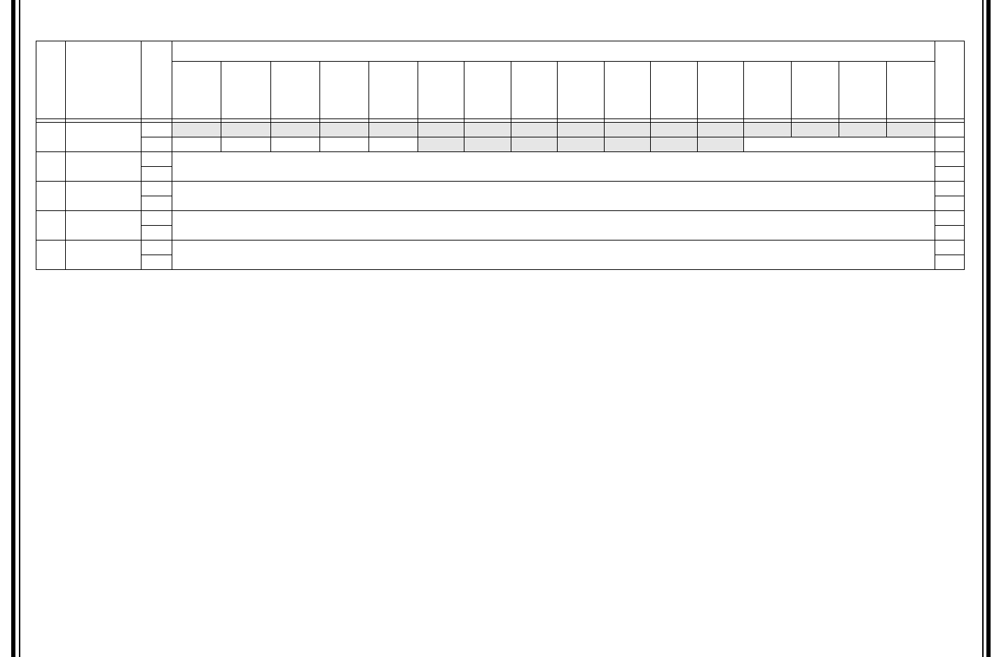
PIC32MX1XX/2XX 28/36/44-PIN FAMILY
DS60001168K-page 56 2011-2018 Microchip Technology Inc.
5.1 Flash Controller Control Registers
TABLE 5-1: FLASH CONTROLLER REGISTER MAP
Virtual Address
(BF80_#)
Register
Name
Bit Range
Bits
All Resets
31/15 30/14 29/13 28/12 27/11 26/10 25/9 24/8 23/7 22/6 21/5 20/4 19/3 18/2 17/1 16/0
F400 NVMCON
(1)
31:16 — — — — — — — — — — — — — — — — 0000
15:0 WR WREN WRERR LVDERR LVDSTAT ———————NVMOP<3:0>0000
F410 NVMKEY 31:16 NVMKEY<31:0> 0000
15:0 0000
F420
NVMADDR
(1)
31:16 NVMADDR<31:0> 0000
15:0 0000
F430 NVMDATA 31:16 NVMDATA<31:0> 0000
15:0 0000
F440 NVMSRCADDR 31:16 NVMSRCADDR<31:0> 0000
15:0 0000
Legend: x = unknown value on Reset; — = unimplemented, read as ‘0’. Reset values are shown in hexadecimal.
Note 1: This register has corresponding CLR, SET and INV registers at its virtual address, plus offsets of 0x4, 0x8 and 0xC, respectively. See Section 11.2 “CLR, SET and INV Registers” for more information.

2011-2018 Microchip Technology Inc. DS60001168K-page 57
PIC32MX1XX/2XX 28/36/44-PIN FAMILY
REGISTER 5-1: NVMCON: PROGRAMMING CONTROL REGISTER
Bit
Range Bit
31/23/15/7 Bit
30/22/14/6 Bit
29/21/13/5 Bit
28/20/12/4 Bit
27/19/11/3 Bit
26/18/10/2 Bit
25/17/9/1 Bit
24/16/8/0
31:24
U-0 U-0 U-0 U-0 U-0 U-0 U-0 U-0
— — — — — — — —
23:16
U-0 U-0 U-0 U-0 U-0 U-0 U-0 U-0
— — — — — — — —
15:8
R/W-0 R/W-0 R-0 R-0 R-0 U-0 U-0 U-0
WR WREN WRERR
(1)
LVDERR
(1)
LVDSTAT
(1)
— — —
7:0
U-0 U-0 U-0 U-0 R/W-0 R/W-0 R/W-0 R/W-0
————NVMOP<3:0>
Legend:
R = Readable bit W = Writable bit U = Unimplemented bit, read as ‘0’
-n = Value at POR ‘1’ = Bit is set ‘0’ = Bit is cleared x = Bit is unknown
bit 31-16 Unimplemented: Read as ‘0’
bit 15 WR: Write Control bit
This bit is writable when WREN = 1 and the unlock sequence is followed.
1 = Initiate a Flash operation. Hardware clears this bit when the operation completes
0 = Flash operation is complete or inactive
bit 14 WREN: Write Enable bit
This is the only bit in this register reset by a device Reset.
1 = Enable writes to WR bit and enables LVD circuit
0 = Disable writes to WR bit and disables LVD circuit
bit 13 WRERR: Write Error bit
(1)
This bit is read-only and is automatically set by hardware.
1 = Program or erase sequence did not complete successfully
0 = Program or erase sequence completed normally
bit 12 LVDERR: Low-Voltage Detect Error bit (LVD circuit must be enabled)
(1)
This bit is read-only and is automatically set by hardware.
1 = Low-voltage detected (possible data corruption, if WRERR is set)
0 = Voltage level is acceptable for programming
bit 11 LVDSTAT: Low-Voltage Detect Status bit (LVD circuit must be enabled)
(1)
This bit is read-only and is automatically set and cleared by the hardware.
1 = Low-voltage event is active
0 = Low-voltage event is not active
bit 10-4 Unimplemented: Read as ‘0’
bit 3-0 NVMOP<3:0>: NVM Operation bits
These bits are writable when WREN = 0.
1111 = Reserved
•
•
•
0111 = Reserved
0110 = No operation
0101 = Program Flash Memory (PFM) erase operation: erases PFM, if all pages are not write-protected
0100 = Page erase operation: erases page selected by NVMADDR, if it is not write-protected
0011 = Row program operation: programs row selected by NVMADDR, if it is not write-protected
0010 = No operation
0001 = Word program operation: programs word selected by NVMADDR, if it is not write-protected
0000 = No operation
Note 1: This bit is cleared by setting NVMOP == ‘b0000, and initiating a Flash operation (i.e., WR).
PIC32MX1XX/2XX 28/36/44-PIN FAMILY
DS60001168K-page 58 2011-2018 Microchip Technology Inc.
REGISTER 5-2: NVMKEY: PROGRAMMING UNLOCK REGISTER
Bit
Range Bit
31/23/15/7 Bit
30/22/14/6 Bit
29/21/13/5 Bit
28/20/12/4 Bit
27/19/11/3 Bit
26/18/10/2 Bit
25/17/9/1 Bit
24/16/8/0
31:24
W-0 W-0 W-0 W-0 W-0 W-0 W-0 W-0
NVMKEY<31:24>
23:16
W-0 W-0 W-0 W-0 W-0 W-0 W-0 W-0
NVMKEY<23:16>
15:8
W-0 W-0 W-0 W-0 W-0 W-0 W-0 W-0
NVMKEY<15:8>
7:0
W-0 W-0 W-0 W-0 W-0 W-0 W-0 W-0
NVMKEY<7:0>
Legend:
R = Readable bit W = Writable bit U = Unimplemented bit, read as ‘0’
-n = Value at POR ‘1’ = Bit is set ‘0’ = Bit is cleared x = Bit is unknown
bit 31-0 NVMKEY<31:0>: Unlock Register bits
These bits are write-only, and read as ‘0’ on any read
Note: This register is used as part of the unlock sequence to prevent inadvertent writes to the PFM.
REGISTER 5-3: NVMADDR: FLASH ADDRESS REGISTER
Bit
Range Bit
31/23/15/7 Bit
30/22/14/6 Bit
29/21/13/5 Bit
28/20/12/4 Bit
27/19/11/3 Bit
26/18/10/2 Bit
25/17/9/1 Bit
24/16/8/0
31:24
R/W-0 R/W-0 R/W-0 R/W-0 R/W-0 R/W-0 R/W-0 R/W-0
NVMADDR<31:24>
23:16
R/W-0 R/W-0 R/W-0 R/W-0 R/W-0 R/W-0 R/W-0 R/W-0
NVMADDR<23:16>
15:8
R/W-0 R/W-0 R/W-0 R/W-0 R/W-0 R/W-0 R/W-0 R/W-0
NVMADDR<15:8>
7:0
R/W-0 R/W-0 R/W-0 R/W-0 R/W-0 R/W-0 R/W-0 R/W-0
NVMADDR<7:0>
Legend:
R = Readable bit W = Writable bit U = Unimplemented bit, read as ‘0’
-n = Value at POR ‘1’ = Bit is set ‘0’ = Bit is cleared x = Bit is unknown
bit 31-0 NVMADDR<31:0>: Flash Address bits
Bulk/Chip/PFM Erase: Address is ignored.
Page Erase: Address identifies the page to erase.
Row Program: Address identifies the row to program.
Word Program: Address identifies the word to program.
2011-2018 Microchip Technology Inc. DS60001168K-page 59
PIC32MX1XX/2XX 28/36/44-PIN FAMILY
REGISTER 5-4: NVMDATA: FLASH PROGRAM DATA REGISTER
Bit
Range Bit
31/23/15/7 Bit
30/22/14/6 Bit
29/21/13/5 Bit
28/20/12/4 Bit
27/19/11/3 Bit
26/18/10/2 Bit
25/17/9/1 Bit
24/16/8/0
31:24
R/W-0 R/W-0 R/W-0 R/W-0 R/W-0 R/W-0 R/W-0 R/W-0
NVMDATA<31:24>
23:16
R/W-0 R/W-0 R/W-0 R/W-0 R/W-0 R/W-0 R/W-0 R/W-0
NVMDATA<23:16>
15:8
R/W-0 R/W-0 R/W-0 R/W-0 R/W-0 R/W-0 R/W-0 R/W-0
NVMDATA<15:8>
7:0
R/W-0 R/W-0 R/W-0 R/W-0 R/W-0 R/W-0 R/W-0 R/W-0
NVMDATA<7:0>
Legend:
R = Readable bit W = Writable bit U = Unimplemented bit, read as ‘0’
-n = Value at POR ‘1’ = Bit is set ‘0’ = Bit is cleared x = Bit is unknown
bit 31-0 NVMDATA<31:0>: Flash Programming Data bits
Note: The bits in this register are only reset by a Power-on Reset (POR).
REGISTER 5-5: NVMSRCADDR: SOURCE DATA ADDRESS REGISTER
Bit
Range Bit
31/23/15/7 Bit
30/22/14/6 Bit
29/21/13/5 Bit
28/20/12/4 Bit
27/19/11/3 Bit
26/18/10/2 Bit
25/17/9/1 Bit
24/16/8/0
31:24
R/W-0 R/W-0 R/W-0 R/W-0 R/W-0 R/W-0 R/W-0 R/W-0
NVMSRCADDR<31:24>
23:16
R/W-0 R/W-0 R/W-0 R/W-0 R/W-0 R/W-0 R/W-0 R/W-0
NVMSRCADDR<23:16>
15:8
R/W-0 R/W-0 R/W-0 R/W-0 R/W-0 R/W-0 R/W-0 R/W-0
NVMSRCADDR<15:8>
7:0
R/W-0 R/W-0 R/W-0 R/W-0 R/W-0 R/W-0 R/W-0 R/W-0
NVMSRCADDR<7:0>
Legend:
R = Readable bit W = Writable bit U = Unimplemented bit, read as ‘0’
-n = Value at POR ‘1’ = Bit is set ‘0’ = Bit is cleared x = Bit is unknown
bit 31-0 NVMSRCADDR<31:0>: Source Data Address bits
The system physical address of the data to be programmed into the Flash when the NVMOP<3:0> bits
(NVMCON<3:0>) are set to perform row programming.

PIC32MX1XX/2XX 28/36/44-PIN FAMILY
DS60001168K-page 60 2011-2018 Microchip Technology Inc.
NOTES:
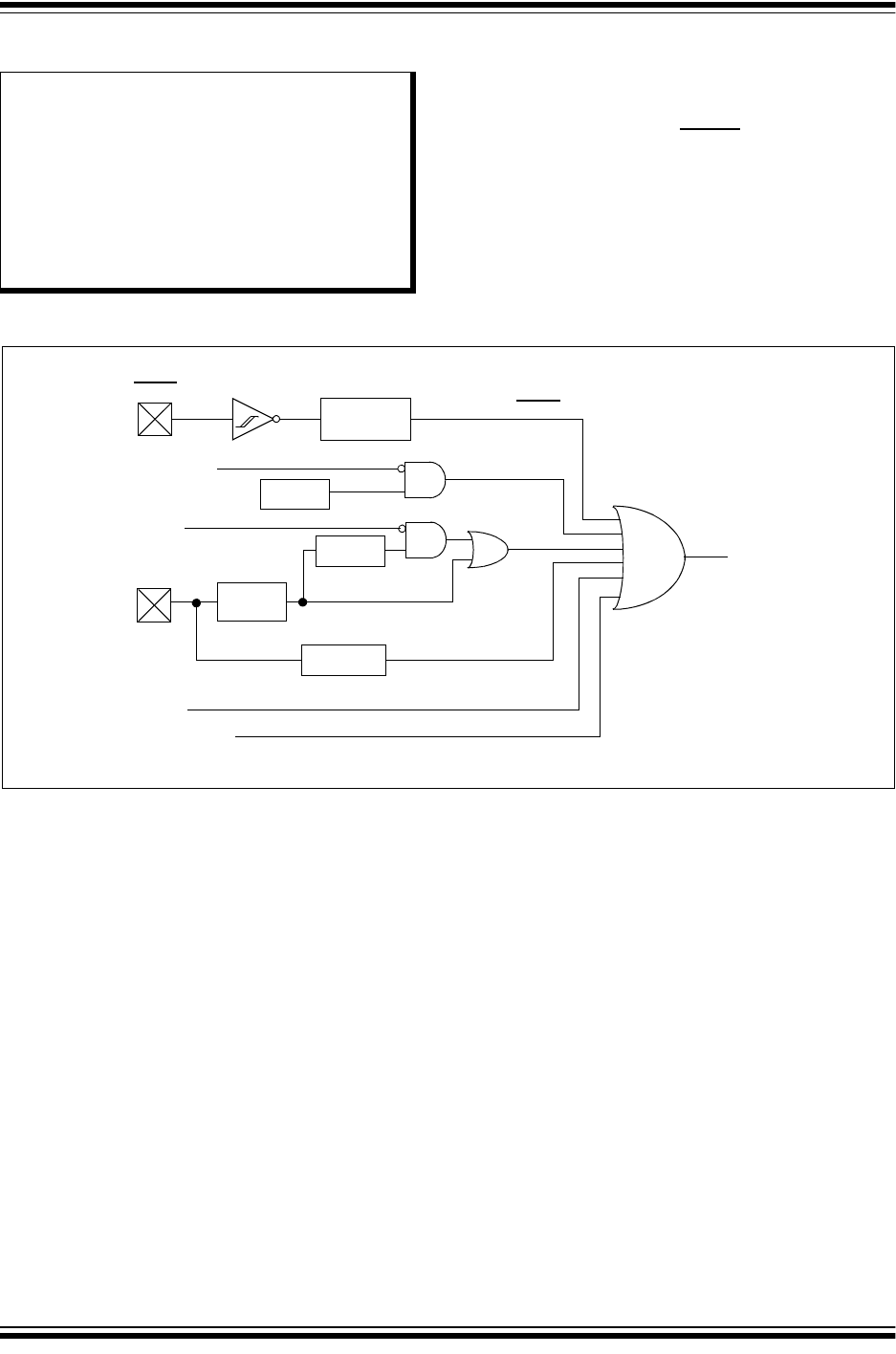
2011-2018 Microchip Technology Inc. DS60001168K-page 61
PIC32MX1XX/2XX 28/36/44-PIN FAMILY
6.0 RESETS
The Reset module combines all Reset sources and
controls the device Master Reset signal, SYSRST. The
following is a list of device Reset sources:
• Power-on Reset (POR)
• Master Clear Reset pin (MCLR)
• Software Reset (SWR)
• Watchdog Timer Reset (WDTR)
• Brown-out Reset (BOR)
• Configuration Mismatch Reset (CMR)
A simplified block diagram of the Reset module is
illustrated in Figure 6-1.
FIGURE 6-1: SYSTEM RESET BLOCK DIAGRAM
Note: This data sheet summarizes the features
of the PIC32MX1XX/2XX 28/36/44-pin
Family of devices. It is not intended to be
a comprehensive reference source. To
complement the information in this data
sheet, refer to Section 7. “Resets”
(DS60001118), which is available from the
Documentation > Reference Manual
section of the Microchip PIC32 web site
(www.microchip.com/pic32).
MCLR
V
DD
V
DD
Rise
Detect
POR
Sleep or Idle
Brown-out
Reset
WDT
Time-out
Glitch Filter
BOR
Configuration
SYSRST
Software Reset
Power-up
Timer
Voltage
Enabled
Reset
WDTR
SWR
CMR
MCLR
Mismatch
Regulator
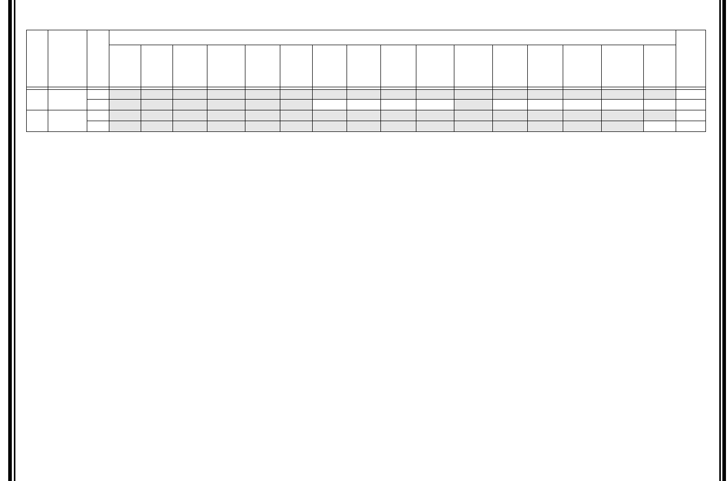
PIC32MX1XX/2XX 28/36/44-PIN FAMILY
DS60001168K-page 62 2011-2018 Microchip Technology Inc.
6.1 Reset Control Registers
TABLE 6-1: RESET CONTROL REGISTER MAP
Virtual Address
(BF80_#)
Register
Name
(1)
Bit Range
Bits
All Resets
31/15 30/14 29/13 28/12 27/11 26/10 25/9 24/8 23/7 22/6 21/5 20/4 19/3 18/2 17/1 16/0
F600 RCON 31:16 — — — — — — — — — — — — — — — — 0000
15:0 — — — — — — CMR VREGS EXTR SWR —WDTOSLEEPIDLE BORPORxxxx
(2)
F610 RSWRST 31:16 — — — — — — — — — — — — — — — — 0000
15:0 — — — — — — — — — — — — — — —SWRST0000
Legend: x = unknown value on Reset; — = unimplemented, read as ‘0’. Reset values are shown in hexadecimal.
Note 1: All registers in this table have corresponding CLR, SET and INV registers at their virtual addresses, plus offsets of 0x4, 0x8 and 0xC, respectively. See Section 11.2 “CLR, SET and INV Registers” for
more information.
2: Reset values are dependent on the DEVCFGx Configuration bits and the type of reset.

2011-2018 Microchip Technology Inc. DS60001168K-page 63
PIC32MX1XX/2XX 28/36/44-PIN FAMILY
REGISTER 6-1: RCON: RESET CONTROL REGISTER
Bit
Range Bit
31/23/15/7 Bit
30/22/14/6 Bit
29/21/13/5 Bit
28/20/12/4 Bit
27/19/11/3 Bit
26/18/10/2 Bit
25/17/9/1 Bit
24/16/8/0
31:24
U-0 U-0 U-0 U-0 U-0 U-0 U-0 U-0
— — — — — — — —
23:16
U-0 U-0 U-0 U-0 U-0 U-0 U-0 U-0
— — — — — — — —
15:8
U-0 U-0 U-0 U-0 U-0 U-0 R/W-0, HS R/W-0
— — — — — — CMR VREGS
7:0
R/W-0, HS R/W-0, HS U-0 R/W-0, HS R/W-0, HS R/W-0, HS R/W-1, HS R/W-1, HS
EXTR SWR — WDTO SLEEP IDLE BOR
(1)
POR
(1)
Legend: HS = Set by hardware
R = Readable bit W = Writable bit U = Unimplemented bit, read as ‘0’
-n = Value at POR ‘1’ = Bit is set ‘0’ = Bit is cleared x = Bit is unknown
bit 31-10 Unimplemented: Read as ‘0’
bit 9 CMR: Configuration Mismatch Reset Flag bit
1 = Configuration mismatch Reset has occurred
0 = Configuration mismatch Reset has not occurred
bit 8 VREGS: Voltage Regulator Standby Enable bit
1 = Regulator is enabled and is on during Sleep mode
0 = Regulator is set to standby tracking mode
bit 7 EXTR: External Reset (MCLR) Pin Flag bit
1 = Master Clear (pin) Reset has occurred
0 = Master Clear (pin) Reset has not occurred
bit 6 SWR: Software Reset Flag bit
1 = Software Reset was executed
0 = Software Reset as not executed
bit 5 Unimplemented: Read as ‘0’
bit 4 WDTO: Watchdog Timer Time-out Flag bit
1 = WDT Time-out has occurred
0 = WDT Time-out has not occurred
bit 3 SLEEP: Wake From Sleep Flag bit
1 = Device was in Sleep mode
0 = Device was not in Sleep mode
bit 2 IDLE: Wake From Idle Flag bit
1 = Device was in Idle mode
0 = Device was not in Idle mode
bit 1 BOR: Brown-out Reset Flag bit
(1)
1 = Brown-out Reset has occurred
0 = Brown-out Reset has not occurred
bit 0 POR: Power-on Reset Flag bit
(1)
1 = Power-on Reset has occurred
0 = Power-on Reset has not occurred
Note 1: User software must clear this bit to view next detection.

PIC32MX1XX/2XX 28/36/44-PIN FAMILY
DS60001168K-page 64 2011-2018 Microchip Technology Inc.
REGISTER 6-2: RSWRST: SOFTWARE RESET REGISTER
Bit
Range Bit
31/23/15/7 Bit
30/22/14/6 Bit
29/21/13/5 Bit
28/20/12/4 Bit
27/19/11/3 Bit
26/18/10/2 Bit
25/17/9/1 Bit
24/16/8/0
31:24
U-0 U-0 U-0 U-0 U-0 U-0 U-0 U-0
— — — — — — — —
23:16
U-0 U-0 U-0 U-0 U-0 U-0 U-0 U-0
— — — — — — — —
15:8
U-0 U-0 U-0 U-0 U-0 U-0 U-0 U-0
— — — — — — — —
7:0
U-0 U-0 U-0 U-0 U-0 U-0 U-0 W-0, HC
— — — — — — —SWRST
(1)
Legend: HC = Cleared by hardware
R = Readable bit W = Writable bit U = Unimplemented bit, read as ‘0’
-n = Value at POR ‘1’ = Bit is set ‘0’ = Bit is cleared x = Bit is unknown
bit 31-1 Unimplemented: Read as ‘0’
bit 0 SWRST: Software Reset Trigger bit
(1)
1 = Enable Software Reset event
0 = No effect
Note 1: The system unlock sequence must be performed before the SWRST bit is written. Refer to Section 6.
“Oscillator” (DS60001112) in the “PIC32 Family Reference Manual” for details.
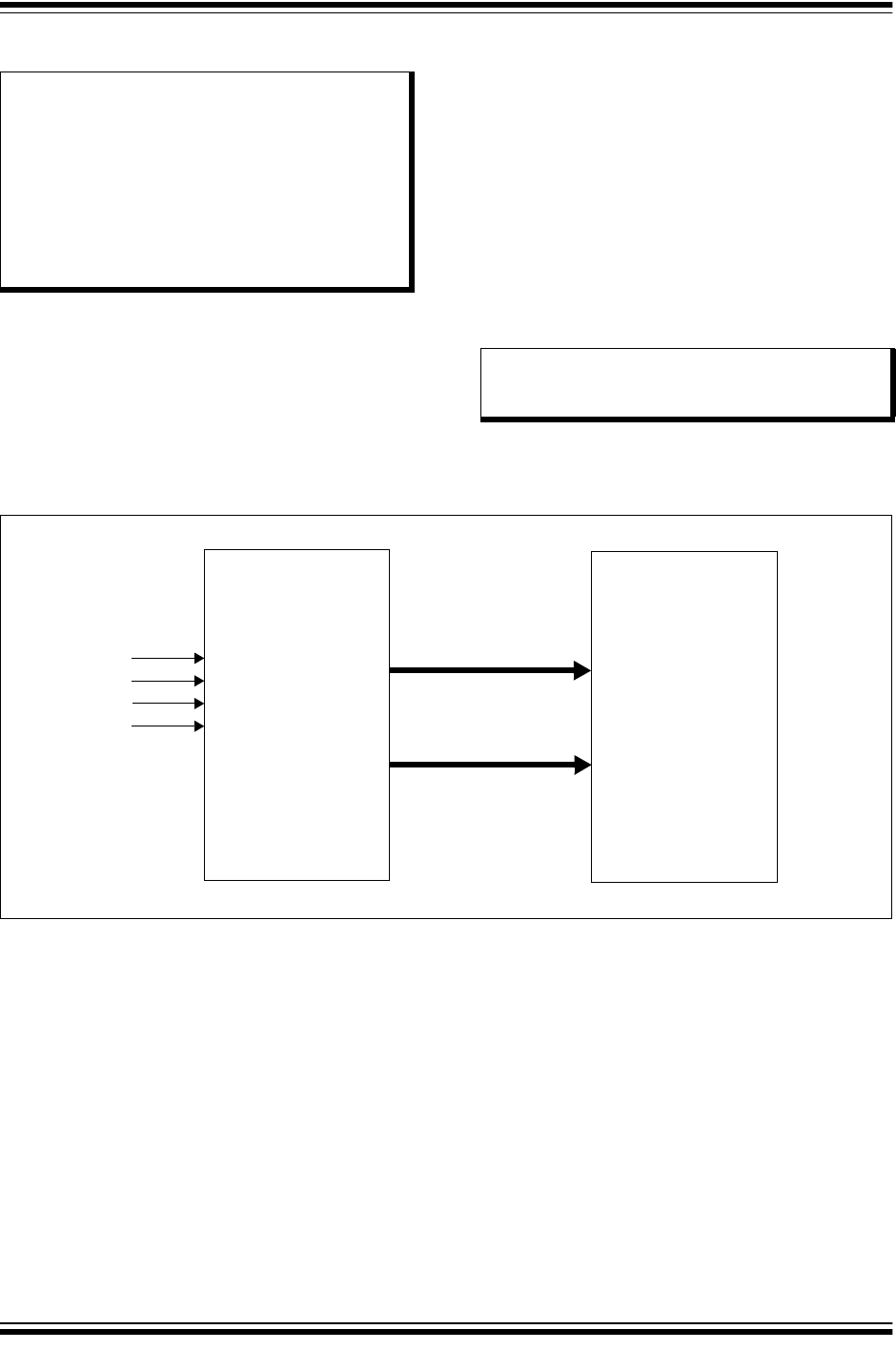
2011-2018 Microchip Technology Inc. DS60001168K-page 65
PIC32MX1XX/2XX 28/36/44-PIN FAMILY
7.0 INTERRUPT CONTROLLER
PIC32MX1XX/2XX 28/36/44-pin Family devices gener-
ate interrupt requests in response to interrupt events
from peripheral modules. The interrupt control module
exists externally to the CPU logic and prioritizes the
interrupt events before presenting them to the CPU.
The PIC32MX1XX/2XX 28/36/44-pin Family interrupt
module includes the following features:
• Up to 64 interrupt sources
• Up to 44 interrupt vectors
• Single and multi-vector mode operations
• Five external interrupts with edge polarity control
• Interrupt proximity timer
• Seven user-selectable priority levels for each
vector
• Four user-selectable subpriority levels within each
priority
• Software can generate any interrupt
• User-configurable Interrupt Vector Table (IVT)
location
• User-configurable interrupt vector spacing
A simplified block diagram of the Interrupt Controller
module is illustrated in Figure 7-1.
FIGURE 7-1: INTERRUPT CONTROLLER MODULE BLOCK DIAGRAM
Note: This data sheet summarizes the features
of the PIC32MX1XX/2XX 28/36/44-pin
Family of devices. It is not intended to be
a comprehensive reference source. To
complement the information in this data
sheet, refer to Section 8. “Interrupt Con-
troller” (DS60001108), which is available
from the Documentation > Reference
Manual section of the Microchip PIC32
web site (www.microchip.com/pic32).
Note: The dedicated shadow register set is not
present on PIC32MX1XX/2XX 28/36/44-
pin Family devices.
Interrupt Controller
Interrupt Requests
Vector Number
CPU Core
Priority Level

PIC32MX1XX/2XX 28/36/44-PIN FAMILY
DS60001168K-page 66 2011-2018 Microchip Technology Inc.
TABLE 7-1: INTERRUPT IRQ, VECTOR AND BIT LOCATION
Interrupt Source
(1)
IRQ
#Vector
#
Interrupt Bit Location Persistent
Interrupt
Flag Enable Priority Sub-priority
Highest Natural Order Priority
CT – Core Timer Interrupt 0 0 IFS0<0> IEC0<0> IPC0<4:2> IPC0<1:0> No
CS0 – Core Software Interrupt 0 1 1 IFS0<1> IEC0<1> IPC0<12:10> IPC0<9:8> No
CS1 – Core Software Interrupt 1 2 2 IFS0<2> IEC0<2> IPC0<20:18> IPC0<17:16> No
INT0 – External Interrupt 3 3 IFS0<3> IEC0<3> IPC0<28:26> IPC0<25:24> No
T1 – Timer1 4 4 IFS0<4> IEC0<4> IPC1<4:2> IPC1<1:0> No
IC1E – Input Capture 1 Error 5 5 IFS0<5> IEC0<5> IPC1<12:10> IPC1<9:8> Yes
IC1 – Input Capture 1 6 5 IFS0<6> IEC0<6> IPC1<12:10> IPC1<9:8> Yes
OC1 – Output Compare 1 7 6 IFS0<7> IEC0<7> IPC1<20:18> IPC1<17:16> No
INT1 – External Interrupt 1 8 7 IFS0<8> IEC0<8> IPC1<28:26> IPC1<25:24> No
T2 – Timer2 9 8 IFS0<9> IEC0<9> IPC2<4:2> IPC2<1:0> No
IC2E – Input Capture 2 10 9 IFS0<10> IEC0<10> IPC2<12:10> IPC2<9:8> Yes
IC2 – Input Capture 2 11 9 IFS0<11> IEC0<11> IPC2<12:10> IPC2<9:8> Yes
OC2 – Output Compare 2 12 10 IFS0<12> IEC0<12> IPC2<20:18> IPC2<17:16> No
INT2 – External Interrupt 2 13 11 IFS0<13> IEC0<13> IPC2<28:26> IPC2<25:24> No
T3 – Timer3 14 12 IFS0<14> IEC0<14> IPC3<4:2> IPC3<1:0> No
IC3E – Input Capture 3 15 13 IFS0<15> IEC0<15> IPC3<12:10> IPC3<9:8> Yes
IC3 – Input Capture 3 16 13 IFS0<16> IEC0<16> IPC3<12:10> IPC3<9:8> Yes
OC3 – Output Compare 3 17 14 IFS0<17> IEC0<17> IPC3<20:18> IPC3<17:16> No
INT3 – External Interrupt 3 18 15 IFS0<18> IEC0<18> IPC3<28:26> IPC3<25:24> No
T4 – Timer4 19 16 IFS0<19> IEC0<19> IPC4<4:2> IPC4<1:0> No
IC4E – Input Capture 4 Error 20 17 IFS0<20> IEC0<20> IPC4<12:10> IPC4<9:8> Yes
IC4 – Input Capture 4 21 17 IFS0<21> IEC0<21> IPC4<12:10> IPC4<9:8> Yes
OC4 – Output Compare 4 22 18 IFS0<22> IEC0<22> IPC4<20:18> IPC4<17:16> No
INT4 – External Interrupt 4 23 19 IFS0<23> IEC0<23> IPC4<28:26> IPC4<25:24> No
T5 – Timer5 24 20 IFS0<24> IEC0<24> IPC5<4:2> IPC5<1:0> No
IC5E – Input Capture 5 Error 25 21 IFS0<25> IEC0<25> IPC5<12:10> IPC5<9:8> Yes
IC5 – Input Capture 5 26 21 IFS0<26> IEC0<26> IPC5<12:10> IPC5<9:8> Yes
OC5 – Output Compare 5 27 22 IFS0<27> IEC0<27> IPC5<20:18> IPC5<17:16> No
AD1 – ADC1 Convert done 28 23 IFS0<28> IEC0<28> IPC5<28:26> IPC5<25:24> Yes
FSCM – Fail-Safe Clock Monitor 29 24 IFS0<29> IEC0<29> IPC6<4:2> IPC6<1:0> No
RTCC – Real-Time Clock and
Calendar
30 25 IFS0<30> IEC0<30> IPC6<12:10> IPC6<9:8> No
FCE – Flash Control Event 31 26 IFS0<31> IEC0<31> IPC6<20:18> IPC6<17:16> No
CMP1 – Comparator Interrupt 32 27 IFS1<0> IEC1<0> IPC6<28:26> IPC6<25:24> No
CMP2 – Comparator Interrupt 33 28 IFS1<1> IEC1<1> IPC7<4:2> IPC7<1:0> No
CMP3 – Comparator Interrupt 34 29 IFS1<2> IEC1<2> IPC7<12:10> IPC7<9:8> No
USB – USB Interrupts 35 30 IFS1<3> IEC1<3> IPC7<20:18> IPC7<17:16> Yes
SPI1E – SPI1 Fault 36 31 IFS1<4> IEC1<4> IPC7<28:26> IPC7<25:24> Yes
SPI1RX – SPI1 Receive Done 37 31 IFS1<5> IEC1<5> IPC7<28:26> IPC7<25:24> Yes
SPI1TX – SPI1 Transfer Done 38 31 IFS1<6> IEC1<6> IPC7<28:26> IPC7<25:24> Yes
Note 1: Not all interrupt sources are available on all devices. See TABLE 1: “PIC32MX1XX 28/36/44-Pin General
Purpose Family Features” and TABLE 2: “PIC32MX2XX 28/36/44-pin USB Family Features” for the
lists of available peripherals.

2011-2018 Microchip Technology Inc. DS60001168K-page 67
PIC32MX1XX/2XX 28/36/44-PIN FAMILY
U1E – UART1 Fault 39 32 IFS1<7> IEC1<7> IPC8<4:2> IPC8<1:0> Yes
U1RX – UART1 Receive Done 40 32 IFS1<8> IEC1<8> IPC8<4:2> IPC8<1:0> Yes
U1TX – UART1 Transfer Done 41 32 IFS1<9> IEC1<9> IPC8<4:2> IPC8<1:0> Yes
I2C1B – I2C1 Bus Collision Event 42 33 IFS1<10> IEC1<10> IPC8<12:10> IPC8<9:8> Yes
I2C1S – I2C1 Slave Event 43 33 IFS1<11> IEC1<11> IPC8<12:10> IPC8<9:8> Yes
I2C1M – I2C1 Master Event 44 33 IFS1<12> IEC1<12> IPC8<12:10> IPC8<9:8> Yes
CNA – PORTA Input Change
Interrupt
45 34 IFS1<13> IEC1<13> IPC8<20:18> IPC8<17:16> Yes
CNB – PORTB Input Change
Interrupt
46 34 IFS1<14> IEC1<14> IPC8<20:18> IPC8<17:16> Yes
CNC – PORTC Input Change
Interrupt
47 34 IFS1<15> IEC1<15> IPC8<20:18> IPC8<17:16> Yes
PMP – Parallel Master Port 48 35 IFS1<16> IEC1<16> IPC8<28:26> IPC8<25:24> Yes
PMPE – Parallel Master Port Error 49 35 IFS1<17> IEC1<17> IPC8<28:26> IPC8<25:24> Yes
SPI2E – SPI2 Fault 50 36 IFS1<18> IEC1<18> IPC9<4:2> IPC9<1:0> Yes
SPI2RX – SPI2 Receive Done 51 36 IFS1<19> IEC1<19> IPC9<4:2> IPC9<1:0> Yes
SPI2TX – SPI2 Transfer Done 52 36 IFS1<20> IEC1<20> IPC9<4:2> IPC9<1:0> Yes
U2E – UART2 Error 53 37 IFS1<21> IEC1<21> IPC9<12:10> IPC9<9:8> Yes
U2RX – UART2 Receiver 54 37 IFS1<22> IEC1<22> IPC9<12:10> IPC9<9:8> Yes
U2TX – UART2 Transmitter 55 37 IFS1<23> IEC1<23> IPC9<12:10> IPC9<9:8> Yes
I2C2B – I2C2 Bus Collision Event 56 38 IFS1<24> IEC1<24> IPC9<20:18> IPC9<17:16> Yes
I2C2S – I2C2 Slave Event 57 38 IFS1<25> IEC1<25> IPC9<20:18> IPC9<17:16> Yes
I2C2M – I2C2 Master Event 58 38 IFS1<26> IEC1<26> IPC9<20:18> IPC9<17:16> Yes
CTMU – CTMU Event 59 39 IFS1<27> IEC1<27> IPC9<28:26> IPC9<25:24> Yes
DMA0 – DMA Channel 0 60 40 IFS1<28> IEC1<28> IPC10<4:2> IPC10<1:0> No
DMA1 – DMA Channel 1 61 41 IFS1<29> IEC1<29> IPC10<12:10> IPC10<9:8> No
DMA2 – DMA Channel 2 62 42 IFS1<30> IEC1<30> IPC10<20:18> IPC10<17:16> No
DMA3 – DMA Channel 3 63 43 IFS1<31> IEC1<31> IPC10<28:26> IPC10<25:24> No
Lowest Natural Order Priority
TABLE 7-1: INTERRUPT IRQ, VECTOR AND BIT LOCATION (CONTINUED)
Interrupt Source
(1)
IRQ
#Vector
#
Interrupt Bit Location Persistent
Interrupt
Flag Enable Priority Sub-priority
Note 1: Not all interrupt sources are available on all devices. See TABLE 1: “PIC32MX1XX 28/36/44-Pin General
Purpose Family Features” and TABLE 2: “PIC32MX2XX 28/36/44-pin USB Family Features” for the
lists of available peripherals.
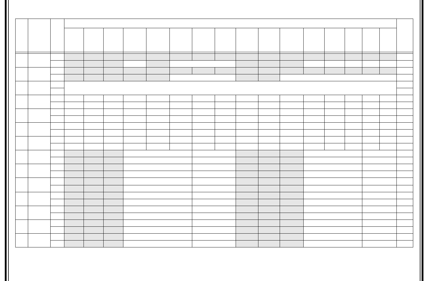
PIC32MX1XX/2XX 28/36/44-PIN FAMILY
DS60001168K-page 68 2011-2018 Microchip Technology Inc.
7.1 Interrupt Control Registers
TABLE 7-2: INTERRUPT REGISTER MAP
Virtual Address
(BF88_#)
Register
Name
(1)
Bit Range
Bits
All
Resets
31/15 30/14 29/13 28/12 27/11 26/10 25/9 24/8 23/7 22/6 21/5 20/4 19/3 18/2 17/1 16/0
1000 INTCON 31:16 — — — — — — — — — — — — — — — — 0000
15:0 — — — MVEC —TPC<2:0>— — — INT4EP INT3EP INT2EP INT1EP INT0EP 0000
1010 INTSTAT
(3)
31:16 — — — — — — — — — — — — — — — — 0000
15:0 — — — — —SRIPL<2:0>—— VEC<5:0> 0000
1020 IPTMR 31:16 IPTMR<31:0> 0000
15:0 0000
1030 IFS0 31:16 FCEIF RTCCIF FSCMIF AD1IF OC5IF IC5IF IC5EIF T5IF INT4IF OC4IF IC4IF IC4EIF T4IF INT3IF OC3IF IC3IF 0000
15:0 IC3EIF T3IF INT2IF OC2IF IC2IF IC2EIF T2IF INT1IF OC1IF IC1IF IC1EIF T1IF INT0IF CS1IF CS0IF CTIF 0000
1040 IFS1 31:16 DMA3IF DMA2IF DMA1IF DMA0IF CTMUIF I2C2MIF I2C2SIF I2C2BIF U2TXIF U2RXIF U2EIF SPI2TXIF SPI2RXIF SPI2EIF PMPEIF PMPIF 0000
15:0 CNCIF CNBIF CNAIF I2C1MIF I2C1SIF I2C1BIF U1TXIF U1RXIF U1EIF SPI1TXIF SPI1RXIF SPI1EIF USBIF
(2)
CMP3IF CMP2IF CMP1IF 0000
1060 IEC0 31:16 FCEIE RTCCIE FSCMIE AD1IE OC5IE IC5IE IC5EIE T5IE INT4IE OC4IE IC4IE IC4EIE T4IE INT3IE OC3IE IC3IE 0000
15:0 IC3EIE T3IE INT2IE OC2IE IC2IE IC2EIE T2IE INT1IE OC1IE IC1IE IC1EIE T1IE INT0IE CS1IE CS0IE CTIE 0000
1070 IEC1 31:16 DMA3IE DMA2IE DMA1IE DMA0IE CTMUIE I2C2MIE I2C2SIE I2C2BIE U2TXIE U2RXIE U2EIE SPI2TXIE SPI2RXIE SPI2EIE PMPEIE PMPIE 0000
15:0 CNCIE CNBIE CNAIE I2C1MIE I2C1SIE I2C1BIE U1TXIE U1RXIE U1EIE SPI1TXIE SPI1RXIE SPI1EIE USBIE
(2)
CMP3IE CMP2IE CMP1IE 0000
1090 IPC0 31:16 — — — INT0IP<2:0> INT0IS<1:0> — — — CS1IP<2:0> CS1IS<1:0> 0000
15:0 — — — CS0IP<2:0> CS0IS<1:0> — — — CTIP<2:0> CTIS<1:0> 0000
10A0 IPC1 31:16 — — — INT1IP<2:0> INT1IS<1:0> — — — OC1IP<2:0> OC1IS<1:0> 0000
15:0 — — — IC1IP<2:0> IC1IS<1:0> — — — T1IP<2:0> T1IS<1:0> 0000
10B0 IPC2 31:16 — — — INT2IP<2:0> INT2IS<1:0> — — — OC2IP<2:0> OC2IS<1:0> 0000
15:0 — — — IC2IP<2:0> IC2IS<1:0> — — — T2IP<2:0> T2IS<1:0> 0000
10C0 IPC3 31:16 — — — INT3IP<2:0> INT3IS<1:0> — — — OC3IP<2:0> OC3IS<1:0> 0000
15:0 — — — IC3IP<2:0> IC3IS<1:0> — — — T3IP<2:0> T3IS<1:0> 0000
10D0 IPC4 31:16 — — — INT4IP<2:0> INT4IS<1:0> — — — OC4IP<2:0> OC4IS<1:0> 0000
15:0 — — — IC4IP<2:0> IC4IS<1:0> — — — T4IP<2:0> T4IS<1:0> 0000
10E0 IPC5 31:16 — — — AD1IP<2:0> AD1IS<1:0> — — — OC5IP<2:0> OC5IS<1:0> 0000
15:0 — — — IC5IP<2:0> IC5IS<1:0> — — — T5IP<2:0> T5IS<1:0> 0000
10F0 IPC6 31:16 — — — CMP1IP<2:0> CMP1IS<1:0> — — — FCEIP<2:0> FCEIS<1:0> 0000
15:0 — — — RTCCIP<2:0> RTCCIS<1:0> — — — FSCMIP<2:0> FSCMIS<1:0> 0000
Legend: x = unknown value on Reset; — = unimplemented, read as ‘0’. Reset values are shown in hexadecimal.
Note 1: With the exception of those noted, all registers in this table have corresponding CLR, SET and INV registers at their virtual addresses, plus offsets of 0x4 0x8 and 0xC, respectively. See Section 11.2 “CLR,
SET and INV Registers” for more information.
2: These bits are not available on PIC32MX1XX devices.
3: This register does not have associated CLR, SET, INV registers.
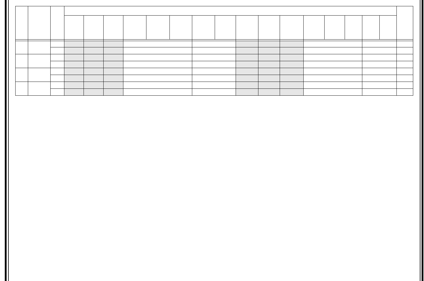
2011-2018 Microchip Technology Inc. DS60001168K-page 69
PIC32MX1XX/2XX 28/36/44-PIN FAMILY
1100 IPC7 31:16 — — — SPI1IP<2:0> SPI1IS<1:0> — — — USBIP<2:0>
(2)
USBIS<1:0>
(2)
0000
15:0 — — — CMP3IP<2:0> CMP3IS<1:0> — — — CMP2IP<2:0> CMP2IS<1:0> 0000
1110 IPC8 31:16 — — — PMPIP<2:0> PMPIS<1:0> — — — CNIP<2:0> CNIS<1:0> 0000
15:0 — — — I2C1IP<2:0> I2C1IS<1:0> — — — U1IP<2:0> U1IS<1:0> 0000
1120 IPC9 31:16 — — — CTMUIP<2:0> CTMUIS<1:0> — — — I2C2IP<2:0> I2C2IS<1:0> 0000
15:0 — — — U2IP<2:0> U2IS<1:0> — — — SPI2IP<2:0> SPI2IS<1:0> 0000
1130 IPC10 31:16 — — — DMA3IP<2:0> DMA3IS<1:0> — — — DMA2IP<2:0> DMA2IS<1:0> 0000
15:0 — — — DMA1IP<2:0> DMA1IS<1:0> — — — DMA0IP<2:0> DMA0IS<1:0> 0000
TABLE 7-2: INTERRUPT REGISTER MAP (CONTINUED)
Virtual Address
(BF88_#)
Register
Name
(1)
Bit Range
Bits
All
Resets
31/15 30/14 29/13 28/12 27/11 26/10 25/9 24/8 23/7 22/6 21/5 20/4 19/3 18/2 17/1 16/0
Legend: x = unknown value on Reset; — = unimplemented, read as ‘0’. Reset values are shown in hexadecimal.
Note 1: With the exception of those noted, all registers in this table have corresponding CLR, SET and INV registers at their virtual addresses, plus offsets of 0x4 0x8 and 0xC, respectively. See Section 11.2 “CLR,
SET and INV Registers” for more information.
2: These bits are not available on PIC32MX1XX devices.
3: This register does not have associated CLR, SET, INV registers.

PIC32MX1XX/2XX 28/36/44-PIN FAMILY
DS60001168K-page 70 2011-2018 Microchip Technology Inc.
REGISTER 7-1: INTCON: INTERRUPT CONTROL REGISTER
Bit
Range Bit
31/23/15/7 Bit
30/22/14/6 Bit
29/21/13/5 Bit
28/20/12/4 Bit
27/19/11/3 Bit
26/18/10/2 Bit
25/17/9/1 Bit
24/16/8/0
31:24
U-0 U-0 U-0 U-0 U-0 U-0 U-0 U-0
— — — — — — — —
23:16
U-0 U-0 U-0 U-0 U-0 U-0 U-0 U-0
— — — — — — — —
15:8
U-0 U-0 U-0 R/W-0 U-0 R/W-0 R/W-0 R/W-0
— — — MVEC —TPC<2:0>
7:0
U-0 U-0 U-0 R/W-0 R/W-0 R/W-0 R/W-0 R/W-0
— — — INT4EP INT3EP INT2EP INT1EP INT0EP
Legend:
R = Readable bit W = Writable bit U = Unimplemented bit, read as ‘0’
-n = Value at POR ‘1’ = Bit is set ‘0’ = Bit is cleared x = Bit is unknown
bit 31-16 Unimplemented: Read as ‘0’
bit 15-13 Unimplemented: Read as ‘0’
bit 12 MVEC: Multi Vector Configuration bit
1 = Interrupt controller configured for Multi-vectored mode
0 = Interrupt controller configured for Single-vectored mode
bit 11 Unimplemented: Read as ‘0’
bit 10-8 TPC<2:0>: Interrupt Proximity Timer Control bits
111 = Interrupts of group priority 7 or lower start the Interrupt Proximity timer
110 = Interrupts of group priority 6 or lower start the Interrupt Proximity timer
101 = Interrupts of group priority 5 or lower start the Interrupt Proximity timer
100 = Interrupts of group priority 4 or lower start the Interrupt Proximity timer
011 = Interrupts of group priority 3 or lower start the Interrupt Proximity timer
010 = Interrupts of group priority 2 or lower start the Interrupt Proximity timer
001 = Interrupts of group priority 1 start the Interrupt Proximity timer
000 = Disables Interrupt Proximity timer
bit 7-5 Unimplemented: Read as ‘0’
bit 4 INT4EP: External Interrupt 4 Edge Polarity Control bit
1 = Rising edge
0 = Falling edge
bit 3 INT3EP: External Interrupt 3 Edge Polarity Control bit
1 = Rising edge
0 = Falling edge
bit 2 INT2EP: External Interrupt 2 Edge Polarity Control bit
1 = Rising edge
0 = Falling edge
bit 1 INT1EP: External Interrupt 1 Edge Polarity Control bit
1 = Rising edge
0 = Falling edge
bit 0 INT0EP: External Interrupt 0 Edge Polarity Control bit
1 = Rising edge
0 = Falling edge
2011-2018 Microchip Technology Inc. DS60001168K-page 71
PIC32MX1XX/2XX 28/36/44-PIN FAMILY
REGISTER 7-2: INTSTAT: INTERRUPT STATUS REGISTER
Bit
Range Bit
31/23/15/7 Bit
30/22/14/6 Bit
29/21/13/5 Bit
28/20/12/4 Bit
27/19/11/3 Bit
26/18/10/2 Bit
25/17/9/1 Bit
24/16/8/0
31:24
U-0 U-0 U-0 U-0 U-0 U-0 U-0 U-0
— — — — — — — —
23:16
U-0 U-0 U-0 U-0 U-0 U-0 U-0 U-0
— — — — — — — —
15:8
U-0 U-0 U-0 U-0 U-0 R/W-0 R/W-0 R/W-0
— — — — —SRIPL<2:0>
(1)
7:0
U-0 U-0 R/W-0 R/W-0 R/W-0 R/W-0 R/W-0 R/W-0
——VEC<5:0>
(1)
Legend:
R = Readable bit W = Writable bit U = Unimplemented bit, read as ‘0’
-n = Value at POR ‘1’ = Bit is set ‘0’ = Bit is cleared x = Bit is unknown
bit 31-11 Unimplemented: Read as ‘0’
bit 10-8 SRIPL<2:0>: Requested Priority Level bits
(1)
111-000 = The priority level of the latest interrupt presented to the CPU
bit 7-6 Unimplemented: Read as ‘0’
bit 5-0 VEC<5:0>: Interrupt Vector bits
(1)
11111-00000 = The interrupt vector that is presented to the CPU
Note 1: This value should only be used when the interrupt controller is configured for Single Vector mode.
REGISTER 7-3: IPTMR: INTERRUPT PROXIMITY TIMER REGISTER
Bit
Range Bit
31/23/15/7 Bit
30/22/14/6 Bit
29/21/13/5 Bit
28/20/12/4 Bit
27/19/11/3 Bit
26/18/10/2 Bit
25/17/9/1 Bit
24/16/8/0
31:24
R/W-0 R/W-0 R/W-0 R/W-0 R/W-0 R/W-0 R/W-0 R/W-0
IPTMR<31:24>
23:16
R/W-0 R/W-0 R/W-0 R/W-0 R/W-0 R/W-0 R/W-0 R/W-0
IPTMR<23:16>
15:8
R/W-0 R/W-0 R/W-0 R/W-0 R/W-0 R/W-0 R/W-0 R/W-0
IPTMR<15:8>
7:0
R/W-0 R/W-0 R/W-0 R/W-0 R/W-0 R/W-0 R/W-0 R/W-0
IPTMR<7:0>
Legend:
R = Readable bit W = Writable bit U = Unimplemented bit, read as ‘0’
-n = Value at POR ‘1’ = Bit is set ‘0’ = Bit is cleared x = Bit is unknown
bit 31-0 IPTMR<31:0>: Interrupt Proximity Timer Reload bits
Used by the Interrupt Proximity Timer as a reload value when the Interrupt Proximity timer is triggered by
an interrupt event.
PIC32MX1XX/2XX 28/36/44-PIN FAMILY
DS60001168K-page 72 2011-2018 Microchip Technology Inc.
REGISTER 7-4: IFSx: INTERRUPT FLAG STATUS REGISTER
Bit
Range Bit
31/23/15/7 Bit
30/22/14/6 Bit
29/21/13/5 Bit
28/20/12/4 Bit
27/19/11/3 Bit
26/18/10/2 Bit
25/17/9/1 Bit
24/16/8/0
31:24
R/W-0 R/W-0 R/W-0 R/W-0 R/W-0 R/W-0 R/W-0 R/W-0
IFS31 IFS30 IFS29 IFS28 IFS27 IFS26 IFS25 IFS24
23:16
R/W-0 R/W-0 R/W-0 R/W-0 R/W-0 R/W-0 R/W-0 R/W-0
IFS23 IFS22 IFS21 IFS20 IFS19 IFS18 IFS17 IFS16
15:8
R/W-0 R/W-0 R/W-0 R/W-0 R/W-0 R/W-0 R/W-0 R/W-0
IFS15 IFS14 IFS13 IFS12 IFS11 IFS10 IFS09 IFS08
7:0
R/W-0 R/W-0 R/W-0 R/W-0 R/W-0 R/W-0 R/W-0 R/W-0
IFS07 IFS06 IFS05 IFS04 IFS03 IFS02 IFS01 IFS00
Legend:
R = Readable bit W = Writable bit U = Unimplemented bit, read as ‘0’
-n = Value at POR ‘1’ = Bit is set ‘0’ = Bit is cleared x = Bit is unknown
bit 31-0 IFS31-IFS00: Interrupt Flag Status bits
1 = Interrupt request has occurred
0 = No interrupt request has occurred
Note: This register represents a generic definition of the IFSx register. Refer to Tab le 7 - 1 for the exact bit
definitions.
REGISTER 7-5: IECx: INTERRUPT ENABLE CONTROL REGISTER
Bit
Range Bit
31/23/15/7 Bit
30/22/14/6 Bit
29/21/13/5 Bit
28/20/12/4 Bit
27/19/11/3 Bit
26/18/10/2 Bit
25/17/9/1 Bit
24/16/8/0
31:24
R/W-0 R/W-0 R/W-0 R/W-0 R/W-0 R/W-0 R/W-0 R/W-0
IEC31 IEC30 IEC29 IEC28 IEC27 IEC26 IEC25 IEC24
23:16
R/W-0 R/W-0 R/W-0 R/W-0 R/W-0 R/W-0 R/W-0 R/W-0
IEC23 IEC22 IEC21 IEC20 IEC19 IEC18 IEC17 IEC16
15:8
R/W-0 R/W-0 R/W-0 R/W-0 R/W-0 R/W-0 R/W-0 R/W-0
IEC15 IEC14 IEC13 IEC12 IEC11 IEC10 IEC09 IEC08
7:0
R/W-0 R/W-0 R/W-0 R/W-0 R/W-0 R/W-0 R/W-0 R/W-0
IEC07 IEC06 IEC05 IEC04 IEC03 IEC02 IEC01 IEC00
Legend:
R = Readable bit W = Writable bit U = Unimplemented bit, read as ‘0’
-n = Value at POR ‘1’ = Bit is set ‘0’ = Bit is cleared x = Bit is unknown
bit 31-0 IEC31-IEC00: Interrupt Enable bits
1 = Interrupt is enabled
0 = Interrupt is disabled
Note: This register represents a generic definition of the IECx register. Refer to Tabl e 7- 1 for the exact bit
definitions.

2011-2018 Microchip Technology Inc. DS60001168K-page 73
PIC32MX1XX/2XX 28/36/44-PIN FAMILY
REGISTER 7-6: IPCx: INTERRUPT PRIORITY CONTROL REGISTER
Bit
Range Bit
31/23/15/7 Bit
30/22/14/6 Bit
29/21/13/5 Bit
28/20/12/4 Bit
27/19/11/3 Bit
26/18/10/2 Bit
25/17/9/1 Bit
24/16/8/0
31:24
U-0 U-0 U-0 R/W-0 R/W-0 R/W-0 R/W-0 R/W-0
— — — IP03<2:0> IS03<1:0>
23:16
U-0 U-0 U-0 R/W-0 R/W-0 R/W-0 R/W-0 R/W-0
— — — IP02<2:0> IS02<1:0>
15:8
U-0 U-0 U-0 R/W-0 R/W-0 R/W-0 R/W-0 R/W-0
— — — IP01<2:0> IS01<1:0>
7:0
U-0 U-0 U-0 R/W-0 R/W-0 R/W-0 R/W-0 R/W-0
— — — IP00<2:0> IS00<1:0>
Legend:
R = Readable bit W = Writable bit U = Unimplemented bit, read as ‘0’
-n = Value at POR ‘1’ = Bit is set ‘0’ = Bit is cleared x = Bit is unknown
bit 31-29 Unimplemented: Read as ‘0’
bit 28-26 IP03<2:0>: Interrupt Priority bits
111 = Interrupt priority is 7
•
•
•
010 = Interrupt priority is 2
001 = Interrupt priority is 1
000 = Interrupt is disabled
bit 25-24 IS03<1:0>: Interrupt Subpriority bits
11 = Interrupt subpriority is 3
10 = Interrupt subpriority is 2
01 = Interrupt subpriority is 1
00 = Interrupt subpriority is 0
bit 23-21 Unimplemented: Read as ‘0’
bit 20-18 IP02<2:0>: Interrupt Priority bits
111 = Interrupt priority is 7
•
•
•
010 = Interrupt priority is 2
001 = Interrupt priority is 1
000 = Interrupt is disabled
bit 17-16 IS02<1:0>: Interrupt Subpriority bits
11 = Interrupt subpriority is 3
10 = Interrupt subpriority is 2
01 = Interrupt subpriority is 1
00 = Interrupt subpriority is 0
bit 15-13 Unimplemented: Read as ‘0’
bit 12-10 IP01<2:0>: Interrupt Priority bits
111 = Interrupt priority is 7
•
•
•
010 = Interrupt priority is 2
001 = Interrupt priority is 1
000 = Interrupt is disabled
Note: This register represents a generic definition of the IPCx register. Refer to Tabl e 7 -1 for the exact bit
definitions.

PIC32MX1XX/2XX 28/36/44-PIN FAMILY
DS60001168K-page 74 2011-2018 Microchip Technology Inc.
bit 9-8 IS01<1:0>: Interrupt Subpriority bits
11 = Interrupt subpriority is 3
10 = Interrupt subpriority is 2
01 = Interrupt subpriority is 1
00 = Interrupt subpriority is 0
bit 7-5 Unimplemented: Read as ‘0’
bit 4-2 IP00<2:0>: Interrupt Priority bits
111 = Interrupt priority is 7
•
•
•
010 = Interrupt priority is 2
001 = Interrupt priority is 1
000 = Interrupt is disabled
bit 1-0 IS00<1:0>: Interrupt Subpriority bits
11 = Interrupt subpriority is 3
10 = Interrupt subpriority is 2
01 = Interrupt subpriority is 1
00 = Interrupt subpriority is 0
REGISTER 7-6: IPCx: INTERRUPT PRIORITY CONTROL REGISTER (CONTINUED)
Note: This register represents a generic definition of the IPCx register. Refer to Tabl e 7- 1 for the exact bit
definitions.

2011-2018 Microchip Technology Inc. DS60001168K-page 75
PIC32MX1XX/2XX 28/36/44-PIN FAMILY
8.0 OSCILLATOR
CONFIGURATION
The PIC32MX1XX/2XX 28/36/44-pin Family oscillator
system has the following modules and features:
• Four external and internal oscillator options as
clock sources
• On-Chip PLL with user-selectable input divider,
multiplier and output divider to boost operating
frequency on select internal and external
oscillator sources
• On-Chip user-selectable divisor postscaler on
select oscillator sources
• Software-controllable switching between
various clock sources
• A Fail-Safe Clock Monitor (FSCM) that detects
clock failure and permits safe application recovery
or shutdown
• Dedicated On-Chip PLL for USB peripheral
A block diagram of the oscillator system is provided in
Figure 8-1.
Note: This data sheet summarizes the features
of the PIC32MX1XX/2XX 28/36/44-pin
Family of devices. It is not intended to be
a comprehensive reference source. To
complement the information in this data
sheet, refer to Section 6. “Oscillator
Configuration” (DS60001112), which is
available from the Documentation >
Reference Manual section of the
Microchip PIC32 web site
(www.microchip.com/pic32).
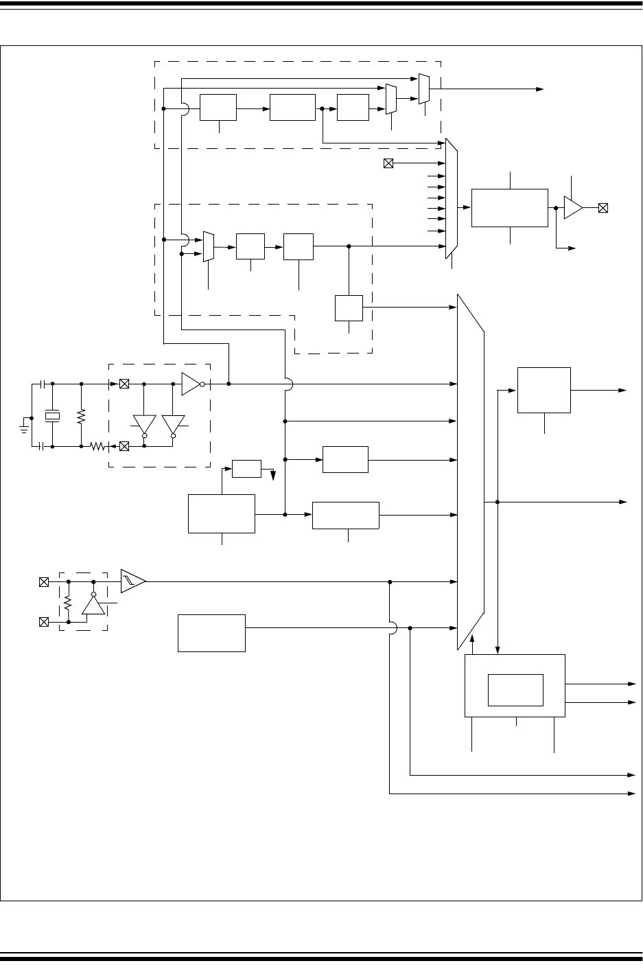
PIC32MX1XX/2XX 28/36/44-PIN FAMILY
DS60001168K-page 76 2011-2018 Microchip Technology Inc.
FIGURE 8-1: OSCILLATOR DIAGRAM
Timer1, RTCC
Clock Control Logic
Fail-Safe
Clock
Monitor
FSCM INT
FSCM Event
COSC<2:0>
NOSC<2:0>
OSWEN
FSCMEN<1:0>
PLL
Secondary Oscillator (S
OSC
)
SOSCEN and FSOSCEN
SOSCO
SOSCI
Primary Oscillator (P
OSC
)
P
OSC
(XT, HS, EC)
CPU and Select Peripherals
Peripherals
FRCDIV<2:0>
WDT, PWRT
8 MHz typical
FRC
31.25 kHz typical
FRC
Oscillator
LPRC
Oscillator
S
OSC
LPRC
FRCDIV
TUN<5:0>
div 16
Postscaler
FPLLIDIV<2:0>
PBDIV<1:0>
FRC/16
Postscaler
COSC<2:0>
F
IN
div x
div y
PLLODIV<2:0>
div x
32.768 kHz
PLLMULT<2:0>
PBCLK (T
PB
)
UF
IN
4 MHz
PLL x24
USB Clock (48 MHz)
div 2
UPLLEN
UFRCEN
div x
UPLLIDIV<2:0>
UF
IN
4 MHz
F
IN
5 MHz
C1
(2)
C2
(2)
XTAL
R
S
(1)
XT
Notes: 1.
A series resistor, R
S
, may be required for AT strip cut crystals or eliminate clipping. Alternately, to increase oscillator circuit gain,
add a parallel resistor, R
P
, with a value of 1 M
2.
Refer to
Section 6. “Oscillator Configuration”
(DS60001112) in the “
PIC32 Family Reference Manual
” for help in determining the
best oscillator components.
3.
The PBCLK out is only available on the OSC2 pin in certain clock modes.
4.
The USB PLL is only available on PIC32MX2XX devices.
OSC2
(3)
OSC1
To Internal
Logic
USB PLL
(4)
div 2
To ADC
SYSCLK
REFCLKI
REFCLKO
OE
To SPI
ROSEL<3:0>
P
OSC
FRC
LPRC
S
OSC
PBCLK
SYSCLK
XTPLL, HSPLL,
ECPLL, FRCPLL
2N
M
512
----------+
RODIV<14:0>
(N)
ROTRIM<8:0>
(M)
R
P
(1)
System PLL
HS 3x 1x
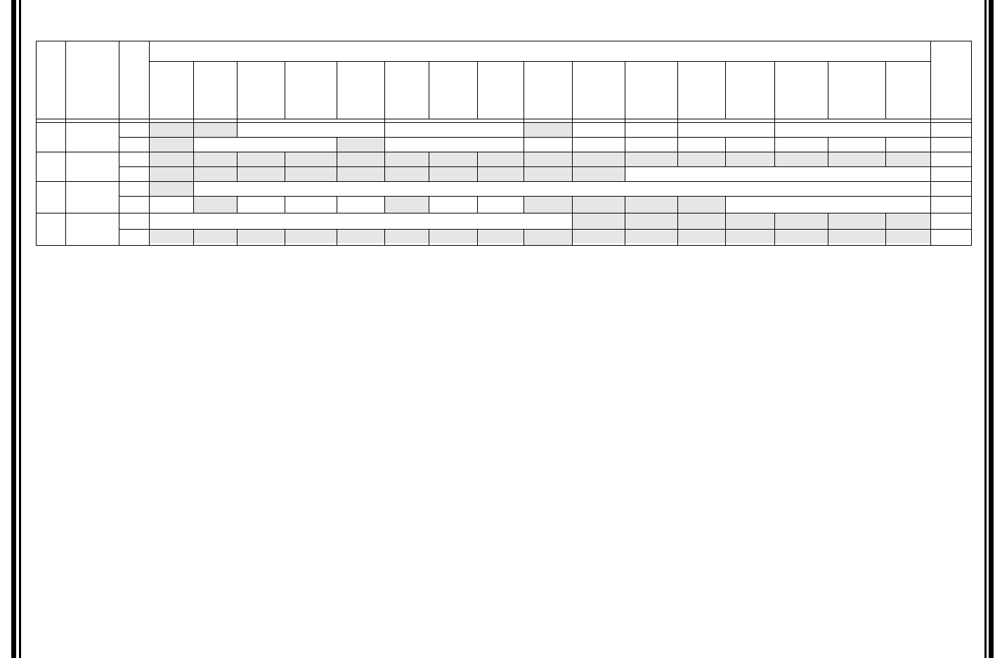
2011-2018 Microchip Technology Inc. DS60001168K-page 77
PIC32MX1XX/2XX 28/36/44-PIN FAMILY
8.1 Oscillator Control Regiters
TABLE 8-1: OSCILLATOR CONTROL REGISTER MAP
Virtual Address
(BF80_#)
Register
Name
(1)
Bit Range
Bits
All Resets
31/15 30/14 29/13 28/12 27/11 26/10 25/9 24/8 23/7 22/6 21/5 20/4 19/3 18/2 17/1 16/0
F000 OSCCON 31:16 —— PLLODIV<2:0> FRCDIV<2:0> — SOSCRDY PBDIVRDY PBDIV<1:0> PLLMULT<2:0> x1xx
(2)
15:0 —COSC<2:0> — NOSC<2:0> CLKLOCK ULOCK
(3)
SLOCK SLPEN CF UFRCEN
(3)
SOSCEN OSWEN xxxx
(2)
F010 OSCTUN 31:16 — — — — — — — — — — — — — — — — 0000
15:0 — — — — — — — — — — TUN<5:0> 0000
F020 REFOCON 31:16 —RODIV<14:0> 0000
15:0 ON —SIDL OERSLP— DIVSWEN ACTIVE — — — — ROSEL<3:0> 0000
F030 REFOTRIM 31:16 ROTRIM<8:0> — — — — — — — 0000
15:0 — — — — — — — — —— — — — — — — 0000
Legend: x = unknown value on Reset; — = unimplemented, read as ‘0’. Reset values are shown in hexadecimal.
Note 1: All registers in this table have corresponding CLR, SET and INV registers at their virtual addresses, plus offsets of 0x4, 0x8 and 0xC, respectively. See Section 11.2 “CLR, SET and INV Registers” for
more information.
2: Reset values are dependent on the DEVCFGx Configuration bits and the type of reset.
3: This bit is only available on PIC32MX2XX devices.
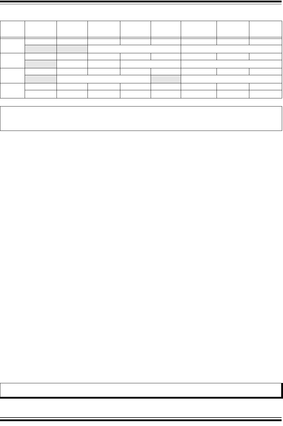
PIC32MX1XX/2XX 28/36/44-PIN FAMILY
DS60001168K-page 78 2011-2018 Microchip Technology Inc.
REGISTER 8-1: OSCCON: OSCILLATOR CONTROL REGISTER
Bit
Range Bit
31/23/15/7 Bit
30/22/14/6 Bit
29/21/13/5 Bit
28/20/12/4 Bit
27/19/11/3 Bit
26/18/10/2 Bit
25/17/9/1 Bit
24/16/8/0
31:24
U-0 U-0 R/W-y R/W-y R/W-y R/W-0 R/W-0 R/W-1
—— PLLODIV<2:0> FRCDIV<2:0>
23:16
U-0 R-0 R-1 R/W-y R/W-y R/W-y R/W-y R/W-y
— SOSCRDY PBDIVRDY PBDIV<1:0> PLLMULT<2:0>
15:8
U-0 R-0 R-0 R-0 U-0 R/W-y R/W-y R/W-y
— COSC<2:0> —NOSC<2:0>
7:0
R/W-0 R-0 R-0 R/W-0 R/W-0 R/W-0 R/W-y R/W-0
CLKLOCK ULOCK
(1)
SLOCK SLPEN CF UFRCEN
(1)
SOSCEN OSWEN
Legend: y = Value set from Configuration bits on POR
R = Readable bit W = Writable bit U = Unimplemented bit, read as ‘0’
-n = Value at POR ‘1’ = Bit is set ‘0’ = Bit is cleared x = Bit is unknown
bit 31-30 Unimplemented: Read as ‘0’
bit 29-27 PLLODIV<2:0>: Output Divider for PLL
111 = PLL output divided by 256
110 = PLL output divided by 64
101 = PLL output divided by 32
100 = PLL output divided by 16
011 = PLL output divided by 8
010 = PLL output divided by 4
001 = PLL output divided by 2
000 = PLL output divided by 1
bit 26-24 FRCDIV<2:0>: Internal Fast RC (FRC) Oscillator Clock Divider bits
111 = FRC divided by 256
110 = FRC divided by 64
101 = FRC divided by 32
100 = FRC divided by 16
011 = FRC divided by 8
010 = FRC divided by 4
001 = FRC divided by 2 (default setting)
000 = FRC divided by 1
bit 23 Unimplemented: Read as ‘0’
bit 22 SOSCRDY: Secondary Oscillator (S
OSC
) Ready Indicator bit
1 = The Secondary Oscillator is running and is stable
0 = The Secondary Oscillator is still warming up or is turned off
bit 21 PBDIVRDY: Peripheral Bus Clock (PBCLK) Divisor Ready bit
1 = PBDIV<1:0> bits can be written
0 = PBDIV<1:0> bits cannot be written
bit 20-19 PBDIV<1:0>: Peripheral Bus Clock (PBCLK) Divisor bits
11 = PBCLK is SYSCLK divided by 8 (default)
10 = PBCLK is SYSCLK divided by 4
01 = PBCLK is SYSCLK divided by 2
00 = PBCLK is SYSCLK divided by 1
Note 1: This bit is only available on PIC32MX2XX devices.
Note: Writes to this register require an unlock sequence. Refer to Section 6. “Oscillator” (DS60001112) in the
“PIC32 Family Reference Manual” for details.

2011-2018 Microchip Technology Inc. DS60001168K-page 79
PIC32MX1XX/2XX 28/36/44-PIN FAMILY
bit 18-16 PLLMULT<2:0>: Phase-Locked Loop (PLL) Multiplier bits
111 = Clock is multiplied by 24
110 = Clock is multiplied by 21
101 = Clock is multiplied by 20
100 = Clock is multiplied by 19
011 = Clock is multiplied by 18
010 = Clock is multiplied by 17
001 = Clock is multiplied by 16
000 = Clock is multiplied by 15
bit 15 Unimplemented: Read as ‘0’
bit 14-12 COSC<2:0>: Current Oscillator Selection bits
111 = Internal Fast RC (FRC) Oscillator divided by FRCDIV<2:0> bits (OSCCON<26:24>)
110 = Internal Fast RC (FRC) Oscillator divided by 16
101 = Internal Low-Power RC (LPRC) Oscillator
100 = Secondary Oscillator (S
OSC
)
011 = Primary Oscillator (P
OSC
) with PLL module (XTPLL, HSPLL or ECPLL)
010 = Primary Oscillator (P
OSC
) (XT, HS or EC)
001 = Internal Fast RC Oscillator with PLL module via Postscaler (FRCPLL)
000 = Internal Fast RC (FRC) Oscillator
bit 11 Unimplemented: Read as ‘0’
bit 10-8 NOSC<2:0>: New Oscillator Selection bits
111 = Internal Fast RC Oscillator (FRC) divided by OSCCON<FRCDIV> bits
110 = Internal Fast RC Oscillator (FRC) divided by 16
101 = Internal Low-Power RC (LPRC) Oscillator
100 = Secondary Oscillator (S
OSC
)
011 = Primary Oscillator with PLL module (XTPLL, HSPLL or ECPLL)
010 = Primary Oscillator (XT, HS or EC)
001 = Internal Fast Internal RC Oscillator with PLL module via Postscaler (FRCPLL)
000 = Internal Fast Internal RC Oscillator (FRC)
On Reset, these bits are set to the value of the FNOSC Configuration bits (DEVCFG1<2:0>).
bit 7 CLKLOCK: Clock Selection Lock Enable bit
If clock switching and monitoring is disabled (FCKSM<1:0> = 1x):
1 = Clock and PLL selections are locked
0 = Clock and PLL selections are not locked and may be modified
If clock switching and monitoring is enabled (FCKSM<1:0> = 0x):
Clock and PLL selections are never locked and may be modified.
bit 6 ULOCK: USB PLL Lock Status bit
(1)
1 = The USB PLL module is in lock or USB PLL module start-up timer is satisfied
0 =The USB PLL module is out of lock or USB PLL module start-up timer is in progress or the USB PLL is
disabled
bit 5 SLOCK: PLL Lock Status bit
1 = The PLL module is in lock or PLL module start-up timer is satisfied
0 = The PLL module is out of lock, the PLL start-up timer is running, or the PLL is disabled
bit 4 SLPEN: Sleep Mode Enable bit
1 = The device will enter Sleep mode when a WAIT instruction is executed
0 = The device will enter Idle mode when a WAIT instruction is executed
REGISTER 8-1: OSCCON: OSCILLATOR CONTROL REGISTER
Note 1: This bit is only available on PIC32MX2XX devices.
Note: Writes to this register require an unlock sequence. Refer to Section 6. “Oscillator” (DS60001112) in the
“PIC32 Family Reference Manual” for details.

PIC32MX1XX/2XX 28/36/44-PIN FAMILY
DS60001168K-page 80 2011-2018 Microchip Technology Inc.
bit 3 CF: Clock Fail Detect bit
1 = FSCM has detected a clock failure
0 = No clock failure has been detected
bit 2 UFRCEN: USB FRC Clock Enable bit
(1)
1 = Enable the FRC as the clock source for the USB clock source
0 = Use the Primary Oscillator or USB PLL as the USB clock source
bit 1 SOSCEN: Secondary Oscillator (S
OSC
) Enable bit
1 = Enable the Secondary Oscillator
0 = Disable the Secondary Oscillator
bit 0 OSWEN: Oscillator Switch Enable bit
1 = Initiate an oscillator switch to selection specified by NOSC<2:0> bits
0 = Oscillator switch is complete
REGISTER 8-1: OSCCON: OSCILLATOR CONTROL REGISTER
Note 1: This bit is only available on PIC32MX2XX devices.
Note: Writes to this register require an unlock sequence. Refer to Section 6. “Oscillator” (DS60001112) in the
“PIC32 Family Reference Manual” for details.

2011-2018 Microchip Technology Inc. DS60001168K-page 81
PIC32MX1XX/2XX 28/36/44-PIN FAMILY
REGISTER 8-2: OSCTUN: FRC TUNING REGISTER
Bit
Range Bit
31/23/15/7 Bit
30/22/14/6 Bit
29/21/13/5 Bit
28/20/12/4 Bit
27/19/11/3 Bit
26/18/10/2 Bit
25/17/9/1 Bit
24/16/8/0
31:24
U-0 U-0 U-0 U-0 U-0 U-0 U-0 U-0
————————
23:16
U-0 R-0 U-0 U-0 U-0 U-0 U-0 U-0
————————
15:8
U-0 R-0 U-0 U-0 U-0 U-0 U-0 U-0
————————
7:0
U-0 U-0 R/W-0 R/W-0 R/W-0 R/W-0 R/W-0 R/W-0
—— TUN<5:0>
(1)
Legend:
R = Readable bit W = Writable bit U = Unimplemented bit, read as ‘0’
-n = Value at POR ‘1’ = Bit is set ‘0’ = Bit is cleared x = Bit is unknown
bit 31-6 Unimplemented: Read as ‘0’
bit 5-0 TUN<5:0>: FRC Oscillator Tuning bits
(1)
100000 = Center frequency -12.5%
100001 =
•
•
•
111111 =
000000 = Center frequency. Oscillator runs at minimal frequency (8 MHz)
000001 =
•
•
•
011110 =
011111 = Center frequency +12.5%
Note 1: OSCTUN functionality has been provided to help customers compensate for temperature effects on the
FRC frequency over a wide range of temperatures. The tuning step size is an approximation, and is neither
characterized, nor tested.
Note: Writes to this register require an unlock sequence. Refer to Section 6. “Oscillator” (DS60001112) in the
“PIC32 Family Reference Manual” for details.

PIC32MX1XX/2XX 28/36/44-PIN FAMILY
DS60001168K-page 82 2011-2018 Microchip Technology Inc.
REGISTER 8-3: REFOCON: REFERENCE OSCILLATOR CONTROL REGISTER
Bit
Range Bit
31/23/15/7 Bit
30/22/14/6 Bit
29/21/13/5 Bit
28/20/12/4 Bit
27/19/11/3 Bit
26/18/10/2 Bit
25/17/9/1 Bit
24/16/8/0
31:24
U-0 R/W-0 R/W-0 R/W-0 R/W-0 R/W-0 R/W-0 R/W-0
—RODIV<14:8>
(1,3)
23:16
R/W-0 R/W-0 R/W-0 R/W-0 R/W-0 R/W-0 R/W-0 R/W-0
RODIV<7:0>
(1,3)
15:8
R/W-0 U-0 R/W-0 R/W-0 R/W-0 U-0 R/W-0, HC R-0, HS, HC
ON —SIDLOE
RSLP
(2)
— DIVSWEN ACTIVE
7:0
U-0 U-0 U-0 U-0 R/W-0 R/W-0 R/W-0 R/W-0
— — — — ROSEL<3:0>
(1)
Legend: HC = Hardware Clearable HS = Hardware Settable
R = Readable bit W = Writable bit U = Unimplemented bit, read as ‘0’
-n = Value at POR ‘1’ = Bit is set ‘0’ = Bit is cleared x = Bit is unknown
bit 31 Unimplemented: Read as ‘0’
bit 30-16 RODIV<14:0> Reference Clock Divider bits
(1,3)
The value selects the reference clock divider bits. See Figure 8-1 for information.
bit 15 ON: Output Enable bit
1 = Reference Oscillator module is enabled
0 = Reference Oscillator module is disabled
bit 14 Unimplemented: Read as ‘0’
bit 13 SIDL: Peripheral Stop in Idle Mode bit
1 = Discontinue module operation when the device enters Idle mode
0 = Continue module operation when the device enters Idle mode
bit 12 OE: Reference Clock Output Enable bit
1 = Reference clock is driven out on REFCLKO pin
0 = Reference clock is not driven out on REFCLKO pin
bit 11 RSLP: Reference Oscillator Module Run in Sleep bit
(2)
1 = Reference Oscillator module output continues to run in Sleep
0 = Reference Oscillator module output is disabled in Sleep
bit 10 Unimplemented: Read as ‘0’
bit 9 DIVSWEN: Divider Switch Enable bit
1 = Divider switch is in progress
0 = Divider switch is complete
bit 8 ACTIVE: Reference Clock Request Status bit
1 = Reference clock request is active
0 = Reference clock request is not active
bit 7-4 Unimplemented: Read as ‘0’
Note 1: The ROSEL and RODIV bits should not be written while the ACTIVE bit is ‘1’, as undefined behavior may
result.
2: This bit is ignored when the ROSEL<3:0> bits = 0000 or 0001.
3: While the ON bit is set to ‘1’, writes to these bits do not take effect until the DIVSWEN bit is also set to ’1’.

2011-2018 Microchip Technology Inc. DS60001168K-page 83
PIC32MX1XX/2XX 28/36/44-PIN FAMILY
bit 3-0 ROSEL<3:0>: Reference Clock Source Select bits
(1)
1111 = Reserved; do not use
•
•
•
1001 = Reserved; do not use
1000 =REFCLKI
0111 = System PLL output
0110 = USB PLL output
0101 =S
OSC
0100 =LPRC
0011 =FRC
0010 =P
OSC
0001 = PBCLK
0000 = SYSCLK
REGISTER 8-3: REFOCON: REFERENCE OSCILLATOR CONTROL REGISTER
Note 1: The ROSEL and RODIV bits should not be written while the ACTIVE bit is ‘1’, as undefined behavior may
result.
2: This bit is ignored when the ROSEL<3:0> bits = 0000 or 0001.
3: While the ON bit is set to ‘1’, writes to these bits do not take effect until the DIVSWEN bit is also set to ’1’.

PIC32MX1XX/2XX 28/36/44-PIN FAMILY
DS60001168K-page 84 2011-2018 Microchip Technology Inc.
REGISTER 8-4: REFOTRIM: REFERENCE OSCILLATOR TRIM REGISTER
Bit
Range Bit
31/23/15/7 Bit
30/22/14/6 Bit
29/21/13/5 Bit
28/20/12/4 Bit
27/19/11/3 Bit
26/18/10/2 Bit
25/17/9/1 Bit
24/16/8/0
31:24
R/W-0 R/W-0 R/W-0 R/W-0 R/W-0 R/W-0 R/W-0 R/W-0
ROTRIM<8:1>
23:16
R/W-0 R-0 U-0 U-0 U-0 U-0 U-0 U-0
ROTRIM<0> — — — — — — —
15:8
U-0 R-0 U-0 U-0 U-0 U-0 U-0 U-0
— — — — — — — —
7:0
U-0 U-0 U-0 U-0 U-0 U-0 U-0 U-0
— — — — — — — —
Legend:
R = Readable bit W = Writable bit U = Unimplemented bit, read as ‘0’
-n = Value at POR ‘1’ = Bit is set ‘0’ = Bit is cleared x = Bit is unknown
bit 31-23 ROTRIM<8:0>: Reference Oscillator Trim bits
111111111 = 511/512 divisor added to RODIV value
111111110 = 510/512 divisor added to RODIV value
•
•
•
100000000 = 256/512 divisor added to RODIV value
•
•
•
000000010 = 2/512 divisor added to RODIV value
000000001 = 1/512 divisor added to RODIV value
000000000 = 0/512 divisor added to RODIV value
bit 22-0 Unimplemented: Read as ‘0’
Note: While the ON (REFOCON<15>) bit is ‘1’, writes to this register do not take effect until the DIVSWEN bit is
also set to ‘1’.
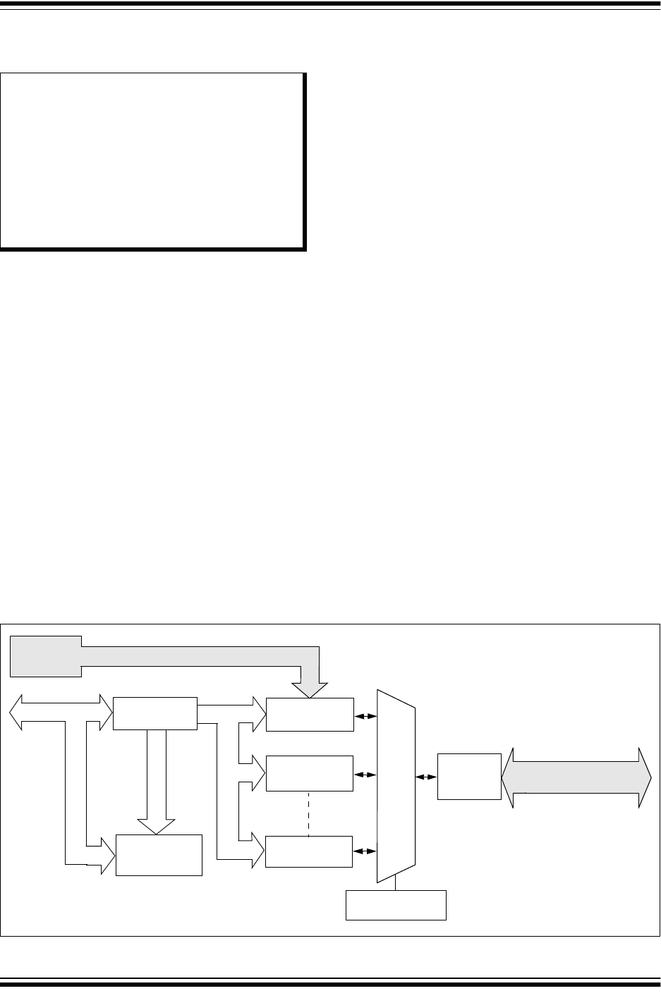
2011-2018 Microchip Technology Inc. DS60001168K-page 85
PIC32MX1XX/2XX 28/36/44-PIN FAMILY
9.0 DIRECT MEMORY ACCESS
(DMA) CONTROLLER
The PIC32 Direct Memory Access (DMA) controller is a
bus master module useful for data transfers between
different devices without CPU intervention. The source
and destination of a DMA transfer can be any of the
memory mapped modules existent in the PIC32, such
as Peripheral Bus devices: SPI, UART, PMP, etc., or
memory itself. Figure 9-1 show a block diagram of the
DMA Controller module.
The DMA Controller module has the following key
features:
• Four identical channels, each featuring:
- Auto-increment source and destination
address registers
- Source and destination pointers
- Memory to memory and memory to
peripheral transfers
• Automatic word-size detection:
- Transfer granularity, down to byte level
- Bytes need not be word-aligned at source
and destination
• Fixed priority channel arbitration
• Flexible DMA channel operating modes:
- Manual (software) or automatic (interrupt)
DMA requests
- One-Shot or Auto-Repeat Block Transfer
modes
- Channel-to-channel chaining
• Flexible DMA requests:
- A DMA request can be selected from any of
the peripheral interrupt sources
- Each channel can select any (appropriate)
observable interrupt as its DMA request
source
- A DMA transfer abort can be selected from
any of the peripheral interrupt sources
- Pattern (data) match transfer termination
• Multiple DMA channel status interrupts:
- DMA channel block transfer complete
- Source empty or half empty
- Destination full or half full
- DMA transfer aborted due to an external
event
- Invalid DMA address generated
• DMA debug support features:
- Most recent address accessed by a DMA
channel
- Most recent DMA channel to transfer data
• CRC Generation module:
- CRC module can be assigned to any of the
available channels
- CRC module is highly configurable
FIGURE 9-1: DMA BLOCK DIAGRAM
Note: This data sheet summarizes the features
of the PIC32MX1XX/2XX 28/36/44-pin
Family of devices. It is not intended to be
a comprehensive reference source. To
complement the information in this data
sheet, refer to Section 31. “Direct Mem-
ory Access (DMA) Controller”
(DS60001117), which is available from the
Documentation > Reference Manual
section of the Microchip PIC32 web site
(www.microchip.com/pic32).
Address Channel 0
Channel 1
Channel n
Global Control
(DMACON)
Bus
Channel Priority
Arbitration
SEL
SEL
Y
I
0
I
1
I
2
I
n
System IRQ
Interrupt
Device Bus and
Peripheral Bus Control
Control
Control
Interface
Decoder
Controller
Bus Arbitration
PIC32MX1XX/2XX 28/36/44-PIN FAMILY
DS60001168K-page 86 2011-2018 Microchip Technology Inc.
9.1 DMA Control Registers
TABLE 9-1: DMA GLOBAL REGISTER MAP
Virtual Address
(BF88_#)
Register
Name
(1)
Bit Range
Bits
All Resets
31/15 30/14 29/13 28/12 27/11 26/10 25/9 24/8 23/7 22/6 21/5 20/4 19/3 18/2 17/1 16/0
3000 DMACON 31:16 — — — — — — — — — — — — — — — — 0000
15:0 ON —— SUSPEND DMABUSY — — — — — — — — — — — 0000
3010 DMASTAT 31:16 — — — — — — — — — — — — — — — — 0000
15:0 — — — — — — — — — — — — RDWR DMACH<2:0>
(2)
0000
3020 DMAADDR 31:16 DMAADDR<31:0> 0000
15:0 0000
Legend: x = unknown value on Reset; — = unimplemented, read as ‘0’. Reset values are shown in hexadecimal.
Note 1: All registers in this table have corresponding CLR, SET and INV registers at its virtual address, plus an offset of 0x4, 0x8 and 0xC, respectively. See Section 11.2 “CLR, SET and INV Registers” for more
information.
TABLE 9-2: DMA CRC REGISTER MAP
Virtual Address
(BF88_#)
Register
Name
(1)
Bit Range
Bits
All Resets
31/15 30/14 29/13 28/12 27/11 26/10 25/9 24/8 23/7 22/6 21/5 20/4 19/3 18/2 17/1 16/0
3030 DCRCCON 31:16 ——BYTO<1:0>WBO——BITO————————0000
15:0 ——— PLEN<4:0> CRCEN CRCAPP CRCTYP —— CRCCH<2:0> 0000
3040 DCRCDATA 31:16 DCRCDATA<31:0> 0000
15:0 0000
3050 DCRCXOR 31:16 DCRCXOR<31:0> 0000
15:0 0000
Legend: x = unknown value on Reset; — = unimplemented, read as ‘0’. Reset values are shown in hexadecimal.
Note 1: All registers in this table have corresponding CLR, SET and INV registers at their virtual addresses, plus offsets of 0x4, 0x8 and 0xC, respectively. See Section 11.2 “CLR, SET and INV Registers” for
more information.
2011-2018 Microchip Technology Inc. DS60001168K-page 87
PIC32MX1XX/2XX 28/36/44-PIN FAMILY
TABLE 9-3: DMA CHANNELS 0-3 REGISTER MAP
Virtual Address
(BF88_#)
Register
Name
(1)
Bit Range
Bits
All Resets
31/15 30/14 29/13 28/12 27/11 26/10 25/9 24/8 23/7 22/6 21/5 20/4 19/3 18/2 17/1 16/0
3060 DCH0CON 31:16 — — — — — — — — — — — — — — — — 0000
15:0 CHBUSY — — — — — — CHCHNS CHEN CHAED CHCHN CHAEN — CHEDET CHPRI<1:0> 0000
3070 DCH0ECON 31:16 — — — — — — — — CHAIRQ<7:0> 00FF
15:0 CHSIRQ<7:0> CFORCE CABORT PATEN SIRQEN AIRQEN — — — FF00
3080 DCH0INT 31:16 — — — — — — — — CHSDIE CHSHIE CHDDIE CHDHIE CHBCIE CHCCIE CHTAIE CHERIE 0000
15:0 — — — — — — — — CHSDIF CHSHIF CHDDIF CHDHIF CHBCIF CHCCIF CHTAIF CHERIF 0000
3090 DCH0SSA 31:16 CHSSA<31:0> 0000
15:0 0000
30A0 DCH0DSA 31:16 CHDSA<31:0> 0000
15:0 0000
30B0 DCH0SSIZ 31:16 — — — — — — — — — — — — — — — — 0000
15:0 CHSSIZ<15:0> 0000
30C0 DCH0DSIZ 31:16 — — — — — — — — — — — — — — — — 0000
15:0 CHDSIZ<15:0> 0000
30D0 DCH0SPTR 31:16 — — — — — — — — — — — — — — — — 0000
15:0 CHSPTR<15:0> 0000
30E0 DCH0DPTR 31:16 — — — — — — — — — — — — — — — — 0000
15:0 CHDPTR<15:0> 0000
30F0 DCH0CSIZ 31:16 — — — — — — — — — — — — — — — — 0000
15:0 CHCSIZ<15:0> 0000
3100 DCH0CPTR 31:16 — — — — — — — — — — — — — — — — 0000
15:0 CHCPTR<15:0> 0000
3110 DCH0DAT 31:16 — — — — — — — — — — — — — — — — 0000
15:0 — — — — — — — — CHPDAT<7:0> 0000
3120 DCH1CON 31:16 — — — — — — — — — — — — — — — — 0000
15:0 CHBUSY — — — — — — CHCHNS CHEN CHAED CHCHN CHAEN — CHEDET CHPRI<1:0> 0000
3130 DCH1ECON 31:16 — — — — — — — — CHAIRQ<7:0> 00FF
15:0 CHSIRQ<7:0> CFORCE CABORT PATEN SIRQEN AIRQEN — — — FF00
3140 DCH1INT 31:16 — — — — — — — — CHSDIE CHSHIE CHDDIE CHDHIE CHBCIE CHCCIE CHTAIE CHERIE 0000
15:0 — — — — — — — — CHSDIF CHSHIF CHDDIF CHDHIF CHBCIF CHCCIF CHTAIF CHERIF 0000
3150 DCH1SSA 31:16 CHSSA<31:0> 0000
15:0 0000
3160 DCH1DSA 31:16 CHDSA<31:0> 0000
15:0 0000
Legend: x = unknown value on Reset; — = unimplemented, read as ‘0’. Reset values are shown in hexadecimal.
Note 1: All registers in this table have corresponding CLR, SET and INV registers at their virtual addresses, plus offsets of 0x4, 0x8 and 0xC, respectively. See Section 11.2 “CLR, SET and INV Registers” for
more information.
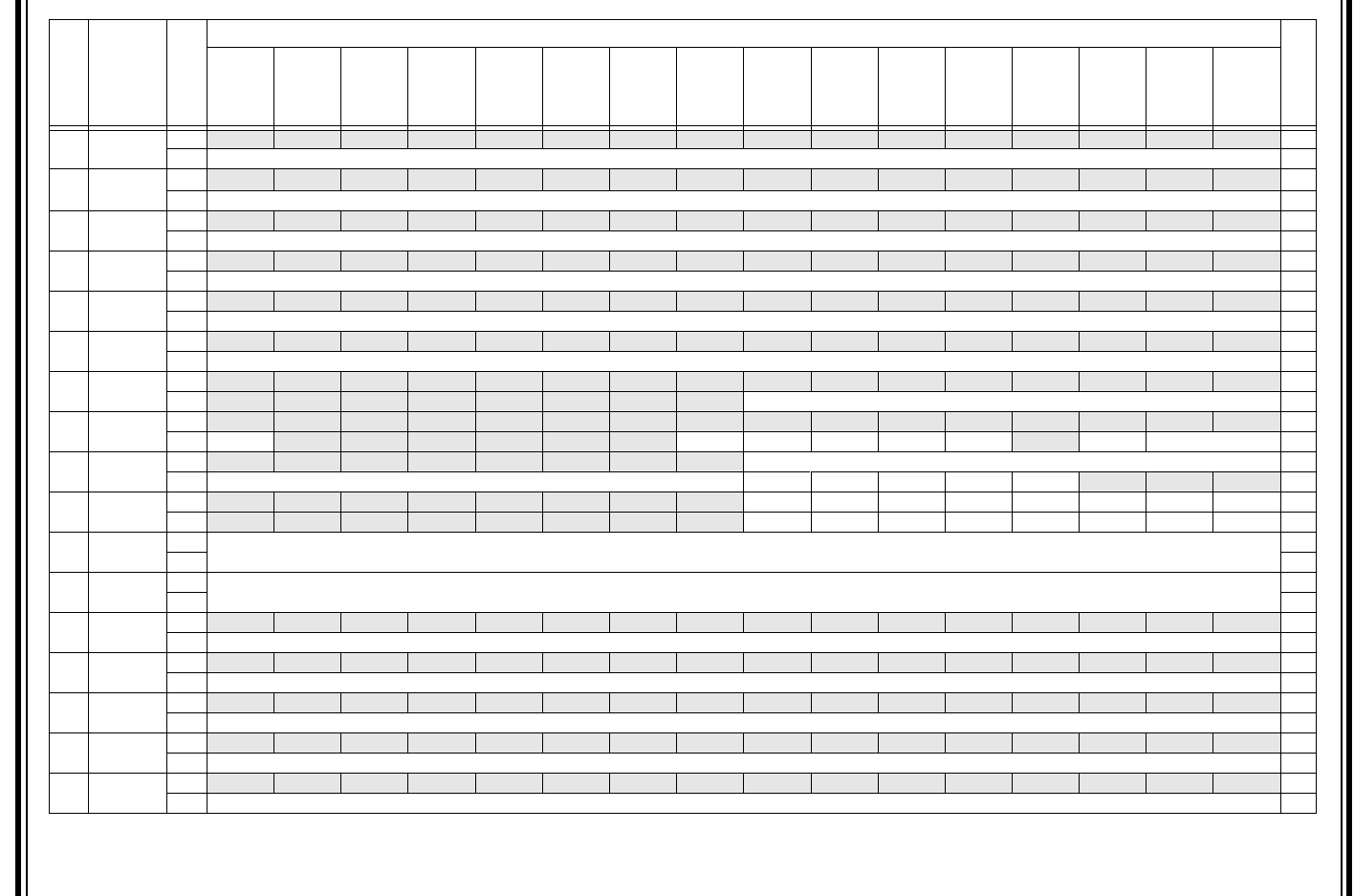
PIC32MX1XX/2XX 28/36/44-PIN FAMILY
DS60001168K-page 88 2011-2018 Microchip Technology Inc.
3170 DCH1SSIZ 31:16 — — — — — — — — — — — — — — — — 0000
15:0 CHSSIZ<15:0> 0000
3180 DCH1DSIZ 31:16 — — — — — — — — — — — — — — — — 0000
15:0 CHDSIZ<15:0> 0000
3190 DCH1SPTR 31:16 — — — — — — — — — — — — — — — — 0000
15:0 CHSPTR<15:0> 0000
31A0 DCH1DPTR 31:16 — — — — — — — — — — — — — — — — 0000
15:0 CHDPTR<15:0> 0000
31B0 DCH1CSIZ 31:16 — — — — — — — — — — — — — — — — 0000
15:0 CHCSIZ<15:0> 0000
31C0 DCH1CPTR 31:16 — — — — — — — — — — — — — — — — 0000
15:0 CHCPTR<15:0> 0000
31D0 DCH1DAT 31:16 — — — — — — — — — — — — — — — — 0000
15:0 — — — — — — — — CHPDAT<7:0> 0000
31E0 DCH2CON 31:16 — — — — — — — — — — — — — — — — 0000
15:0 CHBUSY — — — — — — CHCHNS CHEN CHAED CHCHN CHAEN — CHEDET CHPRI<1:0> 0000
31F0 DCH2ECON 31:16 — — — — — — — — CHAIRQ<7:0> 00FF
15:0 CHSIRQ<7:0> CFORCE CABORT PATEN SIRQEN AIRQEN — — — FF00
3200 DCH2INT 31:16 — — — — — — — — CHSDIE CHSHIE CHDDIE CHDHIE CHBCIE CHCCIE CHTAIE CHERIE 0000
15:0 — — — — — — — — CHSDIF CHSHIF CHDDIF CHDHIF CHBCIF CHCCIF CHTAIF CHERIF 0000
3210 DCH2SSA 31:16 CHSSA<31:0> 0000
15:0 0000
3220 DCH2DSA 31:16 CHDSA<31:0> 0000
15:0 0000
3230 DCH2SSIZ 31:16 — — — — — — — — — — — — — — — — 0000
15:0 CHSSIZ<15:0> 0000
3240 DCH2DSIZ 31:16 — — — — — — — — — — — — — — — — 0000
15:0 CHDSIZ<15:0> 0000
3250 DCH2SPTR 31:16 — — — — — — — — — — — — — — — — 0000
15:0 CHSPTR<15:0> 0000
3260 DCH2DPTR 31:16 — — — — — — — — — — — — — — — — 0000
15:0 CHDPTR<15:0> 0000
3270 DCH2CSIZ 31:16 — — — — — — — — — — — — — — — — 0000
15:0 CHCSIZ<15:0> 0000
TABLE 9-3: DMA CHANNELS 0-3 REGISTER MAP (CONTINUED)
Virtual Address
(BF88_#)
Register
Name
(1)
Bit Range
Bits
All Resets
31/15 30/14 29/13 28/12 27/11 26/10 25/9 24/8 23/7 22/6 21/5 20/4 19/3 18/2 17/1 16/0
Legend: x = unknown value on Reset; — = unimplemented, read as ‘0’. Reset values are shown in hexadecimal.
Note 1: All registers in this table have corresponding CLR, SET and INV registers at their virtual addresses, plus offsets of 0x4, 0x8 and 0xC, respectively. See Section 11.2 “CLR, SET and INV Registers” for
more information.
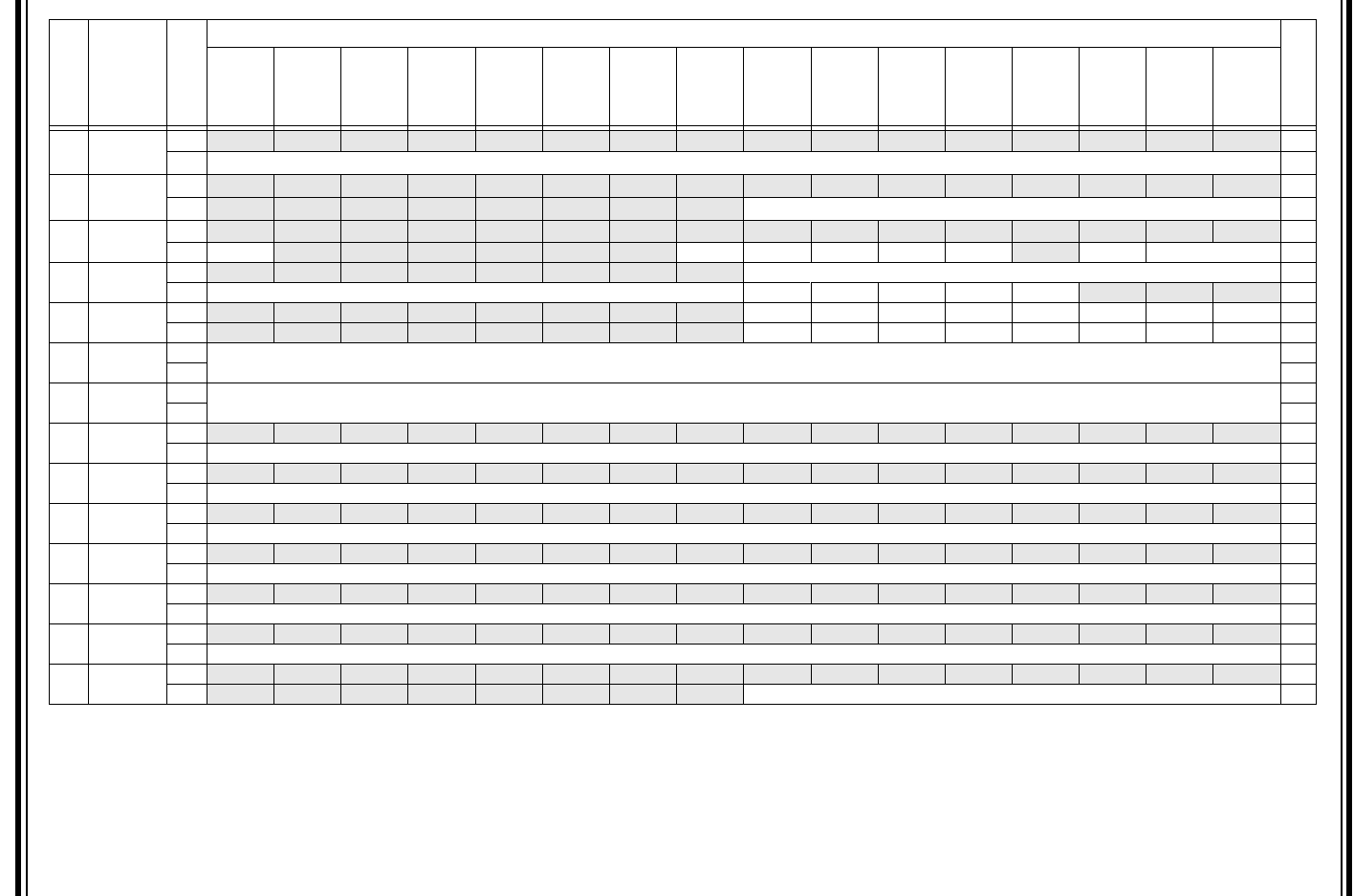
2011-2018 Microchip Technology Inc. DS60001168K-page 89
PIC32MX1XX/2XX 28/36/44-PIN FAMILY
3280 DCH2CPTR 31:16 — — — — — — — — — — — — — — — — 0000
15:0 CHCPTR<15:0> 0000
3290 DCH2DAT 31:16 — — — — — — — — — — — — — — — — 0000
15:0 — — — — — — — — CHPDAT<7:0> 0000
32A0 DCH3CON 31:16 — — — — — — — — — — — — — — — — 0000
15:0 CHBUSY — — — — — — CHCHNS CHEN CHAED CHCHN CHAEN — CHEDET CHPRI<1:0> 0000
32B0 DCH3ECON 31:16 — — — — — — — — CHAIRQ<7:0> 00FF
15:0 CHSIRQ<7:0> CFORCE CABORT PATEN SIRQEN AIRQEN — — — FF00
32C0 DCH3INT 31:16 — — — — — — — — CHSDIE CHSHIE CHDDIE CHDHIE CHBCIE CHCCIE CHTAIE CHERIE 0000
15:0 — — — — — — — — CHSDIF CHSHIF CHDDIF CHDHIF CHBCIF CHCCIF CHTAIF CHERIF 0000
32D0 DCH3SSA 31:16 CHSSA<31:0> 0000
15:0 0000
32E0 DCH3DSA 31:16 CHDSA<31:0> 0000
15:0 0000
32F0 DCH3SSIZ 31:16 — — — — — — — — — — — — — — — — 0000
15:0 CHSSIZ<15:0> 0000
3300 DCH3DSIZ 31:16 — — — — — — — — — — — — — — — — 0000
15:0 CHDSIZ<15:0> 0000
3310 DCH3SPTR 31:16 — — — — — — — — — — — — — — — — 0000
15:0 CHSPTR<15:0> 0000
3320 DCH3DPTR 31:16 — — — — — — — — — — — — — — — — 0000
15:0 CHDPTR<15:0> 0000
3330 DCH3CSIZ 31:16 — — — — — — — — — — — — — — — — 0000
15:0 CHCSIZ<15:0> 0000
3340 DCH3CPTR 31:16 — — — — — — — — — — — — — — — — 0000
15:0 CHCPTR<15:0> 0000
3350 DCH3DAT 31:16 — — — — — — — — — — — — — — — — 0000
15:0 — — — — — — — — CHPDAT<7:0> 0000
TABLE 9-3: DMA CHANNELS 0-3 REGISTER MAP (CONTINUED)
Virtual Address
(BF88_#)
Register
Name
(1)
Bit Range
Bits
All Resets
31/15 30/14 29/13 28/12 27/11 26/10 25/9 24/8 23/7 22/6 21/5 20/4 19/3 18/2 17/1 16/0
Legend: x = unknown value on Reset; — = unimplemented, read as ‘0’. Reset values are shown in hexadecimal.
Note 1: All registers in this table have corresponding CLR, SET and INV registers at their virtual addresses, plus offsets of 0x4, 0x8 and 0xC, respectively. See Section 11.2 “CLR, SET and INV Registers” for
more information.

PIC32MX1XX/2XX 28/36/44-PIN FAMILY
DS60001168K-page 90 2011-2018 Microchip Technology Inc.
REGISTER 9-1: DMACON: DMA CONTROLLER CONTROL REGISTER
Bit
Range Bit
31/23/15/7 Bit
30/22/14/6 Bit
29/21/13/5 Bit
28/20/12/4 Bit
27/19/11/3 Bit
26/18/10/2 Bit
25/17/9/1 Bit
24/16/8/0
31:24
U-0 U-0 U-0 U-0 U-0 U-0 U-0 U-0
— — — — — — — —
23:16
U-0 U-0 U-0 U-0 U-0 U-0 U-0 U-0
— — — — — — — —
15:8
R/W-0 U-0 U-0 R/W-0 R/W-0 U-0 U-0 U-0
ON
(1)
—— SUSPEND DMABUSY — — —
7:0
U-0 U-0 U-0 U-0 U-0 U-0 U-0 U-0
— — — — — — — —
Legend:
R = Readable bit W = Writable bit U = Unimplemented bit, read as ‘0’
-n = Value at POR ‘1’ = Bit is set ‘0’ = Bit is cleared x = Bit is unknown
bit 31-16 Unimplemented: Read as ‘0’
bit 15 ON: DMA On bit
(1)
1 = DMA module is enabled
0 = DMA module is disabled
bit 14-13 Unimplemented: Read as ‘0’
bit 12 SUSPEND: DMA Suspend bit
1 = DMA transfers are suspended to allow CPU uninterrupted access to data bus
0 = DMA operates normally
bit 11 DMABUSY: DMA Module Busy bit
1 = DMA module is active
0 = DMA module is disabled and not actively transferring data
bit 10-0 Unimplemented: Read as ‘0’
Note 1: When using 1:1 PBCLK divisor, the user’s software should not read/write the peripheral’s SFRs in the
SYSCLK cycle immediately following the instruction that clears the module’s ON bit.
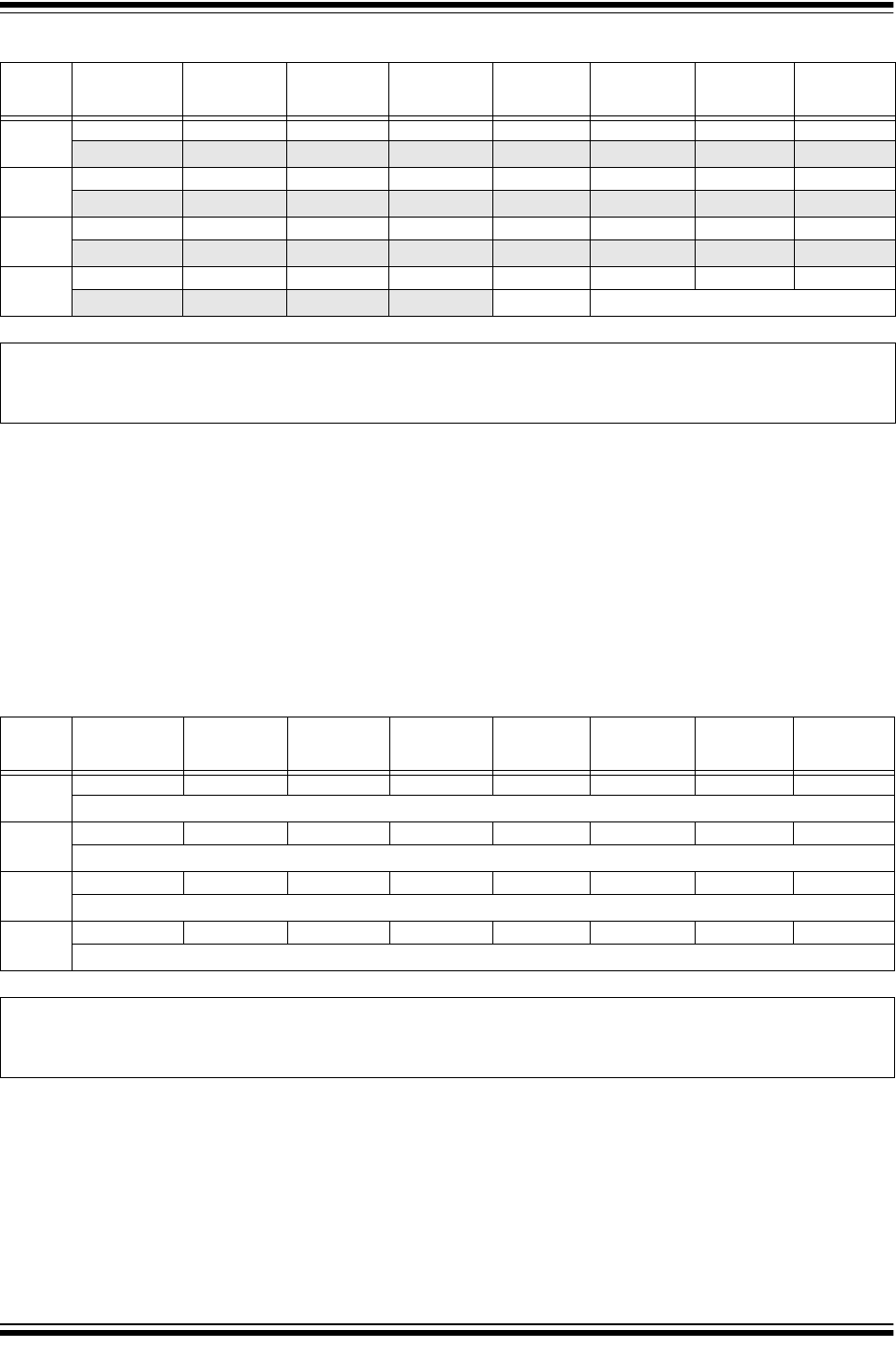
2011-2018 Microchip Technology Inc. DS60001168K-page 91
PIC32MX1XX/2XX 28/36/44-PIN FAMILY
REGISTER 9-2: DMASTAT: DMA STATUS REGISTER
Bit
Range Bit
31/23/15/7 Bit
30/22/14/6 Bit
29/21/13/5 Bit
28/20/12/4 Bit
27/19/11/3 Bit
26/18/10/2 Bit
25/17/9/1 Bit
24/16/8/0
31:24
U-0 U-0 U-0 U-0 U-0 U-0 U-0 U-0
— — — — — — — —
23:16
U-0 U-0 U-0 U-0 U-0 U-0 U-0 U-0
— — — — — — — —
15:8
U-0 U-0 U-0 U-0 U-0 U-0 U-0 U-0
— — — — — — — —
7:0
U-0 U-0 U-0 U-0 R-0 R-0 R-0 R-0
— — — — RDWR DMACH<2:0>
Legend:
R = Readable bit W = Writable bit U = Unimplemented bit, read as ‘0’
-n = Value at POR ‘1’ = Bit is set ‘0’ = Bit is cleared x = Bit is unknown
bit 31-4 Unimplemented: Read as ‘0’
bit 3 RDWR: Read/Write Status bit
1 = Last DMA bus access was a read
0 = Last DMA bus access was a write
bit 2-0 DMACH<2:0>: DMA Channel bits
These bits contain the value of the most recent active DMA channel.
REGISTER 9-3: DMAADDR: DMA ADDRESS REGISTER
Bit
Range Bit
31/23/15/7 Bit
30/22/14/6 Bit
29/21/13/5 Bit
28/20/12/4 Bit
27/19/11/3 Bit
26/18/10/2 Bit
25/17/9/1 Bit
24/16/8/0
31:24
R-0 R-0 R-0 R-0 R-0 R-0 R-0 R-0
DMAADDR<31:24>
23:16
R-0 R-0 R-0 R-0 R-0 R-0 R-0 R-0
DMAADDR<23:16>
15:8
R-0 R-0 R-0 R-0 R-0 R-0 R-0 R-0
DMAADDR<15:8>
7:0
R-0 R-0 R-0 R-0 R-0 R-0 R-0 R-0
DMAADDR<7:0>
Legend:
R = Readable bit W = Writable bit U = Unimplemented bit, read as ‘0’
-n = Value at POR ‘1’ = Bit is set ‘0’ = Bit is cleared x = Bit is unknown
bit 31-0 DMAADDR<31:0>: DMA Module Address bits
These bits contain the address of the most recent DMA access.

PIC32MX1XX/2XX 28/36/44-PIN FAMILY
DS60001168K-page 92 2011-2018 Microchip Technology Inc.
REGISTER 9-4: DCRCCON: DMA CRC CONTROL REGISTER
Bit
Range Bit
31/23/15/7 Bit
30/22/14/6 Bit
29/21/13/5 Bit
28/20/12/4 Bit
27/19/11/3 Bit
26/18/10/2 Bit
25/17/9/1 Bit
24/16/8/0
31:24
U-0 U-0 R/W-0 R/W-0 R/W-0 U-0 U-0 R/W-0
—— BYTO<1:0> WBO
(1)
——BITO
23:16
U-0 U-0 U-0 U-0 U-0 U-0 U-0 U-0
— — — — — — — —
15:8
U-0 U-0 U-0 R/W-0 R/W-0 R/W-0 R/W-0 R/W-0
— — — PLEN<4:0>
7:0
R/W-0 R/W-0 R/W-0 U-0 U-0 R/W-0 R/W-0 R/W-0
CRCEN CRCAPP
(1)
CRCTYP —— CRCCH<2:0>
Legend:
R = Readable bit W = Writable bit U = Unimplemented bit, read as ‘0’
-n = Value at POR ‘1’ = Bit is set ‘0’ = Bit is cleared x = Bit is unknown
bit 31-30 Unimplemented: Read as ‘0’
bit 29-28 BYTO<1:0>: CRC Byte Order Selection bits
11 = Endian byte swap on half-word boundaries (i.e., source half-word order with reverse source byte order
per half-word)
10 = Swap half-words on word boundaries (i.e., reverse source half-word order with source byte order per
half-word)
01 = Endian byte swap on word boundaries (i.e., reverse source byte order)
00 = No swapping (i.e., source byte order)
bit 27 WBO: CRC Write Byte Order Selection bit
(1)
1 = Source data is written to the destination re-ordered as defined by BYTO<1:0>
0 = Source data is written to the destination unaltered
bit 26-25 Unimplemented: Read as ‘0’
bit 24 BITO: CRC Bit Order Selection bit
When CRCTYP (DCRCCON<15>) = 1 (CRC module is in IP Header mode):
1 = The IP header checksum is calculated Least Significant bit (LSb) first (i.e., reflected)
0 = The IP header checksum is calculated Most Significant bit (MSb) first (i.e., not reflected)
When CRCTYP (DCRCCON<15>) = 0 (CRC module is in LFSR mode):
1 = The LFSR CRC is calculated Least Significant bit first (i.e., reflected)
0 = The LFSR CRC is calculated Most Significant bit first (i.e., not reflected)
bit 23-13 Unimplemented: Read as ‘0’
bit 12-8 PLEN<4:0>: Polynomial Length bits
When CRCTYP (DCRCCON<15>) = 1 (CRC module is in IP Header mode):
These bits are unused.
When CRCTYP (DCRCCON<15>) = 0 (CRC module is in LFSR mode):
Denotes the length of the polynomial – 1.
bit 7 CRCEN: CRC Enable bit
1 = CRC module is enabled and channel transfers are routed through the CRC module
0 = CRC module is disabled and channel transfers proceed normally
Note 1: When WBO = 1, unaligned transfers are not supported and the CRCAPP bit cannot be set.

2011-2018 Microchip Technology Inc. DS60001168K-page 93
PIC32MX1XX/2XX 28/36/44-PIN FAMILY
bit 6 CRCAPP: CRC Append Mode bit
(1)
1 = The DMA transfers data from the source into the CRC but NOT to the destination. When a block transfer
completes the DMA writes the calculated CRC value to the location given by CHxDSA
0 = The DMA transfers data from the source through the CRC obeying WBO as it writes the data to the
destination
bit 5 CRCTYP: CRC Type Selection bit
1 = The CRC module will calculate an IP header checksum
0 = The CRC module will calculate a LFSR CRC
bit 4-3 Unimplemented: Read as ‘0’
bit 2-0 CRCCH<2:0>: CRC Channel Select bits
111 = CRC is assigned to Channel 7
110 = CRC is assigned to Channel 6
101 = CRC is assigned to Channel 5
100 = CRC is assigned to Channel 4
011 = CRC is assigned to Channel 3
010 = CRC is assigned to Channel 2
001 = CRC is assigned to Channel 1
000 = CRC is assigned to Channel 0
REGISTER 9-4: DCRCCON: DMA CRC CONTROL REGISTER (CONTINUED)
Note 1: When WBO = 1, unaligned transfers are not supported and the CRCAPP bit cannot be set.
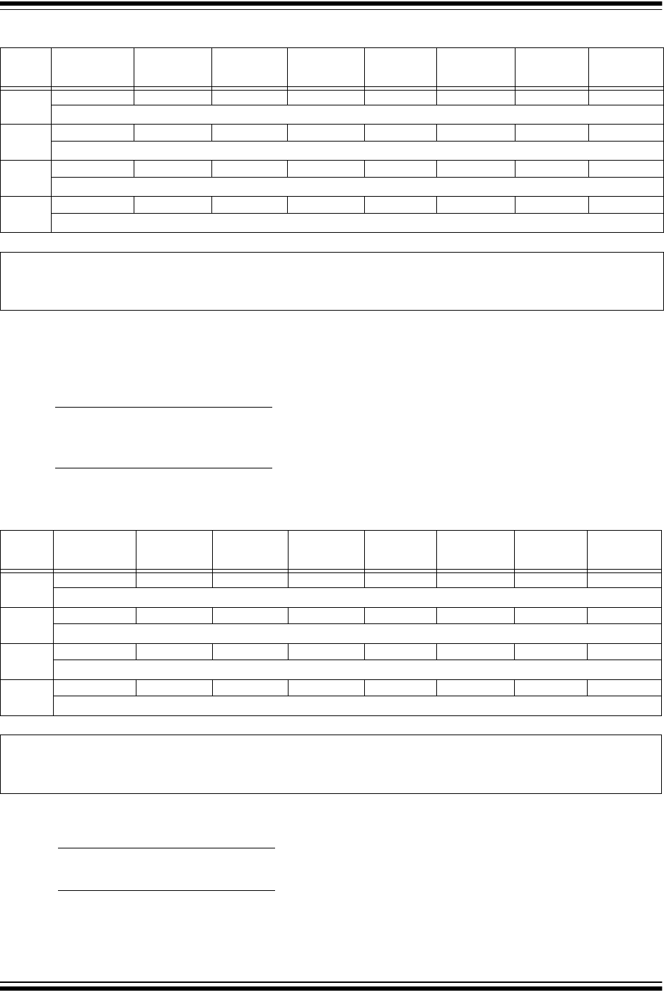
PIC32MX1XX/2XX 28/36/44-PIN FAMILY
DS60001168K-page 94 2011-2018 Microchip Technology Inc.
REGISTER 9-5: DCRCDATA: DMA CRC DATA REGISTER
Bit
Range Bit
31/23/15/7 Bit
30/22/14/6 Bit
29/21/13/5 Bit
28/20/12/4 Bit
27/19/11/3 Bit
26/18/10/2 Bit
25/17/9/1 Bit
24/16/8/0
31:24
R/W-0 R/W-0 R/W-0 R/W-0 R/W-0 R/W-0 R/W-0 R/W-0
DCRCDATA<31:24>
23:16
R/W-0 R/W-0 R/W-0 R/W-0 R/W-0 R/W-0 R/W-0 R/W-0
DCRCDATA<23:16>
15:8
R/W-0 R/W-0 R/W-0 R/W-0 R/W-0 R/W-0 R/W-0 R/W-0
DCRCDATA<15:8>
7:0
R/W-0 R/W-0 R/W-0 R/W-0 R/W-0 R/W-0 R/W-0 R/W-0
DCRCDATA<7:0>
Legend:
R = Readable bit W = Writable bit U = Unimplemented bit, read as ‘0’
-n = Value at POR ‘1’ = Bit is set ‘0’ = Bit is cleared x = Bit is unknown
bit 31-0 DCRCDATA<31:0>: CRC Data Register bits
Writing to this register will seed the CRC generator. Reading from this register will return the current value of
the CRC. Bits greater than PLEN will return ‘0’ on any read.
When CRCTYP (DCRCCON<15>) = 1 (CRC module is in IP Header mode):
Only the lower 16 bits contain IP header checksum information. The upper 16 bits are always ‘0’. Data written
to this register is converted and read back in 1’s complement form (i.e., current IP header checksum value).
When CRCTYP (DCRCCON<15>) = 0 (CRC module is in LFSR mode):
Bits greater than PLEN will return ‘0’ on any read.
REGISTER 9-6: DCRCXOR: DMA CRCXOR ENABLE REGISTER
Bit
Range Bit
31/23/15/7 Bit
30/22/14/6 Bit
29/21/13/5 Bit
28/20/12/4 Bit
27/19/11/3 Bit
26/18/10/2 Bit
25/17/9/1 Bit
24/16/8/0
31:24
R/W-0 R/W-0 R/W-0 R/W-0 R/W-0 R/W-0 R/W-0 R/W-0
DCRCXOR<31:24>
23:16
R/W-0 R/W-0 R/W-0 R/W-0 R/W-0 R/W-0 R/W-0 R/W-0
DCRCXOR<23:16>
15:8
R/W-0 R/W-0 R/W-0 R/W-0 R/W-0 R/W-0 R/W-0 R/W-0
DCRCXOR<15:8>
7:0
R/W-0 R/W-0 R/W-0 R/W-0 R/W-0 R/W-0 R/W-0 R/W-0
DCRCXOR<7:0>
Legend:
R = Readable bit W = Writable bit U = Unimplemented bit, read as ‘0’
-n = Value at POR ‘1’ = Bit is set ‘0’ = Bit is cleared x = Bit is unknown
bit 31-0 DCRCXOR<31:0>: CRC XOR Register bits
When CRCTYP (DCRCCON<15>) = 1 (CRC module is in IP Header mode):
This register is unused.
When CRCTYP (DCRCCON<15>) = 0 (CRC module is in LFSR mode):
1 = Enable the XOR input to the Shift register
0 = Disable the XOR input to the Shift register; data is shifted in directly from the previous stage in
the register

2011-2018 Microchip Technology Inc. DS60001168K-page 95
PIC32MX1XX/2XX 28/36/44-PIN FAMILY
REGISTER 9-7: DCHxCON: DMA CHANNEL ‘x’ CONTROL REGISTER
Bit
Range Bit
31/23/15/7 Bit
30/22/14/6 Bit
29/21/13/5 Bit
28/20/12/4 Bit
27/19/11/3 Bit
26/18/10/2 Bit
25/17/9/1 Bit
24/16/8/0
31:24
U-0 U-0 U-0 U-0 U-0 U-0 U-0 U-0
— — — — — — — —
23:16
U-0 U-0 U-0 U-0 U-0 U-0 U-0 U-0
— — — — — — — —
15:8
R/W-0 U-0 U-0 U-0 U-0 U-0 U-0 R/W-0
CHBUSY — — — — — — CHCHNS
(1)
7:0
R/W-0 R/W-0 R/W-0 R/W-0 U-0 R-0 R/W-0 R/W-0
CHEN
(2)
CHAED CHCHN CHAEN — CHEDET CHPRI<1:0>
Legend:
R = Readable bit W = Writable bit U = Unimplemented bit, read as ‘0’
-n = Value at POR ‘1’ = Bit is set ‘0’ = Bit is cleared x = Bit is unknown
bit 31-16 Unimplemented: Read as ‘0’
bit 15 CHBUSY: Channel Busy bit
1 = Channel is active or has been enabled
0 = Channel is inactive or has been disabled
bit 14-9 Unimplemented: Read as ‘0’
bit 8 CHCHNS: Chain Channel Selection bit
(1)
1 = Chain to channel lower in natural priority (CH1 will be enabled by CH2 transfer complete)
0 = Chain to channel higher in natural priority (CH1 will be enabled by CH0 transfer complete)
bit 7 CHEN: Channel Enable bit
(2)
1 = Channel is enabled
0 = Channel is disabled
bit 6 CHAED: Channel Allow Events If Disabled bit
1 = Channel start/abort events will be registered, even if the channel is disabled
0 = Channel start/abort events will be ignored if the channel is disabled
bit CHCHN: Channel Chain Enable bit
1 = Allow channel to be chained
0 = Do not allow channel to be chained
bit 4 CHAEN: Channel Automatic Enable bit
1 = Channel is continuously enabled, and not automatically disabled after a block transfer is complete
0 = Channel is disabled on block transfer complete
bit 3 Unimplemented: Read as ‘0’
bit 2 CHEDET: Channel Event Detected bit
1 = An event has been detected
0 = No events have been detected
bit 1-0 CHPRI<1:0>: Channel Priority bits
11 = Channel has priority 3 (highest)
10 = Channel has priority 2
01 = Channel has priority 1
00 = Channel has priority 0
Note 1: The chain selection bit takes effect when chaining is enabled (i.e., CHCHN = 1).
2: When the channel is suspended by clearing this bit, the user application should poll the CHBUSY bit (if
available on the device variant) to see when the channel is suspended, as it may take some clock cycles
to complete a current transaction before the channel is suspended.

PIC32MX1XX/2XX 28/36/44-PIN FAMILY
DS60001168K-page 96 2011-2018 Microchip Technology Inc.
REGISTER 9-8: DCHxECON: DMA CHANNEL ‘x’ EVENT CONTROL REGISTER
Bit
Range Bit
31/23/15/7 Bit
30/22/14/6 Bit
29/21/13/5 Bit
28/20/12/4 Bit
27/19/11/3 Bit
26/18/10/2 Bit
25/17/9/1 Bit
24/16/8/0
31:24
U-0 U-0 U-0 U-0 U-0 U-0 U-0 U-0
— — — — — — — —
23:16
R/W-1 R/W-1 R/W-1 R/W-1 R/W-1 R/W-1 R/W-1 R/W-1
CHAIRQ<7:0>
(1)
15:8
R/W-1 R/W-1 R/W-1 R/W-1 R/W-1 R/W-1 R/W-1 R/W-1
CHSIRQ<7:0>
(1)
7:0
S-0 S-0 R/W-0 R/W-0 R/W-0 U-0 U-0 U-0
CFORCE CABORT PATEN SIRQEN AIRQEN — — —
Legend: S = Settable bit
R = Readable bit W = Writable bit U = Unimplemented bit, read as ‘0’
-n = Value at POR ‘1’ = Bit is set ‘0’ = Bit is cleared x = Bit is unknown
bit 31-24 Unimplemented: Read as ‘0’
bit 23-16 CHAIRQ<7:0>: Channel Transfer Abort IRQ bits
(1)
11111111 = Interrupt 255 will abort any transfers in progress and set CHAIF flag
•
•
•
00000001 = Interrupt 1 will abort any transfers in progress and set CHAIF flag
00000000 = Interrupt 0 will abort any transfers in progress and set CHAIF flag
bit 15-8 CHSIRQ<7:0>: Channel Transfer Start IRQ bits
(1)
11111111 = Interrupt 255 will initiate a DMA transfer
•
•
•
00000001 = Interrupt 1 will initiate a DMA transfer
00000000 = Interrupt 0 will initiate a DMA transfer
bit 7 CFORCE: DMA Forced Transfer bit
1 = A DMA transfer is forced to begin when this bit is written to a ‘1’
0 = This bit always reads ‘0’
bit 6 CABORT: DMA Abort Transfer bit
1 = A DMA transfer is aborted when this bit is written to a ‘1’
0 = This bit always reads ‘0’
bit 5 PATEN: Channel Pattern Match Abort Enable bit
1 = Abort transfer and clear CHEN on pattern match
0 = Pattern match is disabled
bit 4 SIRQEN: Channel Start IRQ Enable bit
1 = Start channel cell transfer if an interrupt matching CHSIRQ occurs
0 = Interrupt number CHSIRQ is ignored and does not start a transfer
bit 3 AIRQEN: Channel Abort IRQ Enable bit
1 = Channel transfer is aborted if an interrupt matching CHAIRQ occurs
0 = Interrupt number CHAIRQ is ignored and does not terminate a transfer
bit 2-0 Unimplemented: Read as ‘0’
Note 1: See Table 7-1: “Interrupt IRQ, Vector and Bit Location” for the list of available interrupt IRQ sources.

2011-2018 Microchip Technology Inc. DS60001168K-page 97
PIC32MX1XX/2XX 28/36/44-PIN FAMILY
REGISTER 9-9: DCHxINT: DMA CHANNEL ‘x’ INTERRUPT CONTROL REGISTER
Bit
Range Bit
31/23/15/7 Bit
30/22/14/6 Bit
29/21/13/5 Bit
28/20/12/4 Bit
27/19/11/3 Bit
26/18/10/2 Bit
25/17/9/1 Bit
24/16/8/0
31:24
U-0 U-0 U-0 U-0 U-0 U-0 U-0 U-0
— — — — — — — —
23:16
R/W-0 R/W-0 R/W-0 R/W-0 R/W-0 R/W-0 R/W-0 R/W-0
CHSDIE CHSHIE CHDDIE CHDHIE CHBCIE CHCCIE CHTAIE CHERIE
15:8
U-0 U-0 U-0 U-0 U-0 U-0 U-0 U-0
— — — — — — — —
7:0
R/W-0 R/W-0 R/W-0 R/W-0 R/W-0 R/W-0 R/W-0 R/W-0
CHSDIF CHSHIF CHDDIF CHDHIF CHBCIF CHCCIF CHTAIF CHERIF
Legend:
R = Readable bit W = Writable bit U = Unimplemented bit, read as ‘0’
-n = Value at POR ‘1’ = Bit is set ‘0’ = Bit is cleared x = Bit is unknown
bit 31-24 Unimplemented: Read as ‘0’
bit 23 CHSDIE: Channel Source Done Interrupt Enable bit
1 = Interrupt is enabled
0 = Interrupt is disabled
bit 22 CHSHIE: Channel Source Half Empty Interrupt Enable bit
1 = Interrupt is enabled
0 = Interrupt is disabled
bit 21 CHDDIE: Channel Destination Done Interrupt Enable bit
1 = Interrupt is enabled
0 = Interrupt is disabled
bit 20 CHDHIE: Channel Destination Half Full Interrupt Enable bit
1 = Interrupt is enabled
0 = Interrupt is disabled
bit 19 CHBCIE: Channel Block Transfer Complete Interrupt Enable bit
1 = Interrupt is enabled
0 = Interrupt is disabled
bit 18 CHCCIE: Channel Cell Transfer Complete Interrupt Enable bit
1 = Interrupt is enabled
0 = Interrupt is disabled
bit 17 CHTAIE: Channel Transfer Abort Interrupt Enable bit
1 = Interrupt is enabled
0 = Interrupt is disabled
bit 16 CHERIE: Channel Address Error Interrupt Enable bit
1 = Interrupt is enabled
0 = Interrupt is disabled
bit 15-8 Unimplemented: Read as ‘0’
bit 7 CHSDIF: Channel Source Done Interrupt Flag bit
1 = Channel Source Pointer has reached end of source (CHSPTR = CHSSIZ)
0 = No interrupt is pending
bit 6 CHSHIF: Channel Source Half Empty Interrupt Flag bit
1 = Channel Source Pointer has reached midpoint of source (CHSPTR = CHSSIZ/2)
0 = No interrupt is pending
bit 5 CHDDIF: Channel Destination Done Interrupt Flag bit
1 = Channel Destination Pointer has reached end of destination (CHDPTR = CHDSIZ)
0 = No interrupt is pending

PIC32MX1XX/2XX 28/36/44-PIN FAMILY
DS60001168K-page 98 2011-2018 Microchip Technology Inc.
bit 4 CHDHIF: Channel Destination Half Full Interrupt Flag bit
1 = Channel Destination Pointer has reached midpoint of destination (CHDPTR = CHDSIZ/2)
0 = No interrupt is pending
bit 3 CHBCIF: Channel Block Transfer Complete Interrupt Flag bit
1 = A block transfer has been completed (the larger of CHSSIZ/CHDSIZ bytes has been transferred), or a
pattern match event occurs
0 = No interrupt is pending
bit 2 CHCCIF: Channel Cell Transfer Complete Interrupt Flag bit
1 = A cell transfer has been completed (CHCSIZ bytes have been transferred)
0 = No interrupt is pending
bit 1 CHTAIF: Channel Transfer Abort Interrupt Flag bit
1 = An interrupt matching CHAIRQ has been detected and the DMA transfer has been aborted
0 = No interrupt is pending
bit 0 CHERIF: Channel Address Error Interrupt Flag bit
1 = A channel address error has been detected (either the source or the destination address is invalid)
0 = No interrupt is pending
REGISTER 9-9: DCHxINT: DMA CHANNEL ‘x’ INTERRUPT CONTROL REGISTER (CONTINUED)
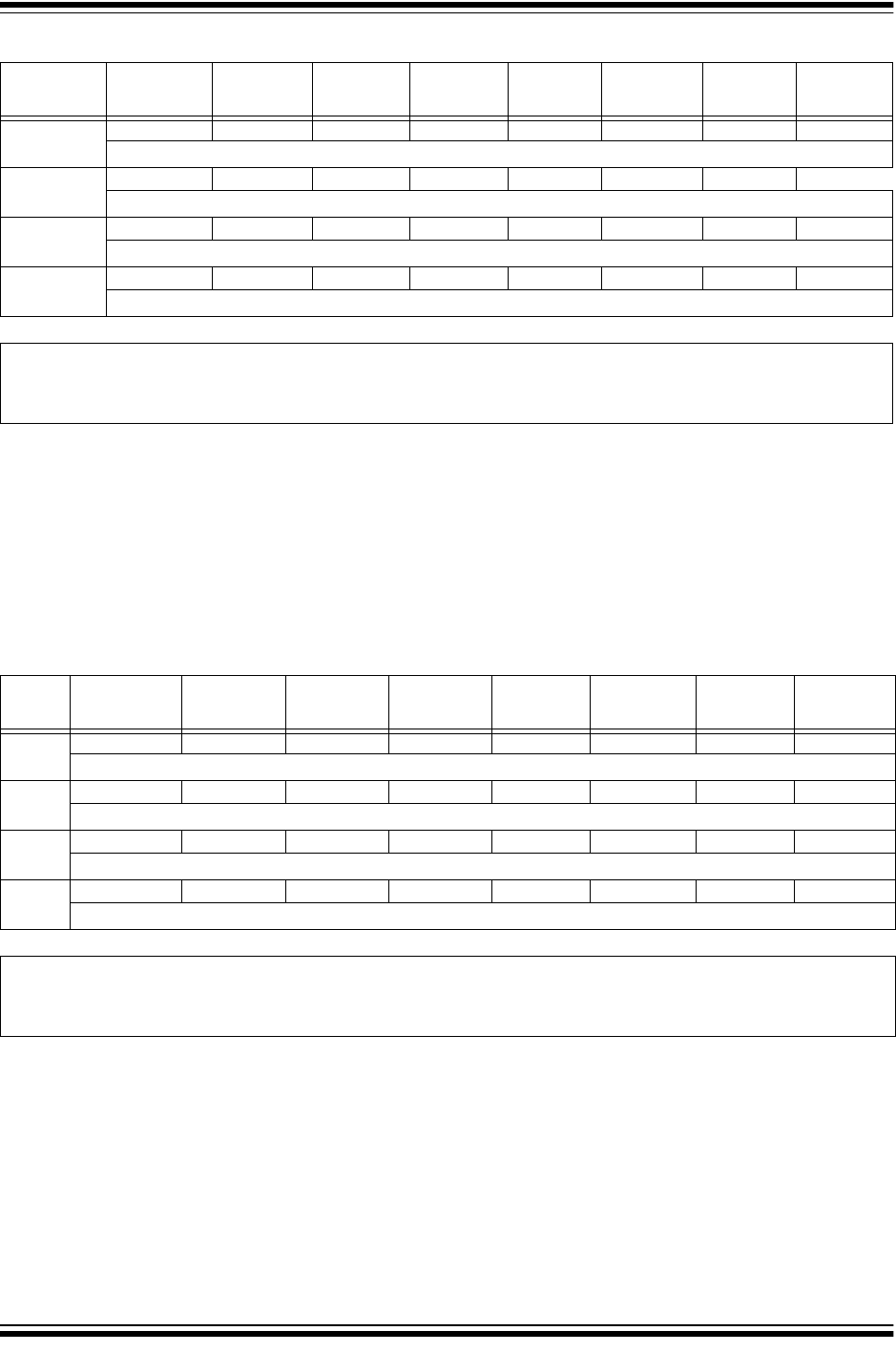
2011-2018 Microchip Technology Inc. DS60001168K-page 99
PIC32MX1XX/2XX 28/36/44-PIN FAMILY
REGISTER 9-10: DCHxSSA: DMA CHANNEL ‘x’ SOURCE START ADDRESS REGISTER
Bit Range Bit
31/23/15/7 Bit
30/22/14/6 Bit
29/21/13/5 Bit
28/20/12/4 Bit
27/19/11/3 Bit
26/18/10/2 Bit
25/17/9/1 Bit
24/16/8/0
31:24
R/W-0 R/W-0 R/W-0 R/W-0 R/W-0 R/W-0 R/W-0 R/W-0
CHSSA<31:24>
23:16
R/W-0 R/W-0 R/W-0 R/W-0 R/W-0 R/W-0 R/W-0 R/W-0
CHSSA<23:16>
15:8
R/W-0 R/W-0 R/W-0 R/W-0 R/W-0 R/W-0 R/W-0 R/W-0
CHSSA<15:8>
7:0
R/W-0 R/W-0 R/W-0 R/W-0 R/W-0 R/W-0 R/W-0 R/W-0
CHSSA<7:0>
Legend:
R = Readable bit W = Writable bit U = Unimplemented bit, read as ‘0’
-n = Value at POR ‘1’ = Bit is set ‘0’ = Bit is cleared x = Bit is unknown
bit 31-0 CHSSA<31:0> Channel Source Start Address bits
Channel source start address.
Note: This must be the physical address of the source.
REGISTER 9-11: DCHxDSA: DMA CHANNEL ‘x’ DESTINATION START ADDRESS REGISTER
Bit
Range Bit
31/23/15/7 Bit
30/22/14/6 Bit
29/21/13/5 Bit
28/20/12/4 Bit
27/19/11/3 Bit
26/18/10/2 Bit
25/17/9/1 Bit
24/16/8/0
31:24
R/W-0 R/W-0 R/W-0 R/W-0 R/W-0 R/W-0 R/W-0 R/W-0
CHDSA<31:24>
23:16
R/W-0 R/W-0 R/W-0 R/W-0 R/W-0 R/W-0 R/W-0 R/W-0
CHDSA<23:16>
15:8
R/W-0 R/W-0 R/W-0 R/W-0 R/W-0 R/W-0 R/W-0 R/W-0
CHDSA<15:8>
7:0
R/W-0 R/W-0 R/W-0 R/W-0 R/W-0 R/W-0 R/W-0 R/W-0
CHDSA<7:0>
Legend:
R = Readable bit W = Writable bit U = Unimplemented bit, read as ‘0’
-n = Value at POR ‘1’ = Bit is set ‘0’ = Bit is cleared x = Bit is unknown
bit 31-0 CHDSA<31:0>: Channel Destination Start Address bits
Channel destination start address.
Note: This must be the physical address of the destination.
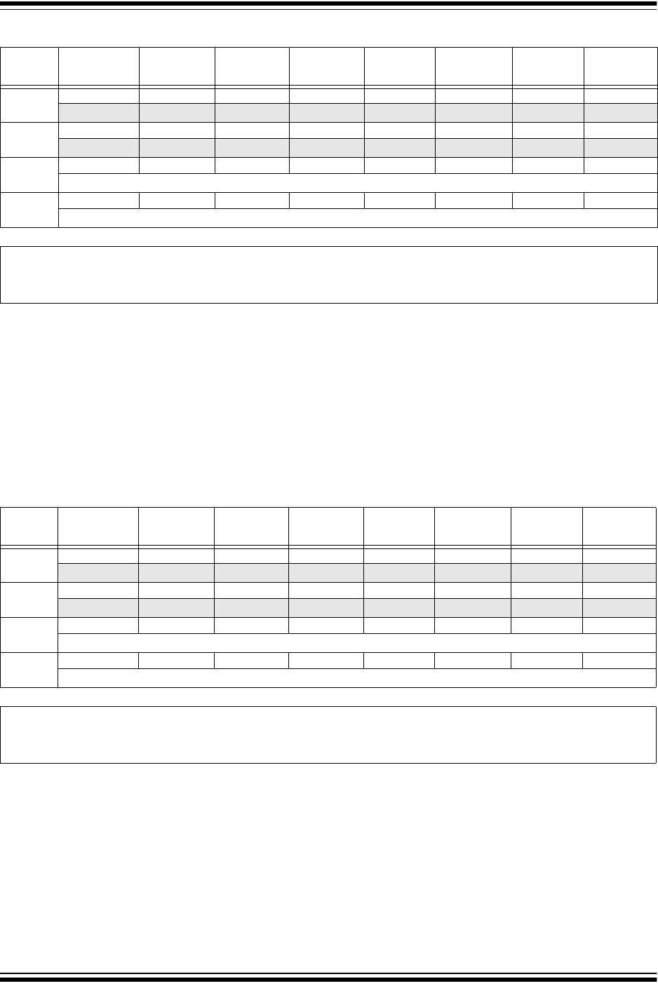
PIC32MX1XX/2XX 28/36/44-PIN FAMILY
DS60001168K-page 100 2011-2018 Microchip Technology Inc.
REGISTER 9-12: DCHxSSIZ: DMA CHANNEL ‘x’ SOURCE SIZE REGISTER
Bit
Range Bit
31/23/15/7 Bit
30/22/14/6 Bit
29/21/13/5 Bit
28/20/12/4 Bit
27/19/11/3 Bit
26/18/10/2 Bit
25/17/9/1 Bit
24/16/8/0
31:24
U-0 U-0 U-0 U-0 U-0 U-0 U-0 U-0
— — — — — — — —
23:16
U-0 U-0 U-0 U-0 U-0 U-0 U-0 U-0
— — — — — — — —
15:8
R/W-0 R/W-0 R/W-0 R/W-0 R/W-0 R/W-0 R/W-0 R/W-0
CHSSIZ<15:8>
7:0
R/W-0 R/W-0 R/W-0 R/W-0 R/W-0 R/W-0 R/W-0 R/W-0
CHSSIZ<7:0>
Legend:
R = Readable bit W = Writable bit U = Unimplemented bit, read as ‘0’
-n = Value at POR ‘1’ = Bit is set ‘0’ = Bit is cleared x = Bit is unknown
bit 31-16 Unimplemented: Read as ‘0’
bit 15-0 CHSSIZ<15:0>: Channel Source Size bits
1111111111111111 = 65,535 byte source size
•
•
•
0000000000000010 = 2 byte source size
0000000000000001 = 1 byte source size
0000000000000000 = 65,536 byte source size
REGISTER 9-13: DCHxDSIZ: DMA CHANNEL ‘x’ DESTINATION SIZE REGISTER
Bit
Range Bit
31/23/15/7 Bit
30/22/14/6 Bit
29/21/13/5 Bit
28/20/12/4 Bit
27/19/11/3 Bit
26/18/10/2 Bit
25/17/9/1 Bit
24/16/8/0
31:24
U-0 U-0 U-0 U-0 U-0 U-0 U-0 U-0
— — — — — — — —
23:16
U-0 U-0 U-0 U-0 U-0 U-0 U-0 U-0
— — — — — — — —
15:8
R/W-0 R/W-0 R/W-0 R/W-0 R/W-0 R/W-0 R/W-0 R/W-0
CHDSIZ<15:8>
7:0
R/W-0 R/W-0 R/W-0 R/W-0 R/W-0 R/W-0 R/W-0 R/W-0
CHDSIZ<7:0>
Legend:
R = Readable bit W = Writable bit U = Unimplemented bit, read as ‘0’
-n = Value at POR ‘1’ = Bit is set ‘0’ = Bit is cleared x = Bit is unknown
bit 31-16 Unimplemented: Read as ‘0’
bit 15-0 CHDSIZ<15:0>: Channel Destination Size bits
1111111111111111 = 65,535 byte destination size
•
•
•
0000000000000010 = 2 byte destination size
0000000000000001 = 1 byte destination size
0000000000000000 = 65,536 byte destination size
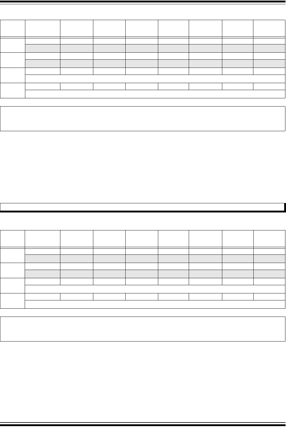
2011-2018 Microchip Technology Inc. DS60001168K-page 101
PIC32MX1XX/2XX 28/36/44-PIN FAMILY
REGISTER 9-14: DCHxSPTR: DMA CHANNEL ‘x’ SOURCE POINTER REGISTER
Bit
Range Bit
31/23/15/7 Bit
30/22/14/6 Bit
29/21/13/5 Bit
28/20/12/4 Bit
27/19/11/3 Bit
26/18/10/2 Bit
25/17/9/1 Bit
24/16/8/0
31:24
U-0 U-0 U-0 U-0 U-0 U-0 U-0 U-0
— — — — — — — —
23:16
U-0 U-0 U-0 U-0 U-0 U-0 U-0 U-0
— — — — — — — —
15:8
R-0 R-0 R-0 R-0 R-0 R-0 R-0 R-0
CHSPTR<15:8>
7:0
R-0 R-0 R-0 R-0 R-0 R-0 R-0 R-0
CHSPTR<7:0>
Legend:
R = Readable bit W = Writable bit U = Unimplemented bit, read as ‘0’
-n = Value at POR ‘1’ = Bit is set ‘0’ = Bit is cleared x = Bit is unknown
bit 31-16 Unimplemented: Read as ‘0’
bit 15-0 CHSPTR<15:0>: Channel Source Pointer bits
1111111111111111 = Points to byte 65,535 of the source
•
•
•
0000000000000001 = Points to byte 1 of the source
0000000000000000 = Points to byte 0 of the source
Note: When in Pattern Detect mode, this register is reset on a pattern detect.
REGISTER 9-15: DCHxDPTR: DMA CHANNEL ‘x’ DESTINATION POINTER REGISTER
Bit
Range Bit
31/23/15/7 Bit
30/22/14/6 Bit
29/21/13/5 Bit
28/20/12/4 Bit
27/19/11/3 Bit
26/18/10/2 Bit
25/17/9/1 Bit
24/16/8/0
31:24
U-0 U-0 U-0 U-0 U-0 U-0 U-0 U-0
— — — — — — — —
23:16
U-0 U-0 U-0 U-0 U-0 U-0 U-0 U-0
— — — — — — — —
15:8
R-0 R-0 R-0 R-0 R-0 R-0 R-0 R-0
CHDPTR<15:8>
7:0
R-0 R-0 R-0 R-0 R-0 R-0 R-0 R-0
CHDPTR<7:0>
Legend:
R = Readable bit W = Writable bit U = Unimplemented bit, read as ‘0’
-n = Value at POR ‘1’ = Bit is set ‘0’ = Bit is cleared x = Bit is unknown
bit 31-16 Unimplemented: Read as ‘0’
bit 15-0 CHDPTR<15:0>: Channel Destination Pointer bits
1111111111111111 = Points to byte 65,535 of the destination
•
•
•
0000000000000001 = Points to byte 1 of the destination
0000000000000000 = Points to byte 0 of the destination
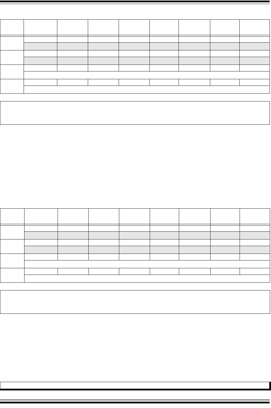
PIC32MX1XX/2XX 28/36/44-PIN FAMILY
DS60001168K-page 102 2011-2018 Microchip Technology Inc.
REGISTER 9-16: DCHxCSIZ: DMA CHANNEL ‘x’ CELL-SIZE REGISTER
Bit
Range Bit
31/23/15/7 Bit
30/22/14/6 Bit
29/21/13/5 Bit
28/20/12/4 Bit
27/19/11/3 Bit
26/18/10/2 Bit
25/17/9/1 Bit
24/16/8/0
31:24
U-0 U-0 U-0 U-0 U-0 U-0 U-0 U-0
— — — — — — — —
23:16
U-0 U-0 U-0 U-0 U-0 U-0 U-0 U-0
— — — — — — — —
15:8
R/W-0 R/W-0 R/W-0 R/W-0 R/W-0 R/W-0 R/W-0 R/W-0
CHCSIZ<15:8>
7:0
R/W-0 R/W-0 R/W-0 R/W-0 R/W-0 R/W-0 R/W-0 R/W-0
CHCSIZ<7:0>
Legend:
R = Readable bit W = Writable bit U = Unimplemented bit, read as ‘0’
-n = Value at POR ‘1’ = Bit is set ‘0’ = Bit is cleared x = Bit is unknown
bit 31-16 Unimplemented: Read as ‘0’
bit 15-0 CHCSIZ<15:0>: Channel Cell Size bits
1111111111111111 = 65,535 bytes transferred on an event
•
•
•
0000000000000010 = 2 bytes transferred on an event
0000000000000001= 1 byte transferred on an event
0000000000000000 = 65,536 bytes transferred on an event
REGISTER 9-17: DCHxCPTR: DMA CHANNEL ‘x’ CELL POINTER REGISTER
Bit
Range Bit
31/23/15/7 Bit
30/22/14/6 Bit
29/21/13/5 Bit
28/20/12/4 Bit
27/19/11/3 Bit
26/18/10/2 Bit
25/17/9/1 Bit
24/16/8/0
31:24
U-0 U-0 U-0 U-0 U-0 U-0 U-0 U-0
— — — — — — — —
23:16
U-0 U-0 U-0 U-0 U-0 U-0 U-0 U-0
— — — — — — — —
15:8
R-0 R-0 R-0 R-0 R-0 R-0 R-0 R-0
CHCPTR<15:8>
7:0
R-0 R-0 R-0 R-0 R-0 R-0 R-0 R-0
CHCPTR<7:0>
Legend:
R = Readable bit W = Writable bit U = Unimplemented bit, read as ‘0’
-n = Value at POR ‘1’ = Bit is set ‘0’ = Bit is cleared x = Bit is unknown
bit 31-16 Unimplemented: Read as ‘0’
bit 15-0 CHCPTR<15:0>: Channel Cell Progress Pointer bits
1111111111111111 = 65,535 bytes have been transferred since the last event
•
•
•
0000000000000001 = 1 byte has been transferred since the last event
0000000000000000 = 0 bytes have been transferred since the last event
Note: When in Pattern Detect mode, this register is reset on a pattern detect.

2011-2018 Microchip Technology Inc. DS60001168K-page 103
PIC32MX1XX/2XX 28/36/44-PIN FAMILY
REGISTER 9-18: DCHxDAT: DMA CHANNEL ‘x’ PATTERN DATA REGISTER
Bit
Range Bit
31/23/15/7 Bit
30/22/14/6 Bit
29/21/13/5 Bit
28/20/12/4 Bit
27/19/11/3 Bit
26/18/10/2 Bit
25/17/9/1 Bit
24/16/8/0
31:24
U-0 U-0 U-0 U-0 U-0 U-0 U-0 U-0
— — — — — — — —
23:16
U-0 U-0 U-0 U-0 U-0 U-0 U-0 U-0
— — — — — — — —
15:8
U-0 U-0 U-0 U-0 U-0 U-0 U-0 U-0
— — — — — — — —
7:0
R/W-0 R/W-0 R/W-0 R/W-0 R/W-0 R/W-0 R/W-0 R/W-0
CHPDAT<7:0>
Legend:
R = Readable bit W = Writable bit U = Unimplemented bit, read as ‘0’
-n = Value at POR ‘1’ = Bit is set ‘0’ = Bit is cleared x = Bit is unknown
bit 31-8 Unimplemented: Read as ‘0’
bit 7-0 CHPDAT<7:0>: Channel Data Register bits
Pattern Terminate mode:
Data to be matched must be stored in this register to allow a “terminate on match”.
All other modes:
Unused.

PIC32MX1XX/2XX 28/36/44-PIN FAMILY
DS60001168K-page 104 2011-2018 Microchip Technology Inc.
NOTES:

2011-2018 Microchip Technology Inc. DS60001168K-page 105
PIC32MX1XX/2XX 28/36/44-PIN FAMILY
10.0 USB ON-THE-GO (OTG)
The Universal Serial Bus (USB) module contains
analog and digital components to provide a USB 2.0
Full-Speed and Low-Speed embedded host, Full-
Speed device or OTG implementation with a minimum
of external components. This module in Host mode is
intended for use as an embedded host and therefore
does not implement a UHCI or OHCI controller.
The USB module consists of the clock generator, the
USB voltage comparators, the transceiver, the Serial
Interface Engine (SIE), a dedicated USB DMA control-
ler, pull-up and pull-down resistors, and the register
interface. A block diagram of the PIC32 USB OTG
module is presented in Figure 10-1.
The clock generator provides the 48 MHz clock
required for USB Full-Speed and Low-Speed communi-
cation. The voltage comparators monitor the voltage on
the V
BUS
pin to determine the state of the bus. The
transceiver provides the analog translation between
the USB bus and the digital logic. The SIE is a state
machine that transfers data to and from the endpoint
buffers and generates the hardware protocol for data
transfers. The USB DMA controller transfers data
between the data buffers in RAM and the SIE. The inte-
grated pull-up and pull-down resistors eliminate the
need for external signaling components. The register
interface allows the CPU to configure and
communicate with the module.
The PIC32 USB module includes the following
features:
• USB Full-Speed support for Host and Device
• Low-Speed Host support
• USB OTG support
• Integrated signaling resistors
• Integrated analog comparators for V
BUS
monitoring
• Integrated USB transceiver
• Transaction handshaking performed by hardware
• Endpoint buffering anywhere in system RAM
• Integrated DMA to access system RAM and Flash
Note: This data sheet summarizes the features
of the PIC32MX1XX/2XX 28/36/44-pin
Family of devices. It is not intended to be
a comprehensive reference source. To
complement the information in this data
sheet, refer to Section 27. “USB On-The-
Go (OTG)” (DS60001126), which is avail-
able from the Documentation > Reference
Manual section of the Microchip PIC32
web site (www.microchip.com/pic32).
Note: The implementation and use of the USB
specifications, as well as other third party
specifications or technologies, may
require licensing; including, but not limited
to, USB Implementers Forum, Inc., also
referred to as USB-IF (www.usb.org). The
user is fully responsible for investigating
and satisfying any applicable licensing
obligations.
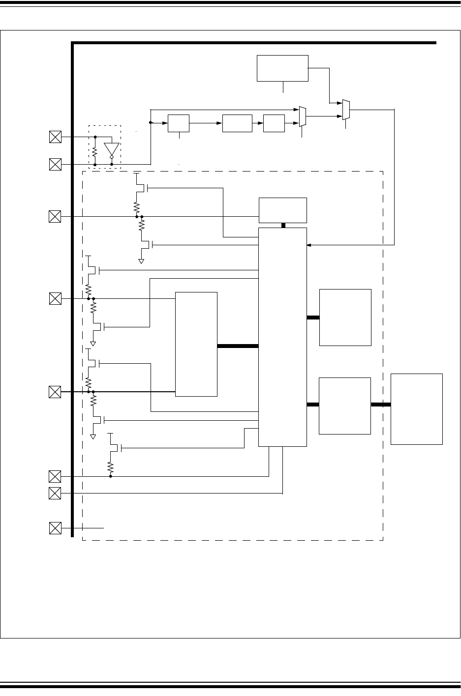
PIC32MX1XX/2XX 28/36/44-PIN FAMILY
DS60001168K-page 106 2011-2018 Microchip Technology Inc.
FIGURE 10-1: PIC32MX1XX/2XX 28/36/44-PIN FAMILY FAMILY USB INTERFACE DIAGRAM
OSC1
OSC2
Primary Oscillator
8MHzTypical
FRC
Oscillator
TUN<5:0>
(3)
PLL
48 MHz USB Clock
(6)
Div x
UPLLEN
(5)
UFRCEN
(2)
(P
OSC
)
UPLLIDIV
(5)
UF
IN(4)
Div 2
V
USB
3
V
3
D+
(1)
D-
(1)
ID
(1)
Bus
Transceiver
SIE
V
BUSON(1)
Comparators
USB
SRP Charge
SRP Discharge
Registers
and
Control
Interface
Transceiver Power 3.3V
USB Module
Voltage
System
RAM
Full Speed Pull-up
Host Pull-down
Low Speed Pull-up
Host Pull-down
ID Pull-up
DMA
Note 1: Pins can be used as digital input/output when USB is not enabled.
2: This bit field is contained in the OSCCON register.
3: This bit field is contained in the OSCTRM register.
4: USB PLL U
F
IN
requirements: 4 MHz.
5: This bit field is contained in the DEVCFG2 register.
6: A 48 MHz clock is required for proper USB operation.
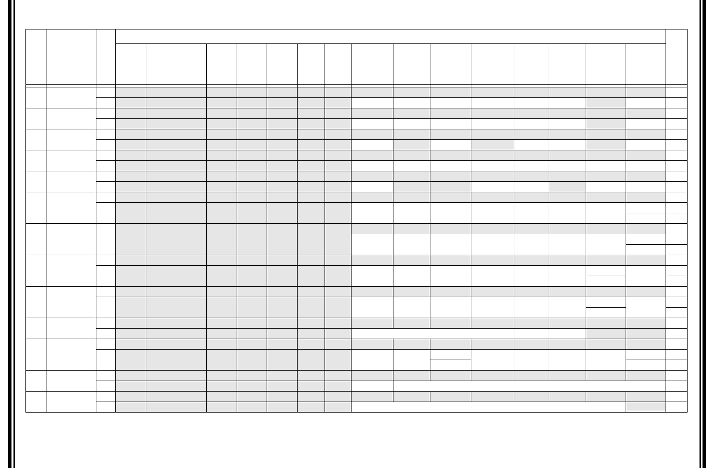
2011-2018 Microchip Technology Inc. DS60001168K-page 107
PIC32MX1XX/2XX 28/36/44-PIN FAMILY
10.1 USB Control Registers
TABLE 10-1: USB REGISTER MAP
Virtual Address
(BF88_#)
Register
Name
(1)
Bit Range
Bits
All Resets
31/15 30/14 29/13 28/12 27/11 26/10 25/9 24/8 23/7 22/6 21/5 20/4 19/3 18/2 17/1 16/0
5040 U1OTGIR
(2)
31:16 — — — — — — — — — — — — — — — — 0000
15:0 ———————— IDIF T1MSECIF LSTATEIF ACTVIF SESVDIF SESENDIF — VBUSVDIF 0000
5050 U1OTGIE 31:16 — — — — — — — — — — — — — — — — 0000
15:0 ———————— IDIE T1MSECIE LSTATEIE ACTVIE SESVDIE SESENDIE — VBUSVDIE 0000
5060 U1OTGSTAT
(3)
31:16 — — — — — — — — — — — — — — — — 0000
15:0 ————————ID —LSTATE — SESVD SESEND — VBUSVD 0000
5070 U1OTGCON 31:16 — — — — — — — — — — — — — — — — 0000
15:0 ———————— DPPULUP DMPULUP DPPULDWN DMPULDWN VBUSON OTGEN VBUSCHG VBUSDIS 0000
5080 U1PWRC 31:16 — — — — — — — — — — — — — — — — 0000
15:0 ————————UACTPND
(4)
—— USLPGRD USBBUSY — USUSPEND USBPWR 0000
5200 U1IR
(2)
31:16 — — — — — — — — — — — — — — — — 0000
15:0 ———————— STALLIF ATTACHIF RESUMEIF IDLEIF TRNIF SOFIF UERRIF URSTIF 0000
DETACHIF 0000
5210 U1IE
31:16 — — — — — — — — — — — — — — — — 0000
15:0 ———————— STALLIE ATTACHIE RESUMEIE IDLEIE TRNIE SOFIE UERRIE URSTIE 0000
DETACHIE 0000
5220 U1EIR
(2)
31:16 — — — — — — — — — — — — — — — — 0000
15:0 ———————— BTSEF BMXEF DMAEF BTOEF DFN8EF CRC16EF CRC5EF PIDEF 0000
EOFEF 0000
5230 U1EIE
31:16 — — — — — — — — — — — — — — — — 0000
15:0 ———————— BTSEE BMXEE DMAEE BTOEE DFN8EE CRC16EE CRC5EE PIDEE 0000
EOFEE 0000
5240 U1STAT
(3)
31:16 — — — — — — — — — — — — — — — — 0000
15:0 ———————— ENDPT<3:0> DIR PPBI — — 0000
5250 U1CON
31:16 — — — — — — — — — — — — — — — — 0000
15:0 ———————— JSTATE SE0 PKTDIS USBRST HOSTEN RESUME PPBRST USBEN 0000
TOKBUSY SOFEN 0000
5260 U1ADDR 31:16 — — — — — — — — — — — — — — — — 0000
15:0 ———————— LSPDEN DEVADDR<6:0> 0000
5270 U1BDTP1 31:16 — — — — — — — — — — — — — — — — 0000
15:0 ———————— BDTPTRL<15:9> —0000
Legend: x = unknown value on Reset; — = unimplemented, read as ‘0’. Reset values are shown in hexadecimal.
Note 1: With the exception of those noted, all registers in this table (except as noted) have corresponding CLR, SET and INV registers at their virtual address, plus an offset of 0x4, 0x8, and 0xC respectively.
See Section 11.2 “CLR, SET and INV Registers” for more information.
2: This register does not have associated SET and INV registers.
3: This register does not have associated CLR, SET and INV registers.
4: Reset value for this bit is undefined.
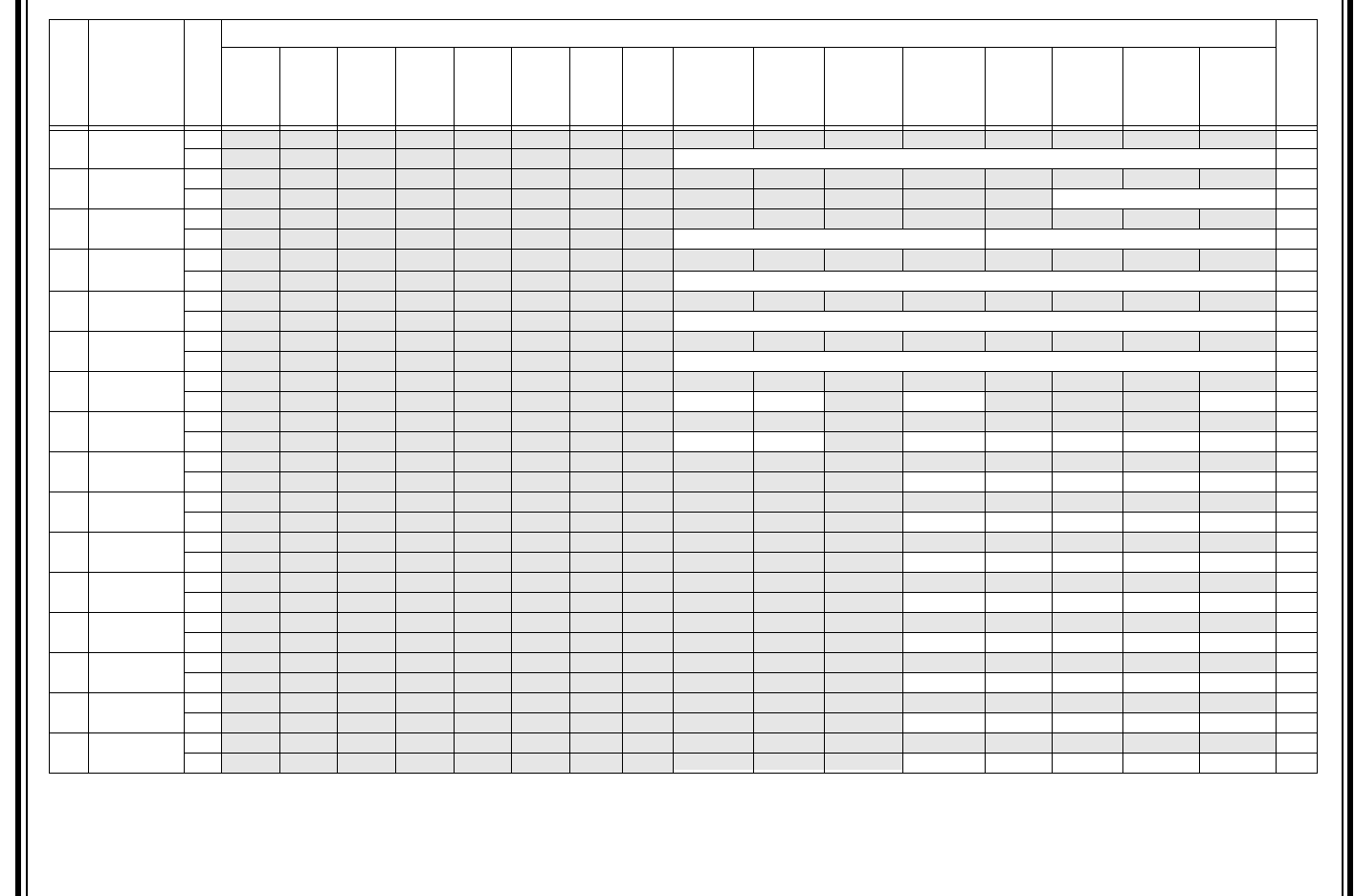
PIC32MX1XX/2XX 28/36/44-PIN FAMILY
DS60001168K-page 108 2011-2018 Microchip Technology Inc.
5280 U1FRML
(3)
31:16 — — — — — — — — — — — — — — — — 0000
15:0 ———————— FRML<7:0> 0000
5290 U1FRMH
(3)
31:16 — — — — — — — — — — — — — — — — 0000
15:0 — — — — — — — — — — — — — FRMH<2:0> 0000
52A0 U1TOK 31:16 — — — — — — — — — — — — — — — — 0000
15:0 ———————— PID<3:0> EP<3:0> 0000
52B0 U1SOF 31:16 — — — — — — — — — — — — — — — — 0000
15:0 ———————— CNT<7:0> 0000
52C0 U1BDTP2 31:16 — — — — — — — — — — — — — — — — 0000
15:0 ———————— BDTPTRH<7:0> 0000
52D0 U1BDTP3 31:16 — — — — — — — — — — — — — — — — 0000
15:0 ———————— BDTPTRU<7:0> 0000
52E0 U1CNFG1 31:16 — — — — — — — — — — — — — — — — 0000
15:0 ———————— UTEYE UOEMON — USBSIDL — — — UASUSPND 0001
5300 U1EP0 31:16 — — — — — — — — — — — — — — — — 0000
15:0 ———————— LSPD RETRYDIS — EPCONDIS EPRXEN EPTXEN EPSTALL EPHSHK 0000
5310 U1EP1 31:16 — — — — — — — — — — — — — — — — 0000
15:0 — — — — — — — — — — — EPCONDIS EPRXEN EPTXEN EPSTALL EPHSHK 0000
5320 U1EP2 31:16 — — — — — — — — — — — — — — — — 0000
15:0 — — — — — — — — — — — EPCONDIS EPRXEN EPTXEN EPSTALL EPHSHK 0000
5330 U1EP3 31:16 — — — — — — — — — — — — — — — — 0000
15:0 — — — — — — — — — — — EPCONDIS EPRXEN EPTXEN EPSTALL EPHSHK 0000
5340 U1EP4 31:16 — — — — — — — — — — — — — — — — 0000
15:0 — — — — — — — — — — — EPCONDIS EPRXEN EPTXEN EPSTALL EPHSHK 0000
5350 U1EP5 31:16 — — — — — — — — — — — — — — — — 0000
15:0 — — — — — — — — — — — EPCONDIS EPRXEN EPTXEN EPSTALL EPHSHK 0000
5360 U1EP6 31:16 — — — — — — — — — — — — — — — — 0000
15:0 — — — — — — — — — — — EPCONDIS EPRXEN EPTXEN EPSTALL EPHSHK 0000
5370 U1EP7 31:16 — — — — — — — — — — — — — — — — 0000
15:0 — — — — — — — — — — — EPCONDIS EPRXEN EPTXEN EPSTALL EPHSHK 0000
5380 U1EP8 31:16 — — — — — — — — — — — — — — — — 0000
15:0 — — — — — — — — — — — EPCONDIS EPRXEN EPTXEN EPSTALL EPHSHK 0000
TABLE 10-1: USB REGISTER MAP (CONTINUED)
Virtual Address
(BF88_#)
Register
Name
(1)
Bit Range
Bits
All Resets
31/15 30/14 29/13 28/12 27/11 26/10 25/9 24/8 23/7 22/6 21/5 20/4 19/3 18/2 17/1 16/0
Legend: x = unknown value on Reset; — = unimplemented, read as ‘0’. Reset values are shown in hexadecimal.
Note 1: With the exception of those noted, all registers in this table (except as noted) have corresponding CLR, SET and INV registers at their virtual address, plus an offset of 0x4, 0x8, and 0xC respectively.
See Section 11.2 “CLR, SET and INV Registers” for more information.
2: This register does not have associated SET and INV registers.
3: This register does not have associated CLR, SET and INV registers.
4: Reset value for this bit is undefined.
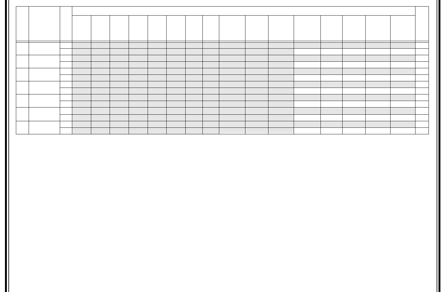
2011-2018 Microchip Technology Inc. DS60001168K-page 109
PIC32MX1XX/2XX 28/36/44-PIN FAMILY
5390 U1EP9 31:16 — — — — — — — — — — — — — — — — 0000
15:0 — — — — — — — — — — — EPCONDIS EPRXEN EPTXEN EPSTALL EPHSHK 0000
53A0 U1EP10 31:16 — — — — — — — — — — — — — — — — 0000
15:0 — — — — — — — — — — — EPCONDIS EPRXEN EPTXEN EPSTALL EPHSHK 0000
53B0 U1EP11 31:16 — — — — — — — — — — — — — — — — 0000
15:0 — — — — — — — — — — — EPCONDIS EPRXEN EPTXEN EPSTALL EPHSHK 0000
53C0 U1EP12 31:16 — — — — — — — — — — — — — — — — 0000
15:0 — — — — — — — — — — — EPCONDIS EPRXEN EPTXEN EPSTALL EPHSHK 0000
53D0 U1EP13 31:16 — — — — — — — — — — — — — — — — 0000
15:0 — — — — — — — — — — — EPCONDIS EPRXEN EPTXEN EPSTALL EPHSHK 0000
53E0 U1EP14 31:16 — — — — — — — — — — — — — — — — 0000
15:0 — — — — — — — — — — — EPCONDIS EPRXEN EPTXEN EPSTALL EPHSHK 0000
53F0 U1EP15 31:16 — — — — — — — — — — — — — — — — 0000
15:0 — — — — — — — — — — — EPCONDIS EPRXEN EPTXEN EPSTALL EPHSHK 0000
TABLE 10-1: USB REGISTER MAP (CONTINUED)
Virtual Address
(BF88_#)
Register
Name
(1)
Bit Range
Bits
All Resets
31/15 30/14 29/13 28/12 27/11 26/10 25/9 24/8 23/7 22/6 21/5 20/4 19/3 18/2 17/1 16/0
Legend: x = unknown value on Reset; — = unimplemented, read as ‘0’. Reset values are shown in hexadecimal.
Note 1: With the exception of those noted, all registers in this table (except as noted) have corresponding CLR, SET and INV registers at their virtual address, plus an offset of 0x4, 0x8, and 0xC respectively.
See Section 11.2 “CLR, SET and INV Registers” for more information.
2: This register does not have associated SET and INV registers.
3: This register does not have associated CLR, SET and INV registers.
4: Reset value for this bit is undefined.

PIC32MX1XX/2XX 28/36/44-PIN FAMILY
DS60001168K-page 110 2011-2018 Microchip Technology Inc.
REGISTER 10-1: U1OTGIR: USB OTG INTERRUPT STATUS REGISTER
Bit
Range Bit
31/23/15/7 Bit
30/22/14/6 Bit
29/21/13/5 Bit
28/20/12/4 Bit
27/19/11/3 Bit
26/18/10/2 Bit
25/17/9/1 Bit
24/16/8/0
31:24
U-0 U-0 U-0 U-0 U-0 U-0 U-0 U-0
————————
23:16
U-0 U-0 U-0 U-0 U-0 U-0 U-0 U-0
————————
15:8
U-0 U-0 U-0 U-0 U-0 U-0 U-0 U-0
————————
7:0
R/WC-0, HS R/WC-0, HS R/WC-0, HS R/WC-0, HS R/WC-0, HS R/WC-0, HS U-0 R/WC-0, HS
IDIF T1MSECIF LSTATEIF ACTVIF SESVDIF SESENDIF —VBUSVDIF
Legend: WC = Write ‘1’ to clear HS = Hardware Settable bit
R = Readable bit W = Writable bit U = Unimplemented bit, read as ‘0’
-n = Value at POR ‘1’ = Bit is set ‘0’ = Bit is cleared x = Bit is unknown
bit 31-8 Unimplemented: Read as ‘0’
bit 7 IDIF: ID State Change Indicator bit
1 = A change in the ID state was detected
0 = No change in the ID state was detected
bit 6 T1MSECIF: 1 Millisecond Timer bit
1 = 1 millisecond timer has expired
0 = 1 millisecond timer has not expired
bit 5 LSTATEIF: Line State Stable Indicator bit
1 = USB line state has been stable for 1 ms, but different from last time
0 = USB line state has not been stable for 1 ms
bit 4 ACTVIF: Bus Activity Indicator bit
1 = Activity on the D+, D-, ID or V
BUS
pins has caused the device to wake-up
0 = Activity has not been detected
bit 3 SESVDIF: Session Valid Change Indicator bit
1 =V
BUS
voltage has dropped below the session end level
0 =V
BUS
voltage has not dropped below the session end level
bit 2 SESENDIF: B-Device V
BUS
Change Indicator bit
1 = A change on the session end input was detected
0 = No change on the session end input was detected
bit 1 Unimplemented: Read as ‘0’
bit 0 VBUSVDIF: A-Device V
BUS
Change Indicator bit
1 = A change on the session valid input was detected
0 = No change on the session valid input was detected

2011-2018 Microchip Technology Inc. DS60001168K-page 111
PIC32MX1XX/2XX 28/36/44-PIN FAMILY
REGISTER 10-2: U1OTGIE: USB OTG INTERRUPT ENABLE REGISTER
Bit
Range Bit
31/23/15/7 Bit
30/22/14/6 Bit
29/21/13/5 Bit
28/20/12/4 Bit
27/19/11/3 Bit
26/18/10/2 Bit
25/17/9/1 Bit
24/16/8/0
31:24
U-0 U-0 U-0 U-0 U-0 U-0 U-0 U-0
————————
23:16
U-0 U-0 U-0 U-0 U-0 U-0 U-0 U-0
————————
15:8
U-0 U-0 U-0 U-0 U-0 U-0 U-0 U-0
————————
7:0
R/W-0 R/W-0 R/W-0 R/W-0 R/W-0 R/W-0 U-0 R/W-0
IDIE T1MSECIE LSTATEIE ACTVIE SESVDIE SESENDIE — VBUSVDIE
Legend:
R = Readable bit W = Writable bit U = Unimplemented bit, read as ‘0’
-n = Value at POR ‘1’ = Bit is set ‘0’ = Bit is cleared x = Bit is unknown
bit 31-8 Unimplemented: Read as ‘0’
bit 7 IDIE: ID Interrupt Enable bit
1 = ID interrupt is enabled
0 = ID interrupt is disabled
bit 6 T1MSECIE: 1 Millisecond Timer Interrupt Enable bit
1 = 1 millisecond timer interrupt is enabled
0 = 1 millisecond timer interrupt is disabled
bit 5 LSTATEIE: Line State Interrupt Enable bit
1 = Line state interrupt is enabled
0 = Line state interrupt is disabled
bit 4 ACTVIE: Bus Activity Interrupt Enable bit
1 = Activity interrupt is enabled
0 = Activity interrupt is disabled
bit 3 SESVDIE: Session Valid Interrupt Enable bit
1 = Session valid interrupt is enabled
0 = Session valid interrupt is disabled
bit 2 SESENDIE: B-Device Session End Interrupt Enable bit
1 = B-Device session end interrupt is enabled
0 = B-Device session end interrupt is disabled
bit 1 Unimplemented: Read as ‘0’
bit 0 VBUSVDIE: A-Device V
BUS
Valid Interrupt Enable bit
1 = A-Device V
BUS
valid interrupt is enabled
0 = A-Device V
BUS
valid interrupt is disabled

PIC32MX1XX/2XX 28/36/44-PIN FAMILY
DS60001168K-page 112 2011-2018 Microchip Technology Inc.
REGISTER 10-3: U1OTGSTAT: USB OTG STATUS REGISTER
Bit
Range Bit
31/23/15/7 Bit
30/22/14/6 Bit
29/21/13/5 Bit
28/20/12/4 Bit
27/19/11/3 Bit
26/18/10/2 Bit
25/17/9/1 Bit
24/16/8/0
31:24
U-0 U-0 U-0 U-0 U-0 U-0 U-0 U-0
— — — — — — — —
23:16
U-0 U-0 U-0 U-0 U-0 U-0 U-0 U-0
— — — — — — — —
15:8
U-0 U-0 U-0 U-0 U-0 U-0 U-0 U-0
— — — — — — — —
7:0
R-0 U-0 R-0 U-0 R-0 R-0 U-0 R-0
ID —LSTATE— SESVD SESEND — VBUSVD
Legend:
R = Readable bit W = Writable bit U = Unimplemented bit, read as ‘0’
-n = Value at POR ‘1’ = Bit is set ‘0’ = Bit is cleared x = Bit is unknown
bit 31-8 Unimplemented: Read as ‘0’
bit 7 ID: ID Pin State Indicator bit
1 = No cable is attached or a “type B” cable has been inserted into the USB receptacle
0 = A “type A” OTG cable has been inserted into the USB receptacle
bit 6 Unimplemented: Read as ‘0’
bit 5 LSTATE: Line State Stable Indicator bit
1 = USB line state (SE0 (U1CON<6>) bit and JSTATE (U1CON<7>)) bit has been stable for previous 1 ms
0 = USB line state (SE0 and JSTATE) has not been stable for previous 1 ms
bit 4 Unimplemented: Read as ‘0’
bit 3 SESVD: Session Valid Indicator bit
1 =V
BUS
voltage is above Session Valid on the A or B device
0 =V
BUS
voltage is below Session Valid on the A or B device
bit 2 SESEND: B-Device Session End Indicator bit
1 =V
BUS
voltage is below Session Valid on the B device
0 =V
BUS
voltage is above Session Valid on the B device
bit 1 Unimplemented: Read as ‘0’
bit 0 VBUSVD: A-Device V
BUS
Valid Indicator bit
1 =V
BUS
voltage is above Session Valid on the A device
0 =V
BUS
voltage is below Session Valid on the A device

2011-2018 Microchip Technology Inc. DS60001168K-page 113
PIC32MX1XX/2XX 28/36/44-PIN FAMILY
REGISTER 10-4: U1OTGCON: USB OTG CONTROL REGISTER
Bit
Range Bit
31/23/15/7 Bit
30/22/14/6 Bit
29/21/13/5 Bit
28/20/12/4 Bit
27/19/11/3 Bit
26/18/10/2 Bit
25/17/9/1 Bit
24/16/8/0
31:24
U-0 U-0 U-0 U-0 U-0 U-0 U-0 U-0
— — — — — — — —
23:16
U-0 U-0 U-0 U-0 U-0 U-0 U-0 U-0
— — — — — — — —
15:8
U-0 U-0 U-0 U-0 U-0 U-0 U-0 U-0
— — — — — — — —
7:0
R/W-0 R/W-0 R/W-0 R/W-0 R/W-0 R/W-0 R/W-0 R/W-0
DPPULUP DMPULUP DPPULDWN DMPULDWN VBUSON OTGEN VBUSCHG VBUSDIS
Legend:
R = Readable bit W = Writable bit U = Unimplemented bit, read as ‘0’
-n = Value at POR ‘1’ = Bit is set ‘0’ = Bit is cleared x = Bit is unknown
bit 31-8 Unimplemented: Read as ‘0’
bit 7 DPPULUP: D+ Pull-Up Enable bit
1 = D+ data line pull-up resistor is enabled
0 = D+ data line pull-up resistor is disabled
bit 6 DMPULUP: D- Pull-Up Enable bit
1 = D- data line pull-up resistor is enabled
0 = D- data line pull-up resistor is disabled
bit 5 DPPULDWN: D+ Pull-Down Enable bit
1 = D+ data line pull-down resistor is enabled
0 = D+ data line pull-down resistor is disabled
bit 4 DMPULDWN: D- Pull-Down Enable bit
1 = D- data line pull-down resistor is enabled
0 = D- data line pull-down resistor is disabled
bit 3 VBUSON: V
BUS
Power-on bit
1 =V
BUS
line is powered
0 =V
BUS
line is not powered
bit 2 OTGEN: OTG Functionality Enable bit
1 = DPPULUP, DMPULUP, DPPULDWN and DMPULDWN bits are under software control
0 = DPPULUP, DMPULUP, DPPULDWN and DMPULDWN bits are under USB hardware control
bit 1 VBUSCHG: V
BUS
Charge Enable bit
1 =V
BUS
line is charged through a pull-up resistor
0 =V
BUS
line is not charged through a resistor
bit 0 VBUSDIS: V
BUS
Discharge Enable bit
1 =V
BUS
line is discharged through a pull-down resistor
0 =V
BUS
line is not discharged through a resistor

PIC32MX1XX/2XX 28/36/44-PIN FAMILY
DS60001168K-page 114 2011-2018 Microchip Technology Inc.
REGISTER 10-5: U1PWRC: USB POWER CONTROL REGISTER
Bit
Range Bit
31/23/15/7 Bit
30/22/14/6 Bit
29/21/13/5 Bit
28/20/12/4 Bit
27/19/11/3 Bit
26/18/10/2 Bit
25/17/9/1 Bit
24/16/8/0
31:24
U-0 U-0 U-0 U-0 U-0 U-0 U-0 U-0
— — — — — — — —
23:16
U-0 U-0 U-0 U-0 U-0 U-0 U-0 U-0
— — — — — — — —
15:8
U-0 U-0 U-0 U-0 U-0 U-0 U-0 U-0
— — — — — — — —
7:0
R-0 U-0 U-0 R/W-0 R/W-0 U-0 R/W-0 R/W-0
UACTPND —— USLPGRD USBBUSY
(1)
— USUSPEND USBPWR
Legend:
R = Readable bit W = Writable bit U = Unimplemented bit, read as ‘0’
-n = Value at POR ‘1’ = Bit is set ‘0’ = Bit is cleared x = Bit is unknown
bit 31-8 Unimplemented: Read as ‘0’
bit 7 UACTPND: USB Activity Pending bit
1 = USB bus activity has been detected; however, an interrupt is pending, which has yet to be generated
0 = An interrupt is not pending
bit 6-5 Unimplemented: Read as ‘0’
bit 4 USLPGRD: USB Sleep Entry Guard bit
1 = Sleep entry is blocked if USB bus activity is detected or if a notification is pending
0 = USB module does not block Sleep entry
bit 3 USBBUSY: USB Module Busy bit
(1)
1 = USB module is active or disabled, but not ready to be enabled
0 = USB module is not active and is ready to be enabled
bit 2 Unimplemented: Read as ‘0’
bit 1 USUSPEND: USB Suspend Mode bit
1 = USB module is placed in Suspend mode
(The 48 MHz USB clock will be gated off. The transceiver is placed in a low-power state.)
0 = USB module operates normally
bit 0 USBPWR: USB Operation Enable bit
1 = USB module is turned on
0 = USB module is disabled
(Outputs held inactive, device pins not used by USB, analog features are shut down to reduce power
consumption.)
Note 1: When USBPWR = 0 and USBBUSY = 1, status from all other registers is invalid and writes to all USB
module registers produce undefined results.

2011-2018 Microchip Technology Inc. DS60001168K-page 115
PIC32MX1XX/2XX 28/36/44-PIN FAMILY
REGISTER 10-6: U1IR: USB INTERRUPT REGISTER
Bit
Range Bit
31/23/15/7 Bit
30/22/14/6 Bit
29/21/13/5 Bit
28/20/12/4 Bit
27/19/11/3 Bit
26/18/10/2 Bit
25/17/9/1 Bit
24/16/8/0
31:24
U-0 U-0 U-0 U-0 U-0 U-0 U-0 U-0
— — — — — — — —
23:16
U-0 U-0 U-0 U-0 U-0 U-0 U-0 U-0
— — — — — — — —
15:8
U-0 U-0 U-0 U-0 U-0 U-0 U-0 U-0
— — — — — — — —
7:0
R/WC-0, HS R/WC-0, HS R/WC-0, HS R/WC-0, HS R/WC-0, HS R/WC-0, HS R-0 R/WC-0, HS
STALLIF ATTACHIF
(1)
RESUMEIF
(2)
IDLEIF TRNIF
(3)
SOFIF UERRIF
(4)
URSTIF
(5)
DETACHIF
(6)
Legend: WC = Write ‘1’ to clear HS = Hardware Settable bit
R = Readable bit W = Writable bit U = Unimplemented bit, read as ‘0’
-n = Value at POR ‘1’ = Bit is set ‘0’ = Bit is cleared x = Bit is unknown
bit 31-8 Unimplemented: Read as ‘0’
bit 7 STALLIF: STALL Handshake Interrupt bit
1 = In Host mode a STALL handshake was received during the handshake phase of the transaction
In Device mode a STALL handshake was transmitted during the handshake phase of the transaction
0 = STALL handshake has not been sent
bit 6 ATTACHIF: Peripheral Attach Interrupt bit
(1)
1 = Peripheral attachment was detected by the USB module
0 = Peripheral attachment was not detected
bit 5 RESUMEIF: Resume Interrupt bit
(2)
1 = K-State is observed on the D+ or D- pin for 2.5 µs
0 = K-State is not observed
bit 4 IDLEIF: Idle Detect Interrupt bit
1 = Idle condition detected (constant Idle state of 3 ms or more)
0 = No Idle condition detected
bit 3 TRNIF: Token Processing Complete Interrupt bit
(3)
1 = Processing of current token is complete; a read of the U1STAT register will provide endpoint information
0 = Processing of current token not complete
bit 2 SOFIF: SOF Token Interrupt bit
1 = SOF token received by the peripheral or the SOF threshold reached by the host
0 = SOF token was not received nor threshold reached
bit 1 UERRIF: USB Error Condition Interrupt bit
(4)
1 = Unmasked error condition has occurred
0 = Unmasked error condition has not occurred
bit 0 URSTIF: USB Reset Interrupt bit (Device mode)
(5)
1 = Valid USB Reset has occurred
0 = No USB Reset has occurred
DETACHIF: USB Detach Interrupt bit (Host mode)
(6)
1 = Peripheral detachment was detected by the USB module
0 = Peripheral detachment was not detected
Note 1: This bit is valid only if the HOSTEN bit is set (see Register 10-11), there is no activity on the USB for
2.5 µs, and the current bus state is not SE0.
2: When not in Suspend mode, this interrupt should be disabled.
3: Clearing this bit will cause the STAT FIFO to advance.
4: Only error conditions enabled through the U1EIE register will set this bit.
5: Device mode.
6: Host mode.

PIC32MX1XX/2XX 28/36/44-PIN FAMILY
DS60001168K-page 116 2011-2018 Microchip Technology Inc.
REGISTER 10-7: U1IE: USB INTERRUPT ENABLE REGISTER
Bit
Range Bit
31/23/15/7 Bit
30/22/14/6 Bit
29/21/13/5 Bit
28/20/12/4 Bit
27/19/11/3 Bit
26/18/10/2 Bit
25/17/9/1 Bit
24/16/8/0
31:24
U-0 U-0 U-0 U-0 U-0 U-0 U-0 U-0
— — — — — — — —
23:16
U-0 U-0 U-0 U-0 U-0 U-0 U-0 U-0
— — — — — — — —
15:8
U-0 U-0 U-0 U-0 U-0 U-0 U-0 U-0
— — — — — — — —
7:0
R/W-0 R/W-0 R/W-0 R/W-0 R/W-0 R/W-0 R/W-0 R/W-0
STALLIE ATTACHIE RESUMEIE IDLEIE TRNIE SOFIE UERRIE
(1)
URSTIE
(2)
DETACHIE
(3)
Legend:
R = Readable bit W = Writable bit U = Unimplemented bit, read as ‘0’
-n = Value at POR ‘1’ = Bit is set ‘0’ = Bit is cleared x = Bit is unknown
bit 31-8 Unimplemented: Read as ‘0’
bit 7 STALLIE: STALL Handshake Interrupt Enable bit
1 = STALL interrupt is enabled
0 = STALL interrupt is disabled
bit 6 ATTACHIE: ATTACH Interrupt Enable bit
1 = ATTACH interrupt is enabled
0 = ATTACH interrupt is disabled
bit 5 RESUMEIE: RESUME Interrupt Enable bit
1 = RESUME interrupt is enabled
0 = RESUME interrupt is disabled
bit 4 IDLEIE: Idle Detect Interrupt Enable bit
1 = Idle interrupt is enabled
0 = Idle interrupt is disabled
bit 3 TRNIE: Token Processing Complete Interrupt Enable bit
1 = TRNIF interrupt is enabled
0 = TRNIF interrupt is disabled
bit 2 SOFIE: SOF Token Interrupt Enable bit
1 = SOFIF interrupt is enabled
0 = SOFIF interrupt is disabled
bit 1 UERRIE: USB Error Interrupt Enable bit
(1)
1 = USB Error interrupt is enabled
0 = USB Error interrupt is disabled
bit 0 URSTIE: USB Reset Interrupt Enable bit
(2)
1 = URSTIF interrupt is enabled
0 = URSTIF interrupt is disabled
DETACHIE: USB Detach Interrupt Enable bit
(3)
1 = DATTCHIF interrupt is enabled
0 = DATTCHIF interrupt is disabled
Note 1: For an interrupt to propagate USBIF, the UERRIE (U1IE<1>) bit must be set.
2: Device mode.
3: Host mode.

2011-2018 Microchip Technology Inc. DS60001168K-page 117
PIC32MX1XX/2XX 28/36/44-PIN FAMILY
REGISTER 10-8: U1EIR: USB ERROR INTERRUPT STATUS REGISTER
Bit
Range Bit
31/23/15/7 Bit
30/22/14/6 Bit
29/21/13/5 Bit
28/20/12/4 Bit
27/19/11/3 Bit
26/18/10/2 Bit
25/17/9/1 Bit
24/16/8/0
31:24
U-0 U-0 U-0 U-0 U-0 U-0 U-0 U-0
— — — — — — — —
23:16
U-0 U-0 U-0 U-0 U-0 U-0 U-0 U-0
— — — — — — — —
15:8
U-0 U-0 U-0 U-0 U-0 U-0 U-0 U-0
— — — — — — — —
7:0
R/WC-0, HS R/WC-0, HS R/WC-0, HS R/WC-0, HS R/WC-0, HS R/WC-0, HS R/WC-0, HS R/WC-0, HS
BTSEF BMXEF DMAEF
(1)
BTOEF
(2)
DFN8EF CRC16EF CRC5EF
(4)
PIDEF
EOFEF
(3,5)
Legend: WC = Write ‘1’ to clear HS = Hardware Settable bit
R = Readable bit W = Writable bit U = Unimplemented bit, read as ‘0’
-n = Value at POR ‘1’ = Bit is set ‘0’ = Bit is cleared x = Bit is unknown
bit 31-8 Unimplemented: Read as ‘0’
bit 7 BTSEF: Bit Stuff Error Flag bit
1 = Packet rejected due to bit stuff error
0 = Packet accepted
bit 6 BMXEF: Bus Matrix Error Flag bit
1 = The base address, of the Buffer Descriptor Table, or the address of an individual buffer pointed to by a
Buffer Descriptor Table entry, is invalid.
0 = No address error
bit 5 DMAEF: DMA Error Flag bit
(1)
1 = USB DMA error condition detected
0 = No DMA error
bit 4 BTOEF: Bus Turnaround Time-Out Error Flag bit
(2)
1 = Bus turnaround time-out has occurred
0 = No bus turnaround time-out
bit 3 DFN8EF: Data Field Size Error Flag bit
1 = Data field received is not an integral number of bytes
0 = Data field received is an integral number of bytes
bit 2 CRC16EF: CRC16 Failure Flag bit
1 = Data packet rejected due to CRC16 error
0 = Data packet accepted
Note 1: This type of error occurs when the module’s request for the DMA bus is not granted in time to service the
module’s demand for memory, resulting in an overflow or underflow condition, and/or the allocated buffer
size is not sufficient to store the received data packet causing it to be truncated.
2: This type of error occurs when more than 16-bit-times of Idle from the previous End-of-Packet (EOP)
has elapsed.
3: This type of error occurs when the module is transmitting or receiving data and the SOF counter has
reached zero.
4: Device mode.
5: Host mode.

PIC32MX1XX/2XX 28/36/44-PIN FAMILY
DS60001168K-page 118 2011-2018 Microchip Technology Inc.
bit 1 CRC5EF: CRC5 Host Error Flag bit
(4)
1 = Token packet rejected due to CRC5 error
0 = Token packet accepted
EOFEF: EOF Error Flag bit
(3,5)
1 = An EOF error condition was detected
0 = No EOF error condition was detected
bit 0 PIDEF: PID Check Failure Flag bit
1 = PID check failed
0 = PID check passed
REGISTER 10-8: U1EIR: USB ERROR INTERRUPT STATUS REGISTER (CONTINUED)
Note 1: This type of error occurs when the module’s request for the DMA bus is not granted in time to service the
module’s demand for memory, resulting in an overflow or underflow condition, and/or the allocated buffer
size is not sufficient to store the received data packet causing it to be truncated.
2: This type of error occurs when more than 16-bit-times of Idle from the previous End-of-Packet (EOP)
has elapsed.
3: This type of error occurs when the module is transmitting or receiving data and the SOF counter has
reached zero.
4: Device mode.
5: Host mode.

2011-2018 Microchip Technology Inc. DS60001168K-page 119
PIC32MX1XX/2XX 28/36/44-PIN FAMILY
REGISTER 10-9: U1EIE: USB ERROR INTERRUPT ENABLE REGISTER
Bit
Range Bit
31/23/15/7 Bit
30/22/14/6 Bit
29/21/13/5 Bit
28/20/12/4 Bit
27/19/11/3 Bit
26/18/10/2 Bit
25/17/9/1 Bit
24/16/8/0
31:24
U-0 U-0 U-0 U-0 U-0 U-0 U-0 U-0
————————
23:16
U-0 U-0 U-0 U-0 U-0 U-0 U-0 U-0
————————
15:8
U-0 U-0 U-0 U-0 U-0 U-0 U-0 U-0
————————
7:0
R/W-0 R/W-0 R/W-0 R/W-0 R/W-0 R/W-0 R/W-0 R/W-0
BTSEE BMXEE DMAEE BTOEE DFN8EE CRC16EE CRC5EE
(1)
PIDEE
EOFEE
(2)
Legend:
R = Readable bit W = Writable bit U = Unimplemented bit, read as ‘0’
-n = Value at POR ‘1’ = Bit is set ‘0’ = Bit is cleared x = Bit is unknown
bit 31-8 Unimplemented: Read as ‘0’
bit 7 BTSEE: Bit Stuff Error Interrupt Enable bit
1 = BTSEF interrupt is enabled
0 = BTSEF interrupt is disabled
bit 6 BMXEE: Bus Matrix Error Interrupt Enable bit
1 = BMXEF interrupt is enabled
0 = BMXEF interrupt is disabled
bit 5 DMAEE: DMA Error Interrupt Enable bit
1 = DMAEF interrupt is enabled
0 = DMAEF interrupt is disabled
bit 4 BTOEE: Bus Turnaround Time-out Error Interrupt Enable bit
1 = BTOEF interrupt is enabled
0 = BTOEF interrupt is disabled
bit 3 DFN8EE: Data Field Size Error Interrupt Enable bit
1 = DFN8EF interrupt is enabled
0 = DFN8EF interrupt is disabled
bit 2 CRC16EE: CRC16 Failure Interrupt Enable bit
1 = CRC16EF interrupt is enabled
0 = CRC16EF interrupt is disabled
bit 1 CRC5EE: CRC5 Host Error Interrupt Enable bit
(1)
1 = CRC5EF interrupt is enabled
0 = CRC5EF interrupt is disabled
EOFEE: EOF Error Interrupt Enable bit
(2)
1 = EOF interrupt is enabled
0 = EOF interrupt is disabled
bit 0 PIDEE: PID Check Failure Interrupt Enable bit
1 = PIDEF interrupt is enabled
0 = PIDEF interrupt is disabled
Note 1: Device mode.
2: Host mode.
Note: For an interrupt to propagate the USBIF register, the UERRIE (U1IE<1>) bit must be set.

PIC32MX1XX/2XX 28/36/44-PIN FAMILY
DS60001168K-page 120 2011-2018 Microchip Technology Inc.
REGISTER 10-10: U1STAT: USB STATUS REGISTER
Bit
Range Bit
31/23/15/7 Bit
30/22/14/6 Bit
29/21/13/5 Bit
28/20/12/4 Bit
27/19/11/3 Bit
26/18/10/2 Bit
25/17/9/1 Bit
24/16/8/0
31:24
U-0 U-0 U-0 U-0 U-0 U-0 U-0 U-0
— — — — — — — —
23:16
U-0 U-0 U-0 U-0 U-0 U-0 U-0 U-0
— — — — — — — —
15:8
U-0 U-0 U-0 U-0 U-0 U-0 U-0 U-0
— — — — — — — —
7:0
R-x R-x R-x R-x R-x R-x U-0 U-0
ENDPT<3:0> DIR PPBI — —
Legend:
R = Readable bit W = Writable bit U = Unimplemented bit, read as ‘0’
-n = Value at POR ‘1’ = Bit is set ‘0’ = Bit is cleared x = Bit is unknown
bit 31-8 Unimplemented: Read as ‘0’
bit 7-4 ENDPT<3:0>: Encoded Number of Last Endpoint Activity bits
(Represents the number of the Buffer Descriptor Table, updated by the last USB transfer.)
1111 = Endpoint 15
1110 = Endpoint 14
•
•
•
0001 = Endpoint 1
0000 = Endpoint 0
bit 3 DIR: Last Buffer Descriptor Direction Indicator bit
1 = Last transaction was a transmit (TX) transfer
0 = Last transaction was a receive (RX) transfer
bit 2 PPBI: Ping-Pong Buffer Descriptor Pointer Indicator bit
1 = The last transaction was to the ODD Buffer Descriptor bank
0 = The last transaction was to the EVEN Buffer Descriptor bank
bit 1-0 Unimplemented: Read as ‘0’
Note: The U1STAT register is a window into a 4-byte FIFO maintained by the USB module. U1STAT value is only
valid when the TRNIF (U1IR<3>) bit is active. Clearing the TRNIF bit advances the FIFO. Data in register
is invalid when the TRNIF bit = 0.

2011-2018 Microchip Technology Inc. DS60001168K-page 121
PIC32MX1XX/2XX 28/36/44-PIN FAMILY
REGISTER 10-11: U1CON: USB CONTROL REGISTER
Bit
Range Bit
31/23/15/7 Bit
30/22/14/6 Bit
29/21/13/5 Bit
28/20/12/4 Bit
27/19/11/3 Bit
26/18/10/2 Bit
25/17/9/1 Bit
24/16/8/0
31:24
U-0 U-0 U-0 U-0 U-0 U-0 U-0 U-0
— — — — — — — —
23:16
U-0 U-0 U-0 U-0 U-0 U-0 U-0 U-0
— — — — — — — —
15:8
U-0 U-0 U-0 U-0 U-0 U-0 U-0 U-0
— — — — — — — —
7:0
R-x R-x R/W-0 R/W-0 R/W-0 R/W-0 R/W-0 R/W-0
JSTATE SE0 PKTDIS
(4)
USBRST HOSTEN
(2)
RESUME
(3)
PPBRST USBEN
(4)
TOKBUSY
(1,5)
SOFEN
(5)
Legend:
R = Readable bit W = Writable bit U = Unimplemented bit, read as ‘0’
-n = Value at POR ‘1’ = Bit is set ‘0’ = Bit is cleared x = Bit is unknown
bit 31-8 Unimplemented: Read as ‘0’
bit 7 JSTATE: Live Differential Receiver JSTATE flag bit
1 = JSTATE was detected on the USB
0 = No JSTATE was detected
bit 6 SE0: Live Single-Ended Zero flag bit
1 = Single-Ended Zero was detected on the USB
0 = No Single-Ended Zero was detected
bit 5 PKTDIS: Packet Transfer Disable bit
(4)
1 = Token and packet processing is disabled (set upon SETUP token received)
0 = Token and packet processing is enabled
TOKBUSY: Token Busy Indicator bit
(1,5)
1 = Token is being executed by the USB module
0 = No token is being executed
bit 4 USBRST: Module Reset bit
(5)
1 = USB reset generated
0 = USB reset terminated
bit 3 HOSTEN: Host Mode Enable bit
(2)
1 = USB host capability is enabled
0 = USB host capability is disabled
bit 2 RESUME: RESUME Signaling Enable bit
(3)
1 = RESUME signaling is activated
0 = RESUME signaling is disabled
Note 1: Software is required to check this bit before issuing another token command to the U1TOK register (see
Register 10-15).
2: All host control logic is reset any time that the value of this bit is toggled.
3: Software must set RESUME for 10 ms if the part is a function, or for 25 ms if the part is a host, and then
clear it to enable remote wake-up. In Host mode, the USB module will append a Low-Speed EOP to the
RESUME signaling when this bit is cleared.
4: Device mode.
5: Host mode.

PIC32MX1XX/2XX 28/36/44-PIN FAMILY
DS60001168K-page 122 2011-2018 Microchip Technology Inc.
bit 1 PPBRST: Ping-Pong Buffers Reset bit
1 = Reset all Even/Odd buffer pointers to the EVEN Buffer Descriptor banks
0 = Even/Odd buffer pointers are not Reset
bit 0 USBEN: USB Module Enable bit
(4)
1 = USB module and supporting circuitry is enabled
0 = USB module and supporting circuitry is disabled
SOFEN: SOF Enable bit
(5)
1 = SOF token is sent every 1 ms
0 = SOF token is disabled
REGISTER 10-11: U1CON: USB CONTROL REGISTER (CONTINUED)
Note 1: Software is required to check this bit before issuing another token command to the U1TOK register (see
Register 10-15).
2: All host control logic is reset any time that the value of this bit is toggled.
3: Software must set RESUME for 10 ms if the part is a function, or for 25 ms if the part is a host, and then
clear it to enable remote wake-up. In Host mode, the USB module will append a Low-Speed EOP to the
RESUME signaling when this bit is cleared.
4: Device mode.
5: Host mode.
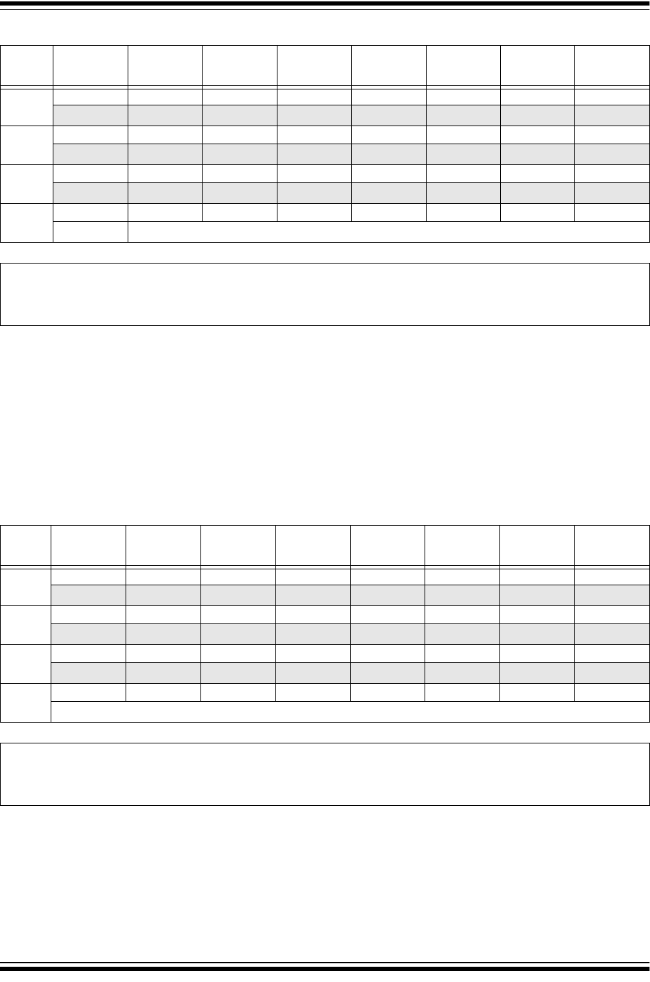
2011-2018 Microchip Technology Inc. DS60001168K-page 123
PIC32MX1XX/2XX 28/36/44-PIN FAMILY
REGISTER 10-12: U1ADDR: USB ADDRESS REGISTER
Bit
Range Bit
31/23/15/7 Bit
30/22/14/6 Bit
29/21/13/5 Bit
28/20/12/4 Bit
27/19/11/3 Bit
26/18/10/2 Bit
25/17/9/1 Bit
24/16/8/0
31:24
U-0 U-0 U-0 U-0 U-0 U-0 U-0 U-0
— — — — — — — —
23:16
U-0 U-0 U-0 U-0 U-0 U-0 U-0 U-0
— — — — — — — —
15:8
U-0 U-0 U-0 U-0 U-0 U-0 U-0 U-0
— — — — — — — —
7:0
R/W-0 R/W-0 R/W-0 R/W-0 R/W-0 R/W-0 R/W-0 R/W-0
LSPDEN DEVADDR<6:0>
Legend:
R = Readable bit W = Writable bit U = Unimplemented bit, read as ‘0’
-n = Value at POR ‘1’ = Bit is set ‘0’ = Bit is cleared x = Bit is unknown
bit 31-8 Unimplemented: Read as ‘0’
bit 7 LSPDEN: Low-Speed Enable Indicator bit
1 = Next token command to be executed at Low-Speed
0 = Next token command to be executed at Full-Speed
bit 6-0 DEVADDR<6:0>: 7-bit USB Device Address bits
REGISTER 10-13: U1FRML: USB FRAME NUMBER LOW REGISTER
Bit
Range Bit
31/23/15/7 Bit
30/22/14/6 Bit
29/21/13/5 Bit
28/20/12/4 Bit
27/19/11/3 Bit
26/18/10/2 Bit
25/17/9/1 Bit
24/16/8/0
31:24
U-0 U-0 U-0 U-0 U-0 U-0 U-0 U-0
————————
23:16
U-0 U-0 U-0 U-0 U-0 U-0 U-0 U-0
————————
15:8
U-0 U-0 U-0 U-0 U-0 U-0 U-0 U-0
————————
7:0
R-0 R-0 R-0 R-0 R-0 R-0 R-0 R-0
FRML<7:0>
Legend:
R = Readable bit W = Writable bit U = Unimplemented bit, read as ‘0’
-n = Value at POR ‘1’ = Bit is set ‘0’ = Bit is cleared x = Bit is unknown
bit 31-8 Unimplemented: Read as ‘0’
bit 7-0 FRML<7:0>: The 11-bit Frame Number Lower bits
The register bits are updated with the current frame number whenever a SOF TOKEN is received.
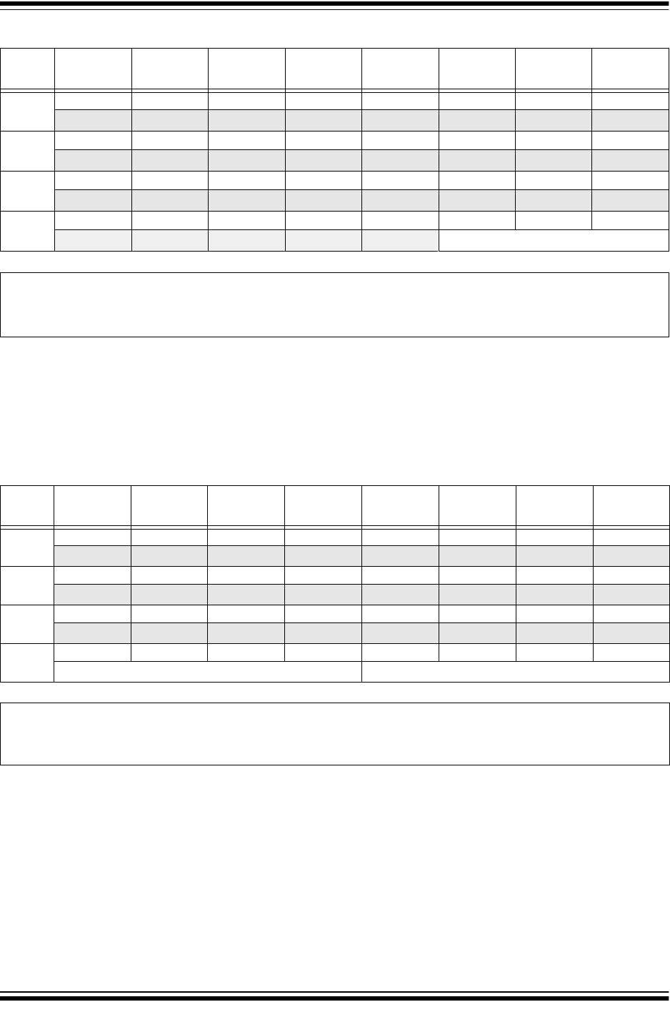
PIC32MX1XX/2XX 28/36/44-PIN FAMILY
DS60001168K-page 124 2011-2018 Microchip Technology Inc.
REGISTER 10-14: U1FRMH: USB FRAME NUMBER HIGH REGISTER
Bit
Range Bit
31/23/15/7 Bit
30/22/14/6 Bit
29/21/13/5 Bit
28/20/12/4 Bit
27/19/11/3 Bit
26/18/10/2 Bit
25/17/9/1 Bit
24/16/8/0
31:24
U-0 U-0 U-0 U-0 U-0 U-0 U-0 U-0
— — — — — — — —
23:16
U-0 U-0 U-0 U-0 U-0 U-0 U-0 U-0
— — — — — — — —
15:8
U-0 U-0 U-0 U-0 U-0 U-0 U-0 U-0
— — — — — — — —
7:0
U-0 U-0 U-0 U-0 U-0 R-0 R-0 R-0
— — — — — FRMH<2:0>
Legend:
R = Readable bit W = Writable bit U = Unimplemented bit, read as ‘0’
-n = Value at POR ‘1’ = Bit is set ‘0’ = Bit is cleared x = Bit is unknown
bit 31-3 Unimplemented: Read as ‘0’
bit 2-0 FRMH<2:0>: The Upper 3 bits of the Frame Numbers bits
The register bits are updated with the current frame number whenever a SOF TOKEN is received.
REGISTER 10-15: U1TOK: USB TOKEN REGISTER
Bit
Range Bit
31/23/15/7 Bit
30/22/14/6 Bit
29/21/13/5 Bit
28/20/12/4 Bit
27/19/11/3 Bit
26/18/10/2 Bit
25/17/9/1 Bit
24/16/8/0
31:24
U-0 U-0 U-0 U-0 U-0 U-0 U-0 U-0
— — — — — — — —
23:16
U-0 U-0 U-0 U-0 U-0 U-0 U-0 U-0
— — — — — — — —
15:8
U-0 U-0 U-0 U-0 U-0 U-0 U-0 U-0
— — — — — — — —
7:0
R/W-0 R/W-0 R/W-0 R/W-0 R/W-0 R/W-0 R/W-0 R/W-0
PID<3:0>
(1)
EP<3:0>
Legend:
R = Readable bit W = Writable bit U = Unimplemented bit, read as ‘0’
-n = Value at POR ‘1’ = Bit is set ‘0’ = Bit is cleared x = Bit is unknown
bit 31-8 Unimplemented: Read as ‘0’
bit 7-4 PID<3:0>: Token Type Indicator bits
(1)
1101 = SETUP (TX) token type transaction
1001 = IN (RX) token type transaction
0001 = OUT (TX) token type transaction
Note: All other values are reserved and must not be used.
bit 3-0 EP<3:0>: Token Command Endpoint Address bits
The four bit value must specify a valid endpoint.
Note 1: All other values are reserved and must not be used.
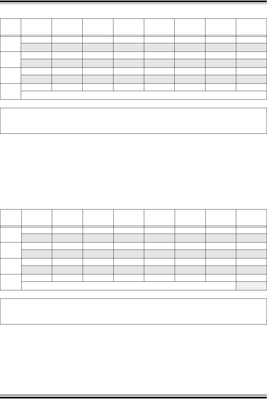
2011-2018 Microchip Technology Inc. DS60001168K-page 125
PIC32MX1XX/2XX 28/36/44-PIN FAMILY
REGISTER 10-16: U1SOF: USB SOF THRESHOLD REGISTER
Bit
Range Bit
31/23/15/7 Bit
30/22/14/6 Bit
29/21/13/5 Bit
28/20/12/4 Bit
27/19/11/3 Bit
26/18/10/2 Bit
25/17/9/1 Bit
24/16/8/0
31:24
U-0 U-0 U-0 U-0 U-0 U-0 U-0 U-0
————————
23:16
U-0 U-0 U-0 U-0 U-0 U-0 U-0 U-0
————————
15:8
U-0 U-0 U-0 U-0 U-0 U-0 U-0 U-0
————————
7:0
R/W-0 R/W-0 R/W-0 R/W-0 R/W-0 R/W-0 R/W-0 R/W-0
CNT<7:0>
Legend:
R = Readable bit W = Writable bit U = Unimplemented bit, read as ‘0’
-n = Value at POR ‘1’ = Bit is set ‘0’ = Bit is cleared x = Bit is unknown
bit 31-8 Unimplemented: Read as ‘0’
bit 7-0 CNT<7:0>: SOF Threshold Value bits
Typical values of the threshold are:
01001010 = 64-byte packet
00101010 = 32-byte packet
00011010 = 16-byte packet
00010010 = 8-byte packet
REGISTER 10-17: U1BDTP1: USB BUFFER DESCRIPTOR TABLE PAGE 1 REGISTER
Bit
Range Bit
31/23/15/7 Bit
30/22/14/6 Bit
29/21/13/5 Bit
28/20/12/4 Bit
27/19/11/3 Bit
26/18/10/2 Bit
25/17/9/1 Bit
24/16/8/0
31:24
U-0 U-0 U-0 U-0 U-0 U-0 U-0 U-0
— — — — — — — —
23:16
U-0 U-0 U-0 U-0 U-0 U-0 U-0 U-0
— — — — — — — —
15:8
U-0 U-0 U-0 U-0 U-0 U-0 U-0 U-0
— — — — — — — —
7:0
R/W-0 R/W-0 R/W-0 R/W-0 R/W-0 R/W-0 R/W-0 U-0
BDTPTRL<15:9> —
Legend:
R = Readable bit W = Writable bit U = Unimplemented bit, read as ‘0’
-n = Value at POR ‘1’ = Bit is set ‘0’ = Bit is cleared x = Bit is unknown
bit 31-8 Unimplemented: Read as ‘0’
bit 7-1 BDTPTRL<15:9>: Buffer Descriptor Table Base Address bits
This 7-bit value provides address bits 15 through 9 of the Buffer Descriptor Table base address, which
defines the starting location of the Buffer Descriptor Table in system memory.
The 32-bit Buffer Descriptor Table base address is 512-byte aligned.
bit 0 Unimplemented: Read as ‘0’
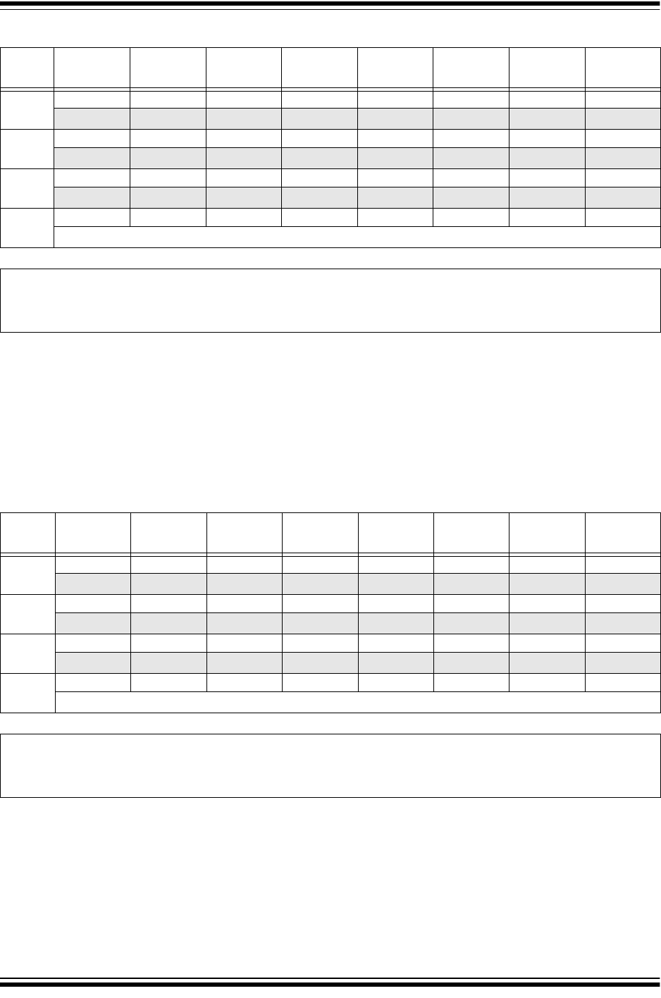
PIC32MX1XX/2XX 28/36/44-PIN FAMILY
DS60001168K-page 126 2011-2018 Microchip Technology Inc.
REGISTER 10-18: U1BDTP2: USB BUFFER DESCRIPTOR TABLE PAGE 2 REGISTER
Bit
Range Bit
31/23/15/7 Bit
30/22/14/6 Bit
29/21/13/5 Bit
28/20/12/4 Bit
27/19/11/3 Bit
26/18/10/2 Bit
25/17/9/1 Bit
24/16/8/0
31:24
U-0 U-0 U-0 U-0 U-0 U-0 U-0 U-0
— — — — — — — —
23:16
U-0 U-0 U-0 U-0 U-0 U-0 U-0 U-0
— — — — — — — —
15:8
U-0 U-0 U-0 U-0 U-0 U-0 U-0 U-0
— — — — — — — —
7:0
R/W-0 R/W-0 R/W-0 R/W-0 R/W-0 R/W-0 R/W-0 R/W-0
BDTPTRH<23:16>
Legend:
R = Readable bit W = Writable bit U = Unimplemented bit, read as ‘0’
-n = Value at POR ‘1’ = Bit is set ‘0’ = Bit is cleared x = Bit is unknown
bit 31-8 Unimplemented: Read as ‘0’
bit 7-0 BDTPTRH<23:16>: Buffer Descriptor Table Base Address bits
This 8-bit value provides address bits 23 through 16 of the Buffer Descriptor Table base address, which
defines the starting location of the Buffer Descriptor Table in system memory.
The 32-bit Buffer Descriptor Table base address is 512-byte aligned.
REGISTER 10-19: U1BDTP3: USB BUFFER DESCRIPTOR TABLE PAGE 3 REGISTER
Bit
Range Bit
31/23/15/7 Bit
30/22/14/6 Bit
29/21/13/5 Bit
28/20/12/4 Bit
27/19/11/3 Bit
26/18/10/2 Bit
25/17/9/1 Bit
24/16/8/0
31:24
U-0 U-0 U-0 U-0 U-0 U-0 U-0 U-0
— — — — — — — —
23:16
U-0 U-0 U-0 U-0 U-0 U-0 U-0 U-0
— — — — — — — —
15:8
U-0 U-0 U-0 U-0 U-0 U-0 U-0 U-0
— — — — — — — —
7:0
R/W-0 R/W-0 R/W-0 R/W-0 R/W-0 R/W-0 R/W-0 R/W-0
BDTPTRU<31:24>
Legend:
R = Readable bit W = Writable bit U = Unimplemented bit, read as ‘0’
-n = Value at POR ‘1’ = Bit is set ‘0’ = Bit is cleared x = Bit is unknown
bit 31-8 Unimplemented: Read as ‘0’
bit 7-0 BDTPTRU<31:24>: Buffer Descriptor Table Base Address bits
This 8-bit value provides address bits 31 through 24 of the Buffer Descriptor Table base address, defines the
starting location of the Buffer Descriptor Table in system memory.
The 32-bit Buffer Descriptor Table base address is 512-byte aligned.

2011-2018 Microchip Technology Inc. DS60001168K-page 127
PIC32MX1XX/2XX 28/36/44-PIN FAMILY
REGISTER 10-20: U1CNFG1: USB CONFIGURATION 1 REGISTER
Bit
Range Bit
31/23/15/7 Bit
30/22/14/6 Bit
29/21/13/5 Bit
28/20/12/4 Bit
27/19/11/3 Bit
26/18/10/2 Bit
25/17/9/1 Bit
24/16/8/0
31:24
U-0 U-0 U-0 U-0 U-0 U-0 U-0 U-0
— — — — — — — —
23:16
U-0 U-0 U-0 U-0 U-0 U-0 U-0 U-0
— — — — — — — —
15:8
U-0 U-0 U-0 U-0 U-0 U-0 U-0 U-0
— — — — — — — —
7:0
R/W-0 R/W-0 U-0 R/W-0 U-0 U-0 U-0 R/W-0
UTEYE UOEMON —USBSIDL — — —UASUSPND
Legend:
R = Readable bit W = Writable bit U = Unimplemented bit, read as ‘0’
-n = Value at POR ‘1’ = Bit is set ‘0’ = Bit is cleared x = Bit is unknown
bit 31-8 Unimplemented: Read as ‘0’
bit 7 UTEYE: USB Eye-Pattern Test Enable bit
1 = Eye-Pattern Test is enabled
0 = Eye-Pattern Test is disabled
bit 6 UOEMON: USB OE Monitor Enable bit
1 = OE signal is active; it indicates intervals during which the D+/D- lines are driving
0 = OE signal is inactive
bit 5 Unimplemented: Read as ‘0’
bit 4 USBSIDL: Stop in Idle Mode bit
1 = Discontinue module operation when the device enters Idle mode
0 = Continue module operation when the device enters Idle mode
bit 3-1 Unimplemented: Read as ‘0’
bit 0 UASUSPND: Automatic Suspend Enable bit
1 = USB module automatically suspends upon entry to Sleep mode. See the USUSPEND bit
(U1PWRC<1>) in Register 10-5.
0 = USB module does not automatically suspend upon entry to Sleep mode. Software must use the
USUSPEND bit (U1PWRC<1>) to suspend the module, including the USB 48 MHz clock.

PIC32MX1XX/2XX 28/36/44-PIN FAMILY
DS60001168K-page 128 2011-2018 Microchip Technology Inc.
REGISTER 10-21: U1EP0-U1EP15: USB ENDPOINT CONTROL REGISTER
Bit
Range Bit
31/23/15/7 Bit
30/22/14/6 Bit
29/21/13/5 Bit
28/20/12/4 Bit
27/19/11/3 Bit
26/18/10/2 Bit
25/17/9/1 Bit
24/16/8/0
31:24
U-0 U-0 U-0 U-0 U-0 U-0 U-0 U-0
————————
23:16
U-0 U-0 U-0 U-0 U-0 U-0 U-0 U-0
————————
15:8
U-0 U-0 U-0 U-0 U-0 U-0 U-0 U-0
————————
7:0
R/W-0 R/W-0 U-0 R/W-0 R/W-0 R/W-0 R/W-0 R/W-0
LSPD RETRYDIS — EPCONDIS EPRXEN EPTXEN EPSTALL EPHSHK
Legend:
R = Readable bit W = Writable bit U = Unimplemented bit, read as ‘0’
-n = Value at POR ‘1’ = Bit is set ‘0’ = Bit is cleared x = Bit is unknown
bit 31-8 Unimplemented: Read as ‘0’
bit 7 LSPD: Low-Speed Direct Connection Enable bit (Host mode and U1EP0 only)
1 = Direct connection to a Low-Speed device enabled
0 = Direct connection to a Low-Speed device disabled; hub required with PRE_PID
bit 6 RETRYDIS: Retry Disable bit (Host mode and U1EP0 only)
1 = Retry NAKed transactions disabled
0 = Retry NAKed transactions enabled; retry done in hardware
bit 5 Unimplemented: Read as ‘0’
bit 4 EPCONDIS: Bidirectional Endpoint Control bit
If EPTXEN = 1 and EPRXEN = 1:
1 = Disable Endpoint n from Control transfers; only TX and RX transfers allowed
0 = Enable Endpoint n for Control (SETUP) transfers; TX and RX transfers also allowed
Otherwise, this bit is ignored.
bit 3 EPRXEN: Endpoint Receive Enable bit
1 = Endpoint n receive is enabled
0 = Endpoint n receive is disabled
bit 2 EPTXEN: Endpoint Transmit Enable bit
1 = Endpoint n transmit is enabled
0 = Endpoint n transmit is disabled
bit 1 EPSTALL: Endpoint Stall Status bit
1 = Endpoint n was stalled
0 = Endpoint n was not stalled
bit 0 EPHSHK: Endpoint Handshake Enable bit
1 = Endpoint Handshake is enabled
0 = Endpoint Handshake is disabled (typically used for isochronous endpoints)
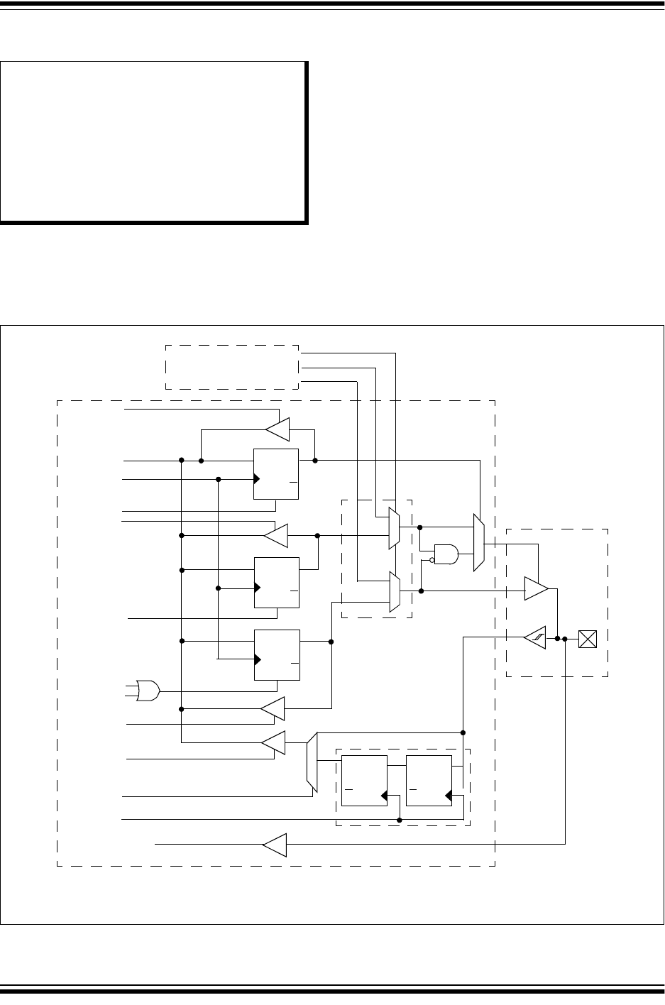
2011-2018 Microchip Technology Inc. DS60001168K-page 129
PIC32MX1XX/2XX 28/36/44-PIN FAMILY
11.0 I/O PORTS
General purpose I/O pins are the simplest of peripher-
als. They allow the PIC
®
MCU to monitor and control
other devices. To add flexibility and functionality, some
pins are multiplexed with alternate functions.
These functions depend on which peripheral features
are on the device. In general, when a peripheral is func-
tioning, that pin may not be used as a general purpose
I/O pin.
Key features of this module include:
• Individual output pin open-drain enable/disable
• Individual input pin weak pull-up and pull-down
• Monitor selective inputs and generate interrupt
when change in pin state is detected
• Operation during Sleep and Idle modes
• Fast bit manipulation using CLR, SET, and INV
registers
Figure 11-1 illustrates a block diagram of a typical
multiplexed I/O port.
FIGURE 11-1: BLOCK DIAGRAM OF A TYPICAL MULTIPLEXED PORT STRUCTURE
Note: This data sheet summarizes the features
of the PIC32MX1XX/2XX 28/36/44-pin
Family of devices. It is not intended to be
a comprehensive reference source. To
complement the information in this data
sheet, refer to Section 12. “I/O Ports”
(DS60001120), which is available from the
Documentation > Reference Manual
section of the Microchip PIC32 web site
(www.microchip.com/pic32).
Peripheral Output Data
Peripheral Module
Peripheral Output Enable
PIO Module
Peripheral Module Enable
WR LAT
I/O Pin
WR PORT
Data Bus
RD LAT
RD PORT
RD TRIS
WR TRIS
0
1
RD ODC
PBCLK
QD
CK
EN Q
QD
CK
EN Q
QD
CK
EN Q
QD
CK
Q
QD
CK
Q
0
1
SYSCLK
WR ODC
ODC
TRIS
LAT
Sleep
1
0
1
0
Output Multiplexers
I/O Cell
Synchronization
R
Peripheral Input
Legend:
R = Peripheral input buffer types may vary. Refer to Ta b l e 1 - 1 for peripheral details.
Note:
This block diagram is a general representation of a shared port/peripheral structure and is only provided for illustration purposes. The
actual structure for any specific port/peripheral combination may be different than it is shown here.
Peripheral Input Buffer

PIC32MX1XX/2XX 28/36/44-PIN FAMILY
DS60001168K-page 130 2011-2018 Microchip Technology Inc.
11.1 Parallel I/O (PIO) Ports
All port pins have 10 registers directly associated with
their operation as digital I/O. The data direction register
(TRISx) determines whether the pin is an input or an
output. If the data direction bit is a ‘1’, then the pin is an
input. All port pins are defined as inputs after a Reset.
Reads from the latch (LATx) read the latch. Writes to
the latch write the latch. Reads from the port (PORTx)
read the port pins, while writes to the port pins write the
latch.
11.1.1 OPEN-DRAIN CONFIGURATION
In addition to the PORTx, LATx, and TRISx registers for
data control, some port pins can also be individually
configured for either digital or open-drain output. This is
controlled by the Open-Drain Control register, ODCx,
associated with each port. Setting any of the bits con-
figures the corresponding pin to act as an open-drain
output.
The open-drain feature allows the generation of
outputs higher than V
DD
(e.g., 5V) on any desired 5V-
tolerant pins by using external pull-up resistors. The
maximum open-drain voltage allowed is the same as
the maximum V
IH
specification.
See the “Pin Diagrams” section for the available pins
and their functionality.
11.1.2 CONFIGURING ANALOG AND
DIGITAL PORT PINS
The ANSELx register controls the operation of the
analog port pins. The port pins that are to function as
analog inputs must have their corresponding ANSEL
and TRIS bits set. In order to use port pins for I/O
functionality with digital modules, such as Timers,
UARTs, etc., the corresponding ANSELx bit must be
cleared.
The ANSELx register has a default value of 0xFFFF;
therefore, all pins that share analog functions are
analog (not digital) by default.
If the TRIS bit is cleared (output) while the ANSELx bit
is set, the digital output level (V
OH
or V
OL
) is converted
by an analog peripheral, such as the ADC module or
Comparator module.
When the PORT register is read, all pins configured as
analog input channels are read as cleared (a low level).
Pins configured as digital inputs do not convert an
analog input. Analog levels on any pin defined as a
digital input (including the ANx pins) can cause the
input buffer to consume current that exceeds the
device specifications.
11.1.3 I/O PORT WRITE/READ TIMING
One instruction cycle is required between a port
direction change or port write operation and a read
operation of the same port. Typically this instruction
would be a NOP.
11.1.4 INPUT CHANGE NOTIFICATION
The input change notification function of the I/O ports
allows the PIC32MX1XX/2XX 28/36/44-pin Family
devices to generate interrupt requests to the processor
in response to a change-of-state on selected input pins.
This feature can detect input change-of-states even in
Sleep mode, when the clocks are disabled. Every I/O
port pin can be selected (enabled) for generating an
interrupt request on a change-of-state.
Five control registers are associated with the CN func-
tionality of each I/O port. The CNENx registers contain
the CN interrupt enable control bits for each of the input
pins. Setting any of these bits enables a CN interrupt
for the corresponding pins.
The CNSTATx register indicates whether a change
occurred on the corresponding pin since the last read
of the PORTx bit.
Each I/O pin also has a weak pull-up and a weak
pull-down connected to it. The pull-ups act as a
current source or sink source connected to the pin,
and eliminate the need for external resistors when
push-button or keypad devices are connected. The
pull-ups and pull-downs are enabled separately using
the CNPUx and the CNPDx registers, which contain
the control bits for each of the pins. Setting any of
the control bits enables the weak pull-ups and/or
pull-downs for the corresponding pins.
An additional control register (CNCONx) is shown in
Register 11-3.
11.2 CLR, SET and INV Registers
Every I/O module register has a corresponding CLR
(clear), SET (set) and INV (invert) register designed to
provide fast atomic bit manipulations. As the name of
the register implies, a value written to a SET, CLR or
INV register effectively performs the implied operation,
but only on the corresponding base register and only
bits specified as ‘1’ are modified. Bits specified as ‘0’
are not modified.
Reading SET, CLR and INV registers returns undefined
values. To see the affects of a write operation to a SET,
CLR, or INV register, the base register must be read.
Note: Pull-ups and pull-downs on change notifi-
cation pins should always be disabled
when the port pin is configured as a digital
output.
2011-2018 Microchip Technology Inc. DS60001168K-page 131
PIC32MX1XX/2XX 28/36/44-PIN FAMILY
11.3 Peripheral Pin Select
A major challenge in general purpose devices is provid-
ing the largest possible set of peripheral features while
minimizing the conflict of features on I/O pins. The chal-
lenge is even greater on low pin-count devices. In an
application where more than one peripheral needs to
be assigned to a single pin, inconvenient workarounds
in application code or a complete redesign may be the
only option.
The Peripheral Pin Select (PPS) configuration provides
an alternative to these choices by enabling peripheral
set selection and their placement on a wide range of
I/O pins. By increasing the pinout options available on
a particular device, users can better tailor the device to
their entire application, rather than trimming the
application to fit the device.
The PPS configuration feature operates over a fixed
subset of digital I/O pins. Users may independently
map the input and/or output of most digital peripherals
to these I/O pins. PPS is performed in software and
generally does not require the device to be repro-
grammed. Hardware safeguards are included that pre-
vent accidental or spurious changes to the peripheral
mapping once it has been established.
11.3.1 AVAILABLE PINS
The number of available pins is dependent on the
particular device and its pin count. Pins that support the
PPS feature include the designation “RPn” in their full
pin designation, where “RP” designates a remappable
peripheral and “n” is the remappable port number.
11.3.2 AVAILABLE PERIPHERALS
The peripherals managed by the PPS are all digital-
only peripherals. These include general serial commu-
nications (UART and SPI), general purpose timer clock
inputs, timer-related peripherals (input capture and out-
put compare) and interrupt-on-change inputs.
In comparison, some digital-only peripheral modules
are never included in the PPS feature. This is because
the peripheral’s function requires special I/O circuitry
on a specific port and cannot be easily connected to
multiple pins. These modules include I
2
C among oth-
ers. A similar requirement excludes all modules with
analog inputs, such as the Analog-to-Digital Converter
(ADC).
A key difference between remappable and non-remap-
pable peripherals is that remappable peripherals are
not associated with a default I/O pin. The peripheral
must always be assigned to a specific I/O pin before it
can be used. In contrast, non-remappable peripherals
are always available on a default pin, assuming that the
peripheral is active and not conflicting with another
peripheral.
When a remappable peripheral is active on a given I/O
pin, it takes priority over all other digital I/O and digital
communication peripherals associated with the pin.
Priority is given regardless of the type of peripheral that
is mapped. Remappable peripherals never take priority
over any analog functions associated with the pin.
11.3.3 CONTROLLING PERIPHERAL PIN
SELECT
PPS features are controlled through two sets of SFRs:
one to map peripheral inputs, and one to map outputs.
Because they are separately controlled, a particular
peripheral’s input and output (if the peripheral has both)
can be placed on any selectable function pin without
constraint.
The association of a peripheral to a peripheral-select-
able pin is handled in two different ways, depending on
whether an input or output is being mapped.
11.3.4 INPUT MAPPING
The inputs of the PPS options are mapped on the basis
of the peripheral. That is, a control register associated
with a peripheral dictates the pin it will be mapped to.
The [pin name]R registers, where [pin name] refers to the
peripheral pins listed in Table 11-1, are used to config-
ure peripheral input mapping (see Register 11-1). Each
register contains sets of 4 bit fields. Programming these
bit fields with an appropriate value maps the RPn pin
with the corresponding value to that peripheral. For any
given device, the valid range of values for any bit field is
shown in Table 11-1.
For example, Figure 11-2 illustrates the remappable
pin selection for the U1RX input.
FIGURE 11-2: REMAPPABLE INPUT
EXAMPLE FOR U1RX
RPA2
RPB6
RPA4
0
1
2U1RX input
U1RXR<3:0>
to peripheral
RPn
n
Note: For input only, PPS functionality does not have
priority over TRISx settings. Therefore, when
configuring RPn pin for input, the corresponding
bit in the TRISx register must also be configured
for input (set to ‘1’).

PIC32MX1XX/2XX 28/36/44-PIN FAMILY
DS60001168K-page 132 2011-2018 Microchip Technology Inc.
TABLE 11-1: INPUT PIN SELECTION
Peripheral Pin [pin name]R SFR [pin name]R bits [pin name]R Value to
RPn Pin Selection
INT4 INT4R INT4R<3:0> 0000 = RPA0
0001 = RPB3
0010 = RPB4
0011 = RPB15
0100 = RPB7
0101 = RPC7
(2)
0110 = RPC0
(1)
0111 = RPC5
(2)
1000 = Reserved
•
•
•
1111 = Reserved
T2CK T2CKR T2CKR<3:0>
IC4 IC4R IC4R<3:0>
SS1 SS1R SS1R<3:0>
REFCLKI REFCLKIR REFCLKIR<3:0>
INT3 INT3R INT3R<3:0> 0000 = RPA1
0001 = RPB5
0010 = RPB1
0011 = RPB11
0100 = RPB8
0101 = RPA8
(2)
0110 = RPC8
(2)
0111 = RPA9
(2)
1000 = Reserved
•
•
•
1111 = Reserved
T3CK T3CKR T3CKR<3:0>
IC3 IC3R IC3R<3:0>
U1CTS U1CTSR U1CTSR<3:0>
U2RX U2RXR U2RXR<3:0>
SDI1 SDI1R SDI1R<3:0>
INT2 INT2R INT2R<3:0> 0000 = RPA2
0001 = RPB6
0010 = RPA4
0011 = RPB13
0100 = RPB2
0101 = RPC6
(2)
0110 = RPC1
(1)
0111 = RPC3
(1)
1000 = Reserved
•
•
•
1111 = Reserved
T4CK T4CKR T4CKR<3:0>
IC1 IC1R IC1R<3:0>
IC5 IC5R IC5R<3:0>
U1RX U1RXR U1RXR<3:0>
U2CTS U2CTSR U2CTSR<3:0>
SDI2 SDI2R SDI2R<3:0>
OCFB OCFBR OCFBR<3:0>
INT1 INT1R INT1R<3:0> 0000 = RPA3
0001 = RPB14
0010 = RPB0
0011 = RPB10
0100 = RPB9
0101 = RPC9
(1)
0110 = RPC2
(2)
0111 = RPC4
(2)
1000 = Reserved
•
•
•
1111 = Reserved
T5CK T5CKR T5CKR<3:0>
IC2 IC2R IC2R<3:0>
SS2 SS2R SS2R<3:0>
OCFA OCFAR OCFAR<3:0>
Note 1: This pin is not available on 28-pin devices.
2: This pin is only available on 44-pin devices.
2011-2018 Microchip Technology Inc. DS60001168K-page 133
PIC32MX1XX/2XX 28/36/44-PIN FAMILY
11.3.5 OUTPUT MAPPING
In contrast to inputs, the outputs of the PPS options
are mapped on the basis of the pin. In this case, a
control register associated with a particular pin
dictates the peripheral output to be mapped. The
RPnR registers (Register 11-2) are used to control
output mapping. Like the [pin name]R registers, each
register contains sets of 4 bit fields. The value of the
bit field corresponds to one of the peripherals, and
that peripheral’s output is mapped to the pin (see
Table 11-2 and Figure 11-3).
A null output is associated with the output register reset
value of ‘0’. This is done to ensure that remappable
outputs remain disconnected from all output pins by
default.
FIGURE 11-3: EXAMPLE OF
MULTIPLEXING OF
REMAPPABLE OUTPUT
FOR RPA0
11.3.6 CONTROLLING CONFIGURATION
CHANGES
Because peripheral remapping can be changed during
run time, some restrictions on peripheral remapping
are needed to prevent accidental configuration
changes. PIC32 devices include two features to
prevent alterations to the peripheral map:
• Control register lock sequence
• Configuration bit select lock
11.3.6.1 Control Register Lock Sequence
Under normal operation, writes to the RPnR and [pin
name]R registers are not allowed. Attempted writes
appear to execute normally, but the contents of the
registers remain unchanged. To change these regis-
ters, they must be unlocked in hardware. The regis-
ter lock is controlled by the Configuration bit,
IOLOCK (CFGCON<13>). Setting IOLOCK prevents
writes to the control registers; clearing IOLOCK
allows writes.
To set or clear the IOLOCK bit, an unlock sequence
must be executed. Refer to Section 6. “Oscillator”
(DS60001112) in the “PIC32 Family Reference
Manual” for details.
11.3.6.2 Configuration Bit Select Lock
As an additional level of safety, the device can be
configured to prevent more than one write session to
the RPnR and [pin name]R registers. The Configuration
bit, IOL1WAY (DEVCFG3<29>), blocks the IOLOCK bit
from being cleared after it has been set once. If
IOLOCK remains set, the register unlock procedure
does not execute, and the PPS control registers cannot
be written to. The only way to clear the bit and re-
enable peripheral remapping is to perform a device
Reset.
In the default (unprogrammed) state, IOL1WAY is set,
restricting users to one write session.
RPA0R<3:0>
0
15
1
Default
U1TX Output
U1RTS Output 2
14
Output Data
RPA0
PIC32MX1XX/2XX 28/36/44-PIN FAMILY
DS60001168K-page 134 2011-2018 Microchip Technology Inc.
TABLE 11-2: OUTPUT PIN SELECTION
RPn Port Pin RPnR SFR RPnR bits RPnR Value to Peripheral
Selection
RPA0 RPA0R RPA0R<3:0> 0000 = No Connect
0001 = U1TX
0010 = U2RTS
0011 = SS1
0100 = Reserved
0101 = OC1
0110 = Reserved
0111 = C2OUT
1000 = Reserved
•
•
•
1111 = Reserved
RPB3 RPB3R RPB3R<3:0>
RPB4 RPB4R RPB4R<3:0>
RPB15 RPB15R RPB15R<3:0>
RPB7 RPB7R RPB7R<3:0>
RPC7 RPC7R RPC7R<3:0>
RPC0 RPC0R RPC0R<3:0>
RPC5 RPC5R RPC5R<3:0>
RPA1 RPA1R RPA1R<3:0> 0000 = No Connect
0001 = Reserved
0010 = Reserved
0011 = SDO1
0100 = SDO2
0101 = OC2
0110 = Reserved
0111 = C3OUT
•
•
•
1111 = Reserved
RPB5 RPB5R RPB5R<3:0>
RPB1 RPB1R RPB1R<3:0>
RPB11 RPB11R RPB11R<3:0>
RPB8 RPB8R RPB8R<3:0>
RPA8 RPA8R RPA8R<3:0>
RPC8 RPC8R RPC8R<3:0>
RPA9 RPA9R RPA9R<3:0>
RPA2 RPA2R RPA2R<3:0> 0000 = No Connect
0001 = Reserved
0010 = Reserved
0011 = SDO1
0100 = SDO2
0101 = OC4
0110 = OC5
0111 = REFCLKO
1000 = Reserved
•
•
•
1111 = Reserved
RPB6 RPB6R RPB6R<3:0>
RPA4 RPA4R RPA4R<3:0>
RPB13 RPB13R RPB13R<3:0>
RPB2 RPB2R RPB2R<3:0>
RPC6 RPC6R RPC6R<3:0>
RPC1 RPC1R RPC1R<3:0>
RPC3 RPC3R RPC3R<3:0>
RPA3 RPA3R RPA3R<3:0> 0000 = No Connect
0001 = U1RTS
0010 = U2TX
0011 = Reserved
0100 = SS2
0101 = OC3
0110 = Reserved
0111 = C1OUT
1000 = Reserved
•
•
•
1111 = Reserved
RPB14 RPB14R RPB14R<3:0>
RPB0 RPB0R RPB0R<3:0>
RPB10 RPB10R RPB10R<3:0>
RPB9 RPB9R RPB9R<3:0>
RPC9 RPC9R RPC9R<3:0>
RPC2 RPC2R RPC2R<3:0>
RPC4 RPC4R RPC4R<3:0>
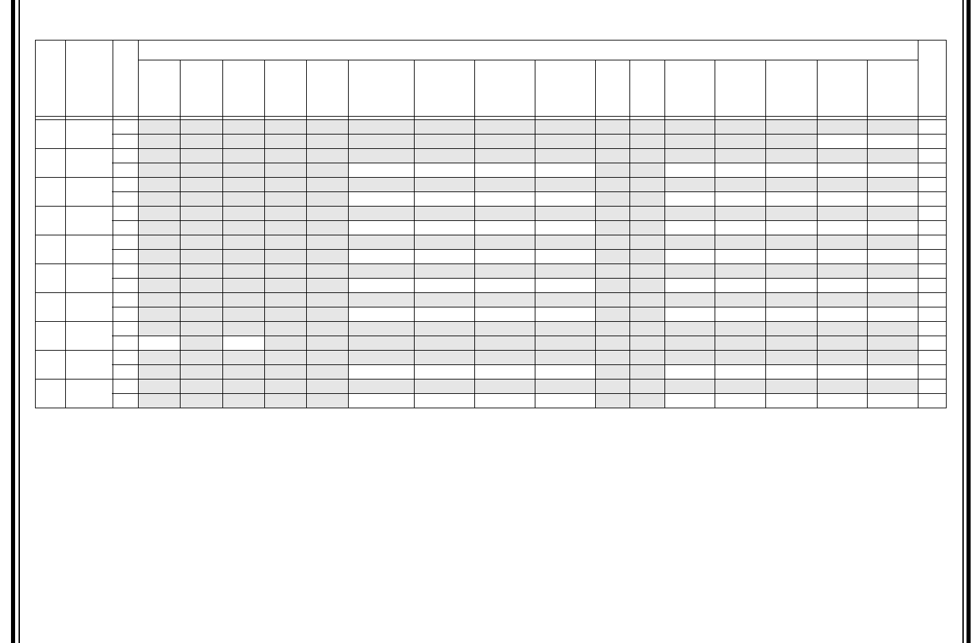
2011-2018 Microchip Technology Inc. DS60001168K-page 135
PIC32MX1XX/2XX 28/36/44-PIN FAMILY
11.4 Ports Control Registers
TABLE 11-3: PORTA REGISTER MAP
Virtual Address
(BF88_#)
Register
Name
(1)
Bit Range
Bits
All Resets
31/15 30/14 29/13 28/12 27/11 26/10 25/9 24/8 23/7 22/6 21/5 20/4 19/3 18/2 17/1 16/0
6000 ANSELA 31:16 — — — — — — — — — — — — — — — — 0000
15:0 — — — — — — — — — — — — — — ANSA1 ANSA0 0003
6010 TRISA 31:16 — — — — — — — — — — — — — — — — 0000
15:0 — — — — — TRISA10
(2)
TRISA9
(2)
TRISA8
(2)
TRISA7
(2)
—— TRISA4 TRISA3 TRISA2 TRISA1 TRISA0 079F
6020 PORTA 31:16 — — — — — — — — — — — 0000
15:0 — — — — —RA10
(2)
RA9
(2)
RA8
(2)
RA7
(2)
—— RA4 RA3 RA2 RA1 RA0 xxxx
6030 LATA 31:16 — — — — — — — — — — — — — — — — 0000
15:0 — — — — —LATA10
(2)
LATA9
(2)
LATA8
(2)
LATA7
(2)
—— LATA4 LATA3 LATA2 LATA1 LATA0 xxxx
6040 ODCA 31:16 — — — — — — — — — — — — — — — — 0000
15:0 — — — — — ODCA10
(2)
ODCA9
(2)
ODCA8
(2)
ODCA7
(2)
—— ODCA4 ODCA3 ODCA2 ODCA1 ODCA0 0000
6050 CNPUA 31:16 — — — — — — — — — — — — — — — — 0000
15:0 — — — — — CNPUA10
(2)
CNPUA9
(2)
CNPUA8
(2)
CNPUA7
(2)
—— CNPUA4 CNPUA3 CNPUA2 CNPUA1 CNPUA0 0000
6060 CNPDA 31:16 — — — — — — — — — — — — — — — — 0000
15:0 — — — — — CNPDA10
(2)
CNPDA9
(2)
CNPDA8
(2)
CNPDA7
(2)
—— CNPDA4 CNPDA3 CNPDA2 CNPDA1 CNPDA0 0000
6070 CNCONA 31:16 — — — — — — — — — — — — — — — — 0000
15:0 ON —SIDL— — — — — — — — — — — — — 0000
6080 CNENA 31:16 — — — — — — — — — — — — — — — — 0000
15:0 — — — — — CNIEA10
(2)
CNIEA9
(2)
CNIEA8
(2)
CNIEA7
(2)
—— CNIEA4 CNIEA3 CNIEA2 CNIEA1 CNIEA0 0000
6090 CNSTATA 31:16 — — — — — — — — — — — — — — — — 0000
15:0 — — — — — CNSTATA10
(2)
CNSTATA9
(2)
CNSTATA8
(2)
CNSTATA7
(2)
—— CNSTATA4 CNSTATA3 CNSTATA2 CNSTATA1 CNSTATA0 0000
Legend: x = unknown value on Reset; — = unimplemented, read as ‘0’. Reset values are shown in hexadecimal.
Note 1: All registers in this table have corresponding CLR, SET and INV registers at their virtual addresses, plus offsets of 0x4, 0x8 and 0xC, respectively. See Section 11.2 “CLR, SET and INV Registers” for
more information.
2: This bit is only available on 44-pin devices.
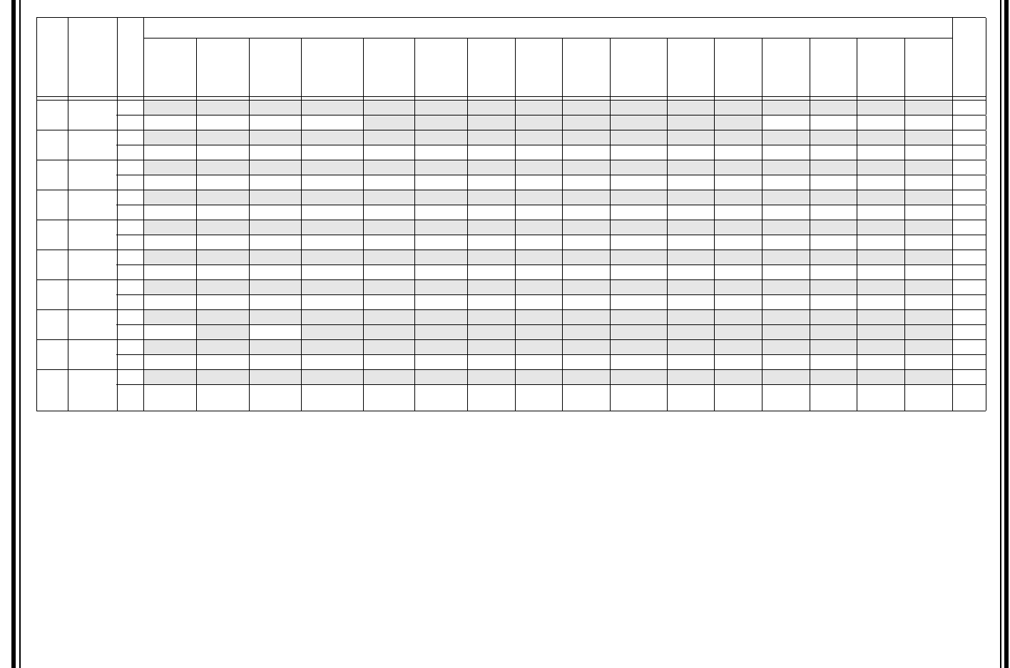
PIC32MX1XX/2XX 28/36/44-PIN FAMILY
DS60001168K-page 136 2011-2018 Microchip Technology Inc.
TABLE 11-4: PORTB REGISTER MAP
Virtual Address
(BF88_#)
Register
Name
Bit Range
Bits
All Resets
31/15 30/14 29/13 28/12 27/11 26/10 25/9 24/8 23/7 22/6 21/5 20/4 19/3 18/2 17/1 16/0
6100 ANSELB 31:16 — — — — — — — — — — — — — — — — 0000
15:0 ANSB15 ANSB14 ANSB13 ANSB12
(2)
— — — — — — — — ANSB3 ANSB2 ANSB1 ANSB0 E00F
6110 TRISB 31:16 — — — — — — — — — — — — — — — — 0000
15:0 TRISB15 TRISB14 TRISB13 TRISB12
(2)
TRISB11 TRISB10 TRISB9 TRISB8 TRISB7 TRISB6
(2)
TRISB5 TRISB4 TRISB3 TRISB2 TRISB1 TRISB0 FFFF
6120 PORTB 31:16 — — — — — — — — — — — 0000
15:0 RB15 RB14 RB13 RB12
(2)
RB11 RB10 RB9 RB8 RB7 RC6
(2)
RB5 RB4 RB3 RB2 RB1 RB0 xxxx
6130 LATB 31:16 — — — — — — — — — — — — — — — — 0000
15:0 LATB15 LATB14 LATB13 LATB12
(2)
LATB11 LATB10 LATB9 LATB8 LATB7 LATB6
(2)
LATB5 LATB4 LATB3 LATB2 LATB1 LATB0 xxxx
6140 ODCB 31:16 — — — — — — — — — — — — — — — — 0000
15:0 ODCB15 ODCB14 ODCB13 ODCB12
(2)
ODCB11 ODCB10 ODCB9 ODCB8 ODCB7 ODCB6 ODCB5 ODCB4 ODCB3 ODCB2 ODCB1 ODCB0 0000
6150 CNPUB 31:16 — — — — — — — — — — — — — — — — 0000
15:0 CNPUB15 CNPUB14 CNPUB13 CNPUB12
(2)
CNPUB11 CNPUB10 CNPUB9 CNPUB8 CNPUB7 CNPUB6
(2)
CNPUB5 CNPUB4 CNPUB3 CNPUB2 CNPUB1 CNPUB0 0000
6160 CNPDB 31:16 — — — — — — — — — — — — — — — — 0000
15:0 CNPDB15 CNPDB14 CNPDB13 CNPDB12
(2)
CNPDB11 CNPDB10 CNPDB9 CNPDB8 CNPDB7 CNPDB6
(2)
CNPDB5 CNPDB4 CNPDB3 CNPDB2 CNPDB1 CNPDB0 0000
6170 CNCONB 31:16 — — — — — — — — — — — — — — — — 0000
15:0 ON —SIDL — — — — — — — — — — — — — 0000
6180 CNENB 31:16 — — — — — — — — — — — — — — — — 0000
15:0 CNIEB15 CNIEB14 CNIEB13 CNIEB11
(2)
CNIEB11 CNIEB10 CNIEB9 CNIEB8 CNIEB7 CNIEB6
(2)
CNIEB5 CNIEB4 CNIEB3 CNIEB2 CNIEB1 CNIEB0 0000
6190 CNSTATB
31:16 — — — — — — — — — — — — — — — — 0000
15:0 CN
STATB15
CN
STATB14
CN
STATB13
CN
STATB12
(2)
CN
STATB11
CN
STATB10
CN
STATB9
CN
STATB8
CN
STATB7
CN
STATB6
(2)
CN
STATB5
CN
STATB4
CN
STATB3
CN
STATB2
CN
STATB1
CN
STATB0 0000
Legend: x = unknown value on Reset; — = unimplemented, read as ‘0’. Reset values are shown in hexadecimal.
Note 1: All registers in this table have corresponding CLR, SET and INV registers at their virtual addresses, plus offsets of 0x4, 0x8 and 0xC, respectively. See Section 11.2 “CLR, SET and INV Registers” for
more information.
2: This bit is not available on PIC32MX2XX devices. The reset value for the TRISB register when this bit is not available is 0x0000EFBF.
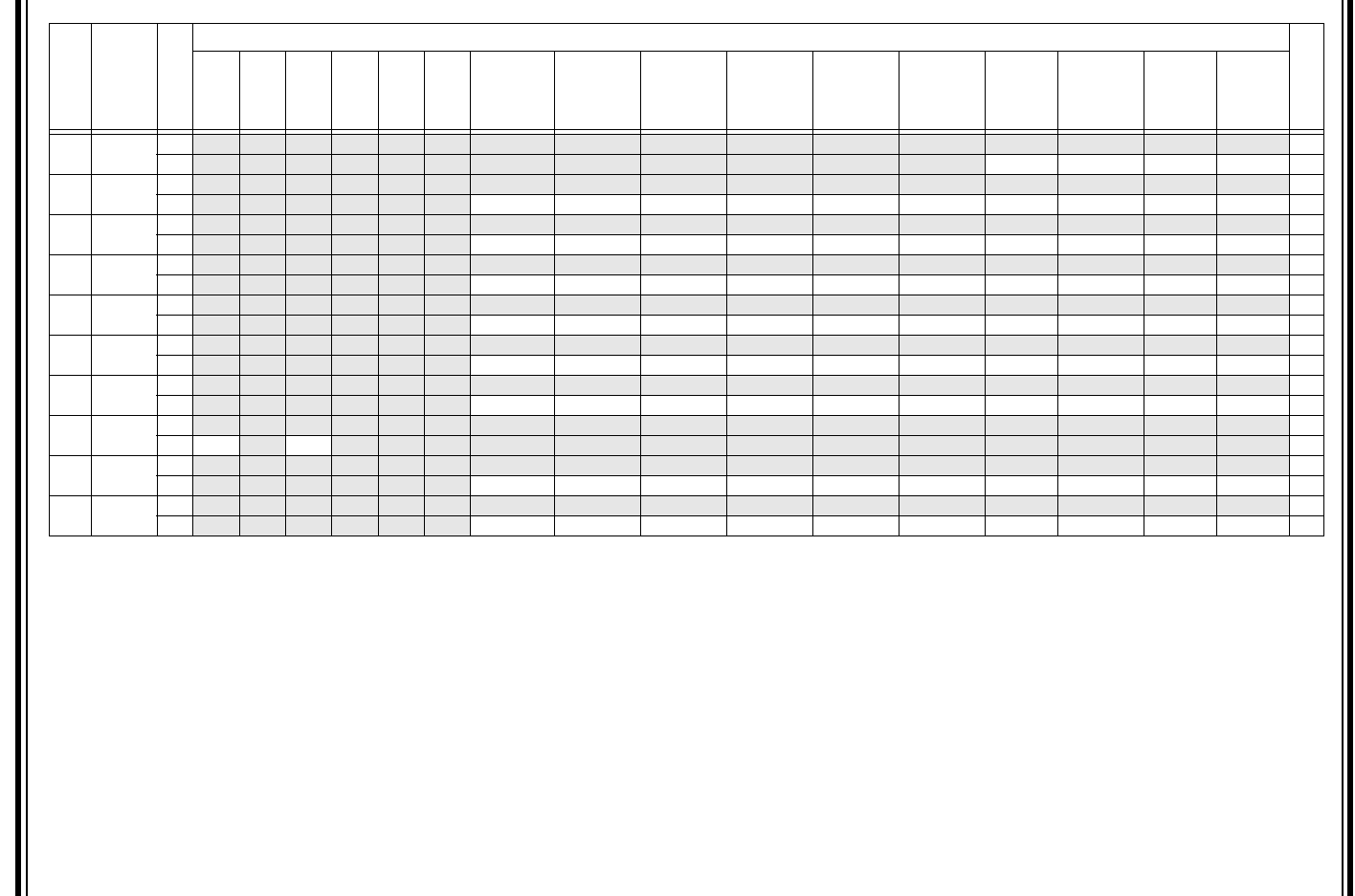
2011-2018 Microchip Technology Inc. DS60001168K-page 137
PIC32MX1XX/2XX 28/36/44-PIN FAMILY
TABLE 11-5: PORTC REGISTER MAP
Virtual Address
(BF88_#)
Register
Name
(1,2)
Bit Range
Bits
All Resets
31/15 30/14 29/13 28/12 27/11 26/10 25/9 24/8 23/7 22/6 21/5 20/4 19/3 18/2 17/1 16/0
6200 ANSELC 31:16 — — — — — — — — — — — — — — — — 0000
15:0 — — — — — — — — — — — — ANSC3
(4)
ANSC2
(3)
ANSC1 ANSC0 000F
6210 TRISC 31:16 — — — — — — — — — — — — — — — — 0000
15:0 —————— TRISC9 TRISC8
(3)
TRISC7
(3)
TRISC6
(3)
TRISC5
(3)
TRISC4
(3)
TRISC3 TRISC2
(3)
TRISC1 TRISC0 03FF
6220 PORTC 31:16 — — — — — — — — — — — 0000
15:0 —————— RC9 RC8
(3)
RC7
(3)
RC6
(3)
RC5
(3)
RC4
(3)
RC3 RC2
(3)
RC1 RC0 xxxx
6230 LATC 31:16 — — — — — — — — — — — — — — — — 0000
15:0 ——————LATC9LATC8
(3)
LATC7
(3)
LATC6
(3)
LATC5
(3)
LATC4
(3)
LATC3 LATC2
(3)
LATC1 LATC0 xxxx
6240 ODCC 31:16 — — — — — — — — — — — — — — — — 0000
15:0 —————— ODCC9 ODCC8
(3)
ODCC7
(3)
ODCC6
(3)
ODCC5
(3)
ODCC4
(3)
ODCC3 ODCC2
(3)
ODCC1 ODCC0 0000
6250 CNPUC 31:16 — — — — — — — — — — — — — — — — 0000
15:0 —————— CNPUC9 CNPUC8
(3)
CNPUC7
(3)
CNPUC6
(3)
CNPUC5
(3)
CNPUC4
(3)
CNPUC3 CNPUC2
(3)
CNPUC1 CNPUC0 0000
6260 CNPDC 31:16 — — — — — — — — — — — — — — — — 0000
15:0 —————— CNPDC9 CNPDC8
(3)
CNPDC7
(3)
CNPDC6
(3)
CNPDC5
(3)
CNPDC4
(3)
CNPDC3 CNPDC2
(3)
CNPDC1 CNPDC0 0000
6270 CNCONC 31:16 — — — — — — — — — — — — — — — — 0000
15:0 ON —SIDL— — — — — — — — — — — — — 0000
6280 CNENC 31:16 — — — — — — — — — — — — — — — — 0000
15:0 —————— CNIEC9 CNIEC8
(3)
CNIEC7
(3)
CNIEC6
(3)
CNIEC5
(3)
CNIEC4
(3)
CNIEC3 CNIEC2
(3)
CNIEC1 CNIEC0 0000
6290 CNSTATC 31:16 — — — — — — — — — — — — — — — — 0000
15:0 —————— CNSTATC9 CNSTATC8
(3)
CNSTATC7
(3)
CNSTATC6
(3)
CNSTATC5
(3)
CNSTATC4
(3)
CNSTATC3 CNSTATC2
(3)
CNSTATC1 CNSTATC0 0000
Legend: x = unknown value on Reset; — = unimplemented, read as ‘0’. Reset values are shown in hexadecimal.
Note 1: All registers in this table have corresponding CLR, SET and INV registers at their virtual addresses, plus offsets of 0x4, 0x8 and 0xC, respectively. See Section 11.2 “CLR, SET and INV Registers” for
more information.
2: PORTC is not available on 28-pin devices.
3: This bit is only available on 44-pin devices.
4: This bit is only available on USB-enabled devices with 36 or 44 pins.

PIC32MX1XX/2XX 28/36/44-PIN FAMILY
DS60001168K-page 138 2011-2018 Microchip Technology Inc.
TABLE 11-6: PERIPHERAL PIN SELECT INPUT REGISTER MAP
Virtual Address
(BF80_#)
Register
Name
Bit Range
Bits
All Resets
31/15 30/14 29/13 28/12 27/11 26/10 25/9 24/8 23/7 22/6 21/5 20/4 19/3 18/2 17/1 16/0
FA04 INT1R 31:16 — — — — — — — — — — — — — — — — 0000
15:0 ————————————INT1R<3:0>0000
FA08 INT2R 31:16 — — — — — — — — — — — — — — — — 0000
15:0 ————————————INT2R<3:0>0000
FA0C INT3R 31:16 — — — — — — — — — — — — — — — — 0000
15:0 ————————————INT3R<3:0>0000
FA10 INT4R 31:16 — — — — — — — — — — — — — — — — 0000
15:0 ————————————INT4R<3:0>0000
FA18 T2CKR 31:16 — — — — — — — — — — — — — — — — 0000
15:0 ————————————T2CKR<3:0>0000
FA1C T3CKR 31:16 — — — — — — — — — — — — — — — — 0000
15:0 ————————————T3CKR<3:0>0000
FA20 T4CKR 31:16 — — — — — — — — — — — — — — — — 0000
15:0 ————————————T4CKR<3:0>0000
FA24 T5CKR 31:16 — — — — — — — — — — — — — — — — 0000
15:0 ————————————T5CKR<3:0>0000
FA28 IC1R 31:16 — — — — — — — — — — — — — — — — 0000
15:0 ———————————— IC1R<3:0> 0000
FA2C IC2R 31:16 — — — — — — — — — — — — — — — — 0000
15:0 ———————————— IC2R<3:0> 0000
FA30 IC3R 31:16 — — — — — — — — — — — — — — — — 0000
15:0 ———————————— IC3R<3:0> 0000
FA34 IC4R 31:16 — — — — — — — — — — — — — — — — 0000
15:0 ———————————— IC4R<3:0> 0000
FA38 IC5R 31:16 — — — — — — — — — — — — — — — — 0000
15:0 ———————————— IC5R<3:0> 0000
FA48 OCFAR 31:16 — — — — — — — — — — — — — — — — 0000
15:0 ————————————OCFAR<3:0>0000
FA4C OCFBR 31:16 — — — — — — — — — — — — — — — — 0000
15:0 ————————————OCFBR<3:0>0000
FA50 U1RXR 31:16 — — — — — — — — — — — — — — — — 0000
15:0 ————————————U1RXR<3:0>0000

2011-2018 Microchip Technology Inc. DS60001168K-page 139
PIC32MX1XX/2XX 28/36/44-PIN FAMILY
FA54 U1CTSR 31:16 — — — — — — — — — — — — — — — — 0000
15:0 ———————————— U1CTSR<3:0> 0000
FA58 U2RXR 31:16 — — — — — — — — — — — — — — — — 0000
15:0 ————————————U2RXR<3:0>0000
FA5C U2CTSR 31:16 — — — — — — — — — — — — — — — — 0000
15:0 ———————————— U2CTSR<3:0> 0000
FA84 SDI1R 31:16 — — — — — — — — — — — — — — — — 0000
15:0 ————————————SDI1R<3:0>0000
FA88 SS1R 31:16 — — — — — — — — — — — — — — — — 0000
15:0 ———————————— SS1R<3:0> 0000
FA90 SDI2R 31:16 — — — — — — — — — — — — — — — — 0000
15:0 ————————————SDI2R<3:0>0000
FA94 SS2R 31:16 — — — — — — — — — — — — — — — — 0000
15:0 ———————————— SS2R<3:0> 0000
FAB8 REFCLKIR 31:16 — — — — — — — — — — — — — — — — 0000
15:0 ———————————— REFCLKIR<3:0> 0000
TABLE 11-6: PERIPHERAL PIN SELECT INPUT REGISTER MAP (CONTINUED)
Virtual Address
(BF80_#)
Register
Name
Bit Range
Bits
All Resets
31/15 30/14 29/13 28/12 27/11 26/10 25/9 24/8 23/7 22/6 21/5 20/4 19/3 18/2 17/1 16/0

PIC32MX1XX/2XX 28/36/44-PIN FAMILY
DS60001168K-page 140 2011-2018 Microchip Technology Inc.
TABLE 11-7: PERIPHERAL PIN SELECT OUTPUT REGISTER MAP
Virtual Address
(BF80_#)
Register
Name
Bit Range
Bits
All Resets
31/15 30/14 29/13 28/12 27/11 26/10 25/9 24/8 23/7 22/6 21/5 20/4 19/3 18/2 17/1 16/0
FB00 RPA0R 31:16 — — — — — — — — — — — — — — — — 0000
15:0 — — — — — — — — — — — — RPA0<3:0> 0000
FB04 RPA1R 31:16 — — — — — — — — — — — — — — — — 0000
15:0 — — — — — — — — — — — — RPA1<3:0> 0000
FB08 RPA2R 31:16 — — — — — — — — — — — — — — — — 0000
15:0 — — — — — — — — — — — — RPA2<3:0> 0000
FB0C RPA3R 31:16 — — — — — — — — — — — — — — — — 0000
15:0 — — — — — — — — — — — — RPA3<3:0> 0000
FB10 RPA4R 31:16 — — — — — — — — — — — — — — — — 0000
15:0 — — — — — — — — — — — — RPA4<3:0> 0000
FB20 RPA8R
(1)
31:16 — — — — — — — — — — — — — — — — 0000
15:0 — — — — — — — — — — — — RPA8<3:0> 0000
FB24 RPA9R
(1)
31:16 — — — — — — — — — — — — — — — — 0000
15:0 — — — — — — — — — — — — RPA9<3:0> 0000
FB2C RPB0R 31:16 — — — — — — — — — — — — — — — — 0000
15:0 — — — — — — — — — — — — RPB0<3:0> 0000
FB30 RPB1R 31:16 — — — — — — — — — — — — — — — — 0000
15:0 — — — — — — — — — — — — RPB1<3:0> 0000
FB34 RPB2R 31:16 — — — — — — — — — — — — — — — — 0000
15:0 — — — — — — — — — — — — RPB2<3:0> 0000
FB38 RPB3R 31:16 — — — — — — — — — — — — — — — — 0000
15:0 — — — — — — — — — — — — RPB3<3:0> 0000
FB3C RPB4R 31:16 — — — — — — — — — — — — — — — — 0000
15:0 — — — — — — — — — — — — RPB4<3:0> 0000
FB40 RPB5R 31:16 — — — — — — — — — — — — — — — — 0000
15:0 — — — — — — — — — — — — RPB5<3:0> 0000
FB44 RPB6R
(2)
31:16 — — — — — — — — — — — — — — — — 0000
15:0 — — — — — — — — — — — — RPB6<3:0> 0000
FB48 RPB7R 31:16 — — — — — — — — — — — — — — — — 0000
15:0 — — — — — — — — — — — — RPB7<3:0> 0000
Legend: x = unknown value on Reset; — = unimplemented, read as ‘0’. Reset values are shown in hexadecimal.
Note 1: This register is only available on 44-pin devices.
2: This register is only available on PIC32MX1XX devices.
3: This register is only available on 36-pin and 44-pin devices.

2011-2018 Microchip Technology Inc. DS60001168K-page 141
PIC32MX1XX/2XX 28/36/44-PIN FAMILY
FB4C RPB8R 31:16 — — — — — — — — — — — — — — — — 0000
15:0 — — — — — — — — — — — — RPB8<3:0> 0000
FB50 RPB9R 31:16 — — — — — — — — — — — — — — — — 0000
15:0 — — — — — — — — — — — — RPB9<3:0> 0000
FB54 RPB10R 31:16 — — — — — — — — — — — — — — — — 0000
15:0 — — — — — — — — — — — — RPB10<3:0> 0000
FB58 RPB11R 31:16 — — — — — — — — — — — — — — — — 0000
15:0 — — — — — — — — — — — — RPB11<3:0> 0000
FB60 RPB13R 31:16 — — — — — — — — — — — — — — — — 0000
15:0 — — — — — — — — — — — — RPB13<3:0> 0000
FB64 RPB14R 31:16 — — — — — — — — — — — — — — — — 0000
15:0 — — — — — — — — — — — — RPB14<3:0> 0000
FB68 RPB15R 31:16 — — — — — — — — — — — — — — — — 0000
15:0 — — — — — — — — — — — — RPB15<3:0> 0000
FB6C RPC0R
(3)
31:16 — — — — — — — — — — — — — — — — 0000
15:0 — — — — — — — — — — — — RPC0<3:0> 0000
FB70 RPC1R
(3)
31:16 — — — — — — — — — — — — — — — — 0000
15:0 — — — — — — — — — — — — RPC1<3:0> 0000
FB74 RPC2R
(1)
31:16 — — — — — — — — — — — — — — — — 0000
15:0 — — — — — — — — — — — — RPC2<3:0> 0000
FB78 RPC3R
(3)
31:16 — — — — — — — — — — — — — — — — 0000
15:0 — — — — — — — — — — — — RPC3<3:0> 0000
FB7C RPC4R
(1)
31:16 — — — — — — — — — — — — — — — — 0000
15:0 — — — — — — — — — — — — RPC4<3:0> 0000
FB80 RPC5R
(1)
31:16 — — — — — — — — — — — — — — — — 0000
15:0 — — — — — — — — — — — — RPC5<3:0> 0000
FB84 RPC6R
(1)
31:16 — — — — — — — — — — — — — — — — 0000
15:0 — — — — — — — — — — — — RPC6<3:0> 0000
FB88 RPC7R
(1)
31:16 — — — — — — — — — — — — — — — — 0000
15:0 — — — — — — — — — — — — RPC7<3:0> 0000
TABLE 11-7: PERIPHERAL PIN SELECT OUTPUT REGISTER MAP (CONTINUED)
Virtual Address
(BF80_#)
Register
Name
Bit Range
Bits
All Resets
31/15 30/14 29/13 28/12 27/11 26/10 25/9 24/8 23/7 22/6 21/5 20/4 19/3 18/2 17/1 16/0
Legend: x = unknown value on Reset; — = unimplemented, read as ‘0’. Reset values are shown in hexadecimal.
Note 1: This register is only available on 44-pin devices.
2: This register is only available on PIC32MX1XX devices.
3: This register is only available on 36-pin and 44-pin devices.
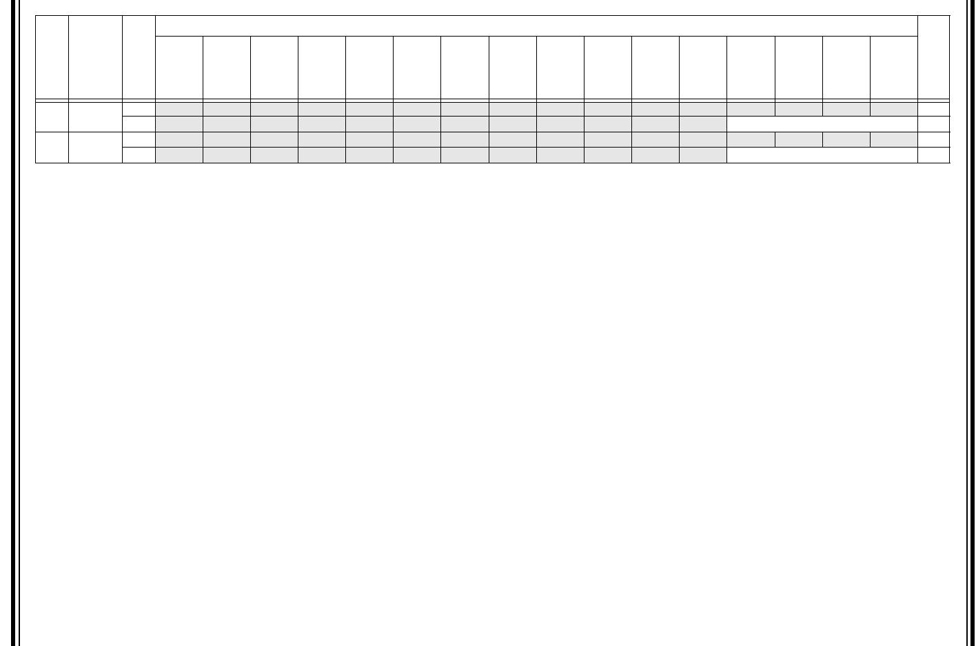
PIC32MX1XX/2XX 28/36/44-PIN FAMILY
DS60001168K-page 142 2011-2018 Microchip Technology Inc.
FB8C RPC8R
(1)
31:16 — — — — — — — — — — — — — — — — 0000
15:0 — — — — — — — — — — — — RPC8<3:0> 0000
FB90 RPC9R
(3)
31:16 — — — — — — — — — — — — — — — — 0000
15:0 — — — — — — — — — — — — RPC9<3:0> 0000
TABLE 11-7: PERIPHERAL PIN SELECT OUTPUT REGISTER MAP (CONTINUED)
Virtual Address
(BF80_#)
Register
Name
Bit Range
Bits
All Resets
31/15 30/14 29/13 28/12 27/11 26/10 25/9 24/8 23/7 22/6 21/5 20/4 19/3 18/2 17/1 16/0
Legend: x = unknown value on Reset; — = unimplemented, read as ‘0’. Reset values are shown in hexadecimal.
Note 1: This register is only available on 44-pin devices.
2: This register is only available on PIC32MX1XX devices.
3: This register is only available on 36-pin and 44-pin devices.
2011-2018 Microchip Technology Inc. DS60001168K-page 143
PIC32MX1XX/2XX 28/36/44-PIN FAMILY
REGISTER 11-1: [pin name]R: PERIPHERAL PIN SELECT INPUT REGISTER
Bit
Range Bit
31/23/15/7 Bit
30/22/14/6 Bit
29/21/13/5 Bit
28/20/12/4 Bit
27/19/11/3 Bit
26/18/10/2 Bit
25/17/9/1 Bit
24/16/8/0
31:24
U-0 U-0 U-0 U-0 U-0 U-0 U-0 U-0
— — — — — — — —
23:16
U-0 U-0 U-0 U-0 U-0 U-0 U-0 U-0
— — — — — — — —
15:8
U-0 U-0 U-0 U-0 U-0 U-0 U-0 U-0
— — — — — — — —
7:0
U-0 U-0 U-0 U-0 R/W-0 R/W-0 R/W-0 R/W-0
————[pin name]R<3:0>
Legend:
R = Readable bit W = Writable bit U = Unimplemented bit, read as ‘0’
-n = Value at POR ‘1’ = Bit is set ‘0’ = Bit is cleared x = Bit is unknown
bit 31-4 Unimplemented: Read as ‘0’
bit 3-0 [pin name]R<3:0>: Peripheral Pin Select Input bits
Where [pin name] refers to the pins that are used to configure peripheral input mapping. See Table 11-1 for
input pin selection values.
Note: Register values can only be changed if the Configuration bit, IOLOCK (CFGCON<13>), = 0.
REGISTER 11-2: RPnR: PERIPHERAL PIN SELECT OUTPUT REGISTER
Bit
Range Bit
31/23/15/7 Bit
30/22/14/6 Bit
29/21/13/5 Bit
28/20/12/4 Bit
27/19/11/3 Bit
26/18/10/2 Bit
25/17/9/1 Bit
24/16/8/0
31:24
U-0 U-0 U-0 U-0 U-0 U-0 U-0 U-0
— — — — — — — —
23:16
U-0 U-0 U-0 U-0 U-0 U-0 U-0 U-0
— — — — — — — —
15:8
U-0 U-0 U-0 U-0 U-0 U-0 U-0 U-0
— — — — — — — —
7:0
U-0 U-0 U-0 U-0 R/W-0 R/W-0 R/W-0 R/W-0
———— RPnR<3:0>
Legend:
R = Readable bit W = Writable bit U = Unimplemented bit, read as ‘0’
-n = Value at POR ‘1’ = Bit is set ‘0’ = Bit is cleared x = Bit is unknown
bit 31-4 Unimplemented: Read as ‘0’
bit 3-0 RPnR<3:0>: Peripheral Pin Select Output bits
See Ta bl e 11 - 2 for output pin selection values.
Note: Register values can only be changed if the Configuration bit, IOLOCK (CFGCON<13>), = 0.

PIC32MX1XX/2XX 28/36/44-PIN FAMILY
DS60001168K-page 144 2011-2018 Microchip Technology Inc.
REGISTER 11-3: CNCONx: CHANGE NOTICE CONTROL FOR PORTx REGISTER (x = A, B, C)
Bit
Range Bit
31/23/15/7 Bit
30/22/14/6 Bit
29/21/13/5 Bit
28/20/12/4 Bit
27/19/11/3 Bit
26/18/10/2 Bit
25/17/9/1 Bit
24/16/8/0
31:24
U-0 U-0 U-0 U-0 U-0 U-0 U-0 U-0
— — — — — — — —
23:16
U-0 U-0 U-0 U-0 U-0 U-0 U-0 U-0
— — — — — — — —
15:8
R/W-0 U-0 R/W-0 U-0 U-0 U-0 U-0 U-0
ON —SIDL— — — — —
7:0
U-0 U-0 U-0 U-0 U-0 U-0 U-0 U-0
— — — — — — — —
Legend:
R = Readable bit W = Writable bit U = Unimplemented bit, read as ‘0’
-n = Value at POR ‘1’ = Bit is set ‘0’ = Bit is cleared x = Bit is unknown
bit 31-16 Unimplemented: Read as ‘0’
bit 15 ON: Change Notice (CN) Control ON bit
1 = CN is enabled
0 = CN is disabled
bit 14 Unimplemented: Read as ‘0’
bit 13 SIDL: Stop in Idle Control bit
1 = Idle mode halts CN operation
0 = Idle does not affect CN operation
bit 12-0 Unimplemented: Read as ‘0’
2011-2017 Microchip Technology Inc. DS60001168K-page 145
PIC32MX1XX/2XX 28/36/44-PIN FAMILY
12.0 TIMER1
This family of PIC32 devices features one
synchronous/asynchronous 16-bit timer that can operate
as a free-running interval timer for various timing applica-
tions and counting external events. This timer can also
be used with the Low-Power Secondary Oscillator
(S
OSC
) for Real-Time Clock (RTC) applications.
The following modes are supported:
• Synchronous Internal Timer
• Synchronous Internal Gated Timer
• Synchronous External Timer
• Asynchronous External Timer
12.1 Additional Supported Features
• Selectable clock prescaler
• Timer operation during CPU Idle and Sleep mode
• Fast bit manipulation using CLR, SET and INV
registers
• Asynchronous mode can be used with the S
OSC
to function as a Real-Time Clock (RTC)
Figure 12-1 illustrates a general block diagram of
Timer1.
FIGURE 12-1: TIMER1 BLOCK DIAGRAM
Note: This data sheet summarizes the features
of the PIC32MX1XX/2XX 28/36/44-pin
Family of devices. It is not intended to be
a comprehensive reference source. To
complement the information in this data
sheet, refer to Section 14. “Timers”
(DS60001105), which is available from the
Documentation > Reference Manual
section of the Microchip PIC32 web site
(www.microchip.com/pic32).
ON
Sync
SOSCI
SOSCO/T1CK
TMR1
T1IF
Equal 16-bit Comparator
PR1
Reset
SOSCEN
Event Flag
1
0
TSYNC
TGATE
TGATE
PBCLK
1
0
TCS
Gate
Sync
TCKPS<1:0>
Prescaler
2
1, 8, 64, 256
x 1
1 0
0 0
Q
QD
Note: The default state of the SOSCEN (OSCCON<1>) bit during a device Reset is controlled by the
FSOSCEN bit in Configuration Word, DEVCFG1.
Data Bus<31:0>
<15:0> <15:0>
PIC32MX1XX/2XX 28/36/44-PIN FAMILY
DS60001168K-page 146 2011-2017 Microchip Technology Inc.
12.2 Timer1 Control Registers
TABLE 12-1: TIMER1 REGISTER MAP
Virtual Address
(BF80_#)
Register
Name
(1)
Bit Range
Bits
All Resets
31/15 30/14 29/13 28/12 27/11 26/10 25/9 24/8 23/7 22/6 21/5 20/4 19/3 18/2 17/1 16/0
0600 T1CON 31:16 ————————————————0000
15:0 ON — SIDL TWDIS TWIP — — —TGATE— TCKPS<1:0> —TSYNCTCS —0000
0610 TMR1 31:16 ————————————————0000
15:0 TMR1<15:0> 0000
0620 PR1 31:16 ————————————————0000
15:0 PR1<15:0> FFFF
Legend: x = unknown value on Reset; — = unimplemented, read as ‘0’. Reset values are shown in hexadecimal.
Note 1: All registers in this table have corresponding CLR, SET and INV registers at their virtual addresses, plus offsets of 0x4, 0x8 and 0xC, respectively. See Section 11.2 “CLR, SET and INV Registers” for
more information.

2011-2017 Microchip Technology Inc. DS60001168K-page 147
PIC32MX1XX/2XX 28/36/44-PIN FAMILY
REGISTER 12-1: T1CON: TYPE A TIMER CONTROL REGISTER
Bit
Range Bit
31/23/15/7 Bit
30/22/14/6 Bit
29/21/13/5 Bit
28/20/12/4 Bit
27/19/11/3 Bit
26/18/10/2 Bit
25/17/9/1 Bit
24/16/8/0
31:24
U-0 U-0 U-0 U-0 U-0 U-0 U-0 U-0
— — — — — — — —
23:16
U-0 U-0 U-0 U-0 U-0 U-0 U-0 U-0
— — — — — — — —
15:8
R/W-0 U-0 R/W-0 R/W-0 R-0 U-0 U-0 U-0
ON
(1)
— SIDL TWDIS TWIP — — —
7:0
R/W-0 U-0 R/W-0 R/W-0 U-0 R/W-0 R/W-0 U-0
TGATE — TCKPS<1:0> — TSYNC TCS —
Legend:
R = Readable bit W = Writable bit U = Unimplemented bit, read as ‘0’
-n = Value at POR ‘1’ = Bit is set ‘0’ = Bit is cleared x = Bit is unknown
bit 31-16 Unimplemented: Read as ‘0’
bit 15 ON: Timer On bit
(1)
1 = Timer is enabled
0 = Timer is disabled
bit 14 Unimplemented: Read as ‘0’
bit 13 SIDL: Stop in Idle Mode bit
1 = Discontinue module operation when the device enters Idle mode
0 = Continue module operation when the device enters Idle mode
bit 12 TWDIS: Asynchronous Timer Write Disable bit
1 = Writes to Timer1 are ignored until pending write operation completes
0 = Back-to-back writes are enabled (Legacy Asynchronous Timer functionality)
bit 11 TWIP: Asynchronous Timer Write in Progress bit
In Asynchronous Timer mode:
1 = Asynchronous write to the Timer1 register in progress
0 = Asynchronous write to Timer1 register is complete
In Synchronous Timer mode:
This bit is read as ‘0’.
bit 10-8 Unimplemented: Read as ‘0’
bit 7 TGATE: Timer Gated Time Accumulation Enable bit
When TCS = 1:
This bit is ignored.
When TCS = 0:
1 = Gated time accumulation is enabled
0 = Gated time accumulation is disabled
bit 6 Unimplemented: Read as ‘0’
bit 5-4 TCKPS<1:0>: Timer Input Clock Prescale Select bits
11 = 1:256 prescale value
10 = 1:64 prescale value
01 = 1:8 prescale value
00 = 1:1 prescale value
Note 1: When using 1:1 PBCmLK divisor, the user’s software should not read/write the peripheral SFRs in the
SYSCLK cycle immediately following the instruction that clears the module’s ON bit.

PIC32MX1XX/2XX 28/36/44-PIN FAMILY
DS60001168K-page 148 2011-2017 Microchip Technology Inc.
bit 3 Unimplemented: Read as ‘0’
bit 2 TSYNC: Timer External Clock Input Synchronization Selection bit
When TCS = 1:
1 = External clock input is synchronized
0 = External clock input is not synchronized
When TCS = 0:
This bit is ignored.
bit 1 TCS: Timer Clock Source Select bit
1 = External clock from TxCKI pin
0 = Internal peripheral clock
bit 0 Unimplemented: Read as ‘0’
REGISTER 12-1: T1CON: TYPE A TIMER CONTROL REGISTER (CONTINUED)
Note 1: When using 1:1 PBCmLK divisor, the user’s software should not read/write the peripheral SFRs in the
SYSCLK cycle immediately following the instruction that clears the module’s ON bit.
2011-2017 Microchip Technology Inc. DS60001168K-page 149
PIC32MX1XX/2XX 28/36/44-PIN FAMILY
13.0 TIMER2/3, TIMER4/5
This family of PIC32 devices features four synchronous
16-bit timers (default) that can operate as a free-
running interval timer for various timing applications
and counting external events. The following modes are
supported:
• Synchronous internal 16-bit timer
• Synchronous internal 16-bit gated timer
• Synchronous external 16-bit timer
Two 32-bit synchronous timers are available by
combining Timer2 with Timer3 and Timer4 with Timer5.
The 32-bit timers can operate in three modes:
• Synchronous internal 32-bit timer
• Synchronous internal 32-bit gated timer
• Synchronous external 32-bit timer
13.1 Additional Supported Features
• Selectable clock prescaler
• Timers operational during CPU idle
• Time base for Input Capture and Output Compare
modules (Timer2 and Timer3 only)
• ADC event trigger (Timer3 in 16-bit mode,
Timer2/3 in 32-bit mode)
• Fast bit manipulation using CLR, SET and INV
registers
Figure 13-1 and Figure 13-2 illustrate block diagrams
of Timer2/3 and Timer4/5.
FIGURE 13-1: TIMER2-TIMER5 BLOCK DIAGRAM (16-BIT)
Note: This data sheet summarizes the features
of the PIC32MX1XX/2XX 28/36/44-pin
Family of devices. It is not intended to be
a comprehensive reference source. To
complement the information in this data
sheet, refer to Section 14. “Timers”
(DS60001105), which is available from the
Documentation > Reference Manual
section of the Microchip PIC32 web site
(www.microchip.com/pic32).
Note: In this chapter, references to registers,
TxCON, TMRx and PRx, use ‘x’ to
represent Timer2 through Timer5 in 16-bit
modes. In 32-bit modes, ‘x’ represents
Timer2 or Timer4 and ‘y’ represents
Timer3 or Timer5.
Sync
PRx
TxIF
Equal Comparator x 16
TMRx
Reset
Event Flag
Q
QD
TGATE
1
0
Gate
TxCK
Sync
ON
TGATE
TCS
TCKPS
Prescaler
3
1, 2, 4, 8, 16,
32, 64, 256
x 1
1 0
0 0
PBCLK
Trigger
(1)
ADC Event
Note 1:
ADC event trigger is available on Timer3 only.
Data Bus<31:0>
<15:0> <15:0>
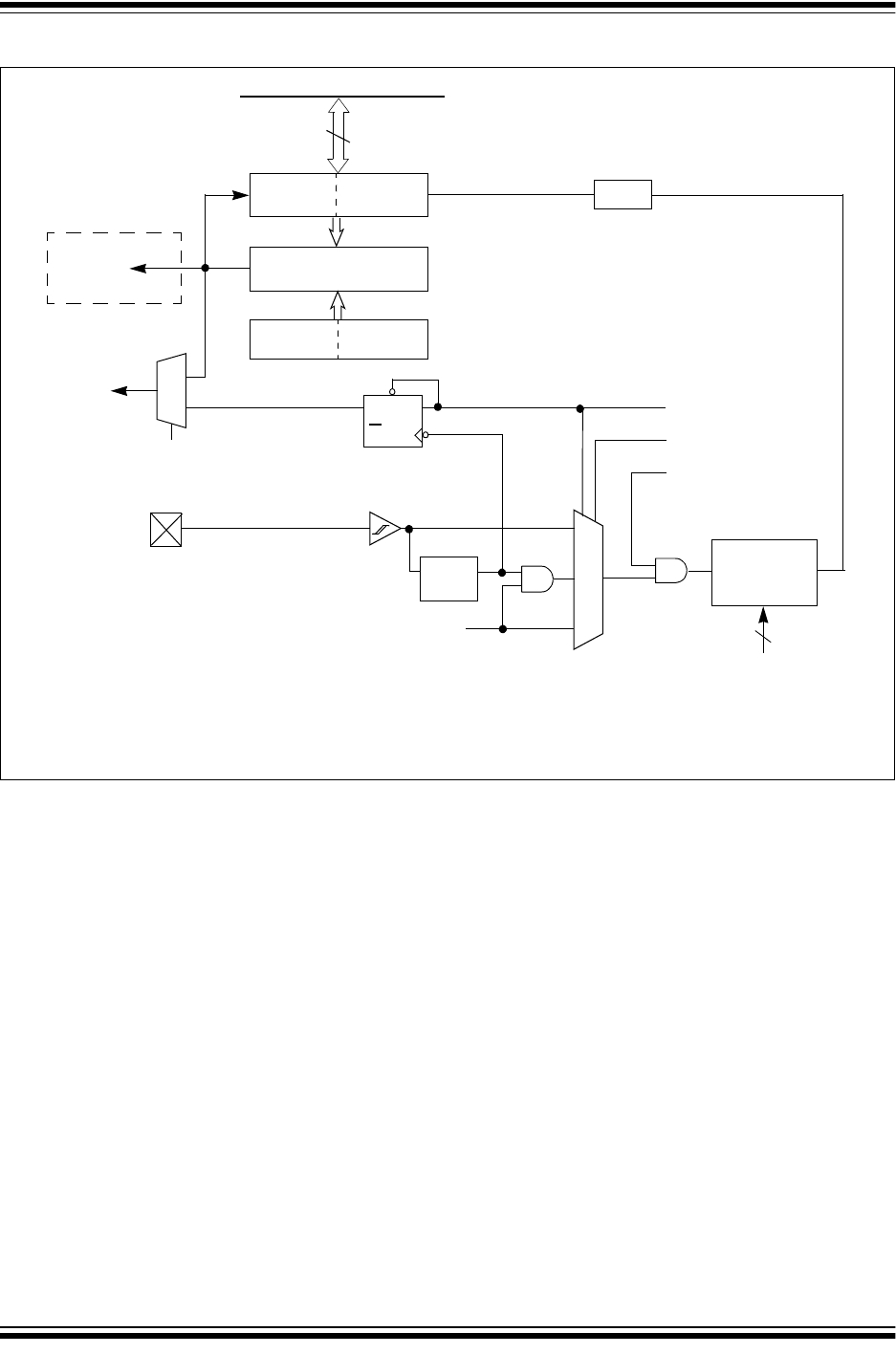
PIC32MX1XX/2XX 28/36/44-PIN FAMILY
DS60001168K-page 150 2011-2017 Microchip Technology Inc.
FIGURE 13-2: TIMER2/3, TIMER4/5 BLOCK DIAGRAM (32-BIT)
TMRy
(1)
TMRx
(1)
TyIF Event
Equal 32-bit Comparator
PRy
PRx
Reset
LS Half Word
MS Half Word
Flag
Note 1: In this diagram, the use of ‘x’ in registers, TxCON, TMRx, PRx and TxCK, refers to either Timer2 or Timer4; the
use of ‘y’ in registers, TyCON, TMRy, PRy, TyIF, refers to either Timer3 or Timer5.
2: ADC event trigger is available only on the Timer2/3 pair.
TGATE
0
1
PBCLK
Gate
TxCK
Sync
Sync
ADC Event
Trigger
(2)
ON
TGATE
TCS
TCKPS
Prescaler
3
1, 2, 4, 8, 16,
32, 64, 256
1 0
0 0
Q
QD
x 1
Data Bus<31:0>
<31:0>
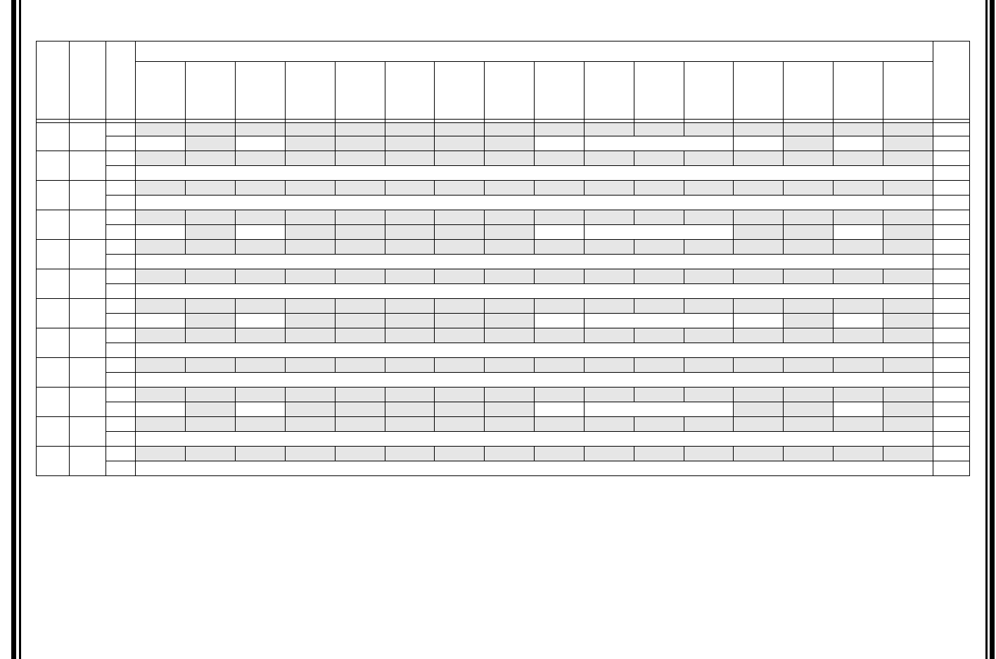
2011-2017 Microchip Technology Inc. DS60001168K-page 151
PIC32MX1XX/2XX 28/36/44-PIN FAMILY
13.2 Timer Control Registers
TABLE 13-1: TIMER2-TIMER5 REGISTER MAP
Virtual Address
(BF80_#)
Register
Name
(1)
Bit Range
Bits
All Resets
31/15 30/14 29/13 28/12 27/11 26/10 25/9 24/8 23/7 22/6 21/5 20/4 19/3 18/2 17/1 16/0
0800 T2CON 31:16 ————————————————0000
15:0 ON —SIDL————— TGATE TCKPS<2:0> T32 —TCS—0000
0810 TMR2 31:16 ————————————————0000
15:0 TMR2<15:0> 0000
0820 PR2 31:16 ————————————————0000
15:0 PR2<15:0> FFFF
0A00 T3CON 31:16 ————————————————0000
15:0 ON —SIDL————— TGATE TCKPS<2:0> ——TCS—0000
0A10 TMR3 31:16 ————————————————0000
15:0 TMR3<15:0> 0000
0A20 PR3 31:16 ————————————————0000
15:0 PR3<15:0> FFFF
0C00 T4CON 31:16 ————————————————0000
15:0 ON —SIDL————— TGATE TCKPS<2:0> T32 —TCS—0000
0C10 TMR4 31:16 ————————————————0000
15:0 TMR4<15:0> 0000
0C20 PR4 31:16 ————————————————0000
15:0 PR4<15:0> FFFF
0E00 T5CON 31:16 ————————————————0000
15:0 ON —SIDL————— TGATE TCKPS<2:0> ——TCS—0000
0E10 TMR5 31:16 ————————————————0000
15:0 TMR5<15:0> 0000
0E20 PR5 31:16 ————————————————0000
15:0 PR5<15:0> FFFF
Legend: x = unknown value on Reset; — = unimplemented, read as ‘0’. Reset values are shown in hexadecimal.
Note 1: All registers in this table have corresponding CLR, SET and INV registers at their virtual addresses, plus offsets of 0x4, 0x8 and 0xC, respectively. See Section 11.2 “CLR, SET and INV Registers” for
more information.

PIC32MX1XX/2XX 28/36/44-PIN FAMILY
DS60001168K-page 152 2011-2017 Microchip Technology Inc.
REGISTER 13-1: TXCON: TYPE B TIMER CONTROL REGISTER
Bit
Range Bit
31/23/15/7 Bit
30/22/14/6 Bit
29/21/13/5 Bit
28/20/12/4 Bit
27/19/11/3 Bit
26/18/10/2 Bit
25/17/9/1 Bit
24/16/8/0
31:24
U-0 U-0 U-0 U-0 U-0 U-0 U-0 U-0
— — — — — — — —
23:16
U-0 U-0 U-0 U-0 U-0 U-0 U-0 U-0
— — — — — — — —
15:8
R/W-0 U-0 R/W-0 U-0 U-0 U-0 U-0 U-0
ON
(1,3)
—SIDL
(4)
— — — — —
7:0
R/W-0 R/W-0 R/W-0 R/W-0 R/W-0 U-0 R/W-0 U-0
TGATE
(3)
TCKPS<2:0>
(3)
T32
(2)
—TCS
(3)
—
Legend:
R = Readable bit W = Writable bit U = Unimplemented bit, read as ‘0’
-n = Value at POR ‘1’ = Bit is set ‘0’ = Bit is cleared x = Bit is unknown
bit 31-16 Unimplemented: Read as ‘0’
bit 15 ON: Timer On bit
(1,3)
1 = Module is enabled
0 = Module is disabled
bit 14 Unimplemented: Read as ‘0’
bit 13 SIDL: Stop in Idle Mode bit
(4)
1 = Discontinue module operation when the device enters Idle mode
0 = Continue module operation when the device enters Idle mode
bit 12-8 Unimplemented: Read as ‘0’
bit 7 TGATE: Timer Gated Time Accumulation Enable bit
(3)
When TCS = 1:
This bit is ignored and is read as ‘0’.
When TCS = 0:
1 = Gated time accumulation is enabled
0 = Gated time accumulation is disabled
bit 6-4 TCKPS<2:0>: Timer Input Clock Prescale Select bits
(3)
111 = 1:256 prescale value
110 = 1:64 prescale value
101 = 1:32 prescale value
100 = 1:16 prescale value
011 = 1:8 prescale value
010 = 1:4 prescale value
001 = 1:2 prescale value
000 = 1:1 prescale value
Note 1: When using 1:1 PBCLK divisor, the user’s software should not read/write the peripheral SFRs in the
SYSCLK cycle immediately following the instruction that clears the module’s ON bit.
2: This bit is available only on even numbered timers (Timer2 and Timer4).
3: While operating in 32-bit mode, this bit has no effect for odd numbered timers (Timer3, and Timer5). All
timer functions are set through the even numbered timers.
4: While operating in 32-bit mode, this bit must be cleared on odd numbered timers to enable the 32-bit timer
in Idle mode.

2011-2017 Microchip Technology Inc. DS60001168K-page 153
PIC32MX1XX/2XX 28/36/44-PIN FAMILY
bit 3 T32: 32-Bit Timer Mode Select bit
(2)
1 = Odd numbered and even numbered timers form a 32-bit timer
0 = Odd numbered and even numbered timers form a separate 16-bit timer
bit 2 Unimplemented: Read as ‘0’
bit 1 TCS: Timer Clock Source Select bit
(3)
1 = External clock from TxCK pin
0 = Internal peripheral clock
bit 0 Unimplemented: Read as ‘0’
REGISTER 13-1: TXCON: TYPE B TIMER CONTROL REGISTER (CONTINUED)
Note 1: When using 1:1 PBCLK divisor, the user’s software should not read/write the peripheral SFRs in the
SYSCLK cycle immediately following the instruction that clears the module’s ON bit.
2: This bit is available only on even numbered timers (Timer2 and Timer4).
3: While operating in 32-bit mode, this bit has no effect for odd numbered timers (Timer3, and Timer5). All
timer functions are set through the even numbered timers.
4: While operating in 32-bit mode, this bit must be cleared on odd numbered timers to enable the 32-bit timer
in Idle mode.

PIC32MX1XX/2XX 28/36/44-PIN FAMILY
DS60001168K-page 154 2011-2017 Microchip Technology Inc.
NOTES:
2011-2018 Microchip Technology Inc. DS60001168K-page 155
PIC32MX1XX/2XX 28/36/44-PIN FAMILY
14.0 WATCHDOG TIMER (WDT)
The WDT, when enabled, operates from the internal
Low-Power Oscillator (LPRC) clock source and can be
used to detect system software malfunctions by reset-
ting the device if the WDT is not cleared periodically in
software. Various WDT time-out periods can be
selected using the WDT postscaler. The WDT can also
be used to wake the device from Sleep or Idle mode.
The following are some of the key features of the WDT
module:
• Configuration or software controlled
• User-configurable time-out period
• Can wake the device from Sleep or Idle mode
Figure 14-1 illustrates a block diagram of the WDT and
Power-up timer.
FIGURE 14-1: WATCHDOG TIMER AND POWER-UP TIMER BLOCK DIAGRAM
Note: This data sheet summarizes the features
of the PIC32MX1XX/2XX 28/36/44-pin
Family of devices. It is not intended to be
a comprehensive reference source. To
complement the information in this data
sheet, refer to Section 9. “Watchdog,
Deadman, and Power-up Timers”
(DS60001114), which are available from
the Documentation > Reference Manual
section of the Microchip PIC32 web site
(www.microchip.com/pic32).
Wake
WDTCLR = 1
WDT Enable
LPRC
Power Save
25-bit Counter
PWRT Enable
WDT Enable
LPRC
WDT Counter Reset
Control
Oscillator
25
Device Reset
NMI (Wake-up)
PWRT
PWRT Enable
FWDTPS<4:0> (DEVCFG1<20:16>)
Clock
Decoder
1
1:64 Output
0
1
WDT Enable
Reset Event
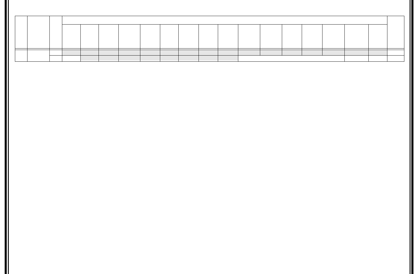
PIC32MX1XX/2XX 28/36/44-PIN FAMILY
DS60001168K-page 156 2011-2018 Microchip Technology Inc.
14.1 Watchdog Timer Control Registers
TABLE 14-1: WATCHDOG TIMER CONTROL REGISTER MAP
Virtual Address
(BF80_#)
Register
Name
(1)
Bit Range
Bits
All Resets
31/15 30/14 29/13 28/12 27/11 26/10 25/9 24/8 23/7 22/6 21/5 20/4 19/3 18/2 17/1 16/0
0000 WDTCON 31:16 — — — — — — — — — — — — — — — — 0000
15:0 ON — — — — — — — — SWDTPS<4:0> WDTWINEN WDTCLR 0000
Legend: x = unknown value on Reset; — = unimplemented, read as ‘0’. Reset values are shown in hexadecimal.
Note 1: All registers in this table have corresponding CLR, SET and INV registers at their virtual addresses, plus offsets of 0x4, 0x8 and 0xC, respectively. See Section 11.2 “CLR, SET and INV Registers” for
more information.

2011-2018 Microchip Technology Inc. DS60001168K-page 157
PIC32MX1XX/2XX 28/36/44-PIN FAMILY
REGISTER 14-1: WDTCON: WATCHDOG TIMER CONTROL REGISTER
Bit
Range Bit
31/23/15/7 Bit
30/22/14/6 Bit
29/21/13/5 Bit
28/20/12/4 Bit
27/19/11/3 Bit
26/18/10/2 Bit
25/17/9/1 Bit
24/16/8/0
31:24
U-0 U-0 U-0 U-0 U-0 U-0 U-0 U-0
— — — — — — — —
23:16
U-0 U-0 U-0 U-0 U-0 U-0 U-0 U-0
— — — — — — — —
15:8
R/W-0 U-0 U-0 U-0 U-0 U-0 U-0 U-0
ON
(1,2)
— — — — — — —
7:0
U-0 R-y R-y R-y R-y R-y R/W-0 R/W-0
— SWDTPS<4:0> WDTWINEN WDTCLR
Legend: y = Values set from Configuration bits on POR
R = Readable bit W = Writable bit U = Unimplemented bit, read as ‘0’
-n = Value at POR ‘1’ = Bit is set ‘0’ = Bit is cleared x = Bit is unknown
bit 31-16 Unimplemented: Read as ‘0’
bit 15 ON: Watchdog Timer Enable bit
(1,2)
1 = Enables the WDT if it is not enabled by the device configuration
0 = Disable the WDT if it was enabled in software
bit 14-7 Unimplemented: Read as ‘0’
bit 6-2 SWDTPS<4:0>: Shadow Copy of Watchdog Timer Postscaler Value from Device Configuration bits
On reset, these bits are set to the values of the WDTPS <4:0> of Configuration bits.
bit 1 WDTWINEN: Watchdog Timer Window Enable bit
1 = Enable windowed Watchdog Timer
0 = Disable windowed Watchdog Timer
bit 0 WDTCLR: Watchdog Timer Reset bit
1 = Writing a ‘1’ will clear the WDT
0 = Software cannot force this bit to a ‘0’
Note 1: A read of this bit results in a ‘1’ if the Watchdog Timer is enabled by the device configuration or software.
2: When using the 1:1 PBCLK divisor, the user’s software should not read or write the peripheral’s SFRs in
the SYSCLK cycle immediately following the instruction that clears the module’s ON bit.

PIC32MX1XX/2XX 28/36/44-PIN FAMILY
DS60001168K-page 158 2011-2018 Microchip Technology Inc.
NOTES:
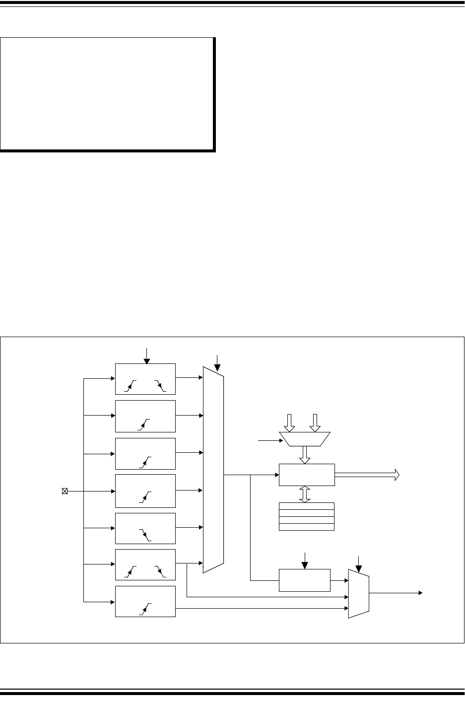
2011-2018 Microchip Technology Inc. DS60001168K-page 159
PIC32MX1XX/2XX 28/36/44-PIN FAMILY
15.0 INPUT CAPTURE
The Input Capture module is useful in applications
requiring frequency (period) and pulse measurement.
The Input Capture module captures the 16-bit or 32-bit
value of the selected Time Base registers when an
event occurs at the ICx pin. The following events cause
capture events:
• Simple capture event modes:
- Capture timer value on every rising and falling
edge of input at ICx pin
- Capture timer value on every edge (rising
and falling)
- Capture timer value on every edge (rising
and falling), specified edge first.
• Prescaler capture event modes:
- Capture timer value on every 4th rising edge of
input at ICx pin
- Capture timer value on every 16th rising edge of
input at ICx pin
Each input capture channel can select between one of
two 16-bit timers (Timer2 or Timer3) for the time base,
or two 16-bit timers (Timer2 and Timer3) together to
form a 32-bit timer. The selected timer can use either
an internal or external clock.
Other operational features include:
• Device wake-up from capture pin during Sleep
and Idle modes
• Interrupt on input capture event
• 4-word FIFO buffer for capture values (interrupt
optionally generated after 1, 2, 3, or 4 buffer
locations are filled)
• Input capture can also be used to provide
additional sources of external interrupts
Figure 15-1 illustrates a general block diagram of the
Input Capture module.
FIGURE 15-1: INPUT CAPTURE BLOCK DIAGRAM
Note: This data sheet summarizes the features
of the PIC32MX1XX/2XX 28/36/44-pin
Family of devices. It is not intended to be
a comprehensive reference source. To
complement the information in this data
sheet, refer to Section 15. “Input Cap-
ture” (DS60001122), which is available
from the Documentation > Reference
Manual section of the Microchip PIC32
web site (www.microchip.com/pic32).
Note:
An ‘x’ in a signal, register or bit name denotes the number of the capture channel.
FIFO CONTROL
ICxBUF
TMR2 TMR3
Capture Event
/N
FIFO
ICI<1:0>
ICM<2:0>
ICM<2:0>
101
100
011
010
001
001
111
To CPU
Set Flag ICxIF
(In IFSx Register)
Rising Edge Mode
Prescaler Mode
(4th Rising Edge)
Falling Edge Mode
Edge Detection
Prescaler Mode
(16th Rising Edge)
Sleep/Idle
Wake-up Mode
C32 || ICTMR
ICx pin
Mode
110
Specified/Every
Edge Mode
FEDGE
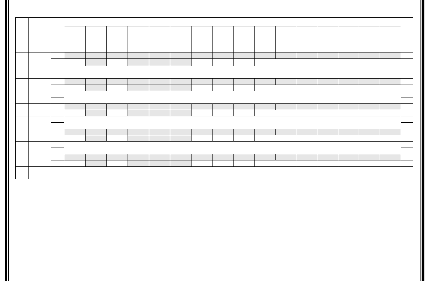
PIC32MX1XX/2XX 28/36/44-PIN FAMILY
DS60001168K-page 160 2011-2018 Microchip Technology Inc.
15.1 Input Capture Control Registers
TABLE 15-1: INPUT CAPTURE 1-INPUT CAPTURE 5 REGISTER MAP
Virtual Address
(BF80_#)
Register
Name
Bit Range
Bits
All Resets
31/15 30/14 29/13 28/12 27/11 26/10 25/9 24/8 23/7 22/6 21/5 20/4 19/3 18/2 17/1 16/0
2000 IC1CON
(1)
31:16 — — — — — — — — — — — — — — — — 0000
15:0 ON —SIDL——— FEDGE C32 ICTMR ICI<1:0> ICOV ICBNE ICM<2:0> 0000
2010 IC1BUF 31:16 IC1BUF<31:0> xxxx
15:0 xxxx
2200 IC2CON
(1)
31:16 — — — — — — — — — — — — — — — — 0000
15:0 ON —SIDL——— FEDGE C32 ICTMR ICI<1:0> ICOV ICBNE ICM<2:0> 0000
2210 IC2BUF 31:16 IC2BUF<31:0> xxxx
15:0 xxxx
2400 IC3CON
(1)
31:16 — — — — — — — — — — — — — — — — 0000
15:0 ON —SIDL——— FEDGE C32 ICTMR ICI<1:0> ICOV ICBNE ICM<2:0> 0000
2410 IC3BUF 31:16 IC3BUF<31:0> xxxx
15:0 xxxx
2600 IC4CON
(1)
31:16 — — — — — — — — — — — — — — — — 0000
15:0 ON —SIDL——— FEDGE C32 ICTMR ICI<1:0> ICOV ICBNE ICM<2:0> 0000
2610 IC4BUF 31:16 IC4BUF<31:0> xxxx
15:0 xxxx
2800 IC5CON
(1)
31:16 — — — — — — — — — — — — — — — — 0000
15:0 ON —SIDL——— FEDGE C32 ICTMR ICI<1:0> ICOV ICBNE ICM<2:0> 0000
2810 IC5BUF 31:16 IC5BUF<31:0> xxxx
15:0 xxxx
Legend: x = unknown value on Reset; — = unimplemented, read as ‘0’. Reset values are shown in hexadecimal.
Note 1: This register has corresponding CLR, SET and INV registers at its virtual address, plus an offset of 0x4, 0x8 and 0xC, respectively. See Section 11.2 “CLR, SET and INV Registers” for more information.

2011-2018 Microchip Technology Inc. DS60001168K-page 161
PIC32MX1XX/2XX 28/36/44-PIN FAMILY
REGISTER 15-1: IC
X
CON: INPUT CAPTURE ‘x’ CONTROL REGISTER
Bit Range Bit
31/23/15/7 Bit
30/22/14/6 Bit
29/21/13/5 Bit
28/20/12/4 Bit
27/19/11/3 Bit
26/18/10/2 Bit
25/17/9/1 Bit
24/16/8/0
31:24
U-0 U-0 U-0 U-0 U-0 U-0 U-0 U-0
— — — — — — — —
23:16
U-0 U-0 U-0 U-0 U-0 U-0 U-0 U-0
— — — — — — — —
15:8
R/W-0 U-0 R/W-0 U-0 U-0 U-0 R/W-0 R/W-0
ON
(1)
—SIDL— — —FEDGEC32
7:0
R/W-0 R/W-0 R/W-0 R-0 R-0 R/W-0 R/W-0 R/W-0
ICTMR ICI<1:0> ICOV ICBNE ICM<2:0>
Legend:
R = Readable bit W = Writable bit U = Unimplemented bit
-n = Bit Value at POR: (‘0’, ‘1’, x = unknown) P = Programmable bit r = Reserved bit
bit 31-16 Unimplemented: Read as ‘0’
bit 15 ON: Input Capture Module Enable bit
(1)
1= Module is enabled
0= Disable and reset module, disable clocks, disable interrupt generation and allow SFR modifications
bit 14 Unimplemented: Read as ‘0’
bit 13 SIDL: Stop in Idle Control bit
1= Halt in Idle mode
0= Continue to operate in Idle mode
bit 12-10 Unimplemented: Read as ‘0’
bit 9 FEDGE: First Capture Edge Select bit (only used in mode 6, ICM<2:0> = 110)
1= Capture rising edge first
0= Capture falling edge first
bit 8 C32: 32-bit Capture Select bit
1= 32-bit timer resource capture
0= 16-bit timer resource capture
bit 7 ICTMR: Timer Select bit (Does not affect timer selection when C32 (ICxCON<8>) is ‘1’)
0= Timer3 is the counter source for capture
1= Timer2 is the counter source for capture
bit 6-5 ICI<1:0>: Interrupt Control bits
11 = Interrupt on every fourth capture event
10 = Interrupt on every third capture event
01 = Interrupt on every second capture event
00 = Interrupt on every capture event
bit 4 ICOV: Input Capture Overflow Status Flag bit (read-only)
1= Input capture overflow has occurred
0= No input capture overflow has occurred
bit 3 ICBNE: Input Capture Buffer Not Empty Status bit (read-only)
1= Input capture buffer is not empty; at least one more capture value can be read
0= Input capture buffer is empty
Note 1: When using 1:1 PBCLK divisor, the user’s software should not read/write the peripheral’s SFRs in the
SYSCLK cycle immediately following the instruction that clears the module’s ON bit.

PIC32MX1XX/2XX 28/36/44-PIN FAMILY
DS60001168K-page 162 2011-2018 Microchip Technology Inc.
bit 2-0 ICM<2:0>: Input Capture Mode Select bits
111 = Interrupt-Only mode (only supported while in Sleep mode or Idle mode)
110 = Simple Capture Event mode – every edge, specified edge first and every edge thereafter
101 = Prescaled Capture Event mode – every sixteenth rising edge
100 = Prescaled Capture Event mode – every fourth rising edge
011 = Simple Capture Event mode – every rising edge
010 = Simple Capture Event mode – every falling edge
001 = Edge Detect mode – every edge (rising and falling)
000 = Input Capture module is disabled
REGISTER 15-1: IC
X
CON: INPUT CAPTURE ‘x’ CONTROL REGISTER (CONTINUED)
Note 1: When using 1:1 PBCLK divisor, the user’s software should not read/write the peripheral’s SFRs in the
SYSCLK cycle immediately following the instruction that clears the module’s ON bit.
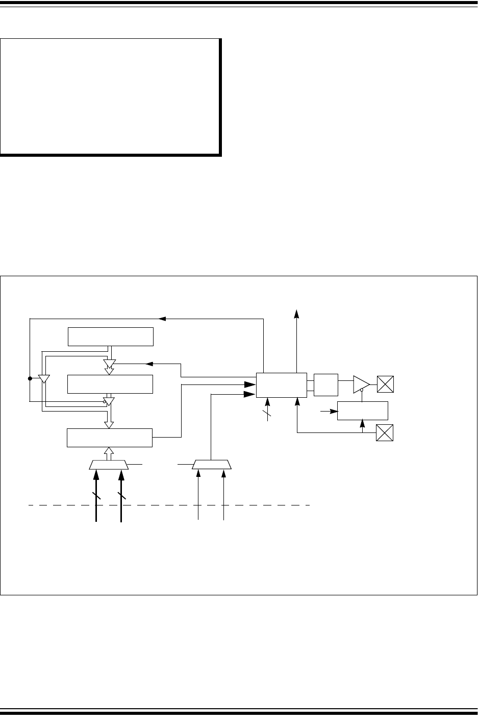
2011-2018 Microchip Technology Inc. DS60001168K-page 163
PIC32MX1XX/2XX 28/36/44-PIN FAMILY
16.0 OUTPUT COMPARE
The Output Compare module is used to generate a sin-
gle pulse or a train of pulses in response to selected
time base events. For all modes of operation, the Out-
put Compare module compares the values stored in
the OCxR and/or the OCxRS registers to the value in
the selected timer. When a match occurs, the Output
Compare module generates an event based on the
selected mode of operation.
The following are some of the key features:
• Multiple Output Compare Modules in a device
• Programmable interrupt generation on compare
event
• Single and Dual Compare modes
• Single and continuous output pulse generation
• Pulse-Width Modulation (PWM) mode
• Hardware-based PWM Fault detection and
automatic output disable
• Can operate from either of two available 16-bit
time bases or a single 32-bit time base
FIGURE 16-1: OUTPUT COMPARE MODULE BLOCK DIAGRAM
Note: This data sheet summarizes the features
of the PIC32MX1XX/2XX 28/36/44-pin
Family of devices. It is not intended to be
a comprehensive reference source. To
complement the information in this data
sheet, refer to Section 16. “Output Com-
pare” (DS60001111), which is available
from the Documentation > Reference
Manual section of the Microchip PIC32
web site (www.microchip.com/pic32).
OCxR
(1)
Comparator
Output
Logic
QS
R
OCM<2:0>
Output Enable
OCx
(1)
Set Flag bit
OCxIF
(1)
OCxRS
(1)
Mode Select
3
Note 1: Where ‘x’ is shown, reference is made to the registers associated with the respective output compare channels,
1 through 5.
2: The OCFA pin controls the OC1-OC4 channels. The OCFB pin controls the OC5 channel.
01
OCTSEL
01
16
16
OCFA or OCFB
(2)
Timer2 Timer2 Timer3
Logic
Output
Enable
Timer3
Rollover Rollover
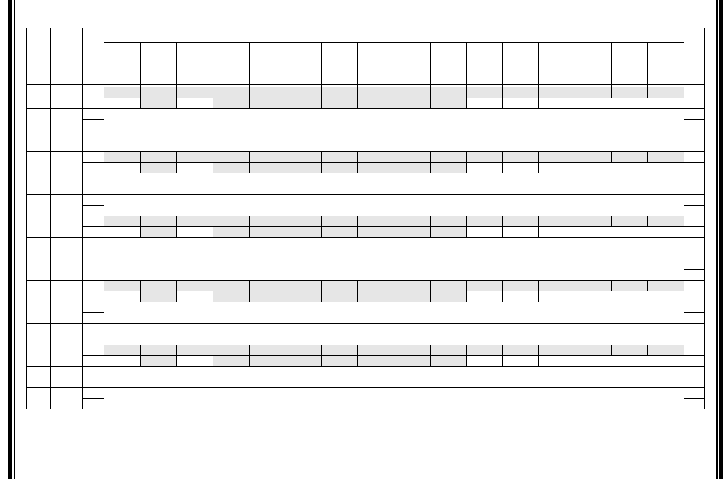
PIC32MX1XX/2XX 28/36/44-PIN FAMILY
DS60001168K-page 164 2011-2018 Microchip Technology Inc.
16.1 Output Compare Control Registers
TABLE 16-1: OUTPUT COMPARE 1-OUTPUT COMPARE 5 REGISTER MAP
Virtual Address
(BF80_#)
Register
Name
(1)
Bit Range
Bits
All Resets
31/15 30/14 29/13 28/12 27/11 26/10 25/9 24/8 23/7 22/6 21/5 20/4 19/3 18/2 17/1 16/0
3000 OC1CON 31:16 ————————————————0000
15:0 ON —SIDL——————— OC32 OCFLT OCTSEL OCM<2:0> 0000
3010 OC1R 31:16 OC1R<31:0> xxxx
15:0 xxxx
3020 OC1RS 31:16 OC1RS<31:0> xxxx
15:0 xxxx
3200 OC2CON 31:16 ————————————————0000
15:0 ON —SIDL——————— OC32 OCFLT OCTSEL OCM<2:0> 0000
3210 OC2R 31:16 OC2R<31:0> xxxx
15:0 xxxx
3220 OC2RS 31:16 OC2RS<31:0> xxxx
15:0 xxxx
3400 OC3CON 31:16 ————————————————0000
15:0 ON —SIDL——————— OC32 OCFLT OCTSEL OCM<2:0> 0000
3410 OC3R 31:16 OC3R<31:0> xxxx
15:0 xxxx
3420 OC3RS 31:16
15:0 OC3RS<31:0> xxxx
xxxx
3600 OC4CON 31:16 ————————————————0000
15:0 ON —SIDL——————— OC32 OCFLT OCTSEL OCM<2:0> 0000
3610 OC4R 31:16 OC4R<31:0> xxxx
15:0 xxxx
3620 OC4RS 31:16
15:0 OC4RS<31:0> xxxx
xxxx
3800 OC5CON 31:16 ————————————————0000
15:0 ON —SIDL——————— OC32 OCFLT OCTSEL OCM<2:0> 0000
3810 OC5R 31:16 OC5R<31:0> xxxx
15:0 xxxx
3820 OC5RS 31:16 OC5RS<31:0> xxxx
15:0 xxxx
Legend: x = unknown value on Reset; — = unimplemented, read as ‘0’. Reset values are shown in hexadecimal.
Note 1: All registers in this table have corresponding CLR, SET and INV registers at their virtual addresses, plus offsets of 0x4, 0x8 and 0xC, respectively. See Section 11.2 “CLR, SET and INV Registers” for
more information.

2011-2018 Microchip Technology Inc. DS60001168K-page 165
PIC32MX1XX/2XX 28/36/44-PIN FAMILY
REGISTER 16-1: OCxCON: OUTPUT COMPARE ‘x’ CONTROL REGISTER
Bit
Range Bit
31/23/15/7 Bit
30/22/14/6 Bit
29/21/13/5 Bit
28/20/12/4 Bit
27/19/11/3 Bit
26/18/10/2 Bit
25/17/9/1 Bit
24/16/8/0
31:24
U-0 U-0 U-0 U-0 U-0 U-0 U-0 U-0
— — — — — — — —
23:16
U-0 U-0 U-0 U-0 U-0 U-0 U-0 U-0
— — — — — — — —
15:8
R/W-0 U-0 R/W-0 U-0 U-0 U-0 U-0 U-0
ON
(1)
—SIDL— — — — —
7:0
U-0 U-0 R/W-0 R-0 R/W-0 R/W-0 R/W-0 R/W-0
—— OC32 OCFLT
(2)
OCTSEL OCM<2:0>
Legend:
R = Readable bit W = Writable bit U = Unimplemented bit, read as ‘0’
-n = Value at POR ‘1’ = Bit is set ‘0’ = Bit is cleared x = Bit is unknown
bit 31-16 Unimplemented: Read as ‘0’
bit 15 ON: Output Compare Peripheral On bit
(1)
1 = Output Compare peripheral is enabled
0 = Output Compare peripheral is disabled
bit 14 Unimplemented: Read as ‘0’
bit 13 SIDL: Stop in Idle Mode bit
1 = Discontinue module operation when the device enters Idle mode
0 = Continue module operation when the device enters Idle mode
bit 12-6 Unimplemented: Read as ‘0’
bit 5 OC32: 32-bit Compare Mode bit
1 = OCxR<31:0> and/or OCxRS<31:0> are used for comparisons to the 32-bit timer source
0 = OCxR<15:0> and OCxRS<15:0> are used for comparisons to the 16-bit timer source
bit 4 OCFLT: PWM Fault Condition Status bit
(2)
1 = PWM Fault condition has occurred (cleared in hardware only)
0 = No PWM Fault condition has occurred
bit 3 OCTSEL: Output Compare Timer Select bit
1 = Timer3 is the clock source for this Output Compare module
0 = Timer2 is the clock source for this Output Compare module
bit 2-0 OCM<2:0>: Output Compare Mode Select bits
111 = PWM mode on OCx; Fault pin enabled
110 = PWM mode on OCx; Fault pin disabled
101 = Initialize OCx pin low; generate continuous output pulses on OCx pin
100 = Initialize OCx pin low; generate single output pulse on OCx pin
011 = Compare event toggles OCx pin
010 = Initialize OCx pin high; compare event forces OCx pin low
001 = Initialize OCx pin low; compare event forces OCx pin high
000 = Output compare peripheral is disabled but continues to draw current
Note 1: When using 1:1 PBCLK divisor, the user’s software should not read/write the peripheral’s SFRs in the
SYSCLK cycle immediately following the instruction that clears the module’s ON bit.
2: This bit is only used when OCM<2:0> = ‘111’. It is read as ‘0’ in all other modes.

PIC32MX1XX/2XX 28/36/44-PIN FAMILY
DS60001168K-page 166 2011-2018 Microchip Technology Inc.
NOTES:
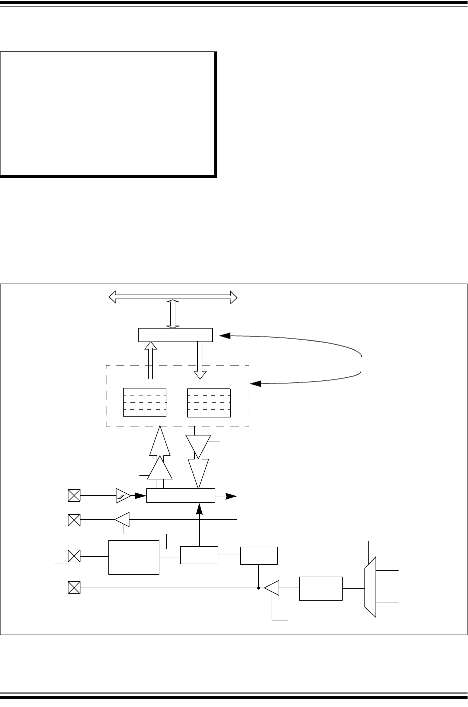
2011-2018 Microchip Technology Inc. DS60001168K-page 167
PIC32MX1XX/2XX 28/36/44-PIN FAMILY
17.0 SERIAL PERIPHERAL
INTERFACE (SPI)
The SPI module is a synchronous serial interface that
is useful for communicating with external peripherals
and other microcontrollers. These peripheral devices
may be Serial EEPROMs, Shift registers, display driv-
ers, Analog-to-Digital Converters (ADC), etc. The
PIC32 SPI module is compatible with Motorola
®
SPI
and SIOP interfaces.
Some of the key features of the SPI module are:
• Master mode and Slave mode support
• Four clock formats
• Enhanced Framed SPI protocol support
• User-configurable 8-bit, 16-bit and 32-bit data width
• Separate SPI FIFO buffers for receive and transmit
- FIFO buffers act as 4/8/16-level deep FIFOs
based on 32/16/8-bit data width
• Programmable interrupt event on every 8-bit,
16-bit and 32-bit data transfer
• Operation during Sleep and Idle modes
• Audio Codec Support:
-I
2
S protocol
- Left-justified
- Right-justified
-PCM
FIGURE 17-1: SPI MODULE BLOCK DIAGRAM
Note: This data sheet summarizes the features
of the PIC32MX1XX/2XX 28/36/44-pin
Family of devices. It is not intended to be
a comprehensive reference source. To
complement the information in this data
sheet, refer to Section 23. “Serial
Peripheral Interface (SPI)”
(DS60001106), which is available from the
Documentation > Reference Manual
section of the Microchip PIC32 web site
(www.microchip.com/pic32).
Internal
Data Bus
SDIx
SDOx
SSx/F
SYNC
SCKx
SPIxSR
bit 0
Shift
Control
Edge
Select
MSTEN
Baud Rate
Slave Select
Sync Control
Clock
Control
Transmit
Receive
and Frame
Note: Access SPIxTXB and SPIxRXB FIFOs via SPIxBUF register.
FIFOs Share Address SPIxBUF
SPIxBUF
Generator
PBCLK
WriteRead
SPIxTXB FIFO
SPIxRXB FIFO
REFCLK
MCLKSEL
1
0
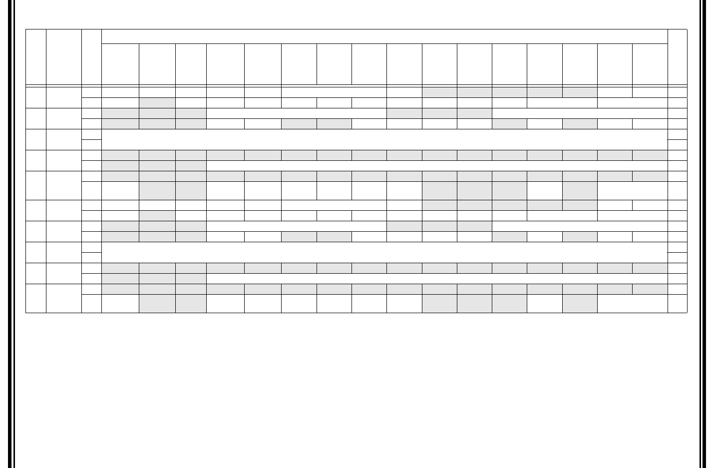
PIC32MX1XX/2XX 28/36/44-PIN FAMILY
DS60001168K-page 168 2011-2018 Microchip Technology Inc.
17.1 SPI Control Registers
TABLE 17-1: SPI1 AND SPI2 REGISTER MAP
Virtual Address
(BF80_#)
Register
Name
(1)
Bit Range
Bits
All Resets
31/15 30/14 29/13 28/12 27/11 26/10 25/9 24/8 23/7 22/6 21/5 20/4 19/3 18/2 17/1 16/0
5800 SPI1CON 31:16 FRMEN FRMSYNC FRMPOL MSSEN FRMSYPW FRMCNT<2:0> MCLKSEL — — — — — SPIFE ENHBUF 0000
15:0 ON — SIDL DISSDO MODE32 MODE16 SMP CKE SSEN CKP MSTEN DISSDI STXISEL<1:0> SRXISEL<1:0> 0000
5810 SPI1STAT 31:16 — — — RXBUFELM<4:0> — — — TXBUFELM<4:0> 0000
15:0 — — — FRMERR SPIBUSY —— SPITUR SRMT SPIROV SPIRBE — SPITBE — SPITBF SPIRBF 0008
5820 SPI1BUF 31:16 DATA<31:0> 0000
15:0 0000
5830 SPI1BRG 31:16 — — — — — — — — — — — — — — — — 0000
15:0 — — — BRG<12:0> 0000
5840 SPI1CON2
31:16 — — — — — — — — — — — — — — — — 0000
15:0 SPI
SGNEXT — — FRM
ERREN
SPI
ROVEN
SPI
TUREN IGNROV IGNTUR AUDEN — — — AUD
MONO — AUDMOD<1:0> 0000
5A00 SPI2CON 31:16 FRMEN FRMSYNC FRMPOL MSSEN FRMSYPW FRMCNT<2:0> MCLKSEL — — — — — SPIFE ENHBUF 0000
15:0 ON — SIDL DISSDO MODE32 MODE16 SMP CKE SSEN CKP MSTEN DISSDI STXISEL<1:0> SRXISEL<1:0> 0000
5A10 SPI2STAT 31:16 — — — RXBUFELM<4:0> — — — TXBUFELM<4:0> 0000
15:0 — — — FRMERR SPIBUSY —— SPITUR SRMT SPIROV SPIRBE — SPITBE — SPITBF SPIRBF 0008
5A20 SPI2BUF 31:16 DATA<31:0> 0000
15:0 0000
5A30 SPI2BRG 31:16 — — — — — — — — — — — — — — — — 0000
15:0 — — — BRG<12:0> 0000
5A40 SPI2CON2
31:16 — — — — — — — — — — — — — — — — 0000
15:0 SPI
SGNEXT — — FRM
ERREN
SPI
ROVEN
SPI
TUREN IGNROV IGNTUR AUDEN — — — AUD
MONO — AUDMOD<1:0> 0000
Legend: x = unknown value on Reset; — = unimplemented, read as ‘0’. Reset values are shown in hexadecimal.
Note 1: All registers in this table except SPIxBUF have corresponding CLR, SET and INV registers at their virtual addresses, plus offsets of 0x4, 0x8 and 0xC, respectively. See Section 11.2 “CLR, SET and INV
Registers” for more information.

2011-2018 Microchip Technology Inc. DS60001168K-page 169
PIC32MX1XX/2XX 28/36/44-PIN FAMILY
REGISTER 17-1: SPIxCON: SPI CONTROL REGISTER
Bit
Range Bit
31/23/15/7 Bit
30/22/14/6 Bit
29/21/13/5 Bit
28/20/12/4 Bit
27/19/11/3 Bit
26/18/10/2 Bit
25/17/9/1 Bit
24/16/8/0
31:24
R/W-0 R/W-0 R/W-0 R/W-0 R/W-0 R/W-0 R/W-0 R/W-0
FRMEN FRMSYNC FRMPOL MSSEN FRMSYPW FRMCNT<2:0>
23:16
R/W-0 U-0 U-0 U-0 U-0 U-0 R/W-0 R/W-0
MCLKSEL
(2)
— — — — — SPIFE ENHBUF
(2)
15:8
R/W-0 U-0 R/W-0 R/W-0 R/W-0 R/W-0 R/W-0 R/W-0
ON
(1)
— SIDL DISSDO MODE32 MODE16 SMP CKE
(3)
7:0
R/W-0 R/W-0 R/W-0 R/W-0 R/W-0 R/W-0 R/W-0 R/W-0
SSEN CKP
(4)
MSTEN DISSDI STXISEL<1:0> SRXISEL<1:0>
Legend:
R = Readable bit W = Writable bit U = Unimplemented bit, read as ‘0’
-n = Value at POR ‘1’ = Bit is set ‘0’ = Bit is cleared x = Bit is unknown
bit 31 FRMEN: Framed SPI Support bit
1 = Framed SPI support is enabled (SSx pin used as FSYNC input/output)
0 = Framed SPI support is disabled
bit 30 FRMSYNC: Frame Sync Pulse Direction Control on SSx pin bit (Framed SPI mode only)
1 = Frame sync pulse input (Slave mode)
0 = Frame sync pulse output (Master mode)
bit 29 FRMPOL: Frame Sync Polarity bit (Framed SPI mode only)
1 = Frame pulse is active-high
0 = Frame pulse is active-low
bit 28 MSSEN: Master Mode Slave Select Enable bit
1 = Slave select SPI support enabled. The SS pin is automatically driven during transmission in
Master mode. Polarity is determined by the FRMPOL bit.
0 = Slave select SPI support is disabled.
bit 27 FRMSYPW: Frame Sync Pulse Width bit
1 = Frame sync pulse is one character wide
0 = Frame sync pulse is one clock wide
bit 26-24 FRMCNT<2:0>: Frame Sync Pulse Counter bits. Controls the number of data characters transmitted per
pulse. This bit is only valid in FRAMED_SYNC mode.
111 = Reserved; do not use
110 = Reserved; do not use
101 = Generate a frame sync pulse on every 32 data characters
100 = Generate a frame sync pulse on every 16 data characters
011 = Generate a frame sync pulse on every 8 data characters
010 = Generate a frame sync pulse on every 4 data characters
001 = Generate a frame sync pulse on every 2 data characters
000 = Generate a frame sync pulse on every data character
bit 23 MCLKSEL: Master Clock Enable bit
(2)
1 = REFCLK is used by the Baud Rate Generator
0 = PBCLK is used by the Baud Rate Generator
bit 22-18 Unimplemented: Read as ‘0’
Note 1: When using the 1:1 PBCLK divisor, the user’s software should not read or write the peripheral’s SFRs in
the SYSCLK cycle immediately following the instruction that clears the module’s ON bit.
2: This bit can only be written when the ON bit = 0.
3: This bit is not used in the Framed SPI mode. The user should program this bit to ‘0’ for the Framed SPI
mode (FRMEN = 1).
4: When AUDEN = 1, the SPI module functions as if the CKP bit is equal to ‘1’, regardless of the actual value
of CKP.

PIC32MX1XX/2XX 28/36/44-PIN FAMILY
DS60001168K-page 170 2011-2018 Microchip Technology Inc.
bit 17 SPIFE: Frame Sync Pulse Edge Select bit (Framed SPI mode only)
1 = Frame synchronization pulse coincides with the first bit clock
0 = Frame synchronization pulse precedes the first bit clock
bit 16 ENHBUF: Enhanced Buffer Enable bit
(2)
1 = Enhanced Buffer mode is enabled
0 = Enhanced Buffer mode is disabled
bit 15 ON: SPI Peripheral On bit
(1)
1 = SPI Peripheral is enabled
0 = SPI Peripheral is disabled
bit 14 Unimplemented: Read as ‘0’
bit 13 SIDL: Stop in Idle Mode bit
1 = Discontinue module operation when the device enters Idle mode
0 = Continue module operation when the device enters Idle mode
bit 12 DISSDO: Disable SDOx pin bit
1 = SDOx pin is not used by the module. Pin is controlled by associated PORT register
0 = SDOx pin is controlled by the module
bit 11-10 MODE<32,16>: 32/16-Bit Communication Select bits
When AUDEN = 1:
MODE32 MODE16 Communication
1124-bit Data, 32-bit FIFO, 32-bit Channel/64-bit Frame
1032-bit Data, 32-bit FIFO, 32-bit Channel/64-bit Frame
0116-bit Data, 16-bit FIFO, 32-bit Channel/64-bit Frame
0016-bit Data, 16-bit FIFO, 16-bit Channel/32-bit Frame
When AUDEN = 0:
MODE32 MODE16 Communication
1x32-bit
0116-bit
008-bit
bit 9 SMP: SPI Data Input Sample Phase bit
Master mode (MSTEN = 1):
1 = Input data sampled at end of data output time
0 = Input data sampled at middle of data output time
Slave mode (MSTEN = 0):
SMP value is ignored when SPI is used in Slave mode. The module always uses SMP = 0.
To wr i te a ' 1' to this bit, the MSTEN value = 1 must first be written.
bit 8 CKE: SPI Clock Edge Select bit
(3)
1 = Serial output data changes on transition from active clock state to Idle clock state (see the CKP bit)
0 = Serial output data changes on transition from Idle clock state to active clock state (see the CKP bit)
bit 7 SSEN: Slave Select Enable (Slave mode) bit
1 = SSx pin used for Slave mode
0 = SSx pin not used for Slave mode, pin controlled by port function.
bit 6 CKP: Clock Polarity Select bit
(4)
1 = Idle state for clock is a high level; active state is a low level
0 = Idle state for clock is a low level; active state is a high level
REGISTER 17-1: SPIxCON: SPI CONTROL REGISTER (CONTINUED)
Note 1: When using the 1:1 PBCLK divisor, the user’s software should not read or write the peripheral’s SFRs in
the SYSCLK cycle immediately following the instruction that clears the module’s ON bit.
2: This bit can only be written when the ON bit = 0.
3: This bit is not used in the Framed SPI mode. The user should program this bit to ‘0’ for the Framed SPI
mode (FRMEN = 1).
4: When AUDEN = 1, the SPI module functions as if the CKP bit is equal to ‘1’, regardless of the actual value
of CKP.

2011-2018 Microchip Technology Inc. DS60001168K-page 171
PIC32MX1XX/2XX 28/36/44-PIN FAMILY
bit 5 MSTEN: Master Mode Enable bit
1 = Master mode
0 =Slave mode
bit 4 DISSDI: Disable SDI bit
1 = SDI pin is not used by the SPI module (pin is controlled by PORT function)
0 = SDI pin is controlled by the SPI module
bit 3-2 STXISEL<1:0>: SPI Transmit Buffer Empty Interrupt Mode bits
11 = Interrupt is generated when the buffer is not full (has one or more empty elements)
10 = Interrupt is generated when the buffer is empty by one-half or more
01 = Interrupt is generated when the buffer is completely empty
00 = Interrupt is generated when the last transfer is shifted out of SPISR and transmit operations are
complete
bit 1-0 SRXISEL<1:0>: SPI Receive Buffer Full Interrupt Mode bits
11 = Interrupt is generated when the buffer is full
10 = Interrupt is generated when the buffer is full by one-half or more
01 = Interrupt is generated when the buffer is not empty
00 = Interrupt is generated when the last word in the receive buffer is read (i.e., buffer is empty)
REGISTER 17-1: SPIxCON: SPI CONTROL REGISTER (CONTINUED)
Note 1: When using the 1:1 PBCLK divisor, the user’s software should not read or write the peripheral’s SFRs in
the SYSCLK cycle immediately following the instruction that clears the module’s ON bit.
2: This bit can only be written when the ON bit = 0.
3: This bit is not used in the Framed SPI mode. The user should program this bit to ‘0’ for the Framed SPI
mode (FRMEN = 1).
4: When AUDEN = 1, the SPI module functions as if the CKP bit is equal to ‘1’, regardless of the actual value
of CKP.

PIC32MX1XX/2XX 28/36/44-PIN FAMILY
DS60001168K-page 172 2011-2018 Microchip Technology Inc.
REGISTER 17-2: SPIxCON2: SPI CONTROL REGISTER 2
Bit
Range Bit
31/23/15/7 Bit
30/22/14/6 Bit
29/21/13/5 Bit
28/20/12/4 Bit
27/19/11/3 Bit
26/18/10/2 Bit
25/17/9/1 Bit
24/16/8/0
31:24
U-0 U-0 U-0 U-0 U-0 U-0 U-0 U-0
— — — — — — — —
23:16
U-0 U-0 U-0 U-0 U-0 U-0 U-0 U-0
— — — — — — — —
15:8
R/W-0 U-0 U-0 R/W-0 R/W-0 R/W-0 R/W-0 R/W-0
SPISGNEXT —— FRMERREN SPIROVEN SPITUREN IGNROV IGNTUR
7:0
R/W-0 U-0 U-0 U-0 R/W-0 U-0 R/W-0 R/W-0
AUDEN
(1)
— — — AUDMONO
(1,2)
— AUDMOD<1:0>
(1,2)
Legend:
R = Readable bit W = Writable bit U = Unimplemented bit, read as ‘0’
-n = Value at POR ‘1’ = Bit is set ‘0’ = Bit is cleared x = Bit is unknown
bit 31-16 Unimplemented: Read as ‘0’
bit 15 SPISGNEXT: Sign Extend Read Data from the RX FIFO bit
1 = Data from RX FIFO is sign extended
0 = Data from RX FIFO is not sign extended
bit 14-13 Unimplemented: Read as ‘0’
bit 12 FRMERREN: Enable Interrupt Events via FRMERR bit
1 = Frame Error overflow generates error events
0 = Frame Error does not generate error events
bit 11 SPIROVEN: Enable Interrupt Events via SPIROV bit
1 = Receive overflow generates error events
0 = Receive overflow does not generate error events
bit 10 SPITUREN: Enable Interrupt Events via SPITUR bit
1 = Transmit underrun generates error events
0 = Transmit underrun does not generate error events
bit 9 IGNROV: Ignore Receive Overflow bit (for Audio Data Transmissions)
1 = A ROV is not a critical error; during ROV data in the FIFO is not overwritten by receive data
0 = A ROV is a critical error that stops SPI operation
bit 8 IGNTUR: Ignore Transmit Underrun bit (for Audio Data Transmissions)
1 = A TUR is not a critical error and zeros are transmitted until the SPIxTXB is not empty
0 = A TUR is a critical error that stops SPI operation
bit 7 AUDEN: Enable Audio CODEC Support bit
(1)
1 = Audio protocol enabled
0 = Audio protocol disabled
bit 6-5 Unimplemented: Read as ‘0’
bit 3 AUDMONO: Transmit Audio Data Format bit
(1,2)
1 = Audio data is mono (Each data word is transmitted on both left and right channels)
0 = Audio data is stereo
bit 2 Unimplemented: Read as ‘0’
bit 1-0 AUDMOD<1:0>: Audio Protocol Mode bit
(1,2)
11 = PCM/DSP mode
10 = Right-Justified mode
01 = Left-Justified mode
00 = I
2
S mode
Note 1: This bit can only be written when the ON bit = 0.
2: This bit is only valid for AUDEN = 1.

2011-2018 Microchip Technology Inc. DS60001168K-page 173
PIC32MX1XX/2XX 28/36/44-PIN FAMILY
REGISTER 17-3: SPIxSTAT: SPI STATUS REGISTER
Bit
Range Bit
31/23/15/7 Bit
30/22/14/6 Bit
29/21/13/5 Bit
28/20/12/4 Bit
27/19/11/3 Bit
26/18/10/2 Bit
25/17/9/1 Bit
24/16/8/0
31:24
U-0 U-0 U-0 R-0 R-0 R-0 R-0 R-0
— — — RXBUFELM<4:0>
23:16
U-0 U-0 U-0 R-0 R-0 R-0 R-0 R-0
— — — TXBUFELM<4:0>
15:8
U-0 U-0 U-0 R/C-0, HS R-0 U-0 U-0 R-0
— — — FRMERR SPIBUSY — — SPITUR
7:0
R-0 R/W-0 R-0 U-0 R-1 U-0 R-0 R-0
SRMT SPIROV SPIRBE — SPITBE — SPITBF SPIRBF
Legend: C = Clearable bit HS = Set in hardware
R = Readable bit W = Writable bit U = Unimplemented bit, read as ‘0’
-n = Value at POR ‘1’ = Bit is set ‘0’ = Bit is cleared x = Bit is unknown
bit 31-29 Unimplemented: Read as ‘0’
bit 28-24 RXBUFELM<4:0>: Receive Buffer Element Count bits (valid only when ENHBUF = 1)
bit 23-21 Unimplemented: Read as ‘0’
bit 20-16 TXBUFELM<4:0>: Transmit Buffer Element Count bits (valid only when ENHBUF = 1)
bit 15-13 Unimplemented: Read as ‘0’
bit 12 FRMERR: SPI Frame Error status bit
1 = Frame error detected
0 = No Frame error detected
This bit is only valid when FRMEN = 1.
bit 11 SPIBUSY: SPI Activity Status bit
1 = SPI peripheral is currently busy with some transactions
0 = SPI peripheral is currently idle
bit 10-9 Unimplemented: Read as ‘0’
bit 8 SPITUR: Transmit Under Run bit
1 = Transmit buffer has encountered an underrun condition
0 = Transmit buffer has no underrun condition
This bit is only valid in Framed Sync mode; the underrun condition must be cleared by disabling (ON bit = 0)
and re-enabling (ON bit = 1) the module, or writing a ‘0’ to SPITUR.
bit 7 SRMT: Shift Register Empty bit (valid only when ENHBUF = 1)
1 = When SPI module shift register is empty
0 = When SPI module shift register is not empty
bit 6 SPIROV: Receive Overflow Flag bit
1 = A new data is completely received and discarded. The user software has not read the previous data in
the SPIxBUF register.
0 = No overflow has occurred
This bit is set in hardware; can bit only be cleared by disabling (ON bit = 0) and re-enabling (ON bit = 1) the
module, or by writing a ‘0’ to SPIROV.
bit 5 SPIRBE: RX FIFO Empty bit (valid only when ENHBUF = 1)
1 = RX FIFO is empty (CRPTR = SWPTR)
0 = RX FIFO is not empty (CRPTR
SWPTR)
bit 4 Unimplemented: Read as ‘0’

PIC32MX1XX/2XX 28/36/44-PIN FAMILY
DS60001168K-page 174 2011-2018 Microchip Technology Inc.
bit 3 SPITBE: SPI Transmit Buffer Empty Status bit
1 = Transmit buffer, SPIxTXB is empty
0 = Transmit buffer, SPIxTXB is not empty
Automatically set in hardware when SPI transfers data from SPIxTXB to SPIxSR.
Automatically cleared in hardware when SPIxBUF is written to, loading SPIxTXB.
bit 2 Unimplemented: Read as ‘0’
bit 1 SPITBF: SPI Transmit Buffer Full Status bit
1 = Transmit not yet started, SPITXB is full
0 = Transmit buffer is not full
Standard Buffer Mode:
Automatically set in hardware when the core writes to the SPIBUF location, loading SPITXB.
Automatically cleared in hardware when the SPI module transfers data from SPITXB to SPISR.
Enhanced Buffer Mode:
Set when CWPTR + 1 = SRPTR; cleared otherwise
bit 0 SPIRBF: SPI Receive Buffer Full Status bit
1 = Receive buffer, SPIxRXB is full
0 = Receive buffer, SPIxRXB is not full
Standard Buffer Mode:
Automatically set in hardware when the SPI module transfers data from SPIxSR to SPIxRXB.
Automatically cleared in hardware when SPIxBUF is read from, reading SPIxRXB.
Enhanced Buffer Mode:
Set when SWPTR + 1 = CRPTR; cleared otherwise
REGISTER 17-3: SPIxSTAT: SPI STATUS REGISTER

2011-2018 Microchip Technology Inc. DS60001168K-page 175
PIC32MX1XX/2XX 28/36/44-PIN FAMILY
18.0 INTER-INTEGRATED CIRCUIT
(I
2
C)
The I
2
C module provides complete hardware support
for both Slave and Multi-Master modes of the I
2
C serial
communication standard. Figure 18-1 illustrates the
I
2
C module block diagram.
Each I
2
C module has a 2-pin interface: the SCLx pin is
clock and the SDAx pin is data.
Each I
2
C module offers the following key features:
•I
2
C interface supporting both master and slave
operation
•I
2
C Slave mode supports 7-bit and 10-bit addressing
•I
2
C Master mode supports 7-bit and 10-bit
addressing
•I
2
C port allows bidirectional transfers between
master and slaves
• Serial clock synchronization for the I
2
C port can
be used as a handshake mechanism to suspend
and resume serial transfer (SCLREL control)
•I
2
C supports multi-master operation; detects bus
collision and arbitrates accordingly
• Provides support for address bit masking
Note: This data sheet summarizes the features
of the PIC32MX1XX/2XX 28/36/44-pin
Family of devices. It is not intended to be
a comprehensive reference source. To
complement the information in this data
sheet, refer to Section 24. “Inter-
Integrated Circuit (I
2
C)” (DS60001116),
which is available from the Documentation
> Reference Manual section of the Micro-
chip PIC32 web site
(www.microchip.com/pic32).
PIC32MX1XX/2XX 28/36/44-PIN FAMILY
DS60001168K-page 176 2011-2018 Microchip Technology Inc.
FIGURE 18-1: I
2
C BLOCK DIAGRAM
Internal
Data Bus
SCLx
SDAx
Shift
Match Detect
I2CxADD
Start and Stop
bit Detect
Clock
Address Match
Clock
Stretching
I2CxTRN
LSB
Shift Clock
BRG Down Counter
Reload
Control
PBCLK
Start and Stop
bit Generation
Acknowledge
Generation
Collision
Detect
I2CxCON
I2CxSTAT
Control Logic
Read
LSB
Write
Read
I2CxBRG
I2CxRSR
Write
Read
Write
Read
Write
Read
Write
Read
Write
Read
I2CxMSK
I2CxRCV
2011-2018 Microchip Technology Inc. DS60001168K-page 177
PIC32MX1XX/2XX 28/36/44-PIN FAMILY
18.1 I2C Control Registers
TABLE 18-1: I2C1 AND I2C2 REGISTER MAP
Virtual Address
(BF80_#)
Register
Name
(1)
Bit Range
Bits
All Resets
31/15 30/14 29/13 28/12 27/11 26/10 25/9 24/8 23/7 22/6 21/5 20/4 19/3 18/2 17/1 16/0
5000 I2C1CON 31:16 — — — — — — — — — — — — — — — — 0000
15:0 ON — SIDL SCLREL STRICT A10M DISSLW SMEN GCEN STREN ACKDT ACKEN RCEN PEN RSEN SEN 1000
5010 I2C1STAT 31:16 — — — — — — — — — — — — — — — — 0000
15:0 ACKSTAT TRSTAT — — — BCL GCSTAT ADD10 IWCOL I2COV D_A P S R_W RBF TBF 0000
5020 I2C1ADD 31:16 — — — — — — — — — — — — — — — — 0000
15:0 —————— Address Register 0000
5030 I2C1MSK 31:16 — — — — — — — — — — — — — — — — 0000
15:0 —————— Address Mask Register 0000
5040 I2C1BRG 31:16 — — — — — — — — — — — — — — — — 0000
15:0 ———— Baud Rate Generator Register 0000
5050 I2C1TRN 31:16 — — — — — — — — — — — — — — — — 0000
15:0 ———————— Transmit Register 0000
5060 I2C1RCV 31:16 — — — — — — — — — — — — — — — — 0000
15:0 ———————— Receive Register 0000
5100 I2C2CON 31:16 — — — — — — — — — — — — — — — — 0000
15:0 ON — SIDL SCLREL STRICT A10M DISSLW SMEN GCEN STREN ACKDT ACKEN RCEN PEN RSEN SEN 1000
5110 I2C2STAT 31:16 — — — — — — — — — — — — — — — — 0000
15:0 ACKSTAT TRSTAT — — — BCL GCSTAT ADD10 IWCOL I2COV D_A P S R_W RBF TBF 0000
5120 I2C2ADD 31:16 — — — — — — — — — — — — — — — — 0000
15:0 —————— Address Register 0000
5130 I2C2MSK 31:16 — — — — — — — — — — — — — — — — 0000
15:0 —————— Address Mask Register 0000
5140 I2C2BRG 31:16 — — — — — — — — — — — — — — — — 0000
15:0 ———— Baud Rate Generator Register 0000
5150 I2C2TRN 31:16 — — — — — — — — — — — — — — — — 0000
15:0 ———————— Transmit Register 0000
5160 I2C2RCV 31:16 — — — — — — — — — — — — — — — — 0000
15:0 ———————— Receive Register 0000
Legend: x = unknown value on Reset; — = unimplemented, read as ‘0’. Reset values are shown in hexadecimal.
Note 1: All registers in this table except I2CxRCV have corresponding CLR, SET and INV registers at their virtual addresses, plus offsets of 0x4, 0x8 and 0xC, respectively. See Section 11.2 “CLR, SET and INV
Registers” for more information.

PIC32MX1XX/2XX 28/36/44-PIN FAMILY
DS60001168K-page 178 2011-2018 Microchip Technology Inc.
REGISTER 18-1: I2C
X
CON: I
2
C CONTROL REGISTER
Bit
Range Bit
31/23/15/7 Bit
30/22/14/6 Bit
29/21/13/5 Bit
28/20/12/4 Bit
27/19/11/3 Bit
26/18/10/2 Bit
25/17/9/1 Bit
24/16/8/0
31:24
U-0 U-0 U-0 U-0 U-0 U-0 U-0 U-0
— — — — — — — —
23:16
U-0 U-0 U-0 U-0 U-0 U-0 U-0 U-0
— — — — — — — —
15:8
R/W-0 U-0 R/W-0 R/W-1, HC R/W-0 R/W-0 R/W-0 R/W-0
ON
(1)
— SIDL SCLREL STRICT A10M DISSLW SMEN
7:0
R/W-0 R/W-0 R/W-0 R/W-0, HC R/W-0, HC R/W-0, HC R/W-0, HC R/W-0, HC
GCEN STREN ACKDT ACKEN RCEN PEN RSEN SEN
Legend: HC = Cleared in Hardware
R = Readable bit W = Writable bit U = Unimplemented bit, read as ‘0’
-n = Value at POR ‘1’ = Bit is set ‘0’ = Bit is cleared x = Bit is unknown
bit 31-16 Unimplemented: Read as ‘0’
bit 15 ON: I
2
C Enable bit
(1)
1 = Enables the I
2
C module and configures the SDA and SCL pins as serial port pins
0 = Disables the I
2
C module; all I
2
C pins are controlled by PORT functions
bit 14 Unimplemented: Read as ‘0’
bit 13 SIDL: Stop in Idle Mode bit
1 = Discontinue module operation when the device enters Idle mode
0 = Continue module operation when the device enters Idle mode
bit 12 SCLREL: SCLx Release Control bit (when operating as I
2
C slave)
1 = Release SCLx clock
0 = Hold SCLx clock low (clock stretch)
If STREN = 1:
Bit is R/W (i.e., software can write ‘0’ to initiate stretch and write ‘1’ to release clock). Hardware clear at
beginning of slave transmission. Hardware clear at end of slave reception.
If STREN = 0:
Bit is R/S (i.e., software can only write ‘1’ to release clock). Hardware clear at beginning of slave
transmission.
bit 11 STRICT: Strict I
2
C Reserved Address Rule Enable bit
1 = Strict reserved addressing is enforced. Device does not respond to reserved address space or generate
addresses in reserved address space.
0 = Strict I
2
C Reserved Address Rule not enabled
bit 10 A10M: 10-bit Slave Address bit
1 = I2CxADD is a 10-bit slave address
0 = I2CxADD is a 7-bit slave address
bit 9 DISSLW: Disable Slew Rate Control bit
1 = Slew rate control disabled
0 = Slew rate control enabled
bit 8 SMEN: SMBus Input Levels bit
1 = Enable I/O pin thresholds compliant with SMBus specification
0 = Disable SMBus input thresholds
Note 1: When using 1:1 PBCLK divisor, the user’s software should not read/write the peripheral’s SFRs in the
SYSCLK cycle immediately following the instruction that clears the module’s ON bit.

2011-2018 Microchip Technology Inc. DS60001168K-page 179
PIC32MX1XX/2XX 28/36/44-PIN FAMILY
bit 7 GCEN: General Call Enable bit (when operating as I
2
C slave)
1 = Enable interrupt when a general call address is received in the I2CxRSR
(module is enabled for reception)
0 = General call address is disabled
bit 6 STREN: SCLx Clock Stretch Enable bit (when operating as I
2
C slave)
Used in conjunction with SCLREL bit.
1 = Enable software or receive clock stretching
0 = Disable software or receive clock stretching
bit 5 ACKDT: Acknowledge Data bit (when operating as I
2
C master, applicable during master receive)
Value that is transmitted when the software initiates an Acknowledge sequence.
1 = Send a NACK during an Acknowledge sequence
0 = Send an ACK during an Acknowledge sequence
bit 4 ACKEN: Acknowledge Sequence Enable bit (when operating as I
2
C master, applicable during master
receive)
1 = Initiate Acknowledge sequence on SDAx and SCLx pins and transmit ACKDT data bit.
Hardware clear at end of master Acknowledge sequence.
0 = Acknowledge sequence not in progress
bit 3 RCEN: Receive Enable bit (when operating as I
2
C master)
1 = Enables Receive mode for I
2
C. Hardware clear at end of eighth bit of master receive data byte.
0 = Receive sequence not in progress
bit 2 PEN: Stop Condition Enable bit (when operating as I
2
C master)
1 = Initiate Stop condition on SDAx and SCLx pins. Hardware clear at end of master Stop sequence.
0 = Stop condition not in progress
bit 1 RSEN: Repeated Start Condition Enable bit (when operating as I
2
C master)
1 = Initiate Repeated Start condition on SDAx and SCLx pins. Hardware clear at end of
master Repeated Start sequence.
0 = Repeated Start condition not in progress
bit 0 SEN: Start Condition Enable bit (when operating as I
2
C master)
1 = Initiate Start condition on SDAx and SCLx pins. Hardware clear at end of master Start sequence.
0 = Start condition not in progress
REGISTER 18-1: I2C
X
CON: I
2
C CONTROL REGISTER (CONTINUED)
Note 1: When using 1:1 PBCLK divisor, the user’s software should not read/write the peripheral’s SFRs in the
SYSCLK cycle immediately following the instruction that clears the module’s ON bit.

PIC32MX1XX/2XX 28/36/44-PIN FAMILY
DS60001168K-page 180 2011-2018 Microchip Technology Inc.
REGISTER 18-2: I2C
X
STAT: I
2
C STATUS REGISTER
Bit
Range Bit
31/23/15/7 Bit
30/22/14/6 Bit
29/21/13/5 Bit
28/20/12/4 Bit
27/19/11/3 Bit
26/18/10/2 Bit
25/17/9/1 Bit
24/16/8/0
31:24
U-0 U-0 U-0 U-0 U-0 U-0 U-0 U-0
— — — — — — — —
23:16
U-0 U-0 U-0 U-0 U-0 U-0 U-0 U-0
— — — — — — — —
15:8
R-0, HSC R-0, HSC U-0 U-0 U-0 R/C-0, HS R-0, HSC R-0, HSC
ACKSTAT TRSTAT — — — BCL GCSTAT ADD10
7:0
R/C-0, HS R/C-0, HS R-0, HSC R/C-0, HSC R/C-0, HSC R-0, HSC R-0, HSC R-0, HSC
IWCOL I2COV D_A P S R_W RBF TBF
Legend: HS = Set in hardware HSC = Hardware set/cleared
R = Readable bit W = Writable bit U = Unimplemented bit, read as ‘0’
-n = Value at POR ‘1’ = Bit is set ‘0’ = Bit is cleared C = Clearable bit
bit 31-16 Unimplemented: Read as ‘0’
bit 15 ACKSTAT: Acknowledge Status bit (when operating as I
2
C master, applicable to master transmit operation)
1 = Acknowledge was not received from slave
0 = Acknowledge was received from slave
Hardware set or clear at end of slave Acknowledge.
bit 14 TRSTAT: Transmit Status bit (when operating as I
2
C master, applicable to master transmit operation)
1 = Master transmit is in progress (8 bits + ACK)
0 = Master transmit is not in progress
Hardware set at beginning of master transmission. Hardware clear at end of slave Acknowledge.
bit 13-11 Unimplemented: Read as ‘0’
bit 10 BCL: Master Bus Collision Detect bit
1 = A bus collision has been detected during a master operation
0 = No collision
Hardware set at detection of bus collision. This condition can only be cleared by disabling (ON bit = 0) and
re-enabling (ON bit = 1) the module.
bit 9 GCSTAT: General Call Status bit
1 = General call address was received
0 = General call address was not received
Hardware set when address matches general call address. Hardware clear at Stop detection.
bit 8 ADD10: 10-bit Address Status bit
1 = 10-bit address was matched
0 = 10-bit address was not matched
Hardware set at match of 2nd byte of matched 10-bit address. Hardware clear at Stop detection.
bit 7 IWCOL: Write Collision Detect bit
1 = An attempt to write the I2CxTRN register failed because the I
2
C module is busy
0 = No collision
Hardware set at occurrence of write to I2CxTRN while busy (cleared by software).
bit 6 I2COV: Receive Overflow Flag bit
1 = A byte was received while the I2CxRCV register is still holding the previous byte
0 = No overflow
Hardware set at attempt to transfer I2CxRSR to I2CxRCV (cleared by software).
bit 5 D_A: Data/Address bit (when operating as I
2
C slave)
1 = Indicates that the last byte received was data
0 = Indicates that the last byte received was device address
Hardware clear at device address match. Hardware set by reception of slave byte.

2011-2018 Microchip Technology Inc. DS60001168K-page 181
PIC32MX1XX/2XX 28/36/44-PIN FAMILY
bit 4 P: Stop bit
1 = Indicates that a Stop bit has been detected last
0 = Stop bit was not detected last
Hardware set or clear when Start, Repeated Start or Stop detected.
bit 3 S: Start bit
1 = Indicates that a Start (or Repeated Start) bit has been detected last
0 = Start bit was not detected last
Hardware set or clear when Start, Repeated Start or Stop detected.
bit 2 R_W: Read/Write Information bit (when operating as I
2
C slave)
1 = Read – indicates data transfer is output from slave
0 = Write – indicates data transfer is input to slave
Hardware set or clear after reception of I
2
C device address byte.
bit 1 RBF: Receive Buffer Full Status bit
1 = Receive complete, I2CxRCV is full
0 = Receive not complete, I2CxRCV is empty
Hardware set when I2CxRCV is written with received byte. Hardware clear when software
reads I2CxRCV.
bit 0 TBF: Transmit Buffer Full Status bit
1 = Transmit in progress, I2CxTRN is full
0 = Transmit complete, I2CxTRN is empty
Hardware set when software writes I2CxTRN. Hardware clear at completion of data transmission.
REGISTER 18-2: I2C
X
STAT: I
2
C STATUS REGISTER (CONTINUED)

PIC32MX1XX/2XX 28/36/44-PIN FAMILY
DS60001168K-page 182 2011-2018 Microchip Technology Inc.
NOTES:
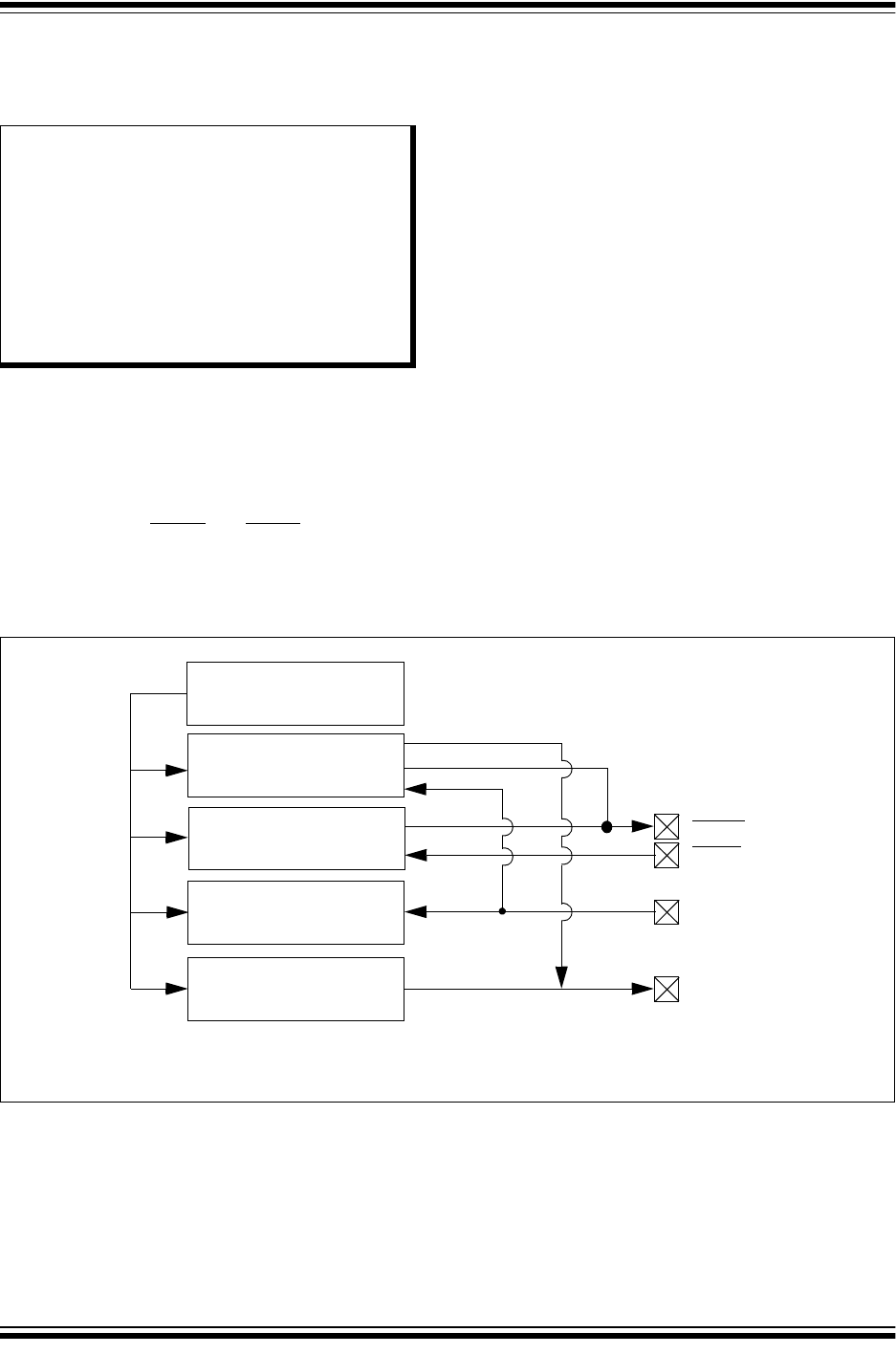
2011-2018 Microchip Technology Inc. DS60001168K-page 183
PIC32MX1XX/2XX 28/36/44-PIN FAMILY
19.0 UNIVERSAL ASYNCHRONOUS
RECEIVER TRANSMITTER
(UART)
The UART module is one of the serial I/O modules
available in PIC32MX1XX/2XX 28/36/44-pin Family
devices. The UART is a full-duplex, asynchronous
communication channel that communicates with
peripheral devices and personal computers through
protocols, such as RS-232, RS-485, LIN, and IrDA
®
.
The UART module also supports the hardware flow
control option, with UxCTS and UxRTS pins, and also
includes an IrDA encoder and decoder.
Key features of the UART module include:
• Full-duplex, 8-bit or 9-bit data transmission
• Even, Odd or No Parity options (for 8-bit data)
• One or two Stop bits
• Hardware auto-baud feature
• Hardware flow control option
• Fully integrated Baud Rate Generator (BRG) with
16-bit prescaler
• Baud rates ranging from 38 bps to 12.5 Mbps at
50 MHz
• 8-level deep First In First Out (FIFO) transmit data
buffer
• 8-level deep FIFO receive data buffer
• Parity, framing and buffer overrun error detection
• Support for interrupt-only on address detect
(9th bit = 1)
• Separate transmit and receive interrupts
• Loopback mode for diagnostic support
• LIN protocol support
• IrDA encoder and decoder with 16x baud clock
output for external IrDA encoder/decoder support
Figure 19-1 illustrates a simplified block diagram of the
UART module.
FIGURE 19-1: UART SIMPLIFIED BLOCK DIAGRAM
Note: This data sheet summarizes the features
of the PIC32MX1XX/2XX 28/36/44-pin
Family of devices. It is not intended to be
a comprehensive reference source. To
complement the information in this data
sheet, refer to Section 21. “Universal
Asynchronous Receiver Transmitter
(UART)” (DS60001107), which is avail-
able from the Documentation > Reference
Manual section of the Microchip PIC32
web site (www.microchip.com/pic32).
Baud Rate Generator
UxRX
Hardware Flow Control
UARTx Receiver
UARTx Transmitter UxTX
UxCTS
UxRTS/BCLKx
IrDA
®
Note: Not all pins are available for all UART modules. Refer to the device-specific pin diagram for more information.
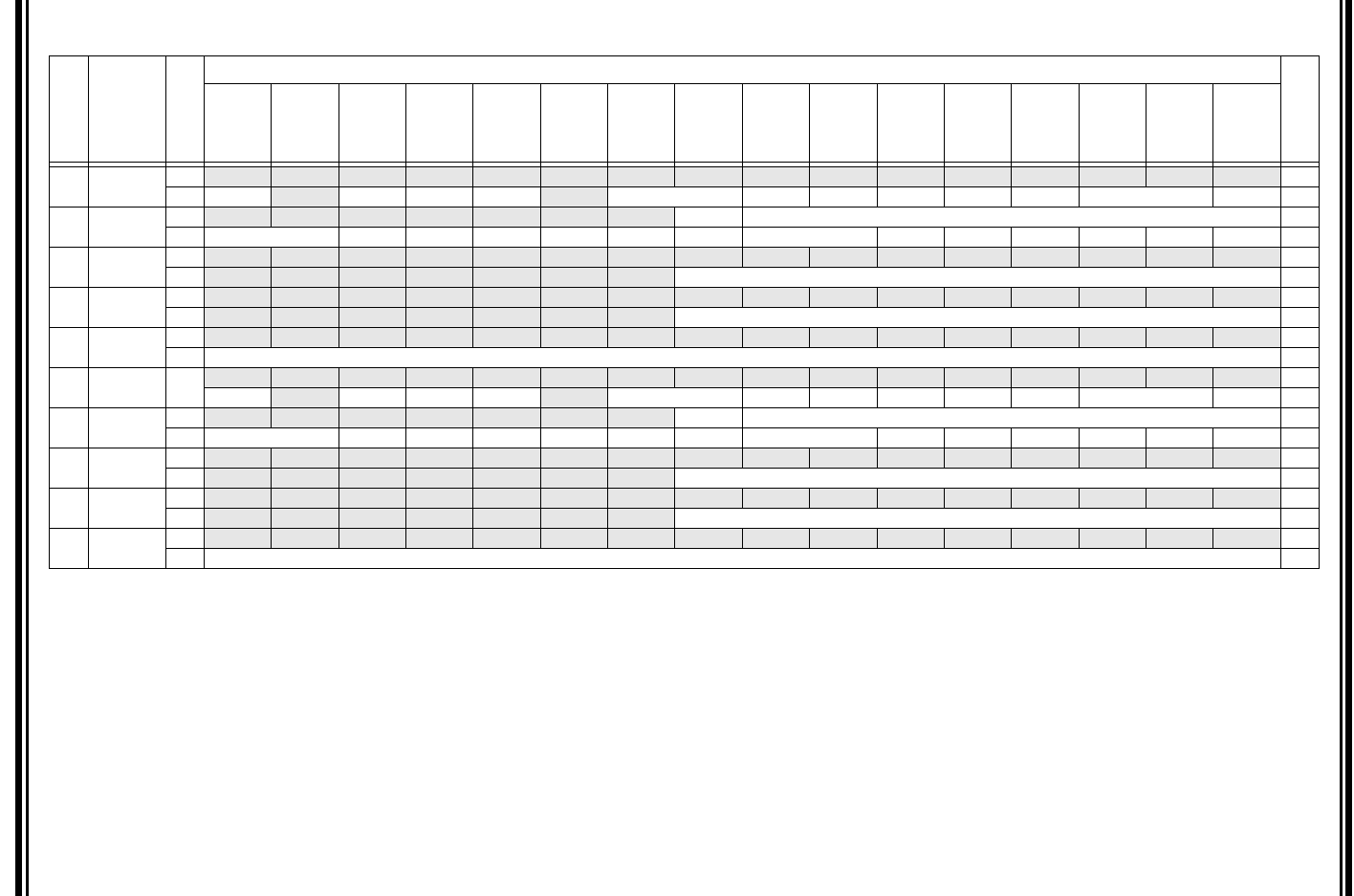
PIC32MX1XX/2XX 28/36/44-PIN FAMILY
DS60001168K-page 184 2011-2018 Microchip Technology Inc.
19.1 UART Control Registers
TABLE 19-1: UART1 AND UART2 REGISTER MAP
Virtual Address
(BF80_#)
Register
Name
Bit Range
Bits
All Resets
31/15 30/14 29/13 28/12 27/11 26/10 25/9 24/8 23/7 22/6 21/5 20/4 19/3 18/2 17/1 16/0
6000 U1MODE
(1)
31:16 ————————————————0000
15:0 ON —SIDLIRENRTSMD— UEN<1:0> WAKE LPBACK ABAUD RXINV BRGH PDSEL<1:0> STSEL 0000
6010 U1STA
(1)
31:16 ——————— ADM_EN ADDR<7:0> 0000
15:0 UTXISEL<1:0> UTXINV URXEN UTXBRK UTXEN UTXBF TRMT URXISEL<1:0> ADDEN RIDLE PERR FERR OERR URXDA 0110
6020 U1TXREG 31:16 ————————————————0000
15:0 ——————— Transmit Register 0000
6030 U1RXREG 31:16 ————————————————0000
15:0 ——————— Receive Register 0000
6040 U1BRG
(1)
31:16 ————————————————0000
15:0 Baud Rate Generator Prescaler 0000
6200 U2MODE
(1)
31:16
15:0
————————————————0000
ON —SIDLIRENRTSMD— UEN<1:0> WAKE LPBACK ABAUD RXINV BRGH PDSEL<1:0> STSEL 0000
6210 U2STA
(1)
31:16 ——————— ADM_EN ADDR<7:0> 0000
15:0 UTXISEL<1:0> UTXINV URXEN UTXBRK UTXEN UTXBF TRMT URXISEL<1:0> ADDEN RIDLE PERR FERR OERR URXDA 0110
6220 U2TXREG 31:16 ————————————————0000
15:0 ——————— Transmit Register 0000
6230 U2RXREG 31:16 ————————————————0000
15:0 ——————— Receive Register 0000
6240 U2BRG
(1)
31:16 ————————————————0000
15:0 Baud Rate Generator Prescaler 0000
Legend: x = unknown value on Reset; — = unimplemented, read as ‘0’. Reset values are shown in hexadecimal.
Note 1: This register has corresponding CLR, SET and INV registers at its virtual address, plus an offset of 0x4, 0x8 and 0xC, respectively. See Section 11.2 “CLR, SET and INV Registers” for more information.
2011-2018 Microchip Technology Inc. DS60001168K-page 185
PIC32MX1XX/2XX 28/36/44-PIN FAMILY
REGISTER 19-1: UxMODE: UARTx MODE REGISTER
Bit
Range Bit
31/23/15/7 Bit
30/22/14/6 Bit
29/21/13/5 Bit
28/20/12/4 Bit
27/19/11/3 Bit
26/18/10/2 Bit
25/17/9/1 Bit
24/16/8/0
31:24
U-0 U-0 U-0 U-0 U-0 U-0 U-0 U-0
— — — — — — — —
23:16
U-0 U-0 U-0 U-0 U-0 U-0 U-0 U-0
— — — — — — — —
15:8
R/W-0 U-0 R/W-0 R/W-0 R/W-0 U-0 R/W-0 R/W-0
ON
(1)
—SIDLIRENRTSMD—UEN<1:0>
7:0
R/W-0 R/W-0 R/W-0 R/W-0 R/W-0 R/W-0 R/W-0 R/W-0
WAKE LPBACK ABAUD RXINV BRGH PDSEL<1:0> STSEL
Legend:
R = Readable bit W = Writable bit U = Unimplemented bit, read as ‘0’
-n = Value at POR ‘1’ = Bit is set ‘0’ = Bit is cleared x = Bit is unknown
bit 31-16 Unimplemented: Read as ‘0’
bit 15 ON: UARTx Enable bit
(1)
1 = UARTx is enabled. UARTx pins are controlled by UARTx as defined by the UEN<1:0> and UTXEN
control bits.
0 = UARTx is disabled. All UARTx pins are controlled by corresponding bits in the PORTx, TRISx and LATx
registers; UARTx power consumption is minimal.
bit 14 Unimplemented: Read as ‘0’
bit 13 SIDL: Stop in Idle Mode bit
1 = Discontinue module operation when the device enters Idle mode
0 = Continue module operation when the device enters Idle mode
bit 12 IREN: IrDA Encoder and Decoder Enable bit
1 = IrDA is enabled
0 = IrDA is disabled
bit 11 RTSMD: Mode Selection for UxRTS Pin bit
1 = UxRTS pin is in Simplex mode
0 = UxRTS pin is in Flow Control mode
bit 10 Unimplemented: Read as ‘0’
bit 9-8 UEN<1:0>: UARTx Enable bits
11 = UxTX, UxRX and UxBCLK pins are enabled and used; UxCTS pin is controlled by corresponding bits
in the PORTx register
10 = UxTX, UxRX, UxCTS and UxRTS pins are enabled and used
01 = UxTX, UxRX and UxRTS pins are enabled and used; UxCTS pin is controlled by corresponding bits
in the PORTx register
00 = UxTX and UxRX pins are enabled and used; UxCTS and UxRTS/UxBCLK pins are controlled by
corresponding bits in the PORTx register
bit 7 WAKE: Enable Wake-up on Start bit Detect During Sleep Mode bit
1 = Wake-up enabled
0 = Wake-up disabled
bit 6 LPBACK: UARTx Loopback Mode Select bit
1 = Loopback mode is enabled
0 = Loopback mode is disabled
Note 1: When using 1:1 PBCLK divisor, the user software should not read/write the peripheral SFRs in the
SYSCLK cycle immediately following the instruction that clears the module’s ON bit.

PIC32MX1XX/2XX 28/36/44-PIN FAMILY
DS60001168K-page 186 2011-2018 Microchip Technology Inc.
bit 5 ABAUD: Auto-Baud Enable bit
1 = Enable baud rate measurement on the next character – requires reception of Sync character (0x55);
cleared by hardware upon completion
0 = Baud rate measurement disabled or completed
bit 4 RXINV: Receive Polarity Inversion bit
1 = UxRX Idle state is ‘0’
0 = UxRX Idle state is ‘1’
bit 3 BRGH: High Baud Rate Enable bit
1 = High-Speed mode – 4x baud clock enabled
0 = Standard Speed mode – 16x baud clock enabled
bit 2-1 PDSEL<1:0>: Parity and Data Selection bits
11 = 9-bit data, no parity
10 = 8-bit data, odd parity
01 = 8-bit data, even parity
00 = 8-bit data, no parity
bit 0 STSEL: Stop Selection bit
1 = 2 Stop bits
0 = 1 Stop bit
REGISTER 19-1: UxMODE: UARTx MODE REGISTER (CONTINUED)
Note 1: When using 1:1 PBCLK divisor, the user software should not read/write the peripheral SFRs in the
SYSCLK cycle immediately following the instruction that clears the module’s ON bit.

2011-2018 Microchip Technology Inc. DS60001168K-page 187
PIC32MX1XX/2XX 28/36/44-PIN FAMILY
REGISTER 19-2: UxSTA: UARTx STATUS AND CONTROL REGISTER
Bit
Range Bit
31/23/15/7 Bit
30/22/14/6 Bit
29/21/13/5 Bit
28/20/12/4 Bit
27/19/11/3 Bit
26/18/10/2 Bit
25/17/9/1 Bit
24/16/8/0
31:24
U-0 U-0 U-0 U-0 U-0 U-0 U-0 R/W-0
— — — — — — —ADM_EN
23:16
R/W-0 R/W-0 R/W-0 R/W-0 R/W-0 R/W-0 R/W-0 R/W-0
ADDR<7:0>
15:8
R/W-0 R/W-0 R/W-0 R/W-0 R/W-0 R/W-0 R-0 R-1
UTXISEL<1:0> UTXINV URXEN UTXBRK UTXEN UTXBF TRMT
7:0
R/W-0 R/W-0 R/W-0 R-1 R-0 R-0 R/W-0 R-0
URXISEL<1:0> ADDEN RIDLE PERR FERR OERR URXDA
Legend:
R = Readable bit W = Writable bit U = Unimplemented bit, read as ‘0’
-n = Value at POR ‘1’ = Bit is set ‘0’ = Bit is cleared x = Bit is unknown
bit 31-25 Unimplemented: Read as ‘0’
bit 24 ADM_EN: Automatic Address Detect Mode Enable bit
1 = Automatic Address Detect mode is enabled
0 = Automatic Address Detect mode is disabled
bit 23-16 ADDR<7:0>: Automatic Address Mask bits
When the ADM_EN bit is ‘1’, this value defines the address character to use for automatic address
detection.
bit 15-14 UTXISEL<1:0>: TX Interrupt Mode Selection bits
11 = Reserved, do not use
10 = Interrupt is generated and asserted while the transmit buffer is empty
01 = Interrupt is generated and asserted when all characters have been transmitted
00 = Interrupt is generated and asserted while the transmit buffer contains at least one empty space
bit 13 UTXINV: Transmit Polarity Inversion bit
If IrDA mode is disabled (i.e., IREN (UxMODE<12>) is ‘0’):
1 = UxTX Idle state is ‘0’
0 = UxTX Idle state is ‘1’
If IrDA mode is enabled (i.e., IREN (UxMODE<12>) is ‘1’):
1 = IrDA encoded UxTX Idle state is ‘1’
0 = IrDA encoded UxTX Idle state is ‘0’
bit 12 URXEN: Receiver Enable bit
1 = UARTx receiver is enabled. UxRX pin is controlled by UARTx (if ON = 1)
0 = UARTx receiver is disabled. UxRX pin is ignored by the UARTx module. UxRX pin is controlled by port.
bit 11 UTXBRK: Transmit Break bit
1 = Send Break on next transmission. Start bit followed by twelve ‘0’ bits, followed by Stop bit; cleared by
hardware upon completion
0 = Break transmission is disabled or completed
bit 10 UTXEN: Transmit Enable bit
1 = UARTx transmitter is enabled. UxTX pin is controlled by UARTx (if ON = 1).
0 = UARTx transmitter is disabled. Any pending transmission is aborted and buffer is reset. UxTX pin is
controlled by port.
bit 9 UTXBF: Transmit Buffer Full Status bit (read-only)
1 = Transmit buffer is full
0 = Transmit buffer is not full, at least one more character can be written
bit 8 TRMT: Transmit Shift Register is Empty bit (read-only)
1 = Transmit shift register is empty and transmit buffer is empty (the last transmission has completed)
0 = Transmit shift register is not empty, a transmission is in progress or queued in the transmit buffer

PIC32MX1XX/2XX 28/36/44-PIN FAMILY
DS60001168K-page 188 2011-2018 Microchip Technology Inc.
bit 7-6 URXISEL<1:0>: Receive Interrupt Mode Selection bit
11 = Reserved; do not use
10 = Interrupt flag bit is asserted while receive buffer is 3/4 or more full (i.e., has 6 or more data characters)
01 = Interrupt flag bit is asserted while receive buffer is 1/2 or more full (i.e., has 4 or more data characters)
00 = Interrupt flag bit is asserted while receive buffer is not empty (i.e., has at least 1 data character)
bit 5 ADDEN: Address Character Detect bit (bit 8 of received data = 1)
1 = Address Detect mode is enabled. If 9-bit mode is not selected, this control bit has no effect.
0 = Address Detect mode is disabled
bit 4 RIDLE: Receiver Idle bit (read-only)
1 = Receiver is Idle
0 = Data is being received
bit 3 PERR: Parity Error Status bit (read-only)
1 = Parity error has been detected for the current character
0 = Parity error has not been detected
bit 2 FERR: Framing Error Status bit (read-only)
1 = Framing error has been detected for the current character
0 = Framing error has not been detected
bit 1 OERR: Receive Buffer Overrun Error Status bit.
This bit is set in hardware and can only be cleared (= 0) in software. Clearing a previously set OERR bit
resets the receiver buffer and the RSR to an empty state.
1 = Receive buffer has overflowed
0 = Receive buffer has not overflowed
bit 0 URXDA: Receive Buffer Data Available bit (read-only)
1 = Receive buffer has data, at least one more character can be read
0 = Receive buffer is empty
REGISTER 19-2: UxSTA: UARTx STATUS AND CONTROL REGISTER (CONTINUED)
2011-2018 Microchip Technology Inc. DS60001168K-page 189
PIC32MX1XX/2XX 28/36/44-PIN FAMILY
Figure 19-2 and Figure 19-3 illustrate typical receive
and transmit timing for the UART module.
FIGURE 19-2: UART RECEPTION
FIGURE 19-3: TRANSMISSION (8-BIT OR 9-BIT DATA)
Start 1 Stop Start 2 Stop 4 Start 5 Stop 10 Start 11 Stop 13
Read to
UxRXREG
UxRX
RIDLE
OERR
UxRXIF
URXISEL = 00
UxRXIF
URXISEL = 01
UxRXIF
URXISEL = 10
Char 1 Char 2-4 Char 5-10 Char 11-13
Cleared by
Software
Cleared by
Software
Cleared by
Software
StartStart Bit 0 Bit 1 Stop
Write to
TSR
BCLK/16
(Shift Clock)
UxTX
UxTXIF
UxTXIF
UTXISEL = 00
Bit 1
UxTXREG
UTXISEL = 01
UxTXIF
UTXISEL = 10
8 into TxBUF
Pull from Buffer

PIC32MX1XX/2XX 28/36/44-PIN FAMILY
DS60001168K-page 190 2011-2018 Microchip Technology Inc.
NOTES:
2011-2018 Microchip Technology Inc. DS60001168K-page 191
PIC32MX1XX/2XX 28/36/44-PIN FAMILY
20.0 PARALLEL MASTER PORT
(PMP)
The PMP is a parallel 8-bit input/output module
specifically designed to communicate with a wide
variety of parallel devices, such as communications
peripherals, LCDs, external memory devices and
microcontrollers. Because the interface to parallel
peripherals varies significantly, the PMP module is
highly configurable.
Key features of the PMP module include:
• Fully multiplexed address/data mode
• Demultiplexed or partially multiplexed address/
data mode
- up to 11 address lines with single Chip Select
- up to 12 address lines without Chip Select
• One Chip Select line
• Programmable strobe options
- Individual read and write strobes or;
- Read/write strobe with enable strobe
• Address auto-increment/auto-decrement
• Programmable address/data multiplexing
• Programmable polarity on control signals
• Legacy parallel slave port support
• Enhanced parallel slave support
- Address support
- 4-byte deep auto-incrementing buffer
• Programmable Wait states
• Selectable input voltage levels
Figure 20-1 illustrates the PMP module block diagram.
FIGURE 20-1: PMP MODULE PINOUT AND CONNECTIONS TO EXTERNAL DEVICES
Note: This data sheet summarizes the features
of the PIC32MX1XX/2XX 28/36/44-pin
Family of devices. It is not intended to be
a comprehensive reference source. To
complement the information in this data
sheet, refer to Section 13. “Parallel
Master Port (PMP)” (DS60001128),
which is available from the Documentation
> Reference Manual section of the
Microchip PIC32 web site
(www.microchip.com/pic32).
PMA<0>
PMA<14>
PMRD
PMWR
PMENB
PMRD/PMWR
PMCS1
PMA<1>
PMA<10:2>
PMALL
PMALH
Flash
Address Bus
Data Bus
Control Lines
PIC32MX1XX/2XX
LCD FIFO
Microcontroller
8-bit Data (with or without multiplexed addressing)
Up to 12-bit Address
Parallel
Buffer
PMD<7:0>
Master Port
EEPROM
SRAM
PIC32MX1XX/2XX 28/36/44-PIN FAMILY
DS60001168K-page 192 2011-2018 Microchip Technology Inc.
20.1 PMP Control Registers
TABLE 20-1: PARALLEL MASTER PORT REGISTER MAP
Virtual Address
(BF80_#)
Register
Name
(1)
Bit Range
Bits
All Resets
31/15 30/14 29/13 28/12 27/11 26/10 25/9 24/8 23/7 22/6 21/5 20/4 19/3 18/2 17/1 16/0
7000 PMCON 31:16 ————————————————0000
15:0 ON — SIDL ADRMUX<1:0> PMPTTL PTWREN PTRDEN CSF<1:0> ALP —CS1P— WRSP RDSP 0000
7010 PMMODE 31:16 ————————————————0000
15:0 BUSY IRQM<1:0> INCM<1:0> — MODE<1:0> WAITB<1:0> WAITM<3:0> WAITE<1:0> 0000
7020 PMADDR
31:16 ————————————————0000
15:0 —
CS1
——— ADDR<10:0> 0000
ADDR14
7030 PMDOUT 31:16 DATAOUT<31:0> 0000
15:0 0000
7040 PMDIN 31:16 DATAIN<31:0> 0000
15:0 0000
7050 PMAEN 31:16 ————————————————0000
15:0 —
PTEN14
——— PTEN<10:0> 0000
7060 PMSTAT 31:16 ————————————————0000
15:0 IBF IBOV —— IB3F IB2F IB1F IB0F OBE OBUF —— OB3E OB2E OB1E OB0E 008F
Legend: x = unknown value on Reset; — = unimplemented, read as ‘0’. Reset values are shown in hexadecimal.
Note 1: All registers in this table have corresponding CLR, SET and INV registers at their virtual addresses, plus offsets of 0x4, 0x8 and 0xC, respectively. See Section 11.2 “CLR, SET and INV Registers” for
more information.

2011-2018 Microchip Technology Inc. DS60001168K-page 193
PIC32MX1XX/2XX 28/36/44-PIN FAMILY
REGISTER 20-1: PMCON: PARALLEL PORT CONTROL REGISTER
Bit
Range Bit
31/23/15/7 Bit
30/22/14/6 Bit
29/21/13/5 Bit
28/20/12/4 Bit
27/19/11/3 Bit
26/18/10/2 Bit
25/17/9/1 Bit
24/16/8/0
31:24
U-0 U-0 U-0 U-0 U-0 U-0 U-0 U-0
————————
23:16
U-0 U-0 U-0 U-0 U-0 U-0 U-0 U-0
————————
15:8
R/W-0 U-0 R/W-0 R/W-0 R/W-0 R/W-0 R/W-0 R/W-0
ON
(1)
—SIDL
ADRMUX<1:0>
PMPTTL PTWREN PTRDEN
7:0
R/W-0 R/W-0 R/W-0 U-0 R/W-0 U-0 R/W-0 R/W-0
CSF<1:0>
(2)
ALP
(2)
—CS1P
(2)
— WRSP RDSP
Legend:
R = Readable bit W = Writable bit U = Unimplemented bit, read as ‘0’
-n = Value at POR ‘1’ = Bit is set ‘0’ = Bit is cleared x = Bit is unknown
bit 31-16 Unimplemented: Read as ‘0’
bit 15 ON: Parallel Master Port Enable bit
(1)
1 = PMP enabled
0 = PMP disabled, no off-chip access performed
bit 14 Unimplemented: Read as ‘0’
bit 13 SIDL: Stop in Idle Mode bit
1 = Discontinue module operation when the device enters Idle mode
0 = Continue module operation when the device enters Idle mode
bit 12-11 ADRMUX<1:0>: Address/Data Multiplexing Selection bits
11 = Lower 8 bits of address are multiplexed on PMD<7:0> pins; upper 8 bits are not used
10 = All 16 bits of address are multiplexed on PMD<7:0> pins
01 = Lower 8 bits of address are multiplexed on PMD<7:0> pins, upper bits are on PMA<10:8> and
PMA<14>
00 = Address and data appear on separate pins
bit 10 PMPTTL: PMP Module TTL Input Buffer Select bit
1 = PMP module uses TTL input buffers
0 = PMP module uses Schmitt Trigger input buffer
bit 9 PTWREN: Write Enable Strobe Port Enable bit
1 = PMWR/PMENB port enabled
0 = PMWR/PMENB port disabled
bit 8 PTRDEN: Read/Write Strobe Port Enable bit
1 = PMRD/PMWR port enabled
0 = PMRD/PMWR port disabled
bit 7-6 CSF<1:0>: Chip Select Function bits
(2)
11 = Reserved
10 = PMCS1 functions as Chip Select
01 = PMCS1 functions as PMA<14>
00 = PMCS1 functions as PMA<14>
bit 5 ALP: Address Latch Polarity bit
(2)
1 = Active-high (PMALL and PMALH)
0 = Active-low (PMALL and PMALH)
Note 1: When using 1:1 PBCLK divisor, the user’s software should not read/write the peripheral’s SFRs in the
SYSCLK cycle immediately following the instruction that clears the module’s ON control bit.
2: These bits have no effect when their corresponding pins are used as address lines.

PIC32MX1XX/2XX 28/36/44-PIN FAMILY
DS60001168K-page 194 2011-2018 Microchip Technology Inc.
bit 4 Unimplemented: Read as ‘0’
bit 3 CS1P: Chip Select 0 Polarity bit
(2)
1 = Active-high (PMCS1)
0 =Active-low (PMCS1
)
bit 2 Unimplemented: Read as ‘0’
bit 1 WRSP: Write Strobe Polarity bit
For Slave Modes and Master mode 2 (MODE<1:0> = 00,01,10):
1= Write strobe active-high (PMWR)
0= Write strobe active-low (PMWR)
For Master mode 1 (MODE<1:0> = 11):
1= Enable strobe active-high (PMENB)
0= Enable strobe active-low (PMENB)
bit 0 RDSP: Read Strobe Polarity bit
For Slave modes and Master mode 2 (MODE<1:0> = 00,01,10):
1= Read Strobe active-high (PMRD)
0= Read Strobe active-low (PMRD)
For Master mode 1 (MODE<1:0> = 11):
1= Read/write strobe active-high (PMRD/PMWR)
0= Read/write strobe active-low (PMRD/PMWR)
REGISTER 20-1: PMCON: PARALLEL PORT CONTROL REGISTER (CONTINUED)
Note 1: When using 1:1 PBCLK divisor, the user’s software should not read/write the peripheral’s SFRs in the
SYSCLK cycle immediately following the instruction that clears the module’s ON control bit.
2: These bits have no effect when their corresponding pins are used as address lines.

2011-2018 Microchip Technology Inc. DS60001168K-page 195
PIC32MX1XX/2XX 28/36/44-PIN FAMILY
REGISTER 20-2: PMMODE: PARALLEL PORT MODE REGISTER
Bit
Range Bit
31/23/15/7 Bit
30/22/14/6 Bit
29/21/13/5 Bit
28/20/12/4 Bit
27/19/11/3 Bit
26/18/10/2 Bit
25/17/9/1 Bit
24/16/8/0
31:24
U-0 U-0 U-0 U-0 U-0 U-0 U-0 U-0
— — — — — — — —
23:16
U-0 U-0 U-0 U-0 U-0 U-0 U-0 U-0
— — — — — — — —
15:8
R-0 R/W-0 R/W-0 R/W-0 R/W-0 U-0 R/W-0 R/W-0
BUSY IRQM<1:0> INCM<1:0> — MODE<1:0>
7:0
R/W-0 R/W-0 R/W-0 R/W-0 R/W-0 R/W-0 R/W-0 R/W-0
WAITB<1:0>
(1)
WAITM<3:0>
(1)
WAITE<1:0>
(1)
Legend:
R = Readable bit W = Writable bit U = Unimplemented bit, read as ‘0’
-n = Value at POR ‘1’ = Bit is set ‘0’ = Bit is cleared x = Bit is unknown
bit 31-16 Unimplemented: Read as ‘0’
bit 15 BUSY: Busy bit (Master mode only)
1 = Port is busy
0 = Port is not busy
bit 14-13 IRQM<1:0>: Interrupt Request Mode bits
11 = Reserved, do not use
10 = Interrupt generated when Read Buffer 3 is read or Write Buffer 3 is written (Buffered PSP mode)
or on a read or write operation when PMA<1:0> =11 (Addressable Slave mode only)
01 = Interrupt generated at the end of the read/write cycle
00 = No Interrupt generated
bit 12-11 INCM<1:0>: Increment Mode bits
11 = Slave mode read and write buffers auto-increment (MODE<1:0> = 00 only)
10 = Decrement ADDR<10:2> and ADDR<14> by 1 every read/write cycle
(2)
01 = Increment ADDR<10:2> and ADDR<14> by 1 every read/write cycle
(2)
00 = No increment or decrement of address
bit 10 Unimplemented: Read as ‘0’
bit 9-8 MODE<1:0>: Parallel Port Mode Select bits
11 = Master mode 1 (PMCS1, PMRD/PMWR, PMENB, PMA<x:0>, and PMD<7:0>)
10 = Master mode 2 (PMCS1, PMRD, PMWR, PMA<x:0>, and PMD<7:0>)
01 = Enhanced Slave mode, control signals (PMRD, PMWR, PMCS1, PMD<7:0>, and PMA<1:0>)
00 = Legacy Parallel Slave Port, control signals (PMRD, PMWR, PMCS1, and PMD<7:0>)
bit 7-6 WAITB<1:0>: Data Setup to Read/Write Strobe Wait States bits
(1)
11 = Data wait of 4 T
PB
; multiplexed address phase of 4 T
PB
10 = Data wait of 3 T
PB
; multiplexed address phase of 3 T
PB
01 = Data wait of 2 T
PB
; multiplexed address phase of 2 T
PB
00 = Data wait of 1 T
PB
; multiplexed address phase of 1 T
PB
(default)
bit 5-2 WAITM<3:0>: Data Read/Write Strobe Wait States bits
(1)
1111 = Wait of 16 T
PB
•
•
•
0001 = Wait of 2 T
PB
0000 = Wait of 1 T
PB
(default)
Note 1: Whenever WAITM<3:0> = 0000, WAITB and WAITE bits are ignored and forced to 1 T
PBCLK
cycle for a
write operation; WAITB = 1 T
PBCLK
cycle, WAITE = 0 T
PBCLK
cycles for a read operation.
2: Address bit A14 is not subject to auto-increment/decrement if configured as Chip Select CS1.

PIC32MX1XX/2XX 28/36/44-PIN FAMILY
DS60001168K-page 196 2011-2018 Microchip Technology Inc.
bit 1-0 WAITE<1:0>: Data Hold After Read/Write Strobe Wait States bits
(1)
11 = Wait of 4 T
PB
10 = Wait of 3 T
PB
01 = Wait of 2 T
PB
00 = Wait of 1 T
PB
(default)
For Read operations:
11 = Wait of 3 T
PB
10 = Wait of 2 T
PB
01 = Wait of 1 T
PB
00 = Wait of 0 T
PB
(default)
REGISTER 20-2: PMMODE: PARALLEL PORT MODE REGISTER (CONTINUED)
Note 1: Whenever WAITM<3:0> = 0000, WAITB and WAITE bits are ignored and forced to 1 T
PBCLK
cycle for a
write operation; WAITB = 1 T
PBCLK
cycle, WAITE = 0 T
PBCLK
cycles for a read operation.
2: Address bit A14 is not subject to auto-increment/decrement if configured as Chip Select CS1.

2011-2018 Microchip Technology Inc. DS60001168K-page 197
PIC32MX1XX/2XX 28/36/44-PIN FAMILY
REGISTER 20-3: PMADDR: PARALLEL PORT ADDRESS REGISTER
Bit
Range Bit
31/23/15/7 Bit
30/22/14/6 Bit
29/21/13/5 Bit
28/20/12/4 Bit
27/19/11/3 Bit
26/18/10/2 Bit
25/17/9/1 Bit
24/16/8/0
31:24
U-0 U-0 U-0 U-0 U-0 U-0 U-0 U-0
— — — — — — — —
23:16
U-0 U-0 U-0 U-0 U-0 U-0 U-0 U-0
— — — — — — — —
15:8
U-0 R/W-0 U-0 U-0 U-0 R/W-0 R/W-0 R/W-0
—CS1
(1)
——— ADDR<10:8>
ADDR14
(2)
7:0
R/W-0 R/W-0 R/W-0 R/W-0 R/W-0 R/W-0 R/W-0 R/W-0
ADDR<7:0>
Legend:
R = Readable bit W = Writable bit U = Unimplemented bit, read as ‘0’
-n = Value at POR ‘1’ = Bit is set ‘0’ = Bit is cleared x = Bit is unknown
bit 31-15 Unimplemented: Read as ‘0’
bit 14 CS1: Chip Select 1 bit
(1)
1 = Chip Select 1 is active
0 = Chip Select 1 is inactive
bit 14 ADDR<14>: Destination Address bit 14
(2)
bit 13-11 Unimplemented: Read as ‘0’
bit 10-0 ADDR<10:0>: Destination Address bits
Note 1: When the CSF<1:0> bits (PMCON<7:6>) = 10.
2: When the CSF<1:0> bits (PMCON<7:6>) = 00 or 01.

PIC32MX1XX/2XX 28/36/44-PIN FAMILY
DS60001168K-page 198 2011-2018 Microchip Technology Inc.
REGISTER 20-4: PMAEN: PARALLEL PORT PIN ENABLE REGISTER
Bit
Range Bit
31/23/15/7 Bit
30/22/14/6 Bit
29/21/13/5 Bit
28/20/12/4 Bit
27/19/11/3 Bit
26/18/10/2 Bit
25/17/9/1 Bit
24/16/8/0
31:24
U-0 U-0 U-0 U-0 U-0 U-0 U-0 U-0
— — — — — — — —
23:16
U-0 U-0 U-0 U-0 U-0 U-0 U-0 U-0
— — — — — — — —
15:8
U-0 R/W-0 U-0 U-0 U-0 R/W-0 R/W-0 R/W-0
—PTEN14——— PTEN<10:8>
7:0
R/W-0 R/W-0 R/W-0 R/W-0 R/W-0 R/W-0 R/W-0 R/W-0
PTEN<7:0>
Legend:
R = Readable bit W = Writable bit U = Unimplemented bit, read as ‘0’
-n = Value at POR ‘1’ = Bit is set ‘0’ = Bit is cleared x = Bit is unknown
bit 31-15 Unimplemented: Read as ‘0’
bit 15-14 PTEN14: PMCS1 Address Port Enable bits
1 = PMA14 functions as either PMA14 or PMCS1
(1)
0 = PMA14 functions as port I/O
bit 13-11 Unimplemented: Read as ‘0’
bit 10-2 PTEN<10:2>: PMP Address Port Enable bits
1 = PMA<10:2> function as PMP address lines
0 = PMA<10:2> function as port I/O
bit 1-0 PTEN<1:0>: PMALH/PMALL Address Port Enable bits
1 = PMA1 and PMA0 function as either PMA<1:0> or PMALH and PMALL
(2)
0 = PMA1 and PMA0 pads functions as port I/O
Note 1: The use of this pin as PMA14 or CS1 is selected by the CSF<1:0> bits in the PMCON register.
2: The use of these pins as PMA1/PMA0 or PMALH/PMALL depends on the Address/Data Multiplex mode
selected by bits ADRMUX<1:0> in the PMCON register.

2011-2018 Microchip Technology Inc. DS60001168K-page 199
PIC32MX1XX/2XX 28/36/44-PIN FAMILY
REGISTER 20-5: PMSTAT: PARALLEL PORT STATUS REGISTER (SLAVE MODES ONLY)
Bit
Range Bit
31/23/15/7 Bit
30/22/14/6 Bit
29/21/13/5 Bit
28/20/12/4 Bit
27/19/11/3 Bit
26/18/10/2 Bit
25/17/9/1 Bit
24/16/8/0
31:24
U-0 U-0 U-0 U-0 U-0 U-0 U-0 U-0
————————
23:16
U-0 U-0 U-0 U-0 U-0 U-0 U-0 U-0
————————
15:8
R-0 R/W-0, HS, SC U-0 U-0 R-0 R-0 R-0 R-0
IBF IBOV — — IB3F IB2F IB1F IB0F
7:0
R-1 R/W-0, HS, SC U-0 U-0 R-1 R-1 R-1 R-1
OBE OBUF —— OB3E OB2E OB1E OB0E
Legend: HS = Hardware Set SC = Cleared by Software
R = Readable bit W = Writable bit U = Unimplemented bit, read as ‘0’
-n = Value at POR ‘1’ = Bit is set ‘0’ = Bit is cleared x = Bit is unknown
bit 31-16 Unimplemented: Read as ‘0’
bit 15 IBF: Input Buffer Full Status bit
1 = All writable input buffer registers are full
0 = Some or all of the writable input buffer registers are empty
bit 14 IBOV: Input Buffer Overflow Status bit
1 = A write attempt to a full input byte buffer occurred (must be cleared in software)
0 = No overflow occurred
bit 13-12 Unimplemented: Read as ‘0’
bit 11-8 IBxF: Input Buffer ‘x’ Status Full bits
1 = Input Buffer contains data that has not been read (reading buffer will clear this bit)
0 = Input Buffer does not contain any unread data
bit 7 OBE: Output Buffer Empty Status bit
1 = All readable output buffer registers are empty
0 = Some or all of the readable output buffer registers are full
bit 6 OBUF: Output Buffer Underflow Status bit
1 = A read occurred from an empty output byte buffer (must be cleared in software)
0 = No underflow occurred
bit 5-4 Unimplemented: Read as ‘0’
bit 3-0 OBxE: Output Buffer ‘x’ Status Empty bits
1 = Output buffer is empty (writing data to the buffer will clear this bit)
0 = Output buffer contains data that has not been transmitted

PIC32MX1XX/2XX 28/36/44-PIN FAMILY
DS60001168K-page 200 2011-2018 Microchip Technology Inc.
NOTES:
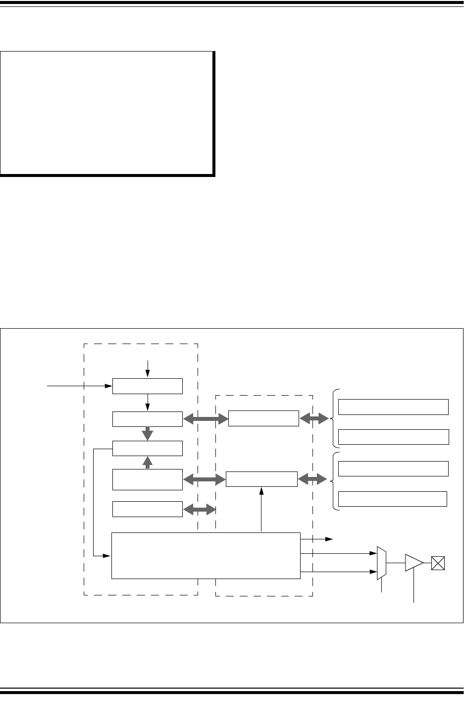
2011-2018 Microchip Technology Inc. DS60001168K-page 201
PIC32MX1XX/2XX 28/36/44-PIN FAMILY
21.0 REAL-TIME CLOCK AND
CALENDAR (RTCC)
The PIC32 RTCC module is intended for applications in
which accurate time must be maintained for extended
periods of time with minimal or no CPU intervention.
Low-power optimization provides extended battery
lifetime while keeping track of time.
Following are some of the key features of this module:
• Time: hours, minutes and seconds
• 24-hour format (military time)
• Visibility of one-half second period
• Provides calendar: day, date, month and year
• Alarm intervals are configurable for half of a
second, one second, 10 seconds, one minute, 10
minutes, one hour, one day, one week, one month
and one year
• Alarm repeat with decrementing counter
• Alarm with indefinite repeat: Chime
• Year range: 2000 to 2099
• Leap year correction
• BCD format for smaller firmware overhead
• Optimized for long-term battery operation
• Fractional second synchronization
• User calibration of the clock crystal frequency with
auto-adjust
• Calibration range: 0.66 seconds error per month
• Calibrates up to 260 ppm of crystal error
• Requirements: External 32.768 kHz clock crystal
• Alarm pulse or seconds clock output on
RTCC pin
FIGURE 21-1: RTCC BLOCK DIAGRAM
Note: This data sheet summarizes the features
of the PIC32MX1XX/2XX 28/36/44-pin
Family of devices. It is not intended to be
a comprehensive reference source. To
complement the information in this data
sheet, refer to Section 29. “Real-Time
Clock and Calendar (RTCC)”
(DS60001125), which is available from the
Documentation > Reference Manual
section of the Microchip PIC32 web site
(www.microchip.com/pic32).
RTCC Prescalers
RTCC Timer
Comparator
Compare Registers
Repeat Counter
ALRMTIME
HR, MIN, SEC
ALRMDATE
with Masks
RTCC Interrupt Logic
Alarm
Event
32.768 kHz Input
from Secondary
0.5s
Alarm Pulse
Set RTCC Flag
RTCVAL
ALRMVAL
RTCC
RTCOE
Oscillator (S
OSC
)
CAL<9:0>
MONTH, DAY, WDAY
RTCTIME
HR, MIN, SEC
RTCDATE
YEAR, MONTH, DAY, WDAY
Seconds Pulse
RTSECSEL
0
1
PIC32MX1XX/2XX 28/36/44-PIN FAMILY
DS60001168K-page 202 2011-2018 Microchip Technology Inc.
21.1 RTCC Control Registers
TABLE 21-1: RTCC REGISTER MAP
Virtual Address
(BF80_#)
Register
Name
(1)
Bit Range
Bits
All Resets
31/15 30/14 29/13 28/12 27/11 26/10 25/9 24/8 23/7 22/6 21/5 20/4 19/3 18/2 17/1 16/0
0200 RTCCON 31:16 — — — — — — CAL<9:0> 0000
15:0 ON —SIDL — — — — — RTSECSEL RTCCLKON —— RTCWREN RTCSYNC HALFSEC RTCOE 0000
0210 RTCALRM 31:16 — — — — — — — — — — — — — — — — 0000
15:0 ALRMEN CHIME PIV ALRMSYNC AMASK<3:0> ARPT<7:0> 0000
0220 RTCTIME 31:16 —— HR10<1:0> HR01<3:0> — MIN10<2:0> MIN01<3:0> xxxx
15:0 — SEC10<2:0> SEC01<3:0> — — — — — — — — xx00
0230 RTCDATE 31:16 YEAR10<3:0> YEAR01<3:0> — — — MONTH10 MONTH01<3:0> xxxx
15:0 —— DAY10<1:0> DAY01<3:0> — — — — — WDAY01<2:0> xx00
0240 ALRMTIME 31:16 —— HR10<1:0> HR01<3:0> — MIN10<2:0> MIN01<3:0> xxxx
15:0 — SEC10<2:0> SEC01<3:0> — — — — — — — — xx00
0250 ALRMDATE 31:16 — — — — — — — — — — — MONTH10 MONTH01<3:0> 00xx
15:0 DAY10<3:0> DAY01<3:0> — — — — — WDAY01<2:0> xx0x
Legend: x = unknown value on Reset; — = unimplemented, read as ‘0’. Reset values are shown in hexadecimal.
Note 1: All registers in this table have corresponding CLR, SET and INV registers at its virtual address, plus an offset of 0x4, 0x8 and 0xC, respectively. See Section 11.2 “CLR, SET and INV Registers” for more
information.

2011-2018 Microchip Technology Inc. DS60001168K-page 203
PIC32MX1XX/2XX 28/36/44-PIN FAMILY
REGISTER 21-1: RTCCON: RTC CONTROL REGISTER
Bit
Range Bit
31/23/15/7 Bit
30/22/14/6 Bit
29/21/13/5 Bit
28/20/12/4 Bit
27/19/11/3 Bit
26/18/10/2 Bit
25/17/9/1 Bit
24/16/8/0
31:24
U-0 U-0 U-0 U-0 U-0 U-0 R/W-0 R/W-0
— — — — — —CAL<9:8>
23:16
R/W-0 R/W-0 R/W-0 R/W-0 R/W-0 R/W-0 R/W-0 R/W-0
CAL<7:0>
15:8
R/W-0 U-0 R/W-0 U-0 U-0 U-0 U-0 U-0
ON
(1,2)
—SIDL— — — — —
7:0
R/W-0 R-0 U-0 U-0 R/W-0 R-0 R-0 R/W-0
RTSECSEL
(3)
RTCCLKON ——RTCWREN
(4)
RTCSYNC HALFSEC
(5)
RTCOE
Legend:
R = Readable bit W = Writable bit U = Unimplemented bit, read as ‘0’
-n = Value at POR ‘1’ = Bit is set ‘0’ = Bit is cleared x = Bit is unknown
bit 31-26 Unimplemented: Read as ‘0’
bit 25-16 CAL<9:0>: RTC Drift Calibration bits, which contain a signed 10-bit integer value
0111111111 = Maximum positive adjustment, adds 511 RTC clock pulses every one minute
•
•
•
0000000001 = Minimum positive adjustment, adds 1 RTC clock pulse every one minute
0000000000 = No adjustment
1111111111 = Minimum negative adjustment, subtracts 1 RTC clock pulse every one minute
•
•
•
1000000000 = Maximum negative adjustment, subtracts 512 clock pulses every one minute
bit 15 ON: RTCC On bit
(1,2)
1 = RTCC module is enabled
0 = RTCC module is disabled
bit 14 Unimplemented: Read as ‘0’
bit 13 SIDL: Stop in Idle Mode bit
1 = Disables the PBCLK to the RTCC when the device enters Idle mode
0 = Continue normal operation when the device enters Idle mode
bit 12-8 Unimplemented: Read as ‘0’
bit 7 RTSECSEL: RTCC Seconds Clock Output Select bit
(3)
1 = RTCC Seconds Clock is selected for the RTCC pin
0 = RTCC Alarm Pulse is selected for the RTCC pin
bit 6 RTCCLKON: RTCC Clock Enable Status bit
1 = RTCC Clock is actively running
0 = RTCC Clock is not running
Note 1: The ON bit is only writable when RTCWREN = 1.
2: When using the 1:1 PBCLK divisor, the user’s software should not read/write the peripheral’s SFRs in the
SYSCLK cycle immediately following the instruction that clears the module’s ON bit.
3: Requires RTCOE = 1 (RTCCON<0>) for the output to be active.
4: The RTCWREN bit can be set only when the write sequence is enabled.
5: This bit is read-only. It is cleared to ‘0’ on a write to the seconds bit fields (RTCTIME<14:8>).
Note: This register is reset only on a Power-on Reset (POR).

PIC32MX1XX/2XX 28/36/44-PIN FAMILY
DS60001168K-page 204 2011-2018 Microchip Technology Inc.
bit 5-4 Unimplemented: Read as ‘0’
bit 3 RTCWREN: RTC Value Registers Write Enable bit
(4)
1 = RTC Value registers can be written to by the user
0 = RTC Value registers are locked out from being written to by the user
bit 2 RTCSYNC: RTCC Value Registers Read Synchronization bit
1 = RTC Value registers can change while reading, due to a rollover ripple that results in an invalid data read
If the register is read twice and results in the same data, the data can be assumed to be valid
0 = RTC Value registers can be read without concern about a rollover ripple
bit 1 HALFSEC: Half-Second Status bit
(5)
1 = Second half period of a second
0 = First half period of a second
bit 0 RTCOE: RTCC Output Enable bit
1 = RTCC clock output enabled – clock presented onto an I/O
0 = RTCC clock output disabled
REGISTER 21-1: RTCCON: RTC CONTROL REGISTER (CONTINUED)
Note 1: The ON bit is only writable when RTCWREN = 1.
2: When using the 1:1 PBCLK divisor, the user’s software should not read/write the peripheral’s SFRs in the
SYSCLK cycle immediately following the instruction that clears the module’s ON bit.
3: Requires RTCOE = 1 (RTCCON<0>) for the output to be active.
4: The RTCWREN bit can be set only when the write sequence is enabled.
5: This bit is read-only. It is cleared to ‘0’ on a write to the seconds bit fields (RTCTIME<14:8>).
Note: This register is reset only on a Power-on Reset (POR).

2011-2018 Microchip Technology Inc. DS60001168K-page 205
PIC32MX1XX/2XX 28/36/44-PIN FAMILY
REGISTER 21-2: RTCALRM: RTC ALARM CONTROL REGISTER
Bit
Range Bit
31/23/15/7 Bit
30/22/14/6 Bit
29/21/13/5 Bit
28/20/12/4 Bit
27/19/11/3 Bit
26/18/10/2 Bit
25/17/9/1 Bit
24/16/8/0
31:24
U-0 U-0 U-0 U-0 U-0 U-0 U-0 U-0
— — — — — — — —
23:16
U-0 U-0 U-0 U-0 U-0 U-0 U-0 U-0
— — — — — — — —
15:8
R/W-0 R/W-0 R/W-0 R-0 R/W-0 R/W-0 R/W-0 R/W-0
ALRMEN
(1,2)
CHIME
(2)
PIV
(2)
ALRMSYNC
(3)
AMASK<3:0>
(2)
7:0
R/W-0 R/W-0 R/W-0 R/W-0 R/W-0 R/W-0 R/W-0 R/W-0
ARPT<7:0>
(2)
Legend:
R = Readable bit W = Writable bit U = Unimplemented bit, read as ‘0’
-n = Value at POR ‘1’ = Bit is set ‘0’ = Bit is cleared x = Bit is unknown
bit 31-16 Unimplemented: Read as ‘0’
bit 15 ALRMEN: Alarm Enable bit
(1,2)
1 = Alarm is enabled
0 = Alarm is disabled
bit 14 CHIME: Chime Enable bit
(2)
1 = Chime is enabled – ARPT<7:0> is allowed to rollover from 0x00 to 0xFF
0 = Chime is disabled – ARPT<7:0> stops once it reaches 0x00
bit 13 PIV: Alarm Pulse Initial Value bit
(2)
When ALRMEN = 0, PIV is writable and determines the initial value of the Alarm Pulse.
When ALRMEN = 1, PIV is read-only and returns the state of the Alarm Pulse.
bit 12 ALRMSYNC: Alarm Sync bit
(3)
1 = ARPT<7:0> and ALRMEN may change as a result of a half second rollover during a read.
The ARPT must be read repeatedly until the same value is read twice. This must be done since multiple
bits may be changing, which are then synchronized to the PB clock domain
0 = ARPT<7:0> and ALRMEN can be read without concerns of rollover because the prescaler is > 32 RTC
clocks away from a half-second rollover
bit 11-8 AMASK<3:0>: Alarm Mask Configuration bits
(2)
0000 = Every half-second
0001 = Every second
0010 = Every 10 seconds
0011 = Every minute
0100 = Every 10 minutes
0101 = Every hour
0110 = Once a day
0111 = Once a week
1000 = Once a month
1001 = Once a year (except when configured for February 29, once every four years)
1010 = Reserved; do not use
1011 = Reserved; do not use
11xx = Reserved; do not use
Note 1: Hardware clears the ALRMEN bit anytime the alarm event occurs, when ARPT<7:0> = 00 and
CHIME = 0.
2: This field should not be written when the RTCC ON bit = ‘1’ (RTCCON<15>) and ALRMSYNC = 1.
3: This assumes a CPU read will execute in less than 32 PBCLKs.
Note: This register is reset only on a Power-on Reset (POR).

PIC32MX1XX/2XX 28/36/44-PIN FAMILY
DS60001168K-page 206 2011-2018 Microchip Technology Inc.
bit 7-0 ARPT<7:0>: Alarm Repeat Counter Value bits
(2)
11111111 = Alarm will trigger 256 times
•
•
•
00000000 = Alarm will trigger one time
The counter decrements on any alarm event. The counter only rolls over from 0x00 to 0xFF if CHIME = 1.
REGISTER 21-2: RTCALRM: RTC ALARM CONTROL REGISTER (CONTINUED)
Note 1: Hardware clears the ALRMEN bit anytime the alarm event occurs, when ARPT<7:0> = 00 and
CHIME = 0.
2: This field should not be written when the RTCC ON bit = ‘1’ (RTCCON<15>) and ALRMSYNC = 1.
3: This assumes a CPU read will execute in less than 32 PBCLKs.
Note: This register is reset only on a Power-on Reset (POR).
2011-2018 Microchip Technology Inc. DS60001168K-page 207
PIC32MX1XX/2XX 28/36/44-PIN FAMILY
REGISTER 21-3: RTCTIME: RTC TIME VALUE REGISTER
Bit
Range Bit
31/23/15/7 Bit
30/22/14/6 Bit
29/21/13/5 Bit
28/20/12/4 Bit
27/19/11/3 Bit
26/18/10/2 Bit
25/17/9/1 Bit
24/16/8/0
31:24
U-0 U-0 R/W-x R/W-x R/W-x R/W-x R/W-x R/W-x
—— HR10<1:0> HR01<3:0>
23:16
U-0 R/W-x R/W-x R/W-x R/W-x R/W-x R/W-x R/W-x
— MIN10<2:0> MIN01<3:0>
15:8
U-0 R/W-x R/W-x R/W-x R/W-x R/W-x R/W-x R/W-x
— SEC10<2:0> SEC01<3:0>
7:0
U-0 U-0 U-0 U-0 U-0 U-0 U-0 U-0
— — — — — — — —
Legend:
R = Readable bit W = Writable bit U = Unimplemented bit, read as ‘0’
-n = Value at POR ‘1’ = Bit is set ‘0’ = Bit is cleared x = Bit is unknown
bit 31-30 Unimplemented: Read as ‘0’
bit 29-28 HR10<1:0>: Binary-Coded Decimal Value of Hours bits, 10s place digit; contains a value from 0 to 2
bit 27-24 HR01<3:0>: Binary-Coded Decimal Value of Hours bits, 1s place digit; contains a value from 0 to 9
bit 23 Unimplemented: Read as ‘0’
bit 22-20 MIN10<2:0>: Binary-Coded Decimal Value of Minutes bits, 10s place digit; contains a value from 0 to 5
bit 19-16 MIN01<3:0>: Binary-Coded Decimal Value of Minutes bits, 1s place digit; contains a value from 0 to 9
bit 15 Unimplemented: Read as ‘0’
bit 14-12 SEC10<2:0>: Binary-Coded Decimal Value of Seconds bits, 10s place digit; contains a value from 0 to 5
bit 11-8 SEC01<3:0>: Binary-Coded Decimal Value of Seconds bits, 1s place digit; contains a value from 0 to 9
bit 7-0 Unimplemented: Read as ‘0’
Note: This register is only writable when RTCWREN = 1 (RTCCON<3>).
PIC32MX1XX/2XX 28/36/44-PIN FAMILY
DS60001168K-page 208 2011-2018 Microchip Technology Inc.
REGISTER 21-4: RTCDATE: RTC DATE VALUE REGISTER
Bit
Range Bit
31/23/15/7 Bit
30/22/14/6 Bit
29/21/13/5 Bit
28/20/12/4 Bit
27/19/11/3 Bit
26/18/10/2 Bit
25/17/9/1 Bit
24/16/8/0
31:24
R/W-x R/W-x R/W-x R/W-x R/W-x R/W-x R/W-x R/W-x
YEAR10<3:0> YEAR01<3:0>
23:16
U-0 U-0 U-0 R/W-x R/W-x R/W-x R/W-x R/W-x
— — — MONTH10 MONTH01<3:0>
15:8
U-0 U-0 R/W-x R/W-x R/W-x R/W-x R/W-x R/W-x
—— DAY10<1:0> DAY01<3:0>
7:0
U-0 U-0 U-0 U-0 U-0 R/W-x R/W-x R/W-x
— — — — — WDAY01<2:0>
Legend:
R = Readable bit W = Writable bit U = Unimplemented bit, read as ‘0’
-n = Value at POR ‘1’ = Bit is set ‘0’ = Bit is cleared x = Bit is unknown
bit 31-28 YEAR10<3:0>: Binary-Coded Decimal Value of Years bits, 10s place digit; contains a value from 0 to 9
bit 27-24 YEAR01<3:0>: Binary-Coded Decimal Value of Years bits, 1s place digit; contains a value from 0 to 9
bit 23-21 Unimplemented: Read as ‘0’
bit 20 MONTH10: Binary-Coded Decimal Value of Months bits, 10s place digit; contains a value of 0 or 1
bit 19-16 MONTH01<3:0>: Binary-Coded Decimal Value of Months bits, 1s place digit; contains a value from 0 to 9
bit 15-14 Unimplemented: Read as ‘0’
bit 13-12 DAY10<1:0>: Binary-Coded Decimal Value of Days bits, 10s place digit; contains a value of 0 to 3
bit 11-8 DAY01<3:0>: Binary-Coded Decimal Value of Days bits, 1s place digit; contains a value from 0 to 9
bit 7-3 Unimplemented: Read as ‘0’
bit 2-0 WDAY01<2:0>: Binary-Coded Decimal Value of Weekdays bits; contains a value from 0 to 6
Note: This register is only writable when RTCWREN = 1 (RTCCON<3>).

2011-2018 Microchip Technology Inc. DS60001168K-page 209
PIC32MX1XX/2XX 28/36/44-PIN FAMILY
REGISTER 21-5: ALRMTIME: ALARM TIME VALUE REGISTER
Bit
Range Bit
31/23/15/7 Bit
30/22/14/6 Bit
29/21/13/5 Bit
28/20/12/4 Bit
27/19/11/3 Bit
26/18/10/2 Bit
25/17/9/1 Bit
24/16/8/0
31:24
U-0 U-0 R/W-x R/W-x R/W-x R/W-x R/W-x R/W-x
—— HR10<1:0> HR01<3:0>
23:16
U-0 R/W-x R/W-x R/W-x R/W-x R/W-x R/W-x R/W-x
— MIN10<2:0> MIN01<3:0>
15:8
U-0 R/W-x R/W-x R/W-x R/W-x R/W-x R/W-x R/W-x
— SEC10<2:0> SEC01<3:0>
7:0
U-0 U-0 U-0 U-0 U-0 U-0 U-0 U-0
— — — — — — — —
Legend:
R = Readable bit W = Writable bit U = Unimplemented bit, read as ‘0’
-n = Value at POR ‘1’ = Bit is set ‘0’ = Bit is cleared x = Bit is unknown
bit 31-30 Unimplemented: Read as ‘0’
bit 29-28 HR10<1:0>: Binary Coded Decimal value of hours bits, 10s place digit; contains a value from 0 to 2
bit 27-24 HR01<3:0>: Binary Coded Decimal value of hours bits, 1s place digit; contains a value from 0 to 9
bit 23 Unimplemented: Read as ‘0’
bit 22-20 MIN10<2:0>: Binary Coded Decimal value of minutes bits, 10s place digit; contains a value from 0 to 5
bit 19-16 MIN01<3:0>: Binary Coded Decimal value of minutes bits, 1s place digit; contains a value from 0 to 9
bit 15 Unimplemented: Read as ‘0’
bit 14-12 SEC10<2:0>: Binary Coded Decimal value of seconds bits, 10s place digit; contains a value from 0 to 5
bit 11-8 SEC01<3:0>: Binary Coded Decimal value of seconds bits, 1s place digit; contains a value from 0 to 9
bit 7-0 Unimplemented: Read as ‘0’

PIC32MX1XX/2XX 28/36/44-PIN FAMILY
DS60001168K-page 210 2011-2018 Microchip Technology Inc.
REGISTER 21-6: ALRMDATE: ALARM DATE VALUE REGISTER
Bit
Range Bit
31/23/15/7 Bit
30/22/14/6 Bit
29/21/13/5 Bit
28/20/12/4 Bit
27/19/11/3 Bit
26/18/10/2 Bit
25/17/9/1 Bit
24/16/8/0
31:24
U-0 U-0 U-0 U-0 U-0 U-0 U-0 U-0
— — — — — — — —
23:16
U-0 U-0 U-0 R/W-x R/W-x R/W-x R/W-x R/W-x
— — — MONTH10 MONTH01<3:0>
15:8
U-0 U-0 R/W-x R/W-x R/W-x R/W-x R/W-x R/W-x
—— DAY10<1:0> DAY01<3:0>
7:0
U-0 U-0 U-0 U-0 U-0 R/W-x R/W-x R/W-x
— — — — — WDAY01<2:0>
Legend:
R = Readable bit W = Writable bit U = Unimplemented bit, read as ‘0’
-n = Value at POR ‘1’ = Bit is set ‘0’ = Bit is cleared x = Bit is unknown
bit 31-21 Unimplemented: Read as ‘0’
bit 20 MONTH10: Binary Coded Decimal value of months bits, 10s place digit; contains a value of 0 or 1
bit 19-16 MONTH01<3:0>: Binary Coded Decimal value of months bits, 1s place digit; contains a value from 0 to 9
bit 15-14 Unimplemented: Read as ‘0’
bit 13-12 DAY10<1:0>: Binary Coded Decimal value of days bits, 10s place digit; contains a value from 0 to 3
bit 11-8 DAY01<3:0>: Binary Coded Decimal value of days bits, 1s place digit; contains a value from 0 to 9
bit 7-3 Unimplemented: Read as ‘0’
bit 2-0 WDAY01<2:0>: Binary Coded Decimal value of weekdays bits; contains a value from 0 to 6
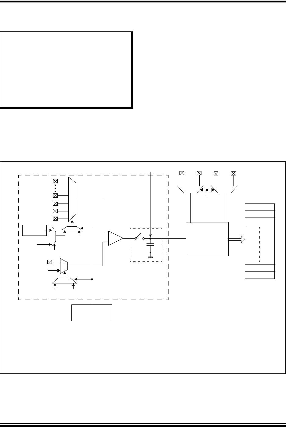
2011-2018 Microchip Technology Inc. DS60001168K-page 211
PIC32MX1XX/2XX 28/36/44-PIN FAMILY
22.0 10-BIT ANALOG-TO-DIGITAL
CONVERTER (ADC)
The 10-bit Analog-to-Digital Converter (ADC) includes
the following features:
• Successive Approximation Register (SAR)
conversion
• Up to 1 Msps conversion speed
• Up to 13 analog input pins
• External voltage reference input pins
• One unipolar, differential Sample and Hold
Amplifier (SHA)
• Automatic Channel Scan mode
• Selectable conversion trigger source
• 16-word conversion result buffer
• Selectable buffer fill modes
• Eight conversion result format options
• Operation during Sleep and Idle modes
A block diagram of the 10-bit ADC is illustrated in
Figure 22-1. Figure 22-2 illustrates a block diagram of
the ADC conversion clock period. The 10-bit ADC has
up to 13 analog input pins, designated AN0-AN12. In
addition, there are two analog input pins for external
voltage reference connections. These voltage
reference inputs may be shared with other analog input
pins and may be common to other analog module
references.
FIGURE 22-1: ADC1 MODULE BLOCK DIAGRAM
Note: This data sheet summarizes the features
of the PIC32MX1XX/2XX 28/36/44-pin
Family of devices. It is not intended to be
a comprehensive reference source. To
complement the information in this data
sheet, refer to Section 17. “10-bit Ana-
log-to-Digital Converter (ADC)”
(DS60001104), which is available from the
Documentation > Reference Manual
section of the Microchip PIC32 web site
(www.microchip.com/pic32).
SAR ADC
S&H
ADC1BUF0
ADC1BUF1
ADC1BUF2
ADC1BUFF
ADC1BUFE
CTMUT
(3)
IV
REF(4)
AN1
V
REFL
CH0SB<4:0>
CH0NA CH0NB
+
-
CH0SA<4:0>
Channel
Scan
CSCNA
Alternate
V
REF
+
(1)
AV
DD
AV
SS
V
REF
-
(1)
Note 1: V
REF
+ and V
REF
- inputs can be multiplexed with other analog inputs.
2: AN8 is only available on 44-pin devices. AN6, AN7, and AN12 are not available on 28-pin devices.
3: Connected to the CTMU module. See Section 25.0 “Charge Time Measurement Unit (CTMU)” for more
information.
4: Internal precision voltage reference (1.2V).
5: This selection is only used with CTMU capacitive and time measurement.
Input Selection
V
REFH
V
REFL
VCFG<2:0>
AN12
(2)
AN0
Open
(5)
CTMUI
(3)
PIC32MX1XX/2XX 28/36/44-PIN FAMILY
DS60001168K-page 212 2011-2018 Microchip Technology Inc.
FIGURE 22-2: ADC CONVERSION CLOCK PERIOD BLOCK DIAGRAM
1
0
Div 2
T
PB(2)
ADC Conversion
Clock Multiplier
2, 4,..., 512
ADRC
T
AD
8
ADCS<7:0>
FRC
(1)
Note 1: See Section 30.0 “Electrical Characteristics” for the exact FRC clock value.
2: Refer to Figure 8-1 in Section 8.0 “Oscillator Configuration” for more information.
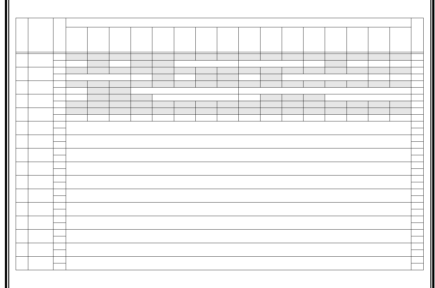
2011-2018 Microchip Technology Inc. DS60001168K-page 213
PIC32MX1XX/2XX 28/36/44-PIN FAMILY
22.1 ADC Control Registers
TABLE 22-1: ADC REGISTER MAP
Virtual Address
(BF80_#)
Register
Name
Bit Range
Bits
All Resets
31/15 30/14 29/13 28/12 27/11 26/10 25/9 24/8 23/7 22/6 21/5 20/4 19/3 18/2 17/1 16/0
9000 AD1CON1
(1)
31:16 ————————————————0000
15:0 ON —SIDL—— FORM<2:0> SSRC<2:0> CLRASAM — ASAM SAMP DONE 0000
9010 AD1CON2
(1)
31:16 ————————————————0000
15:0 VCFG<2:0> OFFCAL — CSCNA ——BUFS— SMPI<3:0> BUFM ALTS 0000
9020 AD1CON3
(1)
31:16 ————————————————0000
15:0 ADRC —— SAMC<4:0> ADCS<7:0> 0000
9040 AD1CHS
(1)
31:16 CH0NB — — — CH0SB<3:0> CH0NA — — — CH0SA<3:0> 0000
15:0 ————————————————0000
9050 AD1CSSL
(1)
31:16 ————————————————0000
15:0 CSSL15 CSSL14 CSSL13 CSSL12 CSSL11 CSSL10 CSSL9 CSSL8 CSSL7 CSSL6 CSSL5 CSSL4 CSSL3 CSSL2 CSSL1 CSSL0 0000
9070 ADC1BUF0 31:16 ADC Result Word 0 (ADC1BUF0<31:0>) 0000
15:0 0000
9080 ADC1BUF1 31:16 ADC Result Word 1 (ADC1BUF1<31:0>) 0000
15:0 0000
9090 ADC1BUF2 31:16 ADC Result Word 2 (ADC1BUF2<31:0>) 0000
15:0 0000
90A0 ADC1BUF3 31:16 ADC Result Word 3 (ADC1BUF3<31:0>) 0000
15:0 0000
90B0 ADC1BUF4 31:16 ADC Result Word 4 (ADC1BUF4<31:0>) 0000
15:0 0000
90C0 ADC1BUF5 31:16 ADC Result Word 5 (ADC1BUF5<31:0>) 0000
15:0 0000
90D0 ADC1BUF6 31:16 ADC Result Word 6 (ADC1BUF6<31:0>) 0000
15:0 0000
90E0 ADC1BUF7 31:16 ADC Result Word 7 (ADC1BUF7<31:0>) 0000
15:0 0000
90F0 ADC1BUF8 31:16 ADC Result Word 8 (ADC1BUF8<31:0>) 0000
15:0 0000
9100 ADC1BUF9 31:16 ADC Result Word 9 (ADC1BUF9<31:0>) 0000
15:0 0000
9110 ADC1BUFA 31:16 ADC Result Word A (ADC1BUFA<31:0>) 0000
15:0 0000
Legend: x = unknown value on Reset; — = unimplemented, read as ‘0’. Reset values are shown in hexadecimal.
Note 1: This register has corresponding CLR, SET and INV registers at its virtual address, plus offsets of 0x4, 0x8 and 0xC, respectively. See Section 11.2 “CLR, SET and INV Registers” for details.
PIC32MX1XX/2XX 28/36/44-PIN FAMILY
DS60001168K-page 214 2011-2018 Microchip Technology Inc.
9120 ADC1BUFB 31:16 ADC Result Word B (ADC1BUFB<31:0>) 0000
15:0 0000
9130 ADC1BUFC 31:16 ADC Result Word C (ADC1BUFC<31:0>) 0000
15:0 0000
9140 ADC1BUFD 31:16 ADC Result Word D (ADC1BUFD<31:0>) 0000
15:0 0000
9150 ADC1BUFE 31:16 ADC Result Word E (ADC1BUFE<31:0>) 0000
15:0 0000
9160 ADC1BUFF 31:16 ADC Result Word F (ADC1BUFF<31:0>) 0000
15:0 0000
TABLE 22-1: ADC REGISTER MAP (CONTINUED)
Virtual Address
(BF80_#)
Register
Name
Bit Range
Bits
All Resets
31/15 30/14 29/13 28/12 27/11 26/10 25/9 24/8 23/7 22/6 21/5 20/4 19/3 18/2 17/1 16/0
Legend: x = unknown value on Reset; — = unimplemented, read as ‘0’. Reset values are shown in hexadecimal.
Note 1: This register has corresponding CLR, SET and INV registers at its virtual address, plus offsets of 0x4, 0x8 and 0xC, respectively. See Section 11.2 “CLR, SET and INV Registers” for details.

2011-2018 Microchip Technology Inc. DS60001168K-page 215
PIC32MX1XX/2XX 28/36/44-PIN FAMILY
REGISTER 22-1: AD1CON1: ADC CONTROL REGISTER 1
Bit
Range Bit
31/23/15/7 Bit
30/22/14/6 Bit
29/21/13/5 Bit
28/20/12/4 Bit
27/19/11/3 Bit
26/18/10/2 Bit
25/17/9/1 Bit
24/16/8/0
31:24
U-0 U-0 U-0 U-0 U-0 U-0 U-0 U-0
— — — — — — — —
23:16
U-0 U-0 U-0 U-0 U-0 U-0 U-0 U-0
— — — — — — — —
15:8
R/W-0 U-0 R/W-0 U-0 U-0 R/W-0 R/W-0 R/W-0
ON
(1)
—SIDL——FORM<2:0>
7:0
R/W-0 R/W-0 R/W-0 R/W-0 U-0 R/W-0 R/W-0, HSC R/C-0, HSC
SSRC<2:0> CLRASAM — ASAM SAMP
(2)
DONE
(3)
Legend:
R = Readable bit W = Writable bit U = Unimplemented bit, read as ‘0’
-n = Value at POR ‘1’ = Bit is set ‘0’ = Bit is cleared x = Bit is unknown
bit 31-16 Unimplemented: Read as ‘0’
bit 15 ON: ADC Operating Mode bit
(1)
1 = ADC module is operating
0 = ADC module is not operating
bit 14 Unimplemented: Read as ‘0’
bit 13 SIDL: Stop in Idle Mode bit
1 = Discontinue module operation when device enters Idle mode
0 = Continue module operation when the device enters Idle mode
bit 12-11 Unimplemented: Read as ‘0’
bit 10-8 FORM<2:0>: Data Output Format bits
111 = Signed Fractional 32-bit (DOUT = sddd dddd dd00 0000 0000 0000 0000)
110 = Fractional 32-bit (DOUT = dddd dddd dd00 0000 0000 0000 0000 0000)
101 = Signed Integer 32-bit (DOUT = ssss ssss ssss ssss ssss sssd dddd dddd)
100 = Integer 32-bit (DOUT = 0000 0000 0000 0000 0000 00dd dddd dddd)
011 = Signed Fractional 16-bit (DOUT = 0000 0000 0000 0000 sddd dddd dd00 0000)
010 = Fractional 16-bit (DOUT = 0000 0000 0000 0000 dddd dddd dd00 0000)
001 = Signed Integer 16-bit (DOUT = 0000 0000 0000 0000 ssss sssd dddd dddd)
000 =Integer 16-bit (DOUT = 0000 0000 0000 0000 0000 00dd dddd dddd)
bit 7-5 SSRC<2:0>: Conversion Trigger Source Select bits
111 = Internal counter ends sampling and starts conversion (auto convert)
110 = Reserved
101 = Reserved
100 = Reserved
011 = CTMU ends sampling and starts conversion
010 = Timer 3 period match ends sampling and starts conversion
001 = Active transition on INT0 pin ends sampling and starts conversion
000 = Clearing SAMP bit ends sampling and starts conversion
Note 1: When using 1:1 PBCLK divisor, the user’s software should not read/write the peripheral’s SFRs in the
SYSCLK cycle immediately following the instruction that clears the module’s ON bit.
2: If ASAM = 0, software can write a ‘1’ to start sampling. This bit is automatically set by hardware if
ASAM = 1. If SSRC = 0, software can write a ‘0’ to end sampling and start conversion. If SSRC
‘0’, this
bit is automatically cleared by hardware to end sampling and start conversion.
3: This bit is automatically set by hardware when analog-to-digital conversion is complete. Software can
write a ‘0’ to clear this bit (a write of ‘1’ is not allowed). Clearing this bit does not affect any operation
already in progress. This bit is automatically cleared by hardware at the start of a new conversion.

PIC32MX1XX/2XX 28/36/44-PIN FAMILY
DS60001168K-page 216 2011-2018 Microchip Technology Inc.
bit 4 CLRASAM: Stop Conversion Sequence bit (when the first ADC interrupt is generated)
1 = Stop conversions when the first ADC interrupt is generated. Hardware clears the ASAM bit when the
ADC interrupt is generated.
0 = Normal operation, buffer contents will be overwritten by the next conversion sequence
bit 3 Unimplemented: Read as ‘0’
bit 2 ASAM: ADC Sample Auto-Start bit
1 = Sampling begins immediately after last conversion completes; SAMP bit is automatically set.
0 = Sampling begins when SAMP bit is set
bit 1 SAMP: ADC Sample Enable bit
(2)
1 = The ADC sample and hold amplifier is sampling
0 = The ADC sample/hold amplifier is holding
When ASAM = 0, writing ‘1’ to this bit starts sampling.
When SSRC = 000, writing ‘0’ to this bit will end sampling and start conversion.
bit 0 DONE: Analog-to-Digital Conversion Status bit
(3)
1 = Analog-to-digital conversion is done
0 = Analog-to-digital conversion is not done or has not started
Clearing this bit will not affect any operation in progress.
REGISTER 22-1: AD1CON1: ADC CONTROL REGISTER 1 (CONTINUED)
Note 1: When using 1:1 PBCLK divisor, the user’s software should not read/write the peripheral’s SFRs in the
SYSCLK cycle immediately following the instruction that clears the module’s ON bit.
2: If ASAM = 0, software can write a ‘1’ to start sampling. This bit is automatically set by hardware if
ASAM = 1. If SSRC = 0, software can write a ‘0’ to end sampling and start conversion. If SSRC
‘0’, this
bit is automatically cleared by hardware to end sampling and start conversion.
3: This bit is automatically set by hardware when analog-to-digital conversion is complete. Software can
write a ‘0’ to clear this bit (a write of ‘1’ is not allowed). Clearing this bit does not affect any operation
already in progress. This bit is automatically cleared by hardware at the start of a new conversion.
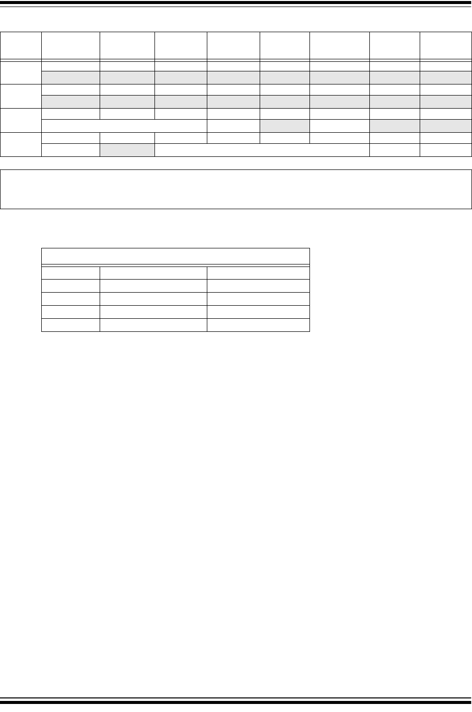
2011-2018 Microchip Technology Inc. DS60001168K-page 217
PIC32MX1XX/2XX 28/36/44-PIN FAMILY
REGISTER 22-2: AD1CON2: ADC CONTROL REGISTER 2
Bit
Range Bit
31/23/15/7 Bit
30/22/14/6 Bit
29/21/13/5 Bit
28/20/12/4 Bit
27/19/11/3 Bit
26/18/10/2 Bit
25/17/9/1 Bit
24/16/8/0
31:24
U-0 U-0 U-0 U-0 U-0 U-0 U-0 U-0
— — — — — — — —
23:16
U-0 U-0 U-0 U-0 U-0 U-0 U-0 U-0
— — — — — — — —
15:8
R/W-0 R/W-0 R/W-0 R/W-0 U-0 R/W-0 U-0 U-0
VCFG<2:0> OFFCAL — CSCNA — —
7:0
R-0 U-0 R/W-0 R/W-0 R/W-0 R/W-0 R/W-0 R/W-0
BUFS — SMPI<3:0> BUFM ALTS
Legend:
R = Readable bit W = Writable bit U = Unimplemented bit, read as ‘0’
-n = Value at POR ‘1’ = Bit is set ‘0’ = Bit is cleared x = Bit is unknown
bit 31-16 Unimplemented: Read as ‘0’
bit 15-13 VCFG<2:0>: Voltage Reference Configuration bits
V
REFH
V
REFL
000 AV
DD
AVss
001 External V
REF
+ pin AV
SS
010 AV
DD
External V
REF
- pin
011 External V
REF
+ pin External V
REF
- pin
1xx AV
DD
AV
SS
bit 12 OFFCAL: Input Offset Calibration Mode Select bit
1 = Enable Offset Calibration mode
Positive and negative inputs of the sample and hold amplifier are connected to V
REFL
0 = Disable Offset Calibration mode
The inputs to the sample and hold amplifier are controlled by AD1CHS or AD1CSSL
bit 11 Unimplemented: Read as ‘0’
bit 10 CSCNA: Input Scan Select bit
1 = Scan inputs
0 = Do not scan inputs
bit 9-8 Unimplemented: Read as ‘0’
bit 7 BUFS: Buffer Fill Status bit
Only valid when BUFM = 1.
1 = ADC is currently filling buffer 0x8-0xF, user should access data in 0x0-0x7
0 = ADC is currently filling buffer 0x0-0x7, user should access data in 0x8-0xF
bit 6 Unimplemented: Read as ‘0’
bit 5-2 SMPI<3:0>: Sample/Convert Sequences Per Interrupt Selection bits
1111 = Interrupts at the completion of conversion for each 16
th
sample/convert sequence
1110 = Interrupts at the completion of conversion for each 15
th
sample/convert sequence
•
•
•
0001 = Interrupts at the completion of conversion for each 2
nd
sample/convert sequence
0000 = Interrupts at the completion of conversion for each sample/convert sequence
bit 1 BUFM: ADC Result Buffer Mode Select bit
1 = Buffer configured as two 8-word buffers, ADC1BUF7-ADC1BUF0, ADC1BUFF-ADCBUF8
0 = Buffer configured as one 16-word buffer ADC1BUFF-ADC1BUF0
bit 0 ALTS: Alternate Input Sample Mode Select bit
1 = Uses Sample A input multiplexer settings for first sample, then alternates between Sample B and
Sample A input multiplexer settings for all subsequent samples
0 = Always use Sample A input multiplexer settings

PIC32MX1XX/2XX 28/36/44-PIN FAMILY
DS60001168K-page 218 2011-2018 Microchip Technology Inc.
REGISTER 22-3: AD1CON3: ADC CONTROL REGISTER 3
Bit
Range Bit
31/23/15/7 Bit
30/22/14/6 Bit
29/21/13/5 Bit
28/20/12/4 Bit
27/19/11/3 Bit
26/18/10/2 Bit
25/17/9/1 Bit
24/16/8/0
31:24
U-0 U-0 U-0 U-0 U-0 U-0 U-0 U-0
— — — — — — — —
23:16
U-0 U-0 U-0 U-0 U-0 U-0 U-0 U-0
— — — — — — — —
15:8
R/W-0 U-0 U-0 R/W-0 R/W-0 R/W-0 R/W-0 R/W-0
ADRC —— SAMC<4:0>
(1)
7:0
R/W-0 R/W-0 R/W-0 R/W-0 R/W-0 R/W-0 R/W R/W-0
ADCS<7:0>
(2)
Legend:
R = Readable bit W = Writable bit U = Unimplemented bit, read as ‘0’
-n = Value at POR ‘1’ = Bit is set ‘0’ = Bit is cleared x = Bit is unknown
bit 31-16 Unimplemented: Read as ‘0’
bit 15 ADRC: ADC Conversion Clock Source bit
1 = Clock derived from FRC
0 = Clock derived from Peripheral Bus Clock (PBCLK)
bit 14-13 Unimplemented: Read as ‘0’
bit 12-8 SAMC<4:0>: Auto-Sample Time bits
(1)
11111 = 31 T
AD
•
•
•
00001 = 1 T
AD
00000 = 0 T
AD
(Not allowed)
bit 7-0 ADCS<7:0>: ADC Conversion Clock Select bits
(2)
11111111 =T
PB
• 2 • (ADCS<7:0> + 1) = 512 • T
PB
= T
AD
•
•
•
00000001 =T
PB
• 2 • (ADCS<7:0> + 1) = 4 • T
PB
= T
AD
00000000 =T
PB
• 2 • (ADCS<7:0> + 1) = 2 • T
PB
= T
AD
Note 1: This bit is only used if the SSRC<2:0> bits (AD1CON1<7:5>) = 111.
2: This bit is not used if the ADRC (AD1CON3<15>) bit = 1.

2011-2018 Microchip Technology Inc. DS60001168K-page 219
PIC32MX1XX/2XX 28/36/44-PIN FAMILY
REGISTER 22-4: AD1CHS: ADC INPUT SELECT REGISTER
Bit
Range Bit
31/23/15/7 Bit
30/22/14/6 Bit
29/21/13/5 Bit
28/20/12/4 Bit
27/19/11/3 Bit
26/18/10/2 Bit
25/17/9/1 Bit
24/16/8/0
31:24
R/W-0 U-0 U-0 U-0 R/W-0 R/W-0 R/W-0 R/W-0
CH0NB — — — CH0SB<3:0>
23:16
R/W-0 U-0 U-0 U-0 R/W-0 R/W-0 R/W-0 R/W-0
CH0NA — — — CH0SA<3:0>
15:8
U-0 U-0 U-0 U-0 U-0 U-0 U-0 U-0
— — — — — — — —
7:0
U-0 U-0 U-0 U-0 U-0 U-0 U-0 U-0
— — — — — — — —
Legend:
R = Readable bit W = Writable bit U = Unimplemented bit, read as ‘0’
-n = Value at POR ‘1’ = Bit is set ‘0’ = Bit is cleared x = Bit is unknown
bit 31 CH0NB: Negative Input Select bit for Sample B
1 = Channel 0 negative input is AN1
0 = Channel 0 negative input is V
REFL
bit 30-28 Unimplemented: Read as ‘0’
bit 27-24 CH0SB<3:0>: Positive Input Select bits for Sample B
1111 = Channel 0 positive input is Open
(1)
1110 = Channel 0 positive input is IV
REF(2)
1101 = Channel 0 positive input is CTMU temperature sensor (CTMUT)
(3)
1100 = Channel 0 positive input is AN12
(4)
•
•
•
0001 = Channel 0 positive input is AN1
0000 = Channel 0 positive input is AN0
bit 23 CH0NA: Negative Input Select bit for Sample A Multiplexer Setting
(2)
1 = Channel 0 negative input is AN1
0 = Channel 0 negative input is V
REFL
bit 22-20 Unimplemented: Read as ‘0’
bit 19-16 CH0SA<3:0>: Positive Input Select bits for Sample A Multiplexer Setting
1111 = Channel 0 positive input is Open
(1)
1110 = Channel 0 positive input is IV
REF(2)
1101 = Channel 0 positive input is CTMU temperature (CTMUT)
(3)
1100 = Channel 0 positive input is AN12
(4)
•
•
•
0001 = Channel 0 positive input is AN1
0000 = Channel 0 positive input is AN0
bit 15-0 Unimplemented: Read as ‘0’
Note 1: This selection is only used with CTMU capacitive and time measurement.
2: See Section 24.0 “Comparator Voltage Reference (CV
REF
)” for more information.
3: See Section 25.0 “Charge Time Measurement Unit (CTMU)” for more information.
4: AN12 is only available on 44-pin devices. AN6-AN8 are not available on 28-pin devices.

PIC32MX1XX/2XX 28/36/44-PIN FAMILY
DS60001168K-page 220 2011-2018 Microchip Technology Inc.
REGISTER 22-5: AD1CSSL: ADC INPUT SCAN SELECT REGISTER
Bit
Range Bit
31/23/15/7 Bit
30/22/14/6 Bit
29/21/13/5 Bit
28/20/12/4 Bit
27/19/11/3 Bit
26/18/10/2 Bit
25/17/9/1 Bit
24/16/8/0
31:24
U-0 U-0 U-0 U-0 U-0 U-0 U-0 U-0
— — — — — — — —
23:16
U-0 U-0 U-0 U-0 U-0 U-0 U-0 U-0
— — — — — — — —
15:8
R/W-0 R/W-0 R/W-0 R/W-0 R/W-0 R/W-0 R/W-0 R/W-0
CSSL15 CSSL14 CSSL13 CSSL12 CSSL11 CSSL10 CSSL9 CSSL8
7:0
R/W-0 R/W-0 R/W-0 R/W-0 R/W-0 R/W-0 R/W-0 R/W-0
CSSL7 CSSL6 CSSL5 CSSL4 CSSL3 CSSL2 CSSL1 CSSL0
Legend:
R = Readable bit W = Writable bit U = Unimplemented bit, read as ‘0’
-n = Value at POR ‘1’ = Bit is set ‘0’ = Bit is cleared x = Bit is unknown
bit 31-16 Unimplemented: Read as ‘0’
bit 15-0 CSSL<15:0>: ADC Input Pin Scan Selection bits
(1,2)
1 = Select ANx for input scan
0 = Skip ANx for input scan
Note 1: CSSL = ANx, where ‘x’ = 0-12; CSSL13 selects CTMU input for scan; CSSL14 selects IV
REF
for scan;
CSSL15 selects V
SS
for scan.
2: On devices with less than 13 analog inputs, all CSSLx bits can be selected; however, inputs selected for
scan without a corresponding input on the device will convert to V
REFL
.
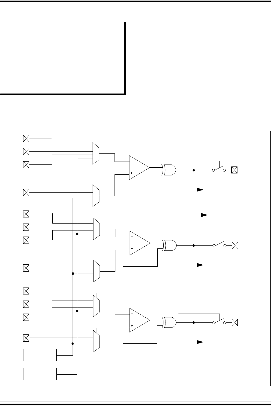
2011-2018 Microchip Technology Inc. DS60001168K-page 221
PIC32MX1XX/2XX 28/36/44-PIN FAMILY
23.0 COMPARATOR
The Analog Comparator module contains three
comparators that can be configured in a variety of
ways.
Following are some of the key features of this module:
• Selectable inputs available include:
- Analog inputs multiplexed with I/O pins
- On-chip internal absolute voltage reference
(IV
REF
)
- Comparator voltage reference (CV
REF
)
• Outputs can be Inverted
• Selectable interrupt generation
A block diagram of the comparator module is provided
in Figure 23-1.
FIGURE 23-1: COMPARATOR BLOCK DIAGRAM
Note: This data sheet summarizes the features
of the PIC32MX1XX/2XX 28/36/44-pin
Family of devices. It is not intended to be
a comprehensive reference source. To
complement the information in this data
sheet, refer to Section 19.
“Comparator” (DS60001110), which is
available from the Documentation >
Reference Manual section of the
Microchip PIC32 web site
(www.microchip.com/pic32).
C3IND
C3INA
C3OUT
CMP3
COE
CREF
CCH<1:0>
CPOL
C3INC
C3INB
CV
REF(1)
IV
REF(2)
C2IND
C2INA
C2OUT
CMP2
COE
CREF
CCH<1:0>
CPOL
C2INC
C2INB
C1IND
C1INA
C1OUT
CMP1
COE
CREF
CCH<1:0>
CPOL
C1INC
C1INB
CMSTAT<C1OUT>
CM1CON<COUT>
CMSTAT<C2OUT>
CM2CON<COUT>
CMSTAT<C3OUT>
CM3CON<COUT>
To CTMU module
(Pulse Generator)
Note 1: Internally connected. See Section 24.0 “Comparator Voltage Reference
(CV
REF
)” for more information.
2: Internal precision voltage reference (1.2V).
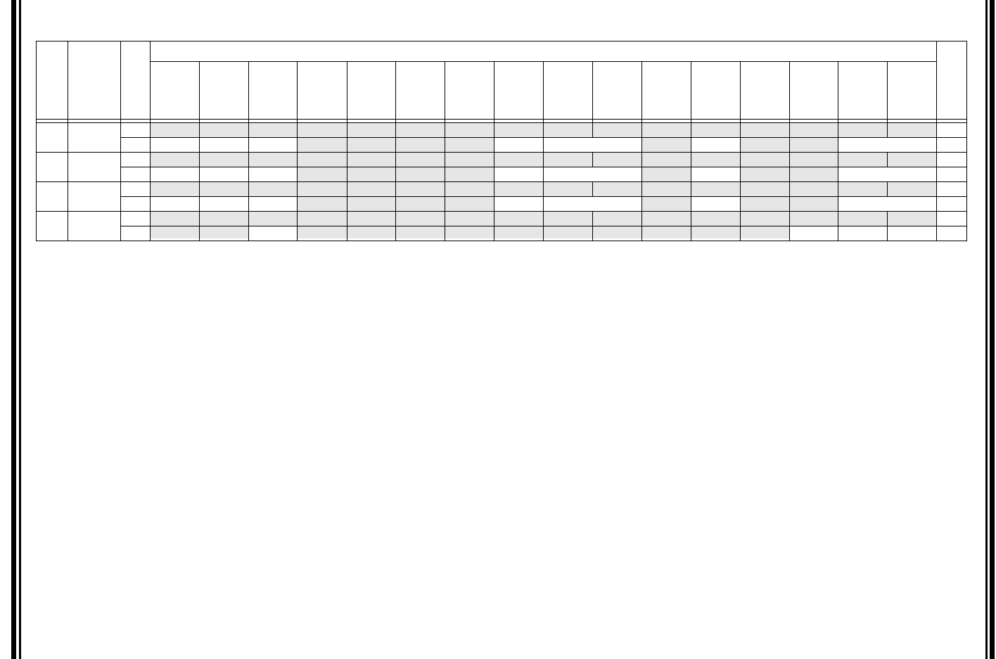
PIC32MX1XX/2XX 28/36/44-PIN FAMILY
DS60001168K-page 222 2011-2018 Microchip Technology Inc.
23.1 Comparator Control Registers
TABLE 23-1: COMPARATOR REGISTER MAP
Virtual Address
(BF80_#)
Register
Name
(1)
Bit Range
Bits
All Resets
31/15 30/14 29/13 28/12 27/11 26/10 25/9 24/8 23/7 22/6 21/5 20/4 19/3 18/2 17/1 16/0
A000 CM1CON 31:16 ————————————————0000
15:0 ON COE CPOL ———— COUT EVPOL<1:0> — CREF —— CCH<1:0> 00C3
A010 CM2CON 31:16 ————————————————0000
15:0 ON COE CPOL ———— COUT EVPOL<1:0> — CREF —— CCH<1:0> 00C3
A020 CM3CON 31:16 ————————————————0000
15:0 ON COE CPOL ———— COUT EVPOL<1:0> — CREF —— CCH<1:0> 00C3
A060 CMSTAT 31:16 ————————————————0000
15:0 ——SIDL—————————— C3OUT C2OUT C1OUT 0000
Legend: x = unknown value on Reset; — = unimplemented, read as ‘0’. Reset values are shown in hexadecimal.
Note 1: All registers in this table have corresponding CLR, SET and INV registers at their virtual addresses, plus offsets of 0x4, 0x8 and 0xC, respectively. See Section 11.2 “CLR, SET and INV Registers” for
more information.

2011-2018 Microchip Technology Inc. DS60001168K-page 223
PIC32MX1XX/2XX 28/36/44-PIN FAMILY
REGISTER 23-1: CMXCON: COMPARATOR CONTROL REGISTER
Bit
Range Bit
31/23/15/7 Bit
30/22/14/6 Bit
29/21/13/5 Bit
28/20/12/4 Bit
27/19/11/3 Bit
26/18/10/2 Bit
25/17/9/1 Bit
24/16/8/0
31:24
U-0 U-0 U-0 U-0 U-0 U-0 U-0 U-0
— — — — — — — —
23:16
U-0 U-0 U-0 U-0 U-0 U-0 U-0 U-0
— — — — — — — —
15:8
R/W-0 R/W-0 R/W-0 U-0 U-0 U-0 U-0 R-0
ON
(1)
COE CPOL
(2)
— — — —COUT
7:0
R/W-1 R/W-1 U-0 R/W-0 U-0 U-0 R/W-1 R/W-1
EVPOL<1:0> —CREF—— CCH<1:0>
Legend:
R = Readable bit W = Writable bit U = Unimplemented bit, read as ‘0’
-n = Value at POR ‘1’ = Bit is set ‘0’ = Bit is cleared x = Bit is unknown
bit 31-16 Unimplemented: Read as ‘0’
bit 15 ON: Comparator ON bit
(1)
1 = Module is enabled. Setting this bit does not affect the other bits in this register
0 = Module is disabled and does not consume current. Clearing this bit does not affect the other bits in this
register
bit 14 COE: Comparator Output Enable bit
1 = Comparator output is driven on the output CxOUT pin
0 = Comparator output is not driven on the output CxOUT pin
bit 13 CPOL: Comparator Output Inversion bit
(2)
1 = Output is inverted
0 = Output is not inverted
bit 12-9 Unimplemented: Read as ‘0’
bit 8 COUT: Comparator Output bit
1 = Output of the Comparator is a ‘1’
0 = Output of the Comparator is a ‘0’
bit 7-6 EVPOL<1:0>: Interrupt Event Polarity Select bits
11 = Comparator interrupt is generated on a low-to-high or high-to-low transition of the comparator output
10 = Comparator interrupt is generated on a high-to-low transition of the comparator output
01 = Comparator interrupt is generated on a low-to-high transition of the comparator output
00 = Comparator interrupt generation is disabled
bit 5 Unimplemented: Read as ‘0’
bit 4 CREF: Comparator Positive Input Configure bit
1 = Comparator non-inverting input is connected to the internal CV
REF
0 = Comparator non-inverting input is connected to the C
X
INA pin
bit 3-2 Unimplemented: Read as ‘0’
bit 1-0 CCH<1:0>: Comparator Negative Input Select bits for Comparator
11 = Comparator inverting input is connected to the IV
REF
10 = Comparator inverting input is connected to the CxIND pin
01 = Comparator inverting input is connected to the CxINC pin
00 = Comparator inverting input is connected to the CxINB pin
Note 1: When using the 1:1 PBCLK divisor, the user’s software should not read/write the peripheral’s SFRs in the
SYSCLK cycle immediately following the instruction that clears the module’s ON bit.
2: Setting this bit will invert the signal to the comparator interrupt generator as well. This will result in an
interrupt being generated on the opposite edge from the one selected by EVPOL<1:0>.

PIC32MX1XX/2XX 28/36/44-PIN FAMILY
DS60001168K-page 224 2011-2018 Microchip Technology Inc.
REGISTER 23-2: CMSTAT: COMPARATOR STATUS REGISTER
Bit
Range Bit
31/23/15/7 Bit
30/22/14/6 Bit
29/21/13/5 Bit
28/20/12/4 Bit
27/19/11/3 Bit
26/18/10/2 Bit
25/17/9/1 Bit
24/16/8/0
31:24
U-0 U-0 U-0 U-0 U-0 U-0 U-0 U-0
— — — — — — — —
23:16
U-0 U-0 U-0 U-0 U-0 U-0 U-0 U-0
— — — — — — — —
15:8
U-0 U-0 R/W-0 U-0 U-0 U-0 U-0 U-0
——SIDL— — — — —
7:0
U-0 U-0 U-0 U-0 U-0 R-0 R-0 R-0
— — — — — C3OUT C2OUT C1OUT
Legend:
R = Readable bit W = Writable bit U = Unimplemented bit, read as ‘0’
-n = Value at POR ‘1’ = Bit is set ‘0’ = Bit is cleared x = Bit is unknown
bit 31-14 Unimplemented: Read as ‘0’
bit 13 SIDL: Stop in Idle Control bit
1 = All Comparator modules are disabled when the device enters Idle mode
0 = All Comparator modules continue to operate when the device enters Idle mode
bit 12-3 Unimplemented: Read as ‘0’
bit 2 C3OUT: Comparator Output bit
1 = Output of Comparator 3 is a ‘1’
0 = Output of Comparator 3 is a ‘0’
bit 1 C2OUT: Comparator Output bit
1 = Output of Comparator 2 is a ‘1’
0 = Output of Comparator 2 is a ‘0’
bit 0 C1OUT: Comparator Output bit
1 = Output of Comparator 1 is a ‘1’
0 = Output of Comparator 1 is a ‘0’
2011-2018 Microchip Technology Inc. DS60001168K-page 225
PIC32MX1XX/2XX 28/36/44-PIN FAMILY
24.0 COMPARATOR VOLTAGE
REFERENCE (CV
REF
)
The CV
REF
module is a 16-tap, resistor ladder network
that provides a selectable reference voltage. Although
its primary purpose is to provide a reference for the
analog comparators, it also may be used independently
of them.
The resistor ladder is segmented to provide two ranges
of voltage reference values and has a power-down
function to conserve power when the reference is not
being used. The module’s supply reference can be pro-
vided from either device V
DD
/V
SS
or an external
voltage reference. The CV
REF
output is available for
the comparators and typically available for pin output.
The comparator voltage reference has the following
features:
• High and low range selection
• Sixteen output levels available for each range
• Internally connected to comparators to conserve
device pins
• Output can be connected to a pin
A block diagram of the module is shown in Figure 24-1.
FIGURE 24-1: COMPARATOR VOLTAGE REFERENCE BLOCK DIAGRAM
Note: This data sheet summarizes the features
of the PIC32MX1XX/2XX 28/36/44-pin
Family of devices. It is not intended to be
a comprehensive reference source. To
complement the information in this data
sheet, refer to Section 20. “Comparator
Voltage Reference (CV
REF
)”
(DS60001109), which is available from the
Documentation > Reference Manual
section of the Microchip PIC32 web site
(www.microchip.com/pic32).
16-to-1 MUX
CVR<3:0>
8R
R
CVREN
CVRSS = 0
AV
DD
V
REF
+CVRSS = 1
8R
CVRSS = 0
V
REF
-CVRSS = 1
R
R
R
R
R
R
16 Steps
CVRR
CV
REFOUT
AV
SS
CVRCON<CVROE>
CV
REF
CV
RSRC

PIC32MX1XX/2XX 28/36/44-PIN FAMILY
DS60001168K-page 226 2011-2018 Microchip Technology Inc.
24.1 Comparator Voltage Reference Control Register
TABLE 24-1: COMPARATOR VOLTAGE REFERENCE REGISTER MAP
Virtual Address
(BF80_#)
Register
Name
(1)
Bit Range
Bits
All Resets
31/15 30/14 29/13 28/12 27/11 26/10 25/9 24/8 23/7 22/6 21/5 20/4 19/3 18/2 17/1 16/0
9800 CVRCON 31:16 — — — — — — — — — — — — — — — — 0000
15:0 ON ———— — ——— CVROE CVRR CVRSS CVR<3:0> 0000
Legend: x = unknown value on Reset; — = unimplemented, read as ‘0’. Reset values are shown in hexadecimal.
Note 1: All registers in this table have corresponding CLR, SET and INV registers at their virtual addresses, plus offsets of 0x4, 0x8 and 0xC, respectively. See Section 11.2 “CLR, SET and INV Registers” for
more information.

2011-2018 Microchip Technology Inc. DS60001168K-page 227
PIC32MX1XX/2XX 28/36/44-PIN FAMILY
REGISTER 24-1: CVRCON: COMPARATOR VOLTAGE REFERENCE CONTROL REGISTER
Bit
Range Bit
31/23/15/7 Bit
30/22/14/6 Bit
29/21/13/5 Bit
28/20/12/4 Bit
27/19/11/3 Bit
26/18/10/2 Bit
25/17/9/1 Bit
24/16/8/0
31:24
U-0 U-0 U-0 U-0 U-0 U-0 U-0 U-0
— — — — — — — —
23:16
U-0 U-0 U-0 U-0 U-0 U-0 U-0 U-0
— — — — — — — —
15:8
R/W-0 U-0 U-0 U-0 U-0 U-0 U-0 U-0
ON
(1)
— — — — — — —
7:0
U-0 R/W-0 R/W-0 R/W-0 R/W-0 R/W-0 R/W-0 R/W-0
— CVROE CVRR CVRSS CVR<3:0>
Legend:
R = Readable bit W = Writable bit U = Unimplemented bit, read as ‘0’
-n = Value at POR ‘1’ = Bit is set ‘0’ = Bit is cleared x = Bit is unknown
bit 31-16 Unimplemented: Read as ‘0’
bit 15 ON: Comparator Voltage Reference On bit
(1)
1= Module is enabled
Setting this bit does not affect other bits in the register.
0= Module is disabled and does not consume current.
Clearing this bit does not affect the other bits in the register.
bit 14-7 Unimplemented: Read as ‘0’
bit 6 CVROE: CV
REFOUT
Enable bit
1= Voltage level is output on CV
REFOUT
pin
0= Voltage level is disconnected from CV
REFOUT
pin
bit 5 CVRR: CV
REF
Range Selection bit
1= 0 to 0.67 CV
RSRC
, with CV
RSRC
/24 step size
0= 0.25 CV
RSRC
to 0.75 CV
RSRC
, with CV
RSRC
/32 step size
bit 4 CVRSS: CV
REF
Source Selection bit
1= Comparator voltage reference source, CV
RSRC
= (V
REF
+) – (V
REF
-)
0= Comparator voltage reference source, CV
RSRC
= AV
DD
– AV
SS
bit 3-0 CVR<3:0>: CV
REF
Value Selection 0 CVR<3:0> 15 bits
When CVRR = 1:
CV
REF
= (CVR<3:0>/24) (CV
RSRC
)
When CVRR = 0:
CV
REF
=1/4 (CV
RSRC
) + (CVR<3:0>/32) (CV
RSRC
)
Note 1: When using 1:1 PBCLK divisor, the user’s software should not read/write the peripheral’s SFRs in the
SYSCLK cycle immediately following the instruction that clears the module’s ON bit.

PIC32MX1XX/2XX 28/36/44-PIN FAMILY
DS60001168K-page 228 2011-2018 Microchip Technology Inc.
NOTES:
2011-2018 Microchip Technology Inc. DS60001168K-page 229
PIC32MX1XX/2XX 28/36/44-PIN FAMILY
25.0 CHARGE TIME
MEASUREMENT UNIT (CTMU)
The Charge Time Measurement Unit (CTMU) is a flex-
ible analog module that has a configurable current
source with a digital configuration circuit built around it.
The CTMU can be used for differential time measure-
ment between pulse sources and can be used for gen-
erating an asynchronous pulse. By working with other
on-chip analog modules, the CTMU can be used for
high resolution time measurement, measure capaci-
tance, measure relative changes in capacitance or
generate output pulses with a specific time delay. The
CTMU is ideal for interfacing with capacitive-based
sensors.
The CTMU module includes the following key features:
• Up to 13 channels available for capacitive or time
measurement input
• On-chip precision current source
• 16-edge input trigger sources
• Selection of edge or level-sensitive inputs
• Polarity control for each edge source
• Control of edge sequence
• Control of response to edges
• High precision time measurement
• Time delay of external or internal signal asynchro-
nous to system clock
• Integrated temperature sensing diode
• Control of current source during auto-sampling
• Four current source ranges
• Time measurement resolution of one nanosecond
A block diagram of the CTMU is shown in Figure 25-1.
FIGURE 25-1: CTMU BLOCK DIAGRAM
Note: This data sheet summarizes the features
of the PIC32MX1XX/2XX 28/36/44-pin
Family of devices. It is not intended to be
a comprehensive reference source. To
complement the information in this data
sheet, refer to Section 37. “Charge Time
Measurement Unit (CTMU)”
(DS60001167), which is available from the
Documentation > Reference Manual
section of the Microchip PIC32 web site
(www.microchip.com/pic32).
CTED1
CTED13
Current Source
Edge
Control
Logic
CTMUCON1 or CTMUCON2
Pulse
Generator
CTMUI
Comparator 2
Timer1
OC1
Current
Control
ITRIM<5:0>
IRNG<1:0>
CTMUCON
CTMU
Control
Logic
EDG1STAT
EDG2STAT
ADC
CTPLS
IC1-IC3
CMP1-CMP3
C2INB
CDelay
CTMUT
Temperature
Sensor
Current Control Selection TGEN EDG1STAT, EDG2STAT
CTMUT
0
EDG1STAT = EDG2STAT
CTMUI
0
EDG1STAT
EDG2STAT
CTMUP
1
EDG1STAT
EDG2STAT
No Connect
1
EDG1STAT = EDG2STAT
Trigger
TGEN
CTMUP
External capacitor
for pulse generation
(To ADC S&H capacitor)
(To ADC)
PBCLK
•
•
•
PIC32MX1XX/2XX 28/36/44-PIN FAMILY
DS60001168K-page 230 2011-2018 Microchip Technology Inc.
25.1 CTMU Control Registers
TABLE 25-1: CTMU REGISTER MAP
Virtual Address
(BF80_#)
Register
Name
(1)
Bit Range
Bits
All Resets
31/15 30/14 29/13 28/12 27/11 26/10 25/9 24/8 23/7 22/6 21/5 20/4 19/3 18/2 17/1 16/0
A200 CTMUCON 31:16 EDG1MOD EDG1POL EDG1SEL<3:0> EDG2STAT EDG1STAT EDG2MOD EDG2POL EDG2SEL<3:0> — — 0000
15:0 ON — CTMUSIDL TGEN EDGEN EDGSEQEN IDISSEN CTTRIG ITRIM<5:0> IRNG<1:0> 0000
Legend: x = unknown value on Reset; — = unimplemented, read as ‘0’. Reset values are shown in hexadecimal.
Note 1: All registers in this table have corresponding CLR, SET and INV registers at its virtual address, plus an offset of 0x4, 0x8 and 0xC, respectively. See Section 11.2 “CLR, SET and INV Registers” for
more information.

2011-2018 Microchip Technology Inc. DS60001168K-page 231
PIC32MX1XX/2XX 28/36/44-PIN FAMILY
REGISTER 25-1: CTMUCON: CTMU CONTROL REGISTER
Bit
Range Bit
31/23/15/7 Bit
30/22/14/6 Bit
29/21/13/5 Bit
28/20/12/4 Bit
27/19/11/3 Bit
26/18/10/2 Bit
25/17/9/1 Bit
24/16/8/0
31:24
R/W-0 R/W-0 R/W-0 R/W-0 R/W-0 R/W-0 R/W-0 R/W-0
EDG1MOD EDG1POL EDG1SEL<3:0> EDG2STAT EDG1STAT
23:16
R/W-0 R/W-0 R/W-0 R/W-0 R/W-0 R/W-0 U-0 U-0
EDG2MOD EDG2POL EDG2SEL<3:0> — —
15:8
R/W-0 U-0 R/W-0 R/W-0 R/W-0 R/W-0 R/W-0 R/W-0
ON —CTMUSIDLTGEN
(1)
EDGEN EDGSEQEN IDISSEN
(2)
CTTRIG
7:0
R/W-0 R/W-0 R/W-0 R/W-0 R/W-0 R/W-0 R/W-0 R/W-0
ITRIM<5:0> IRNG<1:0>
Legend:
R = Readable bit W = Writable bit U = Unimplemented bit, read as ‘0’
-n = Value at POR ‘1’ = Bit is set ‘0’ = Bit is cleared x = Bit is unknown
bit 31 EDG1MOD: Edge1 Edge Sampling Select bit
1 = Input is edge-sensitive
0 = Input is level-sensitive
bit 30 EDG1POL: Edge 1 Polarity Select bit
1 = Edge1 programmed for a positive edge response
0 = Edge1 programmed for a negative edge response
bit 29-26 EDG1SEL<3:0>: Edge 1 Source Select bits
1111 = C3OUT pin is selected
1110 = C2OUT pin is selected
1101 = C1OUT pin is selected
1100 = IC3 Capture Event is selected
1011 = IC2 Capture Event is selected
1010 = IC1 Capture Event is selected
1001 = CTED8 pin is selected
1000 = CTED7 pin is selected
0111 = CTED6 pin is selected
0110 = CTED5 pin is selected
0101 = CTED4 pin is selected
0100 = CTED3 pin is selected
0011 = CTED1 pin is selected
0010 = CTED2 pin is selected
0001 = OC1 Compare Event is selected
0000 = Timer1 Event is selected
bit 25 EDG2STAT: Edge2 Status bit
Indicates the status of Edge2 and can be written to control edge source
1 = Edge2 has occurred
0 = Edge2 has not occurred
Note 1: When this bit is set for Pulse Delay Generation, the EDG2SEL<3:0> bits must be set to ‘1110’ to select
C2OUT.
2: The ADC module Sample and Hold capacitor is not automatically discharged between sample/conversion
cycles. Software using the ADC as part of a capacitive measurement, must discharge the ADC capacitor
before conducting the measurement. The IDISSEN bit, when set to ‘1’, performs this function. The ADC
module must be sampling while the IDISSEN bit is active to connect the discharge sink to the capacitor
array.
3: Refer to the CTMU Current Source Specifications (Table 30-41) in Section 30.0 “Electrical
Characteristics” for current values.
4: This bit setting is not available for the CTMU temperature diode.

PIC32MX1XX/2XX 28/36/44-PIN FAMILY
DS60001168K-page 232 2011-2018 Microchip Technology Inc.
bit 24 EDG1STAT: Edge1 Status bit
Indicates the status of Edge1 and can be written to control edge source
1 = Edge1 has occurred
0 = Edge1 has not occurred
bit 23 EDG2MOD: Edge2 Edge Sampling Select bit
1 = Input is edge-sensitive
0 = Input is level-sensitive
bit 22 EDG2POL: Edge 2 Polarity Select bit
1 = Edge2 programmed for a positive edge response
0 = Edge2 programmed for a negative edge response
bit 21-18 EDG2SEL<3:0>: Edge 2 Source Select bits
1111 = C3OUT pin is selected
1110 = C2OUT pin is selected
1101 = C1OUT pin is selected
1100 = PBCLK clock is selected
1011 = IC3 Capture Event is selected
1010 = IC2 Capture Event is selected
1001 = IC1 Capture Event is selected
1000 = CTED13 pin is selected
0111 = CTED12 pin is selected
0110 = CTED11 pin is selected
0101 = CTED10 pin is selected
0100 = CTED9 pin is selected
0011 = CTED1 pin is selected
0010 = CTED2 pin is selected
0001 = OC1 Compare Event is selected
0000 = Timer1 Event is selected
bit 17-16 Unimplemented: Read as ‘0’
bit 15 ON: ON Enable bit
1 = Module is enabled
0 = Module is disabled
bit 14 Unimplemented: Read as ‘0’
bit 13 CTMUSIDL: Stop in Idle Mode bit
1 = Discontinue module operation when the device enters Idle mode
0 = Continue module operation when the device enters Idle mode
bit 12 TGEN: Time Generation Enable bit
(1)
1 = Enables edge delay generation
0 = Disables edge delay generation
bit 11 EDGEN: Edge Enable bit
1 = Edges are not blocked
0 = Edges are blocked
REGISTER 25-1: CTMUCON: CTMU CONTROL REGISTER (CONTINUED)
Note 1: When this bit is set for Pulse Delay Generation, the EDG2SEL<3:0> bits must be set to ‘1110’ to select
C2OUT.
2: The ADC module Sample and Hold capacitor is not automatically discharged between sample/conversion
cycles. Software using the ADC as part of a capacitive measurement, must discharge the ADC capacitor
before conducting the measurement. The IDISSEN bit, when set to ‘1’, performs this function. The ADC
module must be sampling while the IDISSEN bit is active to connect the discharge sink to the capacitor
array.
3: Refer to the CTMU Current Source Specifications (Table 30-41) in Section 30.0 “Electrical
Characteristics” for current values.
4: This bit setting is not available for the CTMU temperature diode.

2011-2018 Microchip Technology Inc. DS60001168K-page 233
PIC32MX1XX/2XX 28/36/44-PIN FAMILY
bit 10 EDGSEQEN: Edge Sequence Enable bit
1 = Edge1 must occur before Edge2 can occur
0 = No edge sequence is needed
bit 9 IDISSEN: Analog Current Source Control bit
(2)
1 = Analog current source output is grounded
0 = Analog current source output is not grounded
bit 8 CTTRIG: Trigger Control bit
1 = Trigger output is enabled
0 = Trigger output is disabled
bit 7-2 ITRIM<5:0>: Current Source Trim bits
011111 = Maximum positive change from nominal current
011110
•
•
•
000001 = Minimum positive change from nominal current
000000 = Nominal current output specified by IRNG<1:0>
111111 = Minimum negative change from nominal current
•
•
•
100010
100001 = Maximum negative change from nominal current
bit 1-0 IRNG<1:0>: Current Range Select bits
(3)
11 = 100 times base current
10 = 10 times base current
01 = Base current level
00 = 1000 times base current
(4)
REGISTER 25-1: CTMUCON: CTMU CONTROL REGISTER (CONTINUED)
Note 1: When this bit is set for Pulse Delay Generation, the EDG2SEL<3:0> bits must be set to ‘1110’ to select
C2OUT.
2: The ADC module Sample and Hold capacitor is not automatically discharged between sample/conversion
cycles. Software using the ADC as part of a capacitive measurement, must discharge the ADC capacitor
before conducting the measurement. The IDISSEN bit, when set to ‘1’, performs this function. The ADC
module must be sampling while the IDISSEN bit is active to connect the discharge sink to the capacitor
array.
3: Refer to the CTMU Current Source Specifications (Table 30-41) in Section 30.0 “Electrical
Characteristics” for current values.
4: This bit setting is not available for the CTMU temperature diode.

PIC32MX1XX/2XX 28/36/44-PIN FAMILY
DS60001168K-page 234 2011-2018 Microchip Technology Inc.
NOTES:

2011-2018 Microchip Technology Inc. DS60001168K-page 235
PIC32MX1XX/2XX 28/36/44-PIN FAMILY
26.0 POWER-SAVING FEATURES
This section describes power-saving features for the
PIC32MX1XX/2XX 28/36/44-pin Family. The PIC32
devices offer a total of nine methods and modes,
organized into two categories, that allow the user to
balance power consumption with device performance. In
all of the methods and modes described in this section,
power-saving is controlled by software.
26.1 Power Saving with CPU Running
When the CPU is running, power consumption can be
controlled by reducing the CPU clock frequency,
lowering the PBCLK and by individually disabling
modules. These methods are grouped into the
following categories:
• FRC Run mode: the CPU is clocked from the FRC
clock source with or without postscalers
• LPRC Run mode: the CPU is clocked from the
LPRC clock source
•S
OSC
Run mode: the CPU is clocked from the
S
OSC
clock source
In addition, the Peripheral Bus Scaling mode is available
where peripherals are clocked at the programmable
fraction of the CPU clock (SYSCLK).
26.2 CPU Halted Methods
The device supports two power-saving modes, Sleep
and Idle, both of which Halt the clock to the CPU. These
modes operate with all clock sources, as follows:
•P
OSC
Idle mode: the system clock is derived from
the P
OSC
. The system clock source continues to
operate. Peripherals continue to operate, but can
optionally be individually disabled.
• FRC Idle mode: the system clock is derived from
the FRC with or without postscalers. Peripherals
continue to operate, but can optionally be
individually disabled.
•S
OSC
Idle mode: the system clock is derived from
the S
OSC
. Peripherals continue to operate, but
can optionally be individually disabled.
• LPRC Idle mode: the system clock is derived from
the LPRC. Peripherals continue to operate, but
can optionally be individually disabled. This is the
lowest power mode for the device with a clock
running.
• Sleep mode: the CPU, the system clock source
and any peripherals that operate from the system
clock source are Halted. Some peripherals can
operate in Sleep using specific clock sources.
This is the lowest power mode for the device.
26.3 Power-Saving Operation
Peripherals and the CPU can be Halted or disabled to
further reduce power consumption.
26.3.1 SLEEP MODE
Sleep mode has the lowest power consumption of the
device power-saving operating modes. The CPU and
most peripherals are Halted. Select peripherals can
continue to operate in Sleep mode and can be used to
wake the device from Sleep. See the individual
peripheral module sections for descriptions of
behavior in Sleep.
Sleep mode includes the following characteristics:
• The CPU is halted
• The system clock source is typically shutdown.
See Section 26.3.3 “Peripheral Bus Scaling
Method” for specific information.
• There can be a wake-up delay based on the
oscillator selection
• The Fail-Safe Clock Monitor (FSCM) does not
operate during Sleep mode
• The BOR circuit remains operative during Sleep
mode
• The WDT, if enabled, is not automatically cleared
prior to entering Sleep mode
• Some peripherals can continue to operate at
limited functionality in Sleep mode. These
peripherals include I/O pins that detect a change
in the input signal, WDT, ADC, UART and
peripherals that use an external clock input or the
internal LPRC oscillator (e.g., RTCC, Timer1 and
Input Capture).
• I/O pins continue to sink or source current in the
same manner as they do when the device is not in
Sleep
• The USB module can override the disabling of the
Posc or FRC. Refer to the USB section for
specific details.
• Modules can be individually disabled by software
prior to entering Sleep in order to further reduce
consumption
Note: This data sheet summarizes the features
of the PIC32MX1XX/2XX 28/36/44-pin
Family of devices. It is not intended to be
a comprehensive reference source. To
complement the information in this data
sheet, refer to Section 10. “Power-
Saving Features” (DS60001130), which
is available from the Documentation >
Reference Manual section of the
Microchip PIC32 web site
(www.microchip.com/pic32).

PIC32MX1XX/2XX 28/36/44-PIN FAMILY
DS60001168K-page 236 2011-2018 Microchip Technology Inc.
The processor will exit, or ‘wake-up’, from Sleep on one
of the following events:
• On any interrupt from an enabled source that is
operating in Sleep. The interrupt priority must be
greater than the current CPU priority.
• On any form of device Reset
• On a WDT time-out
If the interrupt priority is lower than or equal to the
current priority, the CPU will remain Halted, but the
PBCLK will start running and the device will enter into
Idle mode.
26.3.2 IDLE MODE
In Idle mode, the CPU is Halted but the System Clock
(SYSCLK) source is still enabled. This allows peripher-
als to continue operation when the CPU is Halted.
Peripherals can be individually configured to Halt when
entering Idle by setting their respective SIDL bit.
Latency, when exiting Idle mode, is very low due to the
CPU oscillator source remaining active.
The device enters Idle mode when the SLPEN
(OSCCON<4>) bit is clear and a WAIT instruction is
executed.
The processor will wake or exit from Idle mode on the
following events:
• On any interrupt event for which the interrupt
source is enabled. The priority of the interrupt
event must be greater than the current priority of
the CPU. If the priority of the interrupt event is
lower than or equal to current priority of the CPU,
the CPU will remain Halted and the device will
remain in Idle mode.
• On any form of device Reset
• On a WDT time-out interrupt
26.3.3 PERIPHERAL BUS SCALING
METHOD
Most of the peripherals on the device are clocked using
the PBCLK. The Peripheral Bus can be scaled relative to
the SYSCLK to minimize the dynamic power consumed
by the peripherals. The PBCLK divisor is controlled by
PBDIV<1:0> (OSCCON<20:19>), allowing SYSCLK to
PBCLK ratios of 1:1, 1:2, 1:4 and 1:8. All peripherals
using PBCLK are affected when the divisor is changed.
Peripherals such as the USB, Interrupt Controller, DMA,
and the bus matrix are clocked directly from SYSCLK.
As a result, they are not affected by PBCLK divisor
changes.
Changing the PBCLK divisor affects:
• The CPU to peripheral access latency. The CPU
has to wait for next PBCLK edge for a read to
complete. In 1:8 mode, this results in a latency of
one to seven SYSCLKs.
• The power consumption of the peripherals. Power
consumption is directly proportional to the fre-
quency at which the peripherals are clocked. The
greater the divisor, the lower the power consumed
by the peripherals.
To minimize dynamic power, the PB divisor should be
chosen to run the peripherals at the lowest frequency
that provides acceptable system performance. When
selecting a PBCLK divider, peripheral clock require-
ments, such as baud rate accuracy, should be taken
into account. For example, the UART peripheral may
not be able to achieve all baud rate values at some
PBCLK divider depending on the SYSCLK value.
Note 1: Changing the PBCLK divider ratio
requires recalculation of peripheral tim-
ing. For example, assume the UART is
configured for 9600 baud with a PB clock
ratio of 1:1 and a P
OSC
of 8 MHz. When
the PB clock divisor of 1:2 is used, the
input frequency to the baud clock is cut in
half; therefore, the baud rate is reduced
to 1/2 its former value. Due to numeric
truncation in calculations (such as the
baud rate divisor), the actual baud rate
may be a tiny percentage different than
expected. For this reason, any timing cal-
culation required for a peripheral should
be performed with the new PB clock fre-
quency instead of scaling the previous
value based on a change in the PB divisor
ratio.
2: Oscillator start-up and PLL lock delays
are applied when switching to a clock
source that was disabled and that uses a
crystal and/or the PLL. For example,
assume the clock source is switched from
P
OSC
to LPRC just prior to entering Sleep
in order to save power. No oscillator start-
up delay would be applied when exiting
Idle. However, when switching back to
P
OSC
, the appropriate PLL and/or
oscillator start-up/lock delays would be
applied.

2011-2018 Microchip Technology Inc. DS60001168K-page 237
PIC32MX1XX/2XX 28/36/44-PIN FAMILY
26.4 Peripheral Module Disable
The Peripheral Module Disable (PMD) registers
provide a method to disable a peripheral module by
stopping all clock sources supplied to that module.
When a peripheral is disabled using the appropriate
PMD control bit, the peripheral is in a minimum power
consumption state. The control and status registers
associated with the peripheral are also disabled, so
writes to those registers do not have effect and read
values are invalid.
To disable a peripheral, the associated PMDx bit must
be set to ‘1’. To enable a peripheral, the associated
PMDx bit must be cleared (default). See Table 26-1 for
more information.
TABLE 26-1: PERIPHERAL MODULE DISABLE BITS AND LOCATIONS
Note: Disabling a peripheral module while it’s
ON bit is set, may result in undefined
behavior. The ON bit for the associated
peripheral module must be cleared prior to
disable a module via the PMDx bits.
Peripheral
(1)
PMDx bit Name
(1)
Register Name and Bit Location
ADC1 AD1MD PMD1<0>
CTMU CTMUMD PMD1<8>
Comparator Voltage Reference CVRMD PMD1<12>
Comparator 1 CMP1MD PMD2<0>
Comparator 2 CMP2MD PMD2<1>
Comparator 3 CMP3MD PMD2<2>
Input Capture 1 IC1MD PMD3<0>
Input Capture 2 IC2MD PMD3<1>
Input Capture 3 IC3MD PMD3<2>
Input Capture 4 IC4MD PMD3<3>
Input Capture 5 IC5MD PMD3<4>
Output Compare 1 OC1MD PMD3<16>
Output Compare 2 OC2MD PMD3<17>
Output Compare 3 OC3MD PMD3<18>
Output Compare 4 OC4MD PMD3<19>
Output Compare 5 OC5MD PMD3<20>
Timer1 T1MD PMD4<0>
Timer2 T2MD PMD4<1>
Timer3 T3MD PMD4<2>
Timer4 T4MD PMD4<3>
Timer5 T5MD PMD4<4>
UART1 U1MD PMD5<0>
UART2 U2MD PMD5<1>
SPI1 SPI1MD PMD5<8>
SPI2 SPI2MD PMD5<9>
I2C1 I2C1MD PMD5<16>
I2C2 I2C2MD PMD5<17>
USB
(2)
USBMD PMD5<24>
RTCC RTCCMD PMD6<0>
Reference Clock Output REFOMD PMD6<1>
PMP PMPMD PMD6<16>
Note 1: Not all modules and associated PMDx bits are available on all devices. See TABLE 1: “PIC32MX1XX
28/36/44-Pin General Purpose Family Features” and TABLE 2: “PIC32MX2XX 28/36/44-pin USB
Family Features” for the lists of available peripherals.
2: The module must not be busy after clearing the associated ON bit and prior to setting the USBMD bit.

PIC32MX1XX/2XX 28/36/44-PIN FAMILY
DS60001168K-page 238 2011-2018 Microchip Technology Inc.
26.4.1 CONTROLLING CONFIGURATION
CHANGES
Because peripherals can be disabled during run time,
some restrictions on disabling peripherals are needed
to prevent accidental configuration changes. PIC32
devices include two features to prevent alterations to
enabled or disabled peripherals:
• Control register lock sequence
• Configuration bit select lock
26.4.1.1 Control Register Lock
Under normal operation, writes to the PMDx registers
are not allowed. Attempted writes appear to execute
normally, but the contents of the registers remain
unchanged. To change these registers, they must be
unlocked in hardware. The register lock is controlled by
the Configuration bit, PMDLOCK (CFGCON<12>).
Setting PMDLOCK prevents writes to the control
registers; clearing PMDLOCK allows writes.
To set or clear PMDLOCK, an unlock sequence must
be executed. Refer to Section 6. “Oscillator”
(DS60001112) in the “PIC32 Family Reference
Manual” for details.
26.4.1.2 Configuration Bit Select Lock
As an additional level of safety, the device can be
configured to prevent more than one write session to
the PMDx registers. The Configuration bit, PMDL1WAY
(DEVCFG3<28>), blocks the PMDLOCK bit from being
cleared after it has been set once. If PMDLOCK
remains set, the register unlock procedure does not
execute, and the peripheral pin select control registers
cannot be written to. The only way to clear the bit and
re-enable PMD functionality is to perform a device
Reset.
2011-2018 Microchip Technology Inc. DS60001168K-page 239
PIC32MX1XX/2XX 28/36/44-PIN FAMILY
TABLE 26-2: PERIPHERAL MODULE DISABLE REGISTER MAP
Virtual Address
(BF80_#)
Register
Name
(1)
Bit Range
Bits
All Resets
31/15 30/14 29/13 28/12 27/11 26/10 25/9 24/8 23/7 22/6 21/5 20/4 19/3 18/2 17/1 16/0
F240 PMD1 31:16 — — — — — — — — — — — — — — — — 0000
15:0 — — —CVRMD— — —CTMUMD— — — — — — —AD1MD0000
F250 PMD2 31:16 — — — — — — — — — — — — — — — — 0000
15:0 — — — — — — — — — — — — — CMP3MD CMP2MD CMP1MD 0000
F260 PMD3 31:16 — — — — — — — — — — — OC5MD OC4MD OC3MD OC2MD OC1MD 0000
15:0 — — — — — — — — — — — IC5MD IC4MD IC3MD IC2MD IC1MD 0000
F270 PMD4 31:16 — — — — — — — — — — — — — — — — 0000
15:0 — — — — — — — — — — — T5MD T4MD T3MD T2MD T1MD 0000
F280 PMD5 31:16 — — — — — — —USB1MD— — — — — — I2C1MD I2C1MD 0000
15:0 — — — — — — SPI2MD SPI1MD — — — — — —U2MDU1MD0000
F290 PMD6 31:16 — — — — — — — — — — — — — — — PMPMD 0000
15:0 — — — — — — — — — — — — — — REFOMD RTCCMD 0000
Legend: x = unknown value on Reset; — = unimplemented, read as ‘0’. Reset values are shown in hexadecimal.
Note 1: All registers in this table have corresponding CLR, SET and INV registers at their virtual addresses, plus offsets of 0x4, 0x8 and 0xC, respectively. See Section 11.2 “CLR, SET and INV Registers” for
more information.

PIC32MX1XX/2XX 28/36/44-PIN FAMILY
DS60001168K-page 240 2011-2018 Microchip Technology Inc.
NOTES:

2011-2018 Microchip Technology Inc. DS60001168K-page 241
PIC32MX1XX/2XX 28/36/44-PIN FAMILY
27.0 SPECIAL FEATURES
PIC32MX1XX/2XX 28/36/44-pin Family devices
include the following features intended to maximize
application flexibility, reliability and minimize cost
through elimination of external components.
• Flexible device configuration
• Joint Test Action Group (JTAG) interface
• In-Circuit Serial Programming™ (ICSP™)
27.1 Configuration Bits
The Configuration bits can be programmed using the
following registers to select various device
configurations.
•DEVCFG0: Device Configuration Word 0
•DEVCFG1: Device Configuration Word 1
•DEVCFG2: Device Configuration Word 2
•DEVCFG3: Device Configuration Word 3
•CFGCON: Configuration Control Register
In addition, the DEVID register (Register 27-6)
provides device and revision information.
Note: This data sheet summarizes the features
of the PIC32MX1XX/2XX 28/36/44-pin
Family of devices. However, it is not
intended to be a comprehensive
reference source. To complement the
information in this data sheet, refer to
Section 32. “Configuration”
(DS60001124) and Section 33.
“Programming and Diagnostics”
(DS60001129), which are available from
the Documentation > Reference Manual
section of the Microchip PIC32 web site
(www.microchip.com/pic32).
PIC32MX1XX/2XX 28/36/44-PIN FAMILY
DS60001168K-page 242 2011-2018 Microchip Technology Inc.
27.2 Configuration Registers
TABLE 27-1: DEVCFG: DEVICE CONFIGURATION WORD SUMMARY
Virtual Address
(BFC0_#)
Register
Name
Bit Range
Bits
All Resets
31/15 30/14 29/13 28/12 27/11 26/10 25/9 24/8 23/7 22/6 21/5 20/4 19/3 18/2 17/1 16/0
0BF0 DEVCFG3 31:16 FVBUSONIO FUSBIDIO IOL1WAY PMDL1WAY —— — — — — — — — — — — xxxx
15:0 USERID<15:0> xxxx
0BF4 DEVCFG2 31:16 — — — — — — — — — — — — — FPLLODIV<2:0> xxxx
15:0
UPLLEN
(1)
— — — — UPLLIDIV<2:0>
(1)
— FPLLMUL<2:0> — FPLLIDIV<2:0> xxxx
0BF8 DEVCFG1 31:16 — — — — — — FWDTWINSZ<1:0> FWDTEN WINDIS — WDTPS<4:0> xxxx
15:0 FCKSM<1:0> FPBDIV<1:0> — OSCIOFNC POSCMOD<1:0> IESO — FSOSCEN ——FNOSC<2:0>xxxx
0BFC DEVCFG0 31:16 — — —CP— — —BWP— — — — —PWP<8:6>
(2)
xxxx
15:0 PWP<5:0> — — — — — ICESEL<1:0> JTAGEN DEBUG<1:0> xxxx
Legend: x = unknown value on Reset; — = unimplemented, read as ‘0’. Reset values are shown in hexadecimal.
Note 1: This bit is only available on PIC32MX2XX devices.
2: PWP<8:7> are only available on devices with 256 KB of Flash.
TABLE 27-2: DEVICE ID, REVISION, AND CONFIGURATION SUMMARY
Virtual Address
(BF80_#)
Register
Name
Bit Range
Bits
All Resets
(1)
31/15 30/14 29/13 28/12 27/11 26/10 25/9 24/8 23/7 22/6 21/5 20/4 19/3 18/2 17/1 16/0
F220 DEVID 31:16 VER<3:0> DEVID<27:16> xxxx
(1)
15:0 DEVID<15:0> xxxx
(1)
F200 CFGCON 31:16 — — — — — — — — — — — — — — — — 0000
15:0 — — IOLOCK PMDLOCK — — — — — — — —JTAGEN— — TDOEN 000B
F230 SYSKEY
(3)
31:16 SYSKEY<31:0> 0000
15:0 0000
Legend: x = unknown value on Reset; — = unimplemented, read as ‘0’. Reset values are shown in hexadecimal.
Note 1: Reset values are dependent on the device variant.

2011-2018 Microchip Technology Inc. DS60001168K-page 243
PIC32MX1XX/2XX 28/36/44-PIN FAMILY
REGISTER 27-1: DEVCFG0: DEVICE CONFIGURATION WORD 0
Bit
Range Bit
31/23/15/7 Bit
30/22/14/6 Bit
29/21/13/5 Bit
28/20/12/4 Bit
27/19/11/3 Bit
26/18/10/2 Bit
25/17/9/1 Bit
24/16/8/0
31:24
r-0 r-1 r-1 R/P r-1 r-1 r-1 R/P
— — —CP— — —BWP
23:16
r-1 r-1 r-1 r-1 r-1 R/P R/P R/P
— — — — —PWP<8:6>
(3)
15:8
R/P R/P R/P R/P R/P R/P r-1 r-1
PWP<5:0> — —
7:0
r-1 r-1 r-1 R/P R/P R/P R/P R/P
— — — ICESEL<1:0>
(2)
JTAGEN
(1)
DEBUG<1:0>
Legend: r = Reserved bit P = Programmable bit
R = Readable bit W = Writable bit U = Unimplemented bit, read as ‘0’
-n = Value at POR ‘1’ = Bit is set ‘0’ = Bit is cleared x = Bit is unknown
bit 31 Reserved: Write ‘0’
bit 30-29 Reserved: Write ‘1’
bit 28 CP: Code-Protect bit
Prevents boot and program Flash memory from being read or modified by an external programming device.
1 = Protection is disabled
0 = Protection is enabled
bit 27-25 Reserved: Write ‘1’
bit 24 BWP: Boot Flash Write-Protect bit
Prevents boot Flash memory from being modified during code execution.
1 = Boot Flash is writable
0 = Boot Flash is not writable
bit 23-19 Reserved: Write ‘1’
Note 1: This bit sets the value for the JTAGEN bit in the CFGCON register.
2: The PGEC4/PGED4 pin pair is not available on all devices. Refer to the “Pin Diagrams” section for
availability.
3: The PWP<8:7> bits are only available on devices with 256 KB Flash.

PIC32MX1XX/2XX 28/36/44-PIN FAMILY
DS60001168K-page 244 2011-2018 Microchip Technology Inc.
bit 18-10 PWP<8:0>: Program Flash Write-Protect bits
(3)
Prevents selected program Flash memory pages from being modified during code execution.
111111111 = Disabled
111111110 = Memory below 0x0400 address is write-protected
111111101 = Memory below 0x0800 address is write-protected
111111100 = Memory below 0x0C00 address is write-protected
111111011 = Memory below 0x1000 (4K) address is write-protected
111111010 = Memory below 0x1400 address is write-protected
111111001 = Memory below 0x1800 address is write-protected
111111000 = Memory below 0x1C00 address is write-protected
111110111 = Memory below 0x2000 (8K) address is write-protected
111110110 = Memory below 0x2400 address is write-protected
111110101 = Memory below 0x2800 address is write-protected
111110100 = Memory below 0x2C00 address is write-protected
111110011 = Memory below 0x3000 address is write-protected
111110010 = Memory below 0x3400 address is write-protected
111110001 = Memory below 0x3800 address is write-protected
111110000 = Memory below 0x3C00 address is write-protected
111101111 = Memory below 0x4000 (16K) address is write-protected
•
•
•
110111111 = Memory below 0x10000 (64K) address is write-protected
•
•
•
101111111 = Memory below 0x20000 (128K) address is write-protected
•
•
•
011111111 = Memory below 0x40000 (256K) address is write-protected
•
•
•
000000000 = All possible memory is write-protected
bit 9-5 Reserved: Write ‘1’
bit 4-3 ICESEL<1:0>: In-Circuit Emulator/Debugger Communication Channel Select bits
(2)
11 = PGEC1/PGED1 pair is used
10 = PGEC2/PGED2 pair is used
01 = PGEC3/PGED3 pair is used
00 = PGEC4/PGED4 pair is used
(2)
bit 2 JTAGEN: JTAG Enable bit
(1)
1 = JTAG is enabled
0 = JTAG is disabled
bit 1-0 DEBUG<1:0>: Background Debugger Enable bits (forced to ‘11’ if code-protect is enabled)
11 = Debugger is disabled
0x = Debugger is enabled
REGISTER 27-1: DEVCFG0: DEVICE CONFIGURATION WORD 0 (CONTINUED)
Note 1: This bit sets the value for the JTAGEN bit in the CFGCON register.
2: The PGEC4/PGED4 pin pair is not available on all devices. Refer to the “Pin Diagrams” section for
availability.
3: The PWP<8:7> bits are only available on devices with 256 KB Flash.

2011-2018 Microchip Technology Inc. DS60001168K-page 245
PIC32MX1XX/2XX 28/36/44-PIN FAMILY
REGISTER 27-2: DEVCFG1: DEVICE CONFIGURATION WORD 1
Bit
Range Bit
31/23/15/7 Bit
30/22/14/6 Bit
29/21/13/5 Bit
28/20/12/4 Bit
27/19/11/3 Bit
26/18/10/2 Bit
25/17/9/1 Bit
24/16/8/0
31:24
r-1 r-1 r-1 r-1 r-1 r-1 R/P R/P
— — — — — — FWDTWINSZ<1:0>
23:16
R/P R/P r-1 R/P R/P R/P R/P R/P
FWDTEN WINDIS — WDTPS<4:0>
15:8
R/P R/P R/P R/P r-1 R/P R/P R/P
FCKSM<1:0> FPBDIV<1:0> — OSCIOFNC POSCMOD<1:0>
7:0
R/P r-1 R/P r-1 r-1 R/P R/P R/P
IESO — FSOSCEN ——FNOSC<2:0>
Legend: r = Reserved bit P = Programmable bit
R = Readable bit W = Writable bit U = Unimplemented bit, read as ‘0’
-n = Value at POR ‘1’ = Bit is set ‘0’ = Bit is cleared x = Bit is unknown
bit 31-26 Reserved: Write ‘1’
bit 25-24 FWDTWINSZ<1:0>: Watchdog Timer Window Size bits
11 = Window size is 25%
10 = Window size is 37.5%
01 = Window size is 50%
00 = Window size is 75%
bit 23 FWDTEN: Watchdog Timer Enable bit
1 = Watchdog Timer is enabled and cannot be disabled by software
0 = Watchdog Timer is not enabled; it can be enabled in software
bit 22 WINDIS: Watchdog Timer Window Enable bit
1 = Watchdog Timer is in non-Window mode
0 = Watchdog Timer is in Window mode
bit 21 Reserved: Write ‘1’
bit 20-16 WDTPS<4:0>: Watchdog Timer Postscale Select bits
10100 = 1:1048576
10011 = 1:524288
10010 = 1:262144
10001 = 1:131072
10000 = 1:65536
01111 = 1:32768
01110 = 1:16384
01101 = 1:8192
01100 = 1:4096
01011 = 1:2048
01010 = 1:1024
01001 = 1:512
01000 = 1:256
00111 = 1:128
00110 = 1:64
00101 = 1:32
00100 = 1:16
00011 = 1:8
00010 = 1:4
00001 = 1:2
00000 = 1:1
All other combinations not shown result in operation = 10100
Note 1: Do not disable the P
OSC
(POSCMOD = 11) when using this oscillator source.

PIC32MX1XX/2XX 28/36/44-PIN FAMILY
DS60001168K-page 246 2011-2018 Microchip Technology Inc.
bit 15-14 FCKSM<1:0>: Clock Switching and Monitor Selection Configuration bits
1x = Clock switching is disabled, Fail-Safe Clock Monitor is disabled
01 = Clock switching is enabled, Fail-Safe Clock Monitor is disabled
00 = Clock switching is enabled, Fail-Safe Clock Monitor is enabled
bit 13-12 FPBDIV<1:0>: Peripheral Bus Clock Divisor Default Value bits
11 = PBCLK is SYSCLK divided by 8
10 = PBCLK is SYSCLK divided by 4
01 = PBCLK is SYSCLK divided by 2
00 = PBCLK is SYSCLK divided by 1
bit 11 Reserved: Write ‘1’
bit 10 OSCIOFNC: CLKO Enable Configuration bit
1 = CLKO output disabled
0 = CLKO output signal active on the OSCO pin; Primary Oscillator must be disabled or configured for the
External Clock mode (EC) for the CLKO to be active (POSCMOD<1:0> = 11 or 00)
bit 9-8 POSCMOD<1:0>: Primary Oscillator Configuration bits
11 = Primary Oscillator is disabled
10 = HS Oscillator mode is selected
01 = XT Oscillator mode is selected
00 = External Clock mode is selected
bit 7 IESO: Internal External Switchover bit
1 = Internal External Switchover mode is enabled (Two-Speed Start-up is enabled)
0 = Internal External Switchover mode is disabled (Two-Speed Start-up is disabled)
bit 6 Reserved: Write ‘1’
bit 5 FSOSCEN: Secondary Oscillator Enable bit
1 = Enable Secondary Oscillator
0 = Disable Secondary Oscillator
bit 4-3 Reserved: Write ‘1’
bit 2-0 FNOSC<2:0>: Oscillator Selection bits
111 = Fast RC Oscillator with divide-by-N (FRCDIV)
110 = FRCDIV16 Fast RC Oscillator with fixed divide-by-16 postscaler
101 = Low-Power RC Oscillator (LPRC)
100 = Secondary Oscillator (S
OSC
)
011 = Primary Oscillator (P
OSC
) with PLL module (XT+PLL, HS+PLL, EC+PLL)
010 = Primary Oscillator (XT, HS, EC)
(1)
001 = Fast RC Oscillator with divide-by-N with PLL module (FRCDIV+PLL)
000 = Fast RC Oscillator (FRC)
REGISTER 27-2: DEVCFG1: DEVICE CONFIGURATION WORD 1 (CONTINUED)
Note 1: Do not disable the P
OSC
(POSCMOD = 11) when using this oscillator source.

2011-2018 Microchip Technology Inc. DS60001168K-page 247
PIC32MX1XX/2XX 28/36/44-PIN FAMILY
REGISTER 27-3: DEVCFG2: DEVICE CONFIGURATION WORD 2
Bit
Range Bit
31/23/15/7 Bit
30/22/14/6 Bit
29/21/13/5 Bit
28/20/12/4 Bit
27/19/11/3 Bit
26/18/10/2 Bit
25/17/9/1 Bit
24/16/8/0
31:24
r-1 r-1 r-1 r-1 r-1 r-1 r-1 r-1
— — — — — — — —
23:16
r-1 r-1 r-1 r-1 r-1 R/P R/P R/P
— — — — — FPLLODIV<2:0>
15:8
R/P r-1 r-1 r-1 r-1 R/P R/P R/P
UPLLEN
(1)
— — — — UPLLIDIV<2:0>
(1)
7:0
r-1 R/P-1 R/P R/P-1 r-1 R/P R/P R/P
—FPLLMUL<2:0>— FPLLIDIV<2:0>
Legend: r = Reserved bit P = Programmable bit
R = Readable bit W = Writable bit U = Unimplemented bit, read as ‘0’
-n = Value at POR ‘1’ = Bit is set ‘0’ = Bit is cleared x = Bit is unknown
bit 31-19 Reserved: Write ‘1’
bit 18-16 FPLLODIV<2:0>: Default PLL Output Divisor bits
111 = PLL output divided by 256
110 = PLL output divided by 64
101 = PLL output divided by 32
100 = PLL output divided by 16
011 = PLL output divided by 8
010 = PLL output divided by 4
001 = PLL output divided by 2
000 = PLL output divided by 1
bit 15 UPLLEN: USB PLL Enable bit
(1)
1 = Disable and bypass USB PLL
0 = Enable USB PLL
bit 14-11 Reserved: Write ‘1’
bit 10-8 UPLLIDIV<2:0>: USB PLL Input Divider bits
(1)
111 = 12x divider
110 = 10x divider
101 = 6x divider
100 = 5x divider
011 = 4x divider
010 = 3x divider
010 = 3x divider
001 = 2x divider
000 = 1x divider
bit 7 Reserved: Write ‘1’
bit 6-4 FPLLMUL<2:0>: PLL Multiplier bits
111 = 24x multiplier
110 = 21x multiplier
101 = 20x multiplier
100 = 19x multiplier
011 = 18x multiplier
010 = 17x multiplier
001 = 16x multiplier
000 = 15x multiplier
bit 3 Reserved: Write ‘1’
Note 1: This bit is only available on PIC32MX2XX devices.

PIC32MX1XX/2XX 28/36/44-PIN FAMILY
DS60001168K-page 248 2011-2018 Microchip Technology Inc.
bit 2-0 FPLLIDIV<2:0>: PLL Input Divider bits
111 = 12x divider
110 = 10x divider
101 = 6x divider
100 = 5x divider
011 = 4x divider
010 = 3x divider
001 = 2x divider
000 = 1x divider
REGISTER 27-3: DEVCFG2: DEVICE CONFIGURATION WORD 2 (CONTINUED)
Note 1: This bit is only available on PIC32MX2XX devices.

2011-2018 Microchip Technology Inc. DS60001168K-page 249
PIC32MX1XX/2XX 28/36/44-PIN FAMILY
REGISTER 27-4: DEVCFG3: DEVICE CONFIGURATION WORD 3
Bit
Range Bit
31/23/15/7 Bit
30/22/14/6 Bit
29/21/13/5 Bit
28/20/12/4 Bit
27/19/11/3 Bit
26/18/10/2 Bit
25/17/9/1 Bit
24/16/8/0
31:24
R/P R/P R/P R/P r-1 r-1 r-1 r-1
FVBUSONIO FUSBIDIO IOL1WAY PMDL1WAY — — — —
23:16
r-1 r-1 r-1 r-1 r-1 r-1 r-1 r-1
— — — — — — — —
15:8
R/P R/P R/P R/P R/P R/P R/P R/P
USERID<15:8>
7:0
R/P R/P R/P R/P R/P R/P R/P R/P
USERID<7:0>
Legend: r = Reserved bit P = Programmable bit
R = Readable bit W = Writable bit U = Unimplemented bit, read as ‘0’
-n = Value at POR ‘1’ = Bit is set ‘0’ = Bit is cleared x = Bit is unknown
bit 31 FVBUSONIO: USB V
BUSON
Selection bit
1 = V
BUSON
pin is controlled by the USB module
0 = V
BUSON
pin is controlled by the port function
bit 30 FUSBIDIO: USB USBID Selection bit
1 = USBID pin is controlled by the USB module
0 = USBID pin is controlled by the port function
bit 29 IOL1WAY: Peripheral Pin Select Configuration bit
1 = Allow only one reconfiguration
0 = Allow multiple reconfigurations
bit 28 PMDl1WAY: Peripheral Module Disable Configuration bit
1 = Allow only one reconfiguration
0 = Allow multiple reconfigurations
bit 27-16 Reserved: Write ‘1’
bit 15-0 USERID<15:0>: User ID bits
This is a 16-bit value that is user-defined and is readable via ICSP™ and JTAG.

PIC32MX1XX/2XX 28/36/44-PIN FAMILY
DS60001168K-page 250 2011-2018 Microchip Technology Inc.
REGISTER 27-5: CFGCON: CONFIGURATION CONTROL REGISTER
Bit
Range Bit
31/23/15/7 Bit
30/22/14/6 Bit
29/21/13/5 Bit
28/20/12/4 Bit
27/19/11/3 Bit
26/18/10/2 Bit
25/17/9/1 Bit
24/16/8/0
31:24
U-0 U-0 U-0 U-0 U-0 U-0 U-0 U-0
— — — — — — — —
23:16
U-0 U-0 U-0 U-0 U-0 U-0 U-0 U-0
— — — — — — — —
15:8
U-0 U-0 R/W-0 R/W-0 U-0 U-0 U-0 U-0
—— IOLOCK
(1)
PMDLOCK
(1)
— — — —
7:0
U-0 U-0 U-0 U-0 R/W-1 U-0 U-1 R/W-1
— — — —JTAGEN——TDOEN
Legend:
R = Readable bit W = Writable bit U = Unimplemented bit, read as ‘0’
-n = Value at POR ‘1’ = Bit is set ‘0’ = Bit is cleared x = Bit is unknown
bit 31-14 Unimplemented: Read as ‘0’
bit 13 IOLOCK: Peripheral Pin Select Lock bit
(1)
1 = Peripheral Pin Select is locked. Writes to PPS registers is not allowed.
0 = Peripheral Pin Select is not locked. Writes to PPS registers is allowed.
bit 12 PMDLOCK: Peripheral Module Disable bit
(1)
1 = Peripheral module is locked. Writes to PMD registers is not allowed.
0 = Peripheral module is not locked. Writes to PMD registers is allowed.
bit 11-4 Unimplemented: Read as ‘0’
bit 3 JTAGEN: JTAG Port Enable bit
1 = Enable the JTAG port
0 = Disable the JTAG port
bit 2-1 Unimplemented: Read as ‘1’
bit 0 TDOEN: TDO Enable for 2-Wire JTAG bit
1 = 2-wire JTAG protocol uses TDO
0 = 2-wire JTAG protocol does not use TDO
Note 1: To change this bit, the unlock sequence must be performed. Refer to Section 6. “Oscillator”
(DS60001112) in the “PIC32 Family Reference Manual” for details.

2011-2018 Microchip Technology Inc. DS60001168K-page 251
PIC32MX1XX/2XX 28/36/44-PIN FAMILY
REGISTER 27-6: DEVID: DEVICE AND REVISION ID REGISTER
Bit
Range Bit
31/23/15/7 Bit
30/22/14/6 Bit
29/21/13/5 Bit
28/20/12/4 Bit
27/19/11/3 Bit
26/18/10/2 Bit
25/17/9/1 Bit
24/16/8/0
31:24
RRRRRRRR
VER<3:0>
(1)
DEVID<27:24>
(1)
23:16
RRRRRRRR
DEVID<23:16>
(1)
15:8
RRRRRRRR
DEVID<15:8>
(1)
7:0
RRRRRRRR
DEVID<7:0>
(1)
Legend:
R = Readable bit W = Writable bit U = Unimplemented bit, read as ‘0’
-n = Value at POR ‘1’ = Bit is set ‘0’ = Bit is cleared x = Bit is unknown
bit 31-28 VER<3:0>: Revision Identifier bits
(1)
bit 27-0 DEVID<27:0>: Device ID bits
(1)
Note 1: See the “PIC32 Flash Programming Specification” (DS60001145) for a list of Revision and Device ID
values.
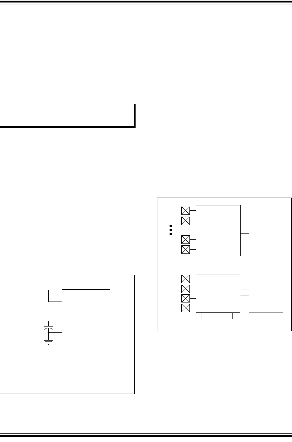
PIC32MX1XX/2XX 28/36/44-PIN FAMILY
DS60001168K-page 252 2011-2018 Microchip Technology Inc.
27.3 On-Chip Voltage Regulator
All PIC32MX1XX/2XX 28/36/44-pin Family devices’
core and digital logic are designed to operate at a nom-
inal 1.8V. To simplify system designs, most devices in
the PIC32MX1XX/2XX 28/36/44-pin Family family
incorporate an on-chip regulator providing the required
core logic voltage from V
DD
.
A low-ESR capacitor (such as tantalum) must be
connected to the V
CAP
pin (see Figure 27-1). This
helps to maintain the stability of the regulator. The
recommended value for the filter capacitor is provided
in Section 30.1 “DC Characteristics”.
27.3.1 ON-CHIP REGULATOR AND POR
It takes a fixed delay for the on-chip regulator to gener-
ate an output. During this time, designated as T
PU
,
code execution is disabled. T
PU
is applied every time
the device resumes operation after any power-down,
including Sleep mode.
27.3.2 ON-CHIP REGULATOR AND BOR
PIC32MX1XX/2XX 28/36/44-pin Family devices also
have a simple brown-out capability. If the voltage
supplied to the regulator is inadequate to maintain a
regulated level, the regulator Reset circuitry will
generate a Brown-out Reset. This event is captured by
the BOR flag bit (RCON<1>). The brown-out voltage
levels are specific in Section 30.1 “DC
Characteristics”.
FIGURE 27-1: CONNECTIONS FOR THE
ON-CHIP REGULATOR
27.4 Programming and Diagnostics
PIC32MX1XX/2XX 28/36/44-pin Family devices pro-
vide a complete range of programming and diagnostic
features that can increase the flexibility of any applica-
tion using them. These features allow system design-
ers to include:
• Simplified field programmability using two-wire
In-Circuit Serial Programming™ (ICSP™)
interfaces
• Debugging using ICSP
• Programming and debugging capabilities using
the EJTAG extension of JTAG
• JTAG boundary scan testing for device and board
diagnostics
PIC32 devices incorporate two programming and diag-
nostic modules, and a trace controller, that provide a
range of functions to the application developer.
Figure 27-2 illustrates a block diagram of the
programming, debugging, and trace ports.
FIGURE 27-2: BLOCK DIAGRAM OF
PROGRAMMING,
DEBUGGING AND TRACE
PORTS
Note: It is important that the low-ESR capacitor
is placed as close as possible to the V
CAP
pin.
V
DD
V
CAP
V
SS
PIC32
C
EFC(2,3)
3.3V
(1)
Note 1: These are typical operating voltages. Refer to
Section 30.1 “DC Characteristics”
for the full
operating ranges of V
DD
.
2:
It is important that the low-ESR capacitor is
placed as close as possible to the V
CAP
pin.
3:
The typical voltage on the V
CAP
pin is 1.8V.
(10 F typ)
TDI
TDO
TCK
TMS
JTAG
Controller
ICSP™
Controller
Core
JTAGEN DEBUG<1:0>
ICESEL
PGEC1
PGED1
PGEC4
PGED4

2011-2018 Microchip Technology Inc. DS60001168K-page 253
PIC32MX1XX/2XX 28/36/44-PIN FAMILY
28.0 INSTRUCTION SET
The PIC32MX1XX/2XX family instruction set
complies with the MIPS32
®
Release 2 instruction set
architecture. The PIC32 device family does not
support the following features:
• Core extend instructions
• Coprocessor 1 instructions
• Coprocessor 2 instructions
Note: Refer to “MIPS32
®
Architecture for
Programmers Volume II: The MIPS32
®
Instruction Set” at www.imgtec.com for
more information.

PIC32MX1XX/2XX 28/36/44-PIN FAMILY
DS60001168K-page 254 2011-2018 Microchip Technology Inc.
NOTES:

2011-2018 Microchip Technology Inc. DS60001168K-page 255
PIC32MX1XX/2XX 28/36/44-PIN FAMILY
29.0 DEVELOPMENT SUPPORT
The PIC
®
microcontrollers (MCU) and dsPIC
®
digital
signal controllers (DSC) are supported with a full range
of software and hardware development tools:
• Integrated Development Environment
- MPLAB
®
X IDE Software
• Compilers/Assemblers/Linkers
- MPLAB XC Compiler
- MPASM
TM
Assembler
-MPLINK
TM
Object Linker/
MPLIB
TM
Object Librarian
- MPLAB Assembler/Linker/Librarian for
Various Device Families
• Simulators
- MPLAB X SIM Software Simulator
•Emulators
- MPLAB REAL ICE™ In-Circuit Emulator
• In-Circuit Debuggers/Programmers
- MPLAB ICD 3
- PICkit™ 3
• Device Programmers
- MPLAB PM3 Device Programmer
• Low-Cost Demonstration/Development Boards,
Evaluation Kits and Starter Kits
• Third-party development tools
29.1 MPLAB X Integrated Development
Environment Software
The MPLAB X IDE is a single, unified graphical user
interface for Microchip and third-party software, and
hardware development tool that runs on Windows
®
,
Linux and Mac OS
®
X. Based on the NetBeans IDE,
MPLAB X IDE is an entirely new IDE with a host of free
software components and plug-ins for high-
performance application development and debugging.
Moving between tools and upgrading from software
simulators to hardware debugging and programming
tools is simple with the seamless user interface.
With complete project management, visual call graphs,
a configurable watch window and a feature-rich editor
that includes code completion and context menus,
MPLAB X IDE is flexible and friendly enough for new
users. With the ability to support multiple tools on
multiple projects with simultaneous debugging, MPLAB
X IDE is also suitable for the needs of experienced
users.
Feature-Rich Editor:
• Color syntax highlighting
• Smart code completion makes suggestions and
provides hints as you type
• Automatic code formatting based on user-defined
rules
• Live parsing
User-Friendly, Customizable Interface:
• Fully customizable interface: toolbars, toolbar
buttons, windows, window placement, etc.
• Call graph window
Project-Based Workspaces:
• Multiple projects
• Multiple tools
• Multiple configurations
• Simultaneous debugging sessions
File History and Bug Tracking:
• Local file history feature
• Built-in support for Bugzilla issue tracker

PIC32MX1XX/2XX 28/36/44-PIN FAMILY
DS60001168K-page 256 2011-2018 Microchip Technology Inc.
29.2 MPLAB XC Compilers
The MPLAB XC Compilers are complete ANSI C
compilers for all of Microchip’s 8, 16, and 32-bit MCU
and DSC devices. These compilers provide powerful
integration capabilities, superior code optimization and
ease of use. MPLAB XC Compilers run on Windows,
Linux or MAC OS X.
For easy source level debugging, the compilers provide
debug information that is optimized to the MPLAB X
IDE.
The free MPLAB XC Compiler editions support all
devices and commands, with no time or memory
restrictions, and offer sufficient code optimization for
most applications.
MPLAB XC Compilers include an assembler, linker and
utilities. The assembler generates relocatable object
files that can then be archived or linked with other relo-
catable object files and archives to create an execut-
able file. MPLAB XC Compiler uses the assembler to
produce its object file. Notable features of the assem-
bler include:
• Support for the entire device instruction set
• Support for fixed-point and floating-point data
• Command-line interface
• Rich directive set
• Flexible macro language
• MPLAB X IDE compatibility
29.3 MPASM Assembler
The MPASM Assembler is a full-featured, universal
macro assembler for PIC10/12/16/18 MCUs.
The MPASM Assembler generates relocatable object
files for the MPLINK Object Linker, Intel
®
standard HEX
files, MAP files to detail memory usage and symbol
reference, absolute LST files that contain source lines
and generated machine code, and COFF files for
debugging.
The MPASM Assembler features include:
• Integration into MPLAB X IDE projects
• User-defined macros to streamline
assembly code
• Conditional assembly for multipurpose
source files
• Directives that allow complete control over the
assembly process
29.4 MPLINK Object Linker/
MPLIB Object Librarian
The MPLINK Object Linker combines relocatable
objects created by the MPASM Assembler. It can link
relocatable objects from precompiled libraries, using
directives from a linker script.
The MPLIB Object Librarian manages the creation and
modification of library files of precompiled code. When
a routine from a library is called from a source file, only
the modules that contain that routine will be linked in
with the application. This allows large libraries to be
used efficiently in many different applications.
The object linker/library features include:
• Efficient linking of single libraries instead of many
smaller files
• Enhanced code maintainability by grouping
related modules together
• Flexible creation of libraries with easy module
listing, replacement, deletion and extraction
29.5 MPLAB Assembler, Linker and
Librarian for Various Device
Families
MPLAB Assembler produces relocatable machine
code from symbolic assembly language for PIC24,
PIC32 and dsPIC DSC devices. MPLAB XC Compiler
uses the assembler to produce its object file. The
assembler generates relocatable object files that can
then be archived or linked with other relocatable object
files and archives to create an executable file. Notable
features of the assembler include:
• Support for the entire device instruction set
• Support for fixed-point and floating-point data
• Command-line interface
• Rich directive set
• Flexible macro language
• MPLAB X IDE compatibility

2011-2018 Microchip Technology Inc. DS60001168K-page 257
PIC32MX1XX/2XX 28/36/44-PIN FAMILY
29.6 MPLAB X SIM Software Simulator
The MPLAB X SIM Software Simulator allows code
development in a PC-hosted environment by simulat-
ing the PIC MCUs and dsPIC DSCs on an instruction
level. On any given instruction, the data areas can be
examined or modified and stimuli can be applied from
a comprehensive stimulus controller. Registers can be
logged to files for further run-time analysis. The trace
buffer and logic analyzer display extend the power of
the simulator to record and track program execution,
actions on I/O, most peripherals and internal registers.
The MPLAB X SIM Software Simulator fully supports
symbolic debugging using the MPLAB XC Compilers,
and the MPASM and MPLAB Assemblers. The soft-
ware simulator offers the flexibility to develop and
debug code outside of the hardware laboratory envi-
ronment, making it an excellent, economical software
development tool.
29.7 MPLAB REAL ICE In-Circuit
Emulator System
The MPLAB REAL ICE In-Circuit Emulator System is
Microchip’s next generation high-speed emulator for
Microchip Flash DSC and MCU devices. It debugs and
programs all 8, 16 and 32-bit MCU, and DSC devices
with the easy-to-use, powerful graphical user interface of
the MPLAB X IDE.
The emulator is connected to the design engineer’s
PC using a high-speed USB 2.0 interface and is
connected to the target with either a connector
compatible with in-circuit debugger systems (RJ-11)
or with the new high-speed, noise tolerant, Low-
Voltage Differential Signal (LVDS) interconnection
(CAT5).
The emulator is field upgradable through future firmware
downloads in MPLAB X IDE. MPLAB REAL ICE offers
significant advantages over competitive emulators
including full-speed emulation, run-time variable
watches, trace analysis, complex breakpoints, logic
probes, a ruggedized probe interface and long (up to
three meters) interconnection cables.
29.8 MPLAB ICD 3 In-Circuit Debugger
System
The MPLAB ICD 3 In-Circuit Debugger System is
Microchip’s most cost-effective, high-speed hardware
debugger/programmer for Microchip Flash DSC and
MCU devices. It debugs and programs PIC Flash
microcontrollers and dsPIC DSCs with the powerful,
yet easy-to-use graphical user interface of the MPLAB
IDE.
The MPLAB ICD 3 In-Circuit Debugger probe is
connected to the design engineer’s PC using a high-
speed USB 2.0 interface and is connected to the target
with a connector compatible with the MPLAB ICD 2 or
MPLAB REAL ICE systems (RJ-11). MPLAB ICD 3
supports all MPLAB ICD 2 headers.
29.9 PICkit 3 In-Circuit Debugger/
Programmer
The MPLAB PICkit 3 allows debugging and program-
ming of PIC and dsPIC Flash microcontrollers at a most
affordable price point using the powerful graphical user
interface of the MPLAB IDE. The MPLAB PICkit 3 is
connected to the design engineer’s PC using a full-
speed USB interface and can be connected to the tar-
get via a Microchip debug (RJ-11) connector (compati-
ble with MPLAB ICD 3 and MPLAB REAL ICE). The
connector uses two device I/O pins and the Reset line
to implement in-circuit debugging and In-Circuit Serial
Programming™ (ICSP™).
29.10 MPLAB PM3 Device Programmer
The MPLAB PM3 Device Programmer is a universal,
CE compliant device programmer with programmable
voltage verification at V
DDMIN
and V
DDMAX
for
maximum reliability. It features a large LCD display
(128 x 64) for menus and error messages, and a mod-
ular, detachable socket assembly to support various
package types. The ICSP cable assembly is included
as a standard item. In Stand-Alone mode, the MPLAB
PM3 Device Programmer can read, verify and program
PIC devices without a PC connection. It can also set
code protection in this mode. The MPLAB PM3
connects to the host PC via an RS-232 or USB cable.
The MPLAB PM3 has high-speed communications and
optimized algorithms for quick programming of large
memory devices, and incorporates an MMC card for file
storage and data applications.

PIC32MX1XX/2XX 28/36/44-PIN FAMILY
DS60001168K-page 258 2011-2018 Microchip Technology Inc.
29.11 Demonstration/Development
Boards, Evaluation Kits, and
Starter Kits
A wide variety of demonstration, development and
evaluation boards for various PIC MCUs and dsPIC
DSCs allows quick application development on fully
functional systems. Most boards include prototyping
areas for adding custom circuitry and provide applica-
tion firmware and source code for examination and
modification.
The boards support a variety of features, including LEDs,
temperature sensors, switches, speakers, RS-232
interfaces, LCD displays, potentiometers and additional
EEPROM memory.
The demonstration and development boards can be
used in teaching environments, for prototyping custom
circuits and for learning about various microcontroller
applications.
In addition to the PICDEM™ and dsPICDEM™
demonstration/development board series of circuits,
Microchip has a line of evaluation kits and demonstra-
tion software for analog filter design, K
EE
L
OQ
®
security
ICs, CAN, IrDA
®
, PowerSmart battery management,
SEEVAL
®
evaluation system, Sigma-Delta ADC, flow
rate sensing, plus many more.
Also available are starter kits that contain everything
needed to experience the specified device. This usually
includes a single application and debug capability, all
on one board.
Check the Microchip web page (www.microchip.com)
for the complete list of demonstration, development
and evaluation kits.
29.12 Third-Party Development Tools
Microchip also offers a great collection of tools from
third-party vendors. These tools are carefully selected
to offer good value and unique functionality.
• Device Programmers and Gang Programmers
from companies, such as SoftLog and CCS
• Software Tools from companies, such as Gimpel
and Trace Systems
• Protocol Analyzers from companies, such as
Saleae and Total Phase
• Demonstration Boards from companies, such as
MikroElektronika, Digilent
®
and Olimex
• Embedded Ethernet Solutions from companies,
such as EZ Web Lynx, WIZnet and IPLogika
®

2011-2018 Microchip Technology Inc. DS60001168K-page 259
PIC32MX1XX/2XX 28/36/44-PIN FAMILY
30.0 ELECTRICAL CHARACTERISTICS
This section provides an overview of the PIC32MX1XX/2XX 28/36/44-pin Family electrical characteristics for
devices that operate at 40 MHz. Refer to Section 31.0 “50 MHz Electrical Characteristics” for additional
specifications for operations at higher frequency. Additional information will be provided in future revisions of this
document as it becomes available.
Absolute maximum ratings for the PIC32MX1XX/2XX 28/36/44-pin Family devices are listed below. Exposure to these
maximum rating conditions for extended periods may affect device reliability. Functional operation of the device at these
or any other conditions, above the parameters indicated in the operation listings of this specification, is not implied.
Absolute Maximum Ratings
(See Note 1)
Ambient temperature under bias.............................................................................................................-40°C to +105°C
Storage temperature .............................................................................................................................. -65°C to +150°C
Voltage on V
DD
with respect to V
SS
......................................................................................................... -0.3V to +4.0V
Voltage on any pin that is not 5V tolerant, with respect to V
SS
(Note 3)......................................... -0.3V to (V
DD
+ 0.3V)
Voltage on any 5V tolerant pin with respect to V
SS
when V
DD
2.3V (Note 3)........................................ -0.3V to +5.5V
Voltage on any 5V tolerant pin with respect to V
SS
when V
DD
< 2.3V (Note 3)........................................ -0.3V to +3.6V
Voltage on D+ or D- pin with respect to V
USB
3
V
3
.................................................................... -0.3V to (V
USB
3
V
3
+ 0.3V)
Voltage on V
BUS
with respect to V
SS
....................................................................................................... -0.3V to +5.5V
Maximum current out of V
SS
pin(s) .......................................................................................................................300 mA
Maximum current into V
DD
pin(s) (Note 2)............................................................................................................300 mA
Maximum output current sunk by any I/O pin..........................................................................................................15 mA
Maximum output current sourced by any I/O pin ....................................................................................................15 mA
Maximum current sunk by all ports .......................................................................................................................200 mA
Maximum current sourced by all ports (Note 2)....................................................................................................200 mA
Note 1: Stresses above those listed under “Absolute Maximum Ratings” may cause permanent damage to the
device. This is a stress rating only and functional operation of the device at those or any other conditions,
above those indicated in the operation listings of this specification, is not implied. Exposure to maximum
rating conditions for extended periods may affect device reliability.
2: Maximum allowable current is a function of device maximum power dissipation (see Tab le 3 0- 2 ).
3: See the “Pin Diagrams” section for the 5V tolerant pins.
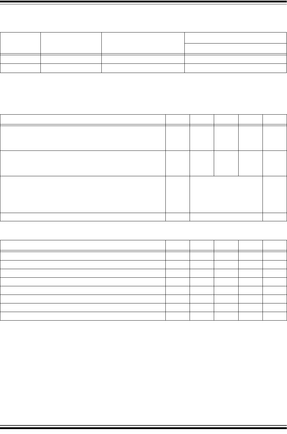
PIC32MX1XX/2XX 28/36/44-PIN FAMILY
DS60001168K-page 260 2011-2018 Microchip Technology Inc.
30.1 DC Characteristics
TABLE 30-1: OPERATING MIPS VS. VOLTAGE
Characteristic V
DD
Range
(in Volts)
(1)
Temp. Range
(in °C)
Max. Frequency
PIC32MX1XX/2XX 28/36/44-pin Family
DC5 2.3-3.6V -40°C to +85°C 40 MHz
DC5b 2.3-3.6V -40°C to +105°C 40 MHz
Note 1: Overall functional device operation at V
BORMIN
< V
DD
< V
DDMIN
is tested, but not characterized. All device
Analog modules, such as ADC, etc., will function, but with degraded performance below V
DDMIN
. Refer to
parameter BO10 in Tab l e 30 -11 for BOR values.
TABLE 30-2: THERMAL OPERATING CONDITIONS
Rating Symbol Min. Typical Max. Unit
Industrial Temperature Devices
Operating Junction Temperature Range T
J
-40 — +125 °C
Operating Ambient Temperature Range T
A
-40 — +85 °C
V-temp Temperature Devices
Operating Junction Temperature Range T
J
-40 — +140 °C
Operating Ambient Temperature Range T
A
-40 — +105 °C
Power Dissipation:
Internal Chip Power Dissipation:
P
INT
= V
DD
x (I
DD
– S I
OH
) P
D
P
INT
+ P
I
/
O
W
I/O Pin Power Dissipation:
I/O = S (({V
DD
– V
OH
} x I
OH
) + S (V
OL
x I
OL
))
Maximum Allowed Power Dissipation P
DMAX
(T
J
– T
A
)/
JA
W
TABLE 30-3: THERMAL PACKAGING CHARACTERISTICS
Characteristics Symbol Typical Max. Unit Notes
Package Thermal Resistance, 28-pin SSOP
JA
71 — °C/W 1
Package Thermal Resistance, 28-pin SOIC
JA
50 — °C/W 1
Package Thermal Resistance, 28-pin SPDIP
JA
42 — °C/W 1
Package Thermal Resistance, 28-pin QFN
JA
35 — °C/W 1
Package Thermal Resistance, 36-pin VTLA
JA
31 — °C/W 1
Package Thermal Resistance, 44-pin QFN
JA
32 — °C/W 1
Package Thermal Resistance, 44-pin TQFP
JA
45 — °C/W 1
Package Thermal Resistance, 44-pin VTLA
JA
30 — °C/W 1
Note 1: Junction to ambient thermal resistance, Theta-
JA
(
JA
) numbers are achieved by package simulations.

2011-2018 Microchip Technology Inc. DS60001168K-page 261
PIC32MX1XX/2XX 28/36/44-PIN FAMILY
TABLE 30-4: DC TEMPERATURE AND VOLTAGE SPECIFICATIONS
DC CHARACTERISTICS
Standard Operating Conditions: 2.3V to 3.6V
(unless otherwise stated)
Operating temperature -40°C T
A
+85°C for Industrial
-40°C T
A
+105°C for V-temp
Param.
No. Symbol Characteristics Min. Typ. Max. Units Conditions
Operating Voltage
DC10 V
DD
Supply Voltage (Note 2) 2.3 — 3.6 V —
DC12 V
DR
RAM Data Retention Voltage
(Note 1) 1.75 — — V —
DC16 V
POR
V
DD
Start Voltage
to Ensure Internal Power-on Reset
Signal
1.75 — 2.1 V —
DC17 S
VDD
V
DD
Rise Rate
to Ensure Internal Power-on Reset
Signal
0.00005 — 0.115 V/s—
Note 1: This is the limit to which V
DD
can be lowered without losing RAM data.
2: Overall functional device operation at V
BORMIN
< V
DD
< V
DDMIN
is tested, but not characterized. All device
Analog modules, such as ADC, etc., will function, but with degraded performance below V
DDMIN
. Refer to
parameter BO10 in Tab l e 30 -11 for BOR values.

PIC32MX1XX/2XX 28/36/44-PIN FAMILY
DS60001168K-page 262 2011-2018 Microchip Technology Inc.
TABLE 30-5: DC CHARACTERISTICS: OPERATING CURRENT (I
DD
)
DC CHARACTERISTICS
Standard Operating Conditions: 2.3V to 3.6V
(unless otherwise stated)
Operating temperature -40°C T
A
+85°C for Industrial
-40°C T
A
+105°C for V-temp
Parameter
No. Typical
(3)
Max. Units Conditions
Operating Current (I
DD
) (Notes 1, 2, 5)
DC20 2 3 mA 4 MHz (Note 4)
DC21 7 10.5 mA 10 MHz
DC221015 mA 20 MHz (Note 4)
DC231523 mA 30 MHz (Note 4)
DC242030 mA 40 MHz
DC25 100 150 µA +25ºC, 3.3V LPRC (31 kHz) (Note 4)
Note 1: A device’s I
DD
supply current is mainly a function of the operating voltage and frequency. Other factors,
such as PBCLK (Peripheral Bus Clock) frequency, number of peripheral modules enabled, internal code
execution pattern, execution from Program Flash memory vs. SRAM, I/O pin loading and switching rate,
oscillator type, as well as temperature, can have an impact on the current consumption.
2: The test conditions for I
DD
measurements are as follows:
• Oscillator mode is EC (for 8 MHz and below) and EC+PLL (for above 8 MHz) with OSC1 driven by
external square wave from rail-to-rail, (OSC1 input clock input over/undershoot < 100 mV required)
• OSC2/CLKO is configured as an I/O input pin
• USB PLL oscillator is disabled if the USB module is implemented, PBCLK divisor = 1:8
• CPU, Program Flash, and SRAM data memory are operational, SRAM data memory Wait states = 1
• No peripheral modules are operating, (ON bit = 0), but the associated PMD bit is cleared
• WDT, Clock Switching, Fail-Safe Clock Monitor, and Secondary Oscillator are disabled
• All I/O pins are configured as inputs and pulled to V
SS
•MCLR
= V
DD
• CPU executing while(1) statement from Flash
• RTCC and JTAG are disabled
3: Data in “Typical” column is at 3.3V, 25°C at specified operating frequency unless otherwise stated.
Parameters are for design guidance only and are not tested.
4: This parameter is characterized, but not tested in manufacturing.
5: I
PD
electrical characteristics for devices with 256 KB Flash are only provided as Preliminary information.

2011-2018 Microchip Technology Inc. DS60001168K-page 263
PIC32MX1XX/2XX 28/36/44-PIN FAMILY
TABLE 30-6: DC CHARACTERISTICS: IDLE CURRENT (I
IDLE
)
DC CHARACTERISTICS
Standard Operating Conditions: 2.3V to 3.6V
(unless otherwise stated)
Operating temperature -40°C T
A
+85°C for Industrial
-40°C T
A
+105°C for V-temp
Parameter
No. Typical
(2)
Max. Units Conditions
Idle Current (I
IDLE
): Core Off, Clock on Base Current (Notes 1, 4)
DC30a 1 1.5 mA 4 MHz (Note 3)
DC31a 2 3 mA 10 MHz
DC32a 4 6 mA 20 MHz (Note 3)
DC33a 5.5 8 mA 30 MHz (Note 3)
DC34a 7.5 11 mA 40 MHz
DC37a 100 — µA -40°C
3.3V
LPRC (31 kHz)
(Note 3)
DC37b 250 — µA +25°C
DC37c 380 — µA +85°C
Note 1: The test conditions for I
IDLE
current measurements are as follows:
• Oscillator mode is EC (for 8 MHz and below) and EC+PLL (for above 8 MHz) with OSC1 driven by
external square wave from rail-to-rail, (OSC1 input clock input over/undershoot < 100 mV required)
• OSC2/CLKO is configured as an I/O input pin
• USB PLL oscillator is disabled if the USB module is implemented, PBCLK divisor = 1:8
• CPU is in Idle mode (CPU core Halted), and SRAM data memory Wait states = 1
• No peripheral modules are operating, (ON bit = 0), but the associated PMD bit is cleared
• WDT, Clock Switching, Fail-Safe Clock Monitor, and Secondary Oscillator are disabled
• All I/O pins are configured as inputs and pulled to V
SS
•MCLR = V
DD
• RTCC and JTAG are disabled
2: Data in the “Typical” column is at 3.3V, 25°C unless otherwise stated. Parameters are for design guidance
only and are not tested.
3: This parameter is characterized, but not tested in manufacturing.
4: I
IDLE
electrical characteristics for devices with 256 KB Flash are only provided as Preliminary information.

PIC32MX1XX/2XX 28/36/44-PIN FAMILY
DS60001168K-page 264 2011-2018 Microchip Technology Inc.
TABLE 30-7: DC CHARACTERISTICS: POWER-DOWN CURRENT (I
PD
)
DC CHARACTERISTICS Standard Operating Conditions: 2.3V to 3.6V (unless otherwise stated)
Operating temperature -40°C T
A
+85°C for Industrial
-40°C T
A
+105°C for V-temp
Param.
No. Typical
(2)
Max. Units Conditions
Power-Down Current (I
PD
) (Notes 1, 5)
DC40k 44 70 A-40°C
Base Power-Down Current
DC40l 44 70 A +25°C
DC40n 168 259 A +85°C
DC40m 335 536 µA +105ºC
Module Differential Current
DC41e 5 20 A 3.6V Watchdog Timer Current: I
WDT
(Note 3)
DC42e 23 50 A 3.6V RTCC + Timer1 w/32 kHz Crystal: I
RTCC
(Note 3)
DC43d 1000 1100 A 3.6V ADC: I
ADC
(Notes 3,4)
Note 1: The test conditions for I
PD
current measurements are as follows:
• Oscillator mode is EC (for 8 MHz and below) and EC+PLL (for above 8 MHz) with OSC1 driven by
external square wave from rail-to-rail, (OSC1 input clock input over/undershoot < 100 mV required)
• OSC2/CLKO is configured as an I/O input pin
• USB PLL oscillator is disabled if the USB module is implemented, PBCLK divisor = 1:8
• CPU is in Sleep mode, and SRAM data memory Wait states = 1
• No peripheral modules are operating, (ON bit = 0), but the associated PMD bit is set
• WDT, Clock Switching, Fail-Safe Clock Monitor, and Secondary Oscillator are disabled
• All I/O pins are configured as inputs and pulled to V
SS
•MCLR = V
DD
• RTCC and JTAG are disabled
2: Data in the “Typical” column is at 3.3V, 25°C unless otherwise stated. Parameters are for design guidance
only and are not tested.
3: The current is the additional current consumed when the module is enabled. This current should be
added to the base I
PD
current.
4: Test conditions for ADC module differential current are as follows: Internal ADC RC oscillator enabled.
5: I
PD
electrical characteristics for devices with 256 KB Flash are only provided as Preliminary information.

2011-2018 Microchip Technology Inc. DS60001168K-page 265
PIC32MX1XX/2XX 28/36/44-PIN FAMILY
TABLE 30-8: DC CHARACTERISTICS: I/O PIN INPUT SPECIFICATIONS
DC CHARACTERISTICS
Standard Operating Conditions: 2.3V to 3.6V (unless otherwise
stated)
Operating temperature -40°C T
A
+85°C for Industrial
-40°C T
A
+105°C for V-temp
Param.
No. Symbol Characteristics Min. Typical
(1)
Max. Units Conditions
V
IL
Input Low Voltage
DI10 I/O Pins with PMP V
SS
—0.15V
DD
V
I/O Pins V
SS
—0.2V
DD
V
DI18 SDAx, SCLx V
SS
—0.3V
DD
V SMBus disabled
(Note 4)
DI19 SDAx, SCLx V
SS
— 0.8 V SMBus enabled
(Note 4)
V
IH
Input High Voltage
DI20 I/O Pins not 5V-tolerant
(5)
0.65 V
DD
—V
DD
V(Note 4,6)
I/O Pins 5V-tolerant with
PMP
(5)
0.25 V
DD
+ 0.8V — 5.5 V (Note 4,6)
I/O Pins 5V-tolerant
(5)
0.65 V
DD
—5.5V
DI28 SDAx, SCLx 0.65 V
DD
— 5.5 V SMBus disabled
(Note 4,6)
DI29 SDAx, SCLx 2.1 — 5.5 V SMBus enabled,
2.3V V
PIN
5.5
(Note 4,6)
DI30 I
CNPU
Change Notification
Pull-up Current ——-50AV
DD
= 3.3V, V
PIN
= V
SS
(Note 3,6)
DI31 I
CNPD
Change Notification
Pull-down Current
(4)
——-50µAV
DD
= 3.3V, V
PIN
= V
DD
I
IL
Input Leakage Current
(Note 3)
DI50 I/O Ports — — +1AV
SS
V
PIN
V
DD
,
Pin at high-impedance
DI51 Analog Input Pins — — +1AV
SS
V
PIN
V
DD
,
Pin at high-impedance
DI55 MCLR
(2)
——+1AV
SS
V
PIN
V
DD
DI56 OSC1 — — +1AV
SS
V
PIN
V
DD
,
XT and HS modes
Note 1: Data in “Typical” column is at 3.3V, 25°C unless otherwise stated. Parameters are for design guidance only
and are not tested.
2: The leakage current on the MCLR pin is strongly dependent on the applied voltage level. The specified
levels represent normal operating conditions. Higher leakage current may be measured at different input
voltages.
3: Negative current is defined as current sourced by the pin.
4: This parameter is characterized, but not tested in manufacturing.
5: See the “Pin Diagrams” section for the 5V-tolerant pins.
6: The V
IH
specifications are only in relation to externally applied inputs, and not with respect to the user-
selectable internal pull-ups. External open drain input signals utilizing the internal pull-ups of the PIC32
device are guaranteed to be recognized only as a logic “high” internally to the PIC32 device, provided that
the external load does not exceed the minimum value of I
CNPU
. For External “input” logic inputs that require
a pull-up source, to guarantee the minimum V
IH
of those components, it is recommended to use an
external pull-up resistor rather than the internal pull-ups of the PIC32 device.

PIC32MX1XX/2XX 28/36/44-PIN FAMILY
DS60001168K-page 266 2011-2018 Microchip Technology Inc.
TABLE 30-9: DC CHARACTERISTICS: I/O PIN INPUT INJECTION CURRENT SPECIFICATIONS
DC CHARACTERISTICS Standard Operating Conditions: 2.3V to 3.6V (unless otherwise stated)
Operating temperature -40°C T
A
+85°C for Industrial
-40°C T
A
+105°C for V-temp
Param.
No. Symbol Characteristics Min. Typ.
(1)
Max. Units Conditions
DI60a I
ICL
Input Low Injection
Current 0—-5
(2,5)
mA This parameter applies to all pins,
with the exception of the power
pins.
DI60b I
ICH
Input High Injection
Current 0—+5
(3,4,5)
mA This parameter applies to all pins,
with the exception of all 5V tolerant
pins, and the SOSCI, SOSCO,
OSC1, D+, and D- pins.
DI60c I
ICT
Total Input Injection
Current (sum of all I/O
and Control pins)
-20
(6)
—+20
(6)
mA Absolute instantaneous sum of all ±
input injection currents from all I/O
pins ( | I
ICL
+ | I
ICH
|) I
ICT
)
Note 1: Data in “Typical” column is at 3.3V, +25°C unless otherwise stated. Parameters are for design guidance
only and are not tested.
2: V
IL
source < (V
SS
- 0.3). Characterized but not tested.
3: V
IH
source > (V
DD
+ 0.3) for non-5V tolerant pins only.
4: Digital 5V tolerant pins do not have an internal high side diode to V
DD
, and therefore, cannot tolerate any
“positive” input injection current.
5: Injection currents > | 0 | can affect the ADC results by approximately 4 to 6 counts (i.e., V
IH
Source > (V
DD
+ 0.3) or V
IL
source < (V
SS
- 0.3)).
6: Any number and/or combination of I/O pins not excluded under I
ICL
or I
ICH
conditions are permitted pro-
vided the “absolute instantaneous” sum of the input injection currents from all pins do not exceed the spec-
ified limit. If Note 2, I
ICL
= (((Vss - 0.3) - V
IL
source) / Rs). If Note 3, I
ICH
= ((I
ICH
source - (V
DD
+ 0.3)) /
RS). RS = Resistance between input source voltage and device pin. If (V
SS
- 0.3) V
SOURCE
(V
DD
+
0.3), injection current = 0.
2011-2018 Microchip Technology Inc. DS60001168K-page 267
PIC32MX1XX/2XX 28/36/44-PIN FAMILY
TABLE 30-10: DC CHARACTERISTICS: I/O PIN OUTPUT SPECIFICATIONS
DC CHARACTERISTICS
Standard Operating Conditions: 2.3V to 3.6V
(unless otherwise stated)
Operating temperature -40°C T
A
+85°C for Industrial
-40°C T
A
+105°C for V-temp
Param. Symbol Characteristic Min. Typ. Max. Units Conditions
DO10 V
OL
Output Low Voltage
I/O Pins
——0.4VI
OL
10 mA, V
DD
= 3.3V
DO20 V
OH
Output High Voltage
I/O Pins
1.5
(1)
——
V
I
OH
-14 mA, V
DD
= 3.3V
2.0
(1)
—— I
OH
-12 mA, V
DD
= 3.3V
2.4 — — I
OH
-10 mA, V
DD
= 3.3V
3.0
(1)
—— I
OH
-7 mA, V
DD
= 3.3V
Note 1:
Parameters are characterized, but not tested.
TABLE 30-11: ELECTRICAL CHARACTERISTICS: BOR
DC CHARACTERISTICS
Standard Operating Conditions: 2.3V to 3.6V
(unless otherwise stated)
Operating temperature -40°C T
A
+85°C for Industrial
-40°C T
A
+105°C for V-temp
Param.
No. Symbol Characteristics Min.
(1)
Typical Max. Units Conditions
BO10 V
BOR
BOR Event on V
DD
transition
high-to-low
(2)
2.0 — 2.3 V —
Note 1:
Parameters are for design guidance only and are not tested in manufacturing.
2:
Overall functional device operation at V
BORMIN
< V
DD
< V
DDMIN
is tested, but not characterized. All device
Analog modules, such as ADC, etc., will function, but with degraded performance below V
DDMIN
.

PIC32MX1XX/2XX 28/36/44-PIN FAMILY
DS60001168K-page 268 2011-2018 Microchip Technology Inc.
TABLE 30-12: DC CHARACTERISTICS: PROGRAM MEMORY
DC CHARACTERISTICS
Standard Operating Conditions: 2.3V to 3.6V
(unless otherwise stated)
Operating temperature -40°C T
A
+85°C for Industrial
-40°C T
A
+105°C for V-temp
Param.
No. Symbol Characteristics Min. Typical
(1)
Max. Units Conditions
Program Flash Memory
(3)
D130 E
P
Cell Endurance 20,000 — — E/W —
D131 V
PR
V
DD
for Read 2.3 — 3.6 V —
D132 V
PEW
V
DD
for Erase or Write 2.3 — 3.6 V —
D134 T
RETD
Characteristic Retention 20 — — Year Provided no other specifications
are violated
D135 I
DDP
Supply Current during
Programming
—10 —mA —
T
WW
Word Write Cycle Time — 411 —
FRC Cycles
See
Note 4
D136 T
RW
Row Write Cycle Time — 6675 — See
Note 2,4
D137 T
PE
Page Erase Cycle Time — 20011 — See
Note 4
T
CE
Chip Erase Cycle Time — 80180 — See
Note 4
Note 1:
Data in “Typical” column is at 3.3V, 25°C unless otherwise stated.
2:
The minimum SYSCLK for row programming is 4 MHz. Care should be taken to minimize bus activities
during row programming, such as suspending any memory-to-memory DMA operations. If heavy bus
loads are expected, selecting Bus Matrix Arbitration mode 2 (rotating priority) may be necessary. The
default Arbitration mode is mode 1 (CPU has lowest priority).
3:
Refer to the “PIC32 Flash Programming Specification” (DS60001145) for operating conditions during
programming and erase cycles.
4:
This parameter depends on FRC accuracy (See Table 30-19) and FRC tuning values (See Register 8-2).

2011-2018 Microchip Technology Inc. DS60001168K-page 269
PIC32MX1XX/2XX 28/36/44-PIN FAMILY
TABLE 30-13: COMPARATOR SPECIFICATIONS
DC CHARACTERISTICS
Standard Operating Conditions (see Note 4): 2.3V to 3.6V
(unless otherwise stated)
Operating temperature -40°C T
A
+85°C for Industrial
-40°C T
A
+105°C for V-temp
Param.
No. Symbol Characteristics Min. Typical Max. Units Comments
D300 V
IOFF
Input Offset Voltage — ±7.5 ±25 mV AV
DD
= V
DD
,
AV
SS
= V
SS
D301 V
ICM
Input Common Mode Voltage 0 — V
DD
VAV
DD
= V
DD
,
AV
SS
= V
SS
(Note 2)
D302 CMRR Common Mode Rejection Ratio 55 — — dB Max V
ICM
= (V
DD
- 1)V
(Note 2)
D303A T
RESP
Large Signal Response Time — 150 400 ns AV
DD
= V
DD
, AV
SS
= V
SS
(Note 1,2)
D303B T
SRESP
Small Signal Response Time — 1 — s This is defined as an input
step of 50 mV with 15 mV
of overdrive
(Note 2)
D304 ON2
OV
Comparator Enabled to Output
Valid
——10s Comparator module is
configured before setting
the comparator ON bit
(Note 2)
D305 IV
REF
Internal Voltage Reference 1.14 1.2 1.26 V —
D312 T
SET
Internal Comparator Voltage
DRC Reference Setting time
——10µs
(Note 3)
Note 1:
Response time measured with one comparator input at (V
DD
– 1.5)/2, while the other input transitions
from V
SS
to V
DD
.
2:
These parameters are characterized but not tested.
3:
Settling time measured while CVRR = 1 and CVR<3:0> transitions from ‘0000’ to ‘1111’. This parameter is
characterized, but not tested in manufacturing.
4:
The Comparator module is functional at V
BORMIN
< V
DD
< V
DDMIN
, but with degraded performance. Unless
otherwise stated, module functionality is tested, but not characterized.

PIC32MX1XX/2XX 28/36/44-PIN FAMILY
DS60001168K-page 270 2011-2018 Microchip Technology Inc.
TABLE 30-14: COMPARATOR VOLTAGE REFERENCE SPECIFICATIONS
DC CHARACTERISTICS
Standard Operating Conditions: 2.3V to 3.6V
(unless otherwise stated)
Operating temperature -40°C T
A
+85°C for Industrial
-40°C T
A
+105°C for V-temp
Param.
No. Symbol Characteristics Min. Typ. Max. Units Comments
D312 T
SET
Internal 4-bit DAC
Comparator Reference
Settling time
— — 10 µs See
Note 1
D313 DAC
REFH
CV
REF
Input Voltage
Reference Range
AV
SS
—AV
DD
VCV
RSRC
with CVRSS = 0
V
REF
-— V
REF
+VCV
RSRC
with CVRSS = 1
D314 DV
REF
CV
REF
Programmable
Output Range
0 — 0.625 x
DAC
REFH
V 0 to 0.625 DAC
REFH
with
DAC
REFH
/24 step size
0.25 x
DAC
REFH
— 0.719 x
DAC
REFH
V0.25 x DAC
REFH
to 0.719
DAC
REFH
with
DAC
REFH
/32 step size
D315 DAC
RES
Resolution — — DAC
REFH
/24 — CVRCON<CVRR> = 1
——DAC
REFH
/32 — CVRCON<CVRR> = 0
D316 DAC
ACC
Absolute Accuracy
(2)
—— 1/4LSBDAC
REFH
/24,
CVRCON<CVRR> = 1
—— 1/2LSBDAC
REFH
/32,
CVRCON<CVRR> = 0
Note 1:
Settling time was measured while CVRR = 1 and CVR<3:0> transitions from ‘0000’ to ‘1111’. This
parameter is characterized, but is not tested in manufacturing.
2:
These parameters are characterized but not tested.
TABLE 30-15: INTERNAL VOLTAGE REGULATOR SPECIFICATIONS
DC CHARACTERISTICS
Standard Operating Conditions: 2.3V to 3.6V
(unless otherwise stated)
Operating temperature -40°C T
A
+85°C for Industrial
-40°C T
A
+105°C for V-temp
Param.
No. Symbol Characteristics Min. Typical Max. Units Comments
D321 C
EFC
External Filter Capacitor Value 8 10 — F Capacitor must be low series
resistance (1 ohm). Typical
voltage on the V
CAP
pin is
1.8V.
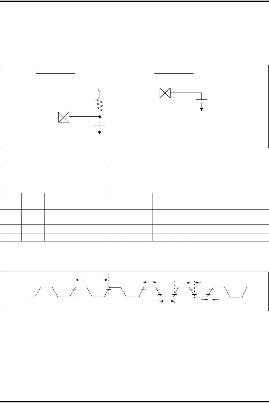
2011-2018 Microchip Technology Inc. DS60001168K-page 271
PIC32MX1XX/2XX 28/36/44-PIN FAMILY
30.2 AC Characteristics and Timing
Parameters
The information contained in this section defines
PIC32MX1XX/2XX 28/36/44-pin Family AC character-
istics and timing parameters.
FIGURE 30-1: LOAD CONDITIONS FOR DEVICE TIMING SPECIFICATIONS
FIGURE 30-2: EXTERNAL CLOCK TIMING
V
DD
/2
C
L
R
L
Pin
Pin
V
SS
V
SS
C
L
R
L
=464
C
L
= 50 pF for all pins
50 pF for OSC2 pin (EC mode)
Load Condition 1 – for all pins except OSC2 Load Condition 2 – for OSC2
TABLE 30-16: CAPACITIVE LOADING REQUIREMENTS ON OUTPUT PINS
AC CHARACTERISTICS
Standard Operating Conditions: 2.3V to 3.6V
(unless otherwise stated)
Operating temperature -40°C T
A
+85°C for Industrial
-40°C T
A
+105°C for V-temp
Param.
No. Symbol Characteristics Min. Typical
(1)
Max. Units Conditions
DO50 Cosco OSC2 Pin — — 15 pF In XT ans HS modes, when exter-
nal crystal is used to drive OSC1
DO56 C
IO
All I/O pins and OSC2 — — 50 pF EC mode
DO58 C
B
SCLx, SDAx — — 400 pF In I
2
C mode
Note 1:
Data in “Typical” column is at 3.3V, 25°C unless otherwise stated. Parameters are for design guidance only
and are not tested.
OSC1
OS20 OS30
OS30
OS31
OS31

PIC32MX1XX/2XX 28/36/44-PIN FAMILY
DS60001168K-page 272 2011-2018 Microchip Technology Inc.
TABLE 30-17: EXTERNAL CLOCK TIMING REQUIREMENTS
AC CHARACTERISTICS
Standard Operating Conditions: 2.3V to 3.6V
(unless otherwise stated)
Operating temperature -40°C T
A
+85°C for Industrial
-40°C T
A
+105°C for V-temp
Param.
No. Symbol Characteristics Min. Typical
(1)
Max. Units Conditions
OS10 F
OSC
External CLKI Frequency
(External clocks allowed only
in EC and ECPLL modes)
DC
4
—
—
40
40
MHz
MHz
EC
(Note 4)
ECPLL
(Note 3)
OS11 Oscillator Crystal Frequency 3 — 10 MHz XT
(Note 4)
OS12 4 — 10 MHz XTPLL
(Notes 3,4)
OS13 10 — 25 MHz HS
(Note 5)
OS14 10 — 25 MHz HSPLL
(Notes 3,4)
OS15 32 32.768 100 kHz S
OSC
(Note 4)
OS20 T
OSC
T
OSC
= 1/F
OSC
= T
CY
(Note 2)
— — — — See parameter
OS10 for F
OSC
value
OS30 T
OS
L,
T
OS
H
External Clock
In (OSC1)
High or Low Time
0.45 x T
OSC
——nsEC
(Note 4)
OS31 T
OS
R,
T
OS
F
External Clock
In (OSC1)
Rise or Fall Time
— — 0.05 x T
OSC
ns EC
(Note 4)
OS40 T
OST
Oscillator Start-up Timer Period
(Only applies to HS, HSPLL,
XT, XTPLL and S
OSC
Clock
Oscillator modes)
— 1024 — T
OSC
(Note 4)
OS41 T
FSCM
Primary Clock Fail Safe
Time-out Period
—2—ms
(Note 4)
OS42 G
M
External Oscillator
Transconductance (Primary
Oscillator only)
—12—mA/VV
DD
= 3.3V,
T
A
= +25°C
(Note 4)
Note 1:
Data in “Typical” column is at 3.3V, 25°C unless otherwise stated. Parameters are characterized but are not
tested.
2:
Instruction cycle period (T
CY
) equals the input oscillator time base period. All specified values are based on
characterization data for that particular oscillator type under standard operating conditions with the device
executing code. Exceeding these specified limits may result in an unstable oscillator operation and/or
higher than expected current consumption. All devices are tested to operate at “min.” values with an
external clock applied to the OSC1/CLKI pin.
3:
PLL input requirements: 4 MH
Z
F
PLLIN
5 MH
Z
(use PLL prescaler to reduce F
OSC
). This parameter is
characterized, but tested at 10 MHz only at manufacturing.
4:
This parameter is characterized, but not tested in manufacturing.
2011-2018 Microchip Technology Inc. DS60001168K-page 273
PIC32MX1XX/2XX 28/36/44-PIN FAMILY
TABLE 30-18: PLL CLOCK TIMING SPECIFICATIONS
AC CHARACTERISTICS
Standard Operating Conditions: 2.3V to 3.6V
(unless otherwise stated)
Operating temperature -40°C T
A
+85°C for Industrial
-40°C T
A
+105°C for V-temp
Param.
No. Symbol Characteristics
(1)
Min. Typical Max. Units Conditions
OS50 F
PLLI
PLL Voltage Controlled
Oscillator (VCO) Input
Frequency Range
3.92 — 5 MHz ECPLL, HSPLL, XTPLL,
FRCPLL modes
OS51 F
SYS
On-Chip VCO System
Frequency
60 — 120 MHz —
OS52 T
LOCK
PLL Start-up Time (Lock Time) — — 2 ms —
OS53 D
CLK
CLKO Stability
(2)
(Period Jitter or Cumulative)
-0.25 — +0.25 % Measured over 100 ms
period
Note 1:
These parameters are characterized, but not tested in manufacturing.
2:
This jitter specification is based on clock-cycle by clock-cycle measurements. To get the effective jitter for
individual time-bases on communication clocks, use the following formula:
For example, if SYSCLK = 40 MHz and SPI bit rate = 20 MHz, the effective jitter is as follows:
EffectiveJitter D
CLK
SYSCLK
CommunicationClock
----------------------------------------------------------
--------------------------------------------------------------
EffectiveJitter D
CLK
40
20
------
--------------D
CLK
1.41
--------------
TABLE 30-19: INTERNAL FRC ACCURACY
AC CHARACTERISTICS
Standard Operating Conditions: 2.3V to 3.6V
(unless otherwise stated)
Operating temperature -40°C T
A
+85°C for Industrial
-40°C T
A
+105°C for V-temp
Param.
No. Characteristics Min. Typical Max. Units Conditions
Internal FRC Accuracy @ 8.00 MHz
(1)
F20b FRC -0.9 — +0.9 % —
Note 1:
Frequency calibrated at 25°C and 3.3V. The TUN bits can be used to compensate for temperature drift.
TABLE 30-20: INTERNAL LPRC ACCURACY
AC CHARACTERISTICS
Standard Operating Conditions: 2.3V to 3.6V
(unless otherwise stated)
Operating temperature -40°C T
A
+85°C for Industrial
-40°C T
A
+105°C for V-temp
Param.
No. Characteristics Min. Typical Max. Units Conditions
LPRC @ 31.25 kHz
(1)
F21 LPRC -15 — +15 % —
Note 1:
Change of LPRC frequency as V
DD
changes.
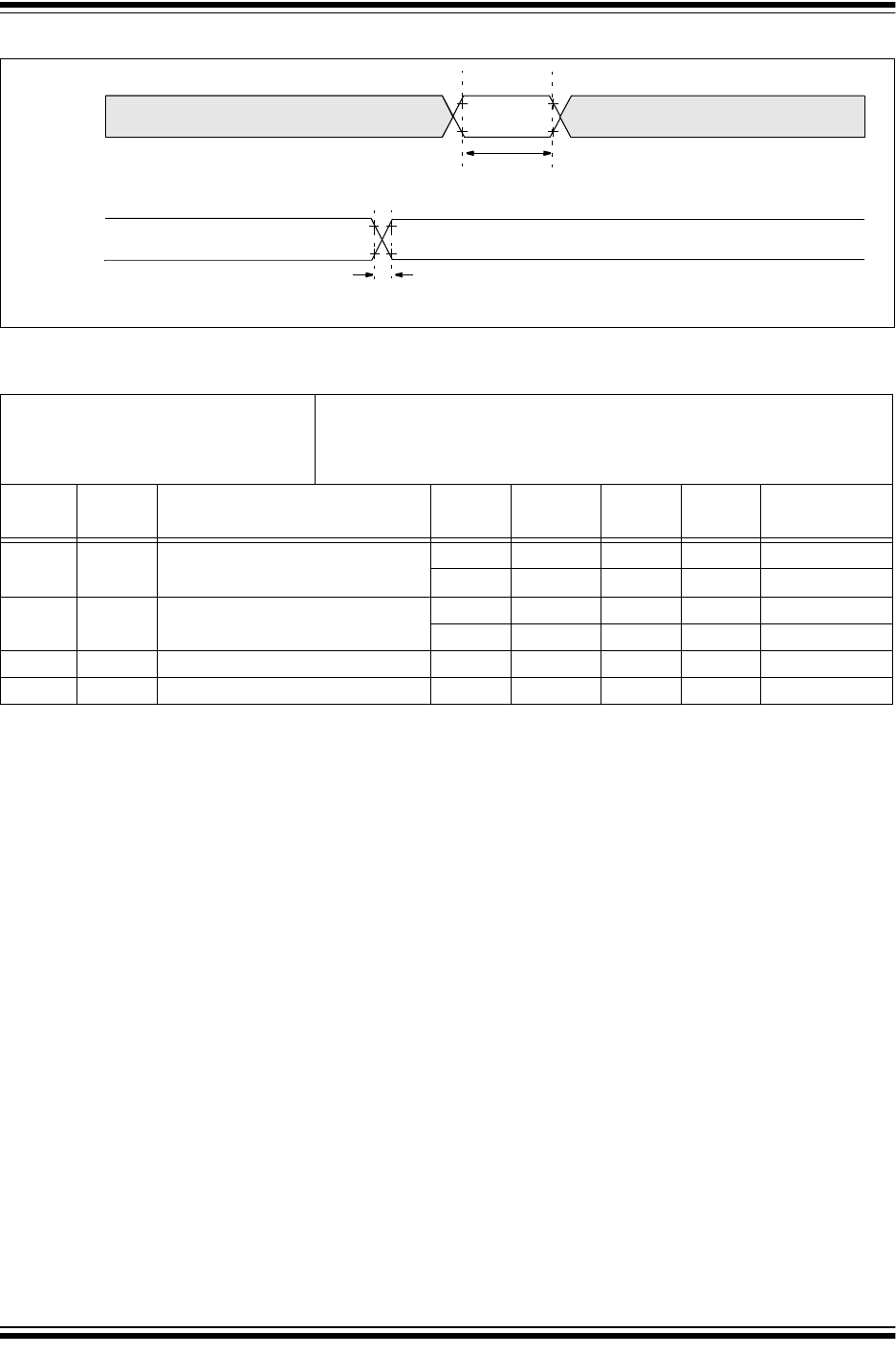
PIC32MX1XX/2XX 28/36/44-PIN FAMILY
DS60001168K-page 274 2011-2018 Microchip Technology Inc.
FIGURE 30-3: I/O TIMING CHARACTERISTICS
Note:
Refer to Figure 30-1 for load conditions.
I/O Pin
(Input)
I/O Pin
(Output)
DI35
DI40
DO31
DO32
TABLE 30-21: I/O TIMING REQUIREMENTS
AC CHARACTERISTICS
Standard Operating Conditions: 2.3V to 3.6V
(unless otherwise stated)
Operating temperature -40°C T
A
+85°C for Industrial
-40°C T
A
+105°C for V-temp
Param.
No. Symbol Characteristics
(2)
Min. Typical
(1)
Max. Units Conditions
DO31 T
IO
R Port Output Rise Time — 5 15 ns V
DD
< 2.5V
—510nsV
DD
> 2.5V
DO32 T
IO
F Port Output Fall Time — 5 15 ns V
DD
< 2.5V
—510nsV
DD
> 2.5V
DI35 T
INP
INTx Pin High or Low Time 10 — — ns —
DI40 T
RBP
CNx High or Low Time (input) 2 — — T
SYSCLK
—
Note 1:
Data in “Typical” column is at 3.3V, 25°C unless otherwise stated.
2:
This parameter is characterized, but not tested in manufacturing.
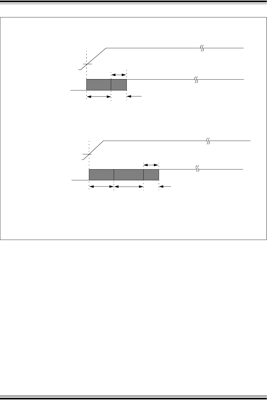
2011-2018 Microchip Technology Inc. DS60001168K-page 275
PIC32MX1XX/2XX 28/36/44-PIN FAMILY
FIGURE 30-4: POWER-ON RESET TIMING CHARACTERISTICS
V
DD
V
POR
Note 1:
The power-up period will be extended if the power-up sequence completes before the device exits from BOR
(V
DD
< V
DDMIN
).
2:
Includes interval voltage regulator stabilization delay.
SY00
Power-up Sequence
(Note 2)
Internal Voltage Regulator Enabled
(T
PU
)
SY10 CPU Starts Fetching Code
Clock Sources = (HS, HSPLL, XT, XTPLL and S
OSC
)
V
DD
V
POR
SY00
Power-up Sequence
(Note 2)
Internal Voltage Regulator Enabled
(T
PU
)
(T
SYSDLY
)
CPU Starts Fetching Code
(Note 1)
(Note 1)
Clock Sources = (FRC, FRCDIV, FRCDIV16, FRCPLL, EC, ECPLL and LPRC)
(T
OST
)
SY02
(T
SYSDLY
)
SY02
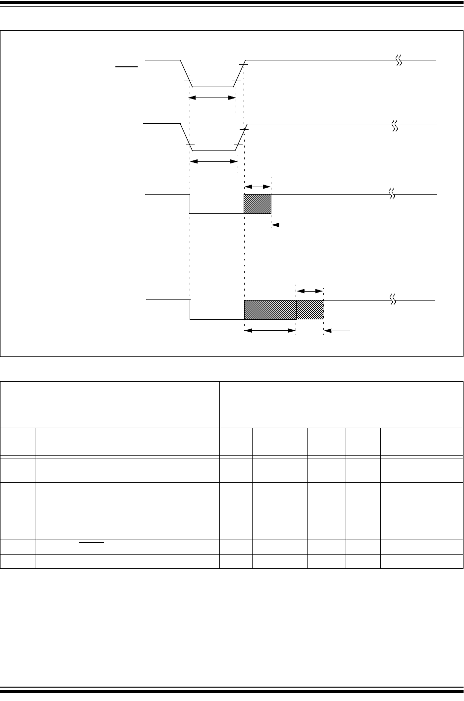
PIC32MX1XX/2XX 28/36/44-PIN FAMILY
DS60001168K-page 276 2011-2018 Microchip Technology Inc.
FIGURE 30-5: EXTERNAL RESET TIMING CHARACTERISTICS
TABLE 30-22: RESETS TIMING
AC CHARACTERISTICS
Standard Operating Conditions: 2.3V to 3.6V
(unless otherwise stated)
Operating temperature -40°C T
A
+85°C for Industrial
-40°C T
A
+105°C for V-temp
Param.
No. Symbol Characteristics
(1)
Min. Typical
(2)
Max. Units Conditions
SY00 T
PU
Power-up Period
Internal Voltage Regulator Enabled
— 400 600 s—
SY02 T
SYSDLY
System Delay Period:
Time Required to Reload Device
Configuration Fuses plus SYSCLK
Delay before First instruction is
Fetched.
—s +
8 SYSCLK
cycles
—— —
SY20 T
MCLR
MCLR Pulse Width (low) 2 — — s—
SY30 T
BOR
BOR Pulse Width (low) — 1 — s—
Note 1:
These parameters are characterized, but not tested in manufacturing.
2:
Data in “Typ” column is at 3.3V, 25°C unless otherwise stated. Characterized by design but not tested.
MCLR
(SY20)
Reset Sequence
(SY10)
CPU Starts Fetching Code
BOR
(SY30)
T
OST
T
MCLR
T
BOR
Reset Sequence
CPU Starts Fetching Code
Clock Sources = (FRC, FRCDIV, FRCDIV16, FRCPLL, EC, ECPLL and LPRC)
Clock Sources = (HS, HSPLL, XT, XTPLL and S
OSC
)
(T
SYSDLY
)
SY02
(T
SYSDLY
)
SY02
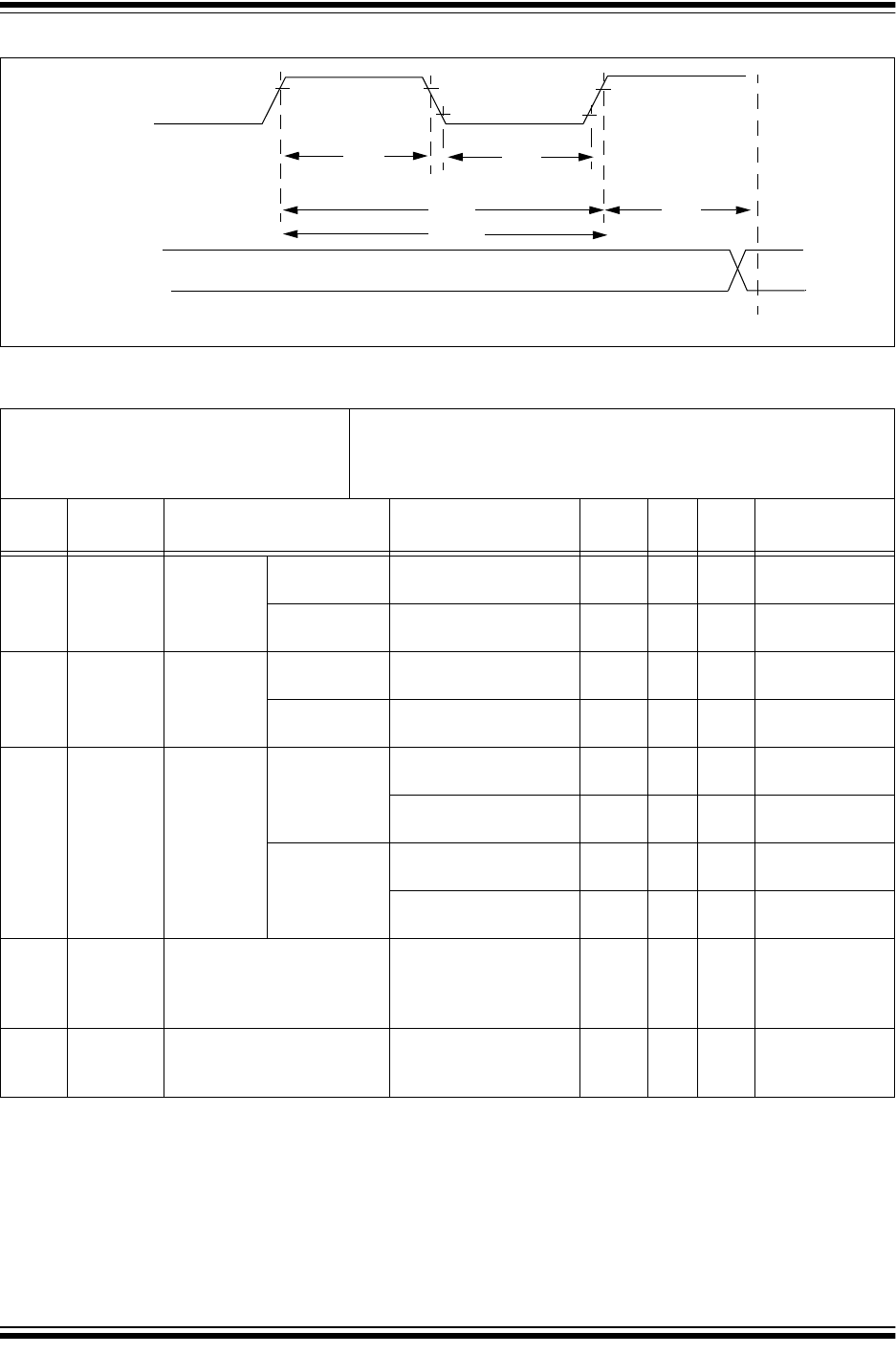
2011-2018 Microchip Technology Inc. DS60001168K-page 277
PIC32MX1XX/2XX 28/36/44-PIN FAMILY
FIGURE 30-6: TIMER1, 2, 3, 4, 5 EXTERNAL CLOCK TIMING CHARACTERISTICS
Note:
Refer to Figure 30-1 for load conditions.
Tx11
Tx15
Tx10
Tx20
TMRx
OS60
TxCK
TABLE 30-23: TIMER1 EXTERNAL CLOCK TIMING REQUIREMENTS
AC CHARACTERISTICS
(1)
Standard Operating Conditions: 2.3V to 3.6V
(unless otherwise stated)
Operating temperature -40°C T
A
+85°C for Industrial
-40°C T
A
+105°C for V-temp
Param.
No. Symbol Characteristics
(2)
Min. Typical Max. Units Conditions
TA10 T
TX
HTxCK
High Time
Synchronous,
with prescaler
[(12.5 ns or 1 T
PB
)/N]
+ 25 ns
— — ns Must also meet
parameter TA15
Asynchronous,
with prescaler
10 — — ns —
TA11 T
TX
LTxCK
Low Time
Synchronous,
with prescaler
[(12.5 ns or 1 T
PB
)/N]
+ 25 ns
— — ns Must also meet
parameter TA15
Asynchronous,
with prescaler
10 — — ns —
TA15 T
TX
PTxCK
Input Period
Synchronous,
with prescaler
[(Greater of 25 ns or
2 T
PB
)/N] + 30 ns
——nsV
DD
> 2.7V
[(Greater of 25 ns or
2 T
PB
)/N] + 50 ns
——nsV
DD
< 2.7V
Asynchronous,
with prescaler
20 — — ns V
DD
> 2.7V
(Note 3)
50 — — ns V
DD
< 2.7V
(Note 3)
OS60 F
T
1 SOSC1/T1CK Oscillator
Input Frequency Range
(oscillator enabled by setting
the TCS (T1CON<1>) bit)
32 — 100 kHz —
TA20 T
CKEXTMRL
Delay from External TxCK
Clock Edge to Timer
Increment
——1T
PB
—
Note 1:
Timer1 is a Type A timer.
2:
This parameter is characterized, but not tested in manufacturing.
3:
N = Prescale Value (1, 8, 64, 256).
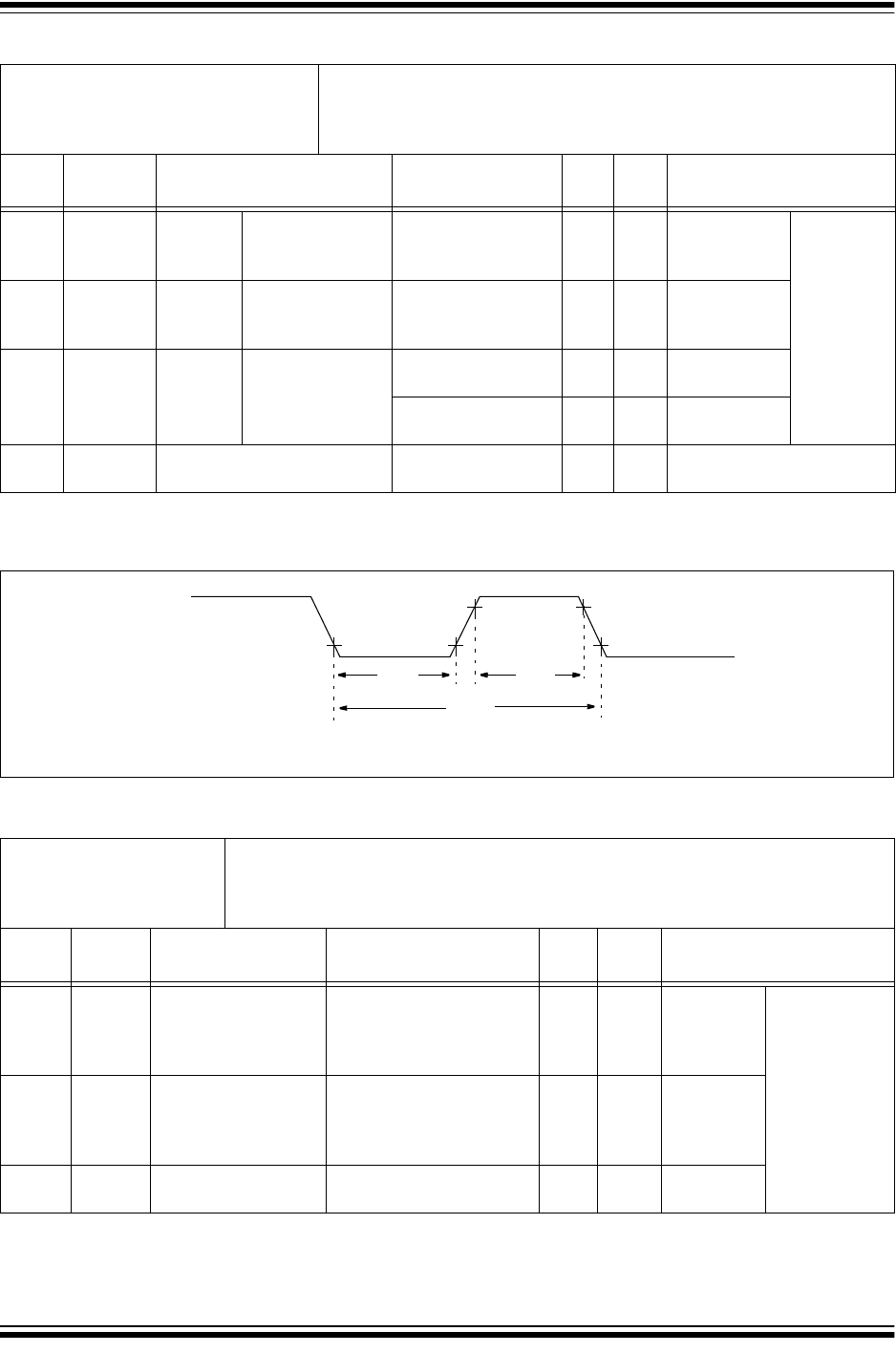
PIC32MX1XX/2XX 28/36/44-PIN FAMILY
DS60001168K-page 278 2011-2018 Microchip Technology Inc.
FIGURE 30-7: INPUT CAPTURE (CAPx) TIMING CHARACTERISTICS
TABLE 30-24: TIMER2, 3, 4, 5 EXTERNAL CLOCK TIMING REQUIREMENTS
AC CHARACTERISTICS
Standard Operating Conditions: 2.3V to 3.6V
(unless otherwise stated)
Operating temperature -40°C T
A
+85°C for Industrial
-40°C T
A
+105°C for V-temp
Param.
No. Symbol Characteristics
(1)
Min. Max. Units Conditions
TB10 T
TX
HTxCK
High Time
Synchronous, with
prescaler
[(12.5 ns or 1 T
PB
)/N]
+ 25 ns
— ns Must also meet
parameter
TB15
N = prescale
value
(1, 2, 4, 8,
16, 32, 64,
256)
TB11 T
TX
LTxCK
Low Time
Synchronous, with
prescaler
[(12.5 ns or 1 T
PB
)/N]
+ 25 ns
— ns Must also meet
parameter
TB15
TB15 T
TX
PTxCK
Input
Period
Synchronous, with
prescaler
[(Greater of [(25 ns or
2 T
PB
)/N] + 30 ns
—nsV
DD
> 2.7V
[(Greater of [(25 ns or
2 T
PB
)/N] + 50 ns
—nsV
DD
< 2.7V
TB20 T
CKEXTMRL
Delay from External TxCK
Clock Edge to Timer Increment
—1T
PB
—
Note 1:
These parameters are characterized, but not tested in manufacturing.
ICx
IC10 IC11
IC15
Note:
Refer to Figure 30-1 for load conditions.
TABLE 30-25: INPUT CAPTURE MODULE TIMING REQUIREMENTS
AC CHARACTERISTICS
Standard Operating Conditions: 2.3V to 3.6V
(unless otherwise stated)
Operating temperature -40°C T
A
+85°C for Industrial
-40°C T
A
+105°C for V-temp
Param.
No. Symbol Characteristics
(1)
Min. Max. Units Conditions
IC10 T
CC
L ICx Input Low Time [(12.5 ns or 1 T
PB
)/N]
+ 25 ns
— ns Must also
meet
parameter
IC15.
N = prescale
value (1, 4, 16)
IC11 T
CC
H ICx Input High Time [(12.5 ns or 1 T
PB
)/N]
+ 25 ns
— ns Must also
meet
parameter
IC15.
IC15 T
CC
P ICx Input Period [(25 ns or 2 T
PB
)/N]
+ 50 ns
—ns —
Note 1:
These parameters are characterized, but not tested in manufacturing.
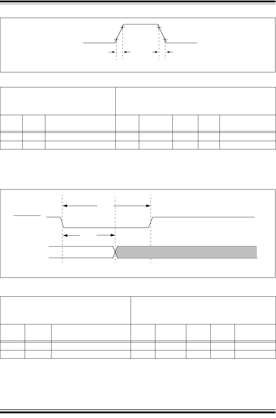
2011-2018 Microchip Technology Inc. DS60001168K-page 279
PIC32MX1XX/2XX 28/36/44-PIN FAMILY
FIGURE 30-8: OUTPUT COMPARE MODULE (OCx) TIMING CHARACTERISTICS
TABLE 30-26: OUTPUT COMPARE MODULE TIMING REQUIREMENTS
FIGURE 30-9: OCx/PWM MODULE TIMING CHARACTERISTICS
AC CHARACTERISTICS
Standard Operating Conditions: 2.3V to 3.6V
(unless otherwise stated)
Operating temperature -40°C T
A
+85°C for Industrial
-40°C T
A
+105°C for V-temp
Param.
No. Symbol Characteristics
(1)
Min. Typical
(2)
Max. Units Conditions
OC10 T
CC
F OCx Output Fall Time — — — ns See parameter DO32
OC11 T
CC
R OCx Output Rise Time — — — ns See parameter DO31
Note 1:
These parameters are characterized, but not tested in manufacturing.
2:
Data in “Typical” column is at 3.3V, 25°C unless otherwise stated. Parameters are for design guidance only
and are not tested.
OCx
OC11 OC10
(Output Compare
Note:
Refer to Figure 30-1 for load conditions.
or PWM mode)
OCFA/OCFB
OCx
OC20
OC15
Note:
Refer to Figure 30-1 for load conditions.
OCx is tri-stated
TABLE 30-27: SIMPLE OCx/PWM MODE TIMING REQUIREMENTS
AC CHARACTERISTICS
Standard Operating Conditions: 2.3V to 3.6V
(unless otherwise stated)
Operating temperature -40°C T
A
+85°C for Industrial
-40°C T
A
+105°C for V-temp
Param
No. Symbol Characteristics
(1)
Min Typical
(2)
Max Units Conditions
OC15 T
FD
Fault Input to PWM I/O Change — — 50 ns —
OC20 T
FLT
Fault Input Pulse Width 50 — — ns —
Note 1:
These parameters are characterized, but not tested in manufacturing.
2:
Data in “Typical” column is at 3.3V, 25°C unless otherwise stated. Parameters are for design guidance only
and are not tested.
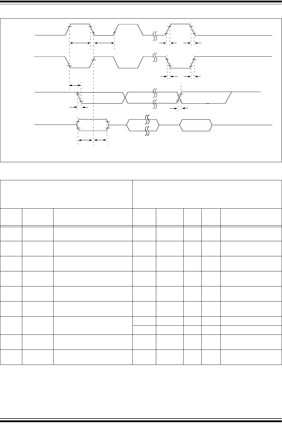
PIC32MX1XX/2XX 28/36/44-PIN FAMILY
DS60001168K-page 280 2011-2018 Microchip Technology Inc.
FIGURE 30-10: SPIx MODULE MASTER MODE (CKE = 0) TIMING CHARACTERISTICS
TABLE 30-28: SPIx MASTER MODE (CKE = 0) TIMING REQUIREMENTS
AC CHARACTERISTICS
Standard Operating Conditions: 2.3V to 3.6V
(unless otherwise stated)
Operating temperature -40°C T
A
+85°C for Industrial
-40°C T
A
+105°C for V-temp
Param.
No. Symbol Characteristics
(1)
Min. Typical
(2)
Max. Units Conditions
SP10 T
SC
LSCKx Output Low Time
(Note 3)
T
SCK
/2 — — ns —
SP11 T
SC
H SCKx Output High Time
(Note 3)
T
SCK
/2 ——ns —
SP20 T
SC
F SCKx Output Fall Time
(Note 4)
———ns
See parameter DO32
SP21 T
SC
R SCKx Output Rise Time
(Note 4)
———
ns See parameter DO31
SP30 T
DO
F SDOx Data Output Fall Time
(Note 4)
———
ns See parameter DO32
SP31 T
DO
R SDOx Data Output Rise Time
(Note 4)
———
ns See parameter DO31
SP35 T
SC
H2
DO
V,
T
SC
L2
DO
V
SDOx Data Output Valid after
SCKx Edge
——
15 ns V
DD
> 2.7V
——
20 ns V
DD
< 2.7V
SP40 T
DI
V2
SC
H,
T
DI
V2
SC
L
Setup Time of SDIx Data Input
to SCKx Edge
10 ——ns —
SP41 T
SC
H2
DI
L,
T
SC
L2
DI
L
Hold Time of SDIx Data Input
to SCKx Edge
10 ——ns —
Note 1:
These parameters are characterized, but not tested in manufacturing.
2:
Data in “Typical” column is at 3.3V, 25°C unless otherwise stated. Parameters are for design guidance
only and are not tested.
3:
The minimum clock period for SCKx is 50 ns. Therefore, the clock generated in Master mode must not
violate this specification.
4:
Assumes 50 pF load on all SPIx pins.
SCKx
(CKP = 0)
SCKx
(CKP = 1)
SDOx
SDIx
SP11 SP10
SP40 SP41
SP21
SP20
SP35
SP20
SP21
MSb LSb
Bit 14 - - - - - -1
MSb In LSb In
Bit 14 - - - -1
SP30
SP31
Note:
Refer to Figure 30-1 for load conditions.
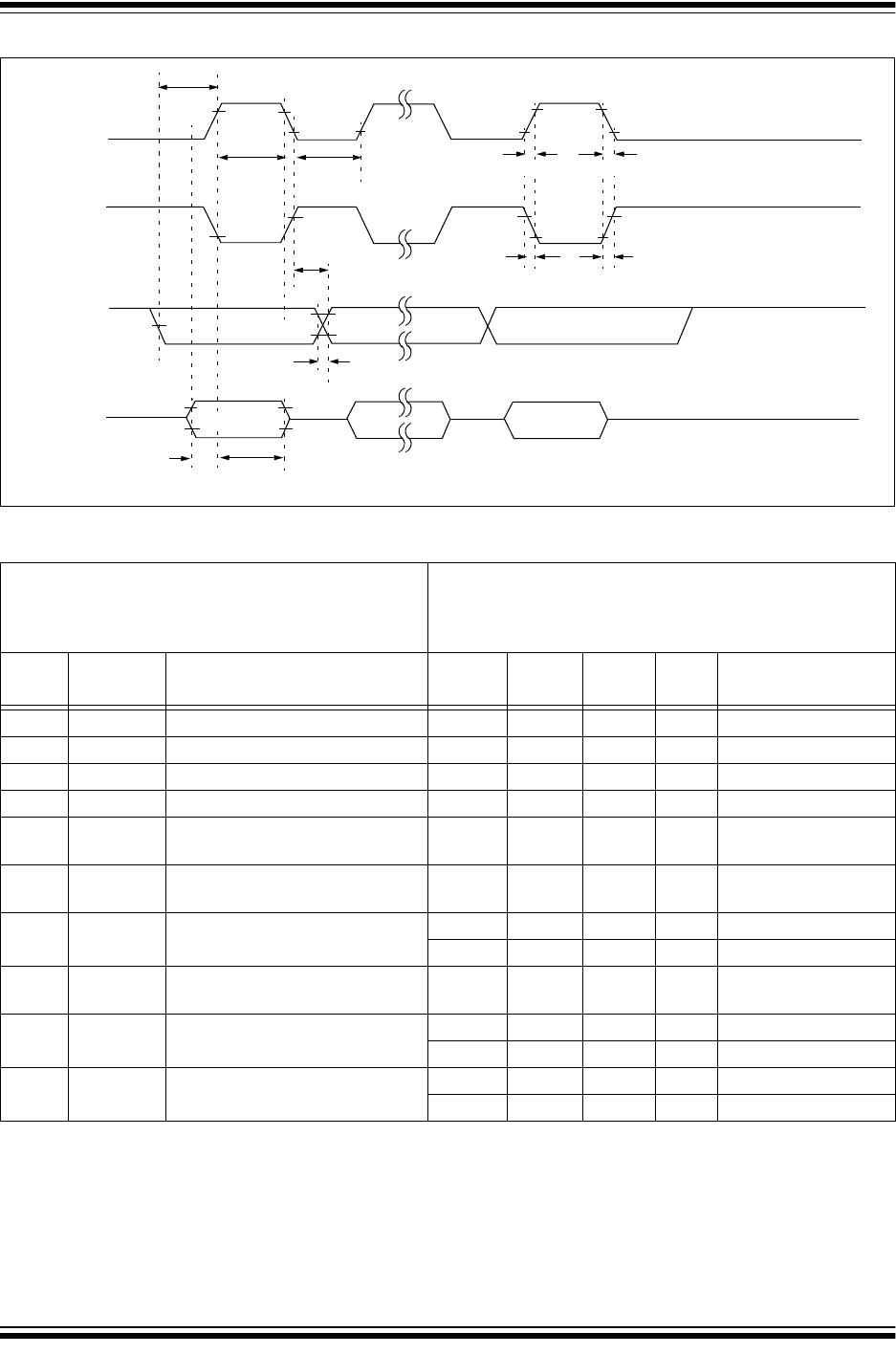
2011-2018 Microchip Technology Inc. DS60001168K-page 281
PIC32MX1XX/2XX 28/36/44-PIN FAMILY
FIGURE 30-11: SPIx MODULE MASTER MODE (CKE = 1) TIMING CHARACTERISTICS
TABLE 30-29: SPIx MODULE MASTER MODE (CKE = 1) TIMING REQUIREMENTS
AC CHARACTERISTICS
Standard Operating Conditions: 2.3V to 3.6V
(unless otherwise stated)
Operating temperature -40°C T
A
+85°C for Industrial
-40°C T
A
+105°C for V-temp
Param.
No. Symbol Characteristics
(1)
Min. Typ.
(2)
Max. Units Conditions
SP10 T
SC
L SCKx Output Low Time
(Note 3)
T
SCK
/2 — — ns —
SP11 T
SC
H SCKx Output High Time
(Note 3)
T
SCK
/2 — — ns —
SP20 T
SC
F SCKx Output Fall Time
(Note 4)
— — — ns See parameter DO32
SP21 T
SC
R SCKx Output Rise Time
(Note 4)
— — — ns See parameter DO31
SP30 T
DO
F SDOx Data Output Fall Time
(Note 4)
— — — ns See parameter DO32
SP31 T
DO
R SDOx Data Output Rise Time
(Note 4)
— — — ns See parameter DO31
SP35 T
SC
H2
DO
V,
T
SC
L2
DO
V
SDOx Data Output Valid after
SCKx Edge
——15nsV
DD
> 2.7V
——20nsV
DD
< 2.7V
SP36 T
DO
V2
SC
,
T
DO
V2
SC
L
SDOx Data Output Setup to
First SCKx Edge
15 — — ns —
SP40 T
DI
V2
SC
H,
T
DI
V2
SC
L
Setup Time of SDIx Data Input to
SCKx Edge
15 — — ns V
DD
> 2.7V
20 — — ns V
DD
< 2.7V
SP41 T
SC
H2
DI
L,
T
SC
L2
DI
L
Hold Time of SDIx Data Input
to SCKx Edge
15 — — ns V
DD
> 2.7V
20 — — ns V
DD
< 2.7V
Note 1:
These parameters are characterized, but not tested in manufacturing.
2:
Data in “Typical” column is at 3.3V, 25°C unless otherwise stated. Parameters are for design guidance only
and are not tested.
3:
The minimum clock period for SCKx is 50 ns. Therefore, the clock generated in Master mode must not
violate this specification.
4:
Assumes 50 pF load on all SPIx pins.
SCK
X
(CKP = 0)
SCK
X
(CKP = 1)
SDO
X
SDI
X
SP36
SP30,SP31
SP35
MSb Bit 14 - - - - - -1
LSb In
Bit 14 - - - -1
LSb
Note:
Refer to Figure 30-1 for load conditions.
SP11 SP10
SP21
SP20
SP40 SP41
SP20
SP21
MSb In
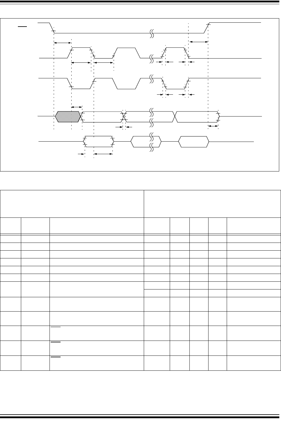
PIC32MX1XX/2XX 28/36/44-PIN FAMILY
DS60001168K-page 282 2011-2018 Microchip Technology Inc.
FIGURE 30-12: SPIx MODULE SLAVE MODE (CKE = 0) TIMING CHARACTERISTICS
SS
X
SCK
X
(CKP = 0)
SCK
X
(CKP = 1)
SDO
X
SP50
SP40 SP41
SP30,SP31 SP51
SP35
MSb LSb
Bit 14 - - - - - -1
Bit 14 - - - -1 LSb In
SP52
SP73
SP72
SP72
SP73
SP71 SP70
Note:
Refer to Figure 30-1 for load conditions.
SDI
X
MSb In
TABLE 30-30: SPIx MODULE SLAVE MODE (CKE = 0) TIMING REQUIREMENTS
AC CHARACTERISTICS
Standard Operating Conditions: 2.3V to 3.6V
(unless otherwise stated)
Operating temperature -40°C T
A
+85°C for Industrial
-40°C T
A
+105°C for V-temp
Param.
No. Symbol Characteristics
(1)
Min. Typ.
(2)
Max. Units Conditions
SP70 T
SC
L SCKx Input Low Time
(Note 3)
T
SCK
/2 — — ns —
SP71 T
SC
H SCKx Input High Time
(Note 3)
T
SCK
/2 — — ns —
SP72 T
SC
F SCKx Input Fall Time — — — ns See parameter DO32
SP73 T
SC
R SCKx Input Rise Time — — — ns See parameter DO31
SP30 T
DO
F SDOx Data Output Fall Time
(Note 4)
— — — ns See parameter DO32
SP31 T
DO
R SDOx Data Output Rise Time
(Note 4)
— — — ns See parameter DO31
SP35 T
SC
H2
DO
V,
T
SC
L2
DO
V
SDOx Data Output Valid after
SCKx Edge
— — 15 ns V
DD
> 2.7V
— — 20 ns V
DD
< 2.7V
SP40 T
DI
V2
SC
H,
T
DI
V2
SC
L
Setup Time of SDIx Data Input
to SCKx Edge
10 — — ns —
SP41 T
SC
H2
DI
L,
T
SC
L2
DI
L
Hold Time of SDIx Data Input
to SCKx Edge
10 — — ns —
SP50 T
SS
L2
SC
H,
T
SS
L2
SC
L
SSx to SCKx or SCKx Input 175 — — ns —
SP51 T
SS
H2
DO
Z SSx to SDOx Output
High-Impedance
(Note 3)
5 — 25 ns —
SP52 T
SC
H2
SS
H
T
SC
L2
SS
H
SSx after SCKx Edge T
SCK
+ 20 — — ns —
Note 1:
These parameters are characterized, but not tested in manufacturing.
2:
Data in “Typical” column is at 3.3V, 25°C unless otherwise stated. Parameters are for design guidance only
and are not tested.
3:
The minimum clock period for SCKx is 50 ns.
4:
Assumes 50 pF load on all SPIx pins.
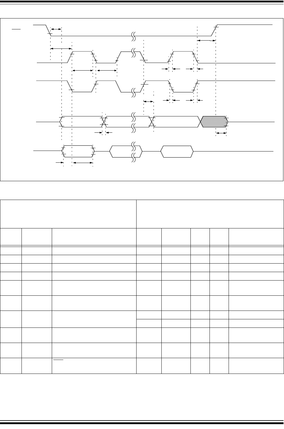
2011-2018 Microchip Technology Inc. DS60001168K-page 283
PIC32MX1XX/2XX 28/36/44-PIN FAMILY
FIGURE 30-13: SPIx MODULE SLAVE MODE (CKE = 1) TIMING CHARACTERISTICS
SSx
SCKx
(CKP = 0)
SCKx
(CKP = 1)
SDOx
SDI
SP60
SDIx
SP30,SP31
MSb Bit 14 - - - - - -1 LSb
SP51
MSb In Bit 14 - - - -1 LSb In
SP52
SP73
SP72
SP72
SP73
SP71
SP40 SP41
Note:
Refer to Figure 30-1 for load conditions.
SP50
SP70
SP35
TABLE 30-31: SPIx MODULE SLAVE MODE (CKE = 1) TIMING REQUIREMENTS
AC CHARACTERISTICS
Standard Operating Conditions: 2.3V to 3.6V
(unless otherwise stated)
Operating temperature -40°C T
A
+85°C for Industrial
-40°C T
A
+105°C for V-temp
Param.
No. Symbol Characteristics
(1)
Min. Typical
(2)
Max. Units Conditions
SP70 T
SC
L SCKx Input Low Time
(Note 3)
T
SCK
/2 — — ns —
SP71 T
SC
H SCKx Input High Time
(Note 3)
T
SCK
/2 — — ns —
SP72 T
SC
F SCKx Input Fall Time — 5 10 ns —
SP73 T
SC
R SCKx Input Rise Time — 5 10 ns —
SP30 T
DO
F SDOx Data Output Fall Time
(Note 4)
— — — ns See parameter DO32
SP31 T
DO
R SDOx Data Output Rise Time
(Note 4)
— — — ns See parameter DO31
SP35 T
SC
H2
DO
V,
T
SC
L2
DO
V
SDOx Data Output Valid after
SCKx Edge
— — 20 ns V
DD
> 2.7V
— — 30 ns V
DD
< 2.7V
SP40 T
DI
V2
SC
H,
T
DI
V2
SC
L
Setup Time of SDIx Data Input
to SCKx Edge
10 — — ns —
SP41 T
SC
H2
DI
L,
T
SC
L2
DI
L
Hold Time of SDIx Data Input
to SCKx Edge
10 — — ns —
SP50 T
SS
L2
SC
H,
T
SS
L2
SC
L
SSx to SCKx or SCKx Input 175 — — ns —
Note 1:
These parameters are characterized, but not tested in manufacturing.
2:
Data in “Typical” column is at 3.3V, 25°C unless otherwise stated. Parameters are for design guidance only
and are not tested.
3:
The minimum clock period for SCKx is 50 ns.
4:
Assumes 50 pF load on all SPIx pins.

PIC32MX1XX/2XX 28/36/44-PIN FAMILY
DS60001168K-page 284 2011-2018 Microchip Technology Inc.
SP51 T
SS
H2
DO
Z SSx to SDO
X
Output
High-Impedance
(Note 4)
5 — 25 ns —
SP52 T
SC
H2
SS
H
T
SC
L2
SS
H
SSx after SCKx Edge T
SCK
+
20
——ns —
SP60 T
SS
L2
DO
V SDOx Data Output Valid after
SSx Edge
— — 25 ns —
TABLE 30-31: SPIx MODULE SLAVE MODE (CKE = 1) TIMING REQUIREMENTS (CONTINUED)
AC CHARACTERISTICS
Standard Operating Conditions: 2.3V to 3.6V
(unless otherwise stated)
Operating temperature -40°C T
A
+85°C for Industrial
-40°C T
A
+105°C for V-temp
Param.
No. Symbol Characteristics
(1)
Min. Typical
(2)
Max. Units Conditions
Note 1:
These parameters are characterized, but not tested in manufacturing.
2:
Data in “Typical” column is at 3.3V, 25°C unless otherwise stated. Parameters are for design guidance only
and are not tested.
3:
The minimum clock period for SCKx is 50 ns.
4:
Assumes 50 pF load on all SPIx pins.

2011-2018 Microchip Technology Inc. DS60001168K-page 285
PIC32MX1XX/2XX 28/36/44-PIN FAMILY
FIGURE 30-14: I2Cx BUS START/STOP BITS TIMING CHARACTERISTICS (MASTER MODE)
FIGURE 30-15: I2Cx BUS DATA TIMING CHARACTERISTICS (MASTER MODE)
SCLx
SDAx
Start
Condition
Stop
Condition
Note:
Refer to Figure 30-1 for load conditions.
IM30
IM31 IM34
IM33
IM11 IM10 IM33
IM11
IM10
IM20
IM26 IM25
IM40 IM40 IM45
IM21
SCLx
SDAx
In
SDAx
Out
Note:
Refer to Figure 30-1 for load conditions.

PIC32MX1XX/2XX 28/36/44-PIN FAMILY
DS60001168K-page 286 2011-2018 Microchip Technology Inc.
TABLE 30-32: I2Cx BUS DATA TIMING REQUIREMENTS (MASTER MODE)
AC CHARACTERISTICS
Standard Operating Conditions: 2.3V to 3.6V
(unless otherwise stated)
Operating temperature -40°C T
A
+85°C for Industrial
-40°C T
A
+105°C for V-temp
Param.
No. Symbol Characteristics Min.
(1)
Max. Units Conditions
IM10 T
LO
:
SCL
Clock Low Time 100 kHz mode T
PB
* (BRG + 2) — s—
400 kHz mode T
PB
* (BRG + 2) — s—
1 MHz mode
(Note 2)
T
PB
* (BRG + 2) — s—
IM11 T
HI
:
SCL
Clock High Time 100 kHz mode T
PB
* (BRG + 2) — s—
400 kHz mode T
PB
* (BRG + 2) — s—
1 MHz mode
(Note 2)
T
PB
* (BRG + 2) — s—
IM20 T
F
:
SCL
SDAx and SCLx
Fall Time
100 kHz mode — 300 ns C
B
is specified to be
from 10 to 400 pF
400 kHz mode 20 + 0.1 C
B
300 ns
1 MHz mode
(Note 2)
— 100 ns
IM21 T
R
:
SCL
SDAx and SCLx
Rise Time
100 kHz mode — 1000 ns C
B
is specified to be
from 10 to 400 pF
400 kHz mode 20 + 0.1 C
B
300 ns
1 MHz mode
(Note 2)
— 300 ns
IM25 T
SU
:
DAT
Data Input
Setup Time
100 kHz mode 250 — ns —
400 kHz mode 100 — ns
1 MHz mode
(Note 2)
100 — ns
IM26 T
HD
:
DAT
Data Input
Hold Time
100 kHz mode 0 — s—
400 kHz mode 0 0.9 s
1 MHz mode
(Note 2)
0 0.3 s
IM30 T
SU
:
STA
Start Condition
Setup Time
100 kHz mode T
PB
* (BRG + 2) — s Only relevant for
Repeated Start
condition
400 kHz mode T
PB
* (BRG + 2) — s
1 MHz mode
(Note 2)
T
PB
* (BRG + 2) — s
IM31 T
HD
:
STA
Start Condition
Hold Time
100 kHz mode T
PB
* (BRG + 2) — s After this period, the
first clock pulse is
generated
400 kHz mode T
PB
* (BRG + 2) — s
1 MHz mode
(Note 2)
T
PB
* (BRG + 2) — s
IM33 T
SU
:
STO
Stop Condition
Setup Time
100 kHz mode T
PB
* (BRG + 2) — s—
400 kHz mode T
PB
* (BRG + 2) — s
1 MHz mode
(Note 2)
T
PB
* (BRG + 2) — s
IM34 T
HD
:
STO
Stop Condition 100 kHz mode T
PB
* (BRG + 2) — ns —
Hold Time 400 kHz mode T
PB
* (BRG + 2) — ns
1 MHz mode
(Note 2)
T
PB
* (BRG + 2) — ns
Note 1:
BRG is the value of the I
2
C Baud Rate Generator.
2:
Maximum pin capacitance = 10 pF for all I2Cx pins (for 1 MHz mode only).
3:
The typical value for this parameter is 104 ns.

2011-2018 Microchip Technology Inc. DS60001168K-page 287
PIC32MX1XX/2XX 28/36/44-PIN FAMILY
IM40 T
AA
:
SCL
Output Valid
from Clock
100 kHz mode — 3500 ns —
400 kHz mode — 1000 ns —
1 MHz mode
(Note 2)
— 350 ns —
IM45 T
BF
:
SDA
Bus Free Time 100 kHz mode 4.7 — s The amount of time the
bus must be free
before a new
transmission can start
400 kHz mode 1.3 — s
1 MHz mode
(Note 2)
0.5 — s
IM50 C
B
Bus Capacitive Loading — 400 pF —
IM51 T
PGD
Pulse Gobbler Delay 52 312 ns See
Note 3
TABLE 30-32: I2Cx BUS DATA TIMING REQUIREMENTS (MASTER MODE) (CONTINUED)
AC CHARACTERISTICS
Standard Operating Conditions: 2.3V to 3.6V
(unless otherwise stated)
Operating temperature -40°C T
A
+85°C for Industrial
-40°C T
A
+105°C for V-temp
Param.
No. Symbol Characteristics Min.
(1)
Max. Units Conditions
Note 1:
BRG is the value of the I
2
C Baud Rate Generator.
2:
Maximum pin capacitance = 10 pF for all I2Cx pins (for 1 MHz mode only).
3:
The typical value for this parameter is 104 ns.
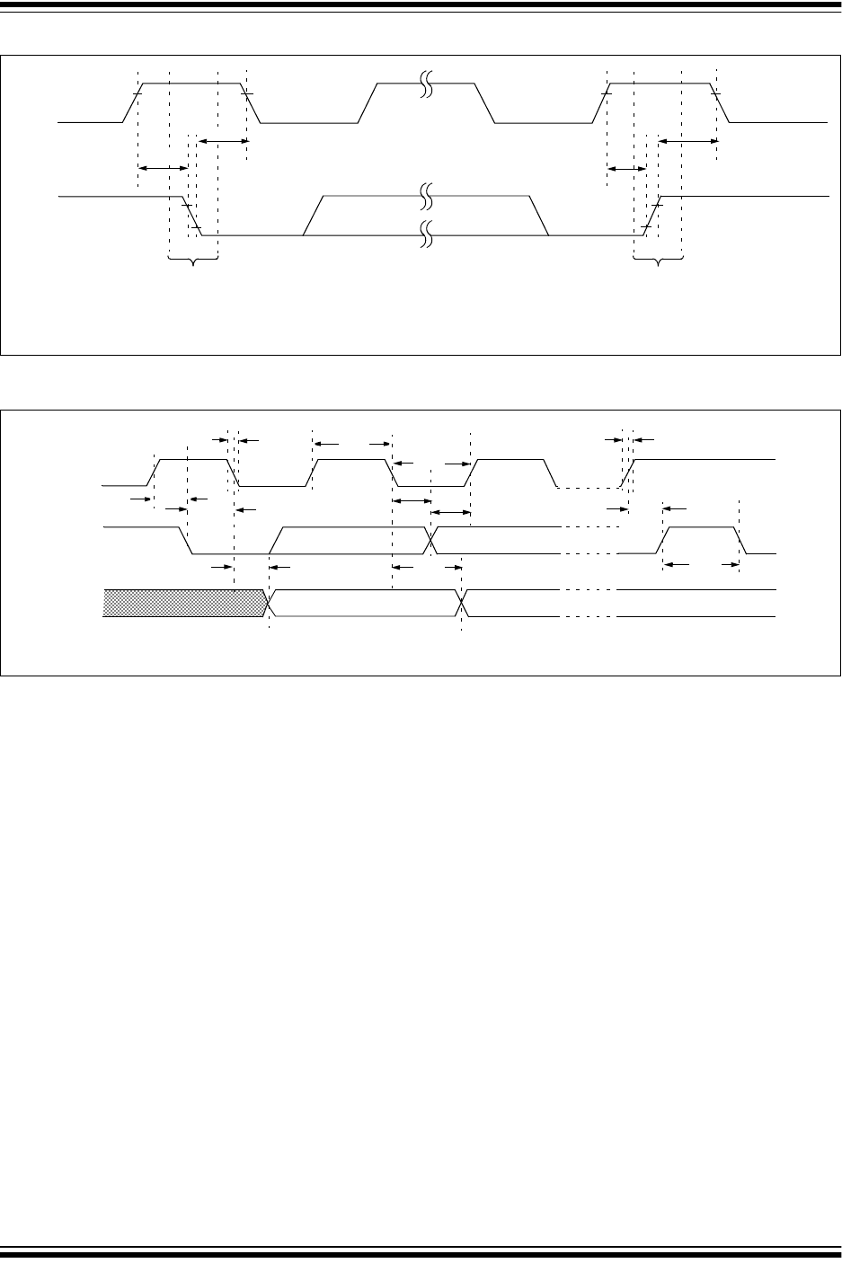
PIC32MX1XX/2XX 28/36/44-PIN FAMILY
DS60001168K-page 288 2011-2018 Microchip Technology Inc.
FIGURE 30-16: I2Cx BUS START/STOP BITS TIMING CHARACTERISTICS (SLAVE MODE)
FIGURE 30-17: I2Cx BUS DATA TIMING CHARACTERISTICS (SLAVE MODE)
IS34
SCLx
SDAx
Start
Condition
Stop
Condition
IS33
Note:
Refer to Figure 30-1 for load conditions.
IS31
IS30
IS30 IS31 IS33
IS11
IS10
IS20
IS26 IS25
IS40 IS40 IS45
IS21
SCLx
SDAx
In
SDAx
Out
Note:
Refer to Figure 30-1 for load conditions.

2011-2018 Microchip Technology Inc. DS60001168K-page 289
PIC32MX1XX/2XX 28/36/44-PIN FAMILY
TABLE 30-33: I2Cx BUS DATA TIMING REQUIREMENTS (SLAVE MODE)
AC CHARACTERISTICS
Standard Operating Conditions: 2.3V to 3.6V
(unless otherwise stated)
Operating temperature -40°C T
A
+85°C for Industrial
-40°C T
A
+105°C for V-temp
Param.
No. Symbol Characteristics Min. Max. Units Conditions
IS10 T
LO
:
SCL
Clock Low Time 100 kHz mode 4.7 — s PBCLK must operate at a
minimum of 800 kHz
400 kHz mode 1.3 — s PBCLK must operate at a
minimum of 3.2 MHz
1 MHz mode
(Note 1)
0.5 — s—
IS11 T
HI
:
SCL
Clock High Time 100 kHz mode 4.0 — s PBCLK must operate at a
minimum of 800 kHz
400 kHz mode 0.6 — s PBCLK must operate at a
minimum of 3.2 MHz
1 MHz mode
(Note 1)
0.5 — s—
IS20 T
F
:
SCL
SDAx and SCLx
Fall Time
100 kHz mode — 300 ns C
B
is specified to be from
10 to 400 pF
400 kHz mode 20 + 0.1 C
B
300 ns
1 MHz mode
(Note 1)
— 100 ns
IS21 T
R
:
SCL
SDAx and SCLx
Rise Time
100 kHz mode — 1000 ns C
B
is specified to be from
10 to 400 pF
400 kHz mode 20 + 0.1 C
B
300 ns
1 MHz mode
(Note 1)
— 300 ns
IS25 T
SU
:
DAT
Data Input
Setup Time
100 kHz mode 250 — ns —
400 kHz mode 100 — ns
1 MHz mode
(Note 1)
100 — ns
IS26 T
HD
:
DAT
Data Input
Hold Time
100 kHz mode 0 — ns —
400 kHz mode 0 0.9 s
1 MHz mode
(Note 1)
00.3s
IS30 T
SU
:
STA
Start Condition
Setup Time
100 kHz mode 4700 — ns Only relevant for Repeated
Start condition
400 kHz mode 600 — ns
1 MHz mode
(Note 1)
250 — ns
IS31 T
HD
:
STA
Start Condition
Hold Time
100 kHz mode 4000 — ns After this period, the first
clock pulse is generated
400 kHz mode 600 — ns
1 MHz mode
(Note 1)
250 — ns
IS33 T
SU
:
STO
Stop Condition
Setup Time
100 kHz mode 4000 — ns —
400 kHz mode 600 — ns
1 MHz mode
(Note 1)
600 — ns
Note 1:
Maximum pin capacitance = 10 pF for all I2Cx pins (for 1 MHz mode only).

PIC32MX1XX/2XX 28/36/44-PIN FAMILY
DS60001168K-page 290 2011-2018 Microchip Technology Inc.
IS34 T
HD
:
STO
Stop Condition
Hold Time
100 kHz mode 4000 — ns —
400 kHz mode 600 — ns
1 MHz mode
(Note 1)
250 ns
IS40 T
AA
:
SCL
Output Valid from
Clock
100 kHz mode 0 3500 ns —
400 kHz mode 0 1000 ns
1 MHz mode
(Note 1)
0 350 ns
IS45 T
BF
:
SDA
Bus Free Time 100 kHz mode 4.7 — s The amount of time the bus
must be free before a new
transmission can start
400 kHz mode 1.3 — s
1 MHz mode
(Note 1)
0.5 — s
IS50 C
B
Bus Capacitive Loading — 400 pF —
TABLE 30-33: I2Cx BUS DATA TIMING REQUIREMENTS (SLAVE MODE) (CONTINUED)
AC CHARACTERISTICS
Standard Operating Conditions: 2.3V to 3.6V
(unless otherwise stated)
Operating temperature -40°C T
A
+85°C for Industrial
-40°C T
A
+105°C for V-temp
Param.
No. Symbol Characteristics Min. Max. Units Conditions
Note 1:
Maximum pin capacitance = 10 pF for all I2Cx pins (for 1 MHz mode only).

2011-2018 Microchip Technology Inc. DS60001168K-page 291
PIC32MX1XX/2XX 28/36/44-PIN FAMILY
TABLE 30-34: ADC MODULE SPECIFICATIONS
AC CHARACTERISTICS
Standard Operating Conditions (see Note 5): 2.5V to 3.6V
(unless otherwise stated)
Operating temperature -40°C T
A
+85°C for Industrial
-40°C T
A
+105°C for V-temp
Param.
No. Symbol Characteristics Min. Typical Max. Units Conditions
Device Supply
AD01 AV
DD
Module V
DD
Supply Greater of
V
DD
– 0.3
or 2.5
— Lesser of
V
DD
+ 0.3 or
3.6
V—
AD02 AV
SS
Module V
SS
Supply V
SS
—AV
DD
V
(Note 1)
Reference Inputs
AD05
AD05a
V
REFH
Reference Voltage High AV
SS
+ 2.0
2.5
—
—
AV
DD
3.6
V
V
(Note 1)
V
REFH
= AV
DD
(Note 3)
AD06 V
REFL
Reference Voltage Low AV
SS
—V
REFH
– 2.0 V
(Note 1)
AD07 V
REF
Absolute Reference
Voltage (V
REFH
– V
REFL
)
2.0 — AV
DD
V
(Note 3)
AD08
AD08a
I
REF
Current Drain —
—
250
—
400
3
µA
µA
ADC operating
ADC off
Analog Input
AD12 V
INH
-V
INL
Full-Scale Input Span V
REFL
—V
REFH
V—
AD13 V
INL
Absolute V
INL
Input
Voltage
AV
SS
– 0.3 — AV
DD
/2 V —
AD14 V
IN
Absolute Input Voltage AV
SS
– 0.3 — AV
DD
+ 0.3 V —
AD15 — Leakage Current — ±0.001 ±0.610 µA V
INL
= AV
SS
= V
REFL
= 0V,
AV
DD
= V
REFH
= 3.3V
Source Impedance = 10 k
AD17 R
IN
Recommended
Impedance of Analog
Voltage Source
—— 5k
(Note 1)
ADC Accuracy – Measurements with External V
REF
+/V
REF
-
AD20c Nr Resolution 10 data bits bits —
AD21c INL Integral Non-linearity > -1 — < 1 LSb V
INL
= AV
SS
= V
REFL
= 0V,
AV
DD
= V
REFH
= 3.3V
AD22c DNL Differential Non-linearity > -1 — < 1 LSb V
INL
= AV
SS
= V
REFL
= 0V,
AV
DD
= V
REFH
= 3.3V
(Note 2)
AD23c G
ERR
Gain Error > -1 — < 1 LSb V
INL
= AV
SS
= V
REFL
= 0V,
AV
DD
= V
REFH
= 3.3V
AD24c E
OFF
Offset Error > -1 — < 1 Lsb V
INL
= AV
SS
= 0V,
AV
DD
= 3.3V
AD25c — Monotonicity — — — — Guaranteed
Note 1:
These parameters are not characterized or tested in manufacturing.
2:
With no missing codes.
3:
These parameters are characterized, but not tested in manufacturing.
4:
Characterized with a 1 kHz sine wave.
5:
The ADC module is functional at V
BORMIN
< V
DD
< 2.5V, but with degraded performance. Unless otherwise
stated, module functionality is tested, but not characterized.
PIC32MX1XX/2XX 28/36/44-PIN FAMILY
DS60001168K-page 292 2011-2018 Microchip Technology Inc.
ADC Accuracy – Measurements with Internal V
REF
+/V
REF
-
AD20d Nr Resolution 10 data bits bits
(Note 3)
AD21d INL Integral Non-linearity > -1 — < 1 LSb V
INL
= AV
SS
= 0V,
AV
DD
= 2.5V to 3.6V
(Note 3)
AD22d DNL Differential Non-linearity > -1 — < 1 LSb V
INL
= AV
SS
= 0V,
AV
DD
= 2.5V to 3.6V
(Notes 2,3)
AD23d G
ERR
Gain Error > -4 — < 4 LSb V
INL
= AV
SS
= 0V,
AV
DD
= 2.5V to 3.6V
(Note 3)
AD24d E
OFF
Offset Error > -2 — < 2 Lsb V
INL
= AV
SS
= 0V,
AV
DD
= 2.5V to 3.6V
(Note 3)
AD25d — Monotonicity — — — — Guaranteed
Dynamic Performance
AD32b SINAD Signal to Noise and
Distortion
55 58.5 — dB
(Notes 3,4)
AD34b ENOB Effective Number of bits 9.0 9.5 — bits
(Notes 3,4)
TABLE 30-34: ADC MODULE SPECIFICATIONS
AC CHARACTERISTICS
Standard Operating Conditions (see Note 5): 2.5V to 3.6V
(unless otherwise stated)
Operating temperature -40°C T
A
+85°C for Industrial
-40°C T
A
+105°C for V-temp
Param.
No. Symbol Characteristics Min. Typical Max. Units Conditions
Note 1:
These parameters are not characterized or tested in manufacturing.
2:
With no missing codes.
3:
These parameters are characterized, but not tested in manufacturing.
4:
Characterized with a 1 kHz sine wave.
5:
The ADC module is functional at V
BORMIN
< V
DD
< 2.5V, but with degraded performance. Unless otherwise
stated, module functionality is tested, but not characterized.
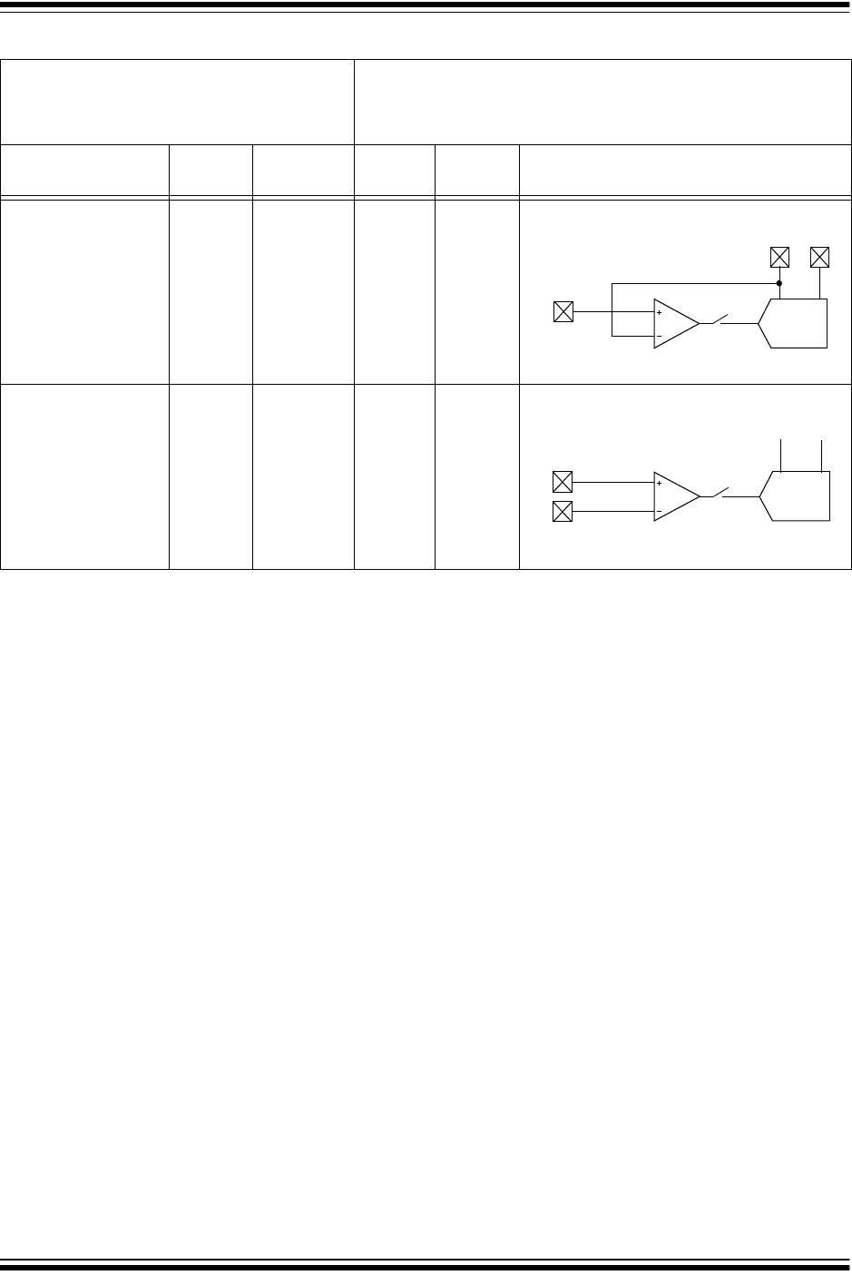
2011-2018 Microchip Technology Inc. DS60001168K-page 293
PIC32MX1XX/2XX 28/36/44-PIN FAMILY
TABLE 30-35: 10-BIT CONVERSION RATE PARAMETERS
AC CHARACTERISTICS
(2)
Standard Operating Conditions (see Note 3): 2.5V to 3.6V
(unless otherwise stated)
Operating temperature -40°C T
A
+85°C for Industrial
-40°C T
A
+105°C for V-temp
ADC Speed T
AD
Min. Sampling
Time Min. R
S
Max. V
DD
ADC Channels Configuration
1 Msps to 400 ksps
(1)
65 ns 132 ns 5003.0V to
3.6V
Up to 400 ksps 200 ns 200 ns 5.0 k2.5V to
3.6V
Note 1:
External V
REF
- and V
REF
+ pins must be used for correct operation.
2:
These parameters are characterized, but not tested in manufacturing.
3:
The ADC module is functional at V
BORMIN
< V
DD
< 2.5V, but with degraded performance. Unless otherwise
stated, module functionality is tested, but not characterized.
V
REF
-V
REF
+
ADC
ANx
SHA
CH
X
V
REF
-V
REF
+
ADC
ANx
SHA
CH
X
ANx or V
REF
-
or
AV
SS
or
AV
DD
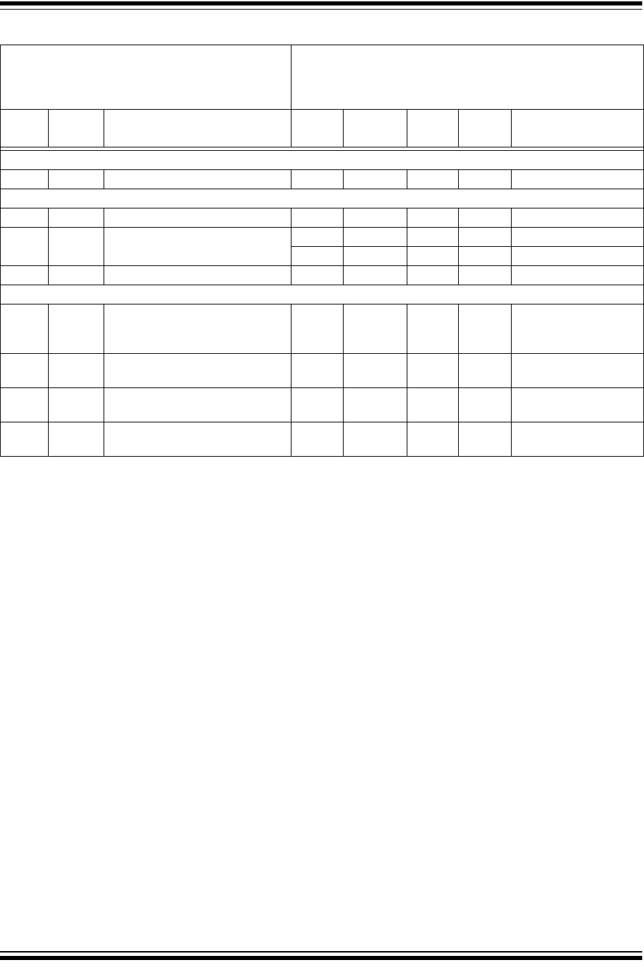
PIC32MX1XX/2XX 28/36/44-PIN FAMILY
DS60001168K-page 294 2011-2018 Microchip Technology Inc.
TABLE 30-36: ANALOG-TO-DIGITAL CONVERSION TIMING REQUIREMENTS
AC CHARACTERISTICS
Standard Operating Conditions (see Note 4): 2.5V to 3.6V
(unless otherwise stated)
Operating temperature -40°C T
A
+85°C for Industrial
-40°C T
A
+105°C for V-temp
Param.
No. Symbol Characteristics Min. Typical
(1)
Max. Units Conditions
Clock Parameters
AD50 T
AD
ADC Clock Period
(2)
65 — — ns See Table 30-35
Conversion Rate
AD55
TCONV
Conversion Time — 12 T
AD
—— —
AD56 F
CNV
Throughput Rate
(Sampling Speed)
— — 1000 ksps AV
DD
= 3.0V to 3.6V
——400kspsAV
DD
= 2.5V to 3.6V
AD57 T
SAMP
Sample Time 1 T
AD
———T
SAMP
must be 132 ns
Timing Parameters
AD60
TPCS
Conversion Start from Sample
Trigger
(3)
—1.0 T
AD
— — Auto-Convert Trigger
(SSRC<2:0> = 111)
not selected
AD61
TPSS
Sample Start from Setting
Sample (SAMP) bit
0.5 T
AD
—1.5 T
AD
——
AD62
TCSS
Conversion Completion to
Sample Start (ASAM = 1)
(3)
—0.5 T
AD
—— —
AD63
TDPU
Time to Stabilize Analog Stage
from ADC Off to ADC On
(3)
—— 2s—
Note 1:
These parameters are characterized, but not tested in manufacturing.
2:
Because the sample caps will eventually lose charge, clock rates below 10 kHz can affect linearity
performance, especially at elevated temperatures.
3:
Characterized by design but not tested.
4:
The ADC module is functional at V
BORMIN
< V
DD
< 2.5V, but with degraded performance. Unless otherwise
stated, module functionality is tested, but not characterized.
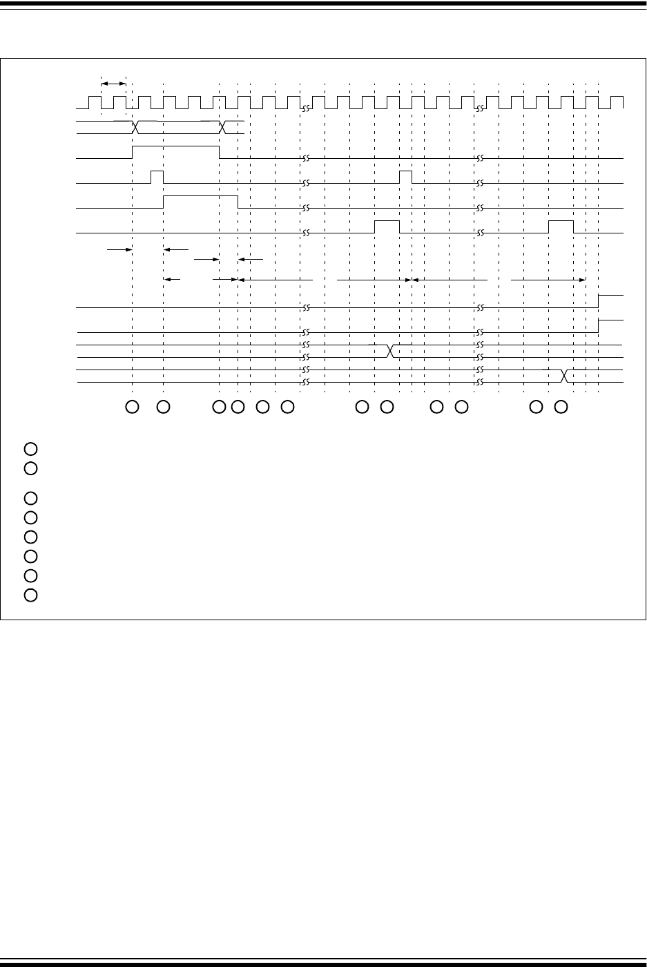
2011-2018 Microchip Technology Inc. DS60001168K-page 295
PIC32MX1XX/2XX 28/36/44-PIN FAMILY
FIGURE 30-18: ANALOG-TO-DIGITAL CONVERSION (10-BIT MODE) TIMING
CHARACTERISTICS (ASAM = 0, SSRC<2:0> = 000)
AD55
T
SAMP
Clear SAMPSet SAMP
AD61
ADCLK
Instruction
SAMP
ch0_dischrg
AD60
CONV
ADxIF
Buffer(
0
)
Buffer(
1
)
1 2 3 4 5 6 8 5 6 7
1– Software sets ADxCON. SAMP to start sampling.
2– Sampling starts after discharge period. T
SAMP
is described in
Section 17. “10-bit Analog-to-Digital Converter (ADC)”
3– Software clears ADxCON. SAMP to start conversion.
4– Sampling ends, conversion sequence starts.
5– Convert bit 9.
8– One T
AD
for end of conversion.
AD50
ch0_samp
eoc
7
AD55
8
6– Convert bit 8.
7– Convert bit 0.
Execution
(DS60001104) in the “PIC32 Family Reference Manual”.
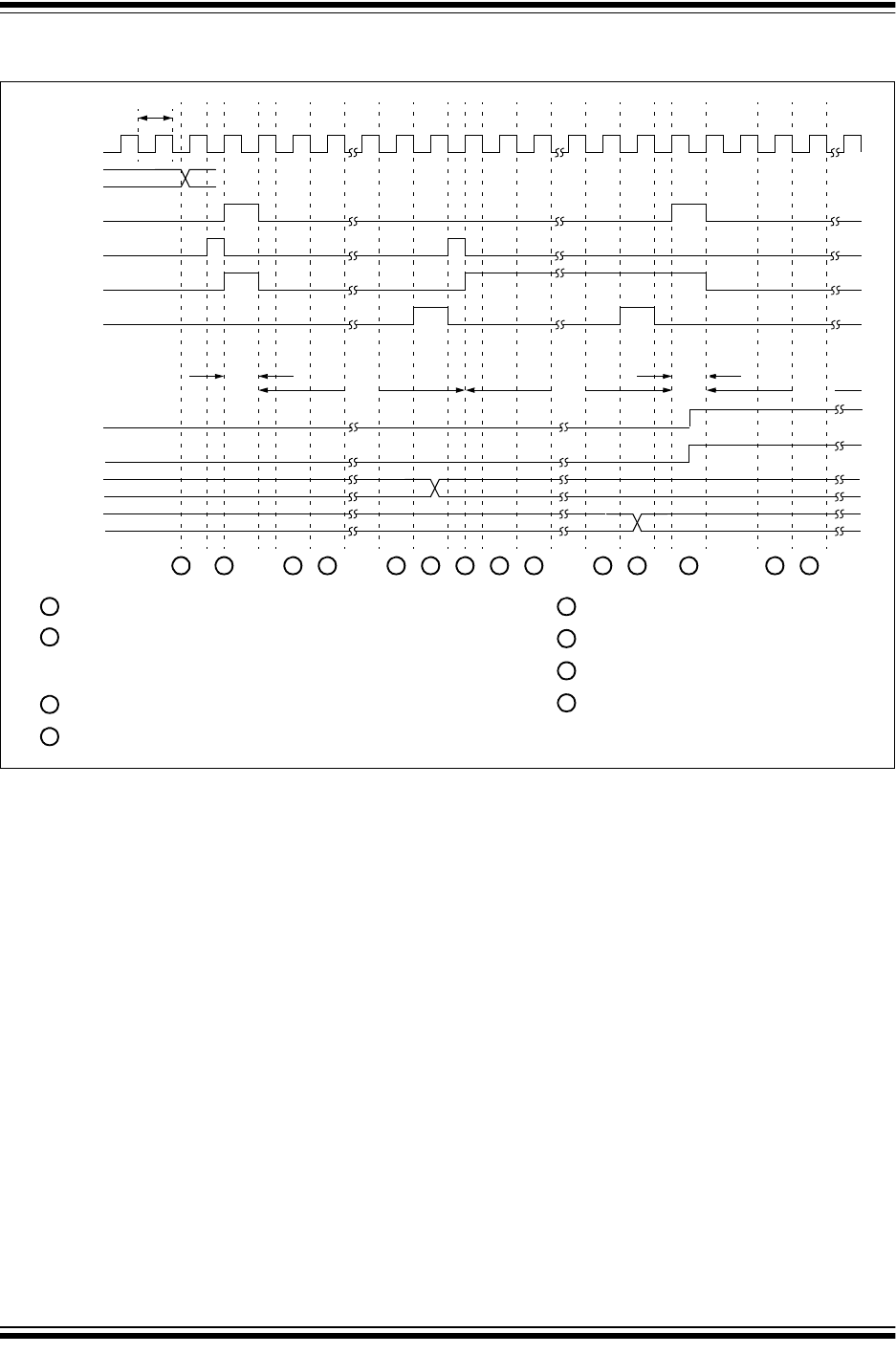
PIC32MX1XX/2XX 28/36/44-PIN FAMILY
DS60001168K-page 296 2011-2018 Microchip Technology Inc.
FIGURE 30-19: ANALOG-TO-DIGITAL CONVERSION (10-BIT MODE) TIMING CHARACTERISTICS
(ASAM = 1, SSRC<2:0> = 111, SAMC<4:0> = 00001)
AD55
T
SAMP
Set ADON
ADCLK
Instruction
SAMP
ch0_dischrg
CONV
ADxIF
Buffer(0)
Buffer(1)
1 2 3 4 5 6 4 5 6 8
1– Software sets ADxCON. ADON to start AD operation.
2– Sampling starts after discharge period.
3– Convert bit 9.
4– Convert bit 8.
5– Convert bit 0.
AD50
ch0_samp
eoc
7 3
AD55
6– One T
AD
for end of conversion.
7– Begin conversion of next channel.
8– Sample for time specified by SAMC<4:0>.
T
SAMP
T
CONV
3 4
Execution
T
SAMP
is described in
Section 17. “10-bit Analog-to-Digital
Converter (ADC)”
(DS60001104).
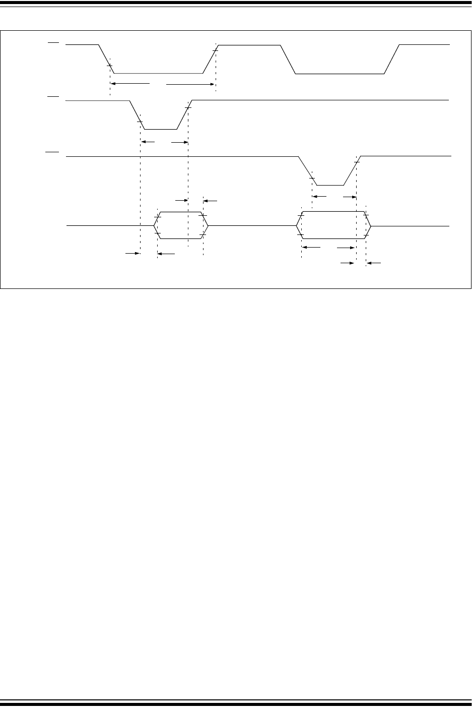
2011-2018 Microchip Technology Inc. DS60001168K-page 297
PIC32MX1XX/2XX 28/36/44-PIN FAMILY
FIGURE 30-20: PARALLEL SLAVE PORT TIMING
CS
RD
WR
PMD<7:0>
PS1
PS2
PS3
PS4
PS5
PS6
PS7
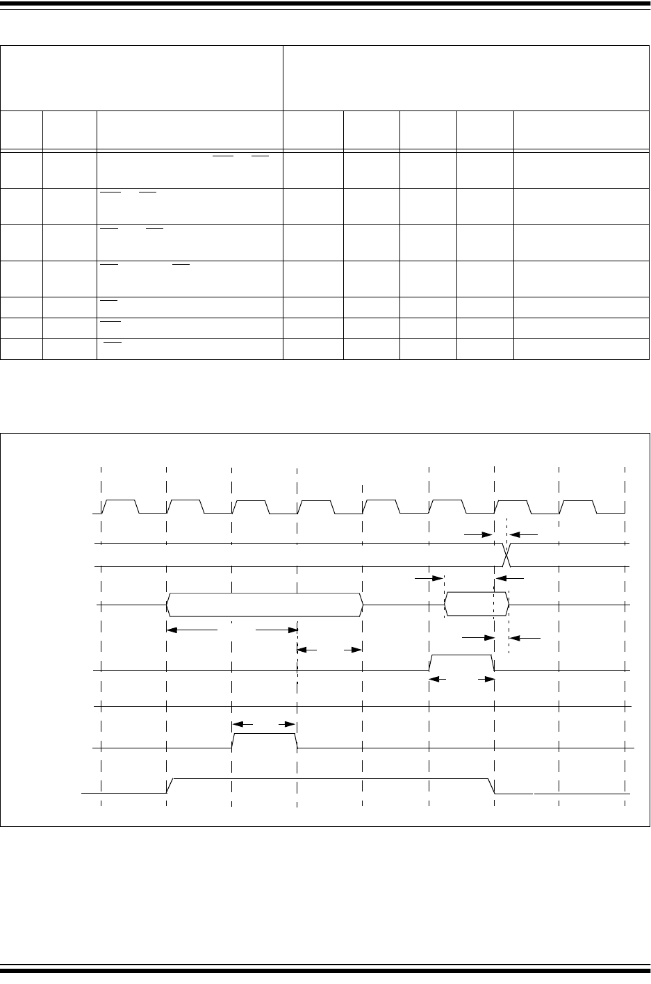
PIC32MX1XX/2XX 28/36/44-PIN FAMILY
DS60001168K-page 298 2011-2018 Microchip Technology Inc.
FIGURE 30-21: PARALLEL MASTER PORT READ TIMING DIAGRAM
TABLE 30-37: PARALLEL SLAVE PORT REQUIREMENTS
AC CHARACTERISTICS
Standard Operating Conditions: 2.3V to 3.6V
(unless otherwise stated)
Operating temperature -40°C T
A
+85°C for Industrial
-40°C T
A
+105°C for V-temp
Para
m.No. Symbol Characteristics
(1)
Min. Typ. Max. Units Conditions
PS1 TdtV2wr
H
Data In Valid before WR or CS
Inactive (setup time)
20 — — ns —
PS2 TwrH2dt
I
WR or CS Inactive to Data-In
Invalid (hold time)
40 — — ns —
PS3 TrdL2dt
V
RD and CS Active to Data-Out
Valid
— — 60 ns —
PS4 TrdH2dtI RD Activeor CS Inactive to
Data-Out Invalid
0 — 10 ns —
PS5 Tcs CS Active Time T
PB
+ 40 — — ns —
PS6 T
WR
WR Active Time T
PB
+ 25 — — ns —
PS7 T
RD
RD Active Time T
PB
+ 25 — — ns —
Note 1:
These parameters are characterized, but not tested in manufacturing.
T
PB
T
PB
T
PB
T
PB
T
PB
T
PB
T
PB
T
PB
PB Clock
PMALL/PMALH
PMD<7:0>
PMA<13:18>
PMRD
PMCS<2:1>
PMWR
PM5
Data
Address<7:0>
PM1
PM3
PM6
Data
PM7
Address<7:0>
Address
PM4
PM2
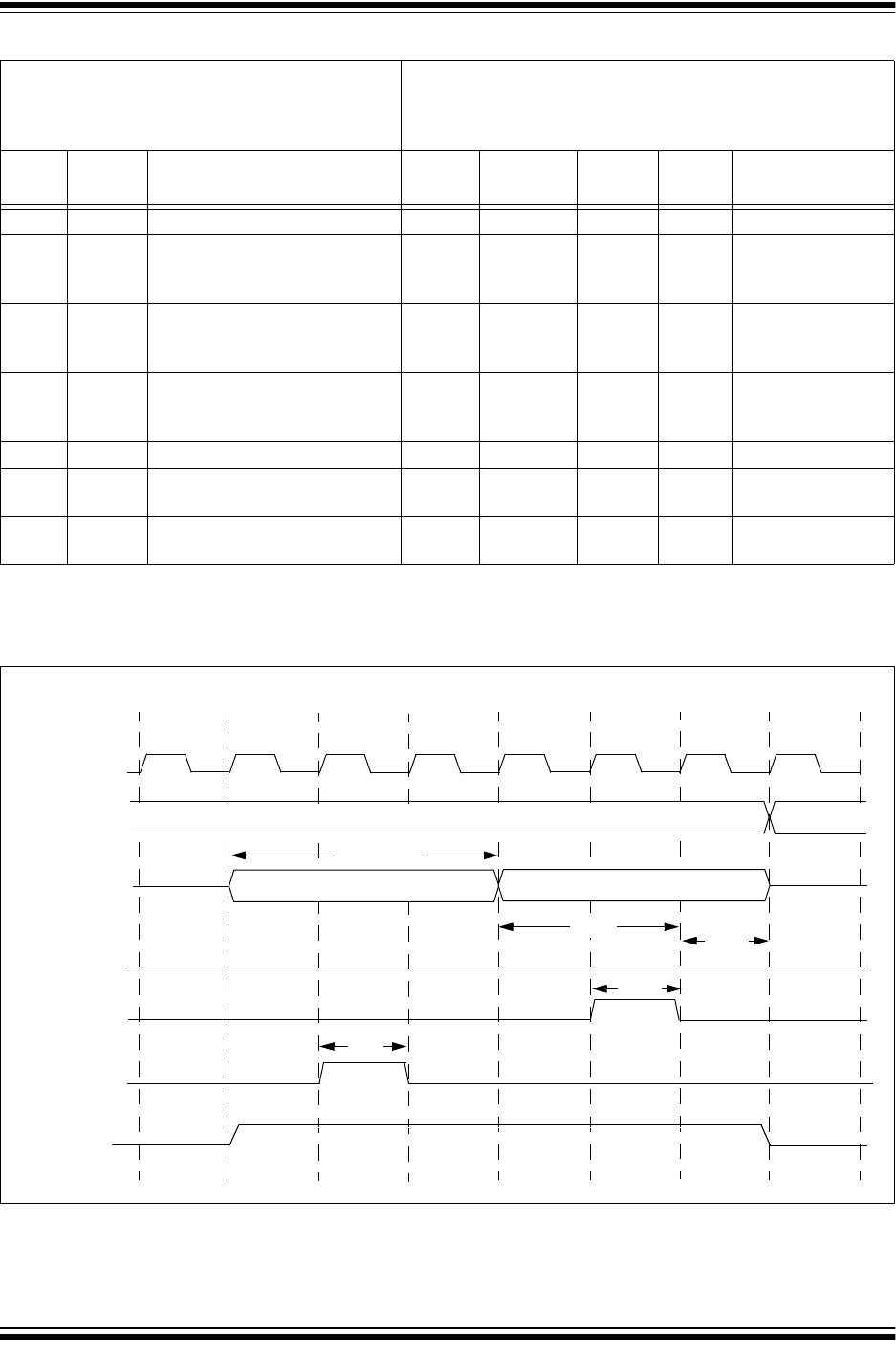
2011-2018 Microchip Technology Inc. DS60001168K-page 299
PIC32MX1XX/2XX 28/36/44-PIN FAMILY
FIGURE 30-22: PARALLEL MASTER PORT WRITE TIMING DIAGRAM
TABLE 30-38: PARALLEL MASTER PORT READ TIMING REQUIREMENTS
AC CHARACTERISTICS
Standard Operating Conditions: 2.3V to 3.6V
(unless otherwise stated)
Operating temperature -40°C T
A
+85°C for Industrial
-40°C T
A
+105°C for V-temp
Param.
No. Symbol Characteristics
(1)
Min. Typ. Max. Units Conditions
PM1 T
LAT
PMALL/PMALH Pulse Width — 1 T
PB
—— —
PM2 T
ADSU
Address Out Valid to
PMALL/PMALH Invalid (address
setup time)
—2 T
PB
—— —
PM3 T
ADHOLD
PMALL/PMALH Invalid to
Address Out Invalid (address
hold time)
—1 T
PB
—— —
PM4 T
AHOLD
PMRD Inactive to Address Out
Invalid
(address hold time)
5——ns —
PM5 T
RD
PMRD Pulse Width — 1 T
PB
—— —
PM6 T
DSU
PMRD or PMENB Active to Data
In Valid (data setup time)
15 — — ns —
PM7 T
DHOLD
PMRD or PMENB Inactive to
Data In Invalid (data hold time)
5——ns —
Note 1:
These parameters are characterized, but not tested in manufacturing.
T
PB
T
PB
T
PB
T
PB
T
PB
T
PB
T
PB
T
PB
PB Clock
PMALL/PMALH
PMD<7:0>
PMA<13:18>
PMWR
PMCS<2:1>
PMRD
PM12 PM13
PM11
Address
Address<7:0> Data
PM2 + PM3
PM1

PIC32MX1XX/2XX 28/36/44-PIN FAMILY
DS60001168K-page 300 2011-2018 Microchip Technology Inc.
TABLE 30-39: PARALLEL MASTER PORT WRITE TIMING REQUIREMENTS
AC CHARACTERISTICS
Standard Operating Conditions: 2.3V to 3.6V
(unless otherwise stated)
Operating temperature -40°C T
A
+85°C for Industrial
-40°C T
A
+105°C for V-temp
Param.
No. Symbol Characteristics
(1)
Min. Typ. Max. Units Conditions
PM11 T
WR
PMWR Pulse Width — 1 T
PB
—— —
PM12 T
DVSU
Data Out Valid before PMWR or
PMENB goes Inactive (data setup
time)
—2 T
PB
—— —
PM13 T
DVHOLD
PMWR or PMEMB Invalid to Data
Out Invalid (data hold time)
—1 T
PB
—— —
Note 1:
These parameters are characterized, but not tested in manufacturing.
TABLE 30-40: OTG ELECTRICAL SPECIFICATIONS
AC CHARACTERISTICS
Standard Operating Conditions: 2.3V to 3.6V
(unless otherwise stated)
Operating temperature -40°C T
A
+85°C for Industrial
-40°C T
A
+105°C for V-temp
Param.
No. Symbol Characteristics
(1)
Min. Typ. Max. Units Conditions
USB313 V
USB
3
V
3
USB Voltage 3.0 — 3.6 V Voltage on V
USB
3
V
3
must be in this range
for proper USB
operation
USB315 V
ILUSB
Input Low Voltage for USB Buffer — — 0.8 V —
USB316 V
IHUSB
Input High Voltage for USB Buffer 2.0 — — V —
USB318 V
DIFS
Differential Input Sensitivity — — 0.2 V The difference
between D+ and D-
must exceed this value
while VCM is met
USB319 VCM Differential Common Mode Range 0.8 — 2.5 V —
USB320 Z
OUT
Driver Output Impedance 28.0 — 44.0 —
USB321 V
OL
Voltage Output Low 0.0 — 0.3 V 1.425 k load
connected to V
USB
3
V
3
USB322 V
OH
Voltage Output High 2.8 — 3.6 V 1.425 k load
connected to ground
Note 1:
These parameters are characterized, but not tested in manufacturing.
2011-2018 Microchip Technology Inc. DS60001168K-page 301
PIC32MX1XX/2XX 28/36/44-PIN FAMILY
TABLE 30-41: CTMU CURRENT SOURCE SPECIFICATIONS
DC CHARACTERISTICS Standard Operating Conditions (see Note 3):2.3V to 3.6V
(unless otherwise stated)
Operating temperature -40°C T
A
+85°C for Industrial
-40°C T
A
+105°C for V-temp
Param
No. Symbol Characteristic Min. Typ. Max. Units Conditions
CTMU C
URRENT
S
OURCE
CTMUI1 I
OUT
1 Base Range
(1)
— 0.55 — µA CTMUCON<9:8> = 01
CTMUI2 I
OUT
2 10x Range
(1)
— 5.5 — µA CTMUCON<9:8> = 10
CTMUI3 I
OUT
3 100x Range
(1)
— 55 — µA CTMUCON<9:8> = 11
CTMUI4 I
OUT
4 1000x Range
(1)
— 550 — µA CTMUCON<9:8> = 00
CTMUFV1 V
F
Temperature Diode Forward
Voltage
(1,2)
—0.598— VT
A
= +25ºC,
CTMUCON<9:8> = 01
—0.658— VT
A
= +25ºC,
CTMUCON<9:8> = 10
—0.721— VT
A
= +25ºC,
CTMUCON<9:8> = 11
CTMUFV2 V
FVR
Temperature Diode Rate of
Change
(1,2)
— -1.92 — mV/ºC CTMUCON<9:8> = 01
— -1.74 — mV/ºC CTMUCON<9:8> = 10
— -1.56 — mV/ºC CTMUCON<9:8> = 11
Note 1:
Nominal value at center point of current trim range (CTMUCON<15:10> = 000000).
2:
Parameters are characterized but not tested in manufacturing. Measurements taken with the following
conditions:
•V
REF
+ = AV
DD
= 3.3V
• ADC module configured for conversion speed of 500 ksps
• All PMD bits are cleared (PMDx = 0)
• Executing a while(1) statement
• Device operating from the FRC with no PLL
3:
The CTMU module is functional at V
BORMIN
< V
DD
< V
DDMIN
, but with degraded performance. Unless
otherwise stated, module functionality is tested, but not characterized.
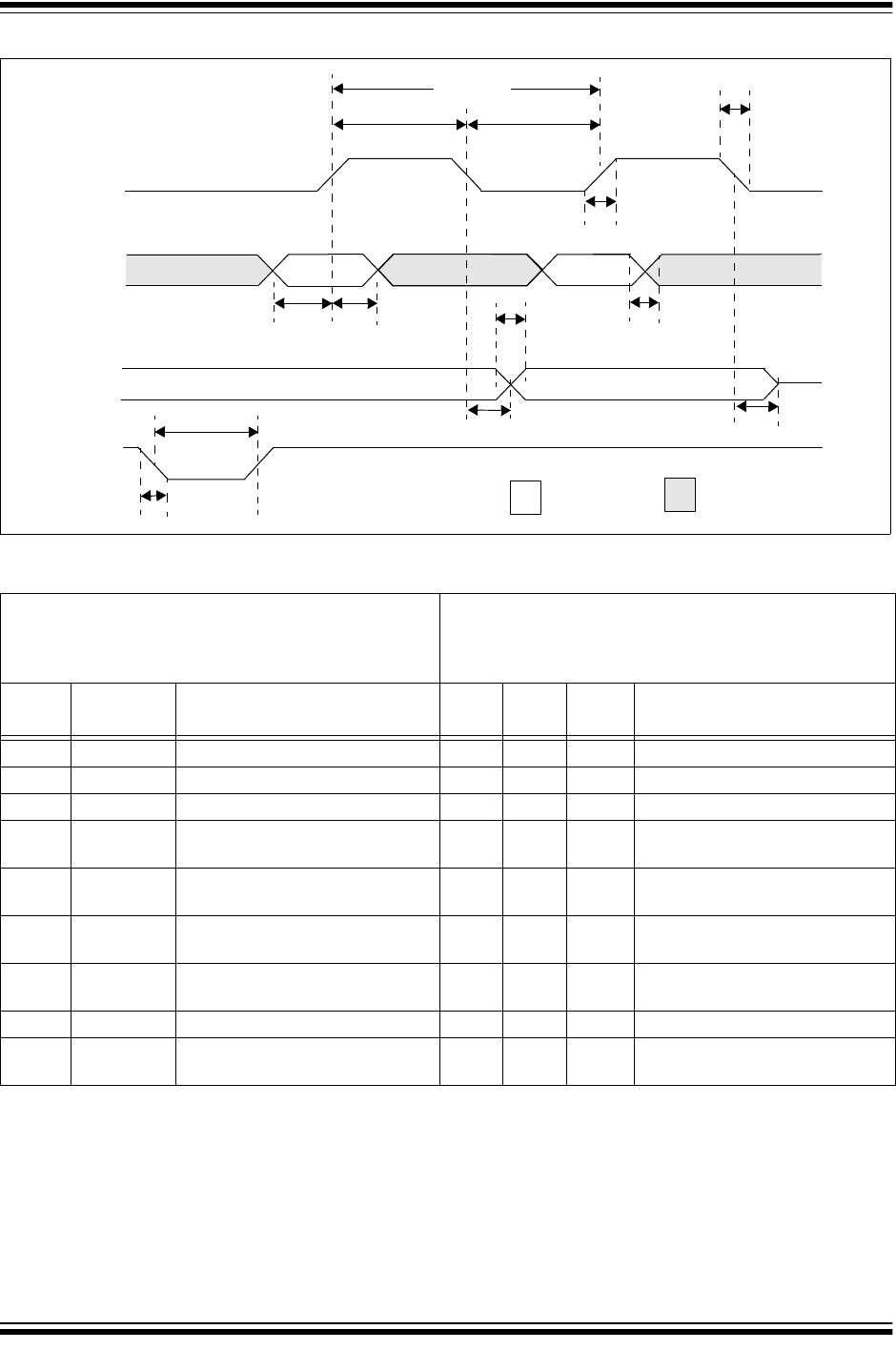
PIC32MX1XX/2XX 28/36/44-PIN FAMILY
DS60001168K-page 302 2011-2018 Microchip Technology Inc.
FIGURE 30-23: EJTAG TIMING CHARACTERISTICS
T
TCKcyc
T
TCKhigh
T
TCKlow
T
rf
T
rf
T
rf
T
rf
T
Tset up
T
Thold
T
TDOout
T
TDOzstate
Defined Undefined
T
TRST*low
T
rf
TCK
TDO
TRST*
TDI
TMS
TABLE 30-42: EJTAG TIMING REQUIREMENTS
AC CHARACTERISTICS
Standard Operating Conditions: 2.3V to 3.6V
(unless otherwise stated)
Operating temperature -40°C T
A
+85°C for Industrial
-40°C T
A
+105°C for V-temp
Param.
No. Symbol Description
(1)
Min. Max. Units Conditions
EJ1 T
TCKCYC
TCK Cycle Time 25 — ns —
EJ2 T
TCKHIGH
TCK High Time 10 — ns —
EJ3 T
TCKLOW
TCK Low Time 10 — ns —
EJ4 T
TSETUP
TAP Signals Setup Time Before
Rising TCK
5—ns —
EJ5 T
THOLD
TAP Signals Hold Time After
Rising TCK
3—ns —
EJ6 T
TDOOUT
TDO Output Delay Time from
Falling TCK
—5ns —
EJ7 T
TDOZSTATE
TDO 3-State Delay Time from
Falling TCK
—5ns —
EJ8 T
TRSTLOW
TRST Low Time 25 — ns —
EJ9 T
RF
TAP Signals Rise/Fall Time, All
Input and Output
——ns —
Note 1:
These parameters are characterized, but not tested in manufacturing.

2011-2018 Microchip Technology Inc. DS60001168K-page 303
PIC32MX1XX/2XX 28/36/44-PIN FAMILY
31.0 50 MHz ELECTRICAL CHARACTERISTICS
This section provides an overview of the PIC32MX1XX/2XX 28/36/44-pin Family electrical characteristics for devices
operating at 50 MHz.
The specifications for 50 MHz are identical to those shown in
Section 30.0 “Electrical Characteristics”
, with the
exception of the parameters listed in this chapter.
Parameters in this chapter begin with the letter “M”, which denotes 50 MHz operation. For example, parameter DC29a
in
Section 30.0 “Electrical Characteristics”
, is the up to 40 MHz operation equivalent for MDC29a.
Absolute maximum ratings for the PIC32MX1XX/2XX 28/36/44-pin Family 50 MHz devices are listed below. Exposure
to these maximum rating conditions for extended periods may affect device reliability. Functional operation of the device
at these or any other conditions, above the parameters indicated in the operation listings of this specification, is not
implied.
Absolute Maximum Ratings
(See Note 1)
Ambient temperature under bias...............................................................................................................-40°C to +85°C
Storage temperature .............................................................................................................................. -65°C to +150°C
Voltage on V
DD
with respect to V
SS
......................................................................................................... -0.3V to +4.0V
Voltage on any pin that is not 5V tolerant, with respect to V
SS
(Note 3)
......................................... -0.3V to (V
DD
+ 0.3V)
Voltage on any 5V tolerant pin with respect to V
SS
when V
DD
2.3V
(Note 3)
........................................ -0.3V to +5.5V
Voltage on any 5V tolerant pin with respect to V
SS
when V
DD
< 2.3V
(Note 3)
........................................ -0.3V to +3.6V
Voltage on D+ or D- pin with respect to V
USB
3
V
3
.................................................................... -0.3V to (V
USB
3
V
3
+ 0.3V)
Voltage on V
BUS
with respect to V
SS
....................................................................................................... -0.3V to +5.5V
Maximum current out of V
SS
pin(s) .......................................................................................................................300 mA
Maximum current into V
DD
pin(s)
(Note 2)
............................................................................................................300 mA
Maximum output current sunk by any I/O pin..........................................................................................................15 mA
Maximum output current sourced by any I/O pin ....................................................................................................15 mA
Maximum current sunk by all ports .......................................................................................................................200 mA
Maximum current sourced by all ports
(Note 2)
....................................................................................................200 mA
Note 1:
Stresses above those listed under
“Absolute Maximum Ratings”
may cause permanent damage to the
device. This is a stress rating only and functional operation of the device at those or any other conditions,
above those indicated in the operation listings of this specification, is not implied. Exposure to maximum
rating conditions for extended periods may affect device reliability.
2:
Maximum allowable current is a function of device maximum power dissipation (see Tab le 3 0- 2 ).
3:
See the
“Pin Diagrams”
section for the 5V tolerant pins.
PIC32MX1XX/2XX 28/36/44-PIN FAMILY
DS60001168K-page 304 2011-2018 Microchip Technology Inc.
31.1 DC Characteristics
TABLE 31-2: DC CHARACTERISTICS: OPERATING CURRENT (I
DD
)
TABLE 31-1: OPERATING MIPS VS. VOLTAGE
Characteristic V
DD
Range
(in Volts)
(1)
Temp. Range
(in °C)
Max. Frequency
PIC32MX1XX/2XX 28/36/44-pin Family
MDC5 2.3-3.6V -40°C to +85°C 50 MHz
Note 1:
Overall functional device operation at V
BORMIN
< V
DD
< V
DDMIN
is tested, but not characterized. All device
Analog modules, such as ADC, etc., will function, but with degraded performance below V
DDMIN
. Refer to
parameter BO10 in Tab l e 30 -11 for BOR values.
DC CHARACTERISTICS Standard Operating Conditions: 2.3V to 3.6V
(unless otherwise stated)
Operating temperature -40°C T
A
+85°C for Industrial
Parameter
No. Typical
(3)
Max. Units Conditions
Operating Current (I
DD
) (Note 1, 2)
MDC24 25 37 mA 50 MHz
Note 1:
A device’s I
DD
supply current is mainly a function of the operating voltage and frequency. Other factors,
such as PBCLK (Peripheral Bus Clock) frequency, number of peripheral modules enabled, internal code
execution pattern, execution from Program Flash memory vs. SRAM, I/O pin loading and switching rate,
oscillator type, as well as temperature, can have an impact on the current consumption.
2:
The test conditions for I
DD
measurements are as follows:
• Oscillator mode is EC (for 8 MHz and below) and EC+PLL (for above 8 MHz) with OSC1 driven by
external square wave from rail-to-rail, (OSC1 input clock input over/undershoot < 100 mV required)
• OSC2/CLKO is configured as an I/O input pin
• USB PLL oscillator is disabled if the USB module is implemented, PBCLK divisor = 1:8
• CPU, Program Flash, and SRAM data memory are operational, SRAM data memory Wait states = 1
• No peripheral modules are operating, (ON bit = 0), but the associated PMD bit is cleared
• WDT, Clock Switching, Fail-Safe Clock Monitor, and Secondary Oscillator are disabled
• All I/O pins are configured as inputs and pulled to V
SS
•MCLR = V
DD
• CPU executing while(1) statement from Flash
3:
RTCC and JTAG are disabled
4:
Data in “Typical” column is at 3.3V, 25°C at specified operating frequency unless otherwise stated.
Parameters are for design guidance only and are not tested.
2011-2018 Microchip Technology Inc. DS60001168K-page 305
PIC32MX1XX/2XX 28/36/44-PIN FAMILY
TABLE 31-3: DC CHARACTERISTICS: IDLE CURRENT (I
IDLE
)
DC CHARACTERISTICS Standard Operating Conditions: 2.3V to 3.6V
(unless otherwise stated)
Operating temperature -40°C T
A
+85°C for Industrial
Parameter
No. Typical
(2)
Max. Units Conditions
Idle Current (I
IDLE
): Core Off, Clock on Base Current (Note 1)
MDC34a 8 13 mA 50 MHz
Note 1:
The test conditions for I
IDLE
current measurements are as follows:
• Oscillator mode is EC (for 8 MHz and below) and EC+PLL (for above 8 MHz) with OSC1 driven by
external square wave from rail-to-rail, (OSC1 input clock input over/undershoot < 100 mV required)
• OSC2/CLKO is configured as an I/O input pin
• USB PLL oscillator is disabled if the USB module is implemented, PBCLK divisor = 1:8
• CPU is in Idle mode (CPU core Halted), and SRAM data memory Wait states = 1
• No peripheral modules are operating, (ON bit = 0), but the associated PMD bit is cleared
• WDT, Clock Switching, Fail-Safe Clock Monitor, and Secondary Oscillator are disabled
• All I/O pins are configured as inputs and pulled to V
SS
•MCLR = V
DD
• RTCC and JTAG are disabled
2:
Data in the “Typical” column is at 3.3V, 25°C unless otherwise stated. Parameters are for design guidance
only and are not tested.
TABLE 31-4: DC CHARACTERISTICS: POWER-DOWN CURRENT (I
PD
)
DC CHARACTERISTICS Standard Operating Conditions: 2.3V to 3.6V (unless otherwise stated)
Operating temperature -40°C T
A
+85°C for Industrial
Param.
No. Typical
(2)
Max. Units Conditions
Power-Down Current (I
PD
) (Note 1)
MDC40k 10 25 A-40°C
Base Power-Down Current
MDC40n 250 500 A +85°C
Module Differential Current
MDC41e 10 55 A 3.6V Watchdog Timer Current: I
WDT
(Note 3)
MDC42e 23 55 A 3.6V RTCC + Timer1 w/32 kHz Crystal: I
RTCC
(Note 3)
MDC43d 1100 1300 A 3.6V ADC: I
ADC
(Notes 3,4)
Note 1:
The test conditions for I
PD
current measurements are as follows:
• Oscillator mode is EC (for 8 MHz and below) and EC+PLL (for above 8 MHz) with OSC1 driven by
external square wave from rail-to-rail, (OSC1 input clock input over/undershoot < 100 mV required)
• OSC2/CLKO is configured as an I/O input pin
• USB PLL oscillator is disabled if the USB module is implemented, PBCLK divisor = 1:8
• CPU is in Sleep mode, and SRAM data memory Wait states = 1
• No peripheral modules are operating, (ON bit = 0), but the associated PMD bit is set
• WDT, Clock Switching, Fail-Safe Clock Monitor, and Secondary Oscillator are disabled
• All I/O pins are configured as inputs and pulled to V
SS
•MCLR = V
DD
• RTCC and JTAG are disabled
2:
Data in the “Typical” column is at 3.3V, 25°C unless otherwise stated. Parameters are for design guidance
only and are not tested.
3:
The current is the additional current consumed when the module is enabled. This current should be
added to the base I
PD
current.
4:
Test conditions for ADC module differential current are as follows: Internal ADC RC oscillator enabled.

PIC32MX1XX/2XX 28/36/44-PIN FAMILY
DS60001168K-page 306 2011-2018 Microchip Technology Inc.
TABLE 31-5: EXTERNAL CLOCK TIMING REQUIREMENTS
AC CHARACTERISTICS Standard Operating Conditions: 2.3V to 3.6V
(unless otherwise stated)
Operating temperature -40°C T
A
+85°C for Industrial
Param.
No. Symbol Characteristics Min. Typical Max. Units Conditions
MOS10 F
OSC
External CLKI Frequency
(External clocks allowed only
in EC and ECPLL modes)
DC
4
—
—
50
50
MHz
MHz
EC
(Note 2)
ECPLL
(Note 1)
Note 1:
PLL input requirements: 4 MHz F
PLLIN
5 MHz (use PLL prescaler to reduce Fosc). This parameter is
characterized, but tested at 10 MHz only at manufacturing.
2:
This parameter is characterized, but not tested in manufacturing.
TABLE 31-6: SPIx MASTER MODE (CKE = 0) TIMING REQUIREMENTS
AC CHARACTERISTICS Standard Operating Conditions: 2.3V to 3.6V
(unless otherwise stated)
Operating temperature -40°C T
A
+85°C for Industrial
Param.
No. Symbol Characteristics Min. Typical Max. Units Conditions
MSP10 T
SC
LSCKx Output Low Time
(Note 1,2)
T
SCK
/2 — — ns —
MSP11 T
SC
H SCKx Output High Time
(Note 1,2)
T
SCK
/2 ——ns —
Note 1:
These parameters are characterized, but not tested in manufacturing.
2:
The minimum clock period for SCKx is 40 ns. Therefore, the clock generated in Master mode must not
violate this specification.
TABLE 31-7: SPIx MODULE MASTER MODE (CKE = 1) TIMING REQUIREMENTS
AC CHARACTERISTICS Standard Operating Conditions: 2.3V to 3.6V
(unless otherwise stated)
Operating temperature -40°C T
A
+85°C for Industrial
Param.
No. Symbol Characteristics
(1)
Min. Typ. Max. Units Conditions
MSP10 T
SC
L SCKx Output Low Time
(Note 1,2)
T
SCK
/2 — — ns —
MSP11 T
SC
H SCKx Output High Time
(Note 1,2)
T
SCK
/2 — — ns —
Note 1:
These parameters are characterized, but not tested in manufacturing.
2:
The minimum clock period for SCKx is 40 ns. Therefore, the clock generated in Master mode must not
violate this specification.
2011-2018 Microchip Technology Inc. DS60001168K-page 307
PIC32MX1XX/2XX 28/36/44-PIN FAMILY
TABLE 31-8: SPIx MODULE SLAVE MODE (CKE = 0) TIMING REQUIREMENTS
AC CHARACTERISTICS
Standard Operating Conditions: 2.3V to 3.6V
(unless otherwise stated)
Operating temperature -40°C T
A
+85°C for Industrial
-40°C T
A
+105°C for V-temp
Param.
No. Symbol Characteristics Min. Typ. Max. Units Conditions
MSP70 T
SC
L SCKx Input Low Time
(Note 1,2)
T
SCK
/2 — — ns —
MSP71 T
SC
H SCKx Input High Time
(Note 1,2)
T
SCK
/2 — — ns —
MSP51 T
SS
H2
DO
Z SSx to SDOx Output
High-Impedance
(Note 2)
5—25ns —
Note 1:
These parameters are characterized, but not tested in manufacturing.
2:
The minimum clock period for SCKx is 40 ns.
TABLE 31-9: SPIx MODULE SLAVE MODE (CKE = 1) TIMING REQUIREMENTS
AC CHARACTERISTICS Standard Operating Conditions: 2.3V to 3.6V
(unless otherwise stated)
Operating temperature -40°C T
A
+85°C for Industrial
Param.
No. Symbol Characteristics Min. Typical Max. Units Conditions
SP70 T
SC
L SCKx Input Low Time
(Note 1,2)
T
SCK
/2 — — ns —
SP71 T
SC
H SCKx Input High Time
(Note 1,2)
T
SCK
/2 — — ns —
Note 1:
These parameters are characterized, but not tested in manufacturing.
2:
The minimum clock period for SCKx is 40 ns.

PIC32MX1XX/2XX 28/36/44-PIN FAMILY
DS60001168K-page 308 2011-2018 Microchip Technology Inc.
NOTES:
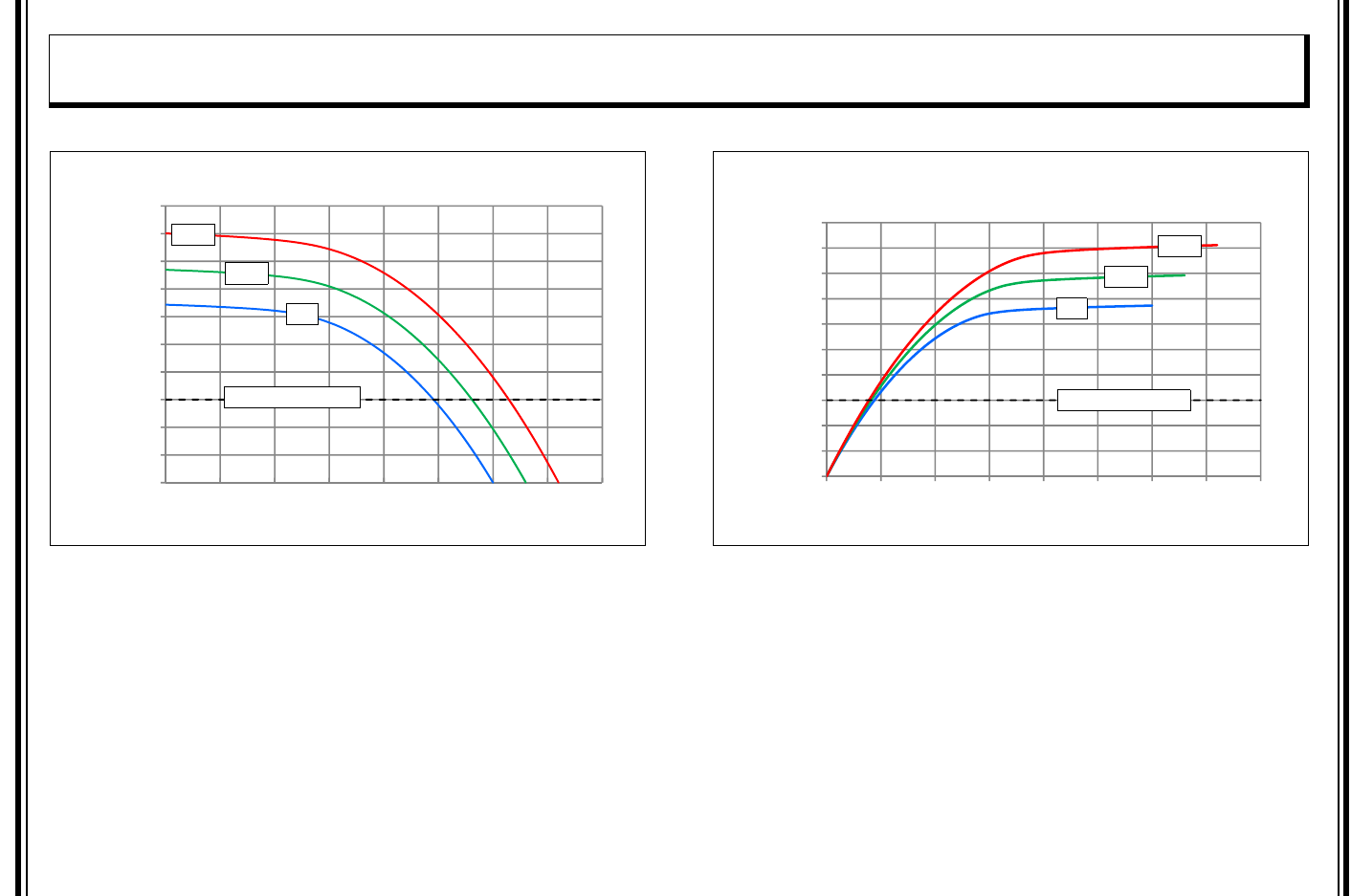
2011-2018 Microchip Technology Inc. DS60001168K-page 309
PIC32MX1XX/2XX 28/36/44-PIN FAMILY
32.0 DC AND AC DEVICE CHARACTERISTICS GRAPHS
FIGURE 32-1: I/O OUTPUT VOLTAGE HIGH (V
OH
) FIGURE 32-2: I/O OUTPUT VOLTAGE LOW (V
OL
)
Note:
The graphs provided following this note are a statistical summary based on a limited number of samples and are provided for design guidance purposes
only. The performance characteristics listed herein are not tested or guaranteed. In some graphs, the data presented may be outside the specified operating
range (e.g., outside specified power supply range) and therefore, outside the warranted range.
-0.050
-0.045
-0.040
-0.035
-0.030
-0.025
-0.020
IOH(A)
VOH (V)
-0.050
-0.045
-0.040
-0.035
-0.030
-0.025
-0.020
-0.015
-0.010
-0.005
0.000
0.00 0.50 1.00 1.50 2.00 2.50 3.00 3.50 4.00
IOH(A)
VOH (V)
3V
3.3V
3.6V
Absolute Maximum
0.015
0.020
0.025
0.030
0.035
0.040
0.045
0.050
IOH(A)
VOL(V)
0.000
0.005
0.010
0.015
0.020
0.025
0.030
0.035
0.040
0.045
0.050
0.00 0.50 1.00 1.50 2.00 2.50 3.00 3.50 4.00
IOH(A)
VOL(V)
3V
3.3V
3.6V
Absolute Maximum

PIC32MX1XX/2XX 28/36/44-PIN FAMILY
DS60001168K-page 310 2011-2018 Microchip Technology Inc.
FIGURE 32-3: TYPICAL I
PD
CURRENT @ V
DD
= 3.3V
FIGURE 32-4: TYPICAL I
DD
CURRENT @ V
DD
= 3.3V
FIGURE 32-5: TYPICAL I
IDLE
CURRENT @ V
DD
= 3.3V
150
200
250
300
350
400
IPD (µA)
0
50
100
150
200
250
300
350
400
-40-30-20-10 0 102030405060708090100
IPD (µA)
Temperature (Celsius)
10
15
20
25
IDD (mA)
0
5
10
15
20
25
0 10203040
IDD (mA)
MIPS
3
4
5
6
7
8
D
LE Current (mA)
0
1
2
0 10203040
II
D
MIPS
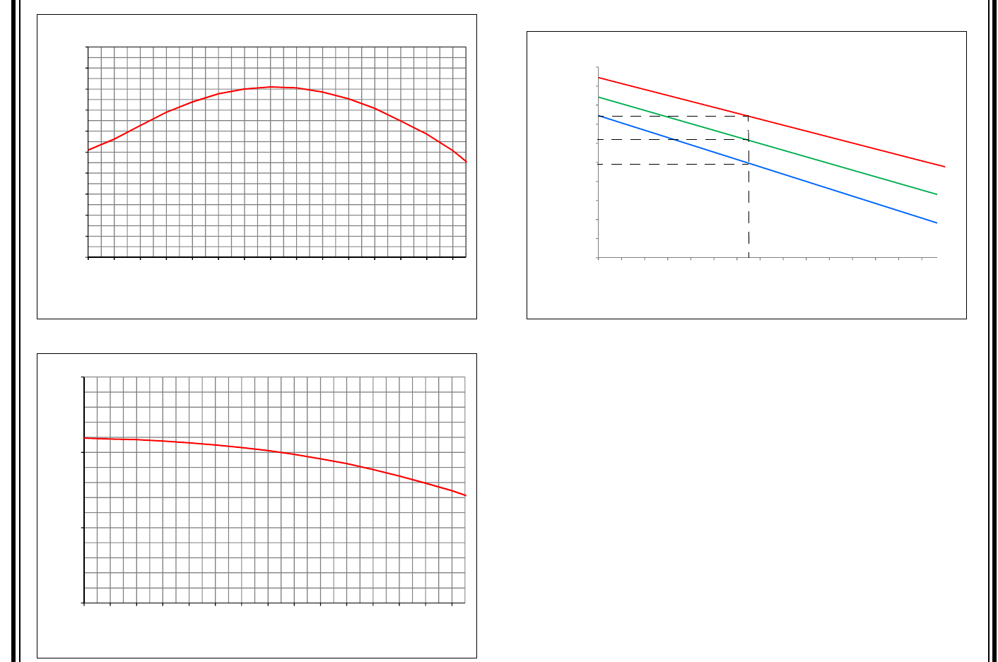
2011-2018 Microchip Technology Inc. DS60001168K-page 311
PIC32MX1XX/2XX 28/36/44-PIN FAMILY
FIGURE 32-6: TYPICAL FRC FREQUENCY @ V
DD
= 3.3V
FIGURE 32-7: TYPICAL LPRC FREQUENCY @ V
DD
= 3.3V
FIGURE 32-8: TYPICAL CTMU TEMPERATURE DIODE
FORWARD VOLTAGE
7930
7940
7950
7960
7970
7980
7990
8000
FRC Frequency (kHz)
7900
7910
7920
7930
7940
7950
7960
7970
7980
7990
8000
-40-30-20-10 0 102030405060708090100
FRC Frequency (kHz)
Temperature (Celsius)
31
32
33
LPRC Frequency (kHz)
30
31
32
33
-40-30-20-10 0 102030405060708090100
LPRC Frequency (kHz)
Temperature (Celsius)
0500
0.550
0.600
0.650
0.700
0.750
0.800
0.850
Forward Voltage (V)
0.350
0.400
0.450
0.500
0.550
0.600
0.650
0.700
0.750
0.800
0.850
-40-30-20-10 0 102030405060708090100110
Forward Voltage (V)
Temperature (Celsius)
V
F
= 0.598
V
F
= 0.658
V
F
= 0.721
55 µA, V
FVR
= -1.56 mV/ºC
5.5 µA, V
FVR
= -1.74 mV/ºC
0.55 µA, V
FVR
= -1.92 mV/ºC

PIC32MX1XX/2XX 28/36/44-PIN FAMILY
DS60001168K-page 312 2011-2018 Microchip Technology Inc.
NOTES:
2011-2018 Microchip Technology Inc. DS60001168K-page 313
PIC32MX1XX/2XX 28/36/44-PIN FAMILY
33.0 PACKAGING INFORMATION
33.1 Package Marking Information
Legend:
XX...X Customer-specific information
Y Year code (last digit of calendar year)
YY Year code (last 2 digits of calendar year)
WW Week code (week of January 1 is week ‘01’)
NNN Alphanumeric traceability code
Pb-free JEDEC designator for Matte Tin (Sn)
*
This package is Pb-free. The Pb-free JEDEC designator ( )
can be found on the outer packaging for this package.
Note:
If the full Microchip part number cannot be marked on one line, it is carried over to the next
line, thus limiting the number of available characters for customer-specific information.
3
e
3
e
Example
32MX220F
032BE/ML
1130235
3
e
28-Lead SSOP
XXXXXXXXXXXX
XXXXXXXXXXXX
YYWWNNN
Example
PIC32MX220F
032B-I/SS
1130235
3
e
28-Lead SOIC
XXXXXXXXXXXXXXXXXXXX
XXXXXXXXXXXXXXXXXXXX
XXXXXXXXXXXXXXXXXXXX
YYWWNNN
Example
PIC32MX220F
1130235
032B-I/SO
3
e
28-Lead QFN
XXXXXXXX
XXXXXXXX
YYWWNNN
28-Lead SPDIP
XXXXXXXXXXXXXXXXX
XXXXXXXXXXXXXXXXX
YYWWNNN
Example
PIC32MX220F
1130235
032B-I/SP
3
e
PIC32MX1XX/2XX 28/36/44-PIN FAMILY
DS60001168K-page 314 2011-2018 Microchip Technology Inc.
33.1 Package Marking Information (Continued)
XXXXXXXXXX
44-Lead QFN
XXXXXXXXXX
XXXXXXXXXX
YYWWNNN
32MX220F
Example
032D-E/ML
1130235
44-Lead TQFP
XXXXXXXXXX
XXXXXXXXXX
XXXXXXXXXX
YYWWNNN
Example
32MX220F
032D-I/PT
1130235
3
e
3
e
Legend:
XX...X Customer-specific information
Y Year code (last digit of calendar year)
YY Year code (last 2 digits of calendar year)
WW Week code (week of January 1 is week ‘01’)
NNN Alphanumeric traceability code
Pb-free JEDEC designator for Matte Tin (Sn)
*
This package is Pb-free. The Pb-free JEDEC designator ( )
can be found on the outer packaging for this package.
Note:
If the full Microchip part number cannot be marked on one line, it is carried over to the next
line, thus limiting the number of available characters for customer-specific information.
3
e
3
e
36-Lead VTLA
XXXXXXXX
XXXXXXXX
YYWWNNN
Example
32MX220F
032CE/TL
1130235
3
e
44-Lead VTLA Example
XXXXXXXXXX
XXXXXXXXXX
XXXXXXXXXX
YYWWNNN
PIC32
MX120F0
1130235
3
e
32DI/TL
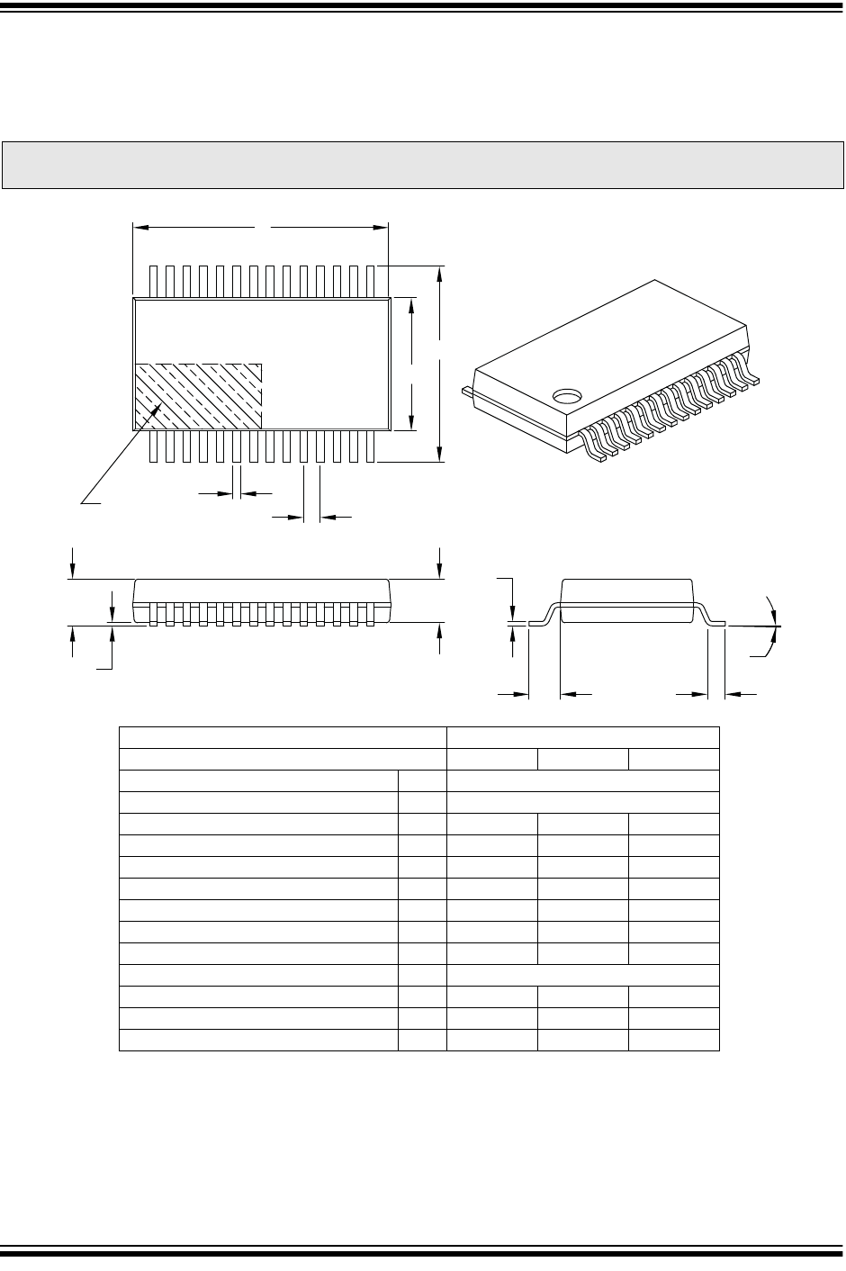
2011-2018 Microchip Technology Inc. DS60001168K-page 315
PIC32MX1XX/2XX 28/36/44-PIN FAMILY
33.2 Package Details
This section provides the technical details of the packages.
/HDG3ODVWLF6KULQN6PDOO2XWOLQH66±PP%RG\>6623@
1RWHV
3LQYLVXDOLQGH[IHDWXUHPD\YDU\EXWPXVWEHORFDWHGZLWKLQWKHKDWFKHGDUHD
'LPHQVLRQV'DQG(GRQRWLQFOXGHPROGIODVKRUSURWUXVLRQV0ROGIODVKRUSURWUXVLRQVVKDOOQRWH[FHHGPPSHUVLGH
'LPHQVLRQLQJDQGWROHUDQFLQJSHU$60(<0
%6& %DVLF'LPHQVLRQ7KHRUHWLFDOO\H[DFWYDOXHVKRZQZLWKRXWWROHUDQFHV
5() 5HIHUHQFH'LPHQVLRQXVXDOO\ZLWKRXWWROHUDQFHIRULQIRUPDWLRQSXUSRVHVRQO\
1RWH )RUWKHPRVWFXUUHQWSDFNDJHGUDZLQJVSOHDVHVHHWKH0LFURFKLS3DFNDJLQJ6SHFLILFDWLRQORFDWHGDW
KWWSZZZPLFURFKLSFRPSDFNDJLQJ
8QLWV 0,//,0(7(56
'LPHQVLRQ/LPLWV 0,1 120 0$;
1XPEHURI3LQV 1
3LWFK H %6&
2YHUDOO+HLJKW $ ± ±
0ROGHG3DFNDJH7KLFNQHVV $
6WDQGRII $ ± ±
2YHUDOO:LGWK (
0ROGHG3DFNDJH:LGWK (
2YHUDOO/HQJWK '
)RRW/HQJWK /
)RRWSULQW / 5()
/HDG7KLFNQHVV F ±
)RRW$QJOH
/HDG:LGWK E ±
L
L1
c
A2
A1
A
E
E1
D
N
12
NOTE 1 b
e
φ
0LFURFKLS 7HFKQRORJ\ 'UDZLQJ &%
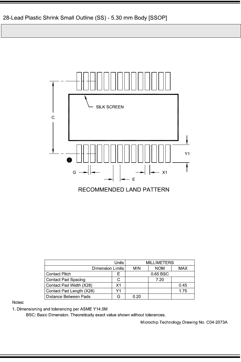
PIC32MX1XX/2XX 28/36/44-PIN FAMILY
DS60001168K-page 316 2011-2018 Microchip Technology Inc.
Note: For the most current package drawings, please see the Microchip Packaging Specification located at
http://www.microchip.com/packaging
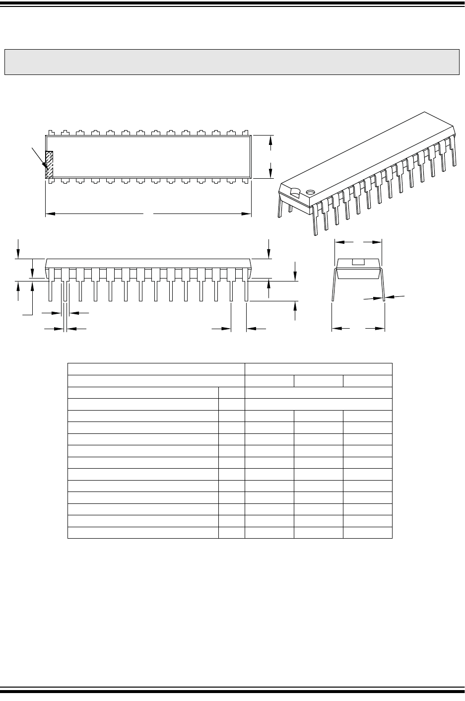
2011-2018 Microchip Technology Inc. DS60001168K-page 317
PIC32MX1XX/2XX 28/36/44-PIN FAMILY
/HDG6NLQQ\3ODVWLF'XDO,Q/LQH63±PLO%RG\>63',3@
1RWHV
3LQYLVXDOLQGH[IHDWXUHPD\YDU\EXWPXVWEHORFDWHGZLWKLQWKHKDWFKHGDUHD
6LJQLILFDQW&KDUDFWHULVWLF
'LPHQVLRQV'DQG(GRQRWLQFOXGHPROGIODVKRUSURWUXVLRQV0ROGIODVKRUSURWUXVLRQVVKDOOQRWH[FHHGSHUVLGH
'LPHQVLRQLQJDQGWROHUDQFLQJSHU$60(<0
%6& %DVLF'LPHQVLRQ7KHRUHWLFDOO\H[DFWYDOXHVKRZQZLWKRXWWROHUDQFHV
1RWH )RUWKHPRVWFXUUHQWSDFNDJHGUDZLQJVSOHDVHVHHWKH0LFURFKLS3DFNDJLQJ6SHFLILFDWLRQORFDWHGDW
KWWSZZZPLFURFKLSFRPSDFNDJLQJ
8QLWV ,1&+(6
'LPHQVLRQ/LPLWV 0,1 120 0$;
1XPEHURI3LQV 1
3LWFK H %6&
7RSWR6HDWLQJ3ODQH $ ± ±
0ROGHG3DFNDJH7KLFNQHVV $
%DVHWR6HDWLQJ3ODQH $ ± ±
6KRXOGHUWR6KRXOGHU:LGWK (
0ROGHG3DFNDJH:LGWK (
2YHUDOO/HQJWK '
7LSWR6HDWLQJ3ODQH /
/HDG7KLFNQHVV F
8SSHU/HDG:LGWK E
/RZHU/HDG:LGWK E
2YHUDOO5RZ6SDFLQJ H% ± ±
NOTE 1
N
12
D
E1
eB
c
E
L
A2
eb
b1
A1
A
3
0LFURFKLS 7HFKQRORJ\ 'UDZLQJ &%
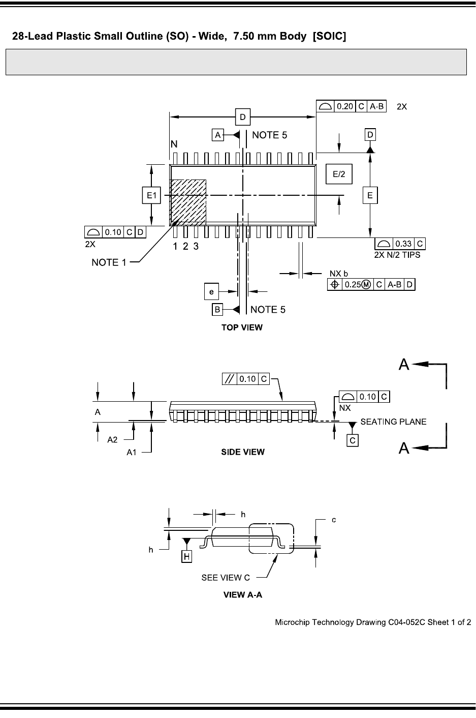
PIC32MX1XX/2XX 28/36/44-PIN FAMILY
DS60001168K-page 318 2011-2018 Microchip Technology Inc.
Note: For the most current package drawings, please see the Microchip Packaging Specification located at
http://www.microchip.com/packaging
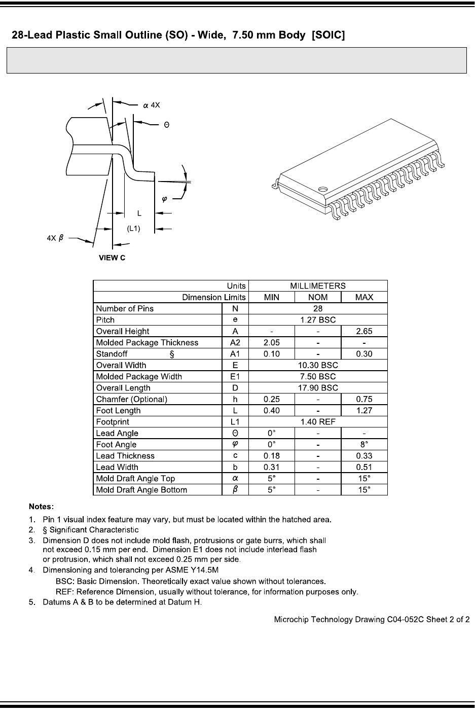
2011-2018 Microchip Technology Inc. DS60001168K-page 319
PIC32MX1XX/2XX 28/36/44-PIN FAMILY
Note: For the most current package drawings, please see the Microchip Packaging Specification located at
http://www.microchip.com/packaging
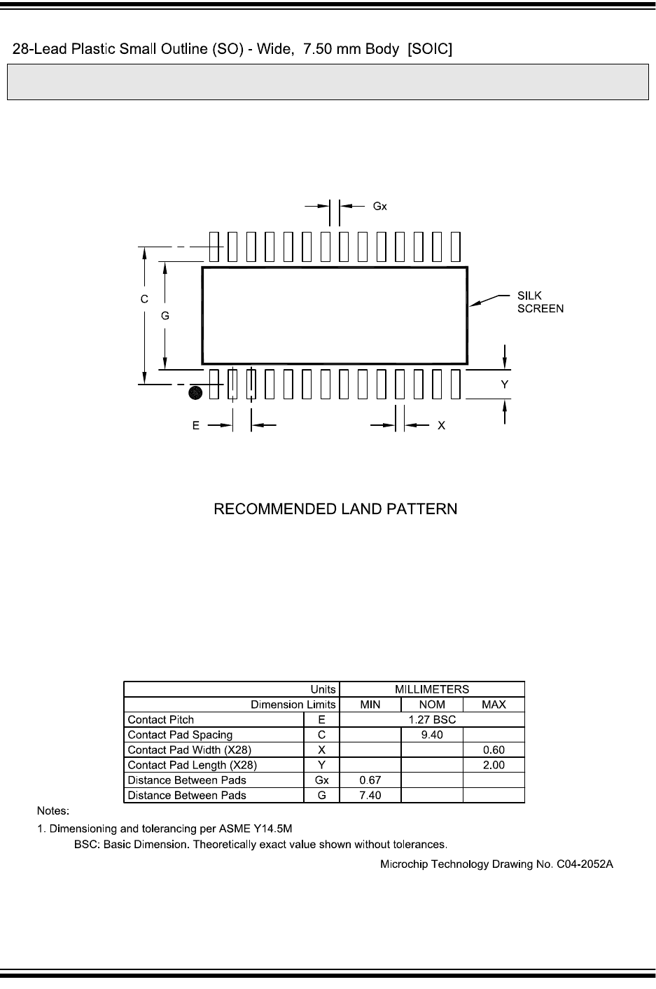
PIC32MX1XX/2XX 28/36/44-PIN FAMILY
DS60001168K-page 320 2011-2018 Microchip Technology Inc.
Note: For the most current package drawings, please see the Microchip Packaging Specification located at
http://www.microchip.com/packaging
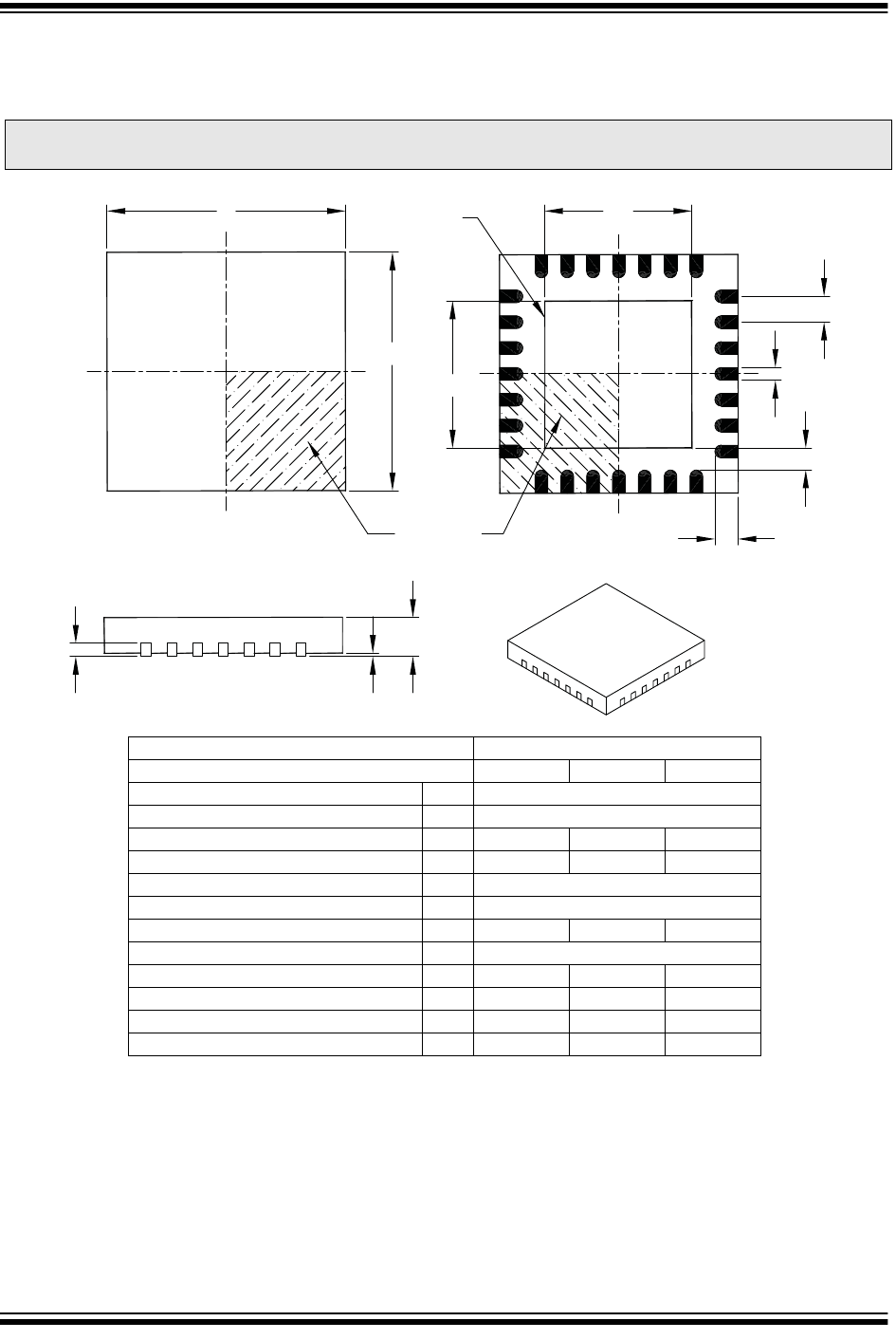
2011-2018 Microchip Technology Inc. DS60001168K-page 321
PIC32MX1XX/2XX 28/36/44-PIN FAMILY
/HDG3ODVWLF4XDG)ODW1R/HDG3DFNDJH0/±[PP%RG\>4)1@
ZLWKPP&RQWDFW/HQJWK
1RWHV
3LQYLVXDOLQGH[IHDWXUHPD\YDU\EXWPXVWEHORFDWHGZLWKLQWKHKDWFKHGDUHD
3DFNDJHLVVDZVLQJXODWHG
'LPHQVLRQLQJDQGWROHUDQFLQJSHU$60(<0
%6& %DVLF'LPHQVLRQ7KHRUHWLFDOO\H[DFWYDOXHVKRZQZLWKRXWWROHUDQFHV
5() 5HIHUHQFH'LPHQVLRQXVXDOO\ZLWKRXWWROHUDQFHIRULQIRUPDWLRQSXUSRVHVRQO\
1RWH )RUWKHPRVWFXUUHQWSDFNDJHGUDZLQJVSOHDVHVHHWKH0LFURFKLS3DFNDJLQJ6SHFLILFDWLRQORFDWHGDW
KWWSZZZPLFURFKLSFRPSDFNDJLQJ
8QLWV 0,//,0(7(56
'LPHQVLRQ/LPLWV 0,1 120 0$;
1XPEHURI3LQV 1
3LWFK H %6&
2YHUDOO+HLJKW $
6WDQGRII $
&RQWDFW7KLFNQHVV $ 5()
2YHUDOO:LGWK ( %6&
([SRVHG3DG:LGWK (
2YHUDOO/HQJWK ' %6&
([SRVHG3DG/HQJWK '
&RQWDFW:LGWK E
&RQWDFW/HQJWK /
&RQWDFWWR([SRVHG3DG . ± ±
DEXPOSED D2
e
b
K
E2
E
L
N
NOTE 1
1
2
2
1
N
A
A1
A3
TOP VIEW BOTTOM VIEW
PAD
0LFURFKLS 7HFKQRORJ\ 'UDZLQJ &%
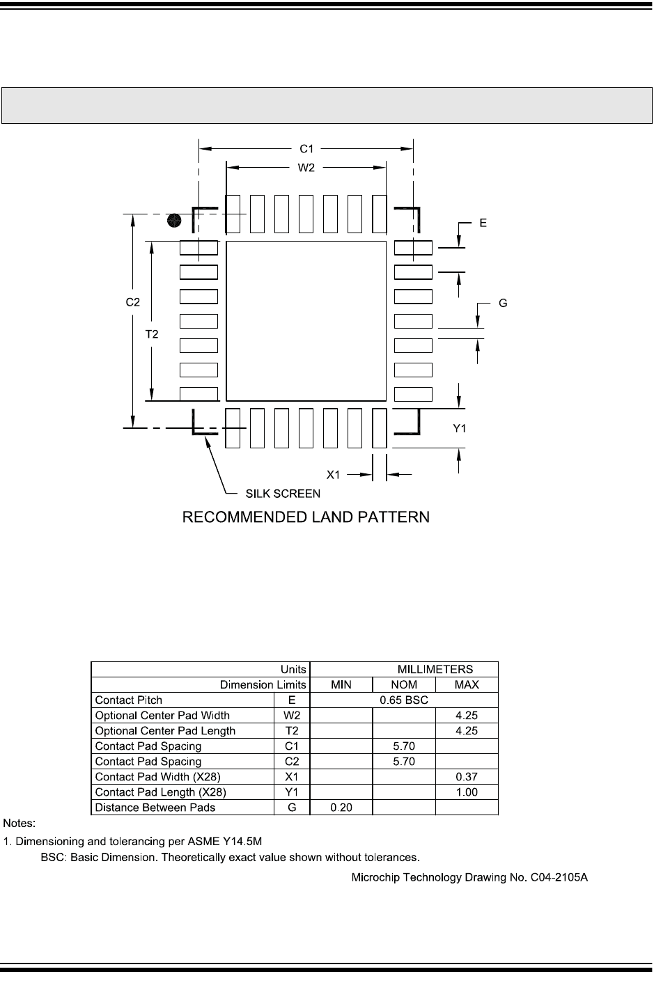
PIC32MX1XX/2XX 28/36/44-PIN FAMILY
DS60001168K-page 322 2011-2018 Microchip Technology Inc.
/HDG3ODVWLF4XDG)ODW1R/HDG3DFNDJH0/±[PP%RG\>4)1@
ZLWKPP&RQWDFW/HQJWK
1RWH )RUWKHPRVWFXUUHQWSDFNDJHGUDZLQJVSOHDVHVHHWKH0LFURFKLS3DFNDJLQJ6SHFLILFDWLRQORFDWHGDW
KWWSZZZPLFURFKLSFRPSDFNDJLQJ
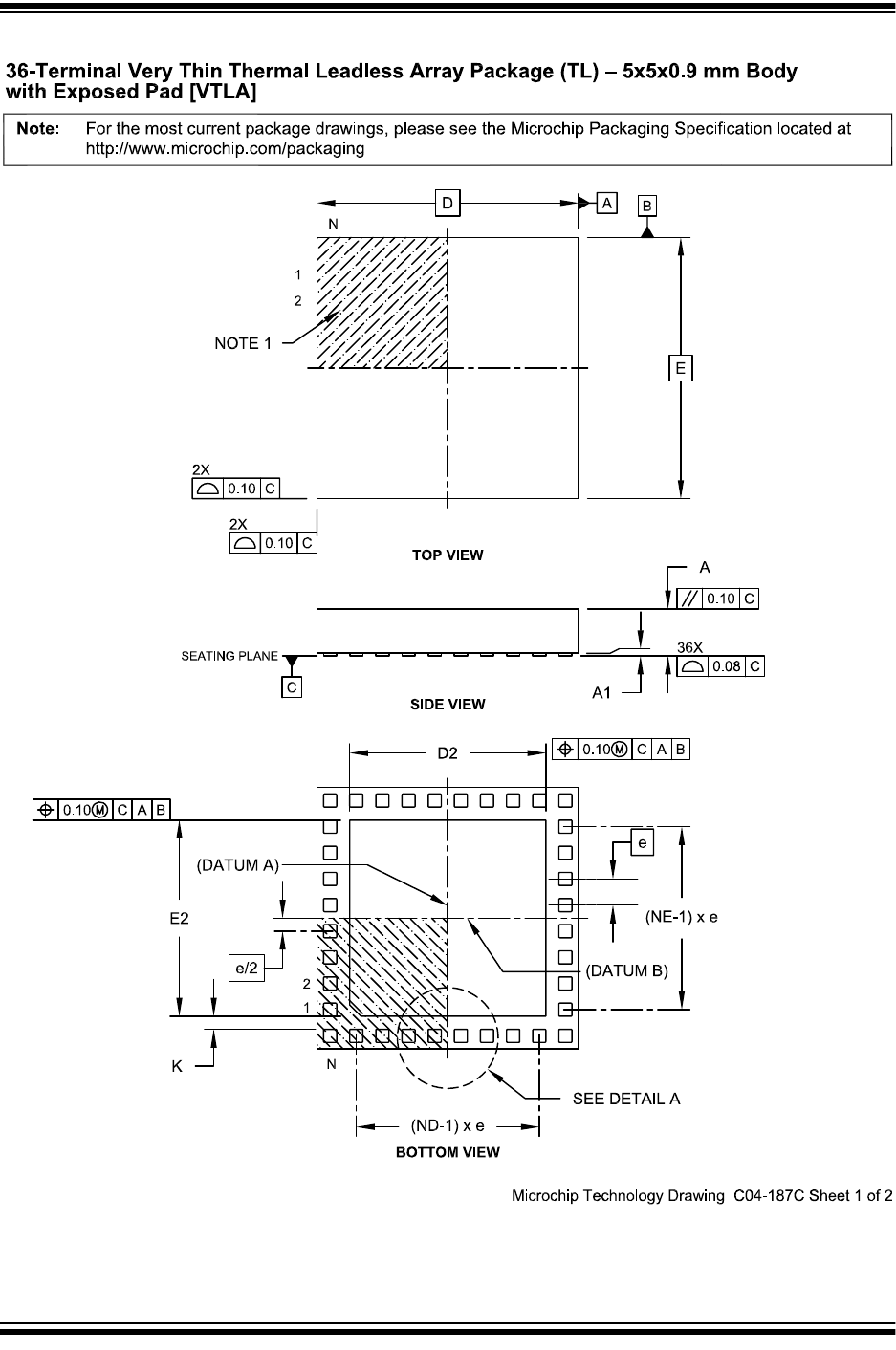
2011-2018 Microchip Technology Inc. DS60001168K-page 323
PIC32MX1XX/2XX 28/36/44-PIN FAMILY
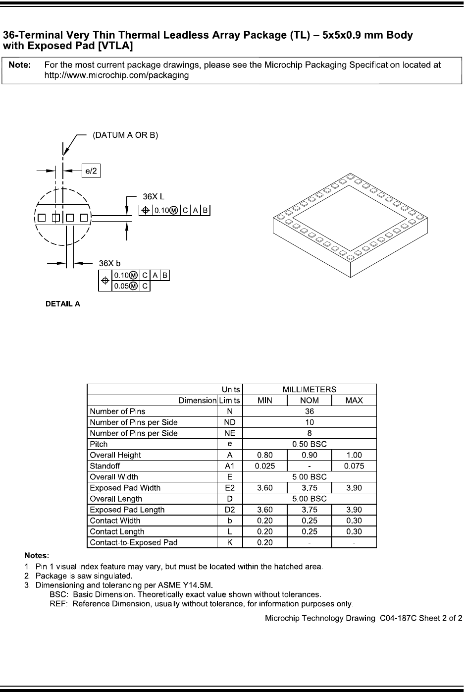
PIC32MX1XX/2XX 28/36/44-PIN FAMILY
DS60001168K-page 324 2011-2018 Microchip Technology Inc.
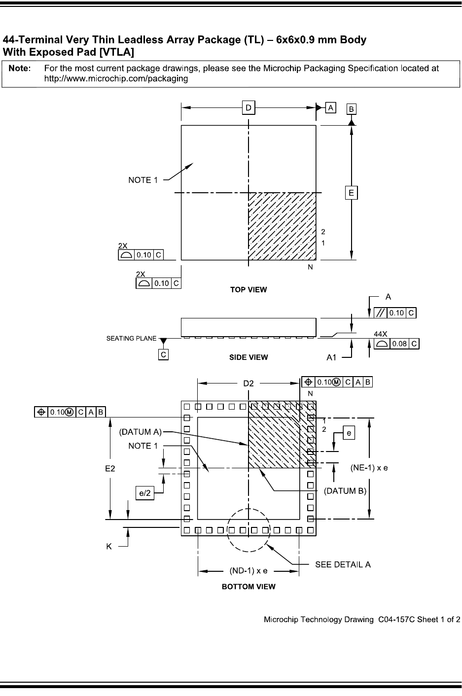
2011-2018 Microchip Technology Inc. DS60001168K-page 325
PIC32MX1XX/2XX 28/36/44-PIN FAMILY
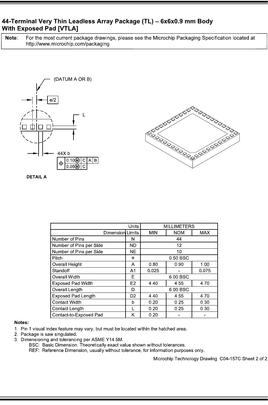
PIC32MX1XX/2XX 28/36/44-PIN FAMILY
DS60001168K-page 326 2011-2018 Microchip Technology Inc.
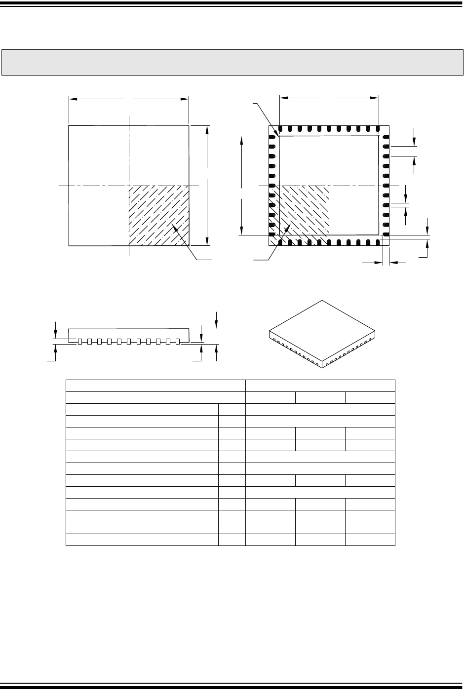
2011-2018 Microchip Technology Inc. DS60001168K-page 327
PIC32MX1XX/2XX 28/36/44-PIN FAMILY
/HDG3ODVWLF4XDG)ODW1R/HDG3DFNDJH0/±[PP%RG\>4)1@
1RWHV
3LQYLVXDOLQGH[IHDWXUHPD\YDU\EXWPXVWEHORFDWHGZLWKLQWKHKDWFKHGDUHD
3DFNDJHLVVDZVLQJXODWHG
'LPHQVLRQLQJDQGWROHUDQFLQJSHU$60(<0
%6& %DVLF'LPHQVLRQ7KHRUHWLFDOO\H[DFWYDOXHVKRZQZLWKRXWWROHUDQFHV
5() 5HIHUHQFH'LPHQVLRQXVXDOO\ZLWKRXWWROHUDQFHIRULQIRUPDWLRQSXUSRVHVRQO\
1RWH )RUWKHPRVWFXUUHQWSDFNDJHGUDZLQJVSOHDVHVHHWKH0LFURFKLS3DFNDJLQJ6SHFLILFDWLRQORFDWHGDW
KWWSZZZPLFURFKLSFRPSDFNDJLQJ
8QLWV 0,//,0(7(56
'LPHQVLRQ/LPLWV 0,1 120 0$;
1XPEHURI3LQV 1
3LWFK H %6&
2YHUDOO+HLJKW $
6WDQGRII $
&RQWDFW7KLFNQHVV $ 5()
2YHUDOO:LGWK ( %6&
([SRVHG3DG:LGWK (
2YHUDOO/HQJWK ' %6&
([SRVHG3DG/HQJWK '
&RQWDFW:LGWK E
&RQWDFW/HQJWK /
&RQWDFWWR([SRVHG3DG . ± ±
DEXPOSED
PAD
D2
e
b
K
L
E2
2
1
N
NOTE 1
2
1
E
N
BOTTOM VIEW
TOP VIEW
A3 A1
A
0LFURFKLS 7HFKQRORJ\ 'UDZLQJ &%
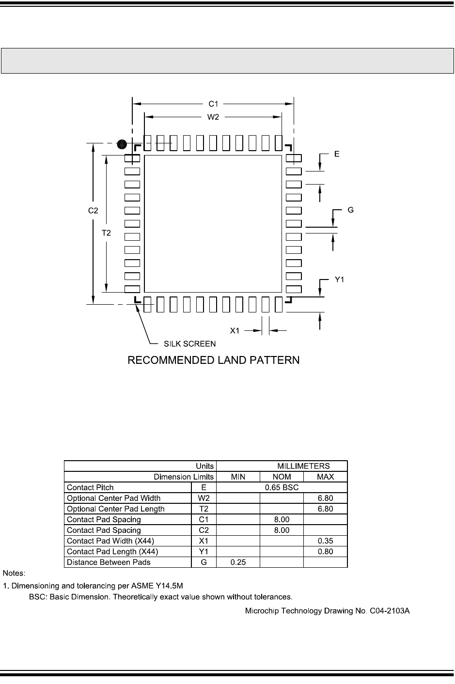
PIC32MX1XX/2XX 28/36/44-PIN FAMILY
DS60001168K-page 328 2011-2018 Microchip Technology Inc.
/HDG3ODVWLF4XDG)ODW1R/HDG3DFNDJH0/±[PP%RG\>4)1@
1RWH )RUWKHPRVWFXUUHQWSDFNDJHGUDZLQJVSOHDVHVHHWKH0LFURFKLS3DFNDJLQJ6SHFLILFDWLRQORFDWHGDW
KWWSZZZPLFURFKLSFRPSDFNDJLQJ
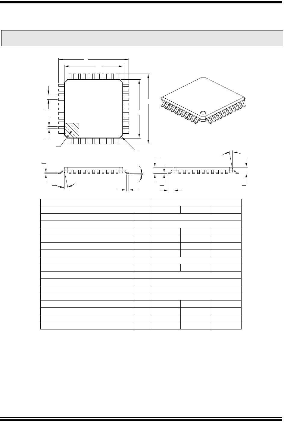
2011-2018 Microchip Technology Inc. DS60001168K-page 329
PIC32MX1XX/2XX 28/36/44-PIN FAMILY
/HDG3ODVWLF7KLQ4XDG)ODWSDFN37±[[PP%RG\PP>74)3@
1RWHV
3LQYLVXDOLQGH[IHDWXUHPD\YDU\EXWPXVWEHORFDWHGZLWKLQWKHKDWFKHGDUHD
&KDPIHUVDWFRUQHUVDUHRSWLRQDOVL]HPD\YDU\
'LPHQVLRQV'DQG(GRQRWLQFOXGHPROGIODVKRUSURWUXVLRQV0ROGIODVKRUSURWUXVLRQVVKDOOQRWH[FHHGPPSHUVLGH
'LPHQVLRQLQJDQGWROHUDQFLQJSHU$60(<0
%6& %DVLF'LPHQVLRQ7KHRUHWLFDOO\H[DFWYDOXHVKRZQZLWKRXWWROHUDQFHV
5() 5HIHUHQFH'LPHQVLRQXVXDOO\ZLWKRXWWROHUDQFHIRULQIRUPDWLRQSXUSRVHVRQO\
1RWH )RUWKHPRVWFXUUHQWSDFNDJHGUDZLQJVSOHDVHVHHWKH0LFURFKLS3DFNDJLQJ6SHFLILFDWLRQORFDWHGDW
KWWSZZZPLFURFKLSFRPSDFNDJLQJ
8QLWV 0,//,0(7(56
'LPHQVLRQ/LPLWV 0,1 120 0$;
1XPEHURI/HDGV 1
/HDG3LWFK H %6&
2YHUDOO+HLJKW $ ± ±
0ROGHG3DFNDJH7KLFNQHVV $
6WDQGRII $ ±
)RRW/HQJWK /
)RRWSULQW / 5()
)RRW$QJOH
2YHUDOO:LGWK ( %6&
2YHUDOO/HQJWK ' %6&
0ROGHG3DFNDJH:LGWK ( %6&
0ROGHG3DFNDJH/HQJWK ' %6&
/HDG7KLFNQHVV F ±
/HDG:LGWK E
0ROG'UDIW$QJOH7RS
0ROG'UDIW$QJOH%RWWRP
A
E
E1
D
D1
e
b
NOTE 1 NOTE 2
N
123
c
A1
L
A2
L1
α
φ
β
0LFURFKLS 7HFKQRORJ\ 'UDZLQJ &%
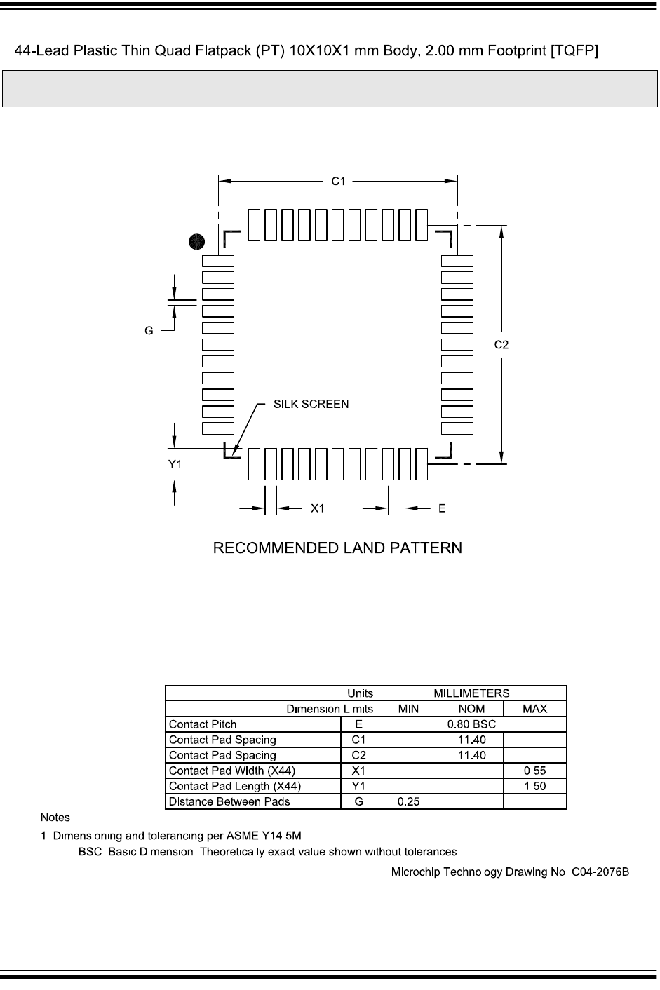
PIC32MX1XX/2XX 28/36/44-PIN FAMILY
DS60001168K-page 330 2011-2018 Microchip Technology Inc.
Note: For the most current package drawings, please see the Microchip Packaging Specification located at
http://www.microchip.com/packaging

2011-2018 Microchip Technology Inc. DS60001168K-page 331
PIC32MX1XX/2XX 28/36/44-PIN FAMILY
APPENDIX A: REVISION HISTORY
Revision A (May 2011)
This is the initial released version of this document.
Revision B (October 2011)
The following two global changes are included in this
revision:
• All packaging references to VLAP have been
changed to VTLA throughout the document
• All references to V
CORE
have been removed
• All occurrences of the ASCL1, ASCL2, ASDA1, and
ASDA2 pins have been removed
• V-temp temperature range (-40ºC to +105ºC) was
added to all electrical specification tables
This revision includes the addition of the following
devices:
Text and formatting changes were incorporated
throughout the document.
All other major changes are referenced by their
respective section in Table A -1 .
• PIC32MX130F064B • PIC32MX230F064B
• PIC32MX130F064C • PIC32MX230F064C
• PIC32MX130F064D • PIC32MX230F064D
• PIC32MX150F128B • PIC32MX250F128B
• PIC32MX150F128C • PIC32MX250F128C
• PIC32MX150F128D • PIC32MX250F128D
TABLE A-1: MAJOR SECTION UPDATES
Section Update Description
“
32-bit Microcontrollers (up to 128 KB
Flash and 32 KB SRAM) with Audio
and Graphics Interfaces, USB, and
Advanced Analog
”
Split the existing Features table into two: PIC32MX1XX General Purpose
Family Features (Table 1) and PIC32MX2XX USB Family Features (Table 2).
Added the SPDIP package reference (see Table 1, Table 2, and
“Pin
Diagrams”
).
Added the new devices to the applicable pin diagrams.
Changed PGED2 to PGED1 on pin 35 of the 36-pin VTLA diagram for
PIC32MX220F032C, PIC32MX220F016C, PIC32MX230F064C, and
PIC32MX250F128C devices.
1.0 “Device Overview”
Added the SPDIP package reference and updated the pin number for AN12
for 44-pin QFN devices in the Pinout I/O Descriptions (see Table 1-1).
Added the PGEC4/PGED4 pin pair and updated the C1INA-C1IND and
C2INA-C2IND pin numbers for 28-pin SSOP/SPDIP/SOIC devices in the
Pinout I/O Descriptions (see Table 1-1).
2.0 “Guidelines for Getting Started
with 32-bit Microcontrollers”
Updated the Recommended Minimum Connection diagram (see Figure 2-1).

PIC32MX1XX/2XX 28/36/44-PIN FAMILY
DS60001168K-page 332 2011-2018 Microchip Technology Inc.
4.0 “Memory Organization”
Added Memory Maps for the new devices (see Figure 4-3 and Figure 4-4).
Removed the BMXCHEDMA bit from the Bus Matrix Register map (see
Table 4-1).
Added the REFOTRIM register, added the DIVSWEN bit to the REFOCON
registers, added Note 4 to the ULOCK and SOSCEN bits and added the
PBDIVRDY bit in the OSCCON register in the in the System Control Register
map (see Table 4-16).
Removed the ALTI2C1 and ALTI2C2 bits from the DEVCFG3 register and
added Note 1 to the UPLLEN and UPLLIDIV<2:0> bits of the DEVCFG2
register in the Device Configuration Word Summary (see Table 4-17).
Updated Note 1 in the Device and Revision ID Summary (see Table 4-18).
Added Note 2 to the PORTA Register map (see Table 4-19).
Added the ANSB6 and ANSB12 bits to the ANSELB register in the PORTB
Register map (see Table 4-20).
Added Notes 2 and 3 to the PORTC Register map (see Table 4-21).
Updated all register names in the Peripheral Pin Select Register map (see
Table 4-23).
Added values in support of new devices (16 KB RAM and 32 KB RAM) in the
Data RAM Size register (see Register 4-5).
Added values in support of new devices (64 KB Flash and 128 KB Flash) in
the Data RAM Size register (see Register 4-5).
8.0 “Oscillator Configuration”
Added Note 5 to the PIC32MX1XX/2XX Family Clock Diagram (see
Figure 8-1).
Added the PBDIVRDY bit and Note 2 to the Oscillator Control register (see
Register 8-1).
Added the DIVSWEN bit and Note 3 to the Reference Oscillator Control
register (see Register 8-3).
Added the REFOTRIM register (see Register 8-4).
21.0 “10-bit Analog-to-Digital
Converter (ADC)”
Updated the ADC1 Module Block Diagram (see Figure 21-1).
Updated the Notes in the ADC Input Select register (see Register 21-4).
24.0 “Charge Time Measurement
Unit (CTMU)”
Updated the CTMU Block Diagram (see Figure 24-1).
Added Note 3 to the CTMU Control register (see Register 24-1)
26.0 “Special Features”
Added Note 1 and the PGEC4/PGED4 pin pair to the ICESEL<1:0> bits in
DEVCFG0: Device Configuration Word 0 (see Register 26-1).
Removed the ALTI2C1 and ALTI2C2 bits from the Device Configuration
Word 3 register (see Register 26-4).
Removed 26.3.3 “Power-up Requirements”.
Added Note 3 to the Connections for the On-Chip Regulator diagram (see
Figure 26-2).
Updated the Block Diagram of Programming, Debugging and Trace Ports
diagram (see Figure 26-3).
TABLE A-1: MAJOR SECTION UPDATES (CONTINUED)
Section Update Description

2011-2018 Microchip Technology Inc. DS60001168K-page 333
PIC32MX1XX/2XX 28/36/44-PIN FAMILY
Revision C (November 2011)
All major changes are referenced by their respective
section in Table A-2.
29.0 “Electrical Characteristics”
Updated the Absolute Maximum Ratings (removed Voltage on V
CORE
with
respect to V
SS
).
Added the SPDIP specification to the Thermal Packaging Characteristics
(see Table 29-2).
Updated the Typical values for parameters DC20-DC24 in the Operating
Current (I
DD
) specification (see Table 29-5).
Updated the Typical values for parameters DC30a-DC34a in the Idle Current
(I
IDLE
) specification (see Table 29-6).
Updated the Typical values for parameters DC40i and DC40n and removed
parameter DC40m in the Power-down Current (I
PD
) specification (see
Table 29-7).
Removed parameter D320 (V
CORE
) from the Internal Voltage Regulator
Specifications and updated the Comments (see Table 29-13).
Updated the Minimum, Typical, and Maximum values for parameter F20b in
the Internal FRC Accuracy specification (see Table 29-17).
Removed parameter SY01 (T
PWRT
) and removed all Conditions from Resets
Timing (see Table 29-20).
Updated all parameters in the CTMU Specifications (see Table 29-39).
31.0 “Packaging Information”
Added the 28-lead SPDIP package diagram information (see
31.1 “Package
Marking Information”
and
31.2 “Package Details”
).
“
Product Identification System
”
Added the SPDIP (SP) package definition.
TABLE A-1: MAJOR SECTION UPDATES (CONTINUED)
Section Update Description
TABLE A-2: MAJOR SECTION UPDATES
Section Update Description
“
32-bit Microcontrollers (up to 128 KB
Flash and 32 KB SRAM) with Audio
and Graphics Interfaces, USB, and
Advanced Analog
”
Revised the source/sink on I/O pins (see
“Input/Output”
on page 1).
Added the SPDIP package to the PIC32MX220F032B device in the
PIC32MX2XX USB Family Features (see Table 2).
4.0 “Memory Organization”
Removed ANSB6 from the ANSELB register and added the ODCB6,
ODCB10, and ODCB11 bits in the PORTB Register Map (see Table 4-20).
29.0 “Electrical Characteristics”
Updated the minimum value for parameter OS50 in the PLL Clock Timing
Specifications (see Table 29-16).

PIC32MX1XX/2XX 28/36/44-PIN FAMILY
DS60001168K-page 334 2011-2018 Microchip Technology Inc.
Revision D (February 2012)
All occurrences of V
USB
were changed to: V
USB
3
V
3
. In
addition, text and formatting changes were
incorporated throughout the document.
All other major changes are referenced by their
respective section in Tab le A-3.
TABLE A-3: MAJOR SECTION UPDATES
Section Update Description
“
32-bit Microcontrollers (up to 128
KB Flash and 32 KB SRAM) with
Audio and Graphics Interfaces, USB,
and Advanced Analog
”
Corrected a part number error in all pin diagrams.
Updated the DMA Channels (Programmable/Dedicated) column in the
PIC32MX1XX General Purpose Family Features (see Table 1).
1.0 “Device Overview”
Added the TQFP and VTLA packages to the 44-pin column heading and
updated the pin numbers for the SCL1, SCL2, SDA1, and SDA2 pins in the
Pinout I/O Descriptions (see Table 1-1).
7.0 “Interrupt Controller”
Updated the Note that follows the features.
Updated the Interrupt Controller Block Diagram (see Figure 7-1).
29.0 “Electrical Characteristics”
Updated the Maximum values for parameters DC20-DC24, and the Minimum
value for parameter DC21 in the Operating Current (I
DD
) DC Characteristics
(see Table 29-5).
Updated all Minimum and Maximum values for the Idle Current (I
IDLE
) DC
Characteristics (see Table 29-6).
Updated the Maximum values for parameters DC40k, DC40l, DC40n, and
DC40m in the Power-down Current (I
PD
) DC Characteristics (see Table 29-7).
Changed the minimum clock period for SCKx from 40 ns to 50 ns in Note 3 of
the SPIx Master and Slave Mode Timing Requirements (see Table 29-26
through Table 29-29).
30.0 “DC and AC Device
Characteristics Graphs”
Updated the Typical I
IDLE
Current @ V
DD
= 3.3V graph (see Figure 30-5).

2011-2018 Microchip Technology Inc. DS60001168K-page 335
PIC32MX1XX/2XX 28/36/44-PIN FAMILY
Revision E (October 2012)
All singular pin diagram occurrences of CV
REF
were
changed to: CV
REFOUT
. In addition, minor text and for-
matting changes were incorporated throughout the
document.
All major changes are referenced by their respective
section in Table A-4.
TABLE A-4: MAJOR SECTION UPDATES
Section Update Description
“32-bit Microcontrollers (up to
128 KB Flash and 32 KB SRAM)
with Audio and Graphics
Interfaces, USB, and Advanced
Analog”
Updated the following feature sections:
• “Operating Conditions”
• “Communication Interfaces”
2.0 “Guidelines for Getting
Started with 32-bit MCUs”
Removed Section 2.8 “Configuration of Analog and Digital Pins During ICSP
Operations”.
3.0 “CPU”
Removed references to GPR shadow registers in
3.1 “Features”
and
3.2.1 “Execution Unit”
.
4.0 “Memory Organization”
Updated the BRG bit range in the SPI1 and SPI2 Register Map (see Table 4-8).
Added the PWP<6> bit to the Device Configuration Word Summary
(see Table 4-17).
5.0 “Flash Program Memory”
Added a note with Flash page size and row size information.
7.0 “Interrupt Controller”
Updated the TPC<2:0> bit definitions (see Register 7-1).
Updated the IPTMR<31:0> bit definition (see Register 7-3).
8.0 “Oscillator Configuration”
Updated the PIC32MX1XX/2XX Family Clock Diagram (see Figure 8-1).
Updated the RODIV<14:0> bit definitions (see Register 8-3).
10.0 “USB On-The-Go (OTG)”
Updated the Notes in the USB Interface Diagram (see Figure 10-1).
18.0 “Universal Asynchronous
Receiver Transmitter (UART)”
Updated the baud rate range in the list of primary features.
26.0 “Special Features”
Added the PWP<6> bit to the Device Configuration Word 0
(see Register 26-1).
29.0 “Electrical Characteristics”
Added Note 1 to Operating MIPS vs. Voltage (see Table 29-1).
Added Note 2 to DC Temperature and Voltage Specifications (see Table 29-4).
Updated the Conditions for parameter DC25 in DC Characteristics: Operating
Current (I
DD
) (see Table 29-5).
Added Note 2 to Electrical Characteristics: BOR (see Table 29-10).
Added Note 4 to Comparator Specifications (see Table 29-12).
Added Note 5 to ADC Module Specifications (see Table 29-32).
Updated the 10-bit Conversion Rate Parameters and added Note 3 (see
Table 29-33).
Added Note 4 to the Analog-to-Digital Conversion Timing Requirements (see
Table 29-34).
Added Note 3 to CTMU Current Source Specifications (see Table 29-39).
30.0 “50 MHz Electrical
Characteristics”
New chapter with electrical characteristics for 50 MHz devices.
31.0 “Packaging Information”
The 36-pin and 44-pin VTLA packages have been updated.

PIC32MX1XX/2XX 28/36/44-PIN FAMILY
DS60001168K-page 336 2011-2018 Microchip Technology Inc.
Revision F (February 2014)
This revision includes the addition of the following
devices:
In addition, this revision includes the following major
changes as described in Ta bl e A - 5 , as well as minor
updates to text and formatting, which were
incorporated throughout the document.
• PIC32MX170F256B • PIC32MX270F256B
• PIC32MX170F256D • PIC32MX270F256D
TABLE A-5: MAJOR SECTION UPDATES
Section Update Description
32-bit Microcontrollers (up to 256
KB Flash and 64 KB SRAM) with
Audio and Graphics Interfaces,
USB, and Advanced Analog
Added new devices to the family features (see Table 1 and Table 2).
Updated pin diagrams to include new devices (see
“Pin Diagrams”
).
1.0 “Device Overview”
Added Note 3 reference to the following pin names: V
BUS
, V
USB
3
V
3
, V
BUSON
,
D+, D-, and USBID.
2.0 “Guidelines for Getting
Started with 32-bit MCUs”
Replaced Figure 2-1: Recommended Minimum Connection.
Updated Figure 2-2: MCLR Pin Connections.
Added
2.9 “S
OSC
Design Recommendation”
.
4.0 “Memory Organization”
Added memory tables for devices with 64 KB RAM (see Table 4-4 through
Table 4-5).
Changed the Virtual Addresses for all registers and updated the PWP bits in
the DEVCFG: Device Configuration Word Summary (see Table 4-17).
Updated the ODCA, ODCB, and ODCC port registers (see Table 4-19, Table 4-
20, and Table 4-21).
The RTCTIME, RTCDATE, ALRMTIME, and ALRMDATE registers were
updated (see Table 4-25).
Added Data Ram Size value for 64 KB RAM devices (see Register 4-5).
Added Program Flash Size value for 256 KB Flash devices (see Register 4-5).
12.0 “Timer1”
The Timer1 block diagram was updated to include the 16-bit data bus (see
Figure 12-1).
13.0 “Timer2/3, Timer4/5”
The Timer2-Timer5 block diagram (16-bit) was updated to include the 16-bit
data bus (see Figure 13-1).
The Timer2/3, Timer4/5 block diagram (32-bit) was updated to include the 32-
bit data bus (see Figure 13-1).
19.0 “Parallel Master Port (PMP)”
The CSF<1:0> bit value definitions for ‘00’ and ‘01’ were updated (see
Register 19-1).
Bit 14 in the Parallel Port Address register (PMADDR) was updated (see
Register 19-3).
20.0 “Real-Time Clock and
Calendar (RTCC)”
The following registers were updated:
RTCTIME (see Register 20-3)
RTCDATE (see Register 20-4)
ALRMTIME (see Register 20-5)
ALRMDATE (see Register 20-6)
26.0 “Special Features”
Updated the PWP bits (see Register 26-1).
29.0 “Electrical Characteristics”
Added parameters DO50 and DO50a to the Capacitive Loading Requirements
on Output Pins (see Table 29-14).
Added Note 5 to the I
DD
DC Characteristics (see Table 29-5).
Added Note 4 to the I
IDLE
DC Characteristics (see Table 29-6).
Added Note 5 to the I
PD
DC Characteristics (see Table 29-7).
Updated the conditions for parameters USB321 (V
OL
) and USB322 (V
OH
) in the
OTG Electrical Specifications (see Table 29-38).
Product Identification System
Added 40 MHz speed information.

2011-2018 Microchip Technology Inc. DS60001168K-page 337
PIC32MX1XX/2XX 28/36/44-PIN FAMILY
Revision G (April 2015)
This revision includes the addition of the following
devices:
The title of the document was updated to avoid
confusion with the PIC32MX1XX/2XX/5XX 64/100-pin
Family data sheet.
All peripheral SFR maps have been relocated from the
Memory chapter to their respective peripheral
chapters.
In addition, this revision includes the following major
changes as described in Ta bl e A - 6 , as well as minor
updates to text and formatting, which were
incorporated throughout the document.
Revision H (July 2015)
This revision includes the following major changes as
described in Tab l e A- 7, as well as minor updates to text
and formatting, which were incorporated throughout
the document.
• PIC32MX130F256B • PIC32MX230F256B
• PIC32MX130F256D • PIC32MX230F256D
TABLE A-6: MAJOR SECTION UPDATES
Section Update Description
32-bit Microcontrollers (up to 256
KB Flash and 64 KB SRAM) with
Audio and Graphics Interfaces,
USB, and Advanced Analog
Added new devices to the family features (see Table 1 and Table 2).
Updated pin diagrams to include new devices (see Pin Diagrams).
2.0 “Guidelines for Getting
Started with 32-bit MCUs”
Updated these sections:
2.2 “Decoupling Capacitors”
,
2.3 “Capacitor on
Internal Voltage Regulator (V
CAP
)”
,
2.4 “Master Clear (MCLR) Pin”
,
2.8.1 “Crystal Oscillator Design Consideration”
4.0 “Memory Organization”
Added Memory Map for new devices (see Figure 4-6).
14.0 “Watchdog Timer (WDT)”
New chapter created from content previously located in the Special Features
chapter.
30.0 “Electrical Characteristics”
Removed parameter D312 (T
SET
) from the Comparator Specifications (see
Table 30-12).
Added the Comparator Voltage Reference Specifications (see Table 30-13).
Updated Table 30-12.
TABLE A-7: MAJOR SECTION UPDATES
Section Update Description
2.0 “Guidelines for Getting
Started with 32-bit MCUs” Section 2.9 “Sosc Design Recommendation”
was removed.
8.0 “Oscillator Configuration”
The Primary Oscillator (P
OSC
) logic in the Oscillator diagram was updated (see
Figure 8-1).
30.0 “Electrical Characteristics”
The Power-Down Current (I
PD
) DC Characteristics parameter DC40k was
updated (see Ta b l e 3 0 - 7 ).
Table 30-9: “DC Characteristics: I/O Pin Input Injection current
Specifications”
was added.

PIC32MX1XX/2XX 28/36/44-PIN FAMILY
DS60001168K-page 338 2011-2018 Microchip Technology Inc.
Revision J (April 2016)
This revision includes the following major changes as
described in Tab l e A- 8, as well as minor updates to text
and formatting, which were incorporated throughout
the document.
Revision K (May 2018)
This revision includes the following major changes as
described in Tab l e A- 9, as well as minor updates to text
and formatting, which were incorporated throughout
the document.
TABLE A-8: MAJOR SECTION UPDATES
Section Update Description
“32-bit Microcontrollers (up to
256 KB Flash and 64 KB
SRAM) with Audio and
Graphics Interfaces, USB, and
Advanced Analog”
The PIC32MX270FDB device and Note 4 were added to
TABLE 2: “PIC32MX2XX
28/36/44-pin USB Family Features”
.
2.0 “Guidelines for Getting
Started with 32-bit MCUs” EXAMPLE 2-1: “Crystal Load Capacitor Calculation”
was updated.
30.0 “Electrical
Characteristics”
Parameter DO50a (C
SOSC
) was removed from the Capacitive Loading
Requirements on Output Pins AC Characteristics (see Table 30-16).
“Product Identification
System”
The device mapping was updated to include type B for Software Targeting.
TABLE A-9: MAJOR SECTION UPDATES
Section Update Description
“32-bit Microcontrollers (up to
256 KB Flash and 64 KB
SRAM) with Audio and
Graphics Interfaces, USB, and
Advanced Analog”
The PIC32MX270F256DB device and Note 4 were removed from the
PIC32MX2XX 28/36/44-Pin USB Family Features (see Tabl e 2).
“Product Identification
System”
Type B for Software Targeting was removed.
Section 2.10 “Considerations
When Interfacing To Remotely
Powered Circuits”
A new section has been added.

2011-2018 Microchip Technology Inc. DS60001168K-page 339
PIC32MX1XX/2XX 28/36/44-PIN FAMILY
INDEX
Numerics
50 MHz Electrical Characteristics ..................................... 303
A
AC Characteristics ............................................................ 271
10-Bit Conversion Rate Parameters ......................... 293
ADC Specifications ................................................... 291
Analog-to-Digital Conversion Requirements............. 294
EJTAG Timing Requirements ................................... 302
Internal FRC Accuracy.............................................. 273
Internal RC Accuracy ................................................ 273
OTG Electrical Specifications ................................... 300
Parallel Master Port Read Requirements ................. 299
Parallel Master Port Write......................................... 300
Parallel Master Port Write Requirements.................. 300
Parallel Slave Port Requirements ............................. 298
PLL Clock Timing...................................................... 273
Analog-to-Digital Converter (ADC).................................... 211
Assembler
MPASM Assembler................................................... 256
B
Block Diagrams
ADC Module.............................................................. 211
Comparator I/O Operating Modes............................. 221
Comparator Voltage Reference ................................ 225
Connections for On-Chip Voltage Regulator............. 252
Core and Peripheral Modules ..................................... 19
CPU ............................................................................ 35
CTMU Configurations
Time Measurement........................................... 229
DMA ............................................................................ 85
I2C Circuit ................................................................. 176
Input Capture ............................................................ 159
Interrupt Controller ...................................................... 65
JTAG Programming, Debugging and Trace Ports .... 252
Output Compare Module........................................... 163
PMP Pinout and Connections to External Devices ... 191
Reset System.............................................................. 61
RTCC ........................................................................ 201
SPI Module ............................................................... 167
Timer1....................................................................... 145
Timer2/3/4/5 (16-Bit)................................................. 149
Typical Multiplexed Port Structure ............................ 129
UART ........................................................................ 183
WDT and Power-up Timer ........................................ 155
Brown-out Reset (BOR)
and On-Chip Voltage Regulator................................ 252
C
C Compilers
MPLAB C18 .............................................................. 256
Charge Time Measurement Unit. See CTMU.
Clock Diagram .................................................................... 76
Comparator
Specifications.................................................... 269, 270
Comparator Module .......................................................... 221
Comparator Voltage Reference (CVref ............................. 225
Configuration Bit ............................................................... 241
Configuring Analog Port Pins............................................ 130
CPU
Architecture Overview................................................. 36
Coprocessor 0 Registers ............................................ 37
Core Exception Types ................................................ 38
EJTAG Debug Support............................................... 38
Power Management ................................................... 38
CPU Module ................................................................. 27, 35
Customer Change Notification Service............................. 343
Customer Notification Service .......................................... 343
Customer Support............................................................. 343
D
DC and AC Characteristics
Graphs and Tables ................................................... 309
DC Characteristics............................................................ 260
I/O Pin Input Specifications .............................. 265, 266
I/O Pin Output Specifications.................................... 267
Idle Current (I
IDLE
) .................................................... 263
Power-Down Current (I
PD
)........................................ 264
Program Memory...................................................... 268
Temperature and Voltage Specifications.................. 261
DC Characteristics (50 MHz)............................................ 304
Idle Current (I
IDLE
) .................................................... 305
Power-Down Current (I
PD
)........................................ 305
Development Support....................................................... 255
Direct Memory Access (DMA) Controller............................ 85
E
Electrical Characteristics .................................................. 259
AC............................................................................. 271
Errata.................................................................................. 17
External Clock
Timer1 Timing Requirements ................................... 277
Timer2, 3, 4, 5 Timing Requirements ....................... 278
Timing Requirements ............................................... 272
External Clock (50 MHz)
Timing Requirements ............................................... 306
F
Flash Program Memory ...................................................... 55
RTSP Operation ......................................................... 55
I
I/O Ports ........................................................................... 129
Parallel I/O (PIO) ...................................................... 130
Write/Read Timing.................................................... 130
Input Change Notification ................................................. 130
Instruction Set................................................................... 253
Inter-Integrated Circuit (I2C .............................................. 175
Internal Voltage Reference Specifications........................ 270
Internet Address ............................................................... 343
Interrupt Controller.............................................................. 65
IRG, Vector and Bit Location...................................... 66
M
Memory Maps
PIC32MX110/210 Devices
(4 KB RAM, 16 KB Flash)................................... 40
PIC32MX120/220 Devices
(8 KB RAM, 32 KB Flash)................................... 41
PIC32MX130/230
(16 KB RAM, 256 KB Flash)............................... 45
PIC32MX130/230 Devices
(16 KB RAM, 64 KB Flash)................................. 42
PIC32MX150/250 Devices
(32 KB RAM, 128 KB Flash)............................... 43
PIC32MX170/270

PIC32MX1XX/2XX 28/36/44-PIN FAMILY
DS60001168K-page 340 2011-2018 Microchip Technology Inc.
(64 KB RAM, 256 KB Flash) ............................... 44
Memory Organization.......................................................... 39
Microchip Internet Web Site ..............................................343
MPLAB ASM30 Assembler, Linker, Librarian ................... 256
MPLAB Integrated Development Environment Software .. 255
MPLAB PM3 Device Programmer.....................................257
MPLAB REAL ICE In-Circuit Emulator System.................257
MPLINK Object Linker/MPLIB Object Librarian ................ 256
O
Oscillator Configuration....................................................... 75
Output Compare................................................................ 163
P
Packaging ......................................................................... 313
Details ....................................................................... 315
Marking ..................................................................... 313
Parallel Master Port (PMP) ...............................................191
PIC32 Family USB Interface Diagram............................... 106
Pinout I/O Descriptions (table) ............................................20
Power-on Reset (POR)
and On-Chip Voltage Regulator................................ 252
Power-Saving Features.....................................................235
CPU Halted Methods ................................................235
Operation .................................................................. 235
with CPU Running.....................................................235
R
Real-Time Clock and Calendar (RTCC)............................ 201
Register Maps ............................................................... 47–??
Registers
[pin name]R (Peripheral Pin Select Input)................. 143
AD1CHS (ADC Input Select) ....................................219
AD1CON1 (ADC Control 1) ......................................215
AD1CON2 (ADC Control 2) ......................................217
AD1CON3 (ADC Control 3) ......................................218
AD1CSSL (ADC Input Scan Select) ......................... 220
ALRMDATE (Alarm Date Value)...............................210
ALRMTIME (Alarm Time Value) ............................... 209
BMXBOOTSZ (Boot Flash (IFM) Size ........................ 53
BMXCON (Bus Matrix Configuration) .........................48
BMXDKPBA (Data RAM Kernel Program
Base Address) .................................................... 49
BMXDRMSZ (Data RAM Size Register) ..................... 52
BMXDUDBA (Data RAM User Data Base Address) ... 50
BMXDUPBA (Data RAM User Program
Base Address) .................................................... 51
BMXPFMSZ (Program Flash (PFM) Size) ..................53
BMXPUPBA (Program Flash (PFM) User Program
Base Address) .................................................... 52
CFGCON (Configuration Control) .............................250
CM1CON (Comparator 1 Control) ............................223
CMSTAT (Comparator Status Register) ...................224
CNCONx (Change Notice Control for PORTx) ......... 144
CTMUCON (CTMU Control) .....................................231
CVRCON (Comparator Voltage Reference Control). 227
DCHxCON (DMA Channel ’x’ Control)........................ 95
DCHxCPTR (DMA Channel ’x’ Cell Pointer) ............. 102
DCHxCSIZ (DMA Channel ’x’ Cell-Size)................... 102
DCHxDAT (DMA Channel ’x’ Pattern Data) .............. 103
DCHxDPTR (Channel ’x’ Destination Pointer) .......... 101
DCHxDSA (DMA Channel ’x’ Destination
Start Address) .....................................................99
DCHxDSIZ (DMA Channel ’x’ Destination Size) ....... 100
DCHxECON (DMA Channel ’x’ Event Control) ........... 96
DCHxINT (DMA Channel ’x’ Interrupt Control)............ 97
DCHxSPTR (DMA Channel ’x’ Source Pointer)........ 101
DCHxSSA (DMA Channel ’x’ Source Start Address).. 99
DCHxSSIZ (DMA Channel ’x’ Source Size).............. 100
DCRCCON (DMA CRC Control)................................. 92
DCRCDATA (DMA CRC Data) ................................... 94
DCRCXOR (DMA CRCXOR Enable) ......................... 94
DEVCFG0 (Device Configuration Word 0) ............... 243
DEVCFG1 (Device Configuration Word 1) ............... 245
DEVCFG2 (Device Configuration Word 2) ............... 247
DEVCFG3 (Device Configuration Word 3) ............... 249
DEVID (Device and Revision ID).............................. 251
DMAADDR (DMA Address)........................................ 91
DMACON (DMA Controller Control) ........................... 90
DMASTAT (DMA Status)............................................ 91
I2CxCON (I2C Control)............................................. 178
I2CxSTAT (I2C Status)............................................. 180
ICxCON (Input Capture ’x’ Control) .......................... 161
IECx (Interrupt Enable Control) .................................. 72
IFSx (Interrupt Flag Status) ........................................ 72
INTCON (Interrupt Control)......................................... 70
INTSTAT (Interrupt Status)......................................... 71
IPCx (Interrupt Priority Control) .................................. 73
IPTMR (Interrupt Proximity Timer).............................. 71
NVMADDR (Flash Address) ....................................... 58
NVMCON (Programming Control) .............................. 57
NVMDATA (Flash Program Data)............................... 59
NVMKEY (Programming Unlock)................................ 58
NVMSRCADDR (Source Data Address) .................... 59
OCxCON (Output Compare ’x’ Control).................... 165
OSCCON (Oscillator Control)..................................... 78
OSCTUN (FRC Tuning).............................................. 81
PMADDR (Parallel Port Address)............................. 197
PMAEN (Parallel Port Pin Enable)............................ 198
PMCON (Parallel Port Control)................................. 193
PMMODE (Parallel Port Mode)................................. 195
PMSTAT (Parallel Port Status (Slave Modes Only).. 199
REFOCON (Reference Oscillator Control) ................. 82
REFOTRIM (Reference Oscillator Trim)..................... 84
RPnR (Peripheral Pin Select Output) ....................... 143
RSWRST (Software Reset) ........................................ 64
RTCALRM (RTC Alarm Control)............................... 205
RTCCON (RTC Control)........................................... 203
RTCDATE (RTC Date Value) ................................... 208
RTCTIME (RTC Time Value).................................... 207
SPIxCON (SPI Control) ............................................ 169
SPIxCON2 (SPI Control 2) ....................................... 172
SPIxSTAT (SPI Status)............................................. 173
T1CON (Type A Timer Control)................................ 147
TxCON (Type B Timer Control) ................................ 152
U1ADDR (USB Address).......................................... 123
U1BDTP1 (USB BDT Page 1) .................................. 125
U1BDTP2 (USB BDT Page 2) .................................. 126
U1BDTP3 (USB BDT Page 3) .................................. 126
U1CNFG1 (USB Configuration 1)............................. 127
U1CON (USB Control).............................................. 121
U1EIE (USB Error Interrupt Enable)......................... 119
U1EIR (USB Error Interrupt Status).......................... 117
U1EP0-U1EP15 (USB Endpoint Control) ................. 128
U1FRMH (USB Frame Number High) ...................... 124
U1FRML (USB Frame Number Low)........................ 123
U1IE (USB Interrupt Enable) .................................... 116
U1IR (USB Interrupt) ................................................ 115
U1OTGCON (USB OTG Control) ............................. 113
U1OTGIE (USB OTG Interrupt Enable).................... 111
U1OTGIR (USB OTG Interrupt Status)..................... 110

2011-2018 Microchip Technology Inc. DS60001168K-page 341
PIC32MX1XX/2XX 28/36/44-PIN FAMILY
U1OTGSTAT (USB OTG Status).............................. 112
U1PWRC (USB Power Control)................................ 114
U1SOF (USB SOF Threshold).................................. 125
U1STAT (USB Status) .............................................. 120
U1TOK (USB Token) ................................................ 124
UxMODE (UARTx Mode).......................................... 185
UxSTA (UARTx Status and Control)......................... 187
WDTCON (Watchdog Timer Control) ....................... 157
Resets................................................................................. 61
Revision History ................................................................ 331
RTCALRM (RTC ALARM Control).................................... 205
S
Serial Peripheral Interface (SPI) ....................................... 167
Software Simulator (MPLAB SIM)..................................... 257
Special Features ............................................................... 241
T
Timer1 Module .................................................................. 145
Timer2/3, Timer4/5 Modules ............................................. 149
Timing Diagrams
10-Bit Analog-to-Digital Conversion
(ASAM = 0, SSRC<2:0> = 000)........................ 295
10-Bit Analog-to-Digital Conversion (ASAM = 1,
SSRC<2:0> = 111, SAMC<4:0> = 00001)........ 296
EJTAG ...................................................................... 302
External Clock........................................................... 271
I/O Characteristics .................................................... 274
I2Cx Bus Data (Master Mode) .................................. 285
I2Cx Bus Data (Slave Mode) .................................... 288
I2Cx Bus Start/Stop Bits (Master Mode) ................... 285
I2Cx Bus Start/Stop Bits (Slave Mode) ..................... 288
Input Capture (CAPx)................................................ 278
OCx/PWM ................................................................. 279
Output Compare (OCx)............................................. 279
Parallel Master Port Read......................................... 298
Parallel Master Port Write......................................... 299
Parallel Slave Port .................................................... 297
SPIx Master Mode (CKE = 0) ................................... 280
SPIx Master Mode (CKE = 1) ................................... 281
SPIx Slave Mode (CKE = 0) ..................................... 282
SPIx Slave Mode (CKE = 1) ..................................... 283
Timer1, 2, 3, 4, 5 External Clock .............................. 277
UART Reception....................................................... 189
UART Transmission (8-bit or 9-bit Data) .................. 189
Timing Requirements
CLKO and I/O ........................................................... 274
Timing Specifications
I2Cx Bus Data Requirements (Master Mode)........... 286
I2Cx Bus Data Requirements (Slave Mode)............. 289
Input Capture Requirements .................................... 278
Output Compare Requirements................................ 279
Simple OCx/PWM Mode Requirements ................... 279
SPIx Master Mode (CKE = 0) Requirements............ 280
SPIx Master Mode (CKE = 1) Requirements............ 281
SPIx Slave Mode (CKE = 1) Requirements.............. 283
SPIx Slave Mode Requirements (CKE = 0).............. 282
Timing Specifications (50 MHz)
SPIx Master Mode (CKE = 0) Requirements............ 306
SPIx Master Mode (CKE = 1) Requirements............ 306
SPIx Slave Mode (CKE = 1) Requirements.............. 307
SPIx Slave Mode Requirements (CKE = 0).............. 307
U
UART................................................................................ 183
USB On-The-Go (OTG).................................................... 105
V
V
CAP
pin............................................................................ 252
Voltage Regulator (On-Chip) ............................................ 252
W
WWW Address ................................................................. 343
WWW, On-Line Support ..................................................... 17

PIC32MX1XX/2XX 28/36/44-PIN FAMILY
DS60001168K-page 342 2011-2018 Microchip Technology Inc.
NOTES:

2011-2018 Microchip Technology Inc. DS60001168K-page 343
PIC32MX1XX/2XX 28/36/44-PIN FAMILY
THE MICROCHIP WEB SITE
Microchip provides online support via our WWW site at
www.microchip.com. This web site is used as a means
to make files and information easily available to
customers. Accessible by using your favorite Internet
browser, the web site contains the following
information:
•
Product Support
– Data sheets and errata,
application notes and sample programs, design
resources, user’s guides and hardware support
documents, latest software releases and archived
software
•
General Technical Support
– Frequently Asked
Questions (FAQ), technical support requests,
online discussion groups, Microchip consultant
program member listing
•
Business of Microchip
– Product selector and
ordering guides, latest Microchip press releases,
listing of seminars and events, listings of
Microchip sales offices, distributors and factory
representatives
CUSTOMER CHANGE NOTIFICATION
SERVICE
Microchip’s customer notification service helps keep
customers current on Microchip products. Subscribers
will receive e-mail notification whenever there are
changes, updates, revisions or errata related to a
specified product family or development tool of interest.
To register, access the Microchip web site at
www.microchip.com. Under “Support”, click on
“Customer Change Notification” and follow the
registration instructions.
CUSTOMER SUPPORT
Users of Microchip products can receive assistance
through several channels:
• Distributor or Representative
• Local Sales Office
• Field Application Engineer (FAE)
• Technical Support
Customers should contact their distributor,
representative or Field Application Engineer (FAE) for
support. Local sales offices are also available to help
customers. A listing of sales offices and locations is
included in the back of this document.
Technical support is available through the web site
at: http://microchip.com/support

2011-2018 Microchip Technology Inc. DS60001168K-page 344
PIC32MX1XX/2XX 28/36/44-PIN FAMILY
PRODUCT IDENTIFICATION SYSTEM
To order or obtain information, e.g., on pricing or delivery, refer to the factory or the listed sales office
.
Architecture MX = M4K
®
MCU core
Product Groups 1XX = General purpose microcontroller family
2XX = General purpose microcontroller family
Flash Memory Family F = Flash program memory
Program Memory Size 016 = 16K
032 = 32K
064 = 64K
128 = 128K
256 = 256K
Pin Count B = 28-pin
C = 36-pin
D = 44-pin
Speed ( ) = 40 MHz – ( ) indicates a blank field; package markings for 40 MHz devices do not include the Speed
50 = 50 MHz
Temperature Range I = -40°C to +85°C (Industrial)
V = -40°C to +105°C (V-temp)
Package ML = 28-Lead (6x6 mm) QFN (Plastic Quad Flatpack)
ML = 44-Lead (8x8 mm) QFN (Plastic Quad Flatpack)
PT = 44-Lead (10x10x1 mm) TQFP (Plastic Thin Quad Flatpack)
SO = 28-Lead (7.50 mm) SOIC (Plastic Small Outline)
SP = 28-Lead (300 mil) SPDIP (Skinny Plastic Dual In-line)
SS = 28-Lead (5.30 mm) SSOP (Plastic Shrink Small Outline)
TL = 36-Lead (5x5 mm) VTLA (Very Thin Leadless Array)
TL = 44-Lead (6x6 mm) VTLA (Very Thin Leadless Array)
Pattern Three-digit QTP, SQTP, Code or Special Requirements (blank otherwise)
ES = Engineering Sample
Example:
PIC32MX110F032DT-I/PT:
General purpose PIC32,
32-bit RISC MCU with M4K
®
core,
32 KB program memory, 44-pin,
Industrial temperature,
TQFP package.
Microchip Brand
Architecture
Flash Memory Family
Pin Count
Product Groups
Program Memory Size (KB)
PIC32 MX1XX F 032 D T - 50 I / PT - XXX
Flash Memory Family
Pattern
Package
Temperature Range
Tape and Reel Flag (if applicable)
Speed (if applicable)

2011-2018 Microchip Technology Inc. DS60001168K-page 345
Information contained in this publication regarding device
applications and the like is provided only for your convenience
and may be superseded by updates. It is your responsibility to
ensure that your application meets with your specifications.
MICROCHIP MAKES NO REPRESENTATIONS OR
WARRANTIES OF ANY KIND WHETHER EXPRESS OR
IMPLIED, WRITTEN OR ORAL, STATUTORY OR
OTHERWISE, RELATED TO THE INFORMATION,
INCLUDING BUT NOT LIMITED TO ITS CONDITION,
QUALITY, PERFORMANCE, MERCHANTABILITY OR
FITNESS FOR PURPOSE
.
Microchip disclaims all liability
arising from this information and its use. Use of Microchip
devices in life support and/or safety applications is entirely at
the buyer’s risk, and the buyer agrees to defend, indemnify and
hold harmless Microchip from any and all damages, claims,
suits, or expenses resulting from such use. No licenses are
conveyed, implicitly or otherwise, under any Microchip
intellectual property rights unless otherwise stated.
Trademarks
The Microchip name and logo, the Microchip logo, AnyRate, AVR,
AVR logo, AVR Freaks, BeaconThings, BitCloud, CryptoMemory,
CryptoRF, dsPIC, FlashFlex, flexPWR, Heldo, JukeBlox, K
EE
L
OQ
,
K
EE
L
OQ
logo, Kleer, LANCheck, LINK MD, maXStylus,
maXTouch, MediaLB, megaAVR, MOST, MOST logo, MPLAB,
OptoLyzer, PIC, picoPower, PICSTART, PIC32 logo, Prochip
Designer, QTouch, RightTouch, SAM-BA, SpyNIC, SST, SST
Logo, SuperFlash, tinyAVR, UNI/O, and XMEGA are registered
trademarks of Microchip Technology Incorporated in the U.S.A.
and other countries.
ClockWorks, The Embedded Control Solutions Company,
EtherSynch, Hyper Speed Control, HyperLight Load, IntelliMOS,
mTouch, Precision Edge, and Quiet-Wire are registered
trademarks of Microchip Technology Incorporated in the U.S.A.
Adjacent Key Suppression, AKS, Analog-for-the-Digital Age, Any
Capacitor, AnyIn, AnyOut, BodyCom, chipKIT, chipKIT logo,
CodeGuard, CryptoAuthentication, CryptoCompanion,
CryptoController, dsPICDEM, dsPICDEM.net, Dynamic Average
Matching, DAM, ECAN, EtherGREEN, In-Circuit Serial
Programming, ICSP, Inter-Chip Connectivity, JitterBlocker,
KleerNet, KleerNet logo, Mindi, MiWi, motorBench, MPASM, MPF,
MPLAB Certified logo, MPLIB, MPLINK, MultiTRAK, NetDetach,
Omniscient Code Generation, PICDEM, PICDEM.net, PICkit,
PICtail, PureSilicon, QMatrix, RightTouch logo, REAL ICE, Ripple
Blocker, SAM-ICE, Serial Quad I/O, SMART-I.S., SQI,
SuperSwitcher, SuperSwitcher II, Total Endurance, TSHARC,
USBCheck, VariSense, ViewSpan, WiperLock, Wireless DNA, and
ZENA are trademarks of Microchip Technology Incorporated in the
U.S.A. and other countries.
SQTP is a service mark of Microchip Technology Incorporated in
the U.S.A.
Silicon Storage Technology is a registered trademark of Microchip
Technology Inc. in other countries.
GestIC is a registered trademark of Microchip Technology
Germany II GmbH & Co. KG, a subsidiary of Microchip Technology
Inc., in other countries.
All other trademarks mentioned herein are property of their
respective companies.
© 2011-2018, Microchip Technology Incorporated, All Rights
Reserved.
ISBN: 978-1-5224-2979-1
Note the following details of the code protection feature on Microchip devices:
• Microchip products meet the specification contained in their particular Microchip Data Sheet.
• Microchip believes that its family of products is one of the most secure families of its kind on the market today, when used in the
intended manner and under normal conditions.
• There are dishonest and possibly illegal methods used to breach the code protection feature. All of these methods, to our
knowledge, require using the Microchip products in a manner outside the operating specifications contained in Microchip’s Data
Sheets. Most likely, the person doing so is engaged in theft of intellectual property.
• Microchip is willing to work with the customer who is concerned about the integrity of their code.
• Neither Microchip nor any other semiconductor manufacturer can guarantee the security of their code. Code protection does not
mean that we are guaranteeing the product as “unbreakable.”
Code protection is constantly evolving. We at Microchip are committed to continuously improving the code protection features of our
products. Attempts to break Microchip’s code protection feature may be a violation of the Digital Millennium Copyright Act. If such acts
allow unauthorized access to your software or other copyrighted work, you may have a right to sue for relief under that Act.
Microchip received ISO/TS-16949:2009 certification for its worldwide
headquarters, design and wafer fabrication facilities in Chandler and
Tempe, Arizona; Gresham, Oregon and design centers in California
and India. The Company’s quality system processes and procedures
are for its PIC
®
MCUs and dsPIC
®
DSCs, K
EE
L
OQ
®
code hopping
devices, Serial EEPROMs, microperipherals, nonvolatile memory and
analog products. In addition, Microchip’s quality system for the design
and manufacture of development systems is ISO 9001:2000 certified.
QUALITY MANAGEMENT S
YSTEM
CERTIFIED BY DNV
== ISO/TS 16949
==

DS60001168K-page 346 2011-2018 Microchip Technology Inc.
AMERICAS
Corporate Office
2355 West Chandler Blvd.
Chandler, AZ 85224-6199
Tel: 480-792-7200
Fax: 480-792-7277
Technical Support:
http://www.microchip.com/
support
Web Address:
www.microchip.com
Atlanta
Duluth, GA
Tel: 678-957-9614
Fax: 678-957-1455
Austin, TX
Tel: 512-257-3370
Boston
Westborough, MA
Tel: 774-760-0087
Fax: 774-760-0088
Chicago
Itasca, IL
Tel: 630-285-0071
Fax: 630-285-0075
Dallas
Addison, TX
Tel: 972-818-7423
Fax: 972-818-2924
Detroit
Novi, MI
Tel: 248-848-4000
Houston, TX
Tel: 281-894-5983
Indianapolis
Noblesville, IN
Tel: 317-773-8323
Fax: 317-773-5453
Tel: 317-536-2380
Los Angeles
Mission Viejo, CA
Tel: 949-462-9523
Fax: 949-462-9608
Tel: 951-273-7800
Raleigh, NC
Tel: 919-844-7510
New York, NY
Tel: 631-435-6000
San Jose, CA
Tel: 408-735-9110
Tel: 408-436-4270
Canada - Toronto
Tel: 905-695-1980
Fax: 905-695-2078
ASIA/PACIFIC
Asia Pacific Office
Suites 3707-14, 37th Floor
Tower 6, The Gateway
Harbour City, Kowloon
Hong Kong
Tel: 852-2943-5100
Fax: 852-2401-3431
Australia - Sydney
Tel: 61-2-9868-6733
Fax: 61-2-9868-6755
China - Beijing
Tel: 86-10-8569-7000
Fax: 86-10-8528-2104
China - Chengdu
Tel: 86-28-8665-5511
Fax: 86-28-8665-7889
China - Chongqing
Tel: 86-23-8980-9588
Fax: 86-23-8980-9500
China - Dongguan
Tel: 86-769-8702-9880
China - Guangzhou
Tel: 86-20-8755-8029
China - Hangzhou
Tel: 86-571-8792-8115
Fax: 86-571-8792-8116
China - Hong Kong SAR
Tel: 852-2943-5100
Fax: 852-2401-3431
China - Nanjing
Tel: 86-25-8473-2460
Fax: 86-25-8473-2470
China - Qingdao
Tel: 86-532-8502-7355
Fax: 86-532-8502-7205
China - Shanghai
Tel: 86-21-3326-8000
Fax: 86-21-3326-8021
China - Shenyang
Tel: 86-24-2334-2829
Fax: 86-24-2334-2393
China - Shenzhen
Tel: 86-755-8864-2200
Fax: 86-755-8203-1760
China - Wuhan
Tel: 86-27-5980-5300
Fax: 86-27-5980-5118
China - Xian
Tel: 86-29-8833-7252
Fax: 86-29-8833-7256
ASIA/PACIFIC
China - Xiamen
Tel: 86-592-2388138
Fax: 86-592-2388130
China - Zhuhai
Tel: 86-756-3210040
Fax: 86-756-3210049
India - Bangalore
Tel: 91-80-3090-4444
Fax: 91-80-3090-4123
India - New Delhi
Tel: 91-11-4160-8631
Fax: 91-11-4160-8632
India - Pune
Tel: 91-20-3019-1500
Japan - Osaka
Tel: 81-6-6152-7160
Fax: 81-6-6152-9310
Japan - Tokyo
Tel: 81-3-6880- 3770
Fax: 81-3-6880-3771
Korea - Daegu
Tel: 82-53-744-4301
Fax: 82-53-744-4302
Korea - Seoul
Tel: 82-2-554-7200
Fax: 82-2-558-5932 or
82-2-558-5934
Malaysia - Kuala Lumpur
Tel: 60-3-6201-9857
Fax: 60-3-6201-9859
Malaysia - Penang
Tel: 60-4-227-8870
Fax: 60-4-227-4068
Philippines - Manila
Tel: 63-2-634-9065
Fax: 63-2-634-9069
Singapore
Tel: 65-6334-8870
Fax: 65-6334-8850
Taiwan - Hsin Chu
Tel: 886-3-5778-366
Fax: 886-3-5770-955
Taiwan - Kaohsiung
Tel: 886-7-213-7830
Taiwan - Taipei
Tel: 886-2-2508-8600
Fax: 886-2-2508-0102
Thailand - Bangkok
Tel: 66-2-694-1351
Fax: 66-2-694-1350
EUROPE
Austria - Wels
Tel: 43-7242-2244-39
Fax: 43-7242-2244-393
Denmark - Copenhagen
Tel: 45-4450-2828
Fax: 45-4485-2829
Finland - Espoo
Tel: 358-9-4520-820
France - Paris
Tel: 33-1-69-53-63-20
Fax: 33-1-69-30-90-79
France - Saint Cloud
Tel: 33-1-30-60-70-00
Germany - Garching
Tel: 49-8931-9700
Germany - Haan
Tel: 49-2129-3766400
Germany - Heilbronn
Tel: 49-7131-67-3636
Germany - Karlsruhe
Tel: 49-721-625370
Germany - Munich
Tel: 49-89-627-144-0
Fax: 49-89-627-144-44
Germany - Rosenheim
Tel: 49-8031-354-560
Israel - Ra’anana
Tel: 972-9-744-7705
Italy - Milan
Tel: 39-0331-742611
Fax: 39-0331-466781
Italy - Padova
Tel: 39-049-7625286
Netherlands - Drunen
Tel: 31-416-690399
Fax: 31-416-690340
Norway - Trondheim
Tel: 47-7289-7561
Poland - Warsaw
Tel: 48-22-3325737
Romania - Bucharest
Tel: 40-21-407-87-50
Spain - Madrid
Tel: 34-91-708-08-90
Fax: 34-91-708-08-91
Sweden - Gothenberg
Tel: 46-31-704-60-40
Sweden - Stockholm
Tel: 46-8-5090-4654
UK - Wokingham
Tel: 44-118-921-5800
Fax: 44-118-921-5820
Worldwide Sales and Service
11/07/16
