PIC32MZ Embedded Connectivity With Floating Point Unit (EF) Family Data Sheet EF Manual 60001320B
User Manual:
Open the PDF directly: View PDF ![]() .
.
Page Count: 718 [warning: Documents this large are best viewed by clicking the View PDF Link!]
- TABLE 1: PIC32MZ EF Family Features
- TABLE 2: Pin Names for 64-pin Devices
- TABLE 3: Pin Names for 100-pin Devices
- TABLE 4: Pin Names for 124-pin Devices
- TABLE 5: Pin Names for 144-pin Devices
- 1.0 Device Overview
- FIGURE 1-1: PIC32MZ EF Family Block Diagram
- TABLE 1-1: ADC Pinout I/O Descriptions
- Table 1-2: Oscillator Pinout I/O Descriptions
- Table 1-3: IC1 through IC9 Pinout I/O Descriptions
- Table 1-4: OC1 Through OC9 Pinout I/O Descriptions
- Table 1-5: External Interrupts Pinout I/O Descriptions
- Table 1-6: PORTA through PORTK Pinout I/O Descriptions
- Table 1-7: Timer1 through Timer9 and RTCC Pinout I/O Descriptions
- Table 1-8: UART1 through UART6 Pinout I/O Descriptions
- Table 1-9: SPI1 through SPI 6 Pinout I/O Descriptions
- Table 1-10: I2C1 through I2C5 Pinout I/O Descriptions
- Table 1-11: Comparator 1, Comparator 2 and CVref Pinout I/O Descriptions
- Table 1-12: PMP Pinout I/O Descriptions
- Table 1-13: EBI Pinout I/O Descriptions
- Table 1-14: USB Pinout I/O Descriptions
- Table 1-15: CAN1 and CAN2 Pinout I/O Descriptions
- Table 1-16: Ethernet MII I/O Descriptions
- Table 1-17: Ethernet RMII Pinout I/O Descriptions
- Table 1-18: Alternate Ethernet MII Pinout I/O Descriptions
- Table 1-19: Alternate Ethernet RMII Pinout I/O Descriptions
- Table 1-20: SQI1 Pinout I/O Descriptions
- TABLE 1-21: Power, Ground, and Voltage Reference Pinout I/O Descriptions
- Table 1-22: JTAG, Trace, and Programming/Debugging Pinout I/O Descriptions
- 2.0 Guidelines for Getting Started with 32-bit Microcontrollers
- 3.0 CPU
- FIGURE 3-1: PIC32MZ EF Family Microprocessor Core Block Diagram
- 3.1 Architecture Overview
- 3.2 Power Management
- 3.3 L1 Instruction and Data Caches
- 3.4 EJTAG Debug Support
- 3.5 MIPS DSP ASE Extension
- 3.6 microMIPS ISA
- 3.7 M-Class Core Configuration
- Register 3-1: Config: Configuration Register; CP0 Register 16, Select 0
- Register 3-2: Config1: Configuration Register 1; CP0 Register 16, Select 1
- Register 3-3: Config3: Configuration Register 3; CP0 Register 16, Select 3
- Register 3-4: Config5: Configuration Register 5; CP0 Register 16, Select 5
- Register 3-5: Config7: Configuration Register 7; CP0 Register 16, Select 7
- Register 3-6: FIR: Floating Point Implementation Register; CP1 Register 0
- Register 3-7: FCCR: Floating Point Condition Codes Register; CP1 Register 25
- Register 3-8: FEXR: Floating Point Exceptions Status Register; CP1 Register 26
- Register 3-9: FENR: Floating Point Exceptions and Modes Enable Register; CP1 Register 28
- Register 3-10: FCSR: Floating Point Control and Status Register; CP1 Register 31
- 4.0 Memory Organization
- 4.1 Memory Layout
- FIGURE 4-1: Memory Map for Devices With 512 KB of Program Memory(1,2)
- FIGURE 4-2: Memory Map for Devices With 1024 KB of Program Memory and 256 KB of Ram(1,2)
- FIGURE 4-3: Memory Map for Devices With 1024 KB of Program Memory and 512 KB of Ram(1,2)
- FIGURE 4-4: Memory Map for Devices With 2048 KB of Program Memory(1,2)
- FIGURE 4-5: Boot and Alias Memory Map
- Table 4-1: SFR Memory Map
- TABLE 4-2: Boot Flash 1 Sequence and Configuration Words Summary
- TABLE 4-3: Boot Flash 2 Sequence and Configuration Words Summary
- Register 4-1: BFxSEQ0/ABFxSEQ0: Boot Flash ‘x’ Sequence Word 0 Register (‘x’ = 1 and 2)
- 4.2 System Bus Arbitration
- 4.3 Permission Access and System Bus Registers
- Table 4-6: System Bus Targets and Associated Protection Registers
- TABLE 4-7: System Bus Register Map
- TABLE 4-8: System Bus Target 0 Register Map
- TABLE 4-9: System Bus Target 1 Register Map
- TABLE 4-10: System Bus Target 2 Register Map
- TABLE 4-11: System Bus Target 3 Register Map
- TABLE 4-12: System Bus Target 4 Register Map
- TABLE 4-13: System Bus Target 5 Register Map
- TABLE 4-14: System Bus Target 6 Register Map
- TABLE 4-15: System Bus Target 7 Register Map
- TABLE 4-16: System Bus Target 8 Register Map
- TABLE 4-17: System Bus Target 9 Register Map
- TABLE 4-18: System Bus Target 10 Register Map
- TABLE 4-19: System Bus Target 11 Register Map
- TABLE 4-20: System Bus Target 12 Register Map
- TABLE 4-21: System Bus Target 13 Register Map
- Register 4-2: SBFLAG: System Bus Status Flag Register
- Register 4-3: SBTxELOG1: System Bus Target ‘x’ Error Log Register 1 (‘x’ = 0-13)
- Register 4-4: SBTxELOG2: System Bus Target ‘x’ Error Log Register 2 (‘x’ = 0-13)
- Register 4-5: SBTxECON: System Bus Target ‘x’ Error Control Register (‘x’ = 0-13)
- Register 4-6: SBTxECLRS: System Bus Target ‘x’ Single Error Clear Register (‘x’ = 0-13)
- Register 4-7: SBTxECLRM: System Bus Target ‘x’ Multiple Error Clear Register (‘x’ = 0-13)
- Register 4-8: SBTxREGy: System Bus Target ‘x’ Region ‘y’ Register (‘x’ = 0-13; ‘y’ = 0-8)
- Register 4-9: SBTxRDy: System Bus Target ‘x’ Region ‘y’ Read Permissions Register (‘x’ = 0-13; ‘y’ = 0-8)
- Register 4-10: SBTxWRy: System Bus Target ‘x’ Region ‘y’ Write Permissions Register (‘x’ = 0-13; ‘y’ = 0-8)
- 4.1 Memory Layout
- 5.0 Flash Program Memory
- 5.1 Flash Control Registers
- TABLE 5-1: Flash Controller Register Map
- Register 5-1: NVMCON: Flash Programming Control Register
- Register 5-2: NVMCON2: Flash Programming Control Register 2
- Register 5-3: NVMKEY: Programming Unlock Register
- Register 5-4: NVMADDR: Flash Address Register
- Register 5-5: NVMDATAx: Flash Data Register (x = 0-3)
- Register 5-6: NVMSRCADDR: Source Data Address Register
- Register 5-7: NVMPWP: Program Flash Write-Protect Register
- Register 5-8: NVMBWP: Flash Boot (Page) Write-Protect Register
- 5.1 Flash Control Registers
- 6.0 Resets
- 7.0 CPU Exceptions and Interrupt Controller
- FIGURE 7-1: CPU Exceptions and Interrupt Controller Module Block Diagram
- 7.1 CPU Exceptions
- 7.2 Interrupts
- 7.3 Interrupt Control Registers
- Table 7-3: Interrupt Register Map
- Register 7-1: INTCON: Interrupt Control Register
- Register 7-2: PRISS: Priority Shadow Select Register
- Register 7-3: INTSTAT: Interrupt Status Register
- Register 7-4: IPTMR: Interrupt Proximity Timer Register
- Register 7-5: IFSx: Interrupt Flag Status Register
- Register 7-6: IECx: Interrupt Enable Control Register
- Register 7-7: IPCx: Interrupt Priority Control Register
- Register 7-8: OFFx: Interrupt Vector Address Offset Register (x = 0-190)
- 8.0 Oscillator Configuration
- FIGURE 8-1: PIC32MZ EF Family Oscillator Diagram
- Table 8-1: System and Peripheral clock Distribution
- 8.1 Fail-Safe Clock Monitor (FSCM)
- 8.2 Oscillator Control Registers
- TABLE 8-2: Oscillator Configuration Register Map
- Register 8-1: OSCCON: Oscillator Control Register
- Register 8-2: OSCTUN: FRC Tuning Register
- Register 8-3: SPLLCON: System PLL Control Register
- Register 8-4: REFOxCON: Reference Oscillator Control Register (‘x’ = 1-4)
- Register 8-5: REFOxTRIM: Reference Oscillator Trim Register (‘x’ = 1-4)
- Register 8-6: PBxDIV: Peripheral Bus ‘x’ Clock Divisor Control Register (‘x’ = 1-7)
- Register 8-7: SLEWCON: Oscillator Slew Control Register
- Register 8-8: CLKSTAT: Oscillator Clock Status Register
- 9.0 Prefetch Module
- 10.0 Direct Memory Access (DMA) Controller
- FIGURE 10-1: DMA Block Diagram
- 10.1 DMA Control Registers
- TABLE 10-1: DMA Global Register Map
- TABLE 10-2: DMA CRC Register Map
- TABLE 10-3: DMA Channel 0 THROUGH Channel 7 Register Map
- Register 10-1: DMACON: DMA Controller Control Register
- Register 10-2: DMASTAT: DMA Status Register
- Register 10-3: DMAADDR: DMA Address Register
- Register 10-4: DCRCCON: DMA CRC Control Register
- Register 10-5: DCRCDATA: DMA CRC Data Register
- Register 10-6: DCRCXOR: DMA CRCXOR Enable Register
- Register 10-7: DCHxCON: DMA Channel x Control Register
- Register 10-8: DCHxECON: DMA Channel x Event Control Register
- Register 10-9: DCHxINT: DMA Channel x Interrupt Control Register
- Register 10-10: DCHxSSA: DMA Channel x Source Start Address Register
- Register 10-11: DCHxDSA: DMA Channel x Destination Start Address Register
- Register 10-12: DCHxSSIZ: DMA Channel x Source Size Register
- Register 10-13: DCHxDSIZ: DMA Channel x Destination Size Register
- Register 10-14: DCHxSPTR: DMA Channel x Source Pointer Register
- Register 10-15: DCHxDPTR: DMA Channel x Destination Pointer Register
- Register 10-16: DCHxCSIZ: DMA Channel x Cell-Size Register
- Register 10-17: DCHxCPTR: DMA Channel x Cell Pointer Register
- Register 10-18: DCHxDAT: DMA Channel x Pattern Data Register
- 11.0 Hi-Speed USB with On- The-Go (OTG)
- FIGURE 11-1: PIC32MZ EF Family USB Interface Diagram
- 11.1 USB OTG Control Registers
- TABLE 11-1: USB Register Map 1
- TABLE 11-2: USB Register Map 2
- Register 11-1: USBCSR0: USB Control Status Register 0
- Register 11-2: USBCSR1: USB Control Status Register 1
- Register 11-3: USBCSR2: USB Control Status Register 2
- Register 11-4: USBCSR3: USB Control Status Register 3
- Register 11-5: USBIE0CSR0: USB Indexed Endpoint Control Status Register 0 (Endpoint 0)
- Register 11-6: USBIE0CSR2: USB Indexed Endpoint Control Status Register 2 (Endpoint 0)
- Register 11-7: USBIE0CSR3: USB Indexed Endpoint Control Status Register 3 (Endpoint 0)
- Register 11-8: USBIENCSR0: USB Indexed Endpoint Control Status Register 0 (Endpoint 1-7)
- Register 11-9: USBIENCSR1: USB Indexed Endpoint Control Status Register 1 (Endpoint 1-7)
- Register 11-10: USBIENCSR2: USB Indexed Endpoint Control Status Register 2 (Endpoint 1-7)
- Register 11-11: USBIENCSR3: USB Indexed Endpoint Control Status Register 3 (Endpoint 1-7)
- Register 11-12: USBFIFOx: USB FIFO Data Register ‘x’ (‘x’ = 0-7)
- Register 11-13: USBOTG: USB OTG Control/Status Register
- Register 11-14: USBFIFOA: USB FIFO Address Register
- Register 11-15: USBHWVER: USB Hardware Version Register
- Register 11-16: USBINFO: USB Information Register
- Register 11-17: USBEOFRST: USB End-of-Frame/Soft Reset Control Register
- Register 11-18: USBEXTXA: USB Endpoint ‘x’ Transmit Address Register
- Register 11-19: USBExRXA: USB Endpoint ‘x’ Receive Address Register
- Register 11-20: USBDMAINT: USB DMA Interrupt Register
- Register 11-21: USBDMAxC: USB DMA Channel ‘x’ Control Register (‘x’ = 1-8)
- Register 11-22: USBDMAxA: USB DMA Channel ‘x’ Memory Address Register (‘x’ = 1-8)
- Register 11-23: USBDMAxN: USB DMA Channel ‘x’ Count Register (‘x’ = 1-8)
- Register 11-24: USBEXRPC: USB Endpoint ‘x’ Request Packet Count Register (Host Mode Only) (‘x’ = 1-7)
- Register 11-25: USBDPBFD: USB Double Packet Buffer Disable Register
- Register 11-26: USBTMCON1: USB Timing Control Register 1
- Register 11-27: USBTMCON2: USB Timing Control Register 2
- Register 11-28: USBLPMR1: USB Link Power Management Control Register 1
- Register 11-29: USBLPMR2: USB Link Power Management Control Register 2
- Register 11-30: USBCRCon: USB Clock/Reset Control Register
- 12.0 I/O Ports
- FIGURE 12-1: Block Diagram of a Typical Multiplexed Port Structure
- 12.1 Parallel I/O (PIO) Ports
- 12.2 Registers for Slew Rate Control
- 12.3 CLR, SET, and INV Registers
- 12.4 Peripheral Pin Select (PPS)
- 12.5 I/O Ports Control Registers
- TABLE 12-4: PORTA Register Map for 100-pin, 124-pin, and 144-pin devices Only
- TABLE 12-5: PORTB Register Map
- TABLE 12-6: PORTC Register Map for 100-pin, 124-pin, and 144-pin Devices Only
- TABLE 12-7: PORTC Register Map for 64-pin Devices Only
- TABLE 12-8: PORTD Register Map for 124-pin and 144-pin Devices Only
- TABLE 12-9: PORTD Register Map for 100-pin Devices Only
- TABLE 12-10: PORTD Register Map for 64-pin Devices Only
- TABLE 12-11: PORTE Register Map for 100-pin, 124-pin, and 144-pin Devices Only
- TABLE 12-12: PORTE Register Map for 64-pin Devices Only
- TABLE 12-13: PORTF Register Map for 100-pin, 124-pin, and 144-pin Devices Only
- TABLE 12-14: PORTF Register Map for 64-pin Devices Only
- TABLE 12-15: PORTG Register Map for 100-pin, 124-pin, and 144-pin Devices Only
- TABLE 12-16: PORTG Register Map for 64-pin Devices Only
- TABLE 12-17: PORTH Register Map for 124-pin Devices Only
- TABLE 12-18: PORTH Register Map for 144-pin Devices Only
- TABLE 12-19: PORTJ Register Map for 124-pin Devices Only
- TABLE 12-20: PORTJ Register Map for 144-pin Devices Only
- TABLE 12-21: PORTK Register Map for 144-pin Devices Only
- Table 12-22: Peripheral Pin Select Input Register Map
- Table 12-23: Peripheral Pin Select Output Register Map
- Register 12-1: [pin name]R: Peripheral Pin Select Input Register
- Register 12-2: RPnR: Peripheral Pin Select Output Register
- Register 12-3: CNCONx: Change Notice control for PORTx Register (x = A – K)
- 13.0 Timer1
- 14.0 Timer2/3, Timer4/5, Timer6/7, and Timer8/9
- 15.0 Deadman Timer (DMT)
- FIGURE 15-1: Deadman Timer Block diagram
- 15.1 Deadman Timer Control Registers
- TABLE 15-1: Deadman Timer Register Map
- Register 15-1: DMTCON: Deadman Timer Control Register
- Register 15-2: DMTPRECLR: Deadman Timer Preclear Register
- Register 15-3: DMTCLR: Deadman Timer Clear Register
- Register 15-4: DMTSTAT: Deadman Timer Status Register
- Register 15-5: DMTCNT: Deadman Timer Count Register
- Register 15-6: DMTPSCNT: Post Status Configure DMT Count Status Register
- Register 15-7: DMTPSINTV: Post Status Configure DMT Interval Status Register
- 16.0 Watchdog Timer (WDT)
- 17.0 Input Capture
- 18.0 Output Compare
- 19.0 Serial Peripheral Interface (SPI) and Inter-IC Sound (I2S)
- 20.0 Serial Quad Interface (SQI)
- FIGURE 20-1: SQI Module Block Diagram
- 20.1 SQI Control Registers
- Table 20-1: Serial Quadrature Interface (SQI) Register Map
- Register 20-1: SQI1XCON1: SQI XIP Control Register 1
- Register 20-2: SQI1XCON2: SQI XIP Control Register 2
- Register 20-3: SQI1CFG: SQI Configuration Register
- Register 20-4: SQI1CON: SQI Control Register
- Register 20-5: SQI1CLKCON: SQI Clock Control Register
- Register 20-6: SQI1CMDTHR: SQI Command Threshold Register
- Register 20-7: SQI1INTTHR: SQI Interrupt Threshold Register
- Register 20-8: SQI1INTEN: SQI Interrupt Enable Register
- Register 20-9: SQI1INTSTAT: SQI Interrupt Status Register
- Register 20-10: SQI1TXDATA: SQI Transmit Data Buffer Register
- Register 20-11: SQI1RXDATA: SQI Receive Data Buffer Register
- Register 20-12: SQI1STAT1: SQI Status Register 1
- Register 20-13: SQI1STAT2: SQI Status Register 2
- Register 20-14: SQI1BDCON: SQI Buffer Descriptor Control Register
- Register 20-15: SQI1BDCurADD: SQI Buffer Descriptor Current Address Register
- Register 20-16: SQI1BDBASEADD: SQI Buffer Descriptor Base Address Register
- Register 20-17: SQI1BDSTAT: SQI Buffer Descriptor Status Register
- Register 20-18: SQI1BDPOLLCON: SQI Buffer Descriptor Poll Control Register
- Register 20-19: SQI1BDTXDSTAT: SQI Buffer Descriptor DMA Transmit Status Register
- Register 20-20: SQI1BDRXDSTAT: SQI Buffer Descriptor DMA Receive Status Register
- Register 20-21: SQI1THR: SQI Threshold Control Register
- Register 20-22: SQI1INTSIGEN: SQI Interrupt Signal Enable Register
- Register 20-23: SQI1TAPCON: SQI TAP Control Register
- Register 20-24: SQI1MEMSTAT: SQI Memory Status Register
- Register 20-25: SQI1XCON3: SQI XIP Control Register 3
- Register 20-26: SQI1XCON4: SQI XIP Control Register 4
- 21.0 Inter-Integrated Circuit™ (I2C™)
- 22.0 Universal Asynchronous Receiver Transmitter (UART)
- 23.0 Parallel Master Port (PMP)
- FIGURE 23-1: PMP Module Pinout and Connections to External Devices
- 23.1 PMP Control Registers
- TABLE 23-1: Parallel Master Port Register Map
- Register 23-1: PMCON: Parallel Port Control Register
- Register 23-2: PMMODE: Parallel Port Mode Register
- Register 23-3: PMADDR: Parallel Port Address Register
- Register 23-4: PMDOUT: Parallel Port Output Data Register
- Register 23-5: PMDIN: Parallel Port Input Data Register
- Register 23-6: PMAEN: Parallel Port Pin Enable Register
- Register 23-7: PMSTAT: Parallel Port Status Register (Slave modes only)
- Register 23-8: PMWADDR: Parallel Port Write Address Register
- Register 23-9: PMRADDR: Parallel Port Read Address Register
- Register 23-10: PMRDIN: Parallel Port Read Input Data Register
- 24.0 External Bus Interface (EBI)
- Table 24-1: EBI Module FEATURES
- FIGURE 24-1: EBI System Block Diagram
- 24.1 EBI Control Registers
- TABLE 24-2: EBI Register Map
- Register 24-1: EBICSX: External Bus Interface Chip Select Register (‘x’ = 0-3)
- Register 24-2: EBIMSKx: External Bus Interface Address Mask Register (‘x’ = 0-3)
- Register 24-3: EBISMTx: External Bus Interface Static Memory Timing Register (‘x’ = 0-2)
- Register 24-4: EBIFTRPD: External Bus Interface Flash Timing Register
- Register 24-5: EBISMCON: External Bus Interface Static Memory Control Register
- 25.0 Real-Time Clock and Calendar (RTCC)
- FIGURE 25-1: RTCC Block Diagram
- 25.1 RTCC Control Registers
- TABLE 25-1: RTCC Register Map
- Register 25-1: RTCCON: Real-Time Clock and Calendar Control Register
- Register 25-2: RTCALRM: Real-Time Clock ALARM Control Register
- Register 25-3: RTCTIME: Real-Time Clock Time Value Register
- Register 25-4: RTCDATE: Real-Time Clock Date Value Register
- Register 25-5: ALRMTIME: Alarm Time Value Register
- Register 25-6: ALRMDATE: Alarm Date Value Register
- 26.0 Crypto Engine
- Table 26-1: Crypto Engine Performance
- FIGURE 26-1: Crypto Engine Block Diagram
- 26.1 Crypto Engine Control Registers
- Table 26-2: Crypto Engine Register Map
- Register 26-1: CEVER: Crypto Engine Revision, Version, and ID Register
- Register 26-2: CECON: Crypto Engine Control Register
- Register 26-3: CEBDADDR: Crypto Engine Buffer Descriptor Register
- Register 26-4: CEBDPADDR: Crypto Engine Buffer Descriptor Processor Register
- Register 26-5: CESTAT: Crypto Engine Status Register
- Register 26-6: CEINTSRC: Crypto Engine Interrupt Source Register
- Register 26-7: CEINTEN: Crypto Engine Interrupt Enable Register
- Register 26-8: CEPOLLCON: Crypto Engine Poll Control Register
- Register 26-9: CEHDLEN: Crypto Engine Header Length Register
- Register 26-10: CETRLLEN: Crypto Engine Trailer Length Register
- 26.2 Crypto Engine Buffer Descriptors
- Table 26-3: Crypto Engine Buffer Descriptors
- FIGURE 26-2: Format of BD_CTRL
- FIGURE 26-3: Format of BD_SADDR
- FIGURE 26-4: Format of BD_SRCADDR
- FIGURE 26-5: Format of BD_DSTADDR
- FIGURE 26-6: Format of BD_NXTADDR
- FIGURE 26-7: Format of BD_UPDPTR
- FIGURE 26-8: Format of BD_MSG_LEN
- FIGURE 26-9: Format of BD_ENC_OFF
- 26.3 Security Association Structure
- 27.0 Random Number Generator (RNG)
- Table 27-1: Random Number Generator Block Diagram
- 27.1 RNG Control Registers
- Table 27-2: Random Number Generator (RNG) Register Map
- Register 27-1: RNGVER: Random Number Generator Version Register
- Register 27-2: RNGCON: Random Number Generator Control Register
- Register 27-3: RNGPOLYx: Random nUMBER Generator Polynomial Register ‘x’ (‘x’ = 1 or 2)
- Register 27-4: RNGNUMGENx: Random nUMBER Generator Register ‘x’ (‘x’ = 1 or 2)
- Register 27-5: RNGSEEDx: True Random Number Generator Seed Register ‘x’ (‘x’ = 1 or 2)
- Register 27-6: RNGCNT: True Random Number Generator Count Register
- 28.0 12-bit High-Speed Successive Approximation Register (SAR) Analog-to- Digital Converter (ADC)
- FIGURE 28-1: ADC Block Diagram
- FIGURE 28-2: S&H Block Diagram
- FIGURE 28-3: FIFO Block Diagram
- 28.1 ADC Control Registers
- Table 28-1: ADC Register Map
- Register 28-1: ADCCON1: ADC Control Register 1
- Register 28-2: ADCCON2: ADC Control Register 2
- Register 28-3: ADCCON3: ADC Control Register 3
- Register 28-4: ADCTRGMODE: ADC Triggering Mode for Dedicated ADC Register
- Register 28-5: ADCIMCON1: ADC Input Mode Control Register 1
- Register 28-6: ADCIMCON2: ADC Input Mode Control Register 2
- Register 28-7: ADCIMCON3: ADC Input Mode Control Register 3
- Register 28-8: ADCGIRQEN1: ADC Global Interrupt Enable Register 1
- Register 28-9: ADCGIRQEN2: ADC Global Interrupt Enable Register 2
- Register 28-10: ADCCSS1: ADC Common Scan Select Register 1
- Register 28-11: ADCCSS2: ADC Common Scan Select Register 2
- Register 28-12: ADCDSTAT1: ADC Data Ready Status Register 1
- Register 28-13: ADCDSTAT2: ADC Data Ready Status Register 2
- Register 28-14: ADCCMPENx: ADC Digital Comparator ‘x’ Enable Register (‘x’ = 1 through 6)
- Register 28-15: ADCCMPx: ADC Digital Comparator ‘x’ Limit Value Register (‘x’ = 1 through 6)
- Register 28-16: ADCFLTRx: ADC Digital Filter ‘x’ Register (‘x’ = 1 through 6)
- Register 28-17: ADCTRG1: ADC Trigger Source 1 Register
- Register 28-18: ADCTRG2: ADC Trigger Source 2 Register
- Register 28-19: ADCTRG3: ADC Trigger Source 3 Register
- Register 28-20: ADCCMPCON1: ADC Digital Comparator 1 Control Register
- Register 28-21: ADCCMPCONx: ADC Digital Comparator ‘x’ Control Register (‘x’ = 2 through 6)
- Register 28-22: ADCFSTAT: ADC FIFO Status Register
- Register 28-23: ADCFIFO: ADC FIFO Data Register
- Register 28-24: ADCBASE: ADC Base Register
- Register 28-25: ADCDATAx: ADC Output Data Register (‘x’ = 0 through 44)
- Register 28-26: ADCTRGSNS: ADC Trigger Level/Edge Sensitivity Register
- Register 28-27: ADCxTIME: Dedicated ADCx Timing Register ‘x’ (‘x’ = 0 through 4)
- Register 28-28: ADCEIEN1: ADC Early Interrupt Enable Register 1
- Register 28-29: ADCEIEN2: ADC Early Interrupt Enable Register 2
- Register 28-30: ADCEISTAT1: ADC Early Interrupt Status Register 1
- Register 28-31: ADCEISTAT2: ADC Early Interrupt Status Register 2
- Register 28-32: ADCANCON: ADC Analog Warm-up Control Register
- Register 28-33: ADCxCFG: ADCx Configuration Register ‘x’ (‘x’ = 1 through 4 and 7)
- Register 28-34: ADCSYSCFG1: ADC System Configuration Register 1
- Register 28-35: ADCSYSCFG2: ADC System Configuration Register 2
- 29.0 Controller Area Network (CAN)
- FIGURE 29-1: PIC32 CAN Module Block Diagram
- 29.1 CAN Control Registers
- TABLE 29-1: CAN1 Register Summary for PIC32MZXXXXECF and PIC32MZXXXXECH Devices
- TABLE 29-2: CAN2 Register Summary for PIC32MZXXXXECF and PIC32MZXXXXECH Devices
- Register 29-1: CiCON: CAN Module Control Register
- Register 29-2: CiCFG: CAN Baud Rate Configuration Register
- Register 29-3: CiINT: CAN Interrupt Register
- Register 29-4: CiVEC: CAN Interrupt Code Register
- Register 29-5: CiTREC: CAN Transmit/Receive Error Count Register
- Register 29-6: CiFSTAT: CAN FIFO Status Register
- Register 29-7: CiRXOVF: CAN Receive FIFO Overflow Status Register
- Register 29-8: CiTMR: CAN Timer Register
- Register 29-9: CiRXMn: CAN Acceptance Filter Mask ‘n’ Register (‘n’ = 0-3)
- Register 29-10: CiFLTCON0: CAN Filter Control Register 0
- Register 29-11: CiFLTCON1: CAN Filter Control Register 1
- Register 29-12: CiFLTCON2: CAN Filter Control Register 2
- Register 29-13: CiFLTCON3: CAN Filter Control Register 3
- Register 29-14: CiFLTCON4: CAN Filter Control Register 4
- Register 29-15: CiFLTCON5: CAN Filter Control Register 5
- Register 29-16: CiFLTCON6: CAN Filter Control Register 6
- Register 29-17: CiFLTCON7: CAN Filter Control Register 7
- Register 29-18: CiRXFn: CAN Acceptance Filter ‘n’ Register 7 (‘n’ = 0-31)
- Register 29-19: CiFIFOBA: CAN Message Buffer Base Address Register
- Register 29-20: CiFIFOCONn: CAN FIFO Control Register ‘n’ (‘n’ = 0-31)
- Register 29-21: CiFIFOINTn: CAN FIFO Interrupt Register ‘n’ (‘n’ = 0-31)
- Register 29-22: CiFIFOUAn: CAN FIFO User Address Register ‘n’ (‘n’ = 0-31)
- Register 29-23: CiFIFOCIn: CAN Module Message Index Register ‘n’ (‘n’ = 0-31)
- 30.0 Ethernet Controller
- FIGURE 30-1: Ethernet Controller Block Diagram
- TABLE 30-1: MII Mode Default Interface Signals (FMIIEN = 1, FETHIO = 1)
- TABLE 30-2: RMII Mode Default Interface Signals (FMIIEN = 0, FETHIO = 1)
- TABLE 30-3: MII Mode Alternate Interface Signals (FMIIEN = 1, FETHIO = 0)
- TABLE 30-4: RMII Mode Alternate Interface Signals (FMIIEN = 0, FETHIO = 0)
- 30.1 Ethernet Control Registers
- TABLE 30-5: Ethernet Controller Register Summary
- Register 30-1: ETHCON1: Ethernet Controller Control Register 1
- Register 30-2: ETHCON2: Ethernet Controller Control Register 2
- Register 30-3: ETHTXST: Ethernet Controller TX Packet Descriptor Start Address Register
- Register 30-4: ETHRXST: Ethernet Controller RX Packet Descriptor Start Address Register
- Register 30-5: ETHHT0: Ethernet Controller Hash Table 0 Register
- Register 30-6: ETHHT1: Ethernet Controller Hash Table 1 Register
- Register 30-7: ETHPMM0: Ethernet Controller Pattern Match Mask 0 Register
- Register 30-8: ETHPMM1: Ethernet Controller Pattern Match Mask 1 Register
- Register 30-9: ETHPMCS: Ethernet Controller Pattern Match Checksum Register
- Register 30-10: ETHPMO: Ethernet Controller Pattern Match Offset Register
- Register 30-11: ETHRXFC: Ethernet Controller Receive Filter Configuration Register
- Register 30-12: ETHRXWM: Ethernet Controller Receive Watermarks Register
- Register 30-13: ETHIEN: Ethernet Controller Interrupt Enable Register
- Register 30-14: ETHIRQ: Ethernet Controller Interrupt Request Register
- Register 30-15: ETHSTAT: Ethernet Controller Status Register
- Register 30-16: ETHRXOVFLOW: Ethernet Controller Receive Overflow Statistics Register
- Register 30-17: ETHFRMTXOK: Ethernet Controller Frames Transmitted OK Statistics Register
- Register 30-18: ETHSCOLFRM: Ethernet Controller Single Collision Frames Statistics Register
- Register 30-19: ETHMCOLFRM: Ethernet Controller Multiple Collision Frames Statistics Register
- Register 30-20: ETHFRMRXOK: Ethernet Controller Frames Received OK Statistics Register
- Register 30-21: ETHFCSERR: Ethernet Controller Frame Check Sequence Error Statistics Register
- Register 30-22: ETHALGNERR: Ethernet Controller Alignment Errors Statistics Register
- Register 30-23: EMAC1CFG1: Ethernet Controller MAC Configuration 1 Register
- Register 30-24: EMAC1CFG2: Ethernet Controller MAC Configuration 2 Register
- TABLE 30-6: Pad Operation
- Register 30-25: EMAC1IPGT: Ethernet Controller MAC Back-to-Back Interpacket Gap Register
- Register 30-26: EMAC1IPGR: Ethernet Controller MAC Non-Back-to-Back Interpacket Gap Register
- Register 30-27: EMAC1CLRT: Ethernet Controller MAC Collision Window/Retry Limit Register
- Register 30-28: EMAC1MAXF: Ethernet Controller MAC Maximum Frame Length Register
- Register 30-29: EMAC1SUPP: Ethernet Controller MAC PHY Support Register
- Register 30-30: EMAC1TEST: Ethernet Controller MAC Test Register
- Register 30-31: EMAC1MCFG: Ethernet Controller MAC MII Management Configuration Register
- TABLE 30-7: MIIM Clock Selection
- Register 30-32: EMAC1MCMD: Ethernet Controller MAC MII Management Command Register
- Register 30-33: EMAC1MADR: Ethernet Controller MAC MII Management Address Register
- Register 30-34: EMAC1MWTD: Ethernet Controller MAC MII Management Write Data Register
- Register 30-35: EMAC1MRDD: Ethernet Controller MAC MII Management Read Data Register
- Register 30-36: EMAC1MIND: Ethernet Controller MAC MII Management Indicators Register
- Register 30-37: EMAC1SA0: Ethernet Controller MAC Station Address 0 Register
- Register 30-38: EMAC1SA1: Ethernet Controller MAC Station Address 1 Register
- Register 30-39: EMAC1SA2: Ethernet Controller MAC Station Address 2 Register
- 31.0 Comparator
- 32.0 Comparator Voltage Reference (CVref)
- 33.0 Power-Saving Features
- 34.0 Special Features
- 34.1 Configuration Bits
- 34.2 Registers
- TABLE 34-1: DEVCFG: Device Configuration Word Summary
- TABLE 34-2: aDEVCFG: Alternate Device Configuration Word Summary
- TABLE 34-3: Device ID, Revision, and Configuration Summary
- TABLE 34-4: Device Serial Number Summary
- Register 34-1: DEVSIGN0/ADEVSIGN0: Device Signature Word 0 Register
- Register 34-2: DEVCP0/ADEVCP0: Device Code-Protect 0 Register
- Register 34-3: DEVCFG0/ADEVCFG0: Device Configuration Word 0
- Register 34-4: DEVCFG1/ADEVCFG1: Device Configuration Word 1
- Register 34-5: DEVCFG2/ADEVCFG2: Device Configuration Word 2
- Register 34-6: DEVCFG3/ADEVCFG3: Device Configuration Word 3
- Register 34-7: CFGCON: Configuration Control Register
- Register 34-8: CFGEBIA: External Bus Interface Address Pin Configuration Register
- Register 34-9: CFGEBIC: External Bus Interface Control Pin Configuration Register
- Register 34-10: CFGPG: Permission Group Configuration Register
- Register 34-11: DEVID: Device and Revision ID Register
- Register 34-12: DEVSNx: Device Serial Number Register ‘x’ (‘x’ = 0, 1)
- 34.3 On-Chip Voltage Regulator
- 34.4 On-chip Temperature Sensor
- 34.5 Programming and Diagnostics
- 35.0 Instruction Set
- 36.0 Development Support
- 36.1 MPLAB X Integrated Development Environment Software
- 36.2 MPLAB XC Compilers
- 36.3 MPASM Assembler
- 36.4 MPLINK Object Linker/ MPLIB Object Librarian
- 36.5 MPLAB Assembler, Linker and Librarian for Various Device Families
- 36.6 MPLAB X SIM Software Simulator
- 36.7 MPLAB REAL ICE In-Circuit Emulator System
- 36.8 MPLAB ICD 3 In-Circuit Debugger System
- 36.9 PICkit 3 In-Circuit Debugger/ Programmer
- 36.10 MPLAB PM3 Device Programmer
- 36.11 Demonstration/Development Boards, Evaluation Kits, and Starter Kits
- 36.12 Third-Party Development Tools
- 37.0 Electrical Characteristics
- 37.1 DC Characteristics
- Table 37-1: Operating MIPS vs. Voltage
- Table 37-2: Thermal Operating Conditions
- Table 37-3: Thermal Packaging Characteristics
- Table 37-4: DC Temperature and Voltage Specifications
- Table 37-5: Electrical Characteristics: BOR
- Table 37-6: DC Characteristics: Operating Current (Idd)
- Table 37-7: DC Characteristics: Idle Current (Iidle)
- Table 37-8: DC Characteristics: Power-Down Current (Ipd)
- Table 37-9: DC Characteristics: I/O Pin Input Specifications
- Table 37-10: DC Characteristics: I/O Pin Input Injection current Specifications
- Table 37-11: DC Characteristics: I/O Pin Output Specifications
- Table 37-12: DC Characteristics: Program Memory(3)
- Table 37-13: DC Characteristics: Program Flash Memory Wait States
- Table 37-14: Comparator Specifications
- Table 37-15: Comparator Voltage Reference Specifications
- 37.2 AC Characteristics and Timing Parameters
- Figure 37-1: Load Conditions for Device Timing Specifications
- Table 37-16: Capacitive Loading Requirements on Output Pins
- Figure 37-2: External Clock Timing
- Table 37-17: External Clock Timing Requirements
- Table 37-18: System Timing Requirements
- Table 37-19: PLL Clock Timing Specifications
- Table 37-20: Internal FRC Accuracy
- Table 37-21: Internal LPRC Accuracy
- Table 37-22: Internal Backup FRC (BFRC) Accuracy
- Figure 37-3: I/O Timing Characteristics
- Table 37-23: I/O Timing Requirements
- Figure 37-4: Power-On Reset Timing Characteristics
- Figure 37-5: External Reset Timing Characteristics
- Table 37-24: Resets Timing
- Figure 37-6: Timer1-Timer9 External Clock Timing Characteristics
- Table 37-25: Timer1 External Clock Timing Requirements(1)
- Table 37-26: Timer2-Timer9 External Clock Timing Requirements
- Figure 37-7: Input Capture (CAPx) Timing Characteristics
- Table 37-27: Input Capture Module Timing Requirements
- Figure 37-8: Output Compare Module (OCx) Timing Characteristics
- Table 37-28: Output Compare Module Timing Requirements
- Figure 37-9: OCx/PWM Module Timing Characteristics
- Table 37-29: Simple OCx/PWM Mode Timing Requirements
- Figure 37-10: SPIx Module Master Mode (CKE = 0) Timing Characteristics
- Table 37-30: SPIx Master Mode (CKE = 0) Timing Requirements
- Figure 37-11: SPIx Module Master Mode (CKE = 1) Timing Characteristics
- Table 37-31: SPIx Module Master Mode (CKE = 1) Timing Requirements
- Figure 37-12: SPIx Module Slave Mode (CKE = 0) Timing Characteristics
- Table 37-32: SPIx Module Slave Mode (CKE = 0) Timing Requirements
- Figure 37-13: SPIx Module Slave Mode (CKE = 1) Timing Characteristics
- Table 37-33: SPIx Module Slave Mode (CKE = 1) Timing Requirements
- Figure 37-14: SQI Serial Input Timing Characteristics
- Figure 37-15: SQI Serial Output Timing Characteristics
- Table 37-34: SQI Timing Requirements
- Figure 37-16: I2Cx Bus Start/Stop Bits Timing Characteristics (Master Mode)
- Figure 37-17: I2Cx Bus Data Timing Characteristics (Master Mode)
- Table 37-35: I2Cx Bus Data Timing Requirements (Master Mode)
- Figure 37-18: I2Cx Bus Start/Stop Bits Timing Characteristics (Slave Mode)
- Figure 37-19: I2Cx Bus Data Timing Characteristics (Slave Mode)
- Table 37-36: I2Cx Bus Data Timing Requirements (Slave Mode)
- Figure 37-20: CANx Module I/O Timing Characteristics
- Table 37-37: CANx Module I/O Timing Requirements
- Table 37-38: ADC Module Specifications
- Table 37-39: Analog-to-Digital Conversion Timing Requirements
- Table 37-40: ADC Sample Times with CVD Enabled
- Table 37-41: Temperature Sensor Specifications
- Figure 37-21: Parallel Slave Port Timing
- Table 37-42: Parallel Slave Port Requirements
- Figure 37-22: Parallel Master Port Read Timing Diagram
- Table 37-43: Parallel Master Port Read Timing Requirements
- Figure 37-23: Parallel Master Port Write Timing Diagram
- Table 37-44: Parallel Master Port Write Timing Requirements
- Table 37-45: USB OTG Electrical Specifications
- Table 37-46: Ethernet Module Specifications
- Figure 37-24: MDIO Sourced by the PIC32 Device
- Figure 37-25: MDIO Sourced by the PHY
- Figure 37-26: Transmit Signal Timing Relationships at the MII
- Figure 37-27: Receive Signal Timing Relationships at the MII
- Figure 37-28: EBI Page Read Timing
- Figure 37-29: EBI Write Timing
- Table 37-47: EBI Timing Requirements
- Table 37-48: EBI Throughput Requirements
- Figure 37-30: EJTAG Timing Characteristics
- Table 37-49: EJTAG Timing Requirements
- 37.1 DC Characteristics
- 38.0 AC and DC Characteristics Graphs
- 39.0 Packaging Information
- Appendix A: Migrating from PIC32MX5XX/6XX/7XX to PIC32MZ EF
- TABLE A-1: Oscillator Configuration differences
- TABLE A-2: Code Differences for Maximum Speed using an External 24 MHz Crystal
- TABLE A-3: ADC Differences
- TABLE A-4: CPU Differences
- TABLE A-5: Reset Differences
- TABLE A-6: USB Differences
- TABLE A-7: DMA Differences
- TABLE A-8: Interrupt Differences
- TABLE A-9: Flash Programming Differences
- TABLE A-10: Peripheral Differences
- TABLE A-11: Package Differences
- Appendix B: Migrating from PIC32MZ EC to PIC32MZ EF
- Appendix C: Revision History
- INDEX
- Corporate Office
- Atlanta
- Austin, TX
- Boston
- Chicago
- Cleveland
- Dallas
- Detroit
- Houston, TX
- Indianapolis
- Los Angeles
- New York, NY
- San Jose, CA
- Canada - Toronto
- Asia Pacific Office
- Hong Kong
- Australia - Sydney
- China - Beijing
- China - Chengdu
- China - Chongqing
- China - Dongguan
- China - Hangzhou
- China - Hong Kong SAR
- China - Nanjing
- China - Qingdao
- China - Shanghai
- China - Shenyang
- China - Shenzhen
- China - Wuhan
- China - Xian
- China - Xiamen
- China - Zhuhai
- India - Bangalore
- India - New Delhi
- India - Pune
- Japan - Osaka
- Japan - Tokyo
- Korea - Daegu
- Korea - Seoul
- Malaysia - Kuala Lumpur
- Malaysia - Penang
- Philippines - Manila
- Singapore
- Taiwan - Hsin Chu
- Taiwan - Kaohsiung
- Taiwan - Taipei
- Thailand - Bangkok
- Austria - Wels
- Denmark - Copenhagen
- France - Paris
- Germany - Dusseldorf
- Germany - Karlsruhe
- Germany - Munich
- Italy - Milan
- Italy - Venice
- Netherlands - Drunen
- Poland - Warsaw
- Spain - Madrid
- Sweden - Stockholm
- UK - Wokingham
- Worldwide Sales and Service

2015 Microchip Technology Inc. Preliminary DS60001320B-page 1
PIC32MZ Embedded Connectivity
with Floating Point Unit (EF) Family
Operating Conditions
• 2.1V to 3.6V, -40ºC to +85ºC, DC to 200 MHz
• 2.1V to 3.6V, -40ºC to +125ºC (Planned)
Core: 200 MHz (up to 330 DMIPS) M-Class
• 16 KB I-Cache, 4 KB D-Cache
• FPU for fast single- and double-precision math
• MMU for optimum embedded OS execution
• microMIPS™ mode for up to 35% smaller code size
• DSP-enhanced core:
- Four 64-bit accumulators
- Single-cycle MAC, saturating, and fractional math
- IEEE 754-compliant
• Code-efficient (C and Assembly) architecture
Clock Management
• Programmable PLLs and oscillator clock sources
• Fail-Safe Clock Monitor (FSCM)
• Independent Watchdog Timers (WDT) and Deadman
Timer (DMT)
• Fast wake-up and start-up
Power Management
• Low-power modes (Sleep and Idle)
• Integrated Power-on Reset (POR) and Brown-out Reset
(BOR)
Memory Interfaces
• 50 MHz External Bus Interface (EBI)
• 50 MHz Serial Quad Interface (SQI)
Audio and Graphics Interfaces
• Graphics interfaces: EBI or PMP
• Audio data communication: I2S, LJ, and RJ
• Audio control interfaces: SPI and I2C™
• Audio master clock: Fractional clock frequencies with USB
synchronization
High-Speed (HS) Communication Interfaces
(with Dedicated DMA)
• USB 2.0-compliant Hi-Speed On-The-Go (OTG) controller
• 10/100 Mbps Ethernet MAC with MII and RMII interface
Security Features
• Crypto Engine with RNG for data encryption/decryption and
authentication (AES, 3DES, SHA, MD5, and HMAC)
• Advanced memory protection:
- Peripheral and memory region access control
Direct Memory Access (DMA)
• Eight channels with automatic data size detection
• Programmable Cyclic Redundancy Check (CRC)
Advanced Analog Features
• 12-bit ADC module:
- 18 Msps with up to six Sample and Hold (S&H) circuits
(five dedicated and one shared)
- Up to 48 analog inputs
- Can operate during Sleep and Idle modes
- Multiple trigger sources
- Six Digital Comparators and six Digital Filters
• Two comparators with 32 programmable voltage
references
• Temperature sensor with ±2ºC accuracy
Communication Interfaces
• Two CAN modules (with dedicated DMA channels):
- 2.0B Active with DeviceNet™ addressing support
• Six UART modules (25 Mbps):
- Supports up to LIN 2.1 and IrDA® protocols
• Six 4-wire SPI modules (up to 50 MHz)
• SQI configurable as an additional SPI module (50 MHz)
•Five I
2C modules (up to 1 Mbaud) with SMBus support
• Parallel Master Port (PMP)
• Peripheral Pin Select (PPS) to enable function remap
Timers/Output Compare/Input Capture
• Nine 16-bit or up to four 32-bit timers/counters
• Nine Output Compare (OC) modules
• Nine Input Capture (IC) modules
• Real-Time Clock and Calendar (RTCC) module
Input/Output
• 5V-tolerant pins with up to 32 mA source/sink
• Selectable open drain, pull-ups, pull-downs, and slew rate
controls
• External interrupts on all I/O pins
• PPS to enable function remap
Qualification and Class B Support
• AEC-Q100 REVG (Grade 1 -40ºC to +125ºC) Planned
• Class B Safety Library, IEC 60730
• Back-up internal oscillator
Debugger Development Support
• In-circuit and in-application programming
• 4-wire MIPS® Enhanced JTAG interface
• Unlimited software and 12 complex breakpoints
• IEEE 1149.2-compatible (JTAG) boundary scan
• Non-intrusive hardware-based instruction trace
Software and Tools Support
• C/C++ compiler with native DSP/fractional and FPU support
•MPLAB
® Harmony Integrated Software Framework
• TCP/IP, USB, Graphics, and mTouch™ middleware
• MFi, Android™, and Bluetooth® audio frameworks
• RTOS Kernels: Express Logic ThreadX, FreeRTOS™,
OPENRTOS®, Micriµm® µC/OS™, and SEGGER embOS®
Packages
Type QFN TQFP VTLA LQFP
Pin Count 64 64 100 144 124 144
I/O Pins (up to) 53 53 78 120 98 120
Contact/Lead Pitch 0.50 mm 0.50 mm 0.40 mm 0.50 mm 0.40 mm 0.50 mm 0.50 mm
Dimensions 9x9x0.9 mm 10x10x1 mm 12x12x1 mm 14x14x1 mm 16x16x1 mm 9x9x0.9 mm 20x20x1.40 mm
32-bit MCUs (up to 2 MB Live-Update Flash and 512 KB SRAM) with FPU,
Audio and Graphics Interfaces, HS USB, Ethernet, and Advanced Analog

PIC32MZ Embedded Connectivity with Floating Point Unit (EF) Family
DS60001320B-page 2 Preliminary 2015 Microchip Technology Inc.
TABLE 1: PIC32MZ EF FAMILY FEATURES
Device
Program
Memory (KB)
Data
Memory (KB)
Pins
Packages
Boot Flash
Memory (KB)
Remappable Peripherals
Crypto
RNG
DMA Channels
(Programmable/
Dedicated)
ADC (Channels)
Analog Comparators
USB 2.0 HS OTG
I2C™
PMP
EBI
SQI
RTCC
Ethernet
I/O Pins
JTAG
Trace
Remappable Pins
Timers/
Capture/
Compare(1)
UART
SPI/I2S
External
Interrupts(2)
CAN 2.0B
PIC32MZ0512EFE064
512 128
64 TQFP,
QFN 160 34 9/9/9 6 4 5
0NY8/12
242Y4 Y NYYY46YY
PIC32MZ0512EFF064 2NY8/16
PIC32MZ0512EFK064 2YY8/18
PIC32MZ1024EFE064
1024
0NY8/12
PIC32MZ1024EFF064 256 2 N Y 8/16
PIC32MZ1024EFK064 2YY8/18
PIC32MZ0512EFE100
512 128
100 TQFP 160 51 9/9/9 6 6 5
0NY8/12
402Y5 Y Y YYY78YY
PIC32MZ0512EFF100 2NY8/16
PIC32MZ0512EFK100 2YY8/18
PIC32MZ1024EFE100
1024
0NY8/12
PIC32MZ1024EFF100 256 2 N Y 8/16
PIC32MZ1024EFK100 2YY8/18
PIC32MZ0512EFE124
512 128
124 VTLA 160 53 9/9/9 6 6 5
0NY8/12
482Y5 Y Y YYY97YY
PIC32MZ0512EFF124 2NY8/16
PIC32MZ0512EFK124 2YY8/18
PIC32MZ1024EFE124
1024
0NY8/12
PIC32MZ1024EFF124 256 2 N Y 8/16
PIC32MZ1024EFK124 2YY8/18
PIC32MZ0512EFE144
512 128
144 LQFP,
TQFP 160 53 9/9/9 6 6 5
0NY8/12
48 2 Y 5 Y Y Y Y Y 120 Y Y
PIC32MZ0512EFF144 2NY8/16
PIC32MZ0512EFK144 2YY8/18
PIC32MZ1024EFE144
1024 256
0NY8/12
PIC32MZ1024EFF144 2NY8/16
PIC32MZ1024EFK144 2YY8/18
Note 1: Eight out of nine timers are remappable.
2: Four out of five external interrupts are remappable.

2015 Microchip Technology Inc. Preliminary DS60001320B-page 3
PIC32MZ Embedded Connectivity with Floating Point Unit (EF) Family
PIC32MZ1024EFG064
1024
512 64 TQFP,
QFN 160 34 9/9/9 6 4 5
0NY8/12
242Y4 Y NYYY46YY
PIC32MZ1024EFH064 2NY8/16
PIC32MZ1024EFM064 2YY8/18
PIC32MZ2048EFG064
2048
0NY8/12
PIC32MZ2048EFH064 2NY8/16
PIC32MZ2048EFM064 2YY8/18
PIC32MZ1024EFG100
1024
512 100 TQFP 160 51 9/9/9 6 6 5
0NY8/12
402Y5 Y Y YYY78YY
PIC32MZ1024EFH100 2NY8/16
PIC32MZ1024EFM100 2YY8/18
PIC32MZ2048EFG100
2048
0NY8/12
PIC32MZ2048EFH100 2NY8/16
PIC32MZ2048EFM100 2YY8/18
PIC32MZ1024EFG124
1024
512 124 VTLA 160 53 9/9/9 6 6 5
0NY8/12
482Y5 Y Y YYY97YY
PIC32MZ1024EFH124 2NY8/16
PIC32MZ1024EFM124 2YY8/18
PIC32MZ2048EFG124
2048
0NY8/12
PIC32MZ2048EFH124 2NY8/16
PIC32MZ2048EFM124 2YY8/18
PIC32MZ1024EFG144
1024
512 144 LQFP,
TQFP 160 53 9/9/9 6 6 5
0NY8/12
48 2 Y 5 Y Y Y Y Y 120 Y Y
PIC32MZ1024EFH144 2NY8/16
PIC32MZ1024EFM144 2YY8/18
PIC32MZ2048EFG144
2048
0NY8/12
PIC32MZ2048EFH144 2NY8/16
PIC32MZ2048EFM144 2YY8/18
TABLE 1: PIC32MZ EF FAMILY FEATURES (CONTINUED)
Device
Program
Memory (KB)
Data
Memory (KB)
Pins
Packages
Boot Flash
Memory (KB)
Remappable Peripherals
Crypto
RNG
DMA Channels
(Programmable/
Dedicated)
ADC (Channels)
Analog Comparators
USB 2.0 HS OTG
I2C™
PMP
EBI
SQI
RTCC
Ethernet
I/O Pins
JTAG
Trace
Remappable Pins
Timers/
Capture/
Compare(1)
UART
SPI/I2S
External
Interrupts(2)
CAN 2.0B
Note 1: Eight out of nine timers are remappable.
2: Four out of five external interrupts are remappable.
PIC32MZ Embedded Connectivity with Floating Point Unit (EF) Family
DS60001320B-page 4 Preliminary 2015 Microchip Technology Inc.
Device Pin Tables
TABLE 2: PIN NAMES FOR 64-PIN DEVICES
Pin # Full Pin Name Pin # Full Pin Name
1 AN17/ETXEN/RPE5/PMD5/RE5 33 VBUS
2 AN16/ETXD0/PMD6/RE6 34 VUSB3V3
3 AN15/ETXD1/PMD7/RE7 35 VSS
4 AN14/C1IND/RPG6/SCK2/PMA5/RG6 36 D-
5 AN13/C1INC/RPG7/SDA4/PMA4/RG7 37 D+
6 AN12/C2IND/RPG8/SCL4/PMA3/RG8 38 RPF3/USBID/RF3
7V
SS 39 VDD
8VDD 40 VSS
9MCLR 41 RPF4/SDA5/PMA9/RF4
10 AN11/C2INC/RPG9/PMA2/RG9 42 RPF5/SCL5/PMA8/RF5
11 AN45/C1INA/RPB5/RB5 43 AERXD0/ETXD2/RPD9/SDA1/PMCS2/PMA15/RD9
12 AN4/C1INB/RB4 44 ECOL/RPD10/SCL1/SCK4/RD10
13 AN3/C2INA/RPB3/RB3 45 AERXCLK/AEREFCLK/ECRS/RPD11/PMCS1/PMA14/RD11
14 AN2/C2INB/RPB2/RB2 46 AERXD1/ETXD3/RPD0/RTCC/INT0/RD0
15 PGEC1/VREF-/CVREF-/AN1/RPB1/RB1 47 SOSCI/RPC13/RC13
16 PGED1/VREF+/CVREF+/AN0/RPB0/PMA6/RB0 48 SOSCO/RPC14/T1CK/RC14
17 PGEC2/AN46/RPB6/RB6 49 EMDIO/AEMDIO/RPD1/SCK1/RD1
18 PGED2/AN47/RPB7/RB7 50 ETXERR/AETXEN/RPD2/SDA3/RD2
19 AVDD 51 AERXERR/ETXCLK/RPD3/SCL3/RD3
20 AVss 52 SQICS0/RPD4/PMWR/RD4
21 AN48/RPB8/PMA10/RB8 53 SQICS1/RPD5/PMRD/RD5
22 AN49/RPB9/PMA7/RB9 54 VDD
23 TMS/CVREFOUT/AN5/RPB10/PMA13/RB10 55 VSS
24 TDO/AN6/PMA12/RB11 56 ERXD3/AETXD1/RPF0/RF0
25 VSS 57 TRCLK/SQICLK/ERXD2/AETXD0/RPF1/RF1
26 VDD 58 TRD0/SQID0/ERXD1/PMD0/RE0
27 TCK/AN7/PMA11/RB12 59 VSS
28 TDI/AN8/RB13 60 VDD
29 AN9/RPB14/SCK3/PMA1/RB14 61 TRD1/SQID1/ERXD0/PMD1/RE1
30 AN10/EMDC/AEMDC/RPB15/OCFB/PMA0/RB15 62 TRD2/SQID2/ERXDV/ECRSDV/AECRSDV/PMD2/RE2
31 OSC1/CLKI/RC12 63 TRD3/SQID3/ERXCLK/EREFCLK/RPE3/PMD3/RE3
32 OSC2/CLKO/RC15 64 AN18/ERXERR/PMD4/RE4
Note 1: The RPn pins can be used by remappable peripherals. See Table 1 for the available peripherals and Section 12.4 “Peripheral Pin
Select (PPS)” for restrictions.
2: Every I/O port pin (RBx-RGx) can be used as a change notification pin (CNBx-CNGx). See Section 12.0 “I/O Ports” for more information.
3: Shaded pins are 5V tolerant.
4: The metal plane at the bottom of the device is not connected to any pins and is recommended to be connected to VSS externally.
1
64
64-PIN QFN(4) AND TQFP (TOP VIEW)
PIC32MZ0512EF(E/F/K)064
PIC32MZ1024EF(G/H/M)064
PIC32MZ2048EF(G/H/M)064
TQFP
QFN(4)
PIC32MZ1024EF(E/F/K)064
1
64
2015 Microchip Technology Inc. Preliminary DS60001320B-page 5
PIC32MZ Embedded Connectivity with Floating Point Unit (EF) Family
TABLE 3: PIN NAMES FOR 100-PIN DEVICES
Pin # Full Pin Name Pin # Full Pin Name
1 AN23/AERXERR/RG15 36 VSS
2 EBIA5/AN34/PMA5/RA5 37 VDD
3 EBID5/AN17/RPE5/PMD5/RE5 38 TCK/EBIA19/AN29/RA1
4 EBID6/AN16/PMD6/RE6 39 TDI/EBIA18/AN30/RPF13/SCK5/RF13
5 EBID7/AN15/PMD7/RE7 40 TDO/EBIA17/AN31/RPF12/RF12
6 EBIA6/AN22/RPC1/PMA6/RC1 41 EBIA11/AN7/ERXD0/AECRS/PMA11/RB12
7 EBIA12/AN21/RPC2/PMA12/RC2 42 AN8/ERXD1/AECOL/RB13
8 EBIWE/AN20/RPC3/PMWR/RC3 43 EBIA1/AN9/ERXD2/AETXD3/RPB14/SCK3/PMA1/RB14
9 EBIOE/AN19/RPC4/PMRD/RC4 44 EBIA0/AN10/ERXD3/AETXD2/RPB15/OCFB/PMA0/RB15
10 AN14/C1IND/ECOL/RPG6/SCK2/RG6 45 VSS
11 EBIA4/AN13/C1INC/ECRS/RPG7/SDA4/PMA4/RG7 46 VDD
12 EBIA3/AN12/C2IND/ERXDV/ECRSDV/AERXDV/
AECRSDV/RPG8/SCL4/PMA3/RG8 47 AN32/AETXD0/RPD14/RD14
13 VSS 48 AN33/AETXD1/RPD15/SCK6/RD15
14 VDD 49 OSC1/CLKI/RC12
15 MCLR 50 OSC2/CLKO/RC15
16 EBIA2/AN11/C2INC/ERXCLK/EREFCLK/AERXCLK/
AEREFCLK/RPG9/PMA2/RG9 51 VBUS
17 TMS/EBIA16/AN24/RA0 52 VUSB3V3
18 AN25/AERXD0/RPE8/RE8 53 VSS
19 AN26/AERXD1/RPE9/RE9 54 D-
20 AN45/C1INA/RPB5/RB5 55 D+
21 AN4/C1INB/RB4 56 RPF3/USBID/RF3
22 AN3/C2INA/RPB3/RB3 57 EBIRDY3/RPF2/SDA3/RF2
23 AN2/C2INB/RPB2/RB2 58 EBIRDY2/RPF8/SCL3/RF8
24 PGEC1/AN1/RPB1/RB1 59 EBICS0/SCL2/RA2
25 PGED1/AN0/RPB0/RB0 60 EBIRDY1/SDA2/RA3
26 PGEC2/AN46/RPB6/RB6 61 EBIA14/PMCS1/PMA14/RA4
27 PGED2/AN47/RPB7/RB7 62 VDD
28 VREF-/CVREF-/AN27/AERXD2/RA9 63 VSS
29 VREF+/CVREF+/AN28/AERXD3/RA10 64 EBIA9/RPF4/SDA5/PMA9/RF4
30 AVDD 65 EBIA8/RPF5/SCL5/PMA8/RF5
31 AVSS 66 AETXCLK/RPA14/SCL1/RA14
32 EBIA10/AN48/RPB8/PMA10/RB8 67 AETXEN/RPA15/SDA1/RA15
33 EBIA7/AN49/RPB9/PMA7/RB9 68 EBIA15/RPD9/PMCS2/PMA15/RD9
34 EBIA13/CVREFOUT/AN5/RPB10/PMA13/RB10 69 RPD10/SCK4/RD10
35 AN6/ERXERR/AETXERR/RB11 70 EMDC/AEMDC/RPD11/RD11
Note 1: The RPn pins can be used by remappable peripherals. See Table 1 for the available peripherals and Section 12.4 “Peripheral Pin
Select (PPS)” for restrictions.
2: Every I/O port pin (RAx-RGx) can be used as a change notification pin (CNAx-CNGx). See Section 12.0 “I/O Ports” for more
information.
3: Shaded pins are 5V tolerant.
1
100
100-PIN TQFP (TOP VIEW)
PIC32MZ0512EF(E/F/K)100
PIC32MZ1024EF(G/H/M)100
PIC32MZ2048EF(G/H/M)100
PIC32MZ1024EF(E/F/K)100
PIC32MZ Embedded Connectivity with Floating Point Unit (EF) Family
DS60001320B-page 6 Preliminary 2015 Microchip Technology Inc.
71 EMDIO/AEMDIO/RPD0/RTCC/INT0/RD0 86 EBID10/ETXD0/RPF1/PMD10/RF1
72 SOSCI/RPC13/RC13 87 EBID9/ETXERR/RPG1/PMD9/RG1
73 SOSCO/RPC14/T1CK/RC14 88 EBID8/RPG0/PMD8/RG0
74 VDD 89 TRCLK/SQICLK/RA6
75 VSS 90 TRD3/SQID3/RA7
76 RPD1/SCK1/RD1 91 EBID0/PMD0/RE0
77 EBID14/ETXEN/RPD2/PMD14/RD2 92 VSS
78 EBID15/ETXCLK/RPD3/PMD15/RD3 93 VDD
79 EBID12/ETXD2/RPD12/PMD12/RD12 94 EBID1/PMD1/RE1
80 EBID13/ETXD3/PMD13/RD13 95 TRD2/SQID2/RG14
81 SQICS0/RPD4/RD4 96 TRD1/SQID1/RG12
82 SQICS1/RPD5/RD5 97 TRD0/SQID0/RG13
83 VDD 98 EBID2/PMD2/RE2
84 VSS 99 EBID3/RPE3/PMD3/RE3
85 EBID11/ETXD1/RPF0/PMD11/RF0 100 EBID4/AN18/PMD4/RE4
TABLE 3: PIN NAMES FOR 100-PIN DEVICES (CONTINUED)
Pin # Full Pin Name Pin # Full Pin Name
Note 1: The RPn pins can be used by remappable peripherals. See Table 1 for the available peripherals and Section 12.4 “Peripheral Pin
Select (PPS)” for restrictions.
2: Every I/O port pin (RAx-RGx) can be used as a change notification pin (CNAx-CNGx). See Section 12.0 “I/O Ports” for more
information.
3: Shaded pins are 5V tolerant.
1
100
100-PIN TQFP (TOP VIEW)
PIC32MZ0512EF(E/F/K)100
PIC32MZ1024EF(G/H/M)100
PIC32MZ2048EF(G/H/M)100
PIC32MZ1024EF(E/F/K)100

2015 Microchip Technology Inc. Preliminary DS60001320B-page 7
PIC32MZ Embedded Connectivity with Floating Point Unit (EF) Family
TABLE 4: PIN NAMES FOR 124-PIN DEVICES
Package
Pin # Full Pin Name Package
Pin # Full Pin Name
A1 No Connect A35 VBUS
A2 AN23/RG15 A36 VUSB3V3
A3 EBID5/AN17/RPE5/PMD5/RE5 A37 D-
A4 EBID7/AN15/PMD7/RE7 A38 RPF3/USBID/RF3
A5 AN35/ETXD0/RJ8 A39 EBIRDY2/RPF8/SCL3/RF8
A6 EBIA12/AN21/RPC2/PMA12/RC2 A40 ERXD3/RH9
A7 EBIOE/AN19/RPC4/PMRD/RC4 A41 EBICS0/SCL2/RA2
A8 EBIA4/AN13/C1INC/RPG7/SDA4/PMA4/RG7 A42 EBIA14/PMCS1/PMA14/RA4
A9 VSS A43 VSS
A10 MCLR A44 EBIA8/RPF5/SCL5/PMA8/RF5
A11 TMS/EBIA16/AN24/RA0 A45 RPA15/SDA1/RA15
A12 AN26/RPE9/RE9 A46 RPD10/SCK4/RD10
A13 AN4/C1INB/RB4 A47 ECRS/RH12
A14 AN3/C2INA/RPB3/RB3 A48 RPD0/RTCC/INT0/RD0
A15 VDD A49 SOSCO/RPC14/T1CK/RC14
A16 AN2/C2INB/RPB2/RB2 A50 VDD
A17 PGEC1/AN1/RPB1/RB1 A51 VSS
A18 PGED1/AN0/RPB0/RB0 A52 RPD1/SCK1/RD1
A19 PGED2/AN47/RPB7/RB7 A53 EBID15/RPD3/PMD15/RD3
A20 VREF+/CVREF+/AN28/RA10 A54 EBID13/PMD13/RD13
A21 AVSS A55 EMDIO/RJ1
A22 AN39/ETXD3/RH1 A56 SQICS0/RPD4/RD4
A23 EBIA7/AN49/RPB9/PMA7/RB9 A57 ETXEN/RPD6/RD6
A24 AN6/RB11 A58 VDD
A25 VDD A59 EBID11/RPF0/PMD11/RF0
A26 TDI/EBIA18/AN30/RPF13/SCK5/RF13 A60 EBID9/RPG1/PMD9/RG1
A27 EBIA11/AN7/PMA11/RB12 A61 TRCLK/SQICLK/RA6
A28 EBIA1/AN9/RPB14/SCK3/PMA1/RB14 A62 RJ4
A29 VSS A63 VSS
A30 AN40/ERXERR/RH4 A64 EBID1/PMD1/RE1
A31 AN42/ERXD2/RH6 A65 TRD1/SQID1/RG12
A32 AN33/RPD15/SCK6/RD15 A66 EBID2/SQID2/PMD2/RE2
A33 OSC2/CLKO/RC15 A67 EBID4/AN18/PMD4/RE4
A34 No Connect A68 No Connect
Note 1: The RPn pins can be used by remappable peripherals. See Table 1 for the available peripherals and Section 12.4 “Peripheral Pin
Select (PPS)” for restrictions.
2: Every I/O port pin (RAx-RJx) can be used as a change notification pin (CNAx-CNJx). See Section 12.0 “I/O Ports” for more information.
3: Shaded pins are 5V tolerant.
4: The metal plane at the bottom of the device is not connected to any pins and is recommended to be connected to VSS externally.
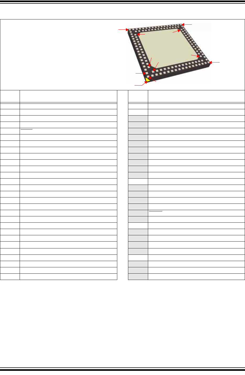
A1
A68
A17 B29
B13
B41
B1
A34
A51
B56
124-PIN VTLA (BOTTOM VIEW)
Polarity Indicator
PIC32MZ0512EF(E/F/K)124
PIC32MZ1024EF(G/H/M)124
PIC32MZ2048EF(G/H/M)124
PIC32MZ1024EF(E/F/K)124
PIC32MZ Embedded Connectivity with Floating Point Unit (EF) Family
DS60001320B-page 8 Preliminary 2015 Microchip Technology Inc.
B1 EBIA5/AN34/PMA5/RA5 B29 VSS
B2 EBID6/AN16/PMD6/RE6 B30 D+
B3 EBIA6/AN22/RPC1/PMA6/RC1 B31 RPF2/SDA3/RF2
B4 AN36/ETXD1/RJ9 B32 ERXD0/RH8
B5 EBIWE/AN20/RPC3/PMWR/RC3 B33 ECOL/RH10
B6 AN14/C1IND/RPG6/SCK2/RG6 B34 EBIRDY1/SDA2/RA3
B7 EBIA3/AN12/C2IND/RPG8/SCL4/PMA3/RG8 B35 VDD
B8 VDD B36 EBIA9/RPF4/SDA5/PMA9/RF4
B9 EBIA2/AN11/C2INC/RPG9/PMA2/RG9 B37 RPA14/SCL1/RA14
B10 AN25/RPE8/RE8 B38 EBIA15/RPD9/PMCS2/PMA15/RD9
B11 AN45/C1INA/RPB5/RB5 B39 EMDC/RPD11/RD11
B12 AN37/ERXCLK/EREFCLK/RJ11 B40 ERXDV/ECRSDV/RH13
B13 VSS B41 SOSCI/RPC13/RC13
B14 PGEC2/AN46/RPB6/RB6 B42 EBID14/RPD2/PMD14/RD2
B15 VREF-/CVREF-/AN27/RA9 B43 EBID12/RPD12/PMD12/RD12
B16 AVDD B44 ETXERR/RJ0
B17 AN38/ETXD2/RH0 B45 EBIRDY3/RJ2
B18 EBIA10/AN48/RPB8/PMA10/RB8 B46 SQICS1/RPD5/RD5
B19 EBIA13/CVREFOUT/AN5/RPB10/PMA13/RB10 B47 ETXCLK/RPD7/RD7
B20 VSS B48 VSS
B21 TCK/EBIA19/AN29/RA1 B49 EBID10/RPF1/PMD10/RF1
B22 TDO/EBIA17/AN31/RPF12/RF12 B50 EBID8/RPG0/PMD8/RG0
B23 AN8/RB13 B51 TRD3/SQID3/RA7
B24 EBIA0/AN10/RPB15/OCFB/PMA0/RB15 B52 EBID0/PMD0/RE0
B25 VDD B53 VDD
B26 AN41/ERXD1/RH5 B54 TRD2/SQID2/RG14
B27 AN32/AETXD0/RPD14/RD14 B55 TRD0/SQID0/RG13
B28 OSC1/CLKI/RC12 B56 EBID3/RPE3/PMD3/RE3
TABLE 4: PIN NAMES FOR 124-PIN DEVICES (CONTINUED)
Package
Pin # Full Pin Name Package
Pin # Full Pin Name
Note 1: The RPn pins can be used by remappable peripherals. See Table 1 for the available peripherals and Section 12.4 “Peripheral Pin
Select (PPS)” for restrictions.
2: Every I/O port pin (RAx-RJx) can be used as a change notification pin (CNAx-CNJx). See Section 12.0 “I/O Ports” for more information.
3: Shaded pins are 5V tolerant.
4: The metal plane at the bottom of the device is not connected to any pins and is recommended to be connected to VSS externally.
A1
A68
A17 B29
B13
B41
B1
A34
A51
B56
124-PIN VTLA (BOTTOM VIEW)
Polarity Indicator
PIC32MZ0512EF(E/F/K)124
PIC32MZ1024EF(G/H/M)124
PIC32MZ2048EF(G/H/M)124
PIC32MZ1024EF(E/F/K)124
2015 Microchip Technology Inc. Preliminary DS60001320B-page 9
PIC32MZ Embedded Connectivity with Floating Point Unit (EF) Family
TABLE 5: PIN NAMES FOR 144-PIN DEVICES
Pin
Number Full Pin Name Pin
Number Full Pin Name
1 AN23/RG15 37 PGEC2/AN46/RPB6/RB6
2 EBIA5/AN34/PMA5/RA5 38 PGED2/AN47/RPB7/RB7
3 EBID5/AN17/RPE5/PMD5/RE5 39 VREF-/CVREF-/AN27/RA9
4 EBID6/AN16/PMD6/RE6 40 VREF+/CVREF+/AN28/RA10
5 EBID7/AN15/PMD7/RE7 41 AVDD
6 EBIA6/AN22/RPC1/PMA6/RC1 42 AVSS
7 AN35/ETXD0/RJ8 43 AN38/ETXD2/RH0
8 AN36/ETXD1/RJ9 44 AN39/ETXD3/RH1
9 EBIBS0/RJ12 45 EBIRP/RH2
10 EBIBS1/RJ10 46 RH3
11 EBIA12/AN21/RPC2/PMA12/RC2 47 EBIA10/AN48/RPB8/PMA10/RB8
12 EBIWE/AN20/RPC3/PMWR/RC3 48 EBIA7/AN49/RPB9/PMA7/RB9
13 EBIOE/AN19/RPC4/PMRD/RC4 49 CVREFOUT/AN5/RPB10/RB10
14 AN14/C1IND/RPG6/SCK2/RG6 50 AN6/RB11
15 AN13/C1INC/RPG7/SDA4/RG7 51 EBIA1/PMA1/RK1
16 AN12/C2IND/RPG8/SCL4/RG8 52 EBIA3/PMA3/RK2
17 VSS 53 EBIA17/RK3
18 VDD 54 VSS
19 EBIA16/RK0 55 VDD
20 MCLR 56 TCK/AN29/RA1
21 EBIA2/AN11/C2INC/RPG9/PMA2/RG9 57 TDI/AN30/RPF13/SCK5/RF13
22 TMS/AN24/RA0 58 TDO/AN31/RPF12/RF12
23 AN25/RPE8/RE8 59 AN7/RB12
24 AN26/RPE9/RE9 60 AN8/RB13
25 AN45/C1INA/RPB5/RB5 61 AN9/RPB14/SCK3/RB14
26 AN4/C1INB/RB4 62 AN10/RPB15/OCFB/RB15
27 AN37/ERXCLK/EREFCLK/RJ11 63 VSS
28 EBIA13/PMA13/RJ13 64 VDD
29 EBIA11/PMA11/RJ14 65 AN40/ERXERR/RH4
30 EBIA0/PMA0/RJ15 66 AN41/ERXD1/RH5
31 AN3/C2INA/RPB3/RB3 67 AN42/ERXD2/RH6
32 VSS 68 EBIA4/PMA4/RH7
33 VDD 69 AN32/RPD14/RD14
34 AN2/C2INB/RPB2/RB2 70 AN33/RPD15/SCK6/RD15
35 PGEC1/AN1/RPB1/RB1 71 OSC1/CLKI/RC12
36 PGED1/AN0/RPB0/RB0 72 OSC2/CLKO/RC15
Note 1: The RPn pins can be used by remappable peripherals. See Table 1 for the available peripherals and Section 12.4 “Peripheral Pin
Select (PPS)” for restrictions.
2: Every I/O port pin (RAx-RKx) can be used as a change notification pin (CNAx-CNKx). See Section 12.0 “I/O Ports” for more
information.
3: Shaded pins are 5V tolerant.
1
144
144-PIN LQFP AND TQFP (TOP VIEW)
PIC32MZ0512EF(E/F/K)144
PIC32MZ1024EF(G/H/M)144
PIC32MZ2048EF(G/H/M)144
PIC32MZ1024EF(E/F/K)144
PIC32MZ Embedded Connectivity with Floating Point Unit (EF) Family
DS60001320B-page 10 Preliminary 2015 Microchip Technology Inc.
73 VBUS 109 RPD1/SCK1/RD1
74 VUSB3V3110 EBID14/RPD2/PMD14/RD2
75 VSS 111 EBID15/RPD3/PMD15/RD3
76 D- 112 EBID12/RPD12/PMD12/RD12
77 D+ 113 EBID13/PMD13/RD13
78 RPF3/USBID/RF3 114 ETXERR/RJ0
79 SDA3/RPF2/RF2 115 EMDIO/RJ1
80 SCL3/RPF8/RF8 116 EBIRDY3/RJ2
81 ERXD0/RH8 117 EBIA22/RJ3
82 ERXD3/RH9 118 SQICS0/RPD4/RD4
83 ECOL/RH10 119 SQICS1/RPD5/RD5
84 EBIRDY2/RH11 120 ETXEN/RPD6/RD6
85 SCL2/RA2 121 ETXCLK/RPD7/RD7
86 EBIRDY1/SDA2/RA3 122 VDD
87 EBIA14/PMCS1/PMA14/RA4 123 VSS
88 VDD 124 EBID11/RPF0/PMD11/RF0
89 VSS 125 EBID10/RPF1/PMD10/RF1
90 EBIA9/RPF4/SDA5/PMA9/RF4 126 EBIA21/RK7
91 EBIA8/RPF5/SCL5/PMA8/RF5 127 EBID9/RPG1/PMD9/RG1
92 EBIA18/RK4 128 EBID8/RPG0/PMD8/RG0
93 EBIA19/RK5 129 TRCLK/SQICLK/RA6
94 EBIA20/RK6 130 TRD3/SQID3/RA7
95 RPA14/SCL1/RA14 131 EBICS0/RJ4
96 RPA15/SDA1/RA15 132 EBICS1/RJ5
97 EBIA15/RPD9/PMCS2/PMA15/RD9 133 EBICS2/RJ6
98 RPD10/SCK4/RD10 134 EBICS3/RJ7
99 EMDC/RPD11/RD11 135 EBID0/PMD0/RE0
100 ECRS/RH12 136 VSS
101 ERXDV/ECRSDV/RH13 137 VDD
102 RH14 138 EBID1/PMD1/RE1
103 EBIA23/RH15 139 TRD2/SQID2/RG14
104 RPD0/RTCC/INT0/RD0 140 TRD1/SQID1/RG12
105 SOSCI/RPC13/RC13 141 TRD0/SQID0/RG13
106 SOSCO/RPC14/T1CK/RC14 142 EBID2/PMD2/RE2
107 VDD 143 EBID3/RPE3/PMD3/RE3
108 VSS 144 EBID4/AN18/PMD4/RE4
TABLE 5: PIN NAMES FOR 144-PIN DEVICES (CONTINUED)
Pin
Number Full Pin Name Pin
Number Full Pin Name
Note 1: The RPn pins can be used by remappable peripherals. See Table 1 for the available peripherals and Section 12.4 “Peripheral Pin
Select (PPS)” for restrictions.
2: Every I/O port pin (RAx-RKx) can be used as a change notification pin (CNAx-CNKx). See Section 12.0 “I/O Ports” for more
information.
3: Shaded pins are 5V tolerant.
1
144
144-PIN LQFP AND TQFP (TOP VIEW)
PIC32MZ0512EF(E/F/K)144
PIC32MZ1024EF(G/H/M)144
PIC32MZ2048EF(G/H/M)144
PIC32MZ1024EF(E/F/K)144

2015 Microchip Technology Inc. Preliminary DS60001320B-page 11
PIC32MZ Embedded Connectivity with Floating Point Unit (EF) Family
Table of Contents
1.0 Device Overview ........................................................................................................................................................................ 15
2.0 Guidelines for Getting Started with 32-bit Microcontrollers ........................................................................................................ 37
3.0 CPU............................................................................................................................................................................................ 43
4.0 Memory Organization................................................................................................................................................................. 61
5.0 Flash Program Memory.............................................................................................................................................................. 99
6.0 Resets ...................................................................................................................................................................................... 109
7.0 CPU Exceptions and Interrupt Controller ................................................................................................................................. 115
8.0 Oscillator Configuration............................................................................................................................................................ 155
9.0 Prefetch Module ....................................................................................................................................................................... 171
10.0 Direct Memory Access (DMA) Controller ................................................................................................................................. 175
11.0 Hi-Speed USB with On-The-Go (OTG) .................................................................................................................................... 199
12.0 I/O Ports ................................................................................................................................................................................... 249
13.0 Timer1 ...................................................................................................................................................................................... 285
14.0 Timer2/3, Timer4/5, Timer6/7, and Timer8/9............................................................................................................................ 289
15.0 Deadman Timer (DMT) ............................................................................................................................................................ 295
16.0 Watchdog Timer (WDT) ........................................................................................................................................................... 303
17.0 Input Capture............................................................................................................................................................................ 307
18.0 Output Compare....................................................................................................................................................................... 311
19.0 Serial Peripheral Interface (SPI) and Inter-IC Sound (I2S)....................................................................................................... 317
20.0 Serial Quad Interface (SQI)...................................................................................................................................................... 327
21.0 Inter-Integrated Circuit™ (I2C™).............................................................................................................................................. 355
22.0 Universal Asynchronous Receiver Transmitter (UART) ........................................................................................................... 363
23.0 Parallel Master Port (PMP)....................................................................................................................................................... 371
24.0 External Bus Interface (EBI)..................................................................................................................................................... 385
25.0 Real-Time Clock and Calendar (RTCC)................................................................................................................................... 393
26.0 Crypto Engine........................................................................................................................................................................... 403
27.0 Random Number Generator (RNG) ......................................................................................................................................... 423
28.0 12-bit High-Speed Successive Approximation Register (SAR) Analog-to-Digital Converter (ADC)......................................... 429
29.0 Controller Area Network (CAN)................................................................................................................................................ 487
30.0 Ethernet Controller ................................................................................................................................................................... 525
31.0 Comparator .............................................................................................................................................................................. 569
32.0 Comparator Voltage Reference (CVREF) ................................................................................................................................. 573
33.0 Power-Saving Features ........................................................................................................................................................... 577
34.0 Special Features ...................................................................................................................................................................... 583
35.0 Instruction Set .......................................................................................................................................................................... 605
36.0 Development Support............................................................................................................................................................... 607
37.0 Electrical Characteristics.......................................................................................................................................................... 611
38.0 AC and DC Characteristics Graphs.......................................................................................................................................... 663
39.0 Packaging Information.............................................................................................................................................................. 665
The Microchip Web Site..................................................................................................................................................................... 717
Customer Change Notification Service .............................................................................................................................................. 717
Customer Support.............................................................................................................................................................................. 717
Product Identification System ............................................................................................................................................................ 718

PIC32MZ Embedded Connectivity with Floating Point Unit (EF) Family
DS60001320B-page 12 Preliminary 2015 Microchip Technology Inc.
TO OUR VALUED CUSTOMERS
It is our intention to provide our valued customers with the best documentation possible to ensure successful use of your Microchip
products. To this end, we will continue to improve our publications to better suit your needs. Our publications will be refined and
enhanced as new volumes and updates are introduced.
If you have any questions or comments regarding this publication, please contact the Marketing Communications Department via
E-mail at docerrors@microchip.com. We welcome your feedback.
Most Current Data Sheet
To obtain the most up-to-date version of this data sheet, please register at our Worldwide Web site at:
http://www.microchip.com
You can determine the version of a data sheet by examining its literature number found on the bottom outside corner of any page.
The last character of the literature number is the version number, (e.g., DS30000000A is version A of document DS30000000).
Errata
An errata sheet, describing minor operational differences from the data sheet and recommended workarounds, may exist for current
devices. As device/documentation issues become known to us, we will publish an errata sheet. The errata will specify the revision
of silicon and revision of document to which it applies.
To determine if an errata sheet exists for a particular device, please check with one of the following:
• Microchip’s Worldwide Web site; http://www.microchip.com
• Your local Microchip sales office (see last page)
When contacting a sales office, please specify which device, revision of silicon and data sheet (include literature number) you are
using.
Customer Notification System
Register on our web site at www.microchip.com to receive the most current information on all of our products.

2015 Microchip Technology Inc. Preliminary DS60001320B-page 13
PIC32MZ Embedded Connectivity with Floating Point Unit (EF) Family
Referenced Sources
This device data sheet is based on the following
individual sections of the “PIC32 Family Reference
Manual”. These documents should be considered as
the general reference for the operation of a particular
module or device feature.
•Section 1. “Introduction” (DS60001127)
•Section 7. “Resets” (DS60001118)
•Section 8. “Interrupt Controller” (DS60001108)
•Section 9. “Watchdog, Deadman, and Power-up Timers” (DS60001114)
•Section 10. “Power-Saving Features” (DS60001130)
•Section 12. “I/O Ports” (DS60001120)
•Section 13. “Parallel Master Port (PMP)” (DS60001128)
•Section 14. “Timers” (DS60001105)
•Section 15. “Input Capture” (DS60001122)
•Section 16. “Output Compare” (DS60001111)
•Section 19. “Comparator” (DS60001110)
•Section 20. “Comparator Voltage Reference (CVREF)” (DS60001109)
•Section 21. “Universal Asynchronous Receiver Transmitter (UART)” (DS60001107)
•Section 22. “12-bit High-Speed Successive Approximation Register (SAR) Analog-to-Digital Converter
(ADC)” (DS60001344)
•Section 23. “Serial Peripheral Interface (SPI)” (DS60001106)
•Section 24. “Inter-Integrated Circuit™ (I2C™)” (DS60001116)
•Section 29. “Real-Time Clock and Calendar (RTCC)” (DS60001125)
•Section 31. “Direct Memory Access (DMA) Controller” (DS60001117)
•Section 32. “Configuration” (DS60001124)
•Section 33. “Programming and Diagnostics” (DS60001129)
•Section 34. “Controller Area Network (CAN)” (DS60001154)
• Section 35. “Ethernet Controller” (DS60001155)
•Section 41. “Prefetch Module for Devices with L1 CPU Cache” (DS60001183)
•Section 42. “Oscillators with Enhanced PLL” (DS60001250)
•Section 46. “Serial Quad Interface (SQI)” (DS60001244)
•Section 47. “External Bus Interface (EBI)” (DS60001245)
•Section 48. “Memory Organization and Permissions” (DS60001214)
•Section 49. “Crypto Engine (CE) and Random Number Generator (RNG)” (DS60001246)
• Section 50. “CPU for Devices with MIPS32® microAptiv™ and M-Class Cores” (DS60001192)
•Section 51. “Hi-Speed USB with On-The-Go (OTG)” (DS60001326)
•Section 52. “Flash Program Memory with Support for Live Update” (DS60001193)
Note: To access the documents listed below,
browse the documentation section of the
Microchip website (www.microchip.com).

PIC32MZ Embedded Connectivity with Floating Point Unit (EF) Family
DS60001320B-page 14 Preliminary 2015 Microchip Technology Inc.
NOTES:
2015 Microchip Technology Inc. Preliminary DS60001320B-page 15
PIC32MZ Embedded Connectivity with Floating Point Unit (EF) Family
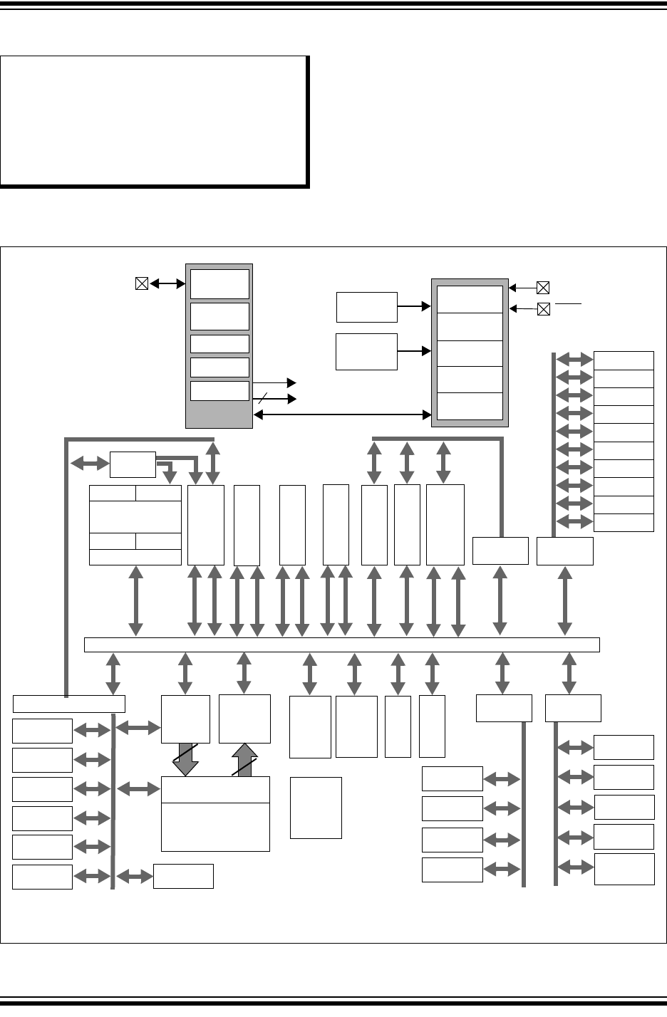
1.0 DEVICE OVERVIEW This data sheet contains device-specific information for
PIC32MZ EF devices.
Figure 1-1 illustrates a general block diagram of the
core and peripheral modules in the PIC32MZ EF family
of devices.
Table 1-21 through Table 1-22 list the pinout I/O
descriptions for the pins shown in the device pin tables
(see Table 2 through Table 5).
FIGURE 1-1: PIC32MZ EF FAMILY BLOCK DIAGRAM
Note: This data sheet summarizes the features
of the PIC32MZ EF family of devices. It is
not intended to be a comprehensive refer-
ence source. To complement the informa-
tion in this data sheet, refer to the “PIC32
Family Reference Manual”, which is avail-
able from the Microchip web site
(www.microchip.com/PIC32).
Note: Not all features are available on all devices. Refer to TABLE 1: “PIC32MZ EF Family Features” for the list of features by device.
I9 I3,
System Bus
I10
T1 T2
UART1-6 Comparator
PORTD
PORTF
PORTH
PORTK
PORTB
MIPS32®
EJTAG INT
128
140-bit wide
I1, I12,
Dual Panel
PORTC
PMP
I2C1-5
SPI1-6
IC1-9
Data
JTAG
BSCAN
I5,
Flash
PORTJ
PORTG
PORTE
Timer1-9
T3
Flash
Memory
Prefetch
Cache
I13
DMAC
I11
CFG
OC1-9
T4
I-Cache D-Cache
System Bus I/F
SQI
CAN2
CAN1
EVIC
Data
EBI
128
I8
6 S&H
SAR ADC
PFM Flash Wrapper
Ethernet
PPS
ICD
WDT
RTCC
PORTA
Flash
Controller
I7
HS USB
T6
T8
T5 T7
DMT
CVREF
T9
Peripheral Bus 1
I14
CRYPTO
T13
RNG
Peripheral
OSC1/CLKI
OSC2/CLKO
VDD,
Timing
Generation
VSS
MCLR
Power-up
Timer
Oscillator
Start-up Timer
Power-on
Reset
Watchdog
Timer
Brown-out
Reset
Precision
Reference
Band Gap
FRC/LPRC
Oscillators Regulator
Voltage
POSC/SOSC
Oscillators
PLL
DIVIDERS
PBCLKx
PLL-USB SYSCLK
Bus 5 Peripheral
Bus 4
Peripheral
Bus 3
Peripheral
Bus 2
Ram
Bank 1 Ram
Bank 2
Controller
6
M-Class Core
1-2
and ECC
T11 T10
I6I4
I2 T12

PIC32MZ Embedded Connectivity with Floating Point Unit (EF) Family
DS60001320B-page 16 Preliminary 2015 Microchip Technology Inc.
TABLE 1-1: ADC PINOUT I/O DESCRIPTIONS
Pin Name
Pin Number
Pin
Type Buffer
Type Description
64-pin
QFN/
TQFP
100-pin
TQFP 124-pin
VTLA
144-pin
TQFP/
LQFP
AN0 16 25 A18 36 I Analog Analog Input Channels
AN1 15 24 A17 35 I Analog
AN2 14 23 A16 34 I Analog
AN3 13 22 A14 31 I Analog
AN4 12 21 A13 26 I Analog
AN5 23 34 B19 49 I Analog
AN6 24 35 A24 50 I Analog
AN7 27 41 A27 59 I Analog
AN8 28 42 B23 60 I Analog
AN9 29 43 A28 61 I Analog
AN10 30 44 B24 62 I Analog
AN11 10 16 B9 21 I Analog
AN12 6 12 B7 16 I Analog
AN13 5 11 A8 15 I Analog
AN14 4 10 B6 14 I Analog
AN15 3 5 A4 5 I Analog
AN16 2 4 B2 4 I Analog
AN17 1 3 A3 3 I Analog
AN18 64 100 A67 144 I Analog
AN19 — 9 A7 13 I Analog
AN20 — 8 B5 12 I Analog
AN21 — 7 A6 11 I Analog
AN22 — 6 B3 6 I Analog
AN23 — 1 A2 1 I Analog
AN24 — 17 A11 22 I Analog
AN25 — 18 B10 23 I Analog
AN26 — 19 A12 24 I Analog
AN27 — 28 B15 39 I Analog
AN28 — 29 A20 40 I Analog
AN29 — 38 B21 56 I Analog
AN30 — 39 A26 57 I Analog
AN31 — 40 B22 58 I Analog
AN32 — 47 B27 69 I Analog
AN33 — 48 A32 70 I Analog
AN34 — 2 B1 2 I Analog
AN35 — — A5 7 I Analog
Legend: CMOS = CMOS-compatible input or output Analog = Analog input P = Power
ST = Schmitt Trigger input with CMOS levels O = Output I = Input
TTL = Transistor-transistor Logic input buffer PPS = Peripheral Pin Select

2015 Microchip Technology Inc. Preliminary DS60001320B-page 17
PIC32MZ Embedded Connectivity with Floating Point Unit (EF) Family
AN36 — — B4 8 I Analog Analog Input Channels
AN37 — — B12 27 I Analog
AN38 — — B17 43 I Analog
AN39 — — A22 44 I Analog
AN40 — — A30 65 I Analog
AN41 — — B26 66 I Analog
AN42 — — A31 67 I Analog
AN45 11 20 B11 25 I Analog
AN46 17 26 B14 37 I Analog
AN47 18 27 A19 38 I Analog
AN48 21 32 B18 47 I Analog
AN49 22 33 A23 48 I Analog
TABLE 1-1: ADC PINOUT I/O DESCRIPTIONS (CONTINUED)
Pin Name
Pin Number
Pin
Type Buffer
Type Description
64-pin
QFN/
TQFP
100-pin
TQFP 124-pin
VTLA
144-pin
TQFP/
LQFP
Legend: CMOS = CMOS-compatible input or output Analog = Analog input P = Power
ST = Schmitt Trigger input with CMOS levels O = Output I = Input
TTL = Transistor-transistor Logic input buffer PPS = Peripheral Pin Select

PIC32MZ Embedded Connectivity with Floating Point Unit (EF) Family
DS60001320B-page 18 Preliminary 2015 Microchip Technology Inc.
TABLE 1-2: OSCILLATOR PINOUT I/O DESCRIPTIONS
Pin Name
Pin Number
Pin
Type Buffer
Type Description
64-pin
QFN/
TQFP
100-pin
TQFP 124-pin
VTLA
144-pin
TQFP/
LQFP
CLKI 31 49 B28 71 I ST/CMOS External clock source input. Always associated with
OSC1 pin function.
CLKO 32 50 A33 72 O — Oscillator crystal output. Connects to crystal or reso-
nator in Crystal Oscillator mode. Optionally functions
as CLKO in RC and EC modes. Always associated
with OSC2 pin function.
OSC1 31 49 B28 71 I ST/CMOS Oscillator crystal input. ST buffer when configured in
RC mode; CMOS otherwise.
OSC2 32 50 A33 72 O — Oscillator crystal output. Connects to crystal or reso-
nator in Crystal Oscillator mode. Optionally functions
as CLKO in RC and EC modes.
SOSCI 47 72 B41 105 I ST/CMOS 32.768 kHz low-power oscillator crystal input; CMOS
otherwise.
SOSCO 48 73 A49 106 O — 32.768 low-power oscillator crystal output.
REFCLKI1 PPS PPS PPS PPS I — Reference Clock Generator Inputs 1-4
REFCLKI3 PPS PPS PPS PPS I —
REFCLKI4 PPS PPS PPS PPS I —
REFCLKO1 PPS PPS PPS PPS O — Reference Clock Generator Outputs 1-4
REFCLKO3 PPS PPS PPS PPS O —
REFCLKO4 PPS PPS PPS PPS O —
Legend: CMOS = CMOS-compatible input or output Analog = Analog input P = Power
ST = Schmitt Trigger input with CMOS levels O = Output I = Input
TTL = Transistor-transistor Logic input buffer PPS = Peripheral Pin Select
TABLE 1-3: IC1 THROUGH IC9 PINOUT I/O DESCRIPTIONS
Pin Name
Pin Number
Pin
Type Buffer
Type Description
64-pin
QFN/
TQFP
100-pin
TQFP 124-pin
VTLA
144-pin
TQFP/
LQFP
Input Capture
IC1 PPS PPS PPS PPS IST Input Capture Inputs 1-9
IC2 PPS PPS PPS PPS IST
IC3 PPS PPS PPS PPS IST
IC4 PPS PPS PPS PPS IST
IC5 PPS PPS PPS PPS IST
IC6 PPS PPS PPS PPS IST
IC7 PPS PPS PPS PPS IST
IC8 PPS PPS PPS PPS IST
IC9 PPS PPS PPS PPS IST
Legend: CMOS = CMOS-compatible input or output Analog = Analog input P = Power
ST = Schmitt Trigger input with CMOS levels O = Output I = Input
TTL = Transistor-transistor Logic input buffer PPS = Peripheral Pin Select

2015 Microchip Technology Inc. Preliminary DS60001320B-page 19
PIC32MZ Embedded Connectivity with Floating Point Unit (EF) Family
TABLE 1-4: OC1 THROUGH OC9 PINOUT I/O DESCRIPTIONS
Pin Name
Pin Number
Pin
Type Buffer
Type Description
64-pin
QFN/
TQFP
100-pin
TQFP 124-pin
VTLA
144-pin
TQFP/
LQFP
Output Compare
OC1 PPS PPS PPS PPS O — Output Compare Outputs 1-9
OC2 PPS PPS PPS PPS O —
OC3 PPS PPS PPS PPS O —
OC4 PPS PPS PPS PPS O —
OC5 PPS PPS PPS PPS O —
OC6 PPS PPS PPS PPS O —
OC7 PPS PPS PPS PPS O —
OC8 PPS PPS PPS PPS O —
OC9 PPS PPS PPS PPS O —
OCFA PPS PPS PPS PPS I ST Output Compare Fault A Input
OCFB 30 44 B24 62 I ST Output Compare Fault B Input
Legend: CMOS = CMOS-compatible input or output Analog = Analog input P = Power
ST = Schmitt Trigger input with CMOS levels O = Output I = Input
TTL = Transistor-transistor Logic input buffer PPS = Peripheral Pin Select
TABLE 1-5: EXTERNAL INTERRUPTS PINOUT I/O DESCRIPTIONS
Pin Name
Pin Number
Pin
Type Buffer
Type Description
64-pin
QFN/
TQFP
100-pin
TQFP 124-pin
VTLA
144-pin
TQFP/
LQFP
External Interrupts
INT0 46 71 A48 104 IST External Interrupt 0
INT1 PPS PPS PPS PPS IST External Interrupt 1
INT2 PPS PPS PPS PPS IST External Interrupt 2
INT3 PPS PPS PPS PPS IST External Interrupt 3
INT4 PPS PPS PPS PPS IST External Interrupt 4
Legend: CMOS = CMOS-compatible input or output Analog = Analog input P = Power
ST = Schmitt Trigger input with CMOS levels O = Output I = Input
TTL = Transistor-transistor Logic input buffer PPS = Peripheral Pin Select

PIC32MZ Embedded Connectivity with Floating Point Unit (EF) Family
DS60001320B-page 20 Preliminary 2015 Microchip Technology Inc.
TABLE 1-6: PORTA THROUGH PORTK PINOUT I/O DESCRIPTIONS
Pin Name
Pin Number
Pin
Type Buffer
Type Description
64-pin
QFN/
TQFP
100-pin
TQFP 124-pin
VTLA
144-pin
TQFP/
LQFP
PORTA
RA0 — 17 A11 22 I/O ST PORTA is a bidirectional I/O port
RA1 — 38 B21 56 I/O ST
RA2 — 59 A41 85 I/O ST
RA3 — 60 B34 86 I/O ST
RA4 — 61 A42 87 I/O ST
RA5 — 2 B1 2 I/O ST
RA6 — 89 A61 129 I/O ST
RA7 — 90 B51 130 I/O ST
RA9 — 28 B15 39 I/O ST
RA10 — 29 A20 40 I/O ST
RA14 — 66 B37 95 I/O ST
RA15 — 67 A45 96 I/O ST
PORTB
RB0 16 25 A18 36 I/O ST PORTB is a bidirectional I/O port
RB1 15 24 A17 35 I/O ST
RB2 14 23 A16 34 I/O ST
RB3 13 22 A14 31 I/O ST
RB4 12 21 A13 26 I/O ST
RB5 11 20 B11 25 I/O ST
RB6 17 26 B14 37 I/O ST
RB7 18 27 A19 38 I/O ST
RB8 21 32 B18 47 I/O ST
RB9 22 33 A23 48 I/O ST
RB10 23 34 B19 49 I/O ST
RB11 24 35 A24 50 I/O ST
RB12 27 41 A27 59 I/O ST
RB13 28 42 B23 60 I/O ST
RB14 29 43 A28 61 I/O ST
RB15 30 44 B24 62 I/O ST
PORTC
RC1 — 6 B3 6 I/O ST PORTC is a bidirectional I/O port
RC2 — 7 A6 11 I/O ST
RC3 — 8 B5 12 I/O ST
RC4 — 9 A7 13 I/O ST
RC12 31 49 B28 71 I/O ST
RC13 47 72 B41 105 I/O ST
RC14 48 73 A49 106 I/O ST
RC15 32 50 A33 72 I/O ST
Legend: CMOS = CMOS-compatible input or output Analog = Analog input P = Power
ST = Schmitt Trigger input with CMOS levels O = Output I = Input
TTL = Transistor-transistor Logic input buffer PPS = Peripheral Pin Select

2015 Microchip Technology Inc. Preliminary DS60001320B-page 21
PIC32MZ Embedded Connectivity with Floating Point Unit (EF) Family
PORTD
RD0 46 71 A48 104 I/O ST PORTD is a bidirectional I/O port
RD1 49 76 A52 109 I/O ST
RD2 50 77 B42 110 I/O ST
RD3 51 78 A53 111 I/O ST
RD4 52 81 A56 118 I/O ST
RD5 53 82 B46 119 I/O ST
RD6 — — A57 120 I/O ST
RD7 — — B47 121 I/O ST
RD9 43 68 B38 97 I/O ST
RD10 44 69 A46 98 I/O ST
RD11 45 70 B39 99 I/O ST
RD12 — 79 B43 112 I/O ST
RD13 — 80 A54 113 I/O ST
RD14 — 47 B27 69 I/O ST
RD15 — 48 A32 70 I/O ST
PORTE
RE0 58 91 B52 135 I/O ST PORTE is a bidirectional I/O port
RE1 61 94 A64 138 I/O ST
RE2 62 98 A66 142 I/O ST
RE3 63 99 B56 143 I/O ST
RE4 64 100 A67 144 I/O ST
RE5 1 3 A3 3 I/O ST
RE6 2 4 B2 4 I/O ST
RE7 3 5 A4 5 I/O ST
RE8 — 18 B10 23 I/O ST
RE9 — 19 A12 24 I/O ST
PORTF
RF0 56 85 A59 124 I/O ST PORTF is a bidirectional I/O port
RF1 57 86 B49 125 I/O ST
RF2 — 57 B31 79 I/O ST
RF3 38 56 A38 78 I/O ST
RF4 41 64 B36 90 I/O ST
RF5 42 65 A44 91 I/O ST
RF8 — 58 A39 80 I/O ST
RF12 — 40 B22 58 I/O ST
RF13 — 39 A26 57 I/O ST
TABLE 1-6: PORTA THROUGH PORTK PINOUT I/O DESCRIPTIONS (CONTINUED)
Pin Name
Pin Number
Pin
Type Buffer
Type Description
64-pin
QFN/
TQFP
100-pin
TQFP 124-pin
VTLA
144-pin
TQFP/
LQFP
Legend: CMOS = CMOS-compatible input or output Analog = Analog input P = Power
ST = Schmitt Trigger input with CMOS levels O = Output I = Input
TTL = Transistor-transistor Logic input buffer PPS = Peripheral Pin Select

PIC32MZ Embedded Connectivity with Floating Point Unit (EF) Family
DS60001320B-page 22 Preliminary 2015 Microchip Technology Inc.
PORTG
RG0 — 88 B50 128 I/O ST PORTG is a bidirectional I/O port
RG1 — 87 A60 127 I/O ST
RG6 4 10 B6 14 I/O ST
RG7 5 11 A8 15 I/O ST
RG8 6 12 B7 16 I/O ST
RG9 10 16 B9 21 I/O ST
RG12 — 96 A65 140 I/O ST
RG13 — 97 B55 141 I/O ST
RG14 — 95 B54 139 I/O ST
RG15 — 1 A2 1 I/O ST
PORTH
RH0 — — B17 43 I/O ST PORTH is a bidirectional I/O port
RH1 — — A22 44 I/O ST
RH2 — — — 45 I/O ST
RH3 — — — 46 I/O ST
RH4 — — A30 65 I/O ST
RH5 — — B26 66 I/O ST
RH6 — — A31 67 I/O ST
RH7 — — — 68 I/O ST
RH8 — — B32 81 I/O ST
RH9 — — A40 82 I/O ST
RH10 — — B33 83 I/O ST
RH11 — — — 84 I/O ST
RH12 — — A47 100 I/O ST
RH13 — — B40 101 I/O ST
RH14 — — — 102 I/O ST
RH15 — — — 103 I/O ST
PORTJ
RJ0 — — B44 114 I/O ST PORTJ is a bidirectional I/O port
RJ1 — — A55 115 I/O ST
RJ2 — — B45 116 I/O ST
RJ3 — — — 117 I/O ST
RJ4 — — A62 131 I/O ST
RJ5 — — — 132 I/O ST
RJ6 — — — 133 I/O ST
RJ7 — — — 134 I/O ST
RJ8 — — A5 7 I/O ST
RJ9 — — B4 8 I/O ST
RJ10 — — — 10 I/O ST
RJ11 — — B12 27 I/O ST
RJ12 — — — 9 I/O ST
RJ13 — — — 28 I/O ST
RJ14 — — — 29 I/O ST
RJ15 — — — 30 I/O ST
TABLE 1-6: PORTA THROUGH PORTK PINOUT I/O DESCRIPTIONS (CONTINUED)
Pin Name
Pin Number
Pin
Type Buffer
Type Description
64-pin
QFN/
TQFP
100-pin
TQFP 124-pin
VTLA
144-pin
TQFP/
LQFP
Legend: CMOS = CMOS-compatible input or output Analog = Analog input P = Power
ST = Schmitt Trigger input with CMOS levels O = Output I = Input
TTL = Transistor-transistor Logic input buffer PPS = Peripheral Pin Select

2015 Microchip Technology Inc. Preliminary DS60001320B-page 23
PIC32MZ Embedded Connectivity with Floating Point Unit (EF) Family
PORTK
RK0 — — — 19 I/O ST PORTK is a bidirectional I/O port
RK1 — — — 51 I/O ST
RK2 — — — 52 I/O ST
RK3 — — — 53 I/O ST
RK4 — — — 92 I/O ST
RK5 — — — 93 I/O ST
RK6 — — — 94 I/O ST
RK7 — — — 126 I/O ST
TABLE 1-6: PORTA THROUGH PORTK PINOUT I/O DESCRIPTIONS (CONTINUED)
Pin Name
Pin Number
Pin
Type Buffer
Type Description
64-pin
QFN/
TQFP
100-pin
TQFP 124-pin
VTLA
144-pin
TQFP/
LQFP
Legend: CMOS = CMOS-compatible input or output Analog = Analog input P = Power
ST = Schmitt Trigger input with CMOS levels O = Output I = Input
TTL = Transistor-transistor Logic input buffer PPS = Peripheral Pin Select

PIC32MZ Embedded Connectivity with Floating Point Unit (EF) Family
DS60001320B-page 24 Preliminary 2015 Microchip Technology Inc.
TABLE 1-7: TIMER1 THROUGH TIMER9 AND RTCC PINOUT I/O DESCRIPTIONS
Pin Name
Pin Number
Pin
Type Buffer
Type Description
64-pin
QFN/
TQFP
100-pin
TQFP 124-pin
VTLA
144-pin
TQFP/
LQFP
Timer1 through Timer9
T1CK 48 73 A49 106 I ST Timer1 External Clock Input
T2CK PPS PPS PPS PPS I ST Timer2 External Clock Input
T3CK PPS PPS PPS PPS I ST Timer3 External Clock Input
T4CK PPS PPS PPS PPS I ST Timer4 External Clock Input
T5CK PPS PPS PPS PPS I ST Timer5 External Clock Input
T6CK PPS PPS PPS PPS I ST Timer6 External Clock Input
T7CK PPS PPS PPS PPS I ST Timer7 External Clock Input
T8CK PPS PPS PPS PPS I ST Timer8 External Clock Input
T9CK PPS PPS PPS PPS I ST Timer9 External Clock Input
Real-Time Clock and Calendar
RTCC 46 71 A48 104 O — Real-Time Clock Alarm/Seconds Output
Legend: CMOS = CMOS-compatible input or output Analog = Analog input P = Power
ST = Schmitt Trigger input with CMOS levels O = Output I = Input
TTL = Transistor-transistor Logic input buffer PPS = Peripheral Pin Select

2015 Microchip Technology Inc. Preliminary DS60001320B-page 25
PIC32MZ Embedded Connectivity with Floating Point Unit (EF) Family
TABLE 1-8: UART1 THROUGH UART6 PINOUT I/O DESCRIPTIONS
Pin Name
Pin Number
Pin
Type Buffer
Type Description
64-pin
QFN/
TQFP
100-pin
TQFP 124-pin
VTLA
144-pin
TQFP/
LQFP
Universal Asynchronous Receiver Transmitter 1
U1RX PPS PPS PPS PPS I ST UART1 Receive
U1TX PPS PPS PPS PPS O — UART1 Transmit
U1CTS PPS PPS PPS PPS I ST UART1 Clear to Send
U1RTS PPS PPS PPS PPS O — UART1 Ready to Send
Universal Asynchronous Receiver Transmitter 2
U2RX PPS PPS PPS PPS I ST UART2 Receive
U2TX PPS PPS PPS PPS O — UART2 Transmit
U2CTS PPS PPS PPS PPS I ST UART2 Clear To Send
U2RTS PPS PPS PPS PPS O — UART2 Ready To Send
Universal Asynchronous Receiver Transmitter 3
U3RX PPS PPS PPS PPS I ST UART3 Receive
U3TX PPS PPS PPS PPS O — UART3 Transmit
U3CTS PPS PPS PPS PPS I ST UART3 Clear to Send
U3RTS PPS PPS PPS PPS O — UART3 Ready to Send
Universal Asynchronous Receiver Transmitter 4
U4RX PPS PPS PPS PPS I ST UART4 Receive
U4TX PPS PPS PPS PPS O — UART4 Transmit
U4CTS PPS PPS PPS PPS I ST UART4 Clear to Send
U4RTS PPS PPS PPS PPS O — UART4 Ready to Send
Universal Asynchronous Receiver Transmitter 5
U5RX PPS PPS PPS PPS I ST UART5 Receive
U5TX PPS PPS PPS PPS O — UART5 Transmit
U5CTS PPS PPS PPS PPS I ST UART5 Clear to Send
U5RTS PPS PPS PPS PPS O — UART5 Ready to Send
Universal Asynchronous Receiver Transmitter 6
U6RX PPS PPS PPS PPS I ST UART6 Receive
U6TX PPS PPS PPS PPS O — UART6 Transmit
U6CTS PPS PPS PPS PPS I ST UART6 Clear to Send
U6RTS PPS PPS PPS PPS O — UART6 Ready to Send
Legend: CMOS = CMOS-compatible input or output Analog = Analog input P = Power
ST = Schmitt Trigger input with CMOS levels O = Output I = Input
TTL = Transistor-transistor Logic input buffer PPS = Peripheral Pin Select

PIC32MZ Embedded Connectivity with Floating Point Unit (EF) Family
DS60001320B-page 26 Preliminary 2015 Microchip Technology Inc.
TABLE 1-9: SPI1 THROUGH SPI 6 PINOUT I/O DESCRIPTIONS
Pin Name
Pin Number
Pin
Type Buffer
Type Description
64-pin
QFN/
TQFP
100-pin
TQFP 124-pin
VTLA
144-pin
TQFP/
LQFP
Serial Peripheral Interface 1
SCK1 49 76 A52 109 I/O ST SPI1 Synchronous Serial Clock Input/Output
SDI1 PPS PPS PPS PPS I ST SPI1 Data In
SDO1 PPS PPS PPS PPS O — SPI1 Data Out
SS1 PPS PPS PPS PPS I/O ST SPI1 Slave Synchronization Or Frame Pulse I/O
Serial Peripheral Interface 2
SCK2 4 10 B6 14 I/O ST SPI2 Synchronous Serial Clock Input/output
SDI2 PPS PPS PPS PPS I ST SPI2 Data In
SDO2 PPS PPS PPS PPS O — SPI2 Data Out
SS2 PPS PPS PPS PPS I/O ST SPI2 Slave Synchronization Or Frame Pulse I/O
Serial Peripheral Interface 3
SCK3 29 43 A28 61 I/O ST SPI3 Synchronous Serial Clock Input/Output
SDI3 PPS PPS PPS PPS I ST SPI3 Data In
SDO3 PPS PPS PPS PPS O — SPI3 Data Out
SS3 PPS PPS PPS PPS I/O ST SPI3 Slave Synchronization Or Frame Pulse I/O
Serial Peripheral Interface 4
SCK4 44 69 A46 98 I/O ST SPI4 Synchronous Serial Clock Input/Output
SDI4 PPS PPS PPS PPS I ST SPI4 Data In
SDO4 PPS PPS PPS PPS O — SPI4 Data Out
SS4 PPS PPS PPS PPS I/O ST SPI4 Slave Synchronization Or Frame Pulse I/O
Serial Peripheral Interface 5
SCK5 — 39 A26 57 I/O ST SPI5 Synchronous Serial Clock Input/Output
SDI5 — PPS PPS PPS I ST SPI5 Data In
SDO5 — PPS PPS PPS O — SPI5 Data Out
SS5 — PPS PPS PPS I/O ST SPI5 Slave Synchronization Or Frame Pulse I/O
Serial Peripheral Interface 6
SCK6 — 48 A32 70 I/O ST SPI6 Synchronous Serial Clock Input/Output
SDI6 — PPS PPS PPS I ST SPI6 Data In
SDO6 — PPS PPS PPS O — SPI6 Data Out
SS6 — PPS PPS PPS I/O ST SPI6 Slave Synchronization Or Frame Pulse I/O
Legend: CMOS = CMOS-compatible input or output Analog = Analog input P = Power
ST = Schmitt Trigger input with CMOS levels O = Output I = Input
TTL = Transistor-transistor Logic input buffer PPS = Peripheral Pin Select

2015 Microchip Technology Inc. Preliminary DS60001320B-page 27
PIC32MZ Embedded Connectivity with Floating Point Unit (EF) Family
TABLE 1-10: I2C1 THROUGH I2C5 PINOUT I/O DESCRIPTIONS
Pin Name
Pin Number
Pin
Type Buffer
Type Description
64-pin
QFN/
TQFP
100-pin
TQFP 124-pin
VTLA
144-pin
TQFP/
LQFP
Inter-Integrated Circuit 1
SCL1 44 66 B37 95 I/O ST I2C1 Synchronous Serial Clock Input/Output
SDA1 43 67 A45 96 I/O ST I2C1 Synchronous Serial Data Input/Output
Inter-Integrated Circuit 2
SCL2 — 59 A41 85 I/O ST I2C2 Synchronous Serial Clock Input/Output
SDA2 — 60 B34 86 I/O ST I2C2 Synchronous Serial Data Input/Output
Inter-Integrated Circuit 3
SCL3 51 58 A39 80 I/O ST I2C3 Synchronous Serial Clock Input/Output
SDA3 50 57 B31 79 I/O ST I2C3 Synchronous Serial Data Input/Output
Inter-Integrated Circuit 4
SCL4 6 12 B7 16 I/O ST I2C4 Synchronous Serial Clock Input/Output
SDA4 5 11 A8 15 I/O ST I2C4 Synchronous Serial Data Input/Output
Inter-Integrated Circuit 5
SCL5 42 65 A44 91 I/O ST I2C5 Synchronous Serial Clock Input/Output
SDA5 41 64 B36 90 I/O ST I2C5 Synchronous Serial Data Input/Output
Legend: CMOS = CMOS-compatible input or output Analog = Analog input P = Power
ST = Schmitt Trigger input with CMOS levels O = Output I = Input
TTL = Transistor-transistor Logic input buffer PPS = Peripheral Pin Select
TABLE 1-11: COMPARATOR 1, COMPARATOR 2 AND CVREF PINOUT I/O DESCRIPTIONS
Pin Name
Pin Number
Pin
Type Buffer
Type Description
64-pin
QFN/
TQFP
100-pin
TQFP 124-pin
VTLA
144-pin
TQFP/
LQFP
Comparator Voltage Reference
CVREF+16 29 A20 40 IAnalog Comparator Voltage Reference (High) Input
CVREF-15 28 B15 39 IAnalog Comparator Voltage Reference (Low) Input
CVREFOUT 23 34 B19 49 OAnalog Comparator Voltage Reference Output
Comparator 1
C1INA 11 20 B11 25 IAnalog Comparator 1 Positive Input
C1INB 12 21 A13 26 IAnalog Comparator 1 Selectable Negative Input
C1INC 511 A8 15 IAnalog
C1IND 410 B6 14 IAnalog
C1OUT PPS PPS PPS PPS O — Comparator 1 Output
Comparator 2
C2INA 13 22 A14 31 IAnalog Comparator 2 Positive Input
C2INB 14 23 A16 34 IAnalog Comparator 2 Selectable Negative Input
C2INC 10 16 B9 21 IAnalog
C2IND 612 B7 16 IAnalog
C2OUT PPS PPS PPS PPS O — Comparator 2 Output
Legend: CMOS = CMOS-compatible input or output Analog = Analog input P = Power
ST = Schmitt Trigger input with CMOS levels O = Output I = Input
TTL = Transistor-transistor Logic input buffer PPS = Peripheral Pin Select

PIC32MZ Embedded Connectivity with Floating Point Unit (EF) Family
DS60001320B-page 28 Preliminary 2015 Microchip Technology Inc.
TABLE 1-12: PMP PINOUT I/O DESCRIPTIONS
Pin Name
Pin Number
Pin
Type Buffer
Type Description
64-pin
QFN/
TQFP
100-pin
TQFP 124-pin
VTLA
144-pin
TQFP/
LQFP
PMA0 30 44 B24 30 I/O TTL/ST Parallel Master Port Address bit 0 Input (Buffered
Slave modes) and Output (Master modes)
PMA1 29 43 A28 51 I/O TTL/ST Parallel Master Port Address bit 1 Input (Buffered
Slave modes) and Output (Master modes)
PMA2 10 16 B9 21 O — Parallel Master Port Address (Demultiplexed Master
modes)
PMA3 6 12 B7 52 O —
PMA4 5 11 A8 68 O —
PMA5 4 2 B1 2 O —
PMA6 16 6 B3 6 O —
PMA7 22 33 A23 48 O —
PMA8 42 65 A44 91 O —
PMA9 41 64 B36 90 O —
PMA10 21 32 B18 47 O —
PMA11 27 41 A27 29 O —
PMA12 24 7 A6 11 O —
PMA13 23 34 B19 28 O —
PMA14 45 61 A42 87 O —
PMA15 43 68 B38 97 O —
PMCS1 45 61 A42 87 O — Parallel Master Port Chip Select 1 Strobe
PMCS2 43 68 B38 97 O — Parallel Master Port Chip Select 2 Strobe
PMD0 58 91 B52 135 I/O TTL/ST Parallel Master Port Data (Demultiplexed Master
mode) or Address/Data (Multiplexed Master modes)
PMD1 61 94 A64 138 I/O TTL/ST
PMD2 62 98 A66 142 I/O TTL/ST
PMD3 63 99 B56 143 I/O TTL/ST
PMD4 64 100 A67 144 I/O TTL/ST
PMD5 1 3 A3 3 I/O TTL/ST
PMD6 2 4 B2 4 I/O TTL/ST
PMD7 3 5 A4 5 I/O TTL/ST
PMD8 — 88 B50 128 I/O TTL/ST
PMD9 — 87 A60 127 I/O TTL/ST
PMD10 — 86 B49 125 I/O TTL/ST
PMD11 — 85 A59 124 I/O TTL/ST
PMD12 — 79 B43 112 I/O TTL/ST
PMD13 — 80 A54 113 I/O TTL/ST
PMD14 — 77 B42 110 I/O TTL/ST
PMD15 — 78 A53 111 I/O TTL/ST
PMALL 30 44 B24 30 O — Parallel Master Port Address Latch Enable Low Byte
(Multiplexed Master modes)
PMALH 29 43 A28 51 O — Parallel Master Port Address Latch Enable High Byte
(Multiplexed Master modes)
PMRD 53 9 A7 13 O — Parallel Master Port Read Strobe
PMWR 52 8 B5 12 O — Parallel Master Port Write Strobe
Legend: CMOS = CMOS-compatible input or output Analog = Analog input P = Power
ST = Schmitt Trigger input with CMOS levels O = Output I = Input
TTL = Transistor-transistor Logic input buffer PPS = Peripheral Pin Select

2015 Microchip Technology Inc. Preliminary DS60001320B-page 29
PIC32MZ Embedded Connectivity with Floating Point Unit (EF) Family
TABLE 1-13: EBI PINOUT I/O DESCRIPTIONS
Pin Name
Pin Number
Pin
Type Buffer
Type Description
64-pin
QFN/
TQFP
100-pin
TQFP 124-pin
VTLA
144-pin
TQFP/
LQFP
EBIA0 — 44 B24 30 O — External Bus Interface Address Bus
EBIA1 — 43 A28 51 O —
EBIA2 — 16 B9 21 O —
EBIA3 — 12 B7 52 O —
EBIA4 — 11 A8 68 O —
EBIA5 — 2 B1 2 O —
EBIA6 — 6 B3 6 O —
EBIA7 — 33 A23 48 O —
EBIA8 — 65 A44 91 O —
EBIA9 — 64 B36 90 O —
EBIA10 — 32 B18 47 O —
EBIA11 — 41 A27 29 O —
EBIA12 — 7 A6 11 O —
EBIA13 — 34 B19 28 O —
EBIA14 — 61 A42 87 O —
EBIA15 — 68 B38 97 O —
EBIA16 — 17 A11 19 O —
EBIA17 — 40 B22 53 O —
EBIA18 — 39 A26 92 O —
EBIA19 — 38 B21 93 O —
EBIA20 — — — 94 O —
EBIA21 — — — 126 O —
EBIA22 — — — 117 O —
EBIA23 — — — 103 O —
EBID0 — 91 B52 135 I/O ST External Bus Interface Data I/O Bus
EBID1 — 94 A64 138 I/O ST
EBID2 — 98 A66 142 I/O ST
EBID3 — 99 B56 143 I/O ST
EBID4 — 100 A67 144 I/O ST
EBID5 — 3 A3 3 I/O ST
EBID6 — 4 B2 4 I/O ST
EBID7 — 5 A4 5 I/O ST
EBID8 — 88 B50 128 I/O ST
EBID9 — 87 A60 127 I/O ST
EBID10 — 86 B49 125 I/O ST
EBID11 — 85 A59 124 I/O ST
EBID12 — 79 B43 112 I/O ST
EBID13 — 80 A54 113 I/O ST
EBID14 — 77 B42 110 I/O ST
EBID15 — 78 A53 111 I/O ST
EBIBS0 — — — 9 O — External Bus Interface Byte Select
EBIBS1 ———10O—
EBICS0 — 59 A41 131 O — External Bus Interface Chip Select
EBICS1 — — — 132 O —
EBICS2 — — — 133 O —
EBICS3 — — — 134 O —
Legend: CMOS = CMOS-compatible input or output Analog = Analog input P = Power
ST = Schmitt Trigger input with CMOS levels O = Output I = Input
TTL = Transistor-transistor Logic input buffer PPS = Peripheral Pin Select

PIC32MZ Embedded Connectivity with Floating Point Unit (EF) Family
DS60001320B-page 30 Preliminary 2015 Microchip Technology Inc.
EBIOE — 9 A7 13 O — External Bus Interface Output Enable
EBIRDY1 — 60 B34 86 I ST External Bus Interface Ready Input
EBIRDY2 — 58 A39 84 I ST
EBIRDY3 — 57 B45 116 I ST
EBIRP — — — 45 O — External Bus Interface Flash Reset Pin
EBIWE — 8 B5 12 O — External Bus Interface Write Enable
TABLE 1-13: EBI PINOUT I/O DESCRIPTIONS (CONTINUED)
Pin Name
Pin Number
Pin
Type Buffer
Type Description
64-pin
QFN/
TQFP
100-pin
TQFP 124-pin
VTLA
144-pin
TQFP/
LQFP
Legend: CMOS = CMOS-compatible input or output Analog = Analog input P = Power
ST = Schmitt Trigger input with CMOS levels O = Output I = Input
TTL = Transistor-transistor Logic input buffer PPS = Peripheral Pin Select

2015 Microchip Technology Inc. Preliminary DS60001320B-page 31
PIC32MZ Embedded Connectivity with Floating Point Unit (EF) Family
TABLE 1-14: USB PINOUT I/O DESCRIPTIONS
Pin Name
Pin Number
Pin
Type Buffer
Type Description
64-pin
QFN/
TQFP
100-pin
TQFP 124-pin
VTLA
144-pin
TQFP/
LQFP
VBUS 33 51 A35 73 I Analog USB bus power monitor
VUSB3V334 52 A36 74 P — USB internal transceiver supply. If the USB module is
not used, this pin must be connected to VSS. When
connected, the shared pin functions on USBID will not
be available.
D+ 37 55 B30 77 I/O Analog USB D+
D- 36 54 A37 76 I/O Analog USB D-
USBID 38 56 A38 78 I ST USB OTG ID detect
Legend: CMOS = CMOS-compatible input or output Analog = Analog input P = Power
ST = Schmitt Trigger input with CMOS levels O = Output I = Input
TTL = Transistor-transistor Logic input buffer PPS = Peripheral Pin Select
TABLE 1-15: CAN1 AND CAN2 PINOUT I/O DESCRIPTIONS
Pin Name
Pin Number
Pin
Type Buffer
Type Description
64-pin
QFN/
TQFP
100-pin
TQFP 124-pin
VTLA
144-pin
TQFP/
LQFP
C1TX PPS PPS PPS PPS O — CAN1 Bus Transmit Pin
C1RX PPS PPS PPS PPS IST CAN1 Bus Receive Pin
C2TX PPS PPS PPS PPS O — CAN2 Bus Transmit Pin
C2RX PPS PPS PPS PPS IST CAN2 Bus Receive Pin
Legend: CMOS = CMOS-compatible input or output Analog = Analog input P = Power
ST = Schmitt Trigger input with CMOS levels O = Output I = Input
TTL = Transistor-transistor Logic input buffer PPS = Peripheral Pin Select

PIC32MZ Embedded Connectivity with Floating Point Unit (EF) Family
DS60001320B-page 32 Preliminary 2015 Microchip Technology Inc.
TABLE 1-16: ETHERNET MII I/O DESCRIPTIONS
Pin Name
Pin Number
Pin
Type Buffer
Type Description
64-pin
QFN/
TQFP
100-pin
TQFP 124-pin
VTLA
144-pin
TQFP/
LQFP
ERXD0 61 41 B32 81 I ST Ethernet Receive Data 0
ERXD1 58 42 B26 66 I ST Ethernet Receive Data 1
ERXD2 57 43 A31 67 I ST Ethernet Receive Data 2
ERXD3 56 44 A40 82 I ST Ethernet Receive Data 3
ERXERR 64 35 A30 65 I ST Ethernet Receive Error Input
ERXDV 62 12 B40 101 I ST Ethernet Receive Data Valid
ERXCLK 63 16 B12 27 I ST Ethernet Receive Clock
ETXD0 2 86 A5 7 O — Ethernet Transmit Data 0
ETXD1 3 85 B4 8 O — Ethernet Transmit Data 1
ETXD2 43 79 B17 43 O — Ethernet Transmit Data 2
ETXD3 46 80 A22 44 O — Ethernet Transmit Data 3
ETXERR 50 87 B44 114 O — Ethernet Transmit Error
ETXEN 1 77 A57 120 O — Ethernet Transmit Enable
ETXCLK 51 78 B47 121 I ST Ethernet Transmit Clock
ECOL 44 10 B33 83 I ST Ethernet Collision Detect
ECRS 45 11 A47 100 I ST Ethernet Carrier Sense
EMDC 30 70 B39 99 O — Ethernet Management Data Clock
EMDIO 49 71 A55 115 I/O — Ethernet Management Data
Legend: CMOS = CMOS-compatible input or output Analog = Analog input P = Power
ST = Schmitt Trigger input with CMOS levels O = Output I = Input
TTL = Transistor-transistor Logic input buffer PPS = Peripheral Pin Select
TABLE 1-17: ETHERNET RMII PINOUT I/O DESCRIPTIONS
Pin Name
Pin Number
Pin
Type Buffer
Type Description
64-pin
QFN/
TQFP
100-pin
TQFP 124-pin
VTLA
144-pin
TQFP/
LQFP
Ethernet MII Interface
ERXD0 61 41 B32 81 IST Ethernet Receive Data 0
ERXD1 58 42 B26 66 IST Ethernet Receive Data 1
ERXERR 64 35 A30 65 IST Ethernet Receive Error Input
ETXD0 286 A5 7 O — Ethernet Transmit Data 0
ETXD1 385 B4 8 O — Ethernet Transmit Data 1
ETXEN 177 A57 120 O — Ethernet Transmit Enable
EMDC 30 70 B39 99 O — Ethernet Management Data Clock
EMDIO 49 71 A55 115 I/O —Ethernet Management Data
EREFCLK 63 16 B12 27 IST Ethernet Reference Clock
ECRSDV 62 12 B40 101 IST Ethernet Carrier Sense Data Valid
Legend: CMOS = CMOS-compatible input or output Analog = Analog input P = Power
ST = Schmitt Trigger input with CMOS levels O = Output I = Input
TTL = Transistor-transistor Logic input buffer PPS = Peripheral Pin Select

2015 Microchip Technology Inc. Preliminary DS60001320B-page 33
PIC32MZ Embedded Connectivity with Floating Point Unit (EF) Family
TABLE 1-18: ALTERNATE ETHERNET MII PINOUT I/O DESCRIPTIONS
Pin Name
Pin Number
Pin
Type Buffer
Type Description
64-pin
QFN/
TQFP
100-pin
TQFP 124-pin
VTLA
144-pin
TQFP/
LQFP
AERXD0 — 18 — — I ST Alternate Ethernet Receive Data 0
AERXD1 — 19 — — I ST Alternate Ethernet Receive Data 1
AERXD2 — 28 — — I ST Alternate Ethernet Receive Data 2
AERXD3 — 29 — — I ST Alternate Ethernet Receive Data 3
AERXERR — 1 — — I ST Alternate Ethernet Receive Error Input
AERXDV — 12 — — I ST Alternate Ethernet Receive Data Valid
AERXCLK — 16 — — I ST Alternate Ethernet Receive Clock
AETXD0 — 47 — — O — Alternate Ethernet Transmit Data 0
AETXD1 — 48 — — O — Alternate Ethernet Transmit Data 1
AETXD2 — 44 — — O — Alternate Ethernet Transmit Data 2
AETXD3 — 43 — — O — Alternate Ethernet Transmit Data 3
AETXERR — 35 — — O — Alternate Ethernet Transmit Error
AECOL — 42 — — I ST Alternate Ethernet Collision Detect
AECRS — 41 — — I ST Alternate Ethernet Carrier Sense
AETXCLK — 66 — — I ST Alternate Ethernet Transmit Clock
AEMDC — 70 — — O — Alternate Ethernet Management Data Clock
AEMDIO — 71 — — I/O — Alternate Ethernet Management Data
AETXEN — 67 — — O — Alternate Ethernet Transmit Enable
Legend: CMOS = CMOS-compatible input or output Analog = Analog input P = Power
ST = Schmitt Trigger input with CMOS levels O = Output I = Input
TTL = Transistor-transistor Logic input buffer PPS = Peripheral Pin Select
TABLE 1-19: ALTERNATE ETHERNET RMII PINOUT I/O DESCRIPTIONS
Pin Name
Pin Number
Pin
Type Buffer
Type Description
64-pin
QFN/
TQFP
100-pin
TQFP 124-pin
VTLA
144-pin
TQFP/
LQFP
AERXD0 43 18 — — I ST Alternate Ethernet Receive Data 0
AERXD1 46 19 — — I ST Alternate Ethernet Receive Data 1
AERXERR 51 1 — — I ST Alternate Ethernet Receive Error Input
AETXD0 57 47 — — O — Alternate Ethernet Transmit Data 0
AETXD1 56 48 — — O — Alternate Ethernet Transmit Data 1
AEMDC 30 70 — — O — Alternate Ethernet Management Data Clock
AEMDIO 49 71 — — I/O —Alternate Ethernet Management Data
AETXEN 50 67 — — O — Alternate Ethernet Transmit Enable
AEREFCLK 45 16 — — I ST Alternate Ethernet Reference Clock
AECRSDV 62 12 — — I ST Alternate Ethernet Carrier Sense Data Valid
Legend: CMOS = CMOS-compatible input or output Analog = Analog input P = Power
ST = Schmitt Trigger input with CMOS levels O = Output I = Input
TTL = Transistor-transistor Logic input buffer PPS = Peripheral Pin Select

PIC32MZ Embedded Connectivity with Floating Point Unit (EF) Family
DS60001320B-page 34 Preliminary 2015 Microchip Technology Inc.
TABLE 1-20: SQI1 PINOUT I/O DESCRIPTIONS
Pin Name
Pin Number
Pin
Type Buffer
Type Description
64-pin
QFN/
TQFP
100-pin
TQFP 124-pin
VTLA
144-pin
TQFP/
LQFP
SQICLK 57 89 A61 129 O — Serial Quad Interface Clock
SQICS0 52 81 A56 118 O — Serial Quad Interface Chip Select 0
SQICS1 53 82 B46 119 O — Serial Quad Interface Chip Select 1
SQID0 58 97 B55 141 I/O ST Serial Quad Interface Data 0
SQID1 61 96 A65 140 I/O ST Serial Quad Interface Data 1
SQID2 62 95 B54 139 I/O ST Serial Quad Interface Data 2
SQID3 63 90 B51 130 I/O ST Serial Quad Interface Data 3
Legend: CMOS = CMOS-compatible input or output Analog = Analog input P = Power
ST = Schmitt Trigger input with CMOS levels O = Output I = Input
TTL = Transistor-transistor Logic input buffer PPS = Peripheral Pin Select
TABLE 1-21: POWER, GROUND, AND VOLTAGE REFERENCE PINOUT I/O DESCRIPTIONS
Pin Name
Pin Number
Pin
Type Buffer
Type Description
64-pin
QFN/
TQFP
100-pin
TQFP 124-pin
VTLA
144-pin
TQFP/
LQFP
Power and Ground
AVDD 19 30 B16 41 P P Positive supply for analog modules. This pin must be
connected at all times.
AVSS 20 31 A21 42 P P Ground reference for analog modules. This pin must
be connected at all times
VDD 8, 26, 39,
54, 60
14, 37,
46, 62,
74, 83, 93
B8, A15,
A25,
B25,
B35,
A50,
A58, B53
18, 33,
55, 64,
88, 107,
122, 137
P — Positive supply for peripheral logic and I/O pins. This
pin must be connected at all times.
VSS 7, 25, 35,
40, 55, 59
13, 36,
45, 53,
63, 75,
84, 92
A9, B13,
B20,
B29,
A29,
A43,
A51,
B48, A63
17, 32,
54, 63,
75, 89,
108,
123, 136
P — Ground reference for logic, I/O pins, and USB. This pin
must be connected at all times.
Voltage Reference
VREF+16 29 A20 40 IAnalog Analog Voltage Reference (High) Input
VREF-15 28 B15 39 IAnalog Analog Voltage Reference (Low) Input
Legend: CMOS = CMOS-compatible input or output Analog = Analog input P = Power
ST = Schmitt Trigger input with CMOS levels O = Output I = Input
TTL = Transistor-transistor Logic input buffer PPS = Peripheral Pin Select

2015 Microchip Technology Inc. Preliminary DS60001320B-page 35
PIC32MZ Embedded Connectivity with Floating Point Unit (EF) Family
TABLE 1-22: JTAG, TRACE, AND PROGRAMMING/DEBUGGING PINOUT I/O DESCRIPTIONS
Pin Name
Pin Number
Pin
Type Buffer
Type Description
64-pin
QFN/
TQFP
100-pin
TQFP 124-pin
VTLA
144-pin
TQFP/
LQFP
JTAG
TCK 27 38 B21 56 I ST JTAG Test Clock Input Pin
TDI 28 39 A26 57 I ST JTAG Test Data Input Pin
TDO 24 40 B22 58 O — JTAG Test Data Output Pin
TMS 23 17 A11 22 I ST JTAG Test Mode Select Pin
Trace
TRCLK 57 89 A61 129 O — Trace Clock
TRD0 58 97 B55 141 O — Trace Data bits 0-3
TRD1 61 96 A65 140 O —
TRD2 62 95 B54 139 O —
TRD3 63 90 B51 130 O —
Programming/Debugging
PGED1 16 25 A18 36 I/O ST Data I/O pin for Programming/Debugging
Communication Channel 1
PGEC1 15 24 A17 35 I ST Clock input pin for Programming/Debugging
Communication Channel 1
PGED2 18 27 A19 38 I/O ST Data I/O pin for Programming/Debugging
Communication Channel 2
PGEC2 17 26 B14 37 I ST Clock input pin for Programming/Debugging
Communication Channel 2
MCLR 9 15 A10 20 I/P ST Master Clear (Reset) input. This pin is an active-low
Reset to the device.
Legend: CMOS = CMOS-compatible input or output Analog = Analog input P = Power
ST = Schmitt Trigger input with CMOS levels O = Output I = Input
TTL = Transistor-transistor Logic input buffer PPS = Peripheral Pin Select

PIC32MZ Embedded Connectivity with Floating Point Unit (EF) Family
DS60001320B-page 36 Preliminary 2015 Microchip Technology Inc.
NOTES:

2015 Microchip Technology Inc. Preliminary DS60001320B-page 37
PIC32MZ Embedded Connectivity with Floating Point Unit (EF) Family
2.0 GUIDELINES FOR GETTING
STARTED WITH 32-BIT
MICROCONTROLLERS
2.1 Basic Connection Requirements
Getting started with the PIC32MZ EF family of 32-bit
Microcontrollers (MCUs) requires attention to a minimal
set of device pin connections before proceeding with
development. The following is a list of pin names, which
must always be connected:
•All VDD and VSS pins (see 2.2 “Decoupling
Capacitors”)
•All AVDD and AVSS pins, even if the ADC module
is not used (see 2.2 “Decoupling Capacitors”)
•MCLR pin (see 2.3 “Master Clear (MCLR) Pin”)
• PGECx/PGEDx pins, used for In-Circuit Serial
Programming™ (ICSP™) and debugging pur-
poses (see 2.4 “ICSP Pins”)
• OSC1 and OSC2 pins, when external oscillator
source is used (see 2.7 “External Oscillator
Pins”)
The following pin(s) may be required as well:
VREF+/VREF- pins, used when external voltage
reference for the ADC module is implemented.
2.2 Decoupling Capacitors
The use of decoupling capacitors on power supply
pins, such as VDD, VSS, AVDD and AVSS is required.
See Figure 2-1.
Consider the following criteria when using decoupling
capacitors:
•Value and type of capacitor: A value of 0.1 µF
(100 nF), 10-20V is recommended. The capacitor
should be a low Equivalent Series Resistance (low-
ESR) capacitor and have resonance frequency in
the range of 20 MHz and higher. It is further
recommended that ceramic capacitors be used.
•Placement on the printed circuit board: The
decoupling capacitors should be placed as close to
the pins as possible. It is recommended that the
capacitors be placed on the same side of the board
as the device. If space is constricted, the capacitor
can be placed on another layer on the PCB using a
via; however, ensure that the trace length from the
pin to the capacitor is within one-quarter inch
(6 mm) in length.
•Handling high frequency noise: If the board is
experiencing high frequency noise, upward of tens
of MHz, add a second ceramic-type capacitor in par-
allel to the above described decoupling capacitor.
The value of the second capacitor can be in the
range of 0.01 µF to 0.001 µF. Place this second
capacitor next to the primary decoupling capacitor.
In high-speed circuit designs, consider implement-
ing a decade pair of capacitances as close to the
power and ground pins as possible. For example,
0.1 µF in parallel with 0.001 µF.
•Maximizing performance: On the board layout
from the power supply circuit, run the power and
return traces to the decoupling capacitors first, and
then to the device pins. This ensures that the decou-
pling capacitors are first in the power chain. Equally
important is to keep the trace length between the
capacitor and the power pins to a minimum thereby
reducing PCB track inductance.
Note 1: This data sheet summarizes the
features of the PIC32MZ EF family of
devices. It is not intended to be a
comprehensive reference source. To
complement the information in this data
sheet, refer to the “PIC32 Family
Reference Manual”, which is available
from the Microchip web site
(www.microchip.com/PIC32).
Note: The AVDD and AVSS pins must be
connected, regardless of ADC use and
the ADC voltage reference source.
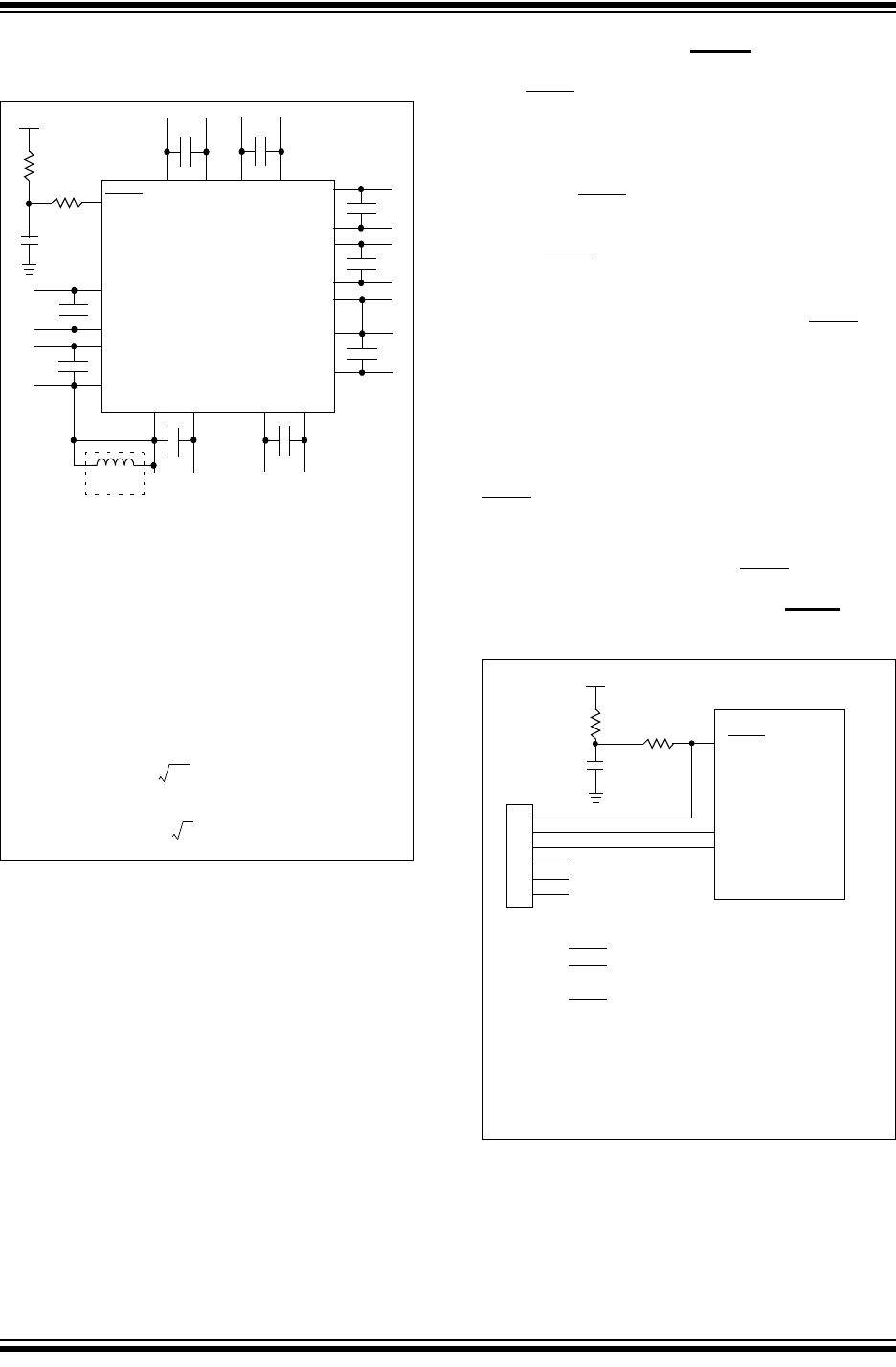
PIC32MZ Embedded Connectivity with Floating Point Unit (EF) Family
DS60001320B-page 38 Preliminary 2015 Microchip Technology Inc.
FIGURE 2-1: RECOMMENDED
MINIMUM CONNECTION
2.2.1 BULK CAPACITORS
The use of a bulk capacitor is recommended to improve
power supply stability. Typical values range from 4.7 µF
to 47 µF. This capacitor should be located as close to
the device as possible.
2.3 Master Clear (MCLR) Pin
The MCLR pin provides for two specific device
functions:
• Device Reset
• Device programming and debugging
Pulling The MCLR pin low generates either a device
Reset or a POR, depending on the setting of the
SMCLR bit (DEVCFG0<15>). Figure 2-2 illustrates a
typical MCLR circuit. During device programming
and debugging, the resistance and capacitance that
can be added to the pin must be considered. Device
programmers and debuggers drive the MCLR pin.
Consequently, specific voltage levels (VIH and VIL)
and fast signal transitions must not be adversely
affected. Therefore, specific values of R and C will
need to be adjusted based on the application and
PCB requirements.
For example, as illustrated in Figure 2-2, it is
recommended that the capacitor C be isolated from the
MCLR pin during programming and debugging
operations.
Place the components illustrated in Figure 2-2 within
one-quarter inch (6 mm) from the MCLR pin.
FIGURE 2-2: EXAMPLE OF MCLR PIN
CONNECTIONS
PIC32
VDD
VSS
VDD
VSS
VDD
VDD
AVDD
AVSS
VDD
VSS
0.1 µF
Ceramic
0.1 µF
Ceramic
0.1 µF
Ceramic
0.1 µF
Ceramic
C
R
VDD
MCLR
0.1 µF
Ceramic
L1(2)
R1
Note 1: If the USB module is not used, this pin must be
connected to VSS.
2: As an option, instead of a hard-wired connection, an
inductor (L1) can be substituted between VDD and
AVDD to improve ADC noise rejection. The inductor
impedance should be less than 1 and the inductor
capacity greater than 10 mA.
Where:
fFCNV
2
--------------=
f1
2LC
-----------------------=
L1
2fC
----------------------
2
=
(i.e., ADC conversion rate/2)
Connect(2)
VUSB3V3(1)
VDD
VSS
VSS
VDD
VDD
VSS
VSS
VSS
Note 1: 470 R1 1 will limit any current flowing into
MCLR from the external capacitor C, in the event of
MCLR pin breakdown, due to Electrostatic Discharge
(ESD) or Electrical Overstress (EOS). Ensure that the
MCLR pin VIH and VIL specifications are met without
interfering with the Debug/Programmer tools.
2: The capacitor can be sized to prevent unintentional
Resets from brief glitches or to extend the device
Reset period during POR.
3: No pull-ups or bypass capacitors are allowed on
active debug/program PGECx/PGEDx pins.
R1(1)
10k
VDD
MCLR
PIC32
1 k
0.1 µF(2)
PGECx(3)
PGEDx(3)
ICSP™
1
5
4
2
3
6
VDD
VSS
NC
R
C
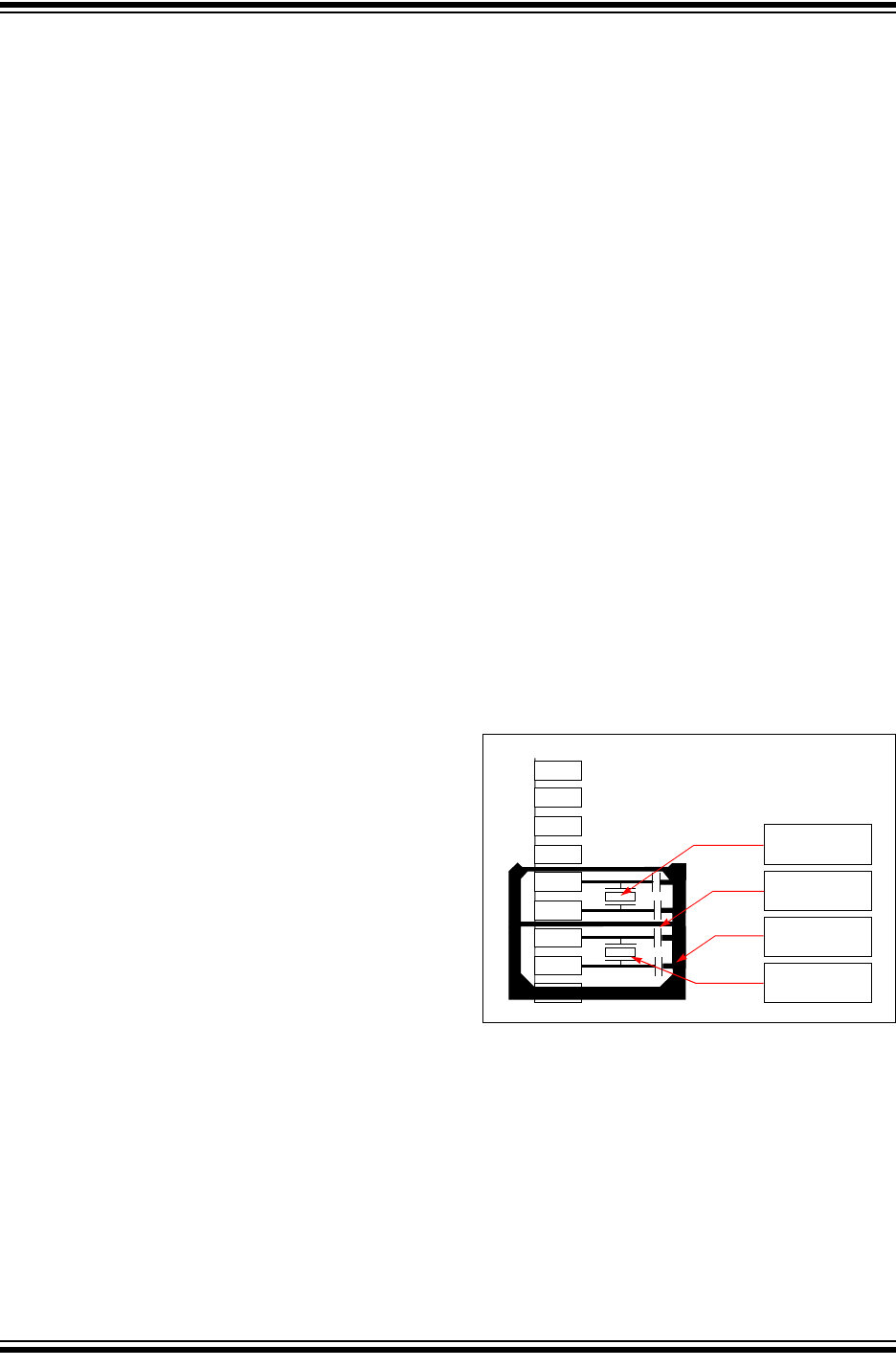
2015 Microchip Technology Inc. Preliminary DS60001320B-page 39
PIC32MZ Embedded Connectivity with Floating Point Unit (EF) Family
2.4 ICSP Pins
The PGECx and PGEDx pins are used for ICSP and
debugging purposes. It is recommended to keep the
trace length between the ICSP connector and the
ICSP pins on the device as short as possible. If the
ICSP connector is expected to experience an ESD
event, a series resistor is recommended, with the
value in the range of a few tens of Ohms, not to
exceed 100 Ohms.
Pull-up resistors, series diodes and capacitors on the
PGECx and PGEDx pins are not recommended as they
will interfere with the programmer/debugger communi-
cations to the device. If such discrete components are
an application requirement, they should be removed
from the circuit during programming and debugging.
Alternatively, refer to the AC/DC characteristics and
timing requirements information in the respective
device Flash programming specification for information
on capacitive loading limits and pin input voltage high
(VIH) and input low (VIL) requirements.
Ensure that the “Communication Channel Select” (i.e.,
PGECx/PGEDx pins) programmed into the device
matches the physical connections for the ICSP to
MPLAB® ICD 3 or MPLAB REAL ICE™.
For more information on ICD 3 and REAL ICE
connection requirements, refer to the following
documents that are available from the Microchip web
site.
•“Using MPLAB® ICD 3” (poster) (DS50001765)
•“MPLAB® ICD 3 Design Advisory” (DS50001764)
•“MPLAB® REAL ICE™ In-Circuit Debugger
User’s Guide” (DS50001616)
•“Using MPLAB® REAL ICE™ Emulator” (poster)
(DS50001749)
2.5 JTAG
The TMS, TDO, TDI and TCK pins are used for testing
and debugging according to the Joint Test Action
Group (JTAG) standard. It is recommended to keep the
trace length between the JTAG connector and the
JTAG pins on the device as short as possible. If the
JTAG connector is expected to experience an ESD
event, a series resistor is recommended, with the value
in the range of a few tens of Ohms, not to exceed 100
Ohms.
Pull-up resistors, series diodes and capacitors on the
TMS, TDO, TDI and TCK pins are not recommended
as they will interfere with the programmer/debugger
communications to the device. If such discrete compo-
nents are an application requirement, they should be
removed from the circuit during programming and
debugging. Alternatively, refer to the AC/DC character-
istics and timing requirements information in the
respective device Flash programming specification for
information on capacitive loading limits and pin input
voltage high (VIH) and input low (VIL) requirements.
2.6 Trace
The trace pins can be connected to a hardware
trace-enabled programmer to provide a compressed
real-time instruction trace. When used for trace, the
TRD3, TRD2, TRD1, TRD0 and TRCLK pins should
be dedicated for this use. The trace hardware
requires a 22 Ohm series resistor between the trace
pins and the trace connector.
2.7 External Oscillator Pins
Many MCUs have options for at least two oscillators: a
high-frequency primary oscillator and a low-frequency
secondary oscillator (refer to Section 8.0 “Oscillator
Configuration” for details).
The oscillator circuit should be placed on the same side
of the board as the device. Also, place the oscillator cir-
cuit close to the respective oscillator pins, not exceed-
ing one-half inch (12 mm) distance between them. The
load capacitors should be placed next to the oscillator
itself, on the same side of the board. Use a grounded
copper pour around the oscillator circuit to isolate them
from surrounding circuits. The grounded copper pour
should be routed directly to the MCU ground. Do not
run any signal traces or power traces inside the ground
pour. Also, if using a two-sided board, avoid any traces
on the other side of the board where the crystal is
placed. A suggested layout is illustrated in Figure 2-3.
FIGURE 2-3: SUGGESTED OSCILLATOR
CIRCUIT PLACEMENT
2.8 Unused I/Os
Unused I/O pins should not be allowed to float as
inputs. They can be configured as outputs and driven
to a logic-low state.
Alternatively, inputs can be reserved by connecting the
pin to VSS through a 1k to 10k resistor and configuring
the pin as an input.
Main Oscillator
Guard Ring
Guard Trace
Secondary
Oscillator
PIC32MZ Embedded Connectivity with Floating Point Unit (EF) Family
DS60001320B-page 40 Preliminary 2015 Microchip Technology Inc.
2.9 Designing for High-Speed
Peripherals
The PIC32MZ EF family devices have peripherals that
operate at frequencies much higher than typical for an
embedded environment. Table 2-1 lists the peripherals
that produce high-speed signals on their external pins:
TABLE 2-1: PERIPHERALS THAT
PRODUCE HS SIGNALS ON
EXTERNAL PINS
Due to these high-speed signals, it is important to
consider several factors when designing a product that
uses these peripherals, as well as the PCB on which
these components will be placed. Adhering to these
recommendations will help achieve the following goals:
• Minimize the effects of electromagnetic interference
to the proper operation of the product
• Ensure signals arrive at their intended destination at
the same time
• Minimize crosstalk
• Maintain signal integrity
• Reduce system noise
• Minimize ground bounce and power sag
2.9.1 SYSTEM DESIGN
2.9.1.1 Impedance Matching
When selecting parts to place on high-speed buses,
particularly the SQI bus, if the impedance of the periph-
eral device does not match the impedance of the pins
on the PIC32MZ EF device to which it is connected,
signal reflections could result, thereby degrading the
quality of the signal.
If it is not possible to select a product that matches
impedance, place a series resistor at the load to create
the matching impedance. See Figure 2-4 for an
example.
FIGURE 2-4: SERIES RESISTOR
2.9.1.2 PCB Layout Recommendations
The following list contains recommendations that will
help ensure the PCB layout will promote the goals
previously listed.
•Component Placement
- Place bypass capacitors as close to their
component power and ground pins as possible,
and place them on the same side of the PCB
- Devices on the same bus that have larger setup
times should be placed closer to the PIC32MZ EF
device
•Power and Ground
- Multi-layer PCBs will allow separate power and
ground planes
- Each ground pin should be connected to the
ground plane individually
- Place bypass capacitor vias as close to the pad
as possible (preferably inside the pad)
- If power and ground planes are not used,
maximize width for power and ground traces
- Use low-ESR, surface-mount bypass capacitors
• Clocks and Oscillators
- Place crystals as close as possible to the
PIC32MZ EF device OSC/SOSC pins
- Do not route high-speed signals near the clock or
oscillator
- Avoid via usage and branches in clock lines
(SQICLK)
- Place termination resistors at the end of clock
lines
•Traces
- Higher-priority signals should have the shortest
traces
- Match trace lengths for parallel buses (EBIAx,
EBIDx, SQIDx)
- Avoid long run lengths on parallel traces to reduce
coupling
- Make the clock traces as straight as possible
- Use rounded turns rather than right-angle turns
- Have traces on different layers intersect on right
angles to minimize crosstalk
- Maximize the distance between traces, preferably
no less than three times the trace width
- Power traces should be as short and as wide as
possible
- High-speed traces should be placed close to the
ground plane
Peripheral High-Speed
Signal Pins
Maximum
Speed on
Signal Pin
EBI EBIAx,
EBIDx 50 MHz
SQI1 SQICLK,
SQICSx,
SQIDx
50 MHz
HS USB D+, D- 480 MHz
PIC32MZ SQI
Flash
Device
50
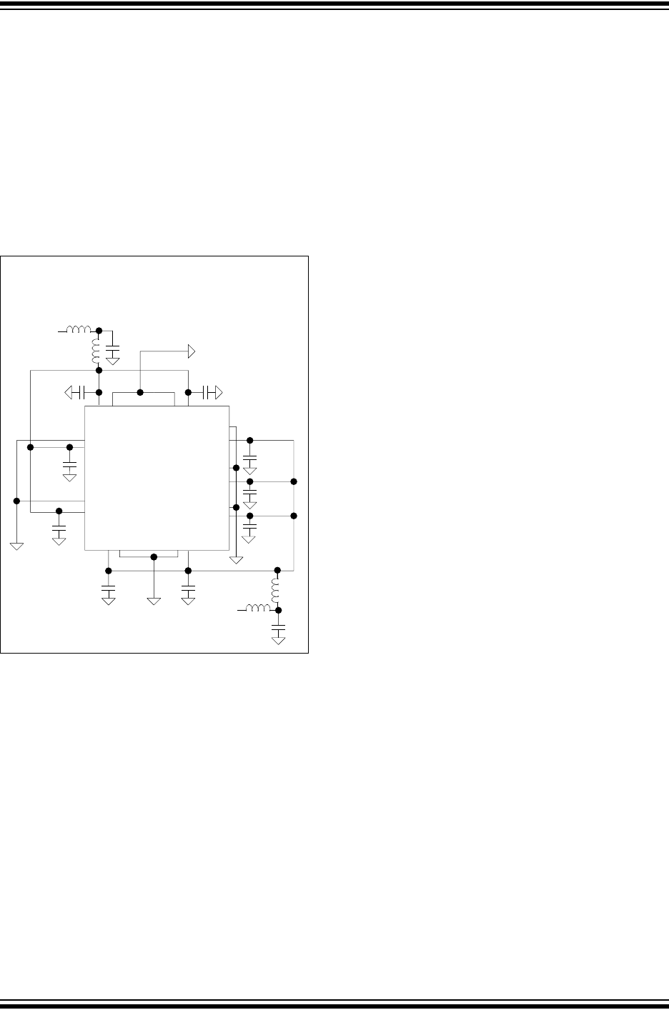
2015 Microchip Technology Inc. Preliminary DS60001320B-page 41
PIC32MZ Embedded Connectivity with Floating Point Unit (EF) Family
2.9.1.3 EMI Suppression Considerations
The use of LDO regulators is preferred to reduce
overall system noise and provide a cleaner power
source. However, when utilizing switching Buck/Boost
regulators as the local power source for PIC32MZ EF
devices, as well as in electrically noisy environments,
users should evaluate the use of T-Filters (i.e., L-C-L)
on the power pins, as shown in Figure 2-5. In addition
to a more stable power source, use of this type of T-Fil-
ter can greatly reduce susceptibility to EMI sources and
events.
FIGURE 2-5:
VSS
VDD
VSS
VUSB3V3
VSS
VDD
VSS
VDD
VDD
VSS
VSS
VDD
VSS
VDD
VSS
VDD
AVDD
AVSS
Ferrite
Chips
0.01 μF
0.01 μF
VDD
VDD
0.1 μF
0.1 μF
0.1 μF
0.1 μF
0.1 μF
0.1 μF
0.1 μF
0.1 μF
Ferrite
Chips
Ferrite Chip SMD
DCR = 0.15ȍ(max)
600 ma ISAT
300ȍ@ 100 MHz
PN#:
0.1 μF
PIC32MZ
PIC32MZ Embedded Connectivity with Floating Point Unit (EF) Family
DS60001320B-page 42 Preliminary 2015 Microchip Technology Inc.
2.10 Typical Application Connection
Examples
Examples of typical application connections are shown
in Figure 2-6 and Figure 2-7.
FIGURE 2-6: AUDIO PLAYBACK APPLICATION
FIGURE 2-7: LOW-COST CONTROLLERLESS (LCC) GRAPHICS APPLICATION WITH
PROJECTED CAPACITIVE TOUCH
Audio
Codec
Display
PMP
I2S
SPI
USB
USB PMD<7:0>
3
3
Stereo Headphones
Speaker
PIC32
Host
PMWR
MMC SD
3
SDI
REFCLKO
LCD Display
PIC32
SRAM
Microchip
Microchip
DMA EBI
ADC
Projected Capacitive
Touch Overlay
GFX Library
External Frame Buffer
ANx
Library
mTouch™
Refresh
Render

2015 Microchip Technology Inc. Preliminary DS60001320B-page 43
PIC32MZ Embedded Connectivity with Floating Point Unit (EF) Family
3.0 CPU
The MIPS32® M-Class Core is the heart of the
PIC32MZ EF family device processor. The CPU
fetches instructions, decodes each instruction, fetches
source operands, executes each instruction and writes
the results of instruction execution to the proper
destinations.
Key features include:
• 5-stage pipeline
• 32-bit address and data paths
• MIPS32 Enhanced Architecture (Release 5):
- Multiply-accumulate and multiply-subtract
instructions
- Targeted multiply instruction
- Zero/One detect instructions
-WAIT instruction
- Conditional move instructions (MOVN, MOVZ)
- Vectored interrupts
- Programmable exception vector base
- Atomic interrupt enable/disable
- GPR shadow registers to minimize latency for
interrupt handlers
- Bit field manipulation instructions
- Virtual memory support
• microMIPS™ compatible instruction set:
- Improves code size density over MIPS32, while
maintaining MIPS32 performance.
- Supports all MIPS32 instructions (except branch-
likely instructions)
- Fifteen additional 32-bit instructions and 39 16-bit
instructions corresponding to commonly-used
MIPS32 instructions
- Stack pointer implicit in instruction
- MIPS32 assembly and ABI compatible
• MMU with Translation Lookaside Buffer (TLB)
mechanism:
- 16 dual-entry fully associative Joint TLB
- 4-entry fully associative Instruction and Data TLB
- 4 KB pages
• Separate L1 data and instruction caches:
- 16 KB 4-way Instruction Cache (I-Cache)
- 4 KB 4-way Data Cache (D-Cache)
• Autonomous Multiply/Divide Unit (MDU):
- Maximum issue rate of one 32x32 multiply per clock
- Early-in iterative divide. Minimum 12 and
maximum 38 clock latency (dividend (rs) sign
extension-dependent)
• Power Control:
- Minimum frequency: 0 MHz
- Low-Power mode (triggered by WAIT instruction)
- Extensive use of local gated clocks
• EJTAG Debug and Instruction Trace:
- Support for single stepping
- Virtual instruction and data address/value
breakpoints
- Hardware breakpoint supports both address
match and address range triggering.
- Eight instruction and four data complex
breakpoints
• iFlowtrace® version 2.0 support:
- Real-time instruction program counter
- Special events trace capability
- Two performance counters with 34 user-
selectable countable events
- Disabled if the processor enters Debug mode
- Program Counter sampling
• Four Watch registers:
- Instruction, Data Read, Data Write options
- Address match masking options
• DSP ASE Extension:
- Native fractional format data type operations
- Register Single Instruction Multiple Data (SIMD)
operations (add, subtract, multiply, shift)
- GPR-based shift
- Bit manipulation
- Compare-Pick
- DSP Control Access
- Indexed-Load
-Branch
- Multiplication of complex operands
- Variable bit insertion and extraction
- Virtual circular buffers
- Arithmetic saturation and overflow handling
- Zero-cycle overhead saturation and rounding
operations
• Floating Point Unit (FPU):
- 1985 IEEE-754 compliant Floating Point Unit
- Supports single and double precision datatypes
- 2008 IEEE-754 compatibility control of NaN
handling and Abs/Neg instructions
- Runs at 1:1 core/FPU clock ratio
Note 1: This data sheet summarizes the fea-
tures of the PIC32MZ EF family of
devices. It is not intended to be a
comprehensive reference source. To
complement the information in this data
sheet, refer to Section 50. “CPU for
Devices with MIPS32® microAptiv™
and M-Class Cores” (DS60001192) of
the “PIC32 Family Reference Manual”,
which is available from the Microchip
web site (www.microchip.com/PIC32).
2: The Series 5 Warrior M-class CPU core
resources are available at:
www.imgtec.com.
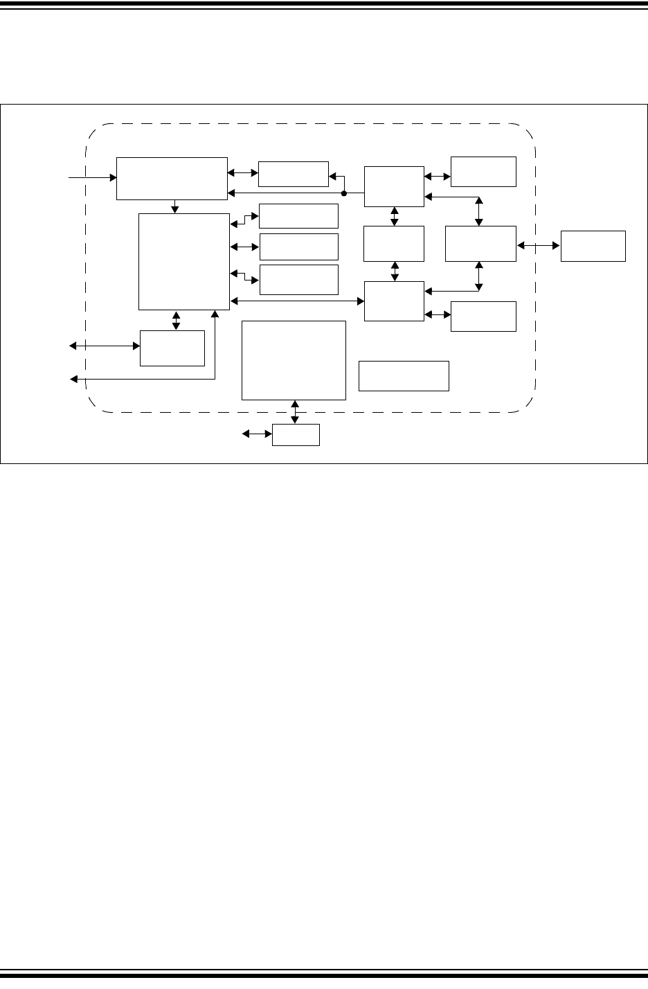
PIC32MZ Embedded Connectivity with Floating Point Unit (EF) Family
DS60001320B-page 44 Preliminary 2015 Microchip Technology Inc.
A block diagram of the PIC32MZ EF family processor
core is shown in Figure 3-1.
FIGURE 3-1: PIC32MZ EF FAMILY MICROPROCESSOR CORE BLOCK DIAGRAM
System Bus
Execution Unit
ALU/Shift
Atomic/LdSt
DSP ASE
System
Coprocessor
Enhanced MDU
(with DSP ASE)
GPR
(8 sets)
Debug/Profiling
Break Points
iFlowtrace®
Fast Debug Channel
Performance Counters
Sampling
Secure Debug
microMIPS™ I-Cache
Controller
MMU
(TLB)
D-Cache
Controller
Power
M-Class Microprocessor Core
System
Interface
Interrupt
Interface
I-Cache
D-Cache
BIU
Decode
(MIPS32®/microMIPS™)
EJTAG
2-wire Debug
Management
PBCLK7
FPU
(Single & Double)

2015 Microchip Technology Inc. Preliminary DS60001320B-page 45
PIC32MZ Embedded Connectivity with Floating Point Unit (EF) Family
3.1 Architecture Overview
The MIPS32 M-Class Microprocessor core in PIC32MZ
EF family devices contains several logic blocks working
together in parallel, providing an efficient high-perfor-
mance computing engine. The following blocks are
included with the core:
• Execution unit
• General Purpose Register (GPR)
• Multiply/Divide Unit (MDU)
• System control coprocessor (CP0)
• Floating Point Unit (FPU)
• Memory Management Unit (MMU)
• Instruction/Data cache controllers
• Power Management
• Instructions and data caches
• microMIPS support
• Enhanced JTAG (EJTAG) controller
3.1.1 EXECUTION UNIT
The processor core execution unit implements a load/
store architecture with single-cycle ALU operations
(logical, shift, add, subtract) and an autonomous multi-
ply/divide unit. The core contains thirty-two 32-bit Gen-
eral Purpose Registers (GPRs) used for integer
operations and address calculation. Seven additional
register file shadow sets (containing thirty-two regis-
ters) are added to minimize context switching overhead
during interrupt/exception processing. The register file
consists of two read ports and one write port and is fully
bypassed to minimize operation latency in the pipeline.
The execution unit includes:
• 32-bit adder used for calculating the data address
• Address unit for calculating the next instruction
address
• Logic for branch determination and branch target
address calculation
• Load aligner
• Trap condition comparator
• Bypass multiplexers used to avoid stalls when
executing instruction streams where data
producing instructions are followed closely by
consumers of their results
• Leading Zero/One detect unit for implementing
the CLZ and CLO instructions
• Arithmetic Logic Unit (ALU) for performing arithmetic
and bitwise logical operations
• Shifter and store aligner
• DSP ALU and logic block for performing DSP
instructions, such as arithmetic/shift/compare
operations
3.1.2 MULTIPLY/DIVIDE UNIT (MDU)
The processor core includes a Multiply/Divide Unit
(MDU) that contains a separate pipeline for multiply
and divide operations, and DSP ASE multiply instruc-
tions. This pipeline operates in parallel with the Integer
Unit (IU) pipeline and does not stall when the IU pipe-
line stalls. This allows MDU operations to be partially
masked by system stalls and/or other integer unit
instructions.
The high-performance MDU consists of a 32x32 booth
recoded multiplier, four pairs of result/accumulation
registers (HI and LO), a divide state machine, and the
necessary multiplexers and control logic. The first num-
ber shown (‘32’ of 32x32) represents the rs operand.
The second number (‘32’ of 32x32) represents the rt
operand.
The MDU supports execution of one multiply or
multiply-accumulate operation every clock cycle.
Divide operations are implemented with a simple 1-bit-
per-clock iterative algorithm. An early-in detection
checks the sign extension of the dividend (rs) oper-
and. If rs is 8 bits wide, 23 iterations are skipped. For
a 16-bit wide rs, 15 iterations are skipped and for a
24-bit wide rs, 7 iterations are skipped. Any attempt to
issue a subsequent MDU instruction while a divide is
still active causes an IU pipeline stall until the divide
operation has completed.
Table 3-1 lists the repeat rate (peak issue rate of cycles
until the operation can be reissued) and latency (num-
ber of cycles until a result is available) for the processor
core multiply and divide instructions. The approximate
latency and repeat rates are listed in terms of pipeline
clocks.
TABLE 3-1: MIPS32® M-CLASS MICROPROCESSOR CORE HIGH-PERFORMANCE INTEGER
MULTIPLY/DIVIDE UNIT LATENCIES AND REPEAT RATES
Opcode Operand Size (mul rt) (div rs)Latency Repeat Rate
MULT/MULTU, MADD/MADDU,
MSUB/MSUBU (HI/LO destination)
16 bits 5 1
32 bits 5 1
MUL (GPR destination) 16 bits 5 1
32 bits 5 1
DIV/DIVU 8 bits 12/14 12/14
16 bits 20/22 20/22
24 bits 28/30 28/30
32 bits 36/38 36/38

PIC32MZ Embedded Connectivity with Floating Point Unit (EF) Family
DS60001320B-page 46 Preliminary 2015 Microchip Technology Inc.
The MIPS architecture defines that the result of a
multiply or divide operation be placed in one of four
pairs of HI and LO registers. Using the Move-From-HI
(MFHI) and Move-From-LO (MFLO) instructions, these
values can be transferred to the General Purpose
Register file.
In addition to the HI/LO targeted operations, the
MIPS32 architecture also defines a multiply instruc-
tion, MUL, which places the least significant results in
the primary register file instead of the HI/LO register
pair. By avoiding the explicit MFLO instruction
required when using the LO register, and by support-
ing multiple destination registers, the throughput of
multiply-intensive operations is increased.
Two other instructions, Multiply-Add (MADD) and
Multiply-Subtract (MSUB), are used to perform the
multiply-accumulate and multiply-subtract operations.
The MADD instruction multiplies two numbers and then
adds the product to the current contents of the HI and
LO registers. Similarly, the MSUB instruction multiplies
two operands and then subtracts the product from the
HI and LO registers. The MADD and MSUB operations
are commonly used in DSP algorithms.
The MDU also implements various shift instructions
operating on the HI/LO register and multiply instruc-
tions as defined in the DSP ASE. The MDU supports all
of the data types required for this purpose and includes
three extra HI/LO registers as defined by the ASE.
Table 3-2 lists the latencies and repeat rates for the
DSP multiply and dot-product operations. The approxi-
mate latencies and repeat rates are listed in terms of
pipeline clocks.
TABLE 3-2: DSP-RELATED LATENCIES
AND REPEAT RATES
3.1.3 SYSTEM CONTROL
COPROCESSOR (CP0)
In the MIPS architecture, CP0 is responsible for the
virtual-to-physical address translation and cache proto-
cols, the exception control system, the processor’s
diagnostics capability, the operating modes (Kernel,
User and Debug) and whether interrupts are enabled or
disabled. Configuration information, such as cache
size and set associativity, and the presence of options
like microMIPS is also available by accessing the CP0
registers, listed in Table 3-3.
Op code Latency Repeat
Rate
Multiply and dot-product without
saturation after accumulation
5 1
Multiply and dot-product with
saturation after accumulation 5 1
Multiply without accumulation 5 1
TABLE 3-3: COPROCESSOR 0 REGISTERS
Register
Number Register
Name Function
0Index Index into the TLB array (MPU only).
1Random Randomly generated index into the TLB array (MPU only).
2EntryLo0 Low-order portion of the TLB entry for even-numbered virtual pages (MPU only).
3EntryLo1 Low-order portion of the TLB entry for odd-numbered virtual pages (MPU only).
4 Context/
UserLocal
Pointer to the page table entry in memory (MPU only).
User information that can be written by privileged software and read via the RDHWR
instruction.
5PageMask/
PageGrain PageMask controls the variable page sizes in TLB entries. PageGrain enables support
of 1 KB pages in the TLB (MPU only).
6Wired Controls the number of fixed (i.e., wired) TLB entries (MPU only).
7HWREna Enables access via the RDHWR instruction to selected hardware registers in
Non-privileged mode.
8BadVAddr Reports the address for the most recent address-related exception.
BadInstr Reports the instruction that caused the most recent exception.
BadInstrP Reports the branch instruction if a delay slot caused the most recent exception.
9Count Processor cycle count.
10 EntryHi High-order portion of the TLB entry (MPU only).
11 Compare Core timer interrupt control.

2015 Microchip Technology Inc. Preliminary DS60001320B-page 47
PIC32MZ Embedded Connectivity with Floating Point Unit (EF) Family
12 Status Processor status and control.
IntCtl Interrupt control of vector spacing.
SRSCtl Shadow register set control.
SRSMap Shadow register mapping control.
View_IPL Allows the Priority Level to be read/written without
extracting or inserting that bit from/to the Status register.
SRSMAP2 Contains two 4-bit fields that provide the mapping from a vector number to the shadow
set number to use when servicing such an interrupt.
13 Cause Describes the cause of the last exception.
NestedExc Contains the error and exception level status bit values that existed prior to the current
exception.
View_RIPL Enables read access to the RIPL bit that is available in the Cause register.
14 EPC Program counter at last exception.
NestedEPC Contains the exception program counter that existed prior to the current exception.
15 PRID Processor identification and revision
Ebase Exception base address of exception vectors.
CDMMBase Common device memory map base.
16 Config Configuration register.
Config1 Configuration register 1.
Config2 Configuration register 2.
Config3 Configuration register 3.
Config4 Configuration register 4.
Config5 Configuration register 5.
Config7 Configuration register 7.
17 LLAddr Load link address (MPU only).
18 WatchLo Low-order watchpoint address (MPU only).
19 WatchHi High-order watchpoint address (MPU only).
20-22 Reserved Reserved in the PIC32 core.
23 Debug EJTAG debug register.
TraceControl EJTAG trace control.
TraceControl2 EJTAG trace control 2.
UserTraceData1 EJTAG user trace data 1 register.
TraceBPC EJTAG trace breakpoint register.
Debug2 Debug control/exception status 1.
24 DEPC Program counter at last debug exception.
UserTraceData2 EJTAG user trace data 2 register.
25 PerfCtl0 Performance counter 0 control.
PerfCnt0 Performance counter 0.
PerfCtl1 Performance counter 1 control.
PerfCnt1 Performance counter 1.
26 ErrCtl Software test enable of way-select and data RAM arrays for I-Cache and D-Cache
(MPU only).
27 Reserved Reserved in the PIC32 core.
28 TagLo/DataLo Low-order portion of cache tag interface (MPU only).
29 Reserved Reserved in the PIC32 core.
30 ErrorEPC Program counter at last error exception.
31 DeSave Debug exception save.
TABLE 3-3: COPROCESSOR 0 REGISTERS (CONTINUED)
Register
Number Register
Name Function

PIC32MZ Embedded Connectivity with Floating Point Unit (EF) Family
DS60001320B-page 48 Preliminary 2015 Microchip Technology Inc.
3.1.4 FLOATING POINT UNIT (FPU)
The Floating Point Unit (FPU), Coprocessor (CP1),
implements the MIPS Instruction Set Architecture for
floating point computation. The implementation sup-
ports the ANSI/IEEE Standard 754 (IEEE for Binary
Floating Point Arithmetic) for single- and double-preci-
sion data formats. The FPU can be programmed to
have thirty-two 32-bit or 64-bit floating point registers
used for floating point operations.
The performance is optimized for single precision for-
mats. Most instructions have one FPU cycle throughput
and four FPU cycle latency. The FPU implements the
multiply-add (MADD) and multiply-sub (MSUB) instruc-
tions with intermediate rounding after the multiply func-
tion. The result is guaranteed to be the same as
executing a MUL and an ADD instruction separately,
but the instruction latency, instruction fetch, dispatch
bandwidth, and the total number of register accesses
are improved.
IEEE denormalized input operands and results are
supported by hardware for some instructions. IEEE
denormalized results are not supported by hardware in
general, but a fast flush-to-zero mode is provided to
optimize performance. The fast flush-to-zero mode is
enabled through the FCCR register, and use of this
mode is recommended for best performance when
denormalized results are generated.
The FPU has a separate pipeline for floating point
instruction execution. This pipeline operates in parallel
with the integer core pipeline and does not stall when
the integer pipeline stalls. This allows long-running
FPU operations, such as divide or square root, to be
partially masked by system stalls and/or other integer
unit instructions. Arithmetic instructions are always
dispatched and completed in order, but loads and
stores can complete out of order. The exception model
is “precise” at all times.
Table 3-4 contains the floating point instruction laten-
cies and repeat rates for the processor core. In this
table, 'Latency' refers to the number of FPU cycles nec-
essary for the first instruction to produce the result
needed by the second instruction. The “Repeat Rate”
refers to the maximum rate at which an instruction can
be executed per FPU cycle.
TABLE 3-4: FPU INSTRUCTION
LATENCIES AND REPEAT
RATES
Op code Latency
(FPU
Cycles)
Repeat
Rate
(FPU
Cycles)
ABS.[S,D], NEG.[S,D],
ADD.[S,D], SUB.[S,D],
C.cond.[S,D], MUL.S
4 1
MADD.S, MSUB.S,
NMADD.S, NMSUB.S,
CABS.cond.[S,D]
4 1
CVT.D.S, CVT.PS.PW,
CVT.[S,D].[W,L]
4 1
CVT.S.D,
CVT.[W,L].[S,D],
CEIL.[W,L].[S,D],
FLOOR.[W,L].[S,D],
ROUND.[W,L].[S,D],
TRUNC.[W,L].[S,D]
4 1
MOV.[S,D], MOVF.[S,D],
MOVN.[S,D],
MOVT.[S,D], MOVZ.[S,D]
4 1
MUL.D 5 2
MADD.D, MSUB.D,
NMADD.D, NMSUB.D
5 2
RECIP.S 13 10
RECIP.D 26 21
RSQRT.S 17 14
RSQRT.D 36 31
DIV.S, SQRT.S 17 14
DIV.D, SQRT.D 32 29
MTC1, DMTC1, LWC1,
LDC1, LDXC1, LUXC1,
LWXC1
4 1
MFC1, DMFC1, SWC1,
SDC1, SDXC1, SUXC1,
SWXC1
1 1
Legend: S = Single D = Double
W = Word L = Long word

2015 Microchip Technology Inc. Preliminary DS60001320B-page 49
PIC32MZ Embedded Connectivity with Floating Point Unit (EF) Family
The FPU implements a high-performance 7-stage
pipeline:
• Decode, register read and unpack (FR stage)
• Multiply tree - double pumped for double (M1
stage)
• Multiply complete (M2 stage)
• Addition first step (A1 stage)
• Addition second and final step (A2 stage)
• Packing to IEEE format (FP stage)
• Register writeback (FW stage)
The FPU implements a bypass mechanism that allows
the result of an operation to be forwarded directly to the
instruction that needs it without having to write the
result to the FPU register and then read it back.
Table 3-5 lists the Coprocessor 1 Registers for the
FPU.
TABLE 3-5: FPU (CP1) REGISTERS
3.2 Power Management
The processor core offers a number of power manage-
ment features, including low-power design, active power
management and power-down modes of operation. The
core is a static design that supports slowing or halting
the clocks, which reduces system power consumption
during Idle periods.
3.2.1 INSTRUCTION-CONTROLLED
POWER MANAGEMENT
The mechanism for invoking Power-Down mode is
through execution of the WAIT instruction. For more
information on power management, see Section 33.0
“Power-Saving Features”.
3.2.2 LOCAL CLOCK GATING
The majority of the power consumed by the processor
core is in the clock tree and clocking registers. The
PIC32MZ family makes extensive use of local gated-
clocks to reduce this dynamic power consumption.
3.3 L1 Instruction and Data Caches
3.3.1 INSTRUCTION CACHE (I-CACHE)
The I-Cache is an on-core memory block of 16 Kbytes.
Because the I-Cache is virtually indexed, the virtual-to-
physical address translation occurs in parallel with the
cache access rather than having to wait for the physical
address translation. The tag holds 22 bits of physical
address, a valid bit, and a lock bit. The LRU
replacement bits are stored in a separate array.
The I-Cache block also contains and manages the
instruction line fill buffer. Besides accumulating data to
be written to the cache, instruction fetches that refer-
ence data in the line fill buffer are serviced either by a
bypass of that data, or data coming from the external
interface. The I-Cache control logic controls the bypass
function.
The processor core supports I-Cache locking. Cache
locking allows critical code or data segments to be
locked into the cache on a per-line basis, enabling the
system programmer to maximize the efficiency of the
system cache.
The cache locking function is always available on all
I-Cache entries. Entries can then be marked as
locked or unlocked on a per entry basis using the
CACHE instruction.
3.3.2 DATA CACHE (D-CACHE)
The D-Cache is an on-core memory block of 4 Kbytes.
This virtually indexed, physically tagged cache is pro-
tected. Because the D-Cache is virtually indexed, the
virtual-to-physical address translation occurs in parallel
with the cache access. The tag holds 22 bits of physical
address, a valid bit, and a lock bit. There is an addi-
tional array holding dirty bits and LRU replacement
algorithm bits for each set of the cache.
In addition to I-Cache locking, the processor core also
supports a D-Cache locking mechanism identical to the
I-Cache. Critical data segments are locked into the
cache on a per-line basis. The locked contents can be
updated on a store hit, but cannot be selected for
replacement on a cache miss.
The D-Cache locking function is always available on
all D-Cache entries. Entries can then be marked as
locked or unlocked on a per-entry basis using the
CACHE instruction.
3.3.3 ATTRIBUTES
The processor core I-Cache and D-Cache attributes
are listed in the Configuration registers (see
Register 3-1 through Register 3-4).
Register
Number Register
Name Function
0FIR Floating Point implementation
register. Contains information
that identifies the FPU.
25 FCCR Floating Point condition codes
register.
26 FEXR Floating Point exceptions
register.
28 FENR Floating Point enables register.
31 FCSR Floating Point Control and
Status register.

PIC32MZ Embedded Connectivity with Floating Point Unit (EF) Family
DS60001320B-page 50 Preliminary 2015 Microchip Technology Inc.
3.4 EJTAG Debug Support
The processor core provides for an Enhanced JTAG
(EJTAG) interface for use in the software debug of
application and kernel code. In addition to standard
User mode and Kernel modes of operation, the proces-
sor core provides a Debug mode that is entered after a
debug exception (derived from a hardware breakpoint,
single-step exception, etc.) is taken and continues until
a Debug Exception Return (DERET) instruction is
executed. During this time, the processor executes the
debug exception handler routine.
The EJTAG interface operates through the Test Access
Port (TAP), a serial communication port used for trans-
ferring test data in and out of the core. In addition to the
standard JTAG instructions, special instructions
defined in the EJTAG specification specify which
registers are selected and how they are used.
3.5 MIPS DSP ASE Extension
The MIPS DSP Application-Specific Extension
Revision 2 is an extension to the MIPS32 architecture.
This extension comprises new integer instructions and
states that include new HI/LO accumulator register
pairs and a DSP control register. This extension is
crucial in a wide range of DSP, multimedia, and DSP-
like algorithms covering Audio and Video processing
applications. The extension supports native fractional
format data type operations, register Single Instruction
Multiple Data (SIMD) operations, such as add,
subtract, multiply, and shift. In addition, the extension
includes the following features that are essential in
making DSP algorithms computationally efficient:
• Support for multiplication of complex operands
• Variable bit insertion and extraction
• Implementation and use of virtual circular buffers
• Arithmetic saturation and overflow handling
support
• Zero cycle overhead saturation and rounding
operations
3.6 microMIPS ISA
The processor core supports the microMIPS ISA,
which contains all MIPS32 ISA instructions (except for
branch-likely instructions) in a new 32-bit encoding
scheme, with some of the commonly used instructions
also available in 16-bit encoded format. This ISA
improves code density through the additional 16-bit
instructions while maintaining a performance similar to
MIPS32 mode. In microMIPS mode, 16-bit or 32-bit
instructions will be fetched and recoded to legacy
MIPS32 instruction opcodes in the pipeline’s I stage, so
that the processor core can have the same microAptiv
UP microarchitecture. Because the microMIPS instruc-
tion stream can be intermixed with 16-bit halfword or
32-bit word size instructions on halfword or word
boundaries, additional logic is in place to address the
word misalignment issues, thus minimizing
performance loss.

2015 Microchip Technology Inc. Preliminary DS60001320B-page 51
PIC32MZ Embedded Connectivity with Floating Point Unit (EF) Family
3.7 M-Class Core Configuration
Register 3-1 through Register 3-4 show the default
configuration of the M-Class core, which is included on
PIC32MZ EF family devices.
REGISTER 3-1: CONFIG: CONFIGURATION REGISTER; CP0 REGISTER 16, SELECT 0
Bit
Range Bit
31/23/15/7 Bit
30/22/14/6 Bit
29/21/13/5 Bit
28/20/12/4 Bit
27/19/11/3 Bit
26/18/10/2 Bit
25/17/9/1 Bit
24/16/8/0
31:24 r-1 U-0 U-0 U-0 U-0 U-0 U-0 R-0
— — — — — — —ISP
23:16 R-0 R-0 R-1 R-0 U-0 R-1 R-0 R-0
DSP UDI SB MDU — MM<1:0> BM
15:8 R-0 R-0 R-0 R-0 R-0 R-1 R-0 R-0
BE AT<1:0> AR<2:0> MT<2:1>
7:0 R-1 U-0 U-0 U-0 U-0 R/W-0 R/W-1 R/W-0
MT<0> — — — — K0<2:0>
Legend: r = Reserved bit
R = Readable bit W = Writable bit U = Unimplemented bit, read as ‘0’
-n = Value at POR ‘1’ = Bit is set ‘0’ = Bit is cleared x = Bit is unknown
bit 31 Reserved: This bit is hardwired to ‘1’ to indicate the presence of the Config1 register.
bit 30-25 Unimplemented: Read as ‘0’
bit 24 ISP: Instruction Scratch Pad RAM bit
0 = Instruction Scratch Pad RAM is not implemented
bit 23 DSP: Data Scratch Pad RAM bit
0 = Data Scratch Pad RAM is not implemented
bit 22 UDI: User-defined bit
0 = CorExtend User-Defined Instructions are not implemented
bit 21 SB: SimpleBE bit
1 = Only Simple Byte Enables are allowed on the internal bus interface
bit 20 MDU: Multiply/Divide Unit bit
0 = Fast, high-performance MDU
bit 19 Unimplemented: Read as ‘0’
bit 18-17 MM<1:0>: Merge Mode bits
10 = Merging is allowed
bit 16 BM: Burst Mode bit
0 = Burst order is sequential
bit 15 BE: Endian Mode bit
0 = Little-endian
bit 14-13 AT<1:0>: Architecture Type bits
00 = MIPS32
bit 12-10 AR<2:0>: Architecture Revision Level bits
001 = MIPS32 Release 2
bit 9-7 MT<2:0>: MMU Type bits
001 = M-Class MPU Microprocessor core uses a TLB-based MMU
bit 6-3 Unimplemented: Read as ‘0’
bit 2-0 K0<2:0>: Kseg0 Coherency Algorithm bits
011 = Cacheable, non-coherent, write-back, write allocate
010 = Uncached
001 = Cacheable, non-coherent, write-through, write allocate
000 = Cacheable, non-coherent, write-through, no write allocate
All other values are not used and mapped to other values. 100, 101, and 110 are mapped to 010. 111 is
mapped to 010.

PIC32MZ Embedded Connectivity with Floating Point Unit (EF) Family
DS60001320B-page 52 Preliminary 2015 Microchip Technology Inc.
REGISTER 3-2: CONFIG1: CONFIGURATION REGISTER 1; CP0 REGISTER 16, SELECT 1
Bit
Range Bit
31/23/15/7 Bit
30/22/14/6 Bit
29/21/13/5 Bit
28/20/12/4 Bit
27/19/11/3 Bit
26/18/10/2 Bit
25/17/9/1 Bit
24/16/8/0
31:24 r-1 R-0 R-0 R-1 R-1 R-1 R-1 R-0
— MMU Size<5:0> IS<2>
23:16 R-1 R-0 R-0 R-1 R-1 R-0 R-1 R-1
IS<1:0> IL<2:0> IA<2:0>
15:8 R-0 R-0 R-0 R-0 R-1 R-1 R-0 R-1
DS<2:0> DL<2:0> DA<2:1>
7:0 R-1 U-0 U-0 R-1 R-1 R-0 R-1 R-1
DA<0> ——PCWRCAEPFP
Legend: r = Reserved bit
R = Readable bit W = Writable bit U = Unimplemented bit, read as ‘0’
-n = Value at POR ‘1’ = Bit is set ‘0’ = Bit is cleared x = Bit is unknown
bit 31 Reserved: This bit is hardwired to a ‘1’ to indicate the presence of the Config2 register.
bit 30-25 MMU Size<5:0>: Contains the number of TLB entries minus 1
001111 = 16 TLB entries
bit 24-22 IS<2:0>: Instruction Cache Sets bits
010 = Contains 256 instruction cache sets per way
bit 21-19 IL<2:0>: Instruction-Cache Line bits
011 = Contains instruction cache line size of 16 bytes
bit 18-16 IA<2:0: Instruction-Cache Associativity bits
011 = Contains 4-way instruction cache associativity
bit 15-13 DS<2:0>: Data-Cache Sets bits
000 = Contains 64 data cache sets per way
bit 12-10 DL<2:0>: Data-Cache Line bits
011 = Contains data cache line size of 16 bytes
bit 9-7 DA<2:0>: Data-Cache Associativity bits
011 = Contains the 4-way set associativity for the data cache
bit 6-5 Unimplemented: Read as ‘0’
bit 4 PC: Performance Counter bit
1 = The processor core contains Performance Counters
bit 3 WR: Watch Register Presence bit
1 = No Watch registers are present
bit 2 CA: Code Compression Implemented bit
0 = No MIPS16e® present
bit 1 EP: EJTAG Present bit
1 = Core implements EJTAG
bit 0 FP: Floating Point Unit bit
1 = Floating Point Unit is present

2015 Microchip Technology Inc. Preliminary DS60001320B-page 53
PIC32MZ Embedded Connectivity with Floating Point Unit (EF) Family
REGISTER 3-3: CONFIG3: CONFIGURATION REGISTER 3; CP0 REGISTER 16, SELECT 3
Bit
Range Bit
31/23/15/7 Bit
30/22/14/6 Bit
29/21/13/5 Bit
28/20/12/4 Bit
27/19/11/3 Bit
26/18/10/2 Bit
25/17/9/1 Bit
24/16/8/0
31:24 r-1 U-0 U-0 U-0 U-0 U-0 U-0 U-0
— — — — — — — —
23:16 U-0 R-0 R-1 R-0 R-0 R-0 R-1 R/W-y
— IPLW<1:0> MMAR<2:0> MCU ISAONEXC(1)
15:8 R-y R-y R-1 R-1 R-1 R-1 U-0 R-1
ISA<1:0>(1) ULRI RXI DSP2P DSPP —ITL
7:0 U-0 R-1 R-1 R-0 R-1 U-0 U-0 R-0
— VEIC VINT SP CDMM ——TL
Legend: r = Reserved bit y = Value set from Configuration bits on POR
R = Readable bit W = Writable bit U = Unimplemented bit, read as ‘0’
-n = Value at POR ‘1’ = Bit is set ‘0’ = Bit is cleared x = Bit is unknown
bit 31 Reserved: This bit is hardwired as ‘1’ to indicate the presence of the Config4 register
bit 30-23 Unimplemented: Read as ‘0’
bit 22-21 IPLW<1:0>: Width of the Status IPL and Cause RIPL bits
01 = IPL and RIPL bits are 8-bits in width
bit 20-18 MMAR<2:0>: microMIPS Architecture Revision Level bits
000 = Release 1
bit 17 MCU: MIPS® MCU™ ASE Implemented bit
1 = MCU ASE is implemented
bit 16 ISAONEXC: ISA on Exception bit(1)
1 = microMIPS is used on entrance to an exception vector
0 = MIPS32 ISA is used on entrance to an exception vector
bit 15-14 ISA<1:0>: Instruction Set Availability bits(1)
11 = Both MIPS32 and microMIPS are implemented; microMIPS is used when coming out of reset
10 = Both MIPS32 and microMIPS are implemented; MIPS32 ISA used when coming out of reset
bit 13 ULRI: UserLocal Register Implemented bit
1 = UserLocal Coprocessor 0 register is implemented
bit 12 RXI: RIE and XIE Implemented in PageGrain bit
1 = RIE and XIE bits are implemented
bit 11 DSP2P: MIPS DSP ASE Revision 2 Presence bit
1 = DSP Revision 2 is present
bit 10 DSPP: MIPS DSP ASE Presence bit
1 = DSP is present
bit 9 Unimplemented: Read as ‘0’
bit 8 ITL: Indicates that iFlowtrace® hardware is present
1 = The iFlowtrace® is implemented in the core
bit 7 Unimplemented: Read as ‘0’
bit 6 VEIC: External Vector Interrupt Controller bit
1 = Support for an external interrupt controller is implemented.
bit 5 VINT: Vector Interrupt bit
1 = Vector interrupts are implemented
bit 4 SP: Small Page bit
0 = 4 KB page size
bit 3 CDMM: Common Device Memory Map bit
1 = CDMM is implemented
bit 2-1 Unimplemented: Read as ‘0’
bit 0 TL: Trace Logic bit
0 = Trace logic is not implemented
Note 1: These bits are set based on the value of the BOOTISA Configuration bit (DEVCFG0<6>).

PIC32MZ Embedded Connectivity with Floating Point Unit (EF) Family
DS60001320B-page 54 Preliminary 2015 Microchip Technology Inc.
REGISTER 3-4: CONFIG5: CONFIGURATION REGISTER 5; CP0 REGISTER 16, SELECT 5
Bit
Range Bit
31/23/15/7 Bit
30/22/14/6 Bit
29/21/13/5 Bit
28/20/12/4 Bit
27/19/11/3 Bit
26/18/10/2 Bit
25/17/9/1 Bit
24/16/8/0
31:24 U-0 U-0 U-0 U-0 U-0 U-0 U-0 U-0
— — — — — — — —
23:16 U-0 U-0 U-0 U-0 U-0 U-0 U-0 U-0
— — — — — — — —
15:8 U-0 U-0 U-0 U-0 U-0 U-0 U-0 U-0
— — — — — — — —
7:0 U-0 U-0 U-0 U-0 U-0 U-0 U-0 R-1
— — — — — — —NF
Legend: r = Reserved
R = Readable bit W = Writable bit U = Unimplemented bit, read as ‘0’
-n = Value at POR ‘1’ = Bit is set ‘0’ = Bit is cleared x = Bit is unknown
bit 31-1 Unimplemented: Read as ‘0’
bit 0 NF: Nested Fault bit
1 = Nested Fault feature is implemented
REGISTER 3-5: CONFIG7: CONFIGURATION REGISTER 7; CP0 REGISTER 16, SELECT 7
Bit
Range Bit
31/23/15/7 Bit
30/22/14/6 Bit
29/21/13/5 Bit
28/20/12/4 Bit
27/19/11/3 Bit
26/18/10/2 Bit
25/17/9/1 Bit
24/16/8/0
31:24 R-1 U-0 U-0 U-0 U-0 U-0 U-0 U-0
WII — — — — — — —
23:16 U-0 U-0 U-0 U-0 U-0 U-0 U-0 U-0
— — — — — — — —
15:8 U-0 U-0 U-0 U-0 U-0 U-0 U-0 U-0
— — — — — — — —
7:0 U-0 U-0 U-0 U-0 U-0 U-0 U-0 U-0
— — — — — — — —
Legend:
R = Readable bit W = Writable bit U = Unimplemented bit, read as ‘0’
-n = Value at POR ‘1’ = Bit is set ‘0’ = Bit is cleared x = Bit is unknown
bit 31 WII: Wait IE Ignore bit
1 = Indicates that this processor will allow an interrupt to unblock a WAIT instruction
bit 30-0 Unimplemented: Read as ‘0’

2015 Microchip Technology Inc. Preliminary DS60001320B-page 55
PIC32MZ Embedded Connectivity with Floating Point Unit (EF) Family
REGISTER 3-6: FIR: FLOATING POINT IMPLEMENTATION REGISTER; CP1 REGISTER 0
Bit
Range Bit
31/23/15/7 Bit
30/22/14/6 Bit
29/21/13/5 Bit
28/20/12/4 Bit
27/19/11/3 Bit
26/18/10/2 Bit
25/17/9/1 Bit
24/16/8/0
31:24 U-0 U-0 U-0 R-1 U-0 U-0 U-0 R-1
— — —UFRP— — —FC
23:16 R-1 R-1 R-1 R-1 R-0 R-0 R-1 R-1
HAS2008 F64 L W MIPS3D PS D S
15:8 R-1 R-0 R-1 R-0 R-0 R-1 R-1 R-1
PRID<7:0>
7:0 R-x R-x R-x R-x R-x R-x R-x R-x
REVISION<7:0>
Legend:
R = Readable bit W = Writable bit U = Unimplemented bit, read as ‘0’
-n = Value at POR ‘1’ = Bit is set ‘0’ = Bit is cleared x = Bit is unknown
bit 31-29 Unimplemented: Read as ‘0’
bit 28 UFRP: User Mode FR Switching Instruction bit
1 = User mode FR switching instructions are supported
0 = User mode FR switching instructions are not supported
bit 27-25 Unimplemented: Read as ‘0’
bit 24 FC: Full Convert Ranges bit
1 = Full convert ranges are implemented (all numbers can be converted to another type by the FPU)
0 = Full convert ranges are not implemented
bit 23 HAS008: IEEE-754-2008 bit
1 = MAC2008, ABS2008, NAN2008 bits exist within the FCSR register
0 = MAC2009, ABS2008, and NAN2008 bits do not exist within the FCSR register
bit 22 F64: 64-bit FPU bit
1 = This is a 64-bit FPU
0 = This is not a 64-bit FPU
bit 21 L: Long Fixed Point Data Type bit
1 = Long fixed point data types are implemented
0 = Long fixed point data types are not implemented
bit 20 W: Word Fixed Point data type bit
1 = Word fixed point data types are implemented
0 = Word fixed point data types are not implemented
bit 19 MIPS3D: MIPS-3D ASE bit
1 = MIPS-3D is implemented
0 = MIPS-3D is not implemented
bit 18 PS: Paired Single Floating Point data bit
1 = PS floating point is implemented
0 = PS floating point is not implemented
bit 17 D: Double-precision floating point data bit
1 = Double-precision floating point data types are implemented
0 = Double-precision floating point data types are not implemented
bit 16 S: Single-precision Floating Point Data bit
1 = Single-precision floating point data types are implemented
0 = Single-precision floating point data types are not implemented
bit 15-8 PRID<7:0>: Processor Identification bits
These bits allow software to distinguish between the various types of MIPS processors. For
PIC32 devices with the M-Class core, this value is 0xA7.
bit 7-0 REVISION<7:0>: Processor Revision Identification bits
These bits allow software to distinguish between one revision and another of the same processor type. This
number is increased on major revisions of the processor core

PIC32MZ Embedded Connectivity with Floating Point Unit (EF) Family
DS60001320B-page 56 Preliminary 2015 Microchip Technology Inc.
REGISTER 3-7: FCCR: FLOATING POINT CONDITION CODES REGISTER; CP1 REGISTER 25
Bit
Range Bit
31/23/15/7 Bit
30/22/14/6 Bit
29/21/13/5 Bit
28/20/12/4 Bit
27/19/11/3 Bit
26/18/10/2 Bit
25/17/9/1 Bit
24/16/8/0
31:24 U-0 U-0 U-0 U-0 U-0 U-0 U-0 U-0
— — — — — — — —
23:16 U-0 U-0 U-0 U-0 U-0 U-0 U-0 U-0
— — — — — — — —
15:8 U-0 U-0 U-0 U-0 U-0 U-0 U-0 U-0
— — — — — — — —
7:0 R/W-x R/W-x R/W-x R/W-x R/W-x R/W-x R/W-x R/W-x
FCC<7:0>
Legend:
R = Readable bit W = Writable bit U = Unimplemented bit, read as ‘0’
-n = Value at POR ‘1’ = Bit is set ‘0’ = Bit is cleared x = Bit is unknown
bit 31-8 Unimplemented: Read as ‘0’
bit 7-0 FCC<7:0>: Floating Point Condition Code bits
These bits record the results of floating point compares and are tested for floating point conditional branches
and conditional moves.

2015 Microchip Technology Inc. Preliminary DS60001320B-page 57
PIC32MZ Embedded Connectivity with Floating Point Unit (EF) Family
REGISTER 3-8: FEXR: FLOATING POINT EXCEPTIONS STATUS REGISTER; CP1 REGISTER 26
Bit
Range Bit
31/23/15/7 Bit
30/22/14/6 Bit
29/21/13/5 Bit
28/20/12/4 Bit
27/19/11/3 Bit
26/18/10/2 Bit
25/17/9/1 Bit
24/16/8/0
31:24 U-0 U-0 U-0 U-0 U-0 U-0 U-0 U-0
— — — — — — — —
23:16
U-0 U-0 U-0 U-0 U-0 U-0 R/W-x R/W-x
— — — — — — CAUSE<5:4>
EV
15:8
R/W-x R/W-x R/W-x U-0 U-0 U-0 U-0 U-0
CAUSE<3:0> — — — —
ZOUI
7:0
U-0 R/W-x R/W-x R/W-x R/W-x R/W-x U-0 U-0
—FLAGS<4:0> — —
VZOUI
Legend:
R = Readable bit W = Writable bit U = Unimplemented bit, read as ‘0’
-n = Value at POR ‘1’ = Bit is set ‘0’ = Bit is cleared x = Bit is unknown
bit 31-18 Unimplemented: Read as ‘0’
bit 17-12 CAUSE<5:0>: FPU Exception Cause bits
These bits indicated the exception conditions that arise during execution of an FPU arithmetic instruction.
bit 17 E: Unimplemented Operation bit
bit 16 V: Invalid Operation bit
bit 15 Z: Divide-by-Zero bit
bit 14 O: Overflow bit
bit 13 U: Underflow bit
bit 12 I: Inexact bit
bit 11-7 Unimplemented: Read as ‘0’
bit 6-2 FLAGS<4:0>: FPU Flags bits
These bits show any exception conditions that have occurred for completed instructions since the flag was
last reset by software.
bit 6 V: Invalid Operation bit
bit 4 Z: Divide-by-Zero bit
bit 4 O: Overflow bit
bit 3 U: Underflow bit
bit 2 I: Inexact bit
bit 1-0 Unimplemented: Read as ‘0’

PIC32MZ Embedded Connectivity with Floating Point Unit (EF) Family
DS60001320B-page 58 Preliminary 2015 Microchip Technology Inc.
REGISTER 3-9: FENR: FLOATING POINT EXCEPTIONS AND MODES ENABLE REGISTER;
CP1 REGISTER 28
Bit
Range Bit
31/23/15/7 Bit
30/22/14/6 Bit
29/21/13/5 Bit
28/20/12/4 Bit
27/19/11/3 Bit
26/18/10/2 Bit
25/17/9/1 Bit
24/16/8/0
31:24 U-0 U-0 U-0 U-0 U-0 U-0 U-0 U-0
— — — — — — — —
23:16 U-0 U-0 U-0 U-0 U-0 U-0 U-0 U-0
— — — — — — — —
15:8
U-0 U-0 U-0 U-0 R/W-x R/W-x R/W-x R/W-x
— — — — ENABLES<4:1>
VZOU
7:0
R/W-x U-0 U-0 U-0 U-0 R-x R/W-x R/W-x
ENABLES<0> — — — —FS RM<1:0>
I
Legend:
R = Readable bit W = Writable bit U = Unimplemented bit, read as ‘0’
-n = Value at POR ‘1’ = Bit is set ‘0’ = Bit is cleared x = Bit is unknown
bit 31-12 Unimplemented: Read as ‘0’
bit 11-7 ENABLES<4:0>: FPU Exception Enable bits
These bits control whether or not a trap is taken when an IEEE exception condition occurs for any of the five
conditions. The trap occurs when both an enable bit and its corresponding cause bit are set either during an
FPU arithmetic operation or by moving a value to the FCSR or one of its alternative representations.
bit 11 V: Invalid Operation bit
bit 10 Z: Divide-by-Zero bit
bit 9 O: Overflow bit
bit 8 U: Underflow bit
bit 7 I: Inexact bit
bit 6-3 Unimplemented: Read as ‘0’
bit 2 FS: Flush to Zero control bit
1 = Denormal input operands are flushed to zero. Tiny results are flushed to either zero or the applied format's
smallest normalized number (MinNorm) depending on the rounding mode settings.
0 = Denormal input operands result in an Unimplemented Operation exception.
bit 1-0 RM<1:0>: Rounding Mode control bits
11 = Round towards Minus Infinity (– )
10 = Round towards Plus Infinity (+ )
01 = Round toward Zero (0)
00 = Round to Nearest

2015 Microchip Technology Inc. Preliminary DS60001320B-page 59
PIC32MZ Embedded Connectivity with Floating Point Unit (EF) Family
REGISTER 3-10: FCSR: FLOATING POINT CONTROL AND STATUS REGISTER; CP1 REGISTER 31
Bit
Range Bit
31/23/15/7 Bit
30/22/14/6 Bit
29/21/13/5 Bit
28/20/12/4 Bit
27/19/11/3 Bit
26/18/10/2 Bit
25/17/9/1 Bit
24/16/8/0
31:24 R/W-x R/W-x R/W-x R/W-x R/W-x R/W-x R/W-x R/W-x
FCC<7:1> FS
23:16 R/W-x R/W-x R/W-x R-0 R-1 R-1 R/W-x R/W-x
FCC<0> FO FN MAC2008 ABS2008 NAN2008 CAUSE<5:4>
15:8
R/W-x R/W-x R/W-x R/W-x R/W-x R/W-x R/W-x R/W-x
CAUSE<3:0> ENABLES<4:1>
VZOU
7:0
R/W-x R/W-x R/W-x R/W-x R/W-x R/W-x R/W-x R/W-x
ENABLES<0> FLAGS<4:0> RM<1:0>
IVZOUI
Legend:
R = Readable bit W = Writable bit U = Unimplemented bit, read as ‘0’
-n = Value at POR ‘1’ = Bit is set ‘0’ = Bit is cleared x = Bit is unknown
bit 31-25 FCC<7:1>: Floating Point Condition Code bits
These bits record the results of floating point compares and are tested for floating point conditional
branches and conditional moves.
bit 24 FS: Flush to Zero control bit
1 = Denormal input operands are flushed to zero. Tiny results are flushed to either zero or the applied
format's smallest normalized number (MinNorm) depending on the rounding mode settings.
0 = Denormal input operands result in an Unimplemented Operation exception.
bit 23 FCC<0>: Floating Point Condition Code bits
These bits record the results of floating point compares and are tested for floating point conditional branches
and conditional moves.
bit 22 FO: Flush Override Control bit
1 = The intermediate result is kept in an internal format, which can be perceived as having the usual
mantissa precision but with unlimited exponent precision and without forcing to a specific value or
taking an exception.
0 = Handling of Tiny Result values depends on setting of the FS bit.
bit 21 FN: Flush to Nearest Control bit
1 = Final result is rounded to either zero or 2E_min (MinNorm), whichever is closest when in Round to
Nearest (RN) rounding mode. For other rounding modes, a final result is given as if FS was set to 1.
0 = Handling of Tiny Result values depends on setting of the FS bit.
bit 20 MAC2008: Fused Multiply Add mode control bit
0 = Unfused multiply-add. Intermediary multiplication results are rounded to the destination format.
bit 19 ABS2008: Absolute value format control bit
1 = ABS.fmt and NEG.fmt instructions compliant with IEEE Standard 754-2008. The ABS and NEG functions
accept QNAN inputs without trapping.
bit 18 NAN2008: NaN Encoding control bit
1 = Quiet and signaling NaN encodings recommended by the IEEE Standard 754-2008. A quiet NaN is
encoded with the first bit of the fraction being 1 and a signaling NaN is encoded with the first bit of the
fraction being 0.
bit 17-12 CAUSE<5:0>: FPU Exception Cause bits
These bits indicated the exception conditions that arise during execution of an FPU arithmetic instruction.
bit 17 E: Unimplemented Operation bit

PIC32MZ Embedded Connectivity with Floating Point Unit (EF) Family
DS60001320B-page 60 Preliminary 2015 Microchip Technology Inc.
bit 16 V: Invalid Operation bit
bit 15 Z: Divide-by-Zero bit
bit 14 O: Overflow bit
bit 13 U: Underflow bit
bit 12 I: Inexact bit
bit 11-7 ENABLES<4:0>: FPU Exception Enable bits
These bits control whether or not a trap is taken when an IEEE exception condition occurs for any of the
five conditions. The trap occurs when both an enable bit and its corresponding cause bit are set either
during an FPU arithmetic operation or by moving a value to the FCSR or one of its alternative
representations.
bit 11 V: Invalid Operation bit
bit 10 Z: Divide-by-Zero bit
bit 9 O: Overflow bit
bit 8 U: Underflow bit
bit 7 I: Inexact bit
bit 6-2 FLAGS<4:0>: FPU Flags bits
These bits show any exception conditions that have occurred for completed instructions since the flag was
last reset by software.
bit 6 V: Invalid Operation bit
bit 5 Z: Divide-by-Zero bit
bit 4 O: Overflow bit
bit 3 U: Underflow bit
bit 2 I: Inexact bit
bit 1-0 RM<1:0>: Rounding Mode control bits
11 = Round towards Minus Infinity (– )
10 = Round towards Plus Infinity (+ )
01 = Round toward Zero (0)
00 = Round to Nearest
REGISTER 3-10: FCSR: FLOATING POINT CONTROL AND STATUS REGISTER; CP1 REGISTER 31

2015 Microchip Technology Inc. Preliminary DS60001320B-page 61
PIC32MZ Embedded Connectivity with Floating Point Unit (EF) Family
4.0 MEMORY ORGANIZATION
PIC32MZ EF microcontrollers provide 4 GB of unified
virtual memory address space. All memory regions, in-
cluding program, data memory, SFRs and Configura-
tion registers, reside in this address space at their
respective unique addresses. The program and data
memories can be optionally partitioned into user and
kernel memories. In addition, PIC32MZ EF devices
allow execution from data memory.
Key features include:
• 32-bit native data width
• Separate User (KUSEG) and Kernel (KSEG0/
KSEG1/KSEG2/KSEG3) mode address space
• Separate boot Flash memory for protected code
• Robust bus exception handling to intercept
runaway code
• Cacheable (KSEG0/KSEG2) and non-cacheable
(KSEG1/KSEG3) address regions
• Read-Write permission access to predefined
memory regions
4.1 Memory Layout
PIC32MZ EF microcontrollers implement two address
schemes: virtual and physical. All hardware resources,
such as program memory, data memory and peripher-
als, are located at their respective physical addresses.
Virtual addresses are exclusively used by the CPU to
fetch and execute instructions as well as access pe-
ripherals. Physical addresses are used by bus master
peripherals, such as DMA and the Flash controller, that
access memory independently of the CPU.
The main memory maps for the PIC32MZ EF devices
are illustrated in Figure 4-1 through Figure 4-4.
Figure 4-5 provides memory map information for boot
Flash and boot alias. Table 4-1 provides memory map
information for Special Function Registers (SFRs).
Note: This data sheet summarizes the features
of the PIC32MZ EF family of devices. It is
not intended to be a comprehensive
reference source.For detailed information,
refer to Section 48. “Memory Organiza-
tion and Permissions” in the “PIC32
Family Reference Manual”, which is avail-
able from the Microchip web site
(www.microchip.com/PIC32).

PIC32MZ Embedded Connectivity with Floating Point Unit (EF) Family
DS60001320B-page 62 Preliminary 2015 Microchip Technology Inc.
FIGURE 4-1: MEMORY MAP FOR DEVICES WITH 512 KB OF PROGRAM MEMORY(1,2)
Virtual
Memory Map Physical
Memory Map
0xFFFFFFFF Reserved Reserved 0xFFFFFFFF
0xF4000000 0x40000000
0xF3FFFFFF External Memory via
SQI
0x3FFFFFFF
0xF0000000 0x34000000
Reserved External Memory via
SQI
0x33FFFFFF
0xE4000000
0xE3FFFFFF External Memory via
EBI
0x30000000
0xE0000000 Reserved
Reserved 0x24000000
0xD4000000 External Memory via
EBI
0x23FFFFFF
0xD3FFFFFF External Memory via
SQI
0xD0000000 0x20000000
Reserved Reserved
0xC4000000 0x1FC74000
0xC3FFFFFF External Memory via
EBI Boot Flash
(see Figure 4-5)
0x1FC73FFF
0xC0000000
0xBFFFFFFF Reserved 0x1FC00000
0xBFC74000 Reserved
0xBFC73FFF Boot Flash
(see Figure 4-5)
0x1F900000
SFRs
(see Table 4-1)
0x1F8FFFFF
0xBFC00000
Reserved 0x1F800000
0xBF900000
Reserved0xBF8FFFFF SFRs
(see Table 4-1)0x1D080000
0xBF800000
Program Flash
0x1D07FFFF
Reserved
0xBD080000 0x1D000000
0xBD07FFFF
Program Flash Reserved 0x00020000
0xBD000000 RAM(3) 0x0001FFFF
Reserved 0x00000000
0xA0020000
0xA001FFFF
RAM(3)
0xA0000000
Reserved
0x9FC74000
0x9FC73FFF Boot Flash
(see Figure 4-5)
0x9FC00000
Reserved
0x9D080000
0x9D07FFFF
Program Flash
0x9D000000
Reserved
0x80020000
0x8001FFFF
RAM(3)
0x80000000
Reserved
0x00000000
Note 1: Memory areas are not shown to scale.
2: The Cache, MMU, and TLB are initialized by compiler start-up code.
3: RAM memory is divided into two equal banks: RAM Bank 1 and RAM Bank 2 on a half boundary.
4: The MMU must be enabled and the TLB must be set up to access this segment.
KSEG1KSEG0 KSEG3(4)
(not cacheable)(not cacheable)(cacheable) KSEG2(4)
(cacheable)
2015 Microchip Technology Inc. Preliminary DS60001320B-page 63
PIC32MZ Embedded Connectivity with Floating Point Unit (EF) Family
FIGURE 4-2: MEMORY MAP FOR DEVICES WITH 1024 KB OF PROGRAM MEMORY AND
256 KB OF RAM(1,2)
Virtual
Memory Map Physical
Memory Map
0xFFFFFFFF Reserved Reserved 0xFFFFFFFF
0xF4000000
0xF3FFFFFF External Memory via
SQI
0xF0000000 0x34000000
Reserved External Memory via
SQI
0x33FFFFFF
0xE4000000
0xE3FFFFFF External Memory via
EBI
0x30000000
0xE0000000 Reserved
Reserved 0x24000000
0xD4000000 External Memory via
EBI
0x23FFFFFF
0xD3FFFFFF External Memory via
SQI
0xD0000000 0x20000000
Reserved Reserved
0xC4000000 0x1FC74000
0xC3FFFFFF External Memory via
EBI Boot Flash
(see Figure 4-5)
0x1FC73FFF
0xC0000000
0xBFFFFFFF Reserved 0x1FC00000
0xBFC74000 Reserved
0xBFC73FFF Boot Flash
(see Figure 4-5)
0x1F900000
SFRs
(see Table 4-1)
0x1F8FFFFF
0xBFC00000
Reserved 0x1F800000
0xBF900000
Reserved0xBF8FFFFF SFRs
(see Table 4-1)0x1D100000
0xBF800000
Program Flash
0x1D0FFFFF
Reserved
0xBD080000 0x1D000000
0xBD0FFFFF
Program Flash Reserved 0x00080000
0xBD000000 RAM(3) 0x0003FFFF
Reserved 0x00000000
0xA0020000
0xA003FFFF
RAM(3)
0xA0000000
Reserved
0x9FC74000
0x9FC73FFF Boot Flash
(see Figure 4-5)
0x9FC00000
Reserved
0x9D080000
0x9D0FFFFF
Program Flash
0x9D000000
Reserved
0x80020000
0x8003FFFF
RAM(3)
0x80000000
Reserved
0x00000000
Note 1: Memory areas are not shown to scale.
2: The Cache, MMU, and TLB are initialized by compiler start-up code.
3: RAM memory is divided into two equal banks: RAM Bank 1 and RAM Bank 2 on a half boundary.
4: The MMU must be enabled and the TLB must be set up to access this segment.
KSEG1KSEG0 KSEG3(4)
(not cacheable)(not cacheable)(cacheable) KSEG2(4)
(cacheable)

PIC32MZ Embedded Connectivity with Floating Point Unit (EF) Family
DS60001320B-page 64 Preliminary 2015 Microchip Technology Inc.
FIGURE 4-3: MEMORY MAP FOR DEVICES WITH 1024 KB OF PROGRAM MEMORY AND
512 KB OF RAM(1,2)
Virtual
Memory Map Physical
Memory Map
0xFFFFFFFF Reserved Reserved 0xFFFFFFFF
0xF4000000
0xF3FFFFFF External Memory via
SQI
0xF0000000 0x34000000
Reserved External Memory via
SQI
0x33FFFFFF
0xE4000000
0xE3FFFFFF External Memory via
EBI
0x30000000
0xE0000000 Reserved
Reserved 0x24000000
0xD4000000 External Memory via
EBI
0x23FFFFFF
0xD3FFFFFF External Memory via
SQI
0xD0000000 0x20000000
Reserved Reserved
0xC4000000 0x1FC74000
0xC3FFFFFF External Memory via
EBI Boot Flash
(see Figure 4-5)
0x1FC73FFF
0xC0000000
0xBFFFFFFF Reserved 0x1FC00000
0xBFC74000 Reserved
0xBFC73FFF Boot Flash
(see Figure 4-5)
0x1F900000
SFRs
(see Table 4-1)
0x1F8FFFFF
0xBFC00000
Reserved 0x1F800000
0xBF900000
Reserved0xBF8FFFFF SFRs
(see Table 4-1)0x1D100000
0xBF800000
Program Flash
0x1D0FFFFF
Reserved
0xBD080000 0x1D000000
0xBD0FFFFF
Program Flash Reserved 0x00080000
0xBD000000 RAM(3) 0x0007FFFF
Reserved 0x00000000
0xA0020000
0xA007FFFF
RAM(3)
0xA0000000
Reserved
0x9FC74000
0x9FC73FFF Boot Flash
(see Figure 4-5)
0x9FC00000
Reserved
0x9D080000
0x9D0FFFFF
Program Flash
0x9D000000
Reserved
0x80020000
0x8007FFFF
RAM(3)
0x80000000
Reserved
0x00000000
Note 1: Memory areas are not shown to scale.
2: The Cache, MMU, and TLB are initialized by compiler start-up code.
3: RAM memory is divided into two equal banks: RAM Bank 1 and RAM Bank 2 on a half boundary.
4: The MMU must be enabled and the TLB must be set up to access this segment.
KSEG1KSEG0 KSEG3(4)
(not cacheable)(not cacheable)(cacheable) KSEG2(4)
(cacheable)
2015 Microchip Technology Inc. Preliminary DS60001320B-page 65
PIC32MZ Embedded Connectivity with Floating Point Unit (EF) Family
FIGURE 4-4: MEMORY MAP FOR DEVICES WITH 2048 KB OF PROGRAM MEMORY(1,2)
Virtual
Memory Map Physical
Memory Map
0xFFFFFFFF Reserved Reserved 0xFFFFFFFF
0xF4000000
0xF3FFFFFF External Memory via
SQI
0xF0000000 0x34000000
Reserved External Memory via
SQI
0x33FFFFFF
0xE4000000
0xE3FFFFFF External Memory via
EBI
0x30000000
0xE0000000 Reserved
Reserved 0x24000000
0xD4000000 External Memory via
EBI
0x23FFFFFF
0xD3FFFFFF External Memory via
SQI
0xD0000000 0x20000000
Reserved Reserved
0xC4000000 0x1FC74000
0xC3FFFFFF External Memory via
EBI Boot Flash
(see Figure 4-5)
0x1FC73FFF
0xC0000000
0xBFFFFFFF Reserved 0x1FC00000
0xBFC74000 Reserved
0xBFC73FFF Boot Flash
(see Figure 4-5)
0x1F900000
SFRs
(see Table 4-1)
0x1F8FFFFF
0xBFC00000
Reserved 0x1F800000
0xBF900000
Reserved0xBF8FFFFF SFRs
(see Table 4-1)0x1D200000
0xBF800000
Program Flash
0x1D1FFFFF
Reserved
0xBD080000 0x1D000000
0xBD1FFFFF
Program Flash Reserved 0x00080000
0xBD000000 RAM(3) 0x0007FFFF
Reserved 0x00000000
0xA0020000
0xA007FFFF
RAM(3)
0xA0000000
Reserved
0x9FC74000
0x9FC73FFF Boot Flash
(see Figure 4-5)
0x9FC00000
Reserved
0x9D080000
0x9D1FFFFF
Program Flash
0x9D000000
Reserved
0x80020000
0x8007FFFF
RAM(3)
0x80000000
Reserved
0x00000000
Note 1: Memory areas are not shown to scale.
2: The Cache, MMU, and TLB are initialized by compiler start-up code.
3: RAM memory is divided into two equal banks: RAM Bank 1 and RAM Bank 2 on a half boundary.
4: The MMU must be enabled and the TLB must be set up to access this segment.
KSEG1KSEG0 KSEG3(4)
(not cacheable)(not cacheable)(cacheable) KSEG2(4)
(cacheable)

PIC32MZ Embedded Connectivity with Floating Point Unit (EF) Family
DS60001320B-page 66 Preliminary 2015 Microchip Technology Inc.
FIGURE 4-5: BOOT AND ALIAS
MEMORY MAP TABLE 4-1: SFR MEMORY MAP
Physical Memory Map(1) 0x1FC74000
Sequence/Configuration Space(3) 0x1FC70000
0x1FC6FF00
Boot Flash 2
0x1FC60000
Reserved 0x1FC54020
Serial Number(4) 0x1FC54000
Sequence/Configuration Space(3) 0x1FC50000
0x1FC4FF00
Boot Flash 1
0x1FC40000
Reserved
0x1FC34000
Unused Configuration Space(5) 0x1FC30000
0x1FC2FF00
Upper Boot Alias 0x1FC20000
Reserved
0x1FC14000
Configuration Space(2,3) 0x1FC10000
0x1FC0FF00
Lower Boot Alias
0x1FC00000
Note 1: Memory areas are not shown to scale.
2: Memory locations 0x1FC0FF40
through 0x1FC0FFFC are used to
initialize Configuration registers (see
Section 34.0 “Special Features”).
3: Refer toSection 4.1.1 “Boot Flash
Sequence and Configuration
Spaces” for more information.
4: Memory locations 0x1FC54020 and
0x1FC54024 contain a unique device
serial number (see Section 34.0
“Special Features”).
5: This configuration space cannot be
used for executing code in the upper
boot alias.
Peripheral
Virtual Address
Base Offset
Start
System Bus(1) 0xBF8F0000 0x0000
Prefetch
0xBF8E0000
0x0000
EBI 0x1000
SQI1 0x2000
USB 0x3000
Crypto 0x5000
RNG 0x6000
CAN1 and CAN2
0xBF880000
0x0000
Ethernet 0x2000
USBCR 0x4000
PORTA-PORTK 0xBF860000 0x0000
Timer1-Timer9
0xBF840000
0x0000
IC1-IC9 0x2000
OC1-OC9 0x4000
ADC 0xB000
Comparator 1, 2 0xC000
I2C1-I2C5
0xBF820000
0x0000
SPI1-SPI6 0x1000
UART1-UART6 0x2000
PMP 0xE000
Interrupt Controller 0xBF810000 0x0000
DMA 0x1000
Configuration
0xBF800000
0x0000
Flash Controller 0x0600
Watchdog Timer 0x0800
Deadman Timer 0x0A00
RTCC 0x0C00
CVREF 0x0E00
Oscillator 0x1200
PPS 0x1400
Note 1: Refer to 4.2 “System Bus Arbitration”
for important legal information.

2015 Microchip Technology Inc. Preliminary DS60001320B-page 67
PIC32MZ Embedded Connectivity with Floating Point Unit (EF) Family
4.1.1 BOOT FLASH SEQUENCE AND
CONFIGURATION SPACES
Sequence space is used to identify which boot Flash is
aliased by aliased regions. If the value programmed
into the TSEQ<15:0> bits of the BF1SEQ0 word is
equal to or greater than the value programmed into the
TSEQ<15:0> bits of the BF2SEQ0 word, Boot Flash 1
is aliased by the lower boot alias region, and Boot
Flash 2 is aliased by the upper boot alias region. If
TSEQ<15:0> bits of BF2SEQ0 is greater than
TSEQ<15:0> bits of BF1SEQ0, the opposite is true
(see Table 4-2 and Table 4-3 for BFxSEQ0 word
memory locations).
The CSEQ<15:0> bits must contain the one’s
complement value of the TSEQ<15:0> bits; otherwise,
the value of TSEQ<15:0> is considered invalid, and an
alternate sequence is used. See Section 4.1.2
“Alternate Sequence and Configuration Words” for
more information.
Once boot Flash memories are aliased, configuration
space located in the lower boot alias region is used as
the basis for the Configuration words, DEVSIGN0,
DEVCP0, and DEVCFGx (and the associated alternate
configuration registers). This means that the boot Flash
region to be aliased by lower boot alias region memory
must contain configuration values in the appropriate
memory locations.
4.1.2 ALTERNATE SEQUENCE AND
CONFIGURATION WORDS
Every word in the configuration space and sequence
space has an associated alternate word (designated by
the letter A as the first letter in the name of the word).
During device start-up, primary words are read and if
uncorrectable ECC errors are found, the BCFGERR
(RCON<27>) flag is set and alternate words are used.
If uncorrectable ECC errors are found in primary and
alternate words, the BCFGFAIL (RCON<26>) flag is
set and the default configuration is used.
Note: Do not use word program operation
(NVMOP<3:0> = 0001) when program-
ming data into the sequence and
configuration spaces.

PIC32MZ Embedded Connectivity with Floating Point Unit (EF) Family
DS60001320B-page 68 Preliminary 2015 Microchip Technology Inc.
TABLE 4-2: BOOT FLASH 1 SEQUENCE AND CONFIGURATION WORDS SUMMARY
Virtual Address
(BFC4_#)
Register
Name
Bit Range
Bits
All Reset
31/15 30/14 29/13 28/12 27/11 26/10 25/9 24/8 23/7 22/6 21/5 20/4 19/3 18/2 17/1 16/0
FF40 ABF1DEVCFG3 31:0
Note: See Table 34-2 for the bit descriptions.
xxxx
FF44 ABF1DEVCFG2 31:0 xxxx
FF48 ABF1DEVCFG1 31:0 xxxx
FF4C ABF1DEVCFG0 31:0 xxxx
FF50 ABF1DEVCP3 31:0 xxxx
FF54 ABF1DEVCP2 31:0 xxxx
FF58 ABF1DEVCP1 31:0 xxxx
FF5C ABF1DEVCP0 31:0 xxxx
FF60 ABF1DEVSIGN3 31:0 xxxx
FF64 ABF1DEVSIGN2 31:0 xxxx
FF68 ABF1DEVSIGN1 31:0 xxxx
FF6C ABF1DEVSIGN0 31:0 xxxx
FF70 ABF1SEQ3 31:16 ————————————————xxxx
15:0 ————————————————xxxx
FFF4 ABF1SEQ2 31:16 ————————————————xxxx
15:0 ————————————————xxxx
FF78 ABF1SEQ1 31:16 ————————————————xxxx
15:0 ————————————————xxxx
FF7C ABF1SEQ0 31:16 CSEQ<15:0> xxxx
15:0 TSEQ<15:0> xxxx
FFC0 BF1DEVCFG3 31:0
Note: See Table 34-1 for the bit descriptions.
xxxx
FFC4 BF1DEVCFG2 31:0 xxxx
FFC8 BF1DEVCFG1 31:0 xxxx
FFCC BF1DEVCFG0 31:0 xxxx
FFD0 BF1DEVCP3 31:0 xxxx
FFD4 BF1DEVCP2 31:0 xxxx
FFD8 BF1DEVCP1 31:0 xxxx
FFDC BF1DEVCP0 31:0 xxxx
FFE0 BF1DEVSIGN3 31:0 xxxx
FFE4 BF1DEVSIGN2 31:0 xxxx
FFE8 BF1DEVSIGN1 31:0 xxxx
FFEC BF1DEVSIGN0 31:0 xxxx
FFF0 BF1SEQ3 31:16 ————————————————xxxx
15:0 ————————————————xxxx
FFF4 BF1SEQ2 31:16 ————————————————xxxx
15:0 ————————————————xxxx
FFF8 BF1SEQ1 31:16 ————————————————xxxx
15:0 ————————————————xxxx
FFFC BF1SEQ0 31:16 CSEQ<15:0> xxxx
15:0 TSEQ<15:0> xxxx
Legend: x = unknown value on Reset; — = Reserved, read as ‘1’. Reset values are shown in hexadecimal.

2015 Microchip Technology Inc. Preliminary DS60001320B-page 69
PIC32MZ Embedded Connectivity with Floating Point Unit (EF) Family
TABLE 4-3: BOOT FLASH 2 SEQUENCE AND CONFIGURATION WORDS SUMMARY
Virtual Address
(BFC6_#)
Register
Name
Bit Range
Bits
All Resets
31/15 30/14 29/13 28/12 27/11 26/10 25/9 24/8 23/7 22/6 21/5 20/4 19/3 18/2 17/1 16/0
FF40 ABF2DEVCFG3 31:0
Note: See Table 34-2 for the bit descriptions.
xxxx
FF44 ABF2DEVCFG2 31:0 xxxx
FF48 ABF2DEVCFG1 31:0 xxxx
FF4C ABF2DEVCFG0 31:0 xxxx
FF50 ABF2DEVCP3 31:0 xxxx
FF54 ABF2DEVCP2 31:0 xxxx
FF58 ABF2DEVCP1 31:0 xxxx
FF5C ABF2DEVCP0 31:0 xxxx
FF60 ABF2DEVSIGN3 31:0 xxxx
FF64 ABF2DEVSIGN2 31:0 xxxx
FF68 ABF2DEVSIGN1 31:0 xxxx
FF6C ABF2DEVSIGN0 31:0 xxxx
FF70 ABF2SEQ3 31:16 ————————————————xxxx
15:0 ————————————————xxxx
FFF4 ABF2SEQ2 31:16 ————————————————xxxx
15:0 ————————————————xxxx
FF78 ABF2SEQ1 31:16 ————————————————xxxx
15:0 ————————————————xxxx
FF7C ABF2SEQ0 31:16 CSEQ<15:0> xxxx
15:0 TSEQ<15:0> xxxx
FFC0 BF2DEVCFG3 31:0
Note: See Table 34-1 for the bit descriptions.
xxxx
FFC4 BF2DEVCFG2 31:0 xxxx
FFC8 BF2DEVCFG1 31:0 xxxx
FFCC BF2DEVCFG0 31:0 xxxx
FFD0 BF2DEVCP3 31:0 xxxx
FFD4 BF2DEVCP2 31:0 xxxx
FFD8 BF2DEVCP1 31:0 xxxx
FFDC BF2DEVCP0 31:0 xxxx
FFE0 BF2DEVSIGN3 31:0 xxxx
FFE4 BF2DEVSIGN2 31:0 xxxx
FFE8 BF2DEVSIGN1 31:0 xxxx
FFEC BF2DEVSIGN0 31:0 xxxx
FFF0 BF2SEQ3 31:16 ————————————————xxxx
15:0 ————————————————xxxx
FFF4 BF2SEQ2 31:16 ————————————————xxxx
15:0 ————————————————xxxx
FFF8 BF2SEQ1 31:16 ————————————————xxxx
15:0 ————————————————xxxx
FFFC BF2SEQ0 31:16 CSEQ<15:0> xxxx
15:0 TSEQ<15:0> xxxx
Legend: x = unknown value on Reset; — = Reserved, read as ‘1’. Reset values are shown in hexadecimal.

PIC32MZ Embedded Connectivity with Floating Point Unit (EF) Family
DS60001320B-page 70 Preliminary 2015 Microchip Technology Inc.
REGISTER 4-1: BFxSEQ0/ABFxSEQ0: BOOT FLASH ‘x’ SEQUENCE WORD 0 REGISTER
(‘x’ = 1 AND 2)
Bit
Range Bit
31/23/15/7 Bit
30/22/14/6 Bit
29/21/13/5 Bit
28/20/12/4 Bit
27/19/11/3 Bit
26/18/10/2 Bit
25/17/9/1 Bit
24/16/8/0
31:24 R/P R/P R/P R/P R/P R/P R/P R/P
CSEQ<15:8>
23:16 R/P R/P R/P R/P R/P R/P R/P R/P
CSEQ<7:0>
15:8 R/P R/P R/P R/P R/P R/P R/P R/P
TSEQ<15:8>
7:0 R/P R/P R/P R/P R/P R/P R/P R/P
TSEQ<7:0>
Legend: P = Programmable bit
R = Readable bit W = Writable bit U = Unimplemented bit, read as ‘0’
-n = Value at POR ‘1’ = Bit is set ‘0’ = Bit is cleared x = Bit is unknown
bit 31-16 CSEQ<15:0>: Boot Flash Complement Sequence Number bits
bit 15-0 TSEQ<15:0>: Boot Flash True Sequence Number bits
Note: The BFxSEQ1 through BFxSEQ3 and ABFxSEQ1 through ABFxSEQ3 registers are used for Quad Word
programming operation when programming the BFxSEQ0/ABFxSEQ0 registers, and do not contain any
valid information.

2015 Microchip Technology Inc. Preliminary DS60001320B-page 71
PIC32MZ Embedded Connectivity with Floating Point Unit (EF) Family
4.2 System Bus Arbitration
As shown in the PIC32MZ EF Family Block Diagram
(see Figure 1-1), there are multiple initiator modules (I1
through I14) in the system that can access various tar-
get modules (T1 through T13). Table 4-4 illustrates
which initiator can access which target. The System
Bus supports simultaneous access to targets by
initiators, so long as the initiators are accessing differ-
ent targets. The System Bus will perform arbitration, if
multiple initiators attempt to access the same target.
Note: The System Bus interconnect
implements one or more instantiations of
the SonicsSX® interconnect from Sonics,
Inc. This document contains materials
that are (c) 2003-2015 Sonics, Inc., and
that constitute proprietary information of
Sonics, Inc. SonicsSX is a registered
trademark of Sonics, Inc. All such
materials and trademarks are used under
license from Sonics, Inc.

PIC32MZ Embedded Connectivity with Floating Point Unit (EF) Family
DS60001320B-page 72 Preliminary 2015 Microchip Technology Inc.
TABLE 4-4: INITIATORS TO TARGETS ACCESS ASSOCIATION
Target
#
Initiator ID 1234567891011121314
Name CPU DMA Read DMA Write USB Ethernet
Read Ethernet
Write CAN1 CAN2 SQI1 Flash
Controller Crypto
1Flash Memory:
Program Flash
Boot Flash
Prefetch Module
XX XX XX X
2RAM Bank 1 Memory X X X XXXXXX X X
3RAM Bank 2 Memory X X X XXXXXX X X
4External Memory via EBI and EBI Module X X X XXXXXX X
5Peripheral Set 1:
System Control, Flash Control, DMT,
RTCC, CVR, PPS Input, PPS Output,
Interrupts, DMA, WDT
X
6Peripheral Set 2:
SPI1-SPI6
I2C1-I2C5
UART1-UART6
PMP
XXX
7Peripheral Set 3:
Timer1-Timer9
IC1-IC9
OC1-OC9
ADC
Comparator 1
Comparator 2
XXX
8Peripheral Set 4:
PORTA-PORTK XXX
9Peripheral Set 5:
CAN1
CAN2
Ethernet Controller
X
10 Peripheral Set 6:
USB X
11 External Memory via SQI1 and
SQI1 Module X
12 Peripheral Set 7:
Crypto Engine X
13 Peripheral Set 8:
RNG Module X

2015 Microchip Technology Inc. Preliminary DS60001320B-page 73
PIC32MZ Embedded Connectivity with Floating Point Unit (EF) Family
The System Bus arbitration scheme implements a non-
programmable, Least Recently Serviced (LRS) priority,
which provides Quality Of Service (QOS) for most
initiators. However, some initiators can use Fixed High
Priority (HIGH) arbitration to guarantee their access to
data.
The arbitration scheme for the available initiators is
shown in Table 4-5.
TABLE 4-5: INITIATOR ID AND QOS
4.3 Permission Access and System
Bus Registers
The System Bus on PIC32MZ EF family of
microcontrollers provides access control capabilities
for the transaction initiators on the System Bus.
The System Bus divides the entire memory space into
fourteen target regions and permits access to each
target by initiators via permission groups. Four
Permission Groups (0 through 3) can be assigned to
each initiator. Each permission group is independent
of the others and can have exclusive or shared
access to a region.
Using the CFGPG register (see Register 34-10 in
Section 34.0 “Special Features”), Boot firmware can
assign a permission group to each initiator, which can
make requests on the System Bus.
The available targets and their regions, as well as the
associated control registers to assign protection, are
described and listed in Table 4-6.
Register 4-2 through Register 4-10 are used for setting
and controlling access permission groups and regions.
To change these registers, they must be unlocked in
hardware. The register lock is controlled by the
PGLOCK Configuration bit (CFGCON<11>). Setting
PGLOCK prevents writes to the control registers;
clearing PGLOCK allows writes.
To set or clear the PGLOCK bit, an unlock sequence
must be executed. Refer to Section 42. “Oscillators
with Enhanced PLL” in the “PIC32 Family Reference
Manual” for details.
Name ID QOS
CPU 1LRS(1)
CPU 2HIGH(1,2)
DMA Read 3LRS(1)
DMA Read 4HIGH(1,2)
DMA Write 5LRS(1)
DMA Write 6HIGH(1,2)
USB 7LRS
Ethernet Read 8LRS
Ethernet Write 9LRS
CAN1 10 LRS
CAN2 11 LRS
SQI1 12 LRS
Flash Controller 13 HIGH(2)
Crypto 14 LRS
Note 1: When accessing SRAM, the DMAPRI bit
(CFGCON<25>) and the CPUPRI bit
(CFGCON<24>) provide arbitration con-
trol for the DMA and CPU (when servicing
an interrupt (i.e., EXL = 1)), respectively,
by selecting the use of LRS or HIGH
When using HIGH, the DMA and CPU get
arbitration preference over all initiators
using LRS.
2: Using HIGH arbitration can have serious
negative effects on other initiators.
Therefore, it is recommended to not
enable this type of arbitration for an initia-
tor that uses significant system band-
width. HIGH arbitration is intended to be
used for low bandwidth applications that
require low latency, such as LCC graphics
applications.

PIC32MZ Embedded Connectivity with Floating Point Unit (EF) Family
DS60001320B-page 74 Preliminary 2015 Microchip Technology Inc.
TABLE 4-6: SYSTEM BUS TARGETS AND ASSOCIATED PROTECTION REGISTERS
Target
Number Target Description(5)
SBTxREGy Register SBTxRDy Register SBTxWRy Register
Name Region Base
(BASE<21:0>)
(see Note 2)
Physical
Start
Address
Region Size
(SIZE<4:0>)
(see Note 3)
Region
Size Priority
(PRI) Priority
Level Name
Read
Permission
(GROUP3,
GROUP2,
GROUP1,
GROUP0)
Name
Write
Permission
(GROUP3,
GROUP2,
GROUP1,
GROUP0)
0System Bus SBT0REG0 R 0x1F8F0000 R 64 KB — 0 SBT0RD0 R/W(1) SBT0WR0 R/W(1)
SBT0REG1 R 0x1F8F8000 R 32 KB — 3 SBT0RD1 R/W(1) SBT0WR1 R/W(1)
1
Flash Memory(6):
Program Flash
Boot Flash
Prefetch Module
SBT1REG0 R 0x1D000000 R(4) R(4) — 0 SBT1RD0 R/W(1) SBT1WR0 0, 0, 0, 0
SBT1REG2 R 0x1F8E0000 R 4 KB 1 2 SBT1RD2 R/W(1) SBT1WR2 R/W(1)
SBT1REG3 R/W R/W R/W R/W 1 2 SBT1RD3 R/W(1) SBT1WR3 0, 0, 0, 0
SBT1REG4 R/W R/W R/W R/W 1 2 SBT1RD4 R/W(1) SBT1WR4 0, 0, 0, 0
SBT1REG5 R/W R/W R/W R/W 1 2 SBT1RD5 R/W(1) SBT1WR5 0, 0, 0, 0
SBT1REG6 R/W R/W R/W R/W 1 2 SBT1RD6 R/W(1) SBT1WR6 0, 0, 0, 0
SBT1REG7 R/W R/W R/W R/W 0 1 SBT1RD7 R/W(1) SBT1WR7 0, 0, 0, 0
SBT1REG8 R/W R/W R/W R/W 0 1 SBT1RD8 R/W(1) SBT1WR8 0, 0, 0, 0
2
RAM Bank 1 Memory SBT2REG0 R 0x00000000 R(4) R(4) — 0 SBT2RD0 R/W(1) SBT2WR0 R/W(1)
SBT2REG1 R/W R/W R/W R/W — 3 SBT2RD1 R/W(1) SBT2WR1 R/W(1)
SBT2REG2 R/W R/W R/W R/W 0 1 SBT2RD2 R/W(1) SBT2WR2 R/W(1)
3
RAM Bank 2 Memory SBT3REG0 R(4) R(4) R(4) R(4) — 0 SBT3RD0 R/W(1) SBT3WR0 R/W(1)
SBT3REG1 R/W R/W R/W R/W — 3 SBT3RD1 R/W(1) SBT3WR1 R/W(1)
SBT3REG2 R/W R/W R/W R/W 0 1 SBT3RD2 R/W(1) SBT3WR2 R/W(1)
4External Memory via EBI and EBI
Module(6) SBT4REG0 R 0x20000000 R 64 MB — 0 SBT4RD0 R/W(1) SBT4WR0 R/W(1)
SBT4REG2 R 0x1F8E1000 R 4 KB 0 1 SBT4RD2 R/W(1) SBT4WR2 R/W(1)
5
Peripheral Set 1:
System Control
Flash Control
DMT/WDT
RTCC
CVR
PPS Input
PPS Output
Interrupts
DMA
SBT5REG0 R 0x1F800000 R 128 KB — 0 SBT5RD0 R/W(1) SBT5WR0 R/W(1)
SBT5REG1 R/W R/W R/W R/W — 3 SBT5RD1 R/W(1) SBT5WR1 R/W(1)
SBT5REG2 R/W R/W R/W R/W 0 1 SBT5RD2 R/W(1) SBT5WR2 R/W(1)
Legend: R = Read; R/W = Read/Write; ‘x’ in a register name = 0-13; ‘y’ in a register name = 0-8.
Note 1: Reset values for these bits are ‘0’, ‘1’, ‘1’, ‘1’, respectively.
2: The BASE<21:0> bits must be set to the corresponding Physical Address and right shifted by 10 bits. For Read-only bits, this value is set by hardware on Reset.
3: The SIZE<4:0> bits must be set to the corresponding Region Size, based on the following formula: Region Size = 2(SIZE-1) x 1024 bytes. For read-only bits, this value is set by hardware on Reset.
4: Refer to the Device Memory Maps (Figure 4-1 through Figure 4-4) for specific device memory sizes and start addresses.
5: See Table 4-1for information on specific target memory size and start addresses.
6: The SBTxREG1 SFRs are reserved, and therefore, are not listed in this table for this target.

2015 Microchip Technology Inc. Preliminary DS60001320B-page 75
PIC32MZ Embedded Connectivity with Floating Point Unit (EF) Family
6
Peripheral Set 2:
SPI1-SPI6
I2C1-I2C5
UART1-UART6
PMP
SBT6REG0 R 0x1F820000 R 64 KB — 0 SBT6RD0 R/W(1) SBT6WR0 R/W(1)
SBT6REG1 R/W R/W R/W R/W — 3 SBT6RD1 R/W(1) SBT6WR1 R/W(1)
7
Peripheral Set 3:
Timer1-Timer9
IC1-IC9
OC1-OC9
ADC
Comparator 1
Comparator 2
SBT7REG0 R 0x1F840000 R 64 KB — 0 SBT7RD0 R/W(1) SBT7WR0 R/W(1)
SBT7REG1 R/W R/W R/W R/W — 3 SBT7RD1 R/W(1) SBT7WR1 R/W(1)
8Peripheral Set 4:
PORTA-PORTK SBT8REG0 R 0x1F860000 R 64 KB — 0 SBT8RD0 R/W(1) SBT8WR0 R/W(1)
SBT8REG1 R/W R/W R/W R/W — 3 SBT8RD1 R/W(1) SBT8WR1 R/W(1)
9
Peripheral Set 5:
CAN1
CAN2
Ethernet Controller
SBT9REG0 R 0x1F880000 R 64 KB — 0 SBT9RD0 R/W(1) SBT9WR0 R/W(1)
SBT9REG1 R/W R/W R/W R/W — 3 SBT9RD1 R/W(1) SBT9WR1 R/W(1)
10 Peripheral Set 6:
USB SBT10REG0 R 0x1F8E3000 R 4 KB — 0 SBT10RD0 R/W(1) SBT10WR0 R/W(1)
11 External Memory via SQI1 and
SQI1 Module SBT11REG0 R 0x30000000 R 64 MB — 0 SBT11RD0 R/W(1) SBT11WR0 R/W(1)
SBT11REG1 R 0x1F8E2000 R 4 KB — 3 SBT11RD1 R/W(1) SBT11WR1 R/W(1)
12 Peripheral Set 7:
Crypto Engine SBT12REG0 R 0x1F8E5000 R 4 KB — 0 SBT12RD0 R/W(1) SBT12WR0 R/W(1)
13 Peripheral Set 8:
RNG Module SBT13REG0 R 0x1F8E6000 R 4 KB — 0 SBT13RD0 R/W(1) SBT13WR0 R/W(1)
TABLE 4-6: SYSTEM BUS TARGETS AND ASSOCIATED PROTECTION REGISTERS (CONTINUED)
Target
Number Target Description(5)
SBTxREGy Register SBTxRDy Register SBTxWRy Register
Name Region Base
(BASE<21:0>)
(see Note 2)
Physical
Start
Address
Region Size
(SIZE<4:0>)
(see Note 3)
Region
Size Priority
(PRI) Priority
Level Name
Read
Permission
(GROUP3,
GROUP2,
GROUP1,
GROUP0)
Name
Write
Permission
(GROUP3,
GROUP2,
GROUP1,
GROUP0)
Legend: R = Read; R/W = Read/Write; ‘x’ in a register name = 0-13; ‘y’ in a register name = 0-8.
Note 1: Reset values for these bits are ‘0’, ‘1’, ‘1’, ‘1’, respectively.
2: The BASE<21:0> bits must be set to the corresponding Physical Address and right shifted by 10 bits. For Read-only bits, this value is set by hardware on Reset.
3: The SIZE<4:0> bits must be set to the corresponding Region Size, based on the following formula: Region Size = 2(SIZE-1) x 1024 bytes. For read-only bits, this value is set by hardware on Reset.
4: Refer to the Device Memory Maps (Figure 4-1 through Figure 4-4) for specific device memory sizes and start addresses.
5: See Table 4-1for information on specific target memory size and start addresses.
6: The SBTxREG1 SFRs are reserved, and therefore, are not listed in this table for this target.

PIC32MZ Embedded Connectivity with Floating Point Unit (EF) Family
DS60001320B-page 76 Preliminary 2015 Microchip Technology Inc.
TABLE 4-7: SYSTEM BUS REGISTER MAP
Virtual Address
(BF8F_#)
Register
Name
Bit Range
Bits
All
Resets
31/15 30/14 29/13 28/12 27/11 26/10 25/9 24/8 23/7 22/6 21/5 20/4 19/3 18/2 17/1 16/0
0510 SBFLAG 31:16 — — — — — — — — — — — — — — — — 0000
15:0 —— T13PGV T12PGV T11PGV T10PGV T9PGV T8PGV T7PGV T6PGV T5PGV T4PGV T3PGV T2PGV T1PGV T0PGV 0000
Legend: x = unknown value on Reset; — = unimplemented, read as ‘0’. Reset values are shown in hexadecimal.
TABLE 4-8: SYSTEM BUS TARGET 0 REGISTER MAP
Virtual Address
(BF8F_#)
Register
Name
Bit Range
Bits
All
Resets
31/15 30/14 29/13 28/12 27/11 26/10 25/9 24/8 23/7 22/6 21/5 20/4 19/3 18/2 17/1 16/0
8020 SBT0ELOG1 31:16 MULTI — — — CODE<3:0> — — — — — — — — 0000
15:0 INITID<7:0> REGION<3:0> —CMD<2:0> 0000
8024 SBT0ELOG2 31:16 — — — — — — — — — — — — — — — — 0000
15:0 — — — — — — — — — — — — — — GROUP<1:0> 0000
8028 SBT0ECON 31:16 — — — — — — — ERRP — — — — — — — — 0000
15:0 — — — — — — — — — — — — — — — — 0000
8030 SBT0ECLRS 31:16 — — — — — — — — — — — — — — — — 0000
15:0 — — — — — — — — — — — — — — — CLEAR 0000
8038 SBT0ECLRM 31:16 — — — — — — — — — — — — — — — — 0000
15:0 — — — — — — — — — — — — — — — CLEAR 0000
8040 SBT0REG0 31:16 BASE<21:6> xxxx
15:0 BASE<5:0> PRI —SIZE<4:0> — — — xxxx
8050 SBT0RD0 31:16 — — — — — — — — — — — — — — — — xxxx
15:0 — — — — — — — — — — — — GROUP3 GROUP2 GROUP1 GROUP0 xxxx
8058 SBT0WR0 31:16 — — — — — — — — — — — — — — — — xxxx
15:0 — — — — — — — — — — — — GROUP3 GROUP2 GROUP1 GROUP0 xxxx
8060 SBT0REG1 31:16 BASE<21:6> xxxx
15:0 BASE<5:0> PRI —SIZE<4:0> — — — xxxx
8070 SBT0RD1 31:16 — — — — — — — — — — — — — — — — xxxx
15:0 — — — — — — — — — — — — GROUP3 GROUP2 GROUP1 GROUP0 xxxx
8078 SBT0WR1 31:16 — — — — — — — — — — — — — — — — xxxx
15:0 — — — — — — — — — — — — GROUP3 GROUP2 GROUP1 GROUP0 xxxx
Legend: x = unknown value on Reset; — = unimplemented, read as ‘0’. Reset values are shown in hexadecimal.
Note: For reset values listed as ‘xxxx’, please refer to Table 4-6 for the actual reset values.

2015 Microchip Technology Inc. Preliminary DS60001320B-page 77
PIC32MZ Embedded Connectivity with Floating Point Unit (EF) Family
TABLE 4-9: SYSTEM BUS TARGET 1 REGISTER MAP
Virtual Address
(BF8F_#)
Register
Name
Bit Range
Bits
All
Resets
31/15 30/14 29/13 28/12 27/11 26/10 25/9 24/8 23/7 22/6 21/5 20/4 19/3 18/2 17/1 16/0
8420 SBT1ELOG1 31:16 MULTI — — — CODE<3:0> — — — — — — — — 0000
15:0 INITID<7:0> REGION<3:0> —CMD<2:0>0000
8424 SBT1ELOG2 31:16 — — — — — — — — — — — — — — — — 0000
15:0 — — — — — — — — — — — — — — GROUP<1:0> 0000
8428 SBT1ECON 31:16 — — — — — — — ERRP — — — — — — — — 0000
15:0 — — — — — — — — — — — — — — — — 0000
8430 SBT1ECLRS 31:16 — — — — — — — — — — — — — — — — 0000
15:0 — — — — — — — — — — — — — — —CLEAR0000
8438 SBT1ECLRM 31:16 — — — — — — — — — — — — — — — — 0000
15:0 — — — — — — — — — — — — — — —CLEAR0000
8440 SBT1REG0 31:16 BASE<21:6> xxxx
15:0 BASE<5:0> PRI —SIZE<4:0> — — — xxxx
8450 SBT1RD0 31:16 — — — — — — — — — — — — — — — — xxxx
15:0 — — — — — — — — — — — — GROUP3 GROUP2 GROUP1 GROUP0 xxxx
8458 SBT1WR0 31:16 — — — — — — — — — — — — — — — — xxxx
15:0 — — — — — — — — — — — — GROUP3 GROUP2 GROUP1 GROUP0 xxxx
8480 SBT1REG2 31:16 BASE<21:6> xxxx
15:0 BASE<5:0> PRI —SIZE<4:0> — — — xxxx
8490 SBT1RD2 31:16 — — — — — — — — — — — — — — — — xxxx
15:0 — — — — — — — — — — — — GROUP3 GROUP2 GROUP1 GROUP0 xxxx
8498 SBT1WR2 31:16 — — — — — — — — — — — — — — — — xxxx
15:0 — — — — — — — — — — — — GROUP3 GROUP2 GROUP1 GROUP0 xxxx
84A0 SBT1REG3 31:16 BASE<21:6> xxxx
15:0 BASE<5:0> PRI —SIZE<4:0> — — — xxxx
84B0 SBT1RD3 31:16 — — — — — — — — — — — — — — — — xxxx
15:0 — — — — — — — — — — — — GROUP3 GROUP2 GROUP1 GROUP0 xxxx
84B8 SBT1WR3 31:16 — — — — — — — — — — — — — — — — xxxx
15:0 — — — — — — — — — — — — GROUP3 GROUP2 GROUP1 GROUP0 xxxx
84C0 SBT1REG4 31:16 BASE<21:6> xxxx
15:0 BASE<5:0> PRI —SIZE<4:0> — — — xxxx
84D0 SBT1RD4 31:16 — — — — — — — — — — — — — — — — xxxx
15:0 — — — — — — — — — — — — GROUP3 GROUP2 GROUP1 GROUP0 xxxx
84D8 SBT1WR4 31:16 — — — — — — — — — — — — — — — — xxxx
15:0 — — — — — — — — — — — — GROUP3 GROUP2 GROUP1 GROUP0 xxxx
Legend: x = unknown value on Reset; — = unimplemented, read as ‘0’. Reset values are shown in hexadecimal.
Note: For reset values listed as ‘xxxx’, please refer to Table 4-6 for the actual reset values.

PIC32MZ Embedded Connectivity with Floating Point Unit (EF) Family
DS60001320B-page 78 Preliminary 2015 Microchip Technology Inc.
84E0 SBT1REG5 31:16 BASE<21:6> xxxx
15:0 BASE<5:0> PRI —SIZE<4:0> — — — xxxx
84F0 SBT1RD5 31:16 — — — — — — — — — — — — — — — — xxxx
15:0 — — — — — — — — — — — — GROUP3 GROUP2 GROUP1 GROUP0 xxxx
84F8 SBT1WR5 31:16 — — — — — — — — — — — — — — — — xxxx
15:0 — — — — — — — — — — — — GROUP3 GROUP2 GROUP1 GROUP0 xxxx
8500 SBT1REG6 31:16 BASE<21:6> xxxx
15:0 BASE<5:0> PRI —SIZE<4:0> — — — xxxx
8510 SBT1RD6 31:16 — — — — — — — — — — — — — — — — xxxx
15:0 — — — — — — — — — — — — GROUP3 GROUP2 GROUP1 GROUP0 xxxx
8518 SBT1WR6 31:16 — — — — — — — — — — — — — — — — xxxx
15:0 — — — — — — — — — — — — GROUP3 GROUP2 GROUP1 GROUP0 xxxx
8520 SBT1REG7 31:16 BASE<21:6> xxxx
15:0 BASE<5:0> PRI —SIZE<4:0> — — — xxxx
8530 SBT1RD7 31:16 — — — — — — — — — — — — — — — — xxxx
15:0 — — — — — — — — — — — — GROUP3 GROUP2 GROUP1 GROUP0 xxxx
8538 SBT1WR7 31:16 — — — — — — — — — — — — — — — — xxxx
15:0 — — — — — — — — — — — — GROUP3 GROUP2 GROUP1 GROUP0 xxxx
8540 SBT1REG8 31:16 BASE<21:6> xxxx
15:0 BASE<5:0> PRI —SIZE<4:0> — — — xxxx
8550 SBT1RD8 31:16 — — — — — — — — — — — — — — — — xxxx
15:0 — — — — — — — — — — — — GROUP3 GROUP2 GROUP1 GROUP0 xxxx
8558 SBT1WR8 31:16 — — — — — — — — — — — — — — — — xxxx
15:0 — — — — — — — — — — — — GROUP3 GROUP2 GROUP1 GROUP0 xxxx
TABLE 4-9: SYSTEM BUS TARGET 1 REGISTER MAP (CONTINUED)
Virtual Address
(BF8F_#)
Register
Name
Bit Range
Bits
All
Resets
31/15 30/14 29/13 28/12 27/11 26/10 25/9 24/8 23/7 22/6 21/5 20/4 19/3 18/2 17/1 16/0
Legend: x = unknown value on Reset; — = unimplemented, read as ‘0’. Reset values are shown in hexadecimal.
Note: For reset values listed as ‘xxxx’, please refer to Table 4-6 for the actual reset values.

2015 Microchip Technology Inc. Preliminary DS60001320B-page 79
PIC32MZ Embedded Connectivity with Floating Point Unit (EF) Family
TABLE 4-10: SYSTEM BUS TARGET 2 REGISTER MAP
Virtual Address
(BF8F_#)
Register
Name
Bit Range
Bits
All
Resets
31/15 30/14 29/13 28/12 27/11 26/10 25/9 24/8 23/7 22/6 21/5 20/4 19/3 18/2 17/1 16/0
8820 SBT2ELOG1 31:16 MULTI — — — CODE<3:0> — — — — — — — — 0000
15:0 INITID<7:0> REGION<3:0> —CMD<2:0>0000
8824 SBT2ELOG2 31:16 — — — — — — — — — — — — — — — — 0000
15:0 — — — — — — — — — — — — — — GROUP<1:0> 0000
8828 SBT2ECON 31:16 — — — — — — — ERRP — — — — — — — — 0000
15:0 — — — — — — — — — — — — — — — — 0000
8830 SBT2ECLRS 31:16 — — — — — — — — — — — — — — — — 0000
15:0 — — — — — — — — — — — — — — —CLEAR0000
8838 SBT2ECLRM 31:16 — — — — — — — — — — — — — — — — 0000
15:0 — — — — — — — — — — — — — — —CLEAR0000
8840 SBT2REG0 31:16 BASE<21:6> xxxx
15:0 BASE<5:0> PRI —SIZE<4:0> — — — xxxx
8850 SBT2RD0 31:16 — — — — — — — — — — — — — — — — xxxx
15:0 — — — — — — — — — — — — GROUP3 GROUP2 GROUP1 GROUP0 xxxx
8858 SBT2WR0 31:16 — — — — — — — — — — — — — — — — xxxx
15:0 — — — — — — — — — — — — GROUP3 GROUP2 GROUP1 GROUP0 xxxx
8860 SBT2REG1 31:16 BASE<21:6> xxxx
15:0 BASE<5:0> PRI —SIZE<4:0> — — — xxxx
8870 SBT2RD1 31:16 — — — — — — — — — — — — — — — — xxxx
15:0 — — — — — — — — — — — — GROUP3 GROUP2 GROUP1 GROUP0 xxxx
8878 SBT2WR1 31:16 — — — — — — — — — — — — — — — — xxxx
15:0 — — — — — — — — — — — — GROUP3 GROUP2 GROUP1 GROUP0 xxxx
8880 SBT2REG2 31:16 BASE<21:6> xxxx
15:0 BASE<5:0> PRI —SIZE<4:0> — — — xxxx
8890 SBT2RD2 31:16 — — — — — — — — — — — — — — — — xxxx
15:0 — — — — — — — — — — — — GROUP3 GROUP2 GROUP1 GROUP0 xxxx
8898 SBT2WR2 31:16 — — — — — — — — — — — — — — — — xxxx
15:0 — — — — — — — — — — — — GROUP3 GROUP2 GROUP1 GROUP0 xxxx
Legend: x = unknown value on Reset; — = unimplemented, read as ‘0’. Reset values are shown in hexadecimal.
Note: For reset values listed as ‘xxxx’, please refer to Table 4-6 for the actual reset values.

PIC32MZ Embedded Connectivity with Floating Point Unit (EF) Family
DS60001320B-page 80 Preliminary 2015 Microchip Technology Inc.
TABLE 4-11: SYSTEM BUS TARGET 3 REGISTER MAP
Virtual Address
(BF8F_#)
Register
Name
Bit Range
Bits
All
Resets
31/15 30/14 29/13 28/12 27/11 26/10 25/9 24/8 23/7 22/6 21/5 20/4 19/3 18/2 17/1 16/0
8C20 SBT3ELOG1 31:16 MULTI — — — CODE<3:0> — — — — — — — — 0000
15:0 INITID<7:0> REGION<3:0> —CMD<2:0>0000
8C24 SBT3ELOG2 31:16 — — — — — — — — — — — — — — — — 0000
15:0 — — — — — — — — — — — — — — GROUP<1:0> 0000
8C28 SBT3ECON 31:16 — — — — — — — ERRP — — — — — — — — 0000
15:0 — — — — — — — — — — — — — — — — 0000
8C30 SBT3ECLRS 31:16 — — — — — — — — — — — — — — — — 0000
15:0 — — — — — — — — — — — — — — —CLEAR0000
8C38 SBT3ECLRM 31:16 — — — — — — — — — — — — — — — — 0000
15:0 — — — — — — — — — — — — — — —CLEAR0000
8C40 SBT3REG0 31:16 BASE<21:6> xxxx
15:0 BASE<5:0> PRI —SIZE<4:0> — — — xxxx
8C50 SBT3RD0 31:16 — — — — — — — — — — — — — — — — xxxx
15:0 — — — — — — — — — — — — GROUP3 GROUP2 GROUP1 GROUP0 xxxx
8C58 SBT3WR0 31:16 — — — — — — — — — — — — — — — — xxxx
15:0 — — — — — — — — — — — — GROUP3 GROUP2 GROUP1 GROUP0 xxxx
8C60 SBT3REG1 31:16 BASE<21:6> xxxx
15:0 BASE<5:0> PRI —SIZE<4:0> — — — xxxx
8C70 SBT3RD1 31:16 — — — — — — — — — — — — — — — — xxxx
15:0 — — — — — — — — — — — — GROUP3 GROUP2 GROUP1 GROUP0 xxxx
8C78 SBT3WR1 31:16 — — — — — — — — — — — — — — — — xxxx
15:0 — — — — — — — — — — — — GROUP3 GROUP2 GROUP1 GROUP0 xxxx
8C80 SBT3REG2 31:16 BASE<21:6> xxxx
15:0 BASE<5:0> PRI —SIZE<4:0> — — — xxxx
8C90 SBT3RD2 31:16 — — — — — — — — — — — — — — — — xxxx
15:0 — — — — — — — — — — — — GROUP3 GROUP2 GROUP1 GROUP0 xxxx
8C98 SBT3WR2 31:16 — — — — — — — — — — — — — — — — xxxx
15:0 — — — — — — — — — — — — GROUP3 GROUP2 GROUP1 GROUP0 xxxx
Legend: x = unknown value on Reset; — = unimplemented, read as ‘0’. Reset values are shown in hexadecimal.
Note: For reset values listed as ‘xxxx’, please refer to Table 4-6 for the actual reset values.

2015 Microchip Technology Inc. Preliminary DS60001320B-page 81
PIC32MZ Embedded Connectivity with Floating Point Unit (EF) Family
TABLE 4-12: SYSTEM BUS TARGET 4 REGISTER MAP
Virtual Address
(BF8F_#)
Register
Name
Bit Range
Bits
All
Resets
31/15 30/14 29/13 28/12 27/11 26/10 25/9 24/8 23/7 22/6 21/5 20/4 19/3 18/2 17/1 16/0
9020 SBT4ELOG1 31:16 MULTI — — — CODE<3:0> — — — — — — — — 0000
15:0 INITID<7:0> REGION<3:0> —CMD<2:0>0000
9024 SBT4ELOG2 31:16 — — — — — — — — — — — — — — — — 0000
15:0 — — — — — — — — — — — — — — GROUP<1:0> 0000
9028 SBT4ECON 31:16 — — — — — — — ERRP — — — — — — — — 0000
15:0 — — — — — — — — — — — — — — — — 0000
9030 SBT4ECLRS 31:16 — — — — — — — — — — — — — — — — 0000
15:0 — — — — — — — — — — — — — — —CLEAR0000
9038 SBT4ECLRM 31:16 — — — — — — — — — — — — — — — — 0000
15:0 — — — — — — — — — — — — — — —CLEAR0000
9040 SBT4REG0 31:16 BASE<21:6> xxxx
15:0 BASE<5:0> PRI —SIZE<4:0> — — — xxxx
9050 SBT4RD0 31:16 — — — — — — — — — — — — — — — — xxxx
15:0 — — — — — — — — — — — — GROUP3 GROUP2 GROUP1 GROUP0 xxxx
9058 SBT4WR0 31:16 — — — — — — — — — — — — — — — — xxxx
15:0 — — — — — — — — — — — — GROUP3 GROUP2 GROUP1 GROUP0 xxxx
9080 SBT4REG2 31:16 BASE<21:6> xxxx
15:0 BASE<5:0> PRI —SIZE<4:0> — — — xxxx
9090 SBT4RD2 31:16 — — — — — — — — — — — — — — — — xxxx
15:0 — — — — — — — — — — — — GROUP3 GROUP2 GROUP1 GROUP0 xxxx
9098 SBT4WR2 31:16 — — — — — — — — — — — — — — — — xxxx
15:0 — — — — — — — — — — — — GROUP3 GROUP2 GROUP1 GROUP0 xxxx
Legend: x = unknown value on Reset; — = unimplemented, read as ‘0’. Reset values are shown in hexadecimal.
Note: For reset values listed as ‘xxxx’, please refer to Table 4-6 for the actual reset values.

PIC32MZ Embedded Connectivity with Floating Point Unit (EF) Family
DS60001320B-page 82 Preliminary 2015 Microchip Technology Inc.
TABLE 4-13: SYSTEM BUS TARGET 5 REGISTER MAP
Virtual Address
(BF8F_#)
Register
Name
Bit Range
Bits
All
Resets
31/15 30/14 29/13 28/12 27/11 26/10 25/9 24/8 23/7 22/6 21/5 20/4 19/3 18/2 17/1 16/0
9420 SBT5ELOG1 31:16 MULTI — — — CODE<3:0> — — — — — — — — 0000
15:0 INITID<7:0> REGION<3:0> —CMD<2:0>0000
9424 SBT5ELOG2 31:16 — — — — — — — — — — — — — — — — 0000
15:0 — — — — — — — — — — — — — — GROUP<1:0> 0000
9428 SBT5ECON 31:16 — — — — — — — ERRP — — — — — — — — 0000
15:0 — — — — — — — — — — — — — — — — 0000
9430 SBT5ECLRS 31:16 — — — — — — — — — — — — — — — — 0000
15:0 — — — — — — — — — — — — — — —CLEAR0000
9438 SBT5ECLRM 31:16 — — — — — — — — — — — — — — — — 0000
15:0 — — — — — — — — — — — — — — —CLEAR0000
9440 SBT5REG0 31:16 BASE<21:6> xxxx
15:0 BASE<5:0> PRI —SIZE<4:0> — — — xxxx
9450 SBT5RD0 31:16 — — — — — — — — — — — — — — — — xxxx
15:0 — — — — — — — — — — — — GROUP3 GROUP2 GROUP1 GROUP0 xxxx
9458 SBT5WR0 31:16 — — — — — — — — — — — — — — — — xxxx
15:0 — — — — — — — — — — — — GROUP3 GROUP2 GROUP1 GROUP0 xxxx
9460 SBT5REG1 31:16 BASE<21:6> xxxx
15:0 BASE<5:0> PRI —SIZE<4:0> — — — xxxx
9470 SBT5RD1 31:16 — — — — — — — — — — — — — — — — xxxx
15:0 — — — — — — — — — — — — GROUP3 GROUP2 GROUP1 GROUP0 xxxx
9478 SBT5WR1 31:16 — — — — — — — — — — — — — — — — xxxx
15:0 — — — — — — — — — — — — GROUP3 GROUP2 GROUP1 GROUP0 xxxx
9480 SBT5REG2 31:16 BASE<21:6> xxxx
15:0 BASE<5:0> PRI —SIZE<4:0> — — — xxxx
9490 SBT5RD2 31:16 — — — — — — — — — — — — — — — — xxxx
15:0 — — — — — — — — — — — — GROUP3 GROUP2 GROUP1 GROUP0 xxxx
9498 SBT5WR2 31:16 — — — — — — — — — — — — — — — — xxxx
15:0 — — — — — — — — — — — — GROUP3 GROUP2 GROUP1 GROUP0 xxxx
Legend: x = unknown value on Reset; — = unimplemented, read as ‘0’. Reset values are shown in hexadecimal.
Note: For reset values listed as ‘xxxx’, please refer to Table 4-6 for the actual reset values.

2015 Microchip Technology Inc. Preliminary DS60001320B-page 83
PIC32MZ Embedded Connectivity with Floating Point Unit (EF) Family
TABLE 4-14: SYSTEM BUS TARGET 6 REGISTER MAP
Virtual Address
(BF8F_#)
Register
Name
Bit Range
Bits
All
Resets
31/15 30/14 29/13 28/12 27/11 26/10 25/9 24/8 23/7 22/6 21/5 20/4 19/3 18/2 17/1 16/0
9820 SBT6ELOG1 31:16 MULTI — — — CODE<3:0> — — — — — — — — 0000
15:0 INITID<7:0> REGION<3:0> —CMD<2:0>0000
9824 SBT6ELOG2 31:16 — — — — — — — — — — — — — — — — 0000
15:0 — — — — — — — — — — — — — — GROUP<1:0> 0000
9828 SBT6ECON 31:16 — — — — — — — ERRP — — — — — — — — 0000
15:0 — — — — — — — — — — — — — — — — 0000
9830 SBT6ECLRS 31:16 — — — — — — — — — — — — — — — — 0000
15:0 — — — — — — — — — — — — — — —CLEAR0000
9838 SBT6ECLRM 31:16 — — — — — — — — — — — — — — — — 0000
15:0 — — — — — — — — — — — — — — —CLEAR0000
9840 SBT6REG0 31:16 BASE<21:6> xxxx
15:0 BASE<5:0> PRI —SIZE<4:0> — — — xxxx
9850 SBT6RD0 31:16 — — — — — — — — — — — — — — — — xxxx
15:0 — — — — — — — — — — — — GROUP3 GROUP2 GROUP1 GROUP0 xxxx
9858 SBT6WR0 31:16 — — — — — — — — — — — — — — — — xxxx
15:0 — — — — — — — — — — — — GROUP3 GROUP2 GROUP1 GROUP0 xxxx
9860 SBT6REG1 31:16 BASE<21:6> xxxx
15:0 BASE<5:0> PRI —SIZE<4:0> — — — xxxx
9870 SBT6RD1 31:16 — — — — — — — — — — — — — — — — xxxx
15:0 — — — — — — — — — — — — GROUP3 GROUP2 GROUP1 GROUP0 xxxx
9878 SBT6WR1 31:16 — — — — — — — — — — — — — — — — xxxx
15:0 — — — — — — — — — — — — GROUP3 GROUP2 GROUP1 GROUP0 xxxx
Legend: x = unknown value on Reset; — = unimplemented, read as ‘0’. Reset values are shown in hexadecimal.
Note: For reset values listed as ‘xxxx’, please refer to Table 4-6 for the actual reset values.

PIC32MZ Embedded Connectivity with Floating Point Unit (EF) Family
DS60001320B-page 84 Preliminary 2015 Microchip Technology Inc.
TABLE 4-15: SYSTEM BUS TARGET 7 REGISTER MAP
Virtual Address
(BF8F_#)
Register
Name
Bit Range
Bits
All
Resets
31/15 30/14 29/13 28/12 27/11 26/10 25/9 24/8 23/7 22/6 21/5 20/4 19/3 18/2 17/1 16/0
9C20 SBT7ELOG1 31:16 MULTI — — — CODE<3:0> — — — — — — — — 0000
15:0 INITID<7:0> REGION<3:0> —CMD<2:0>0000
9C24 SBT7ELOG2 31:16 — — — — — — — — — — — — — — — — 0000
15:0 — — — — — — — — — — — — — — GROUP<1:0> 0000
9C28 SBT7ECON 31:16 — — — — — — — ERRP — — — — — — — — 0000
15:0 — — — — — — — — — — — — — — — — 0000
9C30 SBT7ECLRS 31:16 — — — — — — — — — — — — — — — — 0000
15:0 — — — — — — — — — — — — — — —CLEAR0000
9C38 SBT7ECLRM 31:16 — — — — — — — — — — — — — — — — 0000
15:0 — — — — — — — — — — — — — — —CLEAR0000
9C40 SBT7REG0 31:16 BASE<21:6> xxxx
15:0 BASE<5:0> PRI —SIZE<4:0> — — — xxxx
9C50 SBT7RD0 31:16 — — — — — — — — — — — — — — — — xxxx
15:0 — — — — — — — — — — — — GROUP3 GROUP2 GROUP1 GROUP0 xxxx
9C58 SBT7WR0 31:16 — — — — — — — — — — — — — — — — xxxx
15:0 — — — — — — — — — — — — GROUP3 GROUP2 GROUP1 GROUP0 xxxx
9C60 SBT7REG1 31:16 BASE<21:6> xxxx
15:0 BASE<5:0> PRI —SIZE<4:0> — — — xxxx
9C70 SBT7RD1 31:16 — — — — — — — — — — — — — — — — xxxx
15:0 — — — — — — — — — — — — GROUP3 GROUP2 GROUP1 GROUP0 xxxx
9C78 SBT7WR1 31:16 — — — — — — — — — — — — — — — — xxxx
15:0 — — — — — — — — — — — — GROUP3 GROUP2 GROUP1 GROUP0 xxxx
Legend: x = unknown value on Reset; — = unimplemented, read as ‘0’. Reset values are shown in hexadecimal.
Note: For reset values listed as ‘xxxx’, please refer to Table 4-6 for the actual reset values.

2015 Microchip Technology Inc. Preliminary DS60001320B-page 85
PIC32MZ Embedded Connectivity with Floating Point Unit (EF) Family
TABLE 4-16: SYSTEM BUS TARGET 8 REGISTER MAP
Virtual Address
(BF8F_#)
Register
Name
Bit Range
Bits
All
Resets
31/15 30/14 29/13 28/12 27/11 26/10 25/9 24/8 23/7 22/6 21/5 20/4 19/3 18/2 17/1 16/0
A020 SBT8ELOG1 31:16 MULTI — — — CODE<3:0> — — — — — — — — 0000
15:0 INITID<7:0> REGION<3:0> —CMD<2:0>0000
A024 SBT8ELOG2 31:16 — — — — — — — — — — — — — — — — 0000
15:0 — — — — — — — — — — — — — — GROUP<1:0> 0000
A028 SBT8ECON 31:16 — — — — — — — ERRP — — — — — — — — 0000
15:0 — — — — — — — — — — — — — — — — 0000
A030 SBT8ECLRS 31:16 — — — — — — — — — — — — — — — — 0000
15:0 — — — — — — — — — — — — — — —CLEAR0000
A038 SBT8ECLRM 31:16 — — — — — — — — — — — — — — — — 0000
15:0 — — — — — — — — — — — — — — —CLEAR0000
A040 SBT8REG0 31:16 BASE<21:6> xxxx
15:0 BASE<5:0> PRI —SIZE<4:0> — — — xxxx
A050 SBT8RD0 31:16 — — — — — — — — — — — — — — — — xxxx
15:0 — — — — — — — — — — — — GROUP3 GROUP2 GROUP1 GROUP0 xxxx
A058 SBT8WR0 31:16 — — — — — — — — — — — — — — — — xxxx
15:0 — — — — — — — — — — — — GROUP3 GROUP2 GROUP1 GROUP0 xxxx
A060 SBT8REG1 31:16 BASE<21:6> xxxx
15:0 BASE<5:0> PRI —SIZE<4:0> — — — xxxx
A070 SBT8RD1 31:16 — — — — — — — — — — — — — — — — xxxx
15:0 — — — — — — — — — — — — GROUP3 GROUP2 GROUP1 GROUP0 xxxx
A078 SBT8WR1 31:16 — — — — — — — — — — — — — — — — xxxx
15:0 — — — — — — — — — — — — GROUP3 GROUP2 GROUP1 GROUP0 xxxx
Legend: x = unknown value on Reset; — = unimplemented, read as ‘0’. Reset values are shown in hexadecimal.
Note: For reset values listed as ‘xxxx’, please refer to Table 4-6 for the actual reset values.

PIC32MZ Embedded Connectivity with Floating Point Unit (EF) Family
DS60001320B-page 86 Preliminary 2015 Microchip Technology Inc.
TABLE 4-17: SYSTEM BUS TARGET 9 REGISTER MAP
Virtual Address
(BF8F_#)
Register
Name
Bit Range
Bits
All
Resets
31/15 30/14 29/13 28/12 27/11 26/10 25/9 24/8 23/7 22/6 21/5 20/4 19/3 18/2 17/1 16/0
A420 SBT9ELOG1 31:16 MULTI — — — CODE<3:0> — — — — — — — — 0000
15:0 INITID<7:0> REGION<3:0> —CMD<2:0>0000
A424 SBT9ELOG2 31:16 — — — — — — — — — — — — — — — — 0000
15:0 — — — — — — — — — — — — — — GROUP<1:0> 0000
A428 SBT9ECON 31:16 — — — — — — — ERRP — — — — — — — — 0000
15:0 — — — — — — — — — — — — — — — — 0000
A430 SBT9ECLRS 31:16 — — — — — — — — — — — — — — — — 0000
15:0 — — — — — — — — — — — — — — —CLEAR0000
A438 SBT9ECLRM 31:16 — — — — — — — — — — — — — — — — 0000
15:0 — — — — — — — — — — — — — — —CLEAR0000
A440 SBT9REG0 31:16 BASE<21:6> xxxx
15:0 BASE<5:0> PRI —SIZE<4:0> — — — xxxx
A450 SBT9RD0 31:16 — — — — — — — — — — — — — — — — xxxx
15:0 — — — — — — — — — — — — GROUP3 GROUP2 GROUP1 GROUP0 xxxx
A458 SBT9WR0 31:16 — — — — — — — — — — — — — — — — xxxx
15:0 — — — — — — — — — — — — GROUP3 GROUP2 GROUP1 GROUP0 xxxx
A460 SBT9REG1 31:16 BASE<21:6> xxxx
15:0 BASE<5:0> PRI —SIZE<4:0> — — — xxxx
A470 SBT9RD1 31:16 — — — — — — — — — — — — — — — — xxxx
15:0 — — — — — — — — — — — — GROUP3 GROUP2 GROUP1 GROUP0 xxxx
A478 SBT9WR1 31:16 — — — — — — — — — — — — — — — — xxxx
15:0 — — — — — — — — — — — — GROUP3 GROUP2 GROUP1 GROUP0 xxxx
Legend: x = unknown value on Reset; — = unimplemented, read as ‘0’. Reset values are shown in hexadecimal.
Note: For reset values listed as ‘xxxx’, please refer to Table 4-6 for the actual reset values.

2015 Microchip Technology Inc. Preliminary DS60001320B-page 87
PIC32MZ Embedded Connectivity with Floating Point Unit (EF) Family
TABLE 4-18: SYSTEM BUS TARGET 10 REGISTER MAP
Virtual Address
(BF8F_#)
Register
Name
Bit Range
Bits
All
Resets
31/15 30/14 29/13 28/12 27/11 26/10 25/9 24/8 23/7 22/6 21/5 20/4 19/3 18/2 17/1 16/0
A820 SBT10ELOG1 31:16 MULTI — — — CODE<3:0> — — — — — — — — 0000
15:0 INITID<7:0> REGION<3:0> —CMD<2:0>0000
A824 SBT10ELOG2 31:16 — — — — — — — — — — — — — — — — 0000
15:0 — — — — — — — — — — — — — — GROUP<1:0> 0000
A828 SBT10ECON 31:16 — — — — — — — ERRP — — — — — — — — 0000
15:0 — — — — — — — — — — — — — — — — 0000
A830 SBT10ECLRS 31:16 — — — — — — — — — — — — — — — — 0000
15:0 — — — — — — — — — — — — — — —CLEAR0000
A838 SBT10ECLRM 31:16 — — — — — — — — — — — — — — — — 0000
15:0 — — — — — — — — — — — — — — —CLEAR0000
A840 SBT10REG0 31:16 BASE<21:6> xxxx
15:0 BASE<5:0> PRI —SIZE<4:0> — — — xxxx
A850 SBT10RD0 31:16 — — — — — — — — — — — — — — — — xxxx
15:0 — — — — — — — — — — — — GROUP3 GROUP2 GROUP1 GROUP0 xxxx
A858 SBT10WR0 31:16 — — — — — — — — — — — — — — — — xxxx
15:0 — — — — — — — — — — — — GROUP3 GROUP2 GROUP1 GROUP0 xxxx
Legend: x = unknown value on Reset; — = unimplemented, read as ‘0’. Reset values are shown in hexadecimal.
Note: For reset values listed as ‘xxxx’, please refer to Table 4-6 for the actual reset values.

PIC32MZ Embedded Connectivity with Floating Point Unit (EF) Family
DS60001320B-page 88 Preliminary 2015 Microchip Technology Inc.
TABLE 4-19: SYSTEM BUS TARGET 11 REGISTER MAP
Virtual Address
(BF8F_#)
Register
Name
Bit Range
Bits
All
Resets
31/15 30/14 29/13 28/12 27/11 26/10 25/9 24/8 23/7 22/6 21/5 20/4 19/3 18/2 17/1 16/0
AC20 SBT11ELOG1 31:16 MULTI — — — CODE<3:0> — — — — — — — — 0000
15:0 INITID<7:0> REGION<3:0> —CMD<2:0>0000
AC24 SBT11ELOG2 31:16 — — — — — — — — — — — — — — — — 0000
15:0 — — — — — — — — — — — — — — GROUP<1:0> 0000
AC28 SBT11ECON 31:16 — — — — — — — ERRP — — — — — — — — 0000
15:0 — — — — — — — — — — — — — — — — 0000
AC30 SBT11ECLRS 31:16 — — — — — — — — — — — — — — — — 0000
15:0 — — — — — — — — — — — — — — —CLEAR0000
AC38 SBT11ECLRM 31:16 — — — — — — — — — — — — — — — — 0000
15:0 — — — — — — — — — — — — — — —CLEAR0000
AC40 SBT11REG0 31:16 BASE<21:6> xxxx
15:0 BASE<5:0> PRI —SIZE<4:0> — — — xxxx
AC50 SBT11RD0 31:16 — — — — — — — — — — — — — — — — xxxx
15:0 — — — — — — — — — — — — GROUP3 GROUP2 GROUP1 GROUP0 xxxx
AC58 SBT11WR0 31:16 — — — — — — — — — — — — — — — — xxxx
15:0 — — — — — — — — — — — — GROUP3 GROUP2 GROUP1 GROUP0 xxxx
AC60 SBT11REG1 31:16 BASE<21:6> xxxx
15:0 BASE<5:0> PRI —SIZE<4:0> — — — xxxx
AC70 SBT11RD1 31:16 — — — — — — — — — — — — — — — — xxxx
15:0 — — — — — — — — — — — — GROUP3 GROUP2 GROUP1 GROUP0 xxxx
AC78 SBT11WR1 31:16 — — — — — — — — — — — — — — — — xxxx
15:0 — — — — — — — — — — — — GROUP3 GROUP2 GROUP1 GROUP0 xxxx
Legend: x = unknown value on Reset; — = unimplemented, read as ‘0’. Reset values are shown in hexadecimal.
Note: For reset values listed as ‘xxxx’, please refer to Table 4-6 for the actual reset values.

PIC32MZ Embedded Connectivity with Floating Point Unit (EF) Family
DS60001320B-page 89 Preliminary 2015 Microchip Technology Inc.
TABLE 4-20: SYSTEM BUS TARGET 12 REGISTER MAP
Virtual Address
(BF8F_#)
Register
Name
Bit Range
Bits
All
Resets
31/15 30/14 29/13 28/12 27/11 26/10 25/9 24/8 23/7 22/6 21/5 20/4 19/3 18/2 17/1 16/0
B020 SBT12ELOG1 31:16 MULTI — — — CODE<3:0> — — — — — — — — 0000
15:0 INITID<7:0> REGION<3:0> —CMD<2:0>0000
B024 SBT12ELOG2 31:16 — — — — — — — — — — — — — — — — 0000
15:0 — — — — — — — — — — — — — — GROUP<1:0> 0000
B028 SBT12ECON 31:16 — — — — — — — ERRP — — — — — — — — 0000
15:0 — — — — — — — — — — — — — — — — 0000
B030 SBT12ECLRS 31:16 — — — — — — — — — — — — — — — — 0000
15:0 — — — — — — — — — — — — — — —CLEAR0000
B038 SBT12ECLRM 31:16 — — — — — — — — — — — — — — — — 0000
15:0 — — — — — — — — — — — — — — —CLEAR0000
B040 SBT12REG0 31:16 BASE<21:6> xxxx
15:0 BASE<5:0> PRI —SIZE<4:0> — — — xxxx
B050 SBT12RD0 31:16 — — — — — — — — — — — — — — — — xxxx
15:0 — — — — — — — — — — — — GROUP3 GROUP2 GROUP1 GROUP0 xxxx
B058 SBT12WR0 31:16 — — — — — — — — — — — — — — — — xxxx
15:0 — — — — — — — — — — — — GROUP3 GROUP2 GROUP1 GROUP0 xxxx
Legend: x = unknown value on Reset; — = unimplemented, read as ‘0’. Reset values are shown in hexadecimal.
Note: For reset values listed as ‘xxxx’, please refer to Table 4-6 for the actual reset values.

PIC32MZ Embedded Connectivity with Floating Point Unit (EF) Family
DS60001320B-page 90 Preliminary 2015 Microchip Technology Inc.
TABLE 4-21: SYSTEM BUS TARGET 13 REGISTER MAP
Virtual Address
(BF8F_#)
Register
Name
Bit Range
Bits
All
Resets
31/15 30/14 29/13 28/12 27/11 26/10 25/9 24/8 23/7 22/6 21/5 20/4 19/3 18/2 17/1 16/0
B420 SBT13ELOG1 31:16 MULTI — — — CODE<3:0> — — — — — — — — 0000
15:0 INITID<7:0> REGION<3:0> —CMD<2:0>0000
B424 SBT13ELOG2 31:16 — — — — — — — — — — — — — — — — 0000
15:0 — — — — — — — — — — — — — — GROUP<1:0> 0000
B428 SBT13ECON 31:16 — — — — — — — ERRP — — — — — — — — 0000
15:0 — — — — — — — — — — — — — — — — 0000
B430 SBT13ECLRS 31:16 — — — — — — — — — — — — — — — — 0000
15:0 — — — — — — — — — — — — — — —CLEAR0000
B438 SBT13ECLRM 31:16 — — — — — — — — — — — — — — — — 0000
15:0 — — — — — — — — — — — — — — —CLEAR0000
B440 SBT13REG0 31:16 BASE<21:6> xxxx
15:0 BASE<5:0> PRI —SIZE<4:0> — — — xxxx
B450 SBT13RD0 31:16 — — — — — — — — — — — — — — — — xxxx
15:0 — — — — — — — — — — — — GROUP3 GROUP2 GROUP1 GROUP0 xxxx
B458 SBT13WR0 31:16 — — — — — — — — — — — — — — — — xxxx
15:0 — — — — — — — — — — — — GROUP3 GROUP2 GROUP1 GROUP0 xxxx
Legend: x = unknown value on Reset; — = unimplemented, read as ‘0’. Reset values are shown in hexadecimal.
Note: For reset values listed as ‘xxxx’, please refer to Table 4-6 for the actual reset values.

2015 Microchip Technology Inc. Preliminary DS60001320B-page 91
PIC32MZ Embedded Connectivity with Floating Point Unit (EF) Family
REGISTER 4-2: SBFLAG: SYSTEM BUS STATUS FLAG REGISTER
Bit
Range Bit
31/23/15/7 Bit
30/22/14/6 Bit
29/21/13/5 Bit
28/20/12/4 Bit
27/19/11/3 Bit
26/18/10/2 Bit
25/17/9/1 Bit
24/16/8/0
31:24 U-0 U-0 U-0 U-0 U-0 U-0 U-0 U-0
— — — — — — — —
23:16 U-0 U-0 U-0 U-0 U-0 U-0 U-0 U-0
— — — — — — — —
15:8 U-0 U-0 R-0 R-0 R-0 R-0 R-0 R-0
—— T13PGV T12PGV T11PGV T10PGV T9PGV T8PGV
7:0 R-0 R-0 R-0 R-0 R-0 R-0 R-0 R-0
T7PGV T6PGV T5PGV T4PGV T3PGV T2PGV T1PGV T0PGV
Legend:
R = Readable bit W = Writable bit U = Unimplemented bit, read as ‘0’
-n = Value at POR ‘1’ = Bit is set ‘0’ = Bit is cleared
bit 31-14 Unimplemented: Read as ‘0’
bit 13-0 TxPGV: Target ‘x’ Permission Group Violation Status bits (‘x’ = 0-13)
Refer to Table 4-6 for the list of available targets and their descriptions.
1 = Target is reporting a Permission Group (PG) violation
0 = Target is not reporting a PG violation
Note: All errors are cleared at the source (i.e., SBTxELOG1, SBTxELOG2, SBTxECLRS, or SBTxECLRM
registers).

PIC32MZ Embedded Connectivity with Floating Point Unit (EF) Family
DS60001320B-page 92 Preliminary 2015 Microchip Technology Inc.
REGISTER 4-3: SBTxELOG1: SYSTEM BUS TARGET ‘x’ ERROR LOG REGISTER 1
(‘x’ = 0-13)
Bit
Range Bit
31/23/15/7 Bit
30/22/14/6 Bit
29/21/13/5 Bit
28/20/12/4 Bit
27/19/11/3 Bit
26/18/10/2 Bit
25/17/9/1 Bit
24/16/8/0
31:24 R/W-0, C U-0 U-0 U-0 R/W-0, C R/W-0, C R/W-0, C R/W-0, C
MULTI — — —CODE<3:0>
23:16 U-0 U-0 U-0 U-0 U-0 U-0 U-0 U-0
— — — — — — — —
15:8 R-0 R-0 R-0 R-0 R-0 R-0 R-0 R-0
INITID<7:0>
7:0 R-0 R-0 R-0 R-0 U-0 R-0 R-0 R-0
REGION<3:0> —CMD<2:0>
Legend: C = Clearable bit
R = Readable bit W = Writable bit U = Unimplemented bit, read as ‘0’
-n = Value at POR ‘1’ = Bit is set ‘0’ = Bit is cleared
bit 31 MULTI: Multiple Permission Violations Status bit
This bit is cleared by writing a ‘1’.
1 = Multiple errors have been detected
0 = No multiple errors have been detected
bit 30-28 Unimplemented: Read as ‘0’
bit 27-24 CODE<3:0>: Error Code bits
Indicates the type of error that was detected. These bits are cleared by writing a ‘1’.
1111 = Reserved
1101 = Reserved
•
•
•
0011 = Permission violation
0010 = Reserved
0001 = Reserved
0000 = No error
bit 23-16 Unimplemented: Read as ‘0’
bit 15-8 INITID<7:0>: Initiator ID of Requester bits
11111111 = Reserved
•
•
•
00001111 = Reserved
00001110 = Crypto Engine
00001101 = Flash Controller
00001100 = SQI1
00001011 = CAN2
00001010 = CAN1
00001001 = Ethernet Write
00001000 = Ethernet Read
00000111 = USB
00000110 = DMA Write (DMAPRI (CFGCON<25>) = 1)
00000101 = DMA Write (DMAPRI (CFGCON<25>) = 0)
00000100 = DMA Read (DMAPRI (CFGCON<25>) = 1)
00000011 = DMA Read (DMAPRI (CFGCON<25>) = 0)
00000010 = CPU (CPUPRI (CFGCON<24>) = 1)
00000001 = CPU (CPUPRI (CFGCON<25>) = 0)
00000000 = Reserved
Note: Refer to Table 4-6 for the list of available targets and their descriptions.

2015 Microchip Technology Inc. Preliminary DS60001320B-page 93
PIC32MZ Embedded Connectivity with Floating Point Unit (EF) Family
bit 7-4 REGION<3:0>: Requested Region Number bits
1111 - 0000 = Target’s region that reported a permission group violation
bit 3 Unimplemented: Read as ‘0’
bit 2-0 CMD<2:0>: Transaction Command of the Requester bits
111 = Reserved
110 = Reserved
101 = Write (a non-posted write)
100 = Reserved
011 = Read (a locked read caused by a Read-Modify-Write transaction)
010 = Read
001 = Write
000 = Idle
REGISTER 4-3: SBTxELOG1: SYSTEM BUS TARGET ‘x’ ERROR LOG REGISTER 1
(‘x’ = 0-13) (CONTINUED)
Note: Refer to Table 4-6 for the list of available targets and their descriptions.

PIC32MZ Embedded Connectivity with Floating Point Unit (EF) Family
DS60001320B-page 94 Preliminary 2015 Microchip Technology Inc.
REGISTER 4-4: SBTxELOG2: SYSTEM BUS TARGET ‘x’ ERROR LOG REGISTER 2 (‘x’ = 0-13)
Bit
Range Bit
31/23/15/7 Bit
30/22/14/6 Bit
29/21/13/5 Bit
28/20/12/4 Bit
27/19/11/3 Bit
26/18/10/2 Bit
25/17/9/1 Bit
24/16/8/0
31:24 U-0 U-0 U-0 U-0 U-0 U-0 U-0 U-0
— — — — — — — —
23:16 U-0 U-0 U-0 U-0 U-0 U-0 U-0 U-0
— — — — — — — —
15:8 U-0 U-0 U-0 U-0 U-0 U-0 U-0 U-0
— — — — — — — —
7:0 U-0 U-0 U-0 U-0 U-0 U-0 R-0 R-0
— — — — — — GROUP<1:0>
Legend:
R = Readable bit W = Writable bit U = Unimplemented bit, read as ‘0’
-n = Value at POR ‘1’ = Bit is set ‘0’ = Bit is cleared
bit 31-3 Unimplemented: Read as ‘0’
bit 1-0 GROUP<1:0>: Requested Permissions Group bits
11 = Group 3
10 = Group 2
01 = Group 1
00 = Group 0
Note: Refer to Table 4-6 for the list of available targets and their descriptions.
REGISTER 4-5: SBTxECON: SYSTEM BUS TARGET ‘x’ ERROR CONTROL REGISTER
(‘x’ = 0-13)
Bit
Range Bit
31/23/15/7 Bit
30/22/14/6 Bit
29/21/13/5 Bit
28/20/12/4 Bit
27/19/11/3 Bit
26/18/10/2 Bit
25/17/9/1 Bit
24/16/8/0
31:24 U-0 U-0 U-0 U-0 U-0 U-0 U-0 R/W-0
— — — — — — — ERRP
23:16 U-0 U-0 U-0 U-0 U-0 U-0 U-0 U-0
— — — — — — — —
15:8 U-0 U-0 U-0 U-0 U-0 U-0 U-0 U-0
— — — — — — — —
7:0 U-0 U-0 U-0 U-0 U-0 U-0 U-0 U-0
— — — — — — — —
Legend:
R = Readable bit W = Writable bit U = Unimplemented bit, read as ‘0’
-n = Value at POR ‘1’ = Bit is set ‘0’ = Bit is cleared
bit 31-25 Unimplemented: Read as ‘0’
bit 24 ERRP: Error Control bit
1 = Report protection group violation errors
0 = Do not report protection group violation errors
bit 23-0 Unimplemented: Read as ‘0’
Note: Refer to Table 4-6 for the list of available targets and their descriptions.
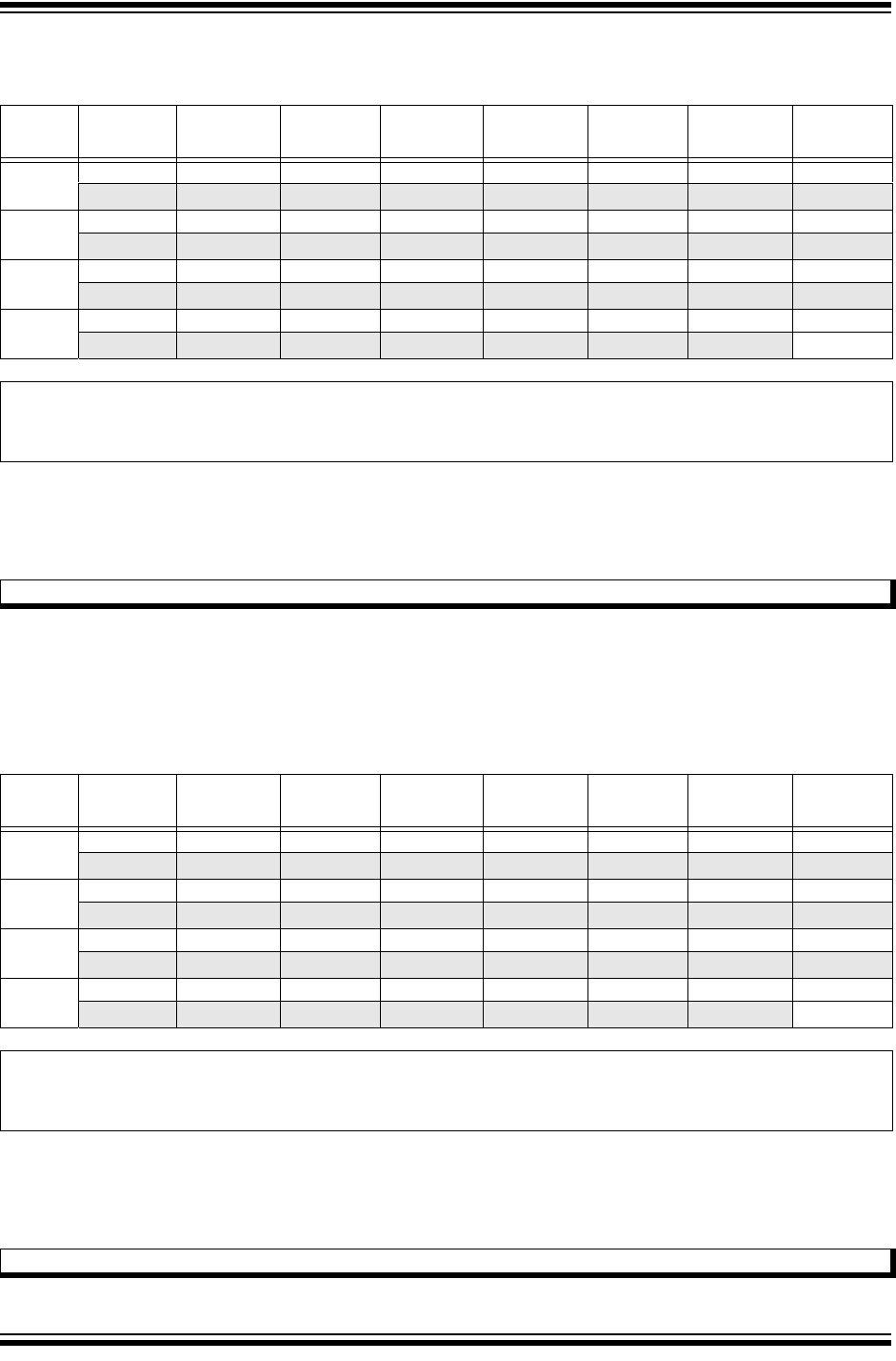
2015 Microchip Technology Inc. Preliminary DS60001320B-page 95
PIC32MZ Embedded Connectivity with Floating Point Unit (EF) Family
REGISTER 4-6: SBTxECLRS: SYSTEM BUS TARGET ‘x’ SINGLE ERROR CLEAR REGISTER
(‘x’ = 0-13)
Bit
Range Bit
31/23/15/7 Bit
30/22/14/6 Bit
29/21/13/5 Bit
28/20/12/4 Bit
27/19/11/3 Bit
26/18/10/2 Bit
25/17/9/1 Bit
24/16/8/0
31:24 U-0 U-0 U-0 U-0 U-0 U-0 U-0 U-0
— — — — — — — —
23:16 U-0 U-0 U-0 U-0 U-0 U-0 U-0 U-0
— — — — — — — —
15:8 U-0 U-0 U-0 U-0 U-0 U-0 U-0 U-0
— — — — — — — —
7:0 U-0 U-0 U-0 U-0 U-0 U-0 U-0 R-0
— — — — — — — CLEAR
Legend:
R = Readable bit W = Writable bit U = Unimplemented bit, read as ‘0’
-n = Value at POR ‘1’ = Bit is set ‘0’ = Bit is cleared
bit 31-1 Unimplemented: Read as ‘0’
bit 0 CLEAR: Clear Single Error on Read bit
A single error as reported via SBTxELOG1 and SBTxELOG2 is cleared by a read of this register.
Note: Refer to Table 4-6 for the list of available targets and their descriptions.
REGISTER 4-7: SBTxECLRM: SYSTEM BUS TARGET ‘x’ MULTIPLE ERROR CLEAR REGISTER
(‘x’ = 0-13)
Bit
Range Bit
31/23/15/7 Bit
30/22/14/6 Bit
29/21/13/5 Bit
28/20/12/4 Bit
27/19/11/3 Bit
26/18/10/2 Bit
25/17/9/1 Bit
24/16/8/0
31:24 U-0 U-0 U-0 U-0 U-0 U-0 U-0 U-0
— — — — — — — —
23:16 U-0 U-0 U-0 U-0 U-0 U-0 U-0 U-0
— — — — — — — —
15:8 U-0 U-0 U-0 U-0 U-0 U-0 U-0 U-0
— — — — — — — —
7:0 U-0 U-0 U-0 U-0 U-0 U-0 U-0 R-0
— — — — — — — CLEAR
Legend:
R = Readable bit W = Writable bit U = Unimplemented bit, read as ‘0’
-n = Value at POR ‘1’ = Bit is set ‘0’ = Bit is cleared
bit 31-1 Unimplemented: Read as ‘0’
bit 0 CLEAR: Clear Multiple Errors on Read bit
Multiple errors as reported via SBTxELOG1 and SBTxELOG2 is cleared by a read of this register.
Note: Refer to Table 4-6 for the list of available targets and their descriptions.

PIC32MZ Embedded Connectivity with Floating Point Unit (EF) Family
DS60001320B-page 96 Preliminary 2015 Microchip Technology Inc.
REGISTER 4-8: SBTxREGy: SYSTEM BUS TARGET ‘x’ REGION ‘y’ REGISTER
(‘x’ = 0-13; ‘y’ = 0-8)
Bit
Range Bit
31/23/15/7 Bit
30/22/14/6 Bit
29/21/13/5 Bit
28/20/12/4 Bit
27/19/11/3 Bit
26/18/10/2 Bit
25/17/9/1 Bit
24/16/8/0
31:24 R/W-0 R/W-0 R/W-0 R/W-0 R/W-0 R/W-0 R/W-0 R/W-0
BASE<21:14>
23:16 R/W-0 R/W-0 R/W-0 R/W-0 R/W-0 R/W-0 R/W-0 R/W-0
BASE<13:6>
15:8 R/W-0 R/W-0 R/W-0 R/W-0 R/W-0 R/W-0 R-0 U-0
BASE<5:0> PRI —
7:0 R/W-0 R/W-0 R/W-0 R/W-0 R/W-0 U-0 U-0 U-0
SIZE<4:0> — — —
Legend:
R = Readable bit W = Writable bit U = Unimplemented bit, read as ‘0’
-n = Value at POR ‘1’ = Bit is set ‘0’ = Bit is cleared
bit 31-10 BASE<21:0>: Region Base Address bits
bit 9 PRI: Region Priority Level bit
1 = Level 2
0 = Level 1
bit 8 Unimplemented: Read as ‘0’
bit 7-3 SIZE<4:0>: Region Size bits
Permissions for a region are only active is the SIZE is non-zero.
11111 = Region size = 2(SIZE – 1) x 1024 (bytes)
•
•
•
00001 = Region size = 2(SIZE – 1) x 1024 (bytes)
00000 = Region is not present
bit 2-0 Unimplemented: Read as ‘0’
Note 1: Refer to Table 4-6 for the list of available targets and their descriptions.
2: For some target regions, certain bits in this register are read-only with preset values. See Table 4-6 for
more information.

2015 Microchip Technology Inc. Preliminary DS60001320B-page 97
PIC32MZ Embedded Connectivity with Floating Point Unit (EF) Family
REGISTER 4-9: SBTxRDy: SYSTEM BUS TARGET ‘x’ REGION ‘y’ READ PERMISSIONS
REGISTER (‘x’ = 0-13; ‘y’ = 0-8)
Bit
Range Bit
31/23/15/7 Bit
30/22/14/6 Bit
29/21/13/5 Bit
28/20/12/4 Bit
27/19/11/3 Bit
26/18/10/2 Bit
25/17/9/1 Bit
24/16/8/0
31:24 U-0 U-0 U-0 U-0 U-0 U-0 U-0 U-0
— — — — — — — —
23:16 U-0 U-0 U-0 U-0 U-0 U-0 U-0 U-0
— — — — — — — —
15:8 U-0 U-0 U-0 U-0 U-0 U-0 U-0 U-0
— — — — — — — —
7:0 U-0 U-0 U-0 U-0 R/W-0 R/W-1 R/W-1 R/W-1
— — — — GROUP3 GROUP2 GROUP1 GROUP0
Legend:
R = Readable bit W = Writable bit U = Unimplemented bit, read as ‘0’
-n = Value at POR ‘1’ = Bit is set ‘0’ = Bit is cleared
bit 31-4 Unimplemented: Read as ‘0’
bit 3 Group3: Group3 Read Permissions bits
1 = Privilege Group 3 has read permission
0 = Privilege Group 3 does not have read permission
bit 2 Group2: Group2 Read Permissions bits
1 = Privilege Group 2 has read permission
0 = Privilege Group 2 does not have read permission
bit 1 Group1: Group1 Read Permissions bits
1 = Privilege Group 1 has read permission
0 = Privilege Group 1 does not have read permission
bit 0 Group0: Group0 Read Permissions bits
1 = Privilege Group 0 has read permission
0 = Privilege Group 0 does not have read permission
Note 1: Refer to Table 4-6 for the list of available targets and their descriptions.
2: For some target regions, certain bits in this register are read-only with preset values. See Table 4-6 for
more information.

PIC32MZ Embedded Connectivity with Floating Point Unit (EF) Family
DS60001320B-page 98 Preliminary 2015 Microchip Technology Inc.
REGISTER 4-10: SBTxWRy: SYSTEM BUS TARGET ‘x’ REGION ‘y’ WRITE PERMISSIONS
REGISTER (‘x’ = 0-13; ‘y’ = 0-8)
Bit
Range Bit
31/23/15/7 Bit
30/22/14/6 Bit
29/21/13/5 Bit
28/20/12/4 Bit
27/19/11/3 Bit
26/18/10/2 Bit
25/17/9/1 Bit
24/16/8/0
31:24 U-0 U-0 U-0 U-0 U-0 U-0 U-0 U-0
— — — — — — — —
23:16 U-0 U-0 U-0 U-0 U-0 U-0 U-0 U-0
— — — — — — — —
15:8 U-0 U-0 U-0 U-0 U-0 U-0 U-0 U-0
— — — — — — — —
7:0 U-0 U-0 U-0 U-0 R/W-0 R/W-1 R/W-1 R/W-1
— — — — GROUP3 GROUP2 GROUP1 GROUP0
Legend:
R = Readable bit W = Writable bit U = Unimplemented bit, read as ‘0’
-n = Value at POR ‘1’ = Bit is set ‘0’ = Bit is cleared
bit 31-4 Unimplemented: Read as ‘0’
bit 3 Group3: Group 3 Write Permissions bits
1 = Privilege Group 3 has write permission
0 = Privilege Group 3 does not have write permission
bit 2 Group2: Group 2 Write Permissions bits
1 = Privilege Group 2 has write permission
0 = Privilege Group 2 does not have write permission
bit 1 Group1: Group 1 Write Permissions bits
1 = Privilege Group 1 has write permission
0 = Privilege Group 1 does not have write permission
bit 0 Group0: Group 0 Write Permissions bits
1 = Privilege Group 0 has write permission
0 = Privilege Group 0 does not have write permission
Note 1: Refer to Table 4-6 for the list of available targets and their descriptions.
2: For some target regions, certain bits in this register are read-only with preset values. See Table 4-6 for
more information.

2015 Microchip Technology Inc. Preliminary DS60001320B-page 99
PIC32MZ Embedded Connectivity with Floating Point Unit (EF) Family
5.0 FLASH PROGRAM MEMORY
PIC32MZ EF devices contain an internal Flash
program memory for executing user code, which
includes the following features:
• Two Flash banks for live update support
• Dual boot support
• Write protection for program and boot Flash
• ECC support
There are three methods by which the user can
program this memory:
• Run-Time Self-Programming (RTSP)
• EJTAG Programming
• In-Circuit Serial Programming™ (ICSP™)
RTSP is performed by software executing from either
Flash or RAM memory. Information about RTSP
techniques is available in Section 52. “Flash
Program Memory with Support for Live Update”
(DS60001193) in the “PIC32 Family Reference
Manual”.
EJTAG is performed using the EJTAG port of the
device and an EJTAG capable programmer.
ICSP is performed using a serial data connection to the
device and allows much faster programming times than
RTSP.
The EJTAG and ICSP methods are described in the
“PIC32 Flash Programming Specification”
(DS60001145), which is available for download from
the Microchip web site (www.microchip.com).
Note: This data sheet summarizes the features
of the PIC32MZ EF family of devices. It is
not intended to be a comprehensive refer-
ence source. To complement the informa-
tion in this data sheet, refer to Section 52.
“Flash Program Memory with Support
for Live Update” (DS60001193) in the
“PIC32 Family Reference Manual”, which
is available from the Microchip web site
(www.microchip.com/PIC32).
Note: In PIC32MZ EF devices, the Flash page
size is 16 KB (4K IW) and the row size is
2 KB (512 IW).

PIC32MZ Embedded Connectivity with Floating Point Unit (EF) Family
DS60001320B-page 100 Preliminary 2015 Microchip Technology Inc.
5.1 Flash Control Registers
TABLE 5-1: FLASH CONTROLLER REGISTER MAP
Virtual Address
(BF80_#)
Register
Name
Bit Range
Bits
All Resets
31/15 30/14 29/13 28/12 27/11 26/10 25/9 24/8 23/7 22/6 21/5 20/4 19/3 18/2 17/1 16/0
0600 NVMCON(1) 31:16 — — — — — — — — — — — — — — — — 0000
15:0 WR WREN WRERR LVDERR — — — — PFSWAP BFSWAP — — NVMOP<3:0> 00x0
0610 NVMKEY 31:16 NVMKEY<31:0> 0000
15:0 0000
0620
NVMADDR
(1) 31:16 NVMADDR<31:0> 0000
15:0 0000
0630 NVMDATA0 31:16 NVMDATA0<31:0> 0000
15:0 0000
0640 NVMDATA1 31:16 NVMDATA1<31:0> 0000
15:0 0000
0650 NVMDATA2 31:16 NVMDATA2<31:0> 0000
15:0 0000
0660 NVMDATA3 31:16 NVMDATA3<31:0> 0000
15:0 0000
0670 NVMSRC
ADDR
31:16 NVMSRCADDR<31:0> 0000
15:0 0000
0680 NVMPWP(1) 31:16 PWPULOCK — — — — — — — PWP<23:16> 8000
15:0 PWP<15:0> 0000
0690 NVMBWP(1) 31:16 — — — — — — — — — — — — — — — — 0000
15:0 LBWPULOCK — — LBWP4 LBWP3 LBWP2 LBWP1 LBWP0 UBWPULOCK — — UBWP4 UBWP3 UBWP2 UBWP1 UBWP0 9FDF
06A0 NVMCON2(1) 31:16 — — — — — — — — — — — — — — — — 001F
15:0 — — — — — — — — SWAPLOCK<1:0> —— — — — — 0000
Legend: x = unknown value on Reset; — = unimplemented, read as ‘0’. Reset values are shown in hexadecimal.
Note 1: This register has corresponding CLR, SET and INV registers at their virtual addresses, plus offsets of 0x4, 0x8 and 0xC, respectively. See Section 12.3 “CLR, SET, and INV Registers” for more information.

2015 Microchip Technology Inc. Preliminary DS60001320B-page 101
PIC32MZ Embedded Connectivity with Floating Point Unit (EF) Family
REGISTER 5-1: NVMCON: FLASH PROGRAMMING CONTROL REGISTER
Bit
Range Bit
31/23/15/7 Bit
30/22/14/6 Bit
29/21/13/5 Bit
28/20/12/4 Bit
27/19/11/3 Bit
26/18/10/2 Bit
25/17/9/1 Bit
24/16/8/0
31:24 U-0 U-0 U-0 U-0 U-0 U-0 U-0 U-0
— — — — — — — —
23:16 U-0 U-0 U-0 U-0 U-0 U-0 U-0 U-0
— — — — — — — —
15:8 R/W-0, HC R/W-0 R-0, HS, HC R-0, HS, HC U-0 U-0 U-0 U-0
WR(1) WREN(1) WRERR(1) LVDERR(1) — — — —
7:0 R/W-0 R/W-x U-0 U-0 R/W-0 R/W-0 R/W-0 R/W-0
PFSWAP BFSWAP ——NVMOP<3:0>
Legend: HC = Hardware Set HC = Hardware Cleared
R = Readable bit W = Writable bit U = Unimplemented bit, read as ‘0’
-n = Value at POR ‘1’ = Bit is set ‘0’ = Bit is cleared x = Bit is unknown
bit 31-16 Unimplemented: Read as ‘0’
bit 15 WR: Write Control bit(1)
This bit cannot be cleared and can be set only when WREN = 1 and the unlock sequence has been
performed.
1 = Initiate a Flash operation
0 = Flash operation is complete or inactive
bit 14 WREN: Write Enable bit(1)
1 = Enable writes to the WR bit and disables writes to the NVMOP<3:0> bits
0 = Disable writes to WR bit and enables writes to the NVMOP<3:0> bits
bit 13 WRERR: Write Error bit(1)
This bit can be cleared only by setting the NVMOP<3:0> bits = 0000 and initiating a Flash operation.
1 = Program or erase sequence did not complete successfully
0 = Program or erase sequence completed normally
bit 12 LVDERR: Low-Voltage Detect Error bit(1)
This bit can be cleared only by setting the NVMOP<3:0> bits = 0000 and initiating a Flash operation.
1 = Low-voltage detected (possible data corruption, if WRERR is set)
0 = Voltage level is acceptable for programming
bit 11-8 Unimplemented: Read as ‘0’
bit 7 PFSWAP: Program Flash Bank Swap Control bit
This bit is only writable when WREN = 0 and the unlock sequence has been performed.
1 = Program Flash Bank 2 is mapped to the lower mapped region and program Flash Bank 1 is mapped to
the upper mapped region
0 = Program Flash Bank 1 is mapped to the lower mapped region and program Flash Bank 2 is mapped to
the upper mapped region
Note 1: These bits are only reset by a Power-on Reset (POR) and are not affected by other reset sources.
2: This operation results in a “no operation” (NOP) when the Dynamic Flash ECC Configuration bits = 00
(FECCCON<1:0> (DVCFG0<9:8>)), which enables ECC at all times. For all other FECCCON<1:0> bit
settings, this command will execute, but will not write the ECC bits for the word and can cause DED errors
if dynamic Flash ECC is enabled (FECCCON<1:0> = 01). Refer to Section 52. “Flash Program Memory
with Support for Live Update” (DS60001193) for information regarding ECC and Flash programming.

PIC32MZ Embedded Connectivity with Floating Point Unit (EF) Family
DS60001320B-page 102 Preliminary 2015 Microchip Technology Inc.
bit 6 BFSWAP: Boot Flash Bank Alias Swap Control bit
This bit is only writable when WREN = 0 and the unlock sequence has been performed.
1 = Boot Flash Bank 2 is mapped to the lower boot alias and boot Flash Bank 1 is mapped to the upper boot
alias
0 = Boot Flash Bank 1 is mapped to the lower boot alias and boot Flash Bank 2 is mapped to the upper boot
alias
bit 5-4 Unimplemented: Read as ‘0’
bit 3-0 NVMOP<3:0>: NVM Operation bits
These bits are only writable when WREN = 0.
1111 = Reserved
•
•
•
1000 = Reserved
0111 = Program erase operation: erase all of program Flash memory (all pages must be unprotected,
PWP<23:0> = 0x000000)
0110 = Upper program Flash memory erase operation: erases only the upper mapped region of program
Flash (all pages in that region must be unprotected)
0101 = Lower program Flash memory erase operation: erases only the lower mapped region of program
Flash (all pages in that region must be unprotected)
0100 = Page erase operation: erases page selected by NVMADDR, if it is not write-protected
0011 = Row program operation: programs row selected by NVMADDR, if it is not write-protected
0010 = Quad Word (128-bit) program operation: programs the 128-bit Flash word selected by NVMADDR,
if it is not write-protected
0001 = Word program operation: programs word selected by NVMADDR, if it is not write-protected(2)
0000 = No operation
REGISTER 5-1: NVMCON: FLASH PROGRAMMING CONTROL REGISTER (CONTINUED)
Note 1: These bits are only reset by a Power-on Reset (POR) and are not affected by other reset sources.
2: This operation results in a “no operation” (NOP) when the Dynamic Flash ECC Configuration bits = 00
(FECCCON<1:0> (DVCFG0<9:8>)), which enables ECC at all times. For all other FECCCON<1:0> bit
settings, this command will execute, but will not write the ECC bits for the word and can cause DED errors
if dynamic Flash ECC is enabled (FECCCON<1:0> = 01). Refer to Section 52. “Flash Program Memory
with Support for Live Update” (DS60001193) for information regarding ECC and Flash programming.

2015 Microchip Technology Inc. Preliminary DS60001320B-page 103
PIC32MZ Embedded Connectivity with Floating Point Unit (EF) Family
REGISTER 5-2: NVMCON2: FLASH PROGRAMMING CONTROL REGISTER 2
Bit
Range Bit
31/23/15/7 Bit
30/22/14/6 Bit
29/21/13/5 Bit
28/20/12/4 Bit
27/19/11/3 Bit
26/18/10/2 Bit
25/17/9/1 Bit
24/16/8/0
31:24 U-0 U-0 U-0 U-0 U-0 U-0 U-0 U-0
— — — — — — — —
23:16 U-0 U-0 U-0 U-0 U-0 U-0 U-0 U-0
— — — — — — — —
15:8 U-0 U-0 U-0 U-0 U-0 U-0 U-0 U-0
— — — — — — — —
7:0 R/W-0 R/W-0 U-0 U-0 U-0 U-0 U-0 U-0
SWAPLOCK<1:0> — — — — — —
Legend: HC = Hardware Set HC = Hardware Cleared
R = Readable bit W = Writable bit U = Unimplemented bit, read as ‘0’
-n = Value at POR ‘1’ = Bit is set ‘0’ = Bit is cleared x = Bit is unknown
bit 31-8 Unimplemented: Read as ‘0’
bit 7-6 SWAPLOCK<1:0>: Flash Memory Swap Lock Control bits
11 = PFSWAP and BFSWAP are not writable and SWAPLOCK is not writable
10 = PFSWAP and BFSWAP are not writable and SWAPLOCK is writable
01 = PFSWAP and BFSWAP are not writable and SWAPLOCK is writable
00 = PFSWAP and BFSWAP are writable and SWAPLOCK is writable
bit 5-0 Unimplemented: Read as ‘0’

PIC32MZ Embedded Connectivity with Floating Point Unit (EF) Family
DS60001320B-page 104 Preliminary 2015 Microchip Technology Inc.
REGISTER 5-3: NVMKEY: PROGRAMMING UNLOCK REGISTER
Bit
Range Bit
31/23/15/7 Bit
30/22/14/6 Bit
29/21/13/5 Bit
28/20/12/4 Bit
27/19/11/3 Bit
26/18/10/2 Bit
25/17/9/1 Bit
24/16/8/0
31:24 W-0 W-0 W-0 W-0 W-0 W-0 W-0 W-0
NVMKEY<31:24>
23:16 W-0 W-0 W-0 W-0 W-0 W-0 W-0 W-0
NVMKEY<23:16>
15:8 W-0 W-0 W-0 W-0 W-0 W-0 W-0 W-0
NVMKEY<15:8>
7:0 W-0 W-0 W-0 W-0 W-0 W-0 W-0 W-0
NVMKEY<7:0>
Legend:
R = Readable bit W = Writable bit U = Unimplemented bit, read as ‘0’
-n = Value at POR ‘1’ = Bit is set ‘0’ = Bit is cleared x = Bit is unknown
bit 31-0 NVMKEY<31:0>: Unlock Register bits
These bits are write-only, and read as ‘0’ on any read
Note: This register is used as part of the unlock sequence to prevent inadvertent writes to the PFM.
REGISTER 5-4: NVMADDR: FLASH ADDRESS REGISTER
Bit
Range Bit
31/23/15/7 Bit
30/22/14/6 Bit
29/21/13/5 Bit
28/20/12/4 Bit
27/19/11/3 Bit
26/18/10/2 Bit
25/17/9/1 Bit
24/16/8/0
31:24 R/W-0 R/W-0 R/W-0 R/W-0 R/W-0 R/W-0 R/W-0 R/W-0
NVMADDR<31:24>(1)
23:16 R/W-0 R/W-0 R/W-0 R/W-0 R/W-0 R/W-0 R/W-0 R/W-0
NVMADDR<23:16>(1)
15:8 R/W-0 R/W-0 R/W-0 R/W-0 R/W-0 R/W-0 R/W-0 R/W-0
NVMADDR<15:8>(1)
7:0 R/W-0 R/W-0 R/W-0 R/W-0 R/W-0 R/W-0 R/W-0 R/W-0
NVMADDR<7:0>(1)
Legend:
R = Readable bit W = Writable bit U = Unimplemented bit, read as ‘0’
-n = Value at POR ‘1’ = Bit is set ‘0’ = Bit is cleared x = Bit is unknown
bit 31-0 NVMADDR<31:0>: Flash Address bits(1)
Note: The bits in this register are only reset by a Power-on Reset (POR) and are not affected by other reset
sources.
NVMOP<3:0>
Selection Flash Address Bits (NVMADDR<31:0>)
Page Erase Address identifies the page to erase (NVMADDR<13:0> are ignored).
Row Program Address identifies the row to program (NVMADDR<10:0> are ignored).
Word Program Address identifies the word to program (NVMADDR<1:0> are ignored).
Quad Word Program Address identifies the quad word (128-bit) to program (NVMADDR<3:0> bits are
ignored).
Note 1: For all other NVMOP<3:0> bit settings, the Flash address is ignored. See the NVMCON
register (Register 5-1) for additional information on these bits.

2015 Microchip Technology Inc. Preliminary DS60001320B-page 105
PIC32MZ Embedded Connectivity with Floating Point Unit (EF) Family
REGISTER 5-5: NVMDATAx: FLASH DATA REGISTER (x = 0-3)
Bit
Range Bit
31/23/15/7 Bit
30/22/14/6 Bit
29/21/13/5 Bit
28/20/12/4 Bit
27/19/11/3 Bit
26/18/10/2 Bit
25/17/9/1 Bit
24/16/8/0
31:24 R/W-0 R/W-0 R/W-0 R/W-0 R/W-0 R/W-0 R/W-0 R/W-0
NVMDATA<31:24>
23:16 R/W-0 R/W-0 R/W-0 R/W-0 R/W-0 R/W-0 R/W-0 R/W-0
NVMDATA<23:16>
15:8 R/W-0 R/W-0 R/W-0 R/W-0 R/W-0 R/W-0 R/W-0 R/W-0
NVMDATA<15:8>
7:0 R/W-0 R/W-0 R/W-0 R/W-0 R/W-0 R/W-0 R/W-0 R/W-0
NVMDATA<7:0>
Legend:
R = Readable bit W = Writable bit U = Unimplemented bit, read as ‘0’
-n = Value at POR ‘1’ = Bit is set ‘0’ = Bit is cleared x = Bit is unknown
bit 31-0 NVMDATA<31:0>: Flash Data bits
Word Program: Writes NVMDATA0 to the target Flash address defined in NVMADDR
Quad Word Program: Writes NVMDATA3:NVMDATA2:NVMDATA1:NVMDATA0 to the target Flash address
defined in NVMADDR. NVMDATA0 contains the Least Significant Instruction Word.
Note: The bits in this register are only reset by a Power-on Reset (POR) and are not affected by other reset
sources.
REGISTER 5-6: NVMSRCADDR: SOURCE DATA ADDRESS REGISTER
Bit
Range Bit
31/23/15/7 Bit
30/22/14/6 Bit
29/21/13/5 Bit
28/20/12/4 Bit
27/19/11/3 Bit
26/18/10/2 Bit
25/17/9/1 Bit
24/16/8/0
31:24 R/W-0 R/W-0 R/W-0 R/W-0 R/W-0 R/W-0 R/W-0 R/W-0
NVMSRCADDR<31:24>
23:16 R/W-0 R/W-0 R/W-0 R/W-0 R/W-0 R/W-0 R/W-0 R/W-0
NVMSRCADDR<23:16>
15:8 R/W-0 R/W-0 R/W-0 R/W-0 R/W-0 R/W-0 R/W-0 R/W-0
NVMSRCADDR<15:8>
7:0 R/W-0 R/W-0 R/W-0 R/W-0 R/W-0 R/W-0 R/W-0 R/W-0
NVMSRCADDR<7:0>
Legend:
R = Readable bit W = Writable bit U = Unimplemented bit, read as ‘0’
-n = Value at POR ‘1’ = Bit is set ‘0’ = Bit is cleared x = Bit is unknown
bit 31-0 NVMSRCADDR<31:0>: Source Data Address bits
The system physical address of the data to be programmed into the Flash when the NVMOP<3:0> bits
(NVMCON<3:0>) are set to perform row programming.
Note: The bits in this register are only reset by a Power-on Reset (POR) and are not affected by other reset
sources.

PIC32MZ Embedded Connectivity with Floating Point Unit (EF) Family
DS60001320B-page 106 Preliminary 2015 Microchip Technology Inc.
REGISTER 5-7: NVMPWP: PROGRAM FLASH WRITE-PROTECT REGISTER
Bit
Range Bit
31/23/15/7 Bit
30/22/14/6 Bit
29/21/13/5 Bit
28/20/12/4 Bit
27/19/11/3 Bit
26/18/10/2 Bit
25/17/9/1 Bit
24/16/8/0
31:24 R/W-1 U-0 U-0 U-0 U-0 U-0 U-0 U-0
PWPULOCK — — — — — — —
23:16 R/W-0 R/W-0 R/W-0 R/W-0 R/W-0 R/W-0 R/W-0 R/W-0
PWP<23:16>
15:8 R/W-0 R/W-0 R-0 R-0 R-0 R-0 R-0 R-0
PWP<15:8>
7:0 R-0 R-0 R-0 R-0 R-0 R-0 R-0 R-0
PWP<7:0>
Legend:
R = Readable bit W = Writable bit U = Unimplemented bit, read as ‘0’
-n = Value at POR ‘1’ = Bit is set ‘0’ = Bit is cleared x = Bit is unknown
bit 31 PWPULOCK: Program Flash Memory Page Write-protect Unlock bit
1 = Register is not locked and can be modified
0 = Register is locked and cannot be modified
This bit is only clearable and cannot be set except by any reset.
bit 30-24 Unimplemented: Read as ‘0’
bit 23-0 PWP<23:0>: Flash Program Write-protect (Page) Address bits
Physical memory below address 0x1Dxxxxxx is write protected, where ‘xxxxxx’ is specified by PWP<23:0>.
When PWP<23:0> has a value of ‘0’, write protection is disabled for the entire program Flash. If the specified
address falls within the page, the entire page and all pages below the current page will be protected.
Note: The bits in this register are only writable when the NVMKEY unlock sequence is followed.

2015 Microchip Technology Inc. Preliminary DS60001320B-page 107
PIC32MZ Embedded Connectivity with Floating Point Unit (EF) Family
REGISTER 5-8: NVMBWP: FLASH BOOT (PAGE) WRITE-PROTECT REGISTER
Bit
Range Bit
31/23/15/7 Bit
30/22/14/6 Bit
29/21/13/5 Bit
28/20/12/4 Bit
27/19/11/3 Bit
26/18/10/2 Bit
25/17/9/1 Bit
24/16/8/0
31:24 U-0 U-0 U-0 U-0 U-0 U-0 U-0 U-0
— — — — — — — —
23:16 U-0 U-0 U-0 U-0 U-0 U-0 U-0 U-0
— — — — — — — —
15:8 R/W-1 U-0 U-0 R/W-1 R/W-1 R/W-1 R/W-1 R/W-1
LBWPULOCK —— LBWP4(1) LBWP3(1) LBWP2(1) LBWP1(1) LBWP0(1)
7:0 R/W-1 r-1 U-0 R/W-1 R/W-1 R/W-1 R/W-1 R/W-1
UBWPULOCK —— UBWP4(1) UBWP3(1) UBWP2(1) UBWP1(1) UBWP0(1)
Legend: r = Reserved
R = Readable bit W = Writable bit U = Unimplemented bit, read as ‘0’
-n = Value at POR ‘1’ = Bit is set ‘0’ = Bit is cleared x = Bit is unknown
bit 31-16 Unimplemented: Read as ‘0’
bit 15 LBWPULOCK: Lower Boot Alias Write-protect Unlock bit
1 = LBWPx bits are not locked and can be modified
0 = LBWPx bits are locked and cannot be modified
This bit is only clearable and cannot be set except by any reset.
bit 14-13 Unimplemented: Read as ‘0’
bit 12 LBWP4: Lower Boot Alias Page 4 Write-protect bit(1)
1 = Write protection for physical address 0x01FC10000 through 0x1FC13FFF enabled
0 = Write protection for physical address 0x01FC10000 through 0x1FC13FFF disabled
bit 11 LBWP3: Lower Boot Alias Page 3 Write-protect bit(1)
1 = Write protection for physical address 0x01FC0C000 through 0x1FC0FFFF enabled
0 = Write protection for physical address 0x01FC0C000 through 0x1FC0FFFF disabled
bit 10 LBWP2: Lower Boot Alias Page 2 Write-protect bit(1)
1 = Write protection for physical address 0x01FC08000 through 0x1FC0BFFF enabled
0 = Write protection for physical address 0x01FC08000 through 0x1FC0BFFF disabled
bit 9 LBWP1: Lower Boot Alias Page 1 Write-protect bit(1)
1 = Write protection for physical address 0x01FC04000 through 0x1FC07FFF enabled
0 = Write protection for physical address 0x01FC04000 through 0x1FC07FFF disabled
bit 8 LBWP0: Lower Boot Alias Page 0 Write-protect bit(1)
1 = Write protection for physical address 0x01FC00000 through 0x1FC03FFF enabled
0 = Write protection for physical address 0x01FC00000 through 0x1FC03FFF disabled
bit 7 UBWPULOCK: Upper Boot Alias Write-protect Unlock bit
1 = UBWPx bits are not locked and can be modified
0 = UBWPx bits are locked and cannot be modified
This bit is only user-clearable and cannot be set except by any reset.
bit 6 Reserved: This bit is reserved for use by development tools
bit 5 Unimplemented: Read as ‘0’
Note 1: These bits are only available when the NVMKEY unlock sequence is performed and the associated Lock
bit (LBWPULOCK or UBWPULOCK) is set.
Note: The bits in this register are only writable when the NVMKEY unlock sequence is followed.

PIC32MZ Embedded Connectivity with Floating Point Unit (EF) Family
DS60001320B-page 108 Preliminary 2015 Microchip Technology Inc.
bit 4 UBWP4: Upper Boot Alias Page 4 Write-protect bit(1)
1 = Write protection for physical address 0x01FC30000 through 0x1FC33FFF enabled
0 = Write protection for physical address 0x01FC30000 through 0x1FC33FFF disabled
bit 3 UBWP3: Upper Boot Alias Page 3 Write-protect bit(1)
1 = Write protection for physical address 0x01FC2C000 through 0x1FC2FFFF enabled
0 = Write protection for physical address 0x01FC2C000 through 0x1FC2FFFF disabled
bit 2 UBWP2: Upper Boot Alias Page 2 Write-protect bit(1)
1 = Write protection for physical address 0x01FC28000 through 0x1FC2BFFF enabled
0 = Write protection for physical address 0x01FC28000 through 0x1FC2BFFF disabled
bit 1 UBWP1: Upper Boot Alias Page 1 Write-protect bit(1)
1 = Write protection for physical address 0x01FC24000 through 0x1FC27FFF enabled
0 = Write protection for physical address 0x01FC24000 through 0x1FC27FFF disabled
bit 0 UBWP0: Upper Boot Alias Page 0 Write-protect bit(1)
1 = Write protection for physical address 0x01FC20000 through 0x1FC23FFF enabled
0 = Write protection for physical address 0x01FC20000 through 0x1FC23FFF disabled
REGISTER 5-8: NVMBWP: FLASH BOOT (PAGE) WRITE-PROTECT REGISTER
Note 1: These bits are only available when the NVMKEY unlock sequence is performed and the associated Lock
bit (LBWPULOCK or UBWPULOCK) is set.
Note: The bits in this register are only writable when the NVMKEY unlock sequence is followed.
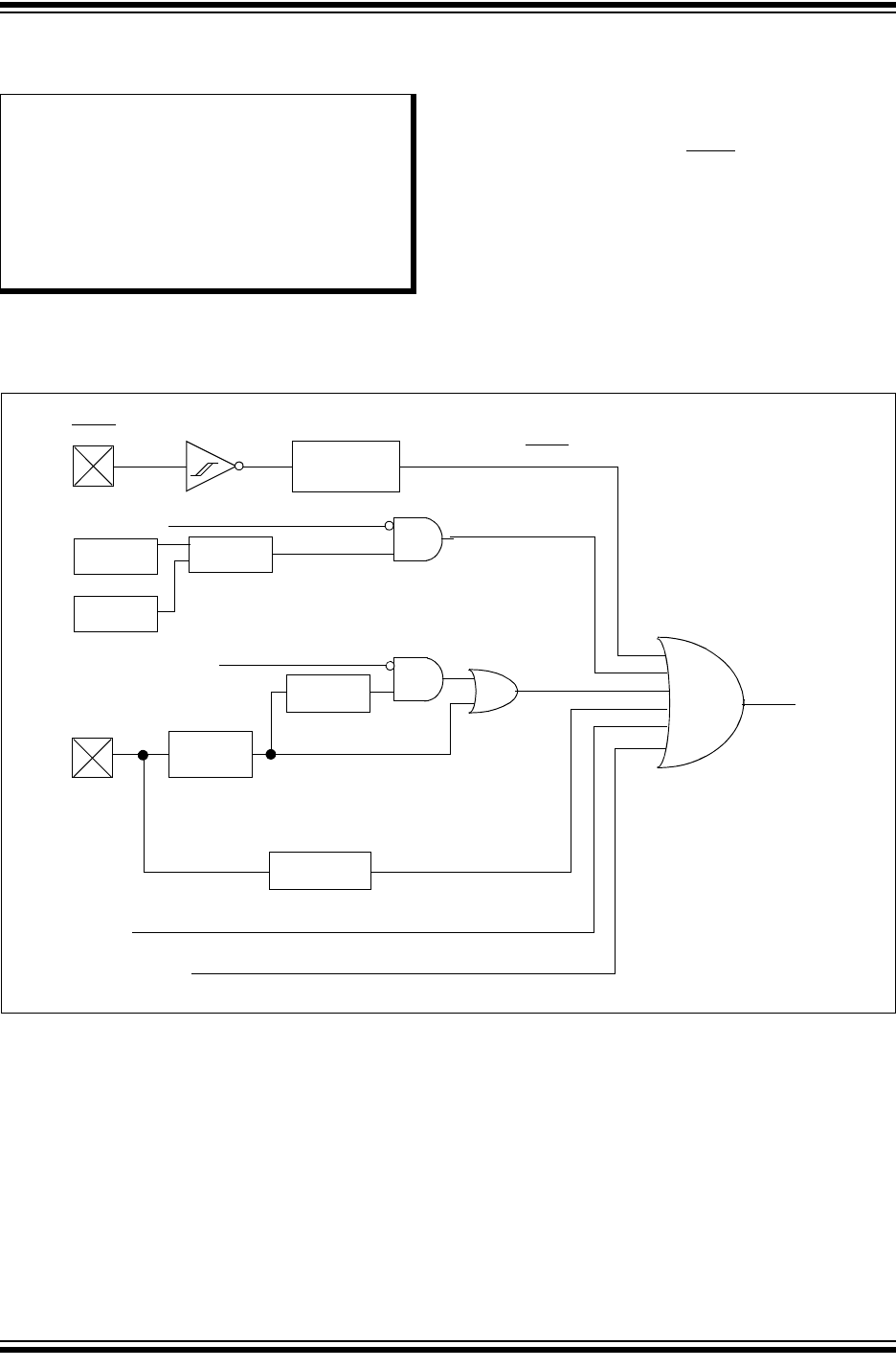
2015 Microchip Technology Inc. Preliminary DS60001320B-page 109
PIC32MZ Embedded Connectivity with Floating Point Unit (EF) Family
6.0 RESETS The Reset module combines all Reset sources and
controls the device Master Reset signal, SYSRST. The
device Reset sources are as follows:
• Power-on Reset (POR)
• Master Clear Reset pin (MCLR)
• Software Reset (SWR)
• Watchdog Timer Reset (WDTR)
• Brown-out Reset (BOR)
• Configuration Mismatch Reset (CMR)
• Deadman Timer Reset (DMTR)
A simplified block diagram of the Reset module is
illustrated in Figure 6-1.
FIGURE 6-1: SYSTEM RESET BLOCK DIAGRAM
Note: This data sheet summarizes the features
of the PIC32MZ EF family of devices. It is
not intended to be a comprehensive refer-
ence source. To complement the informa-
tion in this data sheet, refer to Section 7.
“Resets” (DS60001118) in the “PIC32
Family Reference Manual”, which is avail-
able from the Microchip web site
(www.microchip.com/PIC32).
MCLR
VDD
VDD Rise
Detect
POR
Sleep or Idle
DMT
Time-out
Glitch Filter
BOR
Configuration
SYSRST
Software Reset
Power-up
Timer
Voltage Regulator Enabled
Reset
DMTR/WDTR
SWR
CMR
MCLR
Mismatch
NMI
Time-out
WDT
Time-out
Brown-out
Reset

PIC32MZ Embedded Connectivity with Floating Point Unit (EF) Family
DS60001320B-page 110 Preliminary 2015 Microchip Technology Inc.
6.1 Reset Control Registers
TABLE 6-1: RESETS REGISTER MAP
Virtual Address
(BF80_#)
Register
Name
Bit Range
Bits
All Resets
31/15 30/14 29/13 28/12 27/11 26/10 25/9 24/8 23/7 22/6 21/5 20/4 19/3 18/2 17/1 16/0
1240 RCON 31:16 — — — — BCFGERR BCFGFAIL — — — — — — — — — — 0x00
15:0 — — — — — — CMR —EXTR SWR DMTO WDTO SLEEP IDLE BOR POR 0003
1250 RSWRST 31:16 — — — — — — — — — — — — — — — — 0000
15:0 — — — — — — — — — — — — — — — SWRST 0000
1260 RNMICON 31:16 — — — — — — DMTO WDTO SWNMI — — — GNMI — CF WDTS 0000
15:0 NMICNT<15:0> 0000
1270 PWRCON 31:16 — — — — — — — — — — — — — — — — 0000
15:0 — — — — — — — — — — — — — — — VREGS 0000
Legend: x = unknown value on Reset; — = unimplemented, read as ‘0’. Reset values are shown in hexadecimal.

2015 Microchip Technology Inc. Preliminary DS60001320B-page 111
PIC32MZ Embedded Connectivity with Floating Point Unit (EF) Family
REGISTER 6-1: RCON: RESET CONTROL REGISTER
Bit
Range Bit
31/23/15/7 Bit
30/22/14/6 Bit
29/21/13/5 Bit
28/20/12/4 Bit
27/19/11/3 Bit
26/18/10/2 Bit
25/17/9/1 Bit
24/16/8/0
31:24 U-0 U-0 U-0 U-0 R/W-0, HS R/W-0, HS U-0 U-0
— — — — BCFGERR BCFGFAIL — —
23:16 U-0 U-0 U-0 U-0 U-0 U-0 U-0 U-0
— — — — — — — —
15:8 U-0 U-0 U-0 U-0 U-0 U-0 R/W-0, HS U-0
— — — — — —CMR—
7:0 R/W-0, HS R/W-0, HS R/W-0, HS R/W-0, HS R/W-0, HS R/W-0, HS R/W-1, HS R/W-1, HS
EXTR SWR DMTO WDTO SLEEP IDLE BOR(1) POR(1)
Legend: HS = Hardware Set HC = Hardware Cleared
R = Readable bit W = Writable bit U = Unimplemented bit, read as ‘0’
-n = Value at POR ‘1’ = Bit is set ‘0’ = Bit is cleared x = Bit is unknown
bit 31-28 Unimplemented: Read as ‘0’
bit 27 BCFGERR: Primary Configuration Registers Error Flag bit
1 = An error occurred during a read of the primary configuration registers
0 = No error occurred during a read of the primary configuration registers
bit 26 BCFGFAIL: Primary/Secondary Configuration Registers Error Flag bit
1 = An error occurred during a read of the primary and alternate configuration registers
0 = No error occurred during a read of the primary and alternate configuration registers
bit 25-10 Unimplemented: Read as ‘0’
bit 9 CMR: Configuration Mismatch Reset Flag bit
1 = A Configuration Mismatch Reset has occurred
0 = A Configuration Mismatch Reset has not occurred
bit 8 Unimplemented: Read as ‘0’
bit 7 EXTR: External Reset (MCLR) Pin Flag bit
1 = Master Clear (pin) Reset has occurred
0 = Master Clear (pin) Reset has not occurred
bit 6 SWR: Software Reset Flag bit
1 = Software Reset was executed
0 = Software Reset was not executed
bit 5 DMTO: Deadman Timer Time-out Flag bit
1 = A DMT time-out has occurred
0 = A DMT time-out has not occurred
bit 4 WDTO: Watchdog Timer Time-out Flag bit
1 = WDT Time-out has occurred
0 = WDT Time-out has not occurred
bit 3 SLEEP: Wake From Sleep Flag bit
1 = Device was in Sleep mode
0 = Device was not in Sleep mode
bit 2 IDLE: Wake From Idle Flag bit
1 = Device was in Idle mode
0 = Device was not in Idle mode
bit 1 BOR: Brown-out Reset Flag bit(1)
1 = Brown-out Reset has occurred
0 = Brown-out Reset has not occurred
bit 0 POR: Power-on Reset Flag bit(1)
1 = Power-on Reset has occurred
0 = Power-on Reset has not occurred
Note 1: User software must clear this bit to view the next detection.

PIC32MZ Embedded Connectivity with Floating Point Unit (EF) Family
DS60001320B-page 112 Preliminary 2015 Microchip Technology Inc.
REGISTER 6-2: RSWRST: SOFTWARE RESET REGISTER
Bit
Range Bit
31/23/15/7 Bit
30/22/14/6 Bit
29/21/13/5 Bit
28/20/12/4 Bit
27/19/11/3 Bit
26/18/10/2 Bit
25/17/9/1 Bit
24/16/8/0
31:24 U-0 U-0 U-0 U-0 U-0 U-0 U-0 U-0
— — — — — — — —
23:16 U-0 U-0 U-0 U-0 U-0 U-0 U-0 U-0
— — — — — — — —
15:8 U-0 U-0 U-0 U-0 U-0 U-0 U-0 U-0
— — — — — — — —
7:0 U-0 U-0 U-0 U-0 U-0 U-0 U-0 W-0, HC
— — — — — — —SWRST
(1,2)
Legend: HC = Hardware Cleared
R = Readable bit W = Writable bit U = Unimplemented bit, read as ‘0’
-n = Value at POR ‘1’ = Bit is set ‘0’ = Bit is cleared x = Bit is unknown
bit 31-1 Unimplemented: Read as ‘0’
bit 0 SWRST: Software Reset Trigger bit(1,2)
1 = Enable software Reset event
0 = No effect
Note 1: The system unlock sequence must be performed before the SWRST bit can be written. Refer to Section
42. “Oscillators with Enhanced PLL” in the “PIC32 Family Reference Manual” for details.
2: Once this bit is set, any read of the RSWRST register will cause a reset to occur.

2015 Microchip Technology Inc. Preliminary DS60001320B-page 113
PIC32MZ Embedded Connectivity with Floating Point Unit (EF) Family
REGISTER 6-3: RNMICON: NON-MASKABLE INTERRUPT (NMI) CONTROL REGISTER
Bit
Range Bit
31/23/15/7 Bit
30/22/14/6 Bit
29/21/13/5 Bit
28/20/12/4 Bit
27/19/11/3 Bit
26/18/10/2 Bit
25/17/9/1 Bit
24/16/8/0
31:24 U-0 U-0 U-0 U-0 U-0 U-0 R/W-0 R/W-0
— — — — — —DMTOWDTO
23:16 R/W-0 U-0 U-0 U-0 R/W-0 U-0 R/W-0 R/W-0
SWNMI — — —GNMI —CFWDTS
15:8 R/W-0 R/W-0 R/W-0 R/W-0 R/W-0 R/W-0 R/W-0 R/W-0
NMICNT<15:8>
7:0 R/W-0 R/W-0 R/W-0 R/W-0 R/W-0 R/W-0 R/W-0 R/W-0
NMICNT<7:0>
Legend:
R = Readable bit W = Writable bit U = Unimplemented bit, read as ‘0’
-n = Value at POR ‘1’ = Bit is set ‘0’ = Bit is cleared x = Bit is unknown
bit 31-26 Unimplemented: Read as ‘0’
bit 25 DMTO: Deadman Timer Time-out Flag bit
1 = DMT time-out has occurred and caused a NMI
0 = DMT time-out has not occurred
Setting this bit will cause a DMT NMI event, and NMICNT will begin counting.
bit 24 WDTO: Watchdog Timer Time-Out Flag bit
1 = WDT time-out has occurred and caused a NMI
0 = WDT time-out has not occurred
Setting this bit will cause a WDT NMI event, and MNICNT will begin counting.
bit 23 SWNMI: Software NMI Trigger.
1 = An NMI will be generated
0 = An NMI will not be generated
bit 22-20 Unimplemented: Read as ‘0’
bit 19 GNMI: General NMI bit
1 = A general NMI event has been detected or a user-initiated NMI event has occurred
0 = A general NMI event has not been detected
Setting GNMI to a ‘1’ causes a user-initiated NMI event. This bit is also set by writing 0x4E to the
NMIKEY<7:0> (INTCON<31:24>) bits.
bit 18 Unimplemented: Read as ‘0’
bit 17 CF: Clock Fail Detect bit
1 = FSCM has detected clock failure and caused an NMI
0 = FSCM has not detected clock failure
Setting this bit will cause a a CF NMI event, but will not cause a clock switch to the BFRC.
bit 16 WDTS: Watchdog Timer Time-out in Sleep Mode Flag bit
1 = WDT time-out has occurred during Sleep mode and caused a wake-up from sleep
0 = WDT time-out has not occurred during Sleep mode
Setting this bit will cause a WDT NMI.
bit 15-0 NMICNT<15:0>: NMI Reset Counter Value bits
1111111111111111-0000000000000001 = Number of SYSCLK cycles before a device Reset occurs(1)
0000000000000000 = No delay between NMI assertion and device Reset event
Note 1: When a Watchdog Timer NMI event (when not in Sleep mode) or a Deadman Timer NMI event is triggered
the NMICNT will start decrementing. When NMICNT reaches zero, the device is Reset. This NMI reset
counter is only applicable to these two specific NMI events.
Note: The system unlock sequence must be performed before the SWRST bit can be written. Refer to Section
42. “Oscillators with Enhanced PLL” in the “PIC32 Family Reference Manual” for details.

PIC32MZ Embedded Connectivity with Floating Point Unit (EF) Family
DS60001320B-page 114 Preliminary 2015 Microchip Technology Inc.
REGISTER 6-4: PWRCON: POWER CONTROL REGISTER
Bit
Range Bit
31/23/15/7 Bit
30/22/14/6 Bit
29/21/13/5 Bit
28/20/12/4 Bit
27/19/11/3 Bit
26/18/10/2 Bit
25/17/9/1 Bit
24/16/8/0
31:24 U-0 U-0 U-0 U-0 U-0 U-0 U-0 U-0
— — — — — — — —
23:16 U-0 U-0 U-0 U-0 U-0 U-0 U-0 U-0
— — — — — — — —
15:8 U-0 U-0 U-0 U-0 U-0 U-0 U-0 U-0
— — — — — — — —
7:0 U-0 U-0 U-0 U-0 U-0 U-0 U-0 R/W-0
— — — — — — —VREGS
Legend:
R = Readable bit W = Writable bit U = Unimplemented bit, read as ‘0’
-n = Value at POR ‘1’ = Bit is set ‘0’ = Bit is cleared x = Bit is unknown
bit 31-1 Unimplemented: Read as ‘0’
bit 0 VREGS: Voltage Regulator Stand-by Enable bit
1 = Voltage regulator will remain active during Sleep
0 = Voltage regulator will go to Stand-by mode during Sleep
2015 Microchip Technology Inc. Preliminary DS60001320B-page 115
PIC32MZ Embedded Connectivity with Floating Point Unit (EF) Family
7.0 CPU EXCEPTIONS AND
INTERRUPT CONTROLLER
PIC32MZ EF devices generate interrupt requests in
response to interrupt events from peripheral modules.
The Interrupt Controller module exists outside of the
CPU and prioritizes the interrupt events before
presenting them to the CPU.
The CPU handles interrupt events as part of the excep-
tion handling mechanism, which is described in
Section 7.1 “CPU Exceptions”.
The Interrupt Controller module includes the following
features:
• Up to 213 interrupt sources and vectors with
dedicated programmable offsets, eliminating the
need for redirection
• Single and multi-vector mode operations
• Five external interrupts with edge polarity control
• Interrupt proximity timer
• Seven user-selectable priority levels for each
vector
• Four user-selectable subpriority levels within each
priority
• Seven shadow register sets that can be used for any
priority level, eliminating software context switch and
reducing interrupt latency
• Software can generate any interrupt
Figure 7-1 shows the block diagram for the Interrupt
Controller and CPU exceptions.
FIGURE 7-1: CPU EXCEPTIONS AND INTERRUPT CONTROLLER MODULE BLOCK DIAGRAM
Note: This data sheet summarizes the features
of the PIC32MZ EF family of devices. It is
not intended to be a comprehensive
reference source. To complement the
information in this data sheet, refer to
Section 8. “Interrupt Controller”
(DS60001108) and Section 50. “CPU
for Devices with MIPS32®
microAptiv™ and M-Class Cores”
(DS60001192) of the “PIC32 Family
Reference Manual”, which is available
from the Microchip web site
(www.microchip.com/PIC32).
Interrupt Controller
Interrupt Requests
Vector Number and Offset
CPU Core
Priority Level
Shadow Set Number
SYSCLK
(Exception Handling)

PIC32MZ Embedded Connectivity with Floating Point Unit (EF) Family
DS60001320B-page 116 Preliminary 2015 Microchip Technology Inc.
7.1 CPU Exceptions
CPU coprocessor 0 contains the logic for identifying and managing exceptions.
Exceptions can be caused by a variety of sources, including boundary cases in
data, external events or program errors. Table 7-1 lists the exception types in
order of priority.
TABLE 7-1: MIPS32® M-CLASS MICROPROCESSOR CORE EXCEPTION TYPES
Exception Type
(In Order of
Priority) Description Branches to Status
Bits Set Debug Bits
Set EXCCODE XC32 Function Name
Highest Priority
Reset Assertion MCLR or a Power-on Reset (POR). 0xBFC0_0000 BEV, ERL — — _on_reset
Soft Reset Assertion of a software Reset. 0xBFC0_0000 BEV, SR,
ERL
— — _on_reset
DSS EJTAG debug single step. 0xBFC0_0480 —DSS — —
DINT EJTAG debug interrupt. Caused by the assertion of
the external EJ_DINT input or by setting the
EjtagBrk bit in the ECR register.
0xBFC0_0480 —DINT — —
NMI Assertion of NMI signal. 0xBFC0_0000 BEV, NMI,
ERL
— — _nmi_handler
Machine Check TLB write that conflicts with an existing entry. EBASE+0x180 MCHECK,
EXL
—0x18 _general_exception_handler
Interrupt Assertion of unmasked hardware or software inter-
rupt signal.
See Table 7-2.IPL<2:0> —0x00 See Table 7-2.
Deferred Watch Deferred watch (unmasked by K|DM=>!(K|DM)
transition).
EBASE+0x180 WP, EXL —0x17 _general_exception_handler
DIB EJTAG debug hardware instruction break matched. 0xBFC0_0480 —DIB — —
WATCH A reference to an address that is in one of the
Watch registers (fetch).
EBASE+0x180 EXL —0x17 _general_exception_handler
AdEL Fetch address alignment error. Fetch reference to
protected address.
EBASE+0x180 EXL —0x04 _general_exception_handler
TLBL Fetch TLB miss or fetch TLB hit to page with V = 0. EBASE if Status.EXL = 0 — — 0x02 —
EBASE+0x180 if
Status.EXL == 1
— — 0x02 _general_exception_handler
TLBL Execute
Inhibit
An instruction fetch matched a valid TLB entry that
had the XI bit set.
EBASE+0x180 EXL —0x14 _general_exception_handler
Cache Error Instruction or data reference detects a cache tag or
data error.
EBASE+0x100 — — 0x1E _cache_error_exception

2015 Microchip Technology Inc. Preliminary DS60001320B-page 117
PIC32MZ Embedded Connectivity with Floating Point Unit (EF) Family
IBE Instruction fetch bus error. EBASE+0x180 EXL —0x06 _general_exception_handler
Instruction
Validity
Exceptions
An instruction could not be completed because it
was not allowed to access the required resources
(Coprocessor Unusable) or was illegal (Reserved
Instruction). If both exceptions occur on the same
instruction, the Coprocessor Unusable Exception
takes priority over the Reserved Instruction
Exception.
EBASE+0x180 EXL —0x0A or
0x0B
_general_exception_handler
Execute
Exception
An instruction-based exception occurred: Integer
overflow, trap, system call, breakpoint, floating
point, or DSP ASE state disabled exception.
EBASE+0x180 EXL —0x08-0x0C _general_exception_handler
Tr Execution of a trap (when trap condition is true). EBASE+0x180 EXL —0x0D _general_exception_handler
DDBL/DDBS EJTAG Data Address Break (address only) or
EJTAG data value break on store (address +
value).
0xBFC0_0480 —DDBL or
DDBS
— —
WATCH A reference to an address that is in one of the
Watch registers (data).
EBASE+0x180 EXL —0x17 _general_exception_handler
AdEL Load address alignment error. User mode load
reference to kernel address.
EBASE+0x180 EXL —0x04 _general_exception_handler
AdES Store address alignment error. User mode store to
kernel address.
EBASE+0x180 EXL —0x05 _general_exception_handler
TLBL Load TLB miss or load TLB hit to page with V = 0. EBASE+0x180 EXL —0x02 _general_exception_handler
TLBS Store TLB miss or store TLB hit to page with V = 0. EBASE+0x180 EXL —0x03 _general_exception_handler
DBE Load or store bus error. EBASE+0x180 EXL —0x07 _general_exception_handler
DDBL EJTAG data hardware breakpoint matched in load
data compare.
0xBFC0_0480 —DDBL — —
CBrk EJTAG complex breakpoint. 0xBFC0_0480 —DIBIMPR,
DDBLIMPR,
and/or
DDBSIMPR
— —
Lowest Priority
TABLE 7-1: MIPS32® M-CLASS MICROPROCESSOR CORE EXCEPTION TYPES (CONTINUED)
Exception Type
(In Order of
Priority) Description Branches to Status
Bits Set Debug Bits
Set EXCCODE XC32 Function Name

PIC32MZ Embedded Connectivity with Floating Point Unit (EF) Family
DS60001320B-page 118 Preliminary 2015 Microchip Technology Inc.
7.2 Interrupts
The PIC32MZ EF family uses variable offsets for vector spacing. This allows
the interrupt vector spacing to be configured according to application needs. A
unique interrupt vector offset can be set for each vector using its associated
OFFx register.
For details on the Variable Offset feature, refer to 8.5.2 “Variable Offset” in
Section 8. “Interrupt Controller” (DS60001108) of the “PIC32 Family
Reference Manual”.
Table 7-2 provides the Interrupt IRQ, vector and bit location information.
TABLE 7-2: INTERRUPT IRQ, VECTOR, AND BIT LOCATION
Interrupt Source(1) XC32 Vector Name IRQ
#Vector # Interrupt Bit Location Persistent
Interrupt
Flag Enable Priority Sub-priority
Highest Natural Order Priority
Core Timer Interrupt _CORE_TIMER_VECTOR 0OFF000<17:1> IFS0<0> IEC0<0> IPC0<4:2> IPC0<1:0> No
Core Software Interrupt 0 _CORE_SOFTWARE_0_VECTOR 1OFF001<17:1> IFS0<1> IEC0<1> IPC0<12:10> IPC0<9:8> No
Core Software Interrupt 1 _CORE_SOFTWARE_1_VECTOR 2OFF002<17:1> IFS0<2> IEC0<2> IPC0<20:18> IPC0<17:16> No
External Interrupt _EXTERNAL_0_VECTOR 3OFF003<17:1> IFS0<3> IEC0<3> IPC0<28:26> IPC0<25:24> No
Timer1 _TIMER_1_VECTOR 4OFF004<17:1> IFS0<4> IEC0<4> IPC1<4:2> IPC1<1:0> No
Input Capture 1 Error _INPUT_CAPTURE_1_ERROR_VECTOR 5OFF005<17:1> IFS0<5> IEC0<5> IPC1<12:10> IPC1<9:8> Yes
Input Capture 1 _INPUT_CAPTURE_1_VECTOR 6OFF006<17:1> IFS0<6> IEC0<6> IPC1<20:18> IPC1<17:16> Yes
Output Compare 1 _OUTPUT_COMPARE_1_VECTOR 7OFF007<17:1> IFS0<7> IEC0<7> IPC1<28:26> IPC1<25:24> No
External Interrupt 1 _EXTERNAL_1_VECTOR 8OFF008<17:1> IFS0<8> IEC0<8> IPC2<4:2> IPC2<1:0> No
Timer2 _TIMER_2_VECTOR 9OFF009<17:1> IFS0<9> IEC0<9> IPC2<12:10> IPC2<9:8> No
Input Capture 2 Error _INPUT_CAPTURE_2_ERROR_VECTOR 10 OFF010<17:1> IFS0<10> IEC0<10> IPC2<20:18> IPC2<17:16> Yes
Input Capture 2 _INPUT_CAPTURE_2_VECTOR 11 OFF011<17:1> IFS0<11> IEC0<11> IPC2<28:26> IPC2<25:24> Yes
Output Compare 2 _OUTPUT_COMPARE_2_VECTOR 12 OFF012<17:1> IFS0<12> IEC0<12> IPC3<4:2> IPC3<1:0> No
External Interrupt 2 _EXTERNAL_2_VECTOR 13 OFF013<17:1> IFS0<13> IEC0<13> IPC3<12:10> IPC3<9:8> No
Timer3 _TIMER_3_VECTOR 14 OFF014<17:1> IFS0<14> IEC0<14> IPC3<20:18> IPC3<17:16> No
Input Capture 3 Error _INPUT_CAPTURE_3_ERROR_VECTOR 15 OFF015<17:1> IFS0<15> IEC0<15> IPC3<28:26> IPC3<25:24> Yes
Input Capture 3 _INPUT_CAPTURE_3_VECTOR 16 OFF016<17:1> IFS0<16> IEC0<16> IPC4<4:2> IPC4<1:0> Yes
Output Compare 3 _OUTPUT_COMPARE_3_VECTOR 17 OFF017<17:1> IFS0<17> IEC0<17> IPC4<12:10> IPC4<9:8> No
External Interrupt 3 _EXTERNAL_3_VECTOR 18 OFF018<17:1> IFS0<18> IEC0<18> IPC4<20:18> IPC4<17:16> No
Timer4 _TIMER_4_VECTOR 19 OFF019<17:1> IFS0<19> IEC0<19> IPC4<28:26> IPC4<25:24> No
Input Capture 4 Error _INPUT_CAPTURE_4_ERROR_VECTOR 20 OFF020<17:1> IFS0<20> IEC0<20> IPC5<4:2> IPC5<1:0> Yes
Input Capture 4 _INPUT_CAPTURE_4_VECTOR 21 OFF021<17:1> IFS0<21> IEC0<21> IPC5<12:10> IPC5<9:8> Yes
Note 1: Not all interrupt sources are available on all devices. See TABLE 1: “PIC32MZ EF Family Features” for the list of available peripherals.
2: This interrupt source is not available on 64-pin devices.
3: This interrupt source is not available on 100-pin devices.
4: This interrupt source is not available on 124-pin devices.

2015 Microchip Technology Inc. Preliminary DS60001320B-page 119
PIC32MZ Embedded Connectivity with Floating Point Unit (EF) Family
Output Compare 4 _OUTPUT_COMPARE_4_VECTOR 22 OFF022<17:1> IFS0<22> IEC0<22> IPC5<20:18> IPC5<17:16> No
External Interrupt 4 _EXTERNAL_4_VECTOR 23 OFF023<17:1> IFS0<23> IEC0<23> IPC5<28:26> IPC5<25:24> No
Timer5 _TIMER_5_VECTOR 24 OFF024<17:1> IFS0<24> IEC0<24> IPC6<4:2> IPC6<1:0> No
Input Capture 5 Error _INPUT_CAPTURE_5_ERROR_VECTOR 25 OFF025<17:1> IFS0<25> IEC0<25> IPC6<12:10> IPC6<9:8> Yes
Input Capture 5 _INPUT_CAPTURE_5_VECTOR 26 OFF026<17:1> IFS0<26> IEC0<26> IPC6<20:18> IPC6<17:16> Yes
Output Compare 5 _OUTPUT_COMPARE_5_VECTOR 27 OFF027<17:1> IFS0<27> IEC0<27> IPC6<28:26> IPC6<25:24> No
Timer6 _TIMER_6_VECTOR 28 OFF028<17:1> IFS0<28> IEC0<28> IPC7<4:2> IPC7<1:0> No
Input Capture 6 Error _INPUT_CAPTURE_6_ERROR_VECTOR 29 OFF029<17:1> IFS0<29> IEC0<29> IPC7<12:10> IPC7<9:8> Yes
Input Capture 6 _INPUT_CAPTURE_6_VECTOR 30 OFF030<17:1> IFS0<30> IEC0<30> IPC7<20:18> IPC7<17:16> Yes
Output Compare 6 _OUTPUT_COMPARE_6_VECTOR 31 OFF031<17:1> IFS0<31> IEC0<31> IPC7<28:26> IPC7<25:24> No
Timer7 _TIMER_7_VECTOR 32 OFF032<17:1> IFS1<0> IEC1<0> IPC8<4:2> IPC8<1:0> No
Input Capture 7 Error _INPUT_CAPTURE_7_ERROR_VECTOR 33 OFF033<17:1> IFS1<1> IEC1<1> IPC8<12:10> IPC8<9:8> Yes
Input Capture 7 _INPUT_CAPTURE_7_VECTOR 34 OFF034<17:1> IFS1<2> IEC1<2> IPC8<20:18> IPC8<17:16> Yes
Output Compare 7 _OUTPUT_COMPARE_7_VECTOR 35 OFF035<17:1> IFS1<3> IEC1<3> IPC8<28:26> IPC8<25:24> No
Timer8 _TIMER_8_VECTOR 36 OFF036<17:1> IFS1<4> IEC1<4> IPC9<4:2> IPC9<1:0> No
Input Capture 8 Error _INPUT_CAPTURE_8_ERROR_VECTOR 37 OFF037<17:1> IFS1<5> IEC1<5> IPC9<12:10> IPC9<9:8> Yes
Input Capture 8 _INPUT_CAPTURE_8_VECTOR 38 OFF038<17:1> IFS1<6> IEC1<6> IPC9<20:18> IPC9<17:16> Yes
Output Compare 8 _OUTPUT_COMPARE_8_VECTOR 39 OFF039<17:1> IFS1<7> IEC1<7> IPC9<28:26> IPC9<25:24> No
Timer9 _TIMER_9_VECTOR 40 OFF040<17:1> IFS1<8> IEC1<8> IPC10<4:2> IPC10<1:0> No
Input Capture 9 Error _INPUT_CAPTURE_9_ERROR_VECTOR 41 OFF041<17:1> IFS1<9> IEC1<9> IPC10<12:10> IPC10<9:8> Yes
Input Capture 9 _INPUT_CAPTURE_9_VECTOR 42 OFF042<17:1> IFS1<10> IEC1<10> IPC10<20:18> IPC10<17:16> Yes
Output Compare 9 _OUTPUT_COMPARE_9_VECTOR 43 OFF043<17:1> IFS1<11> IEC1<11> IPC10<28:26> IPC10<25:24> No
ADC Global Interrupt _ADC_VECTOR 44 OFF044<17:1> IFS1<12> IEC1<12> IPC11<4:2> IPC11<1:0> Yes
ADC FIFO Data Ready Interrupt _ADC_FIFO_VECTOR 45 OFF045<17:1> IFS1<13> IEC1<13> IPC11<12:10> IPC11<9:8> Yes
ADC Digital Comparator 1 _ADC_DC1_VECTOR 46 OFF046<17:1> IFS1<14> IEC1<14> IPC11<20:18> IPC11<17:16> Yes
ADC Digital Comparator 2 _ADC_DC2_VECTOR 47 OFF047<17:1> IFS1<15> IEC1<15> IPC11<28:26> IPC11<25:24> Yes
ADC Digital Comparator 3 _ADC_DC3_VECTOR 48 OFF048<17:1> IFS1<16> IEC1<16> IPC12<4:2> IPC12<1:0> Yes
ADC Digital Comparator 4 _ADC_DC4_VECTOR 49 OFF049<17:1> IFS1<17> IEC1<17> IPC12<12:10> IPC12<9:8> Yes
TABLE 7-2: INTERRUPT IRQ, VECTOR, AND BIT LOCATION (CONTINUED)
Interrupt Source(1) XC32 Vector Name IRQ
#Vector # Interrupt Bit Location Persistent
Interrupt
Flag Enable Priority Sub-priority
Note 1: Not all interrupt sources are available on all devices. See TABLE 1: “PIC32MZ EF Family Features” for the list of available peripherals.
2: This interrupt source is not available on 64-pin devices.
3: This interrupt source is not available on 100-pin devices.
4: This interrupt source is not available on 124-pin devices.

PIC32MZ Embedded Connectivity with Floating Point Unit (EF) Family
DS60001320B-page 120 Preliminary 2015 Microchip Technology Inc.
ADC Digital Comparator 5 _ADC_DC5_VECTOR 50 OFF050<17:1> IFS1<18> IEC1<18> IPC12<20:18> IPC12<17:16> Yes
ADC Digital Comparator 6 _ADC_DC6_VECTOR 51 OFF051<17:1> IFS1<19> IEC1<19> IPC12<28:26> IPC12<25:24> Yes
ADC Digital Filter 1 _ADC_DF1_VECTOR 52 OFF052<17:1> IFS1<20> IEC1<20> IPC13<4:2> IPC13<1:0> Yes
ADC Digital Filter 2 _ADC_DF2_VECTOR 53 OFF053<17:1> IFS1<21> IEC1<21> IPC13<12:10> IPC13<9:8> Yes
ADC Digital Filter 3 _ADC_DF3_VECTOR 54 OFF054<17:1> IFS1<22> IEC1<22> IPC13<20:18> IPC13<17:16> Yes
ADC Digital Filter 4 _ADC_DF4_VECTOR 55 OFF055<17:1> IFS1<23> IEC1<23> IPC13<28:26> IPC13<25:24> Yes
ADC Digital Filter 5 _ADC_DF5_VECTOR 56 OFF056<17:1> IFS1<24> IEC1<24> IPC14<4:2> IPC14<1:0> Yes
ADC Digital Filter 6 _ADC_DF6_VECTOR 57 OFF057<17:1> IFS1<25> IEC1<25> IPC14<12:10> IPC14<9:8> Yes
ADC Fault _ADC_FAULT_VECTOR 58 OFF058<17:1> IFS1<26> IEC1<26> IPC14<20:18> IPC14<17:16> No
ADC Data 0 _ADC_DATA0_VECTOR 59 OFF059<17:1> IFS1<27> IEC1<27> IPC14<28:26> IPC14<25:24> Yes
ADC Data 1 _ADC_DATA1_VECTOR 60 OFF060<17:1> IFS1<28> IEC1<28> IPC15<4:2> IPC15<1:0> Yes
ADC Data 2 _ADC_DATA2_VECTOR 61 OFF061<17:1> IFS1<29> IEC1<29> IPC15<12:10> IPC15<9:8> Yes
ADC Data 3 _ADC_DATA3_VECTOR 62 OFF062<17:1> IFS1<30> IEC1<30> IPC15<20:18> IPC15<17:16> Yes
ADC Data 4 _ADC_DATA4_VECTOR 63 OFF063<17:1> IFS1<31> IEC1<31> IPC15<28:26> IPC15<25:24> Yes
ADC Data 5 _ADC_DATA5_VECTOR 64 OFF064<17:1> IFS2<0> IEC2<0> IPC16<4:2> IPC16<1:0> Yes
ADC Data 6 _ADC_DATA6_VECTOR 65 OFF065<17:1> IFS2<1> IEC2<1> IPC16<12:10> IPC16<9:8> Yes
ADC Data 7 _ADC_DATA7_VECTOR 66 OFF066<17:1> IFS2<2> IEC2<2> IPC16<20:18> IPC16<17:16> Yes
ADC Data 8 _ADC_DATA8_VECTOR 67 OFF067<17:1> IFS2<3> IEC2<3> IPC16<28:26> IPC16<25:24> Yes
ADC Data 9 _ADC_DATA9_VECTOR 68 OFF068<17:1> IFS2<4> IEC2<4> IPC17<4:2> IPC17<1:0> Yes
ADC Data 10 _ADC_DATA10_VECTOR 69 OFF069<17:1> IFS2<5> IEC2<5> IPC17<12:10> IPC17<9:8> Yes
ADC Data 11 _ADC_DATA11_VECTOR 70 OFF070<17:1> IFS2<6> IEC2<6> IPC17<20:18> IPC17<17:16> Yes
ADC Data 12 _ADC_DATA12_VECTOR 71 OFF071<17:1> IFS2<7> IEC2<7> IPC17<28:26> IPC17<25:24> Yes
ADC Data 13 _ADC_DATA13_VECTOR 72 OFF072<17:1> IFS2<8> IEC2<8> IPC18<4:2> IPC18<1:0> Yes
ADC Data 14 _ADC_DATA14_VECTOR 73 OFF073<17:1> IFS2<9> IEC2<9> IPC18<12:10> IPC18<9:8> Yes
ADC Data 15 _ADC_DATA15_VECTOR 74 OFF074<17:1> IFS2<10> IEC2<10> IPC18<20:18> IPC18<17:16> Yes
ADC Data 16 _ADC_DATA16_VECTOR 75 OFF075<17:1> IFS2<11> IEC2<11> IPC18<28:26> IPC18<25:24> Yes
ADC Data 17 _ADC_DATA17_VECTOR 76 OFF076<17:1> IFS2<12> IEC2<12> IPC19<4:2> IPC19<1:0> Yes
ADC Data 18 _ADC_DATA18_VECTOR 77 OFF077<17:1> IFS2<13> IEC2<13> IPC19<12:10> IPC19<9:8> Yes
TABLE 7-2: INTERRUPT IRQ, VECTOR, AND BIT LOCATION (CONTINUED)
Interrupt Source(1) XC32 Vector Name IRQ
#Vector # Interrupt Bit Location Persistent
Interrupt
Flag Enable Priority Sub-priority
Note 1: Not all interrupt sources are available on all devices. See TABLE 1: “PIC32MZ EF Family Features” for the list of available peripherals.
2: This interrupt source is not available on 64-pin devices.
3: This interrupt source is not available on 100-pin devices.
4: This interrupt source is not available on 124-pin devices.

2015 Microchip Technology Inc. Preliminary DS60001320B-page 121
PIC32MZ Embedded Connectivity with Floating Point Unit (EF) Family
ADC Data 19(2) _ADC_DATA19_VECTOR 78 OFF078<17:1> IFS2<14> IEC2<14> IPC19<20:18> IPC19<17:16> Yes
ADC Data 20(2) _ADC_DATA20_VECTOR 79 OFF079<17:1> IFS2<15> IEC2<15> IPC19<28:26> IPC19<25:24> Yes
ADC Data 21(2) _ADC_DATA21_VECTOR 80 OFF080<17:1> IFS2<16> IEC2<16> IPC20<4:2> IPC20<1:0> Yes
ADC Data 22(2) _ADC_DATA22_VECTOR 81 OFF081<17:1> IFS2<17> IEC2<17> IPC20<12:10> IPC20<9:8> Yes
ADC Data 23(2) _ADC_DATA23_VECTOR 82 OFF082<17:1> IFS2<18> IEC2<18> IPC20<20:18> IPC20<17:16> Yes
ADC Data 24(2) _ADC_DATA24_VECTOR 83 OFF083<17:1> IFS2<19> IEC2<19> IPC20<28:26> IPC20<25:24> Yes
ADC Data 25(2) _ADC_DATA25_VECTOR 84 OFF084<17:1> IFS2<20> IEC2<20> IPC21<4:2> IPC21<1:0> Yes
ADC Data 26(2) _ADC_DATA26_VECTOR 85 OFF085<17:1> IFS2<21> IEC2<21> IPC21<12:10> IPC21<9:8> Yes
ADC Data 27(2) _ADC_DATA27_VECTOR 86 OFF086<17:1> IFS2<22> IEC2<22> IPC21<20:18> IPC21<17:16> Yes
ADC Data 28(2) _ADC_DATA28_VECTOR 87 OFF087<17:1> IFS2<23> IEC2<23> IPC21<28:26> IPC21<25:24> Yes
ADC Data 29(2) _ADC_DATA29_VECTOR 88 OFF088<17:1> IFS2<24> IEC2<24> IPC22<4:2> IPC22<1:0> Yes
ADC Data 30(2) _ADC_DATA30_VECTOR 89 OFF089<17:1> IFS2<25> IEC2<25> IPC22<12:10> IPC22<9:8> Yes
ADC Data 31(2) _ADC_DATA31_VECTOR 90 OFF090<17:1> IFS2<26> IEC2<26> IPC22<20:18> IPC22<17:16> Yes
ADC Data 32(2) _ADC_DATA32_VECTOR 91 OFF091<17:1> IFS2<27> IEC2<27> IPC22<28:26> IPC22<25:24> Yes
ADC Data 33(2) _ADC_DATA33_VECTOR 92 OFF092<17:1> IFS2<28> IEC2<28> IPC23<4:2> IPC23<1:0> Yes
ADC Data 34(2) _ADC_DATA34_VECTOR 93 OFF093<17:1> IFS2<29> IEC2<29> IPC23<12:10> IPC23<9:8> Yes
ADC Data 35(2,3) _ADC_DATA35_VECTOR 94 OFF094<17:1> IFS2<30> IEC2<30> IPC23<20:18> IPC23<17:16> Yes
ADC Data 36(2,3) _ADC_DATA36_VECTOR 95 OFF095<17:1> IFS2<31> IEC2<31> IPC23<28:26> IPC23<25:24> Yes
ADC Data 37(2,3) _ADC_DATA37_VECTOR 96 OFF096<17:1> IFS3<0> IEC3<0> IPC24<4:2> IPC24<1:0> Yes
ADC Data 38(2,3) _ADC_DATA38_VECTOR 97 OFF097<17:1> IFS3<1> IEC3<1> IPC24<12:10> IPC24<9:8> Yes
ADC Data 39(2,3) _ADC_DATA39_VECTOR 98 OFF098<17:1> IFS3<2> IEC3<2> IPC24<20:18> IPC24<17:16> Yes
ADC Data 40(2,3) _ADC_DATA40_VECTOR 99 OFF099<17:1> IFS3<3> IEC3<3> IPC24<28:26> IPC24<25:24> Yes
ADC Data 41(2,3) _ADC_DATA41_VECTOR 100 OFF100<17:1> IFS3<4> IEC3<4> IPC25<4:2> IPC25<1:0> Yes
ADC Data 42(2,3) _ADC_DATA42_VECTOR 101 OFF101<17:1> IFS3<5> IEC3<5> IPC25<12:10> IPC25<9:8> Yes
ADC Data 43 _ADC_DATA43_VECTOR 102 OFF102<17:1> IFS3<6> IEC3<6> IPC25<20:18> IPC25<17:16> Yes
ADC Data 44 _ADC_DATA44_VECTOR 103 OFF103<17:1> IFS3<7> IEC3<7> IPC25<28:26> IPC25<25:24> Yes
Core Performance Counter Interrupt
_CORE_PERF_COUNT_VECTOR 104 OFF104<17:1> IFS3<8> IEC3<8> IPC26<4:2> IPC26<1:0> No
Core Fast Debug Channel Interrupt _CORE_FAST_DEBUG_CHAN_VECTOR 105 OFF105<17:1> IFS3<9> IEC3<9> IPC26<12:10> IPC26<9:8> Yes
TABLE 7-2: INTERRUPT IRQ, VECTOR, AND BIT LOCATION (CONTINUED)
Interrupt Source(1) XC32 Vector Name IRQ
#Vector # Interrupt Bit Location Persistent
Interrupt
Flag Enable Priority Sub-priority
Note 1: Not all interrupt sources are available on all devices. See TABLE 1: “PIC32MZ EF Family Features” for the list of available peripherals.
2: This interrupt source is not available on 64-pin devices.
3: This interrupt source is not available on 100-pin devices.
4: This interrupt source is not available on 124-pin devices.

PIC32MZ Embedded Connectivity with Floating Point Unit (EF) Family
DS60001320B-page 122 Preliminary 2015 Microchip Technology Inc.
System Bus Protection Violation _SYSTEM_BUS_PROTECTION_VECTOR 106 OFF106<17:1> IFS3<10> IEC3<10> IPC26<20:18> IPC26<17:16> Yes
Crypto Engine Event _CRYPTO_VECTOR 107 OFF107<17:1> IFS3<11> IEC3<11> IPC26<28:26> IPC26<25:24> Yes
Reserved —108 — — — — — —
SPI1 Fault _SPI1_FAULT_VECTOR 109 OFF109<17:1> IFS3<13> IEC3<13> IPC27<12:10> IPC27<9:8> Yes
SPI1 Receive Done _SPI1_RX_VECTOR 110 OFF110<17:1> IFS3<14> IEC3<14> IPC27<20:18> IPC27<17:16> Yes
SPI1 Transfer Done _SPI1_TX_VECTOR 111 OFF111<17:1> IFS3<15> IEC3<15> IPC27<28:26> IPC27<25:24> Yes
UART1 Fault _UART1_FAULT_VECTOR 112 OFF112<17:1> IFS3<16> IEC3<16> IPC28<4:2> IPC28<1:0> Yes
UART1 Receive Done _UART1_RX_VECTOR 113 OFF113<17:1> IFS3<17> IEC3<17> IPC28<12:10> IPC28<9:8> Yes
UART1 Transfer Done _UART1_TX_VECTOR 114 OFF114<17:1> IFS3<18> IEC3<18> IPC28<20:18> IPC28<17:16> Yes
I2C1 Bus Collision Event _I2C1_BUS_VECTOR 115 OFF115<17:1> IFS3<19> IEC3<19> IPC28<28:26> IPC28<25:24> Yes
I2C1 Slave Event _I2C1_SLAVE_VECTOR 116 OFF116<17:1> IFS3<20> IEC3<20> IPC29<4:2> IPC29<1:0> Yes
I2C1 Master Event _I2C1_MASTER_VECTOR 117 OFF117<17:1> IFS3<21> IEC3<21> IPC29<12:10> IPC29<9:8> Yes
PORTA Input Change Interrupt(2) _CHANGE_NOTICE_A_VECTOR 118 OFF118<17:1> IFS3<22> IEC3<22> IPC29<20:18> IPC29<17:16> Yes
PORTB Input Change Interrupt _CHANGE_NOTICE_B_VECTOR 119 OFF119<17:1> IFS3<23> IEC3<23> IPC29<28:26> IPC29<25:24> Yes
PORTC Input Change Interrupt _CHANGE_NOTICE_C_VECTOR 120 OFF120<17:1> IFS3<24> IEC3<24> IPC30<4:2> IPC30<1:0> Yes
PORTD Input Change Interrupt _CHANGE_NOTICE_D_VECTOR 121 OFF121<17:1> IFS3<25> IEC3<25> IPC30<12:10> IPC30<9:8> Yes
PORTE Input Change Interrupt _CHANGE_NOTICE_E_VECTOR 122 OFF122<17:1> IFS3<26> IEC3<26> IPC30<20:18> IPC30<17:16> Yes
PORTF Input Change Interrupt _CHANGE_NOTICE_F_VECTOR 123 OFF123<17:1> IFS3<27> IEC3<27> IPC30<28:26> IPC30<25:24> Yes
PORTG Input Change Interrupt _CHANGE_NOTICE_G_VECTOR 124 OFF124<17:1> IFS3<28> IEC3<28> IPC31<4:2> IPC31<1:0> Yes
PORTH Input Change Interrupt(2,3) _CHANGE_NOTICE_H_VECTOR 125 OFF125<17:1> IFS3<29> IEC3<29> IPC31<12:10> IPC31<9:8> Yes
PORTJ Input Change Interrupt(2,3) _CHANGE_NOTICE_J_VECTOR 126 OFF126<17:1> IFS3<30> IEC3<30> IPC31<20:18> IPC31<17:16> Yes
PORTK Input Change Interrupt(2,3,4) _CHANGE_NOTICE_K_VECTOR 127 OFF127<17:1> IFS3<31> IEC3<31> IPC31<28:26> IPC31<25:24> Yes
Parallel Master Port _PMP_VECTOR 128 OFF128<17:1> IFS4<0> IEC4<0> IPC32<4:2> IPC32<1:0> Yes
Parallel Master Port Error _PMP_ERROR_VECTOR 129 OFF129<17:1> IFS4<1> IEC4<1> IPC32<12:10> IPC32<9:8> Yes
Comparator 1 Interrupt _COMPARATOR_1_VECTOR 130 OFF130<17:1> IFS4<2> IEC4<2> IPC32<20:18> IPC32<17:16> No
Comparator 2 Interrupt _COMPARATOR_2_VECTOR 131 OFF131<17:1> IFS4<3> IEC4<3> IPC32<28:26> IPC32<25:24> No
USB General Event _USB1_VECTOR 132 OFF132<17:1> IFS4<4> IEC4<4> IPC33<4:2> IPC33<1:0> No
USB DMA Event _USB1_DMA_VECTOR 133 OFF133<17:1> IFS4<5> IEC4<5> IPC33<12:10> IPC33<9:8> Yes
TABLE 7-2: INTERRUPT IRQ, VECTOR, AND BIT LOCATION (CONTINUED)
Interrupt Source(1) XC32 Vector Name IRQ
#Vector # Interrupt Bit Location Persistent
Interrupt
Flag Enable Priority Sub-priority
Note 1: Not all interrupt sources are available on all devices. See TABLE 1: “PIC32MZ EF Family Features” for the list of available peripherals.
2: This interrupt source is not available on 64-pin devices.
3: This interrupt source is not available on 100-pin devices.
4: This interrupt source is not available on 124-pin devices.

2015 Microchip Technology Inc. Preliminary DS60001320B-page 123
PIC32MZ Embedded Connectivity with Floating Point Unit (EF) Family
DMA Channel 0 _DMA0_VECTOR 134 OFF134<17:1> IFS4<6> IEC4<6> IPC33<20:18> IPC33<17:16> No
DMA Channel 1 _DMA1_VECTOR 135 OFF135<17:1> IFS4<7> IEC4<7> IPC33<28:26> IPC33<25:24> No
DMA Channel 2 _DMA2_VECTOR 136 OFF136<17:1> IFS4<8> IEC4<8> IPC34<4:2> IPC34<1:0> No
DMA Channel 3 _DMA3_VECTOR 137 OFF137<17:1> IFS4<9> IEC4<9> IPC34<12:10> IPC34<9:8> No
DMA Channel 4 _DMA4_VECTOR 138 OFF138<17:1> IFS4<10> IEC4<10> IPC34<20:18> IPC34<17:16> No
DMA Channel 5 _DMA5_VECTOR 139 OFF139<17:1> IFS4<11> IEC4<11> IPC34<28:26> IPC34<25:24> No
DMA Channel 6 _DMA6_VECTOR 140 OFF140<17:1> IFS4<12> IEC4<12> IPC35<4:2> IPC35<1:0> No
DMA Channel 7 _DMA7_VECTOR 141 OFF141<17:1> IFS4<13> IEC4<13> IPC35<12:10> IPC35<9:8> No
SPI2 Fault _SPI2_FAULT_VECTOR 142 OFF142<17:1> IFS4<14> IEC4<14> IPC35<20:18> IPC35<17:16> Yes
SPI2 Receive Done _SPI2_RX_VECTOR 143 OFF143<17:1> IFS4<15> IEC4<15> IPC35<28:26> IPC35<25:24> Yes
SPI2 Transfer Done _SPI2_TX_VECTOR 144 OFF144<17:1> IFS4<16> IEC4<16> IPC36<4:2> IPC36<1:0> Yes
UART2 Fault _UART2_FAULT_VECTOR 145 OFF145<17:1> IFS4<17> IEC4<17> IPC36<12:10> IPC36<9:8> Yes
UART2 Receive Done _UART2_RX_VECTOR 146 OFF146<17:1> IFS4<18> IEC4<18> IPC36<20:18> IPC36<17:16> Yes
UART2 Transfer Done _UART2_TX_VECTOR 147 OFF147<17:1> IFS4<19> IEC4<19> IPC36<28:26> IPC36<25:24> Yes
I2C2 Bus Collision Event(2) _I2C2_BUS_VECTOR 148 OFF148<17:1> IFS4<20> IEC4<20> IPC37<4:2> IPC37<1:0> Yes
I2C2 Slave Event(2) _I2C2_SLAVE_VECTOR 149 OFF149<17:1> IFS4<21> IEC4<21> IPC37<12:10> IPC37<9:8> Yes
I2C2 Master Event(2) _I2C2_MASTER_VECTOR 150 OFF150<17:1> IFS4<22> IEC4<22> IPC37<20:18> IPC37<17:16> Yes
Control Area Network 1 _CAN1_VECTOR 151 OFF151<17:1> IFS4<23> IEC4<23> IPC37<28:26> IPC37<25:24> Yes
Control Area Network 2 _CAN2_VECTOR 152 OFF152<17:1> IFS4<24> IEC4<24> IPC38<4:2> IPC38<1:0> Yes
Ethernet Interrupt _ETHERNET_VECTOR 153 OFF153<17:1> IFS4<25> IEC4<25> IPC38<12:10> IPC38<9:8> Yes
SPI3 Fault _SPI3_FAULT_VECTOR 154 OFF154<17:1> IFS4<26> IEC4<26> IPC38<20:18> IPC38<17:16> Yes
SPI3 Receive Done _SPI3_RX_VECTOR 155 OFF155<17:1> IFS4<27> IEC4<27> IPC38<28:26> IPC38<25:24> Yes
SPI3 Transfer Done _SPI3_TX_VECTOR 156 OFF156<17:1> IFS4<28> IEC4<28> IPC39<4:2> IPC39<1:0> Yes
UART3 Fault _UART3_FAULT_VECTOR 157 OFF157<17:1> IFS4<29> IEC4<29> IPC39<12:10> IPC39<9:8> Yes
UART3 Receive Done _UART3_RX_VECTOR 158 OFF158<17:1> IFS4<30> IEC4<30> IPC39<20:18> IPC39<17:16> Yes
UART3 Transfer Done _UART3_TX_VECTOR 159 OFF159<17:1> IFS4<31> IEC4<31> IPC39<28:26> IPC39<25:24> Yes
I2C3 Bus Collision Event _I2C3_BUS_VECTOR 160 OFF160<17:1> IFS5<0> IEC5<0> IPC40<4:2> IPC40<1:0> Yes
I2C3 Slave Event _I2C3_SLAVE_VECTOR 161 OFF161<17:1> IFS5<1> IEC5<1> IPC40<12:10> IPC40<9:8> Yes
TABLE 7-2: INTERRUPT IRQ, VECTOR, AND BIT LOCATION (CONTINUED)
Interrupt Source(1) XC32 Vector Name IRQ
#Vector # Interrupt Bit Location Persistent
Interrupt
Flag Enable Priority Sub-priority
Note 1: Not all interrupt sources are available on all devices. See TABLE 1: “PIC32MZ EF Family Features” for the list of available peripherals.
2: This interrupt source is not available on 64-pin devices.
3: This interrupt source is not available on 100-pin devices.
4: This interrupt source is not available on 124-pin devices.

PIC32MZ Embedded Connectivity with Floating Point Unit (EF) Family
DS60001320B-page 124 Preliminary 2015 Microchip Technology Inc.
I2C3 Master Event _I2C3_MASTER_VECTOR 162 OFF162<17:1> IFS5<2> IEC5<2> IPC40<20:18> IPC40<17:16> Yes
SPI4 Fault _SPI4_FAULT_VECTOR 163 OFF163<17:1> IFS5<3> IEC5<3> IPC40<28:26> IPC40<25:24> Yes
SPI4 Receive Done _SPI4_RX_VECTOR 164 OFF164<17:1> IFS5<4> IEC5<4> IPC41<4:2> IPC41<1:0> Yes
SPI4 Transfer Done _SPI4_TX_VECTOR 165 OFF165<17:1> IFS5<5> IEC5<5> IPC41<12:10> IPC41<9:8> Yes
Real Time Clock _RTCC_VECTOR 166 OFF166<17:1> IFS5<6> IEC5<6> IPC41<20:18> IPC41<17:16> No
Flash Control Event _FLASH_CONTROL_VECTOR 167 OFF167<17:1> IFS5<7> IEC5<7> IPC41<28:26> IPC41<25:24> No
Prefetch Module SEC Event _PREFETCH_VECTOR 168 OFF168<17:1> IFS5<8> IEC5<8> IPC42<4:2> IPC42<1:0> Yes
SQI1 Event _SQI1_VECTOR 169 OFF169<17:1> IFS5<9> IEC5<9> IPC42<12:10> IPC42<9:8> Yes
UART4 Fault _UART4_FAULT_VECTOR 170 OFF170<17:1> IFS5<10> IEC5<10> IPC42<20:18> IPC42<17:16> Yes
UART4 Receive Done _UART4_RX_VECTOR 171 OFF171<17:1> IFS5<11> IEC5<11> IPC42<28:26> IPC42<25:24> Yes
UART4 Transfer Done _UART4_TX_VECTOR 172 OFF172<17:1> IFS5<12> IEC5<12> IPC43<4:2> IPC43<1:0> Yes
I2C4 Bus Collision Event _I2C4_BUS_VECTOR 173 OFF173<17:1> IFS5<13> IEC5<13> IPC43<12:10> IPC43<9:8> Yes
I2C4 Slave Event _I2C4_SLAVE_VECTOR 174 OFF174<17:1> IFS5<14> IEC5<14> IPC43<20:18> IPC43<17:16> Yes
I2C4 Master Event _I2C4_MASTER_VECTOR 175 OFF175<17:1> IFS5<15> IEC5<15> IPC43<28:26> IPC43<25:24> Yes
SPI5 Fault(2) _SPI5_FAULT_VECTOR 176 OFF176<17:1> IFS5<16> IEC5<16> IPC44<4:2> IPC44<1:0> Yes
SPI5 Receive Done(2) _SPI5_RX_VECTOR 177 OFF177<17:1> IFS5<17> IEC5<17> IPC44<12:10> IPC44<9:8> Yes
SPI5 Transfer Done(2) _SPI5_TX_VECTOR 178 OFF178<17:1> IFS5<18> IEC5<18> IPC44<20:18> IPC44<17:16> Yes
UART5 Fault _UART5_FAULT_VECTOR 179 OFF179<17:1> IFS5<19> IEC5<19> IPC44<28:26> IPC44<25:24> Yes
UART5 Receive Done _UART5_RX_VECTOR 180 OFF180<17:1> IFS5<20> IEC5<20> IPC45<4:2> IPC45<1:0> Yes
UART5 Transfer Done _UART5_TX_VECTOR 181 OFF181<17:1> IFS5<21> IEC5<21> IPC45<12:10> IPC45<9:8> Yes
I2C5 Bus Collision Event _I2C5_BUS_VECTOR 182 OFF182<17:1> IFS5<22> IEC5<22> IPC45<20:18> IPC45<17:16> Yes
I2C5 Slave Event _I2C5_SLAVE_VECTOR 183 OFF183<17:1> IFS5<23> IEC5<23> IPC45<28:26> IPC45<25:24> Yes
I2C5 Master Event _I2C5_MASTER_VECTOR 184 OFF184<17:1> IFS5<24> IEC5<24> IPC46<4:2> IPC46<1:0> Yes
SPI6 Fault(2) _SPI6_FAULT_VECTOR 185 OFF185<17:1> IFS5<25> IEC5<25> IPC46<12:10> IPC46<9:8> Yes
SPI6 Receive Done(2) _SPI6_RX_VECTOR 186 OFF186<17:1> IFS5<26> IEC5<26> IPC46<20:18> IPC46<17:16> Yes
SPI6 Transfer Done(2) _SPI6_TX_VECTOR 187 OFF187<17:1> IFS5<27> IEC5<27> IPC46<28:26> IPC46<25:24> Yes
UART6 Fault _UART6_FAULT_VECTOR 188 OFF188<17:1> IFS5<28> IEC5<28> IPC47<4:2> IPC47<1:0> Yes
UART6 Receive Done _UART6_RX_VECTOR 189 OFF189<17:1> IFS5<29> IEC5<29> IPC47<12:10> IPC47<9:8> Yes
TABLE 7-2: INTERRUPT IRQ, VECTOR, AND BIT LOCATION (CONTINUED)
Interrupt Source(1) XC32 Vector Name IRQ
#Vector # Interrupt Bit Location Persistent
Interrupt
Flag Enable Priority Sub-priority
Note 1: Not all interrupt sources are available on all devices. See TABLE 1: “PIC32MZ EF Family Features” for the list of available peripherals.
2: This interrupt source is not available on 64-pin devices.
3: This interrupt source is not available on 100-pin devices.
4: This interrupt source is not available on 124-pin devices.

2015 Microchip Technology Inc. Preliminary DS60001320B-page 125
PIC32MZ Embedded Connectivity with Floating Point Unit (EF) Family
UART6 Transfer Done _UART6_TX_VECTOR 190 OFF190<17:1> IFS5<30> IEC5<30> IPC47<20:18> IPC47<17:16> Yes
Reserved —191 — — — — — —
ADC End of Scan Ready _ADC_EOS_VECTOR 192 OFF192<17:1> IFS6<0> IEC6<0> IPC48<4:2> IPC48<1:0> Yes
ADC Analog Circuits Ready _ADC_ARDY_VECTOR 193 OFF193<17:1> IFS6<1> IEC6<1> IPC48<12:10> IPC48<9:8> Yes
ADC Update Ready _ADC_URDY_VECTOR 194 OFF194<17:1> IFS6<2> IEC6<2> IPC48<20:18> IPC48<17:16> Yes
Reserved —195 — — — — — —
ADC Group Early Interrupt Request _ADC_EARLY_VECTOR 196 OFF196<17:1> IFS6<4> IEC6<4> IPC49<4:2> IPC49<1:0> Yes
Reserved —197 — — — — — —
ADC0 Early Interrupt _ADC0_EARLY_VECTOR 198 OFF198<17:1> IFS6<6> IEC6<6> IPC49<20:18> IPC49<17:16> Yes
ADC1 Early Interrupt _ADC1_EARLY_VECTOR 199 OFF199<17:1> IFS6<7> IEC6<7> IPC49<28:26> IPC49<25:24> Yes
ADC2 Early Interrupt _ADC2_EARLY_VECTOR 200 OFF200<17:1> IFS6<8> IEC6<8> IPC50<4:2> IPC50<1:0> Yes
ADC3 Early Interrupt _ADC2_EARLY_VECTOR 201 OFF201<17:1> IFS6<9> IEC6<9> IPC50<12:10> IPC50<9:8> Yes
ADC4 Early Interrupt _ADC4_EARLY_VECTOR 202 OFF202<17:1> IFS6<10> IEC6<10> IPC50<20:18> IPC50<17:16> Yes
Reserved —203 — — — — — —
Reserved —204 — — — — — —
ADC7 Early Interrupt _ADC7_EARLY_VECTOR 205 OFF205<17:1> IFS6<13> IEC6<13> IPC51<12:10> IPC51<9:8> Yes
ADC0 Warm Interrupt _ADC0_WARM_VECTOR 206 OFF206<17:1> IFS6<14> IEC6<14> IPC51<20:18> IPC51<17:16> Yes
ADC1 Warm Interrupt _ADC1_WARM_VECTOR 207 OFF207<17:1> IFS6<15> IEC6<15> IPC51<28:26> IPC51<25:24> Yes
ADC2 Warm Interrupt _ADC2_WARM_VECTOR 208 OFF208<17:1> IFS6<16> IEC6<16> IPC52<4:2> IPC52<1:0> Yes
ADC3 Warm Interrupt _ADC3_WARM_VECTOR 209 OFF209<17:1> IFS6<17> IEC6<17> IPC52<12:10> IPC52<9:8> Yes
ADC4 Warm Interrupt _ADC4_WARM_VECTOR 210 OFF210<17:1> IFS6<18> IEC6<18> IPC52<20:18> IPC52<17:16> Yes
Reserved —211 — — — — — —
Reserved —212 — — — — — —
ADC7 Warm Interrupt _ADC7_WARM_VECTOR 213 OFF213<17:1> IFS6<21> IEC6<21> IPC53<12:10> IPC53<9:8> Yes
Lowest Natural Order Priority
TABLE 7-2: INTERRUPT IRQ, VECTOR, AND BIT LOCATION (CONTINUED)
Interrupt Source(1) XC32 Vector Name IRQ
#Vector # Interrupt Bit Location Persistent
Interrupt
Flag Enable Priority Sub-priority
Note 1: Not all interrupt sources are available on all devices. See TABLE 1: “PIC32MZ EF Family Features” for the list of available peripherals.
2: This interrupt source is not available on 64-pin devices.
3: This interrupt source is not available on 100-pin devices.
4: This interrupt source is not available on 124-pin devices.
PIC32MZ Embedded Connectivity with Floating Point Unit (EF) Family
DS60001320B-page 126 Preliminary 2015 Microchip Technology Inc.
7.3 Interrupt Control Registers
TABLE 7-3: INTERRUPT REGISTER MAP
Virtual Address
(BF81_#)
Register
Name(1)
Bit Range
Bits
All Resets
31/15 30/14 29/13 28/12 27/11 26/10 25/9 24/8 23/7 22/6 21/5 20/4 19/3 18/2 17/1 16/0
0000 INTCON 31:16 NMIKEY<7:0> — — — — — — — — 0000
15:0 — — — MVEC —TPC<2:0> — — — INT4EP INT3EP INT2EP INT1EP INT0EP 0000
0010 PRISS 31:16 PRI7SS<3:0> PRI6SS<3:0> PRI5SS<3:0> PRI4SS<3:0> 0000
15:0 PRI3SS<3:0> PRI2SS<3:0> PRI1SS<3:0> — — — SS0 0000
0020 INTSTAT 31:16 — — — — — — — — — — — — — — — — 0000
15:0 — — — — — SRIPL<2:0> SIRQ<7:0> 0000
0030 IPTMR 31:16 IPTMR<31:0> 0000
15:0 0000
0040 IFS0 31:16 OC6IF IC6IF IC6EIF T6IF OC5IF IC5IF IC5EIF T5IF INT4IF OC4IF IC4IF IC4EIF T4IF INT3IF OC3IF IC3IF 0000
15:0 IC3EIF T3IF INT2IF OC2IF IC2IF IC2EIF T2IF INT1IF OC1IF IC1IF IC1EIF T1IF INT0IF CS1IF CS0IF CTIF 0000
0050 IFS1 31:16 ADCD4IF ADCD3IF ADCD2IF ADCD1IF ADCD0IF ADCFLTIF ADCDF6IF ADCDF5IF ADCDF4IF ADCDF3IF ADCDF2IF ADCDF1IF ADCDC6IF ADCDC5IF ADCDC4IF ADCDC3IF 0000
15:0 ADCDC2IF ADCDC1IF ADCFIFOIF ADCIF OC9IF IC9IF IC9EIF T9IF OC8IF IC8IF IC8EIF T8IF OC7IF IC7IF IC7EIF T7IF 0000
0060 IFS2(5) 31:16 ADCD36IF ADCD35IF ADCD34IF ADCD33IF ADCD32IF ADCD31IF ADCD30IF ADCD29IF ADCD28IF ADCD27IF ADCD26IF ADCD25IF ADCD24IF ADCD23IF ADCD22IF ADCD21IF 0000
15:0 ADCD20IF ADCD19IF ADCD18IF ADCD17IF ADCD16IF ADCD15IF ADCD14IF ADCD13IF ADCD12IF ADCD11IF ADCD10IF ADCD9IF ADCD8IF ADCD7IF ADCD6IF ADCD5IF 0000
0070 IFS3(6) 31:16 CNKIF(8) CNJIF CNHIF CNGIF CNFIF CNEIF CNDIF CNCIF CNBIF CNAIF I2C1MIF I2C1SIF I2C1BIF U1TXIF U1RXIF U1EIF 0000
15:0 SPI1TXIF SPI1RXIF SPI1EIF —CRPTIF(7) SBIF CFDCIF CPCIF ADCD44IF ADCD43IF ADCD42IF ADCD41IF ADCD40IF ADCD39IF ADCD38IF ADCD37IF 0000
0080 IFS4 31:16 U3TXIF U3RXIF U3EIF SPI3TXIF SPI3RXIF SPI3EIF ETHIF CAN2IF(3) CAN1IF(3) I2C2MIF(2) I2C2SIF(2) I2C2BIF(2) U2TXIF U2RXIF U2EIF SPI2TXIF 0000
15:0 SPI2RXIF SPI2EIF DMA7IF DMA6IF DMA5IF DMA4IF DMA3IF DMA2IF DMA1IF DMA0IF USBDMAIF USBIF CMP2IF CMP1IF PMPEIF PMPIF 0000
0090 IFS5 31:16 —U6TXIF U6RXIF U6EIF SPI6TX(2) SPI6RXIF(2) SPI6IF(2) I2C5MIF I2C5SIF I2C5BIF U5TXIF U5RXIF U5EIF SPI5TXIF(2) SPI5RXIF(2) SPI5EIF(2) 0000
15:0 I2C4MIF I2C4SIF I2C4BIF U4TXIF U4RXIF U4EIF SQI1IF PREIF FCEIF RTCCIF SPI4TXIF SPI4RXIF SPI4EIF I2C3MIF I2C3SIF I2C3BIF 0000
00A0 IFS6 31:16 — — — — — — — — — — ADC7WIF — — ADC4WIF ADC3WIF ADC2WIF 0000
15:0 ADC1WIF ADC0WIF ADC7EIF — — ADC4EIF ADC3EIF ADC2EIF ADC1EIF ADC0EIF —ADCGRPIF —ADCURDYIF ADCARDYIF ADCEOSIF 0000
00C0 IEC0 31:16 OC6IE IC6IE IC6EIE T6IE OC5IE IC5IE IC5EIE T5IE INT4IE OC4IE IC4IE IC4EIE T4IE INT3IE OC3IE IC3IE 0000
15:0 IC3EIE T3IE INT2IE OC2IE IC2IE IC2EIE T2IE INT1IE OC1IE IC1IE IC1EIE T1IE INT0IE CS1IE CS0IE CTIE 0000
00D0 IEC1 31:16 ADCD4IE ADCD3IE ADCD2IE ADCD1IE ADCD0IE ADCFLTIE ADCDF6IE ADCDF5IE ADCDF4IE ADCDF3IE ADCDF2IE ADCDF1IE ADCDC6IE ADCDC5IE ADCDC4IE ADCDC3IE 0000
15:0 ADCDC2IE ADCDC1IE ADCFIFOIE ADCIE OC9IE IC9IE IC9EIE T9IE OC8IE IC8IE IC8EIE T8IE OC7IE IC7IE IC7EIE T7IE 0000
00E0 IEC2(5) 31:16 ADCD36IE ADCD35IE ADCD34IE ADCD33IE ADCD32IE ADCD31IE ADCD30IE ADCD29IE ADCD28IE ADCD27IE ADCD26IE ADCD25IE ADCD24IE ADCD23IE ADCD22IE ADCD21IE 0000
15:0 ADCD20IE ADCD19IE ADCD18IE ADCD17IE ADCD16IE ADCD15IE ADCD14IE ADCD13IE ADCD12IE ADCD11IE ADCD10IE ADCD9IE ADCD8IE ADCD7IE ADCD6IE ADCD5IE 0000
Legend: x = unknown value on Reset; — = unimplemented, read as ‘0’. Reset values are shown in hexadecimal.
Note 1: All registers in this table with the exception of the OFFx registers, have corresponding CLR, SET, and INV registers at their virtual addresses, plus offsets of 0x4, 0x8 and 0xC, respectively. See Section 12.3 “CLR, SET, and INV
Registers” for more information.
2: This bit or register is not available on 64-pin devices.
3: This bit or register is not available on devices without a CAN module.
4: This bit or register is not available on 100-pin devices.
5: Bits 31 and 30 are not available on 64-pin and 100-pin devices; bits 29 through 14 are not available on 64-pin devices.
6: Bits 31, 30, 29, and bits 5 through 0 are not available on 64-pin and 100-pin devices; bit 31 is not available on 124-pin devices; bit 22 is not available on 64-pin devices.
7: This bit or register is not available on devices without a Crypto module.
8: This bit or register is not available on 124-pin devices.

2015 Microchip Technology Inc. Preliminary DS60001320B-page 127
PIC32MZ Embedded Connectivity with Floating Point Unit (EF) Family
00F0 IEC3(6) 31:16 CNKIE CNJIE CNHIE CNGIE CNFIE CNEIE CNDIE CNCIE CNBIE CNAIE I2C1MIE I2C1SIE I2C1BIE U1TXIE U1RXIE U1EIE 0000
15:0 SPI1TXIE SPI1RXIE SPI1EIE —CRPTIE(7) SBIE CFDCIE CPCIE ADCD44IE ADCD43IE ADCD42IE ADCD41IE ADCD40IE ADCD39IE ADCD38IE ADCD37IE 0000
0100 IEC4 31:16 U3TXIE U3RXIE U3EIE SPI3TXIE SPI3RXIE SPI3EIE ETHIE CAN2IE(3) CAN1IE(3) I2C2MIE(2) I2C2SIE(2) I2C2BIE(2) U2TXIE U2RXIE U2EIE SPI2TXIE 0000
15:0 SPI2RXIE SPI2EIE DMA7IE DMA6IE DMA5IE DMA4IE DMA3IE DMA2IE DMA1IE DMA0IE USBDMAIE USBIE CMP2IE CMP1IE PMPEIE PMPIE 0000
0110 IEC5 31:16 —U6TXIE U6RXIE U6EIE SPI6TXIE(2) SPI6RXIE(2) SPI6IE(2) I2C5MIE I2C5SIE I2C5BIE U5TXIE U5RXIE U5EIE SPI5TXIE(2) SPI5RXIE(2) SPI5EIE(2) 0000
15:0 I2C4MIE I2C4SIE I2C4BIE U4TXIE U4RXIE U4EIE SQI1IE PREIE FCEIE RTCCIE SPI4TXIE SPI4RXIE SPI4EIE I2C3MIE I2C3SIE I2C3BIE 0000
0120 IEC6 31:16 — — — — — — — — — — ADC7WIE — — ADC4WIE ADC3WIE ADC2WIE 0000
15:0 ADC1WIE ADC0WIE ADC7EIE — — ADC4EIE ADC3EIF ADC2EIE ADC1EIE ADC0EIE —ADCGRPIE —ADCURDYIE ADCARDYIE ADCEOSIE 0000
0140 IPC0 31:16 — — — INT0IP<2:0> INT0IS<1:0> — — — CS1IP<2:0> CS1IS<1:0> 0000
15:0 — — — CS0IP<2:0> CS0IS<1:0> — — — CTIP<2:0> CTIS<1:0> 0000
0150 IPC1 31:16 — — — OC1IP<2:0> OC1IS<1:0> — — — IC1IP<2:0> IC1IS<1:0> 0000
15:0 — — — IC1EIP<2:0> IC1EIS<1:0> — — — T1IP<2:0> T1IS<1:0> 0000
0160 IPC2 31:16 — — — IC2IP<2:0> IC2IS<1:0> — — — IC2EIP<2:0> IC2EIS<1:0> 0000
15:0 — — — T2IP<2:0> T2IS<1:0> — — — INT1IP<2:0> INT1IS<1:0> 0000
0170 IPC3 31:16 — — — IC3EIP<2:0> IC3EIS<1:0> — — — T3IP<2:0> T3IS<1:0> 0000
15:0 — — — INT2IP<2:0> INT2IS<1:0> — — — OC2IP<2:0> OC2IS<1:0> 0000
0180 IPC4 31:16 — — — T4IP<2:0> T4IS<1:0> — — — INT3IP<2:0> INT3IS<1:0> 0000
15:0 — — — OC3IP<2:0> OC3IS<1:0> — — — IC3IP<2:0> IC3IS<1:0> 0000
0190 IPC5 31:16 — — — INT4IP<2:0> INT4IS<1:0> — — — OC4IP<2:0> OC4IS<1:0> 0000
15:0 — — — IC4IP<2:0> IC4IS<1:0> — — — IC4EIP<2:0> IC4EIS<1:0> 0000
01A0 IPC6 31:16 — — — OC5IP<2:0> OC5IS<1:0> — — — IC5IP<2:0> IC5IS<1:0> 0000
15:0 — — — IC5EIP<2:0> IC5EIS<1:0> — — — T5IP<2:0> T5IS<1:0> 0000
01B0 IPC7 31:16 — — — OC6IP<2:0> OC6IS<1:0> — — — IC6IP<2:0> IC6IS<1:0> 0000
15:0 — — — IC6EIP<2:0> IC6EIS<1:0> — — — T6IP<2:0> T6IS<1:0> 0000
01C0 IPC8 31:16 — — — OC7IP<2:0> OC7IS<1:0> — — — IC7IP<2:0> IC7IS<1:0> 0000
15:0 — — — IC7EIP<2:0> IC7EIS<1:0> — — — T7IP<2:0> T7IS<1:0> 0000
01D0 IPC9 31:16 — — — OC8IP<2:0> OC8IS<1:0> — — — IC8IP<2:0> IC8IS<1:0> 0000
15:0 — — — IC8EIP<2:0> IC8EIS<1:0> — — — T8IP<2:0> T8IS<1:0> 0000
01E0 IPC10 31:16 — — — OC9IP<2:0> OC9IS<1:0> — — — IC9IP<2:0> IC9IS<1:0> 0000
15:0 — — — IC9EIP<2:0> IC9EIS<1:0> — — — T9IP<2:0> T9IS<1:0> 0000
TABLE 7-3: INTERRUPT REGISTER MAP (CONTINUED)
Virtual Address
(BF81_#)
Register
Name(1)
Bit Range
Bits
All Resets
31/15 30/14 29/13 28/12 27/11 26/10 25/9 24/8 23/7 22/6 21/5 20/4 19/3 18/2 17/1 16/0
Legend: x = unknown value on Reset; — = unimplemented, read as ‘0’. Reset values are shown in hexadecimal.
Note 1: All registers in this table with the exception of the OFFx registers, have corresponding CLR, SET, and INV registers at their virtual addresses, plus offsets of 0x4, 0x8 and 0xC, respectively. See Section 12.3 “CLR, SET, and INV
Registers” for more information.
2: This bit or register is not available on 64-pin devices.
3: This bit or register is not available on devices without a CAN module.
4: This bit or register is not available on 100-pin devices.
5: Bits 31 and 30 are not available on 64-pin and 100-pin devices; bits 29 through 14 are not available on 64-pin devices.
6: Bits 31, 30, 29, and bits 5 through 0 are not available on 64-pin and 100-pin devices; bit 31 is not available on 124-pin devices; bit 22 is not available on 64-pin devices.
7: This bit or register is not available on devices without a Crypto module.
8: This bit or register is not available on 124-pin devices.

PIC32MZ Embedded Connectivity with Floating Point Unit (EF) Family
DS60001320B-page 128 Preliminary 2015 Microchip Technology Inc.
01F0 IPC11 31:16 — — — ADCDC2IP<2:0> ADCDC2IS<1:0> — — — ADCDC1IP<2:0> ADCDC1IS<1:0> 0000
15:0 — — — ADCFIFOIP<2:0> ADCFIFOIS<1:0> — — — ADCIP<2:0> ADCIS<1:0> 0000
0200 IPC12 31:16 — — — ADCDC6IP<2:0> ADCDC6IS<1:0> — — — ADCDC5IP<2:0> ADCDC5IS<1:0> 0000
15:0 — — — ADCDC4IP<2:0> ADCDC4IS<1:0> — — — ADCDC3IP<2:0> ADCDC3IS<1:0> 0000
0210 IPC13 31:16 — — — ADCDF4IP<2:0> ADCDF4IS<1:0> — — — ADCDF3IP<2:0> ADCDF3IS<1:0> 0000
15:0 — — — ADCDF2IP<2:0> ADCDF2IS<1:0> — — — ADCDF1IP<2:0> ADCDF1IS<1:0> 0000
0220 IPC14 31:16 — — — ADCD0IP<2:0> ADCD0IS<1:0> — — — ADCDFLTIP<2:0> ADCDFLTIS<1:0> 0000
15:0 — — — ADCDF6IP<2:0> ADCDF6IS<1:0> — — — ADCDF5IP<2:0> ADCDF5IS<1:0> 0000
0230 IPC15 31:16 — — — ADCD4IP<2:0> ADCD4IS<1:0> — — — ADCD3IP<2:0> ADCD3IS<1:0> 0000
15:0 — — — ADCD2IP<2:0> ADCD2IS<1:0> — — — ADCD1IP<2:0> ADCD1IS<1:0> 0000
0240 IPC16 31:16 — — — ADCD8IP<2:0> ADCD8IS<1:0> — — — ADCD7IP<2:0> ADCD7IS<1:0> 0000
15:0 — — — ADCD6IP<2:0> ADCD6IS<1:0> — — — ADCD5IP<2:0> ADCD5IS<1:0> 0000
0250 IPC17 31:16 — — — ADCD12IP<2:0> ADCD12IS<1:0> — — — ADCD11IP<2:0> ADCD11IS<1:0> 0000
15:0 — — — ADCD10IP<2:0> ADCD10IS<1:0> — — — ADCD9IP<2:0> ADCD9IS<1:0> 0000
0260 IPC18 31:16 — — — ADCD16IP<2:0> ADCD16IS<1:0> — — — ADCD15IP<2:0> ADCD15IS<1:0> 0000
15:0 — — — ADCD14IP<2:0> ADCD14IS<1:0> — — — ADCD13IP<2:0> ADCD13IS<1:0> 0000
0270 IPC19 31:16 — — — ADCD20IP<2:0>(2) ADCD20IS<1:0>(2) — — — ADCD19IP<2:0>(2) ADCD19IS<1:0>(2) 0000
15:0 — — — ADCD18IP<2:0> ADCD18IS<1:0> — — — ADCD17IP<2:0> ADCD17IS<1:0> 0000
0280 IPC20 31:16 — — — ADCD24IP<2:0>(2) ADCD24IS<1:0>(2) — — — ADCD23IP<2:0>(2) ADCD23IS<1:0>(2) 0000
15:0 — — — ADCD22IP<2:0>(2) ADCD22IS<1:0>(2) — — — ADCD21IP<2:0>(2) ADCD21IS<1:0>(2) 0000
0290 IPC21 31:16 — — — ADCD28IP<2:0>(2) ADCD28IS<1:0>(2) — — — ADCD27IP<2:0>(2) ADCD27IS<1:0>(2) 0000
15:0 — — — ADCD26IP<2:0>(2) ADCD26IS<1:0>(2) — — — ADCD25IP<2:0>(2) ADCD25IS<1:0>(2) 0000
02A0 IPC22 31:16 — — — ADCD32IP<2:0>(2) ADCD32IS<1:0>(2) — — — ADCD31IP<2:0>(2) ADCD31IS<1:0>(2) 0000
15:0 — — — ADCD30IP<2:0>(2) ADCD30IS<1:0>(2) — — — ADCD29IP<2:0>(2) ADCD29IS<1:0>(2) 0000
02B0 IPC23 31:16 — — — ADCD36IP<2:0>(2,4) ADCD36IS<1:0>(2,4) — — — ADCD35IP<2:0>(2,4) ADCD35IS<1:0>(2,4) 0000
15:0 — — — ADCD34IP<2:0>(2) ADCD34IS<1:0>(2) — — — ADCD33IP<2:0>(2) ADCD33IS<1:0>(2) 0000
02C0 IPC24 31:16 — — — ADCD40IP<2:0>(2,4) ADCD40IS<1:0>(2,4) — — — ADCD39IP<2:0>(2,4) ADCD39IS<1:0>(2,4) 0000
15:0 — — — ADCD38IP<2:0>(2,4) ADCD38IS<1:0>(2,4) — — — ADCD37IP<2:0>(2,4) ADCD37IS<1:0>(2,4) 0000
02D0 IPC25 31:16 — — — ADCD44IP<2:0> ADCD44IS<1:0> — — — ADCD43IP<2:0> ADCD43IS<1:0> 0000
15:0 — — — ADCD42IP<2:0>(2,4) ADCD42IS<1:0>(2,4) — — — ADCD41IP<2:0>(2,4) ADCD41IS<1:0>(2,4) 0000
TABLE 7-3: INTERRUPT REGISTER MAP (CONTINUED)
Virtual Address
(BF81_#)
Register
Name(1)
Bit Range
Bits
All Resets
31/15 30/14 29/13 28/12 27/11 26/10 25/9 24/8 23/7 22/6 21/5 20/4 19/3 18/2 17/1 16/0
Legend: x = unknown value on Reset; — = unimplemented, read as ‘0’. Reset values are shown in hexadecimal.
Note 1: All registers in this table with the exception of the OFFx registers, have corresponding CLR, SET, and INV registers at their virtual addresses, plus offsets of 0x4, 0x8 and 0xC, respectively. See Section 12.3 “CLR, SET, and INV
Registers” for more information.
2: This bit or register is not available on 64-pin devices.
3: This bit or register is not available on devices without a CAN module.
4: This bit or register is not available on 100-pin devices.
5: Bits 31 and 30 are not available on 64-pin and 100-pin devices; bits 29 through 14 are not available on 64-pin devices.
6: Bits 31, 30, 29, and bits 5 through 0 are not available on 64-pin and 100-pin devices; bit 31 is not available on 124-pin devices; bit 22 is not available on 64-pin devices.
7: This bit or register is not available on devices without a Crypto module.
8: This bit or register is not available on 124-pin devices.

2015 Microchip Technology Inc. Preliminary DS60001320B-page 129
PIC32MZ Embedded Connectivity with Floating Point Unit (EF) Family
02E0 IPC26 31:16 — — — CRPTIP<2:0>(7) CRPTIS<1:0>(7) — — — SBIP<2:0> SBIS<1:0> 0000
15:0 — — — CFDCIP<2:0> CFDCIS<1:0> — — — CPCIP<2:0> CPCIS<1:0> 0000
02F0 IPC27 31:16 — — — SPI1TXIP<2:0> SPI1TXIS<1:0> — — — SPI1RXIP<2:0> SPI1RXIS<1:0> 0000
15:0 — — — SPI1EIP<2:0> SPI1EIS<1:0> — — — — — — — — 0000
0300 IPC28 31:16 — — — I2C1BIP<2:0> I2C1BIS<1:0> — — — U1TXIP<2:0> U1TXIS<1:0> 0000
15:0 — — — U1RXIP<2:0> U1RXIS<1:0> — — — U1EIP<2:0> U1EIS<1:0> 0000
0310 IPC29 31:16 — — — CNBIP<2:0> CNBIS<1:0> — — — CNAIP<2:0>(2) CNAIS<1:0>(2) 0000
15:0 — — — I2C1MIP<2:0> I2C1MIS<1:0> — — — I2C1SIP<2:0> I2C1SIS<1:0> 0000
0320 IPC30 31:16 — — — CNFIP<2:0> CNFIS<1:0> — — — CNEIP<2:0> CNEIS<1:0> 0000
15:0 — — — CNDIP<2:0> CNDIS<1:0> — — — CNCIP<2:0> CNCIS<1:0> 0000
0330 IPC31 31:16 — — — CNKIP<2:0>(2,4,8) CNKIS<1:0>(2,4,8) — — — CNJIP<2:0>(2,4) CNJIS<1:0>(2,4) 0000
15:0 — — — CNHIP<2:0>(2,4) CNHIS<1:0>(2,4) — — — CNGIP<2:0> CNGIS<1:0> 0000
0340 IPC32 31:16 — — — CMP2IP<2:0> CMP2IS<1:0> — — — CMP1IP<2:0> CMP1IS<1:0> 0000
15:0 — — — PMPEIP<2:0> PMPEIS<1:0> — — — PMPIP<2:0> PMPIS<1:0> 0000
0350 IPC33 31:16 — — — DMA1IP<2:0> DMA1IS<1:0> — — — DMA0IP<2:0> DMA0IS<1:0> 0000
15:0 — — — USBDMAIP<2:0> USBDMAIS<1:0> — — — USBIP<2:0> USBIS<1:0> 0000
0360 IPC34 31:16 — — — DMA5IP<2:0> DMA5IS<1:0> — — — DMA4IP<2:0> DMA4IS<1:0> 0000
15:0 — — — DMA3IP<2:0> DMA3IS<1:0> — — — DMA2IP<2:0> DMA2IS<1:0> 0000
0370 IPC35 31:16 — — — SPI2RXIP<2:0> SPI2RXIS<1:0> — — — SPI2EIP<2:0> SPI2EIS<1:0> 0000
15:0 — — — DMA7IP<2:0> DMA7IS<1:0> — — — DMA6IP<2:0> DMA6IS<1:0> 0000
0380 IPC36 31:16 — — — U2TXIP<2:0> U2TXIS<1:0> — — — U2RXIP<2:0> U2RXIS<1:0> 0000
15:0 — — — U2EIP<2:0> U2EIS<1:0> — — — SPI2TXIP<2:0> SPI2TXIS<1:0> 0000
0390 IPC37 31:16 — — — CAN1IP<2:0>(3) CAN1IS<1:0>(3) — — — I2C2MIP<2:0>(2) I2C2MIS<1:0>(2) 0000
15:0 — — — I2C2SIP<2:0>(2) I2C2SIS<1:0>(2) — — — I2C2BIP<2:0>(2) I2C2BIS<1:0>(2) 0000
03A0 IPC38 31:16 — — — SPI3RXIP<2:0> SPI3RXIS<1:0> — — — SPI3EIP<2:0> SPI3EIS<1:0> 0000
15:0 — — — ETHIP<2:0> ETHIS<1:0> — — — CAN2IP<2:0>(3) CAN2IS<1:0>(3) 0000
03B0 IPC39 31:16 — — — U3TXIP<2:0> U3TXIS<1:0> — — — U3RXIP<2:0> U3RXIS<1:0> 0000
15:0 — — — U3EIP<2:0> U3EIS<1:0> — — — SPI3TXIP<2:0> SPI3TXIS<1:0> 0000
03C0 IPC40 31:16 — — — SPI4EIP<2:0> SPI4EIS<1:0> — — — I2C3MIP<2:0> I2C3MIS<1:0> 0000
15:0 — — — I2C3SIP<2:0> I2C3SIS<1:0> — — — I2C3BIP<2:0> I2C3BIS<1:0> 0000
TABLE 7-3: INTERRUPT REGISTER MAP (CONTINUED)
Virtual Address
(BF81_#)
Register
Name(1)
Bit Range
Bits
All Resets
31/15 30/14 29/13 28/12 27/11 26/10 25/9 24/8 23/7 22/6 21/5 20/4 19/3 18/2 17/1 16/0
Legend: x = unknown value on Reset; — = unimplemented, read as ‘0’. Reset values are shown in hexadecimal.
Note 1: All registers in this table with the exception of the OFFx registers, have corresponding CLR, SET, and INV registers at their virtual addresses, plus offsets of 0x4, 0x8 and 0xC, respectively. See Section 12.3 “CLR, SET, and INV
Registers” for more information.
2: This bit or register is not available on 64-pin devices.
3: This bit or register is not available on devices without a CAN module.
4: This bit or register is not available on 100-pin devices.
5: Bits 31 and 30 are not available on 64-pin and 100-pin devices; bits 29 through 14 are not available on 64-pin devices.
6: Bits 31, 30, 29, and bits 5 through 0 are not available on 64-pin and 100-pin devices; bit 31 is not available on 124-pin devices; bit 22 is not available on 64-pin devices.
7: This bit or register is not available on devices without a Crypto module.
8: This bit or register is not available on 124-pin devices.

PIC32MZ Embedded Connectivity with Floating Point Unit (EF) Family
DS60001320B-page 130 Preliminary 2015 Microchip Technology Inc.
03D0 IPC41 31:16 — — — FCEIP<2:0> FCEIS<1:0> — — — RTCCIP<2:0> RTCCIS<1:0> 0000
15:0 — — — SPI4TXIP<2:0> SPI4TXIS<1:0> — — — SPI4RXIP<2:0> SPI4RXIS<1:0> 0000
03E0 IPC42 31:16 — — — U4RXIP<2:0> U4RXIS<1:0> — — — U4EIP<2:0> U4EIS<1:0> 0000
15:0 — — — SQI1IP<2:0> SQI1IS<1:0> — — — PREIP<2:0> PREIS<1:0> 0000
03F0 IPC43 31:16 — — — I2C4MIP<2:0> I2C4MIS<1:0> — — — I2C4SIP<2:0> I2C4SIS<1:0> 0000
15:0 — — — I2C4BIP<2:0> I2C4BIS<1:0> — — — U4TXIP<2:0> U4TXIS<1:0> 0000
0400 IPC44 31:16 — — — U5EIP<2:0> U5EIS<1:0> — — — SPI5TXIP<2:0>(2) SPI5TXIS<1:0>(2) 0000
15:0 — — — SPI5RXIP<2:0>(2) SPI5RXIS<1:0>(2) — — — SPI5EIP<2:0>(2) SPI5EIS<1:0>(2) 0000
0410 IPC45 31:16 — — — I2C5SIP<2:0> I2C5SIS<1:0> — — — I2C5BIP<2:0> I2C5BIS<1:0> 0000
15:0 — — — U5TXIP<2:0> U5TXIS<1:0> — — — U5RXIP<2:0> U5RXIS<1:0> 0000
0420 IPC46 31:16 — — — SPI6TXIP<2:0>(2) SPI6TXIS<1:0>(2) — — — SPI6RXIP<2:0>(2) SPI6RXIS<1:0>(2) 0000
15:0 — — — SPI6EIP<2:0>(2) SPI6EIS<1:0>(2) — — — I2C5MIP<2:0> I2C5MIS<1:0> 0000
0430 IPC47 31:16 — — — — — — — — — — — U6TXIP<2:0> U6TXIS<1:0> 0000
15:0 — — — U6RXIP<2:0> U6RXIS<1:0> — — — U6EIP<2:0> U6EIS<1:0> 0000
0440 IPC48 31:16 — — — — — — — — — — — ADCURDYIP<2:0> ADCURDYIS<1:0> 0000
15:0 — — — ADCARDYIP<2:0> ADCARDYIS<1:0> — — — ADCEOSIP<2:0> ADCEOSIS<1:0> 0000
0450 IPC49 31:16 — — — ADC1EIP<2:0> ADC1EIS<1:0> ADC0EIP<2:0> ADC0EIS<1:0> 0000
15:0 — — — — — — — — ADCGRPIP<2:0> ADCGRPIS<1:0> 0000
0460 IPC50 31:16 — — — — — — — — ADC4EIP<2:0> ADC4EIS<1:0> 0000
15:0 — — — ADC3EIP<2:0> ADC3EIS<1:0> ADC2EIP<2:0> ADC2EIS<1:0> 0000
0470 IPC51 31:16 — — — ADC1WIP<2:0> ADC1WIS<1:0> ADC0WIP<2:0> ADC0WIS<1:0> 0000
15:0 — — — ADC7EIP<2:0> ADC7EIS<1:0> — — — — — 0000
0480 IPC52 31:16 — — — — — — — — ADC4WIP<2:0> ADC4WIS<1:0> 0000
15:0 — — — ADC3WIP<2:0> ADC3WIS<1:0> ADC2WIP<2:0> ADC2WIS<1:0> 0000
0490 IPC53 31:16 — — — — — — — — — — — — — 0000
15:0 — — — ADC7WIP<2:0> ADC7WIS<1:0> — — — — — 0000
0540 OFF000 31:16 — — — — — — — — — — — — — — VOFF<17:16> 0000
15:0 VOFF<15:1> —0000
0544 OFF001 31:16 — — — — — — — — — — — — — — VOFF<17:16> 0000
15:0 VOFF<15:1> —0000
TABLE 7-3: INTERRUPT REGISTER MAP (CONTINUED)
Virtual Address
(BF81_#)
Register
Name(1)
Bit Range
Bits
All Resets
31/15 30/14 29/13 28/12 27/11 26/10 25/9 24/8 23/7 22/6 21/5 20/4 19/3 18/2 17/1 16/0
Legend: x = unknown value on Reset; — = unimplemented, read as ‘0’. Reset values are shown in hexadecimal.
Note 1: All registers in this table with the exception of the OFFx registers, have corresponding CLR, SET, and INV registers at their virtual addresses, plus offsets of 0x4, 0x8 and 0xC, respectively. See Section 12.3 “CLR, SET, and INV
Registers” for more information.
2: This bit or register is not available on 64-pin devices.
3: This bit or register is not available on devices without a CAN module.
4: This bit or register is not available on 100-pin devices.
5: Bits 31 and 30 are not available on 64-pin and 100-pin devices; bits 29 through 14 are not available on 64-pin devices.
6: Bits 31, 30, 29, and bits 5 through 0 are not available on 64-pin and 100-pin devices; bit 31 is not available on 124-pin devices; bit 22 is not available on 64-pin devices.
7: This bit or register is not available on devices without a Crypto module.
8: This bit or register is not available on 124-pin devices.

2015 Microchip Technology Inc. Preliminary DS60001320B-page 131
PIC32MZ Embedded Connectivity with Floating Point Unit (EF) Family
0548 OFF002 31:16 — — — — — — — — — — — — — — VOFF<17:16> 0000
15:0 VOFF<15:1> —0000
054C OFF003 31:16 — — — — — — — — — — — — — — VOFF<17:16> 0000
15:0 VOFF<15:1> —0000
0550 OFF004 31:16 — — — — — — — — — — — — — — VOFF<17:16> 0000
15:0 VOFF<15:1> —0000
0554 OFF005 31:16 — — — — — — — — — — — — — — VOFF<17:16> 0000
15:0 VOFF<15:1> —0000
0558 OFF006 31:16 — — — — — — — — — — — — — — VOFF<17:16> 0000
15:0 VOFF<15:1> —0000
055C OFF007 31:16 — — — — — — — — — — — — — — VOFF<17:16> 0000
15:0 VOFF<15:1> —0000
0560 OFF008 31:16 — — — — — — — — — — — — — — VOFF<17:16> 0000
15:0 VOFF<15:1> —0000
0564 OFF009 31:16 — — — — — — — — — — — — — — VOFF<17:16> 0000
15:0 VOFF<15:1> —0000
0568 OFF010 31:16 — — — — — — — — — — — — — — VOFF<17:16> 0000
15:0 VOFF<15:1> —0000
056C OFF011 31:16 — — — — — — — — — — — — — — VOFF<17:16> 0000
15:0 VOFF<15:1> —0000
0570 OFF012 31:16 — — — — — — — — — — — — — — VOFF<17:16> 0000
15:0 VOFF<15:1> —0000
0574 OFF013 31:16 — — — — — — — — — — — — — — VOFF<17:16> 0000
15:0 VOFF<15:1> —0000
0578 OFF014 31:16 — — — — — — — — — — — — — — VOFF<17:16> 0000
15:0 VOFF<15:1> —0000
057C OFF015 31:16 — — — — — — — — — — — — — — VOFF<17:16> 0000
15:0 VOFF<15:1> —0000
0580 OFF016 31:16 — — — — — — — — — — — — — — VOFF<17:16> 0000
15:0 VOFF<15:1> —0000
TABLE 7-3: INTERRUPT REGISTER MAP (CONTINUED)
Virtual Address
(BF81_#)
Register
Name(1)
Bit Range
Bits
All Resets
31/15 30/14 29/13 28/12 27/11 26/10 25/9 24/8 23/7 22/6 21/5 20/4 19/3 18/2 17/1 16/0
Legend: x = unknown value on Reset; — = unimplemented, read as ‘0’. Reset values are shown in hexadecimal.
Note 1: All registers in this table with the exception of the OFFx registers, have corresponding CLR, SET, and INV registers at their virtual addresses, plus offsets of 0x4, 0x8 and 0xC, respectively. See Section 12.3 “CLR, SET, and INV
Registers” for more information.
2: This bit or register is not available on 64-pin devices.
3: This bit or register is not available on devices without a CAN module.
4: This bit or register is not available on 100-pin devices.
5: Bits 31 and 30 are not available on 64-pin and 100-pin devices; bits 29 through 14 are not available on 64-pin devices.
6: Bits 31, 30, 29, and bits 5 through 0 are not available on 64-pin and 100-pin devices; bit 31 is not available on 124-pin devices; bit 22 is not available on 64-pin devices.
7: This bit or register is not available on devices without a Crypto module.
8: This bit or register is not available on 124-pin devices.

PIC32MZ Embedded Connectivity with Floating Point Unit (EF) Family
DS60001320B-page 132 Preliminary 2015 Microchip Technology Inc.
0584 OFF017 31:16 — — — — — — — — — — — — — — VOFF<17:16> 0000
15:0 VOFF<15:1> —0000
0588 OFF018 31:16 — — — — — — — — — — — — — — VOFF<17:16> 0000
15:0 VOFF<15:1> —0000
058C OFF019 31:16 — — — — — — — — — — — — — — VOFF<17:16> 0000
15:0 VOFF<15:1> —0000
0590 OFF020 31:16 — — — — — — — — — — — — — — VOFF<17:16> 0000
15:0 VOFF<15:1> —0000
0594 OFF021 31:16 — — — — — — — — — — — — — — VOFF<17:16> 0000
15:0 VOFF<15:1> —0000
0598 OFF022 31:16 — — — — — — — — — — — — — — VOFF<17:16> 0000
15:0 VOFF<15:1> —0000
059C OFF023 31:16 — — — — — — — — — — — — — — VOFF<17:16> 0000
15:0 VOFF<15:1> —0000
05A0 OFF024 31:16 — — — — — — — — — — — — — — VOFF<17:16> 0000
15:0 VOFF<15:1> —0000
05A4 OFF025 31:16 — — — — — — — — — — — — — — VOFF<17:16> 0000
15:0 VOFF<15:1> —0000
05A8 OFF026 31:16 — — — — — — — — — — — — — — VOFF<17:16> 0000
15:0 VOFF<15:1> —0000
05AC OFF027 31:16 — — — — — — — — — — — — — — VOFF<17:16> 0000
15:0 VOFF<15:1> —0000
05B0 OFF028 31:16 — — — — — — — — — — — — — — VOFF<17:16> 0000
15:0 VOFF<15:1> —0000
05B4 OFF029 31:16 — — — — — — — — — — — — — — VOFF<17:16> 0000
15:0 VOFF<15:1> —0000
05B8 OFF030 31:16 — — — — — — — — — — — — — — VOFF<17:16> 0000
15:0 VOFF<15:1> —0000
05BC OFF031 31:16 — — — — — — — — — — — — — — VOFF<17:16> 0000
15:0 VOFF<15:1> —0000
TABLE 7-3: INTERRUPT REGISTER MAP (CONTINUED)
Virtual Address
(BF81_#)
Register
Name(1)
Bit Range
Bits
All Resets
31/15 30/14 29/13 28/12 27/11 26/10 25/9 24/8 23/7 22/6 21/5 20/4 19/3 18/2 17/1 16/0
Legend: x = unknown value on Reset; — = unimplemented, read as ‘0’. Reset values are shown in hexadecimal.
Note 1: All registers in this table with the exception of the OFFx registers, have corresponding CLR, SET, and INV registers at their virtual addresses, plus offsets of 0x4, 0x8 and 0xC, respectively. See Section 12.3 “CLR, SET, and INV
Registers” for more information.
2: This bit or register is not available on 64-pin devices.
3: This bit or register is not available on devices without a CAN module.
4: This bit or register is not available on 100-pin devices.
5: Bits 31 and 30 are not available on 64-pin and 100-pin devices; bits 29 through 14 are not available on 64-pin devices.
6: Bits 31, 30, 29, and bits 5 through 0 are not available on 64-pin and 100-pin devices; bit 31 is not available on 124-pin devices; bit 22 is not available on 64-pin devices.
7: This bit or register is not available on devices without a Crypto module.
8: This bit or register is not available on 124-pin devices.

2015 Microchip Technology Inc. Preliminary DS60001320B-page 133
PIC32MZ Embedded Connectivity with Floating Point Unit (EF) Family
05C0 OFF032 31:16 — — — — — — — — — — — — — — VOFF<17:16> 0000
15:0 VOFF<15:1> —0000
05C4 OFF033 31:16 — — — — — — — — — — — — — — VOFF<17:16> 0000
15:0 VOFF<15:1> —0000
05C8 OFF034 31:16 — — — — — — — — — — — — — — VOFF<17:16> 0000
15:0 VOFF<15:1> —0000
05CC OFF035 31:16 — — — — — — — — — — — — — — VOFF<17:16> 0000
15:0 VOFF<15:1> —0000
05D0 OFF036 31:16 — — — — — — — — — — — — — — VOFF<17:16> 0000
15:0 VOFF<15:1> —0000
05D4 OFF037 31:16 — — — — — — — — — — — — — — VOFF<17:16> 0000
15:0 VOFF<15:1> —0000
05D8 OFF038 31:16 — — — — — — — — — — — — — — VOFF<17:16> 0000
15:0 VOFF<15:1> —0000
05DC OFF039 31:16 — — — — — — — — — — — — — — VOFF<17:16> 0000
15:0 VOFF<15:1> —0000
05E0 OFF040 31:16 — — — — — — — — — — — — — — VOFF<17:16> 0000
15:0 VOFF<15:1> —0000
05E4 OFF041 31:16 — — — — — — — — — — — — — — VOFF<17:16> 0000
15:0 VOFF<15:1> —0000
05E8 OFF042 31:16 — — — — — — — — — — — — — — VOFF<17:16> 0000
15:0 VOFF<15:1> —0000
05EC OFF043 31:16 — — — — — — — — — — — — — — VOFF<17:16> 0000
15:0 VOFF<15:1> —0000
05F0 OFF044 31:16 — — — — — — — — — — — — — — VOFF<17:16> 0000
15:0 VOFF<15:1> —0000
05F4 OFF045 31:16 — — — — — — — — — — — — — — VOFF<17:16> 0000
15:0 VOFF<15:1> —0000
05F8 OFF046 31:16 — — — — — — — — — — — — — — VOFF<17:16> 0000
15:0 VOFF<15:1> —0000
TABLE 7-3: INTERRUPT REGISTER MAP (CONTINUED)
Virtual Address
(BF81_#)
Register
Name(1)
Bit Range
Bits
All Resets
31/15 30/14 29/13 28/12 27/11 26/10 25/9 24/8 23/7 22/6 21/5 20/4 19/3 18/2 17/1 16/0
Legend: x = unknown value on Reset; — = unimplemented, read as ‘0’. Reset values are shown in hexadecimal.
Note 1: All registers in this table with the exception of the OFFx registers, have corresponding CLR, SET, and INV registers at their virtual addresses, plus offsets of 0x4, 0x8 and 0xC, respectively. See Section 12.3 “CLR, SET, and INV
Registers” for more information.
2: This bit or register is not available on 64-pin devices.
3: This bit or register is not available on devices without a CAN module.
4: This bit or register is not available on 100-pin devices.
5: Bits 31 and 30 are not available on 64-pin and 100-pin devices; bits 29 through 14 are not available on 64-pin devices.
6: Bits 31, 30, 29, and bits 5 through 0 are not available on 64-pin and 100-pin devices; bit 31 is not available on 124-pin devices; bit 22 is not available on 64-pin devices.
7: This bit or register is not available on devices without a Crypto module.
8: This bit or register is not available on 124-pin devices.

PIC32MZ Embedded Connectivity with Floating Point Unit (EF) Family
DS60001320B-page 134 Preliminary 2015 Microchip Technology Inc.
05FC OFF047 31:16 — — — — — — — — — — — — — — VOFF<17:16> 0000
15:0 VOFF<15:1> —0000
0600 OFF048 31:16 — — — — — — — — — — — — — — VOFF<17:16> 0000
15:0 VOFF<15:1> —0000
0604 OFF049 31:16 — — — — — — — — — — — — — — VOFF<17:16> 0000
15:0 VOFF<15:1> —0000
0608 OFF050 31:16 — — — — — — — — — — — — — — VOFF<17:16> 0000
15:0 VOFF<15:1> —0000
060C OFF051 31:16 — — — — — — — — — — — — — — VOFF<17:16> 0000
15:0 VOFF<15:1> —0000
0610 OFF052 31:16 — — — — — — — — — — — — — — VOFF<17:16> 0000
15:0 VOFF<15:1> —0000
0614 OFF053 31:16 — — — — — — — — — — — — — — VOFF<17:16> 0000
15:0 VOFF<15:1> —0000
0618 OFF054 31:16 — — — — — — — — — — — — — — VOFF<17:16> 0000
15:0 VOFF<15:1> —0000
061C OFF055 31:16 — — — — — — — — — — — — — — VOFF<17:16> 0000
15:0 VOFF<15:1> —0000
0620 OFF056 31:16 — — — — — — — — — — — — — — VOFF<17:16> 0000
15:0 VOFF<15:1> —0000
0624 OFF057 31:16 — — — — — — — — — — — — — — VOFF<17:16> 0000
15:0 VOFF<15:1> —0000
0628 OFF058 31:16 — — — — — — — — — — — — — — VOFF<17:16> 0000
15:0 VOFF<15:1> —0000
062C OFF059 31:16 — — — — — — — — — — — — — — VOFF<17:16> 0000
15:0 VOFF<15:1> —0000
0630 OFF060 31:16 — — — — — — — — — — — — — — VOFF<17:16> 0000
15:0 VOFF<15:1> —0000
0634 OFF061 31:16 — — — — — — — — — — — — — — VOFF<17:16> 0000
15:0 VOFF<15:1> —0000
TABLE 7-3: INTERRUPT REGISTER MAP (CONTINUED)
Virtual Address
(BF81_#)
Register
Name(1)
Bit Range
Bits
All Resets
31/15 30/14 29/13 28/12 27/11 26/10 25/9 24/8 23/7 22/6 21/5 20/4 19/3 18/2 17/1 16/0
Legend: x = unknown value on Reset; — = unimplemented, read as ‘0’. Reset values are shown in hexadecimal.
Note 1: All registers in this table with the exception of the OFFx registers, have corresponding CLR, SET, and INV registers at their virtual addresses, plus offsets of 0x4, 0x8 and 0xC, respectively. See Section 12.3 “CLR, SET, and INV
Registers” for more information.
2: This bit or register is not available on 64-pin devices.
3: This bit or register is not available on devices without a CAN module.
4: This bit or register is not available on 100-pin devices.
5: Bits 31 and 30 are not available on 64-pin and 100-pin devices; bits 29 through 14 are not available on 64-pin devices.
6: Bits 31, 30, 29, and bits 5 through 0 are not available on 64-pin and 100-pin devices; bit 31 is not available on 124-pin devices; bit 22 is not available on 64-pin devices.
7: This bit or register is not available on devices without a Crypto module.
8: This bit or register is not available on 124-pin devices.

2015 Microchip Technology Inc. Preliminary DS60001320B-page 135
PIC32MZ Embedded Connectivity with Floating Point Unit (EF) Family
0638 OFF062 31:16 — — — — — — — — — — — — — — VOFF<17:16> 0000
15:0 VOFF<15:1> —0000
063C OFF063 31:16 — — — — — — — — — — — — — — VOFF<17:16> 0000
15:0 VOFF<15:1> —0000
0640 OFF064 31:16 — — — — — — — — — — — — — — VOFF<17:16> 0000
15:0 VOFF<15:1> —0000
0644 OFF065 31:16 — — — — — — — — — — — — — — VOFF<17:16> 0000
15:0 VOFF<15:1> —0000
0648 OFF066 31:16 — — — — — — — — — — — — — — VOFF<17:16> 0000
15:0 VOFF<15:1> —0000
064C OFF067 31:16 — — — — — — — — — — — — — — VOFF<17:16> 0000
15:0 VOFF<15:1> —0000
0650 OFF068 31:16 — — — — — — — — — — — — — — VOFF<17:16> 0000
15:0 VOFF<15:1> —0000
0654 OFF069 31:16 — — — — — — — — — — — — — — VOFF<17:16> 0000
15:0 VOFF<15:1> —0000
0658 OFF070 31:16 — — — — — — — — — — — — — — VOFF<17:16> 0000
15:0 VOFF<15:1> —0000
065C OFF071 31:16 — — — — — — — — — — — — — — VOFF<17:16> 0000
15:0 VOFF<15:1> —0000
0660 OFF072 31:16 — — — — — — — — — — — — — — VOFF<17:16> 0000
15:0 VOFF<15:1> —0000
0664 OFF073 31:16 — — — — — — — — — — — — — — VOFF<17:16> 0000
15:0 VOFF<15:1> —0000
0668 OFF074 31:16 — — — — — — — — — — — — — — VOFF<17:16> 0000
15:0 VOFF<15:1> —0000
066C OFF075 31:16 — — — — — — — — — — — — — — VOFF<17:16> 0000
15:0 VOFF<15:1> —0000
0670 OFF076 31:16 — — — — — — — — — — — — — — VOFF<17:16> 0000
15:0 VOFF<15:1> —0000
TABLE 7-3: INTERRUPT REGISTER MAP (CONTINUED)
Virtual Address
(BF81_#)
Register
Name(1)
Bit Range
Bits
All Resets
31/15 30/14 29/13 28/12 27/11 26/10 25/9 24/8 23/7 22/6 21/5 20/4 19/3 18/2 17/1 16/0
Legend: x = unknown value on Reset; — = unimplemented, read as ‘0’. Reset values are shown in hexadecimal.
Note 1: All registers in this table with the exception of the OFFx registers, have corresponding CLR, SET, and INV registers at their virtual addresses, plus offsets of 0x4, 0x8 and 0xC, respectively. See Section 12.3 “CLR, SET, and INV
Registers” for more information.
2: This bit or register is not available on 64-pin devices.
3: This bit or register is not available on devices without a CAN module.
4: This bit or register is not available on 100-pin devices.
5: Bits 31 and 30 are not available on 64-pin and 100-pin devices; bits 29 through 14 are not available on 64-pin devices.
6: Bits 31, 30, 29, and bits 5 through 0 are not available on 64-pin and 100-pin devices; bit 31 is not available on 124-pin devices; bit 22 is not available on 64-pin devices.
7: This bit or register is not available on devices without a Crypto module.
8: This bit or register is not available on 124-pin devices.

PIC32MZ Embedded Connectivity with Floating Point Unit (EF) Family
DS60001320B-page 136 Preliminary 2015 Microchip Technology Inc.
0674 OFF077(2) 31:16 — — — — — — — — — — — — — — VOFF<17:16> 0000
15:0 VOFF<15:1> —0000
0678 OFF078(2) 31:16 — — — — — — — — — — — — — — VOFF<17:16> 0000
15:0 VOFF<15:1> —0000
067C OFF079(2) 31:16 — — — — — — — — — — — — — — VOFF<17:16> 0000
15:0 VOFF<15:1> —0000
0680 OFF080(2) 31:16 — — — — — — — — — — — — — — VOFF<17:16> 0000
15:0 VOFF<15:1> —0000
0684 OFF081(2) 31:16 — — — — — — — — — — — — — — VOFF<17:16> 0000
15:0 VOFF<15:1> —0000
0688 OFF082(2) 31:16 — — — — — — — — — — — — — — VOFF<17:16> 0000
15:0 VOFF<15:1> —0000
068C OFF083(2) 31:16 — — — — — — — — — — — — — — VOFF<17:16> 0000
15:0 VOFF<15:1> —0000
0690 OFF084(2) 31:16 — — — — — — — — — — — — — — VOFF<17:16> 0000
15:0 VOFF<15:1> —0000
0694 OFF085(2) 31:16 — — — — — — — — — — — — — — VOFF<17:16> 0000
15:0 VOFF<15:1> —0000
0698 OFF086(2) 31:16 — — — — — — — — — — — — — — VOFF<17:16> 0000
15:0 VOFF<15:1> —0000
069C OFF087(2) 31:16 — — — — — — — — — — — — — — VOFF<17:16> 0000
15:0 VOFF<15:1> —0000
06A0 OFF088(2) 31:16 — — — — — — — — — — — — — — VOFF<17:16> 0000
15:0 VOFF<15:1> —0000
06A4 OFF089(2) 31:16 — — — — — — — — — — — — — — VOFF<17:16> 0000
15:0 VOFF<15:1> —0000
06A8 OFF090(2) 31:16 — — — — — — — — — — — — — — VOFF<17:16> 0000
15:0 VOFF<15:1> —0000
06AC OFF091(2) 31:16 — — — — — — — — — — — — — — VOFF<17:16> 0000
15:0 VOFF<15:1> —0000
TABLE 7-3: INTERRUPT REGISTER MAP (CONTINUED)
Virtual Address
(BF81_#)
Register
Name(1)
Bit Range
Bits
All Resets
31/15 30/14 29/13 28/12 27/11 26/10 25/9 24/8 23/7 22/6 21/5 20/4 19/3 18/2 17/1 16/0
Legend: x = unknown value on Reset; — = unimplemented, read as ‘0’. Reset values are shown in hexadecimal.
Note 1: All registers in this table with the exception of the OFFx registers, have corresponding CLR, SET, and INV registers at their virtual addresses, plus offsets of 0x4, 0x8 and 0xC, respectively. See Section 12.3 “CLR, SET, and INV
Registers” for more information.
2: This bit or register is not available on 64-pin devices.
3: This bit or register is not available on devices without a CAN module.
4: This bit or register is not available on 100-pin devices.
5: Bits 31 and 30 are not available on 64-pin and 100-pin devices; bits 29 through 14 are not available on 64-pin devices.
6: Bits 31, 30, 29, and bits 5 through 0 are not available on 64-pin and 100-pin devices; bit 31 is not available on 124-pin devices; bit 22 is not available on 64-pin devices.
7: This bit or register is not available on devices without a Crypto module.
8: This bit or register is not available on 124-pin devices.

2015 Microchip Technology Inc. Preliminary DS60001320B-page 137
PIC32MZ Embedded Connectivity with Floating Point Unit (EF) Family
06B0 OFF092(2) 31:16 — — — — — — — — — — — — — — VOFF<17:16> 0000
15:0 VOFF<15:1> —0000
06B4 OFF093(2) 31:16 — — — — — — — — — — — — — — VOFF<17:16> 0000
15:0 VOFF<15:1> —0000
06B8 OFF094(2,4) 31:16 — — — — — — — — — — — — — — VOFF<17:16> 0000
15:0 VOFF<15:1> —0000
06BC OFF095(2,4) 31:16 — — — — — — — — — — — — — — VOFF<17:16> 0000
15:0 VOFF<15:1> —0000
06C0 OFF096(2,4) 31:16 — — — — — — — — — — — — — — VOFF<17:16> 0000
15:0 VOFF<15:1> —0000
06C4 OFF097(2,4) 31:16 — — — — — — — — — — — — — — VOFF<17:16> 0000
15:0 VOFF<15:1> —0000
06C8 OFF098(2,4) 31:16 — — — — — — — — — — — — — — VOFF<17:16> 0000
15:0 VOFF<15:1> —0000
06CC OFF099(2,4) 31:16 — — — — — — — — — — — — — — VOFF<17:16> 0000
15:0 VOFF<15:1> —0000
06D0 OFF100(2,4) 31:16 — — — — — — — — — — — — — — VOFF<17:16> 0000
15:0 VOFF<15:1> —0000
06D4 OFF101(2,4) 31:16 — — — — — — — — — — — — — — VOFF<17:16> 0000
15:0 VOFF<15:1> —0000
06D8 OFF102 31:16 — — — — — — — — — — — — — — VOFF<17:16> 0000
15:0 VOFF<15:1> —0000
06DC OFF103 31:16 — — — — — — — — — — — — — — VOFF<17:16> 0000
15:0 VOFF<15:1> —0000
06E0 OFF104 31:16 — — — — — — — — — — — — — — VOFF<17:16> 0000
15:0 VOFF<15:1> —0000
06E4 OFF105 31:16 — — — — — — — — — — — — — — VOFF<17:16> 0000
15:0 VOFF<15:1> —0000
06E8 OFF106 31:16 — — — — — — — — — — — — — — VOFF<17:16> 0000
15:0 VOFF<15:1> —0000
TABLE 7-3: INTERRUPT REGISTER MAP (CONTINUED)
Virtual Address
(BF81_#)
Register
Name(1)
Bit Range
Bits
All Resets
31/15 30/14 29/13 28/12 27/11 26/10 25/9 24/8 23/7 22/6 21/5 20/4 19/3 18/2 17/1 16/0
Legend: x = unknown value on Reset; — = unimplemented, read as ‘0’. Reset values are shown in hexadecimal.
Note 1: All registers in this table with the exception of the OFFx registers, have corresponding CLR, SET, and INV registers at their virtual addresses, plus offsets of 0x4, 0x8 and 0xC, respectively. See Section 12.3 “CLR, SET, and INV
Registers” for more information.
2: This bit or register is not available on 64-pin devices.
3: This bit or register is not available on devices without a CAN module.
4: This bit or register is not available on 100-pin devices.
5: Bits 31 and 30 are not available on 64-pin and 100-pin devices; bits 29 through 14 are not available on 64-pin devices.
6: Bits 31, 30, 29, and bits 5 through 0 are not available on 64-pin and 100-pin devices; bit 31 is not available on 124-pin devices; bit 22 is not available on 64-pin devices.
7: This bit or register is not available on devices without a Crypto module.
8: This bit or register is not available on 124-pin devices.

PIC32MZ Embedded Connectivity with Floating Point Unit (EF) Family
DS60001320B-page 138 Preliminary 2015 Microchip Technology Inc.
06EC OFF107(7) 31:16 — — — — — — — — — — — — — — VOFF<17:16> 0000
15:0 VOFF<15:1> —0000
06F4 OFF109 31:16 — — — — — — — — — — — — — — VOFF<17:16> 0000
15:0 VOFF<15:1> —0000
06F8 OFF110 31:16 — — — — — — — — — — — — — — VOFF<17:16> 0000
15:0 VOFF<15:1> —0000
06FC OFF111 31:16 — — — — — — — — — — — — — — VOFF<17:16> 0000
15:0 VOFF<15:1> —0000
0700 OFF112 31:16 — — — — — — — — — — — — — — VOFF<17:16> 0000
15:0 VOFF<15:1> —0000
0704 OFF113 31:16 — — — — — — — — — — — — — — VOFF<17:16> 0000
15:0 VOFF<15:1> —0000
0708 OFF114 31:16 — — — — — — — — — — — — — — VOFF<17:16> 0000
15:0 VOFF<15:1> —0000
070C OFF115 31:16 — — — — — — — — — — — — — — VOFF<17:16> 0000
15:0 VOFF<15:1> —0000
0710 OFF116 31:16 — — — — — — — — — — — — — — VOFF<17:16> 0000
15:0 VOFF<15:1> —0000
0714 OFF117 31:16 — — — — — — — — — — — — — — VOFF<17:16> 0000
15:0 VOFF<15:1> —0000
0718 OFF118(2) 31:16 — — — — — — — — — — — — — — VOFF<17:16> 0000
15:0 VOFF<15:1> —0000
071C OFF119 31:16 — — — — — — — — — — — — — — VOFF<17:16> 0000
15:0 VOFF<15:1> —0000
0720 OFF120 31:16 — — — — — — — — — — — — — — VOFF<17:16> 0000
15:0 VOFF<15:1> —0000
0724 OFF121 31:16 — — — — — — — — — — — — — — VOFF<17:16> 0000
15:0 VOFF<15:1> —0000
0728 OFF122 31:16 — — — — — — — — — — — — — — VOFF<17:16> 0000
15:0 VOFF<15:1> —0000
TABLE 7-3: INTERRUPT REGISTER MAP (CONTINUED)
Virtual Address
(BF81_#)
Register
Name(1)
Bit Range
Bits
All Resets
31/15 30/14 29/13 28/12 27/11 26/10 25/9 24/8 23/7 22/6 21/5 20/4 19/3 18/2 17/1 16/0
Legend: x = unknown value on Reset; — = unimplemented, read as ‘0’. Reset values are shown in hexadecimal.
Note 1: All registers in this table with the exception of the OFFx registers, have corresponding CLR, SET, and INV registers at their virtual addresses, plus offsets of 0x4, 0x8 and 0xC, respectively. See Section 12.3 “CLR, SET, and INV
Registers” for more information.
2: This bit or register is not available on 64-pin devices.
3: This bit or register is not available on devices without a CAN module.
4: This bit or register is not available on 100-pin devices.
5: Bits 31 and 30 are not available on 64-pin and 100-pin devices; bits 29 through 14 are not available on 64-pin devices.
6: Bits 31, 30, 29, and bits 5 through 0 are not available on 64-pin and 100-pin devices; bit 31 is not available on 124-pin devices; bit 22 is not available on 64-pin devices.
7: This bit or register is not available on devices without a Crypto module.
8: This bit or register is not available on 124-pin devices.

2015 Microchip Technology Inc. Preliminary DS60001320B-page 139
PIC32MZ Embedded Connectivity with Floating Point Unit (EF) Family
072C OFF123 31:16 — — — — — — — — — — — — — — VOFF<17:16> 0000
15:0 VOFF<15:1> —0000
0730 OFF124 31:16 — — — — — — — — — — — — — — VOFF<17:16> 0000
15:0 VOFF<15:1> —0000
0734 OFF125(2,4) 31:16 — — — — — — — — — — — — — — VOFF<17:16> 0000
15:0 VOFF<15:1> —0000
0738 OFF126(2,4) 31:16 — — — — — — — — — — — — — — VOFF<17:16> 0000
15:0 VOFF<15:1> —0000
073C OFF127(2,4,8) 31:16 — — — — — — — — — — — — — — VOFF<17:16> 0000
15:0 VOFF<15:1> —0000
0740 OFF128 31:16 — — — — — — — — — — — — — — VOFF<17:16> 0000
15:0 VOFF<15:1> —0000
0744 OFF129 31:16 — — — — — — — — — — — — — — VOFF<17:16> 0000
15:0 VOFF<15:1> —0000
0748 OFF130 31:16 — — — — — — — — — — — — — — VOFF<17:16> 0000
15:0 VOFF<15:1> —0000
074C OFF131 31:16 — — — — — — — — — — — — — — VOFF<17:16> 0000
15:0 VOFF<15:1> —0000
0750 OFF132 31:16 — — — — — — — — — — — — — — VOFF<17:16> 0000
15:0 VOFF<15:1> —0000
0754 OFF133 31:16 — — — — — — — — — — — — — — VOFF<17:16> 0000
15:0 VOFF<15:1> —0000
0758 OFF134 31:16 — — — — — — — — — — — — — — VOFF<17:16> 0000
15:0 VOFF<15:1> —0000
075C OFF135 31:16 — — — — — — — — — — — — — — VOFF<17:16> 0000
15:0 VOFF<15:1> —0000
0760 OFF136 31:16 — — — — — — — — — — — — — — VOFF<17:16> 0000
15:0 VOFF<15:1> —0000
0764 OFF137 31:16 — — — — — — — — — — — — — — VOFF<17:16> 0000
15:0 VOFF<15:1> —0000
TABLE 7-3: INTERRUPT REGISTER MAP (CONTINUED)
Virtual Address
(BF81_#)
Register
Name(1)
Bit Range
Bits
All Resets
31/15 30/14 29/13 28/12 27/11 26/10 25/9 24/8 23/7 22/6 21/5 20/4 19/3 18/2 17/1 16/0
Legend: x = unknown value on Reset; — = unimplemented, read as ‘0’. Reset values are shown in hexadecimal.
Note 1: All registers in this table with the exception of the OFFx registers, have corresponding CLR, SET, and INV registers at their virtual addresses, plus offsets of 0x4, 0x8 and 0xC, respectively. See Section 12.3 “CLR, SET, and INV
Registers” for more information.
2: This bit or register is not available on 64-pin devices.
3: This bit or register is not available on devices without a CAN module.
4: This bit or register is not available on 100-pin devices.
5: Bits 31 and 30 are not available on 64-pin and 100-pin devices; bits 29 through 14 are not available on 64-pin devices.
6: Bits 31, 30, 29, and bits 5 through 0 are not available on 64-pin and 100-pin devices; bit 31 is not available on 124-pin devices; bit 22 is not available on 64-pin devices.
7: This bit or register is not available on devices without a Crypto module.
8: This bit or register is not available on 124-pin devices.

PIC32MZ Embedded Connectivity with Floating Point Unit (EF) Family
DS60001320B-page 140 Preliminary 2015 Microchip Technology Inc.
0768 OFF138 31:16 — — — — — — — — — — — — — — VOFF<17:16> 0000
15:0 VOFF<15:1> —0000
076C OFF139 31:16 — — — — — — — — — — — — — — VOFF<17:16> 0000
15:0 VOFF<15:1> —0000
0770 OFF140 31:16 — — — — — — — — — — — — — — VOFF<17:16> 0000
15:0 VOFF<15:1> —0000
0774 OFF141 31:16 — — — — — — — — — — — — — — VOFF<17:16> 0000
15:0 VOFF<15:1> —0000
0778 OFF142 31:16 — — — — — — — — — — — — — — VOFF<17:16> 0000
15:0 VOFF<15:1> —0000
077C OFF143 31:16 — — — — — — — — — — — — — — VOFF<17:16> 0000
15:0 VOFF<15:1> —0000
0780 OFF144 31:16 — — — — — — — — — — — — — — VOFF<17:16> 0000
15:0 VOFF<15:1> —0000
0784 OFF145 31:16 — — — — — — — — — — — — — — VOFF<17:16> 0000
15:0 VOFF<15:1> —0000
0788 OFF146 31:16 — — — — — — — — — — — — — — VOFF<17:16> 0000
15:0 VOFF<15:1> —0000
078C OFF147 31:16 — — — — — — — — — — — — — — VOFF<17:16> 0000
15:0 VOFF<15:1> —0000
0790 OFF148(2) 31:16 — — — — — — — — — — — — — — VOFF<17:16> 0000
15:0 VOFF<15:1> —0000
0794 OFF149(2) 31:16 — — — — — — — — — — — — — — VOFF<17:16> 0000
15:0 VOFF<15:1> —0000
0798 OFF150(2) 31:16 — — — — — — — — — — — — — — VOFF<17:16> 0000
15:0 VOFF<15:1> —0000
079C OFF151(3) 31:16 — — — — — — — — — — — — — — VOFF<17:16> 0000
15:0 VOFF<15:1> —0000
07A0 OFF152(3) 31:16 — — — — — — — — — — — — — — VOFF<17:16> 0000
15:0 VOFF<15:1> —0000
TABLE 7-3: INTERRUPT REGISTER MAP (CONTINUED)
Virtual Address
(BF81_#)
Register
Name(1)
Bit Range
Bits
All Resets
31/15 30/14 29/13 28/12 27/11 26/10 25/9 24/8 23/7 22/6 21/5 20/4 19/3 18/2 17/1 16/0
Legend: x = unknown value on Reset; — = unimplemented, read as ‘0’. Reset values are shown in hexadecimal.
Note 1: All registers in this table with the exception of the OFFx registers, have corresponding CLR, SET, and INV registers at their virtual addresses, plus offsets of 0x4, 0x8 and 0xC, respectively. See Section 12.3 “CLR, SET, and INV
Registers” for more information.
2: This bit or register is not available on 64-pin devices.
3: This bit or register is not available on devices without a CAN module.
4: This bit or register is not available on 100-pin devices.
5: Bits 31 and 30 are not available on 64-pin and 100-pin devices; bits 29 through 14 are not available on 64-pin devices.
6: Bits 31, 30, 29, and bits 5 through 0 are not available on 64-pin and 100-pin devices; bit 31 is not available on 124-pin devices; bit 22 is not available on 64-pin devices.
7: This bit or register is not available on devices without a Crypto module.
8: This bit or register is not available on 124-pin devices.

2015 Microchip Technology Inc. Preliminary DS60001320B-page 141
PIC32MZ Embedded Connectivity with Floating Point Unit (EF) Family
07A4 OFF153 31:16 — — — — — — — — — — — — — — VOFF<17:16> 0000
15:0 VOFF<15:1> —0000
07A8 OFF154 31:16 — — — — — — — — — — — — — — VOFF<17:16> 0000
15:0 VOFF<15:1> —0000
07AC OFF155 31:16 — — — — — — — — — — — — — — VOFF<17:16> 0000
15:0 VOFF<15:1> —0000
07B0 OFF156 31:16 — — — — — — — — — — — — — — VOFF<17:16> 0000
15:0 VOFF<15:1> —0000
07B4 OFF157 31:16 — — — — — — — — — — — — — — VOFF<17:16> 0000
15:0 VOFF<15:1> —0000
07B8 OFF158 31:16 — — — — — — — — — — — — — — VOFF<17:16> 0000
15:0 VOFF<15:1> —0000
07BC OFF159 31:16 — — — — — — — — — — — — — — VOFF<17:16> 0000
15:0 VOFF<15:1> —0000
07C0 OFF160 31:16 — — — — — — — — — — — — — — VOFF<17:16> 0000
15:0 VOFF<15:1> —0000
07C4 OFF161 31:16 — — — — — — — — — — — — — — VOFF<17:16> 0000
15:0 VOFF<15:1> —0000
07C8 OFF162 31:16 — — — — — — — — — — — — — — VOFF<17:16> 0000
15:0 VOFF<15:1> —0000
07CC OFF163 31:16 — — — — — — — — — — — — — — VOFF<17:16> 0000
15:0 VOFF<15:1> —0000
07D0 OFF164 31:16 — — — — — — — — — — — — — — VOFF<17:16> 0000
15:0 VOFF<15:1> —0000
07D4 OFF165 31:16 — — — — — — — — — — — — — — VOFF<17:16> 0000
15:0 VOFF<15:1> —0000
07D8 OFF166 31:16 — — — — — — — — — — — — — — VOFF<17:16> 0000
15:0 VOFF<15:1> —0000
07DC OFF167 31:16 — — — — — — — — — — — — — — VOFF<17:16> 0000
15:0 VOFF<15:1> —0000
TABLE 7-3: INTERRUPT REGISTER MAP (CONTINUED)
Virtual Address
(BF81_#)
Register
Name(1)
Bit Range
Bits
All Resets
31/15 30/14 29/13 28/12 27/11 26/10 25/9 24/8 23/7 22/6 21/5 20/4 19/3 18/2 17/1 16/0
Legend: x = unknown value on Reset; — = unimplemented, read as ‘0’. Reset values are shown in hexadecimal.
Note 1: All registers in this table with the exception of the OFFx registers, have corresponding CLR, SET, and INV registers at their virtual addresses, plus offsets of 0x4, 0x8 and 0xC, respectively. See Section 12.3 “CLR, SET, and INV
Registers” for more information.
2: This bit or register is not available on 64-pin devices.
3: This bit or register is not available on devices without a CAN module.
4: This bit or register is not available on 100-pin devices.
5: Bits 31 and 30 are not available on 64-pin and 100-pin devices; bits 29 through 14 are not available on 64-pin devices.
6: Bits 31, 30, 29, and bits 5 through 0 are not available on 64-pin and 100-pin devices; bit 31 is not available on 124-pin devices; bit 22 is not available on 64-pin devices.
7: This bit or register is not available on devices without a Crypto module.
8: This bit or register is not available on 124-pin devices.
PIC32MZ Embedded Connectivity with Floating Point Unit (EF) Family
DS60001320B-page 142 Preliminary 2015 Microchip Technology Inc.
07E0 OFF168 31:16 — — — — — — — — — — — — — — VOFF<17:16> 0000
15:0 VOFF<15:1> —0000
07E4 OFF169 31:16 — — — — — — — — — — — — — — VOFF<17:16> 0000
15:0 VOFF<15:1> —0000
07E8 OFF170 31:16 — — — — — — — — — — — — — — VOFF<17:16> 0000
15:0 VOFF<15:1> —0000
07EC OFF171 31:16 — — — — — — — — — — — — — — VOFF<17:16> 0000
15:0 VOFF<15:1> —0000
07F0 OFF172 31:16 — — — — — — — — — — — — — — VOFF<17:16> 0000
15:0 VOFF<15:1> —0000
07F4 OFF173 31:16 — — — — — — — — — — — — — — VOFF<17:16> 0000
15:0 VOFF<15:1> —0000
07F8 OFF174 31:16 — — — — — — — — — — — — — — VOFF<17:16> 0000
15:0 VOFF<15:1> —0000
07FC OFF175 31:16 — — — — — — — — — — — — — — VOFF<17:16> 0000
15:0 VOFF<15:1> —0000
0800 OFF176(2) 31:16 — — — — — — — — — — — — — — VOFF<17:16> 0000
15:0 VOFF<15:1> —0000
0804 OFF177(2) 31:16 — — — — — — — — — — — — — — VOFF<17:16> 0000
15:0 VOFF<15:1> —0000
0808 OFF178(2) 31:16 — — — — — — — — — — — — — — VOFF<17:16> 0000
15:0 VOFF<15:1> —0000
080C OFF179 31:16 — — — — — — — — — — — — — — VOFF<17:16> 0000
15:0 VOFF<15:1> —0000
0810 OFF180 31:16 — — — — — — — — — — — — — — VOFF<17:16> 0000
15:0 VOFF<15:1> —0000
0814 OFF181 31:16 — — — — — — — — — — — — — — VOFF<17:16> 0000
15:0 VOFF<15:1> —0000
0818 OFF182 31:16 — — — — — — — — — — — — — — VOFF<17:16> 0000
15:0 VOFF<15:1> —0000
TABLE 7-3: INTERRUPT REGISTER MAP (CONTINUED)
Virtual Address
(BF81_#)
Register
Name(1)
Bit Range
Bits
All Resets
31/15 30/14 29/13 28/12 27/11 26/10 25/9 24/8 23/7 22/6 21/5 20/4 19/3 18/2 17/1 16/0
Legend: x = unknown value on Reset; — = unimplemented, read as ‘0’. Reset values are shown in hexadecimal.
Note 1: All registers in this table with the exception of the OFFx registers, have corresponding CLR, SET, and INV registers at their virtual addresses, plus offsets of 0x4, 0x8 and 0xC, respectively. See Section 12.3 “CLR, SET, and INV
Registers” for more information.
2: This bit or register is not available on 64-pin devices.
3: This bit or register is not available on devices without a CAN module.
4: This bit or register is not available on 100-pin devices.
5: Bits 31 and 30 are not available on 64-pin and 100-pin devices; bits 29 through 14 are not available on 64-pin devices.
6: Bits 31, 30, 29, and bits 5 through 0 are not available on 64-pin and 100-pin devices; bit 31 is not available on 124-pin devices; bit 22 is not available on 64-pin devices.
7: This bit or register is not available on devices without a Crypto module.
8: This bit or register is not available on 124-pin devices.

2015 Microchip Technology Inc. Preliminary DS60001320B-page 143
PIC32MZ Embedded Connectivity with Floating Point Unit (EF) Family
081C OFF183 31:16 — — — — — — — — — — — — — — VOFF<17:16> 0000
15:0 VOFF<15:1> —0000
0820 OFF184 31:16 — — — — — — — — — — — — — — VOFF<17:16> 0000
15:0 VOFF<15:1> —0000
0824 OFF185(2) 31:16 — — — — — — — — — — — — — — VOFF<17:16> 0000
15:0 VOFF<15:1> —0000
0828 OFF186(2) 31:16 — — — — — — — — — — — — — — VOFF<17:16> 0000
15:0 VOFF<15:1> —0000
082C OFF187(2) 31:16 — — — — — — — — — — — — — — VOFF<17:16> 0000
15:0 VOFF<15:1> —0000
0830 OFF188 31:16 — — — — — — — — — — — — — — VOFF<17:16> 0000
15:0 VOFF<15:1> —0000
0834 OFF189 31:16 — — — — — — — — — — — — — — VOFF<17:16> 0000
15:0 VOFF<15:1> —0000
0838 OFF190 31:16 — — — — — — — — — — — — — — VOFF<17:16> 0000
15:0 VOFF<15:1> —0000
0840 OFF192 31:16 — — — — — — — — — — — — — — VOFF<17:16> 0000
15:0 VOFF<15:1> —0000
0844 OFF193 31:16 — — — — — — — — — — — — — — VOFF<17:16> 0000
15:0 VOFF<15:1> —0000
0848 OFF194 31:16 — — — — — — — — — — — — — — VOFF<17:16> 0000
15:0 VOFF<15:1> —0000
0850 OFF196 31:16 — — — — — — — — — — — — — — VOFF<17:16> 0000
15:0 VOFF<15:1> —0000
0858 OFF198 31:16 — — — — — — — — — — — — — — VOFF<17:16> 0000
15:0 VOFF<15:1> —0000
085C OFF199 31:16 — — — — — — — — — — — — — — VOFF<17:16> 0000
15:0 VOFF<15:1> —0000
0860 OFF200 31:16 — — — — — — — — — — — — — — VOFF<17:16> 0000
15:0 VOFF<15:1> —0000
TABLE 7-3: INTERRUPT REGISTER MAP (CONTINUED)
Virtual Address
(BF81_#)
Register
Name(1)
Bit Range
Bits
All Resets
31/15 30/14 29/13 28/12 27/11 26/10 25/9 24/8 23/7 22/6 21/5 20/4 19/3 18/2 17/1 16/0
Legend: x = unknown value on Reset; — = unimplemented, read as ‘0’. Reset values are shown in hexadecimal.
Note 1: All registers in this table with the exception of the OFFx registers, have corresponding CLR, SET, and INV registers at their virtual addresses, plus offsets of 0x4, 0x8 and 0xC, respectively. See Section 12.3 “CLR, SET, and INV
Registers” for more information.
2: This bit or register is not available on 64-pin devices.
3: This bit or register is not available on devices without a CAN module.
4: This bit or register is not available on 100-pin devices.
5: Bits 31 and 30 are not available on 64-pin and 100-pin devices; bits 29 through 14 are not available on 64-pin devices.
6: Bits 31, 30, 29, and bits 5 through 0 are not available on 64-pin and 100-pin devices; bit 31 is not available on 124-pin devices; bit 22 is not available on 64-pin devices.
7: This bit or register is not available on devices without a Crypto module.
8: This bit or register is not available on 124-pin devices.
PIC32MZ Embedded Connectivity with Floating Point Unit (EF) Family
DS60001320B-page 144 Preliminary 2015 Microchip Technology Inc.
0864 OFF201 31:16 — — — — — — — — — — — — — — VOFF<17:16> 0000
15:0 VOFF<15:1> —0000
0868 OFF202 31:16 — — — — — — — — — — — — — — VOFF<17:16> 0000
15:0 VOFF<15:1> —0000
0874 OFF205 31:16 — — — — — — — — — — — — — — VOFF<17:16> 0000
15:0 VOFF<15:1> —0000
0878 OFF206 31:16 — — — — — — — — — — — — — — VOFF<17:16> 0000
15:0 VOFF<15:1> —0000
087C OFF207 31:16 — — — — — — — — — — — — — — VOFF<17:16> 0000
15:0 VOFF<15:1> —0000
0880 OFF208 31:16 — — — — — — — — — — — — — — VOFF<17:16> 0000
15:0 VOFF<15:1> —0000
0884 OFF209 31:16 — — — — — — — — — — — — — — VOFF<17:16> 0000
15:0 VOFF<15:1> —0000
0888 OFF210 31:16 — — — — — — — — — — — — — — VOFF<17:16> 0000
15:0 VOFF<15:1> —0000
0894 OFF213 31:16 — — — — — — — — — — — — — — VOFF<17:16> 0000
15:0 VOFF<15:1> —0000
TABLE 7-3: INTERRUPT REGISTER MAP (CONTINUED)
Virtual Address
(BF81_#)
Register
Name(1)
Bit Range
Bits
All Resets
31/15 30/14 29/13 28/12 27/11 26/10 25/9 24/8 23/7 22/6 21/5 20/4 19/3 18/2 17/1 16/0
Legend: x = unknown value on Reset; — = unimplemented, read as ‘0’. Reset values are shown in hexadecimal.
Note 1: All registers in this table with the exception of the OFFx registers, have corresponding CLR, SET, and INV registers at their virtual addresses, plus offsets of 0x4, 0x8 and 0xC, respectively. See Section 12.3 “CLR, SET, and INV
Registers” for more information.
2: This bit or register is not available on 64-pin devices.
3: This bit or register is not available on devices without a CAN module.
4: This bit or register is not available on 100-pin devices.
5: Bits 31 and 30 are not available on 64-pin and 100-pin devices; bits 29 through 14 are not available on 64-pin devices.
6: Bits 31, 30, 29, and bits 5 through 0 are not available on 64-pin and 100-pin devices; bit 31 is not available on 124-pin devices; bit 22 is not available on 64-pin devices.
7: This bit or register is not available on devices without a Crypto module.
8: This bit or register is not available on 124-pin devices.

2015 Microchip Technology Inc. Preliminary DS60001320B-page 145
PIC32MZ Embedded Connectivity with Floating Point Unit (EF) Family
REGISTER 7-1: INTCON: INTERRUPT CONTROL REGISTER
Bit
Range Bit
31/23/15/7 Bit
30/22/14/6 Bit
29/21/13/5 Bit
28/20/12/4 Bit
27/19/11/3 Bit
26/18/10/2 Bit
25/17/9/1 Bit
24/16/8/0
31:24 R/W-0 R/W-0 R/W-0 R/W-0 R/W-0 R/W-0 R/W-0 R/W-0
NMIKEY<7:0>
23:16 U-0 U-0 U-0 U-0 U-0 U-0 U-0 U-0
— — — — — — — —
15:8 U-0 U-0 U-0 R/W-0 U-0 R/W-0 R/W-0 R/W-0
— — — MVEC —TPC<2:0>
7:0 U-0 U-0 U-0 R/W-0 R/W-0 R/W-0 R/W-0 R/W-0
— — — INT4EP INT3EP INT2EP INT1EP INT0EP
Legend:
R = Readable bit W = Writable bit U = Unimplemented bit, read as ‘0’
-n = Value at POR ‘1’ = Bit is set ‘0’ = Bit is cleared x = Bit is unknown
bit 31-24 NMIKEY<7:0>: Non-Maskable Interrupt Key bits
When the correct key (0x4E) is written, a software NMI will be generated. The status is indicated by the
GNMI bit (RNMICON<19>).
bit 23-13 Unimplemented: Read as ‘0’
bit 12 MVEC: Multi Vector Configuration bit
1 = Interrupt controller configured for multi vectored mode
0 = Interrupt controller configured for single vectored mode
bit 11 Unimplemented: Read as ‘0’
bit 10-8 TPC<2:0>: Interrupt Proximity Timer Control bits
111 = Interrupts of group priority 7 or lower start the Interrupt Proximity timer
110 = Interrupts of group priority 6 or lower start the Interrupt Proximity timer
101 = Interrupts of group priority 5 or lower start the Interrupt Proximity timer
100 = Interrupts of group priority 4 or lower start the Interrupt Proximity timer
011 = Interrupts of group priority 3 or lower start the Interrupt Proximity timer
010 = Interrupts of group priority 2 or lower start the Interrupt Proximity timer
001 = Interrupts of group priority 1 start the Interrupt Proximity timer
000 = Disables Interrupt Proximity timer
bit 7-5 Unimplemented: Read as ‘0’
bit 4 INT4EP: External Interrupt 4 Edge Polarity Control bit
1 = Rising edge
0 = Falling edge
bit 3 INT3EP: External Interrupt 3 Edge Polarity Control bit
1 = Rising edge
0 = Falling edge
bit 2 INT2EP: External Interrupt 2 Edge Polarity Control bit
1 = Rising edge
0 = Falling edge
bit 1 INT1EP: External Interrupt 1 Edge Polarity Control bit
1 = Rising edge
0 = Falling edge
bit 0 INT0EP: External Interrupt 0 Edge Polarity Control bit
1 = Rising edge
0 = Falling edge

PIC32MZ Embedded Connectivity with Floating Point Unit (EF) Family
DS60001320B-page 146 Preliminary 2015 Microchip Technology Inc.
REGISTER 7-2: PRISS: PRIORITY SHADOW SELECT REGISTER
Bit
Range Bit
31/23/15/7 Bit
30/22/14/6 Bit
29/21/13/5 Bit
28/20/12/4 Bit
27/19/11/3 Bit
26/18/10/2 Bit
25/17/9/1 Bit
24/16/8/0
31:24 R/W-0 R/W-0 R/W-0 R/W-0 R/W-0 R/W-0 R/W-0 R/W-0
PRI7SS<3:0>(1) PRI6SS<3:0>(1)
23:16 R/W-0 R/W-0 R/W-0 R/W-0 R/W-0 R/W-0 R/W-0 R/W-0
PRI5SS<3:0>(1) PRI4SS<3:0>(1)
15:8 R/W-0 R/W-0 R/W-0 R/W-0 R/W-0 R/W-0 R/W-0 R/W-0
PRI3SS<3:0> PRI2SS<3:0>(1)
7:0 R/W-0 R/W-0 R/W-0 R/W-0 U-0 U-0 U-0 R/W-0
PRI1SS<3:0>(1) — — — SS0
Legend:
R = Readable bit W = Writable bit U = Unimplemented bit, read as ‘0’
-n = Value at POR ‘1’ = Bit is set ‘0’ = Bit is cleared x = Bit is unknown
bit 31-28 PRI7SS<3:0>: Interrupt with Priority Level 7 Shadow Set bits(1)
1xxx = Reserved (by default, an interrupt with a priority level of 7 uses Shadow Set 0)
0111 = Interrupt with a priority level of 7 uses Shadow Set 7
0110 = Interrupt with a priority level of 7 uses Shadow Set 6
•
•
•
0001 = Interrupt with a priority level of 7 uses Shadow Set 1
0000 = Interrupt with a priority level of 7 uses Shadow Set 0
bit 27-24 PRI6SS<3:0>: Interrupt with Priority Level 6 Shadow Set bits(1)
1xxx = Reserved (by default, an interrupt with a priority level of 6 uses Shadow Set 0)
0111 = Interrupt with a priority level of 6 uses Shadow Set 7
0110 = Interrupt with a priority level of 6 uses Shadow Set 6
•
•
•
0001 = Interrupt with a priority level of 6 uses Shadow Set 1
0000 = Interrupt with a priority level of 6 uses Shadow Set 0
bit 23-20 PRI5SS<3:0>: Interrupt with Priority Level 5 Shadow Set bits(1)
1xxx = Reserved (by default, an interrupt with a priority level of 5 uses Shadow Set 0)
0111 = Interrupt with a priority level of 5 uses Shadow Set 7
0110 = Interrupt with a priority level of 5 uses Shadow Set 6
•
•
•
0001 = Interrupt with a priority level of 5 uses Shadow Set 1
0000 = Interrupt with a priority level of 5 uses Shadow Set 0
bit 19-16 PRI4SS<3:0>: Interrupt with Priority Level 4 Shadow Set bits(1)
1xxx = Reserved (by default, an interrupt with a priority level of 4 uses Shadow Set 0)
0111 = Interrupt with a priority level of 4 uses Shadow Set 7
0110 = Interrupt with a priority level of 4 uses Shadow Set 6
•
•
•
0001 = Interrupt with a priority level of 4 uses Shadow Set 1
0000 = Interrupt with a priority level of 4 uses Shadow Set 0
Note 1: These bits are ignored if the MVEC bit (INTCON<12>) = 0.

2015 Microchip Technology Inc. Preliminary DS60001320B-page 147
PIC32MZ Embedded Connectivity with Floating Point Unit (EF) Family
bit 15-12 PRI3SS<3:0>: Interrupt with Priority Level 3 Shadow Set bits(1)
1xxx = Reserved (by default, an interrupt with a priority level of 3 uses Shadow Set 0)
0111 = Interrupt with a priority level of 3 uses Shadow Set 7
0110 = Interrupt with a priority level of 3 uses Shadow Set 6
•
•
•
0001 = Interrupt with a priority level of 3 uses Shadow Set 1
0000 = Interrupt with a priority level of 3 uses Shadow Set 0
bit 11-8 PRI2SS<3:0>: Interrupt with Priority Level 2 Shadow Set bits(1)
1xxx = Reserved (by default, an interrupt with a priority level of 2 uses Shadow Set 0)
0111 = Interrupt with a priority level of 2 uses Shadow Set 7
0110 = Interrupt with a priority level of 2 uses Shadow Set 6
•
•
•
0001 = Interrupt with a priority level of 2 uses Shadow Set 1
0000 = Interrupt with a priority level of 2 uses Shadow Set 0
bit 7-4 PRI1SS<3:0>: Interrupt with Priority Level 1 Shadow Set bits(1)
1xxx = Reserved (by default, an interrupt with a priority level of 1 uses Shadow Set 0)
0111 = Interrupt with a priority level of 1 uses Shadow Set 7
0110 = Interrupt with a priority level of 1 uses Shadow Set 6
•
•
•
0001 = Interrupt with a priority level of 1 uses Shadow Set 1
0000 = Interrupt with a priority level of 1 uses Shadow Set 0
bit 3-1 Unimplemented: Read as ‘0’
bit 0 SS0: Single Vector Shadow Register Set bit
1 = Single vector is presented with a shadow set
0 = Single vector is not presented with a shadow set
REGISTER 7-2: PRISS: PRIORITY SHADOW SELECT REGISTER (CONTINUED)
Note 1: These bits are ignored if the MVEC bit (INTCON<12>) = 0.

PIC32MZ Embedded Connectivity with Floating Point Unit (EF) Family
DS60001320B-page 148 Preliminary 2015 Microchip Technology Inc.
REGISTER 7-3: INTSTAT: INTERRUPT STATUS REGISTER
Bit
Range Bit
31/23/15/7 Bit
30/22/14/6 Bit
29/21/13/5 Bit
28/20/12/4 Bit
27/19/11/3 Bit
26/18/10/2 Bit
25/17/9/1 Bit
24/16/8/0
31:24 U-0 U-0 U-0 U-0 U-0 U-0 U-0 U-0
— — — — — — — —
23:16 U-0 U-0 U-0 U-0 U-0 U-0 U-0 U-0
— — — — — — — —
15:8 U-0 U-0 U-0 U-0 U-0 R-0 R-0 R-0
— — — — —SRIPL<2:0>
(1)
7:0 R-0 R-0 R-0 R-0 R-0 R-0 R-0 R-0
SIRQ<7:0>
Legend:
R = Readable bit W = Writable bit U = Unimplemented bit, read as ‘0’
-n = Value at POR ‘1’ = Bit is set ‘0’ = Bit is cleared x = Bit is unknown
bit 31-11 Unimplemented: Read as ‘0’
bit 10-8 SRIPL<2:0>: Requested Priority Level bits for Single Vector Mode bits(1)
111-000 = The priority level of the latest interrupt presented to the CPU
bit 7-6 Unimplemented: Read as ‘0’
bit 7-0 SIRQ<7:0>: Last Interrupt Request Serviced Status bits
11111111-00000000 = The last interrupt request number serviced by the CPU
Note 1: This value should only be used when the interrupt controller is configured for Single Vector mode.
REGISTER 7-4: IPTMR: INTERRUPT PROXIMITY TIMER REGISTER
Bit
Range Bit
31/23/15/7 Bit
30/22/14/6 Bit
29/21/13/5 Bit
28/20/12/4 Bit
27/19/11/3 Bit
26/18/10/2 Bit
25/17/9/1 Bit
24/16/8/0
31:24 R/W-0 R/W-0 R/W-0 R/W-0 R/W-0 R/W-0 R/W-0 R/W-0
IPTMR<31:24>
23:16 R/W-0 R/W-0 R/W-0 R/W-0 R/W-0 R/W-0 R/W-0 R/W-0
IPTMR<23:16>
15:8 R/W-0 R/W-0 R/W-0 R/W-0 R/W-0 R/W-0 R/W-0 R/W-0
IPTMR<15:8>
7:0 R/W-0 R/W-0 R/W-0 R/W-0 R/W-0 R/W-0 R/W-0 R/W-0
IPTMR<7:0>
Legend:
R = Readable bit W = Writable bit U = Unimplemented bit, read as ‘0’
-n = Value at POR ‘1’ = Bit is set ‘0’ = Bit is cleared x = Bit is unknown
bit 31-0 IPTMR<31:0>: Interrupt Proximity Timer Reload bits
Used by the Interrupt Proximity Timer as a reload value when the Interrupt Proximity timer is triggered by
an interrupt event.

2015 Microchip Technology Inc. Preliminary DS60001320B-page 149
PIC32MZ Embedded Connectivity with Floating Point Unit (EF) Family
REGISTER 7-5: IFSx: INTERRUPT FLAG STATUS REGISTER
Bit
Range Bit
31/23/15/7 Bit
30/22/14/6 Bit
29/21/13/5 Bit
28/20/12/4 Bit
27/19/11/3 Bit
26/18/10/2 Bit
25/17/9/1 Bit
24/16/8/0
31:24 R/W-0 R/W-0 R/W-0 R/W-0 R/W-0 R/W-0 R/W-0 R/W-0
IFS31 IFS30 IFS29 IFS28 IFS27 IFS26 IFS25 IFS24
23:16 R/W-0 R/W-0 R/W-0 R/W-0 R/W-0 R/W-0 R/W-0 R/W-0
IFS23 IFS22 IFS21 IFS20 IFS19 IFS18 IFS17 IFS16
15:8 R/W-0 R/W-0 R/W-0 R/W-0 R/W-0 R/W-0 R/W-0 R/W-0
IFS15 IFS14 IFS13 IFS12 IFS11 IFS10 IFS9 IFS8
7:0 R/W-0 R/W-0 R/W-0 R/W-0 R/W-0 R/W-0 R/W-0 R/W-0
IFS7 IFS6 IFS5 IFS4 IFS3 IFS2 IFS1 IFS0
Legend:
R = Readable bit W = Writable bit U = Unimplemented bit, read as ‘0’
-n = Value at POR ‘1’ = Bit is set ‘0’ = Bit is cleared x = Bit is unknown
bit 31-0 IFS31-IFS0: Interrupt Flag Status bits
1 = Interrupt request has occurred
0 = No interrupt request has occurred
Note: This register represents a generic definition of the IFSx register. Refer to Table 7-2 for the exact bit
definitions.
REGISTER 7-6: IECx: INTERRUPT ENABLE CONTROL REGISTER
Bit
Range Bit
31/23/15/7 Bit
30/22/14/6 Bit
29/21/13/5 Bit
28/20/12/4 Bit
27/19/11/3 Bit
26/18/10/2 Bit
25/17/9/1 Bit
24/16/8/0
31:24 R/W-0 R/W-0 R/W-0 R/W-0 R/W-0 R/W-0 R/W-0 R/W-0
IEC31 IEC30 IEC29 IEC28 IEC27 IEC26 IEC25 IEC24
23:16 R/W-0 R/W-0 R/W-0 R/W-0 R/W-0 R/W-0 R/W-0 R/W-0
IEC23 IEC22 IEC21 IEC20 IEC19 IEC18 IEC17 IEC16
15:8 R/W-0 R/W-0 R/W-0 R/W-0 R/W-0 R/W-0 R/W-0 R/W-0
IEC15 IEC14 IEC13 IEC12 IEC11 IEC10 IEC9 IEC8
7:0 R/W-0 R/W-0 R/W-0 R/W-0 R/W-0 R/W-0 R/W-0 R/W-0
IEC7 IEC6 IEC5 IEC4 IEC3 IEC2 IEC1 IEC0
Legend:
R = Readable bit W = Writable bit U = Unimplemented bit, read as ‘0’
-n = Value at POR ‘1’ = Bit is set ‘0’ = Bit is cleared x = Bit is unknown
bit 31-0 IEC31-IEC0: Interrupt Enable bits
1 = Interrupt is enabled
0 = Interrupt is disabled
Note: This register represents a generic definition of the IECx register. Refer to Table 7-2 for the exact bit
definitions.

PIC32MZ Embedded Connectivity with Floating Point Unit (EF) Family
DS60001320B-page 150 Preliminary 2015 Microchip Technology Inc.
REGISTER 7-7: IPCx: INTERRUPT PRIORITY CONTROL REGISTER
Bit
Range Bit
31/23/15/7 Bit
30/22/14/6 Bit
29/21/13/5 Bit
28/20/12/4 Bit
27/19/11/3 Bit
26/18/10/2 Bit
25/17/9/1 Bit
24/16/8/0
31:24 U-0 U-0 U-0 R/W-0 R/W-0 R/W-0 R/W-0 R/W-0
— — — IP3<2:0> IS3<1:0>
23:16 U-0 U-0 U-0 R/W-0 R/W-0 R/W-0 R/W-0 R/W-0
— — — IP2<2:0> IS2<1:0>
15:8 U-0 U-0 U-0 R/W-0 R/W-0 R/W-0 R/W-0 R/W-0
— — — IP1<2:0> IS1<1:0>
7:0 U-0 U-0 U-0 R/W-0 R/W-0 R/W-0 R/W-0 R/W-0
— — — IP0<2:0> IS0<1:0>
Legend:
R = Readable bit W = Writable bit U = Unimplemented bit, read as ‘0’
-n = Value at POR ‘1’ = Bit is set ‘0’ = Bit is cleared x = Bit is unknown
bit 31-29 Unimplemented: Read as ‘0’
bit 28-26 IP3<2:0>: Interrupt Priority bits
111 = Interrupt priority is 7
•
•
•
010 = Interrupt priority is 2
001 = Interrupt priority is 1
000 = Interrupt is disabled
bit 25-24 IS3<1:0>: Interrupt Subpriority bits
11 = Interrupt subpriority is 3
10 = Interrupt subpriority is 2
01 = Interrupt subpriority is 1
00 = Interrupt subpriority is 0
bit 23-21 Unimplemented: Read as ‘0’
bit 20-18 IP2<2:0>: Interrupt Priority bits
111 = Interrupt priority is 7
•
•
•
010 = Interrupt priority is 2
001 = Interrupt priority is 1
000 = Interrupt is disabled
bit 17-16 IS2<1:0>: Interrupt Subpriority bits
11 = Interrupt subpriority is 3
10 = Interrupt subpriority is 2
01 = Interrupt subpriority is 1
00 = Interrupt subpriority is 0
bit 15-13 Unimplemented: Read as ‘0’
Note: This register represents a generic definition of the IPCx register. Refer to Table 7-2 for the exact bit
definitions.

2015 Microchip Technology Inc. Preliminary DS60001320B-page 151
PIC32MZ Embedded Connectivity with Floating Point Unit (EF) Family
bit 12-10 IP1<2:0>: Interrupt Priority bits
111 = Interrupt priority is 7
•
•
•
010 = Interrupt priority is 2
001 = Interrupt priority is 1
000 = Interrupt is disabled
bit 9-8 IS1<1:0>: Interrupt Subpriority bits
11 = Interrupt subpriority is 3
10 = Interrupt subpriority is 2
01 = Interrupt subpriority is 1
00 = Interrupt subpriority is 0
bit 7-5 Unimplemented: Read as ‘0’
bit 4-2 IP0<2:0>: Interrupt Priority bits
111 = Interrupt priority is 7
•
•
•
010 = Interrupt priority is 2
001 = Interrupt priority is 1
000 = Interrupt is disabled
bit 1-0 IS0<1:0>: Interrupt Subpriority bits
11 = Interrupt subpriority is 3
10 = Interrupt subpriority is 2
01 = Interrupt subpriority is 1
00 = Interrupt subpriority is 0
REGISTER 7-7: IPCx: INTERRUPT PRIORITY CONTROL REGISTER (CONTINUED)
Note: This register represents a generic definition of the IPCx register. Refer to Table 7-2 for the exact bit
definitions.

PIC32MZ Embedded Connectivity with Floating Point Unit (EF) Family
DS60001320B-page 152 Preliminary 2015 Microchip Technology Inc.
REGISTER 7-8: OFFx: INTERRUPT VECTOR ADDRESS OFFSET REGISTER (x = 0-190)
Bit
Range Bit
31/23/15/7 Bit
30/22/14/6 Bit
29/21/13/5 Bit
28/20/12/4 Bit
27/19/11/3 Bit
26/18/10/2 Bit
25/17/9/1 Bit
24/16/8/0
31:24 U-0 U-0 U-0 U-0 U-0 U-0 U-0 U-0
— — — — — — — —
23:16 U-0 U-0 U-0 U-0 U-0 U-0 R/W-0 R/W-0
— — — — — — VOFF<17:16>
15:8 R/W-0 R/W-0 R/W-0 R/W-0 R/W-0 R/W-0 R/W-0 R/W-0
VOFF<15:8>
7:0 R/W-0 R/W-0 R/W-0 R/W-0 R/W-0 R/W-0 R/W-0 U-0
VOFF<7:1> —
Legend:
R = Readable bit W = Writable bit U = Unimplemented bit, read as ‘0’
-n = Value at POR ‘1’ = Bit is set ‘0’ = Bit is cleared x = Bit is unknown
bit 31-16 Unimplemented: Read as ‘0’
bit 17-1 VOFF<17:1>: Interrupt Vector ‘x’ Address Offset bits
bit 0 Unimplemented: Read as ‘0’

2015 Microchip Technology Inc. Preliminary DS60001320B-page 153
PIC32MZ Embedded Connectivity with Floating Point Unit (EF) Family
NOTES:

PIC32MZ Embedded Connectivity with Floating Point Unit (EF) Family
DS60001320B-page 154 Preliminary 2015 Microchip Technology Inc.

2015 Microchip Technology Inc. Preliminary DS60001320B-page 155
PIC32MZ Embedded Connectivity with Floating Point Unit (EF) Family
8.0 OSCILLATOR
CONFIGURATION
The PIC32MZ EF oscillator system has the following
modules and features:
• A total of five external and internal oscillator options
as clock sources
• On-Chip PLL with user-selectable input divider,
multiplier and output divider to boost operating
frequency on select internal and external oscillator
sources
• On-Chip user-selectable divisor postscaler on select
oscillator sources
• Software-controllable switching between
various clock sources
• A Fail-Safe Clock Monitor (FSCM) that detects
clock failure and permits safe application recovery
or shutdown with dedicated Back-up FRC (BFRC)
• Dedicated On-Chip PLL for USB peripheral
• Flexible reference clock output
• Multiple clock branches for peripherals for better
performance flexibility
• Clock switch/slew control with output divider
A block diagram of the oscillator system is provided
in Figure 8-1. The clock distribution is shown in
Table 8-1.
Note: This data sheet summarizes the
features of the PIC32MZ EF family of
devices. It is not intended to be a
comprehensive reference source. To
complement the information in this data
sheet, refer to Section 42. “Oscillators
with Enhanced PLL” (DS60001250) in
the “PIC32 Family Reference Manual”,
which is available from the Microchip
web site (www.microchip.com/PIC32).
PIC32MZ Embedded Connectivity with Floating Point Unit (EF) Family
DS60001320B-page 156 Preliminary 2015 Microchip Technology Inc.
FIGURE 8-1: PIC32MZ EF FAMILY OSCILLATOR DIAGRAM
Notes: 1. A series resistor, RS, may be required for AT strip cut crystals, or to eliminate clipping. Alternately, to increase oscillator circuit gain,
add a parallel resistor, RP.
2. The internal feedback resistor, RF, is typically in the range of 2 to 10 M
3. Refer to Section 42. “Oscillators with Enhanced PLL” (DS60001250) in the “PIC32 Family Reference Manual” for help in
determining the best oscillator components.
4. PBCLK1 divided by 2 is available on the OSC2 pin in certain clock modes.
5. Shaded regions indicate multiple instantiations of a peripheral or feature.
6. Refer to Table 37-19 in Section 37.0 “Electrical Characteristics” for frequency limitations.
Timer1, RTCC
Clock Control Logic
Fail-Safe
Clock
Monitor
FSCM INT
FSCM Event
COSC<2:0>
NOSC<2:0>
OSWEN
FCKSM<1:0>
Secondary Oscillator (SOSC)
SOSCEN
SOSCO
SOSCI
POSC (HS, EC)
FRCDIV<2:0>
WDT, RTCC
8 MHz typical
32.768 kHz
FRC
Oscillator
LPRC
Oscillator
SOSC
LPRC
FRCDIV
TUN<5:0>
Postscaler
PLLIDIV<2:0>
PLLICLK
FIN(6)
PLLODIV<2:0>
32.768 kHz
PLLMULT<6:0>
SYSCLK
N
Backup FRC
Oscillator
8 MHz typical
BFRC
N
(N)
(N)
(N) REFCLKOx
OE
To SPI,
Reference Clock(5)
RODIV<14:0> (N)
ROTRIM<8:0> (M)
N
SPLL
REFCLKIx POSC
FRC
LPRC
SOSC
PBCLK1
SYSCLK
ROSEL<3:0>
Peripheral Bus Clock(5)
Peripherals,
PBxDIV<6:0>
Postscaler PBCLKx
(N)
C1(3)
C2(3)
XTAL
R
S
(1)
Enable
OSC2(4)
OSC1
RF(2)
Primary Oscillator (POSC)
RP(1)
(M)
PLL x M
USB Clock (USBCLK)
USB PLL
UPLLFSEL
FPLL(6)
BFRC
PLLRANGE<2:0>
To ADC and Flash
ADC,
SQI
FVco(6)
System PLL
From POSC
(12 or 24 MHz only)
CPU
‘x’ = 1-5, 7, 8
FREF(6)
‘x’ = 1-4
REFOxCON REFOxTRIM
2N
M
512
----------+
SPLL
Fsys(6)
Clock
Switch/
Slew
POSCBOOST
POSCGAIN<1:0>
SOSCBOOST
SOSCGAIN<1:0>

2015 Microchip Technology Inc. Preliminary DS60001320B-page 157
PIC32MZ Embedded Connectivity with Floating Point Unit (EF) Family
TABLE 8-1: SYSTEM AND PERIPHERAL CLOCK DISTRIBUTION
8.1 Fail-Safe Clock Monitor (FSCM)
The PIC32MZ EF oscillator system includes a Fail-safe
Clock Monitor (FSCM). The FSCM monitors the
SYSCLK for continuous operation. If it detects that the
SYSCLK has failed, it switches the SYSCLK over to the
BFRC oscillator and triggers a NMI. The BFRC is an
untuned 8 MHz oscillator that will drive the SYSCLK
during FSCM event. When the NMI is executed, soft-
ware can attempt to restart the main oscillator or shut
down the system.
In Sleep mode both the SYSCLK and the FSCM halt,
which prevents FSCM detection.
Peripheral
Clock Source
FRC
LPRC
SOSC
SYSCLK
USBCLK
PBCLK1(1)
PBCLK2
PBCLK3
PBCLK4
PBCLK5
PBCLK7
PBCLK8
REFCLKO1
REFCLKO2
REFCLKO3
CPU X
WDT X X(2)
Deadman Timer X(2) X
Flash X(2) X(2) X(2)
ADC X X X(3) X
Comparator X
Crypto X
RNG X
USB X X(3)
CAN X
Ethernet X(3)
PMP X
I2C™ X
UART X
RTCC X X X(2)
EBI X
SQI X(3) X
SPI X X
Timers X(4) X
Output Compare X
Input Capture X
Ports X
DMA X
Interrupts X
Prefetch X
OSC2 Pin X(5)
Note 1: PBCLK1 is used by system modules and cannot be turned off.
2: SYSCLK/PBCLK1 is used to fetch data from/to the Flash Controller, while the FRC clock is used for
programming.
3: Special Function Register (SFR) access only.
4: Timer1 only.
5: PBCLK1 divided by 2 is available on the OSC2 pin in certain clock modes.

PIC32MZ Embedded Connectivity with Floating Point Unit (EF) Family
DS60001320B-page 158 Preliminary 2015 Microchip Technology Inc.
8.2 Oscillator Control Registers
TABLE 8-2: OSCILLATOR CONFIGURATION REGISTER MAP
Virtual Address
(BF80_#)
Register
Name(1)
Bit Range
Bits
All Resets(2)
31/15 30/14 29/13 28/12 27/11 26/10 25/9 24/8 23/7 22/6 21/5 20/4 19/3 18/2 17/1 16/0
1200 OSCCON 31:16 — — — — — FRCDIV<2:0> DRMEN — SLP2SPD — — — — — 0000
15:0 —COSC<2:0> —NOSC<2:0> CLKLOCK — — SLPEN CF —SOSCEN OSWEN xx0x
1210 OSCTUN 31:16 — — — — — — — — — — — — — — — — 0000
15:0 — — — — — — — — — — TUN<5:0> 00xx
1220 SPLLCON 31:16 — — — — — PLLODIV<2:0> —PLLMULT<6:0> 01xx
15:0 — — — — — PLLIDIV<2:0> PLLICLK — — — — PLLRANGE<2:0> 0x0x
1280 REFO1CON 31:16 —RODIV<14:0> 0000
15:0 ON —SIDL OE RSLP —DIVSWEN ACTIVE — — — — ROSEL<3:0> 0000
1290 REFO1TRIM 31:16 ROTRIM<8:0> — — — — — — — 0000
15:0 — — — — — — — — — — — — — — — — 0000
12A0 REFO2CON 31:16 —RODIV<14:0> 0000
15:0 ON —SIDL OE RSLP —DIVSWEN ACTIVE — — — — ROSEL<3:0> 0000
12B0 REFO2TRIM 31:16 ROTRIM<8:0> — — — — — — — 0000
15:0 — — — — — — — — — — — — — — — — 0000
12C0 REFO3CON 31:16 —RODIV<14:0> 0000
15:0 ON —SIDL OE RSLP —DIVSWEN ACTIVE — — — — ROSEL<3:0> 0000
12D0 REFO3TRIM 31:16 ROTRIM<8:0> — — — — — — — 0000
15:0 — — — — — — — — — — — — — — — — 0000
12E0 REFO4CON 31:16 —RODIV<14:0> 0000
15:0 ON —SIDL OE RSLP —DIVSWEN ACTIVE — — — — ROSEL<3:0> 0000
12F0 REFO4TRIM 31:16 ROTRIM<8:0> — — — — — — — 0000
15:0 — — — — — — — — — — — — — — — — 0000
1300 PB1DIV 31:16 — — — — — — — — — — — — — — — — 0000
15:0 — — — — PBDIVRDY — — — — PBDIV<6:0> 8801
1310 PB2DIV 31:16 — — — — — — — — — — — — — — — — 0000
15:0 ON — — — PBDIVRDY — — — — PBDIV<6:0> 8801
1320 PB3DIV 31:16 — — — — — — — — — — — — — — — — 0000
15:0 ON — — — PBDIVRDY — — — — PBDIV<6:0> 8801
1330 PB4DIV 31:16 — — — — — — — — — — — — — — — — 0000
15:0 ON — — — PBDIVRDY — — — — PBDIV<6:0> 8801
1340 PB5DIV 31:16 — — — — — — — — — — — — — — — — 0000
15:0 ON — — — PBDIVRDY — — — — PBDIV<6:0> 8801
Legend: x = unknown value on Reset; — = unimplemented, read as ‘0’. Reset values are shown in hexadecimal.
Note 1: All registers in this table have corresponding CLR, SET, and INV registers at their virtual addresses, plus offsets of 0x4, 0x8 and 0xC, respectively. See Section 12.3 “CLR, SET, and INV Registers” for more information.
2: Reset values are dependent on the DEVCFGx Configuration bits and the type of reset.
2015 Microchip Technology Inc. Preliminary DS60001320B-page 159
PIC32MZ Embedded Connectivity with Floating Point Unit (EF) Family
1360 PB7DIV 31:16 — — — — — — — — — — — — — — — — 0000
15:0 ON — — — PBDIVRDY — — — — PBDIV<6:0> 8800
1370 PB8DIV 31:16 — — — — — — — — — — — — — — — — 0000
15:0 ON — — — PBDIVRDY — — — — PBDIV<6:0> 8801
13C0 SLEWCON 31:16 — — — — — — — — — — — — SYSDIV<3:0> 0000
15:0 — — — — — SLWDIV<2:0> — — — — — UPEN DNEN BUSY 0204
13D0 CLKSTAT
31:16 — — — — — — — — — — — — — — — — 0000
15:0 — — — — — — — — — — LPRC
RDY SOSC
RDY —POSC
RDY SPLL
DIVRDY FRCRDY 0000
TABLE 8-2: OSCILLATOR CONFIGURATION REGISTER MAP (CONTINUED)
Virtual Address
(BF80_#)
Register
Name(1)
Bit Range
Bits
All Resets(2)
31/15 30/14 29/13 28/12 27/11 26/10 25/9 24/8 23/7 22/6 21/5 20/4 19/3 18/2 17/1 16/0
Legend: x = unknown value on Reset; — = unimplemented, read as ‘0’. Reset values are shown in hexadecimal.
Note 1: All registers in this table have corresponding CLR, SET, and INV registers at their virtual addresses, plus offsets of 0x4, 0x8 and 0xC, respectively. See Section 12.3 “CLR, SET, and INV Registers” for more information.
2: Reset values are dependent on the DEVCFGx Configuration bits and the type of reset.

PIC32MZ Embedded Connectivity with Floating Point Unit (EF) Family
DS60001320B-page 160 Preliminary 2015 Microchip Technology Inc.
REGISTER 8-1: OSCCON: OSCILLATOR CONTROL REGISTER
Bit
Range Bit
31/23/15/7 Bit
30/22/14/6 Bit
29/21/13/5 Bit
28/20/12/4 Bit
27/19/11/3 Bit
26/18/10/2 Bit
25/17/9/1 Bit
24/16/8/0
31:24 U-0 U-0 U-0 U-0 U-0 R/W-0 R/W-0 R/W-0
— — — — — FRCDIV<2:0>
23:16 R/W-0 U-0 R/W-y U-0 U-0 U-0 U-0 U-0
DRMEN — SLP2SPD(1) — — — — —
15:8 U-0 R-0 R-0 R-0 U-0 R/W-y R/W-y R/W-y
—COSC<2:0>—NOSC<2:0>
7:0 R/W-0 U-0 U-0 R/W-0 R/W-0, HS U-0 R/W-y R/W-y
CLKLOCK —— SLPEN CF — SOSCEN OSWEN(1)
Legend: y = Value set from Configuration bits on POR HS = Hardware Set
R = Readable bit W = Writable bit U = Unimplemented bit, read as ‘0’
-n = Value at POR ‘1’ = Bit is set ‘0’ = Bit is cleared x = Bit is unknown
bit 31-27 Unimplemented: Read as ‘0’
bit 26-24 FRCDIV<2:0>: Internal Fast RC (FRC) Oscillator Clock Divider bits
111 = FRC divided by 256
110 = FRC divided by 64
101 = FRC divided by 32
100 = FRC divided by 16
011 = FRC divided by 8
010 = FRC divided by 4
001 = FRC divided by 2
000 = FRC divided by 1 (default setting)
bit 23 DRMEN: Dream Mode Enable bit
1 = Dream mode is enabled
0 = Dream mode is disabled
bit 22 Unimplemented: Read as ‘0’
bit 21 SLP2SPD: Sleep 2-speed Startup Control bit(1)
1 = Use FRC as SYSCLK until selected clock is ready
0 = Use the selected clock directly
bit 20-15 Unimplemented: Read as ‘0’
bit 14-12 COSC<2:0>: Current Oscillator Selection bits
111 = Internal Fast RC (FRC) Oscillator divided by FRCDIV<2:0> bits (FRCDIV)
110 = Back-up Fast RC (BFRC) Oscillator
101 = Internal Low-Power RC (LPRC) Oscillator
100 = Secondary Oscillator (SOSC)
011 = Reserved
010 = Primary Oscillator (POSC) (HS or EC)
001 = System PLL (SPLL)
000 = Internal Fast RC (FRC) Oscillator divided by FRCDIV<2:0> bits (FRCDIV)
bit 11 Unimplemented: Read as ‘0’
Note 1: The reset value for this bit depends on the setting of the IESO (DEVCFG1<7>) bit. When IESO = 1, the
reset value is ‘1’. When IESO = 0, the reset value is ‘0’.
Note: Writes to this register require an unlock sequence. Refer to Section 42. “Oscillators with Enhanced
PLL” (DS60001250) in the “PIC32 Family Reference Manual” for details.

2015 Microchip Technology Inc. Preliminary DS60001320B-page 161
PIC32MZ Embedded Connectivity with Floating Point Unit (EF) Family
bit 10-8 NOSC<2:0>: New Oscillator Selection bits
111 = Internal Fast RC (FRC) Oscillator divided by FRCDIV<2:0> bits (FRCDIV)
110 = Reserved
101 = Internal Low-Power RC (LPRC) Oscillator
100 = Secondary Oscillator (SOSC)
011 = Reserved
010 = Primary Oscillator (POSC) (HS or EC)
001 = System PLL (SPLL)
000 = Internal Fast RC (FRC) Oscillator divided by FRCDIV<2:0> bits (FRCDIV)
On Reset, these bits are set to the value of the FNOSC<2:0> Configuration bits (DEVCFG1<2:0>).
bit 7 CLKLOCK: Clock Selection Lock Enable bit
1 = Clock and PLL selections are locked
0 = Clock and PLL selections are not locked and may be modified
bit 6-5 Unimplemented: Read as ‘0’
bit 4 SLPEN: Sleep Mode Enable bit
1 = Device will enter Sleep mode when a WAIT instruction is executed
0 = Device will enter Idle mode when a WAIT instruction is executed
bit 3 CF: Clock Fail Detect bit
1 = FSCM has detected a clock failure
0 = No clock failure has been detected
bit 2 Unimplemented: Read as ‘0’
bit 1 SOSCEN: Secondary Oscillator (SOSC) Enable bit
1 = Enable Secondary Oscillator
0 = Disable Secondary Oscillator
bit 0 OSWEN: Oscillator Switch Enable bit(1)
1 = Initiate an oscillator switch to selection specified by NOSC<2:0> bits
0 = Oscillator switch is complete
REGISTER 8-1: OSCCON: OSCILLATOR CONTROL REGISTER
Note 1: The reset value for this bit depends on the setting of the IESO (DEVCFG1<7>) bit. When IESO = 1, the
reset value is ‘1’. When IESO = 0, the reset value is ‘0’.
Note: Writes to this register require an unlock sequence. Refer to Section 42. “Oscillators with Enhanced
PLL” (DS60001250) in the “PIC32 Family Reference Manual” for details.

PIC32MZ Embedded Connectivity with Floating Point Unit (EF) Family
DS60001320B-page 162 Preliminary 2015 Microchip Technology Inc.
REGISTER 8-2: OSCTUN: FRC TUNING REGISTER
Bit
Range Bit
31/23/15/7 Bit
30/22/14/6 Bit
29/21/13/5 Bit
28/20/12/4 Bit
27/19/11/3 Bit
26/18/10/2 Bit
25/17/9/1 Bit
24/16/8/0
31:24 U-0 U-0 U-0 U-0 U-0 U-0 U-0 U-0
— — — — — — — —
23:16 U-0 R-0 U-0 U-0 U-0 U-0 U-0 U-0
— — — — — — — —
15:8 U-0 R-0 U-0 U-0 U-0 U-0 U-0 U-0
— — — — — — — —
7:0 U-0 U-0 R/W-0 R/W-0 R/W-0 R/W-0 R/W-0 R/W-0
—— TUN<5:0>(1)
Legend:
R = Readable bit W = Writable bit U = Unimplemented bit, read as ‘0’
-n = Value at POR ‘1’ = Bit is set ‘0’ = Bit is cleared x = Bit is unknown
bit 31-6 Unimplemented: Read as ‘0’
bit 5-0 TUN<5:0>: FRC Oscillator Tuning bits(1)
100000 = Center frequency -2%
100001 =
•
•
•
111111 =
000000 = Center frequency; Oscillator runs at nominal frequency (8 MHz)
000001 =
•
•
•
011110 =
011111 = Center frequency +2%
Note 1: OSCTUN functionality has been provided to help customers compensate for temperature effects on the
FRC frequency over a wide range of temperatures. The tuning step size is an approximation, and is neither
characterized, nor tested.
Note: Writes to this register require an unlock sequence. Refer to Section 42. “Oscillators with Enhanced
PLL” (DS60001250) in the “PIC32 Family Reference Manual” for details.

2015 Microchip Technology Inc. Preliminary DS60001320B-page 163
PIC32MZ Embedded Connectivity with Floating Point Unit (EF) Family
REGISTER 8-3: SPLLCON: SYSTEM PLL CONTROL REGISTER
Bit
Range Bit
31/23/15/7 Bit
30/22/14/6 Bit
29/21/13/5 Bit
28/20/12/4 Bit
27/19/11/3 Bit
26/18/10/2 Bit
25/17/9/1 Bit
24/16/8/0
31:24 U-0 U-0 U-0 U-0 U-0 R/W-y R/W-y R/W-y
————— PLLODIV<2:0>
23:16 U-0 R/W-y R/W-y R/W-y R/W-y R/W-y R/W-y R/W-y
— PLLMULT<6:0>
15:8 U-0 U-0 U-0 U-0 U-0 R/W-y R/W-y R/W-y
—PLLIDIV<2:0>
7:0 R/W-y U-0 U-0 U-0 U-0 R/W-y R/W-y R/W-y
PLLICLK ———— PLLRANGE<2:0>
Legend: y = Value set from Configuration bits on POR
R = Readable bit W = Writable bit U = Unimplemented bit, read as ‘0’
-n = Value at POR ‘1’ = Bit is set ‘0’ = Bit is cleared x = Bit is unknown
bit 31-27 Unimplemented: Read as ‘0’
bit 26-24 PLLODIV<2:0>: System PLL Output Clock Divider bits
111 = PLL Divide by 32
110 = PLL Divide by 32
101 = PLL Divide by 32
100 = PLL Divide by 16
011 = PLL Divide by 8
010 = PLL Divide by 4
001 = PLL Divide by 2
000 = PLL Divide by 2
The default setting is specified by the FPLLODIV<2:0> Configuration bits in the DEVCFG2 register. Refer
to Register 34-5 in Section 34.0 “Special Features” for information.
bit 23 Unimplemented: Read as ‘0’
bit 22-16 PLLMULT<6:0>: System PLL Multiplier bits
1111111 = Multiply by 128
1111110 = Multiply by 127
1111101 = Multiply by 126
1111100 = Multiply by 125
•
•
•
0000000 = Multiply by 1
The default setting is specified by the FPLLMULT<6:0> Configuration bits in the DEVCFG2 register. Refer
to Register 34-5 in Section 34.0 “Special Features” for information.
bit 15-11 Unimplemented: Read as ‘0’
Note 1: Writes to this register require an unlock sequence. Refer to Section 42. “Oscillators with Enhanced
PLL” (DS60001250) in the “PIC32 Family Reference Manual” for details.
2: Writes to this register are not allowed if the SPLL is selected as a clock source (COSC<2:0> = 001).

PIC32MZ Embedded Connectivity with Floating Point Unit (EF) Family
DS60001320B-page 164 Preliminary 2015 Microchip Technology Inc.
bit 10-8 PLLIDIV<2:0>: System PLL Input Clock Divider bits
111 = Divide by 8
110 = Divide by 7
101 = Divide by 6
100 = Divide by 5
011 = Divide by 4
010 = Divide by 3
001 = Divide by 2
000 = Divide by 1
The default setting is specified by the FPLLIDIV<2:0> Configuration bits in the DEVCFG2 register. If the
PLLICLK is set for FRC, this setting is ignored by the PLL and the divider is set for Divide-by-1. Refer to
Register 34-5 in Section 34.0 “Special Features” for information.
bit 7 PLLICLK: System PLL Input Clock Source bit
1 = FRC is selected as the input to the System PLL
0 = POSC is selected as the input to the System PLL
The POR default is specified by the FPLLICLK Configuration bit in the DEVCFG2 register. Refer to
Register 34-5 in Section 34.0 “Special Features” for information.
bit 6-3 Unimplemented: Read as ‘0’
bit 2-0 PLLRANGE<2:0>: System PLL Frequency Range Selection bits
111 = Reserved
110 = Reserved
101 = 34-64 MHz
100 = 21-42 MHz
011 = 13-26 MHz
010 = 8-16 MHz
001 = 5-10 MHz
000 = Bypass
The default setting is specified by the FPLLRNG<2:0> Configuration bits in the DEVCFG2 register. Refer to
Register 34-5 in Section 34.0 “Special Features” for information.
REGISTER 8-3: SPLLCON: SYSTEM PLL CONTROL REGISTER
Note 1: Writes to this register require an unlock sequence. Refer to Section 42. “Oscillators with Enhanced
PLL” (DS60001250) in the “PIC32 Family Reference Manual” for details.
2: Writes to this register are not allowed if the SPLL is selected as a clock source (COSC<2:0> = 001).

2015 Microchip Technology Inc. Preliminary DS60001320B-page 165
PIC32MZ Embedded Connectivity with Floating Point Unit (EF) Family
REGISTER 8-4: REFOxCON: REFERENCE OSCILLATOR CONTROL REGISTER (‘x’ = 1-4)
Bit
Range Bit
31/23/15/7 Bit
30/22/14/6 Bit
29/21/13/5 Bit
28/20/12/4 Bit
27/19/11/3 Bit
26/18/10/2 Bit
25/17/9/1 Bit
24/16/8/0
31:24 U-0 R/W-0 R/W-0 R/W-0 R/W-0 R/W-0 R/W-0 R/W-0
— RODIV<14:8>
23:16 R/W-0 R/W-0 R/W-0 R/W-0 R/W-0 R/W-0 R/W-0 R/W-0
RODIV<7:0>
15:8 R/W-0 U-0 R/W-0 R/W-0 R/W-0 U-0 R/W-0, HC R-0, HS, HC
ON(1) —SIDLOE
RSLP(2) — DIVSWEN ACTIVE(1)
7:0 U-0 U-0 U-0 U-0 R/W-0 R/W-0 R/W-0 R/W-0
— — — — ROSEL<3:0>(3)
Legend: HC = Hardware Cleared HS = Hardware Set
R = Readable bit W = Writable bit U = Unimplemented bit, read as ‘0’
-n = Value at POR ‘1’ = Bit is set ‘0’ = Bit is cleared x = Bit is unknown
bit 31 Unimplemented: Read as ‘0’
bit 30-16 RODIV<14:0> Reference Clock Divider bits
The value selects the reference clock divider bits (see Figure 8-1 for details). A value of ‘0’ selects no divider.
bit 15 ON: Output Enable bit(1)
1 = Reference Oscillator Module enabled
0 = Reference Oscillator Module disabled
bit 14 Unimplemented: Read as ‘0’
bit 13 SIDL: Peripheral Stop in Idle Mode bit
1 = Discontinue module operation when device enters Idle mode
0 = Continue module operation in Idle mode
bit 12 OE: Reference Clock Output Enable bit
1 = Reference clock is driven out on REFCLKOx pin
0 = Reference clock is not driven out on REFCLKOx pin
bit 11 RSLP: Reference Oscillator Module Run in Sleep bit(2)
1 = Reference Oscillator Module output continues to run in Sleep
0 = Reference Oscillator Module output is disabled in Sleep
bit 10 Unimplemented: Read as ‘0’
bit 9 DIVSWEN: Divider Switch Enable bit
1 = Divider switch is in progress
0 = Divider switch is complete
bit 8 ACTIVE: Reference Clock Request Status bit(1)
1 = Reference clock request is active
0 = Reference clock request is not active
bit 7-4 Unimplemented: Read as ‘0’
bit 3-0 ROSEL<3:0>: Reference Clock Source Select bits(3)
1111 = Reserved
•
•
•
1001 = BFRC
1000 =REFCLKIx
0111 = System PLL output
0110 = Reserved
0101 =S
OSC
0100 =LPRC
0011 =FRC
0010 =P
OSC
0001 = PBCLK1
0000 = SYSCLK
Note 1: Do not write to this register when the ON bit is not equal to the ACTIVE bit.
2: This bit is ignored when the ROSEL<3:0> bits = 0000 or 0001.
3: The ROSEL<3:0> bits should not be written while the ACTIVE bit is ‘1’, as undefined behavior may result.

PIC32MZ Embedded Connectivity with Floating Point Unit (EF) Family
DS60001320B-page 166 Preliminary 2015 Microchip Technology Inc.
REGISTER 8-5: REFOxTRIM: REFERENCE OSCILLATOR TRIM REGISTER (‘x’ = 1-4)
Bit
Range Bit
31/23/15/7 Bit
30/22/14/6 Bit
29/21/13/5 Bit
28/20/12/4 Bit
27/19/11/3 Bit
26/18/10/2 Bit
25/17/9/1 Bit
24/16/8/0
31:24 R/W-0 R/W-0 R/W-0 R/W-0 R/W-0 R/W-0 R/W-0 R/W-0
ROTRIM<8:1>
23:16 R/W-0 R-0 U-0 U-0 U-0 U-0 U-0 U-0
ROTRIM<0> — — — — — — —
15:8 U-0 R-0 U-0 U-0 U-0 U-0 U-0 U-0
— — — — — — — —
7:0 U-0 U-0 U-0 U-0 U-0 U-0 U-0 U-0
— — — — — — — —
Legend:
R = Readable bit W = Writable bit U = Unimplemented bit, read as ‘0’
-n = Value at POR ‘1’ = Bit is set ‘0’ = Bit is cleared x = Bit is unknown
bit 31-23 ROTRIM<8:0>: Reference Oscillator Trim bits
111111111 = 511/512 divisor added to RODIV value
111111110 = 510/512 divisor added to RODIV value
•
•
•
100000000 = 256/512 divisor added to RODIV value
•
•
•
000000010 = 2/512 divisor added to RODIV value
000000001 = 1/512 divisor added to RODIV value
000000000 = 0 divisor added to RODIV value
bit 22-0 Unimplemented: Read as ‘0’
Note 1: While the ON bit (REFOxCON<15>) is ‘1’, writes to this register do not take effect until the DIVSWEN bit is
also set to ‘1’.
2: Do not write to this register when the ON bit (REFOxCON<15>) is not equal to the ACTIVE bit
(REFOxCON<8>).
3: Specified values in this register do not take effect if RODIV<14:0> (REFOxCON<30:16>) = 0.

2015 Microchip Technology Inc. Preliminary DS60001320B-page 167
PIC32MZ Embedded Connectivity with Floating Point Unit (EF) Family
REGISTER 8-6: PBxDIV: PERIPHERAL BUS ‘x’ CLOCK DIVISOR CONTROL REGISTER (‘x’ = 1-7)
Bit
Range Bit
31/23/15/7 Bit
30/22/14/6 Bit
29/21/13/5 Bit
28/20/12/4 Bit
27/19/11/3 Bit
26/18/10/2 Bit
25/17/9/1 Bit
24/16/8/0
31:24 U-0 U-0 U-0 U-0 U-0 U-0 U-0 U-0
— — — — — — — —
23:16 U-0 U-0 U-0 U-0 U-0 U-0 U-0 U-0
— — — — — — — —
15:8 R/W-1 U-0 U-0 U-0 R-1 U-0 U-0 U-0
ON(1) — — — PBDIVRDY — — —
7:0 U-0 R/W-x R/W-x R/W-x R/W-x R/W-x R/W-x R/W-x
— PBDIV<6:0>
Legend:
R = Readable bit W = Writable bit U = Unimplemented bit, read as ‘0’
-n = Value at POR ‘1’ = Bit is set ‘0’ = Bit is cleared x = Bit is unknown
bit 31-16 Unimplemented: Read as ‘0’
bit 15 ON: Peripheral Bus ‘x’ Output Clock Enable bit(1)
1 = Output clock is enabled
0 = Output clock is disabled
bit 14-12 Unimplemented: Read as ‘0’
bit 11 PBDIVRDY: Peripheral Bus ‘x’ Clock Divisor Ready bit
1 = Clock divisor logic is not switching divisors and the PBxDIV<6:0> bits may be written
0 = Clock divisor logic is currently switching values and the PBxDIV<6:0> bits cannot be written
bit 10-7 Unimplemented: Read as ‘0’
bit 6-0 PBDIV<6:0>: Peripheral Bus ‘x’ Clock Divisor Control bits
1111111 = PBCLKx is SYSCLK divided by 128
1111110 = PBCLKx is SYSCLK divided by 127
•
•
•
0000011 = PBCLKx is SYSCLK divided by 4
0000010 = PBCLKx is SYSCLK divided by 3
0000001 = PBCLKx is SYSCLK divided by 2 (default value for x 7)
0000000 = PBCLKx is SYSCLK divided by 1 (default value for x = 7)
Note 1: The clock for peripheral bus 1 cannot be turned off. Therefore, the ON bit in the PB1DIV register cannot
be written as a ‘0’.
Note: Writes to this register require an unlock sequence. Refer to Section 42. “Oscillators with Enhanced PLL”
(DS60001250) in the “PIC32 Family Reference Manual” for details.

PIC32MZ Embedded Connectivity with Floating Point Unit (EF) Family
DS60001320B-page 168 Preliminary 2015 Microchip Technology Inc.
REGISTER 8-7: SLEWCON: OSCILLATOR SLEW CONTROL REGISTER
Bit
Range Bit
31/23/15/7 Bit
30/22/14/6 Bit
29/21/13/5 Bit
28/20/12/4 Bit
27/19/11/3 Bit
26/18/10/2 Bit
25/17/9/1 Bit
24/16/8/0
31:24 U-0 U-0 U-0 U-0 U-0 U-0 U-0 U-0
— — — — — — — —
23:16 U-0 U-0 U-0 U-0 R/W-0 R/W-0 R/W-0 R/W-0
— — — — SYSDIV<3:0>(1)
15:8 U-0 U-0 U-0 U-0 U-0 R/W-0 R/W-1 R/W-0
— — — — —SLWDIV<2:0>
7:0 U-0 U-0 U-0 U-0 U-0 R/W-1 R/W-0 R-0, HS, HC
— — — — — UPEN DNEN BUSY
Legend: HC = Hardware Cleared HS = Hardware Set
R = Readable bit W = Writable bit U = Unimplemented bit, read as ‘0’
-n = Value at POR ‘1’ = Bit is set ‘0’ = Bit is cleared x = Bit is unknown
bit 31-20 Unimplemented: Read as ‘0’
bit 19-16 SYSDIV<3:0>: System Clock Divide Control bits(1)
1111 = SYSCLK is divided by 16
1110 = SYSCLK is divided by 15
•
•
•
0010 = SYSCLK is divided by 3
0001 = SYSCLK is divided by 2
0000 = SYSCLK is not divided
bit 15-11 Unimplemented: Read as ‘0’
bit 10-8 SLWDIV<2:0>: Slew Divisor Steps Control bits
These bits control the maximum division steps used when slewing during a frequency change.
111 = Steps are divide by 128, 64, 32, 16, 8, 4, 2, and then no divisor
110 = Steps are divide by 64, 32, 16, 8, 4, 2, and then no divisor
101 = Steps are divide by 32, 16, 8, 4, 2, and then no divisor
100 = Steps are divide by 16, 8, 4, 2, and then no divisor
011 = Steps are divide by 8, 4, 2, and then no divisor
010 = Steps are divide by 4, 2, and then no divisor
001 = Steps are divide by 2, and then no divisor
000 = No divisor is used during slewing
Note: The steps apply in reverse order (i.e., 2, 4, 8, etc.) during a downward frequency change.
bit 7-3 Unimplemented: Read as ‘0’
bit 2 UPEN: Upward Slew Enable bit
1 = Slewing enabled for switching to a higher frequency
0 = Slewing disabled for switching to a higher frequency
bit 1 DNEN: Downward Slew Enable bit
1 = Slewing enabled for switching to a lower frequency
0 = Slewing disabled for switching to a lower frequency
bit 0 BUSY: Clock Switching Slewing Active Status bit
1 = Clock frequency is being actively slewed to the new frequency
0 = Clock switch has reached its final value
Note 1: The SYSDIV<3:0> bit settings are ignored if both UPEN and DNEN = 0, and SYSCLK will be divided by 1.

2015 Microchip Technology Inc. Preliminary DS60001320B-page 169
PIC32MZ Embedded Connectivity with Floating Point Unit (EF) Family
REGISTER 8-8: CLKSTAT: OSCILLATOR CLOCK STATUS REGISTER
Bit
Range Bit
31/23/15/7 Bit
30/22/14/6 Bit
29/21/13/5 Bit
28/20/12/4 Bit
27/19/11/3 Bit
26/18/10/2 Bit
25/17/9/1 Bit
24/16/8/0
31:24 U-0 U-0 U-0 U-0 U-0 U-0 U-0 U-0
— — — — — — — —
23:16 U-0 U-0 U-0 U-0 U-0 U-0 U-0 U-0
— — — — — — — —
15:8 U-0 U-0 U-0 U-0 U-0 U-0 U-0 U-0
— — — — — — — —
7:0 U-0 U-0 R-0 R-0 U-0 R-0 R-0 R-0
—— LPRCRDY SOSCRDY — POSCRDY DIVSPLLRDY FRCRDY
Legend:
R = Readable bit W = Writable bit U = Unimplemented bit, read as ‘0’
-n = Value at POR ‘1’ = Bit is set ‘0’ = Bit is cleared x = Bit is unknown
bit 31-6 Unimplemented: Read as ‘0’
bit 5 LPRCRDY: Low-Power RC (LPRC) Oscillator Ready Status bit
1 = LPRC is stable and ready
0 = LPRC is disabled or not operating
bit 4 SOSCRDY: Secondary Oscillator (SOSC) Ready Status bit
1 = SOSC is stable and ready
0 = SOSC is disabled or not operating
bit 3 Unimplemented: Read as ‘0’
bit 2 POSCRDY: Primary Oscillator (POSC) Ready Status bit
1 = POSC is stable and ready
0 = POSC is disabled or not operating
bit 1 DIVSPLLRDY: Divided System PLL Ready Status bit
1 = Divided System PLL is ready
0 = Divided System PLL is not ready
bit 0 FRCRDY: Fast RC (FRC) Oscillator Ready Status bit
1 = FRC is stable and ready
0 = FRC is disabled for not operating

PIC32MZ Embedded Connectivity with Floating Point Unit (EF) Family
DS60001320B-page 170 Preliminary 2015 Microchip Technology Inc.
NOTES:
2015 Microchip Technology Inc. Preliminary DS60001320B-page 171
PIC32MZ Embedded Connectivity with Floating Point Unit (EF) Family
9.0 PREFETCH MODULE
The Prefetch module is a performance enhancing
module that is included in PIC32MZ EF family devices.
When running at high-clock rates, Wait states must be
inserted into Program Flash Memory (PFM) read
transactions to meet the access time of the PFM. Wait
states can be hidden to the core by prefetching and
storing instructions in a temporary holding area that the
CPU can access quickly. Although the data path to the
CPU is 32 bits wide, the data path to the PFM is 128
bits wide. This wide data path provides the same
bandwidth to the CPU as a 32-bit path running at four
times the frequency.
The Prefetch module holds a subset of PFM in
temporary holding spaces known as lines. Each line
contains a tag and data field. Normally, the lines hold a
copy of what is currently in memory to make
instructions or data available to the CPU without Flash
Wait states.
Key features include:
• 4x16 byte fully-associative lines
• One line for CPU instructions
• One line for CPU data
• Two lines for peripheral data
• 16-byte parallel memory fetch
• Configurable predictive prefetch
• Error detection and correction
A simplified block diagram of the Prefetch module is
shown in Figure 9-1.
FIGURE 9-1: PREFETCH MODULE BLOCK DIAGRAM
Note: This data sheet summarizes the features
of the PIC32MZ EF family of devices. It is
not intended to be a comprehensive refer-
ence source. To complement the informa-
tion in this data sheet, refer to Section 41.
“Prefetch Module for Devices with L1
CPU Cache” (DS60001183) in the “PIC32
Family Reference Manual”, which is avail-
able from the Microchip web site
(www.microchip.com/PIC32).
Bus Control
Prefetch Buffer
Line Control
Tag Data
Program Flash Memory (PFM)
CPU
CPU
SYSCLK

PIC32MZ Embedded Connectivity with Floating Point Unit (EF) Family
DS60001320B-page 172 Preliminary 2015 Microchip Technology Inc.
9.1 Prefetch Control Registers
TABLE 9-1: PREFETCH REGISTER MAP
Virtual Address
(BF8E_#)
Register
Name(1)
Bit Range
Bits
All Resets
31/15 30/14 29/13 28/12 27/11 26/10 25/9 24/8 23/7 22/6 21/5 20/4 19/3 18/2 17/1 16/0
0000 PRECON 31:16 — — — — — PFMSECEN — — — — — — — — — — 0000
15:0 — — — — — — — — — — PREFEN<1:0> —PFMWS<2:0> 0007
0010 PRESTAT 31:16 — — — — PFMDED PFMSEC — — — — — — — — — — 0000
15:0 — — — — — — — — PFMSECCNT<7:0> 0000
Legend: x = unknown value on Reset, — = unimplemented, read as ‘0’. Reset values are shown in hexadecimal.
Note 1: All registers in this table have corresponding CLR, SET and INV registers at its virtual address, plus an offset of 0x4, 0x8 and 0xC, respectively. See Section 12.3 “CLR, SET, and INV Registers” for
more information.

2015 Microchip Technology Inc. Preliminary DS60001320B-page 173
PIC32MZ Embedded Connectivity with Floating Point Unit (EF) Family
REGISTER 9-1: PRECON: PREFETCH MODULE CONTROL REGISTER
Bit Range Bit
31/23/15/7 Bit
30/22/14/6 Bit
29/21/13/5 Bit
28/20/12/4 Bit
27/19/11/3 Bit
26/18/10/2 Bit
25/17/9/1 Bit
24/16/8/0
31:24 U-0 U-0 U-0 U-0 U-0 R/W-0 U-0 U-0
— — — — — PFMSECEN — —
23:16 U-0 U-0 U-0 U-0 U-0 U-0 U-0 U-0
— — — — — — — —
15:8 U-0 U-0 U-0 U-0 U-0 U-0 U-0 U-0
— — — — — — — —
7:0 U-0 U-0 R/W-0 R/W-0 U-0 R/W-1 R/W-1 R/W-1
—— PREFEN<1:0> —PFMWS<2:0>
(1)
Legend:
R = Readable bit W = Writable bit U = Unimplemented bit, read as ‘0’
-n = Value at POR ‘1’ = Bit is set ‘0’ = Bit is cleared x = Bit is unknown
bit 31-27 Unimplemented: Read as ‘0’
bit 26 PFMSECEN: Flash SEC Interrupt Enable bit
1 = Generate an interrupt when the PFMSEC bit (PRESTAT<26>) is set
0 = Do not generate an interrupt when the PFMSEC bit is set
bit 25-6 Unimplemented: Read as ‘0’
bit 5-4 PREFEN<1:0>: Predictive Prefetch Enable bits
11 = Enable predictive prefetch for any address
10 = Enable predictive prefetch for CPU instructions and CPU data
01 = Enable predictive prefetch for CPU instructions only
00 = Disable predictive prefetch
bit 3 Unimplemented: Read as ‘0’
bit 2-0 PFMWS<2:0>: PFM Access Time Defined in Terms of SYSCLK Wait States bits(1)
111 = Seven Wait states
•
•
•
010 = Two Wait states
001 = One Wait state
000 = Zero Wait states
Note 1: For the Wait states to SYSCLK relationship, refer to Table 37-13 in Section37.0 “Electrical
Characteristics”.

PIC32MZ Embedded Connectivity with Floating Point Unit (EF) Family
DS60001320B-page 174 Preliminary 2015 Microchip Technology Inc.
REGISTER 9-2: PRESTAT: PREFETCH MODULE STATUS REGISTER
Bit
Range Bit
31/23/15/7 Bit
30/22/14/6 Bit
29/21/13/5 Bit
28/20/12/4 Bit
27/19/11/3 Bit
26/18/10/2 Bit
25/17/9/1 Bit
24/16/8/0
31:24 U-0 U-0 U-0 U-0 R/W-0, HS R/W-0, HS U-0 U-0
———— PFMDED PFMSEC — —
23:16 U-0 U-0 U-0 U-0 U-0 U-0 U-0 U-0
————————
15:8 U-0 U-0 U-0 U-0 U-0 U-0 U-0 U-0
————————
7:0 R/W-0, HS R/W-0, HS R/W-0, HS R/W-0, HS R/W-0, HS R/W-0, HS R/W-0, HS R/W-0, HS
PFMSECCNT<7:0>
Legend: HS = Hardware Set
R = Readable bit W = Writable bit U = Unimplemented bit, read as ‘0’
-n = Value at POR ‘1’ = Bit is set ‘0’ = Bit is cleared x = Bit is unknown
bit 31-28 Unimplemented: Read as ‘0’
bit 27 PFMDED: Flash Double-bit Error Detected (DED) Status bit
This bit is set in hardware and can only be cleared (i.e., set to ‘0’) in software.
1 = A DED error has occurred
0 = A DED error has not occurred
bit 26 PFMSEC: Flash Single-bit Error Corrected (SEC) Status bit
1 = A SEC error occurred when PFMSECCNT<7:0> was equal to zero
0 = A SEC error has not occurred
bit 25-8 Unimplemented: Read as ‘0’
bit 7-0 PFMSECCNT<7:0>: Flash SEC Count bits
11111111 - 00000000 = SEC count
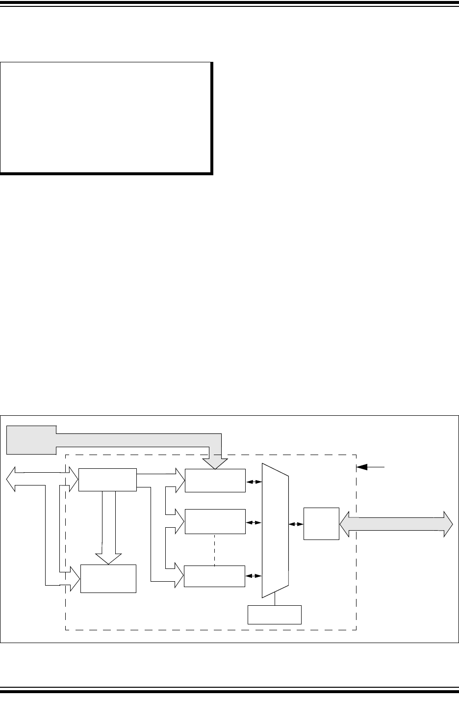
2015 Microchip Technology Inc. Preliminary DS60001320B-page 175
PIC32MZ Embedded Connectivity with Floating Point Unit (EF) Family
10.0 DIRECT MEMORY ACCESS
(DMA) CONTROLLER
The Direct Memory Access (DMA) Controller is a bus
master module useful for data transfers between
different devices without CPU intervention. The source
and destination of a DMA transfer can be any of the
memory mapped modules existent in the device such
as SPI, UART, PMP, etc., or memory itself.
Key features include:
• Eight identical channels, each featuring:
- Auto-increment source and destination
address registers
- Source and destination pointers
- Memory to memory and memory to
peripheral transfers
• Automatic word-size detection:
- Transfer granularity, down to byte level
- Bytes need not be word-aligned at source and
destination
• Fixed priority channel arbitration
• Flexible DMA channel operating modes:
- Manual (software) or automatic (interrupt) DMA
requests
- One-Shot or Auto-Repeat Block Transfer modes
- Channel-to-channel chaining
• Flexible DMA requests:
- A DMA request can be selected from any of the
peripheral interrupt sources
- Each channel can select any (appropriate)
observable interrupt as its DMA request source
- A DMA transfer abort can be selected from any
of the peripheral interrupt sources
- Up to 2-byte Pattern (data) match transfer
termination
• Multiple DMA channel status interrupts:
- DMA channel block transfer complete
- Source empty or half empty
- Destination full or half full
- DMA transfer aborted due to an external event
- Invalid DMA address generated
• DMA debug support features:
- Most recent error address accessed by a DMA
channel
- Most recent DMA channel to transfer data
• CRC Generation module:
- CRC module can be assigned to any of the
available channels
- CRC module is highly configurable
FIGURE 10-1: DMA BLOCK DIAGRAM
Note: This data sheet summarizes the features
of the PIC32MZ EF family of devices. It is
not intended to be a comprehensive refer-
ence source. To complement the informa-
tion in this data sheet, refer to Section 31.
“Direct Memory Access (DMA) Control-
ler” (DS60001117) in the “PIC32 Family
Reference Manual”, which is available
from the Microchip web site
(www.microchip.com/PIC32).
Address Decoder Channel 0 Control
Channel 1 Control
Channel n Control
Global Control
(DMACON)
Bus
Channel Priority
Arbitration
SEL
SEL
Y
I0
I1
I2
In
System IRQINT Controller
Peripheral Bus
Interface
DMA SYSCLK
System Bus + Bus Arbitration
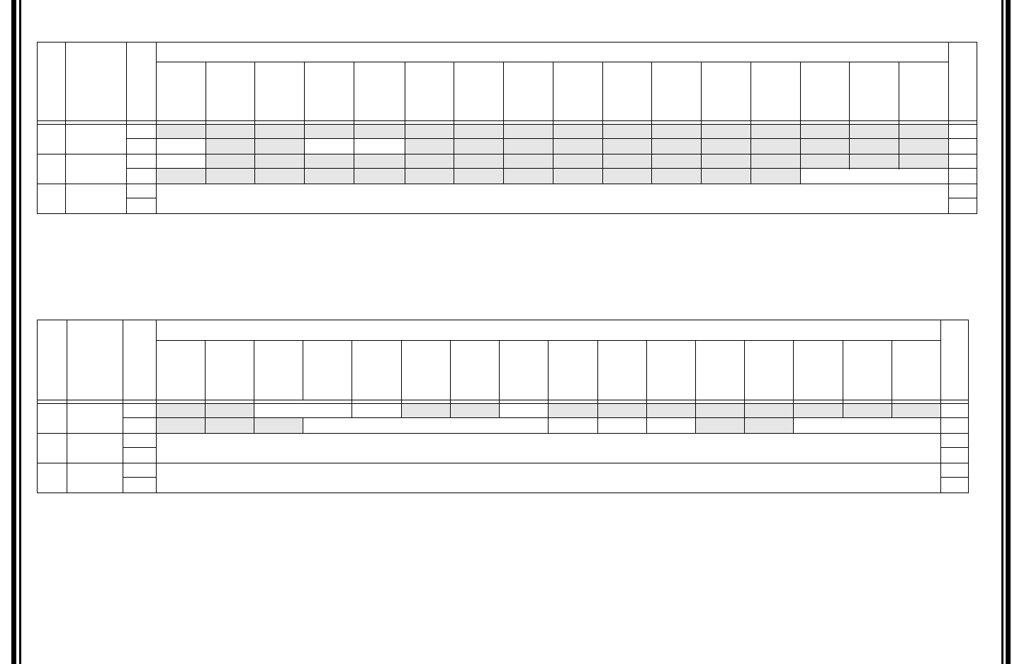
PIC32MZ Embedded Connectivity with Floating Point Unit (EF) Family
DS60001320B-page 176 Preliminary 2015 Microchip Technology Inc.
10.1 DMA Control Registers
TABLE 10-1: DMA GLOBAL REGISTER MAP
Virtual Address
(BF81_#)
Register
Name(1)
Bit Range
Bits
All Resets
31/15 30/14 29/13 28/12 27/11 26/10 25/9 24/8 23/7 22/6 21/5 20/4 19/3 18/2 17/1 16/0
1000 DMACON 31:16 — — — — — — — — — — — — — — — — 0000
15:0 ON — — SUSPEND DMABUSY — — — — — — — — — — — 0000
1010 DMASTAT 31:16 RDWR — — — — — — — — — — — — — — — 0000
15:0 — — — — — — — — — — — — — DMACH<2:0> 0000
1020 DMAADDR 31:16 DMAADDR<31:0> 0000
15:0 0000
Legend: x = unknown value on Reset; — = unimplemented, read as ‘0’. Reset values are shown in hexadecimal.
Note 1: All registers in this table have corresponding CLR, SET and INV registers at its virtual address, plus an offset of 0x4, 0x8 and 0xC, respectively. See Section 12.3 “CLR, SET, and INV Registers” for
more information.
TABLE 10-2: DMA CRC REGISTER MAP
Virtual Address
(BF81_#)
Register
Name(1)
Bit Range
Bits
All Resets
31/15 30/14 29/13 28/12 27/11 26/10 25/9 24/8 23/7 22/6 21/5 20/4 19/3 18/2 17/1 16/0
1030 DCRCCON 31:16 — — BYTO<1:0> WBO — — BITO — — — — — — — — 0000
15:0 ——— PLEN<4:0> CRCEN CRCAPP CRCTYP — — CRCCH<2:0> 0000
1040 DCRCDATA 31:16 DCRCDATA<31:0> 0000
15:0 0000
1050 DCRCXOR 31:16 DCRCXOR<31:0> 0000
15:0 0000
Legend: x = unknown value on Reset; — = unimplemented, read as ‘0’. Reset values are shown in hexadecimal.
Note 1: All registers in this table have corresponding CLR, SET and INV registers at their virtual addresses, plus offsets of 0x4, 0x8 and 0xC, respectively. See Section 12.3 “CLR, SET, and INV Registers” for
more information.

2015 Microchip Technology Inc. Preliminary DS60001320B-page 177
PIC32MZ Embedded Connectivity with Floating Point Unit (EF) Family
TABLE 10-3: DMA CHANNEL 0 THROUGH CHANNEL 7 REGISTER MAP
Virtual Address
(BF81_#)
Register
Name(1)
Bit Range
Bits
All Resets
31/15 30/14 29/13 28/12 27/11 26/10 25/9 24/8 23/7 22/6 21/5 20/4 19/3 18/2 17/1 16/0
1060 DCH0CON 31:16 CHPIGN<7:0> — — — — — — — — 0000
15:0 CHBUSY — CHPIGNEN — CHPATLEN — — CHCHNS CHEN CHAED CHCHN CHAEN — CHEDET CHPRI<1:0> 0000
1070 DCH0ECON 31:16 — — — — — — — — CHAIRQ<7:0> 00FF
15:0 CHSIRQ<7:0> CFORCE CABORT PATEN SIRQEN AIRQEN — — — FF00
1080 DCH0INT 31:16 — — — — — — — — CHSDIE CHSHIE CHDDIE CHDHIE CHBCIE CHCCIE CHTAIE CHERIE 0000
15:0 — — — — — — — — CHSDIF CHSHIF CHDDIF CHDHIF CHBCIF CHCCIF CHTAIF CHERIF 0000
1090 DCH0SSA 31:16 CHSSA<31:0> 0000
15:0 0000
10A0 DCH0DSA 31:16 CHDSA<31:0> 0000
15:0 0000
10B0 DCH0SSIZ 31:16 — — — — — — — — — — — — — — — — 0000
15:0 CHSSIZ<15:0> 0000
10C0 DCH0DSIZ 31:16 — — — — — — — — — — — — — — — — 0000
15:0 CHDSIZ<15:0> 0000
10D0 DCH0SPTR 31:16 — — — — — — — — — — — — — — — — 0000
15:0 CHSPTR<15:0> 0000
10E0 DCH0DPTR 31:16 — — — — — — — — — — — — — — — — 0000
15:0 CHDPTR<15:0> 0000
10F0 DCH0CSIZ 31:16 — — — — — — — — — — — — — — — — 0000
15:0 CHCSIZ<15:0> 0000
1100 DCH0CPTR 31:16 — — — — — — — — — — — — — — — — 0000
15:0 CHCPTR<15:0> 0000
1110 DCH0DAT 31:16 — — — — — — — — — — — — — — — — 0000
15:0 CHPDAT<15:0> 0000
1120 DCH1CON 31:16 CHPIGN<7:0> — — — — — — — — 0000
15:0 CHBUSY — CHPIGNEN — CHPATLEN — — CHCHNS CHEN CHAED CHCHN CHAEN — CHEDET CHPRI<1:0> 0000
1130 DCH1ECON 31:16 — — — — — — — — CHAIRQ<7:0> 00FF
15:0 CHSIRQ<7:0> CFORCE CABORT PATEN SIRQEN AIRQEN — — — FF00
1140 DCH1INT 31:16 — — — — — — — — CHSDIE CHSHIE CHDDIE CHDHIE CHBCIE CHCCIE CHTAIE CHERIE 0000
15:0 — — — — — — — — CHSDIF CHSHIF CHDDIF CHDHIF CHBCIF CHCCIF CHTAIF CHERIF 0000
1150 DCH1SSA 31:16 CHSSA<31:0> 0000
15:0 0000
1160 DCH1DSA 31:16 CHDSA<31:0> 0000
15:0 0000
Legend: x = unknown value on Reset; — = unimplemented, read as ‘0’. Reset values are shown in hexadecimal.
Note 1: All registers in this table have corresponding CLR, SET and INV registers at their virtual addresses, plus offsets of 0x4, 0x8 and 0xC, respectively. See Section 12.3 “CLR, SET, and INV Registers” for
more information.

PIC32MZ Embedded Connectivity with Floating Point Unit (EF) Family
DS60001320B-page 178 Preliminary 2015 Microchip Technology Inc.
1170 DCH1SSIZ 31:16 — — — — — — — — — — — — — — — — 0000
15:0 CHSSIZ<15:0> 0000
1180 DCH1DSIZ 31:16 — — — — — — — — — — — — — — — — 0000
15:0 CHDSIZ<15:0> 0000
1190 DCH1SPTR 31:16 — — — — — — — — — — — — — — — — 0000
15:0 CHSPTR<15:0> 0000
11A0 DCH1DPTR 31:16 — — — — — — — — — — — — — — — — 0000
15:0 CHDPTR<15:0> 0000
11B0 DCH1CSIZ 31:16 — — — — — — — — — — — — — — — — 0000
15:0 CHCSIZ<15:0> 0000
11C0 DCH1CPTR 31:16 — — — — — — — — — — — — — — — — 0000
15:0 CHCPTR<15:0> 0000
11D0 DCH1DAT 31:16 — — — — — — — — — — — — — — — — 0000
15:0 CHPDAT<15:0> 0000
11E0 DCH2CON 31:16 CHPIGN<7:0> — — — — — — — — 0000
15:0 CHBUSY — CHPIGNEN — CHPATLEN — — CHCHNS CHEN CHAED CHCHN CHAEN — CHEDET CHPRI<1:0> 0000
11F0 DCH2ECON 31:16 — — — — — — — — CHAIRQ<7:0> 00FF
15:0 CHSIRQ<7:0> CFORCE CABORT PATEN SIRQEN AIRQEN — — — FF00
1200 DCH2INT 31:16 — — — — — — — — CHSDIE CHSHIE CHDDIE CHDHIE CHBCIE CHCCIE CHTAIE CHERIE 0000
15:0 — — — — — — — — CHSDIF CHSHIF CHDDIF CHDHIF CHBCIF CHCCIF CHTAIF CHERIF 0000
1210 DCH2SSA 31:16 CHSSA<31:0> 0000
15:0 0000
1220 DCH2DSA 31:16 CHDSA<31:0> 0000
15:0 0000
1230 DCH2SSIZ 31:16 — — — — — — — — — — — — — — — — 0000
15:0 CHSSIZ<15:0> 0000
1240 DCH2DSIZ 31:16 — — — — — — — — — — — — — — — — 0000
15:0 CHDSIZ<15:0> 0000
1250 DCH2SPTR 31:16 — — — — — — — — — — — — — — — — 0000
15:0 CHSPTR<15:0> 0000
1260 DCH2DPTR 31:16 — — — — — — — — — — — — — — — — 0000
15:0 CHDPTR<15:0> 0000
1270 DCH2CSIZ 31:16 — — — — — — — — — — — — — — — — 0000
15:0 CHCSIZ<15:0> 0000
TABLE 10-3: DMA CHANNEL 0 THROUGH CHANNEL 7 REGISTER MAP (CONTINUED)
Virtual Address
(BF81_#)
Register
Name(1)
Bit Range
Bits
All Resets
31/15 30/14 29/13 28/12 27/11 26/10 25/9 24/8 23/7 22/6 21/5 20/4 19/3 18/2 17/1 16/0
Legend: x = unknown value on Reset; — = unimplemented, read as ‘0’. Reset values are shown in hexadecimal.
Note 1: All registers in this table have corresponding CLR, SET and INV registers at their virtual addresses, plus offsets of 0x4, 0x8 and 0xC, respectively. See Section 12.3 “CLR, SET, and INV Registers” for
more information.

2015 Microchip Technology Inc. Preliminary DS60001320B-page 179
PIC32MZ Embedded Connectivity with Floating Point Unit (EF) Family
1280 DCH2CPTR 31:16 — — — — — — — — — — — — — — — — 0000
15:0 CHCPTR<15:0> 0000
1290 DCH2DAT 31:16 — — — — — — — — — — — — — — — — 0000
15:0 CHPDAT<15:0> 0000
12A0 DCH3CON 31:16 CHPIGN<7:0> — — — — — — — — 0000
15:0 CHBUSY — CHPIGNEN — CHPATLEN — — CHCHNS CHEN CHAED CHCHN CHAEN — CHEDET CHPRI<1:0> 0000
12B0 DCH3ECON 31:16 — — — — — — — — CHAIRQ<7:0> 00FF
15:0 CHSIRQ<7:0> CFORCE CABORT PATEN SIRQEN AIRQEN — — — FF00
12C0 DCH3INT 31:16 — — — — — — — — CHSDIE CHSHIE CHDDIE CHDHIE CHBCIE CHCCIE CHTAIE CHERIE 0000
15:0 — — — — — — — — CHSDIF CHSHIF CHDDIF CHDHIF CHBCIF CHCCIF CHTAIF CHERIF 0000
12D0 DCH3SSA 31:16 CHSSA<31:0> 0000
15:0 0000
12E0 DCH3DSA 31:16 CHDSA<31:0> 0000
15:0 0000
12F0 DCH3SSIZ 31:16 — — — — — — — — — — — — — — — — 0000
15:0 CHSSIZ<15:0> 0000
1300 DCH3DSIZ 31:16 — — — — — — — — — — — — — — — — 0000
15:0 CHDSIZ<15:0> 0000
1310 DCH3SPTR 31:16 — — — — — — — — — — — — — — — — 0000
15:0 CHSPTR<15:0> 0000
1320 DCH3DPTR 31:16 — — — — — — — — — — — — — — — — 0000
15:0 CHDPTR<15:0> 0000
1330 DCH3CSIZ 31:16 — — — — — — — — — — — — — — — — 0000
15:0 CHCSIZ<15:0> 0000
1340 DCH3CPTR 31:16 — — — — — — — — — — — — — — — — 0000
15:0 CHCPTR<15:0> 0000
1350 DCH3DAT 31:16 — — — — — — — — — — — — — — — — 0000
15:0 CHPDAT<15:0> 0000
1360 DCH4CON 31:16 CHPIGN<7:0> — — — — — — — — 0000
15:0 CHBUSY — CHPIGNEN — CHPATLEN — — CHCHNS CHEN CHAED CHCHN CHAEN — CHEDET CHPRI<1:0> 0000
1370 DCH4ECON 31:16 — — — — — — — — CHAIRQ<7:0> 00FF
15:0 CHSIRQ<7:0> CFORCE CABORT PATEN SIRQEN AIRQEN — — — FF00
1380 DCH4INT 31:16 — — — — — — — — CHSDIE CHSHIE CHDDIE CHDHIE CHBCIE CHCCIE CHTAIE CHERIE 0000
15:0 — — — — — — — — CHSDIF CHSHIF CHDDIF CHDHIF CHBCIF CHCCIF CHTAIF CHERIF 0000
TABLE 10-3: DMA CHANNEL 0 THROUGH CHANNEL 7 REGISTER MAP (CONTINUED)
Virtual Address
(BF81_#)
Register
Name(1)
Bit Range
Bits
All Resets
31/15 30/14 29/13 28/12 27/11 26/10 25/9 24/8 23/7 22/6 21/5 20/4 19/3 18/2 17/1 16/0
Legend: x = unknown value on Reset; — = unimplemented, read as ‘0’. Reset values are shown in hexadecimal.
Note 1: All registers in this table have corresponding CLR, SET and INV registers at their virtual addresses, plus offsets of 0x4, 0x8 and 0xC, respectively. See Section 12.3 “CLR, SET, and INV Registers” for
more information.

PIC32MZ Embedded Connectivity with Floating Point Unit (EF) Family
DS60001320B-page 180 Preliminary 2015 Microchip Technology Inc.
1390 DCH4SSA 31:16 CHSSA<31:0> 0000
15:0 0000
13A0 DCH4DSA 31:16 CHDSA<31:0> 0000
15:0 0000
13B0 DCH4SSIZ 31:16 — — — — — — — — — — — — — — — — 0000
15:0 CHSSIZ<15:0> 0000
13C0 DCH4DSIZ 31:16 — — — — — — — — — — — — — — — — 0000
15:0 CHDSIZ<15:0> 0000
13D0 DCH4SPTR 31:16 — — — — — — — — — — — — — — — — 0000
15:0 CHSPTR<15:0> 0000
13E0 DCH4DPTR 31:16 — — — — — — — — — — — — — — — — 0000
15:0 CHDPTR<15:0> 0000
13F0 DCH4CSIZ 31:16 — — — — — — — — — — — — — — — — 0000
15:0 CHCSIZ<15:0> 0000
1400 DCH4CPTR 31:16 — — — — — — — — — — — — — — — — 0000
15:0 CHCPTR<15:0> 0000
1410 DCH4DAT 31:16 — — — — — — — — — — — — — — — — 0000
15:0 CHPDAT<15:0> 0000
1420 DCH5CON 31:16 CHPIGN<7:0> — — — — — — — — 0000
15:0 CHBUSY — CHPIGNEN — CHPATLEN — — CHCHNS CHEN CHAED CHCHN CHAEN — CHEDET CHPRI<1:0> 0000
1430 DCH5ECON 31:16 — — — — — — — — CHAIRQ<7:0> 00FF
15:0 CHSIRQ<7:0> CFORCE CABORT PATEN SIRQEN AIRQEN — — — FF00
1440 DCH5INT 31:16 — — — — — — — — CHSDIE CHSHIE CHDDIE CHDHIE CHBCIE CHCCIE CHTAIE CHERIE 0000
15:0 — — — — — — — — CHSDIF CHSHIF CHDDIF CHDHIF CHBCIF CHCCIF CHTAIF CHERIF 0000
1450 DCH5SSA 31:16 CHSSA<31:0> 0000
15:0 0000
1460 DCH5DSA 31:16 CHDSA<31:0> 0000
15:0 0000
1470 DCH5SSIZ 31:16 — — — — — — — — — — — — — — — — 0000
15:0 CHSSIZ<15:0> 0000
1480 DCH5DSIZ 31:16 — — — — — — — — — — — — — — — — 0000
15:0 CHDSIZ<15:0> 0000
1490 DCH5SPTR 31:16 — — — — — — — — — — — — — — — — 0000
15:0 CHSPTR<15:0> 0000
TABLE 10-3: DMA CHANNEL 0 THROUGH CHANNEL 7 REGISTER MAP (CONTINUED)
Virtual Address
(BF81_#)
Register
Name(1)
Bit Range
Bits
All Resets
31/15 30/14 29/13 28/12 27/11 26/10 25/9 24/8 23/7 22/6 21/5 20/4 19/3 18/2 17/1 16/0
Legend: x = unknown value on Reset; — = unimplemented, read as ‘0’. Reset values are shown in hexadecimal.
Note 1: All registers in this table have corresponding CLR, SET and INV registers at their virtual addresses, plus offsets of 0x4, 0x8 and 0xC, respectively. See Section 12.3 “CLR, SET, and INV Registers” for
more information.

2015 Microchip Technology Inc. Preliminary DS60001320B-page 181
PIC32MZ Embedded Connectivity with Floating Point Unit (EF) Family
14A0 DCH5DPTR 31:16 — — — — — — — — — — — — — — — — 0000
15:0 CHDPTR<15:0> 0000
14B0 DCH5CSIZ 31:16 — — — — — — — — — — — — — — — — 0000
15:0 CHCSIZ<15:0> 0000
14C0 DCH5CPTR 31:16 — — — — — — — — — — — — — — — — 0000
15:0 CHCPTR<15:0> 0000
14D0 DCH5DAT 31:16 — — — — — — — — — — — — — — — — 0000
15:0 CHPDAT<15:0> 0000
14E0 DCH6CON 31:16 CHPIGN<7:0> — — — — — — — — 0000
15:0 CHBUSY — CHPIGNEN — CHPATLEN — — CHCHNS CHEN CHAED CHCHN CHAEN — CHEDET CHPRI<1:0> 0000
14F0 DCH6ECON 31:16 — — — — — — — — CHAIRQ<7:0> 00FF
15:0 CHSIRQ<7:0> CFORCE CABORT PATEN SIRQEN AIRQEN — — — FF00
1500 DCH6INT 31:16 — — — — — — — — CHSDIE CHSHIE CHDDIE CHDHIE CHBCIE CHCCIE CHTAIE CHERIE 0000
15:0 — — — — — — — — CHSDIF CHSHIF CHDDIF CHDHIF CHBCIF CHCCIF CHTAIF CHERIF 0000
1510 DCH6SSA 31:16 CHSSA<31:0> 0000
15:0 0000
1520 DCH6DSA 31:16 CHDSA<31:0> 0000
15:0 0000
1530 DCH6SSIZ 31:16 — — — — — — — — — — — — — — — — 0000
15:0 CHSSIZ<15:0> 0000
1540 DCH6DSIZ 31:16 — — — — — — — — — — — — — — — — 0000
15:0 CHDSIZ<15:0> 0000
1550 DCH6SPTR 31:16 — — — — — — — — — — — — — — — — 0000
15:0 CHSPTR<15:0> 0000
1560 DCH6DPTR 31:16 — — — — — — — — — — — — — — — — 0000
15:0 CHDPTR<15:0> 0000
1570 DCH6CSIZ 31:16 — — — — — — — — — — — — — — — — 0000
15:0 CHCSIZ<15:0> 0000
1580 DCH6CPTR 31:16 — — — — — — — — — — — — — — — — 0000
15:0 CHCPTR<15:0> 0000
1590 DCH6DAT 31:16 — — — — — — — — — — — — — — — — 0000
15:0 CHPDAT<15:0> 0000
15A0 DCH7CON 31:16 CHPIGN<7:0> — — — — — — — — 0000
15:0 CHBUSY — CHPIGNEN — CHPATLEN — — CHCHNS CHEN CHAED CHCHN CHAEN — CHEDET CHPRI<1:0> 0000
TABLE 10-3: DMA CHANNEL 0 THROUGH CHANNEL 7 REGISTER MAP (CONTINUED)
Virtual Address
(BF81_#)
Register
Name(1)
Bit Range
Bits
All Resets
31/15 30/14 29/13 28/12 27/11 26/10 25/9 24/8 23/7 22/6 21/5 20/4 19/3 18/2 17/1 16/0
Legend: x = unknown value on Reset; — = unimplemented, read as ‘0’. Reset values are shown in hexadecimal.
Note 1: All registers in this table have corresponding CLR, SET and INV registers at their virtual addresses, plus offsets of 0x4, 0x8 and 0xC, respectively. See Section 12.3 “CLR, SET, and INV Registers” for
more information.
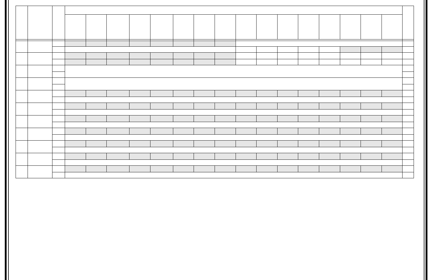
PIC32MZ Embedded Connectivity with Floating Point Unit (EF) Family
DS60001320B-page 182 Preliminary 2015 Microchip Technology Inc.
15B0 DCH7ECON 31:16 — — — — — — — — CHAIRQ<7:0> 00FF
15:0 CHSIRQ<7:0> CFORCE CABORT PATEN SIRQEN AIRQEN — — — FF00
15C0 DCH7INT 31:16 — — — — — — — — CHSDIE CHSHIE CHDDIE CHDHIE CHBCIE CHCCIE CHTAIE CHERIE 0000
15:0 — — — — — — — — CHSDIF CHSHIF CHDDIF CHDHIF CHBCIF CHCCIF CHTAIF CHERIF 0000
15D0 DCH7SSA 31:16 CHSSA<31:0> 0000
15:0 0000
15E0 DCH7DSA 31:16 CHDSA<31:0> 0000
15:0 0000
15F0 DCH7SSIZ 31:16 — — — — — — — — — — — — — — — — 0000
15:0 CHSSIZ<15:0> 0000
1600 DCH7DSIZ 31:16 — — — — — — — — — — — — — — — — 0000
15:0 CHDSIZ<15:0> 0000
1610 DCH7SPTR 31:16 — — — — — — — — — — — — — — — — 0000
15:0 CHSPTR<15:0> 0000
1620 DCH7DPTR 31:16 — — — — — — — — — — — — — — — — 0000
15:0 CHDPTR<15:0> 0000
1630 DCH7CSIZ 31:16 — — — — — — — — — — — — — — — — 0000
15:0 CHCSIZ<15:0> 0000
1640 DCH7CPTR 31:16 — — — — — — — — — — — — — — — — 0000
15:0 CHCPTR<15:0> 0000
1650 DCH7DAT 31:16 — — — — — — — — — — — — — — — — 0000
15:0 CHPDAT<15:0> 0000
TABLE 10-3: DMA CHANNEL 0 THROUGH CHANNEL 7 REGISTER MAP (CONTINUED)
Virtual Address
(BF81_#)
Register
Name(1)
Bit Range
Bits
All Resets
31/15 30/14 29/13 28/12 27/11 26/10 25/9 24/8 23/7 22/6 21/5 20/4 19/3 18/2 17/1 16/0
Legend: x = unknown value on Reset; — = unimplemented, read as ‘0’. Reset values are shown in hexadecimal.
Note 1: All registers in this table have corresponding CLR, SET and INV registers at their virtual addresses, plus offsets of 0x4, 0x8 and 0xC, respectively. See Section 12.3 “CLR, SET, and INV Registers” for
more information.

2015 Microchip Technology Inc. Preliminary DS60001320B-page 183
PIC32MZ Embedded Connectivity with Floating Point Unit (EF) Family
REGISTER 10-1: DMACON: DMA CONTROLLER CONTROL REGISTER
Bit
Range Bit
31/23/15/7 Bit
30/22/14/6 Bit
29/21/13/5 Bit
28/20/12/4 Bit
27/19/11/3 Bit
26/18/10/2 Bit
25/17/9/1 Bit
24/16/8/0
31:24 U-0 U-0 U-0 U-0 U-0 U-0 U-0 U-0
— — — — — — — —
23:16 U-0 U-0 U-0 U-0 U-0 U-0 U-0 U-0
— — — — — — — —
15:8 R/W-0 U-0 U-0 R/W-0 R/W-0 U-0 U-0 U-0
ON —— SUSPEND DMABUSY — — —
7:0 U-0 U-0 U-0 U-0 U-0 U-0 U-0 U-0
— — — — — — — —
Legend:
R = Readable bit W = Writable bit U = Unimplemented bit, read as ‘0’
-n = Value at POR ‘1’ = Bit is set ‘0’ = Bit is cleared x = Bit is unknown
bit 31-16 Unimplemented: Read as ‘0’
bit 15 ON: DMA On bit
1 = DMA module is enabled
0 = DMA module is disabled
bit 14-13 Unimplemented: Read as ‘0’
bit 12 SUSPEND: DMA Suspend bit
1 = DMA transfers are suspended to allow CPU uninterrupted access to data bus
0 = DMA operates normally
bit 11 DMABUSY: DMA Module Busy bit
1 = DMA module is active and is transferring data
0 = DMA module is disabled and not actively transferring data
bit 10-0 Unimplemented: Read as ‘0’

PIC32MZ Embedded Connectivity with Floating Point Unit (EF) Family
DS60001320B-page 184 Preliminary 2015 Microchip Technology Inc.
REGISTER 10-2: DMASTAT: DMA STATUS REGISTER
Bit
Range Bit
31/23/15/7 Bit
30/22/14/6 Bit
29/21/13/5 Bit
28/20/12/4 Bit
27/19/11/3 Bit
26/18/10/2 Bit
25/17/9/1 Bit
24/16/8/0
31:24 R-0 U-0 U-0 U-0 U-0 U-0 U-0 U-0
RDWR — — — — — — —
23:16 U-0 U-0 U-0 U-0 U-0 U-0 U-0 U-0
— — — — — — — —
15:8 U-0 U-0 U-0 U-0 U-0 U-0 U-0 U-0
— — — — — — — —
7:0 U-0 U-0 U-0 U-0 U-0 R-0 R-0 R-0
— — — — — DMACH<2:0>
Legend:
R = Readable bit W = Writable bit U = Unimplemented bit, read as ‘0’
-n = Value at POR ‘1’ = Bit is set ‘0’ = Bit is cleared x = Bit is unknown
bit 31 RDWR: Read/Write Status bit
1 = Last DMA bus access when an error was detected was a read
0 = Last DMA bus access when an error was detected was a write
bit 30-3 Unimplemented: Read as ‘0’
bit 2-0 DMACH<2:0>: DMA Channel bits
These bits contain the value of the most recent active DMA channel when an error was detected.
REGISTER 10-3: DMAADDR: DMA ADDRESS REGISTER
Bit
Range Bit
31/23/15/7 Bit
30/22/14/6 Bit
29/21/13/5 Bit
28/20/12/4 Bit
27/19/11/3 Bit
26/18/10/2 Bit
25/17/9/1 Bit
24/16/8/0
31:24 R-0 R-0 R-0 R-0 R-0 R-0 R-0 R-0
DMAADDR<31:24>
23:16 R-0 R-0 R-0 R-0 R-0 R-0 R-0 R-0
DMAADDR<23:16>
15:8 R-0 R-0 R-0 R-0 R-0 R-0 R-0 R-0
DMAADDR<15:8>
7:0 R-0 R-0 R-0 R-0 R-0 R-0 R-0 R-0
DMAADDR<7:0>
Legend:
R = Readable bit W = Writable bit U = Unimplemented bit, read as ‘0’
-n = Value at POR ‘1’ = Bit is set ‘0’ = Bit is cleared x = Bit is unknown
bit 31-0 DMAADDR<31:0>: DMA Module Address bits
These bits contain the address of the most recent DMA access when an error was detected.

2015 Microchip Technology Inc. Preliminary DS60001320B-page 185
PIC32MZ Embedded Connectivity with Floating Point Unit (EF) Family
REGISTER 10-4: DCRCCON: DMA CRC CONTROL REGISTER
Bit
Range Bit
31/23/15/7 Bit
30/22/14/6 Bit
29/21/13/5 Bit
28/20/12/4 Bit
27/19/11/3 Bit
26/18/10/2 Bit
25/17/9/1 Bit
24/16/8/0
31:24 U-0 U-0 R/W-0 R/W-0 R/W-0 U-0 U-0 R/W-0
—— BYTO<1:0> WBO(1) ——BITO
23:16 U-0 U-0 U-0 U-0 U-0 U-0 U-0 U-0
— — — — — — — —
15:8 U-0 U-0 U-0 R/W-0 R/W-0 R/W-0 R/W-0 R/W-0
— — — PLEN<4:0>
7:0 R/W-0 R/W-0 R/W-0 U-0 U-0 R/W-0 R/W-0 R/W-0
CRCEN CRCAPP(1) CRCTYP —— CRCCH<2:0>
Legend:
R = Readable bit W = Writable bit U = Unimplemented bit, read as ‘0’
-n = Value at POR ‘1’ = Bit is set ‘0’ = Bit is cleared x = Bit is unknown
bit 31-30 Unimplemented: Read as ‘0’
bit 29-28 BYTO<1:0>: CRC Byte Order Selection bits
11 = Endian byte swap on half-word boundaries (i.e., source half-word order with reverse source byte order
per half-word)
10 = Swap half-words on word boundaries (i.e., reverse source half-word order with source byte order per
half-word)
01 = Endian byte swap on word boundaries (i.e., reverse source byte order)
00 = No swapping (i.e., source byte order)
bit 27 WBO: CRC Write Byte Order Selection bit(1)
1 = Source data is written to the destination re-ordered as defined by BYTO<1:0>
0 = Source data is written to the destination unaltered
bit 26-25 Unimplemented: Read as ‘0’
bit 24 BITO: CRC Bit Order Selection bit
When CRCTYP (DCRCCON<15>) = 1 (CRC module is in IP Header mode):
1 = The IP header checksum is calculated Least Significant bit (LSb) first (i.e., reflected)
0 = The IP header checksum is calculated Most Significant bit (MSb) first (i.e., not reflected)
When CRCTYP (DCRCCON<15>) = 0 (CRC module is in LFSR mode):
1 = The LFSR CRC is calculated Least Significant bit first (i.e., reflected)
0 = The LFSR CRC is calculated Most Significant bit first (i.e., not reflected)
bit 23-13 Unimplemented: Read as ‘0’
bit 12-8 PLEN<4:0>: Polynomial Length bits(1)
When CRCTYP (DCRCCON<15>) = 1 (CRC module is in IP Header mode):
These bits are unused.
When CRCTYP (DCRCCON<15>) = 0 (CRC module is in LFSR mode):
Denotes the length of the polynomial – 1.
bit 7 CRCEN: CRC Enable bit
1 = CRC module is enabled and channel transfers are routed through the CRC module
0 = CRC module is disabled and channel transfers proceed normally
Note 1: When WBO = 1, unaligned transfers are not supported and the CRCAPP bit cannot be set.

PIC32MZ Embedded Connectivity with Floating Point Unit (EF) Family
DS60001320B-page 186 Preliminary 2015 Microchip Technology Inc.
bit 6 CRCAPP: CRC Append Mode bit(1)
1 = The DMA transfers data from the source into the CRC but NOT to the destination. When a block transfer
completes the DMA writes the calculated CRC value to the location given by CHxDSA
0 = The DMA transfers data from the source through the CRC obeying WBO as it writes the data to the
destination
bit 5 CRCTYP: CRC Type Selection bit
1 = The CRC module will calculate an IP header checksum
0 = The CRC module will calculate a LFSR CRC
bit 4-3 Unimplemented: Read as ‘0’
bit 2-0 CRCCH<2:0>: CRC Channel Select bits
111 = CRC is assigned to Channel 7
110 = CRC is assigned to Channel 6
101 = CRC is assigned to Channel 5
100 = CRC is assigned to Channel 4
011 = CRC is assigned to Channel 3
010 = CRC is assigned to Channel 2
001 = CRC is assigned to Channel 1
000 = CRC is assigned to Channel 0
REGISTER 10-4: DCRCCON: DMA CRC CONTROL REGISTER (CONTINUED)
Note 1: When WBO = 1, unaligned transfers are not supported and the CRCAPP bit cannot be set.

2015 Microchip Technology Inc. Preliminary DS60001320B-page 187
PIC32MZ Embedded Connectivity with Floating Point Unit (EF) Family
REGISTER 10-5: DCRCDATA: DMA CRC DATA REGISTER
Bit
Range Bit
31/23/15/7 Bit
30/22/14/6 Bit
29/21/13/5 Bit
28/20/12/4 Bit
27/19/11/3 Bit
26/18/10/2 Bit
25/17/9/1 Bit
24/16/8/0
31:24 R/W-0 R/W-0 R/W-0 R/W-0 R/W-0 R/W-0 R/W-0 R/W-0
DCRCDATA<31:24>
23:16 R/W-0 R/W-0 R/W-0 R/W-0 R/W-0 R/W-0 R/W-0 R/W-0
DCRCDATA<23:16>
15:8 R/W-0 R/W-0 R/W-0 R/W-0 R/W-0 R/W-0 R/W-0 R/W-0
DCRCDATA<15:8>
7:0 R/W-0 R/W-0 R/W-0 R/W-0 R/W-0 R/W-0 R/W-0 R/W-0
DCRCDATA<7:0>
Legend:
R = Readable bit W = Writable bit U = Unimplemented bit, read as ‘0’
-n = Value at POR ‘1’ = Bit is set ‘0’ = Bit is cleared x = Bit is unknown
bit 31-0 DCRCDATA<31:0>: CRC Data Register bits
Writing to this register will seed the CRC generator. Reading from this register will return the current value of
the CRC. Bits greater than PLEN will return ‘0’ on any read.
When CRCTYP (DCRCCON<15>) = 1 (CRC module is in IP Header mode):
Only the lower 16 bits contain IP header checksum information. The upper 16 bits are always ‘0’. Data written
to this register is converted and read back in 1’s complement form (i.e., current IP header checksum value).
When CRCTYP (DCRCCON<15>) = 0 (CRC module is in LFSR mode):
Bits greater than PLEN will return ‘0’ on any read.
REGISTER 10-6: DCRCXOR: DMA CRCXOR ENABLE REGISTER
Bit
Range Bit
31/23/15/7 Bit
30/22/14/6 Bit
29/21/13/5 Bit
28/20/12/4 Bit
27/19/11/3 Bit
26/18/10/2 Bit
25/17/9/1 Bit
24/16/8/0
31:24 R/W-0 R/W-0 R/W-0 R/W-0 R/W-0 R/W-0 R/W-0 R/W-0
DCRCXOR<31:24>
23:16 R/W-0 R/W-0 R/W-0 R/W-0 R/W-0 R/W-0 R/W-0 R/W-0
DCRCXOR<23:16>
15:8 R/W-0 R/W-0 R/W-0 R/W-0 R/W-0 R/W-0 R/W-0 R/W-0
DCRCXOR<15:8>
7:0 R/W-0 R/W-0 R/W-0 R/W-0 R/W-0 R/W-0 R/W-0 R/W-0
DCRCXOR<7:0>
Legend:
R = Readable bit W = Writable bit U = Unimplemented bit, read as ‘0’
-n = Value at POR ‘1’ = Bit is set ‘0’ = Bit is cleared x = Bit is unknown
bit 31-0 DCRCXOR<31:0>: CRC XOR Register bits
When CRCTYP (DCRCCON<15>) = 1 (CRC module is in IP Header mode):
This register is unused.
When CRCTYP (DCRCCON<15>) = 0 (CRC module is in LFSR mode):
1 = Enable the XOR input to the Shift register
0 = Disable the XOR input to the Shift register; data is shifted in directly from the previous stage in
the register

PIC32MZ Embedded Connectivity with Floating Point Unit (EF) Family
DS60001320B-page 188 Preliminary 2015 Microchip Technology Inc.
REGISTER 10-7: DCHxCON: DMA CHANNEL x CONTROL REGISTER
Bit
Range Bit
31/23/15/7 Bit
30/22/14/6 Bit
29/21/13/5 Bit
28/20/12/4 Bit
27/19/11/3 Bit
26/18/10/2 Bit
25/17/9/1 Bit
24/16/8/0
31:24 R/W-0 R/W-0 R/W-0 R/W-0 R/W-0 R/W-0 R/W-0 R/W-0
CHPIGN<7:0>
23:16 U-0 U-0 U-0 U-0 U-0 U-0 U-0 U-0
— — — — — — — —
15:8 R/W-0 U-0 R/W-0 U-0 R/W-0 U-0 U-0 R/W-0
CHBUSY —CHIPGNEN— CHPATLEN — — CHCHNS(1)
7:0 R/W-0 R/W-0 R/W-0 R/W-0 U-0 R-0 R/W-0 R/W-0
CHEN(2) CHAED CHCHN CHAEN — CHEDET CHPRI<1:0>
Legend:
R = Readable bit W = Writable bit U = Unimplemented bit, read as ‘0’
-n = Value at POR ‘1’ = Bit is set ‘0’ = Bit is cleared x = Bit is unknown
bit 31-24 CHPIGN<7:0>: Channel Register Data bits
Pattern Terminate mode:
Any byte matching these bits during a pattern match may be ignored during the pattern match determina-
tion when the CHPIGNEN bit is set. If a byte is read that is identical to this data byte, the pattern match
logic will treat it as a “don’t care” when the pattern matching logic is enabled and the CHPIGEN bit is set.
bit 23-16 Unimplemented: Read as ‘0’
bit 15 CHBUSY: Channel Busy bit
1 = Channel is active or has been enabled
0 = Channel is inactive or has been disabled
bit 14 Unimplemented: Read as ‘0’
bit 13 CHPIGNEN: Enable Pattern Ignore Byte bit
1 = Treat any byte that matches the CHPIGN<7:0> bits as a “don’t care” when pattern matching is enabled
0 = Disable this feature
bit 12 Unimplemented: Read as ‘0’
bit 11 CHPATLEN: Pattern Length bit
1 = 2 byte length
0 = 1 byte length
bit 10-9 Unimplemented: Read as ‘0’
bit 8 CHCHNS: Chain Channel Selection bit(1)
1 = Chain to channel lower in natural priority (CH1 will be enabled by CH2 transfer complete)
0 = Chain to channel higher in natural priority (CH1 will be enabled by CH0 transfer complete)
bit 7 CHEN: Channel Enable bit(2)
1 = Channel is enabled
0 = Channel is disabled
bit 6 CHAED: Channel Allow Events If Disabled bit
1 = Channel start/abort events will be registered, even if the channel is disabled
0 = Channel start/abort events will be ignored if the channel is disabled
bit 5 CHCHN: Channel Chain Enable bit
1 = Allow channel to be chained
0 = Do not allow channel to be chained
Note 1: The chain selection bit takes effect when chaining is enabled (i.e., CHCHN = 1).
2: When the channel is suspended by clearing this bit, the user application should poll the CHBUSY bit (if
available on the device variant) to see when the channel is suspended, as it may take some clock cycles
to complete a current transaction before the channel is suspended.

2015 Microchip Technology Inc. Preliminary DS60001320B-page 189
PIC32MZ Embedded Connectivity with Floating Point Unit (EF) Family
bit 4 CHAEN: Channel Automatic Enable bit
1 = Channel is continuously enabled, and not automatically disabled after a block transfer is complete
0 = Channel is disabled on block transfer complete
bit 3 Unimplemented: Read as ‘0’
bit 2 CHEDET: Channel Event Detected bit
1 = An event has been detected
0 = No events have been detected
bit 1-0 CHPRI<1:0>: Channel Priority bits
11 = Channel has priority 3 (highest)
10 = Channel has priority 2
01 = Channel has priority 1
00 = Channel has priority 0
REGISTER 10-7: DCHxCON: DMA CHANNEL x CONTROL REGISTER (CONTINUED)
Note 1: The chain selection bit takes effect when chaining is enabled (i.e., CHCHN = 1).
2: When the channel is suspended by clearing this bit, the user application should poll the CHBUSY bit (if
available on the device variant) to see when the channel is suspended, as it may take some clock cycles
to complete a current transaction before the channel is suspended.

PIC32MZ Embedded Connectivity with Floating Point Unit (EF) Family
DS60001320B-page 190 Preliminary 2015 Microchip Technology Inc.
REGISTER 10-8: DCHxECON: DMA CHANNEL x EVENT CONTROL REGISTER
Bit
Range Bit
31/23/15/7 Bit
30/22/14/6 Bit
29/21/13/5 Bit
28/20/12/4 Bit
27/19/11/3 Bit
26/18/10/2 Bit
25/17/9/1 Bit
24/16/8/0
31:24 U-0 U-0 U-0 U-0 U-0 U-0 U-0 U-0
— — — — — — — —
23:16 R/W-1 R/W-1 R/W-1 R/W-1 R/W-1 R/W-1 R/W-1 R/W-1
CHAIRQ<7:0>(1)
15:8 R/W-1 R/W-1 R/W-1 R/W-1 R/W-1 R/W-1 R/W-1 R/W-1
CHSIRQ<7:0>(1)
7:0 S-0 S-0 R/W-0 R/W-0 R/W-0 U-0 U-0 U-0
CFORCE CABORT PATEN SIRQEN AIRQEN — — —
Legend: S = Settable bit
R = Readable bit W = Writable bit U = Unimplemented bit, read as ‘0’
-n = Value at POR ‘1’ = Bit is set ‘0’ = Bit is cleared x = Bit is unknown
bit 31-24 Unimplemented: Read as ‘0’
bit 23-16 CHAIRQ<7:0>: Channel Transfer Abort IRQ bits(1)
11111111 = Interrupt 255 will abort any transfers in progress and set CHAIF flag
•
•
•
00000001 = Interrupt 1 will abort any transfers in progress and set CHAIF flag
00000000 = Interrupt 0 will abort any transfers in progress and set CHAIF flag
bit 15-8 CHSIRQ<7:0>: Channel Transfer Start IRQ bits(1)
11111111 = Interrupt 255 will initiate a DMA transfer
•
•
•
00000001 = Interrupt 1 will initiate a DMA transfer
00000000 = Interrupt 0 will initiate a DMA transfer
bit 7 CFORCE: DMA Forced Transfer bit
1 = A DMA transfer is forced to begin when this bit is written to a ‘1’
0 = This bit always reads ‘0’
bit 6 CABORT: DMA Abort Transfer bit
1 = A DMA transfer is aborted when this bit is written to a ‘1’
0 = This bit always reads ‘0’
bit 5 PATEN: Channel Pattern Match Abort Enable bit
1 = Abort transfer and clear CHEN on pattern match
0 = Pattern match is disabled
bit 4 SIRQEN: Channel Start IRQ Enable bit
1 = Start channel cell transfer if an interrupt matching CHSIRQ occurs
0 = Interrupt number CHSIRQ is ignored and does not start a transfer
bit 3 AIRQEN: Channel Abort IRQ Enable bit
1 = Channel transfer is aborted if an interrupt matching CHAIRQ occurs
0 = Interrupt number CHAIRQ is ignored and does not terminate a transfer
bit 2-0 Unimplemented: Read as ‘0’
Note 1: See Table 7-2: “Interrupt IRQ, Vector, and Bit Location” for the list of available interrupt IRQ sources.

2015 Microchip Technology Inc. Preliminary DS60001320B-page 191
PIC32MZ Embedded Connectivity with Floating Point Unit (EF) Family
REGISTER 10-9: DCHxINT: DMA CHANNEL x INTERRUPT CONTROL REGISTER
Bit
Range Bit
31/23/15/7 Bit
30/22/14/6 Bit
29/21/13/5 Bit
28/20/12/4 Bit
27/19/11/3 Bit
26/18/10/2 Bit
25/17/9/1 Bit
24/16/8/0
31:24 U-0 U-0 U-0 U-0 U-0 U-0 U-0 U-0
— — — — — — — —
23:16 R/W-0 R/W-0 R/W-0 R/W-0 R/W-0 R/W-0 R/W-0 R/W-0
CHSDIE CHSHIE CHDDIE CHDHIE CHBCIE CHCCIE CHTAIE CHERIE
15:8 U-0 U-0 U-0 U-0 U-0 U-0 U-0 U-0
— — — — — — — —
7:0 R/W-0 R/W-0 R/W-0 R/W-0 R/W-0 R/W-0 R/W-0 R/W-0
CHSDIF CHSHIF CHDDIF CHDHIF CHBCIF CHCCIF CHTAIF CHERIF
Legend:
R = Readable bit W = Writable bit U = Unimplemented bit, read as ‘0’
-n = Value at POR ‘1’ = Bit is set ‘0’ = Bit is cleared x = Bit is unknown
bit 31-24 Unimplemented: Read as ‘0’
bit 23 CHSDIE: Channel Source Done Interrupt Enable bit
1 = Interrupt is enabled
0 = Interrupt is disabled
bit 22 CHSHIE: Channel Source Half Empty Interrupt Enable bit
1 = Interrupt is enabled
0 = Interrupt is disabled
bit 21 CHDDIE: Channel Destination Done Interrupt Enable bit
1 = Interrupt is enabled
0 = Interrupt is disabled
bit 20 CHDHIE: Channel Destination Half Full Interrupt Enable bit
1 = Interrupt is enabled
0 = Interrupt is disabled
bit 19 CHBCIE: Channel Block Transfer Complete Interrupt Enable bit
1 = Interrupt is enabled
0 = Interrupt is disabled
bit 18 CHCCIE: Channel Cell Transfer Complete Interrupt Enable bit
1 = Interrupt is enabled
0 = Interrupt is disabled
bit 17 CHTAIE: Channel Transfer Abort Interrupt Enable bit
1 = Interrupt is enabled
0 = Interrupt is disabled
bit 16 CHERIE: Channel Address Error Interrupt Enable bit
1 = Interrupt is enabled
0 = Interrupt is disabled
bit 15-8 Unimplemented: Read as ‘0’
bit 7 CHSDIF: Channel Source Done Interrupt Flag bit
1 = Channel Source Pointer has reached end of source (CHSPTR = CHSSIZ)
0 = No interrupt is pending
bit 6 CHSHIF: Channel Source Half Empty Interrupt Flag bit
1 = Channel Source Pointer has reached midpoint of source (CHSPTR = CHSSIZ/2)
0 = No interrupt is pending

PIC32MZ Embedded Connectivity with Floating Point Unit (EF) Family
DS60001320B-page 192 Preliminary 2015 Microchip Technology Inc.
bit 5 CHDDIF: Channel Destination Done Interrupt Flag bit
1 = Channel Destination Pointer has reached end of destination (CHDPTR = CHDSIZ)
0 = No interrupt is pending
bit 4 CHDHIF: Channel Destination Half Full Interrupt Flag bit
1 = Channel Destination Pointer has reached midpoint of destination (CHDPTR = CHDSIZ/2)
0 = No interrupt is pending
bit 3 CHBCIF: Channel Block Transfer Complete Interrupt Flag bit
1 = A block transfer has been completed (the larger of CHSSIZ/CHDSIZ bytes has been transferred), or a
pattern match event occurs
0 = No interrupt is pending
bit 2 CHCCIF: Channel Cell Transfer Complete Interrupt Flag bit
1 = A cell transfer has been completed (CHCSIZ bytes have been transferred)
0 = No interrupt is pending
bit 1 CHTAIF: Channel Transfer Abort Interrupt Flag bit
1 = An interrupt matching CHAIRQ has been detected and the DMA transfer has been aborted
0 = No interrupt is pending
bit 0 CHERIF: Channel Address Error Interrupt Flag bit
1 = A channel address error has been detected
Either the source or the destination address is invalid.
0 = No interrupt is pending
REGISTER 10-9: DCHxINT: DMA CHANNEL x INTERRUPT CONTROL REGISTER (CONTINUED)

2015 Microchip Technology Inc. Preliminary DS60001320B-page 193
PIC32MZ Embedded Connectivity with Floating Point Unit (EF) Family
REGISTER 10-10: DCHxSSA: DMA CHANNEL x SOURCE START ADDRESS REGISTER
Bit Range Bit
31/23/15/7 Bit
30/22/14/6 Bit
29/21/13/5 Bit
28/20/12/4 Bit
27/19/11/3 Bit
26/18/10/2 Bit
25/17/9/1 Bit
24/16/8/0
31:24 R/W-0 R/W-0 R/W-0 R/W-0 R/W-0 R/W-0 R/W-0 R/W-0
CHSSA<31:24>
23:16 R/W-0 R/W-0 R/W-0 R/W-0 R/W-0 R/W-0 R/W-0 R/W-0
CHSSA<23:16>
15:8 R/W-0 R/W-0 R/W-0 R/W-0 R/W-0 R/W-0 R/W-0 R/W-0
CHSSA<15:8>
7:0 R/W-0 R/W-0 R/W-0 R/W-0 R/W-0 R/W-0 R/W-0 R/W-0
CHSSA<7:0>
Legend:
R = Readable bit W = Writable bit U = Unimplemented bit, read as ‘0’
-n = Value at POR ‘1’ = Bit is set ‘0’ = Bit is cleared x = Bit is unknown
bit 31-0 CHSSA<31:0> Channel Source Start Address bits
Channel source start address.
Note: This must be the physical address of the source.
REGISTER 10-11: DCHxDSA: DMA CHANNEL x DESTINATION START ADDRESS REGISTER
Bit
Range Bit
31/23/15/7 Bit
30/22/14/6 Bit
29/21/13/5 Bit
28/20/12/4 Bit
27/19/11/3 Bit
26/18/10/2 Bit
25/17/9/1 Bit
24/16/8/0
31:24 R/W-0 R/W-0 R/W-0 R/W-0 R/W-0 R/W-0 R/W-0 R/W-0
CHDSA<31:24>
23:16 R/W-0 R/W-0 R/W-0 R/W-0 R/W-0 R/W-0 R/W-0 R/W-0
CHDSA<23:16>
15:8 R/W-0 R/W-0 R/W-0 R/W-0 R/W-0 R/W-0 R/W-0 R/W-0
CHDSA<15:8>
7:0 R/W-0 R/W-0 R/W-0 R/W-0 R/W-0 R/W-0 R/W-0 R/W-0
CHDSA<7:0>
Legend:
R = Readable bit W = Writable bit U = Unimplemented bit, read as ‘0’
-n = Value at POR ‘1’ = Bit is set ‘0’ = Bit is cleared x = Bit is unknown
bit 31-0 CHDSA<31:0>: Channel Destination Start Address bits
Channel destination start address.
Note: This must be the physical address of the destination.
PIC32MZ Embedded Connectivity with Floating Point Unit (EF) Family
DS60001320B-page 194 Preliminary 2015 Microchip Technology Inc.
REGISTER 10-12: DCHxSSIZ: DMA CHANNEL x SOURCE SIZE REGISTER
Bit
Range Bit
31/23/15/7 Bit
30/22/14/6 Bit
29/21/13/5 Bit
28/20/12/4 Bit
27/19/11/3 Bit
26/18/10/2 Bit
25/17/9/1 Bit
24/16/8/0
31:24 U-0 U-0 U-0 U-0 U-0 U-0 U-0 U-0
— — — — — — — —
23:16 U-0 U-0 U-0 U-0 U-0 U-0 U-0 U-0
— — — — — — — —
15:8 R/W-0 R/W-0 R/W-0 R/W-0 R/W-0 R/W-0 R/W-0 R/W-0
CHSSIZ<15:8>
7:0 R/W-0 R/W-0 R/W-0 R/W-0 R/W-0 R/W-0 R/W-0 R/W-0
CHSSIZ<7:0>
Legend:
R = Readable bit W = Writable bit U = Unimplemented bit, read as ‘0’
-n = Value at POR ‘1’ = Bit is set ‘0’ = Bit is cleared x = Bit is unknown
bit 31-16 Unimplemented: Read as ‘0’
bit 15-0 CHSSIZ<15:0>: Channel Source Size bits
1111111111111111 = 65,535 byte source size
•
•
•
0000000000000010 = 2 byte source size
0000000000000001 = 1 byte source size
0000000000000000 = 65,536 byte source size
REGISTER 10-13: DCHxDSIZ: DMA CHANNEL x DESTINATION SIZE REGISTER
Bit
Range Bit
31/23/15/7 Bit
30/22/14/6 Bit
29/21/13/5 Bit
28/20/12/4 Bit
27/19/11/3 Bit
26/18/10/2 Bit
25/17/9/1 Bit
24/16/8/0
31:24 U-0 U-0 U-0 U-0 U-0 U-0 U-0 U-0
— — — — — — — —
23:16 U-0 U-0 U-0 U-0 U-0 U-0 U-0 U-0
— — — — — — — —
15:8 R/W-0 R/W-0 R/W-0 R/W-0 R/W-0 R/W-0 R/W-0 R/W-0
CHDSIZ<15:8>
7:0 R/W-0 R/W-0 R/W-0 R/W-0 R/W-0 R/W-0 R/W-0 R/W-0
CHDSIZ<7:0>
Legend:
R = Readable bit W = Writable bit U = Unimplemented bit, read as ‘0’
-n = Value at POR ‘1’ = Bit is set ‘0’ = Bit is cleared x = Bit is unknown
bit 31-16 Unimplemented: Read as ‘0’
bit 15-0 CHDSIZ<15:0>: Channel Destination Size bits
1111111111111111 = 65,535 byte destination size
•
•
•
0000000000000010 = 2 byte destination size
0000000000000001 = 1 byte destination size
0000000000000000 = 65,536 byte destination size
2015 Microchip Technology Inc. Preliminary DS60001320B-page 195
PIC32MZ Embedded Connectivity with Floating Point Unit (EF) Family
REGISTER 10-14: DCHxSPTR: DMA CHANNEL x SOURCE POINTER REGISTER
Bit
Range Bit
31/23/15/7 Bit
30/22/14/6 Bit
29/21/13/5 Bit
28/20/12/4 Bit
27/19/11/3 Bit
26/18/10/2 Bit
25/17/9/1 Bit
24/16/8/0
31:24 U-0 U-0 U-0 U-0 U-0 U-0 U-0 U-0
— — — — — — — —
23:16 U-0 U-0 U-0 U-0 U-0 U-0 U-0 U-0
— — — — — — — —
15:8 R-0 R-0 R-0 R-0 R-0 R-0 R-0 R-0
CHSPTR<15:8>
7:0 R-0 R-0 R-0 R-0 R-0 R-0 R-0 R-0
CHSPTR<7:0>
Legend:
R = Readable bit W = Writable bit U = Unimplemented bit, read as ‘0’
-n = Value at POR ‘1’ = Bit is set ‘0’ = Bit is cleared x = Bit is unknown
bit 31-16 Unimplemented: Read as ‘0’
bit 15-0 CHSPTR<15:0>: Channel Source Pointer bits
1111111111111111 = Points to byte 65,535 of the source
•
•
•
0000000000000001 = Points to byte 1 of the source
0000000000000000 = Points to byte 0 of the source
Note: When in Pattern Detect mode, this register is reset on a pattern detect.
REGISTER 10-15: DCHxDPTR: DMA CHANNEL x DESTINATION POINTER REGISTER
Bit
Range Bit
31/23/15/7 Bit
30/22/14/6 Bit
29/21/13/5 Bit
28/20/12/4 Bit
27/19/11/3 Bit
26/18/10/2 Bit
25/17/9/1 Bit
24/16/8/0
31:24 U-0 U-0 U-0 U-0 U-0 U-0 U-0 U-0
— — — — — — — —
23:16 U-0 U-0 U-0 U-0 U-0 U-0 U-0 U-0
— — — — — — — —
15:8 R-0 R-0 R-0 R-0 R-0 R-0 R-0 R-0
CHDPTR<15:8>
7:0 R-0 R-0 R-0 R-0 R-0 R-0 R-0 R-0
CHDPTR<7:0>
Legend:
R = Readable bit W = Writable bit U = Unimplemented bit, read as ‘0’
-n = Value at POR ‘1’ = Bit is set ‘0’ = Bit is cleared x = Bit is unknown
bit 31-16 Unimplemented: Read as ‘0’
bit 15-0 CHDPTR<15:0>: Channel Destination Pointer bits
1111111111111111 = Points to byte 65,535 of the destination
•
•
•
0000000000000001 = Points to byte 1 of the destination
0000000000000000 = Points to byte 0 of the destination
PIC32MZ Embedded Connectivity with Floating Point Unit (EF) Family
DS60001320B-page 196 Preliminary 2015 Microchip Technology Inc.
REGISTER 10-16: DCHxCSIZ: DMA CHANNEL x CELL-SIZE REGISTER
Bit
Range Bit
31/23/15/7 Bit
30/22/14/6 Bit
29/21/13/5 Bit
28/20/12/4 Bit
27/19/11/3 Bit
26/18/10/2 Bit
25/17/9/1 Bit
24/16/8/0
31:24 U-0 U-0 U-0 U-0 U-0 U-0 U-0 U-0
— — — — — — — —
23:16 U-0 U-0 U-0 U-0 U-0 U-0 U-0 U-0
— — — — — — — —
15:8 R/W-0 R/W-0 R/W-0 R/W-0 R/W-0 R/W-0 R/W-0 R/W-0
CHCSIZ<15:8>
7:0 R/W-0 R/W-0 R/W-0 R/W-0 R/W-0 R/W-0 R/W-0 R/W-0
CHCSIZ<7:0>
Legend:
R = Readable bit W = Writable bit U = Unimplemented bit, read as ‘0’
-n = Value at POR ‘1’ = Bit is set ‘0’ = Bit is cleared x = Bit is unknown
bit 31-16 Unimplemented: Read as ‘0’
bit 15-0 CHCSIZ<15:0>: Channel Cell-Size bits
1111111111111111 = 65,535 bytes transferred on an event
•
•
•
0000000000000010 = 2 bytes transferred on an event
0000000000000001= 1 byte transferred on an event
0000000000000000 = 65,536 bytes transferred on an event
REGISTER 10-17: DCHxCPTR: DMA CHANNEL x CELL POINTER REGISTER
Bit
Range Bit
31/23/15/7 Bit
30/22/14/6 Bit
29/21/13/5 Bit
28/20/12/4 Bit
27/19/11/3 Bit
26/18/10/2 Bit
25/17/9/1 Bit
24/16/8/0
31:24 U-0 U-0 U-0 U-0 U-0 U-0 U-0 U-0
— — — — — — — —
23:16 U-0 U-0 U-0 U-0 U-0 U-0 U-0 U-0
— — — — — — — —
15:8 R-0 R-0 R-0 R-0 R-0 R-0 R-0 R-0
CHCPTR<15:8>
7:0 R-0 R-0 R-0 R-0 R-0 R-0 R-0 R-0
CHCPTR<7:0>
Legend:
R = Readable bit W = Writable bit U = Unimplemented bit, read as ‘0’
-n = Value at POR ‘1’ = Bit is set ‘0’ = Bit is cleared x = Bit is unknown
bit 31-16 Unimplemented: Read as ‘0’
bit 15-0 CHCPTR<15:0>: Channel Cell Progress Pointer bits
1111111111111111 = 65,535 bytes have been transferred since the last event
•
•
•
0000000000000001 = 1 byte has been transferred since the last event
0000000000000000 = 0 bytes have been transferred since the last event
Note: When in Pattern Detect mode, this register is reset on a pattern detect.

2015 Microchip Technology Inc. Preliminary DS60001320B-page 197
PIC32MZ Embedded Connectivity with Floating Point Unit (EF) Family
REGISTER 10-18: DCHxDAT: DMA CHANNEL x PATTERN DATA REGISTER
Bit
Range Bit
31/23/15/7 Bit
30/22/14/6 Bit
29/21/13/5 Bit
28/20/12/4 Bit
27/19/11/3 Bit
26/18/10/2 Bit
25/17/9/1 Bit
24/16/8/0
31:24 U-0 U-0 U-0 U-0 U-0 U-0 U-0 U-0
— — — — — — — —
23:16 U-0 U-0 U-0 U-0 U-0 U-0 U-0 U-0
— — — — — — — —
15:8 R/W-0 R/W-0 R/W-0 R/W-0 R/W-0 R/W-0 R/W-0 R/W-0
CHPDAT<15:8>
7:0 R/W-0 R/W-0 R/W-0 R/W-0 R/W-0 R/W-0 R/W-0 R/W-0
CHPDAT<7:0>
Legend:
R = Readable bit W = Writable bit U = Unimplemented bit, read as ‘0’
-n = Value at POR ‘1’ = Bit is set ‘0’ = Bit is cleared x = Bit is unknown
bit 31-16 Unimplemented: Read as ‘0’
bit 15-0 CHPDAT<15:0>: Channel Data Register bits
Pattern Terminate mode:
Data to be matched must be stored in this register to allow terminate on match.
All other modes:
Unused.

PIC32MZ Embedded Connectivity with Floating Point Unit (EF) Family
DS60001320B-page 198 Preliminary 2015 Microchip Technology Inc.
NOTES:

2015 Microchip Technology Inc. Preliminary DS60001320B-page 199
PIC32MZ Embedded Connectivity with Floating Point Unit (EF) Family
11.0 HI-SPEED USB WITH ON-
THE-GO (OTG)
The Universal Serial Bus (USB) module contains
analog and digital components to provide a USB 2.0
embedded host, device, or OTG implementation with a
minimum of external components.
The module supports Hi-Speed, Full-Speed, or Low-
Speed in any of the operating modes. This module in
Host mode is intended for use as an embedded host
and therefore does not implement a UHCI or OHCI
controller.
The USB module consists of the RAM controller,
packet encode/decode, UTM synchronization, end-
point control, a dedicated USB DMA controller, pull-up
and pull-down resistors, and the register interface. A
block diagram of the PIC32 USB OTG module is
presented in Figure 11-1.
The USB module includes the following features:
• USB Hi-Speed, Full-Speed, and Low-Speed
support for host and device
• USB OTG support with one or more Hi-Speed,
Full-Speed, or Low-Speed device
• Integrated signaling resistors
• Integrated analog comparators for VBUS
monitoring
• Integrated USB transceiver
• Transaction handshaking performed by hardware
• Integrated 8-channel DMA to access system RAM
and Flash
• Seven transmit endpoints and seven receive
endpoints, in addition to Endpoint 0
• Session Request Protocol (SRP) and Host
Negotiation Protocol (HNP) support
• Suspend and resume signaling support
• Dynamic FIFO sizing
• Integrated RAM for the FIFOs, eliminating the
need for system RAM for the FIFOs
• Link power management support
Note: This data sheet summarizes the
features of the PIC32MZ EF family of
devices. It is not intended to be a
comprehensive reference source. To
complement the information in this data
sheet, refer to Section 51. “Hi-Speed
USB with On-The-Go (OTG)”
(DS60001326) in the “PIC32 Family
Reference Manual”, which is available
from the Microchip web site
(www.microchip.com/PIC32).
Note 1: The implementation and use of the USB
specifications, as well as other third party
specifications or technologies, may
require licensing; including, but not
limited to, USB Implementers Forum, Inc.
(also referred to as USB-IF). The user is
fully responsible for investigating and
satisfying any applicable licensing
obligations.
2: If the USB module is used, the Primary
Oscillator (POSC) is limited to either
12 MHz or 24 MHz.
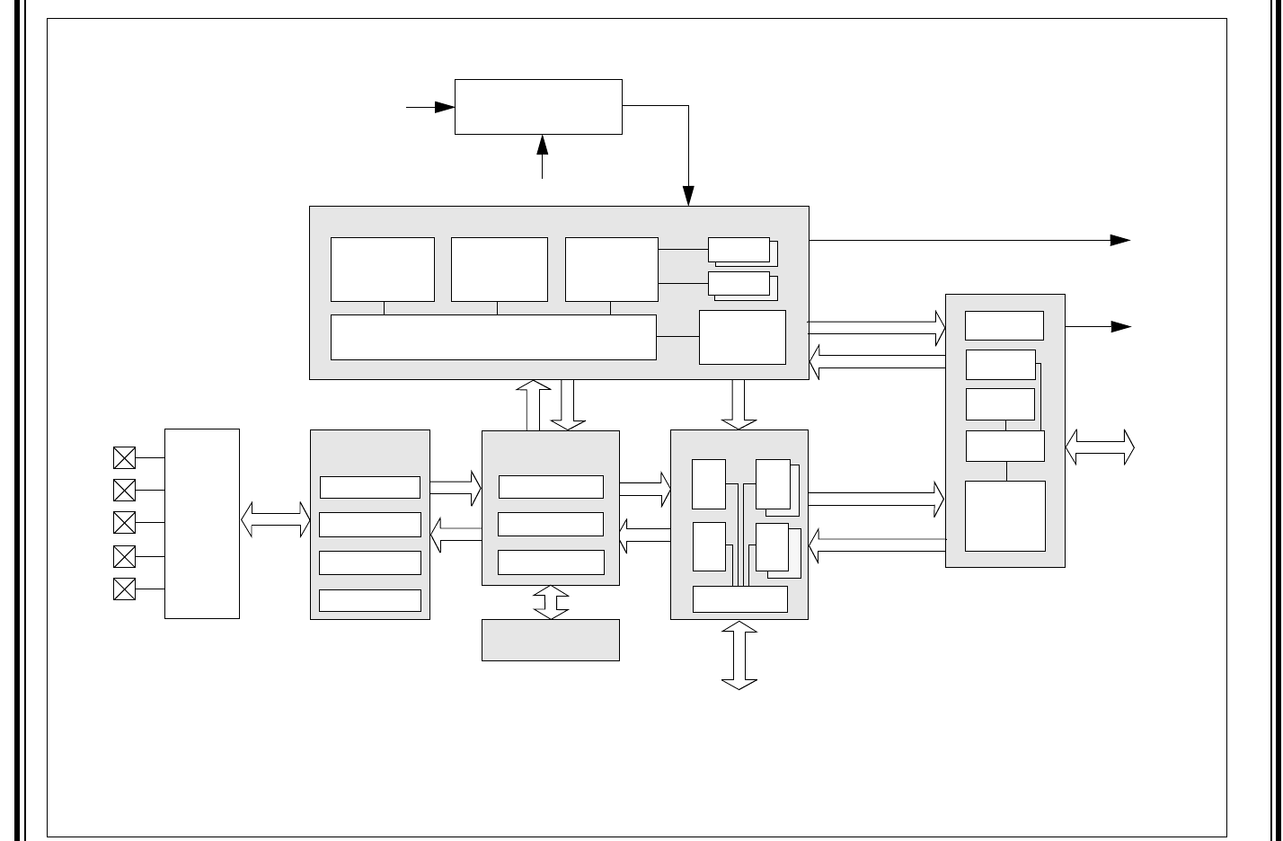
PIC32MZ Embedded Connectivity with Floating Point Unit (EF) Family
DS60001320B-page 200 Preliminary 2015 Microchip Technology Inc.
FIGURE 11-1: PIC32MZ EF FAMILY USB INTERFACE DIAGRAM
Endpoint Control
EP0
Control
Host
EPO
Control
Function
EP1 - EP7
Control
Host
Transaction
Scheduler
Interrupt
Control
EP Reg
Decoder
Common
Regs
Cycle
Control
FIFO
Decoder
RAM
Packet
Encode/Decode
Link Power
Management
Combine Endpoints
Packet Encode
Packet Decode
CRC Gen/Check
Data Sync
HS Negotiation
HNP/SRP
Timers
USB 2.0
HS PHY
UTM
Synchronization
DMA
Requests
Interrupts
System Bus
Slave mode
Transmit
Receive
RAM Controller
RX
Buff
TX
Buff
Cycle Control
RX
Buff
TX
Buff
USB PLL
POSC
(12 MHz or 24 MHz only)
UPLLFSEL
USBCLK
D+
D-
USBID
VUSB3V3
VBUS

2015 Microchip Technology Inc. Preliminary DS60001320B-page 201
PIC32MZ Embedded Connectivity with Floating Point Unit (EF) Family
11.1 USB OTG Control Registers
TABLE 11-1: USB REGISTER MAP 1
Virtual Address
(BF8E_#)
Register
Name
Bit Range
Bits
All Resets
31/15 30/14 29/13 28/12 27/11 26/10 25/9 24/8 23/7 22/6 21/5 20/4 19/3 18/2 17/1 16/0
3000 USBCSR0
31:16 — — — — — — — — EP7TXIF EP6TXIF EP5TXIF EP4TXIF EP3TXIF EP2TXIF EP1TXIF EP0IF 0000
15:0 ISOUPD(1) SOFT
CONN(1) HSEN HSMODE RESET RESUME SUSP
MODE SUSPEN —FUNC<6:0>(1)
2000
—(2) —(2) —(2) —(2) —(2) —(2) —(2) —(2) —(2)
3004 USBCSR1 31:16 — — — — — — — — EP7TXIE EP6TXIE EP5TXIE EP4TXIE EP3TXIE EP2TXIE EP1TXIE EP0IE 00FF
15:0 — — — — — — — — EP7RXIF EP6RXIF EP5RXIF EP4RXIF EP3RXIF EP2RXIF EP1RXIF —0000
3008 USBCSR2 31:16 VBUSERRIE SESSRQIE DISCONIE CONNIE SOFIE RESETIE RESUMEIE SUSPIE VBUSERRIF SESSREQIF DISCONIF CONNIF SOFIF RESETIF RESUMEIF SUSPIF 0600
15:0 — — — — — — — — EP7RXIE EP6RXIE EP5RXIE EP4RXIE EP3RXIE EP2RXIE EP1RXIE —00FE
300C USBCSR3 31:16 FORCEHST FIFOACC FORCEFS FORCEHS PACKET TESTK TESTJ NAK — — — — ENDPOINT<3:0> 0000
15:0 — — — — — RFRMNUM<10:0> 0000
3010 USB
IE0CSR0(3) 31:16 — — — —
—(1) —(1) —(1)
FLSHFIFO
SVC
SETEND(1) SVCRPR(1) SEND
STALL(1) SETUP
END(1) DATAEND(1) SENT
STALL(1) TXPKT
RDY RXPKT
RDY
0000
DISPING(2) DTWREN(2) DATA
TGGL(2) NAK
TMOUT(2) STATPKT(2) REQPKT(2) ERROR(2) SETUP
PKT(2) RXSTALL(2) 0000
15:0 — — — — — — — — — — — — — — — — 0000
3018 USB
IE0CSR2(3) 31:16 — — — NAKLIM<4:0>(2) SPEED<1:0>(2) — — — — — — 0000
15:0 — — — — — — — — — RXCNT<6:0> 0000
301C USB
IE0CSR3(3) 31:16 MPRXEN MPTXEN BIGEND HBRXEN HBTXEN DYNFIFOS SOFTCONE UTMIDWID — — — — — — — — xx00
15:0 — — — — — — — — — — — — — — — — 0000
3010 USB
IENCSR0(4) 31:16 AUTOSET
ISO(1)
MODE DMA
REQEN FRC
DATTG DMA
REQMD
—(1) —(1) INCOMP
TX(1)
CLRDT
SENT
STALL(1) SEND
STALL(1)
FLUSH
UNDER
RUN(1)
FIFONE TXPKT
RDY
0000
—DTWREN(2) DATA
TGGL(2) NAK
TMOUT(2) RXSTALL(2) SETUPPKT(2) ERROR(2) 0000
15:0 MULT<4:0> TXMAXP<10:0> 0000
3014 USB
IENCSR1(4) 31:16 AUTOCLR
ISO(1)
DMA
REQEN
DISNYET(1)
DMA
REQMD
—(1) —(1)
INCOM
PRX CLRDT
SENTSTALL(1) SENDSTALL(1)
FLUSH
DATAERR(1) OVERRUN(1)
FIFOFULL RXPKT
RDY
0000
AUTORQ(2) PIDERR(2) DATA
TWEN(2) DATA
TGGL(2) RXSTALL(2) REQPKT(2) DERR-
NAKT(1) ERROR(2) 0000
15:0 MULT<4:0> RXMAXP<10:0> 0000
3018 USB
IENCSR2(4) 31:16 TXINTERV<7:0>(2) SPEED<1:0>(2) PROTOCOL<1:0> TEP<3:0> 0000
15:0 — — RXCNT<13:0> 0000
301C
USB
IENCSR3
(1,3)
31:16 RXFIFOSZ<3:0> TXFIFOSZ<3:0> — — — — — — — — 0000
15:0 RXINTERV<7:0> SPEED<1:0> PROTOCOL<1:0> TEP<3:0> 0000
3020 USB
FIFO0
31:16 DATA<31:16> 0000
15:0 DATA<15:0> 0000
3024 USB
FIFO1
31:16 DATA<31:16> 0000
15:0 DATA<15:0> 0000
Legend: x = unknown value on Reset; — = unimplemented, read as ‘0’. Reset values are shown in hexadecimal.
Note 1: Device mode.
2: Host mode.
3: Definition for Endpoint 0 (ENDPOINT<3:0> (USBCSR<19:16>) = 0).
4: Definition for Endpoints 1-7 (ENDPOINT<3:0> (USBCSR<19:16>) = 1 through 7).

PIC32MZ Embedded Connectivity with Floating Point Unit (EF) Family
DS60001320B-page 202 Preliminary 2015 Microchip Technology Inc.
3028 USB
FIFO2
31:16 DATA<31:16> 0000
15:0 DATA<15:0> 0000
302C USB
FIFO3
31:16 DATA<31:16> 0000
15:0 DATA<15:0> 0000
3030 USB
FIFO4
31:16 DATA<31:16> 0000
15:0 DATA<15:0> 0000
3034 USB
FIFO5
31:16 DATA<31:16> 0000
15:0 DATA<15:0> 0000
3038 USB
FIFO6
31:16 DATA<31:16> 0000
15:0 DATA<15:0> 0000
303C USB
FIFO7
31:16 DATA<31:16> 0000
15:0 DATA<15:0> 0000
3060 USBOTG 31:16 — — — RXDPB RXFIFOSZ<3:0> — — — TXDPB TXFIFOSZ<3:0> 0000
15:0 — — — — — — TXEDMA RXEDMA BDEV FSDEV LSDEV VBUS<1:0> HOSTMODE HOSTREQ SESSION 0080
3064 USB
FIFOA
31:16 — — — RXFIFOAD<12:0> 0000
15:0 — — — TXFIFOAD<12:0> 0000
306C USB
HWVER
31:16 — — — — — — — — — — — — — — — — 0000
15:0 RC VERMAJOR<4:0> VERMINOR<9:0> 0800
3078 USB
INFO
31:16 VPLEN<7:0> WTCON<3:0> WTID<3:0> 3C5C
15:0 DMACHANS<3:0> RAMBITS<3:0> RXENDPTS<3:0> TXENDPTS<3:0> 8C77
307C USB
EOFRST
31:16 — — — — — — NRSTX NRST LSEOF<7:0> 0072
15:0 FSEOF<7:0> HSEOF<7:0> 7780
3080 USB
E0TXA
31:16 —TXHUBPRT<6:0> MULTTRAN TXHUBADD<6:0> 0000
15:0 — — — — — — — — — TXFADDR<6:0> 0000
3084 USB
E0RXA
31:16 —RXHUBPRT<6:0> MULTTRAN RXHUBADD<6:0> 0000
15:0 — — — — — — — — — — — — — — — — 0000
3088 USB
E1TXA
31:16 —TXHUBPRT<6:0> MULTTRAN TXHUBADD<6:0> 0000
15:0 — — — — — — — — — TXFADDR<6:0> 0000
308C USB
E1RXA
31:16 —RXHUBPRT<6:0> MULTTRAN RXHUBADD<6:0> 0000
15:0 — — — — — — — — — RXFADDR<6:0> 0000
3090 USB
E2TXA
31:16 —TXHUBPRT<6:0> MULTTRAN TXHUBADD<6:0> 0000
15:0 — — — — — — — — — TXFADDR<6:0> 0000
3094 USB
E2RXA
31:16 —RXHUBPRT<6:0> MULTTRAN RXHUBADD<6:0> 0000
15:0 — — — — — — — — — RXFADDR<6:0> 0000
3098 USB
E3TXA
31:16 —TXHUBPRT<6:0> MULTTRAN TXHUBADD<6:0> 0000
15:0 — — — — — — — — — TXFADDR<6:0> 0000
TABLE 11-1: USB REGISTER MAP 1 (CONTINUED)
Virtual Address
(BF8E_#)
Register
Name
Bit Range
Bits
All Resets
31/15 30/14 29/13 28/12 27/11 26/10 25/9 24/8 23/7 22/6 21/5 20/4 19/3 18/2 17/1 16/0
Legend: x = unknown value on Reset; — = unimplemented, read as ‘0’. Reset values are shown in hexadecimal.
Note 1: Device mode.
2: Host mode.
3: Definition for Endpoint 0 (ENDPOINT<3:0> (USBCSR<19:16>) = 0).
4: Definition for Endpoints 1-7 (ENDPOINT<3:0> (USBCSR<19:16>) = 1 through 7).

2015 Microchip Technology Inc. Preliminary DS60001320B-page 203
PIC32MZ Embedded Connectivity with Floating Point Unit (EF) Family
309C USB
E3RXA
31:16 —RXHUBPRT<6:0> MULTTRAN RXHUBADD<6:0> 0000
15:0 — — — — — — — — — RXFADDR<6:0> 0000
30A0 US
BE4TXA
31:16 —TXHUBPRT<6:0> MULTTRAN TXHUBADD<6:0> 0000
15:0 — — — — — — — — — TXFADDR<6:0> 0000
30A4 USB
E4RXA
31:16 —RXHUBPRT<6:0> MULTTRAN RXHUBADD<6:0> 0000
15:0 — — — — — — — — — RXFADDR<6:0> 0000
30A8 USB
E5TXA
31:16 —TXHUBPRT<6:0> MULTTRAN TXHUBADD<6:0> 0000
15:0 — — — — — — — — — TXFADDR<6:0> 0000
30AC USB
E5RXA
31:16 —RXHUBPRT<6:0> MULTTRAN RXHUBADD<6:0> 0000
15:0 — — — — — — — — — RXFADDR<6:0> 0000
30B0 USB
E6TXA
31:16 —TXHUBPRT<6:0> MULTTRAN TXHUBADD<6:0> 0000
15:0 — — — — — — — — — TXFADDR<6:0> 0000
30B4 USB
E6RXA
31:16 —RXHUBPRT<6:0> MULTTRAN RXHUBADD<6:0> 0000
15:0 — — — — — — — — — RXFADDR<6:0> 0000
30B8 USB
E7TXA
31:16 —TXHUBPRT<6:0> MULTTRAN TXHUBADD<6:0> 0000
15:0 — — — — — — — — — TXFADDR<6:0> 0000
30BC USB
E7RXA
31:16 —RXHUBPRT<6:0> MULTTRAN RXHUBADD<6:0> 0000
15:0 — — — — — — — — — RXFADDR<6:0> 0000
3100 USB
E0CSR0
31:16 Indexed by the same bits in USBIE0CSR0 0000
15:0 0000
3108 USB
E0CSR2
31:16 Indexed by the same bits in USBIE0CSR2 0000
15:0 0000
310C USB
E0CSR3
31:16 Indexed by the same bits in USBIE0CSR3 0000
15:0 0000
3110 USB
E1CSR0
31:16 Indexed by the same bits in USBIE1CSR0 0000
15:0 0000
3114 USB
E1CSR1
31:16 Indexed by the same bits in USBIE1CSR1 0000
15:0 0000
3118 USB
E1CSR2
31:16 Indexed by the same bits in USBIE1CSR2 0000
15:0 0000
311C USB
E1CSR3
31:16 Indexed by the same bits in USBIE1CSR3 0000
15:0 0000
3120 USB
E2CSR0
31:16 Indexed by the same bits in USBIE2CSR0 0000
15:0 0000
3124 USB
E2CSR1
31:16 Indexed by the same bits in USBIE2CSR1 0000
15:0 0000
TABLE 11-1: USB REGISTER MAP 1 (CONTINUED)
Virtual Address
(BF8E_#)
Register
Name
Bit Range
Bits
All Resets
31/15 30/14 29/13 28/12 27/11 26/10 25/9 24/8 23/7 22/6 21/5 20/4 19/3 18/2 17/1 16/0
Legend: x = unknown value on Reset; — = unimplemented, read as ‘0’. Reset values are shown in hexadecimal.
Note 1: Device mode.
2: Host mode.
3: Definition for Endpoint 0 (ENDPOINT<3:0> (USBCSR<19:16>) = 0).
4: Definition for Endpoints 1-7 (ENDPOINT<3:0> (USBCSR<19:16>) = 1 through 7).

PIC32MZ Embedded Connectivity with Floating Point Unit (EF) Family
DS60001320B-page 204 Preliminary 2015 Microchip Technology Inc.
3128 USB
E2CSR2
31:16 Indexed by the same bits in USBIE2CSR2 0000
15:0 0000
312C USB
E2CSR3
31:16 Indexed by the same bits in USBIE2CSR3 0000
15:0 0000
3130 USB
E3CSR0
31:16 Indexed by the same bits in USBIE3CSR0 0000
15:0 0000
3134 USB
E3CSR1
31:16 Indexed by the same bits in USBIE3CSR1 0000
15:0 0000
3138 USB
E3CSR2
31:16 Indexed by the same bits in USBIE3CSR2 0000
15:0 0000
313C USB
E3CSR3
31:16 Indexed by the same bits in USBIE3CSR3 0000
15:0 0000
3140 USB
E4CSR0
31:16 Indexed by the same bits in USBIE4CSR0 0000
15:0 0000
3144 USB
E4CSR1
31:16 Indexed by the same bits in USBIE4CSR1 0000
15:0 0000
3148 USB
E4CSR2
31:16 Indexed by the same bits in USBIE4CSR2 0000
15:0 0000
314C USB
E4CSR3
31:16 Indexed by the same bits in USBIE4CSR3 0000
15:0 0000
3150 USB
E5CSR0
31:16 Indexed by the same bits in USBIE5CSR0 0000
15:0 0000
3154 USB
E5CSR1
31:16 Indexed by the same bits in USBIE5CSR1 0000
15:0 0000
3158 USB
E5CSR2
31:16 Indexed by the same bits in USBIE5CSR2 0000
15:0 0000
315C USB
E5CSR3
31:16 Indexed by the same bits in USBIE5CSR3 0000
15:0 0000
3160 USB
E6CSR0
31:16 Indexed by the same bits in USBIE6CSR0 0000
15:0 0000
3164 USB
E6CSR1
31:16 Indexed by the same bits in USBIE6CSR1 0000
15:0 0000
3168 USB
E6CSR2
31:16 Indexed by the same bits in USBIE6CSR2 0000
15:0 0000
316C USB
E6CSR3
31:16 Indexed by the same bits in USBIE6CSR3 0000
15:0 0000
TABLE 11-1: USB REGISTER MAP 1 (CONTINUED)
Virtual Address
(BF8E_#)
Register
Name
Bit Range
Bits
All Resets
31/15 30/14 29/13 28/12 27/11 26/10 25/9 24/8 23/7 22/6 21/5 20/4 19/3 18/2 17/1 16/0
Legend: x = unknown value on Reset; — = unimplemented, read as ‘0’. Reset values are shown in hexadecimal.
Note 1: Device mode.
2: Host mode.
3: Definition for Endpoint 0 (ENDPOINT<3:0> (USBCSR<19:16>) = 0).
4: Definition for Endpoints 1-7 (ENDPOINT<3:0> (USBCSR<19:16>) = 1 through 7).

2015 Microchip Technology Inc. Preliminary DS60001320B-page 205
PIC32MZ Embedded Connectivity with Floating Point Unit (EF) Family
3170 USB
E7CSR0
31:16 Indexed by the same bits in USBIE7CSR0 0000
15:0 0000
3174 USB
E7CSR1
31:16 Indexed by the same bits in USBIE7CSR1 0000
15:0 0000
3178 USB
E7CSR2
31:16 Indexed by the same bits in USBIE7CSR2 0000
15:0 0000
317C USB
E7CSR3
31:16 Indexed by the same bits in USBIE7CSR3 0000
15:0 0000
3200 USB
DMAINT
31:16 — — — — — — — — — — — — — — — — 0000
15:0 — — — — — — — — DMA8IF DMA7IF DMA6IF DMA5IF DMA4IF DMA3IF DMA2IF DMA1IF 0000
3204 USB
DMA1C
31:16 — — — — — — — — — — — — — — — — 0000
15:0 — — — — — DMABRSTM<1:0> DMAERR DMAEP<3:0> DMAIE DMAMODE DMADIR DMAEN 0000
3208 USB
DMA1A
31:16 DMAADDR<31:16> 0000
15:0 DMAADDR<15:0> 0000
320C USB
DMA1N
31:16 DMACOUNT<31:16> 0000
15:0 DMACOUNT<15:0> 0000
3214 USB
DMA2C
31:16 — — — — — — — — — — — — — — — — 0000
15:0 — — — — — DMABRSTM<1:0> DMAERR DMAEP<3:0> DMAIE DMAMODE DMADIR DMAEN 0000
3218 USB
DMA2A
31:16 DMAADDR<31:16> 0000
15:0 DMAADDR<15:0> 0000
321C USB
DMA2N
31:16 DMACOUNT<31:16> 0000
15:0 DMACOUNT<15:0> 0000
3224 USB
DMA3C
31:16 — — — — — — — — — — — — — — — — 0000
15:0 — — — — — DMABRSTM<1:0> DMAERR DMAEP<3:0> DMAIE DMAMODE DMADIR DMAEN 0000
3228 USB
DMA3A
31:16 DMAADDR<31:16> 0000
15:0 DMAADDR<15:0> 0000
322C USB
DMA3N
31:16 DMACOUNT<31:16> 0000
15:0 DMACOUNT<15:0> 0000
3234 USB
DMA4C
31:16 — — — — — — — — — — — — — — — — 0000
15:0 — — — — — DMABRSTM<1:0> DMAERR DMAEP<3:0> DMAIE DMAMODE DMADIR DMAEN 0000
3238 USB
DMA4A
31:16 DMAADDR<31:16> 0000
15:0 DMAADDR<15:0> 0000
323C USB
DMA4N
31:16 DMACOUNT<31:16> 0000
15:0 DMACOUNT<15:0> 0000
3244 USB
DMA5C
31:16 — — — — — — — — — — — — — — — — 0000
15:0 — — — — — DMABRSTM<1:0> DMAERR DMAEP<3:0> DMAIE DMAMODE DMADIR DMAEN 0000
TABLE 11-1: USB REGISTER MAP 1 (CONTINUED)
Virtual Address
(BF8E_#)
Register
Name
Bit Range
Bits
All Resets
31/15 30/14 29/13 28/12 27/11 26/10 25/9 24/8 23/7 22/6 21/5 20/4 19/3 18/2 17/1 16/0
Legend: x = unknown value on Reset; — = unimplemented, read as ‘0’. Reset values are shown in hexadecimal.
Note 1: Device mode.
2: Host mode.
3: Definition for Endpoint 0 (ENDPOINT<3:0> (USBCSR<19:16>) = 0).
4: Definition for Endpoints 1-7 (ENDPOINT<3:0> (USBCSR<19:16>) = 1 through 7).

PIC32MZ Embedded Connectivity with Floating Point Unit (EF) Family
DS60001320B-page 206 Preliminary 2015 Microchip Technology Inc.
3248 USB
DMA5A
31:16 DMAADDR<31:16> 0000
15:0 DMAADDR<15:0> 0000
324C USB
DMA5N
31:16 DMACOUNT<31:16> 0000
15:0 DMACOUNT<15:0> 0000
3254 USB
DMA6C
31:16 — — — — — — — — — — — — — — — — 0000
15:0 — — — — — DMABRSTM<1:0> DMAERR DMAEP<3:0> DMAIE DMAMODE DMADIR DMAEN 0000
3258 USB
DMA6A
31:16 DMAADDR<31:16> 0000
15:0 DMAADDR<15:0> 0000
325C USB
DMA6N
31:16 DMACOUNT<31:16> 0000
15:0 DMACOUNT<15:0> 0000
3264 USB
DMA7C
31:16 — — — — — — — — — — — — — — — — 0000
15:0 — — — — — DMABRSTM<1:0> DMAERR DMAEP<3:0> DMAIE DMAMODE DMADIR DMAEN 0000
3268 USB
DMA7A
31:16 DMAADDR<31:16> 0000
15:0 DMAADDR<15:0> 0000
326C USB
DMA7N
31:16 DMACOUNT<31:16> 0000
15:0 DMACOUNT<15:0> 0000
3274 USB
DMA8C
31:16 — — — — — — — — — — — — — — — — 0000
15:0 — — — — — DMABRSTM<1:0> DMAERR DMAEP<3:0> DMAIE DMAMODE DMADIR DMAEN 0000
3278 USB
DMA8A
31:16 DMAADDR<31:16> 0000
15:0 DMAADDR<15:0> 0000
327C USB
DMA8N
31:16 DMACOUNT<31:16> 0000
15:0 DMACOUNT<15:0> 0000
3304 USB
E1RPC
31:16 — — — — — — — — — — — — — — — — 0000
15:0 RQPKTCNT<15:0> 0000
3308 USB
E2RPC
31:16 — — — — — — — — — — — — — — — — 0000
15:0 RQPKTCNT<15:0> 0000
330C USB
E3RPC
31:16 — — — — — — — — — — — — — — — — 0000
15:0 RQPKTCNT<15:0> 0000
3310 USB
E4RPC
31:16 — — — — — — — — — — — — — — — — 0000
15:0 RQPKTCNT<15:0> 0000
3314 USB
E5RPC
31:16 — — — — — — — — — — — — — — — — 0000
15:0 RQPKTCNT<15:0> 0000
3318 USB
E6RPC
31:16 — — — — — — — — — — — — — — — — 0000
15:0 RQPKTCNT<15:0> 0000
331C USB
E7RPC
31:16 — — — — — — — — — — — — — — — — 0000
15:0 RQPKTCNT<15:0> 0000
TABLE 11-1: USB REGISTER MAP 1 (CONTINUED)
Virtual Address
(BF8E_#)
Register
Name
Bit Range
Bits
All Resets
31/15 30/14 29/13 28/12 27/11 26/10 25/9 24/8 23/7 22/6 21/5 20/4 19/3 18/2 17/1 16/0
Legend: x = unknown value on Reset; — = unimplemented, read as ‘0’. Reset values are shown in hexadecimal.
Note 1: Device mode.
2: Host mode.
3: Definition for Endpoint 0 (ENDPOINT<3:0> (USBCSR<19:16>) = 0).
4: Definition for Endpoints 1-7 (ENDPOINT<3:0> (USBCSR<19:16>) = 1 through 7).

2015 Microchip Technology Inc. Preliminary DS60001320B-page 207
PIC32MZ Embedded Connectivity with Floating Point Unit (EF) Family
3340 USB
DPBFD
31:16 — — — — — — — — EP7TXD EP6TXD EP5TXD EP4TXD EP3TXD EP2TXD EP1TXD —0000
15:0 — — — — — — — — EP7RXD EP6RXD EP5RXD EP4RXD EP3RXD EP2RXD EP1RXD —0000
3344 USB
TMCON1
31:16 THHSRTN<15:0> 05E6
15:0 TUCH<15:0> 4074
3348 USB
TMCON2
31:16 — — — — — — — — — — — — — — — — 0000
15:0 — — — — — — — — — — — — THSBT<3:0> 0000
3360 USB
LPMR1
31:16 — — LPM
ERRIE LPM
RESIE LPMACKIE LPMNYIE LPMSTIE LPMTOIE — — — LPMNAK(1) LPMEN<1:0> LPMRES LPMXMT 0000
—(2) —(2) —(2) 0000
15:0 ENDPOINT<3:0> — — — RMTWAK HIRD<3:0> LNKSTATE<3:0> 0000
3364 USB
LPMR2
31:16 — — — — — — — — — — — — — — — — 0000
15:0 —LPMFADDR<6:0> — — LPMERR(1)
LPMRES LPMNC LPMACK LPMNY LPMST 0000
—(2) 0000
TABLE 11-1: USB REGISTER MAP 1 (CONTINUED)
Virtual Address
(BF8E_#)
Register
Name
Bit Range
Bits
All Resets
31/15 30/14 29/13 28/12 27/11 26/10 25/9 24/8 23/7 22/6 21/5 20/4 19/3 18/2 17/1 16/0
Legend: x = unknown value on Reset; — = unimplemented, read as ‘0’. Reset values are shown in hexadecimal.
Note 1: Device mode.
2: Host mode.
3: Definition for Endpoint 0 (ENDPOINT<3:0> (USBCSR<19:16>) = 0).
4: Definition for Endpoints 1-7 (ENDPOINT<3:0> (USBCSR<19:16>) = 1 through 7).
TABLE 11-2: USB REGISTER MAP 2
Virtual Address
(BF88_#)
Register
Name
Bit Range
Bits
All Resets
31/15 30/14 29/13 28/12 27/11 26/10 25/9 24/8 23/7 22/6 21/5 20/4 19/3 18/2 17/1 16/0
4000 USB
CRCON
31:16 —————USBIF USBRF USBWKUP — — — — — — — — 0100
15:0 ——————USB
IDOVEN USB
IDVAL PHYIDEN VBUS
MONEN ASVAL
MONEN BSVAL
MONEN SEND
MONEN USBIE USBRIE USB
WKUPEN 8000
Legend: x = unknown value on Reset; — = unimplemented, read as ‘0’. Reset values are shown in hexadecimal.

PIC32MZ Embedded Connectivity with Floating Point Unit (EF) Family
DS60001320B-page 208 Preliminary 2015 Microchip Technology Inc.
REGISTER 11-1: USBCSR0: USB CONTROL STATUS REGISTER 0
Bit
Range Bit
31/23/15/7 Bit
30/22/14/6 Bit
29/21/13/5 Bit
28/20/12/4 Bit
27/19/11/3 Bit
26/18/10/2 Bit
25/17/9/1 Bit
24/16/8/0
31:24 U-0 U-0 U-0 U-0 U-0 U-0 U-0 U-0
— — — — — — — —
23:16 R-0, HS R-0, HS R-0, HS R-0, HS R-0, HS R-0, HS R-0, HS R-0, HS
EP7TXIF EP6TXIF EP5TXIF EP4TXIF EP3TXIF EP2TXIF EP1TXIF EP0IF
15:8
R/W-0 R/W-0 R/W-1 R-0, HS R-0 R/W-0 R-0, HC R/W-0
ISOUPD SOFTCONN HSEN HSMODE RESET RESUME SUSPMODE SUSPEN
— —
7:0
U-0 R/W-0 R/W-0 R/W-0 R/W-0 R/W-0 R/W-0 R/W-0
—FUNC<6:0>
— — — — — — —
Legend: HS = Hardware Set HC = Hardware Cleared
R = Readable bit W = Writable bit U = Unimplemented bit, read as ‘0’
-n = Value at POR ‘1’ = Bit is set ‘0’ = Bit is cleared x = Bit is unknown
bit 31-24 Unimplemented: Read as ‘0’
bit 23-17 EP7TXIF:EP1TXIF: Endpoint ‘n’ TX Interrupt Flag bit
1 = Endpoint has a transmit interrupt to be serviced
0 = No interrupt event
bit 16 EP0IF: Endpoint 0 Interrupt bit
1 = Endpoint 0 has an interrupt to be serviced
0 = No interrupt event
All EPxTX and EP0 bits are cleared when the byte is read. Therefore, these bits must be read independently
from the remaining bits in this register to avoid accidental clearing.
bit 15 ISOUPD: ISO Update bit (Device mode only; unimplemented in Host mode)
1 = USB module will wait for a SOF token from the time TXPKTRDY is set before sending the packet
0 = No change in behavior
This bit only affects endpoints performing isochronous transfers when in Device mode. This bit is
unimplemented in Host mode.
bit 14 SOFTCONN: Soft Connect/Disconnect Feature Selection bit
1 = The USB D+/D- lines are enabled and active
0 = The USB D+/D- lines are disabled and are tri-stated
This bit is only available in Device mode.
bit 13 HSEN: Hi-Speed Enable bit
1 = The USB module will negotiate for Hi-Speed mode when the device is reset by the hub
0 = Module only operates in Full-Speed mode
bit 12 HSMODE: Hi-Speed Mode Status bit
1 = Hi-Speed mode successfully negotiated during USB reset
0 = Module is not in Hi-Speed mode
In Device mode, this bit becomes valid when a USB reset completes. In Host mode, it becomes valid when
the RESET bit is cleared.
bit 11 RESET: Module Reset Status bit
1 = Reset signaling is present on the bus
0 = Normal module operation
In Device mode, this bit is read-only. In Host mode, this bit is read/write.

2015 Microchip Technology Inc. Preliminary DS60001320B-page 209
PIC32MZ Embedded Connectivity with Floating Point Unit (EF) Family
bit 10 RESUME: Resume from Suspend control bit
1 = Generate Resume signaling when the device is in Suspend mode
0 = Stop Resume signaling
In Device mode, the software should clear this bit after 10 ms (a maximum of 15 ms) to end Resume signal-
ing. In Host mode, the software should clear this bit after 20 ms.
bit 9 SUSPMODE: Suspend Mode status bit
1 = The USB module is in Suspend mode
0 = The USB module is in Normal operations
This bit is read-only in Device mode. In Host mode, it can be set by software, and is cleared by hardware.
bit 8 SUSPEN: Suspend Mode Enable bit
1 = Suspend mode is enabled
0 = Suspend mode is not enabled
bit 7 Unimplemented: Read as ‘0’
bit 6-0 FUNC<6:0>: Device Function Address bits
These bits are only available in Device mode. This field is written with the address received through a
SET_ADDRESS command, which will then be used for decoding the function address in subsequent token
packets.
REGISTER 11-1: USBCSR0: USB CONTROL STATUS REGISTER 0 (CONTINUED)

PIC32MZ Embedded Connectivity with Floating Point Unit (EF) Family
DS60001320B-page 210 Preliminary 2015 Microchip Technology Inc.
REGISTER 11-2: USBCSR1: USB CONTROL STATUS REGISTER 1
Bit
Range Bit
31/23/15/7 Bit
30/22/14/6 Bit
29/21/13/5 Bit
28/20/12/4 Bit
27/19/11/3 Bit
26/18/10/2 Bit
25/17/9/1 Bit
24/16/8/0
31:24 U-0 U-0 U-0 U-0 U-0 U-0 U-0 U-0
— — — — — — — —
23:16 R/W-1 R/W-1 R/W-1 R/W-1 R/W-1 R/W-1 R/W-1 R/W-0
EP7TXIE EP6TXIE EP5TXIE EP4TXIE EP3TXIE EP2TXIE EP1TXIE EP0IE
15:8 U-0 U-0 U-0 U-0 U-0 U-0 U-0 U-0
— — — — — — — —
7:0 R-0, HS R-0, HS R-0, HS R-0, HS R-0, HS R-0, HS R-0, HS U-0
EP7RXIF EP6RXIF EP5RXIF EP4RXIF EP3RXIF EP2RXIF EP1RXIF —
Legend:
R = Readable bit W = Writable bit U = Unimplemented bit, read as ‘0’
-n = Value at POR ‘1’ = Bit is set ‘0’ = Bit is cleared x = Bit is unknown
bit 31-24 Unimplemented: Read as ‘0’
bit 23-17 EP7TXIE:EP1TXIE: Endpoint ‘n’ Transmit Interrupt Enable bits
1 = Endpoint Transmit interrupt events are enabled
0 = Endpoint Transmit interrupt events are not enabled
bit 16 EP0IE: Endpoint 0 Interrupt Enable bit
1 = Endpoint 0 interrupt events are enabled
0 = Endpoint 0 interrupt events are not enabled
bit 15-8 Unimplemented: Read as ‘0’
bit 7-1 EP7RXIF:EP1RXIF: Endpoint ‘n’ RX Interrupt bit
1 = Endpoint has a receive event to be serviced
0 = No interrupt event
bit 0 Unimplemented: Read as ‘0’

2015 Microchip Technology Inc. Preliminary DS60001320B-page 211
PIC32MZ Embedded Connectivity with Floating Point Unit (EF) Family
REGISTER 11-3: USBCSR2: USB CONTROL STATUS REGISTER 2
Bit
Range Bit
31/23/15/7 Bit
30/22/14/6 Bit
29/21/13/5 Bit
28/20/12/4 Bit
27/19/11/3 Bit
26/18/10/2 Bit
25/17/9/1 Bit
24/16/8/0
31:24 R/W-0 R/W-0 R/W-0 R/W-0 R/W-0 R/W-1 R/W-1 R/W-0
VBUSERRIE SESSRQIE DISCONIE CONNIE SOFIE RESETIE RESUMEIE SUSPIE
23:16 R-0, HS R-0, HS R-0, HS R-0, HS R-0, HS R-0, HS R-0, HS R-0, HS
VBUSERRIF SESSRQIF DISCONIF CONNIF SOFIF RESETIF RESUMEIF SUSPIF
15:8 U-0 U-0 U-0 U-0 U-0 U-0 U-0 U-0
— — — — — — — —
7:0 R/W-1 R/W-1 R/W-1 R/W-1 R/W-1 R/W-1 R/W-1 U-0
EP7RXIE EP6RXIE EP5RXIE EP4RXIE EP3RXIE EP2RXIE EP1RXIE —
Legend: HS = Hardware Set
R = Readable bit W = Writable bit U = Unimplemented bit, read as ‘0’
-n = Value at POR ‘1’ = Bit is set ‘0’ = Bit is cleared x = Bit is unknown
bit 31 VBUSERRIE: VBUS Error Interrupt Enable bit
1 =V
BUS error interrupt is enabled
0 =V
BUS error interrupt is disabled
bit 30 SESSRQIE: Session Request Interrupt Enable bit
1 = Session request interrupt is enabled
0 = Session request interrupt is disabled
bit 29 DISCONIE: Device Disconnect Interrupt Enable bit
1 = Device disconnect interrupt is enabled
0 = Device disconnect interrupt is disabled
bit 28 CONNIE: Device Connection Interrupt Enable bit
1 = Device connection interrupt is enabled
0 = Device connection interrupt is disabled
bit 27 SOFIE: Start of Frame Interrupt Enable bit
1 = Start of Frame event interrupt is enabled
0 = Start of Frame event interrupt is disabled
bit 26 RESETIE: Reset/Babble Interrupt Enable bit
1 = Interrupt when reset (Device mode) or Babble (Host mode) is enabled
0 = Reset/Babble interrupt is disabled
bit 25 RESUMEIE: Resume Interrupt Enable bit
1 = Resume signaling interrupt is enabled
0 = Resume signaling interrupt is disabled
bit 24 SUSPIE: Suspend Interrupt Enable bit
1 = Suspend signaling interrupt is enabled
0 = Suspend signaling interrupt is disabled
bit 23 VBUSERRIF: VBUS Error Interrupt bit
1 =V
BUS has dropped below the VBUS valid threshold during a session
0 = No interrupt
bit 22 SESSRQIF: Session Request Interrupt bit
1 = Session request signaling has been detected
0 = No session request detected
bit 21 DISCONIF: Device Disconnect Interrupt bit
1 =In Host mode, indicates when a device disconnect is detected. In Device mode, indicates when a
session ends.
0 = No device disconnect detected
bit 20 CONNIF: Device Connection Interrupt bit
1 =In Host mode, indicates when a device connection is detected
0 = No device connection detected

PIC32MZ Embedded Connectivity with Floating Point Unit (EF) Family
DS60001320B-page 212 Preliminary 2015 Microchip Technology Inc.
bit 19 SOFIF: Start of Frame Interrupt bit
1 = A new frame has started
0 = No start of frame detected
bit 18 RESETIF: Reset/Babble Interrupt bit
1 =In Host mode, indicates babble is detected. In Device mode, indicates reset signaling is detected on the
bus.
0 = No reset/babble detected
bit 17 RESUMEIF: Resume Interrupt bit
1 = Resume signaling is detected on the bus while USB module is in Suspend mode
0 = No Resume signaling detected
bit 16 SUSPIF: Suspend Interrupt bit
1 = Suspend signaling is detected on the bus (Device mode)
0 = No suspend signaling detected
bit 15-8 Unimplemented: Read as ‘0’
bit 7-1 EP7RXIE:EP1RXIE: Endpoint ‘n’ Receive Interrupt Enable bit
1 = Receive interrupt is enabled for this endpoint
0 = Receive interrupt is not enabled
bit 0 Unimplemented: Read as ‘0’
REGISTER 11-3: USBCSR2: USB CONTROL STATUS REGISTER 2 (CONTINUED)

2015 Microchip Technology Inc. Preliminary DS60001320B-page 213
PIC32MZ Embedded Connectivity with Floating Point Unit (EF) Family
REGISTER 11-4: USBCSR3: USB CONTROL STATUS REGISTER 3
Bit
Range Bit
31/23/15/7 Bit
30/22/14/6 Bit
29/21/13/5 Bit
28/20/12/4 Bit
27/19/11/3 Bit
26/18/10/2 Bit
25/17/9/1 Bit
24/16/8/0
31:24 R/W-0 R/W-0, HC R/W-0 R/W-0 R/W-0 R/W-0 R/W-0 R/W-0
FORCEHST FIFOACC FORCEFS FORCEHS PACKET TESTK TESTJ NAK
23:16 U-0 U-0 U-0 U-0 R/W-0 R/W-0 R/W-0 R/W-0
— — — — ENDPOINT<3:0>
15:8 U-0 U-0 U-0 U-0 U-0 R-0 R-0 R-0
— — — — —RFRMUM<10:8>
7:0 R-0 R-0 R-0 R-0 R-0 R-0 R-0 R-0
RFRMNUM<7:0>
Legend: HC = Hardware Cleared
R = Readable bit W = Writable bit U = Unimplemented bit, read as ‘0’
-n = Value at POR ‘1’ = Bit is set ‘0’ = Bit is cleared x = Bit is unknown
bit 31 FORCEHST: Test Mode Force Host Select bit
1 = Forces USB module into Host mode, regardless of whether it is connected to any peripheral
0 = Normal operation
bit 30 FIFOACC: Test Mode Endpoint 0 FIFO Transfer Force bit
1 = Transfers the packet in the Endpoint 0 TX FIFO to the Endpoint 0 RX FIFO
0 = No transfer
bit 29 FORCEFS: Test mode Force Full-Speed Mode Select bit
This bit is only active if FORCEHST = 1.
1 = Forces USB module into Full-Speed mode. Undefined behavior if FORCEHS = 1.
0 = If FORCEHS = 0, places USB module into Low-Speed mode.
bit 28 FORCEHS: Test mode Force Hi-Speed Mode Select bit
This bit is only active if FORCEHST = 1.
1 = Forces USB module into Hi-Speed mode. Undefined behavior if FORCEFS = 1.
0 = If FORCEFS = 0, places USB module into Low-Speed mode.
bit 27 PACKET: Test_Packet Test Mode Select bit
This bit is only active if module is in Hi-Speed mode.
1 = The USB module repetitively transmits on the bus a 53-byte test packet. Test packet must be loaded
into the Endpoint 0 FIFO before the test mode is entered.
0 = Normal operation
bit 26 TESTK: Test_K Test Mode Select bit
1 = Enters Test_K test mode. The USB module transmits a continuous K on the bus.
0 = Normal operation
This bit is only active if the USB module is in Hi-Speed mode.
bit 25 TESTJ: Test_J Test Mode Select bit
1 = Enters Test_J test mode. The USB module transmits a continuous J on the bus.
0 = Normal operation
This bit is only active if the USB module is in Hi-Speed mode.
bit 24 NAK: Test_SE0_NAK Test Mode Select bit
1 = Enter Test_SE0_NAK test mode. The USB module remains in Hi-Speed mode but responds to any valid
IN token with a NAK
0 = Normal operation
This mode is only active if module is in Hi-Speed mode.
bit 23-20 Unimplemented: Read as ‘0’

PIC32MZ Embedded Connectivity with Floating Point Unit (EF) Family
DS60001320B-page 214 Preliminary 2015 Microchip Technology Inc.
bit 19-16 ENDPOINT<3:0>: Endpoint Registers Select bits
1111 = Reserved
•
•
•
1000 = Reserved
0111 = Endpoint 7
•
•
•
0000 = Endpoint 0
These bits select which endpoint registers are accessed through addresses 3010-301F.
bit 15-11 Unimplemented: Read as ‘0’
bit 10-0 RFRMNUM<10:0>: Last Received Frame Number bits
REGISTER 11-4: USBCSR3: USB CONTROL STATUS REGISTER 3 (CONTINUED)

2015 Microchip Technology Inc. Preliminary DS60001320B-page 215
PIC32MZ Embedded Connectivity with Floating Point Unit (EF) Family
REGISTER 11-5: USBIE0CSR0: USB INDEXED ENDPOINT CONTROL STATUS REGISTER 0
(ENDPOINT 0)
Bit
Range Bit
31/23/15/7 Bit
30/22/14/6 Bit
29/21/13/5 Bit
28/20/12/4 Bit
27/19/11/3 Bit
26/18/10/2 Bit
25/17/9/1 Bit
24/16/8/0
31:24
U-0 U-0 U-0 U-0 R/W-0 R/W-0, HC R/W-0 R/W-0, HC
— — — —
— — — FLSHFIFO
DISPING DTWREN DATATGGL
23:16
R/W-0, HC R/W-0, HC R/W-0, HC R/C-0, HS R/W-0, HS R-0, HS R-0 R-0
SVCSETEND SVCRPR SENDSTALL SETUPEND DATAEND SENTSTALL TXPKTRDY RXPKTRDY
NAKTMOUT STATPKT REQPKT ERROR SETUPPKT RXSTALL
15:8 U-0 U-0 U-0 U-0 U-0 U-0 U-0 U-0
— — — — — — — —
7:0 U-0 U-0 U-0 U-0 U-0 U-0 U-0 U-0
— — — — — — — —
Legend: HC = Hardware Cleared HS = Hardware Set
R = Readable bit W = Writable bit U = Unimplemented bit, read as ‘0’
-n = Value at POR ‘1’ = Bit is set ‘0’ = Bit is cleared x = Bit is unknown
bit 31-28 Unimplemented: Read as ‘0’
bit 27 DISPING: Disable Ping tokens control bit (Host mode)
1 = USB Module will not issue PING tokens in data and status phases of a Hi-Speed Control transfer
0 = Ping tokens are issued
bit 26 DTWREN: Data Toggle Write Enable bit (Host mode)
1 = Enable the current state of the Endpoint 0 data toggle to be written. Automatically cleared.
0 = Disable data toggle write
bit 25 DATATGGL: Data Toggle bit (Host mode)
When read, this bit indicates the current state of the Endpoint 0 data toggle.
If DTWREN = 1, this bit is writable with the desired setting.
If DTWREN = 0, this bit is read-only.
bit 24 FLSHFIFO: Flush FIFO Control bit
1 = Flush the next packet to be transmitted/read from the Endpoint 0 FIFO. The FIFO pointer is reset and
the TXPKTRDY/RXPKTRDY bit is cleared. Automatically cleared when the operation completes. Should
only be used when TXPKTRDY/RXPKTRDY = 1.
0 = No Flush operation
bit 23 SVCSETEND: Clear SETUPEND Control bit (Device mode)
1 = Clear the SETUPEND bit in this register. This bit is automatically cleared.
0 = Do not clear
NAKTMOUT: NAK Time-out Control bit (Host mode)
1 = Endpoint 0 is halted following the receipt of NAK responses for longer than the time set by the
NAKLIM<4:0> bits (USBICSR<28:24>)
0 = Allow the endpoint to continue
bit 22 SVCRPR: Serviced RXPKTRDY Clear Control bit (Device mode)
1 = Clear the RXPKTRDY bit in this register. This bit is automatically cleared.
0 = Do not clear
STATPKT: Status Stage Transaction Control bit (Host mode)
1 = When set at the same time as the TXPKTRDY or REQPKT bit is set, performs a status stage transaction
0 = Do not perform a status stage transaction

PIC32MZ Embedded Connectivity with Floating Point Unit (EF) Family
DS60001320B-page 216 Preliminary 2015 Microchip Technology Inc.
bit 21 SENDSTALL: Send Stall Control bit (Device mode)
1 = Terminate the current transaction and transmit a STALL handshake. This bit is automatically cleared.
0 = Do not send STALL handshake.
REQPKT: IN transaction Request Control bit (Host mode)
1 = Request an IN transaction. This bit is cleared when the RXPKTRDY bit is set.
0 = Do not request an IN transaction
bit 20 SETUPEND: Early Control Transaction End Status bit (Device mode)
1 = A control transaction ended before the DATAEND bit has been set. An interrupt will be generated and
the FIFO flushed at this time.
0 = Normal operation
This bit is cleared by writing a ‘1’ to the SVCSETEND bit in this register.
ERROR: No Response Error Status bit (Host mode)
1 = Three attempts have been made to perform a transaction with no response from the peripheral. An inter-
rupt is generated.
0 = Clear this flag. Software must write a ‘0’ to this bit to clear it.
bit 19 DATAEND: End of Data Control bit (Device mode)
The software sets this bit when:
• Setting TXPKTRDY for the last data packet
• Clearing RXPKTRDY after unloading the last data packet
• Setting TXPKTRDY for a zero length data packet
Hardware clears this bit.
SETUPPKT: Send a SETUP token Control bit (Host mode)
1 = When set at the same time as the TXPKTRDY bit is set, the module sends a SETUP token instead of an
OUT token for the transaction
0 = Normal OUT token operation
Setting this bit also clears the Data Toggle.
bit 18 SENTSTALL: STALL sent status bit (Device mode)
1 = STALL handshake has been transmitted
0 = Software clear of bit
RXSTALL: STALL handshake received Status bit (Host mode)
1 = STALL handshake was received
0 = Software clear of bit
bit 17 TXPKTRDY: TX Packet Ready Control bit
1 = Data packet has been loaded into the FIFO. It is cleared automatically.
0 = No data packet is ready for transmit
bit 16 RXPKTRDY: RX Packet Ready Status bit
1 = Data packet has been received. Interrupt is generated (when enabled) when this bit is set.
0 = No data packet has been received
This bit is cleared by setting the SVCRPR bit.
bit 15-0 Unimplemented: Read as ‘0’
REGISTER 11-5: USBIE0CSR0: USB INDEXED ENDPOINT CONTROL STATUS REGISTER 0
(ENDPOINT 0) (CONTINUED)

2015 Microchip Technology Inc. Preliminary DS60001320B-page 217
PIC32MZ Embedded Connectivity with Floating Point Unit (EF) Family
REGISTER 11-6: USBIE0CSR2: USB INDEXED ENDPOINT CONTROL STATUS REGISTER 2
(ENDPOINT 0)
Bit
Range Bit
31/23/15/7 Bit
30/22/14/6 Bit
29/21/13/5 Bit
28/20/12/4 Bit
27/19/11/3 Bit
26/18/10/2 Bit
25/17/9/1 Bit
24/16/8/0
31:24 U-0 U-0 U-0 R/W-0 R/W-0 R/W-0 R/W-0 R/W-0
— — — NAKLIM<4:0>
23:16 R/W-0 R/W-0 U-0 U-0 U-0 U-0 U-0 U-0
SPEED<1:0> — — — — — —
15:8 U-0 U-0 U-0 U-0 U-0 U-0 U-0 U-0
— — — — — — — —
7:0 U-0 R-0 R-0 R-0 R-0 R-0 R-0 R-0
—RXCNT<6:0>
Legend:
R = Readable bit W = Writable bit U = Unimplemented bit, read as ‘0’
-n = Value at POR ‘1’ = Bit is set ‘0’ = Bit is cleared x = Bit is unknown
bit 31-29 Unimplemented: Read as ‘0’
bit 28-24 NAKLIM<4:0>: Endpoint 0 NAK Limit bits
The number of frames/microframes (Hi-Speed transfers) after which Endpoint 0 should time-out on receiving
a stream of NAK responses.
bit 23-22 SPEED<1:0>: Operating Speed Control bits
11 = Low-Speed
10 = Full-Speed
01 = Hi-Speed
00 = Reserved
bit 21-7 Unimplemented: Read as ‘0’
bit 6-0 RXCNT<6:0>: Receive Count bits
The number of received data bytes in the Endpoint 0 FIFO. The value returned changes as the contents of
the FIFO change and is only valid while RXPKTRDY is set.

PIC32MZ Embedded Connectivity with Floating Point Unit (EF) Family
DS60001320B-page 218 Preliminary 2015 Microchip Technology Inc.
REGISTER 11-7: USBIE0CSR3: USB INDEXED ENDPOINT CONTROL STATUS REGISTER 3
(ENDPOINT 0)
Bit
Range Bit
31/23/15/7 Bit
30/22/14/6 Bit
29/21/13/5 Bit
28/20/12/4 Bit
27/19/11/3 Bit
26/18/10/2 Bit
25/17/9/1 Bit
24/16/8/0
31:24 R-x R-x R-0 R-x R-x R-x R-1 R-0
MPRXEN MPTXEN BIGEND HBRXEN HBTXEN DYNFIFOS SOFTCONE UTMIDWID
23:16 U-0 U-0 U-0 U-0 U-0 U-0 U-0 U-0
— — — — — — — —
15:8 U-0 U-0 U-0 U-0 U-0 U-0 U-0 U-0
— — — — — — — —
7:0 U-0 U-0 U-0 U-0 U-0 U-0 U-0 U-0
— — — — — — — —
Legend:
R = Readable bit W = Writable bit U = Unimplemented bit, read as ‘0’
-n = Value at POR ‘1’ = Bit is set ‘0’ = Bit is cleared x = Bit is unknown
bit 31 MPRXEN: Automatic Amalgamation Option bit
1 = Automatic amalgamation of bulk packets is done
0 = No automatic amalgamation
bit 30 MPTXEN: Automatic Splitting Option bit
1 = Automatic splitting of bulk packets is done
0 = No automatic splitting
bit 29 BIGEND: Byte Ordering Option bit
1 = Big Endian ordering
0 = Little Endian ordering
bit 28 HBRXEN: High-bandwidth RX ISO Option bit
1 = High-bandwidth RX ISO endpoint support is selected
0 = No High-bandwidth RX ISO support
bit 27 HBTXEN: High-bandwidth TX ISO Option bit
1 = High-bandwidth TX ISO endpoint support is selected
0 = No High-bandwidth TX ISO support
bit 26 DYNFIFOS: Dynamic FIFO Sizing Option bit
1 = Dynamic FIFO sizing is supported
0 = No Dynamic FIFO sizing
bit 25 SOFTCONE: Soft Connect/Disconnect Option bit
1 = Soft Connect/Disconnect is supported
0 = Soft Connect/Disconnect is not supported
bit 24 UTMIDWID: UTMI+ Data Width Option bit
Always ‘0’, indicating 8-bit UTMI+ data width
bit 23-0 Unimplemented: Read as ‘0’

2015 Microchip Technology Inc. Preliminary DS60001320B-page 219
PIC32MZ Embedded Connectivity with Floating Point Unit (EF) Family
REGISTER 11-8: USBIENCSR0: USB INDEXED ENDPOINT CONTROL STATUS REGISTER 0
(ENDPOINT 1-7)
Bit
Range Bit
31/23/15/7 Bit
30/22/14/6 Bit
29/21/13/5 Bit
28/20/12/4 Bit
27/19/11/3 Bit
26/18/10/2 Bit
25/17/9/1 Bit
24/16/8/0
31:24
R/W-0 R/W-0 R/W-0 R/W-0 R/W-0 R/W-0 R/W-0 R/W-0
AUTOSET ISO MODE DMAREQEN FRCDATTG DMAREQMD — —
—DATAWENDATATGGL
23:16
R/W-0, HS R/W-0, HC R/W-0, HS R/W-0 R/W-0 R/W-0, HS R/W-0 R/W-0, HC
INCOMPTX CLRDT SENTSTALL SENDSTALL FLUSH UNDERRUN FIFONE TXPKTRDY
NAKTMOUT RXSTALL SETUPPKT ERROR
15:8 R/W-0 R/W-0 R/W-0 R/W-0 R/W-0 R/W-0 R/W-0 R/W-0
MULT<4:0> TXMAXP<10:8>
7:0 R/W-0 R/W-0 R/W-0 R/W-0 R/W-0 R/W-0 R/W-0 R/W-0
TXMAXP<7:0>
Legend:
R = Readable bit W = Writable bit U = Unimplemented bit, read as ‘0’
-n = Value at POR ‘1’ = Bit is set ‘0’ = Bit is cleared x = Bit is unknown
bit 31 AUTOSET: Auto Set Control bit
1 = TXPKTRDY will be automatically set when data of the maximum packet size (value in TXMAXP) is loaded
into the TX FIFO. If a packet of less than the maximum packet size is loaded, then TXPKTRDY will have
to be set manually.
0 = TXPKTRDY must be set manually for all packet sizes
bit 30 ISO: Isochronous TX Endpoint Enable bit (Device mode)
1 = Enables the endpoint for Isochronous transfers
0 = Disables the endpoint for Isochronous transfers and enables it for Bulk or Interrupt transfers.
This bit only has an effect in Device mode. In Host mode, it always returns zero.
bit 29 MODE: Endpoint Direction Control bit
1 = Endpoint is TX
0 = Endpoint is RX
This bit only has any effect where the same endpoint FIFO is used for both TX and RX transactions.
bit 28 DMAREQEN: Endpoint DMA Request Enable bit
1 = DMA requests are enabled for this endpoint
0 = DMA requests are disabled for this endpoint
bit 27 FRCDATTG: Force Endpoint Data Toggle Control bit
1 = Forces the endpoint data toggle to switch and the data packet to be cleared from the FIFO, regardless of
whether an ACK was received.
0 = No forced behavior
bit 26 DMAREQMD: Endpoint DMA Request Mode Control bit
1 = DMA Request Mode 1
0 = DMA Request Mode 0
This bit must not be cleared either before or in the same cycle as the above DMAREQEN bit is cleared.
bit 25 DATAWEN: Data Toggle Write Enable bit (Host mode)
1 = Enable the current state of the TX Endpoint data toggle (DATATGGL) to be written
0 = Disables writing the DATATGGL bit
bit 24 DATATGGL: Data Toggle Control bit (Host mode)
When read, this bit indicates the current state of the TX Endpoint data toggle. If DATAWEN = 1, this bit may
be written with the required setting of the data toggle. If DATAWEN = 0, any value written to this bit is ignored.

PIC32MZ Embedded Connectivity with Floating Point Unit (EF) Family
DS60001320B-page 220 Preliminary 2015 Microchip Technology Inc.
bit 23 INCOMPTX: Incomplete TX Status bit (Device mode)
1 = For high-bandwidth Isochronous endpoint, a large packet has been split into 2 or 3 packets for
transmission but insufficient IN tokens have been received to send all the parts
0 = Normal operation
In anything other than isochronous transfers, this bit will always return 0.
NAKTMOUT: NAK Time-out status bit (Host mode)
1 = TX endpoint is halted following the receipt of NAK responses for longer than the NAKLIM setting
0 = Written by software to clear this bit
bit 22 CLRDT: Clear Data Toggle Control bit
1 = Resets the endpoint data toggle to 0
0 = Do not clear the data toggle
bit 21 SENTSTALL: STALL handshake transmission status bit (Device mode)
1 = STALL handshake is transmitted. The FIFO is flushed and the TXPKTRDY bit is cleared.
0 = Written by software to clear this bit
RXSTALL: STALL receipt bit (Host mode)
1 = STALL handshake is received. Any DMA request in progress is stopped, the FIFO is completely flushed
and the TXPKTRDY bit is cleared.
0 = Written by software to clear this bit
bit 20 SENDSTALL: STALL handshake transmission control bit (Device mode)
1 = Issue a STALL handshake to an IN token
0 = Terminate stall condition
This bit has no effect when the endpoint is being used for Isochronous transfers.
SETUPPKT: Definition bit (Host mode)
1 = When set at the same time as the TXPKTRDY bit is set, send a SETUP token instead of an OUT token
for the transaction. This also clears the Data Toggle.
0 = Normal OUT token for the transaction
bit 19 FLUSH: FIFO Flush control bit
1 = Flush the latest packet from the endpoint TX FIFO. The FIFO pointer is reset, TXPKTRDY is cleared and
an interrupt is generated.
0 = Do not flush the FIFO
bit 18 UNDERRUN: Underrun status bit (Device mode)
1 = An IN token has been received when TXPKTRDY is not set.
0 = Written by software to clear this bit.
ERROR: Handshake failure status bit (Host mode)
1 = Three attempts have been made to send a packet and no handshake packet has been received
0 = Written by software to clear this bit.
bit 17 FIFONE: FIFO Not Empty status bit
1 = There is at least 1 packet in the TX FIFO
0 = TX FIFO is empty
bit 16 TXPKTRDY: TX Packet Ready Control bit
The software sets this bit after loading a data packet into the FIFO. It is cleared automatically when a data
packet has been transmitted. This bit is also automatically cleared prior to loading a second packet into a dou-
ble-buffered FIFO.
REGISTER 11-8: USBIENCSR0: USB INDEXED ENDPOINT CONTROL STATUS REGISTER 0
(ENDPOINT 1-7) (CONTINUED)

2015 Microchip Technology Inc. Preliminary DS60001320B-page 221
PIC32MZ Embedded Connectivity with Floating Point Unit (EF) Family
bit 15-11 MULT<4:0>: Multiplier Control bits
For Isochronous/Interrupt endpoints or of packet splitting on Bulk endpoints, multiplies TXMAXP by MULT+1
for the payload size.
For Bulk endpoints, MULT can be up to 32 and defines the number of “USB” packets of the specified payload
into which a single data packet placed in the FIFO should be split, prior to transfer. The data packet is required
to be an exact multiple of the payload specified by TXMAXP.
For Isochronous/Interrupts endpoints operating in Hi-Speed mode, MULT may be either 2 or 3 and specifies
the maximum number of such transactions that can take place in a single microframe.
bit 10-0 TXMAXP<10:0>: Maximum TX Payload per transaction Control bits
This field sets the maximum payload (in bytes) transmitted in a single transaction. The value is subject to the
constraints placed by the USB Specification on packet sizes for Bulk, Interrupt and Isochronous transfers in
Full-Speed and Hi-Speed operations.
TXMAXP must be set to an even number of bytes for proper interrupt generation in DMA Mode 1.
REGISTER 11-8: USBIENCSR0: USB INDEXED ENDPOINT CONTROL STATUS REGISTER 0
(ENDPOINT 1-7) (CONTINUED)

PIC32MZ Embedded Connectivity with Floating Point Unit (EF) Family
DS60001320B-page 222 Preliminary 2015 Microchip Technology Inc.
REGISTER 11-9: USBIENCSR1: USB INDEXED ENDPOINT CONTROL STATUS REGISTER 1
(ENDPOINT 1-7)
Bit
Range Bit
31/23/15/7 Bit
30/22/14/6 Bit
29/21/13/5 Bit
28/20/12/4 Bit
27/19/11/3 Bit
26/18/10/2 Bit
25/17/9/1 Bit
24/16/8/0
31:24
R/W-0 R/W-0 R/W-0 R/W-0 R/W-0 R/W-0, HC R-0 R/W-0
AUTOCLR ISO DMAREQEN DISNYET DMAREQMD — — INCOMPRX
AUTORQ PIDERR DATATWEN DATATGGL
23:16
R/W-0, HC R/W-0, HS R/W-0 R/W-0, HC R-0, HS R/W-0, HS R-0, HS, HC R/W-0, HS
CLRDT SENTSTALL SENDSTALL FLUSH DATAERR OVERRUN FIFOFULL RXPKTRDY
RXSTALL REQPKT DERRNAKT ERROR
15:8 R/W-0 R/W-0 R/W-0 R/W-0 R/W-0 R/W-0 R/W-0 R/W-0
MULT<4:0> RXMAXP<10:8>
7:0 R/W-0 R/W-0 R/W-0 R/W-0 R/W-0 R/W-0 R/W-0 R/W-0
RXMAXP<7:0>
Legend: HC = Hardware Cleared HS = Hardware Set
R = Readable bit W = Writable bit U = Unimplemented bit, read as ‘0’
-n = Value at POR ‘1’ = Bit is set ‘0’ = Bit is cleared x = Bit is unknown
bit 31 AUTOCLR: RXPKTRDY Automatic Clear Control bit
1 = RXPKTRDY will be automatically cleared when a packet of RXMAXP bytes has been unloaded from the
RX FIFO. When packets of less than the maximum packet size are unloaded, RXPKTRDY will have to be
cleared manually. When using a DMA to unload the RX FIFO, data is read from the RX FIFO in 4-byte
chunks regardless of the RXMAXP.
0 = No automatic clearing of RXPKTRDY
This bit should not be set for high-bandwidth Isochronous endpoints.
bit 30 ISO: Isochronous Endpoint Control bit (Device mode)
1 = Enable the RX endpoint for Isochronous transfers
0 = Enable the RX endpoint for Bulk/Interrupt transfers
AUTORQ: Automatic Packet Request Control bit (Host mode)
1 = REQPKT will be automatically set when RXPKTRDY bit is cleared.
0 = No automatic packet request
This bit is automatically cleared when a short packet is received.
bit 29 DMAREQEN: DMA Request Enable Control bit
1 = Enable DMA requests for the RX endpoint.
0 = Disable DMA requests for the RX endpoint.
bit 28 DISNYET: Disable NYET Handshakes Control/PID Error Status bit (Device mode)
1 = In Bulk/Interrupt transactions, disables the sending of NYET handshakes. All successfully received RX
packets are ACKed including at the point at which the FIFO becomes full.
0 = Normal operation.
In Bulk/Interrupt transactions, this bit only has any effect in Hi-Speed mode, in which mode it should be set for
all Interrupt endpoints.
PIDERR: PID Error Status bit (Host mode)
1 = In ISO transactions, this indicates a PID error in the received packet.
0 = No error
bit 27 DMAREQMD: DMA Request Mode Selection bit
1 = DMA Request Mode 1
0 = DMA Request Mode 0

2015 Microchip Technology Inc. Preliminary DS60001320B-page 223
PIC32MZ Embedded Connectivity with Floating Point Unit (EF) Family
bit 26 DATATWEN: Data Toggle Write Enable Control bit (Host mode)
1 = DATATGGL can be written
0 = DATATGGL is not writable
bit 25 DATATGGL: Data Toggle bit (Host mode)
When read, this bit indicates the current state of the endpoint data toggle.
If DATATWEN = 1, this bit may be written with the required setting of the data toggle.
If DATATWEN = 0, any value written to this bit is ignored.
bit 24 INCOMPRX: Incomplete Packet Status bit
1 = The packet in the RX FIFO during a high-bandwidth Isochronous/Interrupt transfer is incomplete because
parts of the data were not received
0 = Written by then software to clear this bit
In anything other than Isochronous transfer, this bit will always return 0.
bit 23 CLRDT: Clear Data Toggle Control bit
1 = Reset the endpoint data toggle to 0
0 = Leave endpoint data toggle alone
bit 22 SENTSTALL: STALL Handshake Status bit (Device mode)
1 = STALL handshake is transmitted
0 = Written by the software to clear this bit
RXSTALL: STALL Handshake Receive Status bit (Host mode)
1 = A STALL handshake has been received. An interrupt is generated.
0 = Written by the software to clear this bit
bit 21 SENDSTALL: STALL Handshake Control bit (Device mode)
1 = Issue a STALL handshake
0 = Terminate stall condition
REQPKT: IN Transaction Request Control bit (Host mode)
1 = Request an IN transaction.
0 = No request
This bit is cleared when RXPKTRDY is set.
bit 20 FLUSH: Flush FIFO Control bit
1 = Flush the next packet to be read from the endpoint RX FIFO. The FIFO pointer is reset and the
RXPKTRDY bit is cleared. This should only be used when RXPKTRDY is set. If the FIFO is double-
buffered, FLUSH may need to be set twice to completely clear the FIFO.
0 = Normal FIFO operation
This bit is automatically cleared.
bit 19 DATAERR: Data Packet Error Status bit (Device mode)
1 = The data packet has a CRC or bit-stuff error.
0 = No data error
This bit is cleared when RXPKTRDY is cleared. This bit is only valid when the endpoint is operating in ISO
mode. In Bulk mode, it always returns zero.
DERRNAKT: Data Error/NAK Time-out Status bit (Host mode)
1 = The data packet has a CRC or bit-stuff error. In Bulk mode, the RX endpoint is halted following the receipt
of NAK responses for longer than the time set as the NAK limit.
0 = No data or NAK time-out error
REGISTER 11-9: USBIENCSR1: USB INDEXED ENDPOINT CONTROL STATUS REGISTER 1
(ENDPOINT 1-7) (CONTINUED)

PIC32MZ Embedded Connectivity with Floating Point Unit (EF) Family
DS60001320B-page 224 Preliminary 2015 Microchip Technology Inc.
bit 18 OVERRUN: Data Overrun Status bit (Device mode)
1 = An OUT packet cannot be loaded into the RX FIFO.
0 = Written by software to clear this bit
This bit is only valid when the endpoint is operating in ISO mode. In Bulk mode, it always returns zero.
ERROR: No Data Packet Received Status bit (Host mode)
1 = Three attempts have been made to receive a packet and no data packet has been received. An interrupt
is generated.
0 = Written by the software to clear this bit.
This bit is only valid when the RX endpoint is operating in Bulk or Interrupt mode. In ISO mode, it always
returns zero.
bit 17 FIFOFULL: FIFO Full Status bit
1 = No more packets can be loaded into the RX FIFO
0 = The RX FIFO has at least one free space
bit 16 RXPKTRDY: Data Packet Reception Status bit
1 = A data packet has been received. An interrupt is generated.
0 = Written by software to clear this bit when the packet has been unloaded from the RX FIFO.
bit 15-11 MULT<4:0>: Multiplier Control bits
For Isochronous/Interrupt endpoints or of packet splitting on Bulk endpoints, multiplies TXMAXP by MULT+1
for the payload size.
For Bulk endpoints, MULT can be up to 32 and defines the number of “USB” packets of the specified payload
into which a single data packet placed in the FIFO should be split, prior to transfer. The data packet is required
to be an exact multiple of the payload specified by TXMAXP.
For Isochronous/Interrupts endpoints operating in Hi-Speed mode, MULT may be either 2 or 3 and specifies
the maximum number of such transactions that can take place in a single microframe.
bit 10-0 RXMAXP<10:0>: Maximum RX Payload Per Transaction Control bits
This field sets the maximum payload (in bytes) transmitted in a single transaction. The value is subject to the
constraints placed by the USB Specification on packet sizes for Bulk, Interrupt and Isochronous transfers in
Full-Speed and Hi-Speed operations.
RXMAXP must be set to an even number of bytes for proper interrupt generation in DMA Mode 1.
REGISTER 11-9: USBIENCSR1: USB INDEXED ENDPOINT CONTROL STATUS REGISTER 1
(ENDPOINT 1-7) (CONTINUED)

2015 Microchip Technology Inc. Preliminary DS60001320B-page 225
PIC32MZ Embedded Connectivity with Floating Point Unit (EF) Family
REGISTER 11-10: USBIENCSR2: USB INDEXED ENDPOINT CONTROL STATUS REGISTER 2
(ENDPOINT 1-7)
Bit
Range Bit
31/23/15/7 Bit
30/22/14/6 Bit
29/21/13/5 Bit
28/20/12/4 Bit
27/19/11/3 Bit
26/18/10/2 Bit
25/17/9/1 Bit
24/16/8/0
31:24 R/W-0 R/W-0 R/W-0 R/W-0 R/W-0 R/W-0 R/W-0 R/W-0
TXINTERV<7:0>
23:16 R/W-0 R/W-0 R/W-0 R/W-0 R/W-0 R/W-0 R/W-0 R/W-0
SPEED<1:0> PROTOCOL<1:0> TEP<3:0>
15:8 U-0 U-0 R-0 R-0 R-0 R-0 R-0 R-0
—— RXCNT<13:8>
7:0 R-0 R-0 R-0 R-0 R-0 R-0 R-0 R-0
RXCNT<7:0>
Legend: HC = Hardware Cleared HS = Hardware Set
R = Readable bit W = Writable bit U = Unimplemented bit, read as ‘0’
-n = Value at POR ‘1’ = Bit is set ‘0’ = Bit is cleared x = Bit is unknown
bit 31-24 TXINTERV<7:0>: Endpoint TX Polling Interval/NAK Limit bits (Host mode)
For Interrupt and Isochronous transfers, this field defines the polling interval for the endpoint. For Bulk
endpoints, this field sets the number of frames/microframes after which the endpoint should time out on
receiving a stream of NAK responses.
The following table describes the valid values and interpretation for these bits:
bit 23-22 SPEED<1:0>: TX Endpoint Operating Speed Control bits (Host mode)
11 = Low-Speed
10 = Full-Speed
01 = Hi-Speed
00 = Reserved
bit 21-20 PROTOCOL<1:0>: TX Endpoint Protocol Control bits
11 = Interrupt
10 = Bulk
01 = Isochronous
00 = Control
bit 19-16 TEP<3:0>: TX Target Endpoint Number bits
This value is the endpoint number contained in the TX endpoint descriptor returned to the USB module during
device enumeration.
bit 15-14 Unimplemented: Read as ‘0’
bit 13-0 RXCNT<13:0>: Receive Count bits
The number of received data bytes in the endpoint RX FIFO. The value returned changes as the contents of
the FIFO change and is only valid while RXPKTRDY is set.
Transfer Type Speed Valid Values (m) Interpretation
Interrupt Low/Full 0x01 to 0xFF Polling interval is ‘m’ frames.
High 0x01 to 0x10 Polling interval is 2(m-1) frames.
Isochronous Full or High 0x01 to 0x10 Polling interval is 2(m-1) frames/microframes.
Bulk Full or High 0x02 to 0x10 NAK limit is 2(m-1) frames/microframes. A
value of ‘0’ or ‘1’ disables the NAK time-out
function.

PIC32MZ Embedded Connectivity with Floating Point Unit (EF) Family
DS60001320B-page 226 Preliminary 2015 Microchip Technology Inc.
REGISTER 11-11: USBIENCSR3: USB INDEXED ENDPOINT CONTROL STATUS REGISTER 3
(ENDPOINT 1-7)
Bit
Range Bit
31/23/15/7 Bit
30/22/14/6 Bit
29/21/13/5 Bit
28/20/12/4 Bit
27/19/11/3 Bit
26/18/10/2 Bit
25/17/9/1 Bit
24/16/8/0
31:24 R-x R-x R-x R-x R-x R-x R-x R-x
RXFIFOSZ<3:0> TXFIFOSZ<3:0>
23:16 U-0 U-0 U-0 U-0 U-0 U-0 U-0 U-0
— — — — — — — —
15:8 R/W-0 R/W-0 R/W-0 R/W-0 R/W-0 R/W-0 R/W-0 R/W-0
RXINTERV<7:0>
7:0 R/W-0 R/W-0 R/W-0 R/W-0 R/W-0 R/W-0 R/W-0 R/W-0
SPEED<1:0> PROTOCOL<1:0> TEP<3:0>
Legend:
R = Readable bit W = Writable bit U = Unimplemented bit, read as ‘0’
-n = Value at POR ‘1’ = Bit is set ‘0’ = Bit is cleared x = Bit is unknown
bit 31-28 RXFIFOSZ<3:0>: Receive FIFO Size bits
1111 = Reserved
1110 = Reserved
1101 = 8192 bytes
1100 = 4096 bytes
•
•
•
0011 = 8 bytes
0010 = Reserved
0001 = Reserved
0000 = Reserved or endpoint has not been configured
This register only has this interpretation when dynamic sizing is not selected. It is not valid where dynamic
FIFO sizing is used.
bit 27-24 TXFIFOSZ<3:0>: Transmit FIFO Size bits
1111 = Reserved
1110 = Reserved
1101 = 8192 bytes
1100 = 4096 bytes
•
•
•
0011 = 8 bytes
0010 = Reserved
0001 = Reserved
0000 = Reserved or endpoint has not been configured
This register only has this interpretation when dynamic sizing is not selected. It is not valid where dynamic
FIFO sizing is used.
bit 23-16 Unimplemented: Read as ‘0’

2015 Microchip Technology Inc. Preliminary DS60001320B-page 227
PIC32MZ Embedded Connectivity with Floating Point Unit (EF) Family
bit 15-8 RXINTERV<7:0>: Endpoint RX Polling Interval/NAK Limit bits
For Interrupt and Isochronous transfers, this field defines the polling interval for the endpoint. For Bulk end-
points, this field sets the number of frames/microframes after which the endpoint should time out on receiving
a stream of NAK responses.
The following table describes the valid values and meaning for this field:
bit 7-6 SPEED<1:0>: RX Endpoint Operating Speed Control bits
11 = Low-Speed
10 = Full-Speed
01 = Hi-Speed
00 = Reserved
bit 5-4 PROTOCOL<1:0>: RX Endpoint Protocol Control bits
11 = Interrupt
10 = Bulk
01 = Isochronous
00 = Control
bit 3-0 TEP<3:0>: RX Target Endpoint Number bits
This value is the endpoint number contained in the TX endpoint descriptor returned to the USB module during
device enumeration.
REGISTER 11-11: USBIENCSR3: USB INDEXED ENDPOINT CONTROL STATUS REGISTER 3
(ENDPOINT 1-7) (CONTINUED)
Transfer Type Speed Valid Values (m) Interpretation
Interrupt Low/Full 0x01 to 0xFF Polling interval is ‘m’ frames.
High 0x01 to 0x10 Polling interval is 2(m-1) frames.
Isochronous Full or High 0x01 to 0x10 Polling interval is 2(m-1) frames/microframes.
Bulk Full or High 0x02 to 0x10 NAK limit is 2(m-1) frames/microframes. A
value of ‘0’ or ‘1’ disables the NAK time-out
function.

PIC32MZ Embedded Connectivity with Floating Point Unit (EF) Family
DS60001320B-page 228 Preliminary 2015 Microchip Technology Inc.
REGISTER 11-12: USBFIFOx: USB FIFO DATA REGISTER ‘x’ (‘x’ = 0-7)
Bit
Range Bit
31/23/15/7 Bit
30/22/14/6 Bit
29/21/13/5 Bit
28/20/12/4 Bit
27/19/11/3 Bit
26/18/10/2 Bit
25/17/9/1 Bit
24/16/8/0
31:24 R/W-0 R/W-0 R/W-0 R/W-0 R/W-0 R/W-0 R/W-0 R/W-0
DATA<31:24>
23:16 R/W-0 R/W-0 R/W-0 R/W-0 R/W-0 R/W-0 R/W-0 R/W-0
DATA<23:16>
15:8 R/W-0 R/W-0 R/W-0 R/W-0 R/W-0 R/W-0 R/W-0 R/W-0
DATA<15:8>
7:0 R/W-0 R/W-0 R/W-0 R/W-0 R/W-0 R/W-0 R/W-0 R/W-0
DATA<7:0>
Legend:
R = Readable bit W = Writable bit U = Unimplemented bit, read as ‘0’
-n = Value at POR ‘1’ = Bit is set ‘0’ = Bit is cleared x = Bit is unknown
bit 31-0 DATA<31:0>: USB Transmit/Receive FIFO Data bits
Writes to this register loads data into the TxFIFO for the corresponding endpoint. Reading from this register
unloads data from the RxFIFO for the corresponding endpoint.
Transfers may be 8-bit, 16-bit or 32-bit as required, and any combination of access is allowed provided the
data accessed is contiguous. However, all transfers associated with one packet must be of the same width
so that data is consistently byte-, word- or double-word aligned. The last transfer may contain fewer bytes
than the previous transfers in order to complete an odd-byte or odd-word transfer.

2015 Microchip Technology Inc. Preliminary DS60001320B-page 229
PIC32MZ Embedded Connectivity with Floating Point Unit (EF) Family
REGISTER 11-13: USBOTG: USB OTG CONTROL/STATUS REGISTER
Bit
Range Bit
31/23/15/7 Bit
30/22/14/6 Bit
29/21/13/5 Bit
28/20/12/4 Bit
27/19/11/3 Bit
26/18/10/2 Bit
25/17/9/1 Bit
24/16/8/0
31:24 U-0 U-0 U-0 R/W-0 R/W-0 R/W-0 R/W-0 R/W-0
— — — RXDPB RXFIFOSZ<3:0>
23:16 U-0 U-0 U-0 R/W-0 R/W-0 R/W-0 R/W-0 R/W-0
— — — TXDPB TXFIFOSZ<3:0>
15:8 U-0 U-0 U-0 U-0 U-0 U-0 R/W-0 R/W-0
— — — — — — TXEDMA RXEDMA
7:0 R-1 R-0 R-0 R-0 R-0 R-0 R/W-0, HC R/W-0
BDEV FSDEV LSDEV VBUS<1:0> HOSTMODE HOSTREQ SESSION
Legend:
R = Readable bit W = Writable bit U = Unimplemented bit, read as ‘0’
-n = Value at POR ‘1’ = Bit is set ‘0’ = Bit is cleared x = Bit is unknown
bit 31-29 Unimplemented: Read as ‘0’
bit 28 RXDPB: RX Endpoint Double-packet Buffering Control bit
1 = Double-packet buffer is supported. This doubles the size set in RXFIFOSZ.
0 = Double-packet buffer is not supported
bit 27-24 RXFIFOSZ<3:0>: RX Endpoint FIFO Packet Size bits
The maximum packet size to allowed for (before any splitting within the FIFO of Bulk/High-Bandwidth
packets prior to transmission)
1111 = Reserved
•
•
•
1010 = Reserved
1001 = 4096 bytes
1000 = 2048 bytes
0111 = 1024 bytes
0110 = 512 bytes
0101 = 256 bytes
0100 = 128 bytes
0011 = 64 bytes
0010 = 32 bytes
0001 = 16 bytes
0000 = 8 bytes
bit 23-21 Unimplemented: Read as ‘0’
bit 20 TXDPB: TX Endpoint Double-packet Buffering Control bit
1 = Double-packet buffer is supported. This doubles the size set in TXFIFOSZ.
0 = Double-packet buffer is not supported

PIC32MZ Embedded Connectivity with Floating Point Unit (EF) Family
DS60001320B-page 230 Preliminary 2015 Microchip Technology Inc.
bit 19-16 TXFIFOSZ<3:0>: TX Endpoint FIFO packet size bits
The maximum packet size to allowed for (before any splitting within the FIFO of Bulk/High-Bandwidth
packets prior to transmission)
1111 = Reserved
•
•
•
1010 = Reserved
1001 = 4096 bytes
1000 = 2048 bytes
0111 = 1024 bytes
0110 = 512 bytes
0101 = 256 bytes
0100 = 128 bytes
0011 = 64 bytes
0010 = 32 bytes
0001 = 16 bytes
0000 = 8 bytes
bit 15-10 Unimplemented: Read as ‘0’
bit 9 TXEDMA: TX Endpoint DMA Assertion Control bit
1 = DMA_REQ signal for all IN endpoints will be deasserted when MAXP-8 bytes have been written to an
endpoint. This is Early mode.
0 = DMA_REQ signal for all IN endpoints will be deasserted when MAXP bytes have been written to an
endpoint. This is Late mode.
bit 8 RXEDMA: RX Endpoint DMA Assertion Control bit
1 = DMA_REQ signal for all OUT endpoints will be deasserted when MAXP-8 bytes have been written to
an endpoint. This is Early mode.
0 = DMA_REQ signal for all OUT endpoints will be deasserted when MAXP bytes have been written to an
endpoint. This is Late mode.
bit 7 BDEV: USB Device Type bit
1 = USB is operating as a ‘B’ device
0 = USB is operating as an ‘A’ device
bit 6 FSDEV: Full-Speed/Hi-Speed device detection bit (Host mode)
1 = A Full-Speed or Hi-Speed device has been detected being connected to the port
0 = No Full-Speed or Hi-Speed device detected
bit 5 LSDEV: Low-Speed Device Detection bit (Host mode)
1 = A Low-Speed device has been detected being connected to the port
0 = No Low-Speed device detected
bit 4-3 VBUS<1:0>: VBUS Level Detection bits
11 = Above VBUS Valid
10 = Above AValid, below VBUS Valid
01 = Above Session End, below AValid
00 = Below Session End
bit 2 HOSTMODE: Host Mode bit
1 = USB module is acting as a Host
0 = USB module is not acting as a Host
bit 1 HOSTREQ: Host Request Control bit
‘B’ device only:
1 = USB module initiates the Host Negotiation when Suspend mode is entered. This bit is cleared when
Host Negotiation is completed.
0 = Host Negotiation is not taking place
REGISTER 11-13: USBOTG: USB OTG CONTROL/STATUS REGISTER (CONTINUED)

2015 Microchip Technology Inc. Preliminary DS60001320B-page 231
PIC32MZ Embedded Connectivity with Floating Point Unit (EF) Family
bit 0 SESSION: Active Session Control/Status bit
‘A’ device:
1 = Start a session
0 = End a session
‘B’ device:
1 = (Read) Session has started or is in progress, (Write) Initiate the Session Request Protocol
0 = When USB module is in Suspend mode, clearing this bit will cause a software disconnect
Clearing this bit when the USB module is not suspended will result in undefined behavior.
REGISTER 11-13: USBOTG: USB OTG CONTROL/STATUS REGISTER (CONTINUED)

PIC32MZ Embedded Connectivity with Floating Point Unit (EF) Family
DS60001320B-page 232 Preliminary 2015 Microchip Technology Inc.
REGISTER 11-14: USBFIFOA: USB FIFO ADDRESS REGISTER
Bit
Range Bit
31/23/15/7 Bit
30/22/14/6 Bit
29/21/13/5 Bit
28/20/12/4 Bit
27/19/11/3 Bit
26/18/10/2 Bit
25/17/9/1 Bit
24/16/8/0
31:24 U-0 U-0 U-0 R/W-0 R/W-0 R/W-0 R/W-0 R/W-0
— — — RXFIFOAD<12:8>
23:16 R/W-0 R/W-0 R/W-0 R/W-0 R/W-0 R/W-0 R/W-0 R/W-0
RXFIFOAD<7:0>
15:8 U-0 U-0 U-0 R/W-0 R/W-0 R/W-0 R/W-0 R/W-0
— — — TXFIFOAD<12:8>
7:0 R/W-0 R/W-0 R/W-0 R/W-0 R/W-0 R/W-0 R/W-0 R/W-0
TXFIFOAD<7:0>
Legend:
R = Readable bit W = Writable bit U = Unimplemented bit, read as ‘0’
-n = Value at POR ‘1’ = Bit is set ‘0’ = Bit is cleared x = Bit is unknown
bit 31-29 Unimplemented: Read as ‘0’
bit 28-16 RXFIFOAD<12:0>: Receive Endpoint FIFO Address bits
Start address of the endpoint FIFO in units of 8 bytes as follows:
1111111111111 = 0xFFF8
•
•
•
0000000000010 = 0x0010
0000000000001 = 0x0008
0000000000000 = 0x0000
bit 15-13 Unimplemented: Read as ‘0’
bit 12-0 TXFIFOAD<12:0>: Transmit Endpoint FIFO Address bits
Start address of the endpoint FIFO in units of 8 bytes as follows:
1111111111111 = 0xFFF8
•
•
•
0000000000010 = 0x0010
0000000000001 = 0x0008
0000000000000 = 0x0000

2015 Microchip Technology Inc. Preliminary DS60001320B-page 233
PIC32MZ Embedded Connectivity with Floating Point Unit (EF) Family
REGISTER 11-15: USBHWVER: USB HARDWARE VERSION REGISTER
Bit
Range Bit
31/23/15/7 Bit
30/22/14/6 Bit
29/21/13/5 Bit
28/20/12/4 Bit
27/19/11/3 Bit
26/18/10/2 Bit
25/17/9/1 Bit
24/16/8/0
31:24 U-0 U-0 U-0 U-0 U-0 U-0 U-0 U-0
————————
23:16 U-0 U-0 U-0 U-0 U-0 U-0 U-0 U-0
————————
15:8 R-0 R-0 R-0 R-0 R-1 R-0 R-0 R-0
RC VERMAJOR<4:0> VERMINOR<9:8>
7:0 R-0 R-0 R-0 R-0 R-0 R-0 R-0 R-0
VERMINOR<7:0>
Legend:
R = Readable bit W = Writable bit U = Unimplemented bit, read as ‘0’
-n = Value at POR ‘1’ = Bit is set ‘0’ = Bit is cleared x = Bit is unknown
bit 31-16 Unimplemented: Read as ‘0’
bit 15 RC: Release Candidate bit
1 = USB module was created using a release candidate
0 = USB module was created using a full release
bit 14-10 VERMAJOR<4:0>: USB Module Major Version number bits
This read-only number is the Major version number for the USB module.
bit 9-0 VERMINOR<9:0>: USB Module Minor Version number bits
This read-only number is the Minor version number for the USB module.

PIC32MZ Embedded Connectivity with Floating Point Unit (EF) Family
DS60001320B-page 234 Preliminary 2015 Microchip Technology Inc.
REGISTER 11-16: USBINFO: USB INFORMATION REGISTER
Bit
Range Bit
31/23/15/7 Bit
30/22/14/6 Bit
29/21/13/5 Bit
28/20/12/4 Bit
27/19/11/3 Bit
26/18/10/2 Bit
25/17/9/1 Bit
24/16/8/0
31:24 R/W-0 R/W-0 R/W-1 R/W-1 R/W-1 R/W-1 R/W-0 R/W-0
VPLEN<7:0>
23:16 R/W-0 R/W-1 R/W-0 R/W-1 R/W-1 R/W-1 R/W-0 R/W-0
WTCON<3:0> WTID<3:0>
15:8 R-1 R-0 R-0 R-0 R-1 R-1 R-0 R-0
DMACHANS<3:0> RAMBITS<3:0>
7:0 R-0 R-1 R-1 R-1 R-0 R-1 R-1 R-1
RXENDPTS<3:0> TXENDPTS<3:0>
Legend:
R = Readable bit W = Writable bit U = Unimplemented bit, read as ‘0’
-n = Value at POR ‘1’ = Bit is set ‘0’ = Bit is cleared x = Bit is unknown
bit 31-24 VPLEN<7:0>: VBUS pulsing charge length bits
Sets the duration of the VBUS pulsing charge in units of 546.1 µs. (The default setting corresponds to 32.77
ms.)
bit 23-20 WTCON<3:0>: Connect/Disconnect filter control bits
Sets the wait to be applied to allow for the connect/disconnect filter in units of 533.3 ns. The default setting
corresponds to 2.667 µs.
bit 19-6 WTID<3:0>: ID delay valid control bits
Sets the delay to be applied from IDPULLUP being asserted to IDDIG being considered valid in units of
4.369ms. The default setting corresponds to 52.43ms.
bit 15-12 DMACHANS<3:0>: DMA Channels bits
These read-only bits provide the number of DMA channels in the USB module. For the PIC32MZ EF family,
this number is 8.
bit 11-8 RAMBITS<3:0>: RAM address bus width bits
These read-only bits provide the width of the RAM address bus. For the PIC32MZ EF family, this number
is 12.
bit 7-4 RXENDPTS<3:0>: Included RX Endpoints bits
This read-only register gives the number of RX endpoints in the design. For the PIC32MZ EF family, this
number is 7.
bit 3-0 TXENDPTS<3:0>: Included TX Endpoints bits
These read-only bits provide the number of TX endpoints in the design. For the PIC32MZ EF family, this
number is 7.

2015 Microchip Technology Inc. Preliminary DS60001320B-page 235
PIC32MZ Embedded Connectivity with Floating Point Unit (EF) Family
REGISTER 11-17: USBEOFRST: USB END-OF-FRAME/SOFT RESET CONTROL REGISTER
Bit
Range Bit
31/23/15/7 Bit
30/22/14/6 Bit
29/21/13/5 Bit
28/20/12/4 Bit
27/19/11/3 Bit
26/18/10/2 Bit
25/17/9/1 Bit
24/16/8/0
31:24 U-0 U-0 U-0 U-0 U-0 U-0 R/W-0 R/W-0
— — — — — — NRSTX NRST
23:16 R/W-0 R/W-1 R/W-1 R/W-1 R/W-0 R.W-0 R/W-1 R/W-0
LSEOF<7:0>
15:8 R/W-0 R/W-1 R/W-1 R/W-1 R/W-0 R.W-1 R/W-1 R/W-1
FSEOF<7:0>
7:0 R/W-1 R/W-0 R/W-0 R/W-0 R/W-0 R.W-0 R/W-0 R/W-0
HSEOF<7:0>
Legend:
R = Readable bit W = Writable bit U = Unimplemented bit, read as ‘0’
-n = Value at POR ‘1’ = Bit is set ‘0’ = Bit is cleared x = Bit is unknown
bit 31-26 Unimplemented: Read as ‘0’
bit 25 NRSTX: Reset of XCLK Domain bit
1 = Reset the XCLK domain, which is clock recovered from the received data by the PHY
0 = Normal operation
bit 24 NRST: Reset of CLK Domain bit
1 = Reset the CLK domain, which is clock recovered from the peripheral bus
0 = Normal operation
bit 23-16 LSEOF<7:0>: Low-Speed EOF bits
These bits set the Low-Speed transaction in units of 1.067 µs (default setting is 121.6 µs) prior to the EOF
to stop new transactions from beginning.
bit 15-8 FSEOF<7:0>: Full-Speed EOF bits
These bits set the Full-Speed transaction in units of 533.3 µs (default setting is 63.46 µs) prior to the EOF
to stop new transactions from beginning.
bit 7-0 HSEOF<7:0>: Hi-Speed EOF bits
These bits set the Hi-Speed transaction in units of 133.3 µs (default setting is 17.07µs) prior to the EOF to
stop new transactions from beginning.

PIC32MZ Embedded Connectivity with Floating Point Unit (EF) Family
DS60001320B-page 236 Preliminary 2015 Microchip Technology Inc.
REGISTER 11-18: USBExTXA: USB ENDPOINT ‘x’ TRANSMIT ADDRESS REGISTER
Bit
Range Bit
31/23/15/7 Bit
30/22/14/6 Bit
29/21/13/5 Bit
28/20/12/4 Bit
27/19/11/3 Bit
26/18/10/2 Bit
25/17/9/1 Bit
24/16/8/0
31:24 U-0 R/W-0 R/W-0 R/W-0 R/W-0 R/W-0 R/W-0 R/W-0
— TXHUBPRT<6:0>
23:16 R/W-0 R/W-0 R/W-0 R/W-0 R/W-0 R/W-0 R/W-0 R/W-0
MULTTRAN TXHUBADD<6:0>
15:8 U-0 U-0 U-0 U-0 U-0 U-0 U-0 U-0
— — — — — — — —
7:0 U-0 R/W-0 R/W-0 R/W-0 R/W-0 R/W-0 R/W-0 R/W-0
— TXFADDR<6:0>
Legend:
R = Readable bit W = Writable bit U = Unimplemented bit, read as ‘0’
-n = Value at POR ‘1’ = Bit is set ‘0’ = Bit is cleared x = Bit is unknown
bit 31 Unimplemented: Read as ‘0’
bit 30-24 TXHUBPRT<6:0>: TX Hub Port bits (Host mode)
When a low- or Full-Speed device is connected to this endpoint via a Hi-Speed USB 2.0 hub, this field
records the port number of that USB 2.0 hub.
bit 23 MULTTRAN: TX Hub Multiple Translators bit (Host mode)
1 = The USB 2.0 hub has multiple transaction translators
0 = The USB 2.0 hub has a single transaction translator
bit 22-16 TXHUBADD<6:0>: TX Hub Address bits (Host mode)
When a Low-Speed or Full-Speed device is connected to this endpoint via a Hi-Speed USB 2.0 hub, these
bits record the address of the USB 2.0 hub.
bit 15-7 Unimplemented: Read as ‘0’
bit 6-0 TXFADDR<6:0>: TX Functional Address bits (Host mode)
Specifies the address for the target function that is be accessed through the associated endpoint. It needs
to be defined for each TX endpoint that is used.

2015 Microchip Technology Inc. Preliminary DS60001320B-page 237
PIC32MZ Embedded Connectivity with Floating Point Unit (EF) Family
REGISTER 11-19: USBExRXA: USB ENDPOINT ‘x’ RECEIVE ADDRESS REGISTER
Bit
Range Bit
31/23/15/7 Bit
30/22/14/6 Bit
29/21/13/5 Bit
28/20/12/4 Bit
27/19/11/3 Bit
26/18/10/2 Bit
25/17/9/1 Bit
24/16/8/0
31:24 U-0 R/W-0 R/W-0 R/W-0 R/W-0 R/W-0 R/W-0 R/W-0
— RXHUBPRT<6:0>
23:16 R/W-0 R/W-0 R/W-0 R/W-0 R/W-0 R/W-0 R/W-0 R/W-0
MULTTRAN RXHUBADD<6:0>
15:8 U-0 U-0 U-0 U-0 U-0 U-0 U-0 U-0
— — — — — — — —
7:0 U-0 R/W-0 R/W-0 R/W-0 R/W-0 R/W-0 R/W-0 R/W-0
— RXFADDR<6:0>
Legend: HC = Hardware Cleared HS = Hardware Set
R = Readable bit W = Writable bit U = Unimplemented bit, read as ‘0’
-n = Value at POR ‘1’ = Bit is set ‘0’ = Bit is cleared x = Bit is unknown
bit 31 Unimplemented: Read as ‘0’
bit 30-24 RXHUBPRT<6:0>: RX Hub Port bits (Host mode)
When a low- or Full-Speed device is connected to this endpoint via a Hi-Speed USB 2.0 hub, this field records
the port number of that USB 2.0 hub.
bit 23 MULTTRAN: RX Hub Multiple Translators bit (Host mode)
1 = The USB 2.0 hub has multiple transaction translators
0 = The USB 2.0 hub has a single transaction translator
bit 22-16 TXHUBADD<6:0>: RX Hub Address bits (Host mode)
When a Low-Speed or Full-Speed device is connected to this endpoint via a Hi-Speed USB 2.0 hub, these
bits record the address of the USB 2.0 hub.
bit 15-7 Unimplemented: Read as ‘0’
bit 6-0 RXFADDR<6:0>: RX Functional Address bits (Host mode)
Specifies the address for the target function that is be accessed through the associated endpoint. It needs to
be defined for each RX endpoint that is used.

PIC32MZ Embedded Connectivity with Floating Point Unit (EF) Family
DS60001320B-page 238 Preliminary 2015 Microchip Technology Inc.
REGISTER 11-20: USBDMAINT: USB DMA INTERRUPT REGISTER
Bit
Range Bit
31/23/15/7 Bit
30/22/14/6 Bit
29/21/13/5 Bit
28/20/12/4 Bit
27/19/11/3 Bit
26/18/10/2 Bit
25/17/9/1 Bit
24/16/8/0
31:24 U-0 U-0 U-0 U-0 U-0 U-0 U-0 U-0
— — — — — — — —
23:16 U-0 U-0 U-0 U-0 U-0 U-0 U-0 U-0
— — — — — — — —
15:8 U-0 U-0 U-0 U-0 U-0 U-0 U-0 U-0
— — — — — — — —
7:0 R/W-0, HS R/W-0, HS R/W-0, HS R/W-0, HS R/W-0, HS R/W-0, HS R/W-0, HS R/W-0, HS
DMA8IF DMA7IF DMA6IF DMA5IF DMA4IF DMA3IF DMA2IF DMA1IF
Legend:
R = Readable bit W = Writable bit U = Unimplemented bit, read as ‘0’
-n = Value at POR ‘1’ = Bit is set ‘0’ = Bit is cleared x = Bit is unknown
bit 31-8 Unimplemented: Read as ‘0’
bit 7-0 DMAxIF: DMA Channel ‘x’ Interrupt bit
1 = The DMA channel has an interrupt event
0 = No interrupt event
All bits are cleared on a read of the register.

2015 Microchip Technology Inc. Preliminary DS60001320B-page 239
PIC32MZ Embedded Connectivity with Floating Point Unit (EF) Family
REGISTER 11-21: USBDMAxC: USB DMA CHANNEL ‘x’ CONTROL REGISTER (‘x’ = 1-8)
Bit
Range Bit
31/23/15/7 Bit
30/22/14/6 Bit
29/21/13/5 Bit
28/20/12/4 Bit
27/19/11/3 Bit
26/18/10/2 Bit
25/17/9/1 Bit
24/16/8/0
31:24 U-0 U-0 U-0 U-0 U-0 U-0 U-0 U-0
————————
23:16 U-0 U-0 U-0 U-0 U-0 U-0 U-0 U-0
————————
15:8 U-0 U-0 U-0 U-0 U-0 R/W-0 R/W-0 R/W-0
— — — — — DMABRSTM<1:0> DMAERR
7:0 R/W-0 R/W-0 R/W-0 R/W-0 R/W-0 R/W-0 R/W-0 R/W-0
DMAEP<3:0> DMAIE DMAMODE DMADIR DMAEN
Legend:
R = Readable bit W = Writable bit U = Unimplemented bit, read as ‘0’
-n = Value at POR ‘1’ = Bit is set ‘0’ = Bit is cleared x = Bit is unknown
bit 31-11 Unimplemented: Read as ‘0’
bit 10-9 DMABRSTM<1:0>: DMA Burst Mode Selection bit
11 = Burst Mode 3: INCR16, INCR8, INCR4 or unspecified length
10 = Burst Mode 2: INCR8, INCR4 or unspecified length
01 = Burst Mode 1: INCR4 or unspecified length
00 = Burst Mode 0: Bursts of unspecified length
bit 8 DMAERR: Bus Error bit
1 = A bus error has been observed on the input
0 = The software writes this to clear the error
bit 7-4 DMAEP<3:0>: DMA Endpoint Assignment bits
These bits hold the endpoint that the DMA channel is assigned to. Valid values are 0-7.
bit 3 DMAIE: DMA Interrupt Enable bit
1 = Interrupt is enabled for this channel
0 = Interrupt is disabled for this channel
bit 2 DMAMODE: DMA Transfer Mode bit
1 = DMA Mode1 Transfers
0 = DMA Mode0 Transfers
bit 1 DMADIR: DMA Transfer Direction bit
1 = DMA Read (TX endpoint)
0 = DMA Write (RX endpoint)
bit 0 DMAEN: DMA Enable bit
1 = Enable the DMA transfer and start the transfer
0 = Disable the DMA transfer

PIC32MZ Embedded Connectivity with Floating Point Unit (EF) Family
DS60001320B-page 240 Preliminary 2015 Microchip Technology Inc.
REGISTER 11-22: USBDMAxA: USB DMA CHANNEL ‘x’ MEMORY ADDRESS REGISTER (‘x’ = 1-8)
Bit
Range Bit
31/23/15/7 Bit
30/22/14/6 Bit
29/21/13/5 Bit
28/20/12/4 Bit
27/19/11/3 Bit
26/18/10/2 Bit
25/17/9/1 Bit
24/16/8/0
31:24 R/W-0 R/W-0 R/W-0 R/W-0 R/W-0 R/W-0 R/W-0 R/W-0
DMAADDR<31:24>
23:16 R/W-0 R/W-0 R/W-0 R/W-0 R/W-0 R/W-0 R/W-0 R/W-0
DMAADDR<23:16>
15:8 R/W-0 R/W-0 R/W-0 R/W-0 R/W-0 R/W-0 R/W-0 R/W-0
DMAADDR<15:8>
7:0 R/W-0 R/W-0 R/W-0 R/W-0 R/W-0 R/W-0 R-0 R-0
DMAADDR<7:0>
Legend:
R = Readable bit W = Writable bit U = Unimplemented bit, read as ‘0’
-n = Value at POR ‘1’ = Bit is set ‘0’ = Bit is cleared x = Bit is unknown
bit 31-0 DMAADDR<31:0>: DMA Memory Address bits
This register identifies the current memory address of the corresponding DMA channel. The initial memory
address written to this register during initialization must have a value such that its modulo 4 value is equal
to ‘0’. The lower two bits of this register are read only and cannot be set by software. As the DMA transfer
progresses, the memory address will increment as bytes are transferred.
REGISTER 11-23: USBDMAxN: USB DMA CHANNEL ‘x’ COUNT REGISTER (‘X’ = 1-8)
Bit
Range Bit
31/23/15/7 Bit
30/22/14/6 Bit
29/21/13/5 Bit
28/20/12/4 Bit
27/19/11/3 Bit
26/18/10/2 Bit
25/17/9/1 Bit
24/16/8/0
31:24 R/W-0 R/W-0 R/W-0 R/W-0 R/W-0 R/W-0 R/W-0 R/W-0
DMACOUNT<31:24>
23:16 R/W-0 R/W-0 R/W-0 R/W-0 R/W-0 R/W-0 R/W-0 R/W-0
DMACOUNT<23:16>
15:8 R/W-0 R/W-0 R/W-0 R/W-0 R/W-0 R/W-0 R/W-0 R/W-0
DMACOUNT<15:8>
7:0 R/W-0 R/W-0 R/W-0 R/W-0 R/W-0 R/W-0 R/W-0 R/W-0
DMACOUNT<7:0>
Legend:
R = Readable bit W = Writable bit U = Unimplemented bit, read as ‘0’
-n = Value at POR ‘1’ = Bit is set ‘0’ = Bit is cleared x = Bit is unknown
bit 31-0 DMACOUNT<31:0>: DMA Transfer Count bits
This register identifies the current DMA count of the transfer. Software will set the initial count of the transfer
which identifies the entire transfer length. As the count progresses this count is decremented as bytes are
transferred.
2015 Microchip Technology Inc. Preliminary DS60001320B-page 241
PIC32MZ Embedded Connectivity with Floating Point Unit (EF) Family
REGISTER 11-24: USBExRPC: USB ENDPOINT ‘x’ REQUEST PACKET COUNT REGISTER (HOST
MODE ONLY) (‘x’ = 1-7)
Bit
Range Bit
31/23/15/7 Bit
30/22/14/6 Bit
29/21/13/5 Bit
28/20/12/4 Bit
27/19/11/3 Bit
26/18/10/2 Bit
25/17/9/1 Bit
24/16/8/0
31:24 U-0 U-0 U-0 U-0 U-0 U-0 U-0 U-0
————————
23:16 U-0 U-0 U-0 U-0 U-0 U-0 U-0 U-0
————————
15:8 R/W-0 R/W-0 R/W-0 R/W-0 R/W-0 R/W-0 R/W-0 R/W-0
RQPKTCNT<15:8>
7:0 R/W-0 R/W-0 R/W-0 R/W-0 R/W-0 R/W-0 R/W-0 R/W-0
RQPKTCNT<7:0>
Legend:
R = Readable bit W = Writable bit U = Unimplemented bit, read as ‘0’
-n = Value at POR ‘1’ = Bit is set ‘0’ = Bit is cleared x = Bit is unknown
bit 31-16 Unimplemented: Read as ‘0’
bit 15-0 RQPKTCNT<15:0>: Request Packet Count bits
Sets the number of packets of size MAXP that are to be transferred in a block transfer. This register is only
available in Host mode when AUTOREQ is set.
REGISTER 11-25: USBDPBFD: USB DOUBLE PACKET BUFFER DISABLE REGISTER
Bit
Range Bit
31/23/15/7 Bit
30/22/14/6 Bit
29/21/13/5 Bit
28/20/12/4 Bit
27/19/11/3 Bit
26/18/10/2 Bit
25/17/9/1 Bit
24/16/8/0
31:24 U-0 U-0 U-0 U-0 U-0 U-0 U-0 U-0
— — — — — — — —
23:16 R/W-0 R/W-0 R/W-0 R/W-0 R/W-0 R/W-0 R/W-0 U-0
EP7TXD EP6TXD EP5TXD EP4TXD EP3TXD EP2TXD EP1TXD —
15:8 U-0 U-0 U-0 U-0 U-0 U-0 U-0 U-0
— — — — — — — —
7:0 R/W-0 R/W-0 R/W-0 R/W-0 R/W-0 R/W-0 R/W-0 U-0
EP7RXD EP6RXD EP5RXD EP4RXD EP3RXD EP2RXD EP1RXD —
Legend:
R = Readable bit W = Writable bit U = Unimplemented bit, read as ‘0’
-n = Value at POR ‘1’ = Bit is set ‘0’ = Bit is cleared x = Bit is unknown
bit 31-17 EP7TXD:EP1TXD: TX Endpoint ‘x’ Double Packet Buffer Disable bits
1 = TX double packet buffering is disabled for endpoint ‘x’
0 = TX double packet buffering is enabled for endpoint ‘x’
bit 16 Unimplemented: Read as ‘0’
bit 15-1 EP7RXD:EP1RXD: RX Endpoint ‘x’ Double Packet Buffer Disable bits
1 = RX double packet buffering is disabled for endpoint ‘x’
0 = RX double packet buffering is enabled for endpoint ‘x’
bit 0 Unimplemented: Read as ‘0’

PIC32MZ Embedded Connectivity with Floating Point Unit (EF) Family
DS60001320B-page 242 Preliminary 2015 Microchip Technology Inc.
REGISTER 11-26: USBTMCON1: USB TIMING CONTROL REGISTER 1
Bit
Range Bit
31/23/15/7 Bit
30/22/14/6 Bit
29/21/13/5 Bit
28/20/12/4 Bit
27/19/11/3 Bit
26/18/10/2 Bit
25/17/9/1 Bit
24/16/8/0
31:24 R/W-0 R/W-0 R/W-0 R/W-0 R/W-0 R/W-1 R/W-0 R/W-1
THHSRTN<15:8>
23:16 R/W-1 R/W-1 R/W-1 R/W-0 R/W-0 R/W-1 R/W-1 R/W-0
THHSRTN<7:0>
15:8 R/W-0 R/W-1 R/W-0 R/W-0 R/W-0 R/W-0 R/W-0 R/W-0
TUCH<15:8>
7:0 R/W-0 R/W-1 R/W-1 R/W-1 R/W-0 R/W-1 R/W-0 R/W-0
TUCH<7:0>
Legend:
R = Readable bit W = Writable bit U = Unimplemented bit, read as ‘0’
-n = Value at POR ‘1’ = Bit is set ‘0’ = Bit is cleared x = Bit is unknown
bit 31-16 THHSRTN:<15:0>: Hi-Speed Resume Signaling Delay bits
These bits set the delay from the end of Hi-Speed resume signaling (acting as a Host) to enable the UTM
normal operating mode.
bit 15-0 TUCH<15:0>: Chirp Time-out bits
These bits set the chirp time-out. This number, when multiplied by 4, represents the number of USB module
clock cycles before the time-out occurs.
Note: Use of this register will allow the Hi-Speed time-out to be set to values that are greater than the maximum
specified in the USB 2.0 specification, making the USB module non-compliant.
REGISTER 11-27: USBTMCON2: USB TIMING CONTROL REGISTER 2
Bit
Range Bit
31/23/15/7 Bit
30/22/14/6 Bit
29/21/13/5 Bit
28/20/12/4 Bit
27/19/11/3 Bit
26/18/10/2 Bit
25/17/9/1 Bit
24/16/8/0
31:24 U-0 U-0 U-0 U-0 U-0 U-0 U-0 U-0
— — — — — — — —
23:16 U-0 U-0 U-0 U-0 U-0 U-0 U-0 U-0
— — — — — — — —
15:8 U-0 U-0 U-0 U-0 U-0 U-0 U-0 U-0
— — — — — — — —
7:0 U-0 U-0 U-0 U-0 R/W-0 R/W-0 R/W-0 R/W-0
— — — — THBST<3:0>
Legend:
R = Readable bit W = Writable bit U = Unimplemented bit, read as ‘0’
-n = Value at POR ‘1’ = Bit is set ‘0’ = Bit is cleared x = Bit is unknown
bit 31-4 Unimplemented: Read as ‘0’
bit 3-0 THBST<3:0>: High Speed Time-out Adder bits
These bits represent the value to be added to the minimum high speed time-out period of 736 bit times. The
time-out period can be increased in increments of 64 Hi-Speed bit times (133 ns).
Note: Use of this register will allow the Hi-Speed time-out to be set to values that are greater than the maximum
specified in the USB 2.0 specification, making the USB module non-compliant.

2015 Microchip Technology Inc. Preliminary DS60001320B-page 243
PIC32MZ Embedded Connectivity with Floating Point Unit (EF) Family
REGISTER 11-28: USBLPMR1: USB LINK POWER MANAGEMENT CONTROL
REGISTER 1
Bit
Range Bit
31/23/15/7 Bit
30/22/14/6 Bit
29/21/13/5 Bit
28/20/12/4 Bit
27/19/11/3 Bit
26/18/10/2 Bit
25/17/9/1 Bit
24/16/8/0
31:24 U-0 U-0 R/W-0 R/W-0 R/W-0 R/W-0 R/W-0 R/W-0
—— LPMERRIE LPMRESIE LPMACKIE LPMNYIE LPMSTIE LPMTOIE
23:16 U-0 U-0 U-0 R/W-0 R/W-0 R/W-0 R/W-0, HC R/W-0, HC
— — — LPMNAK LPMEN<1:0> LPMRES LPMXMT
15:8 R-0 R-0 R-0 R-0 U-0 U-0 U-0 R-0
ENDPOINT<3:0> — — —RMTWAK
7:0 R-0 R-0 R-0 R-0 R-0 R-0 R-0 R-0
HIRD<3:0> LNKSTATE<3:0>
Legend: HC = Hardware Cleared
R = Readable bit W = Writable bit U = Unimplemented bit, read as ‘0’
-n = Value at POR ‘1’ = Bit is set ‘0’ = Bit is cleared x = Bit is unknown
bit 31-30 Unimplemented: Read as ‘0’
bit 29 LPMERRIE: LPM Error Interrupt Enable bit
1 = LPMERR interrupt is enabled
0 = LPMERR interrupt is disabled
bit 28 LPMRESIE: LPM Resume Interrupt Enable bit
1 = LPMRES interrupt is enabled
0 = LPMRES interrupt is disabled
bit 27 LPMACKIE: LPM Acknowledge Interrupt Enable bit
1 = Enable the LPMACK Interrupt
0 = Disable the LPMACK Interrupt
bit 26 LPMNYIE: LPM NYET Interrupt Enable bit
1 = Enable the LPMNYET Interrupt
0 = Disable the LPMNYET Interrupt
bit 25 LPMSTIE: LPM STALL Interrupt Enable bit
1 = Enable the LPMST Interrupt
0 = Disable the LPMST Interrupt
bit 24 LPMTOIE: LPM Time-out Interrupt Enable bit
1 = Enable the LPMTO Interrupt
0 = Disable the LPMTO Interrupt
bit 23-21 Unimplemented: Read as ‘0’
bit 20 LPMNAK: LPM-only Transaction Setting bit
1 = All endpoints will respond to all transactions other than a LPM transaction with a NAK
0 = Normal transaction operation
Setting this bit to ‘1’ will only take effect after the USB module as been LPM suspended.
bit 19-18 LPMEN<1:0>: LPM Enable bits (Device mode)
11 = LPM Extended transactions are supported
10 = LPM and Extended transactions are not supported
01 = LPM mode is not supported but Extended transactions are supported
00 = LPM Extended transactions are supported
bit 17 LPMRES: LPM Resume bit
1 = Initiate resume (remote wake-up). Resume signaling is asserted for 50 µs.
0 = No resume operation
This bit is self-clearing.

PIC32MZ Embedded Connectivity with Floating Point Unit (EF) Family
DS60001320B-page 244 Preliminary 2015 Microchip Technology Inc.
bit 16 LPMXMT: LPM Transition to the L1 State bit
When in Device mode:
1 = USB module will transition to the L1 state upon the receipt of the next LPM transaction. LPMEN must
be set to ‘0b11. Both LPMXMT and LPMEN must be set in the same cycle.
0 = Maintain current state
When LPMXMT and LPMEN are set, the USB module can respond in the following ways:
• If no data is pending (all TX FIFOs are empty), the USB module will respond with an ACK. The bit will
self clear and a software interrupt will be generated.
• If data is pending (data resides in at least one TX FIFO), the USB module will respond with a NYET. In
this case, the bit will not self clear however a software interrupt will be generated.
When in Host mode:
1 = USB module will transmit an LPM transaction. This bit is self clearing, and will be immediately cleared
upon receipt of any Token or three time-outs have occurred.
0 = Maintain current state
bit 15-12 ENDPOINT<3:0>: LPM Token Packet Endpoint bits
This is the endpoint in the token packet of the LPM transaction.
bit 11-9 Unimplemented: Read as ‘0’
bit 8 RMTWAK: Remote Wake-up Enable bit
This bit is applied on a temporary basis only and is only applied to the current suspend state.
1 = Remote wake-up is enabled
0 = Remote wake-up is disabled
bit 7-4 HIRD<3:0>: Host Initiated Resume Duration bits
The minimum time the host will drive resume on the bus. The value in this register corresponds to an actual
resume time of:
Resume Time = 50 µs + HIRD * 75 µs. The resulting range is 50 µs to 1200 µs.
bit 3-0 LNKSTATE<3:0>: Link State bits
This value is provided by the host to the peripheral to indicate what state the peripheral must transition to
after the receipt and acceptance of a LPM transaction. The only valid value for this register is ‘1’ for Sleep
State (L1). All other values are reserved.
REGISTER 11-28: USBLPMR1: USB LINK POWER MANAGEMENT CONTROL
REGISTER 1 (CONTINUED)

2015 Microchip Technology Inc. Preliminary DS60001320B-page 245
PIC32MZ Embedded Connectivity with Floating Point Unit (EF) Family
REGISTER 11-29: USBLPMR2: USB LINK POWER MANAGEMENT CONTROL REGISTER 2
Bit
Range Bit
31/23/15/7 Bit
30/22/14/6 Bit
29/21/13/5 Bit
28/20/12/4 Bit
27/19/11/3 Bit
26/18/10/2 Bit
25/17/9/1 Bit
24/16/8/0
31:24 U-0 U-0 U-0 U-0 U-0 U-0 U-0 U-0
— — — — — — — —
23:16 U-0 U-0 U-0 U-0 U-0 U-0 U-0 U-0
— — — — — — — —
15:8 U-0 R/W-0 R/W-0 R/W-0 R/W-0 R/W-0 R/W-0 R/W-0
—LPMFADDR<6:0>
7:0 U-0 U-0 R-0 R-0, HS R-0, HS R-0, HS R-0, HS R-0, HS
—— LPMERRIF LPMRESIF LPMNCIF LPMACKIF LPMNYIF LPMSTIF
Legend: HS = Hardware Set
R = Readable bit W = Writable bit U = Unimplemented bit, read as ‘0’
-n = Value at POR ‘1’ = Bit is set ‘0’ = Bit is cleared x = Bit is unknown
bit 31-15 Unimplemented: Read as ‘0’
bit 14-8 LPMFADDR<6:0>: LPM Payload Function Address bits
These bits contain the address of the LPM payload function.
bit 7-6 Unimplemented: Read as ‘0’
bit 5 LPMERRIF: LPM Error Interrupt Flag bit (Device mode)
1 = An LPM transaction was received that had a LINKSTATE field that is not supported. The response will
be a STALL.
0 = No error condition
bit 4 LPMRESIF: LPM Resume Interrupt Flag bit
1 = The USB module has resumed (for any reason)
0 = No Resume condition
bit 3 LPMNCIF: LPM NC Interrupt Flag bit
When in Device mode:
1 = The USB module received a LPM transaction and responded with a NYET due to data pending in the
RX FIFOs.
0 = No NC interrupt condition
When in Host mode:
1 = A LPM transaction is transmitted and the device responded with an ACK
0 = No NC interrupt condition
bit 2 LPMACKIF: LPM ACK Interrupt Flag bit
When in Device mode:
1 = A LPM transaction was received and the USB Module responded with an ACK
0 = No ACK interrupt condition
When in Host mode:
1 = The LPM transaction is transmitted and the device responds with an ACK
0 = No ACK interrupt condition
bit 1 LPMNYIF: LPM NYET Interrupt Flag bit
When in Device mode:
1 = A LPM transaction is received and the USB Module responded with a NYET
0 = No NYET interrupt flag
When in Host mode:
1 = A LPM transaction is transmitted and the device responded with an NYET
0 = No NYET interrupt flag

PIC32MZ Embedded Connectivity with Floating Point Unit (EF) Family
DS60001320B-page 246 Preliminary 2015 Microchip Technology Inc.
bit 0 LPMSTIF: LPM STALL Interrupt Flag bit
When in Device mode:
1 = A LPM transaction was received and the USB Module responded with a STALL
0 = No Stall condition
When in Host mode:
1 = A LPM transaction was transmitted and the device responded with a STALL
0 = No Stall condition
REGISTER 11-29: USBLPMR2: USB LINK POWER MANAGEMENT CONTROL REGISTER 2

2015 Microchip Technology Inc. Preliminary DS60001320B-page 247
PIC32MZ Embedded Connectivity with Floating Point Unit (EF) Family
REGISTER 11-30: USBCRCON: USB CLOCK/RESET CONTROL REGISTER
Bit
Range Bit
31/23/15/7 Bit
30/22/14/6 Bit
29/21/13/5 Bit
28/20/12/4 Bit
27/19/11/3 Bit
26/18/10/2 Bit
25/17/9/1 Bit
24/16/8/0
31:24 U-0 U-0 U-0 U-0 U-0 R-0, HS, HC R-0, HS, HC R/W-1, HS
— — — — — USBIF USBRF USBWKUP
23:16 U-0 U-0 U-0 U-0 U-0 U-0 U-0 U-0
— — — — — — — —
15:8
r-1 U-0 U-0 U-0 U-0 U-0 R/W-0 R/W-0
— — — — — — USB
IDOVEN
USB
IDVAL
7:0
R/W-0 R/W-0 R/W-0 R/W-0 R/W-0 R/W-0 R/W-0 R/W-0
PHYIDEN VBUS
MONEN
ASVAL
MONEN
BSVAL
MONEN
SEND
MONEN USBIE USBRIE USB
WKUPEN
Legend:
R = Readable bit W = Writable bit U = Unimplemented bit, read as ‘0’
-n = Value at POR ‘1’ = Bit is set ‘0’ = Bit is cleared x = Bit is unknown
bit 31-27 Unimplemented: Read as ‘0’
bit 26 USBIF: USB General Interrupt Flag bit
1 = An event on the USB Bus has occurred
0 = No interrupt from USB module or interrupts have not been enabled
bit 25 USBRF: USB Resume Flag bit
1 = Resume from Suspend state. Device wake-up activity can be started.
0 = No Resume activity detected during Suspend, or not in Suspend state
bit 24 USBWK: USB Activity Status bit
1 = Connect, disconnect, or other activity on USB detected since last cleared
0 = No activity detected on USB
Note: This bit should be cleared just prior to entering sleep, but it should be checked that no activity
has already occurred on USB before actually entering sleep.
bit 23-14 Unimplemented: Read as ‘0’
bit 15 Reserved: Read as ‘1’
bit 14-10 Unimplemented: Read as ‘0’
bit 9 USBIDOVEN: USB ID Override Enable bit
1 = Enable use of USBIDVAL bit
0 = Disable use of USBIDVAL and instead use the PHY value
bit 8 USBIDVAL: USB ID Value bit
1 = ID override value is 1
0 = ID override value is 0
bit 7 PHYIDEN: PHY ID Monitoring Enable bit
1 = Enable monitoring of the ID bit from the USB PHY
0 = Disable monitoring of the ID bit from the USB PHY
bit 6 VBUSMONEN: VBUS Monitoring for OTG Enable bit
1 = Enable monitoring for VBUS in VBUS Valid range (between 4.4V and 4.75V)
0 = Disable monitoring for VBUS in VBUS Valid range
bit 5 ASVALMONEN: A-Device VBUS Monitoring for OTG Enable bit
1 = Enable monitoring for VBUS in Session Valid range for A-device (between 0.8V and 2.0V)
0 = Disable monitoring for VBUS in Session Valid range for A-device
bit 4 BSVALMONEN: B-Device VBUS Monitoring for OTG Enable bit
1 = Enable monitoring for VBUS in Session Valid range for B-device (between 0.8V and 4.0V)
0 = Disable monitoring for VBUS in Session Valid range for B-device

PIC32MZ Embedded Connectivity with Floating Point Unit (EF) Family
DS60001320B-page 248 Preliminary 2015 Microchip Technology Inc.
bit 3 SENDMONEN: Session End VBUS Monitoring for OTG Enable bit
1 = Enable monitoring for VBUS in Session End range (between 0.2V and 0.8V)
0 = Disable monitoring for VBUS in Session End range
bit 2 USBIE: USB General Interrupt Enable bit
1 = Enables general interrupt from USB module
0 = Disables general interrupt from USB module
bit 1 USBRIE: USB Resume Interrupt Enable bit
1 = Enable remote resume from suspend Interrupt
0 = Disable interrupt to a Remote Devices USB resume signaling
bit 0 USBWKUPEN: USB Activity Detection Interrupt Enable bit
1 = Enable interrupt for detection of activity on USB bus in Sleep mode
0 = Disable interrupt for detection of activity on USB bus in Sleep mode
REGISTER 11-30: USBCRCON: USB CLOCK/RESET CONTROL REGISTER (CONTINUED)
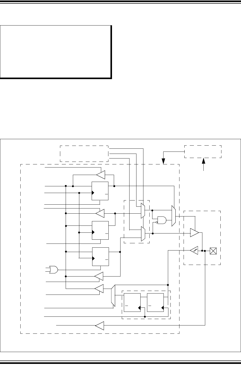
2015 Microchip Technology Inc. Preliminary DS60001320B-page 249
PIC32MZ Embedded Connectivity with Floating Point Unit (EF) Family
12.0 I/O PORTS
General purpose I/O pins are the simplest of
peripherals. They allow the PIC32MZ EF family device
to monitor and control other devices. To add flexibility
and functionality, some pins are multiplexed with
alternate function(s). These functions depend on which
peripheral features are on the device. In general, when
a peripheral is functioning, that pin may not be used as
a general purpose I/O pin.
Some of the key features of the I/O ports are:
• Individual output pin open-drain enable/disable
• Individual input pin weak pull-up and pull-down
• Monitor selective inputs and generate interrupt
when change in pin state is detected
• Operation during Sleep and Idle modes
• Fast bit manipulation using CLR, SET and INV
registers
Figure 12-1 illustrates a block diagram of a typical
multiplexed I/O port.
FIGURE 12-1: BLOCK DIAGRAM OF A TYPICAL MULTIPLEXED PORT STRUCTURE
Note: This data sheet summarizes the features
of the PIC32MZ EF family of devices. It is
not intended to be a comprehensive refer-
ence source. To complement the informa-
tion in this data sheet, refer to Section 12.
“I/O Ports” (DS60001120) in the “PIC32
Family Reference Manual”, which is avail-
able from the Microchip web site
(www.microchip.com/PIC32).
Peripheral Output Data
Peripheral Module
Peripheral Output Enable
PIO Module
Peripheral Module Enable
WR LAT
I/O Pin
WR PORT
Data Bus
RD LAT
RD PORT
RD TRIS
WR TRIS
0
1
RD ODC
PBCLK4
QD
CK
EN Q
QD
CK
EN Q
QD
CK
EN Q
QD
CK
Q
QD
CK
Q
0
1
PBCLK4
WR ODC
ODC
TRIS
LAT
Sleep
1
0
1
0
Output Multiplexers
I/O Cell
Synchronization
R
Peripheral Input
Legend: R = Peripheral input buffer types may vary. Refer to Table 1-1 for peripheral details.
Note: This block diagram is a general representation of a shared port/peripheral structure for illustration purposes only. The actual structure
for any specific port/peripheral combination may be different than it is shown here.
Peripheral Input Buffer
Port Control
PBCLK4

PIC32MZ Embedded Connectivity with Floating Point Unit (EF) Family
DS60001320B-page 250 Preliminary 2015 Microchip Technology Inc.
12.1 Parallel I/O (PIO) Ports
All port pins have up to 14 registers directly associated
with their operation as digital I/O. The data direction
register (TRISx) determines whether the pin is an input
or an output. If the data direction bit is a ‘1’, then the pin
is an input. All port pins are defined as inputs after a
Reset. Reads from the latch (LATx) read the latch.
Writes to the latch write the latch. Reads from the port
(PORTx) read the port pins, while writes to the port pins
write the latch.
12.1.1 OPEN-DRAIN CONFIGURATION
In addition to the PORTx, LATx, and TRISx registers for
data control, some port pins can also be individually
configured for either digital or open-drain output. This is
controlled by the Open-Drain Control register, ODCx,
associated with each port. Setting any of the bits con-
figures the corresponding pin to act as an open-drain
output.
The open-drain feature allows the generation of out-
puts higher than VDD (e.g., 5V) on any desired 5V-tol-
erant pins by using external pull-up resistors. The
maximum open-drain voltage allowed is the same as
the maximum VIH specification.
Refer to the pin name tables (Table 2 through Table 5)
for the available pins and their functionality.
12.1.2 CONFIGURING ANALOG AND
DIGITAL PORT PINS
The ANSELx register controls the operation of the
analog port pins. The port pins that are to function as
analog inputs must have their corresponding ANSEL
and TRIS bits set. In order to use port pins for I/O
functionality with digital modules, such as Timers,
UARTs, etc., the corresponding ANSELx bit must be
cleared.
The ANSELx register has a default value of 0xFFFF;
therefore, all pins that share analog functions are
analog (not digital) by default.
If the TRIS bit is cleared (output) while the ANSELx bit
is set, the digital output level (VOH or VOL) is converted
by an analog peripheral, such as the ADC module or
Comparator module.
When the PORT register is read, all pins configured as
analog input channels are read as cleared (a low level).
Pins configured as digital inputs do not convert an
analog input. Analog levels on any pin defined as a
digital input (including the ANx pins) can cause the
input buffer to consume current that exceeds the
device specifications.
12.1.3 I/O PORT WRITE/READ TIMING
One instruction cycle is required between a port
direction change or port write operation and a read
operation of the same port. Typically this instruction
would be an NOP.
12.1.4 INPUT CHANGE NOTIFICATION
The input change notification function of the I/O ports
allows the PIC32MZ EF devices to generate interrupt
requests to the processor in response to a change-of-
state on selected input pins. This feature can detect
input change-of-states even in Sleep mode, when the
clocks are disabled. Every I/O port pin can be selected
(enabled) for generating an interrupt request on a
change-of-state.
Five control registers are associated with the CN func-
tionality of each I/O port. The CNENx registers contain
the CN interrupt enable control bits for each of the input
pins. Setting any of these bits enables a CN interrupt
for the corresponding pins.
The CNSTATx register indicates whether a change
occurred on the corresponding pin since the last read
of the PORTx bit.
Each I/O pin also has a weak pull-up and a weak
pull-down connected to it. The pull-ups act as a
current source or sink source connected to the pin,
and eliminate the need for external resistors when
push-button or keypad devices are connected. The
pull-ups and pull-downs are enabled separately using
the CNPUx and the CNPDx registers, which contain
the control bits for each of the pins. Setting any of
the control bits enables the weak pull-ups and/or
pull-downs for the corresponding pins.
An additional control register (CNCONx) is shown in
Register 12-3.
Note: Pull-ups and pull-downs on change
notification pins should always be
disabled when the port pin is configured as
a digital output.

2015 Microchip Technology Inc. Preliminary DS60001320B-page 251
PIC32MZ Embedded Connectivity with Floating Point Unit (EF) Family
12.2 Registers for Slew Rate Control
Some I/O pins can be configured for various types of
slew rate control on its associated port. This is
controlled by the Slew Rate Control bits in the
SRCON1x and SRCON0x registers that are associated
with each I/O port. The slew rate control is configured
using the corresponding bit in each register, as shown
in Table 12-1.
As an example, writing 0x0001, 0x0000 to SRCON1A
and SRCON0A, respectively, will enable slew rate
control on the RA0 pin and sets the slew rate to the
slow edge rate.
TABLE 12-1: SLEW RATE CONTROL BIT
SETTINGS
12.3 CLR, SET, and INV Registers
Every I/O module register has a corresponding CLR
(clear), SET (set) and INV (invert) register designed to
provide fast atomic bit manipulations. As the name of
the register implies, a value written to a SET, CLR or
INV register effectively performs the implied operation,
but only on the corresponding base register and only
bits specified as ‘1’ are modified. Bits specified as ‘0’
are not modified.
Reading SET, CLR and INV registers returns undefined
values. To see the affects of a write operation to a SET,
CLR or INV register, the base register must be read.
12.4 Peripheral Pin Select (PPS)
A major challenge in general purpose devices is provid-
ing the largest possible set of peripheral features while
minimizing the conflict of features on I/O pins. The chal-
lenge is even greater on low pin-count devices. In an
application where more than one peripheral needs to
be assigned to a single pin, inconvenient workarounds
in application code or a complete redesign may be the
only option.
PPS configuration provides an alternative to these
choices by enabling peripheral set selection and their
placement on a wide range of I/O pins. By increasing
the pinout options available on a particular device,
users can better tailor the device to their entire
application, rather than trimming the application to fit
the device.
The PPS configuration feature operates over a fixed
subset of digital I/O pins. Users may independently
map the input and/or output of most digital peripherals
to these I/O pins. PPS is performed in software and
generally does not require the device to be repro-
grammed. Hardware safeguards are included that pre-
vent accidental or spurious changes to the peripheral
mapping once it has been established.
12.4.1 AVAILABLE PINS
The number of available pins is dependent on the
particular device and its pin count. Pins that support the
PPS feature include the designation “RPn” in their full
pin designation, where “RP” designates a remappable
peripheral and “n” is the remappable port number.
12.4.2 AVAILABLE PERIPHERALS
The peripherals managed by the PPS are all digital-
only peripherals. These include general serial
communications (UART, SPI, and CAN), general pur-
pose timer clock inputs, timer-related peripherals (input
capture and output compare), interrupt-on-change
inputs, and reference clocks (input and output).
In comparison, some digital-only peripheral modules
are never included in the PPS feature. This is because
the peripheral’s function requires special I/O circuitry
on a specific port and cannot be easily connected to
multiple pins. These modules include I2C among oth-
ers. A similar requirement excludes all modules with
analog inputs, such as the Analog-to-Digital Converter
(ADC).
A key difference between remappable and non-remap-
pable peripherals is that remappable peripherals are
not associated with a default I/O pin. The peripheral
must always be assigned to a specific I/O pin before it
can be used. In contrast, non-remappable peripherals
are always available on a default pin, assuming that the
peripheral is active and not conflicting with another
peripheral.
When a remappable peripheral is active on a given I/O
pin, it takes priority over all other digital I/O and digital
communication peripherals associated with the pin.
Priority is given regardless of the type of peripheral that
is mapped. Remappable peripherals never take priority
over any analog functions associated with the pin.
SRCON1x SRCON0x Description
1 1 Slew rate control is enabled
and is set to the slowest
edge rate.
1 0 Slew rate control is enabled
and is set to the slow edge
rate.
0 1 Slew rate control is enabled
and is set to the medium
edge rate.
0 0 Slew rate control is disabled
and is set to the fastest
edge rate.
Note: By default, all of the Port pins are set to
the fastest edge rate.
PIC32MZ Embedded Connectivity with Floating Point Unit (EF) Family
DS60001320B-page 252 Preliminary 2015 Microchip Technology Inc.
12.4.3 CONTROLLING PPS
PPS features are controlled through two sets of SFRs:
one to map peripheral inputs, and one to map outputs.
Because they are separately controlled, a particular
peripheral’s input and output (if the peripheral has both)
can be placed on any selectable function pin without
constraint.
The association of a peripheral to a peripheral-select-
able pin is handled in two different ways, depending on
whether an input or output is being mapped.
12.4.4 INPUT MAPPING
The inputs of the PPS options are mapped on the basis
of the peripheral. That is, a control register associated
with a peripheral dictates the pin it will be mapped to.
The [pin name]R registers, where [pin name] refers to the
peripheral pins listed in Table 12-2, are used to config-
ure peripheral input mapping (see Register 12-1). Each
register contains sets of 4 bit fields. Programming these
bit fields with an appropriate value maps the RPn pin
with the corresponding value to that peripheral. For any
given device, the valid range of values for any bit field is
shown in Table 12-2.
For example, Figure 12-2 illustrates the remappable
pin selection for the U1RX input.
FIGURE 12-2: REMAPPABLE INPUT
EXAMPLE FOR U1RX
RPD2
RPG8
RPF4
0
1
2U1RX input
U1RXR<3:0>
to peripheral
RPn
n
Note: For input only, PPS functionality does not
have priority over TRISx settings. Therefore,
when configuring RPn pin for input, the
corresponding bit in the TRISx register must
also be configured for input (set to ‘1’).

2015 Microchip Technology Inc. Preliminary DS60001320B-page 253
PIC32MZ Embedded Connectivity with Floating Point Unit (EF) Family
TABLE 12-2: INPUT PIN SELECTION
Peripheral Pin [pin name]R SFR [pin name]R bits [pin name]R Value to
RPn Pin Selection
INT3 INT3R INT3R<3:0> 0000 = RPD2
0001 = RPG8
0010 = RPF4
0011 = RPD10
0100 = RPF1
0101 = RPB9
0110 = RPB10
0111 = RPC14
1000 = RPB5
1001 = Reserved
1010 = RPC1(1)
1011 = RPD14(1)
1100 = RPG1(1)
1101 = RPA14(1)
1110 = RPD6(2)
1111 = Reserved
T2CK T2CKR T2CKR<3:0>
T6CK T6CKR T6CKR<3:0>
IC3 IC3R IC3R<3:0>
IC7 IC7R IC7R<3:0>
U1RX U1RXR U1RXR<3:0>
U2CTS U2CTSR U2CTSR<3:0>
U5RX U5RXR U5RXR<3:0>
U6CTS U6CTSR U6CTSR<3:0>
SDI1 SDI1R SDI1R<3:0>
SDI3 SDI3R SDI3R<3:0>
SDI5(1) SDI5R(1) SDI5R<3:0>(1)
SS6(1) SS6R(1) SS6R<3:0>(1)
REFCLKI1 REFCLKI1R REFCLKI1R<3:0>
INT4 INT4R INT4R<3:0> 0000 = RPD3
0001 = RPG7
0010 = RPF5
0011 = RPD11
0100 = RPF0
0101 = RPB1
0110 = RPE5
0111 = RPC13
1000 = RPB3
1001 = Reserved
1010 = RPC4(1)
1011 = RPD15(1)
1100 = RPG0(1)
1101 = RPA15(1)
1110 = RPD7(2)
1111 = Reserved
T5CK T5CKR T5CKR<3:0>
T7CK T7CKR T7CKR<3:0>
IC4 IC4R IC4R<3:0>
IC8 IC8R IC8R<3:0>
U3RX U3RXR U3RXR<3:0>
U4CTS U4CTSR U4CTSR<3:0>
SDI2 SDI2R SDI2R<3:0>
SDI4 SDI4R SDI4R<3:0>
C1RX(3) C1RXR(3) C1RXR<3:0>(3)
REFCLKI4 REFCLKI4R REFCLKI4R<3:0>
INT2 INT2R INT2R<3:0> 0000 = RPD9
0001 = RPG6
0010 = RPB8
0011 = RPB15
0100 = RPD4
0101 = RPB0
0110 = RPE3
0111 = RPB7
1000 = Reserved
1001 = RPF12(1)
1010 = RPD12(1)
1011 = RPF8(1)
1100 = RPC3(1)
1101 = RPE9(1)
1110 = Reserved
1111 = Reserved
T3CK T3CKR T3CKR<3:0>
T8CK T8CKR T8CKR<3:0>
IC2 IC2R IC2R<3:0>
IC5 IC5R IC5R<3:0>
IC9 IC9R IC9R<3:0>
U1CTS U1CTSR U1CTSR<3:0>
U2RX U2RXR U2RXR<3:0>
U5CTS U5CTSR U5CTSR<3:0>
SS1 SS1R SS1R<3:0>
SS3 SS3R SS3R<3:0>
SS4 SS4R SS4R<3:0>
SS5(1) SS5R(1) SS5R<3:0>(1)
C2RX(3) C2RXR(3) C2RXR<3:0>(3)
Note 1: This selection is not available on 64-pin devices.
2: This selection is not available on 64-pin or 100-pin devices.
3: This selection is not available on devices without a CAN module.

PIC32MZ Embedded Connectivity with Floating Point Unit (EF) Family
DS60001320B-page 254 Preliminary 2015 Microchip Technology Inc.
INT1 INT1R INT1R<3:0> 0000 = RPD1
0001 = RPG9
0010 = RPB14
0011 = RPD0
0100 = Reserved
0101 = RPB6
0110 = RPD5
0111 = RPB2
1000 = RPF3
1001 = RPF13(1)
1010 = No Connect
1011 = RPF2(1)
1100 = RPC2(1)
1101 = RPE8(1)
1110 = Reserved
1111 = Reserved
T4CK T4CKR T4CKR<3:0>
T9CK T9CKR T9CKR<3:0>
IC1 IC1R IC1R<3:0>
IC6 IC6R IC6R<3:0>
U3CTS U3CTSR U3CTSR<3:0>
U4RX U4RXR U4RXR<3:0>
U6RX U6RXR U6RXR<3:0>
SS2 SS2R SS2R<3:0>
SDI6(1) SDI6R(1) SDI6R<3:0>(1)
OCFA OCFAR OCFAR<3:0>
REFCLKI3 REFCLKI3R REFCLKI3R<3:0>
TABLE 12-2: INPUT PIN SELECTION (CONTINUED)
Peripheral Pin [pin name]R SFR [pin name]R bits [pin name]R Value to
RPn Pin Selection
Note 1: This selection is not available on 64-pin devices.
2: This selection is not available on 64-pin or 100-pin devices.
3: This selection is not available on devices without a CAN module.
2015 Microchip Technology Inc. Preliminary DS60001320B-page 255
PIC32MZ Embedded Connectivity with Floating Point Unit (EF) Family
12.4.5 OUTPUT MAPPING
In contrast to inputs, the outputs of the PPS options
are mapped on the basis of the pin. In this case, a
control register associated with a particular pin
dictates the peripheral output to be mapped. The
RPnR registers (Register 12-2) are used to control
output mapping. Like the [pin name]R registers, each
register contains sets of 4 bit fields. The value of the
bit field corresponds to one of the peripherals, and
that peripheral’s output is mapped to the pin (see
Table 12-3 and Figure 12-3).
A null output is associated with the output register reset
value of ‘0’. This is done to ensure that remappable
outputs remain disconnected from all output pins by
default.
FIGURE 12-3: EXAMPLE OF
MULTIPLEXING OF
REMAPPABLE OUTPUT
FOR RPF0
12.4.6 CONTROLLING CONFIGURATION
CHANGES
Because peripheral remapping can be changed during
run time, some restrictions on peripheral remapping
are needed to prevent accidental configuration
changes. PIC32MZ EF devices include two features to
prevent alterations to the peripheral map:
• Control register lock sequence
• Configuration bit select lock
12.4.6.1 Control Register Lock
Under normal operation, writes to the RPnR and [pin
name]R registers are not allowed. Attempted writes
appear to execute normally, but the contents of the
registers remain unchanged. To change these regis-
ters, they must be unlocked in hardware. The regis-
ter lock is controlled by the IOLOCK Configuration bit
(CFGCON<13>). Setting IOLOCK prevents writes to
the control registers; clearing IOLOCK allows writes.
To set or clear the IOLOCK bit, an unlock sequence
must be executed. Refer to Section 42. “Oscillators
with Enhanced PLL” in the “PIC32 Family Reference
Manual” for details.
12.4.6.2 Configuration Bit Select Lock
As an additional level of safety, the device can be
configured to prevent more than one write session to
the RPnR and [pin name]R registers. The IOL1WAY
Configuration bit (DEVCFG3<29>) blocks the IOLOCK
bit from being cleared after it has been set once. If
IOLOCK remains set, the register unlock procedure
does not execute, and the PPS control registers cannot
be written to. The only way to clear the bit and re-
enable peripheral remapping is to perform a device
Reset.
In the default (unprogrammed) state, IOL1WAY is set,
restricting users to one write session.
RPF0R<3:0>
0
15
1
Default
U1TX Output
U2RTS Output 2
14
Output Data RPF0
REFCLKO1

PIC32MZ Embedded Connectivity with Floating Point Unit (EF) Family
DS60001320B-page 256 Preliminary 2015 Microchip Technology Inc.
TABLE 12-3: OUTPUT PIN SELECTION
RPn Port Pin RPnR SFR RPnR bits RPnR Value to Peripheral
Selection
RPD2 RPD2R RPD2R<3:0> 0000 = No Connect
0001 = U3TX
0010 = U4RTS
0011 = Reserved
0100 = Reserved
0101 = SDO1
0110 = SDO2
0111 = SDO3
1000 = Reserved
1001 = SDO5(1)
1010 = SS6(1)
1011 = OC3
1100 = OC6
1101 = REFCLKO4
1110 = C2OUT
1111 = C1TX(3)
RPG8 RPG8R RPG8R<3:0>
RPF4 RPF4R RPF4R<3:0>
RPD10 RPD10R RPD10R<3:0>
RPF1 RPF1R RPF1R<3:0>
RPB9 RPB9R RPB9R<3:0>
RPB10 RPB10R RPB10R<3:0>
RPC14 RPC14R RPC14R<3:0>
RPB5 RPB5R RPB5R<3:0>
RPC1(1) RPC1R(1) RPC1R<3:0>(1)
RPD14(1) RPD14R(1) RPD14R<3:0>(1)
RPG1(1) RPG1R(1) RPG1R<3:0>(1)
RPA14(1) RPA14R(1) RPA14R<3:0>(1)
RPD6(2) RPD6R(2) RPD6R<3:0>(2)
RPD3 RPD3R RPD3R<3:0> 0000 = No Connect
0001 = U1TX
0010 = U2RTS
0011 = U5TX
0100 = U6RTS
0101 = SDO1
0110 = SDO2
0111 = SDO3
1000 = SDO4
1001 = SDO5(1)
1010 = Reserved
1011 = OC4
1100 = OC7
1101 = Reserved
1110 = Reserved
1111 = REFCLKO1
RPG7 RPG7R RPG7R<3:0>
RPF5 RPF5R RPF5R<3:0>
RPD11 RPD11R RPD11R<3:0>
RPF0 RPF0R RPF0R<3:0>
RPB1 RPB1R RPB1R<3:0>
RPE5 RPE5R RPE5R<3:0>
RPC13 RPC13R RPC13R<3:0>
RPB3 RPB3R RPB3R<3:0>
RPC4(1) RPC4R(1) RPC4R<3:0>(1)
RPD15(1) RPD15R(1) RPD15R<3:0>(1)
RPG0(1) RPG0R(1) RPG0R<3:0>(1)
RPA15(1) RPA15R(1) RPA15R<3:0>(1)
RPD7(2) RPD7R(2) RPD7R<3:0>(2)
RPD9 RPD9R RPD9R<3:0> 0000 = No Connect
0001 = U3RTS
0010 = U4TX
0011 = Reserved
0100 = U6TX
0101 = SS1
0110 = Reserved
0111 = SS3
1000 = SS4
1001 = SS5(1)
1010 = SDO6(1)
1011 = OC5
1100 = OC8
1101 = Reserved
1110 = C1OUT
1111 = REFCLKO3
RPG6 RPG6R RPG6R<3:0>
RPB8 RPB8R RPB8R<3:0>
RPB15 RPB15R RPB15R<3:0>
RPD4 RPD4R RPD4R<3:0>
RPB0 RPB0R RPB0R<3:0>
RPE3 RPE3R RPE3R<3:0>
RPB7 RPB7R RPB7R<3:0>
RPF12(1) RPF12R(1) RPF12R<3:0>(1)
RPD12(1) RPD12R(1) RPD12R<3:0>(1)
RPF8(1) RPF8R(1) RPF8R<3:0>(1)
RPC3(1) RPC3R(1) RPC3R<3:0>(1)
RPE9(1) RPE9R(1) RPE9R<3:0>(1)
Note 1: This selection is not available on 64-pin devices.
2: This selection is not available on 64-pin or 100-pin devices.
3: This selection is not available on devices without a CAN module.

2015 Microchip Technology Inc. Preliminary DS60001320B-page 257
PIC32MZ Embedded Connectivity with Floating Point Unit (EF) Family
RPD1 RPD1R RPD1R<3:0> 0000 = No Connect
0001 = U1RTS
0010 = U2TX
0011 = U5RTS
0100 = U6TX
0101 = Reserved
0110 = SS2
0111 = Reserved
1000 = SDO4
1001 = Reserved
1010 = SDO6(1)
1011 = OC2
1100 = OC1
1101 = OC9
1110 = Reserved
1111 = C2TX(3)
RPG9 RPG9R RPG9R<3:0>
RPB14 RPB14R RPB14R<3:0>
RPD0 RPD0R RPD0R<3:0>
RPB6 RPB6R RPB6R<3:0>
RPD5 RPD5R RPD5R<3:0>
RPB2 RPB2R RPB2R<3:0>
RPF3 RPF3R RPF3R<3:0>
RPF13(1) RPF13R(1) RPF13R<3:0>(1)
RPC2(1) RPC2R(1) RPC2R<3:0>(1)
RPE8(1) RPE8R(1) RPE8R<3:0>(1)
RPF2(1) RPF2R(1) RPF2R<3:0>(1)
TABLE 12-3: OUTPUT PIN SELECTION (CONTINUED)
RPn Port Pin RPnR SFR RPnR bits RPnR Value to Peripheral
Selection
Note 1: This selection is not available on 64-pin devices.
2: This selection is not available on 64-pin or 100-pin devices.
3: This selection is not available on devices without a CAN module.

PIC32MZ Embedded Connectivity with Floating Point Unit (EF) Family
DS60001320B-page 258 Preliminary 2015 Microchip Technology Inc.
12.5 I/O Ports Control Registers
TABLE 12-4: PORTA REGISTER MAP FOR 100-PIN, 124-PIN, AND 144-PIN DEVICES ONLY
Virtual Address
(BF86_#)
Register
Name(1)
Bit Range
Bits
All
Resets
31/15 30/14 29/13 28/12 27/11 26/10 25/9 24/8 23/7 22/6 21/5 20/4 19/3 18/2 17/1 16/0
0000 ANSELA 31:16 — — — — — — — — — — — — — — — — 0000
15:0 — — — — — ANSA10 ANSA9 — — — ANSA5 — — — ANSA1 ANSA0 0623
0010 TRISA 31:16 — — — — — — — — — — — — — — — — 0000
15:0 TRISA15 TRISA14 — — — TRISA10 TRISA9 —TRISA7 TRISA6 TRISA5 TRISA4 TRISA3 TRISA2 TRISA1 TRISA0 C6FF
0020 PORTA 31:16 — — — — — — — — — — — — — — — — 0000
15:0 RA15 RA14 — — — RA10 RA9 —RA7 RA6 RA5 RA4 RA3 RA2 RA1 RA0 xxxx
0030 LATA 31:16 — — — — — — — — — — — — — — — — 0000
15:0 LATA15 LATA14 — — — LATA10 LATA9 —LATA7 LATA6 LATA5 LATA4 LATA3 LATA2 LATA1 LATA0 xxxx
0040 ODCA 31:16 — — — — — — — — — — — — — — — — 0000
15:0 ODCA15 ODCA14 — — — ODCA10 ODCA9 —ODCA7 ODCA6 ODCA5 ODCA4 ODCA3 ODCA2 ODCA1 ODCA0 0000
0050 CNPUA 31:16 — — — — — — — — — — — — — — — — 0000
15:0 CNPUA15 CNPUA14 — — — CNPUA10 CNPUA9 —CNPUA7 CNPUA6 CNPUA5 CNPUA4 CNPUA3 CNPUA2 CNPUA1 CNPUA0 0000
0060 CNPDA 31:16 — — — — — — — — — — — — — — — — 0000
15:0 CNPDA15 CNPDA14 — — — CNPDA10 CNPDA9 —CNPDA7 CNPDA6 CNPDA5 CNPDA4 CNPDA3 CNPDA2 CNPDA1 CNPDA0 0000
0070 CNCONA 31:16 — — — — — — — — — — — — — — — — 0000
15:0 ON —SIDL —EDGEDETECT — — — — — — — — — — — 0000
0080 CNENA 31:16 — — — — — — — — — — — — 0000
15:0 CNENA15 CNENA14 — — — CNENA10 CNENA9 CNENA7 CNENA6 CNENA5 CNENA4 CNENA3 CNENA2 CNENA1 CNENA0 0000
0090 CNSTATA
31:16 — — — — — — — — — — — — — — — — 0000
15:0 CN
STATA15 CN
STATA14 — — — CN
STATA10 CN
STATA9 —CN
STATA7 CN
STATA6 CN
STATA5 CN
STATA4 CN
STATA3 CN
STATA2 CN
STATA1 CN
STATA0 0000
00A0 CNNEA 31:16 — — — — — — — — — — — — — — — — 0000
15:0 CNNEA15 CNNEA14 — — — CNNEA10 CNNEA9 —CNNEA7 CNNEA6 CNNEA5 CNNEA4 CNNEA3 CNNEA2 CNNEA1 CNNEA0 0000
00B0 CNFA 31:16 — — — — — — — — — — — — — — — — 0000
15:0 CNFA15 CNFA14 — — — CNFA10 CNFA9 —CNFA7 CNFA76 CNFA5 CNFA4 CNFA3 CNFA2 CNFA71 CNFA0 0000
00C0 SRCON0A 31:16 — — — — — — — — — — — — — — — — 0000
15:0 — — — — — — — — SR0A7 SR0A6 — — — — — — 0000
00D0 SRCON1A 31:16 — — — — — — — — — — — — — — — — 0000
15:0 — — — — — — — — SR1A7 SR0A6 — — — — — — 0000
Legend: x = Unknown value on Reset; — = Unimplemented, read as ‘0’; Reset values are shown in hexadecimal.
Note 1: All registers in this table have corresponding CLR, SET and INV registers at its virtual address, plus an offset of 0x4, 0x8 and 0xC, respectively. See Section 12.3 “CLR, SET, and INV Registers” for
more information.

2015 Microchip Technology Inc. Preliminary DS60001320B-page 259
PIC32MZ Embedded Connectivity with Floating Point Unit (EF) Family
TABLE 12-5: PORTB REGISTER MAP
Virtual Address
(BF86_#)
Register
Name(1)
Bit Range
Bits
All
Resets
31/15 30/14 29/13 28/12 27/11 26/10 25/9 24/8 23/7 22/6 21/5 20/4 19/3 18/2 17/1 16/0
0100 ANSELB 31:16 — — — — — — — — — — — — — — — — 0000
15:0 ANSB15 ANSB14 ANSB13 ANSB12 ANSB11 ANSB10 ANSB9 ANSB8 ANSB7 ANSB6 ANSB5 ANSB41 ANSB3 ANSB2 ANSB1 ANSB0 FFFF
0110 TRISB 31:16 — — — — — — — — — — — — — — — — 0000
15:0 TRISB15 TRISB14 TRISB13 TRISB12 TRISB11 TRISB10 TRISB9 TRISB8 TRISB7 TRISB6 TRISB5 TRISB4 TRISB3 TRISB2 TRISB1 TRISB0 FFFF
0120 PORTB 31:16 — — — — — — — — — — — — — — — — 0000
15:0 RB15 RB14 RB13 RB12 RB11 RB10 RB9 RB8 RB7 RB6 RB5 RB4 RB3 RB2 RB1 RB0 xxxx
0130 LATB 31:16 — — — — — — — — — — — — — — — — 0000
15:0 LATB15 LATB14 LATB13 LATB12 LATB11 LATB10 LATB9 LATB8 LATB7 LATB6 LATB5 LATB4 LATB3 LATB2 LATB1 LATB0 xxxx
0140 ODCB 31:16 — — — — — — — — — — — — — — — — 0000
15:0 ODCB15 ODCB14 ODCB13 ODCB12 ODCB11 ODCB10 ODCB9 ODCB8 ODCB7 ODCB6 ODCB5 ODCB4 ODCB3 ODCB2 ODCB1 ODCB0 0000
0150 CNPUB 31:16 — — — — — — — — — — — — — — — — 0000
15:0 CNPUB15 CNPUB14 CNPUB13 CNPUB12 CNPUB11 CNPUB10 CNPUB9 CNPUB8 CNPUB7 CNPUB6 CNPUB5 CNPUB4 CNPUB3 CNPUB2 CNPUB1 CNPUB0 0000
0160 CNPDB 31:16 — — — — — — — — — — — — — — — — 0000
15:0 CNPDB15 CNPDB14 CNPDB13 CNPDB12 CNPDB11 CNPDB10 CNPDB9 CNPDB8 CNPDB7 CNPDB6 CNPDB5 CNPDB4 CNPDB3 CNPDB2 CNPDB1 CNPDB0 0000
0170 CNCONB
31:16 — — — — — — — — — — — — — — — — 0000
15:0 ON —SIDL —EDGE
DETECT — — — — — — — — — — — 0000
0180 CNENB 31:16 — — — — — — — — — — — — — — — — 0000
15:0 CNENB15 CNENB14 CNENB13 CNENB12 CNENB11 CNENB10 CNENB9 CNENB8 CNENB7 CNENB6 CNENB5 CNENB4 CNENB3 CNENB2 CNENB1 CNENB0 0000
0190 CNSTATB
31:16 — — — — — — — — — — — — — — — — 0000
15:0 CN
STATB15 CN
STATB14 CN
STATB13 CN
STATB12 CN
STATB11 CN
STATB10 CN
STATB9 CN
STATB8 CN
STATB7 CN
STATB6 CN
STATB5 CN
STATB4 CN
STATB3 CN
STATB2 CN
STATB1 CN
STATB0 0000
01A0 CNNEB 31:16 — — — — — — — — — — — — — — — — 0000
15:0 CNNEB15 CNNEB14 CNNEB13 CNNEB12 CNNEB11 CNNEB10 CNNEB9 CNNEB8 CNNEB7 CNNEB6 CNNEB5 CNNEB4 CNNEB3 CNNEB2 CNNEB1 CNNEB0 0000
01B0 CNFB 31:16 — — — — — — — — — — — — — — — — 0000
15:0 CNFB15 CNFB14 CNFB13 CNFB12 CNFB11 CNFB10 CNFB9 CNFB8 CNFB7 CNFB6 CNFB5 CNFB4 CNFB3 CNFB2 CNFB1 CNFB0 0000
01C0 SRCON0B 31:16 — — — — — — — — — — — — — — — — 0000
15:0 —SR0B14 — — — SR0B10 SR0B9 SR0B8 — — SR0B5 —SR0B3 — — — 0000
01D0 SRCON1B 31:16 — — — — — — — — — — — — — — — — 0000
15:0 —SR1B14 — — — SR1B10 SR1B9 SR1B8 — — SR1B5 —SR1B3 — — — 0000
Legend: x = Unknown value on Reset; — = Unimplemented, read as ‘0’; Reset values are shown in hexadecimal.
Note 1: All registers in this table have corresponding CLR, SET and INV registers at its virtual address, plus an offset of 0x4, 0x8 and 0xC, respectively. See Section 12.3 “CLR, SET, and INV Registers” for
more information.

PIC32MZ Embedded Connectivity with Floating Point Unit (EF) Family
DS60001320B-page 260 Preliminary 2015 Microchip Technology Inc.
TABLE 12-6: PORTC REGISTER MAP FOR 100-PIN, 124-PIN, AND 144-PIN DEVICES ONLY
Virtual Address
(BF86_#)
Register
Name(1)
Bit Range
Bits
All
Resets
31/15 30/14 29/13 28/12 27/11 26/10 25/9 24/8 23/7 22/6 21/5 20/4 19/3 18/2 17/1 16/0
0200 ANSELC 31:16 — — — — — — — — — — — — — — — — 0000
15:0 — — — — — — — — — — — ANSC4 ANSC3 ANSC2 ANSC1 —001E
0210 TRISC 31:16 — — — — — — — — — — — — — — — — 0000
15:0 TRISC15 TRISC14 TRISC13 TRISC12 — — — — — — — TRISC4 TRISC3 TRISC2 TRISC1 —F01E
0220 PORTC 31:16 — — — — — — — — — — — — — — — — 0000
15:0 RC15 RC14 RC13 RC12 — — — — — — — RC4 RC3 RC2 RC1 —xxxx
0230 LATC 31:16 — — — — — — — — — — — — — — — — 0000
15:0 LATC15 LATC14 LATC13 LATC12 — — — — — — — LATC4 LATC3 LATC2 LATC1 —xxxx
0240 ODCC 31:16 — — — — — — — — — — — — — — — — 0000
15:0 ODCC15 ODCC14 ODCC13 ODCC12 — — — — — — — ODCC4 ODCC3 ODCC2 ODCC1 —0000
0250 CNPUC 31:16 — — — — — — — — — — — — — — — — 0000
15:0 CNPUC15 CNPUC14 CNPUC13 CNPUC12 — — — — — — — CNPUC4 CNPUC3 CNPUC2 CNPUC1 —0000
0260 CNPDC 31:16 — — — — — — — — — — — — — — — — 0000
15:0 CNPDC15 CNPDC14 CNPDC13 CNPDC12 — — — — — — — CNPDC4 CNPDC3 CNPDC2 CNPDC1 —0000
0270 CNCONC
31:16 — — — — — — — — — — — — — — — — 0000
15:0 ON —SIDL —EDGE
DETECT — — — — — — — — — — — 0000
0280 CNENC 31:16 — — — — — — — — — — — — — — — 0000
15:0 CNENC15 CNENC14 CNENC13 CNENC12 CNENC4 CNENC3 CNENC2 CNENC1 —0000
0290 CNSTATC 31:16 — — — — — — — — — — — — — — — — 0000
15:0 CNSTATC15 CNSTATC14 CNSTATC13 CNSTATC12 — — — — — — — CNSTATC4 CNSTATC3 CNSTATC2 CNSTATC1 —0000
02A0 CNNEC 31:16 — — — — — — — — — — — — — — — 0000
15:0 CNNEC15 CNNEC14 CNNEC13 CNNEC12 — — — — — — — CNNEC4 CNNEC3 CNNEC2 CNNEC1 —0000
02B0 CNFC 31:16 — — — — — — — — — — — — — — — — 0000
15:0 CNFC15 CNFC14 CNFC13 CNFC12 — — — — — — — CNFC4 CNFC3 CNFC2 CNFC1 —0000
Legend: x = Unknown value on Reset; — = Unimplemented, read as ‘0’; Reset values are shown in hexadecimal.
Note 1: All registers in this table have corresponding CLR, SET and INV registers at its virtual address, plus an offset of 0x4, 0x8 and 0xC, respectively. See Section 12.3 “CLR, SET, and INV Registers” for
more information.

2015 Microchip Technology Inc. Preliminary DS60001320B-page 261
PIC32MZ Embedded Connectivity with Floating Point Unit (EF) Family
TABLE 12-7: PORTC REGISTER MAP FOR 64-PIN DEVICES ONLY
Virtual Address
(BF86_#)
Register
Name(1)
Bit Range
Bits
All
Resets
31/15 30/14 29/13 28/12 27/11 26/10 25/9 24/8 23/7 22/6 21/5 20/4 19/3 18/2 17/1 16/0
0210 TRISC 31:16 — — — — — — — — — — — — — — — — 0000
15:0 TRISC15 TRISC14 TRISC13 TRISC12 — — — — — — — — — — — — F000
0220 PORTC 31:16 — — — — — — — — — — — — — — — — 0000
15:0 RC15 RC14 RC13 RC12 — — — — — — — — — — — — xxxx
0230 LATC 31:16 — — — — — — — — — — — — — — — — 0000
15:0 LATC15 LATC14 LATC13 LATC12 — — — — — — — — — — — — xxxx
0240 ODCC 31:16 — — — — — — — — — — — — — — — — 0000
15:0 ODCC15 ODCC14 ODCC13 ODCC12 — — — — — — — — — — — — xxxx
0250 CNPUC 31:16 — — — — — — — — — — — — — — — — 0000
15:0 CNPUC15 CNPUC14 CNPUC13 CNPUC12 — — — — — — — — — — — — 0000
0260 CNPDC 31:16 — — — — — — — — — — — — — — — — 0000
15:0 CNPDC15 CNPDC14 CNPDC13 CNPDC12 — — — — — — — — — — — — 0000
0270 CNCONC
31:16 — — — — — — — — — — — — — — — — 0000
15:0 ON —SIDL —EDGE
DETECT — — — — — — — — — — — 0000
0280 CNENC 31:16 — — — — — — — — — — — — — — — — 0000
15:0 CNENC15 CNENC14 CNENC13 CNENC12 0000
0290 CNSTATC 31:16 — — — — — — — — — — — — — — — — 0000
15:0 CNSTATC15 CNSTATC14 CNSTATC13 CNSTATC12 — — — — — — — — — — — — 0000
02A0 CNNEC 31:16 — — — — — — — — — — — — — — — 0000
15:0 CNNEC15 CNNEC14 CNNEC13 CNNEC12 — — — — — — — — — — — — 0000
02B0 CNFC 31:16 — — — — — — — — — — — — — — — — 0000
15:0 CNFC15 CNFC14 CNFC13 CNFC12 — — — — — — — — — — — — 0000
Legend: x = Unknown value on Reset; — = Unimplemented, read as ‘0’; Reset values are shown in hexadecimal.
Note 1: All registers in this table have corresponding CLR, SET and INV registers at its virtual address, plus an offset of 0x4, 0x8 and 0xC, respectively. See Section 12.3 “CLR, SET, and INV Registers” for
more information.

PIC32MZ Embedded Connectivity with Floating Point Unit (EF) Family
DS60001320B-page 262 Preliminary 2015 Microchip Technology Inc.
TABLE 12-8: PORTD REGISTER MAP FOR 124-PIN AND 144-PIN DEVICES ONLY
Virtual Address
(BF86_#)
Register
Name(1)
Bit Range
Bits
All
Resets
31/15 30/14 29/13 28/12 27/11 26/10 25/9 24/8 23/7 22/6 21/5 20/4 19/3 18/2 17/1 16/0
0300 ANSELD 31:16 — — — — — — — — — — — — — — — — 0000
15:0 ANSD15 ANSD14 — — — — — — — — — — — — — — C000
0310 TRISD 31:16 — — — — — — — — — — — — — — — — 0000
15:0 TRISD15 TRISD14 TRISD13 TRISD12 TRISD11 TRISD10 TRISD9 —TRISD7 TRISD6 TRISD5 TRISD4 TRISD3 TRISD2 TRISD1 TRISD0 FEFF
0320 PORTD 31:16 — — — — — — — — — — — — — — — — 0000
15:0 RD15 RD14 RD13 RD12 RD11 RD10 RD9 —RD7 RD6 RD5 RD4 RD3 RD2 RD1 RD0 xxxx
0330 LATD 31:16 — — — — — — — — — — — — — — — — 0000
15:0 LATD15 LATD14 LATD13 LATD12 LATD11 LATD10 LATD9 —LATD7 LATD6 LATD5 LATD4 LATD3 LATD2 LATD1 LATD0 xxxx
0340 ODCD 31:16 — — — — — — — — — — — — — — — — 0000
15:0 ODCD15 ODCD14 ODCD13 ODCD12 ODCD11 ODCD10 ODCD9 —ODCD7 ODCD6 ODCD5 ODCD4 ODCD3 ODCD2 ODCD1 ODCD0 0000
0350 CNPUD 31:16 — — — — — — — — — — — — — — — — 0000
15:0 CNPUD15 CNPUD14 CNPUD13 CNPUD12 CNPUD11 CNPUD10 CNPUD9 —CNPUD7 CNPUD6 CNPUD5 CNPUD4 CNPUD3 CNPUD2 CNPUD1 CNPUD0 0000
0360 CNPDD 31:16 — — — — — — — — — — — — — — — — 0000
15:0 CNPDD15 CNPDD14 CNPDD13 CNPDD12 CNPDD11 CNPDD10 CNPDD9 —CNPDD7 CNPDD6 CNPDD5 CNPDD4 CNPDD3 CNPDD2 CNPDD1 CNPDD0 0000
0370 CNCOND
31:16 — — — — — — — — — — — — — — — — 0000
15:0 ON —SIDL —EDGE
DETECT — — — — — — — — — — — 0000
0380 CNEND 31:16 — — — — — — — — — — — — — — — — 0000
15:0 CNEND15 CNEND14 CNEND13 CNEND12 CNEND11 CNEND10 CNEND9 —CNEND7 CNEND6 CNEND5 CNEND4 CNEND3 CNEND2 CNEND1 CNEND0 0000
0390 CNSTATD
31:16 — — — — — — — — — — — — — — — — 0000
15:0 CN
STATD15 CN
STATD14 CN
STATD13 CN
STATD12 CN
STATD11 CN
STATD10 CN
STATD9 —CN
STATD7 CN
STATD6 CN
STATD5 CN
STATD4 CN
STATD3 CN
STATD2 CN
STATD1 CN
STATD0 0000
03A0 CNNED 31:16 — — — — — — — — — — — — — — — — 0000
15:0
CNNED15 CNNED14 CNNED13 CNNED12 CNNED11 CNNED10 CNNED9 —CNNED7 CNNED6 CNNED5 CNNED4 CNNED3 CNNED2 CNNED1 CNNED0
0000
03B0 CNFD 31:16 — — — — — — — — — — — — — — — — 0000
15:0 CNFD15 CNFD14 CNFD13 CNFD12 CNFD11 CNFD10 CNFD9 —CNFD7 CNFD6 CNFD5 CNFD4 CNFD3 CNFD2 CNFD1 CNFD0 0000
Legend: x = Unknown value on Reset; — = Unimplemented, read as ‘0’; Reset values are shown in hexadecimal.
Note 1: All registers in this table have corresponding CLR, SET and INV registers at its virtual address, plus an offset of 0x4, 0x8 and 0xC, respectively. See Section 12.3 “CLR, SET, and INV Registers” for
more information.

2015 Microchip Technology Inc. Preliminary DS60001320B-page 263
PIC32MZ Embedded Connectivity with Floating Point Unit (EF) Family
TABLE 12-9: PORTD REGISTER MAP FOR 100-PIN DEVICES ONLY
Virtual Address
(BF86_#)
Register
Name(1)
Bit Range
Bits
All
Resets
31/15 30/14 29/13 28/12 27/11 26/10 25/9 24/8 23/7 22/6 21/5 20/4 19/3 18/2 17/1 16/0
0300 ANSELD 31:16 — — — — — — — — — — — — — — — — 0000
15:0 ANSD15 ANSD14 — — — — — — — — — — — — — — C000
0310 TRISD 31:16 — — — — — — — — — — — — — — — — 0000
15:0 TRISD15 TRISD14 TRISD13 TRISD12 TRISD11 TRISD10 TRISD9 ———TRISD5 TRISD4 TRISD3 TRISD2 TRISD1 TRISD0 FE3F
0320 PORTD 31:16 — — — — — — — — — — — — — — — — 0000
15:0 RD15 RD14 RD13 RD12 RD11 RD10 RD9 ———RD5 RD4 RD3 RD2 RD1 RD0 xxxx
0330 LATD 31:16 — — — — — — — — — — — — — — — — 0000
15:0 LATD15 LATD14 LATD13 LATD12 LATD11 LATD10 LATD9 ———LATD5 LATD4 LATD3 LATD2 LATD1 LATD0 xxxx
0340 ODCD 31:16 — — — — — — — — — — — — — — — — 0000
15:0 ODCD15 ODCD14 ODCD13 ODCD12 ODCD11 ODCD10 ODCD9 — — — ODCD5 ODCD4 ODCD3 ODCD2 ODCD1 ODCD0 0000
0350 CNPUD 31:16 — — — — — — — — — — — — — — — — 0000
15:0 CNPUD15 CNPUD14 CNPUD13 CNPUD12 CNPUD11 CNPUD10 CNPUD9 ———CNPUD5 CNPUD4 CNPUD3 CNPUD2 CNPUD1 CNPUD0 0000
0360 CNPDD 31:16 — — — — — — — — — — — — — — — — 0000
15:0 CNPDD15 CNPDD14 CNPDD13 CNPDD12 CNPDD11 CNPDD10 CNPDD9 ———CNPDD5 CNPDD4 CNPDD3 CNPDD2 CNPDD1 CNPDD0 0000
0370 CNCOND
31:16 — — — — — — — — — — — — — — — — 0000
15:0 ON —SIDL —EDGE
DETECT — — — — — — — — — — — 0000
0380 CNEND 31:16 — — — — — — — — — — — — — — — — 0000
15:0 CNEND15 CNEND14 CNEND13 CNEND12 CNEND11 CNEND10 CNEND9 ———CNEND5 CNEND4 CNEND3 CNEND2 CNEND1 CNEND0 0000
0390 CNSTATD
31:16 — — — — — — — — — — — — — — — — 0000
15:0 CN
STATD15 CN
STATD14 CN
STATD13 CN
STATD12 CN
STATD11 CN
STATD10 CN
STATD9 ——— CN
STATD5 CN
STATD4 CN
STATD3 CN
STATD2 CN
STATD1 CN
STATD0 0000
03A0 CNNED 31:16 — — — — — — — — — — — — — — — — 0000
15:0
CNNED15 CNNED14 CNNED13 CNNED12 CNNED11 CNNED10 CNNED9
———
CNNED5 CNNED4 CNNED3 CNNED2 CNNED1 CNNED0
0000
03B0 CNFD 31:16 — — — — — — — — — — — — — — — — 0000
15:0 CNFD15 CNFD14 CNFD13 CNFD12 CNFD11 CNFD10 CNFD9 ———CNFD5 CNFD4 CNFD3 CNFD2 CNFD1 CNFD0 0000
Legend: x = Unknown value on Reset; — = Unimplemented, read as ‘0’; Reset values are shown in hexadecimal.
Note 1: All registers in this table have corresponding CLR, SET and INV registers at its virtual address, plus an offset of 0x4, 0x8 and 0xC, respectively. See Section 12.3 “CLR, SET, and INV Registers” for
more information.

PIC32MZ Embedded Connectivity with Floating Point Unit (EF) Family
DS60001320B-page 264 Preliminary 2015 Microchip Technology Inc.
TABLE 12-10: PORTD REGISTER MAP FOR 64-PIN DEVICES ONLY
Virtual Address
(BF86_#)
Register
Name(1)
Bit Range
Bits
All
Resets
31/15 30/14 29/13 28/12 27/11 26/10 25/9 24/8 23/7 22/6 21/5 20/4 19/3 18/2 17/1 16/0
0310 TRISD 31:16 — — — — — — — — — — — — — — — — 0000
15:0 — — — — TRISD11 TRISD10 TRISD9 ———TRISD5 TRISD4 TRISD3 TRISD2 TRISD1 TRISD0 0E3F
0320 PORTD 31:16 — — — — — — — — — — — — — — — — 0000
15:0 — — — — RD11 RD10 RD9 ———RD5 RD4 RD3 RD2 RD1 RD0 xxxx
0330 LATD 31:16 — — — — — — — — — — — — — — — — 0000
15:0 — — — — LATD11 LATD10 LATD9 ———LATD5 LATD4 LATD3 LATD2 LATD1 LATD0 xxxx
0340 ODCD 31:16 — — — — — — — — — — — — — — — — 0000
15:0 — — — — ODCD11 ODCD10 ODCD9 ———ODCD5 ODCD4 ODCD3 ODCD2 ODCD1 ODCD0 0000
0350 CNPUD 31:16 — — — — — — — — — — — — — — — — 0000
15:0 — — — — CNPUD11 CNPUD10 CNPUD9 ———CNPUD5 CNPUD4 CNPUD3 CNPUD2 CNPUD1 CNPUD0 0000
0360 CNPDD 31:16 — — — — — — — — — — — — — — — — 0000
15:0 — — — — CNPDD11 CNPDD10 CNPDD9 ———CNPDD5 CNPDD4 CNPDD3 CNPDD2 CNPDD1 CNPDD0 0000
0370 CNCOND
31:16 — — — — — — — — — — — — — — — — 0000
15:0 ON —SIDL —EDGE
DETECT — — — — — — — — — — — 0000
0380 CNEND 31:16 — — — — — — — — — — — — — — — — 0000
15:0 — — — — CNEND11 CNEND10 CNEND9 CNEND5 CNEND4 CNEND3 CNEND2 CNEND1 CNEND0 0000
0390 CNSTATD
31:16 — — — — — — — — — — — — — — — — 0000
15:0 — — — — CN
STATD11 CN
STATD10 CN
STATD9 ———CN
STATD5 CN
STATD4 CN
STATD3 CN
STATD2 CN
STATD1 CN
STATD0 0000
03A0 CNNED 31:16 — — — — — — — — — — — — — — — — 0000
15:0 — — — — CNNED11 CNNED10 CNNED9 ———CNNED5 CNNED4 CNNED3 CNNED2 CNNED1 CNNED0 0000
03B0 CNFD 31:16 — — — — — — — — — — — — — — — — 0000
15:0 — — — — CNFD11 CNFD10 CNFD9 ———CNFD5 CNFD4 CNFD3 CNFD2 CNFD1 CNFD0 0000
Legend: x = Unknown value on Reset; — = Unimplemented, read as ‘0’; Reset values are shown in hexadecimal.
Note 1: All registers in this table have corresponding CLR, SET and INV registers at its virtual address, plus an offset of 0x4, 0x8 and 0xC, respectively. See Section 12.3 “CLR, SET, and INV Registers” for
more information.

2015 Microchip Technology Inc. Preliminary DS60001320B-page 265
PIC32MZ Embedded Connectivity with Floating Point Unit (EF) Family
TABLE 12-11: PORTE REGISTER MAP FOR 100-PIN, 124-PIN, AND 144-PIN DEVICES ONLY
Virtual Address
(BF86_#)
Register
Name(1)
Bit Range
Bits
All
Resets
31/15 30/14 29/13 28/12 27/11 26/10 25/9 24/8 23/7 22/6 21/5 20/4 19/3 18/2 17/1 16/0
0400 ANSELE 31:16 — — — — — — — — — — — — — — — — 0000
15:0 ——————ANSE9 ANSE8 ANSE7 ANSE6 ANSE5 ANSE4 — — — — 03F0
0410 TRISE 31:16 — — — — — — — — — — — — — — — — 0000
15:0 ——————TRISE9 TRISE8 TRISE7 TRISE6 TRISE5 TRISE4 TRISE3 TRISE2 TRISE1 TRISE0 03FF
0420 PORTE 31:16 — — — — — — — — — — — — — — — — 0000
15:0 ——————RE9 RE8 RE7 RE6 RE5 RE4 RE3 RE2 RE1 RE0 xxxx
0430 LATE 31:16 — — — — — — — — — — — — — — — — 0000
15:0 ——————LATE9 LATE8 LATE7 LATE6 LATE5 LATE4 LATE3 LATE2 LATE1 LATE0 xxxx
0440 ODCE 31:16 — — — — — — — — — — — — — — — — 0000
15:0 ——————ODCE9 ODCE8 ODCE7 ODCE6 ODCE5 ODCE4 ODCE3 ODCE2 ODCE1 ODCE0 0000
0450 CNPUE 31:16 — — — — — — — — — — — — — — — — 0000
15:0 ——————CNPUE9 CNPUE8 CNPUE7 CNPUE6 CNPUE5 CNPUE4 CNPUE3 CNPUE2 CNPUE1 CNPUE0 0000
0460 CNPDE 31:16 — — — — — — — — — — — — — — — — 0000
15:0 ——————CNPDE9 CNPDE8 CNPDE7 CNPDE6 CNPDE5 CNPDE4 CNPDE3 CNPDE2 CNPDE1 CNPDE0 0000
0470 CNCONE
31:16 — — — — — — — — — — — — — — — — 0000
15:0 ON —SIDL —EDGE
DETECT — — — — — — — — — — — 0000
0480 CNENE 31:16 — — — — — — — — — — — — — — — — 0000
15:0 ——————CNENE9 CNENE8 CNENE7 CNENE6 CNENE5 CNENE4 CNENE3 CNENE2 CNENE1 CNENE0 0000
0490 CNSTATE
31:16 — — — — — — — — — — — — — — — — 0000
15:0 ——————CN
STATE9 CN
STATE8 CN
STATE7 CN
STATE6 CN
STATE5 CN
STATE4 CN
STATE3 CN
STATE2 CN
STATE1 CN
STATE0 0000
04A0 CNNEE 31:16 — — — — — — — — — — — — — — — — 0000
15:0 ——————CNNEE9 CNNEE8 CNNEE7 CNNEE6 CNNEE5 CNNEE4 CNNEE3 CNNEE2 CNNEE1 CNNEE0 0000
04B0 CNFE 31:16 — — — — — — — — — — — — — — — — 0000
15:0 ——————CNFE9 CNFE8 CNFE7 CNFE6 CNFE5 CNFE4 CNFE3 CNFE2 CNFE1 CNFE0 0000
04C0 SRCON0E 31:16 — — — — — — — — — — — — — — — — 0000
15:0 — — — — — — — — — — — — SR0E3 SR0E2 SR0E1 SR0E0 0000
04D0 SRCON1E 31:16 — — — — — — — — — — — — — — — — 0000
15:0 — — — — — — — — — — — — SR1E3 SR1E2 SR1E1 SR1E0 0000
Legend: x = Unknown value on Reset; — = Unimplemented, read as ‘0’; Reset values are shown in hexadecimal.
Note 1: All registers in this table have corresponding CLR, SET and INV registers at its virtual address, plus an offset of 0x4, 0x8 and 0xC, respectively. See Section 12.3 “CLR, SET, and INV Registers” for
more information.

PIC32MZ Embedded Connectivity with Floating Point Unit (EF) Family
DS60001320B-page 266 Preliminary 2015 Microchip Technology Inc.
TABLE 12-12: PORTE REGISTER MAP FOR 64-PIN DEVICES ONLY
Virtual Address
(BF86_#)
Register
Name(1)
Bit Range
Bits
All
Resets
31/15 30/14 29/13 28/12 27/11 26/10 25/9 24/8 23/7 22/6 21/5 20/4 19/3 18/2 17/1 16/0
0400 ANSELE 31:16 — — — — — — — — — — — — — — — — 0000
15:0 ————————ANSE7 ANSE6 ANSE5 ANSE4 — — — — 00F0
0410 TRISE 31:16 — — — — — — — — — — — — — — — — 0000
15:0 ————————TRISE7 TRISE6 TRISE5 TRISE4 TRISE3 TRISE2 TRISE1 TRISE0 00FF
0420 PORTE 31:16 — — — — — — — — — — — — — — — — 0000
15:0 ————————RE7 RE6 RE5 RE4 RE3 RE2 RE1 RE0 xxxx
0430 LATE 31:16 — — — — — — — — — — — — — — — — 0000
15:0 ————————LATE7 LATE6 LATE5 LATE4 LATE3 LATE2 LATE1 LATE0 xxxx
0440 ODCE 31:16 — — — — — — — — — — — — — — — — 0000
15:0 ————————ODCE7 ODCE6 ODCE5 ODCE4 ODCE3 ODCE2 ODCE1 ODCE0 0000
0450 CNPUE 31:16 — — — — — — — — — — — — — — — — 0000
15:0 ————————CNPUE7 CNPUE6 CNPUE5 CNPUE4 CNPUE3 CNPUE2 CNPUE1 CNPUE0 0000
0460 CNPDE 31:16 — — — — — — — — — — — — — — — — 0000
15:0 ————————CNPDE7 CNPDE6 CNPDE5 CNPDE4 CNPDE3 CNPDE2 CNPDE1 CNPDE0 0000
0470 CNCONE
31:16 — — — — — — — — — — — — — — — — 0000
15:0 ON —SIDL —EDGE
DETECT — — — — — — — — — — — 0000
0480 CNENE 31:16 — — — — — — — — — — — — — — — — 0000
15:0 ————————CNENE7 CNENE6 CNENE5 CNENE4 CNENE3 CNENE2 CNENE1 CNENE0 0000
0490 CNSTATE
31:16 — — — — — — — — — — — — — — — — 0000
15:0 ————————CN
STATE7 CN
STATE6 CN
STATE5 CN
STATE4 CN
STATE3 CN
STATE2 CN
STATE1 CN
STATE0 0000
04A0 CNNEE 31:16 — — — — — — — — — — — — — — — — 0000
15:0 ————————CNNEE7 CNNEE6 CNNEE5 CNNEE4 CNNEE3 CNNEE2 CNNEE1 CNNEE0 0000
04B0 CNFE 31:16 — — — — — — — — — — — — — — — — 0000
15:0 ————————CNFE7 CNFE6 CNFE5 CNFE4 CNFE3 CNFE2 CNFE1 CNFE0 0000
04C0 SRCON0E 31:16 — — — — — — — — — — — — — — — 0000
15:0 — — — — — — — — — — — — SR0E3 SR0E2 SR0E1 SR0E0 0000
04D0 SRCON1E 31:16 — — — — — — — — — — — — — — — — 0000
15:0 — — — — — — — — — — — — SR1E3 SR1E2 SR1E1 SR1E0 0000
Legend: x = Unknown value on Reset; — = Unimplemented, read as ‘0’; Reset values are shown in hexadecimal.
Note 1: All registers in this table have corresponding CLR, SET and INV registers at its virtual address, plus an offset of 0x4, 0x8 and 0xC, respectively. See Section 12.3 “CLR, SET, and INV Registers” for
more information.

2015 Microchip Technology Inc. Preliminary DS60001320B-page 267
PIC32MZ Embedded Connectivity with Floating Point Unit (EF) Family
TABLE 12-13: PORTF REGISTER MAP FOR 100-PIN, 124-PIN, AND 144-PIN DEVICES ONLY
Virtual Address
(BF86_#)
Register
Name(1)
Bit Range
Bits
All
Resets
31/15 30/14 29/13 28/12 27/11 26/10 25/9 24/8 23/7 22/6 21/5 20/4 19/3 18/2 17/1 16/0
0500 ANSELF 31:16 — — — — — — — — — — — — — — — — 0000
15:0 — — ANSF13 ANSF12 — — — — — — — — — — — — 3000
0510 TRISF 31:16 — — — — — — — — — — — — — — — — 0000
15:0 — — TRISF13 TRISF12 — — — TRISF8 — — TRISF5 TRISF4 TRISF3 TRISF2 TRISF1 TRISF0 313F
0520 PORTF 31:16 — — — — — — — — — — — — — — — — 0000
15:0 — — RF13 RF12 — — — RF8 — — RF5 RF4 RF3 RF2 RF1 RF0 xxxx
0530 LATF 31:16 — — — — — — — — — — — — — — — — 0000
15:0 — — LATF13 LATF12 — — — LATF8 — — LATF5 LATF4 LATF3 LATF2 LATF1 LATF0 xxxx
0540 ODCF 31:16 — — — — — — — — — — — — — — — — 0000
15:0 — — ODCF13 ODCF12 — — — ODCF8 — — ODCF5 ODCF4 ODCF3 ODCF2 ODCF1 ODCF0 0000
0550 CNPUF 31:16 — — — — — — — — — — — — — — — — 0000
15:0 — — CNPUF13 CNPUF12 — — — CNPUF8 — — CNPUF5 CNPUF4 CNPUF3 CNPUF2 CNPUF1 CNPUF0 0000
0560 CNPDF 31:16 — — — — — — — — — — — — — — — — 0000
15:0 — — CNPDF13 CNPDF12 — — — CNPDF8 — — CNPDF5 CNPDF4 CNPDF3 CNPDF2 CNPDF1 CNPDF0 0000
0570 CNCONF
31:16 — — — — — — — — — — — — — — — — 0000
15:0 ON —SIDL —EDGE
DETECT — — — — — — — — — — — 0000
0580 CNENF 31:16 — — — — — — — — — — — — — — — — 0000
15:0 — — CNENF13 CNENF12 — — — CNENF8 — — CNENF5 CNENF4 CNENF3 CNENF2 CNENF1 CNENF0 0000
0590 CNSTATF
31:16 — — — — — — — — — — — — — — — — 0000
15:0 — — CN
STATF13 CN
STATF12 — — — CN
STATF8 — — CN
STATF5 CN
STATF4 CN
STATF3 CN
STATF2 CN
STATF1 CN
STATF0 0000
05A0 CNNEF 31:16 — — — — — — — — — — — — — — — — 0000
15:0 — — CNNEF13 CNNEF12 — — — CNNEF8 — — CNNEF5 CNNEF4 CNNEF3 CNNEF2 CNNEF1 CNNEF0 0000
05B0 CNFF 31:16 — — — — — — — — — — — — — — — — 0000
15:0 — — CNFF13 CNFF12 CNFF8 CNFF5 CNFF4 CNFF3 CNFF2 CNFF1 CNFF0 0000
05C0 SRCON0F 31:16 — — — — — — — — — — — — — — — — 0000
15:0 — — — — — — — — — — — — — — SR0F1 SR0F0 0000
05D0 SRCON1F 31:16 — — — — — — — — — — — — — — — — 0000
15:0 — — — — — — — — — — — — — — SR1F1 SR1F0 0000
Legend: x = Unknown value on Reset; — = Unimplemented, read as ‘0’; Reset values are shown in hexadecimal.
Note 1: All registers in this table have corresponding CLR, SET and INV registers at its virtual address, plus an offset of 0x4, 0x8 and 0xC, respectively. See Section 12.3 “CLR, SET, and INV Registers” for
more information.

PIC32MZ Embedded Connectivity with Floating Point Unit (EF) Family
DS60001320B-page 268 Preliminary 2015 Microchip Technology Inc.
TABLE 12-14: PORTF REGISTER MAP FOR 64-PIN DEVICES ONLY
Virtual Address
(BF86_#)
Register
Name(1)
Bit Range
Bits
All
Resets
31/15 30/14 29/13 28/12 27/11 26/10 25/9 24/8 23/7 22/6 21/5 20/4 19/3 18/2 17/1 16/0
0510 TRISF 31:16 ——— —————————————0000
15:0 — — — — — — — — — — TRISF5 TRISF4 TRISF3 —TRISF1 TRISF0 003B
0520 PORTF 31:16 ——— —————————————0000
15:0 — — — — — — — — — — RF5 RF4 RF3 —RF1 RF0 xxxx
0530 LATF 31:16 ——— —————————————0000
15:0 — — — — — — — — — — LATF5 LATF4 LATF3 —LATF1 LATF0 xxxx
0540 ODCF 31:16 ——— —————————————0000
15:0 — — — — — — — — — — ODCF5 ODCF4 ODCF3 —ODCF1 ODCF0 0000
0550 CNPUF 31:16 ——— —————————————0000
15:0 — — — — — — — — — — CNPUF5 CNPUF4 CNPUF3 —CNPUF1 CNPUF0 0000
0560 CNPDF 31:16 ——— —————————————0000
15:0 — — — — — — — — — — CNPDF5 CNPDF4 CNPDF3 —CNPDF1 CNPDF0 0000
0570 CNCONF
31:16 ——— —————————————0000
15:0 ON —SIDL —EDGE
DETECT ———————————0000
0580 CNENF 31:16 ——— —————————————0000
15:0 — — — — — — — — — — CNENF5 CNENF4 CNENF3 —CNENF1 CNENF0 0000
0590 CNSTATF
31:16 ——— —————————————0000
15:0 — — — — — — — — — — CN
STATF5 CN
STATF4 CN
STATF3 —CN
STATF1 CN
STATF0 0000
05A0 CNNEF 31:16 ——— —————————————0000
15:0 — — — — — — — — — — CNNEF5 CNNEF4 CNNEF3 —CNNEF1 CNNEF0 0000
05B0 CNFF 31:16 ——— —————————————0000
15:0 — — — — — — — — — — CNFF5 CNFF4 CNFF3 —CNFF1 CNFF0 0000
05C0 SRCON0F 31:16 ——— —————————————0000
15:0 — — — — — — — — — — — — — — SR0F1 SR0F0 0000
05D0 SRCON1F 31:16 ——— —————————————0000
15:0 — — — — — — — — — — — — — — SR1F1 SR2F0 0000
Legend: x = Unknown value on Reset; — = Unimplemented, read as ‘0’; Reset values are shown in hexadecimal.
Note 1: All registers in this table have corresponding CLR, SET and INV registers at its virtual address, plus an offset of 0x4, 0x8 and 0xC, respectively. See Section 12.3 “CLR, SET, and INV Registers” for
more information.

2015 Microchip Technology Inc. Preliminary DS60001320B-page 269
PIC32MZ Embedded Connectivity with Floating Point Unit (EF) Family
TABLE 12-15: PORTG REGISTER MAP FOR 100-PIN, 124-PIN, AND 144-PIN DEVICES ONLY
Virtual Address
(BF86_#)
Register
Name(1)
Bit Range
Bits
All
Resets
31/15 30/14 29/13 28/12 27/11 26/10 25/9 24/8 23/7 22/6 21/5 20/4 19/3 18/2 17/1 16/0
0600 ANSELG 31:16 — — — — — — — — — — — — — — — — 0000
15:0 ANSG15 — — — — — ANSG9 ANSG8 ANSG7 ANSG6 — — — — — — 83C0
0610 TRISG 31:16 — — — — — — — — — — — — — — — — 0000
15:0 TRISG15 TRISG14 TRISG13 TRISG12 — — TRISG9 TRISG8 TRISG7 TRISG6 — — — — TRISG1 TRISG0 F3C3
0620 PORTG 31:16 — — — — — — — — — — — — — — — — 0000
15:0 RG15 RG14 RG13 RG12 — — RG9 RG8 RG7 RG6 — — — — RG1 RG0 xxxx
0630 LATG 31:16 — — — — — — — — — — — — — — — — 0000
15:0 LATG15 LATG14 LATG13 LATG12 — — LATG9 LATG8 LATG7 LATG6 — — — — LATG1 LATG0 xxxx
0640 ODCG 31:16 — — — — — — — — — — — — — — — — 0000
15:0 ODCG15 ODCG14 ODCG13 ODCG12 — — ODCG9 ODCG8 ODCG7 ODCG6 — — — — ODCG1 ODCG0 0000
0650 CNPUG 31:16 — — — — — — — — — — — — — — — — 0000
15:0 CNPUG15 CNPUG14 CNPUG13 CNPUG12 — — CNPUG9 CNPUG8 CNPUG7 CNPUG6 — — — — CNPUG1 CNPUG0 0000
0660 CNPDG 31:16 — — — — — — — — — — — — — — — — 0000
15:0 CNPDG15 CNPDG14 CNPDG13 CNPDG12 — — CNPDG9 CNPDG8 CNPDG7 CNPDG6 — — — — CNPDG1 CNPDG0 0000
0670 CNCONG
31:16 — — — — — — — — — — — — — — — — 0000
15:0 ON —SIDL —EDGE
DETECT — — — — — — — — — — — 0000
0680 CNENG 31:16 — — — — — — — — — — — — — — — — 0000
15:0 CNENG15 CNENG14 CNENG13 CNENG12 — — CNENG9 CNENG8 CNENG7 CNENG6 — — — — CNENG1 CNENG0 0000
0690 CNSTATG
31:16 — — — — — — — — — — — — — — — — 0000
15:0 CN
STATG15 CN
STATG14 CN
STATG13 CN
STATG12 — — CN
STATG9 CN
STATG8 CN
STATG7 CN
STATG6 — — — — CN
STATG1 CN
STATG0 0000
06A0 CNNEG 31:16 — — — — — — — — — — — — — — — — 0000
15:0 CNNEG15 CNNEG14 CNNEG13 CNNEG12 — — CNNEG9 CNNEG8 CNNEG7 CNNEG6 — — — — CNNEG1 CNNEG0 0000
06B0 CNFG 31:16 — — — — — — — — — — — — — — — — 0000
15:0 CNFG15 CNFG14 CNFG13 CNFG12 — — CNFG9 CNFG8 CNFG7 CNFG6 — — — — CNFG1 CNFG0 0000
06C0 SRCON0G 31:16 — — — — — — — — — — — — — — — — 0000
15:0 —SR0G14 SR0G13 SR0G12 — — SR0G9 — — SR0G6 — — — — — — 0000
06D0 SRCON1G 31:16 — — — — — — — — — — — — — — — — 0000
15:0 —SR1G14 SR1G13 SR1G12 — — SR1G9 — — SR1G6 — — — — — — 0000
Legend: x = Unknown value on Reset; — = Unimplemented, read as ‘0’; Reset values are shown in hexadecimal.
Note 1: All registers in this table have corresponding CLR, SET and INV registers at its virtual address, plus an offset of 0x4, 0x8, and 0xC, respectively. See Section 12.3 “CLR, SET, and INV Registers” for
more information.

PIC32MZ Embedded Connectivity with Floating Point Unit (EF) Family
DS60001320B-page 270 Preliminary 2015 Microchip Technology Inc.
TABLE 12-16: PORTG REGISTER MAP FOR 64-PIN DEVICES ONLY
Virtual Address
(BF86_#)
Register
Name(1)
Bit Range
Bits
All
Resets
31/15 30/14 29/13 28/12 27/11 26/10 25/9 24/8 23/7 22/6 21/5 20/4 19/3 18/2 17/1 16/0
0600 ANSELG 31:16 — — — — — — — — — — — — — — — — 0000
15:0 ——————ANSG9 ANSG8 ANSG7 ANSG6 — — — — — — 03C0
0610 TRISG 31:16 — — — — — — — — — — — — — — — — 0000
15:0 ——————TRISG9 TRISG8 TRISG7 TRISG6 — — — — — — 03C0
0620 PORTG 31:16 — — — — — — — — — — — — — — — — 0000
15:0 — — — — — — RG9 RG8 RG7 RG6 — — — — — — xxxx
0630 LATG 31:16 — — — — — — — — — — — — — — — — 0000
15:0 ——————LATG9 LATG8 LATG7 LATG6 — — — — — — xxxx
0640 ODCG 31:16 — — — — — — — — — — — — — — — — 0000
15:0 ——————ODCG9 ODCG8 ODCG7 ODCG6 — — — — — — 0000
0650 CNPUG 31:16 — — — — — — — — — — — — — — — — 0000
15:0 ——————CNPUG9 CNPUG8 CNPUG7 CNPUG6 — — — — — — 0000
0660 CNPDG 31:16 — — — — — — — — — — — — — — — — 0000
15:0 ——————CNPDG9 CNPDG8 CNPDG7 CNPDG6 — — — — — — 0000
0670 CNCONG
31:16 — — — — — — — — — — — — — — — — 0000
15:0 ON —SIDL —EDGE
DETECT — — — — — — — — — — — 0000
0680 CNENG 31:16 — — — — — — — — — — — — — — — — 0000
15:0 ——————CNENG9 CNENG8 CNENG7 CNENG6 — — — — — — 0000
0690 CNSTATG
31:16 — — — — — — — — — — — — — — — — 0000
15:0 ——————CN
STATG9 CN
STATG8 CN
STATG7 CN
STATG6 — — — — — — 0000
06A0 CNNEG 31:16 — — — — — — — — — — — — — — — — 0000
15:0 ——————CNNEG9 CNNEG8 CNNEG7 CNNEG6 — — — — — — 0000
06B0 CNFG 31:16 — — — — — — — — — — — — — — — — 0000
15:0 ——————CNFG9 CNFG8 CNFG7 CNFG6 — — — — — — 0000
06C0 SRCON0G 31:16 — — — — — — — — — — — — — — — — 0000
15:0 ——————SR0G9 — — SR0G6 — — — — — — 0000
06D0 SRCON1G 31:16 — — — — — — — — — — — — — — — — 0000
15:0 ——————SR1G9 — — SR1G6 — — — — — — 0000
Legend: x = Unknown value on Reset; — = Unimplemented, read as ‘0’; Reset values are shown in hexadecimal.
Note 1: All registers in this table have corresponding CLR, SET and INV registers at its virtual address, plus an offset of 0x4, 0x8 and 0xC, respectively. See Section 12.3 “CLR, SET, and INV Registers” for
more information.

2015 Microchip Technology Inc. Preliminary DS60001320B-page 271
PIC32MZ Embedded Connectivity with Floating Point Unit (EF) Family
TABLE 12-17: PORTH REGISTER MAP FOR 124-PIN DEVICES ONLY
Virtual Address
(BF86_#)
Register
Name(1)
Bit Range
Bits
All
Resets
31/15 30/14 29/13 28/12 27/11 26/10 25/9 24/8 23/7 22/6 21/5 20/4 19/3 18/2 17/1 16/0
0700 ANSELH 31:16 — — — — — — — — — — — — — — — — 0000
15:0 — — — — — — — — — ANSH6 ANSH5 ANSH4 — — ANSH1 ANSH0 0073
0710 TRISH 31:16 — — — — — — — — — — — — — — — — 0000
15:0 — — TRISH13 TRISH12 —TRISH10 TRISH9 TRISH8 —TRISH6 TRISH5 TRISH4 — — TRISH1 TRISH0 3773
0720 PORTH 31:16 — — — — — — — — — — — — — — — — 0000
15:0 — — RH13 RH12 —RH10 RH9 RH8 —RH6 RH5 RH4 — — RH1 RH0 xxxx
0730 LATH 31:16 — — — — — — — — — — — — — — — — 0000
15:0 — — LATH13 LATH12 —LATH10 LATH9 LATH8 —LATH6 LATH5 LATH4 — — LATH1 LATH0 xxxx
0740 ODCH 31:16 — — — — — — — — — — — — — — — — 0000
15:0 — — ODCH13 ODCH12 —ODCH10 ODCH9 ODCH8 —ODCH6 ODCH5 ODCH4 — — ODCH1 ODCH0 0000
0750 CNPUH 31:16 — — — — — — — — — — — — — — — — 0000
15:0 — — CNPUH13 CNPUH12 —CNPUH10 CNPUH9 CNPUH8 —CNPUH6 CNPUH5 CNPUH4 — — CNPUH1 CNPUH0 0000
0760 CNPDH 31:16 — — — — — — — — — — — — — — — — 0000
15:0 — — CNPDH13 CNPDH12 —CNPDH10 CNPDH9 CNPDH8 —CNPDH6 CNPDH5 CNPDH4 — — CNPDH1 CNPDH0 0000
0770 CNCONH
31:16 — — — — — — — — — — — — — — — — 0000
15:0 ON —SIDL —EDGE
DETECT — — — — — — — — — — — 0000
0780 CNENH 31:16 — — — — — — — — — — — — — — — — 0000
15:0 — — CNENH13 CNENH12 —CNENH10 CNENH9 CNENH8 —CNENH6 CNENH5 CNENH4 — — CNENH1 CNENH0 0000
0790 CNSTATH
31:16 — — — — — — — — — — — — — — — — 0000
15:0 — — CN
STATH13 CN
STATH12 —CN
STATH10 CN
STATH9 CN
STATH8 —CN
STATH6 CN
STATH5 CN
STATH4 — — CN
STATH1 CN
STATH0 0000
07A0 CNNEH 31:16 — — — — — — — — — — — — — — — — 0000
15:0 — — CNNEH13 CNNEH12 —CNNEH10 CNNEH9 CNNEH8 —CNNEH6 CNNEH5 CNNEH4 — — CNNEH1 CNNEH0 0000
07B0 CNFH 31:16 — — — — — — — — — — — — — — — — 0000
15:0 — — CNFH13 CNFH12 —CNFH10 CNFH9 CNFH8 —CNFH6 CNFH5 CNFH4 — — CNFH1 CNFH0 0000
Legend: x = Unknown value on Reset; — = Unimplemented, read as ‘0’; Reset values are shown in hexadecimal.
Note 1: All registers in this table have corresponding CLR, SET and INV registers at its virtual address, plus an offset of 0x4, 0x8, and 0xC, respectively. See Section 12.3 “CLR, SET, and INV Registers” for
more information.

PIC32MZ Embedded Connectivity with Floating Point Unit (EF) Family
DS60001320B-page 272 Preliminary 2015 Microchip Technology Inc.
TABLE 12-18: PORTH REGISTER MAP FOR 144-PIN DEVICES ONLY
Virtual Address
(BF86_#)
Register
Name(1)
Bit Range
Bits
All
Resets
31/15 30/14 29/13 28/12 27/11 26/10 25/9 24/8 23/7 22/6 21/5 20/4 19/3 18/2 17/1 16/0
0700 ANSELH 31:16 — — — — — — — — — — — — — — — — 0000
15:0 — — — — — — — — — ANSH6 ANSH5 ANSH4 — — ANSH1 ANSH0 0073
0710 TRISH 31:16 — — — — — — — — — — — — — — — — 0000
15:0 TRISH15 TRISH14 TRISH13 TRISH12 TRISH11 TRISH10 TRISH9 TRISH8 TRISH7 TRISH6 TRISH5 TRISH4 TRISH3 TRISH2 TRISH1 TRISH0 FFFF
0720 PORTH 31:16 — — — — — — — — — — — — — — — — 0000
15:0 RH15 RH14 RH13 RH12 RH11 RH10 RH9 RH8 RH7 RH6 RH5 RH4 RH3 RH2 RH1 RH0 xxxx
0730 LATH 31:16 — — — — — — — — — — — — — — — — 0000
15:0 LATH15 LATH14 LATH13 LATH12 LATH11 LATH10 LATH9 LATH8 LATH7 LATH6 LATH5 LATH4 LATH3 LATH2 LATH1 LATH0 xxxx
0740 ODCH 31:16 — — — — — — — — — — — — — — — — 0000
15:0 ODCH15 ODCH14 ODCH13 ODCH12 ODCH11 ODCH10 ODCH9 ODCH8 ODCH7 ODCH6 ODCH5 ODCH4 ODCH3 ODCH2 ODCH1 ODCH0 0000
0750 CNPUH 31:16 — — — — — — — — — — — — — — — — 0000
15:0 CNPUH15 CNPUH14 CNPUH13 CNPUH12 CNPUH11 CNPUH10 CNPUH9 CNPUH8 CNPUH7 CNPUH6 CNPUH5 CNPUH4 CNPUH3 CNPUH2 CNPUH1 CNPUH0 0000
0760 CNPDH 31:16 — — — — — — — — — — — — — — — — 0000
15:0 CNPDH15 CNPDH14 CNPDH13 CNPDH12 CNPDH11 CNPDH10 CNPDH9 CNPDH8 CNPDH7 CNPDH6 CNPDH5 CNPDH4 CNPDH3 CNPDH2 CNPDH1 CNPDH0 0000
0770 CNCONH
31:16 — — — — — — — — — — — — — — — — 0000
15:0 ON —SIDL —EDGE
DETECT — — — — — — — — — — — 0000
0780 CNENH 31:16 — — — — — — — — — — — — — — — — 0000
15:0 CNENH15 CNENH14 CNENH13 CNENH12 CNENH11 CNENH10 CNENH9 CNENH8 CNENH7 CNENH6 CNENH5 CNENH4 CNENH3 CNENH2 CNENH1 CNENH0 0000
0790 CNSTATH
31:16 — — — — — — — — — — — — — — — — 0000
15:0 CN
STATH15 CN
STATH14 CN
STATH13 CN
STATH12 CN
STATH11 CN
STATH10 CN
STATH9 CN
STATH8 CN
STATH7 CN
STATH6 CN
STATH5 CN
STATH4 CN
STATH3 CN
STATH2 CN
STATH1 CN
STATH0 0000
07A0 CNNEH 31:16 — — — — — — — — — — — — — — — — 0000
15:0 CNNEH15 CNNEH14 CNNEH13 CNNEH12 CNNEH11 CNNEH10 CNNEH9 CNNEH8 CNNEH7 CNNEH6 CNNEH5 CNNEH4 CNNEH3 CNNEH2 CNNEH1 CNNEH0 0000
07B0 CNFH 31:16 — — — — — — — — — — — — — — — — 0000
15:0 CNFH15 CNFH14 CNFH13 CNFH12 CNFH11 CNFH10 CNFH9 CNFH8 CNFH7 CNFH6 CNFH5 CNFH4 CNFH3 CNFH2 CNFH1 CNFH0 0000
Legend: x = Unknown value on Reset; — = Unimplemented, read as ‘0’; Reset values are shown in hexadecimal.
Note 1: All registers in this table have corresponding CLR, SET and INV registers at its virtual address, plus an offset of 0x4, 0x8, and 0xC, respectively. See Section 12.3 “CLR, SET, and INV Registers” for
more information.

2015 Microchip Technology Inc. Preliminary DS60001320B-page 273
PIC32MZ Embedded Connectivity with Floating Point Unit (EF) Family
TABLE 12-19: PORTJ REGISTER MAP FOR 124-PIN DEVICES ONLY
Virtual Address
(BF86_#)
Register
Name(1)
Bit Range
Bits
All
Resets
31/15 30/14 29/13 28/12 27/11 26/10 25/9 24/8 23/7 22/6 21/5 20/4 19/3 18/2 17/1 16/0
0800 ANSELJ 31:16 — — — — — — — — — — — — — — — — 0000
15:0 — — — — ANSJ11 —ANSJ9 ANSJ8 — — — — — — — — 0B00
0810 TRISJ 31:16 — — — — — — — — — — — — — — — — 0000
15:0 — — — — TRISJ11 —TRISJ9 TRISJ8 — — — TRISJ4 —TRISJ2 TRISJ1 TRISJ0 0B17
0820 PORTJ 31:16 — — — — — — — — — — — — — — — — 0000
15:0 — — — — RJ11 —RJ9 RJ8 — — — RJ4 —RJ2 RJ1 RJ0 xxxx
0830 LATJ 31:16 — — — — — — — — — — — — — — — — 0000
15:0 — — — — LATJ11 —LATJ9 LATJ8 — — — LATJ4 —LATJ2 LATJ1 LATJ0 xxxx
0840 ODCJ 31:16 — — — — — — — — — — — — — — — — 0000
15:0 — — — — ODCJ11 —ODCJ9 ODCJ8 — — — ODCJ4 —ODCJ2 ODCJ1 ODCJ0 0000
0850 CNPUJ 31:16 — — — — — — — — — — — — — — — — 0000
15:0 — — — — CNPUJ11 —CNPUJ9 CNPUJ8 — — — CNPUJ4 —CNPUJ2 CNPUJ1 CNPUJ0 0000
0860 CNPDJ 31:16 — — — — — — — — — — — — — — — — 0000
15:0 — — — — CNPDJ11 —CNPDJ9 CNPDJ8 — — — CNPDJ4 —CNPDJ2 CNPDJ1 CNPDJ0 0000
0870 CNCONJ
31:16 — — — — — — — — — — — — — — — — 0000
15:0 ON —SIDL —EDGE
DETECT — — — — — — — — — — — 0000
0880 CNENJ 31:16 — — — — — — — — — — — — — — — — 0000
15:0 CNENJ11 CNENJ9 CNENJ8 CNENJ4 CNENJ2 CNENJ1 CNENJ0 0000
0890 CNSTATJ
31:16 — — — — — — — — — — — — — — — — 0000
15:0 — — — — CN
STATJ11 —CN
STATJ9 CN
STATJ8 — — — CN
STATJ4 —CN
STATJ2 CN
STATJ1 CN
STATJ0 0000
08A0 CNNEJ 31:16 — — — — — — — — — — — — — — — — 0000
15:0 — — — — CNNEJ11 —CNNEJ9 CNNEJ8 — — — CNNEJ4 —CNNEJ2 CNNEJ1 CNNEJ0 0000
08B0 CNFJ 31:16 — — — — — — — — — — — — — — — — 0000
15:0 — — — — CNFJ11 —CNFJ9 CNFJ8 — — — CNFJ4 CNFJ2 CNFJ1 CNFJ0 0000
Legend: x = Unknown value on Reset; — = Unimplemented, read as ‘0’; Reset values are shown in hexadecimal.
Note 1: All registers in this table have corresponding CLR, SET and INV registers at its virtual address, plus an offset of 0x4, 0x8, and 0xC, respectively. See Section 12.3 “CLR, SET, and INV Registers” for
more information.

PIC32MZ Embedded Connectivity with Floating Point Unit (EF) Family
DS60001320B-page 274 Preliminary 2015 Microchip Technology Inc.
TABLE 12-20: PORTJ REGISTER MAP FOR 144-PIN DEVICES ONLY
Virtual Address
(BF86_#)
Register
Name(1)
Bit Range
Bits
All
Resets
31/15 30/14 29/13 28/12 27/11 26/10 25/9 24/8 23/7 22/6 21/5 20/4 19/3 18/2 17/1 16/0
0800 ANSELJ 31:16 — — — — — — — — — — — — — — — — 0000
15:0 — — — — ANSJ11 — ANSJ9 ANSJ8 — — — — — — — — 0B00
0810 TRISJ 31:16 — — — — — — — — — — — — — — — — 0000
15:0 TRISJ15 TRISJ14 TRISJ13 TRISJ12 TRISJ11 TRISJ10 TRISJ9 TRISJ8 TRISJ7 TRISJ6 TRISJ5 TRISJ4 TRISJ3 TRISJ2 TRISJ1 TRISJ0 FFFF
0820 PORTJ 31:16 — — — — — — — — — — — — — — — — 0000
15:0 RJ15 RJ14 RJ13 RJ12 RJ11 RJ10 RJ9 RJ8 RJ7 RJ6 RJ5 RJ4 RJ3 RJ2 RJ1 RJ0 xxxx
0830 LATJ 31:16 — — — — — — — — — — — — — — — — 0000
15:0 LATJ15 LATJ14 LATJ13 LATJ12 LATJ11 LATJ10 LATJ9 LATJ8 LATJ7 LATJ6 LATJ5 LATJ4 LATJ3 LATJ2 LATJ1 LATJ0 xxxx
0840 ODCJ 31:16 — — — — — — — — — — — — — — — — 0000
15:0 ODCJ15 ODCJ14 ODCJ13 ODCJ12 ODCJ11 ODCJ10 ODCJ9 ODCJ18 ODCJ7 ODCJ6 ODCJ5 ODCJ4 ODCJ3 ODCJ2 ODCJ1 ODCJ0 0000
0850 CNPUJ 31:16 — — — — — — — — — — — — — — — — 0000
15:0 CNPUJ15 CNPUJ14 CNPUJ13 CNPUJ12 CNPUJ11 CNPUJ10 CNPUJ9 CNPUJ8 CNPUJ7 CNPUJ6 CNPUJ5 CNPUJ4 CNPUJ3 CNPUJ2 CNPUJ1 CNPUJ0 0000
0860 CNPDJ 31:16 — — — — — — — — — — — — — — — — 0000
15:0 CNPDJ15 CNPDJ14 CNPDJ13 CNPDJ12 CNPDJ11 CNPDJ10 CNPDJ9 CNPDJ8 CNPDJ7 CNPDJ6 CNPDJ5 CNPDJ4 CNPDJ3 CNPDJ2 CNPDJ1 CNPDJ0 0000
0870 CNCONJ
31:16 — — — — — — — — — — — — — — — — 0000
15:0 ON —SIDL —EDGE
DETECT — — — — — — — — — — — 0000
0880 CNENJ 31:16 — — — — — — — — — — — — — — — — 0000
15:0 CNENJ15 CNENJ14 CNENJ13 CNENJ12 CNENJ11 CNENJ10 CNENJ9 CNENJ8 CNENJ7 CNENJ6 CNENJ5 CNENJ4 CNENJ3 CNENJ2 CNENJ1 CNENJ0 0000
0890 CNSTATJ
31:16 — — — — — — — — — — — — — — — — 0000
15:0 CN
STATJ15 CN
STATJ14 CN
STATJ13 CN
STATJ12 CN
STATJ11 CN
STATJ10 CN
STATJ9 CN
STATJ8 CN
STATJ7 CN
STATJ6 CN
STATJ5 CN
STATJ4 CN
STATJ3 CN
STATJ2 CN
STATJ1 CN
STATJ0 0000
08A0 CNNEJ 31:16 — — — — — — — — — — — — — — — — 0000
15:0 CNNEJ15 CNNEJ14 CNNEJ13 CNNEJ12 CNNEJ11 CNNEJ10 CNNEJ9 CNNEJ8 CNNEJ7 CNNEJ6 CNNEJ5 CNNEJ4 CNNEJ3 CNNEJ2 CNNEJ1 CNNEJ0 0000
08B0 CNFJ 31:16 — — — — — — — — — — — — — — — — 0000
15:0 CNFJ15 CNFJ14 CNFJ13 CNFJ12 CNFJ11 CNFJ10 CNFJ9 CNFJ8 CNFJ7 CNFJ6 CNFJ5 CNFJ4 CNFJ3 CNFJ2 CNFJ1 CNFJ0 0000
Legend: x = Unknown value on Reset; — = Unimplemented, read as ‘0’; Reset values are shown in hexadecimal.
Note 1: All registers in this table have corresponding CLR, SET and INV registers at its virtual address, plus an offset of 0x4, 0x8, and 0xC, respectively. See Section 12.3 “CLR, SET, and INV Registers” for
more information.

2015 Microchip Technology Inc. Preliminary DS60001320B-page 275
PIC32MZ Embedded Connectivity with Floating Point Unit (EF) Family
TABLE 12-21: PORTK REGISTER MAP FOR 144-PIN DEVICES ONLY
Virtual Address
(BF86_#)
Register
Name(1)
Bit Range
Bits
All
Resets
31/15 30/14 29/13 28/12 27/11 26/10 25/9 24/8 23/7 22/6 21/5 20/4 19/3 18/2 17/1 16/0
0910 TRISK 31:16 — — — — — — — — — — — — — — — — 0000
15:0 — — — — — — — — TRISK7 TRISK6 TRISK5 TRISK4 TRISK3 TRISK2 TRISK1 TRISK0 00FF
0920 PORTK 31:16 — — — — — — — — — — — — — — — — 0000
15:0 — — — — — — — — RK7 RK6 RK5 RK4 RK3 RK2 RK1 RK0 xxxx
0930 LATK 31:16 — — — — — — — — — — — — — — — — 0000
15:0 — — — — — — — — LATK7 LATK6 LATK5 LATK4 LATK3 LATK2 LATK1 LATK0 xxxx
0940 ODCK 31:16 — — — — — — — — — — — — — — — — 0000
15:0 — — — — — — — — ODCK7 ODCK6 ODCK5 ODCK4 ODCK3 ODCK2 ODCK1 ODCK0 0000
0950 CNPUK 31:16 — — — — — — — — — — — — — — — — 0000
15:0 — — — — — — — — CNPUK7 CNPUK6 CNPUK5 CNPUK4 CNPUK3 CNPUK2 CNPUK1 CNPUK0 0000
0960 CNPDK 31:16 — — — — — — — — — — — — — — — — 0000
15:0 — — — — — — — — CNPDK7 CNPDK6 CNPDK5 CNPDK4 CNPDK3 CNPDK2 CNPDK1 CNPDK0 0000
0970 CNCONK
31:16 — — — — — — — — — — — — — — — — 0000
15:0 ON —SIDL —EDGE
DETECT — — — — — — — — — — — 0000
0980 CNENK 31:16 — — — — — — — — — — — — — — — — 0000
15:0 — — — — — — — — CNENK7 CNENK6 CNENK5 CNENK4 CNENK3 CNENK2 CNENK1 CNENK0 0000
0990 CNSTATK
31:16 — — — — — — — — — — — — — — — — 0000
15:0 — — — — — — — — CN
STATK7 CN
STATK6 CN
STATK5 CN
STATK4 CN
STATK3 CN
STATK2 CN
STATK1 CN
STATK0 0000
09A0 CNNEK 31:16 — — — — — — — — — — — — — — — — 0000
15:0 — — — — — — — — CNNEK7 CNNEK6 CNNEK5 CNNEK4 CNNEK3 CNNEK2 CNNEK1 CNNEK0 0000
09B0 CNFK 31:16 — — — — — — — — — — — — — — — — 0000
15:0 — — — — — — — — CNFK7 CNFK6 CNFK5 CNFK4 CNFK3 CNFK2 CNFK1 CNFK0 0000
Legend: x = Unknown value on Reset; — = Unimplemented, read as ‘0’; Reset values are shown in hexadecimal.
Note 1: All registers in this table have corresponding CLR, SET and INV registers at its virtual address, plus an offset of 0x4, 0x8, and 0xC, respectively. See Section 12.3 “CLR, SET, and INV Registers” for
more information.

PIC32MZ Embedded Connectivity with Floating Point Unit (EF) Family
DS60001320B-page 276 Preliminary 2015 Microchip Technology Inc.
TABLE 12-22: PERIPHERAL PIN SELECT INPUT REGISTER MAP
Virtual Address
(BF80_#)
Register
Name
Bit Range
Bits
All Resets
31/15 30/14 29/13 28/12 27/11 26/10 25/9 24/8 23/7 22/6 21/5 20/4 19/3 18/2 17/1 16/0
1404 INT1R 31:16 — — — — — — — — — — — — — — — — 0000
15:0 — — — — — — — — — — — —INT1R<3:0>0000
1408 INT2R 31:16 — — — — — — — — — — — — — — — — 0000
15:0 — — — — — — — — — — — —INT2R<3:0>0000
140C INT3R 31:16 — — — — — — — — — — — — — — — — 0000
15:0 — — — — — — — — — — — —INT3R<3:0>0000
1410 INT4R 31:16 — — — — — — — — — — — — — — — — 0000
15:0 — — — — — — — — — — — —INT4R<3:0>0000
1418 T2CKR 31:16 — — — — — — — — — — — — — — — — 0000
15:0 — — — — — — — — — — — —T2CKR<3:0>0000
141C T3CKR 31:16 — — — — — — — — — — — — — — — — 0000
15:0 — — — — — — — — — — — —T3CKR<3:0>0000
1420 T4CKR 31:16 — — — — — — — — — — — — — — — — 0000
15:0 — — — — — — — — — — — —T4CKR<3:0>0000
1424 T5CKR 31:16 — — — — — — — — — — — — — — — — 0000
15:0 — — — — — — — — — — — —T5CKR<3:0>0000
1428 T6CKR 31:16 — — — — — — — — — — — — — — — — 0000
15:0 — — — — — — — — — — — —T6CKR<3:0>0000
142C T7CKR 31:16 — — — — — — — — — — — — — — — — 0000
15:0 — — — — — — — — — — — —T7CKR<3:0>0000
1430 T8CKR 31:16 — — — — — — — — — — — — — — — — 0000
15:0 — — — — — — — — — — — —T8CKR<3:0>0000
1434 T9CKR 31:16 — — — — — — — — — — — — — — — — 0000
15:0 — — — — — — — — — — — —T9CKR<3:0>0000
1438 IC1R 31:16 — — — — — — — — — — — — — — — — 0000
15:0 — — — — — — — — — — — — IC1R<3:0> 0000
143C IC2R 31:16 — — — — — — — — — — — — — — — — 0000
15:0 — — — — — — — — — — — — IC2R<3:0> 0000
1440 IC3R 31:16 — — — — — — — — — — — — — — — — 0000
15:0 — — — — — — — — — — — — IC3R<3:0> 0000
Legend: x = unknown value on Reset; — = unimplemented, read as ‘0’. Reset values are shown in hexadecimal.
Note 1: This register is not available on 64-pin devices.
2: This register is not available on devices without a CAN module.

2015 Microchip Technology Inc. Preliminary DS60001320B-page 277
PIC32MZ Embedded Connectivity with Floating Point Unit (EF) Family
1444 IC4R 31:16 — — — — — — — — — — — — — — — — 0000
15:0 — — — — — — — — — — — — IC4R<3:0> 0000
1448 IC5R 31:16 — — — — — — — — — — — — — — — — 0000
15:0 — — — — — — — — — — — — IC5R<3:0> 0000
144C IC6R 31:16 — — — — — — — — — — — — — — — — 0000
15:0 — — — — — — — — — — — — IC6R<3:0> 0000
1450 IC7R 31:16 — — — — — — — — — — — — — — — — 0000
15:0 — — — — — — — — — — — — IC7R<3:0> 0000
1454 IC8R 31:16 — — — — — — — — — — — — — — — — 0000
15:0 — — — — — — — — — — — — IC8R<3:0> 0000
1458 IC9R 31:16 — — — — — — — — — — — — — — — — 0000
15:0 — — — — — — — — — — — — IC9R<3:0> 0000
1460 OCFAR 31:16 — — — — — — — — — — — — — — — — 0000
15:0 — — — — — — — — — — — —OCFAR<3:0>0000
1468 U1RXR 31:16 — — — — — — — — — — — — — — — — 0000
15:0 — — — — — — — — — — — —U1RXR<3:0>0000
146C U1CTSR 31:16 — — — — — — — — — — — — — — — — 0000
15:0 — — — — — — — — — — — — U1CTSR<3:0> 0000
1470 U2RXR 31:16 — — — — — — — — — — — — — — — — 0000
15:0 — — — — — — — — — — — —U2RXR<3:0>0000
1474 U2CTSR 31:16 — — — — — — — — — — — — — — — — 0000
15:0 — — — — — — — — — — — — U2CTSR<3:0> 0000
1478 U3RXR 31:16 — — — — — — — — — — — — — — — — 0000
15:0 — — — — — — — — — — — —U3RXR<3:0>0000
147C U3CTSR 31:16 — — — — — — — — — — — — — — — — 0000
15:0 — — — — — — — — — — — — U3CTSR<3:0> 0000
1480 U4RXR 31:16 — — — — — — — — — — — — — — — — 0000
15:0 — — — — — — — — — — — —U4RXR<3:0>0000
1484 U4CTSR 31:16 — — — — — — — — — — — — — — — — 0000
15:0 — — — — — — — — — — — — U4CTSR<3:0> 0000
TABLE 12-22: PERIPHERAL PIN SELECT INPUT REGISTER MAP (CONTINUED)
Virtual Address
(BF80_#)
Register
Name
Bit Range
Bits
All Resets
31/15 30/14 29/13 28/12 27/11 26/10 25/9 24/8 23/7 22/6 21/5 20/4 19/3 18/2 17/1 16/0
Legend: x = unknown value on Reset; — = unimplemented, read as ‘0’. Reset values are shown in hexadecimal.
Note 1: This register is not available on 64-pin devices.
2: This register is not available on devices without a CAN module.

PIC32MZ Embedded Connectivity with Floating Point Unit (EF) Family
DS60001320B-page 278 Preliminary 2015 Microchip Technology Inc.
1488 U5RXR 31:16 — — — — — — — — — — — — — — — — 0000
15:0 — — — — — — — — — — — —U5RXR<3:0>0000
148C U5CTSR 31:16 — — — — — — — — — — — — — — — — 0000
15:0 — — — — — — — — — — — — U5CTSR<3:0> 0000
1490 U6RXR 31:16 — — — — — — — — — — — — — — — — 0000
15:0 — — — — — — — — — — — —U6RXR<3:0>0000
1494 U6CTSR 31:16 — — — — — — — — — — — — — — — — 0000
15:0 — — — — — — — — — — — — U6CTSR<3:0> 0000
149C SDI1R 31:16 — — — — — — — — — — — — — — — — 0000
15:0 — — — — — — — — — — — —SDI1R<3:0>0000
14A0 SS1R 31:16 — — — — — — — — — — — — — — — — 0000
15:0 — — — — — — — — — — — — SS1R<3:0> 0000
14A8 SDI2R 31:16 — — — — — — — — — — — — — — — — 0000
15:0 — — — — — — — — — — — —SDI2R<3:0>0000
14AC SS2R 31:16 — — — — — — — — — — — — — — — — 0000
15:0 — — — — — — — — — — — — SS2R<3:0> 0000
14B4 SDI3R 31:16 — — — — — — — — — — — — — — — — 0000
15:0 — — — — — — — — — — — —SDI3R<3:0>0000
14B8 SS3R 31:16 — — — — — — — — — — — — — — — — 0000
15:0 — — — — — — — — — — — — SS3R<3:0> 0000
14C0 SDI4R 31:16 — — — — — — — — — — — — — — — — 0000
15:0 — — — — — — — — — — — —SDI4R<3:0>0000
14C4 SS4R 31:16 — — — — — — — — — — — — — — — — 0000
15:0 — — — — — — — — — — — — SS4R<3:0> 0000
14CC SDI5R(1) 31:16 — — — — — — — — — — — — — — — — 0000
15:0 — — — — — — — — — — — —SDI5R<3:0>0000
14D0 SS5R(1) 31:16 — — — — — — — — — — — — — — — — 0000
15:0 — — — — — — — — — — — — SS5R<3:0> 0000
14D8 SDI6R(1) 31:16 — — — — — — — — — — — — — — — — 0000
15:0 — — — — — — — — — — — —SDI6R<3:0>0000
TABLE 12-22: PERIPHERAL PIN SELECT INPUT REGISTER MAP (CONTINUED)
Virtual Address
(BF80_#)
Register
Name
Bit Range
Bits
All Resets
31/15 30/14 29/13 28/12 27/11 26/10 25/9 24/8 23/7 22/6 21/5 20/4 19/3 18/2 17/1 16/0
Legend: x = unknown value on Reset; — = unimplemented, read as ‘0’. Reset values are shown in hexadecimal.
Note 1: This register is not available on 64-pin devices.
2: This register is not available on devices without a CAN module.

2015 Microchip Technology Inc. Preliminary DS60001320B-page 279
PIC32MZ Embedded Connectivity with Floating Point Unit (EF) Family
14DC SS6R(1) 31:16 — — — — — — — — — — — — — — — — 0000
15:0 — — — — — — — — — — — — SS6R<3:0> 0000
14E0 C1RXR(2) 31:16 — — — — — — — — — — — — — — — — 0000
15:0 — — — — — — — — — — — —C1RXR<3:0>0000
14E4 C2RXR(2) 31:16 — — — — — — — — — — — — — — — — 0000
15:0 — — — — — — — — — — — —C2RXR<3:0>0000
14E8 REFCLKI1R 31:16 — — — — — — — — — — — — — — — — 0000
15:0 — — — — — — — — — — — — REFCLKI1R<3:0> 0000
14F0 REFCLKI3R 31:16 — — — — — — — — — — — — — — — — 0000
15:0 — — — — — — — — — — — — REFCLKI3R<3:0> 0000
14F4 REFCLKI4R 31:16 — — — — — — — — — — — — — — — — 0000
15:0 — — — — — — — — — — — — REFCLKI4R<3:0> 0000
TABLE 12-22: PERIPHERAL PIN SELECT INPUT REGISTER MAP (CONTINUED)
Virtual Address
(BF80_#)
Register
Name
Bit Range
Bits
All Resets
31/15 30/14 29/13 28/12 27/11 26/10 25/9 24/8 23/7 22/6 21/5 20/4 19/3 18/2 17/1 16/0
Legend: x = unknown value on Reset; — = unimplemented, read as ‘0’. Reset values are shown in hexadecimal.
Note 1: This register is not available on 64-pin devices.
2: This register is not available on devices without a CAN module.

PIC32MZ Embedded Connectivity with Floating Point Unit (EF) Family
DS60001320B-page 280 Preliminary 2015 Microchip Technology Inc.
TABLE 12-23: PERIPHERAL PIN SELECT OUTPUT REGISTER MAP
Virtual Address
(BF80_#)
Register
Name
Bit Range
Bits
All Resets
31/15 30/14 29/13 28/12 27/11 26/10 25/9 24/8 23/7 22/6 21/5 20/4 19/3 18/2 17/1 16/0
1538 RPA14R(1) 31:16 — — — — — — — — — — — — — — — — 0000
15:0 — — — — — — — — — — — — RPA14R<3:0> 0000
153C RPA15R(1) 31:16 — — — — — — — — — — — — — — — — 0000
15:0 — — — — — — — — — — — — RPA15R<3:0> 0000
1540 RPB0R 31:16 — — — — — — — — — — — — — — — — 0000
15:0 — — — — — — — — — — — — RPB0R<3:0> 0000
1544 RPB1R 31:16 — — — — — — — — — — — — — — — — 0000
15:0 — — — — — — — — — — — — RPB1R<3:0> 0000
1548 RPB2R 31:16 — — — — — — — — — — — — — — — — 0000
15:0 — — — — — — — — — — — — RPB2R<3:0> 0000
154C RPB3R 31:16 — — — — — — — — — — — — — — — — 0000
15:0 — — — — — — — — — — — — RPB3R<3:0> 0000
1554 RPB5R 31:16 — — — — — — — — — — — — — — — — 0000
15:0 — — — — — — — — — — — — RPB5R<3:0> 0000
1558 RPB6R 31:16 — — — — — — — — — — — — — — — — 0000
15:0 — — — — — — — — — — — — RPB6R<3:0> 0000
155C RPB7R 31:16 — — — — — — — — — — — — — — — — 0000
15:0 — — — — — — — — — — — — RPB7R<3:0> 0000
1560 RPB8R 31:16 — — — — — — — — — — — — — — — — 0000
15:0 — — — — — — — — — — — — RPB8R<3:0> 0000
1564 RPB9R 31:16 — — — — — — — — — — — — — — — — 0000
15:0 — — — — — — — — — — — — RPB9R<3:0> 0000
1568 RPB10R 31:16 — — — — — — — — — — — — — — — — 0000
15:0 — — — — — — — — — — — — RPB10R<3:0> 0000
1578 RPB14R 31:16 — — — — — — — — — — — — — — — — 0000
15:0 — — — — — — — — — — — — RPB14R<3:0> 0000
157C RPB15R 31:16 — — — — — — — — — — — — — — — — 0000
15:0 — — — — — — — — — — — — RPB15R<3:0> 0000
1584 RPC1R(1) 31:16 — — — — — — — — — — — — — — — — 0000
15:0 — — — — — — — — — — — —RPC1R<3:0>0000
1588 RPC2R(1) 31:16 — — — — — — — — — — — — — — — — 0000
15:0 — — — — — — — — — — — —RPC2R<3:0>0000
158C RPC3R(1) 31:16 — — — — — — — — — — — — — — — — 0000
15:0 — — — — — — — — — — — —RPC3R<3:0>0000
1590 RPC4R(1) 31:16 — — — — — — — — — — — — — — — — 0000
15:0 — — — — — — — — — — — —RPC4R<3:0>0000
Legend: x = unknown value on Reset; — = unimplemented, read as ‘0’. Reset values are shown in hexadecimal.
Note 1: This register is not available on 64-pin devices.
2: This register is not available on 64-pin and 100-pin devices.

2015 Microchip Technology Inc. Preliminary DS60001320B-page 281
PIC32MZ Embedded Connectivity with Floating Point Unit (EF) Family
15B4 RPC13R 31:16 — — — — — — — — — — — — — — — — 0000
15:0 — — — — — — — — — — — — RPC13R<3:0> 0000
15B8 RPC14R 31:16 — — — — — — — — — — — — — — — — 0000
15:0 — — — — — — — — — — — — RPC14R<3:0> 0000
15C0 RPD0R 31:16 — — — — — — — — — — — — — — — — 0000
15:0 — — — — — — — — — — — —RPD0R<3:0>0000
15C4 RPD1R 31:16 — — — — — — — — — — — — — — — — 0000
15:0 — — — — — — — — — — — —RPD1R<3:0>0000
15C8 RPD2R 31:16 — — — — — — — — — — — — — — — — 0000
15:0 — — — — — — — — — — — —RPD2R<3:0>0000
15CC RPD3R 31:16 — — — — — — — — — — — — — — — — 0000
15:0 — — — — — — — — — — — —RPD3R<3:0>0000
15D0 RPD4R 31:16 — — — — — — — — — — — — — — — — 0000
15:0 — — — — — — — — — — — —RPD4R<3:0>0000
15D4 RPD5R 31:16 — — — — — — — — — — — — — — — — 0000
15:0 — — — — — — — — — — — —RPD5R<3:0>0000
15D8 RPD6R(2) 31:16 — — — — — — — — — — — — — — — — 0000
15:0 — — — — — — — — — — — —RPD6R<3:0>0000
15DC RPD7R(2) 31:16 — — — — — — — — — — — — — — — — 0000
15:0 — — — — — — — — — — — —RPD7R<3:0>0000
15E4 RPD9R 31:16 — — — — — — — — — — — — — — — — 0000
15:0 — — — — — — — — — — — —RPD9R<3:0>0000
15E8 RPD10R 31:16 — — — — — — — — — — — — — — — — 0000
15:0 — — — — — — — — — — — — RPD10R<3:0> 0000
15EC RPD11R 31:16 — — — — — — — — — — — — — — — — 0000
15:0 — — — — — — — — — — — —RPD11R<3:0>0000
15F0 RPD12R(1) 31:16 — — — — — — — — — — — — — — — — 0000
15:0 — — — — — — — — — — — — RPD12R<3:0> 0000
15F8 RPD14R(1) 31:16 — — — — — — — — — — — — — — — — 0000
15:0 — — — — — — — — — — — — RPD14R<3:0> 0000
15FC RPD15R(1) 31:16 — — — — — — — — — — — — — — — — 0000
15:0 — — — — — — — — — — — — RPD15R<3:0> 0000
160C RPE3R 31:16 — — — — — — — — — — — — — — — — 0000
15:0 — — — — — — — — — — — — RPE3R<3:0> 0000
1614 RPE5R 31:16 — — — — — — — — — — — — — — — — 0000
15:0 — — — — — — — — — — — — RPE5R<3:0> 0000
TABLE 12-23: PERIPHERAL PIN SELECT OUTPUT REGISTER MAP (CONTINUED)
Virtual Address
(BF80_#)
Register
Name
Bit Range
Bits
All Resets
31/15 30/14 29/13 28/12 27/11 26/10 25/9 24/8 23/7 22/6 21/5 20/4 19/3 18/2 17/1 16/0
Legend: x = unknown value on Reset; — = unimplemented, read as ‘0’. Reset values are shown in hexadecimal.
Note 1: This register is not available on 64-pin devices.
2: This register is not available on 64-pin and 100-pin devices.

PIC32MZ Embedded Connectivity with Floating Point Unit (EF) Family
DS60001320B-page 282 Preliminary 2015 Microchip Technology Inc.
1620 RPE8R(1) 31:16 — — — — — — — — — — — — — — — — 0000
15:0 — — — — — — — — — — — — RPE8R<3:0> 0000
1624 RPE9R(1) 31:16 — — — — — — — — — — — — — — — — 0000
15:0 — — — — — — — — — — — — RPE9R<3:0> 0000
1640 RPF0R 31:16 — — — — — — — — — — — — — — — — 0000
15:0 — — — — — — — — — — — —RPF0R<3:0>0000
1644 RPF1R 31:16 — — — — — — — — — — — — — — — — 0000
15:0 — — — — — — — — — — — —RPF1R<3:0>0000
1648 RPF2R(1) 31:16 — — — — — — — — — — — — — — — — 0000
15:0 — — — — — — — — — — — —RPF2R<3:0>0000
164C RPF3R 31:16 — — — — — — — — — — — — — — — — 0000
15:0 — — — — — — — — — — — —RPF3R<3:0>0000
1650 RPF4R 31:16 — — — — — — — — — — — — — — — — 0000
15:0 — — — — — — — — — — — —RPF4R<3:0>0000
1654 RPF5R 31:16 — — — — — — — — — — — — — — — — 0000
15:0 — — — — — — — — — — — —RPF5R<3:0>0000
1660 RPF8R(1) 31:16 — — — — — — — — — — — — — — — — 0000
15:0 — — — — — — — — — — — —RPF8R<3:0>0000
1670 RPF12R(1) 31:16 — — — — — — — — — — — — — — — — 0000
15:0 — — — — — — — — — — — — RPG12R<3:0> 0000
1674 RPF13R(1) 31:16 — — — — — — — — — — — — — — — — 0000
15:0 — — — — — — — — — — — —RPG0R<3:0>0000
1680 RPG0R(1) 31:16 — — — — — — — — — — — — — — — — 0000
15:0 — — — — — — — — — — — —RPG1R<3:0>0000
1684 RPG1R(1) 31:16 — — — — — — — — — — — — — — — — 0000
15:0 — — — — — — — — — — — —RPG1R<3:0>0000
1698 RPG6R 31:16 — — — — — — — — — — — — — — — — 0000
15:0 — — — — — — — — — — — —RPG6R<3:0>0000
169C RPG7R 31:16 — — — — — — — — — — — — — — — — 0000
15:0 — — — — — — — — — — — —RPG7R<3:0>0000
16A0 RPG8R 31:16 — — — — — — — — — — — — — — — — 0000
15:0 — — — — — — — — — — — —RPG8R<3:0>0000
16A4 RPG9R 31:16 — — — — — — — — — — — — — — — — 0000
15:0 — — — — — — — — — — — —RPG9R<3:0>0000
TABLE 12-23: PERIPHERAL PIN SELECT OUTPUT REGISTER MAP (CONTINUED)
Virtual Address
(BF80_#)
Register
Name
Bit Range
Bits
All Resets
31/15 30/14 29/13 28/12 27/11 26/10 25/9 24/8 23/7 22/6 21/5 20/4 19/3 18/2 17/1 16/0
Legend: x = unknown value on Reset; — = unimplemented, read as ‘0’. Reset values are shown in hexadecimal.
Note 1: This register is not available on 64-pin devices.
2: This register is not available on 64-pin and 100-pin devices.

2015 Microchip Technology Inc. Preliminary DS60001320B-page 283
PIC32MZ Embedded Connectivity with Floating Point Unit (EF) Family
REGISTER 12-1: [pin name]R: PERIPHERAL PIN SELECT INPUT REGISTER
Bit
Range Bit
31/23/15/7 Bit
30/22/14/6 Bit
29/21/13/5 Bit
28/20/12/4 Bit
27/19/11/3 Bit
26/18/10/2 Bit
25/17/9/1 Bit
24/16/8/0
31:24 U-0 U-0 U-0 U-0 U-0 U-0 U-0 U-0
— — — — — — — —
23:16 U-0 U-0 U-0 U-0 U-0 U-0 U-0 U-0
— — — — — — — —
15:8 U-0 U-0 U-0 U-0 U-0 U-0 U-0 U-0
— — — — — — — —
7:0 U-0 U-0 U-0 U-0 R/W-0 R/W-0 R/W-0 R/W-0
— — — —[pin name]R<3:0>
Legend:
R = Readable bit W = Writable bit U = Unimplemented bit, read as ‘0’
-n = Value at POR ‘1’ = Bit is set ‘0’ = Bit is cleared x = Bit is unknown
bit 31-4 Unimplemented: Read as ‘0’
bit 3-0 [pin name]R<3:0>: Peripheral Pin Select Input bits
Where [pin name] refers to the pins that are used to configure peripheral input mapping. See Table 12-2 for
input pin selection values.
Note: Register values can only be changed if the IOLOCK Configuration bit (CFGCON<13>) = 0.
REGISTER 12-2: RPnR: PERIPHERAL PIN SELECT OUTPUT REGISTER
Bit
Range Bit
31/23/15/7 Bit
30/22/14/6 Bit
29/21/13/5 Bit
28/20/12/4 Bit
27/19/11/3 Bit
26/18/10/2 Bit
25/17/9/1 Bit
24/16/8/0
31:24 U-0 U-0 U-0 U-0 U-0 U-0 U-0 U-0
— — — — — — — —
23:16 U-0 U-0 U-0 U-0 U-0 U-0 U-0 U-0
— — — — — — — —
15:8 U-0 U-0 U-0 U-0 U-0 U-0 U-0 U-0
— — — — — — — —
7:0 U-0 U-0 U-0 U-0 R/W-0 R/W-0 R/W-0 R/W-0
— — — —RPnR<3:0>
Legend:
R = Readable bit W = Writable bit U = Unimplemented bit, read as ‘0’
-n = Value at POR ‘1’ = Bit is set ‘0’ = Bit is cleared x = Bit is unknown
bit 31-4 Unimplemented: Read as ‘0’
bit 3-0 RPnR<3:0>: Peripheral Pin Select Output bits
See Table 12-3 for output pin selection values.
Note: Register values can only be changed if the IOLOCK Configuration bit (CFGCON<13>) = 0.

PIC32MZ Embedded Connectivity with Floating Point Unit (EF) Family
DS60001320B-page 284 Preliminary 2015 Microchip Technology Inc.
REGISTER 12-3: CNCONx: CHANGE NOTICE CONTROL FOR PORTx REGISTER (x = A – K)
Bit
Range Bit
31/23/15/7 Bit
30/22/14/6 Bit
29/21/13/5 Bit
28/20/12/4 Bit
27/19/11/3 Bit
26/18/10/2 Bit
25/17/9/1 Bit
24/16/8/0
31:24 U-0 U-0 U-0 U-0 U-0 U-0 U-0 U-0
— — — — — — — —
23:16 U-0 U-0 U-0 U-0 U-0 U-0 U-0 U-0
— — — — — — — —
15:8
R/W-0 U-0 R/W-0 U-0 R/W-0 U-0 U-0 U-0
ON —SIDL—EDGEDE-
TECT — — —
7:0 U-0 U-0 U-0 U-0 U-0 U-0 U-0 U-0
— — — — — — — —
Legend:
R = Readable bit W = Writable bit U = Unimplemented bit, read as ‘0’
-n = Value at POR ‘1’ = Bit is set ‘0’ = Bit is cleared x = Bit is unknown
bit 31-16 Unimplemented: Read as ‘0’
bit 15 ON: Change Notice (CN) Control ON bit
1 = CN is enabled
0 = CN is disabled
bit 14 Unimplemented: Read as ‘0’
bit 13 SIDL: Stop in Idle Control bit
1 = CPU Idle mode halts CN operation
0 = CPU Idle mode does not affect CN operation
bit 12 Unimplemented: Read as ‘0’
bit 11 EDGEDETECT: Change Notification Style bit
1 = Edge Style. Detect edge transitions (CNFx used for CN Event).
0 = Mismatch Style. Detect change from last PORTx read (CNSTATx used for CN Event).
bit 10-0 Unimplemented: Read as ‘0’
2015 Microchip Technology Inc. Preliminary DS60001320B-page 285
PIC32MZ Embedded Connectivity with Floating Point Unit (EF) Family
13.0 TIMER1
PIC32MZ EF devices feature one synchronous/asyn-
chronous 16-bit timer that can operate as a free-running
interval timer for various timing applications and counting
external events. This timer can also be used with the
Low-Power Secondary Oscillator (SOSC) for real-time
clock applications.
The following modes are supported by Timer1:
• Synchronous Internal Timer
• Synchronous Internal Gated Timer
• Synchronous External Timer
• Asynchronous External Timer
13.1 Additional Supported Features
• Selectable clock prescaler
• Timer operation during Sleep and Idle modes
• Fast bit manipulation using CLR, SET and INV
registers
• Asynchronous mode can be used with the SOSC
to function as a real-time clock
• ADC event trigger
FIGURE 13-1: TIMER1 BLOCK DIAGRAM
Note: This data sheet summarizes the
features of the PIC32MZ EF family of
devices. It is not intended to be a
comprehensive reference source. To
complement the information in this data
sheet, refer to Section 14. “Timers”
(DS60001105) in the “PIC32 Family
Reference Manual”, which is available
from the Microchip web site
(www.microchip.com/PIC32).
ON
Sync
SOSCI
SOSCO/T1CK
PR1
T1IF
Equal 16-bit Comparator
TMR1
Reset
SOSCEN(1)
Event Flag
1
0
TSYNC
TGATE
TGATE
PBCLK3
1
0
TCS
Gate
Sync
TCKPS<1:0>
Prescaler
2
1, 8, 64, 256
x 1
1 0
0 0
Q
QD
Note 1: The default state of the SOSCEN bit (OSCCON<1>) during a device Reset is controlled by the FSOSCEN bit
in Configuration Word, DEVCFG1.
Trigger to ADC
PIC32MZ Embedded Connectivity with Floating Point Unit (EF) Family
DS60001320B-page 286 Preliminary 2015 Microchip Technology Inc.
13.2 Timer1 Control Register
TABLE 13-1: TIMER1 REGISTER MAP
Virtual Address
(BF84_#)
Register
Name(1)
Bit Range
Bits
All Resets
31/15 30/14 29/13 28/12 27/11 26/10 25/9 24/8 23/7 22/6 21/5 20/4 19/3 18/2 17/1 16/0
0000 T1CON 31:16 — — — — — — — — — — — — — — — — 0000
15:0 ON —SIDL TWDIS TWIP — — — TGATE —TCKPS<1:0> —TSYNC TCS —0000
0010 TMR1 31:16 — — — — — — — — — — — — — — — — 0000
15:0 TMR1<15:0> 0000
0020 PR1 31:16 — — — — — — — — — — — — — — — — 0000
15:0 PR1<15:0> FFFF
Legend: x = unknown value on Reset; — = unimplemented, read as ‘0’. Reset values are shown in hexadecimal.
Note 1: All registers in this table have corresponding CLR, SET and INV registers at their virtual addresses, plus offsets of 0x4, 0x8 and 0xC, respectively. See Section 12.3 “CLR, SET, and INV Registers” for
more information.

2015 Microchip Technology Inc. Preliminary DS60001320B-page 287
PIC32MZ Embedded Connectivity with Floating Point Unit (EF) Family
REGISTER 13-1: T1CON: TYPE A TIMER CONTROL REGISTER
Bit
Range Bit
31/23/15/7 Bit
30/22/14/6 Bit
29/21/13/5 Bit
28/20/12/4 Bit
27/19/11/3 Bit
26/18/10/2 Bit
25/17/9/1 Bit
24/16/8/0
31:24 U-0 U-0 U-0 U-0 U-0 U-0 U-0 U-0
— — — — — — — —
23:16 U-0 U-0 U-0 U-0 U-0 U-0 U-0 U-0
— — — — — — — —
15:8 R/W-0 U-0 R/W-0 R/W-0 R-0 U-0 U-0 U-0
ON —SIDL TWDIS TWIP — — —
7:0 R/W-0 U-0 R/W-0 R/W-0 U-0 R/W-0 R/W-0 U-0
TGATE —TCKPS<1:0> —TSYNC TCS —
Legend:
R = Readable bit W = Writable bit U = Unimplemented bit, read as ‘0’
-n = Value at POR ‘1’ = Bit is set ‘0’ = Bit is cleared x = Bit is unknown
bit 31-16 Unimplemented: Read as ‘0’
bit 15 ON: Timer On bit
1 = Timer is enabled
0 = Timer is disabled
bit 14 Unimplemented: Read as ‘0’
bit 13 SIDL: Stop in Idle Mode bit
1 = Discontinue operation when device enters Idle mode
0 = Continue operation even in Idle mode
bit 12 TWDIS: Asynchronous Timer Write Disable bit
1 = Writes to TMR1 are ignored until pending write operation completes
0 = Back-to-back writes are enabled (Legacy Asynchronous Timer functionality)
bit 11 TWIP: Asynchronous Timer Write in Progress bit
In Asynchronous Timer mode:
1 = Asynchronous write to TMR1 register in progress
0 = Asynchronous write to TMR1 register complete
In Synchronous Timer mode:
This bit is read as ‘0’.
bit 10-8 Unimplemented: Read as ‘0’
bit 7 TGATE: Timer Gated Time Accumulation Enable bit
When TCS = 1:
This bit is ignored.
When TCS = 0:
1 = Gated time accumulation is enabled
0 = Gated time accumulation is disabled
bit 6 Unimplemented: Read as ‘0’
bit 5-4 TCKPS<1:0>: Timer Input Clock Prescale Select bits
11 = 1:256 prescale value
10 = 1:64 prescale value
01 = 1:8 prescale value
00 = 1:1 prescale value
bit 3 Unimplemented: Read as ‘0’

PIC32MZ Embedded Connectivity with Floating Point Unit (EF) Family
DS60001320B-page 288 Preliminary 2015 Microchip Technology Inc.
bit 2 TSYNC: Timer External Clock Input Synchronization Selection bit
When TCS = 1:
1 = External clock input is synchronized
0 = External clock input is not synchronized
When TCS = 0:
This bit is ignored.
bit 1 TCS: Timer Clock Source Select bit
1 = External clock from T1CKI pin
0 = Internal peripheral clock
bit 0 Unimplemented: Read as ‘0’
REGISTER 13-1: T1CON: TYPE A TIMER CONTROL REGISTER (CONTINUED)
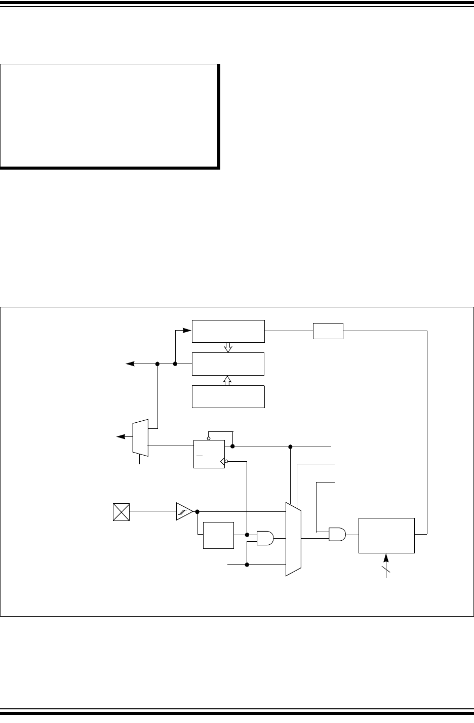
2015 Microchip Technology Inc. Preliminary DS60001320B-page 289
PIC32MZ Embedded Connectivity with Floating Point Unit (EF) Family
14.0 TIMER2/3, TIMER4/5, TIMER6/7,
AND TIMER8/9
This family of devices features eight synchronous
16-bit timers (default) that can operate as a free-
running interval timer for various timing applications
and counting external events.
The following modes are supported:
• Synchronous internal 16-bit timer
• Synchronous internal 16-bit gated timer
• Synchronous external 16-bit timer
Four 32-bit synchronous timers are available by
combining Timer2 with Timer3, Timer4 with Timer5,
Timer6 with Timer7, and Timer8 with Timer9.
The 32-bit timers can operate in one of three modes:
• Synchronous internal 32-bit timer
• Synchronous internal 32-bit gated timer
• Synchronous external 32-bit timer
14.1 Additional Supported Features
• Selectable clock prescaler
• Timers operational during CPU idle
• Time base for Input Capture and Output Compare
modules (Timer2 through Timer7 only)
• ADC event trigger (Timer3 and Timer5 only)
• Fast bit manipulation using CLR, SET, and INV
registers
FIGURE 14-1: TIMER2 THROUGH TIMER9 BLOCK DIAGRAM (16-BIT)
Note: This data sheet summarizes the features
of the PIC32MZ EF family of devices. It is
not intended to be a comprehensive refer-
ence source. To complement the informa-
tion in this data sheet, refer to Section 14.
“Timers” (DS60001105) of the “PIC32
Family Reference Manual”, which is avail-
able from the Microchip web site
(www.microchip.com/PIC32).
Sync
PRx
TxIF Event Flag
Equal Comparator x 16
TMRx
Reset
Q
QD
TGATE
1
0
Gate
TxCK
Sync
ON
TGATE
TCS
TCKPS
Prescaler
3
1, 2, 4, 8, 16,
32, 64, 256
x 1
1 0
0 0
PBCLK3
Trigger to ADC (1)
Note 1: The ADC event trigger is available on Timer3 and Timer5 only.
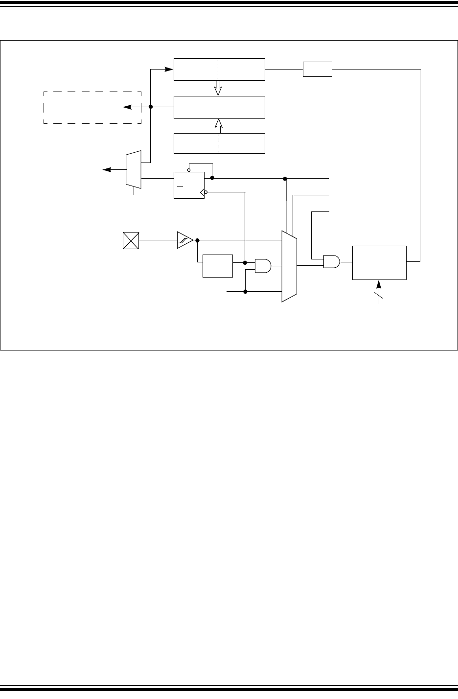
PIC32MZ Embedded Connectivity with Floating Point Unit (EF) Family
DS60001320B-page 290 Preliminary 2015 Microchip Technology Inc.
FIGURE 14-2: TIMER2/3, TIMER4/5, TIMER6/7, AND TIMER8/9 BLOCK DIAGRAM (32-BIT)
TMRy(2) TMRx(2)
TyIF Event Flag(2)
Equal 32-bit Comparator
PRy(2) PRx(2)
Reset
LS Half Word
MS Half Word
Note 1: ADC event trigger is available only on the Timer2/3 and TImer4/5 pairs.
2: In this diagram, ‘x’ represents Timer2, 4, 6, or 8, and ‘y’ represents Timer3, 5, 7, or 9.
TGATE
0
1
PBCLK3
Gate
TxCK(2)
Sync
Sync
ADC Event Trigger(1)
ON
TGATE
TCS
TCKPS
Prescaler
3
1, 2, 4, 8, 16,
32, 64, 256
1 0
0 0
Q
QD
x 1

2015 Microchip Technology Inc. Preliminary DS60001320B-page 291
PIC32MZ Embedded Connectivity with Floating Point Unit (EF) Family
14.2 Timer2-Timer9 Control Registers
TABLE 14-1: TIMER2 THROUGH TIMER9 REGISTER MAP
Virtual Address
(BF84_#)
Register
Name(1)
Bit Range
Bits
All Resets
31/15 30/14 29/13 28/12 27/11 26/10 25/9 24/8 23/7 22/6 21/5 20/4 19/3 18/2 17/1 16/0
0200 T2CON 31:16 — — — — — — — — — — — — — — — — 0000
15:0 ON —SIDL — — — — — TGATE TCKPS<2:0> T32 —TCS —0000
0210 TMR2 31:16 — — — — — — — — — — — — — — — — 0000
15:0 TMR2<15:0> 0000
0220 PR2 31:16 — — — — — — — — — — — — — — — — 0000
15:0 PR2<15:0> FFFF
0400 T3CON 31:16 — — — — — — — — — — — — — — — — 0000
15:0 ON —SIDL — — — — — TGATE TCKPS<2:0> — — TCS —0000
0410 TMR3 31:16 — — — — — — — — — — — — — — — — 0000
15:0 TMR3<15:0> 0000
0420 PR3 31:16 — — — — — — — — — — — — — — — — 0000
15:0 PR3<15:0> FFFF
0600 T4CON 31:16 — — — — — — — — — — — — — — — — 0000
15:0 ON —SIDL — — — — — TGATE TCKPS<2:0> T32 —TCS —0000
0610 TMR4 31:16 — — — — — — — — — — — — — — — — 0000
15:0 TMR4<15:0> 0000
0620 PR4 31:16 — — — — — — — — — — — — — — — — 0000
15:0 PR4<15:0> FFFF
0800 T5CON 31:16 — — — — — — — — — — — — — — — — 0000
15:0 ON —SIDL — — — — — TGATE TCKPS<2:0> — — TCS —0000
0810 TMR5 31:16 — — — — — — — — — — — — — — — — 0000
15:0 TMR5<15:0> 0000
0820 PR5 31:16 — — — — — — — — — — — — — — — — 0000
15:0 PR5<15:0> FFFF
0A00 T6CON 31:16 — — — — — — — — — — — — — — — — 0000
15:0 ON —SIDL — — — — — TGATE TCKPS<2:0> T32 —TCS —0000
0A10 TMR6 31:16 — — — — — — — — — — — — — — — — 0000
15:0 TMR6<15:0> 0000
0A20 PR6 31:16 — — — — — — — — — — — — — — — — 0000
15:0 PR6<15:0> FFFF
0C00 T7CON 31:16 — — — — — — — — — — — — — — — — 0000
15:0 ON —SIDL — — — — — TGATE TCKPS<2:0> — — TCS —0000
Legend: x = unknown value on Reset; — = unimplemented, read as ‘0’. Reset values are shown in hexadecimal.
Note 1: All registers in this table have corresponding CLR, SET and INV registers at their virtual addresses, plus offsets of 0x4, 0x8 and 0xC, respectively. See Section 12.3 “CLR, SET, and INV Registers” for
more information.
PIC32MZ Embedded Connectivity with Floating Point Unit (EF) Family
DS60001320B-page 292 Preliminary 2015 Microchip Technology Inc.
0C10 TMR7 31:16 — — — — — — — — — — — — — — — — 0000
15:0 TMR7<15:0> 0000
0C20 PR7 31:16 — — — — — — — — — — — — — — — — 0000
15:0 PR7<15:0> FFFF
0E00 T8CON 31:16 — — — — — — — — — — — — — — — — 0000
15:0 ON —SIDL — — — — — TGATE TCKPS<2:0> T32 —TCS —0000
0E10 TMR8 31:16 — — — — — — — — — — — — — — — — 0000
15:0 TMR8<15:0> 0000
0E20 PR8 31:16 — — — — — — — — — — — — — — — — 0000
15:0 PR8<15:0> FFFF
1000 T9CON 31:16 — — — — — — — — — — — — — — — — 0000
15:0 ON —SIDL — — — — — TGATE TCKPS<2:0> — — TCS —0000
1010 TMR9 31:16 — — — — — — — — — — — — — — — — 0000
15:0 TMR9<15:0> 0000
1020 PR9 31:16 — — — — — — — — — — — — — — — — 0000
15:0 PR9<15:0> FFFF
TABLE 14-1: TIMER2 THROUGH TIMER9 REGISTER MAP (CONTINUED)
Virtual Address
(BF84_#)
Register
Name(1)
Bit Range
Bits
All Resets
31/15 30/14 29/13 28/12 27/11 26/10 25/9 24/8 23/7 22/6 21/5 20/4 19/3 18/2 17/1 16/0
Legend: x = unknown value on Reset; — = unimplemented, read as ‘0’. Reset values are shown in hexadecimal.
Note 1: All registers in this table have corresponding CLR, SET and INV registers at their virtual addresses, plus offsets of 0x4, 0x8 and 0xC, respectively. See Section 12.3 “CLR, SET, and INV Registers” for
more information.

2015 Microchip Technology Inc. Preliminary DS60001320B-page 293
PIC32MZ Embedded Connectivity with Floating Point Unit (EF) Family
REGISTER 14-1: TxCON: TYPE B TIMER CONTROL REGISTER (‘x’ = 2-9)
Bit
Range Bit
31/23/15/7 Bit
30/22/14/6 Bit
29/21/13/5 Bit
28/20/12/4 Bit
27/19/11/3 Bit
26/18/10/2 Bit
25/17/9/1 Bit
24/16/8/0
31:24 U-0 U-0 U-0 U-0 U-0 U-0 U-0 U-0
— — — — — — — —
23:16 U-0 U-0 U-0 U-0 U-0 U-0 U-0 U-0
— — — — — — — —
15:8 R/W-0 U-0 R/W-0 U-0 U-0 U-0 U-0 U-0
ON(1) —SIDL
(2) — — — — —
7:0 R/W-0 R/W-0 R/W-0 R/W-0 R/W-0 U-0 R/W-0 U-0
TGATE(1) TCKPS<2:0>(1) T32(3) —TCS
(1) —
Legend:
R = Readable bit W = Writable bit U = Unimplemented bit, read as ‘0’
-n = Value at POR ‘1’ = Bit is set ‘0’ = Bit is cleared x = Bit is unknown
bit 31-16 Unimplemented: Read as ‘0’
bit 15 ON: Timer On bit(1)
1 = Module is enabled
0 = Module is disabled
bit 14 Unimplemented: Read as ‘0’
bit 13 SIDL: Stop in Idle Mode bit(2)
1 = Discontinue operation when device enters Idle mode
0 = Continue operation even in Idle mode
bit 12-8 Unimplemented: Read as ‘0’
bit 7 TGATE: Timer Gated Time Accumulation Enable bit(1)
When TCS = 1:
This bit is ignored and is read as ‘0’.
When TCS = 0:
1 = Gated time accumulation is enabled
0 = Gated time accumulation is disabled
bit 6-4 TCKPS<2:0>: Timer Input Clock Prescale Select bits(1)
111 = 1:256 prescale value
110 = 1:64 prescale value
101 = 1:32 prescale value
100 = 1:16 prescale value
011 = 1:8 prescale value
010 = 1:4 prescale value
001 = 1:2 prescale value
000 = 1:1 prescale value
bit 3 T32: 32-Bit Timer Mode Select bit(3)
1 = Odd numbered and even numbered timers form a 32-bit timer
0 = Odd numbered and even numbered timers form separate 16-bit timers
Note 1: While operating in 32-bit mode, this bit has no effect for odd numbered timers (Timer1, Timer3, Timer5,
Timer7, and Timer9). All timer functions are set through the even numbered timers.
2: While operating in 32-bit mode, this bit must be cleared on odd numbered timers to enable the 32-bit timer
in Idle mode.
3: This bit is available only on even numbered timers (Timer2, Timer4, Timer6, and Timer8).

PIC32MZ Embedded Connectivity with Floating Point Unit (EF) Family
DS60001320B-page 294 Preliminary 2015 Microchip Technology Inc.
bit 2 Unimplemented: Read as ‘0’
bit 1 TCS: Timer Clock Source Select bit(1)
1 = External clock from TxCK pin
0 = Internal peripheral clock
bit 0 Unimplemented: Read as ‘0’
REGISTER 14-1: TxCON: TYPE B TIMER CONTROL REGISTER (‘x’ = 2-9) (CONTINUED)
Note 1: While operating in 32-bit mode, this bit has no effect for odd numbered timers (Timer1, Timer3, Timer5,
Timer7, and Timer9). All timer functions are set through the even numbered timers.
2: While operating in 32-bit mode, this bit must be cleared on odd numbered timers to enable the 32-bit timer
in Idle mode.
3: This bit is available only on even numbered timers (Timer2, Timer4, Timer6, and Timer8).
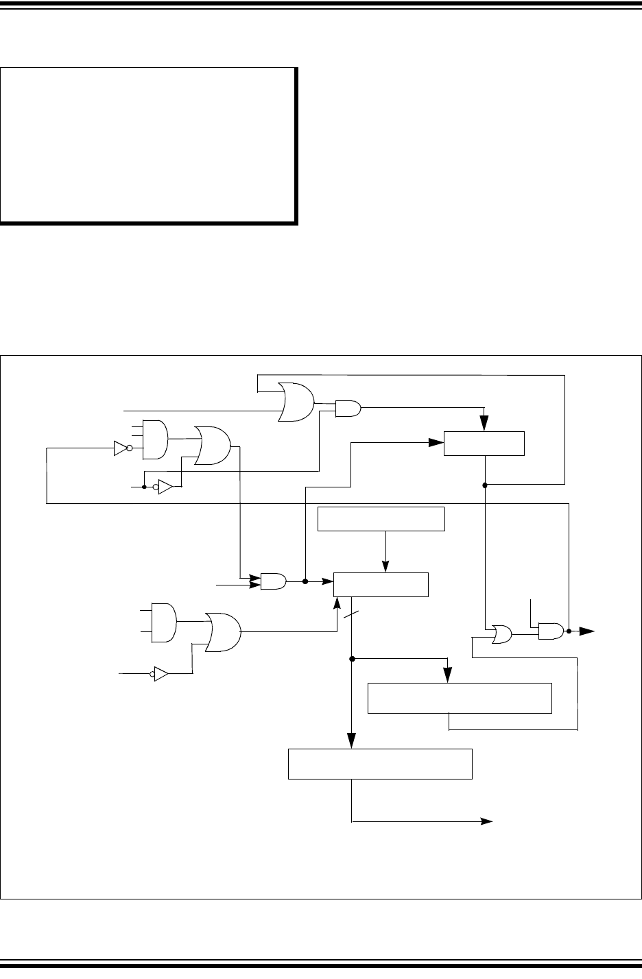
2015 Microchip Technology Inc. Preliminary DS60001320B-page 295
PIC32MZ Embedded Connectivity with Floating Point Unit (EF) Family
15.0 DEADMAN TIMER (DMT)
The primary function of the Deadman Timer (DMT) is
to reset the processor in the event of a software mal-
function. The DMT is a free-running instruction fetch
timer, which is clocked whenever an instruction fetch
occurs until a count match occurs. Instructions are not
fetched when the processor is in Sleep mode.
The DMT consists of a 32-bit counter with a time-out
count match value as specified by the DMTCNT<3:0>
bits in the DEVCFG1 Configuration register.
A Deadman Timer is typically used in mission critical
and safety critical applications, where any single fail-
ure of the software functionality and sequencing must
be detected.
Figure 15-1 shows a block diagram of the Deadman
Timer module.
FIGURE 15-1: DEADMAN TIMER BLOCK DIAGRAM
Note: This data sheet summarizes the features
of the PIC32MZ EF family of devices. It is
not intended to be a comprehensive
reference source. To complement the
information in this data sheet, refer to
Section 9. “Watchdog, Deadman, and
Power-up Timers” (DS60001114) in the
“PIC32 Family Reference Manual”, which
is available from the Microchip web site
(www.microchip.com/PIC32).
32-bit counter
ON
PBCLK7
“Proper Clear Sequence” Flag
ON
Clock ON
DMT Count Reset Load
DMT event
System Reset
System Reset
Instruction Fetched Strobe Force DMT Event
“improper sequence” flag
32
(COUNTER) DMT Window Interval(2)
Window Interval Open
(COUNTER) = DMT Max Count(1)
Counter Initialization Value
Note 1: DMT Max Count is controlled by the DMTCNT<3:0> bits in the DEVCFG1 Configuration register.
2: DMT Window Interval is controlled by the DMTINTV<2:0> bits in the DEVCFG1 Configuration register.
3: Refer to Section 6.0 “Resets” for more information.
to NMI(3)
PIC32MZ Embedded Connectivity with Floating Point Unit (EF) Family
DS60001320B-page 296 Preliminary 2015 Microchip Technology Inc.
15.1 Deadman Timer Control Registers
TABLE 15-1: DEADMAN TIMER REGISTER MAP
Virtual Address
(BF80_#)
Register
Name
Bit Range
Bits
All Resets
31/15 30/14 29/13 28/12 27/11 26/10 25/9 24/8 23/7 22/6 21/5 20/4 19/3 18/2 17/1 16/0
0A00 DMTCON 31:16 — — — — — — — — — — — — — — — — 0000
15:0 ON — — — — — — — — — — — — — — — x000
0A10 DMTPRECLR 31:16 — — — — — — — — — — — — — — — — 0000
15:0 STEP1<7:0> — — — — — — — — 0000
0A20 DMTCLR 31:16 — — — — — — — — — — — — — — — — 0000
15:0 — — — — — — — — STEP2<7:0> 0000
0A30 DMTSTAT 31:16 — — — — — — — — — — — — — — — — 0000
15:0 — — — — — — — — BAD1 BAD2 DMTEVENT — — — — WINOPN 0000
0A40 DMTCNT 31:16 COUNTER<31:0> 0000
15:0 0000
0A60 DMTPSCNT 31:16 PSCNT<31:0> 0000
15:0 00xx
0A70 DMTPSINTV 31:16 PSINTV<31:0> 0000
15:0 000x
Legend: x = unknown value on Reset; — = unimplemented, read as ‘0’. Reset values are shown in hexadecimal.
2015 Microchip Technology Inc. Preliminary DS60001320B-page 297
PIC32MZ Embedded Connectivity with Floating Point Unit (EF) Family
REGISTER 15-1: DMTCON: DEADMAN TIMER CONTROL REGISTER
Bit Range Bit
31/23/15/7 Bit
30/22/14/6 Bit
29/21/13/5 Bit
28/20/12/4 Bit
27/19/11/3 Bit
26/18/10/2 Bit
25/17/9/1 Bit
24/16/8/0
31:24 U-0 U-0 U-0 U-0 U-0 U-0 U-0 U-0
— — — — — — — —
23:16 U-0 U-0 U-0 U-0 U-0 U-0 U-0 U-0
— — — — — — — —
15:8 R/W-y U-0 U-0 U-0 U-0 U-0 U-0 U-0
ON(1) — — — — — — —
7:0 U-0 U-0 U-0 U-0 U-0 U-0 U-0 U-0
— — — — — — — —
Legend: y = Value set from Configuration bits on POR
R = Readable bit W = Writable bit U = Unimplemented bit, read as ‘0’
-n = Value at POR ‘1’ = Bit is set ‘0’ = Bit is cleared x = Bit is unknown
bit 31-16 Unimplemented: Read as ‘0’
bit 15 ON: Deadman Timer Module Enable bit(1)
1 = Deadman Timer module is enabled
0 = Deadman Timer module is disabled
The reset value of this bit is determined by the setting of the FDMTEN bit (DEVCFG1<3>).
bit 13-0 Unimplemented: Read as ‘0’
Note 1: This bit only has control when FDMTEN (DEVCFG1<3>) = 0.
REGISTER 15-2: DMTPRECLR: DEADMAN TIMER PRECLEAR REGISTER
Bit Range Bit
31/23/15/7 Bit
30/22/14/6 Bit
29/21/13/5 Bit
28/20/12/4 Bit
27/19/11/3 Bit
26/18/10/2 Bit
25/17/9/1 Bit
24/16/8/0
31:24 U-0 U-0 U-0 U-0 U-0 U-0 U-0 U-0
— — — — — — — —
23:16 U-0 U-0 U-0 U-0 U-0 U-0 U-0 U-0
— — — — — — — —
15:8 R/W-0 R/W-0 R/W-0 R/W-0 R/W-0 R/W-0 R/W-0 R/W-0
STEP1<7:0>
7:0 U-0 U-0 U-0 U-0 U-0 U-0 U-0 U-0
— — — — — — — —
Legend:
R = Readable bit W = Writable bit U = Unimplemented bit, read as ‘0’
-n = Value at POR ‘1’ = Bit is set ‘0’ = Bit is cleared x = Bit is unknown
bit 31-16 Unimplemented: Read as ‘0’
bit 15-8 STEP1<7:0>: Preclear Enable bits
01000000 = Enables the Deadman Timer Preclear (Step 1)
All other write patterns = Set BAD1 flag.
These bits are cleared when a DMT reset event occurs. STEP1<7:0> is also cleared if the
STEP2<7:0> bits are loaded with the correct value in the correct sequence.
bit 7-0 Unimplemented: Read as ‘0’

PIC32MZ Embedded Connectivity with Floating Point Unit (EF) Family
DS60001320B-page 298 Preliminary 2015 Microchip Technology Inc.
REGISTER 15-3: DMTCLR: DEADMAN TIMER CLEAR REGISTER
Bit Range Bit
31/23/15/7 Bit
30/22/14/6 Bit
29/21/13/5 Bit
28/20/12/4 Bit
27/19/11/3 Bit
26/18/10/2 Bit
25/17/9/1 Bit
24/16/8/0
31:24 U-0 U-0 U-0 U-0 U-0 U-0 U-0 U-0
— — — — — — — —
23:16 U-0 U-0 U-0 U-0 U-0 U-0 U-0 U-0
— — — — — — — —
15:8 U-0 U-0 U-0 U-0 U-0 U-0 U-0 U-0
— — — — — — — —
7:0 R/W-0 R/W-0 R/W-0 R/W-0 R/W-0 R/W-0 R/W-0 R/W-0
STEP2<7:0>
Legend:
R = Readable bit W = Writable bit U = Unimplemented bit, read as ‘0’
-n = Value at POR ‘1’ = Bit is set ‘0’ = Bit is cleared x = Bit is unknown
bit 31-8 Unimplemented: Read as ‘0’
bit 7-0 STEP2<7:0>: Clear Timer bits
00001000 = Clears STEP1<7:0>, STEP2<7:0> and the Deadman Timer if, and only if, preceded by cor-
rect loading of STEP1<7:0> bits in the correct sequence. The write to these bits may be
verified by reading DMTCNT and observing the counter being reset.
All other write patterns = Set BAD2 bit, the value of STEP1<7:0> will remain unchanged, and the new
value being written STEP2<7:0> will be captured. These bits are also cleared when a DMT reset event
occurs.

2015 Microchip Technology Inc. Preliminary DS60001320B-page 299
PIC32MZ Embedded Connectivity with Floating Point Unit (EF) Family
REGISTER 15-4: DMTSTAT: DEADMAN TIMER STATUS REGISTER
Bit Range Bit
31/23/15/7 Bit
30/22/14/6 Bit
29/21/13/5 Bit
28/20/12/4 Bit
27/19/11/3 Bit
26/18/10/2 Bit
25/17/9/1 Bit
24/16/8/0
31:24 U-0 U-0 U-0 U-0 U-0 U-0 U-0 U-0
— — — — — — — —
23:16 U-0 U-0 U-0 U-0 U-0 U-0 U-0 U-0
— — — — — — — —
15:8 U-0 U-0 U-0 U-0 U-0 U-0 U-0 U-0
— — — — — — — —
7:0 R-0, HC, HS R-0, HC, HS R-0, HC, HS U-0 U-0 U-0 U-0 R-0, HC, HS
BAD1 BAD2 DMTEVENT — — — —WINOPN
Legend: HC = Hardware Cleared HS = Hardware Set
R = Readable bit W = Writable bit U = Unimplemented bit, read as ‘0’
-n = Value at POR ‘1’ = Bit is set ‘0’ = Bit is cleared x = Bit is unknown
bit 31-8 Unimplemented: Read as ‘0’
bit 7 BAD1: Bad STEP1<7:0> Value Detect bit
1 = Incorrect STEP1<7:0> value was detected
0 = Incorrect STEP1<7:0> value was not detected
bit 6 BAD2: Bad STEP2<7:0> Value Detect bit
1 = Incorrect STEP2<7:0> value was detected
0 = Incorrect STEP2<7:0> value was not detected
bit 5 DMTEVENT: Deadman Timer Event bit
1 = Deadman timer event was detected (counter expired or bad STEP1<7:0> or STEP2<7:0> value was
entered prior to counter increment)
0 = Deadman timer even was not detected
bit 4-1 Unimplemented: Read as ‘0’
bit 0 WINOPN: Deadman Timer Clear Window bit
1 = Deadman timer clear window is open
0 = Deadman timer clear window is not open

PIC32MZ Embedded Connectivity with Floating Point Unit (EF) Family
DS60001320B-page 300 Preliminary 2015 Microchip Technology Inc.
REGISTER 15-5: DMTCNT: DEADMAN TIMER COUNT REGISTER
Bit Range Bit
31/23/15/7 Bit
30/22/14/6 Bit
29/21/13/5 Bit
28/20/12/4 Bit
27/19/11/3 Bit
26/18/10/2 Bit
25/17/9/1 Bit
24/16/8/0
31:24 R-0 R-0 R-0 R-0 R-0 R-0 R-0 R-0
COUNTER<31:24>
23:16 R-0 R-0 R-0 R-0 R-0 R-0 R-0 R-0
COUNTER<23:16>
15:8 R-0 R-0 R-0 R-0 R-0 R-0 R-0 R-0
COUNTER<15:8>
7:0 R-0 R-0 R-0 R-0 R-0 R-0 R-0 R-0
COUNTER<7:0>
Legend:
R = Readable bit W = Writable bit U = Unimplemented bit, read as ‘0’
-n = Value at POR ‘1’ = Bit is set ‘0’ = Bit is cleared x = Bit is unknown
bit 31-8 COUNTER<31:0>: Read current contents of DMT counter
REGISTER 15-6: DMTPSCNT: POST STATUS CONFIGURE DMT COUNT STATUS REGISTER
Bit Range Bit
31/23/15/7 Bit
30/22/14/6 Bit
29/21/13/5 Bit
28/20/12/4 Bit
27/19/11/3 Bit
26/18/10/2 Bit
25/17/9/1 Bit
24/16/8/0
31:24 R-0 R-0 R-0 R-0 R-0 R-0 R-0 R-0
PSCNT<31:24>
23:16 R-0 R-0 R-0 R-0 R-0 R-0 R-0 R-0
PSCNT<23:16>
15:8 R-0 R-0 R-0 R-0 R-0 R-0 R-0 R-0
PSCNT<15:8>
7:0 R-0 R-0 R-0 R-y R-y R-y R-y R-y
PSCNT<7:0>
Legend: y = Value set from Configuration bits on POR
R = Readable bit W = Writable bit U = Unimplemented bit, read as ‘0’
-n = Value at POR ‘1’ = Bit is set ‘0’ = Bit is cleared x = Bit is unknown
bit 31-8 PSCNT<31:0>: DMT Instruction Count Value Configuration Status bits
This is always the value of the DMTCNT<4:0> bits in the DEVCFG1 Configuration register.

2015 Microchip Technology Inc. Preliminary DS60001320B-page 301
PIC32MZ Embedded Connectivity with Floating Point Unit (EF) Family
REGISTER 15-7: DMTPSINTV: POST STATUS CONFIGURE DMT INTERVAL STATUS REGISTER
Bit Range Bit
31/23/15/7 Bit
30/22/14/6 Bit
29/21/13/5 Bit
28/20/12/4 Bit
27/19/11/3 Bit
26/18/10/2 Bit
25/17/9/1 Bit
24/16/8/0
31:24 R-0 R-0 R-0 R-0 R-0 R-0 R-0 R-0
PSINTV<31:24>
23:16 R-0 R-0 R-0 R-0 R-0 R-0 R-0 R-0
PSINTV<23:16>
15:8 R-0 R-0 R-0 R-0 R-0 R-0 R-0 R-0
PSINTV<15:8>
7:0 R-0 R-0 R-0 R-0 R-0 R-y R-y R-y
PSINTV<7:0>
Legend: y = Value set from Configuration bits on POR
R = Readable bit W = Writable bit U = Unimplemented bit, read as ‘0’
-n = Value at POR ‘1’ = Bit is set ‘0’ = Bit is cleared x = Bit is unknown
bit 31-8 PSINTV<31:0>: DMT Window Interval Configuration Status bits
This is always the value of the DMTINTV<2:0> bits in the DEVCFG1 Configuration register.

PIC32MZ Embedded Connectivity with Floating Point Unit (EF) Family
DS60001320B-page 302 Preliminary 2015 Microchip Technology Inc.
NOTES:
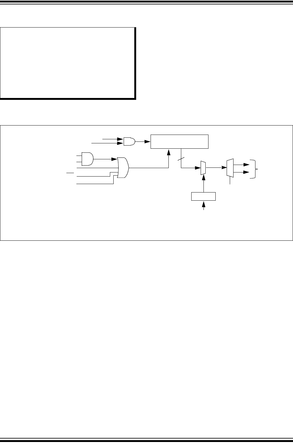
2015 Microchip Technology Inc. Preliminary DS60001320B-page 303
PIC32MZ Embedded Connectivity with Floating Point Unit (EF) Family
16.0 WATCHDOG TIMER (WDT) When enabled, the Watchdog Timer (WDT) operates
from the internal Low-Power Oscillator (LPRC) clock
source and can be used to detect system software mal-
functions by resetting the device if the WDT is not
cleared periodically in software. Various WDT time-out
periods can be selected using the WDT postscaler. The
WDT can also be used to wake the device from Sleep
or Idle mode.
Key features of the WDT module include:
• Configuration or software controlled
• User-configurable time-out period
• Can wake the device from Sleep or Idle
FIGURE 16-1: WATCHDOG TIMER BLOCK DIAGRAM
Note: This data sheet summarizes the features
of the PIC32MZ EF family of devices. It is
not intended to be a comprehensive
reference source. To complement the
information in this data sheet, refer to Sec-
tion 9. “Watchdog, Deadman, and
Power-up Timers” (DS60001114) in the
“PIC32 Family Reference Manual”, which
is available from the Microchip web site
(www.microchip.com/PIC32).
Wake
WDTCLRKEY<15:0> = 0x5743
ON
Power Save
32-bit Counter
WDT Counter Reset
32
WDT Event
RUNDIV<4:0> (WDTCON<12:8>)
Clock
Decoder
0
1
ON
Reset Event
to NMI(1)
Note 1: Refer to 6.0 “Resets” for more information.
ON
LPRC

PIC32MZ Embedded Connectivity with Floating Point Unit (EF) Family
DS60001320B-page 304 Preliminary 2015 Microchip Technology Inc.
16.1 Watchdog Timer Control Registers
TABLE 16-1: WATCHDOG TIMER REGISTER MAP
Virtual Address
(BF80_#)
Register
Name
Bit Range
Bits
All Resets
31/15 30/14 29/13 28/12 27/11 26/10 25/9 24/8 23/7 22/6 21/5 20/4 19/3 18/2 17/1 16/0
0800 WDTCON(1) 31:16 WDTCLRKEY<15:0> 0000
15:0 ON — — RUNDIV<4:0> — — — — — — — WDTWINEN xx00
Legend: x = unknown value on Reset; — = unimplemented, read as ‘0’. Reset values are shown in hexadecimal.
Note 1: This register has corresponding CLR, SET and INV registers at its virtual address, plus an offset of 0x4, 0x8 and 0xC, respectively. See 12.0 “I/O Ports” for more information.

2015 Microchip Technology Inc. Preliminary DS60001320B-page 305
PIC32MZ Embedded Connectivity with Floating Point Unit (EF) Family
REGISTER 16-1: WDTCON: WATCHDOG TIMER CONTROL REGISTER
Bit
Range Bit
31/23/15/7 Bit
30/22/14/6 Bit
29/21/13/5 Bit
28/20/12/4 Bit
27/19/11/3 Bit
26/18/10/2 Bit
25/17/9/1 Bit
24/16/8/0
31:24 W-0 W-0 W-0 W-0 W-0 W-0 W-0 W-0
WDTCLRKEY<15:8>
23:16 W-0 W-0 W-0 W-0 W-0 W-0 W-0 W-0
WDTCLRKEY<7:0>
15:8 R/W-y U-0 U-0 R-y R-y R-y R-y R-y
ON(1) —— RUNDIV<4:0>
7:0 U-0 U-0 U-0 U-0 U-0 U-0 U-0 R/W-0
— — — — — — — WDTWINEN
Legend: y = Values set from Configuration bits on POR
R = Readable bit W = Writable bit U = Unimplemented bit, read as ‘0’
-n = Value at POR ‘1’ = Bit is set ‘0’ = Bit is cleared x = Bit is unknown
bit 31-16 WDTCLRKEY: Watchdog Timer Clear Key bits
To clear the Watchdog Timer to prevent a time-out, software must write the value 0x5743 to this location
using a single 16-bit write.
bit 15 ON: Watchdog Timer Enable bit(1)
1 = The WDT is enabled
0 = The WDT is disabled
bit 14-13 Unimplemented: Read as ‘0’
bit 12-8 RUNDIV<4:0>: Watchdog Timer Postscaler Value bits
On reset, these bits are set to the values of the WDTPS<4:0> Configuration bits in DEVCFG1.
bit 7-1 Unimplemented: Read as ‘0’
bit 0 WDTWINEN: Watchdog Timer Window Enable bit
1 = Enable windowed Watchdog Timer
0 = Disable windowed Watchdog Timer
Note 1: This bit only has control when FWDTEN (DEVCFG1<23>) = 0.

PIC32MZ Embedded Connectivity with Floating Point Unit (EF) Family
DS60001320B-page 306 Preliminary 2015 Microchip Technology Inc.
NOTES:
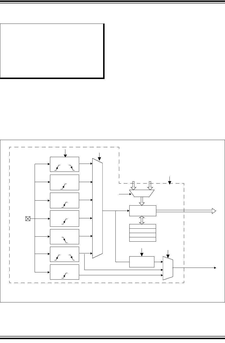
2015 Microchip Technology Inc. Preliminary DS60001320B-page 307
PIC32MZ Embedded Connectivity with Floating Point Unit (EF) Family
17.0 INPUT CAPTURE
The Input Capture module is useful in applications
requiring frequency (period) and pulse measurement.
The Input Capture module captures the 16-bit or 32-bit
value of the selected Time Base registers when an
event occurs at the ICx pin.
Capture events are caused by the following:
• Capture timer value on every edge (rising and falling),
specified edge first
• Prescaler capture event modes:
- Capture timer value on every 4th rising edge of
input at ICx pin
- Capture timer value on every 16th rising edge of
input at ICx pin
Each input capture channel can select between one of
six 16-bit timers for the time base, or two of six 16-bit
timers together to form a 32-bit timer. The selected
timer can use either an internal or external clock.
Other operational features include:
• Device wake-up from capture pin during Sleep and
Idle modes
• Interrupt on input capture event
• 4-word FIFO buffer for capture values; Interrupt
optionally generated after 1, 2, 3, or 4 buffer
locations are filled
• Input capture can also be used to provide additional
sources of external interrupts
FIGURE 17-1: INPUT CAPTURE BLOCK DIAGRAM
Note: This data sheet summarizes the fea-
tures of the PIC32MZ EF family of
devices. It is not intended to be a
comprehensive reference source. To
complement the information in this data
sheet, refer to Section 15. “Input Cap-
ture” (DS60001122) of the “PIC32 Fam-
ily Reference Manual”, which is
available from the Microchip web site
(www.microchip.com/PIC32).
FIFO Control
ICxBUF(1)
Timerx(2)
CaptureEvent
/N
FIFO
ICI<1:0>
ICM<2:0>
ICM<2:0>
101
100
011
010
001
001
111
To CPU
Set Flag ICxIF(1)
(In IFSx Register)
Rising Edge Mode
Prescaler Mode
(4th Rising Edge)
FallingEdgeMode
Edge Detection
Prescaler Mode
(16th Rising Edge)
Sleep/Idle
Wake-up Mode
C32/ICTMR
ICx(1)
Mode
110
Specified/Every
Edge Mode
FEDGE
PBCLK3
Note 1: An ‘x’ in a signal, register or bit name denotes the number of the capture channel.
2: See Table 17-1 for Timerx and Timery selections.
Timery(2)

PIC32MZ Embedded Connectivity with Floating Point Unit (EF) Family
DS60001320B-page 308 Preliminary 2015 Microchip Technology Inc.
The timer source for each Input Capture module
depends on the setting of the ICACLK bit in the
CFGCON register. The available configurations are
shown in Table 17-1.
TABLE 17-1: TIMER SOURCE
CONFIGURATIONS
Input Capture
Module Timerx Timery
ICACLK (CFGCON<17>) = 0
IC1
•
•
•
IC9
Timer2
•
•
•
Timer 2
Timer3
•
•
•
Timer 3
ICACLK (CFGCON<17>) = 1
IC1 Timer4 Timer5
IC2 Timer4 Timer5
IC3 Timer4 Timer5
IC4 Timer2 Timer3
IC5 Timer2 Timer3
IC6 Timer2 Timer3
IC7 Timer6 Timer7
IC8 Timer6 Timer7
IC9 Timer6 Timer7

2015 Microchip Technology Inc. Preliminary DS60001320B-page 309
PIC32MZ Embedded Connectivity with Floating Point Unit (EF) Family
17.1 Input Capture Control Registers
TABLE 17-2: INPUT CAPTURE 1 THROUGH INPUT CAPTURE 9 REGISTER MAP
Virtual Address
(BF84_#)
Register
Name
Bit Range
Bits
All Resets
31/15 30/14 29/13 28/12 27/11 26/10 25/9 24/8 23/7 22/6 21/5 20/4 19/3 18/2 17/1 16/0
2000 IC1CON(1) 31:16 — — — — — — — — — — — — — — — — 0000
15:0 ON —SIDL — — — FEDGE C32 ICTMR ICI<1:0> ICOV ICBNE ICM<2:0> 0000
2010 IC1BUF 31:16 IC1BUF<31:0> xxxx
15:0 xxxx
2200 IC2CON(1) 31:16 — — — — — — — — — — — — — — — — 0000
15:0 ON —SIDL — — — FEDGE C32 ICTMR ICI<1:0> ICOV ICBNE ICM<2:0> 0000
2210 IC2BUF 31:16 IC2BUF<31:0> xxxx
15:0 xxxx
2400 IC3CON(1) 31:16 — — — — — — — — — — — — — — — — 0000
15:0 ON —SIDL — — — FEDGE C32 ICTMR ICI<1:0> ICOV ICBNE ICM<2:0> 0000
2410 IC3BUF 31:16 IC3BUF<31:0> xxxx
15:0 xxxx
2600 IC4CON(1) 31:16 — — — — — — — — — — — — — — — — 0000
15:0 ON —SIDL — — — FEDGE C32 ICTMR ICI<1:0> ICOV ICBNE ICM<2:0> 0000
2610 IC4BUF 31:16 IC4BUF<31:0> xxxx
15:0 xxxx
2800 IC5CON(1) 31:16 — — — — — — — — — — — — — — — — 0000
15:0 ON —SIDL — — — FEDGE C32 ICTMR ICI<1:0> ICOV ICBNE ICM<2:0> 0000
2810 IC5BUF 31:16 IC5BUF<31:0> xxxx
15:0 xxxx
2A00 IC6CON(1) 31:16 — — — — — — — — — — — — — — — — 0000
15:0 ON —SIDL — — — FEDGE C32 ICTMR ICI<1:0> ICOV ICBNE ICM<2:0> 0000
2A10 IC6BUF 31:16 IC6BUF<31:0> xxxx
15:0 xxxx
2C00 IC7CON(1) 31:16 — — — — — — — — — — — — — — — — 0000
15:0 ON —SIDL — — — FEDGE C32 ICTMR ICI<1:0> ICOV ICBNE ICM<2:0> 0000
2C10 IC7BUF 31:16 IC7BUF<31:0> xxxx
15:0 xxxx
2E00 IC8CON(1) 31:16 — — — — — — — — — — — — — — — — 0000
15:0 ON —SIDL — — — FEDGE C32 ICTMR ICI<1:0> ICOV ICBNE ICM<2:0> 0000
2E10 IC8BUF 31:16 IC8BUF<31:0> xxxx
15:0 xxxx
3000 IC9CON(1) 31:16 — — — — — — — — — — — — — — — — 0000
15:0 ON —SIDL — — — FEDGE C32 ICTMR ICI<1:0> ICOV ICBNE ICM<2:0> 0000
3010 IC9BUF 31:16 IC9BUF<31:0> xxxx
15:0 xxxx
Legend: x = unknown value on Reset; — = unimplemented, read as ‘0’. Reset values are shown in hexadecimal.
Note 1: This register has corresponding CLR, SET and INV registers at its virtual address, plus an offset of 0x4, 0x8 and 0xC, respectively. See Section 12.3 “CLR, SET, and INV Registers” for more
information.

PIC32MZ Embedded Connectivity with Floating Point Unit (EF) Family
DS60001320B-page 310 Preliminary 2015 Microchip Technology Inc.
REGISTER 17-1: ICXCON: INPUT CAPTURE X CONTROL REGISTER
Bit Range Bit
31/23/15/7 Bit
30/22/14/6 Bit
29/21/13/5 Bit
28/20/12/4 Bit
27/19/11/3 Bit
26/18/10/2 Bit
25/17/9/1 Bit
24/16/8/0
31:24 U-0 U-0 U-0 U-0 U-0 U-0 U-0 U-0
— — — — — — — —
23:16 U-0 U-0 U-0 U-0 U-0 U-0 U-0 U-0
— — — — — — — —
15:8 R/W-0 U-0 R/W-0 U-0 U-0 U-0 R/W-0 R/W-0
ON —SIDL— — —FEDGEC32
7:0 R/W-0 R/W-0 R/W-0 R-0 R-0 R/W-0 R/W-0 R/W-0
ICTMR ICI<1:0> ICOV ICBNE ICM<2:0>
Legend:
R = Readable bit W = Writable bit U = Unimplemented bit
-n = Bit Value at POR: (‘0’, ‘1’, x = unknown) P = Programmable bit r = Reserved bit
bit 31-16 Unimplemented: Read as ‘0’
bit 15 ON: Input Capture Module Enable bit
1 = Module enabled
0 = Disable and reset module, disable clocks, disable interrupt generation and allow SFR modifications
bit 14 Unimplemented: Read as ‘0’
bit 13 SIDL: Stop in Idle Control bit
1 = Halt in CPU Idle mode
0 = Continue to operate in CPU Idle mode
bit 12-10 Unimplemented: Read as ‘0’
bit 9 FEDGE: First Capture Edge Select bit (only used in mode 6, ICM<2:0> = 110)
1 = Capture rising edge first
0 = Capture falling edge first
bit 8 C32: 32-bit Capture Select bit
1 = 32-bit timer resource capture
0 = 16-bit timer resource capture
bit 7 ICTMR: Timer Select bit (Does not affect timer selection when C32 (ICxCON<8>) is ‘1’)(1)
0 = Timery is the counter source for capture
1 = Timerx is the counter source for capture
bit 6-5 ICI<1:0>: Interrupt Control bits
11 = Interrupt on every fourth capture event
10 = Interrupt on every third capture event
01 = Interrupt on every second capture event
00 = Interrupt on every capture event
bit 4 ICOV: Input Capture Overflow Status Flag bit (read-only)
1 = Input capture overflow occurred
0 = No input capture overflow occurred
bit 3 ICBNE: Input Capture Buffer Not Empty Status bit (read-only)
1 = Input capture buffer is not empty; at least one more capture value can be read
0 = Input capture buffer is empty
bit 2-0 ICM<2:0>: Input Capture Mode Select bits
111 = Interrupt-Only mode (only supported while in Sleep mode or Idle mode)
110 = Simple Capture Event mode – every edge, specified edge first and every edge thereafter
101 = Prescaled Capture Event mode – every sixteenth rising edge
100 = Prescaled Capture Event mode – every fourth rising edge
011 = Simple Capture Event mode – every rising edge
010 = Simple Capture Event mode – every falling edge
001 = Edge Detect mode – every edge (rising and falling)
000 = Input Capture module is disabled
Note 1: Refer to Table 17-1 for Timerx and Timery selections.

2015 Microchip Technology Inc. Preliminary DS60001320B-page 311
PIC32MZ Embedded Connectivity with Floating Point Unit (EF) Family
18.0 OUTPUT COMPARE
The Output Compare module is used to generate a
single pulse or a train of pulses in response to selected
time base events.
For all modes of operation, the Output Compare mod-
ule compares the values stored in the OCxR and/or the
OCxRS registers to the value in the selected timer.
When a match occurs, the Output Compare module
generates an event based on the selected mode of
operation.
The following are some of the key features:
• Multiple Output Compare modules in a device
• Programmable interrupt generation on compare
event
• Single and Dual Compare modes
• Single and continuous output pulse generation
• Pulse-Width Modulation (PWM) mode
• Hardware-based PWM Fault detection and
automatic output disable
• Programmable selection of 16-bit or 32-bit time
bases
• Can operate from either of two available 16-bit
time bases or a single 32-bit time base
• ADC event trigger
FIGURE 18-1: OUTPUT COMPARE MODULE BLOCK DIAGRAM
Note: This data sheet summarizes the
features of the PIC32MZ EF family of
devices. It is not intended to be a
comprehensive reference source. To
complement the information in this data
sheet, refer to Section 16. “Output
Compare” (DS60001111) in the “PIC32
Family Reference Manual”, which is
available from the Microchip web site
(www.microchip.com/PIC32).
OCxR(1)
Comparator
Output
Logic QS
R
OCM<2:0>
Output Enable
OCx(1)
Set Flag bit OCxIF(1)
OCxRS(1)
Mode Select
3
Note 1: Where ‘x’ is shown, reference is made to the registers associated with the respective output compare channels,
1 through 9.
2: The OCFA pin controls the OC1, OC3, and OC7-OC9 channels. The OCFB pin controls the OC4-OC6 channels.
3: Refer to Table 18-1 for Timerx and Timery selections.
4: The ADC event trigger is only available on OC1,OC3, and OC 5.
01
OCTSEL 01
16
16
OCFA or
Timerx(3) Timerx(3)
Logic
Output
Enable
PBCLK3 Timery(3)
Rollover Timery(3)
Rollover
OCFB(2)
Trigger to ADC(4)

PIC32MZ Embedded Connectivity with Floating Point Unit (EF) Family
DS60001320B-page 312 Preliminary 2015 Microchip Technology Inc.
The timer source for each Output Compare module
depends on the setting of the OCACLK bit in the CFG-
CON register. The available configurations are shown
in Table 18-1.
TABLE 18-1: TIMER SOURCE
CONFIGURATIONS
Output
Compare
Module Timerx Timery
OCACLK (CFGCON<16>) = 0
OC1
•
•
•
OC9
Timer2
•
•
•
Timer 2
Timer3
•
•
•
Timer 3
OCACLK (CFGCON<16>) = 1
OC1 Timer4 Timer5
OC2 Timer4 Timer5
OC3 Timer4 Timer5
OC4 Timer2 Timer3
OC5 Timer2 Timer3
OC6 Timer2 Timer3
OC7 Timer6 Timer7
OC8 Timer6 Timer7
OC9 Timer6 Timer7

2015 Microchip Technology Inc. Preliminary DS60001320B-page 313
PIC32MZ Embedded Connectivity with Floating Point Unit (EF) Family
18.1 Output Compare Control Registers
TABLE 18-2: OUTPUT COMPARE 1 THROUGH OUTPUT COMPARE 9 REGISTER MAP
Virtual Address
(BF84_#)
Register
Name(1)
Bit Range
Bits
All Resets
31/15 30/14 29/13 28/12 27/11 26/10 25/9 24/8 23/7 22/6 21/5 20/4 19/3 18/2 17/1 16/0
4000 OC1CON 31:16 ————————————————0000
15:0 ON —SIDL ———————OC32 OCFLT OCTSEL OCM<2:0> 0000
4010 OC1R 31:16 OC1R<31:0> xxxx
15:0 xxxx
4020 OC1RS 31:16 OC1RS<31:0> xxxx
15:0 xxxx
4200 OC2CON 31:16 ————————————————0000
15:0 ON —SIDL ———————OC32 OCFLT OCTSEL OCM<2:0> 0000
4210 OC2R 31:16 OC2R<31:0> xxxx
15:0 xxxx
4220 OC2RS 31:16 OC2RS<31:0> xxxx
15:0 xxxx
4400 OC3CON 31:16 ————————————————0000
15:0 ON —SIDL ———————OC32 OCFLT OCTSEL OCM<2:0> 0000
4410 OC3R 31:16 OC3R<31:0> xxxx
15:0 xxxx
4420 OC3RS 31:16
15:0 OC3RS<31:0> xxxx
xxxx
4600 OC4CON 31:16 ————————————————0000
15:0 ON —SIDL ———————OC32 OCFLT OCTSEL OCM<2:0> 0000
4610 OC4R 31:16 OC4R<31:0> xxxx
15:0 xxxx
4620 OC4RS 31:16
15:0 OC4RS<31:0> xxxx
xxxx
4800 OC5CON 31:16 ————————————————0000
15:0 ON —SIDL ———————OC32 OCFLT OCTSEL OCM<2:0> 0000
4810 OC5R 31:16 OC5R<31:0> xxxx
15:0 xxxx
4820 OC5RS 31:16 OC5RS<31:0> xxxx
15:0 xxxx
Legend: x = unknown value on Reset; — = unimplemented, read as ‘0’. Reset values are shown in hexadecimal.
Note 1: All registers in this table have corresponding CLR, SET and INV registers at their virtual addresses, plus offsets of 0x4, 0x8 and 0xC, respectively. See Section 12.3 “CLR, SET, and INV Registers” for
more information.

PIC32MZ Embedded Connectivity with Floating Point Unit (EF) Family
DS60001320B-page 314 Preliminary 2015 Microchip Technology Inc.
4A00 OC6CON 31:16 ————————————————0000
15:0 ON —SIDL ———————OC32 OCFLT OCTSEL OCM<2:0> 0000
4A10 OC6R 31:16 OC6R<31:0> xxxx
15:0 xxxx
4A20 OC6RS 31:16 OC6RS<31:0> xxxx
15:0 xxxx
4C00 OC7CON 31:16 ————————————————0000
15:0 ON —SIDL ———————OC32 OCFLT OCTSEL OCM<2:0> 0000
4C10 OC7R 31:16 OC7R<31:0> xxxx
15:0 xxxx
4C20 OC7RS 31:16 OC7RS<31:0> xxxx
15:0 xxxx
4E00 OC8CON 31:16 ————————————————0000
15:0 ON —SIDL ———————OC32 OCFLT OCTSEL OCM<2:0> 0000
4E10 OC8R 31:16 OC8R<31:0> xxxx
15:0 xxxx
4E20 OC8RS 31:16
15:0 OC8RS<31:0> xxxx
xxxx
5000 OC9CON 31:16 ————————————————0000
15:0 ON —SIDL ———————OC32 OCFLT OCTSEL OCM<2:0> 0000
5010 OC9R 31:16 OC9R<31:0> xxxx
15:0 xxxx
5020 OC9RS 31:16
15:0 OC9RS<31:0> xxxx
TABLE 18-2: OUTPUT COMPARE 1 THROUGH OUTPUT COMPARE 9 REGISTER MAP (CONTINUED)
Virtual Address
(BF84_#)
Register
Name(1)
Bit Range
Bits
All Resets
31/15 30/14 29/13 28/12 27/11 26/10 25/9 24/8 23/7 22/6 21/5 20/4 19/3 18/2 17/1 16/0
Legend: x = unknown value on Reset; — = unimplemented, read as ‘0’. Reset values are shown in hexadecimal.
Note 1: All registers in this table have corresponding CLR, SET and INV registers at their virtual addresses, plus offsets of 0x4, 0x8 and 0xC, respectively. See Section 12.3 “CLR, SET, and INV Registers” for
more information.

2015 Microchip Technology Inc. Preliminary DS60001320B-page 315
PIC32MZ Embedded Connectivity with Floating Point Unit (EF) Family
REGISTER 18-1: OCxCON: OUTPUT COMPARE ‘x’ CONTROL REGISTER
Bit
Range Bit
31/23/15/7 Bit
30/22/14/6 Bit
29/21/13/5 Bit
28/20/12/4 Bit
27/19/11/3 Bit
26/18/10/2 Bit
25/17/9/1 Bit
24/16/8/0
31:24 U-0 U-0 U-0 U-0 U-0 U-0 U-0 U-0
— — — — — — — —
23:16 U-0 U-0 U-0 U-0 U-0 U-0 U-0 U-0
— — — — — — — —
15:8 R/W-0 U-0 R/W-0 U-0 U-0 U-0 U-0 U-0
ON —SIDL— — — — —
7:0 U-0 U-0 R/W-0 R-0 R/W-0 R/W-0 R/W-0 R/W-0
—— OC32 OCFLT(1) OCTSEL(2) OCM<2:0>
Legend:
R = Readable bit W = Writable bit U = Unimplemented bit, read as ‘0’
-n = Value at POR ‘1’ = Bit is set ‘0’ = Bit is cleared x = Bit is unknown
bit 31-16 Unimplemented: Read as ‘0’
bit 15 ON: Output Compare Peripheral On bit
1 = Output Compare peripheral is enabled
0 = Output Compare peripheral is disabled
bit 14 Unimplemented: Read as ‘0’
bit 13 SIDL: Stop in Idle Mode bit
1 = Discontinue operation when CPU enters Idle mode
0 = Continue operation in Idle mode
bit 12-6 Unimplemented: Read as ‘0’
bit 5 OC32: 32-bit Compare Mode bit
1 = OCxR<31:0> and/or OCxRS<31:0> are used for comparisons to the 32-bit timer source
0 = OCxR<15:0> and OCxRS<15:0> are used for comparisons to the 16-bit timer source
bit 4 OCFLT: PWM Fault Condition Status bit(1)
1 = PWM Fault condition has occurred (cleared in HW only)
0 = No PWM Fault condition has occurred
bit 3 OCTSEL: Output Compare Timer Select bit(2)
1 = Timery is the clock source for this Output Compare module
0 = Timerx is the clock source for this Output Compare module
bit 2-0 OCM<2:0>: Output Compare Mode Select bits
111 = PWM mode on OCx; Fault pin enabled
110 = PWM mode on OCx; Fault pin disabled
101 = Initialize OCx pin low; generate continuous output pulses on OCx pin
100 = Initialize OCx pin low; generate single output pulse on OCx pin
011 = Compare event toggles OCx pin
010 = Initialize OCx pin high; compare event forces OCx pin low
001 = Initialize OCx pin low; compare event forces OCx pin high
000 = Output compare peripheral is disabled but continues to draw current
Note 1: This bit is only used when OCM<2:0> = ‘111’. It is read as ‘0’ in all other modes.
2: Refer to Table 18-1 for Timerx and Timery selections.

PIC32MZ Embedded Connectivity with Floating Point Unit (EF) Family
DS60001320B-page 316 Preliminary 2015 Microchip Technology Inc.
NOTES:
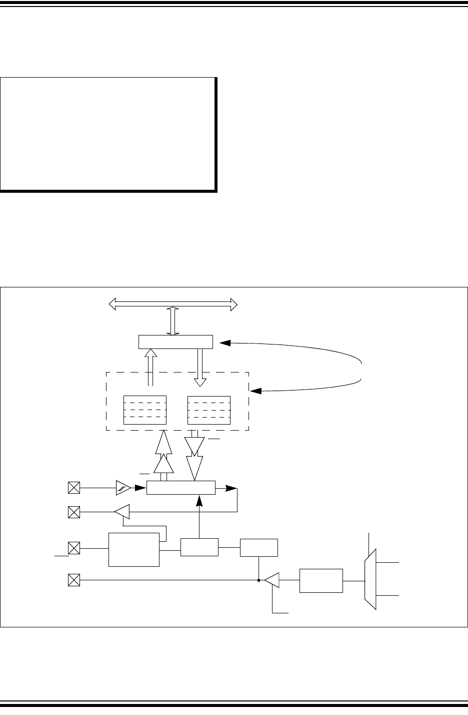
2015 Microchip Technology Inc. Preliminary DS60001320B-page 317
PIC32MZ Embedded Connectivity with Floating Point Unit (EF) Family
19.0 SERIAL PERIPHERAL
INTERFACE (SPI) AND
INTER-IC SOUND (I2S)
The SPI/I2S module is a synchronous serial interface
that is useful for communicating with external
peripherals and other microcontroller devices, as well
as digital audio devices. These peripheral devices may
be Serial EEPROMs, Shift registers, display drivers,
Analog-to-Digital Converters (ADC), etc.
The SPI/I2S module is compatible with Motorola® SPI
and SIOP interfaces.
Key features of the SPI module include:
• Master and Slave modes support
• Four different clock formats
• Enhanced Framed SPI protocol support
• User-configurable 8-bit, 16-bit and 32-bit data width
• Separate SPI FIFO buffers for receive and transmit
- FIFO buffers act as 4/8/16-level deep FIFOs
based on 32/16/8-bit data width
• Programmable interrupt event on every 8-bit,
16-bit and 32-bit data transfer
• Operation during Sleep and Idle modes
• Audio Codec Support:
-I
2S protocol
- Left-justified
- Right-justified
-PCM
FIGURE 19-1: SPI/I2S MODULE BLOCK DIAGRAM
Note: This data sheet summarizes the features
of the PIC32MZ EF family of devices. It is
not intended to be a comprehensive refer-
ence source. To complement the informa-
tion in this data sheet, refer to Section 23.
“Serial Peripheral Interface (SPI)”
(DS60001106) in the “PIC32 Family Refer-
ence Manual”, which is available from the
Microchip web site (www.microchip.com/
PIC32).
Internal
Data Bus
SDIx
SDOx
SSx/FSYNC
SCKx
SPIxSR
bit 0
Shift
Control
Edge
Select
MSTEN
Baud Rate
Slave Select
Sync Control
Clock
Control
Transmit
Receive
and Frame
Note: Access SPIxTXB and SPIxRXB FIFOs via SPIxBUF register.
FIFOs Share Address SPIxBUF
SPIxBUF
Generator
PBCLK2
WriteRead
SPIxTXB FIFO
SPIxRXB FIFO
REFCLKO1
MCLKSEL

PIC32MZ Embedded Connectivity with Floating Point Unit (EF) Family
DS60001320B-page 318 Preliminary 2015 Microchip Technology Inc.
19.1 SPI Control Registers
TABLE 19-1: SPI1 THROUGH SPI6 REGISTER MAP
Virtual Address
(BF82_#)
Register
Name(1)
Bit Range
Bits
All Resets
31/15 30/14 29/13 28/12 27/11 26/10 25/9 24/8 23/7 22/6 21/5 20/4 19/3 18/2 17/1 16/0
1000 SPI1CON 31:16 FRMEN FRMSYNC FRMPOL MSSEN FRMSYPW FRMCNT<2:0> MCLKSEL — — — — — SPIFE ENHBUF 0000
15:0 ON —SIDL DISSDO MODE32 MODE16 SMP CKE SSEN CKP MSTEN DISSDI STXISEL<1:0> SRXISEL<1:0> 0000
1010 SPI1STAT 31:16 — — — RXBUFELM<4:0> — — — TXBUFELM<4:0> 0000
15:0 — — — FRMERR SPIBUSY — — SPITUR SRMT SPIROV SPIRBE —SPITBE —SPITBF SPIRBF 0008
1020 SPI1BUF 31:16 DATA<31:0> 0000
15:0 0000
1030 SPI1BRG 31:16 — — — — — — — — — — — — — — — — 0000
15:0 — — — BRG<12:0> 0000
1040 SPI1CON2
31:16 — — — — — — — — — — — — — — — — 0000
15:0 SPI
SGNEXT — — FRM
ERREN SPI
ROVEN SPI
TUREN IGNROV IGNTUR AUDEN — — — AUD
MONO —AUDMOD<1:0> 0000
1200 SPI2CON 31:16 FRMEN FRMSYNC FRMPOL MSSEN FRMSYPW FRMCNT<2:0> MCLKSEL — — — — — SPIFE ENHBUF 0000
15:0 ON —SIDL DISSDO MODE32 MODE16 SMP CKE SSEN CKP MSTEN DISSDI STXISEL<1:0> SRXISEL<1:0> 0000
1210 SPI2STAT 31:16 — — — RXBUFELM<4:0> — — — TXBUFELM<4:0> 0000
15:0 — — — FRMERR SPIBUSY — — SPITUR SRMT SPIROV SPIRBE —SPITBE —SPITBF SPIRBF 0008
1220 SPI2BUF 31:16 DATA<31:0> 0000
15:0 0000
1230 SPI2BRG 31:16 — — — — — — — — — — — — — — — — 0000
15:0 — — — — — — — BRG<8:0> 0000
1240 SPI2CON2
31:16 — — — — — — — — — — — — — — — — 0000
15:0 SPI
SGNEXT — — FRM
ERREN SPI
ROVEN SPI
TUREN IGNROV IGNTUR AUDEN — — — AUD
MONO —AUDMOD<1:0> 0000
1400 SPI3CON 31:16 FRMEN FRMSYNC FRMPOL MSSEN FRMSYPW FRMCNT<2:0> MCLKSEL — — — — — SPIFE ENHBUF 0000
15:0 ON —SIDL DISSDO MODE32 MODE16 SMP CKE SSEN CKP MSTEN DISSDI STXISEL<1:0> SRXISEL<1:0> 0000
1410 SPI3STAT 31:16 — — — RXBUFELM<4:0> — — — TXBUFELM<4:0> 0000
15:0 — — — FRMERR SPIBUSY — — SPITUR SRMT SPIROV SPIRBE —SPITBE —SPITBF SPIRBF 0008
1420 SPI3BUF 31:16 DATA<31:0> 0000
15:0 0000
1430 SPI3BRG 31:16 — — — — — — — — — — — — — — — — 0000
15:0 — — — — — — — BRG<8:0> 0000
1440 SPI3CON2
31:16 — — — — — — — — — — — — — — — — 0000
15:0 SPI
SGNEXT — — FRM
ERREN SPI
ROVEN SPI
TUREN IGNROV IGNTUR AUDEN — — — AUD
MONO —AUDMOD<1:0> 0000
Legend: x = unknown value on Reset; — = unimplemented, read as ‘0’. Reset values are shown in hexadecimal.
Note 1: All registers in this table except SPIxBUF have corresponding CLR, SET and INV registers at their virtual addresses, plus offsets of 0x4, 0x8 and 0xC, respectively. See Section 12.3 “CLR, SET, and
INV Registers” for more information.

2015 Microchip Technology Inc. Preliminary DS60001320B-page 319
PIC32MZ Embedded Connectivity with Floating Point Unit (EF) Family
1600 SPI4CON 31:16 FRMEN FRMSYNC FRMPOL MSSEN FRMSYPW FRMCNT<2:0> MCLKSEL — — — — — SPIFE ENHBUF 0000
15:0 ON —SIDL DISSDO MODE32 MODE16 SMP CKE SSEN CKP MSTEN DISSDI STXISEL<1:0> SRXISEL<1:0> 0000
1610 SPI4STAT 31:16 — — — RXBUFELM<4:0> — — — TXBUFELM<4:0> 0000
15:0 — — — FRMERR SPIBUSY — — SPITUR SRMT SPIROV SPIRBE —SPITBE —SPITBF SPIRBF 0008
1620 SPI4BUF 31:16 DATA<31:0> 0000
15:0 0000
1630 SPI4BRG 31:16 — — — — — — — — — — — — — — — — 0000
15:0 — — — — — — — BRG<8:0> 0000
1640 SPI4CON2
31:16 — — — — — — — — — — — — — — — — 0000
15:0 SPI
SGNEXT — — FRM
ERREN SPI
ROVEN SPI
TUREN IGNROV IGNTUR AUDEN — — — AUD
MONO —AUDMOD<1:0> 0000
1800 SPI5CON 31:16 FRMEN FRMSYNC FRMPOL MSSEN FRMSYPW FRMCNT<2:0> MCLKSEL — — — — — SPIFE ENHBUF 0000
15:0 ON —SIDL DISSDO MODE32 MODE16 SMP CKE SSEN CKP MSTEN DISSDI STXISEL<1:0> SRXISEL<1:0> 0000
1810 SPI5STAT 31:16 — — — RXBUFELM<4:0> — — — TXBUFELM<4:0> 0000
15:0 — — — FRMERR SPIBUSY — — SPITUR SRMT SPIROV SPIRBE —SPITBE —SPITBF SPIRBF 0008
1820 SPI5BUF 31:16 DATA<31:0> 0000
15:0 0000
1830 SPI5BRG 31:16 — — — — — — — — — — — — — — — — 0000
15:0 — — — — — — — BRG<8:0> 0000
1840 SPI5CON2
31:16 — — — — — — — — — — — — — — — — 0000
15:0 SPI
SGNEXT — — FRM
ERREN SPI
ROVEN SPI
TUREN IGNROV IGNTUR AUDEN — — — AUD
MONO —AUDMOD<1:0> 0000
1A00 SPI6CON 31:16 FRMEN FRMSYNC FRMPOL MSSEN FRMSYPW FRMCNT<2:0> MCLKSEL — — — — — SPIFE ENHBUF 0000
15:0 ON —SIDL DISSDO MODE32 MODE16 SMP CKE SSEN CKP MSTEN DISSDI STXISEL<1:0> SRXISEL<1:0> 0000
1A10 SPI6STAT 31:16 — — — RXBUFELM<4:0> — — — TXBUFELM<4:0> 0000
15:0 — — — FRMERR SPIBUSY — — SPITUR SRMT SPIROV SPIRBE —SPITBE —SPITBF SPIRBF 0008
1A20 SPI6BUF 31:16 DATA<31:0> 0000
15:0 0000
1A30 SPI6BRG 31:16 — — — — — — — — — — — — — — — — 0000
15:0 — — — — — — — BRG<8:0> 0000
1A40 SPI6CON2
31:16 — — — — — — — — — — — — — — — — 0000
15:0 SPI
SGNEXT — — FRM
ERREN SPI
ROVEN SPI
TUREN IGNROV IGNTUR AUDEN — — — AUD
MONO —AUDMOD<1:0> 0000
TABLE 19-1: SPI1 THROUGH SPI6 REGISTER MAP (CONTINUED)
Virtual Address
(BF82_#)
Register
Name(1)
Bit Range
Bits
All Resets
31/15 30/14 29/13 28/12 27/11 26/10 25/9 24/8 23/7 22/6 21/5 20/4 19/3 18/2 17/1 16/0
Legend: x = unknown value on Reset; — = unimplemented, read as ‘0’. Reset values are shown in hexadecimal.
Note 1: All registers in this table except SPIxBUF have corresponding CLR, SET and INV registers at their virtual addresses, plus offsets of 0x4, 0x8 and 0xC, respectively. See Section 12.3 “CLR, SET, and
INV Registers” for more information.

PIC32MZ Embedded Connectivity with Floating Point Unit (EF) Family
DS60001320B-page 320 Preliminary 2015 Microchip Technology Inc.
REGISTER 19-1: SPIxCON: SPI CONTROL REGISTER
Bit
Range Bit
31/23/15/7 Bit
30/22/14/6 Bit
29/21/13/5 Bit
28/20/12/4 Bit
27/19/11/3 Bit
26/18/10/2 Bit
25/17/9/1 Bit
24/16/8/0
31:24 R/W-0 R/W-0 R/W-0 R/W-0 R/W-0 R/W-0 R/W-0 R/W-0
FRMEN FRMSYNC FRMPOL MSSEN FRMSYPW FRMCNT<2:0>
23:16 R/W-0 U-0 U-0 U-0 U-0 U-0 R/W-0 R/W-0
MCLKSEL(1) — — — — — SPIFE ENHBUF(1)
15:8 R/W-0 U-0 R/W-0 R/W-0 R/W-0 R/W-0 R/W-0 R/W-0
ON — SIDL DISSDO(4) MODE32 MODE16 SMP CKE(2)
7:0 R/W-0 R/W-0 R/W-0 R/W-0 R/W-0 R/W-0 R/W-0 R/W-0
SSEN CKP(3) MSTEN DISSDI(4) STXISEL<1:0> SRXISEL<1:0>
Legend:
R = Readable bit W = Writable bit U = Unimplemented bit, read as ‘0’
-n = Value at POR ‘1’ = Bit is set ‘0’ = Bit is cleared x = Bit is unknown
bit 31 FRMEN: Framed SPI Support bit
1 = Framed SPI support is enabled (SSx pin used as FSYNC input/output)
0 = Framed SPI support is disabled
bit 30 FRMSYNC: Frame Sync Pulse Direction Control on SSx pin bit (Framed SPI mode only)
1 = Frame sync pulse input (Slave mode)
0 = Frame sync pulse output (Master mode)
bit 29 FRMPOL: Frame Sync Polarity bit (Framed SPI mode only)
1 = Frame pulse is active-high
0 = Frame pulse is active-low
bit 28 MSSEN: Master Mode Slave Select Enable bit
1 = Slave select SPI support enabled. The SS pin is automatically driven during transmission in
Master mode. Polarity is determined by the FRMPOL bit.
0 = Slave select SPI support is disabled.
bit 27 FRMSYPW: Frame Sync Pulse Width bit
1 = Frame sync pulse is one character wide
0 = Frame sync pulse is one clock wide
bit 26-24 FRMCNT<2:0>: Frame Sync Pulse Counter bits. Controls the number of data characters transmitted per
pulse. This bit is only valid in Framed mode.
111 = Reserved
110 = Reserved
101 = Generate a frame sync pulse on every 32 data characters
100 = Generate a frame sync pulse on every 16 data characters
011 = Generate a frame sync pulse on every 8 data characters
010 = Generate a frame sync pulse on every 4 data characters
001 = Generate a frame sync pulse on every 2 data characters
000 = Generate a frame sync pulse on every data character
bit 23 MCLKSEL: Master Clock Enable bit(1)
1 = REFCLKO1 is used by the Baud Rate Generator
0 = PBCLK2 is used by the Baud Rate Generator
bit 22-18 Unimplemented: Read as ‘0’
Note 1: This bit can only be written when the ON bit = 0. Refer to Section 37.0 “Electrical Characteristics” for
maximum clock frequency requirements.
2: This bit is not used in the Framed SPI mode. The user should program this bit to ‘0’ for the Framed SPI
mode (FRMEN = 1).
3: When AUDEN = 1, the SPI/I2S module functions as if the CKP bit is equal to ‘1’, regardless of the actual
value of the CKP bit.
4: This bit present for legacy compatibility and is superseded by PPS functionality on these devices (see
Section 12.4 “Peripheral Pin Select (PPS)” for more information).

2015 Microchip Technology Inc. Preliminary DS60001320B-page 321
PIC32MZ Embedded Connectivity with Floating Point Unit (EF) Family
bit 17 SPIFE: Frame Sync Pulse Edge Select bit (Framed SPI mode only)
1 = Frame synchronization pulse coincides with the first bit clock
0 = Frame synchronization pulse precedes the first bit clock
bit 16 ENHBUF: Enhanced Buffer Enable bit(1)
1 = Enhanced Buffer mode is enabled
0 = Enhanced Buffer mode is disabled
bit 15 ON: SPI/I2S Module On bit
1 = SPI/I2S module is enabled
0 = SPI/I2S module is disabled
bit 14 Unimplemented: Read as ‘0’
bit 13 SIDL: Stop in Idle Mode bit
1 = Discontinue operation when CPU enters in Idle mode
0 = Continue operation in Idle mode
bit 12 DISSDO: Disable SDOx pin bit(4)
1 = SDOx pin is not used by the module. Pin is controlled by associated PORT register
0 = SDOx pin is controlled by the module
bit 11-10 MODE<32,16>: 32/16-Bit Communication Select bits
When AUDEN = 1:
MODE32 MODE16 Communication
1124-bit Data, 32-bit FIFO, 32-bit Channel/64-bit Frame
1032-bit Data, 32-bit FIFO, 32-bit Channel/64-bit Frame
0116-bit Data, 16-bit FIFO, 32-bit Channel/64-bit Frame
0016-bit Data, 16-bit FIFO, 16-bit Channel/32-bit Frame
When AUDEN = 0:
MODE32 MODE16 Communication
1x32-bit
0116-bit
008-bit
bit 9 SMP: SPI Data Input Sample Phase bit
Master mode (MSTEN = 1):
1 = Input data sampled at end of data output time
0 = Input data sampled at middle of data output time
Slave mode (MSTEN = 0):
SMP value is ignored when SPI is used in Slave mode. The module always uses SMP = 0.
bit 8 CKE: SPI Clock Edge Select bit(2)
1 = Serial output data changes on transition from active clock state to Idle clock state (see CKP bit)
0 = Serial output data changes on transition from Idle clock state to active clock state (see CKP bit)
bit 7 SSEN: Slave Select Enable (Slave mode) bit
1 = SSx pin used for Slave mode
0 = SSx pin not used for Slave mode, pin controlled by port function.
bit 6 CKP: Clock Polarity Select bit(3)
1 = Idle state for clock is a high level; active state is a low level
0 = Idle state for clock is a low level; active state is a high level
REGISTER 19-1: SPIxCON: SPI CONTROL REGISTER (CONTINUED)
Note 1: This bit can only be written when the ON bit = 0. Refer to Section 37.0 “Electrical Characteristics” for
maximum clock frequency requirements.
2: This bit is not used in the Framed SPI mode. The user should program this bit to ‘0’ for the Framed SPI
mode (FRMEN = 1).
3: When AUDEN = 1, the SPI/I2S module functions as if the CKP bit is equal to ‘1’, regardless of the actual
value of the CKP bit.
4: This bit present for legacy compatibility and is superseded by PPS functionality on these devices (see
Section 12.4 “Peripheral Pin Select (PPS)” for more information).

PIC32MZ Embedded Connectivity with Floating Point Unit (EF) Family
DS60001320B-page 322 Preliminary 2015 Microchip Technology Inc.
bit 5 MSTEN: Master Mode Enable bit
1 = Master mode
0 =Slave mode
bit 4 DISSDI: Disable SDI bit(4)
1 = SDI pin is not used by the SPI module (pin is controlled by PORT function)
0 = SDI pin is controlled by the SPI module
bit 3-2 STXISEL<1:0>: SPI Transmit Buffer Empty Interrupt Mode bits
11 = Interrupt is generated when the buffer is not full (has one or more empty elements)
10 = Interrupt is generated when the buffer is empty by one-half or more
01 = Interrupt is generated when the buffer is completely empty
00 = Interrupt is generated when the last transfer is shifted out of SPISR and transmit operations are
complete
bit 1-0 SRXISEL<1:0>: SPI Receive Buffer Full Interrupt Mode bits
11 = Interrupt is generated when the buffer is full
10 = Interrupt is generated when the buffer is full by one-half or more
01 = Interrupt is generated when the buffer is not empty
00 = Interrupt is generated when the last word in the receive buffer is read (i.e., buffer is empty)
REGISTER 19-1: SPIxCON: SPI CONTROL REGISTER (CONTINUED)
Note 1: This bit can only be written when the ON bit = 0. Refer to Section 37.0 “Electrical Characteristics” for
maximum clock frequency requirements.
2: This bit is not used in the Framed SPI mode. The user should program this bit to ‘0’ for the Framed SPI
mode (FRMEN = 1).
3: When AUDEN = 1, the SPI/I2S module functions as if the CKP bit is equal to ‘1’, regardless of the actual
value of the CKP bit.
4: This bit present for legacy compatibility and is superseded by PPS functionality on these devices (see
Section 12.4 “Peripheral Pin Select (PPS)” for more information).

2015 Microchip Technology Inc. Preliminary DS60001320B-page 323
PIC32MZ Embedded Connectivity with Floating Point Unit (EF) Family
REGISTER 19-2: SPIxCON2: SPI CONTROL REGISTER 2
Bit
Range Bit
31/23/15/7 Bit
30/22/14/6 Bit
29/21/13/5 Bit
28/20/12/4 Bit
27/19/11/3 Bit
26/18/10/2 Bit
25/17/9/1 Bit
24/16/8/0
31:24 U-0 U-0 U-0 U-0 U-0 U-0 U-0 U-0
— — — — — — — —
23:16 U-0 U-0 U-0 U-0 U-0 U-0 U-0 U-0
— — — — — — — —
15:8 R/W-0 U-0 U-0 R/W-0 R/W-0 R/W-0 R/W-0 R/W-0
SPISGNEXT —— FRMERREN SPIROVEN SPITUREN IGNROV IGNTUR
7:0 R/W-0 U-0 U-0 U-0 R/W-0 U-0 R/W-0 R/W-0
AUDEN(1) — — — AUDMONO(1,2) — AUDMOD<1:0>(1,2)
Legend:
R = Readable bit W = Writable bit U = Unimplemented bit, read as ‘0’
-n = Value at POR ‘1’ = Bit is set ‘0’ = Bit is cleared x = Bit is unknown
bit 31-16 Unimplemented: Read as ‘0’
bit 15 SPISGNEXT: Sign Extend Read Data from the RX FIFO bit
1 = Data from RX FIFO is sign extended
0 = Data from RX FIFO is not sign extended
bit 14-13 Unimplemented: Read as ‘0’
bit 12 FRMERREN: Enable Interrupt Events via FRMERR bit
1 = Frame Error overflow generates error events
0 = Frame Error does not generate error events
bit 11 SPIROVEN: Enable Interrupt Events via SPIROV bit
1 = Receive overflow generates error events
0 = Receive overflow does not generate error events
bit 10 SPITUREN: Enable Interrupt Events via SPITUR bit
1 = Transmit Underrun Generates Error Events
0 = Transmit Underrun Does Not Generates Error Events
bit 9 IGNROV: Ignore Receive Overflow bit (for Audio Data Transmissions)
1 = A ROV is not a critical error; during ROV data in the FIFO is not overwritten by receive data
0 = A ROV is a critical error which stop SPI operation
bit 8 IGNTUR: Ignore Transmit Underrun bit (for Audio Data Transmissions)
1 = A TUR is not a critical error and zeros are transmitted until the SPIxTXB is not empty
0 = A TUR is a critical error which stop SPI operation
bit 7 AUDEN: Enable Audio CODEC Support bit(1)
1 = Audio protocol enabled
0 = Audio protocol disabled
bit 6-5 Unimplemented: Read as ‘0’
bit 3 AUDMONO: Transmit Audio Data Format bit(1,2)
1 = Audio data is mono (Each data word is transmitted on both left and right channels)
0 = Audio data is stereo
bit 2 Unimplemented: Read as ‘0’
bit 1-0 AUDMOD<1:0>: Audio Protocol Mode bit(1,2)
11 = PCM/DSP mode
10 = Right Justified mode
01 = Left Justified mode
00 = I2S mode
Note 1: This bit can only be written when the ON bit = 0.
2: This bit is only valid for AUDEN = 1.

PIC32MZ Embedded Connectivity with Floating Point Unit (EF) Family
DS60001320B-page 324 Preliminary 2015 Microchip Technology Inc.
REGISTER 19-3: SPIxSTAT: SPI STATUS REGISTER
Bit
Range Bit
31/23/15/7 Bit
30/22/14/6 Bit
29/21/13/5 Bit
28/20/12/4 Bit
27/19/11/3 Bit
26/18/10/2 Bit
25/17/9/1 Bit
24/16/8/0
31:24 U-0 U-0 U-0 R-0 R-0 R-0 R-0 R-0
— — — RXBUFELM<4:0>
23:16 U-0 U-0 U-0 R-0 R-0 R-0 R-0 R-0
— — — TXBUFELM<4:0>
15:8 U-0 U-0 U-0 R/C-0, HS R-0 U-0 U-0 R-0
— — — FRMERR SPIBUSY —— SPITUR
7:0 R-0 R/W-0 R-0 U-0 R-1 U-0 R-0 R-0
SRMT SPIROV SPIRBE — SPITBE — SPITBF SPIRBF
Legend: C = Clearable bit HS = Set in hardware
R = Readable bit W = Writable bit U = Unimplemented bit, read as ‘0’
-n = Value at POR ‘1’ = Bit is set ‘0’ = Bit is cleared x = Bit is unknown
bit 31-29 Unimplemented: Read as ‘0’
bit 28-24 RXBUFELM<4:0>: Receive Buffer Element Count bits (valid only when ENHBUF = 1)
bit 23-21 Unimplemented: Read as ‘0’
bit 20-16 TXBUFELM<4:0>: Transmit Buffer Element Count bits (valid only when ENHBUF = 1)
bit 15-13 Unimplemented: Read as ‘0’
bit 12 FRMERR: SPI Frame Error status bit
1 = Frame error detected
0 = No Frame error detected
This bit is only valid when FRMEN = 1.
bit 11 SPIBUSY: SPI Activity Status bit
1 = SPI peripheral is currently busy with some transactions
0 = SPI peripheral is currently idle
bit 10-9 Unimplemented: Read as ‘0’
bit 8 SPITUR: Transmit Under Run bit
1 = Transmit buffer has encountered an underrun condition
0 = Transmit buffer has no underrun condition
This bit is only valid in Framed Sync mode; the underrun condition must be cleared by disabling/re-enabling
the module.
bit 7 SRMT: Shift Register Empty bit (valid only when ENHBUF = 1)
1 = When SPI module shift register is empty
0 = When SPI module shift register is not empty
bit 6 SPIROV: Receive Overflow Flag bit
1 = A new data is completely received and discarded. The user software has not read the previous data in
the SPIxBUF register.
0 = No overflow has occurred
This bit is set in hardware; can only be cleared (= 0) in software.
bit 5 SPIRBE: RX FIFO Empty bit (valid only when ENHBUF = 1)
1 = RX FIFO is empty (CRPTR = SWPTR)
0 = RX FIFO is not empty (CRPTR SWPTR)
bit 4 Unimplemented: Read as ‘0’

2015 Microchip Technology Inc. Preliminary DS60001320B-page 325
PIC32MZ Embedded Connectivity with Floating Point Unit (EF) Family
bit 3 SPITBE: SPI Transmit Buffer Empty Status bit
1 = Transmit buffer, SPIxTXB is empty
0 = Transmit buffer, SPIxTXB is not empty
Automatically set in hardware when SPI transfers data from SPIxTXB to SPIxSR.
Automatically cleared in hardware when SPIxBUF is written to, loading SPIxTXB.
bit 2 Unimplemented: Read as ‘0’
bit 1 SPITBF: SPI Transmit Buffer Full Status bit
1 = Transmit not yet started, SPITXB is full
0 = Transmit buffer is not full
Standard Buffer Mode:
Automatically set in hardware when the core writes to the SPIBUF location, loading SPITXB.
Automatically cleared in hardware when the SPI module transfers data from SPITXB to SPISR.
Enhanced Buffer Mode:
Set when CWPTR + 1 = SRPTR; cleared otherwise
bit 0 SPIRBF: SPI Receive Buffer Full Status bit
1 = Receive buffer, SPIxRXB is full
0 = Receive buffer, SPIxRXB is not full
Standard Buffer Mode:
Automatically set in hardware when the SPI module transfers data from SPIxSR to SPIxRXB.
Automatically cleared in hardware when SPIxBUF is read from, reading SPIxRXB.
Enhanced Buffer Mode:
Set when SWPTR + 1 = CRPTR; cleared otherwise
REGISTER 19-3: SPIxSTAT: SPI STATUS REGISTER

PIC32MZ Embedded Connectivity with Floating Point Unit (EF) Family
DS60001320B-page 326 Preliminary 2015 Microchip Technology Inc.
NOTES:
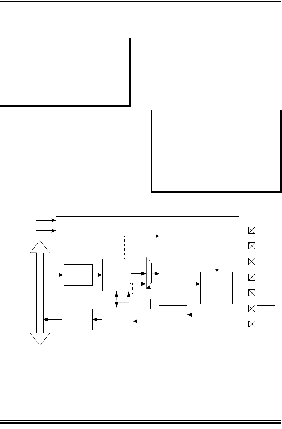
2015 Microchip Technology Inc. Preliminary DS60001320B-page 327
PIC32MZ Embedded Connectivity with Floating Point Unit (EF) Family
20.0 SERIAL QUAD INTERFACE
(SQI)
The SQI module is a synchronous serial interface that
provides access to serial Flash memories and other
serial devices. The SQI module supports Single Lane
(identical to SPI), Dual Lane, and Quad Lane modes.
Key features include:
• Supports Single, Dual, and Quad Lane modes
• Supports Single Data Rate (SDR) and Double
Data Rate (DDR) modes
• Programmable command sequence
• eXecute-In-Place (XIP)
• Data transfer:
- Programmed I/O mode (PIO)
- Buffer descriptor DMA
• Supports SPI Mode 0 and Mode 3
• Programmable Clock Polarity (CPOL) and Clock
Phase (CPHA) bits
• Supports up to two Chip Selects
• Supports up to four bytes of Flash address
• Programmable interrupt thresholds
• 32-byte transmit data buffer
• 32-byte receive data buffer
• 4-word controller buffer
FIGURE 20-1: SQI MODULE BLOCK DIAGRAM
Note: This data sheet summarizes the features
of the PIC32MZ EF family of devices. It is
not intended to be a comprehensive
reference source. To complement the
information in this data sheet, refer to
Section 46. “Serial Quad Interface
(SQI)” (DS60001244) in the “PIC32
Family Reference Manual”, which is
available from the Microchip web site
(www.microchip.com/PIC32).
Note: Once the SQI module is configured,
external devices are memory mapped
into KSEG2 and KSEG3 (see Figure 4-1
through Figure 4-2 in Section 4.0
“Memory Organization” for more
information). The MMU must be enabled
and the TLB must be set up to access
this memory (refer to Section 50. “CPU
for Devices with MIPS32®
microAptiv™ and M-Class Cores”
(DS60001192) of the “PIC32 Family
Reference Manual” for more information).
Transmit
Buffer
SQI Master
Interface
Control and
Status
Registers
(PIO)
System Bus
Receive
Buffer
DMA
Bus Slave
Bus Master
Control
Buffer
Note 1: When configuring the REFCLKO2 clock source, a value of ‘0’ for the ROTRIM<8:0> bits must be selected.
2: This clock source is only used for SQI Special Function Register (SFR) access.
PBCLK5(2)
REFCLKO2(1)
(TBC)SQID0
SQID1
SQID2
SQID3
SQICLK
SQICS0
SQICS1

PIC32MZ Embedded Connectivity with Floating Point Unit (EF) Family
DS60001320B-page 328 Preliminary 2015 Microchip Technology Inc.
20.1 SQI Control Registers
TABLE 20-1: SERIAL QUADRATURE INTERFACE (SQI) REGISTER MAP
Virtual Address
(BF8E_#)
Register
Name
Bit Range
Bits
All Resets
31/15 30/14 29/13 28/12 27/11 26/10 25/9 24/8 23/7 22/6 21/5 20/4 19/3 18/2 17/1 16/0
2000 SQI1
XCON1
31:16 ———DDRDATA DDR
DUMMY DDR
MODE DDR
ADDR DDRCMD DUMMYBYTES<2:0> ADDRBYTES<2:0> READOPCODE<7:6> 0000
15:0 READOPCODE<5:0> TYPEDATA<1:0> TYPEDUMMY<1:0> TYPEMODE<1:0> TYPEADDR<1:0> TYPECMD<1:0> 0000
2004 SQI1
XCON2
31:16 — — — — — — — — — — — — — — — — 0000
15:0 — — — — DEVSEL<1:0> MODEBYTES<1:0> MODECODE<7:0> 0000
2008 SQI1CFG 31:16 — — — — — — CSEN<1:0> SQIEN —DATAEN<1:0> CON
FIFORST RXFIFO
RST TXFIFO
RST RESET 0000
15:0 ———BURSTEN —HOLD WP — — — LSBF CPOL CPHA MODE<2:0> 0000
200C SQI1CON 31:16 — — — — — — — SCHECK DDRMODE DASSERT DEVSEL<1:0> LANEMODE<1:0> CMDINIT<1:0> 0000
15:0 TXRXCOUNT<15:0> 0000
2010 SQI1
CLKCON
31:16 — — — — — — — — — — — — — — CLKDIV<9:8> 0000
15:0 CLKDIV<7:0> — — — — — — STABLE EN 0000
2014 SQI1
CMDTHR
31:16 — — — — — — — — — — — — — — — — 0000
15:0 ——— TXCMDTHR<4:0> — — — RXCMDTHR<4:0> 0000
2018 SQI1
INTTHR
31:16 — — — — — — — — — — — — — — — — 0000
15:0 ——— TXINTTHR<4:0> — — — RXINTTHR<4:0> 0000
201C SQI1
INTEN
31:16 — — — — — — — — — — — — — — — — 0000
15:0 — — — — DMAEIE
PKT
COMPIE BD
DONEIE CON
THRIE CON
EMPTYIE CON
FULLIE RX
THRIE RX
FULLIE RX
EMPTYIE TX
THRIE TX
FULLIE TX
EMPTYIE
0000
2020 SQI1
INTSTAT
31:16 — — — — — — — — — — — — — — — — 0000
15:0 — — — — DMAEIF PKT
COMPIF BD
DONEIF CON
THRIF CON
EMPTYIF CON
FULLIF RX
THRIF RX
FULLIF RX
EMPTYIF TX
THRIF TX
FULLIF TX
EMPTYIF 0000
2024 SQI1
TXDATA
31:16 TXDATA<31:16> 0000
15:0 TXDATA<15:0> 0000
2028 SQI1
RXDATA
31:16 RXDATA<31:16> 0000
15:0 RXDATA<15:0> 0000
202C SQI1
STAT1
31:16 ———————— TXFIFOFREE<7:0> 0000
15:0 ———————— RXFIFOCNT<7:0> 0000
2030 SQI1
STAT2
31:16 — — — — — — — — — — — — — — CMDSTAT<1:0> 0000
15:0 — — — — CONAVAIL<4:0> SDID3 SDID2 SDID1 SDID0 — RXUN TXOV 00x0
2034 SQI1
BDCON
31:16 — — — — — — — — — — — — — — — — 0000
15:0 —————————————START POLLEN DMAEN 0000
2038 SQI1BD
CURADD
31:16 BDCURRADDR<31:16> 0000
15:0 BDCURRADDR<15:0> 0000
2040 SQI1BD
BASEADD
31:16 BDADDR<31:16> 0000
15:0 BDADDR<15:0> 0000

2015 Microchip Technology Inc. Preliminary DS60001320B-page 329
PIC32MZ Embedded Connectivity with Floating Point Unit (EF) Family
2044 SQI1BD
STAT
31:16 —————————— BDSTATE<3:0> DMA
START DMAACTV 0000
15:0 BDCON<15:0> 0000
2048 SQI1BD
POLLCON
31:16 — — — — — — — — — — — — — — — — 0000
15:0 POLLCON<15:0> 0000
204C SQI1BD
TXDSTAT
31:16 ——— TXSTATE<3:0> — — — — TXBUFCNT<4:0> 0000
15:0 ———————— TXCURBUFLEN<7:0> 0000
2050 SQI1BD
RXDSTAT
31:16 ——— RXSTATE<3:0> — — — — RXBUFCNT<4:0> 0000
15:0 ———————— RXCURBUFLEN<7:0> 0000
2054 SQI1THR 31:16 — — — — — — — — — — — — — — — — 0000
15:0 ————————— THRES<6:0> 0000
2058 SQI1INT
SIGEN
31:16 — — — — — — — — — — — — — — — — 0000
15:0 — — — — DMAEISE PKT
DONEISE BD
DONEISE CON
THRISE CON
EMPTYISE CON
FULLISE RX
THRISE RX
FULLISE RX
EMPTYISE TX
THRISE TX
FULLISE TX
EMPTYISE 0000
205C SQI1
TAPCON
31:16 — — — — — — — — — — — — — — — — 0000
15:0 — — CLKINDLY<5:0> DATAOUTDLY<3:0> CLKOUTDLY<3:0> 0000
2060 SQI1
MEMSTAT
31:16 ———————————STATPOS TYPESTAT<1:0> STATBYTES<1:0> 0000
15:0 STATDATA<15:0> 0000
2064 SQI1
XCON3
31:16 ———INIT1
SCHECK INIT1COUNT<1:0> INIT1TYPE<1:0> INIT1CMD3<7:0> 0000
15:0 INIT1CMD2<7:0> INIT1CMD1<7:0> 0000
2068 SQI1
XCON4
31:16 ———INIT2
SCHECK INIT2COUNT<1:0> INIT2TYPE<1:0> INIT2CMD3<7:0> 0000
15:0 INIT2CMD2<7:0> INIT2CMD1<7:0> 0000
TABLE 20-1: SERIAL QUADRATURE INTERFACE (SQI) REGISTER MAP (CONTINUED)
Virtual Address
(BF8E_#)
Register
Name
Bit Range
Bits
All Resets
31/15 30/14 29/13 28/12 27/11 26/10 25/9 24/8 23/7 22/6 21/5 20/4 19/3 18/2 17/1 16/0

PIC32MZ Embedded Connectivity with Floating Point Unit (EF) Family
DS60001320B-page 330 Preliminary 2015 Microchip Technology Inc.
REGISTER 20-1: SQI1XCON1: SQI XIP CONTROL REGISTER 1
Bit
Range Bit
31/23/15/7 Bit
30/22/14/6 Bit
29/21/13/5 Bit
28/20/12/4 Bit
27/19/11/3 Bit
26/18/10/2 Bit
25/17/9/1 Bit
24/16/8/0
31:24 U-0 U-0 U-0 R/W-0 R/W-0 R/W-0 R/W-0 R/W-0
— — — DDRDATA DDRDUMMY DDRMODE DDRADDR DDRCMD
23:16 R/W-0 R/W-0 R/W-0 R/W-0 R/W-0 R/W-0 R/W-0 R/W-0
DUMMYBYTES<2:0> ADDRBYTES<2:0> READOPCODE<7:6>
15:8 R/W-0 R/W-0 R/W-0 R/W-0 R/W-0 R/W-0 R/W-0 R/W-0
READOPCODE<5:0> TYPEDATA<1:0>
7:0 R/W-0 R/W-0 R/W-0 R/W-0 R/W-0 R/W-0 R/W-0 R/W-0
TYPEDUMMY<1:0> TYPEMODE<1:0> TYPEADDR<1:0> TYPECMD<1:0>
Legend:
R = Readable bit W = Writable bit U = Unimplemented bit, read as ‘0’
-n = Value at POR ‘1’ = Bit is set ‘0’ = Bit is cleared x = Bit is unknown
bit 31-29 Unimplemented: Read as ‘0’
bit 28 DDRDATA: SQI Data DDR Mode bit
1 = SQI data bytes are transferred in DDR mode
0 = SQI data bytes are transferred in SDR mode
bit 27 DDRDUMMY: SQI Dummy DDR Mode bit
1 = SQI dummy bytes are transferred in DDR mode
0 = SQI dummy bytes are transferred in SDR mode
bit 26 DDRMODE: SQI DDR Mode bit
1 = SQI mode bytes are transferred in DDR mode
0 = SQI mode bytes are transferred in SDR mode
bit 25 DDRADDR: SQI Address Mode bit
1 = SQI address bytes are transferred in DDR mode
0 = SQI address bytes are transferred in SDR mode
bit 24 DDRCMD: SQI DDR Command Mode bit
1 = SQI command bytes are transferred in DDR mode
0 = SQI command bytes are transferred in SDR mode
bit 23-21 DUMMYBYTES<2:0>: Transmit Dummy Bytes bits
111 = Transmit seven dummy bytes after the address bytes
•
•
•
011 = Transmit three dummy bytes after the address bytes
010 = Transmit two dummy bytes after the address bytes
001 = Transmit one dummy bytes after the address bytes
000 = Transmit zero dummy bytes after the address bytes
bit 20-18 ADDRBYTES<2:0>: Address Cycle bits
111 = Reserved
•
•
•
101 = Reserved
100 = Four address bytes
011 = Three address bytes
010 = Two address bytes
001 = One address bytes
000 = Zero address bytes

2015 Microchip Technology Inc. Preliminary DS60001320B-page 331
PIC32MZ Embedded Connectivity with Floating Point Unit (EF) Family
bit 17-10 READOPCODE<7:0>: Op code Value for Read Operation bits
These bits contain the 8-bit op code value for read operation.
bit 9-8 TYPEDATA<1:0>: SQI Type Data Enable bits
The boot controller will receive the data in Single Lane, Dual Lane, or Quad Lane.
11 = Reserved
10 = Quad Lane mode data is enabled
01 = Dual Lane mode data is enabled
00 = Single Lane mode data is enabled
bit 7-6 TYPEDUMMY<1:0>: SQI Type Dummy Enable bits
The boot controller will send the dummy in Single Lane, Dual Lane, or Quad Lane.
11 = Reserved
10 = Quad Lane mode dummy is enabled
01 = Dual Lane mode dummy is enabled
00 = Single Lane mode dummy is enabled
bit 5-4 TYPEMODE<1:0>: SQI Type Mode Enable bits
The boot controller will send the mode in Single Lane, Dual Lane, or Quad Lane.
11 = Reserved
10 = Quad Lane mode is enabled
01 = Dual Lane mode is enabled
00 = Single Lane mode is enabled
bit 3-2 TYPEADDR<1:0>: SQI Type Address Enable bits
The boot controller will send the address in Single Lane, Dual Lane, or Quad Lane.
11 = Reserved
10 = Quad Lane mode address is enabled
01 = Dual Lane mode address is enabled
00 = Single Lane mode address is enabled
bit 1-0 TYPECMD<1:0>: SQI Type Command Enable bits
The boot controller will send the command in Single Lane, Dual Lane, or Quad Lane.
11 = Reserved
10 = Quad Lane mode command is enabled
01 = Dual Lane mode command is enabled
00 = Single Lane mode command is enabled
REGISTER 20-1: SQI1XCON1: SQI XIP CONTROL REGISTER 1 (CONTINUED)

PIC32MZ Embedded Connectivity with Floating Point Unit (EF) Family
DS60001320B-page 332 Preliminary 2015 Microchip Technology Inc.
REGISTER 20-2: SQI1XCON2: SQI XIP CONTROL REGISTER 2
Bit
Range Bit
31/23/15/7 Bit
30/22/14/6 Bit
29/21/13/5 Bit
28/20/12/4 Bit
27/19/11/3 Bit
26/18/10/2 Bit
25/17/9/1 Bit
24/16/8/0
31:24 U-0 U-0 U-0 U-0 U-0 U-0 U-0 U-0
— — — — — — — —
23:16 U-0 U-0 U-0 U-0 U-0 U-0 U-0 U-0
— — — — — — — —
15:8 U-0 U-0 U-0 U-0 R/W-0 R/W-0 R/W-0 R/W-0
— — — — DEVSEL<1:0> MODEBYTES<1:0>
7:0 R/W-0 R/W-0 R/W-0 R/W-0 R/W-0 R/W-0 R/W-0 R/W-0
MODECODE<7:0>
Legend:
R = Readable bit W = Writable bit U = Unimplemented bit, read as ‘0’
-n = Value at POR ‘1’ = Bit is set ‘0’ = Bit is cleared x = Bit is unknown
bit 31-12 Unimplemented: Read as ‘0’
bit 11-10 DEVSEL<1:0>: Device Select bits
11 = Reserved
10 = Reserved
01 = Device 1 is selected
00 = Device 0 is selected
bit 9-8 MODEBYTES<1:0>: Mode Byte Cycle Enable bits
11 = Three cycles
10 = Two cycles
01 = One cycle
00 = Zero cycles
bit 7-0 MODECODE<7:0>: Mode Code Value bits
These bits contain the 8-bit code value for the mode bits.

2015 Microchip Technology Inc. Preliminary DS60001320B-page 333
PIC32MZ Embedded Connectivity with Floating Point Unit (EF) Family
REGISTER 20-3: SQI1CFG: SQI CONFIGURATION REGISTER
Bit
Range Bit
31/23/15/7 Bit
30/22/14/6 Bit
29/21/13/5 Bit
28/20/12/4 Bit
27/19/11/3 Bit
26/18/10/2 Bit
25/17/9/1 Bit
24/16/8/0
31:24 U-0 U-0 U-0 U-0 U-0 U-0 R/W-0 R/W-0
— — — — — — CSEN<1:0>
23:16
R/W-0 U-0 R/W-0 R/W-0 R/W-0, HC R/W-0, HC R/W-0, HC R/W-0, HC
SQIEN — DATAEN<1:0> CON
FIFORST
RX
FIFORST
TX
FIFORST RESET
15:8 U-0 r-0 r-0 R/W-0 r-0 R/W-0 R/W-0 U-0
— — — BURSTEN(1) —HOLDWP —
7:0 U-0 U-0 R/W-0 R/W-0 R/W-0 R/W-0 R/W-0 R/W-0
—— LSBF CPOL CPHA MODE<2:0>
Legend: HC = Hardware Cleared r = Reserved
R = Readable bit W = Writable bit U = Unimplemented bit, read as ‘0’
-n = Value at POR ‘1’ = Bit is set ‘0’ = Bit is cleared x = Bit is unknown
bit 31-26 Unimplemented: Read as ‘0’
bit 25-24 CSEN<1:0>: Chip Select Output Enable bits
11 = Chip Select 0 and Chip Select 1 are used
10 = Chip Select 1 is used (Chip Select 0 is not used)
01 = Chip Select 0 is used (Chip Select 1 is not used)
00 = Chip Select 0 and Chip Select 1 are not used
bit 23 SQIEN: SQI Enable bit
1 = SQI module is enabled
0 = SQI module is disabled
bit 22 Unimplemented: Read as ‘0’
bit 21-20 DATAEN<1:0>: Data Output Enable bits
11 = Reserved
10 = SQID3-SQID0 outputs are enabled
01 = SQID1 and SQID0 data outputs are enabled
00 = SQID0 data output is enabled
bit 19 CONFIFORST: Control FIFO Reset bit
1 = A reset pulse is generated clearing the control FIFO
0 = A reset pulse is not generated
bit 18 RXFIFORST: Receive FIFO Reset bit
1 = A reset pulse is generated clearing the receive FIFO
0 = A reset pulse is not generated
bit 17 TXFIFORST: Transmit FIFO Reset bit
1 = A reset pulse is generated clearing the transmit FIFO
0 = A reset pulse is not generated
bit 16 RESET: Software Reset Select bit
This bit is automatically cleared by the SQI module. All of the internal state machines and FIFO pointers
are reset by this reset pulse.
1 = A reset pulse is generated
0 = A reset pulse is not generated
bit 15 Unimplemented: Read as ‘0’
bit 14-13 Reserved: Must be programmed as ‘0’
Note 1: This bit must be programmed as ‘1’.

PIC32MZ Embedded Connectivity with Floating Point Unit (EF) Family
DS60001320B-page 334 Preliminary 2015 Microchip Technology Inc.
bit 12 BURSTEN: Burst Configuration bit(1)
1 = Burst is enabled
0 = Burst is not enabled
bit 11 Reserved: Must be programmed as ‘0’
bit 10 HOLD: Hold bit
In Single Lane or Dual Lane mode, this bit is used to drive the SQID3 pin, which can be used for devices
with a HOLD input pin. The meaning of the values for this bit will depend on the device to which SQID3 is
connected.
bit 9 WP: Write Protect bit
In Single Lane or Dual Lane mode, this bit is used to drive the SQID2 pin, which can be used with devices
with a write-protect pin. The meaning of the values for this bit will depend on the device to which SQID2 is
connected.
bit 8-6 Unimplemented: Read as ‘0’
bit 5 LSBF: Data Format Select bit
1 = LSB is sent or received first
0 = MSB is sent or received first
bit 4 CPOL: Clock Polarity Select bit
1 = Active-low SQICLK (SQICLK high is the Idle state)
0 = Active-high SQICLK (SQICLK low is the Idle state)
bit 3 CPHA: Clock Phase Select bit
1 = SQICLK starts toggling at the start of the first data bit
0 = SQICLK starts toggling at the middle of the first data bit
bit 2-0 MODE<2:0>: Mode Select bits
111 = Reserved
•
•
•
100 = Reserved
011 = XIP mode is selected (when this mode is entered, the module behaves as if executing in place (XIP),
but uses the register data to control timing)
010 = DMA mode is selected
001 = CPU mode is selected (the module is controlled by the CPU in PIO mode. This mode is entered when
leaving Boot or XIP mode)
000 = Reserved
REGISTER 20-3: SQI1CFG: SQI CONFIGURATION REGISTER (CONTINUED)
Note 1: This bit must be programmed as ‘1’.

2015 Microchip Technology Inc. Preliminary DS60001320B-page 335
PIC32MZ Embedded Connectivity with Floating Point Unit (EF) Family
REGISTER 20-4: SQI1CON: SQI CONTROL REGISTER
Bit
Range Bit
31/23/15/7 Bit
30/22/14/6 Bit
29/21/13/5 Bit
28/20/12/4 Bit
27/19/11/3 Bit
26/18/10/2 Bit
25/17/9/1 Bit
24/16/8/0
31:24 U-0 U-0 U-0 U-0 U-0 U-0 r-0 R/W-0
— — — — — — — SCHECK
23:16 R/W-0 R/W-0 R/W-0 R/W-0 R/W-0 R/W-0 R/W-0 R/W-0
DDRMODE DASSERT DEVSEL<1:0> LANEMODE<1:0> CMDINIT<1:0>
15:8 R/W-0 R/W-0 R/W-0 R/W-0 R/W-0 R/W-0 R/W-0 R/W-0
TXRXCOUNT<15:8>
7:0 R/W-0 R/W-0 R/W-0 R/W-0 R/W-0 R/W-0 R/W-0 R/W-0
TXRXCOUNT<7:0>
Legend: r = Reserved
R = Readable bit W = Writable bit U = Unimplemented bit, read as ‘0’
-n = Value at POR ‘1’ = Bit is set ‘0’ = Bit is cleared x = Bit is unknown
bit 31-26 Unimplemented: Read as ‘0’
bit 25 Reserved: Must be programmed as ‘0’
bit 24 SCHECK: Flash Status Check bit
1 = Check the status of the Flash
0 = Do not check the status of the Flash
bit 23 DDRMODE: Double Data Rate Mode bit
1 = Set the SQI transfers to DDR mode
0 = Set the SQI transfers to SDR mode
bit 22 DASSERT: Chip Select Assert bit
1 = Chip Select is deasserted after transmission or reception of the specified number of bytes
0 = Chip Select is not deasserted after transmission or reception of the specified number of bytes
bit 21-20 DEVSEL<1:0>: SQI Device Select bits
11 = Reserved
10 = Reserved
01 = Select Device 1
00 = Select Device 0
bit 19-18 LANEMODE<1:0>: SQI Lane Mode Select bits
11 = Reserved
10 = Quad Lane mode
01 = Dual Lane mode
00 = Single Lane mode
bit 17-16 CMDINIT<1:0>: Command Initiation Mode Select bits
If it is Transmit, commands are initiated based on a write to the transmit register or the contents of TX
FIFO. If CMDINIT is Receive, commands are initiated based on reads to the read register or RX FIFO
availability.
11 = Reserved
10 = Receive
01 = Transmit
00 = Idle
bit 15-0 TXRXCOUNT<15:0>: Transmit/Receive Count bits
These bits specify the total number of bytes to transmit or received (based on CMDINIT)

PIC32MZ Embedded Connectivity with Floating Point Unit (EF) Family
DS60001320B-page 336 Preliminary 2015 Microchip Technology Inc.
REGISTER 20-5: SQI1CLKCON: SQI CLOCK CONTROL REGISTER
Bit
Range Bit
31/23/15/7 Bit
30/22/14/6 Bit
29/21/13/5 Bit
28/20/12/4 Bit
27/19/11/3 Bit
26/18/10/2 Bit
25/17/9/1 Bit
24/16/8/0
31:24 U-0 U-0 U-0 U-0 U-0 U-0 U-0 U-0
— — — — — — — —
23:16 U-0 U-0 U-0 U-0 U-0 U-0 R/W-0 R/W-0
— — — — — — CLKDIV<9:8>(1)
15:8 R/W-0 R/W-0 R/W-0 R/W-0 R/W-0 R/W-0 R/W-0 R/W-0
CLKDIV<7:0>(1)
7:0 U-0 U-0 U-0 U-0 U-0 U-0 R-0 R/W-0
— — — — — — STABLE EN
Legend:
R = Readable bit W = Writable bit U = Unimplemented bit, read as ‘0’
-n = Value at POR ‘1’ = Bit is set ‘0’ = Bit is cleared x = Bit is unknown
bit 31-18 Unimplemented: Read as ‘0’
bit 17-8 CLKDIV<9:0>: SQI Clock TSQI Frequency Select bit(1)
1000000000 = Base clock TBC is divided by 2048
0100000000 = Base clock TBC is divided by 1024
0010000000 = Base clock TBC is divided by 512
0001000000 = Base clock TBC is divided by 256
0000100000 = Base clock TBC is divided by 128
0000010000 = Base clock TBC is divided by 64
0000001000 = Base clock TBC is divided by 32
0000000100 = Base clock TBC is divided by 16
0000000010 = Base clock TBC is divided by 8
0000000001 = Base clock TBC is divided by 4
0000000000 = Base clock TBC is divided by 2
Setting these bits to ‘00000000’ specifies the highest frequency of the SQI clock.
bit 7-2 Unimplemented: Read as ‘0’
bit 1 STABLE: TSQI Clock Stable Select bit
This bit is set to ‘1’ when the SQI clock, TSQI, is stable after writing a ‘1’ to the EN bit.
1 = TSQI clock is stable
0 = TSQI clock is not stable
bit 0 EN: TSQI Clock Enable Select bit
When clock oscillation is stable, the SQI module will set the STABLE bit to ‘1’.
1 = Enable the SQI clock (TSQI) (when clock oscillation is stable, the SQI module sets the STABLE bit to ‘1’)
0 = Disable the SQI clock (TSQI) (the SQI module should stop its clock to enter a low power state); SFRs
can still be accessed, as they use PBCLK5
Note 1: Refer to Table in Section 44.0 “Electrical Characteristics” for the maximum clock frequency specifica-
tions.

2015 Microchip Technology Inc. Preliminary DS60001320B-page 337
PIC32MZ Embedded Connectivity with Floating Point Unit (EF) Family
REGISTER 20-6: SQI1CMDTHR: SQI COMMAND THRESHOLD REGISTER
Bit
Range Bit
31/23/15/7 Bit
30/22/14/6 Bit
29/21/13/5 Bit
28/20/12/4 Bit
27/19/11/3 Bit
26/18/10/2 Bit
25/17/9/1 Bit
24/16/8/0
31:24 U-0 U-0 U-0 U-0 U-0 U-0 U-0 U-0
— — — — — — — —
23:16 U-0 U-0 U-0 U-0 U-0 U-0 U-0 U-0
— — — — — — — —
15:8 U-0 U-0 U-0 R/W-0 R/W-0 R/W-0 R/W-0 R/W-0
— — — TXCMDTHR<4:0>
7:0 U-0 U-0 U-0 R/W-0 R/W-0 R/W-0 R/W-0 R/W-0
— — — RXCMDTHR<4:0>(1)
Legend:
R = Readable bit W = Writable bit U = Unimplemented bit, read as ‘0’
-n = Value at POR ‘1’ = Bit is set ‘0’ = Bit is cleared x = Bit is unknown
bit 31-13 Unimplemented: Read as ‘0’
bit 12-8 TXCMDTHR<4:0>: Transmit Command Threshold bits
In transmit initiation mode, the SQI module performs a transmit operation when transmit command
threshold bytes are present in the TX FIFO. These bits should usually be set to ‘1’ for normal Flash
commands, and set to a higher value for page programming. For 16-bit mode, the value should be a
multiple of 2.
bit 7-5 Unimplemented: Read as ‘0’
bit 4-0 RXCMDTHR<4:0>: Receive Command Threshold bits(1)
In receive initiation mode, the SQI module attempts to perform receive operations to fetch the receive com-
mand threshold number of bytes in the receive buffer. If space for these bytes is not present in the FIFO,
the SQI will not initiate a transfer. For 16-bit mode, the value should be a multiple of 2.
If software performs any reads, thereby reducing the FIFO count, hardware would initiate a receive transfer
to make the FIFO count equal to the value in these bits. If software would not like any more words latched
into the FIFO, command initiation mode needs to be changed to Idle before any FIFO reads by software.
In the case of Boot/XIP mode, the SQI module will use the System Bus burst size, instead of the receive
command threshold value.
Note 1: These bits should only be programmed when a receive is not active (i.e., during Idle mode or a transmit).

PIC32MZ Embedded Connectivity with Floating Point Unit (EF) Family
DS60001320B-page 338 Preliminary 2015 Microchip Technology Inc.
REGISTER 20-7: SQI1INTTHR: SQI INTERRUPT THRESHOLD REGISTER
Bit
Range Bit
31/23/15/7 Bit
30/22/14/6 Bit
29/21/13/5 Bit
28/20/12/4 Bit
27/19/11/3 Bit
26/18/10/2 Bit
25/17/9/1 Bit
24/16/8/0
31:24 U-0 U-0 U-0 U-0 U-0 U-0 U-0 U-0
— — — — — — — —
23:16 U-0 U-0 U-0 U-0 U-0 U-0 U-0 U-0
— — — — — — — —
15:8 U-0 U-0 U-0 R/W-0 R/W-0 R/W-0 R/W-0 R/W-0
— — —TXINTTHR<4:0>
7:0 U-0 U-0 U-0 R/W-0 R/W-0 R/W-0 R/W-0 R/W-0
— — — RXINTTHR<4:0>
Legend:
R = Readable bit W = Writable bit U = Unimplemented bit, read as ‘0’
-n = Value at POR ‘1’ = Bit is set ‘0’ = Bit is cleared x = Bit is unknown
bit 31-13 Unimplemented: Read as ‘0’
bit 12-8 TXINTTHR<4:0>: Transmit Interrupt Threshold bits
A transmit interrupt is set when the transmit FIFO has more space than the set number of bytes. For 16-bit
mode, the value should be a multiple of 2.
bit 7-5 Unimplemented: Read as ‘0’
bit 4-0 RXINTTHR<4:0>: Receive Interrupt Threshold bits
A receive interrupt is set when the receive FIFO count is larger than or equal to the set number of bytes. For
16-bit mode, the value should be multiple of 2.

2015 Microchip Technology Inc. Preliminary DS60001320B-page 339
PIC32MZ Embedded Connectivity with Floating Point Unit (EF) Family
REGISTER 20-8: SQI1INTEN: SQI INTERRUPT ENABLE REGISTER
Bit
Range Bit
31/23/15/7 Bit
30/22/14/6 Bit
29/21/13/5 Bit
28/20/12/4 Bit
27/19/11/3 Bit
26/18/10/2 Bit
25/17/9/1 Bit
24/16/8/0
31:24 U-0 U-0 U-0 U-0 U-0 U-0 U-0 U-0
— — — — — — — —
23:16 U-0 U-0 U-0 U-0 U-0 U-0 U-0 U-0
— — — — — — — —
15:8 U-0 U-0 U-0 U-0 R/W-0 R/W-0 R/W-0 R/W-0
— — — —
DMAEIE PKTCOMPIE BDDONEIE CONTHRIE
7:0 R/W-0 R/W-0 R/W-0 R/W-0 R/W-0 R/W-0 R/W-0 R/W-0
CONEMPTYIE CONFULLIE RXTHRIE RXFULLIE RXEMPTYIE TXTHRIE TXFULLIE TXEMPTYIE
Legend: HS = Hardware Set
R = Readable bit W = Writable bit U = Unimplemented bit, read as ‘0’
-n = Value at POR ‘1’ = Bit is set ‘0’ = Bit is cleared x = Bit is unknown
bit 31-12 Unimplemented: Read as ‘0’
bit 11 DMAEIE: DMA Bus Error Interrupt Enable bit
1 = Interrupt is enabled
0 = Interrupt is disabled
bit 10 PKTCOMPIE: DMA Buffer Descriptor Packet Complete Interrupt Enable bit
1 = Interrupt is enabled
0 = Interrupt is disabled
bit 9 BDDONEIE: DMA Buffer Descriptor Done Interrupt Enable bit
1 = Interrupt is enabled
0 = Interrupt is disabled
bit 8 CONTHRIE: Control Buffer Threshold Interrupt Enable bit
1 = Interrupt is enabled
0 = Interrupt is disabled
bit 7 CONEMPTYIE: Control Buffer Empty Interrupt Enable bit
1 = Interrupt is enabled
0 = Interrupt is disabled
bit 6 CONFULLIE: Control Buffer Full Interrupt Enable bit
This bit enables an interrupt when the receive FIFO buffer is full.
1 = Interrupt is enabled
0 = Interrupt is disabled
bit 5 RXTHRIE: Receive Buffer Threshold Interrupt Enable bit
1 = Interrupt is enabled
0 = Interrupt is disabled
bit 4 RXFULLIE: Receive Buffer Full Interrupt Enable bit
1 = Interrupt is enabled
0 = Interrupt is disabled
bit 3 RXEMPTYIE: Receive Buffer Empty Interrupt Enable bit
1 = Interrupt is enabled
0 = Interrupt is disabled
bit 2 TXTHRIE: Transmit Threshold Interrupt Enable bit
1 = Interrupt is enabled
0 = Interrupt is disabled
bit 1 TXFULLIE: Transmit Buffer Full Interrupt Enable bit
1 = Interrupt is enabled
0 = Interrupt is disabled
bit 0 TXEMPTYIE: Transmit Buffer Empty Interrupt Enable bit
1 = Interrupt is enabled
0 = Interrupt is disabled

PIC32MZ Embedded Connectivity with Floating Point Unit (EF) Family
DS60001320B-page 340 Preliminary 2015 Microchip Technology Inc.
REGISTER 20-9: SQI1INTSTAT: SQI INTERRUPT STATUS REGISTER
Bit
Range Bit
31/23/15/7 Bit
30/22/14/6 Bit
29/21/13/5 Bit
28/20/12/4 Bit
27/19/11/3 Bit
26/18/10/2 Bit
25/17/9/1 Bit
24/16/8/0
31:24 U-0 U-0 U-0 U-0 U-0 U-0 U-0 U-0
— — — — — — — —
23:16 U-0 U-0 U-0 U-0 U-0 U-0 U-0 U-0
— — — — — — — —
15:8
U-0 U-0 U-0 U-0 R/W-0, HS R/W-0, HS R/W-0, HS R/W-0, HS
— — — — DMA
EIF PKT
COMPIF BD
DONEIF CON
THRIF
7:0
R/W-1, HS R/W-0, HS R/W-1, HS R/W-0, HS R/W-1, HS R/W-1, HS R/W-0, HS R/W-1, HS
CON
EMPTYIF
CON
FULLIF RXTHRIF(1) RXFULLIF RX
EMPTYIF TXTHRIF TXFULLIF TX
EMPTYIF
Legend: HS = Hardware Set
R = Readable bit W = Writable bit U = Unimplemented bit, read as ‘0’
-n = Value at POR ‘1’ = Bit is set ‘0’ = Bit is cleared x = Bit is unknown
bit 31-12 Unimplemented: Read as ‘0’
bit 11 DMAEIF: DMA Bus Error Interrupt Flag bit
1 = DMA bus error has occurred
0 = DMA bus error has not occurred
bit 10 PKTCOMPIF: DMA Buffer Descriptor Processor Packet Completion Interrupt Flag bit
1 = DMA BD packet is complete
0 = DMA BD packet is in progress
bit 9 BDDONEIF: DMA Buffer Descriptor Done Interrupt Flag bit
1 = DMA BD process is done
0 = DMA BD process is in progress
bit 8 CONTHRIF: Control Buffer Threshold Interrupt Flag bit
1 = The control buffer has more than THRES words of space available
0 = The control buffer has less than THRES words of space available
bit 7 CONEMPTYIF: Control Buffer Empty Interrupt Flag bit
1 = Control buffer is empty
0 = Control buffer is not empty
bit 6 CONFULLIF: Control Buffer Full Interrupt Flag bit
1 = Control buffer is full
0 = Control buffer is not full
bit 5 RXTHRIF: Receive Buffer Threshold Interrupt Flag bit(1)
1 = Receive buffer has more than RXINTTHR words of space available
0 = Receive buffer has less than RXINTTHR words of space available
bit 4 RXFULLIF: Receive Buffer Full Interrupt Flag bit
1 = Receive buffer is full
0 = Receive buffer is not full
bit 3 RXEMPTYIF: Receive Buffer Empty Interrupt Flag bit
1 = Receive buffer is empty
0 = Receive buffer is not empty
Note 1: In the case of Boot/XIP mode, the POR value of the receive buffer threshold is zero. Therefore, this bit will
be set to a ‘1’, immediately after a POR until a read request on the System Bus bus is received.
Note: The bits in the register are cleared by writing a '1' to the corresponding bit position.

2015 Microchip Technology Inc. Preliminary DS60001320B-page 341
PIC32MZ Embedded Connectivity with Floating Point Unit (EF) Family
bit 2 TXTHRIF: Transmit Buffer Threshold Interrupt Flag bit
1 = Transmit buffer has more than TXINTTHR words of space available
0 = Transmit buffer has less than TXINTTHR words of space available
bit 1 TXFULLIF: Transmit Buffer Full Interrupt Flag bit
1 = The transmit buffer is full
0 = The transmit buffer is not full
bit 0 TXEMPTYIF: Transmit Buffer Empty Interrupt Flag bit
1 = The transmit buffer is empty
0 = The transmit buffer has content
REGISTER 20-9: SQI1INTSTAT: SQI INTERRUPT STATUS REGISTER (CONTINUED)
Note 1: In the case of Boot/XIP mode, the POR value of the receive buffer threshold is zero. Therefore, this bit will
be set to a ‘1’, immediately after a POR until a read request on the System Bus bus is received.
Note: The bits in the register are cleared by writing a '1' to the corresponding bit position.
PIC32MZ Embedded Connectivity with Floating Point Unit (EF) Family
DS60001320B-page 342 Preliminary 2015 Microchip Technology Inc.
REGISTER 20-10: SQI1TXDATA: SQI TRANSMIT DATA BUFFER REGISTER
Bit
Range Bit
31/23/15/7 Bit
30/22/14/6 Bit
29/21/13/5 Bit
28/20/12/4 Bit
27/19/11/3 Bit
26/18/10/2 Bit
25/17/9/1 Bit
24/16/8/0
31:24 R/W-0 R/W-0 R/W-0 R/W-0 R/W-0 R/W-0 R/W-0 R/W-0
TXDATA<31:24>
23:16 R/W-0 R/W-0 R/W-0 R/W-0 R/W-0 R/W-0 R/W-0 R/W-0
TXDATA<23:16>
15:8 R/W-0 R/W-0 R/W-0 R/W-0 R/W-0 R/W-0 R/W-0 R/W-0
TXDATA<15:8>
7:0 R/W-0 R/W-0 R/W-0 R/W-0 R/W-0 R/W-0 R/W-0 R/W-0
TXDATA<7:0>
Legend:
R = Readable bit W = Writable bit U = Unimplemented bit, read as ‘0’
-n = Value at POR ‘1’ = Bit is set ‘0’ = Bit is cleared x = Bit is unknown
bit 31-0 TXDATA<31:0>: Transmit Command Data bits
Data is loaded into this register before being transmitted. Just prior to the beginning of a data transfer, the
data in TXDATA is loaded into the shift register (SFDR).
Multiple writes to TXDATA can occur even while a transfer is already in progress. There can be a maximum
of eight commands that can be queued.
REGISTER 20-11: SQI1RXDATA: SQI RECEIVE DATA BUFFER REGISTER
Bit
Range Bit
31/23/15/7 Bit
30/22/14/6 Bit
29/21/13/5 Bit
28/20/12/4 Bit
27/19/11/3 Bit
26/18/10/2 Bit
25/17/9/1 Bit
24/16/8/0
31:24 R-0 R-0 R-0 R-0 R-0 R-0 R-0 R-0
RXDATA<31:24>
23:16 R-0 R-0 R-0 R-0 R-0 R-0 R-0 R-0
RXDATA<23:16>
15:8 R-0 R-0 R-0 R-0 R-0 R-0 R-0 R-0
RXDATA<15:8>
7:0 R-0 R-0 R-0 R-0 R-0 R-0 R-0 R-0
RXDATA<7:0>
Legend:
R = Readable bit W = Writable bit U = Unimplemented bit, read as ‘0’
-n = Value at POR ‘1’ = Bit is set ‘0’ = Bit is cleared x = Bit is unknown
bit 31-0 RXDATA<31:0>: Receive Data Buffer bits
At the end of a data transfer, the data in the shift register is loaded into the RXDATA register. This register
works like a FIFO. The depth of the receive buffer is eight words.

2015 Microchip Technology Inc. Preliminary DS60001320B-page 343
PIC32MZ Embedded Connectivity with Floating Point Unit (EF) Family
REGISTER 20-12: SQI1STAT1: SQI STATUS REGISTER 1
Bit
Range Bit
31/23/15/7 Bit
30/22/14/6 Bit
29/21/13/5 Bit
28/20/12/4 Bit
27/19/11/3 Bit
26/18/10/2 Bit
25/17/9/1 Bit
24/16/8/0
31:24 U-0 U-0 U-0 U-0 U-0 U-0 U-0 U-0
— — — — — — — —
23:16 R-0 R-0 R-0 R-0 R-0 R-0 R-0 R-0
TXFIFOFREE<7:0>
15:8 U-0 U-0 U-0 U-0 U-0 U-0 U-0 U-0
— — — — — — — —
7:0 R-0 R-0 R-0 R-0 R-0 R-0 R-0 R-0
RXFIFOCNT<7:0>
Legend:
R = Readable bit W = Writable bit U = Unimplemented bit, read as ‘0’
-n = Value at POR ‘1’ = Bit is set ‘0’ = Bit is cleared x = Bit is unknown
bit 31-24 Unimplemented: Read as ‘0’
bit 23-16 TXFIFOFREE<7:0>: Transmit FIFO Available Word Space bits
bit 15-8 Unimplemented: Read as ‘0’
bit 7-0 RXFIFOCNT<7:0>: Number of words of read data in the FIFO

PIC32MZ Embedded Connectivity with Floating Point Unit (EF) Family
DS60001320B-page 344 Preliminary 2015 Microchip Technology Inc.
REGISTER 20-13: SQI1STAT2: SQI STATUS REGISTER 2
Bit
Range Bit
31/23/15/7 Bit
30/22/14/6 Bit
29/21/13/5 Bit
28/20/12/4 Bit
27/19/11/3 Bit
26/18/10/2 Bit
25/17/9/1 Bit
24/16/8/0
31:24 U-0 U-0 U-0 U-0 U-0 U-0 U-0 U-0
— — — — — — — —
23:16 U-0 U-0 U-0 U-0 U-0 U-0 R-0 R-0
— — — — — —CMDSTAT<1:0>
15:8 U-0 U-0 U-0 U-0 R-0 R-0 R-0 R-0
— — — — CONAVAIL<4:1>
7:0 R-0 R-0 R-0 R-0 R-0 U-0 R-0 R-0
CONAVAIL<0> SQID3 SQID2 SQID1 SQID0 — RXUN TXOV
Legend:
R = Readable bit W = Writable bit U = Unimplemented bit, read as ‘0’
-n = Value at POR ‘1’ = Bit is set ‘0’ = Bit is cleared x = Bit is unknown
bit 31-18 Unimplemented: Read as ‘0’
bit 17-16 CMDSTAT<1:0>: Current Command Status bits
These bits indicate the current command status.
11 = Reserved
10 = Receive
01 = Transmit
00 = Idle
bit 15-12 Unimplemented: Read as ‘0’
bit 11-7 CONAVAIL<4:0>: Control FIFO Space Available bits
These bits indicate the available control Word space.
11111 = 32 bytes are available
11110 = 31 bytes are available
•
•
•
00001 = 1 byte is available
00000 = No bytes are available
bit 6 SQID3: SQID3 Status bit
1 = Data is present on SQID3
0 = Data is not present on SQID3
bit 5 SQID2: SQID2 Status bit
1 = Data is present on SQID2
0 = Data is not present on SQID2
bit 4 SQID1: SQID1 Status bit
1 = Data is present on SQID1
0 = Data is not present on SQID1
bit 3 SQID0: SQID0 Status bit
1 = Data is present on SQID0
0 = Data is not present on SQID0
bit 2 Unimplemented: Read as ‘0’
bit 1 RXUN: Receive FIFO Underflow Status bit
1 = Receive FIFO Underflow has occurred
0 = Receive FIFO underflow has not occurred
bit 0 TXOV: Transmit FIFO Overflow Status bit
1 = Transmit FIFO overflow has occurred
0 = Transmit FIFO overflow has not occurred

2015 Microchip Technology Inc. Preliminary DS60001320B-page 345
PIC32MZ Embedded Connectivity with Floating Point Unit (EF) Family
REGISTER 20-14: SQI1BDCON: SQI BUFFER DESCRIPTOR CONTROL REGISTER
Bit
Range Bit
31/23/15/7 Bit
30/22/14/6 Bit
29/21/13/5 Bit
28/20/12/4 Bit
27/19/11/3 Bit
26/18/10/2 Bit
25/17/9/1 Bit
24/16/8/0
31:24 U-0 U-0 U-0 U-0 U-0 U-0 U-0 U-0
— — — — — — — —
23:16 U-0 U-0 U-0 U-0 U-0 U-0 U-0 U-0
— — — — — — — —
15:8 U-0 U-0 U-0 U-0 U-0 U-0 U-0 U-0
— — — — — — — —
7:0 U-0 U-0 U-0 U-0 U-0 R/W-0 R/W-0 R/W-0
— — — — — START POLLEN DMAEN
Legend:
R = Readable bit W = Writable bit U = Unimplemented bit, read as ‘0’
-n = Value at POR ‘1’ = Bit is set ‘0’ = Bit is cleared x = Bit is unknown
bit 31-3 Unimplemented: Read as ‘0’
bit 2 START: Buffer Descriptor Processor Start bit
1 = Start the buffer descriptor processor
0 = Disable the buffer descriptor processor
bit 1 POLLEN: Buffer Descriptor Poll Enable bit
1 = BDP poll is enabled
0 = BDP poll is not enabled
bit 0 DMAEN: DMA Enable bit
1 = DMA is enabled
0 = DMA is disabled
REGISTER 20-15: SQI1BDCURADD: SQI BUFFER DESCRIPTOR CURRENT ADDRESS REGISTER
Bit
Range Bit
31/23/15/7 Bit
30/22/14/6 Bit
29/21/13/5 Bit
28/20/12/4 Bit
27/19/11/3 Bit
26/18/10/2 Bit
25/17/9/1 Bit
24/16/8/0
31:24 R-0 R-0 R-0 R-0 R-0 R-0 R-0 R-0
BDCURRADDR<31:24>
23:16 R-0 R-0 R-0 R-0 R-0 R-0 R-0 R-0
BDCURRADDR<23:16>
15:8 R-0 R-0 R-0 R-0 R-0 R-0 R-0 R-0
BDCURRADDR<15:8>
7:0 R-0 R-0 R-0 R-0 R-0 R-0 R-0 R-0
BDCURRADDR<7:0>
Legend:
R = Readable bit W = Writable bit U = Unimplemented bit, read as ‘0’
-n = Value at POR ‘1’ = Bit is set ‘0’ = Bit is cleared x = Bit is unknown
bit 31-0 BDCURRADDR<31:0>: Current Buffer Descriptor Address bits
These bits contain the address of the current descriptor being processed by the Buffer Descriptor
Processor.
PIC32MZ Embedded Connectivity with Floating Point Unit (EF) Family
DS60001320B-page 346 Preliminary 2015 Microchip Technology Inc.
REGISTER 20-16: SQI1BDBASEADD: SQI BUFFER DESCRIPTOR BASE ADDRESS REGISTER
Bit
Range Bit
31/23/15/7 Bit
30/22/14/6 Bit
29/21/13/5 Bit
28/20/12/4 Bit
27/19/11/3 Bit
26/18/10/2 Bit
25/17/9/1 Bit
24/16/8/0
31:24 R/W-0 R/W-0 R/W-0 R/W-0 R/W-0 R/W-0 R/W-0 R/W-0
BDADDR<31:24>
23:16 R/W-0 R/W-0 R/W-0 R/W-0 R/W-0 R/W-0 R/W-0 R/W-0
BDADDR<23:16>
15:8 R/W-0 R/W-0 R/W-0 R/W-0 R/W-0 R/W-0 R/W-0 R/W-0
BDADDR<15:8>
7:0 R/W-0 R/W-0 R/W-0 R/W-0 R/W-0 R/W-0 R/W-0 R/W-0
BDADDR<7:0>
Legend:
R = Readable bit W = Writable bit U = Unimplemented bit, read as ‘0’
-n = Value at POR ‘1’ = Bit is set ‘0’ = Bit is cleared x = Bit is unknown
bit 31-0 BDADDR<31:0>: DMA Base Address bits
These bits contain the physical address of the root buffer descriptor. This register should be updated only
when the DMA is idle.
REGISTER 20-17: SQI1BDSTAT: SQI BUFFER DESCRIPTOR STATUS REGISTER
Bit
Range Bit
31/23/15/7 Bit
30/22/14/6 Bit
29/21/13/5 Bit
28/20/12/4 Bit
27/19/11/3 Bit
26/18/10/2 Bit
25/17/9/1 Bit
24/16/8/0
31:24 U-0 U-0 U-0 U-0 U-0 U-0 U-0 U-0
— — — — — — — —
23:16 U-0 U-0 R-x R-x R-x R-x R-x R-x
— — BDSTATE<3:0> DMASTART DMAACTV
15:8 R-x R-x R-x R-x R-x R-x R-x R-x
BDCON<15:8>
7:0 R-x R-x R-x R-x R-x R-x R-x R-x
BDCON<7:0>
Legend:
R = Readable bit W = Writable bit U = Unimplemented bit, read as ‘0’
-n = Value at POR ‘1’ = Bit is set ‘0’ = Bit is cleared x = Bit is unknown
bit 31-22 Unimplemented: Read as ‘0’
bit 21-18 BDSTATE<3:0>: DMA Buffer Descriptor Processor State Status bits
These bits return the current state of the buffer descriptor processor:
5 = Fetched buffer descriptor is disabled
4 = Descriptor is done
3 = Data phase
2 = Buffer descriptor is loading
1 = Descriptor fetch request is pending
0 = Idle
bit 17 DMASTART: DMA Buffer Descriptor Processor Start Status bit
1 = DMA has started
0 = DMA has not started
bit 16 DMAACTV: DMA Buffer Descriptor Processor Active Status bit
1 = Buffer Descriptor Processor is active
0 = Buffer Descriptor Processor is idle
bit 15-0 BDCON<15:0>: DMA Buffer Descriptor Control Word bits
These bits contain the current buffer descriptor control word.
2015 Microchip Technology Inc. Preliminary DS60001320B-page 347
PIC32MZ Embedded Connectivity with Floating Point Unit (EF) Family
REGISTER 20-18: SQI1BDPOLLCON: SQI BUFFER DESCRIPTOR POLL CONTROL REGISTER
Bit
Range Bit
31/23/15/7 Bit
30/22/14/6 Bit
29/21/13/5 Bit
28/20/12/4 Bit
27/19/11/3 Bit
26/18/10/2 Bit
25/17/9/1 Bit
24/16/8/0
31:24 U-0 U-0 U-0 U-0 U-0 U-0 U-0 U-0
— — — — — — — —
23:16 U-0 U-0 U-0 U-0 U-0 U-0 U-0 U-0
— — — — — — — —
15:8 R/W-0 R/W-0 R/W-0 R/W-0 R/W-0 R/W-0 R/W-0 R/W-0
POLLCON<15:8>
7:0 R/W-0 R/W-0 R/W-0 R/W-0 R/W-0 R/W-0 R/W-0 R/W-0
POLLCON<7:0>
Legend:
R = Readable bit W = Writable bit U = Unimplemented bit, read as ‘0’
-n = Value at POR ‘1’ = Bit is set ‘0’ = Bit is cleared x = Bit is unknown
bit 31-16 Unimplemented: Read as ‘0’
bit 15-0 POLLCON<15:0>: Buffer Descriptor Processor Poll Status bits
These bits indicate the number of cycles the BDP would wait before refetching the descriptor control word
if the previous descriptor fetched was disabled.
REGISTER 20-19: SQI1BDTXDSTAT: SQI BUFFER DESCRIPTOR DMA TRANSMIT STATUS
REGISTER
Bit
Range Bit
31/23/15/7 Bit
30/22/14/6 Bit
29/21/13/5 Bit
28/20/12/4 Bit
27/19/11/3 Bit
26/18/10/2 Bit
25/17/9/1 Bit
24/16/8/0
31:24 U-0 U-0 U-0 R-x R-x R-x R-x U-0
— — — TXSTATE<3:0> —
23:16 U-0 U-0 U-0 R-x R-x R-x R-x R-x
— — — TXBUFCNT<4:0>
15:8 U-0 U-0 U-0 U-0 U-0 U-0 U-0 U-0
— — — — — — — —
7:0 R-x R-x R-x R-x R-x R-x R-x R-x
TXCURBUFLEN<7:0>
Legend:
R = Readable bit W = Writable bit U = Unimplemented bit, read as ‘0’
-n = Value at POR ‘1’ = Bit is set ‘0’ = Bit is cleared x = Bit is unknown
bit 31-29 Unimplemented: Read as ‘0’
bit 28-25 TXSTATE<3:0>: Current DMA Transmit State Status bits
These bits provide information on the current DMA receive states.
bit 24-21 Unimplemented: Read as ‘0’
bit 20-16 TXBUFCNT<4:0>: DMA Buffer Byte Count Status bits
These bits provide information on the internal FIFO space.
bit 15-8 Unimplemented: Read as ‘0’
bit 7-0 TXCURBUFLEN<7:0>: Current DMA Transmit Buffer Length Status bits
These bits provide the length of the current DMA transmit buffer.
PIC32MZ Embedded Connectivity with Floating Point Unit (EF) Family
DS60001320B-page 348 Preliminary 2015 Microchip Technology Inc.
REGISTER 20-20: SQI1BDRXDSTAT: SQI BUFFER DESCRIPTOR DMA RECEIVE STATUS
REGISTER
Bit
Range Bit
31/23/15/7 Bit
30/22/14/6 Bit
29/21/13/5 Bit
28/20/12/4 Bit
27/19/11/3 Bit
26/18/10/2 Bit
25/17/9/1 Bit
24/16/8/0
31:24 U-0 U-0 U-0 R-x R-x R-x R-x U-0
— — — RXSTATE<3:0> —
23:16 U-0 U-0 U-0 R-x R-x R-x R-x R-x
— — — RXBUFCNT<4:0>
15:8 U-0 U-0 U-0 U-0 U-0 U-0 U-0 U-0
— — — — — — — —
7:0 R-x R-x R-x R-x R-x R-x R-x R-x
RXCURBUFLEN<7:0>
Legend:
R = Readable bit W = Writable bit U = Unimplemented bit, read as ‘0’
-n = Value at POR ‘1’ = Bit is set ‘0’ = Bit is cleared x = Bit is unknown
bit 31-29 Unimplemented: Read as ‘0’
bit 28-25 RXSTATE<3:0>: Current DMA Receive State Status bits
These bits provide information on the current DMA receive states.
bit 24-21 Unimplemented: Read as ‘0’
bit 20-16 RXBUFCNT<4:0>: DMA Buffer Byte Count Status bits
These bits provide information on the internal FIFO space.
bit 15-8 Unimplemented: Read as ‘0’
bit 7-0 RXCURBUFLEN<7:0>: Current DMA Receive Buffer Length Status bits
These bits provide the length of the current DMA receive buffer.
REGISTER 20-21: SQI1THR: SQI THRESHOLD CONTROL REGISTER
Bit
Range Bit
31/23/15/7 Bit
30/22/14/6 Bit
29/21/13/5 Bit
28/20/12/4 Bit
27/19/11/3 Bit
26/18/10/2 Bit
25/17/9/1 Bit
24/16/8/0
31:24 U-0 U-0 U-0 U-0 U-0 U-0 U-0 U-0
— — — — — — — —
23:16 U-0 U-0 U-0 U-0 U-0 U-0 U-0 U-0
— — — — — — — —
15:8 U-0 U-0 U-0 U-0 U-0 U-0 U-0 U-0
— — — — — — — —
7:0 U-0 R/W-0 R/W-0 R/W-0 R/W-0 R/W-0 R/W-0 R/W-0
—THRES<6:0>
Legend:
R = Readable bit W = Writable bit U = Unimplemented bit, read as ‘0’
-n = Value at POR ‘1’ = Bit is set ‘0’ = Bit is cleared x = Bit is unknown
bit 31-7 Unimplemented: Read as ‘0’
bit 6-0 THRES<6:0>: SQI Control Threshold Value bits
The SQI control threshold interrupt is asserted when the amount of space indicated by THRES<6:0> is
available in the SQI control buffer.

2015 Microchip Technology Inc. Preliminary DS60001320B-page 349
PIC32MZ Embedded Connectivity with Floating Point Unit (EF) Family
REGISTER 20-22: SQI1INTSIGEN: SQI INTERRUPT SIGNAL ENABLE REGISTER
Bit
Range Bit
31/23/15/7 Bit
30/22/14/6 Bit
29/21/13/5 Bit
28/20/12/4 Bit
27/19/11/3 Bit
26/18/10/2 Bit
25/17/9/1 Bit
24/16/8/0
31:24 U-0 U-0 U-0 U-0 U-0 U-0 U-0 U-0
— — — — — — — —
23:16 U-0 U-0 U-0 U-0 U-0 U-0 U-0 U-0
— — — — — — — —
15:8
U-0 U-0 U-0 U-0 R/W-0 R/W-0 R/W-0 R/W-0
— — — —DMAEISE
PKT
DONEISE
BD
DONEISE
CON
THRISE
7:0
R/W-0 R/W-0 R/W-0 R/W-0 R/W-0 R/W-0 R/W-0 R/W-0
CON
EMPTYISE CON
FULLISE RX
THRISE RX
FULLISE RX
EMPTYISE TX
THRISE TX
FULLISE TX
EMPTYISE
Legend:
R = Readable bit W = Writable bit U = Unimplemented bit, read as ‘0’
-n = Value at POR ‘1’ = Bit is set ‘0’ = Bit is cleared x = Bit is unknown
bit 31-12 Unimplemented: Read as ‘0’
bit 11 DMAEISE: DMA Bus Error Interrupt Signal Enable bit
1 = Interrupt signal is enabled
0 = Interrupt signal is disabled
bit 10 PKTDONEISE: Receive Error Interrupt Signal Enable bit
1 = Interrupt signal is enabled
0 = Interrupt signal is disabled
bit 9 BDDONEISE: Transmit Error Interrupt Signal Enable bit
1 = Interrupt signal is enabled
0 = Interrupt signal is disabled
bit 8 CONTHRISE: Control Buffer Threshold Interrupt Signal Enable bit
1 = Interrupt signal is enabled
0 = Interrupt signal is disabled
bit 7 CONEMPTYISE: Control Buffer Empty Interrupt Signal Enable bit
1 = Interrupt signal is enabled
0 = Interrupt signal is disabled
bit 6 CONFULLISE: Control Buffer Full Interrupt Signal Enable bit
1 = Interrupt signal is enabled
0 = Interrupt signal is disabled
bit 5 RXTHRISE: Receive Buffer Threshold Interrupt Signal Enable bit
1 = Interrupt signal is enabled
0 = Interrupt signal is disabled
bit 4 RXFULLISE: Receive Buffer Full Interrupt Signal Enable bit
1 = Interrupt signal is enabled
0 = Interrupt signal is disabled
bit 3 RXEMPTYISE: Receive Buffer Empty Interrupt Signal Enable bit
1 = Interrupt signal is enabled
0 = Interrupt signal is disabled
bit 2 TXTHRISE: Transmit Buffer Threshold Interrupt Signal Enable bit
1 = Interrupt signal is enabled
0 = Interrupt signal is disabled
bit 1 TXFULLISE: Transmit Buffer Full Interrupt Signal Enable bit
1 = Interrupt signal is enabled
0 = Interrupt signal is disabled
bit 0 TXEMPTYISE: Transmit Buffer Empty Interrupt Signal Enable bit
1 = Interrupt signal is enabled
0 = Interrupt signal is disabled

PIC32MZ Embedded Connectivity with Floating Point Unit (EF) Family
DS60001320B-page 350 Preliminary 2015 Microchip Technology Inc.
REGISTER 20-23: SQI1TAPCON: SQI TAP CONTROL REGISTER
Bit
Range Bit
31/23/15/7 Bit
30/22/14/6 Bit
29/21/13/5 Bit
28/20/12/4 Bit
27/19/11/3 Bit
26/18/10/2 Bit
25/17/9/1 Bit
24/16/8/0
31:24 U-0 U-0 U-0 U-0 U-0 U-0 U-0 U-0
— — — — — — — —
23:16 U-0 U-0 U-0 U-0 U-0 U-0 U-0 U-0
— — — — — — — —
15:8 U-0 U-0 R/W-0 R/W-0 R/W-0 R/W-0 R/W-0 R/W-0
—— CLKINDLY<5:0>
7:0 R/W-0 R/W-0 R/W-0 R/W-0 R/W-0 R/W-0 R/W-0 R/W-0
DATAOUTDLY<3:0> CLKOUTDLY<3:0>
Legend:
R = Readable bit W = Writable bit U = Unimplemented bit, read as ‘0’
-n = Value at POR ‘1’ = Bit is set ‘0’ = Bit is cleared x = Bit is unknown
bit 31-14 Unimplemented: Read as ‘0’
bit 13-8 CLKINDLY<5:0>: SQI Clock Input Delay bits
These bits are used to add fractional delays to SQI Clock Input while sampling the incoming data.
111111 = 64 taps added on clock input
111110 = 63 taps added on clock input
•
•
•
000001 = 2 taps added on clock input
000000 = 1 tap added on clock input
bit 7-4 DATAOUTDLY<3:0>: SQI Data Output Delay bits
These bits are used to add fractional delays to SQI Data Output while writing the data to the Flash.
1111 = 16 taps added on clock output
1110 = 15 taps added on clock output
•
•
•
0001 = 2 taps added on clock output
0000 = 1 tap added on clock output
bit 3-0 CLKOUTDLY<3:0>: SQI Clock Output Delay bits
These bits are used to add fractional delays to SQI Clock Output while writing the data to the Flash.
1111 = 16 taps added on clock output
1110 = 15 taps added on clock output
•
•
•
0001 = 2 taps added on clock output
0000 = 1 tap added on clock output

2015 Microchip Technology Inc. Preliminary DS60001320B-page 351
PIC32MZ Embedded Connectivity with Floating Point Unit (EF) Family
REGISTER 20-24: SQI1MEMSTAT: SQI MEMORY STATUS REGISTER
Bit
Range Bit
31/23/15/7 Bit
30/22/14/6 Bit
29/21/13/5 Bit
28/20/12/4 Bit
27/19/11/3 Bit
26/18/10/2 Bit
25/17/9/1 Bit
24/16/8/0
31:24 U-0 U-0 U-0 U-0 U-0 U-0 U-0 U-0
— — — — — — — —
23:16 U-0 U-0 U-0 R/W-0 R/W-0 R/W-0 R/W-0 R/W-0
— — — STATPOS STATTYPE<1:0> STATBYTES<1:0>
15:8 R/W-0 R/W-0 R/W-0 R/W-0 R/W-0 R/W-0 R/W-0 R/W-0
STATDATA<7:0>
7:0 R/W-0 R/W-0 R/W-0 R/W-0 R/W-0 R/W-0 R/W-0 R/W-0
STATCMD<7:0>
Legend:
R = Readable bit W = Writable bit U = Unimplemented bit, read as ‘0’
-n = Value at POR ‘1’ = Bit is set ‘0’ = Bit is cleared x = Bit is unknown
bit 31-21 Unimplemented: Read as ‘0’
bit 20 STATPOS: Status Bit Position in Flash bit
Indicates the BUSY bit position in the Flash Status register. This bit is added to support all Flash types
(with BUSY bit at 0 and at 7).
1 = BUSY bit position is bit 7 in status register
0 = BUSY bit position is bit 0 in status register
bit 19-18 STATTYPE<1:0>: Status Command/Read Lane Mode bits
11 = Reserved
10 = Status command and read are executed in Quad Lane mode
01 = Status command and read are executed in Dual Lane mode
00 = Status command and read are executed in Single Lane mode
bit 17-16 STATBYTES<1:0>: Number of Status Bytes bits
11 = Reserved
10 = Status command/read is 2 bytes long
01 = Status command/read is 1 byte long
00 = Reserved
bit 15-8 STATDATA<7:0>: Status Data bits
These bits contain the status value of the Flash device
bit 7-0 STATCMD<7:0>: Status Command bits
The status check command is written into these bits

PIC32MZ Embedded Connectivity with Floating Point Unit (EF) Family
DS60001320B-page 352 Preliminary 2015 Microchip Technology Inc.
REGISTER 20-25: SQI1XCON3: SQI XIP CONTROL REGISTER 3
Bit
Range Bit
31/23/15/7 Bit
30/22/14/6 Bit
29/21/13/5 Bit
28/20/12/4 Bit
27/19/11/3 Bit
26/18/10/2 Bit
25/17/9/1 Bit
24/16/8/0
31:24 U-0 U-0 U-0 R/W-0 R/W-0 R/W-0 R/W-0 R/W-0
— — — INIT1SCHECK INIT1COUNT<1:0> INIT1TYPE<1:0>
23:16 R/W-0 R/W-0 R/W-0 R/W-0 R/W-0 R/W-0 R/W-0 R/W-0
INIT1CMD3<7:0>(1)
15:8 R/W-0 R/W-0 R/W-0 R/W-0 R/W-0 R/W-0 R/W-0 R/W-0
INIT1CMD2<7:0>(1)
7:0 R/W-0 R/W-0 R/W-0 R/W-0 R/W-0 R/W-0 R/W-0 R/W-0
INIT1CMD1<7:0>(1)
Legend:
R = Readable bit W = Writable bit U = Unimplemented bit, read as ‘0’
-n = Value at POR ‘1’ = Bit is set ‘0’ = Bit is cleared x = Bit is unknown
bit 31-29 Unimplemented: Read as ‘0’
bit 28 INIT1SCHECK: Flash Initialization 1 Command Status Check bit
1 = Check the status after executing the INIT1 command
0 = Do not check the status
bit 27-26 INIT1COUNT<1:0>: Flash Initialization 1 Command Count bits
11 = INIT1CMD1, INIT1CMD2, and INIT1CMD3 are sent
10 = INIT1CMD1 and INIT1CMD2 are sent, but INIT1CMD3 is still pending
01 = INIT1CMD1 is sent, but INIT1CMD2 and INIT1CMD3 are still pending
00 = No commands are sent
bit 25-24 INIT1TYPE<1:0>: Flash Initialization 1 Command Type bits
11 = Reserved
10 = INIT1 commands are sent in Quad Lane mode
01 = INIT1 commands are sent in Dual Lane mode
00 = INIT1 commands are sent in Single Lane mode
bit 24-16 INIT1CMD3<7:0>: Flash Initialization Command 3 bits(1)
Third command of the Flash initialization.
bit 15-8 INIT1CMD2<7:0>: Flash Initialization Command 2 bits(1)
Second command of the Flash initialization.
bit 7-0 INIT1CMD1<7:0>: Flash Initialization Command 1 bits(1)
First command of the Flash initialization.
Note 1: INIT1CMD1 can be WEN and INIT1CMD2 can be SECTOR UNPROTECT.
Note: Some Flash devices require write enable and sector unprotect commands before write/read operations and
this register is useful in working with those Flash types (XIP mode only)

2015 Microchip Technology Inc. Preliminary DS60001320B-page 353
PIC32MZ Embedded Connectivity with Floating Point Unit (EF) Family
REGISTER 20-26: SQI1XCON4: SQI XIP CONTROL REGISTER 4
Bit
Range Bit
31/23/15/7 Bit
30/22/14/6 Bit
29/21/13/5 Bit
28/20/12/4 Bit
27/19/11/3 Bit
26/18/10/2 Bit
25/17/9/1 Bit
24/16/8/0
31:24 U-0 U-0 U-0 R/W-0 R/W-0 R/W-0 R/W-0 R/W-0
— — — INIT2SCHECK INIT2COUNT<1:0> INIT2TYPE<1:0>
23:16 R/W-0 R/W-0 R/W-0 R/W-0 R/W-0 R/W-0 R/W-0 R/W-0
INIT2CMD3<7:0>(1)
15:8 R/W-0 R/W-0 R/W-0 R/W-0 R/W-0 R/W-0 R/W-0 R/W-0
INIT2CMD2<7:0>(1)
7:0 R/W-0 R/W-0 R/W-0 R/W-0 R/W-0 R/W-0 R/W-0 R/W-0
INIT2CMD1<7:0>(1)
Legend:
R = Readable bit W = Writable bit U = Unimplemented bit, read as ‘0’
-n = Value at POR ‘1’ = Bit is set ‘0’ = Bit is cleared x = Bit is unknown
bit 31-29 Unimplemented: Read as ‘0’
bit 28 INIT2SCHECK: Flash Initialization 2 Command Status Check bit
1 = Check the status after executing the INIT2 command
0 = Do not check the status
bit 27-26 INIT2COUNT<1:0>: Flash Initialization 2 Command Count bits
11 = INIT2CMD1, INIT2CMD2, and INIT2CMD3 are sent
10 = INIT2CMD1 and INIT2CMD2 are sent, but INIT2CMD3 is still pending
01 = INIT2CMD1 is sent, but INIT2CMD2 and INIT2CMD3 are still pending
00 = No commands are sent
bit 25-24 INIT2TYPE<1:0>: Flash Initialization 2 Command Type bits
11 = Reserved
10 = INIT2 commands are sent in Quad Lane mode
01 = INIT2 commands are sent in Dual Lane mode
00 = INIT2 commands are sent in Single Lane mode
bit 24-16 INIT2CMD3<7:0>: Flash Initialization Command 3 bits(1)
Third command of the Flash initialization.
bit 15-8 INIT2CMD2<7:0>: Flash Initialization Command 2 bits(1)
Second command of the Flash initialization.
bit 7-0 INIT2CMD1<7:0>: Flash Initialization Command 1 bits(1)
First command of the Flash initialization.
Note 1: INIT2CMD1 can be WEN and INIT2CMD2 can be SECTOR UNPROTECT.
Note: Some Flash devices require write enable and sector unprotect commands before write/read operations and
this register is useful in working with those Flash types (XIP mode only)

PIC32MZ Embedded Connectivity with Floating Point Unit (EF) Family
DS60001320B-page 354 Preliminary 2015 Microchip Technology Inc.
NOTES:

2015 Microchip Technology Inc. Preliminary DS60001320B-page 355
PIC32MZ Embedded Connectivity with Floating Point Unit (EF) Family
21.0 INTER-INTEGRATED
CIRCUIT™ (I2C™)
The I2C module provides complete hardware support
for both Slave and Multi-Master modes of the I2C serial
communication standard.
Each I2C module has a 2-pin interface:
• SCLx pin is clock
• SDAx pin is data
Each I2C module offers the following key features:
•I
2C interface supporting both master and slave
operation
•I
2C Slave mode supports 7-bit and 10-bit addressing
•I
2C Master mode supports 7-bit and 10-bit addressing
•I
2C port allows bidirectional transfers between
master and slaves
• Serial clock synchronization for the I2C port can be
used as a handshake mechanism to suspend and
resume serial transfer (SCLREL control)
•I
2C supports multi-master operation; detects bus
collision and arbitrates accordingly
• Provides support for address bit masking
• SMBus support
Figure 21-1 illustrates the I2C module block diagram.
Note: This data sheet summarizes the fea-
tures of the PIC32MZ EF family of
devices. It is not intended to be a
comprehensive reference source. To
complement the information in this data
sheet, refer to Section 24. “Inter-
Integrated Circuit™ (I2C™)”
(DS60001116) in the “PIC32 Family Ref-
erence Manual”, which is available from
the Microchip web site (www.micro-
chip.com/PIC32).
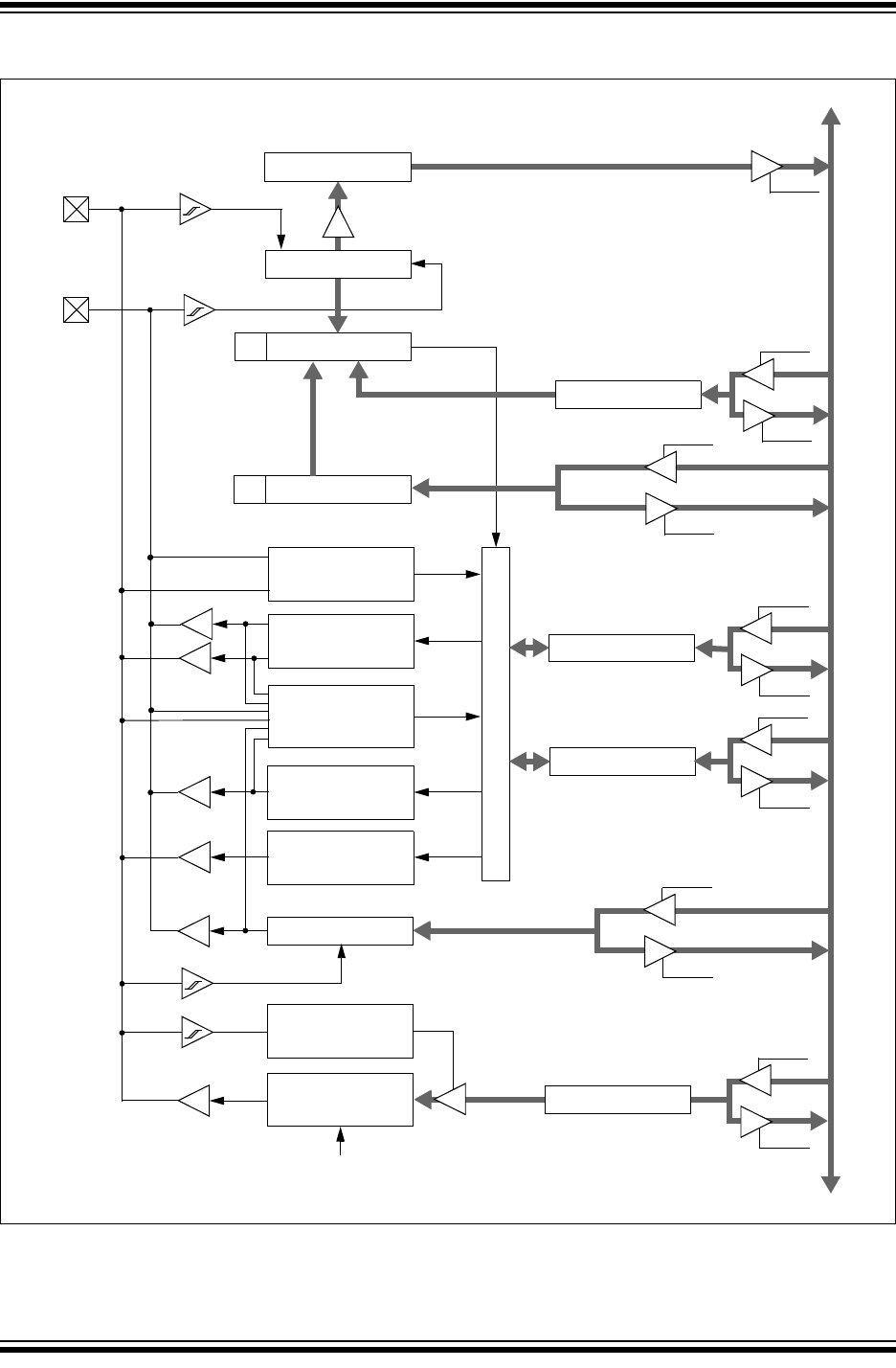
PIC32MZ Embedded Connectivity with Floating Point Unit (EF) Family
DS60001320B-page 356 Preliminary 2015 Microchip Technology Inc.
FIGURE 21-1: I2C™ BLOCK DIAGRAM
Internal
Data Bus
SCLx
SDAx
Shift
Match Detect
I2CxADD
Start and Stop
Bit Detect
Clock
Address Match
Clock
Stretching
I2CxTRN
LSB
Shift Clock
BRG Down Counter
Reload
Control
PBCLK2
Start and Stop
Bit Generation
Acknowledge
Generation
Collision
Detect
I2CxCON
I2CxSTAT
Control Logic
Read
LSB
Write
Read
I2CxBRG
I2CxRSR
Write
Read
Write
Read
Write
Read
Write
Read
Write
Read
I2CxMSK
I2CxRCV

2015 Microchip Technology Inc. Preliminary DS60001320B-page 357
PIC32MZ Embedded Connectivity with Floating Point Unit (EF) Family
21.1 I2C Control Registers
TABLE 21-1: I2C1 THROUGH I2C5 REGISTER MAP
Virtual Address
(BF82_#)
Register
Name(1)
Bit Range
Bits
All Resets
31/15 30/14 29/13 28/12 27/11 26/10 25/9 24/8 23/7 22/6 21/5 20/4 19/3 18/2 17/1 16/0
0000 I2C1CON 31:16 —————————PCIE SCIE BOEN SDAHT SBCDE AHEN DHEN 0000
15:0 ON —SIDL SCLREL STRICT A10M DISSLW SMEN GCEN STREN ACKDT ACKEN RCEN PEN RSEN SEN 1000
0010 I2C1STAT 31:16 — — — — — — — — — — — — — — — — 0000
15:0 ACKSTAT TRSTAT ACKTIM — — BCL GCSTAT ADD10 IWCOL I2COV D/A P S R/W RBF TBF 0000
0020 I2C1ADD 31:16 — — — — — — — — — — — — — — — — 0000
15:0 — — — — — — Address Register 0000
0030 I2C1MSK 31:16 — — — — — — — — — — — — — — — — 0000
15:0 — — — — — — Address Mask Register 0000
0040 I2C1BRG 31:16 — — — — — — — — — — — — — — — — 0000
15:0 Baud Rate Generator Register 0000
0050 I2C1TRN 31:16 — — — — — — — — — — — — — — — — 0000
15:0 ———————— Transmit Register 0000
0060 I2C1RCV 31:16 — — — — — — — — — — — — — — — — 0000
15:0 ———————— Receive Register 0000
0200 I2C2CON(2) 31:16 —————————PCIE SCIE BOEN SDAHT SBCDE AHEN DHEN 0000
15:0 ON —SIDL SCLREL STRICT A10M DISSLW SMEN GCEN STREN ACKDT ACKEN RCEN PEN RSEN SEN 1000
0210 I2C2STAT(2) 31:16 — — — — — — — — — — — — — — — — 0000
15:0 ACKSTAT TRSTAT ACKTIM — — BCL GCSTAT ADD10 IWCOL I2COV D/A P S R/W RBF TBF 0000
0220 I2C2ADD(2) 31:16 — — — — — — — — — — — — — — — — 0000
15:0 — — — — — — Address Register 0000
0230 I2C2MSK(2) 31:16 — — — — — — — — — — — — — — — — 0000
15:0 — — — — — — Address Mask Register 0000
0240 I2C2BRG(2) 31:16 — — — — — — — — — — — — — — — — 0000
15:0 Baud Rate Generator Register 0000
0250 I2C2TRN(2) 31:16 — — — — — — — — — — — — — — — — 0000
15:0 ———————— Transmit Register 0000
0260 I2C2RCV(2) 31:16 — — — — — — — — — — — — — — — — 0000
15:0 ———————— Receive Register 0000
0400 I2C3CON 31:16 —————————PCIE SCIE BOEN SDAHT SBCDE AHEN DHEN 0000
15:0 ON —SIDL SCLREL STRICT A10M DISSLW SMEN GCEN STREN ACKDT ACKEN RCEN PEN RSEN SEN 1000
0410 I2C3STAT 31:16 — — — — — — — — — — — — — — — — 0000
15:0 ACKSTAT TRSTAT ACKTIM — — BCL GCSTAT ADD10 IWCOL I2COV D/A P S R/W RBF TBF 0000
0420 I2C3ADD 31:16 — — — — — — — — — — — — — — — — 0000
15:0 — — — — — — Address Register 0000
Legend: x = unknown value on Reset; — = unimplemented, read as ‘0’. Reset values are shown in hexadecimal.
Note 1: All registers in this table except I2CxRCV have corresponding CLR, SET and INV registers at their virtual addresses, plus offsets of 0x4, 0x8 and 0xC, respectively. See Section 12.3 “CLR, SET, and
INV Registers” for more information.
2: This register is not available on 64-pin devices.

PIC32MZ Embedded Connectivity with Floating Point Unit (EF) Family
DS60001320B-page 358 Preliminary 2015 Microchip Technology Inc.
0430 I2C3MSK 31:16 — — — — — — — — — — — — — — — — 0000
15:0 — — — — — — Address Mask Register 0000
0440 I2C3BRG 31:16 — — — — — — — — — — — — — — — — 0000
15:0 Baud Rate Generator Register 0000
0450 I2C3TRN 31:16 — — — — — — — — — — — — — — — — 0000
15:0 ———————— Transmit Register 0000
0460 I2C3RCV 31:16 — — — — — — — — — — — — — — — — 0000
15:0 ———————— Receive Register 0000
0600 I2C4CON 31:16 —————————PCIE SCIE BOEN SDAHT SBCDE AHEN DHEN 0000
15:0 ON —SIDL SCLREL STRICT A10M DISSLW SMEN GCEN STREN ACKDT ACKEN RCEN PEN RSEN SEN 1000
0610 I2C4STAT 31:16 — — — — — — — — — — — — — — — — 0000
15:0 ACKSTAT TRSTAT ACKTIM — — BCL GCSTAT ADD10 IWCOL I2COV D/A P S R/W RBF TBF 0000
0620 I2C4ADD 31:16 — — — — — — — — — — — — — — — — 0000
15:0 — — — — — — Address Register 0000
0630 I2C4MSK 31:16 — — — — — — — — — — — — — — — — 0000
15:0 — — — — — — Address Mask Register 0000
0640 I2C4BRG 31:16 — — — — — — — — — — — — — — — — 0000
15:0 Baud Rate Generator Register 0000
0650 I2C4TRN 31:16 — — — — — — — — — — — — — — — — 0000
15:0 ———————— Transmit Register 0000
0660 I2C4RCV 31:16 — — — — — — — — — — — — — — — — 0000
15:0 ———————— Receive Register 0000
0800 I2C5CON 31:16 —————————PCIE SCIE BOEN SDAHT SBCDE AHEN DHEN 0000
15:0 ON —SIDL SCLREL STRICT A10M DISSLW SMEN GCEN STREN ACKDT ACKEN RCEN PEN RSEN SEN 1000
0810 I2C5STAT 31:16 — — — — — — — — — — — — — — — — 0000
15:0 ACKSTAT TRSTAT ACKTIM — — BCL GCSTAT ADD10 IWCOL I2COV D/A P S R/W RBF TBF 0000
0820 I2C5ADD 31:16 — — — — — — — — — — — — — — — — 0000
15:0 — — — — — — Address Register 0000
0830 I2C5MSK 31:16 — — — — — — — — — — — — — — — — 0000
15:0 — — — — — — Address Mask Register 0000
0840 I2C5BRG 31:16 — — — — — — — — — — — — — — — — 0000
15:0 Baud Rate Generator Register 0000
0850 I2C5TRN 31:16 — — — — — — — — — — — — — — — — 0000
15:0 ———————— Transmit Register 0000
0860 I2C5RCV 31:16 — — — — — — — — — — — — — — — — 0000
15:0 ———————— Receive Register 0000
TABLE 21-1: I2C1 THROUGH I2C5 REGISTER MAP (CONTINUED)
Virtual Address
(BF82_#)
Register
Name(1)
Bit Range
Bits
All Resets
31/15 30/14 29/13 28/12 27/11 26/10 25/9 24/8 23/7 22/6 21/5 20/4 19/3 18/2 17/1 16/0
Legend: x = unknown value on Reset; — = unimplemented, read as ‘0’. Reset values are shown in hexadecimal.
Note 1: All registers in this table except I2CxRCV have corresponding CLR, SET and INV registers at their virtual addresses, plus offsets of 0x4, 0x8 and 0xC, respectively. See Section 12.3 “CLR, SET, and
INV Registers” for more information.
2: This register is not available on 64-pin devices.

2015 Microchip Technology Inc. Preliminary DS60001320B-page 359
PIC32MZ Embedded Connectivity with Floating Point Unit (EF) Family
REGISTER 21-1: I2CXCON: I2C CONTROL REGISTER
Bit
Range Bit
31/23/15/7 Bit
30/22/14/6 Bit
29/21/13/5 Bit
28/20/12/4 Bit
27/19/11/3 Bit
26/18/10/2 Bit
25/17/9/1 Bit
24/16/8/0
31:24 U-0 U-0 U-0 U-0 U-0 U-0 U-0 U-0
— — — — — — — —
23:16 U-0 R/W-0 R/W-0 R/W-0 R/W-0 R/W-0 R/W-0 R/W-0
— PCIE SCIE BOEN SDAHT SBCDE AHEN DHEN
15:8 R/W-0 U-0 R/W-0 R/W-1, HC R/W-0 R/W-0 R/W-0 R/W-0
ON — SIDL SCKREL STRICT A10M DISSLW SMEN
7:0 R/W-0 R/W-0 R/W-0 R/W-0, HC R/W-0, HC R/W-0, HC R/W-0, HC R/W-0, HC
GCEN STREN ACKDT ACKEN RCEN PEN RSEN SEN
Legend: HC = Cleared in Hardware
R = Readable bit W = Writable bit U = Unimplemented bit, read as ‘0’
-n = Value at POR ‘1’ = Bit is set ‘0’ = Bit is cleared x = Bit is unknown
bit 31-23 Unimplemented: Read as ‘0’
bit 22 PCIE: Stop Condition Interrupt Enable bit (I2C Slave mode only)
1 = Enable interrupt on detection of Stop condition
0 = Stop detection interrupts are disabled
bit 21 SCIE: Start Condition Interrupt Enable bit (I2C Slave mode only)
1 = Enable interrupt on detection of Start or Restart conditions
0 = Start detection interrupts are disabled
bit 20 BOEN: Buffer Overwrite Enable bit (I2C Slave mode only)
1 = I2CxRCV is updated and ACK is generated for a received address/data byte, ignoring the state of the
I2COV bit (I2CxSTAT<6>)only if the RBF bit (I2CxSTAT<2>) = 0
0 = I2CxRCV is only updated when the I2COV bit (I2CxSTAT<6>) is clear
bit 19 SDAHT: SDA Hold Time Selection bit
1 = Minimum of 300 ns hold time on SDA after the falling edge of SCL
0 = Minimum of 100 ns hold time on SDA after the falling edge of SCL
bit 18 SBCDE: Slave Mode Bus Collision Detect Enable bit (I2C Slave mode only)
1 = Enable slave bus collision interrupts
0 = Slave bus collision interrupts are disabled
bit 18 AHEN: Address Hold Enable bit (Slave mode only)
1 = Following the 8th falling edge of SCL for a matching received address byte; SCKREL bit will be cleared
and the SCL will be held low.
0 = Address holding is disabled
bit 16 DHEN: Data Hold Enable bit (I2C Slave mode only)
1 = Following the 8th falling edge of SCL for a received data byte; slave hardware clears the SCKREL bit
and SCL is held low
0 = Data holding is disabled
bit 15 ON: I2C Enable bit
1 = Enables the I2C module and configures the SDA and SCL pins as serial port pins
0 = Disables the I2C module; all I2C pins are controlled by PORT functions
bit 14 Unimplemented: Read as ‘0’
bit 13 SIDL: Stop in Idle Mode bit
1 = Discontinue module operation when device enters Idle mode
0 = Continue module operation in Idle mode

PIC32MZ Embedded Connectivity with Floating Point Unit (EF) Family
DS60001320B-page 360 Preliminary 2015 Microchip Technology Inc.
bit 12 SCLREL: SCLx Release Control bit (when operating as I2C slave)
1 = Release SCLx clock
0 = Hold SCLx clock low (clock stretch)
If STREN = 1:
Bit is R/W (i.e., software can write ‘0’ to initiate stretch and write ‘1’ to release clock). Hardware clear at
beginning of slave transmission. Hardware clear at end of slave reception.
If STREN = 0:
Bit is R/S (i.e., software can only write ‘1’ to release clock). Hardware clear at beginning of slave
transmission.
bit 11 STRICT: Strict I2C Reserved Address Rule Enable bit
1 = Strict reserved addressing is enforced. Device does not respond to reserved address space or generate
addresses in reserved address space.
0 = Strict I2C Reserved Address Rule not enabled
bit 10 A10M: 10-bit Slave Address bit
1 = I2CxADD is a 10-bit slave address
0 = I2CxADD is a 7-bit slave address
bit 9 DISSLW: Disable Slew Rate Control bit
1 = Slew rate control disabled
0 = Slew rate control enabled
bit 8 SMEN: SMBus Input Levels bit
1 = Enable I/O pin thresholds compliant with SMBus specification
0 = Disable SMBus input thresholds
bit 7 GCEN: General Call Enable bit (when operating as I2C slave)
1 = Enable interrupt when a general call address is received in the I2CxRSR
(module is enabled for reception)
0 = General call address disabled
bit 6 STREN: SCLx Clock Stretch Enable bit (when operating as I2C slave)
Used in conjunction with SCLREL bit.
1 = Enable software or receive clock stretching
0 = Disable software or receive clock stretching
bit 5 ACKDT: Acknowledge Data bit (when operating as I2C master, applicable during master receive)
Value that is transmitted when the software initiates an Acknowledge sequence.
1 = Send NACK during Acknowledge
0 = Send ACK during Acknowledge
bit 4 ACKEN: Acknowledge Sequence Enable bit
(when operating as I2C master, applicable during master receive)
1 = Initiate Acknowledge sequence on SDAx and SCLx pins and transmit ACKDT data bit.
Hardware clear at end of master Acknowledge sequence.
0 = Acknowledge sequence not in progress
bit 3 RCEN: Receive Enable bit (when operating as I2C master)
1 = Enables Receive mode for I2C. Hardware clear at end of eighth bit of master receive data byte.
0 = Receive sequence not in progress
bit 2 PEN: Stop Condition Enable bit (when operating as I2C master)
1 = Initiate Stop condition on SDAx and SCLx pins. Hardware clear at end of master Stop sequence.
0 = Stop condition not in progress
bit 1 RSEN: Repeated Start Condition Enable bit (when operating as I2C master)
1 = Initiate Repeated Start condition on SDAx and SCLx pins. Hardware clear at end of
master Repeated Start sequence.
0 = Repeated Start condition not in progress
bit 0 SEN: Start Condition Enable bit (when operating as I2C master)
1 = Initiate Start condition on SDAx and SCLx pins. Hardware clear at end of master Start sequence.
0 = Start condition not in progress
REGISTER 21-1: I2CXCON: I2C CONTROL REGISTER (CONTINUED)

2015 Microchip Technology Inc. Preliminary DS60001320B-page 361
PIC32MZ Embedded Connectivity with Floating Point Unit (EF) Family
REGISTER 21-2: I2CXSTAT: I2C STATUS REGISTER
Bit
Range Bit
31/23/15/7 Bit
30/22/14/6 Bit
29/21/13/5 Bit
28/20/12/4 Bit
27/19/11/3 Bit
26/18/10/2 Bit
25/17/9/1 Bit
24/16/8/0
31:24 U-0 U-0 U-0 U-0 U-0 U-0 U-0 U-0
— — — — — — — —
23:16 U-0 U-0 U-0 U-0 U-0 U-0 U-0 U-0
— — — — — — — —
15:8 R-0, HS, HC R-0, HS, HC
R/C-0, HS, HC
U-0 U-0 R/C-0, HS R-0, HS, HC R-0, HS, HC
ACKSTAT TRSTAT ACKTIM —— BCL GCSTAT ADD10
7:0
R/C-0, HS, SC R/C-0, HS, SC R-0, HS, HC R/C-0, HS, HC R/C-0, HS, HC R-0, HS, HC R-0, HS, HC R-0, HS, HC
IWCOL I2COV D_A P S R_W RBF TBF
Legend: HS = Hardware Set HC = Hardware Cleared SC = Software Cleared
R = Readable bit W = Writable bit U = Unimplemented bit, read as ‘0’
-n = Value at POR ‘1’ = Bit is set ‘0’ = Bit is cleared C = Clearable bit
bit 31-16 Unimplemented: Read as ‘0’
bit 15 ACKSTAT: Acknowledge Status bit
(when operating as I2C™ master, applicable to master transmit operation)
1 = NACK received from slave
0 = ACK received from slave
Hardware set or clear at end of slave Acknowledge.
bit 14 TRSTAT: Transmit Status bit (when operating as I2C master, applicable to master transmit operation)
1 = Master transmit is in progress (8 bits + ACK)
0 = Master transmit is not in progress
Hardware set at beginning of master transmission. Hardware clear at end of slave Acknowledge.
bit 13 ACKTIM: Acknowledge Time Status bit (Valid in I2C Slave mode only)
1 = I2C bus is in an Acknowledge sequence, set on 8th falling edge of SCL clock
0 = Not an Acknowledge sequence, cleared on 9th rising edge of SCL clock
bit 12-11 Unimplemented: Read as ‘0’
bit 10 BCL: Master Bus Collision Detect bit
1 = A bus collision has been detected during a master operation
0 = No collision
Hardware set at detection of bus collision.
bit 9 GCSTAT: General Call Status bit
1 = General call address was received
0 = General call address was not received
Hardware set when address matches general call address. Hardware clear at Stop detection.
bit 8 ADD10: 10-bit Address Status bit
1 = 10-bit address was matched
0 = 10-bit address was not matched
Hardware set at match of 2nd byte of matched 10-bit address. Hardware clear at Stop detection.
bit 7 IWCOL: Write Collision Detect bit
1 = An attempt to write the I2CxTRN register failed because the I2C module is busy
0 = No collision
Hardware set at occurrence of write to I2CxTRN while busy (cleared by software).
bit 6 I2COV: Receive Overflow Flag bit
1 = A byte was received while the I2CxRCV register is still holding the previous byte
0 = No overflow
Hardware set at attempt to transfer I2CxRSR to I2CxRCV (cleared by software).

PIC32MZ Embedded Connectivity with Floating Point Unit (EF) Family
DS60001320B-page 362 Preliminary 2015 Microchip Technology Inc.
bit 5 D_A: Data/Address bit (when operating as I2C slave)
1 = Indicates that the last byte received was data
0 = Indicates that the last byte received was device address
Hardware clear at device address match. Hardware set by reception of slave byte.
bit 4 P: Stop bit
1 = Indicates that a Stop bit has been detected last
0 = Stop bit was not detected last
Hardware set or clear when Start, Repeated Start or Stop detected.
bit 3 S: Start bit
1 = Indicates that a Start (or Repeated Start) bit has been detected last
0 = Start bit was not detected last
Hardware set or clear when Start, Repeated Start or Stop detected.
bit 2 R_W: Read/Write Information bit (when operating as I2C slave)
1 = Read – indicates data transfer is output from slave
0 = Write – indicates data transfer is input to slave
Hardware set or clear after reception of I2C device address byte.
bit 1 RBF: Receive Buffer Full Status bit
1 = Receive complete, I2CxRCV is full
0 = Receive not complete, I2CxRCV is empty
Hardware set when I2CxRCV is written with received byte. Hardware clear when software
reads I2CxRCV.
bit 0 TBF: Transmit Buffer Full Status bit
1 = Transmit in progress, I2CxTRN is full
0 = Transmit complete, I2CxTRN is empty
Hardware set when software writes I2CxTRN. Hardware clear at completion of data transmission.
REGISTER 21-2: I2CXSTAT: I2C STATUS REGISTER (CONTINUED)

2015 Microchip Technology Inc. Preliminary DS60001320B-page 363
PIC32MZ Embedded Connectivity with Floating Point Unit (EF) Family
22.0 UNIVERSAL ASYNCHRONOUS
RECEIVER TRANSMITTER
(UART)
The UART module is one of the serial I/O modules
available in PIC32MZ EF devices. The UART is a
full-duplex, asynchronous communication channel
that communicates with peripheral devices and per-
sonal computers through protocols, such as RS-232,
RS-485, LIN, and IrDA®. The module also supports
the hardware flow control option, with UxCTS and
UxRTS pins, and also includes an IrDA encoder and
decoder.
The primary features of the UART module are:
• Full-duplex, 8-bit or 9-bit data transmission
• Even, Odd or No Parity options (for 8-bit data)
• One or two Stop bits
• Hardware auto-baud feature
• Hardware flow control option
• Fully integrated Baud Rate Generator (BRG) with
16-bit prescaler
• Baud rates ranging from 76 bps to 25 Mbps at
100 MHz (PBCLK2)
• 8-level deep First-In-First-Out (FIFO) transmit
data buffer
• 8-level deep FIFO receive data buffer
• Parity, framing and buffer overrun error detection
• Support for interrupt-only on address detect
(9th bit = 1)
• Separate transmit and receive interrupts
• Loopback mode for diagnostic support
• LIN Protocol support
• IrDA encoder and decoder with 16x baud clock
output for external IrDA encoder/decoder support
Figure 22-1 illustrates a simplified block diagram of the
UART module.
FIGURE 22-1: UART SIMPLIFIED BLOCK DIAGRAM
Note: This data sheet summarizes the features
of the PIC32MZ EF family of devices. It is
not intended to be a comprehensive
reference source. To complement the
information in this data sheet, refer to
Section 21. “Universal Asynchronous
Receiver Transmitter (UART)”
(DS60001107) in the “PIC32 Family
Reference Manual”, which is available
from the Microchip web site
(www.microchip.com/PIC32).
Baud Rate Generator
UxRX
Hardware Flow Control
UARTx Receiver
UARTx Transmitter UxTX
UxCTS
UxRTS/BCLKx
IrDA®
PBCLK2

PIC32MZ Embedded Connectivity with Floating Point Unit (EF) Family
DS60001320B-page 364 Preliminary 2015 Microchip Technology Inc.
22.1 UART Control Registers
TABLE 22-1: UART1 THROUGH UART6 REGISTER MAP
Virtual Address
(BF82_#)
Register
Name
Bit Range
Bits
All Resets
31/15 30/14 29/13 28/12 27/11 26/10 25/9 24/8 23/7 22/6 21/5 20/4 19/3 18/2 17/1 16/0
2000 U1MODE(1) 31:16 — — — — — — — — — — — — — — — — 0000
15:0 ON —SIDL IREN RTSMD —UEN<1:0> WAKE LPBACK ABAUD RXINV BRGH PDSEL<1:0> STSEL 0000
2010 U1STA(1) 31:16 — — — — — — — ADM_EN ADDR<7:0> 0000
15:0 UTXISEL<1:0> UTXINV URXEN UTXBRK UTXEN UTXBF TRMT URXISEL<1:0> ADDEN RIDLE PERR FERR OERR URXDA 0110
2020 U1TXREG 31:16 — — — — — — — — — — — — — — — — 0000
15:0 — — — — — — — TX8 Transmit Register 0000
2030 U1RXREG 31:16 — — — — — — — — — — — — — — — — 0000
15:0 — — — — — — — RX8 Receive Register 0000
2040 U1BRG(1) 31:16 — — — — — — — — — — — — — — — — 0000
15:0 Baud Rate Generator Prescaler 0000
2200 U2MODE(1) 31:16
15:0
— — — — — — — — — — — — — — — — 0000
ON —SIDL IREN RTSMD —UEN<1:0> WAKE LPBACK ABAUD RXINV BRGH PDSEL<1:0> STSEL 0000
2210 U2STA(1) 31:16 — — — — — — — ADM_EN ADDR<7:0> 0000
15:0 UTXISEL<1:0> UTXINV URXEN UTXBRK UTXEN UTXBF TRMT URXISEL<1:0> ADDEN RIDLE PERR FERR OERR URXDA 0110
2220 U2TXREG 31:16 — — — — — — — — — — — — — — — — 0000
15:0 — — — — — — — TX8 Transmit Register 0000
2230 U2RXREG 31:16 — — — — — — — — — — — — — — — — 0000
15:0 — — — — — — — RX8 Receive Register 0000
2240 U2BRG(1) 31:16 — — — — — — — — — — — — — — — — 0000
15:0 Baud Rate Generator Prescaler 0000
2400 U3MODE(1) 31:16
15:0
— — — — — — — — — — — — — — — — 0000
ON —SIDL IREN RTSMD —UEN<1:0> WAKE LPBACK ABAUD RXINV BRGH PDSEL<1:0> STSEL 0000
2410 U3STA(1) 31:16 — — — — — — — ADM_EN ADDR<7:0> 0000
15:0 UTXISEL<1:0> UTXINV URXEN UTXBRK UTXEN UTXBF TRMT URXISEL<1:0> ADDEN RIDLE PERR FERR OERR URXDA 0110
2420 U3TXREG 31:16 — — — — — — — — — — — — — — — — 0000
15:0 — — — — — — — TX8 Transmit Register 0000
2430 U3RXREG 31:16 — — — — — — — — — — — — — — — — 0000
15:0 — — — — — — — RX8 Receive Register 0000
2440 U3BRG(1) 31:16 — — — — — — — — — — — — — — — — 0000
15:0 Baud Rate Generator Prescaler 0000
Legend: x = unknown value on Reset; — = unimplemented, read as ‘0’. Reset values are shown in hexadecimal.
Note 1: This register has corresponding CLR, SET and INV registers at its virtual address, plus an offset of 0x4, 0x8 and 0xC, respectively. See Section 12.3 “CLR, SET, and INV Registers” for more informa-
tion.

2015 Microchip Technology Inc. Preliminary DS60001320B-page 365
PIC32MZ Embedded Connectivity with Floating Point Unit (EF) Family
2600 U4MODE(1) 31:16
15:0
— — — — — — — — — — — — — — — — 0000
ON —SIDL IREN RTSMD —UEN<1:0> WAKE LPBACK ABAUD RXINV BRGH PDSEL<1:0> STSEL 0000
2610 U4STA(1) 31:16 — — — — — — — ADM_EN ADDR<7:0> 0000
15:0 UTXISEL<1:0> UTXINV URXEN UTXBRK UTXEN UTXBF TRMT URXISEL<1:0> ADDEN RIDLE PERR FERR OERR URXDA 0110
2620 U4TXREG 31:16 — — — — — — — — — — — — — — — — 0000
15:0 — — — — — — — TX8 Transmit Register 0000
2630 U4RXREG 31:16 — — — — — — — — — — — — — — — — 0000
15:0 — — — — — — — RX8 Receive Register 0000
2640 U4BRG(1) 31:16 — — — — — — — — — — — — — — — — 0000
15:0 Baud Rate Generator Prescaler 0000
2800 U5MODE(1) 31:16
15:0
— — — — — — — — — — — — — — — — 0000
ON —SIDL IREN RTSMD —UEN<1:0> WAKE LPBACK ABAUD RXINV BRGH PDSEL<1:0> STSEL 0000
2810 U5STA(1) 31:16 — — — — — — — ADM_EN ADDR<7:0> 0000
15:0 UTXISEL<1:0> UTXINV URXEN UTXBRK UTXEN UTXBF TRMT URXISEL<1:0> ADDEN RIDLE PERR FERR OERR URXDA 0110
2820 U5TXREG 31:16 — — — — — — — — — — — — — — — — 0000
15:0 — — — — — — — TX8 Transmit Register 0000
2830 U5RXREG 31:16 — — — — — — — — — — — — — — — — 0000
15:0 — — — — — — — RX8 Receive Register 0000
2840 U5BRG(1) 31:16 — — — — — — — — — — — — — — — — 0000
15:0 Baud Rate Generator Prescaler 0000
2A00 U6MODE(1) 31:16
15:0
— — — — — — — — — — — — — — — — 0000
ON —SIDL IREN RTSMD —UEN<1:0> WAKE LPBACK ABAUD RXINV BRGH PDSEL<1:0> STSEL 0000
2A10 U6STA(1) 31:16 — — — — — — — ADM_EN ADDR<7:0> 0000
15:0 UTXISEL<1:0> UTXINV URXEN UTXBRK UTXEN UTXBF TRMT URXISEL<1:0> ADDEN RIDLE PERR FERR OERR URXDA 0110
2A20 U6TXREG 31:16 — — — — — — — — — — — — — — — — 0000
15:0 — — — — — — — TX8 Transmit Register 0000
2A30 U6RXREG 31:16 — — — — — — — — — — — — — — — — 0000
15:0 — — — — — — — RX8 Receive Register 0000
2A40 U6BRG(1) 31:16 — — — — — — — — — — — — — — — — 0000
15:0 Baud Rate Generator Prescaler 0000
TABLE 22-1: UART1 THROUGH UART6 REGISTER MAP (CONTINUED)
Virtual Address
(BF82_#)
Register
Name
Bit Range
Bits
All Resets
31/15 30/14 29/13 28/12 27/11 26/10 25/9 24/8 23/7 22/6 21/5 20/4 19/3 18/2 17/1 16/0
Legend: x = unknown value on Reset; — = unimplemented, read as ‘0’. Reset values are shown in hexadecimal.
Note 1: This register has corresponding CLR, SET and INV registers at its virtual address, plus an offset of 0x4, 0x8 and 0xC, respectively. See Section 12.3 “CLR, SET, and INV Registers” for more informa-
tion.

PIC32MZ Embedded Connectivity with Floating Point Unit (EF) Family
DS60001320B-page 366 Preliminary 2015 Microchip Technology Inc.
REGISTER 22-1: UxMODE: UARTx MODE REGISTER
Bit
Range Bit
31/23/15/7 Bit
30/22/14/6 Bit
29/21/13/5 Bit
28/20/12/4 Bit
27/19/11/3 Bit
26/18/10/2 Bit
25/17/9/1 Bit
24/16/8/0
31:24 U-0 U-0 U-0 U-0 U-0 U-0 U-0 U-0
— — — — — — — —
23:16 U-0 U-0 U-0 U-0 U-0 U-0 U-0 U-0
— — — — — — — —
15:8 R/W-0 U-0 R/W-0 R/W-0 R/W-0 U-0 R/W-0 R/W-0
ON —SIDLIRENRTSMD—UEN<1:0>
(1)
7:0 R/W-0 R/W-0 R/W-0 R/W-0 R/W-0 R/W-0 R/W-0 R/W-0
WAKE LPBACK ABAUD RXINV BRGH PDSEL<1:0> STSEL
Legend:
R = Readable bit W = Writable bit U = Unimplemented bit, read as ‘0’
-n = Value at POR ‘1’ = Bit is set ‘0’ = Bit is cleared x = Bit is unknown
bit 31-16 Unimplemented: Read as ‘0’
bit 15 ON: UARTx Enable bit
1 = UARTx is enabled. UARTx pins are controlled by UARTx as defined by UEN<1:0> and UTXEN
control bits
0 = UARTx is disabled. All UARTx pins are controlled by corresponding bits in the PORTx, TRISx and LATx
registers; UARTx power consumption is minimal
bit 14 Unimplemented: Read as ‘0’
bit 13 SIDL: Stop in Idle Mode bit
1 = Discontinue operation when device enters Idle mode
0 = Continue operation in Idle mode
bit 12 IREN: IrDA Encoder and Decoder Enable bit
1 = IrDA is enabled
0 = IrDA is disabled
bit 11 RTSMD: Mode Selection for UxRTS Pin bit
1 =UxRTS pin is in Simplex mode
0 =UxRTS
pin is in Flow Control mode
bit 10 Unimplemented: Read as ‘0’
bit 9-8 UEN<1:0>: UARTx Enable bits(1)
11 = UxTX, UxRX and UxBCLK pins are enabled and used; UxCTS pin is controlled by corresponding bits
in the PORTx register
10 = UxTX, UxRX, UxCTS and UxRTS pins are enabled and used
01 = UxTX, UxRX and UxRTS pins are enabled and used; UxCTS pin is controlled by corresponding bits
in the PORTx register
00 = UxTX and UxRX pins are enabled and used; UxCTS and UxRTS/UxBCLK pins are controlled by
corresponding bits in the PORTx register
bit 7 WAKE: Enable Wake-up on Start bit Detect During Sleep Mode bit
1 = Wake-up is enabled
0 = Wake-up is disabled
bit 6 LPBACK: UARTx Loopback Mode Select bit
1 = Loopback mode is enabled
0 = Loopback mode is disabled
Note 1: These bits are present for legacy compatibility, and are superseded by PPS functionality on these devices
(see Section 12.4 “Peripheral Pin Select (PPS)” for more information).

2015 Microchip Technology Inc. Preliminary DS60001320B-page 367
PIC32MZ Embedded Connectivity with Floating Point Unit (EF) Family
bit 5 ABAUD: Auto-Baud Enable bit
1 = Enable baud rate measurement on the next character – requires reception of Sync character (0x55);
cleared by hardware upon completion
0 = Baud rate measurement disabled or completed
bit 4 RXINV: Receive Polarity Inversion bit
1 = UxRX Idle state is ‘0’
0 = UxRX Idle state is ‘1’
bit 3 BRGH: High Baud Rate Enable bit
1 = High-Speed mode – 4x baud clock enabled
0 = Standard Speed mode – 16x baud clock enabled
bit 2-1 PDSEL<1:0>: Parity and Data Selection bits
11 = 9-bit data, no parity
10 = 8-bit data, odd parity
01 = 8-bit data, even parity
00 = 8-bit data, no parity
bit 0 STSEL: Stop Selection bit
1 = 2 Stop bits
0 = 1 Stop bit
REGISTER 22-1: UxMODE: UARTx MODE REGISTER (CONTINUED)
Note 1: These bits are present for legacy compatibility, and are superseded by PPS functionality on these devices
(see Section 12.4 “Peripheral Pin Select (PPS)” for more information).

PIC32MZ Embedded Connectivity with Floating Point Unit (EF) Family
DS60001320B-page 368 Preliminary 2015 Microchip Technology Inc.
REGISTER 22-2: UxSTA: UARTx STATUS AND CONTROL REGISTER
Bit
Range Bit
31/23/15/7 Bit
30/22/14/6 Bit
29/21/13/5 Bit
28/20/12/4 Bit
27/19/11/3 Bit
26/18/10/2 Bit
25/17/9/1 Bit
24/16/8/0
31:24 U-0 U-0 U-0 U-0 U-0 U-0 U-0 R/W-0
— — — — — — —ADM_EN
23:16 R/W-0 R/W-0 R/W-0 R/W-0 R/W-0 R/W-0 R/W-0 R/W-0
ADDR<7:0>
15:8 R/W-0 R/W-0 R/W-0 R/W-0 R/W-0 R/W-0 R-0 R-1
UTXISEL<1:0> UTXINV URXEN UTXBRK UTXEN UTXBF TRMT
7:0 R/W-0 R/W-0 R/W-0 R-1 R-0 R-0 R/W-0 R-0
URXISEL<1:0> ADDEN RIDLE PERR FERR OERR URXDA
Legend:
R = Readable bit W = Writable bit U = Unimplemented bit, read as ‘0’
-n = Value at POR ‘1’ = Bit is set ‘0’ = Bit is cleared x = Bit is unknown
bit 31-25 Unimplemented: Read as ‘0’
bit 24 ADM_EN: Automatic Address Detect Mode Enable bit
1 = Automatic Address Detect mode is enabled
0 = Automatic Address Detect mode is disabled
bit 23-16 ADDR<7:0>: Automatic Address Mask bits
When the ADM_EN bit is ‘1’, this value defines the address character to use for automatic address
detection.
bit 15-14 UTXISEL<1:0>: TX Interrupt Mode Selection bits
11 = Reserved, do not use
10 = Interrupt is generated and asserted while the transmit buffer is empty
01 = Interrupt is generated and asserted when all characters have been transmitted
00 = Interrupt is generated and asserted while the transmit buffer contains at least one empty space
bit 13 UTXINV: Transmit Polarity Inversion bit
If IrDA mode is disabled (i.e., IREN (UxMODE<12>) is ‘0’):
1 = UxTX Idle state is ‘0’
0 = UxTX Idle state is ‘1’
If IrDA mode is enabled (i.e., IREN (UxMODE<12>) is ‘1’):
1 = IrDA encoded UxTX Idle state is ‘1’
0 = IrDA encoded UxTX Idle state is ‘0’
bit 12 URXEN: Receiver Enable bit
1 = UARTx receiver is enabled. UxRX pin is controlled by UARTx (if ON = 1)
0 = UARTx receiver is disabled. UxRX pin is ignored by the UARTx module
bit 11 UTXBRK: Transmit Break bit
1 = Send Break on next transmission. Start bit followed by twelve ‘0’ bits, followed by Stop bit; cleared by
hardware upon completion
0 = Break transmission is disabled or completed
bit 10 UTXEN: Transmit Enable bit
1 = UARTx transmitter is enabled. UxTX pin is controlled by UARTx (if ON = 1)
0 = UARTx transmitter is disabled. Any pending transmission is aborted and buffer is reset
bit 9 UTXBF: Transmit Buffer Full Status bit (read-only)
1 = Transmit buffer is full
0 = Transmit buffer is not full, at least one more character can be written
bit 8 TRMT: Transmit Shift Register is Empty bit (read-only)
1 = Transmit shift register is empty and transmit buffer is empty (the last transmission has completed)
0 = Transmit shift register is not empty, a transmission is in progress or queued in the transmit buffer

2015 Microchip Technology Inc. Preliminary DS60001320B-page 369
PIC32MZ Embedded Connectivity with Floating Point Unit (EF) Family
bit 7-6 URXISEL<1:0>: Receive Interrupt Mode Selection bit
11 = Reserved
10 = Interrupt flag bit is asserted while receive buffer is 3/4 or more full
01 = Interrupt flag bit is asserted while receive buffer is 1/2 or more full
00 = Interrupt flag bit is asserted while receive buffer is not empty (i.e., has at least 1 data character)
bit 5 ADDEN: Address Character Detect bit (bit 8 of received data = 1)
1 = Address Detect mode is enabled. If 9-bit mode is not selected, this control bit has no effect
0 = Address Detect mode is disabled
bit 4 RIDLE: Receiver Idle bit (read-only)
1 = Receiver is Idle
0 = Data is being received
bit 3 PERR: Parity Error Status bit (read-only)
1 = Parity error has been detected for the current character
0 = Parity error has not been detected
bit 2 FERR: Framing Error Status bit (read-only)
1 = Framing error has been detected for the current character
0 = Framing error has not been detected
bit 1 OERR: Receive Buffer Overrun Error Status bit.
This bit is set in hardware and can only be cleared (= 0) in software. Clearing a previously set OERR bit
resets the receiver buffer and RSR to empty state.
1 = Receive buffer has overflowed
0 = Receive buffer has not overflowed
bit 0 URXDA: Receive Buffer Data Available bit (read-only)
1 = Receive buffer has data, at least one more character can be read
0 = Receive buffer is empty
REGISTER 22-2: UxSTA: UARTx STATUS AND CONTROL REGISTER (CONTINUED)
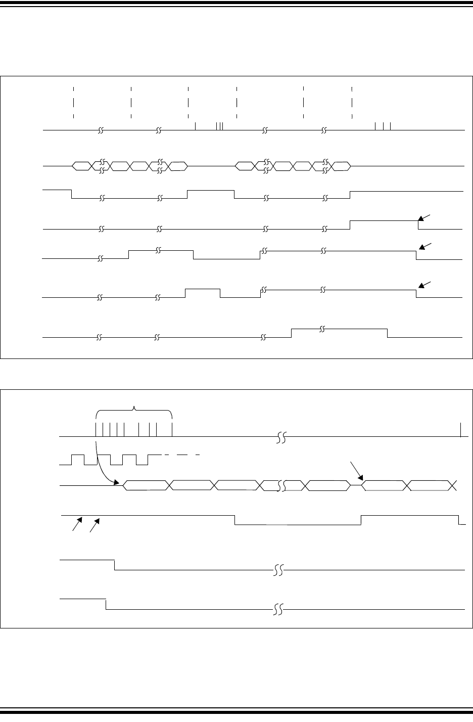
PIC32MZ Embedded Connectivity with Floating Point Unit (EF) Family
DS60001320B-page 370 Preliminary 2015 Microchip Technology Inc.
Figure 22-2 and Figure 22-3 illustrate typical receive
and transmit timing for the UART module.
FIGURE 22-2: UART RECEPTION
FIGURE 22-3: TRANSMISSION (8-BIT OR 9-BIT DATA)
Start 1 Stop Start 2 Stop 4 Start 5 Stop 10 Start 11 Stop 13
Read to
UxRXREG
UxRX
RIDLE
OERR
UxRXIF
URXISEL = 00
UxRXIF
URXISEL = 01
UxRXIF
URXISEL = 10
Char 1 Char 2-4 Char 5-10 Char 11-13
Cleared by
Software
Cleared by
Software
Cleared by
Software
StartStart Bit 0 Bit 1 Stop
Write to
TSR
BCLK/16
(Shift Clock)
UxTX
UxTXIF
UxTXIF
UTXISEL = 00
Bit 1
UxTXREG
UTXISEL = 01
UxTXIF
UTXISEL = 10
8 into TxBUF
Pull from Buffer
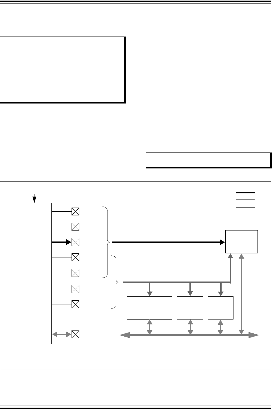
2015 Microchip Technology Inc. Preliminary DS60001320B-page 371
PIC32MZ Embedded Connectivity with Floating Point Unit (EF) Family
23.0 PARALLEL MASTER PORT
(PMP)
The PMP is a parallel 8-bit/16-bit input/output module
specifically designed to communicate with a wide
variety of parallel devices, such as communications
peripherals, LCDs, external memory devices and
microcontrollers. Because the interface to parallel
peripherals varies significantly, the PMP module is
highly configurable.
Key features of the PMP module include:
• 8-bit,16-bit interface
• Up to 16 programmable address lines
• Up to two Chip Select lines
• Programmable strobe options:
- Individual read and write strobes, or
- Read/write strobe with enable strobe
• Address auto-increment/auto-decrement
• Programmable address/data multiplexing
• Programmable polarity on control signals
• Parallel Slave Port support:
- Legacy addressable
- Address support
- 4-byte deep auto-incrementing buffer
• Programmable Wait states
• Operate during Sleep and Idle modes
• Fast bit manipulation using CLR, SET, and INV
registers
FIGURE 23-1: PMP MODULE PINOUT AND CONNECTIONS TO EXTERNAL DEVICES
Note: This data sheet summarizes the features
of the PIC32MZ EF family of devices. It is
not intended to be a comprehensive refer-
ence source. To complement the informa-
tion in this data sheet, refer to Section 13.
“Parallel Master Port (PMP)”
(DS60001128) in the “PIC32 Family Ref-
erence Manual”, which is available from
the Microchip web site (www.micro-
chip.com/PIC32).
Note: On 64-pin devices, data pins PMD<15:8>
are not available in 16-bit Master modes.
PMA0
PMA14
PMRD
PMWR
PMENB
PMRD/PMWR
PMCS1
PMA1
PMA<13:2>
PMALL
PMALH
Flash
Address Bus
Data Bus
Control Lines
LCD FIFO
Microcontroller
8-bit/16-bit Data (with or without multiplexed addressing)
Up to 16-bit Address
Parallel
Buffer
PMD<7:0>
Master Port
EEPROM
SRAM
Note: On 64-pin devices, data pins PMD<15:8> are not available in 16-bit Master modes.
PMD<15:8>(1)
PMA15
PMCS2
PBCLK2
PIC32MZ Embedded Connectivity with Floating Point Unit (EF) Family
DS60001320B-page 372 Preliminary 2015 Microchip Technology Inc.
23.1 PMP Control Registers
TABLE 23-1: PARALLEL MASTER PORT REGISTER MAP
Virtual Address
(BF82_#)
Register
Name(1)
Bit Range
Bits
All Resets
31/15 30/14 29/13 28/12 27/11 26/10 25/9 24/8 23/7 22/6 21/5 20/4 19/3 18/2 17/1 16/0
E000 PMCON 31:16 ————————RDSTART — — — — — DUALBUF —0000
15:0 ON —SIDL ADRMUX<1:0> PMPTTL PTWREN PTRDEN CSF<1:0> ALP CS2P CS1P —WRSP RDSP 0000
E010 PMMODE 31:16 ————————————————0000
15:0 BUSY IRQM<1:0> INCM<1:0> MODE16 MODE<1:0> WAITB<1:0> WAITM<3:0> WAITE<1:0> 0000
E020 PMADDR
31:16 ————————————————0000
15:0
CS2 CS1
ADDR<13:0> 0000
ADDR15 ADDR14
0000
E030 PMDOUT 31:16 ————————————————0000
15:0 DATAOUT<15:0> 0000
E040 PMDIN 31:16 ————————————————0000
15:0 DATAIN<15:0> 0000
E050 PMAEN 31:16 ————————————————0000
15:0 PTEN<15:0> 0000
E060 PMSTAT 31:16 ————————————————0000
15:0 IBF IBOV — — IB3F IB2F IB1F IB0F OBE OBUF — — OB3E OB2E OB1E OB0E 008F
E070 PMWADDR
31:16 ————————————————0000
15:0
WCS2 WCS1
— — — — — — — — — — — — — — 0000
WADDR15 WADDR14
WADDR<13:0> 0000
E080 PMRADDR
31:16 ————————————————0000
15:0
RCS2 RCS1
— — — — — — — — — — — — — — 0000
RADDR15 RADDR14
RADDR<13:0> 0000
E090 PMRDIN 31:16 31:16 ———————————————0000
15:0 15:0 RDATAIN<15:0> 0000
Legend: x = unknown value on Reset; — = unimplemented, read as ‘0’. Reset values are shown in hexadecimal.
Note 1: All registers in this table have corresponding CLR, SET and INV registers at their virtual addresses, plus offsets of 0x4, 0x8 and 0xC, respectively. See Section 12.3 “CLR, SET, and INV Registers” for
more information.

2015 Microchip Technology Inc. Preliminary DS60001320B-page 373
PIC32MZ Embedded Connectivity with Floating Point Unit (EF) Family
REGISTER 23-1: PMCON: PARALLEL PORT CONTROL REGISTER
Bit
Range Bit
31/23/15/7 Bit
30/22/14/6 Bit
29/21/13/5 Bit
28/20/12/4 Bit
27/19/11/3 Bit
26/18/10/2 Bit
25/17/9/1 Bit
24/16/8/0
31:24 U-0 U-0 U-0 U-0 U-0 U-0 U-0 U-0
— — — — — — — —
23:16 R/W-0, HC U-0 U-0 U-0 U-0 U-0 R/W-0 U-0
RDSTART — — — — — DUALBUF —
15:8 R/W-0 U-0 R/W-0 R/W-0 R/W-0 R/W-0 R/W-0 R/W-0
ON —SIDL
ADRMUX<1:0>
PMPTTL PTWREN PTRDEN
7:0 R/W-0 R/W-0 R/W-0 R/W-0 R/W-0 U-0 R/W-0 R/W-0
CSF<1:0>(1) ALP(1) CS2P(1) CS1P(1) — WRSP RDSP
Legend:
R = Readable bit W = Writable bit U = Unimplemented bit, read as ‘0’
-n = Value at POR ‘1’ = Bit is set ‘0’ = Bit is cleared x = Bit is unknown
bit 31-24 Unimplemented: Read as ‘0’
bit 23 RDSTART: Start Read on PMP Bus bit
This bit is cleared by hardware at the end of the read cycle.
1 = Start a read cycle on the PMP bus
0 = No effect
bit 22-18 Unimplemented: Read as ‘0’
bit 17 DUALBUF: Dual Read/Write Buffers enable bit
This bit is valid in Master mode only.
1 = PMP uses separate registers for reads and writes (PMRADDR, PMDATAIN, PMWADDR, PMDATAOUT)
0 = PMP uses legacy registers (PMADDR, PMDATA)
bit 16 Unimplemented: Read as ‘0’
bit 15 ON: Parallel Master Port Enable bit
1 = PMP enabled
0 = PMP disabled, no off-chip access performed
bit 14 Unimplemented: Read as ‘0’
bit 13 SIDL: Stop in Idle Mode bit
1 = Discontinue module operation when device enters Idle mode
0 = Continue module operation in Idle mode
bit 12-11 ADRMUX<1:0>: Address/Data Multiplexing Selection bits
11 = Lower 8 bits of address are multiplexed on PMD<15:0> pins; upper 8 bits are not used
10 = All 16 bits of address are multiplexed on PMD<15:0> pins
01 = Lower 8 bits of address are multiplexed on PMD<7:0> pins, upper bits are on PMA<15:8>
00 = Address and data appear on separate pins
bit 10 PMPTTL: PMP Module TTL Input Buffer Select bit
1 = PMP module uses TTL input buffers
0 = PMP module uses Schmitt Trigger input buffer
bit 9 PTWREN: Write Enable Strobe Port Enable bit
1 = PMWR/PMENB port enabled
0 = PMWR/PMENB port disabled
bit 8 PTRDEN: Read/Write Strobe Port Enable bit
1 = PMRD/PMWR port enabled
0 = PMRD/PMWR port disabled
Note 1: These bits have no effect when their corresponding pins are used as address lines.

PIC32MZ Embedded Connectivity with Floating Point Unit (EF) Family
DS60001320B-page 374 Preliminary 2015 Microchip Technology Inc.
bit 7-6 CSF<1:0>: Chip Select Function bits(1)
11 = Reserved
10 = PMCS1 and PMCS2 function as Chip Select
01 = PMCS2 functions as Chip Select and PMCS1 functions as address bit 14
00 = PMCS1 and PMCS2 function as address bit 14 and address bit 15
bit 5 ALP: Address Latch Polarity bit(1)
1 = Active-high (PMALL and PMALH)
0 = Active-low (PMALL and PMALH)
bit 4 CS2P: Chip Select 2 Polarity bit(1)
1 = Active-high (PMCS2)
0 =Active-low (PMCS2
)
bit 3 CS1P: Chip Select 1 Polarity bit(1)
1 = Active-high (PMCS1)
0 =Active-low (PMCS1
)
bit 2 Unimplemented: Read as ‘0’
bit 1 WRSP: Write Strobe Polarity bit
For Slave Modes and Master mode 2 (MODE<1:0> = 00,01,10):
1 = Write strobe active-high (PMWR)
0 = Write strobe active-low (PMWR)
For Master mode 1 (MODE<1:0> = 11):
1 = Enable strobe active-high (PMENB)
0 = Enable strobe active-low (PMENB)
bit 0 RDSP: Read Strobe Polarity bit
For Slave modes and Master mode 2 (MODE<1:0> = 00,01,10):
1 = Read Strobe active-high (PMRD)
0 = Read Strobe active-low (PMRD)
For Master mode 1 (MODE<1:0> = 11):
1 = Read/write strobe active-high (PMRD/PMWR)
0 = Read/write strobe active-low (PMRD/PMWR)
REGISTER 23-1: PMCON: PARALLEL PORT CONTROL REGISTER (CONTINUED)
Note 1: These bits have no effect when their corresponding pins are used as address lines.

2015 Microchip Technology Inc. Preliminary DS60001320B-page 375
PIC32MZ Embedded Connectivity with Floating Point Unit (EF) Family
REGISTER 23-2: PMMODE: PARALLEL PORT MODE REGISTER
Bit
Range Bit
31/23/15/7 Bit
30/22/14/6 Bit
29/21/13/5 Bit
28/20/12/4 Bit
27/19/11/3 Bit
26/18/10/2 Bit
25/17/9/1 Bit
24/16/8/0
31:24 U-0 U-0 U-0 U-0 U-0 U-0 U-0 U-0
————————
23:16 U-0 U-0 U-0 U-0 U-0 U-0 U-0 U-0
————————
15:8 R-0 R/W-0 R/W-0 R/W-0 R/W-0 R/W-0 R/W-0 R/W-0
BUSY IRQM<1:0> INCM<1:0> MODE16 MODE<1:0>
7:0 R/W-0 R/W-0 R/W-0 R/W-0 R/W-0 R/W-0 R/W-0 R/W-0
WAITB<1:0>(1) WAITM<3:0>(1) WAITE<1:0>(1)
Legend:
R = Readable bit W = Writable bit U = Unimplemented bit, read as ‘0’
-n = Value at POR ‘1’ = Bit is set ‘0’ = Bit is cleared x = Bit is unknown
bit 31-16 Unimplemented: Read as ‘0’
bit 15 BUSY: Busy bit (Master mode only)
1 = Port is busy
0 = Port is not busy
bit 14-13 IRQM<1:0>: Interrupt Request Mode bits
11 = Reserved, do not use
10 = Interrupt generated when Read Buffer 3 is read or Write Buffer 3 is written (Buffered PSP mode)
or on a read or write operation when PMA<1:0> =11 (Addressable Slave mode only)
01 = Interrupt generated at the end of the read/write cycle
00 = No Interrupt generated
bit 12-11 INCM<1:0>: Increment Mode bits
11 = Slave mode read and write buffers auto-increment (MODE<1:0> = 00 only)
10 = Decrement ADDR<15:0> and ADDR<14> by 1 every read/write cycle(2)
01 = Increment ADDR<15:0> and ADDR<14> by 1 every read/write cycle(2)
00 = No increment or decrement of address
bit 10 MODE16: 8/16-bit Mode bit
1 = 16-bit mode: a read or write to the data register invokes a single 16-bit transfer
0 = 8-bit mode: a read or write to the data register invokes a single 8-bit transfer
bit 9-8 MODE<1:0>: Parallel Port Mode Select bits
11 = Master mode 1 (PMCSx, PMRD/PMWR, PMENB, PMA<x:0>, and PMD<15:0>)(3)
10 = Master mode 2 (PMCSx, PMRD, PMWR, PMA<x:0>, and PMD<15:0>)(3)
01 = Enhanced Slave mode, control signals (PMRD, PMWR, PMCSx, PMD<7:0>, and PMA<1:0>)
00 = Legacy Parallel Slave Port, control signals (PMRD, PMWR, PMCSx, and PMD<7:0>)
bit 7-6 WAITB<1:0>: Data Setup to Read/Write Strobe Wait States bits(1)
11 = Data wait of 4 TPBCLK2; multiplexed address phase of 4 TPBCLK2
10 = Data wait of 3 TPBCLK2; multiplexed address phase of 3 TPBCLK2
01 = Data wait of 2 TPBCLK2; multiplexed address phase of 2 TPBCLK2
00 = Data wait of 1 TPBCLK2; multiplexed address phase of 1 TPBCLK2 (default)
Note 1: Whenever WAITM<3:0> = 0000, WAITB and WAITE bits are ignored and forced to 1 TPBCLK2 cycle for a
write operation; WAITB = 1 TPBCLK2 cycle, WAITE = 0 TPBCLK2 cycles for a read operation.
2: Address bits 14 and 15 are is not subject to auto-increment/decrement if configured as Chip Select.
3: The PMD<15:8> bits are not active is the MODE16 bit = 1.

PIC32MZ Embedded Connectivity with Floating Point Unit (EF) Family
DS60001320B-page 376 Preliminary 2015 Microchip Technology Inc.
bit 5-2 WAITM<3:0>: Data Read/Write Strobe Wait States bits(1)
1111 = Wait of 16 TPBCLK2
•
•
•
0001 = Wait of 2 TPBCLK2
0000 = Wait of 1 TPBCLK2 (default)
bit 1-0 WAITE<1:0>: Data Hold After Read/Write Strobe Wait States bits(1)
11 = Wait of 4 TPBCLK2
10 = Wait of 3 TPBCLK2
01 = Wait of 2 TPBCLK2
00 = Wait of 1 TPBCLK2 (default)
For Read operations:
11 = Wait of 3 TPBCLK2
10 = Wait of 2 TPBCLK2
01 = Wait of 1 TPBCLK2
00 = Wait of 0 TPBCLK2 (default)
REGISTER 23-2: PMMODE: PARALLEL PORT MODE REGISTER (CONTINUED)
Note 1: Whenever WAITM<3:0> = 0000, WAITB and WAITE bits are ignored and forced to 1 TPBCLK2 cycle for a
write operation; WAITB = 1 TPBCLK2 cycle, WAITE = 0 TPBCLK2 cycles for a read operation.
2: Address bits 14 and 15 are is not subject to auto-increment/decrement if configured as Chip Select.
3: The PMD<15:8> bits are not active is the MODE16 bit = 1.

2015 Microchip Technology Inc. Preliminary DS60001320B-page 377
PIC32MZ Embedded Connectivity with Floating Point Unit (EF) Family
REGISTER 23-3: PMADDR: PARALLEL PORT ADDRESS REGISTER
Bit
Range Bit
31/23/15/7 Bit
30/22/14/6 Bit
29/21/13/5 Bit
28/20/12/4 Bit
27/19/11/3 Bit
26/18/10/2 Bit
25/17/9/1 Bit
24/16/8/0
31:24 U-0 U-0 U-0 U-0 U-0 U-0 U-0 U-0
— — — — — — — —
23:16 U-0 U-0 U-0 U-0 U-0 U-0 U-0 U-0
— — — — — — — —
15:8
R/W-0 R/W-0 R/W-0 R/W-0 R/W-0 R/W-0 R/W-0 R/W-0
CS2(1) CS1(3)
ADDR<13:8>
ADDR15(2) ADDR14(4)
7:0 R/W-0 R/W-0 R/W-0 R/W-0 R/W-0 R/W-0 R/W-0 R/W-0
ADDR<7:0>
Legend:
R = Readable bit W = Writable bit U = Unimplemented bit, read as ‘0’
-n = Value at POR ‘1’ = Bit is set ‘0’ = Bit is cleared x = Bit is unknown
bit 31-16 Unimplemented: Read as ‘0’
bit 15 CS2: Chip Select 2 bit(1)
1 = Chip Select 2 is active
0 = Chip Select 2 is inactive
bit 15 ADDR<15>: Target Address bit 15(2)
bit 14 CS1: Chip Select 1 bit(3)
1 = Chip Select 1 is active
0 = Chip Select 1 is inactive
bit 14 ADDR<14>: Target Address bit 14(4)
bit 13-0 ADDR<13:0>: Address bits
Note 1: When the CSF<1:0> bits (PMCON<7:6>) = 10 or 01.
2: When the CSF<1:0> bits (PMCON<7:6>) = 00.
3: When the CSF<1:0> bits (PMCON<7:6>) = 10.
4: When the CSF<1:0> bits (PMCON<7:6>) = 00 or 01.
Note: If the DUALBUF bit (PMCON<17>) = 0, the bits in this register control both read and write target
addressing. If the DUALBUF bit = 1, the bits in this register are not used. In this instance, use the
PMRADDR register for Read operations and the PMWADDR register for Write operations.
PIC32MZ Embedded Connectivity with Floating Point Unit (EF) Family
DS60001320B-page 378 Preliminary 2015 Microchip Technology Inc.
REGISTER 23-4: PMDOUT: PARALLEL PORT OUTPUT DATA REGISTER
Bit
Range Bit
31/23/15/7 Bit
30/22/14/6 Bit
29/21/13/5 Bit
28/20/12/4 Bit
27/19/11/3 Bit
26/18/10/2 Bit
25/17/9/1 Bit
24/16/8/0
31:24 U-0 U-0 U-0 U-0 U-0 U-0 U-0 U-0
— — — — — — — —
23:16 U-0 U-0 U-0 U-0 U-0 U-0 U-0 U-0
— — — — — — — —
15:8 R/W-0 R/W-0 R/W-0 R/W-0 R/W-0 R/W-0 R/W-0 R/W-0
DATAOUT<15:8>
7:0 R/W-0 R/W-0 R/W-0 R/W-0 R/W-0 R/W-0 R/W-0 R/W-0
DATAOUT<7:0>
Legend:
R = Readable bit W = Writable bit U = Unimplemented bit, read as ‘0’
-n = Value at POR ‘1’ = Bit is set ‘0’ = Bit is cleared x = Bit is unknown
bit 31-16 Unimplemented: Read as ‘0’
bit 15-0 DATAOUT<15:0>: Port Data Output bits
This register is used for Read operations in the Enhanced Parallel Slave mode and Write operations for Dual
Buffer Master mode.
In Dual Buffer Master mode, the DUALBUF bit (PMPCON<17>) = 1, a write to the MSB triggers the trans-
action on the PMP port. When MODE16 = 1, MSB = DATAOUT<15:8>. When MODE16 = 0,
MSB = DATAOUT<7:0>.
Note: In Master mode, a read will return the last value written to the register. In Slave mode, a read will return
indeterminate results.
REGISTER 23-5: PMDIN: PARALLEL PORT INPUT DATA REGISTER
Bit
Range Bit
31/23/15/7 Bit
30/22/14/6 Bit
29/21/13/5 Bit
28/20/12/4 Bit
27/19/11/3 Bit
26/18/10/2 Bit
25/17/9/1 Bit
24/16/8/0
31:24 U-0 U-0 U-0 U-0 U-0 U-0 U-0 U-0
— — — — — — — —
23:16 U-0 U-0 U-0 U-0 U-0 U-0 U-0 U-0
— — — — — — — —
15:8 R/W-0 R/W-0 R/W-0 R/W-0 R/W-0 R/W-0 R/W-0 R/W-0
DATAIN<15:8>
7:0 R/W-0 R/W-0 R/W-0 R/W-0 R/W-0 R/W-0 R/W-0 R/W-0
DATAIN<7:0>
Legend:
R = Readable bit W = Writable bit U = Unimplemented bit, read as ‘0’
-n = Value at POR ‘1’ = Bit is set ‘0’ = Bit is cleared x = Bit is unknown
bit 31-16 Unimplemented: Read as ‘0’
bit 15-0 DATAIN<15:0>: Port Data Input bits
This register is used for both Parallel Master Port mode and Enhanced Parallel Slave mode.
In Parallel Master mode, a write to the MSB triggers the write transaction on the PMP port. Similarly, a read
to the MSB triggers the read transaction on the PMP port.
When MODE16 = 1, MSB = DATAIN<15:8>. When MODE16 = 0, MSB = DATAIN<7:0>.
Note: This register is not used in Dual Buffer Master mode (i.e., DUALBUF bit (PMPCON<17>) = 1).

2015 Microchip Technology Inc. Preliminary DS60001320B-page 379
PIC32MZ Embedded Connectivity with Floating Point Unit (EF) Family
REGISTER 23-6: PMAEN: PARALLEL PORT PIN ENABLE REGISTER
Bit
Range Bit
31/23/15/7 Bit
30/22/14/6 Bit
29/21/13/5 Bit
28/20/12/4 Bit
27/19/11/3 Bit
26/18/10/2 Bit
25/17/9/1 Bit
24/16/8/0
31:24 U-0 U-0 U-0 U-0 U-0 U-0 U-0 U-0
— — — — — — — —
23:16 U-0 U-0 U-0 U-0 U-0 U-0 U-0 U-0
— — — — — — — —
15:8 R/W-0 R/W-0 R/W-0 R/W-0 R/W-0 R/W-0 R/W-0 R/W-0
PTEN<15:14> PTEN<13:8>
7:0 R/W-0 R/W-0 R/W-0 R/W-0 R/W-0 R/W-0 R/W-0 R/W-0
PTEN<7:0>
Legend:
R = Readable bit W = Writable bit U = Unimplemented bit, read as ‘0’
-n = Value at POR ‘1’ = Bit is set ‘0’ = Bit is cleared x = Bit is unknown
bit 31-15 Unimplemented: Read as ‘0’
bit 15-14 PTEN<15:14>: PMCS1 Strobe Enable bits
1 = PMA15 and PMA14 function as either PMA<15:14> or PMCS1 and PMCS2(1)
0 = PMA15 and PMA14 function as port I/O
bit 13-2 PTEN<13:2>: PMP Address Port Enable bits
1 = PMA<13:2> function as PMP address lines
0 = PMA<13:2> function as port I/O
bit 1-0 PTEN<1:0>: PMALH/PMALL Strobe Enable bits
1 = PMA1 and PMA0 function as either PMA<1:0> or PMALH and PMALL(2)
0 = PMA1 and PMA0 pads function as port I/O
Note 1: The use of these pins as PMA15 and PMA14 or CS1 and CS2 is selected by the CSF<1:0> bits in the
PMCON register.
2: The use of these pins as PMA1/PMA0 or PMALH/PMALL depends on the Address/Data Multiplex mode
selected by bits ADRMUX<1:0> in the PMCON register.

PIC32MZ Embedded Connectivity with Floating Point Unit (EF) Family
DS60001320B-page 380 Preliminary 2015 Microchip Technology Inc.
REGISTER 23-7: PMSTAT: PARALLEL PORT STATUS REGISTER (SLAVE MODES ONLY)
Bit
Range Bit
31/23/15/7 Bit
30/22/14/6 Bit
29/21/13/5 Bit
28/20/12/4 Bit
27/19/11/3 Bit
26/18/10/2 Bit
25/17/9/1 Bit
24/16/8/0
31:24 U-0 U-0 U-0 U-0 U-0 U-0 U-0 U-0
— — — — — — — —
23:16 U-0 U-0 U-0 U-0 U-0 U-0 U-0 U-0
— — — — — — — —
15:8 R-0 R/W-0, HS, SC U-0 U-0 R-0 R-0 R-0 R-0
IBF IBOV —— IB3F IB2F IB1F IB0F
7:0 R-1 R/W-0, HS, SC U-0 U-0 R-1 R-1 R-1 R-1
OBE OBUF —— OB3E OB2E OB1E OB0E
Legend: HS = Hardware Set SC = Software Cleared
R = Readable bit W = Writable bit U = Unimplemented bit, read as ‘0’
-n = Value at POR ‘1’ = Bit is set ‘0’ = Bit is cleared x = Bit is unknown
bit 31-16 Unimplemented: Read as ‘0’
bit 15 IBF: Input Buffer Full Status bit
1 = All writable input buffer registers are full
0 = Some or all of the writable input buffer registers are empty
bit 14 IBOV: Input Buffer Overflow Status bit
1 = A write attempt to a full input byte buffer occurred (must be cleared in software)
0 = No overflow occurred
bit 13-12 Unimplemented: Read as ‘0’
bit 11-8 IBxF: Input Buffer x Status Full bits
1 = Input Buffer contains data that has not been read (reading buffer will clear this bit)
0 = Input Buffer does not contain any unread data
bit 7 OBE: Output Buffer Empty Status bit
1 = All readable output buffer registers are empty
0 = Some or all of the readable output buffer registers are full
bit 6 OBUF: Output Buffer Underflow Status bit
1 = A read occurred from an empty output byte buffer (must be cleared in software)
0 = No underflow occurred
bit 5-4 Unimplemented: Read as ‘0’
bit 3-0 OBxE: Output Buffer x Status Empty bits
1 = Output buffer is empty (writing data to the buffer will clear this bit)
0 = Output buffer contains data that has not been transmitted

2015 Microchip Technology Inc. Preliminary DS60001320B-page 381
PIC32MZ Embedded Connectivity with Floating Point Unit (EF) Family
REGISTER 23-8: PMWADDR: PARALLEL PORT WRITE ADDRESS REGISTER
Bit
Range Bit
31/23/15/7 Bit
30/22/14/6 Bit
29/21/13/5 Bit
28/20/12/4 Bit
27/19/11/3 Bit
26/18/10/2 Bit
25/17/9/1 Bit
24/16/8/0
31:24 U-0 U-0 U-0 U-0 U-0 U-0 U-0 U-0
— — — — — — — —
23:16 U-0 U-0 U-0 U-0 U-0 U-0 U-0 U-0
— — — — — — — —
15:8
R/W-0 R/W-0 R/W-0 R/W-0 R/W-0 R/W-0 R/W-0 R/W-0
WCS2(1) WCS1(3)
WADDR<13:8>
WADDR15(2) WADDR14(4)
7:0 R/W-0 R/W-0 R/W-0 R/W-0 R/W-0 R/W-0 R/W-0 R/W-0
WADDR<7:0>
Legend:
R = Readable bit W = Writable bit U = Unimplemented bit, read as ‘0’
-n = Value at POR ‘1’ = Bit is set ‘0’ = Bit is cleared x = Bit is unknown
bit 31-16 Unimplemented: Read as ‘0’
bit 15 WCS2: Chip Select 2 bit(1)
1 = Chip Select 2 is active
0 = Chip Select 2 is inactive
bit 15 WADDR<15>: Target Address bit 15(2)
bit 14 WCS1: Chip Select 1 bit(3)
1 = Chip Select 1 is active
0 = Chip Select 1 is inactive
bit 14 WADDR<14>: Target Address bit 14(4)
bit 13-0 WADDR<13:0>: Address bits
Note 1: When the CSF<1:0> bits (PMCON<7:6>) = 10 or 01.
2: When the CSF<1:0> bits (PMCON<7:6>) = 00.
3: When the CSF<1:0> bits (PMCON<7:6>) = 10.
4: When the CSF<1:0> bits (PMCON<7:6>) = 00 or 01.
Note: This register is only used when the DUALBUF bit (PMCON<17>) is set to ‘1’.

PIC32MZ Embedded Connectivity with Floating Point Unit (EF) Family
DS60001320B-page 382 Preliminary 2015 Microchip Technology Inc.
REGISTER 23-9: PMRADDR: PARALLEL PORT READ ADDRESS REGISTER
Bit
Range Bit
31/23/15/7 Bit
30/22/14/6 Bit
29/21/13/5 Bit
28/20/12/4 Bit
27/19/11/3 Bit
26/18/10/2 Bit
25/17/9/1 Bit
24/16/8/0
31:24 U-0 U-0 U-0 U-0 U-0 U-0 U-0 U-0
— — — — — — — —
23:16 U-0 U-0 U-0 U-0 U-0 U-0 U-0 U-0
— — — — — — — —
15:8
R/W-0 R/W-0 R/W-0 R/W-0 R/W-0 R/W-0 R/W-0 R/W-0
RCS2(1) RCS1(3)
RADDR<13:8>
RADDR15(2) RADDR14(4)
7:0 R/W-0 R/W-0 R/W-0 R/W-0 R/W-0 R/W-0 R/W-0 R/W-0
RADDR<7:0>
Legend:
R = Readable bit W = Writable bit U = Unimplemented bit, read as ‘0’
-n = Value at POR ‘1’ = Bit is set ‘0’ = Bit is cleared x = Bit is unknown
bit 31-16 Unimplemented: Read as ‘0’
bit 15 RCS2: Chip Select 2 bit(1)
1 = Chip Select 2 is active
0 = Chip Select 2 is inactive (RADDR15 function is selected)
bit 15 RADDR<15>: Target Address bit 15(2)
bit 14 RCS1: Chip Select 1 bit(3)
1 = Chip Select 1 is active
0 = Chip Select 1 is inactive (RADDR14 function is selected)
bit 14 RADDR<14>: Target Address bit 14(4)
bit 13-0 RADDR<13:0>: Address bits
Note 1: When the CSF<1:0> bits (PMCON<7:6>) = 10 or 01.
2: When the CSF<1:0> bits (PMCON<7:6>) = 00.
3: When the CSF<1:0> bits (PMCON<7:6>) = 10.
4: When the CSF<1:0> bits (PMCON<7:6>) = 00 or 01.
Note: This register is only used when the DUALBUF bit (PMCON<17>) is set to ‘1’.

2015 Microchip Technology Inc. Preliminary DS60001320B-page 383
PIC32MZ Embedded Connectivity with Floating Point Unit (EF) Family
REGISTER 23-10: PMRDIN: PARALLEL PORT READ INPUT DATA REGISTER
Bit
Range Bit
31/23/15/7 Bit
30/22/14/6 Bit
29/21/13/5 Bit
28/20/12/4 Bit
27/19/11/3 Bit
26/18/10/2 Bit
25/17/9/1 Bit
24/16/8/0
31:24 U-0 U-0 U-0 U-0 U-0 U-0 U-0 U-0
— — — — — — — —
23:16 U-0 U-0 U-0 U-0 U-0 U-0 U-0 U-0
— — — — — — — —
15:8 R/W-0 R/W-0 R/W-0 R/W-0 R/W-0 R/W-0 R/W-0 R/W-0
RDATAIN<15:8>
7:0 R/W-0 R/W-0 R/W-0 R/W-0 R/W-0 R/W-0 R/W-0 R/W-0
RDATAIN<7:0>
Legend:
R = Readable bit W = Writable bit U = Unimplemented bit, read as ‘0’
-n = Value at POR ‘1’ = Bit is set ‘0’ = Bit is cleared x = Bit is unknown
bit 31-16 Unimplemented: Read as ‘0’
bit 15-0 RDATAIN<15:0>: Port Read Input Data bits
Note: This register is only used when the DUALBUF bit (PMCON<17>) is set to ‘1’ and exclusively for reads. If the
DUALBUF bit is ‘0’, the PMDIN register (Register 23-5) is used for reads instead of PMRDIN.

PIC32MZ Embedded Connectivity with Floating Point Unit (EF) Family
DS60001320B-page 384 Preliminary 2015 Microchip Technology Inc.
NOTES:
2015 Microchip Technology Inc. Preliminary DS60001320B-page 385
PIC32MZ Embedded Connectivity with Floating Point Unit (EF) Family
24.0 EXTERNAL BUS INTERFACE
(EBI)
The External Bus Interface (EBI) module provides a
high-speed, convenient way to interface external
parallel memory devices to the PIC32MZ EF family
device.
With the EBI module, it is possible to connect
asynchronous SRAM and NOR Flash devices, as well
as non-memory devices such as camera sensors and
LCDs.
The features of the EBI module depend on the pin
count of the PIC32MZ EF device, as shown in
Table 24-1.
TABLE 24-1: EBI MODULE FEATURES
FIGURE 24-1: EBI SYSTEM BLOCK DIAGRAM
Note: This data sheet summarizes the features
of the PIC32MZ EF family of devices. It is
not intended to be a comprehensive
reference source. To complement the
information in this data sheet, refer to
Section 47. “External Bus Interface
(EBI)” in the “PIC32 Family Reference
Manual”, which is available from the
Microchip web site (www.microchip.com/
PIC32).
Note: The EBI module is not available on 64-pin
devices.
Feature
Number of Device
Pins
100 124 144
Async SRAM YYY
Async NOR Flash YYY
Available address lines 20 20 24
8-bit data bus support YYY
16-bit data bus support YYY
Available Chip Selects 1 1 4
Timing mode sets 3 3 3
8-bit R/W from 16-bit bus N N Y
Non-memory device YYY
LCD YYY
Note: Once the EBI module is configured, exter-
nal devices will be memory mapped and
can be access from KSEG2 memory
space (see Figure 4-1 through Figure 4-4
in Section 4.0 “Memory Organization”
for more information). The MMU must be
enabled and the TLB must be set up to
access this memory (refer to Section 50.
“CPU for Devices with MIPS32®
microAptiv™ and M-Class Cores”
(DS60001192) of the “PIC32 Family
Reference Manual” for more information).
Control Registers
Address Decoder
Static Memory Controller
Control
Registers
Data
FIFO
Address
FIFO
System
Bus
Bus Interface Memory Interface
External Bus Interface
SYSCLK
EBIA<23:0>
EBID<15:0>
EBIBS<1:0>
EBICS<3:0>
EBIOE
EBIRP
EBIWE
EBIRDY<3:1>
PIC32MZ Embedded Connectivity with Floating Point Unit (EF) Family
DS60001320B-page 386 Preliminary 2015 Microchip Technology Inc.
24.1 EBI Control Registers
TABLE 24-2: EBI REGISTER MAP
Virtual Address
(BF8E_#)
Register
Name
Bit Range
Bits
All Resets
31/15 30/14 29/13 28/12 27/11 26/10 25/9 24/8 23/7 22/6 21/5 20/4 19/3 18/2 17/1 16/0
1014 EBICS0 31:16 CSADDR<15:0> 0000
15:0 — — — — — — — — — — — — — — — — 0000
1018 EBICS1(1) 31:16 CSADDR<15:0> 0000
15:0 — — — — — — — — — — — — — — — — 0000
101C EBICS2(1) 31:16 CSADDR<15:0> 0000
15:0 — — — — — — — — — — — — — — — — 0000
1020 EBICS3(1) 31:16 CSADDR<15:0> 0000
15:0 — — — — — — — — — — — — — — — — 0000
1054 EBIMSK0 31:16 — — — — — — — — — — — — — — — — 0000
15:0 — — — — — REGSEL<2:0> MEMTYPE<2:0> MEMSIZE<4:0> 0020
1058 EBIMSK1(1) 31:16 — — — — — — — — — — — — — — — — 0000
15:0 — — — — — REGSEL<2:0> MEMTYPE<2:0> MEMSIZE<4:0> 0020
105C EBIMSK2(1) 31:16 — — — — — — — — — — — — — — — — 0000
15:0 — — — — — REGSEL<2:0> MEMTYPE<2:0> MEMSIZE<4:0> 0120
1060 EBIMSK3(1) 31:16 — — — — — — — — — — — — — — — — 0000
15:0 — — — — — REGSEL<2:0> MEMTYPE<2:0> MEMSIZE<4:0> 0120
1094 EBISMT0 31:16 — — — — — RDYMODE PAGESIZE<1:0> PAGEMODE TPRC<3:0> TBTA<2:0> 041C
15:0 TWP<5:0> TWR<1:0> TAS<1:0> TRC<5:0> 2D4B
1098 EBISMT1 31:16 — — — — — RDYMODE PAGESIZE<1:0> PAGEMODE TPRC<3:0> TBTA<2:0> 041C
15:0 TWP<5:0> TWR<1:0> TAS<1:0> TRC<5:0> 2D4B
109C EBISMT2 31:16 — — — — — RDYMODE PAGESIZE<1:0> PAGEMODE TPRC<3:0> TBTA<2:0> 014C
15:0 TWP<5:0> TWR<1:0> TAS<1:0> TRC<5:0> 2D4B
10A0 EBIFTRPD 31:16 — — — — — — — — — — — — — — — — 0000
15:0 — — — — TRPD<11:0> 00C8
10A4 EBISMCON 31:16 — — — — — — — — — — — — — — — — 0000
15:0 SMDWIDTH2<2:0> SMDWIDTH1<2:0> SMDWIDTH0<2:0> — — — — — — SMRP 0201
Legend: x = unknown value on Reset; — = unimplemented, read as ‘0’. Reset values are shown in hexadecimal.
Note 1: This register is available on 144-pin devices only.

2015 Microchip Technology Inc. Preliminary DS60001320B-page 387
PIC32MZ Embedded Connectivity with Floating Point Unit (EF) Family
REGISTER 24-1: EBICSx: EXTERNAL BUS INTERFACE CHIP SELECT REGISTER (‘x’ = 0-3)
Bit
Range Bit
31/23/15/7 Bit
30/22/14/6 Bit
29/21/13/5 Bit
28/20/12/4 Bit
27/19/11/3 Bit
26/18/10/2 Bit
25/17/9/1 Bit
24/16/8/0
31:24 R/W-0 R/W-0 R/W-0 R/W-0 R/W-0 R/W-0 R/W-0 R/W-0
CSADDR<15:8>
23:16 R/W-0 R/W-0 R/W-0 R/W-0 R/W-0 R/W-0 R/W-0 R/W-0
CSADDR<7:0>
15:8 U-0 U-0 U-0 U-0 U-0 U-0 U-0 U-0
— — — — — — — —
7:0 U-0 U-0 U-0 U-0 U-0 U-0 U-0 U-0
— — — — — — — —
Legend:
R = Readable bit W = Writable bit U = Unimplemented bit, read as ‘0’
-n = Value at POR ‘1’ = Bit is set ‘0’ = Bit is cleared x = Bit is unknown
bit 31-16 CSADDR<15:0>: Base Address for Device bits
Address in physical memory, which will select the external device.
bit 15-0 Unimplemented: Read as ‘0’

PIC32MZ Embedded Connectivity with Floating Point Unit (EF) Family
DS60001320B-page 388 Preliminary 2015 Microchip Technology Inc.
REGISTER 24-2: EBIMSKx: EXTERNAL BUS INTERFACE ADDRESS MASK REGISTER (‘x’ = 0-3)
Bit
Range Bit
31/23/15/7 Bit
30/22/14/6 Bit
29/21/13/5 Bit
28/20/12/4 Bit
27/19/11/3 Bit
26/18/10/2 Bit
25/17/9/1 Bit
24/16/8/0
31:24 U-0 U-0 U-0 U-0 U-0 U-0 U-0 U-0
— — — — — — — —
23:16 U-0 U-0 U-0 U-0 U-0 U-0 U-0 U-0
— — — — — — — —
15:8 U-0 U-0 U-0 U-0 U-0 R/W-0 R/W-0 R/W-0
— — — — — REGSEL<2:0>
7:0 R/W-0 R/W-0 R/W-1 R/W-0 R/W-0 R/W-0 R/W-0 R/W-0
MEMTYPE<2:0> MEMSIZE<4:0>(1)
Legend:
R = Readable bit W = Writable bit U = Unimplemented bit, read as ‘0’
-n = Value at POR ‘1’ = Bit is set ‘0’ = Bit is cleared x = Bit is unknown
bit 31-11 Unimplemented: Read as ‘0’
bit 10-8 REGSEL<2:0>: Timing Register Set for Chip Select ‘x’ bits
111 = Reserved
•
•
•
011 = Reserved
010 = Use EBISMT2
001 = Use EBISMT1
000 = Use EBISMT0
bit 7-5 MEMTYPE<2:0>: Select Memory Type for Chip Select ‘x’ bits
111 = Reserved
•
•
•
011 = Reserved
010 = NOR-Flash
001 = SRAM
000 = Reserved
bit 4-0 MEMSIZE<4:0>: Select Memory Size for Chip Select ‘x’ bits(1)
11111 = Reserved
•
•
•
01010 = Reserved
01001 = 16 MB
01000 = 8 MB
00111 = 4 MB
00110 = 2 MB
00101 = 1 MB
00100 = 512 KB
00011 = 256 KB
00010 = 128 KB
00001 = 64 KB (smaller memories alias within this range)
00000 = Chip Select is not used
Note 1: The specified value for these bits depends on the number of available address lines. Refer to the specific
device pin table (Table 2 through Table 5) for the available address lines.

2015 Microchip Technology Inc. Preliminary DS60001320B-page 389
PIC32MZ Embedded Connectivity with Floating Point Unit (EF) Family
REGISTER 24-3: EBISMTx: EXTERNAL BUS INTERFACE STATIC MEMORY TIMING REGISTER
(‘x’ = 0-2)
Bit
Range Bit
31/23/15/7 Bit
30/22/14/6 Bit
29/21/13/5 Bit
28/20/12/4 Bit
27/19/11/3 Bit
26/18/10/2 Bit
25/17/9/1 Bit
24/16/8/0
31:24 U-0 U-0 U-0 U-0 U-0 R/W-1 R/W-0 R/W-0
— — — — — RDYMODE PAGESIZE<1:0>
23:16 R/W-0 R/W-0 R/W-0 R/W-1 R/W-1 R/W-1 R/W-0 R/W-0
PAGEMODE TPRC<3:0>(1) TBTA<2:0>(1)
15:8 R/W-0 R/W-0 R/W-1 R/W-0 R/W-1 R/W-1 R/W-0 R/W-1
TWP<5:0>(1) TWR<1:0>(1)
7:0 R/W-0 R/W-1 R/W-0 R/W-0 R/W-1 R/W-0 R/W-1 R/W-1
TAS<1:0>(1) TRC<5:0>(1)
Legend:
R = Readable bit W = Writable bit U = Unimplemented bit, read as ‘0’
-n = Value at POR ‘1’ = Bit is set ‘0’ = Bit is cleared x = Bit is unknown
bit 31-27 Unimplemented: Read as ‘0’
bit 26 RDYMODE: Data Ready Device Select bit
The device associated with register set ‘x’ is a data-ready device, and will use the EBIRDYx pin.
1 = EBIRDYx input is used
0 = EBIRDYx input is not used
bit 25-24 PAGESIZE<1:0>: Page Size for Page Mode Device bits
11 = 32-word page
10 = 16-word page
01 = 8-word page
00 = 4-word page
bit 23 PAGEMODE: Memory Device Page Mode Support bit
1 = Device supports Page mode
0 = Device does not support Page mode
bit 22-19 TPRC<3:0>: Page Mode Read Cycle Time bits(1)
Read cycle time is TPRC + 1 clock cycle.
bit 18-16 TBTA<2:0>: Data Bus Turnaround Time bits(1)
Clock cycles (0-7) for static memory between read-to-write, write-to-read, and read-to-read when Chip
Select changes.
bit 15-10 TWP<5:0>: Write Pulse Width bits(1)
Write pulse width is TWP + 1 clock cycle.
bit 9-8 TWR<1:0>: Write Address/Data Hold Time bits(1)
Number of clock cycles to hold address or data on the bus.
bit 7-6 TAS<1:0>: Write Address Setup Time bits(1)
Clock cycles for address setup time. A value of ‘0’ is only valid in the case of SSRAM.
bit 5-0 TRC<5:0>: Read Cycle Time bits(1)
Read cycle time is TRC + 1 clock cycle.
Note 1: Please refer to Section 47. “External Bus Interface (EBI)” in the “PIC32 Family Reference Manual” for
the EBI timing diagrams and additional information.

PIC32MZ Embedded Connectivity with Floating Point Unit (EF) Family
DS60001320B-page 390 Preliminary 2015 Microchip Technology Inc.
REGISTER 24-4: EBIFTRPD: EXTERNAL BUS INTERFACE FLASH TIMING REGISTER
Bit
Range Bit
31/23/15/7 Bit
30/22/14/6 Bit
29/21/13/5 Bit
28/20/12/4 Bit
27/19/11/3 Bit
26/18/10/2 Bit
25/17/9/1 Bit
24/16/8/0
31:24 U-0U-0U-0U-0U-0U-0U-0U-0
————————
23:16 U-0U-0U-0U-0U-0U-0U-0U-0
————————
15:8 U-0 U-0 U-0 U-0 R/W-0 R/W-0 R/W-0 R/W-0
————TRPD<11:8>
7:0 R/W-0 R/W-0 R/W-0 R/W-0 R/W-0 R/W-0 R/W-0 R/W-0
TRPD<7:0>
Legend:
R = Readable bit W = Writable bit U = Unimplemented bit, read as ‘0’
-n = Value at POR ‘1’ = Bit is set ‘0’ = Bit is cleared x = Bit is unknown
bit 31-12 Unimplemented: Read as ‘0’
bit 11-0 TRPD<11:0>: Flash Timing bits
These bits define the number of clock cycles to wait after resetting the external Flash memory before any
read/write access.

2015 Microchip Technology Inc. Preliminary DS60001320B-page 391
PIC32MZ Embedded Connectivity with Floating Point Unit (EF) Family
REGISTER 24-5: EBISMCON: EXTERNAL BUS INTERFACE STATIC MEMORY CONTROL
REGISTER
Bit
Range Bit
31/23/15/7 Bit
30/22/14/6 Bit
29/21/13/5 Bit
28/20/12/4 Bit
27/19/11/3 Bit
26/18/10/2 Bit
25/17/9/1 Bit
24/16/8/0
31:24 U-0 U-0 U-0 U-0 U-0 U-0 U-0 U-0
— — — — — — — —
23:16 U-0 U-0 U-0 U-0 U-0 U-0 U-0 U-0
— — — — — — — —
15:8 R/W-0 R/W-0 R/W-0 R/W-0 R/W-0 R/W-0 R/W-1 R/W-0
SMDWIDTH2<2:0> SMDWIDTH1<2:0> SMDWIDTH0<2:1>
7:0 R/W-0 U-0 U-0 U-0 U-0 U-0 U-0 R/W-1
SMDWIDTH0<0> — — — — — —SMRP
Legend:
R = Readable bit W = Writable bit U = Unimplemented bit, read as ‘0’
-n = Value at POR ‘1’ = Bit is set ‘0’ = Bit is cleared x = Bit is unknown
bit 31-16 Unimplemented: Read as ‘0’
bit 15-13 SMDWIDTH2<2:0>: Static Memory Width for Register EBISMT2 bits
111 = Reserved
110 = Reserved
101 = Reserved
100 = 8 bits
011 = Reserved
010 = Reserved
001 = Reserved
000 = 16 bits
bit 12-10 SMDWIDTH1<2:0>: Static Memory Width for Register EBISMT1 bits
111 = Reserved
110 = Reserved
101 = Reserved
100 = 8 bits
011 = Reserved
010 = Reserved
001 = Reserved
000 = 16 bits
bit 9-7 SMDWIDTH0<2:0>: Static Memory Width for Register EBISMT0 bits
111 = Reserved
110 = Reserved
101 = Reserved
100 = 8 bits
011 = Reserved
010 = Reserved
001 = Reserved
000 = 16 bits
bit 6-1 Unimplemented: Read as ‘0’
bit 0 SMRP: Flash Reset/Power-down mode Select bit
After a Reset, the controller internally performs a power-down for Flash, and then sets this bit to ‘1’.
1 = Flash is taken out of Power-down mode
0 = Flash is forced into Power-down mode

PIC32MZ Embedded Connectivity with Floating Point Unit (EF) Family
DS60001320B-page 392 Preliminary 2015 Microchip Technology Inc.
NOTES:
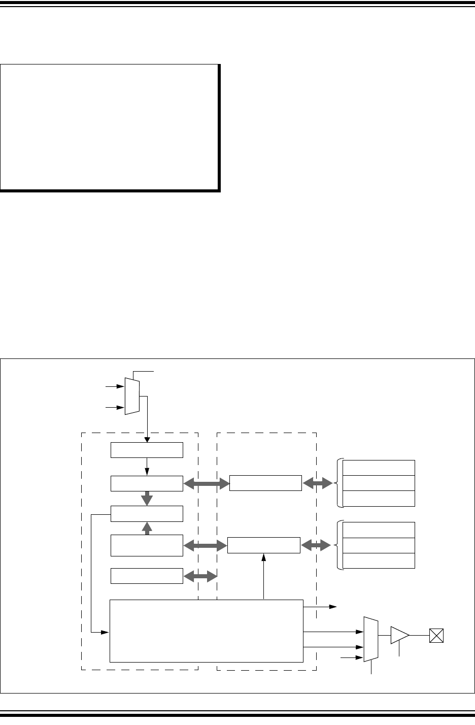
2015 Microchip Technology Inc. Preliminary DS60001320B-page 393
PIC32MZ Embedded Connectivity with Floating Point Unit (EF) Family
25.0 REAL-TIME CLOCK AND
CALENDAR (RTCC)
The RTCC module is intended for applications in which
accurate time must be maintained for extended periods
of time with minimal or no CPU intervention. Low-
power optimization provides extended battery lifetime
while keeping track of time.
Key features of the RTCC module include:
• Time: hours, minutes and seconds
• 24-hour format (military time)
• Visibility of one-half second period
• Provides calendar: Weekday, date, month and year
• Alarm intervals are configurable for half of a second,
one second, 10 seconds, one minute, 10 minutes,
one hour, one day, one week, one month, and one
year
• Alarm repeat with decrementing counter
• Alarm with indefinite repeat: Chime
• Year range: 2000 to 2099
• Leap year correction
• BCD format for smaller firmware overhead
• Optimized for long-term battery operation
• Fractional second synchronization
• User calibration of the clock crystal frequency with
auto-adjust
• Calibration range: 0.66 seconds error per month
• Calibrates up to 260 ppm of crystal error
• Uses external 32.768 kHz crystal or 32 kHz
internal oscillator
• Alarm pulse, seconds clock, or internal clock output
on RTCC pin
FIGURE 25-1: RTCC BLOCK DIAGRAM
Note: This data sheet summarizes the
features of the PIC32MZ EF family of
devices. It is not intended to be a
comprehensive reference source. To
complement the information in this data
sheet, refer to Section 29. “Real-Time
Clock and Calendar (RTCC)”
(DS60001125) in the “PIC32 Family Ref-
erence Manual”, which is available from
the Microchip web site (www.micro-
chip.com/PIC32).
RTCC Prescalers
RTCC Timer
Comparator
Compare Registers
Repeat Counter
YEAR, MTH, DAY
WKDAY
HR, MIN, SEC
MTH, DAY
WKDAY
HR, MIN, SEC
with Masks
RTCC Interrupt Logic
Alarm
Event
32.768 kHz Input from
Secondary Oscillator (SOSC)
0.5 seconds
RTCC Interrupt
RTCVAL
ALRMVAL
RTCC Pin
RTCOE
32 kHz Input from
Internal Oscillator (LPRC)
RTCCLKSEL<1:0>
TRTC
Seconds Pulse
TRTC
Alarm Pulse
RTCOUTSEL<1:0>
PIC32MZ Embedded Connectivity with Floating Point Unit (EF) Family
DS60001320B-page 394 Preliminary 2015 Microchip Technology Inc.
25.1 RTCC Control Registers
TABLE 25-1: RTCC REGISTER MAP
Virtual Address
(BF80_#)
Register
Name(1)
Bit Range
Bits
All Resets
31/15 30/14 29/13 28/12 27/11 26/10 25/9 24/8 23/7 22/6 21/5 20/4 19/3 18/2 17/1 16/0
0C00 RTCCON 31:16 — — — — — — CAL<9:0> 0000
15:0 ON —SIDL — — RTCCLKSEL<1:0> RTCOUTSEL<1:0> RTCCLKON — — RTCWREN RTCSYNC HALFSEC RTCOE 0000
0C10 RTCALRM 31:16 — — — — — — — — — — — — — — — — 0000
15:0 ALRMEN CHIME PIV ALRMSYNC AMASK<3:0> ARPT<7:0> 0000
0C20 RTCTIME 31:16 HR10<3:0> HR01<3:0> MIN10<3:0> MIN01<3:0> xxxx
15:0 SEC10<3:0> SEC01<3:0> — — — — — — — — xx00
0C30 RTCDATE 31:16 YEAR10<3:0> YEAR01<3:0> MONTH10<3:0> MONTH01<3:0> xxxx
15:0 DAY10<3:0> DAY01<3:0> — — — — WDAY01<3:0> xx00
0C40 ALRMTIME 31:16 HR10<3:0> HR01<3:0> MIN10<3:0> MIN01<3:0> xxxx
15:0 SEC10<3:0> SEC01<3:0> — — — — — — — — xx00
0C50 ALRMDATE 31:16 — — — — — — — — MONTH10<3:0> MONTH01<3:0> 00xx
15:0 DAY10<3:0> DAY01<3:0> — — — — WDAY01<3:0> xx0x
Legend: x = unknown value on Reset; — = unimplemented, read as ‘0’. Reset values are shown in hexadecimal.
Note 1: All registers in this table have corresponding CLR, SET and INV registers at its virtual address, plus an offset of 0x4, 0x8 and 0xC, respectively. See Section 12.3 “CLR, SET, and INV Registers” for
more information.

2015 Microchip Technology Inc. Preliminary DS60001320B-page 395
PIC32MZ Embedded Connectivity with Floating Point Unit (EF) Family
REGISTER 25-1: RTCCON: REAL-TIME CLOCK AND CALENDAR CONTROL REGISTER
Bit
Range Bit
31/23/15/7 Bit
30/22/14/6 Bit
29/21/13/5 Bit
28/20/12/4 Bit
27/19/11/3 Bit
26/18/10/2 Bit
25/17/9/1 Bit
24/16/8/0
31:24 U-0 U-0 U-0 U-0 U-0 U-0 R/W-0 R/W-0
— — — — — —CAL<9:8>
23:16 R/W-0 R/W-0 R/W-0 R/W-0 R/W-0 R/W-0 R/W-0 R/W-0
CAL<7:0>
15:8
R/W-0 U-0 R/W-0 U-0 U-0 R/W-0 R/W-0 R/W-0
ON(1) —SIDL—— RTCCLKSEL<1:0> RTC
OUTSEL<1>(2)
7:0
R/W-0 R-0 U-0 U-0 R/W-0 R-0 R-0 R/W-0
RTC
OUTSEL<0>(2) RTC
CLKON(5) — — RTC
WREN(3) RTC
SYNC HALFSEC(4) RTCOE
Legend:
R = Readable bit W = Writable bit U = Unimplemented bit, read as ‘0’
-n = Value at POR ‘1’ = Bit is set ‘0’ = Bit is cleared x = Bit is unknown
bit 31-26 Unimplemented: Read as ‘0’
bit 25-16 CAL<9:0>: Real-Time Clock Drift Calibration bits, which contain a signed 10-bit integer value
0111111111 = Maximum positive adjustment, adds 511 real-time clock pulses every one minute
•
•
•
0000000001 = Minimum positive adjustment, adds 1 real-time clock pulse every one minute
0000000000 = No adjustment
1111111111 = Minimum negative adjustment, subtracts 1 real-time clock pulse every one minute
•
•
•
1000000000 = Maximum negative adjustment, subtracts 512 real-time clock pulses every one minute
bit 15 ON: RTCC On bit(1)
1 = RTCC module is enabled
0 = RTCC module is disabled
bit 14 Unimplemented: Read as ‘0’
bit 13 SIDL: Stop in Idle Mode bit
1 = Disables RTCC operation when CPU enters Idle mode
0 = Continue normal operation when CPU enters Idle mode
bit 12-11 Unimplemented: Read as ‘0’
Note 1: The ON bit is only writable when RTCWREN = 1.
2: Requires RTCOE = 1 (RTCCON<0>) for the output to be active.
3: The RTCWREN bit can be set only when the write sequence is enabled.
4: This bit is read-only. It is cleared to ‘0’ on a write to the seconds bit fields (RTCTIME<14:8>).
5: This bit is undefined when RTCCLKSEL<1:0> = 00 (LPRC is the clock source).
Note: This register is reset only on a Power-on Reset (POR).

PIC32MZ Embedded Connectivity with Floating Point Unit (EF) Family
DS60001320B-page 396 Preliminary 2015 Microchip Technology Inc.
bit 10-9 RTCCLKSEL<1:0>: RTCC Clock Select bits
When a new value is written to these bits, the Seconds Value register should also be written to properly
reset the clock prescalers in the RTCC.
11 = Reserved
10 = Reserved
01 = RTCC uses the external 32.768 kHz Secondary Oscillator (SOSC)
00 = RTCC uses the internal 32 kHz oscillator (LPRC)
bit 8-7 RTCOUTSEL<1:0>: RTCC Output Data Select bits(2)
11 = Reserved
10 = RTCC Clock is presented on the RTCC pin
01 = Seconds Clock is presented on the RTCC pin
00 = Alarm Pulse is presented on the RTCC pin when the alarm interrupt is triggered
bit 6 RTCCLKON: RTCC Clock Enable Status bit(5)
1 = RTCC Clock is actively running
0 = RTCC Clock is not running
bit 5-4 Unimplemented: Read as ‘0’
bit 3 RTCWREN: Real-Time Clock Value Registers Write Enable bit(3)
1 = Real-Time Clock Value registers can be written to by the user
0 = Real-Time Clock Value registers are locked out from being written to by the user
bit 2 RTCSYNC: Real-Time Clock Value Registers Read Synchronization bit
1 = Real-time clock value registers can change while reading (due to a rollover ripple that results in an invalid
data read). If the register is read twice and results in the same data, the data can be assumed to be valid.
0 = Real-time clock value registers can be read without concern about a rollover ripple
bit 1 HALFSEC: Half-Second Status bit(4)
1 = Second half period of a second
0 = First half period of a second
bit 0 RTCOE: RTCC Output Enable bit
1 = RTCC output is enabled
0 = RTCC output is not enabled
REGISTER 25-1: RTCCON: REAL-TIME CLOCK AND CALENDAR CONTROL REGISTER
Note 1: The ON bit is only writable when RTCWREN = 1.
2: Requires RTCOE = 1 (RTCCON<0>) for the output to be active.
3: The RTCWREN bit can be set only when the write sequence is enabled.
4: This bit is read-only. It is cleared to ‘0’ on a write to the seconds bit fields (RTCTIME<14:8>).
5: This bit is undefined when RTCCLKSEL<1:0> = 00 (LPRC is the clock source).
Note: This register is reset only on a Power-on Reset (POR).

2015 Microchip Technology Inc. Preliminary DS60001320B-page 397
PIC32MZ Embedded Connectivity with Floating Point Unit (EF) Family
REGISTER 25-2: RTCALRM: REAL-TIME CLOCK ALARM CONTROL REGISTER
Bit
Range Bit
31/23/15/7 Bit
30/22/14/6 Bit
29/21/13/5 Bit
28/20/12/4 Bit
27/19/11/3 Bit
26/18/10/2 Bit
25/17/9/1 Bit
24/16/8/0
31:24 U-0 U-0 U-0 U-0 U-0 U-0 U-0 U-0
— — — — — — — —
23:16 U-0 U-0 U-0 U-0 U-0 U-0 U-0 U-0
— — — — — — — —
15:8 R/W-0 R/W-0 R/W-0 R-0 R/W-0 R/W-0 R/W-0 R/W-0
ALRMEN(1,2) CHIME(2) PIV(2) ALRMSYNC AMASK<3:0>(2)
7:0 R/W-0 R/W-0 R/W-0 R/W-0 R/W-0 R/W-0 R/W-0 R/W-0
ARPT<7:0>(2)
Legend:
R = Readable bit W = Writable bit U = Unimplemented bit, read as ‘0’
-n = Value at POR ‘1’ = Bit is set ‘0’ = Bit is cleared x = Bit is unknown
bit 31-16 Unimplemented: Read as ‘0’
bit 15 ALRMEN: Alarm Enable bit(1,2)
1 = Alarm is enabled
0 = Alarm is disabled
bit 14 CHIME: Chime Enable bit(2)
1 = Chime is enabled – ARPT<7:0> is allowed to rollover from 0x00 to 0xFF
0 = Chime is disabled – ARPT<7:0> stops once it reaches 0x00
bit 13 PIV: Alarm Pulse Initial Value bit(2)
When ALRMEN = 0, PIV is writable and determines the initial value of the Alarm Pulse.
When ALRMEN = 1, PIV is read-only and returns the state of the Alarm Pulse.
bit 12 ALRMSYNC: Alarm Sync bit
1 = ARPT<7:0> and ALRMEN may change as a result of a half second rollover during a read.
The ARPT must be read repeatedly until the same value is read twice. This must be done since multiple
bits may be changing.
0 = ARPT<7:0> and ALRMEN can be read without concerns of rollover because the prescaler is more than
32 real-time clocks away from a half-second rollover
bit 11-8 AMASK<3:0>: Alarm Mask Configuration bits(2)
0000 = Every half-second
0001 = Every second
0010 = Every 10 seconds
0011 = Every minute
0100 = Every 10 minutes
0101 = Every hour
0110 = Once a day
0111 = Once a week
1000 = Once a month
1001 = Once a year (except when configured for February 29, once every four years)
1010 = Reserved
1011 = Reserved
11xx = Reserved
Note 1: Hardware clears the ALRMEN bit anytime the alarm event occurs, when ARPT<7:0> = 00 and
CHIME = 0.
2: This field should not be written when the RTCC ON bit = ‘1’ (RTCCON<15>) and ALRMSYNC = 1.
Note: This register is reset only on a Power-on Reset (POR).

PIC32MZ Embedded Connectivity with Floating Point Unit (EF) Family
DS60001320B-page 398 Preliminary 2015 Microchip Technology Inc.
bit 7-0 ARPT<7:0>: Alarm Repeat Counter Value bits(2)
11111111 = Alarm will trigger 256 times
•
•
•
00000000 = Alarm will trigger one time
The counter decrements on any alarm event. The counter only rolls over from 0x00 to 0xFF if CHIME = 1.
REGISTER 25-2: RTCALRM: REAL-TIME CLOCK ALARM CONTROL REGISTER (CONTINUED)
Note 1: Hardware clears the ALRMEN bit anytime the alarm event occurs, when ARPT<7:0> = 00 and
CHIME = 0.
2: This field should not be written when the RTCC ON bit = ‘1’ (RTCCON<15>) and ALRMSYNC = 1.
Note: This register is reset only on a Power-on Reset (POR).

2015 Microchip Technology Inc. Preliminary DS60001320B-page 399
PIC32MZ Embedded Connectivity with Floating Point Unit (EF) Family
REGISTER 25-3: RTCTIME: REAL-TIME CLOCK TIME VALUE REGISTER
Bit
Range Bit
31/23/15/7 Bit
30/22/14/6 Bit
29/21/13/5 Bit
28/20/12/4 Bit
27/19/11/3 Bit
26/18/10/2 Bit
25/17/9/1 Bit
24/16/8/0
31:24 R/W-x R/W-x R/W-x R/W-x R/W-x R/W-x R/W-x R/W-x
HR10<3:0> HR01<3:0>
23:16 R/W-x R/W-x R/W-x R/W-x R/W-x R/W-x R/W-x R/W-x
MIN10<3:0> MIN01<3:0>
15:8 R/W-x R/W-x R/W-x R/W-x R/W-x R/W-x R/W-x R/W-x
SEC10<3:0> SEC01<3:0>
7:0 U-0 U-0 U-0 U-0 U-0 U-0 U-0 U-0
— — — — — — — —
Legend:
R = Readable bit W = Writable bit U = Unimplemented bit, read as ‘0’
-n = Value at POR ‘1’ = Bit is set ‘0’ = Bit is cleared x = Bit is unknown
bit 31-28 HR10<3:0>: Binary-Coded Decimal Value of Hours bits, 10 digits; contains a value from 0 to 2
bit 27-24 HR01<3:0>: Binary-Coded Decimal Value of Hours bits, 1 digit; contains a value from 0 to 9
bit 23-20 MIN10<3:0>: Binary-Coded Decimal Value of Minutes bits, 10 digits; contains a value from 0 to 5
bit 19-16 MIN01<3:0>: Binary-Coded Decimal Value of Minutes bits, 1 digit; contains a value from 0 to 9
bit 15-12 SEC10<3:0>: Binary-Coded Decimal Value of Seconds bits, 10 digits; contains a value from 0 to 5
bit 11-8 SEC01<3:0>: Binary-Coded Decimal Value of Seconds bits, 1 digit; contains a value from 0 to 9
bit 7-0 Unimplemented: Read as ‘0’
Note: This register is only writable when RTCWREN = 1 (RTCCON<3>).

PIC32MZ Embedded Connectivity with Floating Point Unit (EF) Family
DS60001320B-page 400 Preliminary 2015 Microchip Technology Inc.
REGISTER 25-4: RTCDATE: REAL-TIME CLOCK DATE VALUE REGISTER
Bit
Range Bit
31/23/15/7 Bit
30/22/14/6 Bit
29/21/13/5 Bit
28/20/12/4 Bit
27/19/11/3 Bit
26/18/10/2 Bit
25/17/9/1 Bit
24/16/8/0
31:24 R/W-x R/W-x R/W-x R/W-x R/W-x R/W-x R/W-x R/W-x
YEAR10<3:0> YEAR01<3:0>
23:16 R/W-x R/W-x R/W-x R/W-x R/W-x R/W-x R/W-x R/W-x
MONTH10<3:0> MONTH01<3:0>
15:8 R/W-x R/W-x R/W-x R/W-x R/W-x R/W-x R/W-x R/W-x
DAY10<3:0> DAY01<3:0>
7:0 U-0 U-0 U-0 U-0 R/W-x R/W-x R/W-x R/W-x
— — — — WDAY01<3:0>
Legend:
R = Readable bit W = Writable bit U = Unimplemented bit, read as ‘0’
-n = Value at POR ‘1’ = Bit is set ‘0’ = Bit is cleared x = Bit is unknown
bit 31-28 YEAR10<3:0>: Binary-Coded Decimal Value of Years bits, 10 digits
bit 27-24 YEAR01<3:0>: Binary-Coded Decimal Value of Years bits, 1 digit
bit 23-20 MONTH10<3:0>: Binary-Coded Decimal Value of Months bits, 10 digits; contains a value from 0 to 1
bit 19-16 MONTH01<3:0>: Binary-Coded Decimal Value of Months bits, 1 digit; contains a value from 0 to 9
bit 15-12 DAY10<3:0>: Binary-Coded Decimal Value of Days bits, 10 digits; contains a value from 0 to 3
bit 11-8 DAY01<3:0>: Binary-Coded Decimal Value of Days bits, 1 digit; contains a value from 0 to 9
bit 7-4 Unimplemented: Read as ‘0’
bit 3-0 WDAY01<3:0>: Binary-Coded Decimal Value of Weekdays bits,1 digit; contains a value from 0 to 6
Note: This register is only writable when RTCWREN = 1 (RTCCON<3>).

2015 Microchip Technology Inc. Preliminary DS60001320B-page 401
PIC32MZ Embedded Connectivity with Floating Point Unit (EF) Family
REGISTER 25-5: ALRMTIME: ALARM TIME VALUE REGISTER
Bit
Range Bit
31/23/15/7 Bit
30/22/14/6 Bit
29/21/13/5 Bit
28/20/12/4 Bit
27/19/11/3 Bit
26/18/10/2 Bit
25/17/9/1 Bit
24/16/8/0
31:24 R/W-x R/W-x R/W-x R/W-x R/W-x R/W-x R/W-x R/W-x
HR10<3:0> HR01<3:0>
23:16 R/W-x R/W-x R/W-x R/W-x R/W-x R/W-x R/W-x R/W-x
MIN10<3:0> MIN01<3:0>
15:8 R/W-x R/W-x R/W-x R/W-x R/W-x R/W-x R/W-x R/W-x
SEC10<3:0> SEC01<3:0>
7:0 U-0 U-0 U-0 U-0 U-0 U-0 U-0 U-0
— — — — — — — —
Legend:
R = Readable bit W = Writable bit U = Unimplemented bit, read as ‘0’
-n = Value at POR ‘1’ = Bit is set ‘0’ = Bit is cleared x = Bit is unknown
bit 31-28 HR10<3:0>: Binary Coded Decimal value of hours bits, 10 digits; contains a value from 0 to 2
bit 27-24 HR01<3:0>: Binary Coded Decimal value of hours bits, 1 digit; contains a value from 0 to 9
bit 23-20 MIN10<3:0>: Binary Coded Decimal value of minutes bits, 10 digits; contains a value from 0 to 5
bit 19-16 MIN01<3:0>: Binary Coded Decimal value of minutes bits, 1 digit; contains a value from 0 to 9
bit 15-12 SEC10<3:0>: Binary Coded Decimal value of seconds bits, 10 digits; contains a value from 0 to 5
bit 11-8 SEC01<3:0>: Binary Coded Decimal value of seconds bits, 1 digit; contains a value from 0 to 9
bit 7-0 Unimplemented: Read as ‘0’

PIC32MZ Embedded Connectivity with Floating Point Unit (EF) Family
DS60001320B-page 402 Preliminary 2015 Microchip Technology Inc.
REGISTER 25-6: ALRMDATE: ALARM DATE VALUE REGISTER
Bit
Range Bit
31/23/15/7 Bit
30/22/14/6 Bit
29/21/13/5 Bit
28/20/12/4 Bit
27/19/11/3 Bit
26/18/10/2 Bit
25/17/9/1 Bit
24/16/8/0
31:24 U-0 U-0 U-0 U-0 U-0 U-0 U-0 U-0
— — — — — — — —
23:16 R/W-x R/W-x R/W-x R/W-x R/W-x R/W-x R/W-x R/W-x
MONTH10<3:0> MONTH01<3:0>
15:8 R/W-x R/W-x R/W-x R/W-x R/W-x R/W-x R/W-x R/W-x
DAY10<1:0> DAY01<3:0>
7:0 U-0 U-0 U-0 U-0 R/W-x R/W-x R/W-x R/W-x
— — — — WDAY01<3:0>
Legend:
R = Readable bit W = Writable bit U = Unimplemented bit, read as ‘0’
-n = Value at POR ‘1’ = Bit is set ‘0’ = Bit is cleared x = Bit is unknown
bit 31-24 Unimplemented: Read as ‘0’
bit 23-20 MONTH10<3:0>: Binary Coded Decimal value of months bits, 10 digits; contains a value from 0 to 1
bit 19-16 MONTH01<3:0>: Binary Coded Decimal value of months bits, 1 digit; contains a value from 0 to 9
bit 15-12 DAY10<3:0>: Binary Coded Decimal value of days bits, 10 digits; contains a value from 0 to 3
bit 11-8 DAY01<3:0>: Binary Coded Decimal value of days bits, 1 digit; contains a value from 0 to 9
bit 7-4 Unimplemented: Read as ‘0’
bit 3-0 WDAY01<3:0>: Binary Coded Decimal value of weekdays bits, 1 digit; contains a value from 0 to 6
2015 Microchip Technology Inc. Preliminary DS60001320B-page 403
PIC32MZ Embedded Connectivity with Floating Point Unit (EF) Family
26.0 CRYPTO ENGINE
The Crypto Engine is intended to accelerate applica-
tions that need cryptographic functions. By execut-
ing these functions in the hardware module, software
overhead is reduced, and actions such as encryp-
tion, decryption, and authentication can execute
much more quickly.
The Crypto Engine uses an internal descriptor-based
DMA for efficient programming of the security associ-
ation data and packet pointers (allowing scatter/
gather data fetching). An intelligent state machine
schedules the Crypto Engines based on the protocol
selection and packet boundaries. The hardware
engines can perform the encryption and authentica-
tion in sequence or in parallel.
Key features of the Crypto Engine are:
• Bulk ciphers and hash engines
• Integrated DMA to off-load processing:
- Buffer descriptor-based
- Secure association per buffer descriptor
• Some functions can execute in parallel
Bulk ciphers that are handled by the Crypto Engine
include:
• AES:
- 128-bit, 192-bit, and 256-bit key sizes
- CBC, ECB, CTR, CFB, and OFB modes
• DES/TDES:
- CBC, ECB, CFB, and OFB modes
Authentication engines that are available through the
Crypto Engine include:
•SHA-1
•SHA-256
•MD-5
• AES-GCM
• HMAC operation (for all authentication engines)
The rate of data that can be processed by the Crypto
Engine depends on a number of factors, including:
• Which engine is in use
• Whether the engines are used in parallel or in series
• The demands on source and destination memories
by other parts of the system (i.e., CPU, DMA, etc.)
• The speed of PBCLK5, which drives the Crypto
Engine
Table 26-1 shows typical performance for various
engines.
TABLE 26-1: CRYPTO ENGINE
PERFORMANCE
FIGURE 26-1: CRYPTO ENGINE BLOCK DIAGRAM
Note: This data sheet summarizes the
features of the PIC32MZ EF family of
devices. It is not intended to be a
comprehensive reference source. To
complement the information in this data
sheet, refer to Section 49. “Crypto
Engine (CE) and Random Number
Generator (RNG)” (DS60001246) in
the “PIC32 Family Reference Manual”,
which is available from the Microchip
web site (www.microchip.com/PIC32).
Engine/
Algorithm
Performance
Factor
(Mbps/MHz)
Maximum Mbps
(PBCLK5 = 100 MHz)
DES 14.4 1440
TDES 6.6 660
AES-128 9.0 900
AES-192 7.9 790
AES-256 7.2 720
MD5 15.6 1560
SHA-1 13.2 1320
SHA-256 9.3 930
DMA
Controller
System
INB
FIFO
OUTB
FIFO
Crypto
FSM
Packet
RD
Packet
WR
AES
TDES
SHA-1
MD5
Local Bus
SFR
System
Bus
Bus
PBCLK5
SHA-256
PIC32MZ Embedded Connectivity with Floating Point Unit (EF) Family
DS60001320B-page 404 Preliminary 2015 Microchip Technology Inc.
26.1 Crypto Engine Control Registers
TABLE 26-2: CRYPTO ENGINE REGISTER MAP
Virtual Address
(BF8E_#)
Register
Name
Bit Range
Bits
All Resets
31/15 30/14 29/13 28/12 27/11 26/10 25/9 24/8 23/7 22/6 21/5 20/4 19/3 18/2 17/1 16/0
5000 CEVER 31:16 REVISION<7:0> VERSION<7:0> 0000
15:0 ID<15:0> 0000
5004 CECON 31:16 — — — — — — — — — — — — — — — — 0000
15:0 — — — — — — — — SWAPOEN SWRST SWAPEN — — BDPCHST BDPPLEN DMAEN 0000
5008 CEBDADDR 31:16 BDPADDR<31:0> 0000
15:0 0000
500C CEBDPADDR 31:16 BASEADDR<31:0> 0000
15:0 0000
5010 CESTAT 31:16 ERRMODE<2:0> ERROP<2:0> ERRPHASE<1:0> — — BDSTATE<3:0> START ACTIVE 0000
15:0 BDCTRL<15:0> 0000
5014 CEINTSRC 31:16 — — — — — — — — — — — — — — — — 0000
15:0 — — — — — — — — — — — — AREIF PKTIF CBDIF PENDIF 0000
5018 CEINTEN 31:16 — — — — — — — — — — — — — — — — 0000
15:0 — — — — — — — — — — — — AREIE PKTIE CBDIE PENDIE 0000
501C CEPOLLCON 31:16 — — — — — — — — — — — — — — — — 0000
15:0 BDPPLCON<15:0> 0000
5020 CEHDLEN 31:16 — — — — — — — — — — — — — — — — 0000
15:0 — — — — — — — — HDRLEN<7:0> 0000
5024 CETRLLEN 31:16 — — — — — — — — — — — — — — — — 0000
15:0 — — — — — — — — TRLRLEN<7:0> 0000
Legend: x = unknown value on Reset; — = unimplemented, read as ‘0’. Reset values are shown in hexadecimal.

2015 Microchip Technology Inc. Preliminary DS60001320B-page 405
PIC32MZ Embedded Connectivity with Floating Point Unit (EF) Family
REGISTER 26-1: CEVER: CRYPTO ENGINE REVISION, VERSION, AND ID REGISTER
Bit
Range Bit
31/23/15/7 Bit
30/22/14/6 Bit
29/21/13/5 Bit
28/20/12/4 Bit
27/19/11/3 Bit
26/18/10/2 Bit
25/17/9/1 Bit
24/16/8/0
31:24 R-0 R-0 R-0 R-0 R-0 R-0 R-0 R-0
REVISION<7:0>
23:16 R-0 R-0 R-0 R-0 R-0 R-0 R-0 R-0
VERSION<7:0>
15:8 R-0 R-0 R-0 R-0 R-0 R-0 R-0 R-0
ID<15:8>
7:0 R-0 R-0 R-0 R-0 R-0 R-0 R-0 R-0
ID<7:0>
Legend:
R = Readable bit W = Writable bit U = Unimplemented bit, read as ‘0’
-n = Value at POR ‘1’ = Bit is set ‘0’ = Bit is cleared x = Bit is unknown
bit 31-24 REVISION<7:0>: Crypto Engine Revision bits
bit 23-16 VERSION<7:0>: Crypto Engine Version bits
bit 15-0 ID<15:0>: Crypto Engine Identification bits

PIC32MZ Embedded Connectivity with Floating Point Unit (EF) Family
DS60001320B-page 406 Preliminary 2015 Microchip Technology Inc.
REGISTER 26-2: CECON: CRYPTO ENGINE CONTROL REGISTER
Bit
Range Bit
31/23/15/7 Bit
30/22/14/6 Bit
29/21/13/5 Bit
28/20/12/4 Bit
27/19/11/3 Bit
26/18/10/2 Bit
25/17/9/1 Bit
24/16/8/0
31:24 U-0 U-0 U-0 U-0 U-0 U-0 U-0 U-0
— — — — — — — —
23:16 U-0 U-0 U-0 U-0 U-0 U-0 U-0 U-0
— — — — — — — —
15:8 U-0 U-0 U-0 U-0 U-0 U-0 U-0 U-0
— — — — — — — —
7:0 R/W-0 R/W-0, HC R/W-0 U-0 U-0 R/W-0 R/W-0 R/W-0
SWAPOEN SWRST SWAPEN —— BDPCHST BDPPLEN DMAEN
Legend: HC = Hardware Cleared
R = Readable bit W = Writable bit U = Unimplemented bit, read as ‘0’
-n = Value at POR ‘1’ = Bit is set ‘0’ = Bit is cleared x = Bit is unknown
bit 31-8 Unimplemented: Read as ‘0’
bit 7 SWAPOEN: Swap Output Data Enable bit
1 = Output data is byte swapped when written by dedicated DMA
0 = Output data is not byte swapped when written by dedicated DMA
bit 6 SWRST: Software Reset bit
1 = Initiate a software reset of the Crypto Engine
0 = Normal operation
bit 5 SWAPEN: Input Data Swap Enable bit
1 = Input data is byte swapped when read by dedicated DMA
0 = Input data is not byte swapped when read by dedicated DMA
bit 4-3 Unimplemented: Read as ‘0’
bit 2 BDPCHST: Buffer Descriptor Processor (BDP) Fetch Enable bit
This bit should be enabled only after all DMA descriptor programming is completed.
1 = BDP descriptor fetch is enabled
0 = BDP descriptor fetch is disabled
bit 1 BDPPLEN: Buffer Descriptor Processor Poll Enable bit
This bit should be enabled only after all DMA descriptor programming is completed.
1 = Poll for descriptor until valid bit is set
0 = Do not poll
bit 0 DMAEN: DMA Enable bit
1 = Crypto Engine DMA is enabled
0 = Crypto Engine DMA is disabled

2015 Microchip Technology Inc. Preliminary DS60001320B-page 407
PIC32MZ Embedded Connectivity with Floating Point Unit (EF) Family
REGISTER 26-3: CEBDADDR: CRYPTO ENGINE BUFFER DESCRIPTOR REGISTER
Bit
Range Bit
31/23/15/7 Bit
30/22/14/6 Bit
29/21/13/5 Bit
28/20/12/4 Bit
27/19/11/3 Bit
26/18/10/2 Bit
25/17/9/1 Bit
24/16/8/0
31:24 R-0 R-0 R-0 R-0 R-0 R-0 R-0 R-0
BDPADDR<31:24>
23:16 R-0 R-0 R-0 R-0 R-0 R-0 R-0 R-0
BDPADDR<23:16>
15:8 R-0 R-0 R-0 R-0 R-0 R-0 R-0 R-0
BDPADDR<15:8>
7:0 R-0 R-0 R-0 R-0 R-0 R-0 R-0 R-0
BDPADDR<7:0>
Legend:
R = Readable bit W = Writable bit U = Unimplemented bit, read as ‘0’
-n = Value at POR ‘1’ = Bit is set ‘0’ = Bit is cleared x = Bit is unknown
bit 31-0 BDPADDR<31:0>: Current Buffer Descriptor Process Address Status bits
These bits contain the current descriptor address that is being processed by the Buffer Descriptor Processor
(BDP).
REGISTER 26-4: CEBDPADDR: CRYPTO ENGINE BUFFER DESCRIPTOR PROCESSOR
REGISTER
Bit
Range Bit
31/23/15/7 Bit
30/22/14/6 Bit
29/21/13/5 Bit
28/20/12/4 Bit
27/19/11/3 Bit
26/18/10/2 Bit
25/17/9/1 Bit
24/16/8/0
31:24 R/W-0 R/W-0 R/W-0 R/W-0 R/W-0 R/W-0 R/W-0 R/W-0
BASEADDR<31:24>
23:16 R/W-0 R/W-0 R/W-0 R/W-0 R/W-0 R/W-0 R/W-0 R/W-0
BASEADDR<23:16>
15:8 R/W-0 R/W-0 R/W-0 R/W-0 R/W-0 R/W-0 R/W-0 R/W-0
BASEADDR<15:8>
7:0 R/W-0 R/W-0 R/W-0 R/W-0 R/W-0 R/W-0 R/W-0 R/W-0
BASEADDR<7:0>
Legend:
R = Readable bit W = Writable bit U = Unimplemented bit, read as ‘0’
-n = Value at POR ‘1’ = Bit is set ‘0’ = Bit is cleared x = Bit is unknown
bit 31-0 BASEADDR<31:0>: Buffer Descriptor Base Address bits
These bits contain the physical address of the first Buffer Descriptor in the Buffer Descriptor chain. When
enabled, the Crypto DMA begins fetching Buffer Descriptors from this address.

PIC32MZ Embedded Connectivity with Floating Point Unit (EF) Family
DS60001320B-page 408 Preliminary 2015 Microchip Technology Inc.
REGISTER 26-5: CESTAT: CRYPTO ENGINE STATUS REGISTER
Bit
Range Bit
31/23/15/7 Bit
30/22/14/6 Bit
29/21/13/5 Bit
28/20/12/4 Bit
27/19/11/3 Bit
26/18/10/2 Bit
25/17/9/1 Bit
24/16/8/0
31:24 R-0 R-0 R-0 R-0 R-0 R-0 R-0 R-0
ERRMODE<2:0> ERROP<2:0> ERRPHASE<1:0>
23:16 U-0 U-0 R-0 R-0 R-0 R-0 R-0 R-0
—— BDSTATE<3:0> START ACTIVE
15:8 R-0 R-0 R-0 R-0 R-0 R-0 R-0 R-0
BDCTRL<15:8>
7:0 R-0 R-0 R-0 R-0 R-0 R-0 R-0 R-0
BDCTRL<7:0>
Legend:
R = Readable bit W = Writable bit U = Unimplemented bit, read as ‘0’
-n = Value at POR ‘1’ = Bit is set ‘0’ = Bit is cleared x = Bit is unknown
bit 31-29 ERRMODE<2:0>: Internal Error Mode Status bits
111 = Reserved
110 = Reserved
101 = Reserved
100 = Reserved
011 = CEK operation
010 = KEK operation
001 = Preboot authentication
000 = Normal operation
bit 28-26 ERROP<2:0>: Internal Error Operation Status bits
111 = Reserved
110 = Reserved
101 = Reserved
100 = Authentication
011 = Reserved
010 = Decryption
001 = Encryption
000 = Reserved
bit 25-24 ERRPHASE<1:0>: Internal Error Phase of DMA Status bits
11 = Destination data
10 = Source data
01 = Security Association (SA) access
00 = Buffer Descriptor (BD) access
bit 23-22 Unimplemented: Read as ‘0’
bit 21-18 BDSTATE<3:0>: Buffer Descriptor Processor State Status bits
The current state of the BDP:
1111 = Reserved
•
•
•
0111 = Reserved
0110 = SA fetch
0101 = Fetch BDP is disabled
0100 = Descriptor is done
0011 = Data phase
0010 = BDP is loading
0001 = Descriptor fetch request is pending
0000 = BDP is idle
bit 17 START: DMA Start Status bit
1 = DMA start has occurred
0 = DMA start has not occurred

2015 Microchip Technology Inc. Preliminary DS60001320B-page 409
PIC32MZ Embedded Connectivity with Floating Point Unit (EF) Family
bit 16 ACTIVE: Buffer Descriptor Processor Status bit
1 = BDP is active
0 = BDP is idle
bit 15-0 BDCTRL<15:0>: Descriptor Control Word Status bits
These bits contain the Control Word for the current Buffer Descriptor.
REGISTER 26-5: CESTAT: CRYPTO ENGINE STATUS REGISTER (CONTINUED)

PIC32MZ Embedded Connectivity with Floating Point Unit (EF) Family
DS60001320B-page 410 Preliminary 2015 Microchip Technology Inc.
REGISTER 26-6: CEINTSRC: CRYPTO ENGINE INTERRUPT SOURCE REGISTER
Bit
Range Bit
31/23/15/7 Bit
30/22/14/6 Bit
29/21/13/5 Bit
28/20/12/4 Bit
27/19/11/3 Bit
26/18/10/2 Bit
25/17/9/1 Bit
24/16/8/0
31:24 U-0 U-0 U-0 U-0 U-0 U-0 U-0 U-0
— — — — — — — —
23:16 U-0 U-0 U-0 U-0 U-0 U-0 U-0 U-0
— — — — — — — —
15:8 U-0 U-0 U-0 U-0 U-0 U-0 U-0 U-0
— — — — — — — —
7:0 U-0 U-0 U-0 U-0 R-0 R-0 R-0 R-0
— — — — AREIF PKTIF CBDIF PENDIF
Legend:
R = Readable bit W = Writable bit U = Unimplemented bit, read as ‘0’
-n = Value at POR ‘1’ = Bit is set ‘0’ = Bit is cleared x = Bit is unknown
bit 31-4 Unimplemented: Read as ‘0’
bit 3 AREIF: Access Response Error Interrupt bit
1 = Error occurred trying to access memory outside the Crypto Engine
0 = No error has occurred
bit 2 PKTIF: DMA Packet Completion Interrupt Status bit
1 = DMA packet was completed
0 = DMA packet was not completed
bit 1 CBDIF: BD Transmit Status bit
1 = Last BD transmit was processed
0 = Last BD transmit has not been processed
bit 0 PENDIF: Crypto Engine Interrupt Pending Status bit
1 = Crypto Engine interrupt is pending (this value is the result of an OR of all interrupts in the Crypto Engine)
0 = Crypto Engine interrupt is not pending

2015 Microchip Technology Inc. Preliminary DS60001320B-page 411
PIC32MZ Embedded Connectivity with Floating Point Unit (EF) Family
REGISTER 26-7: CEINTEN: CRYPTO ENGINE INTERRUPT ENABLE REGISTER
Bit
Range Bit
31/23/15/7 Bit
30/22/14/6 Bit
29/21/13/5 Bit
28/20/12/4 Bit
27/19/11/3 Bit
26/18/10/2 Bit
25/17/9/1 Bit
24/16/8/0
31:24 U-0 U-0 U-0 U-0 U-0 U-0 U-0 U-0
— — — — — — — —
23:16 U-0 U-0 U-0 U-0 U-0 U-0 U-0 U-0
— — — — — — — —
15:8 U-0 U-0 U-0 U-0 U-0 U-0 U-0 U-0
— — — — — — — —
7:0 U-0 U-0 U-0 U-0 R/W-0 R/W-0 R/W-0 R/W-0
— — — — AREIE PKTIE BDPIE PENDIE(1)
Legend:
R = Readable bit W = Writable bit U = Unimplemented bit, read as ‘0’
-n = Value at POR ‘1’ = Bit is set ‘0’ = Bit is cleared x = Bit is unknown
bit 31-4 Unimplemented: Read as ‘0’
bit 3 AREIE: Access Response Error Interrupt Enable bit
1 = Access response error interrupts are enabled
0 = Access response error interrupts are not enabled
bit 2 PKTIE: DMA Packet Completion Interrupt Enable bit
1 = DMA packet completion interrupts are enabled
0 = DMA packet completion interrupts are not enabled
bit 1 BDPIE: DMA Buffer Descriptor Processor Interrupt Enable bit
1 = BDP interrupts are enabled
0 = BDP interrupts are not enabled
bit 0 PENDIE: Master Interrupt Enable bit(1)
1 = Crypto Engine interrupts are enabled
0 = Crypto Engine interrupts are not enabled
Note 1: The PENDIE bit is a Global enable bit and must be enabled together with the other interrupts desired.

PIC32MZ Embedded Connectivity with Floating Point Unit (EF) Family
DS60001320B-page 412 Preliminary 2015 Microchip Technology Inc.
REGISTER 26-8: CEPOLLCON: CRYPTO ENGINE POLL CONTROL REGISTER
Bit
Range Bit
31/23/15/7 Bit
30/22/14/6 Bit
29/21/13/5 Bit
28/20/12/4 Bit
27/19/11/3 Bit
26/18/10/2 Bit
25/17/9/1 Bit
24/16/8/0
31:24 U-0 U-0 U-0 U-0 U-0 U-0 U-0 U-0
— — — — — — — —
23:16 U-0 U-0 U-0 U-0 U-0 U-0 U-0 U-0
— — — — — — — —
15:8 R/W-0 R/W-0 R/W-0 R/W-0 R/W-0 R/W-0 R/W-0 R/W-0
BDPPLCON<15:8>
7:0 R/W-0 R/W-0 R/W-0 R/W-0 R/W-0 R/W-0 R/W-0 R/W-0
BDPPLCON<7:0>
Legend:
R = Readable bit W = Writable bit U = Unimplemented bit, read as ‘0’
-n = Value at POR ‘1’ = Bit is set ‘0’ = Bit is cleared x = Bit is unknown
bit 31-16 Unimplemented: Read as ‘0’
bit 15 BDPPLCON<15:0>: Buffer Descriptor Processor Poll Control bits
These bits determine the number of SYSCLK cycles that the Crypto DMA would wait before refetching the
descriptor control word if the Buffer Descriptor fetched was disabled.
2015 Microchip Technology Inc. Preliminary DS60001320B-page 413
PIC32MZ Embedded Connectivity with Floating Point Unit (EF) Family
REGISTER 26-9: CEHDLEN: CRYPTO ENGINE HEADER LENGTH REGISTER
Bit
Range Bit
31/23/15/7 Bit
30/22/14/6 Bit
29/21/13/5 Bit
28/20/12/4 Bit
27/19/11/3 Bit
26/18/10/2 Bit
25/17/9/1 Bit
24/16/8/0
31:24 U-0 U-0 U-0 U-0 U-0 U-0 U-0 U-0
— — — — — — — —
23:16 U-0 U-0 U-0 U-0 U-0 U-0 U-0 U-0
— — — — — — — —
15:8 U-0 U-0 U-0 U-0 U-0 U-0 U-0 U-0
— — — — — — — —
7:0 R/W-0 R/W-0 R/W-0 R/W-0 R/W-0 R/W-0 R/W-0 R/W-0
HDRLEN<7:0>
Legend:
R = Readable bit W = Writable bit U = Unimplemented bit, read as ‘0’
-n = Value at POR ‘1’ = Bit is set ‘0’ = Bit is cleared x = Bit is unknown
bit 31-8 Unimplemented: Read as ‘0’
bit 7-0 HDRLEN<7:0>: DMA Header Length bits
For every packet, skip this length of locations and start filling the data.
REGISTER 26-10: CETRLLEN: CRYPTO ENGINE TRAILER LENGTH REGISTER
Bit
Range Bit
31/23/15/7 Bit
30/22/14/6 Bit
29/21/13/5 Bit
28/20/12/4 Bit
27/19/11/3 Bit
26/18/10/2 Bit
25/17/9/1 Bit
24/16/8/0
31:24 U-0 U-0 U-0 U-0 U-0 U-0 U-0 U-0
— — — — — — — —
23:16 U-0 U-0 U-0 U-0 U-0 U-0 U-0 U-0
— — — — — — — —
15:8 U-0 U-0 U-0 U-0 U-0 U-0 U-0 U-0
— — — — — — — —
7:0 R/W-0 R/W-0 R/W-0 R/W-0 R/W-0 R/W-0 R/W-0 R/W-0
TRLRLEN<7:0>
Legend:
R = Readable bit W = Writable bit U = Unimplemented bit, read as ‘0’
-n = Value at POR ‘1’ = Bit is set ‘0’ = Bit is cleared x = Bit is unknown
bit 31-8 Unimplemented: Read as ‘0’
bit 7-0 TRLRLEN<7:0>: DMA Trailer Length bits
For every packet, skip this length of locations at the end of the current packet and start putting the next
packet.

PIC32MZ Embedded Connectivity with Floating Point Unit (EF) Family
DS60001320B-page 414 Preliminary 2015 Microchip Technology Inc.
26.2 Crypto Engine Buffer Descriptors
Host software creates a linked list of buffer descriptors
and the hardware updates them. Table 26-3 provides a
list of the Crypto Engine buffer descriptors, followed by
format descriptions of each buffer descriptor (see
Figure 26-2 through Figure 26-9).
TABLE 26-3: CRYPTO ENGINE BUFFER DESCRIPTORS
Name (see Note 1) Bit
31/2315/7 Bit
30/22/14/6 Bit
29/21/13/5 Bit
28/20/12/4 Bit
27/19/11/3 Bit
26/18/10/2 Bit
25/17/9/1 Bit
24/16/8/0
BD_CTRL 31:24 DESC_EN —CRY_MODE<2:0> — — —
23:16 —SA_FETCH_EN — — LAST_BD LIFM PKT_INT_EN CBD_INT_EN
15:8 BD_BUFLEN<15:8>
7:0 BD_BUFLEN<7:0>
BD_SA_ADDR 31:24 BD_SAADDR<31:24>
23:16 BD_SAADDR<23:16>
15:8 BD_SAADDR<15:8>
7:0 BD_SAADR<7:0>
BD_SCRADDR 31:24 BD_SRCADDR<31:24>
23:16 BD_SRCADDR<23:16>
15:8 BD_SRCADDR<15:8>
7:0 BD_SRCADDR<7:0>
BD_DSTADDR 31:24 BD_DSTADDR<31:24>
23:16 BD_DSTADDR<23:16>
15:8 BD_DSTADDR<15:8>
7:0 BD_DSTADDR<7:0>
BD_NXTPTR 31:24 BD_NXTADDR<31:24>
23:16 BD_NXTADDR<23:16>
15:8 BD_NXTADDR<15:8>
7:0 BD_NXTADDR<7:0>
BD_UPDPTR 31:24 BD_UPDADDR<31:24>
23:16 BD_UPDADDR<23:16>
15:8 BD_UPDADDR<15:8>
7:0 BD_UPDADDR<7:0>
BD_MSG_LEN 31:24 MSG_LENGTH<31:24>
23:16 MSG_LENGTH<23:16>
15:8 MSG_LENGTH<15:8>
7:0 MSG_LENGTH<7:0>
BD_ENC_OFF 31:24 ENCR_OFFSET<31:24>
23:16 ENCR_OFFSET<23:16>
15:8 ENCR_OFFSET<15:8>
7:0 ENCR_OFFSET<7:0>
Note 1: The buffer descriptor must be allocated in memory on a 64-bit boundary.

2015 Microchip Technology Inc. Preliminary DS60001320B-page 415
PIC32MZ Embedded Connectivity with Floating Point Unit (EF) Family
FIGURE 26-2: FORMAT OF BD_CTRL
FIGURE 26-3: FORMAT OF BD_SADDR
Bit
Range Bit
31/23/15/7 Bit
30/22/14/6 Bit
29/21/13/5 Bit
28/20/12/4 Bit
27/19/11/3 Bit
26/18/10/2 Bit
25/17/9/1 Bit
24/16/8/0
31-24 DESC_EN — CRY_MODE<2:0> — — —
23-16 —SA_
FETCH_EN —— LAST_BD LIFM PKT_
INT_EN
CBD_
INT_EN
15-8 BD_BUFLEN<15:8>
7-0 BD_BUFLEN<7:0>
bit 31 DESC_EN: Descriptor Enable
1 = The descriptor is owned by hardware. After processing the BD, hardware resets this bit to ‘0’.
0 = The descriptor is owned by software
bit 30 Unimplemented: Must be written as ‘0’
bit 29-27 CRY_MODE<2:0>: Crypto Mode
111 = Reserved
110 = Reserved
101 = Reserved
100 = Reserved
011 = CEK operation
010 = KEK operation
001 = Preboot authentication
000 = Normal operation
bit 22 SA_FETCH_EN: Fetch Security Association From External Memory
1 = Fetch SA from the SA pointer. This bit needs to be set to ‘1’ for every new packet.
0 = Use current fetched SA or the internal SA
bit 21-20 Unimplemented: Must be written as ‘0’
bit 19 LAST_BD: Last Buffer Descriptors
1 = Last Buffer Descriptor in the chain
0 = More Buffer Descriptors in the chain
After the last BD, the CEBDADDR goes to the base address in CEBDPADDR.
bit 18 LIFM: Last In Frame
In case of Receive Packets (from H/W-> Host), this field is filled by the Hardware to indicate whether the
packet goes across multiple buffer descriptors. In case of transmit packets (from Host -> H/W), this field
indicates whether this BD is the last in the frame.
bit 17 PKT_INT_EN: Packet Interrupt Enable
Generate an interrupt after processing the current buffer descriptor, if it is the end of the packet.
bit 16 CBD_INT_EN: CBD Interrupt Enable
Generate an interrupt after processing the current buffer descriptor.
bit 15-0 BD_BUFLEN<15:0>: Buffer Descriptor Length
This field contains the length of the buffer and is updated with the actual length filled by the receiver.
Bit
Range Bit
31/23/15/7 Bit
30/22/14/6 Bit
29/21/13/5 Bit
28/20/12/4 Bit
27/19/11/3 Bit
26/18/10/2 Bit
25/17/9/1 Bit
24/16/8/0
31-24 BD_SAADDR<31:24>
23-16 BD_SAADDR<23:16>
15-8 BD_SAADDR<15:8>
7-0 BD_SAADDR<7:0>
bit 31-0 BD_SAADDR<31:0>: Security Association IP Session Address
The sessions’ SA pointer has the keys and IV values.

PIC32MZ Embedded Connectivity with Floating Point Unit (EF) Family
DS60001320B-page 416 Preliminary 2015 Microchip Technology Inc.
FIGURE 26-4: FORMAT OF BD_SRCADDR
FIGURE 26-5: FORMAT OF BD_DSTADDR
FIGURE 26-6: FORMAT OF BD_NXTADDR
Bit
Range Bit
31/23/15/7 Bit
30/22/14/6 Bit
29/21/13/5 Bit
28/20/12/4 Bit
27/19/11/3 Bit
26/18/10/2 Bit
25/17/9/1 Bit
24/16/8/0
31-24 BD_SCRADDR<31:24>
23-16 BD_SCRADDR<23:16>
15-8 BD_SCRADDR<15:8>
7-0 BD_SCRADDR<7:0>
bit 31-0 BD_SCRADDR: Buffer Source Address
The source address of the buffer that needs to be passed through the PE-CRDMA for encryption or
authentication. This address must be on a 32-bit boundary.
Bit
Range Bit
31/23/15/7 Bit
30/22/14/6 Bit
29/21/13/5 Bit
28/20/12/4 Bit
27/19/11/3 Bit
26/18/10/2 Bit
25/17/9/1 Bit
24/16/8/0
31-24 BD_DSTADDR<31:24>
23-16 BD_DSTADDR<23:16>
15-8 BD_DSTADDR<15:8>
7-0 BD_DSTADDR<7:0>
bit 31-0 BD_DSTADDR: Buffer Destination Address
The destination address of the buffer that needs to be passed through the PE-CRDMA for encryption
or authentication. This address must be on a 32-bit boundary.
Bit
Range Bit
31/23/15/7 Bit
30/22/14/6 Bit
29/21/13/5 Bit
28/20/12/4 Bit
27/19/11/3 Bit
26/18/10/2 Bit
25/17/9/1 Bit
24/16/8/0
31-24 BD_NXTADDR<31:24>
23-16 BD_NXTADDR<23:16>
15-8 BD_NXTADDR<15:8>
7-0 BD_NXTADDR<7:0>
bit 31-0 BD_NXTADDR: Next BD Pointer Address Has Next Buffer Descriptor
The next buffer can be a next segment of the previous buffer or a new packet.

2015 Microchip Technology Inc. Preliminary DS60001320B-page 417
PIC32MZ Embedded Connectivity with Floating Point Unit (EF) Family
FIGURE 26-7: FORMAT OF BD_UPDPTR
FIGURE 26-8: FORMAT OF BD_MSG_LEN
FIGURE 26-9: FORMAT OF BD_ENC_OFF
Bit
Range Bit
31/23/15/7 Bit
30/22/14/6 Bit
29/21/13/5 Bit
28/20/12/4 Bit
27/19/11/3 Bit
26/18/10/2 Bit
25/17/9/1 Bit
24/16/8/0
31-24 BD_UPDADDR<31:24>
23-16 BD_UPDADDR<23:16>
15-8 BD_UPDADDR<15:8>
7-0 BD_UPDADDR<7:0>
bit 31-0 BD_UPDADDR: UPD Address Location
The update address has the location where the CRDMA results are posted. The updated results are
the ICV values, key output values as needed.
Bit
Range Bit
31/23/15/7 Bit
30/22/14/6 Bit
29/21/13/5 Bit
28/20/12/4 Bit
27/19/11/3 Bit
26/18/10/2 Bit
25/17/9/1 Bit
24/16/8/0
31-24 MSG_LENGTH<31:24>
23-16 MSG_LENGTH<23:16>
15-8 MSG_LENGTH<15:8>
7-0 MSG_LENGTH<7:0>
bit 31-0 MSG_LENGTH: Total Message Length
Total message length for the hash and HMAC algorithms in bytes. Total number of crypto bytes in
case of GCM algorithm (LEN-C).
Bit
Range Bit
31/23/15/7 Bit
30/22/14/6 Bit
29/21/13/5 Bit
28/20/12/4 Bit
27/19/11/3 Bit
26/18/10/2 Bit
25/17/9/1 Bit
24/16/8/0
31-24 ENCR_OFFSET<31:24>
23-16 ENCR_OFFSET<23:16>
15-8 ENCR_OFFSET<15:8>
7-0 ENCR_OFFSET<7:0>
bit 31-0 ENCR_OFFSET: Encryption Offset
Encryption offset for the multi-task test cases (both encryption and authentication). The number of
AAD bytes in the case of GCM algorithm (LEN-A).

PIC32MZ Embedded Connectivity with Floating Point Unit (EF) Family
DS60001320B-page 418 Preliminary 2015 Microchip Technology Inc.
26.3 Security Association Structure
Table 26-4 shows the Security Association Structure.
The Crypto Engine uses the Security Association to
determine the settings for processing a Buffer Descrip-
tor Processor. The Security Association contains:
• Which algorithm to use
• Whether to use engines in parallel (for both
authentication and encryption/decryption)
• The size of the key
• Authentication key
• Encryption/decryption key
• Authentication Initialization Vector (IV)
• Encryption IV
TABLE 26-4: CRYPTO ENGINE SECURITY ASSOCIATION STRUCTURE
Name Bit
31/23/15/7 Bit
30/22/14/6 Bit
29/21/13/5 Bit
28/20/12/4 Bit
27/19/11/3 Bit
26/18/10/2 Bit
25/17/9/1 Bit
24/16/8/0
SA_CTRL 31:24 ——VERIFY— NO_RX OR_EN ICVONLY IRFLAG
23:16 LNC LOADIV FB FLAGS — — — ALGO<6>
15:8 ALGO<5:0> ENCTYPE KEYSIZE<1>
7:0 KEYSIZE<0> MULTITASK<2:0> CRYPTOALGO<3:0>
SA_AUTHKEY1 31:24 AUTHKEY<31:24>
23:16 AUTHKEY<23:16>
15:8 AUTHKEY<15:8>
7:0 AUTHKEY<7:0>
SA_AUTHKEY2 31:24 AUTHKEY<31:24>
23:16 AUTHKEY<23:16>
15:8 AUTHKEY<15:8>
7:0 AUTHKEY<7:0>
SA_AUTHKEY3 31:24 AUTHKEY<31:24>
23:16 AUTHKEY<23:16>
15:8 AUTHKEY<15:8>
7:0 AUTHKEY<7:0>
SA_AUTHKEY4 31:24 AUTHKEY<31:24>
23:16 AUTHKEY<23:16>
15:8 AUTHKEY<15:8>
7:0 AUTHKEY<7:0>
SA_AUTHKEY5 31:24 AUTHKEY<31:24>
23:16 AUTHKEY<23:16>
15:8 AUTHKEY<15:8>
7:0 AUTHKEY<7:0>
SA_AUTHKEY6 31:24 AUTHKEY<31:24>
23:16 AUTHKEY<23:16>
15:8 AUTHKEY<15:8>
7:0 AUTHKEY<7:0>
SA_AUTHKEY7 31:24 AUTHKEY<31:24>
23:16 AUTHKEY<23:16>
15:8 AUTHKEY<15:8>
7:0 AUTHKEY<7:0>
SA_AUTHKEY8 31:24 AUTHKEY<31:24>
23:16 AUTHKEY<23:16>
15:8 AUTHKEY<15:8>
7:0 AUTHKEY<7:0>
SA_ENCKEY1 31:24 ENCKEY<31:24>
23:16 ENCKEY<23:16>
15:8 ENCKEY<15:8>
7:0 ENCKEY<7:0>
SA_ENCKEY2 31:24 ENCKEY<31:24>

2015 Microchip Technology Inc. Preliminary DS60001320B-page 419
PIC32MZ Embedded Connectivity with Floating Point Unit (EF) Family
23:16 ENCKEY<23:16>
15:8 ENCKEY<15:8>
7:0 ENCKEY<7:0>
SA_ENCKEY3 31:24 ENCKEY<31:24>
23:16 ENCKEY<23:16>
15:8 ENCKEY<15:8>
7:0 ENCKEY<7:0>
SA_ENCKEY4 31:24 ENCKEY<31:24>
23:16 ENCKEY<23:16>
15:8 ENCKEY<15:8>
7:0 ENCKEY<7:0>
SA_ENCKEY5 31:24 ENCKEY<31:24>
23:16 ENCKEY<23:16>
15:8 ENCKEY<15:8>
7:0 ENCKEY<7:0>
SA_ENCKEY6 31:24 ENCKEY<31:24>
23:16 ENCKEY<23:16>
15:8 ENCKEY<15:8>
7:0 ENCKEY<7:0>
SA_ENCKEY7 31:24 ENCKEY<31:24>
23:16 ENCKEY<23:16>
15:8 ENCKEY<15:8>
7:0 ENCKEY<7:0>
SA_ENCKEY8 31:24 ENCKEY<31:24>
23:16 ENCKEY<23:16>
15:8 ENCKEY<15:8>
7:0 ENCKEY<7:0>
SA_AUTHIV1 31:24 AUTHIV<31:24>
23:16 AUTHIV<23:16>
15:8 AUTHIV<15:8>
7:0 AUTHIV<7:0>
SA_AUTHIV2 31:24 AUTHIV<31:24>
23:16 AUTHIV<23:16>
15:8 AUTHIV<15:8>
7:0 AUTHIV<7:0>
SA_AUTHIV3 31:24 AUTHIV<31:24>
23:16 AUTHIV<23:16>
15:8 AUTHIV<15:8>
7:0 AUTHIV<7:0>
SA_AUTHIV4 31:24 AUTHIV<31:24>
23:16 AUTHIV<23:16>
15:8 AUTHIV<15:8>
7:0 AUTHIV<7:0>
SA_AUTHIV5 31:24 AUTHIV<31:24>
23:16 AUTHIV<23:16>
15:8 AUTHIV<15:8>
7:0 AUTHIV<7:0>
SA_AUTHIV6 31:24 AUTHIV<31:24>
23:16 AUTHIV<23:16>
15:8 AUTHIV<15:8>
7:0 AUTHIV<7:0>
SA_AUTHIV7 31:24 AUTHIV<31:24>
23:16 AUTHIV<23:16>
15:8 AUTHIV<15:8>
7:0 AUTHIV<7:0>
SA_AUTHIV8 31:24 AUTHIV<31:24>
23:16 AUTHIV<23:16>
15:8 AUTHIV<15:8>
7:0 AUTHIV<7:0>
TABLE 26-4: CRYPTO ENGINE SECURITY ASSOCIATION STRUCTURE (CONTINUED)
Name Bit
31/23/15/7 Bit
30/22/14/6 Bit
29/21/13/5 Bit
28/20/12/4 Bit
27/19/11/3 Bit
26/18/10/2 Bit
25/17/9/1 Bit
24/16/8/0

PIC32MZ Embedded Connectivity with Floating Point Unit (EF) Family
DS60001320B-page 420 Preliminary 2015 Microchip Technology Inc.
SA_ENCIV1 31:24 ENCIV<31:24>
23:16 ENCIV<23:16>
15:8 ENCIV<15:8>
7:0 ENCIV<7:0>
SA_ENCIV2 31:24 ENCIV<31:24>
23:16 ENCIV<23:16>
15:8 ENCIV<15:8>
7:0 ENCIV<7:0>
SA_ENCIV3 31:24 ENCIV<31:24>
23:16 ENCIV<23:16>
15:8 ENCIV<15:8>
7:0 ENCIV<7:0>
SA_ENCIV4 31:24 ENCIV<31:24>
23:16 ENCIV<23:16>
15:8 ENCIV<15:8>
7:0 ENCIV<7:0>
TABLE 26-4: CRYPTO ENGINE SECURITY ASSOCIATION STRUCTURE (CONTINUED)
Name Bit
31/23/15/7 Bit
30/22/14/6 Bit
29/21/13/5 Bit
28/20/12/4 Bit
27/19/11/3 Bit
26/18/10/2 Bit
25/17/9/1 Bit
24/16/8/0

2015 Microchip Technology Inc. Preliminary DS60001320B-page 421
PIC32MZ Embedded Connectivity with Floating Point Unit (EF) Family
Figure 26-10 shows the Security Association control
word structure.
The Crypto Engine fetches different structures for dif-
ferent flows and ensures that hardware fetches mini-
mum words from SA required for processing. The
structure is ready for hardware optimal data fetches.
FIGURE 26-10: FORMAT OF SA_CTRL
Bit
Range Bit
31/23/15/7 Bit
30/22/14/6 Bit
29/21/13/5 Bit
28/20/12/4 Bit
27/19/11/3 Bit
26/18/10/2 Bit
25/17/9/1 Bit
24/16/8/0
31-24 ——VERIFY— NO_RX OR_EN ICVONLY IRFLAG
23-16 LNC LOADIV FB FLAGS — — — ALGO<6>
15-8 ALGO<5:0> ENC KEY
SIZE<1>
7-0 KEY
SIZE<0> MULTITASK<2:0> CRYPTOALGO<3:0>
bit 31-30 Reserved: Do not use
bit 29 VERIFY: NIST Procedure Verification Setting
1 = NIST procedures are to be used
0 = Do not use NIST procedures
bit 28 Reserved: Do not use
bit 27 NO_RX: Receive DMA Control Setting
1 = Only calculate ICV for authentication calculations
0 = Normal processing
bit 26 OR_EN: OR Register Bits Enable Setting
1 = OR the register bits with the internal value of the CSR register
0 = Normal processing
bit 25 ICVONLY: Incomplete Check Value Only Flag
This affects the SHA-1 algorithm only. It has no effect on the AES algorithm.
1 = Only three words of the HMAC result are available
0 = All results from the HMAC result are available
bit 24 IRFLAG: Immediate Result of Hash Setting
This bit is set when the immediate result for hashing is requested.
1 = Save the immediate result for hashing
0 = Do not save the immediate result
bit 23 LNC: Load New Keys Setting
1 = Load a new set of keys for encryption and authentication
0 = Do not load new keys
bit 22 LOADIV: Load IV Setting
1 = Load the IV from this Security Association
0 = Use the next IV
bit 21 FB: First Block Setting
This bit indicates that this is the first block of data to feed the IV value.
1 = Indicates this is the first block of data
0 = Indicates this is not the first block of data
bit 20 FLAGS: Incoming/Outgoing Flow Setting
1 = Security Association is associated with an outgoing flow
0 = Security Association is associated with an incoming flow
bit 19-17 Reserved: Do not use

PIC32MZ Embedded Connectivity with Floating Point Unit (EF) Family
DS60001320B-page 422 Preliminary 2015 Microchip Technology Inc.
Figure 26-10: Format of SA_CTRL (Continued)
bit 16-10 ALGO<6:0>: Type of Algorithm to Use
1xxxxxx = HMAC 1
x1xxxxx = SHA-256
xx1xxxx = SHA1
xxx1xxx = MD5
xxxx1xx = AES
xxxxx1x = TDES
xxxxxx1 = DES
bit 9 ENC: Type of Encryption Setting
1 = Encryption
0 = Decryption
bit 8-7 KEYSIZE<1:0>: Size of Keys in SA_AUTHKEYx or SA_ENCKEYx
11 = Reserved; do not use
10 = 256 bits
01 = 192 bits
00 = 128 bits(1)
bit 6-4 MULTITASK<2:0>: How to Combine Parallel Operations in the Crypto Engine
111 = Parallel pass (decrypt and authenticate incoming data in parallel)
101 = Pipe pass (encrypt the incoming data, and then perform authentication on the encrypted data)
011 = Reserved
010 = Reserved
001 = Reserved
000 = Encryption or authentication or decryption (no pass)
bit 3-0 CRYPTOALGO<3:0>: Mode of operation for the Crypto Algorithm
1111 = Reserved
1110 = AES_GCM (for AES processing)
1101 = RCTR (for AES processing)
1100 = RCBC_MAC (for AES processing)
1011 = ROFB (for AES processing)
1010 = RCFB (for AES processing)
1001 = RCBC (for AES processing)
1000 = REBC (for AES processing)
0111 = TOFB (for Triple-DES processing)
0110 = TCFB (for Triple-DES processing)
0101 = TCBC (for Triple-DES processing)
0100 = TECB (for Triple-DES processing)
0011 = OFB (for DES processing)
0010 = CFB (for DES processing)
0001 = CBC (for DES processing)
0000 = ECB (for DES processing)
Note 1: This setting does not alter the size of SA_AUTHKEYx or SA_ENCKEYx in the Security Association,
only the number of bits of SA_AUTHKEYx and SA_ENCKEYx that are used.
2015 Microchip Technology Inc. Preliminary DS60001320B-page 423
PIC32MZ Embedded Connectivity with Floating Point Unit (EF) Family
27.0 RANDOM NUMBER
GENERATOR (RNG)
The Random Number Generator (RNG) core imple-
ments a thermal noise-based, True Random Number
Generator (TRNG) and a cryptographically secure
Pseudo-Random Number Generator (PRNG).
The TRNG uses multiple ring oscillators and the inher-
ent thermal noise of integrated circuits to generate true
random numbers that can initialize the PRNG.
The PRNG is a flexible LSFR, which is capable of
manifesting a maximal length LFSR of up to 64-bits.
The following are some of the key features of the
Random Number Generator:
• TRNG:
- Up to 25 Mbps of random bits
- Multi-Ring Oscillator based design
- Built-in Bias Corrector
• PRNG:
-LSFR-based
- Up to 64-bit polynomial length
- Programmable polynomial
- TRNG can be seed value
TABLE 27-1: RANDOM NUMBER
GENERATOR BLOCK
DIAGRAM
Note: This data sheet summarizes the features
of the PIC32MZ EF family of devices. It is
not intended to be a comprehensive refer-
ence source. To complement the informa-
tion in this data sheet, refer to Section 49.
“Crypto Engine (CE) and Random
Number Generator (RNG)”
(DS60001246) in the “PIC32 Family
Reference Manual”, which is available
from the Microchip web site
(www.microchip.com/PIC32).
System Bus
PRNG
SFR
Edge Comparator
RingRing
BIAS Corrector
TRNG
Oscillator Oscillator
PBCLK5

PIC32MZ Embedded Connectivity with Floating Point Unit (EF) Family
DS60001320B-page 424 Preliminary 2015 Microchip Technology Inc.
27.1 RNG Control Registers
TABLE 27-2: RANDOM NUMBER GENERATOR (RNG) REGISTER MAP
Virtual Address
(BF8E_#)
Register
Name
Bit Range
Bits
All Resets
31/15 30/14 29/13 28/12 27/11 26/10 25/9 24/8 23/7 22/6 21/5 20/4 19/3 18/2 17/1 16/0
6000 RNGVER 31:16 ID<15:0> xxxx
15:0 VERSION<7:0> REVISION<7:0> xxxx
6004 RNGCON 31:16 — — — — — — — — — — — — — — — — 0000
15:0 — — — LOAD TRNGMODE CONT PRNGEN TRNGEN PLEN<7:0> 0064
6008 RNGPOLY1 31:16 POLY<31:0> FFFF
15:0 0000
600C RNGPOLY2 31:16 POLY<31:0> FFFF
15:0 0000
6010 RNGNUMGEN1 31:16 RNG<31:0> FFFF
15:0 FFFF
6014 RNGNUMGEN2 31:16 RNG<31:0> FFFF
15:0 FFFF
6018 RNGSEED1 31:16 SEED<31:0> 0000
15:0 0000
601C RNGSEED2 31:16 SEED<31:0> 0000
15:0 0000
6020 RNGCNT 31:16 — — — — — — — — — — — — — — — — 0000
15:0 — — — — — — — — — RCNT<6:0> 0000
Legend: x = unknown value on Reset; — = unimplemented, read as ‘0’. Reset values are shown in hexadecimal.

2015 Microchip Technology Inc. Preliminary DS60001320B-page 425
PIC32MZ Embedded Connectivity with Floating Point Unit (EF) Family
REGISTER 27-1: RNGVER: RANDOM NUMBER GENERATOR VERSION REGISTER
Bit
Range Bit
31/23/15/7 Bit
30/22/14/6 Bit
29/21/13/5 Bit
28/20/12/4 Bit
27/19/11/3 Bit
26/18/10/2 Bit
25/17/9/1 Bit
24/16/8/0
31:24 R-0 R-0 R-0 R-0 R-0 R-0 R-0 R-0
ID<15:8>
23:16 R-0 R-0 R-0 R-0 R-0 R-0 R-0 R-0
ID<7:0>
15:8 R-0 R-0 R-0 R-0 R-0 R-0 R-0 R-0
VERSION<7:0>
7:0 R-0 R-0 R-0 R-0 R-0 R-0 R-0 R-0
REVISION<7:0>
Legend:
R = Readable bit W = Writable bit U = Unimplemented bit, read as ‘0’
-n = Value at POR ‘1’ = Bit is set ‘0’ = Bit is cleared x = Bit is unknown
bit 31-16 ID<15:0>: Block Identification bits
bit 15-8 VERSION<7:0>: Block Version bits
bit 7-0 REVISION<7:0>: Block Revision bits

PIC32MZ Embedded Connectivity with Floating Point Unit (EF) Family
DS60001320B-page 426 Preliminary 2015 Microchip Technology Inc.
REGISTER 27-2: RNGCON: RANDOM NUMBER GENERATOR CONTROL REGISTER
Bit
Range Bit
31/23/15/7 Bit
30/22/14/6 Bit
29/21/13/5 Bit
28/20/12/4 Bit
27/19/11/3 Bit
26/18/10/2 Bit
25/17/9/1 Bit
24/16/8/0
31:24 U-0 U-0 U-0 U-0 U-0 U-0 U-0 U-0
— — — — — — — —
23:16 U-0 U-0 U-0 U-0 U-0 U-0 U-0 U-0
— — — — — — — —
15:8 U-0 U-0 U-0 R/W-0 R/W-0 R/W-0 R/W-0 R/W-0
— — — LOAD TRNGMODE CONT PRNGEN TRNGEN
7:0 R/W-0 R/W-1 R/W-1 R/W-0 R/W-0 R/W-1 R/W-0 R/W-0
PLEN<7:0>
Legend:
R = Readable bit W = Writable bit U = Unimplemented bit, read as ‘0’
-n = Value at POR ‘1’ = Bit is set ‘0’ = Bit is cleared x = Bit is unknown
bit 31-13 Unimplemented: Read as ‘0’
bit 12 LOAD: Device Select bit
This bit is self-clearing and is used to load the seed from the TRNG (i.e., the random value) as a seed to
the PRNG.
bit 11 TRNGMODE: TRNG Mode Selection bit
1 = Use ring oscillators with bias corrector
0 = Use ring oscillators with XOR tree
Note: Enabling this bit will generate numbers with a more even distribution of randomness.
bit 10 CONT: PRNG Number Shift Enable bit
1 = The PRNG random number is shifted every cycle
0 = The PRNG random number is shifted when the previous value is removed
bit 9 PRNGEN: PRNG Operation Enable bit
1 = PRNG operation is enabled
0 = PRNG operation is not enabled
bit 8 TRNGEN: TRNG Operation Enable bit
1 = TRNG operation is enabled
0 = TRNG operation is not enabled
bit 7-0 PLEN<7:0>: PRNG Polynomial Length bits
These bits contain the length of the polynomial used for the PRNG.
2015 Microchip Technology Inc. Preliminary DS60001320B-page 427
PIC32MZ Embedded Connectivity with Floating Point Unit (EF) Family
REGISTER 27-3: RNGPOLYx: RANDOM NUMBER GENERATOR POLYNOMIAL REGISTER ‘x’
(‘x’ = 1 OR 2)
Bit
Range Bit
31/23/15/7 Bit
30/22/14/6 Bit
29/21/13/5 Bit
28/20/12/4 Bit
27/19/11/3 Bit
26/18/10/2 Bit
25/17/9/1 Bit
24/16/8/0
31:24 R/W-1 R/W-1 R/W-1 R/W-1 R/W-1 R/W-1 R/W-1 R/W-1
POLY<31:24>
23:16 R/W-1 R/W-1 R/W-1 R/W-1 R/W-1 R/W-1 R/W-1 R/W-1
POLY<23:16>
15:8 R/W-0 R/W-0 R/W-0 R/W-0 R/W-0 R/W-0 R/W-0 R/W-0
POLY<15:8>
7:0 R/W-0 R/W-0 R/W-0 R/W-0 R/W-0 R/W-0 R/W-0 R/W-0
POLY<7:0>
Legend:
R = Readable bit W = Writable bit U = Unimplemented bit, read as ‘0’
-n = Value at POR ‘1’ = Bit is set ‘0’ = Bit is cleared x = Bit is unknown
bit 31-0 POLY<31:0>: PRNG LFSR Polynomial MSb/LSb bits (RNGPOLY1 = LSb, RNGPOLY2 = MSb)
REGISTER 27-4: RNGNUMGENx: RANDOM NUMBER GENERATOR REGISTER ‘x’ (‘x’ = 1 OR 2)
Bit
Range Bit
31/23/15/7 Bit
30/22/14/6 Bit
29/21/13/5 Bit
28/20/12/4 Bit
27/19/11/3 Bit
26/18/10/2 Bit
25/17/9/1 Bit
24/16/8/0
31:24 R/W-1 R/W-1 R/W-1 R/W-1 R/W-1 R/W-1 R/W-1 R/W-1
RNG<31:24>
23:16 R/W-1 R/W-1 R/W-1 R/W-1 R/W-1 R/W-1 R/W-1 R/W-1
RNG<23:16>
15:8 R/W-1 R/W-1 R/W-1 R/W-1 R/W-1 R/W-1 R/W-1 R/W-1
RNG<15:8>
7:0 R/W-1 R/W-1 R/W-1 R/W-1 R/W-1 R/W-1 R/W-1 R/W-1
RNG<7:0>
Legend:
R = Readable bit W = Writable bit U = Unimplemented bit, read as ‘0’
-n = Value at POR ‘1’ = Bit is set ‘0’ = Bit is cleared x = Bit is unknown
bit 31-0 RNG<31:0>: Current PRNG MSb/LSb Value bits (RNGNUMGEN1 = LSb, RNGNUMGEN2 = MSb)
PIC32MZ Embedded Connectivity with Floating Point Unit (EF) Family
DS60001320B-page 428 Preliminary 2015 Microchip Technology Inc.
REGISTER 27-5: RNGSEEDx: TRUE RANDOM NUMBER GENERATOR SEED REGISTER ‘x’
(‘x’ = 1 OR 2)
Bit
Range Bit
31/23/15/7 Bit
30/22/14/6 Bit
29/21/13/5 Bit
28/20/12/4 Bit
27/19/11/3 Bit
26/18/10/2 Bit
25/17/9/1 Bit
24/16/8/0
31:24 R-0 R-0 R-0 R-0 R-0 R-0 R-0 R-0
SEED<31:24>
23:16 R-0 R-0 R-0 R-0 R-0 R-0 R-0 R-0
SEED<23:16>
15:8 R-0 R-0 R-0 R-0 R-0 R-0 R-0 R-0
SEED<15:8>
7:0 R-0 R-0 R-0 R-0 R-0 R-0 R-0 R-0
SEED<7:0>
Legend:
R = Readable bit W = Writable bit U = Unimplemented bit, read as ‘0’
-n = Value at POR ‘1’ = Bit is set ‘0’ = Bit is cleared x = Bit is unknown
bit 31-0 SEED<31:0>: TRNG MSb/LSb Value bits (RNGSEED1 = LSb, RNGSEED2 = MSb)
REGISTER 27-6: RNGCNT: TRUE RANDOM NUMBER GENERATOR COUNT REGISTER
Bit
Range Bit
31/23/15/7 Bit
30/22/14/6 Bit
29/21/13/5 Bit
28/20/12/4 Bit
27/19/11/3 Bit
26/18/10/2 Bit
25/17/9/1 Bit
24/16/8/0
31:24 U-0 U-0 U-0 U-0 U-0 U-0 U-0 U-0
— — — — — — — —
23:16 U-0 U-0 U-0 U-0 U-0 U-0 U-0 U-0
— — — — — — — —
15:8 U-0 U-0 U-0 U-0 U-0 U-0 U-0 U-0
— — — — — — — —
7:0 U-0 R/W-0 R/W-0 R/W-0 R/W-0 R/W-0 R/W-0 R/W-0
—RCNT<6:0>
Legend:
R = Readable bit W = Writable bit U = Unimplemented bit, read as ‘0’
-n = Value at POR ‘1’ = Bit is set ‘0’ = Bit is cleared x = Bit is unknown
bit 31-7 Unimplemented: Read as ‘0’
bit 6-0 RCNT<6:0>: Number of Valid TRNG MSB 32 bits

2015 Microchip Technology Inc. Preliminary DS60001320B-page 429
PIC32MZ Embedded Connectivity with Floating Point Unit (EF) Family
28.0 12-BIT HIGH-SPEED
SUCCESSIVE APPROXIMATION
REGISTER (SAR) ANALOG-TO-
DIGITAL CONVERTER (ADC)
The 12-bit High-Speed Successive Approximation
Register (SAR) Analog-to-Digital Converter (ADC)
includes the following features:
• 12-bit resolution
• Six ADC modules with dedicated Sample and
Hold (S&H) circuits
• Two dedicated ADC modules can be combined in
Turbo mode to provide double conversion rate
(clock sources for combined ADC modules must
be synchronous)
• Single-ended and/or differential inputs
• Can operate during Sleep mode
• Supports touch sense applications
• Six digital comparators
• Six digital filters supporting two modes:
- Oversampling mode
- Averaging mode
• Early interrupt generation resulting in faster
processing of converted data
• Designed for motor control, power conversion,
and general purpose applications
A simplified block diagram of the ADC module is
illustrated in Figure 28-1.
The 12-bit HS SAR ADC has up to five dedicated
ADC modules (ADC0-ADC4) and one shared ADC
module (ADC7). The dedicated ADC modules use a
single input (or its alternate) and are intended for
high-speed and precise sampling of time-sensitive or
transient inputs. The the shared ADC module
incorporates a multiplexer on the input to facilitate a
larger group of inputs, with slower sampling, and
provides flexible automated scanning option through
the input scan logic.
For each ADC module, the analog inputs are
connected to the S&H capacitor. The clock, sampling
time, and output data resolution for each ADC
module can be set independently. The ADC module
performs the conversion of the input analog signal
based on the configurations set in the registers.
When conversion is complete, the final result is
stored in the result buffer for the specific analog
input and is passed to the digital filter and digital
comparator if configured to use data from this
particular sample. Input to ADCx mapping is
illustrated in Figure 28-2.
Note: This data sheet summarizes the features
of the PIC32MZ EF family of devices. It is
not intended to be a comprehensive
reference source. To complement the
information in this data sheet, refer to
Section 22. “12-bit High-Speed
Successive Approximation Register
(SAR) Analog-to-Digital Converter
(ADC)” (DS60001344) in the “PIC32
Family Reference Manual”, which is
available from the Microchip web site
(www.microchip.com/PIC32).
PIC32MZ Embedded Connectivity with Floating Point Unit (EF) Family
DS60001320B-page 430 Preliminary 2015 Microchip Technology Inc.
FIGURE 28-1: ADC BLOCK DIAGRAM
ADC0
ADC7
AV
DD
AV
SS
V
REF
+V
REF
-
VREFSEL<2:0>
V
REFH
V
REFL
ADCSEL<1:0>
CONCLKDIV<5:0>
T
Q
ADCDIV<6:0>
(ADCxTIME<22:16>)
ADCDIV<6:0>
(ADCCON2<6:0>)
T
AD0
-T
AD4
T
AD7
ADCDATA0
…...
ADCDATA44
Digital Filter
Digital Comparator Interrupt/Event
Capacitive Voltage
Divider (CVD) Interrupt/Event
Triggers,
Turbo Channel,
Scan Control Logic
Trigger
Status and Control
Registers
ADC4
SH0ALT<1:0>
(ADCTRGMODE<17:16>)
AN5
V
REFL
0
1
DIFF0<1>
(ADCIMCON1<1>)
AN0
AN10
V
REFL
0
1
DIFFx<1>
x = 5 to 44
(ADCIMCONy<z>)
y = 1 to 3,
z = 1 to 31 (Odd numbers)
SH4ALT<1:0>
(ADCTRGMODE<25:24>)
AN9
V
REFL
0
1
DIFF4<1>
(ADCIMCON1<1>)
AN42
IV
TEMP (AN44)
IV
REF (AN43)
AN41
AN5
CVD
Capacitor
T
CLK
AN45
N/C
N/C
00
01
10
11
AN49
N/C
N/C
00
01
10
11
SYSTEMBUS
AN4
Interrupt
Data
01 10 11
00
FIFO
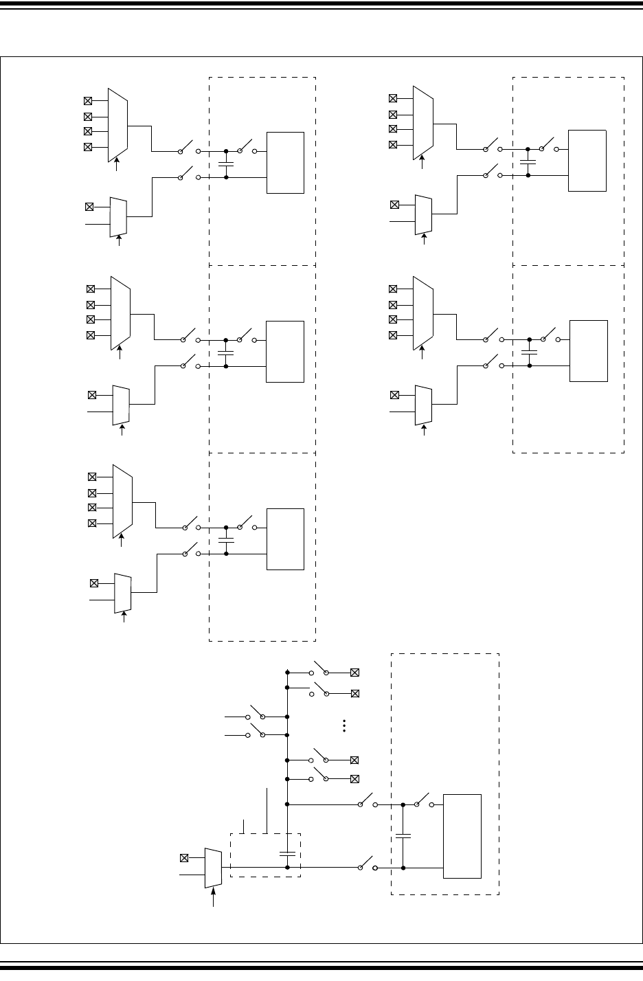
2015 Microchip Technology Inc. Preliminary DS60001320B-page 431
PIC32MZ Embedded Connectivity with Floating Point Unit (EF) Family
FIGURE 28-2: S&H BLOCK DIAGRAM
AN3
AN48
AN8
N/C 11
01
00
N/C 10
SH3ALT<1:0>
(ADCTRGMODE<23:22)
VREFL 1
0
AN0
AN45
AN5
N/C 11
01
00
N/C 10
SH0ALT<1:0>
(ADCTRGMODE<17:16)
VREFL 1
0
AN4
AN49
AN9
N/C 11
01
00
N/C 10
SH4ALT<1:0>
(ADCTRGMODE<25:24)
VREFL 1
0
AN1
AN46
AN6
N/C 11
01
00
N/C 10
SH1ALT<1:0>
(ADCTRGMODE<19:18)
SAR
VREFL 1
0
AN2
AN47
AN7
N/C 11
01
00
N/C 10
SH2ALT<1:0>
(ADCTRGMODE<21:20)
VREFL 1
0
AN10
VREFL 1
0
DIFFx<1>
AN5
AN6
AN41
AN42
IVREF (AN43)
IVTEMP (AN44)
DIFF3<1> (ADCIMCON1<7>)
DIFF0<1> (ADCIMCON1<1>)
DIFF4<1> (ADCIMCON1<9>)
DIFF1<1> (ADCIMCON1<3>)
DIFF2<1> (ADCIMCON1<5>)
ADC1
ADC2
SAR
ADC0
SAR
ADC3
ADC4
SAR
SAR
ADC7
SAR
CVD
Capacitor
CVDEN
(ADCCON1<11>)
CVDCPL<2:0>
(ADCCON2<28:26>)
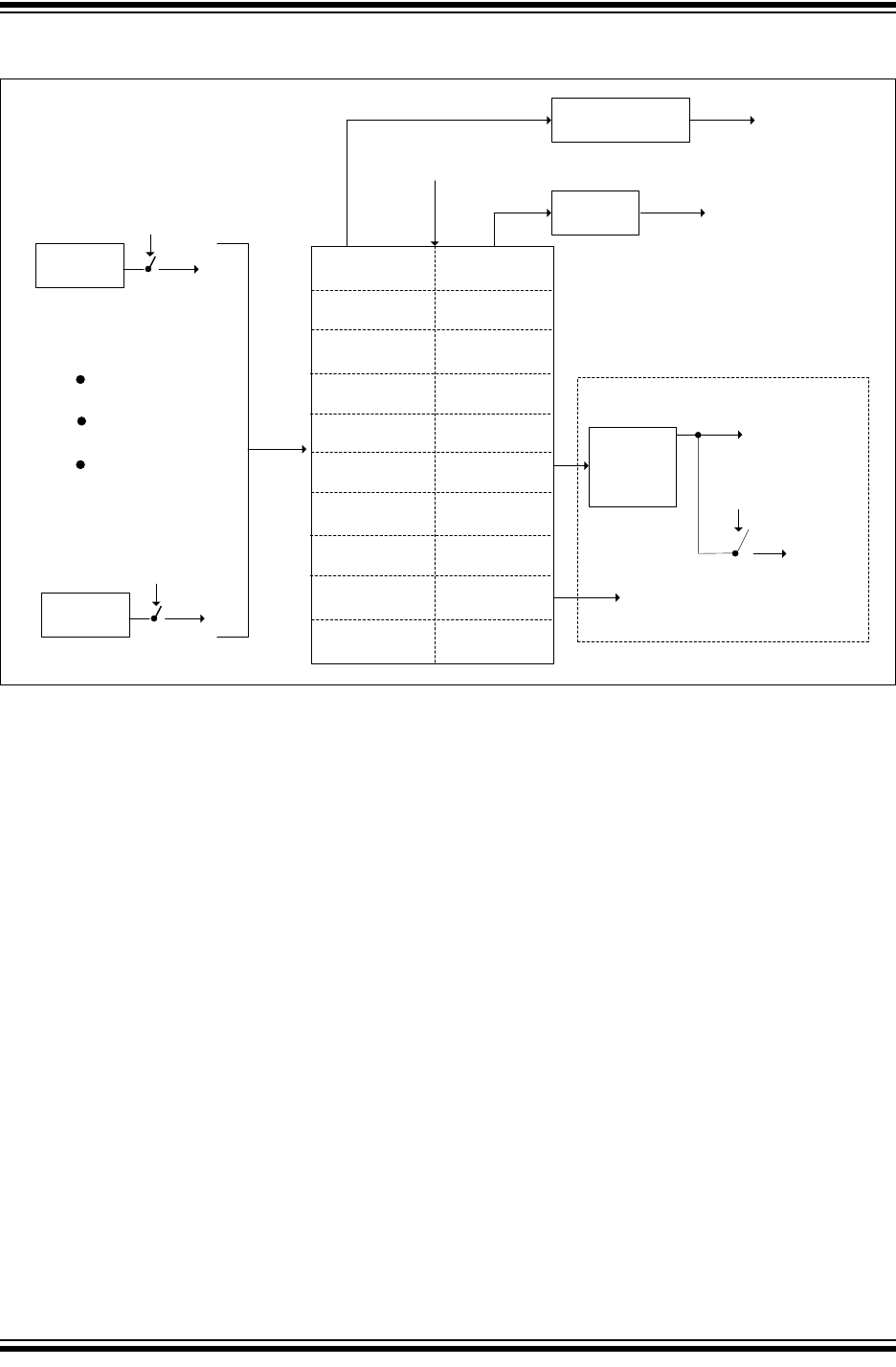
PIC32MZ Embedded Connectivity with Floating Point Unit (EF) Family
DS60001320B-page 432 Preliminary 2015 Microchip Technology Inc.
FIGURE 28-3: FIFO BLOCK DIAGRAM
FEN
(ADCFSTAT<31>)
FIFO (16 Words)
ADCFIFO DATA<31:0>
ADCID<2:0>
(ADCFSTAT<2:0>) ADCx ID
ADCx ID Converted Data
ADC4
ADC4EN
(ADCFSTAT<28>)
ADC0
ADC0EN
(ADCFSTAT<24>)
If data
available in
FIFO
FRDY
(ADCFSTAT<22>)
FIEN
(ADCFSTAT<23>)
Interrupt
FCNT<7:0>
(ADCFSTAT<15:8>)
Number of data in FIFO

2015 Microchip Technology Inc. Preliminary DS60001320B-page 433
PIC32MZ Embedded Connectivity with Floating Point Unit (EF) Family
28.1 ADC Control Registers
TABLE 28-1: ADC REGISTER MAP
Virtual Address
(BF84_#)
Register
Name
Bit Range
Bits
All Resets
31/15 30/14 29/13 28/12 27/11 26/10 25/9 24/8 23/7 22/6 21/5 20/4 19/3 18/2 17/1 16/0
B000 ADCCON1 31:16 TRBEN TRBERR TRBMST<2:0> TRBSLV<2:0> FRACT SELRES<1:0> STRGSRC<4:0> 0060
15:0 ON —SIDL —CVDEN FSSCLKEN FSPBCLKEN — — IRQVS<2:0> STRGLVL — — — 1000
B004 ADCCON2 31:16 BGVRRDY REFFLT EOSRDY CVDCPL<2:0> SAMC<9:0> 0000
15:0 BGVRIEN REFFLTIEN EOSIEN ADCEIOVR —ADCEIS<2:0> —ADCDIV<6:0> 0000
B008 ADCCON3 31:16 ADCSEL<1:0> CONCLKDIV<5:0> DIGEN7 — — DIGEN4 DIGEN3 DIGEN2 DIGEN1 DIGEN0 0000
15:0 VREFSEL<2:0> TRGSUSP UPDIEN UPDRDY SAMP RQCNVRT GLSWTRG GSWTRG ADINSEL<5:0> 0000
B00C ADCTRGMODE 31:16 — — — — — — SH4ALT<1:0> SH3ALT<1:0> SH2ALT<1:0> SH1ALT<1:0> SH0ALT<1:0> 0000
15:0 — — — STRGEN4 STRGEN3 STRGEN2 STRGEN1 STRGEN0 — — — SSAMPEN4 SSAMPEN3 SSAMPEN2 SSAMPEN1 SSAMPEN0 0000
B010 ADCIMCON1 31:16 DIFF15 SIGN15 DIFF14 SIGN14 DIFF13 SIGN13 DIFF12 SIGN12 DIFF11 SIGN11 DIFF10 SIGN10 DIFF9 SIGN9 DIFF8 SIGN8 0000
15:0 DIFF7 SIGN7 DIFF6 SIGN6 DIFF5 SIGN5 DIFF4 SIGN4 DIFF3 SIGN3 DIFF2 SIGN2 DIFF1 SIGN1 DIFF0 SIGN0 0000
B014 ADCIMCON2 31:16 DIFF31(1) SIGN31(1) DIFF30(1) SIGN30(1) DIFF29(1) SIGN29(1) DIFF28(1) SIGN28(1) DIFF27(1) SIGN27(1) DIFF26(1) SIGN26(1) DIFF25(1) SIGN25(1) DIFF24(1) SIGN24(1) 0000
15:0 DIFF23(1) SIGN23(1) DIFF22(1) SIGN22(1) DIFF21(1) SIGN21(1) DIFF20(1) SIGN20(1) DIFF19(1) SIGN19(1) DIFF18 SIGN18 DIFF17 SIGN17 DIFF16 SIGN16 0000
B018 ADCIMCON3 31:16 — — — — — — DIFF44 SIGN44 DIFF43 SIGN43 DIFF42(2) SIGN42(2) DIFF41(2) SIGN41(2) DIFF40(2) SIGN40(2) 0000
15:0 DIFF39(2) SIGN39(2) DIFF38(2) SIGN38(2) DIFF37(2) SIGN37(2) DIFF36(2) SIGN36(2) DIFF35(2) SIGN35(2) DIFF34(1) SIGN34(1) DIFF33(1) SIGN33(1) DIFF32(1) SIGN32(1) 0000
B020 ADCGIRQEN1 31:16 AGIEN31(1) AGIEN30(1) AGIEN29(1) AGIEN28(1) AGIEN27(1) AGIEN26(1) AGIEN25(1) AGIEN24(1) AGIEN23(1) AGIEN22(1) AGIEN21(1) AGIEN20(1) AGIEN19(1) AGIEN18 AGIEN17 AGIEN16 0000
15:0 AGIEN15 AGIEN14 AGIEN13 AGIEN12 AGIEN11 AGIEN10 AGIEN9 AGIEN8 AGIEN7 AGIEN6 AGIEN5 AGIEN4 AGIEN3 AGIEN2 AGIEN1 AGIEN0 0000
B024 ADCGIRQEN2 31:16 — — — — — — — — — — — — — — — — 0000
15:0 — — — AGIEN44 AGIEN43 AGIEN42(2) AGIEN41(2) AGIEN40(2) AGIEN39(2) AGIEN38(2) AGIEN37(2) AGIEN36(2) AGIEN35(2) AGIEN34(1) AGIEN33(1) AGIEN32(1) 0000
B028 ADCCSS1 31:16 CSS31(1) CSS30(1) CSS29(1) CSS28(1) CSS27(1) CSS26(1) CSS25(1) CSS24(1) CSS23(1) CSS22(1) CSS21(1) CSS20(1) CSS19(1) CSS18 CSS17 CSS16 0000
15:0 CSS15 CSS14 CSS13 CSS12 CSS11 CSS10 CSS9 CSS8 CSS7 CSS6 CSS5 CSS4 CSS3 CSS2 CSS1 CSS0 0000
B02C ADCCSS2 31:16 — — — — — — — — — — — — — — — — 0000
15:0 — — — CSS44 CSS43 CSS42(2) CSS41(2) CSS40(2) CSS39(2) CSS38(2) CSS37(2) CSS36(2) CSS35(2) CSS34(1) CSS33(1) CSS32(1) 0000
B030 ADCDSTAT1 31:16 ARDY31(1) ARDY30(1) ARDY29(1) ARDY28(1) ARDY27(1) ARDY26(1) ARDY25(1) ARDY24(1) ARDY23(1) ARDY22(1) ARDY21(1) ARDY20(1) ARDY19(1) ARDY18 ARDY17 ARDY16 0000
15:0 ARDY15 ARDY14 ARDY13 ARDY12 ARDY11 ARDY10 ARDY9 ARDY8 ARDY7 ARDY6 ARDY5 ARDY4 ARDY3 ARDY2 ARDY1 ARDY0 0000
B034 ADCDSTAT2 31:16 — — — — — — — — — — — — — — — — 0000
15:0 — — — ARDY44 ARDY43 ARDY42(2) ARDY41(2) ARDY40(2) ARDY39(2) ARDY38(2) ARDY37(2) ARDY36(2) ARDY35(2) ARDY34(1) ARDY33(1) ARDY32(1) 0000
B038 ADCCMPEN1 31:16 CMPE31(1) CMPE30(1) CMPE29(1) CMPE28(1) CMPE27(1) CMPE26(1) CMPE25(1) CMPE24(1) CMPE23(1) CMPE22(1) CMPE21(1) CMPE20(1) CMPE19(1) CMPE18 CMPE17 CMPE16 0000
15:0 CMPE15 CMPE14 CMPE13 CMPE12 CMPE11 CMPE10 CMPE9 CMPE8 CMPE7 CMPE6 CMPE5 CMPE4 CMPE3 CMPE2 CMPE1 CMPE0 0000
B03C ADCCMP1 31:16 DCMPHI<15:0> 0000
15:0 DCMPLO<15:0> 0000
B040 ADCCMPEN2 31:16 CMPE31(1) CMPE30(1) CMPE29(1) CMPE28(1) CMPE27(1) CMPE26(1) CMPE25(1) CMPE24(1) CMPE23(1) CMPE22(1) CMPE21(1) CMPE20(1) CMPE19(1) CMPE18 CMPE17 CMPE16 0000
15:0 CMPE15 CMPE14 CMPE13 CMPE12 CMPE11 CMPE10 CMPE9 CMPE8 CMPE7 CMPE6 CMPE5 CMPE4 CMPE3 CMPE2 CMPE1 CMPE0 0000
B044 ADCCMP2 31:16 DCMPHI<15:0> 0000
15:0 DCMPLO<15:0> 0000
B048 ADCCMPEN3 31:16 CMPE31(1) CMPE30(1) CMPE29(1) CMPE28(1) CMPE27(1) CMPE26(1) CMPE25(1) CMPE24(1) CMPE23(1) CMPE22(1) CMPE21(1) CMPE20(1) CMPE19(1) CMPE18 CMPE17 CMPE16 0000
15:0 CMPE15 CMPE14 CMPE13 CMPE12 CMPE11 CMPE10 CMPE9 CMPE8 CMPE7 CMPE6 CMPE5 CMPE4 CMPE3 CMPE2 CMPE1 CMPE0 0000
Note 1: This bit or register is not available on 64-pin devices.
2: This bit or register is not available on 64-pin and 100-pin devices.

PIC32MZ Embedded Connectivity with Floating Point Unit (EF) Family
DS60001320B-page 434 Preliminary 2015 Microchip Technology Inc.
B04C ADCCMP3 31:16 DCMPHI<15:0> 0000
15:0 DCMPLO<15:0> 0000
B050 ADCCMPEN4 31:16 CMPE31(1) CMPE30(1) CMPE29(1) CMPE28(1) CMPE27(1) CMPE26(1) CMPE25(1) CMPE24(1) CMPE23(1) CMPE22(1) CMPE21(1) CMPE20(1) CMPE19(1) CMPE18 CMPE17 CMPE16 0000
15:0 CMPE15 CMPE14 CMPE13 CMPE12 CMPE11 CMPE10 CMPE9 CMPE8 CMPE7 CMPE6 CMPE5 CMPE4 CMPE3 CMPE2 CMPE1 CMPE0 0000
B054 ADCCMP4 31:16 DCMPHI<15:0> 0000
15:0 DCMPLO<15:0> 0000
B058 ADCCMPEN5 31:16 CMPE31(1) CMPE30(1) CMPE29(1) CMPE28(1) CMPE27(1) CMPE26(1) CMPE25(1) CMPE24(1) CMPE23(1) CMPE22(1) CMPE21(1) CMPE20(1) CMPE19(1) CMPE18 CMPE17 CMPE16 0000
15:0 CMPE15 CMPE14 CMPE13 CMPE12 CMPE11 CMPE10 CMPE9 CMPE8 CMPE7 CMPE6 CMPE5 CMPE4 CMPE3 CMPE2 CMPE1 CMPE0 0000
B05C ADCCMP5 31:16 DCMPHI<15:0> 0000
15:0 DCMPLO<15:0> 0000
B060 ADCCMPEN6 31:16 CMPE31(1) CMPE30(1) CMPE29(1) CMPE28(1) CMPE27(1) CMPE26(1) CMPE25(1) CMPE24(1) CMPE23(1) CMPE22(1) CMPE21(1) CMPE20(1) CMPE19(1) CMPE18 CMPE17 CMPE16 0000
15:0 CMPE15 CMPE14 CMPE13 CMPE12 CMPE11 CMPE10 CMPE9 CMPE8 CMPE7 CMPE6 CMPE5 CMPE4 CMPE3 CMPE2 CMPE1 CMPE0 0000
B064 ADCCMP6 31:16 DCMPHI<15:0> 0000
15:0 DCMPLO<15:0> 0000
B068 ADCFLTR1 31:16 AFEN DATA16EN DFMODE OVRSAM<2:0> AFGIEN AFRDY — — — CHNLID<4:0> 0000
15:0 FLTRDATA<15:0> 0000
B06C ADCFLTR2 31:16 AFEN DATA16EN DFMODE OVRSAM<2:0> AFGIEN AFRDY — — — CHNLID<4:0> 0000
15:0 FLTRDATA<15:0> 0000
B070 ADCFLTR3 31:16 AFEN DATA16EN DFMODE OVRSAM<2:0> AFGIEN AFRDY — — — CHNLID<4:0> 0000
15:0 FLTRDATA<15:0> 0000
B074 ADCFLTR4 31:16 AFEN DATA16EN DFMODE OVRSAM<2:0> AFGIEN AFRDY — — — CHNLID<4:0> 0000
15:0 FLTRDATA<15:0> 0000
B078 ADCFLTR5 31:16 AFEN DATA16EN DFMODE OVRSAM<2:0> AFGIEN AFRDY — — — CHNLID<4:0> 0000
15:0 FLTRDATA<15:0> 0000
B07C ADCFLTR6 31:16 AFEN DATA16EN DFMODE OVRSAM<2:0> AFGIEN AFRDY — — — CHNLID<4:0> 0000
15:0 FLTRDATA<15:0> 0000
B080 ADCTRG1 31:16 — — — TRGSRC3<4:0> — — — TRGSRC2<4:0> 0000
15:0 — — — TRGSRC1<4:0> — — — TRGSRC0<4:0> 0000
B084 ADCTRG2 31:16 — — — TRGSRC7<4:0> — — — TRGSRC6<4:0> 0000
15:0 — — — TRGSRC5<4:0> — — — TRGSRC4<4:0> 0000
B088 ADCTRG3 31:16 — — — TRGSRC11<4:0> — — — TRGSRC10<4:0> 0000
15:0 — — — TRGSRC9<4:0> — — — TRGSRC8<4:0> 0000
B0A0 ADCCMPCON1 31:16 CVDDATA<15:0> 0000
15:0 — — AINID<5:0> ENDCMP DCMPGIEN DCMPED IEBTWN IEHIHI IEHILO IELOHI IELOLO 0000
B0A4 ADCCMPCON2 31:16 — — — — — — — — — — — — — — — — 0000
15:0 — — — AINID<4:0> ENDCMP DCMPGIEN DCMPED IEBTWN IEHIHI IEHILO IELOHI IELOLO 0000
B0A8 ADCCMPCON3 31:16 — — — — — — — — — — — — — — — — 0000
15:0 — — — AINID<4:0> ENDCMP DCMPGIEN DCMPED IEBTWN IEHIHI IEHILO IELOHI IELOLO 0000
TABLE 28-1: ADC REGISTER MAP (CONTINUED)
Virtual Address
(BF84_#)
Register
Name
Bit Range
Bits
All Resets
31/15 30/14 29/13 28/12 27/11 26/10 25/9 24/8 23/7 22/6 21/5 20/4 19/3 18/2 17/1 16/0
Note 1: This bit or register is not available on 64-pin devices.
2: This bit or register is not available on 64-pin and 100-pin devices.

2015 Microchip Technology Inc. Preliminary DS60001320B-page 435
PIC32MZ Embedded Connectivity with Floating Point Unit (EF) Family
B0AC ADCCMPCON4 31:16 — — — — — — — — — — — — — — — — 0000
15:0 — — — AINID<4:0> ENDCMP DCMPGIEN DCMPED IEBTWN IEHIHI IEHILO IELOHI IELOLO 0000
B0B0 ADCCMPCON5 31:16 — — — — — — — — — — — — — — — — 0000
15:0 — — — AINID<4:0> ENDCMP DCMPGIEN DCMPED IEBTWN IEHIHI IEHILO IELOHI IELOLO 0000
B0B4 ADCCMPCON6 31:16 — — — — — — — — — — — — — — — — 0000
15:0 — — — AINID<4:0> ENDCMP DCMPGIEN DCMPED IEBTWN IEHIHI IEHILO IELOHI IELOLO 0000
B0B8 ADCFSTAT 31:16 FEN — — ADC4EN ADC3EN ADC2EN ADC1EN ADC0EN FIEN FRDY FWROVERR — — — — — 0000
15:0 FCNT<7:0> FSIGN — — — — ADCID<2:0> 0000
B0BC ADCFIFO 31:16 DATA<31:16> 0000
15:0 DATA<15:0> 0000
B0C0 ADCBASE 31:16 — — — — — — — — — — — — — — — — 0000
15:0 ADCBASE<15:0> 0000
B0D0 ADCTRGSNS 31:16 — — — — — — — — — — — — — — — — 0000
15:0 — — — — LVL11 LVL10 LVL9 LVL8 LVL7 LVL6 LVL5 LVL4 LVL3 LVL2 LVL1 LVL0 0000
B0D4 ADC0TIME 31:16 — — — ADCEIS<2:0> SELRES<1:0> —ADCDIV<6:0> 0300
15:0 — — — — — — SAMC<9:0> 0000
B0D8 ADC1TIME 31:16 — — — ADCEIS<2:0> SELRES<1:0> —ADCDIV<6:0> 0300
15:0 — — — — — — SAMC<9:0> 0000
B0DC ADC2TIME 31:16 — — — ADCEIS<2:0> SELRES<1:0> —ADCDIV<6:0> 0300
15:0 — — — — — — SAMC<9:0> 0000
B0E0 ADC3TIME 31:16 — — — ADCEIS<2:0> SELRES<1:0> —ADCDIV<6:0> 0300
15:0 — — — — — — SAMC<9:0> 0000
B0E4 ADC4TIME 31:16 — — — ADCEIS<2:0> SELRES<1:0> —ADCDIV<6:0> 0300
15:0 — — — — — — SAMC<9:0> 0000
B0F0 ADCEIEN1 31:16 EIEN31(1) EIEN30(1) EIEN29(1) EIEN28(1) EIEN27(1) EIEN26(1) EIEN25(1) EIEN24(1) EIEN23(1) EIEN22(1) EIEN21(1) EIEN20(1) EIEN19(1) EIEN18 EIEN17 EIEN16 0000
15:0 EIEN15 EIEN14 EIEN13 EIEN12 EIEN11 EIEN10 EIEN9 EIEN8 EIEN7 EIEN6 EIEN5 EIEN4 EIEN3 EIEN2 EIEN1 EIEN0 0000
B0F4 ADCEIEN2 31:16 — — — — — — — — — — — — — — — — 0000
15:0 — — — EIEN44 EIEN43 EIEN42(2) EIEN41(2) EIEN40(2) EIEN39(2) EIEN38(2) EIEN37(2) EIEN36(2) EIEN35(2) EIEN34(1) EIEN33(1) EIEN32(1) 0000
B0F8 ADCEISTAT1 31:16 EIRDY31(1) EIRDY30(1) EIRDY29(1) EIRDY28(1) EIRDY27(1) EIRDY26(1) EIRDY25(1) EIRDY24(1) EIRDY23(1) EIRDY22(1) EIRDY21(1) EIRDY20(1) EIRDY19(1) EIRDY18 EIRDY17 EIRDY16 0000
15:0 EIRDY15 EIRDY14 EIRDY13 EIRDY12 EIRDY11 EIRDY10 EIRDY9 EIRDY8 EIRDY7 EIRDY6 EIRDY5 EIRDY4 EIRDY3 EIRDY2 EIRDY1 EIRDY0 0000
B0FC ADCEISTAT2 31:16 — — — — — — — — — — — — — — — — 0000
15:0 — — — EIRDY44 EIRDY43 EIRDY42(2) EIRDY41(2) EIRDY40(2) EIRDY39(2) EIRDY38(2) EIRDY37(2) EIRDY36(2) EIRDY35(2) EIRDY34(1) EIRDY33(1) EIRDY32(1) 0000
B100 ADCANCON 31:16 — — — — WKUPCLKCNT<3:0> WKIEN7 — — WKIEN4 WKIEN3 WKIEN2 WKIEN1 WKIEN0 0000
15:0 WKRDY7 — — WKRDY4 WKRDY3 WKRDY2 WKRDY1 WKRDY0 ANEN7 — — ANEN4 ANEN3 ANEN2 ANEN1 ANEN0 0000
B180 ADC0CFG 31:16 ADCCFG<31:16> 0000
15:0 ADCCFG<15:0> 0000
B184 ADC1CFG 31:16 ADCCFG<31:16> 0000
15:0 ADCCFG<15:0> 0000
TABLE 28-1: ADC REGISTER MAP (CONTINUED)
Virtual Address
(BF84_#)
Register
Name
Bit Range
Bits
All Resets
31/15 30/14 29/13 28/12 27/11 26/10 25/9 24/8 23/7 22/6 21/5 20/4 19/3 18/2 17/1 16/0
Note 1: This bit or register is not available on 64-pin devices.
2: This bit or register is not available on 64-pin and 100-pin devices.

PIC32MZ Embedded Connectivity with Floating Point Unit (EF) Family
DS60001320B-page 436 Preliminary 2015 Microchip Technology Inc.
B188 ADC2CFG 31:16 ADCCFG<31:16> 0000
15:0 ADCCFG<15:0> 0000
B18C ADC3CFG 31:16 ADCCFG<31:16> 0000
15:0 ADCCFG<15:0> 0000
B190 ADC4CFG 31:16 ADCCFG<31:16> 0000
15:0 ADCCFG<15:0> 0000
B19C ADC7CFG 31:16 ADCCFG<31:16> 0000
15:0 ADCCFG<15:0> 0000
B1C0 ADCSYSCFG0 31:16 AN<31:16> xxxF
15:0 AN<15:0> FFFF
B1C4 ADCSYSCFG1 31:16 — — — — — — — — — — — — — — — — 0000
15:0 — — — AN<44:32> 1xxx
B200 ADCDATA0 31:16 DATA<31:16> 0000
15:0 DATA<15:0> 0000
B204 ADCDATA1 31:16 DATA<31:16> 0000
15:0 DATA<15:0> 0000
B208 ADCDATA2 31:16 DATA<31:16> 0000
15:0 DATA<15:0> 0000
B20C ADCDATA3 31:16 DATA<31:16> 0000
15:0 DATA<15:0> 0000
B210 ADCDATA4 31:16 DATA<31:16> 0000
15:0 DATA<15:0> 0000
B214 ADCDATA5 31:16 DATA<31:16> 0000
15:0 DATA<15:0> 0000
B218 ADCDATA6 31:16 DATA<31:16> 0000
15:0 DATA<15:0> 0000
B21C ADCDATA7 31:16 DATA<31:16> 0000
15:0 DATA<15:0> 0000
B220 ADCDATA8 31:16 DATA<31:16> 0000
15:0 DATA<15:0> 0000
B224 ADCDATA9 31:16 DATA<31:16> 0000
15:0 DATA<15:0> 0000
B228 ADCDATA10 31:16 DATA<31:16> 0000
15:0 DATA<15:0> 0000
B22C ADCDATA11 31:16 DATA<31:16> 0000
15:0 DATA<15:0> 0000
B230 ADCDATA12 31:16 DATA<31:16> 0000
15:0 DATA<15:0> 0000
TABLE 28-1: ADC REGISTER MAP (CONTINUED)
Virtual Address
(BF84_#)
Register
Name
Bit Range
Bits
All Resets
31/15 30/14 29/13 28/12 27/11 26/10 25/9 24/8 23/7 22/6 21/5 20/4 19/3 18/2 17/1 16/0
Note 1: This bit or register is not available on 64-pin devices.
2: This bit or register is not available on 64-pin and 100-pin devices.

2015 Microchip Technology Inc. Preliminary DS60001320B-page 437
PIC32MZ Embedded Connectivity with Floating Point Unit (EF) Family
B234 ADCDATA13 31:16 DATA<31:16> 0000
15:0 DATA<15:0> 0000
B238 ADCDATA14 31:16 DATA<31:16> 0000
15:0 DATA<15:0> 0000
B23C ADCDATA15 31:16 DATA<31:16> 0000
15:0 DATA<15:0> 0000
B240 ADCDATA16 31:16 DATA<31:16> 0000
15:0 DATA<15:0> 0000
B244 ADCDATA17 31:16 DATA<31:16> 0000
15:0 DATA<15:0> 0000
B248 ADCDATA18 31:16 DATA<31:16> 0000
15:0 DATA<15:0> 0000
B24C ADCDATA19(1) 31:16 DATA<31:16> 0000
15:0 DATA<15:0> 0000
B250 ADCDATA20(1) 31:16 DATA<31:16> 0000
15:0 DATA<15:0> 0000
B254 ADCDATA21(1) 31:16 DATA<31:16> 0000
15:0 DATA<15:0> 0000
B258 ADCDATA22(1) 31:16 DATA<31:16> 0000
15:0 DATA<15:0> 0000
B25C ADCDATA23(1) 31:16 DATA<31:16> 0000
15:0 DATA<15:0> 0000
B260 ADCDATA24(1) 31:16 DATA<31:16> 0000
15:0 DATA<15:0> 0000
B264 ADCDATA25(1) 31:16 DATA<31:16> 0000
15:0 DATA<15:0> 0000
B268 ADCDATA26(1) 31:16 DATA<31:16> 0000
15:0 DATA<15:0> 0000
B26C ADCDATA27(1) 31:16 DATA<31:16> 0000
15:0 DATA<15:0> 0000
B270 ADCDATA28(1) 31:16 DATA<31:16> 0000
15:0 DATA<15:0> 0000
B274 ADCDATA29(1) 31:16 DATA<31:16> 0000
15:0 DATA<15:0> 0000
B278 ADCDATA30(1) 31:16 DATA<31:16> 0000
15:0 DATA<15:0> 0000
B27C ADCDATA31(1) 31:16 DATA<31:16> 0000
15:0 DATA<15:0> 0000
TABLE 28-1: ADC REGISTER MAP (CONTINUED)
Virtual Address
(BF84_#)
Register
Name
Bit Range
Bits
All Resets
31/15 30/14 29/13 28/12 27/11 26/10 25/9 24/8 23/7 22/6 21/5 20/4 19/3 18/2 17/1 16/0
Note 1: This bit or register is not available on 64-pin devices.
2: This bit or register is not available on 64-pin and 100-pin devices.

2015 Microchip Technology Inc. Preliminary DS60001320B-page 438
PIC32MZ Embedded Connectivity with Floating Point Unit (EF) Family
B280 ADCDATA32(1) 31:16 DATA<31:16> 0000
15:0 DATA<15:0> 0000
B284 ADCDATA33(1) 31:16 DATA<31:16> 0000
15:0 DATA<15:0> 0000
B288 ADCDATA34(1) 31:16 DATA<31:16> 0000
15:0 DATA<15:0> 0000
B28C ADCDATA35(2) 31:16 DATA<31:16> 0000
15:0 DATA<15:0> 0000
B290 ADCDATA36(2) 31:16 DATA<31:16> 0000
15:0 DATA<15:0> 0000
B294 ADCDATA37(2) 31:16 DATA<31:16> 0000
15:0 DATA<15:0> 0000
B298 ADCDATA38(2) 31:16 DATA<31:16> 0000
15:0 DATA<15:0> 0000
B29C ADCDATA39(2) 31:16 DATA<31:16> 0000
15:0 DATA<15:0> 0000
B2A0 ADCDATA40(2) 31:16 DATA<31:16> 0000
15:0 DATA<15:0> 0000
B2A4 ADCDATA41(2) 31:16 DATA<31:16> 0000
15:0 DATA<15:0> 0000
B2A8 ADCDATA42(2) 31:16 DATA<31:16> 0000
15:0 DATA<15:0> 0000
B2AC ADCDATA43 31:16 DATA<31:16> 0000
15:0 DATA<15:0> 0000
B2B0 ADCDATA44 31:16 DATA<31:16> 0000
15:0 DATA<15:0> 0000
TABLE 28-1: ADC REGISTER MAP (CONTINUED)
Virtual Address
(BF84_#)
Register
Name
Bit Range
Bits
All Resets
31/15 30/14 29/13 28/12 27/11 26/10 25/9 24/8 23/7 22/6 21/5 20/4 19/3 18/2 17/1 16/0
Note 1: This bit or register is not available on 64-pin devices.
2: This bit or register is not available on 64-pin and 100-pin devices.

2015 Microchip Technology Inc. Preliminary DS60001320B-page 439
PIC32MZ Embedded Connectivity with Floating Point Unit (EF) Family
REGISTER 28-1: ADCCON1: ADC CONTROL REGISTER 1
Bit
Range Bit
31/23/15/7 Bit
30/22/14/6 Bit
29/21/13/5 Bit
28/20/12/4 Bit
27/19/11/3 Bit
26/18/10/2 Bit
25/17/9/1 Bit
24/16/8/0
31:24 R/W-0 R-0, HS, HC R/W-0 R/W-0 R/W-0 R/W-0 R/W-0 R/W-0
TRBEN TRBERR TRBMST<2:0> TRBSLV<2:0>
23:16 R/W-0 R/W-1 R/W-1 R/W-0 R/W-0 R/W-0 R/W-0 R/W-0
FRACT SELRES<1:0> STRGSRC<4:0>
15:8 R/W-0 U-0 R/W-0 r-1 R/W-0 R/W-0 R/W-0 U-0
ON SIDL — CVDEN FSSCLKEN FSPBCLKEN —
7:0 U-0 R/W-0 R/W-0 R/W-0 R/W-0 U-0 U-0 U-0
— IRQVS<2:0> STRGLVL — — —
Legend: HC = Hardware Set HS = Hardware Cleared
R = Readable bit W = Writable bit U = Unimplemented bit, read as ‘0’
-n = Value at POR ‘1’ = Bit is set ‘0’ = Bit is cleared x = Bit is unknown
bit 31 TRBEN: Turbo Channel Enable bit
1 = Enable the Turbo channel
0 = Disable the Turbo channel
bit 30 TRBERR: Turbo Channel Error Status bit
1 = An error occurred while setting the Turbo channel and Turbo channel function to be disabled regardless
of the TRBEN bit being set to ‘1’.
0 = Turbo channel error did not occur
Note: The status of this bit is valid only after the TRBEN bit is set.
bit 29-27 TRBMST<2:0>: Turbo Master ADCx bits
111 = Reserved
110 = ADC4 is selected as the Turbo Master
•
•
•
000 = ADC0 is selected as the Turbo Master
bit 26-24 TRBSLV<2:0>: Turbo Slave ADCx bits
111 = Reserved
110 = ADC4 is selected as the Turbo Slave
•
•
•
000 = ADC0 is selected as the Turbo Slave
bit 23 FRACT: Fractional Data Output Format bit
1 = Fractional
0 = Integer
bit 22-21 SELRES<1:0>: Shared ADC (ADC7) Resolution bits
11 = 12 bits (default)
10 = 10 bits
01 = 8 bits
00 = 6 bits

PIC32MZ Embedded Connectivity with Floating Point Unit (EF) Family
DS60001320B-page 440 Preliminary 2015 Microchip Technology Inc.
bit 20-16 STRGSRC<4:0>: Scan Trigger Source Select bits
11111 = Reserved
•
•
•
01101 = Reserved
01100 = Comparator 2 (COUT)
01011 = Comparator 1 (COUT)
01010 = OCMP5
01001 = OCMP3
01000 = OCMP1
00111 = TMR5 match
00110 = TMR3 match
00101 = TMR1 match
00100 = INT0 External interrupt
00011 = Reserved
00010 = Global level software trigger (GLSWTRG)
00001 = Global software edge trigger (GSWTRG)
00000 = No Trigger
bit 15 ON: ADC Module Enable bit
1 = ADC module is enabled
0 = ADC module is disabled
Note: The ON bit should be set only after the ADC module has been configured.
bit 14 Unimplemented: Read as ‘0’
bit 13 SIDL: Stop in Idle Mode bit
1 = Discontinue module operation when device enters Idle mode
0 = Continue module operation in Idle mode
bit 12 Reserved: Read as ‘1’; must be written as ‘1’.
bit 11 CVDEN: Capacitive Voltage Division Enable bit
1 = CVD operation is enabled
0 = CVD operation is disabled
bit 10 FSSCLKEN: Fast Synchronous System Clock to ADC Control Clock bit
1 = Fast synchronous system clock to ADC control clock is enabled
0 = Fast synchronous system clock to ADC control clock is disabled
bit 9 FSPBCLKEN: Fast Synchronous Peripheral Clock to ADC Control Clock bit
1 = Fast synchronous peripheral clock to ADC control clock is enabled
0 = Fast synchronous peripheral clock to ADC control clock is disabled
bit 8-7 Unimplemented: Read as ‘0’
bit 6-4 IRQVS<2:0>: Interrupt Vector Shift bits
To determine interrupt vector address, this bit specifies the amount of left shift done to the ARDYx status
bits in the ADCDSTAT1 and ADCDSTAT2 registers, prior to adding with the ADCBASE register.
Interrupt Vector Address = Read Value of ADCBASE and Read Value of ADCBASE = Value written to
ADCBASE + x << IRQVS<2:0>, where ‘x’ is the smallest active input ID from the ADCDSTAT1 or
ADCDSTAT2 registers (which has highest priority).
111 = Shift x left 7 bit position
110 = Shift x left 6 bit position
101 = Shift x left 5 bit position
100 = Shift x left 4 bit position
011 = Shift x left 3 bit position
010 = Shift x left 2 bit position
001 = Shift x left 1 bit position
000 = Shift x left 0 bit position
REGISTER 28-1: ADCCON1: ADC CONTROL REGISTER 1 (CONTINUED)

2015 Microchip Technology Inc. Preliminary DS60001320B-page 441
PIC32MZ Embedded Connectivity with Floating Point Unit (EF) Family
bit 3 STRGLVL: Scan Trigger High Level/Positive Edge Sensitivity bit
1 = Scan trigger is high level sensitive. Once STRIG mode is selected (TRGSRCx<4:0> in the ADCTRGx
register), the scan trigger will continue for all selected analog inputs, until the STRIG option is removed.
0 = Scan trigger is positive edge sensitive. Once STRIG mode is selected (TRGSRCx<4:0> in the
ADCTRGx register), only a single scan trigger will be generated, which will complete the scan of all
selected analog inputs.
bit 2-0 Unimplemented: Read as ‘0’
REGISTER 28-1: ADCCON1: ADC CONTROL REGISTER 1 (CONTINUED)

PIC32MZ Embedded Connectivity with Floating Point Unit (EF) Family
DS60001320B-page 442 Preliminary 2015 Microchip Technology Inc.
REGISTER 28-2: ADCCON2: ADC CONTROL REGISTER 2
Bit Range Bit
31/23/15/7 Bit
30/22/14/6 Bit
29/21/13/5 Bit
28/20/12/4 Bit
27/19/11/3 Bit
26/18/10/2 Bit
25/17/9/1 Bit
24/16/8/0
31:24 R-0, HS, HC R-0, HS, HC R-0, HS, HC R/W-0 R/W-0 R/W-0 R/W-0 R/W-0
BGVRRDY REFFLT EOSRDY CVDCPL<2:0> SAMC<9:8>
23:16 R/W-0 R/W-0 R/W-0 R/W-0 R/W-0 R/W-0 R/W-0 R/W-0
SAMC<7:0>
15:8 R/W-0 R/W-0 R/W-0 R/W-0 U-0 R/W-0 R/W-0 R/W-0
BGVRIEN REFFLTIEN EOSIEN ADCEIOVR — ADCEIS<2:0>
7:0 U-0 R/W-0 R/W-0 R/W-0 R/W-0 R/W-0 R/W-0 R/W-0
— ADCDIV<6:0>
Legend: HC = Hardware Set HS = Hardware Cleared r = Reserved
R = Readable bit W = Writable bit U = Unimplemented bit, read as ‘0’
-n = Value at POR ‘1’ = Bit is set ‘0’ = Bit is cleared x = Bit is unknown
bit 31 BGVRRDY: Band Gap Voltage/ADC Reference Voltage Status bit
1 = Both band gap voltage and ADC reference voltages (VREF) are ready
0 = Either or both band gap voltage and ADC reference voltages (VREF) are not ready
Data processing is valid only after BGVRRDY is set by hardware, so the application code must check that
the BGVRRDY bit is set to ensure data validity. This bit set to ‘0’ when ON (ADCCON1<15>) = 0.
bit 30 REFFLT: Band Gap/VREF/AVDD BOR Fault Status bit
1 = Fault in band gap or the VREF voltage while the ON bit (ADCCON1<15>) was set. Most likely a band
gap or VREF fault will be caused by a BOR of the analog VDD supply.
0 = Band gap and VREF voltage are working properly
This bit is cleared when the ON bit (ADCCON1<15>) = 0 and the BGVRRDY bit = 1.
bit 29 EOSRDY: End of Scan Interrupt Status bit
1 = All analog inputs are considered for scanning through the scan trigger (all analog inputs specified in
the ADCCSS1 and ADCCSS2 registers) have completed scanning
0 = Scanning has not completed
This bit is cleared when ADCCON2<31:24> are read in software.
bit 28-26 CVDCPL<2:0>: Capacitor Voltage Divider (CVD) Setting bit
111 = 7 * 2.5 pF = 17.5 pF
110 = 6 * 2.5 pF = 15 pF
101 = 5 * 2.5 pF = 12.5 pF
100 = 4 * 2.5 pF = 10 pF
011 = 3 * 2.5 pF = 7.5 pF
010 = 2 * 2.5 pF = 5 pF
001 = 1 * 2.5 pF = 2.5 pF
000 = 0 * 2.5 pF = 0 pF
bit 25-16 SAMC<9:0>: Sample Time for the Shared ADC (ADC7) bits
1111111111 = 1025 TAD
7
•
•
•
0000000001 = 3 TAD
7
0000000000 = 2 TAD
7
Where TAD
7
= period of the ADC conversion clock for the Shared ADC (ADC7) controlled by the
ADCDIV<6:0> bits.
bit 15 BGVRIEN: Band Gap/VREF Voltage Ready Interrupt Enable bit
1 = Interrupt will be generated when the BGVRDDY bit is set
0 = No interrupt is generated when the BGVRRDY bit is set

2015 Microchip Technology Inc. Preliminary DS60001320B-page 443
PIC32MZ Embedded Connectivity with Floating Point Unit (EF) Family
bit 14 REFFLTIEN: Band Gap/VREF Voltage Fault Interrupt Enable bit
1 = Interrupt will be generated when the REFFLT bit is set
0 = No interrupt is generated when the REFFLT bit is set
bit 13 EOSIEN: End of Scan Interrupt Enable bit
1 = Interrupt will be generated when EOSRDY bit is set
0 = No interrupt is generated when the EOSRDY bit is set
bit 12 ADCEIOVR: Early Interrupt Request Override bit
1 = Early interrupt generation is not overridden and interrupt generation is controlled by the ADCEIEN1
and ADCEIEN2 registers
0 = Early interrupt generation is overridden and interrupt generation is controlled by the ADCGIRQEN1
and ADCGIRQEN2 registers
bit 11 Unimplemented: Read as ‘0’
bit 10-8 ADCEIS<2:0>: Shared ADC (ADC7) Early Interrupt Select bits
These bits select the number of clocks (TAD
7)
prior to the arrival of valid data that the associated interrupt
is generated.
111 = The data ready interrupt is generated 8 ADC clocks prior to end of conversion
110 = The data ready interrupt is generated 7 ADC clocks prior to end of conversion
•
•
•
001 = The data ready interrupt is generated 2 ADC module clocks prior to end of conversion
000 = The data ready interrupt is generated 1 ADC module clock prior to end of conversion
Note: All options are available when the selected resolution, set by the SELRES<1:0> bits
(ADCCON1<22:21>), is 12-bit or 10-bit. For a selected resolution of 8-bit, options from ‘000’ to
‘101’ are valid. For a selected resolution of 6-bit, options from ‘000’ to ‘011’ are valid.
bit 7 Unimplemented: Read as ‘0’
bit 6-0 ADCDIV<6:0>: Shared ADC (ADC7) Clock Divider bits
1111111 = 254 * TQ = TAD
7
•
•
•
0000011 = 6 * TQ = TAD
7
0000010 = 4 * TQ = TAD
7
0000001 = 2 * TQ = TAD
7
0000000 = Reserved
The ADCDIV<6:0> bits divide the ADC control clock (TQ) to generate the clock for the Shared ADC, ADC7
(TAD
7
).
REGISTER 28-2: ADCCON2: ADC CONTROL REGISTER 2 (CONTINUED)

PIC32MZ Embedded Connectivity with Floating Point Unit (EF) Family
DS60001320B-page 444 Preliminary 2015 Microchip Technology Inc.
REGISTER 28-3: ADCCON3: ADC CONTROL REGISTER 3
Bit
Range Bit
31/23/15/7 Bit
30/22/14/6 Bit
29/21/13/5 Bit
28/20/12/4 Bit
27/19/11/3 Bit
26/18/10/2 Bit
25/17/9/1 Bit
24/16/8/0
31:24 R/W-0 R/W-0 R/W-0 R/W-0 R/W-0 R/W-0 R/W-0 R/W-0
ADCSEL<1:0> CONCLKDIV<5:0>
23:16 R/W-0 U-0 U-0 R/W-0 R/W-0 R/W-0 R/W-0 R/W-0
DIGEN7 —— DIGEN4 DIGEN3 DIGEN2 DIGEN1 DIGEN0
15:8 R/W-0 R/W-0 R/W-0 R/W-0 R/W-0 R-0, HS, HC R/W-0 R-0, HS, HC
VREFSEL<2:0> TRGSUSP UPDIEN UPDRDY SAMP(1,2,3,4) RQCNVRT
7:0 R/W-0 R-0, HS, HC R/W-0 R/W-0 R/W-0 R/W-0 R/W-0 R/W-0
GLSWTRG GSWTRG ADINSEL<5:0>
Legend: HC = Hardware Set HS = Hardware Cleared
R = Readable bit W = Writable bit U = Unimplemented bit, read as ‘0’
-n = Value at POR ‘1’ = Bit is set ‘0’ = Bit is cleared x = Bit is unknown
bit 31-30 ADCSEL<1:0>: Analog-to-Digital Clock Source (TCLK) bits
11 = FRC
10 = REFCLK3
01 = System Clock (Tcy)
00 = PBCLK3
bit 29-24 CONCLKDIV<5:0>: Analog-to-Digital Control Clock (TQ) Divider bits
111111 = 64 * TCLK = TQ
•
•
•
000011 = 4 * TCLK = TQ
000010 = 3 * TCLK = TQ
000001 = 2 * TCLK = TQ
000000 = TCLK = TQ
bit 23 DIGEN7: Shared ADC (ADC7) Digital Enable bit
1 = ADC7 is digital enabled
0 = ADC7 is digital disabled
bit 22-21 Unimplemented: Read as ‘0’
bit 20 DIGEN4: ADC4 Digital Enable bit
1 = ADC4 is digital enabled
0 = ADC4 is digital disabled
bit 19 DIGEN3: ADC3 Digital Enable bit
1 = ADC3 is digital enabled
0 = ADC3 is digital disabled
Note 1: The SAMP bit has the highest priority and setting this bit will keep the S&H circuit in Sample mode until the
bit is cleared. Also, usage of the SAMP bit will cause settings of SAMC<9:0> bits (ADCCON2<25:16>) to
be ignored.
2: The SAMP bit only connects Class 2 and Class 3 analog inputs to the shared ADC, ADC7. All Class 1
analog inputs are not affected by the SAMP bit.
3: The SAMP bit is not a self-clearing bit and it is the responsibility of application software to first clear this bit
and only after setting the RQCNVRT bit to start the analog-to-digital conversion.
4: Normally, when the SAMP and RQCNVRT bits are used by software routines, all TRGSRCx<4:0> bits
and STRGSRC<4:0> bits should be set to ‘00000’ to disable all external hardware triggers and prevent
them from interfering with the software-controlled sampling command signal SAMP and with the
software-controlled trigger RQCNVRT.

2015 Microchip Technology Inc. Preliminary DS60001320B-page 445
PIC32MZ Embedded Connectivity with Floating Point Unit (EF) Family
bit 18 DIGEN2: ADC2 Digital Enable bit
1 = ADC2 is digital enabled
0 = ADC2 is digital disabled
bit 17 DIGEN1: ADC1 Digital Enable bit
1 = ADC1 is digital enabled
0 = ADC1 is digital disabled
bit 16 DIGEN0: ADC0 Digital Enable bit
1 = ADC0 is digital enabled
0 = ADC0 is digital disabled
bit 15-13 VREFSEL<2:0>: Voltage Reference (VREF) Input Selection bits
bit 12 TRGSUSP: Trigger Suspend bit
1 = Triggers are blocked from starting a new analog-to-digital conversion, but the ADC module is not disabled
0 = Triggers are not blocked
bit 11 UPDIEN: Update Ready Interrupt Enable bit
1 = Interrupt will be generated when the UPDRDY bit is set by hardware
0 = No interrupt is generated
bit 10 UPDRDY: ADC Update Ready Status bit
1 = ADC SFRs can be updated
0 = ADC SFRs cannot be updated
Note: This bit is only active while the TRGSUSP bit is set and there are no more running conversions of
any ADC modules.
bit 9 SAMP: Class 2 and Class 3 Analog Input Sampling Enable bit(1,2,3,4)
1 = The ADC S&H amplifier is sampling
0 = The ADC S&H amplifier is holding
bit 8 RQCNVRT: Individual ADC Input Conversion Request bit
This bit and its associated ADINSEL<5:0> bits enable the user to individually request an analog-to-digital
conversion of an analog input through software.
1 = Trigger the conversion of the selected ADC input as specified by the ADINSEL<5:0> bits
0 = Do not trigger the conversion
Note: This bit is automatically cleared in the next ADC clock cycle.
bit 7 GLSWTRG: Global Level Software Trigger bit
1 = Trigger conversion for ADC inputs that have selected the GLSWTRG bit as the trigger signal, either
through the associated TRGSRC<4:0> bits in the ADCTRGx registers or through the STRGSRC<4:0>
bits in the ADCCON1 register
0 = Do not trigger an analog-to-digital conversion
REGISTER 28-3: ADCCON3: ADC CONTROL REGISTER 3 (CONTINUED)
Note 1: The SAMP bit has the highest priority and setting this bit will keep the S&H circuit in Sample mode until the
bit is cleared. Also, usage of the SAMP bit will cause settings of SAMC<9:0> bits (ADCCON2<25:16>) to
be ignored.
2: The SAMP bit only connects Class 2 and Class 3 analog inputs to the shared ADC, ADC7. All Class 1
analog inputs are not affected by the SAMP bit.
3: The SAMP bit is not a self-clearing bit and it is the responsibility of application software to first clear this bit
and only after setting the RQCNVRT bit to start the analog-to-digital conversion.
4: Normally, when the SAMP and RQCNVRT bits are used by software routines, all TRGSRCx<4:0> bits
and STRGSRC<4:0> bits should be set to ‘00000’ to disable all external hardware triggers and prevent
them from interfering with the software-controlled sampling command signal SAMP and with the
software-controlled trigger RQCNVRT.
VREFSEL<2:0> ADREF+ADREF-
1xx Reserved; do not use
011 External VREFH External VREFL
010 AVDD External VREFL
001 External VREFH AVss
000 AVDD AVss

PIC32MZ Embedded Connectivity with Floating Point Unit (EF) Family
DS60001320B-page 446 Preliminary 2015 Microchip Technology Inc.
bit 6 GSWTRG: Global Software Trigger bit
1 = Trigger conversion for ADC inputs that have selected the GSWTRG bit as the trigger signal, either
through the associated TRGSRC<4:0> bits in the ADCTRGx registers or through the STRGSRC<4:0>
bits in the ADCCON1 register
0 = Do not trigger an analog-to-digital conversion
Note: This bit is automatically cleared in the next ADC clock cycle.
bit 5-0 ADINSEL<5:0>: Analog Input Select bits
These bits select the analog input to be converted when the RQCNVRT bit is set. As a general rule:
111111 = Reserved
•
•
•
101101 = Reserved
101100 = MAX_AN_INPUT + 2 = IVTEMP
101011 = MAX_AN_INPUT + 1 = IVREF
101010 = MAX_AN_INPUT = AN[MAX_AN_INPUT]
•
•
•
000001 = AN1
000000 = AN0
REGISTER 28-3: ADCCON3: ADC CONTROL REGISTER 3 (CONTINUED)
Note 1: The SAMP bit has the highest priority and setting this bit will keep the S&H circuit in Sample mode until the
bit is cleared. Also, usage of the SAMP bit will cause settings of SAMC<9:0> bits (ADCCON2<25:16>) to
be ignored.
2: The SAMP bit only connects Class 2 and Class 3 analog inputs to the shared ADC, ADC7. All Class 1
analog inputs are not affected by the SAMP bit.
3: The SAMP bit is not a self-clearing bit and it is the responsibility of application software to first clear this bit
and only after setting the RQCNVRT bit to start the analog-to-digital conversion.
4: Normally, when the SAMP and RQCNVRT bits are used by software routines, all TRGSRCx<4:0> bits
and STRGSRC<4:0> bits should be set to ‘00000’ to disable all external hardware triggers and prevent
them from interfering with the software-controlled sampling command signal SAMP and with the
software-controlled trigger RQCNVRT.

2015 Microchip Technology Inc. Preliminary DS60001320B-page 447
PIC32MZ Embedded Connectivity with Floating Point Unit (EF) Family
REGISTER 28-4: ADCTRGMODE: ADC TRIGGERING MODE FOR DEDICATED ADC REGISTER
Bit
Range Bit
31/23/15/7 Bit
30/22/14/6 Bit
29/21/13/5 Bit
28/20/12/4 Bit
27/19/11/3 Bit
26/18/10/2 Bit
25/17/9/1 Bit
24/16/8/0
31:24 U-0 U-0 U-0 U-0 U-0 U-0 R/W-0 R/W-0
— — — — — —SH4ALT<1:0>
23:16 R/W-0 R/W-0 R/W-0 R/W-0 R/W-0 R/W-0 R/W-0 R/W-0
SH3ALT<1:0> SH2ALT<1:0> SH1ALT<1:0> SH0ALT<1:0>
15:8 U-0 U-0 U-0 R/W-0 R/W-0 R/W-0 R/W-0 R/W-0
— — — STRGEN4 STRGEN3 STRGEN2 STRGEN1 STRGEN0
7:0 U-0 U-0 U-0 R/W-0 R/W-0 R/W-0 R/W-0 R/W-0
— — — SSAMPEN4 SSAMPEN3 SSAMPEN2 SSAMPEN1 SSAMPEN0
Legend:
R = Readable bit W = Writable bit U = Unimplemented bit, read as ‘0’
-n = Value at POR ‘1’ = Bit is set ‘0’ = Bit is cleared x = Bit is unknown
bit 31-26 Unimplemented: Read as ‘0’
bit 25-24 SH4ALT<1:0>: ADC4 Analog Input Select bit
11 = Reserved
10 = Reserved
01 = AN49
00 = AN4
bit 23-22 SH3ALT<1:0>: ADC3 Analog Input Select bit
11 = Reserved
10 = Reserved
01 = AN48
00 = AN3
bit 21-20 SH2ALT<1:0>: ADC2 Analog Input Select bit
11 = Reserved
10 = Reserved
01 = AN47
00 = AN2
bit 19-18 SH1ALT<1:0>: ADC1 Analog Input Select bit
11 = Reserved
10 = Reserved
01 = AN46
00 = AN1
bit 17-16 SH0ALT<1:0>: ADC0 Analog Input Select bit
11 = Reserved
10 = Reserved
01 = AN45
00 = AN0
bit 15-13 Unimplemented: Read as ‘0’
bit 12 STRGEN4: ADC4 Presynchronized Triggers bit
1 = ADC4 uses presynchronized triggers
0 = ADC4 does not use presynchronized triggers
bit 11 STRGEN3: ADC3 Presynchronized Triggers bit
1 = ADC3 uses presynchronized triggers
0 = ADC3 does not use presynchronized triggers
bit 10 STRGEN2: ADC2 Presynchronized Triggers bit
1 = ADC2 uses presynchronized triggers
0 = ADC2 does not use presynchronized triggers

PIC32MZ Embedded Connectivity with Floating Point Unit (EF) Family
DS60001320B-page 448 Preliminary 2015 Microchip Technology Inc.
bit 9 STRGEN1: ADC1 Presynchronized Triggers bit
1 = ADC1 uses presynchronized triggers
0 = ADC1 does not use presynchronized triggers
bit 8 STRGEN0: ADC0 Presynchronized Triggers bit
1 = ADC0 uses presynchronized triggers
0 = ADC0 does not use presynchronized triggers
bit 7-5 Unimplemented: Read as ‘0’
bit 4 SSAMPEN4: ADC4 Synchronous Sampling bit
1 = ADC4 uses synchronous sampling for the first sample after being idle or disabled
0 = ADC4 does not use synchronous sampling
bit 3 SSAMPEN3: ADC3 Synchronous Sampling bit
1 = ADC3 uses synchronous sampling for the first sample after being idle or disabled
0 = ADC3 does not use synchronous sampling
bit 2 SSAMPEN2: ADC2Synchronous Sampling bit
1 = ADC2 uses synchronous sampling for the first sample after being idle or disabled
0 = ADC2 does not use synchronous sampling
bit 1 SSAMPEN1: ADC1 Synchronous Sampling bit
1 = ADC1 uses synchronous sampling for the first sample after being idle or disabled
0 = ADC1 does not use synchronous sampling
bit 0 SSAMPEN0: ADC0 Synchronous Sampling bit
1 = ADC0 uses synchronous sampling for the first sample after being idle or disabled
0 = ADC0 does not use synchronous sampling
REGISTER 28-4: ADCTRGMODE: ADC TRIGGERING MODE FOR DEDICATED ADC REGISTER

2015 Microchip Technology Inc. Preliminary DS60001320B-page 449
PIC32MZ Embedded Connectivity with Floating Point Unit (EF) Family
REGISTER 28-5: ADCIMCON1: ADC INPUT MODE CONTROL REGISTER 1
Bit Range Bit
31/23/15/7 Bit
30/22/14/6 Bit
29/21/13/5 Bit
28/20/12/4 Bit
27/19/11/3 Bit
26/18/10/2 Bit
25/17/9/1 Bit
24/16/8/0
31:24 R/W-0 R/W-0 R/W-0 R/W-0 R/W-0 R/W-0 R/W-0 R/W-0
DIFF15 SIGN15 DIFF14 SIGN14 DIFF13 SIGN13 DIFF12 SIGN12
23:16 R/W-0 R/W-0 R/W-0 R/W-0 R/W-0 R/W-0 R/W-0 R/W-0
DIFF11 SIGN11 DIFF10 SIGN10 DIFF9 SIGN9 DIFF8 SIGN8
15:8 R/W-0 R/W-0 R/W-0 R/W-0 R/W-0 R/W-0 R/W-0 R/W-0
DIFF7 SIGN7 DIFF6 SIGN6 DIFF5 SIGN5 DIFF4 SIGN4
7:0 R/W-0 R/W-0 R/W-0 R/W-0 R/W-0 R/W-0 R/W-0 R/W-0
DIFF3 SIGN3 DIFF2 SIGN2 DIFF1 SIGN1 DIFF0 SIGN0
Legend:
R = Readable bit W = Writable bit U = Unimplemented bit, read as ‘0’
-n = Value at POR ‘1’ = Bit is set ‘0’ = Bit is cleared x = Bit is unknown
bit 31 DIFF15: AN15 Mode bit
1 = AN15 is using Differential mode
0 = AN15 is using Single-ended mode
bit 30 SIGN:15 AN15 Signed Data Mode bit
1 = AN15 is using Signed Data mode
0 = AN15 is using Unsigned Data mode
bit 29 DIFF14: AN14 Mode bit
1 = AN14 is using Differential mode
0 = AN14 is using Single-ended mode
bit 28 SIGN14: AN14 Signed Data Mode bit
1 = AN14 is using Signed Data mode
0 = AN14 is using Unsigned Data mode
bit 27 DIFF13: AN13 Mode bit
1 = AN13 is using Differential mode
0 = AN13 is using Single-ended mode
bit 26 SIGN13: AN13 Signed Data Mode bit
1 = AN13 is using Signed Data mode
0 = AN13 is using Unsigned Data mode
bit 25 DIFF12: AN12 Mode bit
1 = AN12 is using Differential mode
0 = AN12 is using Single-ended mode
bit 24 SIGN12: AN12 Signed Data Mode bit
1 = AN12 is using Signed Data mode
0 = AN12 is using Unsigned Data mode
bit 23 DIFF11: AN11 Mode bit
1 = AN11 is using Differential mode
0 = AN11 is using Single-ended mode
bit 22 SIGN11: AN11 Signed Data Mode bit
1 = AN11 is using Signed Data mode
0 = AN11 is using Unsigned Data mode
bit 21 DIFF10: AN10 Mode bit
1 = AN10 is using Differential mode
0 = AN10 is using Single-ended mode

PIC32MZ Embedded Connectivity with Floating Point Unit (EF) Family
DS60001320B-page 450 Preliminary 2015 Microchip Technology Inc.
bit 20 SIGN10: AN10 Signed Data Mode bit
1 = AN10 is using Signed Data mode
0 = AN10 is using Unsigned Data mode
bit 19 DIFF9: AN9 Mode bit
1 = AN9 is using Differential mode
0 = AN9 is using Single-ended mode
bit 18 SIGN9: AN9 Signed Data Mode bit
1 = AN9 is using Signed Data mode
0 = AN9 is using Unsigned Data mode
bit 17 DIFF8: AN 8 Mode bit
1 = AN8 is using Differential mode
0 = AN8 is using Single-ended mode
bit 16 SIGN8: AN8 Signed Data Mode bit
1 = AN8 is using Signed Data mode
0 = AN8 is using Unsigned Data mode
bit 15 DIFF7: AN7 Mode bit
1 = AN7 is using Differential mode
0 = AN7 is using Single-ended mode
bit 14 SIGN7: AN7 Signed Data Mode bit
1 = AN7 is using Signed Data mode
0 = AN7 is using Unsigned Data mode
bit 13 DIFF6: AN6 Mode bit
1 = AN6 is using Differential mode
0 = AN6 is using Single-ended mode
bit 12 SIGN6: AN6 Signed Data Mode bit
1 = AN6 is using Signed Data mode
0 = AN6 is using Unsigned Data mode
bit 11 DIFF5: AN5 Mode bit
1 = AN5 is using Differential mode
0 = AN5 is using Single-ended mode
bit 10 SIGN5: AN5 Signed Data Mode bit
1 = AN5 is using Signed Data mode
0 = AN5 is using Unsigned Data mode
bit 9 DIFF4: AN4 Mode bit
1 = AN4 is using Differential mode
0 = AN4 is using Single-ended mode
bit 8 SIGN4: AN4 Signed Data Mode bit
1 = AN4 is using Signed Data mode
0 = AN4 is using Unsigned Data mode
bit 7 DIFF3: AN3 Mode bit
1 = AN3 is using Differential mode
0 = AN3 is using Single-ended mode
bit 6 SIGN3: AN3 Signed Data Mode bit
1 = AN3 is using Signed Data mode
0 = AN3 is using Unsigned Data mode
bit 5 DIFF2: AN2 Mode bit
1 = AN2 is using Differential mode
0 = AN2 is using Single-ended mode
REGISTER 28-5: ADCIMCON1: ADC INPUT MODE CONTROL REGISTER 1 (CONTINUED)

2015 Microchip Technology Inc. Preliminary DS60001320B-page 451
PIC32MZ Embedded Connectivity with Floating Point Unit (EF) Family
bit 4 SIGN2: AN2 Signed Data Mode bit
1 = AN2 is using Signed Data mode
0 = AN2 is using Unsigned Data mode
bit 3 DIFF1: AN1 Mode bit
1 = AN1 is using Differential mode
0 = AN1 is using Single-ended mode
bit 2 SIGN1: AN1 Signed Data Mode bit
1 = AN1 is using Signed Data mode
0 = AN1 is using Unsigned Data mode
bit 1 DIFF0: AN0 Mode bit
1 = AN0 is using Differential mode
0 = AN0 is using Single-ended mode
bit 0 SIGN0: AN0 Signed Data Mode bit
1 = AN0 is using Signed Data mode
0 = AN0 is using Unsigned Data mode
REGISTER 28-5: ADCIMCON1: ADC INPUT MODE CONTROL REGISTER 1 (CONTINUED)

PIC32MZ Embedded Connectivity with Floating Point Unit (EF) Family
DS60001320B-page 452 Preliminary 2015 Microchip Technology Inc.
REGISTER 28-6: ADCIMCON2: ADC INPUT MODE CONTROL REGISTER 2
Bit Range Bit
31/23/15/7 Bit
30/22/14/6 Bit
29/21/13/5 Bit
28/20/12/4 Bit
27/19/11/3 Bit
26/18/10/2 Bit
25/17/9/1 Bit
24/16/8/0
31:24 R/W-0 R/W-0 R/W-0 R/W-0 R/W-0 R/W-0 R/W-0 R/W-0
DIFF31(1) SIGN31(1) DIFF30(1) SIGN30(1) DIFF29(1) SIGN29(1) DIFF28(1) SIGN28(1)
23:16 R/W-0 R/W-0 R/W-0 R/W-0 R/W-0 R/W-0 R/W-0 R/W-0
DIFF27(1) SIGN27(1) DIFF26(1) SIGN26(1) DIFF25(1) SIGN25(1) DIFF24(1) SIGN24(1)
15:8 R/W-0 R/W-0 R/W-0 R/W-0 R/W-0 R/W-0 R/W-0 R/W-0
DIFF23(1) SIGN23(1) DIFF22(1) SIGN22(1) DIFF21(1) SIGN21(1) DIFF20(1) SIGN20(1)
7:0 R/W-0 R/W-0 R/W-0 R/W-0 R/W-0 R/W-0 R/W-0 R/W-0
DIFF19(1) SIGN19(1) DIFF18 SIGN18 DIFF17 SIGN17 DIFF16 SIGN16
Legend:
R = Readable bit W = Writable bit U = Unimplemented bit, read as ‘0’
-n = Value at POR ‘1’ = Bit is set ‘0’ = Bit is cleared x = Bit is unknown
bit 31 DIFF31: AN31 Mode bit(1)
1 = AN31 is using Differential mode
0 = AN31 is using Single-ended mode
bit 30 SIGN31: AN31 Signed Data Mode bit(1)
1 = AN31 is using Signed Data mode
0 = AN31 is using Unsigned Data mode
bit 29 DIFF30: AN30 Mode bit(1)
1 = AN30 is using Differential mode
0 = AN30 is using Single-ended mode
bit 28 SIGN30: AN30 Signed Data Mode bit(1)
1 = AN30 is using Signed Data mode
0 = AN30 is using Unsigned Data mode
bit 27 DIFF29: AN29 Mode bit(1)
1 = AN29 is using Differential mode
0 = AN29 is using Single-ended mode
bit 26 SIGN29: AN29 Signed Data Mode bit(1)
1 = AN29 is using Signed Data mode
0 = AN29 is using Unsigned Data mode
bit 25 DIFF28: AN28 Mode bit(1)
1 = AN28 is using Differential mode
0 = AN28 is using Single-ended mode
bit 24 SIGN28: AN28 Signed Data Mode bit(1)
1 = AN28 is using Signed Data mode
0 = AN28 is using Unsigned Data mode
bit 23 DIFF27: AN27 Mode bit(1)
1 = AN27 is using Differential mode
0 = AN27 is using Single-ended mode
bit 22 SIGN27: AN27 Signed Data Mode bit(1)
1 = AN27 is using Signed Data mode
0 = AN27 is using Unsigned Data mode
Note 1: This bit is not available on 64-pin devices.

2015 Microchip Technology Inc. Preliminary DS60001320B-page 453
PIC32MZ Embedded Connectivity with Floating Point Unit (EF) Family
bit 21 DIFF26: AN26 Mode bit(1)
1 = AN26 is using Differential mode
0 = AN26 is using Single-ended mode
bit 20 SIGN26: AN26 Signed Data Mode bit(1)
1 = AN26 is using Signed Data mode
0 = AN26 is using Unsigned Data mode
bit 19 DIFF25: AN25 Mode bit(1)
1 = AN25 is using Differential mode
0 = AN25 is using Single-ended mode
bit 18 SIGN25: AN25 Signed Data Mode bit(1)
1 = AN25 is using Signed Data mode
0 = AN25 is using Unsigned Data mode
bit 17 DIFF24: AN24 Mode bit(1)
1 = AN24 is using Differential mode
0 = AN24 is using Single-ended mode
bit 16 SIGN24: AN24 Signed Data Mode bit(1)
1 = AN24 is using Signed Data mode
0 = AN24 is using Unsigned Data mode
bit 15 DIFF23: AN23 Mode bit(1)
1 = AN23 is using Differential mode
0 = AN23 is using Single-ended mode
bit 14 SIGN23: AN23 Signed Data Mode bit(1)
1 = AN23 is using Signed Data mode
0 = AN23 is using Unsigned Data mode
bit 13 DIFF22: AN22 Mode bit(1)
1 = AN22 is using Differential mode
0 = AN22 is using Single-ended mode
bit 12 SIGN22: AN22 Signed Data Mode bit(1)
1 = AN22 is using Signed Data mode
0 = AN22 is using Unsigned Data mode
bit 11 DIFF21: AN21 Mode bit(1)
1 = AN21 is using Differential mode
0 = AN21 is using Single-ended mode
bit 10 SIGN21: AN21 Signed Data Mode bit(1)
1 = AN21 is using Signed Data mode
0 = AN21 is using Unsigned Data mode
bit 9 DIFF20: AN20 Mode bit(1)
1 = AN20 is using Differential mode
0 = AN20 is using Single-ended mode
bit 8 SIGN20: AN20 Signed Data Mode bit(1)
1 = AN20 is using Signed Data mode
0 = AN20 is using Unsigned Data mode
bit 7 DIFF19: AN19 Mode bit(1)
1 = AN19 is using Differential mode
0 = AN19 is using Single-ended mode
REGISTER 28-6: ADCIMCON2: ADC INPUT MODE CONTROL REGISTER 2 (CONTINUED)
Note 1: This bit is not available on 64-pin devices.

PIC32MZ Embedded Connectivity with Floating Point Unit (EF) Family
DS60001320B-page 454 Preliminary 2015 Microchip Technology Inc.
bit 6 SIGN19: AN19 Signed Data Mode bit(1)
1 = AN19 is using Signed Data mode
0 = AN19 is using Unsigned Data mode
bit 5 DIFF18: AN18 Mode bit
1 = AN18 is using Differential mode
0 = AN18 is using Single-ended mode
bit 4 SIGN18: AN18 Signed Data Mode bit
1 = AN18 is using Signed Data mode
0 = AN18 is using Unsigned Data mode
bit 3 DIFF17: AN17 Mode bit
1 = AN17 is using Differential mode
0 = AN17 is using Single-ended mode
bit 2 SIGN17: AN17 Signed Data Mode bit
1 = AN17 is using Signed Data mode
0 = AN17 is using Unsigned Data mode
bit 1 DIFF16: AN16 Mode bit
1 = AN16 is using Differential mode
0 = AN16 is using Single-ended mode
bit 0 SIGN16: AN16 Signed Data Mode bit
1 = AN16 is using Signed Data mode
0 = AN16 is using Unsigned Data mode
REGISTER 28-6: ADCIMCON2: ADC INPUT MODE CONTROL REGISTER 2 (CONTINUED)
Note 1: This bit is not available on 64-pin devices.

2015 Microchip Technology Inc. Preliminary DS60001320B-page 455
PIC32MZ Embedded Connectivity with Floating Point Unit (EF) Family
REGISTER 28-7: ADCIMCON3: ADC INPUT MODE CONTROL REGISTER 3
Bit Range Bit
31/23/15/7 Bit
30/22/14/6 Bit
29/21/13/5 Bit
28/20/12/4 Bit
27/19/11/3 Bit
26/18/10/2 Bit
25/17/9/1 Bit
24/16/8/0
31:24 U-0 U-0 U-0 U-0 U-0 U-0 R/W-0 R/W-0
— — — — — — DIFF44 SIGN44
23:16 R/W-0 R/W-0 R/W-0 R/W-0 R/W-0 R/W-0 R/W-0 R/W-0
DIFF43 SIGN43 DIFF42(2) SIGN42(2) DIFF41(2) SIGN41(2) DIFF40(2) SIGN40(2)
15:8 R/W-0 R/W-0 R/W-0 R/W-0 R/W-0 R/W-0 R/W-0 R/W-0
DIFF39(2) SIGN39(2) DIFF38(2) SIGN38(2) DIFF37(2) SIGN37(2) DIFF36(2) SIGN36(2)
7:0 R/W-0 R/W-0 R/W-0 R/W-0 R/W-0 R/W-0 R/W-0 R/W-0
DIFF35(2) SIGN35(2) DIFF34(1) SIGN34(1) DIFF33(1) SIGN33(1) DIFF32(1) SIGN32(1)
Legend:
R = Readable bit W = Writable bit U = Unimplemented bit, read as ‘0’
-n = Value at POR ‘1’ = Bit is set ‘0’ = Bit is cleared x = Bit is unknown
bit 31-26 Unimplemented: Read as ‘0’
bit 25 DIFF44: AN44 Mode bit
1 = AN44 is using Differential mode
0 = AN44 is using Single-ended mode
bit 24 SIGN44: AN44 Signed Data Mode bit
1 = AN44 is using Signed Data mode
0 = AN44 is using Unsigned Data mode
bit 23 DIFF43: AN43 Mode bit
1 = AN43 is using Differential mode
0 = AN43 is using Single-ended mode
bit 22 SIGN43: AN43 Signed Data Mode bit
1 = AN43 is using Signed Data mode
0 = AN43 is using Unsigned Data mode
bit 21 DIFF42: AN42 Mode bit(2)
1 = AN42 is using Differential mode
0 = AN42 is using Single-ended mode
bit 20 SIGN42: AN42 Signed Data Mode bit(2)
1 = AN42 is using Signed Data mode
0 = AN42 is using Unsigned Data mode
bit 19 DIFF41: AN41 Mode bit(2)
1 = AN41 is using Differential mode
0 = AN41 is using Single-ended mode
bit 18 SIGN41: AN41 Signed Data Mode bit(2)
1 = AN41 is using Signed Data mode
0 = AN41 is using Unsigned Data mode
bit 17 DIFF40: AN40 Mode bit(2)
1 = AN40 is using Differential mode
0 = AN40 is using Single-ended mode
Note 1: This bit is not available on 64-pin devices.
2: This bit is not available on 64-pin and 100-pin devices.

PIC32MZ Embedded Connectivity with Floating Point Unit (EF) Family
DS60001320B-page 456 Preliminary 2015 Microchip Technology Inc.
bit 16 SIGN40: AN40 Signed Data Mode bit(2)
1 = AN40 is using Signed Data mode
0 = AN40 is using Unsigned Data mode
bit 15 DIFF39: AN39 Mode bit(2)
1 = AN39 is using Differential mode
0 = AN39 is using Single-ended mode
bit 14 SIGN39: AN39 Signed Data Mode bit(2)
1 = AN39 is using Signed Data mode
0 = AN39 is using Unsigned Data mode
bit 13 DIFF38: AN38 Mode bit(2)
1 = AN38 is using Differential mode
0 = AN38 is using Single-ended mode
bit 12 SIGN38: AN38 Signed Data Mode bit(2)
1 = AN38 is using Signed Data mode
0 = AN38 is using Unsigned Data mode
bit 11 DIFF37: AN37 Mode bit(2)
1 = AN37 is using Differential mode
0 = AN37 is using Single-ended mode
bit 10 SIGN37: AN37 Signed Data Mode bit(2)
1 = AN37 is using Signed Data mode
0 = AN37 is using Unsigned Data mode
bit 9 DIFF36: AN36 Mode bit(2)
1 = AN36 is using Differential mode
0 = AN36 is using Single-ended mode
bit 8 SIGN36: AN36 Signed Data Mode bit(2)
1 = AN36 is using Signed Data mode
0 = AN36 is using Unsigned Data mode
bit 7 DIFF35: AN35 Mode bit(2)
1 = AN35 is using Differential mode
0 = AN35 is using Single-ended mode
bit 6 SIGN35: AN35 Signed Data Mode bit(2)
1 = AN35 is using Signed Data mode
0 = AN35 is using Unsigned Data mode
bit 5 DIFF34: AN34 Mode bit(1)
1 = AN34 is using Differential mode
0 = AN34 is using Single-ended mode
bit 4 SIGN34: AN34 Signed Data Mode bit(1)
1 = AN34 is using Signed Data mode
0 = AN34 is using Unsigned Data mode
bit 3 DIFF33: AN33 Mode bit(1)
1 = AN33 is using Differential mode
0 = AN33 is using Single-ended mode
bit 2 SIGN33: AN33 Signed Data Mode bit(1)
1 = AN33 is using Signed Data mode
0 = AN33 is using Unsigned Data mode
REGISTER 28-7: ADCIMCON3: ADC INPUT MODE CONTROL REGISTER 3 (CONTINUED)
Note 1: This bit is not available on 64-pin devices.
2: This bit is not available on 64-pin and 100-pin devices.

2015 Microchip Technology Inc. Preliminary DS60001320B-page 457
PIC32MZ Embedded Connectivity with Floating Point Unit (EF) Family
bit 1 DIFF32: AN32 Mode bit(1)
1 = AN32 is using Differential mode
0 = AN32 is using Single-ended mode
bit 0 SIGN32: AN32 Signed Data Mode bit(1)
1 = AN32 is using Signed Data mode
0 = AN32 is using Unsigned Data mode
REGISTER 28-7: ADCIMCON3: ADC INPUT MODE CONTROL REGISTER 3 (CONTINUED)
Note 1: This bit is not available on 64-pin devices.
2: This bit is not available on 64-pin and 100-pin devices.
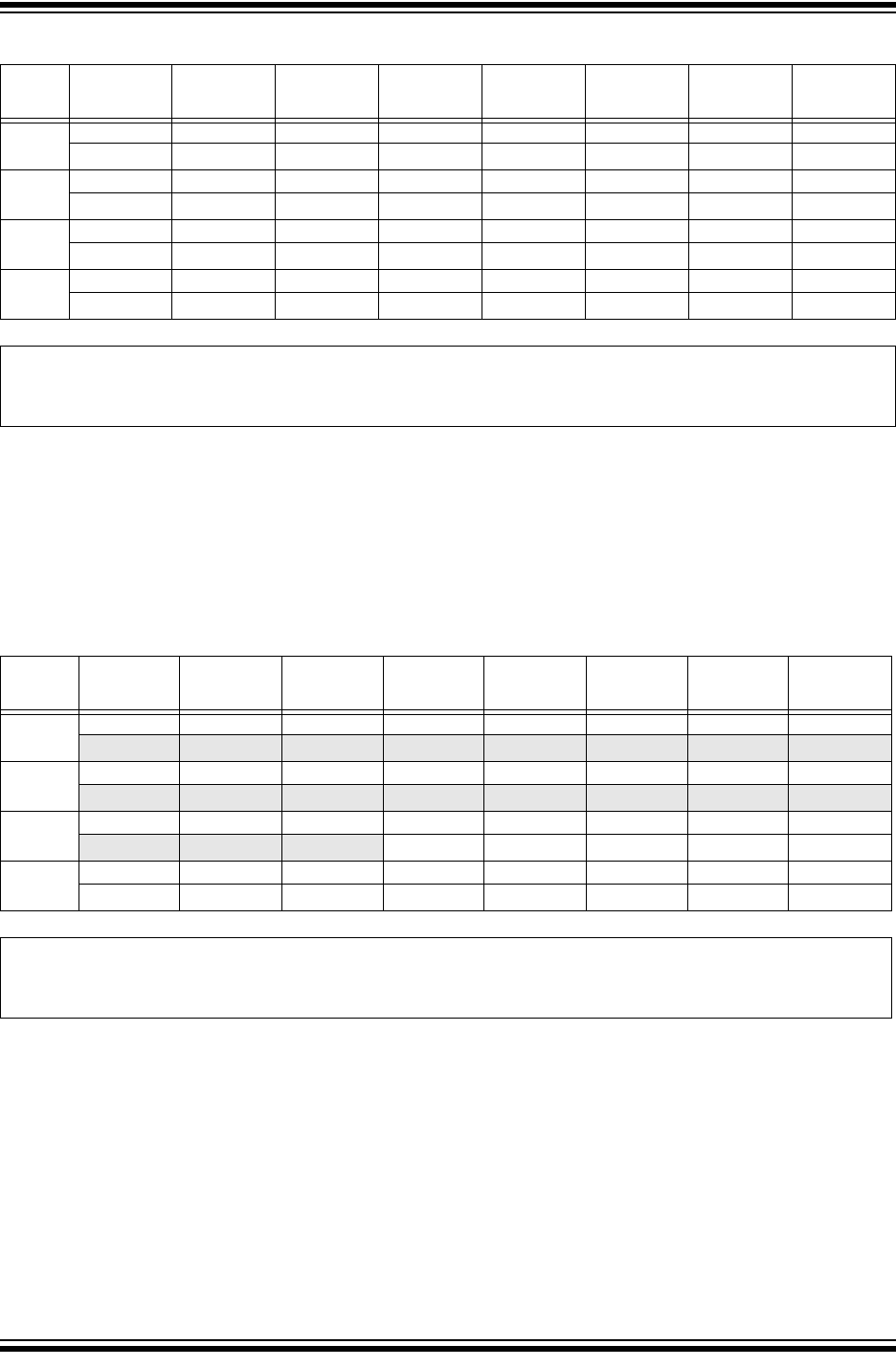
PIC32MZ Embedded Connectivity with Floating Point Unit (EF) Family
DS60001320B-page 458 Preliminary 2015 Microchip Technology Inc.
REGISTER 28-8: ADCGIRQEN1: ADC GLOBAL INTERRUPT ENABLE REGISTER 1
Bit
Range Bit
31/23/15/7 Bit
30/22/14/6 Bit
29/21/13/5 Bit
28/20/12/4 Bit
27/19/11/3 Bit
26/18/10/2 Bit
25/17/9/1 Bit
24/16/8/0
31:24 R/W-0 R/W-0 R/W-0 R/W-0 R/W-0 R/W-0 R/W-0 R/W-0
AGIEN31(1) AGIEN30(1) AGIEN29(1) AGIEN28(1) AGIEN27(1) AGIEN26(1) AGIEN25(1) AGIEN24(1)
23:16 R/W-0 R/W-0 R/W-0 R/W-0 R/W-0 R/W-0 R/W-0 R/W-0
AGIEN23(1) AGIEN22(1) AGIEN21(1) AGIEN20(1) AGIEN19(1) AGIEN18 AGIEN17 AGIEN16
15:8 R/W-0 R/W-0 R/W-0 R/W-0 R/W-0 R/W-0 R/W-0 R/W-0
AGIEN15 AGIEN14 AGIEN13 AGIEN12 AGIEN11 AGIEN10 AGIEN9 AGIEN8
7:0 R/W-0 R/W-0 R/W-0 R/W-0 R/W-0 R/W-0 R/W-0 R/W-0
AGIEN7 AGIEN6 AGIEN5 AGIEN4 AGIEN3 AGIEN2 AGIEN1 AGIEN0
Legend:
R = Readable bit W = Writable bit U = Unimplemented bit, read as ‘0’
-n = Value at POR ‘1’ = Bit is set ‘0’ = Bit is cleared x = Bit is unknown
bit 31-0 AGIEN31:AGIEN0: ADC Global Interrupt Enable bits
1 = Interrupts are enabled for the selected analog input. The interrupt is generated after the converted data
is ready (indicated by the ARDYx bit (‘x’ = 31-0) of the ADCDSTAT1 register)
0 = Interrupts are disabled
Note 1: This bit is not available on 64-pin devices.
REGISTER 28-9: ADCGIRQEN2: ADC GLOBAL INTERRUPT ENABLE REGISTER 2
Bit
Range Bit
31/23/15/7 Bit
30/22/14/6 Bit
29/21/13/5 Bit
28/20/12/4 Bit
27/19/11/3 Bit
26/18/10/2 Bit
25/17/9/1 Bit
24/16/8/0
31:24 U-0 U-0 U-0 U-0 U-0 U-0 U-0 U-0
— — — — — — — —
23:16 U-0 U-0 U-0 U-0 U-0 U-0 U-0 U-0
— — — — — — — —
15:8 U-0 U-0 U-0 R/W-0 R/W-0 R/W-0 R/W-0 R/W-0
— — — AGIEN44(2) AGIEN43(2) AGIEN42(2) AGIEN41(2) AGIEN40(2)
7:0 R/W-0 R/W-0 R/W-0 R/W-0 R/W-0 R/W-0 R/W-0 R/W-0
AGIEN39(2) AGIEN38(2) AGIEN37(2) AGIEN36(2) AGIEN35(2) AGIEN34(1) AGIEN33(1) AGIEN32(1)
Legend:
R = Readable bit W = Writable bit U = Unimplemented bit, read as ‘0’
-n = Value at POR ‘1’ = Bit is set ‘0’ = Bit is cleared x = Bit is unknown
bit 31-13 Unimplemented: Read as ‘0’
bit 12-0 AGIEN44:AGIEN32 ADC Global Interrupt Enable bits
1 = Interrupts are enabled for the selected analog input. The interrupt is generated after the converted data
is ready (indicated by the ARDYx bit (‘x’ = 44-32) of the ADCDSTAT2 register)
0 = Interrupts are disabled
Note 1: This bit is not available on 64-pin devices.
2: This bit is not available on 64-pin and 100-pin devices.

2015 Microchip Technology Inc. Preliminary DS60001320B-page 459
PIC32MZ Embedded Connectivity with Floating Point Unit (EF) Family
REGISTER 28-10: ADCCSS1: ADC COMMON SCAN SELECT REGISTER 1
Bit Range Bit
31/23/15/7 Bit
30/22/14/6 Bit
29/21/13/5 Bit
28/20/12/4 Bit
27/19/11/3 Bit
26/18/10/2 Bit
25/17/9/1 Bit
24/16/8/0
31:24 R/W-0 R/W-0 R/W-0 R/W-0 R/W-0 R/W-0 R/W-0 R/W-0
CSS31(1) CSS30(1) CSS29(1) CSS28(1) CSS27(1) CSS26(1) CSS25(1) CSS24(1)
23:16 R/W-0 R/W-0 R/W-0 R/W-0 R/W-0 R/W-0 R/W-0 R/W-0
CSS23(1) CSS22(1) CSS21(1) CSS20(1) CSS19(1) CSS18 CSS17 CSS16
15:8 R/W-0 R/W-0 R/W-0 R/W-0 R/W-0 R/W-0 R/W-0 R/W-0
CSS15 CSS14 CSS13 CSS12 CSS11 CSS10 CSS9 CSS8
7:0 R/W-0 R/W-0 R/W-0 R/W-0 R/W-0 R/W-0 R/W-0 R/W-0
CSS7 CSS6 CSS5 CSS4 CSS3 CSS2 CSS1 CSS0
Legend:
R = Readable bit W = Writable bit U = Unimplemented bit, read as ‘0’
-n = Value at POR ‘1’ = Bit is set ‘0’ = Bit is cleared x = Bit is unknown
bit 31-0 CSS31:CSS0: Analog Common Scan Select bits
1 = Select ANx for input scan
0 = Skip ANx for input scan
Note 1: This bit is not available on 64-pin devices.
Note 1: In addition to setting the appropriate bits in this register, Class 1 and Class 2 analog inputs must select the
STRIG input as the trigger source if they are to be scanned through the CSSx bits. Refer to the bit
descriptions in the ADCTRGx registers for selecting the STRIG option.
2: If a Class 1 or Class 2 input is included in the scan by setting the CSSx bit to ‘1’ and by setting the
TRGSRCx<4:0> bits to STRIG mode (‘0b11), the user application must ensure that no other triggers are
generated for that input using the RQCNVRT bit in the ADCCON3 register or the hardware input or any
digital filter. Otherwise, the scan behavior is unpredictable.

PIC32MZ Embedded Connectivity with Floating Point Unit (EF) Family
DS60001320B-page 460 Preliminary 2015 Microchip Technology Inc.
REGISTER 28-11: ADCCSS2: ADC COMMON SCAN SELECT REGISTER 2
Bit Range Bit
31/23/15/7 Bit
30/22/14/6 Bit
29/21/13/5 Bit
28/20/12/4 Bit
27/19/11/3 Bit
26/18/10/2 Bit
25/17/9/1 Bit
24/16/8/0
31:24 U-0 U-0 U-0 U-0 U-0 U-0 U-0 U-0
— — — — — — — —
23:16 U-0 U-0 U-0 U-0 U-0 U-0 U-0 U-0
— — — — — — — —
15:8 U-0 U-0 U-0 R/W-0 R/W-0 R/W-0 R/W-0 R/W-0
— — — CSS44 CSS43 CSS42(2) CSS41(2) CSS40(2)
7:0 R/W-0 R/W-0 R/W-0 R/W-0 R/W-0 R/W-0 R/W-0 R/W-0
CSS39(2) CSS38(2) CSS37(2) CSS36(2) CSS35(2) CSS34(1) CSS33(1) CSS32(1)
Legend:
R = Readable bit W = Writable bit U = Unimplemented bit, read as ‘0’
-n = Value at POR ‘1’ = Bit is set ‘0’ = Bit is cleared x = Bit is unknown
bit 31-13 Unimplemented: Read as ‘0’
bit 12-0 CSS44:CSS32: Analog Common Scan Select bits
Analog inputs 44 to 32 are always Class 3, as there are only 32 triggers available.
1 = Select ANx for input scan
0 = Skip ANx for input scan
Note 1: This bit is not available on 64-pin devices.
2: This bit is not available on 64-pin and 100-pin devices.
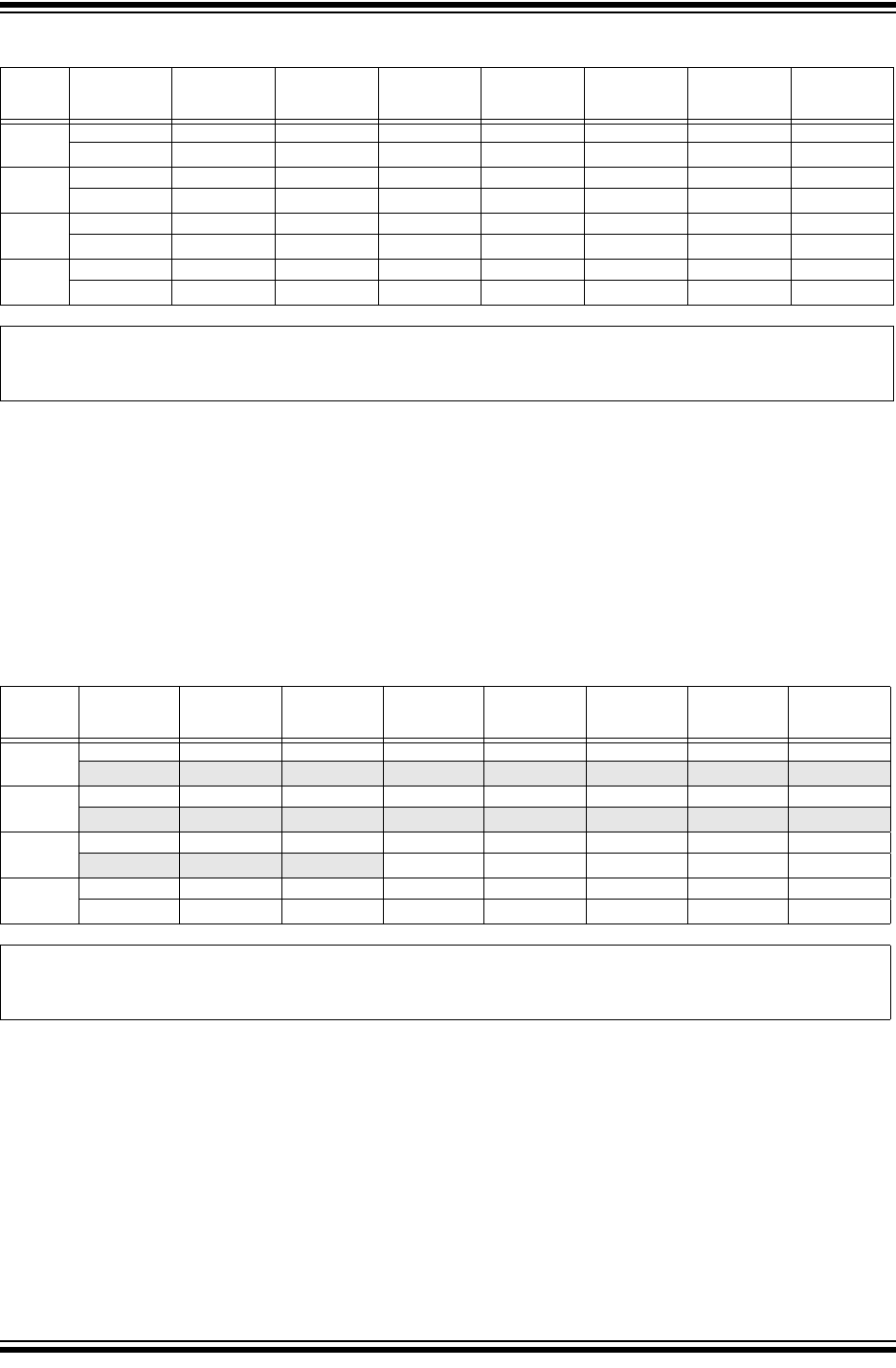
2015 Microchip Technology Inc. Preliminary DS60001320B-page 461
PIC32MZ Embedded Connectivity with Floating Point Unit (EF) Family
REGISTER 28-12: ADCDSTAT1: ADC DATA READY STATUS REGISTER 1
Bit
Range Bit
31/23/15/7 Bit
30/22/14/6 Bit
29/21/13/5 Bit
28/20/12/4 Bit
27/19/11/3 Bit
26/18/10/2 Bit
25/17/9/1 Bit
24/16/8/0
31:24 R-0, HS, HC R-0, HS, HC R-0, HS, HC R-0, HS, HC R-0, HS, HC R-0, HS, HC R-0, HS, HC R-0, HS, HC
ARDY31(1) ARDY30(1) ARDY29(1) ARDY28(1) ARDY27(1) ARDY26(1) ARDY25(1) ARDY24(1)
23:16 R-0, HS, HC R-0, HS, HC R-0, HS, HC R-0, HS, HC R-0, HS, HC R-0, HS, HC R-0, HS, HC R-0, HS, HC
ARDY23(1) ARDY22(1) ARDY21(1) ARDY20(1) ARDY19(1) ARDY18 ARDY17 ARDY16
15:8 R-0, HS, HC R-0, HS, HC R-0, HS, HC R-0, HS, HC R-0, HS, HC R-0, HS, HC R-0, HS, HC R-0, HS, HC
ARDY15 ARDY14 ARDY13 ARDY12 ARDY11 ARDY10 ARDY9 ARDY8
7:0 R-0, HS, HC R-0, HS, HC R-0, HS, HC R-0, HS, HC R-0, HS, HC R-0, HS, HC R-0, HS, HC R-0, HS, HC
ARDY7 ARDY6 ARDY5 ARDY4 ARDY3 ARDY2 ARDY1 ARDY0
Legend: HS = Hardware Set HC = Hardware Cleared
R = Readable bit W = Writable bit U = Unimplemented bit, read as ‘0’
-n = Value at POR ‘1’ = Bit is set ‘0’ = Bit is cleared x = Bit is unknown
bit 31-0 ARDY31:ARDY0: Conversion Data Ready for Corresponding Analog Input Ready bits
1 = This bit is set when converted data is ready in the data register
0 = This bit is cleared when the associated data register is read
Note 1: This bit is not available on 64-pin devices.
REGISTER 28-13: ADCDSTAT2: ADC DATA READY STATUS REGISTER 2
Bit
Range Bit
31/23/15/7 Bit
30/22/14/6 Bit
29/21/13/5 Bit
28/20/12/4 Bit
27/19/11/3 Bit
26/18/10/2 Bit
25/17/9/1 Bit
24/16/8/0
31:24 U-0 U-0 U-0 U-0 U-0 U-0 U-0 U-0
————————
23:16 U-0 U-0 U-0 U-0 U-0 U-0 U-0 U-0
————————
15:8 U-0 U-0 U-0 R-0, HS, HC R-0, HS, HC R-0, HS, HC R-0, HS, HC R-0, HS, HC
— — — ARDY44 ARDY43 ARDY42(2) ARDY41(2) ARDY40(2)
7:0 R-0, HS, HC R-0, HS, HC R-0, HS, HC R-0, HS, HC R-0, HS, HC R-0, HS, HC R-0, HS, HC R-0, HS, HC
ARDY39(2) ARDY38(2) ARDY37(2) ARDY36(2) ARDY35(2) ARDY34(1) ARDY33(1) ARDY32(1)
Legend: HS = Hardware Set HC = Hardware Cleared
R = Readable bit W = Writable bit U = Unimplemented bit, read as ‘0’
-n = Value at POR ‘1’ = Bit is set ‘0’ = Bit is cleared x = Bit is unknown
bit 31-13 Unimplemented: Read as ‘0’
bit 12-0 ARDY44:ARDY32: Conversion Data Ready for Corresponding Analog Input Ready bits
1 = This bit is set when converted data is ready in the data register
0 = This bit is cleared when the associated data register is read
Note 1: This bit is not available on 64-pin devices.
2: This bit is not available on 64 -pin and 100-pin devices.

PIC32MZ Embedded Connectivity with Floating Point Unit (EF) Family
DS60001320B-page 462 Preliminary 2015 Microchip Technology Inc.
REGISTER 28-14: ADCCMPENx: ADC DIGITAL COMPARATOR ‘x’ ENABLE REGISTER
(‘x’ = 1 THROUGH 6)
Bit
Range Bit
31/23/15/7 Bit
30/22/14/6 Bit
29/21/13/5 Bit
28/20/12/4 Bit
27/19/11/3 Bit
26/18/10/2 Bit
25/17/9/1 Bit
24/16/8/0
31:24 R/W-0 R/W-0 R/W-0 R/W-0 R/W-0 R/W-0 R/W-0 R/W-0
CMPE31(1) CMPE30(1) CMPE29(1) CMPE28(1) CMPE27(1) CMPE26(1) CMPE25(1) CMPE24(1)
23:16 R/W-0 R/W-0 R/W-0 R/W-0 R/W-0 R/W-0 R/W-0 R/W-0
CMPE23(1) CMPE22(1) CMPE21(1) CMPE20(1) CMPE19(1) CMPE18 CMPE17 CMPE16
15:8 R/W-0 R/W-0 R/W-0 R/W-0 R/W-0 R/W-0 R/W-0 R/W-0
CMPE15 CMPE14 CMPE13 CMPE12 CMPE11 CMPE10 CMPE9 CMPE8
7:0 R/W-0 R/W-0 R/W-0 R/W-0 R/W-0 R/W-0 R/W-0 R/W-0
CMPE7 CMPE6 CMPE5 CMPE4 CMPE3 CMPE2 CMPE1 CMPE0
Legend:
R = Readable bit W = Writable bit U = Unimplemented bit, read as ‘0’
-n = Value at POR ‘1’ = Bit is set ‘0’ = Bit is cleared x = Bit is unknown
bit 31-0 CMPE31:CMPE0: ADC Digital Comparator ‘x’ Enable bits
These bits enable conversion results corresponding to the Analog Input to be processed by the Digital
Comparator. CMPE0 enables AN0, CMPE1 enables AN1, and so on.
Note 1: This bit is not available on 64-pin devices.
Note 1: CMPEx = ANx, where ‘x’ = 0-31 (Digital Comparator inputs are limited to AN0 through AN31).
2: Changing the bits in this register while the Digital Comparator is enabled (ENDCMP = 1) can result in
unpredictable behavior.

2015 Microchip Technology Inc. Preliminary DS60001320B-page 463
PIC32MZ Embedded Connectivity with Floating Point Unit (EF) Family
REGISTER 28-15: ADCCMPx: ADC DIGITAL COMPARATOR ‘x’ LIMIT VALUE REGISTER
(‘x’ = 1 THROUGH 6)
Bit Range Bit
31/23/15/7 Bit
30/22/14/6 Bit
29/21/13/5 Bit
28/20/12/4 Bit
27/19/11/3 Bit
26/18/10/2 Bit
25/17/9/1 Bit
24/16/8/0
31:24 R/W-0 R/W-0 R/W-0 R/W-0 R/W-0 R/W-0 R/W-0 R/W-0
DCMPHI<15:8>(1,2,3)
23:16 R/W-0 R/W-0 R/W-0 R/W-0 R/W-0 R/W-0 R/W-0 R/W-0
DCMPHI<7:0>(1,2,3)
15:8 R/W-0 R/W-0 R/W-0 R/W-0 R/W-0 R/W-0 R/W-0 R/W-0
DCMPLO<15:8>(1,2,3)
7:0 R/W-0 R/W-0 R/W-0 R/W-0 R/W-0 R/W-0 R/W-0 R/W-0
DCMPLO<7:0>(1,2,3)
Legend:
R = Readable bit W = Writable bit U = Unimplemented bit, read as ‘0’
-n = Value at POR ‘1’ = Bit is set ‘0’ = Bit is cleared x = Bit is unknown
bit 31-16 DCMPHI<15:0>: Digital Comparator ‘x’ High Limit Value bits(1,2,3)
These bits store the high limit value, which is used by digital comparator for comparisons with ADC
converted data.
bit 15-0 DCMPLO<15:0>: Digital Comparator ‘x’ Low Limit Value bits(1,2,3)
These bits store the low limit value, which is used by digital comparator for comparisons with ADC
converted data.
Note 1: Changing theses bits while the Digital Comparator is enabled (ENDCMP = 1) can result in unpredictable
behavior.
2: The format of the limit values should match the format of the ADC converted value in terms of sign and
fractional settings.
3: For Digital Comparator 0 used in CVD mode, the DCMPHI<15:0> and DCMPLO<15:0> bits must always
be specified in signed format, as the CVD output data is differential and is always signed.

PIC32MZ Embedded Connectivity with Floating Point Unit (EF) Family
DS60001320B-page 464 Preliminary 2015 Microchip Technology Inc.
REGISTER 28-16: ADCFLTRx: ADC DIGITAL FILTER ‘x’ REGISTER (‘x’ = 1 THROUGH 6)
Bit
Range Bit
31/23/15/7 Bit
30/22/14/6 Bit
29/21/13/5 Bit
28/20/12/4 Bit
27/19/11/3 Bit
26/18/10/2 Bit
25/17/9/1 Bit
24/16/8/0
31:24 R/W-0 R/W-0 R/W-0 R/W-0 R/W-0 R/W-0 R/W-0 R-0, HS, HC
AFEN DATA16EN DFMODE OVRSAM<2:0> AFGIEN AFRDY
23:16 U-0 U-0 U-0 R/W-0 R/W-0 R/W-0 R/W-0 R/W-0
— — — CHNLID<4:0>
15:8 R-0, HS, HC R-0, HS, HC R-0, HS, HC R-0, HS, HC R-0, HS, HC R-0, HS, HC R-0, HS, HC R-0, HS, HC
FLTRDATA<15:8>
7:0 R-0, HS, HC R-0, HS, HC R-0, HS, HC R-0, HS, HC R-0, HS, HC R-0, HS, HC R-0, HS, HC R-0, HS, HC
FLTRDATA<7:0>
Legend: HS = Hardware Set HC = Hardware Cleared
R = Readable bit W = Writable bit U = Unimplemented bit, read as ‘0’
-n = Value at POR ‘1’ = Bit is set ‘0’ = Bit is cleared x = Bit is unknown
bit 31 AFEN: Digital Filter ‘x’ Enable bit
1 = Digital filter is enabled
0 = Digital filter is disabled and the AFRDY status bit is cleared
bit 30 DATA16EN: Filter Significant Data Length bit
1 = All 16 bits of the filter output data are significant
0 = Only the first 12 bits are significant, followed by four zeros
Note: This bit is significant only if DFMODE = 1 (Averaging Mode) and FRACT (ADCCON1<23>) = 1
(Fractional Output Mode).
bit DFMODE: ADC Filter Mode bit
1 = Filter ‘x’ works in Averaging mode
0 = Filter ‘x’ works in Oversampling Filter mode (default)
bit 28-26 OVRSAM<2:0>: Oversampling Filter Ratio bits
If DFMODE is ‘0’:
111 = 128 samples (shift sum 3 bits to right, output data is in 15.1 format)
110 = 32 samples (shift sum 2 bits to right, output data is in 14.1 format)
101 = 8 samples (shift sum 1 bit to right, output data is in 13.1 format)
100 = 2 samples (shift sum 0 bits to right, output data is in 12.1 format)
011 = 256 samples (shift sum 4 bits to right, output data is 16 bits)
010 = 64 samples (shift sum 3 bits to right, output data is 15 bits)
001 = 16 samples (shift sum 2 bits to right, output data is 14 bits)
000 = 4 samples (shift sum 1 bit to right, output data is 13 bits)
If DFMODE is ‘1’:
111 = 256 samples (256 samples to be averaged)
110 = 128 samples (128 samples to be averaged)
101 = 64 samples (64 samples to be averaged)
100 = 32 samples (32 samples to be averaged)
011 = 16 samples (16 samples to be averaged)
010 = 8 samples (8 samples to be averaged)
001 = 4 samples (4 samples to be averaged)
000 = 2 samples (2 samples to be averaged)
bit 25 AFGIEN: Digital Filter ‘x’ Interrupt Enable bit
1 = Digital filter interrupt is enabled and is generated by the AFRDY status bit
0 = Digital filter is disabled

2015 Microchip Technology Inc. Preliminary DS60001320B-page 465
PIC32MZ Embedded Connectivity with Floating Point Unit (EF) Family
bit 24 AFRDY: Digital Filter ‘x’ Data Ready Status bit
1 = Data is ready in the FLTRDATA<15:0> bits
0 = Data is not ready
Note: This bit is cleared by reading the FLTRDATA<15:0> bits or by disabling the Digital Filter module
(by setting AFEN to ‘0’).
bit 23-21 Unimplemented: Read as ‘0’
bit 20-16 CHNLID<4:0>: Digital Filter Analog Input Selection bits
These bits specify the analog input to be used as the oversampling filter data source.
11111 = AN31
•
•
•
00010 = AN2
00001 = AN1
00000 = AN0
Note: Only the first 32 analog inputs (Class 1 and Class 2) can use a digital filter.
bit 15-0 FLTRDATA<15:0>: Digital Filter ‘x’ Data Output Value bits
The filter output data is as per the fractional format set in the FRACT (ADCCON1<23>) bit. The FRACT bit
should not be changed while the filter is enabled. Changing the state of the FRACT bit after the operation
of the filter ended will not update the value of FLTRDATA<15:0> to reflect the new format.
REGISTER 28-16: ADCFLTRx: ADC DIGITAL FILTER ‘x’ REGISTER (‘x’ = 1 THROUGH 6)

PIC32MZ Embedded Connectivity with Floating Point Unit (EF) Family
DS60001320B-page 466 Preliminary 2015 Microchip Technology Inc.
REGISTER 28-17: ADCTRG1: ADC TRIGGER SOURCE 1 REGISTER
Bit
Range Bit
31/23/15/7 Bit
30/22/14/6 Bit
29/21/13/5 Bit
28/20/12/4 Bit
27/19/11/3 Bit
26/18/10/2 Bit
25/17/9/1 Bit
24/16/8/0
31:24 U-0 U-0 U-0 R/W-0 R/W-0 R/W-0 R/W-0 R/W-0
— — — TRGSRC3<4:0>
23:16 U-0 U-0 U-0 R/W-0 R/W-0 R/W-0 R/W-0 R/W-0
— — — TRGSRC2<4:0>
15:8 U-0 U-0 U-0 R/W-0 R/W-0 R/W-0 R/W-0 R/W-0
— — — TRGSRC1<4:0>
7:0 U-0 U-0 U-0 R/W-0 R/W-0 R/W-0 R/W-0 R/W-0
— — — TRGSRC0<4:0>
Legend:
R = Readable bit W = Writable bit U = Unimplemented bit, read as ‘0’
-n = Value at POR ‘1’ = Bit is set ‘0’ = Bit is cleared x = Bit is unknown
bit 31-29 Unimplemented: Read as ‘0’
bit 28-24 TRGSRC3<4:0>: Trigger Source for Conversion of Analog Input AN3 Select bits
11111 = Reserved
•
•
•
01101 = Reserved
01100 = Comparator 2 (COUT)
01011 = Comparator 1 (COUT)
01010 = OCMP5
01001 = OCMP3
01000 = OCMP1
00111 = TMR5 match
00110 = TMR3 match
00101 = TMR1 match
00100 = INT0 External interrupt
00011 = STRIG
00010 = Global level software trigger (GLSWTRG)
00001 = Global software edge Trigger (GSWTRG)
00000 = No Trigger
For STRIG, in addition to setting the trigger, it also requires programming of the STRGSRC<4:0> bits
(ADCCON1<20:16>) to select the trigger source, and requires the appropriate CSS bits to be set in the
ADCCSSx registers.
bit 23-21 Unimplemented: Read as ‘0’
bit 20-16 TRGSRC2<4:0>: Trigger Source for Conversion of Analog Input AN2 Select bits
See bits 28-24 for bit value definitions.
bit 15-13 Unimplemented: Read as ‘0’
bit 12-8 TRGSRC1<4:0>: Trigger Source for Conversion of Analog Input AN1 Select bits
See bits 28-24 for bit value definitions.
bit 7-5 Unimplemented: Read as ‘0’
bit 4-0 TRGSRC0<4:0>: Trigger Source for Conversion of Analog Input AN0 Select bits
See bits 28-24 for bit value definitions.

2015 Microchip Technology Inc. Preliminary DS60001320B-page 467
PIC32MZ Embedded Connectivity with Floating Point Unit (EF) Family
REGISTER 28-18: ADCTRG2: ADC TRIGGER SOURCE 2 REGISTER
Bit
Range Bit
31/23/15/7 Bit
30/22/14/6 Bit
29/21/13/5 Bit
28/20/12/4 Bit
27/19/11/3 Bit
26/18/10/2 Bit
25/17/9/1 Bit
24/16/8/0
31:24 U-0 U-0 U-0 R/W-0 R/W-0 R/W-0 R/W-0 R/W-0
— — — TRGSRC7<4:0>
23:16 U-0 U-0 U-0 R/W-0 R/W-0 R/W-0 R/W-0 R/W-0
— — — TRGSRC6<4:0>
15:8 U-0 U-0 U-0 R/W-0 R/W-0 R/W-0 R/W-0 R/W-0
— — — TRGSRC5<4:0>
7:0 U-0 U-0 U-0 R/W-0 R/W-0 R/W-0 R/W-0 R/W-0
— — — TRGSRC4<4:0>
Legend:
R = Readable bit W = Writable bit U = Unimplemented bit, read as ‘0’
-n = Value at POR ‘1’ = Bit is set ‘0’ = Bit is cleared x = Bit is unknown
bit 31-29 Unimplemented: Read as ‘0’
bit 28-24 TRGSRC7<4:0>: Trigger Source for Conversion of Analog Input AN7 Select bits
11111 = Reserved
•
•
•
01101 = Reserved
01100 = Comparator 2 (COUT)
01011 = Comparator 1 (COUT)
01010 = OCMP5
01001 = OCMP3
01000 = OCMP1
00111 = TMR5 match
00110 = TMR3 match
00101 = TMR1 match
00100 = INT0 External interrupt
00011 = STRIG
00010 = Global level software trigger (GLSWTRG)
00001 = Global software edge Trigger (GSWTRG)
00000 = No Trigger
For STRIG, in addition to setting the trigger, it also requires programming of the STRGSRC<4:0> bits
(ADCCON1<20:16>) to select the trigger source, and requires the appropriate CSS bits to be set in the
ADCCSSx registers.
bit 23-21 Unimplemented: Read as ‘0’
bit 20-16 TRGSRC6<4:0>: Trigger Source for Conversion of Analog Input AN6 Select bits
See bits 28-24 for bit value definitions.
bit 15-13 Unimplemented: Read as ‘0’
bit 12-8 TRGSRC5<4:0>: Trigger Source for Conversion of Analog Input AN5 Select bits
See bits 28-24 for bit value definitions.
bit 7-5 Unimplemented: Read as ‘0’
bit 4-0 TRGSRC4<4:0>: Trigger Source for Conversion of Analog Input AN4 Select bits
See bits 28-24 for bit value definitions.

PIC32MZ Embedded Connectivity with Floating Point Unit (EF) Family
DS60001320B-page 468 Preliminary 2015 Microchip Technology Inc.
REGISTER 28-19: ADCTRG3: ADC TRIGGER SOURCE 3 REGISTER
Bit
Range Bit
31/23/15/7 Bit
30/22/14/6 Bit
29/21/13/5 Bit
28/20/12/4 Bit
27/19/11/3 Bit
26/18/10/2 Bit
25/17/9/1 Bit
24/16/8/0
31:24 U-0 U-0 U-0 R/W-0 R/W-0 R/W-0 R/W-0 R/W-0
— — — TRGSRC11<4:0>
23:16 U-0 U-0 U-0 R/W-0 R/W-0 R/W-0 R/W-0 R/W-0
— — — TRGSRC10<4:0>
15:8 U-0 U-0 U-0 R/W-0 R/W-0 R/W-0 R/W-0 R/W-0
— — — TRGSRC9<4:0>
7:0 U-0 U-0 U-0 R/W-0 R/W-0 R/W-0 R/W-0 R/W-0
— — — TRGSRC8<4:0>
Legend:
R = Readable bit W = Writable bit U = Unimplemented bit, read as ‘0’
-n = Value at POR ‘1’ = Bit is set ‘0’ = Bit is cleared x = Bit is unknown
bit 31-29 Unimplemented: Read as ‘0’
bit 28-24 TRGSRC11<4:0>: Trigger Source for Conversion of Analog Input AN11 Select bits
11111 = Reserved
•
•
•
01101 = Reserved
01100 = Comparator 2 (COUT)
01011 = Comparator 1 (COUT)
01010 = OCMP5
01001 = OCMP3
01000 = OCMP1
00111 = TMR5 match
00110 = TMR3 match
00101 = TMR1 match
00100 = INT0 External interrupt
00011 = STRIG
00010 = Global level software trigger (GLSWTRG)
00001 = Global software edge Trigger (GSWTRG)
00000 = No Trigger
For STRIG, in addition to setting the trigger, it also requires programming of the STRGSRC<4:0> bits
(ADCCON1<20:16>) to select the trigger source, and requires the appropriate CSS bits to be set in the
ADCCSSx registers.
bit 23-21 Unimplemented: Read as ‘0’
bit 20-16 TRGSRC10<4:0>: Trigger Source for Conversion of Analog Input AN10 Select bits
See bits 28-24 for bit value definitions.
bit 15-13 Unimplemented: Read as ‘0’
bit 12-8 TRGSRC9<4:0>: Trigger Source for Conversion of Analog Input AN9 Select bits
See bits 28-24 for bit value definitions.
bit 7-5 Unimplemented: Read as ‘0’
bit 4-0 TRGSRC8<4:0>: Trigger Source for Conversion of Analog Input AN8 Select bits
See bits 28-24 for bit value definitions.

2015 Microchip Technology Inc. Preliminary DS60001320B-page 469
PIC32MZ Embedded Connectivity with Floating Point Unit (EF) Family
REGISTER 28-20: ADCCMPCON1: ADC DIGITAL COMPARATOR 1 CONTROL REGISTER
Bit
Range Bit
31/23/15/7 Bit
30/22/14/6 Bit
29/21/13/5 Bit
28/20/12/4 Bit
27/19/11/3 Bit
26/18/10/2 Bit
25/17/9/1 Bit
24/16/8/0
31:24 R-0, HS, HC R-0, HS, HC R-0, HS, HC R-0, HS, HC R-0, HS, HC R-0, HS, HC R-0, HS, HC R-0, HS, HC
CVDDATA<15:8>
23:16 R-0, HS, HC R-0, HS, HC R-0, HS, HC R-0, HS, HC R-0, HS, HC R-0, HS, HC R-0, HS, HC R-0, HS, HC
CVDDATA<7:0>
15:8 U-0 U-0 R-0, HS, HC R-0, HS, HC R-0, HS, HC R-0, HS, HC R-0, HS, HC R-0, HS, HC
—— AINID<5:0>
7:0 R/W-0 R/W-0 R-0, HS, HC R/W-0 R/W-0 R/W-0 R/W-0 R/W-0
ENDCMP DCMPGIEN DCMPED IEBTWN IEHIHI IEHILO IELOHI IELOLO
Legend: HS = Hardware Set HC = Hardware Cleared
R = Readable bit W = Writable bit U = Unimplemented bit, read as ‘0’
-n = Value at POR ‘1’ = Bit is set ‘0’ = Bit is cleared x = Bit is unknown
bit 31-16 CVDDATA<15:0>: CVD Data Status bits
In CVD mode, these bits obtain the CVD differential output data (subtraction of CVD positive and negative
measurement), whenever a Digital Comparator interrupt is generated. The value in these bits is compliant
with the FRACT bit (ADCCON1<23>) and is always signed.
bit 15-14 Unimplemented: Read as ‘0’
bit 13-8 AINID<5:0>: Digital Comparator 0 Analog Input Identification (ID) bits
When a digital comparator event occurs (DCMPED = 1), these bits identify the analog input being
monitored by Digital Comparator 0.
Note: In normal ADC mode, only analog inputs <31:0> can be processed by the Digital Comparator 0.
The Digital Comparator 0 also supports the CVD mode, in which all Class 2 and Class 3 analog
inputs may be stored in the AINID<5:0> bits.
111111 = Reserved
•
•
•
101101 = Reserved
101100 = AN44 is being monitored
101011 = AN43 is being monitored
•
•
•
000001 = AN1 is being monitored
000000 = AN0 is being monitored
bit 7 ENDCMP: Digital Comparator 0 Enable bit
1 = Digital Comparator 0 is enabled
0 = Digital Comparator 0 is not enabled, and the DCMPED status bit (ADCCMP0CON<5>) is cleared
bit 6 DCMPGIEN: Digital Comparator 0 Global Interrupt Enable bit
1 = A Digital Comparator 0 interrupt is generated when the DCMPED status bit (ADCCMP0CON<5>) is set
0 = A Digital Comparator 0 interrupt is disabled
bit 5 DCMPED: Digital Comparator 0 “Output True” Event Status bit
The logical conditions under which the digital comparator gets “True” are defined by the IEBTWN, IEHIHI,
IEHILO, IELOHI, and IELOLO bits.
Note: This bit is cleared by reading the AINID<5:0> bits or by disabling the Digital Comparator module
(by setting ENDCMP to ‘0’).
1 = Digital Comparator 0 output true event has occurred (output of Comparator is ‘1’)
0 = Digital Comparator 0 output is false (output of comparator is ‘0’)
bit 4 IEBTWN: Between Low/High Digital Comparator 0 Event bit
1 = Generate a digital comparator event when DCMPLO<15:0> DATA<31:0> < DCMPHI<15:0>
0 = Do not generate a digital comparator event

PIC32MZ Embedded Connectivity with Floating Point Unit (EF) Family
DS60001320B-page 470 Preliminary 2015 Microchip Technology Inc.
bit 3 IEHIHI: High/High Digital Comparator 0 Event bit
1 = Generate a Digital Comparator 0 Event when DCMPHI<15:0> DATA<31:0>
0 = Do not generate an event
bit 2 IEHILO: High/Low Digital Comparator 0 Event bit
1 = Generate a Digital Comparator 0 Event when DATA<31:0> < DCMPHI<15:0>
0 = Do not generate an event
bit 1 IELOHI: Low/High Digital Comparator 0 Event bit
1 = Generate a Digital Comparator 0 Event when DCMPLO<15:0> DATA<31:0>
0 = Do not generate an event
bit 0 IELOLO: Low/Low Digital Comparator 0 Event bit
1 = Generate a Digital Comparator 0 Event when DATA<31:0> < DCMPLO<15:0>
0 = Do not generate an event
REGISTER 28-20: ADCCMPCON1: ADC DIGITAL COMPARATOR 1 CONTROL REGISTER

2015 Microchip Technology Inc. Preliminary DS60001320B-page 471
PIC32MZ Embedded Connectivity with Floating Point Unit (EF) Family
REGISTER 28-21: ADCCMPCONx: ADC DIGITAL COMPARATOR ‘x’ CONTROL REGISTER
(‘x’ = 2 THROUGH 6)
Bit
Range Bit
31/23/15/7 Bit
30/22/14/6 Bit
29/21/13/5 Bit
28/20/12/4 Bit
27/19/11/3 Bit
26/18/10/2 Bit
25/17/9/1 Bit
24/16/8/0
31:24 U-0 U-0 U-0 U-0 U-0 U-0 U-0 U-0
— — — — — — — —
23:16 U-0 U-0 U-0 U-0 U-0 U-0 U-0 U-0
— — — — — — — —
15:8 U-0 U-0 U-0 R-0, HS, HC R-0, HS, HC R-0, HS, HC R-0, HS, HC R-0, HS, HC
— — — AINID<4:0>
7:0 R/W-0 R/W-0 R-0, HS, HC R/W-0 R/W-0 R/W-0 R/W-0 R/W-0
ENDCMP DCMPGIEN DCMPED IEBTWN IEHIHI IEHILO IELOHI IELOLO
Legend: HS = Hardware Set HC = Hardware Cleared
R = Readable bit W = Writable bit U = Unimplemented bit, read as ‘0’
-n = Value at POR ‘1’ = Bit is set ‘0’ = Bit is cleared x = Bit is unknown
bit 31-13 Unimplemented: Read as ‘0’
bit 12-8 AINID<4:0>: Digital Comparator ‘x’ Analog Input Identification (ID) bits
When a digital comparator event occurs (DCMPED = 1), these bits identify the analog input being
monitored by the Digital Comparator.
Note: Only analog inputs <31:0> can be processed by the Digital Comparator module ‘x’ (‘x’ = 1-5).
11111 = AN31 is being monitored
11110 = AN30 is being monitored
•
•
•
00001 = AN1 is being monitored
00000 = AN0 is being monitored
bit 7 ENDCMP: Digital Comparator ‘x’ Enable bit
1 = Digital Comparator ‘x’ is enabled
0 = Digital Comparator ‘x’ is not enabled, and the DCMPED status bit (ADCCMPxCON<5>) is cleared
bit 6 DCMPGIEN: Digital Comparator ‘x’ Global Interrupt Enable bit
1 = A Digital Comparator ‘x’ interrupt is generated when the DCMPED status bit (ADCCMPxCON<5>) is set
0 = A Digital Comparator ‘x’ interrupt is disabled
bit 5 DCMPED: Digital Comparator ‘x’ “Output True” Event Status bit
The logical conditions under which the digital comparator gets “True” are defined by the IEBTWN, IEHIHI,
IEHILO, IELOHI and IELOLO bits.
Note: This bit is cleared by reading the AINID<5:0> bits (ADCCMP0CON<13:8>) or by disabling the
Digital Comparator module (by setting ENDCMP to ‘0’).
1 = Digital Comparator ‘x’ output true event has occurred (output of Comparator is ‘1’)
0 = Digital Comparator ‘x’ output is false (output of Comparator is ‘0’)
bit 4 IEBTWN: Between Low/High Digital Comparator ‘x’ Event bit
1 = Generate a digital comparator event when the DCMPLO<15:0> bits DATA<31:0> bits
< DCMPHI<15:0> bits
0 = Do not generate a digital comparator event
bit 3 IEHIHI: High/High Digital Comparator ‘x’ Event bit
1 = Generate a Digital Comparator ‘x’ Event when the DCMPHI<15:0> bits DATA<31:0> bits
0 = Do not generate an event
bit 2 IEHILO: High/Low Digital Comparator ‘x’ Event bit
1 = Generate a Digital Comparator ‘x’ Event when the DATA<31:0> bits < DCMPHI<15:0> bits
0 = Do not generate an event

PIC32MZ Embedded Connectivity with Floating Point Unit (EF) Family
DS60001320B-page 472 Preliminary 2015 Microchip Technology Inc.
bit 1 IELOHI: Low/High Digital Comparator ‘x’ Event bit
1 = Generate a Digital Comparator ‘x’ Event when the DCMPLO<15:0> bits DATA<31:0> bits
0 = Do not generate an event
bit 0 IELOLO: Low/Low Digital Comparator ‘x’ Event bit
1 = Generate a Digital Comparator ‘x’ Event when the DATA<31:0> bits < DCMPLO<15:0> bits
0 = Do not generate an event
REGISTER 28-21: ADCCMPCONx: ADC DIGITAL COMPARATOR ‘x’ CONTROL REGISTER
(‘x’ = 2 THROUGH 6) (CONTINUED)

2015 Microchip Technology Inc. Preliminary DS60001320B-page 473
PIC32MZ Embedded Connectivity with Floating Point Unit (EF) Family
REGISTER 28-22: ADCFSTAT: ADC FIFO STATUS REGISTER
Bit Range Bit
31/23/15/7 Bit
30/22/14/6 Bit
29/21/13/5 Bit
28/20/12/4 Bit
27/19/11/3 Bit
26/18/10/2 Bit
25/17/9/1 Bit
24/16/8/0
31:24 R/W-0 U-0 U-0 R/W-0 R/W-0 R/W-0 R/W-0 R/W-0
FEN —— ADC4EN ADC3EN ADC2EN ADC1EN ADC0EN
23:16 R/W-0 R-0, HS, HC R-0, HS, HC U-0 U-0 U-0 U-0 U-0
FIEN FRDY FWROVERR — — — — —
15:8 R-0 R-0 R-0 R-0 R-0 R-0 R-0 R-0
FCNT<7:0>
7:0 R-0 U-0 U-0 U-0 U-0 R-0 R-0 R-0
FSIGN — — — —ADCID<2:0>
Legend: HS = Hardware Set HC = Hardware Cleared
R = Readable bit W = Writable bit U = Unimplemented bit, read as ‘0’
-n = Value at POR ‘1’ = Bit is set ‘0’ = Bit is cleared x = Bit is unknown
bit 31 FEN: FIFO Enable bit
1 = FIFO is enabled
0 = FIFO is disabled; no data is being saved into the FIFO
bit 30-29 Unimplemented: Read as ‘0’
bit 28-24 ADC4EN:ADC0EN: ADCx Enable bits (‘x’ = 0 through 4)
1 = Converted output data of ADCx is stored in the FIFO
0 = Converted output data of ADCx is not stored in the FIFO
Note: While using FIFO, the output data is additionally stored in the respective output data register
(ADCDATAx).
bit 23 FIEN: FIFO Interrupt Enable bit
1 = FIFO interrupts are enabled; an interrupt is generated once the FRDY bit is set
0 = FIFO interrupts are disabled
bit 22 FRDY: FIFO Data Ready Interrupt Status bit
1 = FIFO has data to be read
0 = No data is available in the FIFO
Note: This bit is cleared when the FIFO output data in ADCFIFO has been read and there is no
additional data ready in the FIFO (that is, the FIFO is empty).
bit 21 FWROVERR: FIFO Write Overflow Error Status bit
1 = A write overflow error in the FIFO has occurred (circular FIFO)
0 = A write overflow error in the FIFO has not occurred
Note: This bit is cleared after ADCFSTAT<23:16> are read by software.
bit 15-8 FCNT<7:0>: FIFO Data Entry Count Status bit
The value in these bits indicates the number of data entries in the FIFO.
bit 7 FSIGN: FIFO Sign Setting bit
This bit reflects the sign of data stored in the ADCFIFO register.
bit 6-3 Unimplemented: Read as ‘0’
bit 2-0 ADCID<2:0>: ADCx Identifier bits (‘x’ = 0 through 6)
These bits specify the ADC module whose data is stored in the FIFO.
111 = Reserved
110 = Converted data of ADC6 is stored in FIFO
•
•
•
000 = Converted data of ADC0 is stored in FIFO

PIC32MZ Embedded Connectivity with Floating Point Unit (EF) Family
DS60001320B-page 474 Preliminary 2015 Microchip Technology Inc.
REGISTER 28-23: ADCFIFO: ADC FIFO DATA REGISTER
Bit Range Bit
31/23/15/7 Bit
30/22/14/6 Bit
29/21/13/5 Bit
28/20/12/4 Bit
27/19/11/3 Bit
26/18/10/2 Bit
25/17/9/1 Bit
24/16/8/0
31:24 R-0 R-0 R-0 R-0 R-0 R-0 R-0 R-0
DATA<31:24>
23:16 R-0 R-0 R-0 R-0 R-0 R-0 R-0 R-0
DATA<23:16>
15:8 R-0 R-0 R-0 R-0 R-0 R-0 R-0 R-0
DATA<15:8>
7:0 R-0 R-0 R-0 R-0 R-0 R-0 R-0 R-0
DATA<7:0>
Legend:
R = Readable bit W = Writable bit U = Unimplemented bit, read as ‘0’
-n = Value at POR ‘1’ = Bit is set ‘0’ = Bit is cleared x = Bit is unknown
bit 31-0 DATA<31:0>: FIFO Data Output Value bits
Note: When an alternate input is used as the input source for a dedicated ADC module, the data output is still read
from the Primary input Data Output Register.

2015 Microchip Technology Inc. Preliminary DS60001320B-page 475
PIC32MZ Embedded Connectivity with Floating Point Unit (EF) Family
REGISTER 28-24: ADCBASE: ADC BASE REGISTER
Bit Range Bit
31/23/15/7 Bit
30/22/14/6 Bit
29/21/13/5 Bit
28/20/12/4 Bit
27/19/11/3 Bit
26/18/10/2 Bit
25/17/9/1 Bit
24/16/8/0
31:24 U-0 U-0 U-0 U-0 U-0 U-0 U-0 U-0
— — — — — — — —
23:16 U-0 U-0 U-0 U-0 U-0 U-0 U-0 U-0
— — — — — — — —
15:8 R/W-0 R/W-0 R/W-0 R/W-0 R/W-0 R/W-0 R/W-0 R/W-0
ADCBASE<15:8>
7:0 R/W-0 R/W-0 R/W-0 R/W-0 R/W-0 R/W-0 R/W-0 R/W-0
ADCBASE<7:0>
Legend:
R = Readable bit W = Writable bit U = Unimplemented bit, read as ‘0’
-n = Value at POR ‘1’ = Bit is set ‘0’ = Bit is cleared x = Bit is unknown
bit 31-0 Unimplemented: Read as ‘0’
bit 15-0 ADCBASE<15:0>: ADC ISR Base Address bits
This register, when read, contains the base address of the user's ADC ISR jump table. The interrupt vector
address is determined by the IRQVS<2:0> bits of the ADCCON1 register specifying the amount of left
shift done to the ARDYx status bits in the ADCDSTAT1 and ADCDSTAT2 registers, prior to adding with
ADCBASE register.
Interrupt Vector Address = Read Value of ADCBASE and Read Value of ADCBASE = Value written to
ADCBASE + x << IRQVS<2:0>, where ‘x’ is the smallest active analog input ID from the ADCDSTAT1 or
ADCDSTAT2 registers (which has highest priority).

PIC32MZ Embedded Connectivity with Floating Point Unit (EF) Family
DS60001320B-page 476 Preliminary 2015 Microchip Technology Inc.
REGISTER 28-25: ADCDATAx: ADC OUTPUT DATA REGISTER (‘x’ = 0 THROUGH 44)
Bit Range Bit
31/23/15/7 Bit
30/22/14/6 Bit
29/21/13/5 Bit
28/20/12/4 Bit
27/19/11/3 Bit
26/18/10/2 Bit
25/17/9/1 Bit
24/16/8/0
31:24 R-0 R-0 R-0 R-0 R-0 R-0 R-0 R-0
DATA<31:24>
23:16 R-0 R-0 R-0 R-0 R-0 R-0 R-0 R-0
DATA<23:16>
15:8 R-0 R-0 R-0 R-0 R-0 R-0 R-0 R-0
DATA<15:8>
7:0 R-0 R-0 R-0 R-0 R-0 R-0 R-0 R-0
DATA<7:0>
Legend:
R = Readable bit W = Writable bit U = Unimplemented bit, read as ‘0’
-n = Value at POR ‘1’ = Bit is set ‘0’ = Bit is cleared x = Bit is unknown
bit 31-0 DATA<31:0>: ADC Converted Data Output bits.
Note 1: The registers, ADCDATA19 through ADCDATA34, are not available on 64-pin devices.
2: The registers, ADCDATA35 through ADCDATA44, are not available on 64-pin and 100-pin devices.
3: When an alternate input is used as the input source for a dedicated ADC module, the data output is still
read from the Primary input Data Output Register.
4: Reading the ADCDATAx register value after changing the FRACT bit converts the data into the format
specified by FRACT bit.

2015 Microchip Technology Inc. Preliminary DS60001320B-page 477
PIC32MZ Embedded Connectivity with Floating Point Unit (EF) Family
REGISTER 28-26: ADCTRGSNS: ADC TRIGGER LEVEL/EDGE SENSITIVITY REGISTER
Bit Range Bit
31/23/15/7 Bit
30/22/14/6 Bit
29/21/13/5 Bit
28/20/12/4 Bit
27/19/11/3 Bit
26/18/10/2 Bit
25/17/9/1 Bit
24/16/8/0
31:24 U-0 U-0 U-0 U-0 U-0 U-0 U-0 U-0
— — — — — — — —
23:16 U-0 U-0 U-0 U-0 U-0 U-0 U-0 U-0
— — — — — — — —
15:8 U-0 U-0 U-0 U-0 R/W-0 R/W-0 R/W-0 R/W-0
— — — — LVL11 LVL10 LVL9 LVL8
7:0 R/W-0 R/W-0 R/W-0 R/W-0 R/W-0 R/W-0 R/W-0 R/W-0
LVL7 LVL6 LVL5 LVL4 LVL3 LVL2 LVL1 LVL0
Legend:
R = Readable bit W = Writable bit U = Unimplemented bit, read as ‘0’
-n = Value at POR ‘1’ = Bit is set ‘0’ = Bit is cleared x = Bit is unknown
bit 31-12 Unimplemented: Read as ‘0’
bit 11 LVL11:LVL0: Trigger Level and Edge Sensitivity bits
1 = Analog input is sensitive to the high level of its trigger (level sensitivity implies retriggering as long as
the trigger signal remains high)
0 = Analog input is sensitive to the positive edge of its trigger (this is the value after a reset)
Note 1: This register specifies the trigger level for analog inputs 0 to 31.
2: The higher analog input ID belongs to Class 3, and therefore, is only scan triggered. All Class 3 analog
inputs use the Scan Trigger, for which the level/edge is defined by the STRGLVL bit (ADCCON1<3>).

PIC32MZ Embedded Connectivity with Floating Point Unit (EF) Family
DS60001320B-page 478 Preliminary 2015 Microchip Technology Inc.
REGISTER 28-27: ADCxTIME: DEDICATED ADCx TIMING REGISTER ‘x’ (‘x’ = 0 THROUGH 4)
Bit Range Bit
31/23/15/7 Bit
30/22/14/6 Bit
29/21/13/5 Bit
28/20/12/4 Bit
27/19/11/3 Bit
26/18/10/2 Bit
25/17/9/1 Bit
24/16/8/0
31:24 U-0 U-0 U-0 R/W-0 R/W-0 R/W-0 R/W-1 R/W-1
— — — ADCEIS<2:0> SELRES<1:0>
23:16 U-0 R/W-0 R/W-0 R/W-0 R/W-0 R/W-0 R/W-0 R/W-0
— ADCDIV<6:0>
15:8 U-0 U-0 U-0 U-0 U-0 U-0 R/W-0 R/W-0
— — — — — — SAMC<9:8>
7:0 R/W-0 R/W-0 R/W-0 R/W-0 R/W-0 R/W-0 R/W-0 R/W-0
SAMC<7:0>
Legend:
R = Readable bit W = Writable bit U = Unimplemented bit, read as ‘0’
-n = Value at POR ‘1’ = Bit is set ‘0’ = Bit is cleared x = Bit is unknown
bit 31-29 Unimplemented: Read as ‘0’
bit 28-26 ADCEIS<2:0>: ADCx Early Interrupt Select bits
111 = The data ready interrupt is generated 8 ADC clocks prior to the end of conversion
110 = The data ready interrupt is generated 7 ADC clocks prior to the end of conversion
•
•
•
001 = The data ready interrupt is generated 2 ADC clocks prior to the end of conversion
000 = The data ready interrupt is generated 1 ADC clock prior to the end of conversion
Note: All options are available when the selected resolution, specified by the SELRES<1:0> bits
(ADCxTIME<25:24>), is 12-bit or 10-bit. For a selected resolution of 8-bit, options from ‘000’
to ‘101’ are valid. For a selected resolution of 6-bit, options from ‘000’ to ‘011’ are valid.
bit 25-24 SELRES<1:0>: ADCx Resolution Select bits
11 = 12 bits
10 = 10 bits
01 = 8 bits
00 = 6 bits
bit 23 Unimplemented: Read as ‘0’
bit 22-16 ADCDIV<6:0>: ADCx Clock Divisor bits
These bits divide the ADC control clock with period TQ to generate the clock for ADCx (TADx).
1111111 = 254 * TQ = TADx
•
•
•
0000011 = 6 * TQ = TADx
0000010 = 4 * TQ = TADx
0000001 = 2 * TQ = TADx
0000000 = Reserved
bit 15-10 Unimplemented: Read as ‘0’
bit 9-0 SAMC<9:0>: ADCx Sample Time bits
Where TADx = period of the ADC conversion clock for the dedicated ADC controlled by the ADCDIV<6:0>
bits.
1111111111 = 1025 TADx
•
•
•
0000000001 = 3 TADx
0000000000 = 2 TADx
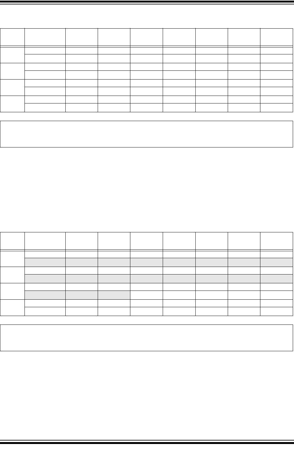
2015 Microchip Technology Inc. Preliminary DS60001320B-page 479
PIC32MZ Embedded Connectivity with Floating Point Unit (EF) Family
REGISTER 28-28: ADCEIEN1: ADC EARLY INTERRUPT ENABLE REGISTER 1
Bit
Range Bit
31/23/15/7 Bit
30/22/14/6 Bit
29/21/13/5 Bit
28/20/12/4 Bit
27/19/11/3 Bit
26/18/10/2 Bit
25/17/9/1 Bit
24/16/8/0
31:24 R/W-0 R/W-0 R/W-0 R/W-0 R/W-0 R/W-0 R/W-0 R/W-0
EIEN31(1) EIEN30(1) EIEN29(1) EIEN28(1) EIEN27(1) EIEN26(1) EIEN25(1) EIEN24(1)
23:16 R/W-0 R/W-0 R/W-0 R/W-0 R/W-0 R/W-0 R/W-0 R/W-0
EIEN23(1) EIEN22(1) EIEN21(1) EIEN20(1) EIEN19(1) EIEN18 EIEN17 EIEN16
15:8 R/W-0 R/W-0 R/W-0 R/W-0 R/W-0 R/W-0 R/W-0 R/W-0
EIEN15 EIEN14 EIEN13 EIEN12 EIEN11 EIEN10 EIEN9 EIEN8
7:0 R/W-0 R/W-0 R/W-0 R/W-0 R/W-0 R/W-0 R/W-0 R/W-0
EIEN7 EIEN6 EIEN5 EIEN4 EIEN3 EIEN2 EIEN1 EIEN0
Legend:
R = Readable bit W = Writable bit U = Unimplemented bit, read as ‘0’
-n = Value at POR ‘1’ = Bit is set ‘0’ = Bit is cleared x = Bit is unknown
bit 31-0 EIEN31:EIEN0: Early Interrupt Enable for Analog Input bits
1 = Early Interrupts are enabled for the selected analog input. The interrupt is generated after the early
interrupt event occurs (indicated by the EIRDYx bit ('x' = 31-0) of the ADCEISTAT1 register)
0 = Interrupts are disabled
Note 1: This bit is not available on 64-pin devices.
REGISTER 28-29: ADCEIEN2: ADC EARLY INTERRUPT ENABLE REGISTER 2
Bit
Range Bit
31/23/15/7 Bit
30/22/14/6 Bit
29/21/13/5 Bit
28/20/12/4 Bit
27/19/11/3 Bit
26/18/10/2 Bit
25/17/9/1 Bit
24/16/8/0
31:24 U-0 U-0 U-0 U-0 U-0 U-0 U-0 U-0
— ———————
23:16 U-0 U-0 U-0 U-0 U-0 U-0 U-0 U-0
— ———————
15:8 U-0 U-0 U-0 R/W-0 R/W-0 R/W-0 R/W-0 R/W-0
— — — EIEN44(2) EIEN43(2) EIEN42(2) EIEN41(2) EIEN40(2)
7:0 R/W-0 R/W-0 R/W-0 R/W-0 R/W-0 R/W-0 R/W-0 R/W-0
EIEN39(2) EIEN38(2) EIEN37(2) EIEN36(2) EIEN35(2) EIEN34(1) EIEN33(1) EIEN32(1)
Legend:
R = Readable bit W = Writable bit U = Unimplemented bit, read as ‘0’
-n = Value at POR ‘1’ = Bit is set ‘0’ = Bit is cleared x = Bit is unknown
bit 31-13 Unimplemented: Read as ‘0’
bit 12-0 EIEN44:EIEN32: Early Interrupt Enable for Analog Input bits
1 = Early Interrupts are enabled for the selected analog input. The interrupt is generated after the early
interrupt event occurs (indicated by the EIRDYx bit ('x' = 44-32) of the ADCEISTAT2 register)
0 = Interrupts are disabled
Note 1: This bit is not available on 64-pin devices.
2: This bit is not available on 64-pin and 100-pin devices.

PIC32MZ Embedded Connectivity with Floating Point Unit (EF) Family
DS60001320B-page 480 Preliminary 2015 Microchip Technology Inc.
REGISTER 28-30: ADCEISTAT1: ADC EARLY INTERRUPT STATUS REGISTER 1
Bit
Range Bit
31/23/15/7 Bit
30/22/14/6 Bit
29/21/13/5 Bit
28/20/12/4 Bit
27/19/11/3 Bit
26/18/10/2 Bit
25/17/9/1 Bit
24/16/8/0
31:24 R-0, HS, HC R-0, HS, HC R-0, HS, HC R-0, HS, HC R-0, HS, HC R-0, HS, HC R-0, HS, HC R-0, HS, HC
EIRDY31(1) EIRDY30(1) EIRDY29(1) EIRDY28(1) EIRDY27(1) EIRDY26(1) EIRDY25(1) EIRDY24(1)
23:16 R-0, HS, HC R-0, HS, HC R-0, HS, HC R-0, HS, HC R-0, HS, HC R-0, HS, HC R-0, HS, HC R-0, HS, HC
EIRDY23(1) EIRDY22(1) EIRDY21(1) EIRDY20(1) EIRDY19(1) EIRDY18 EIRDY17 EIRDY16
15:8 R-0, HS, HC R-0, HS, HC R-0, HS, HC R-0, HS, HC R-0, HS, HC R-0, HS, HC R-0, HS, HC R-0, HS, HC
EIRDY15 EIRDY14 EIRDY13 EIRDY12 EIRDY11 EIRDY10 EIRDY9 EIRDY8
7:0 R-0, HS, HC R-0, HS, HC R-0, HS, HC R-0, HS, HC R-0, HS, HC R-0, HS, HC R-0, HS, HC R-0, HS, HC
EIRDY7 EIRDY6 EIRDY5 EIRDY4 EIRDY3 EIRDY2 EIRDY1 EIRDY0
Legend: HS = Hardware Set HC = Hardware Cleared
R = Readable bit W = Writable bit U = Unimplemented bit, read as ‘0’
-n = Value at POR ‘1’ = Bit is set ‘0’ = Bit is cleared x = Bit is unknown
bit 31-0 EIRDY31:EIRDY0: Early Interrupt for Corresponding Analog Input Ready bits
1 = This bit is set when the early interrupt event occurs for the specified analog input. An interrupt will be
generated if early interrupts are enabled in the ADCEIEN1 register. For the Class 1 analog inputs, this
bit will set as per the configuration of the ADCEIS<2:0> bits in the ADCxTIME register. For the shared
ADC module, this bit will be set as per the configuration of the ADCEIS<2:0> bits in the ADCCON2
register.
0 = Interrupts are disabled
Note 1: This bit is not available on 64-pin devices.

2015 Microchip Technology Inc. Preliminary DS60001320B-page 481
PIC32MZ Embedded Connectivity with Floating Point Unit (EF) Family
REGISTER 28-31: ADCEISTAT2: ADC EARLY INTERRUPT STATUS REGISTER 2
Bit
Range Bit
31/23/15/7 Bit
30/22/14/6 Bit
29/21/13/5 Bit
28/20/12/4 Bit
27/19/11/3 Bit
26/18/10/2 Bit
25/17/9/1 Bit
24/16/8/0
31:24 U-0 U-0 U-0 U-0 U-0 U-0 U-0 U-0
— ———————
23:16 U-0 U-0 U-0 U-0 U-0 U-0 U-0 U-0
— ———————
15:8 U-0 U-0 U-0 R-0, HS, HC R-0, HS, HC R-0, HS, HC R-0, HS, HC R-0, HS, HC
— — — EIRDY44(2) EIRDY43(2) EIRDY42(2) EIRDY41(2) EIRDY40(2)
7:0 R-0, HS, HC R-0, HS, HC R-0, HS, HC R-0, HS, HC R-0, HS, HC R-0, HS, HC R-0, HS, HC R-0, HS, HC
EIRDY39(2) EIRDY38(2) EIRDY37(2) EIRDY36(2) EIRDY35(2) EIRDY34(1) EIRDY33(1) EIRDY32(1)
Legend: HS = Hardware Set HC = Hardware Cleared
R = Readable bit W = Writable bit U = Unimplemented bit, read as ‘0’
-n = Value at POR ‘1’ = Bit is set ‘0’ = Bit is cleared x = Bit is unknown
bit 31-13 Unimplemented: Read as ‘0’
bit 31-0 EIRDY44:EIRDY32: Early Interrupt for Corresponding Analog Input Ready bits
1 = This bit is set when the early interrupt event occurs for the specified analog input. An interrupt will be
generated if early interrupts are enabled in the ADCEIEN2 register. For the Class 1 analog inputs, this
bit will set as per the configuration of the ADCEIS<2:0> bits in the ADCxTIME register. For the shared
ADC module, this bit will be set as per the configuration of the ADCEIS<2:0> bits in the ADCCON2
register.
0 = Interrupts are disabled
Note 1: This bit is not available on 64-pin devices.
2: This bit is not available on 64-pin and 100-pin devices.

PIC32MZ Embedded Connectivity with Floating Point Unit (EF) Family
DS60001320B-page 482 Preliminary 2015 Microchip Technology Inc.
REGISTER 28-32: ADCANCON: ADC ANALOG WARM-UP CONTROL REGISTER
Bit Range Bit
31/23/15/7 Bit
30/22/14/6 Bit
29/21/13/5 Bit
28/20/12/4 Bit
27/19/11/3 Bit
26/18/10/2 Bit
25/17/9/1 Bit
24/16/8/0
31:24 U-0 U-0 U-0 U-0 R/W-0 R/W-0 R/W-0 R/W-0
— — — — WKUPCLKCNT<3:0>
23:16 R/W-0 U-0 U-0 R/W-0 R/W-0 R/W-0 R/W-0 R/W-0
WKIEN7 — — WKIEN4 WKIEN3 WKIEN2 WKIEN1 WKIEN0
15:8 R-0, HS, HC U-0 U-0 R-0, HS, HC R-0, HS, HC R-0, HS, HC R-0, HS, HC R-0, HS, HC
WKRDY7 —— WKRDY4 WKRDY3 WKRDY2 WKRDY1 WKRDY0
7:0 R/W-0 U-0 U-0 R/W-0 R/W-0 R/W-0 R/W-0 R/W-0
ANEN7 —— ANEN4 ANEN3 ANEN2 ANEN1 ANEN0
Legend: HS = Hardware Set HC = Hardware Cleared
R = Readable bit W = Writable bit U = Unimplemented bit, read as ‘0’
-n = Value at POR ‘1’ = Bit is set ‘0’ = Bit is cleared x = Bit is unknown
bit 31-28 Unimplemented: Read as ‘0’
bit 27-24 WKUPCLKCNT<3:0>: Wake-up Clock Count bits
These bits represent the number of ADC clocks required to warm-up the ADC module before it can
perform conversion. Although the clocks are specific to each ADC, the WKUPCLKCNT bit is common to
all ADC modules.
1111 = 215 = 32,768 clocks
•
•
•
0110 = 26 = 64 clocks
0101 = 25 = 32 clocks
0100 = 24 = 16 clocks
0011 = 24 = 16 clocks
0010 = 24 = 16 clocks
0001 = 24 = 16 clocks
0000 = 24 = 16 clocks
bit 23 WKIEN7: Shared ADC (ADC7) Wake-up Interrupt Enable bit
1 = Enable interrupt and generate interrupt when the WKRDY7 status bit is set
0 = Disable interrupt
bit 22-21 Unimplemented: Read as ‘0’
bit 20-16 WKIEN4:WKIEN0: ADC4-ADC0 Wake-up Interrupt Enable bit
1 = Enable interrupt and generate interrupt when the WKRDYx status bit is set
0 = Disable interrupt
bit 15 WKRDY7: Shared ADC (ADC7) Wake-up Status bit
1 = ADC7 Analog and Bias circuitry ready after the wake-up count number 2WKUPEXP clocks after setting
ANEN7 to ‘1’
0 = ADC7 Analog and Bias circuitry is not ready
Note: This bit is cleared by hardware when the ANEN7 bit is cleared
bit 14-13 Unimplemented: Read as ‘0’
bit 12-8 WKRDY4:WKRDY0: ADC4-ADC0 Wake-up Status bit
1 = ADCx Analog and Bias circuitry ready after the wake-up count number 2WKUPEXP clocks after setting
ANENx to ‘1’
0 = ADCx Analog and Bias circuitry is not ready
Note: These bits are cleared by hardware when the ANENx bit is cleared

2015 Microchip Technology Inc. Preliminary DS60001320B-page 483
PIC32MZ Embedded Connectivity with Floating Point Unit (EF) Family
bit 7 ANEN7: Shared ADC (ADC7) Analog and Bias Circuitry Enable bit
1 = Analog and bias circuitry enabled. Once the analog and bias circuit is enabled, the ADC module needs
a warm-up time, as defined by the WKUPCLKCNT<3:0> bits.
0 = Analog and bias circuitry disabled
bit 5-6 Unimplemented: Read as ‘0’
bit 4-0 ANEN4:ANEN0: ADC4-ADC0 Analog and Bias Circuitry Enable bits
1 = Analog and bias circuitry enabled. Once the analog and bias circuit is enabled, the ADC module needs
a warm-up time, as defined by the WKUPCLKCNT<3:0> bits.
0 = Analog and bias circuitry disabled
REGISTER 28-32: ADCANCON: ADC ANALOG WARM-UP CONTROL REGISTER (CONTINUED)

PIC32MZ Embedded Connectivity with Floating Point Unit (EF) Family
DS60001320B-page 484 Preliminary 2015 Microchip Technology Inc.
REGISTER 28-33: ADCxCFG: ADCx CONFIGURATION REGISTER ‘x’ (‘x’ = 1 THROUGH 4 AND 7)
Bit Range Bit
31/23/15/7 Bit
30/22/14/6 Bit
29/21/13/5 Bit
28/20/12/4 Bit
27/19/11/3 Bit
26/18/10/2 Bit
25/17/9/1 Bit
24/16/8/0
31:24 R/W-0 R/W-0 R/W-0 R/W-0 R/W-0 R/W-0 R/W-0 R/W-0
ADCCFG<31:24>
23:16 R/W-0 R/W-0 R/W-0 R/W-0 R/W-0 R/W-0 R/W-0 R/W-0
ADCCFG<23:16>
15:8 R/W-0 R/W-0 R/W-0 R/W-0 R/W-0 R/W-0 R/W-0 R/W-0
ADCCFG<15:8>
7:0 R/W-0 R/W-0 R/W-0 R/W-0 R/W-0 R/W-0 R/W-0 R/W-0
ADCCFG<7:0>
Legend:
R = Readable bit W = Writable bit U = Unimplemented bit, read as ‘0’
-n = Value at POR ‘1’ = Bit is set ‘0’ = Bit is cleared x = Bit is unknown
bit 31-0 ADCCFG<31:0>: ADC Module Configuration Data bits
Note: These bits can only change when the applicable ANENx bit in the ADCANCON register is cleared.
2015 Microchip Technology Inc. Preliminary DS60001320B-page 485
PIC32MZ Embedded Connectivity with Floating Point Unit (EF) Family
REGISTER 28-34: ADCSYSCFG1: ADC SYSTEM CONFIGURATION REGISTER 1
Bit Range Bit
31/23/15/7 Bit
30/22/14/6 Bit
29/21/13/5 Bit
28/20/12/4 Bit
27/19/11/3 Bit
26/18/10/2 Bit
25/17/9/1 Bit
24/16/8/0
31:24 R-y R-y R-y R-y R-y R-y R-y R-y
AN<31:23>
23:16 R-y R-y R-y R-y R-y R-1 R-1 R-1
AN<23:16>
15:8 R-1 R-1 R-1 R-1 R-1 R-1 R-1 R-1
AN<15:8>
7:0 R-1 R-1 R-1 R-1 R-1 R-1 R-1 R-1
AN<7:0>
Legend: y = POR value is determined by the specific device
R = Readable bit W = Writable bit U = Unimplemented bit, read as ‘0’
-n = Value at POR ‘1’ = Bit is set ‘0’ = Bit is cleared x = Bit is unknown
bit 31-0 AN<31:0>: ADC Analog Input bits
These bits reflect the system configuration and are updated during boot-up time. By reading these read-
only bits, the user application can determine whether or not an analog input in the device is available.
AN<31:0>: Reflects the presence or absence of the respective analog input (AN31-AN0).
REGISTER 28-35: ADCSYSCFG2: ADC SYSTEM CONFIGURATION REGISTER 2
Bit Range Bit
31/23/15/7 Bit
30/22/14/6 Bit
29/21/13/5 Bit
28/20/12/4 Bit
27/19/11/3 Bit
26/18/10/2 Bit
25/17/9/1 Bit
24/16/8/0
31:24 U-0 U-0 U-0 U-0 U-0 U-0 U-0 U-0
— — — — — — — —
23:16 U-0 U-0 U-0 U-0 U-0 U-0 U-0 U-0
— — — — — — — —
15:8 U-0 U-0 U-0 R-1 R-1 R-y R-y R-y
— — — AN<44:40>
7:0 R-y R-y R-y R-y R-y R-y R-y R-y
AN<39:32>
Legend: y = POR value is determined by the specific device
R = Readable bit W = Writable bit U = Unimplemented bit, read as ‘0’
-n = Value at POR ‘1’ = Bit is set ‘0’ = Bit is cleared x = Bit is unknown
bit 31-13 Unimplemented: Read as ‘0’
bit 12-0 AN<44:32>: ADC Analog Input bits
These bits reflect the system configuration and are updated during boot-up time. By reading these read-
only bits, the user application can determine whether or not an analog input in the device is available.
AN<63:32>: Reflects the presence or absence of the respective analog input (AN63-AN32).

PIC32MZ Embedded Connectivity with Floating Point Unit (EF) Family
DS60001320B-page 486 Preliminary 2015 Microchip Technology Inc.
NOTES:
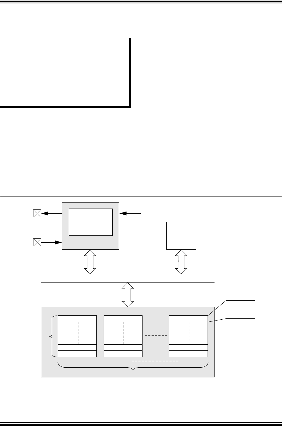
2015 Microchip Technology Inc. Preliminary DS60001320B-page 487
PIC32MZ Embedded Connectivity with Floating Point Unit (EF) Family
29.0 CONTROLLER AREA
NETWORK (CAN)
The Controller Area Network (CAN) module supports
the following key features:
• Standards Compliance:
- Full CAN 2.0B compliance
- Programmable bit rate up to 1 Mbps
• Message Reception and Transmission:
- 32 message FIFOs
- Each FIFO can have up to 32 messages for a
total of 1024 messages
- FIFO can be a transmit message FIFO or a
receive message FIFO
- User-defined priority levels for message
FIFOs used for transmission
- 32 acceptance filters for message filtering
- Four acceptance filter mask registers for
message filtering
- Automatic response to remote transmit request
- DeviceNet™ addressing support
• Additional Features:
- Loopback, Listen All Messages and Listen
Only modes for self-test, system diagnostics
and bus monitoring
- Low-power operating modes
- CAN module is a bus master on the PIC32
System Bus
- Use of DMA is not required
- Dedicated time-stamp timer
- Dedicated DMA channels
- Data-only Message Reception mode
Figure 29-1 illustrates the general structure of the CAN
module.
FIGURE 29-1: PIC32 CAN MODULE BLOCK DIAGRAM
Note: This data sheet summarizes the
features of the PIC32MZ EF family of
devices. It is not intended to be a
comprehensive reference source. To
complement the information in this data
sheet, refer to Section 34. “Controller
Area Network (CAN)” (DS60001154) in
the “PIC32 Family Reference Manual”,
which is available from the Microchip
web site (www.microchip.com/PIC32).
Message Buffer 31
Message Buffer 1
Message Buffer 0
Message Buffer 31
Message Buffer 1
Message Buffer 0
Message Buffer 31
Message Buffer 1
Message Buffer 0
FIFO0 FIFO1 FIFO31
System RAM
Up to 32 Message Buffers
CAN Message FIFO (up to 32 FIFOs)
Message
Buffer Size
2 or 4 Words
System Bus
CPU
CAN Module
32 Filters
4 Masks
CxTX
CxRX
PBCLK5
(‘x’ = 1-2)
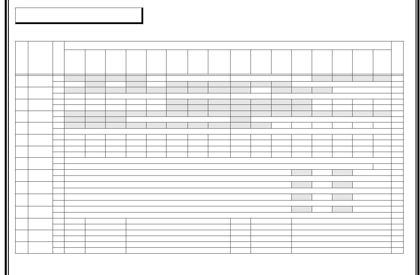
PIC32MZ Embedded Connectivity with Floating Point Unit (EF) Family
DS60001320B-page 488 Preliminary 2015 Microchip Technology Inc.
29.1 CAN Control Registers
Note: The ‘i’ shown in register names denotes
CAN1 or CAN2.
TABLE 29-1: CAN1 REGISTER SUMMARY FOR PIC32MZXXXXECF AND PIC32MZXXXXECH DEVICES
Virtual Address
(BF88_#)
Register
Name(1)
Bit Range
Bits
All Resets
31/15 30/14 29/13 28/12 27/11 26/10 25/9 24/8 23/7 22/6 21/5 20/4 19/3 18/2 17/1 16/0
0000 C1CON 31:16 — — — — ABAT REQOP<2:0> OPMOD<2:0> CANCAP — — — — 0480
15:0 ON —SIDLE —CANBUSY — — — — — — DNCNT<4:0> 0000
0010 C1CFG 31:16 — — — — — — — — — WAKFIL — — — SEG2PH<2:0> 0000
15:0 SEG2PHTS SAM SEG1PH<2:0> PRSEG<2:0> SJW<1:0> BRP<5:0> 0000
0020 C1INT 31:16 IVRIE WAKIE CERRIE SERRIE RBOVIE — — — — — — — MODIE CTMRIE RBIE TBIE 0000
15:0 IVRIF WAKIF CERRIF SERRIF RBOVIF — — — — — — — MODIF CTMRIF RBIF TBIF 0000
0030 C1VEC 31:16 — — — — — — — — — — — — — — — — 0000
15:0 — — — FILHIT<4:0> —ICODE<6:0> 0040
0040 C1TREC 31:16 — — — — — — — — — — TXBO TXBP RXBP TXWARN RXWARN EWARN 0000
15:0 TERRCNT<7:0> RERRCNT<7:0> 0000
0050 C1FSTAT 31:16 FIFOIP31 FIFOIP30 FIFOIP29 FIFOIP28 FIFOIP27 FIFOIP26 FIFOIP25 FIFOIP24 FIFOIP23 FIFOIP22 FIFOIP21 FIFOIP20 FIFOIP19 FIFOIP18 FIFOIP17 FIFOIP16 0000
15:0 FIFOIP15 FIFOIP14 FIFOIP13 FIFOIP12 FIFOIP11 FIFOIP10 FIFOIP9 FIFOIP8 FIFOIP7 FIFOIP6 FIFOIP5 FIFOIP4 FIFOIP3 FIFOIP2 FIFOIP1 FIFOIP0 0000
0060 C1RXOVF 31:16 RXOVF31 RXOVF30 RXOVF29 RXOVF28 RXOVF27 RXOVF26 RXOVF25 RXOVF24 RXOVF23 RXOVF22 RXOVF21 RXOVF20 RXOVF19 RXOVF18 RXOVF17 RXOVF16 0000
15:0 RXOVF15 RXOVF14 RXOVF13 RXOVF12 RXOVF11 RXOVF10 RXOVF9 RXOVF8 RXOVF7 RXOVF6 RXOVF5 RXOVF4 RXOVF3 RXOVF2 RXOVF1 RXOVF0 0000
0070 C1TMR 31:16 CANTS<15:0> 0000
15:0 CANTSPRE<15:0> 0000
0080 C1RXM0 31:16 SID<10:0> -— MIDE —EID<17:16> xxxx
15:0 EID<15:0> xxxx
0090 C1RXM1 31:16 SID<10:0> -— MIDE —EID<17:16> xxxx
15:0 EID<15:0> xxxx
00A0 C1RXM2 31:16 SID<10:0> -— MIDE —EID<17:16> xxxx
15:0 EID<15:0> xxxx
00B0 C1RXM3 31:16 SID<10:0> -— MIDE —EID<17:16> xxxx
15:0 EID<15:0> xxxx
00C0 C1FLTCON0 31:16 FLTEN3 MSEL3<1:0> FSEL3<4:0> FLTEN2 MSEL2<1:0> FSEL2<4:0> 0000
15:0 FLTEN1 MSEL1<1:0> FSEL1<4:0> FLTEN0 MSEL0<1:0> FSEL0<4:0> 0000
00D0 C1FLTCON1 31:16 FLTEN7 MSEL7<1:0> FSEL7<4:0> FLTEN6 MSEL6<1:0> FSEL6<4:0> 0000
15:0 FLTEN5 MSEL5<1:0> FSEL5<4:0> FLTEN4 MSEL4<1:0> FSEL4<4:0> 0000
00E0 C1FLTCON2 31:16 FLTEN11 MSEL11<1:0> FSEL11<4:0> FLTEN10 MSEL10<1:0> FSEL10<4:0> 0000
15:0 FLTEN9 MSEL9<1:0> FSEL9<4:0> FLTEN8 MSEL8<1:0> FSEL8<4:0> 0000
Legend: x = unknown value on Reset; — = unimplemented, read as ‘0’. Reset values are shown in hexadecimal.
Note 1: All registers in this table have corresponding CLR, SET and INV registers at their virtual addresses, plus offsets of 0x4, 0x8 and 0xC, respectively. See Section 12.3 “CLR, SET, and INV Registers” for more
information.

2015 Microchip Technology Inc. Preliminary DS60001320B-page 489
PIC32MZ Embedded Connectivity with Floating Point Unit (EF) Family
00F0 C1FLTCON3 31:16 FLTEN15 MSEL15<1:0> FSEL15<4:0> FLTEN14 MSEL14<1:0> FSEL14<4:0> 0000
15:0 FLTEN13 MSEL13<1:0> FSEL13<4:0> FLTEN12 MSEL12<1:0> FSEL12<4:0> 0000
0100 C1FLTCON4 31:16 FLTEN19 MSEL19<1:0> FSEL19<4:0> FLTEN18 MSEL18<1:0> FSEL18<4:0> 0000
15:0 FLTEN17 MSEL17<1:0> FSEL17<4:0> FLTEN16 MSEL16<1:0> FSEL16<4:0> 0000
0110 C1FLTCON5 31:16 FLTEN23 MSEL23<1:0> FSEL23<4:0> FLTEN22 MSEL22<1:0> FSEL22<4:0> 0000
15:0 FLTEN21 MSEL21<1:0> FSEL21<4:0> FLTEN20 MSEL20<1:0> FSEL20<4:0> 0000
0120 C1FLTCON6 31:16 FLTEN27 MSEL27<1:0> FSEL27<4:0> FLTEN26 MSEL26<1:0> FSEL26<4:0> 0000
15:0 FLTEN25 MSEL25<1:0> FSEL25<4:0> FLTEN24 MSEL24<1:0> FSEL24<4:0> 0000
0130 C1FLTCON7 31:16 FLTEN31 MSEL31<1:0> FSEL31<4:0> FLTEN30 MSEL30<1:0> FSEL30<4:0> 0000
15:0 FLTEN29 MSEL29<1:0> FSEL29<4:0> FLTEN28 MSEL28<1:0> FSEL28<4:0> 0000
0140-
0330 C1RXFn
(n = 0-31)
31:16 SID<10:0> -— EXID —EID<17:16> xxxx
15:0 EID<15:0> xxxx
0340 C1FIFOBA 31:16 C1FIFOBA<31:0> 0000
15:0 0000
0350 C1FIFOCONn
(n = 0)
31:16 — — — — — — — — — — — FSIZE<4:0> 0000
15:0 —FRESET UINC DONLY — — — — TXEN TXABAT TXLARB TXERR TXREQ RTREN TXPRI<1:0> 0000
0360 C1FIFOINTn
(n = 0)
31:16 — — — — — TXNFULLIE TXHALFIE TXEMPTYIE — — — — RXOVFLIE RXFULLIE RXHALFIE RXN
EMPTYIE 0000
15:0 — — — — — TXNFULLIF TXHALFIF TXEMPTYIF — — — — RXOVFLIF RXFULLIF RXHALFIF RXN
EMPTYIF 0000
0370 C1FIFOUAn
(n = 0)
31:16 C1FIFOUA<31:0> 0000
15:0 0000
0380 C1FIFOCIn
(n = 0)
31:16 — — — — — — — — — — — — — — — — 0000
15:0 — — — — — — — — — — — C1FIFOCI<4:0> 0000
0390-
0B40
C1FIFOCONn
C1FIFOINTn
C1FIFOUAn
C1FIFOCIn
(n = 1-31)
31:16 — — — — — — — — — — — FSIZE<4:0> 0000
15:0 —FRESET UINC DONLY — — — — TXEN TXABAT TXLARB TXERR TXREQ RTREN TXPRI<1:0> 0000
31:16 — — — — — TXNFULLIE TXHALFIE TXEMPTYIE — — — — RXOVFLIE RXFULLIE RXHALFIE RXN
EMPTYIE 0000
15:0 — — — — — TXNFULLIF TXHALFIF TXEMPTYIF — — — — RXOVFLIF RXFULLIF RXHALFIF RXN
EMPTYIF 0000
31:16 C1FIFOUA<31:0> 0000
15:0 0000
31:16 — — — — — — — — — — — — — — — — 0000
15:0 — — — — — — — — — — — C1FIFOCI<4:0> 0000
TABLE 29-1: CAN1 REGISTER SUMMARY FOR PIC32MZXXXXECF AND PIC32MZXXXXECH DEVICES (CONTINUED)
Virtual Address
(BF88_#)
Register
Name(1)
Bit Range
Bits
All Resets
31/15 30/14 29/13 28/12 27/11 26/10 25/9 24/8 23/7 22/6 21/5 20/4 19/3 18/2 17/1 16/0
Legend: x = unknown value on Reset; — = unimplemented, read as ‘0’. Reset values are shown in hexadecimal.
Note 1: All registers in this table have corresponding CLR, SET and INV registers at their virtual addresses, plus offsets of 0x4, 0x8 and 0xC, respectively. See Section 12.3 “CLR, SET, and INV Registers” for more
information.
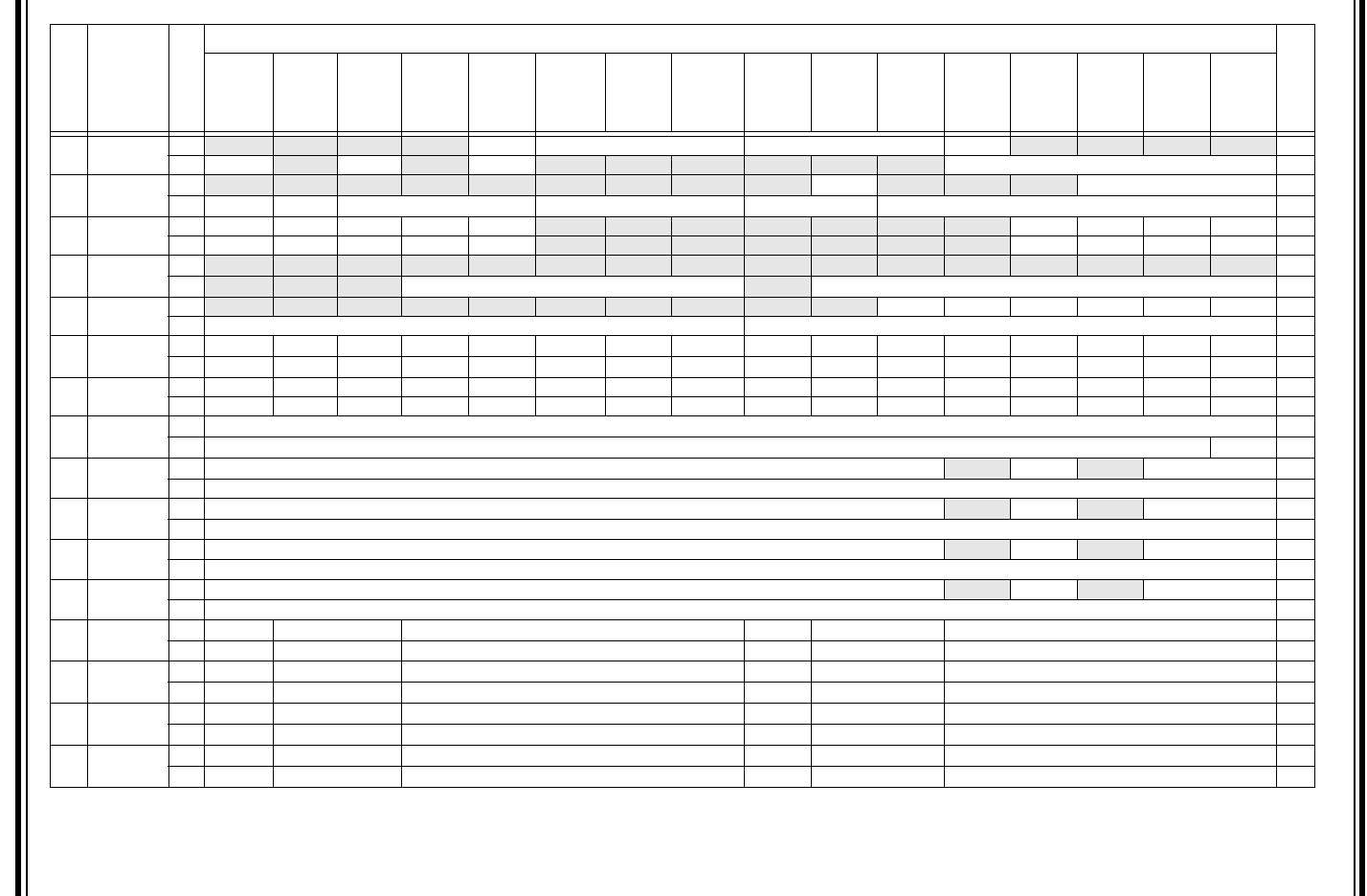
PIC32MZ Embedded Connectivity with Floating Point Unit (EF) Family
DS60001320B-page 490 Preliminary 2015 Microchip Technology Inc.
TABLE 29-2: CAN2 REGISTER SUMMARY FOR PIC32MZXXXXECF AND PIC32MZXXXXECH DEVICES
Virtual Address
(BF88_#)
Register
Name(1)
Bit Range
Bits
All Resets
31/15 30/14 29/13 28/12 27/11 26/10 25/9 24/8 23/7 22/6 21/5 20/4 19/3 18/2 17/1 16/0
1000 C2CON 31:16 — — — — ABAT REQOP<2:0> OPMOD<2:0> CANCAP — — — — 0480
15:0 ON —SIDLE— CANBUSY — — — — — — DNCNT<4:0> 0000
1010 C2CFG 31:16 — — — — — — — — —WAKFIL— — — SEG2PH<2:0> 0000
15:0 SEG2PHTS SAM SEG1PH<2:0> PRSEG<2:0> SJW<1:0> BRP<5:0> 0000
1020 C2INT 31:16 IVRIE WAKIE CERRIE SERRIE RBOVIE — — — — — — — MODIE CTMRIE RBIE TBIE 0000
15:0 IVRIF WAKIF CERRIF SERRIF RBOVIF — — — — — — — MODIF CTMRIF RBIF TBIF 0000
1030 C2VEC 31:16 — — — — — — — — — — — — — — — — 0000
15:0 — — — FILHIT<4:0> — ICODE<6:0> 0040
1040 C2TREC 31:16 — — — — — — — — — — TXBO TXBP RXBP TXWARN RXWARN EWARN 0000
15:0 TERRCNT<7:0> RERRCNT<7:0> 0000
1050 C2FSTAT 31:16 FIFOIP31 FIFOIP30 FIFOIP29 FIFOIP28 FIFOIP27 FIFOIP26 FIFOIP25 FIFOIP24 FIFOIP23 FIFOIP22 FIFOIP21 FIFOIP20 FIFOIP19 FIFOIP18 FIFOIP17 FIFOIP16 0000
15:0 FIFOIP15 FIFOIP14 FIFOIP13 FIFOIP12 FIFOIP11 FIFOIP10 FIFOIP9 FIFOIP8 FIFOIP7 FIFOIP6 FIFOIP5 FIFOIP4 FIFOIP3 FIFOIP2 FIFOIP1 FIFOIP0 0000
1060 C2RXOVF 31:16 RXOVF31 RXOVF30 RXOVF29 RXOVF28 RXOVF27 RXOVF26 RXOVF25 RXOVF24 RXOVF23 RXOVF22 RXOVF21 RXOVF20 RXOVF19 RXOVF18 RXOVF17 RXOVF16 0000
15:0 RXOVF15 RXOVF14 RXOVF13 RXOVF12 RXOVF11 RXOVF10 RXOVF9 RXOVF8 RXOVF7 RXOVF6 RXOVF5 RXOVF4 RXOVF3 RXOVF2 RXOVF1 RXOVF0 0000
1070 C2TMR 31:16 CANTS<15:0> 0000
15:0 CANTSPRE<15:0> 0000
1080 C2RXM0 31:16 SID<10:0> -— MIDE — EID<17:16> xxxx
15:0 EID<15:0> xxxx
10A0 C2RXM1 31:16 SID<10:0> -— MIDE — EID<17:16> xxxx
15:0 EID<15:0> xxxx
10B0 C2RXM2 31:16 SID<10:0> -— MIDE — EID<17:16> xxxx
15:0 EID<15:0> xxxx
10B0 C2RXM3 31:16 SID<10:0> -— MIDE — EID<17:16> xxxx
15:0 EID<15:0> xxxx
1010 C2FLTCON0 31:16 FLTEN3 MSEL3<1:0> FSEL3<4:0> FLTEN2 MSEL2<1:0> FSEL2<4:0> 0000
15:0 FLTEN1 MSEL1<1:0> FSEL1<4:0> FLTEN0 MSEL0<1:0> FSEL0<4:0> 0000
10D0 C2FLTCON1 31:16 FLTEN7 MSEL7<1:0> FSEL7<4:0> FLTEN6 MSEL6<1:0> FSEL6<4:0> 0000
15:0 FLTEN5 MSEL5<1:0> FSEL5<4:0> FLTEN4 MSEL4<1:0> FSEL4<4:0> 0000
10E0 C2FLTCON2 31:16 FLTEN11 MSEL11<1:0> FSEL11<4:0> FLTEN10 MSEL10<1:0> FSEL10<4:0> 0000
15:0 FLTEN9 MSEL9<1:0> FSEL9<4:0> FLTEN8 MSEL8<1:0> FSEL8<4:0> 0000
10F0 C2FLTCON3 31:16 FLTEN15 MSEL15<1:0> FSEL15<4:0> FLTEN14 MSEL14<1:0> FSEL14<4:0> 0000
15:0 FLTEN13 MSEL13<1:0> FSEL13<4:0> FLTEN12 MSEL12<1:0> FSEL12<4:0> 0000
Legend: x = unknown value on Reset; — = unimplemented, read as ‘0’. Reset values are shown in hexadecimal.
Note 1: All registers in this table have corresponding CLR, SET and INV registers at their virtual addresses, plus offsets of 0x4, 0x8 and 0xC, respectively. See Section 12.3 “CLR, SET, and INV Registers” for more
information.
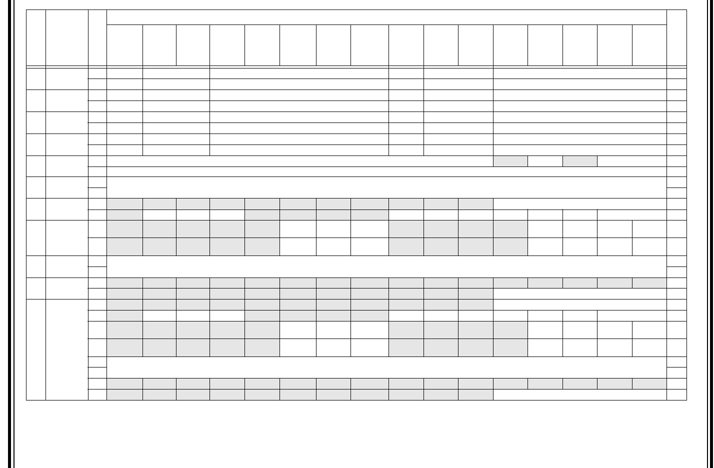
2015 Microchip Technology Inc. Preliminary DS60001320B-page 491
PIC32MZ Embedded Connectivity with Floating Point Unit (EF) Family
1100 C2FLTCON4 31:16 FLTEN19 MSEL19<1:0> FSEL19<4:0> FLTEN18 MSEL18<1:0> FSEL18<4:0> 0000
15:0 FLTEN17 MSEL17<1:0> FSEL17<4:0> FLTEN16 MSEL16<1:0> FSEL16<4:0: 0000
1110 C2FLTCON5 31:16 FLTEN23 MSEL23<1:0> FSEL23<4:0> FLTEN22 MSEL22<1:0> FSEL22<4:0> 0000
15:0 FLTEN21 MSEL21<1:0> FSEL21<4:0> FLTEN20 MSEL20<1:0> FSEL20<4:0> 0000
1120 C2FLTCON6 31:16 FLTEN27 MSEL27<1:0> FSEL27<4:0> FLTEN26 MSEL26<1:0> FSEL26<4:0> 0000
15:0 FLTEN25 MSEL25<1:0> FSEL25<4:0> FLTEN24 MSEL24<1:0> FSEL24<4:0> 0000
1130 C2FLTCON7 31:16 FLTEN31 MSEL31<1:0> FSEL31<4:0> FLTEN30 MSEL30<1:0> FSEL30<4:0> 0000
15:0 FLTEN29 MSEL29<1:0> FSEL29<4:0> FLTEN28 MSEL28<1:0> FSEL28<4:0> 0000
1140-
1330 C2RXFn
(n = 0-31)
31:16 SID<10:0> -— EXID — EID<17:16> xxxx
15:0 EID<15:0> xxxx
1340 C2FIFOBA 31:16 C2FIFOBA<31:0> 0000
15:0 0000
1350 C2FIFOCONn
(n = 0)
31:16 — — — — — — — — — — —FSIZE<4:0>
0000
15:0 — FRESET UINC DONLY ———— TXEN TXABAT TXLARB TXERR TXREQ RTREN TXPRI<1:0> 0000
1360 C2FIFOINTn
(n = 0)
31:16 — — — — — TXNFULLIE TXHALFIE TXEMPTYIE ———— RXOVFLIE RXFULLIE RXHALFIE RXN
EMPTYIE 0000
15:0 — — — — — TXNFULLIF TXHALFIF TXEMPTYIF ———— RXOVFLIF RXFULLIF RXHALFIF RXN
EMPTYIF 0000
1370 C2FIFOUAn
(n = 0)
31:16 C2FIFOUA<31:0> 0000
15:0 0000
1380 C2FIFOCIn
(n = 0)
31:16 — — — — — — — — — — — — — — — — 0000
15:0 — — — — — — — — — — — C2FIFOCI<4:0> 0000
1390-
1B40
C2FIFOCONn
C2FIFOINTn
C2FIFOUAn
C2FIFOCIn
(n = 1-31)
31:16 — — — — — — — — — — —FSIZE<4:0>
0000
15:0 — FRESET UINC DONLY ———— TXEN TXABAT TXLARB TXERR TXREQ RTREN TXPRI<1:0> 0000
31:16 — — — — — TXNFULLIE TXHALFIE TXEMPTYIE ———— RXOVFLIE RXFULLIE RXHALFIE RXN
EMPTYIE 0000
15:0 — — — — — TXNFULLIF TXHALFIF TXEMPTYIF ———— RXOVFLIF RXFULLIF RXHALFIF RXN
EMPTYIF 0000
31:16 C2FIFOUA<31:0> 0000
15:0 0000
31:16 — — — — — — — — — — — — — — — — 0000
15:0 — — — — — — — — — — — C2FIFOCI<4:0> 0000
TABLE 29-2: CAN2 REGISTER SUMMARY FOR PIC32MZXXXXECF AND PIC32MZXXXXECH DEVICES (CONTINUED)
Virtual Address
(BF88_#)
Register
Name(1)
Bit Range
Bits
All Resets
31/15 30/14 29/13 28/12 27/11 26/10 25/9 24/8 23/7 22/6 21/5 20/4 19/3 18/2 17/1 16/0
Legend: x = unknown value on Reset; — = unimplemented, read as ‘0’. Reset values are shown in hexadecimal.
Note 1: All registers in this table have corresponding CLR, SET and INV registers at their virtual addresses, plus offsets of 0x4, 0x8 and 0xC, respectively. See Section 12.3 “CLR, SET, and INV Registers” for more
information.

PIC32MZ Embedded Connectivity with Floating Point Unit (EF) Family
DS60001320B-page 492 Preliminary 2015 Microchip Technology Inc.
REGISTER 29-1: CiCON: CAN MODULE CONTROL REGISTER
Bit
Range Bit
31/23/15/7 Bit
30/22/14/6 Bit
29/21/13/5 Bit
28/20/12/4 Bit
27/19/11/3 Bit
26/18/10/2 Bit
25/17/9/1 Bit
24/16/8/0
31:24 U-0 U-0 U-0 U-0 S/HC-0 R/W-1 R/W-0 R/W-0
— — — — ABAT REQOP<2:0>
23:16 R-1 R-0 R-0 R/W-0 U-0 U-0 U-0 U-0
OPMOD<2:0> CANCAP — — — —
15:8 R/W-0 U-0 R/W-0 U-0 R-0 U-0 U-0 U-0
ON(1) —SIDLE— CANBUSY — — —
7:0 U-0 U-0 U-0 R/W-0 R/W-0 R/W-0 R/W-0 R/W-0
— — — DNCNT<4:0>
Legend: HC = Hardware Clear S = Settable bit
R = Readable bit W = Writable bit P = Programmable bit r = Reserved bit
U = Unimplemented bit -n = Bit Value at POR: (‘0’, ‘1’, x = Unknown)
bit 31-28 Unimplemented: Read as ‘0’
bit 27 ABAT: Abort All Pending Transmissions bit
1 = Signal all transmit buffers to abort transmission
0 = Module will clear this bit when all transmissions aborted
bit 26-24 REQOP<2:0>: Request Operation Mode bits
111 = Set Listen All Messages mode
110 = Reserved - Do not use
101 = Reserved - Do not use
100 = Set Configuration mode
011 = Set Listen Only mode
010 = Set Loopback mode
001 = Set Disable mode
000 = Set Normal Operation mode
bit 23-21 OPMOD<2:0>: Operation Mode Status bits
111 = Module is in Listen All Messages mode
110 = Reserved
101 = Reserved
100 = Module is in Configuration mode
011 = Module is in Listen Only mode
010 = Module is in Loopback mode
001 = Module is in Disable mode
000 = Module is in Normal Operation mode
bit 20 CANCAP: CAN Message Receive Time Stamp Timer Capture Enable bit
1 = CANTMR value is stored on valid message reception and is stored with the message
0 = Disable CAN message receive time stamp timer capture and stop CANTMR to conserve power
bit 19-16 Unimplemented: Read as ‘0’
bit 15 ON: CAN On bit(1)
1 = CAN module is enabled
0 = CAN module is disabled
bit 14 Unimplemented: Read as ‘0’
Note 1: If the user application clears this bit, it may take a number of cycles before the CAN module completes the
current transaction and responds to this request. The user application should poll the CANBUSY bit to
verify that the request has been honored.

2015 Microchip Technology Inc. Preliminary DS60001320B-page 493
PIC32MZ Embedded Connectivity with Floating Point Unit (EF) Family
bit 13 SIDLE: CAN Stop in Idle bit
1 = CAN Stops operation when system enters Idle mode
0 = CAN continues operation when system enters Idle mode
bit 12 Unimplemented: Read as ‘0’
bit 11 CANBUSY: CAN Module is Busy bit
1 = The CAN module is active
0 = The CAN module is completely disabled
bit 10-5 Unimplemented: Read as ‘0’
bit 4-0 DNCNT<4:0>: Device Net Filter Bit Number bits
10011-11111 = Invalid Selection (compare up to 18-bits of data with EID)
10010 = Compare up to data byte 2 bit 6 with EID17 (CiRXFn<17>)
•
•
•
00001 = Compare up to data byte 0 bit 7 with EID0 (CiRXFn<0>)
00000 = Do not compare data bytes
REGISTER 29-1: CiCON: CAN MODULE CONTROL REGISTER (CONTINUED)
Note 1: If the user application clears this bit, it may take a number of cycles before the CAN module completes the
current transaction and responds to this request. The user application should poll the CANBUSY bit to
verify that the request has been honored.

PIC32MZ Embedded Connectivity with Floating Point Unit (EF) Family
DS60001320B-page 494 Preliminary 2015 Microchip Technology Inc.
REGISTER 29-2: CiCFG: CAN BAUD RATE CONFIGURATION REGISTER
Bit
Range Bit
31/23/15/7 Bit
30/22/14/6 Bit
29/21/13/5 Bit
28/20/12/4 Bit
27/19/11/3 Bit
26/18/10/2 Bit
25/17/9/1 Bit
24/16/8/0
31:24 U-0 U-0 U-0 U-0 U-0 U-0 U-0 U-0
— — — — — — — —
23:16 U-0 R/W-0 U-0 U-0 U-0 R/W-0 R/W-0 R/W-0
— WAKFIL — — — SEG2PH<2:0>(1,4)
15:8 R/W-0 R/W-0 R/W-0 R/W-0 R/W-0 R/W-0 R/W-0 R/W-0
SEG2PHTS(1) SAM(2) SEG1PH<2:0> PRSEG<2:0>
7:0 R/W-0 R/W-0 R/W-0 R/W-0 R/W-0 R/W-0 R/W-0 R/W-0
SJW<1:0>(3) BRP<5:0>
Legend: HC = Hardware Clear S = Settable bit
R = Readable bit W = Writable bit P = Programmable bit r = Reserved bit
U = Unimplemented bit -n = Bit Value at POR: (‘0’, ‘1’, x = Unknown)
bit 31-23 Unimplemented: Read as ‘0’
bit 22 WAKFIL: CAN Bus Line Filter Enable bit
1 = Use CAN bus line filter for wake-up
0 = CAN bus line filter is not used for wake-up
bit 21-19 Unimplemented: Read as ‘0’
bit 18-16 SEG2PH<2:0>: Phase Buffer Segment 2 bits(1,4)
111 = Length is 8 x TQ
•
•
•
000 = Length is 1 x TQ
bit 15 SEG2PHTS: Phase Segment 2 Time Select bit(1)
1 = Freely programmable
0 = Maximum of SEG1PH or Information Processing Time, whichever is greater
bit 14 SAM: Sample of the CAN Bus Line bit(2)
1 = Bus line is sampled three times at the sample point
0 = Bus line is sampled once at the sample point
bit 13-11 SEG1PH<2:0>: Phase Buffer Segment 1 bits(4)
111 = Length is 8 x TQ
•
•
•
000 = Length is 1 x TQ
Note 1: SEG2PH SEG1PH. If SEG2PHTS is clear, SEG2PH will be set automatically.
2: 3 Time bit sampling is not allowed for BRP < 2.
3: SJW SEG2PH.
4: The Time Quanta per bit must be greater than 7 (that is, TQBIT > 7).
Note: This register can only be modified when the CAN module is in Configuration mode (OPMOD<2:0>
(CiCON<23:21>) = 100).

2015 Microchip Technology Inc. Preliminary DS60001320B-page 495
PIC32MZ Embedded Connectivity with Floating Point Unit (EF) Family
bit 10-8 PRSEG<2:0>: Propagation Time Segment bits(4)
111 = Length is 8 x TQ
•
•
•
000 = Length is 1 x TQ
bit 7-6 SJW<1:0>: Synchronization Jump Width bits(3)
11 = Length is 4 x TQ
10 = Length is 3 x TQ
01 = Length is 2 x TQ
00 = Length is 1 x TQ
bit 5-0 BRP<5:0>: Baud Rate Prescaler bits
111111 = TQ = (2 x 64)/TPBCLK5
111110 = TQ = (2 x 63)/TPBCLK5
•
•
•
000001 = TQ = (2 x 2)/TPBCLK5
000000 = TQ = (2 x 1)/TPBCLK5
REGISTER 29-2: CiCFG: CAN BAUD RATE CONFIGURATION REGISTER (CONTINUED)
Note 1: SEG2PH SEG1PH. If SEG2PHTS is clear, SEG2PH will be set automatically.
2: 3 Time bit sampling is not allowed for BRP < 2.
3: SJW SEG2PH.
4: The Time Quanta per bit must be greater than 7 (that is, TQBIT > 7).
Note: This register can only be modified when the CAN module is in Configuration mode (OPMOD<2:0>
(CiCON<23:21>) = 100).

PIC32MZ Embedded Connectivity with Floating Point Unit (EF) Family
DS60001320B-page 496 Preliminary 2015 Microchip Technology Inc.
REGISTER 29-3: CiINT: CAN INTERRUPT REGISTER
Bit
Range Bit
31/23/15/7 Bit
30/22/14/6 Bit
29/21/13/5 Bit
28/20/12/4 Bit
27/19/11/3 Bit
26/18/10/2 Bit
25/17/9/1 Bit
24/16/8/0
31:24 R/W-0 R/W-0 R/W-0 R/W-0 R/W-0 U-0 U-0 U-0
IVRIE WAKIE CERRIE SERRIE RBOVIE — — —
23:16 U-0 U-0 U-0 U-0 R/W-0 R/W-0 R/W-0 R/W-0
— — — — MODIE CTMRIE RBIE TBIE
15:8 R/W-0 R/W-0 R/W-0 R/W-0 R/W-0 U-0 U-0 U-0
IVRIF WAKIF CERRIF SERRIF(1) RBOVIF — — —
7:0 U-0 U-0 U-0 U-0 R/W-0 R/W-0 R/W-0 R/W-0
— — — — MODIF CTMRIF RBIF TBIF
Legend:
R = Readable bit W = Writable bit U = Unimplemented bit, read as ‘0’
-n = Value at POR ‘1’ = Bit is set ‘0’ = Bit is cleared x = Bit is unknown
bit 31 IVRIE: Invalid Message Received Interrupt Enable bit
1 = Interrupt request enabled
0 = Interrupt request not enabled
bit 30 WAKIE: CAN Bus Activity Wake-up Interrupt Enable bit
1 = Interrupt request enabled
0 = Interrupt request not enabled
bit 29 CERRIE: CAN Bus Error Interrupt Enable bit
1 = Interrupt request enabled
0 = Interrupt request not enabled
bit 28 SERRIE: System Error Interrupt Enable bit
1 = Interrupt request enabled
0 = Interrupt request not enabled
bit 27 RBOVIE: Receive Buffer Overflow Interrupt Enable bit
1 = Interrupt request enabled
0 = Interrupt request not enabled
bit 26-20 Unimplemented: Read as ‘0’
bit 19 MODIE: Mode Change Interrupt Enable bit
1 = Interrupt request enabled
0 = Interrupt request not enabled
bit 18 CTMRIE: CAN Timestamp Timer Interrupt Enable bit
1 = Interrupt request enabled
0 = Interrupt request not enabled
bit 17 RBIE: Receive Buffer Interrupt Enable bit
1 = Interrupt request enabled
0 = Interrupt request not enabled
bit 16 TBIE: Transmit Buffer Interrupt Enable bit
1 = Interrupt request enabled
0 = Interrupt request not enabled
bit 15 IVRIF: Invalid Message Received Interrupt Flag bit
1 = An invalid messages interrupt has occurred
0 = An invalid message interrupt has not occurred
Note 1: This bit can only be cleared by turning the CAN module Off and On by clearing or setting the ON bit
(CiCON<15>).

2015 Microchip Technology Inc. Preliminary DS60001320B-page 497
PIC32MZ Embedded Connectivity with Floating Point Unit (EF) Family
bit 14 WAKIF: CAN Bus Activity Wake-up Interrupt Flag bit
1 = A bus wake-up activity interrupt has occurred
0 = A bus wake-up activity interrupt has not occurred
bit 13 CERRIF: CAN Bus Error Interrupt Flag bit
1 = A CAN bus error has occurred
0 = A CAN bus error has not occurred
bit 12 SERRIF: System Error Interrupt Flag bit
1 = A system error occurred (typically an illegal address was presented to the System Bus)
0 = A system error has not occurred
bit 11 RBOVIF: Receive Buffer Overflow Interrupt Flag bit
1 = A receive buffer overflow has occurred
0 = A receive buffer overflow has not occurred
bit 10-4 Unimplemented: Read as ‘0’
bit 3 MODIF: CAN Mode Change Interrupt Flag bit
1 = A CAN module mode change has occurred (OPMOD<2:0> has changed to reflect REQOP)
0 = A CAN module mode change has not occurred
bit 2 CTMRIF: CAN Timer Overflow Interrupt Flag bit
1 = A CAN timer (CANTMR) overflow has occurred
0 = A CAN timer (CANTMR) overflow has not occurred
bit 1 RBIF: Receive Buffer Interrupt Flag bit
1 = A receive buffer interrupt is pending
0 = A receive buffer interrupt is not pending
bit 0 TBIF: Transmit Buffer Interrupt Flag bit
1 = A transmit buffer interrupt is pending
0 = A transmit buffer interrupt is not pending
REGISTER 29-3: CiINT: CAN INTERRUPT REGISTER (CONTINUED)
Note 1: This bit can only be cleared by turning the CAN module Off and On by clearing or setting the ON bit
(CiCON<15>).

PIC32MZ Embedded Connectivity with Floating Point Unit (EF) Family
DS60001320B-page 498 Preliminary 2015 Microchip Technology Inc.
REGISTER 29-4: CiVEC: CAN INTERRUPT CODE REGISTER
Bit
Range Bit
31/23/15/7 Bit
30/22/14/6 Bit
29/21/13/5 Bit
28/20/12/4 Bit
27/19/11/3 Bit
26/18/10/2 Bit
25/17/9/1 Bit
24/16/8/0
31:24 U-0 U-0 U-0 U-0 U-0 U-0 U-0 U-0
— — — — — — — —
23:16 U-0 U-0 U-0 U-0 U-0 U-0 U-0 U-0
— — — — — — — —
15:8 U-0 U-0 U-0 R-0 R-0 R-0 R-0 R-0
— — —FILHIT<4:0>
7:0 U-0 R-1 R-0 R-0 R-0 R-0 R-0 R-0
—ICODE<6:0>
(1)
Legend:
R = Readable bit W = Writable bit U = Unimplemented bit, read as ‘0’
-n = Value at POR ‘1’ = Bit is set ‘0’ = Bit is cleared x = Bit is unknown
bit 31-13 Unimplemented: Read as ‘0’
bit 12-8 FILHIT<4:0>: Filter Hit Number bit
11111 = Filter 31
11110 = Filter 30
•
•
•
00001 = Filter 1
00000 = Filter 0
bit 7 Unimplemented: Read as ‘0’
bit 6-0 ICODE<6:0>: Interrupt Flag Code bits(1)
1001000-1111111 = Reserved
1001000 = Invalid message received (IVRIF)
1000111 = CAN module mode change (MODIF)
1000110 = CAN timestamp timer (CTMRIF)
1000101 = Bus bandwidth error (SERRIF)
1000100 = Address error interrupt (SERRIF)
1000011 = Receive FIFO overflow interrupt (RBOVIF)
1000010 = Wake-up interrupt (WAKIF)
1000001 = Error Interrupt (CERRIF)
1000000 = No interrupt
0100000-0111111 = Reserved
0011111 = FIFO31 Interrupt (CiFSTAT<31> set)
0011110 = FIFO30 Interrupt (CiFSTAT<30> set)
•
•
•
0000001 = FIFO1 Interrupt (CiFSTAT<1> set)
0000000 = FIFO0 Interrupt (CiFSTAT<0> set)
Note 1: These bits are only updated for enabled interrupts.

2015 Microchip Technology Inc. Preliminary DS60001320B-page 499
PIC32MZ Embedded Connectivity with Floating Point Unit (EF) Family
REGISTER 29-5: CiTREC: CAN TRANSMIT/RECEIVE ERROR COUNT REGISTER
Bit
Range Bit
31/23/15/7 Bit
30/22/14/6 Bit
29/21/13/5 Bit
28/20/12/4 Bit
27/19/11/3 Bit
26/18/10/2 Bit
25/17/9/1 Bit
24/16/8/0
31:24 U-0 U-0 U-0 U-0 U-0 U-0 U-0 U-0
————————
23:16 U-0 U-0 R-0 R-0 R-0 R-0 R-0 R-0
—— TXBO TXBP RXBP TXWARN RXWARN EWARN
15:8 R-0 R-0 R-0 R-0 R-0 R-0 R-0 R-0
TERRCNT<7:0>
7:0 R-0 R-0 R-0 R-0 R-0 R-0 R-0 R-0
RERRCNT<7:0>
Legend:
R = Readable bit W = Writable bit U = Unimplemented bit, read as ‘0’
-n = Value at POR ‘1’ = Bit is set ‘0’ = Bit is cleared x = Bit is unknown
bit 31-22 Unimplemented: Read as ‘0’
bit 21 TXBO: Transmitter in Error State Bus OFF (TERRCNT 256)
bit 20 TXBP: Transmitter in Error State Bus Passive (TERRCNT 128)
bit 19 RXBP: Receiver in Error State Bus Passive (RERRCNT 128)
bit 18 TXWARN: Transmitter in Error State Warning (128 > TERRCNT 96)
bit 17 RXWARN: Receiver in Error State Warning (128 > RERRCNT 96)
bit 16 EWARN: Transmitter or Receiver is in Error State Warning
bit 15-8 TERRCNT<7:0>: Transmit Error Counter
bit 7-0 RERRCNT<7:0>: Receive Error Counter
REGISTER 29-6: CiFSTAT: CAN FIFO STATUS REGISTER
Bit
Range Bit
31/23/15/7 Bit
30/22/14/6 Bit
29/21/13/5 Bit
28/20/12/4 Bit
27/19/11/3 Bit
26/18/10/2 Bit
25/17/9/1 Bit
24/16/8/0
31:24 R-0 R-0 R-0 R-0 R-0 R-0 R-0 R-0
FIFOIP31 FIFOIP30 FIFOIP29 FIFOIP28 FIFOIP27 FIFOIP26 FIFOIP25 FIFOIP24
23:16 R-0 R-0 R-0 R-0 R-0 R-0 R-0 R-0
FIFOIP23 FIFOIP22 FIFOIP21 FIFOIP20 FIFOIP19 FIFOIP18 FIFOIP17 FIFOIP16
15:8 R-0 R-0 R-0 R-0 R-0 R-0 R-0 R-0
FIFOIP15 FIFOIP14 FIFOIP13 FIFOIP12 FIFOIP11 FIFOIP10 FIFOIP9 FIFOIP8
7:0 R-0 R-0 R-0 R-0 R-0 R-0 R-0 R-0
FIFOIP7 FIFOIP6 FIFOIP5 FIFOIP4 FIFOIP3 FIFOIP2 FIFOIP1 FIFOIP0
Legend:
R = Readable bit W = Writable bit U = Unimplemented bit, read as ‘0’
-n = Value at POR ‘1’ = Bit is set ‘0’ = Bit is cleared x = Bit is unknown
bit 31-0 FIFOIP<31:0>: FIFOx Interrupt Pending bits
1 = One or more enabled FIFO interrupts are pending
0 = No FIFO interrupts are pending

PIC32MZ Embedded Connectivity with Floating Point Unit (EF) Family
DS60001320B-page 500 Preliminary 2015 Microchip Technology Inc.
REGISTER 29-7: CiRXOVF: CAN RECEIVE FIFO OVERFLOW STATUS REGISTER
Bit
Range Bit
31/23/15/7 Bit
30/22/14/6 Bit
29/21/13/5 Bit
28/20/12/4 Bit
27/19/11/3 Bit
26/18/10/2 Bit
25/17/9/1 Bit
24/16/8/0
31:24 R-0 R-0 R-0 R-0 R-0 R-0 R-0 R-0
RXOVF31 RXOVF30 RXOVF29 RXOVF28 RXOVF27 RXOVF26 RXOVF25 RXOVF24
23:16 R-0 R-0 R-0 R-0 R-0 R-0 R-0 R-0
RXOVF23 RXOVF22 RXOVF21 RXOVF20 RXOVF19 RXOVF18 RXOVF17 RXOVF16
15:8 R-0 R-0 R-0 R-0 R-0 R-0 R-0 R-0
RXOVF15 RXOVF14 RXOVF13 RXOVF12 RXOVF11 RXOVF10 RXOVF9 RXOVF8
7:0 R-0 R-0 R-0 R-0 R-0 R-0 R-0 R-0
RXOVF7 RXOVF6 RXOVF5 RXOVF4 RXOVF3 RXOVF2 RXOVF1 RXOVF0
Legend:
R = Readable bit W = Writable bit U = Unimplemented bit, read as ‘0’
-n = Value at POR ‘1’ = Bit is set ‘0’ = Bit is cleared x = Bit is unknown
bit 31-0 RXOVF<31:0>: FIFOx Receive Overflow Interrupt Pending bit
1 = FIFO has overflowed
0 = FIFO has not overflowed
REGISTER 29-8: CiTMR: CAN TIMER REGISTER
Bit
Range Bit
31/23/15/7 Bit
30/22/14/6 Bit
29/21/13/5 Bit
28/20/12/4 Bit
27/19/11/3 Bit
26/18/10/2 Bit
25/17/9/1 Bit
24/16/8/0
31:24 R/W-0 R/W-0 R/W-0 R/W-0 R/W-0 R/W-0 R/W-0 R/W-0
CANTS<15:8>
23:16 R/W-0 R/W-0 R/W-0 R/W-0 R/W-0 R/W-0 R/W-0 R/W-0
CANTS<7:0>
15:8 R/W-0 R/W-0 R/W-0 R/W-0 R/W-0 R/W-0 R/W-0 R/W-0
CANTSPRE<15:8>
7:0 R/W-0 R/W-0 R/W-0 R/W-0 R/W-0 R/W-0 R/W-0 R/W-0
CANTSPRE<7:0>
Legend:
R = Readable bit W = Writable bit U = Unimplemented bit, read as ‘0’
-n = Value at POR ‘1’ = Bit is set ‘0’ = Bit is cleared x = Bit is unknown
bit 31-0 CANTS<15:0>: CAN Time Stamp Timer bits
This is a free-running timer that increments every CANTSPRE system clocks when the CANCAP bit
(CiCON<20>) is set.
bit 15-0 CANTSPRE<15:0>: CAN Time Stamp Timer Prescaler bits
1111 1111 1111 1111 = CAN time stamp timer (CANTS) increments every 65,535 system clocks
•
•
•
0000 0000 0000 0000 = CAN time stamp timer (CANTS) increments every system clock
Note 1: CiTMR will be frozen when CANCAP = 0.
2: The CiTMR prescaler count will be reset on any write to CiTMR (CANTSPRE will be unaffected).

2015 Microchip Technology Inc. Preliminary DS60001320B-page 501
PIC32MZ Embedded Connectivity with Floating Point Unit (EF) Family
REGISTER 29-9: CiRXMN: CAN ACCEPTANCE FILTER MASK ‘n’ REGISTER (‘n’ = 0-3)
Bit
Range Bit
31/23/15/7 Bit
30/22/14/6 Bit
29/21/13/5 Bit
28/20/12/4 Bit
27/19/11/3 Bit
26/18/10/2 Bit
25/17/9/1 Bit
24/16/8/0
31:24 R/W-0 R/W-0 R/W-0 R/W-0 R/W-0 R/W-0 R/W-0 R/W-0
SID<10:3>
23:16 R/W-0 R/W-0 R/W-0 U-0 R/W-0 U-0 R/W-0 R/W-0
SID<2:0> —MIDE—EID<17:16>
15:8 R/W-0 R/W-0 R/W-0 R/W-0 R/W-0 R/W-0 R/W-0 R/W-0
EID<15:8>
7:0 R/W-0 R/W-0 R/W-0 R/W-0 R/W-0 R/W-0 R/W-0 R/W-0
EID<7:0>
Legend:
R = Readable bit W = Writable bit U = Unimplemented bit, read as ‘0’
-n = Value at POR ‘1’ = Bit is set ‘0’ = Bit is cleared x = Bit is unknown
bit 31-21 SID<10:0>: Standard Identifier bits
1 = Include bit, SIDx, in filter comparison
0 = Bit SIDx is ‘don’t care’ in filter operation
bit 20 Unimplemented: Read as ‘0’
bit 19 MIDE: Identifier Receive Mode bit
1 = Match only message types (standard/extended address) that correspond to the EXID bit in filter
0 = Match either standard or extended address message if filters match (that is, if (Filter SID) = (Message
SID) or if (FILTER SID/EID) = (Message SID/EID))
bit 18 Unimplemented: Read as ‘0’
bit 17-0 EID<17:0>: Extended Identifier bits
1 = Include bit, EIDx, in filter comparison
0 = Bit EIDx is ‘don’t care’ in filter operation
Note: This register can only be modified when the CAN module is in Configuration mode (OPMOD<2:0>
(CiCON<23:21>) = 100).

PIC32MZ Embedded Connectivity with Floating Point Unit (EF) Family
DS60001320B-page 502 Preliminary 2015 Microchip Technology Inc.
REGISTER 29-10: CiFLTCON0: CAN FILTER CONTROL REGISTER 0
Bit Range Bit
31/23/15/7 Bit
30/22/14/6 Bit
29/21/13/5 Bit
28/20/12/4 Bit
27/19/11/3 Bit
26/18/10/2 Bit
25/17/9/1 Bit
24/16/8/0
31:24 R/W-0 R/W-0 R/W-0 R/W-0 R/W-0 R/W-0 R/W-0 R/W-0
FLTEN3 MSEL3<1:0> FSEL3<4:0>
23:16 R/W-0 R/W-0 R/W-0 R/W-0 R/W-0 R/W-0 R/W-0 R/W-0
FLTEN2 MSEL2<1:0> FSEL2<4:0>
15:8 R/W-0 R/W-0 R/W-0 R/W-0 R/W-0 R/W-0 R/W-0 R/W-0
FLTEN1 MSEL1<1:0> FSEL1<4:0>
7:0 R/W-0 R/W-0 R/W-0 R/W-0 R/W-0 R/W-0 R/W-0 R/W-0
FLTEN0 MSEL0<1:0> FSEL0<4:0>
Legend:
R = Readable bit W = Writable bit U = Unimplemented bit, read as ‘0’
-n = Value at POR ‘1’ = Bit is set ‘0’ = Bit is cleared x = Bit is unknown
bit 31 FLTEN3: Filter 3 Enable bit
1 = Filter is enabled
0 = Filter is disabled
bit 30-29 MSEL3<1:0>: Filter 3 Mask Select bits
11 = Acceptance Mask 3 selected
10 = Acceptance Mask 2 selected
01 = Acceptance Mask 1 selected
00 = Acceptance Mask 0 selected
bit 28-24 FSEL3<4:0>: FIFO Selection bits
11111 = Message matching filter is stored in FIFO buffer 31
11110 = Message matching filter is stored in FIFO buffer 30
•
•
•
00001 = Message matching filter is stored in FIFO buffer 1
00000 = Message matching filter is stored in FIFO buffer 0
bit 23 FLTEN2: Filter 2 Enable bit
1 = Filter is enabled
0 = Filter is disabled
bit 22-21 MSEL2<1:0>: Filter 2 Mask Select bits
11 = Acceptance Mask 3 selected
10 = Acceptance Mask 2 selected
01 = Acceptance Mask 1 selected
00 = Acceptance Mask 0 selected
bit 20-16 FSEL2<4:0>: FIFO Selection bits
11111 = Message matching filter is stored in FIFO buffer 31
11110 = Message matching filter is stored in FIFO buffer 30
•
•
•
00001 = Message matching filter is stored in FIFO buffer 1
00000 = Message matching filter is stored in FIFO buffer 0
Note: The bits in this register can only be modified if the corresponding filter enable (FLTENn) bit is ‘0’.

2015 Microchip Technology Inc. Preliminary DS60001320B-page 503
PIC32MZ Embedded Connectivity with Floating Point Unit (EF) Family
bit 15 FLTEN1: Filter 1 Enable bit
1 = Filter is enabled
0 = Filter is disabled
bit 14-13 MSEL1<1:0>: Filter 1 Mask Select bits
11 = Acceptance Mask 3 selected
10 = Acceptance Mask 2 selected
01 = Acceptance Mask 1 selected
00 = Acceptance Mask 0 selected
bit 12-8 FSEL1<4:0>: FIFO Selection bits
11111 = Message matching filter is stored in FIFO buffer 31
11110 = Message matching filter is stored in FIFO buffer 30
•
•
•
00001 = Message matching filter is stored in FIFO buffer 1
00000 = Message matching filter is stored in FIFO buffer 0
bit 7 FLTEN0: Filter 0 Enable bit
1 = Filter is enabled
0 = Filter is disabled
bit 6-5 MSEL0<1:0>: Filter 0 Mask Select bits
11 = Acceptance Mask 3 selected
10 = Acceptance Mask 2 selected
01 = Acceptance Mask 1 selected
00 = Acceptance Mask 0 selected
bit 4-0 FSEL0<4:0>: FIFO Selection bits
11111 = Message matching filter is stored in FIFO buffer 31
11110 = Message matching filter is stored in FIFO buffer 30
•
•
•
00001 = Message matching filter is stored in FIFO buffer 1
00000 = Message matching filter is stored in FIFO buffer 0
REGISTER 29-10: CiFLTCON0: CAN FILTER CONTROL REGISTER 0 (CONTINUED)
Note: The bits in this register can only be modified if the corresponding filter enable (FLTENn) bit is ‘0’.

PIC32MZ Embedded Connectivity with Floating Point Unit (EF) Family
DS60001320B-page 504 Preliminary 2015 Microchip Technology Inc.
REGISTER 29-11: CiFLTCON1: CAN FILTER CONTROL REGISTER 1
Bit
Range Bit
31/23/15/7 Bit
30/22/14/6 Bit
29/21/13/5 Bit
28/20/12/4 Bit
27/19/11/3 Bit
26/18/10/2 Bit
25/17/9/1 Bit
24/16/8/0
31:24 R/W-0 R/W-0 R/W-0 R/W-0 R/W-0 R/W-0 R/W-0 R/W-0
FLTEN7 MSEL7<1:0> FSEL7<4:0>
23:16 R/W-0 R/W-0 R/W-0 R/W-0 R/W-0 R/W-0 R/W-0 R/W-0
FLTEN6 MSEL6<1:0> FSEL6<4:0>
15:8 R/W-0 R/W-0 R/W-0 R/W-0 R/W-0 R/W-0 R/W-0 R/W-0
FLTEN5 MSEL5<1:0> FSEL5<4:0>
7:0 R/W-0 R/W-0 R/W-0 R/W-0 R/W-0 R/W-0 R/W-0 R/W-0
FLTEN4 MSEL4<1:0> FSEL4<4:0>
Legend:
R = Readable bit W = Writable bit U = Unimplemented bit, read as ‘0’
-n = Value at POR ‘1’ = Bit is set ‘0’ = Bit is cleared x = Bit is unknown
bit 31 FLTEN7: Filter 7 Enable bit
1 = Filter is enabled
0 = Filter is disabled
bit 30-29 MSEL7<1:0>: Filter 7 Mask Select bits
11 = Acceptance Mask 3 selected
10 = Acceptance Mask 2 selected
01 = Acceptance Mask 1 selected
00 = Acceptance Mask 0 selected
bit 28-24 FSEL7<4:0>: FIFO Selection bits
11111 = Message matching filter is stored in FIFO buffer 31
11110 = Message matching filter is stored in FIFO buffer 30
•
•
•
00001 = Message matching filter is stored in FIFO buffer 1
00000 = Message matching filter is stored in FIFO buffer 0
bit 23 FLTEN6: Filter 6 Enable bit
1 = Filter is enabled
0 = Filter is disabled
bit 22-21 MSEL6<1:0>: Filter 6 Mask Select bits
11 = Acceptance Mask 3 selected
10 = Acceptance Mask 2 selected
01 = Acceptance Mask 1 selected
00 = Acceptance Mask 0 selected
bit 20-16 FSEL6<4:0>: FIFO Selection bits
11111 = Message matching filter is stored in FIFO buffer 31
11110 = Message matching filter is stored in FIFO buffer 30
•
•
•
00001 = Message matching filter is stored in FIFO buffer 1
00000 = Message matching filter is stored in FIFO buffer 0
Note: The bits in this register can only be modified if the corresponding filter enable (FLTENn) bit is ‘0’.

2015 Microchip Technology Inc. Preliminary DS60001320B-page 505
PIC32MZ Embedded Connectivity with Floating Point Unit (EF) Family
bit 15 FLTEN5: Filter 17 Enable bit
1 = Filter is enabled
0 = Filter is disabled
bit 14-13 MSEL5<1:0>: Filter 5 Mask Select bits
11 = Acceptance Mask 3 selected
10 = Acceptance Mask 2 selected
01 = Acceptance Mask 1 selected
00 = Acceptance Mask 0 selected
bit 12-8 FSEL5<4:0>: FIFO Selection bits
11111 = Message matching filter is stored in FIFO buffer 31
11110 = Message matching filter is stored in FIFO buffer 30
•
•
•
00001 = Message matching filter is stored in FIFO buffer 1
00000 = Message matching filter is stored in FIFO buffer 0
bit 7 FLTEN4: Filter 4 Enable bit
1 = Filter is enabled
0 = Filter is disabled
bit 6-5 MSEL4<1:0>: Filter 4 Mask Select bits
11 = Acceptance Mask 3 selected
10 = Acceptance Mask 2 selected
01 = Acceptance Mask 1 selected
00 = Acceptance Mask 0 selected
bit 4-0 FSEL4<4:0>: FIFO Selection bits
11111 = Message matching filter is stored in FIFO buffer 31
11110 = Message matching filter is stored in FIFO buffer 30
•
•
•
00001 = Message matching filter is stored in FIFO buffer 1
00000 = Message matching filter is stored in FIFO buffer 0
REGISTER 29-11: CiFLTCON1: CAN FILTER CONTROL REGISTER 1 (CONTINUED)
Note: The bits in this register can only be modified if the corresponding filter enable (FLTENn) bit is ‘0’.

PIC32MZ Embedded Connectivity with Floating Point Unit (EF) Family
DS60001320B-page 506 Preliminary 2015 Microchip Technology Inc.
REGISTER 29-12: CiFLTCON2: CAN FILTER CONTROL REGISTER 2
Bit
Range Bit
31/23/15/7 Bit
30/22/14/6 Bit
29/21/13/5 Bit
28/20/12/4 Bit
27/19/11/3 Bit
26/18/10/2 Bit
25/17/9/1 Bit
24/16/8/0
31:24 R/W-0 R/W-0 R/W-0 R/W-0 R/W-0 R/W-0 R/W-0 R/W-0
FLTEN11 MSEL11<1:0> FSEL11<4:0>
23:16 R/W-0 R/W-0 R/W-0 R/W-0 R/W-0 R/W-0 R/W-0 R/W-0
FLTEN10 MSEL10<1:0> FSEL10<4:0>
15:8 R/W-0 R/W-0 R/W-0 R/W-0 R/W-0 R/W-0 R/W-0 R/W-0
FLTEN9 MSEL9<1:0> FSEL9<4:0>
7:0 R/W-0 R/W-0 R/W-0 R/W-0 R/W-0 R/W-0 R/W-0 R/W-0
FLTEN8 MSEL8<1:0> FSEL8<4:0>
Legend:
R = Readable bit W = Writable bit U = Unimplemented bit, read as ‘0’
-n = Value at POR ‘1’ = Bit is set ‘0’ = Bit is cleared x = Bit is unknown
bit 31 FLTEN11: Filter 11 Enable bit
1 = Filter is enabled
0 = Filter is disabled
bit 30-29 MSEL11<1:0>: Filter 11 Mask Select bits
11 = Acceptance Mask 3 selected
10 = Acceptance Mask 2 selected
01 = Acceptance Mask 1 selected
00 = Acceptance Mask 0 selected
bit 28-24 FSEL11<4:0>: FIFO Selection bits
11111 = Message matching filter is stored in FIFO buffer 31
11110 = Message matching filter is stored in FIFO buffer 30
•
•
•
00001 = Message matching filter is stored in FIFO buffer 1
00000 = Message matching filter is stored in FIFO buffer 0
bit 23 FLTEN10: Filter 10 Enable bit
1 = Filter is enabled
0 = Filter is disabled
bit 22-21 MSEL10<1:0>: Filter 10 Mask Select bits
11 = Acceptance Mask 3 selected
10 = Acceptance Mask 2 selected
01 = Acceptance Mask 1 selected
00 = Acceptance Mask 0 selected
bit 20-16 FSEL10<4:0>: FIFO Selection bits
11111 = Message matching filter is stored in FIFO buffer 31
11110 = Message matching filter is stored in FIFO buffer 30
•
•
•
00001 = Message matching filter is stored in FIFO buffer 1
00000 = Message matching filter is stored in FIFO buffer 0
Note: The bits in this register can only be modified if the corresponding filter enable (FLTENn) bit is ‘0’.

2015 Microchip Technology Inc. Preliminary DS60001320B-page 507
PIC32MZ Embedded Connectivity with Floating Point Unit (EF) Family
bit 15 FLTEN9: Filter 9 Enable bit
1 = Filter is enabled
0 = Filter is disabled
bit 14-13 MSEL9<1:0>: Filter 9 Mask Select bits
11 = Acceptance Mask 3 selected
10 = Acceptance Mask 2 selected
01 = Acceptance Mask 1 selected
00 = Acceptance Mask 0 selected
bit 12-8 FSEL9<4:0>: FIFO Selection bits
11111 = Message matching filter is stored in FIFO buffer 31
11110 = Message matching filter is stored in FIFO buffer 30
•
•
•
00001 = Message matching filter is stored in FIFO buffer 1
00000 = Message matching filter is stored in FIFO buffer 0
bit 7 FLTEN8: Filter 8 Enable bit
1 = Filter is enabled
0 = Filter is disabled
bit 6-5 MSEL8<1:0>: Filter 8 Mask Select bits
11 = Acceptance Mask 3 selected
10 = Acceptance Mask 2 selected
01 = Acceptance Mask 1 selected
00 = Acceptance Mask 0 selected
bit 4-0 FSEL8<4:0>: FIFO Selection bits
11111 = Message matching filter is stored in FIFO buffer 31
11110 = Message matching filter is stored in FIFO buffer 30
•
•
•
00001 = Message matching filter is stored in FIFO buffer 1
00000 = Message matching filter is stored in FIFO buffer 0
REGISTER 29-12: CiFLTCON2: CAN FILTER CONTROL REGISTER 2 (CONTINUED)
Note: The bits in this register can only be modified if the corresponding filter enable (FLTENn) bit is ‘0’.

PIC32MZ Embedded Connectivity with Floating Point Unit (EF) Family
DS60001320B-page 508 Preliminary 2015 Microchip Technology Inc.
REGISTER 29-13: CiFLTCON3: CAN FILTER CONTROL REGISTER 3
Bit
Range Bit
31/23/15/7 Bit
30/22/14/6 Bit
29/21/13/5 Bit
28/20/12/4 Bit
27/19/11/3 Bit
26/18/10/2 Bit
25/17/9/1 Bit
24/16/8/0
31:24 R/W-0 R/W-0 R/W-0 R/W-0 R/W-0 R/W-0 R/W-0 R/W-0
FLTEN15 MSEL15<1:0> FSEL15<4:0>
23:16 R/W-0 R/W-0 R/W-0 R/W-0 R/W-0 R/W-0 R/W-0 R/W-0
FLTEN14 MSEL14<1:0> FSEL14<4:0>
15:8 R/W-0 R/W-0 R/W-0 R/W-0 R/W-0 R/W-0 R/W-0 R/W-0
FLTEN13 MSEL13<1:0> FSEL13<4:0>
7:0 R/W-0 R/W-0 R/W-0 R/W-0 R/W-0 R/W-0 R/W-0 R/W-0
FLTEN12 MSEL12<1:0> FSEL12<4:0>
Legend:
R = Readable bit W = Writable bit U = Unimplemented bit, read as ‘0’
-n = Value at POR ‘1’ = Bit is set ‘0’ = Bit is cleared x = Bit is unknown
bit 31 FLTEN15: Filter 15 Enable bit
1 = Filter is enabled
0 = Filter is disabled
bit 30-29 MSEL15<1:0>: Filter 15 Mask Select bits
11 = Acceptance Mask 3 selected
10 = Acceptance Mask 2 selected
01 = Acceptance Mask 1 selected
00 = Acceptance Mask 0 selected
bit 28-24 FSEL15<4:0>: FIFO Selection bits
11111 = Message matching filter is stored in FIFO buffer 31
11110 = Message matching filter is stored in FIFO buffer 30
•
•
•
00001 = Message matching filter is stored in FIFO buffer 1
00000 = Message matching filter is stored in FIFO buffer 0
bit 23 FLTEN14: Filter 14 Enable bit
1 = Filter is enabled
0 = Filter is disabled
bit 22-21 MSEL14<1:0>: Filter 14 Mask Select bits
11 = Acceptance Mask 3 selected
10 = Acceptance Mask 2 selected
01 = Acceptance Mask 1 selected
00 = Acceptance Mask 0 selected
bit 20-16 FSEL14<4:0>: FIFO Selection bits
11111 = Message matching filter is stored in FIFO buffer 31
11110 = Message matching filter is stored in FIFO buffer 30
•
•
•
00001 = Message matching filter is stored in FIFO buffer 1
00000 = Message matching filter is stored in FIFO buffer 0
Note: The bits in this register can only be modified if the corresponding filter enable (FLTENn) bit is ‘0’.

2015 Microchip Technology Inc. Preliminary DS60001320B-page 509
PIC32MZ Embedded Connectivity with Floating Point Unit (EF) Family
bit 15 FLTEN13: Filter 13 Enable bit
1 = Filter is enabled
0 = Filter is disabled
bit 14-13 MSEL13<1:0>: Filter 13 Mask Select bits
11 = Acceptance Mask 3 selected
10 = Acceptance Mask 2 selected
01 = Acceptance Mask 1 selected
00 = Acceptance Mask 0 selected
bit 12-8 FSEL13<4:0>: FIFO Selection bits
11111 = Message matching filter is stored in FIFO buffer 31
11110 = Message matching filter is stored in FIFO buffer 30
•
•
•
00001 = Message matching filter is stored in FIFO buffer 1
00000 = Message matching filter is stored in FIFO buffer 0
bit 7 FLTEN12: Filter 12 Enable bit
1 = Filter is enabled
0 = Filter is disabled
bit 6-5 MSEL12<1:0>: Filter 12 Mask Select bits
11 = Acceptance Mask 3 selected
10 = Acceptance Mask 2 selected
01 = Acceptance Mask 1 selected
00 = Acceptance Mask 0 selected
bit 4-0 FSEL12<4:0>: FIFO Selection bits
11111 = Message matching filter is stored in FIFO buffer 31
11110 = Message matching filter is stored in FIFO buffer 30
•
•
•
00001 = Message matching filter is stored in FIFO buffer 1
00000 = Message matching filter is stored in FIFO buffer 0
REGISTER 29-13: CiFLTCON3: CAN FILTER CONTROL REGISTER 3 (CONTINUED)
Note: The bits in this register can only be modified if the corresponding filter enable (FLTENn) bit is ‘0’.

PIC32MZ Embedded Connectivity with Floating Point Unit (EF) Family
DS60001320B-page 510 Preliminary 2015 Microchip Technology Inc.
,4
REGISTER 29-14: CiFLTCON4: CAN FILTER CONTROL REGISTER 4
Bit
Range Bit
31/23/15/7 Bit
30/22/14/6 Bit
29/21/13/5 Bit
28/20/12/4 Bit
27/19/11/3 Bit
26/18/10/2 Bit
25/17/9/1 Bit
24/16/8/0
31:24 R/W-0 R/W-0 R/W-0 R/W-0 R/W-0 R/W-0 R/W-0 R/W-0
FLTEN19 MSEL19<1:0> FSEL19<4:0>
23:16 R/W-0 R/W-0 R/W-0 R/W-0 R/W-0 R/W-0 R/W-0 R/W-0
FLTEN18 MSEL18<1:0> FSEL18<4:0>
15:8 R/W-0 R/W-0 R/W-0 R/W-0 R/W-0 R/W-0 R/W-0 R/W-0
FLTEN17 MSEL17<1:0> FSEL17<4:0>
7:0 R/W-0 R/W-0 R/W-0 R/W-0 R/W-0 R/W-0 R/W-0 R/W-0
FLTEN16 MSEL16<1:0> FSEL16<4:0>
Legend:
R = Readable bit W = Writable bit U = Unimplemented bit, read as ‘0’
-n = Value at POR ‘1’ = Bit is set ‘0’ = Bit is cleared x = Bit is unknown
bit 31 FLTEN19: Filter 19 Enable bit
1 = Filter is enabled
0 = Filter is disabled
bit 30-29 MSEL19<1:0>: Filter 19 Mask Select bits
11 = Acceptance Mask 3 selected
10 = Acceptance Mask 2 selected
01 = Acceptance Mask 1 selected
00 = Acceptance Mask 0 selected
bit 28-24 FSEL19<4:0>: FIFO Selection bits
11111 = Message matching filter is stored in FIFO buffer 31
11110 = Message matching filter is stored in FIFO buffer 30
•
•
•
00001 = Message matching filter is stored in FIFO buffer 1
00000 = Message matching filter is stored in FIFO buffer 0
bit 23 FLTEN18: Filter 18 Enable bit
1 = Filter is enabled
0 = Filter is disabled
bit 22-21 MSEL18<1:0>: Filter 18 Mask Select bits
11 = Acceptance Mask 3 selected
10 = Acceptance Mask 2 selected
01 = Acceptance Mask 1 selected
00 = Acceptance Mask 0 selected
bit 20-16 FSEL18<4:0>: FIFO Selection bits
11111 = Message matching filter is stored in FIFO buffer 31
11110 = Message matching filter is stored in FIFO buffer 30
•
•
•
00001 = Message matching filter is stored in FIFO buffer 1
00000 = Message matching filter is stored in FIFO buffer 0
Note: The bits in this register can only be modified if the corresponding filter enable (FLTENn) bit is ‘0’.

2015 Microchip Technology Inc. Preliminary DS60001320B-page 511
PIC32MZ Embedded Connectivity with Floating Point Unit (EF) Family
bit 15 FLTEN17: Filter 13 Enable bit
1 = Filter is enabled
0 = Filter is disabled
bit 14-13 MSEL17<1:0>: Filter 17 Mask Select bits
11 = Acceptance Mask 3 selected
10 = Acceptance Mask 2 selected
01 = Acceptance Mask 1 selected
00 = Acceptance Mask 0 selected
bit 12-8 FSEL17<4:0>: FIFO Selection bits
11111 = Message matching filter is stored in FIFO buffer 31
11110 = Message matching filter is stored in FIFO buffer 30
•
•
•
00001 = Message matching filter is stored in FIFO buffer 1
00000 = Message matching filter is stored in FIFO buffer 0
bit 7 FLTEN16: Filter 16 Enable bit
1 = Filter is enabled
0 = Filter is disabled
bit 6-5 MSEL16<1:0>: Filter 16 Mask Select bits
11 = Acceptance Mask 3 selected
10 = Acceptance Mask 2 selected
01 = Acceptance Mask 1 selected
00 = Acceptance Mask 0 selected
bit 4-0 FSEL16<4:0>: FIFO Selection bits
11111 = Message matching filter is stored in FIFO buffer 31
11110 = Message matching filter is stored in FIFO buffer 30
•
•
•
00001 = Message matching filter is stored in FIFO buffer 1
00000 = Message matching filter is stored in FIFO buffer 0
REGISTER 29-14: CiFLTCON4: CAN FILTER CONTROL REGISTER 4 (CONTINUED)
Note: The bits in this register can only be modified if the corresponding filter enable (FLTENn) bit is ‘0’.

PIC32MZ Embedded Connectivity with Floating Point Unit (EF) Family
DS60001320B-page 512 Preliminary 2015 Microchip Technology Inc.
REGISTER 29-15: CiFLTCON5: CAN FILTER CONTROL REGISTER 5
Bit
Range Bit
31/23/15/7 Bit
30/22/14/6 Bit
29/21/13/5 Bit
28/20/12/4 Bit
27/19/11/3 Bit
26/18/10/2 Bit
25/17/9/1 Bit
24/16/8/0
31:24 R/W-0 R/W-0 R/W-0 R/W-0 R/W-0 R/W-0 R/W-0 R/W-0
FLTEN23 MSEL23<1:0> FSEL23<4:0>
23:16 R/W-0 R/W-0 R/W-0 R/W-0 R/W-0 R/W-0 R/W-0 R/W-0
FLTEN22 MSEL22<1:0> FSEL22<4:0>
15:8 R/W-0 R/W-0 R/W-0 R/W-0 R/W-0 R/W-0 R/W-0 R/W-0
FLTEN21 MSEL21<1:0> FSEL21<4:0>
7:0 R/W-0 R/W-0 R/W-0 R/W-0 R/W-0 R/W-0 R/W-0 R/W-0
FLTEN20 MSEL20<1:0> FSEL20<4:0>
Legend:
R = Readable bit W = Writable bit U = Unimplemented bit, read as ‘0’
-n = Value at POR ‘1’ = Bit is set ‘0’ = Bit is cleared x = Bit is unknown
bit 31 FLTEN23: Filter 23 Enable bit
1 = Filter is enabled
0 = Filter is disabled
bit 30-29 MSEL23<1:0>: Filter 23 Mask Select bits
11 = Acceptance Mask 3 selected
10 = Acceptance Mask 2 selected
01 = Acceptance Mask 1 selected
00 = Acceptance Mask 0 selected
bit 28-24 FSEL23<4:0>: FIFO Selection bits
11111 = Message matching filter is stored in FIFO buffer 31
11110 = Message matching filter is stored in FIFO buffer 30
•
•
•
00001 = Message matching filter is stored in FIFO buffer 1
00000 = Message matching filter is stored in FIFO buffer 0
bit 23 FLTEN22: Filter 22 Enable bit
1 = Filter is enabled
0 = Filter is disabled
bit 22-21 MSEL22<1:0>: Filter 22 Mask Select bits
11 = Acceptance Mask 3 selected
10 = Acceptance Mask 2 selected
01 = Acceptance Mask 1 selected
00 = Acceptance Mask 0 selected
bit 20-16 FSEL22<4:0>: FIFO Selection bits
11111 = Message matching filter is stored in FIFO buffer 31
11110 = Message matching filter is stored in FIFO buffer 30
•
•
•
00001 = Message matching filter is stored in FIFO buffer 1
00000 = Message matching filter is stored in FIFO buffer 0
Note: The bits in this register can only be modified if the corresponding filter enable (FLTENn) bit is ‘0’.

2015 Microchip Technology Inc. Preliminary DS60001320B-page 513
PIC32MZ Embedded Connectivity with Floating Point Unit (EF) Family
bit 15 FLTEN21: Filter 21 Enable bit
1 = Filter is enabled
0 = Filter is disabled
bit 14-13 MSEL21<1:0>: Filter 21 Mask Select bits
11 = Acceptance Mask 3 selected
10 = Acceptance Mask 2 selected
01 = Acceptance Mask 1 selected
00 = Acceptance Mask 0 selected
bit 12-8 FSEL21<4:0>: FIFO Selection bits
11111 = Message matching filter is stored in FIFO buffer 31
11110 = Message matching filter is stored in FIFO buffer 30
•
•
•
00001 = Message matching filter is stored in FIFO buffer 1
00000 = Message matching filter is stored in FIFO buffer 0
bit 7 FLTEN20: Filter 20 Enable bit
1 = Filter is enabled
0 = Filter is disabled
bit 6-5 MSEL20<1:0>: Filter 20 Mask Select bits
11 = Acceptance Mask 3 selected
10 = Acceptance Mask 2 selected
01 = Acceptance Mask 1 selected
00 = Acceptance Mask 0 selected
bit 4-0 FSEL20<4:0>: FIFO Selection bits
11111 = Message matching filter is stored in FIFO buffer 31
11110 = Message matching filter is stored in FIFO buffer 30
•
•
•
00001 = Message matching filter is stored in FIFO buffer 1
00000 = Message matching filter is stored in FIFO buffer 0
REGISTER 29-15: CiFLTCON5: CAN FILTER CONTROL REGISTER 5 (CONTINUED)
Note: The bits in this register can only be modified if the corresponding filter enable (FLTENn) bit is ‘0’.

PIC32MZ Embedded Connectivity with Floating Point Unit (EF) Family
DS60001320B-page 514 Preliminary 2015 Microchip Technology Inc.
REGISTER 29-16: CiFLTCON6: CAN FILTER CONTROL REGISTER 6
Bit
Range Bit
31/23/15/7 Bit
30/22/14/6 Bit
29/21/13/5 Bit
28/20/12/4 Bit
27/19/11/3 Bit
26/18/10/2 Bit
25/17/9/1 Bit
24/16/8/0
31:24 R/W-0 R/W-0 R/W-0 R/W-0 R/W-0 R/W-0 R/W-0 R/W-0
FLTEN27 MSEL27<1:0> FSEL27<4:0>
23:16 R/W-0 R/W-0 R/W-0 R/W-0 R/W-0 R/W-0 R/W-0 R/W-0
FLTEN26 MSEL26<1:0> FSEL26<4:0>
15:8 R/W-0 R/W-0 R/W-0 R/W-0 R/W-0 R/W-0 R/W-0 R/W-0
FLTEN25 MSEL25<1:0> FSEL25<4:0>
7:0 R/W-0 R/W-0 R/W-0 R/W-0 R/W-0 R/W-0 R/W-0 R/W-0
FLTEN24 MSEL24<1:0> FSEL24<4:0>
Legend:
R = Readable bit W = Writable bit U = Unimplemented bit, read as ‘0’
-n = Value at POR ‘1’ = Bit is set ‘0’ = Bit is cleared x = Bit is unknown
bit 31 FLTEN27: Filter 27 Enable bit
1 = Filter is enabled
0 = Filter is disabled
bit 30-29 MSEL27<1:0>: Filter 27 Mask Select bits
11 = Acceptance Mask 3 selected
10 = Acceptance Mask 2 selected
01 = Acceptance Mask 1 selected
00 = Acceptance Mask 0 selected
bit 28-24 FSEL27<4:0>: FIFO Selection bits
11111 = Message matching filter is stored in FIFO buffer 31
11110 = Message matching filter is stored in FIFO buffer 30
•
•
•
00001 = Message matching filter is stored in FIFO buffer 1
00000 = Message matching filter is stored in FIFO buffer 0
bit 23 FLTEN26: Filter 26 Enable bit
1 = Filter is enabled
0 = Filter is disabled
bit 22-21 MSEL26<1:0>: Filter 26 Mask Select bits
11 = Acceptance Mask 3 selected
10 = Acceptance Mask 2 selected
01 = Acceptance Mask 1 selected
00 = Acceptance Mask 0 selected
bit 20-16 FSEL26<4:0>: FIFO Selection bits
11111 = Message matching filter is stored in FIFO buffer 31
11110 = Message matching filter is stored in FIFO buffer 30
•
•
•
00001 = Message matching filter is stored in FIFO buffer 1
00000 = Message matching filter is stored in FIFO buffer 0
Note: The bits in this register can only be modified if the corresponding filter enable (FLTENn) bit is ‘0’.

2015 Microchip Technology Inc. Preliminary DS60001320B-page 515
PIC32MZ Embedded Connectivity with Floating Point Unit (EF) Family
bit 15 FLTEN25: Filter 25 Enable bit
1 = Filter is enabled
0 = Filter is disabled
bit 14-13 MSEL25<1:0>: Filter 25 Mask Select bits
11 = Acceptance Mask 3 selected
10 = Acceptance Mask 2 selected
01 = Acceptance Mask 1 selected
00 = Acceptance Mask 0 selected
bit 12-8 FSEL25<4:0>: FIFO Selection bits
11111 = Message matching filter is stored in FIFO buffer 31
11110 = Message matching filter is stored in FIFO buffer 30
•
•
•
00001 = Message matching filter is stored in FIFO buffer 1
00000 = Message matching filter is stored in FIFO buffer 0
bit 7 FLTEN24: Filter 24 Enable bit
1 = Filter is enabled
0 = Filter is disabled
bit 6-5 MSEL24<1:0>: Filter 24 Mask Select bits
11 = Acceptance Mask 3 selected
10 = Acceptance Mask 2 selected
01 = Acceptance Mask 1 selected
00 = Acceptance Mask 0 selected
bit 4-0 FSEL24<4:0>: FIFO Selection bits
11111 = Message matching filter is stored in FIFO buffer 31
11110 = Message matching filter is stored in FIFO buffer 30
•
•
•
00001 = Message matching filter is stored in FIFO buffer 1
00000 = Message matching filter is stored in FIFO buffer 0
REGISTER 29-16: CiFLTCON6: CAN FILTER CONTROL REGISTER 6 (CONTINUED)
Note: The bits in this register can only be modified if the corresponding filter enable (FLTENn) bit is ‘0’.

PIC32MZ Embedded Connectivity with Floating Point Unit (EF) Family
DS60001320B-page 516 Preliminary 2015 Microchip Technology Inc.
REGISTER 29-17: CiFLTCON7: CAN FILTER CONTROL REGISTER 7
Bit
Range Bit
31/23/15/7 Bit
30/22/14/6 Bit
29/21/13/5 Bit
28/20/12/4 Bit
27/19/11/3 Bit
26/18/10/2 Bit
25/17/9/1 Bit
24/16/8/0
31:24 R/W-0 R/W-0 R/W-0 R/W-0 R/W-0 R/W-0 R/W-0 R/W-0
FLTEN31 MSEL31<1:0> FSEL31<4:0>
23:16 R/W-0 R/W-0 R/W-0 R/W-0 R/W-0 R/W-0 R/W-0 R/W-0
FLTEN30 MSEL30<1:0> FSEL30<4:0>
15:8 R/W-0 R/W-0 R/W-0 R/W-0 R/W-0 R/W-0 R/W-0 R/W-0
FLTEN29 MSEL29<1:0> FSEL29<4:0>
7:0 R/W-0 R/W-0 R/W-0 R/W-0 R/W-0 R/W-0 R/W-0 R/W-0
FLTEN28 MSEL28<1:0> FSEL28<4:0>
Legend:
R = Readable bit W = Writable bit U = Unimplemented bit, read as ‘0’
-n = Value at POR ‘1’ = Bit is set ‘0’ = Bit is cleared x = Bit is unknown
bit 31 FLTEN31: Filter 31 Enable bit
1 = Filter is enabled
0 = Filter is disabled
bit 30-29 MSEL31<1:0>: Filter 31 Mask Select bits
11 = Acceptance Mask 3 selected
10 = Acceptance Mask 2 selected
01 = Acceptance Mask 1 selected
00 = Acceptance Mask 0 selected
bit 28-24 FSEL31<4:0>: FIFO Selection bits
11111 = Message matching filter is stored in FIFO buffer 31
11110 = Message matching filter is stored in FIFO buffer 30
•
•
•
00001 = Message matching filter is stored in FIFO buffer 1
00000 = Message matching filter is stored in FIFO buffer 0
bit 23 FLTEN30: Filter 30Enable bit
1 = Filter is enabled
0 = Filter is disabled
bit 22-21 MSEL30<1:0>: Filter 30Mask Select bits
11 = Acceptance Mask 3 selected
10 = Acceptance Mask 2 selected
01 = Acceptance Mask 1 selected
00 = Acceptance Mask 0 selected
bit 20-16 FSEL30<4:0>: FIFO Selection bits
11111 = Message matching filter is stored in FIFO buffer 31
11110 = Message matching filter is stored in FIFO buffer 30
•
•
•
00001 = Message matching filter is stored in FIFO buffer 1
00000 = Message matching filter is stored in FIFO buffer 0
Note: The bits in this register can only be modified if the corresponding filter enable (FLTENn) bit is ‘0’.

2015 Microchip Technology Inc. Preliminary DS60001320B-page 517
PIC32MZ Embedded Connectivity with Floating Point Unit (EF) Family
bit 15 FLTEN29: Filter 29 Enable bit
1 = Filter is enabled
0 = Filter is disabled
bit 14-13 MSEL29<1:0>: Filter 29 Mask Select bits
11 = Acceptance Mask 3 selected
10 = Acceptance Mask 2 selected
01 = Acceptance Mask 1 selected
00 = Acceptance Mask 0 selected
bit 12-8 FSEL29<4:0>: FIFO Selection bits
11111 = Message matching filter is stored in FIFO buffer 31
11110 = Message matching filter is stored in FIFO buffer 30
•
•
•
00001 = Message matching filter is stored in FIFO buffer 1
00000 = Message matching filter is stored in FIFO buffer 0
bit 7 FLTEN28: Filter 28 Enable bit
1 = Filter is enabled
0 = Filter is disabled
bit 6-5 MSEL28<1:0>: Filter 28 Mask Select bits
11 = Acceptance Mask 3 selected
10 = Acceptance Mask 2 selected
01 = Acceptance Mask 1 selected
00 = Acceptance Mask 0 selected
bit 4-0 FSEL28<4:0>: FIFO Selection bits
11111 = Message matching filter is stored in FIFO buffer 31
11110 = Message matching filter is stored in FIFO buffer 30
•
•
•
00001 = Message matching filter is stored in FIFO buffer 1
00000 = Message matching filter is stored in FIFO buffer 0
REGISTER 29-17: CiFLTCON7: CAN FILTER CONTROL REGISTER 7 (CONTINUED)
Note: The bits in this register can only be modified if the corresponding filter enable (FLTENn) bit is ‘0’.

PIC32MZ Embedded Connectivity with Floating Point Unit (EF) Family
DS60001320B-page 518 Preliminary 2015 Microchip Technology Inc.
REGISTER 29-18: CiRXFn: CAN ACCEPTANCE FILTER ‘n’ REGISTER 7 (‘n’ = 0-31)
Bit
Range Bit
31/23/15/7 Bit
30/22/14/6 Bit
29/21/13/5 Bit
28/20/12/4 Bit
27/19/11/3 Bit
26/18/10/2 Bit
25/17/9/1 Bit
24/16/8/0
31:24 R/W-x R/W-x R/W-x R/W-x R/W-x R/W-x R/W-x R/W-x
SID<10:3>
23:16 R/W-x R/W-x R/W-x U-0 R/W-0 U-0 R/W-x R/W-x
SID<2:0> — EXID —EID<17:16>
15:8 R/W-x R/W-x R/W-x R/W-x R/W-x R/W-x R/W-x R/W-x
EID<15:8>
7:0 R/W-x R/W-x R/W-x R/W-x R/W-x R/W-x R/W-x R/W-x
EID<7:0>
Legend:
R = Readable bit W = Writable bit U = Unimplemented bit, read as ‘0’
-n = Value at POR ‘1’ = Bit is set ‘0’ = Bit is cleared x = Bit is unknown
bit 31-21 SID<10:0>: Standard Identifier bits
1 = Message address bit SIDx must be ‘1’ to match filter
0 = Message address bit SIDx must be ‘0’ to match filter
bit 20 Unimplemented: Read as ‘0’
bit 19 EXID: Extended Identifier Enable bits
1 = Match only messages with extended identifier addresses
0 = Match only messages with standard identifier addresses
bit 18 Unimplemented: Read as ‘0’
bit 17-0 EID<17:0>: Extended Identifier bits
1 = Message address bit EIDx must be ‘1’ to match filter
0 = Message address bit EIDx must be ‘0’ to match filter
Note: This register can only be modified when the filter is disabled (FLTENn = 0).

2015 Microchip Technology Inc. Preliminary DS60001320B-page 519
PIC32MZ Embedded Connectivity with Floating Point Unit (EF) Family
REGISTER 29-19: CiFIFOBA: CAN MESSAGE BUFFER BASE ADDRESS REGISTER
Bit
Range Bit
31/23/15/7 Bit
30/22/14/6 Bit
29/21/13/5 Bit
28/20/12/4 Bit
27/19/11/3 Bit
26/18/10/2 Bit
25/17/9/1 Bit
24/16/8/0
31:24 R/W-0 R/W-0 R/W-0 R/W-0 R/W-0 R/W-0 R/W-0 R/W-0
CiFIFOBA<31:24>
23:16 R/W-0 R/W-0 R/W-0 R/W-0 R/W-0 R/W-0 R/W-0 R/W-0
CiFIFOBA<23:16>
15:8 R/W-0 R/W-0 R/W-0 R/W-0 R/W-0 R/W-0 R/W-0 R/W-0
CiFIFOBA<15:8>
7:0 R/W-0 R/W-0 R/W-0 R/W-0 R/W-0 R/W-0 R-0(1) R-0(1)
CiFIFOBA<7:0>
Legend:
R = Readable bit W = Writable bit U = Unimplemented bit, read as ‘0’
-n = Value at POR ‘1’ = Bit is set ‘0’ = Bit is cleared x = Bit is unknown
bit 31-0 CiFIFOBA<31:0>: CAN FIFO Base Address bits
These bits define the base address of all message buffers. Individual message buffers are located based
on the size of the previous message buffers. This address is a physical address. Note that bits <1:0> are
read-only and read ‘0’, forcing the messages to be 32-bit word-aligned in device RAM.
Note 1: This bit is unimplemented and will always read ‘0’, which forces word-alignment of messages.
Note: This register can only be modified when the CAN module is in Configuration mode (OPMOD<2:0>
(CiCON<23:21>) = 100).

PIC32MZ Embedded Connectivity with Floating Point Unit (EF) Family
DS60001320B-page 520 Preliminary 2015 Microchip Technology Inc.
REGISTER 29-20: CiFIFOCONn: CAN FIFO CONTROL REGISTER ‘n’ (‘n’ = 0-31)
Bit
Range Bit
31/23/15/7 Bit
30/22/14/6 Bit
29/21/13/5 Bit
28/20/12/4 Bit
27/19/11/3 Bit
26/18/10/2 Bit
25/17/9/1 Bit
24/16/8/0
31:24 U-0 U-0 U-0 U-0 U-0 U-0 U-0 U-0
— — — — — — — —
23:16 U-0 U-0 U-0 R/W-0 R/W-0 R/W-0 R/W-0 R/W-0
— — —FSIZE<4:0>
(1)
15:8 U-0 S/HC-0 S/HC-0 R/W-0 U-0 U-0 U-0 U-0
— FRESET UINC DONLY(1) — — — —
7:0 R/W-0 R-0 R-0 R-0 R/W-0 R/W-0 R/W-0 R/W-0
TXEN TXABAT(2) TXLARB(3) TXERR(3) TXREQ RTREN TXPR<1:0>
Legend:
R = Readable bit W = Writable bit U = Unimplemented bit, read as ‘0’
-n = Value at POR ‘1’ = Bit is set ‘0’ = Bit is cleared x = Bit is unknown
bit 31-21 Unimplemented: Read as ‘0’
bit 20-16 FSIZE<4:0>: FIFO Size bits(1)
11111 = FIFO is 32 messages deep
•
•
•
00010 = FIFO is 3 messages deep
00001 = FIFO is 2 messages deep
00000 = FIFO is 1 message deep
bit 15 Unimplemented: Read as ‘0’
bit 14 FRESET: FIFO Reset bits
1 = FIFO will be reset when bit is set, cleared by hardware when FIFO is reset. After setting, the user should
poll if this bit is clear before taking any action
0 = No effect
bit 13 UINC: Increment Head/Tail bit
TXEN = 1: (FIFO configured as a Transmit FIFO)
When this bit is set the FIFO head will increment by a single message
TXEN = 0: (FIFO configured as a Receive FIFO)
When this bit is set the FIFO tail will increment by a single message
bit 12 DONLY: Store Message Data Only bit(1)
TXEN = 1: (FIFO configured as a Transmit FIFO)
This bit is not used and has no effect.
TXEN = 0: (FIFO configured as a Receive FIFO)
1 = Only data bytes will be stored in the FIFO
0 = Full message is stored, including identifier
bit 11-8 Unimplemented: Read as ‘0’
bit 7 TXEN: TX/RX Buffer Selection bit
1 = FIFO is a Transmit FIFO
0 = FIFO is a Receive FIFO
Note 1: These bits can only be modified when the CAN module is in Configuration mode (OPMOD<2:0> bits
(CiCON<23:21>) = 100).
2: This bit is updated when a message completes (or aborts) or when the FIFO is reset.
3: This bit is reset on any read of this register or when the FIFO is reset.

2015 Microchip Technology Inc. Preliminary DS60001320B-page 521
PIC32MZ Embedded Connectivity with Floating Point Unit (EF) Family
bit 6 TXABAT: Message Aborted bit(2)
1 = Message was aborted
0 = Message completed successfully
bit 5 TXLARB: Message Lost Arbitration bit(3)
1 = Message lost arbitration while being sent
0 = Message did not loose arbitration while being sent
bit 4 TXERR: Error Detected During Transmission bit(3)
1 = A bus error occured while the message was being sent
0 = A bus error did not occur while the message was being sent
bit 3 TXREQ: Message Send Request
TXEN = 1: (FIFO configured as a Transmit FIFO)
Setting this bit to ‘1’ requests sending a message.
The bit will automatically clear when all the messages queued in the FIFO are successfully sent
Clearing the bit to ‘0’ while set (‘1’) will request a message abort.
TXEN = 0: (FIFO configured as a Receive FIFO)
This bit has no effect.
bit 2 RTREN: Auto RTR Enable bit
1 = When a remote transmit is received, TXREQ will be set
0 = When a remote transmit is received, TXREQ will be unaffected
bit 1-0 TXPR<1:0>: Message Transmit Priority bits
11 = Highest Message Priority
10 = High Intermediate Message Priority
01 = Low Intermediate Message Priority
00 = Lowest Message Priority
REGISTER 29-20: CiFIFOCONn: CAN FIFO CONTROL REGISTER ‘n’ (‘n’ = 0-31) (CONTINUED)
Note 1: These bits can only be modified when the CAN module is in Configuration mode (OPMOD<2:0> bits
(CiCON<23:21>) = 100).
2: This bit is updated when a message completes (or aborts) or when the FIFO is reset.
3: This bit is reset on any read of this register or when the FIFO is reset.

PIC32MZ Embedded Connectivity with Floating Point Unit (EF) Family
DS60001320B-page 522 Preliminary 2015 Microchip Technology Inc.
REGISTER 29-21: CiFIFOINTn: CAN FIFO INTERRUPT REGISTER ‘n’ (‘n’ = 0-31)
Bit
Range Bit
31/23/15/7 Bit
30/22/14/6 Bit
29/21/13/5 Bit
28/20/12/4 Bit
27/19/11/3 Bit
26/18/10/2 Bit
25/17/9/1 Bit
24/16/8/0
31:24 U-0 U-0 U-0 U-0 U-0 R/W-0 R/W-0 R/W-0
— — — — — TXNFULLIE TXHALFIE TXEMPTYIE
23:16 U-0 U-0 U-0 U-0 R/W-0 R/W-0 R/W-0 R/W-0
— — — — RXOVFLIE RXFULLIE RXHALFIE RXNEMPTYIE
15:8 U-0 U-0 U-0 U-0 U-0 R-0 R-0 R-0
— — — — —TXNFULLIF
(1) TXHALFIF TXEMPTYIF(1)
7:0 U-0 U-0 U-0 U-0 R/W-0 R-0 R-0 R-0
— — — — RXOVFLIF RXFULLIF(1) RXHALFIF(1) RXNEMPTYIF(1)
Legend:
R = Readable bit W = Writable bit U = Unimplemented bit, read as ‘0’
-n = Value at POR ‘1’ = Bit is set ‘0’ = Bit is cleared x = Bit is unknown
bit 31-27 Unimplemented: Read as ‘0’
bit 26 TXNFULLIE: Transmit FIFO Not Full Interrupt Enable bit
1 = Interrupt enabled for FIFO not full
0 = Interrupt disabled for FIFO not full
bit 25 TXHALFIE: Transmit FIFO Half Full Interrupt Enable bit
1 = Interrupt enabled for FIFO half full
0 = Interrupt disabled for FIFO half full
bit 24 TXEMPTYIE: Transmit FIFO Empty Interrupt Enable bit
1 = Interrupt enabled for FIFO empty
0 = Interrupt disabled for FIFO empty
bit 23-20 Unimplemented: Read as ‘0’
bit 19 RXOVFLIE: Overflow Interrupt Enable bit
1 = Interrupt enabled for overflow event
0 = Interrupt disabled for overflow event
bit 18 RXFULLIE: Full Interrupt Enable bit
1 = Interrupt enabled for FIFO full
0 = Interrupt disabled for FIFO full
bit 17 RXHALFIE: FIFO Half Full Interrupt Enable bit
1 = Interrupt enabled for FIFO half full
0 = Interrupt disabled for FIFO half full
bit 16 RXNEMPTYIE: Empty Interrupt Enable bit
1 = Interrupt enabled for FIFO not empty
0 = Interrupt disabled for FIFO not empty
bit 15-11 Unimplemented: Read as ‘0’
bit 10 TXNFULLIF: Transmit FIFO Not Full Interrupt Flag bit(1)
TXEN = 1: (FIFO configured as a Transmit Buffer)
1 = FIFO is not full
0 = FIFO is full
TXEN = 0: (FIFO configured as a Receive Buffer)
Unused, reads ‘0’
Note 1: This bit is read-only and reflects the status of the FIFO.

2015 Microchip Technology Inc. Preliminary DS60001320B-page 523
PIC32MZ Embedded Connectivity with Floating Point Unit (EF) Family
bit 9 TXHALFIF: FIFO Transmit FIFO Half Empty Interrupt Flag bit(1)
TXEN = 1: (FIFO configured as a Transmit Buffer)
1 = FIFO is half full
0 = FIFO is > half full
TXEN = 0: (FIFO configured as a Receive Buffer)
Unused, reads ‘0’
bit 8 TXEMPTYIF: Transmit FIFO Empty Interrupt Flag bit(1)
TXEN = 1: (FIFO configured as a Transmit Buffer)
1 = FIFO is empty
0 = FIFO is not empty, at least 1 message queued to be transmitted
TXEN = 0: (FIFO configured as a Receive Buffer)
Unused, reads ‘0’
bit 7-4 Unimplemented: Read as ‘0’
bit 3 RXOVFLIF: Receive FIFO Overflow Interrupt Flag bit
TXEN = 1: (FIFO configured as a Transmit Buffer)
Unused, reads ‘0’
TXEN = 0: (FIFO configured as a Receive Buffer)
1 = Overflow event has occurred
0 = No overflow event occured
bit 2 RXFULLIF: Receive FIFO Full Interrupt Flag bit(1)
TXEN = 1: (FIFO configured as a Transmit Buffer)
Unused, reads ‘0’
TXEN = 0: (FIFO configured as a Receive Buffer)
1 = FIFO is full
0 = FIFO is not full
bit 1 RXHALFIF: Receive FIFO Half Full Interrupt Flag bit(1)
TXEN = 1: (FIFO configured as a Transmit Buffer)
Unused, reads ‘0’
TXEN = 0: (FIFO configured as a Receive Buffer)
1 = FIFO is half full
0 = FIFO is < half full
bit 0 RXNEMPTYIF: Receive Buffer Not Empty Interrupt Flag bit(1)
TXEN = 1: (FIFO configured as a Transmit Buffer)
Unused, reads ‘0’
TXEN = 0: (FIFO configured as a Receive Buffer)
1 = FIFO is not empty, has at least 1 message
0 = FIFO is empty
REGISTER 29-21: CiFIFOINTn: CAN FIFO INTERRUPT REGISTER ‘n’ (‘n’ = 0-31) (CONTINUED)
Note 1: This bit is read-only and reflects the status of the FIFO.
PIC32MZ Embedded Connectivity with Floating Point Unit (EF) Family
DS60001320B-page 524 Preliminary 2015 Microchip Technology Inc.
REGISTER 29-22: CiFIFOUAn: CAN FIFO USER ADDRESS REGISTER ‘n’ (‘n’ = 0-31)
Bit
Range Bit
31/23/15/7 Bit
30/22/14/6 Bit
29/21/13/5 Bit
28/20/12/4 Bit
27/19/11/3 Bit
26/18/10/2 Bit
25/17/9/1 Bit
24/16/8/0
31:24 R-x R-x R-x R-x R-x R-x R-x R-x
CiFIFOUAn<31:24>
23:16 R-x R-x R-x R-x R-x R-x R-x R-x
CiFIFOUAn<23:16>
15:8 R-x R-x R-x R-x R-x R-x R-x R-x
CiFIFOUAn<15:8>
7:0 R-x R-x R-x R-x R-x R-x R-0(1) R-0(1)
CiFIFOUAn<7:0>
Legend:
R = Readable bit W = Writable bit U = Unimplemented bit, read as ‘0’
-n = Value at POR ‘1’ = Bit is set ‘0’ = Bit is cleared x = Bit is unknown
bit 31-0 CiFIFOUAn<31:0>: CAN FIFO User Address bits
TXEN = 1: (FIFO configured as a Transmit Buffer)
A read of this register will return the address where the next message is to be written (FIFO head).
TXEN = 0: (FIFO configured as a Receive Buffer)
A read of this register will return the address where the next message is to be read (FIFO tail).
Note 1: This bit will always read ‘0’, which forces byte-alignment of messages.
Note: This register is not guaranteed to read correctly in Configuration mode, and should only be accessed when
the module is not in Configuration mode.
REGISTER 29-23: CiFIFOCIn: CAN MODULE MESSAGE INDEX REGISTER ‘n’ (‘n’ = 0-31)
Bit
Range Bit
31/23/15/7 Bit
30/22/14/6 Bit
29/21/13/5 Bit
28/20/12/4 Bit
27/19/11/3 Bit
26/18/10/2 Bit
25/17/9/1 Bit
24/16/8/0
31:24 U-0 U-0 U-0 U-0 U-0 U-0 U-0 U-0
————————
23:16 U-0 U-0 U-0 U-0 U-0 U-0 U-0 U-0
————————
15:8 U-0 U-0 U-0 U-0 U-0 U-0 U-0 U-0
————————
7:0 U-0 U-0 U-0 R-0 R-0 R-0 R-0 R-0
— — — CiFIFOCIn<4:0>
Legend:
R = Readable bit W = Writable bit U = Unimplemented bit, read as ‘0’
-n = Value at POR ‘1’ = Bit is set ‘0’ = Bit is cleared x = Bit is unknown
bit 31-5 Unimplemented: Read as ‘0’
bit 4-0 CiFIFOCIn<4:0>: CAN Side FIFO Message Index bits
TXEN = 1: (FIFO configured as a Transmit Buffer)
A read of this register will return an index to the message that the FIFO will next attempt to transmit.
TXEN = 0: (FIFO configured as a Receive Buffer)
A read of this register will return an index to the message that the FIFO will use to save the next message.
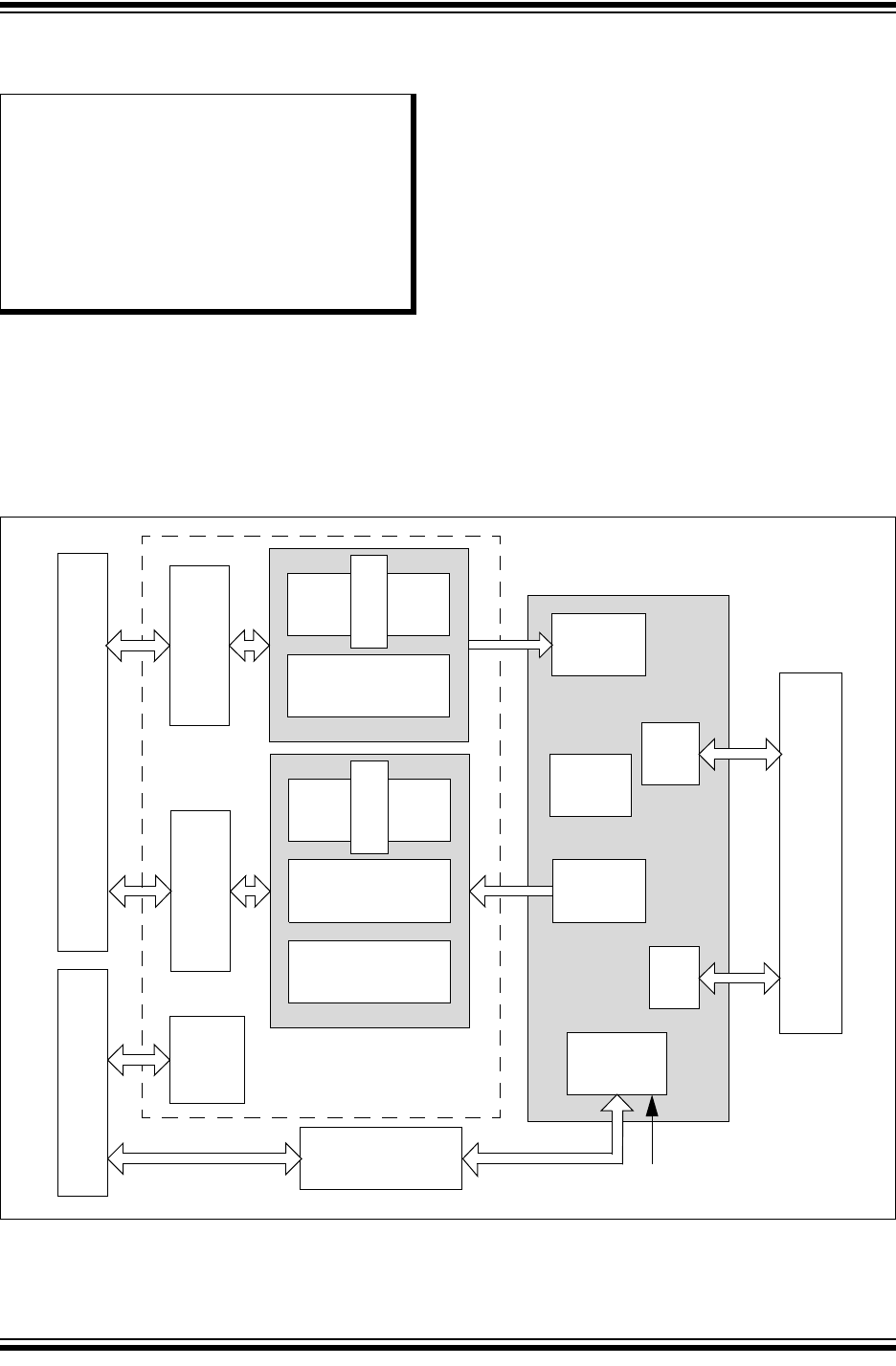
2015 Microchip Technology Inc. Preliminary DS60001320B-page 525
PIC32MZ Embedded Connectivity with Floating Point Unit (EF) Family
30.0 ETHERNET CONTROLLER
The Ethernet controller is a bus master module that
interfaces with an off-chip Physical Layer (PHY) to
implement a complete Ethernet node in a system.
Key features of the Ethernet Controller include:
• Supports 10/100 Mbps data transfer rates
• Supports full-duplex and half-duplex operation
• Supports RMII and MII PHY interface
• Supports MIIM PHY management interface
• Supports both manual and automatic Flow Control
• RAM descriptor-based DMA operation for both
receive and transmit path
• Fully configurable interrupts
• Configurable receive packet filtering
- CRC check
- 64-byte pattern match
- Broadcast, multicast and unicast packets
- Magic Packet™
- 64-bit hash table
- Runt packet
• Supports packet payload checksum calculation
• Supports various hardware statistics counters
Figure 30-1 illustrates a block diagram of the Ethernet
controller.
FIGURE 30-1: ETHERNET CONTROLLER BLOCK DIAGRAM
Note: This data sheet summarizes the
features of the PIC32MZ EF family of
devices. It is not intended to be a
comprehensive reference source. To
complement the information in this data
sheet, refer to Section 35. “Ethernet
Controller” (DS60001155) in the “PIC32
Family Reference Manual”, which is
available from the Microchip web site
(www.microchip.com/PIC32).
TX Bus
Master
System Bus
RX Bus
Master
TX DMA
TX Flow Control
Host IF
RX DMA
RX Filter
Checksum
MAC External
PHY
MII/RMII
IF
MIIM
IF
MAC Control
and
Configuration
Registers
TX Function
RX Function
DMA
Control
Registers
Fast Peripheral Bus
Ethernet Controller
RX Flow
Control
Ethernet DMA
RX BM
TX BM
TX
FIFO
RX
FIFO
PBCLK5

PIC32MZ Embedded Connectivity with Floating Point Unit (EF) Family
DS60001320B-page 526 Preliminary 2015 Microchip Technology Inc.
Table 30-1, Table 30-2, Table 30-3 and Table 30-4
show four interfaces and the associated pins that can
be used with the Ethernet Controller.
TABLE 30-1: MII MODE DEFAULT
INTERFACE SIGNALS
(FMIIEN = 1, FETHIO = 1)
Pin Name Description
EMDC Management Clock
EMDIO Management I/O
ETXCLK Transmit Clock
ETXEN Transmit Enable
ETXD0 Transmit Data
ETXD1 Transmit Data
ETXD2 Transmit Data
ETXD3 Transmit Data
ETXERR Transmit Error
ERXCLK Receive Clock
ERXDV Receive Data Valid
ERXD0 Receive Data
ERXD1 Receive Data
ERXD2 Receive Data
ERXD3 Receive Data
ERXERR Receive Error
ECRS Carrier Sense
ECOL Collision Indication
TABLE 30-2: RMII MODE DEFAULT
INTERFACE SIGNALS
(FMIIEN = 0, FETHIO = 1)
Pin Name Description
EMDC Management Clock
EMDIO Management I/O
ETXEN Transmit Enable
ETXD0 Transmit Data
ETXD1 Transmit Data
EREFCLK Reference Clock
ECRSDV Carrier Sense – Receive Data Valid
ERXD0 Receive Data
ERXD1 Receive Data
ERXERR Receive Error
Note: Ethernet controller pins that are not used
by selected interface can be used by
other peripherals.
TABLE 30-3: MII MODE ALTERNATE
INTERFACE SIGNALS
(FMIIEN = 1, FETHIO = 0)
Pin Name Description
AEMDC Management Clock
AEMDIO Management I/O
AETXCLK Transmit Clock
AETXEN Transmit Enable
AETXD0 Transmit Data
AETXD1 Transmit Data
AETXD2 Transmit Data
AETXD3 Transmit Data
AETXERR Transmit Error
AERXCLK Receive Clock
AERXDV Receive Data Valid
AERXD0 Receive Data
AERXD1 Receive Data
AERXD2 Receive Data
AERXD3 Receive Data
AERXERR Receive Error
AECRS Carrier Sense
AECOL Collision Indication
Note: The MII mode Alternate Interface is not
available on 64-pin devices.
TABLE 30-4: RMII MODE ALTERNATE
INTERFACE SIGNALS
(FMIIEN = 0, FETHIO = 0)
Pin Name Description
AEMDC Management Clock
AEMDIO Management I/O
AETXEN Transmit Enable
AETXD0 Transmit Data
AETXD1 Transmit Data
AEREFCLK Reference Clock
AECRSDV Carrier Sense – Receive Data Valid
AERXD0 Receive Data
AERXD1 Receive Data
AERXERR Receive Error

2015 Microchip Technology Inc. Preliminary DS60001320B-page 527
PIC32MZ Embedded Connectivity with Floating Point Unit (EF) Family
30.1 Ethernet Control Registers
TABLE 30-5: ETHERNET CONTROLLER REGISTER SUMMARY
Virtual Address
(BF88_#)
Register
Name(1)
Bit Range
Bits
All Resets
31/15 30/14 29/13 28/12 27/11 26/10 25/9 24/8 23/7 22/6 21/5 20/4 19/3 18/2 17/1 16/0
2000 ETHCON1 31:16 PTV<15:0> 0000
15:0 ON —SIDL — — — TXRTS RXEN AUTOFC — — MANFC — — — BUFCDEC 0000
2010 ETHCON2 31:16 — — — — — — — — — — — — — — — — 0000
15:0 ————— RXBUFSZ<6:0> — — — — 0000
2020 ETHTXST 31:16 TXSTADDR<31:16> 0000
15:0 TXSTADDR<15:2> — — 0000
2030 ETHRXST 31:16 RXSTADDR<31:16> 0000
15:0 RXSTADDR<15:2> — — 0000
2040 ETHHT0 31:16 HT<31:0> 0000
15:0 0000
2050 ETHHT1 31:16 HT<63:32> 0000
15:0 0000
2060 ETHPMM0 31:16 PMM<31:0> 0000
15:0 0000
2070 ETHPMM1 31:16 PMM<63:32> 0000
15:0 0000
2080 ETHPMCS 31:16 — — — — — — — — — — — — — — — — 0000
15:0 PMCS<15:0> 0000
2090 ETHPMO 31:16 — — — — — — — — — — — — — — — — 0000
15:0 PMO<15:0> 0000
20A0 ETHRXFC
31:16 — — — — — — — — — — — — — — — — 0000
15:0 HTEN MPEN —NOTPM PMMODE<3:0> CRC
ERREN CRC
OKEN RUNT
ERREN RUNTEN UCEN NOT
MEEN MCEN BCEN 0000
20B0 ETHRXWM 31:16 ———————— RXFWM<7:0> 0000
15:0 ———————— RXEWM<7:0> 0000
20C0 ETHIEN
31:16 — — — — — — — — — — — — — — — — 0000
15:0 —TX
BUSEIE RX
BUSEIE — — — EW
MARKIE FW
MARKIE RX
DONEIE PK
TPENDIE RX
ACTIE —TX
DONEIE TX
ABORTIE RX
BUFNAIE RX
OVFLWIE 0000
20D0 ETHIRQ 31:16 — — — — — — — — — — — — — — — — 0000
15:0 —TXBUSE RXBUSE — — — EWMARK FWMARK RXDONE PKTPEND RXACT —TXDONE TXABORT RXBUFNA RXOVFLW 0000
20E0 ETHSTAT 31:16 ———————— BUFCNT<7:0> 0000
15:0 ————————BUSY TXBUSY RXBUSY — — — — — 0000
2100 ETH
RXOVFLOW
31:16 — — — — — — — — — — — — — — — — 0000
15:0 RXOVFLWCNT<15:0> 0000
Legend: x = unknown value on Reset; — = unimplemented, read as ‘0’. Reset values are shown in hexadecimal.
Note 1: All registers in this table (with the exception of ETHSTAT) have corresponding CLR, SET and INV registers at their virtual addresses, plus offsets of 0x4, 0x8 and 0xC, respectively. See Section 12.3 “CLR, SET, and
INV Registers” for more information.
2: Reset values default to the factory programmed value.

PIC32MZ Embedded Connectivity with Floating Point Unit (EF) Family
DS60001320B-page 528 Preliminary 2015 Microchip Technology Inc.
2110 ETH
FRMTXOK
31:16 — — — — — — — — — — — — — — — — 0000
15:0 FRMTXOKCNT<15:0> 0000
2120 ETH
SCOLFRM
31:16 — — — — — — — — — — — — — — — — 0000
15:0 SCOLFRMCNT<15:0> 0000
2130 ETH
MCOLFRM
31:16 — — — — — — — — — — — — — — — — 0000
15:0 MCOLFRMCNT<15:0> 0000
2140 ETH
FRMRXOK
31:16 — — — — — — — — — — — — — — — — 0000
15:0 FRMRXOKCNT<15:0> 0000
2150 ETH
FCSERR
31:16 — — — — — — — — — — — — — — — — 0000
15:0 FCSERRCNT<15:0> 0000
2160 ETH
ALGNERR
31:16 — — — — — — — — — — — — — — — — 0000
15:0 ALGNERRCNT<15:0> 0000
2200 EMAC1
CFG1
31:16 — — — — — — — — — — — — — — — — 0000
15:0 SOFT
RESET SIM
RESET — — RESET
RMCS RESET
RFUN RESET
TMCS RESET
TFUN — — — LOOPBACK TXPAUSE RXPAUSE PASSALL RXENABLE 800D
2210 EMAC1
CFG2
31:16 — — — — — — — — — — — — — — — — 0000
15:0 —EXCESS
DFR BP
NOBKOFF NOBKOFF — — LONGPRE PUREPRE AUTOPAD VLANPAD PAD
ENABLE CRC
ENABLE DELAYCRC HUGEFRM LENGTHCK FULLDPLX 4082
2220 EMAC1
IPGT
31:16 — — — — — — — — — — — — — — — — 0000
15:0 ————————— B2BIPKTGP<6:0> 0012
2230 EMAC1
IPGR
31:16 — — — — — — — — — — — — — — — — 0000
15:0 —NB2BIPKTGP1<6:0> —NB2BIPKTGP2<6:0> 0C12
2240 EMAC1
CLRT
31:16 — — — — — — — — — — — — — — — — 0000
15:0 — — CWINDOW<5:0> — — — — RETX<3:0> 370F
2250 EMAC1
MAXF
31:16 — — — — — — — — — — — — — — — — 0000
15:0 MACMAXF<15:0> 05EE
2260 EMAC1
SUPP
31:16 — — — — — — — — — — — — — — — — 0000
15:0 ————RESET
RMII — — SPEED
RMII — — — — — — — — 1000
2270 EMAC1
TEST
31:16 — — — — — — — — — — — — — — — — 0000
15:0 —————————————TESTBP TESTPAUSE SHRTQNTA 0000
2280 EMAC1
MCFG
31:16 — — — — — — — — — — — — — — — — 0000
15:0 RESET
MGMT ————————— CLKSEL<3:0> NOPRE SCANINC 0020
2290 EMAC1
MCMD
31:16 — — — — — — — — — — — — — — — — 0000
15:0 ——————————————SCAN READ 0000
22A0 EMAC1
MADR
31:16 — — — — — — — — — — — — — — — — 0000
15:0 ——— PHYADDR<4:0> — — — REGADDR<4:0> 0100
TABLE 30-5: ETHERNET CONTROLLER REGISTER SUMMARY (CONTINUED)
Virtual Address
(BF88_#)
Register
Name(1)
Bit Range
Bits
All Resets
31/15 30/14 29/13 28/12 27/11 26/10 25/9 24/8 23/7 22/6 21/5 20/4 19/3 18/2 17/1 16/0
Legend: x = unknown value on Reset; — = unimplemented, read as ‘0’. Reset values are shown in hexadecimal.
Note 1: All registers in this table (with the exception of ETHSTAT) have corresponding CLR, SET and INV registers at their virtual addresses, plus offsets of 0x4, 0x8 and 0xC, respectively. See Section 12.3 “CLR, SET, and
INV Registers” for more information.
2: Reset values default to the factory programmed value.

2015 Microchip Technology Inc. Preliminary DS60001320B-page 529
PIC32MZ Embedded Connectivity with Floating Point Unit (EF) Family
22B0 EMAC1
MWTD
31:16 — — — — — — — — — — — — — — — — 0000
15:0 MWTD<15:0> 0000
22C0 EMAC1
MRDD
31:16 — — — — — — — — — — — — — — — — 0000
15:0 MRDD<15:0> 0000
22D0 EMAC1
MIND
31:16 — — — — — — — — — — — — — — — — 0000
15:0 ————————————LINKFAIL NOTVALID SCAN MIIMBUSY 0000
2300 EMAC1
SA0(2) 31:16 — — — — — — — — — — — — — — — — xxxx
15:0 STNADDR6<7:0> STNADDR5<7:0> xxxx
2310 EMAC1
SA1(2) 31:16 — — — — — — — — — — — — — — — — xxxx
15:0 STNADDR4<7:0> STNADDR3<7:0> xxxx
2320 EMAC1
SA2(2) 31:16 — — — — — — — — — — — — — — — — xxxx
15:0 STNADDR2<7:0> STNADDR1<7:0> xxxx
TABLE 30-5: ETHERNET CONTROLLER REGISTER SUMMARY (CONTINUED)
Virtual Address
(BF88_#)
Register
Name(1)
Bit Range
Bits
All Resets
31/15 30/14 29/13 28/12 27/11 26/10 25/9 24/8 23/7 22/6 21/5 20/4 19/3 18/2 17/1 16/0
Legend: x = unknown value on Reset; — = unimplemented, read as ‘0’. Reset values are shown in hexadecimal.
Note 1: All registers in this table (with the exception of ETHSTAT) have corresponding CLR, SET and INV registers at their virtual addresses, plus offsets of 0x4, 0x8 and 0xC, respectively. See Section 12.3 “CLR, SET, and
INV Registers” for more information.
2: Reset values default to the factory programmed value.

PIC32MZ Embedded Connectivity with Floating Point Unit (EF) Family
DS60001320B-page 530 Preliminary 2015 Microchip Technology Inc.
REGISTER 30-1: ETHCON1: ETHERNET CONTROLLER CONTROL REGISTER 1
Bit Range Bit
31/23/15/7 Bit
30/22/14/6 Bit
29/21/13/5 Bit
28/20/12/4 Bit
27/19/11/3 Bit
26/18/10/2 Bit
25/17/9/1 Bit
24/16/8/0
31:24 R/W-0 R/W-0 R/W-0 R/W-0 R/W-0 R/W-0 R/W-0 R/W-0
PTV<15:8>
23:16 R/W-0 R/W-0 R/W-0 R/W-0 R/W-0 R/W-0 R/W-0 R/W-0
PTV<7:0>
15:8 R/W-0 U-0 R/W-0 U-0 U-0 U-0 R/W-0 R/W-0
ON —SIDL— — — TXRTS RXEN(1)
7:0 R/W-0 U-0 U-0 R/W-0 U-0 U-0 U-0 R/W-0
AUTOFC ——MANFC— — — BUFCDEC
Legend:
R = Readable bit W = Writable bit U = Unimplemented bit, read as ‘0’
-n = Value at POR ‘1’ = Bit is set ‘0’ = Bit is cleared x = Bit is unknown
bit 31-16 PTV<15:0>: PAUSE Timer Value bits
PAUSE Timer Value used for Flow Control.
This register should only be written when RXEN (ETHCON1<8>) is not set.
These bits are only used for Flow Control operations.
bit 15 ON: Ethernet ON bit
1 = Ethernet module is enabled
0 = Ethernet module is disabled
bit 14 Unimplemented: Read as ‘0’
bit 13 SIDL: Ethernet Stop in Idle Mode bit
1 = Ethernet module transfers are paused during Idle mode
0 = Ethernet module transfers continue during Idle mode
bit 12-10 Unimplemented: Read as ‘0’
bit 9 TXRTS: Transmit Request to Send bit
1 = Activate the TX logic and send the packet(s) defined in the TX EDT
0 = Stop transmit (when cleared by software) or transmit done (when cleared by hardware)
After the bit is written with a ‘1’, it will clear to a ‘0’ whenever the transmit logic has finished transmitting
the requested packets in the Ethernet Descriptor Table (EDT). If a ‘0’ is written by the CPU, the transmit
logic finishes the current packet’s transmission and then stops any further.
This bit only affects TX operations.
bit 8 RXEN: Receive Enable bit(1)
1 = Enable RX logic, packets are received and stored in the RX buffer as controlled by the filter
configuration
0 = Disable RX logic, no packets are received in the RX buffer
This bit only affects RX operations.
Note 1: It is not recommended to clear the RXEN bit and then make changes to any RX related field/register. The
Ethernet Controller must be reinitialized (ON cleared to ‘0’), and then the RX changes applied.

2015 Microchip Technology Inc. Preliminary DS60001320B-page 531
PIC32MZ Embedded Connectivity with Floating Point Unit (EF) Family
bit 7 AUTOFC: Automatic Flow Control bit
1 = Automatic Flow Control enabled
0 = Automatic Flow Control disabled
Setting this bit will enable automatic Flow Control. If set, the full and empty watermarks are used to
automatically enable and disable the Flow Control, respectively. When the number of received buffers
BUFCNT (ETHSTAT<16:23>) rises to the full watermark, Flow Control is automatically enabled. When
the BUFCNT falls to the empty watermark, Flow Control is automatically disabled.
This bit is only used for Flow Control operations and affects both TX and RX operations.
bit 6-5 Unimplemented: Read as ‘0’
bit 4 MANFC: Manual Flow Control bit
1 = Manual Flow Control is enabled
0 = Manual Flow Control is disabled
Setting this bit will enable manual Flow Control. If set, the Flow Control logic will send a PAUSE frame
using the PAUSE timer value in the PTV register. It will then resend a PAUSE frame every 128 *
PTV<15:0>/2 TX clock cycles until the bit is cleared.
Note: For 10 Mbps operation, TX clock runs at 2.5 MHz. For 100 Mbps operation, TX clock runs at
25 MHz.
When this bit is cleared, the Flow Control logic will automatically send a PAUSE frame with a 0x0000
PAUSE timer value to disable Flow Control.
This bit is only used for Flow Control operations and affects both TX and RX operations.
bit 3-1 Unimplemented: Read as ‘0’
bit 0 BUFCDEC: Descriptor Buffer Count Decrement bit
The BUFCDEC bit is a write-1 bit that reads as ‘0’. When written with a ‘1’, the Descriptor Buffer Counter,
BUFCNT, will decrement by one. If BUFCNT is incremented by the RX logic at the same time that this bit
is written, the BUFCNT value will remain unchanged. Writing a ‘0’ will have no effect.
This bit is only used for RX operations.
REGISTER 30-1: ETHCON1: ETHERNET CONTROLLER CONTROL REGISTER 1 (CONTINUED)
Note 1: It is not recommended to clear the RXEN bit and then make changes to any RX related field/register. The
Ethernet Controller must be reinitialized (ON cleared to ‘0’), and then the RX changes applied.

PIC32MZ Embedded Connectivity with Floating Point Unit (EF) Family
DS60001320B-page 532 Preliminary 2015 Microchip Technology Inc.
REGISTER 30-2: ETHCON2: ETHERNET CONTROLLER CONTROL REGISTER 2
Bit Range Bit
31/23/15/7 Bit
30/22/14/6 Bit
29/21/13/5 Bit
28/20/12/4 Bit
27/19/11/3 Bit
26/18/10/2 Bit
25/17/9/1 Bit
24/16/8/0
31:24 U-0 U-0 U-0 U-0 U-0 U-0 U-0 U-0
— — — — — — — —
23:16 U-0 U-0 U-0 U-0 U-0 U-0 U-0 U-0
— — — — — — — —
15:8 U-0 U-0 U-0 U-0 U-0 R/W-0 R/W-0 R/W-0
— — — — — RXBUFSZ<6:4>
7:0 R/W-0 R/W-0 R/W-0 R/W-0 U-0 U-0 U-0 U-0
RXBUFSZ<3:0> — — — —
Legend:
R = Readable bit W = Writable bit U = Unimplemented bit, read as ‘0’
-n = Value at POR ‘1’ = Bit is set ‘0’ = Bit is cleared x = Bit is unknown
bit 31-11 Unimplemented: Read as ‘0’
bit 10-4 RXBUFSZ<6:0>: RX Data Buffer Size for All RX Descriptors (in 16-byte increments) bits
1111111 = RX data Buffer size for descriptors is 2032 bytes
•
•
•
1100000 = RX data Buffer size for descriptors is 1536 bytes
•
•
•
0000011 = RX data Buffer size for descriptors is 48 bytes
0000010 = RX data Buffer size for descriptors is 32 bytes
0000001 = RX data Buffer size for descriptors is 16 bytes
0000000 = Reserved
bit 3-0 Unimplemented: Read as ‘0’
Note 1: This register is only used for RX operations.
2: The bits in this register may only be changed while the RXEN bit (ETHCON1<8>) = 0.

2015 Microchip Technology Inc. Preliminary DS60001320B-page 533
PIC32MZ Embedded Connectivity with Floating Point Unit (EF) Family
REGISTER 30-3: ETHTXST: ETHERNET CONTROLLER TX PACKET DESCRIPTOR START
ADDRESS REGISTER
Bit
Range Bit
31/23/15/7 Bit
30/22/14/6 Bit
29/21/13/5 Bit
28/20/12/4 Bit
27/19/11/3 Bit
26/18/10/2 Bit
25/17/9/1 Bit
24/16/8/0
31:24 R/W-0 R/W-0 R/W-0 R/W-0 R/W-0 R/W-0 R/W-0 R/W-0
TXSTADDR<31:24>
23:16 R/W-0 R/W-0 R/W-0 R/W-0 R/W-0 R/W-0 R/W-0 R/W-0
TXSTADDR<23:16>
15:8 R/W-0 R/W-0 R/W-0 R/W-0 R/W-0 R/W-0 R/W-0 R/W-0
TXSTADDR<15:8>
7:0 R/W-0 R/W-0 R/W-0 R/W-0 R/W-0 R/W-0 U-0 U-0
TXSTADDR<7:2> — —
Legend:
R = Readable bit W = Writable bit U = Unimplemented bit, read as ‘0’
-n = Value at POR ‘1’ = Bit is set ‘0’ = Bit is cleared x = Bit is unknown
bit 31-2 TXSTADDR<31:2>: Starting Address of First Transmit Descriptor bits
This register should not be written while any transmit, receive or DMA operations are in progress.
This address must be 4-byte aligned (bits 1-0 must be ‘00’).
bit 1-0 Unimplemented: Read as ‘0’
Note 1: This register is only used for TX operations.
2: This register will be updated by hardware with the last descriptor used by the last successfully transmitted
packet.
REGISTER 30-4: ETHRXST: ETHERNET CONTROLLER RX PACKET DESCRIPTOR START
ADDRESS REGISTER
Bit
Range Bit
31/23/15/7 Bit
30/22/14/6 Bit
29/21/13/5 Bit
28/20/12/4 Bit
27/19/11/3 Bit
26/18/10/2 Bit
25/17/9/1 Bit
24/16/8/0
31:24 R/W-0 R/W-0 R/W-0 R/W-0 R/W-0 R/W-0 R/W-0 R/W-0
RXSTADDR<31:24>
23:16 R/W-0 R/W-0 R/W-0 R/W-0 R/W-0 R/W-0 R/W-0 R/W-0
RXSTADDR<23:16>
15:8 R/W-0 R/W-0 R/W-0 R/W-0 R/W-0 R/W-0 R/W-0 R/W-0
RXSTADDR<15:8>
7:0 R/W-0 R/W-0 R/W-0 R/W-0 R/W-0 R/W-0 U-0 U-0
RXSTADDR<7:2> — —
Legend:
R = Readable bit W = Writable bit U = Unimplemented bit, read as ‘0’
-n = Value at POR ‘1’ = Bit is set ‘0’ = Bit is cleared x = Bit is unknown
bit 31-2 RXSTADDR<31:2>: Starting Address of First Receive Descriptor bits
This register should not be written while any transmit, receive or DMA operations are in progress.
This address must be 4-byte aligned (bits 1-0 must be ‘00’).
bit 1-0 Unimplemented: Read as ‘0’
Note 1: This register is only used for RX operations.
2: This register will be updated by hardware with the last descriptor used by the last successfully transmitted
packet.

PIC32MZ Embedded Connectivity with Floating Point Unit (EF) Family
DS60001320B-page 534 Preliminary 2015 Microchip Technology Inc.
REGISTER 30-5: ETHHT0: ETHERNET CONTROLLER HASH TABLE 0 REGISTER
Bit
Range Bit
31/23/15/7 Bit
30/22/14/6 Bit
29/21/13/5 Bit
28/20/12/4 Bit
27/19/11/3 Bit
26/18/10/2 Bit
25/17/9/1 Bit
24/16/8/0
31:24 R/W-0 R/W-0 R/W-0 R/W-0 R/W-0 R/W-0 R/W-0 R/W-0
HT<31:24>
23:16 R/W-0 R/W-0 R/W-0 R/W-0 R/W-0 R/W-0 R/W-0 R/W-0
HT<23:16>
15:8 R/W-0 R/W-0 R/W-0 R/W-0 R/W-0 R/W-0 R/W-0 R/W-0
HT<15:8>
7:0 R/W-0 R/W-0 R/W-0 R/W-0 R/W-0 R/W-0 R/W-0 R/W-0
HT<7:0>
Legend:
R = Readable bit W = Writable bit U = Unimplemented bit, read as ‘0’
-n = Value at POR ‘1’ = Bit is set ‘0’ = Bit is cleared x = Bit is unknown
bit 31-0 HT<31:0>: Hash Table Bytes 0-3 bits
Note 1: This register is only used for RX operations.
2: The bits in this register may only be changed while the RXEN bit (ETHCON1<8>) = 0 or the HTEN bit
(ETHRXFC<15>) = 0.
REGISTER 30-6: ETHHT1: ETHERNET CONTROLLER HASH TABLE 1 REGISTER
Bit Range Bit
31/23/15/7 Bit
30/22/14/6 Bit
29/21/13/5 Bit
28/20/12/4 Bit
27/19/11/3 Bit
26/18/10/2 Bit
25/17/9/1 Bit
24/16/8/0
31:24 R/W-0 R/W-0 R/W-0 R/W-0 R/W-0 R/W-0 R/W-0 R/W-0
HT<63:56>
23:16 R/W-0 R/W-0 R/W-0 R/W-0 R/W-0 R/W-0 R/W-0 R/W-0
HT<55:48>
15:8 R/W-0 R/W-0 R/W-0 R/W-0 R/W-0 R/W-0 R/W-0 R/W-0
HT<47:40>
7:0 R/W-0 R/W-0 R/W-0 R/W-0 R/W-0 R/W-0 R/W-0 R/W-0
HT<39:32>
Legend:
R = Readable bit W = Writable bit U = Unimplemented bit, read as ‘0’
-n = Value at POR ‘1’ = Bit is set ‘0’ = Bit is cleared x = Bit is unknown
bit 31-0 HT<63:32>: Hash Table Bytes 4-7 bits
Note 1: This register is only used for RX operations.
2: The bits in this register may only be changed while the RXEN bit (ETHCON1<8>) = 0 or the HTEN bit
(ETHRXFC<15>) = 0.

2015 Microchip Technology Inc. Preliminary DS60001320B-page 535
PIC32MZ Embedded Connectivity with Floating Point Unit (EF) Family
REGISTER 30-7: ETHPMM0: ETHERNET CONTROLLER PATTERN MATCH MASK 0 REGISTER
Bit Range Bit
31/23/15/7 Bit
30/22/14/6 Bit
29/21/13/5 Bit
28/20/12/4 Bit
27/19/11/3 Bit
26/18/10/2 Bit
25/17/9/1 Bit
24/16/8/0
31:24 R/W-0 R/W-0 R/W-0 R/W-0 R/W-0 R/W-0 R/W-0 R/W-0
PMM<31:24>
23:16 R/W-0 R/W-0 R/W-0 R/W-0 R/W-0 R/W-0 R/W-0 R/W-0
PMM<23:16>
15:8 R/W-0 R/W-0 R/W-0 R/W-0 R/W-0 R/W-0 R/W-0 R/W-0
PMM<15:8>
7:0 R/W-0 R/W-0 R/W-0 R/W-0 R/W-0 R/W-0 R/W-0 R/W-0
PMM<7:0>
Legend:
R = Readable bit W = Writable bit U = Unimplemented bit, read as ‘0’
-n = Value at POR ‘1’ = Bit is set ‘0’ = Bit is cleared x = Bit is unknown
bit 31-24 PMM<31:24>: Pattern Match Mask 3 bits
bit 23-16 PMM<23:16>: Pattern Match Mask 2 bits
bit 15-8 PMM<15:8>: Pattern Match Mask 1 bits
bit 7-0 PMM<7:0>: Pattern Match Mask 0 bits
Note 1: This register is only used for RX operations.
2: The bits in this register may only be changed while the RXEN bit (ETHCON1<8>) = 0 or the PMMODE bit
(ETHRXFC<11:8>) = 0.
REGISTER 30-8: ETHPMM1: ETHERNET CONTROLLER PATTERN MATCH MASK 1 REGISTER
Bit Range Bit
31/23/15/7 Bit
30/22/14/6 Bit
29/21/13/5 Bit
28/20/12/4 Bit
27/19/11/3 Bit
26/18/10/2 Bit
25/17/9/1
Bit
24/16/8/0
31:24 R/W-0 R/W-0 R/W-0 R/W-0 R/W-0 R/W-0 R/W-0 R/W-0
PMM<63:56>
23:16 R/W-0 R/W-0 R/W-0 R/W-0 R/W-0 R/W-0 R/W-0 R/W-0
PMM<55:48>
15:8 R/W-0 R/W-0 R/W-0 R/W-0 R/W-0 R/W-0 R/W-0 R/W-0
PMM<47:40>
7:0 R/W-0 R/W-0 R/W-0 R/W-0 R/W-0 R/W-0 R/W-0 R/W-0
PMM<39:32>
Legend:
R = Readable bit W = Writable bit U = Unimplemented bit, read as ‘0’
-n = Value at POR ‘1’ = Bit is set ‘0’ = Bit is cleared x = Bit is unknown
bit 31-24 PMM<63:56>: Pattern Match Mask 7 bits
bit 23-16 PMM<55:48>: Pattern Match Mask 6 bits
bit 15-8 PMM<47:40>: Pattern Match Mask 5 bits
bit 7-0 PMM<39:32>: Pattern Match Mask 4 bits
Note 1: This register is only used for RX operations.
2: The bits in this register may only be changed while the RXEN bit (ETHCON1<8>) = 0 or the PMMODE bit
(ETHRXFC<11:8>) = 0.
PIC32MZ Embedded Connectivity with Floating Point Unit (EF) Family
DS60001320B-page 536 Preliminary 2015 Microchip Technology Inc.
REGISTER 30-9: ETHPMCS: ETHERNET CONTROLLER PATTERN MATCH CHECKSUM
REGISTER
Bit Range Bit
31/23/15/7 Bit
30/22/14/6 Bit
29/21/13/5 Bit
28/20/12/4 Bit
27/19/11/3 Bit
26/18/10/2 Bit
25/17/9/1
Bit
24/16/8/0
31:24 U-0 U-0 U-0 U-0 U-0 U-0 U-0 U-0
— — — — — — — —
23:16 U-0 U-0 U-0 U-0 U-0 U-0 U-0 U-0
— — — — — — — —
15:8 R/W-0 R/W-0 R/W-0 R/W-0 R/W-0 R/W-0 R/W-0 R/W-0
PMCS<15:8>
7:0 R/W-0 R/W-0 R/W-0 R/W-0 R/W-0 R/W-0 R/W-0 R/W-0
PMCS<7:0>
Legend:
R = Readable bit W = Writable bit U = Unimplemented bit, read as ‘0’
-n = Value at POR ‘1’ = Bit is set ‘0’ = Bit is cleared x = Bit is unknown
bit 31-16 Unimplemented: Read as ‘0’
bit 15-8 PMCS<15:8>: Pattern Match Checksum 1 bits
bit 7-0 PMCS<7:0>: Pattern Match Checksum 0 bits
Note 1: This register is only used for RX operations.
2: The bits in this register may only be changed while the RXEN bit (ETHCON1<8>) = 0 or the PMMODE bit
(ETHRXFC<11:8>) = 0.
REGISTER 30-10: ETHPMO: ETHERNET CONTROLLER PATTERN MATCH OFFSET REGISTER
Bit
Range Bit
31/23/15/7 Bit
30/22/14/6 Bit
29/21/13/5 Bit
28/20/12/4 Bit
27/19/11/3 Bit
26/18/10/2 Bit
25/17/9/1 Bit
24/16/8/0
31:24 U-0 U-0 U-0 U-0 U-0 U-0 U-0 U-0
————————
23:16 U-0 U-0 U-0 U-0 U-0 U-0 U-0 U-0
————————
15:8 R/W-0 R/W-0 R/W-0 R/W-0 R/W-0 R/W-0 R/W-0 R/W-0
PMO<15:8>
7:0 R/W-0 R/W-0 R/W-0 R/W-0 R/W-0 R/W-0 R/W-0 R/W-0
PMO<7:0>
Legend:
R = Readable bit W = Writable bit U = Unimplemented bit, read as ‘0’
-n = Value at POR ‘1’ = Bit is set ‘0’ = Bit is cleared x = Bit is unknown
bit 31-16 Unimplemented: Read as ‘0’
bit 15-0 PMO<15:0>: Pattern Match Offset 1 bits
Note 1: This register is only used for RX operations.
2: The bits in this register may only be changed while the RXEN bit (ETHCON1<8>) = 0 or the PMMODE bit
(ETHRXFC<11:8>) = 0.

2015 Microchip Technology Inc. Preliminary DS60001320B-page 537
PIC32MZ Embedded Connectivity with Floating Point Unit (EF) Family
REGISTER 30-11: ETHRXFC: ETHERNET CONTROLLER RECEIVE FILTER CONFIGURATION
REGISTER
Bit
Range Bit
31/23/15/7 Bit
30/22/14/6 Bit
29/21/13/5 Bit
28/20/12/4 Bit
27/19/11/3 Bit
26/18/10/2 Bit
25/17/9/1 Bit
24/16/8/0
31:24 U-0 U-0 U-0 U-0 U-0 U-0 U-0 U-0
— — — — — — — —
23:16 U-0 U-0 U-0 U-0 U-0 U-0 U-0 U-0
— — — — — — — —
15:8 R/W-0 R/W-0 U-0 R/W-0 R/W-0 R/W-0 R/W-0 R/W-0
HTEN MPEN — NOTPM PMMODE<3:0>
7:0 R/W-0 R/W-0 R/W-0 R/W-0 R/W-0 R/W-0 R/W-0 R/W-0
CRCERREN CRCOKEN RUNTERREN RUNTEN UCEN NOTMEEN MCEN BCEN
Legend:
R = Readable bit W = Writable bit U = Unimplemented bit, read as ‘0’
-n = Value at POR ‘1’ = Bit is set ‘0’ = Bit is cleared x = Bit is unknown
bit 31-16 Unimplemented: Read as ‘0’
bit 15 HTEN: Enable Hash Table Filtering bit
1 = Enable Hash Table Filtering
0 = Disable Hash Table Filtering
bit 14 MPEN: Magic Packet™ Enable bit
1 = Enable Magic Packet Filtering
0 = Disable Magic Packet Filtering
bit 13 Unimplemented: Read as ‘0’
bit 12 NOTPM: Pattern Match Inversion bit
1 = The Pattern Match Checksum must not match for a successful Pattern Match to occur
0 = The Pattern Match Checksum must match for a successful Pattern Match to occur
This bit determines whether Pattern Match Checksum must match in order for a successful Pattern Match
to occur.
bit 11-8 PMMODE<3:0>: Pattern Match Mode bits
1001 = Pattern match is successful if (NOTPM = 1 XOR Pattern Match Checksum matches) AND
(Packet = Magic Packet)(1,3)
1000 = Pattern match is successful if (NOTPM = 1 XOR Pattern Match Checksum matches) AND
(Hash Table Filter match)(1,1)
0111 = Pattern match is successful if (NOTPM = 1 XOR Pattern Match Checksum matches) AND
(Destination Address = Broadcast Address)(1)
0110 = Pattern match is successful if (NOTPM = 1 XOR Pattern Match Checksum matches) AND
(Destination Address = Broadcast Address)(1)
0101 = Pattern match is successful if (NOTPM = 1 XOR Pattern Match Checksum matches) AND
(Destination Address = Unicast Address)(1)
0100 = Pattern match is successful if (NOTPM = 1 XOR Pattern Match Checksum matches) AND
(Destination Address = Unicast Address)(1)
0011 = Pattern match is successful if (NOTPM = 1 XOR Pattern Match Checksum matches) AND
(Destination Address = Station Address)(1)
0010 = Pattern match is successful if (NOTPM = 1 XOR Pattern Match Checksum matches) AND
(Destination Address = Station Address)(1)
0001 = Pattern match is successful if (NOTPM = 1 XOR Pattern Match Checksum matches)(1)
0000 = Pattern Match is disabled; pattern match is always unsuccessful
Note 1: XOR = True when either one or the other conditions are true, but not both.
2: This Hash Table Filter match is active regardless of the value of the HTEN bit.
3: This Magic Packet Filter match is active regardless of the value of the MPEN bit.
Note 1: This register is only used for RX operations.
2: The bits in this register may only be changed while the RXEN bit (ETHCON1<8>) = 0.

PIC32MZ Embedded Connectivity with Floating Point Unit (EF) Family
DS60001320B-page 538 Preliminary 2015 Microchip Technology Inc.
bit 7 CRCERREN: CRC Error Collection Enable bit
1 = The received packet CRC must be invalid for the packet to be accepted
0 = Disable CRC Error Collection filtering
This bit allows the user to collect all packets that have an invalid CRC.
bit 6 CRCOKEN: CRC OK Enable bit
1 = The received packet CRC must be valid for the packet to be accepted
0 = Disable CRC filtering
This bit allows the user to reject all packets that have an invalid CRC.
bit 5 RUNTERREN: Runt Error Collection Enable bit
1 = The received packet must be a runt packet for the packet to be accepted
0 = Disable Runt Error Collection filtering
This bit allows the user to collect all packets that are runt packets. For this filter, a runt packet is defined as
any packet with a size of less than 64 bytes (when CRCOKEN = 0) or any packet with a size of less than
64 bytes that has a valid CRC (when CRCOKEN = 1).
bit 4 RUNTEN: Runt Enable bit
1 = The received packet must not be a runt packet for the packet to be accepted
0 = Disable Runt filtering
This bit allows the user to reject all runt packets. For this filter, a runt packet is defined as any packet with a
size of less than 64 bytes.
bit 3 UCEN: Unicast Enable bit
1 = Enable Unicast Filtering
0 = Disable Unicast Filtering
This bit allows the user to accept all unicast packets whose Destination Address matches the Station
Address.
bit 2 NOTMEEN: Not Me Unicast Enable bit
1 = Enable Not Me Unicast Filtering
0 = Disable Not Me Unicast Filtering
This bit allows the user to accept all unicast packets whose Destination Address does not match the Station
Address.
bit 1 MCEN: Multicast Enable bit
1 = Enable Multicast Filtering
0 = Disable Multicast Filtering
This bit allows the user to accept all Multicast Address packets.
bit 0 BCEN: Broadcast Enable bit
1 = Enable Broadcast Filtering
0 = Disable Broadcast Filtering
This bit allows the user to accept all Broadcast Address packets.
REGISTER 30-11: ETHRXFC: ETHERNET CONTROLLER RECEIVE FILTER CONFIGURATION
REGISTER (CONTINUED)
Note 1: XOR = True when either one or the other conditions are true, but not both.
2: This Hash Table Filter match is active regardless of the value of the HTEN bit.
3: This Magic Packet Filter match is active regardless of the value of the MPEN bit.
Note 1: This register is only used for RX operations.
2: The bits in this register may only be changed while the RXEN bit (ETHCON1<8>) = 0.

2015 Microchip Technology Inc. Preliminary DS60001320B-page 539
PIC32MZ Embedded Connectivity with Floating Point Unit (EF) Family
REGISTER 30-12: ETHRXWM: ETHERNET CONTROLLER RECEIVE WATERMARKS REGISTER
Bit Range Bit
31/23/15/7 Bit
30/22/14/6 Bit
29/21/13/5 Bit
28/20/12/4 Bit
27/19/11/3 Bit
26/18/10/2 Bit
25/17/9/1 Bit
24/16/8/0
31:24 U-0 U-0 U-0 U-0 U-0 U-0 U-0 U-0
— — — — — — — —
23:16 R/W-0 R/W-0 R/W-0 R/W-0 R/W-0 R/W-0 R/W-0 R/W-0
RXFWM<7:0>
15:8 U-0 U-0 U-0 U-0 U-0 U-0 U-0 U-0
— — — — — — — —
7:0 R/W-0 R/W-0 R/W-0 R/W-0 R/W-0 R/W-0 R/W-0 R/W-0
RXEWM<7:0>
Legend:
R = Readable bit W = Writable bit U = Unimplemented bit, read as ‘0’
-n = Value at POR ‘1’ = Bit is set ‘0’ = Bit is cleared x = Bit is unknown
bit 31-24 Unimplemented: Read as ‘0’
bit 23-16 RXFWM<7:0>: Receive Full Watermark bits
The software controlled RX Buffer Full Watermark Pointer is compared against the RX BUFCNT to
determine the full watermark condition for the FWMARK interrupt and for enabling Flow Control when
automatic Flow Control is enabled. The Full Watermark Pointer should always be greater than the Empty
Watermark Pointer.
bit 15-8 Unimplemented: Read as ‘0’
bit 7-0 RXEWM<7:0>: Receive Empty Watermark bits
The software controlled RX Buffer Empty Watermark Pointer is compared against the RX BUFCNT to
determine the empty watermark condition for the EWMARK interrupt and for disabling Flow Control when
automatic Flow Control is enabled. The Empty Watermark Pointer should always be less than the Full
Watermark Pointer.
Note: This register is only used for RX operations.

PIC32MZ Embedded Connectivity with Floating Point Unit (EF) Family
DS60001320B-page 540 Preliminary 2015 Microchip Technology Inc.
REGISTER 30-13: ETHIEN: ETHERNET CONTROLLER INTERRUPT ENABLE REGISTER
Bit
Range Bit
31/23/15/7 Bit
30/22/14/6 Bit
29/21/13/5 Bit
28/20/12/4 Bit
27/19/11/3 Bit
26/18/10/2 Bit
25/17/9/1 Bit
24/16/8/0
31:24 U-0 U-0 U-0 U-0 U-0 U-0 U-0 U-0
— — — — — — — —
23:16 U-0 U-0 U-0 U-0 U-0 U-0 U-0 U-0
— — — — — — — —
15:8 U-0 R/W-0 R/W-0 U-0 U-0 U-0 R/W-0 R/W-0
— TXBUSEIE(1) RXBUSEIE(2) — — — EWMARKIE(2) FWMARKIE(2)
7:0 R/W-0 R/W-0 R/W-0 U-0 R/W-0 R/W-0 R/W-0 R/W-0
RXDONEIE(2) PKTPENDIE(2) RXACTIE(2) — TXDONEIE(1) TXABORTIE(1) RXBUFNAIE(2) RXOVFLWIE(2)
Legend:
R = Readable bit W = Writable bit U = Unimplemented bit, read as ‘0’
-n = Value at POR ‘1’ = Bit is set ‘0’ = Bit is cleared x = Bit is unknown
bit 31-15 Unimplemented: Read as ‘0’
bit 14 TXBUSEIE: Transmit BVCI Bus Error Interrupt Enable bit(1)
1 = Enable TXBUS Error Interrupt
0 = Disable TXBUS Error Interrupt
bit 13 RXBUSEIE: Receive BVCI Bus Error Interrupt Enable bit(2)
1 = Enable RXBUS Error Interrupt
0 = Disable RXBUS Error Interrupt
bit 12-10 Unimplemented: Read as ‘0’
bit 9 EWMARKIE: Empty Watermark Interrupt Enable bit(2)
1 = Enable EWMARK Interrupt
0 = Disable EWMARK Interrupt
bit 8 FWMARKIE: Full Watermark Interrupt Enable bit(2)
1 = Enable FWMARK Interrupt
0 = Disable FWMARK Interrupt
bit 7 RXDONEIE: Receiver Done Interrupt Enable bit(2)
1 = Enable RXDONE Interrupt
0 = Disable RXDONE Interrupt
bit 6 PKTPENDIE: Packet Pending Interrupt Enable bit(2)
1 = Enable PKTPEND Interrupt
0 = Disable PKTPEND Interrupt
bit 5 RXACTIE: RX Activity Interrupt Enable bit
1 = Enable RXACT Interrupt
0 = Disable RXACT Interrupt
bit 4 Unimplemented: Read as ‘0’
bit 3 TXDONEIE: Transmitter Done Interrupt Enable bit(1)
1 = Enable TXDONE Interrupt
0 = Disable TXDONE Interrupt
bit 2 TXABORTIE: Transmitter Abort Interrupt Enable bit(1)
1 = Enable TXABORT Interrupt
0 = Disable TXABORT Interrupt
bit 1 RXBUFNAIE: Receive Buffer Not Available Interrupt Enable bit(2)
1 = Enable RXBUFNA Interrupt
0 = Disable RXBUFNA Interrupt
bit 0 RXOVFLWIE: Receive FIFO Overflow Interrupt Enable bit(2)
1 = Enable RXOVFLW Interrupt
0 = Disable RXOVFLW Interrupt
Note 1: This bit is only used for TX operations.
2: This bit is only used for RX operations.

2015 Microchip Technology Inc. Preliminary DS60001320B-page 541
PIC32MZ Embedded Connectivity with Floating Point Unit (EF) Family
REGISTER 30-14: ETHIRQ: ETHERNET CONTROLLER INTERRUPT REQUEST REGISTER
Bit Range Bit
31/23/15/7 Bit
30/22/14/6 Bit
29/21/13/5 Bit
28/20/12/4 Bit
27/19/11/3 Bit
26/18/10/2 Bit
25/17/9/1 Bit
24/16/8/0
31:24 U-0 U-0 U-0 U-0 U-0 U-0 U-0 U-0
— — — — — — — —
23:16 U-0 U-0 U-0 U-0 U-0 U-0 U-0 U-0
— — — — — — — —
15:8 U-0 R/W-0 R/W-0 U-0 U-0 U-0 R/W-0 R/W-0
— TXBUSE RXBUSE ——— EWMARK FWMARK
7:0 R/W-0 R/W-0 R/W-0 U-0 R/W-0 R/W-0 R/W-0 R/W-0
RXDONE PKTPEND RXACT — TXDONE TXABORT RXBUFNA RXOVFLW
Legend:
R = Readable bit W = Writable bit U = Unimplemented bit, read as ‘0’
-n = Value at POR ‘1’ = Bit is set ‘0’ = Bit is cleared x = Bit is unknown
bit 31-15 Unimplemented: Read as ‘0’
bit 14 TXBUSE: Transmit BVCI Bus Error Interrupt bit(2)
1 = BVCI Bus Error has occurred
0 = BVCI Bus Error has not occurred
This bit is set when the TX DMA encounters a BVCI Bus error during a memory access. It is cleared by
either a Reset or CPU write of a ‘1’ to the CLR register.
bit 13 RXBUSE: Receive BVCI Bus Error Interrupt bit(2)
1 = BVCI Bus Error has occurred
0 = BVCI Bus Error has not occurred
This bit is set when the RX DMA encounters a BVCI Bus error during a memory access. It is cleared by
either a Reset or CPU write of a ‘1’ to the CLR register.
bit 12-10 Unimplemented: Read as ‘0’
bit 9 EWMARK: Empty Watermark Interrupt bit(2)
1 = Empty Watermark pointer reached
0 = No interrupt pending
This bit is set when the RX Descriptor Buffer Count is less than or equal to the value in the
RXEWM bit (ETHRXWM<0:7>) value. It is cleared by BUFCNT bit (ETHSTAT<16:23>)
being incremented by hardware. Writing a ‘0’ or a ‘1’ has no effect.
bit 8 FWMARK: Full Watermark Interrupt bit(2)
1 = Full Watermark pointer reached
0 = No interrupt pending
This bit is set when the RX Descriptor Buffer Count is greater than or equal to the value in the RXFWM
bit (ETHRXWM<16:23>) field. It is cleared by writing the BUFCDEC (ETHCON1<0>) bit to decrement
the BUFCNT counter. Writing a ‘0’ or a ‘1’ has no effect.
Note 1: This bit is only used for TX operations.
2: This bit is are only used for RX operations.
Note: It is recommended to use the SET, CLR, or INV registers to set or clear any bit in this register. Setting or
clearing any bits in this register should only be done for debug/test purposes.

PIC32MZ Embedded Connectivity with Floating Point Unit (EF) Family
DS60001320B-page 542 Preliminary 2015 Microchip Technology Inc.
bit 7 RXDONE: Receive Done Interrupt bit(2)
1 = RX packet was successfully received
0 = No interrupt pending
This bit is set whenever an RX packet is successfully received. It is cleared by either a Reset or CPU
write of a ‘1’ to the CLR register.
bit 6 PKTPEND: Packet Pending Interrupt bit(2)
1 = RX packet pending in memory
0 = RX packet is not pending in memory
This bit is set when the BUFCNT counter has a value other than ‘0’. It is cleared by either a Reset or by
writing the BUFCDEC bit to decrement the BUFCNT counter. Writing a ‘0’ or a ‘1’ has no effect.
bit 5 RXACT: Receive Activity Interrupt bit(2)
1 = RX packet data was successfully received
0 = No interrupt pending
This bit is set whenever RX packet data is stored in the RXBM FIFO. It is cleared by either a Reset or
CPU write of a ‘1’ to the CLR register.
bit 4 Unimplemented: Read as ‘0’
bit 3 TXDONE: Transmit Done Interrupt bit(2)
1 = TX packet was successfully sent
0 = No interrupt pending
This bit is set when the currently transmitted TX packet completes transmission, and the Transmit Status
Vector is loaded into the first descriptor used for the packet. It is cleared by either a Reset or CPU write
of a ‘1’ to the CLR register.
bit 2 TXABORT: Transmit Abort Condition Interrupt bit(2)
1 = TX abort condition occurred on the last TX packet
0 = No interrupt pending
This bit is set when the MAC aborts the transmission of a TX packet for one of the following reasons:
• Jumbo TX packet abort
• Underrun abort
• Excessive defer abort
• Late collision abort
• Excessive collisions abort
This bit is cleared by either a Reset or CPU write of a ‘1’ to the CLR register.
bit 1 RXBUFNA: Receive Buffer Not Available Interrupt bit(2)
1 = RX Buffer Descriptor Not Available condition has occurred
0 = No interrupt pending
This bit is set by a RX Buffer Descriptor Overrun condition. It is cleared by either a Reset or a CPU write
of a ‘1’ to the CLR register.
bit 0 RXOVFLW: Receive FIFO Over Flow Error bit(2)
1 = RX FIFO Overflow Error condition has occurred
0 = No interrupt pending
RXOVFLW is set by the RXBM Logic for an RX FIFO Overflow condition. It is cleared by either a Reset
or CPU write of a ‘1’ to the CLR register.
REGISTER 30-14: ETHIRQ: ETHERNET CONTROLLER INTERRUPT REQUEST REGISTER
Note 1: This bit is only used for TX operations.
2: This bit is are only used for RX operations.
Note: It is recommended to use the SET, CLR, or INV registers to set or clear any bit in this register. Setting or
clearing any bits in this register should only be done for debug/test purposes.

2015 Microchip Technology Inc. Preliminary DS60001320B-page 543
PIC32MZ Embedded Connectivity with Floating Point Unit (EF) Family
REGISTER 30-15: ETHSTAT: ETHERNET CONTROLLER STATUS REGISTER
Bit
Range Bit
31/23/15/7 Bit
30/22/14/6 Bit
29/21/13/5 Bit
28/20/12/4 Bit
27/19/11/3 Bit
26/18/10/2 Bit
25/17/9/1 Bit
24/16/8/0
31:24 U-0 U-0 U-0 U-0 U-0 U-0 U-0 U-0
— — — — — — — —
23:16 R/W-0 R/W-0 R/W-0 R/W-0 R/W-0 R/W-0 R/W-0 R/W-0
BUFCNT<7:0>(1)
15:8 U-0 U-0 U-0 U-0 U-0 U-0 U-0 U-0
— — — — — — — —
7:0 R/W-0 R/W-0 R/W-0 U-0 U-0 U-0 U-0 U-0
ETHBUSY(5) TXBUSY(2,6) RXBUSY(3,6) — — — — —
Legend:
R = Readable bit W = Writable bit U = Unimplemented bit, read as ‘0’
-n = Value at POR ‘1’ = Bit is set ‘0’ = Bit is cleared x = Bit is unknown
bit 31-24 Unimplemented: Read as ‘0’
bit 23-16 BUFCNT<7:0>: Packet Buffer Count bits(1)
Number of packet buffers received in memory. Once a packet has been successfully received, this register
is incremented by hardware based on the number of descriptors used by the packet. Software decrements
the counter (by writing to the BUFCDEC bit (ETHCON1<0>) for each descriptor used) after a packet has
been read out of the buffer. The register does not roll over (0xFF to 0x00) when hardware tries to increment
the register and the register is already at 0xFF. Conversely, the register does not roll under (0x00 to 0xFF)
when software tries to decrement the register and the register is already at 0x0000. When software attempts
to decrement the counter at the same time that the hardware attempts to increment the counter, the counter
value will remain unchanged.
When this register value reaches 0xFF, the RX logic will halt (only if automatic Flow Control is enabled)
awaiting software to write the BUFCDEC bit in order to decrement the register below 0xFF.
If automatic Flow Control is disabled, the RXDMA will continue processing and the BUFCNT will saturate at
a value of 0xFF.
When this register is non-zero, the PKTPEND status bit will be set and an interrupt may be generated,
depending on the value of the ETHIEN bit <PKTPENDIE> register.
When the ETHRXST register is written, the BUFCNT counter is automatically cleared to 0x00.
Note: BUFCNT will not be cleared when ON is set to ‘0’. This enables software to continue to utilize
and decrement this count.
bit 15-8 Unimplemented: Read as ‘0’
bit 7 ETHBUSY: Ethernet Module busy bit(5)
1 = Ethernet logic has been turned on (ON (ETHCON1<15>) = 1) or is completing a transaction
0 = Ethernet logic is idle
This bit indicates that the module has been turned on or is completing a transaction after being turned off.
Note 1: This bit is only used for RX operations.
2: This bit is only affected by TX operations.
3: This bit is only affected by RX operations.
4: This bit is affected by TX and RX operations.
5: This bit will be set when the ON bit (ETHCON1<15>) = 1.
6: This bit will be cleared when the ON bit (ETHCON1<15>) = 0.

PIC32MZ Embedded Connectivity with Floating Point Unit (EF) Family
DS60001320B-page 544 Preliminary 2015 Microchip Technology Inc.
bit 6 TXBUSY: Transmit Busy bit(2,6)
1 = TX logic is receiving data
0 = TX logic is idle
This bit indicates that a packet is currently being transmitted. A change in this status bit is not necessarily
reflected by the TXDONE interrupt, as TX packets may be aborted or rejected by the MAC.
bit 5 RXBUSY: Receive Busy bit(3,6)
1 = RX logic is receiving data
0 = RX logic is idle
This bit indicates that a packet is currently being received. A change in this status bit is not necessarily
reflected by the RXDONE interrupt, as RX packets may be aborted or rejected by the RX filter.
bit 4-0 Unimplemented: Read as ‘0’
REGISTER 30-15: ETHSTAT: ETHERNET CONTROLLER STATUS REGISTER (CONTINUED)
Note 1: This bit is only used for RX operations.
2: This bit is only affected by TX operations.
3: This bit is only affected by RX operations.
4: This bit is affected by TX and RX operations.
5: This bit will be set when the ON bit (ETHCON1<15>) = 1.
6: This bit will be cleared when the ON bit (ETHCON1<15>) = 0.

2015 Microchip Technology Inc. Preliminary DS60001320B-page 545
PIC32MZ Embedded Connectivity with Floating Point Unit (EF) Family
REGISTER 30-16: ETHRXOVFLOW: ETHERNET CONTROLLER RECEIVE OVERFLOW STATISTICS
REGISTER
Bit Range Bit
31/23/15/7 Bit
30/22/14/6 Bit
29/21/13/5 Bit
28/20/12/4 Bit
27/19/11/3 Bit
26/18/10/2 Bit
25/17/9/1 Bit
24/16/8/0
31:24 U-0 U-0 U-0 U-0 U-0 U-0 U-0 U-0
— — — — — — — —
23:16 U-0 U-0 U-0 U-0 U-0 U-0 U-0 U-0
— — — — — — — —
15:8 R/W-0 R/W-0 R/W-0 R/W-0 R/W-0 R/W-0 R/W-0 R/W-0
RXOVFLWCNT<15:8>
7:0 R/W-0 R/W-0 R/W-0 R/W-0 R/W-0 R/W-0 R/W-0 R/W-0
RXOVFLWCNT<7:0>
Legend:
R = Readable bit W = Writable bit U = Unimplemented bit, read as ‘0’
-n = Value at POR ‘1’ = Bit is set ‘0’ = Bit is cleared x = Bit is unknown
bit 31-16 Unimplemented: Read as ‘0’
bit 15-0 RXOVFLWCNT<15:0>: Dropped Receive Frames Count bits
Increment counter for frames accepted by the RX filter and subsequently dropped due to internal receive
error (RXFIFO overrun). This event also sets the RXOVFLW bit (ETHIRQ<0>) interrupt flag.
Note 1: This register is only used for RX operations.
2: This register is automatically cleared by hardware after a read operation, unless the byte enables for
bytes 0/1 are ‘0’.
3: It is recommended to use the SET, CLR, or INV registers to set or clear any bit in this register. Setting or
clearing any bits in this register should only be done for debug/test purposes.

PIC32MZ Embedded Connectivity with Floating Point Unit (EF) Family
DS60001320B-page 546 Preliminary 2015 Microchip Technology Inc.
REGISTER 30-17: ETHFRMTXOK: ETHERNET CONTROLLER FRAMES TRANSMITTED OK
STATISTICS REGISTER
Bit
Range Bit
31/23/15/7 Bit
30/22/14/6 Bit
29/21/13/5 Bit
28/20/12/4 Bit
27/19/11/3 Bit
26/18/10/2 Bit
25/17/9/1 Bit
24/16/8/0
31:24 U-0 U-0 U-0 U-0 U-0 U-0 U-0 U-0
— — — — — — — —
23:16 U-0 U-0 U-0 U-0 U-0 U-0 U-0 U-0
— — — — — — — —
15:8 R/W-0 R/W-0 R/W-0 R/W-0 R/W-0 R/W-0 R/W-0 R/W-0
FRMTXOKCNT<15:8>
7:0 R/W-0 R/W-0 R/W-0 R/W-0 R/W-0 R/W-0 R/W-0 R/W-0
FRMTXOKCNT<7:0>
Legend:
R = Readable bit W = Writable bit U = Unimplemented bit, read as ‘0’
-n = Value at POR ‘1’ = Bit is set ‘0’ = Bit is cleared x = Bit is unknown
bit 31-16 Unimplemented: Read as ‘0’
bit 15-0 FRMTXOKCNT<15:0>: Frame Transmitted OK Count bits
Increment counter for frames successfully transmitted.
Note 1: This register is only used for TX operations.
2: This register is automatically cleared by hardware after a read operation, unless the byte enables for bytes
0/1 are ‘0’.
3: It is recommended to use the SET, CLR, or INV registers to set or clear any bit in this register. Setting or
clearing any bits in this register should only be done for debug/test purposes.

2015 Microchip Technology Inc. Preliminary DS60001320B-page 547
PIC32MZ Embedded Connectivity with Floating Point Unit (EF) Family
REGISTER 30-18: ETHSCOLFRM: ETHERNET CONTROLLER SINGLE COLLISION FRAMES
STATISTICS REGISTER
Bit Range Bit
31/23/15/7 Bit
30/22/14/6 Bit
29/21/13/5 Bit
28/20/12/4 Bit
27/19/11/3 Bit
26/18/10/2 Bit
25/17/9/1 Bit
24/16/8/0
31:24 U-0 U-0 U-0 U-0 U-0 U-0 U-0 U-0
— — — — — — — —
23:16 U-0 U-0 U-0 U-0 U-0 U-0 U-0 U-0
— — — — — — — —
15:8 R/W-0 R/W-0 R/W-0 R/W-0 R/W-0 R/W-0 R/W-0 R/W-0
SCOLFRMCNT<15:8>
7:0 R/W-0 R/W-0 R/W-0 R/W-0 R/W-0 R/W-0 R/W-0 R/W-0
SCOLFRMCNT<7:0>
Legend:
R = Readable bit W = Writable bit U = Unimplemented bit, read as ‘0’
-n = Value at POR ‘1’ = Bit is set ‘0’ = Bit is cleared x = Bit is unknown
bit 31-16 Unimplemented: Read as ‘0’
bit 15-0 SCOLFRMCNT<15:0>: Single Collision Frame Count bits
Increment count for frames that were successfully transmitted on the second try.
Note 1: This register is only used for TX operations.
2: This register is automatically cleared by hardware after a read operation, unless the byte enables for
bytes 0/1 are ‘0’.
3: It is recommended to use the SET, CLR, or INV registers to set or clear any bit in this register. Setting or
clearing any bits in this register should only be done for debug/test purposes.

PIC32MZ Embedded Connectivity with Floating Point Unit (EF) Family
DS60001320B-page 548 Preliminary 2015 Microchip Technology Inc.
REGISTER 30-19: ETHMCOLFRM: ETHERNET CONTROLLER MULTIPLE COLLISION FRAMES
STATISTICS REGISTER
Bit
Range Bit
31/23/15/7 Bit
30/22/14/6 Bit
29/21/13/5 Bit
28/20/12/4 Bit
27/19/11/3 Bit
26/18/10/2 Bit
25/17/9/1
Bit
24/16/8/0
31:24 U-0 U-0 U-0 U-0 U-0 U-0 U-0 U-0
— — — — — — — —
23:16 U-0 U-0 U-0 U-0 U-0 U-0 U-0 U-0
— — — — — — — —
15:8 R/W-0 R/W-0 R/W-0 R/W-0 R/W-0 R/W-0 R/W-0 R/W-0
MCOLFRMCNT<15:8>
7:0 R/W-0 R/W-0 R/W-0 R/W-0 R/W-0 R/W-0 R/W-0 R/W-0
MCOLFRMCNT<7:0>
Legend:
R = Readable bit W = Writable bit U = Unimplemented bit, read as ‘0’
-n = Value at POR ‘1’ = Bit is set ‘0’ = Bit is cleared x = Bit is unknown
bit 31-16 Unimplemented: Read as ‘0’
bit 15-0 MCOLFRMCNT<15:0>: Multiple Collision Frame Count bits
Increment count for frames that were successfully transmitted after there was more than one collision.
Note 1: This register is only used for TX operations.
2: This register is automatically cleared by hardware after a read operation, unless the byte enables for bytes
0/1 are ‘0’.
3: It is recommended to use the SET, CLR, or INV registers to set or clear any bit in this register. Setting or
clearing any bits in this register should only be done for debug/test purposes.

2015 Microchip Technology Inc. Preliminary DS60001320B-page 549
PIC32MZ Embedded Connectivity with Floating Point Unit (EF) Family
REGISTER 30-20: ETHFRMRXOK: ETHERNET CONTROLLER FRAMES RECEIVED OK
STATISTICS REGISTER
Bit
Range Bit
31/23/15/7 Bit
30/22/14/6 Bit
29/21/13/5 Bit
28/20/12/4 Bit
27/19/11/3 Bit
26/18/10/2 Bit
25/17/9/1 Bit
24/16/8/0
31:24 U-0 U-0 U-0 U-0 U-0 U-0 U-0 U-0
— — — — — — — —
23:16 U-0 U-0 U-0 U-0 U-0 U-0 U-0 U-0
— — — — — — — —
15:8 R/W-0 R/W-0 R/W-0 R/W-0 R/W-0 R/W-0 R/W-0 R/W-0
FRMRXOKCNT<15:8>
7:0 R/W-0 R/W-0 R/W-0 R/W-0 R/W-0 R/W-0 R/W-0 R/W-0
FRMRXOKCNT<7:0>
Legend:
R = Readable bit W = Writable bit U = Unimplemented bit, read as ‘0’
-n = Value at POR ‘1’ = Bit is set ‘0’ = Bit is cleared x = Bit is unknown
bit 31-16 Unimplemented: Read as ‘0’
bit 15-0 FRMRXOKCNT<15:0>: Frames Received OK Count bits
Increment count for frames received successfully by the RX Filter. This count will not be incremented if
there is a Frame Check Sequence (FCS) or Alignment error.
Note 1: This register is only used for RX operations.
2: This register is automatically cleared by hardware after a read operation, unless the byte enables for
bytes 0/1 are ‘0’.
3: It is recommended to use the SET, CLR, or INV registers to set or clear any bit in this register. Setting or
clearing any bits in this register should only be done for debug/test purposes.

PIC32MZ Embedded Connectivity with Floating Point Unit (EF) Family
DS60001320B-page 550 Preliminary 2015 Microchip Technology Inc.
REGISTER 30-21: ETHFCSERR: ETHERNET CONTROLLER FRAME CHECK SEQUENCE ERROR
STATISTICS REGISTER
Bit
Range Bit
31/23/15/7 Bit
30/22/14/6 Bit
29/21/13/5 Bit
28/20/12/4 Bit
27/19/11/3 Bit
26/18/10/2 Bit
25/17/9/1 Bit
24/16/8/0
31:24 U-0 U-0 U-0 U-0 U-0 U-0 U-0 U-0
— — — — — — — —
23:16 U-0 U-0 U-0 U-0 U-0 U-0 U-0 U-0
— — — — — — — —
15:8 R/W-0 R/W-0 R/W-0 R/W-0 R/W-0 R/W-0 R/W-0 R/W-0
FCSERRCNT<15:8>
7:0 R/W-0 R/W-0 R/W-0 R/W-0 R/W-0 R/W-0 R/W-0 R/W-0
FCSERRCNT<7:0>
Legend:
R = Readable bit W = Writable bit U = Unimplemented bit, read as ‘0’
-n = Value at POR ‘1’ = Bit is set ‘0’ = Bit is cleared x = Bit is unknown
bit 31-16 Unimplemented: Read as ‘0’
bit 15-0 FCSERRCNT<15:0>: FCS Error Count bits
Increment count for frames received with FCS error and the frame length in bits is an integral multiple of
8 bits.
Note 1: This register is only used for RX operations.
2: This register is automatically cleared by hardware after a read operation, unless the byte enables for bytes
0/1 are ‘0’.
3: It is recommended to use the SET, CLR, or INV registers to set or clear any bit in this register. Setting or
clearing any bits in this register should be only done for debug/test purposes.

2015 Microchip Technology Inc. Preliminary DS60001320B-page 551
PIC32MZ Embedded Connectivity with Floating Point Unit (EF) Family
REGISTER 30-22: ETHALGNERR: ETHERNET CONTROLLER ALIGNMENT ERRORS STATISTICS
REGISTER
Bit
Range Bit
31/23/15/7 Bit
30/22/14/6 Bit
29/21/13/5 Bit
28/20/12/4 Bit
27/19/11/3 Bit
26/18/10/2 Bit
25/17/9/1 Bit
24/16/8/0
31:24 U-0 U-0 U-0 U-0 U-0 U-0 U-0 U-0
— — — — — — — —
23:16 U-0 U-0 U-0 U-0 U-0 U-0 U-0 U-0
— — — — — — — —
15:8 R/W-0 R/W-0 R/W-0 R/W-0 R/W-0 R/W-0 R/W-0 R/W-0
ALGNERRCNT<15:8>
7:0 R/W-0 R/W-0 R/W-0 R/W-0 R/W-0 R/W-0 R/W-0 R/W-0
ALGNERRCNT<7:0>
Legend:
R = Readable bit W = Writable bit U = Unimplemented bit, read as ‘0’
-n = Value at POR ‘1’ = Bit is set ‘0’ = Bit is cleared x = Bit is unknown
bit 31-16 Unimplemented: Read as ‘0’
bit 15-0 ALGNERRCNT<15:0>: Alignment Error Count bits
Increment count for frames with alignment errors. Note that an alignment error is a frame that has an FCS
error and the frame length in bits is not an integral multiple of 8 bits (a.k.a., dribble nibble)
Note 1: This register is only used for RX operations.
2: This register is automatically cleared by hardware after a read operation, unless the byte enables for bytes
0/1 are ‘0’.
3: It is recommended to use the SET, CLR, or INV registers to set or clear any bit in this register. Setting or
clearing any bits in this register should be only done for debug/test purposes.

PIC32MZ Embedded Connectivity with Floating Point Unit (EF) Family
DS60001320B-page 552 Preliminary 2015 Microchip Technology Inc.
REGISTER 30-23: EMAC1CFG1: ETHERNET CONTROLLER MAC CONFIGURATION 1 REGISTER
Bit
Range Bit
31/23/15/7 Bit
30/22/14/6 Bit
29/21/13/5 Bit
28/20/12/4 Bit
27/19/11/3 Bit
26/18/10/2 Bit
25/17/9/1 Bit
24/16/8/0
31:24 U-0 U-0 U-0 U-0 U-0 U-0 U-0 U-0
— — — — — — — —
23:16 U-0 U-0 U-0 U-0 U-0 U-0 U-0 U-0
— — — — — — — —
15:8
R/W-1 R/W-0 U-0 U-0 R/W-0 R/W-0 R/W-0 R/W-0
SOFT
RESET
SIM
RESET — — RESET
RMCS
RESET
RFUN
RESET
TMCS
RESET
TFUN
7:0
U-0 U-0 U-0 R/W-0 R/W-1 R/W-1 R/W-0 R/W-1
— — — LOOPBACK TX
PAUSE
RX
PAUSE PASSALL RX
ENABLE
Legend:
R = Readable bit W = Writable bit U = Unimplemented bit, read as ‘0’
-n = Value at POR ‘1’ = Bit is set ‘0’ = Bit is cleared x = Bit is unknown
bit 31-16 Unimplemented: Read as ‘0’
bit 15 SOFTRESET: Soft Reset bit
Setting this bit will put the MACMII in reset. Its default value is ‘1’.
bit 14 SIMRESET: Simulation Reset bit
Setting this bit will cause a reset to the random number generator within the Transmit Function.
bit 13-12 Unimplemented: Read as ‘0’
bit 11 RESETRMCS: Reset MCS/RX bit
Setting this bit will put the MAC Control Sub-layer/Receive domain logic in reset.
bit 10 RESETRFUN: Reset RX Function bit
Setting this bit will put the MAC Receive function logic in reset.
bit 9 RESETTMCS: Reset MCS/TX bit
Setting this bit will put the MAC Control Sub-layer/TX domain logic in reset.
bit 8 RESETTFUN: Reset TX Function bit
Setting this bit will put the MAC Transmit function logic in reset.
bit 7-5 Unimplemented: Read as ‘0’
bit 4 LOOPBACK: MAC Loopback mode bit
1 = MAC Transmit interface is loop backed to the MAC Receive interface
0 = MAC normal operation
bit 3 TXPAUSE: MAC TX Flow Control bit
1 = PAUSE Flow Control frames are allowed to be transmitted
0 = PAUSE Flow Control frames are blocked
bit 2 RXPAUSE: MAC RX Flow Control bit
1 = The MAC acts upon received PAUSE Flow Control frames
0 = Received PAUSE Flow Control frames are ignored
bit 1 PASSALL: MAC Pass all Receive Frames bit
1 = The MAC will accept all frames regardless of type (Normal vs. Control)
0 = The received Control frames are ignored
bit 0 RXENABLE: MAC Receive Enable bit
1 = Enable the MAC receiving of frames
0 = Disable the MAC receiving of frames
Note: Both 16-bit and 32-bit accesses are allowed to these registers (including the SET, CLR and INV registers).
8-bit accesses are not allowed and are ignored by the hardware.

2015 Microchip Technology Inc. Preliminary DS60001320B-page 553
PIC32MZ Embedded Connectivity with Floating Point Unit (EF) Family
REGISTER 30-24: EMAC1CFG2: ETHERNET CONTROLLER MAC CONFIGURATION 2 REGISTER
Bit
Range Bit
31/23/15/7 Bit
30/22/14/6 Bit
29/21/13/5 Bit
28/20/12/4 Bit
27/19/11/3 Bit
26/18/10/2 Bit
25/17/9/1 Bit
25/16/8/0
31:24 U-0 U-0 U-0 U-0 U-0 U-0 U-0 U-0
— — — — — — — —
23:16 U-0 U-0 U-0 U-0 U-0 U-0 U-0 U-0
— — — — — — — —
15:8
U-0 R/W-1 R/W-0 R/W-0 U-0 U-0 R/W-0 R/W-0
—EXCESS
DFR
BPNOBK
OFF
NOBK
OFF —— LONGPRE PUREPRE
7:0
R/W-1 R/W-0 R/W-1 R/W-1 R/W-0 R/W-0 R/W-1 R/W-0
AUTO
PAD(1,2) VLAN
PAD(1,2) PAD
ENABLE(1,3) CRC
ENABLE DELAYCRC HUGEFRM LENGTHCK FULLDPLX
Legend:
R = Readable bit W = Writable bit U = Unimplemented bit, read as ‘0’
-n = Value at POR ‘1’ = Bit is set ‘0’ = Bit is cleared x = Bit is unknown
bit 31-15 Unimplemented: Read as ‘0’
bit 14 EXCESSDER: Excess Defer bit
1 = The MAC will defer to carrier indefinitely as per the Standard
0 = The MAC will abort when the excessive deferral limit is reached
bit 13 BPNOBKOFF: Backpressure/No Backoff bit
1 = The MAC after incidentally causing a collision during backpressure will immediately retransmit without
backoff reducing the chance of further collisions and ensuring transmit packets get sent
0 = The MAC will not remove the backoff
bit 12 NOBKOFF: No Backoff bit
1 = Following a collision, the MAC will immediately retransmit rather than using the Binary Exponential Back-
off algorithm as specified in the Standard
0 = Following a collision, the MAC will use the Binary Exponential Backoff algorithm
bit 11-10 Unimplemented: Read as ‘0’
bit 9 LONGPRE: Long Preamble Enforcement bit
1 = The MAC only allows receive packets which contain preamble fields less than 12 bytes in length
0 = The MAC allows any length preamble as per the Standard
bit 8 PUREPRE: Pure Preamble Enforcement bit
1 = The MAC will verify the content of the preamble to ensure it contains 0x55 and is error-free. A packet with
errors in its preamble is discarded
0 = The MAC does not perform any preamble checking
bit 7 AUTOPAD: Automatic Detect Pad Enable bit(1,2)
1 = The MAC will automatically detect the type of frame, either tagged or untagged, by comparing the two
octets following the source address with 0x8100 (VLAN Protocol ID) and pad accordingly
0 = The MAC does not perform automatic detection
Note 1: Table 30-6 provides a description of the pad function based on the configuration of this register.
2: This bit is ignored if the PADENABLE bit is cleared.
3: This bit is used in conjunction with the AUTOPAD and VLANPAD bits.
Note: Both 16-bit and 32-bit accesses are allowed to these registers (including the SET, CLR and INV registers).
8-bit accesses are not allowed and are ignored by the hardware

PIC32MZ Embedded Connectivity with Floating Point Unit (EF) Family
DS60001320B-page 554 Preliminary 2015 Microchip Technology Inc.
TABLE 30-6: PAD OPERATION
bit 6 VLANPAD: VLAN Pad Enable bit(1,2)
1 = The MAC will pad all short frames to 64 bytes and append a valid CRC
0 = The MAC does not perform padding of short frames
bit 5 PADENABLE: Pad/CRC Enable bit(1,3)
1 = The MAC will pad all short frames
0 = The frames presented to the MAC have a valid length
bit 4 CRCENABLE: CRC Enable1 bit
1 = The MAC will append a CRC to every frame whether padding was required or not. Must be set if the
PADENABLE bit is set.
0 = The frames presented to the MAC have a valid CRC
bit 3 DELAYCRC: Delayed CRC bit
This bit determines the number of bytes, if any, of proprietary header information that exist on the front of the
IEEE 802.3 frames.
1 = Four bytes of header (ignored by the CRC function)
0 = No proprietary header
bit 2 HUGEFRM: Huge Frame enable bit
1 = Frames of any length are transmitted and received
0 = Huge frames are not allowed for receive or transmit
bit 1 LENGTHCK: Frame Length checking bit
1 = Both transmit and receive frame lengths are compared to the Length/Type field. If the Length/Type field
represents a length then the check is performed. Mismatches are reported on the transmit/receive
statistics vector.
0 = Length/Type field check is not performed
bit 0 FULLDPLX: Full-Duplex Operation bit
1 = The MAC operates in Full-Duplex mode
0 = The MAC operates in Half-Duplex mode
REGISTER 30-24: EMAC1CFG2: ETHERNET CONTROLLER MAC CONFIGURATION 2 REGISTER
Note 1: Table 30-6 provides a description of the pad function based on the configuration of this register.
2: This bit is ignored if the PADENABLE bit is cleared.
3: This bit is used in conjunction with the AUTOPAD and VLANPAD bits.
Note: Both 16-bit and 32-bit accesses are allowed to these registers (including the SET, CLR and INV registers).
8-bit accesses are not allowed and are ignored by the hardware
Type AUTOPAD VLANPAD PADENABLE Action
Any xx0No pad, check CRC
Any 001Pad to 60 Bytes, append CRC
Any x11Pad to 64 Bytes, append CRC
Any 101If untagged: Pad to 60 Bytes, append CRC
If VLAN tagged: Pad to 64 Bytes, append CRC

2015 Microchip Technology Inc. Preliminary DS60001320B-page 555
PIC32MZ Embedded Connectivity with Floating Point Unit (EF) Family
REGISTER 30-25: EMAC1IPGT: ETHERNET CONTROLLER MAC BACK-TO-BACK INTERPACKET
GAP REGISTER
Bit
Range Bit
31/23/15/7 Bit
30/22/14/6 Bit
29/21/13/5 Bit
28/20/12/4 Bit
27/19/11/3 Bit
26/18/10/2 Bit
25/17/9/1 Bit
24/16/8/0
31:24 U-0 U-0 U-0 U-0 U-0 U-0 U-0 U-0
— — — — — — — —
23:16 U-0 U-0 U-0 U-0 U-0 U-0 U-0 U-0
— — — — — — — —
15:8 U-0 U-0 U-0 U-0 U-0 U-0 U-0 U-0
— — — — — — — —
7:0 U-0 R/W-0 R/W-0 R/W-1 R/W-0 R/W-0 R/W-1 R/W-0
— B2BIPKTGP<6:0>
Legend:
R = Readable bit W = Writable bit U = Unimplemented bit, read as ‘0’
-n = Value at POR ‘1’ = Bit is set ‘0’ = Bit is cleared x = Bit is unknown
bit 31-7 Unimplemented: Read as ‘0’
bit 6-0 B2BIPKTGP<6:0>: Back-to-Back Interpacket Gap bits
This is a programmable field representing the nibble time offset of the minimum possible period between
the end of any transmitted packet, to the beginning of the next. In Full-Duplex mode, the register value
should be the desired period in nibble times minus 3. In Half-Duplex mode, the register value should be the
desired period in nibble times minus 6. In Full-Duplex the recommended setting is 0x15 (21d), which rep-
resents the minimum IPG of 0.96 µs (in 100 Mbps) or 9.6 µs (in 10 Mbps). In Half-Duplex mode, the rec-
ommended setting is 0x12 (18d), which also represents the minimum IPG of 0.96 µs (in 100 Mbps) or 9.6
µs (in 10 Mbps).
Note: Both 16-bit and 32-bit accesses are allowed to these registers (including the SET, CLR and INV registers).
8-bit accesses are not allowed and are ignored by the hardware.

PIC32MZ Embedded Connectivity with Floating Point Unit (EF) Family
DS60001320B-page 556 Preliminary 2015 Microchip Technology Inc.
REGISTER 30-26: EMAC1IPGR: ETHERNET CONTROLLER MAC NON-BACK-TO-BACK
INTERPACKET GAP REGISTER
Bit
Range Bit
31/23/15/7 Bit
30/22/14/6 Bit
29/21/13/5 Bit
28/20/12/4 Bit
27/19/11/3 Bit
26/18/10/2 Bit
25/17/9/1 Bit
24/16/8/0
31:24 U-0 U-0 U-0 U-0 U-0 U-0 U-0 U-0
— — — — — — — —
23:16 U-0 U-0 U-0 U-0 U-0 U-0 U-0 U-0
— — — — — — — —
15:8 U-0 R/W-0 R/W-0 R/W-0 R/W-1 R/W-1 R/W-0 R/W-0
— NB2BIPKTGP1<6:0>
7:0 U-0 R/W-0 R/W-0 R/W-1 R/W-0 R/W-0 R/W-1 R/W-0
— NB2BIPKTGP2<6:0>
Legend:
R = Readable bit W = Writable bit U = Unimplemented bit, read as ‘0’
-n = Value at POR ‘1’ = Bit is set ‘0’ = Bit is cleared x = Bit is unknown
bit 31-15 Unimplemented: Read as ‘0’
bit 14-8 NB2BIPKTGP1<6:0>: Non-Back-to-Back Interpacket Gap Part 1 bits
This is a programmable field representing the optional carrierSense window referenced in section
4.2.3.2.1 “Deference” of the IEEE 80.23 Specification. If carrier is detected during the timing of IPGR1, the
MAC defers to carrier. If, however, carrier becomes after IPGR1, the MAC continues timing IPGR2 and
transmits, knowingly causing a collision, thus ensuring fair access to medium. Its range of values is 0x0 to
IPGR2. Its recommend value is 0xC (12d).
bit 7 Unimplemented: Read as ‘0’
bit 6-0 NB2BIPKTGP2<6:0>: Non-Back-to-Back Interpacket Gap Part 2 bits
This is a programmable field representing the non-back-to-back Inter-Packet-Gap. Its recommended value
is 0x12 (18d), which represents the minimum IPG of 0.96 µs (in 100 Mbps) or 9.6 µs (in 10 Mbps).
Note: Both 16-bit and 32-bit accesses are allowed to these registers (including the SET, CLR and INV registers).
8-bit accesses are not allowed and are ignored by the hardware.

2015 Microchip Technology Inc. Preliminary DS60001320B-page 557
PIC32MZ Embedded Connectivity with Floating Point Unit (EF) Family
REGISTER 30-27: EMAC1CLRT: ETHERNET CONTROLLER MAC COLLISION WINDOW/RETRY
LIMIT REGISTER
Bit
Range Bit
31/23/15/7 Bit
30/22/14/6 Bit
29/21/13/5 Bit
28/20/12/4 Bit
27/19/11/3 Bit
26/18/10/2 Bit
25/17/9/1 Bit
24/16/8/0
31:24 U-0 U-0 U-0 U-0 U-0 U-0 U-0 U-0
— — — — — — — —
23:16 U-0 U-0 U-0 U-0 U-0 U-0 U-0 U-0
— — — — — — — —
15:8 U-0 U-0 R/W-1 R/W-1 R/W-0 R/W-1 R/W-1 R/W-1
—— CWINDOW<5:0>
7:0 U-0 U-0 U-0 U-0 R/W-1 R/W-1 R/W-1 R/W-1
— — — — RETX<3:0>
Legend:
R = Readable bit W = Writable bit U = Unimplemented bit, read as ‘0’
-n = Value at POR ‘1’ = Bit is set ‘0’ = Bit is cleared x = Bit is unknown
bit 31-14 Unimplemented: Read as ‘0’
bit 13-8 CWINDOW<5:0>: Collision Window bits
This is a programmable field representing the slot time or collision window during which collisions occur in
properly configured networks. Since the collision window starts at the beginning of transmission, the pre-
amble and SFD is included. Its default of 0x37 (55d) corresponds to the count of frame bytes at the end of
the window.
bit 7-4 Unimplemented: Read as ‘0’
bit 3-0 RETX<3:0>: Retransmission Maximum bits
This is a programmable field specifying the number of retransmission attempts following a collision before
aborting the packet due to excessive collisions. The Standard specifies the maximum number of attempts
(attemptLimit) to be 0xF (15d). Its default is ‘0xF’.
Note: Both 16-bit and 32-bit accesses are allowed to these registers (including the SET, CLR and INV registers).
8-bit accesses are not allowed and are ignored by the hardware.

PIC32MZ Embedded Connectivity with Floating Point Unit (EF) Family
DS60001320B-page 558 Preliminary 2015 Microchip Technology Inc.
REGISTER 30-28: EMAC1MAXF: ETHERNET CONTROLLER MAC MAXIMUM FRAME LENGTH
REGISTER
Bit
Range Bit
31/23/15/7 Bit
30/22/14/6 Bit
29/21/13/5 Bit
28/20/12/4 Bit
27/19/11/3 Bit
26/18/10/2 Bit
25/17/9/1 Bit
24/16/8/0
31:24 U-0 U-0 U-0 U-0 U-0 U-0 U-0 U-0
— — — — — — — —
23:16 U-0 U-0 U-0 U-0 U-0 U-0 U-0 U-0
— — — — — — — —
15:8 R/W-0 R/W-0 R/W-0 R/W-0 R/W-0 R/W-1 R/W-0 R/W-1
MACMAXF<15:8>(1)
7:0 R/W-1 R/W-1 R/W-1 R/W-0 R/W-1 R/W-1 R/W-1 R/W-0
MACMAXF<7:0>(1)
Legend:
R = Readable bit W = Writable bit U = Unimplemented bit, read as ‘0’
-n = Value at POR ‘1’ = Bit is set ‘0’ = Bit is cleared x = Bit is unknown
bit 31-16 Unimplemented: Read as ‘0’
bit 15-0 MACMAXF<15:0>: Maximum Frame Length bits(1)
These bits reset to 0x05EE, which represents a maximum receive frame of 1518 octets. An untagged
maximum size Ethernet frame is 1518 octets. A tagged frame adds four octets for a total of 1522 octets. If
a shorter/longer maximum length restriction is desired, program this 16-bit field.
Note 1: If a proprietary header is allowed, this bit should be adjusted accordingly. For example, if 4-byte headers
are prepended to frames, MACMAXF could be set to 1527 octets. This would allow the maximum VLAN
tagged frame plus the 4-byte header.
Note: Both 16-bit and 32-bit accesses are allowed to these registers (including the SET, CLR and INV registers).
8-bit accesses are not allowed and are ignored by the hardware.

2015 Microchip Technology Inc. Preliminary DS60001320B-page 559
PIC32MZ Embedded Connectivity with Floating Point Unit (EF) Family
REGISTER 30-29: EMAC1SUPP: ETHERNET CONTROLLER MAC PHY SUPPORT REGISTER
Bit
Range Bit
31/23/15/7 Bit
30/22/14/6 Bit
29/21/13/5 Bit
28/20/12/4 Bit
27/19/11/3 Bit
26/18/10/2 Bit
25/17/9/1 Bit
24/16/8/0
31:24 U-0 U-0 U-0 U-0 U-0 U-0 U-0 U-0
— — — — — — — —
23:16 U-0 U-0 U-0 U-0 U-0 U-0 U-0 U-0
— — — — — — — —
15:8 U-0 U-0 U-0 U-0 R/W-0 U-0 U-0 R/W-0
— — — — RESETRMII(1) —— SPEEDRMII(1)
7:0 U-0 U-0 U-0 U-0 U-0 U-0 U-0 U-0
— — — — — — — —
Legend:
R = Readable bit W = Writable bit U = Unimplemented bit, read as ‘0’
-n = Value at POR ‘1’ = Bit is set ‘0’ = Bit is cleared x = Bit is unknown
bit 31-12 Unimplemented: Read as ‘0’
bit 11 RESETRMII: Reset RMII Logic bit(1)
1 = Reset the MAC RMII module
0 = Normal operation.
bit 10-9 Unimplemented: Read as ‘0’
bit 8 SPEEDRMII: RMII Speed bit(1)
This bit configures the Reduced MII logic for the current operating speed.
1 = RMII is running at 100 Mbps
0 = RMII is running at 10 Mbps
bit 7-0 Unimplemented: Read as ‘0’
Note 1: This bit is only used for the RMII module.
Note: Both 16-bit and 32-bit accesses are allowed to these registers (including the SET, CLR and INV registers).
8-bit accesses are not allowed and are ignored by the hardware.

PIC32MZ Embedded Connectivity with Floating Point Unit (EF) Family
DS60001320B-page 560 Preliminary 2015 Microchip Technology Inc.
REGISTER 30-30: EMAC1TEST: ETHERNET CONTROLLER MAC TEST REGISTER
Bit
Range Bit
31/23/15/7 Bit
30/22/14/6 Bit
29/21/13/5 Bit
28/20/12/4 Bit
27/19/11/3 Bit
26/18/10/2 Bit
25/17/9/1 Bit
24/16/8/0
31:24 U-0 U-0 U-0 U-0 U-0 U-0 U-0 U-0
— — — — — — — —
23:16 U-0 U-0 U-0 U-0 U-0 U-0 U-0 U-0
— — — — — — — —
15:8 U-0 U-0 U-0 U-0 U-0 U-0 U-0 U-0
— — — — — — — —
7:0 U-0 U-0 U-0 U-0 U-0 R/W-0 R/W-0 R/W-0
— — — — — TESTBP TESTPAUSE(1) SHRTQNTA(1)
Legend:
R = Readable bit W = Writable bit U = Unimplemented bit, read as ‘0’
-n = Value at POR ‘1’ = Bit is set ‘0’ = Bit is cleared x = Bit is unknown
bit 31-3 Unimplemented: Read as ‘0’
bit 2 TESTBP: Test Backpressure bit
1 = The MAC will assert backpressure on the link. Backpressure causes preamble to be transmitted, raising
carrier sense. A transmit packet from the system will be sent during backpressure.
0 = Normal operation
bit 1 TESTPAUSE: Test PAUSE bit(1)
1 = The MAC Control sub-layer will inhibit transmissions, just as if a PAUSE Receive Control frame with a
non-zero pause time parameter was received
0 = Normal operation
bit 0 SHRTQNTA: Shortcut PAUSE Quanta bit(1)
1 = The MAC reduces the effective PAUSE Quanta from 64 byte-times to 1 byte-time
0 = Normal operation
Note 1: This bit is only used for testing purposes.
Note: Both 16-bit and 32-bit accesses are allowed to these registers (including the SET, CLR and INV registers).
8-bit accesses are not allowed and are ignored by the hardware.

2015 Microchip Technology Inc. Preliminary DS60001320B-page 561
PIC32MZ Embedded Connectivity with Floating Point Unit (EF) Family
TABLE 30-7: MIIM CLOCK SELECTION
REGISTER 30-31: EMAC1MCFG: ETHERNET CONTROLLER MAC MII MANAGEMENT
CONFIGURATION REGISTER
Bit
Range Bit
31/23/15/7 Bit
30/22/14/6 Bit
29/21/13/5 Bit
28/20/12/4 Bit
27/19/11/3 Bit
26/18/10/2 Bit
25/17/9/1 Bit
24/16/8/0
31:24 U-0 U-0 U-0 U-0 U-0 U-0 U-0 U-0
— — — — — — — —
23:16 U-0 U-0 U-0 U-0 U-0 U-0 U-0 U-0
— — — — — — — —
15:8 R/W-0 U-0 U-0 U-0 U-0 U-0 U-0 U-0
RESETMGMT — — — — — — —
7:0 U-0 U-0 R/W-1 R/W-0 R/W-0 R/W-0 R/W-0 R/W-0
—— CLKSEL<3:0>(1) NOPRE SCANINC
Legend:
R = Readable bit W = Writable bit U = Unimplemented bit, read as ‘0’
-n = Value at POR ‘1’ = Bit is set ‘0’ = Bit is cleared x = Bit is unknown
bit 31-16 Unimplemented: Read as ‘0’
bit 15 RESETMGMT: Test Reset MII Management bit
1 = Reset the MII Management module
0 = Normal Operation
bit 14-6 Unimplemented: Read as ‘0’
bit 5-2 CLKSEL<3:0>: MII Management Clock Select 1 bits(1)
These bits are used by the clock divide logic in creating the MII Management Clock (MDC), which the IEEE
802.3 Specification defines to be no faster than 2.5 MHz. Some PHYs support clock rates up to 12.5 MHz.
bit 1 NOPRE: Suppress Preamble bit
1 = The MII Management will perform read/write cycles without the 32-bit preamble field. Some PHYs
support suppressed preamble
0 = Normal read/write cycles are performed
bit 0 SCANINC: Scan Increment bit
1 = The MII Management module will perform read cycles across a range of PHYs. The read cycles will start
from address 1 through the value set in EMAC1MADR<PHYADDR>
0 = Continuous reads of the same PHY
Note 1: Table 30-7 provides a description of the clock divider encoding.
Note: Both 16-bit and 32-bit accesses are allowed to these registers (including the SET, CLR and INV registers).
8-bit accesses are not allowed and are ignored by the hardware.
MIIM Clock Select EMAC1MCFG<5:2>
TPBCLK5 divided by 4 000x
TPBCLK5 divided by 6 0010
TPBCLK5 divided by 8 0011
TPBCLK5 divided by 10 0100
TPBCLK5 divided by 14 0101
TPBCLK5 divided by 20 0110
TPBCLK5 divided by 28 0111
TPBCLK5 divided by 40 1000
TPBCLK5 divided by 48 1001
TPBCLK5 divided by 50 1010
Undefined Any other combination

PIC32MZ Embedded Connectivity with Floating Point Unit (EF) Family
DS60001320B-page 562 Preliminary 2015 Microchip Technology Inc.
REGISTER 30-32: EMAC1MCMD: ETHERNET CONTROLLER MAC MII MANAGEMENT COMMAND
REGISTER
Bit
Range Bit
31/23/15/7 Bit
30/22/14/6 Bit
29/21/13/5 Bit
28/20/12/4 Bit
27/19/11/3 Bit
26/18/10/2 Bit
25/17/9/1 Bit
24/16/8/0
31:24 U-0 U-0 U-0 U-0 U-0 U-0 U-0 U-0
— — — — — — — —
23:16 U-0 U-0 U-0 U-0 U-0 U-0 U-0 U-0
— — — — — — — —
15:8 U-0 U-0 U-0 U-0 U-0 U-0 U-0 U-0
— — — — — — — —
7:0 U-0 U-0 U-0 U-0 U-0 U-0 R/W-0 R/W-0
— — — — — — SCAN READ
Legend:
R = Readable bit W = Writable bit U = Unimplemented bit, read as ‘0’
-n = Value at POR ‘1’ = Bit is set ‘0’ = Bit is cleared x = Bit is unknown
bit 31-2 Unimplemented: Read as ‘0’
bit 1 SCAN: MII Management Scan Mode bit
1 = The MII Management module will perform read cycles continuously (for example, useful for monitoring
the Link Fail)
0 = Normal Operation
bit 0 READ: MII Management Read Command bit
1 = The MII Management module will perform a single read cycle. The read data is returned in the
EMAC1MRDD register
0 = The MII Management module will perform a write cycle. The write data is taken from the EMAC1MWTD
register
Note: Both 16-bit and 32-bit accesses are allowed to these registers (including the SET, CLR and INV registers).
8-bit accesses are not allowed and are ignored by the hardware.

2015 Microchip Technology Inc. Preliminary DS60001320B-page 563
PIC32MZ Embedded Connectivity with Floating Point Unit (EF) Family
REGISTER 30-33: EMAC1MADR: ETHERNET CONTROLLER MAC MII MANAGEMENT ADDRESS
REGISTER
Bit
Range Bit
31/23/15/7 Bit
30/22/14/6 Bit
29/21/13/5 Bit
28/20/12/4 Bit
27/19/11/3 Bit
26/18/10/2 Bit
25/17/9/1 Bit
24/16/8/0
31:24 U-0 U-0 U-0 U-0 U-0 U-0 U-0 U-0
— — — — — — — —
23:16 U-0 U-0 U-0 U-0 U-0 U-0 U-0 U-0
— — — — — — — —
15:8 U-0 U-0 U-0 R/W-0 R/W-0 R/W-0 R/W-0 R/W-1
— — — PHYADDR<4:0>
7:0 U-0 U-0 U-0 R/W-0 R/W-0 R/W-0 R/W-0 R/W-0
— — — REGADDR<4:0>
Legend:
R = Readable bit W = Writable bit U = Unimplemented bit, read as ‘0’
-n = Value at POR ‘1’ = Bit is set ‘0’ = Bit is cleared x = Bit is unknown
bit 31-13 Unimplemented: Read as ’0’
bit 12-8 PHYADDR<4:0>: MII Management PHY Address bits
This field represents the 5-bit PHY Address field of Management cycles. Up to 31 PHYs can be addressed
(0 is reserved).
bit 7-5 Unimplemented: Read as ’0’
bit 4-0 REGADDR<4:0>: MII Management Register Address bits
This field represents the 5-bit Register Address field of Management cycles. Up to 32 registers can be
accessed.
Note: Both 16-bit and 32-bit accesses are allowed to these registers (including the SET, CLR and INV registers).
8-bit accesses are not allowed and are ignored by the hardware.

PIC32MZ Embedded Connectivity with Floating Point Unit (EF) Family
DS60001320B-page 564 Preliminary 2015 Microchip Technology Inc.
REGISTER 30-34: EMAC1MWTD: ETHERNET CONTROLLER MAC MII MANAGEMENT WRITE
DATA REGISTER
Bit
Range Bit
31/23/15/7 Bit
30/22/14/6 Bit
29/21/13/5 Bit
28/20/12/4 Bit
27/19/11/3 Bit
26/18/10/2 Bit
25/17/9/1 Bit
24/16/8/0
31:24 U-0 U-0 U-0 U-0 U-0 U-0 U-0 U-0
— — — — — — — —
23:16 U-0 U-0 U-0 U-0 U-0 U-0 U-0 U-0
— — — — — — — —
15:8 R/W-0 R/W-0 R/W-0 R/W-0 R/W-0 R/W-0 R/W-0 R/W-0
MWTD<15:8>
7:0 R/W-0 R/W-0 R/W-0 R/W-0 R/W-0 R/W-0 R/W-0 R/W-0
MWTD<7:0>
Legend:
R = Readable bit W = Writable bit U = Unimplemented bit, read as ‘0’
-n = Value at POR ‘1’ = Bit is set ‘0’ = Bit is cleared x = Bit is unknown
bit 31-16 Unimplemented: Read as ’0’
bit 15-0 MWTD<15:0>: MII Management Write Data bits
When written, a MII Management write cycle is performed using the 16-bit data and the preconfigured PHY
and Register addresses from the EMAC1MADR register.
Note: Both 16-bit and 32-bit accesses are allowed to these registers (including the SET, CLR and INV registers).
8-bit accesses are not allowed and are ignored by the hardware.
REGISTER 30-35: EMAC1MRDD: ETHERNET CONTROLLER MAC MII MANAGEMENT READ DATA
REGISTER
Bit
Range Bit
31/23/15/7 Bit
30/22/14/6 Bit
29/21/13/5 Bit
28/20/12/4 Bit
27/19/11/3 Bit
26/18/10/2 Bit
25/17/9/1 Bit
24/16/8/0
31:24 U-0 U-0 U-0 U-0 U-0 U-0 U-0 U-0
— — — — — — — —
23:16 U-0 U-0 U-0 U-0 U-0 U-0 U-0 U-0
— — — — — — — —
15:8 R/W-0 R/W-0 R/W-0 R/W-0 R/W-0 R/W-0 R/W-0 R/W-0
MRDD<15:8>
7:0 R/W-0 R/W-0 R/W-0 R/W-0 R/W-0 R/W-0 R/W-0 R/W-0
MRDD<7:0>
Legend:
R = Readable bit W = Writable bit U = Unimplemented bit, read as ‘0’
-n = Value at POR ‘1’ = Bit is set ‘0’ = Bit is cleared x = Bit is unknown
bit 31-16 Unimplemented: Read as ‘0’
bit 15-0 MRDD<15:0>: MII Management Read Data bits
Following a MII Management Read Cycle, the 16-bit data can be read from this location.
Note: Both 16-bit and 32-bit accesses are allowed to these registers (including the SET, CLR and INV registers).
8-bit accesses are not allowed and are ignored by the hardware.

2015 Microchip Technology Inc. Preliminary DS60001320B-page 565
PIC32MZ Embedded Connectivity with Floating Point Unit (EF) Family
REGISTER 30-36: EMAC1MIND: ETHERNET CONTROLLER MAC MII MANAGEMENT INDICATORS
REGISTER
Bit
Range Bit
31/23/15/7 Bit
30/22/14/6 Bit
29/21/13/5 Bit
28/20/12/4 Bit
27/19/11/3 Bit
26/18/10/2 Bit
25/17/9/1 Bit
24/16/8/0
31:24 U-0 U-0 U-0 U-0 U-0 U-0 U-0 U-0
— — — — — — — —
23:16 U-0 U-0 U-0 U-0 U-0 U-0 U-0 U-0
— — — — — — — —
15:8 U-0 U-0 U-0 U-0 U-0 U-0 U-0 U-0
— — — — — — — —
7:0 U-0 U-0 U-0 U-0 R/W-0 R/W-0 R/W-0 R/W-0
— — — — LINKFAIL NOTVALID SCAN MIIMBUSY
Legend:
R = Readable bit W = Writable bit U = Unimplemented bit, read as ‘0’
-n = Value at POR ‘1’ = Bit is set ‘0’ = Bit is cleared x = Bit is unknown
bit 31-4 Unimplemented: Read as ‘0’
bit 3 LINKFAIL: Link Fail bit
When ‘1’ is returned - indicates link fail has occurred. This bit reflects the value last read from the PHY status
register.
bit 2 NOTVALID: MII Management Read Data Not Valid bit
When ‘1’ is returned - indicates an MII management read cycle has not completed and the Read Data is not
yet valid.
bit 1 SCAN: MII Management Scanning bit
When ‘1’ is returned - indicates a scan operation (continuous MII Management Read cycles) is in progress.
bit 0 MIIMBUSY: MII Management Busy bit
When ‘1’ is returned - indicates MII Management module is currently performing an MII Management Read
or Write cycle.
Note: Both 16-bit and 32-bit accesses are allowed to these registers (including the SET, CLR and INV registers).
8-bit accesses are not allowed and are ignored by the hardware.

PIC32MZ Embedded Connectivity with Floating Point Unit (EF) Family
DS60001320B-page 566 Preliminary 2015 Microchip Technology Inc.
REGISTER 30-37: EMAC1SA0: ETHERNET CONTROLLER MAC STATION ADDRESS 0 REGISTER
Bit
Range Bit
31/23/15/7 Bit
30/22/14/6 Bit
29/21/13/5 Bit
28/20/12/4 Bit
27/19/11/3 Bit
26/18/10/2 Bit
25/17/9/1 Bit
24/16/8/0
31:24 U-0 U-0 U-0 U-0 U-0 U-0 U-0 U-0
— — — — — — — —
23:16 U-0 U-0 U-0 U-0 U-0 U-0 U-0 U-0
— — — — — — — —
15:8 R/W-P R/W-P R/W-P R/W-P R/W-P R/W-P R/W-P R/W-P
STNADDR6<7:0>
7:0 R/W-P R/W-P R/W-P R/W-P R/W-P R/W-P R/W-P R/W-P
STNADDR5<7:0>
Legend: P = Programmable bit
R = Readable bit W = Writable bit U = Unimplemented bit, read as ‘0’
-n = Value at POR ‘1’ = Bit is set ‘0’ = Bit is cleared x = Bit is unknown
bit 31-16 Unimplemented: Read as ‘0’
bit 15-8 STNADDR6<7:0>: Station Address Octet 6 bits
These bits hold the sixth transmitted octet of the station address.
bit 7-0 STNADDR5<7:0>: Station Address Octet 5 bits
These bits hold the fifth transmitted octet of the station address.
Note 1: Both 16-bit and 32-bit accesses are allowed to these registers (including the SET, CLR and INV registers).
8-bit accesses are not allowed and are ignored by the hardware.
2: This register is loaded at reset from the factory preprogrammed station address.

2015 Microchip Technology Inc. Preliminary DS60001320B-page 567
PIC32MZ Embedded Connectivity with Floating Point Unit (EF) Family
REGISTER 30-38: EMAC1SA1: ETHERNET CONTROLLER MAC STATION ADDRESS 1 REGISTER
Bit
Range Bit
31/23/15/7 Bit
30/22/14/6 Bit
29/21/13/5 Bit
28/20/12/4 Bit
27/19/11/3 Bit
26/18/10/2 Bit
25/17/9/1 Bit
24/16/8/0
31:24 U-0 U-0 U-0 U-0 U-0 U-0 U-0 U-0
— ———————
23:16 U-0 U-0 U-0 U-0 U-0 U-0 U-0 U-0
— ———————
15:8 R/W-P R/W-P R/W-P R/W-P R/W-P R/W-P R/W-P R/W-P
STNADDR4<7:0>
7:0 R/W-P R/W-P R/W-P R/W-P R/W-P R/W-P R/W-P R/W-P
STNADDR3<7:0>
Legend: P = Programmable bit
R = Readable bit W = Writable bit U = Unimplemented bit, read as ‘0’
-n = Value at POR ‘1’ = Bit is set ‘0’ = Bit is cleared x = Bit is unknown
bit 31-16 Unimplemented: Read as ‘0’
bit 15-8 STNADDR4<7:0>: Station Address Octet 4 bits
These bits hold the fourth transmitted octet of the station address.
bit 7-0 STNADDR3<7:0>: Station Address Octet 3 bits
These bits hold the third transmitted octet of the station address.
Note 1: Both 16-bit and 32-bit accesses are allowed to these registers (including the SET, CLR and INV registers).
8-bit accesses are not allowed and are ignored by the hardware.
2: This register is loaded at reset from the factory preprogrammed station address.

PIC32MZ Embedded Connectivity with Floating Point Unit (EF) Family
DS60001320B-page 568 Preliminary 2015 Microchip Technology Inc.
REGISTER 30-39: EMAC1SA2: ETHERNET CONTROLLER MAC STATION ADDRESS 2 REGISTER
Bit
Range Bit
31/23/15/7 Bit
30/22/14/6 Bit
29/21/13/5 Bit
28/20/12/4 Bit
27/19/11/3 Bit
26/18/10/2 Bit
25/17/9/1 Bit
24/16/8/0
31:24 U-0 U-0 U-0 U-0 U-0 U-0 U-0 U-0
— — — — — — — —
23:16 U-0 U-0 U-0 U-0 U-0 U-0 U-0 U-0
— — — — — — — —
15:8 R/W-P R/W-P R/W-P R/W-P R/W-P R/W-P R/W-P R/W-P
STNADDR2<7:0>
7:0 R/W-P R/W-P R/W-P R/W-P R/W-P R/W-P R/W-P R/W-P
STNADDR1<7:0>
Legend: P = Programmable bit
R = Readable bit W = Writable bit U = Unimplemented bit, read as ‘0’
-n = Value at POR ‘1’ = Bit is set ‘0’ = Bit is cleared x = Bit is unknown
bit 31-16 Reserved: Maintain as ‘0’; ignore read
bit 15-8 STNADDR2<7:0>: Station Address Octet 2 bits
These bits hold the second transmitted octet of the station address.
bit 7-0 STNADDR1<7:0>: Station Address Octet 1 bits
These bits hold the most significant (first transmitted) octet of the station address.
Note 1: Both 16-bit and 32-bit accesses are allowed to these registers (including the SET, CLR and INV registers).
8-bit accesses are not allowed and are ignored by the hardware.
2: This register is loaded at reset from the factory preprogrammed station address.
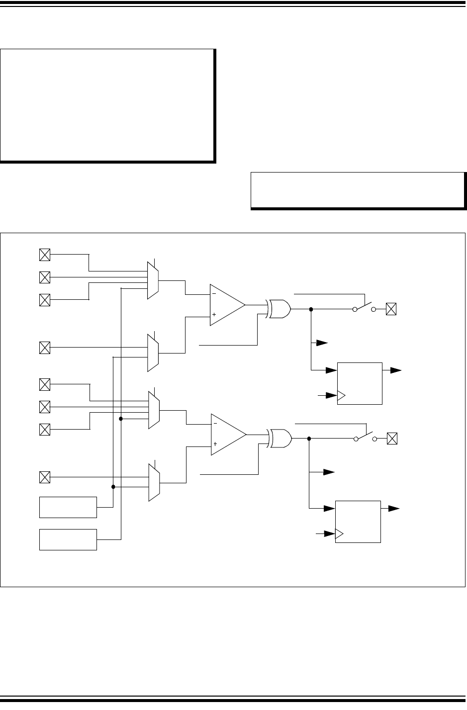
2015 Microchip Technology Inc. Preliminary DS60001320B-page 569
PIC32MZ Embedded Connectivity with Floating Point Unit (EF) Family
31.0 COMPARATOR
The Analog Comparator module consists of two
comparators that can be configured in a variety of
ways.
Key features of the Analog Comparator module are:
• Differential inputs
• Rail-to-rail operation
• Selectable output polarity
• Selectable inputs:
- Analog inputs multiplexed with I/O pins
- On-chip internal absolute voltage reference
- Comparator voltage reference (CVREF)
• Selectable interrupt generation
A block diagram of the comparator module is illustrated
in Figure 31-1.
FIGURE 31-1: COMPARATOR BLOCK DIAGRAM
Note: This data sheet summarizes the
features of the PIC32MZ EF family of
devices. It is not intended to be a
comprehensive reference source. To
complement the information in this
data sheet, refer to Section 19.
“Comparator” (DS60001110) in the
“PIC32 Family Reference Manual”,
which is available from the Microchip
web site (www.microchip.com/PIC32).
Note: To avoid oscillation from the Comparators
in Common mode, a low-pass filter is
required on the inputs to the Comparator.
CVREF(1)
Internal (1.2V)
C2IND
C2INA
C2OUT
CMP2
COE (CM2CON<14>)
CREF
CCH<1:0> (CM2CON<1:0>)
CPOL
C2INC
C2INB
C1IND
C1INA
C1OUT
CMP1
COE (CM1CON<14>)
CREF
CCH<1:0> (CM1CON<1:0>)
CPOL
C1INC
C1INB
COUT (CM1CON<8>)
COUT (CM2CON<8>) and
Note 1: Internally connected. See Section 32.0 “Comparator Voltage Reference (CVREF)” for more information.
(CM1CON<4>)
(CM1CON<13>)
(CM2CON<4>)
(CM2CON<13>)
DQ
PBCLK3
C2OUT
(CMSTAT<1>)
Trigger to ADC
DQ
PBCLK3
C1OUT
(CMSTAT<2>)
and Trigger to ADC
PIC32MZ Embedded Connectivity with Floating Point Unit (EF) Family
DS60001320B-page 570 Preliminary 2015 Microchip Technology Inc.
31.1 Comparator Control Registers
TABLE 31-1: COMPARATOR REGISTER MAP
Virtual Address
(BF84_#)
Register
Name(1)
Bit Range
Bits
All Resets
31/15 30/14 29/13 28/12 27/11 26/10 25/9 24/8 23/7 22/6 21/5 20/4 19/3 18/2 17/1 16/0
C000 CM1CON 31:16 — — — — — — — — — — — — — — — — 0000
15:0 ON COE CPOL — — — — COUT EVPOL<1:0> —CREF — — CCH<1:0> 00C3
C010 CM2CON 31:16 — — — — — — — — — — — — — — — — 0000
15:0 ON COE CPOL — — — — COUT EVPOL<1:0> —CREF — — CCH<1:0> 00C3
C060 CMSTAT 31:16 — — — — — — — — — — — — — — — — 0000
15:0 — — — — — — — — — — — — — — C2OUT C1OUT 0000
Legend: x = unknown value on Reset; — = unimplemented, read as ‘0’. Reset values are shown in hexadecimal.
Note 1: All registers in this table have corresponding CLR, SET and INV registers at their virtual addresses, plus offsets of 0x4, 0x8 and 0xC, respectively. See Section 12.3 “CLR, SET, and INV Registers” for
more information.

2015 Microchip Technology Inc. Preliminary DS60001320B-page 571
PIC32MZ Embedded Connectivity with Floating Point Unit (EF) Family
REGISTER 31-1: CMxCON: COMPARATOR CONTROL REGISTER
Bit
Range Bit
31/23/15/7 Bit
30/22/14/6 Bit
29/21/13/5 Bit
28/20/12/4 Bit
27/19/11/3 Bit
26/18/10/2 Bit
25/17/9/1 Bit
24/16/8/0
31:24 U-0 U-0 U-0 U-0 U-0 U-0 U-0 U-0
— — — — — — — —
23:16 U-0 U-0 U-0 U-0 U-0 U-0 U-0 U-0
— — — — — — — —
15:8 R/W-0 R/W-0 R/W-0 U-0 U-0 U-0 U-0 R-0
ON COE CPOL(1) — — — —COUT
7:0 R/W-1 R/W-1 U-0 R/W-0 U-0 U-0 R/W-1 R/W-1
EVPOL<1:0> —CREF—— CCH<1:0>
Legend:
R = Readable bit W = Writable bit U = Unimplemented bit, read as ‘0’
-n = Value at POR ‘1’ = Bit is set ‘0’ = Bit is cleared x = Bit is unknown
bit 31-16 Unimplemented: Read as ‘0’
bit 15 ON: Comparator ON bit
1 = Module is enabled. Setting this bit does not affect the other bits in this register
0 = Module is disabled and does not consume current. Clearing this bit does not affect the other bits in this
register
bit 14 COE: Comparator Output Enable bit
1 = Comparator output is driven on the output CxOUT pin
0 = Comparator output is not driven on the output CxOUT pin
bit 13 CPOL: Comparator Output Inversion bit(1)
1 = Output is inverted
0 = Output is not inverted
bit 12-9 Unimplemented: Read as ‘0’
bit 8 COUT: Comparator Output bit
1 = Output of the Comparator is a ‘1’
0 = Output of the Comparator is a ‘0’
bit 7-6 EVPOL<1:0>: Interrupt Event Polarity Select bits
11 = Comparator interrupt is generated on a low-to-high or high-to-low transition of the comparator output
10 = Comparator interrupt is generated on a high-to-low transition of the comparator output
01 = Comparator interrupt is generated on a low-to-high transition of the comparator output
00 = Comparator interrupt generation is disabled
bit 5 Unimplemented: Read as ‘0’
bit 4 CREF: Comparator Positive Input Configure bit
1 = Comparator non-inverting input is connected to the internal CVREF
0 = Comparator non-inverting input is connected to the CXINA pin
bit 3-2 Unimplemented: Read as ‘0’
bit 1-0 CCH<1:0>: Comparator Negative Input Select bits for Comparator
11 = Comparator inverting input is connected to the IVREF
10 = Comparator inverting input is connected to the CxIND pin
01 = Comparator inverting input is connected to the CxINC pin
00 = Comparator inverting input is connected to the CxINB pin
Note 1: Setting this bit will invert the signal to the comparator interrupt generator as well. This will result in an
interrupt being generated on the opposite edge from the one selected by EVPOL<1:0>.

PIC32MZ Embedded Connectivity with Floating Point Unit (EF) Family
DS60001320B-page 572 Preliminary 2015 Microchip Technology Inc.
REGISTER 31-2: CMSTAT: COMPARATOR STATUS REGISTER
Bit
Range Bit
31/23/15/7 Bit
30/22/14/6 Bit
29/21/13/5 Bit
28/20/12/4 Bit
27/19/11/3 Bit
26/18/10/2 Bit
25/17/9/1 Bit
24/16/8/0
31:24 U-0 U-0 U-0 U-0 U-0 U-0 U-0 U-0
— — — — — — — —
23:16 U-0 U-0 U-0 U-0 U-0 U-0 U-0 U-0
— — — — — — — —
15:8 U-0 U-0 U-0 U-0 U-0 U-0 U-0 U-0
— — — — — — — —
7:0 U-0 U-0 U-0 U-0 U-0 U-0 R-0 R-0
— — — — — — C2OUT C1OUT
Legend:
R = Readable bit W = Writable bit U = Unimplemented bit, read as ‘0’
-n = Value at POR ‘1’ = Bit is set ‘0’ = Bit is cleared x = Bit is unknown
bit 31-2 Unimplemented: Read as ‘0’
bit 1 C2OUT: Comparator Output bit
1 = Output of Comparator 2 is a ‘1’
0 = Output of Comparator 2 is a ‘0’
bit 0 C1OUT: Comparator Output bit
1 = Output of Comparator 1 is a ‘1’
0 = Output of Comparator 1 is a ‘0’
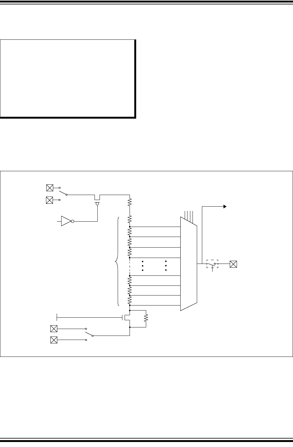
2015 Microchip Technology Inc. Preliminary DS60001320B-page 573
PIC32MZ Embedded Connectivity with Floating Point Unit (EF) Family
32.0 COMPARATOR VOLTAGE
REFERENCE (CVREF)
The CVREF module is a 16-tap, resistor ladder network
that provides a selectable reference voltage. Although
its primary purpose is to provide a reference for the
analog comparators, it also may be used independently
of them.
The resistor ladder is segmented to provide two ranges
of voltage reference values and has a power-down
function to conserve power when the reference is not
being used. The module’s supply reference can be pro-
vided from either device VDD/VSS or an external
voltage reference. The CVREF output is available for
the comparators and typically available for pin output.
The comparator voltage reference has the following
features:
• High and low range selection
• Sixteen output levels available for each range
• Internally connected to comparators to conserve
device pins
• Output can be connected to a pin
A block diagram of the CVREF module is illustrated in
Figure 32-1.
FIGURE 32-1: COMPARATOR VOLTAGE REFERENCE BLOCK DIAGRAM
Note: This data sheet summarizes the
features of the PIC32MZ EF family of
devices. It is not intended to be a
comprehensive reference source. To
complement the information in this data
sheet, refer to Section 20. “Comparator
Voltage Reference (CVREF)”
(DS60001109) in the “PIC32 Family
Reference Manual”, which is available
from the Microchip web site
(www.microchip.com/PIC32).
16-to-1 MUX
CVR<3:0>
8R
R
CVREN
CVRSS = 0
AVDD
VREF+CVRSS = 1
8R
CVRSS = 0
VREF-CVRSS = 1
R
R
R
R
R
R
16 Steps
CVRR
CVREFOUT
AVSS
CVRCON<CVROE>
CVREF
CVRSRC

PIC32MZ Embedded Connectivity with Floating Point Unit (EF) Family
DS60001320B-page 574 Preliminary 2015 Microchip Technology Inc.
32.1 Comparator Voltage Reference Control Registers
TABLE 32-1: COMPARATOR VOLTAGE REFERENCE REGISTER MAP
Virtual Address
(BF80_#)
Register
Name(1)
Bit Range
Bits
All Resets
31/15 30/14 29/13 28/12 27/11 26/10 25/9 24/8 23/7 22/6 21/5 20/4 19/3 18/2 17/1 16/0
0E00 CVRCON 31:16 — — — — — — — — — — — — — — — — 0000
15:0 ON — — — — — — — — CVROE CVRR CVRSS CVR<3:0> 0000
Legend: x = unknown value on Reset; — = unimplemented, read as ‘0’. Reset values are shown in hexadecimal.
Note 1: The register in this table has corresponding CLR, SET and INV registers at their virtual addresses, plus offsets of 0x4, 0x8 and 0xC, respectively. See Section 12.3 “CLR, SET, and INV Registers” for
more information.

2015 Microchip Technology Inc. Preliminary DS60001320B-page 575
PIC32MZ Embedded Connectivity with Floating Point Unit (EF) Family
REGISTER 32-1: CVRCON: COMPARATOR VOLTAGE REFERENCE CONTROL REGISTER
Bit
Range Bit
31/23/15/7 Bit
30/22/14/6 Bit
29/21/13/5 Bit
28/20/12/4 Bit
27/19/11/3 Bit
26/18/10/2 Bit
25/17/9/1 Bit
24/16/8/0
31:24 U-0 U-0 U-0 U-0 U-0 U-0 U-0 U-0
— — — — — — — —
23:16 U-0 U-0 U-0 U-0 U-0 U-0 U-0 U-0
— — — — — — — —
15:8 R/W-0 U-0 U-0 U-0 U-0 U-0 U-0 U-0
ON — — — — — — —
7:0 U-0 R/W-0 R/W-0 R/W-0 R/W-0 R/W-0 R/W-0 R/W-0
— CVROE CVRR CVRSS CVR<3:0>
Legend:
R = Readable bit W = Writable bit U = Unimplemented bit, read as ‘0’
-n = Value at POR ‘1’ = Bit is set ‘0’ = Bit is cleared x = Bit is unknown
bit 31-16 Unimplemented: Read as ‘0’
bit 15 ON: Comparator Voltage Reference On bit
1 = Module is enabled
Setting this bit does not affect other bits in the register.
0 = Module is disabled and does not consume current.
Clearing this bit does not affect the other bits in the register.
bit 14-7 Unimplemented: Read as ‘0’
bit 6 CVROE: CVREFOUT Enable bit
1 = Voltage level is output on CVREFOUT pin
0 = Voltage level is disconnected from CVREFOUT pin
bit 5 CVRR: CVREF Range Selection bit
1 = 0 to 0.67 CVRSRC, with CVRSRC/24 step size
0 = 0.25 CVRSRC to 0.75 CVRSRC, with CVRSRC/32 step size
bit 4 CVRSS: CVREF Source Selection bit
1 = Comparator voltage reference source, CVRSRC = (VREF+) – (VREF-)
0 = Comparator voltage reference source, CVRSRC = AVDD – AVSS
bit 3-0 CVR<3:0>: CVREF Value Selection 0 CVR<3:0> 15 bits
When CVRR = 1:
CVREF = (CVR<3:0>/24) (CVRSRC)
When CVRR = 0:
CVREF = 1/4 (CVRSRC) + (CVR<3:0>/32) (CVRSRC)

PIC32MZ Embedded Connectivity with Floating Point Unit (EF) Family
DS60001320B-page 576 Preliminary 2015 Microchip Technology Inc.
NOTES:

2015 Microchip Technology Inc. Preliminary DS60001320B-page 577
PIC32MZ Embedded Connectivity with Floating Point Unit (EF) Family
33.0 POWER-SAVING FEATURES
This section describes power-saving features for the
PIC32MZ EF devices. These devices offer various
methods and modes that allow the user to balance
power consumption with device performance. In all of
the methods and modes described in this section,
power-saving is controlled by software.
33.1 Power Saving with CPU Running
When the CPU is running, power consumption can be
controlled by reducing the CPU clock frequency,
lowering the speed of PBCLK7, or selecting a lower
power clock source (i.e., LPRC or SOSC).
In addition, the Peripheral Bus Scaling mode is available
for each peripheral bus where peripherals are clocked at
reduced speed by selecting a higher divider for the
associated PBCLKx, or by disabling the clock
completely.
33.2 Power-Saving with CPU Halted
Peripherals and the CPU can be Halted or disabled to
further reduce power consumption.
33.2.1 SLEEP MODE
Sleep mode has the lowest power consumption of the
device power-saving operating modes. The CPU and
most peripherals are Halted and the associated clocks
are disabled. Select peripherals can continue to
operate in Sleep mode and can be used to wake the
device from Sleep. See the individual peripheral
module sections for descriptions of behavior in Sleep.
Sleep mode includes the following characteristics:
• There can be a wake-up delay based on the
oscillator selection
• The Fail-Safe Clock Monitor (FSCM) does not
operate during Sleep mode
• The BOR circuit remains operative during Sleep
mode
• The WDT, if enabled, is not automatically cleared
prior to entering Sleep mode
• Some peripherals can continue to operate at limited
functionality in Sleep mode. These peripherals
include I/O pins that detect a change in the input
signal, WDT, ADC, UART and peripherals that use
an external clock input or the internal LPRC
oscillator (e.g., RTCC, Timer1 and Input Capture).
• I/O pins continue to sink or source current in the
same manner as they do when the device is not in
Sleep
The processor will exit, or ‘wake-up’, from Sleep on one
of the following events:
• On any interrupt from an enabled source that is
operating in Sleep. The interrupt priority must be
greater than the current CPU priority.
• On any form of device Reset
• On a WDT time-out
If the interrupt priority is lower than or equal to the
current priority, the CPU will remain Halted, but the
peripheral bus clocks will start running and the device
will enter into Idle mode.
33.2.2 IDLE MODE
In Idle mode, the CPU is Halted; however, all clocks are
still enabled. This allows peripherals to continue to
operate. Peripherals can be individually configured to
Halt when entering Idle by setting their respective SIDL
bit. Latency, when exiting Idle mode, is very low due to
the CPU oscillator source remaining active.
The device enters Idle mode when the SLPEN bit
(OSCCON<4>) is clear and a WAIT instruction is
executed.
The processor will wake or exit from Idle mode on the
following events:
• On any interrupt event for which the interrupt source
is enabled. The priority of the interrupt event must
be greater than the current priority of the CPU. If the
priority of the interrupt event is lower than or equal
to current priority of the CPU, the CPU will remain
Halted and the device will remain in Idle mode.
• On any form of device Reset
• On a WDT time-out interrupt
Note: This data sheet summarizes the
features of the PIC32MZ EF family of
devices. It is not intended to be a
comprehensive reference source. To
complement the information in this data
sheet, refer to Section 10. “Power-
Saving Features” (DS60001130) in the
“PIC32 Family Reference Manual”, which
is available from the Microchip web site
(www.microchip.com/PIC32).

PIC32MZ Embedded Connectivity with Floating Point Unit (EF) Family
DS60001320B-page 578 Preliminary 2015 Microchip Technology Inc.
33.3 Peripheral Module Disable
The Peripheral Module Disable (PMD) registers
provide a method to disable a peripheral module by
stopping all clock sources supplied to that module.
When a peripheral is disabled using the appropriate
PMD control bit, the peripheral is in a minimum power
consumption state. The control and status registers
associated with the peripheral are also disabled, so
writes to those registers do not have effect and read
values are invalid.
To disable a peripheral, the associated PMDx bit must
be set to ‘1’. To enable a peripheral, the associated
PMDx bit must be cleared (default). See Table 33-1 for
more information.
Note: Disabling a peripheral module while it’s
ON bit is set, may result in undefined
behavior. The ON bit for the associated
peripheral module must be cleared prior to
disable a module via the PMDx bits.
TABLE 33-1: PERIPHERAL MODULE DISABLE BITS AND LOCATIONS(1)
Peripheral PMDx bit Name Register Name and Bit Location
ADC ADCMD PMD1<0>
Comparator Voltage Reference CVRMD PMD1<12>
Comparator 1 CMP1MD PMD2<0>
Comparator 2 CMP2MD PMD2<1>
Input Capture 1 IC1MD PMD3<0>
Input Capture 2 IC2MD PMD3<1>
Input Capture 3 IC3MD PMD3<2>
Input Capture 4 IC4MD PMD3<3>
Input Capture 5 IC5MD PMD3<4>
Input Capture 6 IC6MD PMD3<5>
Input Capture 7 IC7MD PMD3<6>
Input Capture 8 IC8MD PMD3<7>
Input Capture 9 IC9MD PMD3<8>
Output Compare 1 OC1MD PMD3<16>
Output Compare 2 OC2MD PMD3<17>
Output Compare 3 OC3MD PMD3<18>
Output Compare 4 OC4MD PMD3<19>
Output Compare 5 OC5MD PMD3<20>
Output Compare 6 OC6MD PMD3<21>
Output Compare 7 OC7MD PMD3<22>
Output Compare 8 OC8MD PMD3<23>
Output Compare 9 OC9MD PMD3<24>
Timer1 T1MD PMD4<0>
Timer2 T2MD PMD4<1>
Timer3 T3MD PMD4<2>
Timer4 T4MD PMD4<3>
Timer5 T5MD PMD4<4>
Timer6 T6MD PMD4<5>
Timer7 T7MD PMD4<6>
Timer8 T8MD PMD4<7>
Timer9 T9MD PMD4<8>
UART1 U1MD PMD5<0>
UART2 U2MD PMD5<1>
Note 1: Not all modules and associated PMDx bits are available on all devices. See TABLE 1: “PIC32MZ EF
Family Features” for the lists of available peripherals.
2: Module must not be busy after clearing the associated ON bit and prior to setting the USBMD bit.

2015 Microchip Technology Inc. Preliminary DS60001320B-page 579
PIC32MZ Embedded Connectivity with Floating Point Unit (EF) Family
UART3 U3MD PMD5<2>
UART4 U4MD PMD5<3>
UART5 U5MD PMD5<4>
UART6 U6MD PMD5<5>
SPI1 SPI1MD PMD5<8>
SPI2 SPI2MD PMD5<9>
SPI3 SPI3MD PMD5<10>
SPI4 SPI4MD PMD5<11>
SPI5 SPI5MD PMD5<12>
SPI6 SPI6MD PMD5<13>
I2C1 I2C1MD PMD5<16>
I2C2 I2C2MD PMD5<17>
I2C3 I2C3MD PMD5<18>
I2C4 I2C4MD PMD5<19>
I2C5 I2C5MD PMD5<20>
USB(2) USBMD PMD5<24>
CAN1 CAN1MD PMD5<28>
CAN2 CAN2MD PMD5<29>
RTCC RTCCMD PMD6<0>
Reference Clock Output 1 REFO1MD PMD6<8>
Reference Clock Output 2 REFO2MD PMD6<9>
Reference Clock Output 3 REFO3MD PMD6<10>
Reference Clock Output 4 REFO4MD PMD6<11>
PMP PMPMD PMD6<16>
EBI EBIMD PMD6<17>
SQI1 SQI1MD PMD6<23>
Ethernet ETHMD PMD6<28>
DMA DMAMD PMD7<4>
Random Number Generator RNGMD PMD7<20>
Crypto CRYPTMD PMD7<22>
TABLE 33-1: PERIPHERAL MODULE DISABLE BITS AND LOCATIONS(1) (CONTINUED)
Peripheral PMDx bit Name Register Name and Bit Location
Note 1: Not all modules and associated PMDx bits are available on all devices. See TABLE 1: “PIC32MZ EF
Family Features” for the lists of available peripherals.
2: Module must not be busy after clearing the associated ON bit and prior to setting the USBMD bit.

PIC32MZ Embedded Connectivity with Floating Point Unit (EF) Family
DS60001320B-page 580 Preliminary 2015 Microchip Technology Inc.
33.3.1 CONTROLLING CONFIGURATION
CHANGES
Because peripherals can be disabled during run time,
some restrictions on disabling peripherals are needed
to prevent accidental configuration changes. PIC32MZ
EF devices include two features to prevent alterations
to enabled or disabled peripherals:
• Control register lock sequence
• Configuration bit select lock
33.3.1.1 Control Register Lock
Under normal operation, writes to the PMDx registers
are not allowed. Attempted writes appear to execute
normally, but the contents of the registers remain
unchanged. To change these registers, they must be
unlocked in hardware. The register lock is controlled by
the PMDLOCK Configuration bit (CFGCON<12>). Set-
ting PMDLOCK prevents writes to the control registers;
clearing PMDLOCK allows writes.
To set or clear PMDLOCK, an unlock sequence must
be executed. Refer to Section 42. “Oscillators with
Enhanced PLL” in the “PIC32 Family Reference
Manual” for details.
33.3.1.2 Configuration Bit Select Lock
As an additional level of safety, the device can be
configured to prevent more than one write session to
the PMDx registers. The PMDL1WAY Configuration bit
(DEVCFG3<28>) blocks the PMDLOCK bit from being
cleared after it has been set once. If PMDLOCK
remains set, the register unlock procedure does not
execute, and the PPS control registers cannot be writ-
ten to. The only way to clear the bit and re-enable PMD
functionality is to perform a device Reset.

2015 Microchip Technology Inc. Preliminary DS60001320B-page 581
PIC32MZ Embedded Connectivity with Floating Point Unit (EF) Family
TABLE 33-2: PERIPHERAL MODULE DISABLE REGISTER SUMMARY
Virtual Address
(BF80_#)
Register
Name(1)
Bit Range
Bits
All Resets
31/15 30/14 29/13 28/12 27/11 26/10 25/9 24/8 23/7 22/6 21/5 20/4 19/3 18/2 17/1 16/0
0040 PMD1 31:16 — — — — — — — — — — — — — — — — 0000
15:0 — — —CVRMD— — — — — — — — — — —ADCMD0000
0050 PMD2 31:16 — — — — — — — — — — — — — — — — 0000
15:0 —————————————— CMP2MD CMP1MD 0000
0060 PMD3 31:16 — — — — — — — OC9MD OC8MD OC7MD OC6MD OC5MD OC4MD OC3MD OC2MD OC1MD 0000
15:0 — — — — — — — IC9MD IC8MD IC7MD IC6MD IC5MD IC4MD IC3MD IC2MD IC1MD 0000
0070 PMD4 31:16 — — — — — — — — — — — — — — — — 0000
15:0 ——————— T9MD T8MD T7MD T6MD T5MD T4MD T3MD T2MD T1MD 0000
0080 PMD5 31:16 —— CAN2MD CAN1MD — — — USBMD — — — I2C5MD I2C4MD I2C3MD I2C2MD I2C1MD 0000
15:0 —— SPI6MD SPI5MD SPI4MD SPI3MD SPI2MD SPI1MD —— U6MD U5MD U4MD U3MD U2MD U1MD 0000
0090 PMD6 31:16 — — — ETHMD — — — — SQI1MD — — — — — EBIMD PMPMD 0000
15:0 — — — — REFO4MD REFO3MD REFO2MD REFO1MD — — — — — — — RTCCMD 0000
00A0 PMD7 31:16 ————————— CRYPTMD —RNGMD— — — — 0000
15:0 ——————————— DMAMD — — — — 0000
Legend: x = unknown value on Reset; — = unimplemented, read as ‘0’. Reset values are shown in hexadecimal.
Note 1: All registers have corresponding CLR, SET and INV registers at their virtual addresses, plus offsets of 0x4, 0x8 and 0xC, respectively. See Section 12.3 “CLR, SET, and INV Registers” for more
information.

PIC32MZ Embedded Connectivity with Floating Point Unit (EF) Family
DS60001320B-page 582 Preliminary 2015 Microchip Technology Inc.
NOTES:

2015 Microchip Technology Inc. Preliminary DS60001320B-page 583
PIC32MZ Embedded Connectivity with Floating Point Unit (EF) Family
34.0 SPECIAL FEATURES
PIC32MZ EF devices include several features intended
to maximize application flexibility and reliability and
minimize cost through elimination of external
components. These are:
• Flexible device configuration
• Joint Test Action Group (JTAG) interface
• In-Circuit Serial Programming™ (ICSP™)
• Internal temperature sensor
34.1 Configuration Bits
PIC32MZ EF devices contain two Boot Flash memo-
ries (Boot Flash 1 and Boot Flash 2), each with an
associated configuration space. These configuration
spaces can be programmed to contain various
device configurations. Configuration space that is
aliased by the Lower Boot Alias memory region is
used to provide values for Configuration registers
listed below. See 4.1.1 “Boot Flash Sequence and
Configuration Spaces” for more information.
•DEVSIGN0/ADEVSIGN0: Device Signature Word
0 Register
•DEVCP0/ADEVCP0: Device Code-Protect 0
Register
•DEVCFG0/ADEVCFG0: Device Configuration
Word 0
•DEVCFG1/ADEVCFG1: Device Configuration
Word 1
•DEVCFG2/ADEVCFG2: Device Configuration
Word 2
•DEVCFG3/ADEVCFG3: Device Configuration
Word 3
The following run-time programmable Configuration
registers provide additional configuration control:
•CFGCON: Configuration Control Register
•CFGEBIA: External Bus Interface Address Pin
Configuration Register
•CFGEBIC: External Bus Interface Control Pin
Configuration Register
•CFGPG: Permission Group Configuration
Register
In addition, the DEVID register (see Register 34-11)
provides device and revision information, and the
DEVSN0 and DEVSN1 registers contain a unique
serial number of the device (see Register 34-12).
Note: This data sheet summarizes the features
of the PIC32MZ EF family of devices.
However, it is not intended to be a
comprehensive reference source. To
complement the information in this data
sheet, refer to Section 32.
“Configuration” (DS60001124) and
Section 33. “Programming and
Diagnostics” (DS60001129) in the “PIC32
Family Reference Manual”, which are
available from the Microchip web site
(www.microchip.com/PIC32).
Note: Do not use word program operation
(NVMOP<3:0> = 0001) when
programming the device words that are
described in this section.

PIC32MZ Embedded Connectivity with Floating Point Unit (EF) Family
DS60001320B-page 584 Preliminary 2015 Microchip Technology Inc.
34.2 Registers
TABLE 34-1: DEVCFG: DEVICE CONFIGURATION WORD SUMMARY
Virtual Address
(BFC0_#)
Register
Name
Bit Range
Bits
All Resets
31/15 30/14 29/13 28/12 27/11 26/10 25/9 24/8 23/7 22/6 21/5 20/4 19/3 18/2 17/1 16/0
FFC0 DEVCFG3 31:16 —FUSBIDIO IOL1WAY PMDL1WAY PGL1WAY —FETHIO FMIIEN — — — — —— — — xxxx
15:0 USERID<15:0> xxxx
FFC4 DEVCFG2 31:16 —UPLLFSEL — — — — — — — — — — — FPLLODIV<2:0> xxxx
15:0 —FPLLMULT<6:0> FPLLICLK FPLLRNG<2:0> —FPLLIDIV<2:0> xxxx
FFC8 DEVCFG1 31:16 FDMTEN DMTCNT<4:0> FWDTWINSZ<1:0> FWDTEN WINDIS WDTSPGM WDTPS<4:0> xxxx
15:0 FCKSM<1:0> — — — OSCIOFNC POSCMOD<1:0> IESO FSOSCEN DMTINTV<2:0> FNOSC<2:0> xxxx
FFCC DEVCFG0 31:16 —EJTAGBEN — — — — — — — — POSCBOOST POSCGAIN<1:0> SOSCBOOST SOSCGAIN<1:0> xxxx
15:0 SMCLR DBGPER<2:0> —FSLEEP FECCCON<1:0> —BOOTISA TRCEN ICESEL<1:0> JTAGEN DEBUG<1:0> xxxx
FFD0 DEVCP3 31:16 — — — — — — — — — — — — — — — — xxxx
15:0 — — — — — — — — — — — — — — — — xxxx
FFD4 DEVCP2 31:16 — — — — — — — — — — — — — — — — xxxx
15:0 — — — — — — — — — — — — — — — — xxxx
FFD8 DEVCP1 31:16 — — — — — — — — — — — — — — — — xxxx
15:0 — — — — — — — — — — — — — — — — xxxx
FFDC DEVCP0 31:16 — — — CP — — — — — — — — — — — — xxxx
15:0 — — — — — — — — — — — — — — — — xxxx
FFE0 DEVSIGN3 31:16 — — — — — — — — — — — — — — — — xxxx
15:0 — — — — — — — — — — — — — — — — xxxx
FFE4 DEVSIGN2 31:16 — — — — — — — — — — — — — — — — xxxx
15:0 — — — — — — — — — — — — — — — — xxxx
FFE8 DEVSIGN1 31:16 — — — — — — — — — — — — — — — — xxxx
15:0 — — — — — — — — — — — — — — — — xxxx
FFEC DEVSIGN0 31:16 0 — — — — — — — — — — — — — — — xxxx
15:0 — — — — — — — — — — — — — — — — xxxx
Legend: x = unknown value on Reset; — = Reserved, read as ‘1’. Reset values are shown in hexadecimal.

2015 Microchip Technology Inc. Preliminary DS60001320B-page 585
PIC32MZ Embedded Connectivity with Floating Point Unit (EF) Family
TABLE 34-2: ADEVCFG: ALTERNATE DEVICE CONFIGURATION WORD SUMMARY
Virtual Address
(BFC0_#)
Register
Name
Bit Range
Bits
All Resets
31/15 30/14 29/13 28/12 27/11 26/10 25/9 24/8 23/7 22/6 21/5 20/4 19/3 18/2 17/1 16/0
FF40 ADEVCFG3 31:16 — FUSBIDIO IOL1WAY PMDL1WAY PGL1WAY —FETHIO FMIIEN — — — — —— — — xxxx
15:0 USERID<15:0> xxxx
FF44 ADEVCFG2 31:16 — UPLLFSEL — — — — — — — — — — — FPLLODIV<2:0> xxxx
15:0 — FPLLMULT<6:0> FPLLICLK FPLLRNG<2:0> — FPLLIDIV<2:0> xxxx
FF48 ADEVCFG1 31:16 FDMTEN DMTCNT<4:0> FWDTWINSZ<1:0> FWDTEN WINDIS WDTSPGM WDTPS<4:0> xxxx
15:0 FCKSM<1:0> ——— OSCIOFNC POSCMOD<1:0> IESO FSOSCEN DMTINTV<2:0> FNOSC<2:0> xxxx
FF4C ADEVCFG0 31:16 — EJTAGBEN — — — — — — — — POSCBOOST POSCGAIN<1:0> SOSCBOOST SOSCGAIN<1:0> xxxx
15:0 SMCLR DBGPER<2:0> — FSLEEP FECCCON<1:0> — BOOTISA TRCEN ICESEL<1:0> JTAGEN DEBUG<1:0> xxxx
FF50 ADEVCP3 31:16 — — — — — — — — — — — — — — — — xxxx
15:0 — — — — — — — — — — — — — — — — xxxx
FF54 ADEVCP2 31:16 — — — — — — — — — — — — — — — — xxxx
15:0 — — — — — — — — — — — — — — — — xxxx
FF58 ADEVCP1 31:16 — — — — — — — — — — — — — — — — xxxx
15:0 — — — — — — — — — — — — — — — — xxxx
FF5C ADEVCP0 31:16 — — —CP— — — — — — — — — — — — xxxx
15:0 — — — — — — — — — — — — — — — — xxxx
FF60 ADEVSIGN3 31:16 — — — — — — — — — — — — — — — — xxxx
15:0 — — — — — — — — — — — — — — — — xxxx
FF64 ADEVSIGN2 31:16 — — — — — — — — — — — — — — — — xxxx
15:0 — — — — — — — — — — — — — — — — xxxx
FF68 ADEVSIGN1 31:16 — — — — — — — — — — — — — — — — xxxx
15:0 — — — — — — — — — — — — — — — — xxxx
FF6C ADEVSIGN0 31:16 0 — — — — — — — — — — — — — — — xxxx
15:0 — — — — — — — — — — — — — — — — xxxx
Legend: x = unknown value on Reset; — = Reserved, read as ‘1’. Reset values are shown in hexadecimal.

PIC32MZ Embedded Connectivity with Floating Point Unit (EF) Family
DS60001320B-page 586 Preliminary 2015 Microchip Technology Inc.
TABLE 34-3: DEVICE ID, REVISION, AND CONFIGURATION SUMMARY
Virtual Address
(BF80_#)
Register
Name
Bit Range
Bits
All Resets(1)
31/15 30/14 29/13 28/12 27/11 26/10 25/9 24/8 23/7 22/6 21/5 20/4 19/3 18/2 17/1 16/0
0000 CFGCON 31:16 — — — — — — DMAPRI CPUPRI — — — — — — ICACLK OCACLK 0000
15:0 —— IOLOCK PMDLOCK PGLOCK —— USBSSEN IOANCPEN — ECCCON<1:0> JTAGEN TROEN —TDOEN000B
0020 DEVID 31:16 VER<3:0> DEVID<27:16> xxxx
15:0 DEVID<15:0> xxxx
0030 SYSKEY 31:16 SYSKEY<31:0> 0000
15:0 0000
00C0 CFGEBIA(2) 31:16 EBIPINEN — — — — — — — EBIA23EN EBIA22EN EBIA21EN EBIA20EN EBIA19EN EBIA18EN EBIA17EN EBIA16EN 0000
15:0 EBIA15EN EBIA14EN EBIA13EN EBIA12EN EBIA11EN EBIA10EN EBIA9EN EBIA8EN EBIA7EN EBIA6EN EBIA5EN EBIA4EN EBIA3EN EBIA2EN EBIA1EN EBIA0EN 0000
00D0 CFGEBIC(2) 31:16 EBI
RDYINV3 EBI
RDYINV2 EBI
RDYINV1 —EBI
RDYEN3 EBI
RDYEN2 EBI
RDYEN1 — — — — — — — EBI
RDYLVL EBIRPEN 0000
15:0 —— EBIWEEN EBIOEEN —— EBIBSEN1 EBIBSEN0 EBICSEN3 EBICSEN2 EBICSEN1 EBICSEN0 —— EBIDEN1 EBIDEN0 0000
00E0 CFGPG 31:16 ICD1PG<1:0> — — — — CRYPTPG<1:0> FCPG<1:0> SQI1PG<1:0> ——ETHPG<1:0>0000
15:0 CAN2PG<1:0> CAN1PG<1:0> —— USBPG<1:0> —— DMAPG<1:0> —— CPUPG<1:0> 0000
Legend: x = unknown value on Reset; — = unimplemented, read as ‘0’. Reset values are shown in hexadecimal.
Note 1: Reset values are dependent on the device variant.
2: This register is not available on 64-pin devices.
TABLE 34-4: DEVICE SERIAL NUMBER SUMMARY
Virtual Address
(BFC5_#)
Register
Name
Bit Range
Bits
All Resets(1)
31/15 30/14 29/13 28/12 27/11 26/10 25/9 24/8 23/7 22/6 21/5 20/4 19/3 18/2 17/1 16/0
4020 DEVSN0 31:16 Device Serial Number <31:16> xxxx
15:0 Device Serial Number <15:0> xxxx
4024 DEVSN1 31:16 Device Serial Number <31:16> xxxx
15:0 Device Serial Number <15:0> xxxx
Legend: x = unknown value on Reset.
Note 1: Reset values are dependent on the device variant.

2015 Microchip Technology Inc. Preliminary DS60001320B-page 587
PIC32MZ Embedded Connectivity with Floating Point Unit (EF) Family
REGISTER 34-1: DEVSIGN0/ADEVSIGN0: DEVICE SIGNATURE WORD 0 REGISTER
Bit
Range Bit
31/23/15/7 Bit
30/22/14/6 Bit
29/21/13/5 Bit
28/20/12/4 Bit
27/19/11/3 Bit
26/18/10/2 Bit
25/17/9/1 Bit
24/16/8/0
31:24 r-0 r-1 r-1 r-1 r-1 r-1 r-1 r-1
— — — — — — — —
23:16 r-1 r-1 r-1 r-1 r-1 r-1 r-1 r-1
— — — — — — — —
15:8 r-1 r-1 r-1 r-1 r-1 r-1 r-1 r-1
— — — — — — — —
7:0 r-1 r-1 r-1 r-1 r-1 r-1 r-1 r-1
— — — — — — — —
Legend: r = Reserved bit
R = Readable bit W = Writable bit U = Unimplemented bit, read as ‘0’
-n = Value at POR ‘1’ = Bit is set ‘0’ = Bit is cleared x = Bit is unknown
bit 31 Reserved: Write as ‘0’
bit 30-0 Reserved: Write as ‘1’
Note: The DEVSIGN1 through DEVSIGN3 and ADEVSIGN1 through ADEVSIGN3 registers are used for Quad
Word programming operation when programming the DEVSIGN0/ADESIGN0 registers, and do not contain
any valid information.
REGISTER 34-2: DEVCP0/ADEVCP0: DEVICE CODE-PROTECT 0 REGISTER
Bit
Range Bit
31/23/15/7 Bit
30/22/14/6 Bit
29/21/13/5 Bit
28/20/12/4 Bit
27/19/11/3 Bit
26/18/10/2 Bit
25/17/9/1 Bit
24/16/8/0
31:24 r-1 r-1 r-1 R/P r-1 r-1 r-1 r-1
— — — CP — — — —
23:16 r-1 r-1 r-1 r-1 r-1 r-1 r-1 r-1
— — — — — — — —
15:8 r-1 r-1 r-1 r-1 r-1 r-1 r-1 r-1
— — — — — — — —
7:0 r-1 r-1 r-1 r-1 r-1 r-1 r-1 r-1
— — — — — — — —
Legend: r = Reserved bit P = Programmable bit
R = Readable bit W = Writable bit U = Unimplemented bit, read as ‘0’
-n = Value at POR ‘1’ = Bit is set ‘0’ = Bit is cleared x = Bit is unknown
bit 31-29 Reserved: Write as ‘1’
bit 28 CP: Code-Protect bit
Prevents boot and program Flash memory from being read or modified by an external programming device.
1 = Protection is disabled
0 = Protection is enabled
bit 27-0 Reserved: Write as ‘1’
Note: The DEVCP1 through DEVCP3 and ADEVCP1 through ADEVCP3 registers are used for Quad Word
programming operation when programming the DEVCP0/ADEVCP0 registers, and do not contain any valid
information.

PIC32MZ Embedded Connectivity with Floating Point Unit (EF) Family
DS60001320B-page 588 Preliminary 2015 Microchip Technology Inc.
REGISTER 34-3: DEVCFG0/ADEVCFG0: DEVICE CONFIGURATION WORD 0
Bit
Range Bit
31/23/15/7 Bit
30/22/14/6 Bit
29/21/13/5 Bit
28/20/12/4 Bit
27/19/11/3 Bit
26/18/10/2 Bit
25/17/9/1 Bit
24/16/8/0
31:24 r-x R/P r-1 r-1 r-1 r-1 r-1 r-1
— EJTAGBEN — — — — — —
23:16 r-1 r-1 R/P R/P R/P R/P R/P R/P
—— POSCBOOST POSCGAIN<1:0> SOSCBOOST SOSCGAIN<1:0>
15:8 R/P R/P R/P R/P r-y R/P R/P R/P
SMCLR DBGPER<2:0> — FSLEEP FECCCON<1:0>
7:0 r-1 R/P R/P R/P R/P R/P R/P R/P
— BOOTISA TRCEN ICESEL<1:0> JTAGEN(1) DEBUG<1:0>
Legend: r = Reserved bit y = Value set from Configuration bits on POR
R = Readable bit P = Programmable bit U = Unimplemented bit, read as ‘0’
-n = Value at POR ‘1’ = Bit is set ‘0’ = Bit is cleared x = Bit is unknown
bit 31 Reserved: The reset value of this bit is the same as DEVSIGN0<31>.
bit 30 EJTAGBEN: EJTAG Boot Enable bit
1 = Normal EJTAG functionality
0 = Reduced EJTAG functionality
bit 29-22 Reserved: Write as ‘1’
bit 21 POSCBOOST: Primary Oscillator Boost Kick Start Enable bit
1 = Boost the kick start of the oscillator
0 = Normal start of the oscillator
bit 20-19 POSCGAIN<1:0>: Primary Oscillator Gain Control bits
11 = 2x gain setting
10 = 1.5x gain setting
01 = 0.5x gain setting
00 = 1x gain setting
bit 18 SOSCBOOST: Secondary Oscillator Boost Kick Start Enable bit
1 = Boost the kick start of the oscillator
0 = Normal start of the oscillator
bit 17-16 SOSCGAIN<1:0>: Secondary Oscillator Gain Control bits
11 = 2x gain setting
10 = 1.5x gain setting
01 = 0.5x gain setting
00 = 1x gain setting
bit 15 SMCLR: Soft Master Clear Enable bit
1 = MCLR pin generates a normal system Reset
0 = MCLR pin generates a POR Reset
bit 14-12 DBGPER<2:0>: Debug Mode CPU Access Permission bits
1xx = Allow CPU access to Permission Group 2 permission regions
x1x = Allow CPU access to Permission Group 1 permission regions
xx1 = Allow CPU access to Permission Group 0 permission regions
0xx = Deny CPU access to Permission Group 2 permission regions
x0x = Deny CPU access to Permission Group 1 permission regions
xx0 = Deny CPU access to Permission Group 0 permission regions
When the CPU is in Debug mode and the CPU1PG<1:0> bits (CFGPG<1:0>) are set to a denied permission
group as defined by DBGPER<2:0>, the transaction request is assigned Group 3 permissions.
bit 11 Reserved: This bit is controlled by debugger/emulator development tools and should not be modified by
the user.
Note 1: This bit sets the value of the JTAGEN bit in the CFGCON register.

2015 Microchip Technology Inc. Preliminary DS60001320B-page 589
PIC32MZ Embedded Connectivity with Floating Point Unit (EF) Family
bit 10 FSLEEP: Flash Sleep Mode bit
1 = Flash is powered down when the device is in Sleep mode
0 = Flash remains powered when the device is in Sleep mode
bit 9-8 FECCCON<1:0>: Dynamic Flash ECC Configuration bits
Upon a device Reset, the value of these bits is copied to the ECCCON<1:0> bits (CFGCON<5:4>).
11 = ECC and dynamic ECC are disabled (ECCCON<1:0> bits are writable)
10 = ECC and dynamic ECC are disabled (ECCCON<1:0> bits are locked)
01 = Dynamic Flash ECC is enabled (ECCCON<1:0> bits are locked)
00 = Flash ECC is enabled (ECCCON<1:0> bits are locked; disables word Flash writes)
bit 7 Reserved: Write as ‘1’
bit 6 BOOTISA: Boot ISA Selection bit
1 = Boot code and Exception code is MIPS32®
(ISAONEXC bit is set to ‘0’ and the ISA<1:0> bits are set to ‘10’ in the CP0 Config3 register)
0 = Boot code and Exception code is microMIPS™
(ISAONEXC bit is set to ‘1’ and the ISA<1:0> bits are set to ‘11’ in the CP0 Config3 register)
bit 5 TRCEN: Trace Enable bit
1 = Trace features in the CPU are enabled
0 = Trace features in the CPU are disabled
bit 4-3 ICESEL<1:0>: In-Circuit Emulator/Debugger Communication Channel Select bits
11 = PGEC1/PGED1 pair is used
10 = PGEC2/PGED2 pair is used
01 = Reserved
00 = Reserved
bit 2 JTAGEN: JTAG Enable bit(1)
1 = JTAG is enabled
0 = JTAG is disabled
bit 1-0 DEBUG<1:0>: Background Debugger Enable bits (forced to ‘11’ if code-protect is enabled)
1x = Debugger is disabled
0x = Debugger is enabled
REGISTER 34-3: DEVCFG0/ADEVCFG0: DEVICE CONFIGURATION WORD 0 (CONTINUED)
Note 1: This bit sets the value of the JTAGEN bit in the CFGCON register.

PIC32MZ Embedded Connectivity with Floating Point Unit (EF) Family
DS60001320B-page 590 Preliminary 2015 Microchip Technology Inc.
REGISTER 34-4: DEVCFG1/ADEVCFG1: DEVICE CONFIGURATION WORD 1
Bit
Range Bit
31/23/15/7 Bit
30/22/14/6 Bit
29/21/13/5 Bit
28/20/12/4 Bit
27/19/11/3 Bit
26/18/10/2 Bit
25/17/9/1 Bit
24/16/8/0
31:24 R/P R/P R/P R/P R/P R/P R/P R/P
FDMTEN DMTCNT<4:0> FWDTWINSZ<1:0>
23:16 R/P R/P R/P R/P R/P R/P R/P R/P
FWDTEN WINDIS WDTSPGM WDTPS<4:0>
15:8 R/P R/P r-1 r-1 r-1 R/P R/P R/P
FCKSM<1:0> — — — OSCIOFNC POSCMOD<1:0>
7:0 R/P R/P R/P R/P R/P R/P R/P R/P
IESO FSOSCEN DMTINTV<2:0> FNOSC<2:0>
Legend: r = Reserved bit P = Programmable bit
R = Readable bit W = Writable bit U = Unimplemented bit, read as ‘0’
-n = Value at POR ‘1’ = Bit is set ‘0’ = Bit is cleared x = Bit is unknown
bit 31 FDMTEN: Deadman Timer enable bit
1 = Deadman Timer is enabled and cannot be disabled by software
0 = Deadman Timer is disabled and can be enabled by software
bit 30-26 DMTCNT<4:0>: Deadman Timer Count Select bits
11111 = Reserved
•
•
•
11000 = Reserved
10111 = 231 (2147483648)
10110 = 230 (1073741824)
10101 = 229 (536870912)
10100 = 228 (268435456)
•
•
•
00001 = 29 (512)
00000 = 28 (256)
bit 25-24 FWDTWINSZ<1:0>: Watchdog Timer Window Size bits
11 = Window size is 25%
10 = Window size is 37.5%
01 = Window size is 50%
00 = Window size is 75%
bit 23 FWDTEN: Watchdog Timer Enable bit
1 = Watchdog Timer is enabled and cannot be disabled by software
0 = Watchdog Timer is not enabled; it can be enabled in software
bit 22 WINDIS: Watchdog Timer Window Enable bit
1 = Watchdog Timer is in non-Window mode
0 = Watchdog Timer is in Window mode
bit 21 WDTSPGM: Watchdog Timer Stop During Flash Programming bit
1 = Watchdog Timer stops during Flash programming
0 = Watchdog Timer runs during Flash programming (for read/execute while programming Flash
applications)

2015 Microchip Technology Inc. Preliminary DS60001320B-page 591
PIC32MZ Embedded Connectivity with Floating Point Unit (EF) Family
bit 20-16 WDTPS<4:0>: Watchdog Timer Postscale Select bits
10100 = 1:1048576
10011 = 1:524288
10010 = 1:262144
10001 = 1:131072
10000 = 1:65536
01111 = 1:32768
01110 = 1:16384
01101 = 1:8192
01100 = 1:4096
01011 = 1:2048
01010 = 1:1024
01001 = 1:512
01000 = 1:256
00111 = 1:128
00110 = 1:64
00101 = 1:32
00100 = 1:16
00011 = 1:8
00010 = 1:4
00001 = 1:2
00000 = 1:1
All other combinations not shown result in operation = 10100
bit 15-14 FCKSM<1:0>: Clock Switching and Monitoring Selection Configuration bits
11 = Clock switching is enabled and clock monitoring is enabled
10 = Clock switching is disabled and clock monitoring is enabled
01 = Clock switching is enabled and clock monitoring is disabled
00 = Clock switching is disabled and clock monitoring is disabled
bit 13-11 Reserved: Write as ‘1’
bit 10 OSCIOFNC: CLKO Enable Configuration bit
1 = CLKO output disabled
0 = CLKO output signal active on the OSC2 pin; Primary Oscillator must be disabled or configured for the
External Clock mode (EC) for the CLKO to be active (POSCMOD<1:0> = 11 or 00)
bit 9-8 POSCMOD<1:0>: Primary Oscillator Configuration bits
11 = POSC disabled
10 = HS Oscillator mode selected
01 = Reserved
00 = EC mode selected
bit 7 IESO: Internal External Switchover bit
1 = Internal External Switchover mode is enabled (Two-Speed Start-up is enabled)
0 = Internal External Switchover mode is disabled (Two-Speed Start-up is disabled)
bit 6 FSOSCEN: Secondary Oscillator Enable bit
1 = Enable SOSC
0 = Disable SOSC
bit 5-3 DMTINTV<2:0>: Deadman Timer Count Window Interval bits
111 = Window/Interval value is 127/128 counter value
110 = Window/Interval value is 63/64 counter value
101 = Window/Interval value is 31/32 counter value
100 = Window/Interval value is 15/16 counter value
011 = Window/Interval value is 7/8 counter value
010 = Window/Interval value is 3/4 counter value
001 = Window/Interval value is 1/2 counter value
000 = Window/Interval value is zero
REGISTER 34-4: DEVCFG1/ADEVCFG1: DEVICE CONFIGURATION WORD 1 (CONTINUED)

PIC32MZ Embedded Connectivity with Floating Point Unit (EF) Family
DS60001320B-page 592 Preliminary 2015 Microchip Technology Inc.
bit 2-0 FNOSC<2:0>: Oscillator Selection bits
111 = FRC divided by FRCDIV<2:0> bits (FRCDIV)
110 = Reserved
101 = LPRC
100 = SOSC
011 = Reserved
010 = POSC (HS, EC)
001 = SPLL
000 = FRC divided by FRCDIV<2:0> bits (FRCDIV)
REGISTER 34-4: DEVCFG1/ADEVCFG1: DEVICE CONFIGURATION WORD 1 (CONTINUED)

2015 Microchip Technology Inc. Preliminary DS60001320B-page 593
PIC32MZ Embedded Connectivity with Floating Point Unit (EF) Family
REGISTER 34-5: DEVCFG2/ADEVCFG2: DEVICE CONFIGURATION WORD 2
Bit
Range Bit
31/23/15/7 Bit
30/22/14/6 Bit
29/21/13/5 Bit
28/20/12/4 Bit
27/19/11/3 Bit
26/18/10/2 Bit
25/17/9/1 Bit
24/16/8/0
31:24 r-1 R/P r-1 r-1 r-1 r-1 r-1 r-1
— UPLLFSEL — — — — — —
23:16 r-1 r-1 r-1 r-1 r-1 R/P R/P R/P
— — — — — FPLLODIV<2:0>
15:8 r-1 R/P R/P R/P R/P R/P R/P R/P
FPLLMULT<6:0>
7:0 R/P R/P R/P R/P r-1 R/P R/P R/P
FPLLICLK FPLLRNG<2:0> — FPLLIDIV<2:0>
Legend: r = Reserved bit P = Programmable bit
R = Readable bit W = Writable bit U = Unimplemented bit, read as ‘0’
-n = Value at POR ‘1’ = Bit is set ‘0’ = Bit is cleared x = Bit is unknown
bit 31 Reserved: Write as ‘1’
bit 30 UPLLFSEL: USB PLL Input Frequency Select bit
1 = UPLL input clock is 24 MHz
0 = UPLL input clock is 12 MHz
bit 29-19 Reserved: Write as ‘1’
bit 18-16 FPLLODIV<2:0>: Default System PLL Output Divisor bits
111 = PLL output divided by 32
110 = PLL output divided by 32
101 = PLL output divided by 32
100 = PLL output divided by 16
011 = PLL output divided by 8
010 = PLL output divided by 4
001 = PLL output divided by 2
000 = PLL output divided by 2
bit 15 Reserved: Write as ‘1’
bit 14-8 FPLLMULT<6:0>: System PLL Feedback Divider bits
1111111 = Multiply by 128
1111110 = Multiply by 127
1111101 = Multiply by 126
1111100 = Multiply by 125
•
•
•
0000000 = Multiply by 1
bit 7 FPLLICLK: System PLL Input Clock Select bit
1 = FRC is selected as input to the System PLL
0 =P
OSC is selected as input to the System PLL
bit 6-4 FPLLRNG<2:0>: System PLL Divided Input Clock Frequency Range bits
111 = Reserved
110 = Reserved
101 = 34-64 MHz
100 = 21-42 MHz
011 = 13-26 MHz
010 = 8-16 MHz
001 = 5-10 MHz
000 = Bypass

PIC32MZ Embedded Connectivity with Floating Point Unit (EF) Family
DS60001320B-page 594 Preliminary 2015 Microchip Technology Inc.
bit 3 Reserved: Write as ‘1’
bit 2-0 FPLLIDIV<2:0>: PLL Input Divider bits
111 = Divide by 8
110 = Divide by 7
101 = Divide by 6
100 = Divide by 5
011 = Divide by 4
010 = Divide by 3
001 = Divide by 2
000 = Divide by 1
REGISTER 34-5: DEVCFG2/ADEVCFG2: DEVICE CONFIGURATION WORD 2 (CONTINUED)

2015 Microchip Technology Inc. Preliminary DS60001320B-page 595
PIC32MZ Embedded Connectivity with Floating Point Unit (EF) Family
REGISTER 34-6: DEVCFG3/ADEVCFG3: DEVICE CONFIGURATION WORD 3
Bit
Range Bit
31/23/15/7 Bit
30/22/14/6 Bit
29/21/13/5 Bit
28/20/12/4 Bit
27/19/11/3 Bit
26/18/10/2 Bit
25/17/9/1 Bit
24/16/8/0
31:24 r-1 R/P R/P R/P R/P r-1 R/P R/P
— FUSBIDIO IOL1WAY PMDL1WAY PGL1WAY — FETHIO FMIIEN
23:16 r-1 r-1 r-1 r-1 r-1 r-1 r-1 r-1
— — — — — — — —
15:8 R/P R/P R/P R/P R/P R/P R/P R/P
USERID<15:8>
7:0 R/P R/P R/P R/P R/P R/P R/P R/P
USERID<7:0>
Legend: r = Reserved bit P = Programmable bit
R = Readable bit W = Writable bit U = Unimplemented bit, read as ‘0’
-n = Value at POR ‘1’ = Bit is set ‘0’ = Bit is cleared x = Bit is unknown
bit 31 Reserved: Write as ‘1’
bit 30 FUSBIDIO: USB USBID Selection bit
1 = USBID pin is controlled by the USB module
0 = USBID pin is controlled by the port function
If USBMD is ‘1’, USBID reverts to port control.
bit 29 IOL1WAY: Peripheral Pin Select Configuration bit
1 = Allow only one reconfiguration
0 = Allow multiple reconfigurations
bit 28 PMDL1WAY: Peripheral Module Disable Configuration bit
1 = Allow only one reconfiguration
0 = Allow multiple reconfigurations
bit 27 PGL1WAY: Permission Group Lock One Way Configuration bit
1 = Allow only one reconfiguration
0 = Allow multiple reconfigurations
bit 26 Reserved: Write as ‘1’
bit 25 FETHIO: Ethernet I/O Pin Selection Configuration bit
1 = Default Ethernet I/O pins
0 = Alternate Ethernet I/O pins
This bit is ignored for devices that do not have an alternate Ethernet pin selection.
bit 24 FMIIEN: Ethernet MII Enable Configuration bit
1 = MII is enabled
0 = RMII is enabled
bit 23-16 Reserved: Write as ‘1’
bit 15-0 USERID<15:0>: This is a 16-bit value that is user-defined and is readable via ICSP™ and JTAG

PIC32MZ Embedded Connectivity with Floating Point Unit (EF) Family
DS60001320B-page 596 Preliminary 2015 Microchip Technology Inc.
REGISTER 34-7: CFGCON: CONFIGURATION CONTROL REGISTER
Bit
Range Bit
31/23/15/7 Bit
30/22/14/6 Bit
29/21/13/5 Bit
28/20/12/4 Bit
27/19/11/3 Bit
26/18/10/2 Bit
25/17/9/1 Bit
24/16/8/0
31:24 U-0 U-0 U-0 U-0 U-0 U-0 R/W-0 R/W-0
— — — — — — DMAPRI(1) CPUPRI(1)
23:16 U-0 U-0 U-0 U-0 U-0 U-0 R/W-0 R/W-0
— — — — — — ICACLK(1) OCACLK(1)
15:8 U-0 U-0 R/W-0 R/W-0 R/W-0 U-0 U-0 R/W-0
—— IOLOCK(1) PMDLOCK(1) PGLOCK(1) —— USBSSEN(1)
7:0 R/W-0 U-0 R/W-1 R/W-1 R/W-1 R/W-0 U-0 R/W-1
IOANCPEN — ECCCON<1:0> JTAGEN TROEN —TDOEN
Legend:
R = Readable bit W = Writable bit U = Unimplemented bit, read as ‘0’
-n = Value at POR ‘1’ = Bit is set ‘0’ = Bit is cleared x = Bit is unknown
bit 31-26 Unimplemented: Read as ‘0’
bit 25 DMAPRI: DMA Read and DMA Write Arbitration Priority to SRAM bit(1)
1 = DMA gets High Priority access to SRAM
0 = DMA uses Least Recently Serviced Arbitration (same as other initiators)
bit 24 CPUPRI: CPU Arbitration Priority to SRAM When Servicing an Interrupt bit(1)
1 = CPU gets High Priority access to SRAM
0 = CPU uses Least Recently Serviced Arbitration (same as other initiators)
bit 23-18 Unimplemented: Read as ‘0’
bit 17 ICACLK: Input Capture Alternate Clock Selection bit(1)
1 = Input Capture modules use an alternative Timer pair as their timebase clock
0 = All Input Capture modules use Timer2/3 as their timebase clock
bit 16 OCACLK: Output Compare Alternate Clock Selection bit(1)
1 = Output Compare modules use an alternative Timer pair as their timebase clock
0 = All Output Compare modules use Timer2/3 as their timebase clock
bit 15-14 Unimplemented: Read as ‘0’
bit 13 IOLOCK: Peripheral Pin Select Lock bit(1)
1 = Peripheral Pin Select is locked. Writes to PPS registers are not allowed
0 = Peripheral Pin Select is not locked. Writes to PPS registers are allowed
bit 12 PMDLOCK: Peripheral Module Disable bit(1)
1 = Peripheral module is locked. Writes to PMD registers are not allowed
0 = Peripheral module is not locked. Writes to PMD registers are allowed
bit 11 PGLOCK: Permission Group Lock bit(1)
1 = Permission Group registers are locked. Writes to PG registers are not allowed
0 = Permission Group registers are not locked. Writes to PG registers are allowed
bit 10-9 Unimplemented: Read as ‘0’
bit 8 USBSSEN: USB Suspend Sleep Enable bit(1)
Enables features for USB PHY clock shutdown in Sleep mode.
1 = USB PHY clock is shut down when Sleep mode is active
0 = USB PHY clock continues to run when Sleep is active
Note 1: To change this bit, the unlock sequence must be performed. Refer to Section 42. “Oscillators with
Enhanced PLL” in the “PIC32 Family Reference Manual” for details.

2015 Microchip Technology Inc. Preliminary DS60001320B-page 597
PIC32MZ Embedded Connectivity with Floating Point Unit (EF) Family
bit 7 IOANCPEN: I/O Analog Charge Pump Enable bit
The analog IO charge pump improves analog performance when the device is operating at lower voltages.
However, the charge pumps consume additional current.
1 = Charge pump enabled
0 = Charge pump disabled
bit 6 Unimplemented: Read as ‘0’
bit 5-4 ECCCON<1:0>: Flash ECC Configuration bits
11 = ECC and dynamic ECC are disabled (ECCCON<1:0> bits are writable)
10 = ECC and dynamic ECC are disabled (ECCCON<1:0> bits are locked)
01 = Dynamic Flash ECC is enabled (ECCCON<1:0> bits are locked)
00 = Flash ECC is enabled (ECCCON<1:0> bits are locked; disables word Flash writes)
bit 3 JTAGEN: JTAG Port Enable bit
1 = Enable the JTAG port
0 = Disable the JTAG port
bit 2 TROEN: Trace Output Enable bit
1 = Enable trace outputs and start trace clock (trace probe must be present)
0 = Disable trace outputs and stop trace clock
bit 1 Unimplemented: Read as ‘0’
bit 0 TDOEN: TDO Enable for 2-Wire JTAG
1 = 2-wire JTAG protocol uses TDO
0 = 2-wire JTAG protocol does not use TDO
REGISTER 34-7: CFGCON: CONFIGURATION CONTROL REGISTER (CONTINUED)
Note 1: To change this bit, the unlock sequence must be performed. Refer to Section 42. “Oscillators with
Enhanced PLL” in the “PIC32 Family Reference Manual” for details.

PIC32MZ Embedded Connectivity with Floating Point Unit (EF) Family
DS60001320B-page 598 Preliminary 2015 Microchip Technology Inc.
REGISTER 34-8: CFGEBIA: EXTERNAL BUS INTERFACE ADDRESS PIN CONFIGURATION
REGISTER
Bit
Range Bit
31/23/15/7 Bit
30/22/14/6 Bit
29/21/13/5 Bit
28/20/12/4 Bit
27/19/11/3 Bit
26/18/10/2 Bit
25/17/9/1 Bit
24/16/8/0
31:24 R/W-0 U-0 U-0 U-0 U-0 U-0 U-0 U-0
EBIPINEN ———————
23:16 R/W-0 R/W-0 R/W-0 R/W-0 R/W-0 R/W-0 R/W-0 R/W-0
EBIA23EN EBIA22EN EBIA21EN EBIA20EN EBIA19EN EBIA18EN EBIA17EN EBIA16EN
15:8 R/W-0 R/W-0 R/W-0 R/W-0 R/W-0 R/W-0 R/W-0 R/W-0
EBIA15EN EBIA14EN EBIA13EN EBIA12EN EBIA11EN EBIA10EN EBIA9EN EBIA8EN
7:0 R/W-0 R/W-0 R/W-0 R/W-0 R/W-0 R/W-0 R/W-0 R/W-0
EBIA7EN EBIA6EN EBIA5EN EBIA4EN EBIA3EN EBIA2EN EBIA1EN EBIA0EN
Legend:
R = Readable bit W = Writable bit U = Unimplemented bit, read as ‘0’
-n = Value at POR ‘1’ = Bit is set ‘0’ = Bit is cleared x = Bit is unknown
bit 31 EBIPINEN: EBI Pin Enable bit
1 = EBI controls access of pins shared with PMP
0 = Pins shared with EBI are available for general use
bit 30-24 Unimplemented: Read as ‘0’
bit 23-0 EBIA23EN:EBIA0EN: EBI Address Pin Enable bits
1 = EBIAx pin is enabled for use by EBI
0 = EBIAx pin has is available for general use
Note: When EBIMD = 1, the bits in this register are ignored and the pins are available for general use.

2015 Microchip Technology Inc. Preliminary DS60001320B-page 599
PIC32MZ Embedded Connectivity with Floating Point Unit (EF) Family
REGISTER 34-9: CFGEBIC: EXTERNAL BUS INTERFACE CONTROL PIN CONFIGURATION
REGISTER
Bit
Range Bit
31/23/15/7 Bit
30/22/14/6 Bit
29/21/13/5 Bit
28/20/12/4 Bit
27/19/11/3 Bit
26/18/10/2 Bit
25/17/9/1 Bit
24/16/8/0
31:24
R/W-0 R/W-0 R/W-0 U-0 R/W-0 R/W-0 R/W-0 U-0
EBI
RDYINV3
EBI
RDYINV2
EBI
RDYIN1 —EBI
RDYEN3
EBI
RDYEN2
EBI
RDYEN1 —
23:16 U-0 U-0 U-0 U-0 U-0 U-0 R/W-0 R/W-0
— — — — — — EBIRDYLVL EBIRPEN
15:8 U-0 U-0 R/W-0 R/W-0 U-0 U-0 R/W-0 R/W-0
—— EBIWEEN EBIOEEN —— EBIBSEN1 EBIBSEN0
7:0 R/W-0 R/W-0 R/W-0 R/W-0 U-0 U-0 R/W-0 R/W-0
EBICSEN3 EBICSEN2 EBICSEN1 EBICSEN0 —— EBIDEN1 EBIDEN0
Legend:
R = Readable bit W = Writable bit U = Unimplemented bit, read as ‘0’
-n = Value at POR ‘1’ = Bit is set ‘0’ = Bit is cleared x = Bit is unknown
bit 31 EBIRDYINV3: EBIRDY3 Inversion Control bit
1 = Invert EBIRDY3 pin before use
0 = Do not invert EBIRDY3 pin before use
bit 30 EBIRDYINV2: EBIRDY3 Inversion Control bit
1 = Invert EBIRDY3 pin before use
0 = Do not invert EBIRDY3 pin before use
bit 29 EBIRDYINV1: EBIRDY2 Inversion Control bit
1 = Invert EBIRDY2 pin before use
0 = Do not invert EBIRDY2 pin before use
bit 28 Unimplemented: Read as ‘0’
bit 27 EBIRDYEN3: EBIRDY3 Pin Enable bit
1 = EBIRDY3 pin is enabled for use by the EBI module
0 = EBIRDY3 pin is available for general use
bit 26 EBIRDYEN2: EBIRDY3 Pin Enable bit
1 = EBIRDY3 pin is enabled for use by the EBI module
0 = EBIRDY3 pin is available for general use
bit 25 EBIRDYEN1: EBIRDY2 Pin Enable bit
1 = EBIRDY2 pin is enabled for use by the EBI module
0 = EBIRDY2 pin is available for general use
bit 24-18 Unimplemented: Read as ‘0’
bit 17 EBIRDYLVL: EBIRDYx Pin Sensitivity Control bit
1 = Use level detect for EBIRDYx pins
0 = Use edge detect for EBIRDYx pins
bit 16 EBIRPEN: EBIRP Pin Sensitivity Control bit
1 = EBIRP pin is enabled for use by the EBI module
0 = EBIRP pin is available for general use
bit 15-14 Unimplemented: Read as ‘0’
bit 13 EBIWEEN: EBIWE Pin Enable bit
1 = EBIWE pin is enabled for use by the EBI module
0 = EBIWE pin is available for general use
Note: When EBIMD = 1, the bits in this register are ignored and the pins are available for general use.

PIC32MZ Embedded Connectivity with Floating Point Unit (EF) Family
DS60001320B-page 600 Preliminary 2015 Microchip Technology Inc.
bit 12 EBIOEEN: EBIOE Pin Enable bit
1 = EBIOE pin is enabled for use by the EBI module
0 = EBIOE pin is available for general use
bit 11-10 Unimplemented: Read as ‘0’
bit 9 EBIBSEN1: EBIBS1 Pin Enable bit
1 = EBIBS1 pin is enabled for use by the EBI module
0 = EBIBS1 pin is available for general use
bit 8 EBIBSEN1: EBIBS0 Pin Enable bit
1 = EBIBS0 pin is enabled for use by the EBI module
0 = EBIBS0 pin is available for general use
bit 7 EBICSEN3: EBICS3 Pin Enable bit
1 = EBICS3 pin is enabled for use by the EBI module
0 = EBICS3 pin is available for general use
bit 6 EBICSEN2: EBICS2 Pin Enable bit
1 = EBICS2 pin is enabled for use by the EBI module
0 = EBICS2 pin is available for general use
bit 5 EBICSEN1: EBICS1 Pin Enable bit
1 = EBICS1 pin is enabled for use by the EBI module
0 = EBICS1 pin is available for general use
bit 4 EBICSEN0: EBICS0 Pin Enable bit
1 = EBICS0 pin is enabled for use by the EBI module
0 = EBICS0 pin is available for general use
bit 3-2 Unimplemented: Read as ‘0’
bit 1 EBIDEN1: EBI Data Upper Byte Pin Enable bit
1 = EBID<15:8> pins are enabled for use by the EBI module
0 = EBID<15:8> pins have reverted to general use
bit 0 EBIDEN0: EBI Data Lower Byte Pin Enable bit
1 = EBID<7:0> pins are enabled for use by the EBI module
0 = EBID<7:0> pins have reverted to general use
REGISTER 34-9: CFGEBIC: EXTERNAL BUS INTERFACE CONTROL PIN CONFIGURATION
REGISTER (CONTINUED)
Note: When EBIMD = 1, the bits in this register are ignored and the pins are available for general use.

2015 Microchip Technology Inc. Preliminary DS60001320B-page 601
PIC32MZ Embedded Connectivity with Floating Point Unit (EF) Family
REGISTER 34-10: CFGPG: PERMISSION GROUP CONFIGURATION REGISTER
Bit
Range Bit
31/23/15/7 Bit
30/22/14/6 Bit
29/21/13/5 Bit
28/20/12/4 Bit
27/19/11/3 Bit
26/18/10/2 Bit
25/17/9/1 Bit
24/16/8/0
31:24 U-0 U-0 U-0 U-0 U-0 U-0 R/W-0 R/W-0
— — — — — — CRYPTPG<1:0>
23:16 R/W-0 R/W-0 R/W-0 R/W-0 U-0 U-0 R/W-0 R/W-0
FCPG<1:0> SQI1PG<1:0> ——ETHPG<1:0>
15:8 R/W-0 R/W-0 R/W-0 R/W-0 U-0 U-0 R/W-0 R/W-0
CAN2PG<1:0> CAN1PG<1:0> —— USBPG<1:0>
7:0 U-0 U-0 R/W-0 R/W-0 U-0 U-0 R/W-0 R/W-0
—— DMAPG<1:0> —— CPUPG<1:0>
Legend:
R = Readable bit W = Writable bit U = Unimplemented bit, read as ‘0’
-n = Value at POR ‘1’ = Bit is set ‘0’ = Bit is cleared
bit 31-26 Unimplemented: Read as ‘0’
bit 25-24 CRYPTPG<1:0>: Crypto Engine Permission Group bits
11 = Initiator is assigned to Permission Group 3
10 = Initiator is assigned to Permission Group 2
01 = Initiator is assigned to Permission Group 1
00 = Initiator is assigned to Permission Group 0
bit 23-22 FCPG<1:0>: Flash Control Permission Group bits
Same definition as bits 25-24.
bit 21-20 SQI1PG<1:0>: SQI Module Permission Group bits
Same definition as bits 25-24.
bit 19-18 Unimplemented: Read as ‘0’
bit 17-16 ETHPG<1:0>: Ethernet Module Permission Group bits
Same definition as bits 25-24.
bit 15-14 CAN2PG<1:0>: CAN2 Module Permission Group bits
Same definition as bits 25-24.
bit 13-12 CAN1PG<1:0>: CAN1 Module Permission Group bits
Same definition as bits 25-24.
bit 11-10 Unimplemented: Read as ‘0’
bit 9-8 USBPG<1:0>: USB Module Permission Group bits
Same definition as bits 25-24.
bit 7-6 Unimplemented: Read as ‘0’
bit 5-4 DMAPG<1:0>: DMA Module Permission Group bits
Same definition as bits 25-24.
bit 3-2 Unimplemented: Read as ‘0’
bit 1-0 CPUPG<1:0>: CPU Permission Group bits
Same definition as bits 25-24.

PIC32MZ Embedded Connectivity with Floating Point Unit (EF) Family
DS60001320B-page 602 Preliminary 2015 Microchip Technology Inc.
REGISTER 34-11: DEVID: DEVICE AND REVISION ID REGISTER
Bit
Range Bit
31/23/15/7 Bit
30/22/14/6 Bit
29/21/13/5 Bit
28/20/12/4 Bit
27/19/11/3 Bit
26/18/10/2 Bit
25/17/9/1 Bit
24/16/8/0
31:24 RRRRRRRR
VER<3:0>(1) DEVID<27:24>(1)
23:16 RRRRRRRR
DEVID<23:16>(1)
15:8 RRRRRRRR
DEVID<15:8>(1)
7:0 RRRRRRRR
DEVID<7:0>(1)
Legend:
R = Readable bit W = Writable bit U = Unimplemented bit, read as ‘0’
-n = Value at POR ‘1’ = Bit is set ‘0’ = Bit is cleared x = Bit is unknown
bit 31-28 VER<3:0>: Revision Identifier bits(1)
bit 27-0 DEVID<27:0>: Device ID(1)
Note 1: See the “PIC32 Flash Programming Specification” (DS60001145) for a list of Revision and Device ID values.
REGISTER 34-12: DEVSNx: DEVICE SERIAL NUMBER REGISTER ‘x’ (‘x’ = 0, 1)
Bit Range Bit
31/23/15/7 Bit
30/22/14/6 Bit
29/21/13/5 Bit
28/20/12/4 Bit
27/19/11/3 Bit
26/18/10/2 Bit
25/17/9/1 Bit
24/16/8/0
31:24 R R R R R R R R
SN<31:24>
23:16 R R R R R R R R
SN<23:16>
15:8 R R R R R R R R
SN<15:8>
7:0 R R R R R R R R
SN<7:0>
Legend:
R = Readable bit W = Writable bit U = Unimplemented bit, read as ‘0’
-n = Value at POR ‘1’ = Bit is set ‘0’ = Bit is cleared x = Bit is unknown
bit 31-0 SN<31:0>: Device Unique Serial Number bits
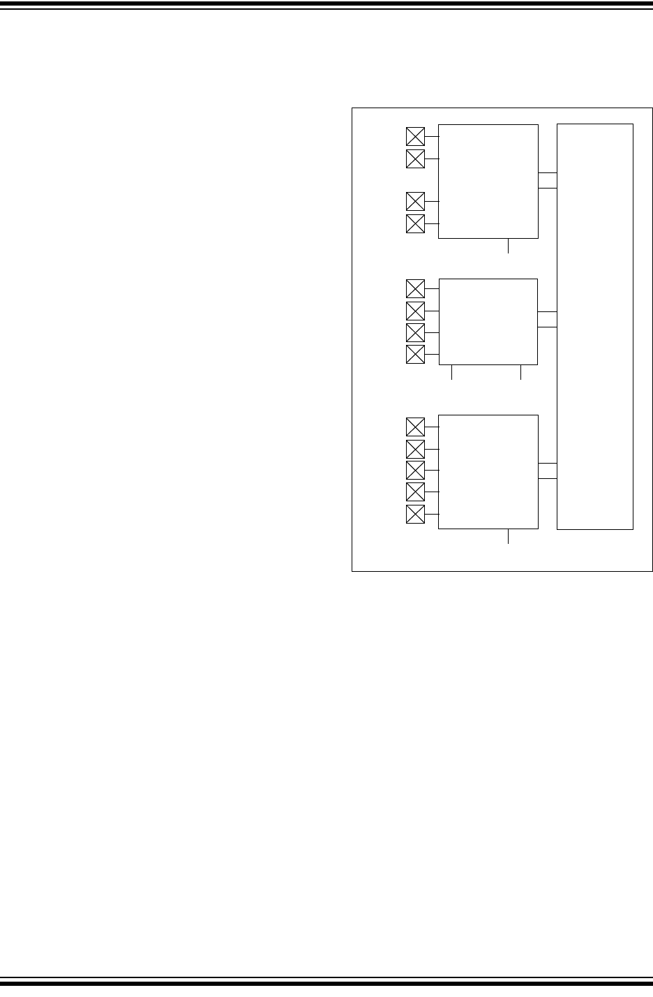
2015 Microchip Technology Inc. Preliminary DS60001320B-page 603
PIC32MZ Embedded Connectivity with Floating Point Unit (EF) Family
34.3 On-Chip Voltage Regulator
The core and digital logic for all PIC32MZ EF devices
is designed to operate at a nominal 1.8V. To simplify
system designs, devices in the PIC32MZ EF family
incorporate an on-chip regulator providing the required
core logic voltage from VDD.
34.3.1 ON-CHIP REGULATOR AND POR
It takes a fixed delay for the on-chip regulator to generate
an output. During this time, designated as TPU, code
execution is disabled. TPU is applied every time the
device resumes operation after any power-down,
including Sleep mode.
34.3.2 ON-CHIP REGULATOR AND BOR
PIC32MZ EF devices also have a simple brown-out
capability. If the voltage supplied to the regulator is
inadequate to maintain a regulated level, the regulator
Reset circuitry will generate a Brown-out Reset. This
event is captured by the BOR flag bit (RCON<1>). The
brown-out voltage levels are specific in Section 37.1
“DC Characteristics”.
34.4 On-chip Temperature Sensor
PIC32MZ EF devices include a temperature sensor
that provides accurate measurement of a device’s
junction temperature (see Section 37.2 “AC
Characteristics and Timing Parameters” for more
information).
The temperature sensor is connected to the ADC
module and can be measured using the shared S&H
circuit (see Section 28.0 “12-bit High-Speed
Successive Approximation Register (SAR) Analog-
to-Digital Converter (ADC)” for more information).
34.5 Programming and Diagnostics
PIC32MZ EF devices provide a complete range of pro-
gramming and diagnostic features that can increase
the flexibility of any application using them. These
features allow system designers to include:
• Simplified field programmability using two-wire
In-Circuit Serial Programming™ (ICSP™)
interfaces
• Debugging using ICSP
• Programming and debugging capabilities using
the EJTAG extension of JTAG
• JTAG boundary scan testing for device and board
diagnostics
PIC32 devices incorporate two programming and diag-
nostic modules, and a trace controller, that provide a
range of functions to the application developer.
FIGURE 34-1: BLOCK DIAGRAM OF
PROGRAMMING,
DEBUGGING AND TRACE
PORTS
TDI
TDO
TCK
TMS
JTAG
Controller
ICSP™
Controller
Core
JTAGEN DEBUG<1:0>
ICESEL
PGEC1
PGED1
PGEC2
PGED2
Instruction Trace
Controller
DEBUG<1:0>
TRCLK
TRD0
TRD2
TRD3
TRD1

PIC32MZ Embedded Connectivity with Floating Point Unit (EF) Family
DS60001320B-page 604 Preliminary 2015 Microchip Technology Inc.
NOTES:

2015 Microchip Technology Inc. Preliminary DS60001320B-page 605
PIC32MZ Embedded Connectivity with Floating Point Unit (EF) Family
35.0 INSTRUCTION SET
The PIC32MZ EF family instruction set complies with
the MIPS32® Release 5 instruction set architecture.
The PIC32MZ EF device family does not support the
following features:
• Core extend instructions
• Coprocessor 2 instructions
Note: Refer to “MIPS32® Architecture for
Programmers Volume II: The MIPS32®
Instruction Set” at www.imgtec.com for
more information.

PIC32MZ Embedded Connectivity with Floating Point Unit (EF) Family
DS60001320B-page 606 Preliminary 2015 Microchip Technology Inc.
NOTES:

2015 Microchip Technology Inc. Preliminary DS60001320B-page 607
PIC32MZ Embedded Connectivity with Floating Point Unit (EF) Family
36.0 DEVELOPMENT SUPPORT
The PIC® microcontrollers (MCU) and dsPIC® digital
signal controllers (DSC) are supported with a full range
of software and hardware development tools:
• Integrated Development Environment
- MPLAB® X IDE Software
• Compilers/Assemblers/Linkers
- MPLAB XC Compiler
- MPASMTM Assembler
-MPLINK
TM Object Linker/
MPLIBTM Object Librarian
- MPLAB Assembler/Linker/Librarian for
Various Device Families
• Simulators
- MPLAB X SIM Software Simulator
•Emulators
- MPLAB REAL ICE™ In-Circuit Emulator
• In-Circuit Debuggers/Programmers
- MPLAB ICD 3
- PICkit™ 3
• Device Programmers
- MPLAB PM3 Device Programmer
• Low-Cost Demonstration/Development Boards,
Evaluation Kits and Starter Kits
• Third-party development tools
36.1 MPLAB X Integrated Development
Environment Software
The MPLAB X IDE is a single, unified graphical user
interface for Microchip and third-party software, and
hardware development tool that runs on Windows®,
Linux and Mac OS® X. Based on the NetBeans IDE,
MPLAB X IDE is an entirely new IDE with a host of free
software components and plug-ins for high-
performance application development and debugging.
Moving between tools and upgrading from software
simulators to hardware debugging and programming
tools is simple with the seamless user interface.
With complete project management, visual call graphs,
a configurable watch window and a feature-rich editor
that includes code completion and context menus,
MPLAB X IDE is flexible and friendly enough for new
users. With the ability to support multiple tools on
multiple projects with simultaneous debugging, MPLAB
X IDE is also suitable for the needs of experienced
users.
Feature-Rich Editor:
• Color syntax highlighting
• Smart code completion makes suggestions and
provides hints as you type
• Automatic code formatting based on user-defined
rules
• Live parsing
User-Friendly, Customizable Interface:
• Fully customizable interface: toolbars, toolbar
buttons, windows, window placement, etc.
• Call graph window
Project-Based Workspaces:
• Multiple projects
• Multiple tools
• Multiple configurations
• Simultaneous debugging sessions
File History and Bug Tracking:
• Local file history feature
• Built-in support for Bugzilla issue tracker

PIC32MZ Embedded Connectivity with Floating Point Unit (EF) Family
DS60001320B-page 608 Preliminary 2015 Microchip Technology Inc.
36.2 MPLAB XC Compilers
The MPLAB XC Compilers are complete ANSI C
compilers for all of Microchip’s 8, 16, and 32-bit MCU
and DSC devices. These compilers provide powerful
integration capabilities, superior code optimization and
ease of use. MPLAB XC Compilers run on Windows,
Linux or MAC OS X.
For easy source level debugging, the compilers provide
debug information that is optimized to the MPLAB X
IDE.
The free MPLAB XC Compiler editions support all
devices and commands, with no time or memory
restrictions, and offer sufficient code optimization for
most applications.
MPLAB XC Compilers include an assembler, linker and
utilities. The assembler generates relocatable object
files that can then be archived or linked with other relo-
catable object files and archives to create an execut-
able file. MPLAB XC Compiler uses the assembler to
produce its object file. Notable features of the assem-
bler include:
• Support for the entire device instruction set
• Support for fixed-point and floating-point data
• Command-line interface
• Rich directive set
• Flexible macro language
• MPLAB X IDE compatibility
36.3 MPASM Assembler
The MPASM Assembler is a full-featured, universal
macro assembler for PIC10/12/16/18 MCUs.
The MPASM Assembler generates relocatable object
files for the MPLINK Object Linker, Intel® standard HEX
files, MAP files to detail memory usage and symbol
reference, absolute LST files that contain source lines
and generated machine code, and COFF files for
debugging.
The MPASM Assembler features include:
• Integration into MPLAB X IDE projects
• User-defined macros to streamline
assembly code
• Conditional assembly for multipurpose
source files
• Directives that allow complete control over the
assembly process
36.4 MPLINK Object Linker/
MPLIB Object Librarian
The MPLINK Object Linker combines relocatable
objects created by the MPASM Assembler. It can link
relocatable objects from precompiled libraries, using
directives from a linker script.
The MPLIB Object Librarian manages the creation and
modification of library files of precompiled code. When
a routine from a library is called from a source file, only
the modules that contain that routine will be linked in
with the application. This allows large libraries to be
used efficiently in many different applications.
The object linker/library features include:
• Efficient linking of single libraries instead of many
smaller files
• Enhanced code maintainability by grouping
related modules together
• Flexible creation of libraries with easy module
listing, replacement, deletion and extraction
36.5 MPLAB Assembler, Linker and
Librarian for Various Device
Families
MPLAB Assembler produces relocatable machine
code from symbolic assembly language for PIC24,
PIC32 and dsPIC DSC devices. MPLAB XC Compiler
uses the assembler to produce its object file. The
assembler generates relocatable object files that can
then be archived or linked with other relocatable object
files and archives to create an executable file. Notable
features of the assembler include:
• Support for the entire device instruction set
• Support for fixed-point and floating-point data
• Command-line interface
• Rich directive set
• Flexible macro language
• MPLAB X IDE compatibility

2015 Microchip Technology Inc. Preliminary DS60001320B-page 609
PIC32MZ Embedded Connectivity with Floating Point Unit (EF) Family
36.6 MPLAB X SIM Software Simulator
The MPLAB X SIM Software Simulator allows code
development in a PC-hosted environment by simulat-
ing the PIC MCUs and dsPIC DSCs on an instruction
level. On any given instruction, the data areas can be
examined or modified and stimuli can be applied from
a comprehensive stimulus controller. Registers can be
logged to files for further run-time analysis. The trace
buffer and logic analyzer display extend the power of
the simulator to record and track program execution,
actions on I/O, most peripherals and internal registers.
The MPLAB X SIM Software Simulator fully supports
symbolic debugging using the MPLAB XC Compilers,
and the MPASM and MPLAB Assemblers. The soft-
ware simulator offers the flexibility to develop and
debug code outside of the hardware laboratory envi-
ronment, making it an excellent, economical software
development tool.
36.7 MPLAB REAL ICE In-Circuit
Emulator System
The MPLAB REAL ICE In-Circuit Emulator System is
Microchip’s next generation high-speed emulator for
Microchip Flash DSC and MCU devices. It debugs and
programs all 8, 16 and 32-bit MCU, and DSC devices
with the easy-to-use, powerful graphical user interface of
the MPLAB X IDE.
The emulator is connected to the design engineer’s
PC using a high-speed USB 2.0 interface and is
connected to the target with either a connector
compatible with in-circuit debugger systems (RJ-11)
or with the new high-speed, noise tolerant, Low-
Voltage Differential Signal (LVDS) interconnection
(CAT5).
The emulator is field upgradable through future firmware
downloads in MPLAB X IDE. MPLAB REAL ICE offers
significant advantages over competitive emulators
including full-speed emulation, run-time variable
watches, trace analysis, complex breakpoints, logic
probes, a ruggedized probe interface and long (up to
three meters) interconnection cables.
36.8 MPLAB ICD 3 In-Circuit Debugger
System
The MPLAB ICD 3 In-Circuit Debugger System is
Microchip’s most cost-effective, high-speed hardware
debugger/programmer for Microchip Flash DSC and
MCU devices. It debugs and programs PIC Flash
microcontrollers and dsPIC DSCs with the powerful,
yet easy-to-use graphical user interface of the MPLAB
IDE.
The MPLAB ICD 3 In-Circuit Debugger probe is
connected to the design engineer’s PC using a high-
speed USB 2.0 interface and is connected to the target
with a connector compatible with the MPLAB ICD 2 or
MPLAB REAL ICE systems (RJ-11). MPLAB ICD 3
supports all MPLAB ICD 2 headers.
36.9 PICkit 3 In-Circuit Debugger/
Programmer
The MPLAB PICkit 3 allows debugging and program-
ming of PIC and dsPIC Flash microcontrollers at a most
affordable price point using the powerful graphical user
interface of the MPLAB IDE. The MPLAB PICkit 3 is
connected to the design engineer’s PC using a full-
speed USB interface and can be connected to the tar-
get via a Microchip debug (RJ-11) connector (compati-
ble with MPLAB ICD 3 and MPLAB REAL ICE). The
connector uses two device I/O pins and the Reset line
to implement in-circuit debugging and In-Circuit Serial
Programming™ (ICSP™).
36.10 MPLAB PM3 Device Programmer
The MPLAB PM3 Device Programmer is a universal,
CE compliant device programmer with programmable
voltage verification at VDDMIN and VDDMAX for
maximum reliability. It features a large LCD display
(128 x 64) for menus and error messages, and a mod-
ular, detachable socket assembly to support various
package types. The ICSP cable assembly is included
as a standard item. In Stand-Alone mode, the MPLAB
PM3 Device Programmer can read, verify and program
PIC devices without a PC connection. It can also set
code protection in this mode. The MPLAB PM3
connects to the host PC via an RS-232 or USB cable.
The MPLAB PM3 has high-speed communications and
optimized algorithms for quick programming of large
memory devices, and incorporates an MMC card for file
storage and data applications.

PIC32MZ Embedded Connectivity with Floating Point Unit (EF) Family
DS60001320B-page 610 Preliminary 2015 Microchip Technology Inc.
36.11 Demonstration/Development
Boards, Evaluation Kits, and
Starter Kits
A wide variety of demonstration, development and
evaluation boards for various PIC MCUs and dsPIC
DSCs allows quick application development on fully
functional systems. Most boards include prototyping
areas for adding custom circuitry and provide applica-
tion firmware and source code for examination and
modification.
The boards support a variety of features, including LEDs,
temperature sensors, switches, speakers, RS-232
interfaces, LCD displays, potentiometers and additional
EEPROM memory.
The demonstration and development boards can be
used in teaching environments, for prototyping custom
circuits and for learning about various microcontroller
applications.
In addition to the PICDEM™ and dsPICDEM™
demonstration/development board series of circuits,
Microchip has a line of evaluation kits and demonstra-
tion software for analog filter design, KEELOQ® security
ICs, CAN, IrDA®, PowerSmart battery management,
SEEVAL® evaluation system, Sigma-Delta ADC, flow
rate sensing, plus many more.
Also available are starter kits that contain everything
needed to experience the specified device. This usually
includes a single application and debug capability, all
on one board.
Check the Microchip web page (www.microchip.com)
for the complete list of demonstration, development
and evaluation kits.
36.12 Third-Party Development Tools
Microchip also offers a great collection of tools from
third-party vendors. These tools are carefully selected
to offer good value and unique functionality.
• Device Programmers and Gang Programmers
from companies, such as SoftLog and CCS
• Software Tools from companies, such as Gimpel
and Trace Systems
• Protocol Analyzers from companies, such as
Saleae and Total Phase
• Demonstration Boards from companies, such as
MikroElektronika, Digilent® and Olimex
• Embedded Ethernet Solutions from companies,
such as EZ Web Lynx, WIZnet and IPLogika®

2015 Microchip Technology Inc. Preliminary DS60001320B-page 611
PIC32MZ Embedded Connectivity with Floating Point Unit (EF) Family
37.0 ELECTRICAL CHARACTERISTICS
This section provides an overview of the PIC32MZ EF electrical characteristics. Additional information will be provided
in future revisions of this document as it becomes available.
Absolute maximum ratings for the PIC32MZ EF devices are listed below. Exposure to these maximum rating conditions
for extended periods may affect device reliability. Functional operation of the device at these or any other conditions,
above the parameters indicated in the operation listings of this specification, is not implied.
Absolute Maximum Ratings
(See Note 1)
Ambient temperature under bias.............................................................................................................-40°C to +125°C
Storage temperature .............................................................................................................................. -65°C to +150°C
Voltage on VDD with respect to VSS ......................................................................................................... -0.3V to +4.0V
Voltage on any pin that is not 5V tolerant, with respect to VSS (Note 3)......................................... -0.3V to (VDD + 0.3V)
Voltage on any 5V tolerant pin with respect to VSS when VDD 2.1V (Note 3)........................................ -0.3V to +5.5V
Voltage on any 5V tolerant pin with respect to VSS when VDD < 2.1V (Note 3)........................................ -0.3V to +3.6V
Voltage on D+ or D- pin with respect to VUSB3V3..................................................................... -0.3V to (VUSB3V3 + 0.3V)
Voltage on VBUS with respect to VSS ....................................................................................................... -0.3V to +5.5V
Maximum current out of VSS pin(s) .......................................................................................................................200 mA
Maximum current into VDD pin(s) (Note 2)............................................................................................................200 mA
Maximum current sunk/sourced by any 4x I/O pin (Note 4)....................................................................................15 mA
Maximum current sunk/sourced by any 8x I/O pin (Note 4)....................................................................................25 mA
Maximum current sunk/sourced by any 12x I/O pin (Note 4)..................................................................................33 mA
Maximum current sunk by all ports .......................................................................................................................150 mA
Maximum current sourced by all ports (Note 2)....................................................................................................150 mA
Note 1: Stresses above those listed under “Absolute Maximum Ratings” may cause permanent damage to the
device. This is a stress rating only and functional operation of the device at those or any other conditions,
above those indicated in the operation listings of this specification, is not implied. Exposure to maximum
rating conditions for extended periods may affect device reliability.
2: Maximum allowable current is a function of device maximum power dissipation (see Table 37-2).
3: See the pin name tables (Table 2 through Table 4) for the 5V tolerant pins.
4: Characterized, but not tested. Refer to parameters DO10, DO20, and DO20a for the 4x, 8x, and 12x I/O
pin lists.

PIC32MZ Embedded Connectivity with Floating Point Unit (EF) Family
DS60001320B-page 612 Preliminary 2015 Microchip Technology Inc.
37.1 DC Characteristics
TABLE 37-1: OPERATING MIPS VS. VOLTAGE
Characteristic VDD Range
(in Volts)
(Note 1)
Temp. Range
(in °C)
Max. Frequency Comment
PIC32MZ EF Devices
DC5 2.1V-3.6V -40°C to +85°C 200 MHz —
DC5b 2.1V-3.6V -40°C to +125°C 180 MHz Planned
Note 1: Overall functional device operation at VBORMIN < VDD < VDDMIN is guaranteed, but not characterized. All
device Analog modules, such as ADC, etc., will function, but with degraded performance below VDDMIN.
Refer to parameter BO10 in Table 37-5 for BOR values.
TABLE 37-2: THERMAL OPERATING CONDITIONS
Rating Symbol Min. Typical Max. Unit
Industrial Temperature Devices
Operating Junction Temperature Range TJ-40 —+125 °C
Operating Ambient Temperature Range TA-40 —+85 °C
Extended Temperature Devices
Operating Junction Temperature Range TJ-40 —+140 °C
Operating Ambient Temperature Range TA-40 —+125 °C
Power Dissipation:
Internal Chip Power Dissipation:
PINT = VDD x (IDD – S IOH) PDPINT + PI/OW
I/O Pin Power Dissipation:
PI/O = S (({VDD – VOH} x IOH) + S (VOL x IOL))
Maximum Allowed Power Dissipation PDMAX (TJ – TA)/JA W
TABLE 37-3: THERMAL PACKAGING CHARACTERISTICS
Characteristics Symbol Typical Max. Unit Notes
Package Thermal Resistance, 64-pin QFN (9x9x0.9 mm) JA 28 —°C/W 1
Package Thermal Resistance, 64-pin TQFP (10x10x1 mm) JA 49 —°C/W 1
Package Thermal Resistance, 100-pin TQFP (12x12x1 mm) JA 43 —°C/W 1
Package Thermal Resistance, 100-pin TQFP (14x14x1 mm) JA 40 —°C/W 1
Package Thermal Resistance, 124-pin VTLA (9x9x0.9 mm) JA 30 —°C/W 1
Package Thermal Resistance, 144-pin TQFP (16x16x1 mm) JA 42 —°C/W 1
Package Thermal Resistance, 144-pin LQFP (20x20x1.4 mm) JA 39 —°C/W 1
Note 1: Junction to ambient thermal resistance, Theta-JA (JA) numbers are achieved by package simulations.

2015 Microchip Technology Inc. Preliminary DS60001320B-page 613
PIC32MZ Embedded Connectivity with Floating Point Unit (EF) Family
TABLE 37-4: DC TEMPERATURE AND VOLTAGE SPECIFICATIONS
DC CHARACTERISTICS
Standard Operating Conditions: 2.1V to 3.6V
(unless otherwise stated)
Operating temperature -40°C TA +85°C for Industrial
-40°C TA +125°C for Extended
Param.
No. Symbol Characteristics Min. Typical Max. Units Conditions
Operating Voltage
DC10 VDD Supply Voltage (Note 1) 2.1—3.6V —
DC12 VDR RAM Data Retention Voltage
(Note 2) 2.0 — — V —
DC16 VPOR VDD Start Voltage
to Ensure Internal
Power-on Reset Signal (Note 3)
1.75 — — V —
DC17 SVDD VDD Rise Rate
to Ensure Internal
Power-on Reset Signal
0.000011 — 1.1 V/µs 300 ms to 3 µs @ 3.3V
Note 1: Overall functional device operation at VBORMIN < VDD < VDDMIN is guaranteed, but not characterized. All
device Analog modules, such as ADC, etc., will function, but with degraded performance below VDDMIN.
Refer to parameter BO10 in Table 37-5 for BOR values.
2: This is the limit to which VDD can be lowered without losing RAM data.
3: This is the limit to which VDD must be lowered to ensure Power-on Reset.
TABLE 37-5: ELECTRICAL CHARACTERISTICS: BOR
DC CHARACTERISTICS
Standard Operating Conditions: 2.1V to 3.6V
(unless otherwise stated)
Operating temperature -40°C TA +85°C for Industrial
-40°C TA +125°C for Extended
Param.
No. Symbol Characteristics Min.(1) Typical Max. Units Conditions
BO10 VBOR BOR Event on VDD transition
high-to-low (Note 2) 1.88 —2.02 V —
Note 1: Parameters are for design guidance only and are not tested in manufacturing.
2: Overall functional device operation at VBORMIN < VDD < VDDMIN is tested, but not characterized. All device
Analog modules, such as ADC, etc., will function, but with degraded performance below VDDMIN.

PIC32MZ Embedded Connectivity with Floating Point Unit (EF) Family
DS60001320B-page 614 Preliminary 2015 Microchip Technology Inc.
TABLE 37-6: DC CHARACTERISTICS: OPERATING CURRENT (IDD)
DC CHARACTERISTICS
Standard Operating Conditions: 2.1V to 3.6V
(unless otherwise stated)
Operating temperature -40°C TA +85°C for Industrial
-40°C TA +125°C for Extended
Parameter
No. Typical(3) Maximum(6) Units Conditions
Operating Current (IDD)(1)
DC20 825 mA 4 MHz (Note 4,5)
DC21 10 30 mA 10 MHz (Note 5)
DC22 32 65 mA 60 MHz (Note 2,4)
DC23 40 75 mA 80 MHz (Note 2,4)
DC25 61 95 mA 130 MHz (Note 2,4)
DC26 72 110 mA 160 MHz (Note 2,4)
DC28 81 120 mA 180 MHz (Note 2,4)
DC27a 92 130 mA 200 MHz (Note 2)
DC27b 78 100 mA 200 MHz (Note 4,5)
Note 1: A device’s IDD supply current is mainly a function of the operating voltage and frequency. Other factors,
such as PBCLK (Peripheral Bus Clock) frequency, number of peripheral modules enabled, internal code
execution pattern, I/O pin loading and switching rate, oscillator type, as well as temperature, can have an
impact on the current consumption.
2: The test conditions for IDD measurements are as follows:
• Oscillator mode is EC (for 8 MHz and below) and EC+PLL (for above 8 MHz) with OSC1 driven by
external square wave from rail-to-rail, (OSC1 input clock input over/undershoot < 100 mV required)
• OSC2/CLKO is configured as an I/O input pin
• USB PLL is disabled (USBMD = 1), VUSB3V3 is connected to VSS
• CPU, Program Flash, and SRAM data memory are operational, Program Flash memory Wait states
are equal to two
• L1 Cache and Prefetch modules are enabled
• No peripheral modules are operating, (ON bit = 0), and the associated PMD bit is set. All clocks are
disabled ON bit (PBxDIV<15>) = 0 (x 1,7)
• WDT, DMT, Clock Switching, Fail-Safe Clock Monitor, and Secondary Oscillator are disabled
• All I/O pins are configured as inputs and pulled to VSS
•MCLR = VDD
• CPU executing while(1) statement from Flash
• RTCC and JTAG are disabled
3: Data in “Typical” column is at 3.3V, +25°C at specified operating frequency unless otherwise stated.
Parameters are for design guidance only and are not tested.
4: This parameter is characterized, but not tested in manufacturing.
5: Note 2 applies with the following exceptions: L1 Cache and Prefetch modules are disabled, Program
Flash memory Wait states are equal to seven.
6: Data in the “Maximum” column is at 3.3V, +85ºC at specified operating frequency, unless otherwise
stated. Parameters are for design guidance only and are not tested.

2015 Microchip Technology Inc. Preliminary DS60001320B-page 615
PIC32MZ Embedded Connectivity with Floating Point Unit (EF) Family
TABLE 37-7: DC CHARACTERISTICS: IDLE CURRENT (IIDLE)
DC CHARACTERISTICS
Standard Operating Conditions: 2.1V to 3.6V
(unless otherwise stated)
Operating temperature -40°C TA +85°C for Industrial
-40°C TA +125°C for Extended
Parameter
No. Typical(2) Maximum(4) Units Conditions
Idle Current (IIDLE): Core Off, Clock on Base Current (Note 1)
DC30a 7 22 mA 4 MHz (Note 3)
DC31a 8 24 mA 10 MHz
DC32a 13 32 mA 60 MHz (Note 3)
DC33a 21 42 mA 130 MHz (Note 3)
DC34 26 48 mA 180 MHz (Note 3)
DC35 28 52 mA 200 MHz
Note 1: The test conditions for IIDLE current measurements are as follows:
• Oscillator mode is EC (for 8 MHz and below) and EC+PLL (for above 8 MHz) with OSC1 driven by
external square wave from rail-to-rail, (OSC1 input clock input over/undershoot < 100 mV required)
• OSC2/CLKO is configured as an I/O input pin
• USB PLL is disabled (USBPMD = 1), VUSB3V3 is connected to VSS, PBCLKx divisor = 1:128 (‘x’ 7)
• CPU is in Idle mode (CPU core Halted)
• L1 Cache and Prefetch modules are disabled
• No peripheral modules are operating, (ON bit = 0), but the associated PMD bit is cleared (except
USBPMD)
• WDT, DMT, Clock Switching, Fail-Safe Clock Monitor, and Secondary Oscillator are disabled
• All I/O pins are configured as inputs and pulled to VSS
•MCLR = VDD
• RTCC and JTAG are disabled
2: Data in “Typical” column is at 3.3V, +25°C unless otherwise stated. Parameters are for design guidance
only and are not tested.
3: This parameter is characterized, but not tested in manufacturing.
4: Data in the “Maximum” column is at 3.3V, +85ºC at specified operating frequency, unless otherwise stated.
Parameters are for design guidance only and are not tested.

PIC32MZ Embedded Connectivity with Floating Point Unit (EF) Family
DS60001320B-page 616 Preliminary 2015 Microchip Technology Inc.
TABLE 37-8: DC CHARACTERISTICS: POWER-DOWN CURRENT (IPD)
DC CHARACTERISTICS Standard Operating Conditions: 2.1V to 3.6V (unless otherwise stated)
Operating temperature -40°C TA +85°C for Industrial
-40°C TA +125°C for Extended
Param.
No. Typical(2) Maximum(5) Units Conditions
Power-Down Current (IPD) (Note 1)
DC40k 0.7 7 mA -40°C
Base Power-Down Current
DC40l 1.5 7 mA +25°C
DC40n 7 20 mA +85°C
DC40m 20 — mA +125ºC
Module Differential Current
DC41e 15 50 µA 3.6V Watchdog Timer Current: IWDT (Note 3)
DC42e 25 50 µA 3.6V RTCC + Timer1 w/32 kHz Crystal: IRTCC (Note 3)
DC43d 3 3.8 mA 3.6V ADC: IADC (Notes 3, 4)
DC44 15 50 µA 3.6V Deadman Timer Current: IDMT (Note 3)
Note 1: The test conditions for IPD current measurements are as follows:
• Oscillator mode is EC (for 8 MHz and below) and EC+PLL (for above 8 MHz) with OSC1 driven by
external square wave from rail-to-rail, (OSC1 input clock input over/undershoot < 100 mV required)
• OSC2/CLKO is configured as an I/O input pin
• USB PLL is disabled (USBMD = 1), VUSB3V3 is connected to VSS
• CPU is in Sleep mode
• L1 Cache and Prefetch modules are disabled
• No peripheral modules are operating, (ON bit = 0), and the associated PMD bit is set. All clocks are
disabled ON bit (PBxDIV<15>) = 0 (x 1,7)
• WDT, DMT, Clock Switching, Fail-Safe Clock Monitor, and Secondary Oscillator are disabled
• All I/O pins are configured as inputs and pulled to VSS
•MCLR = VDD
• RTCC and JTAG are disabled
• Voltage regulator is in Stand-by mode (VREGS = 0)
2: Data in the “Typical” column is at 3.3V, +25°C unless otherwise stated. Parameters are for design guid-
ance only and are not tested.
3: The current is the additional current consumed when the module is enabled. This current should be
added to the base IPD current.
4: Voltage regulator is operational (VREGS = 1).
5: Data in the “Maximum” column is at 3.3V, +85ºC at specified operating frequency, unless otherwise stated.
Parameters are for design guidance only and are not tested.

2015 Microchip Technology Inc. Preliminary DS60001320B-page 617
PIC32MZ Embedded Connectivity with Floating Point Unit (EF) Family
TABLE 37-9: DC CHARACTERISTICS: I/O PIN INPUT SPECIFICATIONS
DC CHARACTERISTICS
Standard Operating Conditions: 2.1V to 3.6V (unless otherwise
stated)
Operating temperature -40°C TA +85°C for Industrial
-40°C TA +125°C for Extended
Param.
No. Symbol Characteristics Min. Typ.(1) Max. Units Conditions
VIL Input Low Voltage
DI10 I/O Pins with PMP VSS —0.15 * VDD V
I/O Pins VSS —0.2 * VDD V
DI18 SDAx, SCLx VSS —0.3 * VDD V SMBus disabled
(Note 4)
DI19 SDAx, SCLx VSS — 0.8 V SMBus enabled
(Note 4)
VIH Input High Voltage
DI20 I/O Pins not 5V-tolerant(5) 0.80 * VDD —VDD V(Note 4,6)
I/O Pins 5V-tolerant with
PMP(5) 0.80 * VDD —5.5V(Note 4,6)
I/O Pins 5V-tolerant(5) 0.80 * VDD —5.5V
DI28a SDAx, SCLx on non-5V
tolerant pins(5) 0.80 * VDD —VDD V SMBus disabled
(Note 4,6)
DI29a SDAx, SCLx on non-5V
tolerant pins(5) 2.1 — VDD V SMBus enabled,
2.1V VPIN 5.5
(Note 4,6)
DI28b SDAx, SCLx on 5V tolerant
pins(5) 0.80 * VDD — 5.5 V SMBus disabled
(Note 4,6)
DI29b SDAx, SCLx on 5V tolerant
pins(5) 2.1 — 5.5 V SMBus enabled,
2.1V VPIN 5.5
(Note 4,6)
DI30 ICNPU Change Notification
Pull-up Current ——-40µAVDD = 3.3V, VPIN = VSS
(Note 3,6)
DI31 ICNPD Change Notification
Pull-down Current(4) 40 — — µA VDD = 3.3V, VPIN = VDD
IIL Input Leakage Current
(Note 3)
DI50 I/O Ports — — +1µAVSS VPIN VDD,
Pin at high-impedance
DI51 Analog Input Pins — — +1µAVSS VPIN VDD,
Pin at high-impedance
DI55 MCLR(2) ——+1µAVSS VPIN VDD
DI56 OSC1 — — +1µAVSS VPIN VDD,
HS mode
Note 1: Data in “Typical” column is at 3.3V, +25°C unless otherwise stated. Parameters are for design guidance
only and are not tested.
2: The leakage current on the MCLR pin is strongly dependent on the applied voltage level. The specified
levels represent normal operating conditions. Higher leakage current may be measured at different input
voltages.
3: Negative current is defined as current sourced by the pin.
4: This parameter is characterized, but not tested in manufacturing.
5: See the pin name tables (Table 2 through Table 4) for the 5V-tolerant pins.
6: The VIH specifications are only in relation to externally applied inputs, and not with respect to the user-
selectable internal pull-ups. External open drain input signals utilizing the internal pull-ups of the PIC32
device are guaranteed to be recognized only as a logic “high” internally to the PIC32 device, provided that
the external load does not exceed the minimum value of ICNPU. For External “input” logic inputs that
require a pull-up source, to guarantee the minimum VIH of those components, it is recommended to use an
external pull-up resistor rather than the internal pull-ups of the PIC32 device.

PIC32MZ Embedded Connectivity with Floating Point Unit (EF) Family
DS60001320B-page 618 Preliminary 2015 Microchip Technology Inc.
TABLE 37-10: DC CHARACTERISTICS: I/O PIN INPUT INJECTION CURRENT SPECIFICATIONS
DC CHARACTERISTICS
Standard Operating Conditions: 2.1V to 3.6V (unless otherwise
stated)
Operating temperature -40°C TA +85°C for Industrial
-40°C TA +125°C for Extended
Param.
No. Symbol Characteristics Min. Typical(1) Max. Units Conditions
DI60a IICL Input Low Injection
Current 0—-5
(2,5) mA This parameter applies
to all pins, with the
exception of RB10.
Maximum IICH current
for this exception is
0 mA.
DI60b IICH Input High Injection
Current 0—+5
(3,4,5) mA This parameter applies
to all pins, with the
exception of all 5V toler-
ant pins, OSCI, OSCO,
SOSCI, SOSCO, D+, D-
and RB10. Maximum
IICH current for these
exceptions is 0 mA.
DI60c IICT Total Input Injection
Current (sum of all I/O
and control pins)
-20(6) —+20
(6) mA Absolute instantaneous
sum of all ± input
injection currents from
all I/O pins
( | IICL + | IICH | ) IICT
Note 1: Data in “Typical” column is at 3.3V, +25°C unless otherwise stated. Parameters are for design guidance
only and are not tested.
2: VIL source < (VSS - 0.3). Characterized but not tested.
3: VIH source > (VDD + 0.3) for non-5V tolerant pins only.
4: Digital 5V tolerant pins do not have an internal high side diode to VDD, and therefore, cannot tolerate any
“positive” input injection current.
5: Injection currents > | 0 | can affect the ADC results by approximately 4 to 6 counts (i.e., VIH Source > (VDD
+ 0.3) or VIL source < (VSS - 0.3)).
6: Any number and/or combination of I/O pins not excluded under IICL or IICH conditions are permitted pro-
vided the “absolute instantaneous” sum of the input injection currents from all pins do not exceed the spec-
ified limit. If Note 2, IICL = (((Vss - 0.3) - VIL source) / Rs). If Note 3, IICH = ((IICH source - (VDD + 0.3)) / RS).
RS = Resistance between input source voltage and device pin. If (VSS - 0.3) VSOURCE (VDD + 0.3),
injection current = 0.

2015 Microchip Technology Inc. Preliminary DS60001320B-page 619
PIC32MZ Embedded Connectivity with Floating Point Unit (EF) Family
TABLE 37-11: DC CHARACTERISTICS: I/O PIN OUTPUT SPECIFICATIONS
DC CHARACTERISTICS
Standard Operating Conditions: 2.1V to 3.6V
(unless otherwise stated)
Operating temperature -40°C TA +85°C for Industrial
-40°C TA +125°C for Extended
Param. Sym. Characteristic Min. Typ. Max. Units Conditions(1)
DO10 VOL
Output Low Voltage
I/O Pins
4x Sink Driver Pins -
RA3, RA9, RA10, RA14, RA15
RB0-RB2, RB4, RB6, RB7, RB11, RB13
RC12-RC15
RD0, RD6-RD7, RD11, RD14
RE8, RE9
RF2, RF3, RF8
RG15
RH0, RH1, RH4-RH6, RH8-RH13
RJ0-RJ2, RJ8, RJ9, RJ11
——0.4V
IOL 10 mA, VDD = 3.3V
Output Low Voltage
I/O Pins:
8x Sink Driver Pins -
RA0-RA2, RA4, RA5
RB3, RB5, RB8-RB10, RB12, RB14, RB15
RC1-RC4
RD1-RD5, RD9, RD10, RD12, RD13, RD15
RE4-RE7
RF0, RF4, RF5, RF12, RF13
RG0, RG1, RG6-RG9
RH2, RH3, RH7, RH14, RH15
RJ3-RJ7, RJ10, RJ12-RJ15
RK0-RK7
——0.4
VI
OL 15 mA, VDD = 3.3V
Output Low Voltage
I/O Pins:
12x Sink Driver Pins -
RA6, RA7
RE0-RE3
RF1
RG12-RG14
——0.4
VI
OL 20 mA, VDD = 3.3V
Note 1: Parameters are characterized, but not tested.

PIC32MZ Embedded Connectivity with Floating Point Unit (EF) Family
DS60001320B-page 620 Preliminary 2015 Microchip Technology Inc.
DO20 VOH
Output High Voltage
I/O Pins:
4x Source Driver Pins -
RA3, RA9, RA10, RA14, RA15
RB0-RB2, RB4, RB6-RB7, RB11, RB13
RC12-RC15
RD0, RD6-RD7, RD11, RD14
RE8, RE9
RF2, RF3, RF8
RG15
RH0, RH1, RH4-RH6, RH8-RH13
RJ0-RJ2, RJ8, RJ9, RJ11
2.4 — — V IOH -10 mA, VDD = 3.3V
Output High Voltage
I/O Pins:
8x Source Driver Pins -
RA0-RA2, RA4, RA5
RB3, RB5, RB8-RB10, RB12, RB14, RB15
RC1-RC4
RD1-RD5, RD9, RD10, RD12, RD13, RD15
RE4-RE7
RF0, RF4, RF5, RF12, RF13
RG0, RG1, RG6-RG9
RH2, RH3, RH7, RH14, RH15
RJ3-RJ7, RJ10, RJ12-RJ15
RK0-RK7
2.4 — — V IOH -15 mA, VDD = 3.3V
Output High Voltage
I/O Pins:
12x Source Driver Pins -
RA6, RA7
RE0-RE3
RF1
RG12-RG14
2.4 — — V IOH -20 mA, VDD = 3.3V
TABLE 37-11: DC CHARACTERISTICS: I/O PIN OUTPUT SPECIFICATIONS (CONTINUED)
DC CHARACTERISTICS
Standard Operating Conditions: 2.1V to 3.6V
(unless otherwise stated)
Operating temperature -40°C TA +85°C for Industrial
-40°C TA +125°C for Extended
Param. Sym. Characteristic Min. Typ. Max. Units Conditions(1)
Note 1: Parameters are characterized, but not tested.

2015 Microchip Technology Inc. Preliminary DS60001320B-page 621
PIC32MZ Embedded Connectivity with Floating Point Unit (EF) Family
DO20a VOH1
Output High Voltage
I/O Pins:
4x Source Driver Pins -
RA3, RA9, RA10, RA14, RA15
RB0-RB2, RB4, RB6-RB7, RB11, RB13
RC12-RC15
RD0, RD6-RD7, RD11, RD14
RE8, RE9
RF2, RF3, RF8
RG15
RH0, RH1, RH4-RH6, RH8-RH13
RJ0-RJ2, RJ8, RJ9, RJ11
1.5 — — V IOH -14 mA, VDD = 3.3V
2.0 — — V IOH -12 mA, VDD = 3.3V
3.0 — — V IOH -7 mA, VDD = 3.3V
Output High Voltage
I/O Pins:
8x Source Driver Pins -
RA0-RA2, RA4, RA5
RB3, RB5, RB8-RB10, RB12, RB14, RB15
RC1-RC4
RD1-RD5, RD9, RD10, RD12, RD13, RD15
RE4-RE7
RF0, RF4, RF5, RF12, RF13
RG0, RG1, RG6-RG9
RH2, RH3, RH7, RH14, RH15
RJ3-RJ7, RJ10, RJ12-RJ15
RK0-RK7
1.5 — — V IOH -22 mA, VDD = 3.3V
2.0 — — V IOH -18 mA, VDD = 3.3V
3.0 — — V IOH -10 mA, VDD = 3.3V
Output High Voltage
I/O Pins:
12x Source Driver Pins -
RA6, RA7
RE0-RE3
RF1
RG12-RG14
1.5 — — V IOH -32 mA, VDD = 3.3V
2.0 — — V IOH -25 mA, VDD = 3.3V
3.0 — — V IOH -14 mA, VDD = 3.3V
TABLE 37-11: DC CHARACTERISTICS: I/O PIN OUTPUT SPECIFICATIONS (CONTINUED)
DC CHARACTERISTICS
Standard Operating Conditions: 2.1V to 3.6V
(unless otherwise stated)
Operating temperature -40°C TA +85°C for Industrial
-40°C TA +125°C for Extended
Param. Sym. Characteristic Min. Typ. Max. Units Conditions(1)
Note 1: Parameters are characterized, but not tested.

PIC32MZ Embedded Connectivity with Floating Point Unit (EF) Family
DS60001320B-page 622 Preliminary 2015 Microchip Technology Inc.
TABLE 37-12: DC CHARACTERISTICS: PROGRAM MEMORY(3)
DC CHARACTERISTICS
Standard Operating Conditions: 2.1V to 3.6V
(unless otherwise stated)
Operating temperature -40°C TA +85°C for Industrial
-40°C TA +125°C for Extended
Param.
No. Sym. Characteristics Min. Typ.(1) Max. Units Conditions
D130a EPCell Endurance 10,000 — — E/W Without ECC
D130b 20,000 — — E/W With ECC
D131 VPR VDD for Read VDDMIN —VDDMAX V—
D132 VPEW VDD for Erase or Write VDDMIN —VDDMAX V—
D134a TRETD Characteristic Retention 10 — — Year Without ECC
D134b 20 — — Year With ECC
D135 IDDP Supply Current during
Programming
——30 mA —
D136 TRW Row Write Cycle Time (Notes 2, 4) — 66813 — FRC Cycles —
D137 TQWW Quad Word Write Cycle Time
(Note 4) —773 — FRC Cycles —
D138 TWW Word Write Cycle Time (Note 4) — 383 — FRC Cycles —
D139 TCE Chip Erase Cycle Time (Note 4) — 515373 — FRC Cycles —
D140 TPFE All Program Flash (Upper and Lower
regions) Erase Cycle Time (Note 4) —256909 — FRC Cycles —
D141 TPBE Program Flash (Upper or Lower
regions) Erase Cycle Time (Note 4) —128453 — FRC Cycles —
D142 TPGE Page Erase Cycle Time (Note 4) — 128453 — FRC Cycles —
Note 1: Data in “Typical” column is at 3.3V, +25°C unless otherwise stated.
2: The minimum PBCLK5 for row programming is 4 MHz.
3: Refer to the “PIC32 Flash Programming Specification” (DS60001145) for operating conditions during
programming and erase cycles.
4: This parameter depends on FRC accuracy (see Table 37-20) and FRC tuning values (see the OSCTUN
register: Register 8-2).
TABLE 37-13: DC CHARACTERISTICS: PROGRAM FLASH MEMORY WAIT STATES
DC CHARACTERISTICS
Standard Operating Conditions: 2.1V to 3.6V
(unless otherwise stated)
Operating temperature -40°C TA +85°C for Industrial
-40°C TA +125°C for Extended
Required Flash Wait States(1) SYSCLK Units Conditions
With ECC:
0 Wait states
1 Wait state
2 Wait states
0 < SYSCLK 66
66 < SYSCLK 133
133 < SYSCLK 200
MHz —
Without ECC:
0 Wait states
1 Wait state
2 Wait states
0 < SYSCLK 83
83 < SYSCLK 166
166 < SYSCLK 200
MHz —
Note 1: To use Wait states, the Prefetch module must be enabled (PREFEN<1:0> 00) and the PFMWS<2:0>
bits must be written with the desired Wait state value.

2015 Microchip Technology Inc. Preliminary DS60001320B-page 623
PIC32MZ Embedded Connectivity with Floating Point Unit (EF) Family
TABLE 37-14: COMPARATOR SPECIFICATIONS
DC CHARACTERISTICS
Standard Operating Conditions (see Note 3): 2.1V to 3.6V
(unless otherwise stated)
Operating temperature -40°C TA +85°C for Industrial
-40°C TA +125°C for Extended
Param.
No. Symbol Characteristics Min. Typical Max. Units Comments
D300 VIOFF Input Offset Voltage — ±10 — mV AVDD = VDD, AVSS = VSS
D301 VICM Input Common Mode Voltage 0 — VDD VAVDD = VDD, AVSS = VSS
(Note 2)
D302 CMRR Common Mode Rejection
Ratio 55 — — dB Max VICM = (VDD – 1)V
(Note 2, 4)
D303 TRESP Response Time — 150 — ns AVDD = VDD, AVSS = VSS
(Notes 1, 2)
D304 ON2OV Comparator Enabled to Out-
put Valid — — 10 µs Comparator module is
configured before setting the
comparator ON bit (Note 2)
D305 IVREF Internal Voltage Reference 1.194 1.2 1.206 V —
Note 1: Response time measured with one comparator input at (VDD – 1.5)/2, while the other input transitions from
VSS to VDD.
2: These parameters are characterized but not tested.
3: The Comparator module is functional at VBORMIN < VDD < VDDMIN, but with degraded performance. Unless
otherwise stated, module functionality is guaranteed, but not characterized.
4: CMRR measurement characterized with a 1 M resistor in parallel with a 25 pF capacitor to VSS.
TABLE 37-15: COMPARATOR VOLTAGE REFERENCE SPECIFICATIONS
DC CHARACTERISTICS
Standard Operating Conditions (see Note 3): 2.1V to 3.6V
(unless otherwise stated)
Operating temperature -40°C TA +85°C for Industrial
-40°C TA +125°C for Extended
Param.
No. Symbol Characteristics Min. Typ. Max. Units Comments
D312 TSET Internal 4-bit DAC
Comparator Reference
Settling time
— — 10 µs See Note 1
D313 DACREFH CVREF Input Voltage
Reference Range AVSS —AVDD VCVRSRC with CVRSS = 0
VREF- — VREF+ V CVRSRC with CVRSS = 1
D314 DVREF CVREF Programmable
Output Range 0 — 0.625 x
DACREFH
V0 to 0.625 DACREFH with
DACREFH/24 step size
0.25 x
DACREFH
—0.719 x
DACREFH
V0.25 x DACREFH to 0.719
DACREFH with DACREFH/32
step size
D315 DACRES Resolution — — DACREFH/24 CVRCON<CVRR> = 1
— — DACREFH/32 CVRCON<CVRR> = 0
D316 DACACC Absolute Accuracy(2) — — 1/4 LSB DACREFH/24,
CVRCON<CVRR> = 1
— — 1/2 LSB DACREFH/32,
CVRCON<CVRR> = 0
Note 1: Settling time was measured while CVRR = 1 and CVR<3:0> transitions from ‘0000’ to ‘1111’. This
parameter is characterized, but is not tested in manufacturing.
2: These parameters are characterized but not tested.
PIC32MZ Embedded Connectivity with Floating Point Unit (EF) Family
DS60001320B-page 624 Preliminary 2015 Microchip Technology Inc.
37.2 AC Characteristics and Timing
Parameters
The information contained in this section defines
PIC32MZ EF device AC characteristics and timing
parameters.
FIGURE 37-1: LOAD CONDITIONS FOR DEVICE TIMING SPECIFICATIONS
VDD/2
CL
RL
Pin
Pin
VSS
VSS
CL
RL=464
Load Condition 1 – for all pins except OSC2 Load Condition 2 – for OSC2 (in EC mode)
TABLE 37-16: CAPACITIVE LOADING REQUIREMENTS ON OUTPUT PINS
AC CHARACTERISTICS
Standard Operating Conditions: 2.1V to 3.6V
(unless otherwise stated)
Operating temperature -40°C TA +85°C for Industrial
-40°C TA +125°C for Extended
Param.
No. Symbol Characteristics Min. Typical(1) Max. Units Conditions
DO50 COSCO OSC2 Pin — — 15 pF In HS mode when the external
clock is used to drive OSC1
DO56 CLAll I/O pins (except pins
used as CxOUT)
— — 50 pF EC mode for OSC2
DO58 CBSCLx, SDAx — — 400 pF In I2C™ mode
DO59 CSQI All SQI pins — — 10 pF —
Note 1: Data in “Typical” column is at 3.3V, +25°C unless otherwise stated. Parameters are for design guidance
only and are not tested.
2015 Microchip Technology Inc. Preliminary DS60001320B-page 625
PIC32MZ Embedded Connectivity with Floating Point Unit (EF) Family
FIGURE 37-2: EXTERNAL CLOCK TIMING
OSC1
OS20 OS30
OS30
OS31
OS31
TABLE 37-17: EXTERNAL CLOCK TIMING REQUIREMENTS
AC CHARACTERISTICS
Standard Operating Conditions: 2.1V to 3.6V
(unless otherwise stated)
Operating temperature -40°C TA +85°C for Industrial
-40°C TA +125°C for Extended
Param.
No. Symbol Characteristics Minimum Typical(1) Maximum Units Conditions
OS10 FOSC External CLKI Frequency
(External clocks allowed only
in EC and ECPLL modes)
DC —64 MHz EC (Note 2,3)
OS13 Oscillator Crystal Frequency 4 — 32 MHz HS (Note 2,3)
OS15 32 32.768 100 kHz SOSC (Note 2)
OS20 TOSC TOSC = 1/FOSC— — — — See parameter
OS10 for FOSC
value
OS30 TOSL,
TOSH
External Clock In (OSC1)
High or Low Time
0.375 x TOSC — — ns EC (Note 2)
OS31 TOSR,
TOSF
External Clock In (OSC1)
Rise or Fall Time
— — 7.5 ns EC (Note 2)
OS40 TOST Oscillator Start-up Timer Period
(Only applies to HS, HSPLL,
and SOSC Clock Oscillator
modes)
—1024 — TOSC (Note 2)
OS41 TFSCM Primary Clock Fail Safe
Time-out Period
— 2 — ms (Note 2)
OS42 GMExternal Oscillator
Transconductance —400 —µA/V VDD = 3.3V,
TA = +25°C, HS
(Note 2)
Note 1: Data in “Typical” column is at 3.3V, +25°C unless otherwise stated. Parameters are characterized but are
not tested.
2: This parameter is characterized, but not tested in manufacturing.
3: See parameter OS50 for PLL input frequency limitations.

PIC32MZ Embedded Connectivity with Floating Point Unit (EF) Family
DS60001320B-page 626 Preliminary 2015 Microchip Technology Inc.
TABLE 37-18: SYSTEM TIMING REQUIREMENTS
AC CHARACTERISTICS
Standard Operating Conditions: 2.1V to 3.6V
(unless otherwise stated)
Operating temperature -40°C TA +85°C for Industrial
-40°C TA +125°C for Extended
Param.
No. Symbol Characteristics Minimum Typical Maximum Units Conditions
OS51 FSYS System Frequency DC —200 MHz USB module disabled
30 —200 MHz USB module enabled
OS55a FPB Peripheral Bus Frequency DC —100 MHz For PBCLKx, ‘x’ 7
OS55b DC —200 MHz For PBCLK7
OS56 FREF Reference Clock Frequency — — 50 MHz For REFCLKI1, 3, 4
and REFCLKO1, 3, 4
pins
TABLE 37-19: PLL CLOCK TIMING SPECIFICATIONS
AC CHARACTERISTICS
Standard Operating Conditions: 2.1V to 3.6V
(unless otherwise stated)
Operating temperature -40°C TA +85°C for Industrial
-40°C TA +125°C for Extended
Param.
No. Symbol Characteristics(1) Min. Typical Max. Units Conditions
OS50 FIN PLL Input Frequency Range 5 — 64 MHz ECPLL, HSPLL, FRCPLL
modes
OS52 TLOCK PLL Start-up Time (Lock Time) — — 100 µs —
OS53 DCLK CLKO Stability(2)
(Period Jitter or Cumulative)
-0.25 —+0.25 %Measured over 100 ms
period
OS54 FVCO PLL VCO Frequency Range 350 —700 MHz —
OS54a FPLL PLL Output Frequency Range 10 —200 MHz —
Note 1: These parameters are characterized, but not tested in manufacturing.
2: This jitter specification is based on clock-cycle by clock-cycle measurements. To get the effective jitter for
individual time-bases on communication clocks, use the following formula:
For example, if PBCLK2 = 100 MHz and SPI bit rate = 50 MHz, the effective jitter is as follows:
EffectiveJitter DCLK
PBCLK2
CommunicationClock
----------------------------------------------------------
--------------------------------------------------------------=
EffectiveJitter DCLK
100
50
---------
--------------DCLK
1.41
--------------==

2015 Microchip Technology Inc. Preliminary DS60001320B-page 627
PIC32MZ Embedded Connectivity with Floating Point Unit (EF) Family
TABLE 37-20: INTERNAL FRC ACCURACY
AC CHARACTERISTICS
Standard Operating Conditions: 2.1V to 3.6V
(unless otherwise stated)
Operating temperature -40°C TA +85°C for Industrial
-40°C TA +125°C for Extended
Param.
No. Characteristics Min. Typ. Max. Units Conditions
Internal FRC Accuracy @ 8.00 MHz(1)
F20 FRC -5 — +5 % 0°C TA +85°C
-8 — +8 % -40°C TA +85°C
Note 1: Frequency calibrated at +25°C and 3.3V. The TUN bits (OSCTUN<5:0>) can be used to compensate for
temperature drift.
TABLE 37-21: INTERNAL LPRC ACCURACY
AC CHARACTERISTICS
Standard Operating Conditions: 2.1V to 3.6V
(unless otherwise stated)
Operating temperature -40°C TA +85°C for Industrial
-40°C TA +125°C for Extended
Param.
No. Characteristics Min. Typ. Max. Units Conditions
Internal LPRC @ 32.768 kHz(1)
F21 LPRC -8 —+8 %0°C TA +85°C
-25 —+25 % -40°C TA +85°C
Note 1: Change of LPRC frequency as VDD changes.
TABLE 37-22: INTERNAL BACKUP FRC (BFRC) ACCURACY
AC CHARACTERISTICS
Standard Operating Conditions: 2.1V to 3.6V
(unless otherwise stated)
Operating temperature -40°C TA +85°C for Industrial
-40°C TA +125°C for Extended
Param.
No. Characteristics Min. Typ. Max. Units Conditions
Internal BFRC Accuracy @ 8 MHzl
F22 BFRC —±30 — % —


2015 Microchip Technology Inc. Preliminary DS60001320B-page 629
PIC32MZ Embedded Connectivity with Floating Point Unit (EF) Family
TABLE 37-23: I/O TIMING REQUIREMENTS
AC CHARACTERISTICS
Standard Operating Conditions: 2.1V to 3.6V
(unless otherwise stated)
Operating temperature -40°C TA +85°C for Industrial
-40°C TA +125°C for Extended
Param.
No. Symbol Characteristics(2) Min. Typ.(1) Max. Units Conditions
DO31 TIORPort Output Rise Time
I/O Pins:
4x Source Driver Pins -
RA3, RA9, RA10, RA14, RA15
RB0-RB2, RB4, RB6-RB7, RB11,
RB13
RC12-RC15
RD0, RD6-RD7, RD11, RD14
RE8, RE9
RF2, RF3, RF8
RG15
RH0, RH1, RH4-RH6, RH8-RH13
RJ0-RJ2, RJ8, RJ9, RJ11
— — 9.5 ns CLOAD = 50 pF
— — 6 ns CLOAD = 20 pF
Port Output Rise Time
I/O Pins:
8x Source Driver Pins -
RA0-RA2, RA4, RA5
RB3, RB5, RB8-RB10, RB12, RB14,
RB15
RC1-RC4
RD1-RD5, RD9, RD10, RD12, RD13,
RD15
RE4-RE7
RF0, RF4, RF5, RF12, RF13
RG0, RG1, RG6-RG9
RH2, RH3, RH7, RH14, RH15
RJ3-RJ7, RJ10, RJ12-RJ15
RK0-RK7
— — 8 ns CLOAD = 50 pF
— — 6 ns CLOAD = 20 pF
Port Output Rise Time
I/O Pins:
12x Source Driver Pins -
RA6, RA7
RE0-RE3
RF1
RG12-RG14
— — 3.5 ns CLOAD = 50 pF
— — 2 ns CLOAD = 20 pF
Note 1: Data in “Typical” column is at 3.3V, +25°C unless otherwise stated.
2: This parameter is characterized, but not tested in manufacturing.

PIC32MZ Embedded Connectivity with Floating Point Unit (EF) Family
DS60001320B-page 630 Preliminary 2015 Microchip Technology Inc.
DO32 TIOFPort Output Fall Time
I/O Pins:
4x Source Driver Pins -
RA3, RA9, RA10, RA14, RA15
RB0-RB2, RB4, RB6-RB7, RB11,
RB13
RC12-RC15
RD0, RD6-RD7, RD11, RD14
RE8, RE9
RF2, RF3, RF8
RG15
RH0, RH1, RH4-RH6, RH8-RH13
RJ0-RJ2, RJ8, RJ9, RJ11
— — 9.5 ns CLOAD = 50 pF
— — 6 ns CLOAD = 20 pF
Port Output Fall Time
I/O Pins:
8x Source Driver Pins -
RA0-RA2, RA4, RA5
RB3, RB5, RB8-RB10, RB12, RB14,
RB15
RC1-RC4
RD1-RD5, RD9, RD10, RD12, RD13,
RD15
RE4-RE7
RF0, RF4, RF5, RF12, RF13
RG0, RG1, RG6-RG9
RH2, RH3, RH7, RH14, RH15
RJ3-RJ7, RJ10, RJ12-RJ15
RK0-RK7
— — 8 ns CLOAD = 50 pF
— — 6 ns CLOAD = 20 pF
Port Output Fall Time
I/O Pins:
12x Source Driver Pins -
RA6, RA7
RE0-RE3
RF1
RG12-RG14
— — 3.5 ns CLOAD = 50 pF
— — 2 ns CLOAD = 20 pF
DI35 TINP INTx Pin High or Low Time 5 — — ns —
DI40 TRBP CNx High or Low Time (input) 5 — — ns —
TABLE 37-23: I/O TIMING REQUIREMENTS (CONTINUED)
AC CHARACTERISTICS
Standard Operating Conditions: 2.1V to 3.6V
(unless otherwise stated)
Operating temperature -40°C TA +85°C for Industrial
-40°C TA +125°C for Extended
Param.
No. Symbol Characteristics(2) Min. Typ.(1) Max. Units Conditions
Note 1: Data in “Typical” column is at 3.3V, +25°C unless otherwise stated.
2: This parameter is characterized, but not tested in manufacturing.
2015 Microchip Technology Inc. Preliminary DS60001320B-page 631
PIC32MZ Embedded Connectivity with Floating Point Unit (EF) Family
FIGURE 37-4: POWER-ON RESET TIMING CHARACTERISTICS
VDD
VPOR
Note 1: The power-up period will be extended if the power-up sequence completes before the device exits from BOR
(VDD < VDDMIN).
2: Includes interval voltage regulator stabilization delay.
SY00
Power-up Sequence
(Note 2)
Internal Voltage Regulator Enabled
(TPU)SY10 CPU Starts Fetching Code
Clock Sources = (HS, HSPLL, and SOSC)
VDD
VPOR
SY00
Power-up Sequence
(Note 2)
Internal Voltage Regulator Enabled
(TPU)
(TSYSDLY)
CPU Starts Fetching Code
(Note 1)
(Note 1)
Clock Sources = (FRC, FRCDIV, FRCPLL, EC, ECPLL and LPRC)
(TOST)
SY02
(TSYSDLY)
SY02

PIC32MZ Embedded Connectivity with Floating Point Unit (EF) Family
DS60001320B-page 632 Preliminary 2015 Microchip Technology Inc.
FIGURE 37-5: EXTERNAL RESET TIMING CHARACTERISTICS
TABLE 37-24: RESETS TIMING
AC CHARACTERISTICS
Standard Operating Conditions: 2.1V to 3.6V
(unless otherwise stated)
Operating temperature -40°C TA +85°C for Industrial
-40°C TA +125°C for Extended
Param.
No. Symbol Characteristics(1) Min. Typical(2) Max. Units Conditions
SY00 TPU Power-up Period
Internal Voltage Regulator Enabled —400 600 s—
SY02 TSYSDLY System Delay Period:
Time Required to Reload Device
Configuration Fuses plus SYSCLK
Delay before First instruction is
Fetched.
—1 µs +
8 SYSCLK
cycles
— — —
SY20 TMCLR MCLR Pulse Width (low) 2 — — s—
SY30 TBOR BOR Pulse Width (low) — 1 — s —
Note 1: These parameters are characterized, but not tested in manufacturing.
2: Data in “Typ” column is at 3.3V, +25°C unless otherwise stated. Characterized by design but not tested.
MCLR
(SY20)
Reset Sequence
(SY10)
CPU Starts Fetching Code
BOR
(SY30)
TOST
TMCLR
TBOR
Reset Sequence
CPU Starts Fetching Code
Clock Sources = (FRC, FRCDIV, FRCPLL, EC, ECPLL and LPRC)
Clock Sources = (HS, HSPLL, and SOSC)(TSYSDLY)
SY02
(TSYSDLY)
SY02
2015 Microchip Technology Inc. Preliminary DS60001320B-page 633
PIC32MZ Embedded Connectivity with Floating Point Unit (EF) Family
FIGURE 37-6: TIMER1-TIMER9 EXTERNAL CLOCK TIMING CHARACTERISTICS
Note: Refer to Figure 37-1 for load conditions.
Tx11
Tx15
Tx10
Tx20
TMRx
OS60
TxCK
TABLE 37-25: TIMER1 EXTERNAL CLOCK TIMING REQUIREMENTS(1)
AC CHARACTERISTICS
Standard Operating Conditions: 2.1V to 3.6V
(unless otherwise stated)
Operating temperature -40°C TA +85°C for Industrial
-40°C TA +125°C for Extended
Param.
No. Symbol Characteristics(2) Min. Typ. Max. Units Conditions
TA10 TTXHTxCK
High Time
Synchronous,
with prescaler
[(12.5 ns or 1 TPBCLK3)
/N] + 20 ns
— — ns Must also meet
parameter TA15
(Note 3)
Asynchronous,
with prescaler
10 — — ns —
TA11 TTXLTxCK
Low Time
Synchronous,
with prescaler
[(12.5 ns or 1 TPBCLK3)
/N] + 20 ns
— — ns Must also meet
parameter TA15
(Note 3)
Asynchronous,
with prescaler
10 — — ns —
TA15 TTXPTxCK
Input Period Synchronous,
with prescaler [(Greater of 20 ns or
2 TPBCLK3)/N] + 30 ns — — ns VDD > 2.7V
(Note 3)
[(Greater of 20 ns or
2 TPBCLK3)/N] + 50 ns
— — ns VDD < 2.7V
(Note 3)
Asynchronous,
with prescaler
20 — — ns VDD > 2.7V
50 — — ns VDD < 2.7V
OS60 FT1SOSC1/T1CK Oscillator
Input Frequency Range
(oscillator enabled by setting
TCS bit (T1CON<1>))
32 —50 kHz —
TA20 TCKEXTMRL Delay from External TxCK
Clock Edge to Timer
Increment
— 1 TPBCLK3—
Note 1: Timer1 is a Type A timer.
2: This parameter is characterized, but not tested in manufacturing.
3: N = Prescale Value (1, 8, 64, 256).
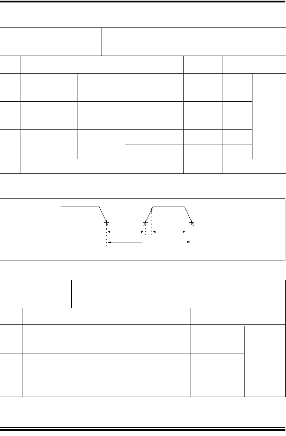
PIC32MZ Embedded Connectivity with Floating Point Unit (EF) Family
DS60001320B-page 634 Preliminary 2015 Microchip Technology Inc.
FIGURE 37-7: INPUT CAPTURE (CAPx) TIMING CHARACTERISTICS
TABLE 37-26: TIMER2-TIMER9 EXTERNAL CLOCK TIMING REQUIREMENTS
AC CHARACTERISTICS
Standard Operating Conditions: 2.1V to 3.6V
(unless otherwise stated)
Operating temperature -40°C TA +85°C for Industrial
-40°C TA +125°C for Extended
Param.
No. Symbol Characteristics(1) Min. Max. Units Conditions
TB10 TTXHTxCK
High Time Synchronous, with
prescaler [(12.5 ns or 1 TPBCLK3)
/N] + 25 ns —nsMust also
meet
parameter
TB15
N = prescale
value
(1, 2, 4, 8,
16, 32, 64,
256)
TB11 TTXLTxCK
Low Time
Synchronous, with
prescaler
[(12.5 ns or 1 TPBCLK3)
/N] + 25 ns
—nsMust also
meet
parameter
TB15
TB15 TTXPTxCK
Input
Period
Synchronous, with
prescaler
[(Greater of [(25 ns or
2 TPBCLK3)/N] + 30 ns
—nsV
DD > 2.7V
[(Greater of [(25 ns or
2 TPBCLK3)/N] + 50 ns
—nsV
DD < 2.7V
TB20 TCKEXTMRL Delay from External TxCK
Clock Edge to Timer Increment
—1TPBCLK3—
Note 1: These parameters are characterized, but not tested in manufacturing.
ICx
IC10 IC11
IC15
Note: Refer to Figure 37-1 for load conditions.
TABLE 37-27: INPUT CAPTURE MODULE TIMING REQUIREMENTS
AC CHARACTERISTICS
Standard Operating Conditions: 2.1V to 3.6V
(unless otherwise stated)
Operating temperature -40°C TA +85°C for Industrial
-40°C TA +125°C for Extended
Param.
No. Symbol Characteristics(1) Min. Max. Units Conditions
IC10 TCCLICx Input Low Time [(12.5 ns or 1 TPBCLK3)
/N] + 25 ns
—ns Must also
meet
parameter
IC15.
N = prescale
value (1, 4, 16)
IC11 TCCHICx Input High Time [(12.5 ns or 1 TPBCLK3)
/N] + 25 ns
—ns Must also
meet
parameter
IC15.
IC15 TCCPICx Input Period [(25 ns or 2 TPBCLK3)
/N] + 50 ns —ns —
Note 1: These parameters are characterized, but not tested in manufacturing.
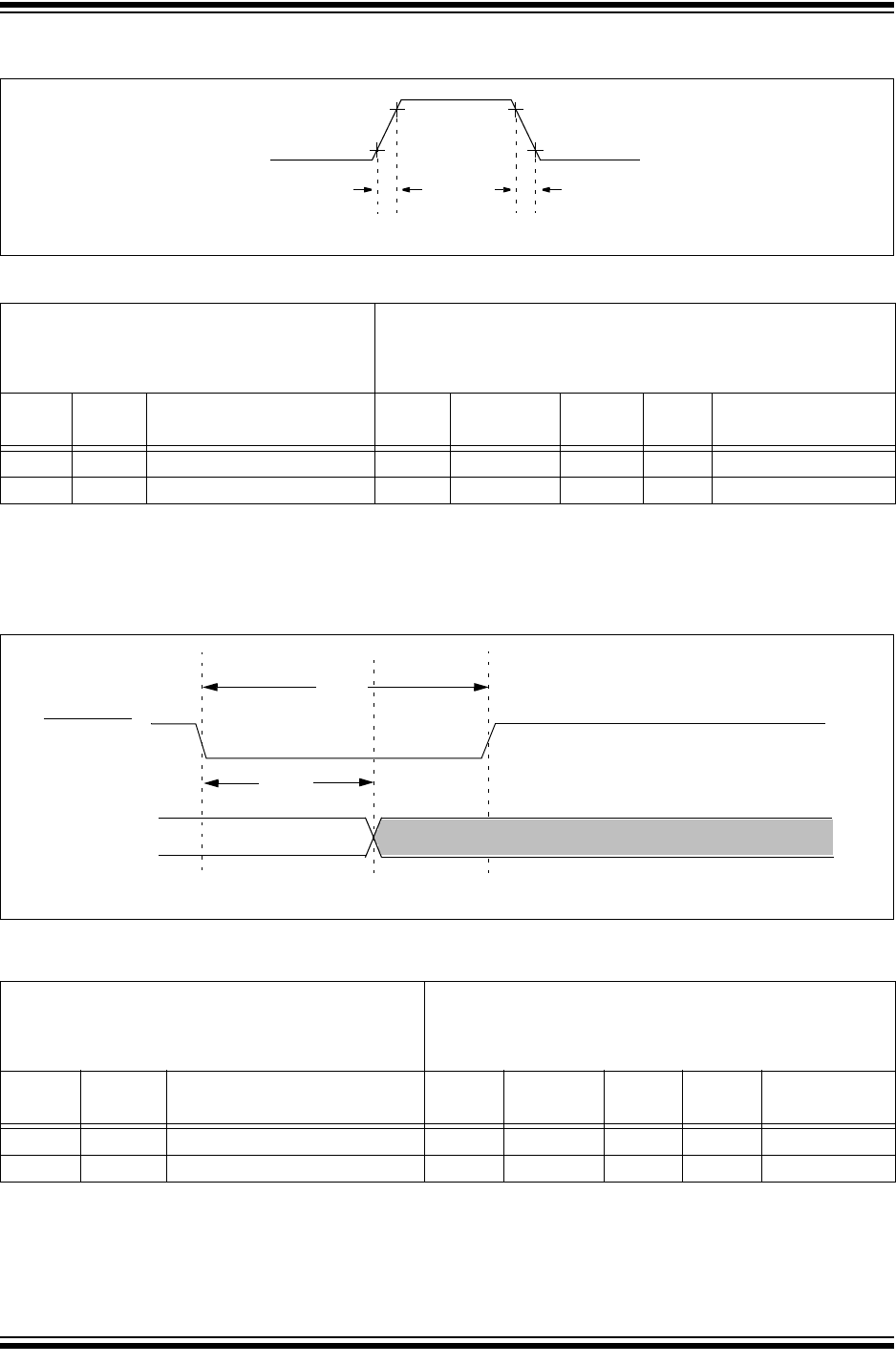
2015 Microchip Technology Inc. Preliminary DS60001320B-page 635
PIC32MZ Embedded Connectivity with Floating Point Unit (EF) Family
FIGURE 37-8: OUTPUT COMPARE MODULE (OCx) TIMING CHARACTERISTICS
TABLE 37-28: OUTPUT COMPARE MODULE TIMING REQUIREMENTS
FIGURE 37-9: OCx/PWM MODULE TIMING CHARACTERISTICS
AC CHARACTERISTICS
Standard Operating Conditions: 2.1V to 3.6V
(unless otherwise stated)
Operating temperature -40°C TA +85°C for Industrial
-40°C TA +125°C for Extended
Param.
No. Symbol Characteristics(1) Min. Typical(2) Max. Units Conditions
OC10 TCCFOCx Output Fall Time — — — ns See parameter DO32
OC11 TCCROCx Output Rise Time — — — ns See parameter DO31
Note 1: These parameters are characterized, but not tested in manufacturing.
2: Data in “Typical” column is at 3.3V, +25°C unless otherwise stated. Parameters are for design guidance
only and are not tested.
OCx
OC11 OC10
(Output Compare
Note: Refer to Figure 37-1 for load conditions.
or PWM mode)
OCFA/OCFB
OCx
OC20
OC15
Note: Refer to Figure 37-1 for load conditions.
OCx is tri-stated
TABLE 37-29: SIMPLE OCx/PWM MODE TIMING REQUIREMENTS
AC CHARACTERISTICS
Standard Operating Conditions: 2.1V to 3.6V
(unless otherwise stated)
Operating temperature -40°C TA +85°C for Industrial
-40°C TA +125°C for Extended
Param
No. Symbol Characteristics(1) Min Typical(2) Max Units Conditions
OC15 TFD Fault Input to PWM I/O Change — — 50 ns —
OC20 TFLT Fault Input Pulse Width 50 — — ns —
Note 1: These parameters are characterized, but not tested in manufacturing.
2: Data in “Typical” column is at 3.3V, +25°C unless otherwise stated. Parameters are for design guidance
only and are not tested.
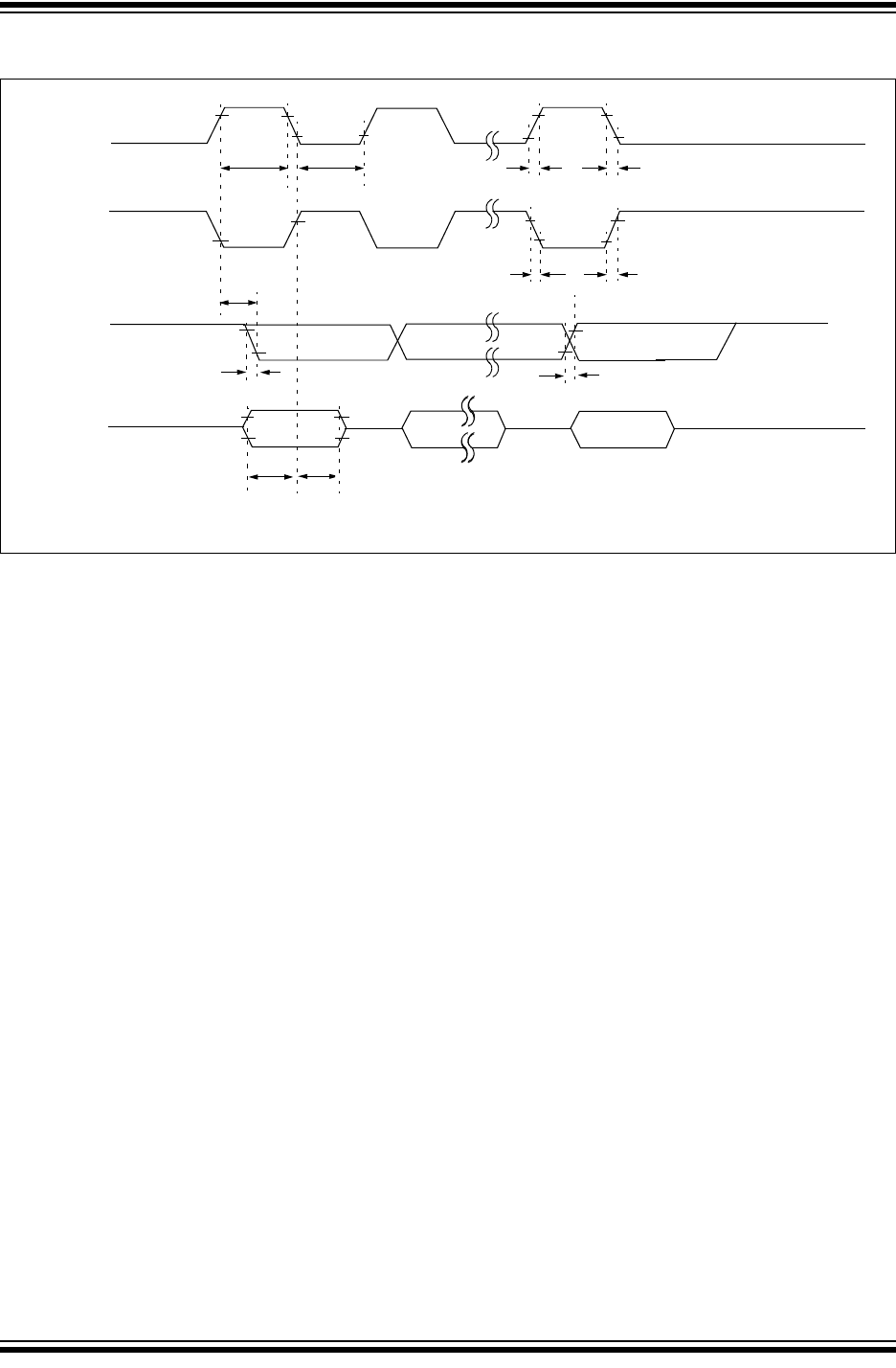
PIC32MZ Embedded Connectivity with Floating Point Unit (EF) Family
DS60001320B-page 636 Preliminary 2015 Microchip Technology Inc.
FIGURE 37-10: SPIx MODULE MASTER MODE (CKE = 0) TIMING CHARACTERISTICS
SCKx
(CKP = 0)
SCKx
(CKP = 1)
SDOx
SDIx
SP11 SP10
SP40 SP41
SP21
SP20
SP35
SP20
SP21
MSb LSb
Bit 14 - - - - - -1
MSb In LSb In
Bit 14 - - - -1
SP30
SP31
Note: Refer to Figure 37-1 for load conditions.

2015 Microchip Technology Inc. Preliminary DS60001320B-page 637
PIC32MZ Embedded Connectivity with Floating Point Unit (EF) Family
TABLE 37-30: SPIx MASTER MODE (CKE = 0) TIMING REQUIREMENTS
AC CHARACTERISTICS
Standard Operating Conditions: 2.1V to 3.6V
(unless otherwise stated)
Operating temperature -40°C TA +85°C for Industrial
-40°C TA +125°C for Extended
Param.
No. Symbol Characteristics(1) Min. Typ.(2) Max. Units Conditions
SP10 TSCLSCKx Output Low Time
(Note 3) TSCK/2 — — ns —
SP11 TSCH SCKx Output High Time
(Note 3) TSCK/2 ——ns —
SP15 TSCK SPI Clock Speed
(Note 5) —
—
—
—
—
25
50
25
50
25
—
—
—
—
—
MHz
MHz
MHz
MHz
MHz
SPI1, SPI4 through SPI6
SPI2 on RPB3, RPB5
SPI2 on other I/O
SPI3 on RPB10, RPB9, RPF0
SPI3 on other I/O
SP20 TSCF SCKx Output Fall Time
(Note 4) ———ns
See parameter DO32
SP21 TSCR SCKx Output Rise Time
(Note 4) ———
ns See parameter DO31
SP30 TDOF SDOx Data Output Fall Time
(Note 4) ———
ns See parameter DO32
SP31 TDOR SDOx Data Output Rise Time
(Note 4) ———
ns See parameter DO31
SP35 TSCH2DOV,
TSCL2DOVSDOx Data Output Valid after
SCKx Edge ——7ns VDD > 2.7V
——
10 ns VDD < 2.7V
SP40 TDIV2SCH,
TDIV2SCLSetup Time of SDIx Data Input
to SCKx Edge 5——ns —
SP41 TSCH2DIL,
TSCL2DIL
Hold Time of SDIx Data Input
to SCKx Edge 5——ns —
Note 1: These parameters are characterized, but not tested in manufacturing.
2: Data in “Typical” column is at 3.3V, +25°C unless otherwise stated. Parameters are for design guidance
only and are not tested.
3: The minimum clock period for SCKx is 20 ns. Therefore, the clock generated in Master mode must not
violate this specification.
4: Assumes 30 pF load on all SPIx pins.
5: To achieve maximum data rate, SMP must be set to ‘1’.
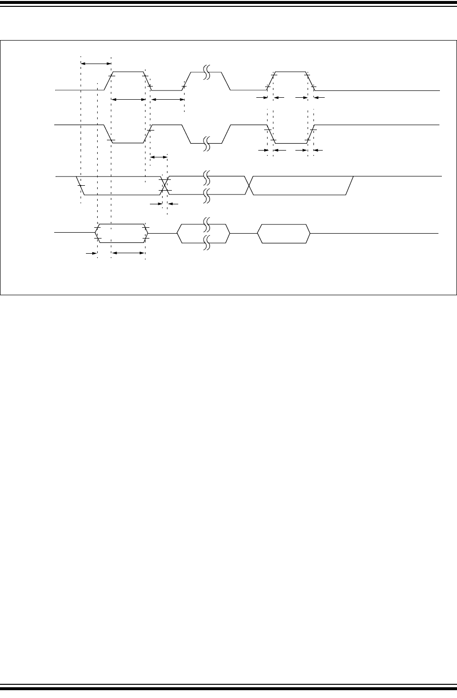
PIC32MZ Embedded Connectivity with Floating Point Unit (EF) Family
DS60001320B-page 638 Preliminary 2015 Microchip Technology Inc.
FIGURE 37-11: SPIx MODULE MASTER MODE (CKE = 1) TIMING CHARACTERISTICS
SCKX
(CKP = 0)
SCKX
(CKP = 1)
SDOX
SDIX
SP36
SP30,SP31
SP35
MSb Bit 14 - - - - - -1
LSb In
Bit 14 - - - -1
LSb
Note: Refer to Figure 37-1 for load conditions.
SP11 SP10
SP21
SP20
SP40 SP41
SP20
SP21
MSb In

2015 Microchip Technology Inc. Preliminary DS60001320B-page 639
PIC32MZ Embedded Connectivity with Floating Point Unit (EF) Family
TABLE 37-31: SPIx MODULE MASTER MODE (CKE = 1) TIMING REQUIREMENTS
AC CHARACTERISTICS
Standard Operating Conditions: 2.1V to 3.6V
(unless otherwise stated)
Operating temperature -40°C TA +85°C for Industrial
-40°C TA +125°C for Extended
Param.
No. Symbol Characteristics(1) Min. Typ.(2) Max. Units Conditions
SP10 TSCL SCKx Output Low Time
(Note 3) TSCK/2 — — ns —
SP11 TSCH SCKx Output High Time
(Note 3) TSCK/2 — — ns —
SP15 TSCK SPI Clock Speed
(Note 5) —
—
—
—
—
25
50
25
50
25
—
—
—
—
—
MHz
MHz
MHz
MHz
MHz
SPI1, SPI4 through SPI6
SPI2 on RPB3, RPB5
SPI2 on other I/O
SPI3 on RPB10, RPB9, RPF0
SPI3 on other I/O
SP20 TSCF SCKx Output Fall Time
(Note 4) — — — ns See parameter DO32
SP21 TSCR SCKx Output Rise Time
(Note 4) — — — ns See parameter DO31
SP30 TDOF SDOx Data Output Fall Time
(Note 4) — — — ns See parameter DO32
SP31 TDOR SDOx Data Output Rise Time
(Note 4) — — — ns See parameter DO31
SP35 TSCH2DOV,
TSCL2DOV
SDOx Data Output Valid after
SCKx Edge
——7nsV
DD > 2.7V
——10nsVDD < 2.7V
SP36 TDOV2SC,
TDOV2SCLSDOx Data Output Setup to
First SCKx Edge 7——ns —
SP40 TDIV2SCH,
TDIV2SCL
Setup Time of SDIx Data Input
to SCKx Edge
7——nsV
DD > 2.7V
10 — — ns VDD < 2.7V
SP41 TSCH2DIL,
TSCL2DIL
Hold Time of SDIx Data Input
to SCKx Edge
7——nsV
DD > 2.7V
10 — — ns VDD < 2.7V
Note 1: These parameters are characterized, but not tested in manufacturing.
2: Data in “Typical” column is at 3.3V, +25°C unless otherwise stated. Parameters are for design guidance
only and are not tested.
3: The minimum clock period for SCKx is 20 ns. Therefore, the clock generated in Master mode must not
violate this specification.
4: Assumes 30 pF load on all SPIx pins.
5: To achieve maximum data rate, SMP must be set to ‘1’.
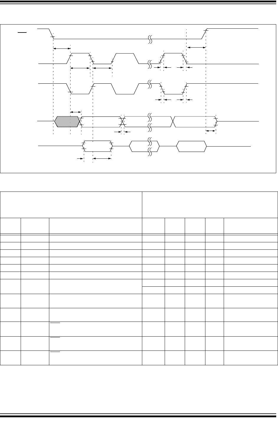
PIC32MZ Embedded Connectivity with Floating Point Unit (EF) Family
DS60001320B-page 640 Preliminary 2015 Microchip Technology Inc.
FIGURE 37-12: SPIx MODULE SLAVE MODE (CKE = 0) TIMING CHARACTERISTICS
SSX
SCKX
(CKP = 0)
SCKX
(CKP = 1)
SDOX
SP50
SP40 SP41
SP30,SP31 SP51
SP35
MSb LSb
Bit 14 - - - - - -1
Bit 14 - - - -1 LSb In
SP52
SP73
SP72
SP72
SP73
SP71 SP70
Note: Refer to Figure 37-1 for load conditions.
SDIXMSb In
TABLE 37-32: SPIx MODULE SLAVE MODE (CKE = 0) TIMING REQUIREMENTS
AC CHARACTERISTICS
Standard Operating Conditions: 2.1V to 3.6V
(unless otherwise stated)
Operating temperature -40°C TA +85°C for Industrial
-40°C TA +125°C for Extended
Param.
No. Symbol Characteristics(1) Min. Typ.(2) Max. Units Conditions
SP70 TSCLSCKx Input Low Time (Note 3) TSCK/2 — — ns —
SP71 TSCHSCKx Input High Time (Note 3) TSCK/2 — — ns —
SP72 TSCFSCKx Input Fall Time — — — ns See parameter DO32
SP73 TSCRSCKx Input Rise Time — — — ns See parameter DO31
SP30 TDOFSDOx Data Output Fall Time (Note 4) — — — ns See parameter DO32
SP31 TDORSDOx Data Output Rise Time (Note 4) — — — ns See parameter DO31
SP35 TSCH2DOV,
TSCL2DOV
SDOx Data Output Valid after
SCKx Edge
— — 7 ns VDD > 2.7V
— — 10 ns VDD < 2.7V
SP40 TDIV2SCH,
TDIV2SCLSetup Time of SDIx Data Input
to SCKx Edge 5 — — ns —
SP41 TSCH2DIL,
TSCL2DILHold Time of SDIx Data Input
to SCKx Edge 5 — — ns —
SP50 TSSL2SCH,
TSSL2SCLSSx to SCKx or SCKx Input 88 — — ns —
SP51 TSSH2DOZSSx to SDOx Output
High-Impedance (Note 3) 2.5 —12 ns —
SP52 TSCH2SSH
TSCL2SSH
SSx after SCKx Edge 10 — — ns —
Note 1: These parameters are characterized, but not tested in manufacturing.
2: Data in “Typical” column is at 3.3V, +25°C unless otherwise stated. Parameters are for design guidance
only and are not tested.
3: The minimum clock period for SCKx is 20 ns.
4: Assumes 30 pF load on all SPIx pins.
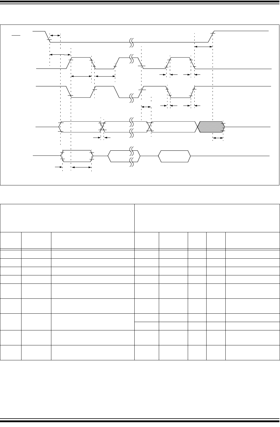
2015 Microchip Technology Inc. Preliminary DS60001320B-page 641
PIC32MZ Embedded Connectivity with Floating Point Unit (EF) Family
FIGURE 37-13: SPIx MODULE SLAVE MODE (CKE = 1) TIMING CHARACTERISTICS
SSx
SCKx
(CKP = 0)
SCKx
(CKP = 1)
SDOx
SDI
SP60
SDIx
SP30,SP31
MSb Bit 14 - - - - - -1 LSb
SP51
MSb In Bit 14 - - - -1 LSb In
SP52
SP73
SP72
SP72
SP73
SP71
SP40 SP41
Note: Refer to Figure 37-1 for load conditions.
SP50
SP70
SP35
TABLE 37-33: SPIx MODULE SLAVE MODE (CKE = 1) TIMING REQUIREMENTS
AC CHARACTERISTICS
Standard Operating Conditions: 2.1V to 3.6V
(unless otherwise stated)
Operating temperature-40°C TA +85°C for Industrial
-40°C TA +125°C for Extended
Param.
No. Symbol Characteristics(1) Min. Typical(2) Max. Units Conditions
SP70 TSCLSCKx Input Low Time (Note 3) TSCK/2 — — ns —
SP71 TSCHSCKx Input High Time (Note 3) TSCK/2 — — ns —
SP72 TSCFSCKx Input Fall Time — — 10 ns —
SP73 TSCRSCKx Input Rise Time — — 10 ns —
SP30 TDOFSDOx Data Output Fall Time
(Note 4) — — — ns See parameter DO32
SP31 TDORSDOx Data Output Rise Time
(Note 4) — — — ns See parameter DO31
SP35 TSCH2DOV,
TSCL2DOVSDOx Data Output Valid after
SCKx Edge — — 10 ns VDD > 2.7V
— — 15 ns VDD < 2.7V
SP40 TDIV2SCH,
TDIV2SCL
Setup Time of SDIx Data Input
to SCKx Edge
0 — — ns —
SP41 TSCH2DIL,
TSCL2DIL
Hold Time of SDIx Data Input
to SCKx Edge
7 — — ns —
Note 1: These parameters are characterized, but not tested in manufacturing.
2: Data in “Typical” column is at 3.3V, +25°C unless otherwise stated. Parameters are for design guidance
only and are not tested.
3: The minimum clock period for SCKx is 20 ns.
4: Assumes 30 pF load on all SPIx pins.

PIC32MZ Embedded Connectivity with Floating Point Unit (EF) Family
DS60001320B-page 642 Preliminary 2015 Microchip Technology Inc.
SP50 TSSL2SCH,
TSSL2SCL
SSx to SCKx or SCKx Input 88 — — ns —
SP51 TSSH2DOZSSx to SDOX Output
High-Impedance
(Note 4)
2.5 —12 ns —
SP52 TSCH2SSH
TSCL2SSHSSx after SCKx Edge 10 — — ns —
SP60 TSSL2DOVSDOx Data Output Valid after
SSx Edge
— — 12.5 ns —
TABLE 37-33: SPIx MODULE SLAVE MODE (CKE = 1) TIMING REQUIREMENTS (CONTINUED)
AC CHARACTERISTICS
Standard Operating Conditions: 2.1V to 3.6V
(unless otherwise stated)
Operating temperature-40°C TA +85°C for Industrial
-40°C TA +125°C for Extended
Param.
No. Symbol Characteristics(1) Min. Typical(2) Max. Units Conditions
Note 1: These parameters are characterized, but not tested in manufacturing.
2: Data in “Typical” column is at 3.3V, +25°C unless otherwise stated. Parameters are for design guidance
only and are not tested.
3: The minimum clock period for SCKx is 20 ns.
4: Assumes 30 pF load on all SPIx pins.
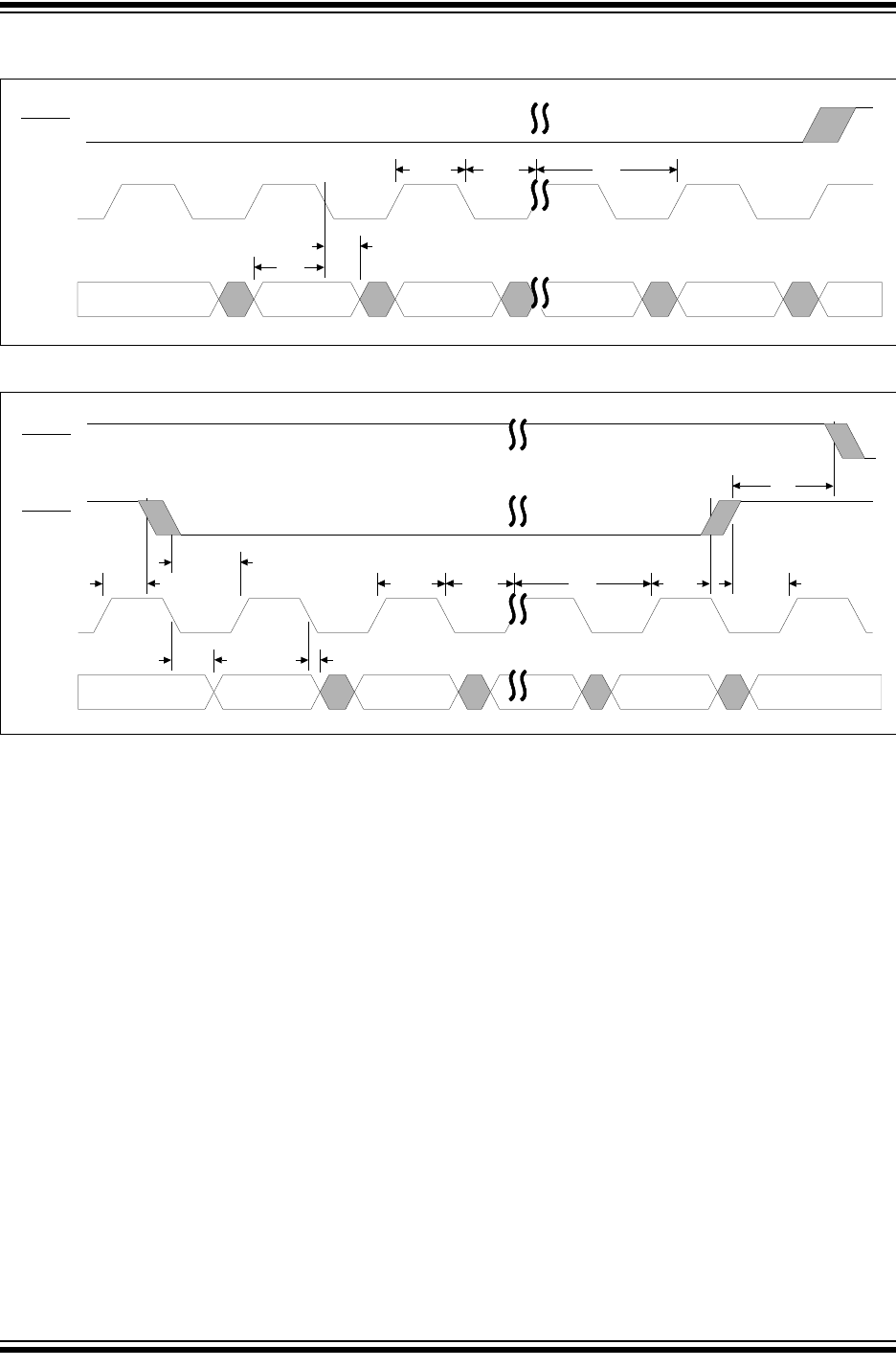
2015 Microchip Technology Inc. Preliminary DS60001320B-page 643
PIC32MZ Embedded Connectivity with Floating Point Unit (EF) Family
FIGURE 37-14: SQI SERIAL INPUT TIMING CHARACTERISTICS
FIGURE 37-15: SQI SERIAL OUTPUT TIMING CHARACTERISTICS
MSB LSB
TDIH
TDIS
TCLKTSCKLTSCKH
SQICS1
SQICLK
SQIDx
MSB LSB
TDOHTDOV
TCHSTCLK TCEHTSCKLTSCKH
TCES
TCHH
TCC
SQICS1
SQICS2
SQICLK
SQIDx

PIC32MZ Embedded Connectivity with Floating Point Unit (EF) Family
DS60001320B-page 644 Preliminary 2015 Microchip Technology Inc.
TABLE 37-34: SQI TIMING REQUIREMENTS
AC CHARACTERISTICS
Standard Operating Conditions: 2.1V to 3.6V
(unless otherwise stated)
Operating temperature -40°C TA +85°C for Industrial
-40°C TA +125°C for Extended
Param.
No. Symbol Characteristic(1,3) Min. Typ.(2) Max. Units Conditions
SQ10 FCLK Serial Clock Frequency (1/TSQI) — 66 — MHz DMA mode Read, SPI mode 0
— 33 — MHz DMA mode Read, SPI mode 3
— 100 — MHz PIO mode Write
SQ11 TSCKH Serial Clock High Time 5 — — ns —
SQ12 TSCKL Serial Clock Low Time 5 — — ns —
SQ13 TSCKR Serial Clock Rise Time — — — ns See parameter DO31
SQ14 TSCKF Serial Clock Fall Time — — — ns See parameter DO32
SQ15 TCSS (TCES)CS Active Setup Time 5 — — ns —
SQ16 TCSH (TCEH)CS Active Hold Time 5 — — ns —
SQ17 TCHS CS Not Active Setup Time 3 — — ns —
SQ18 TCHH CS Not Active Hold Time 3 — — ns —
SQ22 TDIS Data In Setup Time 6 — — ns —
SQ23 TDIH Data In Hold Time 3 — — ns —
SQ24 TDOH Data Out Hold 0 — — ns —
SQ25 TDOV Data Out Valid — — 6 ns —
Note 1: These parameters are characterized, but not tested in manufacturing.
2: Data in the Typical column is at 3.3V, +25°C unless otherwise stated. Parameters are for design guidance
only and are not tested.
3: Assumes 10 pF load on all SQIx pins
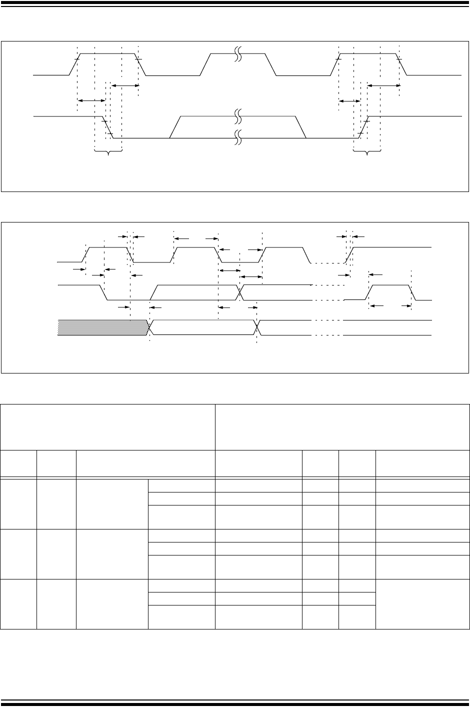
2015 Microchip Technology Inc. Preliminary DS60001320B-page 645
PIC32MZ Embedded Connectivity with Floating Point Unit (EF) Family
FIGURE 37-16: I2Cx BUS START/STOP BITS TIMING CHARACTERISTICS (MASTER MODE)
FIGURE 37-17: I2Cx BUS DATA TIMING CHARACTERISTICS (MASTER MODE)
SCLx
SDAx
Start Condition Stop Condition
Note: Refer to Figure 37-1 for load conditions.
IM30
IM31 IM34
IM33
IM11 IM10 IM33
IM11
IM10
IM20
IM26 IM25
IM40 IM40 IM45
IM21
SCLx
SDAx
In
SDAx
Out
Note: Refer to Figure 37-1 for load conditions.
TABLE 37-35: I2Cx BUS DATA TIMING REQUIREMENTS (MASTER MODE)
AC CHARACTERISTICS
Standard Operating Conditions: 2.1V to 3.6V
(unless otherwise stated)
Operating temperature -40°C TA +85°C for Industrial
-40°C TA +125°C for Extended
Param.
No. Symbol Characteristics Min.(1) Max. Units Conditions
IM10 TLO:SCL Clock Low Time 100 kHz mode TPBCLK2 * (BRG + 2) —µs —
400 kHz mode TPBCLK2 * (BRG + 2) —µs —
1 MHz mode
(Note 2) TPBCLK2 * (BRG + 2) —µs —
IM11 THI:SCL Clock High Time 100 kHz mode TPBCLK2 * (BRG + 2) —µs —
400 kHz mode TPBCLK2 * (BRG + 2) —µs —
1 MHz mode
(Note 2) TPBCLK2 * (BRG + 2) —µs —
IM20 TF:SCL SDAx and SCLx
Fall Time
100 kHz mode —300 ns CB is specified to be
from 10 to 400 pF
400 kHz mode 20 + 0.1 CB300 ns
1 MHz mode
(Note 2) —100 ns
Note 1: BRG is the value of the I2C™ Baud Rate Generator.
2: Maximum pin capacitance = 10 pF for all I2Cx pins (for 1 MHz mode only).
3: The typical value for this parameter is 104 ns.

PIC32MZ Embedded Connectivity with Floating Point Unit (EF) Family
DS60001320B-page 646 Preliminary 2015 Microchip Technology Inc.
IM21 TR:SCL SDAx and SCLx
Rise Time
100 kHz mode —1000 ns CB is specified to be
from 10 to 400 pF
400 kHz mode 20 + 0.1 CB300 ns
1 MHz mode
(Note 2) —300 ns
IM25 TSU:DAT Data Input
Setup Time 100 kHz mode 250 —ns —
400 kHz mode 100 —ns
1 MHz mode
(Note 2) 100 —ns
IM26 THD:DAT Data Input
Hold Time
100 kHz mode 0 — µs —
400 kHz mode 00.9 µs
1 MHz mode
(Note 2) 0 0.3 µs
IM30 TSU:STA Start Condition
Setup Time
100 kHz mode TPBCLK2 * (BRG + 2) —µs Only relevant for
Repeated Start
condition
400 kHz mode TPBCLK2 * (BRG + 2) —µs
1 MHz mode
(Note 2) TPBCLK2 * (BRG + 2) —µs
IM31 THD:STA Start Condition
Hold Time 100 kHz mode TPBCLK2 * (BRG + 2) —µs After this period, the
first clock pulse is
generated
400 kHz mode TPBCLK2 * (BRG + 2) —µs
1 MHz mode
(Note 2) TPBCLK2 * (BRG + 2) —µs
IM33 TSU:STO Stop Condition
Setup Time
100 kHz mode TPBCLK2 * (BRG + 2) —µs —
400 kHz mode TPBCLK2 * (BRG + 2) —µs
1 MHz mode
(Note 2) TPBCLK2 * (BRG + 2) —µs
IM34 THD:STO Stop Condition 100 kHz mode TPBCLK2 * (BRG + 2) —ns —
Hold Time 400 kHz mode TPBCLK2 * (BRG + 2) —ns
1 MHz mode
(Note 2) TPBCLK2 * (BRG + 2) —ns
IM40 TAA:SCL Output Valid
from Clock
100 kHz mode —3500 ns —
400 kHz mode —1000 ns —
1 MHz mode
(Note 2) —350 ns —
IM45 TBF:SDA Bus Free Time 100 kHz mode 4.7 —µs The amount of time
the bus must be free
before a new
transmission can start
400 kHz mode 1.3 —µs
1 MHz mode
(Note 2) 0.5 —µs
IM50 CBBus Capacitive Loading — — pF See parameter DO58
IM51 TPGD Pulse Gobbler Delay 52 312 ns See Note 3
TABLE 37-35: I2Cx BUS DATA TIMING REQUIREMENTS (MASTER MODE) (CONTINUED)
AC CHARACTERISTICS
Standard Operating Conditions: 2.1V to 3.6V
(unless otherwise stated)
Operating temperature -40°C TA +85°C for Industrial
-40°C TA +125°C for Extended
Param.
No. Symbol Characteristics Min.(1) Max. Units Conditions
Note 1: BRG is the value of the I2C™ Baud Rate Generator.
2: Maximum pin capacitance = 10 pF for all I2Cx pins (for 1 MHz mode only).
3: The typical value for this parameter is 104 ns.
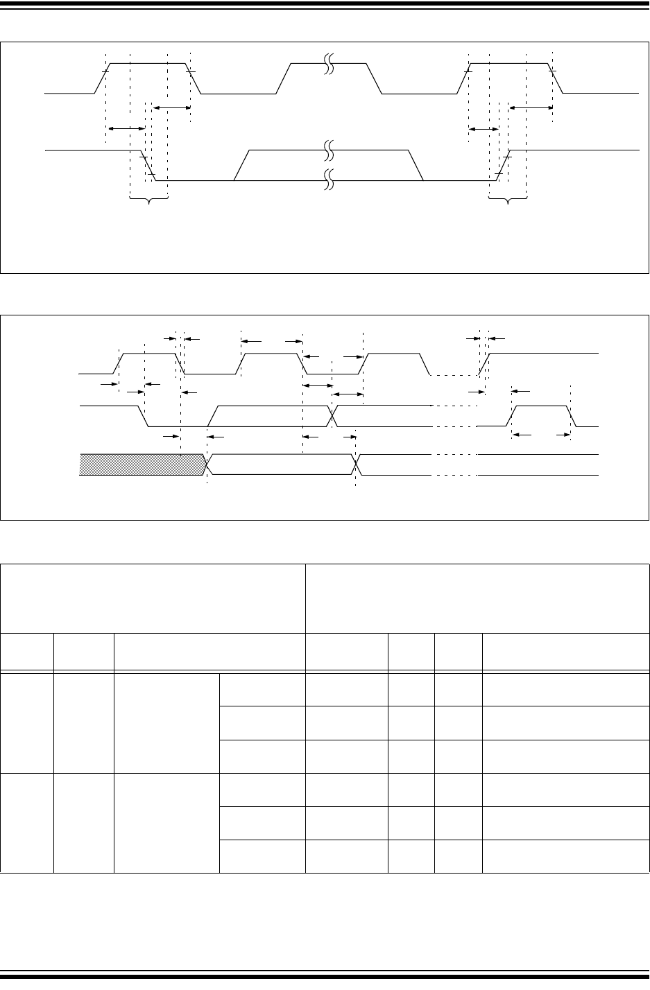
2015 Microchip Technology Inc. Preliminary DS60001320B-page 647
PIC32MZ Embedded Connectivity with Floating Point Unit (EF) Family
FIGURE 37-18: I2Cx BUS START/STOP BITS TIMING CHARACTERISTICS (SLAVE MODE)
FIGURE 37-19: I2Cx BUS DATA TIMING CHARACTERISTICS (SLAVE MODE)
IS34
SCLx
SDAx
Start
Condition
Stop
Condition
IS33
Note: Refer to Figure 37-1 for load conditions.
IS31
IS30
IS30 IS31 IS33
IS11
IS10
IS20
IS26 IS25
IS40 IS40 IS45
IS21
SCLx
SDAx
In
SDAx
Out
Note: Refer to Figure 37-1 for load conditions.
TABLE 37-36: I2Cx BUS DATA TIMING REQUIREMENTS (SLAVE MODE)
AC CHARACTERISTICS
Standard Operating Conditions: 2.1V to 3.6V
(unless otherwise stated)
Operating temperature -40°C TA +85°C for Industrial
-40°C TA +125°C for Extended
Param.
No. Symbol Characteristics Min. Max. Units Conditions
IS10 TLO:SCL Clock Low Time 100 kHz mode 4.7 —µs PBCLK must operate at a
minimum of 800 kHz
400 kHz mode 1.3 —µs PBCLK must operate at a
minimum of 3.2 MHz
1 MHz mode
(Note 1) 0.5 —µs —
IS11 THI:SCL Clock High Time 100 kHz mode 4.0 —µs PBCLK must operate at a
minimum of 800 kHz
400 kHz mode 0.6 —µs PBCLK must operate at a
minimum of 3.2 MHz
1 MHz mode
(Note 1) 0.5 —µs —
Note 1: Maximum pin capacitance = 10 pF for all I2Cx pins (for 1 MHz mode only).

PIC32MZ Embedded Connectivity with Floating Point Unit (EF) Family
DS60001320B-page 648 Preliminary 2015 Microchip Technology Inc.
IS20 TF:SCL SDAx and SCLx
Fall Time
100 kHz mode —300 ns CB is specified to be from
10 to 400 pF
400 kHz mode 20 + 0.1 CB300 ns
1 MHz mode
(Note 1) —100 ns
IS21 TR:SCL SDAx and SCLx
Rise Time
100 kHz mode —1000 ns CB is specified to be from
10 to 400 pF
400 kHz mode 20 + 0.1 CB300 ns
1 MHz mode
(Note 1) —300 ns
IS25 TSU:DAT Data Input
Setup Time 100 kHz mode 250 —ns —
400 kHz mode 100 —ns
1 MHz mode
(Note 1) 100 —ns
IS26 THD:DAT Data Input
Hold Time
100 kHz mode 0 — ns —
400 kHz mode 00.9 µs
1 MHz mode
(Note 1) 00.3 µs
IS30 TSU:STA Start Condition
Setup Time
100 kHz mode 4700 —ns Only relevant for Repeated
Start condition
400 kHz mode 600 —ns
1 MHz mode
(Note 1) 250 —ns
IS31 THD:STA Start Condition
Hold Time 100 kHz mode 4000 —ns After this period, the first
clock pulse is generated
400 kHz mode 600 —ns
1 MHz mode
(Note 1) 250 —ns
IS33 TSU:STO Stop Condition
Setup Time
100 kHz mode 4000 —ns —
400 kHz mode 600 —ns
1 MHz mode
(Note 1) 600 —ns
IS34 THD:STO Stop Condition
Hold Time
100 kHz mode 4000 —ns —
400 kHz mode 600 —ns
1 MHz mode
(Note 1) 250 ns
IS40 TAA:SCL Output Valid from
Clock
100 kHz mode 03500 ns —
400 kHz mode 01000 ns
1 MHz mode
(Note 1) 0350 ns
IS45 TBF:SDA Bus Free Time 100 kHz mode 4.7 —µs The amount of time the bus
must be free before a new
transmission can start
400 kHz mode 1.3 —µs
1 MHz mode
(Note 1) 0.5 —µs
IS50 CBBus Capacitive Loading — — pF See parameter DO58
TABLE 37-36: I2Cx BUS DATA TIMING REQUIREMENTS (SLAVE MODE) (CONTINUED)
AC CHARACTERISTICS
Standard Operating Conditions: 2.1V to 3.6V
(unless otherwise stated)
Operating temperature -40°C TA +85°C for Industrial
-40°C TA +125°C for Extended
Param.
No. Symbol Characteristics Min. Max. Units Conditions
Note 1: Maximum pin capacitance = 10 pF for all I2Cx pins (for 1 MHz mode only).
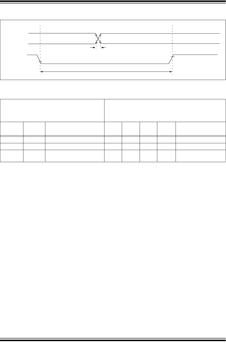
2015 Microchip Technology Inc. Preliminary DS60001320B-page 649
PIC32MZ Embedded Connectivity with Floating Point Unit (EF) Family
FIGURE 37-20: CANx MODULE I/O TIMING CHARACTERISTICS
TABLE 37-37: CANx MODULE I/O TIMING REQUIREMENTS
CiTx Pin
(output)
CA10 CA11
Old Value New Value
CA20
CiRx Pin
(input)
AC CHARACTERISTICS
Standard Operating Conditions: 2.1V to 3.6V
(unless otherwise stated)
Operating temperature -40°C TA +85°C for Industrial
-40°C TA +125°C for Extended
Param
No. Symbol Characteristic(1) Min Typ(2) Max Units Conditions
CA10 TioF Port Output Fall Time — — — ns See parameter DO32
CA11 TioR Port Output Rise Time — — — ns See parameter DO31
CA20 Tcwf Pulse Width to Trigger
CAN Wake-up Filter
700 — — ns —
Note 1: These parameters are characterized but not tested in manufacturing.
2: Data in “Typ” column is at 3.3V, +25°C unless otherwise stated. Parameters are for design guidance only
and are not tested.

PIC32MZ Embedded Connectivity with Floating Point Unit (EF) Family
DS60001320B-page 650 Preliminary 2015 Microchip Technology Inc.
TABLE 37-38: ADC MODULE SPECIFICATIONS
AC CHARACTERISTICS
Standard Operating Conditions: 2.1V to 3.6V
(unless otherwise stated)
Operating temperature -40°C TA +85°C for Industrial
-40°C TA +125°C for Extended
Param.
No. Symbol Characteristics Min. Typ. Max. Units Conditions
Device Supply
AD01 AVDD Module VDD Supply Greater of
VDD – 0.3
or 2.1
— Lesser of
VDD + 0.3
or 3.6 V—
AD02 AVSS Module VSS Supply VSS —VSS + 0.3 V —
Reference Inputs
AD05 VREFH Reference Voltage High VREFL + 1.8 — AVDD V(Note 1)
AD06 VREFL Reference Voltage Low AVSS —VREFH – 1.8 V (Note 1)
AD07 VREF Absolute Reference
Voltage (VREFH – VREFL)
1.8 — AVDD V(Note 2)
AD08 IREF Current Drain — 102 — µA Per ADCx (‘x’ = 0-4, 7)
Analog Input
AD12 VINH-VINL Full-Scale Input Span VREFL —VREFH V—
AD13 VINL Absolute VINL Input
Voltage AVSS —VREFL V—
AD14 VINH Absolute VINH Input
Voltage AVSS —VREFH V—
ADC Accuracy – Measurements with External VREF+/VREF-
AD20c Nr Resolution 6 —12 bits Selectable 6, 8, 10, 12
Resolution Ranges
AD21c INL Integral Nonlinearity — ±3 — LSb VINL = AVSS = VREFL = 0V,
AVDD = VREFH = 3.3V
AD22c DNL Differential Nonlinearity — ±1 — LSb VINL = AVSS = VREFL = 0V,
AVDD = VREFH = 3.3V
AD23c GERR Gain Error — ±8 — LSb VINL = AVSS = VREFL = 0V,
AVDD = VREFH = 3.3V
AD24c EOFF Offset Error — ±2 — LSb VINL = AVSS = 0V,
AVDD = 3.3V
Dynamic Performance
AD31b SINAD Signal to Noise and
Distortion
— 67 — dB Single-ended (Notes 2,3)
AD34b ENOB Effective Number of bits — 10.5 — bits (Notes 2,3)
Note 1: These parameters are not characterized or tested in manufacturing.
2: These parameters are characterized, but not tested in manufacturing.
3: Characterized with a 1 kHz sine wave.
4: The ADC module is functional at VBORMIN < VDD < VDDMIN, but with degraded performance. Unless
otherwise stated, module functionality is guaranteed, but not characterized.

2015 Microchip Technology Inc. Preliminary DS60001320B-page 651
PIC32MZ Embedded Connectivity with Floating Point Unit (EF) Family
TABLE 37-39: ANALOG-TO-DIGITAL CONVERSION TIMING REQUIREMENTS
AC CHARACTERISTICS(2)
Standard Operating Conditions: 2.1V to 3.6V
(unless otherwise stated)
Operating temperature -40°C TA +85°C for Industrial
-40°C TA +125°C for Extended
Param.
No. Symbol Characteristics Min. Typ.(1) Max. Units Conditions
Clock Parameters
AD50 TAD ADC Clock
Period 20 — 6250 ns —
Throughput Rate
AD51 FTP Sample Rate for
ADC0-ADC4
(Class 1 Inputs)
—
—
—
—
—
—
—
—
3.125
3.57
4.16
5
Msps
Msps
Msps
Msps
12-bit resolution Source Impedance 200
10-bit resolution Source Impedance 200
8-bit resolution Source Impedance 200
6-bit resolution Source Impedance 200
Sample Rate for
ADC7
(Class 2 and
Class 3 Inputs)
—
—
—
—
—
—
—
—
2.94
3.33
3.84
4.55
Msps
Msps
Msps
Msps
12-bit resolution Source Impedance 200
10-bit resolution Source Impedance 200
8-bit resolution Source Impedance 200
6-bit resolution Source Impedance 200
Timing Parameters
AD60 TSAMP Sample Time
for ADC0-ADC4
(Class 1 Inputs)
3
4
5
13
——T
AD
Source Impedance 200, Max ADC clock
Source Impedance 500, Max ADC clock
Source Impedance 1 K, Max ADC clock
Source Impedance 5 K, Max ADC clock
Sample Time
for ADC7
(Class 2 and 3
Inputs)
4
5
6
14
——T
AD
Source Impedance 200, Max ADC clock
Source Impedance 500, Max ADC clock
Source Impedance 1 K, Max ADC clock
Source Impedance 5 K, Max ADC clock
Sample Time
for ADC7
(Class 2 and 3
Inputs)
See
Table
37-40 ——T
AD CVDEN (ADCCON1<11>) = 1
AD62 TCONV Conversion
Time
(after
sample time is
complete)
—
—
—
—
—
—
—
—
13
11
9
7
TAD
12-bit resolution
10-bit resolution
8-bit resolution
6-bit resolution
AD65 TWAKE Wake-up time
from Low-
Power Mode
—500—T
AD
Lesser of 500 TAD or 20 µs.
—20—µs
Note 1: These parameters are characterized, but not tested in manufacturing.
2: The ADC module is functional at VBORMIN < VDD < VDDMIN, but with degraded performance. Unless
otherwise stated, module functionality is guaranteed, but not characterized.

PIC32MZ Embedded Connectivity with Floating Point Unit (EF) Family
DS60001320B-page 652 Preliminary 2015 Microchip Technology Inc.
TABLE 37-40: ADC SAMPLE TIMES WITH CVD ENABLED
AC CHARACTERISTICS(2)
Standard Operating Conditions: 2.1V to 3.6V
(unless otherwise stated)
Operating temperature -40°C TA +85°C for Industrial
-40°C TA +125°C for Extended
Param.
No. Symbol Characteristics Min. Typ.(1) Max. Units Conditions
AD60a TSAMP Sample Time for
ADC7 (Class 2 and
Class 3 Inputs) with
the CVDEN bit
(ADCCON1<11>) = 1
8
9
11
12
14
16
17
——
TAD
Source Impedance 200
CVDCPL<2:0> (ADCCON2<28:26>) = 001
CVDCPL<2:0> (ADCCON2<28:26>) = 010
CVDCPL<2:0> (ADCCON2<28:26>) = 011
CVDCPL<2:0> (ADCCON2<28:26>) = 100
CVDCPL<2:0> (ADCCON2<28:26>) = 101
CVDCPL<2:0> (ADCCON2<28:26>) = 110
CVDCPL<2:0> (ADCCON2<28:26>) = 111
10
12
14
16
18
19
21
——
TAD
Source Impedance 500
CVDCPL<2:0> (ADCCON2<28:26>) = 001
CVDCPL<2:0> (ADCCON2<28:26>) = 010
CVDCPL<2:0> (ADCCON2<28:26>) = 011
CVDCPL<2:0> (ADCCON2<28:26>) = 100
CVDCPL<2:0> (ADCCON2<28:26>) = 101
CVDCPL<2:0> (ADCCON2<28:26>) = 110
CVDCPL<2:0> (ADCCON2<28:26>) = 111
13
16
18
21
23
26
28
——
TAD
Source Impedance 1 K
CVDCPL<2:0> (ADCCON2<28:26>) = 001
CVDCPL<2:0> (ADCCON2<28:26>) = 010
CVDCPL<2:0> (ADCCON2<28:26>) = 011
CVDCPL<2:0> (ADCCON2<28:26>) = 100
CVDCPL<2:0> (ADCCON2<28:26>) = 101
CVDCPL<2:0> (ADCCON2<28:26>) = 110
CVDCPL<2:0> (ADCCON2<28:26>) = 111
41
48
56
63
70
78
85
——
TAD
Source Impedance 5 K
CVDCPL<2:0> (ADCCON2<28:26>) = 001
CVDCPL<2:0> (ADCCON2<28:26>) = 010
CVDCPL<2:0> (ADCCON2<28:26>) = 011
CVDCPL<2:0> (ADCCON2<28:26>) = 100
CVDCPL<2:0> (ADCCON2<28:26>) = 101
CVDCPL<2:0> (ADCCON2<28:26>) = 110
CVDCPL<2:0> (ADCCON2<28:26>) = 111
Note 1: These parameters are characterized, but not tested in manufacturing.
2: The ADC module is functional at VBORMIN < VDD < VDDMIN, but with degraded performance. Unless
otherwise stated, module functionality is guaranteed, but not characterized.

2015 Microchip Technology Inc. Preliminary DS60001320B-page 653
PIC32MZ Embedded Connectivity with Floating Point Unit (EF) Family
TABLE 37-41: TEMPERATURE SENSOR SPECIFICATIONS
AC CHARACTERISTICS
Standard Operating Conditions (see Note 1): 2.1V to 3.6V
(unless otherwise stated)
Operating temperature -40°C TA +85°C for Industrial
-40°C TA +125°C for Extended
Param.
No. Symbol Characteristics Min. Typical Max. Units Conditions
TS10 VTS Rate of Change — -5 — mV/ºC —
TS11 TRResolution -2 — +2 ºC —
TS12 IVTEMP Voltage Range 0.2 — 1.2 V —
TS13 TMIN Minimum Temperature — -40 — ºC IVTEMP = 1.2V
TS14 TMAX Maximum Temperature — 160 — ºC IVTEMP = 0.2V
Note 1: The temperature sensor is functional at VBORMIN < VDD < VDDMIN, but with degraded performance. Unless
otherwise stated, module functionality is tested, but not characterized.

PIC32MZ Embedded Connectivity with Floating Point Unit (EF) Family
DS60001320B-page 654 Preliminary 2015 Microchip Technology Inc.
FIGURE 37-21: PARALLEL SLAVE PORT TIMING
PMCSx
PMRD
PMWR
PMD<x:0>
PS1
PS2
PS3
PS4
PS5
PS6
PS7
TABLE 37-42: PARALLEL SLAVE PORT REQUIREMENTS
AC CHARACTERISTICS
Standard Operating Conditions: 2.1V to 3.6V
(unless otherwise stated)
Operating temperature -40°C TA +85°C for Industrial
-40°C TA +125°C for Extended
Param.
No. Symbol Characteristics(1) Min. Typ. Max. Units Conditions
PS1 TdtV2wrH Data In Valid before PMWR or
PMCSx Inactive (setup time) 20 — — ns —
PS2 TwrH2dtI PMWR or PMCSx Inactive to
Data-in Invalid (hold time)
40 — — ns —
PS3 TrdL2dtV PMRD and PMCSx Active to
Data-out Valid
— — 60 ns —
PS4 TrdH2dtI PMRD Activeor PMCSx Inactive to
Data-out Invalid 0 — 10 ns —
PS5 Tcs PMCSx Active Time TPBCLK2 + 40 — — ns —
PS6 TWR PMWR Active Time TPBCLK2 + 25 — — ns —
PS7 TRD PMRD Active Time TPBCLK2 + 25 — — ns —
Note 1: These parameters are characterized, but not tested in manufacturing.
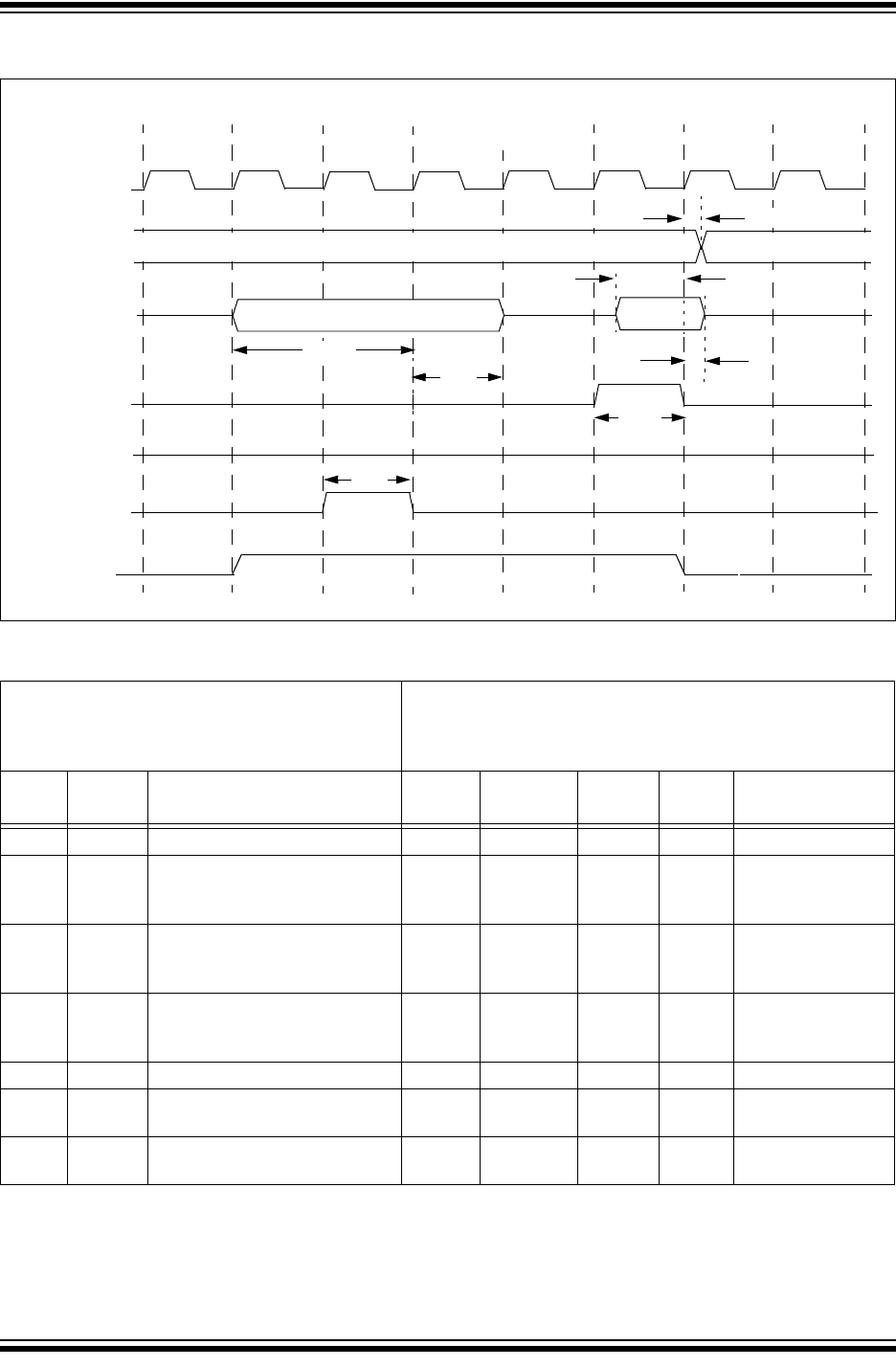
2015 Microchip Technology Inc. Preliminary DS60001320B-page 655
PIC32MZ Embedded Connectivity with Floating Point Unit (EF) Family
FIGURE 37-22: PARALLEL MASTER PORT READ TIMING DIAGRAM
TPBCLK2TPBCLK2TPBCLK2TPBCLK2TPBCLK2TPBCLK2TPBCLK2TPBCLK2
PBCLK2
PMALL/PMALH
PMD<x:0>
PMA<x:0>
PMRD
PMCSx
PMWR
PM5
Data
Address<7:0>
PM1
PM3
PM6
Data
PM7
Address<7:0>
Address
PM4
PM2
TABLE 37-43: PARALLEL MASTER PORT READ TIMING REQUIREMENTS
AC CHARACTERISTICS
Standard Operating Conditions: 2.1V to 3.6V
(unless otherwise stated)
Operating temperature -40°C TA +85°C for Industrial
-40°C TA +125°C for Extended
Param.
No. Symbol Characteristics(1) Min. Typ. Max. Units Conditions
PM1 TLAT PMALL/PMALH Pulse Width —1 TPBCLK2— — —
PM2 TADSU Address Out Valid to PMALL/
PMALH Invalid (address setup
time)
—2 TPBCLK2— — —
PM3 TADHOLD PMALL/PMALH Invalid to
Address Out Invalid (address
hold time)
—1 TPBCLK2— — —
PM4 TAHOLD PMRD Inactive to Address Out
Invalid
(address hold time)
5 — — ns —
PM5 TRD PMRD Pulse Width —1 TPBCLK2— — —
PM6 TDSU PMRD or PMENB Active to Data
In Valid (data setup time) 15 — — ns —
PM7 TDHOLD PMRD or PMENB Inactive to
Data In Invalid (data hold time)
— 80 — ns —
Note 1: These parameters are characterized, but not tested in manufacturing.
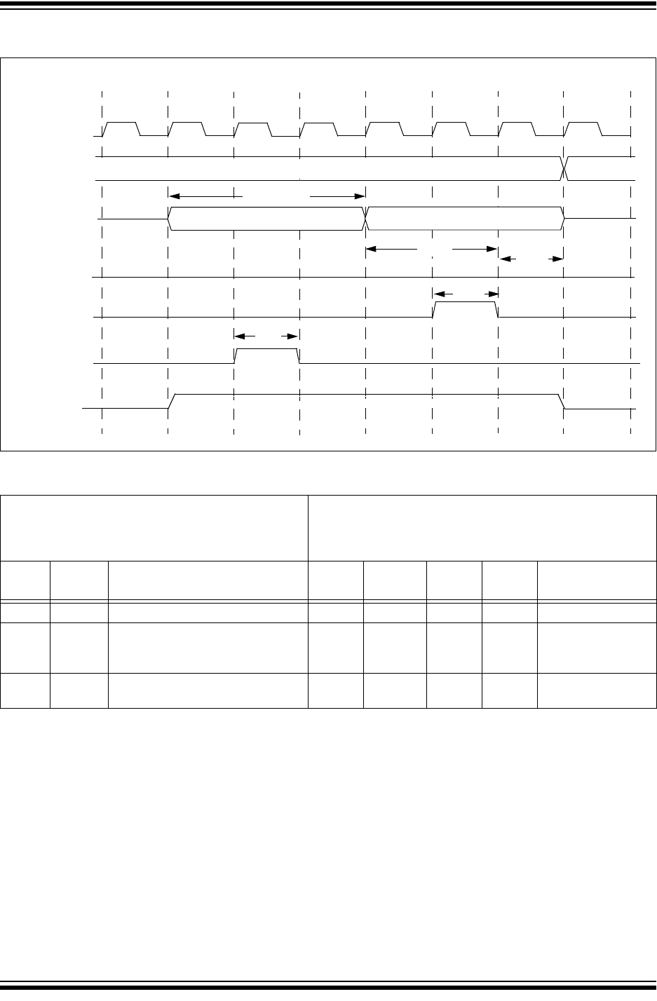
PIC32MZ Embedded Connectivity with Floating Point Unit (EF) Family
DS60001320B-page 656 Preliminary 2015 Microchip Technology Inc.
FIGURE 37-23: PARALLEL MASTER PORT WRITE TIMING DIAGRAM
TPBCLK2TPBCLK2TPBCLK2TPBCLK2TPBCLK2TPBCLK2TPBCLK2TPBCLK2
PBCLK2
PMALL/PMALH
PMD<x:0>
PMA<x:0>
PMWR
PMCSx
PMRD
PM12 PM13
PM11
Address
Address<7:0> Data
PM2 + PM3
PM1
TABLE 37-44: PARALLEL MASTER PORT WRITE TIMING REQUIREMENTS
AC CHARACTERISTICS
Standard Operating Conditions: 2.1V to 3.6V
(unless otherwise stated)
Operating temperature -40°C TA +85°C for Industrial
-40°C TA +125°C for Extended
Param.
No. Symbol Characteristics(1) Min. Typ. Max. Units Conditions
PM11 TWR PMWR Pulse Width —1 TPBCLK2— — —
PM12 TDVSU Data Out Valid before PMWR or
PMENB goes Inactive (data setup
time)
—2 TPBCLK2— — —
PM13 TDVHOLD PMWR or PMEMB Invalid to Data
Out Invalid (data hold time)
—1 TPBCLK2— — —
Note 1: These parameters are characterized, but not tested in manufacturing.

2015 Microchip Technology Inc. Preliminary DS60001320B-page 657
PIC32MZ Embedded Connectivity with Floating Point Unit (EF) Family
TABLE 37-45: USB OTG ELECTRICAL SPECIFICATIONS
AC CHARACTERISTICS
Standard Operating Conditions: 2.1V to 3.6V
(unless otherwise stated)
Operating temperature -40°C TA +85°C for Industrial
-40°C TA +125°C for Extended
Param.
No. Symbol Characteristics(1) Min. Typ. Max. Units Conditions
USB313 VUSB3V3USB Voltage 3.0 — 3.6 V Voltage on VUSB3V3
must be in this range for
proper USB operation
Low-Speed and Full-Speed Modes
USB315 VILUSB Input Low Voltage for USB Buffer — — 0.8 V —
USB316 VIHUSB Input High Voltage for USB Buffer 2.0 — — V —
USB318 VDIFS Differential Input Sensitivity 0.2 — — V The difference between
D+ and D- must exceed
this value while VCM is
met
USB319 VCM Differential Common Mode Range 0.8 — 2.5 V —
USB321 VOL Voltage Output Low 0.0 — 0.3 V 1.425 k load
connected to VUSB3V3
USB322 VOH Voltage Output High 2.8 — 3.6 V 14.25 k load
connected to ground
Hi-Speed Mode
USB323 VHSDI Differential input signal level 150 — — mV —
USB324 VHSSQ SQ detection threshold 100 — 150 mV —
USB325 VHSCM Common mode voltage range -50 — 500 mV —
USB326 VHSOH Data signaling high 360 — 440 mV —
USB327 VHSOL Data signaling low -10 — 10 mV —
USB328 VCHIRPJ Chirp J level 700 — 1100 mV —
USB329 VCHIRPK Chirp K level -900 — -500 mV —
USB330 ZHSDRV Driver output resistance — 45 — —
Note 1: These parameters are characterized, but not tested in manufacturing.
PIC32MZ Embedded Connectivity with Floating Point Unit (EF) Family
DS60001320B-page 658 Preliminary 2015 Microchip Technology Inc.
TABLE 37-46: ETHERNET MODULE SPECIFICATIONS
FIGURE 37-24: MDIO SOURCED BY THE PIC32 DEVICE
FIGURE 37-25: MDIO SOURCED BY THE PHY
AC CHARACTERISTICS
Standard Operating Conditions: 2.1V to 3.6V
(unless otherwise stated)
Operating temperature -40°C TA +85°C for Industrial
-40°C TA +125°C for Extended
Param.
No. Characteristic Min. Typical Max. Units Conditions
MIIM Timing Requirements
ET1 MDC Duty Cycle 40 —60 % —
ET2 MDC Period 400 — — ns —
ET3 MDIO Output Setup and Hold 10 —10 ns See Figure 37-24
ET4 MDIO Input Setup and Hold 0 — 300 ns See Figure 37-25
MII Timing Requirements
ET5 TX Clock Frequency —25 —MHz —
ET6 TX Clock Duty Cycle 35 —65 % —
ET7 ETXDx, ETEN, ETXERR Output Delay 0 — 25 ns See Figure 37-26
ET8 RX Clock Frequency —25 —MHz —
ET9 RX Clock Duty Cycle 35 —65 % —
ET10 ERXDx, ERXDV, ERXERR Setup and Hold 10 —30 ns See Figure 37-27
RMII Timing Requirements
ET11 Reference Clock Frequency —50 —MHz —
ET12 Reference Clock Duty Cycle 35 —65 % —
ET13 ETXDx, ETEN, Setup and Hold 2 — 4 ns —
ET14 ERXDx, ERXDV, ERXERR Setup and Hold 2 — 4 ns —
ET3 (Hold)
(Setup) ET3
MDC
MDIO
VIHMIN
VILMAX
VIHMIN
VILMAX
VIHMIN
VILMAX
VIHMIN
VILMAX
ET4
MDC
MDIO
2015 Microchip Technology Inc. Preliminary DS60001320B-page 659
PIC32MZ Embedded Connectivity with Floating Point Unit (EF) Family
FIGURE 37-26: TRANSMIT SIGNAL TIMING RELATIONSHIPS AT THE MII
FIGURE 37-27: RECEIVE SIGNAL TIMING RELATIONSHIPS AT THE MII
ET7
TX Clock
ETXD<3:0>,
VIHMIN
VILMAX
VIHMIN
VILMAX
ETEN,
ETXERR
ET10 (Hold)
RX Clock
ERXD<3:0>,
VIHMIN
VILMAX
VIHMIN
VILMAX
(Setup) ET10
ERXDV,
ERXERR
PIC32MZ Embedded Connectivity with Floating Point Unit (EF) Family
DS60001320B-page 660 Preliminary 2015 Microchip Technology Inc.
FIGURE 37-28: EBI PAGE READ TIMING
FIGURE 37-29: EBI WRITE TIMING
ADDRESS
00 01 10 11
00
READ DATA READ DATA READ DATA READ DATA
tEBICOtEBICO
tEBICOtEBICO
tEBICOtEBICO
tEBICOtEBICOtEBICOtEBICOtEBICO
tEBICOtEBICO
tEBIDHtEBIDH
tEBIDS
tEBIDH
tEBIDS
tEBIDH
tEBIDStEBIDS
tEBI-PRCtEBI-PRCtEBI-PRCtEBI-PRC tEBI-PRCtEBI-RC tEBI-PRCtEBI-RC
PBCLK8
EBIA<x:2>
EBIA<1:0>
EBICSx
EBIBSx
EBIOE
EBID<15:0>
ADDRESS
BYTE SELECTS
WRITE DATA
tEBIDOtEBIDO
tEBICOtEBICO
tEBICOtEBICO
tEBICOtEBICO
tEBICOtEBICO
tEBI-WRtEBI-WRtEBI-WPtEBI-WPtEBI-AStEBI-AS
PBCLK8
EBIA<x:0>
EBICSx
EBIBSx
EBIOE
EBIWE
EBID<15:0>

2015 Microchip Technology Inc. Preliminary DS60001320B-page 661
PIC32MZ Embedded Connectivity with Floating Point Unit (EF) Family
TABLE 37-47: EBI TIMING REQUIREMENTS
TABLE 37-48: EBI THROUGHPUT REQUIREMENTS
AC CHARACTERISTICS
Standard Operating Conditions: 2.1V to 3.6V
(unless otherwise stated)
Operating temperature -40°C TA +85°C for Industrial
-40°C TA +125°C for Extended
Param.
No. Symbol Characteristic Min. Typ. Max. Units Conditions
EB10 TEBICLK Internal EBI Clock Period
(PBCLK8)
10 — — ns —
EB11 TEBIRC EBI Read Cycle Time
(TRC<5:0>) 20 — — ns —
EB12 TEBIPRC EBI Page Read Cycle Time
(TPRC<3:0>)
20 — — ns —
EB13 TEBIAS EBI Write Address Setup (TAS<1:0>) 10 — — ns —
EB14 TEBIWP EBI Write Pulse Width
(TWP<5:0>)
10 — — ns —
EB15 TEBIWR EBI Write Recovery Time
(TWR<1:0>)
10 — — ns —
EB16 TEBICO EBI Output Control Signal Delay ——5ns See Note 1
EB17 TEBIDO EBI Output Data Signal Delay ——5ns See Note 1
EB18 TEBIDS EBI Input Data Setup 5 — — ns See Note 1
EB19 TEBIDH EBI Input Data Hold 3 — — ns See Note 1, 2
Note 1: Maximum pin capacitance = 10 pF.
2: Hold time from EBI Address change is 0 ns.
AC CHARACTERISTICS
Standard Operating Conditions: 2.1V to 3.6V
(unless otherwise stated)
Operating temperature -40°C TA +85°C for Industrial
-40°C TA +125°C for Extended
Param.
No. Characteristic Min. Typ. Max. Units Conditions
EB20 Asynchronous SRAM Read —100 —Mbps —
EB21 Asynchronous SRAM Write —533 —Mbps —
Note 1: Maximum pin capacitance = 10 pF.
2: Hold time from EBI Address change is 0 ns.
PIC32MZ Embedded Connectivity with Floating Point Unit (EF) Family
DS60001320B-page 662 Preliminary 2015 Microchip Technology Inc.
FIGURE 37-30: EJTAG TIMING CHARACTERISTICS
TTCKcyc
TTCKhigh TTCKlow Trf
Trf
Trf
Trf
TTsetup TThold
TTDOout TTDOzstate
Defined Undefined
TTRST*low
Trf
TCK
TDO
TRST*
TDI
TMS
TABLE 37-49: EJTAG TIMING REQUIREMENTS
AC CHARACTERISTICS
Standard Operating Conditions: 2.1V to 3.6V
(unless otherwise stated)
Operating temperature -40°C TA +85°C for Industrial
-40°C TA +125°C for Extended
Param.
No. Symbol Description(1) Min. Max. Units Conditions
EJ1 TTCKCYC TCK Cycle Time 25 —ns —
EJ2 TTCKHIGH TCK High Time 10 —ns —
EJ3 TTCKLOW TCK Low Time 10 —ns —
EJ4 TTSETUP TAP Signals Setup Time Before
Rising TCK 5 — ns —
EJ5 TTHOLD TAP Signals Hold Time After
Rising TCK
3 — ns —
EJ6 TTDOOUT TDO Output Delay Time from
Falling TCK
— 5 ns —
EJ7 TTDOZSTATE TDO 3-State Delay Time from
Falling TCK — 5 ns —
EJ8 TTRSTLOW TRST Low Time 25 —ns —
EJ9 TRF TAP Signals Rise/Fall Time, All
Input and Output — — ns —
Note 1: These parameters are characterized, but not tested in manufacturing.

2015 Microchip Technology Inc. Preliminary DS60001320B-page 663
PIC32MZ Embedded Connectivity with Floating Point Unit (EF) Family
38.0 AC AND DC CHARACTERISTICS GRAPHS
FIGURE 38-1: VOH – 4x DRIVER PINS
FIGURE 38-2: VOL – 4x DRIVER PINS
FIGURE 38-3: VOH – 8x DRIVER PINS
FIGURE 38-4: VOL – 8x DRIVER PINS
Note: The graphs provided are a statistical summary based on a limited number of samples and are provided for design guidance purposes only. The performance characteristics listed herein are not tested
or guaranteed. In some graphs, the data presented may be outside the specified operating range (e.g., outside specified power supply range) and therefore, outside the warranted range.
Ͳ0.050
Ͳ0.045
Ͳ0.040
Ͳ0.035
Ͳ0.030
Ͳ0.025
0020
IOH(A)
VOH(V)
Ͳ
0
.
020
Ͳ0.015
Ͳ0.010
Ͳ0.005
0.000
0.00 0.50 1.00 1.50 2.00 2.50 3.00 3.50
AbsoluteMaximum
0 020
0.025
0.030
0.035
0.040
0.045
0.050
IOL(A)
VOL(V)
0.000
0.005
0.010
0.015
0
.
020
0.00 0.50 1.00 1.50 2.00 2.50 3.00 3.50
AbsoluteMaximum
Ͳ0.090
Ͳ0.080
Ͳ0.070
Ͳ0.060
Ͳ0.050
Ͳ0.040
IOH(A)
VOH(V)
Ͳ0.030
Ͳ0.020
Ͳ0.010
0.000
0.00 0.50 1.00 1.50 2.00 2.50 3.00 3.50
AbsoluteMaximum
0.040
0.050
0.060
0.070
0.080
0.090
IOL(A)
VOL(V)
0.000
0.010
0.020
0.030
0.00 0.50 1.00 1.50 2.00 2.50 3.00 3.50
AbsoluteMaximum

PIC32MZ Embedded Connectivity with Floating Point Unit (EF) Family
DS60001320B-page 664 Preliminary 2015 Microchip Technology Inc.
FIGURE 38-5: VOH – 12x DRIVER PINS
FIGURE 38-6: VOL – 12x DRIVER PINS
FIGURE 38-7: TYPICAL TEMPERATURE SENSOR VOLTAGE
Ͳ0.140
Ͳ0.120
Ͳ0.100
Ͳ0.080
Ͳ0.060
IOH(A)
VOH(V)
Ͳ0.040
Ͳ0.020
0.000
0.00 0.50 1.00 1.50 2.00 2.50 3.00 3.50
AbsoluteMaximum
0.060
0.080
0.100
0.120
0.140
IOL(A)
VOL(V)
0.000
0.020
0.040
0.00 0.50 1.00 1.50 2.00 2.50 3.00 3.50
AbsoluteMaximum
0650
0.750
0.850
0.950
1.050
1.150
1.250
Voltage (V)
0.350
0.450
0.550
0
.
650
-40-30-20-100 102030405060708090100110120130
Temperature (Celsius)
2015 Microchip Technology Inc. Preliminary DS60001320B-page 665
PIC32MZ Embedded Connectivity with Floating Point Unit (EF) Family
39.0 PACKAGING INFORMATION
39.1 Package Marking Information
MZ2048EFH
064-I/PT
0510017
3
e
Legend: XX...X Customer-specific information
Y Year code (last digit of calendar year)
YY Year code (last 2 digits of calendar year)
WW Week code (week of January 1 is week ‘01’)
NNN Alphanumeric traceability code
Pb-free JEDEC designator for Matte Tin (Sn)
*This package is Pb-free. The Pb-free JEDEC designator ( )
can be found on the outer packaging for this package.
Note: In the event the full Microchip part number cannot be marked on one line, it will
be carried over to the next line, thus limiting the number of available
characters for customer-specific information.
3
e
64-Lead TQFP (10x10x1 mm)
XXXXXXXXXX
XXXXXXXXXX
XXXXXXXXXX
YYWWNNN
Example
100-Lead TQFP (14x14x1 mm)
XXXXXXXXXXXX
XXXXXXXXXXXX
YYWWNNN
Example
MZ2048EFH
100-I/PF
0510017
3
e
XXXXXXXXXX
64-Lead QFN (9x9x0.9 mm)
XXXXXXXXXX
XXXXXXXXXX
YYWWNNN
MZ2048EFH
Example
064-I/MR
0510017
3
e
XXXXXXXXXXXX
PIC32MZ Embedded Connectivity with Floating Point Unit (EF) Family
DS60001320B-page 666 Preliminary 2015 Microchip Technology Inc.
39.1 Package Marking Information (Continued)
XXXXXXXXXX
124-Lead VTLA (9x9x0.9 mm)
XXXXXXXXXX
XXXXXXXXXX
YYWWNNN
MZ2048EFH
Example
124-I/TL
0510017
3
e
144-Lead TQFP (16x16x1 mm)
XXXXXXXXXXXX
XXXXXXXXXXXX
YYWWNNN
Example
MZ2048EFH
144-I/PH
0510017
3
e
Legend: XX...X Customer-specific information
Y Year code (last digit of calendar year)
YY Year code (last 2 digits of calendar year)
WW Week code (week of January 1 is week ‘01’)
NNN Alphanumeric traceability code
Pb-free JEDEC designator for Matte Tin (Sn)
*This package is Pb-free. The Pb-free JEDEC designator ( )
can be found on the outer packaging for this package.
Note: In the event the full Microchip part number cannot be marked on one line, it will
be carried over to the next line, thus limiting the number of available
characters for customer-specific information.
3
e
100-Lead TQFP (12x12x1 mm)
XXXXXXXXXXXX
XXXXXXXXXXXX
YYWWNNN
Example
MZ2048EFH
100-I/PT
0510017
3
e
144-Lead LQFP (20x20x1.40 mm)
XXXXXXXXXXXX
XXXXXXXXXXXX
YYWWNNN
Example
MZ2048EFH
144-I/PL
0510017
3
e
XXXXXXXXXXXX
XXXXXXXXXXXX
XXXXXXXXXXXX
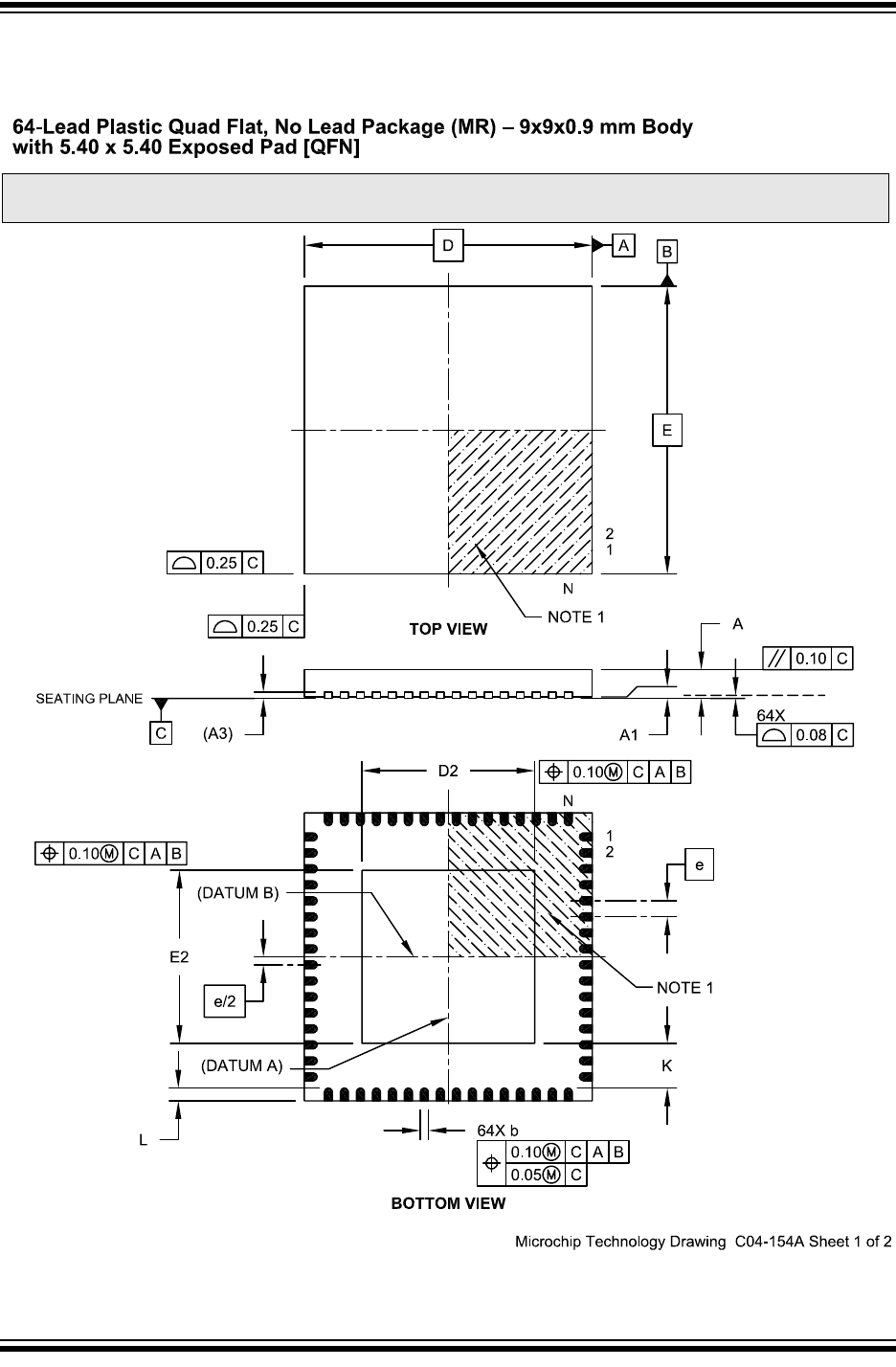
2015 Microchip Technology Inc. Preliminary DS60001320B-page 667
PIC32MZ Embedded Connectivity with Floating Point Unit (EF) Family
39.2 Package Details
Note: For the most current package drawings, please see the Microchip Packaging Specification located at
http://www.microchip.com/packaging
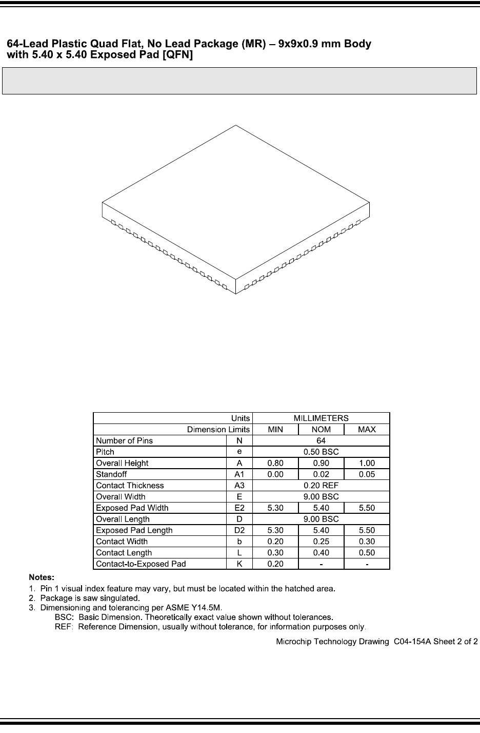
PIC32MZ Embedded Connectivity with Floating Point Unit (EF) Family
DS60001320B-page 668 Preliminary 2015 Microchip Technology Inc.
Note: For the most current package drawings, please see the Microchip Packaging Specification located at
http://www.microchip.com/packaging
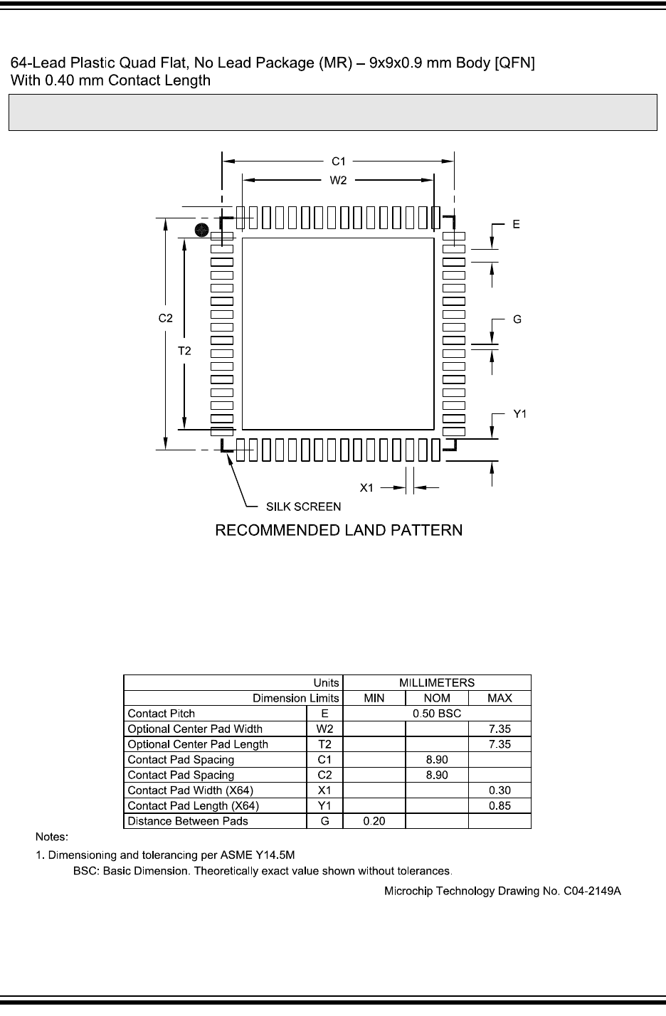
2015 Microchip Technology Inc. Preliminary DS60001320B-page 669
PIC32MZ Embedded Connectivity with Floating Point Unit (EF) Family
Note: For the most current package drawings, please see the Microchip Packaging Specification located at
http://www.microchip.com/packaging
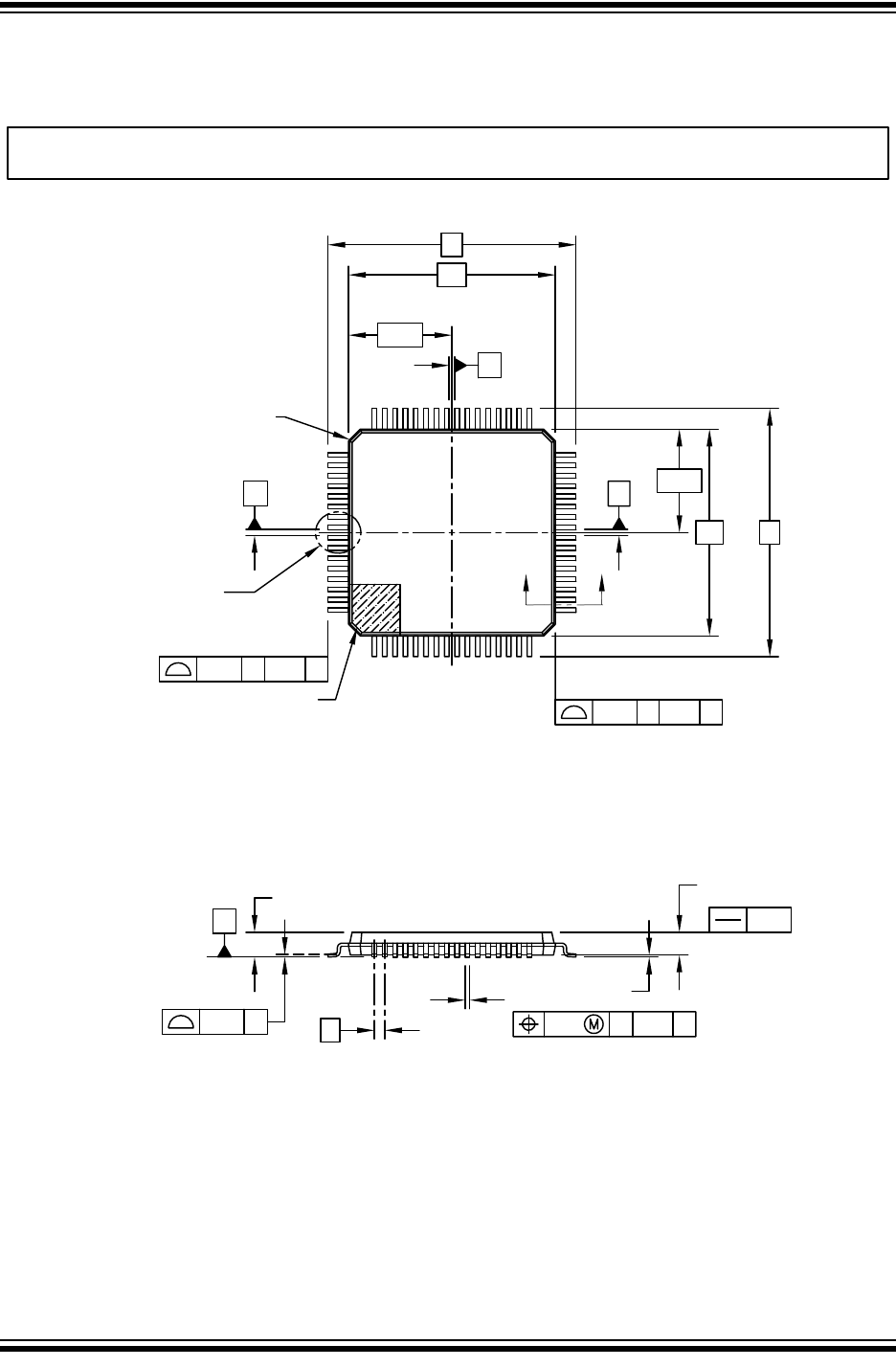
PIC32MZ Embedded Connectivity with Floating Point Unit (EF) Family
DS60001320B-page 670 Preliminary 2015 Microchip Technology Inc.
0.20 CA-B D
64 X b
0.08 CA-B D
C
SEATING
PLANE
4X N/4 TIPS
TOP VIEW
SIDE VIEW
For the most current package drawings, please see the Microchip Packaging Specification located at
http://www.microchip.com/packaging
Note:
Microchip Technology Drawing C04-085C Sheet 1 of 2
64-Lead Plastic Thin Quad Flatpack (PT)-10x10x1 mm Body, 2.00 mm Footprint [TQFP]
D
EE1
D1
D
A B
0.20 HA-B D
4X
D1/2
e
A
0.08 C
A1
A2
SEE DETAIL 1
AA
E1/2
NOTE 1
NOTE 2
123
N
0.05
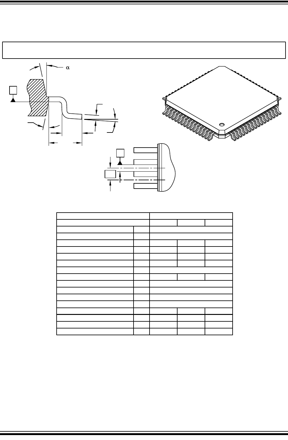
2015 Microchip Technology Inc. Preliminary DS60001320B-page 671
PIC32MZ Embedded Connectivity with Floating Point Unit (EF) Family
For the most current package drawings, please see the Microchip Packaging Specification located at
http://www.microchip.com/packaging
Note:
64-Lead Plastic Thin Quad Flatpack (PT)-10x10x1 mm Body, 2.00 mm Footprint [TQFP]
13°12°11°
E
Mold Draft Angle Bottom
13°12°11°
D
Mold Draft Angle Top
0.270.220.17
b
Lead Width
0.20-0.09
c
Lead Thickness
10.00 BSC
D1
Molded Package Length
10.00 BSCE1Molded Package Width
12.00 BSCDOverall Length
12.00 BSCEOverall Width
7°3.5°0°
I
Foot Angle
0.750.600.45LFoot Length
0.15-0.05A1Standoff
1.051.000.95A2Molded Package Thickness
1.20--AOverall Height
0.50 BSC
e
Lead Pitch
64NNumber of Leads
MAXNOMMINDimension Limits
MILLIMETERSUnits
Footprint L1 1.00 REF
2. Chamfers at corners are optional; size may vary.
1. Pin 1 visual index feature may vary, but must be located within the hatched area.
4. Dimensioning and tolerancing per ASME Y14.5M
BSC: Basic Dimension. Theoretically exact value shown without tolerances.
REF: Reference Dimension, usually without tolerance, for information purposes only.
3. Dimensions D1 and E1 do not include mold flash or protrusions. Mold flash or
protrusions shall not exceed 0.25mm per side.
Notes:
Microchip Technology Drawing C04-085C Sheet 2 of 2
L
(L1)
E
c
H
X
X=A—B OR D
e/2
DETAIL 1
SECTION A-A
T
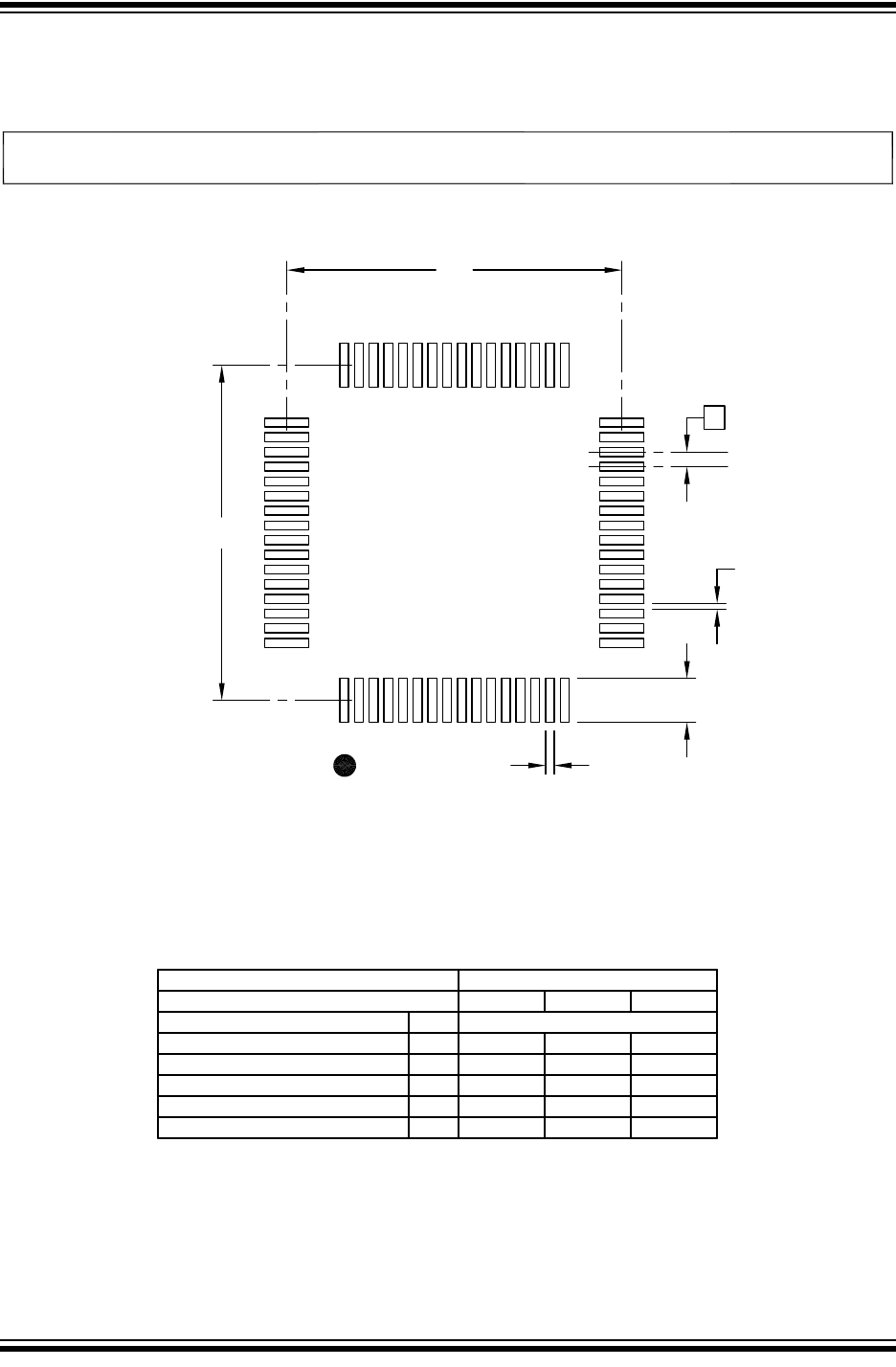
PIC32MZ Embedded Connectivity with Floating Point Unit (EF) Family
DS60001320B-page 672 Preliminary 2015 Microchip Technology Inc.
RECOMMENDED LAND PATTERN
For the most current package drawings, please see the Microchip Packaging Specification located at
http://www.microchip.com/packaging
Note:
Dimension Limits
Units
C1Contact Pad Spacing
Contact Pad Spacing
Contact Pitch
C2
MILLIMETERS
0.50 BSC
MIN
E
MAX
11.40
11.40
Contact Pad Length (X28)
Contact Pad Width (X28)
Y1
X1
1.50
0.30
BSC: Basic Dimension. Theoretically exact value shown without tolerances.
Notes:
1. Dimensioning and tolerancing per ASME Y14.5M
Microchip Technology Drawing C04-2085B Sheet 1 of 1
GDistance Between Pads 0.20
NOM
64-Lead Plastic Thin Quad Flatpack (PT)-10x10x1 mm Body, 2.00 mm Footprint [TQFP]
C2
C1
E
G
Y1
X1
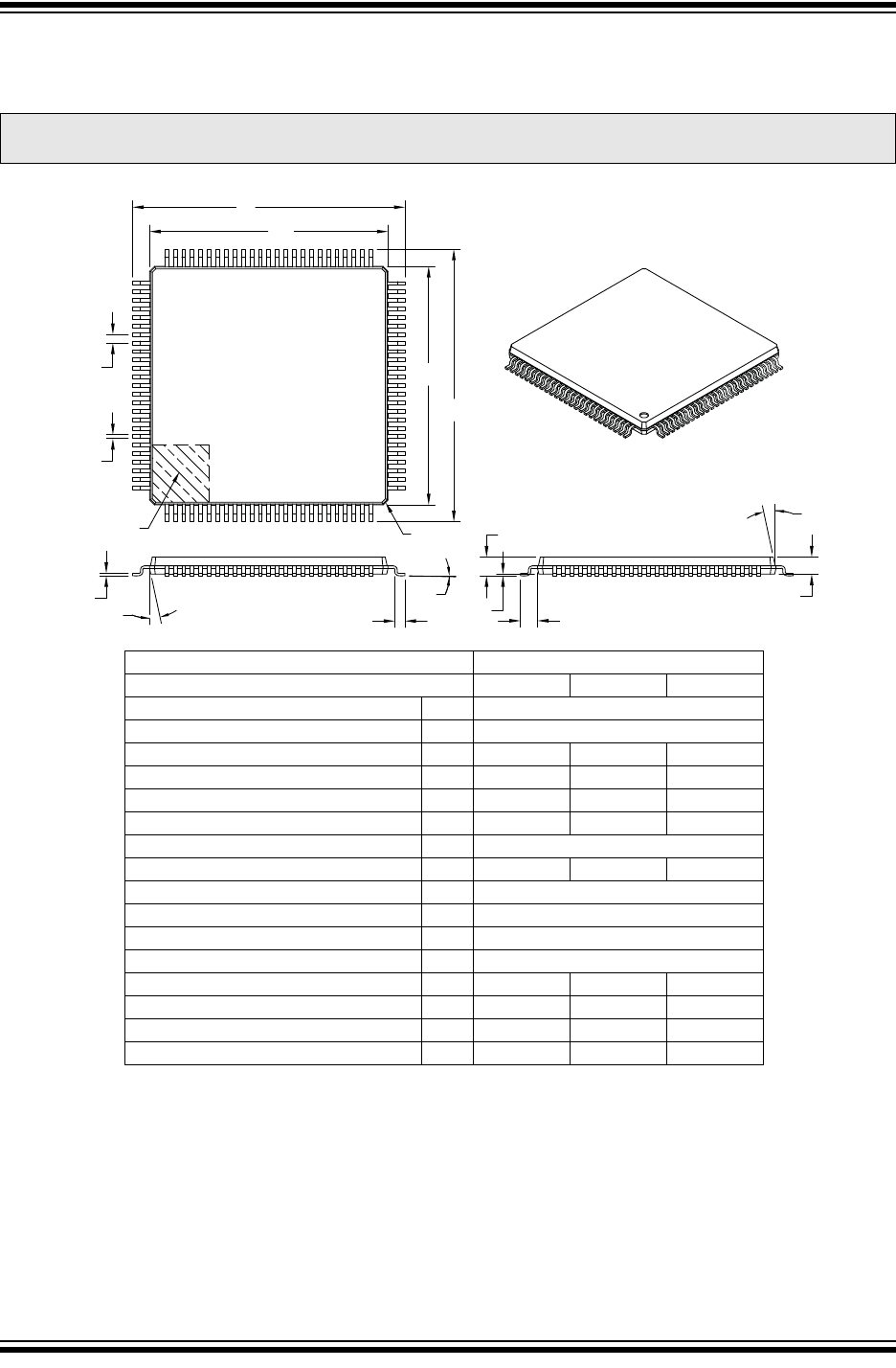
2015 Microchip Technology Inc. Preliminary DS60001320B-page 673
PIC32MZ Embedded Connectivity with Floating Point Unit (EF) Family
D
D1
e
b
E1
E
N
NOTE 1 NOTE 2
123
c
LA1 L1
A2
A
φ
β
α
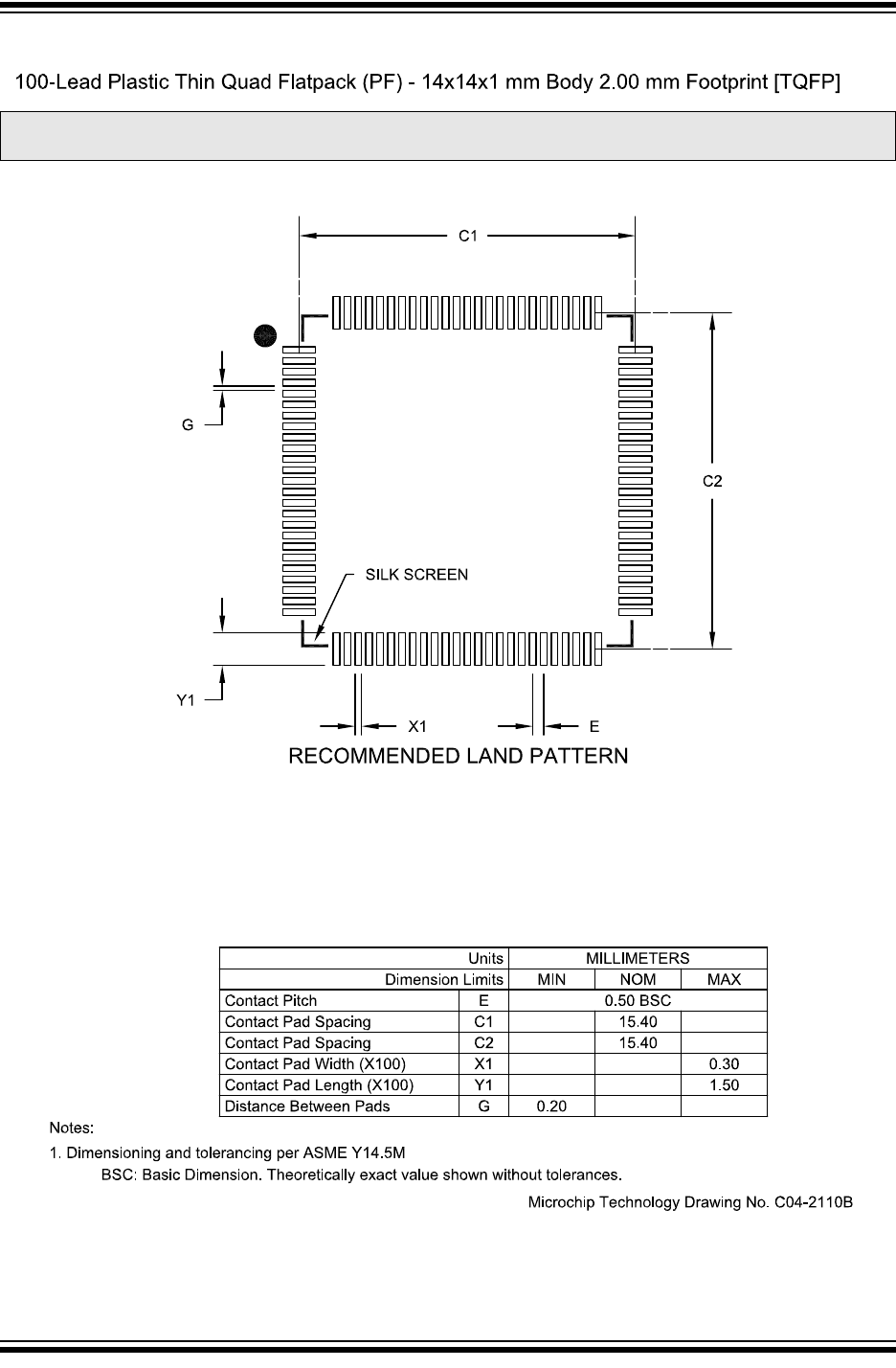
PIC32MZ Embedded Connectivity with Floating Point Unit (EF) Family
DS60001320B-page 674 Preliminary 2015 Microchip Technology Inc.
Note: For the most current package drawings, please see the Microchip Packaging Specification located at
http://www.microchip.com/packaging
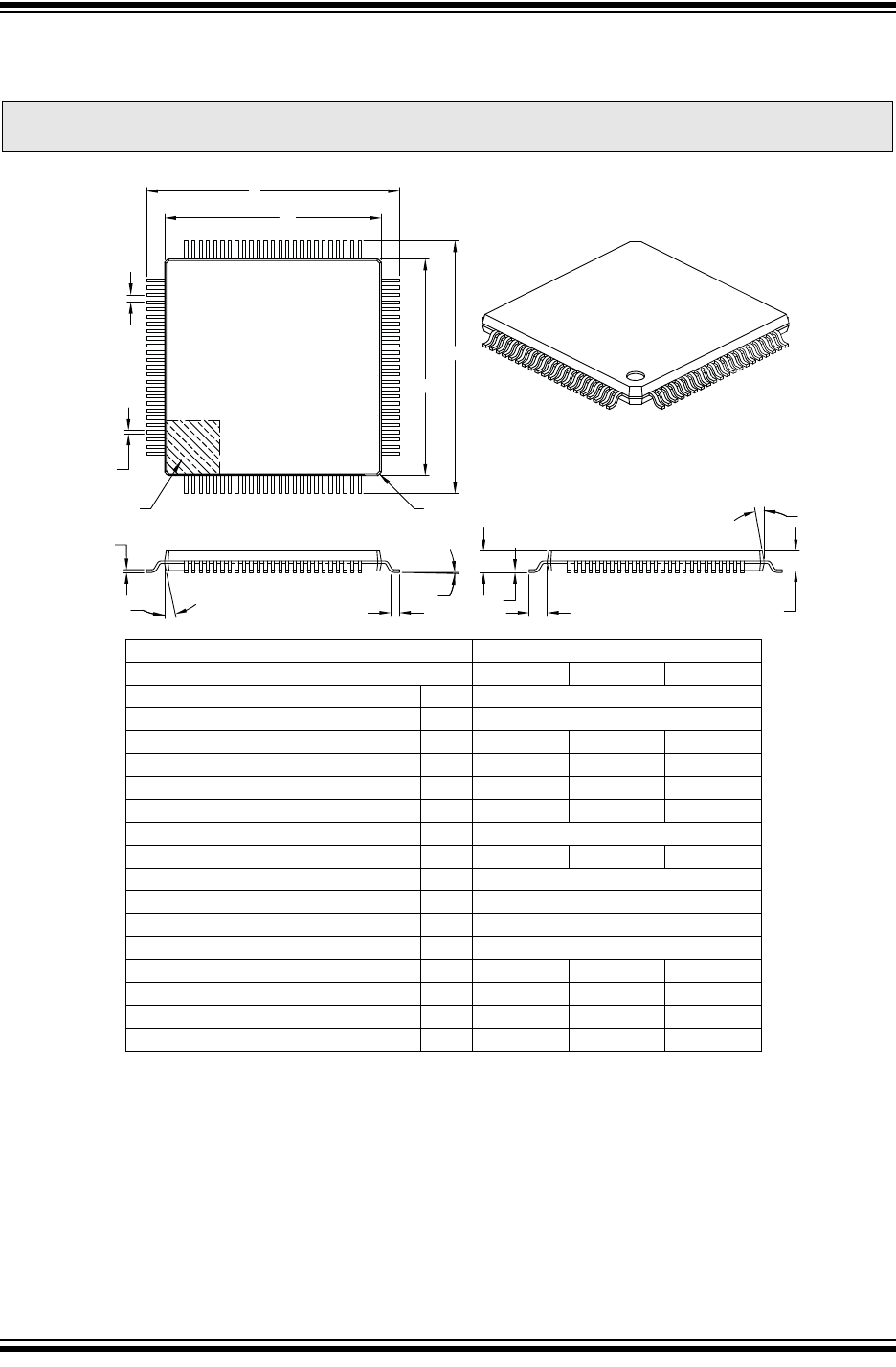
2015 Microchip Technology Inc. Preliminary DS60001320B-page 675
PIC32MZ Embedded Connectivity with Floating Point Unit (EF) Family
D
D1
E
E1
e
bN
123
NOTE 1 NOTE 2
c
LA1 L1
A
A2
α
β
φ
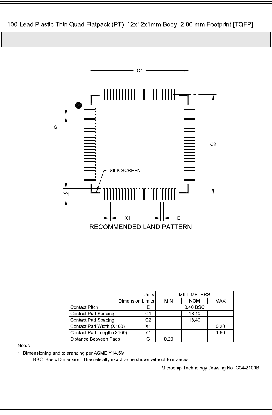
PIC32MZ Embedded Connectivity with Floating Point Unit (EF) Family
DS60001320B-page 676 Preliminary 2015 Microchip Technology Inc.
Note: For the most current package drawings, please see the Microchip Packaging Specification located at
http://www.microchip.com/packaging
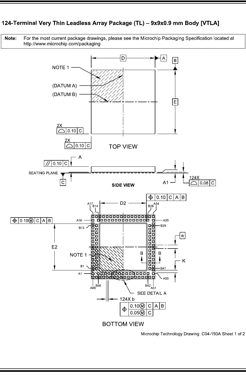
2015 Microchip Technology Inc. Preliminary DS60001320B-page 677
PIC32MZ Embedded Connectivity with Floating Point Unit (EF) Family
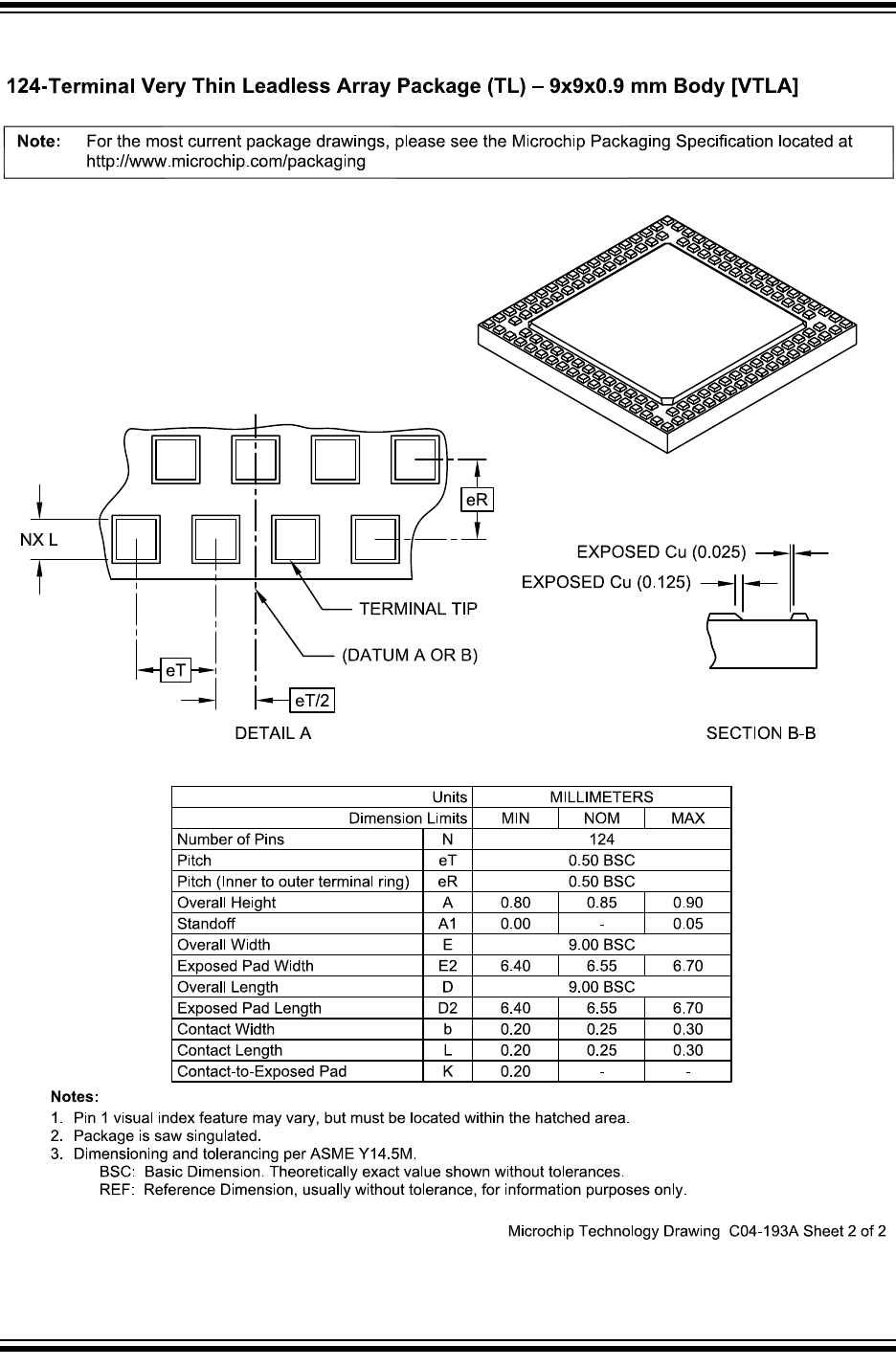
PIC32MZ Embedded Connectivity with Floating Point Unit (EF) Family
DS60001320B-page 678 Preliminary 2015 Microchip Technology Inc.
2015 Microchip Technology Inc. Preliminary DS60001320B-page 679
PIC32MZ Embedded Connectivity with Floating Point Unit (EF) Family
For the most current package drawings, please see the Microchip Packaging Specification located at
http://www.microchip.com/packaging
Note:
RECOMMENDED LAND PATTERN
SILK SCREEN
Dimension Limits
Units
C1
Optional Center Pad Length
Contact Pad Spacing
Contact Pad Spacing
Optional Center Pad Chamfer (X4)
C2
W3
W2
0.10
6.60
MILLIMETERS
MIN MAX
8.50
8.50
Contact Pad Length (X124)
Contact Pad Width (X124)
X2
X1
0.30
0.30
BSC: Basic Dimension. Theoretically exact value shown without tolerances.
Notes:
1. Dimensioning and tolerancing per ASME Y14.5M
Microchip Technology Drawing No. C04-2193A
NOM
Optional Center Pad Width T2
Contact to Center Pad Clearance (X4) G5
Pad Clearance G4
Pad Clearance G3
Pad Clearance G2
Contact Pitch 0.50 BSCE
Pad Clearance G1
6.60
0.30
0.20
0.20
0.20
0.20
E
E/2
W2
W3
G2
G4
X1
G5
X4
C2
C1
G3
G1
X2
E
T2
124-Very Thin Leadless Array Package (TL) – 9x9x0.9 mm Body [VTLA]
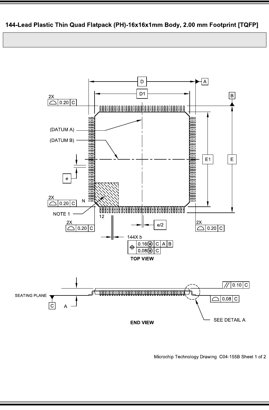
PIC32MZ Embedded Connectivity with Floating Point Unit (EF) Family
DS60001320B-page 680 Preliminary 2015 Microchip Technology Inc.
Note: For the most current package drawings, please see the Microchip Packaging Specification located at
http://www.microchip.com/packaging
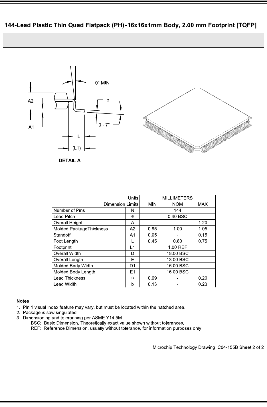
2015 Microchip Technology Inc. Preliminary DS60001320B-page 681
PIC32MZ Embedded Connectivity with Floating Point Unit (EF) Family
Note: For the most current package drawings, please see the Microchip Packaging Specification located at
http://www.microchip.com/packaging
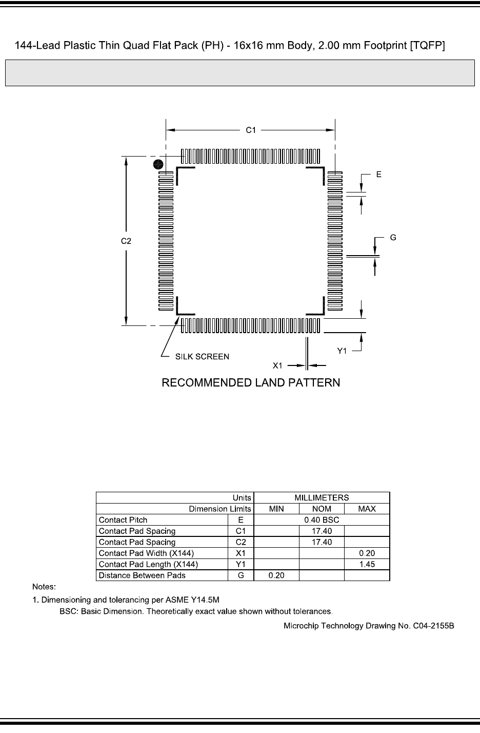
PIC32MZ Embedded Connectivity with Floating Point Unit (EF) Family
DS60001320B-page 682 Preliminary 2015 Microchip Technology Inc.
Note: For the most current package drawings, please see the Microchip Packaging Specification located at
http://www.microchip.com/packaging
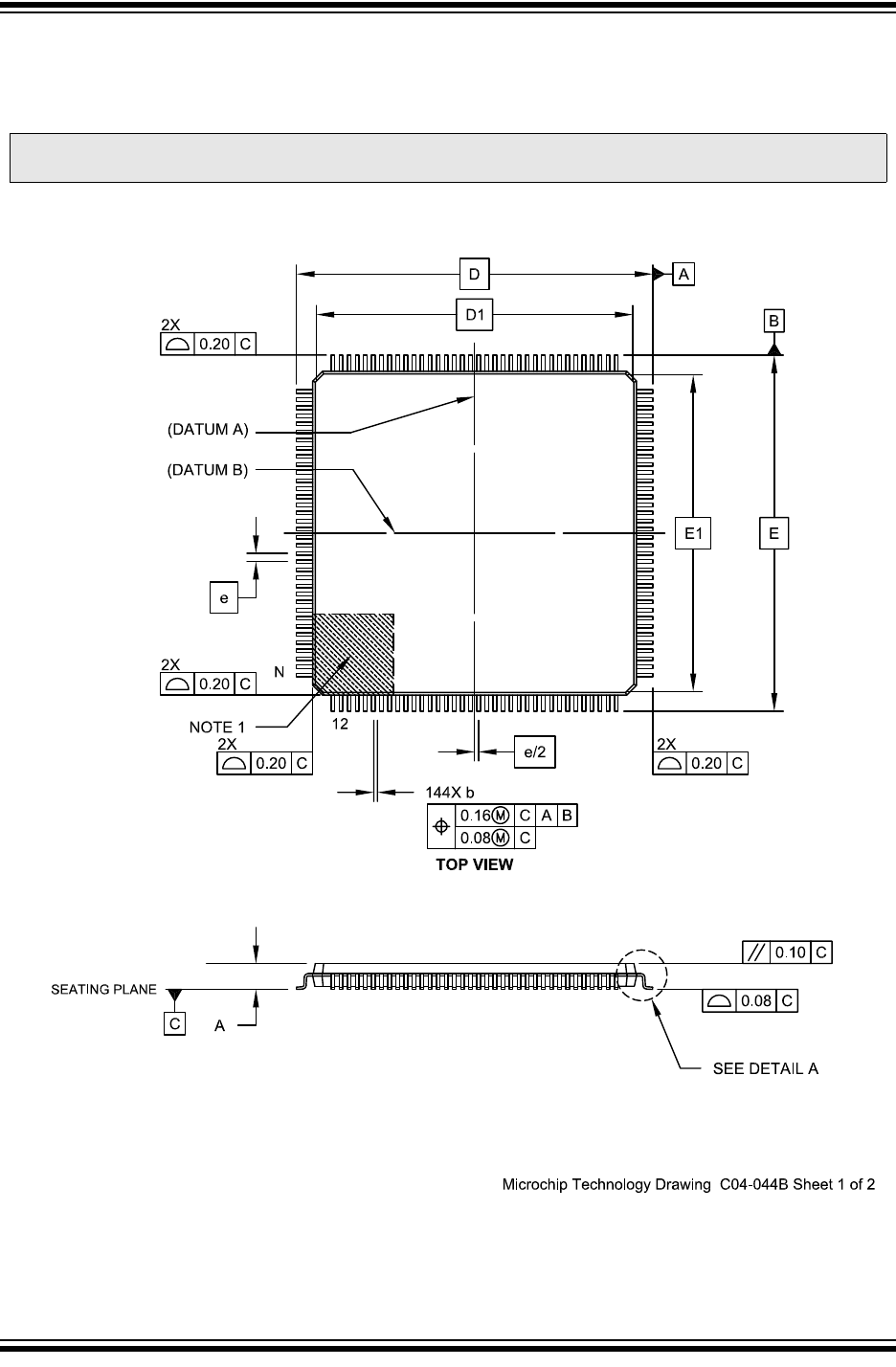
2015 Microchip Technology Inc. Preliminary DS60001320B-page 683
PIC32MZ Embedded Connectivity with Floating Point Unit (EF) Family
144-Lead Plastic Low Profile Quad Flatpack (PL) – 20x20x1.40 mm Body, with 2.00 mm
Footprint [LQFP]
Note: For the most current package drawings, please see the Microchip Packaging Specification located at
http://www.microchip.com/packaging
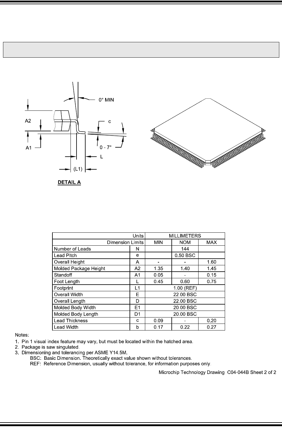
PIC32MZ Embedded Connectivity with Floating Point Unit (EF) Family
DS60001320B-page 684 Preliminary 2015 Microchip Technology Inc.
144-Lead Plastic Low Profile Quad Flatpack (PL) – 20x20x1.40 mm Body, with 2.00 mm
Footprint [LQFP]
Note: For the most current package drawings, please see the Microchip Packaging Specification located at
http://www.microchip.com/packaging
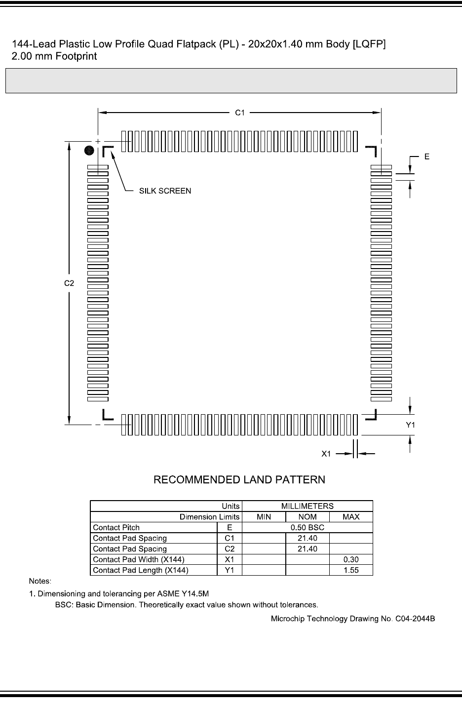
2015 Microchip Technology Inc. Preliminary DS60001320B-page 685
PIC32MZ Embedded Connectivity with Floating Point Unit (EF) Family
Note: For the most current package drawings, please see the Microchip Packaging Specification located at
http://www.microchip.com/packaging

PIC32MZ Embedded Connectivity with Floating Point Unit (EF) Family
DS60001320B-page 686 Preliminary 2015 Microchip Technology Inc.
NOTES:

2015 Microchip Technology Inc. Preliminary DS60001320B-page 687
PIC32MZ Embedded Connectivity with Floating Point Unit (EF) Family
APPENDIX A: MIGRATING FROM
PIC32MX5XX/6XX/7XX
TO PIC32MZ EF
This appendix provides an overview of considerations
for migrating from PIC32MX5XX/6XX/7XX devices to
the PIC32MZ EF family of devices. The code devel-
oped for PIC32MX5XX/6XX/7XX devices can be
ported to PIC32MZ EF devices after making the
appropriate changes outlined in the following sections.
The PIC32MZ EF devices are based on a new
architecture, and feature many improvements and new
capabilities over PIC32MX5XX/6XX/7XX devices.
A.1 Oscillator and PLL Configuration
Because the maximum speed of the PIC32MZ EF
family is 200 MHz, the configuration of the oscillator is
different from prior PIC32MX5XX/6XX/7XX devices.
Table A-1 summarizes the differences (indicated by
Bold type) between the family devices for the oscillator.
TABLE A-1: OSCILLATOR CONFIGURATION DIFFERENCES
PIC32MX5XX/6XX/7XX Feature PIC32MZ EF Feature
Primary Oscillator Configuration
On PIC32MX devices, XT mode had to be selected if the input fre-
quency was in the 3 MHz to 10 MHz range (4-10 for PLL), and HS
mode had to be selected if the input frequency was in the 10 MHz
to 20 MHz range.
On PIC32MZ EF devices, HS mode has a wider input frequency
range (4 MHz to 12 MHz). The bit setting of ‘01’ is Reserved.
POSCMOD<1:0> (DEVCFG1<9:8>)
11 = Primary Oscillator disabled
10 = HS Oscillator mode selected
01 = XT Oscillator mode selected
00 = External Clock mode selected
POSCMOD<1:0> (DEVCFG1<9:8>)
11 = Primary Oscillator disabled
10 = HS Oscillator mode selected
01 = Reserved
00 = External Clock mode selected
Oscillator Selection
On PIC32MX devices, clock selection choices are as follows: On PIC32MZ EF devices, clock selection choices are as follows:
FNOSC<2:0> (DEVCFG1<2:0>)
NOSC<2:0> (OSCCON<10:8>)
111 = FRCDIV
110 = FRCDIV16
101 = LPRC
100 = SOSC
011 = POSC with PLL module
010 = POSC (XT, HS, EC)
001 = FRCDIV+PLL
000 = FRC
FNOSC<2:0> (DEVCFG1<2:0>)
NOSC<2:0> (OSCCON<10:8>)
111 = FRCDIV
110 = Reserved
101 = LPRC
100 = SOSC
011 = Reserved
010 = POSC (HS or EC)
001 = System PLL (SPLL)
000 = FRCDIV
COSC<2:0> (OSCCON<14:12>)
111 = FRC divided by FRCDIV
110 = FRC divided by 16
101 = LPRC
100 = SOSC
011 = POSC + PLL module
010 = POSC
001 = FRCPLL
000 = FRC
COSC<2:0> (OSCCON<14:12>)
111 = FRC divided by FRCDIV
110 = BFRC
101 = LPRC
100 = SOSC
011 = Reserved
010 = POSC
001 = System PLL
000 = FRC divided by FRCDIV
Secondary Oscillator Enable
The location of the SOSCEN bit in the Flash Configuration Words
has moved.
FSOSCEN (DEVCFG1<5>) FSOSCEN (DEVCFG1<6>)

PIC32MZ Embedded Connectivity with Floating Point Unit (EF) Family
DS60001320B-page 688 Preliminary 2015 Microchip Technology Inc.
PLL Configuration
The FNOSC<2:0> and NOSC<2:0> bits select between POSC
and FRC.
Selection of which input clock (POSC or FRC) is now done
through the FPLLICLK/PLLICLK bits.
FNOSC<2:0> (DEVCFG1<2:0>)
NOSC<2:0> (OSCCON<10:8>) FPLLICLK (DEVCFG2<7>)
PLLICLK (SPLLCON<7>)
On PIC32MX devices, the input frequency to the PLL had to be
between 4 MHz and 5 MHz. FPLLIDIV selected how to divide the
input frequency to give it the appropriate range.
On PIC32MZ EF devices, the input range for the PLL is wider (5
MHz to 64 MHz). The input divider values have changed, and new
FPLLRNG/PLLRNG bits have been added to indicate under what
range the input frequency falls.
FPLLIDIV<2:0> (DEVCFG2<2:0>)
111 = 12x divider
110 = 10x divider
101 = 6x divider
100 = 5x divider
011 = 4x divider
010 = 3x divider
001 = 2x divider
000 = 1x divider
FPLLIDIV<2:0> (DEVCFG2<2:0>)
PLLIDIV<2:0> (SPLLCON<2:0>)
111 = Divide by 8
110 = Divide by 7
101 = Divide by 6
100 = Divide by 5
011 = Divide by 4
010 = Divide by 3
001 = Divide by 2
000 = Divide by 1
FPLLRNG<2:0> (DEVCFG2<6:4>)
PLLRNG<2:0> (SPLLCON<2:0>)
111 = Reserved
110 = Reserved
101 = 34-64 MHz
100 = 21-42 MHz
011 = 13-26 MHz
010 = 8-16 MHz
001 = 5-10 MHz
000 = Bypass
On PIC32MX devices, the output frequency of PLL is between
60 MHz and 120 MHz. The PLL multiplier and divider bits
configure the PLL for this range.
The PLL multiplier and divider on PIC32MZ EF devices have a
wider range to accommodate the wider PLL specification range of
10 MHz to 200 MHz.
FPLLMUL<2:0> (DEVCFG2<6:4>)
PLLMULT<2:0> (OSCCON<18:16>)
111 = 24x multiplier
110 = 21x multiplier
101 = 20x multiplier
100 = 19x multiplier
011 = 18x multiplier
010 = 17x multiplier
001 = 16x multiplier
000 = 15x multiplier
FPLLMULT<6:0> (DEVCFG2<14:8>)
PLLMULT<6:0> (SPLLCON<22:16>)
1111111 = Multiply by 128
1111110 = Multiply by 127
1111101 = Multiply by 126
1111100 = Multiply by 125
•
•
•
0000000 = Multiply by 1
FPLLODIV<2:0> (DEVCFG2<18:16>)
PLLODIV<2:0> (OSCCON<29:27>)
111 = 24x multiplier
110 = 21x multiplier
101 = 20x multiplier
100 = 19x multiplier
011 = 18x multiplier
010 = 17x multiplier
001 = 16x multiplier
000 = 15x multiplier
FPLLODIV<2:0> (DEVCFG2<18:16>)
PLLODIV<2:0> (SPLLCON<26:24>)
111 = PLL Divide by 32
110 = PLL Divide by 32
101 = PLL Divide by 32
100 = PLL Divide by 16
011 = PLL Divide by 8
010 = PLL Divide by 4
001 = PLL Divide by 2
000 = PLL Divide by 2
TABLE A-1: OSCILLATOR CONFIGURATION DIFFERENCES (CONTINUED)
PIC32MX5XX/6XX/7XX Feature PIC32MZ EF Feature

2015 Microchip Technology Inc. Preliminary DS60001320B-page 689
PIC32MZ Embedded Connectivity with Floating Point Unit (EF) Family
Crystal/Oscillator Selection for USB
Any frequency that can be divided down to 4 MHz using
UPLLIDIV, including 4, 8, 12, 16, 20, 40, and 48 MHz.
If the USB module is used, the Primary Oscillator is limited to
either 12 MHz or 24 MHz. Which frequency is used is selected
using the UPLLFSEL (DEVCFG2<30>) bit.
USB PLL Configuration
On PIC32MX devices, the PLL for the USB requires an input fre-
quency of 4 MHz.
On PIC32MZ EF devices, the HS USB PHY requires an input
frequency of 12 MHz or 24 MHz. UPLLIDIV has been replaced
with UPLLFSEL.
UPLLIDIV<2:0> (DEVCFG2<10:8>)
111 = 12x divider
110 = 10x divider
101 = 6x divider
100 = 5x divider
011 = 4x divider
010 = 3x divider
010 = 3x divider
001 = 2x divider
000 = 1x divider
UPLLFSEL (DEVCFG2<30>)
1 = UPLL input clock is 24 MHz
0 = UPLL input clock is 12 MHz
Peripheral Bus Clock Configuration
On PIC32MX devices, there is one peripheral bus, and the clock
for that bus is divided from the SYSCLK using FPBDIV/PBDIV. In
addition, the maximum PBCLK frequency is the same as
SYSCLK.
On PIC32MZ EF devices, there are eight peripheral buses with
their own clocks. FPBDIV is removed, and each PBDIV is in its
own register for each PBCLK. The initial PBCLK speed is fixed at
reset, and the maximum PBCLK speed is limited to100 MHz for
all buses, with the exception of PBCLK7, which is 200 MHz.
FPBDIV<1:0> (DEVCFG1<5:4>)
PBDIV<1:0> (OSCCON<20:19>)
11 = PBCLK is SYSCLK divided by 8
10 = PBCLK is SYSCLK divided by 4
01 = PBCLK is SYSCLK divided by 2
00 = PBCLK is SYSCLK divided by 1
PBDIV<6:0> (PBxDIV<6:0>)
1111111 = PBCLKx is SYSCLK divided by 128
1111110 = PBCLKx is SYSCLK divided by 127
•
•
•
0000011 = PBCLKx is SYSCLK divided by 4
0000010 = PBCLKx is SYSCLK divided by 3
0000001 = PBCLKx is SYSCLK divided by 2
(default value for x < 7)
0000000 = PBCLKx is SYSCLK divided by 1
(default value for x 7)
CPU Clock Configuration
On PIC32MX devices, the CPU clock is derived from SYSCLK. On PIC32MZ EF devices, the CPU clock is derived from PBCLK7.
FRCDIV Default
On PIC32MX devices, the default value for FRCDIV was to divide
the FRC clock by two.
On PIC32MZ EF devices, the default has been changed to divide
by one.
FRCDIV<2:0> (OSCCON<26:24>)
111 = FRC divided by 256
110 = FRC divided by 64
101 = FRC divided by 32
100 = FRC divided by 16
011 = FRC divided by 8
010 = FRC divided by 4
001 = FRC divided by 2 (default)
000 = FRC divided by 1
FRCDIV<2:0> (OSCCON<26:24>)
111 = FRC divided by 256
110 = FRC divided by 64
101 = FRC divided by 32
100 = FRC divided by 16
011 = FRC divided by 8
010 = FRC divided by 4
001 = FRC divided by 2
000 = FRC divided by 1 (default)
TABLE A-1: OSCILLATOR CONFIGURATION DIFFERENCES (CONTINUED)
PIC32MX5XX/6XX/7XX Feature PIC32MZ EF Feature

PIC32MZ Embedded Connectivity with Floating Point Unit (EF) Family
DS60001320B-page 690 Preliminary 2015 Microchip Technology Inc.
Table A-2 illustrates the difference in code setup of the
respective parts for maximum speed using an external
24 MHz crystal.
TABLE A-2: CODE DIFFERENCES FOR MAXIMUM SPEED USING AN EXTERNAL 24 MHz
CRYSTAL
Fail-Safe Clock Monitor (FSCM)
On PIC32MX devices, the internal FRC became the clock source
on a failure of the clock source.
On PIC32MZ EF devices, a separate internal Backup FRC
(BFRC) becomes the clock source upon a failure at the clock
source.
On PIC32MX devices, a clock failure resulted in the triggering of
a specific interrupt when the switchover was complete.
On PIC32MZ EF devices, a NMI is triggered instead, and must be
handled by the NMI routine.
FSCM generates an interrupt. FSCM generates a NMI.
The definitions of the FCKSM<1:0> bits has changed on
PIC32MZ EF devices.
FCKSM<1:0> (DEVCFG1<15:14>)
1x = Clock switching is disabled, FSCM is disabled
01 = Clock switching is enabled, FSCM is disabled
00 = Clock switching is enabled, FSCM is enabled
FCKSM<1:0> (DEVCFG1<15:14>)
11 = Clock switching is enabled and clock monitoring
is enabled
10 = Clock switching is disabled and clock monitoring
is enabled
01 = Clock switching is enabled and clock monitoring is disabled
00 = Clock switching is disabled and clock monitoring
is disabled
On PIC32MX devices, the CF (OSCCON<3>) bit indicates a
clock failure. Writing to this bit initiates a FSCM event.
On PIC32MZ EF devices, the CF (OSCCON<3>) bit has the
same functionality as that of PIC32MX device; however, an addi-
tional CF(RNMICON<1>) bit is available to indicate a NMI event.
Writing to this bit causes a NMI event, but not a FSCM event.
On PIC32MX devices, the CLKLOCK (OSCCON<7>) bit is
controlled by the FSCM.
On PIC32MZ EF devices, the CLKLOCK (OSCCON<7>) bit is
not impacted by the FSCM.
CLKLOCK (OSCCON<7>)
If clock switching and monitoring is disabled (FCKSM<1:0> = 1x):
1 = Clock and PLL selections are locked
0 = Clock and PLL selections are not locked and may be modified
If clock switching and monitoring is enabled (FCKSM<1:0> = 0x):
Clock and PLL selections are never locked and may be modified.
CLKLOCK (OSCCON<7>)
1 = Clock and PLL selections are locked
0 = Clock and PLL selections are not locked and may be modified
TABLE A-1: OSCILLATOR CONFIGURATION DIFFERENCES (CONTINUED)
PIC32MX5XX/6XX/7XX Feature PIC32MZ EF Feature
PIC32MX5XX/6XX/7XX @ 80 Hz PIC32MZ EF @ 200 MHz
#include <xc.h>
#pragma config POSCMOD = HS
#pragma config FNOSC = PRIPLL
#pragma config FPLLIDIV = DIV_6
#pragma config FPLLMUL = MUL_20
#pragma config FPLLODIV = DIV_1
#define SYSFREQ (80000000L)
#include <xc.h>
#pragma config POSCMOD = HS
#pragma config FNOSC = SPLL
#pragma config FPLLICLK = PLL_POSC
#pragma config FPLLIDIV = DIV_3
#pragma config FPLLRNG = RANGE_5_10_MHZ
#pragma config FPLLMULT = MUL_50
#pragma config FPLLODIV = DIV_2
#define SYSFREQ (200000000L)

2015 Microchip Technology Inc. Preliminary DS60001320B-page 691
PIC32MZ Embedded Connectivity with Floating Point Unit (EF) Family
A.2 Analog-to-Digital Converter (ADC)
The PIC32MZ EF family of devices has a new Pipe-
lined ADC module that replaces the 10-bit ADC module
in PIC32MX5XX/6XX/7XX devices; therefore, the use
of Bold type to show differences is not used in the fol-
lowing table. Note that not all register differences are
described in this section; however, the key feature
differences are listed in Table A-3.
TABLE A-3: ADC DIFFERENCES
PIC32MX5XX/6XX/7XX Feature PIC32MZ EF Feature
Clock Selection and Operating Frequency (TAD)
On PIC32MX devices, the ADC clock was derived from either the
FRC or from the PBCLK.
On PIC32MZ EF devices, the three possible sources of the ADC
clock are FRC, REFCLKO3, and SYSCLK.
ADRC (AD1CON3<15>)
1 = FRC clock
0 = Clock derived from Peripheral Bus Clock (PBCLK)
ADCSEL<1:0> (ADCCON3<31:30>)
11 = FRC
10 = REFCLKO3
01 = SYSCLK
00 = Reserved
On PIC32MX devices, if the ADC clock was derived from the
PBCLK, that frequency was divided further down, with a maxi-
mum divisor of 512, and a minimum divisor of two.
On PIC32MZ EF devices, any ADC clock source can be divided
down separately for each dedicated ADC and the shared ADC,
with a maximum divisor of 254. The input clock can also be fed
directly to the ADC.
ADCS<7:0> (AD1CON3<7:0>)
11111111 = 512 * TPB = TAD
•
•
•
00000001 = 4 * TPB = TAD
00000000 = 2 * TPB = TAD
ADCDIV<6:0> (ADCTIMEx<22:16>)
ADCDIV<6:0> (ADCCON2<6:0>)
1111111 = 254 * TQ = TAD
•
•
•
0000011 = 6 * TQ = TAD
0000010 = 4 * TQ = TAD
0000001 = 2 * TQ = TAD
0000000 = TQ = TAD
Scan Trigger Source
On PIC32MX devices, there are four sources that can trigger a
scan conversion in the ADC module: Auto, Timer3, INT0, and
clearing the SAMP bit.
On PIC32MZ EF devices, the list of sources for triggering a scan
conversion has been expanded to include the comparators,
Output Compare, and two additional Timers. In addition, trigger
sources can be simulated by setting the RQCNVRT
(ADCCON3<8>) bit.
SSRC<2:0> (AD1CON1<7:5>)
111 = Auto convert
110 = Reserved
101 = Reserved
100 = Reserved
011 = Reserved
010 = Timer3 period match
001 = Active transition on INT0 pin
000 = Clearing SAMP bit
STRGSRC<4:0> (ADCCON1<20:16>)
11111 = Reserved
•
•
•
01101 = Reserved
01100 = Comparator 2 COUT
01011 = Comparator 1 COUT
01010 = OCMP5
01001 = OCMP3
01000 = OCMP1
00111 = TMR5 match
00110 = TMR3 match
00101 = TMR1 match
00100 = INT0
00011 = Reserved
00010 = Global level software trigger (GLSWTRG)
00001 = Global software trigger (GSWTRG)
00000 = No trigger

PIC32MZ Embedded Connectivity with Floating Point Unit (EF) Family
DS60001320B-page 692 Preliminary 2015 Microchip Technology Inc.
Output Format
On PIC32MX devices, the output format was decided for all ADC
channels based on the setting of the FORM<2:0> bits.
On PIC32MZ EF devices, the FRACT bit determines whether
fractional or integer format is used. Then, each input can have its
own setting for input (differential or single-ended) and sign
(signed or unsigned) using the DIFFx and SIGNx bits in the
ADCIMODx registers.
FORM<2:0> (AD1CON1<10:8>)
011 = Signed Fractional 16-bit
010 = Fractional 16-bit
001 = Signed Integer 16-bit
000 = Integer 16-bit
111 = Signed Fractional 32-bit
110 = Fractional 32-bit
101 = Signed Integer 32-bit
100 = Integer 32-bit
FRACT (ADCCON1<23>)
1 = Fractional
0 = Integer
DIFFx (ADCIMODy)
1 = Channel x is using Differential mode
0 = Channel x is using Single-ended mode
SIGNx (ADCMODy)
1 = Channel x is using Signed Data mode
0 = Channel x is using Unsigned Data mode
Interrupts
On PIC32MX devices, an interrupt is triggered from the ADC
module when a certain number of conversions have taken place,
irrespective of which channel was converted.
On PIC32MZ EF devices, the ADC module can trigger an inter-
rupt for each channel when it is converted. Use the Interrupt Con-
troller bits, IEC1<31:27>, IEC2<31:0>, and IEC3<7:0>, to enable/
disable them.
In addition, the ADC support one global interrupt to indicate
conversion on any number of channels.
SMPI<3:0> (AD1CON2<5:2>)
1111 = Interrupt for each 16th sample/convert sequence
1110 = Interrupt for each 15th sample/convert sequence
•
•
•
0001 = Interrupt for each 2nd sample/convert sequence
0000 = Interrupt for each sample/convert sequence
AGIENxx (ADCGIRQENx<y>)
1 = Data ready event will generate a Global ADC interrupt
0 = No global interrupt
In addition, interrupts can be generated for filter and comparator
events.
I/O Pin Analog Function Selection
On PIC32MX devices, the analog function of an I/O pin was deter-
mined by the PCFGx bit in the AD1PCFG register.
On PIC32MZ EF devices, the analog selection function has been
moved into a separate register on each I/O port. Note that the
sense of the bit is different.
PCFGx (AD1PCFG<x>)
1 = Analog input pin in Digital mode
0 = Analog input pin in Analog mode
ANSxy (ANSELx<y>)
1 = Analog input pin in Analog mode
0 = Analog input pin in Digital mode
Electrical Specifications and Timing Requirements
Refer to “Section 31. Electrical Characteristics” in the
PIC32MX5XX/6XX/7XX Data Sheet for ADC module
specifications and timing requirements.
On PIC32MZ EF devices, the ADC module sampling and conver-
sion time and other specifications have changed. Refer to
37.0 “Electrical Characteristics” for more information.
TABLE A-3: ADC DIFFERENCES (CONTINUED)
PIC32MX5XX/6XX/7XX Feature PIC32MZ EF Feature

2015 Microchip Technology Inc. Preliminary DS60001320B-page 693
PIC32MZ Embedded Connectivity with Floating Point Unit (EF) Family
A.3 CPU
The CPU in the PIC32MZ EF family of devices has
been changed to the MIPS32 M-Class MPU architec-
ture. This CPU includes DSP ASE, internal data and
instruction L1 caches, and a TLB-based MMU.
Table A-4 summarizes some of the key differences
(indicated by Bold type) in the internal CPU registers.
TABLE A-4: CPU DIFFERENCES
PIC32MX5XX/6XX/7XX Feature PIC32MZ EF Feature
L1 Data and Instruction Cache and Prefetch Wait States
On PIC32MX devices, the cache was included in the prefetch
module outside the CPU. On PIC32MZ EF devices, the CPU has a separate L1 instruction
and data cache in the core. The PREFEN<1:0> bits still enable
the prefetch module; however, the K0<2:0> bits in the CP0 regis-
ters controls the internal L1 cache for the designated regions.
PREFEN<1:0> (CHECON<5:4>)
11 = Enable predictive prefetch for both cacheable and
non-cacheable regions
10 = Enable predictive prefetch for non-cacheable regions only
01 = Enable predictive prefetch for cacheable regions only
00 = Disable predictive prefetch
DCSZ<1:0> (CHECON<9:8>)
Changing these bits causes all lines to be reinitialized to the
“invalid” state.
11 = Enable data caching with a size of 4 lines
10 = Enable data caching with a size of 2 lines
01 = Enable data caching with a size of 1 line
00 = Disable data caching
CHECOH (CHECON<16>)
1 = Invalidate all data and instruction lines
0 = Invalidate all data and instruction lines that are not locked
PREFEN<1:0> (PRECON<5:4>)
11 = Enable predictive prefetch for any address
10 = Enable predictive prefetch for CPU instructions and CPU
data
01 = Enable predictive prefetch for CPU instructions only
00 = Disable predictive prefetch
K0<2:0> (CP0 Reg 16, Select 0)
011 = Cacheable, non-coherent, write-back, write allocate
010 = Uncached
001 = Cacheable, non-coherent, write-through, write allocate
000 = Cacheable, non-coherent, write-through, no write allocate
The Program Flash Memory read wait state frequency points
have changed in PIC32MZ EF devices. The register for accessing
the PFMWS field has changed from CHECON to PRECON.
PFMWS<2:0> (CHECON<2:0>)
111 = Seven Wait states
110 = Six Wait states
101 = Five Wait states
100 = Four Wait states
011 = Three Wait states
010 = Two Wait states (61-80 MHz)
001 = One Wait state (31-60 MHz)
000 = Zero Wait state (0-30 MHz)
PFMWS<2:0> (PRECON<2:0>)
111 = Seven Wait states
•
•
•
011 = Three Wait states
010 = Two Wait states (133-200 MHz)
001 = One Wait state (66-133 MHz)
000 = Zero Wait states (0-66 MHz)
Note: Wait states listed are for ECC enabled.
Core Instruction Execution
On PIC32MX devices, the CPU can execute MIPS16e
instructions and uses a 16-bit instruction set, which reduces
memory size.
On PIC32MZ EF devices, the CPU can operate a mode called
microMIPS. microMIPS mode is an enhanced MIPS32®
instruction set that uses both 16-bit and 32-bit opcodes. This
mode of operation reduces memory size with minimum
performance impact.
MIPS16e® microMIPS™
The BOOTISA (DEVCFG0<6>) Configuration bit controls the
MIPS32 and microMIPS modes for boot and exception code.
1 = Boot code and Exception code is MIPS32® (ISAONEXC bit is
set to ‘0’ and the ISA<1:0> bits are set to ‘10’ in the CP0 Config3
register)
0 = Boot code and Exception code is microMIPS™ (ISAONEXC
bit is set to ‘1’ and the ISA<1:0> bits are set to ‘11’ in the CP0
Config3 register)

PIC32MZ Embedded Connectivity with Floating Point Unit (EF) Family
DS60001320B-page 694 Preliminary 2015 Microchip Technology Inc.
A.4 Resets
The PIC32MZ EF family of devices has updated the
resets modules to incorporate the new handling of NMI
resets from the WDT, DMT, and the FSCM. In addition,
some bits have been moved, as summarized in
Table A-5.
A.5 USB
The PIC32MZ EF family of devices has a new Hi-
Speed USB module, which requires the updated USB
stack from Microchip. In addition, the USB PLL was
also updated. See Section A.1 “Oscillator and PLL
Configuration” for more information and Table A-6
for a list of additional differences.
TABLE A-5: RESET DIFFERENCES
PIC32MX5XX/6XX/7XX Feature PIC32MZ EF Feature
Power Reset
The VREGS bit, which controls whether the internal regulator is
enabled in Sleep mode, has been moved from RCON in
PIC32MX5XX/6XX/7XX devices to a new PWRCON register in
PIC32MZ EF devices.
VREGS (RCON<8>)
1 = Regulator is enabled and is on during Sleep mode
0 = Regulator is disabled and is off during Sleep mode
VREGS (PWRCON<0>)
1 = Voltage regulator will remain active during Sleep
0 = Voltage regulator will go to Stand-by mode during Sleep
Watchdog Timer Reset
On PIC32MX devices, a WDT expiration immediately triggers a
device reset.
On PIC32MZ EF devices, the WDT expiration now causes a NMI.
The WDTO bit in RNMICON indicates that the WDT caused the
NMI. A new timer, NMICNT, runs when the WDT NMI is triggered,
and if it expires, the device is reset.
WDT expiration immediately causes a device reset. WDT expiration causes a NMI, which can then trigger the
device reset.
WDTO (RNMICON<24>)
1 = WDT time-out has occurred and caused a NMI
0 = WDT time-out has not occurred
NMICNT<7:0> (RNMICON<7:0>)
TABLE A-6: USB DIFFERENCES
PIC32MX5XX/6XX/7XX Feature PIC32MZ EF Feature
Debug Mode
On PIC32MX devices, when stopping on a breakpoint during
debugging, the USB module can be configured to stop or
continue execution from the Freeze Peripherals dialog in MPLAB
X IDE.
On PIC32MZ EF devices, the USB module continues operating
when stopping on a breakpoint during debugging.
VBUSON Pin
PIC32MX devices feature a VBUSON pin for controlling the
external transceiver power supply.
On PIC32MZ EF devices, the VBUSON pin is not available. A port
pin can be used to achieve the same functionality.

2015 Microchip Technology Inc. Preliminary DS60001320B-page 695
PIC32MZ Embedded Connectivity with Floating Point Unit (EF) Family
A.6 DMA
The DMA controller in PIC32MZ EF devices is similar
to the DMA controller in PIC32MX5XX/6XX/7XX
devices. New features include the extension of pattern
matching to two by bytes and the addition of the
optional Pattern Ignore mode. Table A-7 lists differ-
ences (indicated by Bold type) that will affect software
migration.
TABLE A-7: DMA DIFFERENCES
PIC32MX5XX/6XX/7XX Feature PIC32MZ EF Feature
Read/Write Status on Error
The RDWR bit has moved from DMASTAT<3> in PIC32MX5XX/
6XX/7XX devices to DMASTAT<31> in PIC32MZ EF devices.
RDWR (DMASTAT<3>)
1 = Last DMA bus access when an error was detected was a read
0 = Last DMA bus access when an error was detected was a write
RDWR (DMASTAT<31>)
1 = Last DMA bus access when an error was detected was a read
0 = Last DMA bus access when an error was detected was a write
Source-to-Destination Transfer
On PIC32MX devices, a DMA channel performs a read of the
source data and completes the transfer of this data into the desti-
nation address before it is ready to read the next data from the
source.
On PIC32MZ EF devices, the DMA implements a 4-deep queue
for data transfers. A DMA channel reads the source data and
places it into the queue, regardless of whether previous data in
the queue has been delivered to the destination address.

PIC32MZ Embedded Connectivity with Floating Point Unit (EF) Family
DS60001320B-page 696 Preliminary 2015 Microchip Technology Inc.
A.7 Interrupts and Exceptions
The key difference between Interrupt Controllers in
PIC32MX5XX/6XX/7XX devices and PIC32MZ EF
devices concerns vector spacing. Previous PIC32MX
devices had fixed vector spacing, which is adjustable in
set increments, and every interrupt had the same
amount of space. PIC32MZ EF devices replace this
with a variable offset spacing, where each interrupt has
an offset register to determine where to begin
execution.
In addition, the IFSx, IECx, and IPCx registers for old
peripherals have shifted to different registers due to
new peripherals. Please refer to Section 7.0 “CPU
Exceptions and Interrupt Controller” to determine
where the interrupts are now located.
Table A-8 lists differences (indicated by Bold type) in
the registers that will affect software migration.
TABLE A-8: INTERRUPT DIFFERENCES
PIC32MX5XX/6XX/7XX Feature PIC32MZ EF Feature
Vector Spacing
On PIC32MX devices, the vector spacing was determined by the
VS field in the CPU core.
On PIC32MZ EF devices, the vector spacing is variable and
determined by the Interrupt controller. The VOFFx<17:1> bits in
the OFFx register are set to the offset from EBASE where the
interrupt service routine is located.
VS<4:0> (IntCtl<9:5>: CP0 Register 12, Select 1)
10000 = 512-byte vector spacing
01000 = 256-byte vector spacing
00100 = 128-byte vector spacing
00010 = 64-byte vector spacing
00001 = 32-byte vector spacing
00000 = 0-byte vector spacing
VOFFx<17:1> (OFFx<17:1>)
Interrupt Vector ‘x’ Address Offset bits
Shadow Register Sets
On PIC32MX devices, there was one shadow register set which
could be used during interrupt processing. Which interrupt priority
could use the shadow register set was determined by the FSRS-
SEL field in DEVCFG3 and SS0 on INTCON.
On PIC32MZ EF devices, there are seven shadow register sets,
and each priority level can be assigned a shadow register set to
use via the PRIxSS<3:0> bits in the PRISS register. The SS0 bit
is also moved to PRISS<0>.
FSRSSEL<2:0> (DEVCFG3<18:16>)
111 = Assign Interrupt Priority 7 to a shadow register set
110 = Assign Interrupt Priority 6 to a shadow register set
•
•
•
001 = Assign Interrupt Priority 1 to a shadow register set
000 = All interrupt priorities are assigned to a shadow
register set
PRIxSS<3:0> PRISS<y:z>
1xxx = Reserved (by default, an interrupt with a priority
level of x uses Shadow Set 0)
0111 = Interrupt with a priority level of x uses Shadow Set 7
0110 = Interrupt with a priority level of x uses Shadow Set 6
•
•
•
0001 = Interrupt with a priority level of x uses Shadow Set 1
0000 = Interrupt with a priority level of x uses Shadow Set 0
SS0 (INTCON<16>)
1 = Single vector is presented with a shadow register set
0 = Single vector is not presented with a shadow register set
SS0 (PRISS<0>)
1 = Single vector is presented with a shadow register set
0 = Single vector is not presented with a shadow register set
Status
PIC32MX devices, the VEC<5:0> bits show which interrupt is
being serviced.
On PIC32MZ EF devices, the SIRQ<7:0> bits show the IRQ
number of the interrupt last serviced.
VEC<5:0> (INTSTAT<5:0>)
11111-00000 = The interrupt vector that is presented to the
CPU
SIRQ<7:0> (INTSTAT<7:0>)
11111111-00000000 = The last interrupt request number
serviced by the CPU

2015 Microchip Technology Inc. Preliminary DS60001320B-page 697
PIC32MZ Embedded Connectivity with Floating Point Unit (EF) Family
A.8 Flash Programming
The PIC32MZ EF family of devices incorporates a new
Flash memory technology. Applications ported from
PIC32MX5XX/6XX/7XX devices that take advantage of
Run-time Self Programming will need to adjust the
Flash programming steps to incorporate these
changes.
Table A-9 lists the differences (indicated by Bold type)
that will affect software migration.
TABLE A-9: FLASH PROGRAMMING DIFFERENCES
PIC32MX5XX/6XX/7XX Feature PIC32MZ EF Feature
Program Flash Write Protection
On PIC32MX devices, the Program Flash write-protect bits are
part of the Flash Configuration words (DEVCFG0).
On PIC32MZ EF devices, the write-protect register is contained
separately as the NVMPWP register. It has been expanded to 24
bits, and now represents the address below, which all Flash mem-
ory is protected. Note that the lower 14 bits are forced to zero, so
that all memory locations in the page are protected.
PWP<7:0> (DEVCFG0<19:12>)
11111111 = Disabled
11111110 = 0xBD000FFF
11111101 = 0xBD001FFF
11111100 = 0xBD002FFF
11111011 = 0xBD003FFF
11111010 = 0xBD004FFF
11111001 = 0xBD005FFF
11111000 = 0xBD006FFF
11110111 = 0xBD007FFF
11110110 = 0xBD008FFF
11110101 = 0xBD009FFF
11110100 = 0xBD00AFFF
11110011 = 0xBD00BFFF
11110010 = 0xBD00CFFF
11110001 = 0xBD00DFFF
11110000 = 0xBD00EFFF
11101111 = 0xBD00FFFF
•
•
•
01111111 = 0xBD07FFFF
PWP<23:0> (NVMPWP<23:0>)
Physical memory below address 0x1Dxxxxxx is write protected,
where ‘xxxxxx’ is specified by PWP<23:0>. When PWP<23:0>
has a value of ‘0’, write protection is disabled for the entire pro-
gram Flash. If the specified address falls within the page, the
entire page and all pages below the current page will be pro-
tected.
Code Protection
On PIC32MX devices, code protection is enabled by the CP
(DEVCFG<28>) bit.
On PIC32MZ EF devices, code protection is enabled by the CP
(DEVCP0<28>) bit.
Boot Flash Write Protection
On PIC32MX devices, Boot Flash write protection is enable by
the BWP (DEVCFG<24>) bit and protects the entire Boot Flash
memory.
On PIC32MZ EF devices, Boot Flash write protection is divided
into pages and is enable by the LBWPx and UBWPx bits in the
NVMBWP register.
Low-Voltage Detect Status
LVDSTAT (NVMCON<11>)
1 = Low-voltage event is active
0 = Low-voltage event is not active
The LVDSTAT bit is not available in PIC32MZ EF devices.

PIC32MZ Embedded Connectivity with Floating Point Unit (EF) Family
DS60001320B-page 698 Preliminary 2015 Microchip Technology Inc.
Flash Programming
The op codes for programming the Flash memory have been
changed to accommodate the new quad-word programming and
dual-panel features. The row size has changed to 2 KB (512 IW)
from 128 IW. The page size has changed to 16 KB (4K IW) from
4 KB (1K IW). Note that the NVMOP register is now protected,
and requires the WREN bit be set to enable modification.
NVMOP<3:0> (NVMCON<3:0>)
1111 = Reserved
•
•
•
0111 = Reserved
0110 = No operation
0101 = Program Flash (PFM) erase operation
0100 = Page erase operation
0011 = Row program operation
0010 = No operation
0001 = Word program operation
0000 = No operation
NVMOP<3:0> (NVMCON<3:0>)
1111 = Reserved
•
•
•
1000 = Reserved
0111 = Program erase operation
0110 = Upper program Flash memory erase operation
0101 = Lower program Flash memory erase operation
0100 = Page erase operation
0011 = Row program operation
0010 = Quad Word (128-bit) program operation
0001 = Word program operation
0000 = No operation
PIC32MX devices feature a single NVMDATA register for word
programming.
On PIC32MZ EF devices, to support quad word programming,
the NVMDATA register has been expanded to four words.
NVMDATA NVMDATAx, where ‘x’ = 0 through 3
Flash Endurance and Retention
PIC32MX devices support Flash endurance and retention of up
to 20K E/W cycles and 20 years.
On PIC32MZ EF devices, ECC must be enabled to support the
same endurance and retention as PIC32MX devices.
Configuration Words
On PIC32MX devices, Configuration Words can be programmed
with Word or Row program operation.
On PIC32MZ EF devices, all Configuration Words must be
programmed with Quad Word operation.
Configuration Words Reserved Bit
On PIC32MX devices, the DEVCFG0<15> bit is Reserved and
must be programmed to ‘0’.
On PIC32MZ EF devices, this bit is DEVSIGN0<31>.
TABLE A-9: FLASH PROGRAMMING DIFFERENCES (CONTINUED)
PIC32MX5XX/6XX/7XX Feature PIC32MZ EF Feature

2015 Microchip Technology Inc. Preliminary DS60001320B-page 699
PIC32MZ Embedded Connectivity with Floating Point Unit (EF) Family
A.9 Other Peripherals and Features
Most of the remaining peripherals on PIC32MZ EF
devices act identical to their counterparts on PIC32MX-
5XX/6XX/7XX devices. The main differences have to
do with handling the increased peripheral bus clock
speed and additional clock sources.
Table A-10 lists the differences (indicated by Bold
type) that will affect software and hardware migration.
TABLE A-10: PERIPHERAL DIFFERENCES
PIC32MX5XX/6XX/7XX Feature PIC32MZ EF Feature
I2C™
On PIC32MX devices, all pins are 5V-tolerant. On PIC32MZ EF devices, the I2C4 port uses non-5V tolerant
pins, and will have different VOL/VOH specifications.
The Baud Rate Generator register has been expanded from 12
bits to 16 bits.
I2CxBRG<11:0> I2CxBRG<15:0>
Watchdog Timer
Clearing the Watchdog Timer on PIC32MX5XX/6XX/7XX
devices required writing a ‘1’ to the WDTCLR bit.
On PIC32MZ EF devices, the WDTCLR bit has been replaced
with the 16-bit WDTCLRKEY, which must be written with a spe-
cific value (0x5743) to clear the Watchdog Timer. In addition, the
WDTSPGM (DEVCFG1<21>) bit is used to control operation of
the Watchdog Timer during Flash programming.
WDTCLR (WDTCON<0>) WDTCLRKEY<15:0> (WDTCON<31:16>)
RTCC
On PIC32MX devices, the output of the RTCC pin was selected
between the Seconds Clock or the Alarm Pulse.
On PIC32MZ EF devices, the RTCC Clock is added as an
option. RTCSECSEL has been renamed RTCOUTSEL and
expanded to two bits.
RTCSECSEL (RTCCON<7>)
1 = RTCC Seconds Clock is selected for the RTCC pin
0 = RTCC Alarm Pulse is selected for the RTCC pin
RTCOUTSEL<1:0> (RTCCON<8:7>)
11 = Reserved
10 = RTCC Clock is presented on the RTCC pin
01 = Seconds Clock is presented on the RTCC pin
00 = Alarm Pulse is presented on the RTCC pin when the alarm
interrupt is triggered
On PIC32MX devices, the Secondary Oscillator (SOSC) serves
as the input clock for the RTCC module.
On PIC32MZ EF devices, an additional clock source, LPRC, is
available as a choice for the input clock.
RTCCLKSEL<1:0> (RTCCON<10:9>)
11 = Reserved
10 = Reserved
01 = RTCC uses the external 32.768 kHz SOSC
00 = RTCC uses the internal 32 kHz oscillator (LPRC)

PIC32MZ Embedded Connectivity with Floating Point Unit (EF) Family
DS60001320B-page 700 Preliminary 2015 Microchip Technology Inc.
Ethernet
On PIC32MZ EF devices, the input clock divider for the Ethernet
module has expanded options to accommodate the faster
peripheral bus clock.
CLKSEL<3:0> (EMAC1MCFG<5:2>)
1000 = SYSCLK divided by 40
0111 = SYSCLK divided by 28
0110 = SYSCLK divided by 20
0101 = SYSCLK divided by 14
0100 = SYSCLK divided by 10
0011 = SYSCLK divided by 8
0010 = SYSCLK divided by 6
000x = SYSCLK divided by 4
CLKSEL<3:0> (EMAC1MCFG<5:2>)
1010 = PBCLK5 divided by 50
1001 = PBCLK5 divided by 48
1000 = PBCLK5 divided by 40
0111 = PBCLK5 divided by 28
0110 = PBCLK5 divided by 20
0101 = PBCLK5 divided by 14
0100 = PBCLK5 divided by 10
0011 = PBCLK5 divided by 8
0010 = PBCLK5 divided by 6
000x = PBCLK5 divided by 4
Comparator/Comparator Voltage Reference
On PIC32MX devices, it was possible to select the VREF+ pin as
the output to the CVREFOUT pin.
On PIC32MZ EF devices, the CVREFOUT pin must come from the
resistor network.
VREFSEL (CVRCON<10>)
1 = CVREF = VREF+
0 = CVREF is generated by the resistor network
This bit is not available.
On PIC32MX devices, the internal voltage reference (IVREF)
could be chosen by the BGSEL<1:0> bits.
On PIC32MZ EF devices, IVREF is fixed and cannot be changed.
BGSEL<1:0> (CVRCON<9:8>)
11 = IVREF = VREF+
10 = Reserved
01 = IVREF = 0.6V (nominal, default)
00 = IVREF = 1.2V (nominal)
These bits are not available.
Change Notification
On PIC32MX devices, Change Notification is controlled by the
CNCON, CNEN, and CNPUE registers.
On PIC32MZ EF devices, Change Notification functionality has
been relocated into each I/O port and is controlled by the
CNPUx, CNPDx, CNCONx, CNENx, and CNSTATx registers.
System Bus
On PIC32MX devices, the System Bus registers can be used to
configure RAM memory for data and program memory partitions,
cacheability of Flash memory, and RAM Wait states. These reg-
isters are: BMXCON, BMXDKPBA, BMXDUDBA, BMXDUPBA,
BMXPUPBA, BMXDRMSZ, BMXPFMSZ, and BMXBOOTSZ.
On PIC32MZ EF devices, a new System Bus is utilized that sup-
ports using RAM memory for program or data without the need
for special configuration. Therefore, no special registers are
associated with the System Bus to configure these features.
On PIC32MX devices, various arbitration modes are used as ini-
tiators on the System Bus. These modes can be selected by the
BMXARB<2:0> (BMXCON<2:0>) bits.
On PIC32MZ EF devices, a new arbitration scheme has been
implemented on the System Bus. All initiators use the Least
Recently Serviced (LRS) scheme, with the exception of the
DMA, CPU, and the Flash Controller.
The Flash Controller always has High priority over LRS initiators.
The DMA and CPU (when servicing an interrupt) can be selected
to have LRS or High priority using the DMAPRI (CFGCON<25>)
and CPUPRI (CFGCON<24>) bits.
TABLE A-10: PERIPHERAL DIFFERENCES (CONTINUED)
PIC32MX5XX/6XX/7XX Feature PIC32MZ EF Feature

2015 Microchip Technology Inc. Preliminary DS60001320B-page 701
PIC32MZ Embedded Connectivity with Floating Point Unit (EF) Family
A.10 Package Differences
In general, PIC32MZ EF devices are mostly pin com-
patible with PIC32MX5XX/6XX/7XX devices; how-
ever, some pins are not. In particular, the VDD and
VSS pins have been added and moved to different
pins. In addition, I/O functions that were on fixed
pins now will largely be on remappable pins.
TABLE A-11: PACKAGE DIFFERENCES
PIC32MX5XX/6XX/7XX Feature PIC32MZ EF Feature
VCAP Pin
On PIC32MX devices, an external capacitor is required between
a VCAP pin and GND, which provides a filtering capacitor for the
internal voltage regulator.
On PIC32MZ EF devices, this requirement has been removed.
A low-ESR capacitor (typically 10 µF) is required on the VCAP
pin.
No VCAP pin.
VDD and VSS Pins
There are more VDD pins on PIC32MZ EF devices, and many
are located on different pins.
VDD on 64-pin packages: 10, 26, 38, 57
VDD on 100-pin packages: 2, 16, 37, 46, 62, 86
VDD on 64-pin packages: 8, 26, 39, 54, 60
VDD on 100-pin packages: 14, 37, 46, 62, 74, 83, 93
There are more VSS pins on PIC32MZ EF devices, and many are
located on different pins.
VSS on 64-pin packages: 9, 25, 41
VSS on 100-pin packages: 15, 36, 45, 65, 75
VSS on 64-pin packages: 7, 25, 35, 40, 55, 59
VSS on 100-pin packages: 13, 36, 45, 53, 63, 75, 84, 92
PPS I/O Pins
Peripheral functions on PIC32MZ EF devices are now routed
through a PPS module, which routes the signals to the desired
pins. When migrating software, it is necessary to initialize the
PPS I/O functions in order to get the signal to and from the cor-
rect pin.
All peripheral functions are fixed as to what pin upon which they
operate.
PPS functionality for the following peripherals:
•CAN
•UART
• SPI (except SCK)
• Input Capture
• Output Compare
• External Interrupt (except INT0)
• Timer Clocks (except Timer1)
• Reference Clocks (except REFCLK2)

PIC32MZ Embedded Connectivity with Floating Point Unit (EF) Family
DS60001320B-page 702 Preliminary 2015 Microchip Technology Inc.
APPENDIX B: MIGRATING FROM
PIC32MZ EC TO
PIC32MZ EF
This appendix provides an overview of considerations
for migrating from PIC32MZ EC devices to the
PIC32MZ EF family of devices. The code developed for
PIC32MZ EC devices can be ported to PIC32MZ EF
devices after making the appropriate changes outlined
in the following sections.
The PIC32MZ EF devices are similar to PIC32MZ EC
devices, with many feature improvements and new
capabilities.
B.1 Oscillator and PLL Configuration
A number of new features have been added to the
oscillator and PLL to enhance their ability to work with
crystals and to change frequencies.
Table B-1 summarizes the differences (indicated by
Bold type) between the family differences for the
oscillator.
TABLE B-1: OSCILLATOR DIFFERENCES
PIC32MZ EC Feature PIC32MZ EF Feature
Primary Oscillator Crystal Power
On PIC32MZ EC devices, the crystal HS POSC mode is only
functional with crystals that have certain characteristics, such as
very low ESR.
On PIC32MZ EF devices, some DEVCFG0 bits have been
added to allow control over the strength of the oscillator and to
add a kick start boost.
POSCBOOST (DEVCFG0<21>)
1 = Boost the kick start of the oscillator
0 = Normal start of the oscillator
POSCGAIN<1:0> (DEVCFG0<20:19>)
11 = 2x gain setting
10 = 1.5x gain setting
01 = 0.5x gain setting
00 = 1x gain setting
Note that the default for POSCGAIN (2x gain setting) may over-
drive crystals and shorten their life. It is the responsibility of the
designer to ensure crystals are operated properly.
Secondary Oscillator Crystal Power
On PIC32MZ EC devices, the Secondary Oscillator (SOSC) is not
functional.
On PIC32MZ EF devices, the Secondary Oscillator is now
functional, and provides similar strength and kick start boost
features as the POSC.
SOSCBOOST (DEVCFG0<18>)
1 = Boost the kick start of the oscillator
0 = Normal start of the oscillator
SOSCGAIN<1:0> (DEVCFG0<17:16>)
11 = 2x gain setting
10 = 1.5x gain setting
01 = 0.5x gain setting
00 = 1x gain setting
Note that the default for SOSCGAIN (2x gain setting) may over-
drive crystals and shorten their life. It is the responsibility of the
designer to ensure crystals are operated properly.
Clock Status Bits
On PIC32MZ EC devices, the SOSCRDY bit (OSCCON<22>)
indicates when the Secondary Oscillator is ready. There are no
indications of other oscillator status.
A new register, CLKSTAT, has been added, which includes the
SOSCRDY bit (CLKSTAT<4>). In addition, new status bits are
available:
• LPRCRDY (CLKSTAT<5>)
• POSCRDY (CLKSTAT<2>)
• DIVSPLLRDY (CLKSTAT<1>)
• FRCRDY (CLKSTAT<0>)
Clock Switching
On PIC32MZ EC devices, clock switches occur as soon as the
switch command is issued. Also, the only clock sources that can
be divided are the output of the PLL, and the FRC.
To reduce power spikes during clock switches, PIC32MZ EF
devices add a clock slewing feature, so that clock switches can
be controlled in their rate and size. The SLEWCON register
controls this feature. The SLEWCON register also features a
SYSCLK divider, so that all of the possible clock sources may be
divided further as needed.

2015 Microchip Technology Inc. Preliminary DS60001320B-page 703
PIC32MZ Embedded Connectivity with Floating Point Unit (EF) Family
B.2 Analog-to-Digital Converter (ADC)
The PIC32MZ EC family features a Pipelined ADC
module, while the PIC32MZ EF family of devices has
an entirely new 12-bit High-Speed SAR ADC module.
Nearly all registers in this new ADC module differ from
the registers in PIC32MZ EC devices. Due to this differ-
ence, code will not port from PIC32MZ EC devices to
PIC32MZ EF devices. Table B-2 lists some of the differ-
ences in registers to note to adapt code as quickly as
possible.
TABLE B-2: ADC DIFFERENCES
PIC32MZ EC Feature PIC32MZ EF Feature
Clock Selection and Operating Frequency (TAD)
On PIC32MZ EC devices, there are three possible sources of the
ADC clock: FRC, REFCLKO3, and SYSCLK. On PIC32MZ EF devices, there are four sources for the ADC
clock. In addition to the ones for PIC32MZ EC, PBCLK4 is added
as a source. Also, the clock source selection is in a different
register.
ADCSEL<1:0> (AD1CON1<9:8>)
11 = FRC
10 = REFCLKO3
01 = SYSCLK
00 = Reserved
ADCSEL<1:0> (ADCCON3<31:30>)
11 = FRC
10 = REFCLKO3
01 = SYSCLK
00 = PBCLK4
Scan Trigger Sources
On PIC32MZ EC devices, there are 10 available trigger sources
for starting ADC sampling and conversion. On PIC32MZ EF devices, two new sources have been added.
One is a shared trigger source (STRIG). The other is a Global
Level Software Trigger (GLSWTRG). With the GLSWTRG, the
conversions continue until the bit is cleared in software.
STRGSRC<4:0> (AD1CON1<26:22>)
11111 = Reserved
•
•
•
01101 = Reserved
01100 = Comparator 2 COUT
01011 = Comparator 1 COUT
01010 = OCMP5
01001 = OCMP3
01000 = OCMP1
00111 = TMR5 match
00110 = TMR3 match
00101 = TMR1 match
00100 = INT0
00011 = Reserved
00010 = Reserved
00001 = Global Software Trigger (GSWTRG)
00000 = No trigger
TRGSRC<4:0> (ADCTRGx<y:z>)
11111 = Reserved
•
•
•
01101 = Reserved
01100 = Comparator 2 COUT
01011 = Comparator 1 COUT
01010 = OCMP5
01001 = OCMP3
01000 = OCMP1
00111 = TMR5 match
00110 = TMR3 match
00101 = TMR1 match
00100 = INT0
00011 = STRIG
00010 = Global Level Software Trigger (GLSWTRG)
00001 = Global Software Trigger (GSWTRG)
00000 = No trigger
ADC Calibration
PIC32MZ EC devices require calibration values be copied into
the AD1CALx registers before turning on the ADC. These values
come from the DEVADCx registers.
PIC32MZ EF devices do not require this step, and the
corresponding registers are not available.
Debug Mode
On PIC32MZ EC devices, the ADC module continues operating
when stopping on a breakpoint during debugging. On PIC32MZ EF devices, the ADC module will stop during
debugging when stopping on a breakpoint.
Electrical Specifications and Timing Requirements
Refer to the “Electrical Characteristics” chapter in the
PIC32MZ EC data sheet for ADC module specifications and
timing requirements.
On PIC32MZ EF devices, the ADC module sampling and
conversion time and other specifications have changed. Refer to
37.0 “Electrical Characteristics” for more information.

PIC32MZ Embedded Connectivity with Floating Point Unit (EF) Family
DS60001320B-page 704 Preliminary 2015 Microchip Technology Inc.
B.3 CPU
The CPU in PIC32MZ EC devices is the microAptiv™
MPU architecture. The CPU in the PIC32MZ EF
devices is the Series 5 Warrior M-Class M5150 MPU
architecture. Most PIC32MZ EF M-Class core features
are identical to the microAptiv™ core in PIC32MZ EC
devices. The main differences are that in PIC32MZ EF
devices, a floating-point unit (FPU) is included for
improved math performance, and PC Sampling for
performance measurement.
B.4 System Bus
The system bus on PIC32MZ EF devices is similar to
the system bus on PIC32MZ EC devices. There are
two key differences listed in Table B-3.
B.5 Flash Controller
The Flash controller on PIC32MZ EF devices adds the
ability both to control boot Flash aliasing, and for lock-
ing the current swap settings. Table B-4 lists theses
differences.
TABLE B-3: SYSTEM BUS DIFFERENCES
PIC32MZ EC Feature PIC32MZ EF Feature
Permission Groups during NMI
On PIC32MZ EC devices, the permission group in which the
CPU is part of is lost during NMI handling, and must be manually
restored.
On PIC32MZ EF devices, the prior permission group is
preserved, and is restored when the CPU returns from the NMI
handler.
DMA Access
The DMA can access the peripheral registers on Peripheral
Bus 1.
On PIC32MZ EF devices, the DMA no longer has access to
registers on Peripheral Bus 1. Refer to Table 4-4 for details on
which peripherals are now excluded.
TABLE B-4: FLASH CONTROLLER DIFFERENCES
PIC32MZ EC Feature PIC32MZ EF Feature
Boot Flash Aliasing
On PIC32MZ EC devices, boot flash aliasing is done through the
DEVSEQ0 register, but no further changes are possible without
rebooting the processor.
On PIC32MZ EF devices, the initial boot flash aliasing is still
determined by the DEVSEQ0 register, but the BFSWAP bit
(NVMCON<6>) reflects the state of the aliasing, and can be
modified to change it during run-time.
BFSWAP (NVMCON<6>)
1 = Boot Flash Bank 2 is mapped to the lower boot alias, and Boot
Flash bank 1 is mapped to the upper boot alias
0 = Boot Flash Bank 1 is mapped to the lower boot alias, and Boot
Flash Bank 2 is mapped to the upper boot alias
PFM and BFM Swap Locking
On PIC32MZ EC devices, the swapping of PFM is always
available. On PIC32MZ EF devices, a new control, SWAPLOCK<1:0>
(NVMCON2<7:6>) allows the locking of PFSWAP and BFSWAP
bits, and can restrict any further changes.
SWAPLOCK<1:0> (NVMCON2<7:6>)
11 = PFSWAP and BFSWAP are not writable and SWAPLOCK is
not writable
10 = PFSWAP and BFSWAP are not writable and SWAPLOCK is
writable
01 = PFSWAP and BFSWAP are not writable and SWAPLOCK is
writable
00 = PFSWAP and BFSWAP are writable and SWAPLOCK is
writable

2015 Microchip Technology Inc. Preliminary DS60001320B-page 705
PIC32MZ Embedded Connectivity with Floating Point Unit (EF) Family
B.6 Resets
On PIC32MZ EF devices, the Reset module adds eight
bits to the NMICNT field to make the time-out period
before device Reset longer, as described in Table B-5.
TABLE B-5: RESETS DIFFERENCES
B.7 USB
On PIC32MZ EF devices, a new USBCRCON register
has been added to assist in controlling the reset of the
USB module, and triggering interrupts based on VBUS
voltage levels. This register also overcomes an errata
on PIC32MZ EC devices that requires a three second
start-up on the USB module.
B.8 I/O Ports
On PIC32MZ EF devices, many of the I/O pins now
feature slew rate control bits to control how fast the pin
makes a low-to-high or high-to-low transition. The
Change Notification feature has also been enhanced to
allow detection of level events in addition to edge
detection.
B.9 Watchdog Timer
PIC32MZ EF devices use a new Watchdog Timer,
although the overall control through the DEVCFGx
words remains identical to that of PIC32MZ EC
devices. Table B-6 lists two more changes, as well.
TABLE B-6: WATCHDOG TIMER DIFFERENCES
PIC32MZ EC Feature PIC32MZ EF Feature
Countdown to Reset During NMIs
On PIC32MZ EC devices, the NMICNT<7:0> field is eight bits
long, giving a maximum of 256 instructions before the device
Reset.
On PIC32MZ EF devices, the NMICNT<15:0> field is now 16 bits
long, giving a longer period of time (up to 65,536 instructions)
prior to a device Reset.
PIC32MZ EC Feature PIC32MZ EF Feature
Watchdog Timer Postscaler
On PIC32MZ EC devices, the SWDTPS<4:0> bits
(WDTCON<6:2>) reflect the postscaler setting for the Watchdog
Timer.
On PIC32MZ EF devices, the field has been changed to the
RUNDIV<4:0> bits (WDTCON<12:8>).
Watchdog Windowed Mode
On PIC32MZ EC devices, WDTWINEN is at bit position 1
(WDTCON<1>). On PIC32MZ EF devices, WDTWINEN is now at bit position 0
(WDTCON<0>).

PIC32MZ Embedded Connectivity with Floating Point Unit (EF) Family
DS60001320B-page 706 Preliminary 2015 Microchip Technology Inc.
B.10 Serial Quad Interface (SQI)
On PIC32MZ EF devices, the SQI module supports
double-data-rate (DDR) memories. Refer to
20.0 “Serial Quad Interface (SQI)” and Section 46.
“Serial Quad Interface (SQI)” (DS60001128) for infor-
mation.
B.11 PMP
On PIC32MZ EF devices, the PMP features the ability
to buffer reads and writes in both directions, and can
read and write from different addresses. Refer to
23.0 “Parallel Master Port (PMP)” and Section 43.
“Parallel Master Port” (DS60001346) for information.
B.12 Crypto Engine
Table B-7 lists the changes available for the Crypto
Engine.
TABLE B-7: CRYPTO DIFFERENCES
B.13 Device Configuration and Control
A number of enhancements have been added to the
PIC32MZ EF devices that allow greater control and
flexibility on the device. Some bit fields have also
changed location. Table B-8 lists these changes.
TABLE B-8: DEVICE CONFIGURATION AND CONTROL DIFFERENCES
PIC32MZ EC Feature PIC32MZ EF Feature
Output Data Format
On PIC32MZ EC devices, the output of the Crypto Engine is
always in big-endian format, usually requiring a software (or
DMA) solution to put the data into little-endian format, which the
core handles natively.
On PIC32MZ EF devices, the SWAPOEN bit (CECON<7>) has
been added to control output byte swapping. This bit, when
enabled, will byte-swap the output.
PIC32MZ EC Feature PIC32MZ EF Feature
MCLR Pin Configuration
On PIC32MZ EC devices, the MCLR pin always generate a
system reset. On PIC32MZ EF devices, the MCLR pin can now be configured
to generate either a system Reset or an emulated POR Reset.
SMCLR (DEVCFG0<15>)
1 = MCLR pin generates a normal system Reset
0 = MCLR pin generates an emulated POR Reset
I/O Analog Charge Pump
Low VDD environments cause attenuation of analog inputs. A new bit enables an I/O charge pump, which improves analog
performance when operating at lower VDD.
IOANCPEN (CFGCON<7>)
1 = Charge pump is enabled
0 = Charge pump is disabled
EBI Ready Pin Control
The EBIRDY control bits have been moved.
EBIRDYINV<3:1> (CFGEBIC<30:28>)
EBIRDYEN<3:1> (CFGEBIC<26:24>)
EBIRDYINV<3:1> (CFGEBIC<31:29>)
EBIRDYEN<3:1> (CFGEBIC<27:25>)

2015 Microchip Technology Inc. Preliminary DS60001320B-page 707
PIC32MZ Embedded Connectivity with Floating Point Unit (EF) Family
APPENDIX C: REVISION HISTORY
Revision A (January 2015)
This is the initial released version of the document.
Revision B (July 2015)
The document status was updated from Advance
Information to Preliminary.
The revision includes the following major changes,
which are referenced by their respective chapter in
Table C-1.
In addition, minor updates to text and formatting were
incorporated throughout the document.
TABLE C-1: MAJOR SECTION UPDATES
Section Name Update Description
32-bit MCUs (up to 2 MB Live-
Update Flash and 512 KB SRAM)
with FPU, Audio and Graphics
Interfaces, HS USB, Ethernet,
and Advanced Analog
The Operating Conditions were updated to: 2.1V to 3.6V.
4.0 “Memory Organization” Legal information on the System Bus was added (see 4.2 “System Bus
Arbitration”).
5.0 “Flash Program Memory” The BOOTSWAP bit in the NVMCON register was changed to: BFSWAP (see
Register 5-1).
6.0 “Resets” The NVMLTA bit was removed from the RCON register (see Register 6-1).
The GNMI bit was added to the RNMICON register (see Register 6-3).
7.0 “CPU Exceptions and
Interrupt Controller” The ADC FIFO Data Ready Interrupt, IRQ 45, was added (see Table 7-2).
ADC FIFO bits were added, and Note 7 regarding devices without a Crypto
module was added to the Interrupt Register Map (see Table 7-3).
The NMIKEY<7:0> bits were added to the INTCON register (see Register 7-1).
8.0 “Oscillator Configuration” The SPLLRDY bit was removed and the SPLLDIVRDY bit was added to the
CLKSTAT register (see Register 8-8
11.0 “Hi-Speed USB with On-The-
Go (OTG)” The VBUSIE and VBUSIF bits were changed to: VBUSERRIE and
VBUSERRIF, respectively in the USBCSR2 register (see Register 11-3).
15.0 “Deadman Timer (DMT)” The POR values were updated for the PSCNT<4:0> bits in the Post Status
Configure DMT Count Status register (see Register 15-6).
The POR values were updated for the PSINTV<2:0> bits in the Post Status
Configure DMT Interval Status register (see Register 15-7).
16.0 “Watchdog Timer (WDT)” The WDTCON register was updated (see Register 16-1).
23.0 “Parallel Master Port (PMP)” The PMDOUT, PMDIN, and PMRDIN registers were added (see Register 23-4,
Register 23-4, and Register 23-10).
The PMADDR, PMWADDR, and PMRADDR registers were updated (see
Register 23-3, Register 23-8, and Register 23-9).
The PMRDATA register was removed.
24.0 “External Bus Interface
(EBI)” Reset values for the EBIMSK2, EBIMSK3, EBISMT0-EBISMT2, and
EBIFTRPD registers were updated in the EBI Register Map (see Table 24-2).
POR value changes were implemented to the EBI Static Memory Timing
Register (see Register 24-3).

PIC32MZ Embedded Connectivity with Floating Point Unit (EF) Family
DS60001320B-page 708 Preliminary 2015 Microchip Technology Inc.
27.0 “Random Number Generator
(RNG)” The TRNGMODE bit was added to the RNGCON register (see Register 27-2).
28.0 “12-bit High-Speed
Successive Approximation
Register (SAR) Analog-to-Digital
Converter (ADC)”
The S&H Block Diagram was updated (see Figure 28-2).
The registers, ADCTRG4 through ADCTRG8, were removed.
The bit value definitions for the ADCSEL<1:0> and CONCLKDIV<5:0> bits in
the ADCCON3 register were updated (see Register 28-3).
The bit names in the ADC Status registers (Register 28-12 and Register 28-13)
were updated to match the names in the SFR summary table.
The ADCTRGSNS register was updated (see Register 28-26).
The POR values were changed in the ADC System Configuration registers (see
Register 28-34 and Register 28-35).
34.0 “Special Features” The FDBGWP bit was removed from the DEVCFG0/ADEVCFG0 registers (see
Register 34-3).
37.0 “Electrical Characteristics” V-Temp (-40°C TA +105°C) information was removed from all tables.
The operating conditions voltage range was updated in the Absolute Maximum
Ratings and in all tables to: 2.1V to 3.6V.
Notes on Maximum value operating conditions were added to the Operating,
Idle, and Power-Down Current tables (see Table 37-6, Table 37-7, and
Table 37-8, respectively).
The conditions for System Timing Requirement parameters OS55a and OS55b
were updated (see Table 37-18).
The Internal FRC Accuracy specifications were updated (see Table 37-20).
The Internal LPRC Accuracy specifications were updated (see Table 37-21).
The ADC Module Specifications were updated (see Table 37-38).
The Analog-to-Digital Conversion Timing Requirements were updated (see
Table 37-39).
Appendix B: “Migrating from
PIC32MZ EC to PIC32MZ EF” This appendix was added, which provides an overview of considerations for
migrating from PIC32MZ EC devices to the PIC32MZ EF family of devices.
Product Identification System V-Temp (-40°C TA +105°C) information was removed.
TABLE C-1: MAJOR SECTION UPDATES (CONTINUED)
Section Name Update Description

2015 Microchip Technology Inc. Preliminary DS60001320B-page 711
PIC32MZ Embedded Connectivity with Floating Point Unit (EF) Family
INDEX
Symbols
(’y’ = 0-8))...................................................................... 96, 98
*’y’ = 0-8))............................................................................ 97
A
AC Characteristics ............................................................624
ADC Specifications ...................................................650
Analog-to-Digital Conversion Requirements.............651
EJTAG Timing Requirements ................................... 662
Ethernet .................................................................... 658
Internal BFRC Accuracy ...........................................627
Internal FRC Accuracy..............................................627
Internal LPRC Accuracy............................................627
Parallel Master Port Read Requirements ................. 655
Parallel Master Port Write......................................... 656
Parallel Master Port Write Requirements..................656
Parallel Slave Port Requirements............................. 654
PLL Clock Timing......................................................626
USB OTG Electrical Specifications...........................657
Assembler
MPASM Assembler................................................... 608
B
Block Diagrams
Comparator I/O Operating Modes............................. 569
Comparator Voltage Reference ................................ 573
CPU ............................................................................ 44
Crypto Engine ........................................................... 403
DMA.......................................................................... 175
EBI System ............................................................... 385
Ethernet Controller....................................................525
I2C Circuit.................................................................356
Input Capture ............................................................ 307
Interrupt Controller....................................................115
JTAG Programming, Debugging and Trace Ports .... 603
Output Compare Module........................................... 311
PIC32 CAN Module...................................................487
PMP Pinout and Connections to External Devices ... 371
Prefetch Module........................................................ 171
Random Number Generator (RNG) .......................... 423
RTCC........................................................................ 393
Serial Quad Interface (SQI) ......................................327
SPI/I2S Module .........................................................317
System Reset............................................................109
Timer1....................................................................... 285
Timer2-Timer9 (16-Bit).............................................. 289
Typical Multiplexed Port Structure ............................249
UART ........................................................................ 363
WDT.......................................................................... 303
Brown-out Reset (BOR)
and On-Chip Voltage Regulator................................ 603
C
C Compilers
MPLAB...................................................................... 608
Comparator
Specifications............................................................ 623
Comparator Module .......................................................... 569
Comparator Voltage Reference (CVref.............................573
Configuration Bits..............................................................583
Configuring Analog Port Pins............................................ 250
Controller Area Network (CAN).........................................487
CPU
Architecture Overview ................................................ 45
Coprocessor 0 Registers............................................ 46
Core Exception Types .............................................. 116
EJTAG Debug Support............................................... 50
Power Management ................................................... 49
CPU Module ....................................................................... 43
Crypto
Buffer Descriptors..................................................... 414
Format of BD_CTRL................................................. 415
Format of BD_DSTADDR......................................... 416
Format of BD_ENC_OFF ......................................... 417
Format of BD_MSG_LEN ......................................... 417
Format of BD_NXTADDR......................................... 416
Format of BD_SADDR.............................................. 415
Format of BD_SRCADDR ........................................ 416
Format of BD_UPDPTR ........................................... 417
Format of SA_CTRL ................................................. 421
Security Association Structure.................................. 418
Crypto Engine................................................................... 403
Customer Change Notification Service............................. 717
Customer Notification Service .......................................... 717
Customer Support............................................................. 717
D
DC Characteristics............................................................ 612
I/O Pin Input Specifications .............................. 617, 618
I/O Pin Output Specifications.................................... 619
Idle Current (IIDLE).................................................... 615
Power-Down Current (IPD)........................................ 616
Program Flash Memory Wait States......................... 622
Program Memory...................................................... 622
Temperature and Voltage Specifications.................. 613
Development Support....................................................... 607
Direct Memory Access (DMA) Controller.......................... 175
E
Electrical Characteristics .................................................. 611
Errata.................................................................................. 12
Ethernet Controller............................................................ 525
External Bus Interface (EBI) ............................................. 385
External Clock
Timer1 Timing Requirements ................................... 633
Timer2-Timer9 Timing Requirements....................... 634
Timing Requirements ............................................... 625
F
Flash Program Memory...................................................... 99
G
Getting Started ................................................................... 37
H
Hi-Speed USB On-The-Go (OTG).................................... 199
I
I/O Ports ........................................................................... 249
Parallel I/O (PIO) ...................................................... 250
Write/Read Timing.................................................... 250
Input Change Notification ................................................. 250
Instruction Set................................................................... 605
Inter-Integrated Circuit (I2C .............................................. 355
Internet Address ............................................................... 717

PIC32MZ Embedded Connectivity with Floating Point Unit (EF) Family
DS60001320B-page 712 Preliminary 2015 Microchip Technology Inc.
Interrupt Controller
IRG, Vector and Bit Location ....................................118
M
Memory Maps
Devices with 1024 KB Program Memory and 256 KB
RAM....................................................................63
Devices with 1024 KB Program Memory and 512 KB
RAM....................................................................64
Devices with 2048 KB Program Memory ....................65
Devices with 512 KB Program Memory ......................62
Memory Organization..........................................................61
Layout .........................................................................61
Microchip Internet Web Site..............................................717
MPLAB Assembler, Linker, Librarian ................................608
MPLAB ICD 3 In-Circuit Debugger System.......................609
MPLAB PM3 Device Programmer.....................................609
MPLAB REAL ICE In-Circuit Emulator System.................609
MPLAB X Integrated Development Environment Software.....
607
MPLINK Object Linker/MPLIB Object Librarian ................608
O
Oscillator Configuration.....................................................155
Output Compare................................................................311
P
Packaging .........................................................................665
Details ....................................................................... 667
Marking .....................................................................665
Parallel Master Port (PMP) ...............................................371
PICkit 3 In-Circuit Debugger/Programmer ........................609
Pinout I/O Descriptions
ADC ............................................................................16
Alternate Ethernet MII.................................................33
Alternate Ethernet RMII ..............................................33
CAN ............................................................................31
Comparators and CVREF...........................................27
EBI ..............................................................................29
Ethernet MII ................................................................32
Ethernet RMII..............................................................32
External Interrupts.......................................................19
I2C ..............................................................................27
Input Capture ..............................................................18
JTAG, Trace, and Programming/Debugging............... 35
Oscillator ..................................................................... 18
Output Compare .........................................................19
PMP ............................................................................28
Ports............................................................................20
Power, Ground, and Voltage Reference .....................34
SPI ..............................................................................26
SQI..............................................................................34
Timers .........................................................................24
UART ..........................................................................25
USB.............................................................................31
Power-on Reset (POR)
and On-Chip Voltage Regulator................................603
Power-Saving Features.....................................................577
with CPU Running.....................................................577
Prefetch Module ................................................................171
R
Random Number Generator (RNG) ..................................423
Real-Time Clock and Calendar (RTCC)............................393
Register Map
ADEVCFG (Alternate Device Configuration Word Sum-
mary) ................................................................ 585
CAN1 Register Summary ......................................... 488
CAN2 Register Summary ......................................... 490
Comparator............................................................... 570
Comparator Voltage Reference................................ 574
Deadman Timer........................................................ 296
DEVCFG (Device Configuration Word Summary).... 584
Device ID, Revision, and Configuration Summary.... 586
Device Serial Number Summary .............................. 586
DMA Channel 0-7 ..................................................... 177
DMA CRC................................................................. 176
DMA Global .............................................................. 176
EBI............................................................................ 386
Ethernet Controller Register Summary..................... 527
Flash Controller ........................................................ 100
I2C1 Through I2C5 ................................................... 357
Input Capture 1-9...................................................... 309
Interrupt .................................................................... 126
Oscillator Configuration ............................................ 158
Output Compare1-9.................................................. 313
Parallel Master Port.................................................. 372
Peripheral Pin Select Input ....................................... 276
Peripheral Pin Select Output .................................... 280
PORTA ..................................................................... 258
PORTB ..................................................................... 259
PORTC ............................................................. 260, 261
PORTD ..................................................... 262, 263, 264
PORTE ............................................................. 265, 266
PORTF ............................................................. 267, 268
PORTG..................................................................... 270
PORTH ............................................................. 271, 272
PORTJ.............................................................. 273, 274
PORTK ..................................................................... 275
Prefetch .................................................................... 172
Resets ...................................................................... 110
RTCC........................................................................ 394
SPI1 through SPI6.................................................... 318
System Bus ................................................................ 76
System Bus Target 0 .................................................. 76
System Bus Target 1 .................................................. 77
System Bus Target 10 ................................................ 87
System Bus Target 11 ................................................ 88
System Bus Target 12 ................................................ 89
System Bus Target 13 ................................................ 90
System Bus Target 2 .................................................. 79
System Bus Target 3 .................................................. 80
System Bus Target 4 .................................................. 81
System Bus Target 5 .................................................. 82
System Bus Target 6 .................................................. 83
System Bus Target 7 .................................................. 84
System Bus Target 8 .................................................. 85
System Bus Target 9 .................................................. 86
Timer1 ...................................................................... 286
Timer1-Timer9 .......................................................... 291
UART1-6................................................................... 364
USB .................................................................. 201, 207
Watchdog Timer ....................................................... 304
Registers
[pin name]R (Peripheral Pin Select Input) ................ 283
ADCANCON (ADC Analog Warm-up Control Register) .
482
ADCBASE (ADC Base) ............................................ 475
ADCCMP1CON (ADC Digital Comparator 1 Control
Register)........................................................... 469

2015 Microchip Technology Inc. Preliminary DS60001320B-page 713
PIC32MZ Embedded Connectivity with Floating Point Unit (EF) Family
ADCCMPENx (ADC Digital Comparator ‘x’ Enable Reg-
ister (‘x’ = 1 through 6))..................................... 462
ADCCMPx (ADC Digital Comparator ‘x’ Limit Value Reg-
ister (‘x’ = 1 through 6))..................................... 463
ADCCMPxCON (ADC Digital Comparator ‘x’ Control
Register (‘x’ = 1 through 6)) .............................. 471
ADCCON1 (ADC Control Register 1) .......................439
ADCCON2 (ADC Control Register 2) .......................442
ADCCON3 (ADC Control Register 3) .......................444
ADCCSS1 (ADC Common Scan Select Register 1). 459
ADCCSS2 (ADC Common Scan Select Register 2). 460
ADCDATAx (ADC Output Data Register (‘x’ = 0 through
44)) ................................................................... 476
ADCDSTAT1 (ADC Data Ready Status Register 1) . 461
ADCDSTAT2 (ADC Data Ready Status Register 2) . 461
ADCEIEN1 (ADC Early Interrupt Enable Register 1) 479
ADCEIEN2 (ADC Early Interrupt Enable Register 2) 479
ADCEISTAT2 (ADC Early Interrupt Status Register 2)...
481
ADCFLTRx (ADC Digital Filter ‘x’ Register (‘x’ = 1
through 6)) ........................................................464
ADCGIRQEN1 (ADC Interrupt Enable Register 1) ... 458
ADCIMCON1 (ADC Input Mode Control Register 1) 449
ADCIMCON2 (ADC Input Mode Control Register 2) 452
ADCIMCON3 (ADC Input Mode Control Register 3) 455
ADCIRQEN2 (ADC Interrupt Enable Register 2) ...... 458
ADCSYSCFG1 (ADC System Configuration Register 1)
485
ADCSYSCFG2 (ADC System Configuration Register 2)
485
ADCTRG1 (ADC Trigger Source 1 Register)............ 466
ADCTRG2 (ADC Trigger Source 2 Register)............ 467
ADCTRG3 (ADC Trigger Source 3 Register)............ 468
ADCTRGMODE (ADC Triggering Mode for Dedicated
ADC) ................................................................. 447
ADCTRGSNS (ADC Trigger Level/Edge Sensitivity) 477
ADCxCFG (ADCx Configuration Register ‘x’ (‘x’ = 1
through 6)) ........................................................484
ADCxTIME (Dedicated ADCx Timing Register ‘x’ (‘x’ = 0
through 4)) ........................................................478
ALRMTIME (Alarm Time Value) ...............................401
BFxSEQ0/ABFxSEQ0 (Boot Flash ‘x’ Sequence Word 0
Register .............................................................. 70
CEBDADDR (Crypto Engine Buffer Descriptor)........ 407
CEBDPADDR (Crypto Engine Buffer Descriptor Proces-
sor).................................................................... 407
CECON (Crypto Engine Control) .............................. 406
CEHDLEN (Crypto Engine Header Length)..............413
CEINTEN (Crypto Engine Interrupt Enable) .............411
CEINTSRC (Crypto Engine Interrupt Source)........... 410
CEPOLLCON (Crypto Engine Poll Control).............. 412
CESTAT (Crypto Engine Status) ..............................408
CETRLLEN (Crypto Engine Trailer Length).............. 413
CEVER (Crypto Engine Revision, Version, and ID).. 405
CFGEBIA (External Bus Interface Address Pin Configu-
ration)................................................................ 598
CFGEBIC (External Bus Interface Control Pin Configura-
tion)................................................................... 599
CFGPG (Permission Group Configuration)............... 601
CiCFG (CAN Baud Rate Configuration)....................494
CiCON (CAN Module Control) ..................................492
CiFIFOBA (CAN Message Buffer Base Address) ..... 519
CiFIFOCIn (CAN Module Message Index Register ‘n’ (‘n’
= 0-31)) .............................................................524
CiFIFOCONn (CAN FIFO Control Register ‘n’ (‘n’ = 0-
31)) ................................................................... 520
CiFIFOINTn (CAN FIFO Interrupt Register ‘n’ (‘n’ = 0-
31)) ................................................................... 522
CiFIFOUAn (CAN FIFO User Address Register ‘n’ (‘n’ =
0-31))................................................................ 524
CiFLTCON0 (CAN Filter Control Register 0)............ 502
CiFLTCON1 (CAN Filter Control Register 1)............ 504
CiFLTCON2 (CAN Filter Control Register 2)............ 506
CiFLTCON3 (CAN Filter Control Register 3)............ 508
CiFLTCON4 (CAN Filter Control Register 4)............ 510
CiFLTCON5 (CAN Filter Control Register 5)............ 512
CiFLTCON6 (CAN Filter Control Register 6)............ 514
CiFLTCON7 (CAN Filter Control Register 7)............ 516
CiFSTAT (CAN FIFO Status) ................................... 499
CiRXFn (CAN Acceptance Filter ‘n’ Register 7 (‘n’ = 0-
31)) ................................................................... 518
CiRXMn (CAN Acceptance Filter Mask ‘n’ Register (‘n’ =
0-3)).................................................................. 501
CiRXOVF (CAN Receive FIFO Overflow Status) ..... 500
CiTMR (CAN Timer) ................................................. 500
CiTREC (CAN Transmit/Receive Error Count)......... 499
CiVEC (CAN Interrupt Code).................................... 498
CMSTAT (Comparator Control Register) ................. 572
CMxCON (Comparator Control) ............................... 571
CNCONx (Change Notice Control for PORTx)......... 284
CONFIG (Configuration Register - CP0 Register 16, Se-
lect 0).................................................................. 51
CONFIG1 (Configuration Register 1 - CP0 Register 16,
Select 1) ............................................................. 52
CONFIG3 (Configuration Register 3 - CP0 Register 16,
Select 3) ............................................................. 53
CONFIG5 (Configuration Register 5 - CP0 Register 16,
Select 5) ............................................................. 54
CONFIG7 (Configuration Register 7 - CP0 Register 16,
Select 7) ............................................................. 54
CVRCON (Comparator Voltage Reference Control) 575
DCHxCON (DMA Channel x Control)....................... 188
DCHxCPTR (DMA Channel x Cell Pointer) .............. 196
DCHxCSIZ (DMA Channel x Cell-Size).................... 196
DCHxDAT (DMA Channel x Pattern Data) ............... 197
DCHxDPTR (Channel x Destination Pointer) ........... 195
DCHxDSA (DMA Channel x Destination
Start Address)................................................... 193
DCHxDSIZ (DMA Channel x Destination Size) ........ 194
DCHxECON (DMA Channel x Event Control) .......... 190
DCHxINT (DMA Channel x Interrupt Control)........... 191
DCHxSPTR (DMA Channel x Source Pointer) ......... 195
DCHxSSA (DMA Channel x Source Start Address) . 193
DCHxSSIZ (DMA Channel x Source Size) ............... 194
DCRCCON (DMA CRC Control) .............................. 185
DCRCDATA (DMA CRC Data)................................. 187
DCRCXOR (DMA CRCXOR Enable) ....................... 187
DEVCFG0/ADEVCFG0 (Device Configuration Word 0).
588
DEVCFG1/ADEVCFG1 (Device Configuration Word 1).
590
DEVCFG2/ADEVCFG2 (Device Configuration Word 2).
593
DEVCFG3/ADEVCFG3 (Device Configuration Word 3).
595
DEVCP0/ADEVCP0 (Device Code-Protect 0).......... 587
DEVID (Device and Revision ID).............................. 602
DEVSIGN0/ADEVSIGN0 (Device Signature Word 0) ....
587
DMAADDR (DMA Address)...................................... 184

PIC32MZ Embedded Connectivity with Floating Point Unit (EF) Family
DS60001320B-page 714 Preliminary 2015 Microchip Technology Inc.
DMACON (DMA Controller Control)..........................183
DMASTAT (DMA Status) ..........................................184
DMSTAT (Deadman Timer Status)........................... 299
DMTCLR (Deadman Timer Clear) ............................298
DMTCNT (Deadman Timer Count) ...........................300
DMTCON (Deadman Timer Control).........................297
DMTPRECLR (Deadman Timer Preclear) ................297
DMTPSINTV (Post Status Configure DMT Interval Sta-
tus)....................................................................301
EBICSx (External Bus Interface Chip Select) ...........387
EBIFTRPDx (External Bus Interface Flash Timing) .. 390
EBIMSKx (External Bus Interface Address Mask) .... 388
EBISMCON (External Bus Interface Static Memory Con-
trol)....................................................................391
EBISMTx (External Bus Interface Static Memory Timing)
389
EMAC1CFG1 (Ethernet Controller MAC Configuration 1)
552
EMAC1CFG2 (Ethernet Controller MAC Configuration 2)
553
EMAC1CLRT (Ethernet Controller MAC Collision Win-
dow/Retry Limit)................................................557
EMAC1IPGR (Ethernet Controller MAC Non-Back-to-
Back Interpacket Gap) ......................................556
EMAC1IPGT (Ethernet Controller MAC Back-to-Back In-
terpacket Gap) ..................................................555
EMAC1MADR (Ethernet Controller MAC MII Manage-
ment Address)...................................................563
EMAC1MAXF (Ethernet Controller MAC Maximum
Frame Length) ..................................................558
EMAC1MCFG (Ethernet Controller MAC MII Manage-
ment Configuration) ..........................................561
EMAC1MCMD (Ethernet Controller MAC MII Manage-
ment Command) ...............................................562
EMAC1MIND (Ethernet Controller MAC MII Manage-
ment Indicators) ................................................565
EMAC1MRDD (Ethernet Controller MAC MII Manage-
ment Read Data)...............................................564
EMAC1MWTD (Ethernet Controller MAC MII Manage-
ment Write Data)...............................................564
EMAC1SA0 (Ethernet Controller MAC Station Address
0).......................................................................566
EMAC1SA1 (Ethernet Controller MAC Station Address
1).......................................................................567
EMAC1SA2 (Ethernet Controller MAC Station Address
2).......................................................................568
EMAC1SUPP (Ethernet Controller MAC PHY Support) .
559
EMAC1TEST (Ethernet Controller MAC Test).......... 560
ETHALGNERR (Ethernet Controller Alignment Errors
Statistics) ..........................................................551
ETHCON1 (Ethernet Controller Control 1)................530
ETHCON2 (Ethernet Controller Control 2)................532
ETHFCSERR (Ethernet Controller Frame Check Se-
quence Error Statistics).....................................550
ETHFRMRXOK (Ethernet Controller Frames Received
OK Statistics) ....................................................549
ETHFRMTXOK (Ethernet Controller Frames Transmit-
ted OK Statistics) ..............................................546
ETHHT0 (Ethernet Controller Hash Table 0) ............534
ETHHT1 (Ethernet Controller Hash Table 1) ............534
ETHIEN (Ethernet Controller Interrupt Enable).........540
ETHIRQ (Ethernet Controller Interrupt Request) ...... 541
ETHMCOLFRM (Ethernet Controller Multiple Collision
Frames Statistics) .............................................548
ETHPM0 (Ethernet Controller Pattern Match Offset) 536
ETHPMCS (Ethernet Controller Pattern Match Check-
sum).................................................................. 536
ETHPMM0 (Ethernet Controller Pattern Match Mask 0).
535
ETHPMM1 (Ethernet Controller Pattern Match Mask 1).
535
ETHRXFC (Ethernet Controller Receive Filter Configura-
tion)................................................................... 537
ETHRXOVFLOW (Ethernet Controller Receive Overflow
Statistics).......................................................... 545
ETHRXST (Ethernet Controller RX Packet Descriptor
Start Address)................................................... 533
ETHRXWM (Ethernet Controller Receive Watermarks) .
539
ETHSCOLFRM (Ethernet Controller Single Collision
Frames Statistics)............................................. 547
ETHSTAT (Ethernet Controller Status)..................... 543
ETHTXST (Ethernet Controller TX Packet Descriptor
Start Address)................................................... 533
FCCR (Floating Point Condition Codes Register - CP1
Register 25)........................................................ 56
FCSR (Floating Point Control and Status Register - CP1
Register 31)........................................................ 59
FENR (Floating Point Exceptions and Modes Enable
Register - CP1 Register 28) ............................... 58
FEXR (Floating Point Exceptions Status Register - CP1
Register 26)........................................................ 57
FIR (Floating Point Implementation Register - CP1 Reg-
ister 0)................................................................. 55
I2CxCON (I2C Control)............................................. 359
I2CxSTAT (I2C Status)............................................. 361
ICxCON (Input Capture x Control)............................ 310
IECx (Interrupt Enable Control) ................................ 150
IFSx (Interrupt Flag Status) ...................................... 150
INTCON (Interrupt Control)....................................... 146
INTSTAT (Interrupt Status)....................................... 149
IPCx (Interrupt Priority Control) ................................ 151
IPTMR (Interrupt Proximity Timer)............................ 149
NVMADDR (Flash Address) ..................................... 104
NVMBWP (Flash Boot (Page) Write-protect)............ 107
NVMCON (Programming Control) .................... 101, 103
NVMDATAx (Flash Data (’x’ = 0-3)) ......................... 105
NVMKEY (Programming Unlock).............................. 104
NVMPWP (Program Flash Write-Protect)................. 106
NVMSRCADDR (Source Data Address) .................. 105
OCxCON (Output Compare x Control)..................... 315
OSCCON (Oscillator Control)................................... 160
OSCTUN (FRC Tuning)............................................ 162
PMADDR (Parallel Port Address)............................. 377
PMAEN (Parallel Port Pin Enable)............................ 379
PMCON (Parallel Port Control)................................. 373
PMDIN (Parallel Port Input Data)...................... 378, 383
PMDOUT (Parallel Port Output Data)....................... 378
PMMODE (Parallel Port Mode)................................. 375
PMRADDR (Parallel Port Read Address)................. 382
PMSTAT (Parallel Port Status (Slave Modes Only).. 380
PMWADDR (Parallel Port Write Address) ................ 381
PRECON (Prefetch Module Control) ........................ 173
PRESTAT (Prefetch Module Status) ........................ 174
PRISS (Priority Shadow Select) ............................... 147
PSCNT (Post Status Configure DMT Count Status). 300
PWRCON (Power Control) ....................................... 114
REFOxCON (Reference Oscillator Control (’x’ = 1-4)) ...
165

2015 Microchip Technology Inc. Preliminary DS60001320B-page 715
PIC32MZ Embedded Connectivity with Floating Point Unit (EF) Family
REFOxTRIM (Reference Oscillator Trim (’x’ = 1-4)) . 166
RNMICON (Non-maskable Interrupt Control) ........... 113
RPnR (Peripheral Pin Select Output)........................ 283
RSWRST (Software Reset) ......................................112
RTCALRM (RTC ALARM Control)............................ 397
RTCCON (RTCC Control)......................................... 395
RTCDATE (Real-Time Clock Date Value) ................ 400
RTCTIME (Real-Time Clock Time Value).................399
SBFLAG (System Bus Status Flag) ............................ 91
SBTxECLRM (System Bus Target ’x’ Multiple Error Clear
(’x’ = 0-13)).......................................................... 95
SBTxECLRS (System Bus Target ’x’ Single Error Single
(’x’ = 0-13)).......................................................... 95
SBTxECON (System Bus Target ’x’ Error Control (’x’ = 0-
13)) ..................................................................... 94
SBTxELOG1 (System Bus Target ’x’ Error Log 1 (’x’ = 0-
13)) ..................................................................... 92
SBTxELOG2 (System Bus Target ’x’ Error Log 2 (’x’ = 0-
13)) ..................................................................... 94
SBTxRDy (System Bus Target ’x’ Region ’y’ Read Per-
missions (’x’ = 0-13)............................................ 97
SBTxREGy (System Bus Target ’x’ Region ’y’ (’x’ = 0-13)
96
SBTxWRy (System Bus Target ’x’ Region ’y’ Write Per-
missions (’x’ = 0-13)............................................ 98
SPIxCON (SPI Control)............................................. 320
SPIxCON2 (SPI Control 2)........................................ 323
SPIxSTAT (SPI Status)............................................. 324
SPLLCON (System PLL Control).............................. 163
SQI1XCON1 (SQI XIP Control 1) .............................330
SQI1XCON2 (SQI XIP Control Register 2)...............332
T1CON (Type A Timer Control) ................................ 287
TxCON (Type B Timer Control) ................................ 293
USBCSR0 (USB Control Status 0) ........................... 208
USBCSR1 (USB Control Status 1) ........................... 210
USBCSR2 (USB Control Status 2) ........................... 211
USBCSR3 (USB Control Status 3) ........................... 213
USBCSRCON (USB Clock/Reset Control) ...............247
USBDMAINT (USB DMA Interrupt)........................... 238
USBDMAxA (USB DMA Channel ’x’ Memory Address)..
240
USBDMAxC (USB DMA Channel ’x’ Control) ........... 239
USBDMAxN (USB DMA Channel ’x’ Count) ............. 240
USBDPBFD (USB Double Packet Buffer Disable).... 241
USBEOFRST (USB End-of-Frame/Soft Reset Control)..
235
USBExRPC (USB Endpoint ’x’ Request Packet Count
(Host Mode Only)) ............................................ 241
USBExRXA (USB Endpoint ’x’ Receive Address) .... 237
USBExTXA (USB Endpoint ’x’ Transmit Address).... 236
USBFIFOA (USB FIFO Address).............................. 232
USBHWVER (USB Hardware Version)..................... 233
USBIE0CSR0 (USB Indexed Endpoint Control Status 0
(Endpoint 0)) .....................................................215
USBIE0CSR2 (USB Indexed Endpoint Control Status 2
(Endpoint 0)) .....................................................217
USBIE0CSR3 (USB Indexed Endpoint Control Status 3
(Endpoint 0)) .....................................................218
USBIENCSR0 (USB Indexed Endpoint Control Status 0
(Endpoint 1-7))..................................................219
USBIENCSR1 (USB Indexed Endpoint Control Status 1
(Endpoint 1-7))..................................................222
USBIENCSR2 (USB Indexed Endpoint Control Status 2
(Endpoint 1-7))..................................................225
USBIENCSR3 (USB Indexed Endpoint Control Status 3
(Endpoint 1-7)).................................................. 226
USBINFO (USB Information).................................... 234
USBLPMR1 (USB Link Power Management Control 1).
243
USBLPMR2 (USB Link Power Management Control 2).
245
USBTMCON1 (USB Timing Control 1)..................... 242
USBTMCON2 (USB Timing Control 2)..................... 242
WDTCON (Watchdog Timer Control) ....................... 305
Resets .............................................................................. 109
Revision History................................................................ 707
S
Serial Peripheral Interface (SPI) and Inter-IC Sound (I2S)317
Serial Quad Interface (SQI) .............................................. 327
Software Simulator (MPLAB X SIM)................................. 609
Special Features............................................................... 583
T
Timer1 Module.................................................................. 285
Timer2/3, Timer4/5, Timer6/7, and Timer8/9 Modules ..... 289
Timing Diagrams
CAN I/O .................................................................... 649
EJTAG...................................................................... 662
External Clock .......................................................... 625
I/O Characteristics .................................................... 628
I2Cx Bus Data (Master Mode) .................................. 645
I2Cx Bus Data (Slave Mode) .................................... 647
I2Cx Bus Start/Stop Bits (Master Mode)................... 645
I2Cx Bus Start/Stop Bits (Slave Mode)..................... 647
Input Capture (CAPx) ............................................... 634
OCx/PWM................................................................. 635
Output Compare (OCx) ............................................ 635
Parallel Master Port Read ........................................ 655
Parallel Master Port Write......................................... 656
Parallel Slave Port.................................................... 654
SPIx Master Mode (CKE = 0) ................................... 636
SPIx Master Mode (CKE = 1) ................................... 638
SPIx Slave Mode (CKE = 0) ..................................... 640
SPIx Slave Mode (CKE = 1) ..................................... 641
Timer1-TImer9 External Clock.................................. 633
UART Reception....................................................... 370
UART Transmission (8-bit or 9-bit Data) .................. 370
Timing Requirements
CLKO and I/O........................................................... 629
Timing Specifications
CAN I/O Requirements............................................. 649
I2Cx Bus Data Requirements (Master Mode)........... 645
I2Cx Bus Data Requirements (Slave Mode)............. 647
Input Capture Requirements .................................... 634
Output Compare/PWM Requirements...................... 635
Simple OCx/PWM Mode Requirements ................... 635
SPIx Master Mode (CKE = 0) Requirements............ 637
SPIx Master Mode (CKE = 1) Requirements............ 639
SPIx Slave Mode (CKE = 1) Requirements.............. 641
SPIx Slave Mode Requirements (CKE = 0).............. 640
U
UART................................................................................ 363
USB Interface Diagram..................................................... 200
V
Voltage Regulator (On-Chip) ............................................ 603


2015 Microchip Technology Inc. Preliminary DS60001320B-page 717
PIC32MZ Embedded Connectivity with Floating Point Unit (EF) Family
THE MICROCHIP WEB SITE
Microchip provides online support via our WWW site at
www.microchip.com. This web site is used as a means
to make files and information easily available to
customers. Accessible by using your favorite Internet
browser, the web site contains the following
information:
•Product Support – Data sheets and errata,
application notes and sample programs, design
resources, user’s guides and hardware support
documents, latest software releases and archived
software
•General Technical Support – Frequently Asked
Questions (FAQ), technical support requests,
online discussion groups, Microchip consultant
program member listing
•Business of Microchip – Product selector and
ordering guides, latest Microchip press releases,
listing of seminars and events, listings of
Microchip sales offices, distributors and factory
representatives
CUSTOMER CHANGE NOTIFICATION
SERVICE
Microchip’s customer notification service helps keep
customers current on Microchip products. Subscribers
will receive e-mail notification whenever there are
changes, updates, revisions or errata related to a
specified product family or development tool of interest.
To register, access the Microchip web site at
www.microchip.com. Under “Support”, click on
“Customer Change Notification” and follow the
registration instructions.
CUSTOMER SUPPORT
Users of Microchip products can receive assistance
through several channels:
• Distributor or Representative
• Local Sales Office
• Field Application Engineer (FAE)
• Technical Support
Customers should contact their distributor,
representative or Field Application Engineer (FAE) for
support. Local sales offices are also available to help
customers. A listing of sales offices and locations is
included in the back of this document.
Technical support is available through the web site
at: http://microchip.com/support

2015 Microchip Technology Inc. Preliminary DS60001320B-page 718
PIC32MZ Embedded Connectivity with Floating Point Unit (EF) Family
PRODUCT IDENTIFICATION SYSTEM
To order or obtain information, e.g., on pricing or delivery, refer to the factory or the listed sales office.
Architecture MZ = MIPS32® M-Class MPU Core
Flash Memory Size 0512 = 512 KB
1024 = 1024 KB
2048 = 2048 KB
Family EF = Embedded Connectivity Microcontroller Family with Floating Point Unit
Key Feature E = PIC32 EF Family Features (no CAN, no Crypto)
F = PIC32 EF Family Features (CAN, no Crypto)
G = PIC32 EF Family Features (no CAN, no Crypto)
H = PIC32 EF Family Features (CAN, no Crypto)
K = PIC32 EF Family Features (Crypto and CAN)
M = PIC32 EF Family Features (Crypto and CAN)
Pin Count 064 = 64-pin
100 = 100-pin
124 = 124-pin
144 = 144-pin
Temperature Range I = -40°C to +85°C (Industrial)
E = -40°C to +125°C (Extended)
Package MR = 64-Lead (9x9x0.9 mm) QFN (Plastic Quad Flatpack)
PT = 64-Lead (10x10x1 mm) TQFP (Thin Quad Flatpack)
PT = 100-Lead (12x12x1 mm) TQFP (Thin Quad Flatpack)
PF = 100-Lead (14x14x1 mm) TQFP (Thin Quad Flatpack)
TL = 124-Lead (9x9x0.9 mm) VTLA (Very Thin Leadless Array)
PH = 144-Lead (16x16x1 mm) TQFP (Thin Quad Flatpack)
PL = 144-Lead (20x20x1.40 mm) LQFP (Low Profile Quad Flatpack)
Pattern Three-digit QTP, SQTP, Code or Special Requirements (blank otherwise)
ES = Engineering Sample
Example:
PIC32MZ2048EFH144-I/PT:
Embedded Connectivity PIC32,
MIPS32® M-Class MPU core,
2048 KB program memory,
144-pin, with Floating Point Unit,
Industrial temperature, TQFP package.
Microchip Brand
Architecture
Flash Memory Family
Key Feature Set
PIC32 MZ XXXX EF EXXX A T - I / PT - XXX
Flash Memory Size
Tape and Reel Flag (if applicable)
Pattern
Package
Temperature Range
Pin Count
Family
Additional Feature Set

2015 Microchip Technology Inc. Preliminary DS60001320B-page 719
Information contained in this publication regarding device
applications and the like is provided only for your convenience
and may be superseded by updates. It is your responsibility to
ensure that your application meets with your specifications.
MICROCHIP MAKES NO REPRESENTATIONS OR
WARRANTIES OF ANY KIND WHETHER EXPRESS OR
IMPLIED, WRITTEN OR ORAL, STATUTORY OR
OTHERWISE, RELATED TO THE INFORMATION,
INCLUDING BUT NOT LIMITED TO ITS CONDITION,
QUALITY, PERFORMANCE, MERCHANTABILITY OR
FITNESS FOR PURPOSE. Microchip disclaims all liability
arising from this information and its use. Use of Microchip
devices in life support and/or safety applications is entirely at
the buyer’s risk, and the buyer agrees to defend, indemnify and
hold harmless Microchip from any and all damages, claims,
suits, or expenses resulting from such use. No licenses are
conveyed, implicitly or otherwise, under any Microchip
intellectual property rights.
Trademarks
The Microchip name and logo, the Microchip logo, dsPIC,
FlashFlex, flexPWR, JukeBlox, KEELOQ, KEELOQ logo, Kleer,
LANCheck, MediaLB, MOST, MOST logo, MPLAB,
OptoLyzer, PIC, PICSTART, PIC32 logo, RightTouch, SpyNIC,
SST, SST Logo, SuperFlash and UNI/O are registered
trademarks of Microchip Technology Incorporated in the
U.S.A. and other countries.
The Embedded Control Solutions Company and mTouch are
registered trademarks of Microchip Technology Incorporated
in the U.S.A.
Analog-for-the-Digital Age, BodyCom, chipKIT, chipKIT logo,
CodeGuard, dsPICDEM, dsPICDEM.net, ECAN, In-Circuit
Serial Programming, ICSP, Inter-Chip Connectivity, KleerNet,
KleerNet logo, MiWi, MPASM, MPF, MPLAB Certified logo,
MPLIB, MPLINK, MultiTRAK, NetDetach, Omniscient Code
Generation, PICDEM, PICDEM.net, PICkit, PICtail,
RightTouch logo, REAL ICE, SQI, Serial Quad I/O, Total
Endurance, TSHARC, USBCheck, VariSense, ViewSpan,
WiperLock, Wireless DNA, and ZENA are trademarks of
Microchip Technology Incorporated in the U.S.A. and other
countries.
SQTP is a service mark of Microchip Technology Incorporated
in the U.S.A.
Silicon Storage Technology is a registered trademark of
Microchip Technology Inc. in other countries.
GestIC is a registered trademarks of Microchip Technology
Germany II GmbH & Co. KG, a subsidiary of Microchip
Technology Inc., in other countries.
All other trademarks mentioned herein are property of their
respective companies.
© 2015, Microchip Technology Incorporated, Printed in the
U.S.A., All Rights Reserved.
ISBN: 978-1-63277-634-1
Note the following details of the code protection feature on Microchip devices:
• Microchip products meet the specification contained in their particular Microchip Data Sheet.
• Microchip believes that its family of products is one of the most secure families of its kind on the market today, when used in the
intended manner and under normal conditions.
• There are dishonest and possibly illegal methods used to breach the code protection feature. All of these methods, to our
knowledge, require using the Microchip products in a manner outside the operating specifications contained in Microchip’s Data
Sheets. Most likely, the person doing so is engaged in theft of intellectual property.
• Microchip is willing to work with the customer who is concerned about the integrity of their code.
• Neither Microchip nor any other semiconductor manufacturer can guarantee the security of their code. Code protection does not
mean that we are guaranteeing the product as “unbreakable.”
Code protection is constantly evolving. We at Microchip are committed to continuously improving the code protection features of our
products. Attempts to break Microchip’s code protection feature may be a violation of the Digital Millennium Copyright Act. If such acts
allow unauthorized access to your software or other copyrighted work, you may have a right to sue for relief under that Act.
Microchip received ISO/TS-16949:2009 certification for its worldwide
headquarters, design and wafer fabrication facilities in Chandler and
Tempe, Arizona; Gresham, Oregon and design centers in California
and India. The Company’s quality system processes and procedures
are for its PIC® MCUs and dsPIC® DSCs, KEELOQ® code hopping
devices, Serial EEPROMs, microperipherals, nonvolatile memory and
analog products. In addition, Microchip’s quality system for the design
and manufacture of development systems is ISO 9001:2000 certified.
QUALITY MANAGEMENT S
YSTEM
CERTIFIED BY DNV
== ISO/TS 16949 ==

DS60001320B-page 720 Preliminary 2015 Microchip Technology Inc.
AMERICAS
Corporate Office
2355 West Chandler Blvd.
Chandler, AZ 85224-6199
Tel: 480-792-7200
Fax: 480-792-7277
Technical Support:
http://www.microchip.com/
support
Web Address:
www.microchip.com
Atlanta
Duluth, GA
Tel: 678-957-9614
Fax: 678-957-1455
Austin, TX
Tel: 512-257-3370
Boston
Westborough, MA
Tel: 774-760-0087
Fax: 774-760-0088
Chicago
Itasca, IL
Tel: 630-285-0071
Fax: 630-285-0075
Cleveland
Independence, OH
Tel: 216-447-0464
Fax: 216-447-0643
Dallas
Addison, TX
Tel: 972-818-7423
Fax: 972-818-2924
Detroit
Novi, MI
Tel: 248-848-4000
Houston, TX
Tel: 281-894-5983
Indianapolis
Noblesville, IN
Tel: 317-773-8323
Fax: 317-773-5453
Los Angeles
Mission Viejo, CA
Tel: 949-462-9523
Fax: 949-462-9608
New York, NY
Tel: 631-435-6000
San Jose, CA
Tel: 408-735-9110
Canada - Toronto
Tel: 905-673-0699
Fax: 905-673-6509
ASIA/PACIFIC
Asia Pacific Office
Suites 3707-14, 37th Floor
Tower 6, The Gateway
Harbour City, Kowloon
Hong Kong
Tel: 852-2943-5100
Fax: 852-2401-3431
Australia - Sydney
Tel: 61-2-9868-6733
Fax: 61-2-9868-6755
China - Beijing
Tel: 86-10-8569-7000
Fax: 86-10-8528-2104
China - Chengdu
Tel: 86-28-8665-5511
Fax: 86-28-8665-7889
China - Chongqing
Tel: 86-23-8980-9588
Fax: 86-23-8980-9500
China - Dongguan
Tel: 86-769-8702-9880
China - Hangzhou
Tel: 86-571-8792-8115
Fax: 86-571-8792-8116
China - Hong Kong SAR
Tel: 852-2943-5100
Fax: 852-2401-3431
China - Nanjing
Tel: 86-25-8473-2460
Fax: 86-25-8473-2470
China - Qingdao
Tel: 86-532-8502-7355
Fax: 86-532-8502-7205
China - Shanghai
Tel: 86-21-5407-5533
Fax: 86-21-5407-5066
China - Shenyang
Tel: 86-24-2334-2829
Fax: 86-24-2334-2393
China - Shenzhen
Tel: 86-755-8864-2200
Fax: 86-755-8203-1760
China - Wuhan
Tel: 86-27-5980-5300
Fax: 86-27-5980-5118
China - Xian
Tel: 86-29-8833-7252
Fax: 86-29-8833-7256
ASIA/PACIFIC
China - Xiamen
Tel: 86-592-2388138
Fax: 86-592-2388130
China - Zhuhai
Tel: 86-756-3210040
Fax: 86-756-3210049
India - Bangalore
Tel: 91-80-3090-4444
Fax: 91-80-3090-4123
India - New Delhi
Tel: 91-11-4160-8631
Fax: 91-11-4160-8632
India - Pune
Tel: 91-20-3019-1500
Japan - Osaka
Tel: 81-6-6152-7160
Fax: 81-6-6152-9310
Japan - Tokyo
Tel: 81-3-6880- 3770
Fax: 81-3-6880-3771
Korea - Daegu
Tel: 82-53-744-4301
Fax: 82-53-744-4302
Korea - Seoul
Tel: 82-2-554-7200
Fax: 82-2-558-5932 or
82-2-558-5934
Malaysia - Kuala Lumpur
Tel: 60-3-6201-9857
Fax: 60-3-6201-9859
Malaysia - Penang
Tel: 60-4-227-8870
Fax: 60-4-227-4068
Philippines - Manila
Tel: 63-2-634-9065
Fax: 63-2-634-9069
Singapore
Tel: 65-6334-8870
Fax: 65-6334-8850
Taiwan - Hsin Chu
Tel: 886-3-5778-366
Fax: 886-3-5770-955
Taiwan - Kaohsiung
Tel: 886-7-213-7828
Taiwan - Taipei
Tel: 886-2-2508-8600
Fax: 886-2-2508-0102
Thailand - Bangkok
Tel: 66-2-694-1351
Fax: 66-2-694-1350
EUROPE
Austria - Wels
Tel: 43-7242-2244-39
Fax: 43-7242-2244-393
Denmark - Copenhagen
Tel: 45-4450-2828
Fax: 45-4485-2829
France - Paris
Tel: 33-1-69-53-63-20
Fax: 33-1-69-30-90-79
Germany - Dusseldorf
Tel: 49-2129-3766400
Germany - Karlsruhe
Tel: 49-721-625370
Germany - Munich
Tel: 49-89-627-144-0
Fax: 49-89-627-144-44
Italy - Milan
Tel: 39-0331-742611
Fax: 39-0331-466781
Italy - Venice
Tel: 39-049-7625286
Netherlands - Drunen
Tel: 31-416-690399
Fax: 31-416-690340
Poland - Warsaw
Tel: 48-22-3325737
Spain - Madrid
Tel: 34-91-708-08-90
Fax: 34-91-708-08-91
Sweden - Stockholm
Tel: 46-8-5090-4654
UK - Wokingham
Tel: 44-118-921-5800
Fax: 44-118-921-5820
Worldwide Sales and Service
07/14/15
