SPI Data Sheets Pm25LV512A, Pm25LV010A, Pm25LV020, Pm25LV040 Pm25LV512 PM25LV020
User Manual: Pm25LV512
Open the PDF directly: View PDF ![]() .
.
Page Count: 36

512 Kbit /1 Mbit / 2 Mbit / 4 Mbit 3.0 Volt-only,
Serial Flash Memory With 100 MHz SPI Bus Interface
FEATURES
• Single Power Supply Operation
- Low voltage range: 2.7 V - 3.6 V
• Memory Organization
- Pm25LV512A: 64K x 8 (512 Kbit)
- Pm25LV010A: 128K x 8 (1 Mbit)
- Pm25LV020: 256K x 8 (2 Mbit)
- Pm25LV040: 512K x 8 (4 Mbit)
•Cost Effective Sector/Block Architecture
- 512Kb : Uniform 4Kbyte sectors / Two uniform
32Kbyte blocks
- 1Mb : Uniform 4Kbyte sectors / Four uniform
32Kbyte blocks
- 2Mb : Uniform 4Kbyte sectors / Four uniform
64Kbyte blocks
- 4Mb : Uniform 4Kbyte sectors / Eight uniform
64Kbyte blocks
- Bottom sector is configurable as one 4Kbyte sector
or four 1Kbyte sectors (except Pm25LV512A)
•Serial Peripheral Interface (SPI) Compatible
- Supports SPI Modes 0 (0,0) and 3 (1,1)
- Maximum 33 MHz clock rate for normal read
- Maximum 100 MHz clock rate for fast read
• Page Program (up to 256 Bytes) Operation
- Typical 2 ms per page program
•Sector, Block or Chip Erase Operation
- Typical 60 ms sector, block or chip erase
• Software Write Protection
- The Block Protect (BP2, BP1, BP0) bits allow partial
or entire memory to be configured as read-only
• Hardware Write Protection
- Protect and unprotect the device from write operation
by Write Protect (WP#) Pin
•Low Power Consumption
- Typical 10 mA active read current
- Typical 15 mA program/erase current
• High Product Endurance
- Guarantee 200,000 program/erase cycles per single
sector
- Minimum 20 years data retention
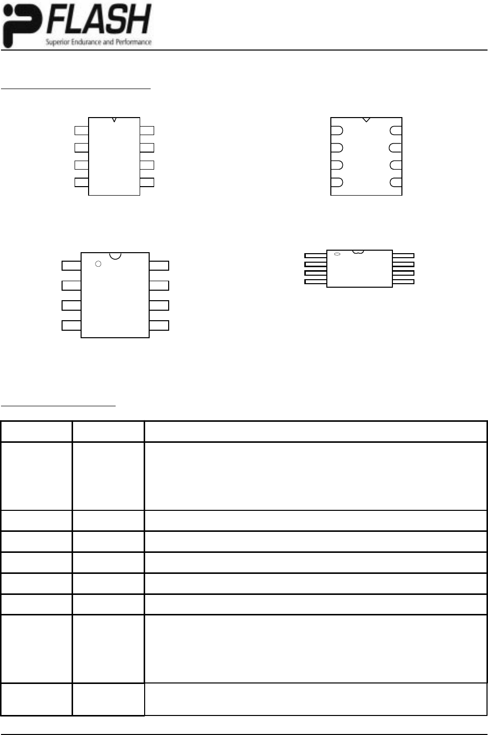
• Industrial Standard Pin-out and Package
- 8-pin 150mil SOIC
- 8-pin 208mil SOIC for Pm25LV040
- 8-pin 300mil PDIP for Pm25LV040
- 8-contact WSON
- 8-pin TSSOP for Pm25LV512A
GENERAL DESCRIPTION
The Pm25LV512A/010A/020/040 are 512Kbit/1 Mbit/2 Mbit/4 Mbit 3.0 Volt-only Serial Peripheral Interface (SPI)
Flash memories. The devices are designed to support 33 MHz fastest clock rate in the industry in normal read
mode, 100 MHz in fast read mode and the bottom 4 Kbyte sector into four smaller 1 Kbyte sectors features(except
Pm25LV512A). The devices use a single low voltage, ranging from 2.7 Volt to 3.6 Volt, power supply to perform
read, erase and program operations. The devices can be programmed in standard EPROM programmers as well.
The Pm25LV512A/010A is backward compatible to their predecessors Pm25LV512/010.
The Pm25LV512A/010A/020/040 are accessed through a 4-wire SPI Interface consists of Serial Data Input (Sl),
Serial Data Output (SO), Serial Clock (SCK), and Chip Enable (CE#) pins. The devices support page program
mode, 1 to 256 bytes data can be programmed into the memory in one program operation. The memory of
Pm25LV512A/010A is divided into uniform 4 Kbyte sectors or uniform 32 Kbyte blocks (sector group - consists of
eight adjacent sectors) for data or code storage. The memory of Pm25LV020/040 are divided into uniform 4 Kbyte
sectors or uniform 64 Kbyte blocks (sector group - consists of sixteen adjacent sectors). The devices have an
innovative feature to configure the bottom 4 Kbyte sector into four smaller 1 Kbyte sectors for eliminating additional
serial EEPROM needed for storing data. This is a further cost reduction for overall system.
The Pm25LV512A/010A/020/040 are manufactured on pFLASH™’s advanced nonvolatile technology. The devices
are offered in 8-pin SOIC, 8-contact WSON and 8-pin PDIP (Pm25LV040) packages with operation frequency up to
100 MHz in fast read and 33 MHz in normal read mode.
Chingis Technology Corporation 1Issue Date: Feb., 2009, Rev: 3.5
Pm25LV512A / 010A / 020 / 040
2
Chingis Technology Corporation Issue Date: Feb., 2009, Rev: 3.5
Pm25LV512A/010A/020/040
PIN DESCRIPTIONS
SYMBOL TYPE DESCRIPTION
CE# INPUT
Chip Enable: CE# goes low activates the devices internal circuitries for
device operation. CE# goes high deselects the devices and switches into
standby mode to reduce the power consumption. When the devices are not
selected, data will not be accepted via the serial input pin (Sl), and the
serial output pin (SO) will remain in a high impedance state.
SCK INPUT Serial Data Clock
SI INPUT Serial Data Input
SO OUTPUT Serial Data Output
GND Ground
Vcc Device Power Supply
WP# INPUT
Write Protect: A hardware program/erase protection for all or partial of
memory array. When the WP# pin is pulled to low, whole or partial of
memory array is write protected depends on the setting of BP2, BP1 and
BP0 bits in the Status Register. When the WP# is pulled high, the devices
are not write protected.
HOLD# INPUT Hold: Pause serial communication with the master device without resetting
the serial sequence.
CONNECTION DIAGRAMS
8-Pin SOIC
5
6
7
81
2
3
4
Vcc
HOLD#
SCK
SI
SO
GND
WP#
CE#
5
6
7
81
2
3
4
Vcc
HOLD#
SCK
SI
SO
GND
WP#
CE#
8-Contact WSON
5
6
7
81
2
3
4
Vcc
HOLD#
SCK
SI
SO
GND
WP#
CE#
8-Pin PDIP
5
6
7
81
2
3
4
Vcc
HOLD#
SCK
SI
SO
GND
WP#
CE#
8-Pin TSSOP
3
Chingis Technology Corporation Issue Date: Feb., 2009, Rev: 3.5
Pm25LV512A/010A/020/040
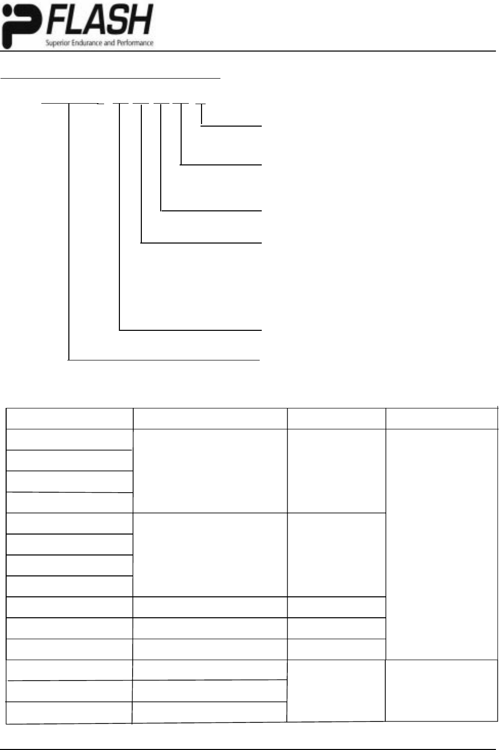
PRODUCT ORDERING INFORMATION
Pm25LVxxxA -100 S C E R
Temperature Range
C = Commercial (-40°C to +105°C)
Package Type
S = 8-pin SOIC 150 mil (8S)
B = 8-pin SOIC 208 mil (8B)
K = 8-contact WSON (8K)
P = 8-pin PDIP 300 mil (8P)
D = TSSOP (8D)
Operating Frequency
-100 : 33MHz normal read, 100MHz fast read
Device Number
Pm25LV512A/010A/020/040
Environmental Attribute
E = Lead-free/RoHS compliance package
Blank = Standard package
Packing Type
R = Tape & Reel
Blank = Tube
Part Number
Pm25LV512A-100SCE
Pm25LV010A-100SCE
Pm25LV020-100SCE
Pm25LV040-100SCE
Operating Frequency (MHz) Package
8S 150mil SOIC
100
8Q WSON
Pm25LV512A-100KCE
Pm25LV010A-100KCE
Pm25LV020-100KCE
Pm25LV040-100KCE
100
Pm25LV040-100BCE
Pm25LV040-100PCE
Pm25LV512A-100DCE
100
100
100
8B 208mil SOIC
8P 300mil PDIP
8D TSSOP
Commercial
(-40oC to +105oC)
Temperature Range
Pm25LV512A-100WC
Commercial
(-40oC to 105oC)
KGD
100
100
100
Pm25LV010A-100WC
Pm25LV020-100WC
4
Chingis Technology Corporation Issue Date: Feb., 2009, Rev: 3.5
Pm25LV512A/010A/020/040
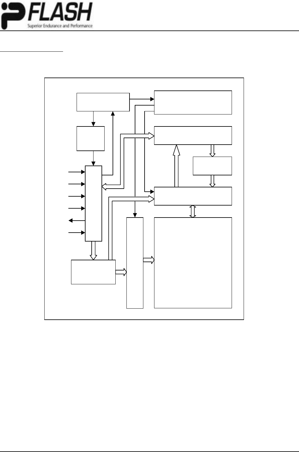
BLOCK DIAGRAM
Hi
g
h Volta
g
e GeneratorControl Lo
g
ic
I/O Buffers and
Data Latches
Address Latch
& Counter
256 B
y
tes
Pa
g
e Buffer
Status
Re
g
ister
Memor
y
Arra
y
X-DECODER
Y-DECODER
Serial Peripheral Interface
CE#
WP#
SCK
SI
SO
HOLD#
5
Chingis Technology Corporation Issue Date: Feb., 2009, Rev: 3.5
Pm25LV512A/010A/020/040
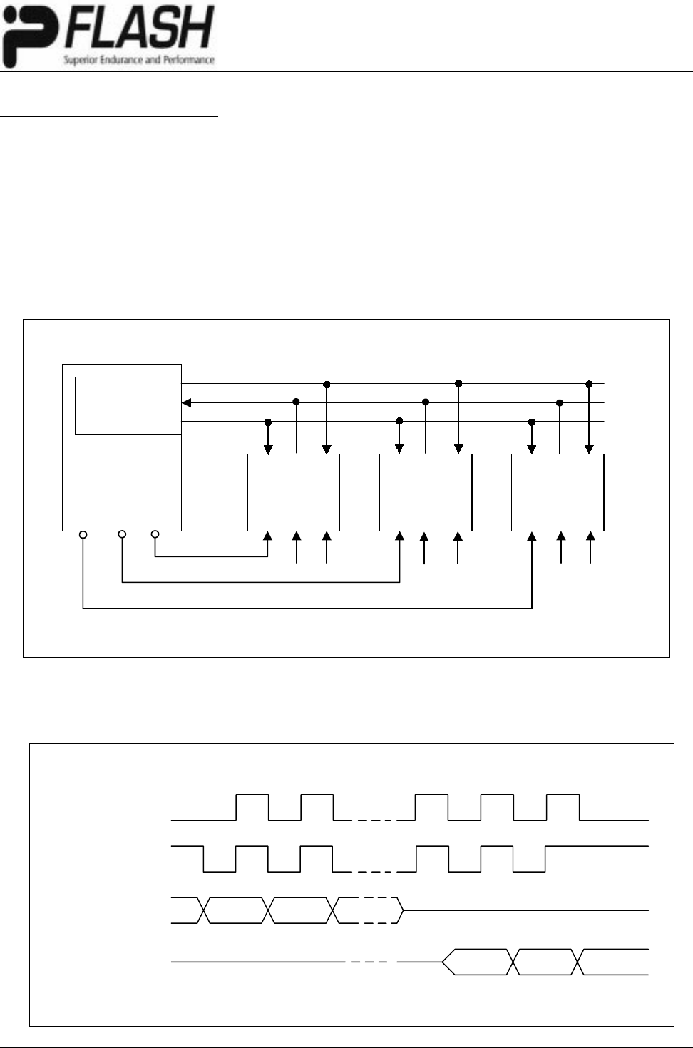
Multiple Pm25LV512A/010A/020/040 devices can be se-
rially connected onto the SPI serial bus controlled by a
SPI Master i.e. microcontroller as shown in Figure 1.
The devices support either of the two SPI modes:
Mode 0 (0, 0)
Mode 3 (1, 1)
SPI MODES DESCRIPTION
SPI Interface with
(0, 0) or (1, 1)
SDO
SDI
SCK
SCK SO SI
SPI Master
(i.e. Microcontroller)
CS3 CS2 CS1
CE# WP# HOLD# HOLD# HOLD#
SPI Memory
Device SPI Memory
Device SPI Memory
Device
Note: 1. The Write Protect (WP#) and Hold (HOLD#) si
g
nals should be driven, Hi
g
h or Low as appropriate.
SCK SO SI SCK SO SI
CE# WP# CE# WP#
Figure 1. Connection Diagram among SPI Master and SPI Slaves (Memory Devices)
The difference between these two modes is the clock
polarity when the SPI master is in Stand-by mode: the
serial clock remains at “0” (SCK = 0) for Mode 0 and the
clock remains at “1” (SCK = 1) for Mode 1. Please refer
to Figure 2. For both modes, the input data is latched on
the rising edge of Serial Clock (SCK), and the output
data is available from the falling edge of SCK.
Figure 2. SPI Modes Supported
SCK
SCK
SI
SO
Mode 0 (0, 0)
Mode 3 (1, 1)
MSB
MSB
6
Chingis Technology Corporation Issue Date: Feb., 2009, Rev: 3.5
Pm25LV512A/010A/020/040
REGISTERS
The Pm25LV512A/010A/020/040 are designed to inter-
face directly with the synchronous Serial Peripheral In-
terface (SPI) of Motorola MC68HCxx series of
microcontrollers or all the SPI interface equipped sys-
tem controllers.
The devices have two superset features can be enabled
through the specific software instructions and Configu-
ration Register:
1. Configurable sector size: The memory array of
Pm25LV512A/010A are divided into uniform 4 Kbyte
sectors or uniform 32 Kbyte blocks (sector group -
consists of eight adjacent sectors). The memory ar-
ray of Pm25LV020/040 are divided into uniform 4
Kbyte sectors or uniform 64 Kbyte blocks (sector
group - consists of sixteen adjacent sectors).
Bit 7 Bit 6 Bit 5 Bit 4 Bit 3 Bit 2 Bit 1 Bit 0
X X X SP0_3 SP0_2 SP0_1 SP0_0 SCFG
Table 1. Configuration Register Format - Pm25LV010A/020/040
Table 2. Configuration Register Bit Definition
Bit Name Definition Read/Write
Bit 0 SCFG
Sector Configuration:
"0" indicates the bottom sector is one 4 Kbyte sector (default)
"1" indicates the bottom sector is broken down to four 1 Kbyte sectors
This feature can be implemented only when BP0,BP1&BP2 of status
register were enabled to "1" which is in protection mode.
R/W
Bit 1 SP0_0 1 Kbyte Sector 0_0 Protection:
"0" indicates sector protection is disabled (default)
"1" indicates sector protection is enabled R/W
Bit 2 SP0_1 1 Kbyte Sector 0_1Protection:
"0" indicates sector protection is disabled (default)
"1" indicates sector protection is enabled R/W
Bit 3 SP0_2 1 Kbyte Sector 0_2 Protection:
"0" indicates sector protection is disabled (default)
"1" indicates sector protection is enabled R/W
Bit 4 SP0_3 1 Kbyte Sector 0_3 Protection:
"0" indicates sector protection is disabled (default)
"1" indicates sector protection is enabled R/W
Bit 5 - 6 RES Reserved for future (don't care) N/A
Bit 7 RES Reserved for future (don't use) N/A
2. The Pm25LV010A/020/040 have an option to config-
ure the 4 Kbyte bottom sector (Sector 0) into four 1
Kbyte smaller sectors (Sector 0_0, Sector 0_1, Sec-
tor 0_2 and Sector 0_3). The finer granularity sector
size architecture allows user to update data more
efficiently. This feature allows user to eliminate the
need of addtional serial EEPROM.
Refer to Table 1 for Configuration Register and Table 2
for Configuration Register Bit Definition.

7
Chingis Technology Corporation Issue Date: Feb., 2009, Rev: 3.5
Pm25LV512A/010A/020/040
REGISTERS (CONTINUED)
CONFIGURATION REGISTER (Pm25LV010A/020/ 040)
The Configuration Register is built by latchs need to be
set each time after power-up before enabling the 1 Kbyte
smaller sector size and 1 Kbyte sector write protection.
The Bit 0 - Bit 7 of Configuration Register are set as “0”s
after power-up reset. Therefore, the devices will be al-
ways set as normal mode - the bottom sector set as 4
Kbyte by default after power-up to maintain the back-
ward-compatibility.
The function of Configuration Register is described as
following:
SCFG bit: The 1 Kbyte smaller sector mode is enabled
by writing “1” to SCFG bit, then Sector 0 is configured
as Sector 0_0, Sector 0_1, Sector 0_2 and Sector 0_3.
A Sector Erase (SECTOR_ER) instruction can be used
to erase any one of those four 1 Kbyte sectors. The
SCFG bit will be reset “0” state automatically at power
on stage. Thus, the 1 Kbyte smaller sector mode is
disabled at power on till SCFG bit was set.
The SCFG bit only can be enabled to “1” when BP0,
BP1&BP2 of status register were “1” state which in pro-
tection mode. On the other word, SCFG bit will be cleared
to “0” state when BPx were “0” to disable the protection
mode.
SP0_x bits: The write protection to those four 1 Kbyte
sectors can be activated by writing “1”s to the SP0_0,
SP0_1, SP0_2 and SP0_3 bits. The 1 Kbyte sector write
protection function can only be enabled when the SCFG
is also enabled.
The Write Configuration Register (WRCR) instruction can
be used to write “0”s or “1”s into Configuration Register.
And the Read Configuration Register (RDCR) instruc-
tion can be used to read the setting of Configuration
Register. Refer to Table 8 for Instruction Set.
STATUS REGISTER
The Status Register contains WIP and WEL status bits
to indicate the status of the devices, the Block Protec-
tion Bits (BP0, BP1 and BP2 (Pm25LV040 only)) to
define the portion of memory blocks to be write protected,
The BP0, BP1, BP2, and SRWD are non-volatile memory
cells that can be written by Write Status Register (WRSR)
instruction. The default value of BP0, BP1, BP2, and
SRWD bits were set as “0” at factory. Once those bits
are written as “0” or “1”, it will not be changed by devices
power-up or power-down until next WRSR instruction al-
ters its value. The Status Register can be read by Read
Status Register (RDSR) instruction for its value and sta-
tus. Refer to Table 8 for Instruction Set.
The function of Status Register is described as following:
WIP bit: The Write In Progress (WIP) bit can be used to
detact the progress or completion of program or erase
operation. When WIP bit is “0”, the devices are ready for
write status register, program or erase operation. When
WIP bit is “1”, the devices are busy.
WEL bit: The Write Enable Latch (WEL) bit indicates
the status of internal write enable latch. When WEL bit
is “0”, the write enable latch is disabled, all write opera-
tions include write status register, write configuration reg-
ister, page program, sector erase, block and chip erase
operations are inhibited. When WEL bit is “1”, the write
enable latch is enabled. Then write operations are allowed.
The WEL bit is enabled by Write Enable (WREN) instruc-
tion. All write register, program and erase instructions
must be preceded by a WREN instruction every time.
The WEL bit can be disabled by Write Disable (WRDI)
instruction or automatically return to reset state after the
completion of a write instruction.
BP2, BP1, BP0 bits: The Block Protection (BP2
(Pm25LV040 only), BP1, BP0) bits are used to define
the portion of memory area to be protected. Refer to Table
5 and Table 6 Block Write Protection Bits Setting for
Pm25LV512A/010A/020 and Pm25LV040. When one of
the combination of BP2, BP1 and BP0 bits were set as
“1”, the relevant memory area is protected. Any program
or erase operation to that area will be prohibited.
Especially, the Chip Erase (CHIP_ER) instruction is ex-
ecuted only if all the Block Protection Bits are set as
“0”s.
If SCFG bit was enabled to support 1KB x4 sectores on
Sector 0, Sector 0’s protection status will respect SP0_x
in Configuration Register and ignore BPx bits status
whatever protection status.
and SRWD control bits to be set for status register write
protection. Refer to Table 3 and Table 4 for Status Reg-
ister Format and Status Register Bit Definition.
8
Chingis Technology Corporation Issue Date: Feb., 2009, Rev: 3.5
Pm25LV512A/010A/020/040
Table 4. Status Register Bit Definition
Bit 7 Bit 6 Bit 5 Bit 4 Bit 3 Bit 2 Bit 1 Bit 0
SRWD 0 0 BP2 BP1 BP0 WEL WIP
Table 3. Status Register Format
REGISTERS (CONTINUED)
Table 5. Block Write Protect Bits for Pm25LV512A/010A/020
SRWD bit: The Status Register Write Disable (SRWD)
bit is operated in conjuction with the Write Protection
(WP#) signal to provide a Hardware Protection Mode.
When the SRWD is set to “0”, the Status Register is not
write protected. When the SRWD is set to “1” and the
WP# is pulled low (VIL), the non-volatile bits of Status
Register (SRWD, BP2, BP1, BP0) become read-only
and the WRSR instruction will be prohibited. If the SRWD
is set to “1” but WP# is pulled high (VIH), the Status
Register is still changeable by WRSR instruction.
Bit Name Definition Read-
/Write Non-Volatile
bit
Bit 0 WIP Write In Progress Bit:
"0" indicates the device is ready
"1" indicates the write cycle is in progress and the device is busy RNo
Bit 1 WEL Write Enable Latch:
"0" indicates the device is not write enabled (default)
"1" indicates the device is write enabled R/W No
Bit 2 BP0 Block Protection Bit: (See Table 5 and Table 6 for details)
"0" indicates the specific blocks are not write protected (default)
"1" indicates the specific blocks are write protected R/W Yes
Bit 3 BP1
Bit 4 BP2
Bits 5 - 6 N/A Reserved: Always "0"s N/A
Bit 7 SRWD Status Register Write Disable: (See Table 7 for details)
"0" indicates the Status Register is not write protected (default)
"1" indicates the Status Register is write protected R/W Yes
BP1 BP0 Pm25LV512A Pm25LV010A Pm25LV020
0 0 None None None
0 1 None Upper quarter (Block 3)
018000h - 01FFFFh
Upper quarter (Block 3)
030000h - 03FFFFh
1 0 None Upper half (Block 2 & 3)
010000h - 01FFFFh
Upper half (Block 2 & 3)
020000h - 03FFFFh
11 All Blocks
000000h - 00FFFFh
All Blocks
000000h - 01FFFFh
All Blocks
000000h - 03FFFFh
Status Register Bits Protected Memory Area
9
Chingis Technology Corporation Issue Date: Feb., 2009, Rev: 3.5
Pm25LV512A/010A/020/040
Status Register Bits Protected Memory Area
BP2 BP1 BP0 Pm25LV040
000 None
0 0 1 Upper eighth (Block 7): 070000h - 07FFFFh
0 1 0 Upper quarter (Block 6 and 7): 060000h - 07FFFFh
0 1 1 Upper half (Block 4 and 7): 040000h - 07FFFFh
100
All Blocks (Block 0 to 7):
000000h - 03FFFFh
10 1
110
111
Table 6. Block Write Protect Bits for Pm25LV040
REGISTERS (CONTINUED)
PROTECTION MODE
The Pm25LV512A/010A/020/040 have two protection
modes: hardware write protection and software write pro-
tection to prevent any irrelevant operation under a pos-
sible noisy environment and protect the data integrity.
HARDWARE WRITE PROTECTION
The devices provide two hardware write protection
features:
a. When input program instruction, the input clock pulses
must be 32 clock pulses for command and address,
and a multiple of eight for 1 to 256 of data before
execution of programming. Other write instrucstion
must fit in with the number of clock pulse what the
instruction requirement before the execution. Any
incomplete instruction command sequence will be
ignored.
b. Write inhibit is 2.1V, all write sequence will be ig-
nored when Vcc drop to 2.1V and lower.
c. The devices feature a Write Protection (WP#) pin to
provide a hardware write protection method for BP2,
BP1,BP0 abd SRWD in the Status Register.
(1)When the WP# is pulled low (VIL), the Status
Register is write protected if the SRWD bit is enabled
(Refer to Table 7 for Hardware Write Protection on
Status Register). Hence part or whole memory area
can be write protected depends on the setting of BP2,
BP1 and BP0 bits.
(2) When the WP# is pulled high (VIH), the Status
Register is not protected, BP2,BP1,BP0 and SRWD
can be changed.
SOFTWARE WRITE PROTECTION
The Pm25LV512A/010A/020/040 also provide two soft-
ware write protection features:
a. Before the execution of any program, erase or write
status register instruction, the Write Enable Latch
(WEL) bit must be enabled by execution of the Write
Enable (WREN) instruction. If the WEL bit is not en-
abled first, the program, erase or write register in-
struction will be ignored.
b. The Block Protection (BP2, BP1, BP0) bits allow part
or whole memory area to be write protected.
SRWD WP# Status Register
0 Low Writable
1 Low Protected
0High Writable
1High Writable
Table 7. Hardware Write Protection on Status
Register
10
Chingis Technology Corporation Issue Date: Feb., 2009, Rev: 3.5
Pm25LV512A/010A/020/040
The Pm25LV512A/010A/020/040 utilize an 8-bit instruc-
tion register. Refer to Table 8 Instruction Set for the de-
tail Instructions and Instruction Codes. All instructions,
addresses, and data are shifted in with the most signifi-
cant bit (MSB) first on Serial Data Input (SI). The input
data on SI is latched on the rising edge of Serial Clock
(SCK) after the Chip Enable (CE#) is driven low (VIL).
Table 8. Instruction Set
DEVICE OPERATION
Every instruction sequence starts with a one-byte in-
struction code and might be followed by address bytes,
data bytes, or address bytes and data bytes depends
on the type of instruction. The CE# must be driven high
(VIH) after the last bit of the instruction sequence has
been shifted in.
HOLD OPERATION
The HOLD# is used in conjunction with the CE# to se-
lect the Pm25LV512A/010A/020/040. When the devices
are selected and a serial sequence is underway, HOLD#
can be used to pause the serial communication
with the master device without resetting the serial
sequence. To pause, the HOLD# must be brought low
while the SCK signal is low. To resume serial communi-
cation, the HOLD# is brought high while the SCK signal
is low (SCK may still toggle during HOLD). Inputs to the
Sl will be ignored while the SO is in the high impedance
state.
Instruction Name Instruction Format Hex Code Operation
WREN 0000 0110 06h Write Enable
WRDI 0000 0100 04h Write Disable
RDSR 0000 0101 05h Read Status Register
WRSR 0000 0001 01h Write Status Register
READ 0000 0011 03h Read Data Bytes from Memory at Normal Read Mode
FAST_READ 0000 1011 0Bh Read Data Bytes from Memory at Fast Read Mode
RDID 1010 1011 ABh Read Manufacturer and Product ID
JEDEC ID READ*1 1001 1111 9Fh Read Manufacturer and Prduct ID by JEDEC ID Command
PAGE_ PROG 0000 0010 02h Page Program Data Bytes Into Memory
RDCR 1010 0001 A1h Read Configuration Register
WRCR 1111 0001 F1h Write Configuration Register
SECTOR_ER 1101 0111 D7h Sector Erase
BLOCK_ER 1101 1000 D8h Block Erase
CHIP_ER 1100 0111 C7h Chip Erase
11
Chingis Technology Corporation Issue Date: Feb., 2009, Rev: 3.5
Pm25LV512A/010A/020/040
01 8 31 38 39 46 47 54
HIGH IMPEDANCE Manufacture ID1 Device ID Manufacture ID2
SCK
CE#
SI
SO
INSTRUCTION
97
1010 1011b
3 Dummy Bytes
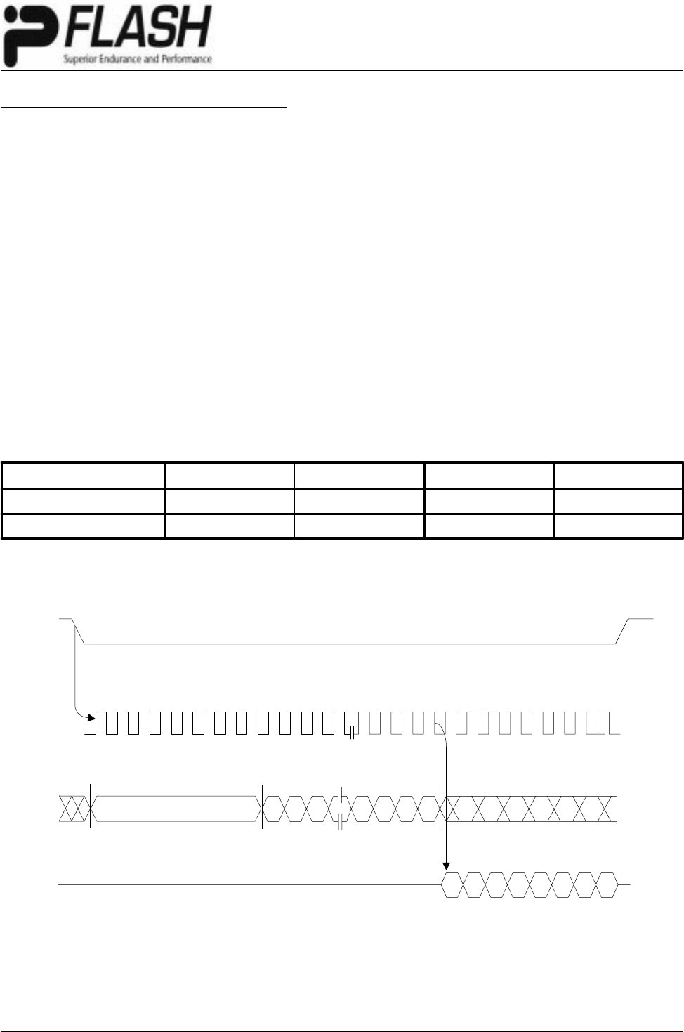
Figure 3. Read Product Identification Sequence
DEVICE OPERATION (CONTINUED)
Product Identification Data
Manufacturer ID First Byte 9Dh
Second Byte 7Fh
Device ID:
Pm25LV512A 7Bh
Pm25LV010A 7Ch
Pm25LV020 7Dh
Pm25LV040 7Eh
Table 9. Product Identification
READ PRODUCT IDENTIFICATION OPERATION
The Read Product Identification (RDID) instruction al-
lows the user to read the manufacturer and product ID of
the devices. Refer to Table 9 Product Identification for
pFLASH™ manufacturer ID and device ID. The RDID in-
struction code is followed by three dummy bytes, each
bit being latched-in on SI during the rising edge of SCK.
Then the first manufacturer ID (9Dh) is shifted out on SO
with the MSB first, followed by the device ID and the
second manufacturer ID (7Fh), each bit been shifted out
during the falling edge of SCK. If the CE# stays low after
the last bit of second manufacturer ID is shifted out, the
manufacturer ID and device ID will be looping until the
pulled high of CE# signal.
12
Chingis Technology Corporation Issue Date: Feb., 2009, Rev: 3.5
Pm25LV512A/010A/020/040
DEVICE OPERATION (CONTINUED)
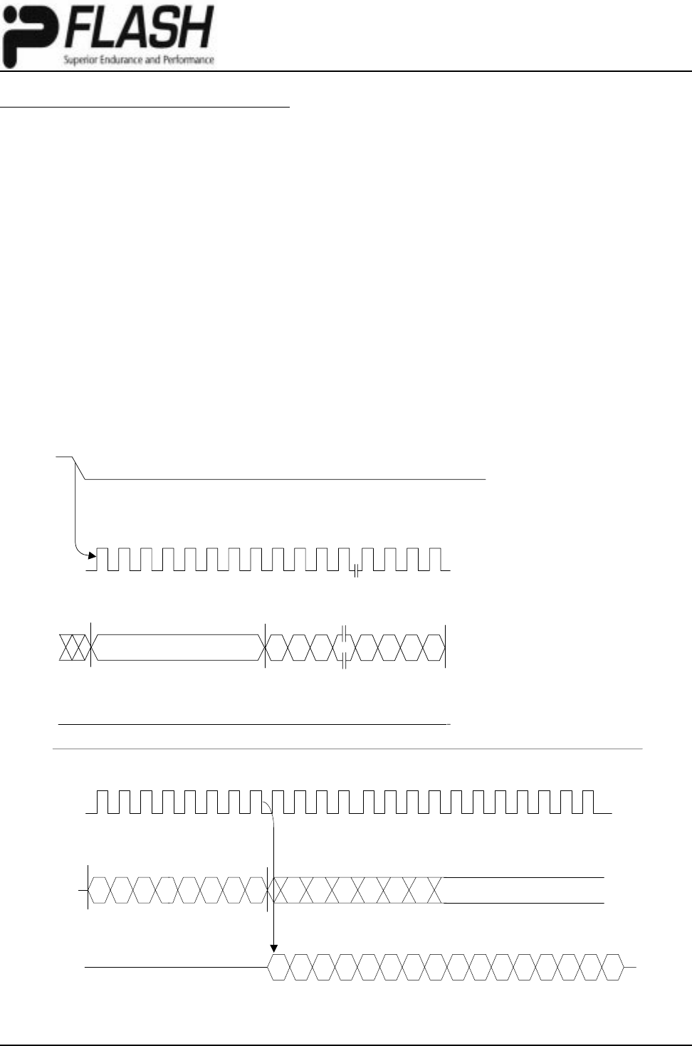
READ PRODUCT IDENTIFICATION BY JEDEC ID
COMMAND
The JEDEC ID READ instruction allows the user to read
the manufacturer and product ID of the devices. Refer to
Table 9 Product Identification for pFLASH™ manufac-
turer ID and device ID. The second manufacturer ID (7Fh)
is shifted out on SO with the MSB first after JEDEC ID
READ command input, followed by the first manufac-
turer ID (9Dh) and the device ID, each bit been shifted
out during the falling edge of SCK.
If the CE# stays low after the last bit of device ID is
shifted out, the manufacturer ID and device ID will be loop-
ing until the pulled high of CE# signal.
Pm25LV512A do not support this JEDEC ID READ
instruction.
Figure 4. Read Product Identification by JEDEC ID READ Sequence
SCK
CE#
SI
INSTRUCTION
1001 1111b
0815 23 24 31
716
HIGH IMPEDANCE
SO Device IDManufacture ID1Manufacture ID2
13
Chingis Technology Corporation Issue Date: Feb., 2009, Rev: 3.5
Pm25LV512A/010A/020/040
DEVICE OPERATION (CONTINUED)
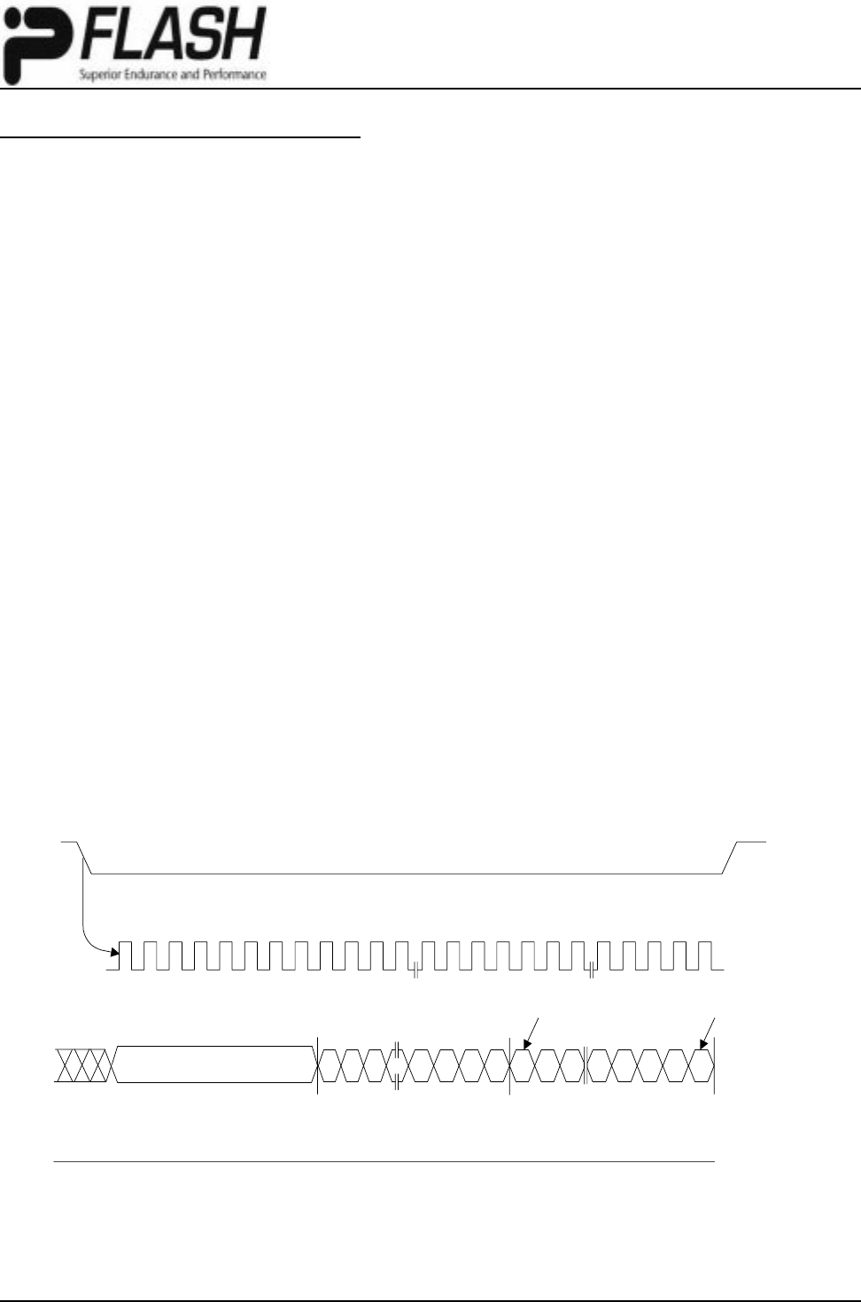
WRITE ENABLE OPERATION
The Write Enable (WREN) instruction is used to set the
Write Enable Latch (WEL) bit. The WEL bit of the
Pm25LV512A/010A/020/040 are set as write disable state
after power-up. The WEL bit must be write enabled be-
fore any write operation includes sector, block and
WRITE DISABLE OPERATION
To protect the device against inadvertent writes, the Write
Disable (WRDI) instruction resets the WEL bit and dis-
ables all write instructions. The WRDI instruction is not
SCK
SI
SO
INSTRUCTION = 0000 0110b
HI-Z
CE#
Figure 5. Write Enable Sequence
Figure 6. Write Disable Sequence
CE#
SCK
SI
SO
INSTRUCTION = 0000 0100b
HI-Z
chip erase, page program, write status register, and write
configuration register operations. The WEL bit will be
reset back to write disable state automatically after the
completion of a write operation. The WREN instruction
is required before any above instruction is executed.
required after the execution of a write instruction. The
WEL will be automatically reset.
14
Chingis Technology Corporation Issue Date: Feb., 2009, Rev: 3.5
Pm25LV512A/010A/020/040
DEVICE OPERATION (CONTINUED)
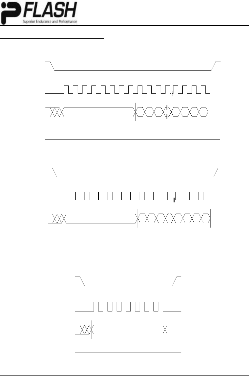
WRITE STATUS REGISTER OPERATION
The Write Status Register (WRSR) instruction allows
the user to enable or disable the block protection and
status register write protection features by writting “0”s
0 1 2 3 5 6 7 8 9 10 11 12 13 14415
7654 32
10
DATA IN
INSTRUCTION = 0000 0001b
HIGH IMPEDANCE
CE#
SCK
SI
SO
Figure 8. Write Status Register Sequence
or “1”s into those non-volatile BP2, BP1, BP0 and SRWD
bits. The erase operation for those non-volatile bits are
not required.
READ STATUS REGISTER OPERATION
The Read Status Register (RDSR) instruction provides
access to the status register. During the execution of a
program, erase or write status register operation, all other
Figure 7. Read Status Register Sequence
CE#
SCK
SI
012 3 5678910 11 12 13 14
4
INSTRUCTION = 0000 0101b
SO 76543210
HIGH IMPEDANCE
DATA OUT
MSB
15
instructions will be ignored except the RDSR instruction
can be used for detecting the progress or completion of
the operations by reading the WIP bit of status register.

15
Chingis Technology Corporation Issue Date: Feb., 2009, Rev: 3.5
Pm25LV512A/010A/020/040
DEVICE OPERATION (CONTINUED)
0 1 2 3 5 6 7 8 9 10 11 12 13 14415
765 4321
0
DATA IN
INSTRUCTION = 1111 0001b
HIGH IMPEDANCE
CE#
SCK
SI
SO
Figure 10. Write Configuration Register Sequence
The Read Configuration Register (RDCR) instruction pro-
vides access to the Configuration Register. This instruc-
tion can be used to verify the configuration setting of
Figure 9. Read Configuration Register Sequence
CE#
SCK
SI
012 3 5678910 11 12 13 14
4
INSTRUCTION = 1010 0001b
SO 76543210
HIGH IMPEDANCE
DATA OUT
MSB
15
bottom Sector 0 and the write protection setting for each
individual 1 Kbyte sector (Sector 0_0 ~ Sector 0_3) within
the Sector 0.
READ CONFIGURATION REGISTER OPERATION
WRITE CONFIGURATION REGISTER OPERATION
The Write Configuration Register (WRCR) instruction al-
lows user to enable or disable four smaller 1K byte
sectors and protection for each 1K byte sector by writ-
ing “0”s or “1”s into SCFG and SP0_3 ~SP0_1 in the
congiguration register. please refer table 2 for details.
Do not require WREN command before this WRCR
operation. Because Configuration Register is a data latch
architecture.
16
Chingis Technology Corporation Issue Date: Feb., 2009, Rev: 3.5
Pm25LV512A/010A/020/040
READ DATA OPERATION
The Read Data (READ) instruction is used to read memory
data of Pm25LV512A/010A/020/040 under normal mode
running up to 33 MHz.
The READ instruction is activated by pulling the CE#
line of the selected device to low (VIL), and the READ
instruction code is transmitted via the Sl line followed by
three bytes address (A23 - A0) to be read. There are
total 24 address bits will be shifted in, only the AMS (most-
significant address) - A0 will be decoded and the rest of
A23 - AMS can be don’t cared. Refer to Table 10 for the
related Address Key. Upon completion, any data on the
Sl will be ignored.
Figure 11. Read Data Sequence
0 1 2 3 4 5 6 7 8 9 10 11 28 29 30 31 32 33 34 3635 37 38
...
23 22 21 3 2 1 0
76543210
3-BYTE ADDRESS
INSTRUCTION = 0000 0011b
HIGH IMPEDANCE
CE#
SCK
SI
SO
39
Address Pm25LV512A Pm25LV010A Pm25LV020 Pm25LV040
ANA15 - A0 A16 - A0 A17 - A0 A18 - A0
Don't Care Bits A23 - A16 A23 - A17 A23 - A18 A23 - A19
Table 10. Address Key
The first byte data D7 - D0 addressed (can be at any
location) is then shifted out onto the SO line. A single
byte data or up to whole memory array can be read out
in one READ instruction. The address is automatically
increamented to the next higher address after each byte
of data is shifted out. The read operation can be termi-
nated any time by driving the CE# high (VIH) after the
data comes out. When the highest address of the de-
vices is reached, the address counter will roll over to the
000000h address allowing the entire memory to be read
in one continuous READ instruction.
DEVICE OPERATION (CONTINUED)
17
Chingis Technology Corporation Issue Date: Feb., 2009, Rev: 3.5
Pm25LV512A/010A/020/040
FAST READ DATA OPERATION
The Pm25LV512A/010A/020/040 also feature a Fast
Read (FAST_READ) instruction. This FAST_READ in-
struction is used to read memory data in 100 MHz clock
rate where the FAST_READ instruction proceeding.
The devices are first selected by driving CE# low (VIL).
The FAST_READ instruction code followed by three bytes
address (A23 - A0) and a dummy byte (8 clocks) is
trasmitted via the SI line, each bit being latched-in dur-
ing the rising edge of SCK. Then the first data byte
DEVICE OPERATION (CONTINUED)
Figure 12. Fast Read Data Sequence
0 1 2 3 4 5 6 7 8 9 10 11 28 29 30 31
...
23 22 21 3 2 1 0
3-BYTE ADDRESS
INSTRUCTION = 0000 1011b
HIGH IMPEDANCE
CE#
SCK
SI
SO
addressed is shifted out on SO line, each bit being shifted
out at a maximum frequency fCT, during the falling edge
of SCK.
The first byte addressed can be at any location. The
address is automatically incremented to the next higher
address after each byte of data is shifted out. When the
highest address is reached, the address counter will roll
over to the 000000h address allowing the entire memory
to be read with a single FAST_READ instruction. The
FAST_READ instruction is terminated by driving CE#
high (VIH).
32 33 34 35 36 37 38 39 40 41 42 43 44 45 46 47
765 30
76543210
HIGH IMPEDANCE
CE#
SCK
SI
SO
4 1
76543210
2
DATA OUT 1 DATA OUT 2
DUMMY BYTE
48
18
Chingis Technology Corporation Issue Date: Feb., 2009, Rev: 3.5
Pm25LV512A/010A/020/040
DEVICE OPERATION (CONTINUED)
PAGE PROGRAM OPERATION
The Page Program (PAGE_PROG) instruction allow up
to 256 bytes data to be programmed into memory in one
program operation page by page. The destination of the
memory to be programmed must be outside the pro-
tected memory area set by the Block Protection (BP2,
BP1, BP0) bits. A PAGE_PROG instruction attemps to
program into a page which is write protected will be
ignored. Before the execution of PAGE_PROG
instruction, the Write Enable Latch (WEL) must be en-
abled through a Write Enable (WREN) instruction.
The PAGE_PROG instruction is activated, after the CE#
is pulled low to select the device and staying low during
the entire instruction sequence, by shifting in the
PAGE_PROG instruction code, three address bytes and
program data (1 to 256 bytes) to be programmed via the
Sl line. Program operation will start immediately after
the CE# is driven high. Chip Select (CE#) must be driven
high after the eighth bit of last data byte has been latch
in, otherwise the PAGE_PROG instruction will not be
executed.
The internal control logic automatically handles the pro-
gramming voltages and timing. During a program
operation, all instructions will be ignored except the
RDSR instruction. The progress or completion of the pro-
gram operation can be determined by reading the WIP
bit in Status Register through a RDSR instruction. If WIP
bit = “1”, the program operation is still in progress. If WIP
bit = “0”, the program operation has completed.
A single PAGE_PROG instruction programs 1 to 256
consecutive bytes within a page if it is not write protected.
If more than 256 bytes data are sent to the devices, the
address counter will roll over on the same page and the
previously latched data are discarded and the last 256
bytes data are kept to be programmed into the page.
The starting byte can be anywhere within the same page.
When the end of the page is reached, the address will
wrap around to the beginning of the same page. If the
data to be programmed are less than a full page, the
data of all other bytes on the same page will remain
unchanged.
A program operation can alter “1”s into “0”s, but an erase
operation is required to change “0”s back to “1”s. The
same byte cannot be reprogrammed without erasing the
whole sector or block first.
Figure 13. Page Program Sequence
0 1 2 3 4 5 6 7 8 9 10 11 28 29 30 31 32 33 34
2075
2076
2077
2078
2079
076 532 21143023 22 21
1st BYTE DATA-IN 256th BYTE DATA-IN
3-BYTE ADDRESS
INSTRUCTION = 0000 0010b
HIGH IMPEDANCE
CE#
SCK
SI
SO

19
Chingis Technology Corporation Issue Date: Feb., 2009, Rev: 3.5
Pm25LV512A/010A/020/040
ERASE OPERATION
The memory array of Pm25LV512A/010A is organized
into uniform 4 Kbyte sectors or 32 Kbyte uniform blocks
(sector group - consists of eight adjacent sectors). The
memory array of Pm25LV020/040 are organized into
uniform 4 Kbyte sectors or 64 Kbyte uniform blocks (sec-
tor group - consists of sixteen adjacent sectors). The
Pm25LV010A/020/040 of bottom sector (Sector 0) of the
devices can be configured into four 1 Kbyte smaller
sectors.
Before a byte can be reprogrammed, the sector or block
which contains this byte must be erased first. In order to
erase the devices, there are three erase instructions in-
clude Sector Erase (SECTOR_ER), Block Erase
(BLOCK_ER) and Chip Erase (CHIP_ER) instructions
can be used. A sector erase operation allows to erase
any individual sector without affecting the data in others.
A block erase operation allows to erase any individual
block. And a chip erase operation allows to erase the
whole memory array of the devices. Pre-programs the
devices are not required prior to a sector erase, block
erase or chip erase operation.
SECTOR ERASE OPERATION
A SECTOR_ER instruction erases a 4 Kbyte sector or a
1 Kbyte smaller sector (Sector 0_3, Sector 0_2, Sector
0_1, Sector 0_0) if the bottom Sector 0 has been config-
ured as four smaller sectors. Before the execution of
SECTOR_ER instruction, the Write Enable Latch (WEL)
must be enabled through a Write Enable (WREN) instruc-
tion. The WEL will be reset automatically after the
completion of sector erase operation.
The SECTOR_ER instruction is entered, after the CE#
is pulled low to select the device and staying low during
the entire instruction sequence, by shifting in the
SECTOR_ER instruction code and three address bytes
via the SI. Erase operation will start immediately after
the CE# is pulled high, otherwise the SECTOR_ER in-
struction will not be executed. The internal control logic
automatically handles the erase voltage and timing. Re-
fer to Figure 13 for Sector Erase Sequence.
During a erase operation, all instruction will be ignored
except the Read Status Register (RDSR) instruction.
The progress or completion of the erase opertion can be
determined by reading the WIP bit in Status Register
through a RDSR instruction. If WIP bit = “1”, the erase
operation is still in progress. If WIP bit = “0”, the erase
operation has been completed.
DEVICE OPERATION (CONTINUED)
BLOCK ERASE OPERATION
A Block Erase (BLOCK_ER) instruction erases a 32
Kbyte block for the Pm25LV512A/010A or a 64 Kbyte
block for the Pm25LV020/040. Before the execution of
BLOCK_ER instruction, the Write Enable Latch (WEL)
must be enabled through a Write Enable (WREN) instruc-
tion. The WEL will be reset automatically after the
completion of block erase operation.
The BLOCK_ER instruction is entered, after the CE# is
pulled low to select the device and staying low during
the entire instruction sequence, by shifting in the
BLOCK_ER instruction code and three address bytes
via the SI. Erase operation will start immediately after
the CE# is pulled high, otherwise the BLOCK_ER in-
struction will not be executed. The internal control logic
automatically handles the erase voltage and timing. Re-
fer to Figure 14 for Block Erase Sequence.
CHIP ERASE OPERATION
A Chip Erase (CHIP_ER) instruction erases the whole
memory array of Pm25LV512A/010A/020/040. Before the
execution of CHIP_ER instruction, the Write Enable Latch
(WEL) must be enabled through a Write Enable (WREN)
instruction. The WEL will be reset automatically after
the completion of chip erase operation.
The CHIP_ER instruction is entered, after the CE# is
pulled low to select the device and staying low during
the entire instruction sequence, by shifting in the
CHIP_ER instruction code via the SI. Erase operation
will start immediately after the CE# is pulled high, other-
wise the CHIP_ER instruction will not be executed. The
internal control logic automatically handles the erase
voltage and timing. Refer to Figure 15 for Chip Erase
Sequence.
20
Chingis Technology Corporation Issue Date: Feb., 2009, Rev: 3.5
Pm25LV512A/010A/020/040
Figure 15. Block Erase Sequence
Figure 16. Chip Erase Sequence
01 234 56789101128 29 30 31
0123212223
...
3-BYTE ADDRESS
INSTRUCTION = 1101 1000b
HIGH IMPEDANCE
CE#
SCK
SI
SO
01234567
HIGH IMPEDANCE
SCK
CE#
SI
SO
INSTRUCTION = 1100 0111b
0 1 2 3 4 5 6 7 8 9 10 11 28 29 30 31
0123212223
...
3-BYTE ADDRESS
INSTRUCTION = 1101 0111b
HIGH IMPEDANCE
CE#
SCK
SI
SO
Figure 14. Sector Erase Sequence
DEVICE OPERATION (CONTINUED)
21
Chingis Technology Corporation Issue Date: Feb., 2009, Rev: 3.5
Pm25LV512A/010A/020/040
Table 11. Block/Sector Addresses of Pm25LV512A/010A
Note: 1. Pm25LV010A support 1KByte small sector - Sector 0 can be configured into four smaller 1 Kbyte
sectors (Sector 0_0: 000000h - 0003FFh, Sector 0_1: 000400h - 0007FFh, Sector 0_2: 000800h -
000BFFh, and Sector 0_3: 000C00h - 000FFFh).
BLOCK/SECTOR ADDRESS
Block No. Block Size
(Kbytes) Sector No. Sector Size
(Kbytes) Address Range
Sector 0(1) 4000000h - 000FFFh
Sector 1 4001000h - 001FFFh
:: :
Sector 7 4007000h - 007FFFh
Sector 8 4008000h - 008FFFh
Sector 9 4009000h - 009FFFh
::
000000h - 006FFFh
Sector 15 400F000h - 00FFFFh
Block 2 32 ""010000h - 017FFFh
Block 3 32 ""018000h - 01FFFFh
Memory Density
1 Mbit
512 Kbit
32
32
Block 0
Block 1
22
Chingis Technology Corporation Issue Date: Feb., 2009, Rev: 3.5
Pm25LV512A/010A/020/040
Table 12. Block/Sector Addresses of Pm25LV020/040
Memory Density Block No. Block Size
(Kbytes) Sector No. Sector Size
(Kbytes) Address Range
2 Mbit
4 Mbit
Block 0 64
Sector 0 (1) 4 000000h - 000FFFh
Sector 1 4 001000h - 001FFFh
:: :
Sector 15 4 00F000h - 00FFFFh
Block 1 64
Sector 16 4 010000h - 010FFFh
Sector 17 4 011000h - 011FFFh
:: :
Sector 31 4 01F000h - 01FFFFh
Block 2 64 ""
020000h - 02FFFFh
Block 3 64 ""
030000h - 03FFFFh
Block 4 64 ""
040000h - 04FFFFh
Block 5 64 ""
050000h - 05FFFFh
Block 6 64 ""
060000h - 06FFFFh
Block 7 64 ""
070000h - 07FFFFh
Note: 1. Sector 0 can be configured into four smaller 1 Kbyte sectors (Sector 0_0: 000000h - 0003FFh, Sector
0_1: 000400h - 0007FFh, Sector 0_2: 000800h - 000BFFh, and Sector 0_3: 000C00h - 000FFFh).
BLOCK/SECTOR ADDRESS (CONTINUED)
23
Chingis Technology Corporation Issue Date: Feb., 2009, Rev: 3.5
Pm25LV512A/010A/020/040
DC AND AC OPERATING RANGE
ABSOLUTE MAXIMUM RATINGS (1)
Notes:
1. Stresses under those listed in “Absolute Maximum Ratings” may cause permanent damage
to the device. This is a stress rating only. The functional operation of the device or any other
conditions under those indicated in the operational sections of this specification is not
implied. Exposure to absolute maximum rating condition for extended periods may affected
device reliability.
2. Maximum DC voltage on input or I/O pins are VCC + 0.5 V. During voltage transitioning
period, input or I/O pins may overshoot to VCC + 2.0 V for a period of time up to 20 ns.
Minimum DC voltage on input or I/O pins are -0.5 V. During voltage transitioning period,
input or I/O pins may undershoot GND to -2.0 V for a period of time up to 20 ns.
Temperature Under Bias -65oC to +125oC
Storage Temperature -65oC to +125oC
Surface Mount Lead Soldering Temperature Standard Package 240oC 3 Seconds
Lead-free Package 260oC 3 Seconds
Input Voltage with Respect to Ground on All Pins (2) -0.5 V to VCC + 0.5 V
All Output Voltage with Respect to Ground -0.5 V to VCC + 0.5 V
VCC (2) -0.5 V to +6.0 V
Part Number Pm25LV512A/010A/020/040
Operating Temperature -40oC to +105oC
Vcc Power Supply 2.7 V - 3.6 V
24
Chingis Technology Corporation Issue Date: Feb., 2009, Rev: 3.5
Pm25LV512A/010A/020/040
DC CHARACTERISTICS
Applicable over recommended operating range from:
TAC = -40°C to +105°C, VCC = 2.7 V to 3.6 V (unless otherwise noted).
Symbol Parameter Min Typ Max Units
ICC1 Vcc Active Read Current 10 15 mA
ICC2 Vcc Pro
g
ram/Erase Current 15 30 mA
ISB1 Vcc Standby Current CMOS 10 20 uA
ISB2 Vcc Standby Current TTL 3 mA
ILI Input Leaka
g
e Current 1 uA
ILO Output Leaka
g
e Current 1 uA
VIL Input Low Volta
g
e-0.50.8V
VIH Input HI
g
h Volta
g
e0.7V
CC VCC + 0.3 V
VOL Output Low Volta
g
e I
OL = 2.1 mA 0.45 V
VOH Output Hi
g
h Volta
g
e I
OH = -100 uA VCC - 0.2 V
2.7V < VCC < 3.6V
VCC = 3.6V, CE# = VIH to VCC
VIN = 0V to VCC
VIN = 0V to VCC, TAC = 0oC to 105oC
Condition
VCC = 3.6V at 33 MHz, SO = Open
VCC = 3.6V at 33 MHz, SO = Open
VCC = 3.6V, CE# = VCC
25
Chingis Technology Corporation Issue Date: Feb., 2009, Rev: 3.5
Pm25LV512A/010A/020/040
AC CHARACTERISTICS
Applicable over recommended operating range from TA = -40°C to +105°C, VCC = 2.7 V to 3.6 V
CL = 1TTL Gate and 10 pF (unless otherwise noted).
Symbol Parameter Min Typ Max Units
fCT Clock Frequency for fast read mode 0 100 MHz
fCClock Frequency for read mode 0 33 MHz
tRI Input Rise Time 8 ns
tFI Input Fall Time 8 ns
tCKH SCK High Time 4 ns
tCKL SCK Low Time 4 ns
tCEH CE# High Time 25 ns
tCS CE# Setup Time 10 ns
tCH CE# Hold Time 5 ns
tDS Data In Setup Time 2 ns
tDH Data in Hold Time 2 ns
tHS Hold Setup Time 15 ns
tHD Hold Time 15 ns
tVOutput Valid 8 ns
tOH Output Hold Time Normal Mode 0 ns
tLZ Hold to Output Low Z 200 ns
tHZ Hold to Output High Z 200 ns
tDIS Output Disable Time 100 ns
tEC Secter/Block/Chip Erase Time 60 100 ms
tPP Page Program Time 25
ms
tWWrite Status Register Time 60 100 ms
tVCS VCC
Set-up Time 50 µs
26
Chingis Technology Corporation Issue Date: Feb., 2009, Rev: 3.5
Pm25LV512A/010A/020/040
AC CHARACTERISTICS (CONTINUED)
SERIAL INPUT/OUTPUT TIMING(1)
Note: 1. For SPI Mode 0 (0,0)
VALID IN
CE#
VIL
VIH
SCK
VIH
VIH
VOH
VIL
VIL
VOL
SI
SO
tCS
tCKH tCKL
tCEH
tDH
tDS
tVtDIS
tOH
HI-Z
HI-Z
tCH
27
Chingis Technology Corporation Issue Date: Feb., 2009, Rev: 3.5
Pm25LV512A/010A/020/040
AC CHARACTERISTICS (CONTINUED)
t
HD
t
HD
t
HS
t
HS
t
HZ
t
LZ
CE#
SCK
HOLD#
SO
HOLD TIMING
Typ Max Units Conditions
CIN 46pF V
IN = 0 V
COUT 812pF V
OUT = 0 V
PIN CAPACITANCE ( f = 1 MHz, T = 25°C )
Note: These parameters are characterized but not 100% tested.
OUTPUT TEST LOAD INPUT TEST WAVEFORMS
AND MEASUREMENT LEVEL
Vcc
1.8 K
1.3 K
OUTPUT PIN
10 pF
0.8Vcc
0.2Vcc
0.5 Vcc
AC
Measurement
Level
Input
Note: 1. Input Pulse Voltage : 0.2Vcc to 0.8Vcc.
2. Input Timing Reference Voltages :
0.3Vcc to 0.7Vcc.
3. Output Timing Reference Voltage : Vcc/2.
28
Chingis Technology Corporation Issue Date: Feb., 2009, Rev: 3.5
Pm25LV512A/010A/020/040
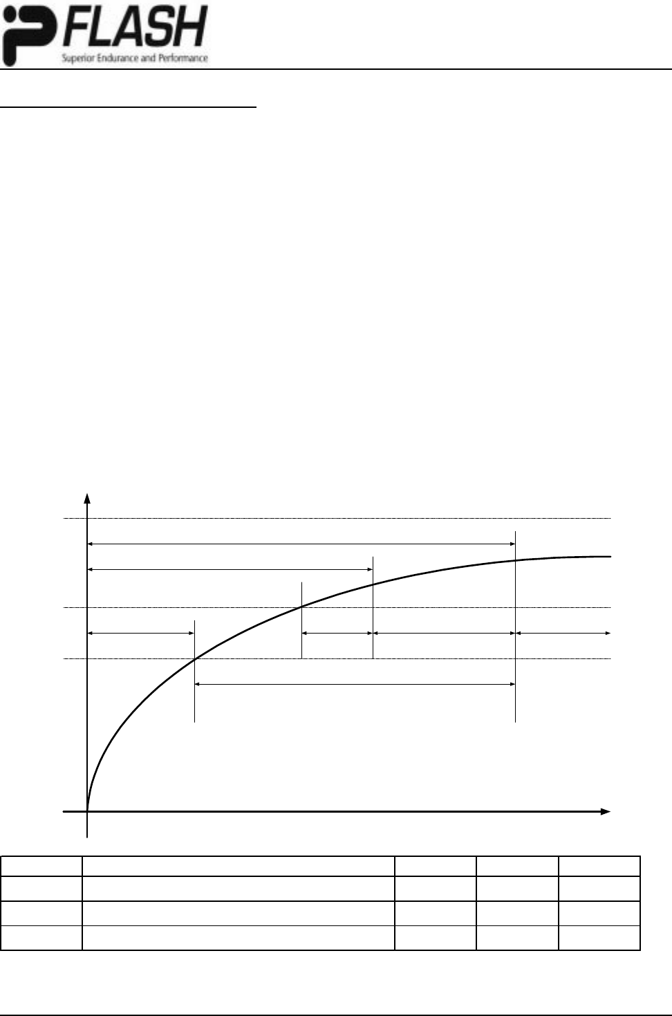
POWER-UP AND POWER-DOWN
At Power-up and Power-down, the device must not be
selected (CE# must follow the voltage applied on Vcc)
until Vcc reaches the correct value:
- Vcc(min) at Power-up, and then for a further delay of
tVCE
- Vss at Power-down
Usually a simple pull-up resistor on CE# can be used to
insure safe and proper Power-up and Power-down.
To avoid data corruption and inadvertent write operations
during power up, a Power On Reset (POR) circuit is
included. The logic inside the device is held reset while
Vcc is less than the POR threshold value (Vwi) during
power up, the device does not respond to any instruction
until a time delay of tPUW has elapsed after the moment
that Vcc rised above the VWI threshold. However, the
correct operation of the device is not guaranteed if, by
this time, Vcc is still below Vcc(min). No Write Status
Chip Selection Not Allowed
All Write Commands are Rejected
tVCE Read Access Allowed Device fully accessible
tPUW
Vcc
Vcc(max)
Vcc(min)
Reset State
V (write inhibit)
Time
Symbol Parameter Min. Max. Unit
tVCE *1 Vcc(min) to CE# Low 10 us
tPUW *1 Power-Up time delay to Write instruction 1 10 ms
VWI*1 Write Inhibit Voltage 2.1 2.3 V
Note : *1. These parameters are characterized only.
Power-up Timing
Register, Program or Erase instructions should be sent
until the later of:
- tPUW after Vcc passed the VWI threshold
- tVCE after Vcc passed the Vcc(min) level
At Power-up, the device is in the following state:
- The device is in the Standby mode
- The Write Enable Latch (WEL) bit is reset
At Power-down, when Vcc drops from the operating
voltage, to below the Vwi, all write operations are dis-
abled and the device does not respond to any write
instruction.
29
Chingis Technology Corporation Issue Date: Feb., 2009, Rev: 3.5
Pm25LV512A/010A/020/040
PROGRAM/ERASE PERFORMANCE
Parameter Unit Typ Max Remarks
Sector Erase Time ms 60 100 From writing erase command to erase completion
Block Erase Time ms 60 100 From writing erase command to erase completion
Chip Erase Time ms 60 100 From writing erase command to erase completion
Page Programming Time ms 2 5 From writing program command to program
completion
Parameter Min Typ Unit Test Method
Endurance 200,000 Cycles JEDEC Standard A117
Data Retention 20 Years JEDEC Standard A103
ESD - Human Body Model 2,000 Volts JEDEC Standard A114
ESD - Machine Model 200 Volts JEDEC Standard A115
ESD - Charged Device Model 1,000 Volts JEDEC Standard C101-A
Latch-Up 100 + ICC1 mA JEDEC Standard 78
Note: These parameters are characterized and are not 100% tested.
Note: These parameters are characterized and are not 100% tested.
RELIABILITY CHARACTERISTICS
30
Chingis Technology Corporation Issue Date: Feb., 2009, Rev: 3.5
Pm25LV512A/010A/020/040
PACKAGE TYPE INFORMATION
`
End View
5.00
4.80
Top View Side View
4.00
3.80
6.20
5.80 1.75
1.35
0.25
0.10
0.51
0.33
1.27 BSC
0.25
0.19
1.27
0.40
45º
8o
0o
0.595
0.495
8S
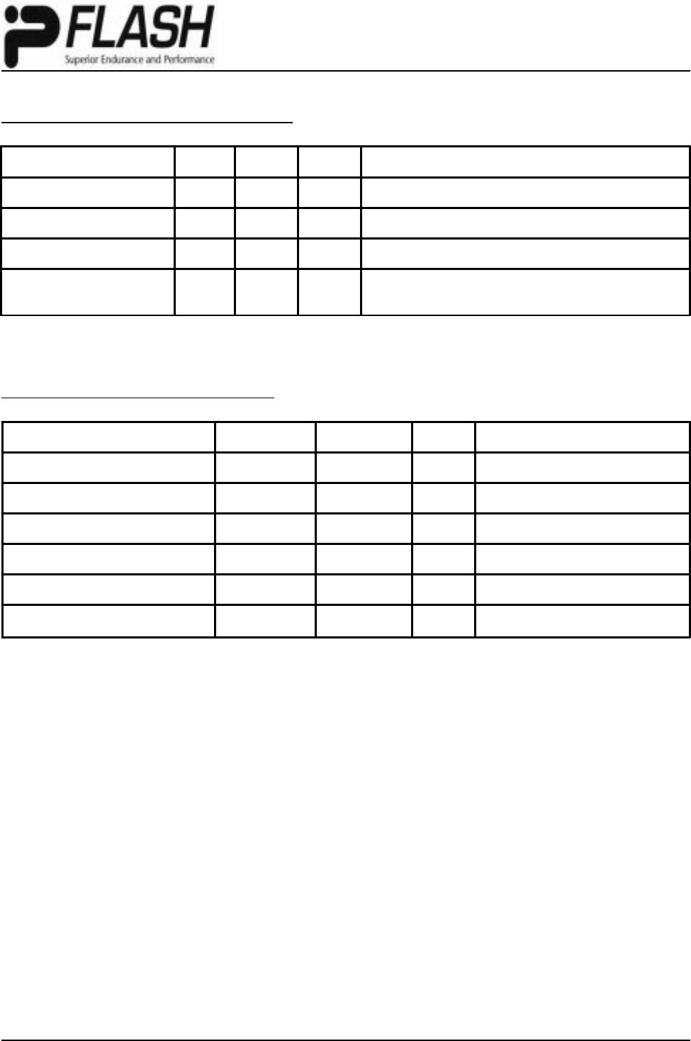
8-Pin JEDEC 150mil Small Outline Integrated Circuit (SOIC) Package
(measure in millimeters)
31
Chingis Technology Corporation Issue Date: Feb., 2009, Rev: 3.5
Pm25LV512A/010A/020/040
PACKAGE TYPE INFORMATION
`
End View
5.38
5.18
Top View Side View
5.38
5.18
8.10
7.70 2.16
1.75
0.25
0.05
0.48
0.35
1.27 BSC
0.25
0.19
0.80
0.50
5.38
5.18
5.33
5.13
8B
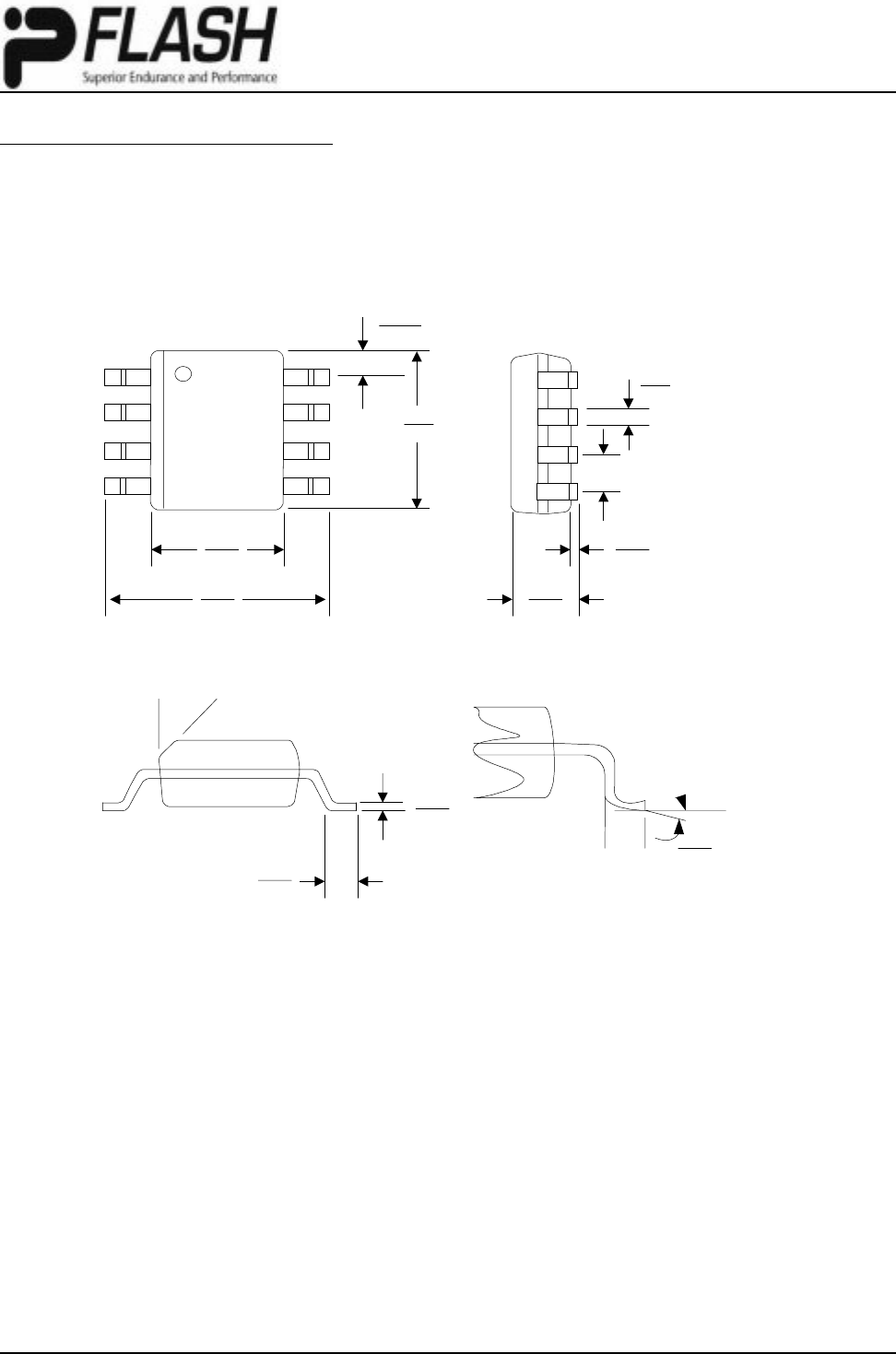
8-Pin JEDEC 208mil Broad Small Outline Integrated Circuit (SOIC) Package
(measure in millimeters)
32
Chingis Technology Corporation Issue Date: Feb., 2009, Rev: 3.5
Pm25LV512A/010A/020/040
PACKAGE TYPE INFORMATION (CONTINUED)
8K
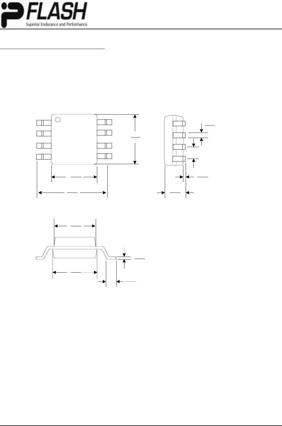
8-Contact Ulta-Thin Small Outline No-Lead (WSON) Package (measure in millimeters)
5.00
BSC
Top View Side View
0.48
0.35
6.00
BSC
0.80
0.70
0.25
0.19
1.27
BSC
Bottom View Pin 1
0.75
0.50
4.00
3.40
33
Chingis Technology Corporation Issue Date: Feb., 2009, Rev: 3.5
Pm25LV512A/010A/020/040
PACKAGE TYPE INFORMATION (CONTINUED)
8P
8-pin 300mil wide body, Plastic Dual In-Line Package PDIP (measure in millimeters)
9.53
9.12
6.60
6.20 9.40
8.38
0o
15o
3.45
3.25
0.38(min)
2.54
(typ)
8.26
7.62
4.20
3.60
3.18(min)
1.65
1.40
0.56
0.36
34
Chingis Technology Corporation Issue Date: Feb., 2009, Rev: 3.5
Pm25LV512A/010A/020/040
PACKAGE TYPE INFORMATION (CONTINUED)
8D
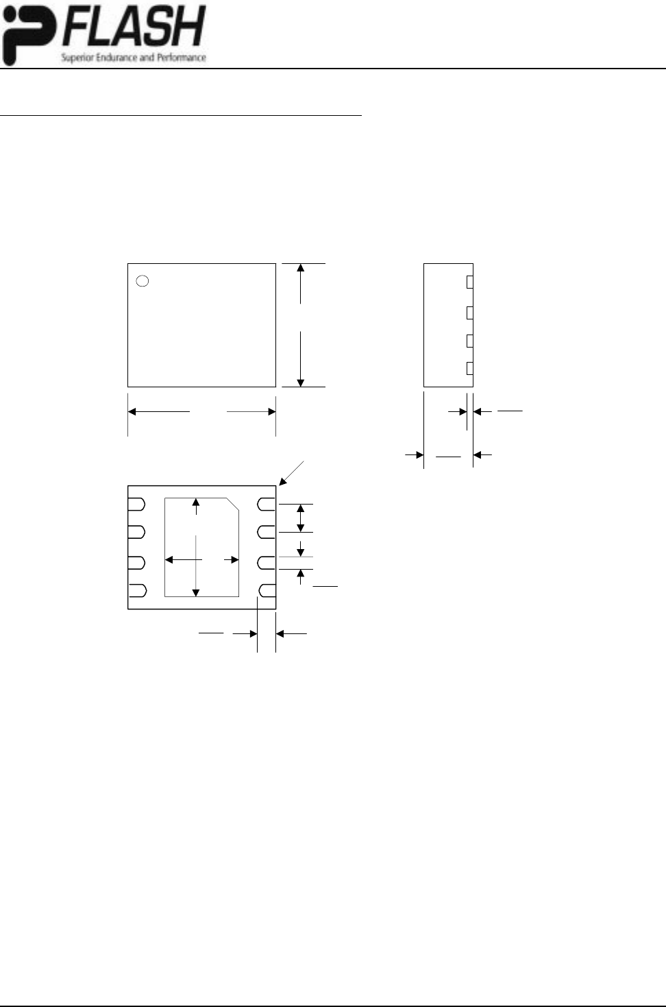
8-pin TSSOP Package (measure in millimeters)
Pin1
4.5
0.65
4.3
6.6
6.2
3.1
2.9
0.30
0.25
1.05
1.00
1.05
1.20
0.15
0.05
8
00
0
0.7
0.5
0.25
GAGE PLANE
Detail A
Detail A
0.127
Unit : millimeters
35
Chingis Technology Corporation Issue Date: Feb., 2009, Rev: 3.5
Pm25LV512A/010A/020/040
REVISION HISTORY
Date Revision No. Description of Changes Page No.
January, 2004 0.3 Advanced Product Specification All
March, 2004 0.4 Extend The Range of Operation Temperature All
August, 2004 0.5 Correct part no for WSON package
Register status setting 3
6,7,8
October, 2004 0.6 Correct part no
Register setting for small sector feathure All
page 7
January, 2005 0.7 Preliminary version release
January, 2005 0.8 1. Support 208mil SOIC package
2. Correct read timing for D0 latch by HOST
3. Remove Turbo mode All
February, 2005 0.9 Support 33MHz
Removed bask side metal of WSON
Standby current
1,3,15,23,24,
30
May, 2005 1.0 JEDEC ID READ instruction
Correct the smaller sector (1KB) feature 6,7,10,12
June, 2005 1.1 Description update for the operation of Configuration
Register 8,9,15,16
July, 2005 2.0 Support 75MHz for Fast Read Mode All
July, 2005 2.1
1. Update fast read speed to 100MHz.
2. Sectore/Block archeticture description.
3. Ordering information - remove non-pbfree parts.
4. Highligh no require WREN before WRCR command.
5. AC measurement conditions.
1,3,16,28
November, 2005 2.3
1. Change AC paramaters for 100MHz spec.
Tv 8ns with 10pF Loading, Data In Hold/Setup tiime
2ns(min), Clock high/low time 4ns(min)
TRI, TFI, 8ns(max), TDIS 10ns(max)
2. Support Commercial Grade to -40~+85degreeC
3. Partno chage for Pm25LV010 to Pm25LV010A.
3, 24,25
February, 2006 2.4 1. Update endurance to 200K cycle.
2. Update write inhibit spec. to 2.1V .
3. Update ESD CDM spec 1000V. 1,9,28
March, 2006 2.5 1.Change Logo and company name
2.Modified test condition for DC All
24
March, 2006 2.6 Extend the operated temperature to +105degreeC 3,23,24,25
April, 2006 2.7 1. Update Pm25LV512A in the datasheet
2. Correct tCH definition
3. Power-up timing difinition
All
25,26
28
May, 2006 2.8 Correct the statement of hardware write protection 9
June, 2006 2.9 Support 8-pin PDIP package for 4Mb SPI 1,2,3,33
May, 2007 3.0 Support sector lock/unlock features
Update erase and WRSR time 1,10,11
1,26,30
Jan. 2008 3.1 Support TSSOP package for Pm25LV512A.
Support Sector Lock/Unlock for Pm25LV020. 1, 3,35
10,11
Feb. 2008 3.2 Support WSON with back side metal 3, 34

36
Chingis Technology Corporation Issue Date: Feb., 2009, Rev: 3.5
Pm25LV512A/010A/020/040
Date R e vision N o. Description o f Changes Page N o.
Jun, 2008 3.3 Add the TSSO P part number 3
July,2008 3.4 Remove 8Q package 3
Feb, 20 09 3 .5 M od ify DC C H Z table 24
