PSM512_Single_Card_512K_8_Bit_Multibus_Memory_Feb81 PSM512 Single Card 512K 8 Bit Multibus Memory Feb81
PSM512_Single_Card_512K_8_Bit_Multibus_Memory_Feb81 PSM512_Single_Card_512K_8_Bit_Multibus_Memory_Feb81
User Manual: PSM512_Single_Card_512K_8_Bit_Multibus_Memory_Feb81
Open the PDF directly: View PDF ![]() .
.
Page Count: 62
PSM512
HANDBOOK
SINGLE
CARD
512K
8
BIT
MEMORY
CD
MICROSYSTEMS
8
P'~ssey
M icrosystems e
.
PSM512
HANDBOOK
SINGLE
CARD
512K
, 8
BIT
MEMORY
..
t
.~
l,se The
?IessI¥
Canoany
l.;mIllId
T'his
~
ana
:Me
rnTonTIatiQn e:rnaJneCI
II.,,,"
may
MOt
ee
e:lCIed. I
used
or
dsc:csecr
In
wnae
or
:n
can
CC3Ct
'MU\
me
oner
·
...
rmen
cerrTUSSIOIT
at
iIIe
~
~
wmrtlld
Ct. If
:l'IIS
=ctIment
;'I3S
::...
~
unaar
a
=rmac::
.....
1n
~;::any.
a UI:lI'4!SI1y
IUl:lanMC
uncer
mat
e::mrac:.
It
is
smied'Mlna.lt
!iacnJry
tor
~
OIl
ClmlGlCI1S.
,.....,.
Mlc:osysttlf'tS l.irntt.e
Water
'..an
••
1"CYICaS':I!t'.
~
~IN'<:
7';:-1
1"'!I6Qr.Cne: :awcurer
I~
::c:l~'Z
rMll:
~'82S
~I!!:
~~..,
":""WC:!Stlr
PSM512
HANDBOOK
-
SINGLE
CARD
512K
8
BIT
421jHBjlO225
MEMORY
r
~C;Et
iSSl;e
1
(;
)
8
Plessey
Microsystems
8
DOCUMENT
AUTHORlSAT10N
Prepared
By:
A.
WAIGHTS
Approved
By
Department:
ENGINEERING
engineering:
Division:
MICROSYSTEMS
Marketing: -
./
/ L
J
k~
"
T?'\..;'/
-
First Issue:
OOCUMENT
ISSUE.
STATE
Issue 1 I I I
Date 2.11.81 I I I
c.'iange No. I I
~
I
~
f I 1 I I I i I t
i I
I
F'a~e
1 2 3
4-
5 6 7 6 9 I
10
t I
I
! I 1 f 1 I 1 I 1 I 1 I 1 I 1 I 1 I 1 I 1
Issue I I I
I
Page
1'1
12
13
14
,S I 16 I 17 18 19 I
20
Issue
I 1 I 1 1 ,- 1 1 I 1 1 1 , I , I
t
~e
I
Z1
2.2
I
~
24
25
26
I
27
2!! I
29
~
Issue , ! 1 I 1 I 1 1 I 1 I 1 I 1 I 1 I 1
-/
.
F'age
31
32
33 34 3S 36
'37
38
39
40
Issue 1 1 1 1 1 1 1 1 I 1 1
Page
41
42
43
44
45
46 47
48
49
SO
issue I I I I I 1 1 T t I
Page
51
52
53
54
5:,
56 57
I
58
Issue 1 1 1 1 1 - 1 1 1
PSM512
HANDBOOK
-
SINGLE
CARD
512K
8 BIT
421
iHB!1
0225
r~EMORY
iSS1.ie
1
;:lage
~
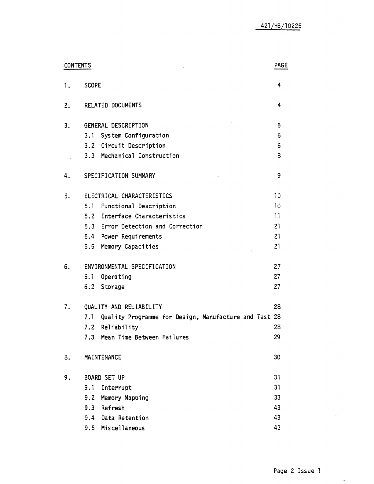
CONTENTS
1.
2.
3.
4.
5.
6.
SCOPE
RELATED
DOCUMENTS
GENERAL
DESCRIPTION
3.1
System
Configuration
3.2 Circuit Description
3.3
Mechanical
Construction
SPECIFICATION
SUMMARY
ELECTRICAL
CHARACTERISTICS
5.1
Functional Description
5.2 Interface Characteristics
5.3 Error Detection
and
Correction
5.4
Power
Requirements
5.5
Memory
Capacities
ENVIRONMENTAL
SPECIFICATION
6.1 Operating
6.2
Storage
421/HB/10225
PAGE
4
4
6
6
6
8
9
10
10
11
21
21
21
27
27
27
7.
QUALITY
AND
RELIABILITY
28
7.1
Quality
Programme
for Design,
Manufacture
and
Test
28
7.2 Reliability
28
7.3
Mean
Time
Between
Failures
8.
MAINTENANCE
9.
BOARD
SET
UP
9.1 Interrupt
9.2
Memory
Mapping
9.3 Refresh
9.4
Data
Retention
9.5
Mi
s
ce
11
aneous
29
30
31
31
33
43
43
43
Page
2 Issue 1

CONTENTS
10.
SYSTEM
DESCRIPTION
10.1
Memory
Array
421jHBjl0225
PAGE
44
44
10.2
Address
Multipying,
Memory
Selection
and
RAS
46
Decode
10.3 Refresh
Logic
47
10.4
Data
Control
49
10.5
Timi.ng
Control
50
10.6 Error Detection
and
Correction
51
11.
FAULT
FINDING
12.
INSTALLATION
AND
OPERATION
12.1
Receiving Inspection
12.2
Installation
12.3
Power
Requirement
APPENDIX
1
52
54
54
54
54
55
-
57
Page
3 Issue 1
421/HB/10225
1.
SCOPE
This
document
defines the functional.
e1ec~rical
and
mechanical
characteristics
of the Plessey Semiconductors
Memory
PSM
512.
designed
and
manufactured
by
Plessey Microsystems Limited.
The
PSM
512
is
part of the Plessey
series
of
module
memory
systems designed for modular storage requirements.
2.'
RELATED
DOCUMENTS
PLESSEY
MICROSYSTEMS
QUALITY
MANUAL
PLESSEY
MICROSYSiEMS
ENGINEERING
INSiRUCiION
MANUAL
APPLICATION
NOTES
PSM
512.
Page
4 Issue 1
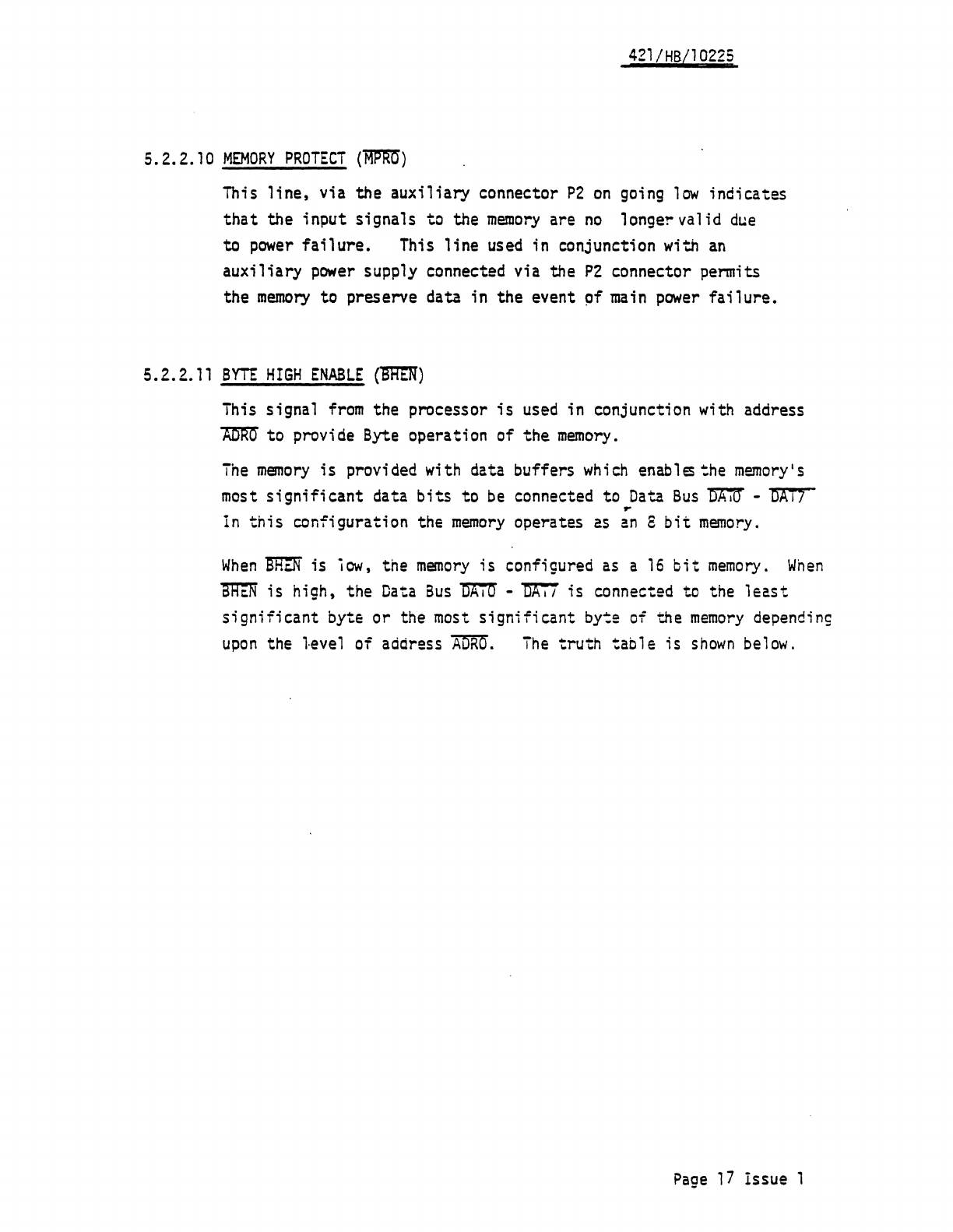
ADDRESS
8US
20
BITS
ADDRESS
I
~
BLOCK
--
-
AOI_
i-
RAS
i~nDC
-
lW
TIfff
EXT
ftE
F
..
1\-~K
lACK
"Q
lU
I»
10
ID
Ul
nnrn
.
"..
0-'
II)
II)
NPIID
c
II-
III
........
..
MS"
1
----
TfA5"
7.
1---.
--
-.
-.. -
..
.
----.-
,ms
J
i(1\S
tl
.-
..
----~---.
----
II-
ADORES
-
....
---
.-
--.----
n[FHESII
Mf.MORV
AIU{A
V
(2S6K 16)
,O\'S"
nEAD
. -... -
----
--_.-
WRI
TE
-.
__
.
__
.
________
.
__
A
__
_
llVH/WORO
---------
512K
8
OIT
f1LMOHV
BLOCK
SUllMIH
I C
----.--
-----
-----
-_.-
-
...
-----
ERROR
DETECTION
&COftRECTION
lOGIC
REAll/
WRITE
8UFnns
8YTE
()
SWAP
OUFF£nS
EUoR
DATA
0-1
"
f'NIo-7
PfUU
READ/
DA
r A
U-
15"
.~
WRITE
. \
....
DUfFER
~
f'o.l
"
.....
j
j:
BYTE
1
--r
421/HB/10225
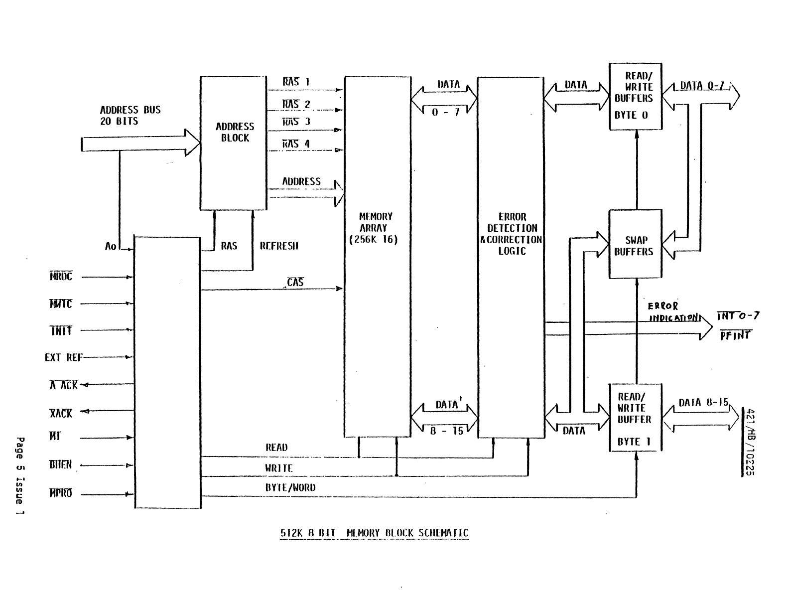
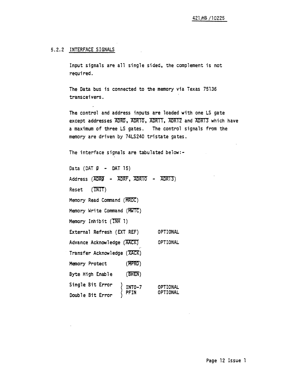
3.
GENERAL
DESCRIPTION
3.1
SYSTEM
CONFIGURATION
The
PSM
512
memory
is
designed to
use
with 8
bit
and
16
bit
microprocessors.
The
memory
has
a
maximum
capacity of 524,288
words
8
bits
and
operates
at
a
maximum
cycle time of
500
nano-
seconds, with
an
access time not greater than
300
nano-seconds.
The
memory
may
be
operated with
an
8
bit
or
16
bit
word
length.
The
memory
has
an
address capability of 16,048,576 words, thus
32
memory
cards
may
be
operated together to give a
maximum
capacity
of 8,048,576
words
16
bits.
The
memory
is
fitted
with single
bit
error
detection
and
correction
and
double
error
detection
circuitry.
The
communication
between
the
Data
Processing
Equipment
and
the
memory
takes place
by
means
of three
main
buses.
These
are:-
Bi-directiona1
Data
Bus
Control
Bus
Address
Bus
3.2
CIRCUIT
DESCRIPTION
The
memory
uses the industry standard
16
pin dua1-in-1ine 65,536
MOS
dynamic
RAMS.
Texas
75136
Transceivers are connected to the
Data
bus.
Address
and
control input
lines
to the
memory
are loaded with
one
LS
gate with
the exception
of
addresses
~,
~,
~,
~
and
~'which
have
a
maximum
load of three
LS
gates.
The
memory
card
can
be
depopulated to give
different
memory
capacities.
On
cardcompari tors enables the memory.starting
and
finishing addresses
to
be
selected
by
means
of a dual-in-1ine switch.
The
address
boundary
for the
starting
and
finishing addresses are
restricted
to
64K
when
working
in a 1
megabyte
field.
When
working
in a
16
megabyte
field
the address
is
switchable into
5l2K
blocks
which
cannot straddle
1
megabyte
boundaries.
The
internal timing signals
for
the
memory
are generated
by
means
of
dual-in-line delay
lines
and
TTL
gates.
The
block
diagram
of the
memory
system
;s
shown
on
Page
5.
Page'6 Issue 1
.....
I/)
III
C
111
0.25 x
4~
(2
PLACES)
0.06R
(12
PLACES)
12.000
REF
. .. _
...
----_._.
----
~.------
.. -
..
.,-------_.-
..
--_
..
-_
..
-
._._-
-
..
-,
.
'"
.'-
.....
.
....
-
~
-
....
-
COMPONnH
S I
DE
86
WAY
lL-------:~::~OC~05
____
-·-_-_·-=1
-
.60
WAY
--W
0.100" cc
I·
3.080
4.570
..
I
~-
0.250
I
-
-f
--.
r-
REF
I
til
.
to
til
.
0
0\
. 0
1+
N
0
0 r
. -n
0
0
til
.
-~~
-
f
I-'
-
...J
[).5~
lQ..30
-0.390
42i/HB!10225
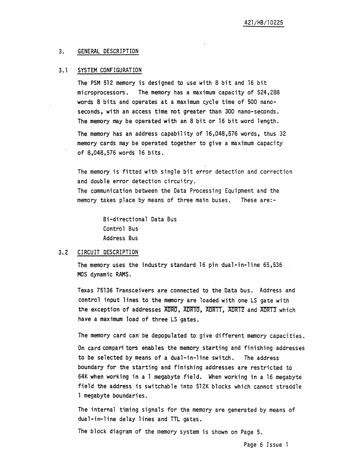
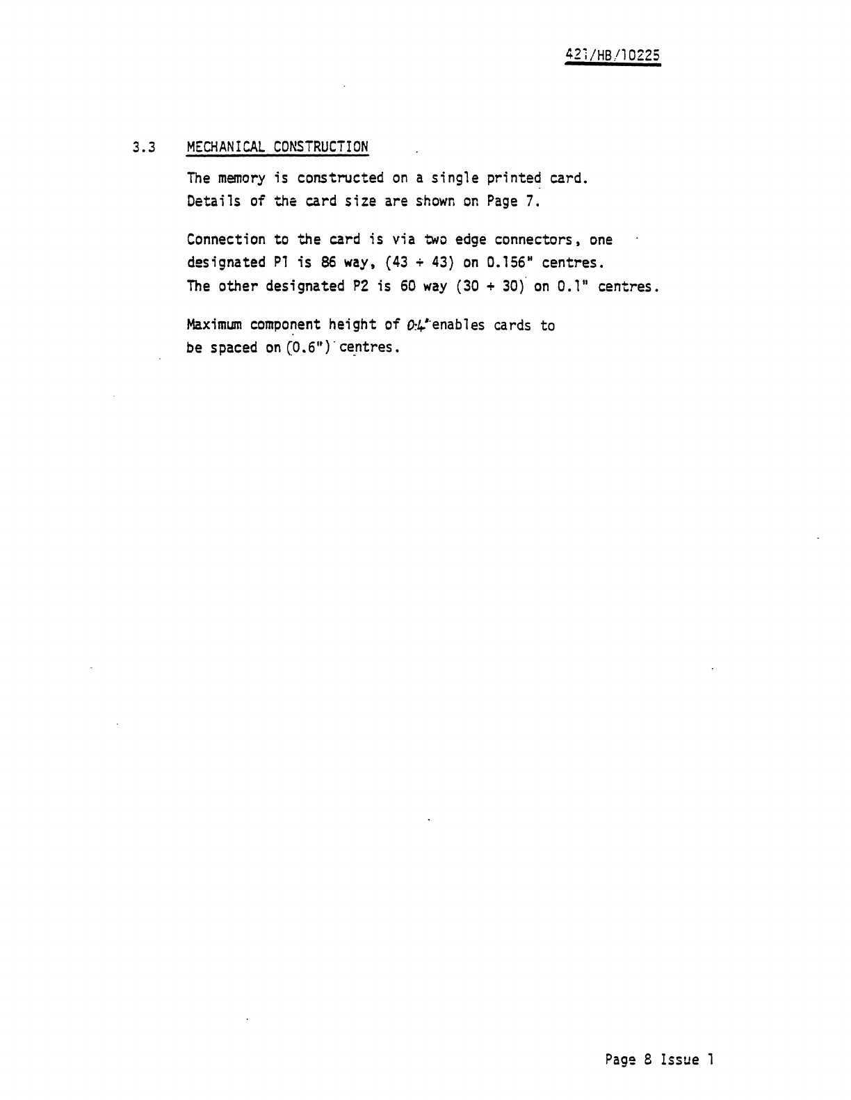
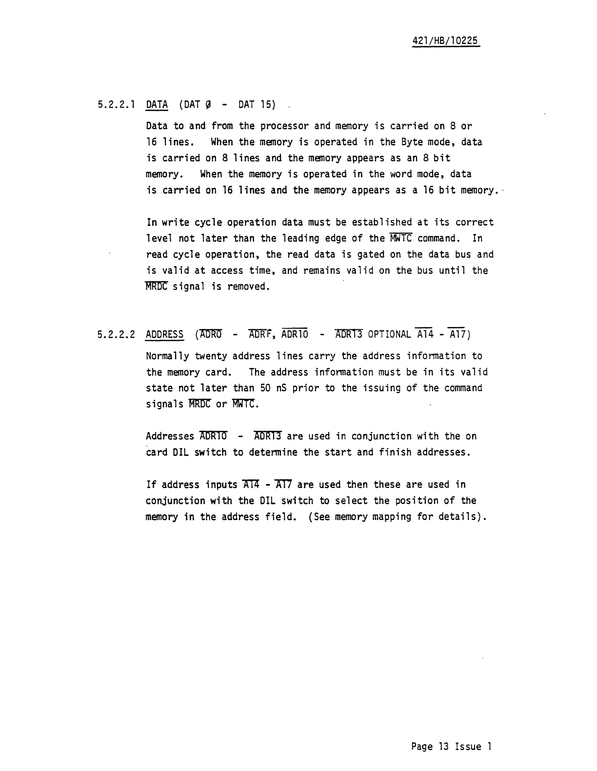
3.3
MECHANICAL
CONSTRUCTION
The
memory
is
constructed
on
a
sing1e
printed
card.
Details
of
the
card
size
are
s-hown
on
Page 7.
Connection
to
the
card
is
via
two
edge
connectors,
one
designated
P1
is
86
way,
(43 + 43)
on
0.156"
centres.
The
other
designated
P2
is
60
way
(30 +
30)-
on
0.1"
centres.
Maximum
component
height
of
£r.4---enables
cards
to
be spaced
on
(0.6")"
ce.ntres.
Pag~
8
Issue
1
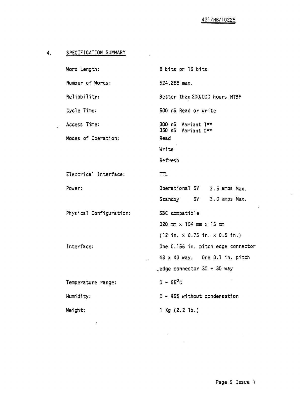
4.
SPECIFICATION
SUMMARY
Word
Length:
Number
of
Words:
Re
1 i
ab
i 1i ty:
Cycle
Time:
Access
Time:
Modes
or Operation:
~lec~rical
Interface:
Power:
?hysical Configuration:
Interface:
Temperature range:
Humidity:
Wei
ght:
42i/HB/l0225
8
bits
or
16
bits
524~288
max.
Better
than
200,000
hours
MTBF
500
nS
Read
or
Write
300
nS
Variant
1**
350
nS
Variant
0**
Read
Write
Rerresh
ill
Operational
SV
3.5
amps
Max.
Standby
5V
3 . 0
amps
Max.
SSC
compatible
320
mm
x
15'
rom
x
~3
mm
(12
in. x 6.75 in. x 0.5
in.)
One
0.156
in.
pitch
edge
connector
43
x
43
way.
One
0.1
in.
pitch
_edge
connector
30
+
30
way
o -
95%
without condensation
1
Kg
(2.2
lb.)
Page
9 Issue 1
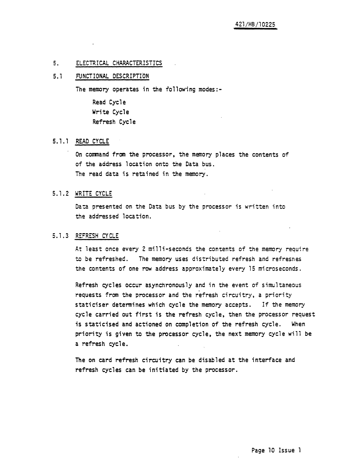
5.
ELECTRICAL
CHARACTERISirCS
5.1
FUNCTIONAL
DESCRIPTION
The
memory
operates in the following modes:-
Read
Cycle
Write
Cycle
Refresh
Cycle
5.1.1
READ
CYCLE
421/HB/10225
On
command
from
the processor, the
memory
places the contents of
of the address location onto the
Data
bus.
The
read data
is
retained in the
memory.
5.1.2
WRITE
CYCLE
Da~a
presented
on
the
Data
bus
by
the processor
is
written into
the addressed location.
5.1.3
R£FRESH
CYCLE
At
ieast
once
every 2 mi11i-seconds the
con~ents
of the
memory
require
to
be
refreshed.
The
memory
uses distributed refresh
and
refresnes
the contents of
one
row
address approximately every
15
microseconds.
Refresh
~cles
occur asynchronously
and
in the event of simultaneous
.
requests
from
the processor
and
the refresh
circuitry,
a
priority
staticiser
determines
which
cycle the
memory
accepts.
If
the
memory
cycle carried out
first
is
the refresh cycle, then the processor request
is
staticised
and
actioned
on
completion of the refresh cycle.
When
priority
is
given
to
the processor cycle. the next
memory
cycle wil'
be
a refresh cycl e.
The
on
card refresh
circuitry
can
be
disabled
at
the
interface
and
refresh cycles
can
be
initiated
by
the processor.
Page
10
Issue 1
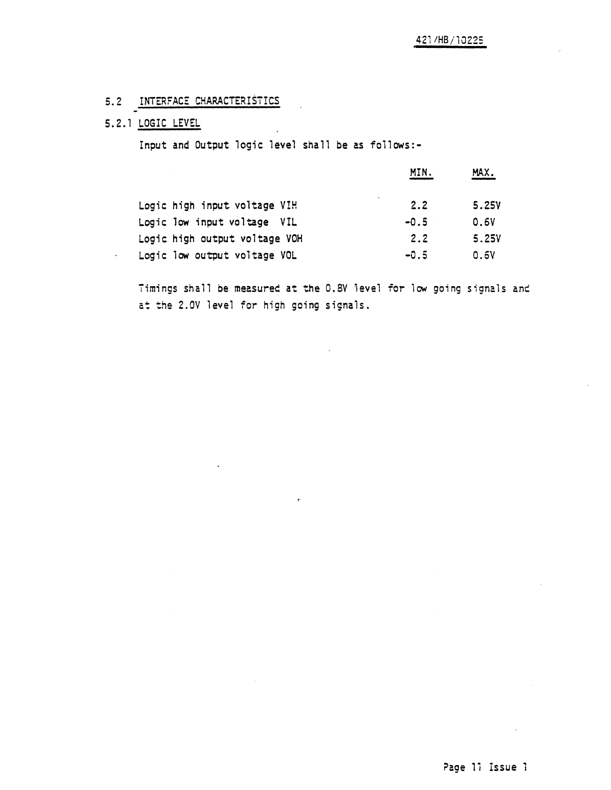
5.2
INTERFACE
CHARACTERISTICS
5.2.1
LOGIC
LEVEL
421/HB/10225
Input
and
Output logic level shall
be
as
follows:-
Logic
high input voltage
V!H
Logic
low
input voltage
VIL
Logic
high output voltage
VOH
Logic
low
output voltage
VOL
MIN.
MAX.
2.2
-0.5
2.2
-0.5
5.25V
O.6V
S.2SY
O.6V
Timings
shall
be
measured
at
the
O.BY
ievel for
low
going
signals
anc
a:
the
2.0Y
level for
high
going
signals.
?age
lj
Issue 1
421;fiB
/10225
5.2.2
INTERFACE
SIGNALS
Input signals are
all
single sided, the
complement
is
not
required.
The
Data
bus
is
connected to the
memory
via
Texas
75136
transceivers.
The
control
and
address inputs are
loaded
with
one
LS
gate
except addresses
Amrn',
mnrrrr,
A'OlITT,
~
and
Arn<T'!
which
have
a
maximum
of three
LS
gates.
The
control signals
from
the
memory
are driven
by
74LS240
tristate
gates.
The
interface signals are tabulated below:-
Data
(OAT
~
-
OAT
15)
Address
(AIliW
-
ADW,
JJm"rn'
-
Arnrr3')
Reset
C!R!T)
Memory
Read
Command
(~)
Memory
Write
Command
(~)
Memory
Inhibit
(TNH
1)
External Refresh
(EXT
REF)
Advance
Acknowledge
(~
Transfer
Acknowledge
(~)
Memory
Protect
Byte
High
Enable
Single Bit Error
Double
Bit Error
(mlJ)
(miEN)
INTO-7
PFIN
OPTIONAL
OPTIONAL
OPTIONAL
OPTIONAL
Page
12
Issue 1
42l/HB/10225
5.2.2.1
DATA
(OAT
~
-
OAT
15)
Data
to
and
from
the processor
and
memory
is
carried
on
8
or
16
lines.
When
the
memory
is
operated in the
Byte
mode,
data
is
carried
on
8
lines
and
the
memory
appears
as
an
8
bit
memory.
When
the
memory
is
operated in the
word
mode,
data
is
carried
on
16
lines
and
the
memory
appears
as
a
16
bit
memory
..
In
write cycle operation data
must
be
established
at
its
correct
level not
later
than the leading
edge
of the
MWTC
command.
In
read cycle operation, the read data
is
gated
on
the data
bus
and
is
valid
at
access time,
and
remains
valid
on
the
bus
until the
~
signal
is
removed.
5.2.2.2
ADDRESS
(AOmr
-
AITRF,
AOR
10
-
AIJRTI
OPTIONAL
A
14
- A
17)
Normally
twenty address
lines
carry the address information to
the
memory
card.
The
address information
must
be
in
its
valid
state
not
later
than
50
nS
prior to the issuing of the
command
signals
~
or
~.
Addresses
~
-
~
are
used
in conjunction with the
on
card
OIL
switch to determine the
start
and
finish
addresses.
If
address inputs
~
-
Jni
are
used
then these are
used
in
conjunction with the
OIL
switch to
select
the position of the
memory
in the address
field.
(See
memory
mapping
for
details).
Page
13
Issue 1

421/HB/10225
5.2.2.3
RESET
(lJfrr)
This
line
when
taken
from
the
high
to the
low
level clears
the
memory
card internal logic.
Page
14
Issue 1
42l/HB/10225
5.2.2.4
MEMORY
READ
COMMAND
(mm'C).
This
line
going
from
the logic high to logic
low
state
initiates
a
memory
read cycle.
In
the event of the
memory
being
busy
due
to a refresh cycle, the
memory
cycle
is
delayed
until
the refresh
cycle
has
been
completed.
5.2.2.5
MEMORY
WRITE
COMMAND
~)
This
line
going
from
the logic high to logic
low
state
initiates
a
memory
write cycle.
In
the event
of
the
memory
being
busy
due
to a refresh cycle being in progress; the
memory
cycle
is
delayed
until
the refresh cycle
has
been
completed.
5.2.2.6
EXTERNAL
REFRESH
(EXT
REF)
This
is
connected
by
means
of
LK24
in
which
case
this
line
when
raised
from
the logic
low
state
to the
high
state
initiates
a
memory
refresh cycle
and
inhibits
the
on
board
refresh
circuitry.
On
return to the
low
state,
the
EXT
REF
line
releases the
on
board refresh
circuitry
which
will then operate in the asynchronous
mode
as
normal
unless the
EXT
REF
line
is
again taken
high
within
15
~
seconds.
The
memory
is
thus completely under the control of
the
EXT
REF
signal
prOvided
it
;s
pulsed every
15
~
seconds.
When
the refresh
line
is
low
for>
15
~
seconds the
on
board refresh
re-asserts
itself
enabling the
RAMS
to
be
refreshed under
idle
or
DMA
transfer
conditions.
Internal Refresh
This
;s
achieved
by
connecting
LK23,
and
under these conditions
the board
initiates
its
own
refresh cycles every
15
~
seconds.
Page
15
Issue 1
421/HB/10225
5.2.2.7
ADVANCE
ACKNOWLEDGE
(AACR)
A signal
from
the
memory
to the processor indicating
that
the
memory
has
received the
command
signal.
This
line
goes
from
the logic high level to logic
low
level not
later
than
100
n seconds
after
the leading
edge
of the
command
signal
and
will
remain
at
logic
low
level
until
the
command
signal
has
been
removed.
5.2.2.8
TRANSFER
ACKNOWLEDGE
(XACK)
Signal
from
the
memory
going
from
a logic high level to a logic
low
level indicating to the processor
that
the Data, in a write
cycle,has
been
accepted
by
the
memory
and
that
the data
lines
may
now
be
changed.
In
a read cycle,
~
indicates
that
the read data
has
been
placed
on
the
Data
Bus.
5.2.2.9
MEMORY
INHIBIT
(iNH
1)
This
line
taken
from
the
high
to
low
state
10
nano-seconds before
the
command
signal
going
low
prevents
memory
access,
on
both
~
and
~
remain
high.
If
the
inhibit
line
is
taken
low
50
nS
after
the
command
then
an
AACR
may
appear but
XACK
will
remain
high. This
permits
PROM
or
memory
mapped
I/O
to
be
allocated space within the
memory
address
field.
Page
16
Issue 1
42l/HB/l0225
5.2.2.10
MEMORY
PROTECT
(~)
This
line,
via the auxiliary connector
P2
on
going
low
indicates
that
the input signals to the
memory
are
no
longe!"
val
id
due
to
power
failure.
This
line
used
in conjunction with
an
auxiliary
power
supply connected via the
P2
connector permits
the
memory
to preserve data in the event pf
main
power
failure.
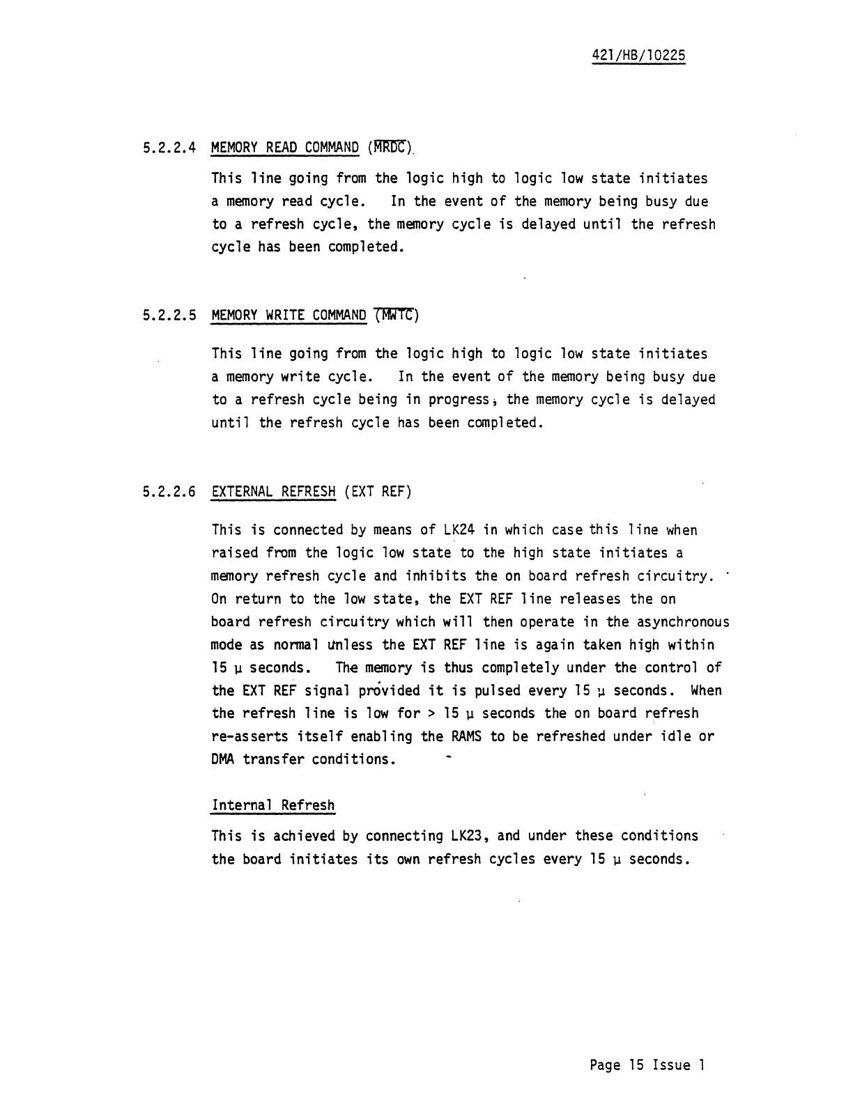
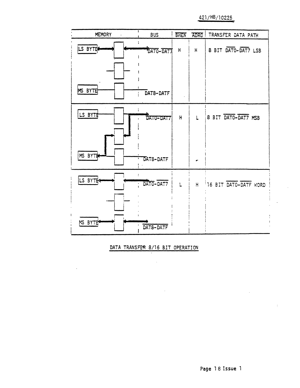
5.2.2.11
BYTE
HIGH
ENABLE
(]RtN)
This
signal
from
the processor
;s
used
in conjunction with address
~
to
provide
Byte
operation of the
memory.
The
memory
is
provided with data buffers
which
enable the
memory's
most
significant
data
bits
to
be
connected to
Data
Bus
~
-
~
0-
In
this
configuration the
memory
operates
as
an
8
bit
memory.
When
~
is jew, the
memory
;s
configured
as
a
16
bit
memory.
When
~
;s
high, the
Data
Bus
]A7rr
-
~
is connected to the
least
significant
byte or the
most
significant
by:e of the
memory
depending
upon
the level of address
AD'R'O.
The
truth
tab 1 e
iss
hown
be
low.
Page
17
Issue 1
421/
H
B/10225
MEMORY
BUS
I mirn
AtJRO
I
TRANSF'ER
DATA
PATrl
11.5
BY~I..
I --
~ATO-15AT
H H S BIT
DATO-DAT7
LSB
-0-
IMS
ByTE!
D
DATS-DATF
I
ILS
BY,]
,
i
I
--
DAIC-DAI;
H L
i8
BIT
DATO-DAT7
~SB
I
I
I
I,.,s
BY
,
OATB-DATF
r-
I "
!
~
ILS
BYr5;~
.1
it I i ,
LJ
D~
T"O-
DAi7
I L i H ! j 5 8
IT
DATO-DATF
'rtORO
, !
!
j-;
'I
-:
W
-
r.s
SYI~'
: I
tLJ
I
DATS-DATF
DATA
TRANSFE'R
8116
B.IT
OPERATION
Page 1 8
Issue
1
421;HB
110225
5.2.2.12
SINGLE
BIT
ERROR
INDICATION
(S.B.E.)
This indicates the occurance of a corrected single
bit
error
in the
word
or
chec~
bits
being read.
This signal
is
optional
and
may
be
linked into
INTO
-7,
power
fail
interrupt,
or a
LED,
but there are conditions for
its
use.
1)
On
initial
power
up
all
memory
locations
which
are
going
to
be
used
should
be
written
to.
2)
No
S.B.E. will
be
indicated
after
power
up
until the
first
read
command.
3)
The
output signal
is
staticised
and
is
reset
by
(a)
The
next write
command
(b)
The
Initialise
signal
(c)
Power
switch off-on
5.2.2.13
DOUBLE
BIT
ERROR
INDICATION
This indicates the occur:.ence of
two
or
more
errors in the
data
word
read
and
leave the
word
uncorrected.
The
output options to the
interrupt
and
their
re-setting
are
as
per the
single
bit
error indication.
Page
19
Issue 1

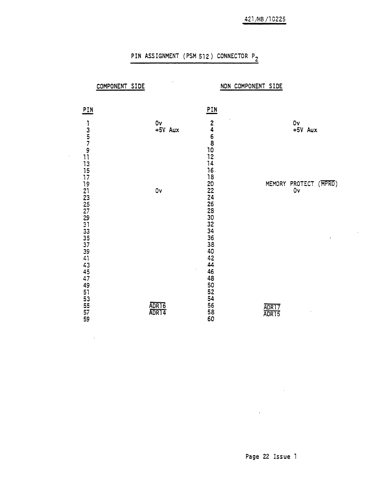
5.2.4
421
IHB
11
0225
PIN
ASS
I
GNt-1ENT
iwo
edge
connectors carry the interface signals to
and from
the
'memory
card.
These
edge
connectors are designated
Pl
and
P2.
Pl
is
the
Bus
connector
and
P2
is
the auxiliary connector
used
when
memory
is
operated in the data retention
mode.
The
pin assignment
is
tabulated below.
Page
20
Issue 1
421
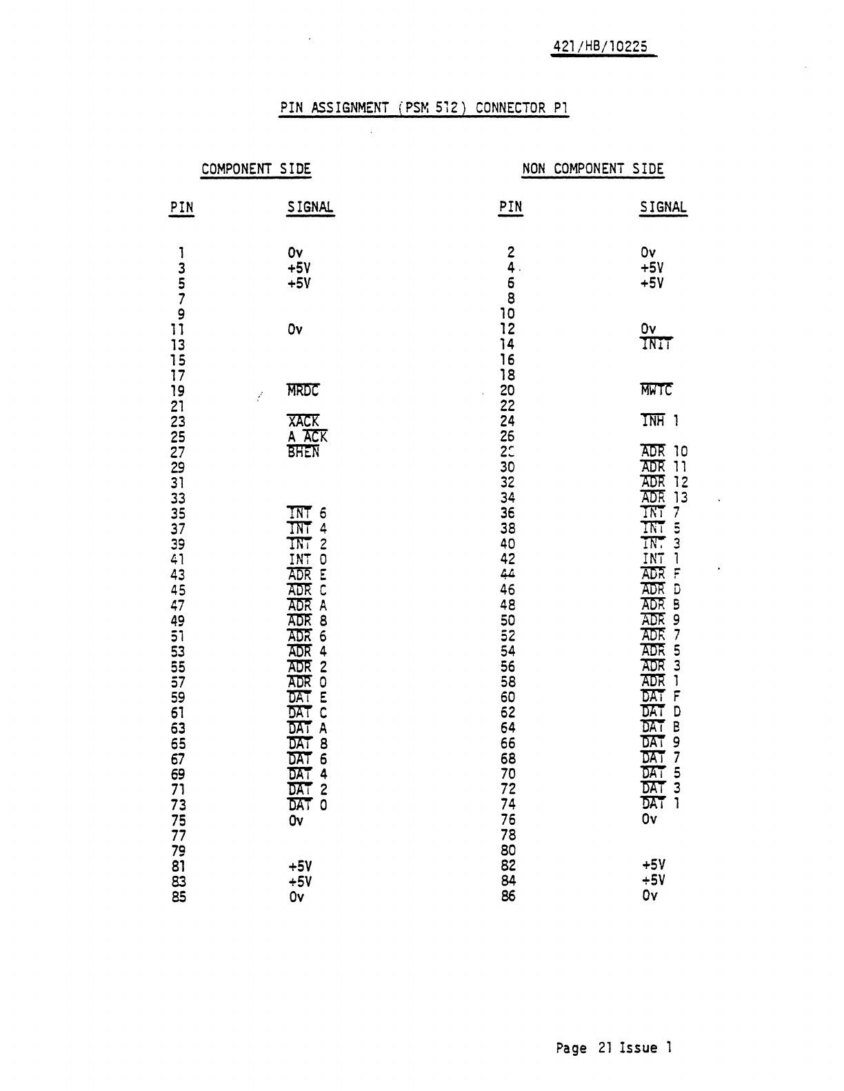
jHB!10225
PIN
ASSIGNMENT
(PSM
512)
CONNECTOR
P1
COMPONENT
SIDE
NON
COMPONENT
SIDE
PIN
SIGNAL
PIN
SIGNAL
1
Ov
2
Ov
3
+5V
4.
+5V
5
+5V
5
+5V
7 8
9
10
11
Ov
12
Ov
13
14
TfW
15
15
17
18
19
~
20
~
21
22
23
XAO':
24
INH
1
25
Am
26
27
~
2:
Am<
10
29
30
Am<
11
31
32
~
12
33 34
AOR
13
35
TNT
5
36
1'Ri7
37
1Ni4
38
w5
39
1Ni2
40
To
3
41
INT
0
42
INT
1
43
ADR
E
4A
~F
45
'AU1<
C
46
AUK
D
47
~A
48
~S
49
A1W
8
50
ATIk
9
51
m6
52
AIm
7
53
Am{
4
54
~5
55
~2
56
Am<
3
57
~o
58
AOK
1
59
mE
60
mF
61
Ni:i C
62
]1ij
0
63
mA
64
]AI
8
55
"OAr
8
66
]Ai
9
67
m6
68
1iAi
7
69
'OAi
4 70
]7ij
5
71
1ID'2 72
]7ij
3
73
ma
74
]Ail
75
Ov
75
Ov
77
78
79
80
81
+5V
82
+5V
83
+5V
84
+5V
85
Ov
86
Ov
Page
21
Issue
1
421,118/10225
PIN
ASSIGNMENT
(PSM
512)
CONNECTOR
P2
COMPONENT
SIDE
NON
COMPONENT
SIDE
PIN
PIN
-1
Ov
2
Ov
3
+5V
Aux
4
+5V
Aux
5 6
7 8
9
10
11
12
13
14
15
16·
17
18
19
20
MEMORY
PROTECT
(~)
21
Ov
22
Ov
23
24
25
26
27
28
29
30
31
32
33
34
35
36
37
38
39
40
41
42
~3
44
45
46
47
48
49
50
51
52
53
54
55
AOiIT6
56
ADm
5i
ADR14
58
ADR1S
59
60
Page
22
Issue 1
421
"HB
/1
0225
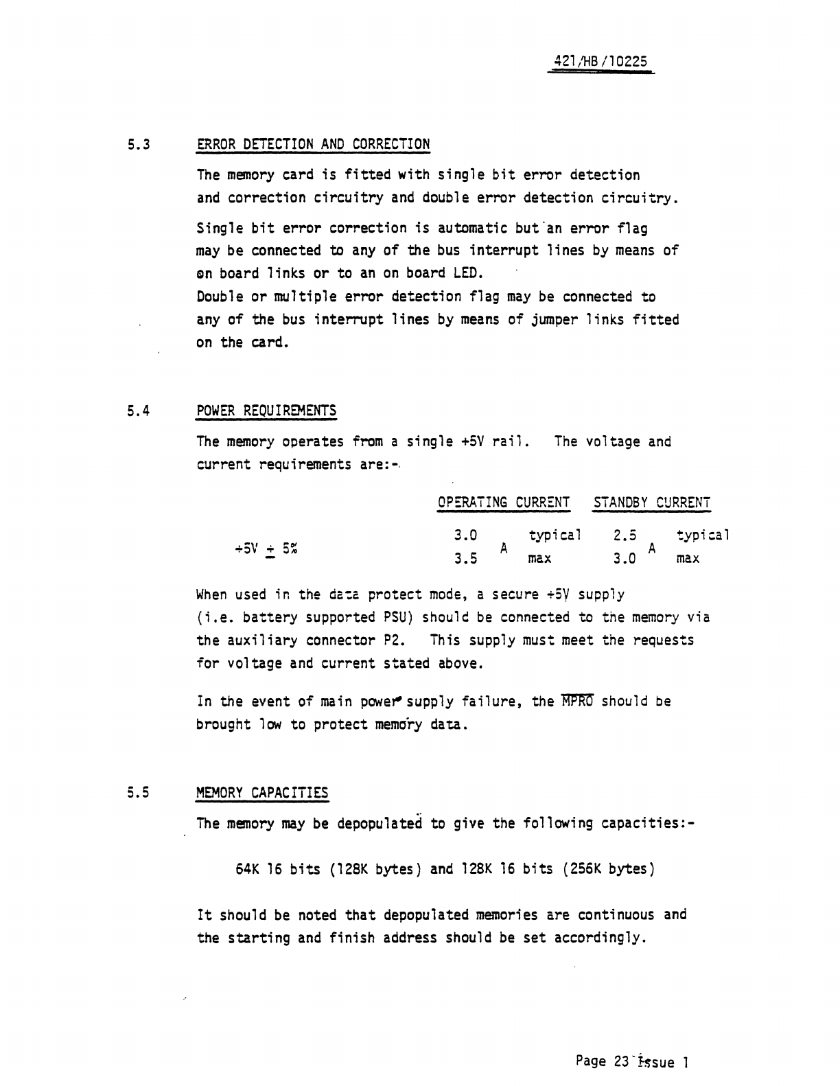
5.3
ERROR
DETECTION
AND
CORRECTION
The
memory
card
is
fitted
with single
bit
error
detection
and
correction
circuitry
and
double
error
detection
circuitry.
Single
bit
error correction
is
automatic but
"an
error
flag
may
be
connected to
any
of the
bus
interrupt
lines
by
means
of
Qn
board links or to
an
on
board
LED.
Double
or multiple
error
detection flag
may
be
connected to
any
of the
bus
interrupt
lines
by
means
of
jumper
links
fitted
on
the card.
5.4
POWER
REQUIREMENTS
The
memory
operates
from
a single
+5V
rail.
The
voltage
and
current requirements are:-·
OP~TTNG
CURRENT
STANDBY
CURRENT
3.0
+5V
+
5%
3.5 A
typi
ca
1
max
2.5
A
3.0
When
used
in the
da~a
protect
mode,
a secure
+sy
supply
typ;~al
max
(i.e.
battery supported
PSU)
shoul,
be
connected to the
memory
via
the auxiliary connector
P2.
This
supply
must
meet
the requests
for voltage
and
current stated
above.
In
the event of
main
poweY'"
supply
failure,
the
r:TI'mJ
should be
brought
low
to protect
memory
data.
5.5
MEMORY
CAPACITIES
The
memory
may
be
depopulated to give the following
capacities:-
64K
16
bits
(128K
bytes)
and
128K
16
bits
(256K
bytes)
It
should
be
noted
that
depopulated
memories
are continuous
and
the
starting
and
finish address should
be
set
accordingly.
Page
23
-
!-$sue
421/
HB/10225
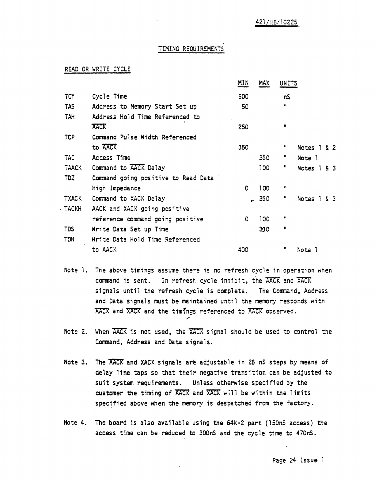
TIMING
REQUIREMENTS
READ
OR
WRITE
CYCLE
MIN
MAX
UNITS
TCY
Cycle
Time
500
nS
TAS
Address
to
Memory
Start
Set
up
50
..
TAH
Address
Hold
Time
Referenced to
~
250
II
TCP
Command
Pulse
Width
Referenced
to
'AAtR
350
II
Notes
1 & 2
TAC
Access
Time
350
II
Note
1
TAACK
Conmand
to
'AACK
Delay
100
II
Notes
1 & 3
TDZ
Command
going
positive to
Read
Data
High
Impedance
0 100
..
TXACK
Conmand
to
XACK
Delay
350
II
Notes
, & 3
..
I
,
TACKH
AACK
and
XACK
going
pcsitive
reference
command
going
positive 0
100
II
TDS
Write
Data
Set
up
Time
390
II
TDH
Write
Data
Hold
Time
Referenced
to
AACK
400
II
Note
1
Note
1.
The
above
timings
assume
there
is
no
refresh cycle in operation
when
command
is
sent.
In
refresh cycle
inhibit,
t'he
mR
and
"X'ArR
signals until the refresh cycle
is
complete.
The
Command,
Address
and
Data
signals
must
be
maintained until the
memory
responds with
~
and
~
and
the timrngs referenced to
AAtK
observed .
. '
Note
2.
When
~
is
not used, the
~
Signal should
be
used
to control the
Command.
Address
and
Data
signals.
Note
3.
The
AArK
and
XACK
signals are adjustable in
25
nS
steps
by
means
of
delay
line
taps
so
that
their
negative
transition
can
be
adjusted to
suit
system requirements.
Unless
otherwise specified
by
the
customer the timing of
1Vi!1(
and
~
w
il
1
be
within the 1 imits
spec~fied
above
when
the
memory
is despatched
from
the factory.
Note
4.
The
board is also available using the
64K-2
part
(150n$
access) the
access time
can
be
reduced to
300nS
and
the cycle time to
470nS.
Page
24
Issue 1
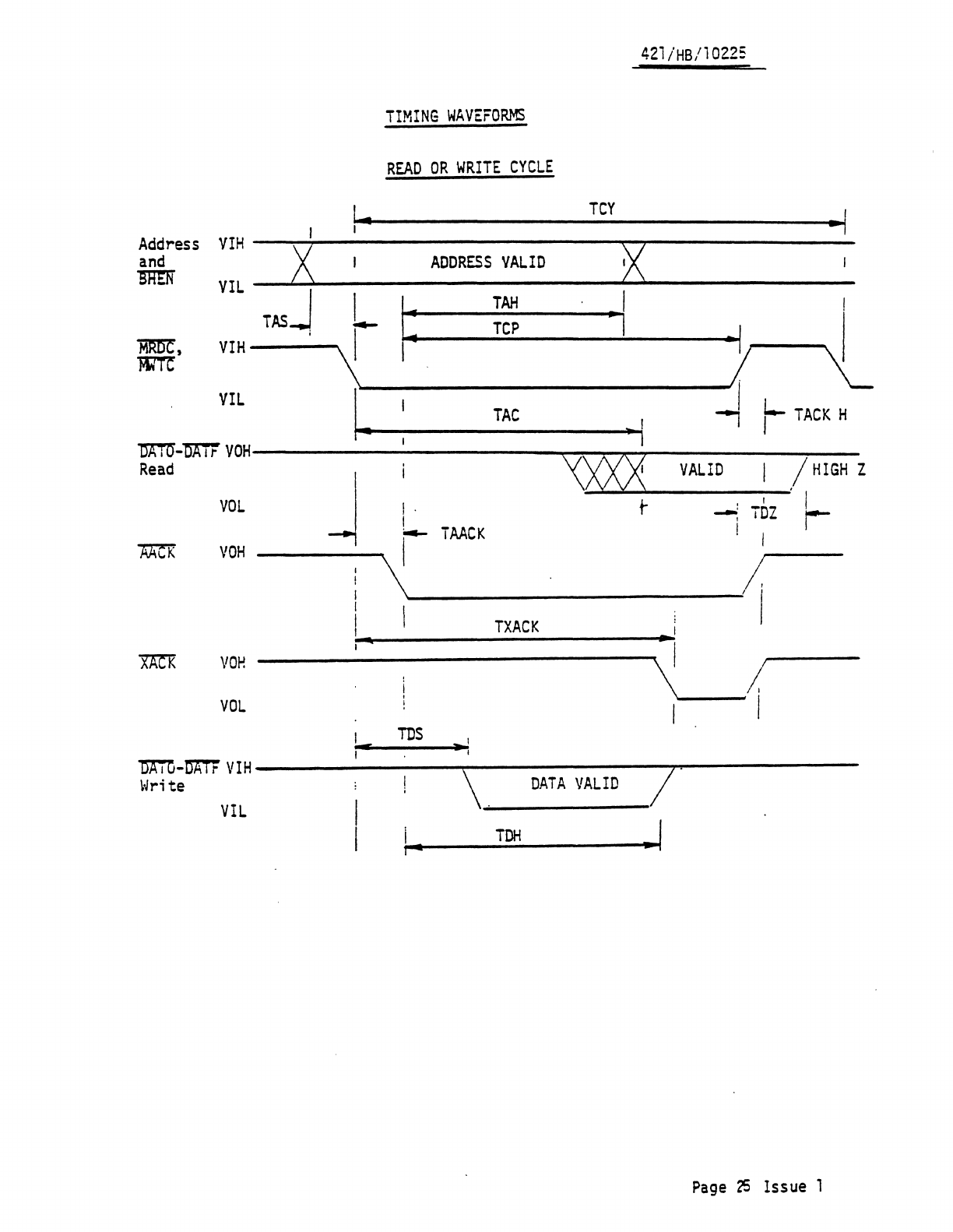
421iHS/l022S
MJmC,
VIH
»m
VIL
VOL
r
~
iDZ
! I
~
____
--,I'---
I
VOH
VOl-!
-----------====
!
-I
VOL
Page
25
Issue 1
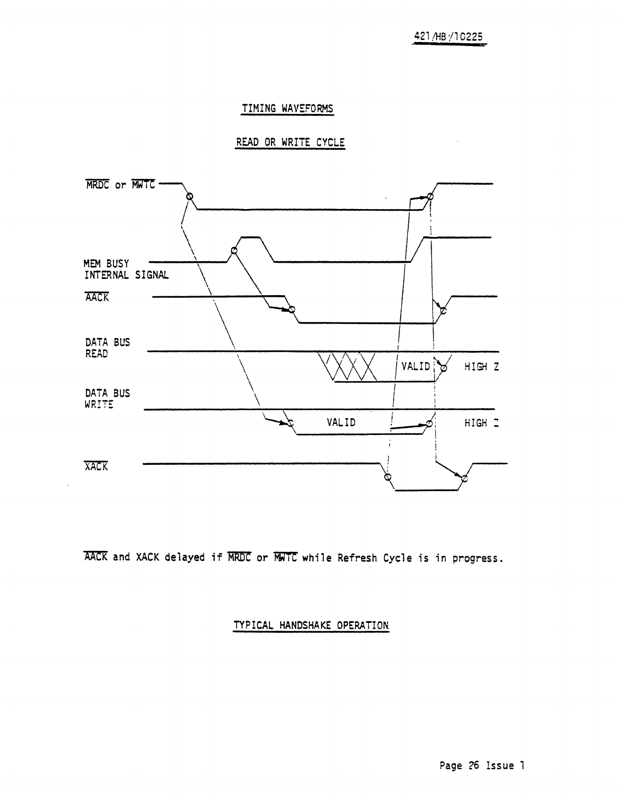
MEM
BUSY
INTERNAL
SIGNAL
DATA
BUS
READ
DATA
BUS
WRITE
XACK
\
\
TIMING
WAVEFORMS
READ
OR
WRITE
CYCLE
'.
~y:x
\
\
\
\
~
VALID
421
.lliB:/1
0225
f
I
I
\)'1
f
VALID
I
HIGH
Z
I 1
!
:Ii
HIGH
:
I i
\
'y
~
and
XACK
delayed
if
~
or
~
whi1e
Refresh
Cycle
is
in progress.
TYPICAL
HANDSHAKE
OPERATIO~
Page
(6 Issue 1
42l/HB/10225
6.
ENVIRONMENTAL
SPECIFICATION
6.
1
OPERATING
The
memory
system
will operate under the following condttions.
Temperature
Range
Cooling
Requirement
Airflow'of
100
metres per minute
parallel to the
edge
connectors
Damage
may
occur to the
memory
if
run
without cooling
for
a period
in excess of
30
minutes
at
maximum
temperature.
Relative
Humidity
Thermal
Shock
Altitude
Vibration
Mechanical
Shock
6.2
STORAGE
Up
to
95%
without condensation
-
300
to +
3000
M
5 -
100Hz
with 0.59 acceleration
109
for 6 mill-seconds
(half
sine)
when
mounted
in a
suitable
racking
system
The
memory
system
may
be
stored or transported without
damage
provided the environment
is
within the limitation
shown
bel~w:-
Temperature
Range
Relative
Humidity
Thenna1
Shock
Altitude
Vibration
Mechanical
Shock
-
5SoC
-+
85°C
o -
95%
without condensation
!
lOoe
per minute
-
300m
to
+
16
,ooOm
o -
500Hz,
29
acceleration
20g
for 6 mill i-seconds
(half
sine)
Page
2J
Issue 1
421/HB/10225
7.
QUALITY
AND
RELIABILITY
7.1
QUALITY
PROGRAMME
FOR
DESIGN,
MANUFACTURE
AND
TEST
All
systems are
manufac~ured
directly
in accordance with a
Quality Plan.
The
Qual;~
Plan monitors the systematic
evolution of system design
and
evaluation
and
production
activity.
By
this
means
it
is
possible to ensure
that
all
systems despatched to the customer
conform
in
all
respects
to
the requirements
set
out in
this
product
specification.
7.2
RELIABILITY
In
order
to
maximise
system
reliability,
all
areas of
activity
are carefully controlled
and
monitored.
Design
-
All
design
activity
is
carried out to preaetermined
rules,
which
includes
component
derating,
stress,
reliability
and
maintainability analysis.
Qualification -
Each
design
is
rigorously tested to ensure
conformance
with the specified performance
and
environmental
requirements.
Pr.ocurement
-
Components
are carefully selected
and
obtained only
from
approved suppliers.
Manufacturing -
Performed
against planned
work
instructions
and
firm
workmanship
standards.
Test -
All
testing
is
performed against defined
test
specifications
and
the.
results
recorded
and
retained.
Thorough
screening
tests
(burn-in) are applied to
all
production,
thereby ensuring
that
all
manufacturing defects are detected
and
corrected
at
the
earliest
opportunity.
Page
28
Issue 1
421/
Hatl
0225
7.3
MEAN
TIME
BETWEEN
FAILURES
The
calculated
mean
time
between
failure
(MTBF)
for
the
memory
is
greater than 200.000
hoursA
The
component
failure
rates
used in
this
calculation
have
been
derived
from
MIL
STO
217B.
British
Post Office publications, manufacturers published data
and
in-house sources.
Page
29
Issue 1
421/HB/10225
8.
MAINTENANCE
No
routine maintenance is necessary
on
the
PSM
512
Memory
Card.
However
it
is
advisable to maintain a preventable maintenance
programme
to give a
maximum
operating efficiency,
this
includes:-
(a) Periodic
checking
of the
Memory
EDC·line
should
be
carried out while reading
from
the
whole
memory
to
check
that
no
memory
device
has
failed
and
is
being
continually corrected
as
this
will reduce
reliability.
(b)
A
check
that
the operating
volt~ge
is
within the limits
of the specification,
ie.
5V
~
5%.
(c)
Also
check
airflow is adequate, clean
and
replace
air
filters
as necessary.
Page
30
Issue 1
421/HB/10225
9.
BOARD
SET
UP
9
..
1 Interrupt
The
memory
provides
an
interrupt
when
either
an
un-correctable
error
(double
bit
or
multi-bit)
is
detected or
when
a Single
bit
corrected
error
has
occurred.
The
un-correctable
error
interrupt
may
be'connected to
either
the
power
fail
line
~
to
one
of
eight
interrupt
lines.
The
correctable
error
interrupt
may
be
connected to
one
of eight
interrupt
lines.
Either of the interrupts
may
also
be
connected to the
LED
fitted
to the front of the card.
Figure 1
illustrates
the
different
possibilities.
Interrupt
is
cleared
on
the next
memory
"'rite
cycl e.
On
power
up
due to the
random
data held in the
RAMS,
errors
and
consequently interrupts will occur
if
attempts are
made
to read
data
from
the
menory.
The
user
must
therefore write data to
all
address locations
after
power
up, before reading data
from
the
memory.
Writing
may
be
in 8
bit
bytes or
~6
bit
words
as
the
interrupt
circuitry
is
enabled
by
the
first
read
command
to the
memory
after
power-up.
If
the
memory
is
used
in
Data
Retention
option
this
condition
does
not apply (see Section
~.~)
Page
31
Issue 1
FOR
421
/MB/l
0226/
ALL
VARIANTS
ISSUE
3
ONWARDS
421/HB/10225
TRISTATE
,..----,0
SINGLE
ERROR--~--'
~
__
---i~RIVER~
CONNECTOR
P2
PF
tNT
o
elKl
0
elK~
lKl
MULTI
ERROR
-E
~::u'"---'
u-
____
~
__
--
__
~-
TO
LED
CONNECTOR
Pl
OlK3
0
«(
.
OlK4
b
._·...,:1--:..1
........
elKS
/9.
IeSl
6/
lK6
'0
INTERRUPT
LINKS
P.C.B.
COMPONENT
SIDE
[K3~
?lK3P-,
-INT a
e
0--
INT 1
t:~::
jLK3
b-
INT 4
J
lK3
'b-
00
5
I
LK2~
!Nt 6
~LK2e,:_
INT 7
INTERRUPT
CIRCUIT
Links
LK2
and
LKS
fitted
on
shipment •
•
Link
LKl
fitted'connects Multi-error to
LED
Indicator.
Link
LK2
fitted
connects Single-error
to
LED
Indicator.
It
is
not permissible to
fit
both
LKl
and
LK2.
Link
LKJ
fitted
connects
~~lti-error
to
Power
Fail Interrupt
L~ne.
Link
LK4
fitted
connects Single-error to
Power
Fail Interrupt Line.
If
neither
LK3
o~.L~4
are
fitted
fit
LK7
to
hold
PF
iNT
high.
Orily
fit
one
of the following
LKJ,
4,
7.
Link
5
fitted
connec~Multi-error
to Interrupt
Bus.
Link
6
fitted
connects Single-error to Interrupt
Bus.
Do
not
fit
both
LKS
and
LK6.
FIGURE
1:
INTERRUPT
FACILITIES
Page
32
Issue 1
42l/HB/10225
9.2
Memory
Mapping
The
user
has
two
memory
map
options dependent
upon
the address
range used.
9.2.1··
Address
Range
1
Megabyte
(Multibus addresses
ADRO
-
ADR13)
ADR10
ADRll
ADR12
ADR13
I
! I
I
i
Two
four
bit
comparators are
used
to
set
the
start
and
finish
address of the
memory.
Multibus addresses
ADR10,
ADRll,
ADR12
and
ADR13
are
fed
to
one
set
of the comparator inputs, the other
set
being controlled
by
dual-in-line switch
SW1
..
The
start
and
finish addresses are thus
set
in
64K
qyte steps.
The
circuitry
is
shown
below.
~
~
f~
SWl
> 1
aN
I
,
:2:1
I
I
j
&.:'....
I
A>8
OV
I I
FInISH
ADDRESS
I
I
SV
!
>
~
i~
I
SWl
I
~.~
-I
'--
A<:'S
OV
__
..,DI---e.e.-
MEMORY
SELECT
START
ADDRESS
Thefintsh address
is
determined
by
switch positions 2, 3, 6
and
8.
The
start
address
is
detennined
by
switch positions 1, 4, 5
and
7.
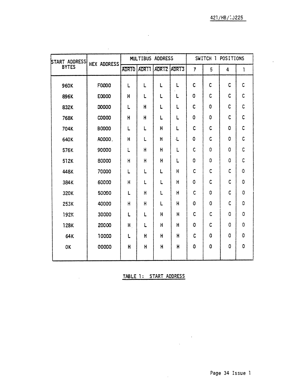
Table 1
shows
the switch settings for the
start
address,
and
Table
2
the
switch settings for the finish address. Table 3
shows
the switch settings for a
5l2K
by~e
memory
with a 1
megabyte
field.
In
the tables a
nc"
indicates the switch
;s
closed,
non
indicates·
open.
Page
33
Issue 1
421/HB/~J225
START
ADDRESS
MUL
TISUS
ADDRESS
SWITCH
1
POSITIONS
HEX
ADDRESS
SYTES
~
~
A1lRT2
PJmT3
7 5 4 1
960K
FOOOO
L L L L C C C C
896K
EOOOO
H L L L a c C C
832K
00000
L H L L C a c c
768K
COOOO
H H L L a a c c
704K
BooOO
L L H L C C a C
640K
AOOOO.
H L H
·L
a c a c
576K
90000
L H H L C 0 a c
512K
80000
H H H L 0 0 0 C
448K
70000
L L L H C C C a
384K
60000
H L L H 0 C C a I
320K
50000
L H L H C 0 C 0
253K
40000
H H L H a a c a
192K
30000
L L H H C C 0 0
128K
20000
H L H H 0 C a a
64K
10000
L H H H C 0 a 0
OK
00000
H H H H a 0 a 0
TABLE
1:
START
ADDRESS
Page
34
Issue 1
421/HB/10225
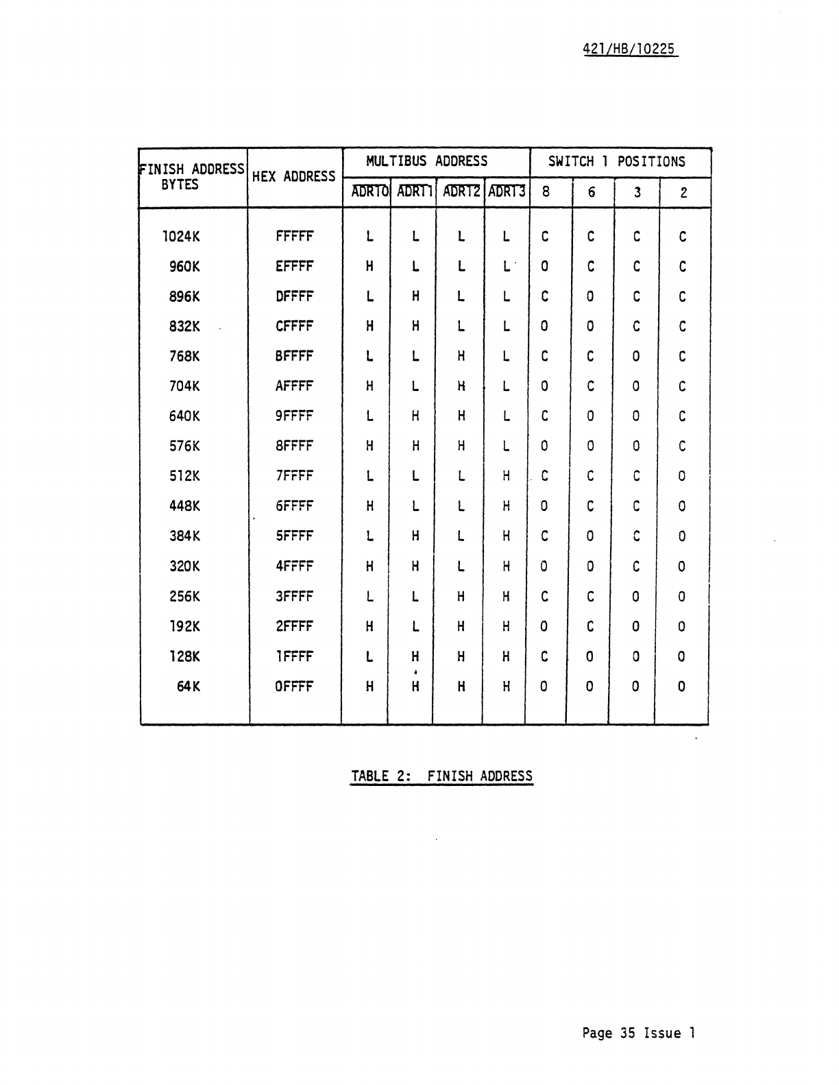
~INISH
ADDRESS
MUL
TISUS
ADDRESS
SWITCH
1
POSITIONS
HEX
ADDRESS
BYTES
Arnrnl
Amm
~
ADm 8 6 3 2
lO24K
FFFFF
L L L L C C C C
960K
EFFFF
H L L
L'
0 C C C
896K
DFFFF
L H L L C a c C
832K
CFFFF
H H L L 0 0 c C
768K
BFFFF
L L H L C C a c
704K
AFFFF
H L H L 0 C 0 C
640K
9FFFF
L H H L C 0 0 C
576K
8FFFF
H H H L 0 0 0 C
I
512K
7FFFF
L L L H , C C C 0
448K
6FFFF
H L L H 0 C C 0
384K
SFFFF
L H L H C 0
,.
0
'"
320K
4FFFF
H H L H 0 0 c 0
256K
3FFFF
L L H H C C 0 0 I
192K
2FFFF
H L H H 0 C 0 0
128K
lFFFF
L H H H C 0 0 0
•
64K
OFFFF
H H H H 0 0 0 0
TABLE
2:
FINISH
ADDRESS
Page
35
Issue
1
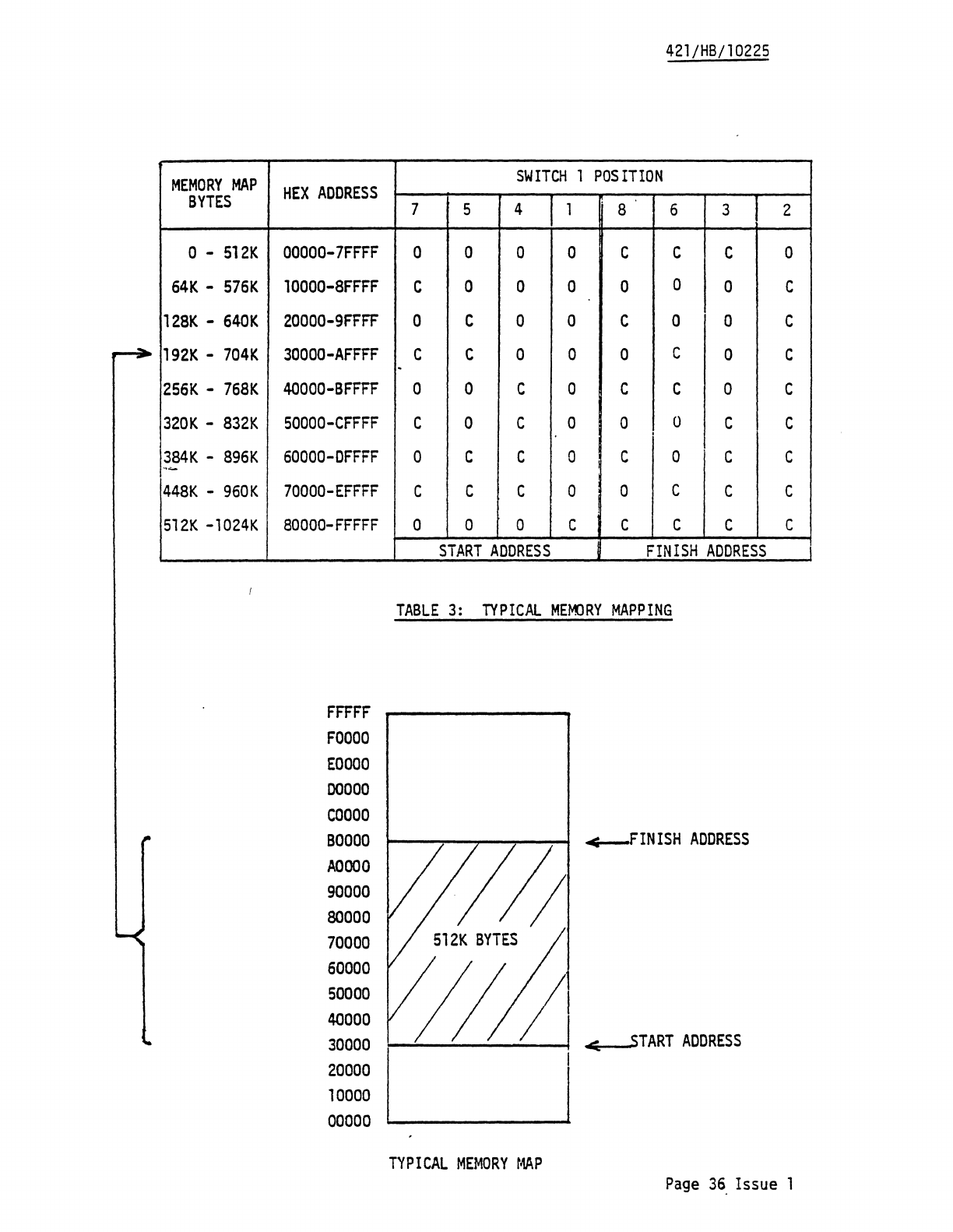
MEMORY
MAP
BYTES
o -
512K
64K
-
576K
12SK
-
640K
192K
-
704K
2S6K
-
768K
320K
-
832K
384K
-
896K
"~
448K
-
960K
512K
-1024K
HEX
ADDRESS
00OOO-7FFFF
10000-SFFFF
20000-9FFFF
30000-AFFFF
40000-BFFFF
50000-CFFFF
60000-DFFFF
70000-EFFFF
80000-FFFFF
FFFFF
FOOOO
EOOOO
00000
COOOO
BOOOO
AOOOO
90000
80000
70000
60000
50000
40000
30000
20000
10000
00000
421/HB/10225
SWITCH
1
POSITION
7 5 4 1 8 6 3 2
0 0 0 0 C C C 0
C 0 0 0 0 0 0 C
0 C 0 a c a 0 C
C C 0 0 0 c 0 c
.
0 0 C 0 C C 0 C
C 0 C 0 0 0 C C
,
0 C C 0 C 0 C C
C C C 0 0 c C C
0 0 0 c C c c C
START
ADDRESS
FINISH
ADDRESS
TABLE
3:
TYPICAL
MEMORY
MAPPING
~FINISH
ADDRESS
<:
START
ADDRESS
TYPICAL
MEMORY
to1AP
Page
36.
Issue
1
421/HB/10225
It
should
be
noted that the
start,
finish address technique
used
on
the
PSM512
memory
allows areas
at
the top
and
bottom
of the
memory
range to
be
inhibited
by
using Tables 1
and
2.
In
the
example
shown
above,
if
the area addressed
by
HEX
30000-3FFFF
was
required for
PROM,
then the
starting
address
would
be
altered to
4060.
Th.;s
feature
is
particularly
useful
when
two
PSM5l2
memories
are
occupying
the
whole
address range of the processor.
Similarly depopulated
memories
can
be
mapped
as
desired.
Page
37 Issue 1
421/HB/10225
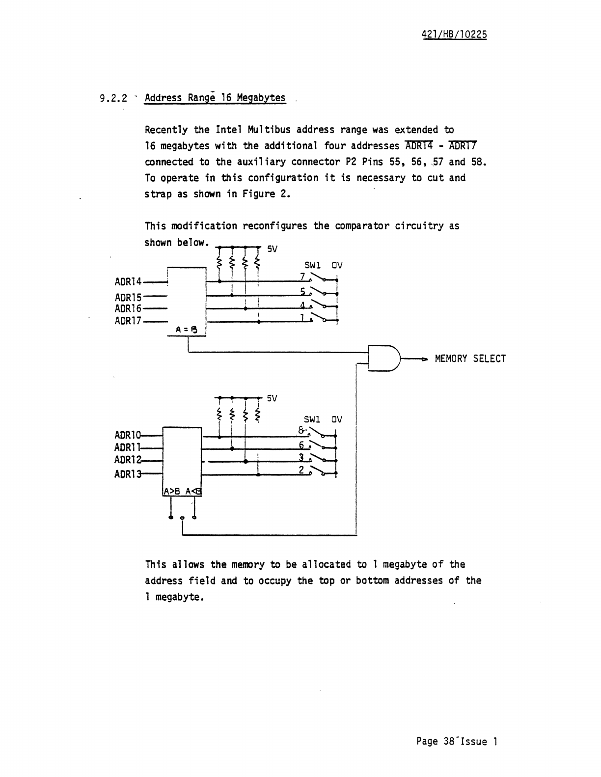
9.2.2 .
Address
Range
, 6
Megabytes
.
Recently the Intel
Mu1tibus
address range
was
extended to
16
megabytes
with the additional four addresses
~
-
~
connected to the
auxi1
iary connector
P2
Pins
55, 56,.57
and
58.
To
operate in
this
configuration
it
is necessary to cut
and
strap
as
shawn
in Figure
2.
This
modification reconfigures the comparator
circuitry
as
shown
below
. ! f
SV
S
I
I
WI
OV
ADR14-----
ADR15--
ADR16--
ADR17--
~
t ? ,
I ,
I i
I
I
•
7
~
5
11.
J
~
ADRl
ADRll
ADR12
ADRl
A=
=D-
MEMORY
SELECT
r • • •
SV
~
t i i
SWl
OV
1---+-!----w"'O:.~
This
allows the
melOOry
to
be
al located
to
1
megabyte
of
the
address
field
and
to
occupy
the
top
or
bottom
addresses of the
1
megabyte.
Page
3S-Is5ue
1
421/HB/l0225
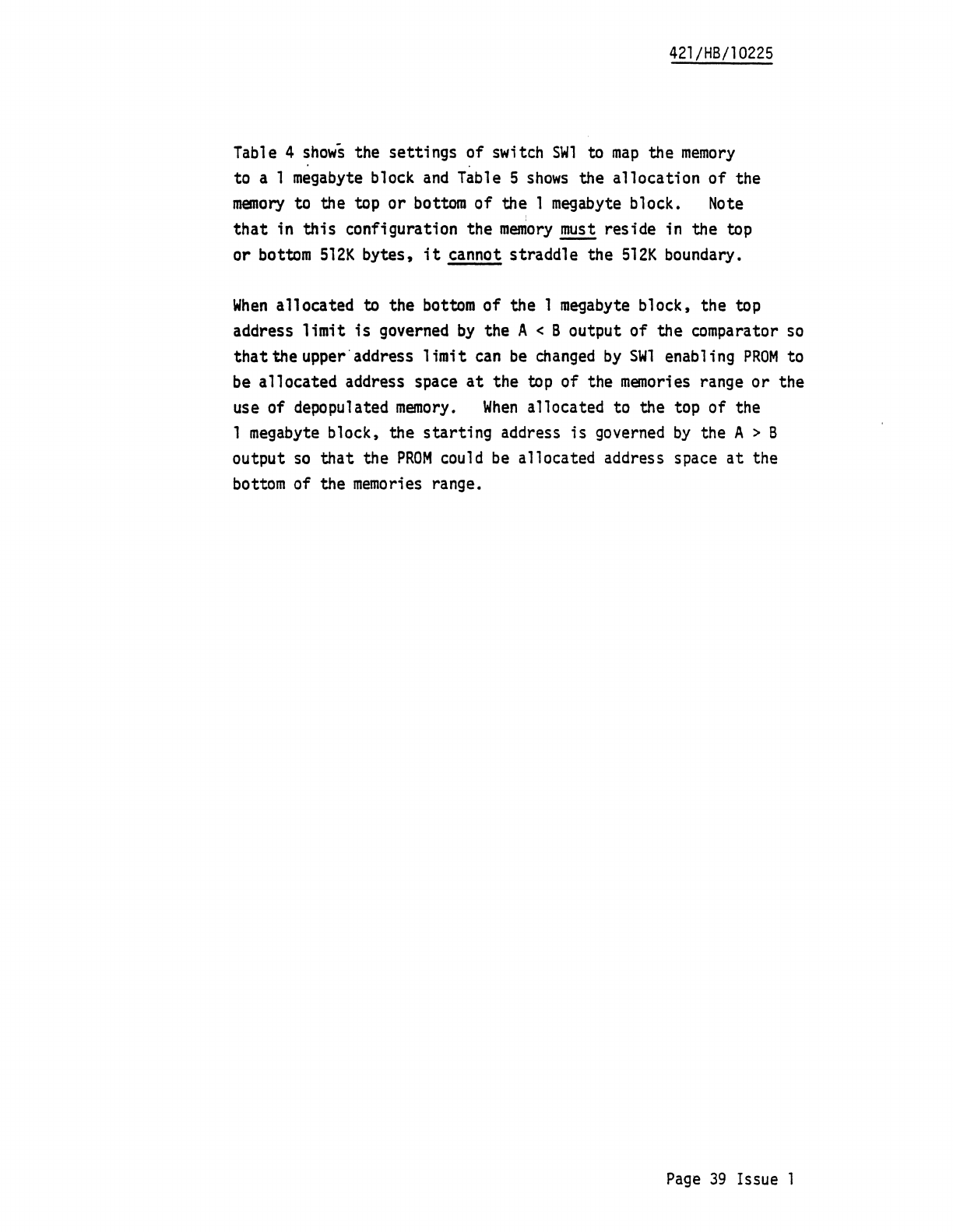
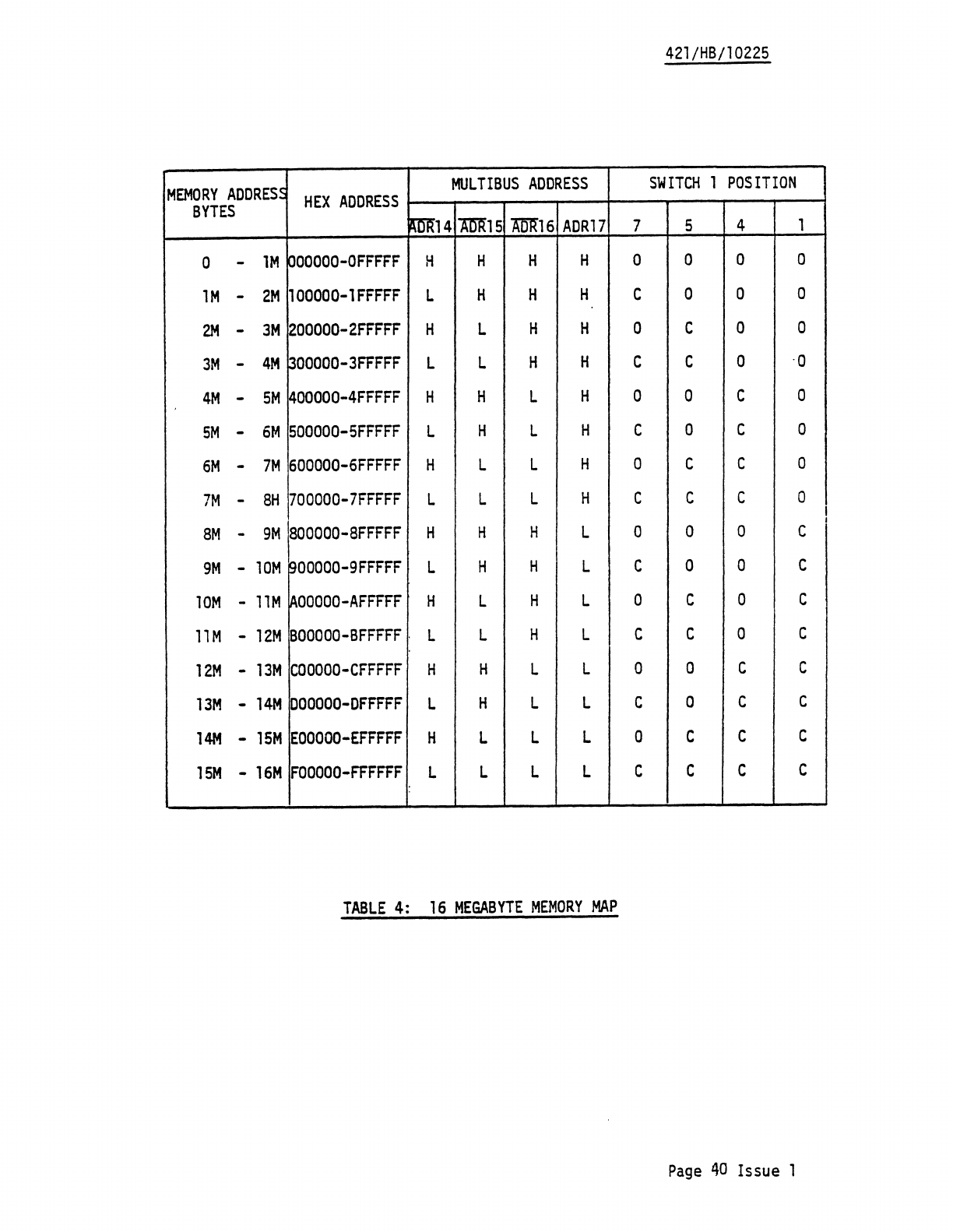
Table 4
shows
the settings of switch
SWl
to
map
the
memory
to a 1
megabyte
block
and
Table 5
shows
the allocation
of
the
memory
to
the top or
bottom
of
the 1
megabyte
block.
Note
,
that
in
this
configuration the
memory
~
reside in the top
or
bottom
5l2K
bytes,
it
cannot straddle the
5l2K
boundary.
When
allocated to the
bottom
of
the 1
megabyte
block, the top
address
limit
is
governed
by
the A < B output of the comparator
so
that
the upper' address 1
imi
t
can
be
changed
by
SWl
enab
1 i
ng
PROM
to
be
allocated address space
at
the top of the
memories
range
or
the
use
of depopulated
memory.
When
allocated to the top of the
1
megabyte
block, the
starting
address
is
governed
by
the A > B
output
so
that
the
PROM
could
be
allocated address space
at
the
bottom
of the
memories
range.
Page
39
Issue 1
421/HB/10225
MEMORY
ADDRES~
MULTIBUS
ADDRESS
SWITCH
1
POSITION
BYTES
HEX
ADDRESS
1'JlR14
AlmlS
Alm16
ADR17
7 5 4 1
0 -
1M
joOOOOO-OFFFFF
H H H H 0 0 0 0
1M
-
2M
100000-1FFFFF
L H H H C 0 0 0
2M
-
3M
200000-2FFFFF
H L H H a C 0 0
3M
-
4M
~OOOOO-3FFFFF
L L H H C C 0
·0
4M
-
5M
400000-4FFFFF
H H L H 0 0 C 0
SM
-
6M
500000-SFFFFF
L H L H C 0 C 0
6M
-
7M
600000-6FFFFF
H L L H 0 C C 0
7M
-
SH
700000-7FFFFF
L L L H C C C 0 I
9M
\SOOOOO-SFFFFF
I
SM
-H H H L 0 0 0 C
9M
-
10M
~00000-9FFFFF
L H H L C 0 0 C
10M
-
11M
jAOOOOO-AFFFFF
H L H L 0 C 0 C
11
M -
12M
BOOOOO-BFFFFF
. L L H L C C 0 C
12M
-
13M
COOOOO-CFFFFF
H H L L 0 0 c C
13M
-
14M
DOOOOO-DFFFFF
L H L L C 0 C C
14M
-
15M
EOOOOO-EFFFFF
H L L L 0 C C C
15M
-
16M
FOOOOO-FFFFFF
L L L L C C C C
TABLE
4:
16
MEGABYTE
MEMORY
MAP
Page
40
Issue
1
421/HB/10225
MEMORY
ADDRESS
SWITCH
1
POSITION
BYTES
HEX
ADDRESS
8 6 3
,2
0 -
512K
XOOOOO
-
X7FFFF
C C C 0
0 -
448K
XOOOOO
-
X6FFFF
O.
C C 0
0 -
384K
XOOOOO
-
X5FFFF
C 0 C 0
0 -
320K
XOOOOO
-
X4FFFF
0 0 C 0
0 -
256K
XOOOOO
-
X3FFFF
C C 0 0
0 -
192K
XOOOOO
-
X2FFFF
0 C 0 0
0 -
128K
XOOOOO
-
X1FFFF
C 0 0 0
0 -
64K
XOOOOO
-
XOFFFF
a 0 a 0
512K
-
1024K
X80000
-
XFFFFF
a 0 a c
576K
-
1024K
X90000
-
XFFFF
C 0 0 C
640K
-
1024K
XAOOOO
-
XFFFF
a c 0 C
704K
-
1024K
XBOOOO
-
XFFFF
C C 0 C
768K
-
1024K
XCOOOO
-
XFFFF
0 0 c C
832K
-
1024K
XDOOO
-
XFFFF
C 0 C C
896K
-
1024K
XEOOOO
-
XFFFF
0 C C C
960K
-
lO24K
XFOOOO
-
XFFFF
C C C C
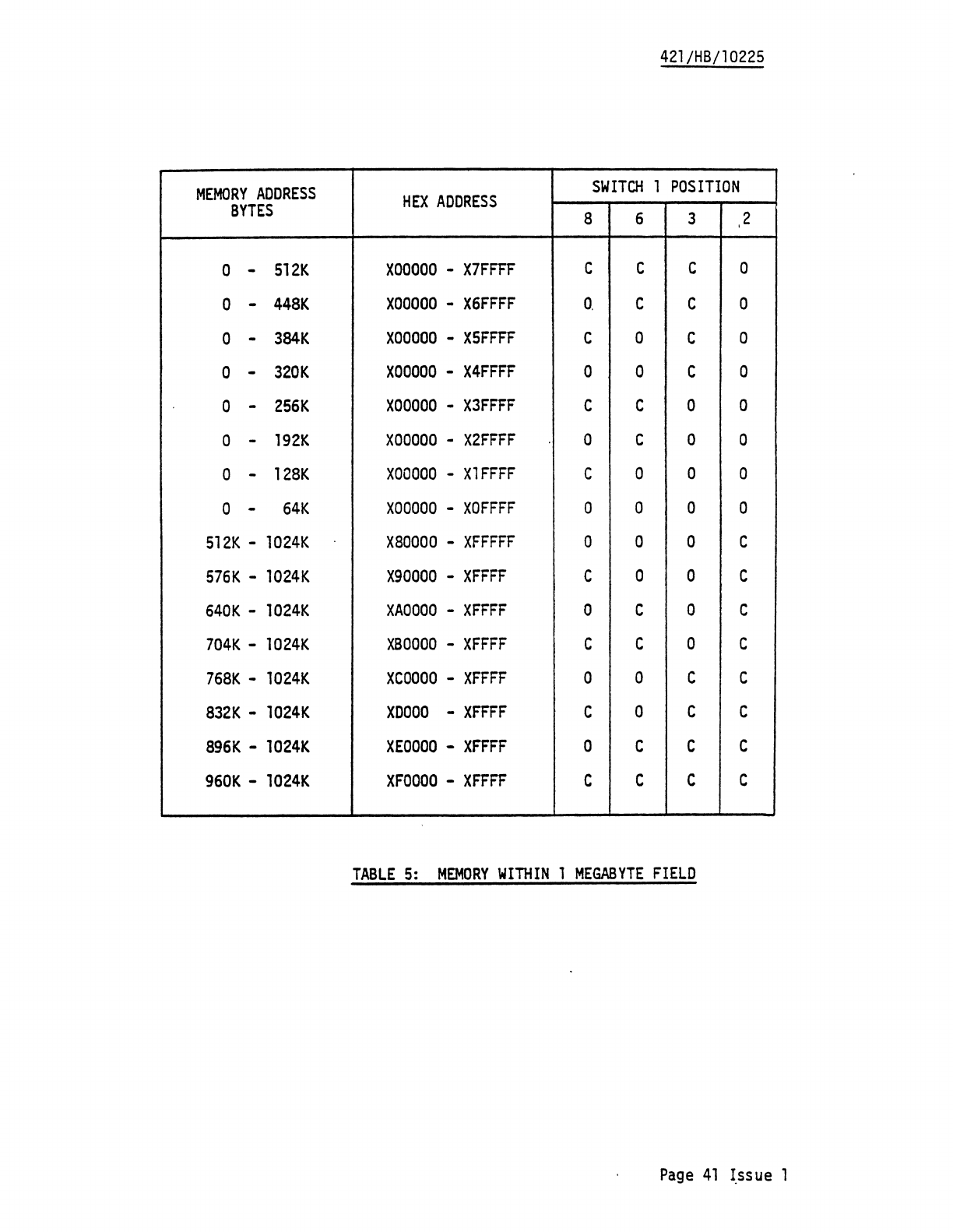
TABLE
5:
MEMORY
WITHIN
1
MEGABYTE
FIELD
Page
41
I.ssue
1
42l/HB/10225
FOR
42l/MB/10226jALL
VARIANTS
ISSUE
3
ONWARDS
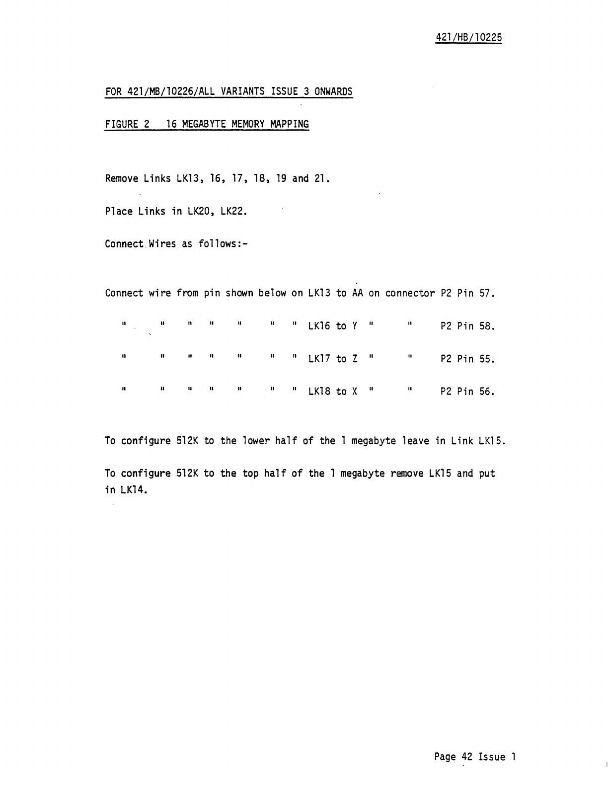
FIGURE
2
16
MEGABYTE
MEMORY
MAPPING
Remove
Links
LK13,
16, 17, 18,
19
and
21.
Place
Links
in
LK20,
LK22.
Connect.
Wires
as
follows:-
Connect
wire
from
pin
shown
below
on
LK13
to
AA
on
connector
P2
Pin
57.
" "
(I
II
" " "
LK16
to Y " "
P2
Pin
58
.
"
..
II II
.. ..
II
LK17
to
Z
..
"
P2
Pin
55.
..
..
II
11
"
..
"
LK18
to X " "
P2
Pin
56.
To
configure
512K
to the
lower
half of the 1
megabyte
leave in
Link
LK15.
To
configure
512K
to the top
half
of the 1
megabyte
remove
LK15
and
put
in
LK14.
Page
42
Issue 1
42l/HB/10225
FOR
421/MB/10226/ALL
VARIANTS
ISSUE
3
ONWARDS
9.3 Refresh
Jumper
link
LK23, LK38,
LK39
control refresh
circuitry.
For
on
board refresh only
LK23,
LK38
are in
and
LK39
removed.
For
external refresh control only
LK39,
is
in
aftdLK23,
LK38
removed.
For
external refresh control unless the
line
is
held
low
for
more
than
15
pS
whereupon
the
on
board
refresh
circuitry
takes over,
this
is
achieved
by
LK23,
LK39
being in with
LK38
removed.
9.4
Data
Retention
If
it
is intended
to
use
the anxiliary
power
supply for data
retention purposes, the following action
is
necessary:-
Remove
wire links
LK24,
LK25
and
wire link
LK40.
9.5 Miscellaneous
9.5.1
~
Option
Jumper
link
LK27
connects
~
to Multibus
Pl
connector
Pin
23
if
this
facility
is
not required,
remove
jumper
link
LK12.
9.5.2
Bus
Priority
Although
the
memory
cannot
act
as
a
Bus
Master, the
facility
exists
on
the
memory
card to short
BPRO
to
BPRIN
by
inserting link
LK26.
This
enables the
memory
card,
when
plugged
into a
system
with
serial
priority,
to
be
positioned
anywhere
with the chassis.
Page
43
Issue 1
421/HB/10225
10.
SYSTEM
DESCRIPTION
The
Plessey
PSM
512
Memory
Card
is
a
random
access semiconductor
memory
using
64K
dynamic
RAMS
with single
bit
error
correction
and
double
bit
detection.
The
Memory
may
be
split
up
into six
main
$ections.
10.1
Memory
Array
10.2
Address
Manipulation
10.3
Refresh
Logi
c
10.4
Data
Control
10.5
Timing
Control
10.6 Error Detection
and
Correction
10.1
MEr40RY
ARRAY
The
memory
array consists of 4
rows
of
22
dynamic
RAMS
(as
shown
in logic
drawing
sheet 2).
Each
ROW
containing
16
data
RAMS
and
6
EDC
,RAMS.
These
are
all
driven with the
same
command
signals of
RAS,
CAS,
WE
and
address
and
each
column
(containing 4
RAMS)
has
command
Data
In
and
Data
Out
signals to complete the array.
Page
44
Issue 1
421/HB/10225
10.1.1
THE
DYNAMIC
RAM
The
memory
is
fitted
with
64K
x 1
dynamic
RAMS.
The
storage
cells
within the
RAM
are matrixed in
rows
and
colu~with
a cell being selected
by
the
row
and
column
address being multiplied onto the device
by
means
of the
falling
edge
of
Row
Address
Strobe
(RAS)
or
Column
Address
Strobe
(CAS)
respectively.
Data
on
the device
Data
In
line
may
be
written into the selected cell
by
bringing the Write
Enable
line
(it)
low
when
RAS
and
CAS
are
both
low.
Data
Read
from
the selected cell
is
presented
on
the
Data
Out
line
at
access time
and
remains
valid until
~
returns to the
high
state
at
which
time
the
Data
Out
lines revert to
high
impedance
state.
The
PSM
512
board permanently
runs
on
a
Read
-
Modify
-Write
Cycle.
In
this
cycle the
row
and
column
addresses are strobed
in
and
the selected cel1·s data
is
latched
onto
the
Data
Out
line
at
access,
this
remains
there until
~
goes
high
(as in a
normal
read cycle) but also during the
same
cycle
new
data
on
the
Data
.
In
line
is written in
by
allowing
it
to
go
low
while
~
and
~
are
still
low.
Thus
enabling a
Read
and
a Write to
be
achieved
on
one
cell location in
one
cycle.
The
only other cycle
used
is
a Refresh cycle
which
is
carried
out
by
means
of a
~
only cycle
which
is
required
to
do
128
cycles every
two
milliseconds.
Page
45
Issue 1
421/HB/10225
10.2
ADDRESS
MULTIPLYING,
MEMORY
SELECT
AND
RAS
DECODE
Address
AO
is
used
in
conjunction with
Byte
Enable
(BHEN)
to
determine whether the
memory
is
operating
in
16
bit
word
of
256K
or
an
a
bit
byte of
512K.
This
is
done
by
using
]RtN
and
AO
to control the data being driven onto the
RAM
or
controlling the data read out of the
RAM
to the output bus.
The
next
16
addresses
(Ai
-
A10)
form
the multiplexed
row
and
column
addresses
which
are driven onto the
RAM
where
they are.
latched to
form
a cell selection.
The
timing of the
multiplexer
is
contrcl1ed
by
a signa1.called
MUX
unless the
memory
is
doing
a refresh cycle
whereupon
the refresh address
is
driven onto the
RAM
address
lines.
Address
All
and
A12
are fed into a
two
to four
line
decoder to
form
a
row
select
which
determines
which
row
of
RAMS
receives
a
~.
Addresses
A10
-
A13
are
used
in
two
hour
bit
magnitude comparators
to determine the area
in
which
the
memory
is
mapped
and
therefore
selected.
One
comparator
is
set
with
A > B
and
the other with
A < B
where
the A input
is
the address with the B input switchable
high or
low
via switches. Therefore the
memory
is
only selected
when
A > B
on
Comparator
I
(Iella)
and
A < B
on
Comparator
II
(ICl19);
for
further"information see the
memory
mapping
section.
Page
46
Issue 1
421/HB/10225
10.3
REFRESH
LOGIC
Dynamic
RAMS
require
all
th~re
rows
to
be
addressed every 2
mS
and
as
there are
128
rows
this
means
for a distributed refresh
lone
row
is
to
be
refreshed every
15
~
Sec.
if
data
is
not to
be
lost.
This
can
be
achieved in
one
of three
ways.
(1)
Leave
control of refresh
to
the
on
board
timer
and
refresh
arbitration
Logic
with External Refresh signal
(EXT.REF)
on
Pl/77 disconnected.
This
will
result
in a distributed refresh cycle every
15
~S
controlled
by
the
LS123
which
makes
up
the timer,
this
then
clocks a D type latch
which
sends
out a Refresh
Request
(REF
REO)
and
goes
into a latch the other side of
which
is
Memory
Request
(M
REO)},
so
dependent
on
whether
REF
RFO
or
MREO
arrives
first
depends
on
whether a refresh cycle
is
completed
before the
memory
cycle
or
after
it.
At
the
end
of
the
RAS
only refresh cycle a counter
is
clocked
which
increments
the refresh address before releasing
Memory
Busy
to allow
another cycle.
(2)
This
gives the driver of the
board
control of refresh
as
long
as the
board
gets a refresh
at
least
once
every
15
~S
otherwise
the
board
initiates
a refresh cycle.
This
is
achieved
by
connecting
EXT.
REF.
into
Pin
1
of
It
109
of
LS123
and
Pin
13
of-
r~~_!~~:.the
LS32
to clock
REF
REO;
under
these conditions
EXT
REF
is
held normally
low,
going
high
to
initiate
a refresh but
if
the
EXT.REF
has
been
low
for
15
~Sec.,
then the
board
will
initiate
its
own.
Page
47
Issue 1
42l/HB/i0225
(3)
This
totally
hands
over refresh control of the board to
the
EXT.REF.
signal with
I~·'.~f
Pin
1 held
high
and
disables
the timing
circuit.
Then
by
connecting
EXT.REF.
into Iel11
Pin
13
means
that
on
each
rising
edge
of
EXT.REF.
initiates
a refresh cycle
and
counts
up
the refresh addresses
so
long
as
there are
128
cycles per 2
mS
no
data loss will occur.
Page
48
Issue 1
421/HB/10225
10.4
DATA
CONTROL
When
the
memory
receives a
command
signal
such
as
MRDC
or
MWTC
it
always
initiates
the
same
Read
Modify
Write cycle, the only difference
is
in the data
control,
fo~
instance in a
16
bit
read cycle the data
from
the
RAMS
(EDC
and
data) passes through the Error Detection
and
correction
(EDC)
device
where
it
is
corrected
and
is
passed out onto
the bus,
it
is
also turned
round
and
written
back
into the
memory
(16
bit),
ie.
on
a read cycle corrected data
is
written
back
into the
read 1 ocati
on
•
During
a write cycle data
is
still
read
-out
of the
RAMS
but
is
not
allowed out
on
the
bus
and
the
new
write data passes into the
EDC
device
which
is
in the write
mode
and
therefore generates
new
EDC
data
and
passes
all
the data through to the
RAMS
to
be
written into
on
the write
part
of the cycle.
On
an
(8
bit)
or byte read
which
is
controlled
by
AO
and
]H!N
where
BHEN
is
high then
AO
controls
which
8
bits
of
the
memory
is
read or
written to.
For
example
in a byte read the
whole
word
is
read
as
a
16
bit
read
but
this
time only 8
bits
are allowed out
either
straight
out for
Data
0 - 7 or byte
swapped
from
8 -
15
into
Data
0 - 7 output.
However
for
a-
byte write the
memory
reads the
16
bit
word
with
EDC
check
bits
and
corrects
it,
then
one
EDC
device
is
put into the read
mode
and
the other with 'the
new
8
bits
of write data
on
its
input
into the write
mode.
Then
the
new
word
consisting of 8
bits
of
read
corrected data
and
8
bits
of
new
write data generate the 6
EDC
check
but data
'and
the
whole
word
is
written into the
memory
thus
completing the cycle.
Page
49
Issue 1
421/HB/10225
10.5
TIMING
CONTROL
The
on
board
timing is controlled via delay
lines,
this
is
used
to
generate the
command
signal for the
RAMls
such
as
RAS,
CAS,
WE
and
MDX.
It
is also
used
to generate the output signals
such
as
~,
~
and
is
used
to strobe the multi
error
and
single error
line
to
determine whether a single or multibit
error
has
occurred.
The·
delay
lines
are
either
driven by'a
command
signal, Readior Write or
by
a Refresh cycle with the
Busy
timer
and
refresh
arbitration
logic
making
sure
that
only
one
signal passes,down the
line
at
a time.
Page
50
Issue 1
421/HB/1022S
10.6
ERROR
DETECTION
AND
CORRECTION
This
is
controlled
by
two
Fujitsu
MB14l2A,
each
of
which
control
8
bits
of data but are interconnected
to
form
a 6
bit
check
bit
output for the
16
bit
word.
Each
device
has
separate
Read
(RDO-7)
and
Write
(WDO-7)
data in
as
well
as
corrected data (00-7) out
and
this
is
controlled
by
means
of a single
line
5TB.
If
5TB
is
a logic
low
the chip is in the
read function
and
data
and
check
bit
(5l0-1S) are read in
and
corrected data
and
syndrone (50-S) outputed
as
well
as
indication
whether a single
bit
error
has
occurred,]!T
or
an
error
has
occurred
in the
check
bit]Ve.
(The
decode
of the
syndrone
is
shown
in
Appendix
1).
If
the
5TB
is
a logic
high
the chip
is
in the write
mode
and
the
data
on
the write input
(WDO-7)
is
outputed onto the data out
(00-7) along with the
check
bit
output
(CO
0-5).
The
devices
together correct
any
single
bit
error
in
data or
EDC
bits
giving
indication
that
a single
bit
error
has
occurred
(by
means
of
a small.
amount
of external logic).
It
is
also able to detect
any
double
bit
error
but
does
not attempt to correct
them.
(An
indication of
which
memory
device
is
failing
is
given
in the syndrone
data,for
information
on
how
to
decode
this
see
fault
finding).
Page
51
Issue 1
421/HB/10225
11.
FAULT
FINDING
The
Plessey
P5M512
memory
is designed
as
a plug
in
item
and
faulty
modules
should
be
returned to P1essey for repair.
However
in order to aid the turn
round
of repaired
modules
an
indication
of
the
fault
symptom
is
invaluable, especially
when
the
fault
is
intermittent or marginal.
In
order to aid diagnosis, logic
diagrams
are provided in the
handbook
together with a description of the
memory
system,
and
the
following syndrone
decoding
chart will help in detecting
any
single
bit
errors.
The
syndrone outputs appear
on
ICll2
as
listed
below
and
this is
only valid
on
the read half of a cycle
and
not
on
a refresh cycle,
a useful strobe
when
the
syndrone
is
valid
is
on
ICll1
Pin
8.
so
is
on
ICl12/2
51
is
on
IC112/l
52
is
on
IC112/13
53
is
on
ICl12/3
54
is
on
ICll2/5
55
is
on
ICl12/4
P:age
52
Issue 1
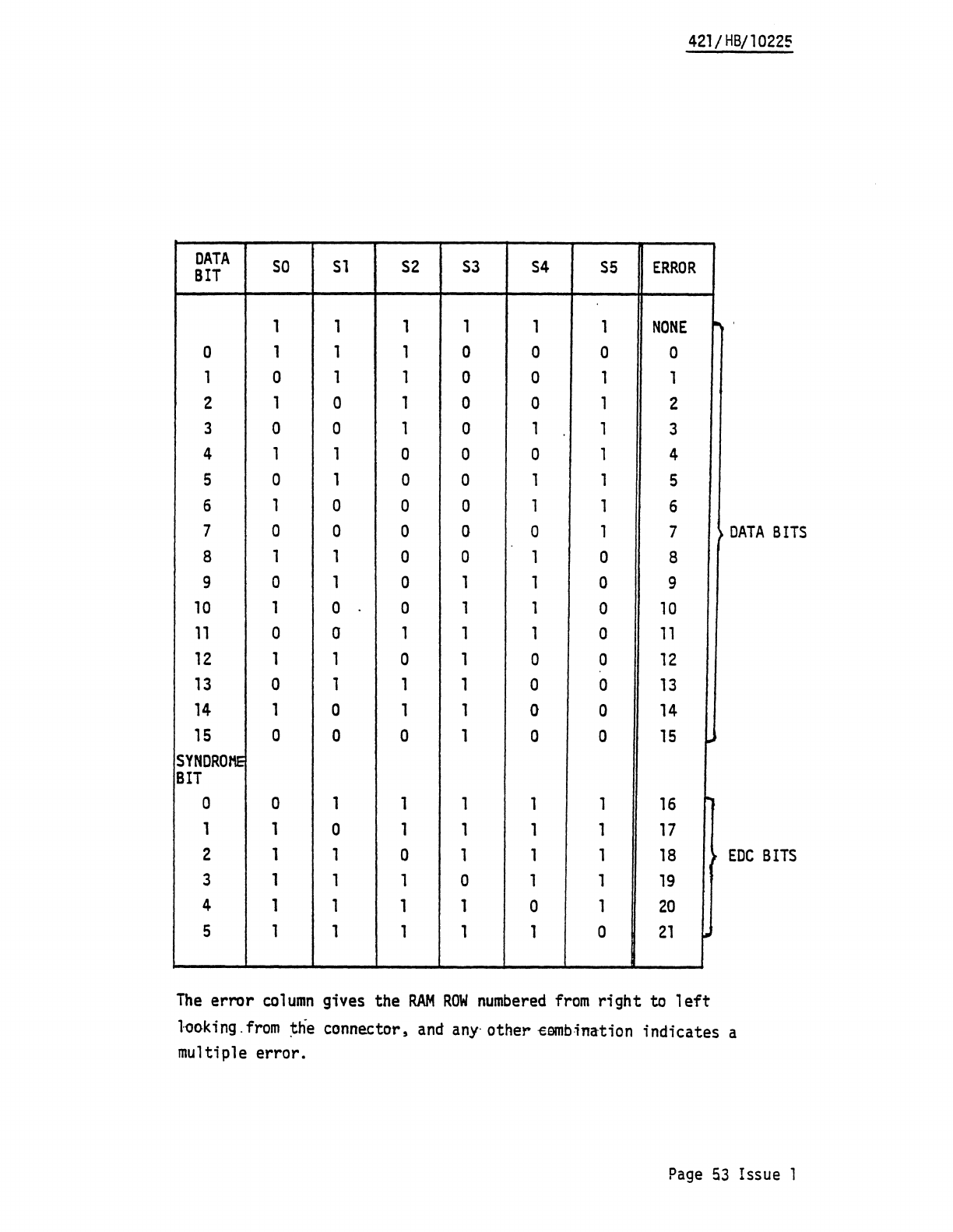
421/
HB/
1 0225
DATA
SO
Sl
S2
S3
S4
S5
ERROR
BIT
1 1 1 1 1 1
NONE
0 1 1 1 0 0 0 0
1 0 1 1 0 a 1 1
2 1 a 1 0 0 1 2
3 0 0 1 0 1 1 3
4 1 1 0 0 0 1 4
5 0 1 0 0 1 1 5
6 1 0 0 0 1 1 6
7 0 0 0 0 0 1 7
~
DATA
BITS
8 1 1 0 0 1 0 8
9 0 1 0 1 1 0 9
10 1 0 0 1 1 0 10
11
0 a 1 1 1 0
11
12
1 1 0 1 0 0 12
13
0 1 1 1 0 0
13
14
1 0 1 1 0 0
14
15 0 0 0 1 0 0
15
SYNDROME
BIT
0 0 1 1 1 1 1
16
1 1 0 1 1 1 1
17
2 1 1 0 1 1 1
18
EDC
BITS
3 1 1 1 0 1 1
19
4 1 1 1 1 0 1
20
5 1 1 1 1 1 0
21
The
error
column
gives the
RAM
ROW
numbered
from
right
to
left
looking.
from
:the
connector,
and
any'
other
€OO1b·ination
indicates a
multiple error.
Page
53
Issue 1
421jHBjl0225
12.
INSTALLATION
AND
OPERATION
This
sections unpacking,
installation
and
operating instructions
for the Plessey
PSM512
memory.
12.1
RECEIVING
INSPECTION
The
PSMS12
memory
is
fully
assembled
and
tested
prior
to shipment
from
the factbry.
The
units are individually
packed
in accordance
with standard practices for electronic equipment.
Every
precaution is taken to ensure
that
each,system leaving the factory
is
complete
and
ready for
installation.
However
it
is
recommended
that
units
be
inspected
upon
receipt for shipping
damage.
12.2
INSTALLATION
The
memory
is
designed for
mounting
in a card
cage
and
to
plug
into
printed
circuit
board connectors.
The
interface connector pin
assignment is
shown
on
Pages
21·and
22~
The
PSM5l2
has
a
number
of
user options available, for
details
see Section 9 of this
document.
Prior to
installation
in the card
cage
check
that
the appropriate
options
have
been
set
up.
12.3
POWER
REQUIREMENT
The
memory
only
has
one
power
rail
of
+SV,
this
should
be
~
5%
and
a
check
should
be
made
that
the
board
pin
assignment coincides with
the backplane.
Page
54
Issue 1
421/HB/l0225
APPENDIX
1
APPLIES
TO
421/MB/10226/ALL
VARIANTS
ISSUE
2
ONLY
Page
55
Issue 1
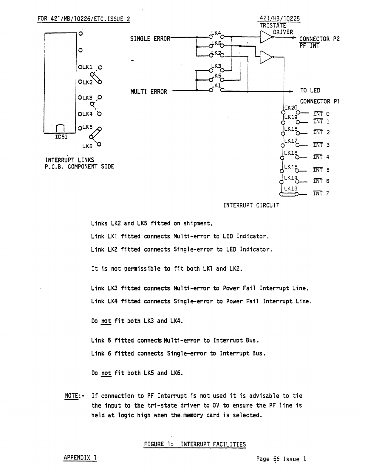
FOR
421/MB/10226/ETC.ISSUE
2
421/HB/10225
TRISTATE
,..----...,0
_
___
,
__
...LK40~'
__
--!C>DRIVER.
SINGLE
ERROR
cr
~
I -
o
C1
K
.•
CONNECTOR
P2
PF
tNT
elKl
0
OLK~
MULTI
ERROR
.
~;tthl
-BK1~U-_--+-
____
+-1
__
TO
LED
OLK3 0
c(
.
OLK4
1:)
._·~r~l---,
OLKS./9.
IeSl
<Y'
LK6
'0
,
INTERRUPT
LINKS
P.C.B.
COMPONENT
SIDE
~
_
CONNECTOR
P1
LK20
LK1S
O-m 0
0--
INT 1
I
LK1~-
!Ni
2
LK1~
!NT 3
LK1~
fNi' 4
d
LK1
0-.-
INT
5
1LK1e-
!Nt
6
I LK13
c:=::::!)
INT 7
INTERRUPT
CIRCUIT
Links
LK2
and
LKS
fitted
on
shipment.
Link
LKl
fitted·connects Multi-error to
LED
Indicator.
Link
LK2
fitted
connects Single-error
to
LED
Indicator.
It
is
not permissible to
fit
both
LKl
and
LK2.
Link
LKJ
fitted
connects Multi-error
to
Power
Fail Interrupt Line.
Link
LK4
fitted
connects Single-error to
Power
Fail Interrupt Line.
Do
]2!
fit
both
LKJ
and
LK4.
Link
5
fitted
connec~Multi-error
to Interrupt
Bus.
Link
6
fitted
connects Single-error to Interrupt
Bus.
Do
not
fit
both
LKS
and
LK6.
~:-
If
connection to
PF
Interrupt is not
used
it
is
advisable to
tie
the input to the
tri-state
driver to
OV
to ensure the
PF
line
is
held
at
logic
high
when
the.
memory
card
is
selected.
FIGURE
1:
INTERRUPT
FACILITIES
APPENDIX
1
Page
~6
Issue 1
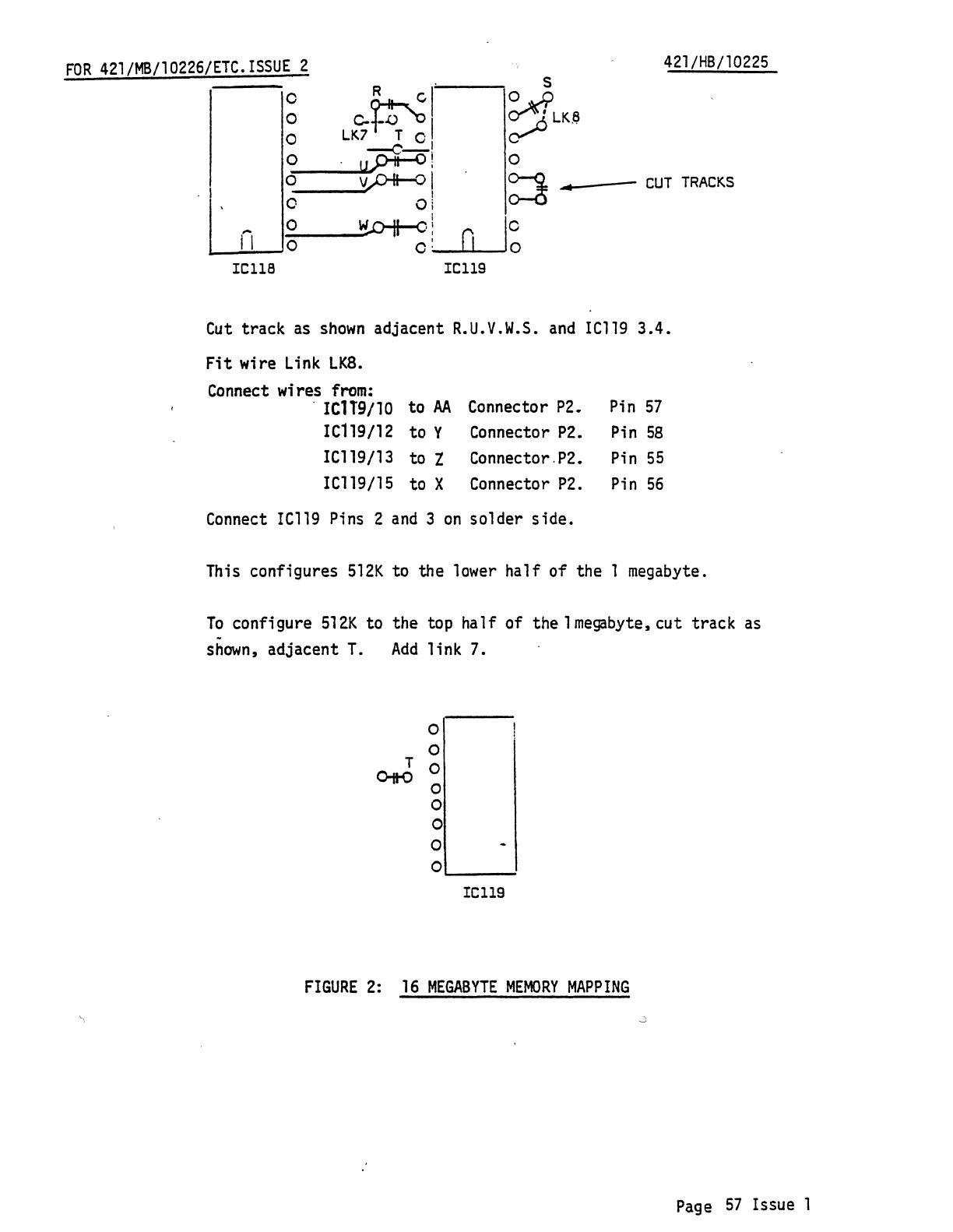
FOR
42l/MB/l0226/ETC.ISSUE
2
42l/HB/10225
~
c-~II·
o LK7 T C
~_I
S
~LK~
o
~
o
vp*-o
o 0
~
...
.04---
CUT
TRACKS
L--
__
n----'~
0
I~
rClla
rCllS
Cut
track
as
shown
adjacent
R.U.V.W.S.
and
ICl19
3.4.
Fit
wire
Link
LK8.
Connect
wires
from:
.
IC1T9/10
to
AA
Connector
P2.
Ic119/l2 to Y Connector
P2.
ICl19/l3 to Z Connector.P2.
ICll9/15 to X Connector
P2.
Connect
ICl19
Pins 2
and
3
on
solder side.
Pin
57
Pin
58
Pin
55
Pin
56
This
configures
512K
to the
lower
half of the 1
megabyte.
To
configure
512K
to the
top
half of the 1
megabyte,
cut track
as
shown,
adjacent
T.
Add
link 7.
0
0
T 0
0it0
0
0
0
0
0
IellS
FIGURE
2:
16
MEGABYTE
MEMORY
MAPPING
Page
57
Issue 1
FOR
42l/MB/10226/ETC.ISSUE
2
42l/HB/10225
9.3
Refresh
Jumper
links
LK23
and
LK24
control the refresh
circuitry.
These
are located adjacent to connector
Pl
Pins 75,
77
and
79.
For
on
board refresh
jumper
link
LK2l
is
fitted.
To
control
refresh externally
LK24
is
fitted.
9.4
Data
Retention
If
it
is
intended to use the auxiliary
power
supply for data
retention purposes, the following actions are necessary:-
a)
Cut
track
as
shown.
A
PCB
COMPONENT
SIDE
b)
Remove
LK9
adjacent
IC12S
Pin
14.
c)
Insert
LK10
positioned
below
IC127.
9.5 Miscellaneous
9.5.1 A
ACK
Option
Jumper
link
LK12
connects A
ACK
to Multibus
Pl
connector Pin
25.
If
this
facility
is
not required, then
remove
jumper
link
LK12.
9.5.2
Bus
Priority
APPPENOIX
1
Although
the
memory
cannot
act
as
a
Bus
Master. the
facility
exists
on
the
memory
card
to
short
BPRO
to
BPRIN
by
inserting
link
LKll
•.
This enables the
memory
card,
when
plugged
into a system with
serial
priority.
to
be
positioned
anywhere
with the chassis.
Page
58
.Issue t
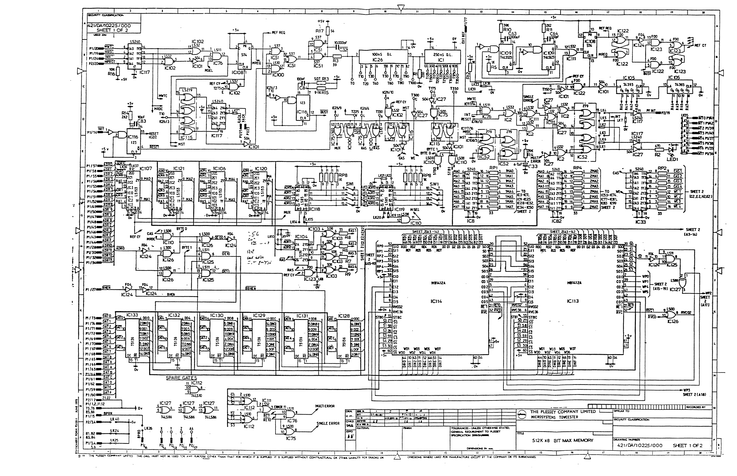
.
po
f
~
'.
~
-
..
z
il
2.1
A
2110All022SIOOO
SHEET 1 OF 2
PlI'alI.~=\oI=-
__
--,~
•
PlI19_~~--='ctJ
I
PlI14._,",'::NH,,=::;:::'
:--~4I
PZlZo...-""""",C.:...T
.-r-
.......
~Q
.SV
D
HWTC
~
MROC
T10
1tlfl/3
>C.
u .
...,-C,
0<'
X.
I~
~
::::-
~S~
1 Z
Cl0l
12c!
t.M
>.I'N
:::,-
[-1/';
IC12l
Ul
1C103
Pl/n,
..
~~-_~~,-~~~~
______
~~
____________
~~~~L-
________
~
________
~O¥~
,
BHOI
"/7
'1/74
Pl/71
PlI7Z
Pl/69
PI/7
PI
/61
Pl/68
Pl/65
SPARE GATES
11
ICl12
U
74LS1O
PI/61
---=~"1
P1162
ii'if 0
Pl/59
WE
'1160
m~
PZll Z
21.ZZ
'111.17
12
1
75.76
.~--------
...
t
O.
85,86 BfS!!
'1115
-1
'=:
~':
r'
lK24 0 T LI2Ii I Y Z
'"
:i:i lK25
~i
1
.•
1 •
Pl/~.
oJ
'lty,
"""
P4«
PZj
9 IC127
12
1C127
!QD-llY-
t4l586 74lS86
7/oLSB6
I)
"81412,.
IC114
..
" I.
HSl412,.
tell
3
"
'"
5I£ET 2
II:Z.£
z.KZJ2
)
"--+-+-wz
SIfiT
Z
1A171
L-.
_____________________________________
-+~----------~
5I£ET
2
(Alii
A
•
G
H
"
§Ii
~~~~~~~1IKOO.CED3.T
N
,_,
.,
I _ .
~,
THE
PLESSE'r
COMPANY
UHfTED
""'UUI
TO
'''.-I H1CBOSrmHS
TOWCES'TtR
IiCI,IrJTT Cl..WIACAllON
~
1"OI...IM.HC:I
..
UN..fSS
0'rHB'WR
ITA-TID.
C<MM<
~
TO
rus:IlT
SI'fOIOCATlOH
~
mu
512K
xB
BIT MAX MEMORY
~
..
-
II
fl
11
...
IS
..
~
.......u
uc;v
"0«.
~
iXL.~
.2Y
n'il
~
0-.
m
SUi!ISIC\AA.£S.
4211DA./10225/000
" " "
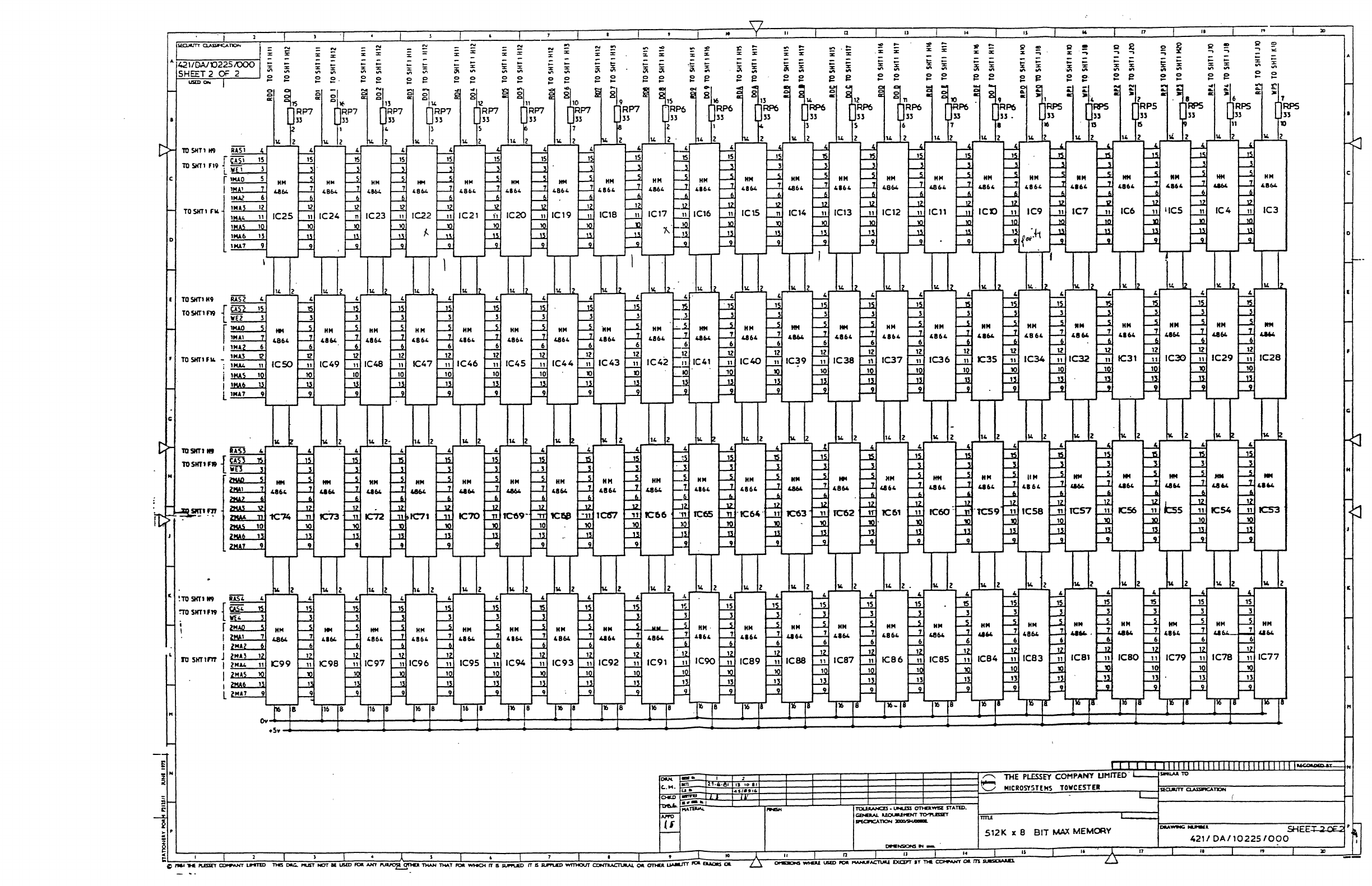
IoECJOtTT
Cl.AUIHCAnoo.
A
QllOA/02251OOO
SHEET
2
OF
2
USIII
"'"
C
E
TOSHTI
N9
TOSHT1f19
"
::
-
%
'"
..
...
gr
II<
"
14
...
s:
::
--
%
:z:
'"
'"
..
..
...
...
~~
is
a:
RP7
33
2
'14
~
~
~
:z: %
:z:
i =
....
-
...
...
...
::
%
:z:
:c
:c
'"
.,..
on
.,..
on
e· 0 e e
...
0
...
8
wr
r
::;1
II<
13
RP7
55
4
2
14
4
N ~ !!!
:
..
~
!!! '" ~
...
::: ::: :z:
;;
:z:
::
:z:
i
:z:
:z:
'I!
~
...
:r.
::
;;
...
...
...
;::
...
~
~
~
:c
:z: :z:
~
~
'~
::: :::
.,..
'"
'"
'" '"
-i
;:
:z:
:z:
....
.,.
e
.. .. .. ..
e 0 e
.. ..
e
...
.-
...
...
...
...
...
e
..
e
...
~
"
RP7
53
" 2
'14
8~r
33
1
2
4
II a
17
..
..
»
'"
po
.=:
:!
po
'$!
...
'II
=:
2
~
.,
50'
5'
'"
;;
:
50'
!!
50'
!!
g
50'
i ;;
;;
:I:
.:1:
% Z
:I:
51
:;
..,
""
:z;
..,
..
...
-.
...
...
.....
i
...
...
...
~
-
;:
ft
...
::
;:
S;
...
;::
...
... ...
A
;:
...
~
..
...
:z:
z
:z:
:z:
:::
'"
x
:z:
%
:z:
:z:
:z:
:z:
:z:
:z: :z:
on
:z:
on
'"
.,.
'"
'"
....
'"
...
'"
.'"
'"
.,.
on
...
'"
.,..
'" '"
..
..
e e
.. ..
..
..
e
..
e e
..
...
..
e
..
.. ..
e
..
..
...
...
...
...
...
...
...
...
0-
...
...
...
... ... ...
..
..
...
~
..
~
'5
'"'
c
:.
6 7
RP6
RPS
RPS
55
53
1S
11
1)
2
c
o
I
G
z
"
CW<
--
'.H~
om
II
10.'
U.
.."."
.
OCD
......
8"--
...
--
§i
~~~~~~~
..
""
THE
PLESSEY
CQHPANY UHITEO'
--
'10
to
MICROSTSTUI5
TOWC£ST£I
SKIMTT
QADlflCAl10H
t1JLIMICIS
.........
01HBl_
SlAm>.
.no
GBaAI.
~
1'O'1'UI:IFt
IPICI'ICAl1OH
__
mu
(r
2
a'
512K
x B BIT
MAX
MEMORY
DM
__
l
SHEEc-l-.o'-U=-"'I
~
~-.----r----,----~---.----.---~----r---~----.---~----.---~----r---~----~~~-L--~--~----r1--~----
r-
__
~~
__
~~~~~T-
__
~~
__
~--~--
__
r---~~~r---~--L-~--4~2~1_/~D_A_/~1~O~2~2~5~/~O~O~O~
__
~~~
~
1 • 7 • •
..
II
12
~
..
-
I.
II
I.
17
"
..
1Il
