QM_XC7A35T_SDRAM_User_Manual(DaughterBoard) QM DB User Manual
User Manual:
Open the PDF directly: View PDF ![]() .
.
Page Count: 18

QM_XC7A35T_SDRAM Daughter Board(User Manual)
QM_XC7A35T SDRAM DB
USER MANUAL
Preface
The QMTech® XC7A35T SDRAM Development Kit uses Xilinx Artix®-7 devices to demonstrate the highest
performance-per-watt fabric, transceiver line rates, DSP processing, and AMS integration in a cost-
optimized FPGA. Featuring the MicroBlaze™ soft processor and 1,066Mb/s DDR3 support, the family is the
best value for a variety of cost and power-sensitive applications including software-defined radio, machine
vision cameras, and low-end wireless backhaul.

QM_XC7A35T_SDRAM Daughter Board User Manual-V01
Table of Contents
1. QM_XC7A35T_SDRAM DB INTRODUCTION........................................ 3
1.1 KIT OVERVIEW ............................................................................. 3
1.2 DAUGHTER BOARD TOP VIEW ......................................................... 3
2. EXPERIMENT (1): USB TO SERIAL PORT .............................................. 4
3. EXPERIMENT (2): VGA DISPLAY .......................................................... 7
4. EXPERIMENT (3): CY7C68013A USB 2.0 SLAVE FIFO ......................... 10
5. REFERENCE ...................................................................................... 17
6. REVISION ......................................................................................... 18
QM_XC7A35T_SDRAM Daughter Board User Manual-V01
1. QM_XC7A35T_SDRAM DB Introduction
1.1 Kit Overview
QM_XC7A35T_SDRAM Daughter Board provides several user interfaces to meet different customer
needs. Below section lists the detailed info of these user interfaces:
USB to UART Serial Port, by using Silicon Labs’ CP2102-GMR chip.
24bit(RGB888) VGA display interface, by using Analog Device’s ADV7123-KSTZ140 chip;
High speed USB 2.0 peripheral controller, by using Cypress’ CY7C68013A-56LTXC chip;
Reserved CMOS/CCD camera interface, by using 18pin female header;
Extended 40 pin male header to provide 34 user IOs, which could be used to connect customized
modules, e.g. ADC/DAC module, Ethernet module, Audio module;
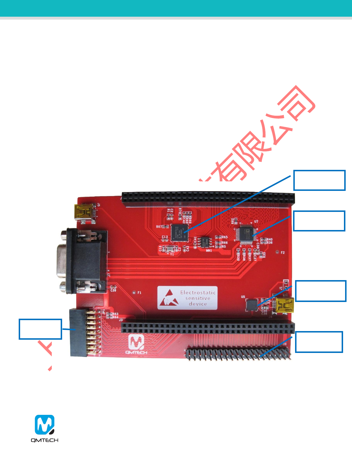
1.2 Daughter Board Top View
Below figure shows the daughter board of QM_XC7A35T_SDRAM development kit. The daughter board’s
dimension is 81.28mm x 108.71mm. All the functional chips’ power supply is injected from the 64P female
connector, detailed connection refer to the hardware schematic.
Figure 1-1. Top View of QM_XC7A35T_SDRAM Daughter Board
CP2102, USB to
Serial Port
ADV7123,24bit
VGA
CY7C68013,USB
2.0 HS
CMOS Camera
Interface
40Pin Header
for User IOs
QM_XC7A35T_SDRAM Daughter Board User Manual-V01
2. Experiment (1): USB to Serial Port
The CP2102-GMR is a USB 2.0 to serial port bridge chip designed by Silicon Labs. The CP2102-GMR
includes a USB 2.0 full-speed function controller, USB transceiver, oscillator, UART and eliminates the
need for other external USB components are required for development. Below figure shows the hardware
design of CP2102-GMR on the QM_XC7A35T_SDRAM daughter board.
Figure 2-1. CP2102 Hardware Design
Before start to test the CP2102-GMR’s USB to UART serial communication function, make sure all the
hardware connections of the development kit are correctly connected. Xilinx USB platform cable’s VREF,
GND, TDI, TMS, TCK, TDO pins shall be connected to QM_XC7A35T_SDRAM core board’s JTAG
interface. Then power on the development kit with 5V DC power source. Xilinx USB platform cable’s
indicator LED’s color will turn from brown into green. At the same time, the Mini-USB cable shall also be
plugged in the board, below figure shows an example hardware setup:
C36
4.7uF
GND
R34 4.7K
U5
CP2102-GM
DCD 1
RI 2
GND
3
D+
4D-
5
VDD
6
REGIN
7VBUS
8
RST 9
NC1
10
SUSPEND 11
SUSPEND 12
NC2
13
CTS 23
RTS 24
RXD 25
TXD 26
DSR 27
DTR 28
NC3
14
NC4
15
NC5
16
NC6
17 NC7 18
NC8 19
NC9 20
NC10 21
NC11 22
GND_TP
29
J4
MINI_USB
Vcc 1
D- 2
D+ 3
ID 4
GND 5
G3
8
G4
9
G2
7
G1
6
GND
DNP
J1
USB_5V_IN
GND
C35
100nF
BANK35_C4
BANK35_D4
Mini-USB Cable
5V DC Source
JTAG Cable
QM_XC7A35T_SDRAM Daughter Board User Manual-V01
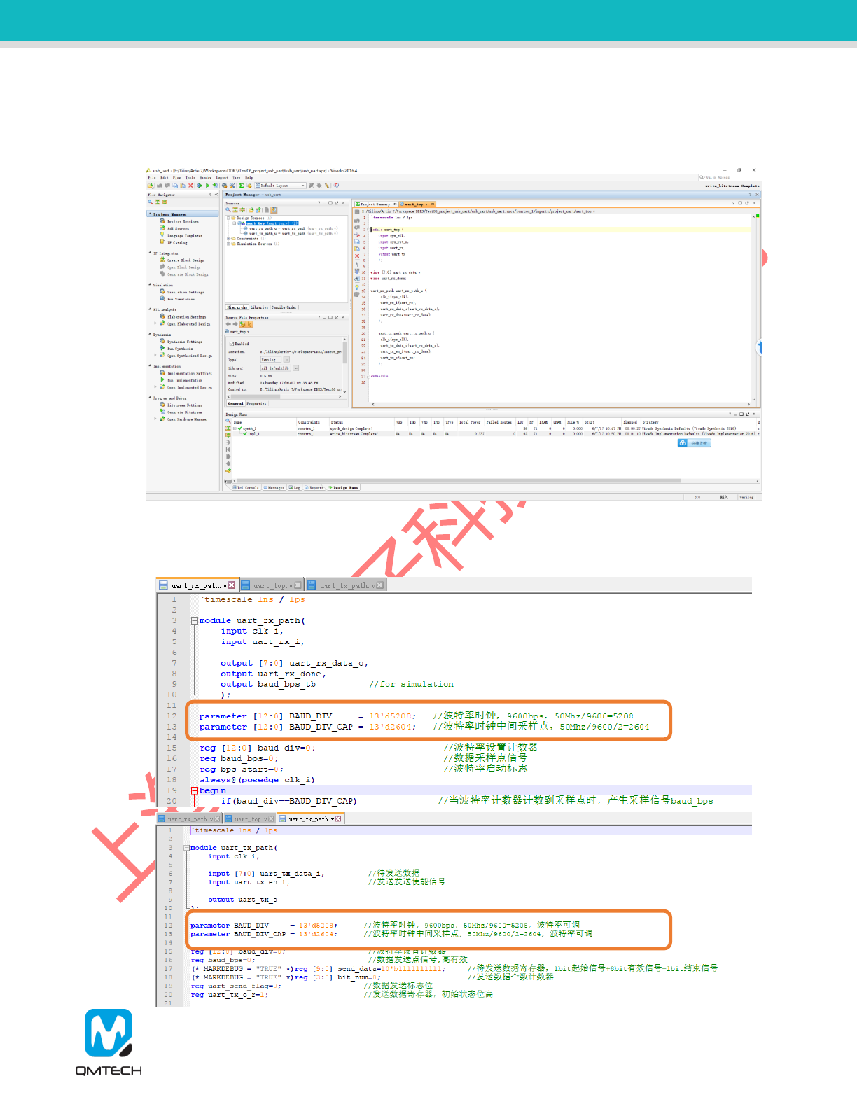
All the test examples are developed in the Xilinx Vivado 2016.4 environment. Open the CP2102 test
project located in this release folder: /Software/Test06_project_usb_uart. Below figure shows the example
project of uart_top:
Figure 2-2. CP2102 UART Communication Test Example
In this example project, the default communication parameters are: 9600bps, 8 data bit, No Parity Check,
1 stop bit. If users want to test other communication parameters, change the source code accordingly.
QM_XC7A35T_SDRAM Daughter Board User Manual-V01
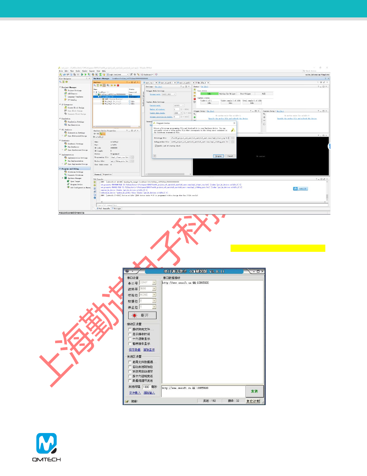
After the CP2102 communication test project correctly synthesized, implemented and generated bit file,
users could use Xilinx program tool to program the generated bit file into FPGA. Below image shows the
FPGA program status with program tool.
Figure 2-3. Program the FPGA
The CP2102 example test project’s main functionality is performing an UART loopback communication.
The FPGA program will send the received UART data back to the PC. Below figure shows user
employees some PC based UART test tool to send data to FPGA: http://www.cmsoft.cn QQ:10865600.
After a short while the PC UART test tool will receive the same data stream from FPGA, which means the
CP2102 loopback test program is running correctly.
Figure 2-4. UART Loopback Test
QM_XC7A35T_SDRAM Daughter Board User Manual-V01
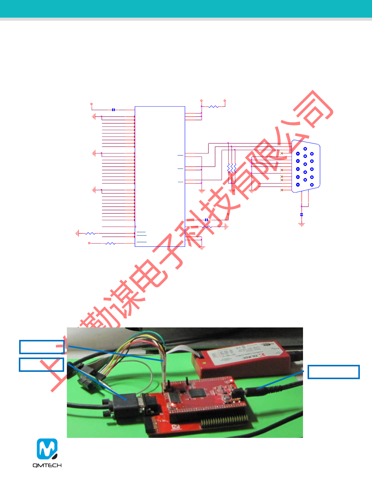
3. Experiment (2): VGA Display
The ADV7123 is a triple high speed, digital-to-analog converter on a single monolithic chip. It consists of
three high speed, 10-bit, video DACs with complementary outputs, a standard TTL input interface, and a
high impedance, analog output current source. The QM_XC7A35T_SDRAM daughter board provides
24bit(RGB888) VGA display function by using ADV7123-KSTZ140. Below figure shows the hardware
design of the ADV7123 chip, the lowest two bits of each color channel are directly connected to GND:
Figure 3-1. ADV7123 Hardware Design
Before start to test the VGA display function, make sure all the hardware connections of the development
kit are correctly connected. Xilinx USB platform cable’s VREF, GND, TDI, TMS, TCK, TDO pins shall be
connected to QM_XC7A35T_SDRAM core board’s JTAG interface. Then power on the development kit
with 5V DC power source. Xilinx USB platform cable’s indicator LED’s color will turn from brown into
green. At the same time, the VGA cable shall also be plugged in the board, below figure shows an
example hardware setup:
GND R62 4.7K
U7
AD7123
G0
1
G1
2
G2
3
G3
4
G4
5
G5
6
G6
7
G7
8
G8
9
G9
10
B0
14
B1
15
B2
16
B3
17
B4
18
B5
19
B6
20
B7
21
B8
22
B9
23
R0
39
R1
40
R2
41
R3
42
R4
43
R5
44
R6
45
R7
46
R8
47
R9
48
COMP
35
SYNC
12
BLANK
11
CLOCK
24
PSAVE
38
IOB 27
IOG 31
IOR 33
IOB 28
IOG 32
IOR 34
RSET 37
VREF 36
VAA1 13
VAA2 29
VAA3 30
GND2 25
GND1 26
GND GND
BANK35_A7
BANK35_B7
GND
GND
GND
GND
BANK34_M2
BANK34_M1
BANK34_N1
BANK34_P1
BANK34_M5
BANK34_N4
BANK34_P4
BANK34_P3
BANK34_L5
BANK34_P5
BANK34_T4
BANK34_T3
BANK34_R3
BANK34_T2
BANK34_R2
BANK34_R1
BANK14_R6
BANK14_M6
BANK14_R5
BANK14_N6
BANK14_R8
BANK14_T7
BANK14_R7
BANK14_T5
BANK14_T8
BANK14_P6
ANA_3V3 3V3
R35 0R
ANA_3V3
C37 100nF
C38 100nF
R36 560R GND GND
C39
100nF
R37
75R R38
75R R39
75R
GND
R40 4.7K
ANA_3V3
ANA_3V3
1
5
6
11
15
10
J7
CONN_VGA
7
6
5
4
3
2
1
8
9
10
11
12
13
14
15
16
17
VGA Cable
5V DC Source
JTAG Cable
QM_XC7A35T_SDRAM Daughter Board User Manual-V01
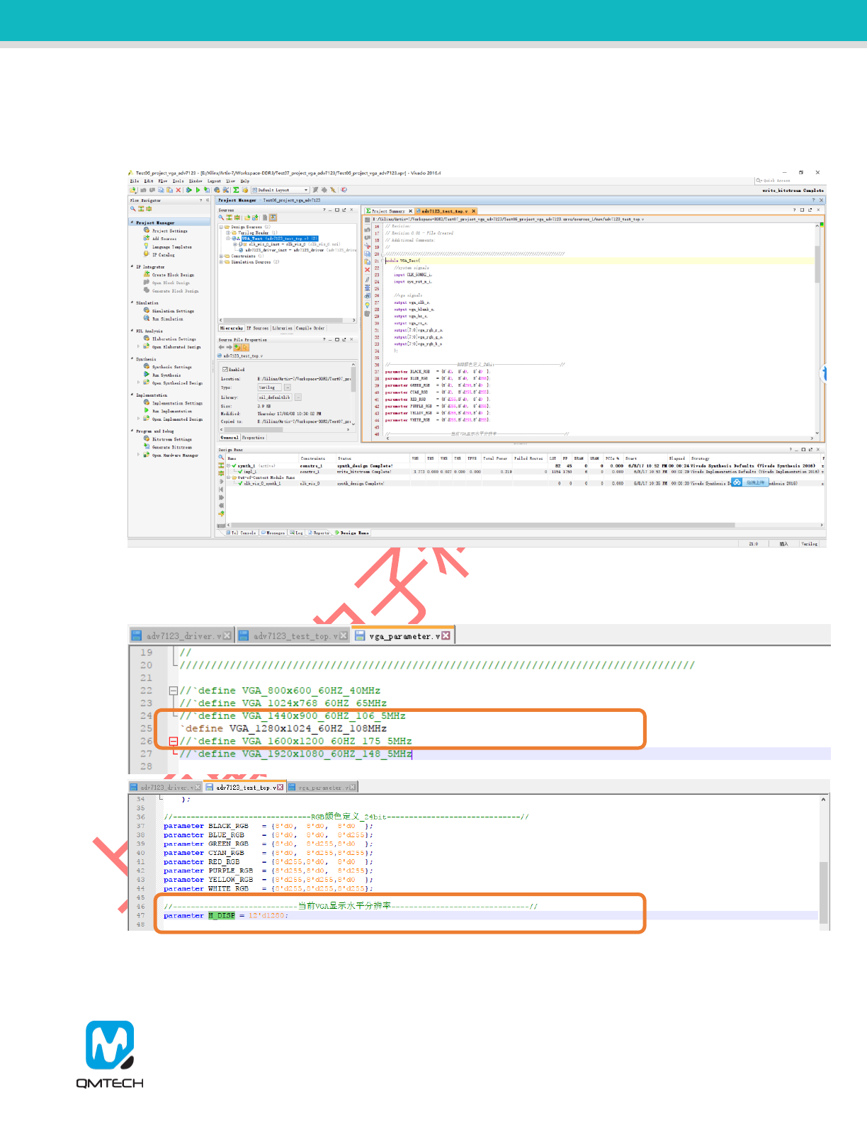
All the test examples are developed in the Xilinx Vivado 2016.4 environment. Open the VGA test project
located in this release folder: /Software/Test07_project_vga_adv7123. Below figure shows the example
project of VGA_test:
Figure 3-2. VGA Display Function Test
In this example project, the default VGA output resolution parameter is 1280x1024@60Hz. If users want
to test other display parameters, change the source code accordingly.
Figure 3-3. VGA Display Parameters
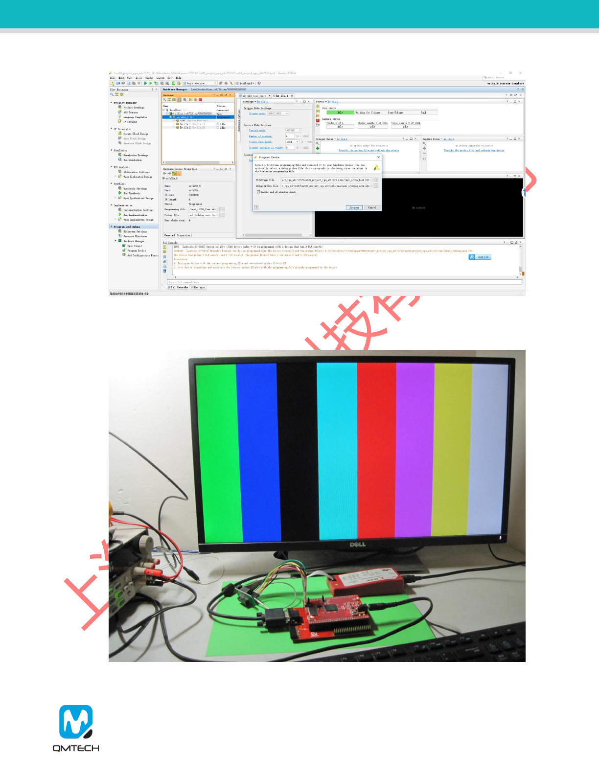
After the VGA display test project correctly synthesized, implemented and generated bit file, users could
use Xilinx program tool to program the generated bit file into FPGA. Below image shows the FPGA
program status with program tool.
QM_XC7A35T_SDRAM Daughter Board User Manual-V01
Figure 3-4. Program FPGA
After the FPGA correctly loaded the VGA_Test bit file, the VGA monitor will display the color bar output
from development kit’s VGA port. Below image shows the example color bar pattern.
Figure 3-5. VGA Display Test
QM_XC7A35T_SDRAM Daughter Board User Manual-V01
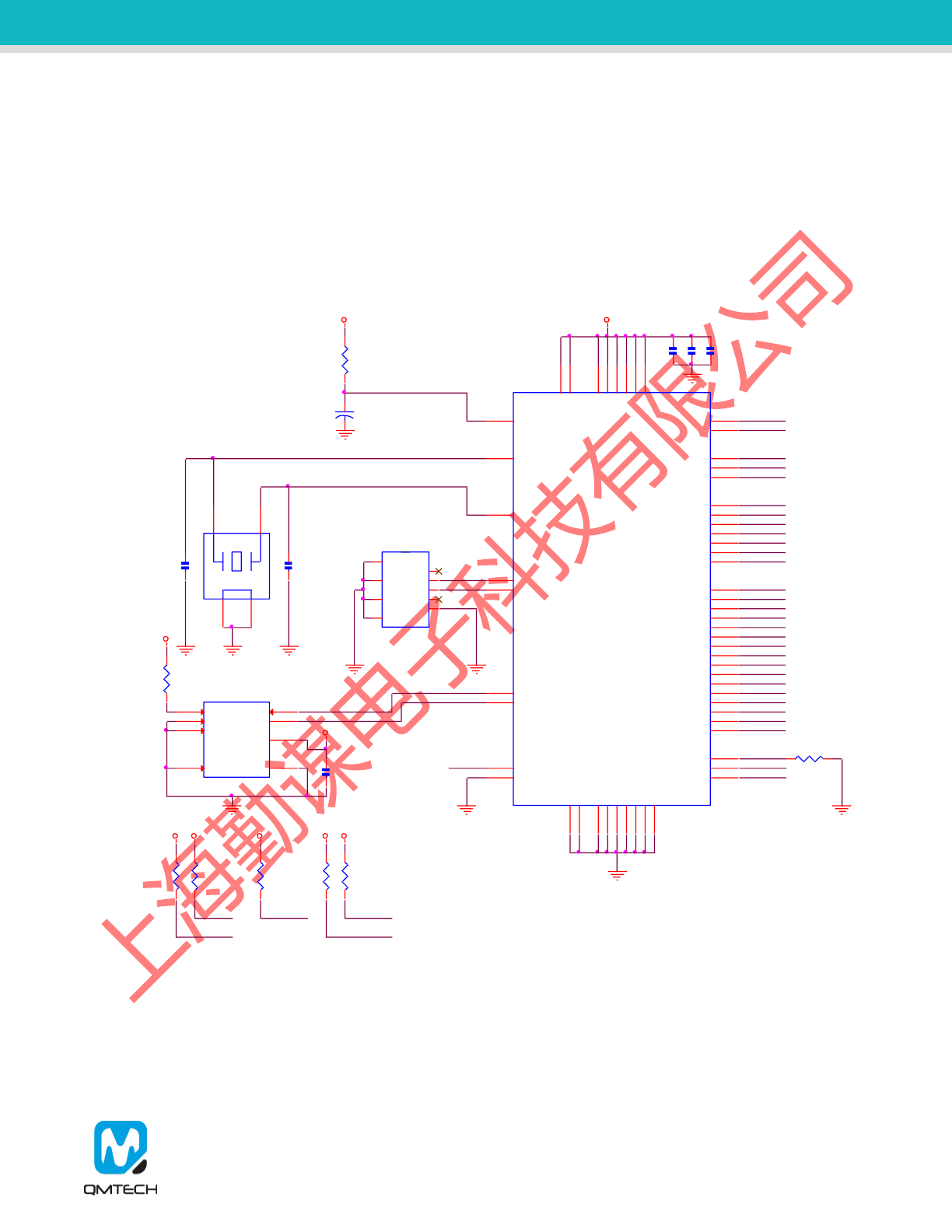
4. Experiment (3): CY7C68013A USB 2.0 Slave FIFO
Cypress’s EZ-USB® FX2LP CY7C68013A is a low-power version of the EZ-USB FX2(CY7C68013),
which is a highly integrated, low-power USB 2.0 microcontroller. By integrating the USB 2.0 transceiver,
serial interface engine (SIE), enhanced 8051 microcontroller, and a programmable peripheral interface in
a single chip, Cypress has created a cost-effective solution that provides superior time-to-market
advantages with low power to enable bus-powered applications. The QM_XC7A35T_SDRAM daughter
board provides slave FIFO interface by using CY7C68013A. Below figure shows the hardware design of
the CY7C68013A chip:
Figure 4-1. CY7C68013A-56LTXC Hardware Design
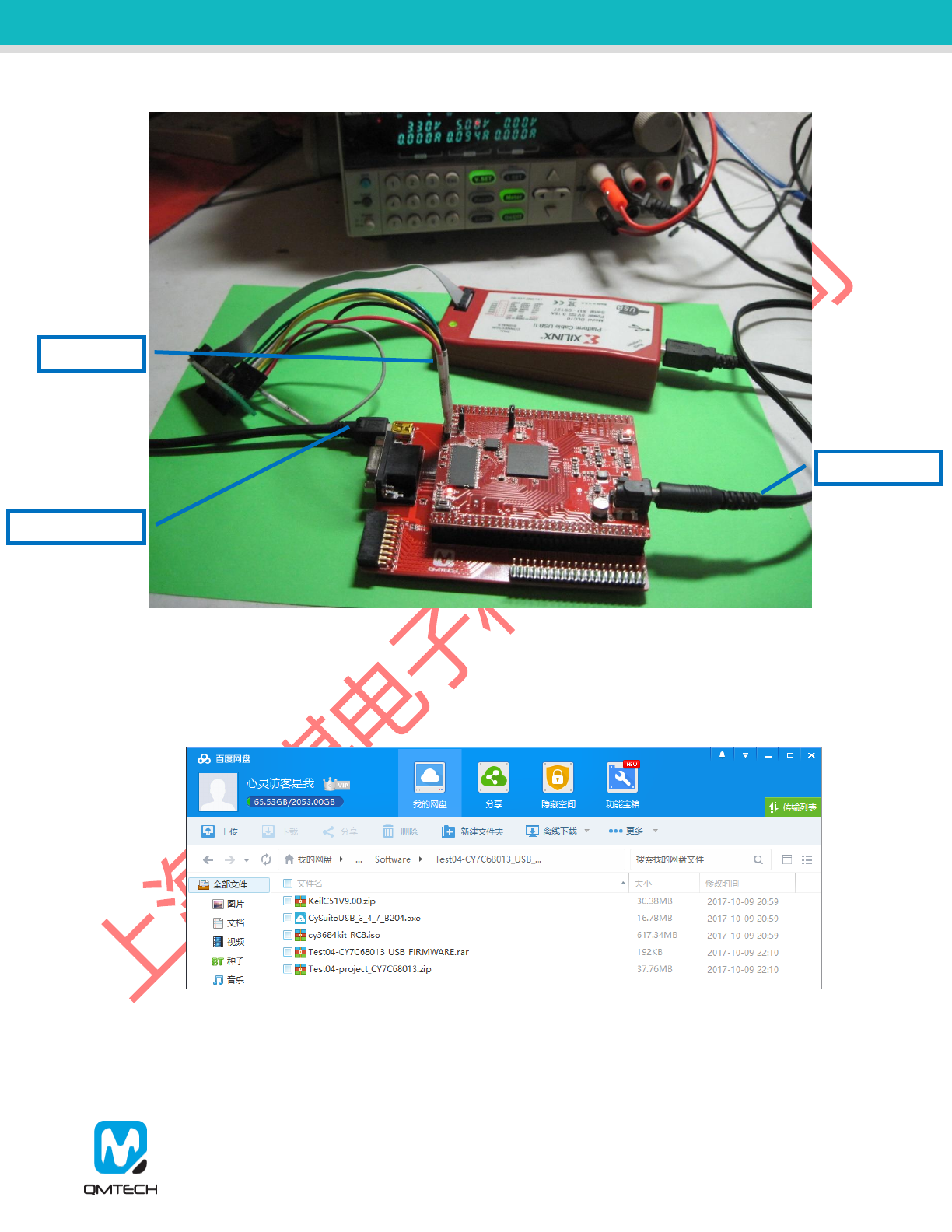
Before start to test the USB slave FIFO function, make sure all the hardware connections of the
development kit are correctly connected. Xilinx USB platform cable’s VREF, GND, TDI, TMS, TCK, TDO
pins shall be connected to QM_XC7A35T_SDRAM core board’s JTAG interface. Then power on the
development kit with 5V DC power source. Xilinx USB platform cable’s indicator LED’s color will turn from
brown into green. At the same time, the Mini-USB cable shall also be plugged in the board, below figure
shows an example hardware setup:
U8
CY7C68013A_56LTXC
RDY0/SLRD 1
RDY1/SLWR 2
AVCC 3
XTALOUT
4
XTALIN
5
AGND
6AVCC 7
DPLUS
8DMINUS
9
AGND
10
VCC 11
GND
12
IFCLK/PE0 13
RESERVED
14
SCL
15
SDA
16
VCC 17
GND
26
VCC 27
GND
28
CTL0/FLAGA 29
CTL1/FLAGB 30
CTL2/FLAGC 31
VCC 32
PA0/INT0# 33
PA1/INT1# 34
PA2/SLOE 35
PA3/WU2 36
PA4/FIFOADR0 37
PA5/FIFOADR1 38
PA6/PKTEND 39
PA7/FLAGD/SLCS# 40
RESET#
42
VCC 43
WAKEUP
44
GND
53
CLKOUT/PE1 54
VCC 55
GND
56
PB0/FD0 18
PB1/FD1 19
PB2/FD2 20
PB3/FD3 21
PB4/FD4 22
PB5/FD5 23
PB6/FD6 24
PB7/FD7 25
PD0/FD8 45
PD1/FD9 46
PD2/FD10 47
PD3/FD11 48
PD4/FD12 49
PD5/FD13 50
PD6/FD14 51
PD7/FD15 52
GND
41
Thermal
57
C13
100NF
MN1
AT24C128
A0
1
A1
2
WP
7
SCL 6
VCC 8
NC
3SDA 5
GND 4
GND
R5
4.7K SCL
SDA
3V3
3V3
Y1
24.000 MHz
1
3
2
4
C16
22PF
C3
22PF
GNDGND GND
J5
MINI_USB
Vcc 1
D- 2
D+ 3
ID 4
GND 5
G3
8
G4
9
G2
7
G1
6
GNDGND
GND
R1
4.7K
C2
0.1uF
3V3
R65
4.7K
3V3
R66
4.7K
3V3
SCL
SDA
GND
3V3
C40
100nF
C41
100nF
C42
100nF
GND
GND
3V3
R67
4.7K
WAKEUP
WAKEUP PA0
PA1
3V3
R68
4.7K
PA1
3V3
R69
4.7K
PA0
R70 4.7K
GND
BANK14_N14
BANK14_K12
BANK14_R10
BANK14_N12
BANK14_P13
BANK14_M16
BANK14_P14
BANK14_T13
BANK14_N13
BANK14_R12
BANK14_R13
BANK14_T12
BANK14_R11
BANK14_T9
BANK14_N9
BANK14_P9
BANK14_T10
BANK14_P10
BANK14_P11
BANK14_M12
BANK14_K13
BANK14_T15
BANK14_T14
BANK14_P16
BANK14_R15
BANK14_R16
BANK14_N16
BANK14_P15
QM_XC7A35T_SDRAM Daughter Board User Manual-V01
Figure 4-2. Hardware Connections
Users also need to install the PC based USB driver and test software provided by Cypress. These driver
and test suite could be retrieved by installing the CySuiteUSB_3_4_7_B204.exe. KeilC51V9.00 is also
suggested to be installed to compile the CY7C68013A firmware. All of those software packages could be
found in the Release folder: /Software/Test04-CY7C68013_USB_2.0_HS.
Figure 4-3. USB 2.0 Test Software Package
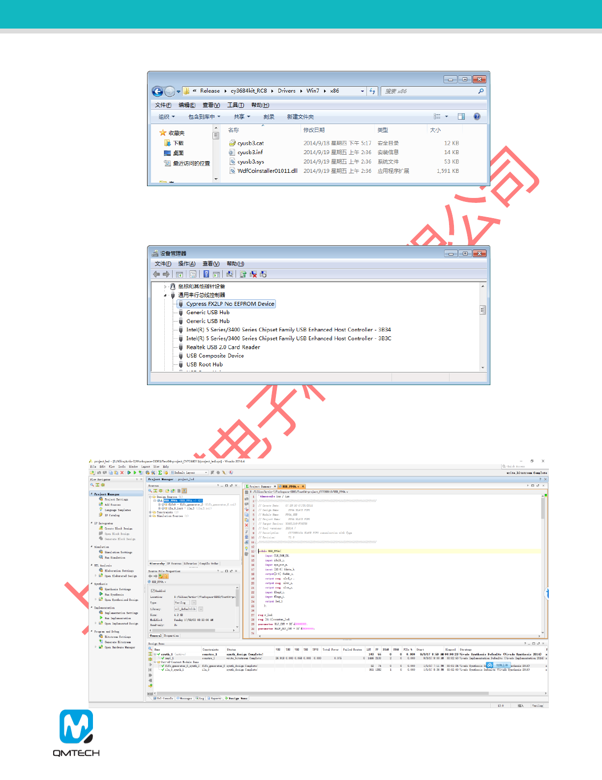
The windows device manager will inform users to install USB driver, after the Mini-USB cable connected
to the PC’s USB host connector. The CY7C68013A USB driver could be found in below folder: cy3684kit_
RC8-> Drivers->Win7->x86. The cy3684kit_RC8.iso could be downloaded from Cypress official site.
JTAG Cable
5V DC Source
Mini-USB Cable
QM_XC7A35T_SDRAM Daughter Board User Manual-V01
Figure 4-4. CY7C68013 USB Driver
After the CY7C68013 USB driver is correctly installed, the device manager will display the enumerated
USB device: ”Cypress FX2LP No EEPROM Device”.
Figure 4-5. Cypress FX2LP No EEPROM Device
Use Vivado 2016.4 to open the Slave FIFO test project located in Release folder: /Software/Test04-
CY7C68013_USB_ 2.0_HS/Test04-project_CY7C68013. Below figure shows the example project of
USB_FPGA:
QM_XC7A35T_SDRAM Daughter Board User Manual-V01
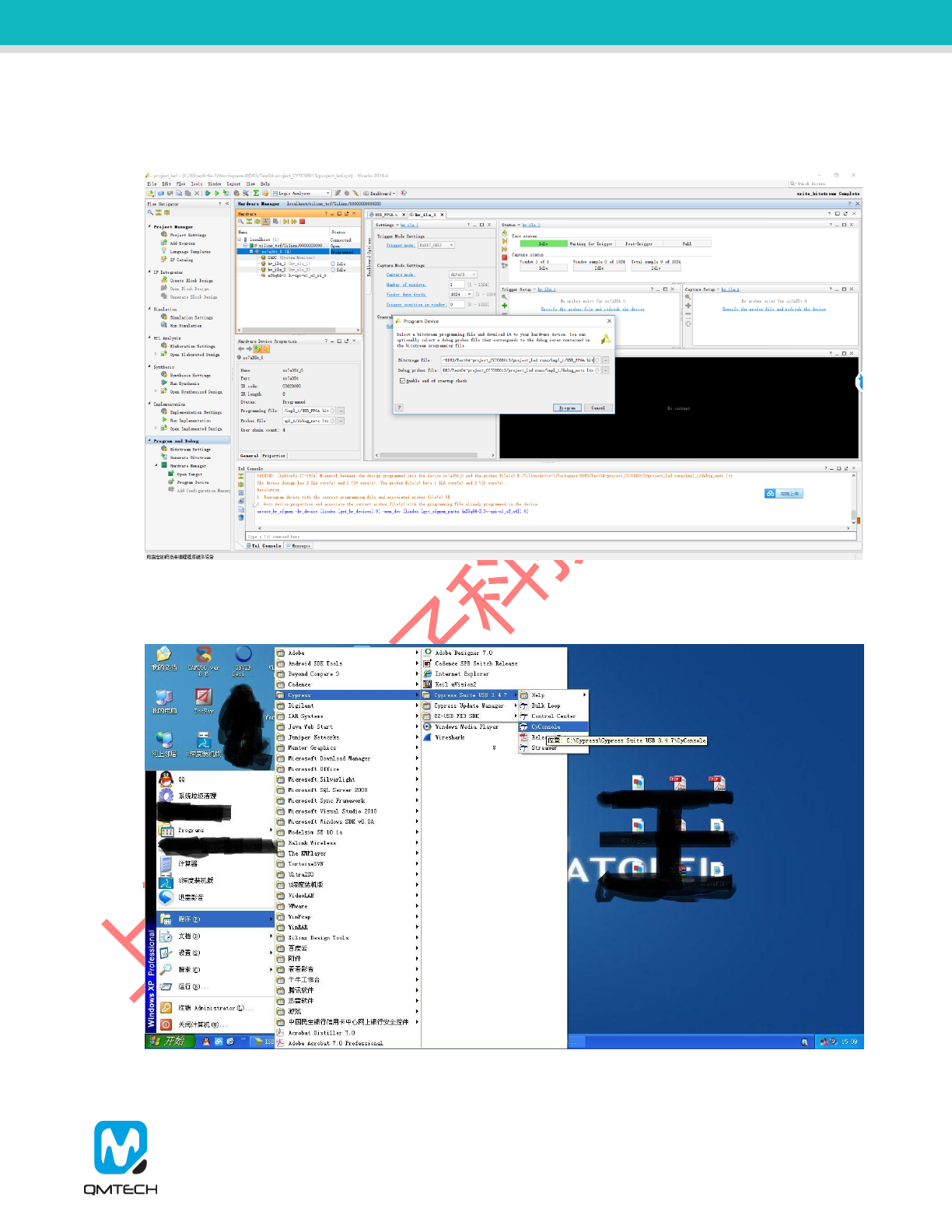
After the Slave FIFO test project correctly synthesized, implemented and generated bit file, users could
use Xilinx program tool to program the generated bit file into FPGA. Below image shows the FPGA
program status with program tool.
Figure 4-6. FPGA Program
Then, users need to download Slave FIFO firmware into CY7C68013A’s internal RAM or external
EEPROM. First step: Windows Start->Cypress->Cypress Suite USB 3.4.7->CyConsole:
Figure 4-7. Open CyConsole Software
QM_XC7A35T_SDRAM Daughter Board User Manual-V01
Click menu Options, select EZ-USB Interface:
Figure 4-8. Choose EZ-USB Interface
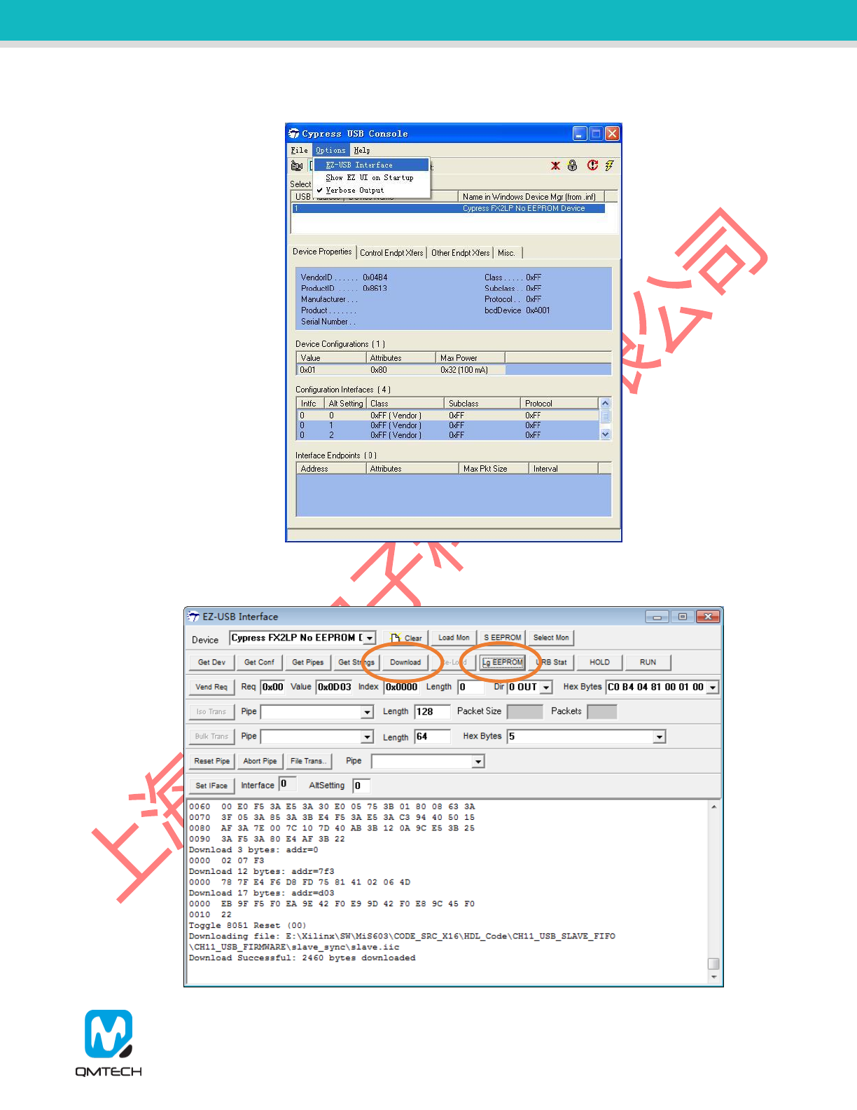
The EZ-USB Interface displays the Device information: Cypress FX2LP No EEPROM Device:
QM_XC7A35T_SDRAM Daughter Board User Manual-V01
Click Download button and select Slave.hex. The Slave.hex is located in Release folder: \software\
Test04-CY7C68013_USB_FIRMWARE\USB_SLAVE_FIFO\USB_FIRMWARE\slave_sync。Notice: if
users want to download firmware into external EEPROM, click Lg EEPROM and select Slave.iic.
Figure 4-9. Program Slave.hex
After the Slave FIFO firmware successfully downloaded, the EZ-USB Interface will display new
enumerated device: QinMou-X16。And then users could send 512 bytes of hex value 0x55 into USB
Endpoint 2 OUT by clicking Bulk Trans button:
Figure 4-10. New QinMou-X16 Device and Send Test Datas
QM_XC7A35T_SDRAM Daughter Board User Manual-V01
Then, change the Pipe selection into Endpoint 6 IN. After click the Bulk Trans button, the log window
will display all the received data from USB Endpoint 6 IN. From below image, users could see all the 512
bytes of hex value 0x55 are correctly read back from Slave FIFO.
Figure 4-11. Receive Test Data
QM_XC7A35T_SDRAM Daughter Board User Manual-V01
5. Reference
[1] ug380-Configuration.pdf
[2] ug385-Package.pdf
[3] ug394-Power Managment.pdf
[4] M25P80.pdf
[5] LPC-Link-II_Rev_C.pdf
[6] Xc7a35t-sdram-v02.pdf
QM_XC7A35T_SDRAM Daughter Board User Manual-V01
6. Revision
Doc. Rev.
Date
Comments
0.1
11/07/2017
Initial Version.
1.0
11/18/2017
V1.0 Formal Release.
