QMTECH_CycloneIV_EP4CE15_User_Manual(CoreBoard) V01 QMTECH Cyclone IV EP4CE15 User Manual(Core Board)
User Manual:
Open the PDF directly: View PDF ![]() .
.
Page Count: 13
- 1. Introduction
- 2. Getting Started
- 2.2 Cyclone IV EP4CE15 Hardware Design
- 2.2.1 Cyclone IV EP4CE15 Power Supply
- 2.2.2 Cyclone IV EP4CE15 SDRAM Memory
- 2.2.3 Cyclone IV EP4CE15 SPI Boot
- 2.2.4 Cyclone IV EP4CE15 System Clock
- 2.2.1 Cyclone IV EP4CE15 JTAG Port
- 2.2.2 Cyclone IV EP4CE15 Power Supply
- 2.2.3 Cyclone IV EP4CE15 Extension IO
- 2.2.4 Cyclone IV EP4CE15 User LED
- 2.2.5 Cyclone IV EP4CE15 User Key
- 2.2 Cyclone IV EP4CE15 Hardware Design
- 3. Reference
- 4. Revision
Cyclone IV EP4CE15 Core Board-User Manual(Hardware)
CYCLONE IV EP4CE15 CORE BOARD
USER MANUAL
Preface
The QMTech® Cyclone IV SDRAM Development Board uses Intel(Altera) EP4CE15F23
device to demonstrate Intel’s leadership in offering power-efficient FPGAs. With enhanced
architecture and silicon, advanced semiconductor process technology, and power
management tools, power consumption for Cyclone IV FPGAs has been reduced by up to 25
percent compared to Cyclone® III FPGAs. The result is the lowest power consumption of any
comparable FPGA.

Cyclone IV EP4CE15 Core Board User Manual-V01
Table of Contents
1. INTRODUCTION .................................................................................. 3
1.1 DOCUMENT SCOPE ..................................................................... 3
1.2 KIT OVERVIEW ........................................................................... 3
1.3 KIT TOP VIEW ........................................................................... 3
2. GETTING STARTED .............................................................................. 4
2.2 CYCLONE IV EP4CE15 HARDWARE DESIGN ..................................... 5
2.2.1 Cyclone IV EP4CE15 Power Supply .............................. 5
2.2.2 Cyclone IV EP4CE15 SDRAM Memory ......................... 6
2.2.3 Cyclone IV EP4CE15 SPI Boot ...................................... 6
2.2.4 Cyclone IV EP4CE15 System Clock .............................. 7
2.2.1 Cyclone IV EP4CE15 JTAG Port ................................... 8
2.2.2 Cyclone IV EP4CE15 Power Supply .............................. 8
2.2.3 Cyclone IV EP4CE15 Extension IO ............................... 9
2.2.4 Cyclone IV EP4CE15 User LED ................................... 11
2.2.5 Cyclone IV EP4CE15 User Key ................................... 11
3. REFERENCE........................................................................................ 12
4. REVISION .......................................................................................... 13
Cyclone IV EP4CE15 Core Board User Manual-V01
1. Introduction
1.1 Document Scope
This demo user manual introduces the Cyclone IV EP4CE15 core board and describes how to setup the
core board running with application software Altera Quartus II 15.1. Users may employee the on board
rich logic resource FPGA EP4CE15F23C8N and large SDRAM memory MT48LC16M16 to implement
various applications. The core board also has 108 non-multiplexed FPGA IOs for extending customized
modules, such as UART module, CMOS/CCD camera module, LCD/HDMI/VGA display module etc.
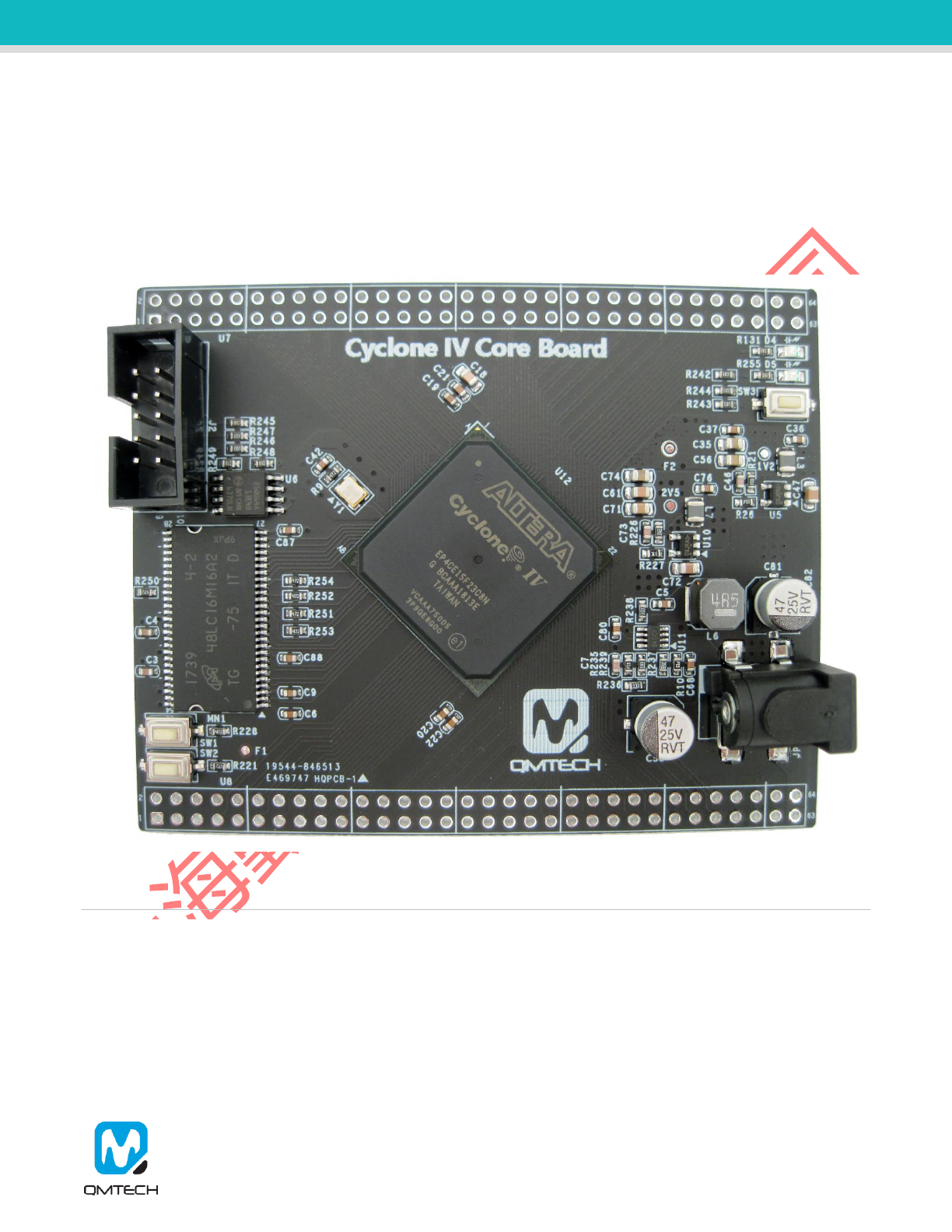
1.2 Kit Overview
Below section lists the parameters of the Cyclone IV EP4CE15:
On-Board FPGA: EP4CE15F23C8N;
On-Board FPGA external crystal frequency: 50MHz;
EP4CE15F23C8N has rich block RAM resource up to 504Kb;
EP4CE15F23C8N has 15K Logic elements;
On-Board N25Q064 SPI Flash, 8M bytes for user configuration code;
On-Board 32MB Micron SDRAM, MT48LC16M16A2;
On-Board 3.3V power supply for FPGA by using MP2315 wide input range DC/DC;
EP4CE15 core board has two 64p, 2.54mm pitch headers for extending user IOs. All IOs are
precisely designed with length matching;
EP4CE15 core board has 3 user switches;
EP4CE15 core board has 2 user LEDs;
EP4CE15 core board has JTAG interface, by using 10p, 2.54mm pitch header;
EP4CE15 core board PCB size is: 6.7cm x 8.4cm;
Default power source for core board is: 1A@5V DC, the DC header type: DC-050, 5.5mmx2.1mm;
1.3 Kit Top View
Figure 1-1. Cyclone IV EP4CE15 Top View
Cyclone IV EP4CE15 Core Board User Manual-V01
2. Getting Started
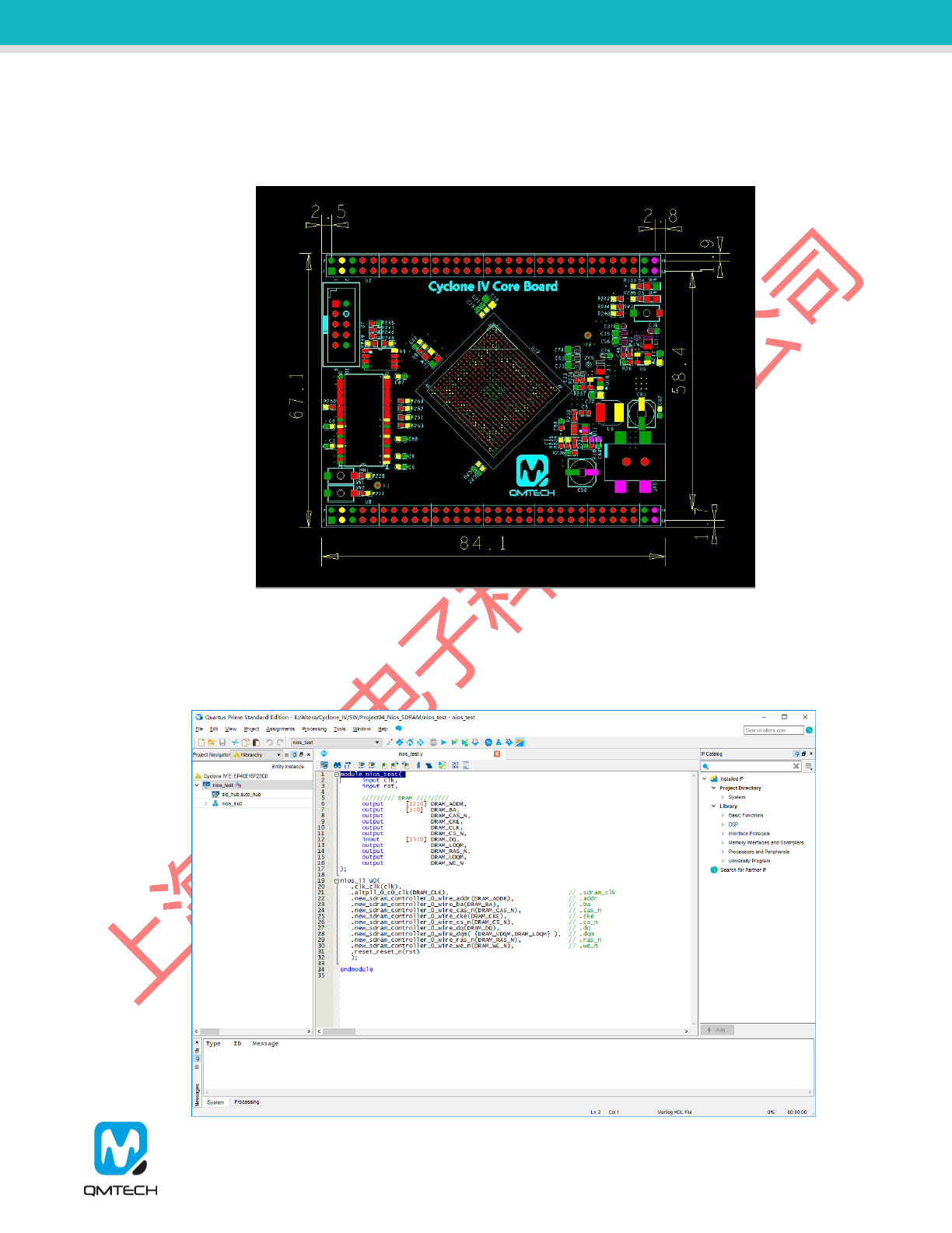
Below image shows the dimension of the Cyclone IV EP4CE15 core board: 67.1mm x 84.1mm. The unit
in below image is millimeter(mm).
Figure 2-1. Cyclone IV EP4CE15 Dimension
The Cyclone IV EP4CE15 core board tool chain consists of Altera Quartus II 15.1, Altera USB Blaster
cable, EP4CE15 core board and 5V DC power supply. Below image shows the Altera Quartus II 15.1
development environment which could be downloaded from Altera(Intel) office website:
Cyclone IV EP4CE15 Core Board User Manual-V01
2.2 Cyclone IV EP4CE15 Hardware Design
2.2.1 Cyclone IV EP4CE15 Power Supply
The core board needs 5V DC input as power supply which could be directly injected from power header
or the 64P header U7/U8. Users may refer to the hardware schematic for the detailed design. The on
board LED D4 indicates the 3.3V supply, it will be turned on when the 5V power supply is active. In
default status, all the FPGA banks IO power level is 3.3V because bank power supply is 3.3V.
Note: FPGA core supply 1.2V is regulated by On-Semi DC/DC chip NCP1529 which could output
maximum 1A current.
Figure 2-2. Power Supply for the FPGA
2V5
1V2
1V2
3V3
EP4CE15F23
U12I
GND1
L10
GND2
L11
GND3
M10
GND4
M11
GND5
L12
GND6
L13
GND7
M12
GND8
M13
GND9
N11
GND10
K11
GND11
N12
GND12
K12
GND13
K13
GND14
N13
GND15
N10
GND16
K10
GND17
J9
GND18
D7
GND19
J5
GND20
H8
GND21
A1
GND22
C5
GND23
C9
GND24
C11
GND25 C12
GND26 C14
GND27 C16
GND28 A22
GND29 E20
GND30 G20
GND31 L20
GND32 P19
GND33 V20
GND34 Y20
GND35 AB22
GND36 Y18
GND37 Y16
GND38 Y12
GND39 Y11
GND40 Y9
GND41 Y5
GND42 AB1
GND43 N3
GND44 U3
GND45 W3
GND46 D3
GND47 F3
GND48 K3
GND49
G2
GND50
AA2
GND51
AA22
GND52 H3
GND53 R3
GND54 AB6
GND55 Y15
GND56 T20
GND57 J19
GND58 C18
GND59 D8
GNDA1
U5
GNDA2
E18
GNDA3
F5
GNDA4
V18
EP4CE15F23
U12J
VCCINT1 J11
VCCINT2 J12
VCCINT3 L14
VCCINT4 M14
VCCINT5 P11
VCCINT6 P12
VCCINT7 L9
VCCINT8 M9
VCCINT9 J13
VCCINT10 J14
VCCINT11 K14
VCCINT12 J10
VCCINT13 K9
VCCINT14 N9
VCCINT15 P9
VCCINT16 P10
VCCINT17 P13
VCCINT18 U16
VCCINT19 U17
VCCINT20 T13
VCCINT21 J8
VCCIO1_1
D4
VCCIO1_2
F4
VCCIO1_3
K4
VCCIO1_4
H4
VCCIO2_1
N4
VCCIO2_2
U4
VCCIO2_3
W4
VCCIO2_4
R4
VCCIO3_1
AB2
VCCIO3_2
W5
VCCIO3_3
W9
VCCIO3_4
W11
VCCIO3_5
AA6
VCCIO4_1
AB21
VCCIO4_2
W12
VCCIO4_3
W16
VCCIO4_4
W18
VCCIO4_5
Y14
VCCIO5_1
P18
VCCIO5_2
V19
VCCIO5_3
Y19
VCCIO5_4
T19
VCCIO6_1
E19
VCCIO6_2
G19
VCCIO6_3
L19
VCCIO6_4
J20
VCCIO7_1
A21
VCCIO7_2
D12
VCCIO7_3
D14
VCCIO7_4
D16
VCCIO7_5
D18
VCCIO8_1
A2
VCCIO8_2
D5
VCCIO8_3
D9
VCCIO8_4
D11
VCCIO8_5
E8
VCCA1 T6
VCCA2 F18
VCCA3 G6
VCCA4 U18
VCCD_PLL1 U6
VCCD_PLL2 E17
VCCD_PLL3 F6
VCCD_PLL4 V17
Cyclone IV EP4CE15 Core Board User Manual-V01
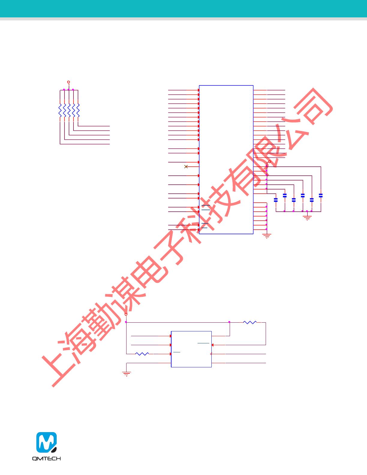
2.2.2 Cyclone IV EP4CE15 SDRAM Memory
Cyclone IV EP4CE15 has on board 16bit width data bus, 32MB memory size MT48LC16M16 SDRAM
provided by Micron. Below image shows the detailed hardware design:
Figure 2-3. SDRAM
2.2.3 Cyclone IV EP4CE15 SPI Boot
Cyclone IV EP4CE15 boots from external SPI Flash, detailed hardware design is shown in below figure.
The SPI flash is using N25Q064 manufactured by Micron, with 64Mbit memory storage.
Note: The SPI Flash is designed with x1 mode.
Figure 2-4. SPI Flash
C4
100NF C6
100NF
C87
100NF
C88
100NF
C9
100NF
MT48LC16M16A2
MN1
A0
23
A1
24
A2
25
A3
26
A4
29
A5
30
A6
31
A7
32
A8
33
A9
34
A10
22
BA0
20
A12
36
DQ0 2
DQ1 4
DQ2 5
DQ3 7
DQ4 8
DQ5 10
DQ6 11
DQ7 13
DQ8 42
DQ9 44
DQ10 45
DQ11 47
DQ12 48
DQ13 50
DQ14 51
DQ15 53
VDD 1
VSS 28
VSS 41
VDDQ 3
VDD 27
N.C
40
CLK
38
CKE
37
DQML
15
DQMH
39
CAS
17
RAS
18
WE
16
CS
19
VDDQ 9
VDDQ 43
VDDQ 49
VSSQ 6
VSSQ 12
VSSQ 46
VSSQ 52
VDD 14
VSS 54
A11
35
BA1
21
C3
100NF
3V3
256 Mbits
DQML
A8
A9
A14
CAS
SD_NCS0
A13
A6
A11
A12
DQMH
SDCLK0
A1
A4
SDWE
A3
A7
RAS
SDCKE0
D2
D4
A5
A2
A0
A10 D9
D14
D5
D12
D10
D7
D6
D0
D3
D15
D11
D13
D1
D8
R250
4.7K
3V3
SDCKE0
R251
4.7K
CAS
R252
4.7K
RAS
R253
4.7K
SDWE
SD_NCS0
R254
4.7K
U6
N25Q064A13ESE40F
nCE
1
HOLD 7
SO
2
VSS
4SI 5
SCK 6
WP
3
VDD 8
3V3
R248 1K
R249 1K
FPGA_NCSO
FPGA_ASDO
FPGA_DCLK
FPGA_DATA0
Cyclone IV EP4CE15 Core Board User Manual-V01
Below image shows the hardware configuration of MSEL[3:0]: 0010, in which way will make the FPGA boot
from Active Serial (x1 or x4) Standard Mode:
Figure 2-5. MSEL Settings
2.2.4 Cyclone IV EP4CE15 System Clock
The Cyclone IV EP4CE15 has system clock frequency 50MHz which is directly provided by external
crystal. The crystal is designed with high accuracy and stability with low temperature drift 10ppm/°c.
Below image shows the detailed hardware design:
Figure 2-6. 50MHz System Clock
nCONFIG
IO_J2
IO_J1
IO_H1
IO_H2
JTAG_TMS
JTAG_TDI R24610K
2V5
R24710K
IO_F2
IO_F1
IO_C2
IO_C1
IO_B1
IO_B2
IO_E1
IO_D2
LED0
JTAG_TCK R2451K
2V5
JTAG_TDO
2V5
3V3
R24410K 3V3
R24310K
R24210K
3V3
FPGA_DCLK
FPGA_NCSO
FPGA_DATA0
FPGA_ASDO
CLK_50M
EP4CE15F23
U12A
IO_H5
H5
IO,DIFFIO_L1P
B2
IO,DIFFIO_L1N
B1
IO_G5
G5
IO,DIFFIO_L2P,nRESET
E4
IO,DIFFIO_L2N
E3
IO,DIFFIO_L3P
C2
IO,DIFFIO_L3N
C1
IO,DIFFIO_L4P
D2
IO,DIFFIO_L4N,DATA1,ASDO D1
IO,VREFB1N0
H7
IO,DIFFIO_L5P
H6
IO,DIFFIO_L5N
J6
IO,DIFFIO_L6P,FLASH_nCE,nCSO E2
IO,DIFFIO_L6N
E1
IO,DIFFIO_L7P
F2
IO,DIFFIO_L7N
F1
IO,DIFFIO_L8P
G4
IO,DIFFIO_L8N
G3
NSTATUS K6
IO,DIFFIO_L9P
L8
IO,DIFFIO_L9N
K8
IO,DIFFIO_L10P
J7
IO,DIFFIO_L10N
K7
IO_J4
J4
IO,DIFFIO_L11P
H2
IO,DIFFIO_L11N
H1
IO,VREFB1N1
J3
IO,DIFFIO_L12P
J2
IO,DIFFIO_L12N
J1 DCLK K2
IO,DATA0 K1
NCONFIG K5
TDI L5
TCK L2
TMS L1
TDO L4
NCE L3
CLK1,DIFFCLK_0N G1
MSEL0 M17
MSEL1 L18
MSEL2 L17
MSEL3 K20
CONF_DONE M18
CLK2,DIFFCLK_1P T2
CLK3,DIFFCLK_1N T1
CLK15,DIFFCLK_6P AA11
CLK14,DIFFCLK_6N AB11
CLK13,DIFFCLK_7P AA12
CLK12,DIFFCLK_7N AB12
CLK10,DIFFCLK_4N A11
CLK11,DIFFCLK_4P B11
CLK7,DIFFCLK_3N T22
CLK6,DIFFCLK_3P T21
CLK5,DIFFCLK_2N G22
CLK4,DIFFCLK_2P G21
CLK8,DIFFCLK_5N A12
CLK9,DIFFCLK_5P B12
50 MHz
VDD
VSS OUT
OE
Y1
SG-8002JC-50.0000M-PCB
41
32
C42
100NF
CLK_50M
3V3
R9 4.7K
Cyclone IV EP4CE15 Core Board User Manual-V01
2.2.1 Cyclone IV EP4CE15 JTAG Port
The on board JTAG port uses 10P 2.54mm pitch header which could be easily connected to Altera USB
blaster cable. Below image shows the hardware design of the JTAG port:
Figure 2-7. JTAG Port
2.2.2 Cyclone IV EP4CE15 Power Supply
The core board’s 3.3V power supply is using high efficiency DC/DC chip MP2315 provided by MPS Inc.
The MP2315 supports wide voltage input range from 4.5V to 24V. In normal use case, 5V DC power
supply is suggested to be applied on the board. Below image shows the MP2315 hardware design:
Figure 2-8. MP2315 Hardware Design
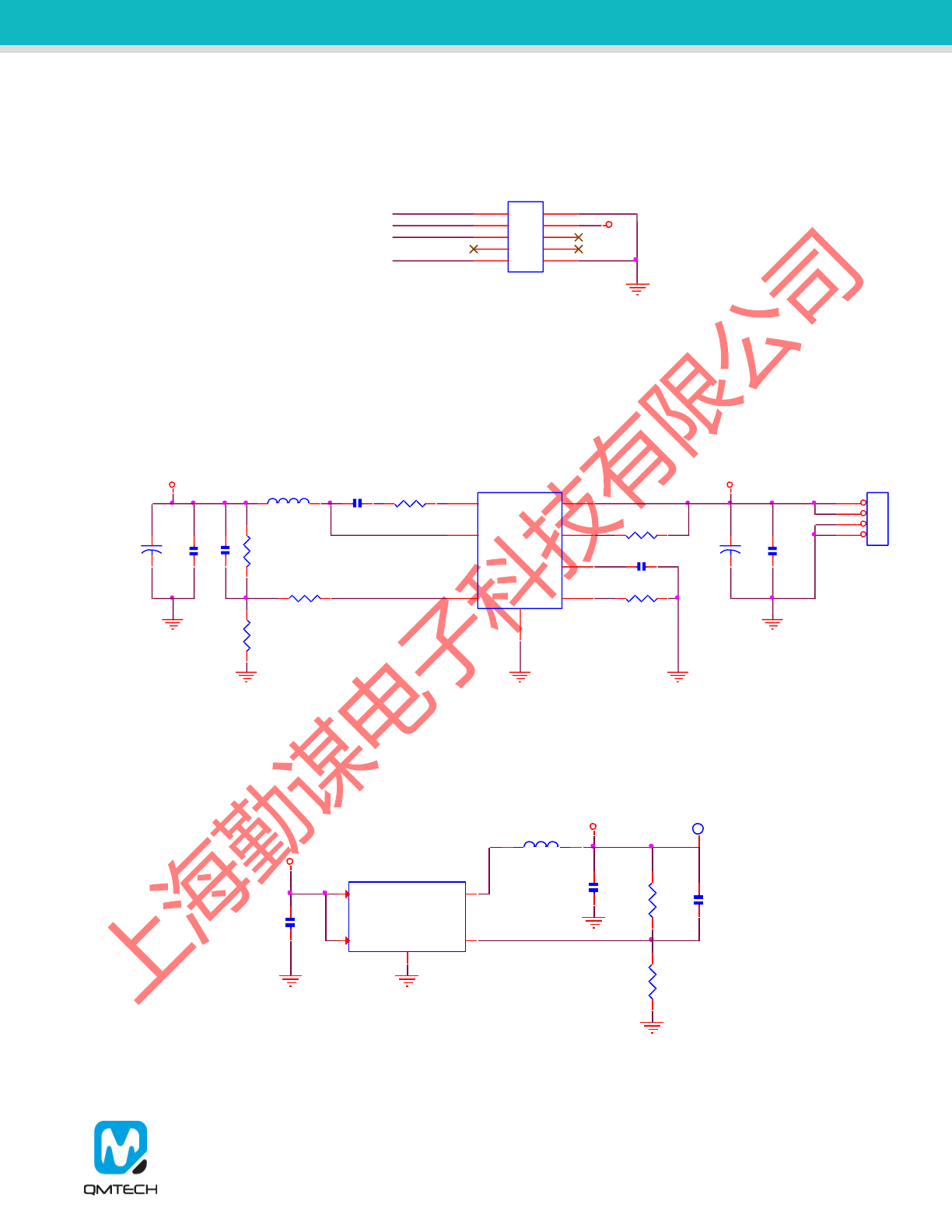
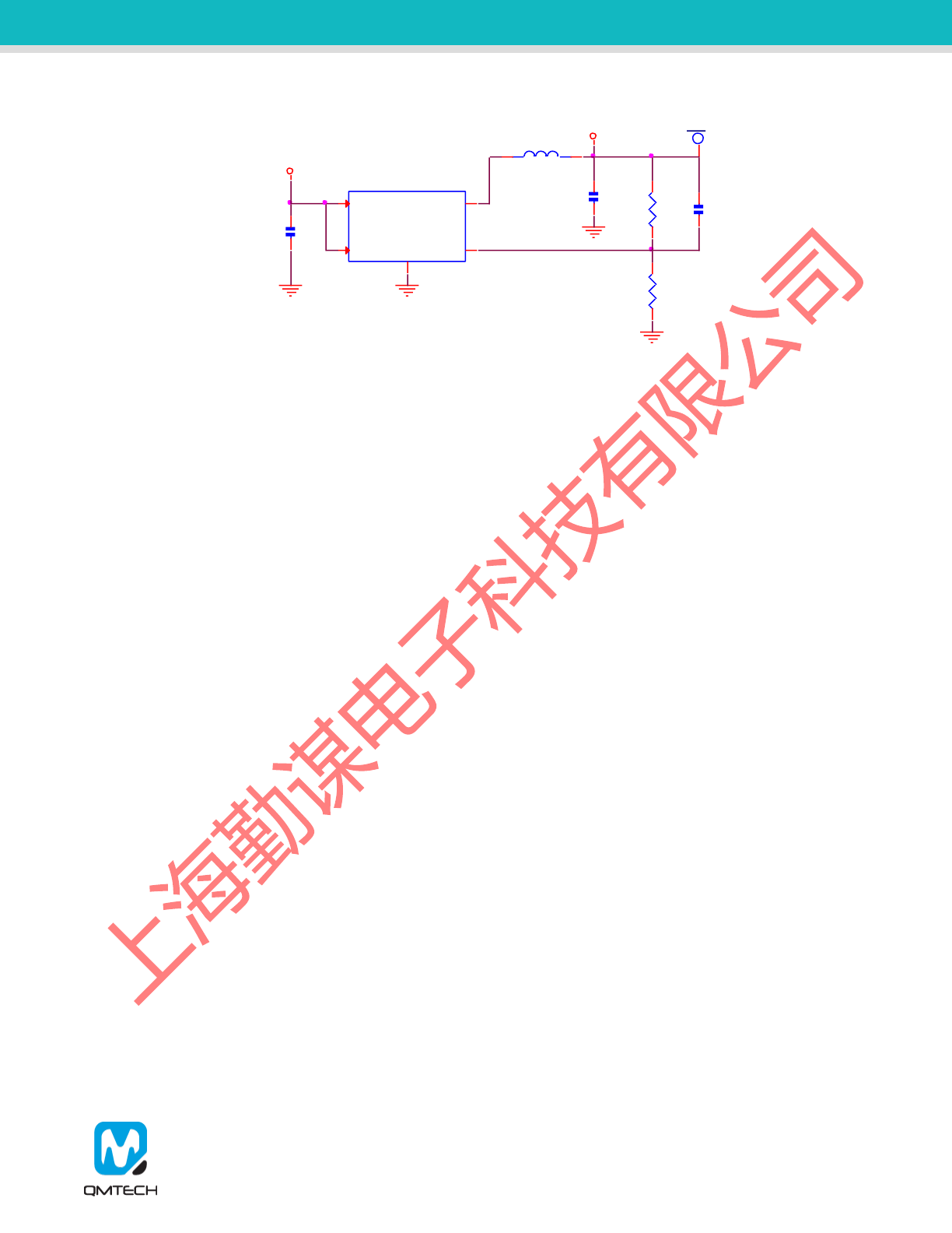
The core board’s 2.5V and 1.2V FPGA core voltage power supply is using high efficiency DC/DC chip
NCP1529 provided by On-Semi Inc.
J2
CONA_10P
1 2
3 4
5 6
7 8
910
JTAG_TDI
JTAG_TMS
JTAG_TDO
JTAG_TCK
2V5
+C58
47uF
+C81
47uF
REGULATED
5V ONLY
L6
4.7uH
C68
100nF
JP5
Power_Header_SMT
1
2
3
4
C82
100nF
VIN
R235 100K
R236
33K
C7 22pF
3V3
R237 75K
U11
MP2315
AAM 1
IN 2
SW
3
GND
4
BST
5
EN/SYNC 6
VCC 7
FB
8
C80 100nF
C5
100nF R238
20R
R239 33K
R10 100K
C71
4.7uF
2V5
L7 4.7uH
3V3
C72
4.7uF
U10
NCP1529
GND
2
FB 5
EN
1
VIN
4SW 3R226
75K C73
22pF
R227
23.7K
M
2V5
Cyclone IV EP4CE15 Core Board User Manual-V01
Figure 2-9. NCP1529 Hardware Design
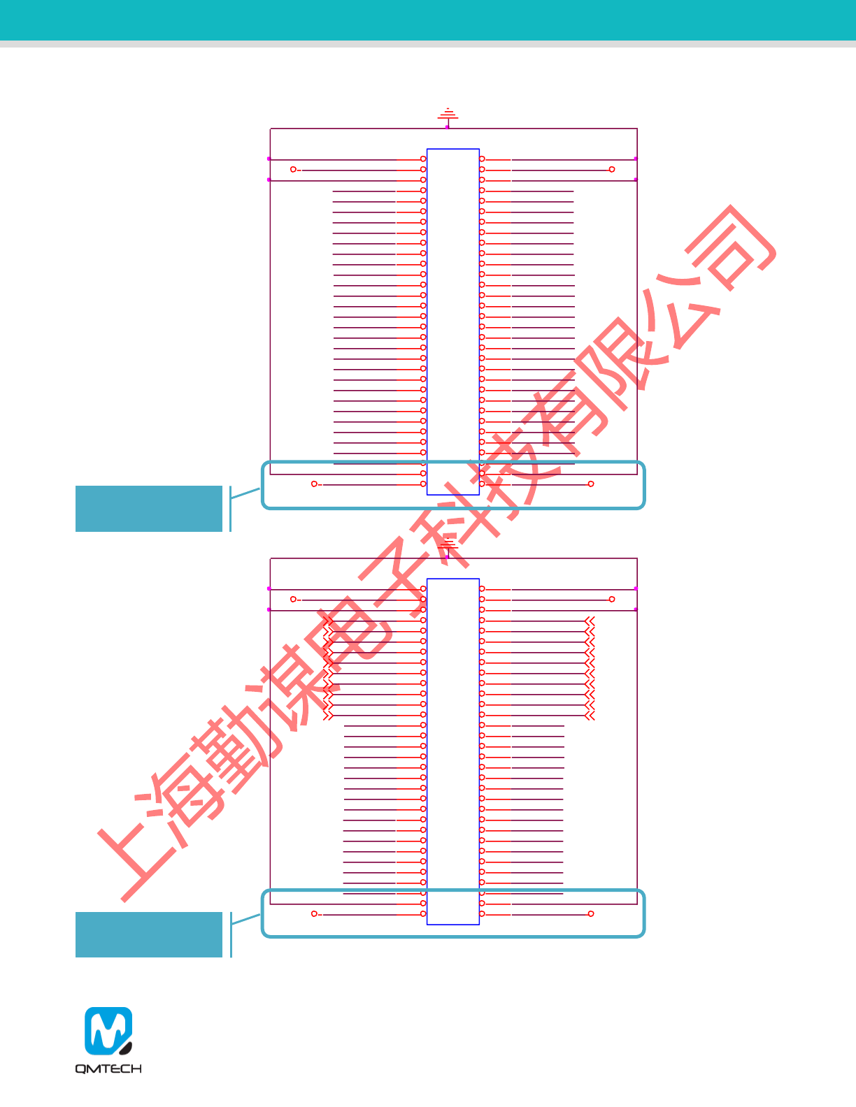
2.2.3 Cyclone IV EP4CE15 Extension IO
The core board has two 64P 2.54mm pitch female headers which are used for extending user modules,
such as ADC/DAC module, audio/video module, ethernet module, etc.
L3 4.7uH
1V2
C47
4.7uF
3V3
U5
NCP1529
GND
2
FB 5
EN
1
VIN
4SW 3C46
22pF
R21
100K
R26
100K
C56
4.7uF
M
1V2
Cyclone IV EP4CE15 Core Board User Manual-V01
Figure 2-10. Extension IO
IO_P1 IO_R2IO_R1
IO_M1 IO_N2IO_N1 IO_P2
IO_M2
U8
HDR_32X2
1 2
3 4
5 6
7 8
910
11 12
13 14
15 16
17 18
19 20
21 22
23 24
25 26
27 28
29 30
31 32
33 34
35 36
37 38
39 40
41 42
43 44
45 46
47 48
49 50
51 52
53 54
55 56
57 58
59 60
61 62
63 64
3V3 3V3
VIN VIN
IO_J2
IO_H2IO_H1
IO_J1
IO_F2IO_F1
IO_B2IO_B1 IO_C2IO_C1 IO_D2IO_E1
VIN
3V3
VIN
3V3
IO_A3IO_B3
U7
HDR_32X2
1 2
3 4
5 6
7 8
910
11 12
13 14
15 16
17 18
19 20
21 22
23 24
25 26
27 28
29 30
31 32
33 34
35 36
37 38
39 40
41 42
43 44
45 46
47 48
49 50
51 52
53 54
55 56
57 58
59 60
61 62
63 64
IO_B4 IO_A4
IO_C3IO_C4
IO_B5
IO_A9
IO_A8
IO_A7
IO_A6IO_B6 IO_A5
IO_B10
IO_B9
IO_B8
IO_B7
IO_A10
IO_A14
IO_A13
IO_A16
IO_A15
IO_A20
IO_A19
IO_A18
IO_A17
IO_B13
IO_B20
IO_B19
IO_B18
IO_B17
IO_B16
IO_B15
IO_B14
IO_AA16
IO_AA15
IO_AA13
IO_AA20
IO_AA19
IO_AA18
IO_AA17
IO_AA14 IO_AB15
IO_AB14
IO_AB13
IO_AB20
IO_AB19
IO_AB18
IO_AB17
IO_AB16
IO_Y21IO_Y22 IO_W21IO_W22
IO_V22 IO_V21
IO_U21IO_U22
IO_P22
IO_R22 IO_R21
IO_N22 IO_P21
IO_N21
IO_M21IO_M22 IO_L21IO_L22 IO_K21IO_K22 IO_J21IO_J22 IO_H21IO_H22 IO_F21IO_F22 IO_E21IO_E22 IO_D21IO_D22 IO_C21IO_C22 IO_B21IO_B22
IO_M20
IO_N20 IO_M19
IO_N19
Connected to VIN
power header.
Connected to VIN
power header.
Cyclone IV EP4CE15 Core Board User Manual-V01
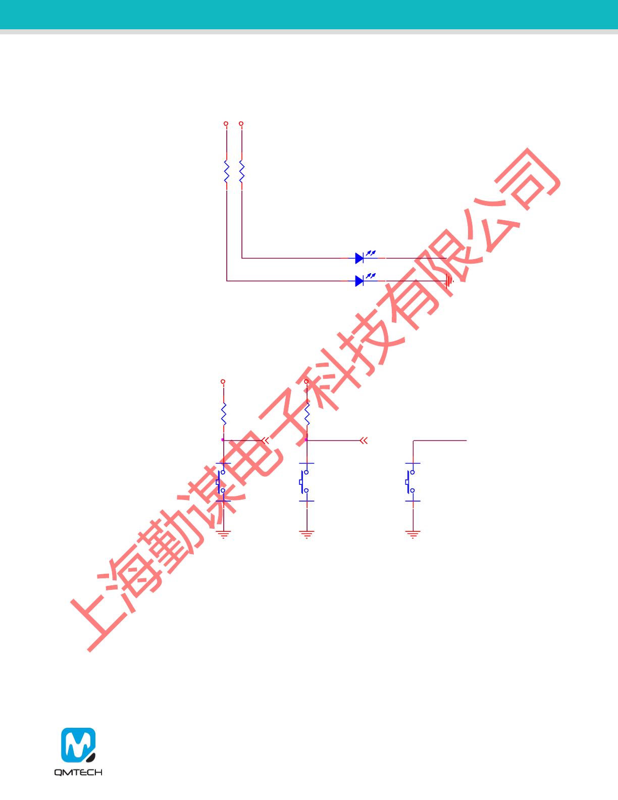
2.2.4 Cyclone IV EP4CE15 User LED
Below image shows one user LED and 3.3V power supply indicator:
Figure 2-11. User LEDs
2.2.5 Cyclone IV EP4CE15 User Key
Below image shows the nCONFIG key and two user keys:
Figure 2-12. User Keys
R131
1K
D4
1 2
3V3
D5
1 2
R255
1K
LED0
3V3
KEY0 KEY1 nCONFIG
SW3
1
2
SW1
1
2
KEY0
SW2
1
2
KEY1
R221
4.7K
3V3
3V3
R228
4.7k

Cyclone IV EP4CE15 Core Board User Manual-V01
3. Reference
[1] ep4ce15f23-sdram.pdf
[2] an592.pdf
[3] an592_ch.pdf
[4] cyiv-5v1.pdf
[5] cyiv-5v2.pdf
[6] cyiv-5v3.pdf
[7] pcg-01008.pdf
Cyclone IV EP4CE15 Core Board User Manual-V01
4. Revision
Doc. Rev.
Date
Comments
0.1
10/21/2018
Initial Version.
1.0
10/28/2018
V1.0 Formal Release.
