MRFE6VP61K25H, MRFE6VP61K25HS 2 Meter Amateur Z 32/5 W RDMRFE6VP61K25H 2MTR
User Manual: Z 32/5 W
Open the PDF directly: View PDF ![]() .
.
Page Count: 16
MRFE6VP61K25H MRFE6VP61K25HS 2 Meter Amateur
1
RF Reference Design Data
Freescale Semiconductor
RF Power Reference Design Library
2 Meter Amateur Reference Design
High Ruggedness N--Channel Enhancement--Mode
Lateral MOSFETs
Reference Design Characteristics
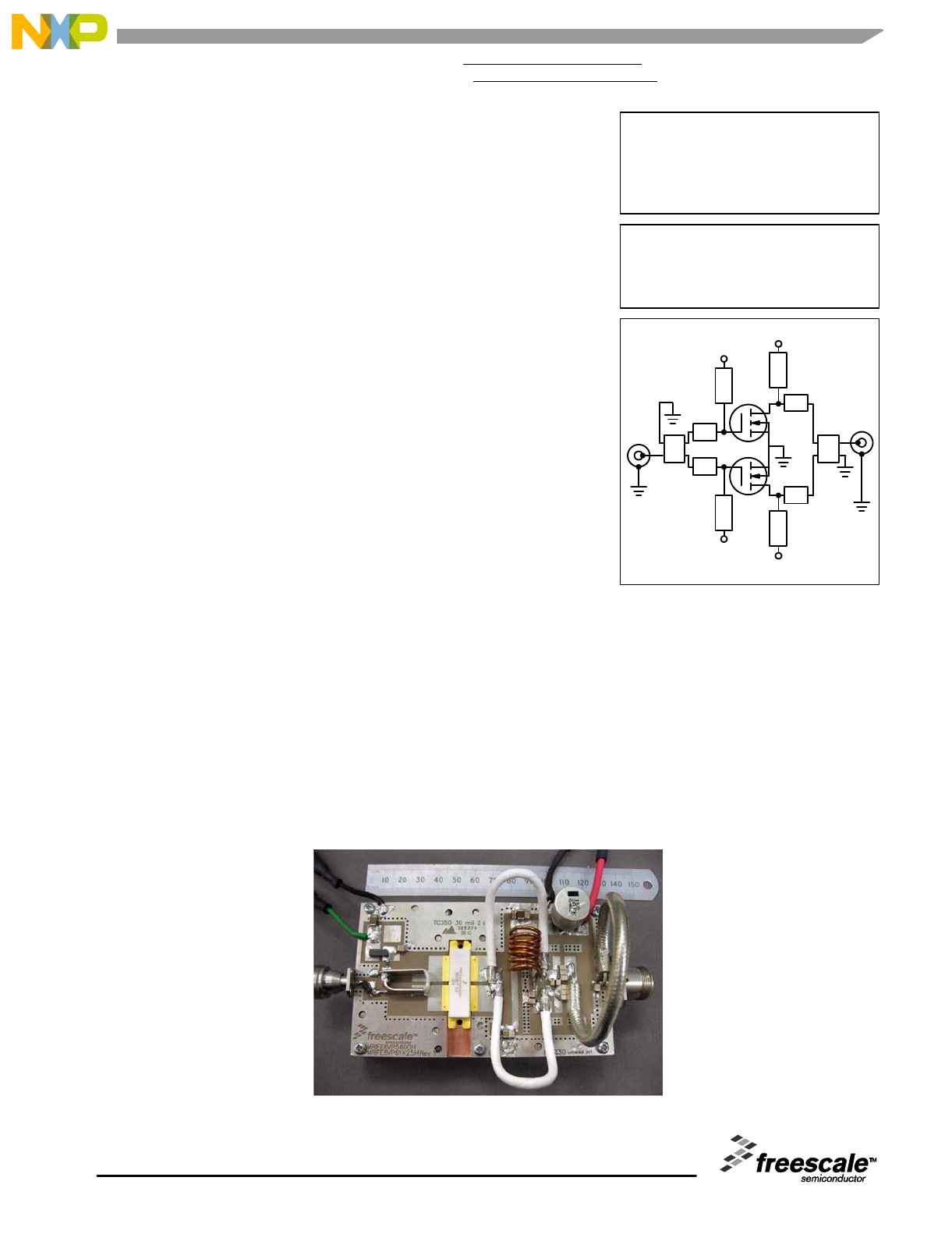
This document describes a high efficiency, rugged linear amplifier reference
design for 2 meter amateur band (144 MHz -- 148 MHz) operation. Because of
the ruggedness and low thermal resistance of the MRFE6VP61K25H transistor
used in the design. the design can output high power even when operating into
high VSWR. The amplifier can be biased for Class AB linear or Class C
operation and is suitable for both analog and digital waveforms (AM/SSB or
WSJT/FM/CW).
Frequency Band: 144--148 MHz
Output Power: >1250 Watts CW
Supply Voltage: 50 Vdc
Power Gain (Typ): 26 dB
Class C Drain Efficiency (Min): >78%
IMD @ 1 kW Output: < --28.5 dB
The MRFE6VP61K25H transistor used in this design is one of the devices in
Freescale’s RF power enhanced ruggedness 50 volt LDMOS product line. These
devices, including the 600 watt MRFE6VP5600H and the 300 watt
MRFE6VP6300H, are all specifically designed for 50 volt operation under harsh
conditions.
2 METER AMATEUR REFERENCE DESIGN
This reference design is designed to demonstrate the RF
performance characteristics of the MRFE6VP61K25H/HS
devices operating in 144--148 MHz amateur radio band. The
reference design shows two operational modes with different
optimizations, VDD =50volts,I
DQ = 2500 mA for Class AB
linear operation or VDD =43volts,I
DQ =200mAforClassC
operation.
REFERENCE DESIGN LIBRARY TERMS
AND CONDITIONS
Freescale is pleased to make this reference design
available for your use in development and testing of your
own product or products. The reference design contains an
easy--to--copy, fully functional amplifier design. It consists of
“no tune” distributed element matching circuits designed to
be as small as possible, and is designed to be used as a
“building block” by our customers.
HEATSINKING
When operating this fixture it is critical that adequate
heatsinking is provided for the device. Excessive heating of
the device may prevent duplication of the included
measurements and/or destruction of the device.
Available at http://freescale.com/RFindustrial > Design Support > Reference Designs or
http://freescale.com/RFbroadcast > Design Support > Reference Designs
Rev. 0, 6/2011
Freescale Semiconductor
Technical Data
Freescale Semiconductor, Inc., 2011.
A
ll rights reserved.
MRFE6VP61K25H
MRFE6VP61K25HS
2 Meter Amateur
144--148 MHz, 1250 W CW, 50 V
2 METER AMATEUR
REFERENCE DESIGN
RF
OUTPUT
RF
INPUT
M
VDD
VGG
BIAS
-
+
+
-
VDD
VGG
M
M
M
BIAS
BIAS
BIAS
M=Match
Figure 1. 2 Meter Amateur Reference Design Fixture
2RF Reference Design Data
Freescale Semiconductor
MRFE6VP61K25H MRFE6VP61K25HS 2 Meter Amateur
PERFORMANCE AND RF MEASUREMENTS
Measurement is done using a CW (single tone) signal
unless specified otherwise.
Data was taken using an automated characterization
system, ensuring repeatable measurements.
The reference design was tuned with a trade--off between
linearity and efficiency. Other tuning optimizations are
possible.
Table 1. 50 V Drain Supply, IDQ = 2500 mA (for Class AB, linear operation)
Freq.
(MHz) Pin
(W) Pout
(W) Gain
(dB) IRL
(dB) Eff.
(%) VDD
(v) IDD
(A)
144 0.1 73 28.6 --17.6 19.6 50 7.5
144 0.3 178 28.5 --18.1 31.8 50 11.2
144 0.5 392 28.9 --17.7 48.0 50 16.3
144 0.7 573 28.8 --17.1 57.8 50 19.8
144 1.0 724 28.6 --16.0 64.2 50 22.5
144 P1dB 1.5 920 27.9 --14.2 70.7 50 26.0
144 1.75 1003 27.6 --13.4 73.0 50 27.4
144 2.25 1135 27.0 --12.1 76.4 50 29.7
144 2.5 1201 26.8 -- 11.3 78.0 50 31.0
144 3.0 1250 26.2 -- 11.3 78.8 50 31.7
144 P3dB 3.5 1311 25.7 --10.9 79.9 50 32.8
Table 2. 50 V Drain Supply, IDQ = 200 mA (for Class C, non--linear operation, without board retuning)
Freq.
(MHz) Pin
(W) Pout
(W) Gain
(dB) IRL
(dB) Eff.
(%) VDD
(v) IDD
(A)
144 0.1 19 22.9 --14.5 11.6 50 3.3
144 0.3 79 25.0 --16.2 23.6 50 6.8
144 0.5 271 27.3 --16.7 42.7 50 12.7
144 0.8 372 27.0 --17.5 49.8 50 14.9
144 1.0 513 27.1 --17.4 57.6 50 17.8
144 1.5 771 27.1 --15.6 68.2 50 22.6
144 1.7 821 26.7 --15.3 69.8 50 23.5
144 2.2 975 26.4 --13.8 74.2 50 26.2
144 2.5 1059 26.3 --12.8 76.3 50 27.7
144 3.0 1118 25.7 --12.6 77.8 50 28.7
144 3.5 1195 25.3 --12.0 79.5 50 30.0
144 4.0 1255 25.0 -- 11.6 80.7 50 31.0
144 4.5 1301 24.6 -- 11.4 81.6 50 31.8
144 5.0 1339 24.3 -- 11.2 82.4 50 32.5
Table 3. 43 V Drain Supply, IDQ = 200 mA (for Class C, non--linear operation, without board retuning)
Freq.
(MHz) Pin
(W) Pout
(W) Gain
(dB) IRL
(dB) Eff.
(%) VDD
(v) IDD
(A)
144 0.1 17 22.5 --14.2 12.9 43 3.2
144 0.3 74 24.8 --16.2 26.9 43 6.5
144 0.5 254 27.1 --16.7 48.4 43 12.2
144 0.8 337 26.5 --17.5 55.1 43 14.2
144 1.0 459 26.6 --16.9 62.8 43 17.0
144 1.5 640 26.3 --14.7 71.2 43 20.9
144 1.8 708 26.1 --13.8 73.8 43 22.3
144 2.3 797 25.5 --12.9 76.8 43 24.1
144 2.5 752 24.8 --14.3 75.3 43 23.2
144 3.0 900 24.8 -- 11.8 79.7 43 26.2
144 3.5 953 24.3 -- 11.4 81.1 43 27.3
144 4.0 991 24.0 -- 11.1 81.9 43 28.1
144 4.5 1038 23.6 -- 11.0 83.1 43 29.0
144 5.0 1060 23.3 --10.9 83.5 43 29.5
MRFE6VP61K25H MRFE6VP61K25HS 2 Meter Amateur
3
RF Reference Design Data
Freescale Semiconductor
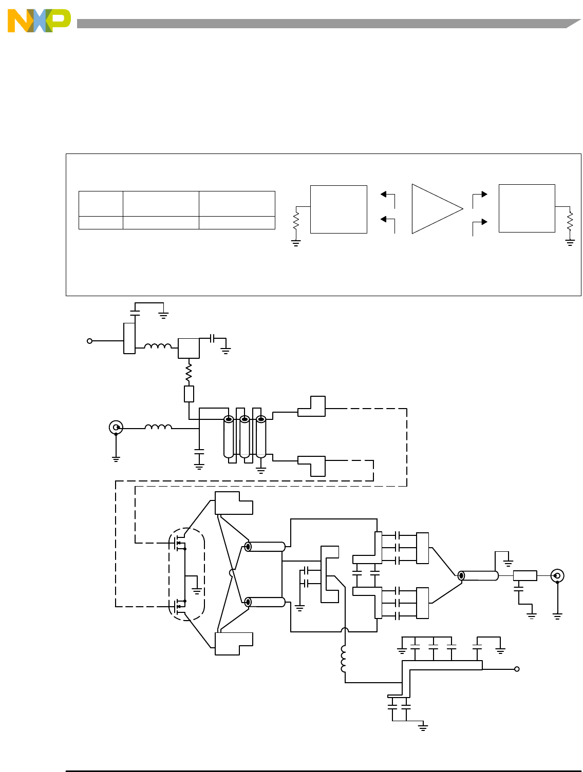
CIRCUIT DESCRIPTION
The input circuit uses a 9/1 balun transformer with a
prematch done by a series inductor and a shunt capacitor.
The shunt capacitor is optional but is useful to center the
input return loss (IRL). The input circuit return loss is always
better than 10.5 dB, equivalent to a worst case VSWR of 1.8.
The output circuit consists of a 4/1 transformer using two
4.7lengths of 10 coaxial cable. It is also recommended
that three DC blocks in parallel be used in order to lower the
total equivalent series resistance (ESR) which is critical at
this high power.
The output balun is made from a 6.7length of “Sucoform
250” 50 coaxial cable, and acts as a Pi match with
2 x 15 pF at the input and 5.6 pF at the output.
FIXTURE IMPEDANCE
VDD =50Vdc,I
DQ = 200 mA, Pout = 1100 W CW
f
MHz Zsource
Zload
144 1.6 + j5.0 3.9 + j1.5
Zsource = Test circuit impedance as measured from
gate to gate, balanced configuration.
Zload = Test circuit impedance as measured from
drain to drain, balanced configuration.
Figure 2. Series Equivalent Source and Load Impedance
Figure 3. 2 Meter Amateur Reference Design Schematic Diagram
C7
C8
C9
C10
C11
C12
RF
OUTPUT
C4
COAX1
COAX2
COAX3
C5
C6
C19 C20
C17C16C15 C18
VDD
C13 C14
L2
B1
C1
VGS
C3
R1
C2
L1
RF
INPUT
T1
Zsource Zload
Input
Matching
Network
Device
Under
Test
Output
Matching
Network
--
-- +
+
4RF Reference Design Data
Freescale Semiconductor
MRFE6VP61K25H MRFE6VP61K25HS 2 Meter Amateur
Figure 4. 2 Meter Amateur Reference Design Component Layout
*C7, C8, C9, C10, C11, and C12 are mounted vertically.
+
C1
COAX1
MRFE6VP61K25H Rev. 2
C3
R1
B1
L1
T1
C13
C14
COAX2
COAX3
C6
C5
C19C20
C7
C8
C9
C10
C11
C12
C4
C18
C15 C16 C17
L2
Note: Component number C2 is not used.
Table 4. 2 Meter Amateur Reference Design Component Designations and Values
Part Description Part Number Manufacturer
B-- 95 , 100 MHz Long Ferrite Bead 2743021447 Fair--Rite
C1 6.8 F, 50 V Chip Capacitor C4532X7R1H685K TDK
C3, C5, C7, C8, C9, C10,
C11, C12, C13, C15 1000 pF Chip Capacitors ATC100B102KT50XT ATC
C4 5.6 pF Chip Capacitor ATC100B5R6CT500XT ATC
C6 470 pF Chip Capacitor ATC100B471JT200XT ATC
C14, C16 1 F, 100 V Chip Capacitors C3225JB2A105KT TDK
C17 2.2 F, 100 V Chip Capacitor HMK432B7225KM--T Taiyo Yuden
C18 470 F, 100 V Electrolytic Capacitor MCGPR100V477M16X32--RH Multicomp
C19, C20 15 pF Chip Capacitors ATC100B150JT500XT ATC
L1 43 nH Inductor B10TJLC CoilCraft
L2 7 Turn, #14 AWG, ID = 0.4Inductor Handwound Freescale
R1 11 , 1/4 W Chip Resistor CRCW120611R0FKEA Vishay
T1 Balun TUI--9 Comm Concepts
Coax1, Coax2 Flex Cables, 10.2 ,4.7TC--12 Comm Concepts
Coax3 Coax Cable, 50 ,6.7SUCOFORM250--01 Huber+Suhner
PCB 0.030”, r= 3.50 TC--350 Arlon
* PCB artwork for this reference design is available at http://freescale.com/RFindustrial > Design Support > Reference Designs or
http://freescale.com/RFbroadcast > Design Support > Reference Designs.
Note: See Appendix B for Mounting Tips.
MRFE6VP61K25H MRFE6VP61K25HS 2 Meter Amateur
5
RF Reference Design Data
Freescale Semiconductor
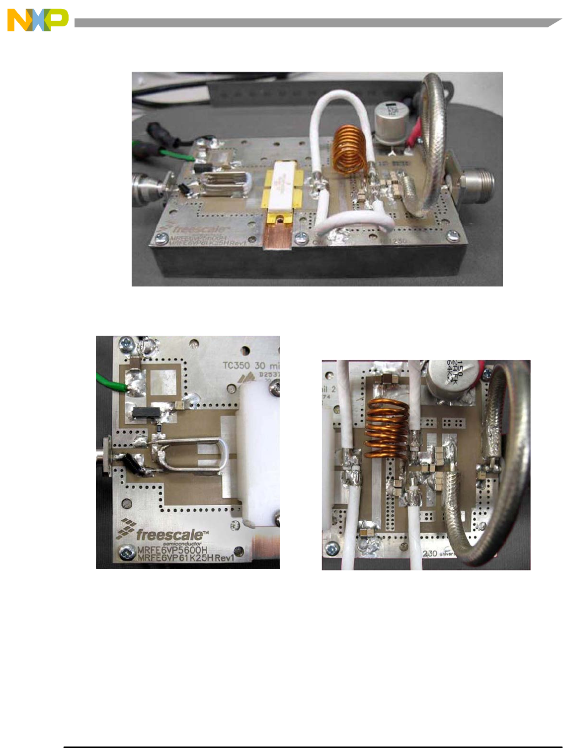
VIEWS OF 2 METER AMATEUR REFERENCE DESIGN
Figure 5. 2 Meter Amateur Reference Design Detailed Views
Overall
Input Output
6RF Reference Design Data
Freescale Semiconductor
MRFE6VP61K25H MRFE6VP61K25HS 2 Meter Amateur
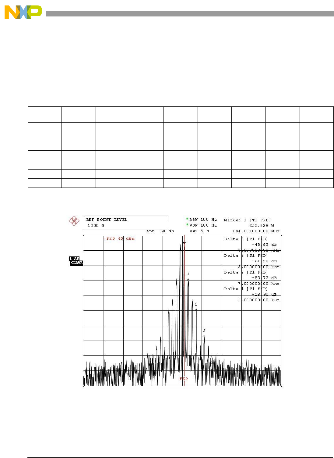
IMD MEASUREMENT
IMD measurement was done using two signal generator
with a tone spacing of 1 kHz. Quiescent current was set for
2.5 A under 50 volts with no RF signal at input. 2.5 A was
choosen as a good compromise between gain, linearity and
efficiency.
In order to get optimal linearity, a thermal compensation
circuit was used that tracks the quiescent current of the
board over the temperature range (not shown on picture).
Refer to Freescale’s AN1643 RF LDMOS Power Modules for
GSM Base Station Application: Optimum Biasing Circuit
application note(1) or the VHF Broadcast reference design for
more information.(2)
The two--tone IMD values are referenced to the peak
envelope power (PEP) and are spaced 1 kHz apart.
Table 5. Two--Tone IMD
Pout
(W) PEP IM3--L IM3--U IM5--L IM5--U IM7--L IM7--U IM9--L IM9--U
100.0 --42.2 --42.2 --61.3 --64.1 --72.5 --74.4 --85.1 --85.1
199.5 --42.0 --42.3 --57.8 --59.6 --69.9 --70.6 --75.2 --78.0
399.8 --44.8 --44.0 --50.8 --51.7 --66.6 --68.2 --73.3 --72.1
599.3 --41.7 --41.5 --45.1 --45.5 --68.1 --71.7 --68.1 --68.9
797.1 --33.7 --33.7 --42.4 --42.2 --56.5 --57.3 --68.5 --65.9
899.8 --30.8 --30.9 --42.0 --41.8 --51.9 --52.4 --68.0 --69.5
997.8 --28.7 --28.6 --42.7 --42.3 --48.6 --48.7 --73.7 --73.4
ate: 3.NOV.2010 14:48:
D19
Figure 6. 1000 W PEP Two--Tone Spectrum
MRFE6VP61K25H MRFE6VP61K25HS 2 Meter Amateur
7
RF Reference Design Data
Freescale Semiconductor
ate: 3.NOV.2010 14:46:32
D
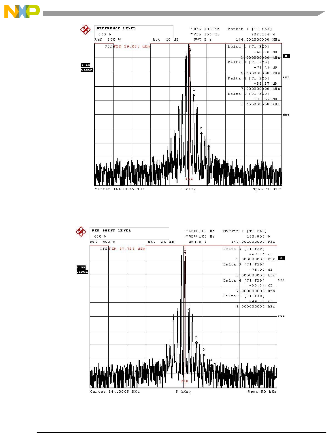
Figure 7. 800 W Two--Tone Spectrum
ate: 3.NOV.2010 14: :
D52 11
Figure 8. 600 W Two--Tone spectrum
8RF Reference Design Data
Freescale Semiconductor
MRFE6VP61K25H MRFE6VP61K25HS 2 Meter Amateur
ate: 3.NOV.2010 14: :
D51 00
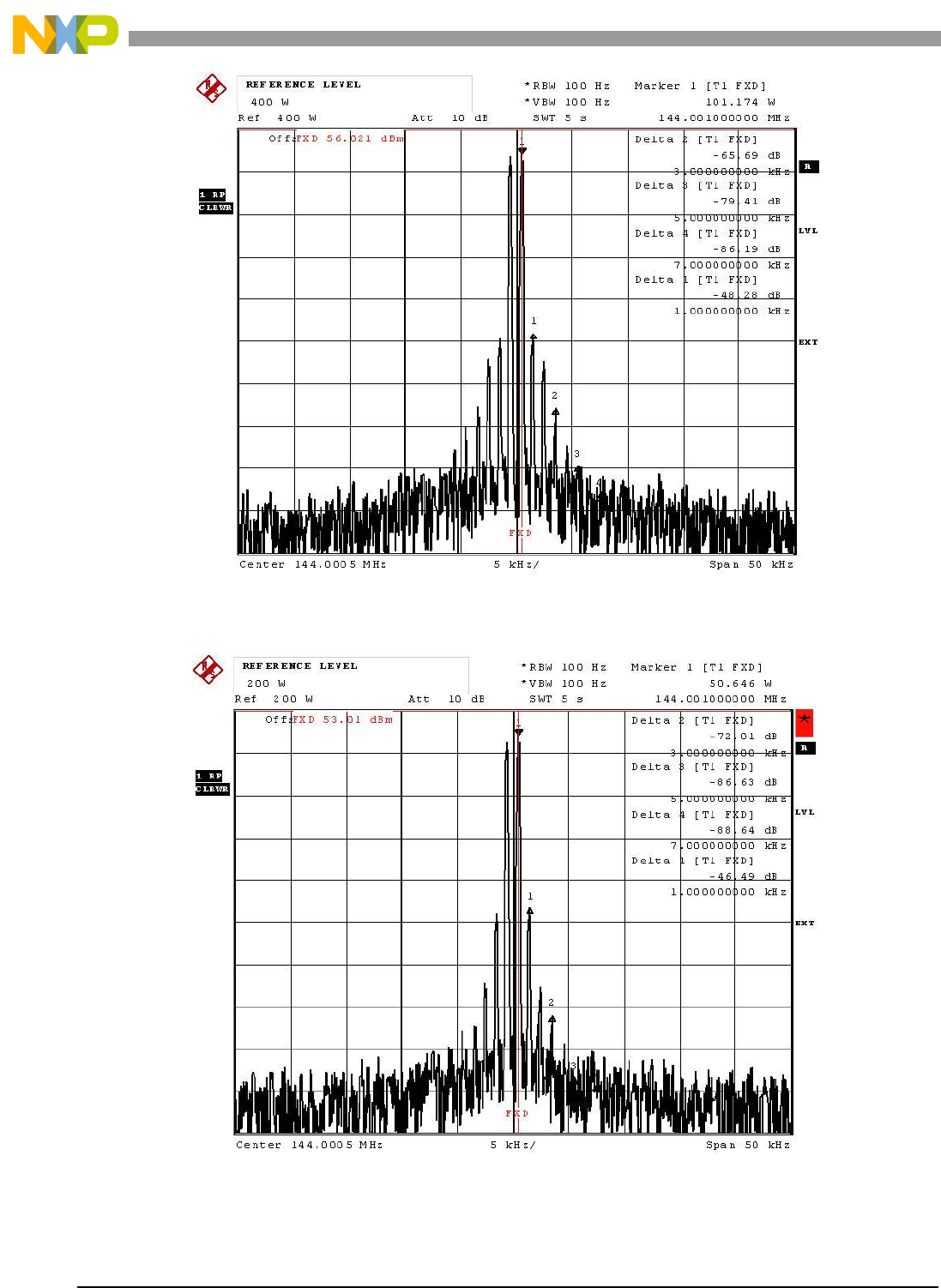
Figure 9. 400 W Two--Tone SPectrum
ate: 3.NOV.2010 14: :
D51 00
Figure 10. 200 W Two--Tone Spectrum
MRFE6VP61K25H MRFE6VP61K25HS 2 Meter Amateur
9
RF Reference Design Data
Freescale Semiconductor
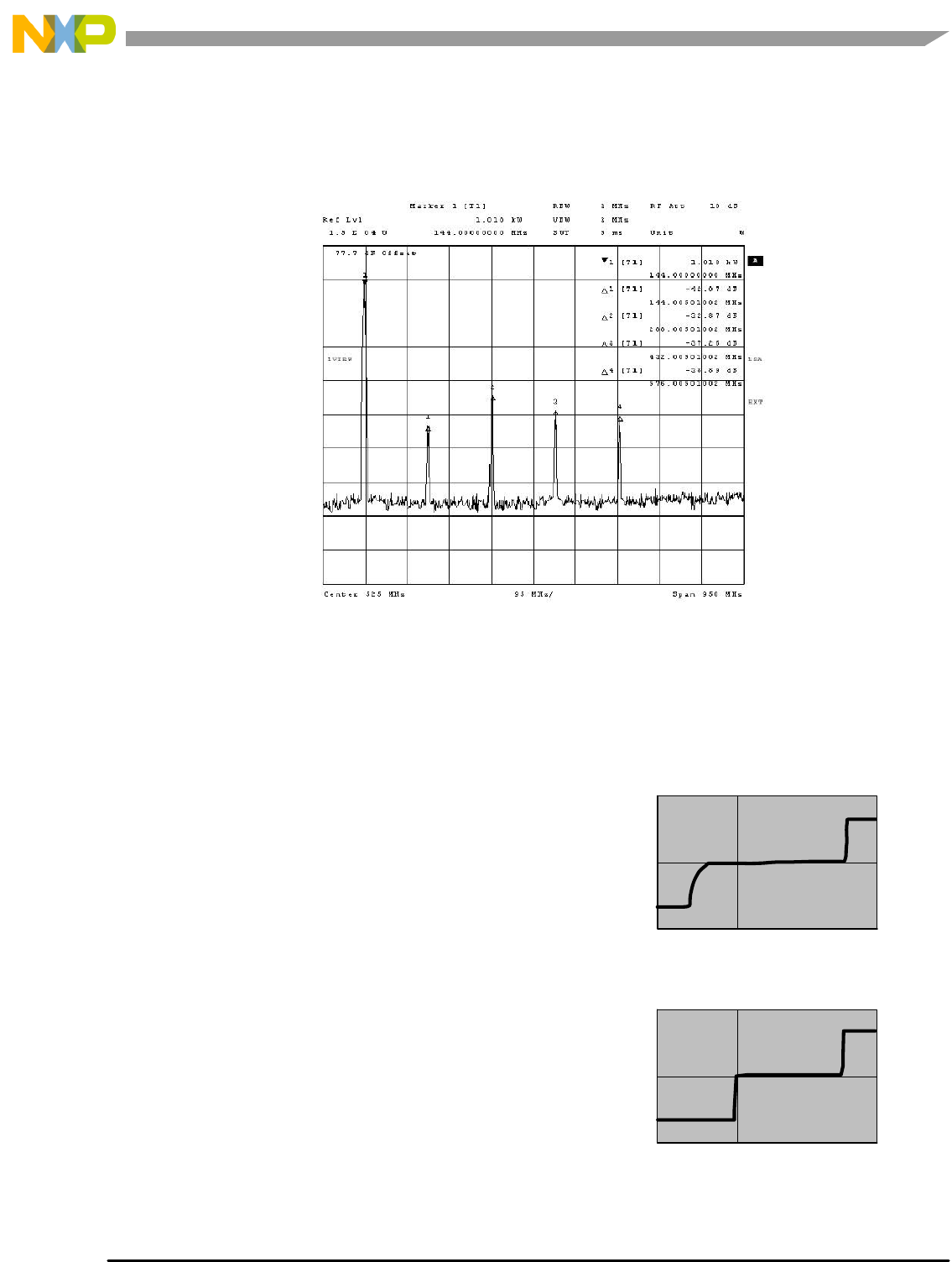
HARMONIC MEASUREMENTS
At the one kW level, second harmonic is --42 dBc, third
harmonic is --32 dBc, and fourth harmonic is --37 dBc.
To be used “on the AIR” this amplifier will likely need a filter
to be compliant with local regulations. A diplexer could give
better results than a simple low pass filter because
harmonics are absorbed in a resistive load instead of being
reflected to the transistor.
ate: 4.NOV.2010 16: :
D47 52
Figure 11. Harmonics @ 1 kW
FREESCALE RF POWER 50 V TECHNICAL ADVANTAGES
50 V Drain Voltage
50 volt operation offers benefits over lower voltage
operation because the output impedance of the device for
the same output power is much greater, so the output match
circuitry is simpler and has lower loss. IMD performance is
better and supply current will also be lower than with low
voltage operation.
The reference fixture was designed with the market
standard power supply, allowing the amplifier to utilize a
standard 48 volt power supply (most are adjustable from 43
to 54 volts).
Extended Gate Voltage Range
The enhanced electro--static discharge protection
structure at the gate of the transistor is a Freescale
innovation pioneered in the cellular infrastructure market that
is incorporated into the 50 V LDMOS RF power product
portfolios. This ESD structure can tolerate moderate reverse
bias conditions applied to the gate lead up to --6 volts (see
Figure 12). This allows Freescale transistors to be used in
applications where the gate voltage needs to be set as low
as --6 volts.
This feature can dramatically simplify protection circuits,
as it allows the transistor to be shut down because of high
VSWR or PLL unlock without shutting down the drive power.
Setting the gate bias voltage to around --4 volts will totally
block the transistor even if the RF input signal is still there.
Figure 12. Gate Voltage Breakdown with ESD
2.E--02
0.E+00
-- 2 . E -- 0 2
-- 1 . E -- 0 2
-- 5 . E -- 0 3
5.E--03
1.E--02
-- 1 5 0--10 --5 5 10 15 20 25
VGS (V)
IESD (A)
Enhanced ESD
2.E--02
0.E+00
-- 2 . E -- 0 2
-- 1 . E -- 0 2
-- 5 . E -- 0 3
5.E--03
1.E--02
-- 1 5 0--10 --5 5 10 15 20 25
VGS (V)
IESD (A)
Standard ESD
10 RF Reference Design Data
Freescale Semiconductor
MRFE6VP61K25H MRFE6VP61K25HS 2 Meter Amateur
Ruggedness
MRFE6VP61K25H is a very rugged part capable of
handling 65:1 VSWR, provided thermal limits are not
exceeded.
It was designed for high mismatch applications, such as
laser and plasma exciters, that under normal operation
exhibit high VSWR values at startup and then come back to
a more friendly impedance. In CW at high VSWR values and
simultaneously at rated power, the limiting factor is the
maximum DC power dissipation.
VSWR protection that shuts down the gate voltage within
10 ms will protect the transistor effectively.
The amplifier presented here was tested at full power with
all phase angles with 10 ms pulsed 5% duty cycle without
failure or degradation in RF performance.
Reliability
MTTF is defined as the mean time to failure of 50% of the
device within a sample size, the primary factor in device
reliability failure is due to electromigration. Once average
operating condition for the applicatin is set, MTTF can be
calculated using the Rth found on the offical Freescale data
sheet.
Example: If desired operating output power is 1000 watts,
with 82% drain efficiency at 43 volts:
IDrain @ 1 kW 82% eff = 28.2 A
MRFE6VP61K25H Rth =0.15C/W, case temperature =
63C
Dissipated power = 219 Watts
Temperature rise (junction to case) = 219 Watts
0.15C/W = 32.8C
TJ=T
rise +T
case =63C + 32.8C = 95.8C
Utilizing the graph below which cacluates MTTF versus
IDrain and TJ; IDrain = 28 A, MTTF for this example was 8000
years.
230
100000
70
1000
100
1
90 110 130 150 170
MTTF
(YEARS)
190 210
10000
10
24 Amp
28 Amp
20 Amp
Figure 13. MTTF versus Junction Temperature
TJ, JUNCTION TEMPERATURE (C)
There is an MTTF (Median--Time--To--Failure) calculator(3)
available to assist the customers in estimating the
MRFE6VP61K25H device reliability in terms of
electromigration wear--out mechanism.
MRFE6VP61K25H MRFE6VP61K25HS 2 Meter Amateur
11
RF Reference Design Data
Freescale Semiconductor
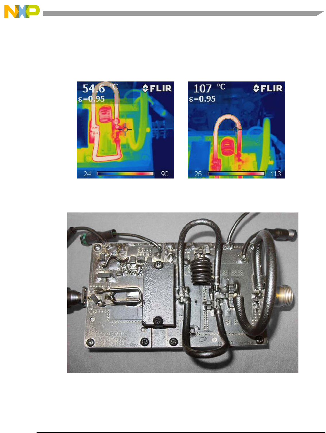
THERMAL MEASUREMENTS
After one minute at 1 kW CW 44 volt supply at 80%
efficiency, with no airflow on the top of the board, the output
capacitor matching runs at 55C, and the 10 coax section
is around 90C.
After 5 minutes “key down” CW, the highest temperature is
113C on the 10 coax section (Teflon cable is rated up to
200C), output match capacitors do not show signs of
overheating.
If the board is run at levels higher than 1 kW CW or digital
mode, airflow over the top side of the board could help to
cool down coax and improve reliability.
As shown in Figure 14, the board was painted with black coating to correct for variations in emissivity
Figure 14. Reference design with black coating needed to obtain accurate thermograph images

12 RF Reference Design Data
Freescale Semiconductor
MRFE6VP61K25H MRFE6VP61K25HS 2 Meter Amateur
REFERENCES
1. “RF LDMOS Power Modules for GSM Base Station
Application: Optimum Biasing Circuit.” (Document
Number: AN1643) Application Note, 1998.
2. VHF Broadcast Reference Design available at
http://freescale.com/RFbroadcast > Design Support >
Reference Designs.
3. MRFE6VP61K25H MTTF calculator available at
http://freescale.com/RFpower > Software & Tools >
Development Tools > Simulations and Models >
Calculators. Enter the “part number” into the Search field
for quickest results.
4. “Mounting Recommendations for Copper Tungsten
Flanged Transistors.” (Document Number: AN1617)
Application Note, 1997.
Technical documentation, including data sheets and application notes, for Freescale RF Power product can be found at:
http://freescale.com/RFpower. Enter the applicable Document Number into “Keyword” search for quickest results.

MRFE6VP61K25H MRFE6VP61K25HS 2 Meter Amateur
13
RF Reference Design Data
Freescale Semiconductor
APPENDIX A
Cautions
The board drive level is very low and excessive drive level
will destroy the transistor. If used with a transmitter, be
careful with your power control as some transmitters have
very high power spikes at startup due to a badly designed
ALC. It is a better idea is to put a power attenuator ahead of
this amplifier to protect against overdrive.

14 RF Reference Design Data
Freescale Semiconductor
MRFE6VP61K25H MRFE6VP61K25HS 2 Meter Amateur
APPENDIX B
Mounting Tips
An Arlon TC350 PCB was chosen for its high thermal
conductivity.
Mounting is done on a copper heat spreader. Flatness
under the transistor flange is critical; good flatness is
mandatory for both RF and thermal performance. The
transistor is mounted on the heat spreader using a thin layer
of thermal compound.
When using bolt--down mounting do not over--torque the
part. Over tightening the fasteners can deform the transistor
flange and degrade both the RF and thermal performance,
as well as long term reliability.
To reach optimum performance, the PCB must be
soldered to the copper heat spreader. This is usually done
using a hotplate and solder paste. It is critical that the
soldering near the transistor and connectors is free of voids
and is of high quality in to order to achieve best performance
and reliability.
Refer to Freescale’s AN1617 Mounting Recommendations
for Copper Tungsten Flanged Transistors application note for
more information.(4)

MRFE6VP61K25H MRFE6VP61K25HS 2 Meter Amateur
15
RF Reference Design Data
Freescale Semiconductor
APPENDIX C
Copper Heatsink for 2 Meter Amateur Fixture
A
2.737 (69.51) 0.41 (10.41)
D
D
A
1.813 (46.04)
0.813 (20.64)
0.140 (3.56)
0.125 (3.17)
0.00 (0.00)
0.177 (4.50)
0.929 (23.59)
1.558 (39.58)
1.724 (43.78)
2.134 (54.19)
2.283 (57.98)
2.929 (74.38)
4.499 (114.28)
4.725 (120.02)
E
F
F
E
1.929 (48.98)
D
A
A
D
B
4.548 (115.52)
2.882 (73.19)
2.719 (69.07)
2.011 (51.08)
0.611 (15.52)
0.130 (3.32)
AA
D
D
A
A
B
1.309 (33.26)
1.668 (42.38)
1.489 (37.83)
1.129 (28.69)
0.950 (24.14)
0.188 (4.76)
0.000 (0.00)
0.000 (0.00)
0.128 (3.25)
0.324 (8.23)
0.038 (0.97)
1.929 (48.99)
C, Device Channel
EE
0.929 (23.59)
2.929 (74.39)
Gutter is 0.030 wide
and 0.046 deep, both
sides
0 (0.00)
0.300 (7.62)
0.720 (18.29)
B
0.000 (0.00)
inches (mm)
8x
#4--40
0.300deep
0.720Copper Heatsink Hole Details
Designators Details
A2 places, both sides, drill and tap, #2--56 screw depth 0.300
B2 places, both sides, 0.1875diameter notch 0.020deep
CNI--1230 channel 0.410wide by 0.0380deep
D2 places, both sides, drill depth 0.250and tap for #4--40 screw
ELocator holes from bottom diameter = 0.257, depth = 0.400
F 2 places, drill through and tap for #4--40 screw
Figure 15. Heatspreader Design

16 RF Reference Design Data
Freescale Semiconductor
MRFE6VP61K25H MRFE6VP61K25HS 2 Meter Amateur
Information in this document is provided solely to enable system and software
implementers to use Freescale Semiconductor products. There are no express or
implied copyright licenses granted hereunder to design or fabricate any integrated
circuits or integrated circuits based on the information in this document.
Freescale Semiconductor reserves the right to make changes without further notice to
any products herein. Freescale Semiconductor makes no warranty, representation or
guarantee regarding the suitability of its products for any particular purpose, nor does
Freescale Semiconductor assume any liability arising out of the application or use of
any product or circuit, and specifically disclaims any and all liability, including without
limitation consequential or incidental damages. “Typical” parameters that may be
provided in Freescale Semiconductor data sheets and/or specifications can and do
vary in different applications and actual performance may vary over time. All operating
parameters, including “Typicals”, must be validated for each customer application by
customer’s technical experts. Freescale Semiconductor does not convey any license
under its patent rights nor the rights of others. Freescale Semiconductor products are
not designed, intended, or authorized for use as components in systems intended for
surgical implant into the body, or other applications intended to support or sustain life,
or for any other application in which the failure of the Freescale Semiconductor product
could create a situation where personal injury or death may occur. Should Buyer
purchase or use Freescale Semiconductor products for any such unintended or
unauthorized application, Buyer shall indemnify and hold Freescale Semiconductor
and its officers, employees, subsidiaries, affiliates, and distributors harmless against all
claims, costs, damages, and expenses, and reasonable attorney fees arising out of,
directly or indirectly, any claim of personal injury or death associated with such
unintended or unauthorized use, even if such claim alleges that Freescale
Semiconductor was negligent regarding the design or manufacture of the part.
Freescaletand the Freescale logo are trademarks of Freescale Semiconductor, Inc.
All other product or service names are the property of their respective owners.
Freescale Semiconductor, Inc. 2011. All rights reserved.
How to Reach Us:
Home Page:
www.freescale.com
Web Support:
http://www.freescale.com/support
USA/Europe or Locations Not Listed:
Freescale Semiconductor, Inc.
Technical Information Center, EL516
2100 East Elliot Road
Tempe, Arizona 85284
1--800--521--6274 or +1--480--768--2130
www.freescale.com/support
Europe, Middle East, and Africa:
Freescale Halbleiter Deutschland GmbH
Technical Information Center
Schatzbogen 7
81829 Muenchen, Germany
+44 1296 380 456 (English)
+46 8 52200080 (English)
+49 89 92103 559 (German)
+33169354848(French)
www.freescale.com/support
Japan:
Freescale Semiconductor Japan Ltd.
Headquarters
ARCO Tower 15F
1--8--1, Shimo--Meguro, Meguro--ku,
Tokyo 153--0064
Japan
0120 191014 or +81 3 5437 9125
support.japan@freescale.com
Asia/Pacific:
Freescale Semiconductor China Ltd.
Exchange Building 23F
No. 118 Jianguo Road
Chaoyang District
Beijing 100022
China
+86 10 5879 8000
support.asia@freescale.com
For Literature Requests Only:
Freescale Semiconductor Literature Distribution Center
1--800--441--2447 or +1--303--675--2140
Fax: +1--303--675--2150
LDCForFreescaleSemiconductor@hibbertgroup.com
Available at http://freescale.com/RFindustrial > Design Support > Reference Designs or
http://freescale.com/RFbroadcast > Design Support > Reference Designs
Rev. 0, 6/2011
