RPvdsEx Manual RPvds Ex
User Manual:
Open the PDF directly: View PDF ![]() .
.
Page Count: 356 [warning: Documents this large are best viewed by clicking the View PDF Link!]
- Introduction to RPvdsEx
- Part 1 RPvdsEx Fundamentals
- Part 2 Circuit Design
- Circuit Design Basics
- Hardware Considerations
- Multi-Channel Circuit Design
- MultiProcessor Circuit Design
- Digital I/O Circuit Design
- Part 3 Reference
- Macro Reference
- Component Reference
- Audio Processing
- Basic Analysis
- Basic Math
- Buffer Operations
- Coefficient Generators
- Counters and Logic
- Data Reduction
- Delay Functions
- Device Status
- Digital Filters
- Exponents and Logs
- Gating Functions
- Helpers
- Input/Output
- Integer Math
- Multi-processor
- NeuroAnalysis
- OpenEx Headers
- State/Flow Control
- Trigonometry
- Type Conversion
- Waveform Generators
- Menu and Toolbar Reference
- Part 4 Troubleshooting
- RPvdsEx Known Anomalies
- Common RPvdsEx Error Messages and Warnings
- Error Loading RP Circuit
- Data type mismatch: ....
- Link cannot originate from 'Input' port or Link cannot terminate at 'output' port
- Apparent nChannels mismatch between connected components
- Components intersecting Iterator
- MCHop source is not found for component
- zBus Error: Call RPxAddCmp/ zError: Memory Allocation Failure
- Before Debugging a Circuit
- Common RPvdsEx Problems
- Appendix A - Sampling
- Revision History
- Index

RPvdsEx Manual
RPvdsEx Manual
RPvdsEx Manual
Copyright
© 2000 – 2011 Tucker-Davis Technologies, Inc. (TDT). All rights reserved.
No part of this manual may be reproduced or transmitted in any form or by any means, electronic
or mechanical, including photocopying and recording, for any purpose without the express written
permission of TDT.
Licenses and Trademarks
Windows 7 is a registered trademark of Microsoft Corporation.
Updated: 9/14/2011 2:50 PM
i
Table of Contents
INTRODUCTION TO RPVDSEX.............................................................................................................. 1
DSP BASICS AND SYSTEM 3........................................................................................................................ 3
Digital Signal Processors - DSPs........................................................................................................... 3
Why RPvdsEx?........................................................................................................................................ 3
The Processing Chain............................................................................................................................. 3
Using Compiled Circuit Files................................................................................................................. 4
BEFORE YOU BEGIN.................................................................................................................................... 5
PC System Requirements........................................................................................................................ 5
Installation.............................................................................................................................................. 5
Hardware Requirements......................................................................................................................... 5
Organization of the Manual ................................................................................................................... 5
PART 1 RPVDSEX FUNDAMENTALS............................................................................................... 7
THE RPVDSEX ENVIRONMENT.................................................................................................................... 9
Overview of the Workspace.................................................................................................................... 9
Menus and Toolbars............................................................................................................................. 10
The Messages Window.......................................................................................................................... 10
The Pages ............................................................................................................................................. 11
Compiling Selected Processors ............................................................................................................ 16
File Formats......................................................................................................................................... 17
Device Setup......................................................................................................................................... 17
THE COMPONENTS .................................................................................................................................... 19
Component Overview ........................................................................................................................... 19
Component Numbering......................................................................................................................... 20
Links Treated as Components............................................................................................................... 21
Data Types............................................................................................................................................ 23
Parameter Access Rules ....................................................................................................................... 24
Time Slices............................................................................................................................................ 25
Duplication Information....................................................................................................................... 28
MACROS.................................................................................................................................................... 30
Macro Overview................................................................................................................................... 30
Adding Macros ..................................................................................................................................... 31
Working with Macros ........................................................................................................................... 32
TIME SAVING RPVDSEX TECHNIQUES ...................................................................................................... 34
Changing Component Names Systematically ....................................................................................... 34
Changing Parameters Systematically................................................................................................... 34
Using Indexing...................................................................................................................................... 35
Using the Preferences Dialog Box ....................................................................................................... 37
Updating Number of Channels Systematically..................................................................................... 38
RPvdsEx Shortcuts................................................................................................................................ 38
PART 2 CIRCUIT DESIGN................................................................................................................. 41
CIRCUIT DESIGN BASICS ........................................................................................................................... 43
Creating and Running a Simple Circuit ............................................................................................... 43
Triggering............................................................................................................................................. 44
Gating a Signal..................................................................................................................................... 45
Acquiring and Storing the Signal ......................................................................................................... 46
Signal Processing................................................................................................................................. 48
Using Parameter Tags for Software Control........................................................................................ 50
HARDWARE CONSIDERATIONS .................................................................................................................. 51
RPvdsEx Manual
ii
Input/Output Delays ............................................................................................................................. 51
The Sample Clock and Sampling Rates ................................................................................................ 53
Cycle Usage.......................................................................................................................................... 54
Transferring Data Between the Processor and the PC ........................................................................ 56
MULTI-CHANNEL CIRCUIT DESIGN........................................................................................................... 57
Overview............................................................................................................................................... 57
The Nature of Multi-Channel Signals................................................................................................... 57
Multi-Channel Circuit Design Strategies ............................................................................................. 58
MULTIPROCESSOR CIRCUIT DESIGN ......................................................................................................... 64
Overview............................................................................................................................................... 64
Assigning DSPs in RPvdsEx................................................................................................................. 64
MultiProcessor Hop Components......................................................................................................... 65
Using the {d} Variable.......................................................................................................................... 66
Store Pooling........................................................................................................................................ 66
Multi-Processor Circuit Design Strategies........................................................................................... 67
Multi-Processor Circuit Design - RZ2 ................................................................................................. 67
DIGITAL I/O CIRCUIT DESIGN ................................................................................................................... 72
Working with BitIn - BitOut.................................................................................................................. 72
Working with WordIn - WordOut......................................................................................................... 72
Addressing Digital Bits In A Word....................................................................................................... 73
PART 3 REFERENCE ......................................................................................................................... 77
MACRO REFERENCE.................................................................................................................................. 79
Macro Reference List ........................................................................................................................... 79
COMPONENT REFERENCE .......................................................................................................................... 84
Audio Processing.................................................................................................................................. 84
Basic Analysis....................................................................................................................................... 93
Basic Math............................................................................................................................................ 99
Buffer Operations............................................................................................................................... 115
Coefficient Generators ....................................................................................................................... 144
Counters and Logic ............................................................................................................................ 152
Data Reduction................................................................................................................................... 166
Delay Functions.................................................................................................................................. 181
Device Status...................................................................................................................................... 191
Digital Filters..................................................................................................................................... 195
Exponents and Logs............................................................................................................................ 208
Gating Functions................................................................................................................................ 212
Helpers ............................................................................................................................................... 215
Input/Output ....................................................................................................................................... 229
Integer Math....................................................................................................................................... 240
Multi-processor .................................................................................................................................. 248
NeuroAnalysis..................................................................................................................................... 257
OpenEx Headers................................................................................................................................. 276
State/Flow Control ............................................................................................................................. 280
Trigonometry...................................................................................................................................... 287
Type Conversion................................................................................................................................. 291
Waveform Generators ........................................................................................................................ 309
MENU AND TOOLBAR REFERENCE .......................................................................................................... 319
Menus ................................................................................................................................................. 319
Toolbars.............................................................................................................................................. 324
PART 4 TROUBLESHOOTING....................................................................................................... 331
RPVDSEX KNOWN ANOMALIES .............................................................................................................. 333
General............................................................................................................................................... 333
Parameters ......................................................................................................................................... 333
Components........................................................................................................................................ 334
iii
COMMON RPVDSEX ERROR MESSAGES AND WARNINGS........................................................................ 336
BEFORE DEBUGGING A CIRCUIT.............................................................................................................. 338
COMMON RPVDSEX PROBLEMS.............................................................................................................. 340
APPENDIX A - SAMPLING................................................................................................................... 341
Understanding Aliasing and Imaging ................................................................................................ 341
REVISION HISTORY............................................................................................................................. 343
INDEX....................................................................................................................................................... 347
RPvdsEx Manual
iv
~

Introduction to RPvdsEx
RPvdsEx Manual
2
~
RPvdsEx Manual
3
DSP Basics and System 3
System 3 is TDT’s integrated hardware and software research platform. The modular,
programmable hardware systems are built around a powerful group of digital signal processors
(DSPs), specifically designed to perform complex signal processing algorithms in real-time.
Signal processing—the manipulation or analysis of analog or digital signals—is the core function
of every TDT workstation. System 3 real-time processors can be used for a broad range of
applications and can be used to process virtually any type of signal including sound, biological
signals, and many others. Processing may include storage, reconstruction, filtering, compression,
or feature extraction. Every time you play a tone, filter a noisy input signal, or store spike data,
you are signal processing. When you do this using TDT hardware, you’re putting the power of
System 3’s real-time processors to work for you.
Digital Signal Processors - DSPs
The processors are available in several different form factors, utilizing one or more DSPs. A DSP
is nothing more than a specialized microprocessor. This programmable device is designed to make
quick calculations and execute signal processing specific operations. From a top-down approach,
you can consider the DSP as a programmable “black box” with points of input and output. Each
TDT processor module that inputs real world analog signals also includes analog-to-digital
convertors (ADCs) and those that output analog signals include digital-to analog convertors
(DACs). Signals can then be input to the device and manipulated digitally before storing the result
or playing a signal out. All of these tasks are configured via the RPvdsEx design interface.
Why RPvdsEx?
To optimize performance, DSPs must be programmed in low-level assembly code. Because
programming in assembly is a complex, tedious, and lengthy process that requires the programmer
to be familiar with the target processor’s architecture, DSPs are typically programmed “at the
factory” to run specialized time-critical tasks. In most implementations, the end-user cannot
modify the “embedded” DSP program, and so the flexibility that is often critical for research
applications is lost.
The System 3 processors are controlled using a common configuration tool, our Real-time
Processor Visual Design Studio (RPvdsEx). This graphical design interface gives you unparalleled
control over signal presentation and data acquisition, allowing you to customize the function of
each signal-processing module in your system.
RPvdsEx gives you control over the DSP without the complexity of writing assembly code.
The Processing Chain
RPvdsEx includes a powerful library of over 300 components, representing a variety of
fundamental processing tasks. Using RPvdsEx you can combine components to create exactly the
processing function you require. This ordered set of tasks is called the processing chain and it
takes the form of a series of linked components that form a “circuit”. Each component maps to a
segment of optimized DSP code, and all the code segments are joined together to make a master
program by the RPvdsEx compiler.
TDT processors load your custom processing chain through the PC interface. When the processor
is running, the processing chain is executed on every tick of the sample clock. In this way, TDT
RPvdsEx Manual
4
real-time processors are “field configurable.” Your application is loaded when you are ready to
run your protocol, and the DSP can be reconfigured rapidly if you need to make any changes.
Using Compiled Circuit Files
Compiled circuit files can be run from TDT run-time software applications or custom applications,
created using TDT development tools.
The design paths for using System 3 are outlined below.
Higher-level software applications load the circuit to the hardware at run-time and give the user
access to experimental parameters while the experiment is running.
Circuit design
and development
in RPvdsEx.
Use RPvdsEx for
debugging and
demonstration.
Save compiled
circuit files in
RPvdsEx.
Use circuit with TDT run-
time a
pp
lication. Use circuit with custom
a
pp
lications.
RPvdsEx Manual
5
Before You Begin
PC System Requirements
The recommended operating system for all TDT systems is Windows 7®.
Recommended PC Specs:
Memory: 1 GB
HardDrive: 80 GB
Processor: 2.0 GHz Intel Pentium IV
Video Card w/ 64 MB
2.2 compliant PCI slot (required for Gigabit or Optibit Interface cards)
DVD-R or CD combo
Installation
RPvdsEx is installed as part of the TDT Drivers Installation. See your system’s installation guide
for installation instructions.
Hardware Requirements
Some RPvdsEx circuit design features are not available unless your PC is connected to a TDT
system, so it is a good idea to set up your hardware before you begin working in RPvdsEx. See
your system’s installation guide for installation and set-up instructions.
Organization of the Manual
This manual is organized in the following sections:
RPvdsEx Fundamentals
About the workspace, the components, and macros.
Circuit Design
Design techniques for basic, multi-channel, multi-processor, and digital I/O circuits.
Reference
A reference for macros, components, menus and toolbars.
Troubleshooting
Anomalies, common design problems, and debugging circuits.
RPvdsEx Manual
6
~

Part 1 RPvdsEx Fundamentals
RPvdsEx Manual
8
~
RPvdsEx Manual
9
The RPvdsEx Environment
Overview of the Workspace
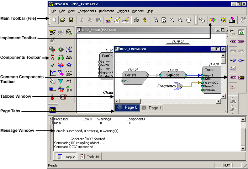
The RPvdsEx workspace has been designed for ease of use and flexibility. Circuit diagrams,
representing the processing chain, are created on the pages of a tabbed window using drag-and-
drop techniques. Unless otherwise assigned, all pages of a window form a single complete circuit.
When using a multi-DSP device, pages or segments of the circuit can be assigned to one or more
processors.
Windows and toolbars can be arranged to customize the workspace for easy access to commonly
used components and design tools. Before making changes to the workspace it will appear similar
to the illustration below.
The workspace contains the following elements:
Tabbed Window
Click and drag to arrange and connect components to form a circuit diagram.
Main Toolbar (File)
Open, create, and save files.
Implement Toolbar
Access tools for compiling and running the circuit or select and configure the device setup.
Components Toolbar
Select a group button to access hundreds of components for signal processing tasks organized into
intuitive groups.

RPvdsEx Manual
10
Common Components Toolbar
Select one of the most commonly used components.
Zoom and Pan
View circuit segments and move around a page.
Messages Window
View compilation status, errors, or warnings in a tabbed messages window – select an error in the
list to navigate to the problem area of the circuit.
Page Tabs
Pages are navigated using tabs at the bottom left corner of the tabbed window allowing you to
quickly switch between areas of the circuit. Pages organize complex circuits and allow you to
assign individual pages to one or more DSPs on a multi-DSP device. They can be added and
removed at any time.
Menus and Toolbars
RPvdsEx provides you with a full set of menus and toolbars. Using menus, commands, and
toolbar buttons, you can create, open, and save circuit files; build new circuits or edit existing
circuits; and access hardware configuration settings. The menus and toolbars are covered in detail
in the Menu and Toolbar reference, beginning on page 319.
The Messages Window
The messages window is provided specifically for compilation and error reports. By default, the
window is docked at the bottom of the RPvdsEx workspace. The window can be moved and
resized and has two tabs – Output and Task List
Output
The Output window displays details about the compilation such as the start and success of
compiling, loading, and running the current circuit. It also displays errors and warnings
encountered while compiling. If more than five errors are encountered on compilation, compiling
stops, and a Build failed error is displayed.
If a multi-processor device is specified in the hardware setup, this window also reports the number
of components on each processor when the circuit compiles successfully.
Task List
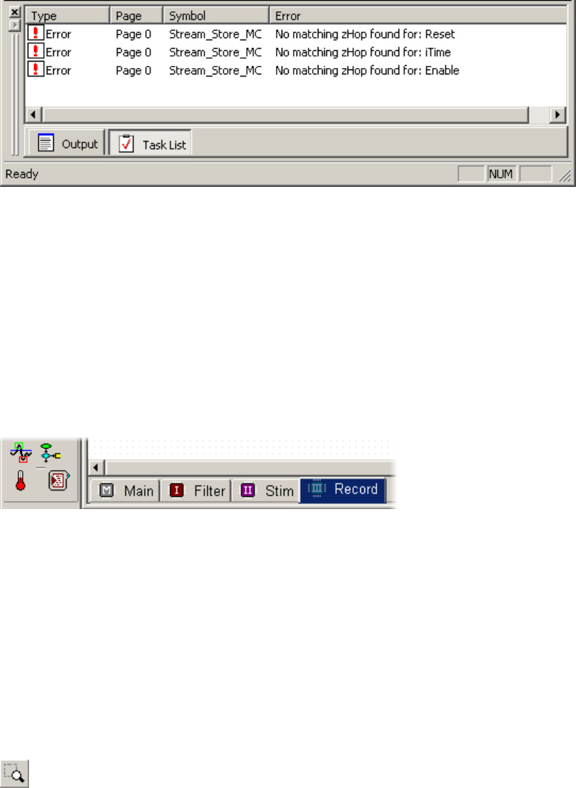
The Task List window displays details about the errors and warnings listed on the Output tab. It
consists of four columns – Type, Page, Symbol, and Error.
Type tells the user whether the item is an error or warning.
RPvdsEx Manual
11
Page specifies the page name or number where the error or warning can be found.
Symbol specifies the specific component, hop, or symbol that caused the error.
Error describes the problem through a comment.
Errors listed in the Task List are highlighted in the circuit diagram in red and warnings are
highlighted in blue. To quickly access the page on which the error or warning occurred, click the
icon next to the message. The correct page will be displayed and the error or warning will appear
in bold black in the circuit diagram. Click the icon again to toggle the colors between bold black
and red for errors and blue for warnings. To troubleshoot RPvdsEx related problems, see Common
RPvdsEx Error Messages, page 336.
The Pages
When a new tabbed window is created a default page, Page 0, is created. Pages can be added,
removed, resized, or renamed using a shortcut menu accessed by right-clicking the tabbed
window.
When using a multi-DSP device, users can assign each page to one or more processors. Users can
move around the page and adjust the zoom level using commands found on the View menu.
Viewing Pages
A circuit diagram may be contained on a single page or across multiple pages. By default, the page
magnification is set to allow the components to be viewed clearly. Areas of the page that are out of
view can be brought into view using standard MS Windows scroll bars or zoom and pan features.
Pages can be brought to the foreground by clicking the tabs located in the bottom left corner of the
window.
Zoom and Pan Features
Zoom and pan features are available on the View menu or on the main toolbar (File).
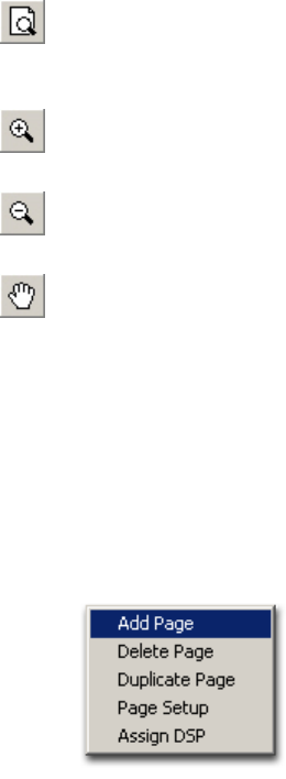
Zoom: When the Zoom command is selected, the pointer changes to a magnifying glass and
clicking an area of the page, zooms in on that area. The Zoom command is in effect until another
zoom or pan feature is selected.
Tip: To quickly turn off the Zoom command, select the Pan feature and click the page once.
RPvdsEx Manual
12
Zoom To Fit/Zoom to Page: When the Zoom To Page (Zoom to Fit) command is selected;
the page magnification is automatically adjusted so that the entire circuit diagram found on the
current page is in view.
Zoom In: When the Zoom In command is selected the magnification level is increased. The
command can be selected again to further increase the magnification level.
Zoom Out: When the Zoom Out command is selected the magnification level is decreased.
The command can be selected again to further decrease the magnification level.
Pan: When the Pan command is selected, the pointer changes to a hand and dragging moves
the page in the corresponding direction. The pointer returns to normal after one use. The pan
command can be selected again to Pan again.
Adding and Removing Pages
A single circuit diagram can be divided across several pages to make working with the circuit
more manageable.
To add a page:
1. Right-click the window and click Add Page on the shortcut menu.
2. The page is added to the window and a tab for the new page is visible in the bottom left
corner.
To remove a page:
1. Click the tab for the page to be removed.
2. Right-click the window and click Delete Page on the shortcut menu.
3. Warning!: Any portion of the circuit diagram on the current page will be lost when the
page is deleted.
4. Click Yes to confirm the deletion.
To move a page:
1. Left-click and hold to highlight the page you wish to move.
2. Drag the page over an existing page.
3. Release the left mouse button to exchange the two pages.
Renaming a Page
Page names can add organization to circuits, making it easier to move directly to an area of
interest.
RPvdsEx Manual
13
To change the page name:
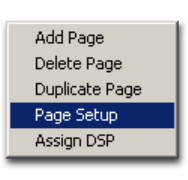
1. Right-click the window and click Page Setup on the shortcut menu.
2. Type a new name in the Page Name box.
3. Click OK.
Changing the Page Size
The default page is 1020 x 782 pixels but the page size can be modified in the Page Setup dialog
box.
To change the page size:
1. Right-click the window and click Page Setup on the shortcut menu.
2. Select one of the following Page Size options.
3. Enlarge page size to fit all components
4. Match the printer page setup
5. Set to X:___ Y:___ pixels (To use this option, select another option first, then return to
this option. This will allow the X and Y field to be edited.)
6. Click OK.
Choosing a Page Size Option
The Page Size option provides users with an extra measure of flexibility. They also provide quick
solutions for the common situations listed below.
When: Choose:
Pasting circuit components to a page results in some components
being outside the page area. Enlarge page size to fit all
components
When: Choose:
A circuit will be printed for offline viewing or debugging. Match the printer page setup
When: Choose:
An entire circuit being visible on screen will help viewing or
debugging. Set to X:___ Y:___ pixels
Duplicating Pages
When parallel structures must be added to a circuit, such as additional channels of filtering or
acquisition, it might save time to duplicate an existing page.
Be sure to review the new page and make any necessary modifications after duplication.
RPvdsEx Manual
14
To duplicate a page:
1. Click the tab for the page to be duplicated.
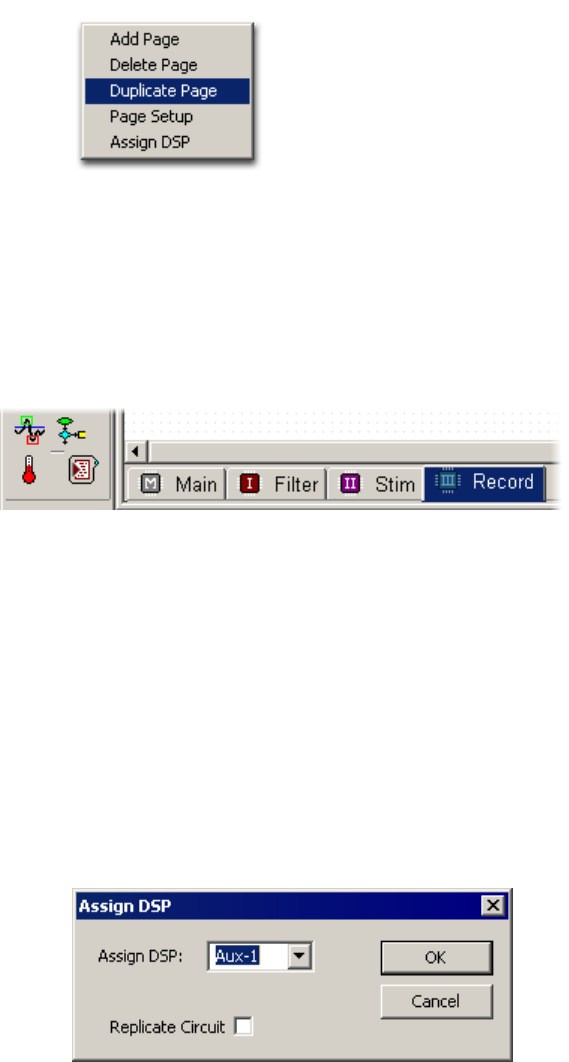
2. Right-click the window and click Duplicate Page on the shortcut menu.
3. Review the duplicate page and re-index items such as parameter tags with channel
numbers and update the parameters of components as needed.
Assigning Pages to a DSP
When a multi-DSP device is used, the user can assign each page of an RPvdsEx file to one or
more processors. Multiple pages can be assigned to the same processor. Because the architecture
of RX and RZ multi-processor devices differs, they are handled slightly differently.
Regardless of the processor type, an icon on the page tab indicates which processor has been
assigned, and if multiple processors have been assigned. See Page Icons, page 15, for more
information.
Single Processor Devices
All pages are assigned to a single processor and the Assign DSP functionality is not available.
RX Devices
By default all pages are assigned to the main processor.
To assign a page to processors:
1. Right-click the page and click Assign DSP, to display the Assign to DSP dialog box.
2. Select a processor from the Assign DSP drop-down list.
3. Under Replicate Circuit check box, select the check boxes for the desired processor(s) to
assign additional processors. Circuits are replicated on all processors selected.
4. Click OK.
RPvdsEx Manual
15
RZ Devices
By default all pages are assigned to the first processor, DSP-1.
To assign a page to processors:
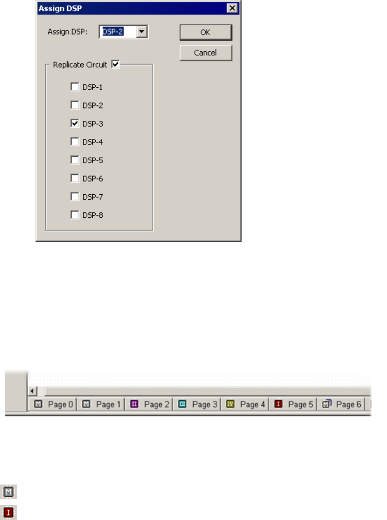
1. Right-click the page and click Assign DSP, to display the Assign to DSP dialog box.
2. Select a DSP from the drop down list. If you wish to replicate the circuit on multiple
DSPs, click the Replicate Circuit check box to display an extended view.
3. Click and clear check boxes to select or deselect the corresponding processor(s) to assign
to the page.
Note: Users should be familiar with the number of DSPs available in their device and
only assign pages to those DSP.
4. Click OK.
Page Icons
When pages in an RPvdsEx file are assigned to different processors in a multi-processor device
such as an RX5, an icon next to the page number identifies the associated processor as illustrated
in the figure above. The icons are described as follows.
RX Devices
Main processor
Auxiliary processors 1 through 4 as designated by the Roman numeral in the icon

RPvdsEx Manual
16
Replicated page - a page that is assigned to the main processor and replicated on one or more
of the auxiliary processors
RZ Devices
Processors 1 through 8 as designated by the numeral in the icon
MultiProcessor page - a page that is assigned to more than one DSP
Compiling Selected Processors
When using a RX multi-processor device it is possible to compile, build, and run segments of the
circuit assigned to a selected individual processor. This gives the user more control over the
compilation process. By default, when a circuit is compiled, the entire circuit is compiled. After a
single processor select command (such as Main DSP or Aux One) has been selected, all
compilation and code-building tasks are performed on the selected processor only. For example, if
Aux One has been selected and the compile button is clicked, only segments of the circuit
assigned to auxiliary processor one will be compiled and the messages window will display the
result of compilation and number of components for auxiliary processor one only.
Accessing the Processor Selection Commands
The processor selection commands are available from the Implement menu or the Processor Select
toolbar.
Main DSP Selects main processor
Aux One Selects first auxiliary processor
Aux Two Selects second auxiliary processor
Aux Three Selects third auxiliary processor
Aux Four Selects fourth auxiliary processor
All DSPs Selects all processors
When a processor is selected, its icon (menu) or button (toolbar) will appear "pressed." Either a
single processor or all processors may be selected. Selection of two, three, or four processors is
not supported.
Note: these commands are only available when the device selected in the Set Hardware
Parameters dialog box is a RX device.
Hop Related Compilation Errors
Circuits that use zHops or MCzHops might generate errors when compiling only a single
processor of a multi-processor circuit. The zHops and MCzHops allow transfer of signals between
processors within a device and must be used in pairs.
If the matching zHops are assigned to a processor that is not being compiled, a "No matching
zHop found" error will be generated for each zHop used. If the circuit uses zHops it must be
modified before it can be compiled. For more information about zHops see MCzHops, page 251
and zHops, page 255.

RPvdsEx Manual
17
File Formats
The circuit you design in RPvdsEx is loaded to the processor as a control object. The control
object contains the compiled processing chain (DSP code) for the circuit diagram and can be used
with TDT run-time applications or custom programs developed using TDT ActiveX controls.
By default, both the graphical circuit representation and the compiled control object are saved in a
single file with the .rcx format. RPvdsEx also supports the legacy two file format used by earlier
versions of TDT software.
Legacy File Formats
The legacy format consists of two separate files. The circuit diagram is saved in one file in an .rpx
or .rpd format and the control object must be saved separately in an .rco format.
To revert to the legacy RPX/RCO file system:
1. On the Edit menu, click Preferences.
2. Clear the Embed RCO object file check box.
3. Click OK.
After performing this step, the Build RCO command is enabled (available on the Implement menu
or on the Implement toolbar) and can be used to save the control object as a file with the .rco
extension.
Device Setup
Some RPvdsEx features and components are not supported by all device types. To ensure all the
features available for your device are enabled, specify a device type before beginning circuit
design.
To set the device type:
1. Click the Implement menu or click the button.
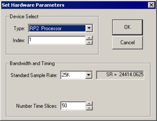
2. Click Device Setup to open the Set Hardware Parameters dialog box.
3. Select your processor from the Type drop-down menu in the Device Select group box.
RPvdsEx Manual
18
Depending on the device you select, the dialog box may expand to allow you to configure
more option, such as arbitrary sampling rates or digital I/O configuration.
4. Click OK.
Index
Devices in the TDT workstation are indexed according to their logical order in the system. The
logical order reflects the order of the connections between devices. Each device type is indexed
beginning with 1. So, index numbers higher than one only occur when the system includes more
than one module or device of the same type. The index number for a particular device can be
verified using TDT’s zBusMon program.
Sample Rate
In the Bandwidth and Timing area, you can select from a list of Standard Sample Rates. Sample
rates in the drop down menu are approximations. The actual sample rate is shown to the right. If
the selected device supports arbitrary rates, the Set Hardware Parameters box expands to include
an option for input of arbitrary rates. For more information about sample rates see, page 51.
Time Slices
In general, the entire processing chain is executed on each tick of the sample clock. Time slices
provide a means of processing some components less frequently. When time slices are defined, by
specifying the number of time slices here, you can assign some components to a specific time slice
(n) and are only processed on the nth time slice of the defined number of time slices. For more on
using time slices, see page 25.
Device Configuration Register
Many devices include hardware components, such as programmable digital I/O that can be
configured using the Device Configuration Register. If the selected device includes configurable
features, the dialog box will expand to display the Device Configuration Register. See the
reference for your device for configuration information.
RPvdsEx Manual
19
The Components
Component Overview
Components are the building blocks of the processing chain and perform fundamental processing
tasks such as generating a tone, filtering a signal, or summing several signals. RPvdsEx has
hundreds of processing components to tailor circuit designs for particular applications.
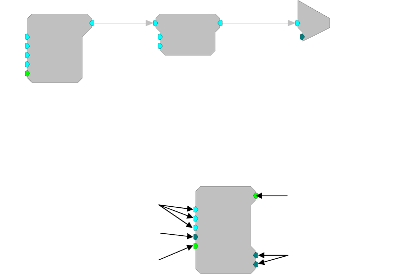
The following simple processing chain illustrates icons for some typical RPvdsEx components.
Generator
(primary signal output)
Body of Chain
(signal input, modification,
then output)
Terminator
(primary signal input)
Tone
Amp=1
Shft=0
Freq=1000
Phse=0
Wave [1:1 - 0
]
Rst=Run
ScaleAdd
SF=1
Shft=0
[1:2,0]
c
O
[1:3,0]
Ch=1
Component properties depend on their function. Components have at most one primary signal
input and one primary signal output. In addition, components can have one or more secondary
inputs and outputs, also called parameters. Illustrated below is an example of the different color-
coding standards seen in RPvdsEx. Floating Point parameters are designated by a teal coloring
while Integer parameters are designated by a dark green color. Left side parameters are Inputs,
while right side parameters are Outputs.
PulseTrain
Thi=10
Tg=0
Tlo=10
Npls=0
[1:1,0
]
CurN=0
Stage=0
Trg=0
Component parameters are specified with initial values when the chain is loaded. The user sets
these values by clicking on the component symbol and editing the values before the chain is run.
Most parameter values can also be changed dynamically while the chain is running. The parameter
can be fed from the output signal of another sub-chain or the value can be changed manually from
the host PC (via parameter tags). Parameters flagged as static, or constant, CANNOT be updated
dynamically and must be left unchanged while the circuit is running. Static parameters have a
black colored input symbol.
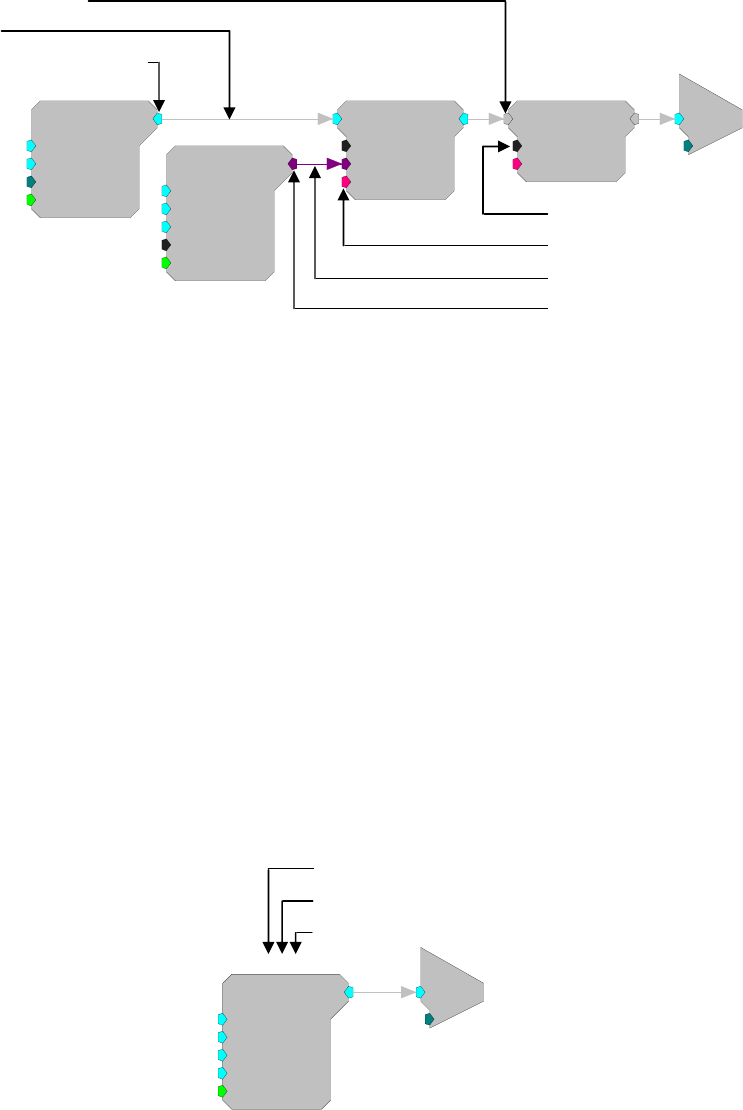
Component signal inputs and dynamic parameters usually expect a certain data type such as
integer, floating point, or logic. In the example below, the GaussNoise component has an output
that generates floating-point numbers. The output from GaussNoise is connected by a link to the
floating-point input on Biquad. It is important to match data types when connecting outputs and
inputs. Some components, like ShortDelay accept any data type.
Parameter Input (Floating Point)
Parameter Input (Integer)
Parameter Input (Logic)
Signal Output (Logic)
Parameter Output
RPvdsEx Manual
20
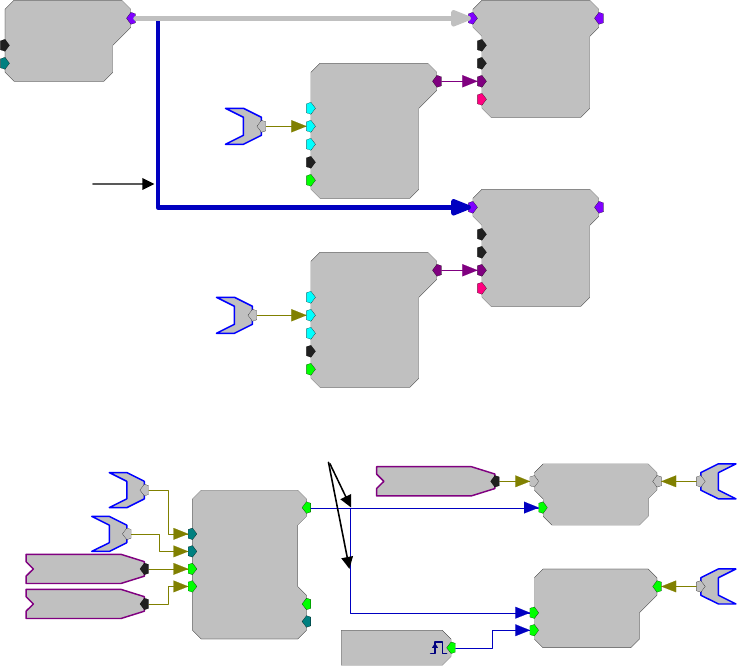
Components links may also indicate single (designated by a thin line) or multi-channel (designated
by a thicker line) data streams.
c
O
[1:5,0]
Ch=1
GaussNoise
Amp=1
Shft=0
Seed=0
Rst=Run
[1:2,0]
Biquad
nBIQ=1
{>Coef}
{>Delay}
[1:3,0]
ButCoef1
Gain=1
Fc=1000
BW=100
Type=LP
[1:1,0]
Enab=Yes
ShortDelay
Nms=1
{>Data}
[1:4,0]
When a circuit is compiled, RPvdsEx automatically generates a processing chain that orders
components in the order in which they will be run. The maximum number of components that can
be compiled in a single circuit is 128 for single-processor devices (such as the RA16BA) 256 per
DSP RX processor devices (such as the RX5), and 768 per DSP for Z-series processor devices
(such as the RZ2).
RPvdsEx has a growing library of processing components. Detailed information, including each
component's function and its associated parameters, is described in the Component Reference
section (beginning on page 77).
Component Numbering
There is a series of numbers listed above each component to denote the DSP number, component
number and time slice. The DSPs are numbered with the main processor being assigned number 1.
When a circuit is compiled, RPvdsEx orders the components. The component numbers indicate
the order components are executed in the processing chain on that particular DSP. The Time Slice
number is used to indicate the "time slice" in which a component is executed. For more
information on Time Slices, see page 25.
In the following figure, the components represent the first two components in time slice zero on
the main processor of a multi-processor device or the first two components in a circuit on a classic
processor.
Tone
Amp=1
Shft=0
Freq=1000
Phse=0
[1:1,0]
Rst=Run
c
O
[1:2,0]
Ch=1
The DSP number and component number ensure that each component on each processor will be
assigned a unique set of numbers. For example, components assigned to the main processor will
Static Parameter
External Data Input
Pointer Link
Pointer Output
Any Data Type
Link
Floating Point Output
DSP Number
Component Number
Time Slice
RPvdsEx Manual
21
have numbers from (1:1) to (1:256). Components assigned to the first auxiliary processor will
have numbers from (2:1) to (2:256) etc.
When a circuit segment is replicated across several processors or duplicated with an iterate box,
the numbering scheme changes to reflect this difference. See Duplication Information for more
information, page 28 .
Links Treated as Components
Links pass signals or parameter information between components. Some links are only a graphical
representation of signal flow and do not correspond to any additional processing task; for example,
passing a signal from one process (component) to the next process (component) in sequence.
Other links, however, do represent processing tasks, such as routing a signal to a second process
that occurs later in the processing chain. Because these links contribute to the overall demand
placed on the processor, they are treated as components and given a component number. To keep
the circuit diagram from becoming cluttered and confusing, the component numbers assigned to
links are hidden, but it is important to keep in mind the contribution they make to the total number
of components in a circuit.
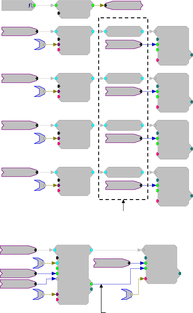
The four types of link components are listed below.
1) SigPatch: A SigPatch is created when a component’s primary output signal is routed to two or
more primary inputs. Because the signal must be delayed and routed to a later process
(component) any link to a primary input beyond the initial connection is treated as a SigPatch
component.
MCAdcIn
nChan=32
ChanOS=1
[1:2,0]
MCBiquad
nChan=32
nBIQ=1
{>Coef}
{>Delay}
[1:3,0]
MCBiquad
nChan=32
nBIQ=1
{>Coef}
{>Delay}
[1:6,0]
LPFreq
ButCoef1
Gain=1
Fc=500
BW=100
Type=HP
[1:1,0]
Enab=Yes
HPFreq
ButCoef1
Gain=1
Fc=1000
BW=100
Type=LP
[1:4,0]
Enab=Yes
2) ParFeed: A ParFeed is created when the primary output signal is routed to a parameter input.
PulseTrain2
nPer=25000
nPulse=1
Enab=Yes
Rst=Run
[1:1,0]
PCount=0
PLate=0
zSwPeriod
zSwCount
Latch
Trg=0
[1:4,0]
RSFlipFlop
Set=0
Rst=0
[1:7,0]
[1:5,0]
Src=Soft1
tTicker
sTicker
Enable
Reset
iTime
SigPatch
ParFeed
RPvdsEx Manual
22
3) MultiFeed: A MultiFeed occurs when a primary output signal is routed to four or more
parameter inputs. This is an extension of the ParFeed component.
A single primary output routed to three parameter inputs is treated as three ParFeed components.
A single primary output routed to four or more parameter inputs is treated as one MultiFeed
component.
[1:1,0]
Src=zBusA EdgeDetect
Edge=Rising
[1:2,0]
Reset
Biquad
nBIQ=4
{>Coef}
{>Delay}
[1:5,0]
RMS
[1:6,0]
SerStore
Size=1000
Rst=0
WrEnab=1
[1:7,0]
Index=0
{>Data}
Reset
BBand
Biquad
nBIQ=4
{>Coef}
{>Delay}
[1:9,0]
BBand
RMS
[1:10,0]
Reset
SerStore
Size=1000
Rst=0
WrEnab=1
[1:11,0]
Index=0
{>Data}
Biquad
nBIQ=4
{>Coef}
{>Delay}
[1:13,0]
RMS
[1:14,0]
SerStore
Size=1000
Rst=0
WrEnab=1
[1:15,0]
Index=0
{>Data}
Reset
BBand
Biquad
nBIQ=4
{>Coef}
{>Delay}
[1:17,0]
BBand
RMS
[1:18,0]
Reset
SerStore
Size=1000
Rst=0
WrEnab=1
[1:19,0]
Index=0
{>Data}
FiltSig~1
FiltSig~2
FiltSig~3
FiltSig~4
4) PatchFeed: A PatchFeed is when a parameter output signal is routed to a parameter input.
SerStore
Size=1000
Rst=0
WrEnab=1
[1:8,0]
Index=0
{>Data}
Reset
aEA~3
cEA~3
FiltSig~3
SortSpike2
nWid/4=8
Thresh=1
UseSign=1
Enab/Rst=1
[1:6,0]
SortBits=0
Strobe=0
Tag
{>Coef}
{>Data}
Enable
iTime
dEA~3
PatchFeed
MultiFeed - Primary output Reset is routed to four parameter inputs

RPvdsEx Manual
23
Data Types
When working in RPvdsEx, data types for component inputs and outputs are color coded and type
checking is performed automatically. Component ports of like colors can be linked together.
Illegal links are flagged as errors and colored red when the circuit is compiled.
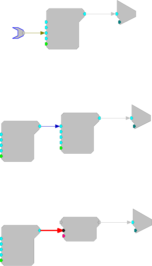
The following table lists currently supported data types and their general use:
RPX Data Types
Float IEEE standard. Handles majority of signal processing. Has units for signal type
carried, for example when feeding a DAC, value is in volts, when feeding a
frequency value is in Hz.
Integer Signed integer format. Used for counters and buffer indexes. Also used to integrate
digital port input and output into a processing circuit.
Logic Logic signal can be High (1) or Low (0). Used to carry trigger and enable controls
and to integrate digital inputs and outputs with the processing circuit.
Any Use to handle any data type (except pointers). Typically used on memory buffers
when stored type does not matter as long as read and write operations match data
type.
Pointer Used to reference data buffers within RPvdsEx. Do not directly access these data
elements.
Stereo Carries two standard Float signals one identified as LEFT and the other as RIGHT.
Multi-Channel Handles any data type (except pointers). Used for multi-channel signals.
Coefficient Used to reference coefficient buffers within RPvdsEx.
Static Static data format. Used for various static component settings (such as the number
of Biquads for a filter). Their values are set at compile time.
RPvdsEx Manual
24
Parameter Access Rules
Every component has a number of inputs and outputs called parameters. The parameters of a
component control how the component functions when running in the processing chain. For
example, the Freq parameter of the Tone component controls what frequency signal will be
generated by the Tone component.
Dynamic Access
Most processing components support some number of parameter ports that have an initial value
and are later changed 'dynamically' while the chain is running. An example of this is shown below
where the frequency of the Tone is initially set to 1000 Hz. This value can then be changed
dynamically using ActiveX controls and the parameter tag called Freq.
c
O
[1:2,0]
Ch=1
Tone
Amp=1
Shft=0
Freq=1000
Phse=0
[1:1,0]
Rst=Run
Freq
Another method of dynamically changing a component parameter is to 'feed' the parameter with
the output of another component. The example below shows how to create an AM signal by
feeding the output of one tone generator into the Amp parameter input of another.
Here the initial value of 5, specified in the second Tone's Amp parameter, has no effect because
this value is over-written on the first tick of the sample clock with the output of the modulator
Tone component.
c
O
[1:4,0]
Ch=1
Tone
Amp=5
Shft=0
Freq=1000
Phse=0
[1:3,0]
Rst=Run
Tone
Amp=1
Shft=0
Freq=1000
Phse=0
[1:1,0]
Rst=Run
Static Access
Some parameter inputs cannot be changed while the chain is running. They are called static or
constant. When working in RPvdsEx static parameters are color coded in black and connecting to
them, as shown below, will generate an error (link shown in red).
c
O
[1:3,0]
Ch=1
Tone
Amp=1
Shft=0
Freq=50
Phse=0
[1:1,0]
Rst=Run
ShortDelay
Nms=1
{>Data}
[1:2,0]
RPvdsEx Manual
25
Data Port Access
All Buffers and components that buffer signals, such as filters, have a data port. This port allows
direct access to the dynamic memory and program memory of a component. This allows users to
load data from a program, file, or helper component to a memory buffer on a component such as a
Serial Buffer or data can be downloaded to the computer from the memory buffer. The data port
(that is, the dynamic memory of the component) is accessed through helper components from
within RPvdsEx or using ActiveX controls.
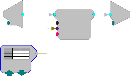
The DataTable and SourceFile can be used to send data to a data port. For example, to use a
specialized digital filter such as an IIR or FIR a data table is created that contains the coefficients
for generating the filter. In the example below a DataTable component is sending coefficients to
the filter. A data table can have hundreds of filter coefficients. Before the circuit is run the filter
proprieties can be changed within RPvdsEx by clicking the up and down arrows on the DataTable
component.
c
O
[1:3,0]
Ch=1
d
c
[1:1,0]
Ch=1
FIR
Order=32
{>Coef}
{>Delay}
[1:2,0]
FIR Coefs
= 0
Time Slices
By default, components are calculated on every tick of the processor’s sample clock. However,
there are situations where it is not necessary to calculate a component on every sample and it
wastes processing cycles to do so. Time slices, provide a means of processing some components
less frequently. Most components are assigned a time slice of 0, meaning that they are processed
in all time slices (on every tick of the processor’s sample clock). However, some components are
assigned to a specific time slice (n) and are only processed on the nth time slice of a user defined
number of time slices.
For example, if you are generating filter coefficients for a low-pass filter and the frequency of the
filter does not change, you don't need to calculate the filter coefficients on every sample of the
clock (in fact you may only need to calculate them once). So, to conserve cycle usage on the DSP,
you could set the coefficient generator to generate coefficients in a particular time slice, say time
slice 1. If there are 10 time slices total, then the coefficients will be calculated once every 10
samples. The total number of time slices and the time slice value for individual components can be
set from within RPvdsEx.
Consider the following example where three bands of noise are FM modulated to create a single
output. The rates of modulation are low so the coefficients generator components can be run at a
decimated rate but all components, including the coefficient generators are processed on every tick
of the sample clock.
The following diagram shows the circuit without time-slicing, notice the cycle usage is over
70%.

RPvdsEx Manual
26
GaussNoise
Amp=1
Shft=0
Seed=0
Rst=Run
[1:4,0
]
Tone
Amp=250
Shft=500
Freq=1
Phse=0
[1:1,0
]
Rst=Run
Tone
Amp=500
Shft=1000
Freq=2.13
Phse=0
[1:6,0
]
Rst=Run
Tone
Amp=1000
Shft=2000
Freq=3.73
Phse=0
[1:11,0]
Rst=Run
ButCoef1
Gain=1
Fc=1000
BW=100
Type=LP
[1:3,0]
Enab=Yes
ButCoef1
Gain=1
Fc=1000
BW=100
Type=LP
[1:8,0]
Enab=Yes
ButCoef1
Gain=1
Fc=1000
BW=100
Type=LP
[1:13,0
]
Enab=Yes
Biquad
nBIQ=1
{>Coef}
{>Delay}
[1:5,0]
Biquad
nBIQ=1
{>Coef}
{>Delay}
[1:15,0]
Biquad
nBIQ=1
{>Coef}
{>Delay}
[1:10,0]
CycUsage
[1:18,0]
74
[1:16,0]
Sum
c
O
[1:17,0]
Ch=1
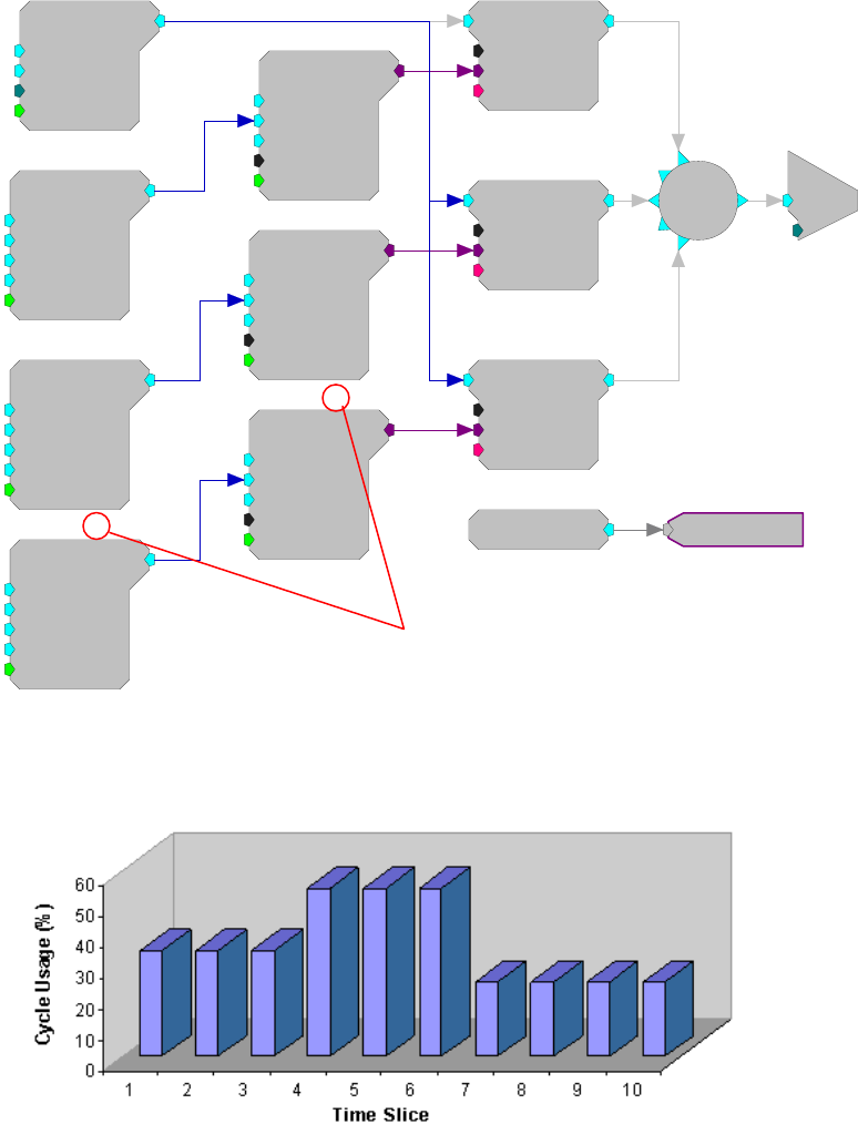
To improve circuit performance and 'free-up' DSP power for doing some other processing, we can
move all three modulating Tone generators and their corresponding ButCoef1 coefficient
generators to time-slices. Each will be placed in its own time slice reducing the DSP cycle usage
to about 45%. Note that because the Tone components are now running at 1/10th the actual sample
rate their frequencies must be multiplied up by a factor of ten. The resulting diagram is shown
below with a chart showing sample-by-sample cycle usage for each time-slice.
Same circuit with time slicing used, note cycle usage has been reduced to 47%.
RPvdsEx Manual
27
GaussNoise
Amp=1
Shft=0
Seed=0
Rst=Run
[1:4,0]
Tone
Amp=1
Shft=0
Freq=1000
Phse=0
[1:1,1]
Rst=Run
Tone
Amp=1
Shft=0
Freq=1000
Phse=0
[1:6,2]
Rst=Run
Tone
Amp=1
Shft=0
Freq=1000
Phse=0
[1:11,3
]
Rst=Run
ButCoef1
Gain=1
Fc=1000
BW=100
Type=LP
[1:3,4]
Enab=Yes
ButCoef1
Gain=1
Fc=1000
BW=100
Type=LP
[1:8,5]
Enab=Yes
ButCoef1
Gain=1
Fc=1000
BW=100
Type=LP
[1:13,6
]
Enab=Yes
Biquad
nBIQ=1
{>Coef}
{>Delay}
[1:5,0]
Biquad
nBIQ=1
{>Coef}
{>Delay}
[1:10,0]
Biquad
nBIQ=1
{>Coef}
{>Delay}
[1:15,0]
[1:16,0]
Sum
c
O
[1:17,0]
Ch=1
CycUsage
[1:18,0]
46.9831
The chart below illustrates cycle usage for each of the ten time-slices.
Note: time slices 7 through 10 have the lowest current usage and should be used next when a time
slice is needed.
Setting the Number of Time Slices
The number of time slices is set in the Set Hardware Parameters dialog box. To open the dialog,
click the Device Setup command on the Implement menu. The maximum number of time slices is
200.
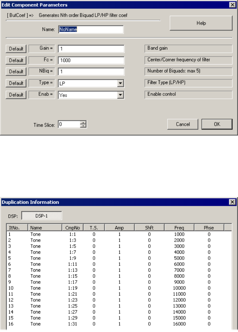
Specifying a Time Slice
To specify the time slice in which a component will run, double-click the component and enter the
desired number in the Time Slice box in the component's dialog box.
Time Slice Value
RPvdsEx Manual
28
Duplication Information
When a circuit segment is replicated across several processors or duplicated with an iterate box, a
Duplication Information dialog is available to display the item number, name, component number,
time slice and parameters for each of the duplicated components.
By right-clicking the replicated component, the user can view a table like the following:
This table was generated for a Tone component duplicated 16 times in an iterate box with the Freq
parameter incremented with the iteration number. If this component were also replicated across
multiple processors, there would be tabs for each applicable processor next to the DSP-1 tab. The
duplication information can also be accessed when editing the component’s parameters by clicking
on the Duplication Info button.

RPvdsEx Manual
29
Also when a component is replicated or duplicated, the component numbering scheme changes.
The following figure shows the numbering to reflect the duplication:
The second DSP number is used to display the range of applicable DSPs if the circuit segment is
replicated across multiple processors. For example, if the circuit segment were assigned to the
main processor and replicated on two auxiliary processors, the second DSP number would be 3.
DSP Number
Time Slice
Component Number
DSP Number
RPvdsEx Manual
30
Macros
Macro Overview
RPvdsEx includes very powerful macro functionality. Macros replace common circuit constructs
and provide an interface for changing circuit parameters. The underlying macro creation tools are
intended primarily for TDT use, with end users simply inserting existing macros into their circuit.
TDT has developed a core set of macros and will continue to add to the macro library over time.
Using macros reduces the complexity of configuration at the circuit level, reducing the number of
properties that must be set in each functional block.
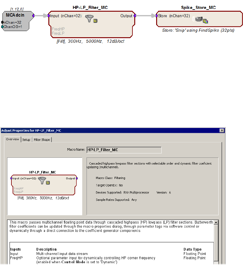
In the example below, large functional blocks of components designed to bandpass filter neural
data and to detect, sort, and store neural spikes are replaced by incorporating a set of easy-to-use
Macro components.
Setting parameters for each construct is accomplished at the Macro level. Macros are added to a
circuit much like other components and their properties can be configured in each Macro’s
properties dialog box. Just double-click the macro component in the RPvdsEx workspace to open
the dialog. Variables set here propagate through each of the basic components comprising the
Macro, ensuring correspondence throughout the entire processing block. Help for each Macro
component is also provided in the properties dialog box.
Using macros greatly simplifies the process of modifying the underlying circuits used in complex
circuits (such as those used in OpenEx projects).
RPvdsEx Manual
31
Making common changes, such as controlling time stamping, sampling rate, and storage
properties, requires fewer steps and less intimate knowledge of the details of the circuit structure
than designing circuits without macros.
See Designing Multi-Channel Circuits, page 58, for examples of how macros can be used to
simplify multi-channel circuit design.
Adding Macros
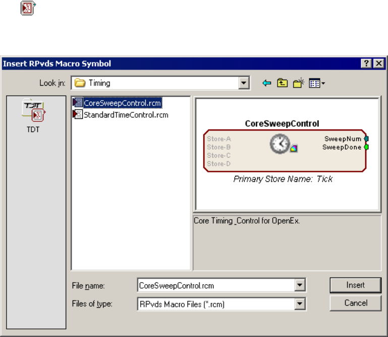
Macro components are placed in a circuit and linked in a manner similar to that used for
traditional RPvdsEx components. They can be added to processing chains using the Insert RPvds
Macro Symbol dialog box, which can be opened using any of the following:
The Insert Macro icon in the RPvdsEx Components toolbar
The Circuit Macros command on the Components menu
The Open Macro Design command on the File menu
The macro chooser dialog allows the user to browse for existing macro and shows a graphical
representation of any selected macro component with a brief description. Graphical symbols on
the macro icon help to quickly identify the type of macro, whether it is designed for use in
OpenEx, and whether it requires the use of high performance devices (RX or RZ).
Macros are a special type of circuit file and are stored at the following path:
TDT|RPvdsEx|Macros
Keeping all macros in this directory ensures they can easily be found when the Insert RPvds
Macro Symbol dialog opens.
Note: The macro chooser dialog is not available when editing a macro circuit. Making a macro out
of macros is not supported.

RPvdsEx Manual
32
Identifying Symbols
A macro belonging to a particular group (e.g. Timing, Filtering, Control) will have an identifying
graphic included as part of the macro icon. Further graphics identify if a macro is to be used
exclusively with OpenEx or only with a multi-processor device (RX or RZ). The following lists
shows the graphics used for some common macro groups.
Timing
Data Storing
Filtering
Hardware Control
Calculators
Input-Output
OpenEx
High Performance Processors (RX or RZ)
OpenEx and High Performance Processors (RX or RZ)
Working with Macros
The symbols above can be helpful in selecting macros and debugging circuits. Macro icons also
feature color coded inputs and outputs like other components. Other helpful features include a
tabbed setup dialog with internal documentation, parameter enabled inputs, and parameter
summaries.
To open the macro setup dialog:
Double-click the macro or right-click the macro and click Properties on the shortcut menu.
Parameter Enabled Inputs
Some macros have inputs that do not appear to be active (grayed out). These inputs are either
enabled or disabled based on the macro parameter settings. This feature prevents accidental
connections to ports that would not be connected at compile time based on the macro settings. For
example, the filtering macros have conditional inputs named FreqHP and FreqLP. These inputs are
only enabled if the macro is set up to provide Dynamic control of the filter corner frequencies.
Parameter Summaries
Most macros include an informative text bar across the bottom of the macro to view parameters at
a glance. When referring to the HP-LP_Filter_1Ch macro, for example, the text bar shows the
filter updating mode, the LP and HP corner frequencies and the filter roll off.
RPvdsEx Manual
33
OpenEx Macros
Macros designed for use with OpenEx are added to circuits in much the same way as other macros
and offer the same easy-to-use parameter settings dialog box. These special macros generate
information that is saved together in the compiled circuit file and then used by OpenEx to auto-
configure some aspects of the OpenEx experiment.
All circuits developed using macros and intended for use with OpenEx must include one and only
one CoreSweepControl macro. This macro supplies required tags and signal lines used by other
macros, such as the data storing macros.
OpenEx users, see the OpenEx Getting Started Tutorial for more information on using macros
to design circuits for OpenEx.
RPvdsEx Manual
34
Time Saving RPvdsEx Techniques
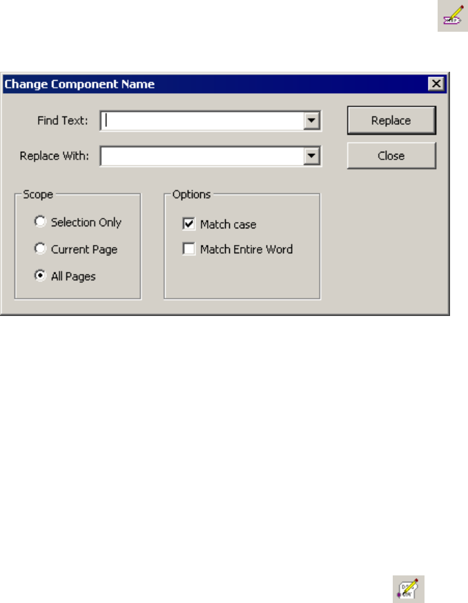
Changing Component Names Systematically
The Change Component Name dialog box is accessed via the Edit menu or the button on the
File toolbar. It can be used to replace all or part of the component name(s) systematically within a
selection, page, or entire circit.
Find Text: Type the text to be changed.
Replace With: Type the desired text.
Scope: Choose to apply the change to a selected section of a circuit, all components and macros
on the current page, or the entire circuit. To use Selection Only, select the desired area of the
circuit before opening the dialog box.
Options: Choose options such as Match case and Match entire word to ensure only the desired
parameters are changed.
Replace: Click to apply the change. A message box will open and report the number of instances
changed.
Close: Click to close the dialog box without applying further changes.
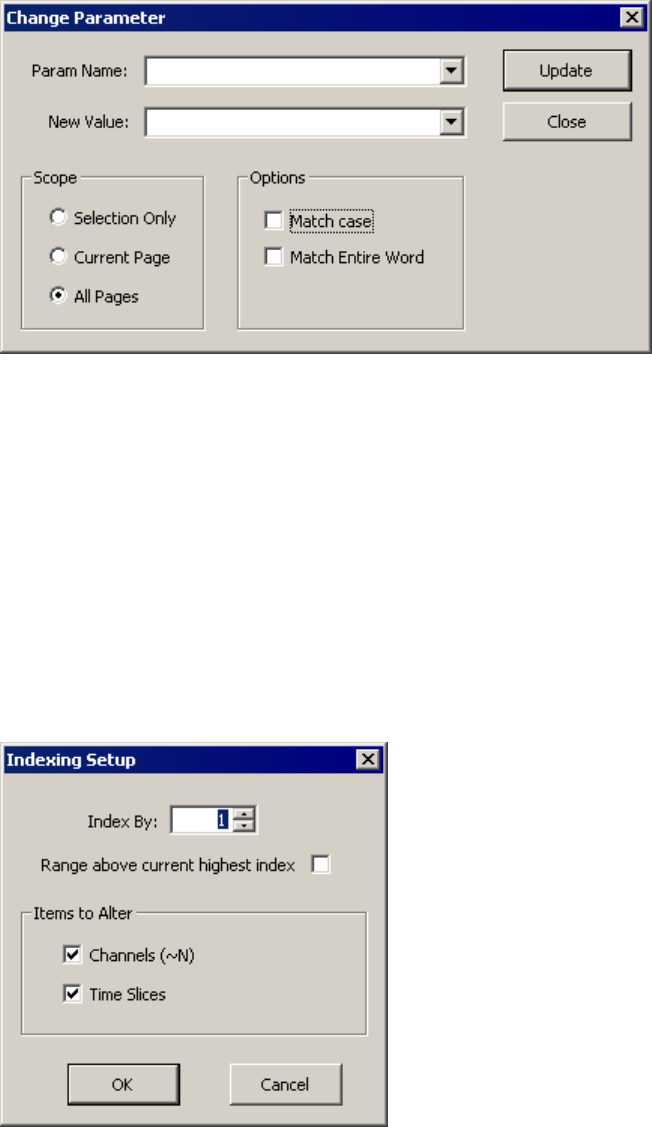
Changing Parameters Systematically
The Change Parameter dialog box is accessed via the Edit menu or the button on the File
toolbar. It can be used to replace parameter values systematically within a selection, page, or entire
circuit.
RPvdsEx Manual
35
Param Name: Type the name of the parameter to be changed.
New Value: Type the desired value.
Scope: Choose to apply the change to a selected section of a circuit, all components and macros
on the current page, or the entire circuit. To use Selection Only, select the desired area of the
circuit before opening the dialog box.
Options: Choose options such as Match case and Match entire word to ensure only the desired
parameters are changed.
Update: Click to apply the change. A message box will open and report the number of instances
changed.
Close: Click to close the dialog box without applying further changes.
Using Indexing
The Indexing Setup dialog is
accessed from the Edit menu. It
can be used to increment
channel number parameter tags
and/or time slices for selected
components.
Index By: determines the number that Items to Alter will be incremented by. Each selected
component will be incremented by the value set here.
Range above current highest index: When this check box is selected the Items to Alter will be
set to a number equal to the highest index value present in the document plus the Index By value.
RPvdsEx Manual
36
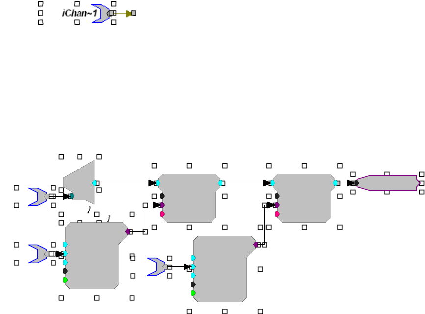
Channels (~N) check box: Select to apply the setting in this dialog box to selected channel
number parameter tags, which follow the form: iChan~1.
Time Slices check box: Select to apply the settings in this dialog box to selected components that
are currently in a time slice (that is, time slice not equal to 0).
To use indexing:
1. Select the components to be incremented.
2. Click the Edit menu and click Index.
3. Select the desired combination of settings in the Indexing Setup Dialog box.
4. Click OK.
5. The settings are applied to the selected components.
Selecting Multiple Components
In the example below, an entire circuit construct has been selected. Setting in the Indexing Setup
dialog box would be applied to all components.
For example:
If the Channels (~N) check box is selected, the Time Slices check box is cleared, and the Index
By value is set to 1; then iChan~3 would be incremented to yield iChan~4. This would be the only
change.
If the Channels (~N) check box is cleared, the Time Slices check box is selected, and the Index
By value is set to 1; then the BufCoef components currently set to time slices 5 and 6 would be
moved to time slices 6 and 7 respectively. No other components would be affected.
ButCoef1
Gain=1
Fc=300
BW=100
Type=HP
[4:231,0]
Enab=Yes
Biquad
nBIQ=1
{>Coef}
{>Delay}
[4:231,0]
d
c
[
4:231,0]
Ch=3
Biquad
nBIQ=1
{>Coef}
{>Delay}
[4:231,0]
ButCoef1
Gain=1
Fc=5000
BW=100
Type=LP
[4:231,0
]
Enab=Yes
LPFreq
Chan3
iChan~3
HPFreq

RPvdsEx Manual
37
Using the Preferences Dialog Box
The Preferences dialog is accessed from the Edit menu. It can be used to set compiler and control
object file settings.
Sort Component List: When checked, the components in each group will be arranged in
alphabetical order when viewing the component selection browser.
Embed RCO Object File: If this option is checked, the RPvdsEx file will be saved with the
extension rcx. Files with this extension contain both the graphical circuit representation for use
within RPvdsEx and the control object information to be loaded to a device. This eliminates the
need for a separate rco file.
Notes:
The Build RCO button on the Implement toolbar is grayed out when the check box is selected.
If a circuit is saved after this preference has been modified, RPvdsEx will display the following
message to alert the user that the file extension has been changed:
Compiler Parameters: The user can set the compiler to minimize the circuit delay or the number
of components.
Save as Default: If checked, the above preferences are saved.
RPvdsEx Manual
38
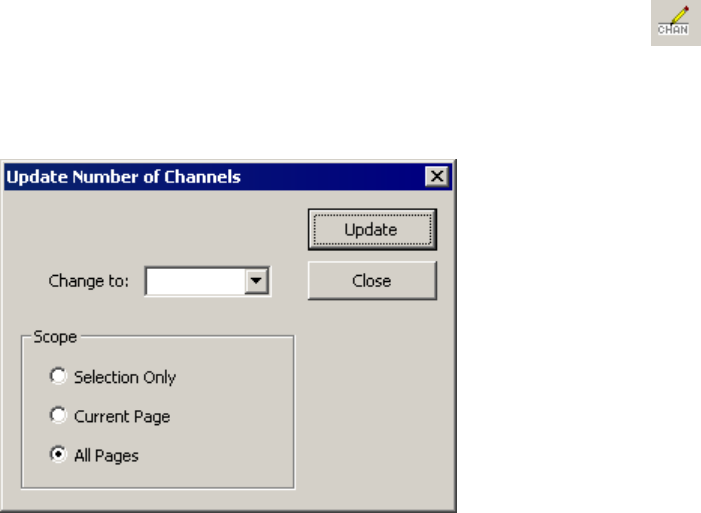
Updating Number of Channels Systematically
The Update Number of Channels dialog box is accessed via the Edit menu or the button on
the File toolbar. It can be used to replace channel number parameters systematically within a
selection, page, or entire circuit. The change is implemented for both component parameters and
macro parameters and provides an easy way to avoid channel number mismatches.
Change to: Type the desired number of channels.
Scope: Choose to apply the change to a selected section of a circuit, all components and macros
on the current page, or the entire circuit. To us Selection Only, select the desired area of the circuit
before opening the dialog box.
Update: Click to apply the change. A message box will open and report the number of instances
changed.
Close: Click to close the dialog box without applying further changes.
RPvdsEx Shortcuts
Placing Links
Press the Spacebar to activate single-click placing of a link.
Or
Double-click the output terminal where you want to start a link.
Cancel Linking
Right clicking the workspace will cancel the link option.
Keyboard Shortcuts
Most standard Windows keyboard shortcuts (such as Ctrl + c to copy a selected item) can be used
in RPvdsEx.
RPvdsEx Manual
39
Copying Circuits
In cases where you want to repeat a circuit several times, select the block by clicking and dragging
a box around the items you want to select. Then choose copy and paste to create a second copy of
the circuit.
Using Cut, Copy, and Paste
Cut, Copy, and Paste can speed up circuit design. They affect the currently selected items within
the RPvdsEx circuit diagram. A single component or an entire circuit can be cut, copied, or pasted.
Items that are selected are surrounded by small square selection handles. To select multiple items,
hold down Shift and click each item to select or click and drag a box around all the items to select.
For example:
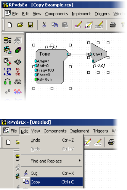
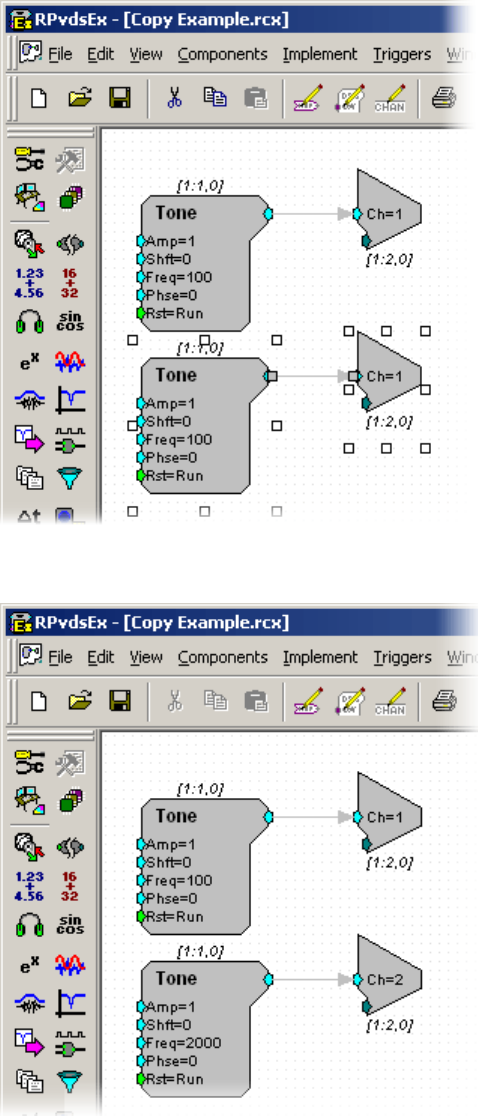
Starting with a circuit that plays a tone out of channel 1, we copy and paste the circuit to create
another tone that plays out of channel 2.
1. Select the circuit by clicking and dragging a box around the entire circuit. Items that are
selected will have square selection handles around them.
2. Select Copy from the Edit menu.
RPvdsEx Manual
40
3. Select Paste from the Edit menu to paste a copy of the circuit.
4. Change the second DAC output to channel 2, and set the tone to the desired frequency
and amplitude.

Part 2 Circuit Design
RPvdsEx Manual
42
~
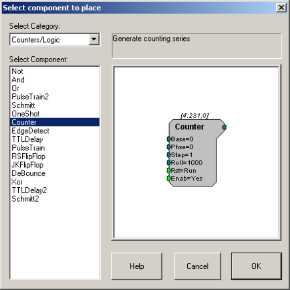
RPvdsEx Manual
43
Circuit Design Basics
Creating and Running a Simple Circuit
Earlier sections of the user guide introduced the components, macros, and provided some
information about how components are linked. The best way of putting all of these concepts
together is to create and run a simple circuit. Follow the steps below to implement a simple
counter circuit and become familiar with the basic mechanics of the circuit design process.
To create a simple circuit, follow the steps below:
1. Ensure at least one processor module is connected to your PC and turned on.
2. Launch RPvdsEx.
3. On the File menu, click New to open a new tabbed window.
4. On the Implement menu, click Device Setup.
5. In the Set Hardware Parameters dialog box, select your processor from the Type drop
down menu.
6. The default index and sampling rate should be fine, so click OK to continue.
7. Double-click the tabbed window grid area to open up the Select component to place
dialog box.
8. In the Select Category box, choose Counters/Logic.
9. In the Select Component box, click Counter.
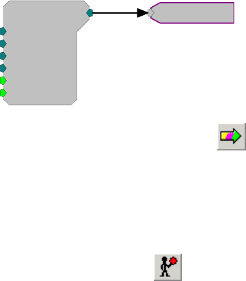
RPvdsEx Manual
44
The Counter component implements a simple counting function based on the
component’s parameters. Using the default parameter values, it will count up from 0 to
1000 then reset and continue.
10. Click OK to add the component to the RPvdsEx workspace.
11. Double-click the tabbed window grid area again to open the Select component to place
dialog box.
12. In the Select Category box, choose Helpers.
13. In the Select Component box, click ParWatch. This component displays the connected
signal in RPvdsEx and is commonly used for debugging circuits.
14. To link the components, double-click the output port of the Counter component.
The cursor will change from a pointer to a circle with cross hairs. As you drag the cursor
a line will appear.
15. Connect that line to the input port of the ParWatch by moving the cross hairs over the
input port and clicking once.
A line and arrow will appear connecting the two components. This is called a link. The
circuit should look like this:
Counter
Base=0
Phse=0
Step=1
Roll=1000
[1:1,0]
Rst=Run
Enab=Yes
ParWatch
16. To run the circuit in RPvdsEx, click the Compile, load, and run button on the
Implement toolbar. This compiles the circuit, loads the circuit on the real-time processor
device, and runs the circuit.
You should see the counter signal advance in the ParWatch component. The counter will
continue until the circuit is stopped. Controlling the presentation of the signal requires
additional components.
17. To stop the circuit, click the Halt RP button on the Implement toolbar.
18. When the file is saved the circuit diagram and the control object are saved together. The
resulting circuit file can be used with run-time applications.
Triggering
TDT’s System 3 Processors support several triggering options. It is important to understand that
the processor is always running a processing chain in normal operation. Therefore, instead of
instructing the processor to ‘play’ the signal, you would instead trigger a gate to control the circuit
output.
Triggering Options
The external, zBus, and software triggers are added to a circuit by adding a TrgIn (page 237)
component.
RPvdsEx Manual
45
External Trigger
Many of the System 3 processor modules provide an external trigger input that can be triggered by
a TTL pulse from an external device. This TRIG input is separate from other digital input lines
(typically found on 25-pin connector inputs).
zBus Triggers
zBus triggers are triggered from software. They are a convenient way to simultaneously trigger all
zBus modules. TDT processors support two zBus triggers, A and B. They can be set as a pulse,
always high or always low. The zBus triggers can be fired from RPvdsEx or from programs such
as OpenEx, BrainWare, PyschRP or ActiveX controls.
Software Triggers
Software triggers are triggered from software, either by clicking the trigger on the Trigger menu in
RPvdsEx or by issuing a software command that causes the trigger to fire. SoftTrg is initiated in a
single circuit. The processors respond to ten unique software triggers. Software triggers do not
allow precise timing across several modules because of the delay in sending and receiving
information across the PC interface connection.
Digital Inputs
The RX processors have up to 40 bits of programmable digital I/O. See the technical
specifications for each device for more information. The RP processors have eight digital inputs
on the 25-pin connector. The RM has four or eight digital inputs on the 9-pin connector. These
can be used in a circuit using the BitIn (page 230) or WordIn (page 237) components.
One Shot
The OneShot (page 157) delivers one TTL signal when the circuit is run on the processor.
Pulse Train
The PulseTrain (page 158) generates a train of TTL pulses with a specified pulse duration and
inter-pulse interval. It is useful for repeating a stimulus that is triggered by one external trigger.
Gating a Signal
Gating functions gate the amplitude of the signal on and off with a set rise/fall time (msec). The
rise/fall time is a static parameter and cannot be modified in a circuit. The gate begins to open
when a trigger goes high (=1) and starts to close when the trigger goes low (=0). A Schmitt trigger
can also be used to control the duration of the signal between opening and closing the gate.
Triggering a Schmitt component sends a pulse out for a set duration. In this example the Schmitt
trigger sends a 100 millisecond pulse to the Cos2Gate when it receives a software trigger (TrgIn).
Triggers are one way users can control components in the processing chain. The Cos2Gate opens
to 90% of the amplitude of the signal in 10 milliseconds and then starts to close at the end of the
Schmitt pulse.
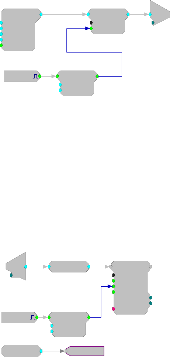
RPvdsEx Manual
46
Tone
Amp=5
Shft=0
Freq=2000
Phse=0
[1:4,0]
Rst=Run
Cos2Gate
Trf=10
Ctrl=Closed
[1:5,0]
c
O
[1:6,0]
Ch=1
[1:1,0]
Src=Soft1
Schmitt
Thi=100
Tlo=10
[1:2,0]
Acquiring and Storing the Signal
RPvdsEx uses memory buffers to store signal data for stimulus presentation and data acquisition.
Memory Buffers: Serial and Ram Buffers
There are two types of buffer components, random access and serial. The random access
component allows users to directly access any value in the buffer; however, the user has to tell the
memory buffer where the data should be or is stored. The serial buffer automatically increments to
the next position while it is acquiring or presenting signals.
The examples below show how a random access buffer and serial buffer differ. In these examples
the buffers acquire 100 milliseconds of signal. In the serial buffer example the data is saved as
long as the Schmitt trigger that is connected to the AccEnab line remains high. In the RamBuffer
example the Schmitt trigger must first start a counter to increment the Index on the RamBuf to the
next position. Note that the cycle usage for the serial buffer is smaller.
Serial Buffer
[1:1,0
]
Src=Soft1
Schmitt
Thi=100
Tlo=10
[1:2,0
]
d
c
[1:4,0]
Ch=1
RMS
[1:5,0]
SerialBuf
Size=1000
Rst=0
AccEnab=1
Write=1
[1:6,0]
NBl ks=0
Index=0
{>Data}
CycUsage
[1:7,0
]
11.39
Starts the Schmitt trigger
Controls the duration
of the
g
ate
Gates the Tone on and of
f
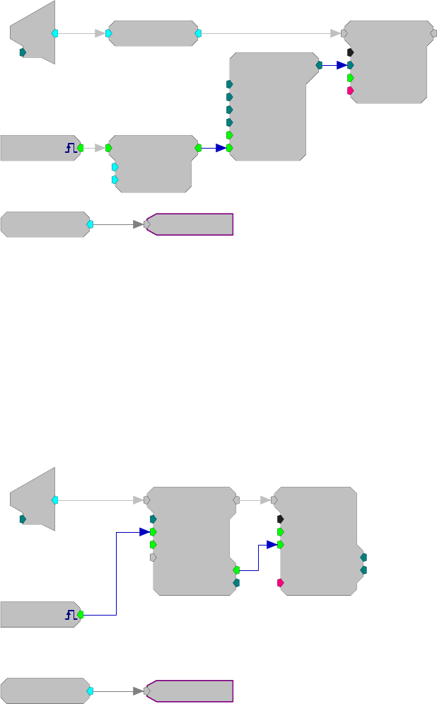
RPvdsEx Manual
47
Ram Buffer
[1:1,0]
Src=Soft1
Schmitt
Thi=100
Tlo=10
[1:2,0
]
d
c
[1:6,0]
Ch=1
RMS
[1:7,0]
CycUsage
[1:9,0]
13.1827
RamBuf
Size=1000
Index=0
Write=0
{>Data}
[1:8,0]
Counter
Base=0
Phse=0
Step=1
Roll=1000
[1:4,0]
Rst=Run
Enab=Yes
Block Access
A BlockAcc (block access) component acquires a set number of signal values and stores them in a
serial buffer. The advantage of a BlockAcc is that it automatically transfers a set number of points
to the buffer. This is advantageous if the signal is to be averaged. In the example below a
BlockAcc and an AvgBuf (average buffer) are used together to acquire a small signal.
The BlockAcc takes the place of the Schmitt Trigger in the example above. When the block access
is triggered it acquires a set number of samples (1000) and then sends them out to a buffer. The
example below demonstrates an averaged buffer. The average buffer, unlike the serial buffer, adds
the incoming signals to the values in the buffer. A serial buffer or ram buffer would overwrite the
old values with the new values.
[1:1,0]
Src=Soft1
d
c
[1:3,0]
Ch=1
CycUsage
[1:7,0
]
10.9711
BlockAcc
BlkSze=1000
StEnab=0
Skip=0
Tag
[1:4,0]
AccEnab=0
Nski p =0
AvgBuf
Size=1000
Rst=0
AccEnab=0
[1:6,0]
NBl ks=0
Index=0
{>Data}
The Data Port
All buffers and components that buffer signals, such as filters, have a data port. This port allows
direct access to the memory location. Several components can access the data port to store,
display, or download signals to the PC.
To learn more about using these components with the data port,Data Port Access, page 25.

RPvdsEx Manual
48
Signal Processing
Signals, whether acquired or generated, can also be filtered, smoothed, and analyzed for particular
patterns. Two common signal processing techniques, filtering and signal splitting are illustrated
below.
Filtering Gaussian Noise
The GaussNoise (Gaussian noise generator) produces unfiltered broadband noise. Filter and
coefficient generating components can be added to the circuit to produce a narrow band of noise.
In the example below, a Gaussian signal is bandpass filtered using a Biquad filter component. A
ButCoef1 (Butterworth coefficient generator) generates the values for the necessary biquad filters.
Biquad filters are used because of their stability. Filter properties can be changed in real time.
GaussNoise
Amp=1
Shft=0
Seed=0
Rst=Run
[1:2,0]
Biquad
nBIQ=1
{>Coef}
{>Delay}
[1:3,0]
ButCoef1
Gain=1
Fc=2000
BW=10
Type=BP
[1:1,0]
Enab=Yes
c
O
[1:4,0]
Ch=1
A single Biquad component filters the Gaussian noise. The ButCoef1 generates coefficients for a
bandpass filter centered around 2000 Hz with a BW of 10 Hz. This bandwidth puts the 3dB
corners at 2005 Hz and 1995 Hz. The output of the Biquad is then played out of DAC channel 1.
Notes:
The filter generated is rather broad. If a narrow band is required, filters can be connected together
to narrow the bandwidth or users can generate their own filter values for use with our IIR and FIR
filters.
To alter the values on the fly connect a parameter tag or Data Table to the Fc and BW of the
ButCoef1.
Signal Detector: Splitting the Signal Path
The System 3 processors allow users to process signals in real-time without any modification from
the PC. This allows users to detect changes in signal levels and respond in less than a millisecond.
In the example below the circuit detects changes in an incoming signal and lights one of the
outputs on an RP (RP2, RA16, or RL2) module.
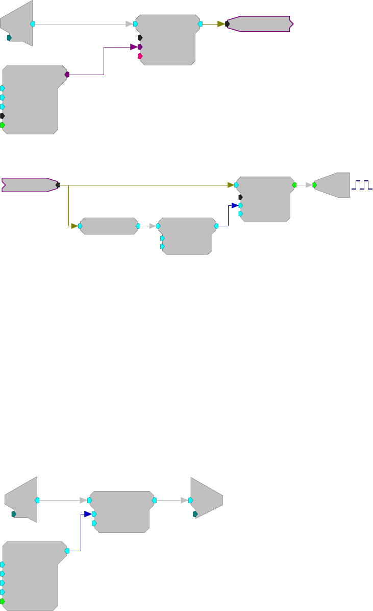
RPvdsEx Manual
49
In the example below a signal is filtered so that only signals in a particular frequency are detected.
1. Bandpass filter the incoming signal.
Biquad
nBIQ=1
{>Coef}
{>Delay}
[1:3,0]
ButCoef1
Gain=1
Fc=1000
BW=200
Type=BP
[1:1,0]
Enab=Yes
d
c
[1:2,0]
Ch=1 Channel 1
2. Detect signals that are at least five times greater than the background RMS level
FeatSrch
FC=Above
K1=0
K2=0
[1:4,0]
RMS
[1:1,0]
ScaleAdd
SF=5
Shft=0
[1:2,0]
Bi
[1:5,0]
M=1
Channel 1
A Hop (Channel 1) is used to simplify the logic of the circuit. The hop allows the circuit design to
be split. The hop does not alter the processing chain it allows the chain to be easier to follow and
debug. A single HopOut can have multiple HopIns that split the signal.
The split signal goes to two components: the RMS (root mean square) and the FeatSrch (feature
search). When the RMS is calculated it determines the criteria necessary to activate the FeatSrch.
While a signal meets the criteria of the FeatSrch a logical value is set high (goes from 0 to 1). In
this case the Signal must be 5 times the normal noise of the filtered signal for a pulse to be
generated. All these parameters can be easily modified. The logical pulse can be used to light an
output or to start acquisition of the signal or both.
In addition, delays can be added to the circuit so that the acquisition of a signal includes all of the
waveform.
Scale and Add
This circuit implements a simple AM modulator. The signal connected to the channel one A/D
input will be 50% modulated by a 50 Hz sinusoid generated by the Tone component. The result is
played from channel one of the DAC.
d
c
[1:3,0]
Ch=1
ScaleAdd
SF=1
Shft=0
[1:4,0]
Tone
Amp=0.5
Shft=1
Freq=50
Phse=0
[1:1,0]
Rst=Run
c
O
[1:5,0]
Ch=1
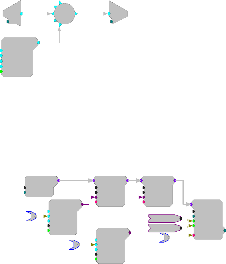
RPvdsEx Manual
50
Note: the circuit using ScaleAdd will run in fewer cycles than the alternate construct shown below
using Mult.
d
c
[1:1,0]
Ch=1
Tone
Amp=0.5
Shft=1
Freq=50
Phse=0
[1:2,0]
Rst=Run
c
O
[1:4,0]
Ch=1
[1:3,0]
Mult
Using Parameter Tags for Software Control
When your circuit is saved as a circuit file it can be used by all TDT application software and can
be incorporated in to custom programs you develop using a programming language that supports
ActiveX.
Parameter tags are pointers that create named access points within your circuit. They can be used
to control parameters and access data while the process chain is running.
The example below acquires, filters, and stores a multi-channel signal. The HPFreq and LPFreq
parameter tags allow users to control the corner frequency of the cascaded filters while the dWav
parameter tag allows the user to access the stored data for data visualization and analysis.
MCAdcIn
nChan=16
ChanOS=1
[1:3,0]
MCBiquad
nChan=16
nBIQ=1
{>Coef}
{>Delay}
[1:4,0]
MCBiquad
nChan=16
nBIQ=1
{>Coef}
{>Delay}
[1:5,0]
ButCoef1
Gain=1
Fc=300
BW=100
Type=HP
[1:1,0]
Enab=Yes
ButCoef1
Gain=1
Fc=3000
BW=100
Type=LP
[1:2,0]
Enab=Yes
LPFreq
MCSerStore
nChan=16
Size=1024
Rst=0
WrEnab=1
[1:6,0
]
Index=0
{>Data}
dWav
Reset
Enable
HPFreq
There two ParTag components, a right and a left version, allowing you to choose the tag that will
make your circuit easier to read. There is no functional difference between the two.
Parameter tags can be connected to any parameter input or any output. However, they cannot be
connected directly to a signal input. To use a parameter tag with a signal input you must first route
the signal path through ConstF, ConstL, or ConstI component.
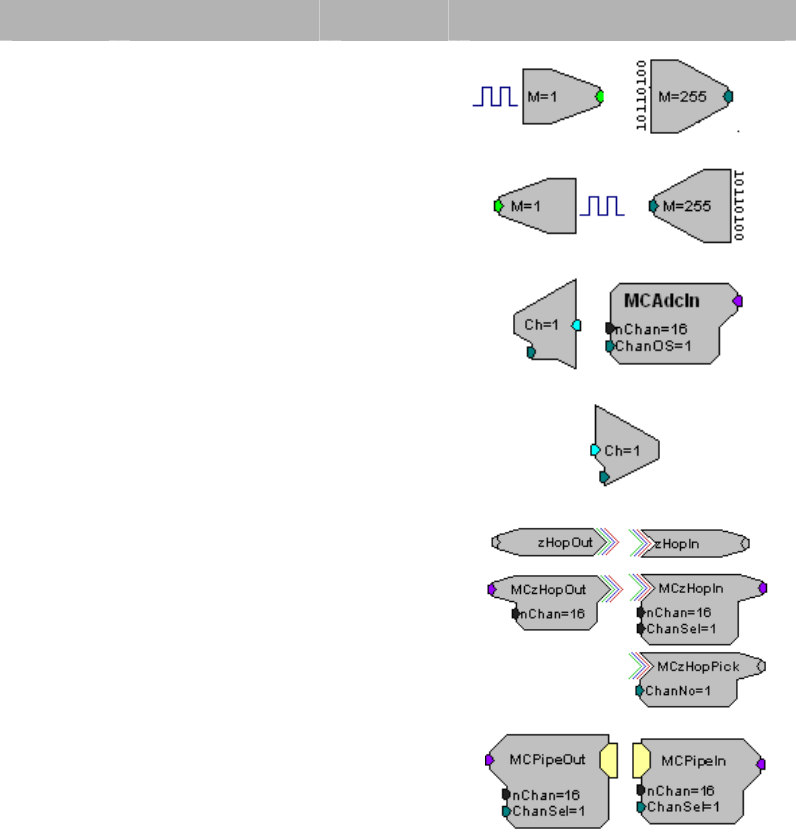
RPvdsEx Manual
51
Hardware Considerations
Input/Output Delays
When synchronizing processing circuits users should be aware of delays associated with the I/O of
their hardware devices. Users can synchronize I/O using delay components provided in RPvdsEx.
See Delay Functions in the Component Referencesection, page 181, for more information.
The table below provides a comparison of the delays associated with types of I/O and components.
I/O Type RPvdsEx Component Delay Component Icons
Digital
Input BitIn
WordIn 2 samples
Digital
Output BitOut
WordOut 3 samples
Analog
Input AdcIn
MCAdcIn
device
specific*
Analog
Output DacOut device
specific*
Inter-DSP
zHop Pairs
zHopOut/In
MCzHopOut/In
MCzHopPick 1 sample
RZ2 Data
Pipe MCPipeOut/In 2 samples
* See DAC and ADC tables below.

RPvdsEx Manual
52
DAC and ADC Delays
Several of the System 3 processor modules use Sigma-Delta digital-to-analog and/or analog-to-
digital converters. These converters provide over-sampling that generates signals up to 90% of the
Nyquist frequency (half the sample rate) without the need for additional anti-imaging and anti-
aliasing filters. While these devices provide for superior conversion quality and extended useful
bandwidths, they have an inherent fixed group delay. When synchronizing the processing circuits
with external devices via triggers, and so forth, one must account for associated delays in the
converters being used.
Note: Information about delays and converter specifications can also be found in the technical
reference for each device.
Sigma-Delta Sample Delays
The table below lists the devices that use Sigma-Delta converters along with their associated
delays.
Device Type SD DAC Delay SD ADC Delay
RZ6 47 samples 66 samples
RX6 47 samples 66 samples
RX8 24 samples 47 samples
RP2.1 65 samples 30 samples
RP2 and RL2 40 samples 30 samples
See Delay Functions in the Component Referencesection, page 181, for a complete list of
componets that can be used to synchronize circuits when needed.
PCM Sample Delays
The table below lists the devices that use PCM converters along with their associated delays. PCM
converters have a much shorter delay and, in general, do NOT necessitate the use of a delay
component.
Device PCM DAC PCM ADC
RZ2 4 samples 3 samples
RZ5 4 samples 3 samples
RX5 4 samples NA
RX7 4 samples NA
RX8 4 samples 3 samples
RPvdsEx Manual
53
The Sample Clock and Sampling Rates
TDT’s System 3 processors have a continuously running sample clock. The rate of this clock can
be set to match the bandwidth of the signals you are working with. For example, studies with
humans need a 20 kHz bandwidth, so the sample clock should be set to 50 kHz. At that rate, TDT
devices that use sigma-delta type D/A's and A/D's can utilize nearly a 25 kHz bandwidth with no
anti-aliasing filter.
Each TDT device has a fixed set of sample rate capabilities. The use of high performance sigma-
delta DACs makes supporting completely arbitrary rates unreasonable in some devices. For
example, the RV8 does not use sigma-delta DACs so it can offer any rate (derived from 25 MHz)
while the RX6 uses sigma-delta DACs and thus supports a limited set of sample rates.
Note: The RX8 can be configured with sigma-delta converters and/or PCM converters. The
realizable sampling rate depends on which type of converter is used. See the System 3 Manual for
more information on selecting an appropriate sampling rate for your RX8.
The setup dialog in RPvdsEx will always return the true available rate for any device when the
'Check Realizable' button is clicked.
Converting Sample Rates
Files recorded with other systems (including TDT System II devices) will have different sample
rates. To convert files to System 3 requires changing the sample rate. Programs like Cool Edit
allow you to change the sample rate of a signal. In addition MATLAB's Signal Processing
Toolbox has resampling tools.
Sample Rate Synchronization Issues
Problems with synchronizing waveforms (such as a triangle wave) and with generating proper
delays on two devices are typically a result of differing sample rates. The device with the higher
rate can generate waveforms or delays with more resolution than the device at a lower rate.
Sample Rate Related Timing Issues
TDT software that offers arbitrary delays always bases the actual delay specified on the lowest
sample rate used. If possible, use standard sample rates that will be related by a simple factor of
two, four, etc. If you are using any of the non-linear generator components, be aware that only
frequencies related to the sample rate by an integer multiple can be generated.
Components parameters that define a high, low, or delay period based on time are directly related
to the sampling period. There is always a fixed difference between expected and actual values
related to the sample period (inverse of the sample rate). The maximum possible difference with
these components is +/- the sample period. When using these components, the actual time value
will be the closest interval depending on the sample rate.
For example, at 100 kHz, a PulseTrain set to go high for 2 ms would be high for 1.9968 ms,
because the sample period is 10.24 us. Because these slight differences are less noticeable on
devices using oversampling, such as those using sigma-delta converters, this issue is most
noticeable when synchronizing several devices using different types of converters.
RPvdsEx Manual
54
The table below shows the possible difference at different sample rates.
Standard Sample
Rate (Hz) Actual Sample Rate
(Hz) Sample Period (us) Max difference (us)
200k 195312.5 5.12 +/- 5.12
100k 97656.25 10.24 +/- 10.24
50k 48828.125 20.48 +/- 20.48
25k 24414.0625 40.96 +/- 40.96
12k 12207.03125 81.92 +/- 81.92
6k 6103.515625 163.84 +/- 163.84
The actual length of time that the component will remain high is the multiple of the sample period
that is the closest to the set time.
For example, the table below assumes that a component, such as a PulseTrain, is set to go high for
2 ms. The actual time that the PulseTrain would remain high and the expected difference are in the
final two columns.
Standard Sample
Rate (Hz) Max Difference (us) Expected High Time
for 2ms (ms) Expected Difference
(us)
200k +/- 5.12 2.00192 1.92
100k +/- 10.24 1.9968 3.20
50k +/-20.48 2.00704 7.04
25k +/-81.92 1.96608 33.92
12k +/- 81.92 1.96608 33.92
6k +/- 163.84 1.95508 33.92
Cycle Usage
The main function of the DSP is to execute the processing chain; however, the DSP must also
control or manage each aspect of the processor “black box” device. It must control the converters,
move data, and pass instructions to and from the PC across the zBus/PC interface. On each tick of
the sample clock the DSP:
Executes the processing chain
Performs “house-keeping” tasks
Transfers data to and from the host computer across the zBus interface
Again, all of this must happen within one tick of the sample clock. You can imagine that as the
sample clock gets faster, or the processing chain gets more complex, the DSP has less time to
perform all of the necessary functions. At some point the DSP can no longer keep up, and errors
occur. DSP/PC communication suffers and some components in the processing chain are no
longer updated. i.e. when the amount of processing exceeds the sample period….
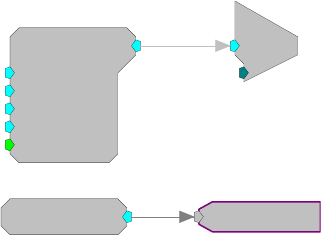
RPvdsEx Manual
55
In fact, the window for communication with the host PC is entirely dependant on the time it takes
to execute the processing chain. The DSP prioritizes the processing chain over PC data transfers.
Thus, if executing the processing chain takes up 75% of a given sample cycle, the DSP has less
than 25% of the remaining sample period to move data across the DSP/PC interface.
Cycle usage is a measure of the DSP workload including DSP house keeping and processing chain
execution. It is expressed as a percentage of the sample period consumed by these tasks. If cycle
usage is near 100%, no data can be exchanged with the host pc. Furthermore, when the processing
chain exceeds 100% cycle usage, the execution of the chain breaks down, and errors occur.
Each DSP has a set number of DSP cycles per tick of the sample clock. Cycle usage is dependent
on the sample rate of the system, the processing power of the RP, and the components used. The
lower the sample rate the more complex the circuit design can be. High sample rates (>50 kHz)
will often limit what components can be used. Very high sample rates (200 kHz or more) may
limit a circuit to only a few components. At higher sample rates, the number of available DSP
cycles is lower and the overhead (running the D/A converters etc.) is greater. Use only the
minimum necessary sample rate for your needs.
The table below shows the relationship between the sample rate and processing power and lists
cycle usage and overhead for each sample rate for the RP2 processor.
Sample Rate DSP Cycles Available (RP2) Overhead (RP2) Total Usage for Sample Circuit
6K 8192 0.6 % 1.7 %
12K 4096 1.2 % 3.5 %
25K 2048 2.5 % 7.0 %
50K 1024 5.0 % 14 %
100K 512 10 % 28 %
200K 256 20 % 56 %
Many processors display cycle usage on a front panel LCD screen or using indicator lights. A
CycUsage (cycle usage) component can also be added to a circuit to monitor how much
processing power the circuit uses. When running a circuit from the RPvdsEx interface, connecting
CycUsage to a ParWatch (parameter watch) helper component will display the cycle usage of the
circuit.
The example below shows how to use a ParWatch to measure the number of cycles being used by
the circuit that is running. In this example the Tone generator and DAC are using eight percent of
the available cycles. Time slices may be used to reduce cycle usage by running calculations only
on certain samples rather than on every tick of the sample clock.
Tone
Amp=1
Shft=0
Freq=1000
Phse=0
[1:1,0]
Rst=Run
c
O
[1:2,0]
Ch=1
CycUsage
[1:3,0
]
8.17438
RPvdsEx Manual
56
Transferring Data Between the Processor and the
PC
Most of the System 3 processors have onboard memory. Single processor devices with 32MB of
memory can store eight million samples of uncompressed data and up to 32 million samples of
compressed data. RPvdsEx has several built-in functions for using source data from the PC, such
as DataTable and SourceFile. Users can also see the data by using ParWatch (parameter watch)
and Graph. More sophisticated ways of transferring the data to and from the processor module
requires the use of ActiveX controls and some degree of programming.
USB Transfer Rates
USB transfers are limited to 100,000 samples per second of 32-bit data. Streaming of signals to
and from disks may present a problem for high sample rate or high channel number acquisition
and presentation. For example, 16-channels of 25 KHz data produces 400,000 samples of data per
second. Data reduction techniques, such as CompTo16 (Compress to 16) and ShufTo16 (Shuffle
to 16), reduce the data size.
Gigabit Transfer Rates
The Gigabit transfer rate is limited to 400,000 samples per second of 32-bit data. Streaming
signals to and from disks should not present a problem unless very high channel numbers are
required. At this time, the maximum number of channels that the Gigabit can stream with 32-bit
data is 16-channels at 25 kHz. Data reduction techniques such as CompTo16 (Compress to 16)
and ShufTo16 (Shuffle to 16) can be used to reduce the data size.
Optibit Transfer Rates
The Optibit transfer rate is up to 8x times faster than the original Gigabit interface and also
reduces the system’s susceptibility to EMF. Devices are connected in a simple loop using provided
high speed noise immune fiber optic cabling. Also, when using the Optibit interface, all devices
(across all caddies) are automatically phase locked to a single clock. The Optibit interface supports
high channel counts but is still subject to limitations. Data reduction techniques such as
CompTo16 (Compress to 16) and ShufTo16 (Shuffle to 16) can be used to reduce the data size.
Interface Performance Comparison
The table below illustrates typical transfer rates for the UZ2, Optibit, and Gigabit interfaces:
Interface Transfer Type RP Devices RX Devices RZ Devices
PO5e/PO5/FO5 Read 1.5 10 20.0
Write 1.5 2.5 20.0
PI5/FI5 Read 1.5 2.5 NS
Write 1.5 2.5 NS
UZ2 Read 1.5 2.5 NS
Write 1.5 2.5 NS
Transfer rates are in MB/s.
NS – Not supported
RPvdsEx Manual
57
Multi-Channel Circuit Design
Overview
In a typical multi-channel application most, if not all, channels will be processed in the same way.
The user can take advantage of this fact by using multi-channel components and multi-channel
macros wherever possible. These components and macros have been designed specifically for
multi-channel processing and are more efficient than their single channel counterparts. When
neither multi-channel components nor a multi-channel macro is available for a particular
processing task, iterations can be used to simplify the parts of the circuit that must use single
channel components.
When designing multi-channel circuits the user should keep in mind that:
Simplifying circuit design makes debugging or modifying the circuit easier.
Using the most efficient components possible improves performance and ensures that all
processing tasks can be accomplished without overtaxing the processor or exceeding the
maximum number of components allowed.
Using macros reduces the overall number of parameter and configuration settings required
while reducing the likelihood of channel number or data type mismatches.
Note: Multi-channel components can only be used with high performance devices, such as the RX
and RZ devices. Circuits that implement them will not run on single processor systems, such as
the Medusa RA16BA. However, the iteration function can be used by all devices to streamline
circuit design. Macros that use multi-channel components typically include "MC" in the macro
name. See the reference for your device for specific information on component compatability.
The Nature of Multi-Channel Signals
A multi-channel signal is an array of data points arranged according to channels. On each tick of
the sample clock, the multi-channel component processes one point from each channel.
Working with Multi-Channel Components
Multi-channel components are a powerful group of components for working with multi-channel
signals. When working with these components the user must carefully consider the number of
channels and type of data in the multi-channel data stream.
Data Types
Most multi-channel components accept any data type as input. No error will be generated if the
signal output from one component is linked to a component input that requires another data type.
Therefore, the user must ensure that data types are consistent.
nChan Parameter
Multi-channel components can be used to process multi-channel signals from four to 256
channels. Many multi-channel components include a channel number (nChan) parameter that must
be set at design time, to the number of channels in the multi-channel signal input. Mismatched
channel number parameters may cause warnings, but will not cause errors when the circuit is
compiled. Therefore, the user must ensure that the channel number parameter is set correctly.
RPvdsEx Manual
58
Multi-Channel Circuit Design Strategies
The best circuit design for multi-channel circuits maximizes the use of multi-channel components
and multi-channel macros while minimizing the number of conversions between multi-channel
components and single channel components. This path has several advantages. Multi-channel
components use fewer cycles, and require fewer components to accomplish processing tasks for
multiple channels. Also, multi-channel components and macros help to keep circuit design
cleaner, more manageable, and easier to debug. Macros help eliminate common multi-channel
errors, such as mismatched data types and mismatched number of channels.
This section provides general guidelines for multi-channel circuit design by taking the user
through the process of building commonly used circuit segments.
Acquisition
Users must consider their hardware configuration when designing an acquisition circuit.
The RZ2 Processor
The RZ2 is equipped with several different analog I/O capabilities. Two types of fiber optic ports
allow a direct connection to Z-Series or Medusa Preamplifiers. The RZ2 also includes onboard
A/D for input of signals from a variety of other analog sources.
RZ2_Input_MC
Data Pipe, 16 Chans (1-16)
SourceData
The RZ2_Input_MC macro provides a universal solution for analog input via the RZ2,
automatically selecting the correct components, applying any scale factors or channel offsets, and
performing and data type conversion needed based on information the user provides about the
input source. The macro outputs a multi-channel data stream to facilitate multi-channel signal
processing and storage. TDT highly reccomends using the input macro whenever possible.
When the input macro is not used, onboard A/D and Medusa Preamplifier inputs are accessed
using single channel ADCIn components. Single channel data can be converted to a multi-channel
data stream using techniques discussed under Combining Channels below.
The Z-Series amplifier input channels are typically accessed using the Pipe components on page
249. They can also be accessed using the MCAdcIn component starting at channel 128; however,
this access method is less efficient and not recommended for high channel count applications.
When the input macro is not used see the RZ2 technical reference in the System 3 Manual for
detailed information about the RZ2 I/O hardware for scale factors and channel numbers.
The RZ5 Processor
The RZ5 is equipped with fiber optic ports for a direct connection to Medusa Preamplifiers and
onboard A/D for input of signals from a variety of other analog sources.
RZ5_AmpIn_MC
Amp -A-, 16 Chans (1-16)
Output
RPvdsEx Manual
59
The RZ5_AmpIn_MC macro provides a solution for multi-channel amplifier input via the RZ5,
automatically selecting the correct components, applying the appropriate scale factor and channel
offsets needed based on information the user provides about the input source. The macro outputs a
multi-channel data stream to facilitate multi-channel signal processing and storage.
Amplifier inputs and onboard A/D can also be accessed using appropriate single channel ADCIn
components. Single channel data can be converted to a multi-channel data stream using techniques
discussed under Combining Channels below. When the input macro is not used see the RZ5
technical reference in the System 3 Manual for detailed information about the RZ5 I/O hardware
for scale factors and channel numbers.
The RZ6 Processor
The RZ6 is equipped with onboard A/D for superior high frequency acquisition. An optional fiber
optic port can be equipped for a direct connection to a four channel Medusa Preamplifier.
Important!: The RZ6 device macros are required for accessing analog and digital inputs and
outputs.
Analog input is accessed in RPvdsEx through the RZ6_AudioIn macro.
RZ6_AudioIn
ADC-A
ADC-B
The RZ6_AmpIn macro automatically applies the necessary scale factors and channel offsets for
configuring the optional preamplifier fiber optic port.
RZ6_AmpIn
Output-1
Output-2
Output-3
Output-4
Note: All RZ6 device macros input or output single channel signals, however, the RZ6 supports
multi-channel circuit components. See Combining Channels, page 61 for more information on
converting single channel signals to a multi-channel signal.
RX Processors
The MCAdcIn component is the best choice to feed the circuit with multi-channel signals when
using RX processors. Signals are typically digitized on a preamplifier and then transferred to the
base station via fiber optics. This basic acquisition circuit uses the MCAdcIn and a multi-channel
filter macro to acquire and filter multi-channel data.
MCAdcIn
nChan=16
ChanOS=1
[1:1,0]
HP-LP_Filter_MC
[Filt], 300Hz, 5000Hz, 12dB/oct
Input (nChan=16)
FreqHP
FreqLP
Output FiltSig
RPvdsEx Manual
60
In this sub-circuit, signals on channels 1 – 16 are acquired and filtered. The FiltSig HopOut routes
the filtered signals to another area of the circuit for further processing or storage. A similar circuit
using single channel components would require 112 components to accomplish this same
processing task.
When using the MCAdcIn the user must specify the channels to acquire using the number of
channels (nChan) and the channel offset (ChanOS) parameters. For example, the circuit above
acquires 16 channels. Because the offset is set to 1, acquisition will begin with channel 1. The user
must again consider their hardware configuration. On the RX5, channels 1-16 are acquired via
fiber optic port 1. This means that a 16-channel preamplifier must be connected to the Amp-A
fiber optic port to acquire all 16 channels of data. A preamplifier connected to the Amp-B port
(Channels 17-32) would be ignored.
To acquire 32 channels from two 16 channels amplifiers that are connected to ports A and B,
simply change each of the nChan parameters to 32. A single MCAdcIn can be used to acquire any
block of consecutive channel numbers. However, if there is a break in the channel numbers to be
acquired, multiple MCAdcIns must be used. A MCMerge component is used to combine multiple
multi-channel signals into one multi-channel signal.
MCAdcIn
nChan=4
ChanOS=1
[1:1,0]
HP-LP_Filter_MC
[Filt], 300Hz, 5000Hz, 12dB/oct
Input (nChan=16)
FreqHP
FreqLP
Output FiltSig
MCAdcIn
nChan=4
ChanOS=17
[1:3,0]
[1:4,0]
Merge
In this example, two MCAdcIns are used to acquire channels 1-4 and 17- 20. This circuit acquires
eight channels of data using two 4 channel amplifiers, connected to ports A and B.
The output from MCAdcIn is in floating-point format. The nChan parameter of the filter macro
must match the number of channels in the signal input. In the first example, 16 channels are fed
directly from the MCAdcIn to the macro. In the second example, a MCMerge component is used
to combine the multi-channel signals from two MCAdcIns and a total of eight channels are fed to
the macro.
The filtered signals can be processed further or stored to a memory buffer using MCSerStore or a
multi-channel data store macro. The signal can also be split into its single channel signals (see
Extracting Channels below) and processed individually.
Processing and Converting Signals
The scope of the multi-channel components is limited to the most common processing tasks.
When an acquisition circuit requires additional processing, it will often be necessary to extract
single channel signals using the MCToSing or MCzHopPick components.
MCAdcIn
nChan=16
ChanOS=1
[1:1,0]
MCAdcIn
nChan=16
ChanOS=1
[1:3,0]
MCToSing
ChanSel=2
[1:2,0]
Channel 2MCSig
nChan=16
MCSig
ChanNo=2
[1:5,0]
Channel 2
Or
RPvdsEx Manual
61
Extracting Channels and Using Iterations
When single channel processing must be performed on many channels, using iterations keeps the
circuit manageable. The iteration box is drawn around a sub-circuit that must be repeated a
specified number of times. The following example extracts the individual channels from an 8-
channel signal called MCSignal, using a HopIn, full wave rectifies them. All this is done within an
iterate box. The single channels are then recombined using MCFromHop to form an 8-channel
signal. The MCFromHop component is only supported by RX and RZ multi-processor devices.
For single processor devices such as the RA16BA see Iterate, page 220.
The iterate box is used to duplicate the sub-circuit 8 times, extracting 8 single channels from the
multi-channel signal. The iterate variable {x} (which corresponds to the iteration number) is used
to set the channel number for the HopIn component in each iteration ensuring that each iteration
extracts a different channel.
The parameter tag also uses the iterate variable {x} to ensure that each iterated circuit processes a
unique channel with a unique set of parameters. The iterative notation MCSignalR~{x} allows the
MCFromHop component to reconstruct the multi-channel signal MCSignal from the 8 single
channels. Once reconstructed, the multi-channel signal MCSignalR is then stored using
MCSerStore.
Iterate: x =1 to 8 by 1
MCSignal
Absval
[1...,6-01...]
M
CSignalR~{x}
{>PM
}
MCSignalR
nChan=8
[1:28,0]
MCSerStore
nChan=8
Size=1024
Rst=0
WrEnab=1
[1:29,0]
Index=0
{>Data}
Reset
Enable
Data
MCToSing
ChanSel={x}
[1...,5-01...]
Combining Channels
There are two components that combine multiple signals paths into a single multi-channel signal,
MCFromSing (ToMC) and MCMerge. MCFromSing (ToMC) is used to build a multi-channel
signal from several single channels.
[1:3,0]
Merge
The MCMerge component merges multi-channel signals into higher order multi-channel signals.
Each of these components combines up to four signal paths. They can also be used together in
sequence to build a larger multi-channel signal.
4 Single
Channel Signals One 4 - Channel Signal

RPvdsEx Manual
62
[1:7,0]
Merge
[1:3,0]
ToMC
[1:4,0]
ToMC
[1:5,0]
ToMC
[1:6,0]
ToMC
Data Storage
There are three possible methods for data storage.
OpenEx users can select from a variety of data storage macros designed specifically for use in
OpenEx. These macros greatly simplify circuit design for multi-channel data storage.
For users who develop their own applications using ActiveX, RPvdsEx currently supports a
limited number of multi-channel buffer operation components.
When no other method is available, use iterate boxes with single-channel buffer operations
(similar to the process described above). See the iterate function, page 220, for an example of this
method.
The example circuits below each pull together acquisition, filtering and data storage in an efficient
processing chain.
OpenEx Example
Using OpenEx allows for extensive use of macros for circuit design: from timing to storage. The
circuit below uses the Block_Store_MC macro to store a 16 channel filtered input to the OpenEx
DataTank using the Store name “Blck”.
MCAdcIn
nChan=16
ChanOS=1
[1:1,0]
CoreSweepControl
Primary Store Name: Tick
Store-A
Store-B
Store-C
Store-D
SweepNum
SweepDone
HP-LP_Filter_MC
[Filt], 300Hz, 5000Hz, 12dB/oct
Input (nChan=16)
FreqHP
FreqLP
Output
Block_Store_MC
Store: Blck, 16Ch, 100Floats, 24414.1Hz
Store (nChan=16)
Trigger - Rising Edge
Active
4 Single
Channel Signals
4 Single
Channel Signals
4 Single
Channel Signals
4 Single
Channel Signals
One 16 – Channel Signal
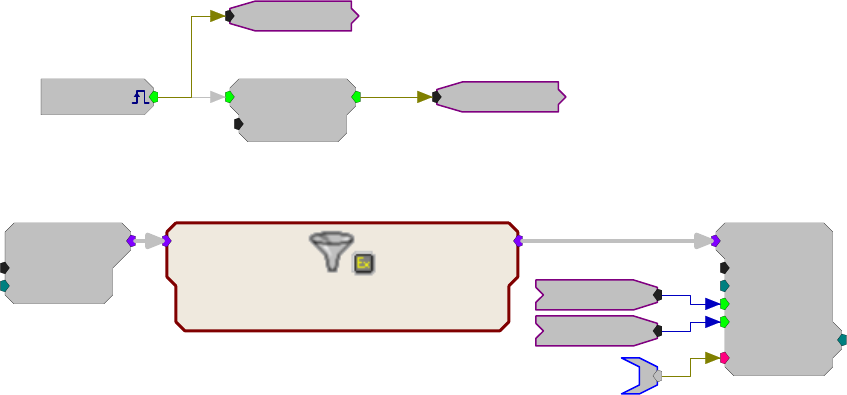
RPvdsEx Manual
63
ActiveX Example
Below, the MCAdcIn feeds the circuit with a 16-channel input. The MCSerStore component stores
all 16 channels into a single 3200 points buffer. The dWav parameter tag is used to read the buffer
back to the PC.
MCAdcIn
nChan=16
ChanOS=1
[1:6,0]
HP-LP_Filter_MC
[Filt], 300Hz, 5000Hz, 12dB/oct
Input (nChan=16)
FreqHP
FreqLP
Output
[1:2,0]
Src=zBusA
EdgeDetect
Edge=Rising
[1:4,0]
Enable
Reset
MCSerStore
nChan=16
Size=3200
Rst=0
WrEnab=1
[1:9,0]
Index=0
{>Data}
Reset
Enable
dWav
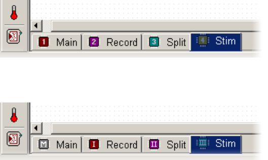
RPvdsEx Manual
64
MultiProcessor Circuit Design
Overview
The combined processing power offered by the multi-processor devices makes them ideal for
high-channel count or high-sampling rate data acquisition. Multi-DSP architectures allow
processing tasks to be distributed across several processors. This provides a number of advantages.
It reduces the likelihood that the number of RPvdsEx components used on any one processor will
exceed the processor’s maximum (256 for RX processors and 768 for each RZ processor).
It makes it possible to reduce the cycle usage demand on each processor, enabling each processor
to run at a higher sample rate.
Before attempting to design multi-processor circuits, it is a good idea to become familiar with the
special tools available for multi-processor circuit design in RPvdsEx. TDT also recommends
reviewing the multi-DSP architecture of your device.
Assigning DSPs in RPvdsEx
A single RPvdsEx file must contain all the processing tasks for one device. In order to reduce
individual processor load, these tasks can be split across all of the DSPs contained in a device.
There are two methods available: using pages or using DspAssign.
Note: When using either method, users should be familiar with the number of DSPs available in
their device and only assign pages to those DSP.
Using Pages
In RPvdsEx the workspace is divided into tabbed pages. The user can assign each page within the
file to one or more processors on that device. The circuit on that page will then run on the assigned
processor. Multiple pages can be assigned to the same processor. By default all pages are assigned
to the first or main processor.
RZ Processors
RX Processors
An icon on the page tab indicates which processor has been assigned, and if multiple processors
have been assigned.
For more information on assigning pages to processors, see Assigning Pages to a DSP, page 14.
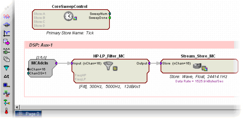
RPvdsEx Manual
65
Using DspAssign
The DspAssign component is specifically designed to designate a section of an RPvdsEx page to
run on a processor other than the one assigned to that page. Paired with RPvdsEx macros, this
component enables many multi-processor circuits to be displayed in a single page.
To use DspAssign, add it to the page then drag the borders to encompass the segment to be
assigned to a different processor.
In the RX device circuit below, the CoreSweepControl macro runs on the Main DSP. The
remainder of the components on the page is assigned by the DspAssign component to run on DSP
Aux-1.
For more information on DspAssign, see page 249.
MultiProcessor Hop Components
The MultiProcessor Hop components are a special group of RPvdsEx components used to pass
circuit signals between multiple processors. Signals are sent and received between DSPs via
specialized hardware and these components.
zHopOut moves a single channel signal
zHopIn retrieves a single channel signal
MCzHopOut moves a multi-channel signal
MCzHopIn retrieves a multi-channel signal
MCzHopPick retrieves a multi-channel signal and outputs a single channel
Unlike the single processor HopIn and HopOut, each zHop compiles and is counted as a
component that uses processing cycles. There is a consistent one-sample delay associated with
these components to ensure known and consistent timing delays across multiple processors.
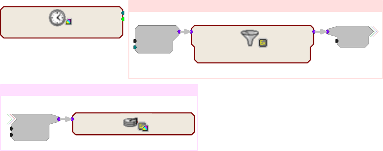
RPvdsEx Manual
66
MCAdcIn
nChan=16
ChanOS=1
[2:1,0]
HP-LP_Filter_MC
[Filt], 300Hz, 5000Hz, 12dB/oct
Input (nChan=16
)
FreqHP
FreqLP
Output
CoreSweepControl
Primary Store Name: Tick
Store-A
Store-B
Store-C
Store-D
SweepNum
SweepDone
DSP: Aux-1
Signal
nChan=16
DSP: Aux-2
ChanSel=1
Signal
nChan=16
Spike_Store_MC
Store: 'Snip' using SortSpike2 (32pts)
Store (nChan=16)
In the example above, a MCzHopOut feeds a 16 channel signal to a spike storage macro. All
timing for the circuit is done on the main DSP processor while filtering and storage are done by
separate (DSP: Aux-1 and DSP: Aux-2) processors. The DspAssign component splits the tasks
while the zHop components make the signals available across multiple processors.
Using the {d} Variable
The variable d in braces, that is {d}, can be used to represent a number associated with the
processor in any parameter or text label in a circuit. Values for the main and auxiliary processors
of the RX devices are 0, 1, 2, 3 and 4 (max) respectively. Values for the RZ processors are 1
through 8 (max).
When the circuit is compiled the character d will take the value corresponding to the processor to
which it is assigned. For example, if the channel number parameter for an AdcIn is set to {d}, and
the page is assigned to the Aux-1 processor, then the channel number will be 1.
When a page is assigned to more than one processor, the variable can be used to yield different
values for different processors. The {d} variable can also be used with formulas to yield the
desired value.
For example:
A parameter value set to {1 + ((d– 1) * 16)} will take the values:
1 in the first auxiliary processor
17 in the second auxiliary processor
33 in the third auxiliary processor
49 in the fourth auxiliary processor
Note: This formula is suitable for the RZ processors and the RX auxiliary processors but cannot
be used on the RX main processor, which has a value of 0.
Store Pooling
Store Pooling is a special feature of some data storage macros targeted for TDT’s OpenEx
software suite. When groups of channels from a larger multi-channel signal are processed and
stored using different processors on a multi-processor device, Store Pooling serves to identify
stored data as being part of a large whole.
For example:
If channels 1 – 16 of a 32 channel signal are stored using a data storage macro on DSP-1
And channels 17 – 32 are stored using a data storage macro on DSP-2
RPvdsEx Manual
67
Store Pooling ensures all 32 channels appear to be one “Data Store” in the OpenEx DataTank.
See the internal macro help of the data saving macros for more information on using Store
Pooling.
Multi-Processor Circuit Design Strategies
When designing circuits for multiprocessor devices, users should employ strategies that take
advantage of the distributed processing made possible by the multi-DSP architecture and the
MultiProcessor components available in RPvdsEx. These strategies typically include organizing
the circuit into logical units by task and distributing tasks across processors. For high-channel
count applications this will often include distributing data storage across multiple processors.
So, a 64 Channel Spike Sorting circuit might be distributed as follows:
DSP-1: timing and control
DSP-2: process and store 16 channels
DSP-3: process and store next 16 channels
DSP-4: process and store next 16 channels
DSP-5: process and store next 16 channels
When distributing processing tasks across multiple processors, users must
always consider:
The limitations of each processor.
The multi-DSP architecture of the device.
Each processor:
Has a finite amount of processing power dependent on sampling rate.
Each processor may be assigned up to 256 components for RX processors and 768 for RZ
processors.
The number of components on each processor is reported by RPvdsEx after compiling the circuit,
and the cycle usage of each processor is reported on the front panel display of the devices.
Device architecture:
RX devices rely on the Main processor to handle all communications. When using an RX device
TDT recommends keeping the processing tasks assigned to the Main processor light, freeing it up
to handle communications and data transfer more efficiently.
Multi-Processor Circuit Design - RZ2
The RZ2 processor has a unique architecture that includes a "Pipe Bus" not available in RX or
other RZ devices. Its multi-processor architecture combined with an x4 multiplier in processor
speed yields an extremely powerful system capable of sophisticated real-time processing and
simultaneous acquisition on 256 channels at sampling rates up to ~25 kHz and up to ~50 kHz on
up to 128 channels. Before attempting to design multi-processor circuits for the RZ2, it is a good
idea to become familiar with the device's multi-DSP, multi-bus architecture, and the special tools
available for multi-processor circuit design in RPvdsEx.
The RZ2 Multi-Bus Advantage
The RZ2 offers all the advantages of the multi-processor approach introduced with the RX High
Performance Processors while eliminating most of the bottlenecks found in the RX design. While
the RX device is very fast and flexible, its shared bus architecture generates a few restrictions that
RPvdsEx Manual
68
limit device capability in high channel count environments. The RZ2’s multi-bus approach uses a
more efficient data handling system to deliver the full potential of its ultra fast processors.
See the TDT System 3 Manual for more information about the RZ2 multi-processor architecture.
Multi-processor Pipe Components
The Multi-Processor Pipe components are a special group of RPvdsEx components used to pass
circuit signals between multiple processors on the RZ2. These signals are shared or passed
between DSPs using either the Data Pipe Bus or the zHop Bus. Pipe components move data most
efficiently across the Data Pipe Bus. There is a consistent two-sample delay associated with these
components to ensure known and consistent timing delays across multiple processors.
PipeSource feeds up to 256 channels to a DSP’s pipe input, either directly from a
preamplifier, via the optical input port, or from another DSP
PipeIn retrieves a single channel signal from a DSP’s pipe input
PipeOut moves a single channel signal to a DSP’s pipe output
MCPipeIn retrieves a multi-channel signal from a DSP’s pipe input
MCPipeOut moves a multi-channel signal to a DSP’s pipe output
Typically, all high channel count connections on the RZ2 are made using the Pipe components.
However, the RZ2’s zHop Bus does support up to 126 zHop pairs.
The zHop components were designed to pass arbitrary control and data signals between DSPs in
the RX systems and are more commonly used with RX processors.
See Multi-Processor Hop Components, page for 65 more information.
Designing Multi-processor Circuits for the RZ2
When designing circuits for multi-processor devices, users should take advantage of the
distributed processing made possible by the multi-DSP architecture of their device and the Multi-
processor components available in RPvdsEx.
Note: See TDT System 3 Manual for more information about the RZ2 multi-processor
architecture before reviewing the example below.
When working with RZ2 devices the user should be aware of the following:
The RZ2 allows an extra level of ‘pipe-lining’ in a number of areas creating an extra sample
of delay with some data transfer types. For example, data passed from one processor to
another now has a two cycle delay instead of one cycle as with the RX devices.
When the DataPipe is used to feed signals from a Z-Series PreAmp, a MCInt2Float or
Int2Float must be used with a scale factor of 1e-9. This is done for you when using the
RZ2_Input_MC macro.
Every DSP that uses the pipe bus must have a PipeSource component. There is a checkbox in
the RZ2_Input_MC macro that inserts this for you, or you must manually place one in the
circuit for that DSP.
Onboard A/D and D/A I/O are accessed using the ADC and DAC components in RPvdsEx.
The PZ Amplifier input channels are accessed using the Pipe components. The BioAmp
inputs can also be accessed using the RPvdsEx AdcIn or MCAdcIn component starting at
channel 128; however, this access method is less efficient and not recommended for high
channel count applications.
While zHops are fully supported with the Z-Series architecture it is recommended that the
new Data Pipe transfer method be used with high channel count applications.
DSPs do not share memory as with RX devices, so circuits that rely on memory sharing will
have to be modified to run on the RZ2 processor.
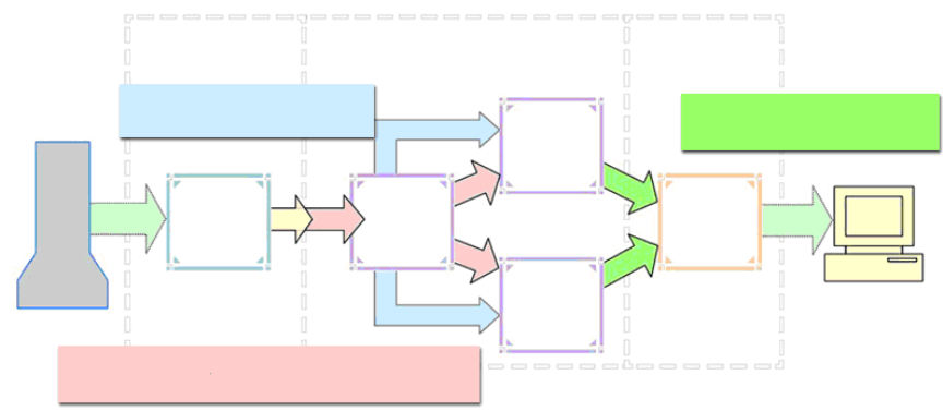
RPvdsEx Manual
69
While sample rates from 6kHz to 50kHz are supported, the RZ2 can only support 128-
channels when sampling at 50kHz. While sampling at 50kHz:
Only the first 128 BioAmp channels will be available
All Data Pipes will have a max of 128 channels instead of 256
Both halves (A and B) of the PipeSource component must be selecting the desired source.
For example, when acquiring data from a PZ preamplifier, Pipe[A] and Pipe[B] both
need to be set to Amp. Chan[1..128].
As with other devices, your expected sustained RZ-to-Host PC data rate should not exceed 1/2
to 2/3 of the rated data transfer speed. For the RZ2 device this is 160 Mbits/second (Mbps) so
your designs should have a sustained data rate of no more than ~100 Mbps. This maximum
rate may be further limited by your PC’s ability to store the data to disk.
Example: RZ2 - 16 Channel Spike Sorting
In the following example, a multi-processor circuit acquires and filters 16 channels of data
acquired using the RZ2 processor and PZn BioAmp. When using the PZn, signals are carried from
the BioAmp across a high speed fiber optic cable to the RZ2's Optical Port where the I/O interface
routes signals to the Pipe Bus. Once on the Pipe Bus, data is available to all DSPs.
The circuit supports spike sorting and stores sorted spikes and streamed data.
These tasks are split across three processors with multi-processor RPvdsEx components that
efficiently pass the data between DSPs at different stages of processing. The flow and circuit
diagrams below show how the signals are moved through the processor based on the bus
architecture and the circuit design.
Timing and Control
In the diagram above, blue arrows show how some signals are being distributed across the DSP
Block, from DSP-1 to DSP-2 and DSP-3, via the zHop bus. The CoreSweepControl macro in the
diagram below produces core timing and control signals required in all circuits designed for use
with TDT’s OpenEx software. These signals, such as enable and reset, are used throughout the
circuit and are distributed via zHops (this is handled within the macro and is transparent to the
user). Although the zHop Bus is a less efficient method for handling high channel count data, it is
suitable for this type of data transfer.
The zHop Bus carries single-channel
timing and control signals to each DSP
The Pipe Bus efficiently carries multi-channel signals across the
DSP Block
The zBus Interface Bus transfers data
buffers to the PC for data storage
Optical
Fiber Optical
Fiber
PZn Biological
Pream
p
Optical
I/O Port DSP-1
Processor
DSP-2
Processor
DSP-3
Processor
zBUS
Host PC
Interface
Controller
I/O
Interface DSP Block zBUS
Interface
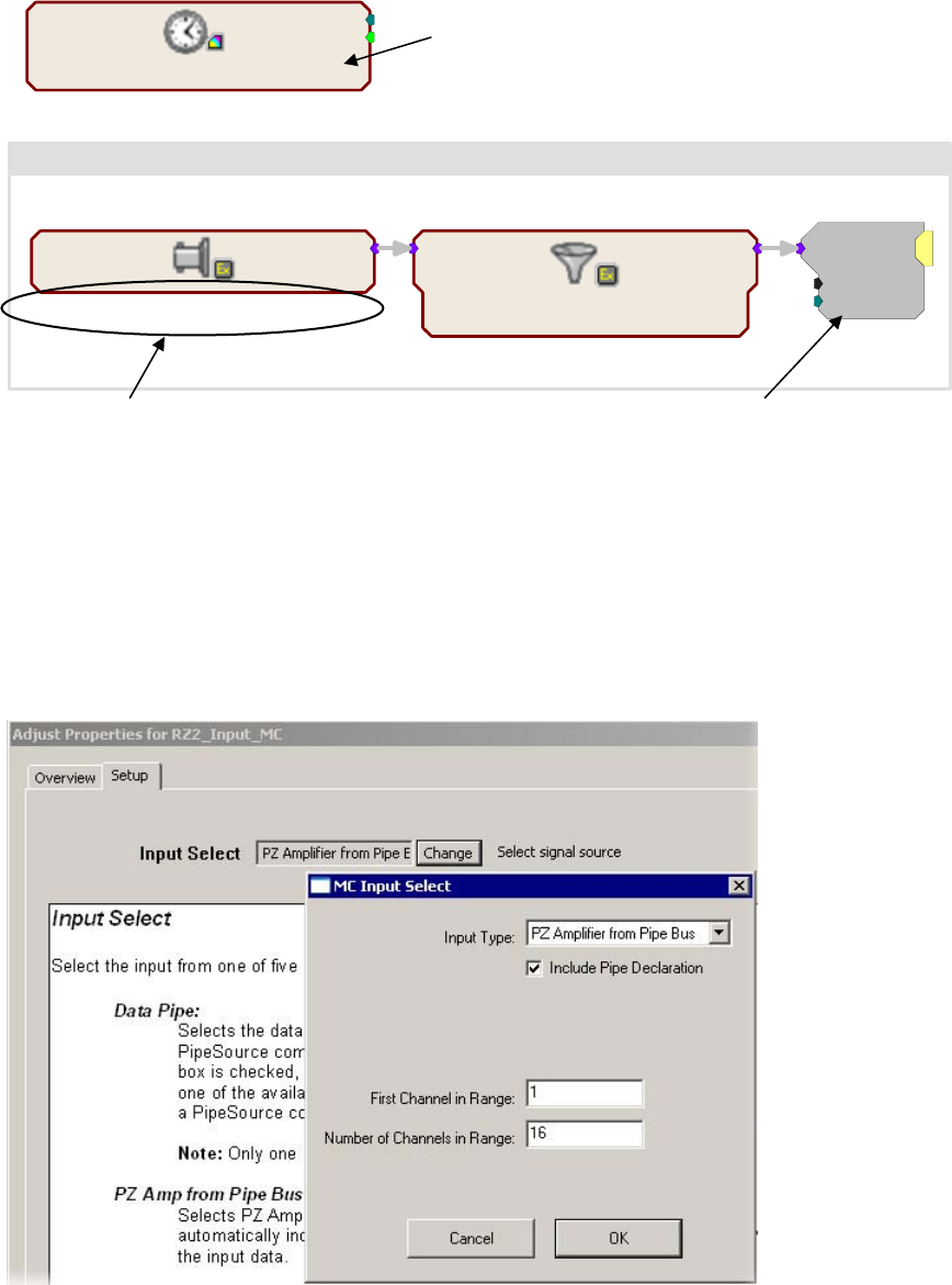
RPvdsEx Manual
70
CoreSweepControl
Primary Store Name: Tick
Store-A
Store-B
Store-C
Store-D
SweepNum
SweepDone
DSP: 1
RZ2_Input_MC
P
Z Amplifier from Pipe Bus, 16 Chans (1-16
)
SourceData
HP-LP_Filter_MC
[Filt], 300Hz, 5000Hz, 12dB/oct
Input (nChan=16)
FreqHP
FreqLP
Output
ChanSel=1
MCPipeOut
nChan=16
Acquisition and Filtering
In the circuit segment above, DSP-1 acquires and filters raw data from a Z-Series BioAmp across
the Pipe Bus. The RZ2_Input_MC macro handles all the tasks associated with acquiring signals
using the RZ2, including making the necessary data type conversion and applying the correct scale
factor for display and analysis. Because scale and channel offsets vary for different types of RZ2
inputs, the user must select the type of input within the macro Setup properties.
Macro setup properties...
When needed, an MCPipeIn is automatically included within the RZ2_Input_MC macro, but the
user must select the Include Pipe Declaration check box in the macro's MC Input Select dialog
box to automatically place the PipeSource. The circuit for each DSP that includes any of the pipe
The RZ2_Input_MC macro configures DSP-1 to acquire signals digitized on the
PZ2 preamplifier directly from the RZ2’s 256 channel fiber optic port. The
circuit is fed with 16 channels of data.
The MCPipeOut component makes filtered signals
available to other DSPs via the Pipe Bus.
The CoreSweepControl macro produces core
timing and control signals, such as enable and
reset lines. These single channel signals are
distributed via zHops using the zHop Bus.
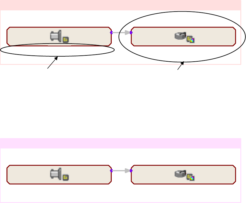
RPvdsEx Manual
71
input or output components must also include one and only one PipeSource component. The
PipeSource declaration may be added internally (automatically by the macro) or externally
(manually added outside of the macro).
Once configured, the RZ2_Input_MC macro feeds the circuit with the first 16 channels of data.
The HP-LP_Filter_MC macro filters all 16 channels through cascaded highpass and lowpass
filters. MCPipeOut makes the filtered multi-channel signal available to other DSPs via the Pipe
Bus.
Storing Streamed Data
On DSP-2, the RZ2_Input Macro is used to feed the processor with data from the Pipe Bus.
Note: this can also be accomplished using the PipeSource and MCPipeIn components.
In this example, the RZ2_Input Macro is used to configure DSP-2 to pipe in filtered data from
DSP-1 across the Pipe Bus. It routes 16 channels of acquired and filtered signals to the
Stream_Store_MC macro for data storage. Data is then transferred to the zBus Interface and
ultimately to the PC via the zBus Interface bus, as indicated by the green arrows in the previous
flow diagram on page 115.The following diagram illustrates the DSP-2 configuration.
RZ2_Input_MC
Data Pipe, Dsp-1, 16 Chans (1-16)
SourceData
DSP: 2
Stream_Store_MC
Store: Wave, Float, 24414.1Hz
Data Rate = 1525.9 kBytes/Sec
Store (nChan=16)
Spike Sorting and Snippet Storage
On DSP-3, the RZ2_Input Macro again configures the DSP to pipe in data from DSP-1. It routes
16 channels of acquired and filtered signals to the Spike_Store_MC macro for spike sorting and
data storage. This macro can be set to use one of several supported sorting methods. Again stored
data is transferred to the zBus Interface and ultimately to the PC via the zBus Interface bus.
RZ2_Input_MC
Data Pipe, Dsp-1, 16 Chans (1-16)
SourceData
DSP: 3
Spike_Store_MC
Store: 'Snip' using SortSpike2 (32pts)
Store (nChan=16)
This simple circuit acquires, filters, processes and stores 16 channels of data.
Data is transferred to the zBus Interface and ultimately to the
PC via the zBus Interface Bus.
Configures DSP-2 to pipe in data from DSP-1
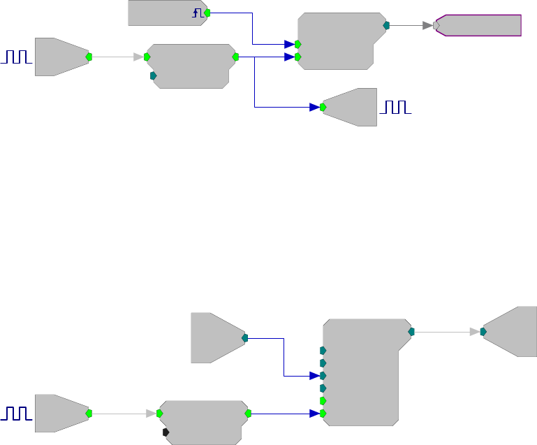
RPvdsEx Manual
72
Digital I/O Circuit Design
Digital I/O is extremely useful for producing logical status or control signals. Many System 3
devices allow digital I/O to be configured through RPvdsEx. See the reference for your device to
determine which bytes are available.
Working with BitIn - BitOut
This simple logic circuit will increment a simple counter for every sample that bit-0 is a logic
high. A DeBounce is used to filter transients from a switch, such as a button press. A software
trigger can be used to reset the counter to 0. Bit-1 will output a logic high whenever the counter is
enabled and incrementing. This logic high can be output as a control bit or as a status bit such as
an LED.
The input logic on the RP2 device is set for logic high (5 Volts in). For a circuit to work when a
button press occurs, invert the output using a NOT gate component.
Note: Bitmasks always start with bit-0. Use 2n and insert the bit needed to use the correct mask
value. For example, to use bit-3, compute 23 or a mask value of 8.
Bi
[1:1,0]
M=1
DeBounce
nChks=10
[1:2,0] 10000
SimpCount
Rst=0
Enable=1
[1:9,0]
[1:7,0
]
Src=Soft1
Bi
[1:11,0]
M=2
Working with WordIn - WordOut
This circuit demonstrates the use of WordIn and WordOut and how the mask parameter is used to
assign bits of the input and output ports to different tasks. In this example, bit-8 of the input port is
used to trigger the counter shown. On each rising edge of bit-8 the counter will be advanced by the
value input on bits 0 through 3 of the input port. The resulting count output is fed to all eight bits
of the digital output port. The EdgeDetect component makes sure that only one value is saved for
each logic high present at its input.
W
[1:12,0]
M=15
10110100
Bi
[1:14,0]
M=8
Counter
Base=0
Phse=0
Step=1
Roll=1000
[1:17,0]
Rst=Run
Enab=Yes
W
[1:18,0]
M=255
10110100
EdgeDetect
Edge=Rising
[1:15,0]

RPvdsEx Manual
73
Addressing Digital Bits In A Word
Some high performance processors include digital I/O that must be addressed as a word. Word
addressable bits can be addressed using the WordOut RPvdsEx component. To address these bits
you must first specify the maximum bitmask value in the WordOut component for the byte that
contains the bits you want to address. The table below includes a list of the maximum values for
each byte. These values apply to any module with a digital I/O word.
Table 1
Byte Bitmask
A 255
B 65,280
C 16,711,680
D 4,278,190,080
Note: Not all devices include all four bytes. See the reference for your device to determine
which bytes are available.
Addressing Separate Bits in a Byte
It is possible to address each bit in a byte separately depending on the integer value sent into or out
of the WordIn or WordOut component. The following table shows the integer values for each bit
in each byte.
Table 2
Integer Value (Bitmask)
Byte A B C D
Bit 0 1 256 65,536 16,777,216
Bit 1 2 512 131,072 33,554,432
Bit 2 4 1,024 262,144 67,108,864
Bit 3 8 2,048 524,288 134,217,728
Bit 4 16 4,096 1,048,576 268,435,456
Bit 5 32 8,192 2,097,152 536,870,912
Bit 6 64 16,384 4,194,304 1,073,741,824
Bit 7 128 32,768 8,388,608 2,147,483,648

RPvdsEx Manual
74
For example:
When addressing Byte C, the bitmask value on the WordOut component should be 16,711,680.
Then, to address bit 5 an integer of 2,097,152 should be sent into the WordOut. Both of these
values are required to send a pulse out to only Bit 5 in Byte C. The following table shows the
alignment of the bits to complete the operation.
Byte D Byte C Byte B Byte A Value
Bit # 7 6 5 4 3 2 1 0 7 6 5 4 3 2 1 0 7 6 5 4 3 2 1 0 7 6 5 4 3 2 1 0 N/A
Bitmask in
WordOut 0 0 0 0 0 0 0 0 1 1 1 1 1 1 1 1 0 0 0 0 0 0 0 0 0 0 0 0 0 0 0 0 16,711,680
Value Sent
to
WordOut
0 0 0 0 0 0 0 0 0 0 1 0 0 0 0 0 0 0 0 0 0 0 0 0 0 0 0 0 0 0 0 0 2,097,152
(221)
Note: This will also light up the Bit 5 LED on the device if the device’s Bits Lights are configured
to Byte C. See the Digital Input/Output section for your device for more information on
configuring Bits Lights.
Addressing More Than One Bit in a Byte
The values in the table above will only address one bit at a time. However, it is also possible to
address a combination of bits. For this task, determine what bits you would like to address in a
specific Byte and then convert that binary value to decimal. However, before converting this
value to decimal, consider the location of each byte in the digital word. Byte A is converted as
normal, but Byte B is shifted left by 8 bits (add eight 0s to the end of the binary value), Byte C
sixteen 0s, and Byte D twenty-four 0s. The decimal value is the integer to send into the WordOut
component (or the integer coming in from a WordIn component).
For example:
To address all of the bits in Byte B, set the Bitmask value in the WordIn or WordOut component
for Byte B (see Table 1) and then determine the integer value to be sent into the component
(calculated in steps below).
Since we are attempting to address all eight bits of a byte, the binary value should be eight 1s:
1111 1111
For Byte B, eight 0s should be added to the binary value making the value:
1111 1111 0000 0000
The binary number converted to decimal is:
65,280
Therefore, an integer of 65,280 should be sent to a WordOut component with a BitMask value of
65280 (this value from Table 1). Another way to complete the same operation is to add the integer
values of the bits you want to address in a given byte (Table 2) to determine the integer value to
send to the WordOut component.
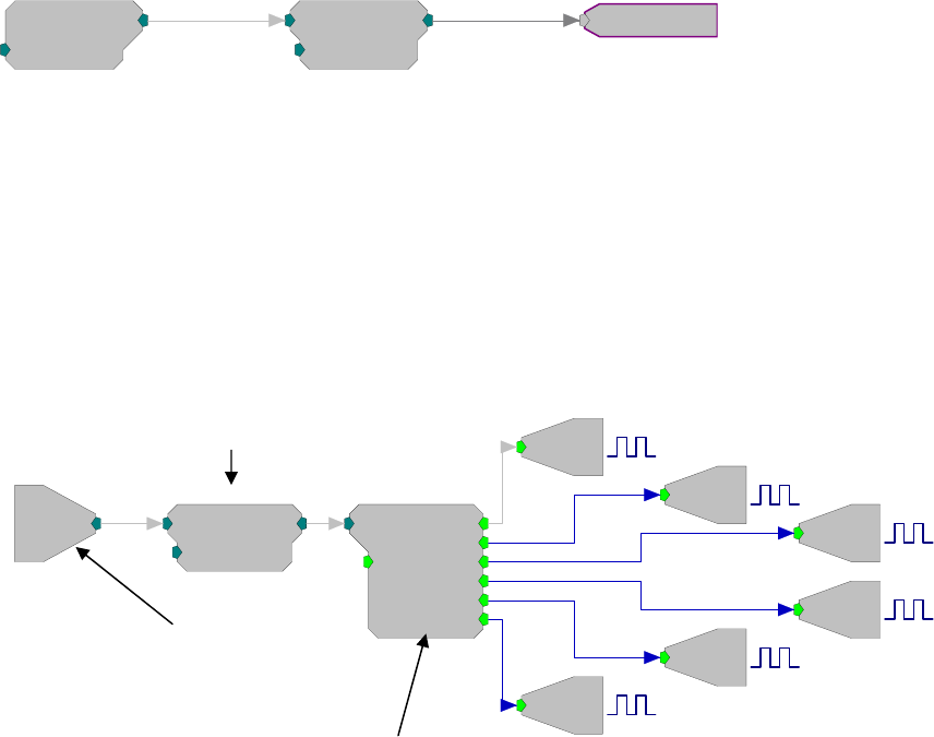
RPvdsEx Manual
75
Addressing More Than One Bit in a Byte using the RPvdsEx iBitShift
Component
When addressing bits in a digital word, the integer value out can range from 1 to 2,147,483,648.
Since each group is addressable as a single byte, it is often easier to assign values in a range from
1 - 255 then use an iBitShift to move the integer by a fixed number of bits to the left or right.
When addressing different bytes, you need only modify the iBitShift “N” parameter.
For example:
Byte A would use a bit shift of 0, while Byte B would require a bit shift of 8 for output and –8 for
input. Circuits that use Byte C would use 16 and –16 and D would use 24 or –24. Designing
circuits using this method makes it possible to read in the bit values for Byte D using integers
from 1 – 255 as compared to integers between 16,777,216 and 2,147,483,648. Using iBitShift also
allows values to be processed using ToBits or FromBit.
The following example circuit shows how the iBitShift component can be used with Word
components to remove the eight least significant bits in a 16-bit integer.
ConstI
K=65280
[1:1,0
]
iBitShift
N=-8
[1:2,0]
255
As the example (above) explains, the iBitShift is used to remove the eight least significant bits
from the integer 65280. The integer 65280 corresponds to eight high bits in Byte B. The next
example (below) shows an iBitShift that removes the eight least significant bits from a WordIn
component that is bitmasked to Byte B. The ToBits component then separates the bits and each bit
is sent out to the first six addressable bits.
iBitShift
N=-8
[1:2,0]
W
[1:1,0]
M=65280
10110100
b5
b4
b3
b2
b1
ToBits
Rst=0
[1:3,0]
b0
Bi
[1:4,0]
M=1
Bi
[1:6,0]
M=2
Bi
[1:8,0]
M=4
Bi
[1:10,0
]
M=8
Bi
[1:12,0]
M=16
Bi
[1:14,0]
M=32
The ToBits component is only used for up to 6 bits; it may give errors if the 7th or 8th bits are
used.
Note: The first 6 addressable bits must be configured as outputs and Word B must be left as an
input.
This circuit removes the 8 least significant bits.
(1111 1111 0000 0000 to 1111 1111)
The binary equivalent of the integer 65280 is:
1111 1111 0000 0000
The binary equivalent of the integer 255 is:
1111 1111
Removes last 8 binary values
(1111 1111 0000 0000 to 1111 1111)
In order to read in from Word B use
M=65280 (1111 1111 0000 0000)
This circuit sends a digital signal out to the first 6 addressable bits corresponding to the first 6 bits in Word B
RPvdsEx Manual
76
~

RPvdsEx Manual
77
Part 3 Reference
RPvdsEx Manual
78
~

RPvdsEx Manual
79
Macro Reference
Help for each Macro component is provided in the properties dialog box. For more information
about using macros, see the Macro Overview on page 30.
Macro Reference List
Macro Name Function Use Notes
Timing
CoreSweepControl Generation of the core timing &
control signals used in OpenEx.
This macro should be used once
and only once in each OpenEx
circuit.
Single and multi-
processor devices.
Designed for OpenEx.
StandardTimeControl Generation and storage of the
basic timing/control signals
needed to drive various
stimulation or acquisition
structures.
Single and multi-
processor devices.
Designed for OpenEx.
Filtering
HP-LP_Filter_1Ch Filtering of floating point single-
channel data streams through
cascaded highpass (HP) and
lowpass (LP) filters.
Single and multi-
processor devices.
HP-LP_Filter_4Ch Filtering for up to four-channels
of floating point data streams
through cascaded highpass (HP)
and lowpass (LP) filters.
Single and multi-
processor devices.
HP-LP_Filter_MC Filtering of floating point multi-
channel data streams through
cascaded highpass (HP) and
lowpass (LP) filters.
Multi-processor devices
only.
Data Saving | Segment_Snip
Block_Store_1-4Ch Continuous or decimated block
storage for up to four-channels of
floating point data streams.
Single and multi-
processor devices.
Designed for OpenEx.
Block_Store_1-8Ch Continuous or decimated block
storage for up to eight-channels
of floating point data streams.
Single and multi-
processor devices.
Designed for OpenEx.

RPvdsEx Manual
80
Block_Store_MC Continuous or decimated block
storage of multi-channel floating
point data streams.
Multi-processor devices
only.
Designed for OpenEx.
Spike_Store_1-4Ch Spike thresholding and sorting
for up to four-channels of
floating point data streams using
the FindSpike, SortSpike,
SortSpike2, or SortSpike3
components, and storage of the
snippets.
Single and multi-
processor devices.
Designed for OpenEx.
Spike_Store_MC Spike thresholding and sorting of
floating point data streams using
the FindSpike, SortSpike,
SortSpike2, or SortSpike3
components, and storage of the
snippets.
Multi-processor devices
only.
Designed for OpenEx.
Data Saving | Streaming
Stream_Store_1-4Ch Continuous or decimated storage
for up to four-channels of
floating point data streams.
Single and multi-
processor devices.
Designed for OpenEx.
Stream_Store_1-8Ch Continuous or decimated storage
for up to eight-channels of
floating point data streams.
Single and multi-
processor devices.
Designed for OpenEx.
Stream_Store_MC Continuous or decimated storage
of multi-channel floating point
data streams.
Multi-processor devices
only.
Designed for OpenEx.
Stream_Store_MC2 Continuous or decimated storage
of multi-channel floating point
data streams.
Multi-processor devices
only.
Designed for OpenEx.
Async_Stream_Store_1-
4CH Asynchronous continuous
storage of floating or fixed point
data.
Multi-processor devices
only.
Designed for OpenEx.
Asynch_Stream_Store_MC Asynchronous continuous storage
of multi-channel floating or fixed
point data.
Multi-processor devices
only.
Designed for OpenEx.
Data Saving | Epoch Store
Epoc_Store Storage of scalar Epocs on
transitions of control or signal
inputs.
Single and multi-
processor devices.
Designed for OpenEx.

RPvdsEx Manual
81
Slow_Store_1-4Ch Triggered storage for up to four-
channels of floating point or
integer data streams.
Single and multi-
processor devices.
Designed for OpenEx.
Slow_Store_1-8Ch Triggered storage for up to eight-
channels of floating point or
integer data streams.
Single and multi-
processor devices.
Designed for OpenEx.
Slow_Store_MC
Triggered storage of multi-
channel floating point or integer
data streams.
Multi-processor devices
only.
Designed for OpenEx.
Epoc_Store_with_Offset Storage of scalar Epocs with
onset and offset coding. Single and multi-
processor devices.
Designed for OpenEx.
Data Saving | With Processing | Averaging
Block_Avg_Store_1-4Ch Asynchronous block storage of
data streams. Multi-processor devices
only.
Designed for OpenEx.
Block_Avg_Store_MC Asynchronous block storage of
data streams.
Multi-processor devices
only.
Designed for OpenEx.
Device | PO8e_Streamer
Stream_Remote_MC Configure RZ to PO8e data
streaming. RZDSP-U equipped RZs.
Device | RZ2 Processor
RZ2_Control Configure RZ2 Digital I/O. RZ2 only.
RZ2_Input_MC Configure RZ2 Analog I/O. RZ2 only.
Device | RZ5 Processor
RZ5_Control Configure RZ5 Digital I/O. RZ5 only.
RZ5_AmpIn_MC Configure RZ5 preamplifier input
(4-32 channels). RZ5 only.
RZ5_AmpIn Configures a single channel of
RZ5 preamplifier input. RZ5 only.
Device | RZ6 Processor
RZ6_Control Configure RZ6 Digital I/O. RZ6 only.
RZ6_AmpIn Configures up to four channels of RZ6 only.

RPvdsEx Manual
82
RZ6 preamplifier input.
RZ6_AudioIn Configures two channels of RZ6
ADC input. RZ6 only.
RZ6_AudioOut Configures two channels of RZ6
DAC output. RZ6 only.
Device\RS4_Data_Streamer
Stream_Server_MC Configure RZ2 to RS4 data
streaming. RZDSP-S equipped RZs.
Device\RV2 Video Processor
Video_Access Control the RV2 Video Processor
via an RZ processor. RZDSP-V equipped RZs.
Device | PZ2 Bioamp
PZ2_Control Configures PZ2 LEDs and power
down status. Also configures
direct input from PZ2 when run
on an RZDSP-P.
RZ2 or any RZ equipped
with an RZDSP-P.
Device | PZ3 Amplifier
PZ3_ChanMap Maps channels from PZ3 to build
a multi-channel output containing
either the amplified waveforms
or corresponding impedances.
RZ2 only.
PZ3_Control Configures PZ3 operation modes.
Also configures direct input from
PZ2 when run on an RZDSP-P.
RZ2 or any RZ equipped
with an RZDSP-P.
Device | IZ2 Stimulus Isolator
IZ2_Control Control the IZ2 Stimulus Isolator
via an RZ processor. Also control
an SH16-Z connected to an IZ2.
RZDSP-I equipped RZs.
Device | MS16 Stimulus Isolator
MS16_Control Control the MS16 Stimulus
Isolator via the RZ5 or RX7
processor.
RZ5 or RX7 only.
Device | SH16 Switching Headstage
SH16_Control Control the SH16 switching
headstage via the RZ5 or RX7
processor.
RZ5 or RX7 only.
Signal Generators
PulseGenN A biphasic pulse train generator Single and multi-

RPvdsEx Manual
83
with all timing specified in
samples. processor devices.
Test_Spike_MC A multi-channel spike test signal
generator. Multi-processor devices.
Misc Calculators
RateToSamples Convert input rate to number of
samples based on the sample rate
of the circuit.
Single and multi-
processor devices.
TimeToSamples Convert an input time to number
of samples based on the sample
rate of the circuit and bound the
output regardless of the input.
Single and multi-
processor devices.
RPvdsEx Manual
84
Component Reference
Audio Processing
Audio Processing Components
This group includes components that are related to 3D audio processing. This section also includes
information about the HRTF file format used by TDT.
This group includes the following components:
DistScale
HrtfCoef
HrtfFir
Reverb
HRTF File Format
The following information gives a general overview of HRTF's and the file format for using
custom HRTF coefficients.
Introduction
An HRTF (Head Related Transfer Function) contains all the listening cues that are applied to a
sound as it travels through the environment to arrive at the ear. The signal at the ear will depend
on the azimuth, elevation and distance of the source relative to the ears. A complete set of HRTF
consists of many filters that describe a spherical map of the possible sound sources. The HRTF
contains information about frequency dependent sound delays and intensity differences between
ears. When a signal is sent through an HRTF filter and then played through headphones the
listener receives the impression of where the sound source should be.
In the picture below each point represents a sound source. The distance of the source is a constant
relative to the center of the head. Sources can
change in the lateral position around the head
(Azimuth) or the elevation of the source
relative to the ears. In general, differences in
delay and intensity between ears for a given
sound changes greatest in the Azimuthal
position and less so for elevation. These
differences are frequency dependent.
Values can be sent to the RPvdsEx HRTF
component coefficient for Azimuth and
Elevation. The HRTF coefficient processor
finds the proper coefficients in a look up table
on a Ram Buffer component, interpolates the
values and sends them to the HRTF filter. This
produces real-time virtual 3-D audio
processing on the RP. Output of the processor
can be feed to the HRTF filter processor.
HRTF coefficients are organized in the
following file format for retrieve by the HRTF
filters.

RPvdsEx Manual
85
The filter coefficients are loaded into a RAM buffer large enough to hold all the coefficients. The
component number of the RAM buffer is stored on the HRTF coefficient processor. It is possible
to have several sets of HRTF coefficients in different Buffers and switch between them.
Information about the organization of the HRTF is given in the header section. The following
format is required for the header.
HRTF Header Format
Definition Data Type Description
Number_of_filters Int32 Number of filter positions in RAM buffer. (number of
Azimuths * Number of elevations)+1.
This is so that the filter position at 90 is included.
In cases where there will be no filter at 90 it is still
necessary to include a dummy filter at 90 degrees.
Number_of_taps_x2 Int32 Number of taps (coefficients) including Interaural delay
(ITD) delay (x2) per filter. e.g. 31 tap filter =31 x 2 + 2
(delay values)=64
Number_of_taps Int32 Number of taps including the delay. e.g. 31 tap filter= 31
taps + delay value
Minimum_Az Flt32 Minimum Azimuth value in degrees (e.g. -165)
Maximum_Az Flt32 Maximum Azimuth value in degrees (e.g. 180)
Resolution_Az Flt32 Inverse of the Position separation of Az in degrees, defined
as 1.0/(AZ separation)
e.g. 15 degrees between channel would =0.066666.
Number_of_Az Int32 Number of Az positions at each elevation.
Minimum_El Flt32 Minimum Elevation value in degrees.
Maximum_El Flt32 Maximum Elevation value in degrees (Must include a value
for 90).
Resolution_El Flt32 Inverse of the Position separation of Elevation in degrees,
defined as 1.0/(EL separation).
e.g. 30 degrees between EL would be 1/30=.0333.
Number_of_El Int32 Number of elevation positions for each Azimuth+1. The
additional value is for the filter at 90 degrees. In cases
where there will be no filter at 90 degrees elevation it is
still necessary to include a dummy filter.
Sample_Period Flt32 Filter sampling period in microseconds. Calculated as the
inverse of the sampling rate * 1,000,000.
A 90 degree filter value must be specified for the Maximum_AZ value.
Resolution values are defined as the inverse of the AZ or EL separation.

RPvdsEx Manual
86
HRTF Filter Organization
Filter coefficients are grouped first according to their elevation from maximum elevation to
minimum (e.g. 90, 60,...-60, -90). For each elevation the filters are organized from maximum AZ
to minimum AZ values (e.g. 180, 165,...-165). The table below gives an example of the filter
organization. IMPORTANT: Even if there are no values for elevation of 90 degrees a dummy set
of filter values must be included.
EL AZ
90
60 180
60 165
60 150
60 .
.
.
60 -165
30 180
30 165
30 .
.
.
30 -165
0 180
0 165
0 .
.
.
0 -165
0 -180
.
.
.
.
.
.
-30

RPvdsEx Manual
87
HRTF Filter Coefficient Format
The coefficient values for the HRTF must have the following format. They must be minimum-
phase with the left and right channels interleaved. Filter values are stored as 32-bit floats with the
filter's group delay stored as the last element of the filter. The example below shows the file
format for a 31 tap left/right filter pair. The HRTF FIR filter requires that the order include the
delay.
Ear Filter# Order#
L 1 0
L 2 1
L 3 2
... .. ..
L 31 30
Left group delay xx 31
R 1 0
R 2 1
R 3 2
.. .. ..
R 31 30
Right group delay xx 31
All Coefficients and delays are 32-bit floating point values. The delays are specified in number of
samples.
The order of the filter must include the number of taps and the delay. A filter order of 32 has 31
taps and 1 group delay.
The MaxITD value must be greater than the maximum delay specified for any filter to be used and
is fixed at the start of the circuit.
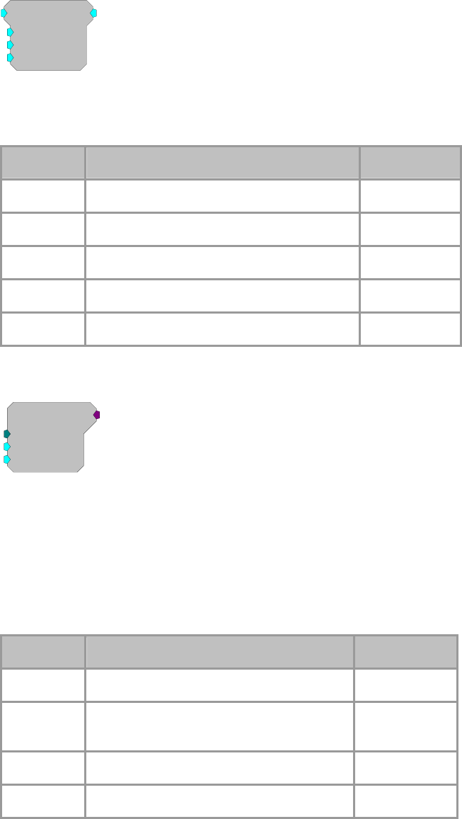
RPvdsEx Manual
88
DistScale
DistScale
DistMax=100
DistMin=1
DistCur=50
[1:1,0]
Description:
Scales signal to model attenuation with distance. The DistCur is limited to the
DistMin and DistMax specified. Then the signal is scaled by DistMin / DistCur.
Name Description Data Type
Input Input Floating Point
Output Output scaled as Output*DistMin/DistCur Floating Point
DistMax Maximum Distance for attenuation Floating Point
DistMin Minimum distance for attenuation number Floating Point
DistCur Current distance of the signal Floating Point
HrtfCoef
HrtfCoef
CmpNo=1
Az=0
El=0
[1:1,0]
Description:
HRTF Coefficient generator. HrtfCoef obtains coefficients from the memory of
CmpNo. Azimuth and Elevation inputs can be dynamically changed to switch
between azimuth and elevation-specific HRTFs. The HrtfCoef generator will
interpolate between sets of coefficients as Azimuth and Elevation are changed.
RPvdsEx comes with a set of HRTFcoef.
For information about making custom HRTF filters see the HRTF Filter
description, page 84.
Name Description Data Type
Output Filter Coefficients for HRTFFir filter Floating Point
CmpNo Component Number of RAM buffer storing
filter coefficients and look up table Integer (Static)
AZ AZ of signal source in degrees Floating Point
El Elevation of signal source in degrees Floating Point
Example(s):
3D Circle, page 90.

RPvdsEx Manual
89
HrtfFir
HrtfFir
Order=32
MaxITD=100
{>Coef}
{>Delay}
[1:1,0]
Description:
FIR filter using HRTF coefficients. Filter coefficients can be obtained by
connecting the HrtfCoef component to the >Coef pointer on HrtfFIR. Custom
filter processing can be done by using the >Coef and >Delay lines.
The Order of the filters is equal to the number of taps (per ear) plus the delay
value (ITD). A 31 tap filter will have a filter order of 32.
The maximum ITD (Interaural Time Delay) is static and must exceed the
maximum value from any of the filters.
The RPvdsEx comes with HRTF filters. Information about using custom filters
can be found in HRTF File Format, page 84.
Name Description Data Type
Input Input Floating Point
Output Filtered signal Stereo
Order
N
umber of Taps (per ear) plus one (delay
value) Integer (Static)
MaxITD Maximum Interaural Delay (no Filter value
should have a greater delay) Floating Point
(Static)
>Coef Pointer to Coef buffer (PM) Ordering:
Ordered as follows:
B0, B1, B2, ... Bn n=order.
Pointer
>delay Pointer to delay buffer (DM). Ordering:
X1(1), X2(1), Y1(1), Y2(1), X1(1), X2(1),
Y1(1), Y2(1),... X1(n), X2(n), Y1(n), Y2(n).
Pointer
Example(s):
3D Circle, page 90.

RPvdsEx Manual
90
Reverb
Reverb
Dmax=100
Dcur=100
Decay=0.75
WetMix=0.25
[1:1,0]
Description:
Reverberation component. The Reverb component can be used to obtain more
realistic spatialization of 3D sound.
Name Description Data Type
Input Input Floating Point
Output Reverb component of a stereo signal Floating Point
(Stereo out)
Dmax Maximum delay in msec Static
Dcur Current delay in msec Floating Point
Decay Room decay log scale decline Floating Point
WetMix Reverberation scalar for splitting signal into
stereo Floating Point
Example:
3D Circle
File: Examples\3D_Sound\3d_circle.rcx
Default Device: RP2 Processor
Sampling Rate: 50 kHz
This example implements a basic 3D application. The circuit generates a pulsed
sound and filters it through dynamically changing HRTF filters. The processor
is also controlling the trajectory of the sound. A RampTooth generator is used
to produce the appropriate azimuth values to make the sound circle the head.
The pulsed sound could easily be replaced by audio inputs to the processor.
Note: High-quality headphones should be used to reproduce the 3D
spatialization effect. The 3D sound effect will not be heard over speakers.
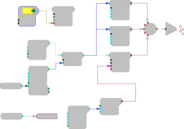
RPvdsEx Manual
91
RamBuf
Size=100000
Index=0
Write=0
{>Data}
[1:1,-1]
NoName
Name=C:\T
D
N=33000
OS=0
HrtfCoef
CmpNo=1
Az=0
El=0
[1:8,0]
e
o
[1:17,0]
Ch=1
Random
Amp=2
Shft=0
Seed=0
Rst=Run
[1:9,0]
Cos2Gate
Trf=10
Ctrl=Closed
[1:10,0]
PulseTrain
Thi=30
Tg=0
Tlo=100
Npls=0
[1:4,0]
CurN=0
Stage=0
Trg=0
OneShot
[1:2,0]
HrtfFir
Order=32
MaxITD=100
{>Coef}
{>Delay}
[1:11,0]
RampTooth
Amp=180
Shft=0
Freq=2
Phse=0
[1:6,1]
Rst=Run
Reverb
Dmax=100
Dcur=57
Decay=0.75
WetMix=0.08
[1:13,0]
Reverb
Dmax=100
Dcur=13
Decay=0.75
WetMix=0.15
[1:15,0]
75.6605CycUsage
[1:18,0]
[1:16,0]
t
ereoSu
Example:
FlyBy
File: Examples\3D_Sound\flyby.rcx
Default Device: RP2 Processor
Sampling Rate: 50 kHz
This example shows how to implement a flyby. A short helicopter.wav file is
loaded into the circuit and then run through processing that adjusts sound level,
direction, and Doppler shift based on distance. The DistScale component is
used to control sound level as a function of distance. The LongDynDel
component is used to generate the Doppler shift. The HrtfCoef and HrtfFir
components are used to change the apparent azimuth of the helicopter as it flies
by.
Note: High-quality headphones should be used to reproduce the 3D
spatialization effect. The 3D sound effect will not be heard over speakers.

RPvdsEx Manual
92
File1
Name=C:\T
D
N=33000
OS=0
RamBuf
Size=50000
Index=0
Write=0
{>Data}
[1:1,-1]
Sound
DistScale
DistMax=100
DistMin=2
DistCur=50
[1:12,0]
LongDynDel
Mms=100
Dms=50
{>Data}
[1:13,0]
HrtfCoef
CmpNo=1
Az=0
El=0
[1:10,0]
HrtfFir
Order=32
MaxITD=100
{>Coef}
{>Delay}
[1:14,0]
e
o
[1:15,0]
Ch=1
ScaleAdd
SF=57
Shft=90
[1:8,0]
Arctan
[1:7,0]
Absval
[1:3,0
]
RampTooth
Amp=50
Shft=0
Freq=0.15
Phse=-179
[1:2,0]
Rst=Run
CycUsage
[1:16,0]
58.0505
File2
Name=C:\T
D
N=10000
OS=0
SerialBuf
Size=10000
Rst=0
AccEnab=1
Write=0
[1:11,1]
NB l ks=0
Index=0
{>Data}
Sound
RPvdsEx Manual
93
Basic Analysis
Basic Analysis Components
Components in the Basic Analysis group analyze various aspects of a signal.
This group includes the following components:
FeatSrch
FindFreq
PowerBand
RMS
TrackMax
TrackMin
This group also includes the following component, if RPvdsEx Device Setup is
configured for a high performance device, such as the RXn or RZn:
RMS2

RPvdsEx Manual
94
FeatSrch
FeatSrch
FC=Above
K1=0
K2=0
[1:1,0]
Description:
A feature search looks for a particular set of criteria to be reached. When the
criteria are met the feature search component generates a logical high (1)
otherwise a logical low (0) is generated. Users choose fixed criteria for the
search (e.g. the input is between two values). The condition levels can be
changed while the circuit is running. The possible feature search codes are:
OFF No search in progress (output is always 0)
ABOVE Checks to see if the input is above K1
BELOW Checks to see if the input is below K1
BETWEEN Checks to see if the input is above K1 and below K2
OUTSIDE Checks to see if the input is below K1 or above K2
RISING Checks to see if the input is rising
FALLING Checks to see if the input is falling
PEAK Checks to see if the input rose and then fell
VALLEY Checks to see if the input fell and then rose
TIP Checks to see if the PEAK or VALLEY event has occurred
RISETHRU Checks to see if the input has risen through K1
FALLTHRU Checks to see if the input has fallen through K1
PASSTHRU Checks to see if the RISETHRU or FALLTHRU event has
occurred
Name Description Data Type
Input Input Floating Point
Output 1 if conditions met 0 if not Logic
FC Feature search condition Static
K1 First search condition Floating Point
K2 Second search condition Floating Point
Example:
Feature Search
File: Example\FeatSrch.rcx
Default Device: RP2 Processor
Sampling Rate: 50 kHz
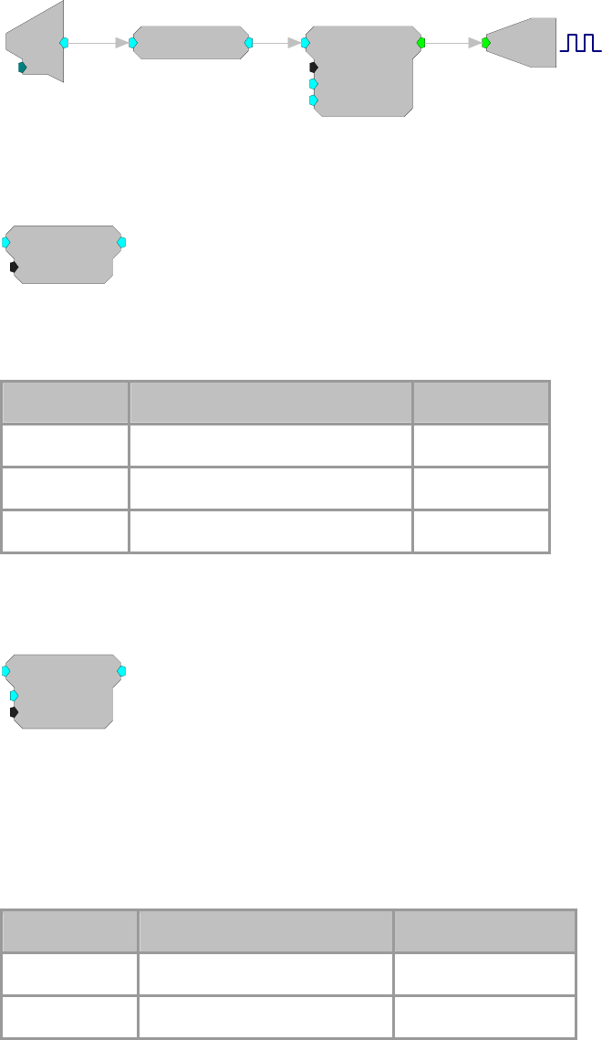
RPvdsEx Manual
95
This example implements a simple signal detector. It calculates the RMS of the
input and FeatSrch sends a TTL pulse to the BitOut when the RMS goes above
0.38. To save the signal that comes in, modify the circuit with a Serial Buffer.
Note: Additional circuitry is included in the example file to demonstrate how
the example works.
d
c
[1:1,0]
Ch=1 RMS
[1:2,0]
FeatSrch
FC=Above
K1=0.38
K2=0
[1:3,0]
Bi
[1:4,0]
M=1
FindFreq
FindFreq
Tau=100
[1:1,0]
Description:
FindFreq calculates the frequency of a signal using zero-crossings. Tau is the
number of milliseconds over which the zero-crossing is calculated.
Name Description Data Type
Input Input Floating Point
Output Frequency based on zero-crossings Floating Point
Tau Feature search condition Static
PowerBand
PowerBand
Fc=1000
BW=10
[1:1,0]
Description:
This component computes the power of the input signal within the specified
band. Power is defined as the integral (area under the curve) of that bandwidth.
The time it takes to calculate the PowerBand is inversely related to the
bandwidth, i.e. a 1 Hz band width takes 1 second while a .1 Hz band width
takes 10 seconds. To calculate level, you would take the square root of the
output.
Name Description Data Type
Input Input Floating Point
Output Power of the input signal Floating Point
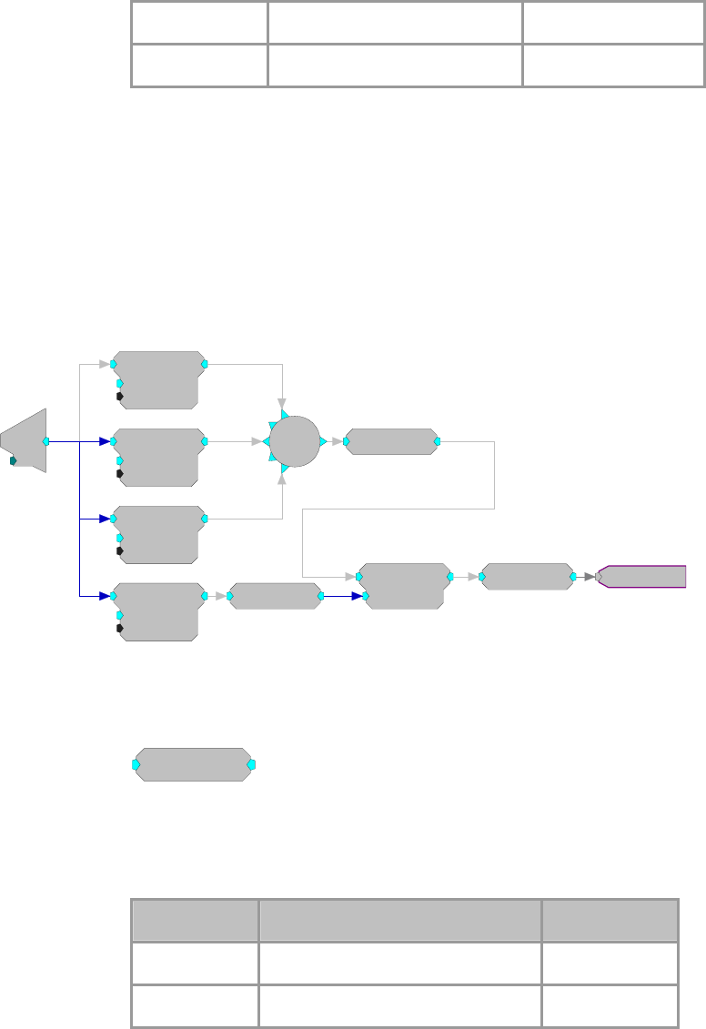
RPvdsEx Manual
96
Fc Frequency to measure Floating Point (Static )
BW 3dB bandwidth to measure Floating Point (Static)
Example:
Power Band
This circuit builds a THD (Total Harmonic Distortion) measurement system.
The signal applied to A/D channel one is passed through four PowerBand
components. The power measured at the first three distortion components is
summed and converted back to RMS via the SqRoot processor. The
fundamental is also measured and converted to RMS. The two RMS results are
then compared via Divide and converted to a dB ratio with LinTodB. This
analyzer can measure THD ratios down to about 90 dB.
d
c
[1:1,0]
Ch=1
PowerBand
Fc=2000
BW=0.1
[1:2,0]
PowerBand
Fc=3000
BW=0.1
[1:4,0]
PowerBand
Fc=4000
BW=0.1
[1:6,0]
PowerBand
Fc=1000
BW=0.1
[1:8,0]
[1:11,0]
Sum SqRoot
[1:12,0]
SqRoot
[1:9,0]
Divide
Den=1
[1:13,0]
LinTodB
[1:14,0]
0.138633
RMS
RMS
[1:1,0]
Description:
This component computes the RMS value by squaring the input, lowpass
filtering the input data, and taking the square root.
Note: The RMS component has a built-in time constant (tau) of 1 second.
Name Description Data Type
Input Input Floating Point
Output Root Mean Square of Input value Floating Point
Equation:
Output = RMS ( Input )
Example(s):
Feature Search, page 94.
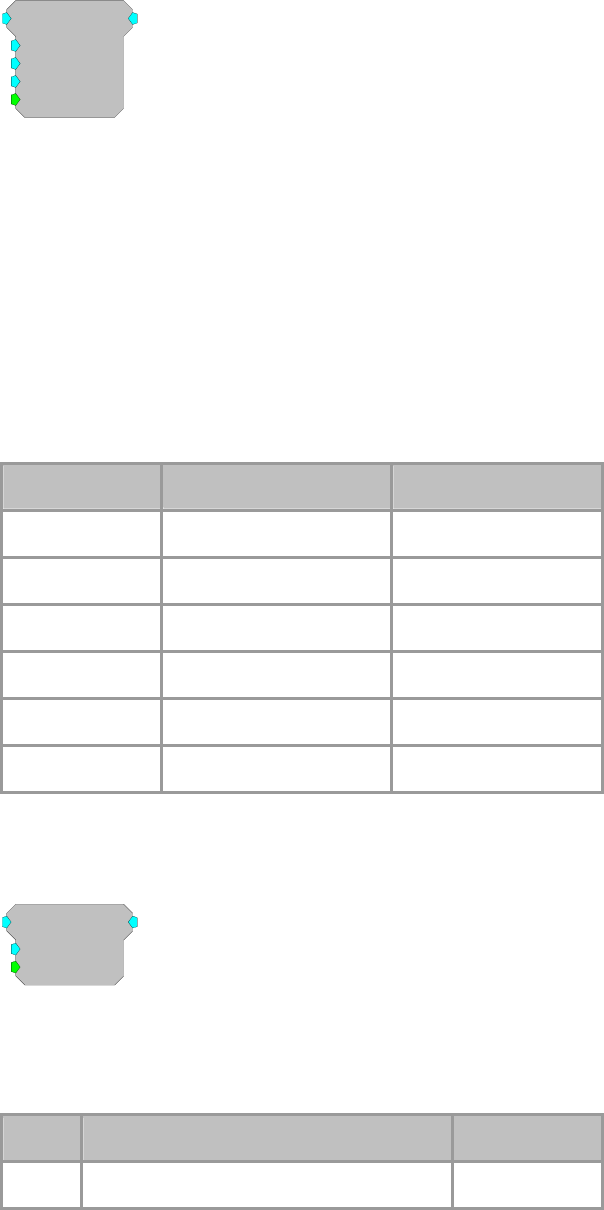
RPvdsEx Manual
97
RMS2
RMS2
Tau=3000
Scale=1
LoLim=1e-006
Rst=0
[1:1,0]
Description:
RMS2 calculates an approximate RMS value of the input signal with a moving
average filter to disregard spurious signals that are in excess of 3X the running
average. The lowest possible output of this component is set by LoLim and the
smoothing average time constant is set by Tau. Reset forces the output to
LoLim and restarts the averaging process. This component has been optimized
to improve cycle usage for multi-channel use and should only be used for neural
signals with a Gaussian probability, not sinusoidal signals. The LoLim value
should match the experimental threshold and with each reset, the output will
begin deviating from this value at a rate not greater than 1.3X LoLim per unit of
time defined in Tau.
Note: This component is for use with only high performance processor devices,
such as RXn or RZn.
Name Description Data Type
Input Input signal Floating Point
Output Output signal Floating Point
Tau Time constant Floating Point
Scale Scale factor Floating point
LoLim Output lower limit Floating point (non-zero)
Rst Reset Logic
TrackMax
TrackMax
Vi=-1e+030
Rst=0
[1:1,0]
Description:
Tracks the maximum value of an input until the reset is triggered. When reset
(Rst=1), the maximum value is reset to Vi. This function is useful for measuring
peak amplitudes in signals.
Name Description Data Type
Input Input Floating Point
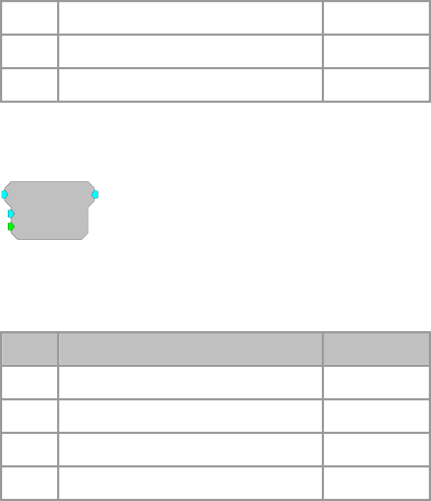
RPvdsEx Manual
98
Output Maximum value found from last reset Floating Point
Vi Value at reset, when reset=1 output=Vi Floating Point
Rst Resets output value to Vi Logic
TrackMin
TrackMin
Vi=1e+030
Rst=0
[1:1,0]
Description:
Tracks the minimum value of an input until the reset is triggered. When reset
(Rst=1), the minimum value is reset to Vi. This function is useful for measuring
trough amplitudes in signals.
Name Description Data Type
Input Input Floating Point
Output Minimum value found from last reset Floating Point
Vi Value at reset, when reset=1 output=Vi Floating Point
Rst Resets output value to Vi Logic
RPvdsEx Manual
99
Basic Math
Basic Math Components
The processing components in this group are used to perform low-level math operations.
Remember that even simple math operations might use many DSP cycles. For example, the Divide
processor will use about 30 cycles while ScaleAdd uses only about 10 for both a multiplication
and addition. Avoid the Divide, SqRoot, and Modulus processors whenever possible.
This group includes the following components:
AbsVal
Bound
Ceiling
Compare
Divide
Floor
Limit
Min and Max
Modulus
ScaleAdd
Sign
SqRoot
Square
StereoScale
StereoSum
Sum and Mult
This group also includes the following components, if RPvdsEx Device Setup is
configured for a high performance device, such as the RXn or RZn:
MCAbsVal
MCBound
MCMatMult
MCScale
MCSign
MCSum and MCMult

RPvdsEx Manual
100
AbsVal
Absval
[1:1,0]
Description:
AbsVal computes the absolute value of the signal.
Name Description Data Type
Input Input Floating Point
Output Absolute value of Input Floating Point
Equation:
Output = Abs (Input)
Example(s):
AbsVal (-2.3) = 2.3
AbsVal (2.3) = 2.3
Bound
Bound
Max=1
Min=-1
Vnan=0
[1:1,0]
Description:
Bound functions similar to the Limit component but evaluates to Vnan for
inputs that produce a NaN (not a number) error.
Note: NaN is output when a division by 0 is applied to a signal value.
Name Description Data Type
Input Input Floating Point
Output Value no less than Min and no greater
than Max. Floating Point
Max Maximum output value Floating Point
Min Minimum output value Floating Point
Vnan Value output in the event that input =
N
aN
(not a number)
Floating Point
Equation:
If Input > Max then Output = Max
Else If Min <= Input <= Max then Output = Input
RPvdsEx Manual
101
Else If Input < Min then Output = Min
Else If Input = NaN then Output = Vnan
Ceiling
Ceiling
[1:1,0]
Description:
Ceiling rounds the input to the next highest integer value (returned in floating
point format). If the input is a negative value, Ceiling rounds towards zero.
Name Description Data Type
Input Input Floating Point
Output Rounded up value of Input Floating Point
Equation:
Output = Ceiling (Input )
Example(s):
Ceiling (2.3) = 3.0
Ceiling (-2.3) = -2.0
Ceiling (-2.7) = -2.0
Compare
Compare
K=0
Test=EQ
[1:1,0]
Description:
This component uses a specified test to compare the input signal to a specified
value, K. The output reports the result, true or false, as a logical value. The
comparison test can be any of the following: equal to, not equal to, greater than,
less than, greater than or equal to, or less than or equal to. The Compare
component can be thought of as an If... statement. For example, If the signal
value equals K then the output is true (1).
Name Description Data Type
Input Input Floating Point
Output 1 if compare is true, 0 if false Logic
K Test value Floating Point

RPvdsEx Manual
102
Test Comparison types:
EQ: Equal
N
E: Not Equal
GT: Greater Than
LT: Less Than
GE: Greater than or Equal to
LE: Less than or Equal to
Static
Equation:
Output = Compare (Input Test K)
Example(s):
K = 20; Test = EQ
When Input = 20, Output = 1; otherwise Output = 0
K = 20; Test = GT
When Input > 20, Output = 1; otherwise Output = 0
Divide
Divide
Den=1
[1:1,0]
Description:
This component divides the input signal by the denominator and passes the
quotient to the output. Division by zero results in an error value. The Divide
component can also be used to multiply by defining a Den value between zero
and one.
The ScaleAdd and Mult components offer similar functionality and can also be
used to divide. The ScaleAdd is the most efficient of these three components
and should, therefore, be used whenever possible.
Name Description Data Type
Input Input Floating Point
Output Input/Den Floating Point
Den Denominator for the divide Floating Point
Equation:
Output = Input / Den ( Denominator)
Example(s):
PowerBand, page 96.
Biquad Filter, page 196.
RPvdsEx Manual
103
Floor
Floor
[1:1,0]
Description:
Floor rounds the input to the next lowest integer value (returned in floating
point format). If the input is a negative value Floor rounds away from zero.
Name Description Data Type
Input Input Floating Point
Output Round down of Input Floating Point
Equation:
Output = Floor (Input )
Example(s):
Floor (2.3) = 2.0
Floor (-2.3) = -3.0
Limit
Limit
Max=1
Min=-1
[1:1,0]
Description:
This component limits the signal to a range defined by the Max and Min
parameters. If the input signal is greater than the Max value then the signal out
is the Max value. If the input signal is less than the Min value then the signal
out is the Min value. If the input signal is between the Min and Max values it is
passed through as the signal output without change.
Note: If Max is defined as a value less than the defined Min value, the output
will always be the defined Min, regardless of the input value.
Name Description Data Type
Input Input Floating Point
Output Value no less than Min and no greater than Max Floating Point
Max Maximum output value Floating Point
Min Minimum output value Floating Point
Equation:
If Input > Max then Output = Max
Else If Min <= Input <= Max then Output = Input
Else If Input < Min then Output = Min
RPvdsEx Manual
104
Min
Max
[1:1,0]
Min
[1:2,0]
Max
Description:
The Max and Min components evaluate multiple input signals and pass the
maximum or minimum input to the output. All inputs signals must come from
the primary output of another component. If it is necessary to route a parameter
output to this function use a ConstF to make it a primary output.
Name Description Data Type
Input (multiple) Input (multiple) Floating Point
Output Min or Max of inputs Floating Point
Example(s):
Output =Min (Input1I-InputnI), Output =Max (Input1I-InputnI)
Min (4.0, -12.3, 22.7) = -12.3, Max (-3.0, 4, 16.2) = 16.2
MCAbsVal
MCAbsVal
nChan=16
[1:2,0]
Description:
MCAbsVal computes the absolute value of the multi-channel signal.
Note: This component is for use with only high performance processor devices,
such as RXn or RZn.
Name Description Data Type
Input Multi-channel input Floating Point
Output Absolute value of multi-channel Input Floating Point
nChan
N
umber of channels of input/outpu
t
Integer (Static)
Equation:
Output n = Abs (Input n)

RPvdsEx Manual
105
MCBound
MCBound
nChan=16
Max=1
Min=-1
Vnan=0
[1:2,0]
Description:
MCBound functions similar to the Limit component but evaluates to Vnan for
inputs that produce a NaN (not a number) error.
Note: NaN is output when a division by 0 is applied to a signal value.
Note: This component is for use with only high performance processor devices,
such as RXn or RZn.
Name Description Data Type
Input Multi-channel input Floating Point
Output Multi-channel Output, Value no less than Min
and no greater than Max. Floating Point
nChan
N
umber of channels of input/outpu
t
Integer (Static)
Max Maximum output value Floating Point
Min Minimum output value Floating Point
Vnan Value output in the event that input = NaN
(not a number)
Floating Point
Equation:
If Input n > Max then Output n = Max
Else If Min <= Input n <= Max then Output n = Input n
Else If Input n < Min then Output n = Min
Else If Input n = NaN then Output n = Vnan
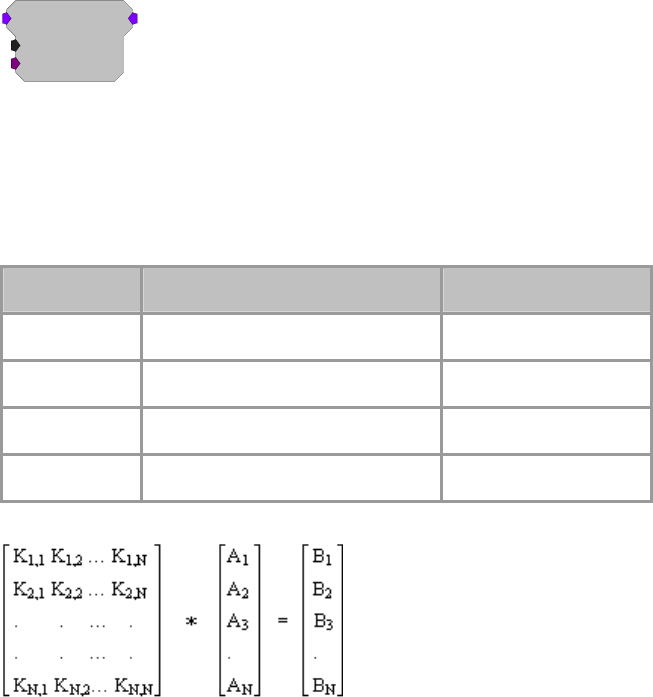
RPvdsEx Manual
106
MCMatMult
MCMatMult
nChan=16
{>K}
[1:2,0]
Description:
MCMatMult performs matrix multiplication of the multi-channel input signal
and the matrix data entered on >K. The dimensions for >K must match nChan
(e.g., when nChan is set to 4, >K is a 4 x 4 matrix).
Note: This component is for use with only high performance processor devices,
such as RXn or RZn.
Name Description Data Type
Input Multi-channel input signal Floating Point
Output Multi-channel input signal Floating Point
nChan
N
umber of Channels (4 - 256) Integer (Static)
>K Scaling matrix Pointer
Equation:
K x A = B
Where, K is the N x N scaling matrix. A is the input N x 1 matrix, one data
point for each of the N input channels and B is the output N x 1 matrix, one data
point for each of the N output channels. N is the total number of channels
(nChan).
The operation is computed on every sample based on the current input
provided.
B1 = K1,1 * A1 + K1,2 * A2 + K1,3 * A3 + … K1,N * AN
.
.
.
BN = KN,1 * A1 + KN,2 * A2 + KN,3 * A3 + … KN,N * AN
Ordering:
The matrix data for K must be loaded as a vector. Matrix row data is
concatenated to form the vector. For example, to load a 4 x 4 identity matrix:
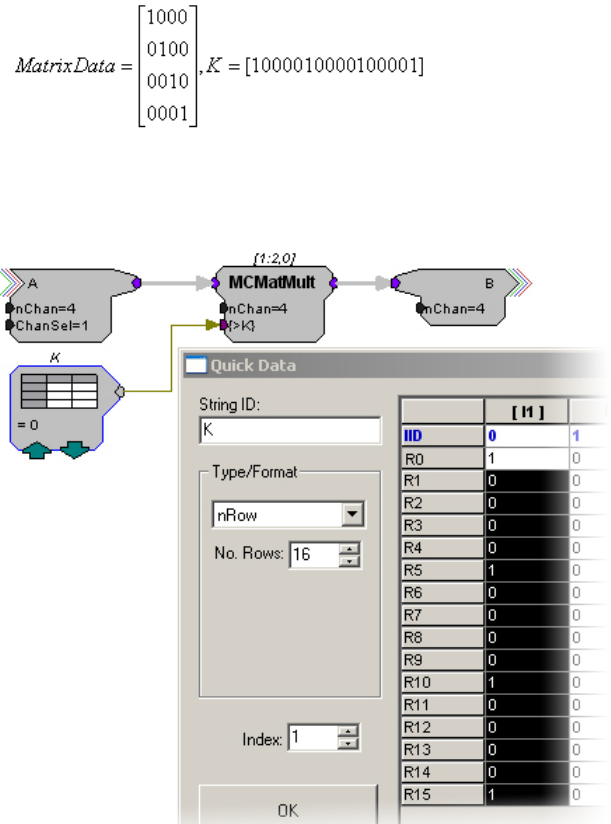
RPvdsEx Manual
107
In RPvdsEx, the >K scaling matrix is typically loaded using a DataTable
component. Load the K matrix as a column vector using the nRow Type/Format
shown below. The No. Rows value is equal to N * N (or in this case 4 * 4 =16).
In this diagram, the DataTable K is used to load the identity matrix. The number
pattern from above K = [1000 0100 0010 0001] is listed in the first column.
Note: The DataTable component allows a maximum of 1024 rows. This would
correspond to a 32 x 32 scaling matrix. This means that the maximum number
of channels you can use with this component is 32. If you need to use a larger
channel amount, a SourceFile component or parameter tag can be used to load
in a larger scaling matrix.
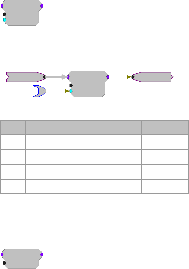
RPvdsEx Manual
108
MCScale
MCScale
nChan=16
SF=1
[1:2,0]
Description:
MCScale multiplies each signal in a multi-channel input by the value of the SF
parameter. The scaled signals are output as a multi-channel signal. The SF
parameter input can be used to update the scale factor dynamically.
ScaleFactor
MCSigIn MCSigOut
MCScale
nChan=16
SF=1
[1:2,0]
Note: This component is for use with only high performance processor devices,
such as RXn or RZn.
Name Description Data Type
Input Multi-channel signal input Floating Point
Output Multi-channel scaled output Floating Point
nChan
N
umber of channels of input/outpu
t
Integer (Static)
SF Scale factor Floating Point
Equation:
Output[x] = Input[x] * SF
MCSign
MCSign
nChan=16
[1:2,0]
Description:
This component determines the sign of the multi-channel input and outputs
either -1 (signal with negative value), 0 (signal with no value), or 1 (signal with
positive value).
Note: This component is for use with only high performance processor devices,
such as RXn or RZn.
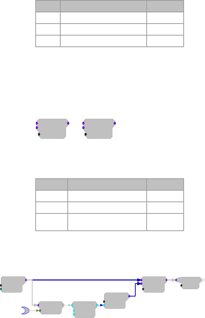
RPvdsEx Manual
109
Name Description Data Type
Input Multi-channel signal input Floating Point
Output Sign value of multi-channel input: -1, 0, 1 Floating Point
nChan
N
umber of channels of input/outpu
t
Integer (Static)
Equation:
If Input n < 0.0 then Output n = -1
Else If Input n = 0.0 then Output n = 0
Else If Input n > 0.0 then Output n = 1
MCSum
MCMult
Inp
2
MCSum
nChan=16
[1:3,0]
Inp
2
MCMult
nChan=16
[1:5,0]
Description:
These multi-input components perform basic summing and multiplying
functions for two multi-channel inputs.
Note: This component is for use with only high performance processor devices,
such as RXn or RZn.
Name Description Data Type
Inputs (two) Input Floating Point
N
Chan
N
umber of Channels Integer (Static)
Output Multiplied or summed value of the
inputs Floating Point
Equation:
Output =(Input1Ch# + Input2Ch#)
Output =(Input1Ch# * Input2Ch#)
Examples:
MCAdcIn
nChan=16
ChanOS=1
[1:1,0]
Inp
2
MCSum
nChan=16
[1:8,0]
MCToSing
ChanSel=1
[1:2,0]
RefChan
ScaleAdd
SF=-1
Shft=0
[1:3,0] MCConst
nChan=16
Value=1
[1:5,0]
DiffSig
nChan=16

RPvdsEx Manual
110
This circuit acquires 16 channels of input, and performs digital subtraction of
one channel from all the others. The channel to be subtracted is defined by the
parameter tag named RefChan.
MCAdcIn
nChan=4
ChanOS=1
[1:7,0]
Inp
2
MCMult
nChan=4
[1:8,0]
ConstF
K=1
[1:1,0]
ConstF
K=1
[1:2,0]
ConstF
K=1
[1:3,0]
ConstF
K=1
[1:4,0]
CH1Scale
CH2Scale
CH3Scale
CH4Scale
[1:5,0]
ToMC
MCSig
nChan=4
This circuit shows how to scale each channel of an MC input by a different
scale factor.
Note: Use the MCScale component when all signals are to be scaled by the
same value.
Modulus
Modulus
Mod=1
[1:1,0]
Description:
Returns the remainder after the input is divided by the modulus.
Note: Check Known Anomalies for updates on this component.
Name Description Data Type
Input Input Floating Point
Output Remainder of Input and Modulus Floating Point
Mod Modulus value (to calculate remainder) Floating Point
Equation:
Ouput=Mod (Input)
For example: Input=5, Mod=2: Output = 1. (i.e. 5/2=2 with remainder of 1)
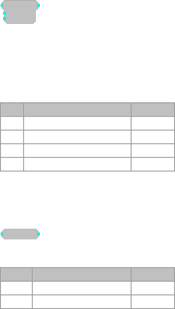
RPvdsEx Manual
111
ScaleAdd
ScaleAdd
SF=1
Shft=0
[1:1,0]
Description:
ScaleAdd multiplies a signal by the value of the SF parameter and then sums
the result with the Shft value.
Note: the SF and Shft parameters can be set to a constant value or connected to
signal sources. This enables the ScaleAdd function to be used to multiply two
signals, add two signals, or take the product of two signals and sum it to a third.
Using ScaleAdd to sum two signals is preferable to using the multi-input sum
function because it saves DSP cycles.
Name Description Data Type
Input Input Floating Point
Output Product of input and SF plus shft Floating Point
SF Scale factor (multiply) Floating Point
Shft Add value Floating Point
Equation:
Output = (Input * SF) + Shft
Note that Shft can be another signal.
Sign
Sign
[1:1,0]
Description:
This component determines the sign of the input and outputs either -1 (signal
with negative value), 0 (signal with no value), or 1 (signal with positive value).
Name Description Data Type
Input Input Floating Point
Output Sign value of input: -1, 0, 1 Floating Point
Equation:
If Input < 0.0 then Output = -1
Else If Input = 0.0 then Output = 0
Else If Input > 0.0 then Output= 1
RPvdsEx Manual
112
SqRoot
SqRoot
[1:1,0]
Description:
This component computes the mathematical square root operation. The function
has a lower bound of 0.
Name Description Data Type
Input Input Floating Point
Output Square root of input Floating Point
Equation:
Output = Input 1/ 2
Example(s):
PowerBand, page 96.
Biquad Filter, page 196.
Square
Square
[1:1,0]
Description:
This component computes the mathematical square operation and passes the
result to the output.
Name Description Data Type
Input Input Floating Point
Output Square of input Floating Point
Equation:
Output = Input 2
Example:
Smooth, page 205.
RPvdsEx Manual
113
StereoScale
StereoScale
SFL=1
SFR=1
[1:1,0]
Description:
Scales a stereo signal. The left and right signals are scaled independently by
SFL and SFR respectively.
Name Description Data Type
Input Stereo signal Floating Point
Output Stereo signal Floating Point
SFL Scale signal right channel Floating Point
SFR Scale signal right channel Floating Point
StereoSum
[1:1,0]
t
ereoSu
Description:
Sums up to five stereo inputs and outputs one stereo signal.
Name Description Data Type
Inputs Stereo signal Floating Point
Output Summed stereo signal Floating Point
Sum
Mult
[1:1,0]
Sum
[1:2,0]
Mult
Description:
These multi-input components perform basic summing and multiplying
functions. They work most efficiently when three or more inputs are used.
Unused inputs will be ignored. All multiple inputs must come from primary
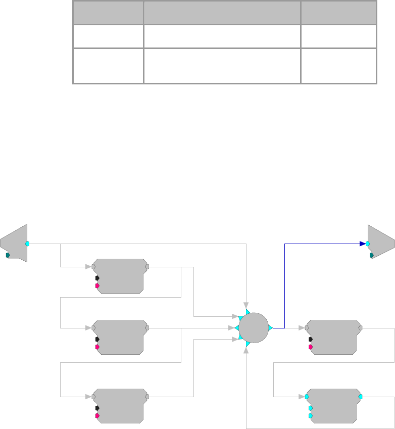
RPvdsEx Manual
114
outputs. If it is necessary to route a parameter output to this function, use a
CONSTF to convert the signal to a primary output.
Name Description Data Type
Input (multiple) Input (multiple) Floating Point
Output Multiplied or summed value of the
inputs Floating Point
Equation:
Output = (Input1I + Input2I + Input3I + ... InputnI)
or
Output = (Input1I * Input2I * Input3I * ... InputnI)
Example: Sum
This construct implements a typical 'Reverb' circuit. The first three long delays
are summed to simulate early reflections. The 4th delay is added back
recursively to create the reverb chain. Try it out, it sounds like a big reverberant
warehouse.
d
c
[1:1,0]
Ch=1
LongDelay
Nms=50
{>Data}
[1:2,0]
LongDelay
Nms=37
{>Data}
[1:3,0]
LongDelay
Nms=17
{>Data}
[1:4,0]
LongDelay
Nms=11
{>Data}
[1:6,0]
ScaleAdd
SF=0.3
Shft=0
[1:7,0]
c
O
[1:9,0]
Ch=1
[1:5,0]
Sum
RPvdsEx Manual
115
Buffer Operations
Buffer Components
Buffer components are used to create and access data buffers. Data buffers can be used to store
signals, prepare for averaging, or create complex mappings. Most buffer operations (AvgBuf,
SerialBuf, and RamBuf) are associated with some amount of physical memory that can be
accessed by that component. For example, adding a SerialBuf component to a chain will result in
the required amount of SDRAM memory being allocated and associated with the component.
Other components (such as, ReadBuf and WriteBuf) utilize another component's memory buffer.
Because the RP2-5 does not have any SDRAM, it can not make use of the buffer operations.
Changing the Buffer Size Dynamically
For some Buffer components size is a dynamic parameter, allowing users to allocate a variable
size to the buffer from an application outside of RPvdsEx. However, when the RPvdsEx circuit is
first run, a memory buffer is allocated based on the size. The size can not be increased beyond the
allocated memory. So, size can be changed dynamically, but it can only be decreased.
This group includes the following components:
AvgBuf
AvgBuf2
BlockAcc
BlockAvg
RamBuf
ReadBuf
SerialBuf
SerSource
SerStore
SnipStore
TagStore
WriteBuf
This group also includes the following component, if RPvdsEx Device Setup is
configured for a high performance device, such as the RXn or RZn:
MCSerStore
MCSerSource

RPvdsEx Manual
116
Comparing Buffer Components
This table provides a quick reference summary of the features of the buffer components.
Buffer
Primary Function
Artifact Rejection
Trigger/Enable Line*
Access
Read/Write
Buffer Size^
Index Generator
Often Used With ...
AvgBuf Sums the data input to a
buffer
None
Enable
Serial
Write
Static
Internal
BlockAcc
AvgBuf2 Sums the data input to a
buffer
Yes
Trigger
Serial
Write
Dynamic
N/A
N/A
BlockAcc Reads then writes data of a
fixed block size
Yes
Trigger
Serial
Read and
Write
Dynamic
N/A
SerialBuff
, AvgBuf
BlockAvg Sums block inputs to the
buffer
None
Trigger
Serial
Read/
Write
Dynamic
N/A
TagStore
RamBuf Allocates a buffer and
allows read or write access
to any point in the buffer
None
None
Random
Read or
Write
Static
External
N/A
ReadBuf Reads from specific indices
in a specified buffer
None
None
Random
Read
N/A
External
RamBuf,
SerialBuf,
AvgBuf
SerialBuf Performs sequential storage
of data
None
Enable
Serial
Read or
Write
Static
Internal
BlockAcc
SerSource Stores data for play out
None
Enable
Serial
Read
Dynamic
Internal
OpenEx

RPvdsEx Manual
117
Buffer
Primary Function
Artifact Rejection
Trigger/Enable Line*
Access
Read/Write
Buffer Size^
Index Generator
Often Used With ...
SerStore Acquires data for
downloading to a PC
None
Enable
Serial
Write
Dynamic
Internal
OpenEx
SnipStore Stores a snippet of data with
specified number of samples
before and after the trigger
None
Trigger
Serial
Write
Dynamic
Internal
Tetrode
TagStore Stores data with tag
information
None
Enable
Serial
Write
Dynamic
Internal
BlockAvg
WriteBuf Writes to specific indices in
a specified buffer
None
None
Random
Write
N/A
External
RamBuf,
SerialBuf,
AvgBuf
* The enable lines of some of these components require a high signal for the duration of acquisition (For
example: AccEnable in AvgBuf) and are classified as Enable lines. In other components, these lines are
triggered to start and continue acquisition for a fixed number of samples (for example: StEnable in
BlocAcc) and are classified as Triggers.
^ For some Buffer components size is a dynamic parameter, allowing users to allocate a variable size to the
buffer from an application outside of RPvdsEx. However, when the RPvdsEx circuit is first run, a memory
buffer is allocated based on the size. The size can not be increased beyond the allocated memory.
So, size can be changed dynamically, but it can only be decreased.
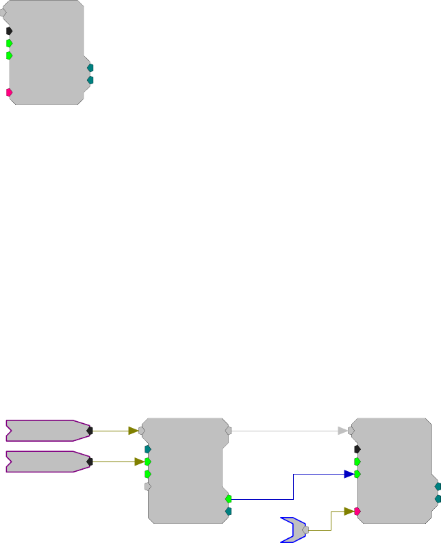
RPvdsEx Manual
118
AvgBuf
AvgBuf
Size=1000
Rst=0
AccEnab=0
[1:1,0]
NBl ks=0
Index=0
{>Data}
Description:
Implements a summer in memory (to get the average divide by the number of
blocks at the end of acquisition). On each tick of the sample clock, where the
AccEnable is high, a sample will be acquired and summed with the current
value at the current index position in the buffer. The internal index generator is
incremented with each acquisition and loops back to 0 when the total number of
samples specified in the Size parameter have been acquired and summed.
Index reports the value of the internal index generator. NBlks reflects the
number of times the AccEnab input is enabled and disabled and can be thought
of as a block counter (assuming Size equals the block size fed into AvgBuf and
AccEnable remains high for the entire block acquisition then goes from high to
low between blocks). These outputs can be accessed from software or used
within the circuit.
AvgBuf is often used with the BlockAcc component, which is enabled with a
single enable pulse at the beginning of the block and then outputs an enable line
that remains high for exactly the specified (BlkSze) number of samples.
BlockAcc
BlkSze=1000
StEnab=0
Skip=0
Tag
[1:1,0]
AccEnab=0
Nski p =0
AvgBuf
Size=1000
Rst=0
AccEnab=0
[1:3,0]
NBl ks=0
Index=0
{>Data}
Data
Signal
Enable
Interleaved averaging can be performed by writing blocks that are smaller than
the buffer size allocated. For example, to calculate two interleaved averages of
500 points, use BlockAcc to write 500 point blocks to AvgBuf with size 1000.
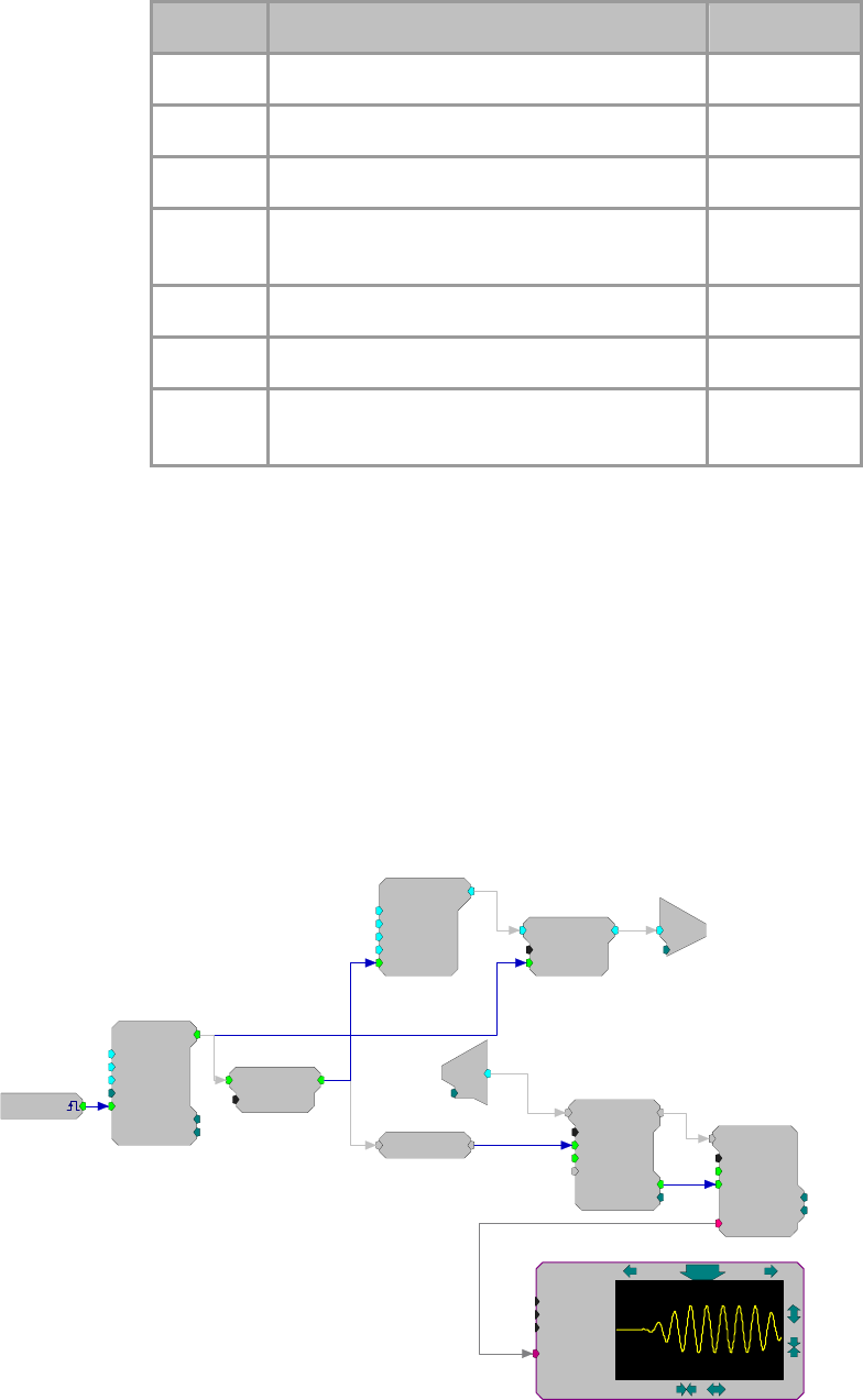
RPvdsEx Manual
119
Name Description Data Type
Input Input Any
Size Size of buffer in words Integer (Static)
Rst Resets the buffer offset (index) to zero Logic
AccEnab Enables acquisition (data acquired only when
high) Logic
>Data Pointer to data buffer Pointer
Index Position of offset in buffer Integer
N
Blks
N
umber of times AccEnab is enabled and
disabled Integer
Example:
Averaged Buffer
File: Examples\AvgBufex1.rcx
Default Device: RP2.1 Processor
Sampling Rate: 50 kHz
This example implements averaging using the AvgBuf component. A zBus
trigger starts a pulse train with 100, 9 ms pulses with a gating time of 2 ms.
These pulses trigger a Cos2Gate to generate 9 ms tones with a 2 ms rise/fall
time. The pulse train is also used to write a block of 500 points (10 ms at ~50
kHz sample rate) from the ADC input to the AvgBuf component, which sums
these points into its 500 point buffer. A DACDelay is used to synchronize the
signal out to the data acquisition. A graphing function allows the user to see the
results of the acquisition.
Tone
Amp=1
Shft=0
Freq=1000
Phse=0
[1:9,0]
Rst=Run
PulseTrain
Thi=9
Tg=2
Tlo=100
Npls=100
[1:3,0]
CurN=0
Stage=0
Trg=0
Cos2Gate
Trf=2
Ctrl=Closed
[1:10,0]
BlockAcc
BlkSze=500
StEnab=0
Skip=0
Tag
[1:13,0]
AccEnab=0
Nski p =0
AvgBuf
Size=500
Rst=0
AccEnab=0
[1:15,0]
NB l ks=0
Index=0
{>Data}
[1:1,0]
Src=zBusA
EdgeDetect
Edge=Rising
[1:5,0]
DT=Float32
nChan=1
UD=2Hz
Source
200
-2000500
DACDelay
[1:7,0]
c
O
[1:11,0]
Ch=1
d
c
[1:12,0]
Ch=1
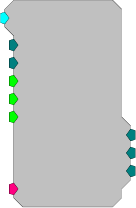
RPvdsEx Manual
120
AvgBuf2
AvgBuf2
nSize=512
nAvg=50
Reset=0
Trg=0
[1:1,0]
nArts=0
nGood=0
Art=0
{>Data}
StCode=0
Description:
AvgBuf2 sums two alternating signals, acquired on a single input line. AvgBuf2
differs from AvgBuf in four ways. 1) It sums two signals separately. 2) It allows
for variable buffer size. 3) It allows for artifact rejection. 4) It has an internal
block access feature for acquiring each signal. In addition, AvgBuf2 has two
additional buffers that hold the raw signal before the sums are complete.
When using AvgBuf2, the buffer size (nSize) is defined as the number of
samples to be included for each signal. For example, if nSize = 512 then two
buffers of 512 samples each are acquired. The nAvg parameter is used to define
the number of blocks to be acquired and summed for each signal. A trigger
starts the acquisition for each individual buffer.
Two triggers (one for the first buffer and one for the second) are required to
acquire signals for both buffers. When the number of triggers presented to the
Trg input reaches nAvg, the next trigger delivered moves the first sum to the
first average buffer and finally, one last trigger is required to move the second
sum to the second average buffer. The average buffer stores a sum of data
blocks. In order to get their average, the user must divide each sum by the
number of good acquisitions (nGood).
The nGood and nArts outputs provide access to current status for the number of
good acquisitions and artifacts, respectively, for the current average. If artifact
rejection is required, the Art parameter can be linked to a logical input. If Art
goes high for any sample within the acquisition time of the current block, the
block will be rejected. So, for example, if nSize = 100, and the processor is
running at 25 kHz, then Art has to be within 100 * 1/24414 = 4.096 ms from the
start of acquisition of a block.
StCode tells the user which one of the two signals it is currently acquiring.
StCode 1 indicates acquisition to the first buffer and StCode 2 indicates
acquisition to the second buffer. StCode 8 indicates the end of the data
acquisition for a pair of average buffers.
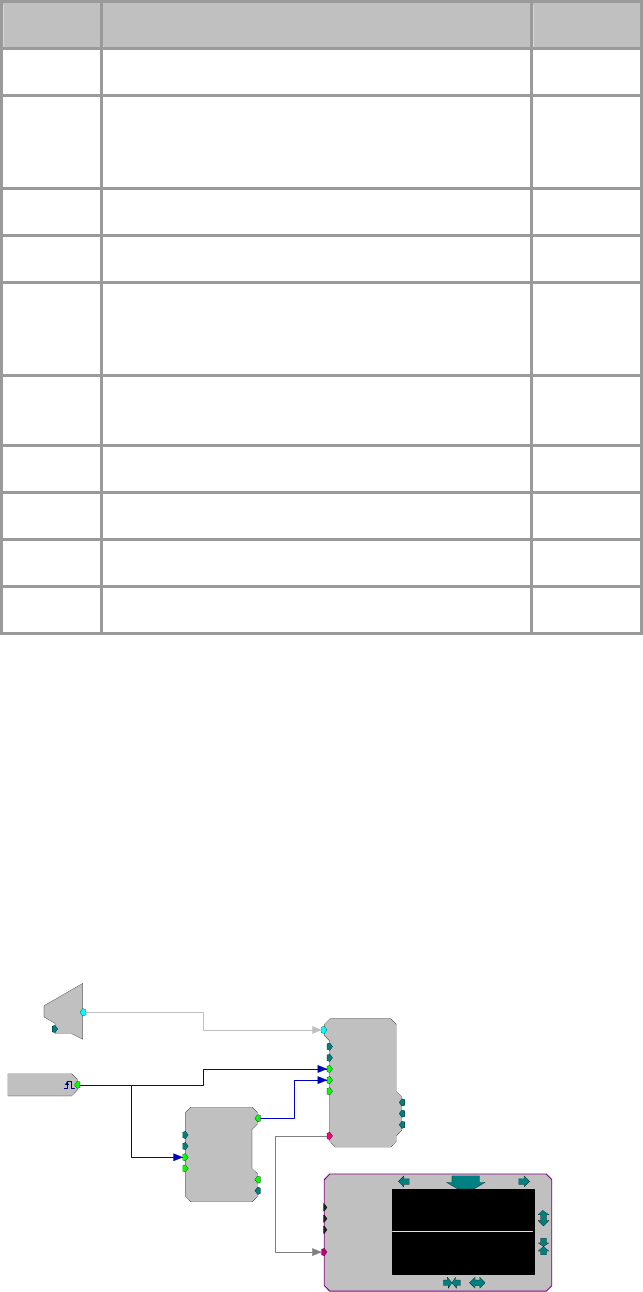
RPvdsEx Manual
121
Name Description Data Type
Input Input Any
nSize Size of buffer in words (see page 115 for an
important note on dynamically changing the size
parameter)
Integer
nAvg
N
umber of averages for each signal Integer
Reset Resets the buffer offsets to 0 Logic
Trg Triggers acquisition of a single buffer or writing sum
of buffers to average buffer (total number of triggers
for a pair of averages is 2N + 2, where N = nAvg)
Logic
Art Rejects the last two block acquisitions (one of each
signal) Logic
>Data Memory buffer for the data Pointer
nGood
N
umber of good acquisitions Integer
nArts
N
umber of rejected acquisitions due to artifacts Integer
StCode Position in acquisition sequence Integer
Example:
Averaged Buffer
The example below acquires and sums 50 blocks into each of the two buffers on
AvgBuf2. The raw data is stored in a separate buffer before it is moved to the
average buffer. Before the raw data is moved it can be deleted using the artifact
rejection line. The values of the stored or average buffer (viewed in RPvdsEx
using >Data) represent the previous summed signal values and not the values of
the block currently being acquired.
Note that the pulse train is set for 102. For each buffer, the Trg must be pulsed
once for each block that is to be summed. Two additional trigger pulses are
required to move the data from each sum buffer to the average buffer. In this
case there are two buffers with 50 blocks each, so [2(50) + 2] pulses are needed
to complete the acquisition and store the summed data.
d
c
[1:6,0]
Ch=1
AvgBuf2
nSize=510
nAvg=50
Reset=0
Trg=0
[1:7,0
]
nArts=0
nGood=0
Art=0
{>Data}
StCode=0
[1:1,0]
Src=zBusA
PulseTrain2
nPer=510
nPulse=102
Enab=Yes
Rst=Run
[1:4,0]
PCount=0
PLate=0
DT=Float32
nChan=1
UD=2Hz
Source
1
-10100
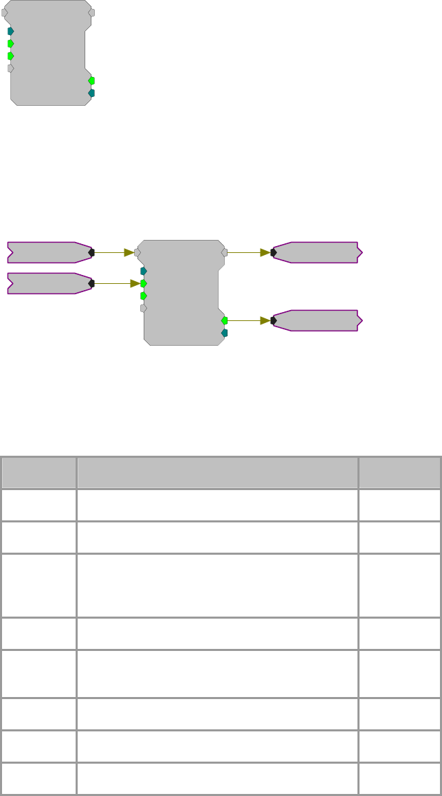
RPvdsEx Manual
122
BlockAcc
BlockAcc
BlkSze=100
StEnab=0
Skip=0
Tag
[1:1,0]
AccEnab=0
Nski p=0
Description:
BlockAcc (block access) is designed for use with SerialBuf and AvgBuf to
support block read/write functions. When the enable (StEnab) line is high, the
AccEnab output will go high for BlkSize ticks of the sample clock.
BlockAcc
BlkSze=500
StEnab=0
Skip=0
Tag
[1:1,0]
AccEnab=0
Nski p =0
Buffer
BufferEnable
Signal
Enable
To support block marking, the BlockAcc has a Tag input. The value of the Tag
input will be written as the first element of each buffer block. Also, to support
artifact rejection in averaging, a Skip input is provided to allow buffer average
skipping. If the skip line is made high, the next time StEnab is detected high it
will be ignored and the Nskip output will be incremented by one.
Name Description Data Type
Input Input Any
Output Block data out Any
BlkSze Size of data block in words (see page 115 for an
important note on dynamically changing the size
parameter)
Integer
StEnab Sets the enable line of the BlockAcc Logic
Skip Ignores the next AccEnable high and skips one tag
value Logic
Tag Tag: Times the Blk access has been written Any
AccEnab Starts data transfer to SerialBuff or AvgBuff Logic
N
skip
N
umber of times the Tag line is skipped Pointer
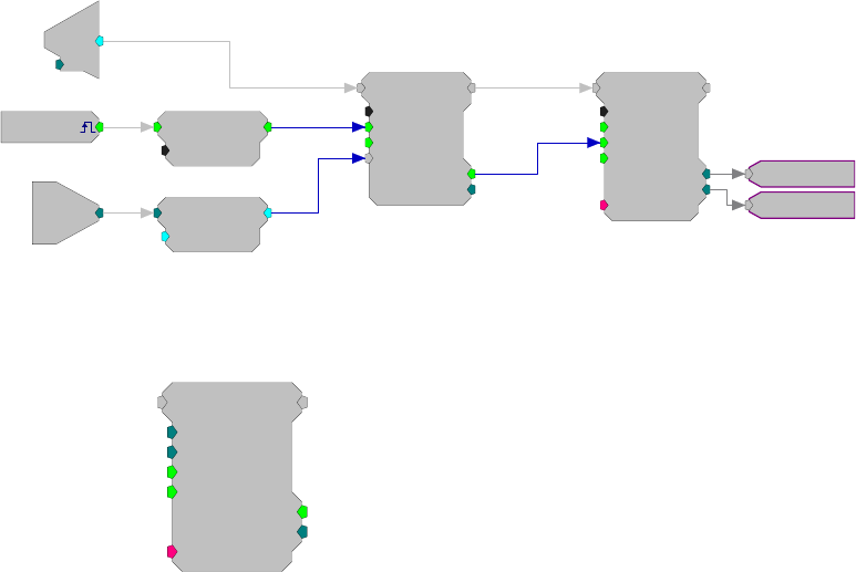
RPvdsEx Manual
123
Example:
Block Access
File: Examples\BlockAccEx.rcx
Default Device: RP2 Processor
Sampling Rate: 50 kHz
The example circuit shown below will save 75 samples from A/D input channel
one each time the software trigger 1 goes high. The EdgeDetect component
ensures that for one cycle of the sample clock, a high is sent to the BlockAcc
StEnab input for each rising software trigger. The 75 samples will be saved to a
SerialBuf with room for 100, 75-element blocks. Each block of data written will
include a Tag value written as its first element. This circuit will write the eight-
bit value at the digital input port as the tag value (the first value of each
block).The eight bit value is read using the WordIn component with bitmask
255. This integer value needs to be converted to float values to be consistent
with the data stored.
[1:1,0]
Src=Soft1
W
[1:4,0]
M=255
10110100
EdgeDetect
Edge=Rising
[1:2,0]
BlockAcc
BlkSze=75
StEnab=0
Skip=0
Tag
[1:8,0]
AccEnab=0
Nskip=0
SerialBuf
Size=7500
Rst=0
AccEnab=0
Write=1
[1:10,0]
NB l ks=0
Index=0
{>Data}
Int2Float
SF=1
[1:5,0]
d
c
[1:7,0]
Ch=1
75
1
BlockAvg
BlockAvg
BlkSze=100
NumAvg=100
Trig=0
Reset=0
[1:1,0]
AvgCnt=0
WrEnab=0
{>Data}
Description:
BlockAvg (block average) was primarily designed for use in OpenEx and TDT
macros. Use the Block_Avg_Store macros for data averaging when possible.
BlockAvg acquires a selectable number of input blocks, summing them as they
are acquired. Input blocks may be scaled before being fed to BlockAvg, to
achieve an average when the specified number of blocks are summed. The
accumulated sum is available on the output port when WrEnab is high. The
input and output ports are equal except when WrEnab goes high, at that time,
the sum is available.
Note: This component is for use with only high performance processor devices,
such as RXn or RZn.
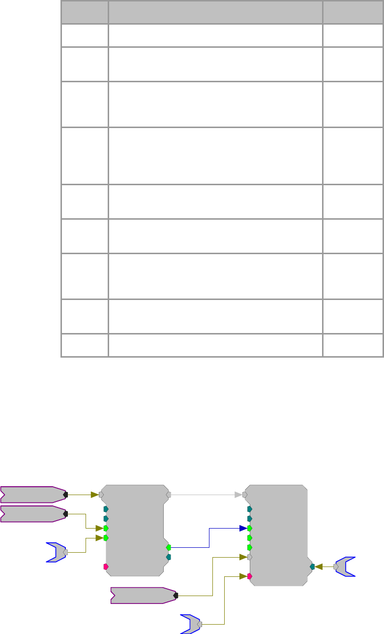
RPvdsEx Manual
124
Name Description Data Type
Input Input Any
Output Passes input through until WrEnab goes high at
which point the Output equals the summed data Any
Blk Size Size of the memory buffer (see page 115 for an
important note on dynamically changing the size
parameter)
Integer
(Dynamic)
N
umAvg Sets the number of blocks to be summed. Blk Size
can be changed dynamically, however, if the new
N
umAvg value is less than or equal to the current
AvCnt, the component is reset
Integer
Trig A low to high pulse acquires a sample of the input
signal Logic
Reset Resets the block average to the start point and clears
the buffer. Also resets AvgCnt Logic
WrEnab Goes high for number of samples equal to BlkSze
when an average is available and is used to clock the
output into a storage device
Logic
AvgCnt Outputs the current number of blocks acquired.
Automatically resets once NumAvg is reached Integer
>Data Pointer to data buffer Pointer
Example:
Block Average
In the example below, BlockAvg acquires samples of the input signal each time
Trig goes high. Each sample is summed with the accumulated sum until 100
samples have been acquired (set by the NumAvg parameter). The accumulated
sum is output and WrEnable goes high to clock the data into the TagStore
component with the Time parameter tag. The current sample count is monitored
on AvgCnt and is reset to zero by a logic high on Reset.
BlockAvg
BlkSze=200
NumAvg=100
Trig=0
Reset=0
[1:1,0]
AvgCnt=0
WrEnab=0
{>Data}
Reset
TagStore
Size=2010
BlkSize=201
Enable=1
Strobe=1
[1:3,0]
Index=0
Rst=0
{>Data}
Tag
Data
Index
Signal
Trig
Time
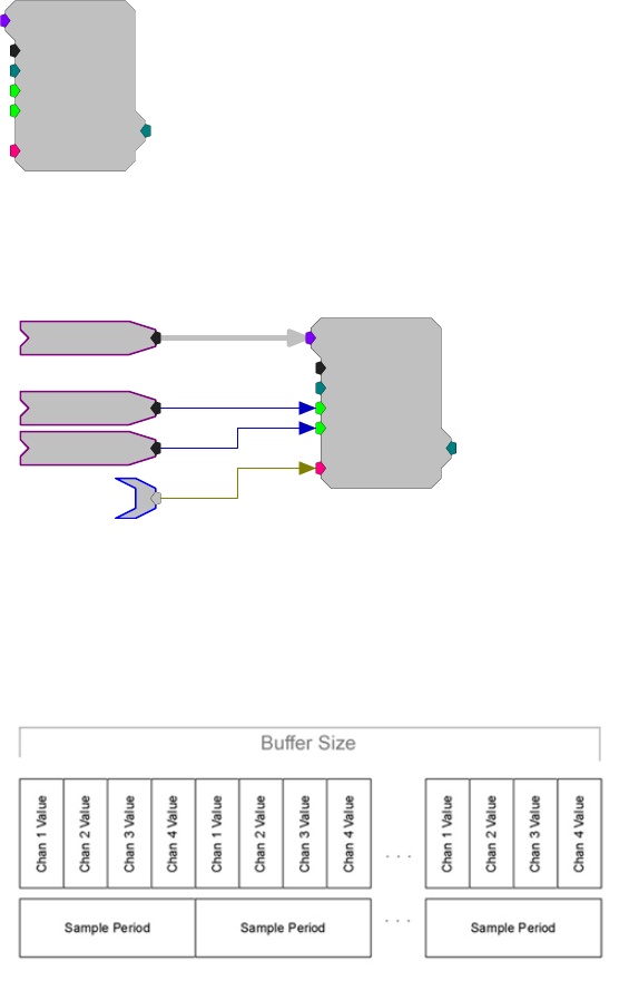
RPvdsEx Manual
125
MCSerStore
MCSerStore
nChan=16
Size=1024
Rst=0
WrEnab=1
[1:2,0]
Index=0
{>Data}
Description:
MCSerStore stores data from a multi-channel signal. The data port (>Data)
provides access to the buffer so that data can be downloaded to the PC.
MCSigIn
Reset
Enable
Data
MCSerStore
nChan=16
Size=1024
Rst=0
WrEnab=1
[1:5,0]
Index=0
{>Data}
If WrEnable is high, values from each signal in the multi-channel input are read
and stored in the next nChan buffer positions on each tick of the sample clock.
The index is also incremented to the next nChan buffer positions. This means
that data from all channels is stored in an interleaved fashion. The internal index
generator is incremented until the total number of samples specified in the Size
parameter has been written.
When the index reaches the end of the memory buffer, it automatically wraps
back to zero and continues to increase from there. Any data currently in the
buffers will be written over. Size must be set to the total number of points for
all signals in the multi-channel input (Size = number of points in each signal *
nChan). Size is a dynamic parameter, which allows users to specify the size of
the buffer after the circuit has been loaded to the device.
There are currently no multi-channel versions of other buffer components, such
as SnipStore or AvgBuf. Users who require these special features available with
these components will have to convert the multi-channel signal to single
channel.
Note: This component is for use with only high performance processor devices,
such as RXn or RZn.
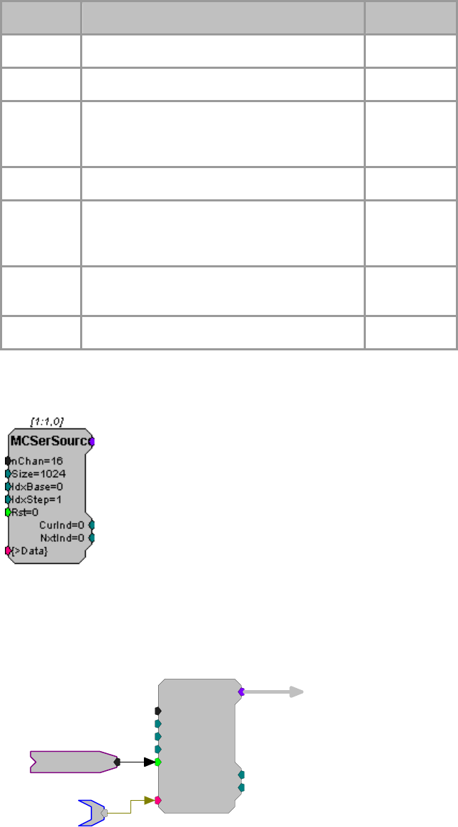
RPvdsEx Manual
126
Name Description Data Type
Input Multi-channel input Any
nChan
N
umber of channels in inpu
t
Integer (Static)
Size Size of the memory buffer (see page 115 for an
important note on dynamically changing the size
parameter)
Integer
Rst Resets the offset (index) of each buffer Logic
WrEnab Enables data acquisition and increments the
offset position of the buffers (WrEnable needs to
remain high for the duration of data acquisition)
Logic
Index Sends out the present buffer position relative to a
starting position of zero Integer
>Data Pointer to data buffers Pointer
MCSerSource
Description:
MCSerSource creates a multi-channel signal. Data can be written to the buffer
via the data port (>Data). IdxBase and IdxStep control which index is being
sent out of the buffer.
MCSerSourc
e
nChan=16
Size=1024
IdxBase=0
IdxStep=1
[1:1,0]
NxtInd=0
CurInd=0
{>Data}
Rst=0
Data
Reset
IdxBase defines the index for the first point in the buffer. The index is
incremented by IdxStep on each sample. When the index reaches the end of the
memory buffer, it automatically wraps back to IdxBase and continues from
there. Set IdxStep = 0 to hold the index constant and equal to IdxBase.

RPvdsEx Manual
127
Size must be set to the total number of points for all signals in the multi-channel
input (Size = number of points in each signal * nChan). Size is a dynamic
parameter; the size of the buffer can be set after the circuit has been loaded to
the device.
All channel data is stored in an interleaved fashion.
Note: This component is for use with only high performance processor devices,
such as RXn or RZn.
Name Description Data Type
nChan
N
umber of channels in outpu
t
Integer (Static)
Size Size of the memory buffer (see page 115 for an
important note on dynamically changing the size
parameter)
Integer
IdxBase Minimum index value Integer
IdxStep Index step size on each sample Integer
Rst Resets the index of the buffer to IdxBase Logic
>Data Pointer to data buffers Pointer
CurInd Sends out the present buffer position relative to a
starting position of zero Logic
N
extInd Sends out the next buffer position relative to a
starting position of zero Integer
Output Multi-channel output Any

RPvdsEx Manual
128
RamBuf
RamBuf
Size=1000
Index=0
Write=0
{>Data}
[1:1,0]
Description:
Implements a random access memory function. The RamBuf processing
component is used to allocate and optionally access a buffer located in external
SDRAM memory. Buffers can be any size (limited only by the amount of
installed memory). When placed in a processing chain, RamBuf can be used to
save data, play arbitrary waveforms, create complex mappings, or access
specific data points in a buffer.
The index parameter controls the currently accessed buffer position. Index can
have any value from 0 to 231. However, if the Buffer size is smaller than the
index the index will overshoot the buffer size and the data accessed will be
invalid.
The accessed buffer position will automatically be calculated as the modulus
(Index/Size). The Write parameter is set to 0 for reading the index in memory.
The Write parameter is set to 1 to write the current input value to the current
index.
The output will always reflect the last value written to the current buffer
location. So even if Write is made true and the current signal input is written to
the memory, RamBuf will first read the old value from this location and use it
for output.
In order to read the new value, write has to be 0 for the new value to be written
into the buffer, and then write has to be changed to 1 to read this new value
from that buffer location.
If simultaneous read and write access is needed for the same memory buffer, try
using ReadBuf or WriteBuf in conjunction with RamBuf.
Name Description Data Type
Input Input Any
Output Buffer data out Any
Size Size of buffer in words Integer
(Static)
Index The position of the accessed data point Integer
Write Enables read(0)or write(1) Logic
>Data Pointer to data buffer Integer
Example:
RAM Buffer
In this example we use a RamBuf component to map a frequency input to a
modulator output. The Tone component at [1:1,0] modulates the frequency of
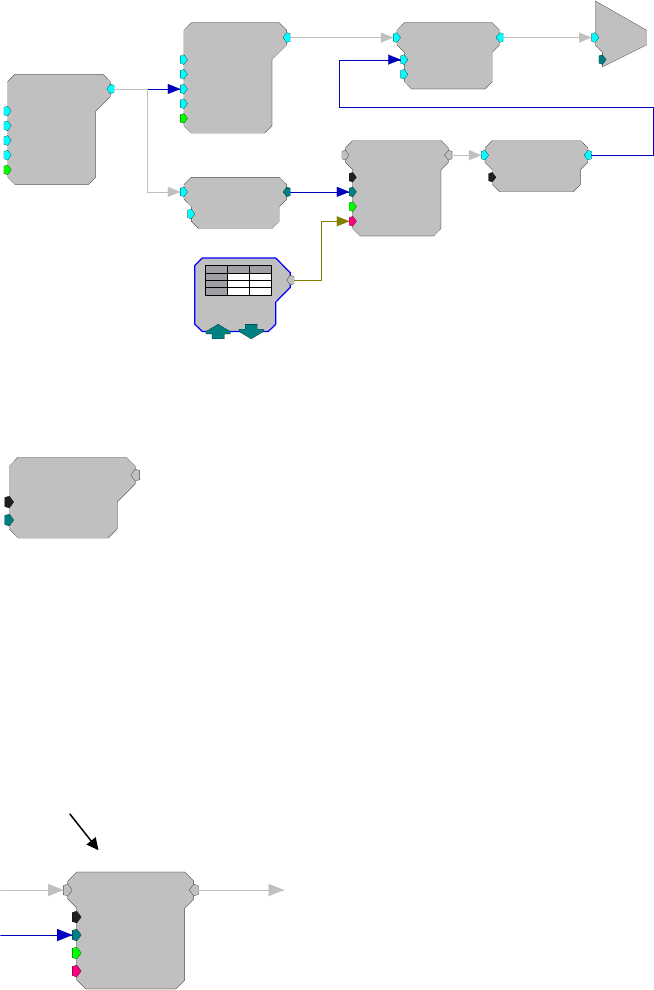
RPvdsEx Manual
129
the second Tone at [1:8,0]. The modulator frequency is also scaled and fed into
the index input of the RamBuf allowing for a mapping from frequency to
intensity scaling, which is held in the data table InvXFer. This type of circuit
can be used to normalize a FM sweep for transducer variance across frequency.
Tone
Amp=1000
Shft=0
Freq=3000
Phse=0
[1:1,0]
Rst=Run
Tone
Amp=5
Shft=0
Freq=100
Phse=0
[1:8,0]
Rst=Run
ScaleAdd
SF=1
Shft=0
[1:9,0]
c
O
[1:10,0]
Ch=1
Float2Int
SF=0.01
[1:3,0]
RamBuf
Size=1000
Index=0
Write=0
{>Data}
[1:5,0]
Smooth
Tau=1
[1:6,0]
InvXFer
= 0
ReadBuf
ReadBuf
CmpNo=1
Index=0
[1:1,0]
Description:
Gets a value from a specified memory buffer using a specified index. The buffer
is specified by setting the CmpNo parameter to the component number of a
RamBuf, SerialBuf, or AvgBuf component found within the circuit. The
component number is the first number in parenthesis found at the top of each
component. The index number is the position within the buffer and must be set
to a number less than or equal to the block size for the specified buffer.
For example, to read a value from the RamBuf below, the ReadBuf CmpNo
parameter is set to 4.
Component Number
RamBuf
Size=1000
Index=0
Write=0
{>Data}
[1:4,0]
Important!: Every time the circuit is even slightly modified, the component
number of the required buffer might change. Always check the component
number after recompiling. If the component number has changed update the
ReadBuf component's CmpNo parameter, recompile, and recheck the
component number.
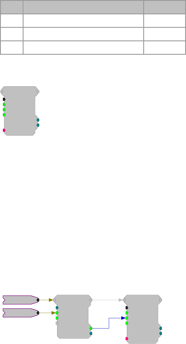
RPvdsEx Manual
130
Name Description Data Type
Output Buffer data out Any
CmpNo Component number of the buffer being read Integer (Static)
Index The position of the accessed data point Integer
SerialBuf
SerialBuf
Size=1000
Rst=0
AccEnab=1
Write=1
[1:1,0]
NBl ks=0
Index=0
{>Data}
Description:
The SerialBuf component is a memory buffer manager with a built-in serial
index generator. SerialBuf supports writing or reading, but does not support
random access or simultaneous reading/writing. The Write control selects
writing to (high) or reading from (low) the buffer and AccEnab triggers the read
or write function. If AccEnable is high, the component will access the current
index position in the memory buffer and the internal index generator is
incremented. When the index reaches the total number of samples specified in
the Size parameter it is automatically reset to zero and starts increasing again
from there. Any data currently in the buffer will be written over.
Two outputs report the status of the SerialBuf component. The Index output
reports the value of the internal serial index generator. The nBlks output counts
the number of times the AccEnab input is enabled and disabled. This output can
be thought of as a block counter.
Because SerialBuf requires that the AccEnable line remain high for each sample
that is acquired, it is often used with the BlockAcc component. BlockAcc is
enabled with a single enable pulse at the beginning of the block and then
outputs an enable line that remains high for exactly the specified (BlkSze)
number of samples.
SerialBuf
Size=7500
Rst=0
AccEnab=1
Write=1
[1:3,0]
NBl ks=0
Index=0
{>Data}
BlockAcc
BlkSze=100
StEnab=0
Skip=0
Tag
[1:1,0]
AccEnab=0
Nski p =0
Signal
Enable
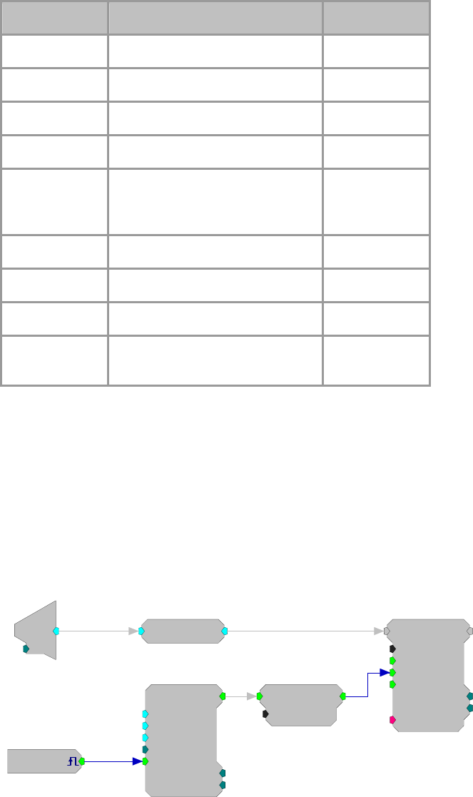
RPvdsEx Manual
131
Name Description Data Type
Input Input Any
Output Output of serial buffer Any
Size Size of buffer in words Integer (Static)
Rst Resets the buffer offset to zero Logic
AccEnab Enables data acquisition, needs to
stay high for the duration of
acquisition
Logic
Write Enables read(0)or write(1) Logic
>Data Pointer to data buffer Pointer
Index Position of offset in buffer Integer
N
Blks
N
umber of time AccEnab is enabled
and disabled Integer
Example:
Serial Buffer
File: Examples\SerialBuffer_ex.rcx
Default Processor: RP2 Processor
Sampling Rate: 50 kHz
This circuit will compute the RMS level of channel one of the A/D input. When
triggered via a zBus trigger, the RMS level will be written to the SerialBuf
every 100 ms for 100 values. The EdgeDetect component makes sure that only
one value is saved for each pulse out. The SerialBuf is 1000 points long, so the
software trigger can be issued ten times before the buffer is full.
[1:1,0]
Src=Soft1
PulseTrain
Thi=1
Tg=0
Tlo=99
Npls=100
[1:3,0
]
CurN=0
Stage=0
Trg=0
EdgeDetect
Edge=Rising
[1:4,0]
SerialBuf
Size=1000
Rst=0
AccEnab=1
Write=1
[1:8,0]
NBlks=0
Index=0
{>Data}
RMS
[1:7,0]
d
c
[1:6,0]
Ch=1

RPvdsEx Manual
132
SerSource
SerSource
Size=1000
Rst=0
IdxEnab=1
[1:1,0
]
Index=0
{>Data}
Description:
Implements a serial access memory function for playing a signal. When
IdxEnab is set high the SerSource reads a value from the memory buffer, sends
out the output, and increments to the next position in the buffer. The internal
index generator is incremented until the total number of samples specified in the
Size parameter has been read. When the index reaches the end of the memory
buffer, it is automatically reset to zero and starts increasing again from there.
SerSource has several advantages over SerialBuf or RamBuf. It uses fewer
cycles because it can only read from a buffer and users have direct control over
the buffer size. Do not use SerSource if you need both record and play or if you
need to move to a particular position in the buffer.
When using SerSource, note that the first value loaded is ready for plays out at
index 0. When the enable line (IndxEnab) goes high with the first trigger, the
index is incremented and the next value is sent to the SerSource signal output
line. So, at index 1 the second value is played out. When SerSource is used to
play out a list of individual values (such as a list of stimulus parameters) the
first value sent to the SerSource might appear to be skipped. A Latch can be
used to ensure that the output and index correspond more accurately to an
ordered list of values. See Comparing SerSource and SerialBuf Indexing and
Output below for more information.
Name Description Data Type
Output Output Any
Size Size of the memory buffer (see page 115 for an
important note on dynamically changing the size
parameter)
Integer
(Dynamic)
Rst Resets the signal to the start of the buffer Logic
IdxEnab Enables play out and increments the position of
the buffer Logic
Index Sends out the preset buffer position relative to a
starting position of zero Integer
>Data Pointer to data buffer Any
Example:
SerSource
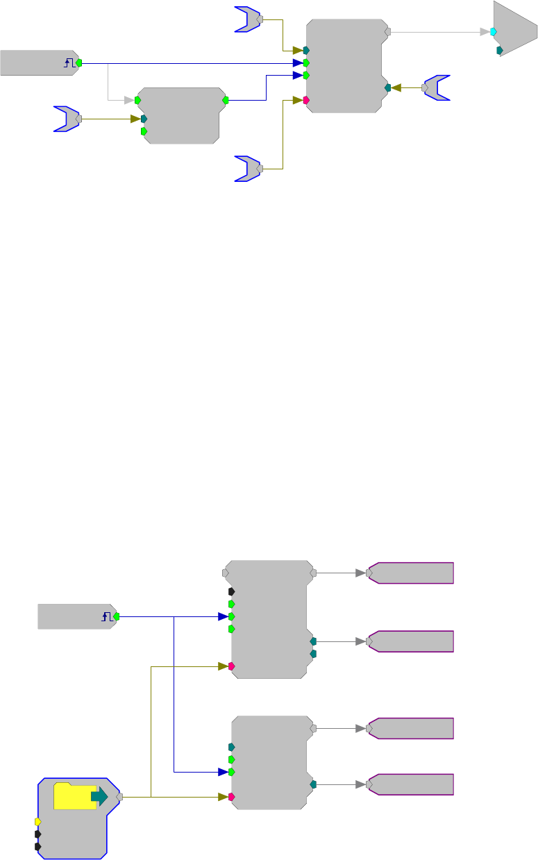
RPvdsEx Manual
133
SerSource
Size=1000
Rst=0
IdxEnab=1
[1:5,0]
Index=0
{>Data}
BufferSize
BufferSize
[1:1,0]
Src=Soft1
Schmitt2
nHi=100
nEnab=1
[1:3,0]
c
O
[1:6,0]
Ch=1
BuffPos
Data
The example above shows a simple circuit that will play a signal out when a
software trigger is generated. The BufferSize is read to both the SerSource and
to the Schmitt2 trigger (nHi). This ensures that there is no dead time for the
signal out. The buffered signal is played out of the SerSource when the trigger
goes high.
Comparing SerSource and SerialBuf Indexing and Output
When a circuit containing the SerSource component is run, the first value is loaded to the
SerSource buffer, even if the enable line (IdxEnab) is low. When the enable line is triggered, the
second value is loaded into the buffer, the index is incremented, and the second value is played
out. This can sometimes give the appearance that the first value has been skipped, especially when
individual values, such as a list of stimulus values, are being played out rather than a continuous
waveform.
The simple circuit pictured below compares the output of the SerSource to that of the SerialBuf to
demonstrate the differences in indexing and play out between these common components. In this
example, the data in a SourceFile is fed to both the SerialBuf and SerSource. A simple software
trigger is used to enable the buffers.
Circuit is loaded to the hardware...
SerialBuf
Size=1000
Rst=0
AccEnab=1
Write=1
[1:4,0]
NBl ks=0
Index=0
{>Data}
SerSource
Size=1000
Rst=0
IdxEnab=1
[1:5,0]
Index=0
{>Data}
[1:1,0]
Src=Soft1
NoName
Name=C:\Do
N=0
OS=0
0
0
Value in
Text File:
1
2
3
4
.
.
0
0
The values from the SourceFile are not yet ready for play out of either buffer.
RPvdsEx Manual
134
Circuit is run ... First software trigger ...
SerialBuf
Size=1000
Rst=0
AccEnab=1
Write=1
[1:4,0]
NBl ks=0
Index=0
{>Data}
SerSource
Size=1000
Rst=0
IdxEnab=1
[1:5,0]
Index=0
{>Data}
0
0
0
1
SerialBuf
Size=1000
Rst=0
AccEnab=1
Write=1
[1:4,0]
NBl ks=0
Index=0
{>Data}
SerSource
Size=1000
Rst=0
IdxEnab=1
[1:5,0]
Index=0
{>Data} 1
1
1
2
Although index is 0, the first value from
the file is already loaded and ready for
play out of the SerSource.
Although the index is 1, the second value
has been loaded and played out of the
SerSource.
Second software trigger ... Third software trigger ...
SerialBuf
Size=1000
Rst=0
AccEnab=1
Write=1
[1:4,0]
NBl ks=0
Index=0
{>Data}
SerSource
Size=1000
Rst=0
IdxEnab=1
[1:5,0]
Index=0
{>Data} 2
2
2
3
SerialBuf
Size=1000
Rst=0
AccEnab=1
Write=1
[1:4,0]
NBl ks=0
Index=0
{>Data}
SerSource
Size=1000
Rst=0
IdxEnab=1
[1:5,0]
Index=0
{>Data} 3
3
3
4
While the index for both components is 2,
the SerSource plays out the third value. At index 3, SerSource plays out the fourth
value.
Using a Latch with SerSource
When using a SerSource, you can avoid the discrepancy between the index and the value accessed
by adding a Latch that is triggered by the same trigger that triggers the SerSource enable line. This

RPvdsEx Manual
135
will latch the value loaded during the previous sample period so that the index and value number
will match. In the example below, the earlier circuit has been modified to include a Latch.
Note: the same software trigger is used for the Latch and the buffer.
Circuit that is loaded to the hardware...
SerialBuf
Size=1000
Rst=0
AccEnab=1
Write=0
[1:4,0]
NBl ks=0
Index=0
{>Data}
SerSource
Size=1000
Rst=0
IdxEnab=1
[1:7,0
]
Index=0
{>Data}
[1:1,0]
Src=Soft1
NoName
Name=C:\Do
N=0
OS=0
Value in
Text File:
1
2
3
4
.
.
0
0
[1:5,0]
Src=Soft1
Latch
Trg=0
[1:8,0]
0
0
0
Circuit is run...
SerialBuf
Size=1000
Rst=0
AccEnab=1
Write=0
[1:4,0]
NBl ks=0
Index=0
{>Data}
SerSource
Size=1000
Rst=0
IdxEnab=1
[1:7,0]
Index=0
{>Data}
0
0
[1:5,0]
Src=Soft1
Latch
Trg=0
[1:8,0]
0
0
1
Although the first value from the SourceFile is already available for play out, the output of the
Latch is still 0.
RPvdsEx Manual
136
First software trigger...
SerialBuf
Size=1000
Rst=0
AccEnab=1
Write=0
[1:4,0]
NBl ks=0
Index=0
{>Data}
SerSource
Size=1000
Rst=0
IdxEnab=1
[1:7,0]
Index=0
{>Data}
1
1
[1:5,0]
Src=Soft1
Latch
Trg=0
[1:8,0]
1
1
2
The second value has been loaded, but the output of the Latch is 1, the first value in the
SourceFile.
Second software trigger...
SerialBuf
Size=1000
Rst=0
AccEnab=1
Write=0
[1:4,0]
NBl ks=0
Index=0
{>Data}
SerSource
Size=1000
Rst=0
IdxEnab=1
[1:7,0]
Index=0
{>Data}
2
2
[1:5,0]
Src=Soft1
Latch
Trg=0
[1:8,0]
2
2
3
The output of the SerSource is 3 (the third value), but the output of the Latch is still 2.
RPvdsEx Manual
137
Third software trigger...
SerialBuf
Size=1000
Rst=0
AccEnab=1
Write=0
[1:4,0]
NBl ks=0
Index=0
{>Data}
SerSource
Size=1000
Rst=0
IdxEnab=1
[1:7,0]
Index=0
{>Data}
3
3
[1:5,0]
Src=Soft1
Latch
Trg=0
[1:8,0]
3
3
4
Here the index is 3 and the Latch output is 3, the third value in the SourceFile.
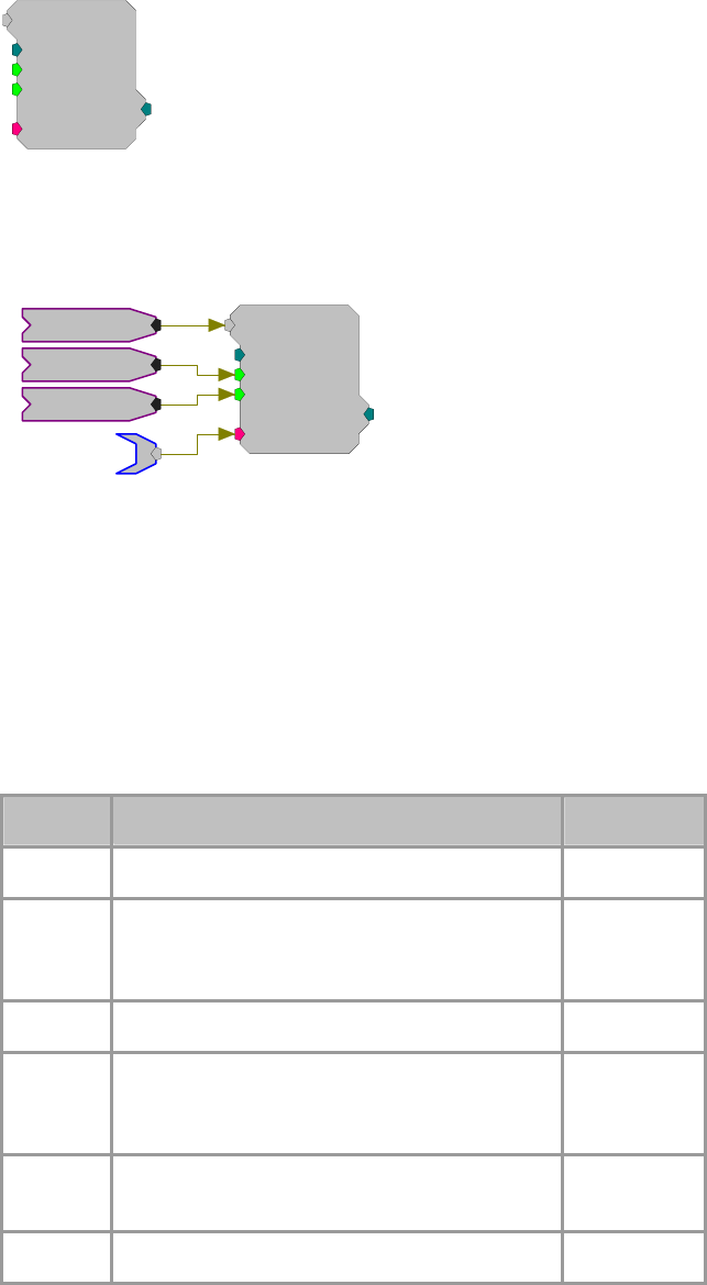
RPvdsEx Manual
138
SerStore
SerStore
Size=1000
Rst=0
WrEnab=1
[1:1,0]
Index=0
{>Data}
Description:
Implements a serial access memory function for storing data. The data port
(>Data) provides access to the buffer so that it can be downloaded to the PC.
SerStore
Size=1000
Rst=0
WrEnab=1
[1:1,0]
Index=0
{>Data}
Data
Signal
Reset
Enable
On each tick of the sample clock, when WrEnable is high, the SerStore reads a
value from the input, stores it to the buffer, and increments to the next position
in the buffer. The internal index generator is incremented until the total number
of samples specified in the Size parameter have been written. When the index
reaches the end of the memory buffer, it is automatically reset to zero and starts
increasing again from there. Any data currently in the buffer will be written
over.
SerStore has several advantages over SerialBuf or RamBuffer. It uses fewer
cycles because it is a write only buffer and users have direct control over the
buffer size. Do not use SerStore if you need to both record and play or if you
need to move to a particular position in the buffer.
Name Description Data Type
Input Input Any
Size Size of the memory buffer (see page 115 for an
important note on dynamically changing the size
parameter)
Integer
(Dynamic)
Rst Resets the offset (index) of the buffer Logic
WrEnab Enables data acquisition and increments the offset
position of the buffer (WrEnable needs to remain
high for the duration of data acquisition)
Logic
Index Sends out the present buffer position relative to a
starting position of zero Integer
>Data Pointer to data buffer Any
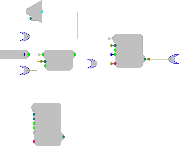
RPvdsEx Manual
139
Note for OpenEx users: When using with a data construct such as OxStream,
the size of SerStore should be an even multiple of the block size of the
construct.
Example: SerStore
The example below uses a parameter tag to generate the buffer size of the
SerStore. The parameter tag also determines the duration of the Schmitt2 trigger
(in samples). When a trigger is generated (Soft1) the Schmitt2 Trigger is
enabled. This stores the number of samples specified by BufferSize to the
SerStore. When the acquisition is finished the data can be downloaded to a PC
from the >Data port.
SerStore
Size=1000
Rst=0
WrEnab=1
[1:5,0]
Index=0
{>Data}
BufferSize
BufferSize
Data
Schmitt2
nHi=100
nEnab=1
[1:2,0]
[1:1,0]
Src=Soft1
d
c
[1:4,0
]
Ch=1
BufferPos
SnipStore
SnipStore
Size=32000
nBlk/2=16
Rst=0
Go=1
[1:1,0]
Index=0
Tag
{>Data}
Description:
The SnipStore component stores multiple snippets of data to a buffer. The
SnipStore was designed for use with the Tetrode component but can be used for
any signal where the values before the trigger are important.
The SnipStore acquires a signal snippet based on the block size, nBlk/2 = X.
When a logical high is detected, the store acquires nBlk/2-1 samples before the
start of the trigger and nBlk/2-1 samples after the trigger. A Tag value is also
stored at the start of each stored snippet. To avoid writing partial snippets, the
snippet block size (nBlk) should always be a multiple of the buffer size (Size).
The data port (>Data) provides access to the buffer so that it can be downloaded
to the PC.
When used with a threshold detection circuit, SnipStore stores data with
reference to the point at which a threshold is crossed. As shown in the figure
below, it stores half the total number of points (specified as nBlk/2) before the
threshold was crossed and half after that point.

RPvdsEx Manual
140
As a result, the point at which the threshold is crossed will always be centered
in the acquired snippet. However, in many cases the threshold is not at the
center of the signal of interest. For example, the portion of the signal of interest
that occurs after the threshold is crossed may be longer than the portion of the
signal that occurs before threshold is crossed. In these cases, the user must
specify a block size that is larger than the expected length of the signal to ensure
that the entire signal is stored.
Name Description Data Type
Input Input Any
Size Size of the memory buffer (see page 115 for an
important note on dynamically changing the size
parameter)
Integer
nBlk/2 1/2 the size of the acquired signal in samples Integer
Rst Resets the signal to the start of the buffer Logic
Go Enables the start of the acquisition block Logic
Tag Stores a value at the start of the acquisition that
indicates the start of the sample Any
Index Sends out the present buffer position relative to a
starting position of zero (Always a multiple of
[(nBlk/2)x2] )
Integer
>Data Pointer to data buffer Any
Example:
See the Tetrode component information, page 273, for an example of how the
SnipStore can be used.

RPvdsEx Manual
141
TagStore
TagStore
Size=1024
BlkSize=16
Enable=1
Strobe=1
[1:1,0]
Index=0
Rst=0
{>Data}
Tag
Description:
TagStore was primarily designed for use in OpenEx and TDT macros. If used
outside the OpenEx environment, be aware that the Tag input’s data type may
differ from the data type of the acquired waveform.
TagStore implements a serial access memory function for storing input data and
is used to mark an acquired waveform with a scalar value such as a timestamp
or other event code. On the first sample that both Enable and Strobe are high,
storage of a block is initiated. TagStore stores the Tag value and the input value
immediately. On each subsequent tick of the sample clock, when Strobe is high,
the TagStore reads a value from the input, stores it to the buffer, and increments
to the next position in the buffer. This continues until a full block of samples
(defined by BlkSize) is stored, and then TagStore becomes ready to store the
next block. When the index reaches the end of the memory buffer, it is
automatically reset to zero. The data port (>Data) provides access to the buffer
so it can be downloaded to the PC.
Data will be stored at the sampling rate of the DSP circuit if the Strobe input is
always high. It can also decimate the incoming signal by providing a pulsed
signal to the Strobe input. The period of the pulse determines how the signal is
decimated.
Note: This component is for use with only high performance processor devices,
such as RXn or RZn.
Name Description Data Type
Input Input Any
Size Size of the memory buffer (see page 115
for an important note on dynamically
changing the size parameter)
Must be a multiple of the BlkSize value
Integer
(Dynamic)
Blk Size Size of each data block in samples Integer
Enable Enables data acquisition and increments
the offset position of the buffer
When Enable goes low, the current block
being stored will finish before storage is
halted
Logic
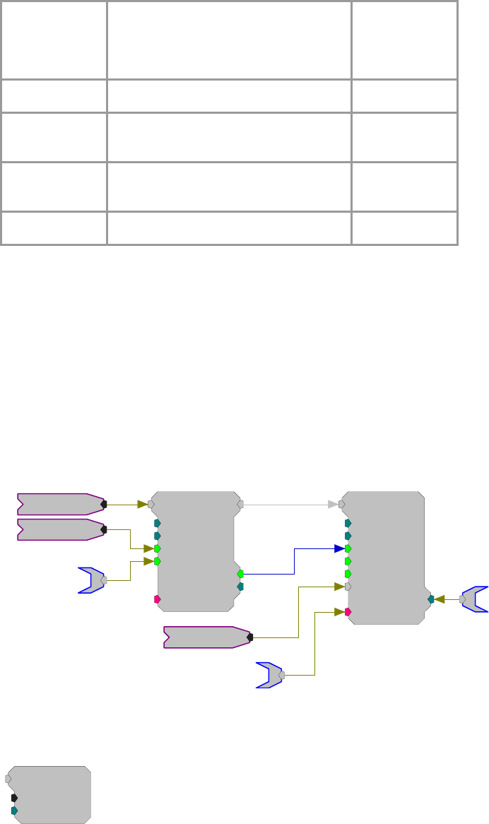
RPvdsEx Manual
142
Strobe Optional additional write enable
Useful for decimation
Data is only written when Strobe is high
Logic
Rst Resets the Index to zero Logic
Tag Tag to be stored with data (usually a time
stamp) Any
Index Sends out the present buffer position
relative to a starting position of zero Integer
>Data Pointer to data buffer Pointer
Note for OpenEx users: When using with a data construct such as OxStream,
the size of TagStore should be an even multiple of the block size of the
construct.
Example:
In the example below, BlockAvg acquires 200 samples (set by the BlkSze
parameter) of the input signal each time Trig goes high. Each block of 200
samples is summed with the current memory contents until 100 blocks have
been acquired (set by the NumAvg parameter). The accumulated sum is output
and WrEnable goes high to enable writing the data into the TagStore component
with the Time HopIn component placing a time stamp on the data. The current
sample count is monitored on AvgCnt and is reset to zero by a logic high on
Reset.
BlockAvg
BlkSze=200
NumAvg=100
Trig=0
Reset=0
[1:1,0]
AvgCnt=0
WrEnab=0
{>Data}
Reset
TagStore
Size=2010
BlkSize=201
Enable=1
Strobe=1
[1:3,0]
Index=0
Rst=0
{>Data}
Tag
Data
Index
Signal
Trig
Time
WriteBuf
WriteBuf
CmpNo=1
Index=0
[1:1,0]
Description:
Writes a value to a specified memory buffer using a specified index. The buffer
is specified by setting the CmpNo parameter to the component number of a
RamBuf, SerialBuf, or AvgBuf component found within the circuit. The
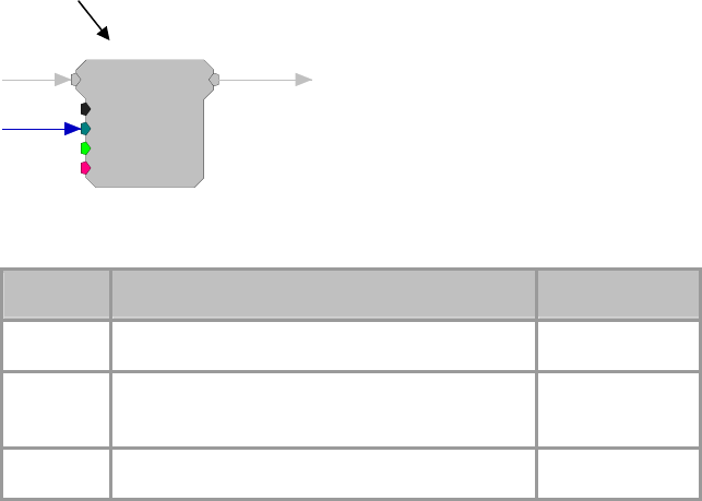
RPvdsEx Manual
143
component number is the first number in parenthesis found at the top of each
component. The index number is the position within the buffer and must be set
to a number less than or equal to the block size for the specified buffer.
For example, to read a value to the RamBuf below, the WriteBuf CmpNo
parameter is set to 4.
Important!: Every time the circuit is even slightly modified, the component
number of the required buffer might change. Always check the component
number (as shown in the figure below) after recompiling.
Component Number
RamBuf
Size=1000
Index=0
Write=0
{>Data}
[1:4,0]
If the component number has changed update the WriteBuf component's
CmpNo parameter, recompile, and recheck the component number.
Name Description Data Type
Input Buffer data input Any
CmpNo Component number of the buffer being written
to Integer (Static)
Index The position of the accessed data point Integer
RPvdsEx Manual
144
Coefficient Generators
Coefficient Generator Components
Coefficient generators are used to calculate the coefficients of specified high-pass, low-pass, band-
pass, or notch filters in real-time. Their outputs can be connected to the filter coefficient port of a
Biquad filter component.
Note: Coefficient generator components are designed to be used with a single filter component.
Do not use a single coefficient generator component with multiple filter components.
This group includes the following components:
ButCoef
ButCoef1
CoefLoad
ParaCoef

RPvdsEx Manual
145
ButCoef
ButCoef
Gain=1
Fc=1000
NBiq=1
Type=LP
[1:1,0]
Enab=Yes
Description:
This component generates the coefficients for an Nth order Butterworth filter
(highpass or lowpass) having the specified attributes for the Biquad filter. New
coefficient values are generated whenever the enable line (Enab) is high (1).
Setting the enable line to low (0) after the coefficients have been generated
decreases cycle usage. The ButCoef can also be placed in time slice -1 to
generate the coefficients only once. The coefficients will be generated when the
processing chain is run and will remain unchanged during acquisition, further
reducing cycle usage. To generate coefficients for notch or bandpass filters, use
ButCoef1.
Note: To satisfy the Nyquist Theorem, the sampling frequency of the system
should be greater than 2 times the highest frequency component passed by the
filter.
Name Description Data Type
Output Generated Butterworth coefficients Any
Gain Scales the filtered portion of the coefficients,
gain is linear Floating point
Fc Center/corner frequency (min=2 Hz) Floating point
N
Biq
N
umber of Biquad coefficients generated (must
match NBiq of filter) Integer (Static)
Type LP = lowpass, HP = highpass Static
Enab Enables the generation of new coefficient values Logic
Tech Note:
Clipping (when voltage value is greater than the DAC can handle) will occur
when the Gain of the ButCoef to the input signal produces a voltage value
larger than +/- 10 and is sent to a D/A for play out. Check the output values of
the filtered signal to determine if this is a problem.
Example:
Second Order Biquad Filter
File: Examples\ButCoef_ex.rcx
Default Device: RP2 Processor
Sampling Rate: 50 kHz
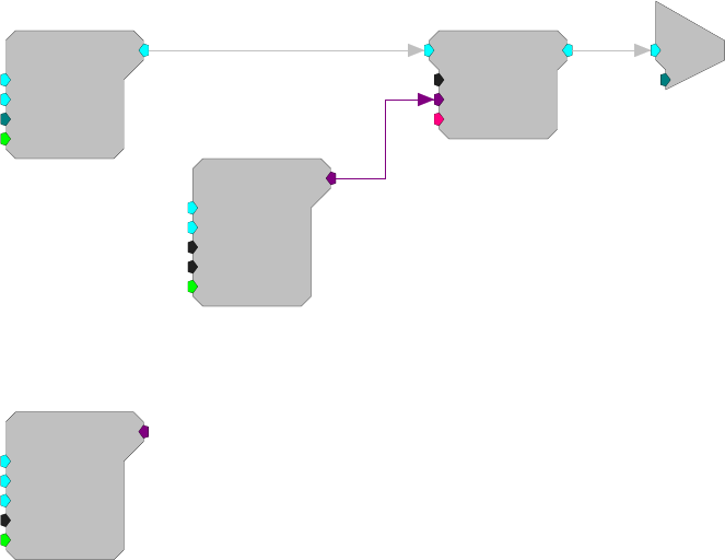
RPvdsEx Manual
146
This example uses a ButCoef to create a second order biquad filter, with a 2000
Hz high-pass, and generates filtered noise. Notice that nBIQ has been set to two
for both the Biquad and ButCoef components.
GaussNoise
Amp=1
Shft=0
Seed=0
Rst=Run
[1:2,0
]
Biquad
nBIQ=2
{>Coef}
{>Delay}
[1:3,0]
ButCoef
Gain=1
Fc=2000
NBiq=2
Type=HP
[1:1,0]
Enab=Yes
c
O
[1:4,0]
Ch=1
ButCoef1
ButCoef1
Gain=1
Fc=1000
BW=100
Type=LP
[1:1,0]
Enab=Yes
Description:
This component generates the coefficients for a second order Butterworth filter
(lowpass, bandpass, highpass, or notch) having the specified attributes for the
Biquad filter. When using a bandpass or notch filter, the BW (bandwidth)
parameter refers to the filter bandwidth at 3dB attenuation (e.g. for Fc = 5 kHz
and BW = 1 kHz, the 3dB attenuation would occur at 4.5 kHz and 5.5 kHz).
When the filter type is set to LP (lowpass) or HP (highpass), the BW parameter
is redundant and is ignored.
New coefficient values are generated whenever the enable line (Enab) is high
(1). Setting the enable line to low (0) after the coefficients have been generated
decreases cycle usage. The ButCoef1 can also be placed in time slice -1 to
generate the coefficients only once. The coefficients will be generated when the
processing chain is run and will remain unchanged during acquisition, further
reducing cycle usage.
ButCoef1 allows the user to build only lower order filters. Multiple filters can
be cascaded to make higher order bandpass and notch filters. To generate
coefficients for higher order lowpass and highpass filters users should use
ButCoef.
Note: To satisfy the Nyquist Theorem, the sampling frequency of the system
should be greater than 2 times the highest frequency component passed by the
filter.
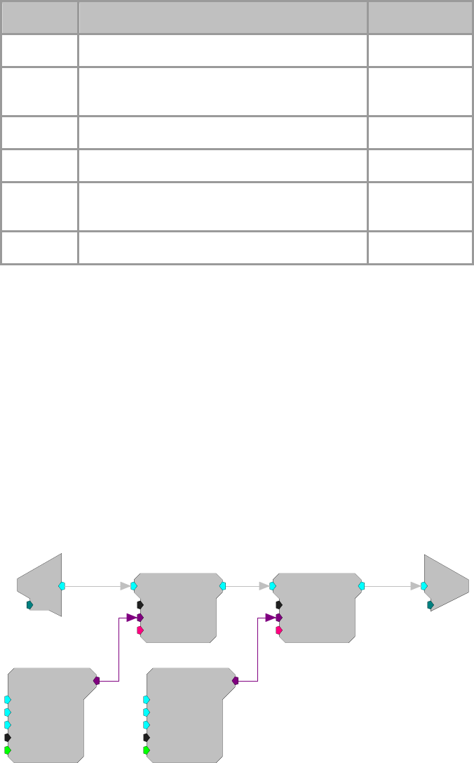
RPvdsEx Manual
147
Name Description Data Type
Output Generated Butterworth coefficients Any
Gain Scales the filtered portion of the coefficients, gain
is linear Floating point
Fc Center/corner filter frequency (min=2 Hz) Floating point
BW Bandwidth at 3dB attenuation Floating point
Type LP = lowpass, BP = bandpass, HP = highpass, NT
= notch Static
Enab Enables the generation of new coefficient values Logic
Tech Note:
Clipping (when voltage value is greater than the DAC can handle) will occur
when the Gain of the ButCoef1 to the input signal produces a voltage value
larger than +/- 10 and is sent to a D/A for play out. Check the output values of
the filtered signal to determine if this is a problem.
Example:
Butterworth Coefficients
File: Examples\ButCoef1_ex.rcx
Default Device: RP2 Processor
Sampling Rate: 25 kHz
This example uses two ButCoef1 generators to filter the signal input. The first
ButCoef1 generates a 50 Hz notch filter and the second generates a 5000 Hz
low-pass filter. The filtered signal is sent to D/A channel one. Note that the
number of Biquads (nBIQ) is one.
c
O
[1:6,0]
Ch=1
d
c
[1:3,0]
Ch=1 Biquad
nBIQ=1
{>Coef}
{>Delay}
[1:4,0]
ButCoef1
Gain=1
Fc=50
BW=20
Type=NT
[1:1,0]
Enab=Yes
Biquad
nBIQ=1
{>Coef}
{>Delay}
[1:5,0]
ButCoef1
Gain=1
Fc=5000
BW=1000
Type=LP
[1:2,0]
Enab=Yes

RPvdsEx Manual
148
CoefLoad
CoefLoad
Nu m Bl ks=4
BlkSize=10
BlkSel=0
EnabFF=No
[1:1,0
]
ActCnt=0
FlipFlop=0
{>CoefBlks}
Description:
The CoefLoad component is used to quickly load and update component
coefficients at run-time under user control. Uses include updating filter
coefficients and channel mappings. Using this component extends the
usefulness of components like FIR2 by allowing many more blocks of
coefficients to be used. These blocks are stored in the much larger XM memory
area and then loaded to the smaller PM memory when needed.
Because the coefficients are loaded one at a time on each tick of the sample
clock, when a new coefficient set is needed, it will take BlkSize+1 cycles to
load (BlkSize equals the number of coefficients being loaded). This time delay
is typically not an issue. The CoefLoad component has an optional FlipFlop
output that can be used to drive the block select input of the loaded component.
The ActCnt output is used to determine if there are more coefficients to be
loaded. If ActCnt > 0, the component is active and is in the process of loading
coefficients.
Coefficient blocks within this component can have any format and any
arrangement. However, this arrangement must match the needed format and
arrangement of the target component. The blocks of coefficients are then simply
placed sequentially in the components XM memory.
Name Description Data Type
Output Selected block of coefficients Any
N
umBlks
N
umber of blocks of coefficients Integer (Static)
BlkSize
N
umber of coefficients per bloc
k
Integer (Static)
BlkSel Index to the block of coefficients to be used Integer
EnableFF Enables optional flip flop output Logic
>CoefBlks Pointer to CoefBlks buffer (PM) Pointer
FlipFlop Optional output to drive the block select input
of the loaded component Integer
ActCnt Output used to determine the state of the
component Integer
Example:
Load Coefficients
For setting arbitrary channel mappings using the MCMap component:

RPvdsEx Manual
149
CoefLoad
Nu m Bl ks=4
BlkSize=16
BlkSel=0
EnabFF=No
[1:1,0
]
ActCnt=0
FlipFlop=0
{>CoefBlks}
MapSelect
MapLoad
MCAdcIn
nChan=16
ChanOS=1
[1:2,0]
MCMap
nChan=16
{>Map}
[1:3,0]
Mapped Input
nChan=16
This circuit supports four channel mappings on the 16 channel input signal. The
MapLoad tag must be loaded with the channel mappings before the MapSelect
parameter is set. In this case, the loaded values would be 32 bit integers
arranged in four blocks of 16 values each.
Note: EnabFF = No for this application.
To dynamically update the coefficients of a filter:
PulseTrain2
nPer=5000
nPulse=-1
Enab=Yes
Rst=Run
[1:1,0]
PCount=0
PLate=0
SimpCount
Rst=0
Enable=1
[1:3,0]
CoefLoad
Nu m Bl ks=4
BlkSize=32
BlkSel=0
EnabFF=Yes
[1:5,0]
ActCnt=0
FlipFlop=0
{>CoefBl ks}
CoefLoad
Flip
SigIn
FIR2
Order=31
nSets=1
SetSel=0
{>Coef}
[1:8,0]
{>Delay}
Flip
SigOut
This circuit supports the loading of 4 different sets of coefficients into the FIR2
filter component. Each block contains 32 filter taps arranged as specified by the
FIR2 component description. Every 5000 ticks of the sample clock, the
PulseTrain2 will advance the SimpCount counter causing the next filter set to
be loaded and selected (via the FlipFlop control). It is important that the
SimpCount output does not exceed NumBlks and that the nPer argument in
PulseTrain2 is not set less than BlkSize+1.
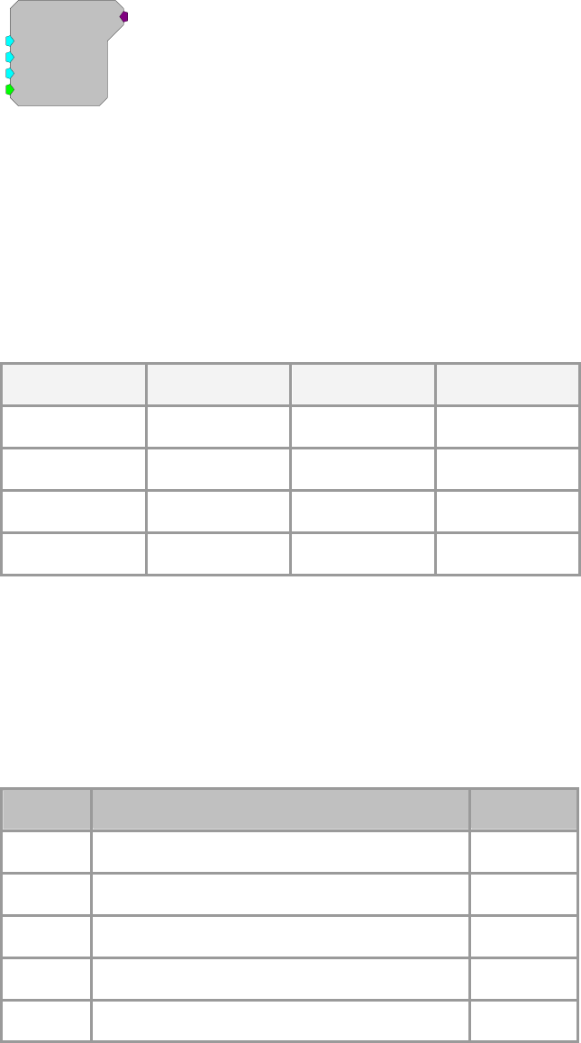
RPvdsEx Manual
150
ParaCoef
ParaCoef
Gain=1
Fc=1000
BW=100
Enab=Yes
[1:1,0]
Description:
This component generates the parametric coefficients for a second order
equalizing Biquad filter. Center frequency (Fc) and bandwidth at 3 dB (BW) are
specified by the user and the band gain increases the intensity of the signal
within the band by the linear scale factor (gain) specified. The gain value should
be set carefully to ensure that the amplified signal will not exceed the dynamic
range (typically +/- 10 V) of the processor module. When a unity gain (Gain =
1) is specified, coefficient for an all pass filter are generated.
The table below lists typical roll-offs from the center frequency for several gain
settings.
Center Frequency Bandwidth Gain Roll-Off
10 kHz 100 Hz 10 18 dB/octave
10 kHz 1000 Hz 10 15 dB/octave
10 kHz 100 Hz 20 24 dB/octave
10 kHz 1000 Hz 20 15 dB/octave
New coefficient values are generated whenever the enable line (Enab) is high
(1). Setting the enable line to low (0) after the coefficients have been generated
decreases cycle usage. The ParaCoef can also be placed in time slice -1 to
generate the coefficients only once. The coefficients will be generated when the
processing chain is run and will remain unchanged during acquisition, further
reducing cycle usage.
Note: To satisfy the Nyquist Theorem, the sampling frequency of the system
should be greater than 2 times the highest frequency component passed by the
filter.
Name Description Data Type
Output Generated parametric coefficients Any
Gain Band gain of filtered signal (linear scale factor) Floating point
Fc Center frequency Floating Point
BW Bandwidth at 3dB attenuation Floating point
Enab Enables the generation of new coefficient values Logic
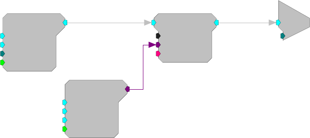
RPvdsEx Manual
151
Tech Note:
Clipping (when voltage value is greater than the DAC can handle) will occur
when the Gain of the ParaCoef to the input signal produces a voltage value
larger than +/- 10 and is sent to a D/A for play out. Check the output values of
the filtered signal to determine if this is a problem.
Example:
Parametric Coefficient
File: Examples\ParaCoef_ex.rcx
Default Device: RP2 Processor
Sampling Rate: 50 kHz
This example uses the ParaCoef generator with a Biquad to filter a band of
noise 100 Hz wide centered at 1000 Hz. The gain is set to 10 dB to increase the
output level of the filter. Parametric filters act like equalizers on an amplifier.
ParaCoef
Gain=10
Fc=1000
BW=100
Enab=Yes
[1:1,0]
c
O
[1:4,0]
Ch=1
Biquad
nBIQ=1
{>Coef}
{>Delay}
[1:3,0]
GaussNoise
Amp=1
Shft=0
Seed=0
Rst=Run
[1:2,0]
RPvdsEx Manual
152
Counters and Logic
Counters and Logic Components
Counters and logical operations are used primarily for program control. They often control the
activity of individual components via trigger or enable inputs.
This group includes the following components:
And
Counter
DeBounce
EdgeDetect
JKFlipFlop
Not
OneShot
Or
PulseTrain
PulseTrain2
RSFlipFlop
Schmitt
Schmitt2
TTLDelay
TTLDelay2
Xor
RPvdsEx Manual
153
And
[1:1,0]
AND
Description:
Logical AND function. Returns 1 (true) if all inputs are 1 (true). If all inputs are
0 the output is 0. All multiple inputs must be from a primary output. If it is
necessary to route a parameter output to this function use a CONSTL to make it
a primary output.
Name Description Data Type
Input (multiple) Input (multiple) Logic
Output AND operation of data set Logic
Equation:
Output = AND (Input1I, Input2I, Input3I, ... InputnI)
Example(s):
AND (0, 0, 0, 0, 0) = 0 (false)
AND (0, 0, 0, 1, 0) = 0 (false)
AND (1, 1, 1, 1, 1) = 1 (true)
Counter
Counter
Base=0
Phse=0
Step=1
Roll=1000
[1:1,0]
Rst=Run
Enab=Yes
Description:
The Counter is a count up/down counter. It counts for as long as a high pulse is
going to the enable port (Enab). It increments the count by a set value
(determined by Step) for each pulse of sample clock (e.g. if the enable is high
for 1 msec and the sample rate is 25 kHz then the counter will step 25 times).
Once it exceeds the sum of the Base and Roll value the Counter starts counting
again at the base value (Base) (see below for more details). The first time the
counter is started or after the Reset (Rst) port has been triggered (value goes
from low (0) to high (1)) the Counter starts at the Base value plus the Phase
(Phse) value.
RPvdsEx Manual
154
Name Description Data Type
Output Incremented integer value Integer
Base Base value Integer
Phase On reset the starting value of the Counter Integer
Step Increment value Integer
Roll Roll over value Integer
Rst Resets counter when logic is high Logic
Enab When enable line is set high(1) counter is
incremented on each tick of the clock Logic
The example below shows many of the features of the Counter.
Example parameter settings are: Base = 8, Phse = 11, Step = 2, Roll = 20.
The Counter sequence begins at the Phse value when the circuit is first run:
The initial count value output is therefore 11.
The count value on progressive samples would be incremented by Step = 2:
13, 15, 17, 19, 21, 23, 25, 27
The Roll and Base values determine the value at which the counter rolls over.
Since Base = 8 and Roll = 20, the counter will roll over when its count value is
incremented to a value greater than or equal to 28 (8 + 20). During a rollover,
the remainder of the Step value is carried over.
Recall that our last counter value output was 27. As the counter increments this
value to 29 there is a remainder of 1 prior to the rollover (29 - 28). This
remainder is added to the Base value and output on the following sample.
Since Base = 8 the new counter value output will be 9 (8 + 1).
The counter will then be incremented by Step for each progressive sample until
the rollover value is encountered. The sequence will repeat as long as Enab is
high and Rst is not triggered.
Tech Notes:
The Counter is incremented for each tick of the sample clock.
Phse only functions when the enab first goes high or after Rst has been
triggered.
As long as Rst is high (1) the count value remains at the Base + Phse.
All Components of the Counter are available while the RP2 chain is running.
To use the Counter as a Count down circuit the Base value must be less than the
roll value. When the Counter reaches the Base value it Rolls over to the Roll
value and repeats the count down.
The Counter does work properly when Rst is less than zero.
The Base value can be negative only if Roll and Step are positive values.
Example:
WordIn-WordOut, page 72.
RPvdsEx Manual
155
DeBounce
DeBounce
nChks=10
[1:1,0]
Description:
A DeBounce filters out transient changes in input. The output of the signal is
tied to the input. When the input changes and remains constant for a set number
of samples the output switches. If the input switches state during the sampling
period the output does not change.
Name Description Data Type
Input Input Logic
Output Output Logic
nChks
N
umber of samples that input must remain
constant before state changes. Clock times
will differ depending on sampling rate.
Integer
EdgeDetect
EdgeDetect
Edge=Rising
[1:1,0]
Description:
This component returns true for one cycle of the sample clock when the
specified edge (rising or falling) is encountered. It is useful for converting a
TTL to a single sample high. The edge direction can not be changed once the
processing chain is started.
Name Description Data Type
Input Input Logic
Output Output goes high for one cycle on either
rising or falling edge Logic
Edge Rising or falling edge detect Static
Edge = Rising or Falling (goes high either on rising or falling edge (static))
Example(s):
Block Access (example with trigger), page 123.
Serial Buffer (example with PulseTrain), page 131.
RPvdsEx Manual
156
JKFlipFlop
JKFlipFlop
J=0
K=0
Rst=0
[1:1,0]
Description:
Implements a standard J-K flip-flop. See truth table below.
Name Description Data Type
Output Output Logic
J J input Logic
K K input Logic
Rst Resets state of the FlipFlop to 0. Logic
Equation:
On each tick of the sample clock the following truth-table applies:
Rst J K Output
H X X L
L L L unchanged
L L H L
L H L H
L H H Toggle
Not
No
[1:1,0]
Description:
Inverts signal logic, i.e. changes 0's to 1's and 1's to 0's.
Name Description Data Type
Input Input Logic
Output Output (Inverted value of Input) Logic
Equation:
Output = NOT (Input )
RPvdsEx Manual
157
OneShot
OneShot
[1:1,0
]
Description:
Generates a single TTL output when chain is first run.
Name Description Data Type
Output TTL pulse when chain is started Logic
Equation:
Output = 1
Or
[1:1,0]
OR
Description:
Logical OR function. Returns 1 (true) if any input is 1 (true). All multiple inputs
must be from a primary output. If it is necessary to route a parameter output to
this function use a CONSTL to make it a primary output.
Name Description Data Type
Input
(multiple) Input (multiple) Logic
Output OR operation of inputs Logic
Equation:
Output = OR (InputI, InputI, InputI, ... InputnI)
Example(s):
OR (0, 0, 0, 0, 0) = 0 (false)
OR (0, 0, 0, 1, 0) = 1 (true)
OR (1, 1, 1, 1, 1) = 1 (true)

RPvdsEx Manual
158
PulseTrain
PulseTrain
Thi=10
Tg=0
Tlo=10
Npls=0
[1:1,0
]
CurN=0
Stage=0
Trg=0
Description:
This component generates a pulse train, i.e. a series of pulses with specified
times for a high (1) and low pulse (0)).
Name Description Data Type
Output Pulse value (0 or 1) Logic
Thi Time stimulus is high in milliseconds Floating Point
Tg Gate time: signal high time is (Thi-Tg) and is low
for Tlo; use with Cos2gate and Lin2gate
(milliseconds)
Floating Point
Tlo Time stimulus is low in milliseconds Floating Point
N
pls The number of pulses to generate Integer
Trg Starts pulse generator Logic
Stage Stage in pulse cycle; 0 = waiting for trigger, 1 =
Output high, 2 = Output low Integer
CuN Current number of pulses left (Counts down from
N
pls to 1 then resets.); when Npls is 0
(continuous) CuN is negative
Integer
When externally triggered (via Trg) with a low (0) to high (1) pulse, the rising
edge of trg, the PulseTrain component sends out a number of pulses (Npls
(positive integer)). Each pulse will go high for a set time (Thi Time High (in
milliseconds)). The pulse then goes low for a set time (Tlo Time Low (in
milliseconds)). After all pulses have been sent PulseTrain waits for another
Trigger (Trg).
The signal output will be high for the (Thi-Tg) milliseconds and then low for
Tlo milliseconds. The Tg parameter can be used when the PulseTrain is driving
a signal gate.
Two parameters (Stage and CurN) are used to determine the status of
PulseTrain. Stage determines if PulseTrain is waiting for a Trigger (Stage=0), is
sending a high pulse (Stage =1) or a low pulse (Stage=2). Current Number
(CurN) determines how many pulses remain.
For example the values in the picture above would generate the following
response: On a trigger from low to high (Trg) the pulse train would send out 5
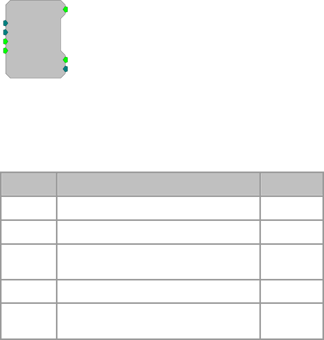
RPvdsEx Manual
159
pulses each with a 99.75 msec high (100 (Thi)-0.25(Tg)) and a 100 msec low
(Tlo).
Tech Notes:
Pulse Train responses to the rising edge of a trg.
Setting Npls = 0 produces a continuous series of pulses. When Npls = 0 CurN
counts down from 0 (produces negative values).
A Schmitt Trigger performs a similar operation, but differs in a variety of ways
such as it has 1) no gate time, 2)a single pulse,3) detects high state rather than
rising edge.
All components of a PulseTrain can be accessed while the RP2 chain is running.
The PulseTrain ALWAYS is triggered by going from low to high regardless of
the Trg value.
Pulse minimum Thi is two ticks of the sample clock. This is true even when Thi
= 0
Minimum for Tlo = 0
Example:
Averaged Buffer (generating a pulse train to trigger a signal), page 119.
PulseTrain2
PulseTrain2
nPer=100
nPulse=-1
Enab=Yes
Rst=Run
[1:1,0
]
PCount=0
PLate=0
Description:
PulseTrain2 sends out a TTL pulse (one cycle) every nSamples (nPer). The
number of pulses generated is set with nPulse. While the Enab line is high (1)
the PulseTrain2 counts up to the number of pulses. When the Enab line goes
low the PulseTrain2 is locked at the last nPulse, unless Rst is triggered. Rst
resets the number of pulses generated (Pcount) to zero.
Name Description Data Type
Out Signal output (single TTL pulse) Logic
nPer
N
umber of samples between TTL pulses Integer
nPulse
N
umber of pulses generated while Enab line is
high Integer
Enab While Enab is high TTL pulses are generated Logic
Rst When reset the number of pulses generated is set
to zero Logic

RPvdsEx Manual
160
PLate Sends out a TTL pulse n-2 samples after signal
out Logic
PCount Counts the number of pulses generated Integer
Tech Notes:
Rst resets the counter even while the system is enabled.
If the Enab line and the Rst line are set high, PulseTrain2 still generates TTL
pulses.
The nPer (number of samples between pulses) and the nPulses (number of
pulses) can be changed while the PulseTrain2 is enabled. However, this can
cause problems if the nPulses is less than the number of pulses generated.
Setting nPulse to -1 generates a continuous number of pulses.
Example:
PulseTrain2
In this example a TTL pulse is generated every 5000 samples. Each time a pulse
is generated the RMS signal from A/D channel 1 is stored into a memory
buffer. To start and stop the acquisition a zBUS trigger is generated. The zBUS
trigger is used because it can be set always high or low, unlike the software
triggers that stay high for a single pulse.
d
c
[1:6,0]
Ch=1 RMS
[1:7,0]
SerialBuf
Size=1000
Rst=0
AccEnab=1
Write=1
[1:8,0]
NBl ks=0
Index=0
{>Data}
PulseTrain2
nPer=5000
nPulse=-1
Enab=Yes
Rst=Run
[1:3,0
]
PCount=0
PLate=0
EdgeDetect
Edge=Rising
[1:4,0]
[1:1,0]
Src=zBusA
RSFlipFlop
RSFlipFlop
Set=0
Rst=0
[1:1,0]
Description:
Simple set/reset flip flop similar to an on/off light switch. Set turns on the
switch (makes it high) when triggered by a high pulse. Rst turns the switch off
when it is triggered by a high pulse. If both Set and Rst are 0 then the output is
not altered (switch either stays On or Off).
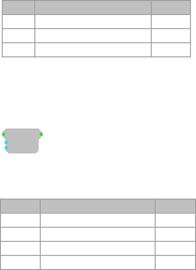
RPvdsEx Manual
161
Name Description Data Type
Output Output Logic
Set Set value Logic
Rst Resets state of the RSFlipFlop to 0 Logic
Equation:
Output = 0 when Rst = 1
Output = Output(t-1) when Set=0 and Rst = 0
Output = 1 when Rst = 0 and Set = 1
Schmitt
Schmitt
Thi=100
Tlo=10
[1:1,0]
Description:
This component performs a Schmitt trigger. If a logical high is detected, the
output goes to a high state for a set amount of time (determined by Thi). At the
end of the high time, the output goes to a low state for a set time (determined by
Tlo). Once that time has expired, the Schmitt can be triggered again.
Name Description Data Type
Input Input Logic
Output Logical value (0 or 1). Logic
Thi Output high time (in milliseconds) after trigger Floating Point
Tlo Output low time (in milliseconds) after high Floating Point
Tech Notes:
If the input to the Schmitt trigger is high(1) at the end of the cycle (Thi+Tlo) a
new pulse is sent out. This is in contrast to PulseTrain that responds only to a
rising edge of a trigger.
By setting Tlo to zero the Schmitt trigger is immediately ready for another
trigger event.
The minimum time high (Thi) is two ticks of the sample clock.
It has a lower cycle usage compared to a PulseTrain.
Equation:
If (InputI) then
From t = 0 to Thii OutputO = 1
From t = (Thi1+1) to Tlo2 OutputO = 0
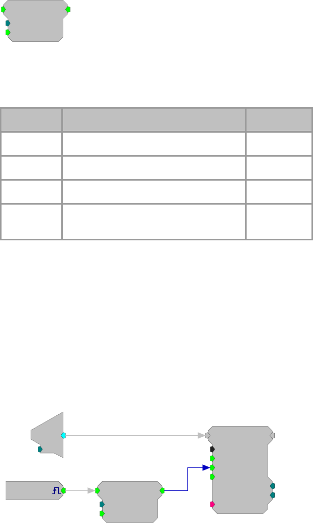
RPvdsEx Manual
162
Schmitt2
Schmitt2
nHi=100
nEnab=1
[1:1,0]
Description:
This component performs a Schmitt trigger. If a logical high is detected, the
output goes to a high state for a set number of samples (determined by nHi).
Once that time has expired, the Schmitt2 component can be triggered again.
Name Description Data Type
Input Input logic high to start trigger Logic
Output Logical value (0 or 1). Logic
nHi
N
umber of samples high Integer
nEnab If nEnab line is 0 the Schmitt output will
not go high Logic
Tech Notes:
The Schmitt2 trigger is excellent for storing a set number of samples to a buffer.
Equation:
If (InputI) then
From s = 0 to nHi if nEnab=1 OutputO = 1
else Output
O = 0
Example:
Schmitt2
Acquire 100 samples of a signal.
Schmitt2
nHi=100
nEnab=1
[1:2,0]
SerialBuf
Size=1000
Rst=0
AccEnab=1
Write=1
[1:5,0]
NBl ks=0
Index=0
{>Data}
d
c
[1:4,0]
Ch=1
[1:1,0]
Src=Soft1
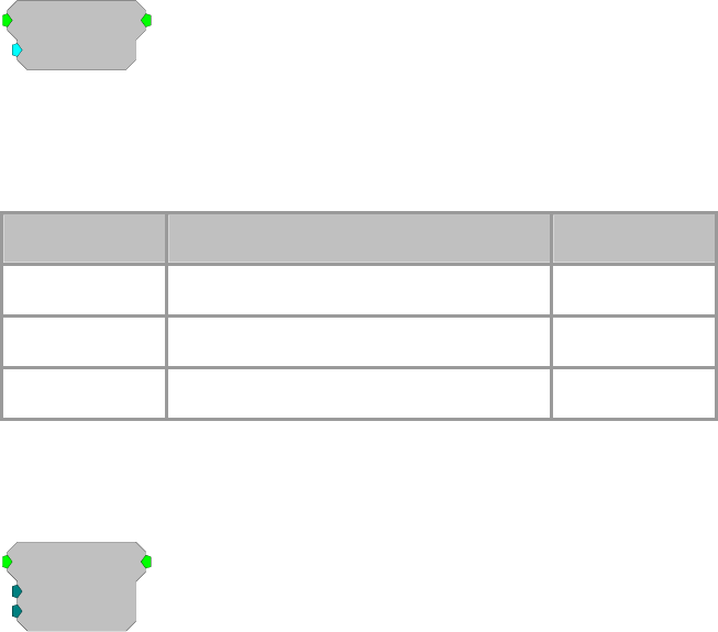
RPvdsEx Manual
163
TTLDelay
TTLDelay
Tdel=1000
[1:1,0]
Description:
This component looks for the rising edge of the input and generates a TTL for a
single sample after the specified delay. This function is useful if two signals are
to be triggered with a short delay between them.
Name Description Data Type
Input Input Logic
Output Logical value (0 or 1) Logic
Tdel Delay time (in milliseconds) Floating Point
TTLDelay2
TTLDelay2
N1=10
N2=0
[1:1,0]
Description:
When the input to this component is a logical 1, the output is a pulse train that is
logic high for one sample and low for N1 + N2 – 1 samples. This pulse train is
also delayed from the onset of the input by N1 + N2 samples. This is different
than TTLDelay which sends out one pulse after each rising edge of the input
(see figure below). The total delay is specified by N1 + N2 samples, however,
depending on the application, N2 may be zero.
Note: No pulses are sent if both N1 and N2 are both set to zero. Ensure that you
have at least a 1 entered for either N1 or N2.
The following figure shows the output of the TTLDelay2 component compared
to that of TTLDelay.

RPvdsEx Manual
164
If an EdgeDetect (Edge=Rising) precedes TTLDelay2 in a circuit, the output of
TTLDelay2 is similar to that of TTLDelay.
Name Description Data Type
Input Input Logic
Output Logical value (0 or 1) Logic
N
1 Sample delay one Integer
N
2 Sample delay two Integer
Xor
XOR
[1:1,0]
Description:
Logical XOR function. Returns 1 (true) if only one input is 1 (true). All
multiple inputs must be from a primary output. If it is necessary to route a
parameter output to this function use a ConstL to make it a primary output.
If more than two inputs are used, the XOR function steps through from top to
bottom.
Name Description Data Type
Input
(multiple) Input (multiple) Logic
Output XOR operation of inputs Logic
RPvdsEx Manual
165
Equation:
Output = XOR (InputI, Input2I, Input3I, ... InputnI)
Examples:
XOR (0, 0) = 0 (false)
XOR(1, 1) = 0 (false)
XOR (0, 1) = 1 (true)
XOR (1, 0) = 1 (true)
Note: If more than two inputs are used, the XOR function steps through from
top to bottom.
XOR (1, 1, 1, 1, 1) = 1 (true)
For this example the XOR function evaluates the inputs two at a time.
1 (1st input) XOR 1 (2nd input) = 0
0 (result of 1st and 2nd ) XOR 1 (3rd input) = 1
1 (result of 1st, 2nd, and 3rd input) XOR 1 (4th input) = 0
0 (result of other 4 inputs) XOR 1 (5th input) = 1
RPvdsEx Manual
166
Data Reduction
Data Reduction Components
Data reduction techniques decrease the size of the data set at the expense of resolution.
This group includes the following components:
CompTo16
CompTo16D
CompTo8
CompTo8D
ExpFrom16
ExpFrom8
PlotDec16
ShufTo16
ShufTo8
SplitFrom16
SplitFrom8
This group also includes the following components, if RPvdsEx Device Setup is
configured for a high performance device, such as the RXn or RZn:
MCCpTo8D
MCCpTo16D
MCPDec16
CompressTo/ExpandFrom functions take a single input and reduce it from a 32-bit value to an 8
or 16-bit value. The data is stored as a 32-bit word. For example CompTo8 stores data in one-
fourth the space and has one-fourth the resolution or dynamic range (e.g. 200,000 points of data
with 32-bit resolution is reduced to 50,000 with 8-bit resolution). ExpandFrom8 takes the stored
data (32-bit word) and expands it into four 32-bit words for data output and manipulation.
ShuffleTo/SplitFrom functions take several inputs and reduce them from a 32-bit value to 8 or
16-bit value. The data is stored as a 32-bit word. For example ShuffleTo16 takes two inputs and
reduces the resolution by one-half (16-bit). It stores the first input value in the high portion of the
word and the second input in the low portion of the word. SplitFrom reverses the process. It
extracts the two/four values in word format and outputs them as 32-bit words for data output and
manipulation.
ReadTagVex is the ActiveX format to for reading reduced data in MATLAB. Other programming
languages can use either ReadTagVex or ReadTag. When using ReadTag it is necessary to write
your own data splitting or expansion routines.
Data Reduction and Scale Factor
It is sometimes desirable to reduce data sets to either increase data transfer rates or reduce required
memory allocation for data storage. This can be done by compressing 32-bit numbers to 16-bit
numbers, or by compressing 32-bit numbers to 8-bit numbers, etc. For demonstration, we will
consider converting 32-bit values to 16 bits of precision.
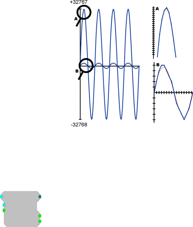
RPvdsEx Manual
167
The largest number that can be represented with 16 bits is 65535 (216–1). If we designate one bit
as a sign bit, the largest value that the remaining 15 bits can represent is 32767. Using this sign bit
results in a range from –32768 to 32767. This range represents the number of discrete amplitude
values available for the converted signal. The level of the signal samples in the converted signal is
essentially rounded to the nearest digital value upon conversion. This process results in a
quantization error. To minimize this error and produce the best resolution in the conversion, the
scale factor should be set to best fit the input signal to this range. If the input waveform is known
to have a voltage swing of +/- 1.0 V, the
scale factor should be set to 32767. If the
voltage swing is +/- 10 V, the scale factor
should be set to 3276.7. Setting the scale
factor incorrectly will result in poor
resolution or meaningless data.
For example: Our range gives us 65535
divisions of the y-axes below. In the figure
to the right, if we zoom in on the improperly
scaled input signal (B), we can see that the
quantized signal is degraded. This waveform
can be represented by only 11 possible
digital amplitude values. On the other hand,
each sample in the properly scaled
waveform (A) can take on any of the 65536
values in the entire range. This quantized
waveform (blue) is a much better
representation of the input waveform (red).
Later in the processing chain, if we convert
the values back, the signals are rescaled to
match their original range by using the inverse of the scale factor used earlier. The output values
will have the dynamic range of the reduced data.
The process is very similar when compressing numbers to 8 bits of precision.
CompTo16
CompTo16
SF=32767
[1:1,0]
Strobe1=0
Byp/Rst=0
Strobe2=0
Description:
CompTo16 (compress to 16-bit) takes a stream of 32-bit floating values, scales
and converts them to 16-bit fixed point numbers. Successive values are then
output in the upper and lower portions of a 32-bit integer. The Strobe1 output
sends a pulse high when the data is sent and should be linked to the AccEnable
parameter of the buffer component.
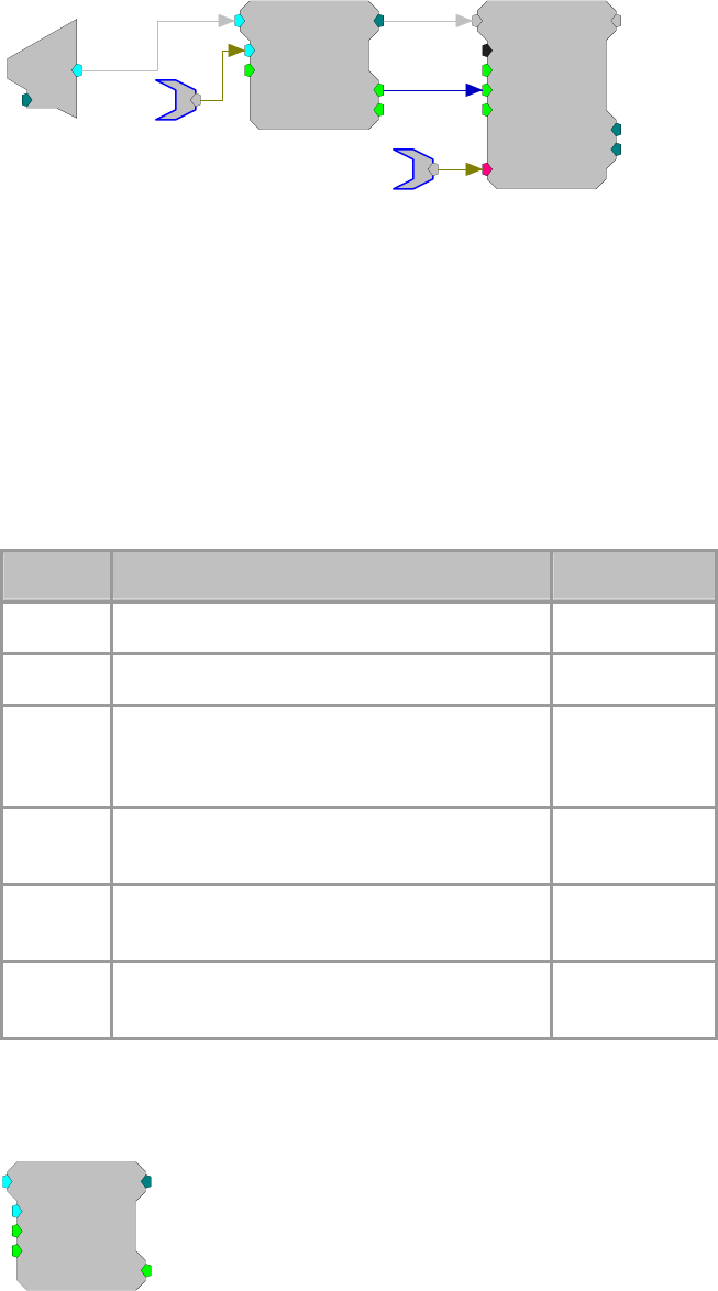
RPvdsEx Manual
168
CompTo16
SF=32767
[1:2,0]
Strobe1=0
Byp/Rst=0
Strobe2=0
d
c
[1:1,0]
Ch=1
Scale
SerialBuf
Size=100000
Rst=0
AccEnab=1
Write=1
[1:4,0]
NBl ks=0
Index=0
{>Data}
Data
This reduction technique can be used to decrease memory allocation for data
storage or double the data transfer rate to and from the PC.
The scale factor (SF) is used to appropriately scale the floating point input
before it is converted to 16 bits. The range that can be specified using 16 bits is
+/- 32767. To get the maximum resolution, SF should be selected in such a way
that the maximum input voltage scales to +/- 32767. The default SF is set to
32767 and assumes that the input is bounded between +/- 1.0 V. Use an SF of
3276.7 for a +/- 10 V range. The SF and input values must be matched.
Mismatch between the SF and input value range gives poor resolution or
meaningless data. Use ExpandFrom16 to reverse the process. See Data
Reduction - Scale Factor for more information on properly setting the scale
factor, page 166.
Name Description Data Type
Input Input Floating Point
Output Integer containing two 16-bit variables Integer
SF Scale factor sets the scale for the input before
sample conversion; scale factor depends on input
voltage
Floating Point
Byp/Rst When high it resets the start of sample
conversion; when set high data is not converted Logic
Strobe1 Pulses high when data is sent; connect to
AccEnable line Logic
Strobe2 Pulses high when component is in bypass mode;
bypass mode passes the data unaltered Logic
CompTo16D
CompTo16D
SF=32767
Rst=0
Enab=1
[1:1,0]
Strobe=0
Description:
CompTo16D (compress to 16-bit) is essentially the same as CompTo16 except
it allows for an enable input that ensures no data is passed through when

RPvdsEx Manual
169
compression is not enabled. When enabled it scales and converts a stream of 32-
bit floating values to 16-bit fixed point numbers. Successive values are then
output in the upper and lower portions of a 32-bit integer. The Strobe output
sends a pulse high when the data is sent and should be linked to the AccEnable
parameter of the buffer component. This reduction technique can be used to
decrease memory allocation for data storage and double the data transfer rate to
and from the PC.
Scale factor (SF) is used to appropriately scale the floating point input before it
is converted to 16 bits. The largest number that can be specified using 16 bits is
+/- 32767. To get the maximum resolution, SF should be selected in such a way
that the maximum input voltage scales to +/- 32767. The default SF is 32767
and assumes that the input is bounded between +/- 1.0 V. Use an SF of 3276.7
for a +/- 10 V range. The SF and input values must be matched. Mismatch
between the SF and input value range gives poor resolution or meaningless
data. Use ExpandFrom16 to reverse the process.
See Data Reduction - Scale Factor for more information on properly setting the
scale factor, page 166.
Name Description Data Type
Input Input Floating Point
Output 32-bit integer containing two 16-bit variables Integer
SF Scale factor sets the scale for the input before
sample conversion; (scale factor should be
calculated based on the input voltage)
Floating Point
Rst When high it resets the start of sample
conversion; when set high, data is not
converted
Logic
Enab Enables output when high Logic
Strobe Pulses high when data is sent Logic
CompTo8
CompTo8
SF=127
[1:1,0]
Strobe1=0
Byp/Rst=0
Strobe2=0
Description:
CompTo8 (compress to 8-bit) takes a stream of 32-bit floating values, scales
and converts them to 8-bit fixed point numbers. Each value is stored in an 8-bit
portion of a 32-bit integer. The Strobe1 output sends a pulse high when the data
is sent and should be linked to the AccEnable parameter of the buffer
component. This reduction technique can be used to decrease memory
allocation or increase transfer rates.
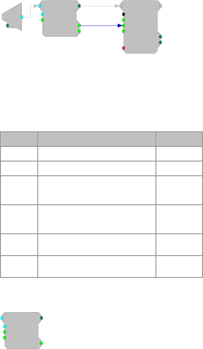
RPvdsEx Manual
170
CompTo8
SF=127
[1:2,0]
Strobe1=0
Byp/Rst=0
Strobe2=0
SerialBuf
Size=1000
Rst=0
AccEnab=1
Write=1
[1:4,0]
NBl ks=0
Index=0
{>Data}
d
c
[1:1,0]
Ch=1
Scale factor (SF) scales the floating point value before storing in integer format.
The largest number that can be specified using eight bits is +/- 127. To get the
maximum resolution, SF should be selected in such a way that the maximum
input voltage scales to +/- 127. The default SF is set to 127 and assumes that the
input is bounded between +/- 1.0 V. Use an SF of 12.7 for a +/- 10 V range. The
SF and input values must be matched. Mismatch between the SF and input
values gives poor resolution or meaningless data. ExpandFrom8 reverses the
process.See Data Reduction - Scale Factor for more information on properly
setting the scale factor, page 166.
Name Description Data Type
Input Input Floating Point
Output Integer containing four 8-bit variables Integer
SF Scale factor sets the scale for the input before
sample conversion; scale factor depends on
input voltage
Floating Point
Byp/Rst When high it resets the start of sample
conversion; when set High data is not
converted
Logic
Strobe1 Pulses high when data is sent; patch to
AccEnable line Logic
Strobe2 Pulses high when component is in bypass
mode; bypass mode passes the data unaltered Logic
CompTo8D
CompTo8D
SF=127
Rst=0
Enab=1
[1:1,0]
Strobe=0
Description:
CompTo8D (compress to 8-bit) is essentially the same as CompTo8 except it
allows for an enable input that ensures no data is passed through when
compression is not enabled. When enabled it scales and converts a stream of 32-
bit floating values to 8-bit fixed point numbers. Each value is stored in an 8-bit
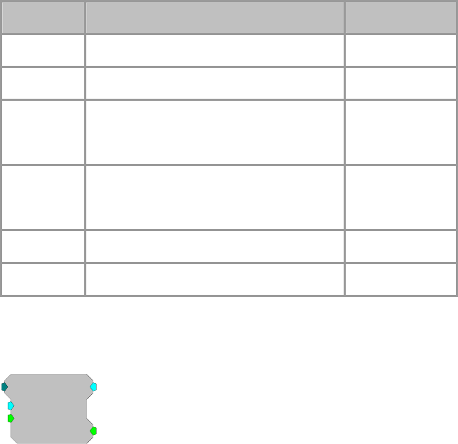
RPvdsEx Manual
171
portion of a 32-bit integer. The Strobe output sends a pulse high when the data
is sent and should be linked to the AccEnable parameter of the buffer
component. This reduction technique can be used to decrease memory
allocation and increase transfer rates.
Scale factor (SF) scales the floating point value before storing in integer format.
The largest number that can be specified using eight bits is +/- 127. To get the
maximum resolution, SF should be selected in such a way that the maximum
input voltage scales to +/- 127. The default SF is 127 and assumes that the input
is bounded between +/- 1.0 V. Use an SF of 12.7 for a +/-10 V range. The SF
and input values must be matched. Mismatch between the SF and input values
gives poor resolution or meaningless data. ExpandFrom8 reverses the process.
See Data Reduction - Scale Factor for more information on properly setting the
scale factor, page 166.
Name Description Data Type
Input Input Floating Point
Output 32-bit integer containing four 8-bit numbers Integer
SF Scale factor sets the scale for the input before
sample conversion; scale factor should be
calculated based on the input voltage
Floating Point
Rst When high it resets the start of sample
conversion; when set high, data is not
converted
Logic
Enab Enables output when high Logic
Strobe Pulses high when enabled and data is sent Logic
ExpFrom16
ExpFrom16
SF=3.05185e
-
[1:1,0]
Strobe=0
Byp/Rst=0
Description:
ExpFrom16 (expand from 16-bit) converts integer data at its input to floating
point data at its output. It takes a stream of dual 16-bit integers and converts
them into two 32-bit floating point values for output. The scale factor (SF)
scales the output values and a Strobe sends a pulse high each time a 32-bit value
is read by the component.

RPvdsEx Manual
172
ExpFrom16
SF=3.05185e
-
[1:2,0]
Strobe=0
Byp/Rst=0
c
O
[1:4,0]
Ch=1
Strobe
Strobe
SerialBuf
Size=1000
Rst=0
AccEnab=1
Write=1
[1:1,0]
NBl ks=0
Index=0
{>Data}
SF defines the range of the expanded data set. It can be the inverse of the scale
factor value used to reduce the data. The default SF is set to 3.05185 e-05, the
inverse of the default scale factor for CompTo16 (32767). Data is passed
through unexpanded when Byp/Rst is set high. See Data Reduction - Scale
Factor for more information on properly setting the scale factor, page 166.
Name Description Data Type
Input Input (two 16-bit variables) Integer
Output Input values in floating point Floating Point
SF Scale factor sets the conversion factor after
data has been expanded Floating Point
Byp/Rst When high it resets the start of sample
conversion; when set High data is not
converted
Logic
Strobe Pulses high on data ready for conversion Logic
ExpFrom8
ExpFrom8
SF=0.007874
0
[1:1,0]
Strobe=0
Byp/Rst=0
Description:
ExpFrom8 (expand from 8-bit) converts integer data at its input to floating point
data at its output. It takes a stream of four 8-bit integers and converts them into
four 32-bit floating point values for output. Output values have the dynamic
range of the reduced data.
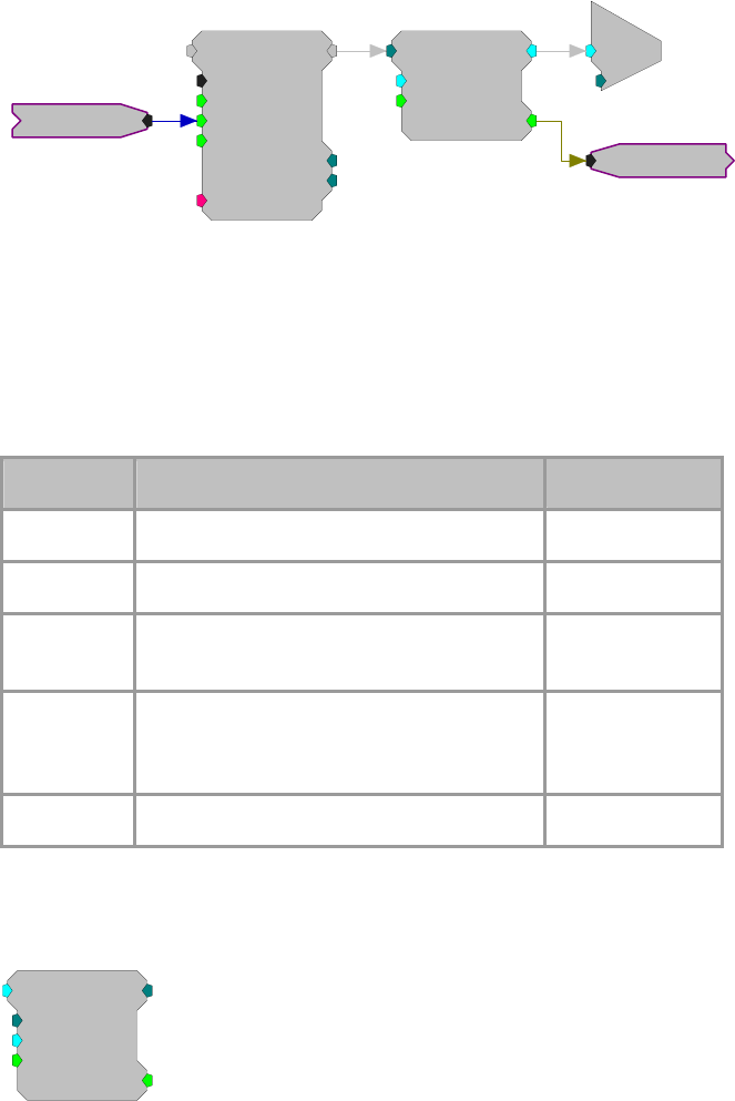
RPvdsEx Manual
173
c
O
[1:4,0]
Ch=1
Strobe
Strobe
ExpFrom8
SF=0.007874
0
[1:2,0]
Strobe=0
Byp/Rst=0
SerialBuf
Size=1000
Rst=0
AccEnab=1
Write=1
[1:1,0]
NBl ks=0
Index=0
{>Data}
Scale factor (SF) defines the range of the expanded data set. It can be the
inverse of the scale factor value used to reduce the data. The default SF is set to
0.007874, the inverse of the default scale factor for CompTo8 (127).
Mismatching scale factors results in an inaccurate scaling of the data. See Data
Reduction - Scale Factor for more information on properly setting the scale
factor, page 166.
Strobe sends a pulse high each time a 32-bit value is loaded to the component.
Name Description Data Type
Input Input (four 8-bit variables) Integer
Output Input values in floating point Floating Point
SF Scale factor sets the conversion factor after
data has been expanded Floating Point
Byp/Rst When high it resets the start of sample
conversion; when set high data is passed
through unexpanded
Logic
Strobe Pulses high on data ready for conversion Logic
PlotDec16
PlotDec16
nDec=10
SF=32767
Enab=1
[1:1,0]
Strobe=0
Description:
PlotDec16 tracks the max and min of the input for a set sample number (nDec),
scales and then outputs the values as the lower and upper portion of a word.
Data can then be stored in a memory buffer for access by a computer. Max
values are stored in the upper 16-bits of the word. Min values are stored in the
lower 16-bits of the word.
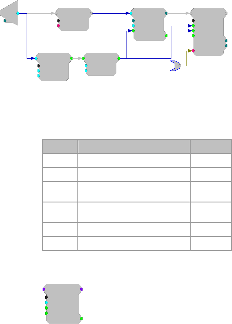
RPvdsEx Manual
174
SerialBuf
Size=100
Rst=0
AccEnab=1
Write=1
[1:11,0]
NB l ks=0
Index=0
{>Data}
d
c
[1:1,0]
Ch=1
LongDelay
Nms=1
{>Data}
[1:2,0]
FeatSrch
FC=Above
K1=0.1
K2=0
[1:4,0]
Schmitt
Thi=10.5
Tlo=0.1
[1:5,0]
PlotDec16
nDec=10
SF=32767
Enab=1
[1:9,0]
Strobe=0
PlotData
Scale factor (SF) sets the output range. For SF = 100, a +/- 1.0 volt signal will
have a range of +/- 100. Data values can be set for a graph plot that is 200
pixels high by using a scale factor of 100 (+/- 100 pixels). To separate the
output into the corresponding max and min values use ReadTagVEX (See
ActiveX help).
Note: because the values are stored using 16 bits, if the scaled input value
exceeds +/- 32767 the data can be corrupted.
Name Description Data Type
Input Signal Float
Output Decimated value based on SF and nDec 32-bit Integer
nDec Block size of data points in which a min and
max are found Integer
SF Scale factor is the conversion value before
compression Floating Point
Enab When enable high, PlotDec16 is running Logic
Strobe Pulses high when data is sent Logic
MCCpTo8D
MCCpTo8D
nChan=16
SF=127
Rst=0
[1:2,0]
Strobe=0
Enab=1
Description:
MCCpTo8D (compress to 8-bit) is the multi-channel version of CompTo8D.
When enabled, the device scales and converts a stream of multi-channel 32-bit
floating-point values to multi-channel 8-bit fixed-point numbers. Each value is
stored in an 8-bit portion of a 32-bit integer. The Strobe output goes high when
the data is available and may be used to clock the data into a buffer component.

RPvdsEx Manual
175
This reduction technique can be used to decrease memory allocation and
increase transfer rates.
Scale factor (SF) scales the floating-point value before storing in integer format.
The largest number that can be specified using eight bits is +/- 127. To get the
maximum resolution, SF should be selected in such a way that the maximum
input voltage scales to +/- 127. The default SF is 127 and assumes that the input
is bounded between +/- 1.0 V. Use an SF of 12.7 for a +/-10 V range. The SF
and input values must be matched. Mismatch between the SF and input values
gives poor resolution or meaningless data. Use ExpandFrom8 on each channel
of data to reverse the process. See Data Reduction - Scale Factor for more
information on properly setting the scale factor, page 166.
Note: This component is for use with only high performance processor devices,
such as RXn or RZn.
Name Description Data Type
Input Multi-channel input Floating Point
Output Multi-channel output (32-bit integers
containing four 8-bit numbers each) Integer
nChan
N
umber of channels Integer (static)
SF Scale factor sets the scale for the input before
sample conversion; scale factor should be
calculated based on the input voltage
Floating Point
Rst When high it resets the start of sample
conversion; when set high, data is not
converted
Logic
Enab Enables output when high Logic
Strobe Pulses high when enabled and data is sent Logic
MCCpTo16D
MCCpTo16D
nChan=16
SF=32767
Rst=0
[1:2,0]
Strobe=0
Enab=1
Description:
MCCpTo16D is the multi-channel version of CompTo16D (compress to 16-bit).
When enabled, MCCpTo16D scales and converts a multi-channel stream of 32-
bit floating-point values to multi-channel 16-bit fixed-point numbers.
Successive values are then output in the upper and lower portions of a 32-bit
integer. The Strobe output goes high when the data is available and may be used
to clock the data into a buffer component. This reduction technique can be used

RPvdsEx Manual
176
to decrease memory allocation for data storage and double the data transfer rate
to and from the PC.
Scale factor (SF) is used to appropriately scale the floating point input before it
is converted to 16 bits. The largest number that can be specified using 16 bits is
+/- 32767. To get the maximum resolution, SF should be selected in such a way
that the maximum input voltage scales to +/- 32767. The default SF is 32767
and assumes that the input is bounded between +/- 1.0 V. Use an SF of 3276.7
for a +/- 10 V range. The SF and input values must be matched. Mismatch
between the SF and input value range gives poor resolution or meaningless
data. Use ExpandFrom16 on each channel of data to reverse the process. See
Data Reduction - Scale Factor for more information on properly setting the
scale factor, page 166.
Note: This component is for use with only high performance processor devices,
such as RXn or RZn.
Name Description Data Type
Input Multi-channel input Floating Point
Output Multi-channel output (32-bit integers containing
two 16-bit numbers each) Integer
nChan
N
umber of channels Integer (static)
SF Scale factor sets the scale for the input before
sample conversion; scale factor should be
calculated based on the input voltage
Floating Point
Rst When high it resets the start of sample
conversion; when set high, data is not converted Logic
Enab Enables output when high Logic
Strobe Pulses high when enabled and data is sent Logic
MCPDec16
MCPDec16
nChan=16
nDec=10
SF=32767
[1:2,0]
Strobe=0
Enab=1
Description:
MCPDec16 is the multi-channel version of PlotDec16. It tracks the maximum
and minimum values of the input for a set number of samples (nDec), scales
them, and then outputs the values as the lower and upper portion of a word.
Data can then be stored in a memory buffer for access by a computer.
Maximum values are stored in the upper 16-bits of the word. Minimum values
are stored in the lower 16-bits of the word.
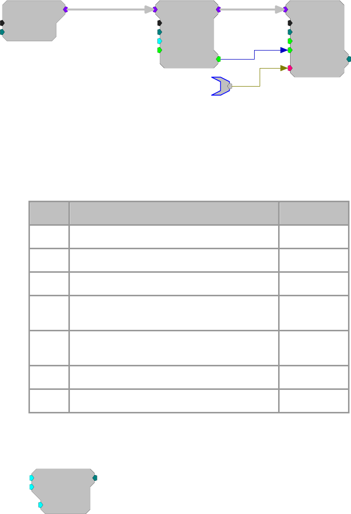
RPvdsEx Manual
177
MCAdcIn
nChan=16
ChanOS=1
[1:1,0
]
MCPDec16
nChan=16
nDec=100
SF=32767
[1:2,0
]
Strobe=0
Enab=1
MCSerStore
nChan=16
Size=16000
Rst=0
WrEnab=1
[1:4,0
]
Index=0
{>Data}
MCPlotData
Scale factor (SF) sets the output range. For SF = 100, a +/- 1.0 volt signal will
have a range of +/- 100. Data values can be set for a graph plot that is 200
pixels high by using a scale factor of 100 (+/- 100 pixels). To separate the
output into the corresponding max and min values use ReadTagVEX (See
ActiveX help). Note: because the values are stored using 16 bits, if the scaled
input value exceeds +/- 32767 the data can be corrupted.
Note: This component is for use with only high performance processor devices,
such as RXn or RZn.
Name Description Data Type
Input Signal Floating Point
Output Decimated value based on SF and nDec 32-bit Integer
nChan
N
umber of channels in the input signal Integer (Static)
nDec Block size of data points in which a min and max
are found Integer
SF Scale factor is the conversion value before
compression Floating Point
Enab When enable high, MCPDec16 is running Logic
Strobe Pulses high when data is sent Logic
ShufTo16
ShufTo16
SF=32767
[1:1,0]
~1
~2
Description:
ShufTo16 takes 32-bit floating point values from two inputs, reduces each,
combines them, and sends them from a single output as 32-bit integers. The top
16-bits stores the first channel and the bottom 16-bits stores the second channel.
This reduction technique can be used to store data from two analog inputs for
high speed transfer. At a 100k sampling rate it is possible to stream two
channels in real-time to disk.
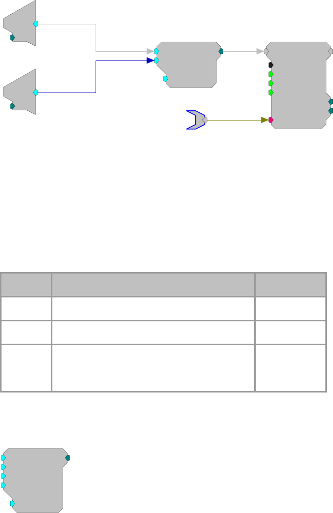
RPvdsEx Manual
178
ShufTo16
SF=32767
[1:4,0]
~1
~2
d
c
[1:3,0]
Ch=1
d
c
[1:1,0]
Ch=2
SerialBuf
Size=1000
Rst=0
AccEnab=1
Write=1
[1:5,0]
NBl ks=0
Index=0
{>Data}
Data
Scale factor (SF) is used to define the upper and lower limits of the signal. The
largest number that can be specified using 16 bits is +/- 32767. To get the
maximum resolution, SF should be selected in such a way that the maximum
input voltage scales to +/- 32767. The default SF is set to 32767 and assumes
that the input is between +/- 1.0 V. Use an SF of 3276.7 for a +/- 10 V range.
The SF and input values must be matched. Mismatch between the SF and input
values gives poor resolution or meaningless data. SplitFrom16 reverses the
process.
See Data Reduction - Scale Factor for more information on properly setting the
scale factor, page 166.
Name Description Data Type
Input(1-2) Input Floating Point
Output Integer containing 2 16-bit values Integer
SF Scale factor sets the scale for the input before
sample conversion; scale factor depends on input
voltage
Floating Point
ShufTo8
ShufTo8
SF=127
[1:1,0]
~1
~2
~3
~4
Description:
ShufTo8 (Shuffle To 8-bit) takes 32-bit floating point values from four inputs,
reduces each and sends them as a 32-bit integer for output. The first 8-bits
stores the first channel the second 8-bits the second and so forth. This reduction
technique can be used to store data from four analog inputs for high speed
transfer.
Scale factor (SF) is used to define the upper and lower limits of the signal. The
largest number that can be specified using eight bits is +/- 127. To get the
maximum resolution, SF should be selected in such a way that the maximum
input voltage scales to +/- 127. The default SF is set to 127 and assumes that the
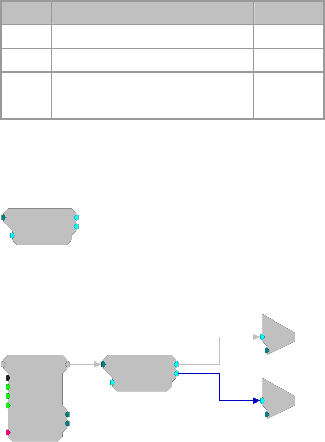
RPvdsEx Manual
179
input is bounded by +/- 1.0 V. Use a scale factor of 12.7 for a +/- 10 V range.
The SF and input values must be matched. Mismatch between scale factor and
input values gives poor resolution or meaningless data. SplitFrom8 reverses the
process.
See Data Reduction - Scale Factor for more information on properly setting the
scale factor, page 166.
Name Description Data Type
Input(1-4) Input Floating Point
Output Integer containing four 8-bit variables Integer
SF Scale factor sets the scale for the input before
sample conversion; scale factor depends on input
voltage
Floating Point
Example(s):
See ShufTo16, page 177.
SplitFrom16
SplitFrom16
SF=3.05185e-
0
[1:1,0]
~1
~2
Description:
SplitFrom16 takes 32-bit integers and splits them into two 16-bit values and
converts them to two floating point values for output. Output values have the
dynamic range of the reduced data.
SplitFrom16
SF=3.05185e-
0
[1:2,0]
~1
~2
SerialBuf
Size=100000
Rst=0
AccEnab=1
Write=1
[1:1,0]
NBl ks=0
Index=0
{>Data}
c
O
[1:3,0]
Ch=1
c
O
[1:5,0]
Ch=1
Scale factor (SF) defines the range of the shuffled data sets. It must be the
inverse of the scale factor value used to shuffle the data. The default scale factor
is set to 3.05185 e-05, the inverse of the default scale factor for ShufTo16
(32767). Mismatching scale factors results in inaccurate scaling of the data. See
Data Reduction - Scale Factor for more information on properly setting the
scale factor, page 166.
The outputs are matched to the original inputs.

RPvdsEx Manual
180
Name Description Data Type
Input Input (integer value containing two 16-bit
values) Integer
Output(1-2) Converted floating point values Floating Points
SF Scale factor sets the scale for the input before
sample conversion; scale factor depends on
input voltage
Floating Point
SplitFrom8
SplitFrom8
SF=0.007874
0
[1:1,0]
~1
~2
~3
~4
Description:
SplitFrom8 takes 32-bit integers and splits them into four 8-bit values and sends
them as floating point values for output. Output values have the dynamic range
of the reduced data.
Scale factor (SF) defines the range of the shuffled data sets. It must be the
inverse of the scale factor value used to shuffle the data. The default SF is set to
0.07874, the inverse of the default scale factor for ShufTo8 (127). Mismatch
between scale factors results in inaccurate scaling of the data. See Data
Reduction - Scale Factor for more information on properly setting the scale
factor, page 166.
The channel output match the original channels for input.
Name Description Data Type
Input Input (integer value containing four 8-bit
variables) Integer
Output(1-4) Converted floating point values Floating Points
SF Scale factor sets the scale for the input before
sample conversion; scale factor depends on
input voltage
Floating Point
Example:
See SplitFrom16, page 179
RPvdsEx Manual
181
Delay Functions
Delay Function Components
Delay functions can be used to create intentional delays between signals or to synchronize delays
that are introduced by the ADC and DAC. See DAC and ADC delays, page 51, for more
information.
This group includes the following components:
ADCDelay
DACDelay
Latch
LongDelay
LongDynDelay
MultLatch
SampDelay
ShortDelay
ShortDynDelay
This group also includes the following component, if RPvdsEx Device Setup is
configured for a high performance device, such as the RXn or RZn:
MCDelay
MCLatch
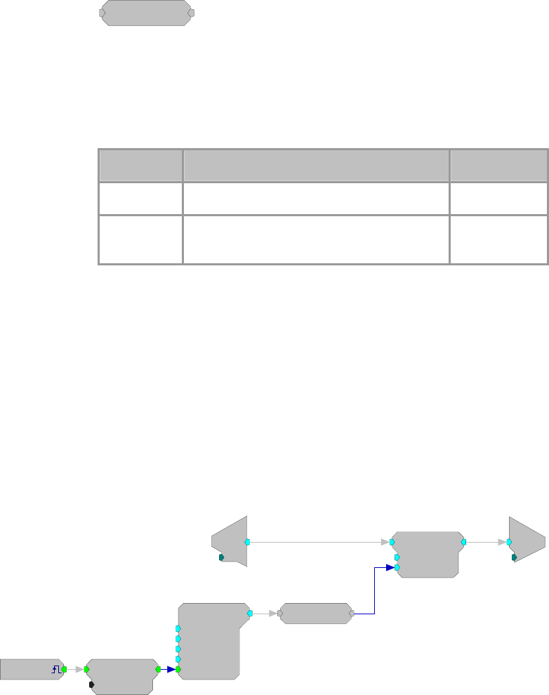
RPvdsEx Manual
182
ADCDelay
ADCDelay
[1:1,0]
Description:
Time delay equal to ADC group delay for the RP2.
Note: The ADCDelay component will always delay for 41 samples, which is
correct for an RP2. Because of the different ADC delays of the various
processors (RP2.1 = 65 samples, RX6 = 70 samples, etc.), this component will
delay accurately for the RP2 only.
Name Description Data Type
Input Input Any
Output Input delayed by 41 samples (group delay of
RP2 ADC) Any
Equation:
Output = ( Input[-ADCDelay])
Example:
Analog-to-Digital Delay
File: Examples\ADCdelayEx.rcx
Default Device: RP2 Processor
Sampling Rate: 50 kHz
This example mixes the input from channel one with a tone generated by the
circuit. The phase of the tone is reset to zero when an external trigger is
detected. The ADCDelay component is included in the circuit before the
ScaleAdd to ensure that the tone and the input signal phase are matched.
d
c
[1:7,0]
Ch=1
ScaleAdd
SF=1
Shft=0
[1:8,0]
c
O
[1:9,0]
Ch=1
Tone
Amp=1
Shft=0
Freq=1000
Phse=0
[1:4,0]
Rst=Run
ADCDelay
[1:5,0]
EdgeDetect
Edge=Rising
[1:2,0]
[1:1,0]
Src=Extern
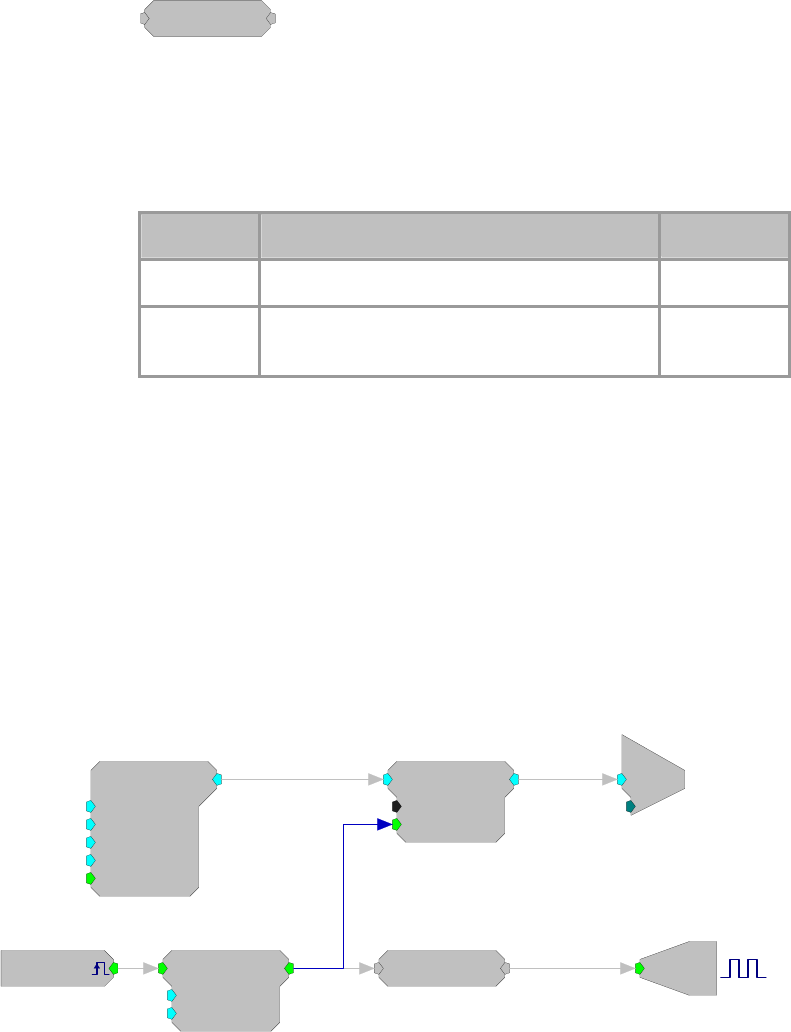
RPvdsEx Manual
183
DACDelay
DACDelay
[1:1,0]
Description:
Time delay equal to 30 samples, the DAC group delay for the RP2 and RP2.1.
Note: The DACDelay component will always delay for 30 samples, which is
correct for an RP2 and RP2.1. However, the RA16 has a DAC delay of 18
samples and the RV8 has a DAC delay of 2-4 samples. This component will
accurately account for the DAC delay for the RP2 and RP2.1 only.
Name Description Data Type
Input Input Any
Output Input delayed by 30 samples (group delay of
DAC for RP2 and RP2.1) Any
Equation:
Output = ( Input[-DACDelay])
Example:
Digital-to-Analog Delay
File: Examples\DAC_ex.rcx
Default Device: RP2.1 Processor
Sampling Rate: 50 kHz
This example plays a tone from analog output channel one when it receives a
software trigger. A DACDelay is used to synchronize the output on Bit-1 of the
digital output with the output of the Tone on the DAC. A LinGate is used to
ramp the tone on and off with a 10 ms rise-fall time. A Schmitt trigger controls
the duration of the tone.
c
O
[1:8,0]
Ch=1
Bi
[1:5,0]
M=1
[1:1,0]
Src=Soft1
Tone
Amp=1
Shft=0
Freq=1000
Phse=0
[1:6,0]
Rst=Run
LinGate
Trf=10
Ctrl=Closed
[1:7,0]
Schmitt
Thi=100
Tlo=10
[1:2,0]
DACDelay
[1:4,0]
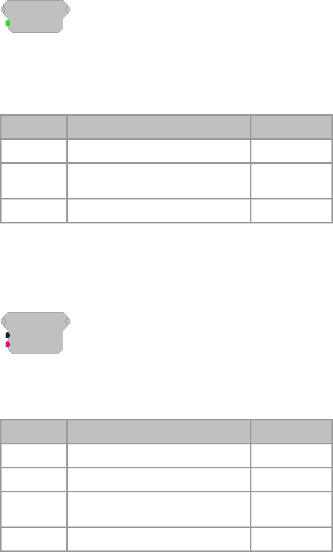
RPvdsEx Manual
184
Latch
Latch
Trg=0
[1:1,0]
Description:
Latches input to output on the rising edge of a trigger. The output will remain
unchanged until the trigger goes high again and the output is latched to the new
value.
Note: Until the first time the trigger goes high, the output will be zero.
Name Description Data Type
Input Input Any
Output When Trg = 1 output = input else output
remains unchanged Any
Trg Triggers latch Logic
Equation:
If (Trg) then Output = ( Input ) else Output remains unchanged
LongDelay
LongDelay
Nms=100
{>Data}
[1:1,0]
Description:
Time delay using SDRAM. (Will not work with RP2-5, because it does not
have memory. Can only use short delay). Data port can be used to view data
currently in delay line.
Name Description Data Type
Input Input Any
Output Input with a set time delay Any
N
ms Length of delay in milliseconds (maximum
is 10,000,000; the minimum is 1 ms) Floating Point
(Static)
>Data Pointer to delay line Pointer
Equation:
Output = ( Input[-Nms])
Example:
Sum, page 114.

RPvdsEx Manual
185
LongDynDel
LongDynDel
Mms=100
Dms=50
{>Data}
[1:1,0]
Description:
The LongDynDel component performs a dynamic delay using SDRAM. Unlike
the LongDelay component, which has a delay value that is fixed at compile
time, the delay value (Dms) on LongDynDelay is dynamic. The maximum
delay value (Mms) is fixed and Dms can never be allowed to exceed it. The
LongDynDel component can be used to generate delays that are not quantized
to the sample rate. To do this, it cross fades (averages) the two points about the
delay. An example is generating Doppler effects for 3D auditory displays.
When setting up a variable delay line, keep in mind that the signal may be
distorted if the delays are not multiples of the sample period. When the delay is
not a multiple of the sample period, there is a linear relationship between the
location of the delay and the amount that the point on either side of the delay
contributes to the corresponding point in the delayed signal. For example, if the
desired delay was 0.25 samples, each point in the delayed signal would be
described by the following:
(1-0.25)*sample value before delay + 0.25*sample value after delay.
Because this component uses cross fading to implement the delay, it is not
suitable for delaying a TTL pulse. To delay a TTL pulse, use either the
TTLDelay or TTLDelay2 component. Because it uses SDRAM, it will not work
on the RP2-5.
Name Description Data Type
Input Input Floating Point
Output Input with a set time delay Floating Point
Mms Maximum delay value for Dms. Floating Point
(Static)
Dms Delay length in milliseconds. It cannot exceed
Maximum delay value. Floating Point
>Data Pointer to delay line Pointer
RPvdsEx Manual
186
MCDelay
MCDelay
nChan=16
nDelay=16
[1:2,0]
Description:
MCDelay implements a delay of n samples on each of the channels in the multi-
channel input. This component uses internal device memory. Because internal
memory is a limited resource (20kB) you may need to monitor the available
internal memory when using this component
See the FreeDM component, page 193.
Also see: Important Consideration for Working with Multi-Channel
Components, page 57.
Note: This component is for use with only high performance processor devices,
such as RXn or RZn.
Name Description Data Type
Input Multi-channel input Any
Output Multi-channel delayed output Same as input
nChan
N
umber of channels in the input/outpu
t
Integer (Static)
nDelay Delay to be applied in number of samples Integer
MCLatch
Description:
MCLatch is the multi-channel version of the Latch component. It latches input
to output on the rising edge of a trigger. The output will remain unchanged until
the trigger goes high again and the output is latched to the new value.
Note: Until the first time the trigger goes high, the output will be zero.
Name Description Data Type
Input Input signal to be latched Any
Output When Trg = 1, Output = Input
otherwise Output remains unchanged
Any
Trg Triggers latch Logic

RPvdsEx Manual
187
Equation:
If (Trg) then Output = ( Input ) else Output remains unchanged.
MultLatch
MultLatch
In1=0
In2=0
In3=0
Trg=0
[1:1,0]
>
>
>
Description:
The 'MultLatch' latches multiple inputs to multiple outputs when triggered.
Inputs can take all formats including Parameter tags. The Multlatch should be
used when several parameters need to be sent out at the same time. In the
example below the frequency, amplitude and phase of a tone generator are
latched at the same time.
Name Description Data Type
In1 Input Floating Point
In2 Input Floating Point
In3 Input Floating Point
Trg Triggers latch TTL
> Output Floating Point
> Output Floating Point
> Output Floating Point
Tech Notes:
All inputs and outputs act as Parameters.
Equation:
If (Trg) then Output = ( Input ) else Output=0
Example:
MultLatch
In this example, a PulseTrain2 triggers the MultLatch. Any changes in the
ParTags will modify the phase, frequency and/or amplitude of the Tone
generator.
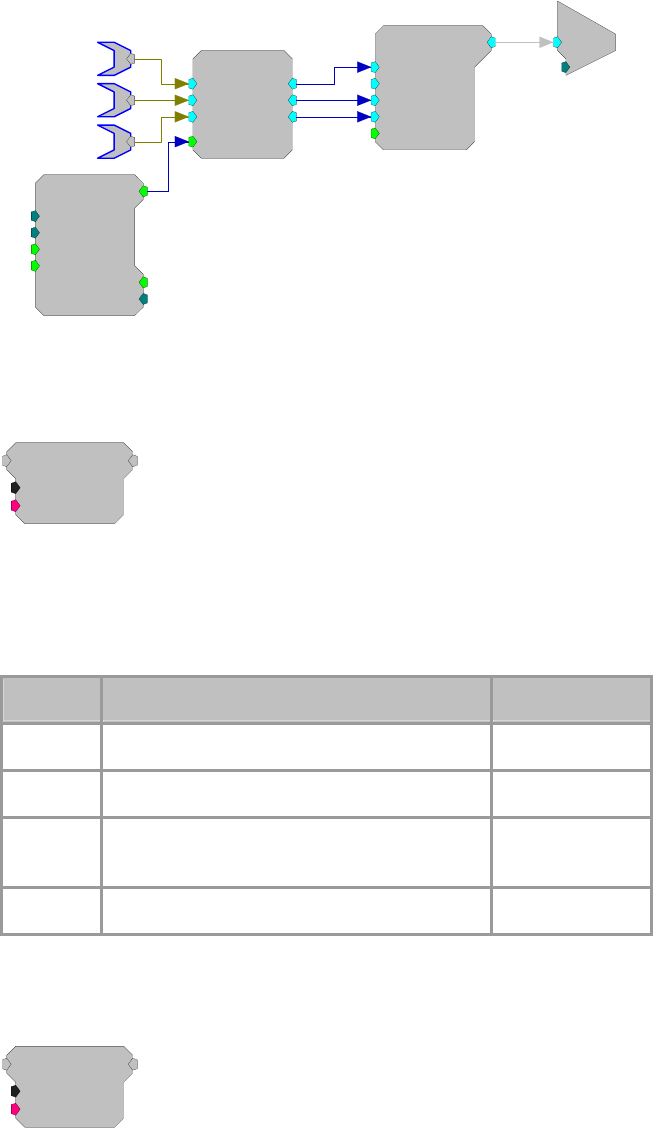
RPvdsEx Manual
188
Tone
Amp=1
Shft=0
Freq=1000
Phse=0
[1:7,0
]
Rst=Run
c
O
[1:8,0]
Ch=1
MultLatch
In1=0
In2=0
In3=0
Trg=0
[1:3,0]
>
>
>
PulseTrain2
nPer=100
nPulse=-1
Enab=Yes
Rst=Run
[1:1,0
]
PCount=0
PLate=0
Amp
Freq
Phase
SampDelay
SampDelay
nDelay=1
{>Data}
[1:1,0]
Description:
Time delay using SDRAM. (Will not work with RP2-5 because it does not have
extended memory). This component is similar to the LongDelay component
except the delay parameter nDelay is specified in samples instead of
milliseconds. Data port can be used to view data currently in delay line.
Name Description Data Type
Input Input Any
Output Delayed output Any
nDelay Delay to be applied in number of samples
(maximum 100,000,000) Integer
>Data Pointer to delay line Pointer
ShortDelay
ShortDelay
Nms=1
{>Data}
[1:1,0]
Description:
Time delay using internal memory. Maximum delay of 10 ms. Data port can be
used to view data currently in delay line.
Note that there is only 1024 32-bit words of Dynamic Memory allocated for
Delay functions. The number of short delays that are allowed is dependent on
RPvdsEx Manual
189
the delay length and the sampling rate. For example a millisecond ShortDelay
consumes 50 words at 50 kHz sampling rate.
Name Description Data Type
Input Input Any
Output Input with a set time delay Any
N
ms Length of delay in milliseconds (maximum is 10) Floating Point
(Static)
>Data Pointer to delay line Pointer
Equation:
Output = ( Input[-Nms])
Example:
Short Delay, page 190.
ShortDynDel
ShortDynDel
Nms=1
Dms=0.5
{>Data}
[1:1,0]
Description:
The ShortDynDel component implements a dynamic delay using internal
memory. Unlike the ShortDelay component, which has a delay value that is
fixed at compile time, the delay value (Dms) on ShortDynDelay is dynamic.
The maximum delay value (Mms) is fixed and Dms can never be allowed to
exceed it. The maximum value of Mms is 10 milliseconds. If a longer delay is
required, use the LongDynDel component, which has a larger memory buffer.
This component can be used to generate delays that are not quantized to the
sample rate. To do this, it cross fades (averages) the two points about the delay.
An example is generating Doppler effects for 3D auditory displays.
When setting up a variable delay line, keep in mind that the signal may be
distorted if the delays are not multiples of the sample period. When the delay is
not a multiple of the sample period, there is a linear relationship between the
location of the delay and the amount that the point on either side of the delay
contributes to the corresponding point in the delayed signal. For example, if the
desired delay was 0.25 samples, each point in the delayed signal would be
described by the following:
(1-0.25)*sample value before delay + 0.25*sample value after delay.
Because this component uses cross fading to implement the delay, it will not
work correctly for delaying a TTL pulse. To delay a TTL pulse, use either the
TTLDelay or TTLDelay2 component. Because it uses internal memory, it is
compatible with the RP2-5.
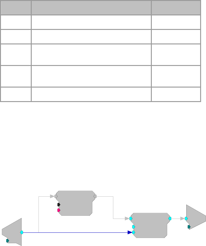
RPvdsEx Manual
190
Name Description Data Type
Input Input Floating Point
Output Input with a set time delay Floating Point
Mms Maximum delay value for Dms(10) Floating Point
(Static)
Dms Delay length in milliseconds. It cannot exceed
Maximum delay value. Floating Point
>Data Pointer to delay line Pointer
Example:
Short Delay
File: Examples\shortdelay_ex.rcx
Default Device: RP2 Processor
Sampling Rate: 50 kHz
This example adds an echo to the input of the ADC and plays it out DAC
channel one. The ShortDelay adds a one millisecond delay to the input. It is
then scaled by -0.5 to reduce its level and flip its phase and then added back to
the original signal with the ScaleAdd component.
c
O
[1:5,0]
Ch=1
d
c
[1:1,0]
Ch=1
ScaleAdd
SF=-0.5
Shft=0
[1:4,0]
ShortDelay
Nms=1
{>Data}
[1:3,0]
RPvdsEx Manual
191
Device Status
Device Status Components
Device status components serve both to monitor and do math with major system status values.
These components feed the processing chain with specific system information like DSP cycle
usage or available system memory. The value can be used to compute some circuit parameter or
simply monitored system status. When using RPvdsEx a ParWatch can be used to monitor the
output of a Device Status component.
This group includes the following components:
CycUsage
FreeDM
FreePM
FreeXM
PowCtrl
PowStat
Important Note!: This group also includes two undocumented components: Peek and Poke.
These components are intended primarily for TDT use and should not be used without TDT
assistance.
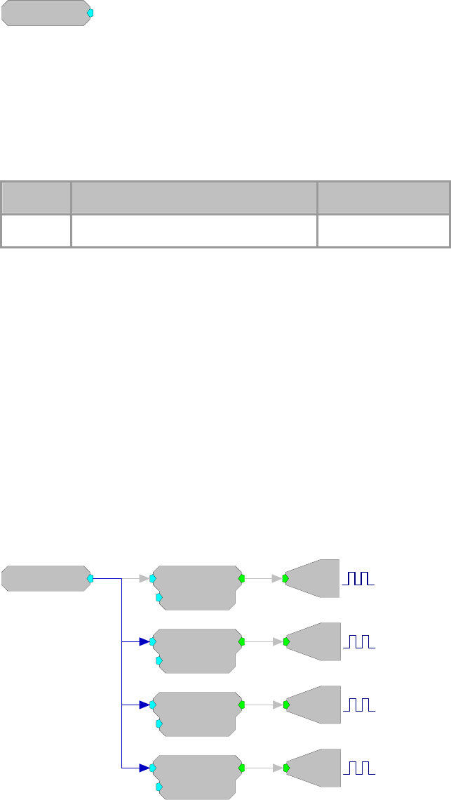
RPvdsEx Manual
192
CycUsage
CycUsage
[1:1,0
]
Description:
Feeds stream with DSP cycle usage in percent. Unpredictable behavior may be
experienced when cycle usage exceeds 90%.
Important:! If cycle usage is over 100% the value returned will not indicate
this. For example a cycle usage of 120% will return 20%. To determine if your
cycle usage is over 100% lower your sampling rate and check to see if
cycUsage "increases". An increase means that the cycle usage was greater than
100%. Higher sampling rates use more cycles than lower.
Name Description Data Type
Output Cycle Usage (0-100) Floating Point
Equation:
Output = 100% * DSP_Cycle_Used_Per_Second / 50,000,000
Example:
Cycle Usage
File: Examples\cycleUsage_ex.rcx
Default Device: RP2 Processor
Sampling Rate: 50 kHz
This circuit uses the four face plate LEDs found on the RP2 as a DSP cycle
usage reporting meter. The CycUsage component is fed to four Float2TTL
converters which have threshold settings. These settings are set to indicate
activity over the levels shown. The four TTL signals are then made to control
the four LEDs of the TTL output port. Notice that because Bit-0 is physically
located at the top of the four LED group it is used to indicate the highest level
of usage. In general, adding cycle usage with a parameter watch is a good way
of determining the cycle usage of your system.
CycUsage
[1:1,0
]
Float2TTL
Thrsh=12.5
[1:2,0]
Bi
[1:3,0]
M=8
Float2TTL
Thrsh=37.5
[1:5,0]
Bi
[1:6,0]
M=4
Float2TTL
Thrsh=62.5
[1:8,0]
Bi
[1:9,0]
M=2
Float2TTL
Thrsh=87.5
[1:11,0]
Bi
[1:12,0]
M=1
RPvdsEx Manual
193
FreeDM
FreePM
FreeXM
FreeDM
[1:1,0
]
FreePM
[1:2,0
]
FreeXM
[1:3,0
]
Description:
Feeds stream with amount of currently available memory of specified type.
Data memory (DM) is typically used for filter delay line and short delays.
Program Memory (PM) holds filter coefficients and External Memory (XM) is
used for long delays and buffers.
Note: The value shown is the number of free 4-byte words (samples) rather than
the number of free bytes.
Name Description Data Type
Output Amount of memory left (DM, PM or XM) Integer
PowCtrl
PowCtrl
PowDn=No
PowUp=No
Elem=None
[1:1,0]
Description:
PowCtrl works with all battery operated RP devices. Power is conserved by
shutting down device elements not used on a circuit. When not in use the DAC,
ADC, and SDRAM draw power from the battery. PowDn powers down an
element. PowUp powers up an element that has been powered down.
WARNING: Data in memory buffers is lost when the SDRAM is PowDn.
Name Description Data Type
PowDn On Trigger hi (one cycle) Power to the DAC,
ADC or SDRAM is stopped. Logic
PowUp On Trigger hi (one cycle) Power to the DAC,
ADC or SDRAM is restored. Logic
Elem Device Element. 0= No device, 1=DAC,
2=ADC, 3=SDRAM Integer
RPvdsEx Manual
194
PowStat
PowStat
[1:1,0
]
Description:
When the battery voltage is good the PowStat output goes high. When the
battery voltage goes low the PowStat output goes low.
Note: May not work with Lithium-Ion Batteries.
Name Description Data Type
Output Power Status
Hi=Good Voltage, Lo=Warning
Logic
RPvdsEx Manual
195
Digital Filters
Digital Filter Components
This group of processors performs basic digital filtering tasks. Coefficients can be pre-loaded or
generated and updated on-the-fly. See Coefficient Generators, page 144, for information on
dynamically changing filter performance.
Note: To satisfy the Nyquist theorem, the filter's corner frequency should always be less than half
the sampling frequency.
This group includes the following components:
Biquad
FIR
IIR
Smooth
This group also includes the following components, if RPvdsEx Device Setup is
configured for a high performance device, such as the RXn or RZn:
FIR2
MCBiquad
MCFIR
MCFIR2
MCSmooth
StereoFIR2

RPvdsEx Manual
196
Biquad
Biquad
nBIQ=1
{>Coef}
{>Delay}
[1:1,0]
Description:
This component filters the input with an Nth stage Biquad. nBiq can be from
one to 16 and care must be taken to match the number of stages with whatever
coefficient generation scheme you are using. The Coefficient buffer is [nBIQ*5]
in length and is kept in PM. A delay line of length [nBIQ*4] is held in DM.
Each digital filter needs its own coefficient generator. Biquad accepts
coefficient inputs from the filter coefficient generators.
Coefficients can be generated using one of the Coefficient Generator
components or supplied via parameter tag (for example, when generated using
the Biquad Coefficient Control in OpenController software).
Note: Filter frequencies should be less than half the sampling rate of the
system.
Name Description Data Type
Input Input Floating Point
Output Filtered signal Floating Point
nBIQ
N
umber of Biquads (min=1, max=16) Integer (Static)
>Coef Pointer to Coef buffer (PM).
Ordering: B0(1), B1(1), B2(1), A1(1), A2(1),
B0(2), B1(2), B2(2), A1(2), A2(2), … B0(n),
B1(n), B2(n), A1(n), A2(n), where n=nBiq.
Pointer
>Delay Pointer to delay buffer (DM). Pointer
Equation:
Output = Biquad (Input)
Example:
Biquad Filter
File: Examples\BiquadEx.rcx
Default Device: RP2 Processor
Sampling Rate: 50 kHz
This somewhat complex circuit demonstrates a number of processing concepts,
including the Biquad filter and the ButCoef, a Butterworth coefficient generator
with specific attributes for the Biquad filter. The circuit generates filtered
amplitude modulated noise for D/A channel one. The noise is low-pass filtered
using a Biquad with the filtering coefficients being generated in real-time via
the ButCoef component. Because the coefficients are generated in real-time the
low-pass filter frequency can be changed dynamically.
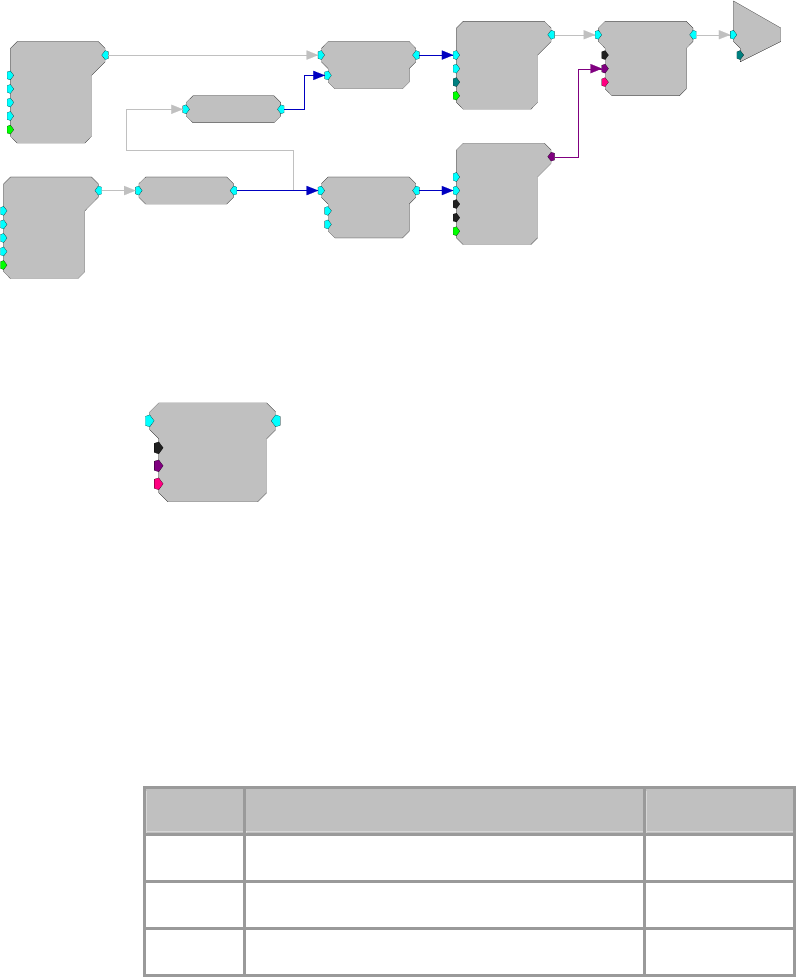
RPvdsEx Manual
197
The Tone generator at chain position [1:1,0] is used to modulate the filter corner
frequency by octaves. The Exp2 component converts the octave output to a
linear multiplier that is then scaled by 2000 via ScaleAdd. This generates a
sinusoidal non-linear frequency sweep that goes from two octaves (500 Hz)
below to two octaves (8000 Hz) above 2000 Hz.
The Tone generator at [1:5, 0] is used to modulate the amplitude of the noise to
a depth of 50%. SqRoot and Divide are used to normalize the level of the
circuit's output so it won't get louder as the bandwidth gets wider.
Tone
Amp=2
Shft=0
Freq=0.5
Phse=0
[1:1,0]
Rst=Run
Tone
Amp=0.5
Shft=1
Freq=50
Phse=0
[1:5,0]
Rst=Run
GaussNoise
Amp=1
Shft=0
Seed=0
Rst=Run
[1:12,0]
ScaleAdd
SF=2000
Shft=0
[1:9,0]
Divide
Den=1
[1:6,0]
Exp2
[1:2,0]
SqRoot
[1:3,0]
ButCoef
Gain=1
Fc=1000
NBiq=1
Type=LP
[1:11,0]
Enab=Yes
Biquad
nBIQ=1
{>Coef}
{>Delay}
[1:13,0] c
O
[1:14,0]
Ch=1
FIR
FIR
Order=32
{>Coef}
{>Delay}
[1:1,0]
Description:
This component filters the input with an Nth order FIR. The Order must be
specified as at least 1 and not more than 1024. Two memory buffers are
associated with FIR. The Coefficient buffer is [Order+1] in length and is kept in
PM. A delay line of length [Order+1] is held in DM. Each digital filter needs its
own coefficient generator.
Coefficients can be generated using one of the Coefficient Generator
components or supplied via parameter tag (for example, when generated using
the Biquad Coefficient Control in OpenController software).
Note: Filter frequencies should be less than half the sampling rate of the system.
Name Description Data Type
Input Input Floating Point
Output Filtered signal Floating Point
Order
N
umber of taps minus 1. Min=1, Max=1024 Integer (Static)
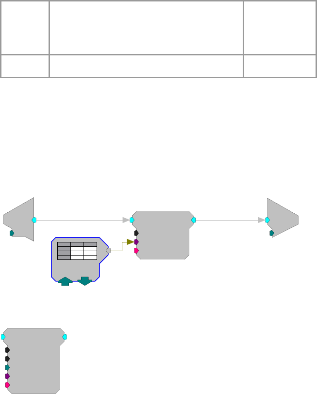
RPvdsEx Manual
198
>Coef Pointer to Coef buffer (PM).
Ordering:
B(0), B(1), B(2), … B(n), where n=Order
Pointer
>Delay Pointer to delay buffer (DM). Pointer
Equation:
Output = FIR (Input)
Example:
FIR/Data Table
This example uses an FIR filter to alter the input signal. The FIR filter
coefficients are loaded into a DataTable. The input of ADC channel one is
filtered by the 33 tap FIR filter and played out of the DAC. The contents of the
DataTable can be loaded with FIR filters generated from MATLAB.
FIR
Order=32
{>Coef}
{>Delay}
[1:2,0]
d
c
[1:1,0]
Ch=1
c
O
[1:3,0]
Ch=1
FIR Coefs
= 0
FIR2
FIR2
Order=31
nSets=1
SetSel=0
{>Coef}
[1:1,0]
{>Delay}
Description:
The FIR2 is a single channel, optimized FIR filter that supports multiple filter
coefficient sets.
This component filters the input with an Nth order FIR. Order must be specified
as at least 5 and should always be odd (nTaps will be even). Two memory
buffers are associated with FIR2. The Coefficient buffer is [(Order+1)*nSets] in
length and is kept in PM. A delay line of length [Order+1] is held in DM. FIR2
supports instant coefficient switching through (zero-based) SetSel. Note that the
FIR Coefficient Data Table may not be used with the FIR2 component.
SetSel is used to specify the coefficient set to use. This input can range from 0
to nSets-1. Setting this input to a value outside this range will cause your
circuit to fail.
All of the xxFIR2 components allow for a unique set of coefficients for each
channel (when more than one channel is applicable) and instantaneous
switching between coefficients sets using the SetSel input. Also longer filters
can be specified. While there is a hard limit on the filter order of 8191, this
value is more often limited by the amount of PM memory available for the

RPvdsEx Manual
199
filter. When specifying an FIR2 type filter, pay special attention to any loading
or memory allocation errors that are generated when your circuit is loaded.
Note: This component is for use with only high performance processor devices,
such as RXn or RZn.
Note: Filter frequencies should be less than half the sampling rate of the
system.
Name Description Data Type
Input Input Floating Point
Output Filtered signal Floating Point
Order
N
umber of taps minus 1. Must be odd.
Min=5, Max is limited by available memory. Integer (Static)
nSets
N
umber of coefficient sets. Integer (Static)
SetSel Selects the coefficient sets to apply. Integer
>Coef Pointer to Coef buffer (PM)
See below for coefficient ordering.
Pointer
>Delay Pointer to delay buffer (DM). Pointer
Equation:
Output = FIR (Input)
Coefficient
Ordering:
To optimize performance the FIR2 component requires each coefficient set be
arranged into a shuffled format. Each coefficient set must be shuffled as
follows:
n = nTaps = Order + 1
B(0), B(n/2), B(1), B(n/2+1) … B(n/2-1), B(n-1)
For Example:
Order = 9
nSets = 3
Filter coefficients in logical order:
B0 B1 B2 B3 B4 B5 B6 B7 B8 B9
Set1: 1.0 1.1 1.2 1.3 1.4 1.5 1.6 1.7 1.8 1.9
Set2: 2.0 2.1 2.2 2.3 2.4 2.5 2.6 2.7 2.8 2.9
Set3: 3.0 3.1 3.2 3.3 3.4 3.5 3.6 3.7 3.8 3.9

RPvdsEx Manual
200
The coefficients must be shuffled as follows:
B0 B5 B1 B6 B2 B7 B3 B8 B4 B9
Set1: 1.0 1.5 1.1 1.6 1.2 1.7 1.3 1.8 1.4 1.9
Set2: 2.0 2.5 2.1 2.6 2.2 2.7 2.3 2.8 2.4 2.9
Set3: 3.0 3.5 3.1 3.6 3.2 3.7 3.3 3.8 3.4 3.9
The coefficients are then concatenated and loaded as a row vector as follows:
Coef = [Set1, Set2, Set3]
IIR
IIR
Order=2
{>Coef}
{>Delay}
[1:1,0]
Description:
This component filters the input with an Nth order IIR. The Order must be
specified as at least 1 and not more than 32. Two memory buffers are associated
with IIR. The Coefficient buffer is [(Order*2)+2] in length and is held in PM. A
delay line of length [(Order*2)+2] is held in DM. Each digital filter needs its
own coefficient generator.
Coefficients can be generated using one of the Coefficient Generator
components or supplied via parameter tag (for example, when generated using
the Biquad Coefficient Control in OpenController software).
Note: Filter frequencies should be less than half the sampling rate of the
system.
Name Description Data Type
Input Input Floating Point
Output Filtered signal Floating Point
Order
N
umber of taps minus 1. Min=1, Max=32 Integer (Static)
>Coef Pointer to Coef buffer (PM).
Ordering: B(0), B(1), … B(n), A(1), …
A(n), where n=Order
Pointer
>Delay Pointer to delay buffer (DM). Pointer
Equation:
FO = IIR (FI)

RPvdsEx Manual
201
MCBiquad
MCBiquad
nChan=16
nBIQ=1
{>Coef}
{>Delay}
[1:2,0]
Description:
This component is a multi-channel version of the Biquad component.
Coefficients must be supplied via the coefficient pointer (>Coef). The
Coefficient buffer is [nBIQ*5] in length and is kept in PM. A delay line of
length [((nBIQ*4)+1)*nChans] is held in DM.
Coefficients can be generated using one of the Coefficient Generator
components or supplied via parameter tag (for example, when generated using
the Biquad Coefficient Control in OpenController software). One to 16 biquad
stages can be specified (nBIQ). The number of stages specified in MCBiquad
must match the number of stages specified in the coefficient generator. A
separate coefficient generator must be used for each MCBiquad.
MCBiquad
nChan=16
nBIQ=1
{>Coef}
{>Delay}
[1:3,0]
MCAdcIn
nChan=16
ChanOS=1
[1:2,0]
ButCoef
Gain=1
Fc=1000
NBiq=1
Type=LP
[1:1,0]
Enab=Yes
FiltMCOut
Also see: Important Consideration for Working with Multi-Channel
Components, page 57.
Note: This component is for use with only high performance processor devices,
such as RXn or RZn.
Name Description Data Type
Input Multi-channel input Floating Point
Output Filtered multi-channel output Floating Point
nChan
N
umber of channels of input/outpu
t
Integer (Static)
nBIQ
N
umber of Biquads (min=1, max=16) Integer (Static)
>Coef Pointer to Coef buffer (PM)
See Biquad component, page 196 for ordering.
Pointer
>Delay Pointer to delay buffer (DM) Pointer
RPvdsEx Manual
202
MCFIR
MCFIR
nChan=16
Order=31
{>Coef}
{>Delay}
[1:2,0]
Description:
The MCFIR filters each channel of a multi-channel input with an Nth order
FIR. Order must be specified as at least 1 and must always be odd. The
Coefficient buffer is [Order+1] in length and is kept in PM. A delay line of
length [((Order+1)*nChan)+nChan] is held in DM.
The MCFIR component is similar to the MCBiquad filter in that all channels
are filtered with the same set of coefficients.
See MCFIR2 if you need to have a different filter for each channel.
Note: This component is for use with only high performance processor devices,
such as RXn or RZn.
Name Description Data Type
Input Multi-channel input Floating Point
Output Multi-channel filtered signal Floating Point
nChan
N
umber of channels Integer (Static)
Order
N
umber of taps minus 1. Must be odd. Min=1 Integer (Static)
>Coef Pointer to Coef buffer (PM).
See FIR component, page 197 for ordering.
Pointer
>Delay Pointer to delay buffer (DM). Pointer
Equation:
Output = FIR (Input)
MCFIR2
MCFIR2
nChan=16
Order=31
nSets=1
SetSel=0
[1:2,0]
{>Coef}
{>Delay}
Description:
The MCFIR2 is a multi-channel version of the FIR2 component. This
component supports a different filter for each channel and multiple coefficient
sets.
RPvdsEx Manual
203
This component filters each channel in a multi-channel input with an Nth order
FIR. Order must be specified as at least 3 and must be odd (nTaps will be
even). The Coefficient buffer is [(Order+1)*nChan*nSets] in length and is kept
in PM. A delay line of length [((Order+1)*nChan)+nChan] is held in DM.
MCFIR2 supports instant coefficient switching through SetSel. See FIR2 for
more details.
Note: This component is for use with only high performance processor devices,
such as RXn or RZn.
Name Description Data Type
Input Mult-channel input Floating Point
Output Multi-channel filtered signal Floating Point
nChan
N
umber of channels Integer (Static)
Order
N
umber of taps minus 1. Must be odd. Min=3 Integer (Static)
nSets
N
umber of coefficient sets. Integer (Static)
SetSelect Selects the coefficient sets to apply. Integer
>Coef Pointer to Coef buffer (PM)
See below for coefficient ordering.
Pointer
>Delay Pointer to delay buffer (DM). Pointer
Equation:
Output = FIR (Input)
Ordering:
Odd and even channel coefficients must be shuffled as follows:
n = nTaps = Order + 1
c = nChans
B0(1), B0(2), B1(1), B1(2), ...Bn-1(1), Bn-1(2) : B0(3), B0(4), B1(3), B1(4) ...
For Example:
Order = 3
nChan = 6
Filter coefficients in logical order:
RPvdsEx Manual
204
Chan B0 B1 B2 B3
1 1.0 1.1 1.2 1.3
2 2.0 2.1 2.2 2.3
3 3.0 3.1 3.2 3.3
4 4.0 4.1 4.2 4.3
5 5.0 5.1 5.2 5.3
6 6.0 6.1 6.2 6.3
These coefficients must be shuffled as follows:
B0(o) B0(e) B1(o) B1(e) B2(o) B2(e) B3(o) B3(e)
Ch1_2 1.0 2.0 1.1 2.1 1.2 2.2 1.3 2.3
Ch3_4 3.0 4.0 3.1 4.1 3.2 4.2 3.3 4.3
Ch5_6 5.0 6.0 5.1 6.1 5.2 6.2 5.3 6.3
The coefficients are then concatenated and loaded as a row vector as follows
(multiple sets are appended):
Coef = [Ch1_2, Ch3_4, Ch5_6][next set...]
MCSmooth
MCSmooth
nChan=16
Alpha=0.0025
1
[1:2,0]
Description:
The MCSmooth is a multi-channel version of the Smooth component. This
component however, smooths multi-channel data using an exponential moving
average.
Note: This component is for use with only high performance processor devices,
such as RXn or RZn.
Name Description Data Type
Input Multi-channel Input Floating Point
Output Multi-channel Scaled plus add value of
multi-channel Input Floating Point
nChan
N
umber of channels of inpu
t
/output Integer (Static)
Alpha Smoothing factor (adjusts the degree of
weighing) Floating Point
RPvdsEx Manual
205
Equation:
Notes:
Output = Alpha * Input + (1 - Alpha) * Output -1
Larger values of Alpha have less of a smoothing effect and place more weight
on recent changes to the input. Smaller values of Alpha respond less to recent
changes and produce a greater smoothing effect.
Example:
This example filters out any DC bias effectively AC coupling the multi-channel
input signal.
MCAdcIn
nChan=16
ChanOS=1
[1:1,0]
MCSmooth
nChan=16
Alpha=0.0025
1
[1:2,0]
MCScale
nChan=16
SF=-1
[1:3,0]
Inp
2
MCSum
nChan=16
[1:6,0]
ACCoupled
nChan=16
MCSmooth is used to eliminate frequency content below a certain frequency.
The equation to calculate Alpha is based on the desired cutoff frequency and the
sampling rate of the RPvdsEx circuit. The equation is:
Alpha = 1 - e(-2*pi*high_pass_frequency/sampling_rate)
where high_pass_frequency is the desired high-pass frequency
and sampling_rate is the sampling rate of the RPvdsEx circuit (e.g.
24414.0625)
In this example circuit, Alpha = .00251 corresponds to ~9.8Hz high-pass filter.
Smooth
Smooth
Tau=100
[1:1,0]
Description:
This component filters with a simple averaging filter.
Name Description Data Type
Input Input Floating Point
Output Scaled plus add value of Input Floating Point
Tau Smoothing Time constant in milliseconds Floating Point
(Static)
Equation:
Output = (1-K) * Input + K * Output -1
Where: K = exp( -2*pi / ((Tau/1000) * SRATE))
Example:
Smooth
RPvdsEx Manual
206
This simple example demonstrates how smooth can be used to build an RMS
measurement circuit. The input signal is smoothed with a time constant of 1000
milliseconds before the RMS of the input is output.
Smooth
Tau=1000
[1:2,0]
10.0464
RMS
[1:3,0]
d
c
[1:1,0]
Ch=1
StereoFIR2
StereoFIR2
Order=31
nSets=1
SetSel=0
{>Coef}
[1:1,0]
{>Delay}
Description:
The StereoFIR2 is an optimized stereo FIR filter that supports multiple filter
coefficient sets and instantaneous set selection.
This component filters the stereo input with an Nth order FIR. Order must be
specified as at least 5 and always odd (nTaps will be even). The Coefficient
buffer is [(Order+1)*nSets*2] in length and is kept in PM. A delay line of
length [(Order+1)*2] is held in DM.
StereoFIR2 works similarly to FIR2.
See this component's description for more information on coefficient set
selection.
Note: This component is for use with only high performance processor devices,
such as RXn or RZn.
Name Description Data Type
Input Stereo input Floating Point
Output Filtered stereo signal Floating Point
Order
N
umber of taps minus 1. Must be odd. Min=5 Integer (Static)
nSets
N
umber of coefficient sets. Integer (Static)
SetSel Selects the coefficient sets to apply. See FIR2. Integer
>Coef Pointer to Coef buffer (PM)
See below for coefficient ordering.
Pointer
>Delay Pointer to delay buffer (DM). Pointer
Equation:
Output = FIR (Input) (two channels)
RPvdsEx Manual
207
Coefficient
Ordering:
The coefficients must be shuffled into stereo sets as follows:
n = nTaps = Order + 1
BL(0), BR(0), BL(1), BR(1) … BL(n-1), BR(n-1)
For Example:
Order = 5
nSets = 1
Filter coefficients in logical order:
Left B0 B1 B2 B3 B4 B5
1.0 1.1 1.2 1.3 1.4 1.5
Right B0 B1 B2 B3 B4 B5
2.0 2.1 2.2 2.3 2.4 2.5
The coefficients must be shuffled and loaded as follows:
BL0 BR0 BL1 BR1 BL2 BR2 BL3 BR3 BL4 BR4 BL5 BR5
1.0 2.0 1.1 2.1 1.2 2.2 1.3 2.3 1.4 2.4 1.5 2.5
Multiple sets are appended logically as illustrated in FIR2.
RPvdsEx Manual
208
Exponents and Logs
Exponent and Log Components
These processors include typical log and exponential functions as well as a linear-to-dB and dB-
to-linear processes.
This group includes the following components:
dBToLin
Exp2
Exp
Exp10
ExpN
LinTodB
Log2
LN
Log10
LogN
RPvdsEx Manual
209
dBToLin
dBToLin
[1:1,0]
Description:
Converts dB input to linear.
Name Description Data Type
Input Input Floating Point
Output Linear conversion of dB level. OutputO = 10 ^
( Inputi / 20 ) Floating Point
Equation:
OutputO = 10 ^ ( Inputi / 20 )
Exp
Exp2
Exp10
Exp
[1:1,0]
Exp2
[1:2,0]
Exp10
[1:3,0]
Description:
These processors compute exponent of indicated base.
Name Description Data Type
Input Input Floating Point
Output Exponential increase of input value (base 2,
N
atural Log or base 10) Floating Point
Equation:
FO = e ^ Fi or FO = 2 ^ Fi or FO = 10 ^ Fi

RPvdsEx Manual
210
ExpN
ExpN
a=1
b=1
[1:1,0]
Description:
Computes natural exponent of the input with additional scalar values that alter
the input and the computed Exponential value.
Name Description Data Type
Input Input Floating Point
Output Exp (a*Input)*b Floating Point
a Exponential scale factor alters input. Floating Point
b Output scale factor Floating Point
Equation:
Output = Exp (a * Input ) * b
LinTodB
LinTodB
[1:1,0]
Description:
Converts linear input to dB.
Name Description Data Type
Input Input Floating Point
Output Linear conversion of dB level. Output =
20*Log10 ( Input) Floating Point
Equation:
FO = 20 * Log10 ( Fi )
Example:
PowerBand, page 96.
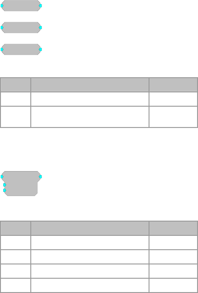
RPvdsEx Manual
211
LN
Log2
Log10
LN
[1:1,0]
Log2
[1:2,0]
Log10
[1:3,0]
Description:
These processors compute logarithm of indicated base.
Name Description Data Type
Input Input Floating Point
Output Logarithm of input (Log 2, Natural Log or log
10) Floating Point
Equation:
FO = Ln( Fi ) or FO = Log2 ( Fi ) or FO = Log10 ( Fi )
LogN
LogN
a=1
b=1
[1:1,0]
Description:
Computes natural log with scalars for changing base, and so forth.
Name Description Data Type
Input Input Floating Point
Output Ln(a*Input)*b Floating Point
a Exponential scale factor alters input. Floating Point
b Output scale factor Floating Point
Equation:
Output = Ln (a * Input) * b
RPvdsEx Manual
212
Gating Functions
Gating Function Components
The components in this group are used to gate the onset and offset of signals with the specified
envelope shape.
This group includes the following components:
Cos2Gate
LinGate
LinRamp

RPvdsEx Manual
213
Cos2Gate
Cos2Gate
Trf=10
Ctrl=Closed
[1:1,0]
Description:
Gates signal with Cos2 of specified rise/fall. Functions as an enable line. The
gate will stay on as long as CTRL is HI. The rise time is the time it takes for the
signal to reach 90% of the maximum value. The fall time is the time it takes the
signal to reach 10% of the maximum value. The signal will start falling as soon
as the CTRL goes low.
Name Description Data Type
Input Input Floating Point
Output Gated Signal Floating Point
Trf Rise/Fall time in milliseconds Floating Point (Static)
Ctrl Opens gate on High closes on Low. Logic
Example:
External Trigger, page 237.
LinGate
LinGate
Trf=10
Ctrl=Closed
[1:1,0]
Description:
Generates a linear gate with specified characteristics when triggered. Ctrl acts
as an enable line. The rise time is the time it takes for the signal to reach 90% of
the maximum value. The fall time is the time it takes the signal to reach 10% of
the maximum value. The signal will start falling as soon as the Ctrl goes low.
Name Description Data Type
Input Input Floating Point
Output Gated Signal Floating Point
Trf Rise/Fall time in milliseconds Floating Point (Static)
Ctrl Opens gate on High closes on Low. Logic
Example:
Digital-to-Analog Delay, 183.
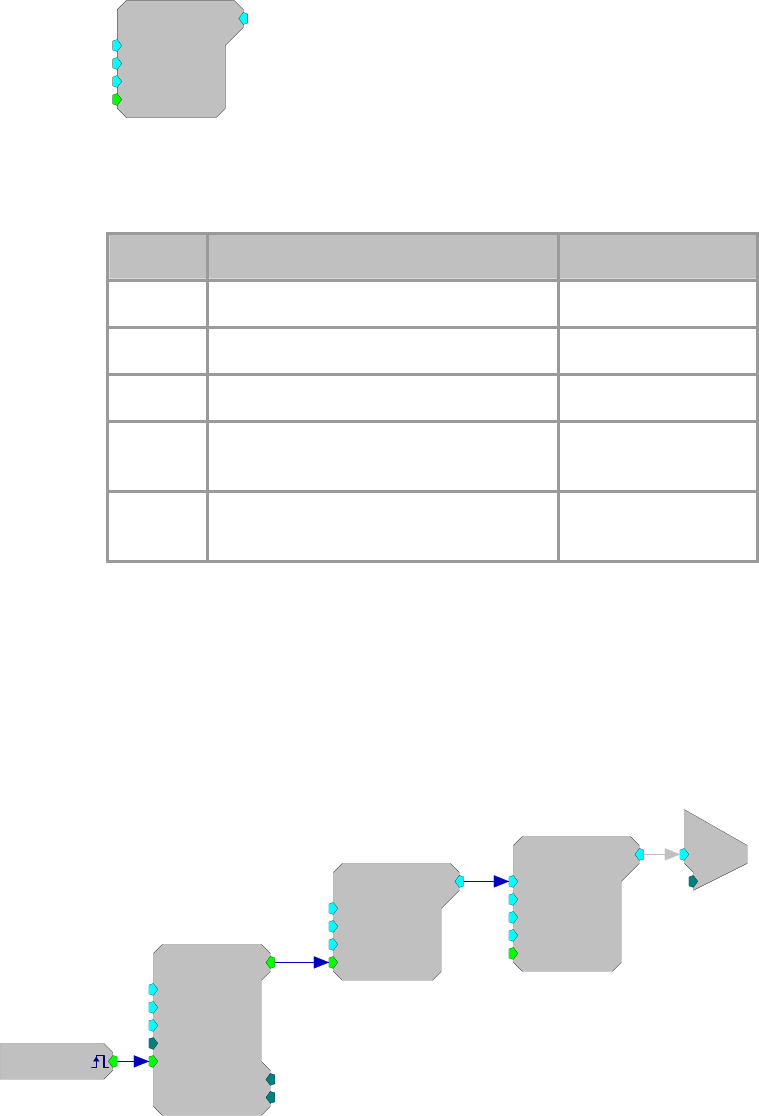
RPvdsEx Manual
214
LinRamp
LinRamp
Min=0
Max=1
Trf=10
Ctrl=Closed
[1:1,0]
Description:
Generates a linear ramp that begins at the Min value and goes towards the Max
value over the specified Rise/Fall Time.
Name Description Data Type
Output Output value Floating Point
Min Minimum gate value Floating Point
Max Maximum gate value Floating Point
Trf Rise/Fall time in milliseconds between
Min and Max value Floating Point
Ctrl Ramp starts on pulse high stays on until
pulse goes low. Logic
Example:
Linear Ramp
File: Examples\LinRamp_ex.rcx
Default Device: RP2.1 Processor
Sampling Rate: 25 kHz
This example creates 20 ms long pulses with a 100 ms inter-pulse interval that
is used to ramp a tone on and off using LinRamp. The output from LinRamp is
used to control the amplitude parameter of the tone to gate it on and off.
[1:1,0]
Src=Soft1
PulseTrain
Thi=20
Tg=0
Tlo=100
Npls=0
[1:3,0
]
CurN=0
Stage=0
Trg=0
LinRamp
Min=0
Max=1
Trf=10
Ctrl=Closed
[1:5,0]
Tone
Amp=1
Shft=0
Freq=1000
Phse=0
[1:7,0]
Rst=Run
c
O
[1:8,0]
Ch=1
RPvdsEx Manual
215
Helpers
Helper Components
Helpers are used to simplify circuit design (HopFrom, HopTo), debug a circuit (Graph,
ParWatch), control a circuit while it is running (DataTable), or send data between the PC and the
RPX (ParTag, Graph, DataFile).
Note to RL2Stingray users: Remember to turn off Helpers before undocking the Stingray.
This group includes the following components:
DataTable
DestinFile
Graph
HopFrom and HopTo
Iterate
MemoBox
ParTag
ParWatch
ScriptTag
SourceFile

RPvdsEx Manual
216
DataTable
MyData
= 1
Description:
The DataTable can be used to supply data to a parameter or Data type input.
Supports output of scalar values; Biquad, IIR, and FIR filter coefficients; and
State Machine values. The up and down arrows manually change the index that
selects the output data and are accessible using ActiveX controls or in
RPvdsEx. Table values are set before the chain is run. A dialog box is opened
by double-clicking on the DataTable icon:
The DataTable dialog box has a drop down menu for the format of the Table the
possible formats are
Type Format Function
Disabled No Data values
Scalar Single Floating point value
FIR Coef Coefficients generated for FIR filter.
IIR Coef Coefficients generated for IIR filter
BIQ Coef Coefficients generated for Biquad filter
nRow Multiple rows
State Machine Generates Jump table for State Machine
Chan Map Channel Mapping for MCMap
Note: Channel Map starts with Channel 0
RPvdsEx Manual
217
For most of the DataTable types a row index is generated for the number of
rows required in the data table. Each table can hold 1024 values. The values can
be divided between the number of rows and columns. For example a Table with
700 rows would have 1 column. While a table with 20 rows could have 51
columns. The number of rows is controlled by a number box like the one below.
You select the Type/Format of the DataTable and the No.
Rows or Coefficients in the table and then reformat the table.
Changing the output of a Data Table
To change the Column number while the circuit is running
click on the up/down arrows on the DataTable icon from
within RPvdsEx.
The index of the Data Table can also be changed using an ActiveX control.
Name Description Data Type
Output Output values from a data table Any
Index Data table that values are read from. Integer
Example(s):
FIR/Data Table, page 198
DestinFile
NoName
Name=
N=0
OS=0
Append=0
Description:
A DestinFile can transfer data from the RP Device to the PC. DestinFiles are
supported within RPvdsEx only. While designing the circuit, information like
the exact location of the file for storing the data (NAME), the number of data
points to be stored in the file (N) , and the offset value for the data file (OS) are
set in the component.
If number of data points to be stored is not known, '0' can be entered. To append
the data to an existing data file 'Append' should be set to '1'.
The Data transfer is initiated by clicking the green arrow in the DestinFile
component.
The DestinFile component can also be used with 16-Bit integer format('. I16')
data if the 'Comp to 16' component is used to convert the data to 16-Bit integer
format before transferring it to the destination file. Data cannot be saved to a
'wav' file using the DestinFile component.
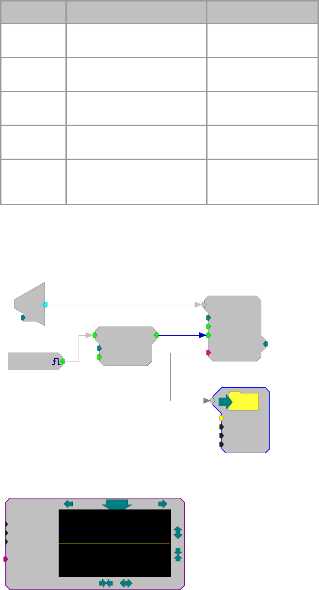
RPvdsEx Manual
218
Name Description Data Type
Input Input to the 'destin file' 32-Bit Floating Point (F32),
16-Bit Integer (I16)
N
ame
N
ame of the destination file with
exact path String
N
N
umber of points to be stored in
the data file ('0'if unknown) Integer
O Offset value of the data file ('0' if
no offset) Floating Point
Append Append='1' if you want to append
the data, '0' writes over existing
data.
Integer
Example:
DestinFile
The example below collects 100000 points from an Analog channel input when
a software trigger is set. After the data is acquired the user can download the
signal information by clicking on the green arrow.
d
c
[1:4,0]
Ch=1 SerStore
Size=100000
Rst=0
WrEnab=1
[1:5,0]
Index=0
{>Data}
Schmitt2
nHi=100000
nEnab=1
[1:2,0]
[1:1,0]
Src=Soft1
NoName
Name=C:\T
D
N=100000
OS=0
Append=0
Graph
DT=Float32
nChan=1
UD=2Hz
Source
10
-100100
Description:
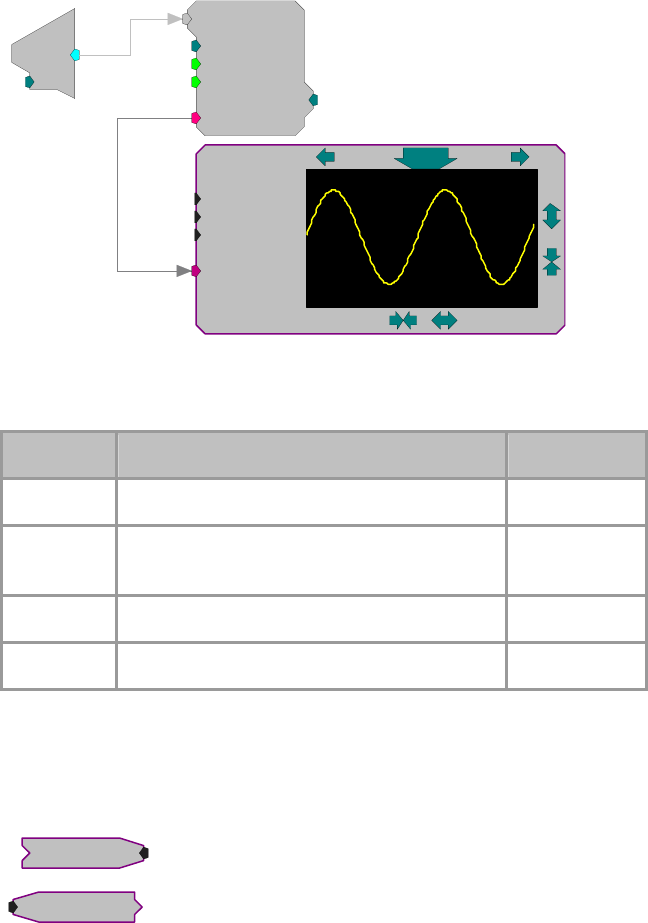
RPvdsEx Manual
219
Graph contents of buffer connected to Source. Graph works within RPvdsEx.
The arrows surrounding the graph are used to change the scale of the x and y
axes. The large arrow is used to manually update the graph. Double click to
modify update mode with one of the listed options.
d
c
[1:9,0]
Ch=1
SerStore
Size=100000
Rst=0
WrEnab=1
[1:10,0
]
Index=0
{>Data}
DT=Float32
nChan=1
UD=2Hz
Source
2
-20200
Notice that the connector points to the Graph
Graph can graph all data types, as well as multiple channels. With a high speed
USB connection it is possible for graph to refresh the screen 10 times a second.
Name Description Data Type
UD Update of graph (Man,1,2,5,10) times a second. Static
DT Data Type (32-bit float, 32-,16-,8-bit integer
values) Static
nChan
N
umber of channels (1,2,4) Static
Source Pointer to DataBuffer Pointer
HopFrom
HopTo
Hop From...
... Hop To
Description:
Allows graphical breaks in the RPvdsEx circuit, which allows one to build
complex circuits without overlapping lines. Used as a pair with one Hop From
and one or more HopTo. There are no accessible parameters. Double-click on
Hop to access the label.
Example: Hops
In this example a HopTo is connected to the output of the Biquad filter, and
named 'Noise'. A separate HopFrom named 'Noise' is connected to a ScaleAdd
component and to a second DAC.
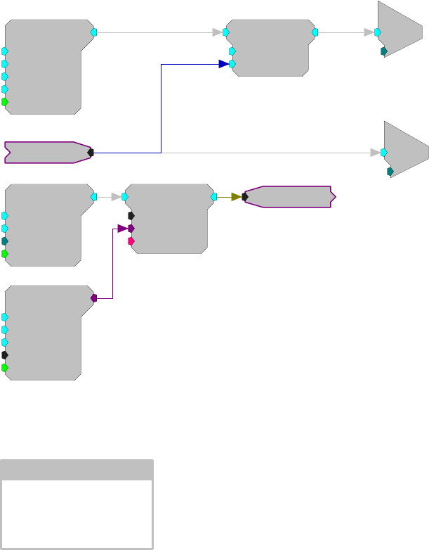
RPvdsEx Manual
220
Tone
Amp=1
Shft=0
Freq=1000
Phse=0
[1:6,0]
Rst=Run
GaussNoise
Amp=1
Shft=0
Seed=0
Rst=Run
[1:2,0]
ButCoef1
Gain=1
Fc=1000
BW=100
Type=LP
[1:1,0]
Enab=Yes
Biquad
nBIQ=1
{>Coef}
{>Delay}
[1:3,0]
Noise
Noise
c
O
[1:5,0]
Ch=2
ScaleAdd
SF=1
Shft=0
[1:7,0]
c
O
[1:8,0]
Ch=1
Iterate
Iterate: x =1 to 16 by 1
Description:
An iteration box is a helper that greatly simplifies multi-channel circuit design.
The sub-circuit within the iterate box is duplicated a specified number of times.
The number of duplications is specified using the variable parameter x along
with its start and step size. Adding the character ‘x’ enclosed in braces ({x}) in
the sub-circuit will cause consecutive values from 1 to x to be inserted in place
of the ‘x’ in each duplicate.
For example:
If x = 16, start = 1 and step = 2, then there will be eight iterations and x will
take the values 1, 3, 5, 7,.., 13, and 15.
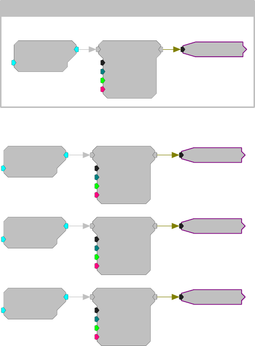
RPvdsEx Manual
221
Using Iteration
Iterate: x =1 to 3 by 1
ConstF
K=10
[1...,1-01...
]
RamBuf
Size=1000
Index=0
Write=0
{>Data}
[1...,2-01...]
Signal{x}
An Equivalent Circuit Without Iteration
ConstF
K=10
[1:1,0]
RamBuf
Size=1000
Index=0
Write=0
{>Data}
[1:2,0]
Signal1
ConstF
K=10
[1:3,0]
RamBuf
Size=1000
Index=0
Write=0
{>Data}
[1:4,0]
Signal2
ConstF
K=10
[1:5,0]
RamBuf
Size=1000
Index=0
Write=0
{>Data}
[1:6,0]
Signal3
Using iterations greatly simplifies circuit design. However, it does not reduce
the number of components. The number of components created by the circuits
above is identical.
In fact the circuits are equivalent and produce identical results when compiled.
The main advantage of using iterations is the manageability of the circuit. It
makes the circuit concise and easy to manage and edit. Each modification in the
circuit needs to be made only once.
When the iterate component is added, the user can drag the box boundaries
around any sub-circuit. All components and links must be either inside or
outside the box. Intersecting the box with a link is not permitted.
Note: When hops or parameter tags are used within the iterate box, they should
typically include the variable {x} in their labels. If the x variable is not used, a
single object such as a parameter tag will have multiple sources.
Using Variables
Iterations can make use of up to three variables, including the x variable and
two constants, a and b. The variables can be accessed and edited in the
parameter box which can be opened by double-clicking the top border of the
iterate box. The variables may be used in the labels of hops, parameter tags, or
component parameters.
RPvdsEx Manual
222
Adding the character for any of the variables (x, a, or b) within braces (such as,
{a}, {b}, or {x}), will cause the value for the variable to be inserted in place of
the symbol in every iteration. With the variable x, such as {x+a}, the value of x
is incremented with each iteration. This is very useful when a channel offset
number is needed.
For example:
If x = 16, start = 1, step = 1, and a = 16, then (x+a) will take values 17, 18,
19,…, 31 and 32.
Using Iterations with MCToSing
Another powerful and efficient use of the iterate component is its use with the
multi-channel component MCToSing. Together these components can be used
to extract single-channel signals from a multi-channel signal. Each channel can
then be processed by single channel components. Ordinarily, a separate circuit
segment would be required to extract and process each signal. With the use of
iterate, the user can put the circuit for a single channel within the iterate box,
and then put {x} in the channel selector of MCToSing and in the labels of any
parameter tags in the sub-circuit.
Assigning An Iterate Box To More Than One Processor
Assigning a page that contains an iteration box to multiple processors allows the
user to build the iterate box with the associated circuitry within it, just once.
When this technique is used, the character d, within braces ({d}), must be added
in the circuit wherever the iterate box needs to be different for each processor.
The letter d will take the value corresponding to the processor to which it is
assigned. Values are 0, 1, 2, 3 and 4 for the main and auxiliary processors
respectively.
For example:
If x = 16, start = 1, step = 1, a = 16, then {x + (d*a)} will take values:
1, 2, 3,…, 15, 16 in the first auxiliary processor
17, 18, 19,…,31, 32 in the second auxiliary processor
33, 34, 35,…, 47, 48 in the third auxiliary processor
49, 50, 51,…, 63, 64 in the fourth auxiliary processor
Note: In this example, the four auxiliary processors are used to process 16
channels each.
Because the value associated with the main processor is 0, the formula used in
this example should not be used when the iteration box is assigned to multiple
processors.
The Duplication Information Dialog Box
After the circuit has been compiled a Duplication Information Dialog Box can
be displayed by right-clicking a component and clicking Duplication Info. The
Duplication Information dialog box displays several columns of information
regarding the state of the component and its parameters in each iteration of the
circuit. Buttons at the top of the dialog box allow the user to display
information for each processor to which the component might have been
assigned.
The first four columns are always the duplication number (ItNo.), component
name (Name), component number (CmpNo.), and time slice (T.S.). The
component numbers displayed are offset for each auxiliary processor. Because
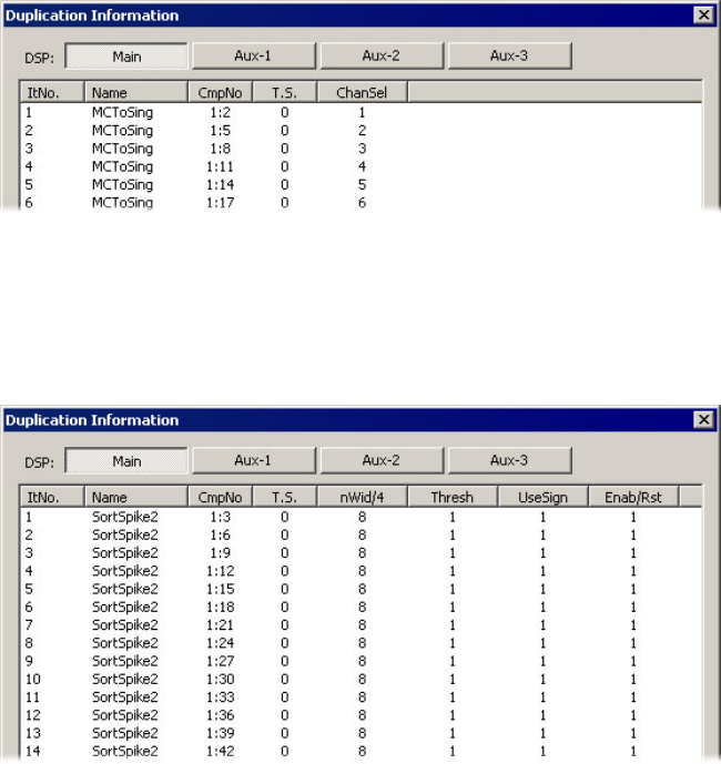
RPvdsEx Manual
223
each processor can utilize up to 256 components, each processor is offset by a
multiple of 256. For example, the main processor uses component numbers 1-
256, while the Aux-1 processor uses component numbers 257-512.
The standard columns are followed by columns for each of the components
parameters. This list of iterations and variable values are for user reference and
debugging.
For example, the duplication information for the MCToSing component from
the example below is shown here. Notice that the channel number (ChanSel)
varies from 1 through 16. In the example the iteration variable {x} was assigned
to channel number.
Similarly, the duplication information for the SortSpike2 component from the
example below is shown here. Because the variable {x} is not a part of any of
the parameters of the SerStore component, none of the columns have a list of
successive or changing values.
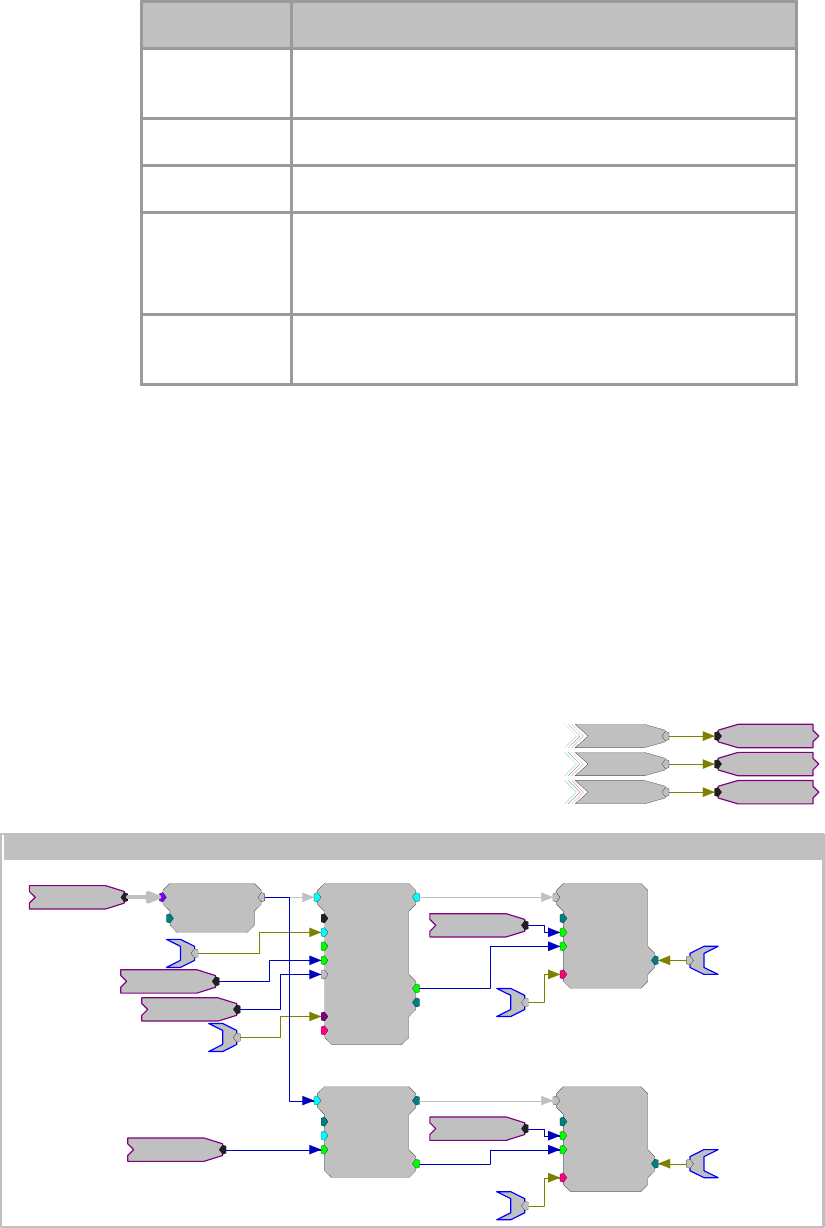
RPvdsEx Manual
224
Name Description
Repeats The number of times the iteration is produced and the value of
the variable {x} within the circuit
Start
N
umber where x starts
Step
N
umber by which to increment x
a= A constant value which is inserted everywhere {a} is found in
the iterated circuit.
Also works with {x+a}, {x-a} and so on.
b= A constant value which is inserted everywhere {b} is found in
the iterated circuit. Also works with {x+b}, {x-b} and so on.
Example:
Iterations
Iterations are commonly used with a MCToSing and single channel processing
components, to extract and process each channel of a multi-channel signal.
When MCToSing is used inside an iteration box, the variable x associated with
the iteration box can be assigned as the channel number. In the example below,
FiltSig is a 16 channel signal, from which one channel is extracted. Spikes are
then sorted on the extracted channel. This entire circuit is being iterated 16
times, that is, when the circuit is compiled the iterated portion of the circuit will
be duplicated 16 times. Each instance will process a different channel. Notice
that the variable x is included everywhere in the circuit where distinctions need
to be made between the channels (for example, parameter tags).
Iterate: x =1 to 16 by 1
Enable
Reset
iTime
Enable
Reset
iTime
FiltSig
MCToSing
ChanSel={x}
[1...,13-01...]
SortSpike2
nWid/4=5
Thresh=1
UseSign=1
Enab/Rst=1
[1...,14-01...]
SortBits=0
Strobe=0
Tag
{>Coef}
{>Data}
aEA~{x+a}
Enable
iTime
cEA~{x+a}
PlotDec16
nDec=128
SF=1e+006
Enab=1
[1...,18-01...]
Strobe=0
Enable
SerStore
Size=12800
Rst=0
WrEnab=1
[1...,20-01...
]
Index=0
{>Data}
Reset
dPD~{x+a}
sPD
SerStore
Size=32000
Rst=0
WrEnab=1
[1...,16-01...
]
Index=0
{>Data}
dEA~{x+a}
Reset
sEA~{x+a}
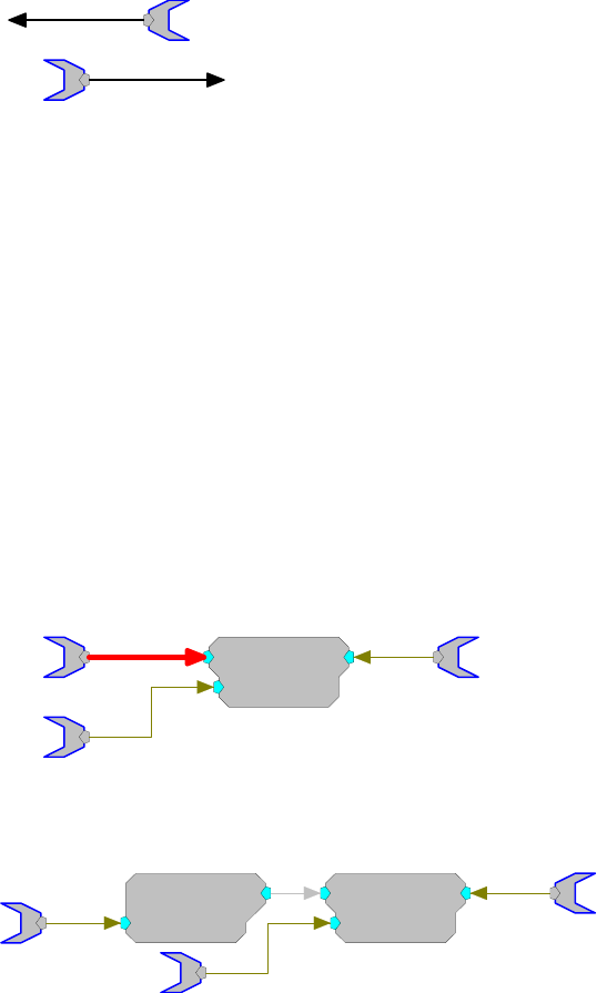
RPvdsEx Manual
225
MemoBox
This is a MemoBox
Description:
A MemoBox component is used to place text in the circuit. The MemoBox does
not affect the functionality of the circuit in anyway. It is useful for describing
how the circuit works (similar to comments in source code) and labeling parts
of the circuit.
ParTag
ParTagL
ParTagR
Description:
Parameter tags are used to control component Parameter variables and access
data from signal outputs, component parameters and data ports from a program
while the chain is running. To find out how parameter tags are used in
programming see the ActiveX help.
Parameter tags always point to the parameter component.
ParTagL and ParTagR function the same. The difference is for aesthetic
purposes.
The maximum length of a parameter Tags name is 32 characters. Parameter tag
names are case sensitive.
Parameter tags function in Control Object Files (*.rco) that are accessed via
ActiveX controls or through DLL's.
Connecting to a Signal Input
Parameter tags can not access signal inputs directly. Signal Inputs are found in
the top right-hand part of the components. The illustration below shows two
correct parameter connections and an incorrect one (red connection path).
Divide
Den=1
[1:1,0]
Incorrect
Denominator
Output
To access a signal input use one of the following: ConstF, ConstI or ConstL.
The example below uses a constant Float to convert the parameter tag into
signal output that can be feed into a signal input.
Divide
Den=1
[1:2,0]
Correct
Denominator
ConstF
K=0
[1:1,0]
Output
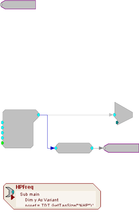
RPvdsEx Manual
226
ParWatch
ParWatch
Description:
Parameter Watch. When connected to the output of any component, it reports
the value of the component. Very useful for debugging circuits and checking
cycle usage. The default data type for ParWatch is floating point.
When connected to a parameter value that allows any type a floating point value
will be returned. This gives erroneous values for integer or logical values. To
fix this include an INT2FLT or TTL2FLT component between the output and
the ParWatch.
Monitoring Output Values
This example shows how a parameter watch can be used to monitor the levels
of another component. Here it is reporting the RMS value.
Tone
Amp=1
Shft=0
Freq=1000
Phse=0
[1:1,0]
Rst=Run
c
O
[1:2,0]
Ch=1
0.707511
RMS
[1:4,0
]
ScriptTag
Description:
A ScriptTag makes it possible to include scripting in RPvdsEx circuits. This
powerful new feature allows for complex automatic access to circuit elements
via an imbedded basic language. It includes an editor and a debugger and has
been extended to include a number of powerful hardware access commands.
The code within the scripted tag is executed when the tag is accessed (read from
or written to). This is done in the same manner as accessing parameter tags with
ActiveX commands or through OpenEx.
Important: This component is primarily for TDT use. Comprehensive
documentation and support for end-user scripting is not available at this time.
Example:
This example sets the value of a ScriptTag named HPFreq with ActiveX
commands.
setval = RP.SetTagVal(HPFreq,hp)
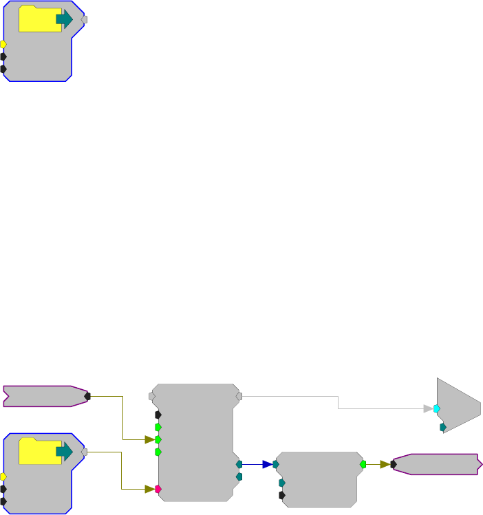
RPvdsEx Manual
227
When the ScriptTag is written to, the internal code is run. The internal code
may or may not use the value ‘hp’ from the SetTagVal command. Therefore, if
you only need to trigger the code to run, the value for ‘hp’ is irrelevant.
Note: A ScriptTag given the reserved name ‘InitScript’ will execute its code
when the RPvdsEx circuit is run. This enables the user to set default values
without having to explicitly access the ScriptTag.
SourceFile
NoName
Name=
N=0
OS=0
Description:
A data file sends a file from the PC to the RP device. SourceFiles are supported
within the RPvdsEx application and with ActiveX controls. During the design
of the circuit using a SourceFile, the number of points to load from the file and
the OS (offset of the data file) are set. Once the circuit is running, the
information from the data file resides in a memory Buffer.
The data file can have any of the following data formats 32-Bit float, 32 and 16-
bit integer, ASCII, or WAV files. The memory buffer of the component that the
SourceFile is connected to has access to the file. In most cases a portion of the
file is stored in a memory buffer. The size of the buffer is dependent on the
amount of memory allocated to the serial or RAM buffer.
When a SourceFile is used with a serial or RAM buffer the write enable line
must be set to 0 (read from buffer).
When used within RPvdsEx, before the chain is run the user must define the file
name, number of points to read, and offset. With ActiveX it is possible to
control some of these variables dynamically.
SerialBuf
Size=3000
Rst=0
AccEnab=1
Write=0
[1:1,0]
NBl ks=0
Index=0
{>Data}
Signal
Name=C:\T
D
N=0
OS=0
iCompare
K=2999
Test=LT
[1:4,0]
c
O
[1:2,0]
Ch=1
StopPlay
SigPlay
In the example above, when the circuit starts the SourceFile is loaded and the
serial buffer plays the signal until it reaches the end of the buffer. The iCompare
sends out a logical high while the buffer index is less than 2999 (buffers start at
zero) when it reaches 2999 StopPlay is set to 1.
RPvdsEx Manual
228
Name Description Data Type
Output Output value from a data file Any
N
ame File name and path. Can have the following data
formats: 32-bit floating point 32- and 16-bit floating
point, ASCII file and WAV file format.
String
N
N
umber of points to read Integer
OS Offset value of data file Floating Point
Example(s):
3D Circle, page 90.
RPvdsEx Manual
229
Input/Output
Input and Output Components
This set of components handle input and output for circuits. Inputs include A/D converters, TTL
inputs, and Trigger inputs. Outputs include D/A converters and TTL outputs. Use circuit
components from this group to connect a circuit to the physical world.
This group includes the following components:
AdcIn
BitIn
BitOut
DacOut
StereoAdc
StereoDac
TimeStamp
TrgIn
WordIn
WordOut
This group also includes the following components, if RPvdsEx Device Setup is
configured for a high performance device, such as the RXn or RZn:
MCAdcIn
MCDacOut
MCeStim
Important Note!: This group also includes MCVidAcc and MCStrmFifo components, intended
primarily for TDT use in behind-the-scenes macro design. They are not intended for general use.
RPvdsEx Manual
230
AdcIn
d
c
[1:1,0]
Ch=1
Description:
Feeds the signal stream with A/D input channel specified. Converts 24 bit
integer input to floating point value. Also scaled and shifted to yield calibrated
voltage level.
A parameter input allows users to dynamically change the channel number.
Name Description Data Type
Output Output values from ADC channel Floating Point
Channel Parameter input to dynamically change the
channel number Integer
Equation:
FO = ADC channel D1
Example(s):
Scale and Add, page 49.
Butterworth Coefficients, page 147.
BitIn
Bi
[1:1,0]
M=8
Description:
Feeds the signal chain with bit(s) from the digital input port. BitIn will logic
'OR' all bits of the input port specified in Mask to produce a single logic high or
low.
Name Description Data Type
Output Logic value after bit-masked OR Logic
M Bit-Mask value for port; if any of those port
values are high BitIn goes high Floating Point
Standard integer values for addressing digital bits are provided in the table
below.
Digital Bit Bit Mask (M=__)
Bit 0 1
RPvdsEx Manual
231
Bit 1 2
Bit 2 4
Bit 3 8
Bit 4 16
Bit 5 32
Bit 6 64
Bit 7 128
Note: There is a two cycle delay when using the BitIn component.
Equation:
LO = If (Digital Input Port && D1)
Example(s):
If Digital Input Port = 7 and D1 = 3 Then LO = 1
If Digital Input Port = 8 and D1 = 3 Then LO = 0
BitOut
Bi
[1:1,0]
M=8
Description:
Sets or clears bits of the digital output port based on the inputs logic level. All
bits specified in Mask will be set when the input is high else the bits will be
cleared.
Name Description Data Type
Input Logic value Logic
M When logic goes high all port values set with
the bit-mask go high Floating Point
Standard integer values for addressing digital bits are provided in the table
below.
Digital Bit Bit Mask (M=__)
Bit 0 1
Bit 1 2
Bit 2 4
Bit 3 8
RPvdsEx Manual
232
Bit 4 16
Bit 5 32
Bit 6 64
Bit 7 128
Note: There is a three cycle delay when using the BitOut component.
Important:! Circuits that contain both BitOut and WordOut the Bitmasks can
not overlap. For example, a circuit where the BitOut and WordOut both use bit
2 (BitMask=4) the circuit will set the value based on the last component in the
circuit.
Equation:
Digital Output Port = Li masked by D1
Example(s):
If Li = 1 and D1 = 3 then Digital Output Port bits 0 and 1 = 1
If Li = 0 and D1 = 3 then Digital Output Port bits 0 and 1 = 0
DacOut
c
O
[1:1,0]
Ch=1
Description:
Converts floating point signal input to integer value and sends to specified D/A
output channel. The value is scaled and shifted to provide calibrated voltage
output.
A parameter feed allows users to change the channel output dynamically.
Name Description Data Type
Input Input Floating Point
Channel # Changes the channel number dynamically Integer
Equation:
DAC channel D1 = Fi
Example(s):
See ScaleAdd, page 49.
RPvdsEx Manual
233
MCAdcIn
MCAdcIn
nChan=16
ChanOS=1
[1:1,0]
Description:
This component is a multi-channel version of the AdcIn component. MCAdcIn
feeds the circuit with the multi-channel input from a high performance device,
such as the RX5. With the RX5, analog signals are digitized on a preamplifier
and sent to the base station via its fiber optic ports (Amp-A, Amp-B, Amp-C,
and Amp-D). The channel offset (ChanOS) can be used to specify acquisition
channels, such as channels from a specific amplifier. For example, to acquire
signal data from Amp-B you would set the channel offset to 17. The number of
channels fed to the multi-channel output is specified by nChan.
The minimum and maximum number of channels allowed in multi-channel
signals is 4 and 256, respectively. However, the user must consider their
hardware configuration when setting the number of channels. For example, the
maximum number of analog input channels available on the Pentusa (RX5BA-
5) is 64. Therefore, the number of channels for the MCAdcIn component must
not exceed 64 when using this device.
Also see: Important Consideration for Working with Multi-Channel
Components, page 57.
Note: This component is for use with only high performance processor devices,
such as RXn or RZn. See the reference for your device for more information.
Name Description Data Type
Output Multi-channel output Floating Point
nChan
N
umber of channels in output signal Integer (Static)
ChanOS Channel offset number Integer
MCDacOut
MCDacOut
nChan=4
ChanOS=1
[1:2,0]
Description:
This component is a multi-channel version of the DacOut component.
MCDacOut converts the floating-point values in the multi-channel input signal
to integer values and sends them to the specified analog output channels. The
values are scaled and shifted to provide calibrated voltage output.
RPvdsEx Manual
234
MCDacOut
nChan=4
ChanOS=1
[1:4,0]
MCConst
nChan=4
Value=1
[1:3,0]
Tone
Amp=1
Shft=0
Freq=1000
Phse=0
[1:1,0]
Rst=Run
The minimum and maximum number of channels allowed in multi-channel
signals is 4 and 256, respectively. However, the user must consider their
hardware configuration when setting the number of channels. For example, the
maximum number of analog outputs available on the Pentusa is four. Therefore,
the number of channels for the MCDacOut must not exceed four.
Note: This component is for use with only high performance processor devices,
such as RXn or RZn.
Name Description Data Type
Input Multi-channel input Floating Point
nChan
N
umber of channels require
d
Integer (Static)
ChanOS Channel offset Integer
MCeStim
Description:
This component is used to send digital stimulus waveforms to the IZ2 Stimulus
Isolator. The total number of channels configured for stimulation is defined in
the nChan parameter. A multi-channel input accepts stimulus waveforms and an
eight-channel output returns the actual stimulus voltage for monitoring. The
MonBank parameter selects which bank of eight channels to be monitored.
The logic input parameter VMode determines if the IZ2 acts as a constant
current (0) or voltage (1) source.
Use of the IZ2_Control macro is highly recommended as it provides all of the
necessary settings for the IZ2 Stimulator.
Note: This component is for use with the IZ2 Stimulus Isolator and RZ2 high
performance processor devices. See the System 3 Manual for more information.
Name Description Data Type
Input Multi-channel floating point input stream of
stimulus waveforms Floating Point

RPvdsEx Manual
235
Output Eight channel floating point multichannel
monitor output. Floating Point
nChan
N
umber of stimulus channels to send to IZ2. Integer (Static)
VMode Configures the IZ2 to run in Voltage Mode
(1) or Current Mode (0). Logic
MonBank Select which bank of eight channels to
monitor (integer, 0-15) Integer
OpBits
N
ot used at this time. Integer
StereoAdc
e
o
[1:1,0]
Ch=1
Description:
Generates stereo signal from channel 1 (left) and 2 (right) ADC inputs.
Name Description Data Type
Output Stereo formatted signal Floating Point
Ch Left channel input (must =1) Integer (Static)
StereoDac
e
o
[1:1,0]
Ch=1
Description:
Plays stereo input out of channel 1 (left) and 2 (right) DAC outputs.
Name Description Data Type
Input Stereo input Floating Point
Ch Left channel input (must = 1) Integer (Static)
RPvdsEx Manual
236
TimeStamp
TimeStamp
BitNum=0
Rst=Run
Enab=Yes
[1:1,0
]
Strobe=0
Description:
TimeStamp is used with the Barracuda(RV8) and Multifunction Processor
(RX6). It is a submicrosecond accurate event-timer. On each tick of the sample
clock the TimeStamp waits for a trigger input. When the trigger goes high, the
TimeStamp component outputs a value equal to the number of microseconds
since the start of the sample period.
The TimeStamp can detect triggers on a specified digital input line. The
BitNum parameter determines which digital input bit is monitored for triggers.
A Reset line (Rst) resets the TimeStamp and readys it for the next event. The
Enable (Enab) line enables the TimeStamp function (Yes=1 to enable). The
Strobe out should be connected to a latch or buffer operation to save the
TimeStamp value (see example below).
Note: On the RV8, bits 0-15 can be monitored for triggers. On the RX6, bits 0-
3 can be monitored.
Name Description Data Type
Output Time in microseconds since the beginning of the
current sample period Floating Point
BitNum The number of the digital input bit (0-15 RV8, 0-3
RX6) Integer
Rst Resets the timer value (logic high allows it to run
continuously) Logic
Enab Enables the TimeStamp Logic
Strobe Pulses out a logical high for a tick of the clock
when component is triggered (used to latch/store
data)
Logic
RPvdsEx Manual
237
TrgIn
[1:1,0]
Src=Soft1
Description:
Feeds the signal chain with the specified trigger source. Use to feed system
triggers to various Logic inputs of counters etc. Trigger options set before run.
When the zTrigIn component is configured for a software trigger, the trigger
will remain high for one sample. However, if the zTrigIn is configured for the
zBusA or zBusB trigger the time high will depend upon the sample rate. For
example, at 6 kHz the trigger will remain high for one sample, but at 25 kHz the
trigger will remain high for 5 samples.
If you wish to use the zBusA or zBusB trigger and need a single sample trigger
pulse, use an EdgeDetect component to detect the rising edge of the trigger
before feeding the trigger line to enable, reset, or other triggering parameters.
Name Description Data Type
Output Pulses high when triggered Logic
Src external Trigger: Triggers RPX through the trigger
in port
z
Bus Trigger's A and B: synchronizes Triggering to
RPX connected across racks
Software Trigger 's#1-10: Sends a trigger to an RPX
device via a software control on the PC
Static
Equation:
LO = If ( D1 )
Example:
External Trigger
This circuit uses an external trigger as an Enable line to gate a tone on and off.
When the external trigger goes high, the Cos2Gate will rise with a 10 ms rise
time. When the external trigger goes low, the Cos2Gate will fall with a 10 ms
fall time.
[1:1,0]
Src=Extern
Tone
Amp=1
Shft=0
Freq=1000
Phse=0
[1:3,0]
Rst=Run
Cos2Gate
Trf=10
Ctrl=Closed
[1:4,0]
c
O
[1:5,0]
Ch=1

RPvdsEx Manual
238
WordIn
W
[1:1,0]
M=255
10110100
Description:
Feeds the chain with an integer representation of the digital input port. The
digital input port is logic 'ANDed' with the specified Mask and the resulting
value is fed to the signal chain.
Name Description Data Type
Output Integer representation of digital input port Integer
M Bit-mask. Decimal value for desired bits on port. Integer
Note: There is a two cycle delay when using the WordIn component.
Equation:
Io = Digital Port In 'AND' D1
Example(s):
If Digital Port In = 7 and D1 = 3
Then Io =3
Also see WordIn - WordOut, page 72
WordOut
W
[1:1,0]
M=255
10110100
Description:
Passes an integer value to the specified bits of the digital output port. Only bits
specified in the Mask will be affected on the output port. Bits not specified in
the Mask will be unaffected and can be used for other things.
Name Description Data Type
Input Integer value digital representation of Digital
Output port. Integer
M Bit-mask. Decimal value for desired bits on port. Integer (Static)
Note: There is a three cycle delay when using the WordOut component.
Important:! Circuits that contain both BitOut and WordOut the Bitmasks can
not overlap. For example, a circuit where the BitOut and WordOut both use bit
2 (BitMask=4) the circuit will try set the value based on the last component in
the circuit.
RPvdsEx Manual
239
Equation:
Digital Port Out = Ii for bits specified in D1
Example(s):
If Ii = 7 and D1 = 3
Then Port Out =3
Also see WordIn - WordOut, page 72
RX Support for I/O Components
The tables below compare high performance processors support of various
analog input/output RPvdsEx components.
Analog Outputs
Device DacOut
RX5 x
RX6 x
RX7 x
RX8 x
Analog Inputs
Device AdcIn MCAdcIn StereoAdc †
RX5 x x x
RX6 x* x**
RX7 x x x
RX8 x x x
x supported
x* channels 1-16 access optical inputs, channels 128 and 129 access audio
inputs
x** component supported for access to optical inputs only (use AdcIn or
StereoADC for analog input BNCs)
† The StereoAdc component is limited to ADC channels one and two only.
RPvdsEx Manual
240
Integer Math
Integer Math Components
The Integer Math components provide mathematical functions for integer data, allowing bitwise
mathematical operations.
This group includes the following components:
FromBits
iAbsVal
iAnd
iBitShift
iCompare
iLimit
iNot
iOr
iScaleAdd
iSign
iXor
ToBits
RPvdsEx Manual
241
FromBits
FromBits
Rst=0
b0=0
b1=0
b2=0
[1:1,0]
b3=0
b4=0
b5=0
Description:
Converts bit format to an integer value. See ToBits, page 246.
Name Description Data Type
Inputs Input Logic
Output Integer value calculated from Logical ins Integer
Rst Resets output to zero Logic
Equation:
I1 = L0-7 Bit-mask
Example(s):
B0=1,B1=1,B2=1,B3=0,B4=0,B5=0,I1=7
B0=1,B1=0,B2=0,B3=0,B4=1,B5=1,I1=49
B0=1,B1=1,B2=1,B3=1,B4=1,B5=1,I1=63
iAbsVal
iAbsval
[1:1,0]
Description:
Computes the absolute value of the signal.
Name Description Data Type
Input Input Integer
Output Absolute value of Input Integer
Equation:
Io = |Ii|
Example(s):
AbsVal (-2) = 2
AbsVal (2) = 2
RPvdsEx Manual
242
iAnd
iAnd
N=0
[1:1,0]
Description:
Bitwise AND function. Bitwise AND of integer input and N.
Name Description Data Type
Input Input Integer
Output Bitwise AND function Integer
N
Decimal value for doing Bitwise conversion Integer
Equation:
IO = II AND N1
Example(s):
7(0000 0111) AND 3 (0000 0011)= 3
7(0000 0111) AND 9 (0000 1001)= 1
iBitShift
iBitShift
N=0
[1:1,0]
Description:
Bit shifts input by N bits. Positive N bit shifts to the left negative shifts to the
right.
Name Description Data Type
Input Input Integer
Output Bitwise AND function Integer
N
Decimal value for doing Bit shift Integer
Equation:
IO = I1 * 2^N1
Example(s):
N=1; iBitShift (20) = 40
RPvdsEx Manual
243
iCompare
iCompare
K=0
Test=EQ
[1:1,0]
Description:
Compares input to K using specified Test and reports TRUE or FALSE as logic
High or Low respectively. Test can be EQ: Equal; NE: Not Equal; GT: Greater
Than; LT: Less Than; GE: Greater than or Equal to; LE: Less than or equal to.
Can be thought of as an If... statement.
Name Description Data Type
Input Input Integer
Output One if test is true 0 if test is false Logic
K Test value Integer
Test Compare type: EQ: Equal; NE: Not Equal; GT:
Greater Than; LT: Less Than; GE: Greater than or
Equal to; LE: Less than or equal to
Static
Equation:
IO = iCompare (Ii Test K)
Example(s):
K = 20; Test Eq; When Ii = 20, Io=1, otherwise Io=0;
K=20; Test GT; When Ii > 20, Io=1; otherwise Io=0;
iLimit
iLimit
Max=1
Min=1
[1:1,0]
Description:
Limits the signal to the Maximum and Minimum levels specified. If the input
signal is greater than the Max value then the signal out is the Max value. If the
input signal is less than the Min value then the signal out is the Min value. If the
input signal is between the Min and Max values it is passed through as the
signal output without change.
Important:! If Max is defined as a value less than the defined Min value, the
output will always be the defined Min, regardless of the input value.
Name Description Data Type
Input Input Integer
Output Value no less than Min and no greater than Max Integer

RPvdsEx Manual
244
Max Maximum input value Integer
Min Minimum input value Integer
Equation:
If Fi > D1 then FO = D1
Else If D2<= Fi <= D1 then FO = Fi
Else If Fi < D2 then FO = D2
iNot
iNot
[1:1,0]
Description:
Inverts bits of integer value.
Name Description Data Type
Input Input Integer
Output Bit-Inverted value of Input Integer
Equation:
OutputO = NOT (InputI )
Example(s):
NOT ( 0x000F ) = 0xFFF0
NOT(7)=-8
iOr
iOr
N=0
[1:1,0]
Description:
Bitwise OR function.
Name Description Data Type
Input Input Integer
Output Bitwise OR function Integer
N
Decimal value for doing Bitwise OR Integer
Equation:
OutputO = Inputi OR N1

RPvdsEx Manual
245
Example(s):
7(0000 0111) OR 3 (0000 0011)= 7
7(0000 0111) OR 9 (0000 1001)= 15
iScaleAdd
iScaleAdd
SF=1
Shft=0
[1:1,0]
Description:
Multiply signal by scale factor and add shift factor. The SF parameter can be
used to apply a simple scalar, or modulate a signal. The Shift parameter can be
used to place a DC shift on a signal or add two signals together.
Name Description Data Type
Input Input Integer
Output Scaled plus add value of Input Integer
SF Scale factor (multiply) Integer
Shift DC offset adds a value after SF Integer
Equation:
Output = (Input* SF) + Shift
iSign
iSign
[1:1,0]
Description:
This component determines the sign of the input.
Name Description Data Type
Input Input Integer
Output Sign of Input value (-1,0,1) Integer
Equation:
If Ii < 0 then IO = -1
Else If Ii = 0 then IO = 0
Else If Ii > 0 then IO = 1
RPvdsEx Manual
246
iXor
iXor
N=0
[1:1,0]
Description:
Output is changed based on the bit-form of the parameter value using an
exclusive OR bit mask. Exclusive OR only includes those bit-values that have a
single 1. See the examples below.
Name Description Data Type
Input Input Integer
Output Bitwise XOR function Integer
N
Decimal value for doing Bitwise OR Integer
Equation:
OutputO = Inputi IXOR (Np)
Example(s):
7(0000 0111) IXOR 1 (0000 0001) = 6
7(0000 0111) IXOR 7(0000 0111) = 0
14(0000 1110) IXOR 7 (0000 0111) = 9
ToBits
b5
b4
b3
b2
b1
ToBits
Rst=0
[1:1,0]
b0
Description:
Converts the first 6 bits of an Integer to a series of logical outputs. Values
greater than 63 and less than 0 may give unexpected results. See FromBits, page
241.
Note: The b0 output is a primary output on the ToBits component. The b1
through b5 outputs are secondary. This may cause a problem when connecting
b1 through b5 to logic inputs requiring a primary input (e.g. And, Or etc.). Use
a ConstL between the two components to solve this problem.
Name Description Data Type
Input Input Integer
Outputs Logical values from Integer input Integer
Rst Resets outputs to zero Logic
RPvdsEx Manual
247
Equation:
Outputi = Input1 Bit-mask
Example(s):
Input1=7 B0=1,B1=1,B2=1,B3=0,B4=0,B5=0
I1=2001 B0=1,B1=0,B2=0,B3=0,B4=1,B5=0
I1=-1 B0=1,B1=1,B2=1,B3=1,B4=1,B5=1
RPvdsEx Manual
248
Multi-processor
Multi-processor Components
The Multi-processor components are designed for use with high performance devices, such as
RXn or RZn. They are used to pass circuit signals between multiple processors on a single device.
Signals are sent and received between DSPs via specialized hardware and these components.
This group includes the following components:
AssignDSP
MCzHopIn and MCzHopOut
MCzHopPick
zHopIn and zHopOut
For the RZ2 only:
MCPipeIn and MCPipeOut
PipeIn and PipeOut
PipeSource
While both RX and RZ multi-DSP processors support zHops, the Pipe components are used only
with the RZ2 device. Because the Data Pipe architecture is more efficient for multi-channel data
transfers, TDT recommends using the Data Pipe transfer method (rather than zHops) for high
channel count applications when using the RZ2. Users should be aware of the delays associated
with each type of components and keep in mind the limitations associated with them.
A limited number of zHops and Data Pipes can be used in an RPvdsEx circuit. One zHop pair is
counted for each single zHop pair and for each channel of a MCzHop pair.
RXn and RZ5 devices..... 126 zHop pairs maximum
RZ2 devices (<50 kHz)..... 126 zHop pairs maximum and 256 channels of Data Pipes maximum
RZ2 devices (50 kHz)..... 126 zHop pairs maximum and 128 channels of Data Pipes maximum
RPvdsEx Manual
249
DspAssign
DSP: Main
Description:
The DspAssign component is used to designate a section of an RPvdsEx page to
run on a processor other that the one assigned to the RPvdsEx page. Paired with
RPvdsEx macros, this component enables many multi-processor circuits to be
displayed in a single page view. Similar to the Iterate component, components
cannot intersect the DspAssign boundary.
Note: This component is for use with only high performance processor devices,
such as RXn or RZn, but users must be familiar with the number of DSPs
available in their device and only assign pages to those DSP.
Name Description Data Type
DSP Target DSP Static
MCPipeIn
MCPipeOut
ChanSel=1
MCPipeIn
nChan=16
ChanSel=1
MCPipeOut
nChan=16
Description:
These components allow multi-channel transfer of data between processors
within an RZ device. The components are used to either get data from or put
data onto the RZ’s Data Pipe Bus. Once the data is on the bus it is available to
the other DSPs in the system. The source data available to MCPipeIn or from
MCPipeOut is configured using the PipeSource component. There is a two
cycle delay when transferring signals using the MCPipeIn and MCPipeOut.
(This is accounted for in TDT developed macros)
For single channel transfer between processors on an RZ, use PipeIn and
PipeOut.
Note: The PipeSource component must be included on any DSP that uses
PipeIn, PipeOut, MCPipeIn, or MCPipeOut. Some macros, like the
RZ2_Input_MC allow declaration of a PipeSource component, so that a
separate PipeSource component is not needed.
Note: These components are for use with the RZ2 processor devices. Do not
use them with the RZ5, RZ6, RXn or single processor devices. These
components will only appear in the component list when a multi-processor
device is selected in the hardware setup dialog box.
RPvdsEx Manual
250
MCPipeIn
Name Description Data Type
nChan
N
umber of channels of information being
accessed Integer (Static)
ChanSel First channel number Integer
Output Multi-channel output Any
MCPipeOut
Name Description Data Type
Input Multi-channel input Any
nChan
N
umber of channels of information being
accessed Integer (Static)
ChanSel First channel number Integer
Example:
MCPipeIn/MCPipeOut
Processor 1
The RZ2_Input_MC macro acquires data directly from the RZ2’s fiber optic
port. Signals are carried from the PZn BioAmp across a fiber optic cable to the
Optical Port and routed by the I/O interface to the Pipe Bus. Data on the Pipe
Bus is available to all DSPs in groups of 128 channels via the Pipe components.
The RZ2_Input_MC macro combines several Pipe components to feed the
circuit with the first 16 channels of data (nChan=16) beginning with channel
1(ChanSel=1). The RZ2_Input_MC macro handles all required data scaling
when acquiring data from the PZn BioAmp. The data is filtered and then
MCPipeOut makes the filtered multi-channel signal available on the pipe bus.
Note: Each DSP that includes any of the Pipe input or output components must
also include the PipeSource component. This is handled internally by the
RZ2_Input_MC macro.
Processor 2
On the second processor PipeSource is used to acquire the data that DSP-1 put
on the Data Pipe Bus. MCPipeIn routes the data for storage. Alternatively, this
example can use the RZ2_Input_MC macro in place of the PipeSource and
MCPipeIn components.
RPvdsEx Manual
251
DSP: 2
Stream_Store_MC
Store: Wave, Float, 24414.1Hz
Data Rate = 1525.9 kBytes/Sec
Store (nChan=16)
ChanSel=1
MCPipeIn
nChan=16
Pipe[B]=DSP-1, Chan[129..256]
PipeSource
Pipe[A]=DSP-1, Chan[1..128]
MCzHopIn
MCzHopOut
ChanSel=1
MCzHopIn
nChan=16
MCzHopOut
nChan=16
Description:
These components allow multi-channel transfer of data between processors
within a device. They enable the user to distribute processing tasks across
multiple processors within a multi-DSP device, such as the any RXn or RZn.
There is a one cycle delay when transferring signals using the MCzHopOut and
MCzHopIn.
These components work together. Adding an MCzHopIn without the
corresponding MCzHopOut/ (or vice versa) will produce an error. Each
MCzHopOut must have a unique label. The hop label can be accessed and
edited by double-clicking the component. Multiple MCzHopIns can be used
with a single MCzHopOut.
Note: The MCzHopPick can be used in place of an MCzHopIn, to access a
single channel from a MCzHopOut.
Use zHopIn and zHopOut for single channel transfer between processors.
Note: An RPvdsEx circuit can include a maximum of 126 zHop pairs. One
zHop pair is counted for each single zHop pair and for each channel of an
MCzHop pair.
Note: This component is for use with only high performance processor devices,
such as RXn or RZn.
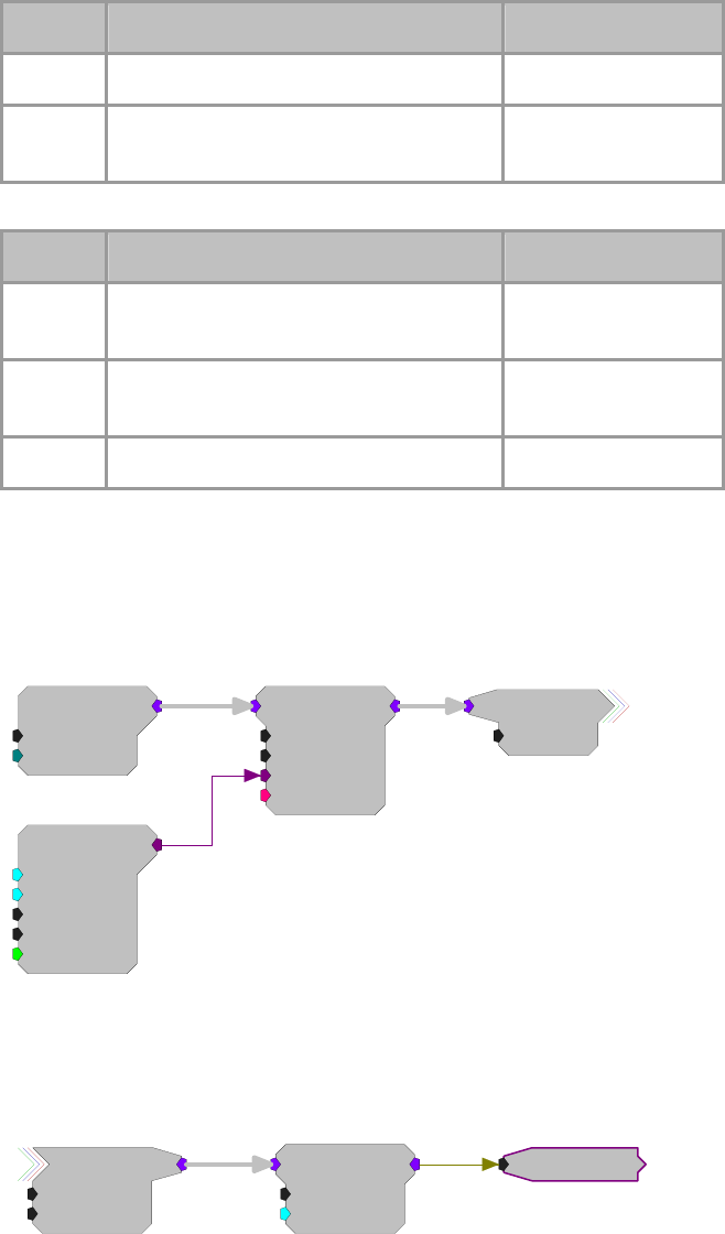
RPvdsEx Manual
252
MCzHopOut
Name Description Data Type
Input Multi-channel input Any
nChan
N
umber of channels of information being
accessed Integer (Static)
MCzHopIn
Name Description Data Type
nChan
N
umber of channels of information being
accessed Integer (Static)
ChanSel First channel number of nChan channels in
the multi-channel signal Integer (Static)
Output Multi-channel output Any
Example:
MCzHops
Processor 1
This circuit filters all 64 A/D inputs and then makes them available to any of
the processors on the device.
MCSignal
nChan=64
MCAdcIn
nChan=64
ChanOS=1
[1:3,0]
ButCoef
Gain=1
Fc=300
NBiq=1
Type=HP
[1:2,0]
Enab=Yes
MCBiquad
nChan=64
nBIQ=1
{>Coef}
{>Delay}
[1:4,0]
Processor 2
On a second processor the multi-channel signal is retrieved and each signal is
scaled then output as a multi-channel signal. The ScaledMC HopOut is a helper
that carries the signal to another part of the circuit on the same processor.
ChanSel=1
MCSignal
nChan=64
MCScale
nChan=64
SF=0.01
[1:2,0]
ScaledMC
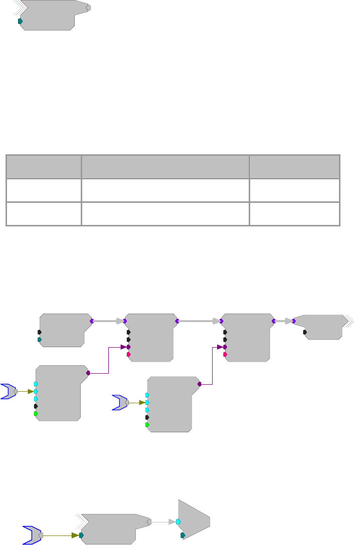
RPvdsEx Manual
253
MCzHopPick
MCzHopPick
ChanNo=1
[1:7,0]
Description:
This component allows transfer of data between processors within a device,
with the added advantage of being able to pick one channel to retrieve from a
multi-channel signal. A MCzHopOut with the same label must also be added to
the RPvdsEx file. The label can be accessed and edited by double-clicking the
component.
Note: This component is for use with only high performance processor devices,
such as RXn or RZn.
Name Description Data Type
ChanNo Channel from which info is required Integer
Output Single-channel output Any
Example:
MCzHopPick
Processor 1
This circuit filters 16 A/D inputs and then makes them available to any of the processors
on the device.
MCAdcIn
nChan=16
ChanOS=1
[1:3,0]
MCBiquad
nChan=16
nBIQ=1
{>Coef}
{>Delay}
[1:4,0]
MCBiquad
nChan=16
nBIQ=1
{>Coef}
{>Delay}
[1:5,0]
ButCoef1
Gain=1
Fc=300
BW=100
Type=HP
[1:1,0]
Enab=Yes
ButCoef1
Gain=1
Fc=3000
BW=100
Type=LP
[1:2,0]
Enab=Yes
HPFreq
LPFreq
MCSignal
nChan=16
Processor 2
This circuit picks channel 1 out of the 16 channels of filtered signals and plays it from the
analog output to allow the user to monitor any one of the recording channels. The channel
number can be selected dynamically via the ChanSelect parameter tag.
ChanSelect
c
O
[1:2,0]
Ch=1
MCSignal
ChanNo=1
[1:1,0]
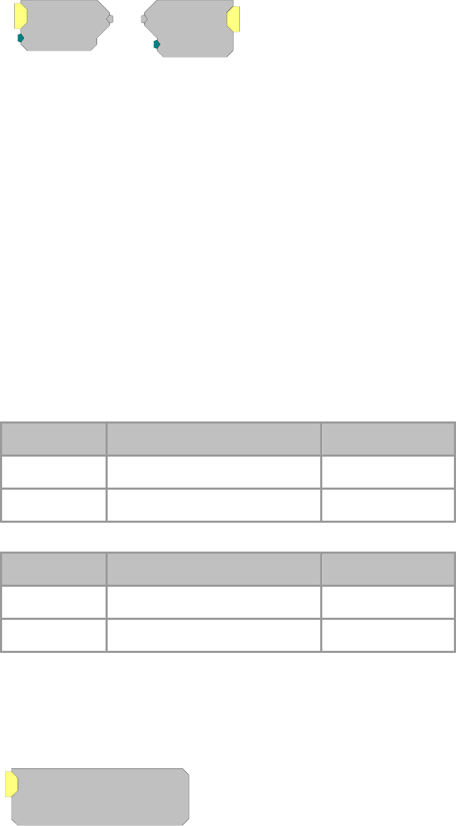
RPvdsEx Manual
254
PipeIn
PipeOut
PipeIn
ChanSel=1
PipeOut
ChanSel=1
Description:
These components allow single-channel transfer of data between processors
within the RZ2 processor. The components are used to either get data from or
put data onto the RZ2’s Data Pipe Bus. Once the data is on the bus it is
available to the other DSPs in the system. The source data available to PipeIn or
from PipeOut is configured using the PipeSource component. There is a two
cycle delay when transferring signals using the PipeIn and PipeOut. (This delay
is accounted for in TDT Developed macros.)
For multi-channel transfer between processors on an RZ2, use MCPipeIn and
MCPipeOut.
Note: The PipeSource component must be included on any DSP that uses
PipeIn, PipeOut, MCPipeIn, or MCPipeOut. Some macros, like the
RZ2_Input_MC allow declaration of a PipeSource component, so that a
separate PipeSource component is not needed.
Note: These components are for use with the RZ2 processor device. Do not use
them with the RZ5, RZ6, RXn or single processor devices. These components
will only appear in the component list when a multi-processor device is selected
in the hardware setup dialog box.
PipeIn
Name Description Data Type
ChanSel Channel number Integer
Output Single-channel output Any
PipeOut
Name Description Data Type
Input Single-channel input Any
ChanSel Cannel number Integer
Example:
See MCPipeIn and MCPipeOut, page 249.
PipeSource
Pipe[B]=DSP-1, Chan[129..256]
PipeSource
Pipe[A]=DSP-1, Chan[1..128]

RPvdsEx Manual
255
Description:
This component allows the user to configure the source data available to the
DSP from the Data Pipe Bus and must be included on any DSP that uses PipeIn,
PipeOut, MCPipeIn, or MCPipeOut.
Two parameters, Pipe[A] and Pipe[B] are used to select the source data.
Pipe[A] represents channels 1-128 and Pipe[B] represents channels 129-256.
The source data for each pipe can be the first or second 128-channel block of
data from any of the DSPs in the system or the Z-Series BioAmp via the RZ2’s
256-channel fiber optic port. Double-clicking on the component brings up the
Edit Component Parameters dialog to change the settings.
Note: This component is for use with the RZ2 processor device. Do not use
them with the RZ5, RZ6, RXn or single processor devices. The component will
only appear in the component list when a multi-processor device is selected in
the hardware setup dialog box.
Name Description Data Type
Pipe[A] Pipe data source for channels 1-128 Static
Pipe[B] Pipe data source for channels 129-256 Static
Example:
See MCPipeIn and MCPipeOut, page 249.
zHopIn
zHopOut
zHopOutzHopIn
Description:
These components allow single channel transfer of signals between processors
within a device. They enable the user to distribute processing tasks across
multiple processors within a multi-DSP device, such as the RX5. There is a one
cycle delay when transferring signals using the zHopOut and zHopIn.
These components work together. Each zHopOut must have a unique label.
Multiple zHopIns can be used with a single zHopOut. Adding a zHopIn without
the corresponding zHopOut (or vice versa) will produce an error.
The hop label can be accessed and edited by double-clicking the component.
For multi-channel transfer between processors, use MCzHopIn and
MCzHopOut.
Note: An RPvdsEx circuit can include a maximum of 126 zHop pairs. One
zHop pair is counted for each single zHop pair and for each channel of a
MCzHop pair.
Note: This component is for use with only high performance processor devices,
such as RXn or RZn.
zHopIn
Name Description Data Type
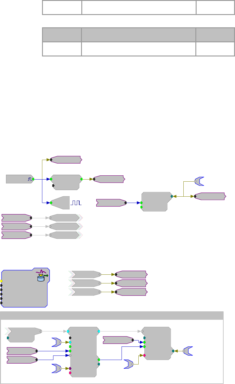
RPvdsEx Manual
256
Output Single channel output Any
zHopOut
Name Description Data Type
Input Single channel input Any
Example:
ZHops
In this example zHopOuts are used on Page 1 to transfer the trigger, reset, and
iTime lines to Page 2, which has been assigned to another processor. On page
two, the trigger lines are used to enable data storage. Notice that in this
example, HopOut and HopIn (helpers) are used in coordination with the zHops.
Keep in mind that, unlike the zHops, the helpers (HopIn and HopOut) do not
use processor cycles or incur delays, so they can be used liberally. When
multiple hops are needed on a single processor, using HopIn and HopOut helps
to reduce the overall number of components in a circuit.
Page 1 - Main Processor
SimpCount
Rst=0
Enable=1
ExtSimp [1:7 - 0]
zTime
iTime
Reset
Enable
iTime
Reset
Enable
Reset
iTime
[1:1,0]
Src=zBusA
EdgeDetect
Edge=Rising
[1:4,0]
Enable
Reset
Bi
[1:10,0]
M=1
Page 2 - Auxiliary Processor
Iterate: x =1 to 32 by 1
Enable
Reset
iTime
Enable
Reset
iTime
SortSpike2
nWid/4=8
Thresh=1
UseSign=1
Enab/Rst=1
[2...,141-02...
]
SortBits=0
Strobe=0
Tag
{>Coef}
{>Data}
aEA~{x}
Enable
iTime
cEA~{x}
SerStore
Size=32000
Rst=0
WrEnab=1
[
2...,16-02...
]
Index=0
{>Data}
dEA~{x}
Reset
sEA~{x}
ECSignal
ChanNo={x}
S
ignal [2... - 13-0
2
oxSnippet
Tag_Root=EA
Blk_Size=32
Data_Form=Float
Sort_Code=Yes
Dec_Factor=1
Channels=0
RPvdsEx Manual
257
NeuroAnalysis
Neuro Analysis Components
This group includes the following components developed primarily for neurophysiology
applications:
BinRate
FindSpike
InstRate
SampSubtract
SortSpike
SortSpike2
SortSpike3
Tetrode
Note: The ArtReject, FindSpike2, FindSpike3, Convolv, Classify, Classify2, BoxClassA, and
BoxClassB1 components are used primarily By TDT's OpenEx and OpenController applications
for real-time spike sorting. These components are not intended for general use at this time.
This group also includes the following components, if RPvdsEx Device Setup is
configured for a high performance device, such as the RXn or RZn:
SortBin8
SortFlag16

RPvdsEx Manual
258
BinRate
BinRate
SortCode=0
[1:1,0]
Bits=0
Reset=1
Description:
The BinRate component allows users to store or view spike rates. The Strobe
output of a spike sorting component (or other pulse) is fed to the BinRate
component’s input to indicate a spike has occurred. At each falling edge of the
input, the component uses the value of the SortCode parameter (an integer
ranging from 0-3) to select and increment the count value of one of four internal
bins. Each time reset goes high, the bin counts are latched to the output and then
reset to zero. The output is a 32-bit integer with each byte representing a bin.
The first eight bits store the values for SortCode 0 the next eight bits for
SortCode 1 and so on.
Note: If the BinRate component receives more than 127 pulses in any bin in
one interval, it will give erroneous results for that interval, as well as for all
following intervals. TDT recommends using an update rate of 125 ms or less for
the BinRate component.
The Bits output takes on one of four values (1, 2, 4, or 8) corresponding to the
SortCode value at the falling edge of the input pulse. For example, if the
SortCode is set to 3, the Bits output will be the integer 8 for one sample at the
falling edge of the input.
Name Description Data Type
Input Pulse, usually indicating the a spike event
occurred
The pulse can be of any width, only the falling
edge is detected as a pulse
Logic
Output A 32-bit integer, with each 8-bit byte
representing a count of spikes that were sorted
into a bin
Integer
SortCode An integer value representing a SortCode and
ranging from 0 – 3 Integer
Reset Latches counts to output then resets counts Logic
Bits One of four values (1, 2, 4, or 8) corresponding
to the SortCode value at the falling edge of the
input
Remains 0 at all times except at the falling edge
of a pulse received at the Input port
Integer
Anomalies:
BinRate records one spike during each of the first two samples of running the
circuit. The easiest work around is to ignore the first two spikes counted.

RPvdsEx Manual
259
However, if the circuit permits, you can add the circuitry shown in the example
below to automatically reset the BinRate to ignore the two erroneous spikes.
When a circuit is run, the Bits output will show a spike being detected, that is
the output will go to 1, 2, 4 or 8 for the first and second sample clock tick,
irrespective of whether a pulse came in or not. If the output is being used, it can
be ANDed with NOT OneShot.
Example: BinRate
In the example below, the BinRate component counts the number of spikes
detected by SortSpike2, based on the SortCode value of each spike. The strobe
output of SortSpike2 triggers the input of the BinRate component and the
SortBits output is fed to the SortCode input. A PulseTrain2 resets the BinRate
output once every two seconds. Therefore, the counts represent the number of
spikes in each bin during a two second interval. The BinRate output is split into
the counts for each bin by the SplitTo8 component.
The Bits output is used to light an LED every time a spike with the SortCode 0
(unsorted spikes in OpenEx) is detected. The components in the red blocks are
temporarly needed for bugs.
SortSpike2
nWid/4=8
Thresh=1
UseSign=1
Enab/Rst=1
[4:231,0]
SortBits=0
Strobe=0
Tag
{>Coef}
{>Data}
SerStore
Size=1000
Rst=0
WrEnab=1
[4:231,0]
Index=0
{>Data}
aEA~1
cEA~1 SFire
SCode
sEA~1
Reset
Enable
iTime
FiltSig1
PulseTrain2
nPer=100
nPulse=-1
Enab=Yes
Rst=Run
[1:1,0]
PCount=0
PLate=0
OneShot
[1:2,0]
TTLDelay2
N1=1
N2=0
[1:3,0
]
[1:4,0]
OR
BinReset
SFire
SCode
BinReset
BinRate
SortCode=0
[1:6,0]
Bits=0
Reset=1
SplitFrom8
SF=1
[1:7,0]
~1
~2
~3
~4
iCompare
K=1
Test=EQ
[1:9,0] [1:10,0]
A
ND
No
[1:2,0]
OneShot
[1:1,0
]
Schmitt
Thi=100
Tlo=10
[1:11,0]
Bi
[1:12,0]
M=1
0
0
0
0
LED 1 will go on for 100 ms
everytime a spike with sort code 0
occurs
Counts for each
sort code;
refreshed every 2
seconds

RPvdsEx Manual
260
FindSpike
FindSpike
nWidth=40
Tau=1000
ThrLo=3
ThrHi=1000
[1:1,0]
Strobe=0
RMS^2=0
Rst=0
{>Data}
Tag
Description:
FindSpike detects spikes based on their deviations from the noise of the system.
An RMS (root mean square) of the signal is calculated for a given time interval
(Tau). Signal voltages that deviate by more than ThrLo and less than ThrHi
deviations from the RMS are detected. The detector stores the waveform
(nWidth in size) centered around its peak. The waveform along with a
timestamp can be stored in a memory buffer.
Name Description Data Type
Input Input Floating Point
Output Spike waveform of nWidth samples Floating Point
nWidth
N
umber of samples stored Integer (Static)
Tau Time length in milliseconds for calculating the
RMS of the noise Floating Point
(Static)
ThrLo Lower threshold (in deviations from RMS) for
detecting a spike Floating Point
ThrHi Upper threshold (in deviations from RMS) for
detecting a spike Floating Point
Rst Resets the FindSpike so that candidate spikes are
only acquired during an acquisition period Logic
Tag Tag some form of identifier for the waveform, can
be a time stamp or counter value Any
RMS^2 Square of the RMS (Root Mean Square value) of
the noise, output value can be stored to a buffer Floating Point
Strobe Goes high for the length of the sample when a
spike is detected Logic
>Data Data Port, allows access to the memory buffer Pointer
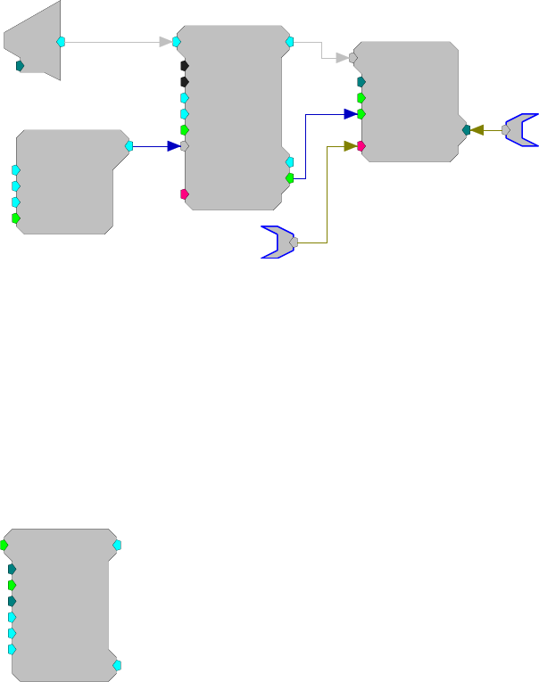
RPvdsEx Manual
261
Example:
FindSpike
FindSpike
nWidth=40
Tau=1000
ThrLo=3
ThrHi=1000
[1:4,0]
Strobe=0
RMS^2=0
Rst=0
{>Data}
Tag
TSlope
Min=0
Slp=0
Max=1
Rst=Run
[1:1,0]
d
c
[1:3,0]
Ch=1
SerStore
Size=40000
Rst=0
WrEnab=1
[1:6,0]
Index=0
{>Data}
SpikeData
SpikeNumber
In the example above an analog input is sent to the FindSpike component. A
TSlope is used to generate a timestamp. Data is saved to a SerStore (Note: the
Strobe output is connected to the WrEnab line of the SerStore). Parameter tags
allow ActiveX controls to access the spike data and spike number from the
buffer. This FindSpike saves 39 points of data plus a timestamp tag
(nWidth=40).
The Rst line allows the user to reset the FindSpike to the start of a candidate
spike. This allows acquisition in a sweep based mode to only include spikes
from the start of the sweep.
InstRate
InstRate
SortCode=0
UseFall=1
SortMatch=0
FcFact=0.2
[1:1,0]
FcFeed=0
FcMin=3
FcReturn=0
Description:
The InstRate (instantaneous rate) component acquires TTL inputs and converts
each TTL pulse to a large floating point value. This value is then filtered
through a low pass filter. The filtered value is then fed back into the InstRate
component. Based on the input rate it either increases the filter (higher spike
rates) or decreases the filter (lower spike rates) by a set value (FcFact) this
value is then sent out the FcFeed parameter output to the input of the filter
coefficient generator (Fc). Additional component features allow the signal to be
generated in the falling edge of the TTL input or to use a SortCode.

RPvdsEx Manual
262
Name Description Data Type
Input Input Logic
Output Floating point number representing the raw
instant rate Floating Point
SortCode Sort code value assigned to the waveform
represented by the logical input Integer
UseFall Sets the edge of the waveform used Logic
SortMach Sort Code value for which firing rate is desired Integer
FcFact Frequency feedback factor Floating Point
FcMin Frequency feedback minimum Floating Point
FcReturn Frequency feedback minimum Floating Point
FcFeed Adjusted filter cutoff frequency based on
measured spike rate Floating Point
Example:
Instantaneous Rate
The example below shows how the InstRate component could be used to find
the firing rate of neural activity. The logical output of the SortSpike Strobe is
fed into the InstRate component where it is converted to a floating point value.
A parameter tag allows ActiveX controls to access the firing rate from the
Biquad.
Spike1
IRate
ButCoef
Gain=1
Fc=1000
NBiq=2
Type=LP
[1:7,0]
Enab=Yes
FireRate
IRate
Biquad
nBIQ=2
{>Coef}
{>Delay}
[1:2,0]
InstRate
SortCode=0
UseFall=1
SortMatch=0
FcFact=0.2
[1:5,0]
FcFeed=0
FcMin=3
FcReturn=0
d
c
[1:1,0]
Ch=1
SortSpike
nWid/2=16
ThrLo=0.000
2
ThrHi=10
Enab/Rst=1
[1:2,0]
SortBits=0
Strobe=0
Tag
{>Coef}
{>Data}
SerStore
Size=32000
Rst=0
WrEnab=1
[1:4,0]
Index=0
{>Data}
aEA~1
bEA~1
cEA~1
Spike1
dEA~1
Enable
iTime
Reset
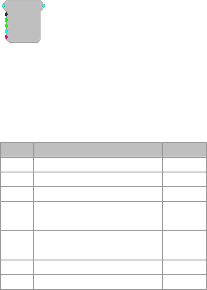
RPvdsEx Manual
263
SampSubtract
SampSubtract
nWidth=10
Sync=0
EnabSub=1
SF=0.01
[1:1,0]
{>Data}
Description:
The SampSubtract component is useful for removing artifacts in the signal that
are generated in a predictable manner (such as an artifact from electrical
stimulation).
In order to remove the artifact, a signal snippet is acquired and added to a buffer
during each occurrence of the artifact. A weighted fraction of the summed
signal snippets is subtracted from the signal as each new artifact occurs. Over-
time the artifact will be removed from the signal with increasing accuracy and
without reducing the integrity of the signal of interest.
Note: This component is for use with only high performance processor devices,
such as RXn or RZn.
Name Description Data Type
Input Input signal Floating Point
Output Filtered signal Floating Point
nWidth Size of buffer for the weighted sum Static
Sync Enables acquisition of artifact signal and triggers
summing and subtraction. The Sync input should
remain high for the duration of the artifact.
Logic
EnabSub Enables subtraction when high and disables the
subtraction, letting the signal pass unaltered, when
low
Logic
SF Scale Factor Floating Point
>Data Memory buffer for the weighted sum Pointer
Accurate acquisition and removal of the artifact can only occur if the onset and
length of the artifact are known and predictable. The Sync line is used to trigger
acquisition, summing, and subtraction. So, the Sync input should be synced
with the generation of the stimulus, and its duration should be set to the
duration of the stimulus. Each time the Sync input goes high, SampSubtract
acquires the snippet of signal for the duration of Sync pulse and calculates the
sum of snippets that is then weighted (multiplied by a fraction related to the
Scale Factor) and subtracted from the input signal the next time that Sync goes
high. The calculation of the weighted sum is related to the Scale Factor but also
depends on the amplitude of the summed snippets.
Note: A delay may be required before the Sync input goes high to compensate
for the time taken for the electrical stimulus to go through the outputs, into the
brain, and back into the amplifier as an artifact.

RPvdsEx Manual
264
When the circuit is run, the artifact will be gradually reduced as the weighted
sum gradually increases. Hence, the signal will undergo a training period before
the artifact rejection reaches an optimum level. The higher the value of Scale
Factor, the shorter the training period, and greater the chance of the useful part
of the signal leaking into the weighted sum. Generally, a scale factor of 0.01 to
0.05 will provide good rejection results.
If the scale factor is set to 0, the summing stops, but the current weighted sum
remains in the buffer, and continues to be subtracted from the signal. Setting the
scale factor to 0 after the initial training period will continue the subtraction, but
stop further growth of the subtracted signal reducing the likelihood that the
useful signal around the artifact will be affected.
The nWidth parameter sets a predetermined buffer size to hold the weighted
sum. It should be made sufficiently large to hold the summed signal.
The >Data pointer provides access to the weighted sum.
When the EnabSub input is high, the subtraction is enabled; when low,
subtraction is disabled and the signal passes to the component output unaltered.
SortBin8
SortBin8
nChan=16
[1:6,0]
Strobe=0
SyncIn=0
Description:
The SortBin8 component is useful for counting the number of sort codes per
channel in a multi-channel signal. The input of the SortBin8 component is
typically a multi-channel integer representing the sort code value for each
channel. The output for each channel is a single 32-bit integer. Each byte in the
integer contains the count for a single sort code making a total of four sort
codes (1, 2, 3, and 4).
Sort Code:
4 3 2 1
0000 0000 | 0000 0000 | 0000 0000 | 0000 0000
MSB LSB
On a rising edge of SyncIn, the sort code count for all channels is reset to 0. At
this time the Strobe output simultaneously goes high for one sample to indicate
that the count has been reset.
For example, suppose there are 7 spikes with sort code 1 and 9 spikes with sort
code 2 since the last SyncIn. The ouput will be 231110 or:
4 3 2 1
0000 0000 | 0000 0000 | 0000 1001 | 0000 0111
MSB LSB
Note: This component is for use with only high performance processor devices,
such as RXn or RZn.
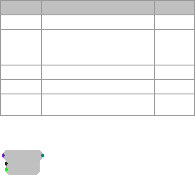
RPvdsEx Manual
265
Name Description Data Type
Input Multi-channel input signal Integer
Output Sort code count. This is a 32-bit integer
value with each of the four sort bins
represented by a single byte out of the 32-bit
value.
Integer
nChan
N
umber of channels to store sort counts for. Integer (Static)
SyncIn Resets the count value for all channels to 0 Logic
Strobe Goes high for a single sample when the
count is reset. Logic
SortFlag16
SortFlag16
nChan=16
SyncIn=0
[1:2,0]
Description:
SortFlag16 is useful for monitoring sort code activity over a period of time. The
SortFlag16 component flags two sort codes for each channel based on its multi-
channel input signal (which will most likely come from a SpikePac power
macro sort code output). SortFlag16 polls each input channel for a value of 1 or
2, if either value exists on any channel, SortFlag16 sets the corresponding flag
bit to a logic high (1). On the rising edge of SyncIn, SortFlag16 latches a 32-bit
integer value which contains two flag bits for each channel (each flag represents
a sort code of 1 or 2).
The SortFlag16 output structure for the 32-bit integer is shown below.
Channel Sort code
162 161 ... 32 31 22 21 12 11
0 0 … 0 0 0 0 0 0
MSB LSB
After SyncIn has detected a rising edge it resets the internal flags for each
channel.
For example, you are sending a rising edge to the SyncIn input every 10 ms. A
sort code value of 1 and 2 are sent to channels 1, 3, and 5 between the last rising
edge of SyncIn. On the next rising edge of SyncIn, the output will be 81910 or:
0000 0000 | 0000 0000 | 0000 0011 | 0011 0011
MSB LSB
Notice that the sort code flags (1 and 2) are set for channels 1, 3, and 5.
Note: This component is for use with only high performance processor devices,
such as RXn or RZn.
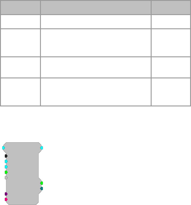
RPvdsEx Manual
266
Name Description Data Type
Input Multi-channel input signal Integer
Output 16-channel sort code flag. This is a 32-bit
integer value containing two sort code flags
(1 and 2) for each channel.
Integer
nChan
N
umber of channels to store sort code flags
for. The maximum is 16 Integer (Static)
SyncIn On a rising edge, outputs the current 32-bit
flag and resets the flag values for all
channels to 0
Logic
SortSpike
SortSpike
nWid/2=16
ThrLo=1
ThrHi=1000
Enab/Rst=1
[1:1,0]
SortBits=0
Strobe=0
Tag
{>Coef}
{>Data}
Description:
The SortSpike component sorts spikes using a time/voltage window
discriminator. The threshold voltage (window) is selected with the ThrLo and
ThrHi parameters. When a candidate waveform is detected it is tagged with the
value from the Tag input and a sort value is assigned (SortBits). The data output
contains the Tag value (timestamp), sort value (sort code) and the waveform.
The waveform is stored with the peak of the spike centered in the data buffer.
For more information see the OpenEx Manual.
Organization of Waveform Data
Sample 1 = Tag Value (Timestamp)
Samples 2:(n-1) = Waveform
Sample n = Sort code
Sample n/2 = Waveform Peak
For a SortSpike with nWid/2 = 16 the number of waveform samples would be
32-2 (Tag and SortBit) or 30 points of signal waveform. The peak would be at
sample 15.
This component is used primarily by TDT turnkey applications such as
OpenEx. Users should read the description of how to use SortSpike in OpenEx.
A description of how to use the component with custom codes is described
below.
Setting the Time-Voltage and Sort Codes via Custom Software
RPvdsEx Manual
267
The SortSpike component uses information stored in a coefficient vector to
determine the time-voltage and sort code values.
Organization of the coefficient vector is as follows:
The coefficients are organized into a vector array which is 3 times the length of
the waveform. Three consecutive indices in the vector are associated with a
single sample along the waveform. These three values define a time-voltage
window discriminator or ‘hoop’ that a given waveform may pass through.
This means that vector indices [0], [1], and [2] represent the three time-voltage
hoop characteristics for the first sample of the waveform.
The three values used to define a hoop are the Center Voltage, Half-Height
Voltage, and Sort Code.
The Center and Half-Height Voltages are specified in Volts while the Sort Code
is specified as a positive integer from 1 to 30.
Note: If the incoming waveform passes through more than one hoop, the hoop
in which the waveform passes closest to the Center Voltage determines which
hoop’s Sort Code gets assigned.
Samples not containing hoops must have all three hoop characteristics zeroed.
For Example, a waveform containing 8 samples will use a coefficient vector
with a length of 24. If we wish to have two hoops, one at waveform position 3
and another at waveform position 6, the coefficient vector to be loaded would
be:
0 0 0 0 0 0 C1 H1 S1 0 0 0 0 0 0 C2 H2 S2 0 0 0 0 0 0
Where:
C1, H1, and S1 are the Center Volt, Half-Height Volt, and Sort Code values for
Hoop 1
C2, H2, and S2 are the Center Volt, Half-Height Volt, and Sort Code values for
Hoop 2
Users can upload the vector to the component's coefficient parameter. A simple
path for using this setup would require that candidate waveforms be
downloaded to the PC. Users would then view the plotted waveforms and
determine the time in samples and voltage position that would differentiate two
classes of waveforms.
RPvdsEx Manual
268
Name Description Data Type
Input Input Floating Point
Output Spike waveform of nWid samples Floating Point
nWid/2 1/2 number of samples stored Integer (Static)
ThrLo Lower threshold (in voltage) for detecting a spike Floating Point
ThrHi Upper threshold (in voltage) for detecting a spike Floating Point
Enable Resets the SortSpike so that candidate spikes are
only acquired during an acquisition period Logic
Tag Tag some form of identifier for the waveform, can
be a time stamp or counter value Any
Strobe Goes high for the length of the sample when a spike
is detected Logic
SortBits Sort Code value associated with the waveform Integer
>Coef Coefficients that determine the time/voltage values
and sort code values Pointer
>Data Data Port, allows access to memory buffer Pointer
SortSpike2
SortSpike2
nWid/4=8
Thresh=1
UseSign=1
Enab/Rst=1
[1:1,0]
SortBits=0
Strobe=0
Tag
{>Coef}
{>Data}
Description:
The SortSpike2 component sorts spikes using a time/voltage window
discriminator. Candidate waveforms are detected when the rising edge (positive
waveforms) or falling edge (negative waveforms) of the waveform crosses the
threshold voltage (window) set for the Thresh parameter. The UseSign
parameter allows the user to specify unidirectional or bidirectional waveform
detection. When a candidate waveform is detected it is tagged with the value
from the Tag input and a sort value is assigned (SortBits). The data output
contains the Tag value (timestamp of rising or falling edge), sort value (sort
code) and the waveform. The waveform is stored with the point at which the
RPvdsEx Manual
269
rising or falling edge crosses the threshold at nWid/4 samples. For more
information see the OpenEx Manual.
Organization of Waveform Data
Sample 1 = Tag Value (Timestamp)
Samples 2:(n-1) = Waveform
Sample n = Sort Code
For a SortSpike2 with nWid/4 = 16 the number of waveform samples would be
64 - 2 (Tag and SortBit) or 62 points of signal waveform.
This component is used primarily by TDT turnkey applications such as
OpenEx. Users should read the description of how to use SortSpike2 in
OpenEx. A description of how to use the component with custom codes is
described below.
Setting the Time-Voltage and Sort Codes via Custom Software
The SortSpike component uses information stored in a coefficient vector to
determine the time-voltage and sort code values.
Organization of the coefficient vector is as follows:
The coefficients are organized into a vector array which is 3 times the length of
the waveform. Three consecutive indices in the vector are associated with a
single sample along the waveform. These three values define a time-voltage
window discriminator or ‘hoop’ that a given waveform may pass through.
This means that vector indices [0], [1], and [2] represent the three time-voltage
hoop characteristics for the first sample of the waveform.
The three values used to define a hoop are the Center Voltage, Half-Height
Voltage, and Sort Code.
The Center and Half-Height Voltages are specified in Volts while the Sort Code
is specified as a positive integer from 1 to 30.
Note: If the incoming waveform passes through more than one hoop, the hoop
in which the waveform passes closest to the Center Voltage determines which
hoop’s Sort Code gets assigned.
Samples not containing hoops must have all three hoop characteristics zeroed.
For Example, a waveform containing 8 samples will use a coefficient vector
with a length of 24. If we wish to have two hoops, one at waveform position 3
and another at waveform position 6, the coefficient vector to be loaded would
be:
0 0 0 0 0 0 C1 H1 S1 0 0 0 0 0 0 C2 H2 S2 0 0 0 0 0 0
Where:
C1, H1, and S1 are the Center Volt, Half-Height Volt, and Sort Code values for
Hoop 1
C2, H2, and S2 are the Center Volt, Half-Height Volt, and Sort Code values for
Hoop 2
Users can upload the table to the component's coefficient parameter. A simple
path for using this setup would require that candidate waveforms be
downloaded to the PC. Users would then view the plotted waveforms and
determine the time in samples and voltage position that would differentiate two
classes of waveforms.

RPvdsEx Manual
270
Name Description Data Type
Input Input Floating Point
Output Spike waveform of nWid samples Floating Point
nWid/4 1/4 number of samples stored Integer (Static)
Thresh Threshold (in voltage) for detecting a spike Floating Point
Use Sign If set to zero any sign entered with the Thresh
value is disregarded and the value is considered
to be a +/- number. If set to one, Thresh value
sign is considered.
Logic
Enable Resets so that candidate spikes are only
acquired during an acquisition period Logic
Tag Identifier for the waveform, can be a timestamp
or counter value Any
Strobe Goes high for the length of the sample when a
spike is detected Logic
SortBits Sort Code value associated with waveform Integer
>Coef Coefficients that determine the time/voltage
values and sort code values Pointer
>Data Data Port, allows access to memory buffer Pointer
SortSpike3
SortSpike3
nWid/4=8
Thresh=1
UseSign=1
Enab/Rst=1
[1:1,0]
SortBits=0
Strobe=0
Tag
{>Coef}
{>Data}
Description:
The SortSpike3 component sorts spikes using a time/voltage window
discriminator. Candidate waveforms are detected when the rising edge (positive
waveforms) or falling edge (negative waveforms) of the waveform crosses the
threshold voltage (window) set for the Thresh parameter. The UseSign
parameter allows the user to specify unidirectional or bidirectional waveform
detection. When a candidate waveform is detected it is tagged with the value
from the Tag input and a sort value is assigned (SortBits). The data output
contains the Tag value (timestamp of rising or falling edge), the waveform and
RPvdsEx Manual
271
sort value (sort code). The waveform is stored with the point at which the rising
or falling edge crosses the threshold at nWid/4 samples.
SortSpike3 is a slight modification to the SortSpike2 component. The only
difference is in the determination of the sort code. See Determining Sort Code
for more information.
Organization of Waveform Data
Sample 1 = Tag Value (Timestamp)
Samples 2:(n-1) = Waveform
Sample n = Sort Code
For a SortSpike3 with nWid/4 = 16, the number of waveform samples would be
64. This number includes 62 points of signal waveform, the tag value and sort
code.
This component is used primarily by TDT turnkey applications such as
OpenEx. Users should read the description of how to use SortSpike3 in
OpenEx. A description of how to use the component with custom codes is
described below.
Setting the Time-Voltage and Sort Codes via Custom Software
The SortSpike component uses information stored in a coefficient vector to
determine the time-voltage and sort code values.
Organization of the coefficient vector is as follows:
The coefficients are organized into a vector array which is 3 times the length of
the waveform. Three consecutive indices in the vector are associated with a
single sample along the waveform. These three values define a time-voltage
window discriminator or ‘hoop’ that a given waveform may pass through.
This means that vector indices [0], [1], and [2] represent the three time-voltage
hoop characteristics for the first sample of the waveform.
The three values used to define a hoop are the Center Voltage, Half-Height
Voltage, and Hoop Number.
The Center and Half-Height Voltages are specified in Volts while the Hoop
Number is specified as a positive integer.
Samples not containing hoops must have all three hoop characteristics zeroed.
For Example, a waveform containing 8 samples will use a coefficient vector
with a length of 24. If we wish to have two hoops, one at waveform position 3
and another at waveform position 6, the coefficient vector to be loaded would
be:
0 0 0 0 0 0 C1 H1 N1 0 0 0 0 0 0 C2 H2 N2 0 0 0 0 0 0
Where:
C1, H1, and N1 are the Center Volt, Half-Height Volt, and Hoop Number values
for Hoop 1
C2, H2, and N2 are the Center Volt, Half-Height Volt, and Hoop Number values
for Hoop 2
If the incoming waveform passes through more than one hoop, each hoop sets a
corresponding bit in the final sort code by the relationship:
2(HoopNum-1)
For example, if an incoming waveform passes through hoops 1,2 and 3, the
following bits would be set:
RPvdsEx Manual
272
Value Bit
2(1-1)=1 0
2(2-1)=2 1
2(3-1)=4 2
This results in a final sort code of 7.
Users can upload the table to the component's coefficient parameter. A simple
path for using this setup would require that candidate waveforms be
downloaded to the PC. Users would then view the plotted waveforms and
determine the time in samples and voltage position that would differentiate two
classes of waveforms.
Note: This component is for use with only high performance processor devices,
such as RXn or RZn.
Name Description Data Type
Input Input Floating Point
Output Spike waveform of nWid samples Floating Point
nWid/4 1/4 number of samples stored Integer (Static)
Thresh Threshold (in voltage) for detecting a spike Floating Point
Use Sign If set to zero any sign entered with the Thresh value is
disregarded and the value is considered to be a +/-
number. If set to one, Thresh value sign is considered.
Logic
Enable Resets the SortSpike3 so that candidate spikes are only
acquired during an acquisition period Logic
Tag Some form of identifier for the waveform, can be a
timestamp or counter value Any
Strobe Goes high for the length of the sample when a spike is
detected Logic
SortBits Sort Code value associated with the waveform Integer
>Coef Coefficients that determine the time/voltage values and
sort code values Pointer
>Data Data Port, allows access to the memory buffer Pointer

RPvdsEx Manual
273
Tetrode
Tetrode
Thr1=1
[1:1,0]
~1
~2
~3
~4
Thr2=1
Thr3=1
Thr4=1
Enable
Description:
The Tetrode component is designed to synchronize the acquisition of snippets
from multiple channels. Trigger inputs (Thr1-4) set the voltage threshold for
each channel of the tetrode. When the signal from a channel crosses its
threshold a TTL pulse is generated. The TTL output can be sent to a Block
Access (with a delay) or it can be used to trigger a SnipStore component that
saves the waveform and stores a time stamp.
Tetrode and SnipStore are designed primarily for use with the OpenEx software
suite. To learn more about how to use the Tetrode and SnipStore components
with OpenEx check your OpenEx documentation.
Note: This component is for use with only high performance processor devices,
such as RXn or RZn. If you are using a Classic Processor, see the examples
below for an alternative circuit design or contact TDT technical support for
more information.
Name Description Data Type
~1 Input signal from a channel 1 Floating Point
~2 Input signal from a channel 2 Floating Point
~3 Input signal from a channel 3 Floating Point
~4 Input signal from a channel 4 Floating Point
Output TTL pulse Logic
Thr1 Upper threshold (in voltage) for triggering logical high Floating Point
Thr2 Upper threshold (in voltage) for triggering logical high Floating Point
Thr3 Upper threshold (in voltage) for triggering logical high Floating Point
Thr4 Upper threshold (in voltage) for triggering logical high Floating Point
Enable When the Enable line is high, a TTL pulse is triggered
when any channel goes above threshold Logic
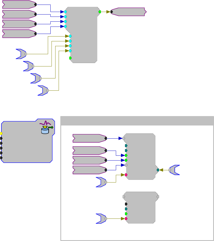
RPvdsEx Manual
274
Example:
Tetrode
The example below shows how the basic Tetrode component could be used in
OpenEx. The Tetrode component compares signals from four input channels to
a corresponding voltage threshold. When a threshold is reached on any of the
four channels, the Tetrode output sends out a pulse for one cycle.
This output pulse (Go) can then be used to trigger the buffer acquisitions which
iterate four times, 1 for each channel. Each signal can be acquired with a
SnipStore that stores n/2 samples before and after the trigger as well as a time
stamp (Tag). Since each channel of the buffer would have the same number of
stored values only one Index needs to be polled. The use of "cSnip~{x}" with a
RamBuf allows threshold controls in OpenController.
Tetrode
Thr1=1
[1:16,0]
~1
~2
~3
~4
Thr2=1
Thr3=1
Thr4=1
Enable
Go
Sig1
Sig2
Sig3
Sig4
aSnip~1
aSnip~2
aSnip~3
aSnip~4
oxSnippet
Tag_Root=Snip
Blk_Size=64
Data_Form=Float
Sort_Code=No
Dec_Factor=1
Channels=4
Iterate: x =1 to 4 by 1
SnipStore
Size=32000
nBlk/2=32
Rst=0
Go=1
[1...,25-01...]
Index=0
Tag
{>Data}
Sig{x}
@Reset
Go
@Time
dSnip~{x}
sSnip~{x}
RamBuf
Size=1000
Index=0
Write=0
{>Data}
[1...,1-01...]
cSnip~{x}
This example illustrates an alternative circuit design to achieve a signal
equivalent to the output of the Tetrode component without using the component
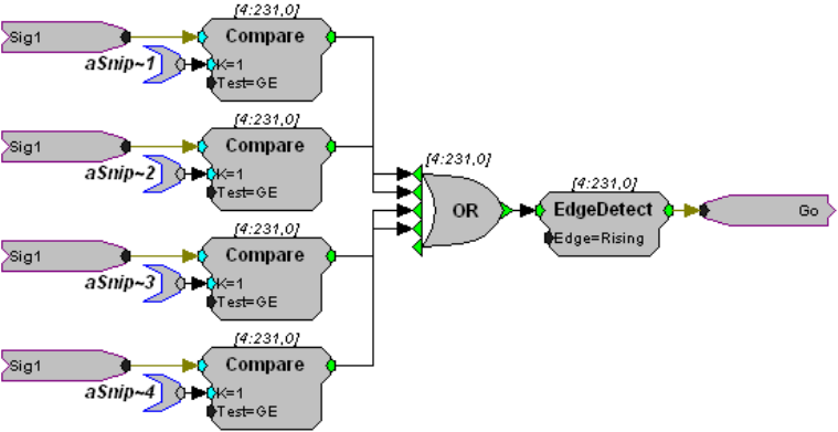
RPvdsEx Manual
275
itself. This example is for users who wish to achieve the same operation as
Tetrode using lower order components on a Classic Processor.
The corresponding voltage threshold for each input channel can be controlled
by modifying the aSnip~ tag value tied to the K parameter of each Compare
component.
RPvdsEx Manual
276
OpenEx Headers
OpenEx Header Components
OpenEx components are used with the OpenEx software suite, consolidating information about a
circuit construct and making it readily available in OpenWorkbench.
This group includes the following components:
OxBuffer
OxList
OxScalar
OxSnippet
OxStream
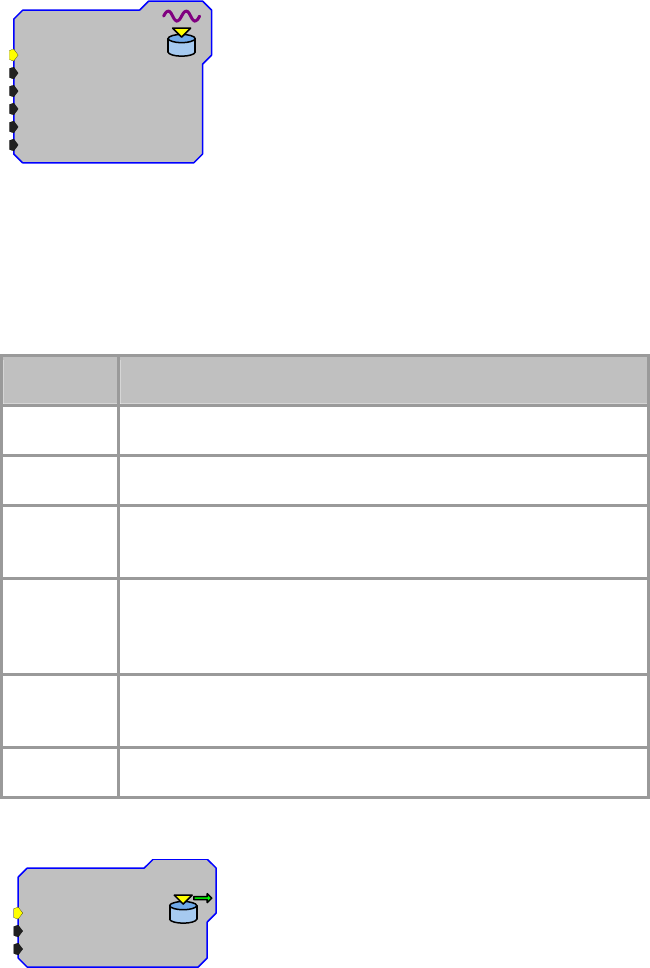
RPvdsEx Manual
277
OxBuffer
oxBuffer
Tag_Root=
Buffer_Size=32
Data_Form=Float
Dec_Factor=1
Handshake=Soft-1
Channels=0
Description:
The OXBuffer component is used with the OpenEx software suite. The
OXBuffer acts as a circuit header, consolidating information about a circuit
construct and making it readily available in OpenWorkbench. The OXBuffer is
used in data buffer circuit constructs, which store an array of data in a memory
buffer. See OpenEx help for more information.
Name Description
Tag_Root Base name of the construct
Buffer_Size Block size of the acquired data
Data_Form Format of the data - the data type can be float, integer, short, or
byte
Dec_Factor Decimation factor - if the data is reduced either through a
Plot16dec or through changes in the time-slice then a decimation
factor other than one should be used
HandShake Indicates whether a software trigger will be used for the
handshake
Channels The number of channels associated with the buffer
OxList
oxList
Tag_Root=
Data_Form=Float
Channels=0
37
.
45
0
.65
1
...
Description:
The OXList component is used with the OpenEx software suite. The OXList
acts as a circuit header, consolidating information about a circuit construct and
making it readily available in OpenWorkbench. The OXList is used in data list
circuit constructs, in which a list of values is stored in one buffer and
corresponding time stamps are stored in another buffer. See OpenEx help for
more information.
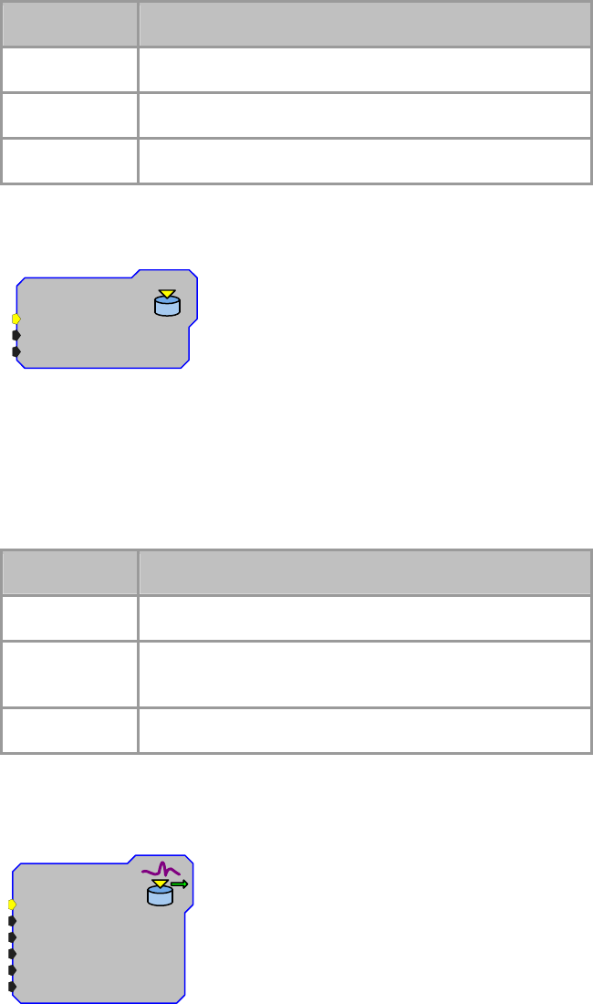
RPvdsEx Manual
278
Name Description
Tag_Root Base name of the construct
Data_Form Format of the data - the data type can be float or integer
Channels The number of channels associated with the list
OxScalar
oxScalar
Tag_Root=
Handshake=Soft-1
Channels=0
37.45
Description:
The OXScalar component is used with the OpenEx software suite. The
OXScalar acts as a circuit header, consolidating information about a circuit
construct and making it readily available in OpenWorkbench. The OXScalar is
used in triggered scalar circuit constructs, which are used when single variables
that require a precise time stamp must be stored and the interval between events
varies. See OpenEx help for more information.
Name Description
Tag_Root Base name of the construct
HandShake Indicates whether a software trigger will be used for the
handshake
Channels The number of channels associated with the scalar
OxSnippet
oxSnippet
Tag_Root=
Blk_Size=32
Data_Form=Float
Sort_Code=No
Dec_Factor=1
Channels=0
Description:
The OXSnippet component is used with the OpenEx software suite. The
OXSnippet acts as a circuit header, consolidating information about a circuit
construct and making it readily available in OpenWorkbench. The OXSnippet is
used in signal snippet circuit constructs, which consist of a time stamp and an
associated data buffer. See OpenEx help for more information.
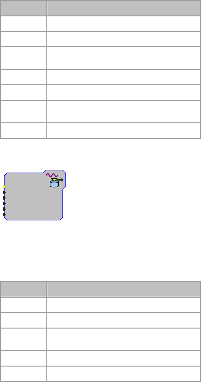
RPvdsEx Manual
279
Name Description
Tag_Root Base name of the construct
Blk_Size Block size of the acquired snippet
Data_Form Format of the data - the data type can be float, integer, short,
or byte
Sort_Code Sort code
Dec_Factor Decimation factor
HandShake Indicates whether a software trigger will be used for the
handshake
Channels The number of channels associated with the snippet
OxStream
oxStream
Tag_Root=
Blk_Size=32
Data_Form=Float
Dec_Factor=1
Channels=0
...
Imp_MC=No
Description:
The OxStream component is used with the OpenEx software suite. The
OxStream acts as a circuit header, consolidating information about a circuit
construct and making it readily available in OpenWorkbench. The OxStream is
used in continuous waveform circuit constructs, which are used for
continuously acquired data waveforms that do not require a unique time stamp.
See OpenEx help for more information.
Name Description
Tag_Root Base name of the construct
Blk_Size Block size of the stream acquired
Data_Form Format of the data - the data type can be float, integer, short,
or byte
Dec_Factor Decimation factor
Channels The number of channels associated with the snippet
RPvdsEx Manual
280
State/Flow Control
StateFlow Control Components
This group includes components for the StateFlow control functions.
This group includes the following components:
MuxIn
MuxOut
SampHold
SimpCount
StateMach
This group also includes the following component, if RPvdsEx Device Setup is
configured for a high performance device, such as the RXn or RZn:
MCSampHold
Important Note!: This group also includes the undocumented components: SeqIndex. This
component is not intended for general use at this time.
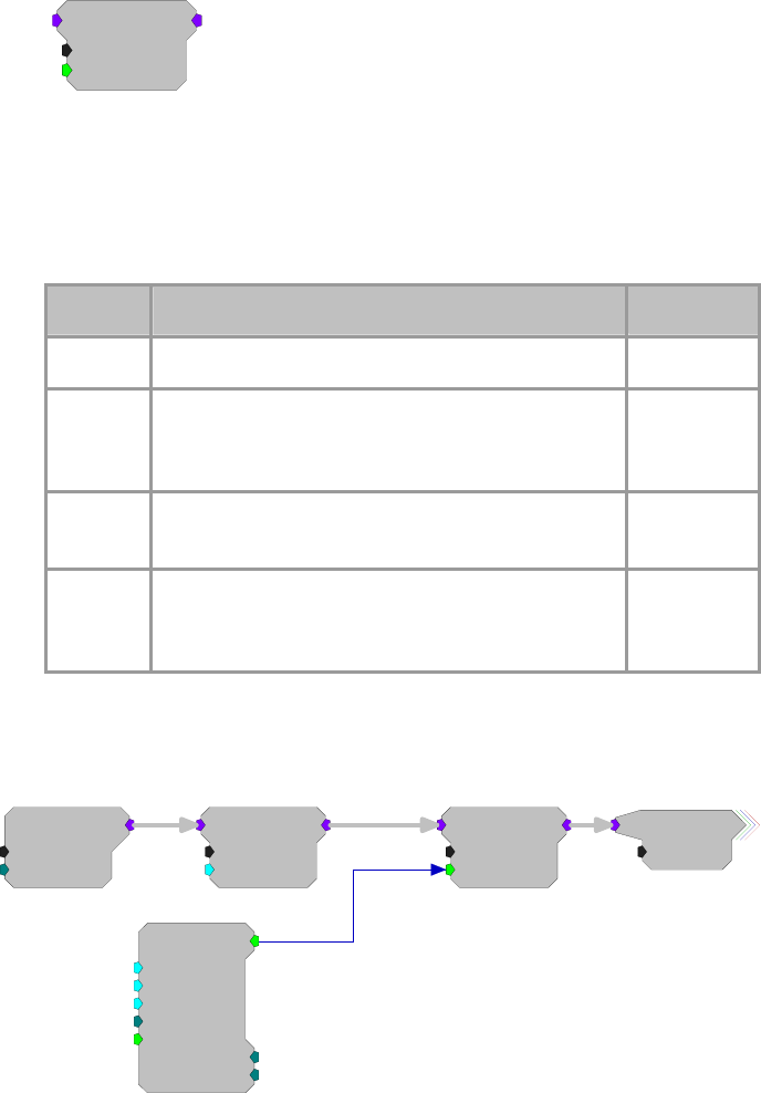
RPvdsEx Manual
281
MCSampHold
MCSampHold
nChan=16
S/H=1
[1:2,0]
Description:
The MCSampHold component is the multi-channel version of the SampHold
component. It samples input values while S/H is set to a logical high. When S/H
goes to zero, the last value is held. SampHold differs from Latch in that Latch
holds the first value when triggered by a logical high input and holds that value
until the next logical high.
Name Description Data Type
Inputs Input signal to be sampled/held Any
Output Output value of the component (Depending on the
value of S/H, this will either be a held value or a
newly sampled value of the input signal.)
Any
nChan
N
umber of channels in the input signal Integer
(Static)
S/H Sample/Hold Control (When set high (1), the
component will sample. When set low (0), the
component will hold.)
Logic
Example:
Multi-channel Sample and Hold
MCSampHold
nChan=16
S/H=1
[1:5,0]
PulseTrain
Thi=1000
Tg=0
Tlo=1000
Npls=0
[1:1,0]
CurN=0
Stage=0
Trg=1
MCAdcIn
nChan=16
ChanOS=1
[1:3,0]
MCScale
nChan=16
SF=0.5
[1:4,0]
Half
nChan=16
The above example uses a MCSampHold component to look at the scaled value
of the multi-channel input from the ADC every 2000 milliseconds. The S/H
parameter is set high for a 1000 ms and set low the rest of the time, so it
samples for a 1000 milliseconds and then holds the last value for 1000
milliseconds.
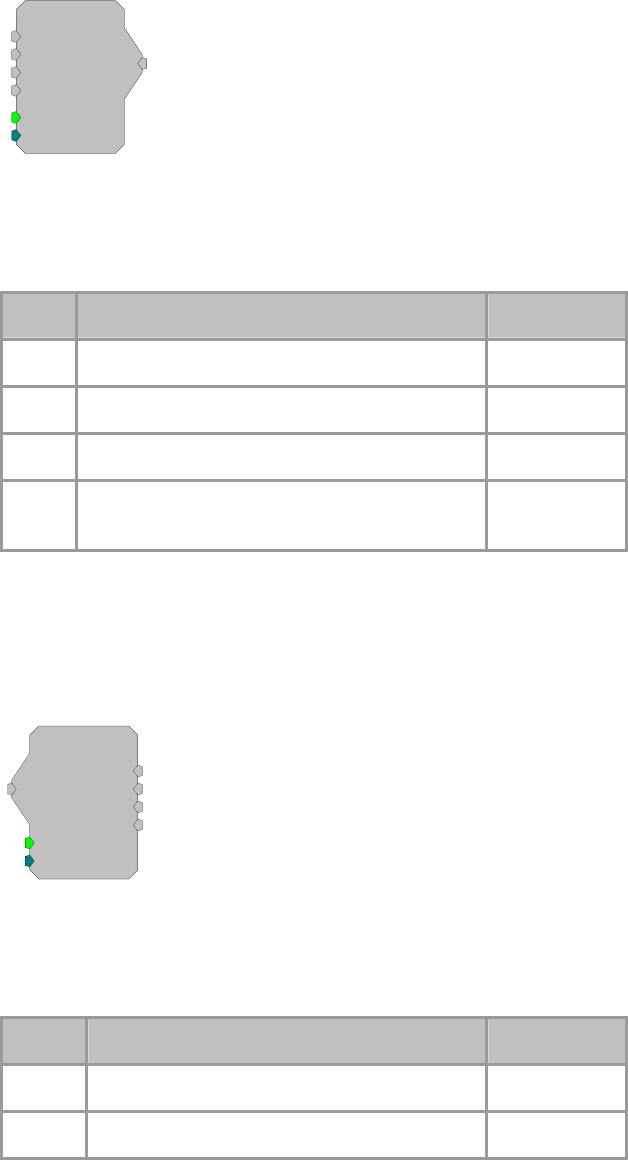
RPvdsEx Manual
282
MuxIn
MuxIn
Rst=0
Sel=0
In0
In1
[1:1,0]
In2
In3
Description:
Multiplexer device. Takes four input streams and sends one of them to its
output. The select parameter indicates which input is sent to the output. Reset
sets the output value to zero. See MuxOut.
Name Description Data Type
Inputs Input Floating
Output Input signal based on Select line Floating
Rst Resets the MuxIn line to Ln0 Logic
Sel Select line Integer value between 0 and 3 selects
the input line Integer
Equation:
Lo = Ii 1=Select value
MuxOut
MuxOut
Rst=0
Sel=0
Out0
Out1
[1:1,0]
Out2
Out3
Description:
Multiplexer device. Takes one input and sends it to one of four outputs. The
select parameter determines which output stream is chosen. Reset sets all
outputs to zero. See MuxIn.
Name Description Data Type
Input Input Floating
Outputs Output signal based on Select line Floating
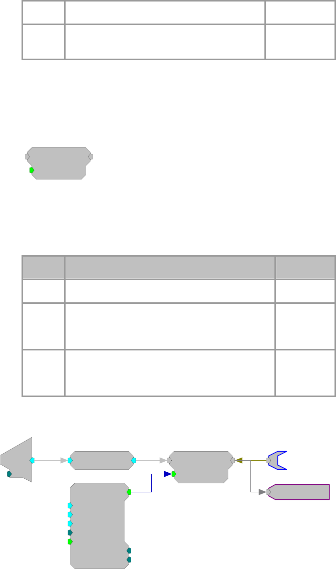
RPvdsEx Manual
283
Rst Resets the MuxOut line to Out0 Logic
Sel Select line Integer value between 0 and 3 selects
the Output line Integer
Equation:
Lo = Ii 1=Select value
SampHold
SampHold
S/H=1
[1:1,0]
Description:
The SampHold component Samples input values while S/H is set logical high.
When S/H goes to zero the last value is held. SampHold differs from Latch in
that Latch holds the first value when triggered by a logical high input and holds
that value until the next logical high.
Name Description Data Type
Inputs Input signal to be sampled/held Any
Output Output value of the component (Depending on the
value of S/H, this will either be a held value or a
newly sampled value of the input signal.)
Any
S/H Sample/Hold Control (When set high (1), the
component will sample. When set low (0), the
component will hold.)
Logic
Example:
Sample and Hold
d
c
[1:3,0]
Ch=1
RMS
[1:4,0]
SampHold
S/H=1
[1:5,0]
RMS
0.711
PulseTrain
Thi=1000
Tg=0
Tlo=1000
Npls=0
[1:1,0
]
CurN=0
Stage=0
Trg=1
The above example uses a SampHold component to look at the RMS value of
the input from the ADC every 2000 milliseconds. The S/H parameter is set high
for a 1000 ms and set low the rest of the time, so it samples for a 1000
milliseconds and then holds the last value for 1000 milliseconds.
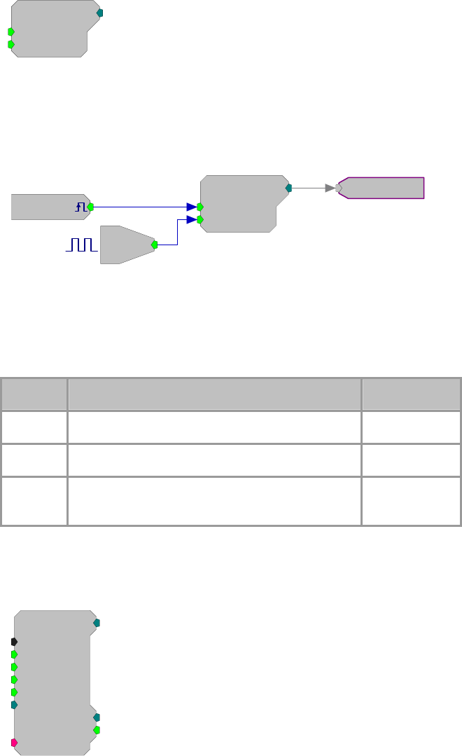
RPvdsEx Manual
284
SimpCount
SimpCount
Rst=0
Enable=1
[1:1,0]
Description:
The SimpCount component is a simple counter that starts at zero and counts up
from there. The count goes up by one for each sample period that the Enable
parameter is set high. If the Reset parameter is set high, the count gets reset to
zero.
SimpCount
Rst=0
Enable=1
[1:5,0]
Bi
[1:1,0]
M=1
[1:3,0]
Src=Soft1
72845
Counts the number of samples that digital input
1 is high.
The counter can be reset by software trigger 1.
The Counter component is more powerful than SimpCount, and allows for
different starting values, looping, etc. SimpCount is useful for basic counting
tasks, but Counter is required for more advanced counting tasks such as
offsetting the position in a memory buffer.
Name Description Data Type
Output Current integer count Integer
Rst Resets counter when logic is high (1) Logic
Enable When enable is set high (1), counter is incremented
on each tick of the clock Logic
StateMach
StateMach
nStates=4
Rst=0
Enab=1
JmpA=0
[1:1,0]
StChange=0
StNum=0
JmpB=0
{>Data}
OutSel=0
Description:
A state machine changes its output based on the combination of inputs to the
system. A look-up table (see following example) determines the state of the
machine. An additional Output select table allows the user to send a given
output based on the machine's state.

RPvdsEx Manual
285
The state machine is divided into two parts. The first part determines the state
of the machine and the second part determines the output value.
Determining The State Of The Machine.
Four inputs determine the state of the machine.
When Reset is high (=1) the machine state becomes state 0.
When Enable is low (=0) the machine state is fixed at the last state until it goes
high again (=1).
When Enable is high (=1) and Reset is low(=0) the state of the machine is
determined by the input values for JmpA and JmpB. The top portion of the
look-up table (see following example) determines the state based on the present
state of the machine and the input values for JmpA and JmpB.
Using the example below: if the last state of the machine was State 2, (JmpB=1)
and JmpA went high (=1) the state machine would go to state 0 (In state 2 when
both JmpA and JmpB are high (=1) the state of the machine becomes State 0). It
then becomes State 3 (When Both=1 in State 0 the State changes to State 3).
After that it toggles between state 3 and state 0.
Use StNum to check the present state of the Machine.
Use Stchange to check if the state of the machine has changed.
Determining The Output Of The State Machine.
The Output select (OutSel) value (in conjugation with the machine state)
determines the output value of the State machine.
In the look-up table example below when machine is in State 1 (S1) and the
OutSel=3 the Output value is the integer 7.
Use DataTable to design the look-up table. Below is the logical structure for a
look-up table. In the table below, the columns S0, S1, S2, and S3 correspond to
the four possible states of this state machine. The logic rows (If None, If JmpA,
If JmpB, If Both) are used to control how the state machine jumps from one
state to another. The Output rows are used to control the output of the state
machine, depending on the OutSel input and the current state.
Note: the state machine outputs only integers.

RPvdsEx Manual
286
Name Description Data Type
Output Value in look-up table based on the state of the
machine Integer
nStates
N
umber of possible states for the State Machine Integer (Static)
Rst When Rst is high (1)the state of the machine is at
State 0 Logic
Enab Enab low fixes the state of the machine at the last
State. State changes can occur when Rst is low and
Enab is high
Logic
JmpA JmpA changes state of machine Logic
JmpB JmpB changes the state of the machine Logic
Outsel Depending on state of the machine sends out an
integer value Integer
>Data Pointer to Lookup table pointer
Stnum Present state of the Machine Integer
StChange checks to see if the state of the machine has
changed recently Logic
Outputs Output signal based on Select line Floating
RPvdsEx Manual
287
Trigonometry
Trigonometry Components
This group includes components for the trigonometric functions. All trigonometric functions are in
Radians.
This group includes the following components:
Arccos
Arcsin
Arctan
Cos
Distance
Sin
Tan
RPvdsEx Manual
288
Arccos
Arccos
[1:1,0]
Description:
This component calculates the arccosine of the input that is bounded by -1 to 1.
Output is in Radians. The output values are the arccos valued in the range [0,
pi].
Name Description Data Type
Input Input Floating Point
Output Arccos (Input) in Radians Floating Point
Equation:
Output = Arccos (Input )
Arcsin
Arcsin
[1:1,0]
Description:
This component calculates the arcsine of the input that is bounded by -1 to 1.
Out put is in Radians. The output values are the arcsin values in the range [-
pi/2, pi/2].
Name Description Data Type
Input Input Floating Point
Output Arcsin (Input) in Radians Floating Point
Equation:
Output = Arcsin (Input )
Arctan
Arctan
[1:1,0]
Description:
This component calculates the arctangent of the unbounded input. Output is in
Radians. The output values are the arctan values in the range [-pi/2, pi/2].
Name Description Data Type
Input Input Floating Point
Output Arctan (Input) in Radians Floating Point
Equation:
Output = Arctan (Input )
RPvdsEx Manual
289
Cos
Cos
[1:1,0]
Description:
This component calculates the cosine of the unbounded input. Output is in
Radians.
Name Description Data Type
Input Input Floating Point
Output Cos (Input) in Radians Floating Point
Equation:
Output = Cos (Input )
Distance
Distance
Xo=0
Yo=0
[1:1,0]
Description:
Calculates the distance between two points in x,y space. Useful for computing
distance between output of eye tracker and desired focus location.
Name Description Data Type
Input Stereo signal, put x, y data in stereo format Floating Point
Output Mono signal Floating Point
Xo X-value in X,Y space Floating Point
Yo Y-value in X,Y space Floating Point
Note: Stereo processor input (put x,y data in stereo format) X = X position, Y =
Y position
Example:
Distance
File: Examples\Distance_ex.rcx
Default Device: RP2.1 Processor
Sampling Rate: 50 kHz
This example demonstrates how Distance can be used to detect when the output
from an eye-tracker is within a specified radius of a target. A StereoADC is
used to acquire two channels of eye tracker input. The distance between the X,Y
input from the ADC and the XCenter and YCenter of the target is compared to
RPvdsEx Manual
290
0.5 V and a TTL pulse is sent out whenever it is less than 0.5 V. Use the ConstF
functions to modify the circuit in RPvdsEx.
Note: XCenter and YCenter require the use of ActiveX controls or TDT
programs other than RPvdsEx. Additional circuitry not shown is included to
make the example run within RPvdsEx.
Bi
[1:13,0]
M=1
Compare
K=0.5
Test=LT
[1:12,0]
Distance
Xo=0
Yo=0
[1:11,0]
e
o
[1:10,0]
Ch=1
ConstF
K=2
Y
Center [1:6 -
0
ConstF
K=5
X
Center [1:8 -
0
X_center
Y_center
Sin
Sin
[1:1,0]
Description:
This component calculates the sine of the unbounded input. Output is in
Radians.
Name Description Data Type
Input Input Floating Point
Output Sin (Input) in Radians Floating Point
Equation:
Output = Sin(Input )
Tan
Tan
[1:1,0]
Description:
This component calculates the tangent of the unbounded input. Output is in
Radians.
Name Description Data Type
Input Input Floating Point
Output Tan (Input) in Radians Floating Point
Equation:
Output = Tan (Input )
RPvdsEx Manual
291
Type Conversion
Type Conversion Components
These components are used to convert a signal from one data type to another.
This group includes the following components:
Float2Int
Float2TTL
Flt2Stereo
FromHopPick
Int2Float
Int2TTL
Stereo2Flt
TTL2Float
TTL2Int
This group also includes the following components, if RPvdsEx Device Setup is
configured for a high performance device, such as the RXn or RZn:
MCFloat2Int
MCFloat2Int8
MCFloat2Int16
MCForceCC
MCFromHop
MCFromSer
MCFromSing
MCInt2Float
MCInt16ToFLT
MCInt8ToFlt
MCMap
MCMerge
MCSubSel
MCToSing
Important Note!: This group also includes MCToSer, Any2Any, Float2Float, Int2Int, and
TTL2TTL, components are intended primarily for TDT use in behind-the-scenes macro design.
They are not intended for general use.
RPvdsEx Manual
292
Float2Int
Float2Int
SF=1
[1:1,0]
Description:
The Float2Int scales the input and converts the result from a 32-bit float to a 32-
bit integer.
Name Description Data Type
Input Input Floating Point
Output Round (Input*SF) Integer
SF Scale Factor Floating Point
Equation:
Output = round(Input * SF))
Example:
RAM Buffer, see page 128.
Float2TTL
Float2TTL
Thrsh=1
[1:1,0]
Description:
This component returns 1 if the input is above the threshold value.
Name Description Data Type
Input Input Floating Point
Output If Input>Thrsh then Output=1 else Output=0 Logic
Thrsh Threshold value for TTL high Floating Point
Equation:
If ( Input > Thrsh) then Output = 1
else Output= 0
Example:
Cycle Usage, see page 192.
RPvdsEx Manual
293
Flt2Stereo
Stereo
R
[1:1,0]
L
Description:
Converts to two floating point inputs into a stereo formatted signal.
Name Description Data Type
L Left channel input Floating Point
R Right channel input Floating Point
Output Stereo formatted signal Floating Point
FromHopPick
{>PM}
IndexSel=1
FromHopPick
nChan=16
[4:231,0]
Description:
FromHopPick outputs a single channel from an array of single channel indexed
hops. Each hop must be named [Root]~# where [Root] is the name of
FromHopPick and # is the channel number. There must be a hop for each
channel. Use IndexSel to choose which hop to output from FromHopPick. See
example below.
MCAdcIn
nChan=16
ChanOS=1
[1:1,0]
Iterate: x =1 to 16 by 1
RMS~{x}
RMS
[1...,3-01...]
MCSig
MCToSing
ChanSel={x}
[1...,2-01...]
MCSig
{>PM}
IndexSel=1
RMS
nChan=16
[1:49,0]
channel
In this example, each channel of a 16-channel stream (MCSig) is extracted
using MCToSing, the RMS computed and FromHopPick is used to access one
channel for further processing. The RMS calculation occurs inside of an iterate
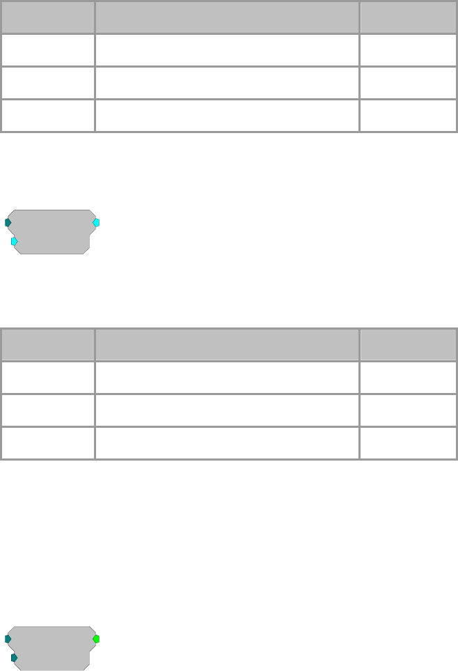
RPvdsEx Manual
294
box to simplify programming. This example is useful when MC components
don’t exist for the desired function.
Note: This component is for use with only high performance processor devices,
such as RXn or RZn.
Name Description Data Type
Output Multi-channel signal Floating Point
nChan
N
umber of channels (4-256) Integer (Static)
IndexSel Selects the desired hop Integer
Int2Float
Int2Float
SF=1
[1:1,0]
Description:
This component converts the input from a 32-bit integer to a 32-bit float and
then scales the result.
Name Description Data Type
Input Input Integer
Output Input*SF Floating Point
SF Scale Factor Floating Point
Equation:
Output = Input * SF
Example:
Block Access, see page 123.
Int2TTL
Int2TTL
BitN=0
[1:1,0]
Description:
This component outputs 1 if the specified bit of the input is set.
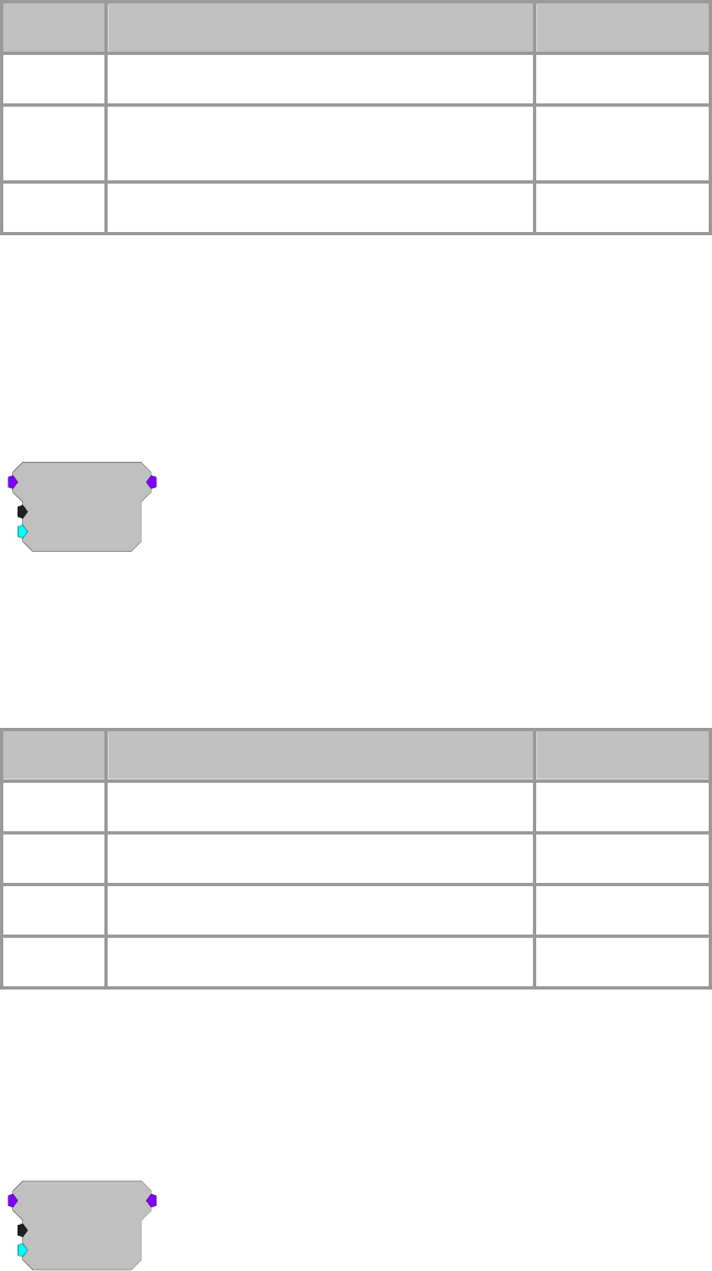
RPvdsEx Manual
295
Name Description Data Type
Input Input Integer
Output If Input BitMask=1 then Output=1 else
Output=0 Logic
BitN Bit value for Output high Integer
Equation:
If (Input AND BitN) = 1, then Output = 1
else Output = 0
MCFloat2Int
MCFloat2Int
nChan=16
SF=1
[1:2,0]
Description:
This is the multi-channel version of Float2Int. It scales the 32-bit floating point
input of each channel and then converts the result to a 32-bit integer.
Note: This component is for use with only high performance processor devices,
such as RXn or RZn.
Name Description Data Type
Input Multi-channel input signal Floating Point
Output Multi-channel output signal Integer
nChan
N
umber of Channels Integer (Static)
SF Scale Factor Floating Point
Equation:
Output = round(Input * SF)
MCFloat2Int8
MCFloat2Int8
nChan=16
SF=255
[1:4,0]
Description:
MCFloat2Int8 takes a multi-channel input of 32-bit floating values, scales them,
converts them to 8-bit integer numbers and packs them into 32-bit integers. The
resultant MC stream has nChan/4 channels.

RPvdsEx Manual
296
MCAdcIn
nChan=16
ChanOS=1
[1:1,0]
MCFloat2Int8
nChan=16
SF=127
[1:2,0]
MCSerStore
nChan=4
Size=1024
Rst=0
WrEnab=1
[1:3,0]
Index=0
{>Data}
Data
RPvdsEx might warn of a channel mismatch. It is okay to ignore this warning.
This reduction technique can be used to decrease memory allocation for data
storage or quadruple the data transfer rate to and from the PC.
The scale factor (SF) is used to appropriately scale the floating point input
before it is converted to an 8-bit integer. Use an SF of 127 for a +/- 1V range
and an SF of 12.7 for a +/- 10 V range. The SF and input values must be
matched. Mismatch between the SF and input value range gives poor resolution
or meaningless data.
See Data Reduction - Scale Factor for more information on properly setting the
scale factor, page 166.
Note: This component is for use with only high performance processor devices,
such as RXn or RZn.
Name Description Data Type
Input Multi-channel input Floating Point
Output Multi-channel output of 32-bit integers; four
channels of 8-bit integers are packed into each
channel
Integer
SF Scale factor sets the scale for the input before
sample conversion; scale factor depends on
input voltage
Floating Point
nChan
N
umber of Channels Integer (Static)
MCFloat2Int16
MCFloat2Int16
nChan=16
SF=32767
[1:6,0]
Description:
MCFloat2Int16 takes a multi-channel input of 32-bit floating values, scales and
converts them to 16-bit integer numbers and packs them into 32-bit integers.
The resultant MC stream has nChan/2 channels.
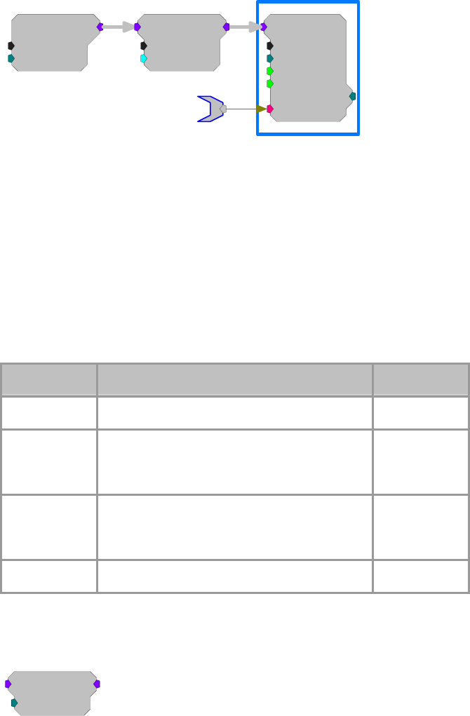
RPvdsEx Manual
297
MCAdcIn
nChan=16
ChanOS=1
[1:1,0]
MCSerStore
nChan=8
Size=1024
Rst=0
WrEnab=1
[1:3,0]
Index=0
{>Data}
Data
MCFloat2Int16
nChan=16
SF=32767
[1:2,0]
RPvdsEx might warn of a channel mismatch. It is okay to ignore this warning.
This reduction technique can be used to decrease memory allocation for data
storage or double the data transfer rate to and from the PC.
The scale factor (SF) is used to appropriately scale the floating point input
before it is converted to a 16-bit integer. The default SF is set to 32767 and
assumes that the input is bounded between +/- 1.0 V. Use an SF of 3276.7 for a
+/- 10 V range. The SF and input values must be matched. Mismatch between
the SF and input value range gives poor resolution or meaningless data. See
Data Reduction - Scale Factor for more information on properly setting the
scale factor, page 166.
Note: This component is for use with only high performance processor devices,
such as RXn or RZn.
Name Description Data Type
Input Multi-channel input Floating Point
Output Multi-channel output of 32-bit integers; two
channels of 16-bit integers are packed into each
channel
Integer
SF Scale factor sets the scale for the input before
sample conversion; scale factor depends on
input voltage
Floating Point
nChan
N
umber of Channels Integer (Static)
MCForceCC
MCForceCC
nChan=16
[1:2,0]
Description:
The MCForceCC component is used to force the in-path channel count to the
specified value. This is useful for type conversions that inherently change the
channel count (such as MCInt16ToFlt).
Note: This component is for use with only high performance processor devices,
such as RXn or RZn.
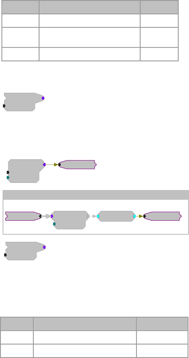
RPvdsEx Manual
298
Name Description Data Type
Input Mult-channel input signal Floating Point
Output Multi-channel signal with specified
channel count Floating Point
nChan
N
umber of channels in the output signal Integer (Static)
MCFromHop
{>PM
}
MCFromHop
nChan=16
[1:19,0]
Description:
MCFromHop builds a multi-channel signal from single channel indexed hops.
Each hop must be named [Root]~# where [Root] is the name of MCFromHop
and # is the channel number. There must be a hop for each channel. See
example below.
MCAdcIn
nChan=4
ChanOS=1
[1:1,0]
Iterate: x =1 to 4 by 1
RMS~{x}
{>PM
}
RMS
nChan=4
[1:13,0
]
RMS
[1...,3-01...]
MCSig
MCToSing
ChanSel={x}
[1...,2-01...]
MCSig
In this example, each channel of a four-channel stream (MCSig) is extracted
using MCToSing, the RMS computed and the MC signal is reformed using
MCFromHop. This occurs inside of an iterate box to simplify programming.
This example is useful when MC components don’t exist for the desired
function.
Note: This component is for use with only high performance processor devices,
such as RXn or RZn.
Name Description Data Type
Output Multi-channel signal Floating Point
nChan
N
umber of channels (4-256) Integer (Static)
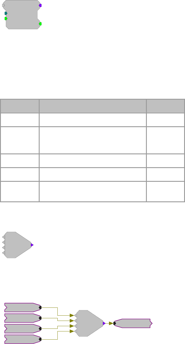
RPvdsEx Manual
299
MCFromSer
MCFromSer
nChan=16
[1:9,0]
Strobe=0
SyncIn=0
Description:
The MCFromSer component converts a serial sequence of integer values to a
multi-channel signal. The rising edge of SyncIn is used to begin the conversion
and should stay high for the total number of channels (nChan). When all
channels have been written to, the Strobe output will go high for one sample
indicating that the first sample for each channel has been converted.
Note: This component is for use with only high performance processor devices,
such as RXn or RZn.
Name Description Data Type
Input Single channel input signal Integer
Output Parallel conversion of serial input. Each
progressive channel contains the next serial
input value
Integer
nChan
N
umber of channels to convert serial input to Integer
SyncIn Initiates the conversion on a rising edge Logic
Strobe Goes high for a single sample when a single
sample has been converted for all channels Logic
MCFromSing
[1:7,0]
ToMC
Description:
MCFromSing builds a multi-channel signal from multiple single channel
signals. Most multi-channel components require merged multi-channel inputs.
MCFromSing can be used to create a multi-channel signal using up to four
single channels.
[1:7,0]
ToMC
Chan 1-4
Chan1
Chan2
Chan3
Chan4
To build a multi-channel signal with more than four single channels, the signals
must first be merged in groups of four using MCFromSing. The outputs from
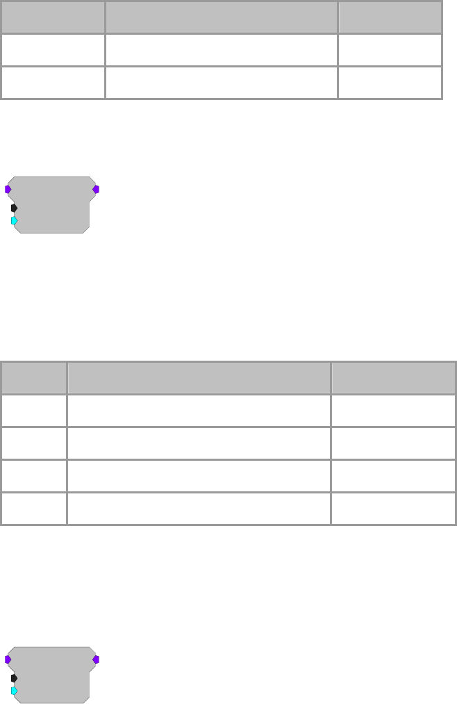
RPvdsEx Manual
300
each MCFromSing can then be merged using the MCMerge. For higher
channel counts or for a simplified technique, see MCFromHop.
Caution: Inputs to the MCFromSing must be of the same data type.
Note: This component is for use with only high performance processor devices,
such as RXn or RZn.
Name Description Data Type
Input (Multiple) Single channel inputs Any
Output Multi-channel output Same as input
MCInt2Float
MCInt2Float
nChan=16
SF=1
[1:2,0]
Description:
This is the multi-channel version of the Int2Float component. It converts the
multi-channel input from 32-bit integers to 32-bit floating-point values and then
scales the result.
Note: This component is for use with only high performance processor devices,
such as RXn or RZn.
Name Description Data Type
Input Multi-channel input signal Integer
Output Multi-channel output signal Floating Point
SF Scale Factor Floating Point
nChan
N
umber of Channels Integer (Static)
Equation:
Output = Input * SF
MCInt16ToFlt
MCInt16ToFlt
nChan=16
SF=1
[1:2,0]
Description:
MCInt16ToFlt takes a multi-channel input of 32-bit integers where each 32-bit
integer is packed with two 16-bit integers, scales and converts them to 32-bit
floating point for further floating point processing. The input MC stream should

RPvdsEx Manual
301
have nChan/2 channels because of the integer packing. The output MC stream
has nChan channels. This is the inverse operation of MCFloat2Int16.
Note: This component is for use with only high performance processor devices,
such as RXn or RZn.
Name Description Data Type
Input Multi-channel input; two 16-bit integers packed
into each channel Integer
Output Multi-channel output of 32-bit floats Floating Point
SF Scale factor sets the scale for the input before
sample conversion; scale factor depends on
input voltage
Floating Point
nChan
N
umber of Channels Integer (Static)
MCInt8ToFlt
MCInt8ToFlt
nChan=16
SF=1
[1:2,0]
Description:
MCInt8ToFlt takes a multi-channel input of 32-bit integers where each 32-bit
integer is packed with four 8-bit integers, scales and converts them to 32-bit
floating point for further floating point processing. The input MC stream should
have nChan/4 channels because of the integer packing. The output MC stream
has nChan channels. This is the inverse operation of MCFloat2Int8.
Note: This component is for use with only high performance processor devices,
such as RXn or RZn.
Name Description Data Type
Input Multi-channel input; four 8-bit integers packed
into each channel Integer
Output Multi-channel output of 32-bit floats Floating Point
SF Scale factor sets the scale for the input before
sample conversion; scale factor depends on
input voltage
Floating Point
nChan
N
umber of Channels Integer (Static)
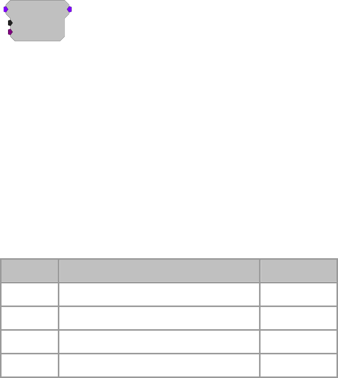
RPvdsEx Manual
302
MCMap
MCMap
nChan=16
{>Map}
[1:2,0]
Description:
McMap is a component that allows users to reorganize the input channel
configuration to a desired output configuration. This allows the logical channel
organization to match the spatial orientation of an electrode array. It can also be
used to reorder TDT adapters to ZIF-Clips or EEG cap arrays.
Input channels from a MC component are reorganized based on the ordering of
the channel number configuration from the >Map input parameter. The MCMap
memory is an array equal in length to nChan that contains the reordered
channels. For example, if recording channel eight of sixteen was the most distal
electrode it could be remapped as either the first or last channel (channel 16).
Set nChan to the number of channels in the output signal (not the input signal).
If nChan is smaller than the number of channels at the input a warning will be
given in RPvdsEx, this warning may be disregarded if the intention is to output
a subset of the multi-channel input signal.
Note: This component is for use with only high performance processor devices,
such as RXn or RZn.
Name Description Data Type
Input Mult-channel input signal Floating Point
Output Multi-channel sub-set of input Floating Point
nChan
N
umber of channels in the output signal Integer (Static)
>Map Pointer to Map buffer (PM) Pointer
Example:
The example below illustrates how to remap the physical electrode sites of a 16-
channel acute probe to the headstage.
A pinout of the headstage/adapter as well as the probe are required. The
DataTable component in RPvdsEx can be used to load the channel map to the
MCMap component.
Select ChanMap in the Type/Format drop down menu located in the DataTable
component settings dialog when using the DataTable with the MCMap
component.
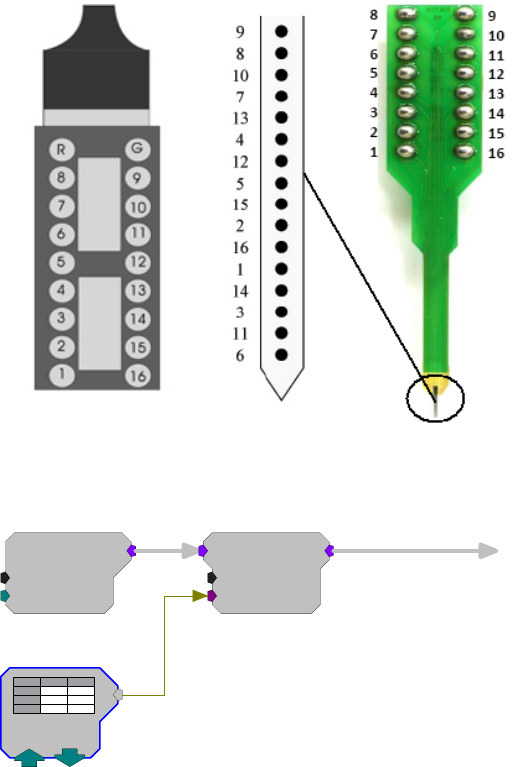
RPvdsEx Manual
303
Headstage pinout 16-Channel Acute Probe and its site mapping
Below is an example of the basic components used to remap the input signal.
MCAdcIn
nChan=16
ChanOS=1
[1:2,0]
MCMap
nChan=16
{>Map}
[1:3,0]
ChanMap
= 0
Based on the pinouts pictured above, the DataTable entries are mapped
according to the desired position of the physical electrode sites. For instance,
the most distal electrode on the acute probe is channel 6. If we wish this to
represent channel 16, we would need to remap channel 6 to channel 16.
Since the headstage pinout matches the electrode, we only need to remap the
electrode sites. After remapping the electrode sites according to their insertion
depth from channel 1 to 16, the new physical site mapping will look like this:
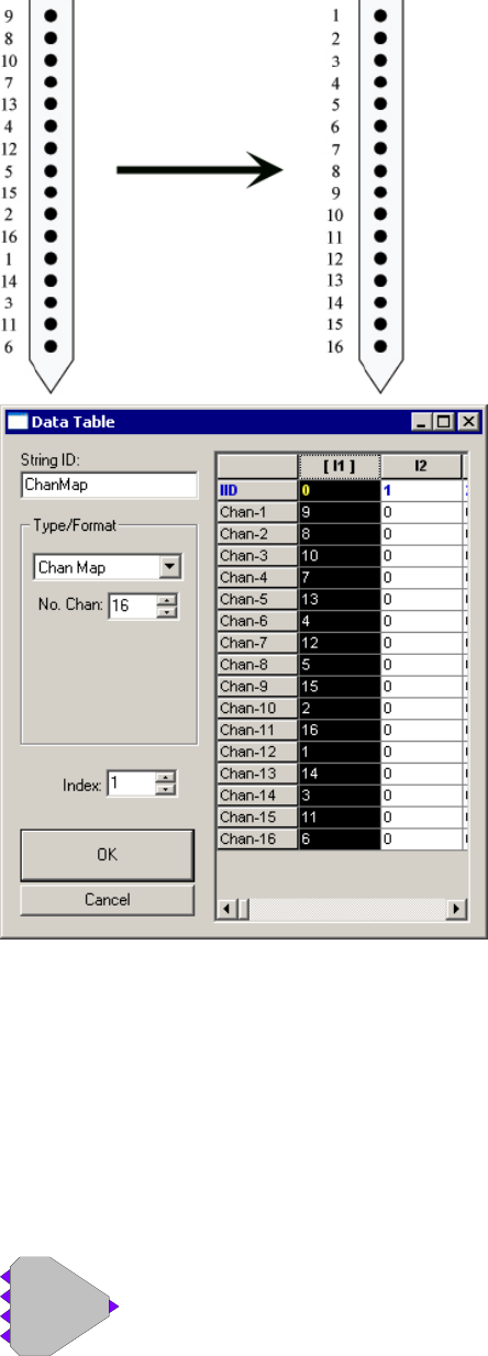
RPvdsEx Manual
304
Notice that in the circuit above the currently selected index (0) matches the
column containing the channel map values in the DataTable component
settings. Selecting a particular index loads the channel map that is contained
within the corresponding column.
Note: If you are not using the DataTable with the MCMap component, the
channel map can be loaded as follows:
Map = 9 8 10 7 13 4 12 5 15 2 16 1 14 3 11 6
MCMerge
[1:2,0]
Merge
Description:

RPvdsEx Manual
305
MCMerge merges multiple multi-channel signals to form a single multi-channel
signal. The MCMerge inputs must be multi-channel signals. Single channel
signals can be merged into a multi-channel signal using MCFromSing (ToMC).
The MCMerge inputs may include any number of channels, so long as they are
multi-channel signals.
[1:5,0]
ToMC
Chan1
Chan2
Chan3
Chan4
[1:6,0]
Merge
Chans 1-16
The MCMerge component is typically used to merge multiple channel signals
from several MCFromSing components. If more than four channels are to be
merged, they must first be merged in groups of four using MCFromSing. The
outputs from each MCFromSing can then be merged using the MCMerge.
Note: This component is for use with only high performance processor devices,
such as RXn or RZn.
Name Description Data Type
Input (multiple) Multiple multi-channel inputs Any
Output Merged output Same as Input
MCSubSel
MCSubSel
nChan=16
ChanSel=1
[1:7,0]
Description:
The MCSubSel is used to form a multi-channel signal from a sub-set of another
multi-channel signal. Set nChan to the desired number of channels in the
output signal (not the input signal). Set ChanSel to the first channel in the range
of interest. ChanSel + nChan should not be greater than the number of channels
contained in the input signal.
Note: This component is for use with only high performance processor devices,
such as RXn or RZn.
Name Description Data Type
Input Mult-channel input signal Floating Point
Output Multi-channel sub-set of input Floating Point
nChan
N
umber of channels in the output signal Integer (Static)
Merge up to four
multi-channel signals
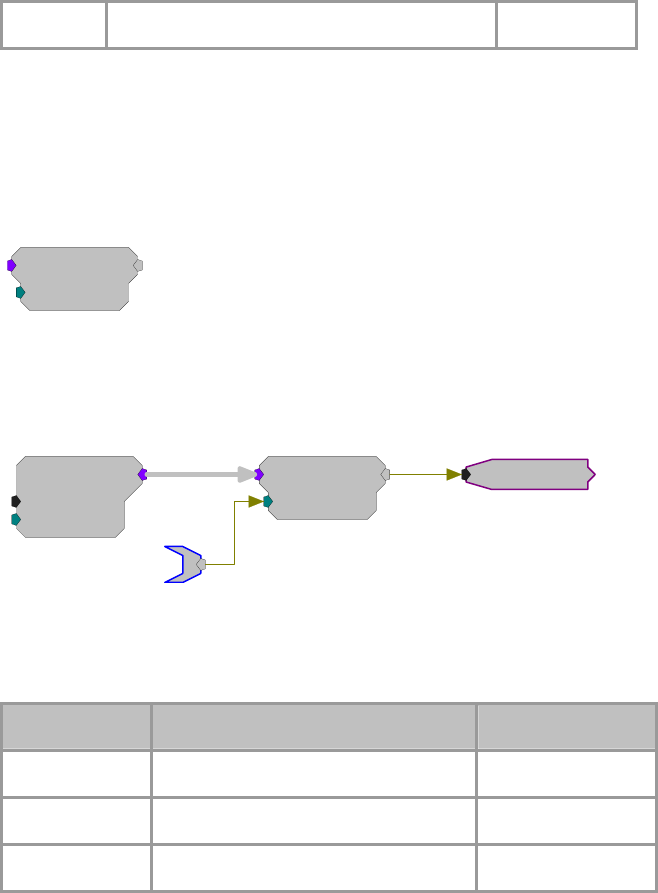
RPvdsEx Manual
306
ChanSel Channel select line Integer
Example:
To select channels 33 thru 48 of a 64 channel input signal, set nChan = 16 and
ChanSel = 33.
MCToSing
MCToSing
ChanSel=1
[1:7,0]
Description:
This component allows the user to extract a single channel signal from a multi-
channel signal by selecting the channel number required. The channel number
can be selected dynamically.
MCToSing
ChanSel=1
[1:2,0]
MCAdcIn
nChan=16
ChanOS=1
[1:1,0]
ChanSelect
SignalOut
One MCToSing component is required for each single channel signal to be
extracted. This component is particularly powerful when used with iterations.
Note: This component is for use with only high performance processor devices,
such as RXn or RZn.
Name Description Data Type
Input Multi-channel input signal Any
Output Single channel output Any
ChanSel Channel select line Dynamic Integer
Example:
MCToSing
MCToSing is used to extract a channel for further processing using single-
channel components. Typically, single channel signals must be extracted when
there is no multi-channel component that can perform the necessary processing
task. In the example below a single channel is extracted from a 16-channel
signal, that channel is then processed for sorting spike data using SortSpike2.
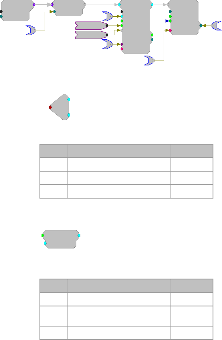
RPvdsEx Manual
307
MCAdcIn
nChan=16
ChanOS=1
[1:1,0]
MCToSing
ChanSel=1
[1:2,0]
ChanSelect
SortSpike2
nWid/4=8
Thresh=1
UseSign=1
Enab/Rst=1
[1:3,0]
SortBits=0
Strobe=0
Tag
{>Coef}
{>Data}
aEA~{x}
cEA~{x}
SerStore
Size=32000
Rst=0
WrEnab=1
[1:5,0]
Index=0
{>Data}
dEA~{x}
sEA~{x}
Enable
iTime
Stereo2Flt
R
[1:1,0] L
Stereo
Description:
Splits a stereo input into separate Left and Right signals.
Name Description Data Type
Input Stereo formatted signal Floating Point
L Left channel out Floating Point
R Right channel out Floating Point
TTL2Float
TTL2Float
HiVal=1
[1:1,0]
Description:
This component converts the input from a TTL value to the specified 32-bit
float when true, else it converts the input to 0.
Name Description Data Type
Input Input Logic
Output If Logic high then Output=HiVal else
Output=0 Floating Point
HiVal Hival for logic Hi Floating Point
Equation:
If Input = 1, then Output = HiVal

RPvdsEx Manual
308
else Output=0
TTL2Int
TTL2Int
HiVal=1
[1:1,0]
Description:
This component converts the input from a TTL value to the specified 32-bit
integer when true, else it converts the input to 0.
Name Description Data Type
Input Input Logic
Output If logic high then Output=HiVal else
Output=0 Integer
HiVal HiVal for Logic high Integer
Equation:
If Input = 1, then Output = HiVal
else Output = 0
RPvdsEx Manual
309
Waveform Generators
Waveform Generator Components
Waveform generators are components that generate signals on the DSP. Almost any signal can be
produced by combining these basic waveform generators with filters and signal mixers.
This group includes the following components:
ConstF
ConstI
ConstL
FStep
GaussNoise
RampTooth
Random
SawTooth
Tone
TSlope
This group also includes the following component, if RPvdsEx Device Setup is
configured for a high performance device, such as the RXn or RZn:
MCConst
MCValList
RPvdsEx Manual
310
ConstF
ConstF
K=0
[1:1,0
]
Description:
This component feeds the signal chain with the specified constant. Often used
with parameter tags, which are unable to connect to the input port of a
processor.
Name Description Data Type
Output K Floating Point
K Constant Value Floating Point
Equation:
OutputO = K1
ConstI
ConstI
K=0
[1:1,0
]
Description:
This component feeds the signal chain with the specified constant. Often used
with parameter tags, which are unable to connect to the input port of a
processor.
Name Description Data Type
Output K Integer
K Constant Value Integer
Equation:
OutputO = K1
ConstL
ConstL
K=0
[1:1,0
]
Description:
This component feeds the signal chain with the specified constant. Often used
with parameter tags, which are unable to connect to the input port of a
processor.
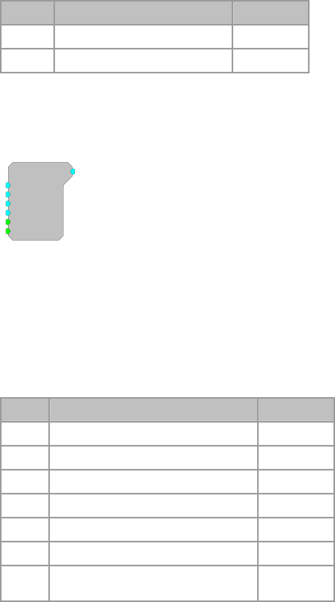
RPvdsEx Manual
311
Name Description Data Type
Output K Logic
K Constant Value Logic
Equation:
LO = K1
FStep
FStep
Base=0
Step=0
Min=-1e+020
Max=1e+020
[1:1,0]
Rst=Run
Enab=Run
Description:
The FStep is an up/down counter. It counts for the duration of a high pulse sent
to the Enable port (Enab). It increments the count by a set value (determined by
Step) for each pulse of sample clock (e.g. if the enable is high for 1 msec and
the sample rate is 25 Kilohertz then the counter will step 25 times). When it
reaches the Min or Max value the FStep stops and retains that value until reset
(see below for more details). The FStep starts at the Base value the first time the
counter is started or after the Reset (Rst) port is triggered (value goes from low
(0) to high (1)).
Use FStep in place of Counter (which is primarily designed for RamBuffers) for
functions that require countdown, negative numbers, or floating point output.
Name Description Data Type
Output Incremented Floating point value Floating Point
Base Base value Floating Point
Step Step Size Floating Point
Min Minimum value for counter Floating Point
Max Maximum value for counter Floating Point
Rst Resets counter when Logic is High Logic
Enable When Enable line is set hi(1) counter is
incremented on each tick of the clock. Logic
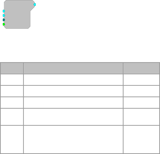
RPvdsEx Manual
312
GaussNoise
GaussNoise
Amp=1
Shft=0
Seed=0
Rst=Run
[1:1,0]
Description:
This component generates a white noise process with a Gaussian probability
density function with the specified attributes. Peak voltages will be higher. To
avoid clipping a signal the RMS amplitude should be less than 2.1.
Name Description Data Type
Output Gaussian Noise Floating Point
Amp RMS Amplitude of the Signal Floating Point
Shift DC shift of signal output. Floating Point
Seed Integer value for Random generation of noise
output Integer
Rst When set high, resets sequence to restart at
random (seed). Feeding new Seeds produces
different noise. Feeding the same seed produces
the same noise sequence.
Logic
All noise generators produce a fixed energy across the bandwidth of the
RPvdsEx circuit. In other words, the noise power is spread evenly across the
entire Nyquist bandwidth. Changing the sampling rate changes the Nyquist
bandwidth and thus alters the RMS noise level over a fixed bandwidth by the
following relationship:
RMS dB change=20*log(New SR/Old SR)/2
Doubling the sample rate will double the Nyquist frequency and decrease the
RMS noise level over a fixed bandwidth by 3 dB. Similarly, halving the SR will
increase the RMS over that bandwidth by 3 dB.
Note: the PowerBand difference will be 6dB.
Example(s):
Second Order Biquad Filter (filtered noise with Butterworth coefficients), see
page 145.
Parametric Coefficient (filtered noise with parametric coefficients), see page
151.
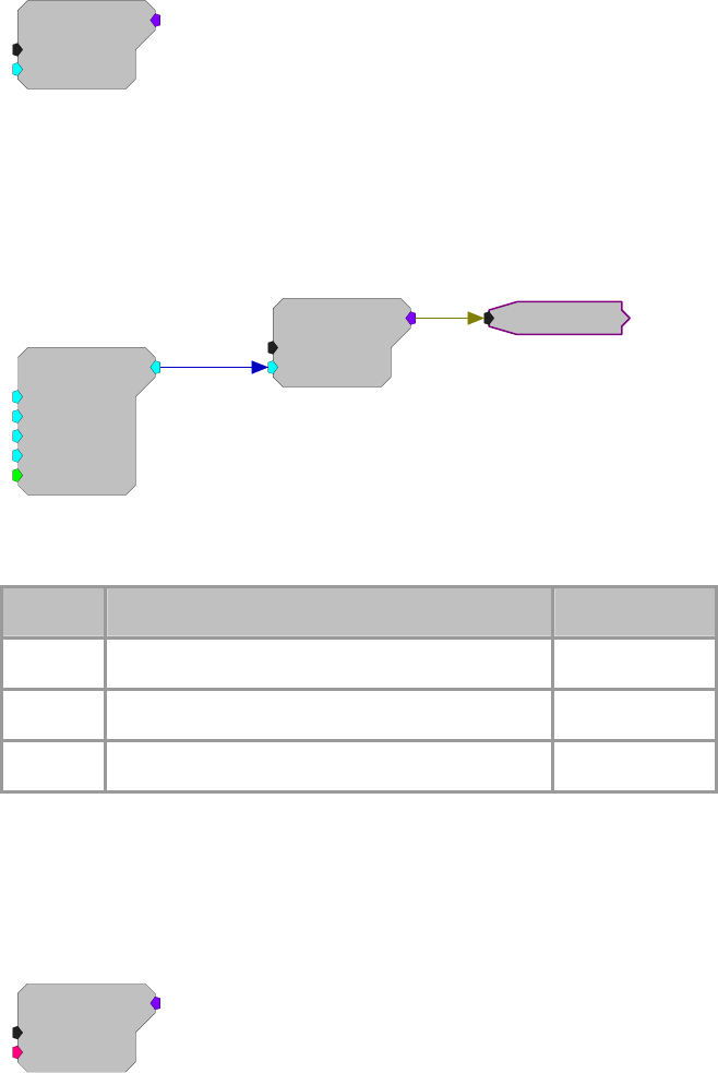
RPvdsEx Manual
313
MCConst
MCConst
nChan=16
Value=1
[1:1,0]
Description:
This component is a multi-channel version of the ConstF component. MCConst
feeds a specified constant to a multi-channel output. The constant is specified
using the Value parameter and can be controlled dynamically. The constant is
fed to each of the signals in the multi-channel signal. The number of channels in
the output is specified by the nChan parameter.
MCConst
nChan=16
Value=1
[1:3,0]
Tone
Amp=1
Shft=0
Freq=1000
Phse=0
[1:1,0]
Rst=Run
MCTone
Note: This component is for use with only high performance processor devices,
such as RXn or RZn.
Name Description Data Type
Output Multi-channel output Floating Point
nChan
N
umber of channels required in output signal Integer (Static)
Value Constant value fed to the output Floating Point
Equation:
Output(1: nChan) = Value
MCValList
MCValList
nChan=16
{>List}
[1:1,0]
Description:
This component is similar to MCConst but lets you specify the value for each
individual channel. MCValList feeds a specified list to a multi-channel output.
The value list is specified using the {>List} parameter and can be controlled
statically with an nRow DataTable or dynamically with a ParTag. The number
of channels in the output is specified by the nChan parameter.

RPvdsEx Manual
314
MCValList
nChan=16
{>List}
[1:1,0]
ScaleFactor
s
= 0
MCConst
nChan=16
Value=1
[1:5,0]
Inp
2
MCMult
nChan=16
[1:6,0]
MCValues
myList
Tone
Amp=1
Shft=0
Freq=1000
Phse=0
[1:3,0]
Rst=Run
Note: This component is for use with only high performance processor devices,
such as RXn or RZn.
Name Description Data Type
Output Multi-channel output Floating Point
nChan
N
umber of channels required in output signal Integer (Static)
{>List} Pointer to value list (DataTable or ParTag) Floating Point
Equation:
Output(1: nChan) = {>List}
RampTooth
RampTooth
Amp=1
Shft=0
Freq=1000
Phse=0
[1:1,0]
Rst=Run
Description:
This component generates a ramped waveform with the specified attributes.
Note: Ensure that the bounds of the phase parameter are greater than -180 and
less than +180. Any value (including exactly -180 or +180) outside of these
bounds will be set to a phase of zero.
Name Description Data Type
Output Ramped waveform Floating Point
Amp Peak amplitude of the signal Floating Point
Shift DC shift of signal output Floating Point

RPvdsEx Manual
315
Freq Frequency in Hz Floating Point
Phse Phase of sine when Rst goes from high to low Floating Point
Rst When reset goes high. Sine phase resets to Phse Logic
Random
Random
Amp=1
Shft=0
Seed=0
Rst=Run
[1:1,0]
Description:
This component generates a white noise process with a uniform probability
density function with the specified attributes. The amplitude specifies the
maximum output of the component.
Name Description Data Type
Output Uniformed distribution of values. Floating Point
Amp Peak Amplitude. Floating Point
Shift DC shift of signal output. Floating Point
Seed Integer value for Random generation of noise
output Integer
Rst When set high, resets sequence to restart at
random (seed). Feeding new Seeds produces
different noise. Feeding the same seed produces
the same noise sequence.
Logic
All noise generators produce a fixed energy across the bandwidth of the
RPvdsEx circuit. In other words, the noise power is spread evenly across the
entire Nyquist bandwidth. Changing the sampling rate changes the Nyquist
bandwidth and thus alters the RMS noise level over a fixed bandwidth by the
following relationship:
RMS dB change=20*log(New SR/Old SR)/2
Doubling the sample rate will double the Nyquist frequency and decrease the
RMS noise level over a fixed bandwidth by 3 dB. Similarly, halving the SR will
increase the RMS over that bandwidth by 3 dB.
Note: the PowerBand difference will be 6dB.
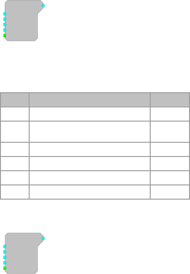
RPvdsEx Manual
316
SawTooth
SawTooth
Amp=1
Shft=0
Freq=1000
Phse=0
[1:1,0]
Rst=Run
Description:
This component generates a saw tooth waveform with the specified attributes.
Note: Ensure that the bounds of the phase parameter are greater than -180 and
less than +180. Any value (including exactly -180 or +180) outside of these
bounds will be set to a phase of zero.
Name Description Data Type
Output Gaussian noise Floating Point
Amp RMS amplitude of the Signal (0.707 rms=1 volt
max peak-to-peak) Floating Point
Shift DC shift of signal output Floating Point
Freq Frequency in Hz Floating Point
Phse Phase of sine when Rst goes from high to low Floating Point
Rst When reset goes high, sine phase resets to Phse Logic
Tone
Tone
Amp=1
Shft=0
Freq=1000
Phse=0
[1:1,0]
Rst=Run
Description:
Generates a sinusoid Waveform with the specified frequency and phase. The
waveform's Amplitude and DC Shift can also be controlled. The Rst control is
used to reset the signals phase. The output will remain locked at the specified
starting Phase as long as Rst is high. Typically an Edge Detector is used in
conjunction with the Rst control.
Note: Ensure that the bounds of the phase parameter are greater than -180 and
less than +180. Any value (including exactly -180 or +180) outside of these
bounds will be set to a phase of zero.
RPvdsEx Manual
317
Name Description Data Type
Output Tone of set frequency amplitude and DC shift Floating Point
Amp Peak amplitude of the signal Floating Point
Shift DC shift of signal output Floating Point
Freq Frequency in Hz Floating Point
Phse Phase of sine when Rst goes from high to low Floating Point
Rst When reset goes high, sine phase resets to Phse Logic
Example:
Tone
Tone
Amp=1
Shft=0
Freq=50
Phse=90
[1:7,0]
Rst=Run
Tone
Amp=1
Shft=0
Freq=1000
Phse=0
[1:9,0]
Rst=Run
[1:1,0]
Src=Extern
EdgeDetect
Edge=Rising
[1:2,0]
No
[1:5,0]
c
O
[1:10,0]
Ch=1
This example demonstrates a number of circuit design concepts as well as the
use of the Tone component. The circuit shown will generate an AM modulated
sinusoidal output from channel one of the DAC. The output will be 100%
modulated with a peak voltage of 2.0 volts.
The external trigger input is used to turn the output on and off by driving the
Rst control of the modulator tone. Notice that the phase for the modulator tone
is specified as -90 degrees causing it to fully 'close' when the reset line is high
(trigger input is low).
The carrier tone is set for 1000 Hz output. The default value of Amp = 1.0 will
be ignored as this parameter is being dynamically controlled by the modulator
tone. The carrier's Rst is fed by an edge detector connected to the external
trigger. This forces the carrier to start at sine phase 0.0 each time the external
trigger is high.
Modulator Tone
Carrier Tone
RPvdsEx Manual
318
TSlope
TSlope
Min=0
Slp=0
Max=1
Rst=Run
[1:1,0]
Description:
This component generates a linear ramp waveform with the specified attributes.
It is useful for generating a time value for time stamping buffer operations.
Name Description Data Type
Output Linear ramp related to slope rate Floating Point
Min Minimum (starting) value of the Output Floating Point
Slp Slope of amplitude ramp in units/millisecond Floating Point
Max Maximum value of the Output Floating Point
Rst When reset goes Hi. Reset Output to Min and
generate ramp. Logic
RPvdsEx Manual
319
Menu and Toolbar Reference
Menus
File Menu
The File menu includes standard file operations for saving, loading, and printing RPvdsEx files.
New Opens a new file.
Open Opens the Open dialog box so that an existing file can be opened.
Close Closes the active file, leaving the application open.
Save Saves the current file with the current name. If the file has not previously
been saved, the Save As dialog box opens so that the file can be named.
Save As Opens the Save As dialog box so that the file can be saved with a new name.
Macro
New Macro Design Opens a new macro file.
Open Macro Design Opens the RPvdsEx macro chooser dialog. The default folder location to
search for macros is C:\TDT\RPvdsEx\Macros.
Workspace
Open Workspace Opens the Workspace dialog box.
Save Workspace Not currently supported. The most recent workspace configuration is
automatically saved upon exit.
Close Workspace Closes all open tabbed windows.
Print Prints the current tabbed window, including all pages.
Print Preview Switches to Print Preview mode, displaying the circuit diagram as it will
print. This mode provides additional options for viewing pages.
Print Setup Opens the Print dialog box. Available options depend on the installed
printer(s).
Recent Files The fourth section of the File menu lists recently used files. Clicking a file
name opens the file. The recent workspaces are also listed (currently, only the
Default workspace is supported).
Exit Closes the application.
RPvdsEx Manual
320
Edit Menu
The Edit menu includes tools for modifying circuit diagrams.
Undo Undo will undo the last action. RPvdsEx supports multiple undos.
Redo Redo will reinstate the change that was undone by the last undo.
RPvdsEx supports multiple redos.
Find and Replace
Rename Components Opens the Change Component Name Dialog box. Enables the user to
implement a text find and replace in the component name field of
components in the current selection, page, or circuit.
Change Component
Parameters Opens the Change Parameter Dialog box. Enables the user to change
the value of a component parameter in the current selection, page, or
circuit.
Change Number of
Channels Opens the Update Number of Channels Dialog box. Enables the user to
change the number of channels as specified in the channel number
parameter of component and macros in the current selection, page, or
circuit.
Cut Removes the current selection, allowing it to be pasted in a subsequent
operation.
Copy Copies the current selection, allowing it to be pasted in a subsequent
operation.
Paste Adds the most recently cut or copied selection to the circuit diagram.
Index Opens the Indexing Setup dialog box (page 35), which can be used to
increment indexed parameter tags (such as iChan~2) or time slices. The
settings are applied to currently selected components only.
Preferences Opens the Preferences dialog box. This dialog contains compiler and
control object file settings.
RPvdsEx Manual
321
View Menu
The View menu includes tools for adjusting the window’s display.
Toolbar Allows toggling the display of selected toolbars.
Status Bar Toggles the display of the status bar on the bottom of the window.
Zoom Zooms in on a pointer position. Click to activate zoom.
Zoom To Page Zooms to fit the contents of the page.
Zoom In Zooms in display.
Zoom Out Zooms out display.
Pan Allows the user to drag the page using the mouse.
Customize Customize allows you to drag icons to any toolbar so that you can
customize and arrange icons on your toolbars
Components Menu
The Components menu is used to place components and links on the RPvdsEx circuit. The
components are grouped into different function types, which can be found in the RP Component
Reference section.
Helpers Opens the Select component to place dialog box to the Helpers category.
This category includes important tools for working and debugging in the
RPvdsEx environment.
Macro Tools Opens the Select component to place dialog box to the Macro Tools
category. This command is only available when working with a macro
circuit (*.rcm).
OpenEx Headers Opens the Select component to place dialog box to the OpenEx Headers
category. This category contains components designed exclusively for use
in circuits designed for the OpenEx environment.
Multi-Processor Opens the Select component to place dialog box to the Multi-processor
category. This command is only available when a high performance
processor, such as the RX5, has been specified in the hardware setup.
Common Displays a submenu listing the most commonly used components. Using
this menu allow the user to bypass the Select components to place dialog
box.
Component
Groups Opens the Select component to place dialog box to the specified category.
Categories group similar components together by function.
Circuit Macros Opens the Macro Chooser Dialog. This command is not available when
editing a macro circuit.
RPvdsEx Manual
322
Implement Menu
The Implement menu includes tools for compiling, running, or generating code. It also allows
different devices to be selected and configured.
Device Setup Opens the Set Hardware Parameters dialog box allowing users to
configure the circuit for the correct RP module. In addition, it allows
access to such properties as the sample rate and time slices.
Build, Load and Run Compiles the DSP code from the circuit diagram, loads the code to
the processor, and runs the code.
Compile Diagram Compiles the circuit diagram, determining the proper processing
chain order and generating the DSP code. If errors are found in the
circuit diagram, such as links that don't terminate anywhere or links
between incompatible data types, the circuit diagram will be updated
with red links to call attention to the errors.
Load Chain Loads the processing chain (DSP code) to the processor.
Run Processor Runs the loaded processing chain (DSP code) on the processor.
Halt Processor Halts the processing chain on the processor.
Build Control Object Generates Circuit file.
By default, RPvdsEx v60 and greater uses an RCX combined file
format instead of the legacy two file system (RPX, RCO). With this
preferred file format, the separate control file is no longer needed and
the Build RCO button is intentionally grayed out.
Reverting to the legacy RPX/RCO file system...
1. On the Edit menu, click Preferences.
2. Clear the Embed RCO object file check box.
3. Click OK.
After performing this step, the Build RCO button is enabled and
Circuit files can be created as before.
Generate Code Generates C code, for the processing chain, that can be incorporated
into a custom program.
Processor Select Displays a submenu listing processor select options. When a multi-
DSP device is specified in the hardware setup, the processor select
submenu is used to select the processor(s) that will be compiled when
the user compiles the circuit.
RPvdsEx Manual
323
Triggers Menu
The Triggers menu allows the user to fire hardware or software triggers from within the RPvdsEx
environment. This is useful for testing circuits.
Pulse zTrg-A Pulses zBus trigger A.
zTrg-A High Sets zBus trigger A high.
zTrg-A Low Sets zBus trigger A low.
Pulse zTrg-B Pulses zBus trigger B.
zTrg-B High Sets zBus trigger B high.
zTrg-B Low Sets zBus trigger B low.
Soft-1 Pulses software trigger one.
Soft-2 Pulses software trigger two.
Soft-3 Pulses software trigger three.
Soft-4 Pulses software trigger four.
zTrg-A and zTrg-B are global triggers that are generated on the zBUS. They can be used to
synchronize the start of several chains across multiple zBUS caddies. zTrig can be set as a pulse or
always high or always low. zTrig can be initiated from RPvdsEx or from a program such as
BrainWare or PyschRP.
RPvdsEx supports up to ten software triggers in a circuit, however, only the first four can be
triggered from the RPvdsEx interface.
RPvdsEx Window Menu
The Window menu allows you to arrange multiple windows that may be open in RPvdsEx.
Cascade Arranges windows in an overlapping fashion with the title bar of each
window visible.
Tile Arranges open windows so that windows don't overlap.
Arrange Icons Neatly arranges minimized window icons at the bottom of the RPvdsEx
window.
Open Windows The last menu section lists the open windows. A window can be brought to
the top and made active by clicking it in the list.

RPvdsEx Manual
324
Toolbars
Main (File)
The Main toolbar (also called the File toolbar) includes standard file operations for saving,
loading, and printing RPvdsEx files and tools for viewing and editing files.
New Opens a new file.
Open Opens the Open dialog box so that an existing file can be opened.
Save Saves the current file. If the file has not previously been saved, the Save
As dialog box opens so that the file can be named.
Cut Removes the current selection, allowing it to be pasted in a subsequent
operation.
Copy Copies the current selection, allowing it to be pasted in a subsequent
operation.
Paste Adds the most recently cut or copied selection to the circuit diagram.
Rename
Components Opens the Change Component Name Dialog box. Enables the user to
implement a text find and replace in the component name field of
components in the current selection, page, or circuit.
Change
Component
Parameters
Opens the Change Parameter Dialog box. Enables the user to change the
value of a component parameter in the current selection, page, or circuit.
Change Number
of Channels Opens the Update Number of Channels Dialog box. Enables the user to
change the number of channels in the channel number parameter of
component and macros in the current selection, page, or circuit.
Print Prints the current tabbed window, including all pages.
About Display program information, version number, and copyright.
Zoom Zooms in on a pointer position. Click to activate zoom.
Zoom To Page Zooms to fit the contents of the page.
Zoom In Zooms in display.
Zoom Out Zooms out display.
Pan Allows the user to drag the page using the mouse.

RPvdsEx Manual
325
Implement
The Implement toolbar includes tools for compiling, running, or generating code. It also allows
different devices to be selected and configured.
Device Setup Opens the Set Hardware Parameters dialog box allowing users to
configure the circuit for the correct RP module. In addition, it allows
access to such properties as the sample rate and time slices.
Build, Load and
Run Compiles the DSP code from the circuit diagram, loads the code to the
processor, and runs the code.
Compile Diagram Compiles the circuit diagram, determining the proper processing chain
order and generating the DSP code.
Load Chain Loads the processing chain (DSP code) to the processor.
Run Processor Runs the loaded processing chain (DSP code) on the processor.
Halt Processor Halts the processing chain on the processor.
Turn Helpers On
Turn Helpers Off
Build Control
Object Generates an RP Control Object (RCO) file.
By default, RPvdsEx v60 and greater uses an RCX combined file format
instead of the legacy two file system (RPX, RCO). With this preferred
file format, the separate control file is no longer needed and the Build
RCO button is intentionally grayed out.
Generate Code Generates C code, for the processing chain, that can be incorporated
into a custom program.

RPvdsEx Manual
326
Processors
The processor selection commands are available from the Implement menu or the Processor Select
toolbar. When a processor is selected, its button will appear "pressed." Either a single processor or
all processors may be selected. Selection of two, three, or four processors is not supported.
Main DSP Selects main processor
Aux One Selects first auxiliary processor
Aux Two Selects second auxiliary processor
Aux Three Selects third auxiliary processor
Aux Four Selects fourth auxiliary processor
All DSPs Selects all processors
Note: these commands are only available when the device selected in the Set Hardware
Parameters dialog box is a RX device.
Components
Most buttons on this toolbar opens the Select component to place dialog box to the specified
category. Categories group similar components together by function.
Helpers Opens to important tools for working and
debugging in the RPvdsEx environment.
OpenEx
Headers Opens to components designed exclusively for
use in circuits designed for the OpenEx
environment.
Input/Output Opens to input and output components to
connect a circuit to the physical world.
Basic Math Opens to low-level math operations.
Audio
Processing Opens to components that are related to 3D
audio processing.
Exponents
and Logs Opens to typical log and exponential functions
as well as a linear-to-dB and dB-to-linear
processes.
Gating
Functions Opens to components used to gate the onset
and offset of signals.
Coefficient
Generators Opens to components used to calculate the
coefficients of specified high-pass, low-pass,
band-pass, or notch filters in real-time.
Their outputs can be connected to the filter
coefficient port of a Biquad filter component.

RPvdsEx Manual
327
Buffer
Operations Opens to components used to create and access
data buffers.
Delay
Functions Opens to components used to create or
synchronize intentional delays.
Neuro
Analysis Opens to components developed primarily for
neurophysiology applications.
Device Status Opens to components to monitor and do math
with major system status values.
Macro Tools This command is only available when working
within a macro circuit.
Multi-
Processor Opens to components designed for use with
multi-processor devices.
Type
conversion Opens to components used to convert a signal
from one basic data type to another.
Integer Math Opens to mathematical functions for integer
data, allowing bitwise mathematical
operations.
Trigonometry Opens to trigonometric functions.
Waveform
Generators Opens to components that generate signals on
the DSP.
Digital
Filters Opens to Basic digital filtering tasks.
Counters and
Logic Opens to counter and logic functions.
Data
Reduction Opens to functions to decrease the size of the
data set.
Basic
Analysis Opens to components that analyze various
aspects of a signal.
State/Flow
Control Opens to state and flow components.
Macro Opens the Insert RPvdsEx Macro Dialog Box

RPvdsEx Manual
328
Common Components
This toolbar provides quick access to commonly used components, allowing the user to bypass the
Select components to place dialog box.
Link Starts link creation. After clicking this button the
user can click the output and input ports of
components on the circuit diagram to create a
link.
Iterate Selects the Iterate function to be added to the
circuit diagram.
HopTo Selects the HopTo helper to be added to the
circuit diagram.
HopFrom Selects the HopFrom helper to be added to the
circuit diagram.
zHopTo Selects the zHopTo component to be added to the
circuit diagram.
zHopFrom Selects the zHop components to be added to the
circuit diagram.
ParTag
Right Selects the right parameter tag to be added to the
circuit diagram.
ParTag
Left Selects the left parameter tag to be added to the
circuit diagram.
Script Tag
ParWatch Selects the parameter watch to be added to the
circuit diagram.
Graph Selects the graph to be added to the circuit
diagram.
Memo Selects the memo to be added to the circuit
diagram.

RPvdsEx Manual
329
Triggers
The Triggers toolbar allows the user to fire hardware or software triggers from within the
RPvdsEx environment. This is useful for testing circuits.
zBus A Pulse
zBus A High
zBus A Low
zBus B Pulse
zBus B High
zBus B Low
Software 1
Software 2
Software 3
Software 4

Part 4 Troubleshooting
RPvdsEx Manual
332
~
RPvdsEx Manual
333
RPvdsEx Known Anomalies
General
Moving Between RPvdsEx Circuits
In version 44 and higher, moving between RPvdsEx circuits when one circuit is running can
produce the following error: "zBUSError Call RpxgetCmpPar zError Specified memory area not
valid". This occurs if a second circuit (to the same device) is run at the same time. This error also
occurs when two RA16 base stations are connected together and a base station, other than the one
connected to the amplifier, has compiled circuit file loaded to it. The error message cannot be
removed without closing RPvds. End RPvdsEx using Ctrl-Alt-Del, Task Manager -> Applications,
select RPvdsEx and click End Task.
Network Printers
If printers are added to your system, RPvdsEx documents generated before the printer was
installed may take an inordinately long time to load (>10 minutes). Disconnecting the computer
from the Network or uninstalling the printer driver will usually solve the problem. The file can
also be loaded, reduced, copied, and pasted into a new document.
RA16 Cycle Usage Error
In version 41 and higher, when two RA16s are connected via a fiber optic cable, under certain
conditions, the RA16 connected to an amplifier may display incorrect cycle usage. RA16s up the
chain from the amplifier must all be set to the same sample rate. If using two RA16s, make sure
both have circuits running on them and that the first circuit run is for the RA16 connected to the
amplifier. If only using one RA16, disconnect the fiber optics to the other base stations.
Technical Support File Format
If you are using version 45 or below you may be unable to open .rpd files provided by Tech
Support. If you cannot upgrade to latest version of RPvdsEx, Tech Support can send screen
captures of the circuit.
RX8 Device Setup
The RX8 allows sample rates up to 100KHz, however RPvdsEx may allow the user to enter
arbitrary sampling rates above 100 kHz in the RX8 Device Setup. When entering arbitrary
sampling rates in the RPvdsEx Device Setup, enter only sampling rates that are supported by the
device, i.e. up to 100 kHz for the RX8.
Parameters
CmpNo Parameters
Because component numbers are assigned when compiling the circuit; the user must check the
"CmpNo" parameters on components, such as ReadBuf and HrtfCoef, to make sure they are set to
the right value every time the circuit is recompiled. If the circuit is run with the "CmpNo"
parameter set to the wrong value, the circuit will not work correctly and a hardware reset may be
required.
RPvdsEx Manual
334
Phase Parameter
The phase parameter of the waveform generator components (Tone, RampTooth, and SawTooth)
must be greater than -180 and less than +180. Any value (including exactly -180 or +180) outside
of these bounds will be set to a phase of zero. If a phase of exactly 180 is needed, use 179.999
instead. To alternate between opposite phases, use a ScaleAdd component to flip the sign of the
waveform.
Components
State Machine
In v66, the StateMachine component may reset unexpectedly when the circuit is compiled.
Contact TDT for updated version of RPvdsEx.
When Enable is high (=1) and Reset is low (=0) the state of the machine does not correctly change
states even when the correct JmpA and JmpB inputs are set. The Enable input must be triggered
with a rising edge simultaneously with the JmpA and JmpB input values in order to change states.
Arccos, Arcsin, and Arctan
The Trigonometry components: Arccos, Arcsin, and Arctan have slight rounding errors and should
not be used in applications requiring very precise values, until they are fixed in a new version. For
example: Arccos(-1) should be pi (3.14159), but the component's output is 3.09164
Bin Rate
BinRate records one spike during each of the first two samples of running the circuit. The easiest
work around is to ignore the first two spikes counted. See BinRate, page 259 for an alternate
solution.
Cos2Gate and LinGate
If a Gating component (Cos2Gate or LinGate) is controlled by a Schmitt component, invalid
output values may occur. If a ParWatch is connected to the output of the gating component, the
invalid output value will display as "-1#QNAN". If the invalid output occurs consistently, the
circuit file should be re-created.
Destination File
The DestinFile component always writes out a 32-bit raw floating-point file, no matter what file
type is specified. Other formats, such as wav and .txt files, are not supported at this time. A 16-Bit
integer format ('. I16') can also be used if the 'Comp to 16' component is used to convert the data
to 16 Bit integer format before transferring it to the destination file.
Feature Search
The Peak, Valley, and Tip conditions in the FeatSrch component are not always correct for
frequencies less than 2 Hz.
Find Frequency
The FindFreq component takes longer to stabilize (>10 sec) when the input frequency is less than
0.5 Hz. An incorrect value is returned when the input frequency approaches zero (<0.005 Hz).
FIR and FIR2
Loading a large number of coefficients to an FIR or FIR2 filter can take several seconds when
using a USB PC-to-zBus interface. Because coefficient values are loaded to data memory, which
RPvdsEx Manual
335
does not support block read and writes, values must be loaded from the PC to data memory one
value at a time. When using a USB interface this can take between 1 (USB 2.0) and 5 (USB 1.0)
milliseconds for each write. Coefficients on the order of 1000 points can take over a second to
load.
MCFIR and MCFIR2
A memory allocation error in the MCFIR and MCFIR2 components causes erroneous results if the
number of channels is set to be greater than the number of taps.
Modulus
The Modulus component gives incorrect output for some inputs. The problem occurs when
modding a multiple of the Mod parameter, i.e., when doing Kx mod x for some nonzero integer K.
This component should not be used until it is fixed in a new version.
SimpCount
The SimpCount component runs on every sample, even when it is put into a time slice.
Tan
The Trigonometry component Tan gives incorrect values and should not be used until it is fixed in
a new version.
WordIn/WordOut
Beginning with TDT Drivers version 57 and RPvdsEx version 5.4, the WordOut and Word In
components are implemented differently. A Bitmask value of -1 should no longer be used.
RPvdsEx Manual
336
Common RPvdsEx Error Messages
and Warnings
Error Loading RP Circuit
This often indicates that RPvdsEx is not recognizing your processor. The device should appear in
the hardware diagram in the zBUSmon utility if it is recognized. If it does not appear, check your
connections and cables. If the device is recognized:
Ensure that your circuit does not contain more than the maximum number of components for
the processor selected in the hardware setup.
Exit the RPvdsEx program (after saving any circuits) and restart RPvdsEx (make sure that no
other RPvdsEx programs are loaded).
Exit out of RPvdsEx, reset the hardware (hardware reset button on the zBUSmon program),
restart RPvdsEx, and rerun the circuit.
Shut off the zBUS device caddie (always remove battery operated units before powering
down) and turn the RP system back on. Restart RPvdsEx.
If you still receive this Error message contact TDT at support@tdt.com.
Data type mismatch: ....
Input and output ports are color-coded by data type for easy identification. When necessary, use
Type Conversion components to convert the signal to the appropriate type.
Link cannot originate from 'Input' port or Link cannot terminate at
'output' port
These messages may occur for several reasons:
The connection direction goes from a parameter tag to a port. The parameter tag is a "pointer"
to the value in the port. No matter what direction the parameter tag points, the connection is
always from the parameter tag to the port value.
The output port connects to a signal input and not a parameter input. This occurs when you
are attempting to make a parameter value a signal. For example AND, OR, and SUM ports all
require that the input is a signal.
Apparent nChannels mismatch between connected components
Mismatched channel number parameters cause warnings (rather than errors) when the circuit is
compiled and do not prevent the circuit from running. If the multi-channel input includes more
channels than specified in nChan, the excess channels will be ignored. If the multi-channel output
has fewer channels than specified in nChan, then the excess channels will be undefined. When
using macros, setting the channel number parameter in the macro setup ensures that all component
channel numbers in the underlying circuit will match. RPvdsEx also includes a convenient global
replace for channel numbers that can help ensure matching channel numbers are used.
Components intersecting Iterator
The indicated process is not fully contained in the Iterator box. It may be necessary to use
HopIn/Out pairs to fully contain the process.
RPvdsEx Manual
337
MCHop source is not found for component
A multi-channel HopFrom component is missing an input. Ensure that Hop component labels
match, including case, and when indexed hops are used, ensure that there is a hop for each
channel.
zBus Error: Call RPxAddCmp/ zError: Memory Allocation Failure
If you have a Stingray processor this often indicates that the Stingray is undocked, or has a low
battery. Check the status lights to make sure that the Stingray is docked to the system. All lights
should be on. If any light is off or flashing redock the Stingray. If this fails, do a hardware reset.
Go into the zBUSmon program on your desktop and press the hardware reset button.

RPvdsEx Manual
338
Before Debugging a Circuit
The first step in debugging a problem with a circuit is to decide if it is a hardware or software
problem. The steps provided in this section will help you make that determination. Before you
follow these steps make sure that the drivers, RPvdsEx software, and microcode on the RP/RM
module are the same. (See Diagnosing Version in the System 3 Hardware Reference.)
Hardware problems are, in general, not affected by the circuit you run. They can include:
Bad cables (no sound or noisy signal). The first thing to check are the patch cables. If they are
faulty it will cause many problems with your system. (See below for more information on
checking for cable problems.)
Bad DAC's (no sound, distorted signal). Test the output with a simple circuit such as a tone
connected to a DAC out.
Bad ADC's (noisy signal input, distorted signal). Test the input by playing a tone out and then
a tone in to a serial buffer.
Bad USB device module (RP modules disappear from zBUSmon). This can be caused by
static discharge. If the RP module disappears while running a simple circuit (such as tone out)
it may mean that the USB module is bad.
If you experience hardware problems, other than cable problems, contact TDT technical support at
386-462-9622. If you suspect that your problem is software or cable related, check for cable
problems before debugging.
Checking for Cable Problems
To make sure that all the patch (BNC) cables are in good condition, run simple circuits. The
following circuits should work under all conditions:
Tone circuit with a single tone generator and a single channel out. Send the output from Channel 1
of your module to a headphone buffer, speaker, or Oscilloscope. If the sound plays out it indicates
that the system is working.
Tone
Amp=1
Shft=0
Freq=1000
Phse=0
[1:1,0]
Rst=Run
c
O
[1:2,0]
Ch=1
The following acquisition circuit uses the Tone circuit above to generate a pulse, store it in a
buffer and send it back to the PC to be graphed.

RPvdsEx Manual
339
Tone
Amp=1
Shft=0
Freq=1000
Phse=0
[1:1,0]
Rst=Run
c
O
[1:2,0]
Ch=1
SerialBuf
Size=1000
Rst=0
AccEnab=1
Write=1
[1:4,0]
NBl ks=0
Index=0
{>Data}
DT=Float32
nChan=1
UD=2Hz
Source
2
-20100
d
c
[1:3,0]
Ch=1
If this circuit above does not work for you there are three possibilities.
The cables are bad and you should try a new set of cables.
The cables are connected incorrectly. Make sure that IN 1 and OUT 1 are setup correctly.
The circuit is not running. Connect a parameter watch to the Tone out to see if it is running and
also to the Ch=1 to see if it is acquiring signals.
Tone
Amp=1
Shft=0
Freq=1000
Phse=0
[1:1,0]
Rst=Run
c
O
[1:2,0]
Ch=1
SerialBuf
Size=1000
Rst=0
AccEnab=1
Write=1
[1:4,0]
NBl ks=0
Index=0
{>Data}
DT=Float32
nChan=1
UD=2Hz
Source
2
-20100
-0.988312-0.994564
d
c
[1:3,0]
Ch=1
RPvdsEx Manual
340
Common RPvdsEx Problems
This section focuses on common circuit design problems. If the Compile, Load, Run arrow is
grayed out, see Troubleshooting Communication Problems in the System 3 Reference. If you have
encountered an error message, see Common RPvdsEx Error Messages, page 340.
Component Incompatibility
When a circuit that was compiled after upgrading both the TDT Drivers and the microcode does
not run or crashes a device, the problem typically relates to the components in the circuit. Newer
versions of RPvdsEx include components that are not supported on all devices. You might have
used a component in the circuit that is not supported by the device. For example, multi-processor
and multi-channel components will only run on the new multi-DSP devices, such as the RX5, and
RZ2.
Quick Solutions to Common Problems
Serial Buffer does not record or play out.
Make sure the AccEnab line is set high.
Make sure that the buffer size is large enough for the signal.
Make sure that the write Enab is set to 1 to store data to a buffer or 0 to read.
Pulse Generator does not send out a pulse.
Check to see if the enable line has been triggered or is set to 1.
Debugging a Circuit
If you have trouble getting a circuit to run there are several things to try:
Check that you are not exceeding maximum cycle usage. To do this place a cycle usage
component and connect it to a parameter watch.
If you exceed maximum cycle usage you have several options:
Run at a slower sampling rate, which will give you more cycles (i.e. operations) per sample
Run functions that do not have to be calculated on every cycle in a specified time slice.
Break up the processing chain so that it runs on more than one RP device (single processors)
or DSP (multi-processors).
Use the Parameter Watch to inspect values at different points in the circuit.
Load a Memory Buffer with data and then use the graph to view its contents.
It is possible to crash an RP device (For example, by writing over memory). Usually you will get
an error message indicating difficulty communicating with the RP device. The only way to recover
from this is to exit RPvdsEx, and power down the zBUS containing the RP device. Wait a few
seconds before powering back up.
Note: When the RP2 is powered up, the lights on the Dout LEDs on the RP2 normally strobe
repeatedly from 0 to 3. The Din lights normally stay lit.
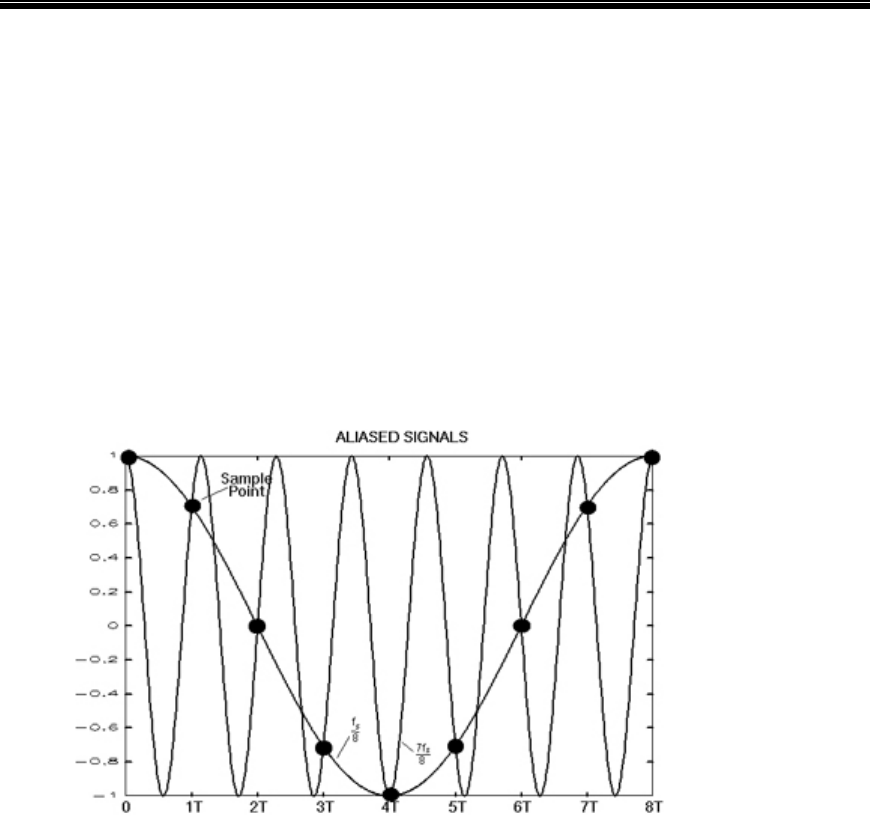
Appendix A - Sampling
Understanding Aliasing and Imaging ...
In all digital data acquisition systems, samples of an analog signal are taken at discrete time
intervals. The accuracy of a sampled signal is directly related to both the rate at which samples are
taken (the sampling rate or sampling frequency) and the signal's frequency content.
In theory, if a signal's frequency spectrum is band limited to some maximum frequency, fmax, an
exact representation of the signal can be acquired if the sampling frequency, fs, is at least twice the
maximum frequency: fs > 2fmax. This is known as the Shannon-Nyquist sampling theory, which
also states that the original analog signal can be faithfully reconstructed from these samples.
Analog signals can be band limited by the frequency response of the system or by filtering. If the
analog signal is not adequately band limited for the chosen sampling frequency, a phenomenon
known as aliasing or imaging will occur, resulting in highly undesirable effects. As the terms
suggests, different analog signals sometimes yield exactly the same samples; this is illustrated by
the figure below.
The aliasing effect can occur with broad-band signals where components beyond fs/2 will result in
additive distortions in the spectrum between 0 and fs/2. The figure below shows a typical broad-
band signal spectrum, for example, from an audio microphone.
The frequency response of the microphone begins to roll off gradually at 15kHz, and although
most audible information is below about 10kHz, high-frequency room noise can extend the signal
spectrum appreciably (the microphone's frequency response is down only 40dB at 60kHz!). With
fs = 100kHz, the shaded area of the spectrum is "folded over" about 50kHz and added to the
spectrum of the sampled signal as indicated by the pass-band reflection area in the figure below.
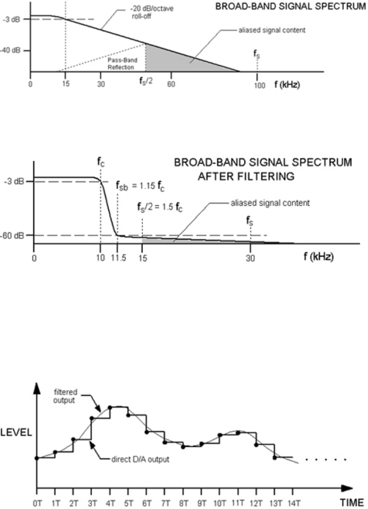
RPvdsEx Manual
342
A 100kHz sampling frequency is high enough to prevent aliasing from corrupting most of the
sampled signal's frequency spectrum, at least in the audio-frequency range. However, it is not
always possible to sample at a high enough rate to avoid aliasing.
To minimize the effects of aliasing, while greatly reducing the required sampling frequency, an
anti-aliasing filter can be used to limit the spectral content of the analog signal. This filter might be
a separate analog filter or built in to the device (as with sigma-delta A/D and D/A converters). The
spectrum below shows the result of filtering the broad-band microphone spectrum with an analog
filter.
The frequency at which the filter begins to limit the spectrum is the corner frequency, fc. The filter
used here has a stop-band frequency of 10 kHz, beyond which a signal attenuation of 60dB is
guaranteed. The sampling frequency should be at least twice the stop-band frequency.
Comparing the filtered and non-filtered spectral plots, it is evident that filtering greatly reduces the
total amount of signal content immediately beyond the 0 to 10kHz frequency range of interest; this
in turn greatly reduces the sampling frequency required to avoid aliasing.
During signal reconstruction digital numbers are converted to analog levels by a D/A converter at
discrete time intervals. The analog level of each sample is held constant for the sampling period
until the next sample resulting in a staircase analog output as shown below:
Here an anti-imaging filter is used to "smooth" out the staircase into a continuous waveform,
shown super-imposed (note the slight delay which results from filtering). This filter is functionally
the same as an anti-aliasing filter, but in this case it eliminates high-frequency "images" of the
signal spectrum caused by the staircase jumps in reconstruction.

Revision History
This list includes new components, new features, and bug fixes implemented in each version.
Version 7.2 – Jan 3, 2011
The following new components and macros have been added to RPvdsEx:
Components…
MCeStim, MCValList, MCVidAcc, MCLatch, MCForceCC, MCInt16ToFlt, MCInt8ToFlt,
MCPZAcc
Macro…
IZ2_Control, Video_Access
Version 7.1 – May 4, 2010
New RPvdsEx Features:
Support added for the RZ6 Processor and RS4 Data Streamer
Drivers will no longer support the (Gigabit) PI5 interface.
Added support for Optibit cards (PO5/PO5e) on all 64-bit Windows O/Ss (there is currently
no support for a 64-bit USB interface).
The following new components and macros have been added to RPvdsEx:
Components…
MCFloat2Int16, MCFloat2Int8
Macros…
RZ6_AmpIn, RZ6_AudioIn, RZ6_AudioOut, RZ6_Control, and Stream_Server_MC
Version 7.0 – July 8, 2009
New RPvdsEx Features:
Support added for the RZ5 processor
The following new components and macros have been added to RPvdsEx:
Components…
SortBin8, MCFromSer, MCToSer
Macros…
RZ5_AmpIn, RZ5_AmpIn_MC, RZ5_Control
Version 6.8 – June 6, 2008
New RPvdsEx Features:
Support added for optimizing printing control
Support added for SpikePac OpenEx toolset
RPvdsEx Manual
344
The following new components and macros have been added to RPvdsEx:
Components…
MCSmooth, MCBound
Macros…
PZ3_Control, PZ3_ChanMap, Test_Spike_MC
Version 6.6 – June 22, 2007
New RPvdsEx Features:
Introduced the following features which provide find and replace functionality to simplify
circuit changes and avoid common errors introduced when circuits are modified:
Change Component Name Dialog Box
Change Parameter Dialog Box
Update Number of Channels Dialog Box
The following new components and macros have been added to RPvdsEx:
Components…
MCFromHop, FromHopPick, MCMatMult, MCSum, and MCMult
Macros…
RZ2_Input_MC, MS16_Control, SH16_Control, Epoc_Store_with_Offset, Block_Avg_Store_1-
4Ch, Block_Avg_Store_MC, RateToSamples, TimeToSamples, PulseGenN
Version 6.4 - January 23, 2007
Maintenance release in support of changes to the OpenEx Suite.
The following new components and macros have been added to RPvdsEx to support Z-Series
processing:
Components...
TagStore, RMS2, FindSpike2, Convolv, Classify, MCPDec16, MCSampHold
Macros...
SlowStore_1-4Ch, Async_Stream_Store_1-4Ch, Async_Stream_Store_MC
Version 6.2 - September, 8, 2006
Introduced macros tools and a core set of macros targeted primarily to the OpenEx environment.
Added support for RZ2 Processor and PZ2 Preamplifiers.
The following new components and macros have been added to RPvdsEx to support Z-Series
processing:
Components...
PipeSource, PipeIn, PipeOut, MCPipeIn, MCPipeOut
Macros...
RZ2_Control macro, PZ2_Control macro
Version 6.0 - January 18, 2006
Improved support of High Performance Processor line (RX).
Expanded RX support for analog input/output components.
New RPvdsEx Scripted Tag allows scripting in RPvdsEx circuits.
Macro feature added.
Components...
RPvdsEx Manual
345
FIR2, STFIR2, MCFIR, MCFIR2
Version 5.8 - December 21, 2004
Improved support for USB2.0 interfaces and the high performance processors, including the RX8.
Version 5.7 - June 18, 2004
Included support for the latest version of the Gigabit Interface.
Version 5.3 - January 2004
Components...
SortSpike3, SampSubtract, BinRate, CompTo8D, CompTo16D, Peek, Poke, SeqIndex
Version 5.2 - November 2003
Support for Pentusa Multi-DSP Processors added.
Support for System II removed.
New RPvdsEx Features:
Better error reporting capabilities. An additional window that reports the number of
components on each processor, along with any errors encountered during compilation has been
added.
Multi-paging capabilities in the RPvdsEx interface allow complex chains to be split graphically
across multiple pages – enhancing readability without sacrificing functionality.
File format changed from .rpd to .rpx.
Components...
MCAdcIn, MCBiquad, MCConst, MCDacOut, MCFromSing, MCMerge, MCScale, MCSerStore,
MCToSing, MCDelay, MCzHopPick, Iterate, MCzHopIn, MCzHopOut, zHopIn, zHopOut
Version 5.0 - July 2003
Support for RM Mobile Processors added.
RPvdsEx bug fixes:
"Error loading Component specification file: CmpSpec.txt" error fixed. Users can now
double-click an .rpx file to open it.
Rounding error with FStep fixed.
3D Sound example circuits now function load without errors.
Ceiling and Floor components now give correct results for negative input values.
Version 4.6
Components...
Tetrode, SnipStore
Version 4.4
Components...
SerSource, SerStore, SortSpike
Version 4.3 - February 2002
Support for Gigabit High-Speed Interface added.
Name of zUSBmon Changed To zBUSmon to indicate addition of the Gigabit Interface.
Support for XBUS Interface removed.
RPvdsEx Manual
346
Version 4.2
Components...
PulseTrain2
Version 3.8 - April 25, 2000
RPvdsEx bug fix:
Rounding error on Tslope
Version 3.7 - December 25, 2000
New RPvdsEx features:
Error Flag when connecting a parameter to a primary input on a component.
Information on the Stingray added.
RPvdsEx bug fix:
Fixes problem with clearing delay lines.
Version 3.6 - November 10, 2000
New RPvdsEx features:
Parameter watch, Graph and HopIn and HopOut are accessible from the toolbar
Helpers On/Off feature for disconnecting portable RP devices
Context sensitive help for each component
Additional Device types in the Implement menu (RL2)
RPProg includes microcode for the RL2 (Stingray)
Components...
FindSpike PowStat PowCtrl
Version 3.5 - September 12, 2000
Components...
DeBounce, XOr, CompTo16, CompTo8, ExpFrom16, ExpFrom8, ShufTo16, ShufTo8,
SplitFrom16, SplitFrom8, iXOr, ToBits, FromBits, MuxIn, MuxOut, StateMach, FStep
RPvdsEx bug fixes:
Fixes problem with JK Flip-Flop
Fixes problem with high speed data transfer (requires hardware fix)
Changes TTL delay to milliseconds from microseconds
Version 2.20
First Major release of System 3 Drivers and RPvdsEx.

Index
A
AbsVal, 100, 104
ADCDelay, 182
AdcIn, 230, 239
And, 153
Anomalies, 333
Any2Any, 291
Arccos, 288, 334
Arcsin, 288, 334
Arctan, 288, 334
ArtReject, 257
AssignDSP, 248
AvgBuf, 115, 116, 117, 118, 119
AvgBuf2, 115, 116, 120
B
BinRate, 258, 334
Biquad, 146, 196
BitIn, 45, 72, 230
BitOut, 72, 231
BlockAcc, 115, 116, 122
BlockAvg, 115, 116, 117, 123
Bound, 100
BoxClassA, 257
BoxClassB1, 257
ButCoef, 144, 145, 146
ButCoef1, 144, 146, 147
C
Ceiling, 101
Classify, 257
Classify2, 257
CoefLoad, 144, 148
Compare, 101
Compiling Selected Processors, 16
Components, 19
CompTo16, 166, 167
CompTo16D, 166, 168
CompTo8, 166, 169
CompTo8D, 166, 170
ConstF, 225, 310
ConstI, 225, 310
ConstL, 225, 310
Convolv, 257
Cos, 289
Cos2Gate, 213, 334
Counter, 153, 154
Cycle Usage, 54
CycUsage, 55, 192
D
d Variable, 66
DACDelay, 183
DacOut, 232, 239
Data Port Access, 25
Data Transfer, 56
Data Types, 23
DataTable, 216
dBToLin, 209
DeBounce, 155
DestinFile, 217, 334
Digital Filter Components, 195
Distance, 289
DistScale, 88
Divide, 102
DspAssign, 249
Duplication Information, 28
Dynamic Access, 24
E
EdgeDetect, 155
Error Messages, 336
Exp, 209
Exp10, 209
Exp2, 209
ExpFrom16, 166, 171
ExpFrom8, 166, 172
ExpN, 210
F
FeatSrch, 94, 95, 334
FindFreq, 95, 334
FindSpike, 80, 260
FindSpike2, 257
FindSpike3, 257
RPvdsEx Manual
348
FIR, 87, 197, 198, 334
FIR2, 198, 334
Float2Float, 291
Float2Int, 292
Float2TTL, 292
Floor, 103
Flt2Stereo, 293
FreeDM, 193
FreePM, 193
FreeXM, 193
FromBits, 241
FromHopPick, 293
FStep, 311
G
GaussNoise, 312
Graph, 218
H
HopFrom, 219
HopTo, 219
HRTF File Format, 84
HrtfCoef, 88, 333
HrtfFir, 89
I
iAbsVal, 241
iAnd, 242
iBitShift, 75, 242
iCompare, 243
IIR, 200
iLimit, 243
iNot, 244
Input/Output Delays, 51
InstRate, 261
Int2Float, 294
Int2Int, 291
Int2TTL, 294
iOr, 244
iScaleAdd, 245
iSign, 245
Iterate, 220
iXor, 246
J
JKFlipFlop, 156
L
Latch, 184
Limit, 103
LinGate, 213, 334
Links, 21
LinRamp, 214
LinTodB, 210
LN, 211
Log10, 211
Log2, 211
LogN, 211
LongDelay, 184
LongDynDel, 185
M
Macros, 30
Max, 104, 318
MCAdcIn, 59, 233, 239
MCBiquad, 201
MCBound, 105
MCConst, 313
MCCpTo16D, 166, 175
MCCpTo8D, 166, 174
MCDacOut, 233
MCDelay, 186
MCeStim, 234
MCFIR, 202, 335
MCFIR2, 202, 335
MCFloat2Int, 295
MCFloat2Int16, 296
MCFloat2Int8, 295
MCForceCC, 297
MCFromHop, 298
MCFromSer, 299
MCFromSing, 299
MCInt16ToFlt, 300
MCInt2Float, 300
MCInt8ToFlt, 301
MCLatch, 186
MCMap, 302
MCMatMult, 106
MCMerge, 304
MCMult, 109
MCPDec16, 166, 176
MCPipeIn, 248, 249
MCPipeOut, 248, 249
MCSampHold, 281
MCScale, 108
MCSerSource, 126
MCSerStore, 115, 125
MCSign, 108
MCSmooth, 204
MCStrmFifo, 229
MCSubSel, 291, 305
MCSum, 109
MCToSing, 306
MCValList, 313
MCVidAcc, 229
MCzHopIn, 248, 251
MCzHopOut, 248, 251
MCzHopPick, 60, 248, 253
MemoBox, 225
Messages Window, 10
Min, 104, 318
Modulus, 110, 335
Mult, 113
Multi-Channel Signals, 57
MultiProcessor Components, 65
MultLatch, 187
MuxIn, 282
RPvdsEx Manual
349
MuxOut, 282
N
Not, 156
O
OneShot, 45, 157
OpenEx Header, 276
Or, 157
OxBuffer, 277
OxList, 277
OxScalar, 278
OxSnippet, 278
OxStream, 279
P
Pages, 11
ParaCoef, 144, 150, 151
ParTag, 225
ParWatch, 55, 226
Peek, 191
PipeIn, 248, 254
PipeOut, 248, 254
PipeSource, 248, 254
PlotDec16, 166, 173
Poke, 191
PowCtrl, 193
PowerBand, 95, 96
PowStat, 194
PulseTrain, 45, 158
PulseTrain2, 159
R
RamBuf, 115, 116, 117, 128
RampTooth, 314, 334
Random, 315
ReadBuf, 115, 116, 129, 333
Reverb, 90
RMS, 96, 260
RMS2, 97
RSFlipFlop, 160
S
SampDelay, 188
SampHold, 283
Sample Clock, 53
SampSubtract, 263
SawTooth, 316, 334
ScaleAdd, 50, 111, 334
Schmitt, 161
Schmitt2, 162
ScriptTag, 226
SeqIndex, 280
SerialBuf, 115, 116, 117, 130, 131, 133
SerSource, 115, 116, 132, 133
SerStore, 115, 138
ShortDelay, 188, 189, 190
ShortDynDelay, 189
ShufTo16, 166, 177
ShufTo8, 166, 178
Sign, 111
SimpCount, 284, 335
Sin, 290
Smooth, 205, 206
SnipStore, 115, 117, 139
SortBin8, 264
SortFlag16, 265
SortSpike, 80, 266
SortSpike2, 80, 268
SortSpike3, 80, 270
SourceFile, 227
SplitFrom16, 166, 179
SplitFrom8, 166, 179, 180
SqRoot, 112
Square, 112
StateMach, 284
StateMachine, 334
Static Access, 24
Stereo2Flt, 307
StereoAdc, 235, 239
StereoDac, 235
StereoFIR2, 206
StereoScale, 113
StereoSum, 113
Store Pooling, 66
Sum, 113, 114
T
TagStore, 115, 116, 117, 141
Tan, 290, 335
Tetrode, 117, 273
Time Slices, 25
TimeStamp, 236
ToBits, 246
Tone, 316
TrackMax, 97
TrackMin, 98
TrgIn, 44, 237
Triggering, 44
Trigonometry, 287
TSlope, 318
TTL2Float, 307
TTL2Int, 308
TTL2TTL, 291
TTLDelay, 163
TTLDelay2, 163
Type Conversion, 291
W
WordIn, 45, 72, 238, 335
WordOut, 72, 238, 335
WriteBuf, 115, 117, 142
RPvdsEx Manual
350
X
XOr, 164
Z
zHopIn, 248, 255
zHopOut, 248, 255