RRAM V2.0Beta Quick User Guide Updated May
RRAM__v2.0Beta_Quick_User_Guide_Updated_May
RRAM__v2.0Beta_Quick_User_Guide_Updated_May
User Manual:
Open the PDF directly: View PDF ![]() .
.
Page Count: 12
1
A Quick User Guide on
Peking University-Stanford University
Resistive Random Access Memory (RRAM)
SPICE Model
Version: 2.0Beta
Patent Pending.
Copyright Peking University and Stanford University 2015
All rights reserved.
April 13th, 2015
Contributors:
Prof. Jinfeng Kang, Prof. Xiaoyan Liu, Prof. H.-S. Philip Wong
Dr. Ximeng Guan, Dr. Shimeng Yu, Dr. Peng Huang, Dr. Bin Gao
Haitong Li, Zizhen Jiang

2
Terms of Use
Peking University and Stanford University and the authors provide these model files to you
subject to the Terms of Use, which may be updated by us from time to time without notice
to you. The most up-to-date Terms of Use can be found on the Stanford University
Nanoelectronics Lab Model Website at http://nano.stanford.edu/models.php.
By using the Peking University and Stanford University RRAM SPICE Model
(“Model”), you acknowledge that you have read the most up-to-date Terms of Use
and agree to abide by the Terms of Use (“Terms”).
These Terms include, but are not limited to, the following (for a comprehensive, and
up-to-date version of the Terms of Use, please visit the Stanford University Model
Website):
License Agreement
Peking University and Stanford grants you a non-transferable license to use this
Model on a single computer for a single user (You). This license may not be sub-leased,
sub-licensed, sold or otherwise transferred to another individual, company, or third party.
Peking University and Stanford reserves the right to revoke this license at any time, at
which point you must stop using the Model and delete all Model files.
Acceptable Usage
This Model shall be used solely for non-commercial academic and industrial research
by the individual to whom this Model, and its license, is granted.
The Model and its files may not be used, in part or in whole, by another individual,
institution, or third party other than the original individual to whom this Model, and its
license, is granted without prior written approval from Peking University and Stanford.
The Model and its files may not be copied, redistributed, or otherwise transferred, in part
or in whole, to a third party without prior written approval from Peking University and
Stanford.
You agree not to disclose the ideas and inventions inherent in this Model to other
individuals, institutions, or third parties. You further agree not to decompile or otherwise
reverse-engineer this Model, in part or in whole; not to decompose the Model and its files;
and not to misrepresent the Models and its files through modifications and add-ons.
Additional Terms
You agree to appropriately acknowledge and reference the Model work by Peking

3
University and Stanford in all publications, presentations, and/or other works
derived from the use, in part or in whole, of this Model and/or its variants. (See
Section 5. References and additional references on the Website.)
Disclaimer and Limitation of Liability
This Model is provided to you “As Is,” without warranty of any kind, either expressed or
implied. By using this Model, you agree that you and your representing institution or
company will not hold Peking University and Stanford University, the Model inventors,
the Model authors, as well as all other contributing members to the Model and its official
distribution, liable for damage of any kind resulting from the download or use of the Model
and its files and documents.
Legal Notice
This Model, including the files, documents, and inherent ideas, are protected by United
States Copyright Law and United States Patent Law. Peking University and Stanford
University and the authors reserve all rights. Unauthorized reproduction the files and/or the
documents included in the Model package is unlawful.

4
1. Model Files
Table 1. Summary of Model Files
File Name
Description
RRAM_v2.0Beta
RRAM SPICE Model File
Additional Files
File Name
Description
User Guide
RRAM Model v2.0Beta Quick User Guide.pdf
This User Guide in PDF format.
References/Publications
[1]-[5]
Sample Decks
test_RRAM_SET.sp
Example HSPICE decks: SET operation
test_RRAM_RESET.sp
Example HSPICE decks: RESET operation
AC_RRAM_SET.sp
Example HSPICE decks: SET pulse
AC_RRAM_RESET.sp
Example HSPICE decks: RESET pulse
This documentation pertains to the model files in the RRAM SPICE Model v2.0Beta
package. A brief summary and description of the model files included in the package are
shown in Table 1. This model is a beta-version intended for advanced users. There are still
issues such as occasional non-convergence. Please report issues to the developers. For
users who prefer a more stable model, please download RRAM v1.0.0 from the NCN
NEEDS: https://nanohub.org/publications/19
The package should include all and only these files, plus this User Guide document. A
summary of the model scope is in 2. Scope of the Model; details regarding model usage
and instantiation can be found in 3. Model Usage; and 4. Model Description and
Parameters describes the model assumptions and default parameters. 5. Sample results.

5
2. Scope of the Model
Table 2 below summarizes the scope of the model.
Table 2. Summary of the Scope of the RRAM Model
Device Types
Metal-Oxide Bipolar RRAM
Device Dimensions:
Switching Layer Thickness
~2 nm - 5 nm
Formed filament width
~1 nm - 5 nm
Initial filament width
~0.5 nm
Cell Size
~5 nm × 5 nm to 100 µm × 100 µm
Number of RRAMs / device
1 to Unlimited
Physics Aspects & Practical Non-idealities:
Filament Growth
Two-dimensional growth of one dominant filament
Electronic Conduction
Combined: Ohmic & generalized tunneling mechanism
Device parasitic effects
RC components of MIM structure
Temperature and Heat Conduction
Joule heating
Variations: Resistance States
Included
Variations: Switching Voltages
Included
Dynamic Current Fluctuations
Included for RESET process
This model was designed for fast and accurate simulation of metal-oxide based RRAM
devices [1]. The model captures typical DC and AC electrical behaviors of metal-oxide
based RRAM devices with physics-based compact model descriptions. The model assumes
a conductive filament (CF) evolution process described by a change of the CF geometry
during SET/RESET processes under various bias conditions. The core of the model is a
two-dimension description of CF, which includes both CF gap region and the CF width as
the control variables, where the CF dimensions are not limited. Parasitic effects are also
modeled, including both parasitic resistance of switching layer and electrodes, and
parasitic MIM capacitance. Intrinsic variation effects such as statistical distributions of
resistance states and switching voltages after SET/RESET processes as well as current
fluctuations during RESET are supported, which has made this model the first one
supporting the complete suite of RRAM variation effects to date. Since the model invoked
in HSPICE or other SPICE software is a two-terminal component, it can thus be easily
implemented in any circuit including memory array structures such as 1R, 1D1R, 1T1R
and 1S1R [2]-[4].
6
3. Model Usage
The model is developed in Verilog-A, and can be instantiated in HSPICE or other SPICE
tools (with the appropriate Verilog-A support). This section illustrates how to instantiate
the model in HSPICE.
3.1 Model Variants – Standard Model vs. Dynamic Model
Two model variants are available:
1) Standard RRAM Model (if parameter “switch” == 0)
2) Dynamic RRAM Model (if parameter “switch” == 1)
The Standard Model is recommended for describing the ensemble-average DC switching
behavior. The Dynamic Model is recommended for applications that involve dynamic
current fluctuations and variations of RRAM cell characteristics.
3.2 Convergence and Settings
For improved accuracy and convergence, include the following lines of code at the
beginning of the SPICE deck:
***************************************************
.option converge = 0
.option RUNLVL = 6
.option METHOD=GEAR
***************************************************
3.3 Model Instantiation
To instantiate the devices in the model, the library must be included at the beginning of the
SPICE deck.
.hdl RRAM_v2.0Beta.va
The Verilog-A compiler should automatically compile the Verilog-A model when the
SPICE deck is compiled. The Verilog-A compilation should only occur the first time the
model is used and can take a few minutes. Afterwards, the model does not need to be
recompiled for different simulation runs or different SPICE decks.
To instantiate an RRAM device, use the appropriate syntax below. The usage of this model
is similar to that of the Si CMOS transistor model.
* Standard RRAM Model
-Hspice 2013.03 SP2
X_RRAM TE BE RRAM_v2.0Beta < switch = 0 Parameter_Name =
Parameter_Value>
7
*Dynamic RRAM Model
-Hspice 2013.03
X_RRAM TE BE RRAM_v2.0Beta < switch = 1 Parameter_Name =
Parameter_Value>
The port definitions, TE and BE, for the RRAM are for the top electrode and the bottom
electrode, respectively. The ports TE and BE are not interchangeable in this model due to
nature of the asymmetry of the RRAM programming mechanism and the details of the
model implementation.
The device parameters indicated in the < ... > are optional and can be set differently for
each device instance. If the device parameters are omitted, default or global values set in
the parameter definition file are used. The syntax for setting a parameter is:
parameter_name = value or parameter
Please see Table 3 for the definitions and default values of the device parameters.
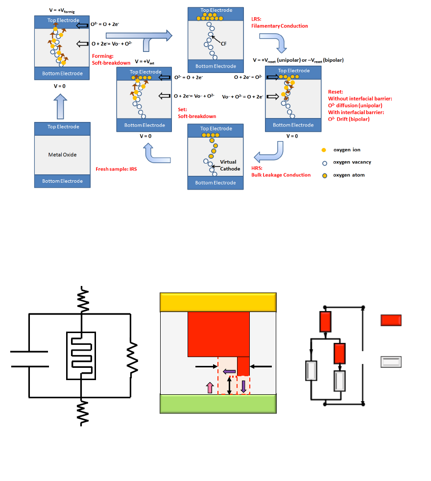
Figure 1 illustrates the basic physical model for the set and reset programming of the
RRAM [1]. Figure 2 shows the model assumptions for the filament evolutions processes
and corresponding models of electrical transport and parasitic effects.
8
4. Model Assumptions and Parameters
Fig. 1. Schematic of RRAM operation mechanisms, which serve as the physical basis of the analytical
SPICE model.
Fig. 2. Illustration of the RRAM SPICE model. (a) Equivalent circuit of RRAM cell composed of resistive
switching element and parasitic elements. (b) Schematic of conductive filament evolution. (c) Equivalent
circuit of resistive switching element modeling the metal-like and hopping current paths.

9
1The entire range and all possible combinations of the parameters have not been tested. The range listed
represents reasonable values based on experimental observations and physical insights. The units should be
the same as the default values.
Table 3. Model Parameter Descriptions and Default Values
Parameters
Descriptions
Default Value
Suggested Range1
I0
ρ
a
f
Ea
Eh
Ei
αa & αh
γ
Z & e
Rth
RH
RL
CP
L0
x0
WCF
Weff
w0
VT
T0
Switch
deltaGap
deltaCF
crit_x
hopping current density
resistivity of the CF
distance between VO
VO vibration frequency
average active energy of VO
hopping barrier of O2-
electrode/oxide interface
energy enhancement factor
voltage enhancement factor
charge number & unit charge
effective thermal resistance
oxide parasitic resistance
electrode contact resistance
electrode parasitic capacitance
initial switching layer length
initial gap length
switching layer width
effective width
initial CF width
characteristic voltage
ambient temperature
“model switch”
Gap varying rate
CF width varying rate
Gap variation fitting point
1013 A/m2
19.64 µΩ·m
0.25 nm
1013 Hz
0.7 eV
1.12 eV
0.82 eV
0.75 nm
1.5
1 & e
5×10⁵ K/W
200 MΩ
20 Ω
20 fF
3 nm
{L0, 0}
5 nm
0.5 nm
{0.5 nm, WCF}
0.4 V
300 K
0
4e-5 m/s
1e-4 m/s
0.5 nm
[1e10,1e15]
[0.1,1000]
[0.2,0.4]
[0.8e13,1.2e13]
[0.5,1.2]
[0.8,1.4]
[0.6,1.2]
0.75
1.5
1 & e
[2e5,1e6]
[1e6,1e9]
(0,25]
(0,25]
[1,10]
L0/0
[1,10]
0.5
(0,WCF]
0.4
(4,500)
{0,1}
[0,1e-4]
[0,5e-4]
[0, L0]
10
5. Sample Results
-3 -2 -1 0 1 2
10-8
10-6
10-4
100 cycles Exp.
Simulation
Current (A)
Voltage (V)
DSA HfOx/TiOx
RRAM device
Fig. 3. Typical DC switching I-V curves.
Note: the RRAM SPICE model runs in a dynamic way so that DC characteristics can only be
obtained by simulating transient operations under stair-like voltage sweeps similar to realistic
measurement setup.
020 40 60 80 100
0
50
100
Current (µA)
Time (ns)
0
1
2
Voltage (V)
020 40 60 80 100
0
50
100
150
200
Current (µA)
Time (ns)
0
1
2
Voltage (V)
Fig. 4. Typical transient SET and RESET operation with pulse applied.
11
6. References
[1] H.-S P. Wong, H.-Y. Lee, S. Yu, Y.-S. Chen, Y. Wu, P.-S. Chen, B. Lee, F. Chen, and M.-J.
Tsai, “Metal–Oxide RRAM,” Proceedings of IEEE, vol.100, no.6, pp. 1951-1970, June 2012,
DOI: 10.1109/JPROC.2012.2190369
[2] H. Li, Z. Jiang, P. Huang, Y. Wu, H.-Y. Chen, B. Gao, X. Liu, J. Kang, and H.-S. P. Wong,
“Variation-aware, reliability-emphasized design and optimization of RRAM using SPICE
model,” Design, Automation & Test in Europe (DATE), pp. 1426 – 1430, 2015
[3] Z. Jiang, S. Yu, Y. Wu, J. H. Engel, X. Guan, and H.-S. P. Wong, “Verilog-A Compact Model
for Oxide-based Resistive Random Access Memory (RRAM),” International Conference on
Simulation of Semiconductor Processes and Devices (SISPAD), pp. 41 – 44, 2014. DOI:
10.1109/SISPAD.2014.6931558
[4] H. Li, P. Huang, B. Gao, B. Chen, X. Liu, and J. Kang, “A SPICE Model of Resistive Random
Access Memory for Large-Scale Memory Array Simulation,” IEEE Electron Device Lett., vol.
35, no. 2, pp. 211 – 213, 2014. DOI: 10.1109/LED.2013.2293354
[5] X. Guan, S. Yu, and H.-S. P. Wong, “A SPICE Compact Model of Metal Oxide Resistive
Switching Memory With Variations,” IEEE Electron Device Lett., pp. 1405 – 1407, 2012.
DOI: 10.1109/LED.2012.2210856

12
7. Contacts and Website
Please direct all inquiries and comments to:
RRAM Model Email Address
Email: nano_rram_model@list.stanford.edu
Jinfeng Kang, Professor of Peking University
Email: kangjf@pku.edu.cn
H.-S. Philip Wong, Professor of Stanford University
Email: hspwong@stanford.edu
OR (for technical support):
Zizhen Jiang, Ph.D. candidate with Stanford University
Email: jiangzz@stanford.edu
Haitong Li, Undergraduate student with Peking University
(Prospective graduate student with Stanford University)
Email: haitongl@stanford.edu; lihaitong@pku.edu.cn
For the latest model file updates and the most current Terms of Use (“Software Download
License”) as well as other documents, please visit:
http://nano.stanford.edu/models.php .
Please report any bugs to us. Suggestions and comments are also welcome.
