S32K1XXRM, S32K1xx Series Reference Manual S32K
S32K_ReferenceManual
User Manual:
Open the PDF directly: View PDF ![]() .
.
Page Count: 2013 [warning: Documents this large are best viewed by clicking the View PDF Link!]
- S32K1xx Reference Manual (Supports S32K116, S32K118, S32K142, S32K144, S32K146, and S32K148)
- Contents
- Chapter 1: About This Manual
- Chapter 2: Introduction
- Chapter 3: Memory Map
- Chapter 4: Signal Multiplexing and Pin Assignment
- Chapter 5: Security Overview
- Chapter 6: Safety Overview
- Chapters 7-24 Core and System Modules
- Chapter 7: CM4 Overview
- Chapter 8: CM0+ Overview
- Chapter 9: Micro Trace Buffer (MTB)
- Chapter 10: Miscellaneous Control Module (MCM)
- Chapter 11: System Integration Module (SIM)
- Chip-specific SIM information
- Introduction
- Memory map and register definition
- SIM register descriptions
- SIM Memory map
- Chip Control register (CHIPCTL)
- FTM Option Register 0 (FTMOPT0)
- LPO Clock Select Register (LPOCLKS)
- ADC Options Register (ADCOPT)
- FTM Option Register 1 (FTMOPT1)
- Miscellaneous control register 0 (MISCTRL0)
- System Device Identification Register (SDID)
- Platform Clock Gating Control Register (PLATCGC)
- Flash Configuration Register 1 (FCFG1)
- Unique Identification Register High (UIDH)
- Unique Identification Register Mid-High (UIDMH)
- Unique Identification Register Mid Low (UIDML)
- Unique Identification Register Low (UIDL)
- System Clock Divider Register 4 (CLKDIV4)
- Miscellaneous Control register 1 (MISCTRL1)
- SIM register descriptions
- Chapter 12: Port Control and Interrupts (PORT)
- Chapter 13: General-Purpose Input/Output (GPIO)
- Chapter 14: Crossbar Switch Lite (AXBS-Lite)
- Chapter 15: Memory Protection Unit (MPU)
- Chip-specific MPU information
- Introduction
- Overview
- MPU register descriptions
- MPU Memory map
- Control/Error Status Register (CESR)
- Error Address Register, slave port n (EAR0 - EAR4)
- Error Detail Register, slave port n (EDR0 - EDR4)
- Region Descriptor n, Word 0 (RGD0_WORD0 - RGD15_WORD0)
- Region Descriptor 0, Word 1 (RGD0_WORD1)
- Region Descriptor 0, Word 2 (RGD0_WORD2)
- Region Descriptor 0, Word 3 (RGD0_WORD3)
- Region Descriptor n, Word 1 (RGD1_WORD1 - RGD15_WORD1)
- Region Descriptor n, Word 2 (RGD1_WORD2 - RGD15_WORD2)
- Region Descriptor n, Word 3 (RGD1_WORD3 - RGD15_WORD3)
- Region Descriptor Alternate Access Control 0 (RGDAAC0)
- Region Descriptor Alternate Access Control n (RGDAAC1 - RGDAAC15)
- Functional description
- Initialization information
- Application information
- Chapter 16: Peripheral Bridge (AIPS-Lite)
- Chip-specific AIPS information
- Introduction
- Memory map/register definition
- AIPS register descriptions
- AIPS Memory map
- Master Privilege Register A (MPRA)
- Peripheral Access Control Register (PACRA)
- Peripheral Access Control Register (PACRB)
- Peripheral Access Control Register (PACRD)
- Off-Platform Peripheral Access Control Register (OPACRA)
- Off-Platform Peripheral Access Control Register (OPACRB)
- Off-Platform Peripheral Access Control Register (OPACRC)
- Off-Platform Peripheral Access Control Register (OPACRD)
- Off-Platform Peripheral Access Control Register (OPACRE)
- Off-Platform Peripheral Access Control Register (OPACRF)
- Off-Platform Peripheral Access Control Register (OPACRG)
- Off-Platform Peripheral Access Control Register (OPACRH)
- Off-Platform Peripheral Access Control Register (OPACRI)
- Off-Platform Peripheral Access Control Register (OPACRJ)
- Off-Platform Peripheral Access Control Register (OPACRK)
- Off-Platform Peripheral Access Control Register (OPACRL)
- AIPS register descriptions
- Functional description
- Chapter 17: Direct Memory Access Multiplexer (DMAMUX)
- Chapter 18: Enhanced Direct Memory Access (eDMA)
- Chip-specific eDMA information
- Introduction
- Modes of operation
- Memory map/register definition
- TCD memory
- TCD initialization
- TCD structure
- Reserved memory and bit fields
- DMA register descriptions
- DMA Memory map
- Control Register (CR)
- Error Status Register (ES)
- Enable Request Register (ERQ)
- Enable Error Interrupt Register (EEI)
- Clear Enable Error Interrupt Register (CEEI)
- Set Enable Error Interrupt Register (SEEI)
- Clear Enable Request Register (CERQ)
- Set Enable Request Register (SERQ)
- Clear DONE Status Bit Register (CDNE)
- Set START Bit Register (SSRT)
- Clear Error Register (CERR)
- Clear Interrupt Request Register (CINT)
- Interrupt Request Register (INT)
- Error Register (ERR)
- Hardware Request Status Register (HRS)
- Enable Asynchronous Request in Stop Register (EARS)
- Channel Priority Register (DCHPRI0 - DCHPRI15)
- TCD Source Address (TCD0_SADDR - TCD15_SADDR)
- TCD Signed Source Address Offset (TCD0_SOFF - TCD15_SOFF)
- TCD Transfer Attributes (TCD0_ATTR - TCD15_ATTR)
- TCD Minor Byte Count (Minor Loop Mapping Disabled) (TCD0_NBYTES_MLNO - TCD15_NBYTES_MLNO)
- TCD Signed Minor Loop Offset (Minor Loop Mapping Enabled and Offset Disabled) (TCD0_NBYTES_MLOFFNO - TCD15_NBYTES_MLOFFNO)
- TCD Signed Minor Loop Offset (Minor Loop Mapping and Offset Enabled) (TCD0_NBYTES_MLOFFYES - TCD15_NBYTES_MLOFFYES)
- TCD Last Source Address Adjustment (TCD0_SLAST - TCD15_SLAST)
- TCD Destination Address (TCD0_DADDR - TCD15_DADDR)
- TCD Signed Destination Address Offset (TCD0_DOFF - TCD15_DOFF)
- TCD Current Minor Loop Link, Major Loop Count (Channel Linking Disabled) (TCD0_CITER_ELINKNO - TCD15_CITER_ELINKNO)
- TCD Current Minor Loop Link, Major Loop Count (Channel Linking Enabled) (TCD0_CITER_ELINKYES - TCD15_CITER_ELINKYES)
- TCD Last Destination Address Adjustment/Scatter Gather Address (TCD0_DLASTSGA - TCD15_DLASTSGA)
- TCD Control and Status (TCD0_CSR - TCD15_CSR)
- TCD Beginning Minor Loop Link, Major Loop Count (Channel Linking Disabled) (TCD0_BITER_ELINKNO - TCD15_BITER_ELINKNO)
- TCD Beginning Minor Loop Link, Major Loop Count (Channel Linking Enabled) (TCD0_BITER_ELINKYES - TCD15_BITER_ELINKYES)
- Functional description
- Initialization/application information
- Chapter 19: Trigger MUX Control (TRGMUX)
- Chip-specific TRGMUX information
- Introduction
- Features
- Memory map and register definition
- TRGMUX register descriptions
- TRGMUX Memory map
- TRGMUX DMAMUX0 Register (DMAMUX0)
- TRGMUX EXTOUT0 Register (EXTOUT0)
- TRGMUX EXTOUT1 Register (EXTOUT1)
- TRGMUX ADC0 Register (ADC0)
- TRGMUX ADC1 Register (ADC1)
- TRGMUX CMP0 Register (CMP0)
- TRGMUX FTM0 Register (FTM0)
- TRGMUX FTM1 Register (FTM1)
- TRGMUX FTM2 Register (FTM2)
- TRGMUX FTM3 Register (FTM3)
- TRGMUX PDB0 Register (PDB0)
- TRGMUX PDB1 Register (PDB1)
- TRGMUX FLEXIO Register (FLEXIO)
- TRGMUX LPIT0 Register (LPIT0)
- TRGMUX LPUART0 Register (LPUART0)
- TRGMUX LPUART1 Register (LPUART1)
- TRGMUX LPI2C0 Register (LPI2C0)
- TRGMUX LPSPI0 Register (LPSPI0)
- TRGMUX LPSPI1 Register (LPSPI1)
- TRGMUX LPTMR0 Register (LPTMR0)
- TRGMUX LPI2C1 Register (LPI2C1)
- TRGMUX FTM4 Register (FTM4)
- TRGMUX FTM5 Register (FTM5)
- TRGMUX FTM6 Register (FTM6)
- TRGMUX FTM7 Register (FTM7)
- TRGMUX register descriptions
- Chapter 20: External Watchdog Monitor (EWM)
- Chapter 21: Error Injection Module (EIM)
- Chapter 22: Error Reporting Module (ERM)
- Chapter 23: Watchdog timer (WDOG)
- Chapter 24: Cyclic Redundancy Check (CRC)
- Chapters 25-26 Reset and Boot
- Chapters 27-30 Clocking
- Chapter 27: Clock Distribution
- Chapter 28: System Clock Generator (SCG)
- Chapter 29: Peripheral Clock Controller (PCC)
- Chip-specific PCC information
- Introduction
- Features
- Functional description
- Memory map and register definition
- PCC register descriptions
- PCC Memory map
- PCC FTFC Register (PCC_FTFC)
- PCC DMAMUX Register (PCC_DMAMUX)
- PCC FlexCAN0 Register (PCC_FlexCAN0)
- PCC FlexCAN1 Register (PCC_FlexCAN1)
- PCC FTM3 Register (PCC_FTM3)
- PCC ADC1 Register (PCC_ADC1)
- PCC FlexCAN2 Register (PCC_FlexCAN2)
- PCC LPSPI0 Register (PCC_LPSPI0)
- PCC LPSPI1 Register (PCC_LPSPI1)
- PCC LPSPI2 Register (PCC_LPSPI2)
- PCC PDB1 Register (PCC_PDB1)
- PCC CRC Register (PCC_CRC)
- PCC PDB0 Register (PCC_PDB0)
- PCC LPIT Register (PCC_LPIT)
- PCC FTM0 Register (PCC_FTM0)
- PCC FTM1 Register (PCC_FTM1)
- PCC FTM2 Register (PCC_FTM2)
- PCC ADC0 Register (PCC_ADC0)
- PCC RTC Register (PCC_RTC)
- PCC LPTMR0 Register (PCC_LPTMR0)
- PCC PORTA Register (PCC_PORTA)
- PCC PORTB Register (PCC_PORTB)
- PCC PORTC Register (PCC_PORTC)
- PCC PORTD Register (PCC_PORTD)
- PCC PORTE Register (PCC_PORTE)
- PCC SAI0 Register (PCC_SAI0)
- PCC SAI1 Register (PCC_SAI1)
- PCC FlexIO Register (PCC_FlexIO)
- PCC EWM Register (PCC_EWM)
- PCC LPI2C0 Register (PCC_LPI2C0)
- PCC LPI2C1 Register (PCC_LPI2C1)
- PCC LPUART0 Register (PCC_LPUART0)
- PCC LPUART1 Register (PCC_LPUART1)
- PCC LPUART2 Register (PCC_LPUART2)
- PCC FTM4 Register (PCC_FTM4)
- PCC FTM5 Register (PCC_FTM5)
- PCC FTM6 Register (PCC_FTM6)
- PCC FTM7 Register (PCC_FTM7)
- PCC CMP0 Register (PCC_CMP0)
- PCC QSPI Register (PCC_QSPI)
- PCC ENET Register (PCC_ENET)
- Chapter 30: Clock Monitoring Unit (CMU)
- Chapters 31-37 Memories and Memory Interfaces
- Chapter 31: Memories and Memory Interfaces
- Chapter 32: PRAM Controller (PRAMC)
- Chapter 33: Local Memory Controller (LMEM)
- Chapter 34: Miscellaneous System Control Module (MSCM)
- Chip-specific MSCM information
- Overview
- Chip Configuration and Boot
- MSCM Memory Map/Register Definition
- CPU Configuration Memory Map and Registers
- MSCM register descriptions
- MSCM Memory map
- Processor X Type Register (CPxTYPE)
- Processor X Number Register (CPxNUM)
- Processor X Master Register (CPxMASTER)
- Processor X Count Register (CPxCOUNT)
- Processor X Configuration Register 0 (CPxCFG0)
- Processor X Configuration Register 1 (CPxCFG1)
- Processor X Configuration Register 2 (CPxCFG2)
- Processor X Configuration Register 3 (CPxCFG3)
- Processor 0 Type Register (CP0TYPE)
- Processor 0 Number Register (CP0NUM)
- Processor 0 Master Register (CP0MASTER)
- Processor 0 Count Register (CP0COUNT)
- Processor 0 Configuration Register 0 (CP0CFG0)
- Processor 0 Configuration Register 1 (CP0CFG1)
- Processor 0 Configuration Register 2 (CP0CFG2)
- Processor 0 Configuration Register 3 (CP0CFG3)
- On-Chip Memory Descriptor Register (OCMDR0)
- On-Chip Memory Descriptor Register (OCMDR1)
- On-Chip Memory Descriptor Register (OCMDR2)
- Chapter 35: Flash Memory Controller (FMC)
- Chapter 36: Flash Memory Module (FTFC)
- Chip-specific FTFC information
- Flash memory types
- Flash memory sizes
- 128 KB program flash / 32 KB FlexNVM / 2 KB FlexRAM module
- 256 KB program flash / 32 KB FlexNVM / 2 KB FlexRAM module
- 256 KB program flash / 64 KB FlexNVM / 4 KB FlexRAM module
- 512 KB program flash / 64 KB FlexNVM / 4 KB FlexRAM module
- 1 MB program flash / 256 KB FlexNVM / 4 KB FlexRAM module
- 2 MB program flash / 256 KB FlexNVM / 4 KB FlexRAM module
- Flash memory map
- Flash memory security
- Power mode restrictions on flash memory programming
- Flash memory modes
- Erase all contents of flash memory
- Customize MCU operations via FTFC_FOPT register
- Simultaneous operations on PFLASH read partitions
- Introduction
- External signal description
- Memory map and registers
- Flash configuration field description
- Program flash 0 IFR map
- Data flash 0 IFR map
- Register descriptions
- FTFC register descriptions
- FTFC Memory map
- Flash Status Register (FSTAT)
- Flash Configuration Register (FCNFG)
- Flash Security Register (FSEC)
- Flash Option Register (FOPT)
- Flash Common Command Object Registers (FCCOB0 - FCCOBB)
- Program Flash Protection Registers (FPROT0 - FPROT3)
- EEPROM Protection Register (FEPROT)
- Data Flash Protection Register (FDPROT)
- Flash CSEc Status Register (FCSESTAT)
- Flash Error Status Register (FERSTAT)
- Flash Error Configuration Register (FERCNFG)
- FTFC register descriptions
- Functional description
- Flash protection
- FlexNVM description
- Interrupts
- Flash operation in low-power modes
- Functional modes of operation
- Flash memory reads and ignored writes
- Read while write (RWW)
- Flash program and erase
- FTFC command operations
- Margin read commands
- Flash command descriptions
- Read 1s Block command
- Read 1s Section command
- Program Check command
- Program Phrase command
- Erase Flash Block command
- Erase Flash Sector command
- Program Section command
- Read 1s All Blocks command
- Read Once command
- Program Once command
- Erase All Blocks command
- Verify Backdoor Access Key command
- Erase All Blocks Unsecure command
- Program Partition command
- Set FlexRAM Function command
- Security
- Cryptographic Services Engine (CSEc)
- Key/seed/random number generation
- Secure boot mode
- User CSEc command interface and command set
- Generic PRAM interface description
- CMD_ENC_ECB
- CMD_ENC_CBC
- CMD_DEC_ECB
- CMD_DEC_CBC
- CMD_GENERATE_MAC
- CSEc format for CMD_GENERATE_MAC (pointer method)
- CMD_VERIFY_MAC
- CMD_VERIFY_MAC - CSEc format (pointer method)
- CMD_LOAD_KEY
- CMD_LOAD_PLAIN_KEY
- CMD_EXPORT_RAM_KEY
- CMD_INIT_RNG
- CMD_EXTEND_SEED
- CMD_RND
- CMD_SECURE_BOOT
- CMD_BOOT_FAILURE
- CMD_BOOT_OK
- CMD_GET_STATUS
- CMD_GET_ID
- CMD_CANCEL
- CMD_BOOT_DEFINE
- CMD_DBG_CHAL
- CMD_DBG_AUTH
- CMD_MP_COMPRESS
- Reset sequence
- Chip-specific FTFC information
- Chapter 37: Quad Serial Peripheral Interface (QuadSPI)
- Chip-specific QuadSPI information
- Introduction
- External Signal Description
- Memory Map and Register Definition
- Register Write Access
- Peripheral Bus Register Descriptions
- QuadSPI
- QuadSPI_MCR
- QuadSPI_IPCR
- QuadSPI_FLSHCR
- QuadSPI_BUF0CR
- QuadSPI_BUF1CR
- QuadSPI_BUF2CR
- QuadSPI_BUF3CR
- QuadSPI_BFGENCR
- QuadSPI_SOCCR
- QuadSPI_BUF0IND
- QuadSPI_BUF1IND
- QuadSPI_BUF2IND
- QuadSPI_SFAR
- QuadSPI_SFACR
- QuadSPI_SMPR
- QuadSPI_RBSR
- QuadSPI_RBCT
- QuadSPI_TBSR
- QuadSPI_TBDR
- QuadSPI_TBCT
- QuadSPI_SR
- QuadSPI_FR
- QuadSPI_RSER
- QuadSPI_SPNDST
- QuadSPI_SPTRCLR
- QuadSPI_SFA1AD
- QuadSPI_SFA2AD
- QuadSPI_SFB1AD
- QuadSPI_SFB2AD
- QuadSPI_RBDRn
- QuadSPI_LUTKEY
- QuadSPI_LCKCR
- QuadSPI_LUTn
- QuadSPI
- Serial Flash Address Assignment
- Flash memory mapped AMBA bus
- Interrupt Signals
- Functional Description
- Initialization/Application Information
- Byte Ordering - Endianness
- Driving Flash Control Signals in Single and Dual Mode
- Serial Flash Devices
- Example Sequences
- Read Command (Spansion Hyperflash/HyperRAM)
- Read Status Register(Spansion Hyperflash/HyperRAM)
- Word Program (Spansion Hyperflash/HyperRAM)
- Fast Read Sequence (Macronix/Numonyx/Spansion/Winbond)
- Fast Dual I/O DT Read Sequence (Macronix)
- Fast Read Quad Output (Winbond)
- 4 x I/O Read Enhance Performance Mode (XIP) (Macronix)
- Dual Command Page Program (Numonyx)
- Sector Erase (Macronix/Spansion/Numonyx)
- Read Status Register (Macronix/Spansion/Numonyx/Winbond)
- Example Sequences
- Sampling of Serial Flash Input Data
- Data Input Hold Requirement of Flash
- Chapters 38-40 Power Management
- Chapter 38: Power Management
- Chapter 39: System Mode Controller (SMC)
- Chapter 40: Power Management Controller (PMC)
- Chapters 41-43 Analog Modules
- Chapter 41: ADC Configuration
- Instantiation information
- Register implementation
- DMA Support on ADC
- ADC Hardware Interleaved Channels
- ADC internal supply monitoring
- ADC Reference Options
- ADC Trigger Sources
- Trigger Selection
- Trigger Latching and Arbitration
- ADC triggering configurations
- ADC low-power modes
- ADC Trigger Concept – Use Case
- ADC calibration scheme
- Chapter 42: Analog-to-Digital Converter (ADC)
- Chip-specific ADC information
- Introduction
- ADC signal descriptions
- ADC register descriptions
- ADC Memory map
- ADC Status and Control Register 1 (SC1A - aSC1P)
- ADC Configuration Register 1 (CFG1)
- ADC Configuration Register 2 (CFG2)
- ADC Data Result Registers (RA - aRP)
- Compare Value Registers (CV1 - CV2)
- Status and Control Register 2 (SC2)
- Status and Control Register 3 (SC3)
- BASE Offset Register (BASE_OFS)
- ADC Offset Correction Register (OFS)
- USER Offset Correction Register (USR_OFS)
- ADC X Offset Correction Register (XOFS)
- ADC Y Offset Correction Register (YOFS)
- ADC Gain Register (G)
- ADC User Gain Register (UG)
- ADC General Calibration Value Register S (CLPS)
- ADC Plus-Side General Calibration Value Register 3 (CLP3)
- ADC Plus-Side General Calibration Value Register 2 (CLP2)
- ADC Plus-Side General Calibration Value Register 1 (CLP1)
- ADC Plus-Side General Calibration Value Register 0 (CLP0)
- ADC Plus-Side General Calibration Value Register X (CLPX)
- ADC Plus-Side General Calibration Value Register 9 (CLP9)
- ADC General Calibration Offset Value Register S (CLPS_OFS)
- ADC Plus-Side General Calibration Offset Value Register 3 (CLP3_OFS)
- ADC Plus-Side General Calibration Offset Value Register 2 (CLP2_OFS)
- ADC Plus-Side General Calibration Offset Value Register 1 (CLP1_OFS)
- ADC Plus-Side General Calibration Offset Value Register 0 (CLP0_OFS)
- ADC Plus-Side General Calibration Offset Value Register X (CLPX_OFS)
- ADC Plus-Side General Calibration Offset Value Register 9 (CLP9_OFS)
- ADC Status and Control Register 1 (SC1AA - SC1Z)
- ADC Data Result Registers (RAA - RZ)
- Functional description
- Chapter 43: Comparator (CMP)
- Chapter 41: ADC Configuration
- Chapters 44-48 Timer Modules
- Chapter 44: Programmable delay block (PDB)
- Chapter 45: FlexTimer Module (FTM)
- Chip-specific FTM information
- Introduction
- FTM signal descriptions
- Memory map and register definition
- Memory map
- Register descriptions
- FTM register descriptions
- FTM Memory map
- Status And Control (SC)
- Counter (CNT)
- Modulo (MOD)
- Channel (n) Status And Control (C0SC - C7SC)
- Channel (n) Value (C0V - C7V)
- Counter Initial Value (CNTIN)
- Capture And Compare Status (STATUS)
- Features Mode Selection (MODE)
- Synchronization (SYNC)
- Initial State For Channels Output (OUTINIT)
- Output Mask (OUTMASK)
- Function For Linked Channels (COMBINE)
- Deadtime Configuration (DEADTIME)
- FTM External Trigger (EXTTRIG)
- Channels Polarity (POL)
- Fault Mode Status (FMS)
- Input Capture Filter Control (FILTER)
- Fault Control (FLTCTRL)
- Quadrature Decoder Control And Status (QDCTRL)
- Configuration (CONF)
- FTM Fault Input Polarity (FLTPOL)
- Synchronization Configuration (SYNCONF)
- FTM Inverting Control (INVCTRL)
- FTM Software Output Control (SWOCTRL)
- FTM PWM Load (PWMLOAD)
- Half Cycle Register (HCR)
- Pair 0 Deadtime Configuration (PAIR0DEADTIME)
- Pair 1 Deadtime Configuration (PAIR1DEADTIME)
- Pair 2 Deadtime Configuration (PAIR2DEADTIME)
- Pair 3 Deadtime Configuration (PAIR3DEADTIME)
- Mirror of Modulo Value (MOD_MIRROR)
- Mirror of Channel (n) Match Value (C0V_MIRROR - C7V_MIRROR)
- Functional Description
- Clock source
- Prescaler
- Counter
- Channel Modes
- Input Capture Mode
- Output Compare mode
- Edge-Aligned PWM (EPWM) mode
- Center-Aligned PWM (CPWM) mode
- Combine mode
- Modified Combine PWM Mode
- Complementary Mode
- Registers updated from write buffers
- PWM synchronization
- Inverting
- Software Output Control Mode
- Deadtime insertion
- Output mask
- Fault Control
- Polarity Control
- Initialization
- Features Priority
- External Trigger
- Initialization Trigger
- Capture Test Mode
- DMA
- Dual Edge Capture Mode
- Quadrature Decoder Mode
- Debug mode
- Reload Points
- Global Load
- Global time base (GTB)
- Channel trigger output
- External Control of Channels Output
- Dithering
- Reset Overview
- FTM Interrupts
- Initialization Procedure
- Chapter 46: Low Power Interrupt Timer (LPIT)
- Chip-specific LPIT information
- Introduction
- Modes of operation
- Memory Map and Registers
- LPIT register descriptions
- LPIT Memory map
- Version ID Register (VERID)
- Parameter Register (PARAM)
- Module Control Register (MCR)
- Module Status Register (MSR)
- Module Interrupt Enable Register (MIER)
- Set Timer Enable Register (SETTEN)
- Clear Timer Enable Register (CLRTEN)
- Timer Value Register (TVAL0 - TVAL3)
- Current Timer Value (CVAL0 - CVAL3)
- Timer Control Register (TCTRL0 - TCTRL3)
- LPIT register descriptions
- Functional description
- Chapter 47: Low Power Timer (LPTMR)
- Chapter 48: Real Time Clock (RTC)
- Chapters 49-55 Communication Modules
- Chapter 49: Low Power Serial Peripheral Interface (LPSPI)
- Chip-specific LPSPI information
- Introduction
- Memory Map and Registers
- LPSPI register descriptions
- LPSPI Memory map
- Version ID Register (VERID)
- Parameter Register (PARAM)
- Control Register (CR)
- Status Register (SR)
- Interrupt Enable Register (IER)
- DMA Enable Register (DER)
- Configuration Register 0 (CFGR0)
- Configuration Register 1 (CFGR1)
- Data Match Register 0 (DMR0)
- Data Match Register 1 (DMR1)
- Clock Configuration Register (CCR)
- FIFO Control Register (FCR)
- FIFO Status Register (FSR)
- Transmit Command Register (TCR)
- Transmit Data Register (TDR)
- Receive Status Register (RSR)
- Receive Data Register (RDR)
- LPSPI register descriptions
- Functional description
- Chapter 50: Low Power Inter-Integrated Circuit (LPI2C)
- Chip-specific LPI2C information
- Introduction
- Memory Map and Registers
- LPI2C register descriptions
- LPI2C Memory map
- Version ID Register (VERID)
- Parameter Register (PARAM)
- Master Control Register (MCR)
- Master Status Register (MSR)
- Master Interrupt Enable Register (MIER)
- Master DMA Enable Register (MDER)
- Master Configuration Register 0 (MCFGR0)
- Master Configuration Register 1 (MCFGR1)
- Master Configuration Register 2 (MCFGR2)
- Master Configuration Register 3 (MCFGR3)
- Master Data Match Register (MDMR)
- Master Clock Configuration Register 0 (MCCR0)
- Master Clock Configuration Register 1 (MCCR1)
- Master FIFO Control Register (MFCR)
- Master FIFO Status Register (MFSR)
- Master Transmit Data Register (MTDR)
- Master Receive Data Register (MRDR)
- Slave Control Register (SCR)
- Slave Status Register (SSR)
- Slave Interrupt Enable Register (SIER)
- Slave DMA Enable Register (SDER)
- Slave Configuration Register 1 (SCFGR1)
- Slave Configuration Register 2 (SCFGR2)
- Slave Address Match Register (SAMR)
- Slave Address Status Register (SASR)
- Slave Transmit ACK Register (STAR)
- Slave Transmit Data Register (STDR)
- Slave Receive Data Register (SRDR)
- LPI2C register descriptions
- Functional description
- Chapter 51: Low Power Universal Asynchronous Receiver/Transmitter (LPUART)
- Chip-specific LPUART information
- Introduction
- Register definition
- LPUART register descriptions
- LPUART Memory map
- Version ID Register (VERID)
- Parameter Register (PARAM)
- LPUART Global Register (GLOBAL)
- LPUART Pin Configuration Register (PINCFG)
- LPUART Baud Rate Register (BAUD)
- LPUART Status Register (STAT)
- LPUART Control Register (CTRL)
- LPUART Data Register (DATA)
- LPUART Match Address Register (MATCH)
- LPUART Modem IrDA Register (MODIR)
- LPUART FIFO Register (FIFO)
- LPUART Watermark Register (WATER)
- LPUART register descriptions
- Functional description
- Chapter 52: Flexible I/O (FlexIO)
- Chip-specific FlexIO information
- Introduction
- Memory Map and Registers
- FLEXIO register descriptions
- FLEXIO Memory map
- Version ID Register (VERID)
- Parameter Register (PARAM)
- FlexIO Control Register (CTRL)
- Pin State Register (PIN)
- Shifter Status Register (SHIFTSTAT)
- Shifter Error Register (SHIFTERR)
- Timer Status Register (TIMSTAT)
- Shifter Status Interrupt Enable (SHIFTSIEN)
- Shifter Error Interrupt Enable (SHIFTEIEN)
- Timer Interrupt Enable Register (TIMIEN)
- Shifter Status DMA Enable (SHIFTSDEN)
- Shifter Control N Register (SHIFTCTL0 - SHIFTCTL3)
- Shifter Configuration N Register (SHIFTCFG0 - SHIFTCFG3)
- Shifter Buffer N Register (SHIFTBUF0 - SHIFTBUF3)
- Shifter Buffer N Bit Swapped Register (SHIFTBUFBIS0 - SHIFTBUFBIS3)
- Shifter Buffer N Byte Swapped Register (SHIFTBUFBYS0 - SHIFTBUFBYS3)
- Shifter Buffer N Bit Byte Swapped Register (SHIFTBUFBBS0 - SHIFTBUFBBS3)
- Timer Control N Register (TIMCTL0 - TIMCTL3)
- Timer Configuration N Register (TIMCFG0 - TIMCFG3)
- Timer Compare N Register (TIMCMP0 - TIMCMP3)
- FLEXIO register descriptions
- Functional description
- Application Information
- Chapter 53: FlexCAN
- Chip-specific FlexCAN information
- Introduction
- FlexCAN signal descriptions
- Memory map/register definition
- FlexCAN memory mapping
- CAN register descriptions
- CAN Memory map
- Module Configuration Register (MCR)
- Control 1 register (CTRL1)
- Free Running Timer (TIMER)
- Rx Mailboxes Global Mask Register (RXMGMASK)
- Rx 14 Mask register (RX14MASK)
- Rx 15 Mask register (RX15MASK)
- Error Counter (ECR)
- Error and Status 1 register (ESR1)
- Interrupt Masks 1 register (IMASK1)
- Interrupt Flags 1 register (IFLAG1)
- Control 2 register (CTRL2)
- Error and Status 2 register (ESR2)
- CRC Register (CRCR)
- Rx FIFO Global Mask register (RXFGMASK)
- Rx FIFO Information Register (RXFIR)
- CAN Bit Timing Register (CBT)
- Rx Individual Mask Registers (RXIMR0 - RXIMR31)
- Pretended Networking Control 1 Register (CTRL1_PN)
- Pretended Networking Control 2 Register (CTRL2_PN)
- Pretended Networking Wake Up Match Register (WU_MTC)
- Pretended Networking ID Filter 1 Register (FLT_ID1)
- Pretended Networking DLC Filter Register (FLT_DLC)
- Pretended Networking Payload Low Filter 1 Register (PL1_LO)
- Pretended Networking Payload High Filter 1 Register (PL1_HI)
- Pretended Networking ID Filter 2 Register / ID Mask Register (FLT_ID2_IDMASK)
- Pretended Networking Payload Low Filter 2 Register / Payload Low Mask Register (PL2_PLMASK_LO)
- Pretended Networking Payload High Filter 2 low order bits / Payload High Mask Register (PL2_PLMASK_HI)
- Wake Up Message Buffer Register for C/S (WMB0_CS - WMB3_CS)
- Wake Up Message Buffer Register for ID (WMB0_ID - WMB3_ID)
- Wake Up Message Buffer Register for Data 0-3 (WMB0_D03 - WMB3_D03)
- Wake Up Message Buffer Register Data 4-7 (WMB0_D47 - WMB3_D47)
- CAN FD Control Register (FDCTRL)
- CAN FD Bit Timing Register (FDCBT)
- CAN FD CRC Register (FDCRC)
- Message buffer structure
- FlexCAN Memory Partition for CAN FD
- FlexCAN message buffer memory map
- Rx FIFO structure
- Functional description
- Initialization/application information
- Chapter 54: Synchronous Audio Interface (SAI)
- Chip-specific SAI information
- Introduction
- External signals
- Memory map and register definition
- I2S register descriptions
- I2S Memory map
- Version ID Register (VERID)
- Parameter Register (PARAM)
- SAI Transmit Control Register (TCSR)
- SAI Transmit Configuration 1 Register (TCR1)
- SAI Transmit Configuration 2 Register (TCR2)
- SAI Transmit Configuration 3 Register (TCR3)
- SAI Transmit Configuration 4 Register (TCR4)
- SAI Transmit Configuration 5 Register (TCR5)
- SAI Transmit Data Register (TDR0 - TDR3)
- SAI Transmit FIFO Register (TFR0 - TFR3)
- SAI Transmit Mask Register (TMR)
- SAI Receive Control Register (RCSR)
- SAI Receive Configuration 1 Register (RCR1)
- SAI Receive Configuration 2 Register (RCR2)
- SAI Receive Configuration 3 Register (RCR3)
- SAI Receive Configuration 4 Register (RCR4)
- SAI Receive Configuration 5 Register (RCR5)
- SAI Receive Data Register (RDR0 - RDR3)
- SAI Receive FIFO Register (RFR0 - RFR3)
- SAI Receive Mask Register (RMR)
- I2S register descriptions
- Functional description
- Chapter 55: Ethernet MAC (ENET)
- Chip-specific ENET information
- Introduction
- Overview
- External signal description
- Memory map/register definition
- ENET
- ENET_EIR
- ENET_EIMR
- ENET_RDAR
- ENET_TDAR
- ENET_ECR
- ENET_MMFR
- ENET_MSCR
- ENET_MIBC
- ENET_RCR
- ENET_TCR
- ENET_PALR
- ENET_PAUR
- ENET_OPD
- ENET_IAUR
- ENET_IALR
- ENET_GAUR
- ENET_GALR
- ENET_TFWR
- ENET_RDSR
- ENET_TDSR
- ENET_MRBR
- ENET_RSFL
- ENET_RSEM
- ENET_RAEM
- ENET_RAFL
- ENET_TSEM
- ENET_TAEM
- ENET_TAFL
- ENET_TIPG
- ENET_FTRL
- ENET_TACC
- ENET_RACC
- ENET_RMON_T_DROP
- ENET_RMON_T_PACKETS
- ENET_RMON_T_BC_PKT
- ENET_RMON_T_MC_PKT
- ENET_RMON_T_CRC_ALIGN
- ENET_RMON_T_UNDERSIZE
- ENET_RMON_T_OVERSIZE
- ENET_RMON_T_FRAG
- ENET_RMON_T_JAB
- ENET_RMON_T_COL
- ENET_RMON_T_P64
- ENET_RMON_T_P65TO127
- ENET_RMON_T_P128TO255
- ENET_RMON_T_P256TO511
- ENET_RMON_T_P512TO1023
- ENET_RMON_T_P1024TO2047
- ENET_RMON_T_P_GTE2048
- ENET_RMON_T_OCTETS
- ENET_IEEE_T_DROP
- ENET_IEEE_T_FRAME_OK
- ENET_IEEE_T_1COL
- ENET_IEEE_T_MCOL
- ENET_IEEE_T_DEF
- ENET_IEEE_T_LCOL
- ENET_IEEE_T_EXCOL
- ENET_IEEE_T_MACERR
- ENET_IEEE_T_CSERR
- ENET_IEEE_T_SQE
- ENET_IEEE_T_FDXFC
- ENET_IEEE_T_OCTETS_OK
- ENET_RMON_R_PACKETS
- ENET_RMON_R_BC_PKT
- ENET_RMON_R_MC_PKT
- ENET_RMON_R_CRC_ALIGN
- ENET_RMON_R_UNDERSIZE
- ENET_RMON_R_OVERSIZE
- ENET_RMON_R_FRAG
- ENET_RMON_R_JAB
- ENET_RMON_R_RESVD_0
- ENET_RMON_R_P64
- ENET_RMON_R_P65TO127
- ENET_RMON_R_P128TO255
- ENET_RMON_R_P256TO511
- ENET_RMON_R_P512TO1023
- ENET_RMON_R_P1024TO2047
- ENET_RMON_R_P_GTE2048
- ENET_RMON_R_OCTETS
- ENET_IEEE_R_DROP
- ENET_IEEE_R_FRAME_OK
- ENET_IEEE_R_CRC
- ENET_IEEE_R_ALIGN
- ENET_IEEE_R_MACERR
- ENET_IEEE_R_FDXFC
- ENET_IEEE_R_OCTETS_OK
- ENET_ATCR
- ENET_ATVR
- ENET_ATOFF
- ENET_ATPER
- ENET_ATCOR
- ENET_ATINC
- ENET_ATSTMP
- ENET_TGSR
- ENET_TCSRn
- ENET_TCCRn
- ENET
- Functional description
- Ethernet MAC frame formats
- IP and higher layers frame format
- IEEE 1588 message formats
- MAC receive
- MAC transmit
- Full-duplex flow control operation
- Magic packet detection
- IP accelerator functions
- Resets and stop controls
- IEEE 1588 functions
- FIFO thresholds
- Loopback options
- Legacy buffer descriptors
- Enhanced buffer descriptors
- Client FIFO application interface
- FIFO protection
- Reference clock
- PHY management interface
- Ethernet interfaces
- Chapter 49: Low Power Serial Peripheral Interface (LPSPI)
- Chapters 56-57 Debug Modules
- Chapter 56: Debug
- Chapter 57: JTAG Controller (JTAGC)
- Appendix A: Release Notes for Revision 7
- General changes
- About This Manual changes
- Introduction changes
- Memory map changes
- Signal multiplexing changes
- Security Overview changes
- Safety Overview changes
- CM0+ Overview changes
- CM4 Overview changes
- MTB changes
- MCM changes
- SIM changes
- PORT changes
- GPIO changes
- AXBS-Lite changes
- MPU changes
- AIPS-Lite changes
- DMAMUX changes
- eDMA changes
- TRGMUX changes
- EWM changes
- EIM changes
- ERM changes
- WDOG changes
- CRC module changes
- Reset and Boot changes
- RCM changes
- Clock Distribution changes
- SCG changes
- PCC changes
- CMU changes
- Memories and memory interfaces changes
- PRAMC changes
- LMEM changes
- MSCM changes
- FMC changes
- FTFC changes
- QSPI changes
- Power Management changes
- SMC changes
- PMC changes
- ADC Configuration changes
- ADC changes
- CMP changes
- PDB changes
- FTM changes
- LPIT changes
- LPTMR changes
- RTC changes
- LPSPI changes
- LPI2C changes
- LPUART changes
- FlexIO changes
- FlexCAN changes
- SAI changes
- ENETchanges
- Debug changes
- JTAGC changes
- Contents

S32K1xx Series Reference Manual
Supports S32K116, S32K118, S32K142, S32K144, S32K146, and
S32K148
Document Number: S32K1XXRM
Rev. 7, 04/2018

S32K1xx Series Reference Manual, Rev. 7, 04/2018
2 NXP Semiconductors

Contents
Section number Title Page
Chapter 1
About This Manual
1.1 Audience....................................................................................................................................................................... 49
1.2 Organization..................................................................................................................................................................49
1.3 Module descriptions......................................................................................................................................................49
1.3.1 Example: chip-specific information that clarifies content in the same chapter............................................. 50
1.3.2 Example: chip-specific information that refers to a different chapter........................................................... 51
1.4 Register descriptions.....................................................................................................................................................52
1.5 Conventions.................................................................................................................................................................. 53
1.5.1 Notes, Cautions, and Warnings......................................................................................................................53
1.5.2 Numbering systems........................................................................................................................................53
1.5.3 Typographic notation..................................................................................................................................... 54
1.5.4 Special terms..................................................................................................................................................54
Chapter 2
Introduction
2.1 Overview.......................................................................................................................................................................57
2.2 S32K1xx Series introduction........................................................................................................................................57
2.2.1 S32K14x.........................................................................................................................................................57
2.2.2 S32K11x ........................................................................................................................................................59
2.3 Feature summary...........................................................................................................................................................60
2.4 Block diagram...............................................................................................................................................................63
2.5 Feature comparison.......................................................................................................................................................64
2.6 Applications..................................................................................................................................................................66
2.7 Module functional categories........................................................................................................................................67
2.7.1 Arm Cortex-M4F Core Modules....................................................................................................................68
2.7.2 Arm Cortex-M0+ Core Modules....................................................................................................................69
2.7.3 System modules............................................................................................................................................. 69
2.7.4 Memories and memory interfaces..................................................................................................................70
S32K1xx Series Reference Manual, Rev. 7, 04/2018
NXP Semiconductors 3

Section number Title Page
2.7.5 Power Management........................................................................................................................................71
2.7.6 Clocking.........................................................................................................................................................71
2.7.7 Analog modules............................................................................................................................................. 72
2.7.8 Timer modules............................................................................................................................................... 72
2.7.9 Communication interfaces............................................................................................................................. 73
2.7.10 Debug modules.............................................................................................................................................. 73
Chapter 3
Memory Map
3.1 Introduction...................................................................................................................................................................75
3.2 SRAM memory map.....................................................................................................................................................75
3.2.1 S32K14x: SRAM memory map ....................................................................................................................75
3.2.2 S32K11x: SRAM memory map ....................................................................................................................75
3.3 Flash memory map........................................................................................................................................................76
3.4 Peripheral bridge (AIPS-Lite) memory map.................................................................................................................76
3.4.1 Read-after-write sequence and required serialization of memory operations................................................77
3.5 Private Peripheral Bus (PPB) memory map..................................................................................................................78
3.6 Aliased bit-band regions for CM4 core........................................................................................................................ 79
Chapter 4
Signal Multiplexing and Pin Assignment
4.1 Introduction...................................................................................................................................................................81
4.2 Functional description...................................................................................................................................................81
4.3 Pad description..............................................................................................................................................................82
4.4 Default pad state........................................................................................................................................................... 83
4.5 Signal Multiplexing sheet............................................................................................................................................. 84
4.5.1 IO Signal Table ............................................................................................................................................. 84
4.5.2 Input muxing table......................................................................................................................................... 86
4.6 Pinout diagrams............................................................................................................................................................ 87
Chapter 5
Security Overview
5.1 Introduction...................................................................................................................................................................89
S32K1xx Series Reference Manual, Rev. 7, 04/2018
4 NXP Semiconductors

Section number Title Page
5.2 Device security..............................................................................................................................................................89
5.2.1 Flash memory security...................................................................................................................................89
5.2.2 Cryptographic Services Engine (CSEc) security features..............................................................................90
5.2.3 Device Boot modes........................................................................................................................................ 91
5.3 Security use case examples...........................................................................................................................................91
5.3.1 Secure boot: check bootloader for integrity and authenticity........................................................................ 91
5.3.2 Chain of trust: check flash memory for integrity and authenticity................................................................ 92
5.3.3 Secure communication...................................................................................................................................93
5.3.4 Component protection....................................................................................................................................94
5.3.5 Message-authentication example................................................................................................................... 95
5.4 Steps required before failure analysis...........................................................................................................................96
5.5 Security programming flow example (Secure Boot).................................................................................................... 97
Chapter 6
Safety Overview
6.1 Introduction...................................................................................................................................................................99
6.2 S32K1xx safety concept............................................................................................................................................... 100
6.2.1 Cortex-M4/M0+ Structural Core Self Test (SCST).......................................................................................101
6.2.2 ECC on RAM and flash memory...................................................................................................................102
6.2.3 Power supply monitoring...............................................................................................................................102
6.2.4 Clock monitoring........................................................................................................................................... 103
6.2.5 Temporal protection.......................................................................................................................................103
6.2.6 Operational interference protection............................................................................................................... 103
6.2.7 CRC................................................................................................................................................................105
6.2.8 Diversity of system resources........................................................................................................................ 105
Chapter 7
CM4 Overview
7.1 Arm Cortex-M4F core configuration............................................................................................................................107
7.1.1 Buses, interconnects, and interfaces.............................................................................................................. 108
7.1.2 System Tick Timer.........................................................................................................................................108
S32K1xx Series Reference Manual, Rev. 7, 04/2018
NXP Semiconductors 5

Section number Title Page
7.1.3 Debug facilities.............................................................................................................................................. 108
7.1.4 Caches............................................................................................................................................................ 109
7.1.5 Core privilege levels...................................................................................................................................... 109
7.2 Nested Vectored Interrupt Controller (NVIC) Configuration...................................................................................... 110
7.2.1 Interrupt priority levels.................................................................................................................................. 110
7.2.2 Non-maskable interrupt..................................................................................................................................111
7.2.3 Determining the bitfield and register location for configuring a particular interrupt.................................... 111
7.3 Asynchronous Wake-up Interrupt Controller (AWIC) Configuration..........................................................................112
7.3.1 Wake-up sources............................................................................................................................................112
7.4 FPU configuration.........................................................................................................................................................113
7.5 JTAG controller configuration......................................................................................................................................114
Chapter 8
CM0+ Overview
8.1 Arm Cortex-M0+ core introduction..............................................................................................................................115
8.1.1 Buses, interconnects, and interfaces.............................................................................................................. 116
8.1.2 System tick timer........................................................................................................................................... 116
8.1.3 Debug facilities.............................................................................................................................................. 116
8.1.4 Core privilege levels...................................................................................................................................... 116
8.2 Nested vectored interrupt controller (NVIC) ...............................................................................................................117
8.2.1 Interrupt priority levels.................................................................................................................................. 117
8.2.2 Non-maskable interrupt..................................................................................................................................117
8.2.3 Determining the bitfield and register location for configuring a particular interrupt.................................... 117
8.3 AWIC introduction....................................................................................................................................................... 118
8.3.1 Wake-up sources............................................................................................................................................118
Chapter 9
Micro Trace Buffer (MTB)
9.1 Introduction...................................................................................................................................................................121
9.1.1 Overview........................................................................................................................................................121
9.1.2 Features.......................................................................................................................................................... 123
S32K1xx Series Reference Manual, Rev. 7, 04/2018
6 NXP Semiconductors

Section number Title Page
9.1.3 Modes of operation........................................................................................................................................ 124
9.2 Memory map and register definition.............................................................................................................................124
9.2.1 MTB_DWT Memory Map.............................................................................................................................125
Chapter 10
Miscellaneous Control Module (MCM)
10.1 Chip-specific MCM information.................................................................................................................................. 135
10.2 Introduction...................................................................................................................................................................136
10.2.1 Features.......................................................................................................................................................... 136
10.3 Memory map/register descriptions............................................................................................................................... 136
10.3.1 Crossbar Switch (AXBS) Slave Configuration (MCM_PLASC)..................................................................137
10.3.2 Crossbar Switch (AXBS) Master Configuration (MCM_PLAMC).............................................................. 138
10.3.3 Core Platform Control Register (MCM_CPCR)............................................................................................139
10.3.4 Interrupt Status and Control Register (MCM_ISCR).................................................................................... 142
10.3.5 Process ID Register (MCM_PID)..................................................................................................................145
10.3.6 Compute Operation Control Register (MCM_CPO)..................................................................................... 146
10.3.7 Local Memory Descriptor Register (MCM_LMDRn)...................................................................................147
10.3.8 Local Memory Descriptor Register2 (MCM_LMDR2).................................................................................150
10.3.9 LMEM Parity and ECC Control Register (MCM_LMPECR).......................................................................154
10.3.10 LMEM Parity and ECC Interrupt Register (MCM_LMPEIR)...................................................................... 155
10.3.11 LMEM Fault Address Register (MCM_LMFAR).........................................................................................156
10.3.12 LMEM Fault Attribute Register (MCM_LMFATR).....................................................................................157
10.3.13 LMEM Fault Data High Register (MCM_LMFDHR).................................................................................. 158
10.3.14 LMEM Fault Data Low Register (MCM_LMFDLR)....................................................................................158
10.4 Functional description...................................................................................................................................................159
10.4.1 Interrupts........................................................................................................................................................ 159
Chapter 11
System Integration Module (SIM)
11.1 Chip-specific SIM information.....................................................................................................................................161
11.1.1 SIM register bitfield implementation.............................................................................................................161
S32K1xx Series Reference Manual, Rev. 7, 04/2018
NXP Semiconductors 7

Section number Title Page
11.2 Introduction...................................................................................................................................................................161
11.2.1 Features.......................................................................................................................................................... 161
11.3 Memory map and register definition.............................................................................................................................162
11.3.1 SIM register descriptions............................................................................................................................... 162
Chapter 12
Port Control and Interrupts (PORT)
12.1 Chip-specific PORT information..................................................................................................................................189
12.1.1 Number of PCRs............................................................................................................................................ 189
12.1.2 I/O configuration sequence ........................................................................................................................... 190
12.1.3 Digital input filter configuration sequence ................................................................................................... 190
12.2 Introduction...................................................................................................................................................................191
12.3 Overview.......................................................................................................................................................................191
12.3.1 Features.......................................................................................................................................................... 192
12.3.2 Modes of operation........................................................................................................................................ 192
12.4 External signal description............................................................................................................................................193
12.5 Detailed signal description............................................................................................................................................193
12.6 Memory map and register definition.............................................................................................................................194
12.6.1 Pin Control Register n (PORT_PCRn).......................................................................................................... 196
12.6.2 Global Pin Control Low Register (PORT_GPCLR)......................................................................................199
12.6.3 Global Pin Control High Register (PORT_GPCHR).....................................................................................199
12.6.4 Global Interrupt Control Low Register (PORT_GICLR)..............................................................................200
12.6.5 Global Interrupt Control High Register (PORT_GICHR).............................................................................200
12.6.6 Interrupt Status Flag Register (PORT_ISFR)................................................................................................ 201
12.6.7 Digital Filter Enable Register (PORT_DFER).............................................................................................. 202
12.6.8 Digital Filter Clock Register (PORT_DFCR)................................................................................................202
12.6.9 Digital Filter Width Register (PORT_DFWR).............................................................................................. 203
12.7 Functional description...................................................................................................................................................203
12.7.1 Pin control......................................................................................................................................................203
12.7.2 Global pin control.......................................................................................................................................... 204
S32K1xx Series Reference Manual, Rev. 7, 04/2018
8 NXP Semiconductors

Section number Title Page
12.7.3 Global interrupt control..................................................................................................................................205
12.7.4 External interrupts..........................................................................................................................................205
12.7.5 Digital filter....................................................................................................................................................206
Chapter 13
General-Purpose Input/Output (GPIO)
13.1 Chip-specific GPIO information...................................................................................................................................207
13.1.1 Instantiation information................................................................................................................................207
13.1.2 GPIO ports memory map............................................................................................................................... 207
13.1.3 GPIO register reset values .............................................................................................................................208
13.2 Introduction...................................................................................................................................................................208
13.2.1 Features.......................................................................................................................................................... 209
13.2.2 Modes of operation........................................................................................................................................ 209
13.2.3 GPIO signal descriptions............................................................................................................................... 209
13.3 Memory map and register definition.............................................................................................................................210
13.3.1 GPIO register descriptions.............................................................................................................................211
13.4 Functional description...................................................................................................................................................218
13.4.1 General-purpose input....................................................................................................................................218
13.4.2 General-purpose output..................................................................................................................................218
Chapter 14
Crossbar Switch Lite (AXBS-Lite)
14.1 Chip-specific AXBS-Lite information..........................................................................................................................221
14.1.1 Crossbar Switch master assignments............................................................................................................. 221
14.1.2 Crossbar Switch slave assignments................................................................................................................221
14.2 Introduction...................................................................................................................................................................222
14.2.1 Features.......................................................................................................................................................... 222
14.3 Functional Description..................................................................................................................................................223
14.3.1 General operation...........................................................................................................................................223
14.3.2 Arbitration......................................................................................................................................................223
14.4 Initialization/application information........................................................................................................................... 225
S32K1xx Series Reference Manual, Rev. 7, 04/2018
NXP Semiconductors 9

Section number Title Page
Chapter 15
Memory Protection Unit (MPU)
15.1 Chip-specific MPU information................................................................................................................................... 227
15.1.1 MPU Slave Port Assignments........................................................................................................................227
15.1.2 MPU Logical Bus Master Assignments.........................................................................................................228
15.1.3 Current PID....................................................................................................................................................228
15.1.4 Region descriptors and slave port configuration............................................................................................228
15.2 Introduction...................................................................................................................................................................229
15.3 Overview.......................................................................................................................................................................229
15.3.1 Block diagram................................................................................................................................................229
15.3.2 Features.......................................................................................................................................................... 230
15.4 MPU register descriptions.............................................................................................................................................231
15.4.1 MPU Memory map........................................................................................................................................ 231
15.4.2 Control/Error Status Register (CESR)........................................................................................................... 234
15.4.3 Error Address Register, slave port n (EAR0 - EAR4)................................................................................... 236
15.4.4 Error Detail Register, slave port n (EDR0 - EDR4)...................................................................................... 237
15.4.5 Region Descriptor n, Word 0 (RGD0_WORD0 - RGD15_WORD0)...........................................................239
15.4.6 Region Descriptor 0, Word 1 (RGD0_WORD1)...........................................................................................240
15.4.7 Region Descriptor 0, Word 2 (RGD0_WORD2)...........................................................................................241
15.4.8 Region Descriptor 0, Word 3 (RGD0_WORD3)...........................................................................................244
15.4.9 Region Descriptor n, Word 1 (RGD1_WORD1 - RGD15_WORD1)...........................................................245
15.4.10 Region Descriptor n, Word 2 (RGD1_WORD2 - RGD15_WORD2)...........................................................246
15.4.11 Region Descriptor n, Word 3 (RGD1_WORD3 - RGD15_WORD3)...........................................................249
15.4.12 Region Descriptor Alternate Access Control 0 (RGDAAC0)....................................................................... 251
15.4.13 Region Descriptor Alternate Access Control n (RGDAAC1 - RGDAAC15)...............................................254
15.5 Functional description...................................................................................................................................................257
15.5.1 Access evaluation macro................................................................................................................................257
15.5.2 Putting it all together and error terminations................................................................................................. 259
15.5.3 Power management........................................................................................................................................259
S32K1xx Series Reference Manual, Rev. 7, 04/2018
10 NXP Semiconductors

Section number Title Page
15.6 Initialization information.............................................................................................................................................. 260
15.7 Application information................................................................................................................................................260
Chapter 16
Peripheral Bridge (AIPS-Lite)
16.1 Chip-specific AIPS information................................................................................................................................... 263
16.1.1 Instantiation information................................................................................................................................263
16.1.2 Memory maps................................................................................................................................................ 263
16.2 Introduction...................................................................................................................................................................264
16.2.1 Features.......................................................................................................................................................... 265
16.2.2 General operation...........................................................................................................................................265
16.3 Memory map/register definition................................................................................................................................... 265
16.3.1 AIPS register descriptions..............................................................................................................................265
16.4 Functional description...................................................................................................................................................309
16.4.1 Access support............................................................................................................................................... 309
Chapter 17
Direct Memory Access Multiplexer (DMAMUX)
17.1 Chip-specific DMAMUX information......................................................................................................................... 311
17.1.1 Number of channels ...................................................................................................................................... 311
17.1.2 DMA transfers via TRGMUX trigger............................................................................................................311
17.2 Introduction...................................................................................................................................................................312
17.2.1 Overview........................................................................................................................................................312
17.2.2 Features.......................................................................................................................................................... 312
17.2.3 Modes of operation........................................................................................................................................ 313
17.3 Memory map/register definition................................................................................................................................... 313
17.3.1 DMAMUX register descriptions....................................................................................................................313
17.4 Functional description...................................................................................................................................................315
17.4.1 DMA channels with periodic triggering capability........................................................................................315
17.4.2 DMA channels with no triggering capability.................................................................................................318
17.4.3 Always-enabled DMA sources...................................................................................................................... 318
S32K1xx Series Reference Manual, Rev. 7, 04/2018
NXP Semiconductors 11

Section number Title Page
17.5 Initialization/application information........................................................................................................................... 319
17.5.1 Reset...............................................................................................................................................................319
17.5.2 Enabling and configuring sources..................................................................................................................319
Chapter 18
Enhanced Direct Memory Access (eDMA)
18.1 Chip-specific eDMA information ................................................................................................................................323
18.1.1 Number of channels ...................................................................................................................................... 323
18.2 Introduction...................................................................................................................................................................324
18.2.1 eDMA system block diagram........................................................................................................................ 324
18.2.2 Block parts..................................................................................................................................................... 325
18.2.3 Features.......................................................................................................................................................... 326
18.3 Modes of operation....................................................................................................................................................... 327
18.4 Memory map/register definition................................................................................................................................... 327
18.4.1 TCD memory................................................................................................................................................. 327
18.4.2 TCD initialization.......................................................................................................................................... 328
18.4.3 TCD structure.................................................................................................................................................328
18.4.4 Reserved memory and bit fields.....................................................................................................................328
18.4.5 DMA register descriptions.............................................................................................................................329
18.5 Functional description...................................................................................................................................................378
18.5.1 eDMA basic data flow................................................................................................................................... 378
18.5.2 Fault reporting and handling..........................................................................................................................380
18.5.3 Channel preemption....................................................................................................................................... 383
18.6 Initialization/application information........................................................................................................................... 384
18.6.1 eDMA initialization....................................................................................................................................... 384
18.6.2 Programming errors....................................................................................................................................... 386
18.6.3 Arbitration mode considerations....................................................................................................................386
18.6.4 Performing DMA transfers............................................................................................................................ 387
18.6.5 Monitoring transfer descriptor status............................................................................................................. 391
18.6.6 Channel Linking.............................................................................................................................................393
S32K1xx Series Reference Manual, Rev. 7, 04/2018
12 NXP Semiconductors

Section number Title Page
18.6.7 Dynamic programming.................................................................................................................................. 394
18.6.8 Suspend/resume a DMA channel with active hardware service requests......................................................397
Chapter 19
Trigger MUX Control (TRGMUX)
19.1 Chip-specific TRGMUX information...........................................................................................................................399
19.1.1 Module interconnectivity............................................................................................................................... 399
19.1.2 TRGMUX register information..................................................................................................................... 403
19.2 Introduction...................................................................................................................................................................403
19.3 Features.........................................................................................................................................................................403
19.4 Memory map and register definition.............................................................................................................................404
19.4.1 TRGMUX register descriptions.....................................................................................................................404
Chapter 20
External Watchdog Monitor (EWM)
20.1 Chip-specific EWM information ................................................................................................................................. 443
20.1.1 EWM_OUT signal configuration...................................................................................................................443
20.1.2 EWM Memory Map access............................................................................................................................443
20.1.3 EWM low-power modes................................................................................................................................ 443
20.2 Introduction...................................................................................................................................................................443
20.2.1 Features.......................................................................................................................................................... 444
20.2.2 Modes of Operation....................................................................................................................................... 444
20.2.3 Block Diagram............................................................................................................................................... 445
20.3 EWM Signal Descriptions............................................................................................................................................ 446
20.4 Memory Map/Register Definition.................................................................................................................................447
20.4.1 EWM register descriptions.............................................................................................................................447
20.5 Functional Description..................................................................................................................................................452
20.5.1 The EWM_OUT_b Signal............................................................................................................................. 452
20.5.2 EWM_OUT_b pin state in low power modes................................................................................................453
20.5.3 The EWM_in Signal...................................................................................................................................... 453
20.5.4 EWM Counter................................................................................................................................................454
S32K1xx Series Reference Manual, Rev. 7, 04/2018
NXP Semiconductors 13

Section number Title Page
20.5.5 EWM Compare Registers.............................................................................................................................. 454
20.5.6 EWM Refresh Mechanism.............................................................................................................................454
20.5.7 EWM Interrupt...............................................................................................................................................455
20.5.8 Counter clock prescaler..................................................................................................................................455
Chapter 21
Error Injection Module (EIM)
21.1 Chip-specific EIM information.....................................................................................................................................457
21.1.1 EIM channel assignments.............................................................................................................................. 457
21.2 Introduction...................................................................................................................................................................457
21.2.1 Overview........................................................................................................................................................457
21.2.2 Features.......................................................................................................................................................... 459
21.3 EIM register descriptions..............................................................................................................................................459
21.3.1 EIM Memory map..........................................................................................................................................460
21.3.2 Error Injection Module Configuration Register (EIMCR)............................................................................ 460
21.3.3 Error Injection Channel Enable register (EICHEN)...................................................................................... 461
21.3.4 Error Injection Channel Descriptor n, Word0 (EICHD0_WORD0 - EICHD1_WORD0)............................464
21.3.5 Error Injection Channel Descriptor n, Word1 (EICHD0_WORD1 - EICHD1_WORD1)............................466
21.4 Functional description...................................................................................................................................................467
21.4.1 Error injection scenarios................................................................................................................................ 467
Chapter 22
Error Reporting Module (ERM)
22.1 Chip-specific ERM information................................................................................................................................... 469
22.1.1 Sources of memory error events.................................................................................................................... 469
22.2 Introduction...................................................................................................................................................................469
22.2.1 Overview........................................................................................................................................................469
22.2.2 Features.......................................................................................................................................................... 470
22.3 ERM register descriptions.............................................................................................................................................470
22.3.1 ERM Memory map........................................................................................................................................ 470
22.3.2 ERM Configuration Register 0 (CR0)........................................................................................................... 471
S32K1xx Series Reference Manual, Rev. 7, 04/2018
14 NXP Semiconductors

Section number Title Page
22.3.3 ERM Status Register 0 (SR0)........................................................................................................................ 473
22.3.4 ERM Memory n Error Address Register (EAR0 - EAR1)............................................................................ 475
22.4 Functional description...................................................................................................................................................476
22.4.1 Single-bit correction events........................................................................................................................... 476
22.4.2 Non-correctable error events..........................................................................................................................477
22.5 Initialization..................................................................................................................................................................478
Chapter 23
Watchdog timer (WDOG)
23.1 Chip-specific WDOG information................................................................................................................................479
23.1.1 WDOG clocks................................................................................................................................................479
23.1.2 WDOG low-power modes............................................................................................................................. 479
23.1.3 Default watchdog timeout .............................................................................................................................480
23.2 Introduction...................................................................................................................................................................480
23.2.1 Features.......................................................................................................................................................... 480
23.2.2 Block diagram................................................................................................................................................481
23.3 Memory map and register definition.............................................................................................................................482
23.3.1 WDOG register descriptions..........................................................................................................................482
23.4 Functional description...................................................................................................................................................488
23.4.1 Clock source...................................................................................................................................................488
23.4.2 Watchdog refresh mechanism........................................................................................................................489
23.4.3 Configuring the Watchdog.............................................................................................................................491
23.4.4 Using interrupts to delay resets......................................................................................................................492
23.4.5 Backup reset...................................................................................................................................................492
23.4.6 Functionality in debug and low-power modes...............................................................................................493
23.4.7 Fast testing of the watchdog...........................................................................................................................493
23.5 Application Information................................................................................................................................................495
23.5.1 Disable Watchdog..........................................................................................................................................495
23.5.2 Disable Watchdog after Reset........................................................................................................................495
23.5.3 Configure Watchdog......................................................................................................................................496
S32K1xx Series Reference Manual, Rev. 7, 04/2018
NXP Semiconductors 15

Section number Title Page
23.5.4 Refreshing the Watchdog...............................................................................................................................496
Chapter 24
Cyclic Redundancy Check (CRC)
24.1 Chip-specific CRC information....................................................................................................................................497
24.2 Introduction...................................................................................................................................................................497
24.2.1 Features.......................................................................................................................................................... 497
24.2.2 Block diagram................................................................................................................................................498
24.2.3 Modes of operation........................................................................................................................................ 498
24.3 Memory map and register descriptions.........................................................................................................................498
24.3.1 CRC register descriptions.............................................................................................................................. 498
24.4 Functional description...................................................................................................................................................503
24.4.1 CRC initialization/reinitialization..................................................................................................................503
24.4.2 CRC calculations............................................................................................................................................503
24.4.3 Transpose feature........................................................................................................................................... 504
24.4.4 CRC result complement.................................................................................................................................506
Chapter 25
Reset and Boot
25.1 Introduction...................................................................................................................................................................507
25.2 Reset..............................................................................................................................................................................507
25.2.1 Power-on reset (POR).................................................................................................................................... 508
25.2.2 System reset sources...................................................................................................................................... 508
25.2.3 MCU Resets................................................................................................................................................... 511
25.2.4 Reset pin ........................................................................................................................................................512
25.2.5 Debug resets...................................................................................................................................................513
25.3 Boot...............................................................................................................................................................................514
25.3.1 Boot sources...................................................................................................................................................514
25.3.2 FOPT boot options.........................................................................................................................................514
25.3.3 Boot sequence................................................................................................................................................ 515
Chapter 26
Reset Control Module (RCM)
S32K1xx Series Reference Manual, Rev. 7, 04/2018
16 NXP Semiconductors

Section number Title Page
26.1 Chip-specific RCM information................................................................................................................................... 517
26.1.1 RCM register information .............................................................................................................................517
26.2 Reset pin filter operation in STOP1/2 modes .............................................................................................................. 517
26.3 Introduction...................................................................................................................................................................518
26.4 Reset memory map and register descriptions............................................................................................................... 518
26.4.1 Version ID Register (RCM_VERID).............................................................................................................518
26.4.2 Parameter Register (RCM_PARAM)............................................................................................................ 520
26.4.3 System Reset Status Register (RCM_SRS)................................................................................................... 522
26.4.4 Reset Pin Control register (RCM_RPC)........................................................................................................ 525
26.4.5 Sticky System Reset Status Register (RCM_SSRS)......................................................................................527
26.4.6 System Reset Interrupt Enable Register (RCM_SRIE)................................................................................. 529
Chapter 27
Clock Distribution
27.1 Introduction...................................................................................................................................................................533
27.2 High level clocking diagram.........................................................................................................................................533
27.3 Clock definitions...........................................................................................................................................................534
27.4 Internal clocking requirements..................................................................................................................................... 536
27.4.1 Clock divider values after reset......................................................................................................................539
27.4.2 HSRUN mode clocking................................................................................................................................. 540
27.4.3 VLPR mode clocking.....................................................................................................................................540
27.4.4 VLPR/VLPS mode entry............................................................................................................................... 540
27.5 Clock Gating.................................................................................................................................................................541
27.6 Module clocks...............................................................................................................................................................541
Chapter 28
System Clock Generator (SCG)
28.1 Chip-specific SCG information.................................................................................................................................... 553
28.1.1 Supported frequency ranges...........................................................................................................................553
28.1.2 Oscillator and SPLL guidelines..................................................................................................................... 554
28.1.3 System clock switching .................................................................................................................................554
S32K1xx Series Reference Manual, Rev. 7, 04/2018
NXP Semiconductors 17

Section number Title Page
28.1.4 System clock and clock monitor requirement ...............................................................................................555
28.2 Introduction...................................................................................................................................................................555
28.2.1 Features.......................................................................................................................................................... 555
28.3 Memory Map/Register Definition.................................................................................................................................556
28.3.1 Version ID Register (SCG_VERID)..............................................................................................................558
28.3.2 Parameter Register (SCG_PARAM)............................................................................................................. 558
28.3.3 Clock Status Register (SCG_CSR)................................................................................................................559
28.3.4 Run Clock Control Register (SCG_RCCR)...................................................................................................561
28.3.5 VLPR Clock Control Register (SCG_VCCR)...............................................................................................564
28.3.6 HSRUN Clock Control Register (SCG_HCCR)............................................................................................566
28.3.7 SCG CLKOUT Configuration Register (SCG_CLKOUTCNFG).................................................................568
28.3.8 System OSC Control Status Register (SCG_SOSCCSR)..............................................................................569
28.3.9 System OSC Divide Register (SCG_SOSCDIV).......................................................................................... 571
28.3.10 System Oscillator Configuration Register (SCG_SOSCCFG)...................................................................... 572
28.3.11 Slow IRC Control Status Register (SCG_SIRCCSR)....................................................................................574
28.3.12 Slow IRC Divide Register (SCG_SIRCDIV)................................................................................................ 575
28.3.13 Slow IRC Configuration Register (SCG_SIRCCFG)....................................................................................576
28.3.14 Fast IRC Control Status Register (SCG_FIRCCSR)..................................................................................... 577
28.3.15 Fast IRC Divide Register (SCG_FIRCDIV)..................................................................................................579
28.3.16 Fast IRC Configuration Register (SCG_FIRCCFG)..................................................................................... 580
28.3.17 System PLL Control Status Register (SCG_SPLLCSR)............................................................................... 581
28.3.18 System PLL Divide Register (SCG_SPLLDIV)............................................................................................583
28.3.19 System PLL Configuration Register (SCG_SPLLCFG)............................................................................... 584
28.4 Functional description...................................................................................................................................................586
28.4.1 SCG Clock Mode Transitions........................................................................................................................586
Chapter 29
Peripheral Clock Controller (PCC)
29.1 Chip-specific PCC information.....................................................................................................................................589
29.1.1 PCC register information............................................................................................................................... 589
S32K1xx Series Reference Manual, Rev. 7, 04/2018
18 NXP Semiconductors

Section number Title Page
29.2 Introduction...................................................................................................................................................................592
29.3 Features.........................................................................................................................................................................592
29.4 Functional description...................................................................................................................................................593
29.5 Memory map and register definition.............................................................................................................................594
29.6 PCC register descriptions..............................................................................................................................................594
29.6.1 PCC Memory map......................................................................................................................................... 594
29.6.2 PCC FTFC Register (PCC_FTFC)................................................................................................................ 595
29.6.3 PCC DMAMUX Register (PCC_DMAMUX).............................................................................................. 597
29.6.4 PCC FlexCAN0 Register (PCC_FlexCAN0)................................................................................................ 598
29.6.5 PCC FlexCAN1 Register (PCC_FlexCAN1)................................................................................................ 600
29.6.6 PCC FTM3 Register (PCC_FTM3)............................................................................................................... 601
29.6.7 PCC ADC1 Register (PCC_ADC1)...............................................................................................................603
29.6.8 PCC FlexCAN2 Register (PCC_FlexCAN2)................................................................................................ 604
29.6.9 PCC LPSPI0 Register (PCC_LPSPI0)...........................................................................................................606
29.6.10 PCC LPSPI1 Register (PCC_LPSPI1)...........................................................................................................607
29.6.11 PCC LPSPI2 Register (PCC_LPSPI2)...........................................................................................................609
29.6.12 PCC PDB1 Register (PCC_PDB1)................................................................................................................610
29.6.13 PCC CRC Register (PCC_CRC)....................................................................................................................612
29.6.14 PCC PDB0 Register (PCC_PDB0)................................................................................................................613
29.6.15 PCC LPIT Register (PCC_LPIT)...................................................................................................................615
29.6.16 PCC FTM0 Register (PCC_FTM0)............................................................................................................... 616
29.6.17 PCC FTM1 Register (PCC_FTM1)............................................................................................................... 618
29.6.18 PCC FTM2 Register (PCC_FTM2)............................................................................................................... 619
29.6.19 PCC ADC0 Register (PCC_ADC0)...............................................................................................................621
29.6.20 PCC RTC Register (PCC_RTC)....................................................................................................................623
29.6.21 PCC LPTMR0 Register (PCC_LPTMR0).....................................................................................................624
29.6.22 PCC PORTA Register (PCC_PORTA)......................................................................................................... 626
29.6.23 PCC PORTB Register (PCC_PORTB)..........................................................................................................628
29.6.24 PCC PORTC Register (PCC_PORTC)..........................................................................................................629
S32K1xx Series Reference Manual, Rev. 7, 04/2018
NXP Semiconductors 19

Section number Title Page
29.6.25 PCC PORTD Register (PCC_PORTD)......................................................................................................... 631
29.6.26 PCC PORTE Register (PCC_PORTE).......................................................................................................... 632
29.6.27 PCC SAI0 Register (PCC_SAI0)...................................................................................................................634
29.6.28 PCC SAI1 Register (PCC_SAI1)...................................................................................................................635
29.6.29 PCC FlexIO Register (PCC_FlexIO).............................................................................................................637
29.6.30 PCC EWM Register (PCC_EWM)................................................................................................................638
29.6.31 PCC LPI2C0 Register (PCC_LPI2C0).......................................................................................................... 640
29.6.32 PCC LPI2C1 Register (PCC_LPI2C1).......................................................................................................... 641
29.6.33 PCC LPUART0 Register (PCC_LPUART0)................................................................................................ 643
29.6.34 PCC LPUART1 Register (PCC_LPUART1)................................................................................................ 644
29.6.35 PCC LPUART2 Register (PCC_LPUART2)................................................................................................ 646
29.6.36 PCC FTM4 Register (PCC_FTM4)............................................................................................................... 648
29.6.37 PCC FTM5 Register (PCC_FTM5)............................................................................................................... 649
29.6.38 PCC FTM6 Register (PCC_FTM6)............................................................................................................... 651
29.6.39 PCC FTM7 Register (PCC_FTM7)............................................................................................................... 653
29.6.40 PCC CMP0 Register (PCC_CMP0)...............................................................................................................654
29.6.41 PCC QSPI Register (PCC_QSPI).................................................................................................................. 656
29.6.42 PCC ENET Register (PCC_ENET)............................................................................................................... 657
Chapter 30
Clock Monitoring Unit (CMU)
30.1 CMU chip-specific information....................................................................................................................................661
30.2 Introduction...................................................................................................................................................................663
30.2.1 Basic operation...............................................................................................................................................663
30.2.2 Features.......................................................................................................................................................... 664
30.3 CMU_FC register descriptions..................................................................................................................................... 665
30.3.1 CMU_FC Memory map.................................................................................................................................665
30.3.2 Global Configuration Register (GCR)........................................................................................................... 665
30.3.3 Reference Count Configuration Register (RCCR).........................................................................................666
30.3.4 High Threshold Configuration Register (HTCR).......................................................................................... 667
S32K1xx Series Reference Manual, Rev. 7, 04/2018
20 NXP Semiconductors

Section number Title Page
30.3.5 Low Threshold Configuration Register (LTCR)........................................................................................... 668
30.3.6 Status Register (SR).......................................................................................................................................669
30.3.7 Interrupt Enable Register (IER)..................................................................................................................... 671
30.4 Functional description...................................................................................................................................................673
30.4.1 Monitored clock lost...................................................................................................................................... 673
30.5 Programming guidelines...............................................................................................................................................674
30.5.1 Programming HFREF and LFREF................................................................................................................ 674
30.5.2 Programming RCCR[REF_CNT]..................................................................................................................674
30.5.3 CMU_FC programming sequence................................................................................................................. 675
Chapter 31
Memories and Memory Interfaces
31.1 Introduction...................................................................................................................................................................677
31.2 Flash Memory Controller and flash memory modules................................................................................................. 677
31.3 SRAM configuration.....................................................................................................................................................677
31.3.1 SRAM sizes....................................................................................................................................................678
31.3.2 SRAM accessibility........................................................................................................................................679
31.3.3 SRAM arbitration and priority control...........................................................................................................680
31.3.4 SRAM retention: power modes and resets.....................................................................................................680
Chapter 32
PRAM Controller (PRAMC)
32.1 PRAMC chip-specific information ..............................................................................................................................683
32.2 Introduction...................................................................................................................................................................683
32.3 Memory map and register definition.............................................................................................................................684
32.4 Functional description...................................................................................................................................................684
32.4.1 Error Correcting Code (ECC)........................................................................................................................ 684
32.4.2 Read/Write introduction.................................................................................................................................685
32.4.3 Reads..............................................................................................................................................................685
32.4.4 Writes.............................................................................................................................................................686
32.4.5 Late write hits.................................................................................................................................................687
S32K1xx Series Reference Manual, Rev. 7, 04/2018
NXP Semiconductors 21

Section number Title Page
32.5 Initialization / application information......................................................................................................................... 688
Chapter 33
Local Memory Controller (LMEM)
33.1 Chip-specific LMEM information ............................................................................................................................... 689
33.1.1 LMEM region description..............................................................................................................................689
33.1.2 LMEM SRAM sizes.......................................................................................................................................689
33.2 Introduction...................................................................................................................................................................689
33.2.1 Block Diagram............................................................................................................................................... 690
33.2.2 Cache features................................................................................................................................................691
33.3 Memory Map/Register Definition.................................................................................................................................693
33.3.1 LMEM register descriptions.......................................................................................................................... 693
33.4 Functional Description..................................................................................................................................................702
33.4.1 LMEM Function............................................................................................................................................ 702
33.4.2 SRAM Function............................................................................................................................................. 703
33.4.3 Cache Function.............................................................................................................................................. 705
33.4.4 Cache Control................................................................................................................................................ 706
Chapter 34
Miscellaneous System Control Module (MSCM)
34.1 Chip-specific MSCM information................................................................................................................................711
34.1.1 Chip-specific TMLSZ/TMUSZ information................................................................................................. 711
34.1.2 Chip-specific register information................................................................................................................. 711
34.2 Overview.......................................................................................................................................................................712
34.3 Chip Configuration and Boot........................................................................................................................................712
34.4 MSCM Memory Map/Register Definition....................................................................................................................712
34.4.1 CPU Configuration Memory Map and Registers...........................................................................................712
34.4.2 MSCM register descriptions.......................................................................................................................... 713
Chapter 35
Flash Memory Controller (FMC)
35.1 Chip-specific FMC information....................................................................................................................................745
35.1.1 FMC masters..................................................................................................................................................745
S32K1xx Series Reference Manual, Rev. 7, 04/2018
22 NXP Semiconductors

Section number Title Page
35.1.2 Program flash and Data flash port width....................................................................................................... 746
35.2 Introduction...................................................................................................................................................................746
35.2.1 Overview........................................................................................................................................................746
35.2.2 Features.......................................................................................................................................................... 746
35.3 Modes of operation....................................................................................................................................................... 747
35.4 External signal description............................................................................................................................................747
35.5 Functional description...................................................................................................................................................747
35.5.1 Default configuration..................................................................................................................................... 747
35.5.2 Speculative reads............................................................................................................................................748
35.6 Initialization and application information.....................................................................................................................749
Chapter 36
Flash Memory Module (FTFC)
36.1 Chip-specific FTFC information...................................................................................................................................751
36.1.1 Flash memory types....................................................................................................................................... 751
36.1.2 Flash memory sizes........................................................................................................................................752
36.1.3 Flash memory map.........................................................................................................................................771
36.1.4 Flash memory security...................................................................................................................................771
36.1.5 Power mode restrictions on flash memory programming..............................................................................772
36.1.6 Flash memory modes..................................................................................................................................... 772
36.1.7 Erase all contents of flash memory................................................................................................................772
36.1.8 Customize MCU operations via FTFC_FOPT register..................................................................................772
36.1.9 Simultaneous operations on PFLASH read partitions .................................................................................. 772
36.2 Introduction...................................................................................................................................................................773
36.2.1 Features.......................................................................................................................................................... 774
36.2.2 Block diagram................................................................................................................................................776
36.2.3 Glossary......................................................................................................................................................... 776
36.3 External signal description............................................................................................................................................779
36.4 Memory map and registers............................................................................................................................................779
36.4.1 Flash configuration field description............................................................................................................. 779
S32K1xx Series Reference Manual, Rev. 7, 04/2018
NXP Semiconductors 23

Section number Title Page
36.4.2 Program flash 0 IFR map...............................................................................................................................779
36.4.3 Data flash 0 IFR map..................................................................................................................................... 780
36.4.4 Register descriptions......................................................................................................................................781
36.5 Functional description...................................................................................................................................................799
36.5.1 Flash protection..............................................................................................................................................799
36.5.2 FlexNVM description.................................................................................................................................... 801
36.5.3 Interrupts........................................................................................................................................................ 804
36.5.4 Flash operation in low-power modes.............................................................................................................805
36.5.5 Functional modes of operation.......................................................................................................................805
36.5.6 Flash memory reads and ignored writes........................................................................................................ 805
36.5.7 Read while write (RWW).............................................................................................................................. 806
36.5.8 Flash program and erase................................................................................................................................ 806
36.5.9 FTFC command operations............................................................................................................................806
36.5.10 Margin read commands..................................................................................................................................813
36.5.11 Flash command descriptions..........................................................................................................................814
36.5.12 Security.......................................................................................................................................................... 840
36.5.13 Cryptographic Services Engine (CSEc).........................................................................................................842
36.5.14 Reset sequence............................................................................................................................................... 880
Chapter 37
Quad Serial Peripheral Interface (QuadSPI)
37.1 Chip-specific QuadSPI information..............................................................................................................................881
37.1.1 Overview........................................................................................................................................................881
37.1.2 Memory size requirement ............................................................................................................................. 881
37.1.3 QuadSPI register reset values........................................................................................................................ 881
37.1.4 Use case..........................................................................................................................................................882
37.1.5 Supported read modes....................................................................................................................................882
37.1.6 External memory options...............................................................................................................................883
37.1.7 Recommended software configuration.......................................................................................................... 883
37.1.8 Recommended programming sequence......................................................................................................... 884
S32K1xx Series Reference Manual, Rev. 7, 04/2018
24 NXP Semiconductors

Section number Title Page
37.1.9 Clock ratio between QuadSPI clocks ............................................................................................................884
37.1.10 QuadSPI_MCR[SCLKCFG] implementation ...............................................................................................884
37.1.11 QuadSPI_SOCCR[SOCCFG] implementation .............................................................................................885
37.2 Introduction...................................................................................................................................................................887
37.2.1 Features.......................................................................................................................................................... 887
37.2.2 Block Diagram............................................................................................................................................... 888
37.2.3 QuadSPI Modes of Operation........................................................................................................................889
37.2.4 Acronyms and Abbreviations.........................................................................................................................890
37.2.5 Glossary for QuadSPI module....................................................................................................................... 890
37.3 External Signal Description.......................................................................................................................................... 892
37.3.1 Driving External Signals................................................................................................................................893
37.4 Memory Map and Register Definition..........................................................................................................................895
37.4.1 Register Write Access....................................................................................................................................895
37.4.2 Peripheral Bus Register Descriptions............................................................................................................ 896
37.4.3 Serial Flash Address Assignment.................................................................................................................. 939
37.5 Flash memory mapped AMBA bus.............................................................................................................................. 940
37.5.1 AHB Bus Access Considerations...................................................................................................................941
37.5.2 Memory Mapped Serial Flash Data - Individual Flash Mode on Flash A.....................................................941
37.5.3 Memory Mapped Serial Flash Data - Individual Flash Mode on Flash B..................................................... 942
37.5.4 AHB RX Data Buffer (QSPI_ARDB0 to QSPI_ARDB31).......................................................................... 943
37.6 Interrupt Signals............................................................................................................................................................945
37.7 Functional Description..................................................................................................................................................946
37.7.1 Serial Flash Access Schemes......................................................................................................................... 946
37.7.2 Normal Mode................................................................................................................................................. 946
37.7.3 HyperRAM Support.......................................................................................................................................965
37.8 Initialization/Application Information..........................................................................................................................966
37.8.1 Power Up and Reset.......................................................................................................................................966
37.8.2 Available Status/Flag Information.................................................................................................................966
37.8.3 Exclusive Access to Serial Flash for AHB Commands................................................................................. 969
S32K1xx Series Reference Manual, Rev. 7, 04/2018
NXP Semiconductors 25

Section number Title Page
37.8.4 Command Arbitration ................................................................................................................................... 970
37.8.5 Flash Device Selection...................................................................................................................................971
37.8.6 DMA Usage................................................................................................................................................... 971
37.9 Byte Ordering - Endianness..........................................................................................................................................975
37.9.1 Programming Flash Data............................................................................................................................... 976
37.9.2 Reading Flash Data into the RX Buffer.........................................................................................................977
37.9.3 Reading Flash Data into the AHB Buffer...................................................................................................... 978
37.10 Driving Flash Control Signals in Single and Dual Mode............................................................................................. 978
37.11 Serial Flash Devices......................................................................................................................................................979
37.11.1 Example Sequences........................................................................................................................................979
37.12 Sampling of Serial Flash Input Data.............................................................................................................................985
37.12.1 Basic Description........................................................................................................................................... 985
37.12.2 Supported read modes....................................................................................................................................986
37.12.3 Data Strobe (DQS) sampling method............................................................................................................ 988
37.13 Data Input Hold Requirement of Flash.........................................................................................................................992
Chapter 38
Power Management
38.1 Introduction...................................................................................................................................................................993
38.2 Power modes description.............................................................................................................................................. 993
38.3 Entering and exiting power modes............................................................................................................................... 995
38.4 Clocking modes............................................................................................................................................................ 995
38.4.1 Clock gating................................................................................................................................................... 995
38.4.2 Stop mode options..........................................................................................................................................995
38.4.3 DMA wake-up................................................................................................................................................996
38.4.4 Compute Operation (CPO).............................................................................................................................997
38.4.5 Peripheral Doze..............................................................................................................................................998
38.5 Power mode transitions.................................................................................................................................................999
38.6 Shutdown sequencing for power modes....................................................................................................................... 1000
38.7 Power mode restrictions on flash memory programming.............................................................................................1000
S32K1xx Series Reference Manual, Rev. 7, 04/2018
26 NXP Semiconductors

Section number Title Page
38.8 Module operation in available low power modes.........................................................................................................1001
38.9 QuadSPI, Ethernet, and SAI operation ........................................................................................................................ 1005
Chapter 39
System Mode Controller (SMC)
39.1 Introduction...................................................................................................................................................................1007
39.2 Modes of operation....................................................................................................................................................... 1007
39.3 Memory map and register descriptions.........................................................................................................................1009
39.3.1 SMC Version ID Register (SMC_VERID)....................................................................................................1010
39.3.2 SMC Parameter Register (SMC_PARAM)................................................................................................... 1011
39.3.3 Power Mode Protection register (SMC_PMPROT).......................................................................................1012
39.3.4 Power Mode Control register (SMC_PMCTRL)...........................................................................................1013
39.3.5 Stop Control Register (SMC_STOPCTRL)...................................................................................................1015
39.3.6 Power Mode Status register (SMC_PMSTAT)............................................................................................. 1017
39.4 Functional description...................................................................................................................................................1017
39.4.1 Power mode transitions..................................................................................................................................1018
39.4.2 Power mode entry/exit sequencing................................................................................................................ 1019
39.4.3 Run modes......................................................................................................................................................1021
39.4.4 Stop modes.....................................................................................................................................................1024
39.4.5 Debug in low power modes........................................................................................................................... 1025
Chapter 40
Power Management Controller (PMC)
40.1 Chip-specific PMC information....................................................................................................................................1027
40.1.1 Modes supported............................................................................................................................................1027
40.2 Introduction...................................................................................................................................................................1027
40.3 Features.........................................................................................................................................................................1027
40.4 Modes of Operation...................................................................................................................................................... 1027
40.4.1 Full Performance Mode (FPM)......................................................................................................................1027
40.4.2 Low Power Mode (LPM)...............................................................................................................................1028
40.5 Low Voltage Detect (LVD) System............................................................................................................................. 1028
S32K1xx Series Reference Manual, Rev. 7, 04/2018
NXP Semiconductors 27

Section number Title Page
40.5.1 Low Voltage Reset (LVR) Operation............................................................................................................ 1028
40.5.2 LVD Interrupt Operation............................................................................................................................... 1029
40.5.3 Low-voltage warning (LVW) interrupt operation......................................................................................... 1029
40.6 Memory Map and Register Definition..........................................................................................................................1029
40.6.1 PMC register descriptions..............................................................................................................................1029
Chapter 41
ADC Configuration
41.1 Instantiation information...............................................................................................................................................1037
41.1.1 Number of ADC channels..............................................................................................................................1037
41.1.2 ADC Connections/Channel Assignment........................................................................................................1038
41.2 Register implementation...............................................................................................................................................1039
41.3 DMA Support on ADC.................................................................................................................................................1039
41.4 ADC Hardware Interleaved Channels.......................................................................................................................... 1040
41.5 ADC internal supply monitoring.................................................................................................................................. 1041
41.6 ADC Reference Options............................................................................................................................................... 1041
41.7 ADC Trigger Sources................................................................................................................................................... 1041
41.7.1 PDB triggering scheme.................................................................................................................................. 1043
41.7.2 TRGMUX trigger scheme..............................................................................................................................1044
41.8 Trigger Selection...........................................................................................................................................................1045
41.9 Trigger Latching and Arbitration..................................................................................................................................1046
41.10 ADC triggering configurations .................................................................................................................................... 1048
41.11 ADC low-power modes................................................................................................................................................ 1055
41.12 ADC Trigger Concept – Use Case................................................................................................................................1055
41.13 ADC calibration scheme...............................................................................................................................................1057
Chapter 42
Analog-to-Digital Converter (ADC)
42.1 Chip-specific ADC information....................................................................................................................................1059
42.2 Introduction...................................................................................................................................................................1059
42.2.1 Features.......................................................................................................................................................... 1059
S32K1xx Series Reference Manual, Rev. 7, 04/2018
28 NXP Semiconductors

Section number Title Page
42.2.2 Block diagram................................................................................................................................................1060
42.3 ADC signal descriptions............................................................................................................................................... 1061
42.3.1 Analog Power (VDDA)................................................................................................................................. 1061
42.3.2 Analog Ground (VSSA).................................................................................................................................1061
42.3.3 Voltage Reference Select...............................................................................................................................1061
42.3.4 Analog Channel Inputs (ADx)....................................................................................................................... 1062
42.4 ADC register descriptions.............................................................................................................................................1062
42.4.1 ADC Memory map.........................................................................................................................................1062
42.4.2 ADC Status and Control Register 1 (SC1A - aSC1P)................................................................................... 1064
42.4.3 ADC Configuration Register 1 (CFG1).........................................................................................................1068
42.4.4 ADC Configuration Register 2 (CFG2).........................................................................................................1069
42.4.5 ADC Data Result Registers (RA - aRP)........................................................................................................ 1070
42.4.6 Compare Value Registers (CV1 - CV2)........................................................................................................ 1072
42.4.7 Status and Control Register 2 (SC2)..............................................................................................................1073
42.4.8 Status and Control Register 3 (SC3)..............................................................................................................1076
42.4.9 BASE Offset Register (BASE_OFS).............................................................................................................1077
42.4.10 ADC Offset Correction Register (OFS).........................................................................................................1078
42.4.11 USER Offset Correction Register (USR_OFS)............................................................................................. 1079
42.4.12 ADC X Offset Correction Register (XOFS)..................................................................................................1080
42.4.13 ADC Y Offset Correction Register (YOFS)..................................................................................................1081
42.4.14 ADC Gain Register (G)..................................................................................................................................1082
42.4.15 ADC User Gain Register (UG)...................................................................................................................... 1084
42.4.16 ADC General Calibration Value Register S (CLPS)..................................................................................... 1085
42.4.17 ADC Plus-Side General Calibration Value Register 3 (CLP3)..................................................................... 1086
42.4.18 ADC Plus-Side General Calibration Value Register 2 (CLP2)..................................................................... 1087
42.4.19 ADC Plus-Side General Calibration Value Register 1 (CLP1)..................................................................... 1087
42.4.20 ADC Plus-Side General Calibration Value Register 0 (CLP0)..................................................................... 1088
42.4.21 ADC Plus-Side General Calibration Value Register X (CLPX)....................................................................1089
42.4.22 ADC Plus-Side General Calibration Value Register 9 (CLP9)..................................................................... 1090
S32K1xx Series Reference Manual, Rev. 7, 04/2018
NXP Semiconductors 29

Section number Title Page
42.4.23 ADC General Calibration Offset Value Register S (CLPS_OFS).................................................................1091
42.4.24 ADC Plus-Side General Calibration Offset Value Register 3 (CLP3_OFS).................................................1092
42.4.25 ADC Plus-Side General Calibration Offset Value Register 2 (CLP2_OFS).................................................1093
42.4.26 ADC Plus-Side General Calibration Offset Value Register 1 (CLP1_OFS).................................................1094
42.4.27 ADC Plus-Side General Calibration Offset Value Register 0 (CLP0_OFS).................................................1095
42.4.28 ADC Plus-Side General Calibration Offset Value Register X (CLPX_OFS)............................................... 1096
42.4.29 ADC Plus-Side General Calibration Offset Value Register 9 (CLP9_OFS).................................................1097
42.4.30 ADC Status and Control Register 1 (SC1AA - SC1Z).................................................................................. 1098
42.4.31 ADC Data Result Registers (RAA - RZ).......................................................................................................1101
42.5 Functional description...................................................................................................................................................1102
42.5.1 Clock select and divide control......................................................................................................................1102
42.5.2 Voltage reference selection............................................................................................................................1103
42.5.3 Hardware trigger and channel selects............................................................................................................ 1103
42.5.4 Conversion control.........................................................................................................................................1104
42.5.5 Automatic compare function..........................................................................................................................1108
42.5.6 Calibration function....................................................................................................................................... 1109
42.5.7 User-defined offset function.......................................................................................................................... 1110
42.5.8 MCU Normal Stop mode operation...............................................................................................................1111
Chapter 43
Comparator (CMP)
43.1 Chip-specific CMP information....................................................................................................................................1113
43.1.1 Instantiation information................................................................................................................................1113
43.1.2 CMP input connections..................................................................................................................................1113
43.1.3 CMP external references................................................................................................................................1114
43.1.4 External window/sample input.......................................................................................................................1114
43.1.5 CMP trigger mode..........................................................................................................................................1114
43.1.6 Programming recommendation......................................................................................................................1115
43.2 Introduction...................................................................................................................................................................1115
43.3 Features.........................................................................................................................................................................1116
S32K1xx Series Reference Manual, Rev. 7, 04/2018
30 NXP Semiconductors

Section number Title Page
43.3.1 CMP features..................................................................................................................................................1116
43.3.2 8-bit DAC key features.................................................................................................................................. 1117
43.3.3 ANMUX key features.................................................................................................................................... 1117
43.4 CMP, DAC, and ANMUX diagram..............................................................................................................................1117
43.5 CMP block diagram......................................................................................................................................................1118
43.6 CMP pin descriptions....................................................................................................................................................1120
43.6.1 External pins.................................................................................................................................................. 1120
43.7 CMP functional modes................................................................................................................................................. 1121
43.7.1 Disabled mode (# 1).......................................................................................................................................1122
43.7.2 Continuous mode (#s 2A & 2B).................................................................................................................... 1122
43.7.3 Sampled, Non-Filtered mode (#s 3A & 3B).................................................................................................. 1123
43.7.4 Sampled, Filtered mode (#s 4A & 4B).......................................................................................................... 1125
43.7.5 Windowed mode (#s 5A & 5B)..................................................................................................................... 1127
43.7.6 Windowed/Resampled mode (# 6).................................................................................................................1129
43.7.7 Windowed/Filtered mode (#7).......................................................................................................................1130
43.8 Memory map/register definitions..................................................................................................................................1131
43.8.1 CMP Control Register 0 (CMP_C0)..............................................................................................................1131
43.8.2 CMP Control Register 1 (CMP_C1)..............................................................................................................1135
43.8.3 CMP Control Register 2 (CMP_C2)..............................................................................................................1138
43.9 CMP functional description..........................................................................................................................................1140
43.9.1 Initialization................................................................................................................................................... 1140
43.9.2 Low-pass filter............................................................................................................................................... 1141
43.10 Interrupts.......................................................................................................................................................................1143
43.11 DMA support................................................................................................................................................................ 1143
43.12 DAC functional description.......................................................................................................................................... 1144
43.12.1 Digital-to-analog converter block diagram....................................................................................................1144
43.12.2 DAC resets..................................................................................................................................................... 1144
43.12.3 DAC clocks....................................................................................................................................................1145
43.12.4 DAC interrupts...............................................................................................................................................1145
S32K1xx Series Reference Manual, Rev. 7, 04/2018
NXP Semiconductors 31

Section number Title Page
43.13 Trigger mode.................................................................................................................................................................1145
Chapter 44
Programmable delay block (PDB)
44.1 Chip-specific PDB information.................................................................................................................................... 1149
44.1.1 Instantiation Information................................................................................................................................1149
44.1.2 PDB trigger interconnections with ADC and TRGMUX.............................................................................. 1150
44.1.3 Back-to-back acknowledgement connections................................................................................................1150
44.1.4 Pulse-Out Enable Register Implementation...................................................................................................1157
44.2 Introduction...................................................................................................................................................................1157
44.2.1 Features.......................................................................................................................................................... 1157
44.2.2 Implementation.............................................................................................................................................. 1158
44.2.3 Back-to-back acknowledgment connections..................................................................................................1158
44.2.4 Block diagram................................................................................................................................................1159
44.2.5 Modes of operation........................................................................................................................................ 1160
44.3 Memory map and register definition.............................................................................................................................1160
44.3.1 Status and Control register (PDB_SC)...........................................................................................................1162
44.3.2 Modulus register (PDB_MOD)......................................................................................................................1165
44.3.3 Counter register (PDB_CNT)........................................................................................................................ 1166
44.3.4 Interrupt Delay register (PDB_IDLY)........................................................................................................... 1166
44.3.5 Channel n Control register 1 (PDB_CHnC1)................................................................................................ 1167
44.3.6 Channel n Status register (PDB_CHnS)........................................................................................................ 1168
44.3.7 Channel n Delay 0 register (PDB_CHnDLY0)..............................................................................................1168
44.3.8 Channel n Delay 1 register (PDB_CHnDLY1)..............................................................................................1169
44.3.9 Channel n Delay 2 register (PDB_CHnDLY2)..............................................................................................1170
44.3.10 Channel n Delay 3 register (PDB_CHnDLY3)..............................................................................................1170
44.3.11 Channel n Delay 4 register (PDB_CHnDLY4)..............................................................................................1171
44.3.12 Channel n Delay 5 register (PDB_CHnDLY5)..............................................................................................1172
44.3.13 Channel n Delay 6 register (PDB_CHnDLY6)..............................................................................................1172
44.3.14 Channel n Delay 7 register (PDB_CHnDLY7)..............................................................................................1173
S32K1xx Series Reference Manual, Rev. 7, 04/2018
32 NXP Semiconductors

Section number Title Page
44.3.15 Pulse-Out n Enable register (PDB_POEN)....................................................................................................1173
44.3.16 Pulse-Out n Delay register (PDB_POnDLY)................................................................................................ 1174
44.4 Functional description...................................................................................................................................................1174
44.4.1 PDB pre-trigger and trigger outputs...............................................................................................................1174
44.4.2 PDB trigger input source selection................................................................................................................ 1177
44.4.3 Pulse-Out's..................................................................................................................................................... 1177
44.4.4 Updating the delay registers...........................................................................................................................1178
44.4.5 Interrupts........................................................................................................................................................ 1180
44.4.6 DMA.............................................................................................................................................................. 1180
44.5 Application information................................................................................................................................................1180
44.5.1 Impact of using the prescaler and multiplication factor on timing resolution............................................... 1180
Chapter 45
FlexTimer Module (FTM)
45.1 Chip-specific FTM information....................................................................................................................................1183
45.1.1 Instantiation Information................................................................................................................................1183
45.1.2 FTM Interrupts...............................................................................................................................................1184
45.1.3 FTM Fault Detection Inputs...........................................................................................................................1184
45.1.4 FTM Hardware Triggers and Synchronization.............................................................................................. 1186
45.1.5 FTM Input Capture Options...........................................................................................................................1188
45.1.6 FTM Hall sensor support............................................................................................................................... 1189
45.1.7 FTM Modulation Implementation................................................................................................................. 1189
45.1.8 FTM Global Time Base................................................................................................................................. 1190
45.1.9 FTM BDM and debug halt mode...................................................................................................................1191
45.2 Introduction...................................................................................................................................................................1191
45.2.1 FlexTimer philosophy....................................................................................................................................1191
45.2.2 Features.......................................................................................................................................................... 1192
45.2.3 Modes of operation........................................................................................................................................ 1194
45.2.4 Block Diagram............................................................................................................................................... 1194
45.3 FTM signal descriptions............................................................................................................................................... 1197
S32K1xx Series Reference Manual, Rev. 7, 04/2018
NXP Semiconductors 33

Section number Title Page
45.4 Memory map and register definition.............................................................................................................................1197
45.4.1 Memory map..................................................................................................................................................1197
45.4.2 Register descriptions......................................................................................................................................1198
45.4.3 FTM register descriptions.............................................................................................................................. 1198
45.5 Functional Description..................................................................................................................................................1255
45.5.1 Clock source...................................................................................................................................................1255
45.5.2 Prescaler.........................................................................................................................................................1256
45.5.3 Counter...........................................................................................................................................................1256
45.5.4 Channel Modes.............................................................................................................................................. 1262
45.5.5 Input Capture Mode....................................................................................................................................... 1264
45.5.6 Output Compare mode...................................................................................................................................1269
45.5.7 Edge-Aligned PWM (EPWM) mode............................................................................................................. 1270
45.5.8 Center-Aligned PWM (CPWM) mode.......................................................................................................... 1272
45.5.9 Combine mode............................................................................................................................................... 1274
45.5.10 Modified Combine PWM Mode.................................................................................................................... 1282
45.5.11 Complementary Mode....................................................................................................................................1285
45.5.12 Registers updated from write buffers.............................................................................................................1286
45.5.13 PWM synchronization....................................................................................................................................1288
45.5.14 Inverting.........................................................................................................................................................1304
45.5.15 Software Output Control Mode......................................................................................................................1305
45.5.16 Deadtime insertion......................................................................................................................................... 1307
45.5.17 Output mask................................................................................................................................................... 1311
45.5.18 Fault Control.................................................................................................................................................. 1312
45.5.19 Polarity Control..............................................................................................................................................1316
45.5.20 Initialization................................................................................................................................................... 1317
45.5.21 Features Priority.............................................................................................................................................1317
45.5.22 External Trigger............................................................................................................................................. 1318
45.5.23 Initialization Trigger...................................................................................................................................... 1319
45.5.24 Capture Test Mode.........................................................................................................................................1321
S32K1xx Series Reference Manual, Rev. 7, 04/2018
34 NXP Semiconductors

Section number Title Page
45.5.25 DMA.............................................................................................................................................................. 1322
45.5.26 Dual Edge Capture Mode...............................................................................................................................1323
45.5.27 Quadrature Decoder Mode.............................................................................................................................1331
45.5.28 Debug mode................................................................................................................................................... 1337
45.5.29 Reload Points................................................................................................................................................. 1338
45.5.30 Global Load....................................................................................................................................................1341
45.5.31 Global time base (GTB).................................................................................................................................1342
45.5.32 Channel trigger output................................................................................................................................... 1343
45.5.33 External Control of Channels Output.............................................................................................................1344
45.5.34 Dithering........................................................................................................................................................ 1344
45.6 Reset Overview.............................................................................................................................................................1355
45.7 FTM Interrupts..............................................................................................................................................................1357
45.7.1 Timer Overflow Interrupt...............................................................................................................................1357
45.7.2 Reload Point Interrupt....................................................................................................................................1357
45.7.3 Channel (n) Interrupt......................................................................................................................................1357
45.7.4 Fault Interrupt................................................................................................................................................ 1357
45.8 Initialization Procedure.................................................................................................................................................1358
Chapter 46
Low Power Interrupt Timer (LPIT)
46.1 Chip-specific LPIT information....................................................................................................................................1361
46.1.1 Instantiation Information................................................................................................................................1361
46.1.2 LPIT/DMA Periodic Trigger Assignments ...................................................................................................1361
46.1.3 LPIT input triggers ........................................................................................................................................1362
46.1.4 LPIT/ADC Trigger.........................................................................................................................................1362
46.2 Introduction...................................................................................................................................................................1363
46.2.1 Overview........................................................................................................................................................1363
46.2.2 Block Diagram............................................................................................................................................... 1365
46.3 Modes of operation....................................................................................................................................................... 1366
46.4 Memory Map and Registers..........................................................................................................................................1367
S32K1xx Series Reference Manual, Rev. 7, 04/2018
NXP Semiconductors 35

Section number Title Page
46.4.1 LPIT register descriptions..............................................................................................................................1367
46.5 Functional description...................................................................................................................................................1383
46.5.1 LPIT programming model............................................................................................................................. 1383
46.5.2 Initialization................................................................................................................................................... 1384
46.5.3 Timer Modes..................................................................................................................................................1385
46.5.4 Trigger Control for Timers............................................................................................................................ 1386
46.5.5 Channel Chaining...........................................................................................................................................1387
46.5.6 Detailed timing...............................................................................................................................................1387
Chapter 47
Low Power Timer (LPTMR)
47.1 Chip-specific LPTMR information...............................................................................................................................1401
47.1.1 Instantiation Information................................................................................................................................1401
47.1.2 LPTMR pulse counter input options..............................................................................................................1401
47.2 Introduction...................................................................................................................................................................1402
47.2.1 Features.......................................................................................................................................................... 1402
47.2.2 Modes of operation........................................................................................................................................ 1402
47.3 LPTMR signal descriptions.......................................................................................................................................... 1403
47.3.1 Detailed signal descriptions........................................................................................................................... 1403
47.4 Memory map and register definition.............................................................................................................................1403
47.4.1 LPTMR register descriptions.........................................................................................................................1404
47.5 Functional description...................................................................................................................................................1409
47.5.1 LPTMR power and reset................................................................................................................................1409
47.5.2 LPTMR clocking............................................................................................................................................1409
47.5.3 LPTMR prescaler/glitch filter........................................................................................................................1410
47.5.4 LPTMR compare............................................................................................................................................1411
47.5.5 LPTMR counter............................................................................................................................................. 1411
47.5.6 LPTMR hardware trigger...............................................................................................................................1412
47.5.7 LPTMR interrupt............................................................................................................................................1412
Chapter 48
S32K1xx Series Reference Manual, Rev. 7, 04/2018
36 NXP Semiconductors

Section number Title Page
Real Time Clock (RTC)
48.1 Chip-specific RTC information.................................................................................................................................... 1415
48.1.1 RTC instantiation........................................................................................................................................... 1415
48.1.2 RTC interrupts ...............................................................................................................................................1415
48.1.3 Software recommendation............................................................................................................................. 1415
48.2 Introduction...................................................................................................................................................................1415
48.2.1 Features.......................................................................................................................................................... 1416
48.2.2 Modes of operation........................................................................................................................................ 1416
48.2.3 RTC signal descriptions.................................................................................................................................1416
48.3 Register definition.........................................................................................................................................................1417
48.3.1 RTC register descriptions...............................................................................................................................1417
48.4 Functional description...................................................................................................................................................1427
48.4.1 Power, clocking, and reset............................................................................................................................. 1427
48.4.2 Time counter.................................................................................................................................................. 1428
48.4.3 Compensation.................................................................................................................................................1429
48.4.4 Time alarm..................................................................................................................................................... 1430
48.4.5 Update mode.................................................................................................................................................. 1430
48.4.6 Register lock.................................................................................................................................................. 1430
48.4.7 Interrupt..........................................................................................................................................................1430
Chapter 49
Low Power Serial Peripheral Interface (LPSPI)
49.1 Chip-specific LPSPI information..................................................................................................................................1433
49.1.1 Instantiation Information................................................................................................................................1433
49.2 Introduction...................................................................................................................................................................1434
49.2.1 Features.......................................................................................................................................................... 1436
49.2.2 Block Diagram............................................................................................................................................... 1436
49.2.3 Modes of operation........................................................................................................................................ 1437
49.2.4 Signal Descriptions........................................................................................................................................ 1437
49.2.5 Wiring options................................................................................................................................................1438
S32K1xx Series Reference Manual, Rev. 7, 04/2018
NXP Semiconductors 37

Section number Title Page
49.3 Memory Map and Registers..........................................................................................................................................1440
49.3.1 LPSPI register descriptions............................................................................................................................1440
49.4 Functional description...................................................................................................................................................1463
49.4.1 Clocking and resets........................................................................................................................................ 1463
49.4.2 Master Mode.................................................................................................................................................. 1464
49.4.3 Slave Mode.................................................................................................................................................... 1470
49.4.4 Interrupts and DMA Requests........................................................................................................................1472
49.4.5 Peripheral Triggers.........................................................................................................................................1473
Chapter 50
Low Power Inter-Integrated Circuit (LPI2C)
50.1 Chip-specific LPI2C information................................................................................................................................. 1475
50.1.1 Instantiation information................................................................................................................................1475
50.2 Introduction...................................................................................................................................................................1476
50.2.1 Features.......................................................................................................................................................... 1477
50.2.2 Block Diagram............................................................................................................................................... 1479
50.2.3 Modes of operation........................................................................................................................................ 1479
50.2.4 Signal Descriptions........................................................................................................................................ 1480
50.2.5 Wiring options................................................................................................................................................1480
50.3 Memory Map and Registers..........................................................................................................................................1482
50.3.1 LPI2C register descriptions............................................................................................................................1483
50.4 Functional description...................................................................................................................................................1521
50.4.1 Clocking and Resets.......................................................................................................................................1521
50.4.2 Master Mode.................................................................................................................................................. 1522
50.4.3 Slave Mode.................................................................................................................................................... 1528
50.4.4 Interrupts and DMA Requests........................................................................................................................1530
50.4.5 Peripheral Triggers.........................................................................................................................................1532
Chapter 51
Low Power Universal Asynchronous Receiver/Transmitter (LPUART)
51.1 Chip-specific LPUART information.............................................................................................................................1535
S32K1xx Series Reference Manual, Rev. 7, 04/2018
38 NXP Semiconductors

Section number Title Page
51.1.1 Instantiation Information................................................................................................................................1535
51.2 Introduction...................................................................................................................................................................1536
51.2.1 Features.......................................................................................................................................................... 1536
51.2.2 Modes of operation........................................................................................................................................ 1537
51.2.3 Signal Descriptions........................................................................................................................................ 1537
51.2.4 Block diagram................................................................................................................................................1537
51.3 Register definition.........................................................................................................................................................1539
51.3.1 LPUART register descriptions.......................................................................................................................1539
51.4 Functional description...................................................................................................................................................1565
51.4.1 Baud rate generation...................................................................................................................................... 1565
51.4.2 Transmitter functional description.................................................................................................................1566
51.4.3 Receiver functional description..................................................................................................................... 1569
51.4.4 Additional LPUART functions...................................................................................................................... 1576
51.4.5 Infrared interface............................................................................................................................................1578
51.4.6 Interrupts and status flags.............................................................................................................................. 1579
51.4.7 Peripheral Triggers.........................................................................................................................................1580
Chapter 52
Flexible I/O (FlexIO)
52.1 Chip-specific FlexIO information.................................................................................................................................1581
52.1.1 FlexIO Configuration.....................................................................................................................................1581
52.2 Introduction...................................................................................................................................................................1581
52.2.1 Overview........................................................................................................................................................1581
52.2.2 Features.......................................................................................................................................................... 1582
52.2.3 Block Diagram............................................................................................................................................... 1582
52.2.4 Modes of operation........................................................................................................................................ 1583
52.2.5 FlexIO Signal Descriptions............................................................................................................................1583
52.3 Memory Map and Registers..........................................................................................................................................1584
52.3.1 FLEXIO register descriptions........................................................................................................................ 1584
52.4 Functional description...................................................................................................................................................1608
S32K1xx Series Reference Manual, Rev. 7, 04/2018
NXP Semiconductors 39

Section number Title Page
52.4.1 Clocking and Resets.......................................................................................................................................1608
52.4.2 Shifter operation.............................................................................................................................................1609
52.4.3 Timer Operation.............................................................................................................................................1611
52.4.4 Pin operation.................................................................................................................................................. 1614
52.4.5 Interrupts and DMA Requests........................................................................................................................1615
52.4.6 Peripheral Triggers.........................................................................................................................................1616
52.5 Application Information................................................................................................................................................1616
52.5.1 UART Transmit............................................................................................................................................. 1616
52.5.2 UART Receive...............................................................................................................................................1617
52.5.3 SPI Master......................................................................................................................................................1619
52.5.4 SPI Slave........................................................................................................................................................1621
52.5.5 I2C Master......................................................................................................................................................1623
52.5.6 I2S Master......................................................................................................................................................1625
52.5.7 I2S Slave........................................................................................................................................................ 1626
Chapter 53
FlexCAN
53.1 Chip-specific FlexCAN information.............................................................................................................................1629
53.1.1 Instantiation information................................................................................................................................1629
53.1.2 Reset value of MDIS bit.................................................................................................................................1630
53.1.3 FlexCAN external time tick .......................................................................................................................... 1630
53.1.4 FlexCAN Interrupts........................................................................................................................................1630
53.1.5 FlexCAN Operation in Low Power Modes....................................................................................................1631
53.1.6 FlexCAN oscillator clock...............................................................................................................................1631
53.1.7 Supported baud rate ...................................................................................................................................... 1631
53.1.8 Requirements for entering FlexCAN modes: Freeze, Disable, Stop............................................................. 1631
53.2 Introduction...................................................................................................................................................................1633
53.2.1 Overview........................................................................................................................................................1634
53.2.2 FlexCAN module features............................................................................................................................. 1635
53.2.3 Modes of operation........................................................................................................................................ 1637
S32K1xx Series Reference Manual, Rev. 7, 04/2018
40 NXP Semiconductors

Section number Title Page
53.3 FlexCAN signal descriptions........................................................................................................................................1639
53.3.1 CAN Rx .........................................................................................................................................................1639
53.3.2 CAN Tx .........................................................................................................................................................1639
53.4 Memory map/register definition................................................................................................................................... 1639
53.4.1 FlexCAN memory mapping...........................................................................................................................1639
53.4.2 CAN register descriptions..............................................................................................................................1641
53.4.3 Message buffer structure................................................................................................................................1712
53.4.4 FlexCAN Memory Partition for CAN FD..................................................................................................... 1718
53.4.5 FlexCAN message buffer memory map.........................................................................................................1719
53.4.6 Rx FIFO structure.......................................................................................................................................... 1722
53.5 Functional description...................................................................................................................................................1724
53.5.1 Transmit process............................................................................................................................................ 1725
53.5.2 Arbitration process.........................................................................................................................................1726
53.5.3 Receive process..............................................................................................................................................1730
53.5.4 Matching process........................................................................................................................................... 1732
53.5.5 Receive Process under Pretended Networking Mode....................................................................................1737
53.5.6 Move process................................................................................................................................................. 1741
53.5.7 Data coherence...............................................................................................................................................1743
53.5.8 Rx FIFO......................................................................................................................................................... 1746
53.5.9 CAN protocol related features....................................................................................................................... 1749
53.5.10 Clock domains and restrictions......................................................................................................................1770
53.5.11 Modes of operation details.............................................................................................................................1774
53.5.12 Interrupts........................................................................................................................................................ 1778
53.5.13 Bus interface.................................................................................................................................................. 1779
53.6 Initialization/application information........................................................................................................................... 1780
53.6.1 FlexCAN initialization sequence................................................................................................................... 1780
Chapter 54
Synchronous Audio Interface (SAI)
54.1 Chip-specific SAI information .....................................................................................................................................1783
S32K1xx Series Reference Manual, Rev. 7, 04/2018
NXP Semiconductors 41

Section number Title Page
54.1.1 SAI configuration...........................................................................................................................................1783
54.1.2 Chip-specific register information................................................................................................................. 1784
54.2 Introduction...................................................................................................................................................................1785
54.2.1 Features.......................................................................................................................................................... 1785
54.2.2 Block diagram................................................................................................................................................1785
54.2.3 Modes of operation........................................................................................................................................ 1786
54.3 External signals.............................................................................................................................................................1786
54.4 Memory map and register definition.............................................................................................................................1787
54.4.1 I2S register descriptions.................................................................................................................................1787
54.5 Functional description...................................................................................................................................................1817
54.5.1 SAI clocking.................................................................................................................................................. 1817
54.5.2 SAI resets....................................................................................................................................................... 1818
54.5.3 Synchronous modes....................................................................................................................................... 1819
54.5.4 Frame sync configuration...............................................................................................................................1820
54.5.5 Data FIFO...................................................................................................................................................... 1820
54.5.6 Word mask register........................................................................................................................................ 1824
54.5.7 Interrupts and DMA requests.........................................................................................................................1825
Chapter 55
Ethernet MAC (ENET)
55.1 Chip-specific ENET information..................................................................................................................................1829
55.1.1 Software guideline during ENET operation...................................................................................................1829
55.2 Introduction...................................................................................................................................................................1829
55.3 Overview.......................................................................................................................................................................1830
55.3.1 Features.......................................................................................................................................................... 1830
55.3.2 Block diagram................................................................................................................................................1833
55.4 External signal description............................................................................................................................................1833
55.5 Memory map/register definition................................................................................................................................... 1835
55.5.1 Interrupt Event Register (ENET_EIR)...........................................................................................................1840
55.5.2 Interrupt Mask Register (ENET_EIMR)........................................................................................................1843
S32K1xx Series Reference Manual, Rev. 7, 04/2018
42 NXP Semiconductors

Section number Title Page
55.5.3 Receive Descriptor Active Register (ENET_RDAR)....................................................................................1846
55.5.4 Transmit Descriptor Active Register (ENET_TDAR)...................................................................................1847
55.5.5 Ethernet Control Register (ENET_ECR).......................................................................................................1848
55.5.6 MII Management Frame Register (ENET_MMFR)...................................................................................... 1850
55.5.7 MII Speed Control Register (ENET_MSCR)................................................................................................ 1850
55.5.8 MIB Control Register (ENET_MIBC).......................................................................................................... 1853
55.5.9 Receive Control Register (ENET_RCR)....................................................................................................... 1854
55.5.10 Transmit Control Register (ENET_TCR)......................................................................................................1857
55.5.11 Physical Address Lower Register (ENET_PALR)........................................................................................ 1859
55.5.12 Physical Address Upper Register (ENET_PAUR)........................................................................................ 1859
55.5.13 Opcode/Pause Duration Register (ENET_OPD)........................................................................................... 1860
55.5.14 Descriptor Individual Upper Address Register (ENET_IAUR).................................................................... 1860
55.5.15 Descriptor Individual Lower Address Register (ENET_IALR).................................................................... 1861
55.5.16 Descriptor Group Upper Address Register (ENET_GAUR).........................................................................1861
55.5.17 Descriptor Group Lower Address Register (ENET_GALR).........................................................................1862
55.5.18 Transmit FIFO Watermark Register (ENET_TFWR)................................................................................... 1862
55.5.19 Receive Descriptor Ring Start Register (ENET_RDSR)...............................................................................1863
55.5.20 Transmit Buffer Descriptor Ring Start Register (ENET_TDSR).................................................................. 1864
55.5.21 Maximum Receive Buffer Size Register (ENET_MRBR)............................................................................1865
55.5.22 Receive FIFO Section Full Threshold (ENET_RSFL)..................................................................................1866
55.5.23 Receive FIFO Section Empty Threshold (ENET_RSEM)............................................................................ 1866
55.5.24 Receive FIFO Almost Empty Threshold (ENET_RAEM)............................................................................1867
55.5.25 Receive FIFO Almost Full Threshold (ENET_RAFL)..................................................................................1867
55.5.26 Transmit FIFO Section Empty Threshold (ENET_TSEM)........................................................................... 1868
55.5.27 Transmit FIFO Almost Empty Threshold (ENET_TAEM)...........................................................................1868
55.5.28 Transmit FIFO Almost Full Threshold (ENET_TAFL)................................................................................ 1869
55.5.29 Transmit Inter-Packet Gap (ENET_TIPG).................................................................................................... 1869
55.5.30 Frame Truncation Length (ENET_FTRL).....................................................................................................1870
55.5.31 Transmit Accelerator Function Configuration (ENET_TACC).................................................................... 1870
S32K1xx Series Reference Manual, Rev. 7, 04/2018
NXP Semiconductors 43

Section number Title Page
55.5.32 Receive Accelerator Function Configuration (ENET_RACC)......................................................................1871
55.5.33 Reserved Statistic Register (ENET_RMON_T_DROP)................................................................................1872
55.5.34 Tx Packet Count Statistic Register (ENET_RMON_T_PACKETS)............................................................ 1873
55.5.35 Tx Broadcast Packets Statistic Register (ENET_RMON_T_BC_PKT)........................................................1873
55.5.36 Tx Multicast Packets Statistic Register (ENET_RMON_T_MC_PKT)........................................................1874
55.5.37 Tx Packets with CRC/Align Error Statistic Register (ENET_RMON_T_CRC_ALIGN)............................ 1874
55.5.38 Tx Packets Less Than Bytes and Good CRC Statistic Register (ENET_RMON_T_UNDERSIZE)............1874
55.5.39 Tx Packets GT MAX_FL bytes and Good CRC Statistic Register (ENET_RMON_T_OVERSIZE)..........1875
55.5.40 Tx Packets Less Than 64 Bytes and Bad CRC Statistic Register (ENET_RMON_T_FRAG).....................1875
55.5.41 Tx Packets Greater Than MAX_FL bytes and Bad CRC Statistic Register (ENET_RMON_T_JAB)........ 1876
55.5.42 Tx Collision Count Statistic Register (ENET_RMON_T_COL).................................................................. 1876
55.5.43 Tx 64-Byte Packets Statistic Register (ENET_RMON_T_P64)................................................................... 1876
55.5.44 Tx 65- to 127-byte Packets Statistic Register (ENET_RMON_T_P65TO127)............................................ 1877
55.5.45 Tx 128- to 255-byte Packets Statistic Register (ENET_RMON_T_P128TO255)........................................ 1877
55.5.46 Tx 256- to 511-byte Packets Statistic Register (ENET_RMON_T_P256TO511)........................................ 1878
55.5.47 Tx 512- to 1023-byte Packets Statistic Register (ENET_RMON_T_P512TO1023).................................... 1878
55.5.48 Tx 1024- to 2047-byte Packets Statistic Register (ENET_RMON_T_P1024TO2047)................................ 1879
55.5.49 Tx Packets Greater Than 2048 Bytes Statistic Register (ENET_RMON_T_P_GTE2048).......................... 1879
55.5.50 Tx Octets Statistic Register (ENET_RMON_T_OCTETS).......................................................................... 1879
55.5.51 Reserved Statistic Register (ENET_IEEE_T_DROP)...................................................................................1880
55.5.52 Frames Transmitted OK Statistic Register (ENET_IEEE_T_FRAME_OK)................................................1880
55.5.53 Frames Transmitted with Single Collision Statistic Register (ENET_IEEE_T_1COL)............................... 1881
55.5.54 Frames Transmitted with Multiple Collisions Statistic Register (ENET_IEEE_T_MCOL).........................1881
55.5.55 Frames Transmitted after Deferral Delay Statistic Register (ENET_IEEE_T_DEF)....................................1881
55.5.56 Frames Transmitted with Late Collision Statistic Register (ENET_IEEE_T_LCOL)..................................1882
55.5.57 Frames Transmitted with Excessive Collisions Statistic Register (ENET_IEEE_T_EXCOL).....................1882
55.5.58 Frames Transmitted with Tx FIFO Underrun Statistic Register (ENET_IEEE_T_MACERR)....................1883
55.5.59 Frames Transmitted with Carrier Sense Error Statistic Register (ENET_IEEE_T_CSERR)....................... 1883
55.5.60 Reserved Statistic Register (ENET_IEEE_T_SQE)......................................................................................1883
S32K1xx Series Reference Manual, Rev. 7, 04/2018
44 NXP Semiconductors

Section number Title Page
55.5.61 Flow Control Pause Frames Transmitted Statistic Register (ENET_IEEE_T_FDXFC)...............................1884
55.5.62 Octet Count for Frames Transmitted w/o Error Statistic Register (ENET_IEEE_T_OCTETS_OK)...........1884
55.5.63 Rx Packet Count Statistic Register (ENET_RMON_R_PACKETS)............................................................1885
55.5.64 Rx Broadcast Packets Statistic Register (ENET_RMON_R_BC_PKT)....................................................... 1885
55.5.65 Rx Multicast Packets Statistic Register (ENET_RMON_R_MC_PKT)....................................................... 1885
55.5.66 Rx Packets with CRC/Align Error Statistic Register (ENET_RMON_R_CRC_ALIGN)............................1886
55.5.67 Rx Packets with Less Than 64 Bytes and Good CRC Statistic Register
(ENET_RMON_R_UNDERSIZE)................................................................................................................1886
55.5.68 Rx Packets Greater Than MAX_FL and Good CRC Statistic Register (ENET_RMON_R_OVERSIZE)...1887
55.5.69 Rx Packets Less Than 64 Bytes and Bad CRC Statistic Register (ENET_RMON_R_FRAG).................... 1887
55.5.70 Rx Packets Greater Than MAX_FL Bytes and Bad CRC Statistic Register (ENET_RMON_R_JAB)....... 1887
55.5.71 Reserved Statistic Register (ENET_RMON_R_RESVD_0).........................................................................1888
55.5.72 Rx 64-Byte Packets Statistic Register (ENET_RMON_R_P64)...................................................................1888
55.5.73 Rx 65- to 127-Byte Packets Statistic Register (ENET_RMON_R_P65TO127)........................................... 1889
55.5.74 Rx 128- to 255-Byte Packets Statistic Register (ENET_RMON_R_P128TO255)....................................... 1889
55.5.75 Rx 256- to 511-Byte Packets Statistic Register (ENET_RMON_R_P256TO511)....................................... 1889
55.5.76 Rx 512- to 1023-Byte Packets Statistic Register (ENET_RMON_R_P512TO1023)................................... 1890
55.5.77 Rx 1024- to 2047-Byte Packets Statistic Register (ENET_RMON_R_P1024TO2047)............................... 1890
55.5.78 Rx Packets Greater than 2048 Bytes Statistic Register (ENET_RMON_R_P_GTE2048)...........................1891
55.5.79 Rx Octets Statistic Register (ENET_RMON_R_OCTETS)..........................................................................1891
55.5.80 Frames not Counted Correctly Statistic Register (ENET_IEEE_R_DROP).................................................1891
55.5.81 Frames Received OK Statistic Register (ENET_IEEE_R_FRAME_OK).................................................... 1892
55.5.82 Frames Received with CRC Error Statistic Register (ENET_IEEE_R_CRC)..............................................1892
55.5.83 Frames Received with Alignment Error Statistic Register (ENET_IEEE_R_ALIGN)................................ 1893
55.5.84 Receive FIFO Overflow Count Statistic Register (ENET_IEEE_R_MACERR)..........................................1893
55.5.85 Flow Control Pause Frames Received Statistic Register (ENET_IEEE_R_FDXFC)...................................1893
55.5.86 Octet Count for Frames Received without Error Statistic Register (ENET_IEEE_R_OCTETS_OK).........1894
55.5.87 Adjustable Timer Control Register (ENET_ATCR)..................................................................................... 1894
55.5.88 Timer Value Register (ENET_ATVR).......................................................................................................... 1896
S32K1xx Series Reference Manual, Rev. 7, 04/2018
NXP Semiconductors 45

Section number Title Page
55.5.89 Timer Offset Register (ENET_ATOFF)........................................................................................................1897
55.5.90 Timer Period Register (ENET_ATPER)........................................................................................................1897
55.5.91 Timer Correction Register (ENET_ATCOR)................................................................................................1898
55.5.92 Time-Stamping Clock Period Register (ENET_ATINC).............................................................................. 1898
55.5.93 Timestamp of Last Transmitted Frame (ENET_ATSTMP).......................................................................... 1899
55.5.94 Timer Global Status Register (ENET_TGSR)...............................................................................................1899
55.5.95 Timer Control Status Register (ENET_TCSRn)............................................................................................1900
55.5.96 Timer Compare Capture Register (ENET_TCCRn)......................................................................................1901
55.6 Functional description...................................................................................................................................................1902
55.6.1 Ethernet MAC frame formats........................................................................................................................ 1902
55.6.2 IP and higher layers frame format..................................................................................................................1905
55.6.3 IEEE 1588 message formats.......................................................................................................................... 1909
55.6.4 MAC receive..................................................................................................................................................1913
55.6.5 MAC transmit................................................................................................................................................ 1919
55.6.6 Full-duplex flow control operation................................................................................................................ 1923
55.6.7 Magic packet detection.................................................................................................................................. 1925
55.6.8 IP accelerator functions..................................................................................................................................1926
55.6.9 Resets and stop controls.................................................................................................................................1930
55.6.10 IEEE 1588 functions...................................................................................................................................... 1933
55.6.11 FIFO thresholds..............................................................................................................................................1937
55.6.12 Loopback options...........................................................................................................................................1940
55.6.13 Legacy buffer descriptors...............................................................................................................................1941
55.6.14 Enhanced buffer descriptors...........................................................................................................................1942
55.6.15 Client FIFO application interface.................................................................................................................. 1948
55.6.16 FIFO protection..............................................................................................................................................1951
55.6.17 Reference clock..............................................................................................................................................1953
55.6.18 PHY management interface........................................................................................................................... 1954
55.6.19 Ethernet interfaces..........................................................................................................................................1957
Chapter 56
S32K1xx Series Reference Manual, Rev. 7, 04/2018
46 NXP Semiconductors

Section number Title Page
Debug
56.1 Introduction...................................................................................................................................................................1963
56.2 CM4 and CM0+ ROM table......................................................................................................................................... 1966
56.3 Debug port.................................................................................................................................................................... 1967
56.3.1 JTAG-to-SWD change sequence................................................................................................................... 1968
56.4 Debug port pin descriptions..........................................................................................................................................1969
56.5 System TAP connection................................................................................................................................................1969
56.5.1 IR codes..........................................................................................................................................................1969
56.6 MDM-AP status and control registers.......................................................................................................................... 1970
56.6.1 MDM-AP Control Register............................................................................................................................1971
56.6.2 MDM-AP Status Register.............................................................................................................................. 1972
56.7 Debug resets..................................................................................................................................................................1973
56.8 AHB-AP........................................................................................................................................................................1974
56.9 ITM............................................................................................................................................................................... 1974
56.10 Core trace connectivity................................................................................................................................................. 1975
56.11 TPIU..............................................................................................................................................................................1975
56.12 DWT............................................................................................................................................................................. 1976
56.13 MTB .............................................................................................................................................................................1976
56.14 Debug in low-power modes..........................................................................................................................................1977
56.14.1 Debug module state in low-power modes......................................................................................................1977
56.15 Debug and security....................................................................................................................................................... 1978
Chapter 57
JTAG Controller (JTAGC)
57.1 Chip-specific JTAGC information................................................................................................................................1979
57.2 Introduction...................................................................................................................................................................1979
57.2.1 Block diagram................................................................................................................................................1979
57.2.2 Features.......................................................................................................................................................... 1980
57.2.3 Modes of operation........................................................................................................................................ 1980
57.3 External signal description............................................................................................................................................1982
S32K1xx Series Reference Manual, Rev. 7, 04/2018
NXP Semiconductors 47

Section number Title Page
57.3.1 Test clock input (TCK).................................................................................................................................. 1982
57.3.2 Test data input (TDI)......................................................................................................................................1982
57.3.3 Test data output (TDO)..................................................................................................................................1982
57.3.4 Test mode select (TMS).................................................................................................................................1983
57.4 Register description...................................................................................................................................................... 1983
57.4.1 Instruction register......................................................................................................................................... 1983
57.4.2 Bypass register............................................................................................................................................... 1983
57.4.3 Device identification register.........................................................................................................................1984
57.4.4 Boundary scan register...................................................................................................................................1984
57.5 Functional description...................................................................................................................................................1985
57.5.1 JTAGC reset configuration............................................................................................................................ 1985
57.5.2 IEEE 1149.1-2001 (JTAG) TAP....................................................................................................................1985
57.5.3 TAP controller state machine.........................................................................................................................1985
57.5.4 JTAGC block instructions..............................................................................................................................1988
57.5.5 Boundary scan................................................................................................................................................1991
57.6 Initialization/application information........................................................................................................................... 1991
S32K1xx Series Reference Manual, Rev. 7, 04/2018
48 NXP Semiconductors

Chapter 1
About This Manual
1.1 Audience
This reference manual is intended for system software and hardware developers and
applications programmers who want to develop products with this device. It assumes that
the reader understands operating systems, microprocessor system design, and basic
principles of software and hardware. The manual describes the functionality of the
superset device of the S32K1xx series. For the available features, register implementation
of a specific S32K1xx derivative (derivative device), please refer to the respective Chip-
specific module information.
NOTE
S32K116 and S32K118 specific information is preliminary
until these devices are qualified.
1.2 Organization
This manual has two main sets of chapters.
1. Chapters in the first set contain information that applies to all components on the
chip.
2. Chapters in the second set are organized into functional groupings that detail
particular areas of functionality.
• Examples of these groupings are clocking, timers, and communication interfaces.
• Each grouping includes chapters that provide a technical description of
individual modules.
1.3 Module descriptions
Each module chapter has two main parts:
S32K1xx Series Reference Manual, Rev. 7, 04/2018
NXP Semiconductors 49
•The first section, Chip-specific [module name] information, provides details such as
the number of module instances on the chip and connections between the module and
other modules. Read this section first because its content is crucial to understanding
the information in other sections of the chapter.
• The subsequent sections provide general information about the module, including its
signals, registers, and functional description.
Chapter 49
Enhanced Serial Communication Interface (eSCI)
49.1 Chip-specific eSCI information
This chip has six instances of the eSCI module. Some feature details vary between the
instances.
The following table summarizes the feature differences. The table does not list feature
details that the instances share.
Table 49-1. eSCI instance feature differences
Instance DMA support
eSCI_A and eSCI_B Yes
eSCI_C, eSCI_D, eSCI_E, and eSCI_F No: descriptions of eSCI DMA functionality do not apply to
these instances
NOTE
For eSCI_D, the single wire feature does not apply for TX/RX
via PCSA3 because this pad works only as an output.
49.2 Introduction
The eSCI block is an enhanced SCI block with a LIN master interface layer and DMA
support. The LIN master layer complies with the specifications LIN 1.3, LIN 2.0, LIN
2.1, and SAE J2602/1.
49.2.1 Bibliography
• LIN Specification Package Revision 1.3; December 12, 2002
• LIN Specification Package Revision 2.0; September 23, 2003
Sample Reference Manual
EXAMPLE
Chip-specific information
that should be read first
Beginning of general
module information
Figure 1-1. Example: chapter chip-specific information and general module information
1.3.1 Example: chip-specific information that clarifies content in
the same chapter
The example below shows chip-specific information that clarifies general module
information presented later in the chapter. In this case, the chip-specific register reset
values supercede the reset values that appear in the register diagram.
Module descriptions
S32K1xx Series Reference Manual, Rev. 7, 04/2018
50 NXP Semiconductors
Chapter 34
Software Watchdog Timer (SWT)
34.1 Chip-specific SWT information
This chip has two instances of the SWT module: SWT_A and SWT_B.
34.1.1 SWT register reset values
The following table identifies chip-specific reset values of SWT registers.
Table 34-1. Chip-specific SWT register reset values
Register SWT_A SWT_B
CR FF00_010Bh FF00_010Ah
TO 0005_FCD0h 0005_FCD0h
34.2 Introduction
Sample Reference Manual
This section provides an overview, list of features, and modes of operation for the SWT.
The Software Watchdog Timer (SWT) is a peripheral module that can prevent system
lockup in situations such as software getting trapped in a loop or if a bus transaction fails
to terminate. When enabled, the SWT requires periodic execution of a watchdog
servicing operation. The servicing operation resets the timer to a specified time-out
period. If this servicing action does not occur before the timer expires the SWT generates
an interrupt or hardware reset. The SWT can be configured to generate a reset or interrupt
on an initial time-out. A reset is always generated on a second consecutive time-out.
34.2.1 Overview
accesses by masters without permission. If the RIA bit in the SWT_CR is set then the
SWT generates a system reset on an invalid access otherwise a bus error is generated. If
either the HLK or SLK bits in the SWT_CR are set, then the SWT_CR, SWT_TO,
SWT_WN, and SWT_SK registers are read-only.
The SWT memory map is shown in the following table.
SWT memory map
Address
offset (hex) Register name Width
(in bits) Access Reset value Section/
page
0 SWT Control Register (SWT_CR) 32 R/W See section 34.4.1/1331
4 SWT Interrupt Register (SWT_IR) 32 R/W 0000_0000h 34.4.2/1334
8 SWT Time-out Register (SWT_TO) 32 R/W See section 34.4.3/1334
C SWT Window Register (SWT_WN) 32 R/W 0000_0000h 34.4.4/1335
10 SWT Service Register (SWT_SR) 32 W 0000_0000h 34.4.5/1335
14 SWT Counter Output Register (SWT_CO) 32 R 0000_0000h 34.4.6/1336
18 SWT Service Key Register (SWT_SK) 32 R/W 0000_0000h 34.4.7/1336
34.4.1 SWT Control Register (SWT_CR)
NOTE
The reset value for the SWT_CR is implementation specific.
See the configuration information.
The SWT_CR contains fields for configuring and controlling the SWT.
This register is read-only if either the SWT_CR[HLK] or SWT_CR[SLK] bits are set.
Address: 0h base + 0h offset = 0h
Bit 0 1 2 3 4 5 6 7 8 9 10 11 12 13 14 15
R
MAP0
MAP1
MAP2
MAP3
MAP4
MAP5
MAP6
MAP7
0
W
Reset 0* 0* 0* 0* 0* 0* 0* 0* 0* 0* 0* 0* 0* 0* 0* 0*
Bit 16 17 18 19 20 21 22 23 24 25 26 27 28 29 30 31
R0
SMD RIA WND ITR HLK SLK CSL STP FRZ WEN
W
Reset 0* 0* 0* 0* 0* 0* 0* 0* 0* 0* 0* 0* 0* 0* 0* 0*
* Notes:
The reset value for the SWT_CR is implementation specific. See the configuration information.•
Chapter 34 Software Watchdog Timer (SWT)
Sample Reference Manual
EXAMPLE
Figure 1-2. Example: chip-specific information that clarifies content in the same chapter
1.3.2 Example: chip-specific information that refers to a different
chapter
The chip-specific information below refers to another chapter's chip-specific information.
In this case, read both sets of chip-specific information before reading further in the
chapter.
Chapter 1 About This Manual
S32K1xx Series Reference Manual, Rev. 7, 04/2018
NXP Semiconductors 51
Chapter 10
Crossbar Integrity Checker (XBIC)
10.1 Chip-specific XBIC information
This chip has one instance of the XBIC module.
10.1.1 XBIC master and slave assignments
The XBIC identifies each XBAR master and slave in terms of the master or slave's
physical port number. See the "Physical master port" assignments in Table 9-1 and the
"Slave port" assignments in Table 9-2.
10.1.2 Unimplemented MCR and ESR fields
10.2 Overview
Sample Reference Manual
Chapter 9
Crossbar Switch (XBAR)
9.1 Chip-specific XBAR information
This chip has one instance of the XBAR module.
9.1.1 XBAR master and slave assignments
The following table lists the XBAR physical port numbers and logical IDs for all master
ports on this SoC.
• Each port number matches the default priority assigned to the corresponding physical
master port. This default priority equals the reset value of the priority field for each
master port in the PRSnregisters.
• A priority value of 0 is the highest priority. There is no "disabled" value for the
priority.
• A Nexus_3 module and core data bus share the same physical master port for each
core.
The logical master ID corresponds to the logical address provided by the master module
and is unique for each module. The logical master IDs are used by the bus masters
connected to the XBAR. The Nexus master is identified by setting the MSB in the 4-bit
field that supplies the master ID number.
Table 9-1. XBAR master ports and logical master IDs
Module Physical master port Logical master ID Comment
Core0 instruction 0 0
Core0 data 10
Nexus_3_0 8 Nexus_3_0 arbitrates with Core0 data for XBAR port 1
Core1 instruction 2 1
Core1 data 31
Nexus_3_1 9 Nexus_3_1 arbitrates with Core1 data for XBAR port 3
Table continues on the next page...
Sample Reference Manual
The Crossbar Integrity Checker (XBIC) verifies the integrity of the crossbar transfers.
For forward signals (master to slave), it is done by verifying the integrity of the attribute
information using an 8-bit Error Detection Code (EDC). The EDC detects any single- or
double-bit errors in the attribute information and signals the Fault Collection and Control
Unit (FCCU) when an error is detected. For feedback signals (slave to master), it is done
by comparing the consistency of the signals during the AHB dataphase.There are three
signals from slave to master, hready, hresp0, and hresp2. If any of the master signals is
different from the slave signals during dataphase, the error will be reported in the Error
Status Register.
On this chip, the MCR[SE5] and ESR[DPSE5] fields are not implemented. In XBIC
Module Control Register (XBIC_MCR) and XBIC Error Status Register (XBIC_ESR),
these fields are reserved.
EXAMPLE
Figure 1-3. Example: chip-specific information that refers to a different chapter
1.4 Register descriptions
Module chapters present register information in:
• Memory maps containing:
• An offset from the module's base address
• The name and acronym/abbreviation of each register
• The width of each register (in bits)
• Each register's reset value
• The page number on which each register is described
• Register figures
• Field-description tables
• Associated text
The register figures show the field structure using the conventions in the following figure.
Register descriptions
S32K1xx Series Reference Manual, Rev. 7, 04/2018
52 NXP Semiconductors

R
WReserved
Reserved,
unimplemented
R
W1
Write-only one
0
R
W
Write-only zero
R
W
1
Read-only one
0
R
W
Read-only zero
R
W
Mnemonic
0
Read-only
writes zero
R
W
Mnemonic
1
Read-only
writes one
R
W
Mnemonic
Read-only
writes undefined
R
WMnemonic
Write-only
reads undefined
R
W
Mnemonic
w1c
Write one to clear
R
WMnemonic
Read/write
R
W
Mnemonic
Read-only
R
WMnemonic
Write-only
R
WMnemonic
0
Write-only
reads zero
R
WMnemonic
1
Write-only
reads one
Figure 1-4. Register figure conventions
Conventions
1.5.1 Notes, Cautions, and Warnings
Note, Caution, and Warning notices appear throughout this manual. Each notice type
alerts readers to a specific kind of information.
NOTE
Notes convey information that may be tangential to a topic or
that may not apply to all readers.
CAUTION
Caution notices call out information that readers should know
before taking further action. Cautions frequently point to
trouble spots that may damage the chip or board.
WARNING
Warning notices inform readers about actions that could result
in unwanted consequences, especially those that may cause
bodily injury.
1.5.2 Numbering systems
The following suffixes identify different numbering systems:
1.5
Chapter 1 About This Manual
S32K1xx Series Reference Manual, Rev. 7, 04/2018
NXP Semiconductors 53

This suffix Identifies a
b Binary number. For example, the binary equivalent of the number 5 is written 101b. In some cases,
binary numbers are shown with the prefix 0b.
d Decimal number. Decimal numbers are followed by this suffix only when the possibility of confusion
exists. In general, decimal numbers are shown without a suffix.
h Hexadecimal number. For example, the hexadecimal equivalent of the number 60 is written 3Ch. In
some cases, hexadecimal numbers are shown with the prefix 0x.
1.5.3 Typographic notation
The following typographic notation is used throughout this document:
Example Description
placeholder, x Items in italics are placeholders for information that you provide. Italicized text is also used for
the titles of publications and for emphasis. Plain lowercase letters are also used as
placeholders for single letters and numbers.
code Fixed-width type indicates text that must be typed exactly as shown. It is used for instruction
mnemonics, directives, symbols, subcommands, parameters, and operators. Fixed-width type
is also used for example code. Instruction mnemonics and directives in text and tables are
shown in all caps; for example, BSR.
SR[SCM] A mnemonic in brackets represents a named field in a register. This example refers to the
Scaling Mode (SCM) field in the Status Register (SR).
REVNO[6:4], XAD[7:0] Numbers in brackets and separated by a colon represent either:
• A subset of a register's named field
For example, REVNO[6:4] refers to bits 6–4 that are part of the COREREV field that
occupies bits 6–0 of the REVNO register.
• A continuous range of individual signals of a bus
For example, XAD[7:0] refers to signals 7–0 of the XAD bus.
1.5.4 Special terms
The following terms have special meanings:
Term Meaning
asserted Refers to the state of a signal as follows:
• An active-high signal is asserted when high (1).
• An active-low signal is asserted when low (0).
deasserted Refers to the state of a signal as follows:
• An active-high signal is deasserted when low (0).
• An active-low signal is deasserted when high (1).
In some cases, deasserted signals are described as negated.
Table continues on the next page...
Conventions
S32K1xx Series Reference Manual, Rev. 7, 04/2018
54 NXP Semiconductors

Term Meaning
reserved Refers to a memory space, register, field, or programming setting. Device operation is not
guaranteed when reserved locations are written to any value.
• Do not modify the default value of a reserved programming setting, such as the reset value of
a reserved register field.
• Consider undefined locations in memory to be reserved.
w1c Write 1 to clear: Refers to a register bitfield that must be written as 1 to be "cleared."
Chapter 1 About This Manual
S32K1xx Series Reference Manual, Rev. 7, 04/2018
NXP Semiconductors 55

Conventions
S32K1xx Series Reference Manual, Rev. 7, 04/2018
56 NXP Semiconductors

Chapter 2
Introduction
2.1 Overview
The S32K1xx product series further extends the highly scalable portfolio of Arm®
Cortex®-M0+/M4F MCUs in the automotive industry. It builds on the legacy of the KEA
series, while introducing higher memory options alongside a richer peripheral set
extending capability into a variety of automotive applications. With a 2.70–5.5 V supply
and focus on automotive environment robustness, the S32K product series devices are
well suited to a wide range of applications in electrically harsh environments, and are
optimized for cost-sensitive applications offering low pin-count options. The S32K
product series offers a broad range of memory, peripherals, and package options. It shares
common peripherals and pin counts, allowing developers to migrate easily within an
MCU family or among the MCU families to take advantage of more memory or feature
integration. This scalability allows developers to use the S32K product series as the
standard for their end product platforms, maximizing hardware and software reuse and
reducing time to market.
S32K1xx Series introduction
2.2.1 S32K14x
S32K14x series of devices are 32-bit general purpose automotive microcontrollers based
on the Arm Cortex-M4F core. They offer superior performance, large memories and the
most scalable peripherals in this class. This product series provides up to 112 MHz CPU
performance with DSP and FPU support, with up to 2 MB Flash and up to 256 KB
SRAM. Overview of device features:
• 32-bit Arm Cortex-M4F core with FPU, up to 112 MHz (HSRUN) and 80 MHz
(Normal RUN)
2.2
S32K1xx Series Reference Manual, Rev. 7, 04/2018
NXP Semiconductors 57

• Up to 2 MB code flash memory and 64 KB FlexMem (supports up to 4 KB emulated
EEPROM 1 with 4 KB FlexRAM)
• Up to 256 KB SRAM supporting both CPU private access and crossbar access to
provide parallel access of instruction and data
• Modified Harvard connections with Local Memory controller (LMEM) to support
tightly coupled RAM and 4 KB Code Cache2
• Integrated clocking architecture with on-chip fast IRC 48-60 MHz, slow IRC 8
MHz / 2 MHz, 128 KHz LPO and a PLL unit
• Analog modules providing precision mixed-signal capabilities, including 12-bit up to
two 1 Msps SAR ADC, high-speed comparator
• Power Management Controller (PMC) with internal regulators capable of supporting
multiple power modes including:
• HSRUN 2, , 3
• RUN
• STOP
• VLPR
• VLPS
• I/O supporting 2.7 V to 5.5 V supply
• Wide operating voltage ranges (2.7–5.5 V) with fully functional flash memory
program/erase/read operations
• 64 LQFP, 100 LQFP, 144 LQFP, 176 LQFP and 100 MAPBGA packages with up to
156 GPIO pins
• Ambient operating temperature ranges from –40 °C to 125 °C 3
The S32K14x MCU portfolio is supported by a highly comprehensive set of development
tools and software. The enablement package includes: NXP Arduino compatible
evaluation boards, S32K Software Development Kit (SDK) including graphical
configurability and S32 Design Studio software, as well as broad support from IAR
Systems, Arm, Software, Green Hills, and other partners.
1. CSEc (Security) or EEPROM writes/erase will trigger error flags in HSRUN mode (112 MHz) because this use case
is not allowed to execute simultaneously. The device will need to switch to RUN mode (80 Mhz) to execute CSEc
(Security) or EEPROM writes/erase.
2. This refers to region addressable by Arm CM4 Code bus and is used to cache code as well as data in this region.
See S32K1xx_memory_map.xlsx for more details on cacheability of different regions.
3. HSRUN mode (112 MHz) operation is not valid at 125 °C.
S32K1xx Series introduction
S32K1xx Series Reference Manual, Rev. 7, 04/2018
58 NXP Semiconductors

2.2.2 S32K11x
S32K11x series of devices are 32-bit general purpose automotive microcontrollers based
on the Arm Cortex-M0+ core. They offer superior performance, large memories and the
most scalable peripherals in this class. This product series provides 48 MHz CPU
performance, with up to 256 KB Flash and up to 25 KB SRAM. Overview of device
features:
• 32-bit Arm Cortex-M0+ core with 48 MHz CPU
• Up to 256 KB code flash memory and 32 KB FlexMem (supports up to 2 KB
emulated EEPROM with 2 KB FlexRAM)
• Up to 25 KB SRAM
• Integrated clocking architecture with on-chip fast IRC 48 MHz, slow IRC 8MHz, and
128 KHz LPO
• Analog modules providing precision mixed-signal capabilities, including 12-bit 1
Msps SAR ADC, high-speed comparator
• Power Management Controller (PMC) with internal regulators capable of supporting
multiple power modes including:
• RUN
• STOP
• VLPR
• VLPS
• I/O supporting 2.7 V to 5.5 V supply
• Wide operating voltage ranges (2.7–5.5 V) with fully functional flash memory
program/erase/read operations
• 32-pin QFN, 48-pinLQFP, 64-pinLQFP with up to 58 GPIO pins
• Ambient operating temperature ranges from –40 °C to 125 °C
The S32K11x MCU portfolio is supported by a highly comprehensive set of development
tools and software. The enablement package includes: NXP Arduino compatible
evaluation boards, S32K Software Development Kit (SDK) including graphical
configurability and S32 Design Studio software, as well as broad support from IAR
Systems, Cosmic Software, Green Hills, and other partners.
Chapter 2 Introduction
S32K1xx Series Reference Manual, Rev. 7, 04/2018
NXP Semiconductors 59

2.3 Feature summary
The following table lists the features integrated on S32K1xx product series.
Table 2-1. Device feature summary
Feature S32K14x product series S32K11x product series
Hardware Characteristics
Package 64-pin LQFP, 10*10 mm, 0.5 mm pitch
100-pin LQFP, 14*14 mm, 0.5 mm pitch
144-pin LQFP, 20*20 mm, 0.5 mm pitch
176-pin LQFP, 24*24 mm, 0.5 mm pitch
100-pin MAPBGA, 11*11 mm, 1 mm ball
pitch
32-pin QFN , 5*5 mm, 0.5 mm pitch
48-pin LQFP, 7*7 mm, 0.5 mm pitch
64-pin LQFP, 10*10 mm, 0.5 mm pitch
Voltage range 2.7 V to 5.5 V
Temperature range (TA) -40 °C to 125 °C12
Temperature range (TJ) -40 °C to 135 °C
System
Central processing unit (CPU) Arm Cortex-M4F Arm Cortex-M0+
Maximum CPU frequency 112 MHz 1, 248 MHz
Digital signal processor (DSP) Yes No
Floating point unit (FPU) Yes No
System memory protection unit
(MPU)3Yes
Code Cache size 4 KB Not available
Nested vectored Interrupt
controller (NVIC)
up to 240 vectored interrupts
16 programmable interrupt priority levels
up to 48 interrupts
4 programmable interrupt priority levels
Wake-up interrupt controller (WIC) Yes
Direct memory access (DMA) 16 channels 4 channels
Direct memory access multiplexer
(DMAMUX)
Yes
Non-maskable interrupt (NMI) Yes
Software watchdog Yes
Hardware watchdog Yes, with external monitor pin. Not available
Debug 2-pin serial wire debug (SWD)
IEEE 1149.1 Joint Test Access Group
(JTAG)
Available only for BSR
Trace Trace Port Interface Unit (TPIU) MTB
Boundary scan Yes
Unique Identification (ID) Number 128-bit wide
Memory
Program flash memory up to 2MB up to 256 KB
Table continues on the next page...
Feature summary
S32K1xx Series Reference Manual, Rev. 7, 04/2018
60 NXP Semiconductors

Table 2-1. Device feature summary (continued)
Feature S32K14x product series S32K11x product series
FlexMemory 64 KB
Data flash (D-flash)/emulated EEPROM 2
backup (E-Flash) memory: 4 KB additional
FlexRAM supporting high-endurance, non-
volatile emulated EEPROM
32 KB
Data flash (D-flash)/emulated EEPROM
backup (E-Flash) memory: 2 KB additional
FlexRAM supporting high-endurance, non-
volatile emulated EEPROM
Flash memory controller cache Yes (single speculative prefetch buffer only)
Flash memory access control
(FAC)
No
Random-access memory (RAM) Up to 256 KB. 4 KB is part of the EEERAM
solution
Up to 25 KB. 2 KB is part of the EEERAM
solution
Low-leakage standby memory RAM retained in all modes
QuadSPI Supports SDR and HyperRAM modes upto
4 and 8 bidirectional data lines respectively
Not avaiable
Cyclic redundancy check (CRC) 16- or 32-bit CRC with programmable generator polynomial
Clocks
System clock generator (SCG) OSC, FIRC, SIRC, PLL OSC, FIRC, SIRC
External crystal oscillator or
resonator
OSC: 4 - 40 MHz with low power or full-swing
External square wave input clock DC to 50 MHz
Internal clock references (IRC) 48 MHz internal IRC (FIRC) with 1% max deviation across full temperature
8 MHz internal IRC (SIRC) with 3% maximum deviation across full temperature
Phase-locked loop (PLL) Up to 320 MHz VCO Not available
Human-Machine Interface (HMI)
General-purpose input/output
(GPIO)
Up to 156 GPIOs Up to 58 GPIOs
Pin interrupt / DMA request capability
Configurable digital glitch filter
Hysteresis, pull up and pull down control on all input pins
Passive input filter on NMI_b and RESET_B input pins
High drive capability on up to 32 pins
Analog
Power management controller
(PMC)
Low voltage warning
Internal regulators offering various power modes
128 kHz LPO clock
12-bit analog-to-digital converter 1 Msps with 12-bit mode
1.2 Msps with 10-bit mode
Up to 64 single-ended external channels Up to 32 single-ended external channels
Up to 64 control and result registers Up to 32 control and result registers
Support result compare
High-speed comparator (CMP) Comparator with own 8-bit DAC
Timers
Programmable delay block (PDB) PDB0 with up to 4 ADC channels with 8 pre-triggers for each channel for ADC0
Table continues on the next page...
Chapter 2 Introduction
S32K1xx Series Reference Manual, Rev. 7, 04/2018
NXP Semiconductors 61

Table 2-1. Device feature summary (continued)
Feature S32K14x product series S32K11x product series
1 pulse-out channel
PDB1 with up 2 ADC channel with 8 pre-
triggers for each channel for ADC1
1 pulse-out channel
Not available
Flexible timer (FTM) 16-bit, 64 channels 16-bit, 16 channels
GTB and Global Load
Up to 2 with Quadrature Decoder
Deadtime by Pair
Up to 2 with Dither enable
32-bit Low-power programmable
interrupt timer (LPIT)
4 independent channels
Real-time clock (RTC) Yes
Low-power timer (LPTMR) LPTMR
1-channel, 16-bit pulse counter or Periodic interrupt
Communication Interfaces
Ethernet controller Dual-speed 10/100-Mbit/s Ethernet MAC
compliant with the IEEE802.3-2002
standard.
Compatible with half- or fullduplex 10/100-
Mbit/s Ethernet LANs
Not available
Control Area Network (CAN) With optional ISO CAN-FD support With optional ISO CAN-FD support
FlexIO Capable of supporting a wide range of protocols (UART, I2C, SPI, I2S) and PWM/
waveform generation
Low Power Serial peripheral
interface (LPSPI)
DMA support, 4 word FIFO support on all LPSPIs
Low Power Inter-Integrated Circuit
(LPI2C)
Standard SMBUS compatible I2C
4 word FIFO support on LPI2C0
DMA support
1 Mbps ability (even with maximum I2C bus loading of 400 pF)
Only high-drive pins are able to support 1 Mbps
Low Power UART (LPUART) Supports LIN protocol versions 1.3, 2.0, 2.1, 2.2A, and SAE J2602
Standard features
Configurable from 4x to 32x oversampling
LIN slave operation support
32-bit data width
All LPUARTs support DMA and 4-word FIFO
SAI Supports full duplex serial interfaces with
frame synchronization such as I2S, AC97,
TDM, and codec/DSP interfaces.
Not available
1. HSRUN mode is limited to a maximum ambient temperature of 105°C TA
Feature summary
S32K1xx Series Reference Manual, Rev. 7, 04/2018
62 NXP Semiconductors
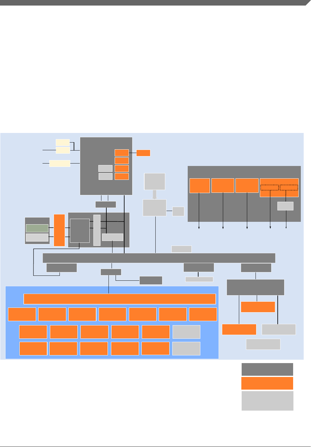
2. CSEc (Security) or EEPROM writes/erase will trigger error flags in HSRUN mode (112 MHz) because this use case is not
allowed to execute simultaneously. The device need to switch to RUN mode (80 Mhz) to execute CSEc (Security) or
EEPROM writes/erase.
3. On this device, NXP's system MPU implements the safety mechanisms to prevent masters from accessing restricted
memory regions. This system MPU provides memory protection at the level of the Crossbar Switch. Each Crossbar master
(Core, DMA, Ethernet) can be assigned different access rights to each protected memory region. The Arm M4 core version
in this family does not integrate the Arm Core MPU, which would concurrently monitor only core-initiated memory
accesses. In this document, the term MPU refers to NXP’s system MPU.
2.4 Block diagram
The following figure shows block diagram of the S32K14x product series.
Mux
Trace
port
Crossbar switch (AXBS-Lite)
eDMA
DMA
MUX
Core
Peripheral bus controller
CRC
WDOG
S1
M0 M1
DSP
NVIC
ITM
FPB
DWT
AWIC
SWJ-DP
TPIU
JTAG &
Serial Wire
Arm Cortex M4F
ICODE
DCODE
AHB-AP
PPB
System
M2
S2
GPIO
Mux
FPU Clock
SPLL
LPO
128 kHz
Async
512B
TCD
LPIT
LPI2C FlexIO
Flash memory
controller
Code flash
S0
Data flash
Low Power
Timer
12-bit ADC
TRGMUX
LPUART
LPSPI
FlexCAN FlexTimer
PDB
generation
LPIT
Peripherals present
on all S32K devices
Peripherals present
on selected S32K devices
Key:
Device architectural IP
on all S32K devices
S3
FIRC
48 MHz
M3
ENET
SAI
SOSC
8-40 MHz
(see the "Feature Comparison"
memory memory
4-40 MHz
QuadSPI
RTC
CMP
8-bit DAC
SIRC
8 MHz
FlexRAM/
SRAM
1: On this device, NXP’s system MPU implements the safety mechanisms to prevent masters from
accessing restricted memory regions. This system MPU provides memory protection at the
level of the Crossbar Switch. Each Crossbar master (Core, DMA, Ethernet) can be assigned
different access rights to each protected memory region. The Arm M4 core version in this family
does not integrate the Arm Core MPU, which would concurrently monitor only core-initiated memory
accesses. In this document, the term MPU refers to NXP’s system MPU.
2: For the device-specific sizes, see the "On-chip SRAM sizes" table in the "Memories and Memory Interfaces"
chapter of the S32K1xx Series Reference Manual.
section)
ERM
EWM
MCM
Lower region
Upper region
Main SRAM2
Code Cache
System MPU1
EIM
LMEM
controller
LMEM
QSPI
CSEc3
System MPU1System MPU1System MPU1
3: CSEc (Security) or EEPROM writes/erase will trigger error flags in HSRUN mode (112 MHz) because this
use case is not allowed to execute simultaneously. The device need to switch to RUN mode (80 MHz) to
execute CSEc (Security) or EEPROM writes/erase.
Figure 2-1. S32K14x product series block diagram
Chapter 2 Introduction
S32K1xx Series Reference Manual, Rev. 7, 04/2018
NXP Semiconductors 63
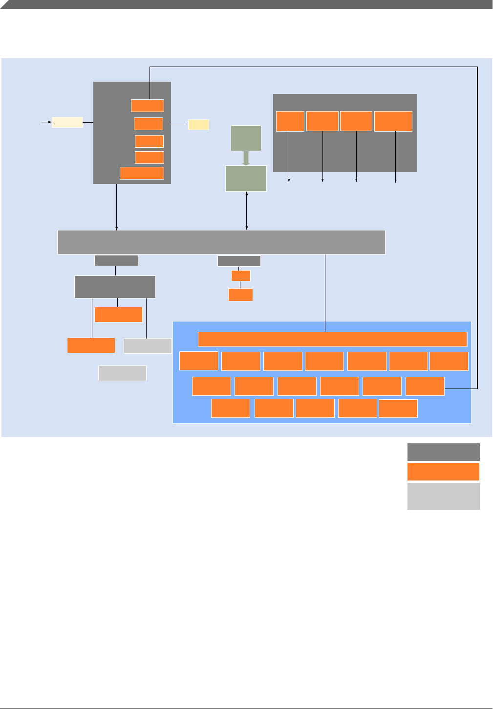
The following figure shows block diagram of the S32K11x product series.
Crossbar switch (AXBS-Lite)
eDMA
DMA
MUX
SW-DP
Unified Bus
Serial Wire
AHBLite
AHBLite
AWIC
S0 S1
Clock
LPO
128 kHz
generation
FIRC
48 MHz
SOSC
4-40 MHz
SIRC
8 MHz
Peripheral bus controller
CRC
WDOG
LPIT
LPI2C FlexIO Low Power
Timer
12-bit ADC
TRGMUX
LPUART
LPSPI
FlexCAN FlexTimer
PDB
LPIT
RTC
CMP
8-bit DAC
ERM
CMU GPIO
M0 M2
Flash memory
controller
Data flash
memory
FlexRAM/
SRAM2
Code flash
memory
EIM
SRAM2
IO PORT
NVIC
PPB
MTB+DWT
BPU
AHB-AP
Arm Cortex M0+
Peripherals present
on all S32K devices
Peripherals present
on selected S32K devices
Key:
Device architectural IP
on all S32K devices
(see the "Feature Comparison"
1: On this device, NXP’s system MPU implements the safety mechanisms to prevent masters from
accessing restricted memory regions. This system MPU provides memory protection at the
level of the Crossbar Switch. Crossbar master (Core, DMA) can be assigned
different access rights to each protected memory region. The Arm M0+ core version in this family
does not integrate the Arm Core MPU, which would concurrently monitor only core-initiated memory
accesses. In this document, the term MPU refers to NXP’s system MPU.
2: For the device-specific sizes, see the "On-chip SRAM sizes" table in the "Memories and Memory Interfaces"
chapter of the S32K1xx Series Reference Manual.
section)
S2
IO PORT
CSEc
System MPU1System MPU1
Figure 2-2. S32K11x product series block diagram
2.5 Feature comparison
The following figure summarizes the memory, peripherals and packaging options for the
S32K1xx devices. All devices which share a common package are pin-to-pin compatible.
Feature comparison
S32K1xx Series Reference Manual, Rev. 7, 04/2018
64 NXP Semiconductors

2 KB (up to 32 KB D-Flash)
EEPROM emulated by FlexRAM1
2 KB
FlexRAM (also available as system RAM)
Cache
25 KB
System RAM (including FlexRAM and MTB) 17 KB
Flash 128 KB 256 KB
2.7 - 5.5 V
Single supply voltage
HSRUN mode1
Watchdog 1x
Number of I/Os up to 43 up to 58
Memory Protection Unit (MPU)
K116 K118
Parameter
Peripheral speed
CRC module
IEEE-754 FPU
Arm® Cortex™-M0+
Core
1x
External Watchdog Monitor (EWM)
DMA
Crossbar
capable up to ASIL-B
ISO 26262
Cryptographic Services Engine (CSEc)1
48 MHz
Frequency
up to 48 MHz
Error Correcting Code (ECC)
1x
Low Power Timer (LPTMR)
1x
Low Power Interrupt Timer (LPIT)
LEGEND:
Not implemented
Available on the device
1 No write or erase access to Flash module, including Security (CSEc) and EEPROM commands, are allowed when
device is running at HSRUN mode (112MHz) or VLPR mode.
2 Available when EEEPROM, CSEc and Data Flash are not used. Else only up to 1,984 KB is available for Program Flash.
3 4 KB (up to 512 KB D-Flash as a part of 2 MB Flash). Up to 64 KB of flash is used as EEPROM backup and the remaining 448 KB
of the last 512 KB block can be used as Data flash or Program flash. See chapter FTFC for details.
4 Only for Boundary Scan Register
5 See Dimensions section for package drawings
Trigger mux (TRGMUX)
1x
Real Time Counter (RTC)
FlexTimer (16-bit counter) 8 channels 2x (16)
External memory interface
1x (16)
2x
1x
10/100 Mbps IEEE-1588 Ethernet MAC
12-bit SAR ADC (1 Msps each)
1x
FlexIO (8 pins configurable as UART, SPI, I2C, I2S)
Low Power I2C (LPI2C)
Low Power UART/LIN (LPUART)
(Supports LIN protocol versions 1.3, 2.0, 2.1, 2.2A, and SAE J2602)
SWD, MTB (1 KB), JTAG4
Debug & trace
NXP S32 Design Studio (GCC) + SDK,
IAR, GHS, Arm®, Lauterbach, iSystems
48-pin LQFP
64-pin LQFP
Packages5
Ecosystem
(IDE, compiler, debugger)
32-pin QFN
48-pin LQFP
FlexCAN
(CAN-FD ISO/CD 11898-1) 1x
(1x with FD)
1x 2x
Low Power SPI (LPSPI)
Serial Audio Interface (AC97, TDM, I2S)
Comparator with 8-bit DAC 1x
Programmable Delay Block (PDB) 1x
S32K11x S32K14x
K142 K144 K146 K148
1x
SWD, JTAG (ITM, SWV, SWO)
NXP S32 Design Studio (GCC) + SDK,
IAR, GHS, Arm®, Lauterbach, iSystems
64-pin LQFP
100-pin LQFP
64-pin LQFP
100-pin LQFP
100-pin MAPBGA
64-pin LQFP
100-pin MAPBGA
100-pin LQFP
144-pin LQFP
100-pin MAPBGA
144-pin LQFP
176-pin LQFP
SWD, JTAG
(ITM, SWV,
SWO), ETM
1x (64)
2x (16) 2x (24) 2x (32)
1x
2x 3x
1x 2x
2x
(1x with FD) 3x
(2x with FD) 3x
(3x with FD)
3x
(1x with FD)
2x 3x
2x
1x
1x (73) 1x (81)
80 MHz (RUN mode) or 112 MHz (HSRUN mode)1
1x
Arm® Cortex™-M4F
1x
capable up to ASIL-B
up to 112 MHz (HSRUN)
4 KB (up to 64 KB D-Flash)
4 KB
4 KB
32 KB 48/64 KB 96/128 KB 192/256 KB
-40oC to +85oC / +105oC / +125oC
256 KB 512 KB 1 MB 2 MB2
2.7 - 5.5 V
up to 89 up to 128 up to 156
1x
1x
1x
4x (32) 6x (48) 8x (64)
QuadSPI incl.
HyperBus™
2x
See footnote 3
MemoryAnalog Timer
Communication
IDEs
Other System
-40oC to +85oC / +105oC / +125oC
Ambient Operation Temperature (Ta)
1x (43) 1x (45)
1x (13)
FIRC CMU
Low power modes
Figure 2-3. S32K1xx product series comparison
Chapter 2 Introduction
S32K1xx Series Reference Manual, Rev. 7, 04/2018
NXP Semiconductors 65

2.6 Applications
The S32K1xx product series are the ideal choices for general purpose automotive
applications, which include but not limited to:
• Exterior and interior lighting
• HVAC
• Door/Window/Wiper/Seat controller
• BLDC/PMSM motor control
• Park assistant
• E-shifter
• TPMS
• Real time control in infotainment system
• Battery management system
• Human machine interface such as touch sense control
• Secured vehicle data transfer
• Safety controller
• Over the air update 4
Moreover, the 100 Mbit IEEE-1588 Ethernet MAC and Serial audio interface (AC97,
TDM, and I2S) on S32K148 make it fit perfectly for Ethernet connected edge nodes in
vehicle, and the audio streaming application.
In addition to automotive applications, the S32K1xx product series can also be used in
challenging environments found in industrial, automation, communications,
transportation, medical and A & D applications which need high level quality, reliability
and safety.
NOTE
• For safety aware and critical application, the user must
refer to S32K1xx Safety Manual and Using the S32K1xx
EEPROM Functionality application note available on
nxp.com for correct part operation requirements.
• See S32K1xx Safety Manual and Production Flash
Programming Best Practices for S32K1xx MCUs
application note available on nxp.com for correct part
operation and memory handling during programming of the
internal flash memory.
4. See S32K Architecture and Capabilities to Enable Over the Air Updates
Applications
S32K1xx Series Reference Manual, Rev. 7, 04/2018
66 NXP Semiconductors

2.7 Module functional categories
The modules on this device are grouped into functional categories. The following
sections describe the modules assigned to each category in more detail.
Table 2-2. Module functional categories
Module category Description
Arm® Cortex®-M4F core • 32-bit MCU core from Arm's Cortex-M class adding DSP instructions and
single-precision floating point unit based on Armv7 architecture
Arm® Cortex®-M0+ core • 32-bit MCU core from Arm’s Cortex-M class, implements the Armv6-M
architecture profile.
System • Miscellaneous control module (MCM)
• System integration module (SIM)
• Port Control and Interrupts (PORT)
• General purpose input/output controller (GPIO)
• Crossbar switch (AXBS-Lite)
• Peripheral bridge (AIPS-Lite)
• Trigger Mux Control (TRGMUX)
• Watchdog timer (WDOG)
• Cyclic Redundancy Check (CRC)
Clocking • Multiple clock generation options available from internally- and externally-
generated clocks
• System oscillator to provide clock source for the MCU
Memories • Internal memories include:
• Program flash memory
• FlexMemory
• FlexNVM
• FlexRAM
• SRAM
• Direct memory access (DMA) controller with multiplexer to increase available
DMA requests. DMA can now handle transfers in VLPS mode
Power Management Power management and mode controllers (PMC)
• Multiple power modes available based on high speed run, run, stop
Security • Error-correcting code (ECC) on Flash and SRAM memories
• 128-bit unique identification (ID) number
• System Memory Protection Unit (MPU) module
Safety Clock monitoring unit (CMU), for monitoring FIRC clock
Power Management Power management and mode controllers (PMC)
• Multiple power modes available based on high speed run, run, stop
Analog • High speed analog-to-digital converter (ADC)
• Comparator (CMP), containing 8 bit reference DAC
• Bandgap voltage reference (1V reference voltage)
Timers • Programmable delay block (PDB)
• FlexTimers
• Low-power periodic interrupt timer (LPIT)
• Low power timer (LPTMR)
• Independent real time clock (RTC)
Communications • Ethernet MAC with IEEE802.3-2002 standard.
• Low-power Serial peripheral interface (LPSPI)
Table continues on the next page...
Chapter 2 Introduction
S32K1xx Series Reference Manual, Rev. 7, 04/2018
NXP Semiconductors 67

Table 2-2. Module functional categories (continued)
Module category Description
• Low-power Inter-integrated circuit (LPI2C)
• Low-power UART (LPUART)
• Synchronous Audio Interface (SAI)/Integrated interchip sound (I2S)
• FlexIO
• FlexCAN
Debug • JTAG Controller (JTAGC)
2.7.1 Arm® Cortex®-M4F Core Modules
The following core modules are available on this device.
Table 2-3. Core modules
Module Description
Arm Cortex-M4F The Arm® Cortex®-M4F is the newest member of the Cortex M Series of
processors targeting microcontroller cores focused on very cost sensitive,
deterministic, interrupt driven environments. The Cortex M4F processor is based
on the Armv7 Architecture and Thumb®-2 ISA and is upward compatible with the
Cortex M3, Cortex M1, and Cortex M0 architectures. Cortex M4F improvements
include an Armv7 Thumb-2 DSP (ported from the Armv7-A/R profile architectures)
providing 32-bit instructions with SIMD (single instruction multiple data) DSP style
multiply-accumulates and saturating arithmetic.
Floating point unit (FPU) A single-precision floating point unit (FPU) that is compliant to the IEEE Standard
for Floating-Point Arithmetic (IEEE 754).
NVIC The Armv7-M exception model and nested-vectored interrupt controller (NVIC)
implement a relocatable vector table supporting many external interrupts, a single
non-maskable interrupt (NMI), and priority levels.
The NVIC replaces shadow registers with equivalent system and simplified
programmability. The NVIC contains the address of the function to execute for a
particular handler. The address is fetched via the instruction port allowing parallel
register stacking and look-up. The first sixteen entries are allocated to Arm internal
sources, with the others mapping to MCU-defined interrupts.
AWIC The primary function of the Asynchronous Wake-up Interrupt Controller (AWIC) is
to detect asynchronous wake-up events in stop modes and then signal to clock
control logic to resume system clocking. After clock restart, the NVIC observes the
pending interrupt and performs the normal interrupt or event processing.
Debug interfaces Most of the debug capability on this device is based on the Arm CoreSight™
architecture. Following debug interfaces are supported:
• Serial wire IEEE 1149.1 JTAG debug Port (SWJ-DP), with 2 pin serial wire
debug (SWD) for external debugger
• Debug Watchpoint and Trace (DWT), with four configurable comparators as
hardware watchpoints
• Serial wire output (SWO)-synchronous trace data support
• Instrumentation Trace Macrocell (ITM) with software and hardware trace,
plus time stamping
• Flash Patch and Breakpoints (FPB) with ability to patch code and data from
code space to system space
Module functional categories
S32K1xx Series Reference Manual, Rev. 7, 04/2018
68 NXP Semiconductors

Table 2-3. Core modules
Module Description
• Serial Wire Viewer (SWV): A trace capability providing displays of reads,
writes, exceptions, PC Samples and printf.
• Supports 4 pin trace interface
2.7.2 Arm Cortex-M0+ Core Modules
The following core modules are available on this device.
Table 2-4. Core modules
Module Description
Arm Cortex-M0+ The Arm® Cortex™-M0+processor is a configurable, multistage, 32-bit RISC
processor. It has an AMBA AHB-Lite interface and includes an NVIC component. It
also has optional hardware debug, single-cycle I/O interfacing, and memory-
protection functionality. The processor can execute Thumb code and is compatible
with other Cortex-M profile processors.
NVIC NVIC features up to 32 external interrupt inputs, each with four levels of priority. It
implements optional relocation of the vector table.
It features dedicated Non-Maskable Interrupt (NMI) input, supprts optional Wake-
up Interrupt Controller (WIC), providing ultra-low power sleep mode support.
AWIC The primary function of the Asynchronous Wake-up Interrupt Controller (AWIC) is
to detect asynchronous wake-up events in stop modes and signal to clock control
logic to resume system clocking. After clock restart, the NVIC observes the
pending interrupt and performs the normal interrupt or event processing.
Single-cycle I/O Port For high-speed, single-cycle access to peripherals, the Cortex-M0+ processor
implements a dedicated single-cycle I/O port.
Debug interfaces Most of this device's debug is based on the Arm CoreSight™ architecture. One
debug interfaces are supported:
• Serial Wire Debug (SWD)
• Micro Trace Buffer (MTB)
2.7.3 System modules
The following system modules are available on this device.
Table 2-5. System modules
Module Description
Miscellaneous control module (MCM) The MCM includes miscellaneous control logic for Core and System modules.
System integration module (SIM) The SIM includes miscellaneous device configuration and status registers.
Table continues on the next page...
Chapter 2 Introduction
S32K1xx Series Reference Manual, Rev. 7, 04/2018
NXP Semiconductors 69

Table 2-5. System modules (continued)
Module Description
PORT The Port Control and Interrupt (PORT) module provides support for port control,
digital filtering, and external interrupt functions.
GPIO The general-purpose input and output (GPIO) module communicates to the
processor core via a zero wait state interface for maximum pin performance. The
GPIO registers support 8-bit, 16-bit or 32-bit accesses.
Crossbar switch (AXBS-Lite) The AXBS-Lite connects bus masters and bus slaves, allowing all bus masters to
access different bus slaves simultaneously and providing arbitration among the bus
masters when they access the same slave.
System Memory protection unit (MPU) The system MPU provides memory protection and task isolation. It concurrently
monitors all bus master transactions for the slave connections.
Peripheral bridge (AIPS-Lite) The AIPS-Lite converts the crossbar switch interface to an interface that allows
access to a majority of peripherals on the device.
Direct memory access multiplexer
(DMAMUX)
The DMAMUX selects from many DMA requests down to a smaller number for the
DMA controller.
enhanced Direct Memory Access
controller (eDMA)
The eDMA provides programmable channels with transfer control descriptors for
data movement via dual-address transfers for 8-bit, 16-bit, 32-bit, 16-byte and 32-
byte data values.
TRGMUX The trigger multiplexer (TRGMUX) module allows software to configure the trigger
sources for various peripherals.
External watchdog monitor (EWM) The EWM is a redundant mechanism to the software watchdog module that
monitors both internal and external system operation for fail conditions.
Software watchdog (WDOG) The WDOG monitors internal system operation and forces a reset in case of
failure. It can run from an independent 128 kHz low power oscillator with a
programmable refresh window to detect deviations in program flow or system
frequency.
CRC Hardware CRC generator circuit using 16/32-bit shift register. Error detection for all
single, double, odd, and most multi-bit errors, programmable initial seed value, and
optional feature to transpose input data and CRC result via transpose register.
2.7.4 Memories and memory interfaces
The following memories and memory interfaces are available on this device.
Table 2-6. Memories and memory interfaces
Module Description
Local memory controller(LMEM) Manages simultaneous accesses to system RAM by multiple master peripherals
and core. Also provide cache control, which improves system performance by
providing single-cycle access to the instruction and data pipelines.
Miscellaneous System Control Module
(MSCM)
The Miscellaneous System Control Module (MSCM) contains CPU configuration
registers and on-chip memory controller registers.
Flash memory • Program flash memory — non-volatile flash memory that can execute
program code
• FlexMemory — encompasses the following memory types:
Table continues on the next page...
Module functional categories
S32K1xx Series Reference Manual, Rev. 7, 04/2018
70 NXP Semiconductors

Table 2-6. Memories and memory interfaces (continued)
Module Description
• FlexNVM — Non-volatile flash memory that can execute program
code, store data, or backup emulated EEPROM data
• FlexRAM — RAM memory that can be used as traditional SRAM or as
high-endurance emulated EEPROM storage, and also accelerates
flash programming
QuadSPI The Quad Serial Peripheral Interface (QuadSPI) block acts as an interface to
external serial flash device. It supports SDR and HyperRAM modes up to 4 and 8
bidirectional data lines respectively.
Flash memory controller Manages the interface between the device and the on-chip flash memory.
SRAM Internal system RAM.
2.7.5 Power Management
The following modules are available on this device for power management and system
power modes control:
Table 2-7. Power Management modules
Module Description
PMC The PMC contains the internal voltage regulator, power on reset (POR) and the
low voltage detect (LVD) system.
SMC The System Mode Controller (SMC) is responsible for sequencing the system into
and out of all low-power Stop and Run modes.
2.7.6 Clocking
The following clock modules are available on this device.
Table 2-8. Clock modules
Module Description
System clock generator (SCG) The SCG provides several clock sources for the MCU that include:
• Phase-locked loop (PLL) — Voltage-controlled oscillator (VCO)
• Fast internal reference clock (FIRC) — An internally-generated 48 MHz
clock, which can be used as a clock source for other on-chip peripherals
• Slow internal reference clock (SIRC) — An internally-generated 8 MHz clock,
which can be used as a clock source for other on-chip peripherals
• System oscillator (OSC) — The system oscillator, in conjunction with an
external crystal or resonator, generates a reference clock for the MCU
Low Power Oscillator (LPO) An internally-generated low power clock with typical frequency of 128 kHz, which
can be used as clock source for modules operational in low power modes.
Peripheral Clock Control (PCC) Controls the clock selection for most modules.
Chapter 2 Introduction
S32K1xx Series Reference Manual, Rev. 7, 04/2018
NXP Semiconductors 71

2.7.7 Analog modules
The following analog modules are available on this device:
Table 2-9. Analog modules
Module Description
12-bit analog-to-digital converters (ADC) 12-bit successive-approximation ADC
Analog comparators (CMP) Compares two analog input voltages across the full range of the supply voltage.
8-bit digital-to-analog converters (DAC)
within CMP
256-tap resistor ladder network which provides a selectable voltage reference for
applications where a voltage reference is needed.
2.7.8 Timer modules
The following timer modules are available on this device:
Table 2-10. Timer modules
Module Description
Programmable delay block (PDB) • 16-bit resolution
• 3-bit prescaler
• Positive transition of trigger event signal initiates the counter
• Supports multiple triggered delay output signals, each with an independently-
controlled delay from the trigger event
• Continuous-pulse output or single-shot mode supported, each output is
independently enabled, with possible trigger events
• Supports bypass mode
• Supports DMA
Flexible timer module (FTM) • Selectable FTM source clock, programmable prescaler
• 16-bit counter supporting free-running or initial/final value, and counting is up
or up-down
• Input capture, output compare, and edge-aligned and center-aligned PWM
modes
• Operation of FTM channels as pairs with equal outputs, pairs with
complementary outputs, or independent channels with independent outputs
• Deadtime insertion is available for each complementary pair
• Generation of hardware triggers
• Software control of PWM outputs
• Up to 4 fault inputs for global fault control
• Configurable channel polarity
• Programmable interrupt on input capture, reference compare, overflowed
counter, or detected fault condition and reload opportunity.
• Quadrature decoder with input filters, relative position counting, and interrupt
on position count or capture of position count on external event
• DMA support for FTM events
Low-power periodic interrupt timer
(LPIT)
• Four general purpose interrupt timers
• Interrupt timers for triggering ADC conversions
Table continues on the next page...
Module functional categories
S32K1xx Series Reference Manual, Rev. 7, 04/2018
72 NXP Semiconductors

Table 2-10. Timer modules (continued)
Module Description
• 32-bit counter resolution
• The counter is clocked by an asynchronous clock that can remain enabled in
low power modes.
• DMA support
• Supports chaining of Timer channels
Low power timer (LPTMR) • Selectable clock for prescaler/glitch filter of 128 kHz (internal LPO), or
internal reference clock
• Configurable glitch filter or prescaler with 16-bit counter
• 16-bit time or pulse counter with compare
• Interrupt generated on Timer Compare
• Hardware trigger generated on Timer Compare
Real-time clock (RTC) • 32-bit seconds counter with 32-bit alarm
• 16-bit prescaler with compensation that can correct errors between 0.12 ppm
and 3906 ppm
2.7.9 Communication interfaces
The following communication interfaces are available on this device:
Table 2-11. Communication modules
Module Description
Low-power Serial peripheral interface
(LPSPI)
Synchronous serial bus for communication to an external device. LPSPI optionally
remains functional in low power modes.
Low-power Inter-integrated circuit
(LPI2C)
Allows communication between a number of devices. Also supports the System
Management Bus (SMBus) Specification, version 2. LPI2C optionally remains
functional in low power modes.
Low-power Universal asynchronous
receiver/transmitters (LPUART)
Asynchronous serial bus communication interface, supporting LIN master and
slave operation. LPUART optionally remains functional in low power modes.
SAI/I2S The I2S (or I2S) module provides a synchronous audio interface (SAI) that
supports fullduplex serial interfaces with frame synchronization such as I2S, AC97,
TDM, and codec/DSP interfaces.
ENET The core implements a dual-speed 10/100-Mbit/s Ethernet MAC compliant with the
IEEE802.3-2002 standard. The MAC layer provides compatibility with half- or
fullduplex 10/100-Mbit/s Ethernet LANs.
FlexCAN The FlexCAN module is a communication controller implementing the CAN
protocol according to the ISO 11898-1 standard and CAN 2.0 B protocol
specifications.
2.7.10 Debug modules
The following Debug modules are available on this device:
Chapter 2 Introduction
S32K1xx Series Reference Manual, Rev. 7, 04/2018
NXP Semiconductors 73

Table 2-12. Debug modules
Module Description
JTAGC The JTAGC block provides the means to test chip functionality and connectivity
while remaining transparent to system logic when not in test mode. Testing is
performed via a boundary scan technique, as defined in the IEEE 1149.1-2001
standard. All data input to and output from the JTAGC block is communicated in
serial format.
Module functional categories
S32K1xx Series Reference Manual, Rev. 7, 04/2018
74 NXP Semiconductors

Chapter 3
Memory Map
3.1 Introduction
This chip contains various memories and memory-mapped peripherals that are located in
one 32-bit contiguous memory space. This chapter describes the memory and peripheral
locations within that memory space.
Details about the memory map appear in the spreadsheet that is attached to this
document: S32K1xx_memory_map.xlsx. To access this spreadsheet, view the document's
list of attachments.
3.2 SRAM memory map
3.2.1 S32K14x: SRAM memory map
The on-chip RAM is split in two regions: SRAM_L and SRAM_U. The RAM is
implemented such that the SRAM_L and SRAM_U ranges form a contiguous block in
the memory map. See S32K1xx_memory_map.xlsx attached to this document for details.
Accesses to the SRAM_L and SRAM_U memory ranges outside the amount of RAM on
the chip causes the bus cycle to be terminated with an error followed by the appropriate
response in the requesting bus master.
3.2.2 S32K11x: SRAM memory map
In S32K11x on-chip RAM can be used in following applications:
• Safety critical applications: SRAM_U can be used, which starts from 2000_0000
• Non-safety critical applications: SRAM_U along with 1 KB MTB can be used
S32K1xx Series Reference Manual, Rev. 7, 04/2018
NXP Semiconductors 75

NOTE
CM0+ architecture implements single RAM controller, hence
SRAM_U and MTB are referred as single contiguous memory
regions. MTB in S32K11x is present at the same location as
SRAM_L in S32K14x.
See S32K1xx_memory_map.xlsx attached to this document for details. Accesses to the
memory ranges outside the amount of RAM on the chip causes the bus cycle to be
terminated with an error followed by the appropriate response in the requesting bus
master.
3.3 Flash memory map
The various flash memories and the flash memory registers are located at different base
addresses as shown in the following figure. The base address for each is specified in the
S32K1xx_memory_map.xlsx file attached to this document.
Program flash
Flash memory configuration field
FlexNVM base address
Program flash memory base address
Flash memory base address
Registers
FlexNVM
FlexRAM
FlexRAM base address
memory
Figure 3-1. Flash memory map
3.4 Peripheral bridge (AIPS-Lite) memory map
The peripheral memory map is accessible via a crossbar slave port.
There are three regions associated with peripheral space, as shown in the following table.
Flash memory map
S32K1xx Series Reference Manual, Rev. 7, 04/2018
76 NXP Semiconductors

Table 3-1. Regions associated with peripheral space
Address space Region description
0x4000_0000–0x4001_FFFF A 128 KB region, partitioned as 32 spaces, each 4 KB in size and reserved for on-
platform peripheral devices. AIPS-Lite generates unique module enables for all 32
spaces.
0x4002_0000–0x4007_FFFF A 384 KB region, partitioned as 96 spaces, each 4 KB in size and reserved for off-
platform modules. AIPS-Lite generates unique module enables for all 96 spaces.
0x400F_F000 A 4 KB region for accessing the GPIO module. This block is connected to the
AMBA bus via the port splitter and provides direct master access without incurring
wait states associated with accesses via the AIPS-Lite modules. The GPIO is
implemented only in the upper space of this region (4 KB beginning at
0x400F_F000).
Modules that are disabled via their clock gate control bits in the PCC/SIM registers
disable the associated AIPS-Lite slots. Access to any address within an unimplemented or
disabled peripheral bridge slot results in a transfer error termination.
NOTE
While trying to access memory map region of unavailable
feature (See SIM_SDID[FEATURES]) with corresponding
module clock enabled through PCC CGC bit, there will not be
any transfer error termination.
3.4.1 Read-after-write sequence and required serialization of
memory operations
In some situations, a write to a peripheral must be completed fully before a subsequent
action can occur. Examples of such situations include:
• Exiting an interrupt service routine (ISR)
• Changing a mode
• Configuring a function
In these situations, the application software must perform a read-after-write sequence to
guarantee the required serialization of the memory operations, as shown in the following
table.
Table 3-2. Read-after-write sequence to guarantee required serialization of memory
operations
Step Action
1 Write the peripheral register.
2 Read the written peripheral register to verify the write.
3 Continue with subsequent operations.
Chapter 3 Memory Map
S32K1xx Series Reference Manual, Rev. 7, 04/2018
NXP Semiconductors 77

NOTE
In S32K14x series of devices, one factor contributing to these
situations is processor write buffering. The processor
architecture has a programmable configuration field to disable
write buffering: ACTLR[DISDEFWBUF]. (For details see
Arm® Cortex® M4 Processor Technical Reference Manual,
Revision r0p1, at http://arm.com ). However, disabling buffered
writes is likely to degrade system performance much more than
simply performing the required memory serialization for the
situations that truly require it.
3.5 Private Peripheral Bus (PPB) memory map
The PPB is part of the defined Arm bus architecture and provides access to select
processor-local modules. These resources are only accessible from the core; other system
masters do not have access to them.
Table 3-3. PPB memory map for CM4
System 32-bit address range Resource
0xE000_0000–0xE000_0FFF Instrumentation Trace Macrocell (ITM)
0xE000_1000–0xE000_1FFF Data Watchpoint and Trace (DWT)
0xE000_2000–0xE000_2FFF Flash Patch and Breakpoint (FPB)
0xE000_3000–0xE000_DFFF Reserved
0xE000_E000–0xE000_EFFF System Control Space (SCS) (for NVIC and FPU
0xE000_F000–0xE003_FFFF Reserved
0xE004_0000–0xE004_0FFF Trace Port Interface Unit (TPIU)
0xE004_1000–0xE004_1FFF Reserved
0xE004_2000–0xE004_2FFF Reserved
0xE004_3000–0xE004_3FFF Reserved
0xE004_4000–0xE007_FFFF Reserved
0xE008_0000–0xE008_0FFF Miscellaneous Control Module (MCM)
0xE008_1000–0xE008_1FFF Reserved
0xE008_2000–0xE008_2FFF Cache Controller (LMEM)
0xE008_3000–0xE00F_EFFF Reserved
0xE00F_F000–0xE00F_FFFF Arm Core ROM Table1 - allows auto-detection of debug components
1. The Arm Core ROM table is optionally required by Arm CoreSight debug infrastructure to discover the components on the
chip. This ROM table has no any relationship with the MCU Boot ROM.
Private Peripheral Bus (PPB) memory map
S32K1xx Series Reference Manual, Rev. 7, 04/2018
78 NXP Semiconductors

Table 3-4. PPB memory map for CM0+
System 32-bit address range Resource
0xE000_0000–0xE000_0FFF Reserved 1
0xE000_1000–0xE000_1FFF Data Watchpoint and Trace (DWT)
0xE000_2000–0xE000_2FFF Arm Core ROM Table
0xE000_3000–0xE000_DFFF Reserved1
0xE000_E000–0xE000_EFFF System Control Space (SCS) (for NVIC)
0xE000_F000–0xE003_FFFF Reserved1
0xE004_0000–0xE004_0FFF Reserved1
0xE004_1000–0xE004_1FFF Reserved1
0xE004_2000–0xE004_2FFF Reserved1
0xE004_3000–0xE004_3FFF Reserved1
0xE004_4000–0xE007_FFFF Reserved1
0xE008_0000–0xE008_0FFF Reserved1
0xE008_1000–0xE008_1FFF Reserved1
0xE008_2000–0xE008_2FFF Reserved1
0xE008_3000–0xE00F_EFFF Reserved1
0xE00F_F000–0xE00F_FFFF Reserved1
0xE010_0000-0xEFFF_FFFF Reserved1
1. Reserved area return transfer error. Reserved is Unknown/Should be 0. Software must not rely on reading as all 0s, and it
must treat the value as if it is unknown.
3.6 Aliased bit-band regions for CM4 core
The SRAM_U, AIPS-Lite, and general purpose input/output (GPIO) module resources
reside in the Cortex-M4F processor bit-band regions.
The processor also includes two 32 MB aliased bit-band regions associated with the two
1 MB bit-band spaces. Each 32-bit location in the 32 MB space maps to an individual bit
in the bit-band region. A 32-bit write in the alias region has the same effect as a read-
modify-write operation on the targeted bit in the bit-band region.
Bit 0 of the value written to the alias region determines what value is written to the target
bit:
• Writing a value with bit 0 set writes a 1 to the target bit.
• Writing a value with bit 0 clear writes a 0 to the target bit.
A 32-bit read in the alias region returns either:
• a value of 0x0000_0000 to indicate the target bit is clear
• a value of 0x0000_0001 to indicate the target bit is set
Chapter 3 Memory Map
S32K1xx Series Reference Manual, Rev. 7, 04/2018
NXP Semiconductors 79

31 0 0
31
Bit-band region Alias bit-band region
1 MB
32 MB
Figure 3-2. Alias bit-band mapping
NOTE
Each bit in a bit-band region has an equivalent bit that can be
manipulated through bit 0 in a corresponding long word in the
alias bit-band region.
NOTE
Do not use bit banding for w1c status bits.
CAUTION
The S32K product series and the software drivers support bit-
banding, but Arm no longer promotes its usage. Therefore, we
recommend that bit-banding should not be used.
Aliased bit-band regions for CM4 core
S32K1xx Series Reference Manual, Rev. 7, 04/2018
80 NXP Semiconductors
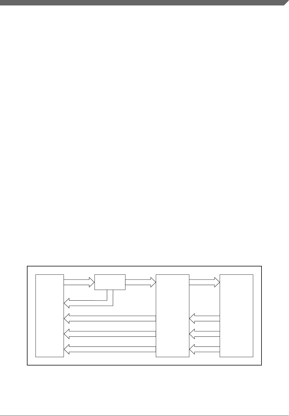
Chapter 4
Signal Multiplexing and Pin Assignment
4.1 Introduction
The signal multiplexing enables the sharing of single pad for multiple functions.
The signal multiplexing unit comprises of control signals from GPIO, PORT and pad
interface logic. The signal multiplexing unit consists of several individual sub-units, each
handling the signal multiplexing of one pad.
The Port Control block controls the module specific pad settings (pull up etc) and the
signal present on the external pin. See PORT_PCR for the description of control signals.
For reset values per port, see IO Signal Description Input Multiplexing sheet(s) attached
to the Reference Manual.
4.2 Functional description
The signal multiplexing architectural implementation is as shown in the following figure.
ibe
GPIO
ind
Functional
Modules/
Peripherals
obe
Pad controls
do
ind
ibe
obe
do
ind
Padring Signal
Multiplexing
Unit
Figure 4-1. Signal Multiplexing
S32K1xx Series Reference Manual, Rev. 7, 04/2018
NXP Semiconductors 81
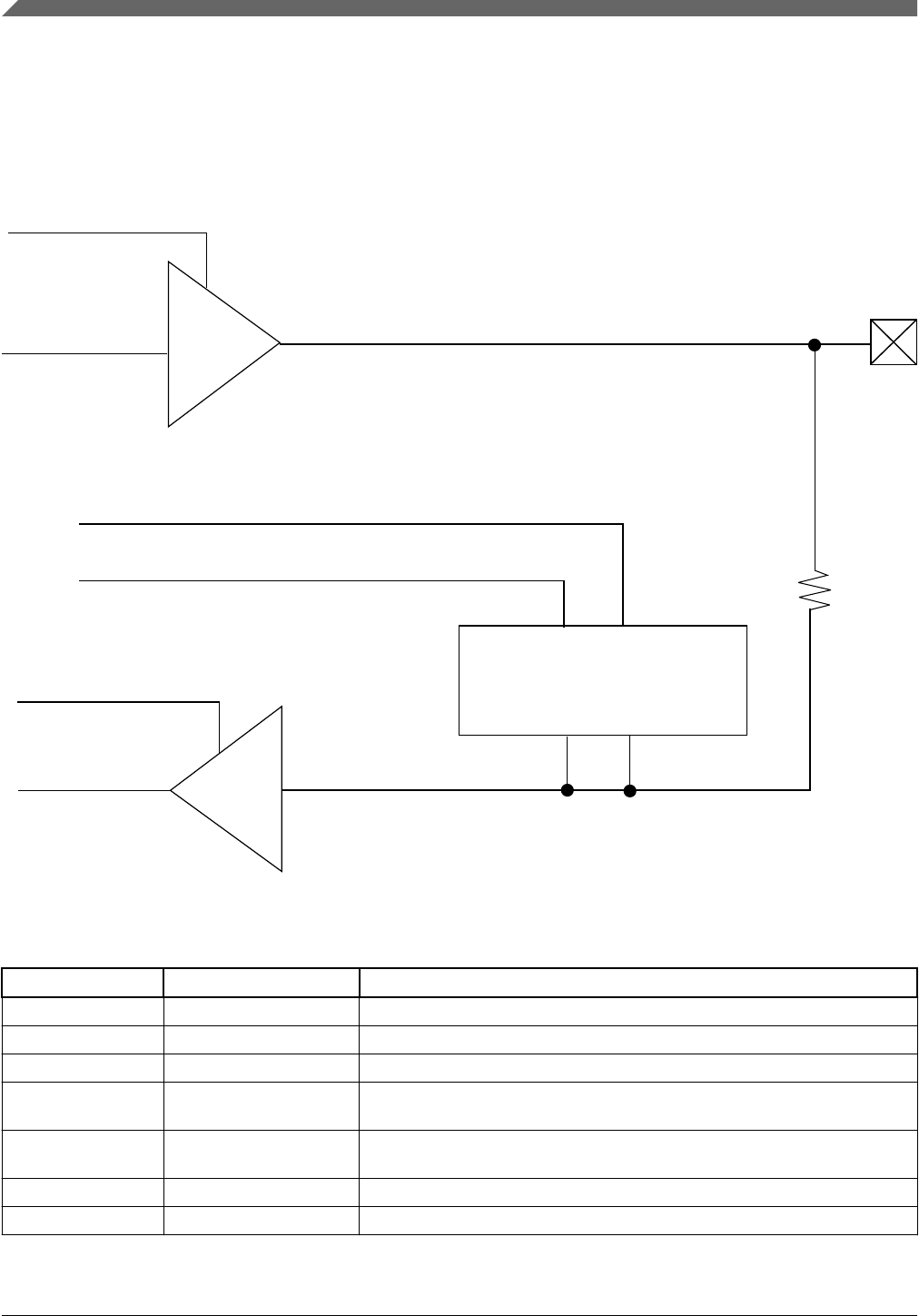
4.3 Pad description
Following figure shows the basic representation of a GPIO Pad.
obe
do
pue
pus
ibe
ind
Pull logic
Input
Receiver
Output
Driver
Pad
Figure 4-2. GPIO pad representation
Table 4-1. Pad Signal description
Signal name Direction Descriprtion
pad I/O I/O to external world
do I Data coming from the core into the pad
obe I Enable output driver
pue I 0: Disable internal pullup or pulldown resistor 1: Enable internal pullup or
pulldown resistor
pus I 0: Enable internal pulldown resistor if pue is set 1: Enable internal pullup
resistor if pue is set
ibe I Enable input receiver
ind O Data coming out of the pad into the core
Pad description
S32K1xx Series Reference Manual, Rev. 7, 04/2018
82 NXP Semiconductors

Table 4-2. Truth table
obe do pad Description
0 X Z Output buffer disabled, pad hi-Z (If not configured as input)
1 0/1 0/1 Output buffer enable, pad = do
pue pus pad Description
0 X - Weak pull disabled. Pad retains previous state
1 0 0 Weak pull down enabled
1 1 1 Weak pull up enabled
ibe pad ind Description
0 X 0 Input buffer disabled, ind gets low
1 0/1 0/1 Input buffer enabled, ind = pad
NOTE
The device does not support open drain on all the pins. Only
pins that are configured for a protocol that requires open-drain
(e.g;, LPI2C, LPUART single-wire) will work in open-drain
mode.
4.4 Default pad state
The default pad configurations out of reset are as follows. For PTA4, PTA5, PTC4 and
PTC5, the default configurations are as per protocol specifications/requirements.
Table 4-3. Default pad configurations
Pin Default
function
Default pad
state1ibe obe pue pus
PTA4 JTAG_TMS Weak pull-up
enabled
1011
PTA5 2RESET_b Weak pull-up
enabled
1011
PTC4 JTAG_TCK Weak pull-down
enabled
1010
PTC5 JTAG_TDI Weak pull-up
enabled
1011
Others Disabled High impedance 0 0 0 0
Chapter 4 Signal Multiplexing and Pin Assignment
S32K1xx Series Reference Manual, Rev. 7, 04/2018
NXP Semiconductors 83
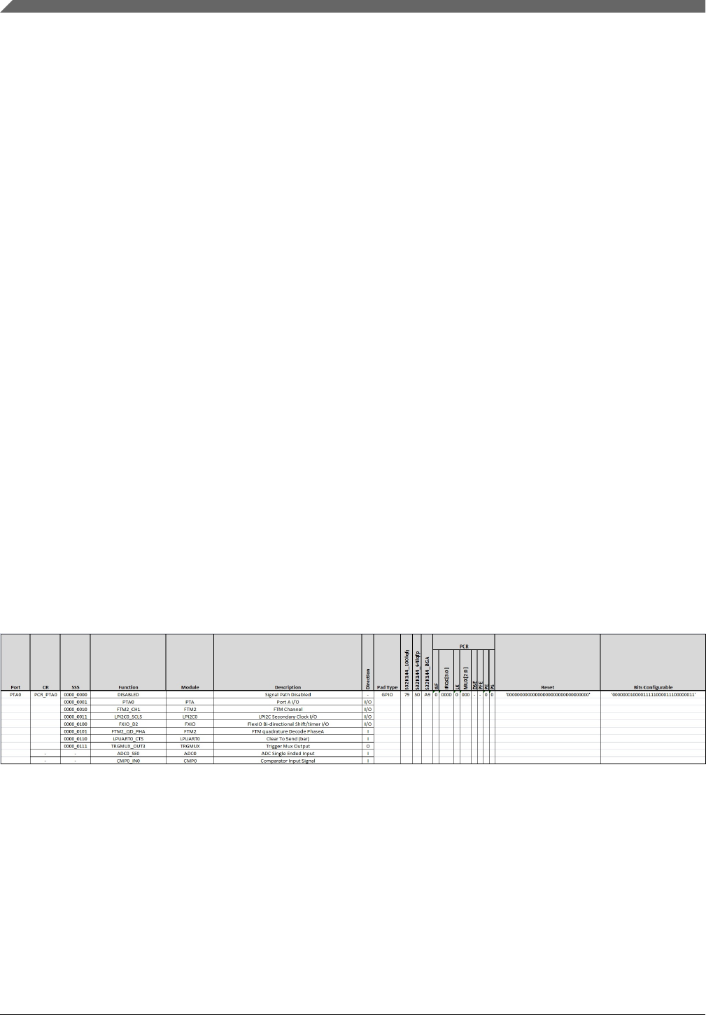
1. The IO pad states are undefined until VDD rises sufficiently to enable the POR circuits. The level at which this occurs will
vary from device to device, but for reference it is approximately 700 mV. After POR circuits are enabled, the IO pad states
are high impedance with weak pull devices disabled until POR release.
2. While in reset, the pin behavior is same apart from reset pin. Chip drives pad low via obe=1, pue=0, till reset sequence is
complete to indicate reset to off-chip connected devices.
4.5 Signal Multiplexing sheet
IO Signal Description Input Multiplexing sheet(s) attached to the Reference Manual
contains information on pins/balls of this device.
The 'IO Signal Table' and 'Input Muxing' tabs in the sheet correspond to the signal
multiplexing information. The 'IO Signal Table' consists of all the pin muxing details and
the 'Input Muxing' specifies the priority for the input muxing where an input path is
driven by more than one pad.
S32K1xx variant specific IO Signal Description Input Multiplexing sheets attached to the
Reference Manual contains information about the pins/balls of the particular variant.
Module functionality is dependent on the availability of functional pins in a particular
package. For example LPI2C HREQ pin is not available in 48-LQFP and 32-QFN
package.
4.5.1 IO Signal Table
Following is an example snippet of IO Signal Table. For selecting any functionality, the
pad PCR register (refer to PORT_PCRn) needs to be configured accordingly.
Figure 4-3. IO signal table snippet
The columns of the above figure are described below:
• Port: This field in IO Signal Table specifies the PAD names of the device.
• CR(Control Register): This field specifies the name of PCR corresponding to the Port
field. On this device there are five PORT instances, namely, PTA, PTB, PTC, PTD
and PTE. Each pad has a corresponding Control Register, referred to as PCR_PTXn
Signal Multiplexing sheet
S32K1xx Series Reference Manual, Rev. 7, 04/2018
84 NXP Semiconductors

in the IO Signal Table, where X refers to PORT instance and n refers to
corresponding pin of that PORT instance. Refer PORT_PCR for description of PCR
fields.
• SSS: This field specifies the ALT mode of operation as per PCR[Mux_mode]. Not
all pins support all pin muxing slots. Unimplemented pin muxing slots are reserved.
The corresponding pin is configured in the following pin muxing slot as follows:
• 000: Alternative 0 (Signal path disabled)
• 001: Alternative 1 (GPIO)
• 010: Alternative 2 (chip-specific)
• 011: Alternative 3 (chip-specific)
• 100: Alternative 4 (chip-specific)
• 101: Alternative 5 (chip-specific)
• 110: Alternative 6 (chip-specific)
• 111: Alternative 7 (chip-specific)
The analog functionalities are specified with '-' in this field. Here ADC_SE0 and
CMP_IN0 represent analog functions.
By default, ALT0 mode (configured by PTXn_PCR[SSS] as 3’b000)
corresponds to disabled functionality and pad represents disabled (high-
impedance) state. In case if the pad consists of analog functions, the ALT0 mode
corresponds to analog functionality once the analog module is configured to
enable corresponding channel/input.
For example, PTA0 supports ADC0 channel 0 and CMP channel 0. By default
the pad is disabled. After ADC0 is configured to enable channel0 using
ADC0_SC1n[ADCH], the pad functions as ADC input channel. Alternatively if
CMP is configured to enable channel 0 using CMP_C1[PSEL] or
CMP_C1[MSEL], the pad functions as CMP input channel. The software must
ensure to enable only one function at a time.
• Function: This field specifies the functionality of the pad as per the corresponding
ALT mode specified by SSS field.
• Module: The Module field contains the module which is governing the pad for the
ALT mode.
• Description: This field mentions a short description of pad functionality.
• Direction: This field specifies the direction (Input, Output or Inout) of the pad for the
concerned functionality.
• The next columns specify the pin number in the supported packages for the device.
• PCR: This field specifies the default PCR value for corresponding pad. Refer
PORT_PCR for description of PCR fields.
Chapter 4 Signal Multiplexing and Pin Assignment
S32K1xx Series Reference Manual, Rev. 7, 04/2018
NXP Semiconductors 85
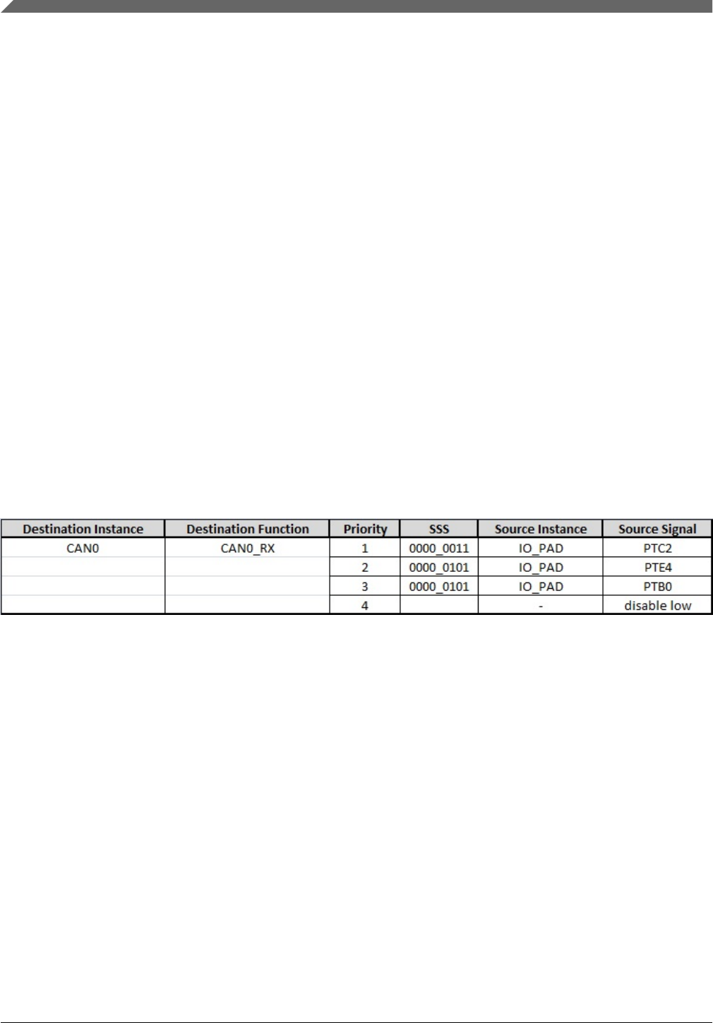
• The next two columns specify the reset value and the configurable bit fields of PCR
corresponding to pad.
• Pad Type: This field mentions the pad type of the corresponding pad.
• GPIO: General Purpose IO Pad (Standard)
• GPIO-HD: General Purpose IO Pad that support high drive functionality
(Strong)
• GPIO-FAST: General Purpose IO Pad that support High Speed (applicable for
S32K148 only)
NOTE
If oscillator is enabled then enabling the GPIO or LPI2C
function for EXTAL/XTAL pins can lead to device damage.
This must be avoided by software.
4.5.2 Input muxing table
As the same function can be multiplexed to several pads by configuring their respective
PCRs, there is priority input muxing. In case of same input being driven from multiple
pads, the one with highest priority (1 being the highest) will drive the input. Following is
a snippet of Input Muxing Table.
Figure 4-4. Input muxing table snippet
The columns of the figure are briefly described below:
• Destination Instance: This field contains the instance name of the input path to where
the signal will propagate from padring.
• Destination Function: This field mentions the function name of the input path.
• Priority: This field specifies the priority of the path. Priority level 1 is highest and it
decreases onwards.
• SSS: This field specifies the PCR[Mux_mode] value corresponding to the pad
specified in source signal column. A blank is mentioned for the default source when
none pad is driving the input path.
• Source Instance: This field specifies the source pad type. A blank is mentioned for
the default source when none pad is driving the input path.
• Source Signal: This field mentions the pad name. A ‘disable low’/’disable high’
specifies the signal behavior when none of the pads are driving the input path.
Signal Multiplexing sheet
S32K1xx Series Reference Manual, Rev. 7, 04/2018
86 NXP Semiconductors

4.6 Pinout diagrams
See IO Signal Description Input Multiplexing sheet(s) attached to the Reference Manual
for pinout diagrams corresponding to available packages.
Chapter 4 Signal Multiplexing and Pin Assignment
S32K1xx Series Reference Manual, Rev. 7, 04/2018
NXP Semiconductors 87

Pinout diagrams
S32K1xx Series Reference Manual, Rev. 7, 04/2018
88 NXP Semiconductors

Chapter 5
Security Overview
5.1 Introduction
All chips of this S32K1xx product series have a comprehensive set of customer-
configurable security features designed to protect code and data from unauthorized
access.
5.2 Device security
Flash memory security is available to both CSEc and non-CSEc parts. SIM_SDID[7]
indicates whether CSEc is available on your device.
Both CSEc and non CSEc users need to run PGMPART command to configure the Key
Size for the device. For more information, see Program Partition command. This process
involves configuring a number of user keys. For non CSEc users, Key Size will be 00.
• The total size of EEERAM is reduced by the space required to store the user keys.
(See Introduction chapter for available EEERAM.)
• The user key space effectively becomes un-addressable space in the EEERAM.
• For non-CSEc parts and CSEc parts with key size=00, CSEc_PRAM access is not
guaranteed.
5.2.1 Flash memory security
The flash memory module provides security information to the MCU based on the state
held by the FSEC[SEC] field. The MCU, in turn, confirms the security request and limits
access to flash memory resources. During reset, the flash memory module initializes the
FSEC register using data read from the security byte of the flash memory configuration
field.
S32K1xx Series Reference Manual, Rev. 7, 04/2018
NXP Semiconductors 89

NOTE
The security features apply only to external accesses via debug.
CPU accesses to the flash memory are not affected by the status
of FSEC.
In the unsecured state, all flash memory commands are available to the programming
interfaces (SWD (Serial Wire Debug) and JTAG (Joint Test Access Group)), as are user
code execution of Flash Memory Controller commands. When the flash memory is
secured (FSEC[SEC] = 00b, 01b, or 11b), programmer interfaces are allowed to launch
only mass erase operations and have no access to memory locations.
Further information regarding the flash memory security options and enabling/disabling
flash security is available in the Flash Memory Module.
5.2.1.1 Flash memory security interactions with debug
When flash memory security is active, the JTAG port cannot access the memory
resources of the MCU. Boundary scan chain operations work, but debugging capabilities
are disabled so that the debug port cannot read flash memory contents.
When flash memory security is active, the SWD port cannot access the memory resources
of the MCU.
Although most debug functions are disabled, the debugger can write to the Flash Mass
Erase in Progress bit in the MDM-AP Control register to trigger a mass erase (Erase All
Blocks) command provided that MEEN (mass erase) is enabled. Running the mass erase
de -asserts the FSEC and after that JTAG port can access the memory resources. A mass
erase via the debugger is allowed even when some memory locations are protected.
When mass erase is disabled, mass erase via the debugger is blocked. Hence, you will not
be able to connect the debugger in a secure device (MEEN disabled). An alternative in
that case would be to run verify backdoor key access through any communication
interface.
The FTFC_FCSESTAT[EDB] bit clear status is as follows:
• If the debugger has switched to SWD mode, the FTFC_FCSESTAT[EDB] bit can be
reset only through POR.
• If the debugger remains in JTAG mode, the FTFC_FCSESTAT[EDB] bit is reset on
pin_reset if correct debugger disconnection takes place or on POR.
Device security
S32K1xx Series Reference Manual, Rev. 7, 04/2018
90 NXP Semiconductors

5.2.2 Cryptographic Services Engine (CSEc) security features
The FTFC module's Cryptographic Services Engine (CSEc) implements a comprehensive
set of cryptographic functions as described in the SHE Functional Specification,
including:
• >10 general purpose keys
• AES-128, CBC, ECB, CMAC
• Sequential, Parallel, and Strict Boot mode
• AES-128 CMAC calculation and authentication
• Pseudo random number generation (PRNG) and true random number generation
(TRNG)
5.2.3 Device Boot modes
In parallel secure boot mode, secure boot and application boot shall happen in parallel.
Also even if the secure boot fails, the application shall boot. But Keys having
BOOT_PROT attribute set to one, would be disabled. Application can make use of rest of
the keys and encryption/decryption/SHE functions. However, application code should
poll the Busy Flag FCSESTAT[BSY] , before attempting to actuate any SHE command.
Additionally, during parallel secure boot, any mode transition initiated by Core will be
aborted and secure boot will proceed.
During parallel boot operation FLASH_CLK must be the default FIRC_CLK and should
not be changed until boot operation is complete. Once the boot operation is complete it
can be changed to any value including its maximum value of 26.6 MHz in RUN mode
and 28 MHz in HSRUN mode.
In Sequential Secure boot, Application shall boot only after successful completion of
Secure boot. And, Application can actuate any command without bothering for
FCSESTAT[BSY] flag. However, in Strict boot mode, the chip will not boot at all and
will remain stuck in reset, if secure boot fails.
Security use case examples
5.3.1 Secure boot: check bootloader for integrity and
authenticity
The following diagram illustrates a use case for detecting and preventing bootloader
modification.
5.3
Chapter 5 Security Overview
S32K1xx Series Reference Manual, Rev. 7, 04/2018
NXP Semiconductors 91
Figure 5-1. Bootloader integrity and authencity
The MAC protects against modification of the bootloader and depends on the (secret)
boot key.
Only if the calculated MAC value matches the stored boot MAC value: a successful
secure boot occurs, and keys become unlocked for further use.
5.3.2 Chain of trust: check flash memory for integrity and
authenticity
In this use case:
• The bootloader is protected by the secure boot process.
• MACs stored in the bootloader provide integrity and authenticity of the related parts
in flash memory.
• Part-by-part checking of flash memory ensures each part's integrity and authenticity
before executing it. Critical parts of flash memory (for example, MCU
configuration/IRQ table) are checked and then executed as soon as possible.
Security use case examples
S32K1xx Series Reference Manual, Rev. 7, 04/2018
92 NXP Semiconductors
Figure 5-2. Flash memory integrity and authenticity
5.3.3 Secure communication
This use case demonstrates how to prevent illegal messages sent by ECUs.
• Random number generation and checking protect against replay attacks.
• Encryption protects against eavesdropping.
• Random number generation/checking and encryption ensure data integrity and
authenticity.
Chapter 5 Security Overview
S32K1xx Series Reference Manual, Rev. 7, 04/2018
NXP Semiconductors 93
Figure 5-3. Secure communication
5.3.4 Component protection
The replacement or modification of ECU <n> will change its unique ID and/or keys. This
use case shows how both changes are detected.
Figure 5-4. Component protection
Security use case examples
S32K1xx Series Reference Manual, Rev. 7, 04/2018
94 NXP Semiconductors

5.3.5 Message-authentication example
This use case consists of an Rx-CAN message authentication scenario:
1. CAN data stored in local buffer
2. FlexCAN triggers interrupt to core/DMA
3. Transfer data to CSEc memory (maximum 12 CAN messages of 8 bytes + 16-byte
CMAC)
4. Trigger CSEc CMAC calculation/verification
5. CSEc triggers interrupt to core
6. Core reads processed message data
Chapter 5 Security Overview
S32K1xx Series Reference Manual, Rev. 7, 04/2018
NXP Semiconductors 95
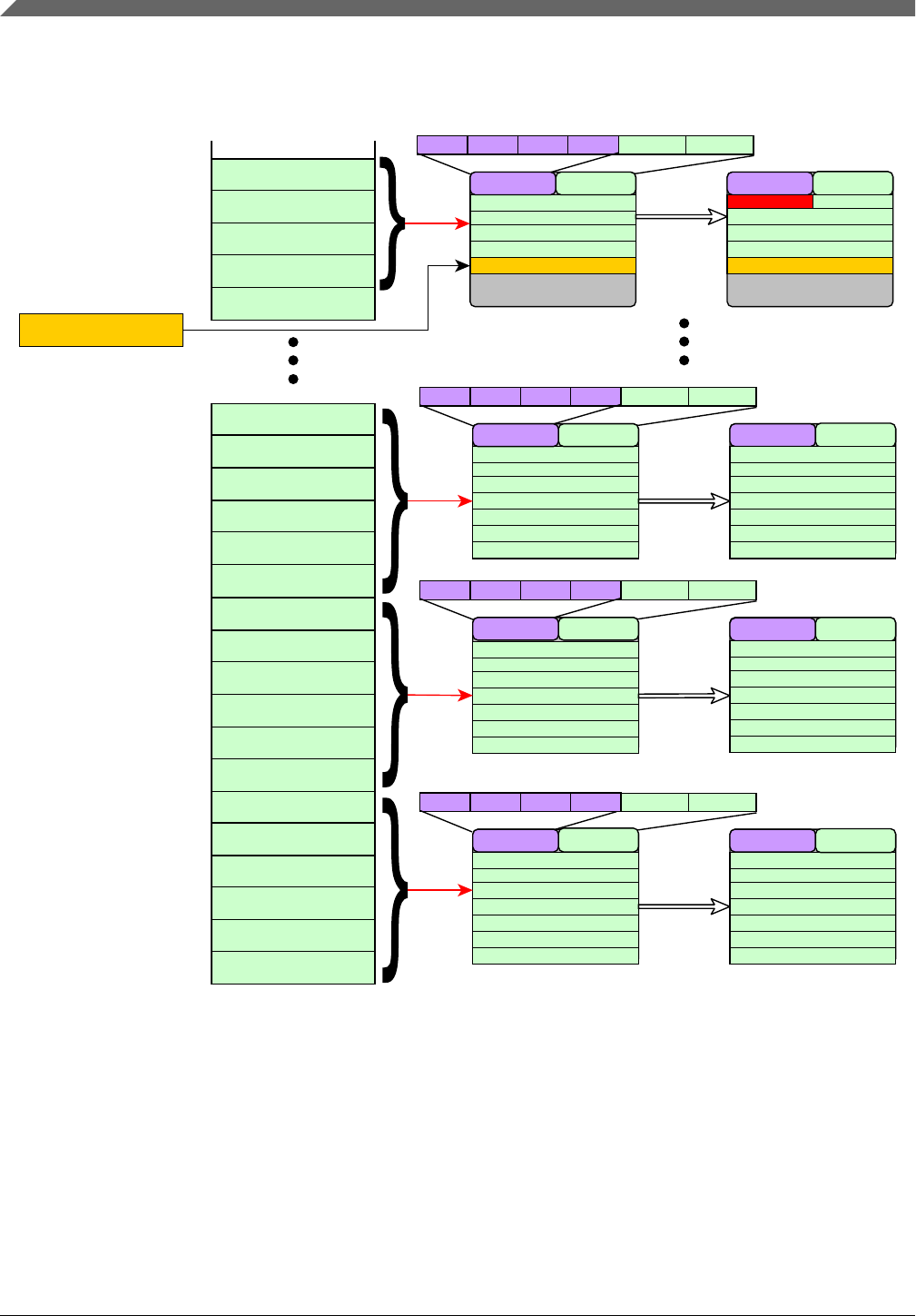
Parameter RAM
n
n-1
n-2
n-3
n-4
9
8
7
6
5
4
3
2
1
16 Bytes Blocks
6
5
4
3
2
1
Parameter RAM
CMD Word
2
1
7
13
12
10
14
17
16
15
19
18
13
12
11
10
9
8
14
20
19
18
17
16
15
21
n-3
n-2
n-1
n
Input Output
CSEc
System Memory
function
processing
time
function
processing
time
function
processing
time
function
processing
time
KeyID0x06 0x00 0x00
CMD Word
MAC
7
MAC Len MSG Len
Length
KeyID0x06 0x00 0x01
CMD Word
MAC Len MSG Len
Length
KeyID0x06 0x00 0x01
CMD Word
MAC Len MSG Len
Length
KeyID0x06 0x00 0x01
CMD Word
MAC Len MSG Len
Length
3
4
5
6
Length
CMD Word Length
CMD Word Length
CMD Word Length
13
12
11
10
9
8
14
20
19
18
17
16
15
21
n-3
n-2 n-1
n
MACMAC
Ver Status
Figure 5-5. Message authentication
5.4 Steps required before failure analysis
Before returning a device to NXP for failure analysis, the user must run the
CMD_DBG_CHAL and CMD_DBG_AUTH commands and ensure that all user keys are
deleted. This is a mandatory step to enable failure analysis at NXP.
Steps required before failure analysis
S32K1xx Series Reference Manual, Rev. 7, 04/2018
96 NXP Semiconductors

NOTE
If WRITE_PROTECTION flag is set for any key then the user
will be unable to delete that key with DEBUG_CHAL and
DEBUG_AUTH commands and failure analysis would not be
possible.
5.5 Security programming flow example (Secure Boot)
1. Run PGMPART to configure desired number of keys and other parameters
2. Program code section in Pflash to be checked in secure boot
3. LOAD_KEY(BOOT_MAC_KEY)
4. CMD_BOOT_DEFINE to select the flavor of boot and size of data to validate in
Pflash
Then optionally reset the part to "auto calculate" and program the BOOT_MAC or
the user loads the BOOT_MAC by external calculation.
Chapter 5 Security Overview
S32K1xx Series Reference Manual, Rev. 7, 04/2018
NXP Semiconductors 97

Security programming flow example (Secure Boot)
S32K1xx Series Reference Manual, Rev. 7, 04/2018
98 NXP Semiconductors

Chapter 6
Safety Overview
6.1 Introduction
The S32K1xx series is developed according to ISO 26262 and has an integrated safety
concept targeting an ISO26262 ASIL-B integrity level. The following documentation
supports the integration of an S32K1xx chip into safety-related systems:
• Reference Manual (S32K1XXRM): describes the programming model and
functionality of S32K1xx chips
• Data Sheet (S32K1XX): describes S32K1xx operating conditions as well as timing
and electrical characteristics
• Safety Manual (S32K1XXSM): describes the S32K1xx safety concept and possible
safety mechanisms (integrated in S32K1xx, system-level hardware, or system-level
software) as well as measures to reduce dependent failures
• Dynamic FMEDA: inductive analysis enabling customization of system-level safety
mechanisms, including the resulting safety metrics for ISO 26262 (SPFM, LFM &
PMHF) and IEC 61508 (SFF & Beta IC Factor)
• FMEDA Report: describes the FMEDA methodology and safety mechanisms
supported in the FMEDA, including source of failure rates, failure modes, and
assumptions during the analysis
The S32K1xx series is a SafeAssure™ solution. For more information regarding
functional safety at NXP, visit http://www.nxp.com/safeassure.
S32K1xx Series Reference Manual, Rev. 7, 04/2018
NXP Semiconductors 99

Figure 6-1. Functional safety overview
6.2 S32K1xx safety concept
The S32K1xx series has an integrated safety concept targeting safety-related systems that
require an ASIL-B safety integrity level. In general, safety integrity is achieved by using
and applying S32K1xx safety features as described in the Safety Manual.
The following diagram provides an overview of integrated S32K1xx architecture and
safety features.
S32K1xx safety concept
S32K1xx Series Reference Manual, Rev. 7, 04/2018
100 NXP Semiconductors
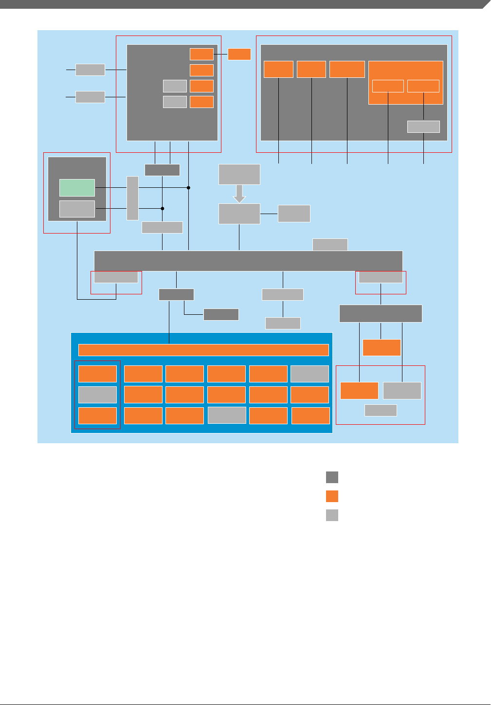
ENET
1: On this device, NXP’s system MPU implements the safety mechanisms to
prevent masters from accessing restricted memory regions. This system MPU
provides memory protection at the level of the Crossbar Switch. Each Crossbar
master (Core, DMA, Ethernet) can be assigned different access rights to each
protected memory region. The Arm M4 core version in this family does not
integrate the Arm Core MPU, which would concurrently monitor only core-initiated
memory accesses. In this document, the term MPU refers to NXP’s system MPU.
Device architectural IP on all
S32K devices.
Peripherals present on all
S32K devices.
Peripherals present on selected
S32K devices. See section
Feature Comparison.
Key:
DMA
mux
JTAG &
serial
wire
Async
trace
port
System MPU1
S0
Crossbar switch (AXBS-Lite)
M2
S3
M1
S2
M0
System MPU1
Mux
GPIO
iahb_gasket
QuadSPI
TCD
512B
Code Cache
Mux
System MPU1
SWJ-DP
TPIU
AHB-AP
PPB
Arm Cortex
M0+ / M4F Core
DSP
FPU
DWT
FPB
ITM
NVIC AWIC
S1
eDMA
Clock Generation
Power
supply
monitoring
Clock
monitoring
System
memory
protection
unit
ECC on
flash
memory
Core
self test
ECC on
SRAM
Peripheral
protection
Internal SW
watchdog
External SW
watchdog
CRC
Register
protection Diversity of digital
analog signal paths Diversity of
communication channels
Main
SRAM2
Lower
Region
Upper
Region
System
DCODE
ICODE
SPLL
4-40 MHz 8-40 MHz
SIRC
8 MHz FIRC
48 MHz
LPO
128 kHz SOSC
System MPU1
M3
WDOG 12-bit ADC LPI2C
EWM LPUART
CRC TRGMUX
FlexIO
FlexCAN
Low power
timer
FlexTimer
PDB
SAI
LPIT
Peripheral bus controller
CSEc
LPSPI
Code flash
memory Data flash
memory
Flash memory
controller
RTC
CMP
8-bit DAC
QuadSPI
2: See Memories and Memory Interfaces chapter: On-chip SRAM sizes table for Device specific sizes
FlexRAM/
SRAM
Figure 6-2. S32K1xx safety block diagram
Chapter 6 Safety Overview
S32K1xx Series Reference Manual, Rev. 7, 04/2018
NXP Semiconductors 101

6.2.1 Cortex-M4/M0+ Structural Core Self Test (SCST)
Cortex-M4/M0+ Structural Core Self Test (SCST) is a software product from NXP. It
was developed for detecting hardware permanent faults in a core by executing machine
opcodes with a fixed set of operands and comparing their execution results. This library
is considered a Safety Element out of context and was developed according to ASIL-B.
The SCST delivery contains the SCST library, a quality package, and a safety package.
• The quality package contains code coverage analysis, a MISRA report, a software
requirements specification, and a Test Specification.
• The safety package consists of the SCST fault coverage estimation, the Safety
Analysis and Concept, and the SCST Safety Manual.
The Safety Manual for Structural Core Self Test Library contains a list of
recommendations and assumptions that should be fulfilled and verified by a user for the
proper use of the SCST library for a Cortex-M4/M0+ core.
6.2.2 ECC on RAM and flash memory
Error correcting codes are used to protect transfers from a CPU core to flash memory and
from a CPU core to system memory. Error Correcting Code (ECC) is implemented with
Single-Error Correction, Double-Error Detection (SECDED).
References:
• Functional description: in this Reference Manual, see MCM, EIM, ERM, LMEM,
and FTFC
• ECC on RAM and flash memory in safety concept: see Safety Manual
6.2.3 Power supply monitoring
S32K1xx includes a system for managing low-voltage conditions to protect memory
contents and control MCU system states during supply voltage variations.
• Power-on reset (POR)
• Low-voltage detection (LVD)
References:
• Functional description: in this Reference Manual, see Power Management
• Power supply monitoring in safety concept: see Safety Manual chapter
S32K1xx safety concept
S32K1xx Series Reference Manual, Rev. 7, 04/2018
102 NXP Semiconductors

6.2.4 Clock monitoring
Clocks in the S32K1xx are supervised by clock monitor units.
• System PLL clock monitor1 : monitors the loss of PLL clock
• System Oscillator (SOSC) clock monitor 2 : monitors the loss of oscillator clock
• CMU monitor3 FIRC clock for:
• Loss of clock
• Out of high and low range
References:
• Functional description: in this Reference Manual, see Clock Distribution
• Clock monitoring in safety concept: see Safety Manual chapter
6.2.5 Temporal protection
In a safety concept, watchdog timers provide temporal protection and monitor the
operation of the system by expecting periodic communication from the software.
S32K1xx offers two watchdog timers:
• Watchdog timer (WDOG) 4 : An independent timer that is available for system use. It
provides a safety feature to ensure that software is executing as planned and that the
CPU is not stuck in an infinite loop.
• External Watchdog Monitor (EWM) 5 : A redundant watchdog system for safety. The
EWM provides an independent output signal. It does not reset the MCU and
peripherals.
References:
• Functional description: in this Reference Manual, see WDOG and EWM
• Temporal protection in safety concept: see Safety Manual chapter
6.2.6 Operational interference protection
S32K1xx provides safety mechanisms to:
1. Available in S32K14x variants only
2. Available in all S32K1xx variants
3. Available in S32K11x only
4. Available in all S32K1xx variants
5. Available in S32K14x variants only
Chapter 6 Safety Overview
S32K1xx Series Reference Manual, Rev. 7, 04/2018
NXP Semiconductors 103

• prevent non-safety masters from interfering with the operation of the Safety Core
• manage the concurrent execution of software with different (lower) ASIL
A hierarchical memory protection scheme, which includes the following, protects against
interference:
• System Memory Protection Unit (MPU)
• Peripheral Bridge (AIPS-Lite)
• Register protection
6.2.6.1 System Memory Protection Unit (MPU)
For ASIL-B applications, the system Memory Protection Unit (MPU) is used for
execution control. It assigns access rights and ensures that only authorized software tasks
can configure modules and access their allocated resources.
• The system MPU6 provides memory protection at the Crossbar Switch. It splits the
physical memory into 16 different regions.
• Each XBAR master (core, DMA, Ethernet) can be assigned different access rights to
each region.
• The system MPU can be used to prevent non-safety masters (including DMA or
Ethernet Controller) from accessing restricted memory regions.
References:
• Functional description: in this Reference Manual, see MPU
• MPU in safety concept: see Safety Manual chapter
6.2.6.2 Peripheral protection
Peripheral protection is based on the Peripheral Bridge (AIPS-Lite) module. It provides
memory protection functionality by defining bus masters' access rights to various
peripherals on the chip.
References:
• Functional description: in this Reference Manual, see AIPS-Lite
• Peripheral protection in safety concept: see Safety Manual chapter
6. On this device, NXP’s system MPU implements the safety mechanisms to prevent masters from accessing
restricted memory regions. This system MPU provides memory protection at the level of the Crossbar Switch. Each
Crossbar master (Core, DMA, Ethernet) can be assigned different access rights to each protected memory region.
The Arm M4 core version in this family does not integrate the Arm Core MPU, which would concurrently monitor
only core-initiated memory accesses. In this document, the term MPU refers to NXP’s system MPU.
S32K1xx safety concept
S32K1xx Series Reference Manual, Rev. 7, 04/2018
104 NXP Semiconductors

6.2.6.3 Register protection
S32K1xx offers register protection for safety-critical registers. This protection is based on
CPU program execution mode—User vs. Supervisor (privileged) mode—as well as
another type of access restriction based on a lock feature implemented for certain
registers. The lock-based access restriction inhibits a register update until the next system
reset or requires a special key to unlock access.
References:
• Functional description: in this Reference Manual, see notes about register protection
features for a specific register or a group of registers in the register-description
sections for SIM, SCG, ERM, RCM, MSCM, and others
• Register protection in safety concept: see Safety Manual
6.2.7 CRC
The CRC unit supports the detection of accidental alteration of data in memory or
configuration registers by calculating its CRC signature and comparing it to a previously
calculated CRC. The CRC module can also detect erroneous corruption of data during
transmission or storage.
References:
• Functional description: in this Reference Manual, see CRC
• CRC in safety concept: see Safety Manual chapter
6.2.8 Diversity of system resources
Features that are relevant to functional safety usually have redundant support in the
system. S32K1xx offers a diversity of system resources to provide this support.
• Digital inputs can be replicated to acquire safety-critical inputs redundantly
• Safety-critical digital outputs can always be written redundantly or in combination
with a read-back operation
• Analog inputs can operate in oversampling mode to detect transient faults affecting
the ADC channel, and two ADC units can acquire and digitize redundant copies of
an analog signal connected to a safety-relevant signal
• For cases of communication-channel redundancy for safety reasons, S32K1xx offers
redundant instances of communication peripherals:
• Synchronous Serial Communication Controller (LPSPI) modules
Chapter 6 Safety Overview
S32K1xx Series Reference Manual, Rev. 7, 04/2018
NXP Semiconductors 105

• FlexIO module: capable of supporting a wide range of protocols (UART, I2C,
SPI, I2S) and PWM/waveform generation
• UART modules: support UART and LIN communication
References:
• Functional description: in this Reference Manual, see SIM, LPSPI, LPI2C, FlexIO,
and LPUART
• Diversity of system resources in safety concept: see Safety Manual
S32K1xx safety concept
S32K1xx Series Reference Manual, Rev. 7, 04/2018
106 NXP Semiconductors
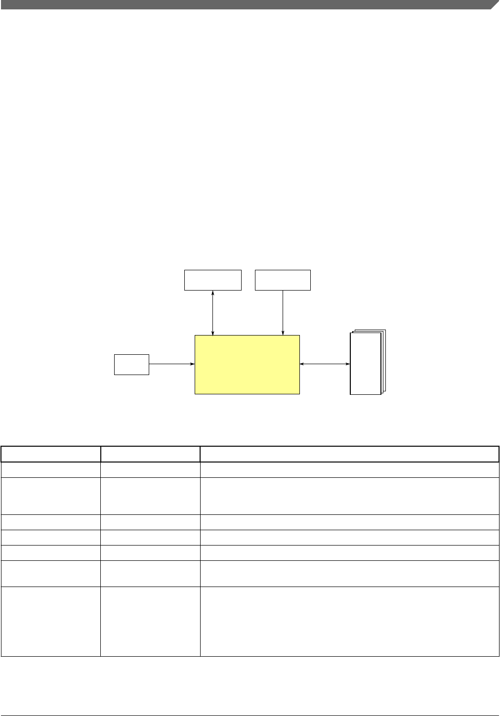
Chapter 7
CM4 Overview
7.1 Arm Cortex-M4F core configuration
This section summarizes how the module has been configured in the chip. Full
documentation for this module is provided by Arm and can be found at arm.com.
PPB
modules
PPB
Arm Cortex-M4
core
Debug
Interrupts
Crossbar
switch
Figure 7-1. Core configuration
Table 7-1. Reference links to related information
Topic Related module Reference
Full description Arm Cortex-M4F core Arm Cortex-M4F Technical Reference Manual
— ARM Cortex-M4
Devices Generic User
Guide
ARM Cortex-M4 Devices Generic User Guide
System memory map — See the S32K1xx_memory_map.xlsx attached to this document.
Clocking — Clock distribution
Power management — Power management
System/instruction/data
bus module
Crossbar switch Crossbar switch
Debug IEEE 1149.1 JTAG
Serial Wire Debug
(SWD)
Arm Real-Time Trace
Interface
Debug
Table continues on the next page...
S32K1xx Series Reference Manual, Rev. 7, 04/2018
NXP Semiconductors 107

Table 7-1. Reference links to related information (continued)
Topic Related module Reference
Interrupts Nested Vectored
Interrupt Controller
(NVIC)
NVIC
Private Peripheral Bus
(PPB) module
Miscellaneous Control
Module (MCM)
MCM
Private Peripheral Bus
(PPB) module
Single-precision floating
point unit (FPU)
FPU
7.1.1 Buses, interconnects, and interfaces
The Arm Cortex-M4 core has four buses as described in the following table.
Table 7-2. Arm core buses
Bus name Description
Instruction code (ICODE) bus The ICODE and DCODE buses are muxed. This muxed bus is called the CODE bus and is
connected to the crossbar switch via a single master port.
Data code (DCODE) bus
System bus The system bus is connected to a separate master port on the crossbar.
Private peripheral (PPB) bus The PPB provides access to these modules:
• Arm modules such as the NVIC, ITM, DWT, FBP, and ROM table
• NXP Miscellaneous Control Module (MCM)
7.1.2 System Tick Timer
The System Tick Timer's clock source is always the core clock, CORE_CLK. This results
in the following:
• The CLKSOURCE bit in SysTick Control and Status register is always set to select
the core clock.
• Because the timing reference (CORE_CLK) is a variable frequency, the TENMS bit
in the SysTick Calibration Value Register is always zero.
• The NOREF bit in SysTick Calibration Value Register is always set, implying that
CORE_CLK is the only available source of reference timing.
Arm Cortex-M4F core configuration
S32K1xx Series Reference Manual, Rev. 7, 04/2018
108 NXP Semiconductors

7.1.3 Debug facilities
This chip has extensive debug capabilities including run control and tracing capabilities.
This is a standard Arm debug port that supports JTAG and SWD interfaces.
7.1.4 Caches
This device includes one 4 KB code cache to minimize the performance impact of
memory access latencies. The code cache exists on the I/D bus, and there is no cache on
the system bus.
Features of the cache are:
• 2-way set associative
• 4 word lines
• Lines can be individually flushed
• Entire cache can be flushed at once
7.1.4.1 Control
For control purposes, the cache can be in one of these states:
1. Write Back / Write Allocate (WBWA)
2. Write Through
3. No cache
For each defined region there will be 2 bits allocated on the control register (see
PCCRMR that determines the cache state for the memory region associated with this
section. The user can only "lower" the cache attribute, given the fixed relationship of
WBWA > WT > NC - so, you can demote a WBWA region to either WT or NC, you can
demote a WT space to NC. In order to change the state upwards a system reset is
required.
NOTE
See LMEM for the cache reset states.
7.1.5 Core privilege levels
The Arm documentation uses different terms than this document to distinguish between
privilege levels.
Chapter 7 CM4 Overview
S32K1xx Series Reference Manual, Rev. 7, 04/2018
NXP Semiconductors 109
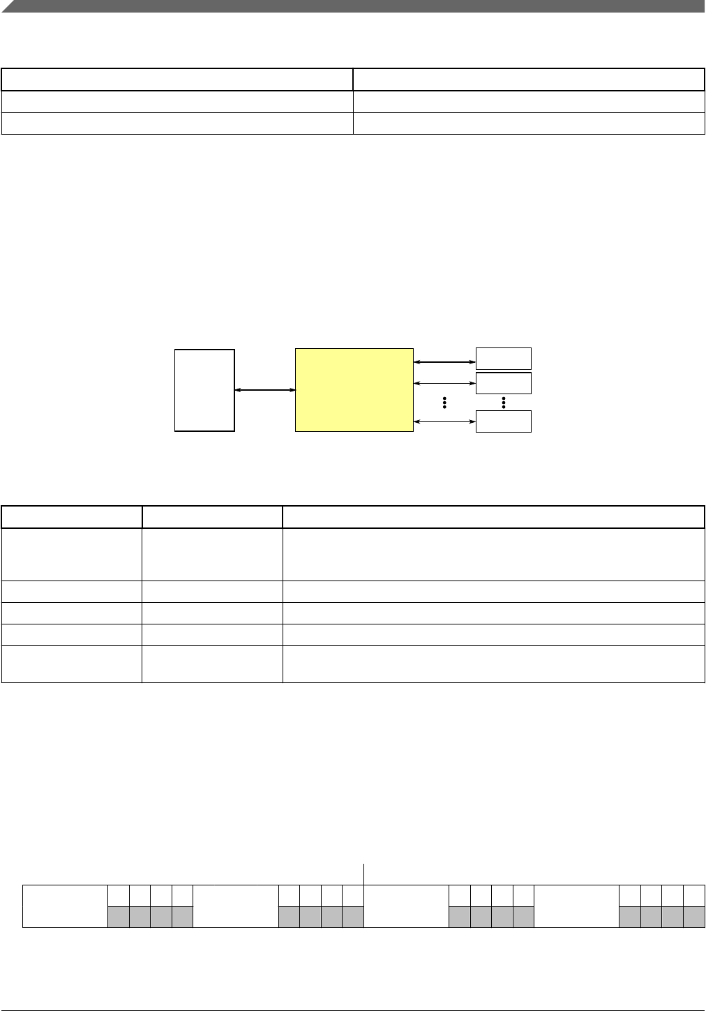
Table 7-3. Terms used
If you see this term... it also means this term...
Privileged Supervisor
Unprivileged or user User
7.2 Nested Vectored Interrupt Controller (NVIC)
Configuration
This section summarizes how the module has been configured in the chip. Full
documentation for this module is provided by Arm and can be found at arm.com.
Nested Vectored
Interrupt Controller
(NVIC)
Arm
Cortex-M4
core
Interrupts Module
Module
Module
PPB
Figure 7-2. NVIC configuration
Table 7-4. Reference links to related information
Topic Related module Reference
Full description Nested Vectored
Interrupt Controller
(NVIC)
Arm Cortex-M4F Technical Reference Manual - Nested Vectored Interrupt
Controller
System memory map — Refer to the S32K1xx_memory_map.xlsx attached to this document.
Clocking — Clock distribution
Power management — Power management
Private Peripheral Bus
(PPB)
Arm Cortex-M4 core Arm Cortex-M4F Technical Reference Manual - Private Peripheral Bus
(PPB)
7.2.1 Interrupt priority levels
This device supports 16 priority levels for interrupts. Therefore, in the NVIC each source
in the IPR registers contains 4 bits. For example, the IPR0 diagram is shown below.
31 30 29 28 27 26 25 24 23 22 21 20 19 18 17 16 15 14 13 12 11 10 9 8 7 6 5 4 3 2 1 0
RIRQ3 0000 IRQ2 0000 IRQ1 0 0 0 0 IRQ0 0 0 0 0
W
Nested Vectored Interrupt Controller (NVIC) Configuration
S32K1xx Series Reference Manual, Rev. 7, 04/2018
110 NXP Semiconductors

7.2.2 Non-maskable interrupt
The non-maskable interrupt request to the NVIC is controlled by the external NMI signal.
The pin on which the NMI signal is multiplexed must be configured for the NMI function
in order to generate the non-maskable interrupt request.
See IO Signal Description Input Multiplexing sheet(s) attached to the Reference Manual
for details on NMI pad.
7.2.3 Determining the bitfield and register location for
configuring a particular interrupt
Suppose you need to configure the low-power timer (LPTMR) interrupt. The following
table is an excerpt of the LPTMR row from the file
'S32K1xx_DMA_INT_mapping.xlsm' attached to this Reference Manual.
Table 7-6. LPTMR interrupt vector assignment
Address Vector IRQ1NVIC non-IPR
register number2NVIC IPR register
number3Source module
0x0000_0128 74 58 1 14 Low Power Timer
1. Indicates the NVIC's interrupt source number.
2. Indicates the NVIC's ISER, ICER, ISPR, ICPR, and IABR register number used for this IRQ. The equation to calculate this
value is: IRQ div 32
3. Indicates the NVIC's IPR register number used for this IRQ. The equation to calculate this value is: IRQ div 4
The NVIC registers you would use to configure the interrupt are:
• NVICISER1
• NVICICER1
• NVICISPR1
• NVICICPR1
• NVICIABR1
• NVICIPR14
To determine the particular IRQ's bitfield location within these particular registers:
• NVICISER1, NVICICER1, NVICISPR1, NVICICPR1, NVICIABR1 bit location =
IRQ mod 32 = 26
• NVICIPR14 bitfield starting location = 8 × (IRQ mod 4) + 4 = 20
Since the NVICIPR bitfields are 4-bit wide (16 priority levels), the NVICIPR14
bitfield range is 20-23
Chapter 7 CM4 Overview
S32K1xx Series Reference Manual, Rev. 7, 04/2018
NXP Semiconductors 111
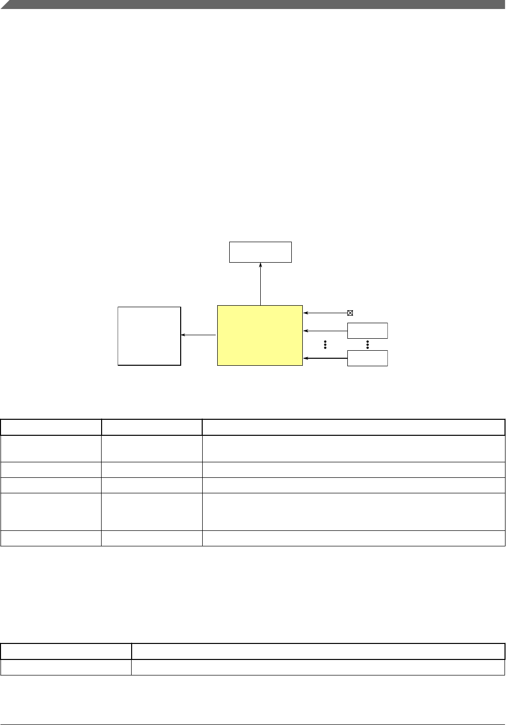
Therefore, the following bitfield locations are used to configure the LPTMR interrupts:
• NVICISER1[26]
• NVICICER1[26]
• NVICISPR1[26]
• NVICICPR1[26]
• NVICIABR1[26]
• NVICIPR14[23:20]
7.3 Asynchronous Wake-up Interrupt Controller (AWIC)
Configuration
Asynchronous
Wake-up Interrupt
Controller (AWIC)
Nested vectored
interrupt controller
(NVIC)
Wake-up
requests
Module
Module
Clock logic
Figure 7-3. Asynchronous Wake-up Interrupt Controller configuration
Table 7-7. Reference links to related information
Topic Related module Reference
System memory map — Refer to the S32K1xx_memory_map.xlsx attached to Reference Manual
for details.
Clocking — Clock distribution
Power management — Power management
Nested Vectored
Interrupt Controller
(NVIC)
—NVIC
Wake-up requests — AWIC wake-up sources
7.3.1 Wake-up sources
Table 7-8. AWIC stop and VLPS wake-up sources
Wake-up source Description
Available system resets RESET pin, WDOG, JTAG
Table continues on the next page...
Asynchronous Wake-up Interrupt Controller (AWIC) Configuration
S32K1xx Series Reference Manual, Rev. 7, 04/2018
112 NXP Semiconductors

Table 7-8. AWIC stop and VLPS wake-up sources (continued)
Wake-up source Description
Pin interrupts Port Control Module - Any enabled pin interrupt is capable of waking the system
ADCx (1) Async Interrupt in STOP1 (2) Sync Interrupt in STOP2
CMP (1) Async Interrupt in STOP1 (2) Sync Interrupt in STOP2 (3) Functional in VLPS modes
and will cause async Interrupt for wake up
LPI2C0 (1) Async Interrupt in STOP1 (2) Sync Interrupt in STOP2 (3) Functional in VLPS mode with
SIRC as clock source
LPUART (1) Async Interrupt in STOP1 (2) Sync Interrupt in STOP2 (3)Functional in VLPS mode with
SIRC as clock source
LPSPI (1) Async Interrupt in STOP1 (2) Sync Interrupt in STOP2 (3) Functional in VLPS mode with
SIRC as clock source
LPTMR0 (1) Async Interrupt in STOP1 (2) Sync Interrupt in STOP2 (3) Functional in VLPS modes
and will cause async Interrupt for wake up
RTC (1) Async Interrupt in STOP1 (2) Sync Interrupt in STOP2 (3) RTC running in VLPS from
either LPO or RTC_CLKIN. Wakeup from alarm interrupt
CAN PNET is supported in STOP1/2 modes and will cause wake up. Only CAN0 supports PNET
feature.
NMI Non-maskable interrupt
WDOG (1) Async Interrupt in STOP1 (2) Sync Interrupt in STOP2 (3) Functional in VLPS modes
and will cause async Interrupt for wake up
FlexIO (1) Async Interrupt in STOP1 (2) Sync Interrupt in STOP2
LPIT (1) Async Interrupt in STOP1 (2) Sync Interrupt in STOP2 (3) Functional in VLPS mode with
SIRC as clock source.
EWM Module off in STOP1 and VLPS. Can cause wakeup through sync Interrupt in STOP2.
CRC Module off in STOP1 and VLPS. Can cause wakeup through sync Interrupt in STOP2.
SCG (1) Async Interrupt in STOP1 (2) Sync Interrupt in STOP2
7.4 FPU configuration
This section summarizes how the module has been configured in the chip.
FPU
transfers
Arm Cortex M4
core
PPB
Figure 7-4. FPU configuration
Table 7-9. Reference links to related information
Topic Related module Reference
Full description FPU Arm Cortex-M4 Technical Reference Manual - Floating-Point Unit
Table continues on the next page...
Chapter 7 CM4 Overview
S32K1xx Series Reference Manual, Rev. 7, 04/2018
NXP Semiconductors 113
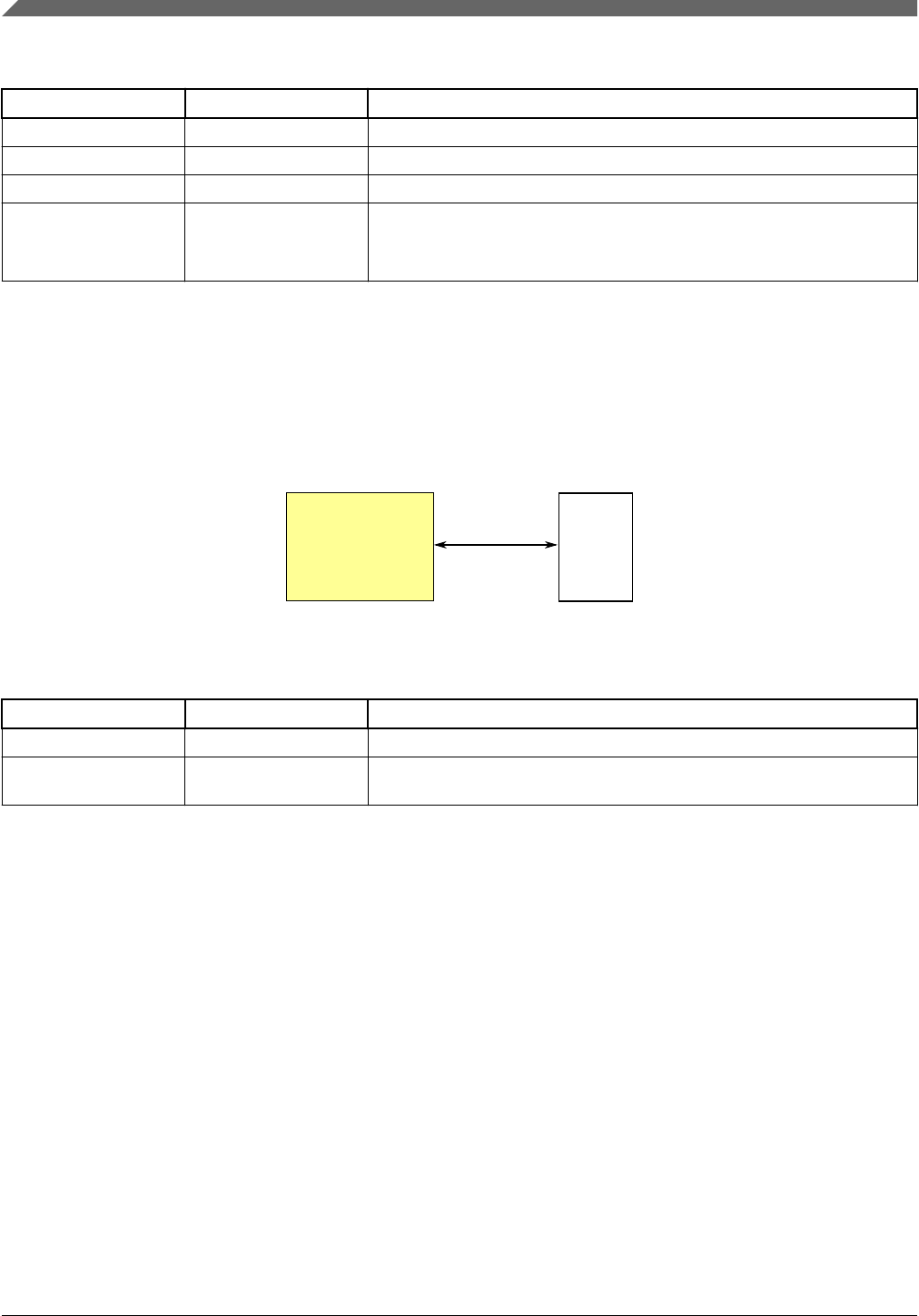
Table 7-9. Reference links to related information (continued)
Topic Related module Reference
System memory map — Refer to the S32K1xx_memory_map.xlsx attached to this document.
Clocking — Clock Distribution
Power Management — Power Management
Transfers
Private Peripheral Bus
(PPB)
Arm Cortex M4 core Arm Cortex-M4 Technical Reference Manual - Private Peripheral Bus
7.5 JTAG controller configuration
This section summarizes how the module has been configured in the chip.
Signal
multiplexing
JTAG controller
Figure 7-5. JTAG controller configuration
Table 7-10. Reference links to related information
Topic Related module Reference
Full description JTAGC JTAGC
Signal multiplexing Port control See IO Signal Description Input Multiplexing sheet(s) attached to the
Reference Manual attached to this document for details.
JTAG controller configuration
S32K1xx Series Reference Manual, Rev. 7, 04/2018
114 NXP Semiconductors

Chapter 8
CM0+ Overview
8.1 Arm Cortex-M0+ core introduction
The enhanced Arm Cortex M0+ is the member of the Cortex-M Series of processors
targeting microcontroller cores focused on very cost sensitive, low power applications. It
has a single 32-bit AMBA AHB-Lite interface and includes an NVIC component. It also
has hardware debug functionality including support for simple program trace capability.
The processor supports the Armv6-M instruction set (Thumb) architecture including all
but three 16-bit Thumb opcodes (52 total) plus seven 32-bit instructions. It is upward
compatible with other Cortex-M profile processors.
Table 8-1. Reference links to related information
Topic Related module Reference
Full description Arm Cortex-M0+ core Arm Cortex-M0+ Technical Reference Manual
— ARM Cortex-M0
Devices Generic User
Guide
ARM Cortex-M0 Devices Generic User Guide
System memory map — See the S32K1xx_memory_map.xlsx attached to this document.
Clocking — Clock distribution
Power management — Power management
System/instruction/data
bus module
Crossbar switch Crossbar switch
Debug IEEE 1149.1 JTAG
Serial Wire Debug
(SWD)
MTB
Arm Real-Time Trace
Interface
Debug
Interrupts Nested Vectored
Interrupt Controller
(NVIC)
NVIC
S32K1xx Series Reference Manual, Rev. 7, 04/2018
NXP Semiconductors 115

8.1.1 Buses, interconnects, and interfaces
The Arm Cortex-M0+ core has two bus interfaces:
• Single 32-bit AMBA-3 AHB-Lite system interface that provides connections to
peripherals and all system memory, which includes flash memory and RAM
• Single 32-bit I/O port bus interfacing to the GPIO with 1-cycle loads and stores
8.1.2 System tick timer
The CLKSOURCE field in SysTick Control and Status register selects either the core
clock (when CLKSOURCE = 1) or a divide-by-16 of the core clock (when
CLKSOURCE = 0). Because the timing reference is a variable frequency, the TENMS
field in the SysTick Calibration Value Register is always 0.
8.1.3 Debug facilities
This device supports standard Arm 2-pin SWD debug port.
8.1.4 Core privilege levels
The core on this device is implemented with both privileged and unprivileged levels. The
Arm documentation uses different terms than this document to distinguish between
privilege levels.
If you see this term... it also means this term...
Privileged Supervisor
Unprivileged or user User
Arm Cortex-M0+ core introduction
S32K1xx Series Reference Manual, Rev. 7, 04/2018
116 NXP Semiconductors

Nested vectored interrupt controller (NVIC)
8.2.1 Interrupt priority levels
This device supports four priority levels for interrupts. Therefore, in the NVIC, each
source in the IPR registers contains two bits. For example, IPR0 is shown below:
31 30 29 28 27 26 25 24 23 22 21 20 19 18 17 16 15 14 13 12 11 10 9 8 7 6 5 4 3 2 1 0
RIRQ3 000000IRQ2 000000IRQ1 0 0 0 0 0 0 IRQ0 0 0 0 0 0 0
W
8.2.2 Non-maskable interrupt
The non-maskable interrupt request to the NVIC is controlled by the external NMI signal.
The pin the NMI signal is multiplexed on, must be configured for the NMI function to
generate the non-maskable interrupt request. See IO Signal Description Input
Multiplexing sheet(s) attached to the Reference Manual for details on NMI pad.
8.2.3 Determining the bitfield and register location for
configuring a particular interrupt
Suppose you need to configure the SPI0 interrupt. The following table is an excerpt of the
FlexCAN row from the file 'S32K1xx_DMA_INT_mapping.xlsm' attached to this
Reference Manual.
Table 8-3. Interrupt vector assignments
Address Vector IRQ1NVIC IPR
register
number2
Source
module
0x0000_006C 27 11 2 FlexCAN
1. Indicates the NVIC's interrupt source number.
2. Indicates the NVIC's IPR register number used for this IRQ. The equation to calculate this value is: IRQ div 4.
• The NVIC registers you would use to configure the interrupt are:
• NVICIPR2
• To determine the particular IRQ's field location within these particular registers:
• NVICIPR2 field starting location = 8 * (IRQ mod 4) + 6 = 22
8.2
Chapter 8 CM0+ Overview
S32K1xx Series Reference Manual, Rev. 7, 04/2018
NXP Semiconductors 117

Since the NVICIPR fields are 2-bit wide (4 priority levels), the NVICIPR2 field
range is 22–23.
Therefore, the following field locations are used to configure the FlexCAN interrupts:
• NVICIPR2[23:22]
8.3 AWIC introduction
The primary function of the AWIC block is to detect asynchronous wake-up events in
stop modes and signal to clock control logic to resume system clocking. After clock
restart, the NVIC observes the pending interrupt and performs the normal interrupt or
event processing.
Table 8-4. Reference links to related information
Topic Related module Reference
System memory map — Refer to the S32K1xx_memory_map.xlsx attached to Reference Manual
for details.
Clocking — Clock distribution
Power management — Power management
Nested Vectored
Interrupt Controller
(NVIC)
—NVIC
Wake-up requests — AWIC wake-up sources
8.3.1 Wake-up sources
The device uses the following internal and external inputs to the AWIC module.
Table 8-5. AWIC stop and VLPS wake-up sources
Wake-up source Description
Available system resets RESET pin, WDOG, JTAG
Pin interrupts Port Control Module - Any enabled pin interrupt is capable of waking the system
ADCx (1) Async Interrupt in STOP1 (2) Sync Interrupt in STOP2
CMP (1) Async Interrupt in STOP1 (2) Sync Interrupt in STOP2 (3) Functional in VLPS modes
and will cause async Interrupt for wake up
LPI2C0 (1) Async Interrupt in STOP1 (2) Sync Interrupt in STOP2 (3) Functional in VLPS mode with
SIRC as clock source
LPUART (1) Async Interrupt in STOP1 (2) Sync Interrupt in STOP2 (3) Functional in VLPS mode with
SIRC as clock source
Table continues on the next page...
AWIC introduction
S32K1xx Series Reference Manual, Rev. 7, 04/2018
118 NXP Semiconductors

Table 8-5. AWIC stop and VLPS wake-up sources (continued)
Wake-up source Description
LPSPI (1) Async Interrupt in STOP1 (2) Sync Interrupt in STOP2 (3) Functional in VLPS mode with
SIRC as clock source
LPTMR0 (1) Async Interrupt in STOP1 (2) Sync Interrupt in STOP2 (3) Functional in VLPS modes
and will cause async Interrupt for wake up
RTC (1) Async Interrupt in STOP1 (2) Sync Interrupt in STOP2 (3 )RTC running in VLPS from
either LPO or RTC_CLKIN. Wakeup from alarm interrupt
CAN PNET is supported in STOP1/2 modes and will cause wake up. Only CAN0 supports PNET
feature.
NMI Non-maskable interrupt
WDOG (1) Async Interrupt in STOP1 (2) Sync Interrupt in STOP2 (3) Functional in VLPS modes
and will cause async Interrupt for wake up
FlexIO (1) Async Interrupt in STOP1 (2) Sync Interrupt in STOP2
LPIT (1) Async Interrupt in STOP1 (2) Sync Interrupt in STOP2 (3) Functional in VLPS mode with
SIRC as clock source
CRC Module off in STOP1 and VLPS. Can cause wakeup through sync Interrupt in STOP2.
SCG (1) Async Interrupt in STOP1 (2) Sync Interrupt in STOP2
Chapter 8 CM0+ Overview
S32K1xx Series Reference Manual, Rev. 7, 04/2018
NXP Semiconductors 119

AWIC introduction
S32K1xx Series Reference Manual, Rev. 7, 04/2018
120 NXP Semiconductors

Chapter 9
Micro Trace Buffer (MTB)
9.1 Introduction
Microcontrollers using the Cortex-M0+ processor core include support for a CoreSight
Micro Trace Buffer to provide program trace capabilities.
The proper name for this function is the CoreSight Micro Trace Buffer for the Cortex-
M0+ Processor; in this document, it is simply abbreviated as the MTB.
The simple program trace function creates instruction address change-of-flow data
packets in a user-defined region of the system RAM. Accordingly, the system RAM
controller manages requests from two sources:
• AMBA-AHB reads and writes from the system bus
• program trace packet writes from the processor
As part of the MTB functionality, there is a MTB_DWT (Data Watchpoint and Trace)
module that allows the user to define watchpoint addresses, or optionally, an address and
data value, that when triggered, can be used to start or stop the program trace recording.
9.1.1 Overview
As shown in the main block diagram, the platform RAM (PRAM) controller connects to
two input buses:
• the crossbar slave port for system bus accesses
• a "private execution MTB port" from the core
The logical paths from the crossbar master input ports to the PRAM controller are
highlighted along with the private execution trace port from the processor core. The
private MTB port signals the instruction address information needed for the 64-bit
program trace packets written into the system RAM. The PRAM controller output
interfaces to the attached RAM array. In this document, the PRAM controller is the
MTB_RAM controller.
S32K1xx Series Reference Manual, Rev. 7, 04/2018
NXP Semiconductors 121
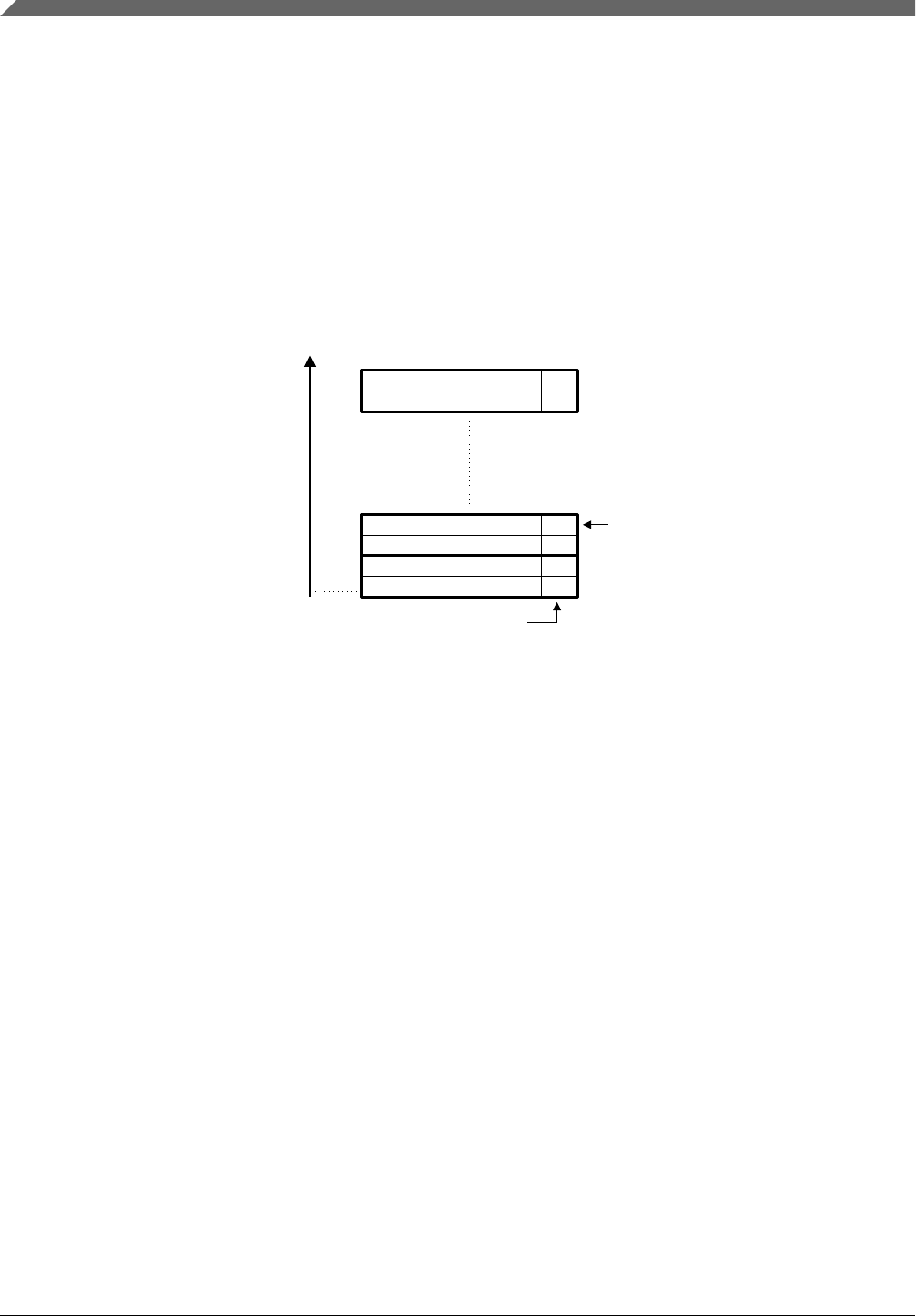
The following information is taken from the ARM CoreSight Micro Trace Buffer
documentation.
"The execution trace packet consists of a pair of 32-bit words that the MTB generates
when it detects the processor PC value changes non-sequentially. A non-sequential PC
change can occur during branch instructions or during exception entry.
The processor can cause a trace packet to be generated for any instruction.
The following figure shows how the execution trace information is stored in memory as a
sequence of packets.
Incrementing
SRAM memory
address
Nth destination address
Nth source address
S
A
31 0
1
2nd destination address
2nd source address
S
A
31 0
1
1st destination address
1st source address
S
A
Atom bit
Start bit
Odd word address
Even word address
Odd word address
Even word address
Figure 9-1. MTB execution trace storage format
The first, lower addressed, word contains the source of the branch, the address it
branched from. The value stored only records bits[31:1] of the source address, because
Thumb instructions are at least halfword aligned. The least significant bit of the value is
the A-bit. The A-bit indicates the atomic state of the processor at the time of the branch,
and can differentiate whether the branch originated from an instruction in a program, an
exception, or a PC update in Debug state. When it is zero the branch originated from an
instruction, when it is one the branch originated from an exception or PC update in
Debug state. This word is always stored at an even word location.
The second, higher addressed word contains the destination of the branch, the address it
branched to. The value stored only records bits[31:1] of the branch address. The least
significant bit of the value is the S-bit. The S-bit indicates where the trace started. An S-
bit value of 1 indicates where the first packet after the trace started and a value of 0 is
used for other packets. Because it is possible to start and stop tracing multiple times in a
trace session, the memory might contain several packets with the S-bit set to 1. This word
is always stored in the next higher word in memory, an odd word address.
Introduction
S32K1xx Series Reference Manual, Rev. 7, 04/2018
122 NXP Semiconductors

When the A-bit is set to 1, the source address field contains the architecturally-preferred
return address for the exception. For example, if an exception was caused by an SVC
instruction, then the source address field contains the address of the following instruction.
This is different from the case where the A-bit is set to 0. In this case, the source address
contains the address of the branch instruction.
For an exception return operation, two packets are generated:
• The first packet has the:
• Source address field set to the address of the instruction that causes the exception
return, BX or POP.
• Destination address field set to bits[31:1] of the EXC_RETURN value. See the
ARM v6-M Architecture Reference Manual.
• The A-bit set to 0.
• The second packet has the:
• Source address field set to bits[31:1] of the EXC_RETURN value.
• Destination address field set to the address of the instruction where execution
commences.
• A-bit set to 1."
Given the recorded change-of-flow trace packets in system RAM and the memory image
of the application, a debugger can read out the data and create an instruction-by-
instruction program trace. In keeping with the low area and power implementation cost
design targets, the MTB trace format is less efficient than other CoreSight trace modules,
for example, the ETM (Embedded Trace Macrocell). Since each branch packet is 8 bytes
in size, a 1 KB block of system RAM can contain 128 branches. Using the Dhrystone 2.1
benchmark's dynamic runtime as an example, this corresponds to about 875 instructions
per KB of trace RAM, or with a zero wait state memory, this corresponds to
approximately 1600 processor cycles per KB. This metric is obviously very sensitive to
the runtime characteristics of the user code.
The MTB_DWT function (not shown in the core platform block diagram) monitors the
processor address and data buses so that configurable watchpoints can be detected to
trigger the appropriate response in the MTB recording.
9.1.2 Features
The key features of the MTB_RAM and MTB_DWT include:
• Memory controller for system RAM and Micro Trace Buffer for program trace
packets
• Read/write capabilities for system RAM accesses, write-only for program trace
packets
Chapter 9 Micro Trace Buffer (MTB)
S32K1xx Series Reference Manual, Rev. 7, 04/2018
NXP Semiconductors 123

• Supports zero wait state response to system bus accesses when no trace data is being
written
• Can buffer two AHB address phases and one data write for system RAM accesses
• Supports 64-bit program trace packets including source and destination instruction
addresses
• Program trace information in RAM available to MCU's application code or external
debugger
• Program trace watchpoint configuration accessible by MCU's application code or
debugger
• Location and size of RAM trace buffer is configured by software
• Two DWT comparators (addresses or address + data) provide programmable start/
stop recording
• CoreSight compliant debug functionality
9.1.3 Modes of operation
The MTB_RAM and MTB_DWT functions do not support any special modes of
operation. The MTB_RAM controller, as a memory-mapped device located on the
platform's slave AHB system bus, responds strictly on the basis of memory addresses for
accesses to its attached RAM array. The MTB private execution bus provides program
trace packet write information to the RAM controller. Both the MTB_RAM and
MTB_DWT modules are memory-mapped, so their programming models can be
accessed.
All functionality associated with the MTB_RAM and MTB_DWT modules resides in the
core platform's clock domain; this includes its connections with the RAM array.
9.2 Memory map and register definition
The MTB_RAM and MTB_DWT modules each support a sparsely-populated 4 KB
address space for their programming models. For each address space, there are a variety
of control and configurable registers near the base address, followed by a large unused
address space and finally a set of CoreSight registers to support dynamic determination of
the debug configuration for the device.
Accesses to the programming model follow standard ARM conventions. Taken from the
ARM CoreSight Micro Trace Buffer documentation, these are:
• Do not attempt to access reserved or unused address locations. Attempting to access
these locations can result in UNPREDICTABLE behavior.
Memory map and register definition
S32K1xx Series Reference Manual, Rev. 7, 04/2018
124 NXP Semiconductors

• The behavior of the MTB is UNPREDICTABLE if the registers with UNKNOWN
reset values are not programmed prior to enabling trace.
• Unless otherwise stated in the accompanying text:
• Do not modify reserved register bits
• Ignore reserved register bits on reads
• All register bits are reset to a logic 0 by a system or power-on reset
• Use only word size, 32-bit, transactions to access all registers
9.2.1 MTB_DWT Memory Map
The MTB_DWT programming model supports a very simplified subset of the v7M debug
architecture and follows the standard ARM DWT definition.
MTB_DWT memory map
Address
offset (hex) Register name Width
(in bits) Access Reset value Section/
page
0 MTB DWT Control Register (MTB_DWT_CTRL) 32 R 2F00_0000h 9.2.1.1/126
20 MTB_DWT Comparator Register (MTB_DWT_COMP0) 32 R/W 0000_0000h 9.2.1.2/127
24 MTB_DWT Comparator Mask Register
(MTB_DWT_MASK0) 32 R/W 0000_0000h 9.2.1.3/127
28 MTB_DWT Comparator Function Register 0
(MTB_DWT_FCT0) 32 R/W 0000_0000h 9.2.1.4/128
30 MTB_DWT Comparator Register (MTB_DWT_COMP1) 32 R/W 0000_0000h 9.2.1.2/127
34 MTB_DWT Comparator Mask Register
(MTB_DWT_MASK1) 32 R/W 0000_0000h 9.2.1.3/127
38 MTB_DWT Comparator Function Register 1
(MTB_DWT_FCT1) 32 R/W 0000_0000h 9.2.1.5/130
200 MTB_DWT Trace Buffer Control Register
(MTB_DWT_TBCTRL) 32 R/W 2000_0000h 9.2.1.6/131
FC8 Device Configuration Register (MTB_DWT_DEVICECFG) 32 R 0000_0000h 9.2.1.7/133
FCC Device Type Identifier Register (MTB_DWT_DEVICETYPID) 32 R 0000_0004h 9.2.1.8/133
FD0 Peripheral ID Register (MTB_DWT_PERIPHID4) 32 R See section 9.2.1.9/134
FD4 Peripheral ID Register (MTB_DWT_PERIPHID5) 32 R See section 9.2.1.9/134
FD8 Peripheral ID Register (MTB_DWT_PERIPHID6) 32 R See section 9.2.1.9/134
FDC Peripheral ID Register (MTB_DWT_PERIPHID7) 32 R See section 9.2.1.9/134
FE0 Peripheral ID Register (MTB_DWT_PERIPHID0) 32 R See section 9.2.1.9/134
FE4 Peripheral ID Register (MTB_DWT_PERIPHID1) 32 R See section 9.2.1.9/134
FE8 Peripheral ID Register (MTB_DWT_PERIPHID2) 32 R See section 9.2.1.9/134
FEC Peripheral ID Register (MTB_DWT_PERIPHID3) 32 R See section 9.2.1.9/134
FF0 Component ID Register (MTB_DWT_COMPID0) 32 R See section 9.2.1.10/
134
FF4 Component ID Register (MTB_DWT_COMPID1) 32 R See section 9.2.1.10/
134
Table continues on the next page...
Chapter 9 Micro Trace Buffer (MTB)
S32K1xx Series Reference Manual, Rev. 7, 04/2018
NXP Semiconductors 125

MTB_DWT memory map (continued)
Address
offset (hex) Register name Width
(in bits) Access Reset value Section/
page
FF8 Component ID Register (MTB_DWT_COMPID2) 32 R See section 9.2.1.10/
134
FFC Component ID Register (MTB_DWT_COMPID3) 32 R See section 9.2.1.10/
134
9.2.1.1 MTB DWT Control Register (MTB_DWT_CTRL)
The MTBDWT_CTRL register provides read-only information on the watchpoint
configuration for the MTB_DWT.
Address: 0h base + 0h offset = 0h
Bit 31 30 29 28 27 26 25 24 23 22 21 20 19 18 17 16 15 14 13 12 11 10 9 8 7 6 5 4 3 2 1 0
RNUMCMP DWTCFGCTRL
W
Reset 0 0 1 0 1 1 1 1 0 0 0 0 0 0 0 0 0 0 0 0 0 0 0 0 0 0 0 0 0 0 0 0
MTB_DWT_CTRL field descriptions
Field Description
31–28
NUMCMP
Number of comparators
The MTB_DWT implements two comparators.
DWTCFGCTRL DWT configuration controls
This field is hardwired to 0xF00_0000, disabling all the remaining DWT functionality. The specific fields
and their state are:
MTBDWT_CTRL[27] = NOTRCPKT = 1, trace sample and exception trace is not supported
MTBDWT_CTRL[26] = NOEXTTRIG = 1, external match signals are not supported
MTBDWT_CTRL[25] = NOCYCCNT = 1, cycle counter is not supported
MTBDWT_CTRL[24] = NOPRFCNT = 1, profiling counters are not supported
MTBDWT_CTRL[22] = CYCEBTENA = 0, no POSTCNT underflow packets generated
MTBDWT_CTRL[21] = FOLDEVTENA = 0, no folded instruction counter overflow events
MTBDWT_CTRL[20] = LSUEVTENA = 0, no LSU counter overflow events
MTBDWT_CTRL[19] = SLEEPEVTENA = 0, no sleep counter overflow events
MTBDWT_CTRL[18] = EXCEVTENA = 0, no exception overhead counter events
MTBDWT_CTRL[17] = CPIEVTENA = 0, no CPI counter overflow events
MTBDWT_CTRL[16] = EXCTRCENA = 0, generation of exception trace disabled
MTBDWT_CTRL[12] = PCSAMPLENA = 0, no periodic PC sample packets generated
MTBDWT_CTRL[11:10] = SYNCTAP = 0, no synchronization packets
MTBDWT_CTRL[9] = CYCTAP = 0, cycle counter is not supported
Table continues on the next page...
Memory map and register definition
S32K1xx Series Reference Manual, Rev. 7, 04/2018
126 NXP Semiconductors

MTB_DWT_CTRL field descriptions (continued)
Field Description
MTBDWT_CTRL[8:5] = POSTINIT = 0, cycle counter is not supported
MTBDWT_CTRL[4:1] = POSTPRESET = 0, cycle counter is not supported
MTBDWT_CTRL[0] = CYCCNTENA = 0, cycle counter is not supported
9.2.1.2 MTB_DWT Comparator Register (MTB_DWT_COMPn)
The MTBDWT_COMPn registers provide the reference value for comparator n.
Address: 0h base + 20h offset + (16d × i), where i=0d to 1d
Bit 31 30 29 28 27 26 25 24 23 22 21 20 19 18 17 16 15 14 13 12 11 10 9 8 7 6 5 4 3 2 1 0
RCOMP
W
Reset 0 0 0 0 0 0 0 0 0 0 0 0 0 0 0 0 0 0 0 0 0 0 0 0 0 0 0 0 0 0 0 0
MTB_DWT_COMPn field descriptions
Field Description
COMP Reference value for comparison
If MTBDWT_COMP0 is used for a data value comparator and the access size is byte or halfword, the data
value must be replicated across all appropriate byte lanes of this register. For example, if the data is a
byte-sized "x" value, then COMP[31:24] = COMP[23:16] = COMP[15:8] = COMP[7:0] = "x". Likewise, if the
data is a halfword-size "y" value, then COMP[31:16] = COMP[15:0] = "y".
9.2.1.3 MTB_DWT Comparator Mask Register (MTB_DWT_MASKn)
The MTBDWT_MASKn registers define the size of the ignore mask applied to the
reference address for address range matching by comparator n. Note the format of this
mask field is different than the MTB_MASTER[MASK].
Address: 0h base + 24h offset + (16d × i), where i=0d to 1d
Bit 31 30 29 28 27 26 25 24 23 22 21 20 19 18 17 16 15 14 13 12 11 10 9 8 7 6 5 4 3 2 1 0
R0MASK
W
Reset 0 0 0 0 0 0 0 0 0 0 0 0 0 0 0 0 0 0 0 0 0 0 0 0 0 0 0 0 0 0 0 0
MTB_DWT_MASKn field descriptions
Field Description
31–5
Reserved
This field is reserved.
This read-only field is reserved and always has the value 0.
MASK MASK
Table continues on the next page...
Chapter 9 Micro Trace Buffer (MTB)
S32K1xx Series Reference Manual, Rev. 7, 04/2018
NXP Semiconductors 127

MTB_DWT_MASKn field descriptions (continued)
Field Description
The value of the ignore mask, 0-31 bits, is applied to address range matching. MASK = 0 is used to
include all bits of the address in the comparison, except if MASK = 0 and the comparator is configured to
watch instruction fetch addresses, address bit [0] is ignored by the hardware since all fetches must be at
least halfword aligned. For MASK != 0 and regardless of watch type, address bits [x-1:0] are ignored in the
address comparison.
Using a mask means the comparator matches on a range of addresses, defined by the unmasked most
significant bits of the address, bits [31:x]. The maximum MASK value is 24, producing a 16 Mbyte mask.
An attempted write of a MASK value > 24 is limited by the MTBDWT hardware to 24.
If MTBDWT_COMP0 is used as a data value comparator, then MTBDWT_MASK0 should be programmed
to zero.
9.2.1.4 MTB_DWT Comparator Function Register 0 (MTB_DWT_FCT0)
The MTBDWT_FCTn registers control the operation of comparator n.
Address: 0h base + 28h offset = 28h
Bit 31 30 29 28 27 26 25 24 23 22 21 20 19 18 17 16
R0
MATCHED
0 0
W
Reset 0 0 0 0 0 0 0 0 0 0 0 0 0 0 0 0
Bit 15 14 13 12 11 10 9 8 7 6 5 4 3 2 1 0
R
DATAVADDR0 DATAVSIZE
0
DATAVMATCH
0
FUNCTION
W
Reset 0 0 0 0 0 0 0 0 0 0 0 0 0 0 0 0
Memory map and register definition
S32K1xx Series Reference Manual, Rev. 7, 04/2018
128 NXP Semiconductors

MTB_DWT_FCT0 field descriptions
Field Description
31–25
Reserved
This field is reserved.
This read-only field is reserved and always has the value 0.
24
MATCHED
Comparator match
If this read-only flag is asserted, it indicates the operation defined by the FUNCTION field occurred since
the last read of the register. Reading the register clears this bit.
0 No match.
1 Match occurred.
23–20
Reserved
This field is reserved.
This read-only field is reserved and always has the value 0.
19–16
Reserved
This field is reserved.
This read-only field is reserved and always has the value 0.
15–12
DATAVADDR0
Data Value Address 0
Since the MTB_DWT implements two comparators, the DATAVADDR0 field is restricted to values {0,1}.
When the DATAVMATCH bit is asserted, this field defines the comparator number to use for linked
address comparison.
If MTBDWT_COMP0 is used as a data watchpoint and MTBDWT_COMP1 as an address watchpoint,
DATAVADDR0 must be set.
11–10
DATAVSIZE
Data Value Size
For data value matching, this field defines the size of the required data comparison.
00 Byte.
01 Halfword.
10 Word.
11 Reserved. Any attempts to use this value results in UNPREDICTABLE behavior.
9
Reserved
This field is reserved.
This read-only field is reserved and always has the value 0.
8
DATAVMATCH
Data Value Match
When this field is 1, it enables data value comparison. For this implementation, MTBDWT_COMP0
supports address or data value comparisons; MTBDWT_COMP1 only supports address comparisons.
0 Perform address comparison.
1 Perform data value comparison.
7–4
Reserved
This field is reserved.
This read-only field is reserved and always has the value 0.
FUNCTION Function
Selects the action taken on a comparator match. If MTBDWT_COMP0 is used for a data value and
MTBDWT_COMP1 for an address value, then MTBDWT_FCT1[FUNCTION] must be set to zero. For this
configuration, MTBDWT_MASK1 can be set to a non-zero value, so the combined comparators match on
a range of addresses.
0000 Disabled.
0100 Instruction fetch.
0101 Data operand read.
0110 Data operand write.
0111 Data operand (read + write).
others Reserved. Any attempts to use this value results in UNPREDICTABLE behavior.
Chapter 9 Micro Trace Buffer (MTB)
S32K1xx Series Reference Manual, Rev. 7, 04/2018
NXP Semiconductors 129

MTB_DWT_FCT0 field descriptions (continued)
Field Description
9.2.1.5 MTB_DWT Comparator Function Register 1 (MTB_DWT_FCT1)
The MTBDWT_FCTn registers control the operation of comparator n. Since the
MTB_DWT only supports data value comparisons on comparator 0, there are several
fields in the MTBDWT_FCT1 register that are RAZ/WI (bits 12, 11:10, 8).
Address: 0h base + 38h offset = 38h
Bit 31 30 29 28 27 26 25 24 23 22 21 20 19 18 17 16
R0
MATCHED
0
W
Reset 0 0 0 0 0 0 0 0 0 0 0 0 0 0 0 0
Bit 15 14 13 12 11 10 9 8 7 6 5 4 3 2 1 0
R0
FUNCTION
W
Reset 0 0 0 0 0 0 0 0 0 0 0 0 0 0 0 0
MTB_DWT_FCT1 field descriptions
Field Description
31–25
Reserved
This field is reserved.
This read-only field is reserved and always has the value 0.
Table continues on the next page...
Memory map and register definition
S32K1xx Series Reference Manual, Rev. 7, 04/2018
130 NXP Semiconductors

MTB_DWT_FCT1 field descriptions (continued)
Field Description
24
MATCHED
Comparator match
If this read-only flag is asserted, it indicates the operation defined by the FUNCTION field occurred since
the last read of the register. Reading the register clears this bit.
0 No match.
1 Match occurred.
23–4
Reserved
This field is reserved.
This read-only field is reserved and always has the value 0.
FUNCTION Function
Selects the action taken on a comparator match. If MTBDWT_COMP0 is used for a data value and
MTBDWT_COMP1 for an address value, then MTBDWT_FCT1[FUNCTION] must be set to zero. For this
configuration, MTBDWT_MASK1 can be set to a non-zero value, so the combined comparators match on
a range of addresses.
0000 Disabled.
0100 Instruction fetch.
0101 Data operand read.
0110 Data operand write.
0111 Data operand (read + write).
others Reserved. Any attempts to use this value results in UNPREDICTABLE behavior.
9.2.1.6 MTB_DWT Trace Buffer Control Register
(MTB_DWT_TBCTRL)
The MTBDWT_TBCTRL register defines how the watchpoint comparisons control the
actual trace buffer operation.
Recall the MTB supports starting and stopping the program trace based on the watchpoint
comparisons signaled via TSTART and TSTOP. The watchpoint comparison signals are
enabled in the MTB's control logic by setting the appropriate enable bits,
MTB_MASTER[TSTARTEN, TSTOPEN]. In the event of simultaneous assertion of
both TSTART and TSTOP, TSTART takes priority. There are two signals formed by the
MTB_DWT module and driven to the MTB_RAM controller: TSTART (trace start) and
TSTOP (trace stop). These signals can be configured using the trace watchpoints to
define programmable addresses and data values to affect the program trace recording
state.
Chapter 9 Micro Trace Buffer (MTB)
S32K1xx Series Reference Manual, Rev. 7, 04/2018
NXP Semiconductors 131

Address: 0h base + 200h offset = 200h
Bit 31 30 29 28 27 26 25 24 23 22 21 20 19 18 17 16
RNUMCOMP 0
W
Reset 0 0 1 0 0 0 0 0 0 0 0 0 0 0 0 0
Bit 15 14 13 12 11 10 9 8 7 6 5 4 3 2 1 0
R0
ACOMP1
ACOMP0
W
Reset 0 0 0 0 0 0 0 0 0 0 0 0 0 0 0 0
MTB_DWT_TBCTRL field descriptions
Field Description
31–28
NUMCOMP
Number of Comparators
This read-only field specifies the number of comparators in the MTB_DWT. This implementation includes
two registers.
27–2
Reserved
This field is reserved.
This read-only field is reserved and always has the value 0.
1
ACOMP1
Action based on Comparator 1 match
When the MTBDWT_FCT1[MATCHED] is set, it indicates MTBDWT_COMP1 address compare has
triggered and the trace buffer's recording state is changed.
0 Trigger TSTOP based on the assertion of MTBDWT_FCT1[MATCHED].
1 Trigger TSTART based on the assertion of MTBDWT_FCT1[MATCHED].
0
ACOMP0
Action based on Comparator 0 match
When the MTBDWT_FCT0[MATCHED] is set, it indicates MTBDWT_COMP0 address compare has
triggered and the trace buffer's recording state is changed. The assertion of MTBDWT_FCT0[MATCHED]
is caused by the following conditions:
• Address match in MTBDWT_COMP0 when MTBDWT_FCT0[DATAVMATCH] = 0
• Data match in MTBDWT_COMP0 when MTBDWT_FCT0[DATAVMATCH, DATAVADDR0] = {1,0}
• Data match in MTBDWT_COMP0 and address match in MTBDWT_COMP1 when
MTBDWT_FCT0[DATAVMATCH, DATAVADDR0] = {1,1}
0 Trigger TSTOP based on the assertion of MTBDWT_FCT0[MATCHED].
1 Trigger TSTART based on the assertion of MTBDWT_FCT0[MATCHED].
Memory map and register definition
S32K1xx Series Reference Manual, Rev. 7, 04/2018
132 NXP Semiconductors

9.2.1.7 Device Configuration Register (MTB_DWT_DEVICECFG)
This register indicates the device configuration. It is hardwired to specific values used
during the auto-discovery process by an external debug agent.
Address: 0h base + FC8h offset = FC8h
Bit 31 30 29 28 27 26 25 24 23 22 21 20 19 18 17 16 15 14 13 12 11 10 9 8 7 6 5 4 3 2 1 0
RDEVICECFG
W
Reset 0 0 0 0 0 0 0 0 0 0 0 0 0 0 0 0 0 0 0 0 0 0 0 0 0 0 0 0 0 0 0 0
MTB_DWT_DEVICECFG field descriptions
Field Description
DEVICECFG DEVICECFG
Hardwired to 0x0000_0000.
9.2.1.8 Device Type Identifier Register (MTB_DWT_DEVICETYPID)
This register indicates the device type ID. It is hardwired to specific values used during
the auto-discovery process by an external debug agent.
Address: 0h base + FCCh offset = FCCh
Bit 31 30 29 28 27 26 25 24 23 22 21 20 19 18 17 16 15 14 13 12 11 10 9 8 7 6 5 4 3 2 1 0
RDEVICETYPID
W
Reset 0 0 0 0 0 0 0 0 0 0 0 0 0 0 0 0 0 0 0 0 0 0 0 0 0 0 0 0 0 1 0 0
MTB_DWT_DEVICETYPID field descriptions
Field Description
DEVICETYPID DEVICETYPID
Hardwired to 0x0000_0004.
Chapter 9 Micro Trace Buffer (MTB)
S32K1xx Series Reference Manual, Rev. 7, 04/2018
NXP Semiconductors 133

9.2.1.9 Peripheral ID Register (MTB_DWT_PERIPHIDn)
These registers indicate the peripheral IDs. They are hardwired to specific values used
during the auto-discovery process by an external debug agent.
Address: 0h base + FD0h offset + (4d × i), where i=0d to 7d
Bit 31 30 29 28 27 26 25 24 23 22 21 20 19 18 17 16 15 14 13 12 11 10 9 8 7 6 5 4 3 2 1 0
RPERIPHID
W
Reset x* x* x* x* x* x* x* x* x* x* x* x* x* x* x* x* x* x* x* x* x* x* x* x* x* x* x* x* x* x* x* x*
MTB_DWT_PERIPHIDn field descriptions
Field Description
PERIPHID PERIPHID
Peripheral ID1 is hardwired to 0x0000_00E0; ID2 to 0x0000_0008; and all the others to 0x0000_0000.
9.2.1.10 Component ID Register (MTB_DWT_COMPIDn)
These registers indicate the component IDs. They are hardwired to specific values used
during the auto-discovery process by an external debug agent.
Address: 0h base + FF0h offset + (4d × i), where i=0d to 3d
Bit 31 30 29 28 27 26 25 24 23 22 21 20 19 18 17 16 15 14 13 12 11 10 9 8 7 6 5 4 3 2 1 0
RCOMPID
W
Reset x* x* x* x* x* x* x* x* x* x* x* x* x* x* x* x* x* x* x* x* x* x* x* x* x* x* x* x* x* x* x* x*
MTB_DWT_COMPIDn field descriptions
Field Description
COMPID Component ID
Component ID0 is hardwired to 0x0000_000D; ID1 to 0x0000_0090; ID2 to 0x0000_0005; ID3 to
0x0000_00B1.
Memory map and register definition
S32K1xx Series Reference Manual, Rev. 7, 04/2018
134 NXP Semiconductors

Chapter 10
Miscellaneous Control Module (MCM)
10.1 Chip-specific MCM information
The following table summarizes the chip-specific register reset values of this module for
each chip in the product series.
Table 10-1. MCM register reset values
Register S32K116 S32K118 S32K142 S32K144 S32K146 S32K148
MCM_LMDR0 8104_0000 8104_0000 8504_0003 8604_0003 8704_0003 8804_0003
MCM_LMDR1 8504_2003 9604_2003 8504_2003 8604_2003 8704_2003 8804_2003
MCM_LMDR2 NA NA 8424_40A0 8424_40A0 8424_40A0 8424_40A0
MCM_PLASC 0007 0007 0007 0007 0007 000F
MCM_PLAMC 0005 0005 0007 0007 0007 000F
NOTE
For S32K11x , LMDR information can be inferred for SRAM
size as below:
• S32K116: LMDR1[LMSZH]=0, LMDR1[LMSZH]=0x5 ,
so SRAM_U size 1*(16) KB = 16 KB. Actual size is 16
KB – 2 KB = 14 KB
• S32K118: LMDR1[LMSZH]=1, LMDR1[LMSZH]=0x6 ,
so SRAM_U size 0.75*(32) KB = 24 KB. Actual size is 24
KB – 2 KB = 22 KB
Address offset of LMPEIR register varies between S32K14x and S32K11x as given
below.
Table 10-2. MCM register offset
Register S32K14x offset S32K11x offset
MCM_LMPEIR 0x488 0x484
S32K1xx Series Reference Manual, Rev. 7, 04/2018
NXP Semiconductors 135

10.2 Introduction
The Miscellaneous Control Module (MCM) provides miscellaneous control functions.
NOTE
• Cache write buffer is not supported on S32K1xx.
• ECC on SRAML/MTB, FPU, and Cache is not supported
on S32K11x.
10.2.1 Features
The MCM includes the following feature:
• Program-visible information on the platform configuration and revision
10.3 Memory map/register descriptions
The memory map and register descriptions below describe the Miscellaneous Control
Module registers.
NOTE
• All registers are accessible only in Supervisor mode. User
mode accesses will generate an error.
• Writing to read-only MCM_PLASC and MCM_PLAMC
registers, would generate a bus error.
MCM memory map
Address
offset (hex) Register name Width
(in bits) Access Reset value Section/
page
8Crossbar Switch (AXBS) Slave Configuration
(MCM_PLASC) 16 R 0007h 10.3.1/137
ACrossbar Switch (AXBS) Master Configuration
(MCM_PLAMC) 16 R 0007h 10.3.2/138
C Core Platform Control Register (MCM_CPCR) 32 R/W See section 10.3.3/139
10 Interrupt Status and Control Register (MCM_ISCR) 32 R 0002_0000h 10.3.4/142
30 Process ID Register (MCM_PID) 32 R/W 0000_0000h 10.3.5/145
40 Compute Operation Control Register (MCM_CPO) 32 R/W 0000_0000h 10.3.6/146
400 Local Memory Descriptor Register (MCM_LMDR0) 32 R/W See section 10.3.7/147
404 Local Memory Descriptor Register (MCM_LMDR1) 32 R/W See section 10.3.7/147
Table continues on the next page...
Introduction
S32K1xx Series Reference Manual, Rev. 7, 04/2018
136 NXP Semiconductors

MCM memory map (continued)
Address
offset (hex) Register name Width
(in bits) Access Reset value Section/
page
408 Local Memory Descriptor Register2 (MCM_LMDR2) 32 R/W 8424_40A0h 10.3.8/150
480 LMEM Parity and ECC Control Register (MCM_LMPECR) 32 R/W 0000_0000h 10.3.9/154
488 LMEM Parity and ECC Interrupt Register (MCM_LMPEIR) 32 R/W 0000_0000h 10.3.10/155
490 LMEM Fault Address Register (MCM_LMFAR) 32 R 0000_0000h 10.3.11/156
494 LMEM Fault Attribute Register (MCM_LMFATR) 32 R 0000_0000h 10.3.12/157
4A0 LMEM Fault Data High Register (MCM_LMFDHR) 32 R 0000_0000h 10.3.13/158
4A4 LMEM Fault Data Low Register (MCM_LMFDLR) 32 R 0000_0000h 10.3.14/158
10.3.1 Crossbar Switch (AXBS) Slave Configuration (MCM_PLASC)
PLASC is a 16-bit read-only register identifying the presence/absence of bus slave
connections to the device’s crossbar switch.
Address: 0h base + 8h offset = 8h
Bit 15 14 13 12 11 10 9 8 7 6 5 4 3 2 1 0
Read 0 ASC
Write
Reset 0 0 0 0 0 0 0 0 0 0 0 0 0 1 1 1
MCM_PLASC field descriptions
Field Description
15–8
Reserved
This field is reserved.
This read-only field is reserved and always has the value 0.
ASC Each bit in the ASC field indicates whether there is a corresponding connection to the crossbar switch's
slave input port.
0 A bus slave connection to AXBS input port n is absent
1 A bus slave connection to AXBS input port n is present
Chapter 10 Miscellaneous Control Module (MCM)
S32K1xx Series Reference Manual, Rev. 7, 04/2018
NXP Semiconductors 137

10.3.2 Crossbar Switch (AXBS) Master Configuration (MCM_PLAMC)
PLAMC is a 16-bit read-only register identifying the presence/absence of bus master
connections to the device's crossbar switch.
Address: 0h base + Ah offset = Ah
Bit 15 14 13 12 11 10 9 8 7 6 5 4 3 2 1 0
Read 0 AMC
Write
Reset 0 0 0 0 0 0 0 0 0 0 0 0 0 1 1 1
MCM_PLAMC field descriptions
Field Description
15–8
Reserved
This field is reserved.
This read-only field is reserved and always has the value 0.
AMC Each bit in the AMC field indicates whether there is a corresponding connection to the AXBS master input
port.
0 A bus master connection to AXBS input port n is absent
1 A bus master connection to AXBS input port n is present
Memory map/register descriptions
S32K1xx Series Reference Manual, Rev. 7, 04/2018
138 NXP Semiconductors

10.3.3 Core Platform Control Register (MCM_CPCR)
CPCR defines the arbitration and protection schemes for the two system RAM arrays.
Address: 0h base + Ch offset = Ch
Bit 31 30 29 28 27 26 25 24 23 22 21 20 19 18 17 16
R
Reserved
SRAMLWP
SRAMLAP
0
SRAMUWP
SRAMUAP Reserved
W
Reset 0 0 0 0 0 0 0 0 0 0 0 0 0 0 0 0
Chapter 10 Miscellaneous Control Module (MCM)
S32K1xx Series Reference Manual, Rev. 7, 04/2018
NXP Semiconductors 139

Bit 15 14 13 12 11 10 9 8 7 6 5 4 3 2 1 0
R
Reserved CBR
RReserved
PBRIDGE_IDLE
Reserved
FMC_PF_IDLE
AXBS_HLTD
AXBS_HLT_REQ
HLT_FSM_
ST
W
Reset 0 0 0 0 0 0 0 0 0 x* 0 x* 0 0 0 0
* Notes:
x = Undefined at reset.•
MCM_CPCR field descriptions
Field Description
31
Reserved
This field is reserved.
30
SRAMLWP
SRAM_L Write Protect
When this field is set, writes to SRAM_L array generate a bus error.
NOTE: This bit field is Reserved and Read-Only 0 for S32K11x variants.
29–28
SRAMLAP
SRAM_L Arbitration Priority
Defines the arbitration scheme and priority for the processor and SRAM backdoor accesses to the
SRAM_L array.
NOTE: This bit field is Reserved and Read-Only 0 for S32K11x variants.
00 Round robin
01 Special round robin (favors SRAM backdoor accesses over the processor)
10 Fixed priority. Processor has highest, backdoor has lowest
11 Fixed priority. Backdoor has highest, processor has lowest
Table continues on the next page...
Memory map/register descriptions
S32K1xx Series Reference Manual, Rev. 7, 04/2018
140 NXP Semiconductors

MCM_CPCR field descriptions (continued)
Field Description
27
Reserved
This field is reserved.
This read-only field is reserved and always has the value 0.
26
SRAMUWP
SRAM_U Write Protect
When this field is set, writes to SRAM_U array generate a bus error.
NOTE: This bit field is Reserved and Read-Only 0 for S32K11x variants.
25–24
SRAMUAP
SRAM_U Arbitration Priority
Defines the arbitration scheme and priority for the processor and SRAM backdoor accesses to the
SRAM_U array.
NOTE: This bit field is Reserved and Read-Only 0 for S32K11x variants.
00 Round robin
01 Special round robin (favors SRAM backdoor accesses over the processor)
10 Fixed priority. Processor has highest, backdoor has lowest
11 Fixed priority. Backdoor has highest, processor has lowest
23–10
Reserved
This field is reserved.
9
CBRR
Crossbar Round-robin Arbitration Enable
Configures the crossbar slave ports to fixed-priority or round-robin arbitration.
0 Fixed-priority arbitration
1 Round-robin arbitration
8–7
Reserved
This field is reserved.
6
PBRIDGE_IDLE
Peripheral Bridge Idle
This field indicates if the Peripheral Bridge is idle.
0 PBRIDGE is not idle
1 PBRIDGE is currently idle
5
Reserved
This field is reserved.
4
FMC_PF_IDLE
Flash Memory Controller Program Flash Idle
This field indicates if the program portion of the flash memory is idle.
0 FMC program flash is not idle
1 FMC program flash is currently idle
3
AXBS_HLTD
AXBS Halted
This field indicates if AXBS is in a halted state.
0 AXBS is not currently halted
1 AXBS is currently halted
2
AXBS_HLT_REQ
AXBS Halt Request
This field indicates if AXBS has received a halt request.
Table continues on the next page...
Chapter 10 Miscellaneous Control Module (MCM)
S32K1xx Series Reference Manual, Rev. 7, 04/2018
NXP Semiconductors 141

MCM_CPCR field descriptions (continued)
Field Description
0 AXBS is not receiving halt request
1 AXBS is receiving halt request
HLT_FSM_ST AXBS Halt State Machine Status
This field indicates the state of an AXBS halt.
00 Waiting for request
01 Waiting for platform idle
11 Platform stalled
10 Unused state
10.3.4 Interrupt Status and Control Register (MCM_ISCR)
ISCR defines the configuration and reports status for a number of core-related interrupt
exception conditions. It includes the enable and status fields associated with the core’s
floating-point exceptions and the bus errors associated with the core’s cache write buffer.
The individual event indicators are first qualified with their exception enables and then
logically summed to form an interrupt request sent to the core’s NVIC.
Bits 15-8 are read-only indicator flags based on the processor’s FPSCR. Attempted writes
to these fields are ignored. After the flags are set, they remain asserted until software
clears the corresponding FPSCR field.
NOTE
This register is Reserved for S32K11x variants.
Address: 0h base + 10h offset = 10h
Bit 31 30 29 28 27 26 25 24 23 22 21 20 19 18 17 16
R
FIDCE
0
FIXCE
FUFCE
FOFCE
FDZCE
FIOCE
0
Reserved
0 1 0
W
Reset 0 0 0 0 0 0 0 0 0 0 0 0 0 0 1 0
Memory map/register descriptions
S32K1xx Series Reference Manual, Rev. 7, 04/2018
142 NXP Semiconductors

Bit 15 14 13 12 11 10 9 8 7 6 5 4 3 2 1 0
R
FIDC
0
FIXC
FUFC
FOFC
FDZC
FIOC
0
Reserved
0
Ww1c
Reset 0 0 0 0 0 0 0 0 0 0 0 0 0 0 0 0
MCM_ISCR field descriptions
Field Description
31
FIDCE
FPU Input Denormal Interrupt Enable
0 Disable interrupt
1 Enable interrupt
30–29
Reserved
This field is reserved.
This read-only field is reserved and always has the value 0.
28
FIXCE
FPU Inexact Interrupt Enable
0 Disable interrupt
1 Enable interrupt
27
FUFCE
FPU Underflow Interrupt Enable
0 Disable interrupt
1 Enable interrupt
26
FOFCE
FPU Overflow Interrupt Enable
0 Disable interrupt
1 Enable interrupt
25
FDZCE
FPU Divide-by-Zero Interrupt Enable
0 Disable interrupt
1 Enable interrupt
24
FIOCE
FPU Invalid Operation Interrupt Enable
0 Disable interrupt
1 Enable interrupt
23–21
Reserved
This field is reserved.
This read-only field is reserved and always has the value 0.
20
Reserved
This field is reserved.
19–18
Reserved
This field is reserved.
This read-only field is reserved and always has the value 0.
Table continues on the next page...
Chapter 10 Miscellaneous Control Module (MCM)
S32K1xx Series Reference Manual, Rev. 7, 04/2018
NXP Semiconductors 143

MCM_ISCR field descriptions (continued)
Field Description
17
Reserved
This field is reserved.
This read-only field is reserved and always has the value 1.
16
Reserved
This field is reserved.
This read-only field is reserved and always has the value 0.
15
FIDC
FPU Input Denormal Interrupt Status
This field is a copy of the core’s FPSCR[IDC] field and signals input denormalized number has been
detected in the processor’s FPU. After the field is set, it remains set until software clears FPSCR[IDC].
0 No interrupt
1 Interrupt occurred
14–13
Reserved
This field is reserved.
This read-only field is reserved and always has the value 0.
12
FIXC
FPU Inexact Interrupt Status
This field is a copy of the core’s FPSCR[IXC] field and signals an inexact number has been detected in the
processor’s FPU. Once set, this field remains set until software clears FPSCR[IXC].
0 No interrupt
1 Interrupt occurred
11
FUFC
FPU Underflow Interrupt Status
This field is a copy of the core’s FPSCR[UFC] field and signals an underflow has been detected in the
processor’s FPU. After this field is set, it remains set until software clears FPSCR[UFC].
0 No interrupt
1 Interrupt occurred
10
FOFC
FPU Overflow Interrupt Status
This field is a copy of the core’s FPSCR[OFC] field and signals an overflow has been detected in the
processor’s FPU. After this field is set, it remains set until software clears FPSCR[OFC].
0 No interrupt
1 Interrupt occurred
9
FDZC
FPU Divide-by-Zero Interrupt Status
This field is a copy of the core’s FPSCR[DZC] field and signals a divide by zero has been detected in the
processor’s FPU. After this field is set, it remains set until software clears FPSCR[DZC].
0 No interrupt
1 Interrupt occurred
8
FIOC
FPU Invalid Operation Interrupt Status
This field is a copy of the core’s FPSCR[IOC] field and signals an illegal operation has been detected in
the processor’s FPU. After this field is set, it remains set until software clears FPSCR[IOC].
0 No interrupt
1 Interrupt occurred
7–5
Reserved
This field is reserved.
This read-only field is reserved and always has the value 0.
Table continues on the next page...
Memory map/register descriptions
S32K1xx Series Reference Manual, Rev. 7, 04/2018
144 NXP Semiconductors

MCM_ISCR field descriptions (continued)
Field Description
4
Reserved
This field is reserved.
Reserved This field is reserved.
This read-only field is reserved and always has the value 0.
10.3.5 Process ID Register (MCM_PID)
This register drives the M0_PID and M1_PID values in the Memory Protection Unit
(MPU). System software loads this register before passing control to a given user mode
process. If the PID of the process does not match the value in this register, a bus error
occurs. See the MPU chapter for more details.
Address: 0h base + 30h offset = 30h
Bit 31 30 29 28 27 26 25 24 23 22 21 20 19 18 17 16 15 14 13 12 11 10 9 8 7 6 5 4 3 2 1 0
R0PID
W
Reset 0 0 0 0 0 0 0 0 0 0 0 0 0 0 0 0 0 0 0 0 0 0 0 0 0 0 0 0 0 0 0 0
MCM_PID field descriptions
Field Description
31–8
Reserved
This field is reserved.
This read-only field is reserved and always has the value 0.
PID M0_PID and M1_PID for MPU
Drives the M0_PID and M1_PID values in the MPU.
Chapter 10 Miscellaneous Control Module (MCM)
S32K1xx Series Reference Manual, Rev. 7, 04/2018
NXP Semiconductors 145

10.3.6 Compute Operation Control Register (MCM_CPO)
This register controls the compute operation.
Address: 0h base + 40h offset = 40h
Bit 31 30 29 28 27 26 25 24 23 22 21 20 19 18 17 16
R0
W
Reset 0 0 0 0 0 0 0 0 0 0 0 0 0 0 0 0
Bit 15 14 13 12 11 10 9 8 7 6 5 4 3 2 1 0
R0
CPOWOI
CPOACK
CPOREQ
W
Reset 0 0 0 0 0 0 0 0 0 0 0 0 0 0 0 0
MCM_CPO field descriptions
Field Description
31–3
Reserved
This field is reserved.
This read-only field is reserved and always has the value 0.
2
CPOWOI
Compute Operation Wakeup On Interrupt
0 No effect.
1 When set, the CPOREQ is cleared on any interrupt or exception vector fetch.
1
CPOACK
Compute Operation Acknowledge
0 Compute operation entry has not completed or compute operation exit has completed.
1 Compute operation entry has completed or compute operation exit has not completed.
0
CPOREQ
Compute Operation Request
This field is auto-cleared by vector fetching if CPOWOI = 1.
Table continues on the next page...
Memory map/register descriptions
S32K1xx Series Reference Manual, Rev. 7, 04/2018
146 NXP Semiconductors

MCM_CPO field descriptions (continued)
Field Description
0 Request is cleared.
1 Request Compute Operation.
10.3.7 Local Memory Descriptor Register (MCM_LMDRn)
The LMDRn registers mapping to the LMEMs is as follows:
• LMDR0: SRAM_L
• LMDR1: SRAM_U
This section of the programming model is an array of 32-bit generic on-chip memory
descriptor registers that provide static information on the attached memories as well as
configurable controls (where appropriate).
Privileged 32-bit reads from a processor core or the debugger return the appropriate
processor information. Reads from any other bus master return all zeroes. Privileged
writes from a processor core or the debugger to writeable registers update the appropriate
fields. Privileged writes from other bus masters are ignored. Attempted user mode
accesses or any access with a size other than 32 bits are terminated with an error.
Chapter 10 Miscellaneous Control Module (MCM)
S32K1xx Series Reference Manual, Rev. 7, 04/2018
NXP Semiconductors 147

Address: 0h base + 400h offset + (4d × i), where i=0d to 1d
Bit 31 30 29 28 27 26 25 24 23 22 21 20 19 18 17 16
RV
Reserved
Reserved
LMSZH
LMSZ WY DPW
LOCK
W
Reset x* x* x* x* x* x* x* x* x* x* x* x* x* x* x* x*
Bit 15 14 13 12 11 10 9 8 7 6 5 4 3 2 1 0
RMT
Reserved
Reserved Reserved CF0
W
Reset x* x* x* x* x* x* x* x* x* x* x* x* x* x* x* x*
* Notes:
Memory map/register descriptions
S32K1xx Series Reference Manual, Rev. 7, 04/2018
148 NXP Semiconductors

The reset values are different for the individual LMDR registers. LMDR0: 0x8804_0003; LMDR1: 0x8804_2003. x =
Undefined at reset.
•
MCM_LMDRn field descriptions
Field Description
31
V
Local Memory Valid
This field defines the validity (presence) of the local memory.
0 LMEMn is not present.
1 LMEMn is present.
30
Reserved
This field is reserved.
29
Reserved
This field is reserved.
28
LMSZH
LMEM Size Hole
For local memories that are not fully populated, that is, include a memory hole in the upper 25% of the
address range, this field is used.
0 LMEMn is a power-of-2 capacity.
1 LMEMn is not a power-of-2, with a capacity is 0.75 × LMSZ.
27–24
LMSZ
LMEM Size
This field provides an encoded value of the local memory size. The capacity of the memory is expressed
as Size [bytes] = 2(9+LMSZ) where LMSZ is non-zero; a LMSZ = 0 indicates the memory is not present.
0000 no LMEMn (0 KB)
0001 1 KB LMEMn
0010 2 KB LMEMn
0011 4 KB LMEMn
0100 8 KB LMEMn
0101 16 KB LMEMn
0110 32 KB LMEMn
0111 64 KB LMEMn
1000 128 KB LMEMn
1001 256 KB LMEMn
1010 512 KB LMEMn
1011 1024 KB LMEMn
1100 2048 KB LMEMn
1101 4096 KB LMEMn
1110 8192 KB LMEMn
1111 16384 KB LMEMn
23–20
WY
Level 1 Cache Ways
0000 No Cache
0010 2-Way Set Associative
0100 4-Way Set Associative
19–17
DPW
LMEM Data Path Width. This field defines the width of the local memory.
000-001 Reserved
Table continues on the next page...
Chapter 10 Miscellaneous Control Module (MCM)
S32K1xx Series Reference Manual, Rev. 7, 04/2018
NXP Semiconductors 149

MCM_LMDRn field descriptions (continued)
Field Description
010 LMEMn 32-bits wide
011 LMEMn 64-bits wide
100-111 Reserved
16
LOCK
LOCK
Lock bit.
This field provides a mechanism to lock the configuration state defined by LMDRn[7:0]. Once asserted,
attempted writes to the LMDRn[7:0] register are ignored until the next reset clears the flag. Along with
LMDRn[7:0], this bit locks itself. Once locked, only reset can clear this bit.
NOTE: This bit field is Reserved and Read-Only 0 for S32K11x variants.
0 Writes to the LMDRn[7:0] are allowed.
1 Writes to the LMDRn[7:0] are ignored.
15–13
MT
Memory Type
This field defines the type of the local memory.
000 SRAM_L
001 SRAM_U
12
Reserved
This field is reserved.
11–8
Reserved
This field is reserved.
7–4
Reserved
This field is reserved.
CF0 Control Field 0
NOTE
LMDR0[CF0] bit field is Reserved and Read-Only 0 for S32K11x
variants.
This field is used for TCM ECC control functions.
• CF0[3] - Reserved
• CF0[2] - Reserved
• CF0[1] - EERC = ECC Enable Read Check
• CF0[0] - EEWG = ECC Enable Write Generation
10.3.8 Local Memory Descriptor Register2 (MCM_LMDR2)
The LMDR2 registers mapping to the LMEMs representing PC CACHE.
NOTE
This value represents the maximum available cache within the
entire family. See Figure 2-3 to view the specific amount of
cache for a particular device.
Memory map/register descriptions
S32K1xx Series Reference Manual, Rev. 7, 04/2018
150 NXP Semiconductors

This section of the programming model is an array of 32-bit generic on-chip memory
descriptor registers that provide static information on the attached memories as well as
configurable controls (where appropriate).
Privileged 32-bit reads from a processor core or the debugger return the appropriate
processor information. Reads from any other bus master return all zeroes. Privileged
writes from a processor core or the debugger to writeable registers update the appropriate
fields. Privileged writes from other bus masters are ignored. Attempted user mode
accesses or any access with a size other than 32 bits are terminated with an error.
Address: 0h base + 408h offset = 408h
Bit 31 30 29 28 27 26 25 24 23 22 21 20 19 18 17 16
RV
Reserved
Reserved
LMSZH
LMSZ WY DPW
LOCK
W
Reset 1 0 0 0 0 1 0 0 0 0 1 0 0 1 0 0
Chapter 10 Miscellaneous Control Module (MCM)
S32K1xx Series Reference Manual, Rev. 7, 04/2018
NXP Semiconductors 151

Bit 15 14 13 12 11 10 9 8 7 6 5 4 3 2 1 0
RMT
Reserved
Reserved CF1 Reserved
W
Reset 0 1 0 0 0 0 0 0 1 0 1 0 0 0 0 0
MCM_LMDR2 field descriptions
Field Description
31
V
Local Memory Valid
This field defines the validity (presence) of the local memory.
0 LMEMn is not present.
1 LMEMn is present.
30
Reserved
This field is reserved.
29
Reserved
This field is reserved.
28
LMSZH
LMEM Size Hole
For local memories that are not fully populated, that is, include a memory hole in the upper 25% of the
address range, this field is used.
0 LMEMn is a power-of-2 capacity.
1 LMEMn is not a power-of-2, with a capacity is 0.75 × LMSZ.
27–24
LMSZ
LMEM Size
This field provides an encoded value of the local memory size; a LMSZ = 0 indicates the memory is not
present.
0100 4 KB LMEMn
23–20
WY
Level 1 Cache Ways
0000 No Cache
0010 2-Way Set Associative
0100 4-Way Set Associative
Table continues on the next page...
Memory map/register descriptions
S32K1xx Series Reference Manual, Rev. 7, 04/2018
152 NXP Semiconductors

MCM_LMDR2 field descriptions (continued)
Field Description
19–17
DPW
LMEM Data Path Width. This field defines the width of the local memory.
000-001 Reserved
010 LMEMn 32-bits wide
011 LMEMn 64-bits wide
100-111 Reserved
16
LOCK
LOCK
Lock bit
This field provides a mechanism to lock the configuration state defined by LMDRn[7:0]. Once asserted,
attempted writes to the LMDRn[7:0] register are ignored until the next reset clears the flag. Along with
LMDRn[7:0], this bit locks itself. Once locked, only reset can clear this bit.
NOTE: This bit field is Reserved and Read-Only 0 for S32K11x variants.
0 Writes to the LMDRn[7:0] are allowed.
1 Writes to the LMDRn[7:0] are ignored.
15–13
MT
Memory Type
This field defines the type of the local memory.
010 PC Cache
12
Reserved
This field is reserved.
11–8
Reserved
This field is reserved.
7–4
CF1
Control Field 1
This field is used for cache parity control functions.
• CF1[3]-PCPFE = PC Parity Fault Enable
• CF1[2]-Reserved
• CF1[1]-PCPME = PC Parity Miss Enable
• CF1[0]-Reserved
Reserved This field is reserved.
Chapter 10 Miscellaneous Control Module (MCM)
S32K1xx Series Reference Manual, Rev. 7, 04/2018
NXP Semiconductors 153

10.3.9 LMEM Parity and ECC Control Register (MCM_LMPECR)
Address: 0h base + 480h offset = 480h
Bit 31 30 29 28 27 26 25 24 23 22 21 20 19 18 17 16
R0
ECPR
0 0
W
Reset 0 0 0 0 0 0 0 0 0 0 0 0 0 0 0 0
Bit 15 14 13 12 11 10 9 8 7 6 5 4 3 2 1 0
R0
ER1BR
0
ERNCR
W
Reset 0 0 0 0 0 0 0 0 0 0 0 0 0 0 0 0
MCM_LMPECR field descriptions
Field Description
31–21
Reserved
This field is reserved.
This read-only field is reserved and always has the value 0.
20
ECPR
Enable Cache Parity Reporting
NOTE: This bit field is Reserved and Read-Only 0 for S32K11x variants.
0 Reporting disabled
1 Reporting enabled
19–17
Reserved
This field is reserved.
This read-only field is reserved and always has the value 0.
16
Reserved
This field is reserved.
This read-only field is reserved and always has the value 0.
15–9
Reserved
This field is reserved.
This read-only field is reserved and always has the value 0.
8
ER1BR
Enable RAM ECC 1 Bit Reporting
0 Reporting disabled
1 Reporting enabled
7–1
Reserved
This field is reserved.
This read-only field is reserved and always has the value 0.
0
ERNCR
Enable RAM ECC Noncorrectable Reporting
0 Reporting disabled
1 Reporting enabled
Memory map/register descriptions
S32K1xx Series Reference Manual, Rev. 7, 04/2018
154 NXP Semiconductors

10.3.10 LMEM Parity and ECC Interrupt Register (MCM_LMPEIR)
NOTE
Writes of 1 to the error bit in LMPEIR[23:0] can clear the
interrupt flag. For S32K11x variants, MCM interrupt for ECC
is not supported and this register only captures the event.
Address: 0h base + 488h offset = 488h
Bit 31 30 29 28 27 26 25 24 23 22 21 20 19 18 17 16
RV 0 PEELOC PE
Ww1c
Reset 0 0 0 0 0 0 0 0 0 0 0 0 0 0 0 0
Bit 15 14 13 12 11 10 9 8 7 6 5 4 3 2 1 0
RE1B ENC
Ww1c w1c
Reset 0 0 0 0 0 0 0 0 0 0 0 0 0 0 0 0
MCM_LMPEIR field descriptions
Field Description
31
V
Valid Bit
30–29
Reserved
This field is reserved.
This read-only field is reserved and always has the value 0.
28–24
PEELOC
Parity or ECC Error Location
00 Non-correctable ECC event from SRAM_L
01 Non-correctable ECC event from SRAM_U
08 1-bit correctable ECC event from SRAM_L
09 1-bit correctable ECC event from SRAM_U
14 PC tag parity error
15 PC data parity error
23–16
PE
Cache Parity Error
• [21] - PC Data Parity Error
• [20] - PC Tag Parity Error
• [19] - Reserved
• [18] - Reserved
NOTE: This bit field is Reserved and Read-Only 0 for S32K11x variants.
15–8
E1B
E1Bn = ECC 1-bit Error n
• PEIR[15:10] - Reserved
Table continues on the next page...
Chapter 10 Miscellaneous Control Module (MCM)
S32K1xx Series Reference Manual, Rev. 7, 04/2018
NXP Semiconductors 155

MCM_LMPEIR field descriptions (continued)
Field Description
• PEIR[9] - 1-bit Error detected on SRAM_U
• PEIR[8] - 1-bit Error detected on SRAM_L. (This is Reserved for S32K11x variants.)
ENC ENCn = ECC Noncorrectable Error n
• PEIR[7:2] - Reserved
• PEIR[1] - Noncorrectable Error detected on SRAM_U
• PEIR[0] - Noncorrectable Error detected on SRAM_L (This is Reserved for S32K11x variants.)
10.3.11 LMEM Fault Address Register (MCM_LMFAR)
Address: 0h base + 490h offset = 490h
Bit 31 30 29 28 27 26 25 24 23 22 21 20 19 18 17 16 15 14 13 12 11 10 9 8 7 6 5 4 3 2 1 0
REFADD
W
Reset 0 0 0 0 0 0 0 0 0 0 0 0 0 0 0 0 0 0 0 0 0 0 0 0 0 0 0 0 0 0 0 0
MCM_LMFAR field descriptions
Field Description
EFADD ECC Fault Address
Memory map/register descriptions
S32K1xx Series Reference Manual, Rev. 7, 04/2018
156 NXP Semiconductors

10.3.12 LMEM Fault Attribute Register (MCM_LMFATR)
Address: 0h base + 494h offset = 494h
Bit 31 30 29 28 27 26 25 24 23 22 21 20 19 18 17 16
R
OVR
0 0 0
W
Reset 0 0 0 0 0 0 0 0 0 0 0 0 0 0 0 0
Bit 15 14 13 12 11 10 9 8 7 6 5 4 3 2 1 0
RPEFMST
PEFW
PEFSIZE PEFPRT
W
Reset 0 0 0 0 0 0 0 0 0 0 0 0 0 0 0 0
MCM_LMFATR field descriptions
Field Description
31
OVR
Overrun
30
Reserved
This field is reserved.
This read-only field is reserved and always has the value 0.
29–24
Reserved
This field is reserved.
This read-only field is reserved and always has the value 0.
23–16
Reserved
This field is reserved.
This read-only field is reserved and always has the value 0.
15–8
PEFMST
Parity/ECC Fault Master Number
7
PEFW
Parity/ECC Fault Write
Table continues on the next page...
Chapter 10 Miscellaneous Control Module (MCM)
S32K1xx Series Reference Manual, Rev. 7, 04/2018
NXP Semiconductors 157

MCM_LMFATR field descriptions (continued)
Field Description
6–4
PEFSIZE
Parity/ECC Fault Master Size
000 8-bit access
001 16-bit access
010 32-bit access
011 64-bit access
1xx Reserved
PEFPRT Parity/ECC Fault Protection
• FATR[3] - Cacheable: 0=Non-cacheable, 1=Cacheable
• FATR[2] - Bufferable: 0=Non-bufferable, 1=Bufferable
• FATR[1] - Mode: 0=User mode, 1=Supervisor mode
• FATR[0] - Type: 0=I-Fetch, 1=Data
10.3.13 LMEM Fault Data High Register (MCM_LMFDHR)
Address: 0h base + 4A0h offset = 4A0h
Bit 31 30 29 28 27 26 25 24 23 22 21 20 19 18 17 16 15 14 13 12 11 10 9 8 7 6 5 4 3 2 1 0
RPEFDH
W
Reset 0 0 0 0 0 0 0 0 0 0 0 0 0 0 0 0 0 0 0 0 0 0 0 0 0 0 0 0 0 0 0 0
MCM_LMFDHR field descriptions
Field Description
PEFDH Parity or ECC Fault Data High
10.3.14 LMEM Fault Data Low Register (MCM_LMFDLR)
Address: 0h base + 4A4h offset = 4A4h
Bit 31 30 29 28 27 26 25 24 23 22 21 20 19 18 17 16 15 14 13 12 11 10 9 8 7 6 5 4 3 2 1 0
RPEFDL
W
Reset 0 0 0 0 0 0 0 0 0 0 0 0 0 0 0 0 0 0 0 0 0 0 0 0 0 0 0 0 0 0 0 0
Memory map/register descriptions
S32K1xx Series Reference Manual, Rev. 7, 04/2018
158 NXP Semiconductors

MCM_LMFDLR field descriptions
Field Description
PEFDL Parity or ECC Fault Data Low
10.4 Functional description
This section describes the functional description of MCM module.
10.4.1 Interrupts
The MCM interrupt is generated if any of the following is true:
• FPU input denormal interrupt is enabled (FIDCE) and an input is denormalized
(FIDC)
• FPU inexact interrupt is enabled (FIXCE) and a number is inexact (FIXC)
• FPU underflow interrupt is enabled (FUFCE) and an underflow occurs (FUFC)
• FPU overflow interrupt is enabled (FOFCE) and an overflow occurs (FOFC)
• FPU divide-by-zero interrupt is enabled (FDZCE) and a divide-by-zero occurs
(FDZC)
• FPU invalid operation interrupt is enabled (FIOCE) and an invalid occurs (FIOC)
• SRAM_L correctable (1-bit) ECC error
• SRAM_L uncorrectable ECC error
• SRAM_U correctable (1-bit) ECC error
• SRAM_U uncorrectable ECC error
• PC data parity error
• PC tag parity error
• Cache write buffer error
NOTE
The above interrupt is not applicable for S32K11x variants.
10.4.1.1 Determining source of the interrupt
These steps can be used to determine the exact source of the interrupt:
1. Logical AND the interrupt status flags with the corresponding interrupt enable bits:
ISCR[31:16] and ISCR[15:0].
2. Search the result for asserted bits which indicate the exact interrupt sources.
Chapter 10 Miscellaneous Control Module (MCM)
S32K1xx Series Reference Manual, Rev. 7, 04/2018
NXP Semiconductors 159

NOTE
ECC and Parity interrupts are determined by LMPECR
(interrupt enable) and LMPEIR (interrupt source).
Functional description
S32K1xx Series Reference Manual, Rev. 7, 04/2018
160 NXP Semiconductors

Chapter 11
System Integration Module (SIM)
11.1 Chip-specific SIM information
Some aspects of the SIM vary across the products in the S32K1xx series.
11.1.1 SIM register bitfield implementation
Not all register bitfields shown in the SIM memory map are implemented in every
S32K1xx variant. Register/ register bit field availability vary accordingly to the
availability of a module/the number of module instances present in a variant. See Figure
2-3 for details on module and instance information.
NOTE
PLATCGC register has CGCGPIO bit field at position 5 for
GPIO Clock Gating Control. This bit is available in S32K11x
variants only.
11.2 Introduction
The System Integration Module (SIM) provides system control and chip configuration
registers.
11.2.1 Features
Features of the SIM include:
• System clocking configuration
• Flash memory and system RAM size configuration
• FlexTimer clock channel and configuration
S32K1xx Series Reference Manual, Rev. 7, 04/2018
NXP Semiconductors 161

• ADC trigger selection
• LPO clock source selection
• ENET clock control
• Flash memory configuration
• System device identification (ID)
11.3 Memory map and register definition
The SIM contains many fields for selecting the clock source and dividers for various
module clocks. See section: Clock Distribution chapter for more information, including
block diagrams and clock definitions.
NOTE
The SIM registers can only be written in supervisor mode. In
user mode, write accesses are blocked and will result in a bus
error.
NOTE
Writing to Read-Only registers may /may not generate Transfer
error.
11.3.1 SIM register descriptions
11.3.1.1 SIM Memory map
SIM base address: 4004_8000h
Offset Register Width
(In bits)
Access Reset value
4h Chip Control register (CHIPCTL) 32 RW 0030_0000h
Ch FTM Option Register 0 (FTMOPT0) 32 RW 0000_0000h
10h LPO Clock Select Register (LPOCLKS) 32 RW 0000_0003h
18h ADC Options Register (ADCOPT) 32 RW 0000_0000h
1Ch FTM Option Register 1 (FTMOPT1) 32 RW 0000_0000h
20h Miscellaneous control register 0 (MISCTRL0) 32 RW 0000_0000h
24h System Device Identification Register (SDID) 32 RO See
description.
40h Platform Clock Gating Control Register (PLATCGC) 32 RW 0000_001Fh
Table continues on the next page...
Memory map and register definition
S32K1xx Series Reference Manual, Rev. 7, 04/2018
162 NXP Semiconductors

Offset Register Width
(In bits)
Access Reset value
4Ch Flash Configuration Register 1 (FCFG1) 32 RW See
description.
54h Unique Identification Register High (UIDH) 32 RO See
description.
58h Unique Identification Register Mid-High (UIDMH) 32 RO See
description.
5Ch Unique Identification Register Mid Low (UIDML) 32 RO See
description.
60h Unique Identification Register Low (UIDL) 32 RO See
description.
68h System Clock Divider Register 4 (CLKDIV4) 32 RW 1000_0000h
6Ch Miscellaneous Control register 1 (MISCTRL1) 32 RW 0000_0000h
11.3.1.2 Chip Control register (CHIPCTL)
11.3.1.2.1 Offset
Register Offset
CHIPCTL 4h
11.3.1.2.2 Function
SIM_CHIPCTL contains the controls for selecting ADC COCO trigger, trace clock,
clock out source, PDB back-to-back mode, and ADC interleave channel.
NOTE
Bits 31:16 are reset on POR.
Chapter 11 System Integration Module (SIM)
S32K1xx Series Reference Manual, Rev. 7, 04/2018
NXP Semiconductors 163

11.3.1.2.3 Diagram
Bits 31 30 29 28 27 26 25 24 23 22 21 20 19 18 17 16
R
Reserved
Reserved
SRAML_RETE
N
SRAMU_RETE
N
ADC_SUPPLYEN
ADC_SUPPLY
W
Reset 0 0 0 0 0 0 0 0 0 0 1 1 0 0 0 0
Bits 15 14 13 12 11 10 9 8 7 6 5 4 3 2 1 0
R
Reserved
PDB_BB_SE
L
TRACECLK_SE
L
CLKOUTEN
CLKOUTDIV
CLKOUTSEL
ADC_INTERLEAVE_EN
W
Reset 0 0 0 0 0 0 0 0 0 0 0 0 0 0 0 0
11.3.1.2.4 Fields
Field Function
31-24
—
Reserved
23-22
—
Reserved
21
SRAML_RETEN
SRAML_RETEN
SRAML retention
NOTE: For S32K11x devices, SRAML refers to MTB RAM.
0b - SRAML contents are retained across resets
1b - No SRAML retention
20
SRAMU_RETE
N
SRAMU_RETEN
SRAMU retention
0b - SRAMU contents are retained across resets
1b - No SRAMU retention
19
ADC_SUPPLYE
N
ADC_SUPPLYEN
Enable for internal supply monitoring on ADC0 internal channel 0 (configured by selecting
ADC0_SC1n[ADCH] as 010101b).
0b - Disable internal supply monitoring
1b - Enable internal supply monitoring
18-16
ADC_SUPPLY
ADC_SUPPLY
Table continues on the next page...
Memory map and register definition
S32K1xx Series Reference Manual, Rev. 7, 04/2018
164 NXP Semiconductors

Field Function
Internal supplies monitored on ADC0 internal channel 0 (configured by selecting ADC0_SC1n[ADCH] as
010101b)
000b - 5 V input VDD supply (VDD)
001b - 5 V input analog supply (VDDA)
010b - ADC Reference Supply (VREFH)
011b - 3.3 V Oscillator Regulator Output (VDD_3V)
100b - 3.3 V flash regulator output (VDD_flash_3V)
101b - 1.2 V core regulator output (VDD_LV)
110b - Reserved
111b - Reserved
15-14
—
Reserved
13
PDB_BB_SEL
PDB back-to-back select
Selects ADC COCO source as pdb back-to-back mode, see section Back-to-back acknowledgement
connections for details.
NOTE: This bit field is Reserved and Read-Only Zero for S32K11x variants.
0b - PDB0 channel 0 back-to-back operation with ADC0 COCO[7:0] and PDB1 channel 0 back-to-
back operation with ADC1 COCO[7:0]
1b - Channel 0 of PDB0 and PDB1 back-to-back operation with COCO[7:0] of ADC0 and ADC1.
12
TRACECLK_SE
L
Debug trace clock select
Selects core clock or platform clock as the trace clock source.
NOTE: This bit field is Reserved and Read-Only Zero for S32K11x variants.
0b - Core clock
1b - Reserved
11
CLKOUTEN
CLKOUT enable
NOTE: The below sequence should be followed while CLKOUT configuration:
1. Configure SIM_CHIPCTL[CLKOUTSEL]
2. Configure SIM_CHIPCTL[CLKOUTDIV]
3. Enable SIM_CHIPCTL[CLKOUTEN]
(While switching, CLKOUTEN should be first cleared and then the above sequence should be
followed)
0b - Clockout disable
1b - Clockout enable
10-8
CLKOUTDIV
CLKOUT Divide Ratio
NOTE: The below sequence should be followed while CLKOUT configuration:
1. Configure SIM_CHIPCTL[CLKOUTSEL]
2. Configure SIM_CHIPCTL[CLKOUTDIV]
3. Enable SIM_CHIPCTL[CLKOUTEN]
(While switching, CLKOUTEN should be first cleared and then the above sequence should be
followed)
000b - Divide by 1
001b - Divide by 2
010b - Divide by 3
011b - Divide by 4
100b - Divide by 5
101b - Divide by 6
110b - Divide by 7
111b - Divide by 8
7-4 CLKOUT Select
Table continues on the next page...
Chapter 11 System Integration Module (SIM)
S32K1xx Series Reference Manual, Rev. 7, 04/2018
NXP Semiconductors 165

Field Function
CLKOUTSEL NOTE: The below sequence should be followed while CLKOUT configuration:
1. Configure SIM_CHIPCTL[CLKOUTSEL]
2. Configure SIM_CHIPCTL[CLKOUTDIV]
3. Enable SIM_CHIPCTL[CLKOUTEN]
(While switching, CLKOUTEN should be first cleared and then the above sequence should be
followed)
NOTE: For QuadSPI clocks, see QuadSPI clocking diagram in table 'Peripheral module clocking'
Selects the clock to output on the CLKOUT pin.
0000b - SCG CLKOUT
0001b - Reserved
0010b - SOSC DIV2 CLK
0011b - Reserved
0100b - SIRC DIV2 CLK
0101b - For S32K148: QSPI_SFIF_CLK_HYP_PREMUX: Divide by 2 clock (configured through
SCLKCONFIG[5]) for HyperRAM going to sfif clock to QSPI; For others: Reserved
0110b - FIRC DIV2 CLK
0111b - HCLK
1000b - For S32K14x: SPLL DIV2 CLK For S32K11x: Reserved
1001b - BUS_CLK
1010b - LPO128K_CLK
1011b - For S32K148: QSPI_Module clock; For others: Reserved
1100b - LPO_CLK as selected by SIM_LPOCLKS[LPOCLKSEL]
1101b - For S32K148: QSPI_SFIF_CLK; For others: Reserved
1110b - RTC_CLK as selected by SIM_LPOCLKS[RTCCLKSEL]
1111b - For S32K148: QSPI_2xSFIF_CLK; For others: Reserved
3-0
ADC_INTERLE
AVE_EN
ADC interleave channel enable
Select ADC interleave pins. See section ADC Hardware Interleaved Channels for more information.
NOTE: This bit field is Reserved and Read-Only Zero for S32K11x variants.
0000b - Interleaving disabled. No channel pair interleaved. Interleaved channels are individually
connected to pins. PTC0 is connected to ADC0_SE8. PTC1 is connected to ADC0_SE9. PTB15 is
connected to ADC1_SE14. PTB16 is connected to ADC1_SE15. PTB0 is connected to ADC0_SE4.
PTB1 is connected to ADC0_SE5. PTB13 is connected to ADC1_SE8. PTB14 is connected to
ADC1_SE9.
1xxxb - PTB14 to ADC1_SE9 and ADC0_SE9
x1xxb - PTB13 to ADC1_SE8 and ADC0_SE8
xx1xb - PTB1 to ADC0_SE5 and ADC1_SE15
xxx1b - PTB0 to ADC0_SE4 and ADC1_SE14
11.3.1.3 FTM Option Register 0 (FTMOPT0)
11.3.1.3.1 Offset
Register Offset
FTMOPT0 Ch
Memory map and register definition
S32K1xx Series Reference Manual, Rev. 7, 04/2018
166 NXP Semiconductors

11.3.1.3.2 Diagram
Bits 31 30 29 28 27 26 25 24 23 22 21 20 19 18 17 16
R
FTM3CLKSEL
FTM2CLKSEL
FTM1CLKSEL
FTM0CLKSEL
FTM7CLKSEL
FTM6CLKSEL
FTM5CLKSEL
FTM4CLKSEL
W
Reset 0 0 0 0 0 0 0 0 0 0 0 0 0 0 0 0
Bits 15 14 13 12 11 10 9 8 7 6 5 4 3 2 1 0
R
0
FTM3FLTxSEL
0
FTM2FLTxSEL
0
FTM1FLTxSEL
0
FTM0FLTxSEL
W
Reset 0 0 0 0 0 0 0 0 0 0 0 0 0 0 0 0
11.3.1.3.3 Fields
Field Function
31-30
FTM3CLKSEL
FTM3 External Clock Pin Select
Selects the external pin used to drive the FTM3 module clock.
NOTE: The selected pin must also be configured for the FTM3 external clock function through the
appropriate Pin Control Register in the Port Control module.
00b - FTM3 external clock driven by TCLK0 pin.
01b - FTM3 external clock driven by TCLK1 pin.
10b - FTM3 external clock driven by TCLK2 pin.
11b - No clock input
29-28
FTM2CLKSEL
FTM2 External Clock Pin Select
Selects the external pin used to drive the FTM2 module clock.
NOTE: The selected pin must also be configured for the FTM2 external clock function through the
appropriate Pin Control Register in the Port Control module.
00b - FTM2 external clock driven by TCLK0 pin.
01b - FTM2 external clock driven by TCLK1 pin.
10b - FTM2 external clock driven by TCLK2 pin.
11b - No clock input
27-26
FTM1CLKSEL
FTM1 External Clock Pin Select
Selects the external pin used to drive the FTM1 module clock.
NOTE: The selected pin must also be configured for the FTM1 external clock function through the
appropriate Pin Control Register in the Port Control module.
00b - FTM1 external clock driven by TCLK0 pin.
01b - FTM1 external clock driven by TCLK1 pin.
10b - FTM1 external clock driven by TCLK2 pin.
11b - No clock input
25-24 FTM0 External Clock Pin Select
Table continues on the next page...
Chapter 11 System Integration Module (SIM)
S32K1xx Series Reference Manual, Rev. 7, 04/2018
NXP Semiconductors 167

Field Function
FTM0CLKSEL Selects the external pin used to drive the FTM0 module clock.
NOTE: The selected pin must also be configured for the FTM0 external clock function through the
appropriate Pin Control Register in the Port Control module.
00b - FTM0 external clock driven by TCLK0 pin.
01b - FTM0 external clock driven by TCLK1 pin.
10b - FTM0 external clock driven by TCLK2 pin.
11b - No clock input
23-22
FTM7CLKSEL
FTM7 External Clock Pin Select
Selects the external pin used to drive the FTM7 module clock.
NOTE: The selected pin must also be configured for the FTM7 external clock function through the
appropriate Pin Control Register in the Port Control module.
00b - FTM7 external clock driven by TCLK0 pin.
01b - FTM7 external clock driven by TCLK1 pin.
10b - FTM7 external clock driven by TCLK2 pin.
11b - No clock input
21-20
FTM6CLKSEL
FTM6 External Clock Pin Select
Selects the external pin used to drive the FTM6 module clock.
NOTE: The selected pin must also be configured for the FTM6 external clock function through the
appropriate Pin Control Register in the Port Control module.
00b - FTM6 external clock driven by TCLK0 pin.
01b - FTM6 external clock driven by TCLK1 pin.
10b - FTM6 external clock driven by TCLK2 pin.
11b - No clock input
19-18
FTM5CLKSEL
FTM5 External Clock Pin Select
Selects the external pin used to drive the FTM5 module clock.
NOTE: The selected pin must also be configured for the FTM5 external clock function through the
appropriate Pin Control Register in the Port Control module.
00b - FTM5 external clock driven by TCLK0 pin.
01b - FTM5 external clock driven by TCLK1 pin.
10b - FTM5 external clock driven by TCLK2 pin.
11b - No clock input
17-16
FTM4CLKSEL
FTM4 External Clock Pin Select
Selects the external pin used to drive the FTM4 module clock.
NOTE: The selected pin must also be configured for the FTM4 external clock function through the
appropriate Pin Control Register in the Port Control module.
00b - FTM4 external clock driven by TCLK0 pin.
01b - FTM4 external clock driven by TCLK1 pin.
10b - FTM4 external clock driven by TCLK2 pin.
11b - No clock input
15
—
Reserved
14-12
FTM3FLTxSEL
FTM3 Fault X Select
Selects the source of the FTM3 fault. Every bit means one fault input, respectively.
NOTE: The pin source of the fault must be configured for FTM3 fault function through the appropriate
PORT_PCRn field when the fault comes from an external pin. TRGMUX_FTM3 SELx
corresponds to the FTM3 Fault x input.
000b - FTM3_FLTx pin
Table continues on the next page...
Memory map and register definition
S32K1xx Series Reference Manual, Rev. 7, 04/2018
168 NXP Semiconductors

Field Function
001b - TRGMUX_FTM3 out
11
—
Reserved
10-8
FTM2FLTxSEL
FTM2 Fault X Select
Selects the source of the FTM2 fault. Every bit means one fault input, respectively.
NOTE: The pin source of the fault must be configured for FTM2 fault function through the appropriate
PORT_PCRn field when the fault comes from an external pin. TRGMUX_FTM2 SELx
corresponds to the FTM2 Fault x input.
000b - FTM2_FLTx pin
001b - TRGMUX_FTM2 out
7
—
Reserved
6-4
FTM1FLTxSEL
FTM1 Fault X Select
Selects the source of the FTM1 fault. Every bit means one fault input, respectively.
NOTE: The pin source of the fault must be configured for FTM1 fault function through the appropriate
PORT_PCRn field when the fault comes from an external pin. TRGMUX_FTM1 SELx
corresponds to the FTM1 Fault x input.
000b - FTM1_FLTx pin
001b - TRGMUX_FTM1 out
3
—
Reserved
2-0
FTM0FLTxSEL
FTM0 Fault X Select
Selects the source of the FTM0 fault. Every bit means one fault input, respectively.
NOTE: The pin source of the fault must be configured for FTM0 fault function through the appropriate
PORT_PCRn field when the fault comes from an external pin. TRGMUX_FTM0 SELx
corresponds to the FTM0 Fault x input.
000b - FTM0_FLTx pin
001b - TRGMUX_FTM0 out
11.3.1.4 LPO Clock Select Register (LPOCLKS)
11.3.1.4.1 Offset
Register Offset
LPOCLKS 10h
Chapter 11 System Integration Module (SIM)
S32K1xx Series Reference Manual, Rev. 7, 04/2018
NXP Semiconductors 169

11.3.1.4.2 Function
NOTE
The LPOCLKS register is a write-once register, and is reset
only on POR or LVD.
11.3.1.4.3 Diagram
Bits 31 30 29 28 27 26 25 24 23 22 21 20 19 18 17 16
R 0
W
Reset 0 0 0 0 0 0 0 0 0 0 0 0 0 0 0 0
Bits 15 14 13 12 11 10 9 8 7 6 5 4 3 2 1 0
R
0
RTCCLKSE
L
LPOCLKSEL
LPO32KCLKEN
LPO1KCLKEN
W
Reset 0 0 0 0 0 0 0 0 0 0 0 0 0 0 1 1
11.3.1.4.4 Fields
Field Function
31-6
—
Reserved
5-4
RTCCLKSEL
32 kHz clock source select
Selects 32 kHz clock source for peripherals
00b - SOSCDIV1_CLK
01b - 32 kHz LPO_CLK
10b - RTC_CLKIN clock
11b - FIRCDIV1_CLK
3-2
LPOCLKSEL
LPO clock source select
Selects LPO clock source for peripherals
00b - 128 kHz LPO_CLK
01b - No clock
10b - 32 kHz LPO_CLK which is derived from the 128 kHz LPO_CLK
11b - 1 kHz LPO_CLK which is derived from the 128 kHz LPO_CLK
1
LPO32KCLKEN
32 kHz LPO_CLK enable
0b - Disable 32 kHz LPO_CLK output
1b - Enable 32 kHz LPO_CLK output
0
LPO1KCLKEN
1 kHz LPO_CLK enable
0b - Disable 1 kHz LPO_CLK output
1b - Enable 1 kHz LPO_CLK output
Memory map and register definition
S32K1xx Series Reference Manual, Rev. 7, 04/2018
170 NXP Semiconductors

11.3.1.5 ADC Options Register (ADCOPT)
11.3.1.5.1 Offset
Register Offset
ADCOPT 18h
11.3.1.5.2 Diagram
Bits 31 30 29 28 27 26 25 24 23 22 21 20 19 18 17 16
R 0
W
Reset 0 0 0 0 0 0 0 0 0 0 0 0 0 0 0 0
Bits 15 14 13 12 11 10 9 8 7 6 5 4 3 2 1 0
R
0
ADC1PRETRGSE
L
ADC1SWPRETRG
ADC1TRGSEL
0
ADC0PRETRGSE
L
ADC0SWPRETRG
ADC0TRGSEL
W
Reset 0 0 0 0 0 0 0 0 0 0 0 0 0 0 0 0
11.3.1.5.3 Fields
Field Function
31-16
—
Reserved
15-14
—
Reserved
13-12
ADC1PRETRG
SEL
ADC1 pretrigger source select
Selects pretrigger source for ADC1.
00b - PDB pretrigger (default)
01b - TRGMUX pretrigger
10b - Software pretrigger
11b - Reserved
11-9
ADC1SWPRET
RG
ADC1 software pretrigger sources
000b - Software pretrigger disabled
001b - Reserved (do not use)
010b - Reserved (do not use)
Table continues on the next page...
Chapter 11 System Integration Module (SIM)
S32K1xx Series Reference Manual, Rev. 7, 04/2018
NXP Semiconductors 171

Field Function
011b - Reserved (do not use)
100b - Software pretrigger 0
101b - Software pretrigger 1
110b - Software pretrigger 2
111b - Software pretrigger 3
8
ADC1TRGSEL
ADC1 trigger source select
Selects trigger source for ADC1.
NOTE: Each PDB supports two ADC channels, and each channel has 8 pretriggers. If needed, the
trigger of two ADC channels are OR'ed together to support up to 16 pretriggers.
0b - PDB output
1b - TRGMUX output
7-6
—
Reserved
5-4
ADC0PRETRG
SEL
ADC0 pretrigger source select
Selects pretrigger source for ADC0.
00b - PDB pretrigger (default)
01b - TRGMUX pretrigger
10b - Software pretrigger
11b - Reserved
3-1
ADC0SWPRET
RG
ADC0 software pretrigger sources
000b - Software pretrigger disabled
001b - Reserved (do not use)
010b - Reserved (do not use)
011b - Reserved (do not use)
100b - Software pretrigger 0
101b - Software pretrigger 1
110b - Software pretrigger 2
111b - Software pretrigger 3
0
ADC0TRGSEL
ADC0 trigger source select
Selects trigger source for ADC0.
NOTE: Each PDB supports two ADC channels, and each channel has 8 pretriggers. If needed, the
trigger of two ADC channels are OR'ed together to support up to 16 pretriggers.
0b - PDB output
1b - TRGMUX output
11.3.1.6 FTM Option Register 1 (FTMOPT1)
11.3.1.6.1 Offset
Register Offset
FTMOPT1 1Ch
Memory map and register definition
S32K1xx Series Reference Manual, Rev. 7, 04/2018
172 NXP Semiconductors

11.3.1.6.2 Diagram
Bits 31 30 29 28 27 26 25 24 23 22 21 20 19 18 17 16
RFTM3_OUTSEL FTM0_OUTSEL
W
Reset 0 0 0 0 0 0 0 0 0 0 0 0 0 0 0 0
Bits 15 14 13 12 11 10 9 8 7 6 5 4 3 2 1 0
R
FTMGLDOK
FTM7SYNCBIT
FTM6SYNCBIT
FTM5SYNCBIT
FTM4SYNCBIT
0
FTM2CH1SEL
FTM2CH0SEL
FTM1CH0SEL
FTM3SYNCBIT
FTM2SYNCBIT
FTM1SYNCBIT
FTM0SYNCBIT
W
Reset 0 0 0 0 0 0 0 0 0 0 0 0 0 0 0 0
11.3.1.6.3 Fields
Field Function
31-24
FTM3_OUTSEL
FTM3 channel modulation select with FTM2_CH1
Bits 7 to 0 of this field are for channel 7 to 0, respectively.
00000000b - No modulation with FTM2_CH1
00000001b - Modulation with FTM2_CH1
23-16
FTM0_OUTSEL
FTM0 channel modulation select with FTM1_CH1
Bits 7 to 0 of this field are for channel 7 to 0, respectively.
00000000b - No modulation with FTM1_CH1
00000001b - Modulation with FTM1_CH1
15
FTMGLDOK
FTM global load enable
This bit is not self-clearing. For subsequent reload operations, it should be cleared and then set.
0b - FTM Global load mechanism disabled.
1b - FTM Global load mechanism enabled
14
FTM7SYNCBIT
FTM7 Sync Bit
This is used as trigger source for FTM7. See section FTM Hardware Triggers and Synchronization for
details on FTM hardware triggering.
13
FTM6SYNCBIT
FTM6 Sync Bit
This is used as trigger source for FTM6. See section FTM Hardware Triggers and Synchronization for
details on FTM hardware triggering.
12
FTM5SYNCBIT
FTM5 Sync Bit
This is used as trigger source for FTM5. See section FTM Hardware Triggers and Synchronization for
details on FTM hardware triggering.
11
FTM4SYNCBIT
FTM4 Sync Bit
This is used as trigger source for FTM4. See section FTM Hardware Triggers and Synchronization for
details on FTM hardware triggering.
10-9
—
Reserved
Table continues on the next page...
Chapter 11 System Integration Module (SIM)
S32K1xx Series Reference Manual, Rev. 7, 04/2018
NXP Semiconductors 173

Field Function
8
FTM2CH1SEL
FTM2 CH1 Select
Selects FTM2 CH1 input
0b - FTM2_CH1 input
1b - exclusive OR of FTM2_CH0,FTM2_CH1,and FTM1_CH1
7-6
FTM2CH0SEL
FTM2 CH0 Select
Selects FTM2 CH0 input
00b - FTM2_CH0 input
01b - CMP0 output
10b - Reserved
11b - Reserved
5-4
FTM1CH0SEL
FTM1 CH0 Select
Selects FTM1 CH0 input
00b - FTM1_CH0 input
01b - CMP0 output
10b - Reserved
11b - Reserved
3
FTM3SYNCBIT
FTM3 Sync Bit
This is used as trigger source for FTM3. See section FTM Hardware Triggers and Synchronization for
details on FTM hardware triggering.
2
FTM2SYNCBIT
FTM2 Sync Bit
This is used as trigger source for FTM2. See section FTM Hardware Triggers and Synchronization for
details on FTM hardware triggering.
1
FTM1SYNCBIT
FTM1 Sync Bit
This is used as trigger source for FTM1. See section FTM Hardware Triggers and Synchronization for
details on FTM hardware triggering.
0
FTM0SYNCBIT
FTM0 Sync Bit
This is used as trigger source for FTM0. See section FTM Hardware Triggers and Synchronization for
details on FTM hardware triggering.
11.3.1.7 Miscellaneous control register 0 (MISCTRL0)
11.3.1.7.1 Offset
Register Offset
MISCTRL0 20h
Memory map and register definition
S32K1xx Series Reference Manual, Rev. 7, 04/2018
174 NXP Semiconductors

11.3.1.7.2 Diagram
Bits 31 30 29 28 27 26 25 24 23 22 21 20 19 18 17 16
R
Reserved
QSPI_CLK_SE
L
RMII_CLK_SEL
RMII_CLK_OBE
FTM7_OBE_CTRL
FTM6_OBE_CTRL
FTM5_OBE_CTRL
FTM4_OBE_CTRL
FTM3_OBE_CTRL
FTM2_OBE_CTRL
FTM1_OBE_CTRL
FTM0_OBE_CTRL
W
Reset 0 0 0 0 0 0 0 0 0 0 0 0 0 0 0 0
Bits 15 14 13 12 11 10 9 8 7 6 5 4 3 2 1 0
R
Reserved
FTM_GTB_SPLIT_EN
Reserved
STOP2_MONITOR
STOP1_MONITOR
Reserved
W
W1C
W1C
Reset 0 0 0 0 0 0 0 0 0 0 0 0 0 0 0 0
11.3.1.7.3 Fields
Field Function
31-27
—
Reserved
26
QSPI_CLK_SEL
QSPI CLK Select bit
QSPI asynchronous clock gating enable
0b - QuadSPI internal reference clock is gated.
1b - QuadSPI internal reference clock is enabled.
25
RMII_CLK_SEL
RMII CLK Select bit
Set this bit to enable SOSCDIV1_CLK as ENET RMII clock in Internal loopback mode.
24
RMII_CLK_OBE
RMII CLK OBE bit
Output Buffer Enable for ENET RMII clock in internal loopback mode
23
FTM7_OBE_CT
RL
FTM7 OBE CTRL bit
0b - The FTM channel output is put to safe state when the FTM counter is enabled and the FTM
channel output is enabled by Fault Control (FTM_MODE[FAULTM]!=2'b00 and
FTM_FLTCTRL[FSTATE]=1'b0) and PWM is enabled (FTM_SC[PWMENn] = 1'b1). Otherwise the
channel output is tristated.
1b - The FTM channel output state is retained when the channel is in output mode. The output
channel is tristated when the channel is in input capture [DECAPEN=1'b0, COMBINE=1'b0,
MSnB:MSnA=2'b00] or dual edge capture mode [DECAPEN=1'b1].
22 FTM6 OBE CTRL bit
Table continues on the next page...
Chapter 11 System Integration Module (SIM)
S32K1xx Series Reference Manual, Rev. 7, 04/2018
NXP Semiconductors 175

Field Function
FTM6_OBE_CT
RL
0b - The FTM channel output is put to safe state when the FTM counter is enabled and the FTM
channel output is enabled by Fault Control (FTM_MODE[FAULTM]!=2'b00 and
FTM_FLTCTRL[FSTATE]=1'b0) and PWM is enabled (FTM_SC[PWMENn] = 1'b1). Otherwise the
channel output is tristated.
1b - The FTM channel output state is retained when the channel is in output mode. The output
channel is tristated when the channel is in input capture [DECAPEN=1'b0, COMBINE=1'b0,
MSnB:MSnA=2'b00] or dual edge capture mode [DECAPEN=1'b1].
21
FTM5_OBE_CT
RL
FTM5 OBE CTRL bit
0b - The FTM channel output is put to safe state when the FTM counter is enabled and the FTM
channel output is enabled by Fault Control (FTM_MODE[FAULTM]!=2'b00 and
FTM_FLTCTRL[FSTATE]=1'b0) and PWM is enabled (FTM_SC[PWMENn] = 1'b1). Otherwise the
channel output is tristated.
1b - The FTM channel output state is retained when the channel is in output mode. The output
channel is tristated when the channel is in input capture [DECAPEN=1'b0, COMBINE=1'b0,
MSnB:MSnA=2'b00] or dual edge capture mode [DECAPEN=1'b1].
20
FTM4_OBE_CT
RL
FTM4 OBE CTRL bit
0b - The FTM channel output is put to safe state when the FTM counter is enabled and the FTM
channel output is enabled by Fault Control (FTM_MODE[FAULTM]!=2'b00 and
FTM_FLTCTRL[FSTATE]=1'b0) and PWM is enabled (FTM_SC[PWMENn] = 1'b1). Otherwise the
channel output is tristated.
1b - The FTM channel output state is retained when the channel is in output mode. The output
channel is tristated when the channel is in input capture [DECAPEN=1'b0, COMBINE=1'b0,
MSnB:MSnA=2'b00] or dual edge capture mode [DECAPEN=1'b1].
19
FTM3_OBE_CT
RL
FTM3 OBE CTRL bit
0b - The FTM channel output is put to safe state when the FTM counter is enabled and the FTM
channel output is enabled by Fault Control (FTM_MODE[FAULTM]!=2'b00 and
FTM_FLTCTRL[FSTATE]=1'b0) and PWM is enabled (FTM_SC[PWMENn] = 1'b1). Otherwise the
channel output is tristated.
1b - The FTM channel output state is retained when the channel is in output mode. The output
channel is tristated when the channel is in input capture [DECAPEN=1'b0, COMBINE=1'b0,
MSnB:MSnA=2'b00] or dual edge capture mode [DECAPEN=1'b1].
18
FTM2_OBE_CT
RL
FTM2 OBE CTRL bit
0b - The FTM channel output is put to safe state when the FTM counter is enabled and the FTM
channel output is enabled by Fault Control (FTM_MODE[FAULTM]!=2'b00 and
FTM_FLTCTRL[FSTATE]=1'b0) and PWM is enabled (FTM_SC[PWMENn] = 1'b1). Otherwise the
channel output is tristated.
1b - The FTM channel output state is retained when the channel is in output mode. The output
channel is tristated when the channel is in input capture [DECAPEN=1'b0, COMBINE=1'b0,
MSnB:MSnA=2'b00] or dual edge capture mode [DECAPEN=1'b1].
17
FTM1_OBE_CT
RL
FTM1 OBE CTRL bit
0b - The FTM channel output is put to safe state when the FTM counter is enabled and the FTM
channel output is enabled by Fault Control (FTM_MODE[FAULTM]!=2'b00 and
FTM_FLTCTRL[FSTATE]=1'b0) and PWM is enabled (FTM_SC[PWMENn] = 1'b1). Otherwise the
channel output is tristated.
1b - The FTM channel output state is retained when the channel is in output mode. The output
channel is tristated when the channel is in input capture [DECAPEN=1'b0, COMBINE=1'b0,
MSnB:MSnA=2'b00] or dual edge capture mode [DECAPEN=1'b1].
16
FTM0_OBE_CT
RL
FTM0 OBE CTRL bit
0b - The FTM channel output is put to safe state when the FTM counter is enabled and the FTM
channel output is enabled by Fault Control (FTM_MODE[FAULTM]!=2'b00 and
FTM_FLTCTRL[FSTATE]=1'b0) and PWM is enabled (FTM_SC[PWMENn] = 1'b1). Otherwise the
channel output is tristated.
1b - The FTM channel output state is retained when the channel is in output mode. The output
channel is tristated when the channel is in input capture [DECAPEN=1'b0, COMBINE=1'b0,
MSnB:MSnA=2'b00] or dual edge capture mode [DECAPEN=1'b1].
Table continues on the next page...
Memory map and register definition
S32K1xx Series Reference Manual, Rev. 7, 04/2018
176 NXP Semiconductors

Field Function
15
—
Reserved
14
FTM_GTB_SPLI
T_EN
FTM GTB split enable/disable bit
Split time base enable/disable.
0b - All the FTMs have a single global time-base
1b - FTM0-3 have a common time-base and others have a different common time-base. Please
refer 'FTM global time base' in FTM chapter for implementation details.
13-11
—
Reserved
10
STOP2_MONIT
OR
STOP2 monitor bit
This status bit monitors system clock status on STOP2 mode entry and can be used for monitoring
whether STOP2 entry was successful or aborted (In STOP2, system clock is disabled and bus clock is
enabled). This bit needs to be W1C after wakeup from STOP2 mode.
NOTE: This bit is reset on POR.
0b - System clock enabled or STOP2 entry aborted
1b - STOP2 entry successful
9
STOP1_MONIT
OR
STOP1 monitor bit
This status bit monitors bus clock status on STOP1 mode entry and can be used for monitoring whether
STOP1 entry was successful or aborted (In STOP1, both system and bus clocks are disabled). This bit
needs to be W1C after wakeup from STOP1 mode.
NOTE: This bit is reset on POR.
0b - Bus clock enabled or STOP1 entry aborted
1b - STOP1 entry successful
8-0
—
Reserved
11.3.1.8 System Device Identification Register (SDID)
11.3.1.8.1 Offset
Register Offset
SDID 24h
11.3.1.8.2 Function
NOTE
This register's reset value is loaded during system reset from
flash memory IFR.
Chapter 11 System Integration Module (SIM)
S32K1xx Series Reference Manual, Rev. 7, 04/2018
NXP Semiconductors 177

11.3.1.8.3 Diagram
Bits 31 30 29 28 27 26 25 24 23 22 21 20 19 18 17 16
RGENERATION SUBSERIES DERIVATE RAMSIZE
W
Reset uuuuuuuuuuuuuuuu
Bits 15 14 13 12 11 10 9 8 7 6 5 4 3 2 1 0
RREVID PACKAGE FEATURES
W
Reset uuuuuuuuuuuuuuuu
11.3.1.8.4 Fields
Field Function
31-28
GENERATION
S32K product series generation
Specifies the generation of the S32K product series of chips. Generation for this chip is 1.
27-24
SUBSERIES
Subseries
Specifies the sub-series of the chip. The value is 4 (S32K14x chip) or 1 (S32K11x chip).
23-20
DERIVATE
Derivate
Specifies the derivate of the chip. The value is 8 (S32K148), 6 (S32K146), 4 (S32K144), 2 (S32K142), 8
(S32118), or 6 (S32K116).
19-16
RAMSIZE
RAM size
This field specifies the total amount of system RAM available on the chip, including FlexRAM.
0000b - Reserved
0001b - Reserved
0010b - Reserved
0011b - Reserved
0100b - Reserved
0101b - Reserved
0110b - Reserved
0111b - Reserved
1000b - Reserved
1001b - Reserved
1010b - Reserved
1011b - 192 KB (S32K148), 96 KB (S32K146), Reserved (others)
1100b - Reserved
1101b - 48 KB (S32K144), Reserved (others)
1110b - Reserved
1111b - 256 KB (S32K148), 128 KB (S32K146), 64 KB (S32K144), 32 KB (S32K142), 25 KB
(S32K118), 17 KB (S32K116)
15-12
REVID
Device revision number
Specifies the silicon implementation number for the chip. REV ID for this chip is 0.
11-8
PACKAGE
Package
Specifies the available package options for the chip.
0000b - Reserved
Table continues on the next page...
Memory map and register definition
S32K1xx Series Reference Manual, Rev. 7, 04/2018
178 NXP Semiconductors

Field Function
0001b - Reserved
0010b - 48 LQFP
0011b - 64 LQFP
0100b - 100 LQFP
0101b - Reserved
0110b - 144 LQFP
0111b - 176 LQFP
1000b - 100 MAP BGA
1001b - Reserved
1010b - Reserved
1011b - Reserved
1100b - Reserved
1101b - Reserved
1110b - Reserved
1111b - Reserved
7-0
FEATURES
Features
Specifies the supported features of the chip.
NOTE: • While trying to access memory map region of un-available feature with corresponding
module clock enabled through PCC CGC bit, there will not be any transfer error
termination.
• This bit field overrides the PCC.PR status for the chip.
1 Feature is present
0 Feature is not present
Each bit in this field represents the following:
• Bit 7: Security
• Bit 6: ISO CAN-FD
• Bit 5: FlexIO
• Bit 4: QuadSPI
• Bit 3: ENET
• Bit 2: Reserved
• Bit 1: SAI
• Bit 0: Reserved
11.3.1.9 Platform Clock Gating Control Register (PLATCGC)
11.3.1.9.1 Offset
Register Offset
PLATCGC 40h
Chapter 11 System Integration Module (SIM)
S32K1xx Series Reference Manual, Rev. 7, 04/2018
NXP Semiconductors 179

11.3.1.9.2 Diagram
Bits 31 30 29 28 27 26 25 24 23 22 21 20 19 18 17 16
R 0
W
Reset 0 0 0 0 0 0 0 0 0 0 0 0 0 0 0 0
Bits 15 14 13 12 11 10 9 8 7 6 5 4 3 2 1 0
R
0
0
CGCEIM
CGCERM
CGCDMA
CGCMPU
CGCMSCM
W
Reset 0 0 0 0 0 0 0 0 0 0 0 1 1 1 1 1
11.3.1.9.3 Fields
Field Function
31-6
—
Reserved
5
—
Reserved
4
CGCEIM
EIM Clock Gating Control
Controls the clock gating to the EIM.
0b - Clock disabled
1b - Clock enabled
3
CGCERM
ERM Clock Gating Control
Controls the clock gating to the ERM.
0b - Clock disabled
1b - Clock enabled
2
CGCDMA
DMA Clock Gating Control
Controls the clock gating to the DMA module.
0b - Clock disabled
1b - Clock enabled
1
CGCMPU
MPU Clock Gating Control
Controls the clock gating to the MPU module.
0b - Clock disabled
1b - Clock enabled
0
CGCMSCM
MSCM Clock Gating Control
Controls the clock gating to the MSCM.
0b - Clock disabled
1b - Clock enabled
Memory map and register definition
S32K1xx Series Reference Manual, Rev. 7, 04/2018
180 NXP Semiconductors

11.3.1.10 Flash Configuration Register 1 (FCFG1)
11.3.1.10.1 Offset
Register Offset
FCFG1 4Ch
11.3.1.10.2 Function
NOTE
The reset value of DEPART field of this register is loaded
during system reset from flash memory IFR.
NOTE
Attempted writes to this register may result in unpredictable
behavior.
11.3.1.10.3 Diagram
Bits 31 30 29 28 27 26 25 24 23 22 21 20 19 18 17 16
RReserved Reserved 0EEERAMSIZE
W
Reset uuuuuuuuuuuuuuuu
Bits 15 14 13 12 11 10 9 8 7 6 5 4 3 2 1 0
R
DEPART
0
Reserved
Reserved
W
Reset uuuuuuuuuuuuuuuu
11.3.1.10.4 Fields
Field Function
31-28
—
Reserved
27-24
—
Reserved
23-20 Reserved
Table continues on the next page...
Chapter 11 System Integration Module (SIM)
S32K1xx Series Reference Manual, Rev. 7, 04/2018
NXP Semiconductors 181

Field Function
—
19-16
EEERAMSIZE
EEE SRAM SIZE
EEE SRAM data size.
0000b - Reserved
0001b - Reserved
0010b - 4 KB
0011b - 2 KB
0100b - 1 KB
0101b - 512 Bytes
0110b - 256 Bytes
0111b - 128 Bytes
1000b - 64 Bytes
1001b - 32 Bytes
1111b - 0 Bytes
15-12
DEPART
FlexNVM partition
Data flash memory / emulated EEPROM backup split. See DEPART field description in FTFC chapter.
11-2
—
Reserved
1
—
Reserved
0
—
Reserved
11.3.1.11 Unique Identification Register High (UIDH)
11.3.1.11.1 Offset
Register Offset
UIDH 54h
11.3.1.11.2 Function
NOTE
• UID127_96, UID95_64, UID63_32, and UID31_0 together
represents 128-bit unique identification number for this
device.
• This register's reset value is loaded during system reset
from flash memory IFR.
Memory map and register definition
S32K1xx Series Reference Manual, Rev. 7, 04/2018
182 NXP Semiconductors

11.3.1.11.3 Diagram
Bits 31 30 29 28 27 26 25 24 23 22 21 20 19 18 17 16
RUID127_96
W
Reset uuuuuuuuuuuuuuuu
Bits 15 14 13 12 11 10 9 8 7 6 5 4 3 2 1 0
RUID127_96
W
Reset uuuuuuuuuuuuuuuu
11.3.1.11.4 Fields
Field Function
31-0
UID127_96
Unique Identification
Unique identification for the chip.
11.3.1.12 Unique Identification Register Mid-High (UIDMH)
11.3.1.12.1 Offset
Register Offset
UIDMH 58h
11.3.1.12.2 Function
NOTE
This register's reset value is loaded during system reset from
flash memory IFR.
Chapter 11 System Integration Module (SIM)
S32K1xx Series Reference Manual, Rev. 7, 04/2018
NXP Semiconductors 183

11.3.1.12.3 Diagram
Bits 31 30 29 28 27 26 25 24 23 22 21 20 19 18 17 16
RUID95_64
W
Reset uuuuuuuuuuuuuuuu
Bits 15 14 13 12 11 10 9 8 7 6 5 4 3 2 1 0
RUID95_64
W
Reset uuuuuuuuuuuuuuuu
11.3.1.12.4 Fields
Field Function
31-0
UID95_64
Unique Identification
Unique identification for the chip.
11.3.1.13 Unique Identification Register Mid Low (UIDML)
11.3.1.13.1 Offset
Register Offset
UIDML 5Ch
11.3.1.13.2 Function
NOTE
This register's reset value is loaded during system reset from
flash memory IFR.
Memory map and register definition
S32K1xx Series Reference Manual, Rev. 7, 04/2018
184 NXP Semiconductors

11.3.1.13.3 Diagram
Bits 31 30 29 28 27 26 25 24 23 22 21 20 19 18 17 16
RUID63_32
W
Reset uuuuuuuuuuuuuuuu
Bits 15 14 13 12 11 10 9 8 7 6 5 4 3 2 1 0
RUID63_32
W
Reset uuuuuuuuuuuuuuuu
11.3.1.13.4 Fields
Field Function
31-0
UID63_32
Unique Identification
Unique identification for the chip.
11.3.1.14 Unique Identification Register Low (UIDL)
11.3.1.14.1 Offset
Register Offset
UIDL 60h
11.3.1.14.2 Function
NOTE
This register's reset value is loaded during system reset from
flash memory IFR.
Chapter 11 System Integration Module (SIM)
S32K1xx Series Reference Manual, Rev. 7, 04/2018
NXP Semiconductors 185

11.3.1.14.3 Diagram
Bits 31 30 29 28 27 26 25 24 23 22 21 20 19 18 17 16
RUID31_0
W
Reset uuuuuuuuuuuuuuuu
Bits 15 14 13 12 11 10 9 8 7 6 5 4 3 2 1 0
RUID31_0
W
Reset uuuuuuuuuuuuuuuu
11.3.1.14.4 Fields
Field Function
31-0
UID31_0
Unique Identification
Unique identification for the chip.
11.3.1.15 System Clock Divider Register 4 (CLKDIV4)
11.3.1.15.1 Offset
Register Offset
CLKDIV4 68h
11.3.1.15.2 Function
NOTE
This register is Reserved for S32K11x variants.
Memory map and register definition
S32K1xx Series Reference Manual, Rev. 7, 04/2018
186 NXP Semiconductors

11.3.1.15.3 Diagram
Bits 31 30 29 28 27 26 25 24 23 22 21 20 19 18 17 16
R
0
TRACEDIVEN
0
W
Reset 0 0 0 1 0 0 0 0 0 0 0 0 0 0 0 0
Bits 15 14 13 12 11 10 9 8 7 6 5 4 3 2 1 0
R
0
TRACEDIV
TRACEFRAC
W
Reset 0 0 0 0 0 0 0 0 0 0 0 0 0 0 0 0
11.3.1.15.4 Fields
Field Function
31-29
—
Reserved
28
TRACEDIVEN
Debug Trace Divider control
This field controls the Debug Trace Divider.
0b - Debug trace divider disabled
1b - Debug trace divider enabled
27-4
—
Reserved
3-1
TRACEDIV
Trace Clock Divider value To configure TRACEDIV, you must first disable TRACEDIVEN, then enable it
after setting TRACEDIV.
This field sets the divide value for the fractional clock divider used as a source for trace clock. The source
clock for the trace clock is set by the SIM_CHIPCTL[TRACECLK_SEL]. Divider output clock = Divider
input clock * [(TRACEFRAC+1)/(TRACEDIV+1)].
NOTE: TRACEFRAC should be ≤ TRACEDIV
0
TRACEFRAC
Trace Clock Divider fraction To configure TRACEDIV and TRACEFRAC, you must first clear
TRACEDIVEN to disable the trace clock divide function.
This field sets the divide value for the fractional clock divider used as a source for trace clock. The source
clock for the trace clock is set by the SIM_CHIPCTL[TRACECLK_SEL]. Divider output clock = Divider
input clock * [(TRACEFRAC+1)/(TRACEDIV+1)].
NOTE: TRACEFRAC should be ≤ TRACEDIV
Chapter 11 System Integration Module (SIM)
S32K1xx Series Reference Manual, Rev. 7, 04/2018
NXP Semiconductors 187

11.3.1.16 Miscellaneous Control register 1 (MISCTRL1)
11.3.1.16.1 Offset
Register Offset
MISCTRL1 6Ch
11.3.1.16.2 Diagram
Bits 31 30 29 28 27 26 25 24 23 22 21 20 19 18 17 16
R 0
W
Reset 0 0 0 0 0 0 0 0 0 0 0 0 0 0 0 0
Bits 15 14 13 12 11 10 9 8 7 6 5 4 3 2 1 0
R
0
SW_TR
G
W
Reset 0 0 0 0 0 0 0 0 0 0 0 0 0 0 0 0
11.3.1.16.3 Fields
Field Function
31-1
—
Reserved
0
SW_TRG
Software trigger to TRGMUX. Writing to this bit generates software trigger to peripherals through
TRGMUX (Refer to Figure: Trigger interconnectivity).
Memory map and register definition
S32K1xx Series Reference Manual, Rev. 7, 04/2018
188 NXP Semiconductors

Chapter 12
Port Control and Interrupts (PORT)
12.1 Chip-specific PORT information
Not all pin control settings mentioned in PORT_PCRn register are configurable for all
pins. Refer 'Bits Configurable' field in 'IO Signal Table' tab of IO Signal Description
Input Multiplexing sheet(s) attached to the Reference Manual. The bits apart from 'Bit
Configurable' fields are reserved and should not be varied from the reset values.
PCR bits corresponding to reset pad are non-sticky bits and on a functional reset, reset
functionality on this pin will be resumed. Prior to entering any ALT functionality, PCR of
corresponding pad should be properly configured.
Before entering Analog mode (ALT0 corresponding to PORT_PCRn[MUX]=3'b000 for
corresponding pads for which Analog functionality is available), PUE and PUS should be
configured as 0 in corresponding PCR register.
PORT_PCRn[PFE] is configurable for only PTA5 and PTD3. See IO Signal Description
Input Multiplexing sheet(s) attached to the Reference Manual. PFE for these should be
configured in ALT7 mode only. For other modes, PFE should be kept 0.
The corresponding PAD should be configured for disabled mode(ALT0) prior to
configuring PORT_DFER register.
Any pad configuration done in RUN/VLPR mode is retained in low power
modes(STOP1,STOP2/VLPS).
Wait mode is not supported on this device.
See Module operation in available low power modes for details on available power
modes.
S32K1xx Series Reference Manual, Rev. 7, 04/2018
NXP Semiconductors 189

12.1.1 Number of PCRs
The number of PCRs for each PORT varies across the products in the S32K1xx series.
The following table shows the number of PCRs for each PORT on each product. Memory
map and register definition documents the superset number of implemented ports. PCR
registers corresponding to ports which are not present in a particular device are read only
0. See the RM attachments IO Signal Description Input Multiplexing sheet(s) for details
on the count of PCRs on each product.
Table 12-1. PCRs on each product
PORT Number of PCRs1
S32K116 S32K118 S32K142 S32K144 S32K146 S32K148
PORT A 11 12 18 18 25 32
PORT B 9 10 18 18 27 32
PORT C 12 14 18 18 25 32
PORT D 7 10 18 18 27 32
PORT E 4 12 17 17 24 28
1. See the attachments IO Signal Description Input Multiplexing sheet(s) for details.
12.1.2 I/O configuration sequence
1. Ensure pins for the peripheral are in tristate sate (default out of reset).
2. Initialize peripheral clock in the Peripheral Clock Controller register(PCC) and
peripheral specific clocking configurations.
3. Configure the peripheral
4. Initialize port clock for the peripheral pins in the Peripheral Clock Controller register
(PCC_PORTx).
5. Configure the peripheral pins mux and features in the Port Control and Interrupts
register (PORTx_PCRn).
6. Start communication
12.1.3 Digital input filter configuration sequence
1. Configure digital pin filtering controls for the corresponding pin using
PORTx_DFCR and PORTx_DFWR
2. Enable PORTx_DFER[DFE]
3. Configure PORTx_PCRn[MUX] for GPIO mode
4. Wait for delay equivalent to PORTx_DFWR for filter enabling glitches to propagate
5. Enable the corresponding function of the pin by configuring PORTx_PCRn[MUX]
Chip-specific PORT information
S32K1xx Series Reference Manual, Rev. 7, 04/2018
190 NXP Semiconductors

12.1.3.1 Digital input filter configuration sequence while using GPIO
interrupt
1. Configure digital pin filtering controls for the corresponding pin using
PORTx_DFCR and PORTx_DFWR
2. Enable PORTx_DFER[DFE]
3. Configure PORTx_PCRn[MUX] for GPIO mode
4. Wait for delay equivalent to PORTx_DFWR for filter enabling glitches to propagate
5. Enable the interrupt on the corresponding pin by configuring PORTx_PCRn[IRQC]
12.1.3.2 Digital input filter configuration sequence while using NMI
1. Configure digital pin filtering controls for NMI pin using PORTD_DFCR and
PORTD_DFWR
2. Enable PORTD_DFER[3]
3. Configure PORTD_PCR3[MUX] for GPIO mode
4. Wait for delay equivalent to PORTD_DFWR for filter enabling glitches to propagate
5. Configure the pin for NMI mode using PORTD_PCR3[MUX]
Before entering STOP/VLPS modes, filter clock should be configured as
LPO128K_CLK and reconfigured on wakeup, if required.
If filtering is not required in STOP/VLPS modes, filtering should be disabled using
PORTx_DFER and reconfigured on wakeup, if required. If filtering is not required in
STOP/VLPS modes and is required wakeup onwards without reconfiguring
PORTx_DFER (with bus clock as filter clock), it should be ensured that:
cycles_tISR >> (PORTx_DFWR+3)*(SCG_xCCR[DIVBUS]+1)
where cycles_tISR: Core clock cycles in Interrupt Service Routine (ISR) from system
entering RUN mode till PORTx_PCRn[ISF] clearing for corresponding pin.
(Sufficient delay should be added in ISR, if required, to achieve the above)
12.2 Introduction
12.3 Overview
The Port Control and Interrupt (PORT) module provides support for port control, digital
filtering, and external interrupt functions.
Chapter 12 Port Control and Interrupts (PORT)
S32K1xx Series Reference Manual, Rev. 7, 04/2018
NXP Semiconductors 191

Most functions can be configured independently for each pin in the 32-bit port and affect
the pin regardless of its pin muxing state.
There is one instance of the PORT module for each port. Not all pins within each port are
implemented on a specific device.
12.3.1 Features
The PORT module has the following features:
• Pin interrupt
• Interrupt flag and enable registers for each pin
• Support for edge sensitive (rising, falling, both) or level sensitive (low, high)
configured per pin
• Support for interrupt or DMA request configured per pin
• Asynchronous wake-up in low-power modes
• Pin interrupt is functional in all digital pin muxing modes
• Digital input filter
• Digital input filter for each pin, usable by any digital peripheral muxed onto the
pin
• Individual enable or bypass control field per pin
• Selectable clock source for digital input filter with a five bit resolution on filter
size
• Functional in all digital pin multiplexing modes
• Port control
• Individual pull control fields with pullup, pulldown, and pull-disable support
• Individual drive strength field supporting high and low drive strength
• Individual input passive filter field supporting enable and disable of the
individual input passive filter
• Individual mux control field supporting analog or pin disabled, GPIO, and up to
six chip-specific digital functions
• Pad configuration fields are functional in all digital pin muxing modes.
12.3.2 Modes of operation
12.3.2.1 Run mode
In Run mode, the PORT operates normally.
Overview
S32K1xx Series Reference Manual, Rev. 7, 04/2018
192 NXP Semiconductors

12.3.2.2 Wait mode
In Wait mode, PORT continues to operate normally and may be configured to exit the
Low-Power mode if an enabled interrupt is detected. DMA requests are still generated
during the Wait mode, but do not cause an exit from the Low-Power mode.
12.3.2.3 Stop mode
In Stop mode, the PORT can be configured to exit the Low-Power mode via an
asynchronous wake-up signal if an enabled interrupt is detected.
In Stop mode, the digital input filters are bypassed unless they are configured to run from
the LPO clock source.
12.3.2.4 Debug mode
In Debug mode, PORT operates normally.
12.4 External signal description
The table found here describes the PORT external signal.
Table 12-2. Signal properties
Name Function I/O Reset Pull
PORTx[31:0] External interrupt I/O 0 -
NOTE
Not all pins within each port are implemented on each device.
12.5 Detailed signal description
The table found here contains the detailed signal description for the PORT interface.
Table 12-3. PORT interface—detailed signal description
Signal I/O Description
PORTx[31:0] I/O External interrupt.
State meaning Asserted—pin is logic 1.
Negated—pin is logic 0.
Table continues on the next page...
Chapter 12 Port Control and Interrupts (PORT)
S32K1xx Series Reference Manual, Rev. 7, 04/2018
NXP Semiconductors 193

Table 12-3. PORT interface—detailed signal description (continued)
Signal I/O Description
Timing Assertion—may occur at any time and can assert
asynchronously to the system clock.
Negation—may occur at any time and can assert
asynchronously to the system clock.
12.6 Memory map and register definition
Any read or write access to the PORT memory space that is outside the valid memory
map results in a bus error. All register accesses complete with zero wait states.
PORT memory map
Address
offset (hex) Register name Width
(in bits) Access Reset value Section/
page
0 Pin Control Register n (PORT_PCR0) 32 R/W See section 12.6.1/196
4 Pin Control Register n (PORT_PCR1) 32 R/W See section 12.6.1/196
8 Pin Control Register n (PORT_PCR2) 32 R/W See section 12.6.1/196
C Pin Control Register n (PORT_PCR3) 32 R/W See section 12.6.1/196
10 Pin Control Register n (PORT_PCR4) 32 R/W See section 12.6.1/196
14 Pin Control Register n (PORT_PCR5) 32 R/W See section 12.6.1/196
18 Pin Control Register n (PORT_PCR6) 32 R/W See section 12.6.1/196
1C Pin Control Register n (PORT_PCR7) 32 R/W See section 12.6.1/196
20 Pin Control Register n (PORT_PCR8) 32 R/W See section 12.6.1/196
24 Pin Control Register n (PORT_PCR9) 32 R/W See section 12.6.1/196
28 Pin Control Register n (PORT_PCR10) 32 R/W See section 12.6.1/196
2C Pin Control Register n (PORT_PCR11) 32 R/W See section 12.6.1/196
30 Pin Control Register n (PORT_PCR12) 32 R/W See section 12.6.1/196
34 Pin Control Register n (PORT_PCR13) 32 R/W See section 12.6.1/196
38 Pin Control Register n (PORT_PCR14) 32 R/W See section 12.6.1/196
3C Pin Control Register n (PORT_PCR15) 32 R/W See section 12.6.1/196
40 Pin Control Register n (PORT_PCR16) 32 R/W See section 12.6.1/196
44 Pin Control Register n (PORT_PCR17) 32 R/W See section 12.6.1/196
48 Pin Control Register n (PORT_PCR18) 32 R/W See section 12.6.1/196
4C Pin Control Register n (PORT_PCR19) 32 R/W See section 12.6.1/196
50 Pin Control Register n (PORT_PCR20) 32 R/W See section 12.6.1/196
54 Pin Control Register n (PORT_PCR21) 32 R/W See section 12.6.1/196
58 Pin Control Register n (PORT_PCR22) 32 R/W See section 12.6.1/196
5C Pin Control Register n (PORT_PCR23) 32 R/W See section 12.6.1/196
60 Pin Control Register n (PORT_PCR24) 32 R/W See section 12.6.1/196
Table continues on the next page...
Memory map and register definition
S32K1xx Series Reference Manual, Rev. 7, 04/2018
194 NXP Semiconductors

PORT memory map (continued)
Address
offset (hex) Register name Width
(in bits) Access Reset value Section/
page
64 Pin Control Register n (PORT_PCR25) 32 R/W See section 12.6.1/196
68 Pin Control Register n (PORT_PCR26) 32 R/W See section 12.6.1/196
6C Pin Control Register n (PORT_PCR27) 32 R/W See section 12.6.1/196
70 Pin Control Register n (PORT_PCR28) 32 R/W See section 12.6.1/196
74 Pin Control Register n (PORT_PCR29) 32 R/W See section 12.6.1/196
78 Pin Control Register n (PORT_PCR30) 32 R/W See section 12.6.1/196
7C Pin Control Register n (PORT_PCR31) 32 R/W See section 12.6.1/196
80 Global Pin Control Low Register (PORT_GPCLR) 32
W
(always
reads 0)
0000_0000h 12.6.2/199
84 Global Pin Control High Register (PORT_GPCHR) 32
W
(always
reads 0)
0000_0000h 12.6.3/199
88 Global Interrupt Control Low Register (PORT_GICLR) 32
W
(always
reads 0)
0000_0000h 12.6.4/200
8C Global Interrupt Control High Register (PORT_GICHR) 32
W
(always
reads 0)
0000_0000h 12.6.5/200
A0 Interrupt Status Flag Register (PORT_ISFR) 32 w1c 0000_0000h 12.6.6/201
C0 Digital Filter Enable Register (PORT_DFER) 32 R/W 0000_0000h 12.6.7/202
C4 Digital Filter Clock Register (PORT_DFCR) 32 R/W 0000_0000h 12.6.8/202
C8 Digital Filter Width Register (PORT_DFWR) 32 R/W 0000_0000h 12.6.9/203
Chapter 12 Port Control and Interrupts (PORT)
S32K1xx Series Reference Manual, Rev. 7, 04/2018
NXP Semiconductors 195

12.6.1 Pin Control Register n (PORT_PCRn)
NOTE
See the Signal Multiplexing and Pin Assignment chapter for the
reset value of this device.
See the GPIO Configuration section for details on the available
functions for each pin.
Do not modify pin configuration registers associated with pins
that are not available in a reduced-pin package offering.
Unbonded pins not available in a package are disabled by
default to prevent them from consuming power.
Address: 0h base + 0h offset + (4d × i), where i=0d to 31d
Bit 31 30 29 28 27 26 25 24 23 22 21 20 19 18 17 16
R0 ISF 0
IRQC
Ww1c
Reset 0 0 0 0 0 0 0 0 0 0 0 0 0 0 0 0
Bit 15 14 13 12 11 10 9 8 7 6 5 4 3 2 1 0
R
LK
0
MUX
0
DSE
Reserved
PFE
0
Reserved
PE PS
W
Reset 0 0 0 0 0 * * * 0 * 0 * 0 0 * *
* Notes:
MUX field: Varies by port. See Signal Multiplexing and Signal Descriptions chapter for reset values per port.•
DSE field: Varies by port. See the Signal Multiplexing and Signal Descriptions chapter for reset values per port.•
PFE field: Varies by port. See Signal Multiplexing and Signal Descriptions chapter for reset values per port.•
PE field: Varies by port. See Signal Multiplexing and Signal Descriptions chapter for reset values per port.•
PS field: Varies by port. See Signal Multiplexing and Signal Descriptions chapter for reset values per port.•
Memory map and register definition
S32K1xx Series Reference Manual, Rev. 7, 04/2018
196 NXP Semiconductors

PORT_PCRn field descriptions
Field Description
31–25
Reserved
This field is reserved.
This read-only field is reserved and always has the value 0.
24
ISF
Interrupt Status Flag
The pin interrupt configuration is valid in all digital pin muxing modes.
0 Configured interrupt is not detected.
1 Configured interrupt is detected. If the pin is configured to generate a DMA request, then the
corresponding flag will be cleared automatically at the completion of the requested DMA transfer.
Otherwise, the flag remains set until a logic 1 is written to the flag. If the pin is configured for a level
sensitive interrupt and the pin remains asserted, then the flag is set again immediately after it is
cleared.
23–20
Reserved
This field is reserved.
This read-only field is reserved and always has the value 0.
19–16
IRQC
Interrupt Configuration
The pin interrupt configuration is valid in all digital pin muxing modes. The corresponding pin is configured
to generate interrupt/DMA request as follows:
0000 Interrupt Status Flag (ISF) is disabled.
0001 ISF flag and DMA request on rising edge.
0010 ISF flag and DMA request on falling edge.
0011 ISF flag and DMA request on either edge.
0100 Reserved.
0101 Reserved.
0110 Reserved.
0111 Reserved.
1000 ISF flag and Interrupt when logic 0.
1001 ISF flag and Interrupt on rising-edge.
1010 ISF flag and Interrupt on falling-edge.
1011 ISF flag and Interrupt on either edge.
1100 ISF flag and Interrupt when logic 1.
1101 Reserved.
1110 Reserved.
1111 Reserved.
15
LK
Lock Register
0 Pin Control Register fields [15:0] are not locked.
1 Pin Control Register fields [15:0] are locked and cannot be updated until the next system reset.
14–11
Reserved
This field is reserved.
This read-only field is reserved and always has the value 0.
10–8
MUX
Pin Mux Control
Not all pins support all pin muxing slots. Unimplemented pin muxing slots are reserved and may result in
configuring the pin for a different pin muxing slot.
The corresponding pin is configured in the following pin muxing slot as follows:
000 Pin disabled (Alternative 0) (analog).
001 Alternative 1 (GPIO).
010 Alternative 2 (chip-specific).
Table continues on the next page...
Chapter 12 Port Control and Interrupts (PORT)
S32K1xx Series Reference Manual, Rev. 7, 04/2018
NXP Semiconductors 197

PORT_PCRn field descriptions (continued)
Field Description
011 Alternative 3 (chip-specific).
100 Alternative 4 (chip-specific).
101 Alternative 5 (chip-specific).
110 Alternative 6 (chip-specific).
111 Alternative 7 (chip-specific).
7
Reserved
This field is reserved.
This read-only field is reserved and always has the value 0.
6
DSE
Drive Strength Enable
Drive strength configuration is valid in all digital pin muxing modes.
0 Low drive strength is configured on the corresponding pin, if pin is configured as a digital output.
1 High drive strength is configured on the corresponding pin, if pin is configured as a digital output.
5
Reserved
This field is reserved.
4
PFE
Passive Filter Enable
Passive filter configuration is valid in all digital pin muxing modes.
0 Passive input filter is disabled on the corresponding pin.
1 Passive input filter is enabled on the corresponding pin, if the pin is configured as a digital input. Refer
to the device data sheet for filter characteristics.
3
Reserved
This field is reserved.
This read-only field is reserved and always has the value 0.
2
Reserved
This field is reserved.
1
PE
Pull Enable
Pull configuration is valid in all digital pin muxing modes.
0 Internal pullup or pulldown resistor is not enabled on the corresponding pin.
1 Internal pullup or pulldown resistor is enabled on the corresponding pin, if the pin is configured as a
digital input.
0
PS
Pull Select
Pull configuration is valid in all digital pin muxing modes.
0 Internal pulldown resistor is enabled on the corresponding pin, if the corresponding PE field is set.
1 Internal pullup resistor is enabled on the corresponding pin, if the corresponding PE field is set.
Memory map and register definition
S32K1xx Series Reference Manual, Rev. 7, 04/2018
198 NXP Semiconductors

12.6.2 Global Pin Control Low Register (PORT_GPCLR)
Only 32-bit writes are supported to this register.
Address: 0h base + 80h offset = 80h
Bit 31 30 29 28 27 26 25 24 23 22 21 20 19 18 17 16 15 14 13 12 11 10 9 8 7 6 5 4 3 2 1 0
R0 0
WGPWE GPWD
Reset 0 0 0 0 0 0 0 0 0 0 0 0 0 0 0 0 0 0 0 0 0 0 0 0 0 0 0 0 0 0 0 0
PORT_GPCLR field descriptions
Field Description
31–16
GPWE
Global Pin Write Enable
Selects which Pin Control Registers (15 through 0) bits [15:0] update with the value in GPWD. If a
selected Pin Control Register is locked then the write to that register is ignored.
0 Corresponding Pin Control Register is not updated with the value in GPWD.
1 Corresponding Pin Control Register is updated with the value in GPWD.
GPWD Global Pin Write Data
Write value that is written to all Pin Control Registers bits [15:0] that are selected by GPWE.
12.6.3 Global Pin Control High Register (PORT_GPCHR)
Only 32-bit writes are supported to this register.
Address: 0h base + 84h offset = 84h
Bit 31 30 29 28 27 26 25 24 23 22 21 20 19 18 17 16 15 14 13 12 11 10 9 8 7 6 5 4 3 2 1 0
R0 0
WGPWE GPWD
Reset 0 0 0 0 0 0 0 0 0 0 0 0 0 0 0 0 0 0 0 0 0 0 0 0 0 0 0 0 0 0 0 0
PORT_GPCHR field descriptions
Field Description
31–16
GPWE
Global Pin Write Enable
Selects which Pin Control Registers (31 through 16) bits [15:0] update with the value in GPWD. If a
selected Pin Control Register is locked then the write to that register is ignored.
0 Corresponding Pin Control Register is not updated with the value in GPWD.
1 Corresponding Pin Control Register is updated with the value in GPWD.
GPWD Global Pin Write Data
Table continues on the next page...
Chapter 12 Port Control and Interrupts (PORT)
S32K1xx Series Reference Manual, Rev. 7, 04/2018
NXP Semiconductors 199

PORT_GPCHR field descriptions (continued)
Field Description
Write value that is written to all Pin Control Registers bits [15:0] that are selected by GPWE.
12.6.4 Global Interrupt Control Low Register (PORT_GICLR)
Only 32-bit writes are supported to this register.
Address: 0h base + 88h offset = 88h
Bit 31 30 29 28 27 26 25 24 23 22 21 20 19 18 17 16 15 14 13 12 11 10 9 8 7 6 5 4 3 2 1 0
R0 0
WGIWD GIWE
Reset 0 0 0 0 0 0 0 0 0 0 0 0 0 0 0 0 0 0 0 0 0 0 0 0 0 0 0 0 0 0 0 0
PORT_GICLR field descriptions
Field Description
31–16
GIWD
Global Interrupt Write Data
Write value that is written to all Pin Control Registers bits [31:16] that are selected by GIWE.
GIWE Global Interrupt Write Enable
Selects which Pin Control Registers (15 through 0) bits [31:16] update with the value in GIWD.
0 Corresponding Pin Control Register is not updated with the value in GPWD.
1 Corresponding Pin Control Register is updated with the value in GPWD.
12.6.5 Global Interrupt Control High Register (PORT_GICHR)
Only 32-bit writes are supported to this register.
Address: 0h base + 8Ch offset = 8Ch
Bit 31 30 29 28 27 26 25 24 23 22 21 20 19 18 17 16 15 14 13 12 11 10 9 8 7 6 5 4 3 2 1 0
R0 0
WGIWD GIWE
Reset 0 0 0 0 0 0 0 0 0 0 0 0 0 0 0 0 0 0 0 0 0 0 0 0 0 0 0 0 0 0 0 0
PORT_GICHR field descriptions
Field Description
31–16
GIWD
Global Interrupt Write Data
Write value that is written to all Pin Control Registers bits [31:16] that are selected by GIWE.
Table continues on the next page...
Memory map and register definition
S32K1xx Series Reference Manual, Rev. 7, 04/2018
200 NXP Semiconductors

PORT_GICHR field descriptions (continued)
Field Description
GIWE Global Interrupt Write Enable
Selects which Pin Control Registers (31 through 16) bits [31:16] update with the value in GIWD.
0 Corresponding Pin Control Register is not updated with the value in GPWD.
1 Corresponding Pin Control Register is updated with the value in GPWD.
12.6.6 Interrupt Status Flag Register (PORT_ISFR)
The pin interrupt configuration is valid in all digital pin muxing modes. The Interrupt
Status Flag for each pin is also visible in the corresponding Pin Control Register, and
each flag can be cleared in either location.
Address: 0h base + A0h offset = A0h
Bit 31 30 29 28 27 26 25 24 23 22 21 20 19 18 17 16 15 14 13 12 11 10 9 8 7 6 5 4 3 2 1 0
RISF
Ww1c
Reset 0 0 0 0 0 0 0 0 0 0 0 0 0 0 0 0 0 0 0 0 0 0 0 0 0 0 0 0 0 0 0 0
PORT_ISFR field descriptions
Field Description
ISF Interrupt Status Flag
Each bit in the field indicates the detection of the configured interrupt of the same number as the field.
0 Configured interrupt is not detected.
1 Configured interrupt is detected. If the pin is configured to generate a DMA request, then the
corresponding flag will be cleared automatically at the completion of the requested DMA transfer.
Otherwise, the flag remains set until a logic 1 is written to the flag. If the pin is configured for a level
sensitive interrupt and the pin remains asserted, then the flag is set again immediately after it is
cleared.
Chapter 12 Port Control and Interrupts (PORT)
S32K1xx Series Reference Manual, Rev. 7, 04/2018
NXP Semiconductors 201

12.6.7 Digital Filter Enable Register (PORT_DFER)
The digital filter configuration is valid in all digital pin muxing modes.
Address: 0h base + C0h offset = C0h
Bit 31 30 29 28 27 26 25 24 23 22 21 20 19 18 17 16 15 14 13 12 11 10 9 8 7 6 5 4 3 2 1 0
RDFE
W
Reset 0 0 0 0 0 0 0 0 0 0 0 0 0 0 0 0 0 0 0 0 0 0 0 0 0 0 0 0 0 0 0 0
PORT_DFER field descriptions
Field Description
DFE Digital Filter Enable
The digital filter configuration is valid in all digital pin muxing modes. The output of each digital filter is
reset to zero at system reset and whenever the digital filter is disabled. Each bit in the field enables the
digital filter of the same number as the field.
0 Digital filter is disabled on the corresponding pin and output of the digital filter is reset to zero.
1 Digital filter is enabled on the corresponding pin, if the pin is configured as a digital input.
12.6.8 Digital Filter Clock Register (PORT_DFCR)
The digital filter configuration is valid in all digital pin muxing modes.
Address: 0h base + C4h offset = C4h
Bit 31 30 29 28 27 26 25 24 23 22 21 20 19 18 17 16
R0
W
Reset 0 0 0 0 0 0 0 0 0 0 0 0 0 0 0 0
Bit 15 14 13 12 11 10 9 8 7 6 5 4 3 2 1 0
R0CS
W
Reset 0 0 0 0 0 0 0 0 0 0 0 0 0 0 0 0
PORT_DFCR field descriptions
Field Description
31–1
Reserved
This field is reserved.
This read-only field is reserved and always has the value 0.
0
CS
Clock Source
Table continues on the next page...
Memory map and register definition
S32K1xx Series Reference Manual, Rev. 7, 04/2018
202 NXP Semiconductors

PORT_DFCR field descriptions (continued)
Field Description
The digital filter configuration is valid in all digital pin muxing modes. Configures the clock source for the
digital input filters. Changing the filter clock source must be done only when all digital filters are disabled.
0 Digital filters are clocked by the bus clock.
1 Digital filters are clocked by the LPO clock.
12.6.9 Digital Filter Width Register (PORT_DFWR)
The digital filter configuration is valid in all digital pin muxing modes.
Address: 0h base + C8h offset = C8h
Bit 31 30 29 28 27 26 25 24 23 22 21 20 19 18 17 16 15 14 13 12 11 10 9 8 7 6 5 4 3 2 1 0
R0FILT
W
Reset 0 0 0 0 0 0 0 0 0 0 0 0 0 0 0 0 0 0 0 0 0 0 0 0 0 0 0 0 0 0 0 0
PORT_DFWR field descriptions
Field Description
31–5
Reserved
This field is reserved.
This read-only field is reserved and always has the value 0.
FILT Filter Length
The digital filter configuration is valid in all digital pin muxing modes. Configures the maximum size of the
glitches, in clock cycles, that the digital filter absorbs for the enabled digital filters. Glitches that are longer
than this register setting will pass through the digital filter, and glitches that are equal to or less than this
register setting are filtered. Changing the filter length must be done only after all filters are disabled.
12.7 Functional description
12.7.1 Pin control
Each port pin has a corresponding Pin Control register, PORT_PCRn, associated with it.
The upper half of the Pin Control register configures the pin's capability to either
interrupt the CPU or request a DMA transfer, on a rising/falling edge or both edges as
well as a logic level occurring on the port pin. It also includes a flag to indicate that an
interrupt has occurred.
Chapter 12 Port Control and Interrupts (PORT)
S32K1xx Series Reference Manual, Rev. 7, 04/2018
NXP Semiconductors 203

The lower half of the Pin Control register configures the following functions for each pin
within the 32-bit port.
• Pullup or pulldown enable
• Drive strength
• Passive input filter enable
• Pin Muxing mode
The functions apply across all digital pin muxing modes and individual peripherals do not
override the configuration in the Pin Control register. For example, if an I2C function is
enabled on a pin, that does not override the pullup configuration for that pin.
When the Pin Muxing mode is configured for analog or is disabled, all the digital
functions on that pin are disabled. This includes the pullup and pulldown enables, output
buffer enable, input buffer enable, and passive filter enable.
The LK bit (bit 15 of Pin Control Register PCRn) allows the configuration for each pin to
be locked until the next system reset. When locked, writes to the lower half of that pin
control register are ignored, although a bus error is not generated on an attempted write to
a locked register.
The configuration of each Pin Control register is retained when the PORT module is
disabled.
Whenever a pin is configured in any digital pin muxing mode, the input buffer for that
pin is enabled allowing the pin state to be read via the corresponding GPIO Port Data
Input Register (GPIO_PDIR) or allowing a pin interrupt or DMA request to be generated.
If a pin is ever floating when its input buffer is enabled, then this can cause an increase in
power consumption and must be avoided. A pin can be floating due to an input pin that is
not connected or an output pin that has tri-stated (output buffer is disabled).
Enabling the internal pull resistor (or implementing an external pull resistor) will ensure a
pin does not float when its input buffer is enabled; note that the internal pull resistor is
automatically disabled whenever the output buffer is enabled allowing the Pull Enable bit
to remain set. Configuring the Pin Muxing mode to disabled or analog will disable the
pin’s input buffer and results in the lowest power consumption.
12.7.2 Global pin control
The two global pin control registers allow a single register write to update the lower half
of the pin control register on up to 16 pins, all with the same value. Registers that are
locked cannot be written using the global pin control registers.
Functional description
S32K1xx Series Reference Manual, Rev. 7, 04/2018
204 NXP Semiconductors

The global pin control registers are designed to enable software to quickly configure
multiple pins within the one port for the same peripheral function. However, the interrupt
functions cannot be configured using the global pin control registers.
The global pin control registers are write-only registers, that always read as 0.
12.7.3 Global interrupt control
The two global interrupt control registers allow a single register write to update the upper
half of the pin control register on up to 16 pins, all with the same value.
The global interrupt control registers are designed to enable software to quickly configure
multiple pins within the one port for the same interrupt configuration. However, the pin
control functions cannot be configured using the global interrupt control registers.
The global interrupt control registers are write-only registers and always read as 0.
12.7.4 External interrupts
The external interrupt capability of the PORT module is available in all digital pin
muxing modes provided the PORT module is enabled.
Each pin can be individually configured for any of the following external interrupt
modes:
• Interrupt disabled, default out of reset
• Active high level sensitive interrupt
• Active low level sensitive interrupt
• Rising edge sensitive interrupt
• Falling edge sensitive interrupt
• Rising and falling edge sensitive interrupt
• Rising edge sensitive DMA request
• Falling edge sensitive DMA request
• Rising and falling edge sensitive DMA request
The interrupt status flag is set when the configured edge or level is detected on the pin or
at the output of the digital input filter, if the digital input digital filter is enabled. When
not in Stop mode, the input is first synchronized to the bus clock to detect the configured
level or edge transition.
Chapter 12 Port Control and Interrupts (PORT)
S32K1xx Series Reference Manual, Rev. 7, 04/2018
NXP Semiconductors 205

The PORT module generates a single interrupt that asserts when the interrupt status flag
is set for any enabled interrupt for that port. The interrupt negates after the interrupt status
flags for all enabled interrupts have been cleared by writing a logic 1 to the ISF flag in
either the PORT_ISFR or PORT_PCRn registers.
The PORT module generates a single DMA request that asserts when the interrupt status
flag is set for any enabled DMA request in that port. The DMA request negates after the
DMA transfer is completed, because that clears the interrupt status flags for all enabled
DMA requests.
During Stop mode, the interrupt status flag for any enabled interrupt is asynchronously
set if the required level or edge is detected. This also generates an asynchronous wake-up
signal to exit the Low-Power mode.
12.7.5 Digital filter
The digital filter capabilities of the PORT module are available in all digital Pin Muxing
modes if the PORT module is enabled.
The clock used for all digital filters within one port can be configured between the bus
clock or the LPO clock. This selection must be changed only when all digital filters for
that port are disabled. If the digital filters for a port are configured to use the bus clock,
then the digital filters are bypassed for the duration of Stop mode. While the digital filters
are bypassed, the output of each digital filter always equals the input pin, but the internal
state of the digital filters remains static and does not update due to any change on the
input pin.
The filter width in clock size is the same for all enabled digital filters within one port and
must be changed only when all digital filters for that port are disabled.
The output of each digital filter is logic zero after system reset and whenever a digital
filter is disabled. After a digital filter is enabled, the input is synchronized to the filter
clock, either the bus clock or the LPO clock. If the synchronized input and the output of
the digital filter remain different for a number of filter clock cycles equal to the filter
width register configuration, then the output of the digital filter updates to equal the
synchronized filter input.
The maximum latency through a digital filter equals three filter clock cycles plus the
filter width configuration register.
Functional description
S32K1xx Series Reference Manual, Rev. 7, 04/2018
206 NXP Semiconductors

Chapter 13
General-Purpose Input/Output (GPIO)
Chip-specific GPIO information
13.1.1 Instantiation information
Port control and interrupt module features are supported, each 32-pin port will support a
single interrupt. Not all pins are available on each package supported. See IO Signal
Description Input Multiplexing sheet(s) attached to the Reference Manual for the details
on which pins are supported in different packages. See Port Control and Interrupts
(PORT) for details of how to control the ports.
See Module operation in available low power modes for details on available power
modes.
13.1.2 GPIO ports memory map
This chip implements five instances of GPIOs GPIOA to GPIOE. The GPIO register
descriptions in this chapter are generic. Refer to the table below to see how addresses are
allocated to every instance of GPIO in the device memory map.
Table 13-1. GPIO ports memory map
Start address Port
Base + 0h Port A
Base + 40h Port B
Base + 80h Port C
Base + C0h Port D
Base + 100h Port E
13.1
S32K1xx Series Reference Manual, Rev. 7, 04/2018
NXP Semiconductors 207

NOTE
• In S32K14x, GPIO can only be accessed by the core
through the cross bar interface at 0x400F_F000.
• In S32K11x, GPIO is multi-ported and can be accessed
directly by the core with zero wait states at base address
[0xF800_0000 + 0x40*n (n: 0 to 4)]. It can also be
accessed by the core through the cross bar/AIPS interface
at [0x400F_F000 + 0x40*n (n: 0 to 4)] and at an aliased
slot (15) at address [0x4000_F000 + 0x40*n (n: 0 to 4)].
• In S32K11x, when in GPIO mode (PORT_PCRn[MUX]
programmed to 0x1), the register PIDR cannot be written to
0x1. This programming helps to disable the input mode and
this is not possible to achieve in S32K11x. The implication
of this is that when the GPIO is configured in output mode
(PDDR[n] programmed to 1), the data written on PDOR
register would be reflected on PDIR after some delay if the
output does not toggle to often. If the pad needs to be tri-
stated, the PORT_PCRn[MUX] needs to be 00.
GPIO at 0x400FF000 GPIO at 0x4000F000 GPIO at 0xF8000000
S32K14x Accessible in CPO mode NA NA
S32K11x Not accessible in CPO mode Not accessible in CPO mode Accessible in CPO mode
13.1.3 GPIO register reset values
Following table defines the chip-specific register reset value.
Table 13-2. GPIO register reset values
Register Reset value
PDIR 0000_0020
13.2 Introduction
The general-purpose input and output (GPIO) module communicates to the processor
core via a zero wait state interface for maximum pin performance. The GPIO registers
support 8-bit, 16-bit or 32-bit accesses.
Introduction
S32K1xx Series Reference Manual, Rev. 7, 04/2018
208 NXP Semiconductors

The GPIO data direction and output data registers control the direction and output data of
each pin when the pin is configured for the GPIO function. The GPIO input data register
displays the logic value on each pin when the pin is configured for any digital function,
provided the corresponding Port Control and Interrupt module for that pin is enabled.
Efficient bit manipulation of the general-purpose outputs is supported through the
addition of set, clear, and toggle write-only registers for each port output data register.
13.2.1 Features
Features of the GPIO module include:
• Port Data Input register visible in all digital pin-multiplexing modes
• Port Data Output register with corresponding set/clear/toggle registers
• Port Data Direction register
NOTE
The GPIO module is clocked by system clock.
13.2.2 Modes of operation
The following table depicts different modes of operation and the behavior of the GPIO
module in these modes.
Table 13-3. Modes of operation
Modes of operation Description
Run The GPIO module operates normally.
Stop The GPIO module is disabled.
Debug The GPIO module operates normally.
13.2.3 GPIO signal descriptions
Table 13-4. GPIO signal descriptions
GPIO signal descriptions Description I/O
PORTA31–PORTA0 General-purpose input/output I/O
PORTB31–PORTB0 General-purpose input/output I/O
PORTC31–PORTC0 General-purpose input/output I/O
PORTD31–PORTD0 General-purpose input/output I/O
PORTE31–PORTE0 General-purpose input/output I/O
Chapter 13 General-Purpose Input/Output (GPIO)
S32K1xx Series Reference Manual, Rev. 7, 04/2018
NXP Semiconductors 209

NOTE
Not all pins within each port are implemented on each device.
See the chapter on signal multiplexing for the number of GPIO
ports available in the device.
13.2.3.1 Detailed signal description
Table 13-5. GPIO interface-detailed signal descriptions
Signal I/O Description
PORTA31–PORTA0
PORTB31–PORTB0
PORTC31–PORTC0
PORTD31–PORTD0
PORTE31–PORTE0
I/O General-purpose input/output
State meaning Asserted: The pin is logic 1.
Deasserted: The pin is logic 0.
Timing Assertion: When output, this
signal occurs on the rising-
edge of the system clock. For
input, it may occur at any time
and input may be asserted
asynchronously to the system
clock.
Deassertion: When output,
this signal occurs on the
rising-edge of the system
clock. For input, it may occur
at any time and input may be
asserted asynchronously to
the system clock.
NOTE
Not all pins within each port are implemented on each device.
See the chapter on signal multiplexing for the number of GPIO
ports available in the device.
13.3 Memory map and register definition
The registers for each GPIO port occupy 64-byte of the memory map. Any read or write
access to the GPIO slot outside this space results in a bus error.
NOTE
For simplicity, each GPIO port's registers appear with the same
width of 32 bits, corresponding to 32 pins. The actual number
of pins per port (and therefore the number of usable control bits
per port register) is chip-specific. Refer to the chip-specific
GPIO information to see the exact control bits for each port.
Memory map and register definition
S32K1xx Series Reference Manual, Rev. 7, 04/2018
210 NXP Semiconductors

13.3.1 GPIO register descriptions
13.3.1.1 GPIO Memory map
GPIOA base address: 400F_F000h
GPIOB base address: 400F_F040h
GPIOC base address: 400F_F080h
GPIOD base address: 400F_F0C0h
GPIOE base address: 400F_F100h
Offset Register Width
(In bits)
Access Reset value
0h Port Data Output Register (PDOR) 32 RW 0000_0000h
4h Port Set Output Register (PSOR) 32 WORZ 0000_0000h
8h Port Clear Output Register (PCOR) 32 WORZ 0000_0000h
Ch Port Toggle Output Register (PTOR) 32 WORZ 0000_0000h
10h Port Data Input Register (PDIR) 32 RO 0000_0000h
14h Port Data Direction Register (PDDR) 32 RW 0000_0000h
18h Port Input Disable Register (PIDR) 32 RW 0000_0000h
13.3.1.2 Port Data Output Register (PDOR)
13.3.1.2.1 Offset
Register Offset
PDOR 0h
13.3.1.2.2 Function
This register configures the logic levels that are driven on each general-purpose output
pin.
Chapter 13 General-Purpose Input/Output (GPIO)
S32K1xx Series Reference Manual, Rev. 7, 04/2018
NXP Semiconductors 211

NOTE
Do not modify pin configuration registers associated with pins
not available in your selected package. All unbonded pins not
available in your package will default to DISABLE state for
lowest power consumption.
13.3.1.2.3 Diagram
Bits 31 30 29 28 27 26 25 24 23 22 21 20 19 18 17 16
RPDO
W
Reset 0 0 0 0 0 0 0 0 0 0 0 0 0 0 0 0
Bits 15 14 13 12 11 10 9 8 7 6 5 4 3 2 1 0
RPDO
W
Reset 0 0 0 0 0 0 0 0 0 0 0 0 0 0 0 0
13.3.1.2.4 Fields
Field Function
31-0
PDO
Port Data Output
Register bits for unbonded pins return an undefined value when read.
0b - Logic level 0 is driven on pin, provided pin is configured for general-purpose output.
1b - Logic level 1 is driven on pin, provided pin is configured for general-purpose output.
13.3.1.3 Port Set Output Register (PSOR)
13.3.1.3.1 Offset
Register Offset
PSOR 4h
13.3.1.3.2 Function
This register configures whether to set the fields of the PDOR.
Memory map and register definition
S32K1xx Series Reference Manual, Rev. 7, 04/2018
212 NXP Semiconductors

13.3.1.3.3 Diagram
Bits 31 30 29 28 27 26 25 24 23 22 21 20 19 18 17 16
R 0
WPTSO
Reset 0 0 0 0 0 0 0 0 0 0 0 0 0 0 0 0
Bits 15 14 13 12 11 10 9 8 7 6 5 4 3 2 1 0
R 0
WPTSO
Reset 0 0 0 0 0 0 0 0 0 0 0 0 0 0 0 0
13.3.1.3.4 Fields
Field Function
31-0
PTSO
Port Set Output
Writing to this register updates the contents of the corresponding bit in the PDOR as follows:
0b - Corresponding bit in PDORn does not change.
1b - Corresponding bit in PDORn is set to logic 1.
13.3.1.4 Port Clear Output Register (PCOR)
13.3.1.4.1 Offset
Register Offset
PCOR 8h
13.3.1.4.2 Function
This register configures whether to clear the fields of PDOR.
Chapter 13 General-Purpose Input/Output (GPIO)
S32K1xx Series Reference Manual, Rev. 7, 04/2018
NXP Semiconductors 213

13.3.1.4.3 Diagram
Bits 31 30 29 28 27 26 25 24 23 22 21 20 19 18 17 16
R 0
WPTCO
Reset 0 0 0 0 0 0 0 0 0 0 0 0 0 0 0 0
Bits 15 14 13 12 11 10 9 8 7 6 5 4 3 2 1 0
R 0
WPTCO
Reset 0 0 0 0 0 0 0 0 0 0 0 0 0 0 0 0
13.3.1.4.4 Fields
Field Function
31-0
PTCO
Port Clear Output
Writing to this register updates the contents of the corresponding bit in the Port Data Output Register
(PDOR) as follows:
0b - Corresponding bit in PDORn does not change.
1b - Corresponding bit in PDORn is cleared to logic 0.
13.3.1.5 Port Toggle Output Register (PTOR)
13.3.1.5.1 Offset
Register Offset
PTOR Ch
13.3.1.5.2 Function
This register toggles the logic levels that are driven on each general-purpose output pin.
Memory map and register definition
S32K1xx Series Reference Manual, Rev. 7, 04/2018
214 NXP Semiconductors

13.3.1.5.3 Diagram
Bits 31 30 29 28 27 26 25 24 23 22 21 20 19 18 17 16
R 0
WPTTO
Reset 0 0 0 0 0 0 0 0 0 0 0 0 0 0 0 0
Bits 15 14 13 12 11 10 9 8 7 6 5 4 3 2 1 0
R 0
WPTTO
Reset 0 0 0 0 0 0 0 0 0 0 0 0 0 0 0 0
13.3.1.5.4 Fields
Field Function
31-0
PTTO
Port Toggle Output
Writing to this register updates the contents of the corresponding bit in the PDOR as follows:
0b - Corresponding bit in PDORn does not change.
1b - Corresponding bit in PDORn is set to the inverse of its existing logic state.
13.3.1.6 Port Data Input Register (PDIR)
13.3.1.6.1 Offset
Register Offset
PDIR 10h
13.3.1.6.2 Function
This register captures the logic levels that are driven into each general-purpose input pin.
NOTE
Do not modify pin configuration registers associated with pins
not available in your selected package. All unbonded pins not
available in your package will default to DISABLE state for
lowest power consumption.
Chapter 13 General-Purpose Input/Output (GPIO)
S32K1xx Series Reference Manual, Rev. 7, 04/2018
NXP Semiconductors 215

13.3.1.6.3 Diagram
Bits 31 30 29 28 27 26 25 24 23 22 21 20 19 18 17 16
RPDI
W
Reset 0 0 0 0 0 0 0 0 0 0 0 0 0 0 0 0
Bits 15 14 13 12 11 10 9 8 7 6 5 4 3 2 1 0
RPDI
W
Reset 0 0 0 0 0 0 0 0 0 0 0 0 0 0 0 0
13.3.1.6.4 Fields
Field Function
31-0
PDI
Port Data Input
Reads 0 at the unimplemented pins for a particular device. Pins that are not configured for a digital
function read 0. If the Port Control and Interrupt module is disabled, then the corresponding bit in PDIR
does not update.
0b - Pin logic level is logic 0, or is not configured for use by digital function.
1b - Pin logic level is logic 1.
13.3.1.7 Port Data Direction Register (PDDR)
13.3.1.7.1 Offset
Register Offset
PDDR 14h
13.3.1.7.2 Function
The PDDR configures the individual port pins for input or output.
Memory map and register definition
S32K1xx Series Reference Manual, Rev. 7, 04/2018
216 NXP Semiconductors

13.3.1.7.3 Diagram
Bits 31 30 29 28 27 26 25 24 23 22 21 20 19 18 17 16
RPDD
W
Reset 0 0 0 0 0 0 0 0 0 0 0 0 0 0 0 0
Bits 15 14 13 12 11 10 9 8 7 6 5 4 3 2 1 0
RPDD
W
Reset 0 0 0 0 0 0 0 0 0 0 0 0 0 0 0 0
13.3.1.7.4 Fields
Field Function
31-0
PDD
Port Data Direction
Configures individual port pins for input or output.
0b - Pin is configured as general-purpose input, for the GPIO function. The pin will be high-Z if the
port input is disabled in GPIOx_PIDR register.
1b - Pin is configured as general-purpose output, for the GPIO function.
13.3.1.8 Port Input Disable Register (PIDR)
13.3.1.8.1 Offset
Register Offset
PIDR 18h
13.3.1.8.2 Function
This register disables each general-purpose pin from acting as an input.
Chapter 13 General-Purpose Input/Output (GPIO)
S32K1xx Series Reference Manual, Rev. 7, 04/2018
NXP Semiconductors 217

13.3.1.8.3 Diagram
Bits 31 30 29 28 27 26 25 24 23 22 21 20 19 18 17 16
RPID
W
Reset 0 0 0 0 0 0 0 0 0 0 0 0 0 0 0 0
Bits 15 14 13 12 11 10 9 8 7 6 5 4 3 2 1 0
RPID
W
Reset 0 0 0 0 0 0 0 0 0 0 0 0 0 0 0 0
13.3.1.8.4 Fields
Field Function
31-0
PID
Port Input Disable
0b - Pin is configured for General Purpose Input, provided the pin is configured for any digital
function.
1b - Pin is not configured as General Purpose Input. Corresponding Port Data Input Register bit will
read zero.
13.4 Functional description
13.4.1 General-purpose input
The logic state of each pin is available via the Port Data Input registers, provided the
corresponding bit in the port input enable register is set, the pin is configured for a digital
function and the corresponding Port Control and Interrupt module is enabled.
The input pin synchronizers are shared with the Port Control and Interrupt module, so
that if the corresponding Port Control and Interrupt module is disabled, then
synchronizers are also disabled. This reduces power consumption when a port is not
required for general-purpose input functionality.
13.4.2 General-purpose output
The logic state of each pin can be controlled via the port data output registers and port
data direction registers, provided the pin is configured for the GPIO function. The
following table depicts the conditions for a pin to be configured as input/output.
Functional description
S32K1xx Series Reference Manual, Rev. 7, 04/2018
218 NXP Semiconductors

If Then
A pin is configured for the GPIO function and the
corresponding port data direction register bit is clear.
The pin is configured as an input.
A pin is configured for the GPIO function and the
corresponding port data direction register bit is set.
The pin is configured as an output and the logic state of the
pin is equal to the corresponding port data output register.
To facilitate efficient bit manipulation on the general-purpose outputs, pin data set, pin
data clear, and pin data toggle registers exist to allow one or more outputs within one port
to be set, cleared, or toggled from a single register write.
The corresponding Port Control and Interrupt module does not need to be enabled to
update the state of the port data direction registers and port data output registers including
the set/clear/toggle registers.
Chapter 13 General-Purpose Input/Output (GPIO)
S32K1xx Series Reference Manual, Rev. 7, 04/2018
NXP Semiconductors 219

Functional description
S32K1xx Series Reference Manual, Rev. 7, 04/2018
220 NXP Semiconductors

Chapter 14
Crossbar Switch Lite (AXBS-Lite)
Chip-specific AXBS-Lite information
14.1.1 Crossbar Switch master assignments
The following table identifies the masters connected to the Crossbar Switch and their
priority order in fixed-priority mode.
Table 14-1. Master port assignments and priority order for fixed-priority arbitration
Chips Master port number 0 Master port number 1 Master port number 2 Master port number 3
Priority 3 1Priority 21Priority 11Priority 41
S32K148 Arm core code bus Arm core system bus DMA ENET
S32K146 Arm core code bus Arm core system bus DMA -
S32K144 Arm core code bus Arm core system bus DMA
S32K142 Arm core code bus Arm core system bus DMA
S32K116 Arm core master bus - DMA
S32K118 Arm core master bus - DMA
1. Priority in fixed-priority mode. MCM controls mode selection for global slave port arbitration. For fixed priority, set
MCM_CPCR[CBRR] to 0. For round robin, set MCM_CPCR[CBRR] to 1. The arbitration setting applies to all slave ports.
14.1.2 Crossbar Switch slave assignments
The following table identifies the slaves connected to the Crossbar Switch and whether
the system MPU protects them.
Table 14-2. Slave port assignments and system MPU protection
Chips Slave port number 0 Slave port number 1 Slave port number 2 Slave port number 3
S32K148 Flash memory
controller1SRAM controllers 1Peripheral Bridge 0/
GPIO 2QuadSPI 1
Table continues on the next page...
14.1
S32K1xx Series Reference Manual, Rev. 7, 04/2018
NXP Semiconductors 221

Table 14-2. Slave port assignments and system MPU protection (continued)
Chips Slave port number 0 Slave port number 1 Slave port number 2 Slave port number 3
S32K146 Flash memory
controller1SRAM controllers 1Peripheral Bridge 0/
GPIO 2-
S32K144 Flash memory
controller 1SRAM controllers 1Peripheral Bridge 0/
GPIO 2
S32K142 Flash memory
controller 1SRAM controllers 1Peripheral Bridge 0/
GPIO 2
S32K116 Flash memory
controller 1SRAM controllers 1Peripheral Bridge 0/
GPIO 2
S32K118 Flash memory
controller 1SRAM controllers 1Peripheral Bridge 0/
GPIO2
1. Protected by system MPU
2. Not protected by system MPU: System MPU does not protect access to peripheral registers, including system MPU's own
registers. Protection is built into Peripheral Bridge (AIPS-Lite).
14.2 Introduction
The information found here provides information on the layout, configuration, and
programming of the crossbar switch.
The crossbar switch connects bus masters and bus slaves using a crossbar switch
structure. This structure allows up to four bus masters to access different bus slaves
simultaneously, while providing arbitration among the bus masters when they access the
same slave.
14.2.1 Features
The crossbar switch includes these features:
• Symmetric crossbar bus switch implementation
• Allows concurrent accesses from different masters to different slaves
• Up to single-clock 32-bit transfer
• Programmable configuration for fixed-priority or round-robin slave port arbitration
(see the chip-specific information).
Introduction
S32K1xx Series Reference Manual, Rev. 7, 04/2018
222 NXP Semiconductors

14.3 Functional Description
Information about general operation and arbitration can be found here.
14.3.1 General operation
When a master accesses the crossbar switch, the access is immediately taken. If the
targeted slave port of the access is available, then the access is immediately presented on
the slave port. Single-clock or zero-wait-state accesses are possible through the crossbar.
If the targeted slave port of the access is busy or parked on a different master port, the
requesting master simply sees wait states inserted until the targeted slave port can service
the master's request. The latency in servicing the request depends on each master's
priority level and the responding slave's access time.
Because the crossbar switch appears to be just another slave to the master device, the
master device has no knowledge of whether it actually owns the slave port it is targeting.
While the master does not have control of the slave port it is targeting, it simply waits.
After the master has control of the slave port it is targeting, the master remains in control
of the slave port until it relinquishes the slave port by running an IDLE cycle or by
targeting a different slave port for its next access.
The master can also lose control of the slave port if another higher-priority master makes
a request to the slave port.
The crossbar terminates all master IDLE transfers, as opposed to allowing the termination
to come from one of the slave buses. Additionally, when no master is requesting access to
a slave port, the crossbar drives IDLE transfers onto the slave bus, even though a default
master may be granted access to the slave port.
When a slave bus is being idled by the crossbar, it remains parked with the last master to
use the slave port. This is done to save the initial clock of arbitration delay that otherwise
would be seen if the same master had to arbitrate to gain control of the slave port.
14.3.2 Arbitration
The crossbar switch supports two arbitration algorithms:
• Fixed priority
• Round-robin
Chapter 14 Crossbar Switch Lite (AXBS-Lite)
S32K1xx Series Reference Manual, Rev. 7, 04/2018
NXP Semiconductors 223

The selection of the global slave port arbitration algorithm is described in the crossbar
switch chip-specific information.
14.3.2.1 Arbitration during undefined length bursts
Undefined length bursts can be interrupted.
14.3.2.2 Fixed-priority operation
When operating in fixed-priority mode, each master is assigned a unique priority level
with the highest numbered master having the highest priority (for example, in a system
with 5 masters, master 1 has lower priority than master 3). If two masters request access
to the same slave port, the master with the highest priority gains control over the slave
port.
NOTE
In this arbitration mode, a higher-priority master can
monopolize a slave port, preventing accesses from any lower-
priority master to the port.
When a master makes a request to a slave port, the slave port checks whether the new
requesting master's priority level is higher than that of the master that currently has
control over the slave port, unless the slave port is in a parked state. The slave port
performs an arbitration check at every clock edge to ensure that the proper master, if any,
has control of the slave port.
The following table describes possible scenarios based on the requesting master port:
Table 14-3. How the Crossbar Switch grants control of a slave port to a master
When Then the Crossbar Switch grants control to the
requesting master
Both of the following are true:
• The current master is not running a transfer.
• The new requesting master's priority level is higher than
that of the current master.
At the next clock edge
Both of the following are true:
• The current master is running an undefined length burst
transfer.
• The requesting master's priority level is higher than that
of the current master.
At the next arbitration point for the undefined length burst
transfer
The requesting master's priority level is lower than the current
master.
At the conclusion of one of the following cycles:
• An IDLE cycle
• A non-IDLE cycle to a location other than the current
slave port
Functional Description
S32K1xx Series Reference Manual, Rev. 7, 04/2018
224 NXP Semiconductors

14.3.2.3 Round-robin priority operation
When operating in round-robin mode, each master is assigned a relative priority based on
the master port number. This relative priority is compared to the master port number (ID)
of the last master to perform a transfer on the slave bus. The highest priority requesting
master becomes owner of the slave bus at the next transfer boundary. Priority is based on
how far ahead the ID of the requesting master is to the ID of the last master.
After granted access to a slave port, a master may perform as many transfers as desired to
that port until another master makes a request to the same slave port. The next master in
line is granted access to the slave port at the next transfer boundary, or possibly on the
next clock cycle if the current master has no pending access request.
As an example of arbitration in round-robin mode, assume the crossbar is implemented
with master ports 0, 1, 4, and 5. If the last master of the slave port was master 1, and
master 0, 4, and 5 make simultaneous requests, they are serviced in the order: 4 then 5
then 0.
The round-robin arbitration mode generally provides a more fair allocation of the
available slave-port bandwidth (compared to fixed priority) as the fixed master priority
does not affect the master selection.
14.4 Initialization/application information
No initialization is required for the crossbar switch.
Chapter 14 Crossbar Switch Lite (AXBS-Lite)
S32K1xx Series Reference Manual, Rev. 7, 04/2018
NXP Semiconductors 225

Initialization/application information
S32K1xx Series Reference Manual, Rev. 7, 04/2018
226 NXP Semiconductors

Chapter 15
Memory Protection Unit (MPU)
15.1 Chip-specific MPU information
On this device, NXP's system MPU implements the safety mechanisms to prevent
masters from accessing restricted memory regions. This system MPU provides memory
protection at the level of the Crossbar Switch. Each Crossbar master (Core, DMA,
Ethernet) can be assigned different access rights to each protected memory region. The
Arm M4 and M0+ core version in this family does not integrate the Arm Core MPU,
which would concurrently monitor only core-initiated memory accesses. In this
document, the term MPU refers to NXP's system MPU.
15.1.1 MPU Slave Port Assignments
The memory-mapped resources protected by the MPU are:
Table 15-1. MPU Slave Port Assignments For S32K14x series
Source MPU Slave Port Assignment Destination
Crossbar slave port 0 MPU slave port 0 Flash Controller
Crossbar slave port 1 MPU slave port 1 SRAM backdoor
Code Bus MPU slave port 2 SRAM_L frontdoor
System Bus MPU slave port 3 SRAM_U frontdoor
Crossbar slave port 3 MPU Slave port 4 QuadSPI
Table 15-2. MPU Slave Port Assignments for S32K11x series
Source MPU Slave Port Assignment Destination
Crossbar slave port 0 MPU slave port 0 Flash Controller
Crossbar slave port 1 MPU slave port 1 SRAM controller/MTB_RAM/MCM
S32K1xx Series Reference Manual, Rev. 7, 04/2018
NXP Semiconductors 227

15.1.2 MPU Logical Bus Master Assignments
The logical bus master assignments for the MPU are:
Table 15-3. MPU Logical Bus Master Assignments
MPU
Logical
Bus
Master
ID
Bus
Master
Possible access types PID
avaialable
User Supervisor Data Instruction Read Write Execute
0 Core ✓ ✓ ✓ ✓ ✓ ✓ ✓ ✓
1 Debugger ✓ ✓ ✓ ✓ ✓ ✓ ✓ ✓
2 DMA - ✓ ✓ -✓ ✓ - -
3 ENET ✓-✓-✓ ✓ - -
4-7 Not implemented. The region descriptor register fields for these master IDs are Reserved.
15.1.3 Current PID
Current PID is configured at Miscellaneous Control Module Process ID register
(MCM_PID).
15.1.4 Region descriptors and slave port configuration
For each chip in the product series, the following table shows the numbers of region
descriptors and slave ports as well as the reset value of Control/Error Status Register
(CESR) that reflects those numbers.
Table 15-4. MPU configurations
Chips Region descriptors Slave ports CESR reset value
S32K116 8 2 0081_2001
S32K118 8 2 0081_2001
S32K142 8 4 0081_4001h
S32K144 8 4 0081_4001h
S32K146 8 4 0081_4001h
S32K148 16 5 0081_5201h
Chip-specific MPU information
S32K1xx Series Reference Manual, Rev. 7, 04/2018
228 NXP Semiconductors
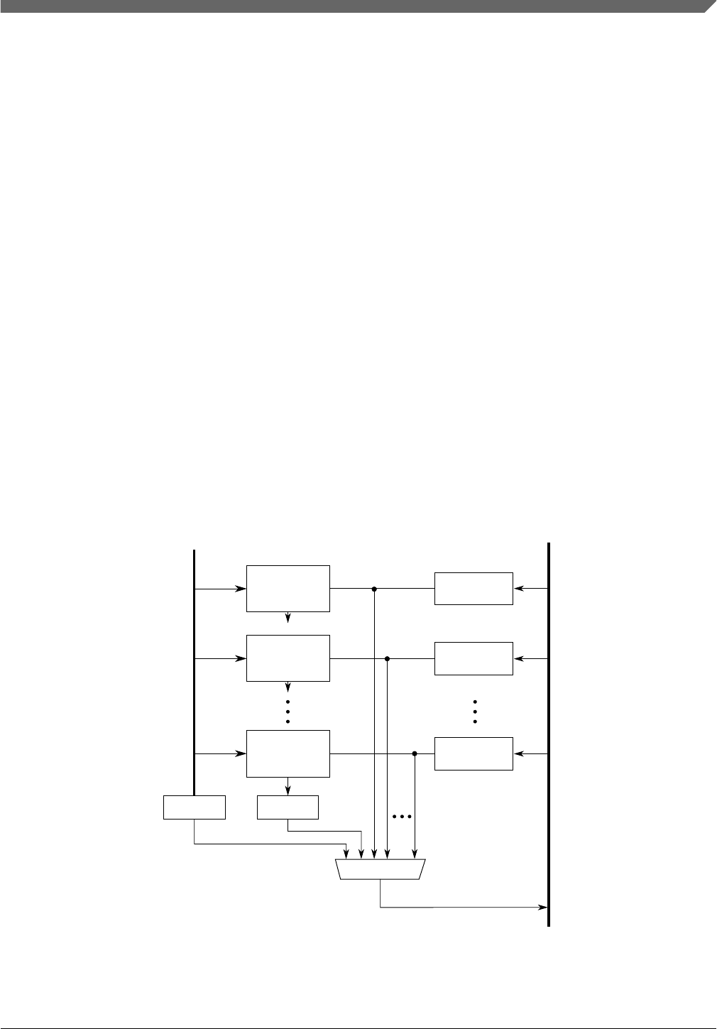
15.2 Introduction
The memory protection unit (MPU) provides hardware access control for all memory
references generated in the device.
15.3 Overview
The MPU concurrently monitors all system bus transactions and evaluates their
appropriateness using pre-programmed region descriptors that define memory spaces and
their access rights. Memory references that have sufficient access control rights are
allowed to complete, while references that are not mapped to any region descriptor or
have insufficient rights are terminated with a protection error response.
15.3.1 Block diagram
A simplified block diagram of the MPU module is shown in the following figure.
Slave Port n Internal
Region
Descriptor 0
Region
Descriptor 1
Region
Descriptor x
Access
Evaluation
Macro
Access
Evaluation
Macro
Access
Evaluation
Macro
Mux
Address Phase Signals Peripheral Bus
MPU_EARnMPU_EDRn
Figure 15-1. MPU block diagram
Chapter 15 Memory Protection Unit (MPU)
S32K1xx Series Reference Manual, Rev. 7, 04/2018
NXP Semiconductors 229

The hardware's two-dimensional connection matrix is clearly visible with the basic access
evaluation macro shown as the replicated submodule block. The crossbar switch slave
ports are shown on the left, the region descriptor registers in the middle, and the
peripheral bus interface on the right side. The evaluation macro contains two magnitude
comparators connected to the start and end address registers from each region descriptor
as well as the combinational logic blocks to determine the region hit and the access
protection error. For details of the access evaluation macro, see Access evaluation macro.
15.3.2 Features
The MPU implements a two-dimensional hardware array of memory region descriptors
and the crossbar slave ports to continuously monitor the legality of every memory
reference generated by each bus master in the system.
The feature set includes:
• 16 program-visible 128-bit region descriptors, accessible by four 32-bit words each
• Each region descriptor defines a modulo-32 byte space, aligned anywhere in
memory
• Region sizes can vary from 32 bytes to 4 Gbytes
• Two access control permissions defined in a single descriptor word
• Masters 0–3: read, write, and execute attributes for supervisor and user
accesses
• Masters 4–7: read and write attributes
• Hardware-assisted maintenance of the descriptor valid bit minimizes coherency
issues
• Alternate programming model view of the access control permissions word
• Priority given to granting permission over denying access for overlapping region
descriptors
• Detects access protection errors if a memory reference does not hit in any memory
region, or if the reference is illegal in all hit memory regions. If an access error
occurs, the reference is terminated with an error response, and the MPU inhibits the
bus cycle being sent to the targeted slave device.
Overview
S32K1xx Series Reference Manual, Rev. 7, 04/2018
230 NXP Semiconductors

• Error registers, per slave port, capture the last faulting address, attributes, and other
information
• Global MPU enable/disable control bit
15.4 MPU register descriptions
The programming model is partitioned into three groups:
• Control/status registers
• The data structure containing the region descriptors
• The alternate view of the region descriptor access control values
The programming model can be referenced using only 32-bit accesses. The programming
model can be accessed only in supervisor mode.
Attempted references of the following types generate an error termination:
• Non-32-bit references
• Accesses in user mode
• References to undefined—that is, reserved—addresses
• References with a non-supported access type, such as a write access to a read-only
register or a read access of a write-only register
15.4.1 MPU Memory map
MPU base address: 4000_D000h
Offset Register Width
(In bits)
Access Reset value
0h Control/Error Status Register (CESR) 32 RW 0081_5201h
10h Error Address Register, slave port 0 (EAR0) 32 RO 0000_0000h
14h Error Detail Register, slave port 0 (EDR0) 32 RO 0000_0000h
18h Error Address Register, slave port 1 (EAR1) 32 RO 0000_0000h
1Ch Error Detail Register, slave port 1 (EDR1) 32 RO 0000_0000h
20h Error Address Register, slave port 2 (EAR2) 32 RO 0000_0000h
24h Error Detail Register, slave port 2 (EDR2) 32 RO 0000_0000h
28h Error Address Register, slave port 3 (EAR3) 32 RO 0000_0000h
2Ch Error Detail Register, slave port 3 (EDR3) 32 RO 0000_0000h
Table continues on the next page...
Chapter 15 Memory Protection Unit (MPU)
S32K1xx Series Reference Manual, Rev. 7, 04/2018
NXP Semiconductors 231

Offset Register Width
(In bits)
Access Reset value
30h Error Address Register, slave port 4 (EAR4) 32 RO 0000_0000h
34h Error Detail Register, slave port 4 (EDR4) 32 RO 0000_0000h
400h Region Descriptor 0, Word 0 (RGD0_WORD0) 32 RW 0000_0000h
404h Region Descriptor 0, Word 1 (RGD0_WORD1) 32 RW FFFF_FFFFh
408h Region Descriptor 0, Word 2 (RGD0_WORD2) 32 RW 0061_F7DFh
40Ch Region Descriptor 0, Word 3 (RGD0_WORD3) 32 RW 0000_0001h
410h Region Descriptor 1, Word 0 (RGD1_WORD0) 32 RW 0000_0000h
414h Region Descriptor 1, Word 1 (RGD1_WORD1) 32 RW 0000_001Fh
418h Region Descriptor 1, Word 2 (RGD1_WORD2) 32 RW 0000_0000h
41Ch Region Descriptor 1, Word 3 (RGD1_WORD3) 32 RW 0000_0000h
420h Region Descriptor 2, Word 0 (RGD2_WORD0) 32 RW 0000_0000h
424h Region Descriptor 2, Word 1 (RGD2_WORD1) 32 RW 0000_001Fh
428h Region Descriptor 2, Word 2 (RGD2_WORD2) 32 RW 0000_0000h
42Ch Region Descriptor 2, Word 3 (RGD2_WORD3) 32 RW 0000_0000h
430h Region Descriptor 3, Word 0 (RGD3_WORD0) 32 RW 0000_0000h
434h Region Descriptor 3, Word 1 (RGD3_WORD1) 32 RW 0000_001Fh
438h Region Descriptor 3, Word 2 (RGD3_WORD2) 32 RW 0000_0000h
43Ch Region Descriptor 3, Word 3 (RGD3_WORD3) 32 RW 0000_0000h
440h Region Descriptor 4, Word 0 (RGD4_WORD0) 32 RW 0000_0000h
444h Region Descriptor 4, Word 1 (RGD4_WORD1) 32 RW 0000_001Fh
448h Region Descriptor 4, Word 2 (RGD4_WORD2) 32 RW 0000_0000h
44Ch Region Descriptor 4, Word 3 (RGD4_WORD3) 32 RW 0000_0000h
450h Region Descriptor 5, Word 0 (RGD5_WORD0) 32 RW 0000_0000h
454h Region Descriptor 5, Word 1 (RGD5_WORD1) 32 RW 0000_001Fh
458h Region Descriptor 5, Word 2 (RGD5_WORD2) 32 RW 0000_0000h
45Ch Region Descriptor 5, Word 3 (RGD5_WORD3) 32 RW 0000_0000h
460h Region Descriptor 6, Word 0 (RGD6_WORD0) 32 RW 0000_0000h
464h Region Descriptor 6, Word 1 (RGD6_WORD1) 32 RW 0000_001Fh
468h Region Descriptor 6, Word 2 (RGD6_WORD2) 32 RW 0000_0000h
46Ch Region Descriptor 6, Word 3 (RGD6_WORD3) 32 RW 0000_0000h
470h Region Descriptor 7, Word 0 (RGD7_WORD0) 32 RW 0000_0000h
474h Region Descriptor 7, Word 1 (RGD7_WORD1) 32 RW 0000_001Fh
478h Region Descriptor 7, Word 2 (RGD7_WORD2) 32 RW 0000_0000h
47Ch Region Descriptor 7, Word 3 (RGD7_WORD3) 32 RW 0000_0000h
480h Region Descriptor 8, Word 0 (RGD8_WORD0) 32 RW 0000_0000h
484h Region Descriptor 8, Word 1 (RGD8_WORD1) 32 RW 0000_001Fh
488h Region Descriptor 8, Word 2 (RGD8_WORD2) 32 RW 0000_0000h
48Ch Region Descriptor 8, Word 3 (RGD8_WORD3) 32 RW 0000_0000h
490h Region Descriptor 9, Word 0 (RGD9_WORD0) 32 RW 0000_0000h
494h Region Descriptor 9, Word 1 (RGD9_WORD1) 32 RW 0000_001Fh
Table continues on the next page...
MPU register descriptions
S32K1xx Series Reference Manual, Rev. 7, 04/2018
232 NXP Semiconductors

Offset Register Width
(In bits)
Access Reset value
498h Region Descriptor 9, Word 2 (RGD9_WORD2) 32 RW 0000_0000h
49Ch Region Descriptor 9, Word 3 (RGD9_WORD3) 32 RW 0000_0000h
4A0h Region Descriptor 10, Word 0 (RGD10_WORD0) 32 RW 0000_0000h
4A4h Region Descriptor 10, Word 1 (RGD10_WORD1) 32 RW 0000_001Fh
4A8h Region Descriptor 10, Word 2 (RGD10_WORD2) 32 RW 0000_0000h
4ACh Region Descriptor 10, Word 3 (RGD10_WORD3) 32 RW 0000_0000h
4B0h Region Descriptor 11, Word 0 (RGD11_WORD0) 32 RW 0000_0000h
4B4h Region Descriptor 11, Word 1 (RGD11_WORD1) 32 RW 0000_001Fh
4B8h Region Descriptor 11, Word 2 (RGD11_WORD2) 32 RW 0000_0000h
4BCh Region Descriptor 11, Word 3 (RGD11_WORD3) 32 RW 0000_0000h
4C0h Region Descriptor 12, Word 0 (RGD12_WORD0) 32 RW 0000_0000h
4C4h Region Descriptor 12, Word 1 (RGD12_WORD1) 32 RW 0000_001Fh
4C8h Region Descriptor 12, Word 2 (RGD12_WORD2) 32 RW 0000_0000h
4CCh Region Descriptor 12, Word 3 (RGD12_WORD3) 32 RW 0000_0000h
4D0h Region Descriptor 13, Word 0 (RGD13_WORD0) 32 RW 0000_0000h
4D4h Region Descriptor 13, Word 1 (RGD13_WORD1) 32 RW 0000_001Fh
4D8h Region Descriptor 13, Word 2 (RGD13_WORD2) 32 RW 0000_0000h
4DCh Region Descriptor 13, Word 3 (RGD13_WORD3) 32 RW 0000_0000h
4E0h Region Descriptor 14, Word 0 (RGD14_WORD0) 32 RW 0000_0000h
4E4h Region Descriptor 14, Word 1 (RGD14_WORD1) 32 RW 0000_001Fh
4E8h Region Descriptor 14, Word 2 (RGD14_WORD2) 32 RW 0000_0000h
4ECh Region Descriptor 14, Word 3 (RGD14_WORD3) 32 RW 0000_0000h
4F0h Region Descriptor 15, Word 0 (RGD15_WORD0) 32 RW 0000_0000h
4F4h Region Descriptor 15, Word 1 (RGD15_WORD1) 32 RW 0000_001Fh
4F8h Region Descriptor 15, Word 2 (RGD15_WORD2) 32 RW 0000_0000h
4FCh Region Descriptor 15, Word 3 (RGD15_WORD3) 32 RW 0000_0000h
800h Region Descriptor Alternate Access Control 0 (RGDAAC0) 32 RW 0061_F7DFh
804h Region Descriptor Alternate Access Control 1 (RGDAAC1) 32 RW 0000_0000h
808h Region Descriptor Alternate Access Control 2 (RGDAAC2) 32 RW 0000_0000h
80Ch Region Descriptor Alternate Access Control 3 (RGDAAC3) 32 RW 0000_0000h
810h Region Descriptor Alternate Access Control 4 (RGDAAC4) 32 RW 0000_0000h
814h Region Descriptor Alternate Access Control 5 (RGDAAC5) 32 RW 0000_0000h
818h Region Descriptor Alternate Access Control 6 (RGDAAC6) 32 RW 0000_0000h
81Ch Region Descriptor Alternate Access Control 7 (RGDAAC7) 32 RW 0000_0000h
820h Region Descriptor Alternate Access Control 8 (RGDAAC8) 32 RW 0000_0000h
824h Region Descriptor Alternate Access Control 9 (RGDAAC9) 32 RW 0000_0000h
828h Region Descriptor Alternate Access Control 10 (RGDAAC10) 32 RW 0000_0000h
82Ch Region Descriptor Alternate Access Control 11 (RGDAAC11) 32 RW 0000_0000h
830h Region Descriptor Alternate Access Control 12 (RGDAAC12) 32 RW 0000_0000h
834h Region Descriptor Alternate Access Control 13 (RGDAAC13) 32 RW 0000_0000h
Table continues on the next page...
Chapter 15 Memory Protection Unit (MPU)
S32K1xx Series Reference Manual, Rev. 7, 04/2018
NXP Semiconductors 233
Offset Register Width
(In bits)
Access Reset value
838h Region Descriptor Alternate Access Control 14 (RGDAAC14) 32 RW 0000_0000h
83Ch Region Descriptor Alternate Access Control 15 (RGDAAC15) 32 RW 0000_0000h
15.4.2 Control/Error Status Register (CESR)
15.4.2.1 Offset
Register Offset
CESR 0h
15.4.2.2 Diagram
Bits 31 30 29 28 27 26 25 24 23 22 21 20 19 18 17 16
R
SPERR
0
SPERR
1
SPERR
2
SPERR
3
SPERR
4
0
0
0
1
0
HRL
W
W1C
W1C
W1C
W1C
W1C
Reset 0 0 0 0 0 0 0 0 1 0 0 0 0 0 0 1
Bits 15 14 13 12 11 10 9 8 7 6 5 4 3 2 1 0
RNSP NRGD 0VLD
W
Reset 0 1 0 1 0 0 1 0 0 0 0 0 0 0 0 1
15.4.2.3 Fields
Field Function
31
SPERR0
Slave Port 0 Error
Indicates a captured error in EAR0 and EDR0. This bit is set when the hardware detects an error and
records the faulting address and attributes. It is cleared by writing one to it. If another error is captured at
the exact same cycle as the write, the flag remains set. A find-first-one instruction or equivalent can
detect the presence of a captured error.
0b - No error has occurred for slave port 0.
Table continues on the next page...
MPU register descriptions
S32K1xx Series Reference Manual, Rev. 7, 04/2018
234 NXP Semiconductors

Field Function
1b - An error has occurred for slave port 0.
30
SPERR1
Slave Port 1 Error
Indicates a captured error in EAR1 and EDR1. This bit is set when the hardware detects an error and
records the faulting address and attributes. It is cleared by writing one to it. If another error is captured at
the exact same cycle as the write, the flag remains set. A find-first-one instruction or equivalent can
detect the presence of a captured error.
0b - No error has occurred for slave port 1.
1b - An error has occurred for slave port 1.
29
SPERR2
Slave Port 2 Error
Indicates a captured error in EAR2 and EDR2. This bit is set when the hardware detects an error and
records the faulting address and attributes. It is cleared by writing one to it. If another error is captured at
the exact same cycle as the write, the flag remains set. A find-first-one instruction or equivalent can
detect the presence of a captured error.
0b - No error has occurred for slave port 2.
1b - An error has occurred for slave port 2.
28
SPERR3
Slave Port 3 Error
Indicates a captured error in EAR3 and EDR3. This bit is set when the hardware detects an error and
records the faulting address and attributes. It is cleared by writing one to it. If another error is captured at
the exact same cycle as the write, the flag remains set. A find-first-one instruction or equivalent can
detect the presence of a captured error.
0b - No error has occurred for slave port 3.
1b - An error has occurred for slave port 3.
27
SPERR4
Slave Port 4 Error
Indicates a captured error in EAR4 and EDR4. This bit is set when the hardware detects an error and
records the faulting address and attributes. It is cleared by writing one to it. If another error is captured at
the exact same cycle as the write, the flag remains set. A find-first-one instruction or equivalent can
detect the presence of a captured error.
0b - No error has occurred for slave port 4.
1b - An error has occurred for slave port 4.
26
—
Reserved
25
—
Reserved
24
—
Reserved
23
—
Reserved
22-20
—
Reserved
19-16
HRL
Hardware Revision Level
Specifies the MPU’s hardware and definition revision level. It can be read by software to determine the
functional definition of the module.
15-12
NSP
Number Of Slave Ports
Specifies the number of slave ports connected to the MPU.
11-8 Number Of Region Descriptors
Table continues on the next page...
Chapter 15 Memory Protection Unit (MPU)
S32K1xx Series Reference Manual, Rev. 7, 04/2018
NXP Semiconductors 235

Field Function
NRGD Indicates the number of region descriptors implemented in the MPU.
0000b - 8 region descriptors
0001b - 12 region descriptors
0010b - 16 region descriptors
7-1
—
Reserved
0
VLD
Valid
Global enable/disable for the MPU.
0b - MPU is disabled. All accesses from all bus masters are allowed.
1b - MPU is enabled
15.4.3 Error Address Register, slave port n (EAR0 - EAR4)
15.4.3.1 Offset
Register Offset
EAR0 10h
EAR1 18h
EAR2 20h
EAR3 28h
EAR4 30h
15.4.3.2 Function
When the MPU detects an access error on slave port n, the 32-bit reference address is
captured in this read-only register and the corresponding bit in CESR[SPERRn] is set.
Additional information about the faulting access is captured in the corresponding EDRn
at the same time. This register and the corresponding EDRn contain the most recent
access error; there are no hardware interlocks with CESR[SPERRn], as the error registers
are always loaded upon the occurrence of each protection violation.
MPU register descriptions
S32K1xx Series Reference Manual, Rev. 7, 04/2018
236 NXP Semiconductors

15.4.3.3 Diagram
Bits 31 30 29 28 27 26 25 24 23 22 21 20 19 18 17 16
READDR
W
Reset 0 0 0 0 0 0 0 0 0 0 0 0 0 0 0 0
Bits 15 14 13 12 11 10 9 8 7 6 5 4 3 2 1 0
READDR
W
Reset 0 0 0 0 0 0 0 0 0 0 0 0 0 0 0 0
15.4.3.4 Fields
Field Function
31-0
EADDR
Error Address
Indicates the reference address from slave port n that generated the access error
15.4.4 Error Detail Register, slave port n (EDR0 - EDR4)
15.4.4.1 Offset
Register Offset
EDR0 14h
EDR1 1Ch
EDR2 24h
EDR3 2Ch
EDR4 34h
15.4.4.2 Function
When the MPU detects an access error on slave port n, 32 bits of error detail are captured
in this read-only register and the corresponding bit in CESR[SPERRn] is set. Information
on the faulting address is captured in the corresponding EARn register at the same time.
This register and the corresponding EARn register contain the most recent access error;
Chapter 15 Memory Protection Unit (MPU)
S32K1xx Series Reference Manual, Rev. 7, 04/2018
NXP Semiconductors 237

there are no hardware interlocks with CESR[SPERRn] as the error registers are always
loaded upon the occurrence of each protection violation.
15.4.4.3 Diagram
Bits 31 30 29 28 27 26 25 24 23 22 21 20 19 18 17 16
REACD
W
Reset 0 0 0 0 0 0 0 0 0 0 0 0 0 0 0 0
Bits 15 14 13 12 11 10 9 8 7 6 5 4 3 2 1 0
REPID EMN EATTR ERW
W
Reset 0 0 0 0 0 0 0 0 0 0 0 0 0 0 0 0
15.4.4.4 Fields
Field Function
31-16
EACD
Error Access Control Detail
Indicates the region descriptor with the access error.
• If EDRn contains a captured error and EACD is cleared, an access did not hit in any region
descriptor.
• If only a single EACD bit is set, the protection error was caused by a single non-overlapping region
descriptor.
• If two or more EACD bits are set, the protection error was caused by an overlapping set of region
descriptors.
15-8
EPID
Error Process Identification
Records the process identifier of the faulting reference. The process identifier is typically driven only by
processor cores; for other bus masters, this field is cleared.
7-4
EMN
Error Master Number
Indicates the bus master that generated the access error.
3-1
EATTR
Error Attributes
Indicates attribute information about the faulting reference.
NOTE: All other encodings are reserved.
000b - User mode, instruction access
001b - User mode, data access
010b - Supervisor mode, instruction access
011b - Supervisor mode, data access
0
ERW
Error Read/Write
Indicates the access type of the faulting reference.
0b - Read
1b - Write
MPU register descriptions
S32K1xx Series Reference Manual, Rev. 7, 04/2018
238 NXP Semiconductors

15.4.5 Region Descriptor n, Word 0 (RGD0_WORD0 - RGD15_WO
RD0)
15.4.5.1 Offset
For n = 0 to 15:
Register Offset
RGDn_WORD0 400h + (n × 10h)
15.4.5.2 Function
The first word of the region descriptor defines the 0-modulo-32 byte start address of the
memory region. Writes to this register clear the region descriptor’s valid bit
(RGDn_WORD3[VLD]).
15.4.5.3 Diagram
Bits 31 30 29 28 27 26 25 24 23 22 21 20 19 18 17 16
RSRTADDR
W
Reset 0 0 0 0 0 0 0 0 0 0 0 0 0 0 0 0
Bits 15 14 13 12 11 10 9 8 7 6 5 4 3 2 1 0
RSRTADDR 0
W
Reset 0 0 0 0 0 0 0 0 0 0 0 0 0 0 0 0
15.4.5.4 Fields
Field Function
31-5
SRTADDR
Start Address
Defines the most significant bits of the 0-modulo-32 byte start address of the memory region.
4-0
—
Reserved
Chapter 15 Memory Protection Unit (MPU)
S32K1xx Series Reference Manual, Rev. 7, 04/2018
NXP Semiconductors 239

15.4.6 Region Descriptor 0, Word 1 (RGD0_WORD1)
15.4.6.1 Offset
Register Offset
RGD0_WORD1 404h
15.4.6.2 Function
The second word of the region descriptor defines the 31-modulo-32 byte end address of
the memory region. Writes to this register clear the region descriptor’s valid bit
(RGDn_WORD3[VLD]).
15.4.6.3 Diagram
Bits 31 30 29 28 27 26 25 24 23 22 21 20 19 18 17 16
RENDADDR
W
Reset 1 1 1 1 1 1 1 1 1 1 1 1 1 1 1 1
Bits 15 14 13 12 11 10 9 8 7 6 5 4 3 2 1 0
RENDADDR Reserved
W
Reset 1 1 1 1 1 1 1 1 1 1 1 1 1 1 1 1
15.4.6.4 Fields
Field Function
31-5
ENDADDR
End Address
Defines the most significant bits of the 31-modulo-32 byte end address of the memory region.
NOTE: The MPU does not verify that ENDADDR ≥ SRTADDR.
4-0
—
Reserved
MPU register descriptions
S32K1xx Series Reference Manual, Rev. 7, 04/2018
240 NXP Semiconductors

15.4.7 Region Descriptor 0, Word 2 (RGD0_WORD2)
15.4.7.1 Offset
Register Offset
RGD0_WORD2 408h
15.4.7.2 Function
The third word of the region descriptor defines the access control rights of the memory
region. The access control privileges depend on two broad classifications of bus masters:
• Bus masters 0–3 have a 5-bit field defining separate privilege rights for user and
supervisor mode accesses. Each of these bus masters optionally includes a process
identification field (if implemented for the master) within the definition.
• Bus masters 4–7 are limited to separate read and write permissions.
For the privilege rights of bus masters 0–3, there are three flags associated with this
function:
• Read (r) refers to accessing the referenced memory address using an operand (data)
fetch
• Write (w) refers to updating the referenced memory address using a store (data)
instruction
• Execute (x) refers to reading the referenced memory address using an instruction
fetch
Writes to RGDn_WORD2 clear the region descriptor’s valid bit
(RGDn_WORD3[VLD]). If only updating the access controls, write to RGDAACn
instead because stores to these locations do not affect the descriptor’s valid bit.
Chapter 15 Memory Protection Unit (MPU)
S32K1xx Series Reference Manual, Rev. 7, 04/2018
NXP Semiconductors 241

15.4.7.3 Diagram
Bits 31 30 29 28 27 26 25 24 23 22 21 20 19 18 17 16
R
M7RE
M7WE
M6RE
M6WE
M5RE
M5WE
M4RE
M4WE
Reserved
M3SM
M3UM
Reserved
M2SM
W
Reset 0 0 0 0 0 0 0 0 0 1 1 0 0 0 0 1
Bits 15 14 13 12 11 10 9 8 7 6 5 4 3 2 1 0
R
M2SM
M2UM
M1PE
M1SM
M1UM
M0PE
M0SM
M0UM
W
Reset 1 1 1 1 0 1 1 1 1 1 0 1 1 1 1 1
15.4.7.4 Fields
Field Function
31
M7RE
Bus Master 7 Read Enable
0b - Bus master 7 reads terminate with an access error and the read is not performed
1b - Bus master 7 reads allowed
30
M7WE
Bus Master 7 Write Enable
0b - Bus master 7 writes terminate with an access error and the write is not performed
1b - Bus master 7 writes allowed
29
M6RE
Bus Master 6 Read Enable
0b - Bus master 6 reads terminate with an access error and the read is not performed
1b - Bus master 6 reads allowed
28
M6WE
Bus Master 6 Write Enable
0b - Bus master 6 writes terminate with an access error and the write is not performed
1b - Bus master 6 writes allowed
27
M5RE
Bus Master 5 Read Enable
0b - Bus master 5 reads terminate with an access error and the read is not performed
1b - Bus master 5 reads allowed
26
M5WE
Bus Master 5 Write Enable
0b - Bus master 5 writes terminate with an access error and the write is not performed
1b - Bus master 5 writes allowed
25
M4RE
Bus Master 4 Read Enable
0b - Bus master 4 reads terminate with an access error and the read is not performed
1b - Bus master 4 reads allowed
24
M4WE
Bus Master 4 Write Enable
0b - Bus master 4 writes terminate with an access error and the write is not performed
1b - Bus master 4 writes allowed
23
—
Reserved
This bit must be written with a zero.
22-21 Bus Master 3 Supervisor Mode Access Control
Table continues on the next page...
MPU register descriptions
S32K1xx Series Reference Manual, Rev. 7, 04/2018
242 NXP Semiconductors

Field Function
M3SM Defines the access controls for bus master 3 in Supervisor mode.
00b - r/w/x; read, write and execute allowed
01b - r/x; read and execute allowed, but no write
10b - r/w; read and write allowed, but no execute
11b - Same as User mode defined in M3UM
20-18
M3UM
Bus Master 3 User Mode Access Control
Defines the access controls for bus master 3 in User mode. M3UM consists of three independent bits,
enabling read (r), write (w), and execute (x) permissions. In M3UM[2:0]: M3UM[2] controls read
permissions, M3UM[1] controls write permissions, and M3UM[0] controls execute permissions. For each
bit:
0b - An attempted access of that mode may be terminated with an access error (if not allowed by
another descriptor) and the access not performed
1b - Allows the given access type to occur
17
—
Reserved
This bit must be written with a zero.
16-15
M2SM
Bus Master 2 Supervisor Mode Access Control
Defines the access controls for bus master 2 in Supervisor mode.
00b - r/w/x; read, write and execute allowed
01b - r/x; read and execute allowed, but no write
10b - r/w; read and write allowed, but no execute
11b - Same as User mode defined in M2UM
14-12
M2UM
Bus Master 2 User Mode Access control
Defines the access controls for bus master 2 in User mode. M2UM consists of three independent bits,
enabling read (r), write (w), and execute (x) permissions. In M2UM[2:0]: M2UM[2] controls read
permissions, M2UM[1] controls write permissions, and M2UM[0] controls execute permissions. For each
bit:
0b - An attempted access of that mode may be terminated with an access error (if not allowed by
another descriptor) and the access not performed
1b - Allows the given access type to occur
11
M1PE
Bus Master 1 Process Identifier enable
0b - Do not include the process identifier in the evaluation
1b - Include the process identifier and mask (RGDn.RGDAAC) in the region hit evaluation
10-9
M1SM
Bus Master 1 Supervisor Mode Access Control
Defines the access controls for bus master 1 in Supervisor mode.
00b - r/w/x; read, write and execute allowed
01b - r/x; read and execute allowed, but no write
10b - r/w; read and write allowed, but no execute
11b - Same as User mode defined in M1UM
8-6
M1UM
Bus Master 1 User Mode Access Control
Defines the access controls for bus master 1 in User mode. M1UM consists of three independent bits,
enabling read (r), write (w), and execute (x) permissions. In M1UM[2:0]: M1UM[2] controls read
permissions, M1UM[1] controls write permissions, and M1UM[0] controls execute permissions. For each
bit:
0b - An attempted access of that mode may be terminated with an access error (if not allowed by
another descriptor) and the access not performed
1b - Allows the given access type to occur
5
M0PE
Bus Master 0 Process Identifier enable
0b - Do not include the process identifier in the evaluation
1b - Include the process identifier and mask (RGDn.RGDAAC) in the region hit evaluation
4-3 Bus Master 0 Supervisor Mode Access Control
Table continues on the next page...
Chapter 15 Memory Protection Unit (MPU)
S32K1xx Series Reference Manual, Rev. 7, 04/2018
NXP Semiconductors 243

Field Function
M0SM Defines the access controls for bus master 0 in Supervisor mode.
00b - r/w/x; read, write and execute allowed
01b - r/x; read and execute allowed, but no write
10b - r/w; read and write allowed, but no execute
11b - Same as User mode defined in M0UM
2-0
M0UM
Bus Master 0 User Mode Access Control
Defines the access controls for bus master 0 in User mode. M0UM consists of three independent bits,
enabling read (r), write (w), and execute (x) permissions. In M0UM[2:0]: M0UM[2] controls read
permissions, M0UM[1] controls write permissions, and M0UM[0] controls execute permissions. For each
bit:
0b - An attempted access of that mode may be terminated with an access error (if not allowed by
another descriptor) and the access not performed
1b - Allows the given access type to occur
15.4.8 Region Descriptor 0, Word 3 (RGD0_WORD3)
15.4.8.1 Offset
Register Offset
RGD0_WORD3 40Ch
15.4.8.2 Function
The fourth word of the region descriptor contains the optional process identifier and
mask, plus the region descriptor’s valid bit.
15.4.8.3 Diagram
Bits 31 30 29 28 27 26 25 24 23 22 21 20 19 18 17 16
RPID PIDMASK
W
Reset 0 0 0 0 0 0 0 0 0 0 0 0 0 0 0 0
Bits 15 14 13 12 11 10 9 8 7 6 5 4 3 2 1 0
R 0 VLD
W
Reset 0 0 0 0 0 0 0 0 0 0 0 0 0 0 0 1
MPU register descriptions
S32K1xx Series Reference Manual, Rev. 7, 04/2018
244 NXP Semiconductors

15.4.8.4 Fields
Field Function
31-24
PID
Process Identifier
Specifies the process identifier that is included in the region hit determination if RGDn_WORD2[MxPE] is
set. PIDMASK can mask individual bits in this field.
23-16
PIDMASK
Process Identifier Mask
Provides a masking capability so that multiple process identifiers can be included as part of the region hit
determination. If a bit in PIDMASK is set, then the corresponding PID bit is ignored in the comparison.
This field and PID are included in the region hit determination if RGDn_WORD2[MxPE] is set. For more
information on the handling of the PID and PIDMASK, see “Access Evaluation - Hit Determination.”
15-1
—
Reserved
0
VLD
Valid
Signals the region descriptor is valid. Any write to RGDn_WORD0–2 clears this bit.
0b - Region descriptor is invalid
1b - Region descriptor is valid
15.4.9 Region Descriptor n, Word 1 (RGD1_WORD1 - RGD15_WO
RD1)
15.4.9.1 Offset
For n = 1 to 15:
Register Offset
RGDn_WORD1 404h + (n × 10h)
15.4.9.2 Function
The second word of the region descriptor defines the 31-modulo-32 byte end address of
the memory region. Writes to this register clear the region descriptor’s valid bit
(RGDn_WORD3[VLD]).
Chapter 15 Memory Protection Unit (MPU)
S32K1xx Series Reference Manual, Rev. 7, 04/2018
NXP Semiconductors 245

15.4.9.3 Diagram
Bits 31 30 29 28 27 26 25 24 23 22 21 20 19 18 17 16
RENDADDR
W
Reset 0 0 0 0 0 0 0 0 0 0 0 0 0 0 0 0
Bits 15 14 13 12 11 10 9 8 7 6 5 4 3 2 1 0
RENDADDR Reserved
W
Reset 0 0 0 0 0 0 0 0 0 0 0 1 1 1 1 1
15.4.9.4 Fields
Field Function
31-5
ENDADDR
End Address
Defines the most significant bits of the 31-modulo-32 byte end address of the memory region.
NOTE: The MPU does not verify that ENDADDR ≥ SRTADDR.
4-0
—
Reserved
15.4.10 Region Descriptor n, Word 2 (RGD1_WORD2 - RGD15_
WORD2)
15.4.10.1 Offset
For n = 1 to 15:
Register Offset
RGDn_WORD2 408h + (n × 10h)
MPU register descriptions
S32K1xx Series Reference Manual, Rev. 7, 04/2018
246 NXP Semiconductors

15.4.10.2 Function
The third word of the region descriptor defines the access control rights of the memory
region. The access control privileges depend on two broad classifications of bus masters:
• Bus masters 0–3 have a 5-bit field defining separate privilege rights for user and
supervisor mode accesses. Each of these bus masters optionally includes a process
identification field (if implemented for the master) within the definition.
• Bus masters 4–7 are limited to separate read and write permissions.
For the privilege rights of bus masters 0–3, there are three flags associated with this
function:
• Read (r) refers to accessing the referenced memory address using an operand (data)
fetch
• Write (w) refers to updating the referenced memory address using a store (data)
instruction
• Execute (x) refers to reading the referenced memory address using an instruction
fetch
Writes to RGDn_WORD2 clear the region descriptor’s valid bit
(RGDn_WORD3[VLD]). If only updating the access controls, write to RGDAACn
instead because stores to these locations do not affect the descriptor’s valid bit.
15.4.10.3 Diagram
Bits 31 30 29 28 27 26 25 24 23 22 21 20 19 18 17 16
R
M7RE
M7WE
M6RE
M6WE
M5RE
M5WE
M4RE
M4WE
Reserved
M3SM
M3UM
Reserved
M2SM
W
Reset 0 0 0 0 0 0 0 0 0 0 0 0 0 0 0 0
Bits 15 14 13 12 11 10 9 8 7 6 5 4 3 2 1 0
R
M2SM
M2UM
M1PE
M1SM
M1UM
M0PE
M0SM
M0UM
W
Reset 0 0 0 0 0 0 0 0 0 0 0 0 0 0 0 0
Chapter 15 Memory Protection Unit (MPU)
S32K1xx Series Reference Manual, Rev. 7, 04/2018
NXP Semiconductors 247

15.4.10.4 Fields
Field Function
31
M7RE
Bus Master 7 Read Enable
0b - Bus master 7 reads terminate with an access error and the read is not performed
1b - Bus master 7 reads allowed
30
M7WE
Bus Master 7 Write Enable
0b - Bus master 7 writes terminate with an access error and the write is not performed
1b - Bus master 7 writes allowed
29
M6RE
Bus Master 6 Read Enable
0b - Bus master 6 reads terminate with an access error and the read is not performed
1b - Bus master 6 reads allowed
28
M6WE
Bus Master 6 Write Enable
0b - Bus master 6 writes terminate with an access error and the write is not performed
1b - Bus master 6 writes allowed
27
M5RE
Bus Master 5 Read Enable
0b - Bus master 5 reads terminate with an access error and the read is not performed
1b - Bus master 5 reads allowed
26
M5WE
Bus Master 5 Write Enable
0b - Bus master 5 writes terminate with an access error and the write is not performed
1b - Bus master 5 writes allowed
25
M4RE
Bus Master 4 Read Enable
0b - Bus master 4 reads terminate with an access error and the read is not performed
1b - Bus master 4 reads allowed
24
M4WE
Bus Master 4 Write Enable
0b - Bus master 4 writes terminate with an access error and the write is not performed
1b - Bus master 4 writes allowed
23
—
Reserved
This bit must be written with a zero.
22-21
M3SM
Bus Master 3 Supervisor Mode Access Control
Defines the access controls for bus master 3 in Supervisor mode.
00b - r/w/x; read, write and execute allowed
01b - r/x; read and execute allowed, but no write
10b - r/w; read and write allowed, but no execute
11b - Same as User mode defined in M3UM
20-18
M3UM
Bus Master 3 User Mode Access Control
Defines the access controls for bus master 3 in User mode. M3UM consists of three independent bits,
enabling read (r), write (w), and execute (x) permissions. In M3UM[2:0]: M3UM[2] controls read
permissions, M3UM[1] controls write permissions, and M3UM[0] controls execute permissions. For each
bit:
0b - An attempted access of that mode may be terminated with an access error (if not allowed by
another descriptor) and the access not performed
1b - Allows the given access type to occur
17
—
Reserved
This bit must be written with a zero.
16-15
M2SM
Bus Master 2 Supervisor Mode Access Control
Defines the access controls for bus master 2 in Supervisor mode.
00b - r/w/x; read, write and execute allowed
01b - r/x; read and execute allowed, but no write
Table continues on the next page...
MPU register descriptions
S32K1xx Series Reference Manual, Rev. 7, 04/2018
248 NXP Semiconductors

Field Function
10b - r/w; read and write allowed, but no execute
11b - Same as User mode defined in M2UM
14-12
M2UM
Bus Master 2 User Mode Access control
Defines the access controls for bus master 2 in User mode. M2UM consists of three independent bits,
enabling read (r), write (w), and execute (x) permissions. In M2UM[2:0]: M2UM[2] controls read
permissions, M2UM[1] controls write permissions, and M2UM[0] controls execute permissions. For each
bit:
0b - An attempted access of that mode may be terminated with an access error (if not allowed by
another descriptor) and the access not performed
1b - Allows the given access type to occur
11
M1PE
Bus Master 1 Process Identifier enable
0b - Do not include the process identifier in the evaluation
1b - Include the process identifier and mask (RGDn.RGDAAC) in the region hit evaluation
10-9
M1SM
Bus Master 1 Supervisor Mode Access Control
Defines the access controls for bus master 1 in Supervisor mode.
00b - r/w/x; read, write and execute allowed
01b - r/x; read and execute allowed, but no write
10b - r/w; read and write allowed, but no execute
11b - Same as User mode defined in M1UM
8-6
M1UM
Bus Master 1 User Mode Access Control
Defines the access controls for bus master 1 in User mode. M1UM consists of three independent bits,
enabling read (r), write (w), and execute (x) permissions. In M1UM[2:0]: M1UM[2] controls read
permissions, M1UM[1] controls write permissions, and M1UM[0] controls execute permissions. For each
bit:
0b - An attempted access of that mode may be terminated with an access error (if not allowed by
another descriptor) and the access not performed
1b - Allows the given access type to occur
5
M0PE
Bus Master 0 Process Identifier enable
0b - Do not include the process identifier in the evaluation
1b - Include the process identifier and mask (RGDn.RGDAAC) in the region hit evaluation
4-3
M0SM
Bus Master 0 Supervisor Mode Access Control
Defines the access controls for bus master 0 in Supervisor mode.
00b - r/w/x; read, write and execute allowed
01b - r/x; read and execute allowed, but no write
10b - r/w; read and write allowed, but no execute
11b - Same as User mode defined in M0UM
2-0
M0UM
Bus Master 0 User Mode Access Control
Defines the access controls for bus master 0 in User mode. M0UM consists of three independent bits,
enabling read (r), write (w), and execute (x) permissions. In M0UM[2:0]: M0UM[2] controls read
permissions, M0UM[1] controls write permissions, and M0UM[0] controls execute permissions. For each
bit:
0b - An attempted access of that mode may be terminated with an access error (if not allowed by
another descriptor) and the access not performed
1b - Allows the given access type to occur
Chapter 15 Memory Protection Unit (MPU)
S32K1xx Series Reference Manual, Rev. 7, 04/2018
NXP Semiconductors 249

15.4.11 Region Descriptor n, Word 3 (RGD1_WORD3 - RGD15_
WORD3)
15.4.11.1 Offset
For n = 1 to 15:
Register Offset
RGDn_WORD3 40Ch + (n × 10h)
15.4.11.2 Function
The fourth word of the region descriptor contains the optional process identifier and
mask, plus the region descriptor’s valid bit.
15.4.11.3 Diagram
Bits 31 30 29 28 27 26 25 24 23 22 21 20 19 18 17 16
RPID PIDMASK
W
Reset 0 0 0 0 0 0 0 0 0 0 0 0 0 0 0 0
Bits 15 14 13 12 11 10 9 8 7 6 5 4 3 2 1 0
R 0 VLD
W
Reset 0 0 0 0 0 0 0 0 0 0 0 0 0 0 0 0
15.4.11.4 Fields
Field Function
31-24
PID
Process Identifier
Specifies the process identifier that is included in the region hit determination if RGDn_WORD2[MxPE] is
set. PIDMASK can mask individual bits in this field.
23-16
PIDMASK
Process Identifier Mask
Provides a masking capability so that multiple process identifiers can be included as part of the region hit
determination. If a bit in PIDMASK is set, then the corresponding PID bit is ignored in the comparison.
Table continues on the next page...
MPU register descriptions
S32K1xx Series Reference Manual, Rev. 7, 04/2018
250 NXP Semiconductors

Field Function
This field and PID are included in the region hit determination if RGDn_WORD2[MxPE] is set. For more
information on the handling of the PID and PIDMASK, see “Access Evaluation - Hit Determination.”
15-1
—
Reserved
0
VLD
Valid
Signals the region descriptor is valid. Any write to RGDn_WORD0–2 clears this bit.
0b - Region descriptor is invalid
1b - Region descriptor is valid
15.4.12 Region Descriptor Alternate Access Control 0 (RGDA
AC0)
15.4.12.1 Offset
Register Offset
RGDAAC0 800h
15.4.12.2 Function
Because software may adjust only the access controls within a region descriptor
(RGDn_WORD2) as different tasks execute, an alternate programming view of this 32-
bit entity is available. Writing to this register does not affect the descriptor’s valid bit.
Chapter 15 Memory Protection Unit (MPU)
S32K1xx Series Reference Manual, Rev. 7, 04/2018
NXP Semiconductors 251

15.4.12.3 Diagram
Bits 31 30 29 28 27 26 25 24 23 22 21 20 19 18 17 16
R
M7RE
M7WE
M6RE
M6WE
M5RE
M5WE
M4RE
M4WE
Reserved
M3SM
M3UM
Reserved
M2SM
W
Reset
10 0 0 0 0 0 0 0 0 1 1 0 0 0 0 1
Bits 15 14 13 12 11 10 9 8 7 6 5 4 3 2 1 0
R
M2SM
M2UM
M1PE
M1SM
M1UM
M0PE
M0SM
M0UM
W
Reset 1 1 1 1 0 1 1 1 1 1 0 1 1 1 1 1
1. RGDAAC0 resets to 61F7DFh. Other RGDAACn registers reset to 0h.
15.4.12.4 Fields
Field Function
31
M7RE
Bus Master 7 Read Enable
0b - Bus master 7 reads terminate with an access error and the read is not performed
1b - Bus master 7 reads allowed
30
M7WE
Bus Master 7 Write Enable
0b - Bus master 7 writes terminate with an access error and the write is not performed
1b - Bus master 7 writes allowed
29
M6RE
Bus Master 6 Read Enable
0b - Bus master 6 reads terminate with an access error and the read is not performed
1b - Bus master 6 reads allowed
28
M6WE
Bus Master 6 Write Enable
0b - Bus master 6 writes terminate with an access error and the write is not performed
1b - Bus master 6 writes allowed
27
M5RE
Bus Master 5 Read Enable
0b - Bus master 5 reads terminate with an access error and the read is not performed
1b - Bus master 5 reads allowed
26
M5WE
Bus Master 5 Write Enable
0b - Bus master 5 writes terminate with an access error and the write is not performed
1b - Bus master 5 writes allowed
25
M4RE
Bus Master 4 Read Enable
0b - Bus master 4 reads terminate with an access error and the read is not performed
1b - Bus master 4 reads allowed
24
M4WE
Bus Master 4 Write Enable
0b - Bus master 4 writes terminate with an access error and the write is not performed
1b - Bus master 4 writes allowed
23
—
Reserved
This bit must be written with a zero.
Table continues on the next page...
MPU register descriptions
S32K1xx Series Reference Manual, Rev. 7, 04/2018
252 NXP Semiconductors

Field Function
22-21
M3SM
Bus Master 3 Supervisor Mode Access Control
Defines the access controls for bus master 3 in Supervisor mode.
00b - r/w/x; read, write and execute allowed
01b - r/x; read and execute allowed, but no write
10b - r/w; read and write allowed, but no execute
11b - Same as User mode defined in M3UM
20-18
M3UM
Bus Master 3 User Mode Access Control
Defines the access controls for bus master 3 in User mode. M3UM consists of three independent bits,
enabling read (r), write (w), and execute (x) permissions. In M3UM[2:0]: M3UM[2] controls read
permissions, M3UM[1] controls write permissions, and M3UM[0] controls execute permissions. For each
bit:
0b - An attempted access of that mode may be terminated with an access error (if not allowed by
another descriptor) and the access not performed
1b - Allows the given access type to occur
17
—
Reserved
This bit must be written with a zero.
16-15
M2SM
Bus Master 2 Supervisor Mode Access Control
Defines the access controls for bus master 2 in Supervisor mode.
00b - r/w/x; read, write and execute allowed
01b - r/x; read and execute allowed, but no write
10b - r/w; read and write allowed, but no execute
11b - Same as User mode defined in M2UM
14-12
M2UM
Bus Master 2 User Mode Access Control
Defines the access controls for bus master 2 in User mode. M2UM consists of three independent bits,
enabling read (r), write (w), and execute (x) permissions. In M2UM[2:0]: M2UM[2] controls read
permissions, M2UM[1] controls write permissions, and M2UM[0] controls execute permissions. For each
bit:
0b - An attempted access of that mode may be terminated with an access error (if not allowed by
another descriptor) and the access not performed
1b - Allows the given access type to occur
11
M1PE
Bus Master 1 Process Identifier Enable
NOTE: For RGDAAC0: Only bus master 1 can write to M1PE.
0b - Do not include the process identifier in the evaluation
1b - Include the process identifier and mask (RGDn.RGDAAC) in the region hit evaluation
10-9
M1SM
Bus Master 1 Supervisor Mode Access Control
Defines the access controls for bus master 1 in Supervisor mode.
NOTE: For RGDAAC0: Only bus master 1 can write to M1SM.
00b - r/w/x; read, write and execute allowed
01b - r/x; read and execute allowed, but no write
10b - r/w; read and write allowed, but no execute
11b - Same as User mode defined in M1UM
8-6
M1UM
Bus Master 1 User Mode Access Control
Defines the access controls for bus master 1 in User mode. M1UM consists of three independent bits,
enabling read (r), write (w), and execute (x) permissions. In M1UM[2:0]: M1UM[2] controls read
permissions, M1UM[1] controls write permissions, and M1UM[0] controls execute permissions.
NOTE: For RGDAAC0: Only bus master 1 can write to M1UM.
For each bit:
0b - An attempted access of that mode may be terminated with an access error (if not allowed by
another descriptor) and the access not performed
Table continues on the next page...
Chapter 15 Memory Protection Unit (MPU)
S32K1xx Series Reference Manual, Rev. 7, 04/2018
NXP Semiconductors 253

Field Function
1b - Allows the given access type to occur
5
M0PE
Bus Master 0 Process Identifier Enable
0b - Do not include the process identifier in the evaluation
1b - Include the process identifier and mask (RGDn.RGDAAC) in the region hit evaluation
4-3
M0SM
Bus Master 0 Supervisor Mode Access Control
Defines the access controls for bus master 0 in Supervisor mode.
00b - r/w/x; read, write and execute allowed
01b - r/x; read and execute allowed, but no write
10b - r/w; read and write allowed, but no execute
11b - Same as User mode defined in M0UM
2-0
M0UM
Bus Master 0 User Mode Access Control
Defines the access controls for bus master 0 in User mode. M0UM consists of three independent bits,
enabling read (r), write (w), and execute (x) permissions. In M0UM[2:0]: M0UM[2] controls read
permissions, M0UM[1] controls write permissions, and M0UM[0] controls execute permissions. For each
bit:
0b - An attempted access of that mode may be terminated with an access error (if not allowed by
another descriptor) and the access not performed
1b - Allows the given access type to occur
15.4.13 Region Descriptor Alternate Access Control n (RGDA
AC1 - RGDAAC15)
15.4.13.1 Offset
For n = 1 to 15:
Register Offset
RGDAACn 800h + (n × 4h)
15.4.13.2 Function
Because software may adjust only the access controls within a region descriptor
(RGDn_WORD2) as different tasks execute, an alternate programming view of this 32-
bit entity is available. Writing to this register does not affect the descriptor’s valid bit.
MPU register descriptions
S32K1xx Series Reference Manual, Rev. 7, 04/2018
254 NXP Semiconductors

15.4.13.3 Diagram
Bits 31 30 29 28 27 26 25 24 23 22 21 20 19 18 17 16
R
M7RE
M7WE
M6RE
M6WE
M5RE
M5WE
M4RE
M4WE
Reserved
M3SM
M3UM
Reserved
M2SM
W
Reset
10 0 0 0 0 0 0 0 0 0 0 0 0 0 0 0
Bits 15 14 13 12 11 10 9 8 7 6 5 4 3 2 1 0
R
M2SM
M2UM
M1PE
M1SM
M1UM
M0PE
M0SM
M0UM
W
Reset 0 0 0 0 0 0 0 0 0 0 0 0 0 0 0 0
1. RGDAAC0 resets to 61F7DFh. Other RGDAACn registers reset to 0h.
15.4.13.4 Fields
Field Function
31
M7RE
Bus Master 7 Read Enable
0b - Bus master 7 reads terminate with an access error and the read is not performed
1b - Bus master 7 reads allowed
30
M7WE
Bus Master 7 Write Enable
0b - Bus master 7 writes terminate with an access error and the write is not performed
1b - Bus master 7 writes allowed
29
M6RE
Bus Master 6 Read Enable
0b - Bus master 6 reads terminate with an access error and the read is not performed
1b - Bus master 6 reads allowed
28
M6WE
Bus Master 6 Write Enable
0b - Bus master 6 writes terminate with an access error and the write is not performed
1b - Bus master 6 writes allowed
27
M5RE
Bus Master 5 Read Enable
0b - Bus master 5 reads terminate with an access error and the read is not performed
1b - Bus master 5 reads allowed
26
M5WE
Bus Master 5 Write Enable
0b - Bus master 5 writes terminate with an access error and the write is not performed
1b - Bus master 5 writes allowed
25
M4RE
Bus Master 4 Read Enable
0b - Bus master 4 reads terminate with an access error and the read is not performed
1b - Bus master 4 reads allowed
24
M4WE
Bus Master 4 Write Enable
0b - Bus master 4 writes terminate with an access error and the write is not performed
1b - Bus master 4 writes allowed
23
—
Reserved
This bit must be written with a zero.
Table continues on the next page...
Chapter 15 Memory Protection Unit (MPU)
S32K1xx Series Reference Manual, Rev. 7, 04/2018
NXP Semiconductors 255

Field Function
22-21
M3SM
Bus Master 3 Supervisor Mode Access Control
Defines the access controls for bus master 3 in Supervisor mode.
00b - r/w/x; read, write and execute allowed
01b - r/x; read and execute allowed, but no write
10b - r/w; read and write allowed, but no execute
11b - Same as User mode defined in M3UM
20-18
M3UM
Bus Master 3 User Mode Access Control
Defines the access controls for bus master 3 in User mode. M3UM consists of three independent bits,
enabling read (r), write (w), and execute (x) permissions. In M3UM[2:0]: M3UM[2] controls read
permissions, M3UM[1] controls write permissions, and M3UM[0] controls execute permissions. For each
bit:
0b - An attempted access of that mode may be terminated with an access error (if not allowed by
another descriptor) and the access not performed
1b - Allows the given access type to occur
17
—
Reserved
This bit must be written with a zero.
16-15
M2SM
Bus Master 2 Supervisor Mode Access Control
Defines the access controls for bus master 2 in Supervisor mode.
00b - r/w/x; read, write and execute allowed
01b - r/x; read and execute allowed, but no write
10b - r/w; read and write allowed, but no execute
11b - Same as User mode defined in M2UM
14-12
M2UM
Bus Master 2 User Mode Access Control
Defines the access controls for bus master 2 in User mode. M2UM consists of three independent bits,
enabling read (r), write (w), and execute (x) permissions. In M2UM[2:0]: M2UM[2] controls read
permissions, M2UM[1] controls write permissions, and M2UM[0] controls execute permissions. For each
bit:
0b - An attempted access of that mode may be terminated with an access error (if not allowed by
another descriptor) and the access not performed
1b - Allows the given access type to occur
11
M1PE
Bus Master 1 Process Identifier Enable
NOTE: For RGDAAC0: Only bus master 1 can write to M1PE.
0b - Do not include the process identifier in the evaluation
1b - Include the process identifier and mask (RGDn.RGDAAC) in the region hit evaluation
10-9
M1SM
Bus Master 1 Supervisor Mode Access Control
Defines the access controls for bus master 1 in Supervisor mode.
NOTE: For RGDAAC0: Only bus master 1 can write to M1SM.
00b - r/w/x; read, write and execute allowed
01b - r/x; read and execute allowed, but no write
10b - r/w; read and write allowed, but no execute
11b - Same as User mode defined in M1UM
8-6
M1UM
Bus Master 1 User Mode Access Control
Defines the access controls for bus master 1 in User mode. M1UM consists of three independent bits,
enabling read (r), write (w), and execute (x) permissions. In M1UM[2:0]: M1UM[2] controls read
permissions, M1UM[1] controls write permissions, and M1UM[0] controls execute permissions.
NOTE: For RGDAAC0: Only bus master 1 can write to M1UM.
For each bit:
0b - An attempted access of that mode may be terminated with an access error (if not allowed by
another descriptor) and the access not performed
Table continues on the next page...
MPU register descriptions
S32K1xx Series Reference Manual, Rev. 7, 04/2018
256 NXP Semiconductors

Field Function
1b - Allows the given access type to occur
5
M0PE
Bus Master 0 Process Identifier Enable
0b - Do not include the process identifier in the evaluation
1b - Include the process identifier and mask (RGDn.RGDAAC) in the region hit evaluation
4-3
M0SM
Bus Master 0 Supervisor Mode Access Control
Defines the access controls for bus master 0 in Supervisor mode.
00b - r/w/x; read, write and execute allowed
01b - r/x; read and execute allowed, but no write
10b - r/w; read and write allowed, but no execute
11b - Same as User mode defined in M0UM
2-0
M0UM
Bus Master 0 User Mode Access Control
Defines the access controls for bus master 0 in User mode. M0UM consists of three independent bits,
enabling read (r), write (w), and execute (x) permissions. In M0UM[2:0]: M0UM[2] controls read
permissions, M0UM[1] controls write permissions, and M0UM[0] controls execute permissions. For each
bit:
0b - An attempted access of that mode may be terminated with an access error (if not allowed by
another descriptor) and the access not performed
1b - Allows the given access type to occur
15.5 Functional description
In this section, the functional operation of the MPU is detailed, including the operation of
the access evaluation macro and the handling of error-terminated bus cycles.
15.5.1 Access evaluation macro
The basic operation of the MPU is performed in the access evaluation macro, a hardware
structure replicated in the two-dimensional connection matrix. As shown in the following
figure, the access evaluation macro inputs the crossbar bus address phase signals and the
contents of a region descriptor (RGDn) and performs two major functions:
• Region hit determination
• Detection of an access protection violation
The following figure shows a functional block diagram.
Chapter 15 Memory Protection Unit (MPU)
S32K1xx Series Reference Manual, Rev. 7, 04/2018
NXP Semiconductors 257

start end
error
≥ ≥
RGDn
MPU_EDRnAccess not allowed
≥ ≤
hit_b
Address
(hit AND error) (no hit OR error)
r,w,x
Figure 15-2. MPU access evaluation macro
15.5.1.1 Hit determination
To determine whether the current reference hits in the given region, two magnitude
comparators are used with the region's start and end addresses. The boolean equation for
this portion of the hit determination is:
region_hit = ((addr[31:5] >= RGDn_Word0[SRTADDR]) & (addr[31:5] <= RGDn_Word1[ENDADDR])) &
RGDn_Word3[VLD]
where addr is the current reference address, RGDn_Word0[SRTADDR] and
RGDn_Word1[ENDADDR] are the start and end addresses, and RGDn_Word3[VLD] is
the valid bit.
NOTE
The MPU does not verify that ENDADDR ≥ SRTADDR.
In addition to the comparison of the reference address versus the region descriptor's start
and end addresses, the optional process identifier is examined against the region
descriptor's PID and PIDMASK fields. A process identifier hit term is formed as follows:
pid_hit = ~RGDn_Word2[MxPE] |
((current_pid |
RGDn_Word3[PIDMASK]) == (RGDn_Word3[PID] | RGDn_Word3[PIDMASK]))
where the current_pid is the selected process identifier from the current bus master, and
RGDn_Word3[PID] and RGDn_Word3[PIDMASK] are the process identifier fields from
region descriptor n. For bus masters that do not output a process identifier, the MPU
forces the pid_hit term to assert.
Functional description
S32K1xx Series Reference Manual, Rev. 7, 04/2018
258 NXP Semiconductors

15.5.1.2 Privilege violation determination
While the access evaluation macro is determining region hit, the logic is also evaluating
if the current access is allowed by the permissions defined in the region descriptor. Using
the master and supervisor/user mode signals, a set of effective permissions is generated
from the appropriate fields in the region descriptor. The protection violation logic then
evaluates the access against the effective permissions as shown in the following table.
Table 15-5. Protection violation definition
Description MxUM Protection violation?
r w x
Instruction fetch read — — 0 Yes, no execute permission
— — 1 No, access is allowed
Data read 0 — — Yes, no read permission
1 — — No, access is allowed
Data write — 0 — Yes, no write permission
— 1 — No, access is allowed
15.5.2 Putting it all together and error terminations
For each slave port monitored, the MPU performs a reduction-AND of all the individual
terms from each access evaluation macro. This expression then terminates the bus cycle
with an error and reports a protection error for three conditions:
• If the access does not hit in any region descriptor, a protection error is reported.
• If the access hits in a single region descriptor and that region signals a protection
violation, a protection error is reported.
• If the access hits in multiple (overlapping) regions and all regions signal protection
violations, a protection error is reported.
As shown in the third condition, granting permission is a higher priority than denying
access for overlapping regions. This approach is more flexible to system software in
region descriptor assignments. For an example of the use of overlapping region
descriptors, see Application information.
Chapter 15 Memory Protection Unit (MPU)
S32K1xx Series Reference Manual, Rev. 7, 04/2018
NXP Semiconductors 259

15.5.3 Power management
Disabling the MPU by clearing CESR[VLD] minimizes power dissipation. To minimize
the power dissipation of an enabled MPU, invalidate unused region descriptors by
clearing the associated RGDn_Word3[VLD] bits.
15.6 Initialization information
At system startup, load the appropriate number of region descriptors, including setting
RGDn_Word3[VLD]. Setting CESR[VLD] enables the module.
If the system requires that all the loaded region descriptors be enabled simultaneously,
first ensure that the entire MPU is disabled (CESR[VLD]=0).
Note
If the MPU registers are protected by the MPU, a region
descriptor must be set to allow access to the MPU registers if
further changes are needed.
15.7 Application information
In an operational system, interfacing with the MPU is generally classified into the
following activities:
• Creating a new memory region—Load the appropriate region descriptor into an
available RGDn, using four sequential 32-bit writes. The hardware assists in the
maintenance of the valid bit, so if this approach is followed, there are no coherency
issues with the multi-cycle descriptor writes. (Clearing RGDn_Word3[VLD] deletes/
removes an existing memory region.)
• Altering only access privileges—To not affect the valid bit, write to the alternate
version of the access control word (RGDAACn), so there are no coherency issues
involved with the update. When the write completes, the memory region's access
rights switch instantaneously to the new value.
• Changing a region's start and end addresses—Write a minimum of three words to the
region descriptor (RGDn_Word{0,1,3}). Word 0 and 1 redefine the start and end
addresses, respectively. Word 3 re-enables the region descriptor valid bit. In most
situations, all four words of the region descriptor are rewritten.
Initialization information
S32K1xx Series Reference Manual, Rev. 7, 04/2018
260 NXP Semiconductors

• Accessing the MPU—Allocate a region descriptor to restrict MPU access to
supervisor mode from a specific master.
• Detecting an access error—The current bus cycle is terminated with an error
response and EARn and EDRn capture information on the faulting reference. The
error-terminated bus cycle typically initiates an error response in the originating bus
master. For example, a processor core may respond with a bus error exception, while
a data movement bus master may respond with an error interrupt. The processor can
retrieve the captured error address and detail information simply by reading
E{A,D}Rn. CESR[SPERR] signals which error registers contain captured fault data.
• Overlapping region descriptors—Applying overlapping regions often reduces the
number of descriptors required for a given set of access controls. In the overlapping
memory space, the protection rights of the corresponding region descriptors are
logically summed together (the boolean OR operator).
The following dual-core system example contains four bus masters:
• The two processors: CP0, CP1
• Two DMA engines: DMA1, a traditional data movement engine transferring data
between RAM and peripherals and DMA2, a second engine transferring data to/
from the RAM only
Consider the following region descriptor assignments:
Table 15-6. Overlapping region descriptor example
Region description RGDn CP0 CP1 DMA1 DMA2
CP0 code 0 rwx r-- — — Flash
CP1 code 1 r-- rwx — —
CP0 data & stack 2 rw- — — —
RAM
CP0 → CP1 shared data 2 3 r-- r-- — —
CP1 → CP0 shared data 4
CP1 data & stack 4 — rw- — —
Shared DMA data 5 rw- rw- rw rw
MPU 6 rw- rw- — — Peripheral
space
Peripherals 7 rw- rw- rw —
In this example, there are eight descriptors used to span nine regions in the three main
spaces of the system memory map: flash, RAM, and peripheral space. Each region
indicates the specific permissions for each of the four bus masters and this definition
provides an appropriate set of shared, private and executable memory spaces.
Of particular interest are the two overlapping spaces: region descriptors 2 & 3 and 3 & 4.
Chapter 15 Memory Protection Unit (MPU)
S32K1xx Series Reference Manual, Rev. 7, 04/2018
NXP Semiconductors 261

The space defined by RGD2 with no overlap is a private data and stack area that provides
read/write access to CP0 only. The overlapping space between RGD2 and RGD3 defines
a shared data space for passing data from CP0 to CP1 and the access controls are defined
by the logical OR of the two region descriptors. Thus, CP0 has (rw- | r--) = (rw-)
permissions, while CP1 has (--- | r--) = (r--) permission in this space. Both DMA engines
are excluded from this shared processor data region. The overlapping spaces between
RGD3 and RGD4 defines another shared data space, this one for passing data from CP1
to CP0. For this overlapping space, CP0 has (r-- | ---) = (r--) permission, while CP1 has
(rw- | r--) = (rw-) permission. The non-overlapped space of RGD4 defines a private data
and stack area for CP1 only.
The space defined by RGD5 is a shared data region, accessible by all four bus masters.
Finally, the slave peripheral space mapped onto the IPS bus is partitioned into two
regions:
• One containing the MPU's programming model accessible only to the two processor
cores
• The remaining peripheral region accessible to both processors and the traditional
DMA1 master
This example shows one possible application of the capabilities of the MPU in a typical
system.
Application information
S32K1xx Series Reference Manual, Rev. 7, 04/2018
262 NXP Semiconductors

Chapter 16
Peripheral Bridge (AIPS-Lite)
Chip-specific AIPS information
16.1.1 Instantiation information
This device contains one peripheral bridge. The peripheral access protection is supported
by AIPS. The MPU will not cover peripheral access protection.
16.1.2 Memory maps
The peripheral bridge is used to access the registers of most of the modules on this
device. See S32K1xx_memory_map.xlsx attached to Reference Manual for the memory
slot assignment.
AIPS_PACR0 – PACR31 refer to on platform peripherals with corresponding AIPS
Peripheral bridge slot numbers from 0 -31. AIPS_OPACR0 – OPACR95 refer to off
platform peripherals with corresponding AIPS Peripheral bridge slot numbers from 32
-127. For logical master ID assignments see MPU Logical Bus Master Assignments.
16.1.2.1 Register reset values
The following table shows chip-specific reset values for AIPS registers:
Table 16-1. Register reset values
Register S32K116 S32K118 S32K142 S32K144 S32K146 S32K148
MPRA 7770_0000 7770_0000 7770_0000 7770_0000 7770_0000 7777_0000
PACRA 5400_0000 5400_0000 5400_0000 5400_0000 5400_0000 5400_0000
PACRB 4400_0404 4400_0404 4400_0400 4400_0400 4400_0400 4400_0400
PACRD 4400_0000 4400_0000 4400_0000 4400_0000 4400_0000 4400_0000
Table continues on the next page...
16.1
S32K1xx Series Reference Manual, Rev. 7, 04/2018
NXP Semiconductors 263

Table 16-1. Register reset values (continued)
Register S32K116 S32K118 S32K142 S32K144 S32K146 S32K148
OPACRA 4400_4000 4400_4000 4400_4444 4400_4444 4400_4444 4400_4444
OPACRB 0000_4000 0000_4400 0000_4400 0000_4400 0000_4400 0004_4440
OPACRC 0040_0044 0040_0044 0440_0044 0440_0044 0440_0044 0440_0044
OPACRD 4404_0444 4404_0444 4444_0400 4444_0400 4444_0400 4444_0400
OPACRE 4000_0040 4000_0040 4000_0040 4000_0040 4000_0040 4000_0040
OPACRF 4444_4400 4444_4400 4444_4400 4444_4400 4444_4400 4444_4400
OPACRG 0040_0000 0040_0000 0040_0000 0040_0000 0040_0000 0040_4400
OPACRH 0040_0000 0040_0000 0040_0000 0040_0000 0040_0000 0040_0000
OPACRI 0004_4440 0004_4440 0404_4440 0404_4440 0404_4440 0404_4444
OPACRJ 0044_0000 0044_0000 0044_0000 0044_0000 0044_4044 0044_4044
OPACRK 0004_0000 0004_0000 0004_0000 0004_0000 0004_0000 4404_0040
OPACRL 0000_0444 0000_0444 0000_0444 0000_0444 0000_0444 0400_0444
16.1.2.2 Register information
In S32K11x, CMU0 and CMU1 reside on Off-platform slots 30 and 31 respectively, and
access of the same is controlled by bits OPACRD[0:7] shown below. In S32K14x these
bits are Reserved as show in AIPS register descriptions.
Table 16-2. OPARCD register
Bit
fields
S32K14x S32K11x
Bitfiled[0:
7]
Reserved Bit 0: TP7 (Trusted Protect 7)
Bit 1: WP7 (Write Protect 7)
Bit 2: SP7 (Supervisor Protect 7)
Bit 3: Reserved
Bit 4: TP6 (Trusted Protect 6)
Bit 5: WP6 (Write Protect 6)
Bit 6: SP6 (Supervisor Protect 6)
Bit 7: Reserved
16.2 Introduction
The peripheral bridge converts the crossbar switch interface to an interface that can
access most of the slave peripherals on this chip.
Introduction
S32K1xx Series Reference Manual, Rev. 7, 04/2018
264 NXP Semiconductors

The peripheral bridge occupies 64 MB of the address space, which is divided into
peripheral slots of 4 KB. (It might be possible that all the peripheral slots are not used.
See the memory map chapter for details on slot assignments.) The bridge includes
separate clock enable inputs for each of the slots to accommodate slower peripherals.
16.2.1 Features
Key features of the peripheral bridge are:
• Supports peripheral slots with 8-, 16-, and 32-bit datapath width
• Programming model provides memory protection functionality
16.2.2 General operation
The slave devices connected to the peripheral bridge are modules which contain a
programming model of control and status registers. The system masters read and write
these registers through the peripheral bridge.
The register maps of the peripherals are located on 4-KB boundaries. Each peripheral is
allocated one or more 4-KB block(s) of the memory map.
16.3 Memory map/register definition
The 32-bit peripheral bridge registers can be accessed only in supervisor mode by trusted
bus masters. Additionally, these registers must be read from or written to only by a 32-bit
aligned access. The peripheral bridge registers are mapped into the Peripheral Access
Control Register A PACRA[PACR0] address space.
16.3.1 AIPS register descriptions
16.3.1.1 AIPS Memory map
AIPS_Lite base address: 4000_0000h
Chapter 16 Peripheral Bridge (AIPS-Lite)
S32K1xx Series Reference Manual, Rev. 7, 04/2018
NXP Semiconductors 265

Offset Register Width
(In bits)
Access Reset value
0h Master Privilege Register A (MPRA) 32 RW 2C36_0000h
20h Peripheral Access Control Register (PACRA) 32 RW 5400_0000h
24h Peripheral Access Control Register (PACRB) 32 RW 4400_0400h
2Ch Peripheral Access Control Register (PACRD) 32 RW 4400_0000h
40h Off-Platform Peripheral Access Control Register (OPACRA) 32 RW 4400_4444h
44h Off-Platform Peripheral Access Control Register (OPACRB) 32 RW 0004_4440h
48h Off-Platform Peripheral Access Control Register (OPACRC) 32 RW 0440_0044h
4Ch Off-Platform Peripheral Access Control Register (OPACRD) 32 RW 4444_0400h
50h Off-Platform Peripheral Access Control Register (OPACRE) 32 RW 4000_0040h
54h Off-Platform Peripheral Access Control Register (OPACRF) 32 RW 4444_4400h
58h Off-Platform Peripheral Access Control Register (OPACRG) 32 RW 0040_4400h
5Ch Off-Platform Peripheral Access Control Register (OPACRH) 32 RW 0040_0000h
60h Off-Platform Peripheral Access Control Register (OPACRI) 32 RW 0404_4444h
64h Off-Platform Peripheral Access Control Register (OPACRJ) 32 RW 0044_4044h
68h Off-Platform Peripheral Access Control Register (OPACRK) 32 RW 4404_0040h
6Ch Off-Platform Peripheral Access Control Register (OPACRL) 32 RW 0400_0444h
16.3.1.2 Master Privilege Register A (MPRA)
16.3.1.2.1 Offset
Register Offset
MPRA 0h
16.3.1.2.2 Function
The MPRA specifies identical 4-bit fields defining the access-privilege level associated
with a bus master to various peripherals on the chip. The register provides one field per
bus master.
A register field that maps to an unimplemented master or peripheral behaves as read-
only-zero.
Each master is assigned a logical ID from 0 to 15. See the master logical ID assignment
table in the chip-specific AIPS information.
Memory map/register definition
S32K1xx Series Reference Manual, Rev. 7, 04/2018
266 NXP Semiconductors

16.3.1.2.3 Diagram
Bits 31 30 29 28 27 26 25 24 23 22 21 20 19 18 17 16
R
0
MTR0
MTW0
MPL0
0
MTR1
MTW1
MPL1
0
MTR2
MTW2
MPL2
0
MTR3
MTW3
MPL3
W
Reset 0 0 1 0 1 1 0 0 0 0 1 1 0 1 1 0
Bits 15 14 13 12 11 10 9 8 7 6 5 4 3 2 1 0
R 0 Reserved 0Reserved 0Reserved 0Reserved
W
Reset 0 0 0 0 0 0 0 0 0 0 0 0 0 0 0 0
16.3.1.2.4 Fields
Field Function
31
—
Reserved
30
MTR0
Master 0 Trusted For Read
Determines whether the master is trusted for read accesses.
0b - This master is not trusted for read accesses.
1b - This master is trusted for read accesses.
29
MTW0
Master 0 Trusted For Writes
Determines whether the master is trusted for write accesses.
0b - This master is not trusted for write accesses.
1b - This master is trusted for write accesses.
28
MPL0
Master 0 Privilege Level
Specifies how the privilege level of the master is determined.
0b - Accesses from this master are forced to user-mode.
1b - Accesses from this master are not forced to user-mode.
27
—
Reserved
26
MTR1
Master 1 Trusted for Read
Determines whether the master is trusted for read accesses.
0b - This master is not trusted for read accesses.
1b - This master is trusted for read accesses.
25
MTW1
Master 1 Trusted for Writes
Determines whether the master is trusted for write accesses.
0b - This master is not trusted for write accesses.
1b - This master is trusted for write accesses.
24
MPL1
Master 1 Privilege Level
Specifies how the privilege level of the master is determined.
0b - Accesses from this master are forced to user-mode.
1b - Accesses from this master are not forced to user-mode.
Table continues on the next page...
Chapter 16 Peripheral Bridge (AIPS-Lite)
S32K1xx Series Reference Manual, Rev. 7, 04/2018
NXP Semiconductors 267

Field Function
23
—
Reserved
22
MTR2
Master 2 Trusted For Read
Determines whether the master is trusted for read accesses.
0b - This master is not trusted for read accesses.
1b - This master is trusted for read accesses.
21
MTW2
Master 2 Trusted For Writes
Determines whether the master is trusted for write accesses.
0b - This master is not trusted for write accesses.
1b - This master is trusted for write accesses.
20
MPL2
Master 2 Privilege Level
Specifies how the privilege level of the master is determined.
0b - Accesses from this master are forced to user-mode.
1b - Accesses from this master are not forced to user-mode.
19
—
Reserved
18
MTR3
Master 3 Trusted For Read
Determines whether the master is trusted for read accesses.
0b - This master is not trusted for read accesses.
1b - This master is trusted for read accesses.
17
MTW3
Master 3 Trusted For Writes
Determines whether the master is trusted for write accesses.
0b - This master is not trusted for write accesses.
1b - This master is trusted for write accesses.
16
MPL3
Master 3 Privilege Level
Specifies how the privilege level of the master is determined.
0b - Accesses from this master are forced to user-mode.
1b - Accesses from this master are not forced to user-mode.
15
—
Reserved
14-12
—
Reserved
11
—
Reserved
10-8
—
Reserved
7
—
Reserved
6-4
—
Reserved
3
—
Reserved
2-0 Reserved
Memory map/register definition
S32K1xx Series Reference Manual, Rev. 7, 04/2018
268 NXP Semiconductors

Field Function
—
16.3.1.3 Peripheral Access Control Register (PACRA)
16.3.1.3.1 Offset
Register Offset
PACRA 20h
16.3.1.3.2 Function
Each PACR register consists of eight 4-bit PACR fields. Each PACR field defines the
access levels for a particular on-platform peripheral. The peripheral assignment to each
PACR field is defined by the memory map slot of the peripheral. See the chip-specific
AIPS information for the field assignment of a particular peripheral.
Every PACR field to which no peripheral is assigned is reserved. Reads to reserved
locations return zeros, and writes are ignored.
16.3.1.3.3 Diagram
Bits 31 30 29 28 27 26 25 24 23 22 21 20 19 18 17 16
R 0 SP0 WP0 TP0 0SP1 WP1 TP1 0 0
W
Reset 0 1 0 1 0 1 0 0 0 0 0 0 0 0 0 0
Bits 15 14 13 12 11 10 9 8 7 6 5 4 3 2 1 0
R 0 0 0 0
W
Reset 0 0 0 0 0 0 0 0 0 0 0 0 0 0 0 0
16.3.1.3.4 Fields
Field Function
31 Reserved
Table continues on the next page...
Chapter 16 Peripheral Bridge (AIPS-Lite)
S32K1xx Series Reference Manual, Rev. 7, 04/2018
NXP Semiconductors 269

Field Function
—
30
SP0
Supervisor Protect
Determines whether the peripheral requires supervisor privilege level for accesses. When this field is set,
the master privilege level must indicate the supervisor access attribute, and the MPRx[MPLn] control field
for the master must be set. If not, access terminates with an error response and no peripheral access
initiates.
0b - This peripheral does not require supervisor privilege level for accesses.
1b - This peripheral requires supervisor privilege level for accesses.
29
WP0
Write Protect
Determines whether the peripheral allows write accesses. When this field is set and a write access is
attempted, access terminates with an error response and no peripheral access initiates.
0b - This peripheral allows write accesses.
1b - This peripheral is write protected.
28
TP0
Trusted Protect
Determines whether the peripheral allows accesses from an untrusted master. When this field is set and
an access is attempted by an untrusted master, the access terminates with an error response and no
peripheral access initiates.
0b - Accesses from an untrusted master are allowed.
1b - Accesses from an untrusted master are not allowed.
27
—
Reserved
26
SP1
Supervisor Protect
Determines whether the peripheral requires supervisor privilege level for accesses. When this field is set,
the master privilege level must indicate the supervisor access attribute, and the MPRx[MPLn] control field
for the master must be set. If not, access terminates with an error response and no peripheral access
initiates.
0b - This peripheral does not require supervisor privilege level for accesses.
1b - This peripheral requires supervisor privilege level for accesses.
25
WP1
Write Protect
Determines whether the peripheral allows write accesses. When this field is set and a write access is
attempted, access terminates with an error response and no peripheral access initiates.
0b - This peripheral allows write accesses.
1b - This peripheral is write protected.
24
TP1
Trusted Protect
Determines whether the peripheral allows accesses from an untrusted master. When this field is set and
an access is attempted by an untrusted master, the access terminates with an error response and no
peripheral access initiates.
0b - Accesses from an untrusted master are allowed.
1b - Accesses from an untrusted master are not allowed.
23-20
—
Reserved
19-16
—
Reserved
15-12
—
Reserved
11-8 Reserved
Table continues on the next page...
Memory map/register definition
S32K1xx Series Reference Manual, Rev. 7, 04/2018
270 NXP Semiconductors

Field Function
—
7-4
—
Reserved
3-0
—
Reserved
16.3.1.4 Peripheral Access Control Register (PACRB)
16.3.1.4.1 Offset
Register Offset
PACRB 24h
16.3.1.4.2 Function
Each PACR register consists of eight 4-bit PACR fields. Each PACR field defines the
access levels for a particular on-platform peripheral. The peripheral assignment to each
PACR field is defined by the memory map slot of the peripheral. See the chip-specific
AIPS information for the field assignment of a particular peripheral.
Every PACR field to which no peripheral is assigned is reserved. Reads to reserved
locations return zeros, and writes are ignored.
16.3.1.4.3 Diagram
Bits 31 30 29 28 27 26 25 24 23 22 21 20 19 18 17 16
R 0 SP0 WP0 TP0 0SP1 WP1 TP1 0 0
W
Reset 0 1 0 0 0 1 0 0 0 0 0 0 0 0 0 0
Bits 15 14 13 12 11 10 9 8 7 6 5 4 3 2 1 0
R 0 0 SP5 WP5 TP5 0 0
W
Reset 0 0 0 0 0 1 0 0 0 0 0 0 0 0 0 0
Chapter 16 Peripheral Bridge (AIPS-Lite)
S32K1xx Series Reference Manual, Rev. 7, 04/2018
NXP Semiconductors 271

16.3.1.4.4 Fields
Field Function
31
—
Reserved
30
SP0
Supervisor Protect
Determines whether the peripheral requires supervisor privilege level for accesses. When this field is set,
the master privilege level must indicate the supervisor access attribute, and the MPRx[MPLn] control field
for the master must be set. If not, access terminates with an error response and no peripheral access
initiates.
0b - This peripheral does not require supervisor privilege level for accesses.
1b - This peripheral requires supervisor privilege level for accesses.
29
WP0
Write Protect
Determines whether the peripheral allows write accesses. When this field is set and a write access is
attempted, access terminates with an error response and no peripheral access initiates.
0b - This peripheral allows write accesses.
1b - This peripheral is write protected.
28
TP0
Trusted Protect
Determines whether the peripheral allows accesses from an untrusted master. When this field is set and
an access is attempted by an untrusted master, the access terminates with an error response and no
peripheral access initiates.
0b - Accesses from an untrusted master are allowed.
1b - Accesses from an untrusted master are not allowed.
27
—
Reserved
26
SP1
Supervisor Protect
Determines whether the peripheral requires supervisor privilege level for accesses. When this field is set,
the master privilege level must indicate the supervisor access attribute, and the MPRx[MPLn] control field
for the master must be set. If not, access terminates with an error response and no peripheral access
initiates.
0b - This peripheral does not require supervisor privilege level for accesses.
1b - This peripheral requires supervisor privilege level for accesses.
25
WP1
Write Protect
Determines whether the peripheral allows write accesses. When this field is set and a write access is
attempted, access terminates with an error response and no peripheral access initiates.
0b - This peripheral allows write accesses.
1b - This peripheral is write protected.
24
TP1
Trusted Protect
Determines whether the peripheral allows accesses from an untrusted master. When this field is set and
an access is attempted by an untrusted master, the access terminates with an error response and no
peripheral access initiates.
0b - Accesses from an untrusted master are allowed.
1b - Accesses from an untrusted master are not allowed.
23-20
—
Reserved
19-16
—
Reserved
15-12 Reserved
Table continues on the next page...
Memory map/register definition
S32K1xx Series Reference Manual, Rev. 7, 04/2018
272 NXP Semiconductors

Field Function
—
11
—
Reserved
10
SP5
Supervisor Protect
Determines whether the peripheral requires supervisor privilege level for accesses. When this field is set,
the master privilege level must indicate the supervisor access attribute, and the MPRx[MPLn] control field
for the master must be set. If not, access terminates with an error response and no peripheral access
initiates.
0b - This peripheral does not require supervisor privilege level for accesses.
1b - This peripheral requires supervisor privilege level for accesses.
9
WP5
Write Protect
Determines whether the peripheral allows write accesses. When this field is set and a write access is
attempted, access terminates with an error response and no peripheral access initiates.
0b - This peripheral allows write accesses.
1b - This peripheral is write protected.
8
TP5
Trusted Protect
Determines whether the peripheral allows accesses from an untrusted master. When this field is set and
an access is attempted by an untrusted master, the access terminates with an error response and no
peripheral access initiates.
0b - Accesses from an untrusted master are allowed.
1b - Accesses from an untrusted master are not allowed.
7-4
—
Reserved
3-0
—
Reserved
16.3.1.5 Peripheral Access Control Register (PACRD)
16.3.1.5.1 Offset
Register Offset
PACRD 2Ch
16.3.1.5.2 Function
Each PACR register consists of eight 4-bit PACR fields. Each PACR field defines the
access levels for a particular on-platform peripheral. The peripheral assignment to each
PACR field is defined by the memory map slot of the peripheral. See the chip-specific
AIPS information for the field assignment of a particular peripheral.
Chapter 16 Peripheral Bridge (AIPS-Lite)
S32K1xx Series Reference Manual, Rev. 7, 04/2018
NXP Semiconductors 273

Every PACR field to which no peripheral is assigned is reserved. Reads to reserved
locations return zeros, and writes are ignored.
16.3.1.5.3 Diagram
Bits 31 30 29 28 27 26 25 24 23 22 21 20 19 18 17 16
R 0 SP0 WP0 TP0 0SP1 WP1 TP1 0 0
W
Reset 0 1 0 0 0 1 0 0 0 0 0 0 0 0 0 0
Bits 15 14 13 12 11 10 9 8 7 6 5 4 3 2 1 0
R 0 0 0 0
W
Reset 0 0 0 0 0 0 0 0 0 0 0 0 0 0 0 0
16.3.1.5.4 Fields
Field Function
31
—
Reserved
30
SP0
Supervisor Protect
Determines whether the peripheral requires supervisor privilege level for accesses. When this field is set,
the master privilege level must indicate the supervisor access attribute, and the MPRx[MPLn] control field
for the master must be set. If not, access terminates with an error response and no peripheral access
initiates.
0b - This peripheral does not require supervisor privilege level for accesses.
1b - This peripheral requires supervisor privilege level for accesses.
29
WP0
Write Protect
Determines whether the peripheral allows write accesses. When this field is set and a write access is
attempted, access terminates with an error response and no peripheral access initiates.
0b - This peripheral allows write accesses.
1b - This peripheral is write protected.
28
TP0
Trusted Protect
Determines whether the peripheral allows accesses from an untrusted master. When this field is set and
an access is attempted by an untrusted master, the access terminates with an error response and no
peripheral access initiates.
0b - Accesses from an untrusted master are allowed.
1b - Accesses from an untrusted master are not allowed.
27
—
Reserved
26
SP1
Supervisor Protect
Table continues on the next page...
Memory map/register definition
S32K1xx Series Reference Manual, Rev. 7, 04/2018
274 NXP Semiconductors

Field Function
Determines whether the peripheral requires supervisor privilege level for accesses. When this field is set,
the master privilege level must indicate the supervisor access attribute, and the MPRx[MPLn] control field
for the master must be set. If not, access terminates with an error response and no peripheral access
initiates.
0b - This peripheral does not require supervisor privilege level for accesses.
1b - This peripheral requires supervisor privilege level for accesses.
25
WP1
Write Protect
Determines whether the peripheral allows write accesses. When this field is set and a write access is
attempted, access terminates with an error response and no peripheral access initiates.
0b - This peripheral allows write accesses.
1b - This peripheral is write protected.
24
TP1
Trusted Protect
Determines whether the peripheral allows accesses from an untrusted master. When this field is set and
an access is attempted by an untrusted master, the access terminates with an error response and no
peripheral access initiates.
0b - Accesses from an untrusted master are allowed.
1b - Accesses from an untrusted master are not allowed.
23-20
—
Reserved
19-16
—
Reserved
15-12
—
Reserved
11-8
—
Reserved
7-4
—
Reserved
3-0
—
Reserved
16.3.1.6 Off-Platform Peripheral Access Control Register (OPACRA)
16.3.1.6.1 Offset
Register Offset
OPACRA 40h
Chapter 16 Peripheral Bridge (AIPS-Lite)
S32K1xx Series Reference Manual, Rev. 7, 04/2018
NXP Semiconductors 275

16.3.1.6.2 Function
Each OPACR register consists of eight 4-bit OPACR fields. Each OPACR field defines
the access levels for a particular off-platform peripheral. The peripheral assignment to
each OPACR field is defined by the memory map slot of the peripheral. See the chip-
specific AIPS information for the field assignment of a particular peripheral.
16.3.1.6.3 Diagram
Bits 31 30 29 28 27 26 25 24 23 22 21 20 19 18 17 16
R 0 SP0 WP0 TP0 0SP1 WP1 TP1 0 0
W
Reset 0 1 0 0 0 1 0 0 0 0 0 0 0 0 0 0
Bits 15 14 13 12 11 10 9 8 7 6 5 4 3 2 1 0
R 0 SP4 WP4 TP4 0SP5 WP5 TP5 0SP6 WP6 TP6 0SP7 WP7 TP7
W
Reset 0 1 0 0 0 1 0 0 0 1 0 0 0 1 0 0
16.3.1.6.4 Fields
Field Function
31
—
Reserved
30
SP0
Supervisor Protect
Determines whether the peripheral requires supervisor privilege level for accesses. When this field is set,
the master privilege level must indicate the supervisor access attribute, and the MPRx[MPLn] control field
for the master must be set. If not, access terminates with an error response and no peripheral access
initiates.
0b - This peripheral does not require supervisor privilege level for accesses.
1b - This peripheral requires supervisor privilege level for accesses.
29
WP0
Write Protect
Determines whether the peripheral allows write accesses. When this field is set and a write access is
attempted, access terminates with an error response and no peripheral access initiates.
0b - This peripheral allows write accesses.
1b - This peripheral is write protected.
28
TP0
Trusted Protect
Determines whether the peripheral allows accesses from an untrusted master. When this bit is set and an
access is attempted by an untrusted master, the access terminates with an error response and no
peripheral access initiates.
0b - Accesses from an untrusted master are allowed.
1b - Accesses from an untrusted master are not allowed.
27
—
Reserved
Table continues on the next page...
Memory map/register definition
S32K1xx Series Reference Manual, Rev. 7, 04/2018
276 NXP Semiconductors

Field Function
26
SP1
Supervisor Protect
Determines whether the peripheral requires supervisor privilege level for access. When this field is set,
the master privilege level must indicate the supervisor access attribute, and the MPRx[MPLn] control field
for the master must be set. If not, access terminates with an error response and no peripheral access
initiates.
0b - This peripheral does not require supervisor privilege level for accesses.
1b - This peripheral requires supervisor privilege level for accesses.
25
WP1
Write Protect
Determines whether the peripheral allows write accesses. When this field is set and a write access is
attempted, access terminates with an error response and no peripheral access initiates.
0b - This peripheral allows write accesses.
1b - This peripheral is write protected.
24
TP1
Trusted Protect
Determines whether the peripheral allows accesses from an untrusted master. When this field is set and
an access is attempted by an untrusted master, the access terminates with an error response and no
peripheral access initiates.
0b - Accesses from an untrusted master are allowed.
1b - Accesses from an untrusted master are not allowed.
23-20
—
Reserved
19-16
—
Reserved
15
—
Reserved
14
SP4
Supervisor Protect
Determines whether the peripheral requires supervisor privilege level for access. When this bit is set, the
master privilege level must indicate the supervisor access attribute, and the MPRx[MPLn] control bit for
the master must be set. If not, access terminates with an error response and no peripheral access
initiates.
0b - This peripheral does not require supervisor privilege level for accesses.
1b - This peripheral requires supervisor privilege level for accesses.
13
WP4
Write Protect
Determines whether the peripheral allows write accesses. When this field is set and a write access is
attempted, access terminates with an error response and no peripheral access initiates.
0b - This peripheral allows write accesses.
1b - This peripheral is write protected.
12
TP4
Trusted Protect
Determines whether the peripheral allows accesses from an untrusted master. When this bit is set and an
access is attempted by an untrusted master, the access terminates with an error response and no
peripheral access initiates.
0b - Accesses from an untrusted master are allowed.
1b - Accesses from an untrusted master are not allowed.
11
—
Reserved
10
SP5
Supervisor Protect
Table continues on the next page...
Chapter 16 Peripheral Bridge (AIPS-Lite)
S32K1xx Series Reference Manual, Rev. 7, 04/2018
NXP Semiconductors 277

Field Function
Determines whether the peripheral requires supervisor privilege level for accesses. When this field is set,
the master privilege level must indicate the supervisor access attribute, and the MPRx[MPLn] control field
for the master must be set. If not, access terminates with an error response and no peripheral access
initiates.
0b - This peripheral does not require supervisor privilege level for accesses.
1b - This peripheral requires supervisor privilege level for accesses.
9
WP5
Write Protect
Determines whether the peripheral allows write accesses. When this field is set and a write access is
attempted, access terminates with an error response and no peripheral access initiates.
0b - This peripheral allows write accesses.
1b - This peripheral is write protected.
8
TP5
Trusted Protect
Determines whether the peripheral allows accesses from an untrusted master. When this field is set and
an access is attempted by an untrusted master, the access terminates with an error response and no
peripheral access initiates.
0b - Accesses from an untrusted master are allowed.
1b - Accesses from an untrusted master are not allowed.
7
—
Reserved
6
SP6
Supervisor Protect
Determines whether the peripheral requires supervisor privilege level for accesses. When this field is set,
the master privilege level must indicate the supervisor access attribute, and the MPRx[MPLn] control field
for the master must be set. If not, access terminates with an error response and no peripheral access
initiates.
0b - This peripheral does not require supervisor privilege level for accesses.
1b - This peripheral requires supervisor privilege level for accesses.
5
WP6
Write Protect
Determines whether the peripheral allows write accesses. When this field is set and a write access is
attempted, access terminates with an error response and no peripheral access initiates.
0b - This peripheral allows write accesses.
1b - This peripheral is write protected.
4
TP6
Trusted Protect
Determines whether the peripheral allows accesses from an untrusted master. When this field is set and
an access is attempted by an untrusted master, the access terminates with an error response and no
peripheral access initiates.
0b - Accesses from an untrusted master are allowed.
1b - Accesses from an untrusted master are not allowed.
3
—
Reserved
2
SP7
Supervisor Protect
Determines whether the peripheral requires supervisor privilege level for accesses. When this field is set,
the master privilege level must indicate the supervisor access attribute, and the MPRx[MPLn] control field
for the master must be set. If not, access terminates with an error response and no peripheral access
initiates.
0b - This peripheral does not require supervisor privilege level for accesses.
1b - This peripheral requires supervisor privilege level for accesses.
1
WP7
Write Protect
Table continues on the next page...
Memory map/register definition
S32K1xx Series Reference Manual, Rev. 7, 04/2018
278 NXP Semiconductors

Field Function
Determines whether the peripheral allows accesses from an untrusted master. When this field is set and
an access is attempted by an untrusted master, the access terminates with an error response and no
peripheral access initiates.
0b - This peripheral allows write accesses.
1b - This peripheral is write protected.
0
TP7
Trusted Protect
Determines whether the peripheral allows accesses from an untrusted master. When this field is set and
an access is attempted by an untrusted master, the access terminates with an error response and no
peripheral access initiates.
0b - Accesses from an untrusted master are allowed.
1b - Accesses from an untrusted master are not allowed.
16.3.1.7 Off-Platform Peripheral Access Control Register (OPACRB)
16.3.1.7.1 Offset
Register Offset
OPACRB 44h
16.3.1.7.2 Function
Each OPACR register consists of eight 4-bit OPACR fields. Each OPACR field defines
the access levels for a particular off-platform peripheral. The peripheral assignment to
each OPACR field is defined by the memory map slot of the peripheral. See the chip-
specific AIPS information for the field assignment of a particular peripheral.
16.3.1.7.3 Diagram
Bits 31 30 29 28 27 26 25 24 23 22 21 20 19 18 17 16
R 0 0 0 0 SP3 WP3 TP3
W
Reset 0 0 0 0 0 0 0 0 0 0 0 0 0 1 0 0
Bits 15 14 13 12 11 10 9 8 7 6 5 4 3 2 1 0
R 0 SP4 WP4 TP4 0SP5 WP5 TP5 0SP6 WP6 TP6 0
W
Reset 0 1 0 0 0 1 0 0 0 1 0 0 0 0 0 0
Chapter 16 Peripheral Bridge (AIPS-Lite)
S32K1xx Series Reference Manual, Rev. 7, 04/2018
NXP Semiconductors 279

16.3.1.7.4 Fields
Field Function
31-28
—
Reserved
27-24
—
Reserved
23-20
—
Reserved
19
—
Reserved
18
SP3
Supervisor Protect
Determines whether the peripheral requires supervisor privilege level for accesses. When this field is set,
the master privilege level must indicate the supervisor access attribute, and the MPRx[MPLn] control field
for the master must be set. If not, access terminates with an error response and no peripheral access
initiates.
0b - This peripheral does not require supervisor privilege level for accesses.
1b - This peripheral requires supervisor privilege level for accesses.
17
WP3
Write Protect
Determines whether the peripheral allows write access. When this bit is set and a write access is
attempted, access terminates with an error response and no peripheral access initiates.
0b - This peripheral allows write accesses.
1b - This peripheral is write protected.
16
TP3
Trusted Protect
Determines whether the peripheral allows accesses from an untrusted master. When this field is set and
an access is attempted by an untrusted master, the access terminates with an error response and no
peripheral access initiates.
0b - Accesses from an untrusted master are allowed.
1b - Accesses from an untrusted master are not allowed.
15
—
Reserved
14
SP4
Supervisor Protect
Determines whether the peripheral requires supervisor privilege level for access. When this bit is set, the
master privilege level must indicate the supervisor access attribute, and the MPRx[MPLn] control bit for
the master must be set. If not, access terminates with an error response and no peripheral access
initiates.
0b - This peripheral does not require supervisor privilege level for accesses.
1b - This peripheral requires supervisor privilege level for accesses.
13
WP4
Write Protect
Determines whether the peripheral allows write accesses. When this field is set and a write access is
attempted, access terminates with an error response and no peripheral access initiates.
0b - This peripheral allows write accesses.
1b - This peripheral is write protected.
12
TP4
Trusted Protect
Determines whether the peripheral allows accesses from an untrusted master. When this bit is set and an
access is attempted by an untrusted master, the access terminates with an error response and no
peripheral access initiates.
Table continues on the next page...
Memory map/register definition
S32K1xx Series Reference Manual, Rev. 7, 04/2018
280 NXP Semiconductors

Field Function
0b - Accesses from an untrusted master are allowed.
1b - Accesses from an untrusted master are not allowed.
11
—
Reserved
10
SP5
Supervisor Protect
Determines whether the peripheral requires supervisor privilege level for accesses. When this field is set,
the master privilege level must indicate the supervisor access attribute, and the MPRx[MPLn] control field
for the master must be set. If not, access terminates with an error response and no peripheral access
initiates.
0b - This peripheral does not require supervisor privilege level for accesses.
1b - This peripheral requires supervisor privilege level for accesses.
9
WP5
Write Protect
Determines whether the peripheral allows write accesses. When this field is set and a write access is
attempted, access terminates with an error response and no peripheral access initiates.
0b - This peripheral allows write accesses.
1b - This peripheral is write protected.
8
TP5
Trusted Protect
Determines whether the peripheral allows accesses from an untrusted master. When this field is set and
an access is attempted by an untrusted master, the access terminates with an error response and no
peripheral access initiates.
0b - Accesses from an untrusted master are allowed.
1b - Accesses from an untrusted master are not allowed.
7
—
Reserved
6
SP6
Supervisor Protect
Determines whether the peripheral requires supervisor privilege level for accesses. When this field is set,
the master privilege level must indicate the supervisor access attribute, and the MPRx[MPLn] control field
for the master must be set. If not, access terminates with an error response and no peripheral access
initiates.
0b - This peripheral does not require supervisor privilege level for accesses.
1b - This peripheral requires supervisor privilege level for accesses.
5
WP6
Write Protect
Determines whether the peripheral allows write accesses. When this field is set and a write access is
attempted, access terminates with an error response and no peripheral access initiates.
0b - This peripheral allows write accesses.
1b - This peripheral is write protected.
4
TP6
Trusted Protect
Determines whether the peripheral allows accesses from an untrusted master. When this field is set and
an access is attempted by an untrusted master, the access terminates with an error response and no
peripheral access initiates.
0b - Accesses from an untrusted master are allowed.
1b - Accesses from an untrusted master are not allowed.
3-0
—
Reserved
Chapter 16 Peripheral Bridge (AIPS-Lite)
S32K1xx Series Reference Manual, Rev. 7, 04/2018
NXP Semiconductors 281
16.3.1.8 Off-Platform Peripheral Access Control Register (OPACRC)
16.3.1.8.1 Offset
Register Offset
OPACRC 48h
16.3.1.8.2 Function
Each OPACR register consists of eight 4-bit OPACR fields. Each OPACR field defines
the access levels for a particular off-platform peripheral. The peripheral assignment to
each OPACR field is defined by the memory map slot of the peripheral. See the chip-
specific AIPS information for the field assignment of a particular peripheral.
16.3.1.8.3 Diagram
Bits 31 30 29 28 27 26 25 24 23 22 21 20 19 18 17 16
R 0 0 SP1 WP1 TP1 0SP2 WP2 TP2 0
W
Reset 0 0 0 0 0 1 0 0 0 1 0 0 0 0 0 0
Bits 15 14 13 12 11 10 9 8 7 6 5 4 3 2 1 0
R 0 0 0 SP6 WP6 TP6 0SP7 WP7 TP7
W
Reset 0 0 0 0 0 0 0 0 0 1 0 0 0 1 0 0
16.3.1.8.4 Fields
Field Function
31-28
—
Reserved
27
—
Reserved
26
SP1
Supervisor Protect
Determines whether the peripheral requires supervisor privilege level for access. When this field is set,
the master privilege level must indicate the supervisor access attribute, and the MPRx[MPLn] control field
for the master must be set. If not, access terminates with an error response and no peripheral access
initiates.
0b - This peripheral does not require supervisor privilege level for accesses.
1b - This peripheral requires supervisor privilege level for accesses.
Table continues on the next page...
Memory map/register definition
S32K1xx Series Reference Manual, Rev. 7, 04/2018
282 NXP Semiconductors

Field Function
25
WP1
Write Protect
Determines whether the peripheral allows write accesses. When this field is set and a write access is
attempted, access terminates with an error response and no peripheral access initiates.
0b - This peripheral allows write accesses.
1b - This peripheral is write protected.
24
TP1
Trusted Protect
Determines whether the peripheral allows accesses from an untrusted master. When this field is set and
an access is attempted by an untrusted master, the access terminates with an error response and no
peripheral access initiates.
0b - Accesses from an untrusted master are allowed.
1b - Accesses from an untrusted master are not allowed.
23
—
Reserved
22
SP2
Supervisor Protect
Determines whether the peripheral requires supervisor privilege level for access. When this bit is set, the
master privilege level must indicate the supervisor access attribute, and the MPRx[MPLn] control bit for
the master must be set. If not, access terminates with an error response and no peripheral access
initiates.
0b - This peripheral does not require supervisor privilege level for accesses.
1b - This peripheral requires supervisor privilege level for accesses.
21
WP2
Write Protect
Determines whether the peripheral allows write accesses. When this field is set and a write access is
attempted, access terminates with an error response and no peripheral access initiates.
0b - This peripheral allows write accesses.
1b - This peripheral is write protected.
20
TP2
Trusted Protect
Determines whether the peripheral allows accesses from an untrusted master. When this bit is set and an
access is attempted by an untrusted master, the access terminates with an error response and no
peripheral access initiates.
0b - Accesses from an untrusted master are allowed.
1b - Accesses from an untrusted master are not allowed.
19-16
—
Reserved
15-12
—
Reserved
11-8
—
Reserved
7
—
Reserved
6
SP6
Supervisor Protect
Determines whether the peripheral requires supervisor privilege level for accesses. When this field is set,
the master privilege level must indicate the supervisor access attribute, and the MPRx[MPLn] control field
for the master must be set. If not, access terminates with an error response and no peripheral access
initiates.
0b - This peripheral does not require supervisor privilege level for accesses.
1b - This peripheral requires supervisor privilege level for accesses.
Table continues on the next page...
Chapter 16 Peripheral Bridge (AIPS-Lite)
S32K1xx Series Reference Manual, Rev. 7, 04/2018
NXP Semiconductors 283

Field Function
5
WP6
Write Protect
Determines whether the peripheral allows write accesses. When this field is set and a write access is
attempted, access terminates with an error response and no peripheral access initiates.
0b - This peripheral allows write accesses.
1b - This peripheral is write protected.
4
TP6
Trusted Protect
Determines whether the peripheral allows accesses from an untrusted master. When this field is set and
an access is attempted by an untrusted master, the access terminates with an error response and no
peripheral access initiates.
0b - Accesses from an untrusted master are allowed.
1b - Accesses from an untrusted master are not allowed.
3
—
Reserved
2
SP7
Supervisor Protect
Determines whether the peripheral requires supervisor privilege level for accesses. When this field is set,
the master privilege level must indicate the supervisor access attribute, and the MPRx[MPLn] control field
for the master must be set. If not, access terminates with an error response and no peripheral access
initiates.
0b - This peripheral does not require supervisor privilege level for accesses.
1b - This peripheral requires supervisor privilege level for accesses.
1
WP7
Write Protect
Determines whether the peripheral allows accesses from an untrusted master. When this field is set and
an access is attempted by an untrusted master, the access terminates with an error response and no
peripheral access initiates.
0b - This peripheral allows write accesses.
1b - This peripheral is write protected.
0
TP7
Trusted Protect
Determines whether the peripheral allows accesses from an untrusted master. When this field is set and
an access is attempted by an untrusted master, the access terminates with an error response and no
peripheral access initiates.
0b - Accesses from an untrusted master are allowed.
1b - Accesses from an untrusted master are not allowed.
16.3.1.9 Off-Platform Peripheral Access Control Register (OPACRD)
16.3.1.9.1 Offset
Register Offset
OPACRD 4Ch
Memory map/register definition
S32K1xx Series Reference Manual, Rev. 7, 04/2018
284 NXP Semiconductors

16.3.1.9.2 Function
Each OPACR register consists of eight 4-bit OPACR fields. Each OPACR field defines
the access levels for a particular off-platform peripheral. The peripheral assignment to
each OPACR field is defined by the memory map slot of the peripheral. See the chip-
specific AIPS information for the field assignment of a particular peripheral.
16.3.1.9.3 Diagram
Bits 31 30 29 28 27 26 25 24 23 22 21 20 19 18 17 16
R 0 SP0 WP0 TP0 0SP1 WP1 TP1 0SP2 WP2 TP2 0SP3 WP3 TP3
W
Reset 0 1 0 0 0 1 0 0 0 1 0 0 0 1 0 0
Bits 15 14 13 12 11 10 9 8 7 6 5 4 3 2 1 0
R 0 0 SP5 WP5 TP5 0 0
W
Reset 0 0 0 0 0 1 0 0 0 0 0 0 0 0 0 0
16.3.1.9.4 Fields
Field Function
31
—
Reserved
30
SP0
Supervisor Protect
Determines whether the peripheral requires supervisor privilege level for accesses. When this field is set,
the master privilege level must indicate the supervisor access attribute, and the MPRx[MPLn] control field
for the master must be set. If not, access terminates with an error response and no peripheral access
initiates.
0b - This peripheral does not require supervisor privilege level for accesses.
1b - This peripheral requires supervisor privilege level for accesses.
29
WP0
Write Protect
Determines whether the peripheral allows write accesses. When this field is set and a write access is
attempted, access terminates with an error response and no peripheral access initiates.
0b - This peripheral allows write accesses.
1b - This peripheral is write protected.
28
TP0
Trusted Protect
Determines whether the peripheral allows accesses from an untrusted master. When this bit is set and an
access is attempted by an untrusted master, the access terminates with an error response and no
peripheral access initiates.
0b - Accesses from an untrusted master are allowed.
1b - Accesses from an untrusted master are not allowed.
27
—
Reserved
Table continues on the next page...
Chapter 16 Peripheral Bridge (AIPS-Lite)
S32K1xx Series Reference Manual, Rev. 7, 04/2018
NXP Semiconductors 285

Field Function
26
SP1
Supervisor Protect
Determines whether the peripheral requires supervisor privilege level for access. When this field is set,
the master privilege level must indicate the supervisor access attribute, and the MPRx[MPLn] control field
for the master must be set. If not, access terminates with an error response and no peripheral access
initiates.
0b - This peripheral does not require supervisor privilege level for accesses.
1b - This peripheral requires supervisor privilege level for accesses.
25
WP1
Write Protect
Determines whether the peripheral allows write accesses. When this field is set and a write access is
attempted, access terminates with an error response and no peripheral access initiates.
0b - This peripheral allows write accesses.
1b - This peripheral is write protected.
24
TP1
Trusted Protect
Determines whether the peripheral allows accesses from an untrusted master. When this field is set and
an access is attempted by an untrusted master, the access terminates with an error response and no
peripheral access initiates.
0b - Accesses from an untrusted master are allowed.
1b - Accesses from an untrusted master are not allowed.
23
—
Reserved
22
SP2
Supervisor Protect
Determines whether the peripheral requires supervisor privilege level for access. When this bit is set, the
master privilege level must indicate the supervisor access attribute, and the MPRx[MPLn] control bit for
the master must be set. If not, access terminates with an error response and no peripheral access
initiates.
0b - This peripheral does not require supervisor privilege level for accesses.
1b - This peripheral requires supervisor privilege level for accesses.
21
WP2
Write Protect
Determines whether the peripheral allows write accesses. When this field is set and a write access is
attempted, access terminates with an error response and no peripheral access initiates.
0b - This peripheral allows write accesses.
1b - This peripheral is write protected.
20
TP2
Trusted Protect
Determines whether the peripheral allows accesses from an untrusted master. When this bit is set and an
access is attempted by an untrusted master, the access terminates with an error response and no
peripheral access initiates.
0b - Accesses from an untrusted master are allowed.
1b - Accesses from an untrusted master are not allowed.
19
—
Reserved
18
SP3
Supervisor Protect
Determines whether the peripheral requires supervisor privilege level for accesses. When this field is set,
the master privilege level must indicate the supervisor access attribute, and the MPRx[MPLn] control field
for the master must be set. If not, access terminates with an error response and no peripheral access
initiates.
0b - This peripheral does not require supervisor privilege level for accesses.
1b - This peripheral requires supervisor privilege level for accesses.
Table continues on the next page...
Memory map/register definition
S32K1xx Series Reference Manual, Rev. 7, 04/2018
286 NXP Semiconductors

Field Function
17
WP3
Write Protect
Determines whether the peripheral allows write access. When this bit is set and a write access is
attempted, access terminates with an error response and no peripheral access initiates.
0b - This peripheral allows write accesses.
1b - This peripheral is write protected.
16
TP3
Trusted Protect
Determines whether the peripheral allows accesses from an untrusted master. When this field is set and
an access is attempted by an untrusted master, the access terminates with an error response and no
peripheral access initiates.
0b - Accesses from an untrusted master are allowed.
1b - Accesses from an untrusted master are not allowed.
15-12
—
Reserved
11
—
Reserved
10
SP5
Supervisor Protect
Determines whether the peripheral requires supervisor privilege level for accesses. When this field is set,
the master privilege level must indicate the supervisor access attribute, and the MPRx[MPLn] control field
for the master must be set. If not, access terminates with an error response and no peripheral access
initiates.
0b - This peripheral does not require supervisor privilege level for accesses.
1b - This peripheral requires supervisor privilege level for accesses.
9
WP5
Write Protect
Determines whether the peripheral allows write accesses. When this field is set and a write access is
attempted, access terminates with an error response and no peripheral access initiates.
0b - This peripheral allows write accesses.
1b - This peripheral is write protected.
8
TP5
Trusted Protect
Determines whether the peripheral allows accesses from an untrusted master. When this field is set and
an access is attempted by an untrusted master, the access terminates with an error response and no
peripheral access initiates.
0b - Accesses from an untrusted master are allowed.
1b - Accesses from an untrusted master are not allowed.
7-4
—
Reserved
3-0
—
Reserved
16.3.1.10 Off-Platform Peripheral Access Control Register (OPACRE)
Chapter 16 Peripheral Bridge (AIPS-Lite)
S32K1xx Series Reference Manual, Rev. 7, 04/2018
NXP Semiconductors 287
16.3.1.10.1 Offset
Register Offset
OPACRE 50h
16.3.1.10.2 Function
Each OPACR register consists of eight 4-bit OPACR fields. Each OPACR field defines
the access levels for a particular off-platform peripheral. The peripheral assignment to
each OPACR field is defined by the memory map slot of the peripheral. See the chip-
specific AIPS information for the field assignment of a particular peripheral.
16.3.1.10.3 Diagram
Bits 31 30 29 28 27 26 25 24 23 22 21 20 19 18 17 16
R 0 SP0 WP0 TP0 0 0 0
W
Reset 0 1 0 0 0 0 0 0 0 0 0 0 0 0 0 0
Bits 15 14 13 12 11 10 9 8 7 6 5 4 3 2 1 0
R 0 0 0 SP6 WP6 TP6 0
W
Reset 0 0 0 0 0 0 0 0 0 1 0 0 0 0 0 0
16.3.1.10.4 Fields
Field Function
31
—
Reserved
30
SP0
Supervisor Protect
Determines whether the peripheral requires supervisor privilege level for accesses. When this field is set,
the master privilege level must indicate the supervisor access attribute, and the MPRx[MPLn] control field
for the master must be set. If not, access terminates with an error response and no peripheral access
initiates.
0b - This peripheral does not require supervisor privilege level for accesses.
1b - This peripheral requires supervisor privilege level for accesses.
29
WP0
Write Protect
Determines whether the peripheral allows write accesses. When this field is set and a write access is
attempted, access terminates with an error response and no peripheral access initiates.
0b - This peripheral allows write accesses.
1b - This peripheral is write protected.
Table continues on the next page...
Memory map/register definition
S32K1xx Series Reference Manual, Rev. 7, 04/2018
288 NXP Semiconductors

Field Function
28
TP0
Trusted Protect
Determines whether the peripheral allows accesses from an untrusted master. When this bit is set and an
access is attempted by an untrusted master, the access terminates with an error response and no
peripheral access initiates.
0b - Accesses from an untrusted master are allowed.
1b - Accesses from an untrusted master are not allowed.
27-24
—
Reserved
23-20
—
Reserved
19-16
—
Reserved
15-12
—
Reserved
11-8
—
Reserved
7
—
Reserved
6
SP6
Supervisor Protect
Determines whether the peripheral requires supervisor privilege level for accesses. When this field is set,
the master privilege level must indicate the supervisor access attribute, and the MPRx[MPLn] control field
for the master must be set. If not, access terminates with an error response and no peripheral access
initiates.
0b - This peripheral does not require supervisor privilege level for accesses.
1b - This peripheral requires supervisor privilege level for accesses.
5
WP6
Write Protect
Determines whether the peripheral allows write accesses. When this field is set and a write access is
attempted, access terminates with an error response and no peripheral access initiates.
0b - This peripheral allows write accesses.
1b - This peripheral is write protected.
4
TP6
Trusted Protect
Determines whether the peripheral allows accesses from an untrusted master. When this field is set and
an access is attempted by an untrusted master, the access terminates with an error response and no
peripheral access initiates.
0b - Accesses from an untrusted master are allowed.
1b - Accesses from an untrusted master are not allowed.
3-0
—
Reserved
16.3.1.11 Off-Platform Peripheral Access Control Register (OPACRF)
Chapter 16 Peripheral Bridge (AIPS-Lite)
S32K1xx Series Reference Manual, Rev. 7, 04/2018
NXP Semiconductors 289
16.3.1.11.1 Offset
Register Offset
OPACRF 54h
16.3.1.11.2 Function
Each OPACR register consists of eight 4-bit OPACR fields. Each OPACR field defines
the access levels for a particular off-platform peripheral. The peripheral assignment to
each OPACR field is defined by the memory map slot of the peripheral. See the chip-
specific AIPS information for the field assignment of a particular peripheral.
16.3.1.11.3 Diagram
Bits 31 30 29 28 27 26 25 24 23 22 21 20 19 18 17 16
R 0 SP0 WP0 TP0 0SP1 WP1 TP1 0SP2 WP2 TP2 0SP3 WP3 TP3
W
Reset 0 1 0 0 0 1 0 0 0 1 0 0 0 1 0 0
Bits 15 14 13 12 11 10 9 8 7 6 5 4 3 2 1 0
R 0 SP4 WP4 TP4 0SP5 WP5 TP5 0 0
W
Reset 0 1 0 0 0 1 0 0 0 0 0 0 0 0 0 0
16.3.1.11.4 Fields
Field Function
31
—
Reserved
30
SP0
Supervisor Protect
Determines whether the peripheral requires supervisor privilege level for accesses. When this field is set,
the master privilege level must indicate the supervisor access attribute, and the MPRx[MPLn] control field
for the master must be set. If not, access terminates with an error response and no peripheral access
initiates.
0b - This peripheral does not require supervisor privilege level for accesses.
1b - This peripheral requires supervisor privilege level for accesses.
29
WP0
Write Protect
Determines whether the peripheral allows write accesses. When this field is set and a write access is
attempted, access terminates with an error response and no peripheral access initiates.
0b - This peripheral allows write accesses.
1b - This peripheral is write protected.
Table continues on the next page...
Memory map/register definition
S32K1xx Series Reference Manual, Rev. 7, 04/2018
290 NXP Semiconductors

Field Function
28
TP0
Trusted Protect
Determines whether the peripheral allows accesses from an untrusted master. When this bit is set and an
access is attempted by an untrusted master, the access terminates with an error response and no
peripheral access initiates.
0b - Accesses from an untrusted master are allowed.
1b - Accesses from an untrusted master are not allowed.
27
—
Reserved
26
SP1
Supervisor Protect
Determines whether the peripheral requires supervisor privilege level for access. When this field is set,
the master privilege level must indicate the supervisor access attribute, and the MPRx[MPLn] control field
for the master must be set. If not, access terminates with an error response and no peripheral access
initiates.
0b - This peripheral does not require supervisor privilege level for accesses.
1b - This peripheral requires supervisor privilege level for accesses.
25
WP1
Write Protect
Determines whether the peripheral allows write accesses. When this field is set and a write access is
attempted, access terminates with an error response and no peripheral access initiates.
0b - This peripheral allows write accesses.
1b - This peripheral is write protected.
24
TP1
Trusted Protect
Determines whether the peripheral allows accesses from an untrusted master. When this field is set and
an access is attempted by an untrusted master, the access terminates with an error response and no
peripheral access initiates.
0b - Accesses from an untrusted master are allowed.
1b - Accesses from an untrusted master are not allowed.
23
—
Reserved
22
SP2
Supervisor Protect
Determines whether the peripheral requires supervisor privilege level for access. When this bit is set, the
master privilege level must indicate the supervisor access attribute, and the MPRx[MPLn] control bit for
the master must be set. If not, access terminates with an error response and no peripheral access
initiates.
0b - This peripheral does not require supervisor privilege level for accesses.
1b - This peripheral requires supervisor privilege level for accesses.
21
WP2
Write Protect
Determines whether the peripheral allows write accesses. When this field is set and a write access is
attempted, access terminates with an error response and no peripheral access initiates.
0b - This peripheral allows write accesses.
1b - This peripheral is write protected.
20
TP2
Trusted Protect
Determines whether the peripheral allows accesses from an untrusted master. When this bit is set and an
access is attempted by an untrusted master, the access terminates with an error response and no
peripheral access initiates.
0b - Accesses from an untrusted master are allowed.
1b - Accesses from an untrusted master are not allowed.
19 Reserved
Table continues on the next page...
Chapter 16 Peripheral Bridge (AIPS-Lite)
S32K1xx Series Reference Manual, Rev. 7, 04/2018
NXP Semiconductors 291

Field Function
—
18
SP3
Supervisor Protect
Determines whether the peripheral requires supervisor privilege level for accesses. When this field is set,
the master privilege level must indicate the supervisor access attribute, and the MPRx[MPLn] control field
for the master must be set. If not, access terminates with an error response and no peripheral access
initiates.
0b - This peripheral does not require supervisor privilege level for accesses.
1b - This peripheral requires supervisor privilege level for accesses.
17
WP3
Write Protect
Determines whether the peripheral allows write access. When this bit is set and a write access is
attempted, access terminates with an error response and no peripheral access initiates.
0b - This peripheral allows write accesses.
1b - This peripheral is write protected.
16
TP3
Trusted Protect
Determines whether the peripheral allows accesses from an untrusted master. When this field is set and
an access is attempted by an untrusted master, the access terminates with an error response and no
peripheral access initiates.
0b - Accesses from an untrusted master are allowed.
1b - Accesses from an untrusted master are not allowed.
15
—
Reserved
14
SP4
Supervisor Protect
Determines whether the peripheral requires supervisor privilege level for access. When this bit is set, the
master privilege level must indicate the supervisor access attribute, and the MPRx[MPLn] control bit for
the master must be set. If not, access terminates with an error response and no peripheral access
initiates.
0b - This peripheral does not require supervisor privilege level for accesses.
1b - This peripheral requires supervisor privilege level for accesses.
13
WP4
Write Protect
Determines whether the peripheral allows write accesses. When this field is set and a write access is
attempted, access terminates with an error response and no peripheral access initiates.
0b - This peripheral allows write accesses.
1b - This peripheral is write protected.
12
TP4
Trusted Protect
Determines whether the peripheral allows accesses from an untrusted master. When this bit is set and an
access is attempted by an untrusted master, the access terminates with an error response and no
peripheral access initiates.
0b - Accesses from an untrusted master are allowed.
1b - Accesses from an untrusted master are not allowed.
11
—
Reserved
10
SP5
Supervisor Protect
Determines whether the peripheral requires supervisor privilege level for accesses. When this field is set,
the master privilege level must indicate the supervisor access attribute, and the MPRx[MPLn] control field
for the master must be set. If not, access terminates with an error response and no peripheral access
initiates.
0b - This peripheral does not require supervisor privilege level for accesses.
1b - This peripheral requires supervisor privilege level for accesses.
Table continues on the next page...
Memory map/register definition
S32K1xx Series Reference Manual, Rev. 7, 04/2018
292 NXP Semiconductors

Field Function
9
WP5
Write Protect
Determines whether the peripheral allows write accesses. When this field is set and a write access is
attempted, access terminates with an error response and no peripheral access initiates.
0b - This peripheral allows write accesses.
1b - This peripheral is write protected.
8
TP5
Trusted Protect
Determines whether the peripheral allows accesses from an untrusted master. When this field is set and
an access is attempted by an untrusted master, the access terminates with an error response and no
peripheral access initiates.
0b - Accesses from an untrusted master are allowed.
1b - Accesses from an untrusted master are not allowed.
7-4
—
Reserved
3-0
—
Reserved
16.3.1.12 Off-Platform Peripheral Access Control Register (OPACRG)
16.3.1.12.1 Offset
Register Offset
OPACRG 58h
16.3.1.12.2 Function
Each OPACR register consists of eight 4-bit OPACR fields. Each OPACR field defines
the access levels for a particular off-platform peripheral. The peripheral assignment to
each OPACR field is defined by the memory map slot of the peripheral. See the chip-
specific AIPS information for the field assignment of a particular peripheral.
Chapter 16 Peripheral Bridge (AIPS-Lite)
S32K1xx Series Reference Manual, Rev. 7, 04/2018
NXP Semiconductors 293

16.3.1.12.3 Diagram
Bits 31 30 29 28 27 26 25 24 23 22 21 20 19 18 17 16
R 0 0 0 SP2 WP2 TP2 0
W
Reset 0 0 0 0 0 0 0 0 0 1 0 0 0 0 0 0
Bits 15 14 13 12 11 10 9 8 7 6 5 4 3 2 1 0
R 0 SP4 WP4 TP4 0SP5 WP5 TP5 0 0
W
Reset 0 1 0 0 0 1 0 0 0 0 0 0 0 0 0 0
16.3.1.12.4 Fields
Field Function
31-28
—
Reserved
27-24
—
Reserved
23
—
Reserved
22
SP2
Supervisor Protect
Determines whether the peripheral requires supervisor privilege level for access. When this bit is set, the
master privilege level must indicate the supervisor access attribute, and the MPRx[MPLn] control bit for
the master must be set. If not, access terminates with an error response and no peripheral access
initiates.
0b - This peripheral does not require supervisor privilege level for accesses.
1b - This peripheral requires supervisor privilege level for accesses.
21
WP2
Write Protect
Determines whether the peripheral allows write accesses. When this field is set and a write access is
attempted, access terminates with an error response and no peripheral access initiates.
0b - This peripheral allows write accesses.
1b - This peripheral is write protected.
20
TP2
Trusted Protect
Determines whether the peripheral allows accesses from an untrusted master. When this bit is set and an
access is attempted by an untrusted master, the access terminates with an error response and no
peripheral access initiates.
0b - Accesses from an untrusted master are allowed.
1b - Accesses from an untrusted master are not allowed.
19-16
—
Reserved
15
—
Reserved
14 Supervisor Protect
Table continues on the next page...
Memory map/register definition
S32K1xx Series Reference Manual, Rev. 7, 04/2018
294 NXP Semiconductors

Field Function
SP4 Determines whether the peripheral requires supervisor privilege level for access. When this bit is set, the
master privilege level must indicate the supervisor access attribute, and the MPRx[MPLn] control bit for
the master must be set. If not, access terminates with an error response and no peripheral access
initiates.
0b - This peripheral does not require supervisor privilege level for accesses.
1b - This peripheral requires supervisor privilege level for accesses.
13
WP4
Write Protect
Determines whether the peripheral allows write accesses. When this field is set and a write access is
attempted, access terminates with an error response and no peripheral access initiates.
0b - This peripheral allows write accesses.
1b - This peripheral is write protected.
12
TP4
Trusted Protect
Determines whether the peripheral allows accesses from an untrusted master. When this bit is set and an
access is attempted by an untrusted master, the access terminates with an error response and no
peripheral access initiates.
0b - Accesses from an untrusted master are allowed.
1b - Accesses from an untrusted master are not allowed.
11
—
Reserved
10
SP5
Supervisor Protect
Determines whether the peripheral requires supervisor privilege level for accesses. When this field is set,
the master privilege level must indicate the supervisor access attribute, and the MPRx[MPLn] control field
for the master must be set. If not, access terminates with an error response and no peripheral access
initiates.
0b - This peripheral does not require supervisor privilege level for accesses.
1b - This peripheral requires supervisor privilege level for accesses.
9
WP5
Write Protect
Determines whether the peripheral allows write accesses. When this field is set and a write access is
attempted, access terminates with an error response and no peripheral access initiates.
0b - This peripheral allows write accesses.
1b - This peripheral is write protected.
8
TP5
Trusted Protect
Determines whether the peripheral allows accesses from an untrusted master. When this field is set and
an access is attempted by an untrusted master, the access terminates with an error response and no
peripheral access initiates.
0b - Accesses from an untrusted master are allowed.
1b - Accesses from an untrusted master are not allowed.
7-4
—
Reserved
3-0
—
Reserved
16.3.1.13 Off-Platform Peripheral Access Control Register (OPACRH)
Chapter 16 Peripheral Bridge (AIPS-Lite)
S32K1xx Series Reference Manual, Rev. 7, 04/2018
NXP Semiconductors 295

16.3.1.13.1 Offset
Register Offset
OPACRH 5Ch
16.3.1.13.2 Function
Each OPACR register consists of eight 4-bit OPACR fields. Each OPACR field defines
the access levels for a particular off-platform peripheral. The peripheral assignment to
each OPACR field is defined by the memory map slot of the peripheral. See the chip-
specific AIPS information for the field assignment of a particular peripheral.
16.3.1.13.3 Diagram
Bits 31 30 29 28 27 26 25 24 23 22 21 20 19 18 17 16
R 0 0 0 SP2 WP2 TP2 0
W
Reset 0 0 0 0 0 0 0 0 0 1 0 0 0 0 0 0
Bits 15 14 13 12 11 10 9 8 7 6 5 4 3 2 1 0
R 0 0 0 0
W
Reset 0 0 0 0 0 0 0 0 0 0 0 0 0 0 0 0
16.3.1.13.4 Fields
Field Function
31-28
—
Reserved
27-24
—
Reserved
23
—
Reserved
22
SP2
Supervisor Protect
Determines whether the peripheral requires supervisor privilege level for access. When this bit is set, the
master privilege level must indicate the supervisor access attribute, and the MPRx[MPLn] control bit for
the master must be set. If not, access terminates with an error response and no peripheral access
initiates.
0b - This peripheral does not require supervisor privilege level for accesses.
1b - This peripheral requires supervisor privilege level for accesses.
Table continues on the next page...
Memory map/register definition
S32K1xx Series Reference Manual, Rev. 7, 04/2018
296 NXP Semiconductors

Field Function
21
WP2
Write Protect
Determines whether the peripheral allows write accesses. When this field is set and a write access is
attempted, access terminates with an error response and no peripheral access initiates.
0b - This peripheral allows write accesses.
1b - This peripheral is write protected.
20
TP2
Trusted Protect
Determines whether the peripheral allows accesses from an untrusted master. When this bit is set and an
access is attempted by an untrusted master, the access terminates with an error response and no
peripheral access initiates.
0b - Accesses from an untrusted master are allowed.
1b - Accesses from an untrusted master are not allowed.
19-16
—
Reserved
15-12
—
Reserved
11-8
—
Reserved
7-4
—
Reserved
3-0
—
Reserved
16.3.1.14 Off-Platform Peripheral Access Control Register (OPACRI)
16.3.1.14.1 Offset
Register Offset
OPACRI 60h
16.3.1.14.2 Function
Each OPACR register consists of eight 4-bit OPACR fields. Each OPACR field defines
the access levels for a particular off-platform peripheral. The peripheral assignment to
each OPACR field is defined by the memory map slot of the peripheral. See the chip-
specific AIPS information for the field assignment of a particular peripheral.
Chapter 16 Peripheral Bridge (AIPS-Lite)
S32K1xx Series Reference Manual, Rev. 7, 04/2018
NXP Semiconductors 297

16.3.1.14.3 Diagram
Bits 31 30 29 28 27 26 25 24 23 22 21 20 19 18 17 16
R 0 0 SP1 WP1 TP1 0 0 SP3 WP3 TP3
W
Reset 0 0 0 0 0 1 0 0 0 0 0 0 0 1 0 0
Bits 15 14 13 12 11 10 9 8 7 6 5 4 3 2 1 0
R 0 SP4 WP4 TP4 0SP5 WP5 TP5 0SP6 WP6 TP6 0SP7 WP7 TP7
W
Reset 0 1 0 0 0 1 0 0 0 1 0 0 0 1 0 0
16.3.1.14.4 Fields
Field Function
31-28
—
Reserved
27
—
Reserved
26
SP1
Supervisor Protect
Determines whether the peripheral requires supervisor privilege level for access. When this field is set,
the master privilege level must indicate the supervisor access attribute, and the MPRx[MPLn] control field
for the master must be set. If not, access terminates with an error response and no peripheral access
initiates.
0b - This peripheral does not require supervisor privilege level for accesses.
1b - This peripheral requires supervisor privilege level for accesses.
25
WP1
Write Protect
Determines whether the peripheral allows write accesses. When this field is set and a write access is
attempted, access terminates with an error response and no peripheral access initiates.
0b - This peripheral allows write accesses.
1b - This peripheral is write protected.
24
TP1
Trusted Protect
Determines whether the peripheral allows accesses from an untrusted master. When this field is set and
an access is attempted by an untrusted master, the access terminates with an error response and no
peripheral access initiates.
0b - Accesses from an untrusted master are allowed.
1b - Accesses from an untrusted master are not allowed.
23-20
—
Reserved
19
—
Reserved
18
SP3
Supervisor Protect
Table continues on the next page...
Memory map/register definition
S32K1xx Series Reference Manual, Rev. 7, 04/2018
298 NXP Semiconductors

Field Function
Determines whether the peripheral requires supervisor privilege level for accesses. When this field is set,
the master privilege level must indicate the supervisor access attribute, and the MPRx[MPLn] control field
for the master must be set. If not, access terminates with an error response and no peripheral access
initiates.
0b - This peripheral does not require supervisor privilege level for accesses.
1b - This peripheral requires supervisor privilege level for accesses.
17
WP3
Write Protect
Determines whether the peripheral allows write access. When this bit is set and a write access is
attempted, access terminates with an error response and no peripheral access initiates.
0b - This peripheral allows write accesses.
1b - This peripheral is write protected.
16
TP3
Trusted Protect
Determines whether the peripheral allows accesses from an untrusted master. When this field is set and
an access is attempted by an untrusted master, the access terminates with an error response and no
peripheral access initiates.
0b - Accesses from an untrusted master are allowed.
1b - Accesses from an untrusted master are not allowed.
15
—
Reserved
14
SP4
Supervisor Protect
Determines whether the peripheral requires supervisor privilege level for access. When this bit is set, the
master privilege level must indicate the supervisor access attribute, and the MPRx[MPLn] control bit for
the master must be set. If not, access terminates with an error response and no peripheral access
initiates.
0b - This peripheral does not require supervisor privilege level for accesses.
1b - This peripheral requires supervisor privilege level for accesses.
13
WP4
Write Protect
Determines whether the peripheral allows write accesses. When this field is set and a write access is
attempted, access terminates with an error response and no peripheral access initiates.
0b - This peripheral allows write accesses.
1b - This peripheral is write protected.
12
TP4
Trusted Protect
Determines whether the peripheral allows accesses from an untrusted master. When this bit is set and an
access is attempted by an untrusted master, the access terminates with an error response and no
peripheral access initiates.
0b - Accesses from an untrusted master are allowed.
1b - Accesses from an untrusted master are not allowed.
11
—
Reserved
10
SP5
Supervisor Protect
Determines whether the peripheral requires supervisor privilege level for accesses. When this field is set,
the master privilege level must indicate the supervisor access attribute, and the MPRx[MPLn] control field
for the master must be set. If not, access terminates with an error response and no peripheral access
initiates.
0b - This peripheral does not require supervisor privilege level for accesses.
1b - This peripheral requires supervisor privilege level for accesses.
9
WP5
Write Protect
Table continues on the next page...
Chapter 16 Peripheral Bridge (AIPS-Lite)
S32K1xx Series Reference Manual, Rev. 7, 04/2018
NXP Semiconductors 299

Field Function
Determines whether the peripheral allows write accesses. When this field is set and a write access is
attempted, access terminates with an error response and no peripheral access initiates.
0b - This peripheral allows write accesses.
1b - This peripheral is write protected.
8
TP5
Trusted Protect
Determines whether the peripheral allows accesses from an untrusted master. When this field is set and
an access is attempted by an untrusted master, the access terminates with an error response and no
peripheral access initiates.
0b - Accesses from an untrusted master are allowed.
1b - Accesses from an untrusted master are not allowed.
7
—
Reserved
6
SP6
Supervisor Protect
Determines whether the peripheral requires supervisor privilege level for accesses. When this field is set,
the master privilege level must indicate the supervisor access attribute, and the MPRx[MPLn] control field
for the master must be set. If not, access terminates with an error response and no peripheral access
initiates.
0b - This peripheral does not require supervisor privilege level for accesses.
1b - This peripheral requires supervisor privilege level for accesses.
5
WP6
Write Protect
Determines whether the peripheral allows write accesses. When this field is set and a write access is
attempted, access terminates with an error response and no peripheral access initiates.
0b - This peripheral allows write accesses.
1b - This peripheral is write protected.
4
TP6
Trusted Protect
Determines whether the peripheral allows accesses from an untrusted master. When this field is set and
an access is attempted by an untrusted master, the access terminates with an error response and no
peripheral access initiates.
0b - Accesses from an untrusted master are allowed.
1b - Accesses from an untrusted master are not allowed.
3
—
Reserved
2
SP7
Supervisor Protect
Determines whether the peripheral requires supervisor privilege level for accesses. When this field is set,
the master privilege level must indicate the supervisor access attribute, and the MPRx[MPLn] control field
for the master must be set. If not, access terminates with an error response and no peripheral access
initiates.
0b - This peripheral does not require supervisor privilege level for accesses.
1b - This peripheral requires supervisor privilege level for accesses.
1
WP7
Write Protect
Determines whether the peripheral allows accesses from an untrusted master. When this field is set and
an access is attempted by an untrusted master, the access terminates with an error response and no
peripheral access initiates.
0b - This peripheral allows write accesses.
1b - This peripheral is write protected.
0
TP7
Trusted Protect
Memory map/register definition
S32K1xx Series Reference Manual, Rev. 7, 04/2018
300 NXP Semiconductors
Field Function
Determines whether the peripheral allows accesses from an untrusted master. When this field is set and
an access is attempted by an untrusted master, the access terminates with an error response and no
peripheral access initiates.
0b - Accesses from an untrusted master are allowed.
1b - Accesses from an untrusted master are not allowed.
16.3.1.15 Off-Platform Peripheral Access Control Register (OPACRJ)
16.3.1.15.1 Offset
Register Offset
OPACRJ 64h
16.3.1.15.2 Function
Each OPACR register consists of eight 4-bit OPACR fields. Each OPACR field defines
the access levels for a particular off-platform peripheral. The peripheral assignment to
each OPACR field is defined by the memory map slot of the peripheral. See the chip-
specific AIPS information for the field assignment of a particular peripheral.
16.3.1.15.3 Diagram
Bits 31 30 29 28 27 26 25 24 23 22 21 20 19 18 17 16
R 0 0 0 SP2 WP2 TP2 0SP3 WP3 TP3
W
Reset 0 0 0 0 0 0 0 0 0 1 0 0 0 1 0 0
Bits 15 14 13 12 11 10 9 8 7 6 5 4 3 2 1 0
R 0 SP4 WP4 TP4 0 0 SP6 WP6 TP6 0SP7 WP7 TP7
W
Reset 0 1 0 0 0 0 0 0 0 1 0 0 0 1 0 0
16.3.1.15.4 Fields
Field Function
31-28 Reserved
Table continues on the next page...
Chapter 16 Peripheral Bridge (AIPS-Lite)
S32K1xx Series Reference Manual, Rev. 7, 04/2018
NXP Semiconductors 301

Field Function
—
27-24
—
Reserved
23
—
Reserved
22
SP2
Supervisor Protect
Determines whether the peripheral requires supervisor privilege level for access. When this bit is set, the
master privilege level must indicate the supervisor access attribute, and the MPRx[MPLn] control bit for
the master must be set. If not, access terminates with an error response and no peripheral access
initiates.
0b - This peripheral does not require supervisor privilege level for accesses.
1b - This peripheral requires supervisor privilege level for accesses.
21
WP2
Write Protect
Determines whether the peripheral allows write accesses. When this field is set and a write access is
attempted, access terminates with an error response and no peripheral access initiates.
0b - This peripheral allows write accesses.
1b - This peripheral is write protected.
20
TP2
Trusted Protect
Determines whether the peripheral allows accesses from an untrusted master. When this bit is set and an
access is attempted by an untrusted master, the access terminates with an error response and no
peripheral access initiates.
0b - Accesses from an untrusted master are allowed.
1b - Accesses from an untrusted master are not allowed.
19
—
Reserved
18
SP3
Supervisor Protect
Determines whether the peripheral requires supervisor privilege level for accesses. When this field is set,
the master privilege level must indicate the supervisor access attribute, and the MPRx[MPLn] control field
for the master must be set. If not, access terminates with an error response and no peripheral access
initiates.
0b - This peripheral does not require supervisor privilege level for accesses.
1b - This peripheral requires supervisor privilege level for accesses.
17
WP3
Write Protect
Determines whether the peripheral allows write access. When this bit is set and a write access is
attempted, access terminates with an error response and no peripheral access initiates.
0b - This peripheral allows write accesses.
1b - This peripheral is write protected.
16
TP3
Trusted Protect
Determines whether the peripheral allows accesses from an untrusted master. When this field is set and
an access is attempted by an untrusted master, the access terminates with an error response and no
peripheral access initiates.
0b - Accesses from an untrusted master are allowed.
1b - Accesses from an untrusted master are not allowed.
15
—
Reserved
14 Supervisor Protect
Table continues on the next page...
Memory map/register definition
S32K1xx Series Reference Manual, Rev. 7, 04/2018
302 NXP Semiconductors

Field Function
SP4 Determines whether the peripheral requires supervisor privilege level for access. When this bit is set, the
master privilege level must indicate the supervisor access attribute, and the MPRx[MPLn] control bit for
the master must be set. If not, access terminates with an error response and no peripheral access
initiates.
0b - This peripheral does not require supervisor privilege level for accesses.
1b - This peripheral requires supervisor privilege level for accesses.
13
WP4
Write Protect
Determines whether the peripheral allows write accesses. When this field is set and a write access is
attempted, access terminates with an error response and no peripheral access initiates.
0b - This peripheral allows write accesses.
1b - This peripheral is write protected.
12
TP4
Trusted Protect
Determines whether the peripheral allows accesses from an untrusted master. When this bit is set and an
access is attempted by an untrusted master, the access terminates with an error response and no
peripheral access initiates.
0b - Accesses from an untrusted master are allowed.
1b - Accesses from an untrusted master are not allowed.
11-8
—
Reserved
7
—
Reserved
6
SP6
Supervisor Protect
Determines whether the peripheral requires supervisor privilege level for accesses. When this field is set,
the master privilege level must indicate the supervisor access attribute, and the MPRx[MPLn] control field
for the master must be set. If not, access terminates with an error response and no peripheral access
initiates.
0b - This peripheral does not require supervisor privilege level for accesses.
1b - This peripheral requires supervisor privilege level for accesses.
5
WP6
Write Protect
Determines whether the peripheral allows write accesses. When this field is set and a write access is
attempted, access terminates with an error response and no peripheral access initiates.
0b - This peripheral allows write accesses.
1b - This peripheral is write protected.
4
TP6
Trusted Protect
Determines whether the peripheral allows accesses from an untrusted master. When this field is set and
an access is attempted by an untrusted master, the access terminates with an error response and no
peripheral access initiates.
0b - Accesses from an untrusted master are allowed.
1b - Accesses from an untrusted master are not allowed.
3
—
Reserved
2
SP7
Supervisor Protect
Determines whether the peripheral requires supervisor privilege level for accesses. When this field is set,
the master privilege level must indicate the supervisor access attribute, and the MPRx[MPLn] control field
for the master must be set. If not, access terminates with an error response and no peripheral access
initiates.
0b - This peripheral does not require supervisor privilege level for accesses.
1b - This peripheral requires supervisor privilege level for accesses.
Table continues on the next page...
Chapter 16 Peripheral Bridge (AIPS-Lite)
S32K1xx Series Reference Manual, Rev. 7, 04/2018
NXP Semiconductors 303

Field Function
1
WP7
Write Protect
Determines whether the peripheral allows accesses from an untrusted master. When this field is set and
an access is attempted by an untrusted master, the access terminates with an error response and no
peripheral access initiates.
0b - This peripheral allows write accesses.
1b - This peripheral is write protected.
0
TP7
Trusted Protect
Determines whether the peripheral allows accesses from an untrusted master. When this field is set and
an access is attempted by an untrusted master, the access terminates with an error response and no
peripheral access initiates.
0b - Accesses from an untrusted master are allowed.
1b - Accesses from an untrusted master are not allowed.
16.3.1.16 Off-Platform Peripheral Access Control Register (OPACRK)
16.3.1.16.1 Offset
Register Offset
OPACRK 68h
16.3.1.16.2 Function
Each OPACR register consists of eight 4-bit OPACR fields. Each OPACR field defines
the access levels for a particular off-platform peripheral. The peripheral assignment to
each OPACR field is defined by the memory map slot of the peripheral. See the chip-
specific AIPS information for the field assignment of a particular peripheral.
16.3.1.16.3 Diagram
Bits 31 30 29 28 27 26 25 24 23 22 21 20 19 18 17 16
R 0 SP0 WP0 TP0 0SP1 WP1 TP1 0 0 SP3 WP3 TP3
W
Reset 0 1 0 0 0 1 0 0 0 0 0 0 0 1 0 0
Bits 15 14 13 12 11 10 9 8 7 6 5 4 3 2 1 0
R 0 0 0 SP6 WP6 TP6 0
W
Reset 0 0 0 0 0 0 0 0 0 1 0 0 0 0 0 0
Memory map/register definition
S32K1xx Series Reference Manual, Rev. 7, 04/2018
304 NXP Semiconductors

16.3.1.16.4 Fields
Field Function
31
—
Reserved
30
SP0
Supervisor Protect
Determines whether the peripheral requires supervisor privilege level for accesses. When this field is set,
the master privilege level must indicate the supervisor access attribute, and the MPRx[MPLn] control field
for the master must be set. If not, access terminates with an error response and no peripheral access
initiates.
0b - This peripheral does not require supervisor privilege level for accesses.
1b - This peripheral requires supervisor privilege level for accesses.
29
WP0
Write Protect
Determines whether the peripheral allows write accesses. When this field is set and a write access is
attempted, access terminates with an error response and no peripheral access initiates.
0b - This peripheral allows write accesses.
1b - This peripheral is write protected.
28
TP0
Trusted Protect
Determines whether the peripheral allows accesses from an untrusted master. When this bit is set and an
access is attempted by an untrusted master, the access terminates with an error response and no
peripheral access initiates.
0b - Accesses from an untrusted master are allowed.
1b - Accesses from an untrusted master are not allowed.
27
—
Reserved
26
SP1
Supervisor Protect
Determines whether the peripheral requires supervisor privilege level for access. When this field is set,
the master privilege level must indicate the supervisor access attribute, and the MPRx[MPLn] control field
for the master must be set. If not, access terminates with an error response and no peripheral access
initiates.
0b - This peripheral does not require supervisor privilege level for accesses.
1b - This peripheral requires supervisor privilege level for accesses.
25
WP1
Write Protect
Determines whether the peripheral allows write accesses. When this field is set and a write access is
attempted, access terminates with an error response and no peripheral access initiates.
0b - This peripheral allows write accesses.
1b - This peripheral is write protected.
24
TP1
Trusted Protect
Determines whether the peripheral allows accesses from an untrusted master. When this field is set and
an access is attempted by an untrusted master, the access terminates with an error response and no
peripheral access initiates.
0b - Accesses from an untrusted master are allowed.
1b - Accesses from an untrusted master are not allowed.
23-20
—
Reserved
19
—
Reserved
Table continues on the next page...
Chapter 16 Peripheral Bridge (AIPS-Lite)
S32K1xx Series Reference Manual, Rev. 7, 04/2018
NXP Semiconductors 305

Field Function
18
SP3
Supervisor Protect
Determines whether the peripheral requires supervisor privilege level for accesses. When this field is set,
the master privilege level must indicate the supervisor access attribute, and the MPRx[MPLn] control field
for the master must be set. If not, access terminates with an error response and no peripheral access
initiates.
0b - This peripheral does not require supervisor privilege level for accesses.
1b - This peripheral requires supervisor privilege level for accesses.
17
WP3
Write Protect
Determines whether the peripheral allows write access. When this bit is set and a write access is
attempted, access terminates with an error response and no peripheral access initiates.
0b - This peripheral allows write accesses.
1b - This peripheral is write protected.
16
TP3
Trusted Protect
Determines whether the peripheral allows accesses from an untrusted master. When this field is set and
an access is attempted by an untrusted master, the access terminates with an error response and no
peripheral access initiates.
0b - Accesses from an untrusted master are allowed.
1b - Accesses from an untrusted master are not allowed.
15-12
—
Reserved
11-8
—
Reserved
7
—
Reserved
6
SP6
Supervisor Protect
Determines whether the peripheral requires supervisor privilege level for accesses. When this field is set,
the master privilege level must indicate the supervisor access attribute, and the MPRx[MPLn] control field
for the master must be set. If not, access terminates with an error response and no peripheral access
initiates.
0b - This peripheral does not require supervisor privilege level for accesses.
1b - This peripheral requires supervisor privilege level for accesses.
5
WP6
Write Protect
Determines whether the peripheral allows write accesses. When this field is set and a write access is
attempted, access terminates with an error response and no peripheral access initiates.
0b - This peripheral allows write accesses.
1b - This peripheral is write protected.
4
TP6
Trusted Protect
Determines whether the peripheral allows accesses from an untrusted master. When this field is set and
an access is attempted by an untrusted master, the access terminates with an error response and no
peripheral access initiates.
0b - Accesses from an untrusted master are allowed.
1b - Accesses from an untrusted master are not allowed.
3-0
—
Reserved
Memory map/register definition
S32K1xx Series Reference Manual, Rev. 7, 04/2018
306 NXP Semiconductors
16.3.1.17 Off-Platform Peripheral Access Control Register (OPACRL)
16.3.1.17.1 Offset
Register Offset
OPACRL 6Ch
16.3.1.17.2 Function
Each OPACR register consists of eight 4-bit OPACR fields. Each OPACR field defines
the access levels for a particular off-platform peripheral. The peripheral assignment to
each OPACR field is defined by the memory map slot of the peripheral. See the chip-
specific AIPS information for the field assignment of a particular peripheral.
16.3.1.17.3 Diagram
Bits 31 30 29 28 27 26 25 24 23 22 21 20 19 18 17 16
R 0 0 SP1 WP1 TP1 0 0
W
Reset 0 0 0 0 0 1 0 0 0 0 0 0 0 0 0 0
Bits 15 14 13 12 11 10 9 8 7 6 5 4 3 2 1 0
R 0 0 SP5 WP5 TP5 0SP6 WP6 TP6 0SP7 WP7 TP7
W
Reset 0 0 0 0 0 1 0 0 0 1 0 0 0 1 0 0
16.3.1.17.4 Fields
Field Function
31-28
—
Reserved
27
—
Reserved
26
SP1
Supervisor Protect
Determines whether the peripheral requires supervisor privilege level for access. When this field is set,
the master privilege level must indicate the supervisor access attribute, and the MPRx[MPLn] control field
for the master must be set. If not, access terminates with an error response and no peripheral access
initiates.
0b - This peripheral does not require supervisor privilege level for accesses.
1b - This peripheral requires supervisor privilege level for accesses.
Table continues on the next page...
Chapter 16 Peripheral Bridge (AIPS-Lite)
S32K1xx Series Reference Manual, Rev. 7, 04/2018
NXP Semiconductors 307

Field Function
25
WP1
Write Protect
Determines whether the peripheral allows write accesses. When this field is set and a write access is
attempted, access terminates with an error response and no peripheral access initiates.
0b - This peripheral allows write accesses.
1b - This peripheral is write protected.
24
TP1
Trusted Protect
Determines whether the peripheral allows accesses from an untrusted master. When this field is set and
an access is attempted by an untrusted master, the access terminates with an error response and no
peripheral access initiates.
0b - Accesses from an untrusted master are allowed.
1b - Accesses from an untrusted master are not allowed.
23-20
—
Reserved
19-16
—
Reserved
15-12
—
Reserved
11
—
Reserved
10
SP5
Supervisor Protect
Determines whether the peripheral requires supervisor privilege level for accesses. When this field is set,
the master privilege level must indicate the supervisor access attribute, and the MPRx[MPLn] control field
for the master must be set. If not, access terminates with an error response and no peripheral access
initiates.
0b - This peripheral does not require supervisor privilege level for accesses.
1b - This peripheral requires supervisor privilege level for accesses.
9
WP5
Write Protect
Determines whether the peripheral allows write accesses. When this field is set and a write access is
attempted, access terminates with an error response and no peripheral access initiates.
0b - This peripheral allows write accesses.
1b - This peripheral is write protected.
8
TP5
Trusted Protect
Determines whether the peripheral allows accesses from an untrusted master. When this field is set and
an access is attempted by an untrusted master, the access terminates with an error response and no
peripheral access initiates.
0b - Accesses from an untrusted master are allowed.
1b - Accesses from an untrusted master are not allowed.
7
—
Reserved
6
SP6
Supervisor Protect
Determines whether the peripheral requires supervisor privilege level for accesses. When this field is set,
the master privilege level must indicate the supervisor access attribute, and the MPRx[MPLn] control field
for the master must be set. If not, access terminates with an error response and no peripheral access
initiates.
0b - This peripheral does not require supervisor privilege level for accesses.
1b - This peripheral requires supervisor privilege level for accesses.
Table continues on the next page...
Memory map/register definition
S32K1xx Series Reference Manual, Rev. 7, 04/2018
308 NXP Semiconductors

Field Function
5
WP6
Write Protect
Determines whether the peripheral allows write accesses. When this field is set and a write access is
attempted, access terminates with an error response and no peripheral access initiates.
0b - This peripheral allows write accesses.
1b - This peripheral is write protected.
4
TP6
Trusted Protect
Determines whether the peripheral allows accesses from an untrusted master. When this field is set and
an access is attempted by an untrusted master, the access terminates with an error response and no
peripheral access initiates.
0b - Accesses from an untrusted master are allowed.
1b - Accesses from an untrusted master are not allowed.
3
—
Reserved
2
SP7
Supervisor Protect
Determines whether the peripheral requires supervisor privilege level for accesses. When this field is set,
the master privilege level must indicate the supervisor access attribute, and the MPRx[MPLn] control field
for the master must be set. If not, access terminates with an error response and no peripheral access
initiates.
0b - This peripheral does not require supervisor privilege level for accesses.
1b - This peripheral requires supervisor privilege level for accesses.
1
WP7
Write Protect
Determines whether the peripheral allows accesses from an untrusted master. When this field is set and
an access is attempted by an untrusted master, the access terminates with an error response and no
peripheral access initiates.
0b - This peripheral allows write accesses.
1b - This peripheral is write protected.
0
TP7
Trusted Protect
Determines whether the peripheral allows accesses from an untrusted master. When this field is set and
an access is attempted by an untrusted master, the access terminates with an error response and no
peripheral access initiates.
0b - Accesses from an untrusted master are allowed.
1b - Accesses from an untrusted master are not allowed.
16.4 Functional description
The peripheral bridge functions as a bus protocol translator between the crossbar switch
and the slave peripheral bus.
The peripheral bridge manages all transactions destined for the attached slave devices and
generates select signals for modules on the peripheral bus by decoding accesses within
the attached address space.
Chapter 16 Peripheral Bridge (AIPS-Lite)
S32K1xx Series Reference Manual, Rev. 7, 04/2018
NXP Semiconductors 309

16.4.1 Access support
Aligned and misaligned 32-bit, 16-bit, and byte accesses are supported for 32-bit
peripherals. Misaligned accesses are supported to allow memory to be placed on the slave
peripheral bus. Peripheral registers must not be misaligned, although no explicit checking
is performed by the peripheral bridge. All accesses are performed with a single transfer.
All accesses to the peripheral slots must be sized less than or equal to the designated
peripheral slot size. If an access is attempted that is larger than the targeted port, an error
response is generated.
Functional description
S32K1xx Series Reference Manual, Rev. 7, 04/2018
310 NXP Semiconductors

Chapter 17
Direct Memory Access Multiplexer (DMAMUX)
Chip-specific DMAMUX information
17.1.1 Number of channels
The number of channels across S32K1xx series varies across variants. See below table
for the same.
Table 17-1. Number of channles
Chips Number of channels
S32K116 4
S32K118 4
S32K142 16
S32K144 16
S32K146 16
S32K148 16
17.1.2 DMA transfers via TRGMUX trigger
The triggers from TRGMUX module can trigger a DMA transfer on the first four DMA
channels, for example, the LPIT can trigger DMA via TRGMUX. See Figure 19-2 for
module interconnectivity details. The LPIT/DMA periodic trigger assignments are
detailed at LPIT/DMA Periodic Trigger Assignments.
Asynchronous DMA operation does not support trigger options.
In cases where multiple DMA request are routed to DMAMUX source, software needs to
make sure that only one DMA request is enabled at a time. For example DMA request of
one Ethernet timer can be enabled at a particular time, while others can enable interrupt
during that time.
17.1
S32K1xx Series Reference Manual, Rev. 7, 04/2018
NXP Semiconductors 311
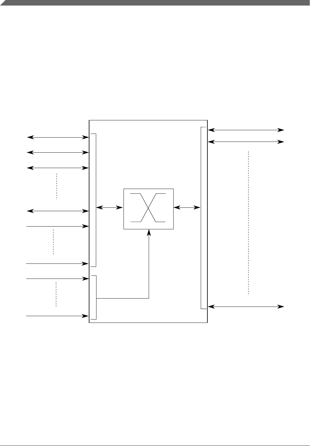
17.2 Introduction
17.2.1 Overview
The Direct Memory Access Multiplexer (DMAMUX) routes DMA sources, called slots,
to any of the 16 DMA channels. See the chip-specific information to know the detailed
source numbers. This process is illustrated in the following figure.
DMA channel #0
Source #1
Source #2
Source #3
Always #1
DMA channel #n
Always #y
Source #x
Trigger #1
Trigger #z
DMA channel #1
DMAMUX
Figure 17-1. DMAMUX block diagram
17.2.2 Features
The DMAMUX module provides these features:
• Up to 61 peripheral slots and up to 2 always-on slots can be routed to 16 channels.
• 16 independently selectable DMA channel routers.
Introduction
S32K1xx Series Reference Manual, Rev. 7, 04/2018
312 NXP Semiconductors

• The first 4 channels additionally provide a trigger functionality.
• Each channel router can be assigned to one of the possible peripheral DMA slots or
to one of the always-on slots.
17.2.3 Modes of operation
The following operating modes are available:
• Disabled mode
In this mode, the DMA channel is disabled. Because disabling and enabling of DMA
channels is done primarily via the DMA configuration registers, this mode is used
mainly as the reset state for a DMA channel in the DMA channel MUX. It may also
be used to temporarily suspend a DMA channel while reconfiguration of the system
takes place, for example, changing the period of a DMA trigger.
• Normal mode
In this mode, a DMA source is routed directly to the specified DMA channel. The
operation of the DMAMUX in this mode is completely transparent to the system.
• Periodic Trigger mode
In this mode, a DMA source may only request a DMA transfer, such as when a
transmit buffer becomes empty or a receive buffer becomes full, periodically.
Configuration of the period is done by an external periodic interrupt timer (for
example, PIT). This mode is available only for channels 0–3.
17.3 Memory map/register definition
This section provides a detailed description of all memory-mapped registers in the
DMAMUX.
17.3.1 DMAMUX register descriptions
Chapter 17 Direct Memory Access Multiplexer (DMAMUX)
S32K1xx Series Reference Manual, Rev. 7, 04/2018
NXP Semiconductors 313

17.3.1.1 DMAMUX Memory map
DMAMUX base address: 4002_1000h
Offset Register Width
(In bits)
Access Reset value
0h - Fh Channel Configuration register (CHCFG0 - CHCFG15) 8 RW 00h
17.3.1.2 Channel Configuration register (CHCFG0 - CHCFG15)
17.3.1.2.1 Offset
For a = 0 to 15:
Register Offset
CHCFGa 0h + (a × 1h)
17.3.1.2.2 Function
Each of the DMA channels can be independently enabled/disabled and associated with
one of the DMA slots (peripheral slots or always-on slots) in the system.
NOTE
Setting multiple CHCFG registers with the same source value
will result in unpredictable behavior. This is true, even if a
channel is disabled (ENBL==0).
Before changing the trigger or source settings, a DMA channel
must be disabled via CHCFGn[ENBL].
17.3.1.2.3 Diagram
Bits 7 6 5 4 3 2 1 0
R
ENB
L
TRIG
SOURC
E
W
Reset 0 0 0 0 0 0 0 0
Memory map/register definition
S32K1xx Series Reference Manual, Rev. 7, 04/2018
314 NXP Semiconductors

17.3.1.2.4 Fields
Field Function
7
ENBL
DMA Channel Enable
Enables the DMA channel.
0b - DMA channel is disabled. This mode is primarily used during configuration of the DMAMux.
The DMA has separate channel enables/disables, which should be used to disable or reconfigure a
DMA channel.
1b - DMA channel is enabled
6
TRIG
DMA Channel Trigger Enable
Enables the periodic trigger capability for the triggered DMA channel.
0b - Triggering is disabled. If triggering is disabled and ENBL is set, the DMA Channel will simply
route the specified source to the DMA channel. (Normal mode)
1b - Triggering is enabled. If triggering is enabled and ENBL is set, the DMAMUX is in Periodic
Trigger mode.
5-0
SOURCE
DMA Channel Source (Slot)
Specifies which DMA source, if any, is routed to a particular DMA channel. See the chip-specific
DMAMUX information for details about the peripherals and their slot numbers.
17.4 Functional description
The primary purpose of the DMAMUX is to provide flexibility in the system's use of the
available DMA channels.
As such, configuration of the DMAMUX is intended to be a static procedure done during
execution of the system boot code. However, if the procedure outlined in Enabling and
configuring sources is followed, the configuration of the DMAMUX may be changed
during the normal operation of the system.
Functionally, the DMAMUX channels may be divided into two classes:
• Channels that implement the normal routing functionality plus periodic triggering
capability
• Channels that implement only the normal routing functionality
17.4.1 DMA channels with periodic triggering capability
Besides the normal routing functionality, the first 4 channels of the DMAMUX provide a
special periodic triggering capability that can be used to provide an automatic mechanism
to transmit bytes, frames, or packets at fixed intervals without the need for processor
intervention.
Chapter 17 Direct Memory Access Multiplexer (DMAMUX)
S32K1xx Series Reference Manual, Rev. 7, 04/2018
NXP Semiconductors 315
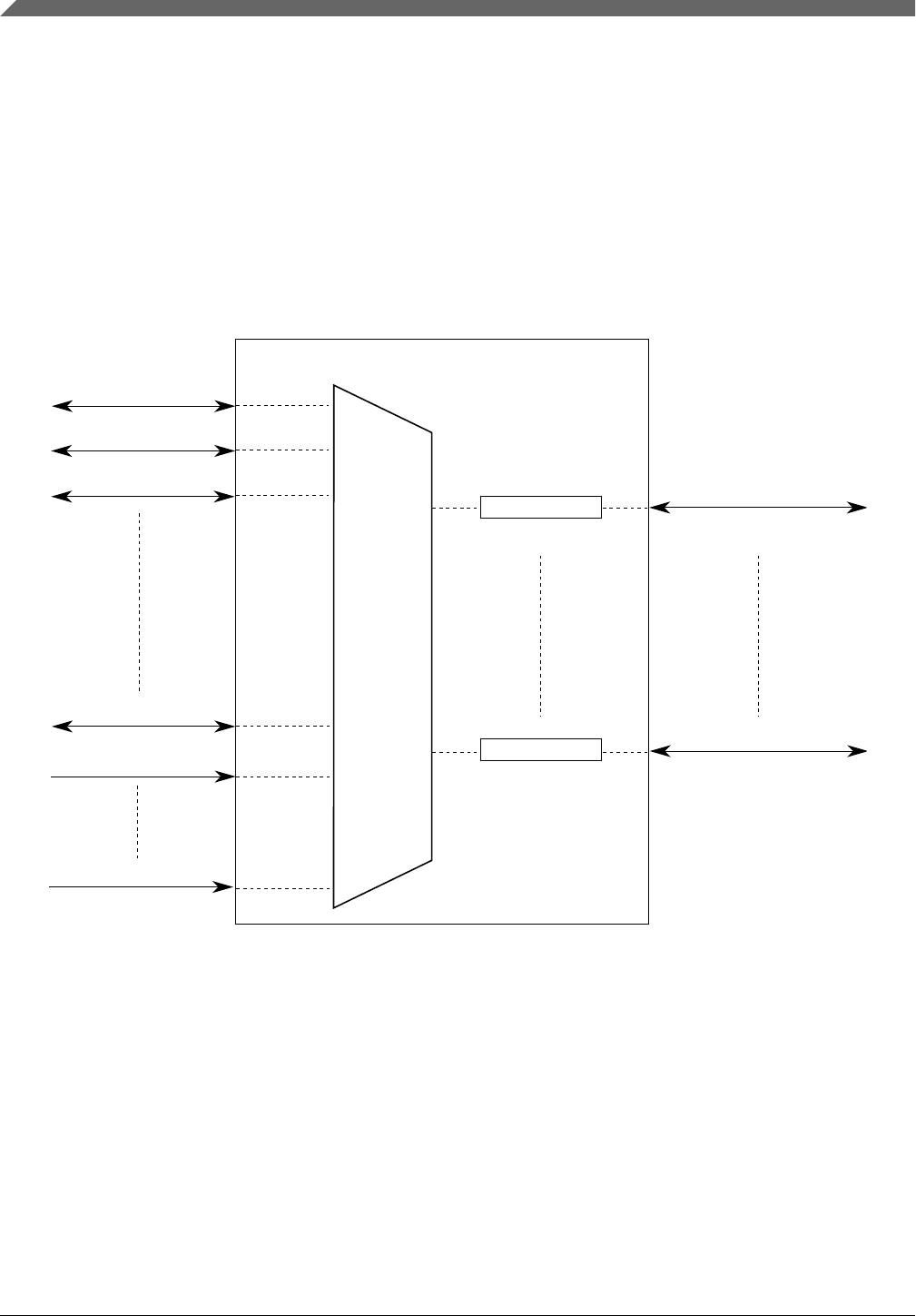
The trigger is generated by an external periodic interrupt timer (for example, PIT); as
such, the configuration of the periodic triggering interval is done via configuring the
external periodic timer.
Note
Because of the dynamic nature of the system (due to DMA
channel priorities, bus arbitration, interrupt service routine
lengths, etc.), the number of clock cycles between a trigger and
the actual DMA transfer cannot be guaranteed.
DMA channel #0
Source #1
Source #2
Source #3
Always #1
DMA channel #m-1
Always #y
Trigger #m
Source #x
Trigger #1
Figure 17-2. DMAMUX triggered channels
The DMA channel triggering capability allows the system to schedule regular DMA
transfers, usually on the transmit side of certain peripherals, without the intervention of
the processor. This trigger works by gating the request from the peripheral to the DMA
until a trigger event has been seen. This is illustrated in the following figure.
Functional description
S32K1xx Series Reference Manual, Rev. 7, 04/2018
316 NXP Semiconductors
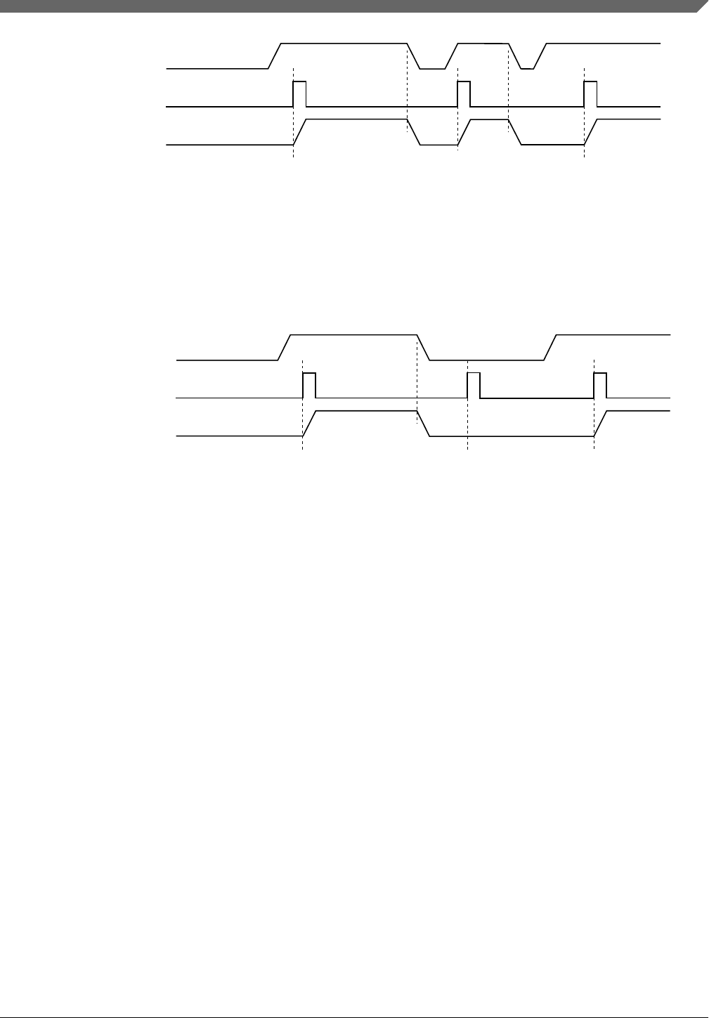
DMA request
Peripheral request
Trigger
Figure 17-3. DMAMUX channel triggering: normal operation
After the DMA request has been serviced, the peripheral will negate its request,
effectively resetting the gating mechanism until the peripheral reasserts its request and
the next trigger event is seen. This means that if a trigger is seen, but the peripheral is not
requesting a transfer, then that trigger will be ignored. This situation is illustrated in the
following figure.
DMA request
Peripheral request
Trigger
Figure 17-4. DMAMUX channel triggering: ignored trigger
This triggering capability may be used with any peripheral that supports DMA transfers,
and is most useful for two types of situations:
• Periodically polling external devices on a particular bus
As an example, the transmit side of an SPI is assigned to a DMA channel with a
trigger, as described above. After it has been set up, the SPI will request DMA
transfers, presumably from memory, as long as its transmit buffer is empty. By using
a trigger on this channel, the SPI transfers can be automatically performed every 5 μs
(as an example). On the receive side of the SPI, the SPI and DMA can be configured
to transfer receive data into memory, effectively implementing a method to
periodically read data from external devices and transfer the results into memory
without processor intervention.
• Using the GPIO ports to drive or sample waveforms
By configuring the DMA to transfer data to one or more GPIO ports, it is possible to
create complex waveforms using tabular data stored in on-chip memory. Conversely,
using the DMA to periodically transfer data from one or more GPIO ports, it is
possible to sample complex waveforms and store the results in tabular form in on-
chip memory.
Chapter 17 Direct Memory Access Multiplexer (DMAMUX)
S32K1xx Series Reference Manual, Rev. 7, 04/2018
NXP Semiconductors 317

17.4.2 DMA channels with no triggering capability
The other channels of the DMAMUX provide the normal routing functionality as
described in Modes of operation.
17.4.3 Always-enabled DMA sources
In addition to the peripherals that can be used as DMA sources, there are 2 additional
DMA sources that are always enabled. Unlike the peripheral DMA sources, where the
peripheral controls the flow of data during DMA transfers, the sources that are always
enabled provide no such "throttling" of the data transfers. These sources are most useful
in the following cases:
• Performing DMA transfers to/from GPIO—Moving data from/to one or more GPIO
pins, either unthrottled (that is, as fast as possible), or periodically (using the DMA
triggering capability).
• Performing DMA transfers from memory to memory—Moving data from memory to
memory, typically as fast as possible, sometimes with software activation.
• Performing DMA transfers from memory to the external bus, or vice-versa—Similar
to memory to memory transfers, this is typically done as quickly as possible.
• Any DMA transfer that requires software activation—Any DMA transfer that should
be explicitly started by software.
In cases where software should initiate the start of a DMA transfer, an always-enabled
DMA source can be used to provide maximum flexibility. When activating a DMA
channel via software, subsequent executions of the minor loop require that a new start
event be sent. This can either be a new software activation, or a transfer request from the
DMA channel MUX. The options for doing this are:
• Transfer all data in a single minor loop.
By configuring the DMA to transfer all of the data in a single minor loop (that is,
major loop counter = 1), no reactivation of the channel is necessary. The
disadvantage to this option is the reduced granularity in determining the load that the
DMA transfer will impose on the system. For this option, the DMA channel must be
disabled in the DMA channel MUX.
• Use explicit software reactivation.
Functional description
S32K1xx Series Reference Manual, Rev. 7, 04/2018
318 NXP Semiconductors

In this option, the DMA is configured to transfer the data using both minor and major
loops, but the processor is required to reactivate the channel by writing to the DMA
registers after every minor loop. For this option, the DMA channel must be disabled
in the DMA channel MUX.
• Use an always-enabled DMA source.
In this option, the DMA is configured to transfer the data using both minor and major
loops, and the DMA channel MUX does the channel reactivation. For this option, the
DMA channel should be enabled and pointing to an "always enabled" source. Note
that the reactivation of the channel can be continuous (DMA triggering is disabled)
or can use the DMA triggering capability. In this manner, it is possible to execute
periodic transfers of packets of data from one source to another, without processor
intervention.
17.5 Initialization/application information
This section provides instructions for initializing the DMA channel MUX.
17.5.1 Reset
The reset state of each individual bit is shown in Memory map/register definition. In
summary, after reset, all channels are disabled and must be explicitly enabled before use.
17.5.2 Enabling and configuring sources
To enable a source with periodic triggering:
1. Determine with which DMA channel the source will be associated. Note that only the
first 4 DMA channels have periodic triggering capability.
2. Clear the CHCFG[ENBL] and CHCFG[TRIG] fields of the DMA channel.
3. Ensure that the DMA channel is properly configured in the DMA. The DMA channel
may be enabled at this point.
4. Configure the corresponding timer.
5. Select the source to be routed to the DMA channel. Write to the corresponding
CHCFG register, ensuring that the CHCFG[ENBL] and CHCFG[TRIG] fields are
set.
Chapter 17 Direct Memory Access Multiplexer (DMAMUX)
S32K1xx Series Reference Manual, Rev. 7, 04/2018
NXP Semiconductors 319

NOTE
The following is an example. See the chip-specific information
for the number of this device's DMA channels that have
triggering capability.
To configure source #5 transmit for use with DMA channel 1, with periodic triggering
capability:
1. Write 0x00 to CHCFG1.
2. Configure channel 1 in the DMA, including enabling the channel.
3. Configure a timer for the desired trigger interval.
4. Write 0xC5 to CHCFG1.
The following code example illustrates steps 1 and 4 above:
void DMAMUX_Init(uint8_t DMA_CH, uint8_t DMAMUX_SOURCE)
{
DMAMUX_0.CHCFG[DMA_CH].B.SOURCE = DMAMUX_SOURCE;
DMAMUX_0.CHCFG[DMA_CH].B.ENBL = 1;
DMAMUX_0.CHCFG[DMA_CH].B.TRIG = 1;
}
To enable a source, without periodic triggering:
1. Determine with which DMA channel the source will be associated. Note that only the
first 4 DMA channels have periodic triggering capability.
2. Clear the CHCFG[ENBL] and CHCFG[TRIG] fields of the DMA channel.
3. Ensure that the DMA channel is properly configured in the DMA. The DMA channel
may be enabled at this point.
4. Select the source to be routed to the DMA channel. Write to the corresponding
CHCFG register, ensuring that CHCFG[ENBL] is setwhile CHCFG[TRIG] is
cleared.
NOTE
The following is an example. See the chip configuration details
for the number of this device's DMA channels that have
triggering capability.
To configure source #5 transmit for use with DMA channel 1, with no periodic triggering
capability:
1. Write 0x00 to CHCFG1.
2. Configure channel 1 in the DMA, including enabling the channel.
3. Write 0x85 to CHCFG1.
The following code example illustrates steps 1 and 3 above:
In File registers.h:
#define DMAMUX_BASE_ADDR 0x40021000/* Example only ! */
/* Following example assumes char is 8-bits */
volatile unsigned char *CHCFG0 = (volatile unsigned char *) (DMAMUX_BASE_ADDR+0x0000);
Initialization/application information
S32K1xx Series Reference Manual, Rev. 7, 04/2018
320 NXP Semiconductors

volatile unsigned char *CHCFG1 = (volatile unsigned char *) (DMAMUX_BASE_ADDR+0x0001);
volatile unsigned char *CHCFG2 = (volatile unsigned char *) (DMAMUX_BASE_ADDR+0x0002);
volatile unsigned char *CHCFG3 = (volatile unsigned char *) (DMAMUX_BASE_ADDR+0x0003);
volatile unsigned char *CHCFG4 = (volatile unsigned char *) (DMAMUX_BASE_ADDR+0x0004);
volatile unsigned char *CHCFG5 = (volatile unsigned char *) (DMAMUX_BASE_ADDR+0x0005);
volatile unsigned char *CHCFG6 = (volatile unsigned char *) (DMAMUX_BASE_ADDR+0x0006);
volatile unsigned char *CHCFG7 = (volatile unsigned char *) (DMAMUX_BASE_ADDR+0x0007);
volatile unsigned char *CHCFG8 = (volatile unsigned char *) (DMAMUX_BASE_ADDR+0x0008);
volatile unsigned char *CHCFG9 = (volatile unsigned char *) (DMAMUX_BASE_ADDR+0x0009);
volatile unsigned char *CHCFG10= (volatile unsigned char *) (DMAMUX_BASE_ADDR+0x000A);
volatile unsigned char *CHCFG11= (volatile unsigned char *) (DMAMUX_BASE_ADDR+0x000B);
volatile unsigned char *CHCFG12= (volatile unsigned char *) (DMAMUX_BASE_ADDR+0x000C);
volatile unsigned char *CHCFG13= (volatile unsigned char *) (DMAMUX_BASE_ADDR+0x000D);
volatile unsigned char *CHCFG14= (volatile unsigned char *) (DMAMUX_BASE_ADDR+0x000E);
volatile unsigned char *CHCFG15= (volatile unsigned char *) (DMAMUX_BASE_ADDR+0x000F);
In File main.c:
#include "registers.h"
:
:
*CHCFG1 = 0x00;
*CHCFG1 = 0x85;
To disable a source:
A particular DMA source may be disabled by not writing the corresponding source value
into any of the CHCFG registers. Additionally, some module-specific configuration may
be necessary. See the appropriate section for more details.
To switch the source of a DMA channel:
1. Disable the DMA channel in the DMA and reconfigure the channel for the new
source.
2. Clear the CHCFG[ENBL] and CHCFG[TRIG] bits of the DMA channel.
3. Select the source to be routed to the DMA channel. Write to the corresponding
CHCFG register, ensuring that the CHCFG[ENBL] and CHCFG[TRIG] fields are
set.
To switch DMA channel 8 from source #5 transmit to source #7 transmit:
1. In the DMA configuration registers, disable DMA channel 8 and reconfigure it to
handle the transfers to peripheral slot 7. This example assumes channel 8 doesn't
have triggering capability.
2. Write 0x00 to CHCFG8.
3. Write 0x87 to CHCFG8. (In this example, setting CHCFG[TRIG] would have no
effect due to the assumption that channel 8 does not support the periodic triggering
functionality.)
The following code example illustrates steps 2 and 3 above:
In File registers.h:
#define DMAMUX_BASE_ADDR 0x40021000/* Example only ! */
/* Following example assumes char is 8-bits */
volatile unsigned char *CHCFG0 = (volatile unsigned char *) (DMAMUX_BASE_ADDR+0x0000);
volatile unsigned char *CHCFG1 = (volatile unsigned char *) (DMAMUX_BASE_ADDR+0x0001);
volatile unsigned char *CHCFG2 = (volatile unsigned char *) (DMAMUX_BASE_ADDR+0x0002);
volatile unsigned char *CHCFG3 = (volatile unsigned char *) (DMAMUX_BASE_ADDR+0x0003);
Chapter 17 Direct Memory Access Multiplexer (DMAMUX)
S32K1xx Series Reference Manual, Rev. 7, 04/2018
NXP Semiconductors 321

volatile unsigned char *CHCFG4 = (volatile unsigned char *) (DMAMUX_BASE_ADDR+0x0004);
volatile unsigned char *CHCFG5 = (volatile unsigned char *) (DMAMUX_BASE_ADDR+0x0005);
volatile unsigned char *CHCFG6 = (volatile unsigned char *) (DMAMUX_BASE_ADDR+0x0006);
volatile unsigned char *CHCFG7 = (volatile unsigned char *) (DMAMUX_BASE_ADDR+0x0007);
volatile unsigned char *CHCFG8 = (volatile unsigned char *) (DMAMUX_BASE_ADDR+0x0008);
volatile unsigned char *CHCFG9 = (volatile unsigned char *) (DMAMUX_BASE_ADDR+0x0009);
volatile unsigned char *CHCFG10= (volatile unsigned char *) (DMAMUX_BASE_ADDR+0x000A);
volatile unsigned char *CHCFG11= (volatile unsigned char *) (DMAMUX_BASE_ADDR+0x000B);
volatile unsigned char *CHCFG12= (volatile unsigned char *) (DMAMUX_BASE_ADDR+0x000C);
volatile unsigned char *CHCFG13= (volatile unsigned char *) (DMAMUX_BASE_ADDR+0x000D);
volatile unsigned char *CHCFG14= (volatile unsigned char *) (DMAMUX_BASE_ADDR+0x000E);
volatile unsigned char *CHCFG15= (volatile unsigned char *) (DMAMUX_BASE_ADDR+0x000F);
In File main.c:
#include "registers.h"
:
:
*CHCFG8 = 0x00;
*CHCFG8 = 0x87;
Initialization/application information
S32K1xx Series Reference Manual, Rev. 7, 04/2018
322 NXP Semiconductors

Chapter 18
Enhanced Direct Memory Access (eDMA)
18.1 Chip-specific eDMA information
Wait mode is not supported. See Module operation in available low power modes for
details on available power modes.
16-byte burst and 32-byte burst is not supported on S32K11x variants.
NOTE
For S32K11x variants, when executing a large, zero wait-stated
memory-to-memory transfer, insert bandwidth control using the
TCD_CSR[BWC] bits to avoid:
• Starvation of another master accessing the memory.
• Any delay in writing a TCD during the transfer.
18.1.1 Number of channels
The number of channels across S32K1xx series varies across variants. See below table
for the same.
Table 18-1. Number of channles
Chips Number of channels
S32K116 4
S32K118 4
S32K142 16
S32K144 16
S32K146 16
S32K148 16
S32K1xx Series Reference Manual, Rev. 7, 04/2018
NXP Semiconductors 323
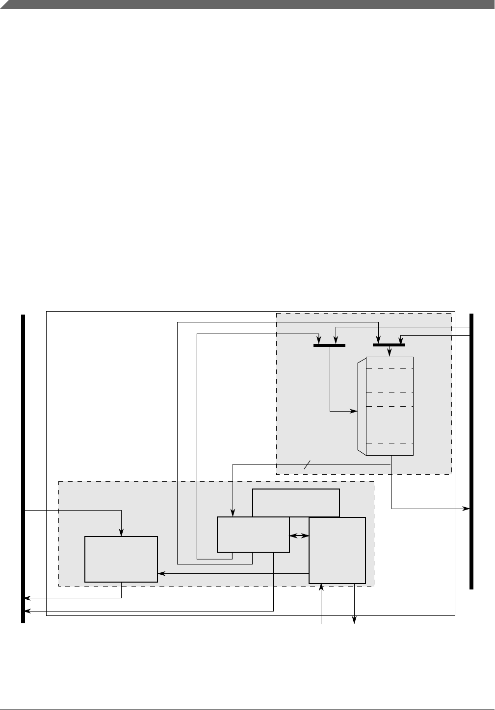
18.2 Introduction
The enhanced direct memory access (eDMA) controller is a second-generation module
capable of performing complex data transfers with minimal intervention from a host
processor. The hardware microarchitecture includes:
• A DMA engine that performs:
• Source address and destination address calculations
• Data-movement operations
• Local memory containing transfer control descriptors for each of the 16 channels
18.2.1 eDMA system block diagram
Figure 18-1 illustrates the components of the eDMA system, including the eDMA
module ("engine").
1
Transfer Control
Descriptor (TCD)
eDMA engine
Data Path
eDMA system
0
Program Model/
64
Control
n-1
To/From Crossbar Switch
2
Channel Arbitration
Address Path
Read Data
Write Data
Address
Read Data
Write Data
Write Address
Internal Peripheral Bus
eDMA Peripheral
Request eDMA Done
Figure 18-1. eDMA system block diagram
Introduction
S32K1xx Series Reference Manual, Rev. 7, 04/2018
324 NXP Semiconductors

18.2.2 Block parts
The eDMA module is partitioned into two major modules: the eDMA engine and the
transfer-control descriptor local memory.
The eDMA engine is further partitioned into four submodules:
Table 18-2. eDMA engine submodules
Submodule Function
Address path This block implements registered versions of two channel transfer control descriptors, channel x
and channel y, and manages all master bus-address calculations. All the channels provide the
same functionality. This structure allows data transfers associated with one channel to be
preempted after the completion of a read/write sequence if a higher priority channel activation is
asserted while the first channel is active. After a channel is activated, it runs until the minor loop is
completed, unless preempted by a higher priority channel. This provides a mechanism (enabled
by DCHPRIn[ECP]) where a large data move operation can be preempted to minimize the time
another channel is blocked from execution.
When any channel is selected to execute, the contents of its TCD are read from local memory and
loaded into the address path channel x registers for a normal start and into channel y registers for
a preemption start. After the minor loop completes execution, the address path hardware writes
the new values for the TCDn_{SADDR, DADDR, CITER} back to local memory. If the major
iteration count is exhausted, additional processing is performed, including the final address pointer
updates, reloading the TCDn_CITER field, and a possible fetch of the next TCDn from memory as
part of a scatter/gather operation.
Data path This block implements the bus master read/write datapath. It includes a data buffer and the
necessary multiplex logic to support any required data alignment. The internal read data bus is the
primary input, and the internal write data bus is the primary output.
The address and data path modules directly support the 2-stage pipelined internal bus. The
address path module represents the 1st stage of the bus pipeline (address phase), while the data
path module implements the 2nd stage of the pipeline (data phase).
Program model/channel
arbitration
This block implements the first section of the eDMA programming model as well as the channel
arbitration logic. The programming model registers are connected to the internal peripheral bus.
The eDMA peripheral request inputs and interrupt request outputs are also connected to this block
(via control logic).
Control This block provides all the control functions for the eDMA engine. For data transfers where the
source and destination sizes are equal, the eDMA engine performs a series of source read/
destination write operations until the number of bytes specified in the minor loop byte count has
moved. For descriptors where the sizes are not equal, multiple accesses of the smaller size data
are required for each reference of the larger size. As an example, if the source size references 16-
bit data and the destination is 32-bit data, two reads are performed, then one 32-bit write.
The transfer-control descriptor local memory is further partitioned into:
Table 18-3. Transfer control descriptor memory
Submodule Description
Memory controller This logic implements the required dual-ported controller, managing accesses from the eDMA
engine as well as references from the internal peripheral bus. As noted earlier, in the event of
Table continues on the next page...
Chapter 18 Enhanced Direct Memory Access (eDMA)
S32K1xx Series Reference Manual, Rev. 7, 04/2018
NXP Semiconductors 325

Table 18-3. Transfer control descriptor memory (continued)
Submodule Description
simultaneous accesses, the eDMA engine is given priority and the peripheral transaction is
stalled.
Memory array TCD storage for each channel's transfer profile.
18.2.3 Features
The eDMA is a highly programmable data-transfer engine optimized to minimize any
required intervention from the host processor. It is intended for use in applications where
the data size to be transferred is statically known and not defined within the transferred
data itself. The eDMA module features:
• All data movement via dual-address transfers: read from source, write to destination
• Programmable source and destination addresses and transfer size
• Support for enhanced addressing modes
• 16-channel implementation that performs complex data transfers with minimal
intervention from a host processor
• Internal data buffer, used as temporary storage to support 16- and 32-byte
transfers
• Connections to the crossbar switch for bus mastering the data movement
• Transfer control descriptor (TCD) organized to support two-deep, nested transfer
operations
• 32-byte TCD stored in local memory for each channel
• An inner data transfer loop defined by a minor byte transfer count
• An outer data transfer loop defined by a major iteration count
• Channel activation via one of three methods:
• Explicit software initiation
• Initiation via a channel-to-channel linking mechanism for continuous transfers
• Peripheral-paced hardware requests, one per channel
• Fixed-priority and round-robin channel arbitration
• Channel completion reported via programmable interrupt requests
Introduction
S32K1xx Series Reference Manual, Rev. 7, 04/2018
326 NXP Semiconductors

• One interrupt per channel, which can be asserted at completion of major iteration
count
• Programmable error terminations per channel and logically summed together to
form one error interrupt to the interrupt controller
• Programmable support for scatter/gather DMA processing
• Support for complex data structures
In the discussion of this module, n is used to reference the channel number.
18.3 Modes of operation
The eDMA operates in the following modes:
Table 18-4. Modes of operation
Mode Description
Normal In Normal mode, the eDMA transfers data between a source and a destination. The source and
destination can be a memory block or an I/O block capable of operation with the eDMA.
A service request initiates a transfer of a specific number of bytes (NBYTES) as specified in the
transfer control descriptor (TCD). The minor loop is the sequence of read-write operations that
transfers these NBYTES per service request. Each service request executes one iteration of the
major loop, which transfers NBYTES of data.
Debug DMA operation is configurable in Debug mode via the control register:
• If CR[EDBG] is cleared, the DMA continues to operate.
• If CR[EDBG] is set, the eDMA stops transferring data. If Debug mode is entered while a
channel is active, the eDMA continues operation until the channel retires.
Wait Before entering Wait mode, the DMA attempts to complete its current transfer. After the transfer
completes, the device enters Wait mode.
18.4 Memory map/register definition
The eDMA's programming model is partitioned into two regions:
• The first region defines a number of registers providing control functions
• The second region corresponds to the local transfer control descriptor (TCD)
memory
Chapter 18 Enhanced Direct Memory Access (eDMA)
S32K1xx Series Reference Manual, Rev. 7, 04/2018
NXP Semiconductors 327

18.4.1 TCD memory
Each channel requires a 32-byte transfer control descriptor for defining the desired data
movement operation. The channel descriptors are stored in the local memory in
sequential order: channel 0, channel 1, ... channel 15. Each TCDn definition is presented
as 11 registers of 16 or 32 bits.
18.4.2 TCD initialization
Prior to activating a channel, you must initialize its TCD with the appropriate transfer
profile.
18.4.3 TCD structure
SADDR
31 30
29
28
27
26
25
24
23
22 21
20
19
18
17
16
15
14
13
12
11
10 9
8
7
6
5 4
3
2
1
0
SOFF SMOD SSIZE DMOD DSIZE
SMLOE
DMLOE
MLOFF or NBYTES NBYTES
SLAST
DADDR
31 30
29
28
27
26
25
24
23
22 21
20
19
18
17
16
15
14
13
12
11
10 9
8
7
6
5 4
3
2
1
0
CITER.E_LINK
CITER or
CITER.LINKCH CITER DOFF
DLAST_SGA
BITER.E_LINK
BITER or
BITER.LINKCH BITER
START
INT_MAJ
INT_HALF
D_REQ
E_SG
MAJOR.E_LINK
ACTIVE
DONE
BWC
MAJOR.LINKCH
NBYTES
0000h
0004h
0008h
DMA_CR[EMLM] enabled
000Ch
0010h
0014h
0018h
001Ch
Reserved
DMA_CR[EMLM] disabled
{
{
{
18.4.4 Reserved memory and bit fields
• Reading reserved bits in a register returns the value of zero.
• Writes to reserved bits in a register are ignored.
• Reading or writing a reserved memory location generates a bus error.
Memory map/register definition
S32K1xx Series Reference Manual, Rev. 7, 04/2018
328 NXP Semiconductors

18.4.5 DMA register descriptions
18.4.5.1 DMA Memory map
DMA base address: 4000_8000h
Offset Register Width
(In bits)
Access Reset value
0h Control Register (CR) 32 RW See
description.
4h Error Status Register (ES) 32 RO 0000_0000h
Ch Enable Request Register (ERQ) 32 RW 0000_0000h
14h Enable Error Interrupt Register (EEI) 32 RW 0000_0000h
18h Clear Enable Error Interrupt Register (CEEI) 8 WORZ 00h
19h Set Enable Error Interrupt Register (SEEI) 8 WORZ 00h
1Ah Clear Enable Request Register (CERQ) 8 WORZ 00h
1Bh Set Enable Request Register (SERQ) 8 WORZ 00h
1Ch Clear DONE Status Bit Register (CDNE) 8 WORZ 00h
1Dh Set START Bit Register (SSRT) 8 WORZ 00h
1Eh Clear Error Register (CERR) 8 WORZ 00h
1Fh Clear Interrupt Request Register (CINT) 8 WORZ 00h
24h Interrupt Request Register (INT) 32 W1C 0000_0000h
2Ch Error Register (ERR) 32 W1C 0000_0000h
34h Hardware Request Status Register (HRS) 32 RO 0000_0000h
44h Enable Asynchronous Request in Stop Register (EARS) 32 RW 0000_0000h
100h Channel Priority Register (DCHPRI3) 8 RW 03h
101h Channel Priority Register (DCHPRI2) 8 RW 02h
102h Channel Priority Register (DCHPRI1) 8 RW 01h
103h Channel Priority Register (DCHPRI0) 8 RW 00h
104h Channel Priority Register (DCHPRI7) 8 RW 07h
105h Channel Priority Register (DCHPRI6) 8 RW 06h
106h Channel Priority Register (DCHPRI5) 8 RW 05h
107h Channel Priority Register (DCHPRI4) 8 RW 04h
108h Channel Priority Register (DCHPRI11) 8 RW 0Bh
109h Channel Priority Register (DCHPRI10) 8 RW 0Ah
10Ah Channel Priority Register (DCHPRI9) 8 RW 09h
10Bh Channel Priority Register (DCHPRI8) 8 RW 08h
10Ch Channel Priority Register (DCHPRI15) 8 RW 0Fh
Table continues on the next page...
Chapter 18 Enhanced Direct Memory Access (eDMA)
S32K1xx Series Reference Manual, Rev. 7, 04/2018
NXP Semiconductors 329

Offset Register Width
(In bits)
Access Reset value
10Dh Channel Priority Register (DCHPRI14) 8 RW 0Eh
10Eh Channel Priority Register (DCHPRI13) 8 RW 0Dh
10Fh Channel Priority Register (DCHPRI12) 8 RW 0Ch
1000h -
11E0h
TCD Source Address (TCD0_SADDR - TCD15_SADDR) 32 RW See
description.
1004h -
11E4h
TCD Signed Source Address Offset (TCD0_SOFF - TCD15_SOFF) 16 RW See
description.
1006h -
11E6h
TCD Transfer Attributes (TCD0_ATTR - TCD15_ATTR) 16 RW See
description.
1008h -
11E8h
TCD Minor Byte Count (Minor Loop Mapping Disabled) (TCD0_NBY
TES_MLNO - TCD15_NBYTES_MLNO)
32 RW See
description.
1008h -
11E8h
TCD Signed Minor Loop Offset (Minor Loop Mapping Enabled and
Offset Disabled) (TCD0_NBYTES_MLOFFNO - TCD15_NBYTES_
MLOFFNO)
32 RW See
description.
1008h -
11E8h
TCD Signed Minor Loop Offset (Minor Loop Mapping and Offset
Enabled) (TCD0_NBYTES_MLOFFYES - TCD15_NBYTES_MLO
FFYES)
32 RW See
description.
100Ch -
11ECh
TCD Last Source Address Adjustment (TCD0_SLAST - TCD15_SL
AST)
32 RW See
description.
1010h - 11F0h TCD Destination Address (TCD0_DADDR - TCD15_DADDR) 32 RW See
description.
1014h - 11F4h TCD Signed Destination Address Offset (TCD0_DOFF - TCD15_DO
FF)
16 RW See
description.
1016h - 11F6h TCD Current Minor Loop Link, Major Loop Count (Channel Linking
Disabled) (TCD0_CITER_ELINKNO - TCD15_CITER_ELINKNO)
16 RW See
description.
1016h - 11F6h TCD Current Minor Loop Link, Major Loop Count (Channel Linking
Enabled) (TCD0_CITER_ELINKYES - TCD15_CITER_ELINKYES)
16 RW See
description.
1018h - 11F8h TCD Last Destination Address Adjustment/Scatter Gather Address
(TCD0_DLASTSGA - TCD15_DLASTSGA)
32 RW See
description.
101Ch -
11FCh
TCD Control and Status (TCD0_CSR - TCD15_CSR) 16 RW See
description.
101Eh -
11FEh
TCD Beginning Minor Loop Link, Major Loop Count (Channel Linking
Disabled) (TCD0_BITER_ELINKNO - TCD15_BITER_ELINKNO)
16 RW See
description.
101Eh -
11FEh
TCD Beginning Minor Loop Link, Major Loop Count (Channel Linking
Enabled) (TCD0_BITER_ELINKYES - TCD15_BITER_ELINKYES)
16 RW See
description.
18.4.5.2 Control Register (CR)
18.4.5.2.1 Offset
Register Offset
CR 0h
Memory map/register definition
S32K1xx Series Reference Manual, Rev. 7, 04/2018
330 NXP Semiconductors

18.4.5.2.2 Function
The CR defines the basic operating configuration of the DMA.
Arbitration can be configured to use either a fixed-priority or a round-robin scheme. For
fixed-priority arbitration, the highest priority channel requesting service is selected to
execute. The channel priority registers assign the priorities; see the DCHPRIn registers.
For round-robin arbitration, the channel priorities are ignored and channels are cycled
through (from high to low channel number) without regard to priority.
NOTE
For correct operation, writes to the CR register must be
performed only when the DMA channels are inactive; that is,
when TCDn_CSR[ACTIVE] bits are cleared.
Minor loop offsets are address offset values added to the final source address
(TCDn_SADDR) or destination address (TCDn_DADDR) upon minor loop completion.
When minor loop offsets are enabled, the minor loop offset (MLOFF) is added to the
final source address (TCDn_SADDR), to the final destination address (TCDn_DADDR),
or to both prior to the addresses being written back into the TCD. If the major loop is
complete, the minor loop offset is ignored and the major loop address offsets
(TCDn_SLAST and TCDn_DLAST_SGA) are used to compute the next TCDn_SADDR
and TCDn_DADDR values.
When minor loop mapping is enabled (EMLM is 1), TCDn word2 is redefined. A portion
of TCDn word2 is used to specify multiple fields: a source enable bit (SMLOE) to
specify the minor loop offset should be applied to the source address (TCDn_SADDR)
upon minor loop completion, a destination enable bit (DMLOE) to specify the minor loop
offset should be applied to the destination address (TCDn_DADDR) upon minor loop
completion, and the sign extended minor loop offset value (MLOFF). The same offset
value (MLOFF) is used for both source and destination minor loop offsets. When either
minor loop offset is enabled (SMLOE set or DMLOE set), the NBYTES field is reduced
to 10 bits. When both minor loop offsets are disabled (SMLOE cleared and DMLOE
cleared), the NBYTES field is a 30-bit vector.
When minor loop mapping is disabled (EMLM is 0), all 32 bits of TCDn word2 are
assigned to the NBYTES field.
Chapter 18 Enhanced Direct Memory Access (eDMA)
S32K1xx Series Reference Manual, Rev. 7, 04/2018
NXP Semiconductors 331

18.4.5.2.3 Diagram
Bits 31 30 29 28 27 26 25 24 23 22 21 20 19 18 17 16
R
ACTIVE
Reserved
0
CX
EC
X
W
Reset 0uuuuuuu00000000
Bits 15 14 13 12 11 10 9 8 7 6 5 4 3 2 1 0
R
0
EMLM
CLM
HALT
HOE
Reserved
ERCA
EDB
G
Reserved
W
Reset 0 0 0 0 0 0 0 0 0 0 0 0 0 0 0 0
18.4.5.2.4 Fields
Field Function
31
ACTIVE
DMA Active Status
0b - eDMA is idle.
1b - eDMA is executing a channel.
30-24
—
eDMA version number
Reserved
23-18
—
Reserved
17
CX
Cancel Transfer
0b - Normal operation
1b - Cancel the remaining data transfer. Stop the executing channel and force the minor loop to
finish. The cancel takes effect after the last write of the current read/write sequence. The CX bit
clears itself after the cancel has been honored. This cancel retires the channel normally as if the
minor loop was completed.
16
ECX
Error Cancel Transfer
0b - Normal operation
1b - Cancel the remaining data transfer in the same fashion as the CX bit. Stop the executing
channel and force the minor loop to finish. The cancel takes effect after the last write of the current
read/write sequence. The ECX bit clears itself after the cancel is honored. In addition to cancelling
the transfer, ECX treats the cancel as an error condition, thus updating the Error Status register
(DMAx_ES) and generating an optional error interrupt.
15-8
—
Reserved
7
EMLM
Enable Minor Loop Mapping
0b - Disabled. TCDn.word2 is defined as a 32-bit NBYTES field.
1b - Enabled. TCDn.word2 is redefined to include individual enable fields, an offset field, and the
NBYTES field. The individual enable fields allow the minor loop offset to be applied to the source
address, the destination address, or both. The NBYTES field is reduced when either offset is
enabled.
Table continues on the next page...
Memory map/register definition
S32K1xx Series Reference Manual, Rev. 7, 04/2018
332 NXP Semiconductors

Field Function
6
CLM
Continuous Link Mode
NOTE: Do not use continuous link mode with a channel linking to itself if there is only one minor loop
iteration per service request, for example, if the channel's NBYTES value is the same as either
the source or destination size. The same data transfer profile can be achieved by simply
increasing the NBYTES value, which provides more efficient, faster processing.
0b - A minor loop channel link made to itself goes through channel arbitration before being
activated again.
1b - A minor loop channel link made to itself does not go through channel arbitration before being
activated again. Upon minor loop completion, the channel activates again if that channel has a
minor loop channel link enabled and the link channel is itself. This effectively applies the minor loop
offsets and restarts the next minor loop.
5
HALT
Halt DMA Operations
0b - Normal operation
1b - Stall the start of any new channels. Executing channels are allowed to complete. Channel
execution resumes when this bit is cleared.
4
HOE
Halt On Error
0b - Normal operation
1b - Any error causes the HALT bit to set. Subsequently, all service requests are ignored until the
HALT bit is cleared.
3
—
Reserved
Reserved
2
ERCA
Enable Round Robin Channel Arbitration
0b - Fixed priority arbitration is used for channel selection .
1b - Round robin arbitration is used for channel selection .
1
EDBG
Enable Debug
0b - When in debug mode, the DMA continues to operate.
1b - When in debug mode, the DMA stalls the start of a new channel. Executing channels are
allowed to complete. Channel execution resumes when the system exits debug mode or the EDBG
bit is cleared.
0
—
Reserved
Reserved
18.4.5.3 Error Status Register (ES)
18.4.5.3.1 Offset
Register Offset
ES 4h
18.4.5.3.2 Function
The ES provides information concerning the last recorded channel error. Channel errors
can be caused by:
Chapter 18 Enhanced Direct Memory Access (eDMA)
S32K1xx Series Reference Manual, Rev. 7, 04/2018
NXP Semiconductors 333

• A configuration error, that is:
• An illegal setting in the transfer-control descriptor, or
• An illegal priority register setting in fixed-arbitration
• An error termination to a bus master read or write cycle
• A cancel transfer with error bit that will be set when a transfer is canceled via the
corresponding cancel transfer control bit
See Fault reporting and handling for more details.
18.4.5.3.3 Diagram
Bits 31 30 29 28 27 26 25 24 23 22 21 20 19 18 17 16
RVLD 0ECX
W
Reset 0 0 0 0 0 0 0 0 0 0 0 0 0 0 0 0
Bits 15 14 13 12 11 10 9 8 7 6 5 4 3 2 1 0
R 0 CPE 0ERRCHN SAE SOE DAE DOE NCE SGE SBE DBE
W
Reset 0 0 0 0 0 0 0 0 0 0 0 0 0 0 0 0
18.4.5.3.4 Fields
Field Function
31
VLD
VLD
Logical OR of all ERR status bits
0b - No ERR bits are set.
1b - At least one ERR bit is set indicating a valid error exists that has not been cleared.
30-17
—
Reserved
16
ECX
Transfer Canceled
0b - No canceled transfers
1b - The last recorded entry was a canceled transfer by the error cancel transfer input
15
—
Reserved
14
CPE
Channel Priority Error
0b - No channel priority error
1b - The last recorded error was a configuration error in the channel priorities . Channel priorities
are not unique.
13-12
—
Reserved
11-8 Error Channel Number or Canceled Channel Number
Table continues on the next page...
Memory map/register definition
S32K1xx Series Reference Manual, Rev. 7, 04/2018
334 NXP Semiconductors

Field Function
ERRCHN The channel number of the last recorded error, excluding CPE errors, or last recorded error canceled
transfer.
7
SAE
Source Address Error
0b - No source address configuration error.
1b - The last recorded error was a configuration error detected in the TCDn_SADDR field.
TCDn_SADDR is inconsistent with TCDn_ATTR[SSIZE].
6
SOE
Source Offset Error
0b - No source offset configuration error
1b - The last recorded error was a configuration error detected in the TCDn_SOFF field.
TCDn_SOFF is inconsistent with TCDn_ATTR[SSIZE].
5
DAE
Destination Address Error
0b - No destination address configuration error
1b - The last recorded error was a configuration error detected in the TCDn_DADDR field.
TCDn_DADDR is inconsistent with TCDn_ATTR[DSIZE].
4
DOE
Destination Offset Error
0b - No destination offset configuration error
1b - The last recorded error was a configuration error detected in the TCDn_DOFF field.
TCDn_DOFF is inconsistent with TCDn_ATTR[DSIZE].
3
NCE
NBYTES/CITER Configuration Error
0b - No NBYTES/CITER configuration error
1b - The last recorded error was a configuration error detected in the TCDn_NBYTES or
TCDn_CITER fields. TCDn_NBYTES is not a multiple of TCDn_ATTR[SSIZE] and
TCDn_ATTR[DSIZE], orTCDn_CITER[CITER] is equal to zero, orTCDn_CITER[ELINK] is not equal
to TCDn_BITER[ELINK]
2
SGE
Scatter/Gather Configuration Error
0b - No scatter/gather configuration error
1b - The last recorded error was a configuration error detected in the TCDn_DLASTSGA field. This
field is checked at the beginning of a scatter/gather operation after major loop completion if
TCDn_CSR[ESG] is enabled. TCDn_DLASTSGA is not on a 32 byte boundary.
1
SBE
Source Bus Error
0b - No source bus error
1b - The last recorded error was a bus error on a source read
0
DBE
Destination Bus Error
0b - No destination bus error
1b - The last recorded error was a bus error on a destination write
18.4.5.4 Enable Request Register (ERQ)
18.4.5.4.1 Offset
Register Offset
ERQ Ch
Chapter 18 Enhanced Direct Memory Access (eDMA)
S32K1xx Series Reference Manual, Rev. 7, 04/2018
NXP Semiconductors 335

18.4.5.4.2 Function
The ERQ register provides a bit map for the 16 channels to enable the request signal for
each channel. The state of any given channel enable is directly affected by writes to this
register; it is also affected by writes to the SERQ and CERQ registers. These registers are
provided so the request enable for a single channel can easily be modified without
needing to perform a read-modify-write sequence to this register.
DMA request input signals and this enable request flag must be asserted before a
channel's hardware service request is accepted. The state of the DMA enable request flag
does not affect a channel service request made explicitly through software or a linked
channel request.
NOTE
Disable a channel's hardware service request at the source
before clearing the channel's ERQ bit.
18.4.5.4.3 Diagram
Bits 31 30 29 28 27 26 25 24 23 22 21 20 19 18 17 16
R 0
W
Reset 0 0 0 0 0 0 0 0 0 0 0 0 0 0 0 0
Bits 15 14 13 12 11 10 9 8 7 6 5 4 3 2 1 0
R
ERQ15
ERQ14
ERQ13
ERQ12
ERQ11
ERQ10
ERQ9
ERQ8
ERQ7
ERQ6
ERQ5
ERQ4
ERQ3
ERQ2
ERQ1
ERQ0
W
Reset 0 0 0 0 0 0 0 0 0 0 0 0 0 0 0 0
18.4.5.4.4 Fields
Field Function
31-16
—
Reserved
15
ERQ15
Enable DMA Request 15
0b - The DMA request signal for the corresponding channel is disabled
1b - The DMA request signal for the corresponding channel is enabled
14
ERQ14
Enable DMA Request 14
0b - The DMA request signal for the corresponding channel is disabled
1b - The DMA request signal for the corresponding channel is enabled
13
ERQ13
Enable DMA Request 13
0b - The DMA request signal for the corresponding channel is disabled
1b - The DMA request signal for the corresponding channel is enabled
Table continues on the next page...
Memory map/register definition
S32K1xx Series Reference Manual, Rev. 7, 04/2018
336 NXP Semiconductors

Field Function
12
ERQ12
Enable DMA Request 12
0b - The DMA request signal for the corresponding channel is disabled
1b - The DMA request signal for the corresponding channel is enabled
11
ERQ11
Enable DMA Request 11
0b - The DMA request signal for the corresponding channel is disabled
1b - The DMA request signal for the corresponding channel is enabled
10
ERQ10
Enable DMA Request 10
0b - The DMA request signal for the corresponding channel is disabled
1b - The DMA request signal for the corresponding channel is enabled
9
ERQ9
Enable DMA Request 9
0b - The DMA request signal for the corresponding channel is disabled
1b - The DMA request signal for the corresponding channel is enabled
8
ERQ8
Enable DMA Request 8
0b - The DMA request signal for the corresponding channel is disabled
1b - The DMA request signal for the corresponding channel is enabled
7
ERQ7
Enable DMA Request 7
0b - The DMA request signal for the corresponding channel is disabled
1b - The DMA request signal for the corresponding channel is enabled
6
ERQ6
Enable DMA Request 6
0b - The DMA request signal for the corresponding channel is disabled
1b - The DMA request signal for the corresponding channel is enabled
5
ERQ5
Enable DMA Request 5
0b - The DMA request signal for the corresponding channel is disabled
1b - The DMA request signal for the corresponding channel is enabled
4
ERQ4
Enable DMA Request 4
0b - The DMA request signal for the corresponding channel is disabled
1b - The DMA request signal for the corresponding channel is enabled
3
ERQ3
Enable DMA Request 3
0b - The DMA request signal for the corresponding channel is disabled
1b - The DMA request signal for the corresponding channel is enabled
2
ERQ2
Enable DMA Request 2
0b - The DMA request signal for the corresponding channel is disabled
1b - The DMA request signal for the corresponding channel is enabled
1
ERQ1
Enable DMA Request 1
0b - The DMA request signal for the corresponding channel is disabled
1b - The DMA request signal for the corresponding channel is enabled
0
ERQ0
Enable DMA Request 0
0b - The DMA request signal for the corresponding channel is disabled
1b - The DMA request signal for the corresponding channel is enabled
18.4.5.5 Enable Error Interrupt Register (EEI)
18.4.5.5.1 Offset
Register Offset
EEI 14h
Chapter 18 Enhanced Direct Memory Access (eDMA)
S32K1xx Series Reference Manual, Rev. 7, 04/2018
NXP Semiconductors 337

18.4.5.5.2 Function
The EEI register provides a bit map for the 16 channels to enable the error interrupt
signal for each channel. The state of any given channel's error interrupt enable is directly
affected by writes to this register; it is also affected by writes to the SEEI and CEEI.
These registers are provided so that the error interrupt enable for a single channel can
easily be modified without the need to perform a read-modify-write sequence to the EEI
register.
The DMA error indicator and the error interrupt enable flag must be asserted before an
error interrupt request for a given channel is asserted to the interrupt controller.
18.4.5.5.3 Diagram
Bits 31 30 29 28 27 26 25 24 23 22 21 20 19 18 17 16
R 0
W
Reset 0 0 0 0 0 0 0 0 0 0 0 0 0 0 0 0
Bits 15 14 13 12 11 10 9 8 7 6 5 4 3 2 1 0
R
EEI15
EEI14
EEI13
EEI12
EEI11
EEI10
EEI
9
EEI
8
EEI
7
EEI
6
EEI
5
EEI
4
EEI
3
EEI
2
EEI
1
EEI
0
W
Reset 0 0 0 0 0 0 0 0 0 0 0 0 0 0 0 0
18.4.5.5.4 Fields
Field Function
31-16
—
Reserved
15
EEI15
Enable Error Interrupt 15
0b - The error signal for corresponding channel does not generate an error interrupt
1b - The assertion of the error signal for corresponding channel generates an error interrupt request
14
EEI14
Enable Error Interrupt 14
0b - The error signal for corresponding channel does not generate an error interrupt
1b - The assertion of the error signal for corresponding channel generates an error interrupt request
13
EEI13
Enable Error Interrupt 13
0b - The error signal for corresponding channel does not generate an error interrupt
1b - The assertion of the error signal for corresponding channel generates an error interrupt request
12
EEI12
Enable Error Interrupt 12
0b - The error signal for corresponding channel does not generate an error interrupt
1b - The assertion of the error signal for corresponding channel generates an error interrupt request
11 Enable Error Interrupt 11
Table continues on the next page...
Memory map/register definition
S32K1xx Series Reference Manual, Rev. 7, 04/2018
338 NXP Semiconductors

Field Function
EEI11 0b - The error signal for corresponding channel does not generate an error interrupt
1b - The assertion of the error signal for corresponding channel generates an error interrupt request
10
EEI10
Enable Error Interrupt 10
0b - The error signal for corresponding channel does not generate an error interrupt
1b - The assertion of the error signal for corresponding channel generates an error interrupt request
9
EEI9
Enable Error Interrupt 9
0b - The error signal for corresponding channel does not generate an error interrupt
1b - The assertion of the error signal for corresponding channel generates an error interrupt request
8
EEI8
Enable Error Interrupt 8
0b - The error signal for corresponding channel does not generate an error interrupt
1b - The assertion of the error signal for corresponding channel generates an error interrupt request
7
EEI7
Enable Error Interrupt 7
0b - The error signal for corresponding channel does not generate an error interrupt
1b - The assertion of the error signal for corresponding channel generates an error interrupt request
6
EEI6
Enable Error Interrupt 6
0b - The error signal for corresponding channel does not generate an error interrupt
1b - The assertion of the error signal for corresponding channel generates an error interrupt request
5
EEI5
Enable Error Interrupt 5
0b - The error signal for corresponding channel does not generate an error interrupt
1b - The assertion of the error signal for corresponding channel generates an error interrupt request
4
EEI4
Enable Error Interrupt 4
0b - The error signal for corresponding channel does not generate an error interrupt
1b - The assertion of the error signal for corresponding channel generates an error interrupt request
3
EEI3
Enable Error Interrupt 3
0b - The error signal for corresponding channel does not generate an error interrupt
1b - The assertion of the error signal for corresponding channel generates an error interrupt request
2
EEI2
Enable Error Interrupt 2
0b - The error signal for corresponding channel does not generate an error interrupt
1b - The assertion of the error signal for corresponding channel generates an error interrupt request
1
EEI1
Enable Error Interrupt 1
0b - The error signal for corresponding channel does not generate an error interrupt
1b - The assertion of the error signal for corresponding channel generates an error interrupt request
0
EEI0
Enable Error Interrupt 0
0b - The error signal for corresponding channel does not generate an error interrupt
1b - The assertion of the error signal for corresponding channel generates an error interrupt request
18.4.5.6 Clear Enable Error Interrupt Register (CEEI)
18.4.5.6.1 Offset
Register Offset
CEEI 18h
Chapter 18 Enhanced Direct Memory Access (eDMA)
S32K1xx Series Reference Manual, Rev. 7, 04/2018
NXP Semiconductors 339

18.4.5.6.2 Function
The CEEI provides a simple memory-mapped mechanism to clear a given bit in the EEI
to disable the error interrupt for a given channel. The data value on a register write causes
the corresponding bit in the EEI to be cleared. Setting the CAEE bit provides a global
clear function, forcing the EEI contents to be cleared, disabling all DMA request inputs.
If the NOP bit is set, the command is ignored. This allows you to set a single, byte-wide
register with a 32-bit write while not affecting the other registers addressed in the write.
In such a case the other three bytes of the word would all have their NOP bit set so that
that these register will not be affected by the write.
Reads of this register return all zeroes.
18.4.5.6.3 Diagram
Bits 7 6 5 4 3 2 1 0
R
0
0
0
W
NOP
CAE
E
0
CEE
I
Reset 0 0 0 0 0 0 0 0
18.4.5.6.4 Fields
Field Function
7
NOP
No Op enable
0b - Normal operation
1b - No operation, ignore the other bits in this register
6
CAEE
Clear All Enable Error Interrupts
0b - Clear only the EEI bit specified in the CEEI field
1b - Clear all bits in EEI
5-4
—
Reserved
3-0
CEEI
Clear Enable Error Interrupt
Clears the corresponding bit in EEI
18.4.5.7 Set Enable Error Interrupt Register (SEEI)
Memory map/register definition
S32K1xx Series Reference Manual, Rev. 7, 04/2018
340 NXP Semiconductors

18.4.5.7.1 Offset
Register Offset
SEEI 19h
18.4.5.7.2 Function
The SEEI provides a simple memory-mapped mechanism to set a given bit in the EEI to
enable the error interrupt for a given channel. The data value on a register write causes
the corresponding bit in the EEI to be set. Setting the SAEE bit provides a global set
function, forcing the entire EEI contents to be set.
If the NOP bit is set, the command is ignored. This allows you to set a single, byte-wide
register with a 32-bit write while not affecting the other registers addressed in the write.
In such a case the other three bytes of the word would all have their NOP bit set so that
that these register will not be affected by the write.
Reads of this register return all zeroes.
18.4.5.7.3 Diagram
Bits 7 6 5 4 3 2 1 0
R
0
0
0
W
NOP
SAE
E
0
SE
EI
Reset 0 0 0 0 0 0 0 0
18.4.5.7.4 Fields
Field Function
7
NOP
No Op enable
0b - Normal operation
1b - No operation, ignore the other bits in this register
6
SAEE
Sets All Enable Error Interrupts
0b - Set only the EEI bit specified in the SEEI field.
1b - Sets all bits in EEI
5-4
—
Reserved
3-0
SEEI
Set Enable Error Interrupt
Sets the corresponding bit in EEI
Chapter 18 Enhanced Direct Memory Access (eDMA)
S32K1xx Series Reference Manual, Rev. 7, 04/2018
NXP Semiconductors 341

18.4.5.8 Clear Enable Request Register (CERQ)
18.4.5.8.1 Offset
Register Offset
CERQ 1Ah
18.4.5.8.2 Function
The CERQ provides a simple memory-mapped mechanism to clear a given bit in the
ERQ to disable the DMA request for a given channel. The data value on a register write
causes the corresponding bit in the ERQ to be cleared. Setting the CAER bit provides a
global clear function, forcing the entire contents of the ERQ to be cleared, disabling all
DMA request inputs.
If the NOP bit is set, the command is ignored. This allows you to set a single, byte-wide
register with a 32-bit write while not affecting the other registers addressed in the write.
In such a case the other three bytes of the word would all have their NOP bit set so that
that these register will not be affected by the write.
Reads of this register return all zeroes.
NOTE
Disable a channel's hardware service request at the source
before clearing the channel's ERQ bit.
18.4.5.8.3 Diagram
Bits 7 6 5 4 3 2 1 0
R
0
0
0
W
NOP
CAER
0
CERQ
Reset 0 0 0 0 0 0 0 0
18.4.5.8.4 Fields
Field Function
7 No Op enable
0b - Normal operation
Table continues on the next page...
Memory map/register definition
S32K1xx Series Reference Manual, Rev. 7, 04/2018
342 NXP Semiconductors

Field Function
NOP 1b - No operation, ignore the other bits in this register
6
CAER
Clear All Enable Requests
0b - Clear only the ERQ bit specified in the CERQ field
1b - Clear all bits in ERQ
5-4
—
Reserved
3-0
CERQ
Clear Enable Request
Clears the corresponding bit in ERQ.
18.4.5.9 Set Enable Request Register (SERQ)
18.4.5.9.1 Offset
Register Offset
SERQ 1Bh
18.4.5.9.2 Function
The SERQ provides a simple memory-mapped mechanism to set a given bit in the ERQ
to enable the DMA request for a given channel. The data value on a register write causes
the corresponding bit in the ERQ to be set. Setting the SAER bit provides a global set
function, forcing the entire contents of ERQ to be set.
If the NOP bit is set, the command is ignored. This allows you to set a single, byte-wide
register with a 32-bit write while not affecting the other registers addressed in the write.
In such a case the other three bytes of the word would all have their NOP bit set so that
that these register will not be affected by the write.
Reads of this register return all zeroes.
18.4.5.9.3 Diagram
Bits 7 6 5 4 3 2 1 0
R
0
0
0
W
NOP
SAE
R
0
SER
Q
Reset 0 0 0 0 0 0 0 0
Chapter 18 Enhanced Direct Memory Access (eDMA)
S32K1xx Series Reference Manual, Rev. 7, 04/2018
NXP Semiconductors 343

18.4.5.9.4 Fields
Field Function
7
NOP
No Op enable
0b - Normal operation
1b - No operation, ignore the other bits in this register
6
SAER
Set All Enable Requests
0b - Set only the ERQ bit specified in the SERQ field
1b - Set all bits in ERQ
5-4
—
Reserved
3-0
SERQ
Set Enable Request
Sets the corresponding bit in ERQ.
18.4.5.10 Clear DONE Status Bit Register (CDNE)
18.4.5.10.1 Offset
Register Offset
CDNE 1Ch
18.4.5.10.2 Function
The CDNE provides a simple memory-mapped mechanism to clear the DONE bit in the
TCD of the given channel. The data value on a register write causes the DONE bit in the
corresponding transfer control descriptor to be cleared. Setting the CADN bit provides a
global clear function, forcing all DONE bits to be cleared.
If the NOP bit is set, the command is ignored. This allows you to set a single, byte-wide
register with a 32-bit write while not affecting the other registers addressed in the write.
In such a case the other three bytes of the word would all have their NOP bit set so that
that these register will not be affected by the write.
Reads of this register return all zeroes.
Memory map/register definition
S32K1xx Series Reference Manual, Rev. 7, 04/2018
344 NXP Semiconductors

18.4.5.10.3 Diagram
Bits 7 6 5 4 3 2 1 0
R
0
0
0
W
NOP
CADN
0
CDNE
Reset 0 0 0 0 0 0 0 0
18.4.5.10.4 Fields
Field Function
7
NOP
No Op enable
0b - Normal operation
1b - No operation, ignore the other bits in this register
6
CADN
Clears All DONE Bits
0b - Clears only the TCDn_CSR[DONE] bit specified in the CDNE field
1b - Clears all bits in TCDn_CSR[DONE]
5-4
—
Reserved
3-0
CDNE
Clear DONE Bit
Clears the corresponding bit in TCDn_CSR[DONE]
18.4.5.11 Set START Bit Register (SSRT)
18.4.5.11.1 Offset
Register Offset
SSRT 1Dh
18.4.5.11.2 Function
The SSRT provides a simple memory-mapped mechanism to set the START bit in the
TCD of the given channel. The data value on a register write causes the START bit in the
corresponding transfer control descriptor to be set. Setting the SAST bit provides a global
set function, forcing all START bits to be set.
Chapter 18 Enhanced Direct Memory Access (eDMA)
S32K1xx Series Reference Manual, Rev. 7, 04/2018
NXP Semiconductors 345

If the NOP bit is set, the command is ignored. This allows you to set a single, byte-wide
register with a 32-bit write while not affecting the other registers addressed in the write.
In such a case the other three bytes of the word would all have their NOP bit set so that
that these register will not be affected by the write.
Reads of this register return all zeroes.
18.4.5.11.3 Diagram
Bits 7 6 5 4 3 2 1 0
R
0
0
0
W
NOP
SAS
T
0
SSR
T
Reset 0 0 0 0 0 0 0 0
18.4.5.11.4 Fields
Field Function
7
NOP
No Op enable
0b - Normal operation
1b - No operation, ignore the other bits in this register
6
SAST
Set All START Bits (activates all channels)
0b - Set only the TCDn_CSR[START] bit specified in the SSRT field
1b - Set all bits in TCDn_CSR[START]
5-4
—
Reserved
3-0
SSRT
Set START Bit
Sets the corresponding bit in TCDn_CSR[START]
18.4.5.12 Clear Error Register (CERR)
18.4.5.12.1 Offset
Register Offset
CERR 1Eh
Memory map/register definition
S32K1xx Series Reference Manual, Rev. 7, 04/2018
346 NXP Semiconductors

18.4.5.12.2 Function
The CERR provides a simple memory-mapped mechanism to clear a given bit in the ERR
to disable the error condition flag for a given channel. The given value on a register write
causes the corresponding bit in the ERR to be cleared. Setting the CAEI bit provides a
global clear function, forcing the ERR contents to be cleared, clearing all channel error
indicators. If the NOP bit is set, the command is ignored. This allows you to write
multiple-byte registers as a 32-bit word. Reads of this register return all zeroes.
18.4.5.12.3 Diagram
Bits 7 6 5 4 3 2 1 0
R
0
0
0
W
NOP
CAEI
0
CER
R
Reset 0 0 0 0 0 0 0 0
18.4.5.12.4 Fields
Field Function
7
NOP
No Op enable
0b - Normal operation
1b - No operation, ignore the other bits in this register
6
CAEI
Clear All Error Indicators
0b - Clear only the ERR bit specified in the CERR field
1b - Clear all bits in ERR
5-4
—
Reserved
3-0
CERR
Clear Error Indicator
Clears the corresponding bit in ERR
18.4.5.13 Clear Interrupt Request Register (CINT)
18.4.5.13.1 Offset
Register Offset
CINT 1Fh
Chapter 18 Enhanced Direct Memory Access (eDMA)
S32K1xx Series Reference Manual, Rev. 7, 04/2018
NXP Semiconductors 347

18.4.5.13.2 Function
The CINT provides a simple, memory-mapped mechanism to clear a given bit in the INT
to disable the interrupt request for a given channel. The given value on a register write
causes the corresponding bit in the INT to be cleared. Setting the CAIR bit provides a
global clear function, forcing the entire contents of the INT to be cleared, disabling all
DMA interrupt requests.
If the NOP bit is set, the command is ignored. This allows you to set a single, byte-wide
register with a 32-bit write while not affecting the other registers addressed in the write.
In such a case the other three bytes of the word would all have their NOP bit set so that
that these register will not be affected by the write.
Reads of this register return all zeroes.
18.4.5.13.3 Diagram
Bits 7 6 5 4 3 2 1 0
R
0
0
0
W
NOP
CAIR
0
CINT
Reset 0 0 0 0 0 0 0 0
18.4.5.13.4 Fields
Field Function
7
NOP
No Op enable
0b - Normal operation
1b - No operation, ignore the other bits in this register
6
CAIR
Clear All Interrupt Requests
0b - Clear only the INT bit specified in the CINT field
1b - Clear all bits in INT
5-4
—
Reserved
3-0
CINT
Clear Interrupt Request
Clears the corresponding bit in INT
18.4.5.14 Interrupt Request Register (INT)
Memory map/register definition
S32K1xx Series Reference Manual, Rev. 7, 04/2018
348 NXP Semiconductors

18.4.5.14.1 Offset
Register Offset
INT 24h
18.4.5.14.2 Function
The INT register provides a bit map for the 16 channels signaling the presence of an
interrupt request for each channel. Depending on the appropriate bit setting in the
transfer-control descriptors, the eDMA engine generates an interrupt on data transfer
completion. The outputs of this register are directly routed to the interrupt controller.
During the interrupt-service routine associated with any given channel, it is the software's
responsibility to clear the appropriate bit, negating the interrupt request. Typically, a
write to the CINT register in the interrupt service routine is used for this purpose.
The state of any given channel's interrupt request is directly affected by writes to this
register; it is also affected by writes to the CINT register. On writes to INT, a 1 in any bit
position clears the corresponding channel's interrupt request. A zero in any bit position
has no affect on the corresponding channel's current interrupt status. The CINT register is
provided so the interrupt request for a single channel can easily be cleared without the
need to perform a read-modify-write sequence to the INT register.
18.4.5.14.3 Diagram
Bits 31 30 29 28 27 26 25 24 23 22 21 20 19 18 17 16
R 0
W
Reset 0 0 0 0 0 0 0 0 0 0 0 0 0 0 0 0
Bits 15 14 13 12 11 10 9 8 7 6 5 4 3 2 1 0
R
INT15
INT14
INT13
INT12
INT11
INT10
INT9
INT8
INT7
INT6
INT5
INT4
INT3
INT2
INT1
INT0
W
W1C
W1C
W1C
W1C
W1C
W1C
W1C
W1C
W1C
W1C
W1C
W1C
W1C
W1C
W1C
W1C
Reset 0 0 0 0 0 0 0 0 0 0 0 0 0 0 0 0
18.4.5.14.4 Fields
Field Function
31-16 Reserved
Table continues on the next page...
Chapter 18 Enhanced Direct Memory Access (eDMA)
S32K1xx Series Reference Manual, Rev. 7, 04/2018
NXP Semiconductors 349

Field Function
—
15
INT15
Interrupt Request 15
0b - The interrupt request for corresponding channel is cleared
1b - The interrupt request for corresponding channel is active
14
INT14
Interrupt Request 14
0b - The interrupt request for corresponding channel is cleared
1b - The interrupt request for corresponding channel is active
13
INT13
Interrupt Request 13
0b - The interrupt request for corresponding channel is cleared
1b - The interrupt request for corresponding channel is active
12
INT12
Interrupt Request 12
0b - The interrupt request for corresponding channel is cleared
1b - The interrupt request for corresponding channel is active
11
INT11
Interrupt Request 11
0b - The interrupt request for corresponding channel is cleared
1b - The interrupt request for corresponding channel is active
10
INT10
Interrupt Request 10
0b - The interrupt request for corresponding channel is cleared
1b - The interrupt request for corresponding channel is active
9
INT9
Interrupt Request 9
0b - The interrupt request for corresponding channel is cleared
1b - The interrupt request for corresponding channel is active
8
INT8
Interrupt Request 8
0b - The interrupt request for corresponding channel is cleared
1b - The interrupt request for corresponding channel is active
7
INT7
Interrupt Request 7
0b - The interrupt request for corresponding channel is cleared
1b - The interrupt request for corresponding channel is active
6
INT6
Interrupt Request 6
0b - The interrupt request for corresponding channel is cleared
1b - The interrupt request for corresponding channel is active
5
INT5
Interrupt Request 5
0b - The interrupt request for corresponding channel is cleared
1b - The interrupt request for corresponding channel is active
4
INT4
Interrupt Request 4
0b - The interrupt request for corresponding channel is cleared
1b - The interrupt request for corresponding channel is active
3
INT3
Interrupt Request 3
0b - The interrupt request for corresponding channel is cleared
1b - The interrupt request for corresponding channel is active
2
INT2
Interrupt Request 2
0b - The interrupt request for corresponding channel is cleared
1b - The interrupt request for corresponding channel is active
1
INT1
Interrupt Request 1
0b - The interrupt request for corresponding channel is cleared
1b - The interrupt request for corresponding channel is active
0
INT0
Interrupt Request 0
0b - The interrupt request for corresponding channel is cleared
1b - The interrupt request for corresponding channel is active
Memory map/register definition
S32K1xx Series Reference Manual, Rev. 7, 04/2018
350 NXP Semiconductors

18.4.5.15 Error Register (ERR)
18.4.5.15.1 Offset
Register Offset
ERR 2Ch
18.4.5.15.2 Function
The ERR register provides a bit map for the 16 channels, signaling the presence of an
error for each channel. The eDMA engine signals the occurrence of an error condition by
setting the appropriate bit in this register. The outputs of this register are enabled by the
contents of the EEI register, and then routed to the interrupt controller. During the
execution of the interrupt-service routine associated with any DMA errors, it is software's
responsibility to clear the appropriate bit, negating the error-interrupt request. Typically,
a write to the CERR in the interrupt-service routine is used for this purpose. The normal
DMA channel completion indicators (setting the transfer control descriptor DONE flag
and the possible assertion of an interrupt request) are not affected when an error is
detected.
The contents of this register can also be polled because a non-zero value indicates the
presence of a channel error regardless of the state of the EEI fields. The state of any given
channel's error indicators is affected by writes to this register; it is also affected by writes
to the CERR. On writes to the ERR, a one in any bit position clears the corresponding
channel's error status. A zero in any bit position has no affect on the corresponding
channel's current error status. The CERR is provided so the error indicator for a single
channel can easily be cleared.
Chapter 18 Enhanced Direct Memory Access (eDMA)
S32K1xx Series Reference Manual, Rev. 7, 04/2018
NXP Semiconductors 351

18.4.5.15.3 Diagram
Bits 31 30 29 28 27 26 25 24 23 22 21 20 19 18 17 16
R 0
W
Reset 0 0 0 0 0 0 0 0 0 0 0 0 0 0 0 0
Bits 15 14 13 12 11 10 9 8 7 6 5 4 3 2 1 0
R
ERR1
5
ERR1
4
ERR1
3
ERR1
2
ERR1
1
ERR1
0
ERR
9
ERR
8
ERR
7
ERR
6
ERR
5
ERR
4
ERR
3
ERR
2
ERR
1
ERR
0
W
W1C
W1C
W1C
W1C
W1C
W1C
W1C
W1C
W1C
W1C
W1C
W1C
W1C
W1C
W1C
W1C
Reset 0 0 0 0 0 0 0 0 0 0 0 0 0 0 0 0
18.4.5.15.4 Fields
Field Function
31-16
—
Reserved
15
ERR15
Error In Channel 15
0b - An error in this channel has not occurred
1b - An error in this channel has occurred
14
ERR14
Error In Channel 14
0b - An error in this channel has not occurred
1b - An error in this channel has occurred
13
ERR13
Error In Channel 13
0b - An error in this channel has not occurred
1b - An error in this channel has occurred
12
ERR12
Error In Channel 12
0b - An error in this channel has not occurred
1b - An error in this channel has occurred
11
ERR11
Error In Channel 11
0b - An error in this channel has not occurred
1b - An error in this channel has occurred
10
ERR10
Error In Channel 10
0b - An error in this channel has not occurred
1b - An error in this channel has occurred
9
ERR9
Error In Channel 9
0b - An error in this channel has not occurred
1b - An error in this channel has occurred
8
ERR8
Error In Channel 8
0b - An error in this channel has not occurred
1b - An error in this channel has occurred
7
ERR7
Error In Channel 7
0b - An error in this channel has not occurred
1b - An error in this channel has occurred
Table continues on the next page...
Memory map/register definition
S32K1xx Series Reference Manual, Rev. 7, 04/2018
352 NXP Semiconductors

Field Function
6
ERR6
Error In Channel 6
0b - An error in this channel has not occurred
1b - An error in this channel has occurred
5
ERR5
Error In Channel 5
0b - An error in this channel has not occurred
1b - An error in this channel has occurred
4
ERR4
Error In Channel 4
0b - An error in this channel has not occurred
1b - An error in this channel has occurred
3
ERR3
Error In Channel 3
0b - An error in this channel has not occurred
1b - An error in this channel has occurred
2
ERR2
Error In Channel 2
0b - An error in this channel has not occurred
1b - An error in this channel has occurred
1
ERR1
Error In Channel 1
0b - An error in this channel has not occurred
1b - An error in this channel has occurred
0
ERR0
Error In Channel 0
0b - An error in this channel has not occurred
1b - An error in this channel has occurred
18.4.5.16 Hardware Request Status Register (HRS)
18.4.5.16.1 Offset
Register Offset
HRS 34h
18.4.5.16.2 Function
The HRS register provides a bit map for the DMA channels, signaling the presence of a
hardware request for each channel. The hardware request status bits reflect the current
state of the register and qualified (via the ERQ fields) DMA request signals as seen by
the DMA's arbitration logic. This view into the hardware request signals may be used for
debug purposes.
NOTE
These bits reflect the state of the request as seen by the
arbitration logic. Therefore, this status is affected by the ERQ
bits.
Chapter 18 Enhanced Direct Memory Access (eDMA)
S32K1xx Series Reference Manual, Rev. 7, 04/2018
NXP Semiconductors 353

18.4.5.16.3 Diagram
Bits 31 30 29 28 27 26 25 24 23 22 21 20 19 18 17 16
R 0
W
Reset 0 0 0 0 0 0 0 0 0 0 0 0 0 0 0 0
Bits 15 14 13 12 11 10 9 8 7 6 5 4 3 2 1 0
R
HRS15
HRS14
HRS13
HRS12
HRS11
HRS10
HRS
9
HRS
8
HRS
7
HRS
6
HRS
5
HRS
4
HRS
3
HRS
2
HRS
1
HRS
0
W
Reset 0 0 0 0 0 0 0 0 0 0 0 0 0 0 0 0
18.4.5.16.4 Fields
Field Function
31-16
—
Reserved
15
HRS15
Hardware Request Status Channel 15
The HRS bit for its respective channel remains asserted for the period when a Hardware Request is
Present on the Channel. After the Request is completed and Channel is free, the HRS bit is automatically
cleared by hardware.
0b - A hardware service request for channel 15 is not present
1b - A hardware service request for channel 15 is present
14
HRS14
Hardware Request Status Channel 14
The HRS bit for its respective channel remains asserted for the period when a Hardware Request is
Present on the Channel. After the Request is completed and Channel is free, the HRS bit is automatically
cleared by hardware.
0b - A hardware service request for channel 14 is not present
1b - A hardware service request for channel 14 is present
13
HRS13
Hardware Request Status Channel 13
The HRS bit for its respective channel remains asserted for the period when a Hardware Request is
Present on the Channel. After the Request is completed and Channel is free, the HRS bit is automatically
cleared by hardware.
0b - A hardware service request for channel 13 is not present
1b - A hardware service request for channel 13 is present
12
HRS12
Hardware Request Status Channel 12
The HRS bit for its respective channel remains asserted for the period when a Hardware Request is
Present on the Channel. After the Request is completed and Channel is free, the HRS bit is automatically
cleared by hardware.
0b - A hardware service request for channel 12 is not present
1b - A hardware service request for channel 12 is present
11
HRS11
Hardware Request Status Channel 11
Table continues on the next page...
Memory map/register definition
S32K1xx Series Reference Manual, Rev. 7, 04/2018
354 NXP Semiconductors

Field Function
The HRS bit for its respective channel remains asserted for the period when a Hardware Request is
Present on the Channel. After the Request is completed and Channel is free, the HRS bit is automatically
cleared by hardware.
0b - A hardware service request for channel 11 is not present
1b - A hardware service request for channel 11 is present
10
HRS10
Hardware Request Status Channel 10
The HRS bit for its respective channel remains asserted for the period when a Hardware Request is
Present on the Channel. After the Request is completed and Channel is free, the HRS bit is automatically
cleared by hardware.
0b - A hardware service request for channel 10 is not present
1b - A hardware service request for channel 10 is present
9
HRS9
Hardware Request Status Channel 9
The HRS bit for its respective channel remains asserted for the period when a Hardware Request is
Present on the Channel. After the Request is completed and Channel is free, the HRS bit is automatically
cleared by hardware.
0b - A hardware service request for channel 9 is not present
1b - A hardware service request for channel 9 is present
8
HRS8
Hardware Request Status Channel 8
The HRS bit for its respective channel remains asserted for the period when a Hardware Request is
Present on the Channel. After the Request is completed and Channel is free, the HRS bit is automatically
cleared by hardware.
0b - A hardware service request for channel 8 is not present
1b - A hardware service request for channel 8 is present
7
HRS7
Hardware Request Status Channel 7
The HRS bit for its respective channel remains asserted for the period when a Hardware Request is
Present on the Channel. After the Request is completed and Channel is free, the HRS bit is automatically
cleared by hardware.
0b - A hardware service request for channel 7 is not present
1b - A hardware service request for channel 7 is present
6
HRS6
Hardware Request Status Channel 6
The HRS bit for its respective channel remains asserted for the period when a Hardware Request is
Present on the Channel. After the Request is completed and Channel is free, the HRS bit is automatically
cleared by hardware.
0b - A hardware service request for channel 6 is not present
1b - A hardware service request for channel 6 is present
5
HRS5
Hardware Request Status Channel 5
The HRS bit for its respective channel remains asserted for the period when a Hardware Request is
Present on the Channel. After the Request is completed and Channel is free, the HRS bit is automatically
cleared by hardware.
0b - A hardware service request for channel 5 is not present
1b - A hardware service request for channel 5 is present
4
HRS4
Hardware Request Status Channel 4
The HRS bit for its respective channel remains asserted for the period when a Hardware Request is
Present on the Channel. After the Request is completed and Channel is free, the HRS bit is automatically
cleared by hardware.
0b - A hardware service request for channel 4 is not present
1b - A hardware service request for channel 4 is present
3
HRS3
Hardware Request Status Channel 3
Table continues on the next page...
Chapter 18 Enhanced Direct Memory Access (eDMA)
S32K1xx Series Reference Manual, Rev. 7, 04/2018
NXP Semiconductors 355

Field Function
The HRS bit for its respective channel remains asserted for the period when a Hardware Request is
Present on the Channel. After the Request is completed and Channel is free, the HRS bit is automatically
cleared by hardware.
0b - A hardware service request for channel 3 is not present
1b - A hardware service request for channel 3 is present
2
HRS2
Hardware Request Status Channel 2
The HRS bit for its respective channel remains asserted for the period when a Hardware Request is
Present on the Channel. After the Request is completed and Channel is free, the HRS bit is automatically
cleared by hardware.
0b - A hardware service request for channel 2 is not present
1b - A hardware service request for channel 2 is present
1
HRS1
Hardware Request Status Channel 1
The HRS bit for its respective channel remains asserted for the period when a Hardware Request is
Present on the Channel. After the Request is completed and Channel is free, the HRS bit is automatically
cleared by hardware.
0b - A hardware service request for channel 1 is not present
1b - A hardware service request for channel 1 is present
0
HRS0
Hardware Request Status Channel 0
The HRS bit for its respective channel remains asserted for the period when a Hardware Request is
Present on the Channel. After the Request is completed and Channel is free, the HRS bit is automatically
cleared by hardware.
0b - A hardware service request for channel 0 is not present
1b - A hardware service request for channel 0 is present
18.4.5.17 Enable Asynchronous Request in Stop Register (EARS)
18.4.5.17.1 Offset
Register Offset
EARS 44h
18.4.5.17.2 Function
The EARS register is used to enable or disable the DMA requests in Enable Request
Register (ERQ) by AND'ing the bits of these two registers.
Memory map/register definition
S32K1xx Series Reference Manual, Rev. 7, 04/2018
356 NXP Semiconductors

18.4.5.17.3 Diagram
Bits 31 30 29 28 27 26 25 24 23 22 21 20 19 18 17 16
R 0
W
Reset 0 0 0 0 0 0 0 0 0 0 0 0 0 0 0 0
Bits 15 14 13 12 11 10 9 8 7 6 5 4 3 2 1 0
R
EDREQ_15
EDREQ_14
EDREQ_13
EDREQ_12
EDREQ_11
EDREQ_10
EDREQ_
9
EDREQ_
8
EDREQ_
7
EDREQ_
6
EDREQ_
5
EDREQ_
4
EDREQ_
3
EDREQ_
2
EDREQ_
1
EDREQ_
0
W
Reset 0 0 0 0 0 0 0 0 0 0 0 0 0 0 0 0
18.4.5.17.4 Fields
Field Function
31-16
—
Reserved
15
EDREQ_15
Enable asynchronous DMA request in stop mode for channel 15
0b - Disable asynchronous DMA request for channel 15.
1b - Enable asynchronous DMA request for channel 15.
14
EDREQ_14
Enable asynchronous DMA request in stop mode for channel 14
0b - Disable asynchronous DMA request for channel 14.
1b - Enable asynchronous DMA request for channel 14.
13
EDREQ_13
Enable asynchronous DMA request in stop mode for channel 13
0b - Disable asynchronous DMA request for channel 13.
1b - Enable asynchronous DMA request for channel 13.
12
EDREQ_12
Enable asynchronous DMA request in stop mode for channel 12
0b - Disable asynchronous DMA request for channel 12.
1b - Enable asynchronous DMA request for channel 12.
11
EDREQ_11
Enable asynchronous DMA request in stop mode for channel 11
0b - Disable asynchronous DMA request for channel 11.
1b - Enable asynchronous DMA request for channel 11.
10
EDREQ_10
Enable asynchronous DMA request in stop mode for channel 10
0b - Disable asynchronous DMA request for channel 10.
1b - Enable asynchronous DMA request for channel 10.
9
EDREQ_9
Enable asynchronous DMA request in stop mode for channel 9
0b - Disable asynchronous DMA request for channel 9.
1b - Enable asynchronous DMA request for channel 9.
8
EDREQ_8
Enable asynchronous DMA request in stop mode for channel 8
0b - Disable asynchronous DMA request for channel 8.
1b - Enable asynchronous DMA request for channel 8.
7
EDREQ_7
Enable asynchronous DMA request in stop mode for channel 7
0b - Disable asynchronous DMA request for channel 7.
1b - Enable asynchronous DMA request for channel 7.
6 Enable asynchronous DMA request in stop mode for channel 6
Table continues on the next page...
Chapter 18 Enhanced Direct Memory Access (eDMA)
S32K1xx Series Reference Manual, Rev. 7, 04/2018
NXP Semiconductors 357

Field Function
EDREQ_6 0b - Disable asynchronous DMA request for channel 6.
1b - Enable asynchronous DMA request for channel 6.
5
EDREQ_5
Enable asynchronous DMA request in stop mode for channel 5
0b - Disable asynchronous DMA request for channel 5.
1b - Enable asynchronous DMA request for channel 5.
4
EDREQ_4
Enable asynchronous DMA request in stop mode for channel 4
0b - Disable asynchronous DMA request for channel 4.
1b - Enable asynchronous DMA request for channel 4.
3
EDREQ_3
Enable asynchronous DMA request in stop mode for channel 3.
0b - Disable asynchronous DMA request for channel 3.
1b - Enable asynchronous DMA request for channel 3.
2
EDREQ_2
Enable asynchronous DMA request in stop mode for channel 2.
0b - Disable asynchronous DMA request for channel 2.
1b - Enable asynchronous DMA request for channel 2.
1
EDREQ_1
Enable asynchronous DMA request in stop mode for channel 1.
0b - Disable asynchronous DMA request for channel 1
1b - Enable asynchronous DMA request for channel 1.
0
EDREQ_0
Enable asynchronous DMA request in stop mode for channel 0.
0b - Disable asynchronous DMA request for channel 0.
1b - Enable asynchronous DMA request for channel 0.
18.4.5.18 Channel Priority Register (DCHPRI0 - DCHPRI15)
18.4.5.18.1 Offset
Register Offset
DCHPRI3 100h
DCHPRI2 101h
DCHPRI1 102h
DCHPRI0 103h
DCHPRI7 104h
DCHPRI6 105h
DCHPRI5 106h
DCHPRI4 107h
DCHPRI11 108h
DCHPRI10 109h
DCHPRI9 10Ah
DCHPRI8 10Bh
DCHPRI15 10Ch
DCHPRI14 10Dh
DCHPRI13 10Eh
DCHPRI12 10Fh
Memory map/register definition
S32K1xx Series Reference Manual, Rev. 7, 04/2018
358 NXP Semiconductors

18.4.5.18.2 Function
When fixed-priority channel arbitration is enabled (CR[ERCA] = 0), the contents of these
registers define the unique priorities associated with each channel. The channel priorities
are evaluated by numeric value; for example, 0 is the lowest priority, 1 is the next higher
priority, then 2, 3, etc. Software must program the channel priorities with unique values;
otherwise, a configuration error is reported. The range of the priority value is limited to
the values of 0 through 15.
18.4.5.18.3 Diagram
Bits 7 6 5 4 3 2 1 0
RECP DPA 0CHPRI
W
Reset
See
Register
reset values.
18.4.5.18.4 Register reset values
Register Reset value
DCHPRI0 00h
DCHPRI1 01h
DCHPRI2 02h
DCHPRI3 03h
DCHPRI4 04h
DCHPRI5 05h
DCHPRI6 06h
DCHPRI7 07h
DCHPRI8 08h
DCHPRI9 09h
DCHPRI10 0Ah
DCHPRI11 0Bh
DCHPRI12 0Ch
DCHPRI13 0Dh
DCHPRI14 0Eh
DCHPRI15 0Fh
Chapter 18 Enhanced Direct Memory Access (eDMA)
S32K1xx Series Reference Manual, Rev. 7, 04/2018
NXP Semiconductors 359

18.4.5.18.5 Fields
Field Function
7
ECP
Enable Channel Preemption. This field resets to 0.
0b - Channel n cannot be suspended by a higher priority channel's service request.
1b - Channel n can be temporarily suspended by the service request of a higher priority channel.
6
DPA
Disable Preempt Ability. This field resets to 0.
0b - Channel n can suspend a lower priority channel.
1b - Channel n cannot suspend any channel, regardless of channel priority.
5-4
—
Reserved
3-0
CHPRI
Channel n Arbitration Priority
Channel priority when fixed-priority arbitration is enabled
18.4.5.19 TCD Source Address (TCD0_SADDR - TCD15_SADDR)
18.4.5.19.1 Offset
For n = 0 to 15:
Register Offset
TCDn_SADDR 1000h + (n × 20h)
18.4.5.19.2 Function
This register contains the source address of the transfer.
18.4.5.19.3 Diagram
Bits 31 30 29 28 27 26 25 24 23 22 21 20 19 18 17 16
RSADDR
W
Reset uuuuuuuuuuuuuuuu
Bits 15 14 13 12 11 10 9 8 7 6 5 4 3 2 1 0
RSADDR
W
Reset uuuuuuuuuuuuuuuu
Memory map/register definition
S32K1xx Series Reference Manual, Rev. 7, 04/2018
360 NXP Semiconductors

18.4.5.19.4 Fields
Field Function
31-0
SADDR
Source Address
Memory address pointing to the source data.
18.4.5.20 TCD Signed Source Address Offset (TCD0_SOFF - TCD15_
SOFF)
18.4.5.20.1 Offset
For n = 0 to 15:
Register Offset
TCDn_SOFF 1004h + (n × 20h)
18.4.5.20.2 Diagram
Bits 15 14 13 12 11 10 9 8 7 6 5 4 3 2 1 0
RSOFF
W
Reset uuuuuuuuuuuuuuuu
18.4.5.20.3 Fields
Field Function
15-0
SOFF
Source address signed offset
Sign-extended offset applied to the current source address to form the next-state value as each source
read is completed.
18.4.5.21 TCD Transfer Attributes (TCD0_ATTR - TCD15_ATTR)
18.4.5.21.1 Offset
For n = 0 to 15:
Chapter 18 Enhanced Direct Memory Access (eDMA)
S32K1xx Series Reference Manual, Rev. 7, 04/2018
NXP Semiconductors 361

Register Offset
TCDn_ATTR 1006h + (n × 20h)
18.4.5.21.2 Diagram
Bits 15 14 13 12 11 10 9 8 7 6 5 4 3 2 1 0
RSMOD SSIZE DMOD DSIZE
W
Reset uuuuuuuuuuuuuuuu
18.4.5.21.3 Fields
Field Function
15-11
SMOD
Source Address Modulo
00000b - Source address modulo feature is disabled
00001-11111b - This value defines a specific address range specified to be the value after SADDR
+ SOFF calculation is performed on the original register value. Setting this field provides the ability
to implement a circular data queue easily. For data queues requiring power-of-2 size bytes, the
queue should start at a 0-modulo-size address and the SMOD field should be set to the appropriate
value for the queue, freezing the desired number of upper address bits. The value programmed into
this field specifies the number of lower address bits allowed to change. For a circular queue
application, the SOFF is typically set to the transfer size to implement post-increment addressing
with the SMOD function constraining the addresses to a 0-modulo-size range.
10-8
SSIZE
Source data transfer size
NOTE: Using a Reserved value causes a configuration error.
NOTE: The eDMA defaults to privileged data access for all transactions.
000b - 8-bit
001b - 16-bit
010b - 32-bit
011b - Reserved
100b - 16-byte burst
101b - 32-byte burst
110b - Reserved
111b - Reserved
7-3
DMOD
Destination Address Modulo
See the SMOD definition
2-0
DSIZE
Destination data transfer size
See the SSIZE definition
18.4.5.22 TCD Minor Byte Count (Minor Loop Mapping Disabled)
(TCD0_NBYTES_MLNO - TCD15_NBYTES_MLNO)
Memory map/register definition
S32K1xx Series Reference Manual, Rev. 7, 04/2018
362 NXP Semiconductors

18.4.5.22.1 Offset
For n = 0 to 15:
Register Offset
TCDn_NBYTES_MLNO 1008h + (n × 20h)
18.4.5.22.2 Function
This register, or one of the next two registers (TCD_NBYTES_MLOFFNO,
TCD_NBYTES_MLOFFYES), defines the number of bytes to transfer per request.
Which register to use depends on whether minor loop mapping is disabled, enabled but
not used for this channel, or enabled and used.
TCD word 2 is defined as follows if:
• Minor loop mapping is disabled (CR[EMLM] = 0)
If minor loop mapping is enabled, see the TCD_NBYTES_MLOFFNO and
TCD_NBYTES_MLOFFYES register descriptions for the definition of TCD word 2.
18.4.5.22.3 Diagram
Bits 31 30 29 28 27 26 25 24 23 22 21 20 19 18 17 16
RNBYTES
W
Reset uuuuuuuuuuuuuuuu
Bits 15 14 13 12 11 10 9 8 7 6 5 4 3 2 1 0
RNBYTES
W
Reset uuuuuuuuuuuuuuuu
18.4.5.22.4 Fields
Field Function
31-0
NBYTES
Minor Byte Transfer Count
Number of bytes to be transferred in each service request of the channel. As a channel activates, the
appropriate TCD contents load into the eDMA engine, and the appropriate reads and writes perform until
the minor byte transfer count has transferred. This is an indivisible operation and cannot be halted. It can,
however, be stalled by using the bandwidth control field, or via preemption. After the minor count is
exhausted, the SADDR and DADDR values are written back into the TCD memory, the major iteration
count is decremented and restored to the TCD memory. If the major iteration count is completed,
additional processing is performed.
Chapter 18 Enhanced Direct Memory Access (eDMA)
S32K1xx Series Reference Manual, Rev. 7, 04/2018
NXP Semiconductors 363

Field Function
NOTE: An NBYTES value of 0x0000_0000 is interpreted as a 4 GB transfer.
18.4.5.23 TCD Signed Minor Loop Offset (Minor Loop Mapping
Enabled and Offset Disabled) (TCD0_NBYTES_MLOFFNO -
TCD15_NBYTES_MLOFFNO)
18.4.5.23.1 Offset
For n = 0 to 15:
Register Offset
TCDn_NBYTES_MLOFF
NO
1008h + (n × 20h)
18.4.5.23.2 Function
One of three registers (this register, TCD_NBYTES_MLNO, or
TCD_NBYTES_MLOFFYES), defines the number of bytes to transfer per request.
Which register to use depends on whether minor loop mapping is disabled, enabled but
not used for this channel, or enabled and used.
TCD word 2 is defined as follows if:
• Minor loop mapping is enabled (CR[EMLM] = 1) and
• SMLOE = 0 and DMLOE = 0
If minor loop mapping is enabled and SMLOE or DMLOE is set, then refer to the
TCD_NBYTES_MLOFFYES register description. If minor loop mapping is disabled,
then refer to the TCD_NBYTES_MLNO register description.
Memory map/register definition
S32K1xx Series Reference Manual, Rev. 7, 04/2018
364 NXP Semiconductors

18.4.5.23.3 Diagram
Bits 31 30 29 28 27 26 25 24 23 22 21 20 19 18 17 16
R
SMLOE
DMLOE
NBYTE
S
W
Reset uuuuuuuuuuuuuuuu
Bits 15 14 13 12 11 10 9 8 7 6 5 4 3 2 1 0
RNBYTES
W
Reset uuuuuuuuuuuuuuuu
18.4.5.23.4 Fields
Field Function
31
SMLOE
Source Minor Loop Offset Enable
Selects whether the minor loop offset is applied to the source address upon minor loop completion.
0b - The minor loop offset is not applied to the SADDR
1b - The minor loop offset is applied to the SADDR
30
DMLOE
Destination Minor Loop Offset enable
Selects whether the minor loop offset is applied to the destination address upon minor loop completion.
0b - The minor loop offset is not applied to the DADDR
1b - The minor loop offset is applied to the DADDR
29-0
NBYTES
Minor Byte Transfer Count
Number of bytes to be transferred in each service request of the channel.
As a channel activates, the appropriate TCD contents load into the eDMA engine, and the appropriate
reads and writes perform until the minor byte transfer count has transferred. This is an indivisible
operation and cannot be halted. It can, however, be stalled by using the bandwidth control field, or via
preemption. After the minor count is exhausted, the SADDR and DADDR values are written back into the
TCD memory, the major iteration count is decremented and restored to the TCD memory. If the major
iteration count is completed, additional processing is performed.
18.4.5.24 TCD Signed Minor Loop Offset (Minor Loop Mapping and
Offset Enabled) (TCD0_NBYTES_MLOFFYES - TCD15_NB
YTES_MLOFFYES)
18.4.5.24.1 Offset
For n = 0 to 15:
Chapter 18 Enhanced Direct Memory Access (eDMA)
S32K1xx Series Reference Manual, Rev. 7, 04/2018
NXP Semiconductors 365

Register Offset
TCDn_NBYTES_MLOFF
YES
1008h + (n × 20h)
18.4.5.24.2 Function
One of three registers (this register, TCD_NBYTES_MLNO, or
TCD_NBYTES_MLOFFNO), defines the number of bytes to transfer per request. Which
register to use depends on whether minor loop mapping is disabled, enabled but not used
for this channel, or enabled and used.
TCD word 2 is defined as follows if:
• Minor loop mapping is enabled (CR[EMLM] = 1) and
• Minor loop offset is enabled (SMLOE or DMLOE = 1)
If minor loop mapping is enabled and SMLOE and DMLOE are cleared, then refer to the
TCD_NBYTES_MLOFFNO register description. If minor loop mapping is disabled, then
refer to the TCD_NBYTES_MLNO register description.
18.4.5.24.3 Diagram
Bits 31 30 29 28 27 26 25 24 23 22 21 20 19 18 17 16
R
SMLOE
DMLOE
MLOFF
W
Reset uuuuuuuuuuuuuuuu
Bits 15 14 13 12 11 10 9 8 7 6 5 4 3 2 1 0
RMLOFF NBYTES
W
Reset uuuuuuuuuuuuuuuu
18.4.5.24.4 Fields
Field Function
31
SMLOE
Source Minor Loop Offset Enable
Selects whether the minor loop offset is applied to the source address upon minor loop completion.
0b - The minor loop offset is not applied to the SADDR
1b - The minor loop offset is applied to the SADDR
30 Destination Minor Loop Offset enable
Table continues on the next page...
Memory map/register definition
S32K1xx Series Reference Manual, Rev. 7, 04/2018
366 NXP Semiconductors

Field Function
DMLOE Selects whether the minor loop offset is applied to the destination address upon minor loop completion.
0b - The minor loop offset is not applied to the DADDR
1b - The minor loop offset is applied to the DADDR
29-10
MLOFF
If SMLOE or DMLOE is set, this field represents a sign-extended offset applied to the source or
destination address to form the next-state value after the minor loop completes.
9-0
NBYTES
Minor Byte Transfer Count
Number of bytes to be transferred in each service request of the channel.
As a channel activates, the appropriate TCD contents load into the eDMA engine, and the appropriate
reads and writes perform until the minor byte transfer count has transferred. This is an indivisible
operation and cannot be halted. It can, however, be stalled by using the bandwidth control field, or via
preemption. After the minor count is exhausted, the SADDR and DADDR values are written back into the
TCD memory, the major iteration count is decremented and restored to the TCD memory. If the major
iteration count is completed, additional processing is performed.
18.4.5.25 TCD Last Source Address Adjustment (TCD0_SLAST -
TCD15_SLAST)
18.4.5.25.1 Offset
For n = 0 to 15:
Register Offset
TCDn_SLAST 100Ch + (n × 20h)
18.4.5.25.2 Diagram
Bits 31 30 29 28 27 26 25 24 23 22 21 20 19 18 17 16
RSLAST
W
Reset uuuuuuuuuuuuuuuu
Bits 15 14 13 12 11 10 9 8 7 6 5 4 3 2 1 0
RSLAST
W
Reset uuuuuuuuuuuuuuuu
Chapter 18 Enhanced Direct Memory Access (eDMA)
S32K1xx Series Reference Manual, Rev. 7, 04/2018
NXP Semiconductors 367

18.4.5.25.3 Fields
Field Function
31-0
SLAST
Last Source Address Adjustment
Adjustment value added to the source address at the completion of the major iteration count. This value
can be applied to restore the source address to the initial value, or adjust the address to reference the
next data structure.
This register uses two's complement notation; the overflow bit is discarded.
18.4.5.26 TCD Destination Address (TCD0_DADDR - TCD15_DADDR)
18.4.5.26.1 Offset
For n = 0 to 15:
Register Offset
TCDn_DADDR 1010h + (n × 20h)
18.4.5.26.2 Function
This register contains the destination address of the transfer.
18.4.5.26.3 Diagram
Bits 31 30 29 28 27 26 25 24 23 22 21 20 19 18 17 16
RDADDR
W
Reset uuuuuuuuuuuuuuuu
Bits 15 14 13 12 11 10 9 8 7 6 5 4 3 2 1 0
RDADDR
W
Reset uuuuuuuuuuuuuuuu
18.4.5.26.4 Fields
Field Function
31-0 Destination Address
Memory map/register definition
S32K1xx Series Reference Manual, Rev. 7, 04/2018
368 NXP Semiconductors

Field Function
DADDR Memory address pointing to the destination data.
18.4.5.27 TCD Signed Destination Address Offset (TCD0_DOFF -
TCD15_DOFF)
18.4.5.27.1 Offset
For n = 0 to 15:
Register Offset
TCDn_DOFF 1014h + (n × 20h)
18.4.5.27.2 Diagram
Bits 15 14 13 12 11 10 9 8 7 6 5 4 3 2 1 0
RDOFF
W
Reset uuuuuuuuuuuuuuuu
18.4.5.27.3 Fields
Field Function
15-0
DOFF
Destination Address Signed Offset
Sign-extended offset applied to the current destination address to form the next-state value as each
destination write is completed.
18.4.5.28 TCD Current Minor Loop Link, Major Loop Count (Channel
Linking Disabled) (TCD0_CITER_ELINKNO - TCD15_CITER_
ELINKNO)
18.4.5.28.1 Offset
For n = 0 to 15:
Chapter 18 Enhanced Direct Memory Access (eDMA)
S32K1xx Series Reference Manual, Rev. 7, 04/2018
NXP Semiconductors 369

Register Offset
TCDn_CITER_ELINKNO 1016h + (n × 20h)
18.4.5.28.2 Function
This register contains the minor-loop channel-linking configuration and the channel's
current iteration count. It is the same register as TCD Current Minor Loop Link, Major
Loop Count (Channel Linking Enabled) (TCD0_CITER_ELINKYES - TCD15_CITER_
ELINKYES), but its fields are defined differently based on the state of the ELINK field.
If the ELINK field is cleared, this register is defined as follows.
18.4.5.28.3 Diagram
Bits 15 14 13 12 11 10 9 8 7 6 5 4 3 2 1 0
R
ELINK
CITER
W
Reset uuuuuuuuuuuuuuuu
18.4.5.28.4 Fields
Field Function
15
ELINK
Enable channel-to-channel linking on minor-loop complete
As the channel completes the minor loop, this flag enables linking to another channel, defined by the
LINKCH field. The link target channel initiates a channel service request via an internal mechanism that
sets the TCDn_CSR[START] bit of the specified channel.
If channel linking is disabled, the CITER value is extended to 15 bits in place of a link channel number. If
the major loop is exhausted, this link mechanism is suppressed in favor of the MAJORELINK channel
linking.
NOTE: This bit must be equal to the BITER[ELINK] bit; otherwise, a configuration error is reported.
0b - The channel-to-channel linking is disabled
1b - The channel-to-channel linking is enabled
14-0
CITER
Current Major Iteration Count
This field is the current major loop count for the channel. It is decremented each time the minor loop is
completed and updated in the transfer control descriptor memory. After the major iteration count is
exhausted, the channel performs a number of operations, for example, final source and destination
address calculations, optionally generating an interrupt to signal channel completion before reloading the
CITER field from the Beginning Iteration Count (BITER) field.
NOTE: When the CITER field is initially loaded by software, it must be set to the same value as that
contained in the BITER field.
NOTE: If the channel is configured to execute a single service request, the initial values of BITER and
CITER should be 0x0001.
Memory map/register definition
S32K1xx Series Reference Manual, Rev. 7, 04/2018
370 NXP Semiconductors

18.4.5.29 TCD Current Minor Loop Link, Major Loop Count (Channel
Linking Enabled) (TCD0_CITER_ELINKYES - TCD15_CI
TER_ELINKYES)
18.4.5.29.1 Offset
For n = 0 to 15:
Register Offset
TCDn_CITER_ELINKYE
S
1016h + (n × 20h)
18.4.5.29.2 Function
This register contains the minor-loop channel-linking configuration and the channel's
current iteration count. It is the same register as TCD Current Minor Loop Link, Major
Loop Count (Channel Linking Disabled) (TCD0_CITER_ELINKNO - TCD15_CITER_
ELINKNO), but its fields are defined differently based on the state of the ELINK field. If
the ELINK field is set, this register is defined as follows.
18.4.5.29.3 Diagram
Bits 15 14 13 12 11 10 9 8 7 6 5 4 3 2 1 0
R
ELINK
LINKCH
CITER
W
0
Reset uuuuuuuuuuuuuuuu
18.4.5.29.4 Fields
Field Function
15
ELINK
Enable channel-to-channel linking on minor-loop complete
As the channel completes the minor loop, this flag enables linking to another channel, defined by the
LINKCH field. The link target channel initiates a channel service request via an internal mechanism that
sets the TCDn_CSR[START] bit of the specified channel.
If channel linking is disabled, the CITER value is extended to 15 bits in place of a link channel number. If
the major loop is exhausted, this link mechanism is suppressed in favor of the MAJORELINK channel
linking.
NOTE: This bit must be equal to the BITER[ELINK] bit; otherwise, a configuration error is reported.
Table continues on the next page...
Chapter 18 Enhanced Direct Memory Access (eDMA)
S32K1xx Series Reference Manual, Rev. 7, 04/2018
NXP Semiconductors 371

Field Function
0b - The channel-to-channel linking is disabled
1b - The channel-to-channel linking is enabled
14-13
—
Reserved
12-9
LINKCH
Minor Loop Link Channel Number
If channel-to-channel linking is enabled (ELINK = 1), then after the minor loop is exhausted, the eDMA
engine initiates a channel service request to the channel defined by this field by setting that channel's
TCDn_CSR[START] bit.
8-0
CITER
Current Major Iteration Count
This field is the current major loop count for the channel. It is decremented each time the minor loop is
completed and updated in the transfer control descriptor memory. After the major iteration count is
exhausted, the channel performs a number of operations, for example, final source and destination
address calculations, optionally generating an interrupt to signal channel completion before reloading the
CITER field from the Beginning Iteration Count (BITER) field.
NOTE: When the CITER field is initially loaded by software, it must be set to the same value as that
contained in the BITER field.
NOTE: If the channel is configured to execute a single service request, the initial values of BITER and
CITER should be 0x0001.
18.4.5.30 TCD Last Destination Address Adjustment/Scatter Gather
Address (TCD0_DLASTSGA - TCD15_DLASTSGA)
18.4.5.30.1 Offset
For n = 0 to 15:
Register Offset
TCDn_DLASTSGA 1018h + (n × 20h)
18.4.5.30.2 Diagram
Bits 31 30 29 28 27 26 25 24 23 22 21 20 19 18 17 16
RDLASTSGA
W
Reset uuuuuuuuuuuuuuuu
Bits 15 14 13 12 11 10 9 8 7 6 5 4 3 2 1 0
RDLASTSGA
W
Reset uuuuuuuuuuuuuuuu
Memory map/register definition
S32K1xx Series Reference Manual, Rev. 7, 04/2018
372 NXP Semiconductors

18.4.5.30.3 Fields
Field Function
31-0
DLASTSGA
DLASTSGA
Destination last address adjustment or the memory address for the next transfer control descriptor to be
loaded into this channel (scatter/gather).
If (TCDn_CSR[ESG] = 0) then:
• Adjustment value added to the destination address at the completion of the major iteration count.
This value can apply to restore the destination address to the initial value or adjust the address to
reference the next data structure.
• This field uses two's complement notation for the final destination address adjustment.
Otherwise:
• This address points to the beginning of a 0-modulo-32-byte region containing the next transfer
control descriptor to be loaded into this channel. This channel reload is performed as the major
iteration count completes. The scatter/gather address must be 0-modulo-32-byte, otherwise a
configuration error is reported.
18.4.5.31 TCD Control and Status (TCD0_CSR - TCD15_CSR)
18.4.5.31.1 Offset
For n = 0 to 15:
Register Offset
TCDn_CSR 101Ch + (n × 20h)
18.4.5.31.2 Diagram
Bits 15 14 13 12 11 10 9 8 7 6 5 4 3 2 1 0
R
BWC
MAJORLINKCH
DONE
ACTIVE
MAJORELINK
ES
G
DREQ
INTHALF
INTMAJOR
START
W
0
W0C
Reset uuuuuuuuuuuuuuuu
Chapter 18 Enhanced Direct Memory Access (eDMA)
S32K1xx Series Reference Manual, Rev. 7, 04/2018
NXP Semiconductors 373

18.4.5.31.3 Fields
Field Function
15-14
BWC
Bandwidth Control
Throttles the amount of bus bandwidth consumed by the eDMA. Generally, as the eDMA processes the
minor loop, it continuously generates read/write sequences until the minor count is exhausted. This field
forces the eDMA to stall after the completion of each read/write access to control the bus request
bandwidth seen by the crossbar switch.
NOTE: If the source and destination sizes are equal, this field is ignored between the first and second
transfers and after the last write of each minor loop. This behavior is a side effect of reducing
start-up latency.
00b - No eDMA engine stalls.
01b - Reserved
10b - eDMA engine stalls for 4 cycles after each R/W.
11b - eDMA engine stalls for 8 cycles after each R/W.
13-12
—
Reserved
11-8
MAJORLINKCH
Major Loop Link Channel Number
If (MAJORELINK = 0) then:
• No channel-to-channel linking, or chaining, is performed after the major loop counter is exhausted.
Otherwise:
• After the major loop counter is exhausted, the eDMA engine initiates a channel service request at
the channel defined by this field by setting that channel's TCDn_CSR[START] bit.
7
DONE
Channel Done
This flag indicates the eDMA has completed the major loop. The eDMA engine sets it as the CITER count
reaches zero. The software clears it, or the hardware when the channel is activated.
NOTE: This bit must be cleared to write the MAJORELINK or ESG bits.
6
ACTIVE
Channel Active
This flag signals the channel is currently in execution. It is set when channel service begins, and is
cleared by the eDMA as the minor loop completes or when any error condition is detected.
5
MAJORELINK
Enable channel-to-channel linking on major loop complete
As the channel completes the major loop, this flag enables the linking to another channel, defined by
MAJORLINKCH. The link target channel initiates a channel service request via an internal mechanism
that sets the TCDn_CSR[START] bit of the specified channel.
NOTE: To support the dynamic linking coherency model, this field is forced to zero when written to while
the TCDn_CSR[DONE] bit is set.
0b - The channel-to-channel linking is disabled.
1b - The channel-to-channel linking is enabled.
4
ESG
Enable Scatter/Gather Processing
As the channel completes the major loop, this flag enables scatter/gather processing in the current
channel. If enabled, the eDMA engine uses DLASTSGA as a memory pointer to a 0-modulo-32 address
containing a 32-byte data structure loaded as the transfer control descriptor into the local memory.
NOTE: To support the dynamic scatter/gather coherency model, this field is forced to zero when written
to while the TCDn_CSR[DONE] bit is set.
0b - The current channel's TCD is normal format.
1b - The current channel's TCD specifies a scatter gather format. The DLASTSGA field provides a
memory pointer to the next TCD to be loaded into this channel after the major loop completes its
execution.
Table continues on the next page...
Memory map/register definition
S32K1xx Series Reference Manual, Rev. 7, 04/2018
374 NXP Semiconductors

Field Function
3
DREQ
Disable Request
If this flag is set, the eDMA hardware automatically clears the corresponding ERQ bit when the current
major iteration count reaches zero.
0b - The channel's ERQ bit is not affected.
1b - The channel's ERQ bit is cleared when the major loop is complete.
2
INTHALF
Enable an interrupt when major counter is half complete.
If this flag is set, the channel generates an interrupt request by setting the appropriate bit in the INT
register when the current major iteration count reaches the halfway point. Specifically, the comparison
performed by the eDMA engine is (CITER == (BITER >> 1)). This halfway point interrupt request is
provided to support double-buffered, also known as ping-pong, schemes or other types of data movement
where the processor needs an early indication of the transfer's progress.
NOTE: If BITER = 1, do not use INTHALF. Use INTMAJOR instead.
0b - The half-point interrupt is disabled.
1b - The half-point interrupt is enabled.
1
INTMAJOR
Enable an interrupt when major iteration count completes.
If this flag is set, the channel generates an interrupt request by setting the appropriate bit in the INT when
the current major iteration count reaches zero.
0b - The end-of-major loop interrupt is disabled.
1b - The end-of-major loop interrupt is enabled.
0
START
Channel Start
If this flag is set, the channel is requesting service. The eDMA hardware automatically clears this flag
after the channel begins execution.
0b - The channel is not explicitly started.
1b - The channel is explicitly started via a software initiated service request.
18.4.5.32 TCD Beginning Minor Loop Link, Major Loop Count
(Channel Linking Disabled) (TCD0_BITER_ELINKNO - TCD1
5_BITER_ELINKNO)
18.4.5.32.1 Offset
For n = 0 to 15:
Register Offset
TCDn_BITER_ELINKNO 101Eh + (n × 20h)
18.4.5.32.2 Function
If the TCDn_BITER[ELINK] bit is cleared, the TCDn_BITER register is defined as
follows.
Chapter 18 Enhanced Direct Memory Access (eDMA)
S32K1xx Series Reference Manual, Rev. 7, 04/2018
NXP Semiconductors 375

18.4.5.32.3 Diagram
Bits 15 14 13 12 11 10 9 8 7 6 5 4 3 2 1 0
R
ELINK
BITE
R
W
Reset uuuuuuuuuuuuuuuu
18.4.5.32.4 Fields
Field Function
15
ELINK
Enables channel-to-channel linking on minor loop complete
As the channel completes the minor loop, this flag enables the linking to another channel, defined by
BITER[LINKCH]. The link target channel initiates a channel service request via an internal mechanism
that sets the TCDn_CSR[START] bit of the specified channel. If channel linking is disabled, the BITER
value extends to 15 bits in place of a link channel number. If the major loop is exhausted, this link
mechanism is suppressed in favor of the MAJORELINK channel linking.
NOTE: When the software loads the TCD, this field must be set equal to the corresponding CITER field;
otherwise, a configuration error is reported. As the major iteration count is exhausted, the
contents of this field are reloaded into the CITER field.
0b - The channel-to-channel linking is disabled
1b - The channel-to-channel linking is enabled
14-0
BITER
Starting Major Iteration Count
As the transfer control descriptor is first loaded by software, this 9-bit (ELINK = 1) or 15-bit (ELINK = 0)
field must be equal to the value in the CITER field. As the major iteration count is exhausted, the contents
of this field are reloaded into the CITER field.
NOTE: When the software loads the TCD, this field must be set equal to the corresponding CITER field;
otherwise, a configuration error is reported. As the major iteration count is exhausted, the
contents of this field is reloaded into the CITER field. If the channel is configured to execute a
single service request, the initial values of BITER and CITER should be 0x0001.
18.4.5.33 TCD Beginning Minor Loop Link, Major Loop Count
(Channel Linking Enabled) (TCD0_BITER_ELINKYES - TCD1
5_BITER_ELINKYES)
18.4.5.33.1 Offset
For n = 0 to 15:
Register Offset
TCDn_BITER_ELINKYE
S
101Eh + (n × 20h)
Memory map/register definition
S32K1xx Series Reference Manual, Rev. 7, 04/2018
376 NXP Semiconductors

18.4.5.33.2 Function
If the TCDn_BITER[ELINK] bit is set, the TCDn_BITER register is defined as follows.
18.4.5.33.3 Diagram
Bits 15 14 13 12 11 10 9 8 7 6 5 4 3 2 1 0
R
ELINK
LINKCH
BITE
R
W
0
Reset uuuuuuuuuuuuuuuu
18.4.5.33.4 Fields
Field Function
15
ELINK
Enables channel-to-channel linking on minor loop complete
As the channel completes the minor loop, this flag enables the linking to another channel, defined by
BITER[LINKCH]. The link target channel initiates a channel service request via an internal mechanism
that sets the TCDn_CSR[START] bit of the specified channel. If channel linking disables, the BITER
value extends to 15 bits in place of a link channel number. If the major loop is exhausted, this link
mechanism is suppressed in favor of the MAJORELINK channel linking.
NOTE: When the software loads the TCD, this field must be set equal to the corresponding CITER field;
otherwise, a configuration error is reported. As the major iteration count is exhausted, the
contents of this field are reloaded into the CITER field.
0b - The channel-to-channel linking is disabled
1b - The channel-to-channel linking is enabled
14-13
—
Reserved
12-9
LINKCH
Link Channel Number
If channel-to-channel linking is enabled (ELINK = 1), then after the minor loop is exhausted, the eDMA
engine initiates a channel service request at the channel defined by this field by setting that channel's
TCDn_CSR[START] bit.
NOTE: When the software loads the TCD, this field must be set equal to the corresponding CITER field;
otherwise, a configuration error is reported. As the major iteration count is exhausted, the
contents of this field are reloaded into the CITER field.
8-0
BITER
Starting major iteration count
As the transfer control descriptor is first loaded by software, this 9-bit (ELINK = 1) or 15-bit (ELINK = 0)
field must be equal to the value in the CITER field. As the major iteration count is exhausted, the contents
of this field are reloaded into the CITER field.
NOTE: When the software loads the TCD, this field must be set equal to the corresponding CITER field;
otherwise, a configuration error is reported. As the major iteration count is exhausted, the
contents of this field are reloaded into the CITER field. If the channel is configured to execute a
single service request, the initial values of BITER and CITER should be 0x0001.
Chapter 18 Enhanced Direct Memory Access (eDMA)
S32K1xx Series Reference Manual, Rev. 7, 04/2018
NXP Semiconductors 377

18.5 Functional description
The operation of the eDMA is described in the following subsections.
18.5.1 eDMA basic data flow
The basic flow of a data transfer can be partitioned into three segments.
As shown in the following diagram, the first segment involves the channel activation:
1
eDMA Engine
Data Path
eDMA
0
Program Model/
64
Control
n-1
To/From Crossbar Switch
2
Channel Arbitration
Address Path
Read Data
Write Data
Address
Read Data
Write Data
Write Address
Internal Peripheral Bus
eDMA Peripheral
Request eDMA Done
Transfer
Control
Descriptor (TCD)
Figure 18-2. eDMA operation, part 1
This example uses the assertion of the eDMA peripheral request signal to request service
for channel n. Channel activation via software and the TCDn_CSR[START] bit follows
the same basic flow as peripheral requests. The eDMA request input signal is registered
internally and then routed through the eDMA engine: first through the control module,
Functional description
S32K1xx Series Reference Manual, Rev. 7, 04/2018
378 NXP Semiconductors
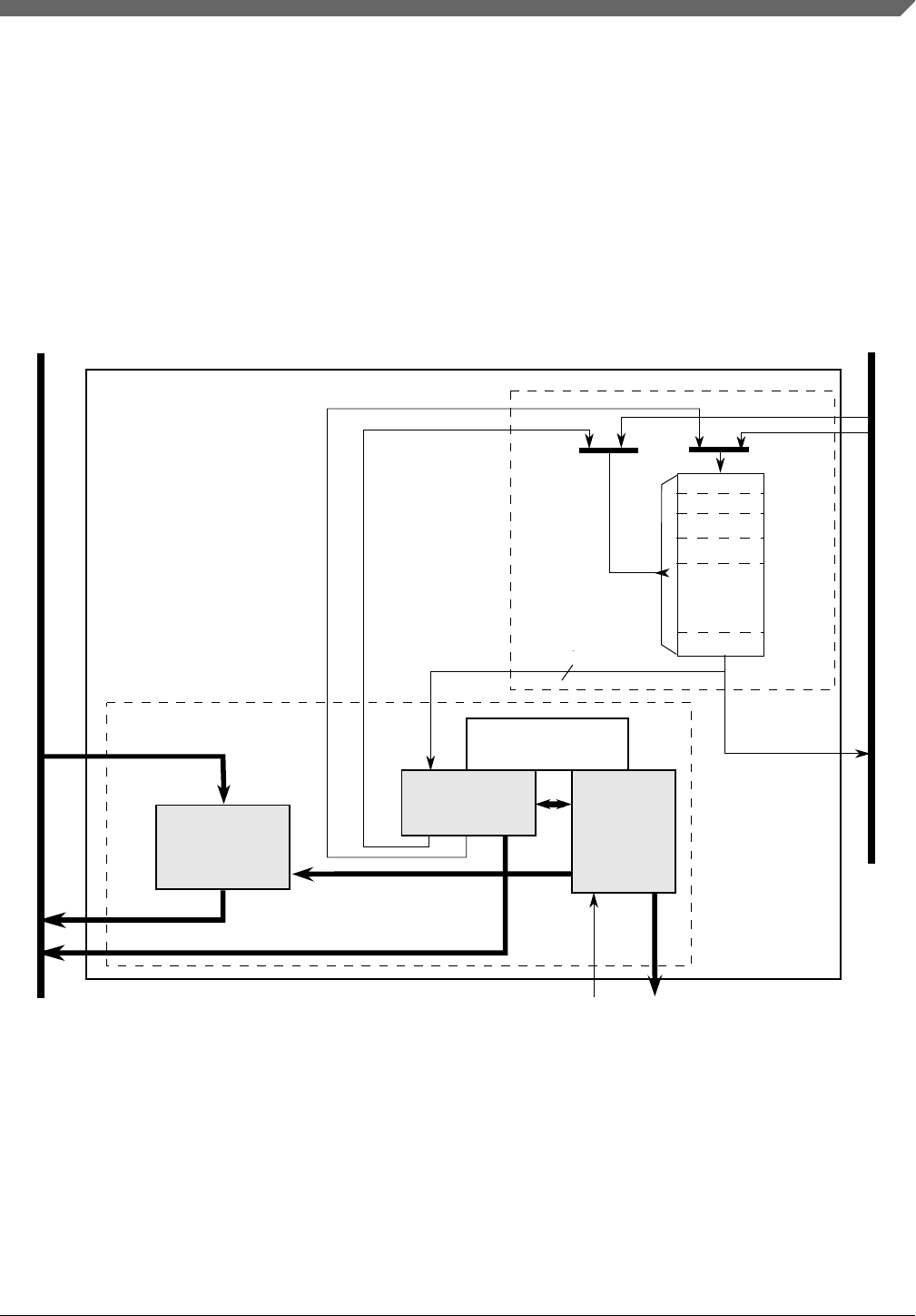
then into the program model and channel arbitration. In the next cycle, the channel
arbitration performs, using the fixed-priority or round-robin algorithm. After arbitration is
complete, the activated channel number is sent through the address path and converted
into the required address to access the local memory for TCDn. Next, the TCD memory
is accessed and the required descriptor read from the local memory and loaded into the
eDMA engine address path channel x or y registers. The TCD memory is 64 bits wide to
minimize the time needed to fetch the activated channel descriptor and load it into the
address path channel x or y registers.
The following diagram illustrates the second part of the basic data flow:
1
eDMA Engine
Data Path
eDMA
0
Program Model/
64
Control
n-1
To/From Crossbar Switch
2
Channel Arbitration
Address Path
Read Data
Write Data
Address
Read Data
Write Data
Write Address
eDMA Peripheral
Request eDMA Done
Transfer
Control
Descriptor (TCD)
Internal Peripheral Bus
Figure 18-3. eDMA operation, part 2
The modules associated with the data transfer (address path, data path, and control)
sequence through the required source reads and destination writes to perform the actual
data movement. The source reads are initiated and the fetched data is temporarily stored
Chapter 18 Enhanced Direct Memory Access (eDMA)
S32K1xx Series Reference Manual, Rev. 7, 04/2018
NXP Semiconductors 379
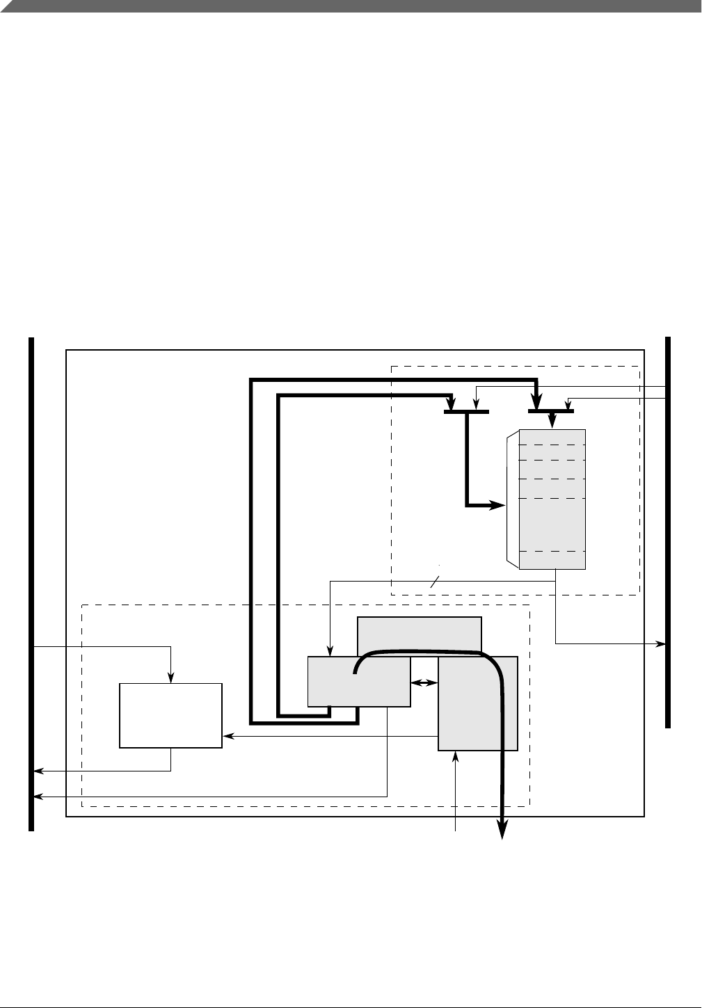
in the data path block until it is gated onto the internal bus during the destination write.
This source read/destination write processing continues until the minor byte count has
transferred.
After the minor byte count has moved, the final phase of the basic data flow is performed.
In this segment, the address path logic performs the required updates to certain fields in
the appropriate TCD, for example, SADDR, DADDR, CITER. If the major iteration
count is exhausted, additional operations are performed. These include the final address
adjustments and reloading of the BITER field into the CITER. Assertion of an optional
interrupt request also occurs at this time, as does a possible fetch of a new TCD from
memory using the scatter/gather address pointer included in the descriptor (if scatter/
gather is enabled). The updates to the TCD memory and the assertion of an interrupt
request are shown in the following diagram.
1
eDMA Engine
Data Path
eDMA
0
Program Model/
64
Control
n-1
To/From Crossbar Switch
2
Channel Arbitration
Address Path
Read Data
Write Data
Address
Read Data
Write Data
Write Address
eDMA Peripheral
Request eDMA Done
Transfer
Control
Descriptor (TCD)
Internal Peripheral Bus
Figure 18-4. eDMA operation, part 3
Functional description
S32K1xx Series Reference Manual, Rev. 7, 04/2018
380 NXP Semiconductors

18.5.2 Fault reporting and handling
Channel errors are reported in the Error Status register (DMAx_ES) and can be caused
by:
• A configuration error, which is an illegal setting in the transfer-control descriptor or
an illegal priority register setting in Fixed-Arbitration mode, or
• An error termination to a bus master read or write cycle
A configuration error is reported when the starting source or destination address, source
or destination offsets, minor loop byte count, or the transfer size represent an inconsistent
state. Each of these possible causes are detailed below:
• The addresses and offsets must be aligned on 0-modulo-transfer-size boundaries.
• The minor loop byte count must be a multiple of the source and destination transfer
sizes.
• All source reads and destination writes must be configured to the natural boundary of
the programmed transfer size respectively.
• In fixed arbitration mode, a configuration error is caused by any two channel
priorities being equal. All channel priority levels must be unique when fixed
arbitration mode is enabled.
NOTE
When two channels have the same priority, a channel
priority error exists and will be reported in the Error Status
register. However, the channel number will not be reported
in the Error Status register. When all of the channel
priorities within a group are not unique, the channel
number selected by arbitration in undetermined.
To aid in Channel Priority Error (CPE) debug, set the Halt
On Error bit in the DMA’s Control Register. If all of the
channel priorities within a group are not unique, the DMA
will be halted after the CPE error is recorded. The DMA
will remain halted and will not process any channel service
requests. Once all of the channel priorities are set to unique
numbers, the DMA may be enabled again by clearing the
Halt bit.
Chapter 18 Enhanced Direct Memory Access (eDMA)
S32K1xx Series Reference Manual, Rev. 7, 04/2018
NXP Semiconductors 381

• If a scatter/gather operation is enabled upon channel completion, a configuration
error is reported if the scatter/gather address (DLAST_SGA) is not aligned on a 32-
byte boundary.
• If minor loop channel linking is enabled upon channel completion, a configuration
error is reported when the link is attempted if the TCDn_CITER[E_LINK] bit does
not equal the TCDn_BITER[E_LINK] bit.
If enabled, all configuration error conditions, except the scatter/gather and minor-loop
link errors, report as the channel activates and asserts an error interrupt request. A scatter/
gather configuration error is reported when the scatter/gather operation begins at major
loop completion when properly enabled. A minor loop channel link configuration error is
reported when the link operation is serviced at minor loop completion.
If a system bus read or write is terminated with an error, the data transfer is stopped and
the appropriate bus error flag set. In this case, the state of the channel's transfer control
descriptor is updated by the eDMA engine with the current source address, destination
address, and current iteration count at the point of the fault. When a system bus error
occurs, the channel terminates after the next transfer. Due to pipeline effect, the next
transfer is already in progress when the bus error is received by the eDMA. If a bus error
occurs on the last read prior to beginning the write sequence, the write executes using the
data captured during the bus error. If a bus error occurs on the last write prior to
switching to the next read sequence, the read sequence executes before the channel
terminates due to the destination bus error.
A transfer may be cancelled by software with the CR[CX] bit. When a cancel transfer
request is recognized, the DMA engine stops processing the channel. The current read-
write sequence is allowed to finish. If the cancel occurs on the last read-write sequence of
a major or minor loop, the cancel request is discarded and the channel retires normally.
The error cancel transfer is the same as a cancel transfer except the Error Status register
(DMAx_ES) is updated with the cancelled channel number and ECX is set. The TCD of a
cancelled channel contains the source and destination addresses of the last transfer saved
in the TCD. If the channel needs to be restarted, you must re-initialize the TCD because
the aforementioned fields no longer represent the original parameters. When a transfer is
cancelled by the error cancel transfer mechanism, the channel number is loaded into
DMA_ES[ERRCHN] and ECX and VLD are set. In addition, an error interrupt may be
generated if enabled.
NOTE
The cancel transfer request allows the user to stop a large data
transfer in the event the full data transfer is no longer needed.
The cancel transfer bit does not abort the channel. It simply
stops the transferring of data and then retires the channel
through its normal shutdown sequence. The application
Functional description
S32K1xx Series Reference Manual, Rev. 7, 04/2018
382 NXP Semiconductors

software must handle the context of the cancel. If an interrupt is
desired (or not), then the interrupt should be enabled (or
disabled) before the cancel request. The application software
must clean up the transfer control descriptor since the full
transfer did not occur.
The occurrence of any error causes the eDMA engine to stop normal processing of the
active channel immediately (it goes to its error processing states and the transaction to the
system bus still has pipeline effect), and the appropriate channel bit in the eDMA error
register is asserted. At the same time, the details of the error condition are loaded into the
Error Status register (DMAx_ES). The major loop complete indicators, setting the
transfer control descriptor DONE flag and the possible assertion of an interrupt request,
are not affected when an error is detected. After the error status has been updated, the
eDMA engine continues operating by servicing the next appropriate channel. A channel
that experiences an error condition is not automatically disabled. If a channel is
terminated by an error and then issues another service request before the error is fixed,
that channel executes and terminates with the same error condition.
18.5.3 Channel preemption
Channel preemption is enabled on a per-channel basis by setting the DCHPRIn[ECP] bit.
Channel preemption allows the executing channel’s data transfers to temporarily suspend
in favor of starting a higher priority channel. After the preempting channel has completed
all its minor loop data transfers, the preempted channel is restored and resumes
execution. After the restored channel completes one read/write sequence, it is again
eligible for preemption. If any higher priority channel is requesting service, the restored
channel is suspended and the higher priority channel is serviced. Nested preemption, that
is, attempting to preempt a preempting channel, is not supported. After a preempting
channel begins execution, it cannot be preempted. Preemption is available only when
fixed arbitration is selected.
A channel’s ability to preempt another channel can be disabled by setting
DCHPRIn[DPA]. When a channel’s preempt ability is disabled, that channel cannot
suspend a lower priority channel’s data transfer, regardless of the lower priority channel’s
ECP setting. This allows for a pool of low priority, large data-moving channels to be
defined. These low priority channels can be configured to not preempt each other, thus
preventing a low priority channel from consuming the preempt slot normally available to
a true, high priority channel.
Chapter 18 Enhanced Direct Memory Access (eDMA)
S32K1xx Series Reference Manual, Rev. 7, 04/2018
NXP Semiconductors 383

18.6 Initialization/application information
The following sections discuss initialization of the eDMA and programming
considerations.
18.6.1 eDMA initialization
To initialize the eDMA:
1. Write to the CR if a configuration other than the default is desired.
2. Write the channel priority levels to the DCHPRIn registers if a configuration other
than the default is desired.
3. Enable error interrupts in the EEI register if so desired.
4. Write the 32-byte TCD for each channel that may request service.
5. Enable any hardware service requests via the ERQ register.
6. Request channel service via either:
•Software: setting the TCDn_CSR[START]
• Hardware: slave device asserting its eDMA peripheral request signal
After any channel requests service, a channel is selected for execution based on the
arbitration and priority levels written into the programmer's model. The eDMA engine
reads the entire TCD, including the TCD control and status fields, as shown in the
following table, for the selected channel into its internal address path module.
As the TCD is read, the first transfer is initiated on the internal bus, unless a
configuration error is detected. Transfers from the source, as defined by TCDn_SADDR,
to the destination, as defined by TCDn_DADDR, continue until the number of bytes
specified by TCDn_NBYTES are transferred.
When the transfer is complete, the eDMA engine's local TCDn_SADDR,
TCDn_DADDR, and TCDn_CITER are written back to the main TCD memory and any
minor loop channel linking is performed, if enabled. If the major loop is exhausted,
further post processing executes, such as interrupts, major loop channel linking, and
scatter/gather operations, if enabled.
Initialization/application information
S32K1xx Series Reference Manual, Rev. 7, 04/2018
384 NXP Semiconductors
Table 18-5. TCD Control and Status fields
TCDn_CSR field
name Description
START Control bit to start channel explicitly when using a software initiated DMA service (Automatically
cleared by hardware)
ACTIVE Status bit indicating the channel is currently in execution
DONE Status bit indicating major loop completion (cleared by software when using a software initiated
DMA service)
D_REQ Control bit to disable DMA request at end of major loop completion when using a hardware initiated
DMA service
BWC Control bits for throttling bandwidth control of a channel
E_SG Control bit to enable scatter-gather feature
INT_HALF Control bit to enable interrupt when major loop is half complete
INT_MAJ Control bit to enable interrupt when major loop completes
The following figure shows how each DMA request initiates one minor-loop transfer, or
iteration, without CPU intervention. DMA arbitration can occur after each minor loop,
and one level of minor loop DMA preemption is allowed. The number of minor loops in
a major loop is specified by the beginning iteration count (BITER).
DMA request
DMA request
DMA request
Minor loop Minor loop Minor loop
Major loop
Current major
loop iteration
count (CITER)
3
2
1
Source or destination memory
Figure 18-5. Example of multiple loop iterations
The following figure lists the memory array terms and how the TCD settings interrelate.
Chapter 18 Enhanced Direct Memory Access (eDMA)
S32K1xx Series Reference Manual, Rev. 7, 04/2018
NXP Semiconductors 385
xADDR: (Starting address)
xLAST: Number of bytes added to
current address after major loop
(typically used to loop back)
Minor loop
(NBYTES in
minor loop,
often the same
value as xSIZE)
Minor loop
Last minor loop
Offset (xOFF): number of bytes added to
current address after each transfer
(often the same value as xSIZE)
Each DMA source (S) and
destination (D) has its own:
Address (xADDR)
Size (xSIZE)
Offset (xOFF)
Modulo (xMOD)
Last Address Adjustment (xLAST)
where x = S or D
Peripheral queues typically
have size and offset equal
to NBYTES.
xSIZE: (size of one
data transfer)
Figure 18-6. Memory array terms
18.6.2 Programming errors
The eDMA performs various tests on the transfer control descriptor to verify consistency
in the descriptor data. Most programming errors are reported on a per channel basis with
the exception of channel priority error (ES[CPE]).
For all error types other than channel priority error, the channel number causing the error
is recorded in the Error Status register (DMAx_ES). If the error source is not removed
before the next activation of the problem channel, the error is detected and recorded
again.
If priority levels are not unique, when any channel requests service, a channel priority
error is reported. The highest channel priority with an active request is selected, but the
lowest numbered channel with that priority is selected by arbitration and executed by the
eDMA engine. The hardware service request handshake signals, error interrupts, and
error reporting is associated with the selected channel.
18.6.3 Arbitration mode considerations
This section discusses arbitration considerations for the eDMA.
Initialization/application information
S32K1xx Series Reference Manual, Rev. 7, 04/2018
386 NXP Semiconductors

18.6.3.1 Fixed channel arbitration
In this mode, the channel service request from the highest priority channel is selected to
execute.
18.6.3.2 Round-robin channel arbitration
Channels are serviced starting with the highest channel number and rotating through to
the lowest channel number without regard to the channel priority levels.
18.6.4 Performing DMA transfers
This section presents examples on how to perform DMA transfers with the eDMA.
18.6.4.1 Single request
To perform a simple transfer of n bytes of data with one activation, set the major loop to
one (TCDn_CITER = TCDn_BITER = 1). The data transfer begins after the channel
service request is acknowledged and the channel is selected to execute. After the transfer
is complete, the TCDn_CSR[DONE] bit is set and an interrupt generates if properly
enabled.
For example, the following TCD entry is configured to transfer 16 bytes of data. The
eDMA is programmed for one iteration of the major loop transferring 16 bytes per
iteration. The source memory has a byte wide memory port located at 0x1000. The
destination memory has a 32-bit port located at 0x2000. The address offsets are
programmed in increments to match the transfer size: one byte for the source and four
bytes for the destination. The final source and destination addresses are adjusted to return
to their beginning values.
TCDn_CITER = TCDn_BITER = 1
TCDn_NBYTES = 16
TCDn_SADDR = 0x1000
TCDn_SOFF = 1
TCDn_ATTR[SSIZE] = 0
TCDn_SLAST = -16
TCDn_DADDR = 0x2000
TCDn_DOFF = 4
TCDn_ATTR[DSIZE] = 2
TCDn_DLAST_SGA= –16
TCDn_CSR[INT_MAJ] = 1
TCDn_CSR[START] = 1 (Should be written last after all other fields have been initialized)
All other TCDn fields = 0
This generates the following event sequence:
Chapter 18 Enhanced Direct Memory Access (eDMA)
S32K1xx Series Reference Manual, Rev. 7, 04/2018
NXP Semiconductors 387

1. User write to the TCDn_CSR[START] bit requests channel service.
2. The channel is selected by arbitration for servicing.
3. eDMA engine writes: TCDn_CSR[DONE] = 0, TCDn_CSR[START] = 0,
TCDn_CSR[ACTIVE] = 1.
4. eDMA engine reads: channel TCD data from local memory to internal register file.
5. The source-to-destination transfers are executed as follows:
a. Read byte from location 0x1000, read byte from location 0x1001, read byte from
0x1002, read byte from 0x1003.
b. Write 32-bits to location 0x2000 → first iteration of the minor loop.
c. Read byte from location 0x1004, read byte from location 0x1005, read byte from
0x1006, read byte from 0x1007.
d. Write 32-bits to location 0x2004 → second iteration of the minor loop.
e. Read byte from location 0x1008, read byte from location 0x1009, read byte from
0x100A, read byte from 0x100B.
f. Write 32-bits to location 0x2008 → third iteration of the minor loop.
g. Read byte from location 0x100C, read byte from location 0x100D, read byte
from 0x100E, read byte from 0x100F.
h. Write 32-bits to location 0x200C → last iteration of the minor loop → major loop
complete.
6. The eDMA engine writes: TCDn_SADDR = 0x1000, TCDn_DADDR = 0x2000,
TCDn_CITER = 1 (TCDn_BITER).
7. The eDMA engine writes: TCDn_CSR[ACTIVE] = 0, TCDn_CSR[DONE] = 1,
INT[n] = 1.
8. The channel retires and the eDMA goes idle or services the next channel.
18.6.4.2 Multiple requests
The following example transfers 32 bytes via two hardware requests, but is otherwise the
same as the previous example. The only fields that change are the major loop iteration
count and the final address offsets. The eDMA is programmed for two iterations of the
major loop transferring 16 bytes per iteration. After the channel's hardware requests are
enabled in the ERQ register, the slave device initiates channel service requests.
Initialization/application information
S32K1xx Series Reference Manual, Rev. 7, 04/2018
388 NXP Semiconductors

TCDn_CITER = TCDn_BITER = 2
TCDn_SLAST = –32
TCDn_DLAST_SGA = –32
This would generate the following sequence of events:
1. First hardware, that is, eDMA peripheral, request for channel service.
2. The channel is selected by arbitration for servicing.
3. eDMA engine writes: TCDn_CSR[DONE] = 0, TCDn_CSR[START] = 0,
TCDn_CSR[ACTIVE] = 1.
4. eDMA engine reads: channel TCDn data from local memory to internal register file.
5. The source to destination transfers are executed as follows:
a. Read byte from location 0x1000, read byte from location 0x1001, read byte from
0x1002, read byte from 0x1003.
b. Write 32-bits to location 0x2000 → first iteration of the minor loop.
c. Read byte from location 0x1004, read byte from location 0x1005, read byte from
0x1006, read byte from 0x1007.
d. Write 32-bits to location 0x2004 → second iteration of the minor loop.
e. Read byte from location 0x1008, read byte from location 0x1009, read byte from
0x100A, read byte from 0x100B.
f. Write 32-bits to location 0x2008 → third iteration of the minor loop.
g. Read byte from location 0x100C, read byte from location 0x100D, read byte
from 0x100E, read byte from 0x100F.
h. Write 32-bits to location 0x200C → last iteration of the minor loop.
6. eDMA engine writes: TCDn_SADDR = 0x1010, TCDn_DADDR = 0x2010,
TCDn_CITER = 1.
7. eDMA engine writes: TCDn_CSR[ACTIVE] = 0.
8. The channel retires → one iteration of the major loop. The eDMA goes idle or
services the next channel.
9. Second hardware, that is, eDMA peripheral, requests channel service.
10. The channel is selected by arbitration for servicing.
11. eDMA engine writes: TCDn_CSR[DONE] = 0, TCDn_CSR[START] = 0,
TCDn_CSR[ACTIVE] = 1.
Chapter 18 Enhanced Direct Memory Access (eDMA)
S32K1xx Series Reference Manual, Rev. 7, 04/2018
NXP Semiconductors 389

12. eDMA engine reads: channel TCD data from local memory to internal register file.
13. The source to destination transfers are executed as follows:
a. Read byte from location 0x1010, read byte from location 0x1011, read byte from
0x1012, read byte from 0x1013.
b. Write 32-bits to location 0x2010 → first iteration of the minor loop.
c. Read byte from location 0x1014, read byte from location 0x1015, read byte from
0x1016, read byte from 0x1017.
d. Write 32-bits to location 0x2014 → second iteration of the minor loop.
e. Read byte from location 0x1018, read byte from location 0x1019, read byte from
0x101A, read byte from 0x101B.
f. Write 32-bits to location 0x2018 → third iteration of the minor loop.
g. Read byte from location 0x101C, read byte from location 0x101D, read byte
from 0x101E, read byte from 0x101F.
h. Write 32-bits to location 0x201C → last iteration of the minor loop → major loop
complete.
14. eDMA engine writes: TCDn_SADDR = 0x1000, TCDn_DADDR = 0x2000,
TCDn_CITER = 2 (TCDn_BITER).
15. eDMA engine writes: TCDn_CSR[ACTIVE] = 0, TCDn_CSR[DONE] = 1, INT[n] =
1.
16. The channel retires → major loop complete. The eDMA goes idle or services the next
channel.
18.6.4.3 Using the modulo feature
The modulo feature of the eDMA provides the ability to implement a circular data queue
in which the size of the queue is a power of 2. MOD is a 5-bit field for the source and
destination in the TCD, and it specifies which lower address bits increment from their
original value after the address+offset calculation. All upper address bits remain the same
as in the original value. A setting of 0 for this field disables the modulo feature.
Initialization/application information
S32K1xx Series Reference Manual, Rev. 7, 04/2018
390 NXP Semiconductors

The following table shows how the transfer addresses are specified based on the setting
of the MOD field. Here a circular buffer is created where the address wraps to the
original value while the 28 upper address bits (0x1234567x) retain their original value. In
this example the source address is set to 0x12345670, the offset is set to 4 bytes and the
MOD field is set to 4, allowing for a 24 byte (16-byte) size queue.
Table 18-6. Modulo example
Transfer Number Address
1 0x12345670
2 0x12345674
3 0x12345678
4 0x1234567C
5 0x12345670
6 0x12345674
18.6.5 Monitoring transfer descriptor status
This section discusses how to monitor eDMA status.
18.6.5.1 Testing for minor loop completion
There are two methods to test for minor loop completion when using software initiated
service requests. The first is to read the TCDn_CITER field and test for a change.
Another method may be extracted from the sequence shown below. The second method is
to test the TCDn_CSR[START] bit and the TCDn_CSR[ACTIVE] bit. The minor-loop-
complete condition is indicated by both bits reading zero after the TCDn_CSR[START]
was set. Polling the TCDn_CSR[ACTIVE] bit may be inconclusive, because the active
status may be missed if the channel execution is short in duration.
The TCD status bits execute the following sequence for a software activated channel:
Stage TCDn_CSR bits State
START ACTIVE DONE
1 1 0 0 Channel service request via software
2 0 1 0 Channel is executing
3a 0 0 0 Channel has completed the minor loop and is idle
3b 0 0 1 Channel has completed the major loop and is idle
Chapter 18 Enhanced Direct Memory Access (eDMA)
S32K1xx Series Reference Manual, Rev. 7, 04/2018
NXP Semiconductors 391

The best method to test for minor-loop completion when using hardware, that is,
peripheral, initiated service requests is to read the TCDn_CITER field and test for a
change. The hardware request and acknowledge handshake signals are not visible in the
programmer's model.
The TCD status bits execute the following sequence for a hardware-activated channel:
Stage TCDn_CSR bits State
START ACTIVE DONE
1 0 0 0 Channel service request via hardware (peripheral
request asserted)
2 0 1 0 Channel is executing
3a 0 0 0 Channel has completed the minor loop and is idle
3b 0 0 1 Channel has completed the major loop and is idle
For both activation types, the major-loop-complete status is explicitly indicated via the
TCDn_CSR[DONE] bit.
The TCDn_CSR[START] bit is cleared automatically when the channel begins execution
regardless of how the channel activates.
18.6.5.2 Reading the transfer descriptors of active channels
The eDMA reads back the true TCDn_SADDR, TCDn_DADDR, and TCDn_NBYTES
values if read while a channel executes. The true values of the SADDR, DADDR, and
NBYTES are the values the eDMA engine currently uses in its internal register file and
not the values in the TCD local memory for that channel. The addresses, SADDR and
DADDR, and NBYTES, which decrement to zero as the transfer progresses, can give an
indication of the progress of the transfer. All other values are read back from the TCD
local memory.
18.6.5.3 Checking channel preemption status
Preemption is available only when fixed arbitration is selected as the channel arbitration
mode. A preemptive situation is one in which a preempt-enabled channel runs and a
higher priority request becomes active. When the eDMA engine is not operating in fixed
channel arbitration mode, the determination of the actively running relative priority
outstanding requests become undefined. Channel priorities are treated as equal, that is,
constantly rotating, when Round-Robin Arbitration mode is selected.
Initialization/application information
S32K1xx Series Reference Manual, Rev. 7, 04/2018
392 NXP Semiconductors

The TCDn_CSR[ACTIVE] bit for the preempted channel remains asserted throughout
the preemption. The preempted channel is temporarily suspended while the preempting
channel executes one major loop iteration. If two TCDn_CSR[ACTIVE] bits are set
simultaneously in the global TCD map, a higher priority channel is actively preempting a
lower priority channel.
18.6.6 Channel Linking
Channel linking (or chaining) is a mechanism where one channel sets the
TCDn_CSR[START] bit of another channel (or itself), therefore initiating a service
request for that channel. When properly enabled, the EDMA engine automatically
performs this operation at the major or minor loop completion.
The minor loop channel linking occurs at the completion of the minor loop (or one
iteration of the major loop). The TCDn_CITER[E_LINK] field determines whether a
minor loop link is requested. When enabled, the channel link is made after each iteration
of the major loop except for the last. When the major loop is exhausted, only the major
loop channel link fields are used to determine if a channel link should be made. For
example, the initial fields of:
TCDn_CITER[E_LINK] = 1
TCDn_CITER[LINKCH] = 0xC
TCDn_CITER[CITER] value = 0x4
TCDn_CSR[MAJOR_E_LINK] = 1
TCDn_CSR[MAJOR_LINKCH] = 0x7
executes as:
1. Minor loop done → set TCD12_CSR[START] bit
2. Minor loop done → set TCD12_CSR[START] bit
3. Minor loop done → set TCD12_CSR[START] bit
4. Minor loop done, major loop done→ set TCD7_CSR[START] bit
When minor loop linking is enabled (TCDn_CITER[E_LINK] = 1), the
TCDn_CITER[CITER] field uses a nine bit vector to form the current iteration count.
When minor loop linking is disabled (TCDn_CITER[E_LINK] = 0), the
TCDn_CITER[CITER] field uses a 15-bit vector to form the current iteration count. The
bits associated with the TCDn_CITER[LINKCH] field are concatenated onto the CITER
value to increase the range of the CITER.
Chapter 18 Enhanced Direct Memory Access (eDMA)
S32K1xx Series Reference Manual, Rev. 7, 04/2018
NXP Semiconductors 393

Note
The TCDn_CITER[E_LINK] bit and the
TCDn_BITER[E_LINK] bit must equal or a configuration error
is reported. The CITER and BITER vector widths must be
equal to calculate the major loop, half-way done interrupt point.
The following table summarizes how a DMA channel can link to another DMA channel,
i.e, use another channel's TCD, at the end of a loop.
Table 18-7. Channel Linking Parameters
Desired Link
Behavior TCD Control Field Name Description
Link at end of
Minor Loop
CITER[E_LINK] Enable channel-to-channel linking on minor loop completion (current
iteration)
CITER[LINKCH] Link channel number when linking at end of minor loop (current iteration)
Link at end of
Major Loop
CSR[MAJOR_E_LINK] Enable channel-to-channel linking on major loop completion
CSR[MAJOR_LINKCH] Link channel number when linking at end of major loop
18.6.7 Dynamic programming
This section provides recommended methods to change the programming model during
channel execution.
18.6.7.1 Dynamically changing the channel priority
The following two options are recommended for dynamically changing channel priority
levels:
1. Switch to Round-Robin Channel Arbitration mode, change the channel priorities,
then switch back to Fixed Arbitration mode,
2. Disable all the channels, change the channel priorities, then enable the appropriate
channels.
Initialization/application information
S32K1xx Series Reference Manual, Rev. 7, 04/2018
394 NXP Semiconductors

18.6.7.2 Dynamic channel linking
Dynamic channel linking is the process of setting the TCDn_CSR[MAJORELINK] bit
during channel execution (see the diagram in TCD structure). This bit is read from the
TCD local memory at the end of channel execution, thus allowing the user to enable the
feature during channel execution.
Because the user is allowed to change the configuration during execution, a coherency
model is needed. Consider the scenario where the user attempts to execute a dynamic
channel link by enabling the TCDn_CSR[MAJORELINK] bit at the same time the
eDMA engine is retiring the channel. The TCDn_CSR[MAJORELINK] would be set in
the programmer’s model, but it would be unclear whether the actual link was made
before the channel retired.
The following coherency model is recommended when executing a dynamic channel link
request.
1. Write 1 to the TCDn_CSR[MAJORELINK] bit.
2. Read back the TCDn_CSR[MAJORELINK] bit.
3. Test the TCDn_CSR[MAJORELINK] request status:
• If TCDn_CSR[MAJORELINK] = 1, the dynamic link attempt was successful.
• If TCDn_CSR[MAJORELINK] = 0, the attempted dynamic link did not succeed
(the channel was already retiring).
For this request, the TCD local memory controller forces the
TCDn_CSR[MAJORELINK] bit to zero on any writes to a channel’s TCD.word7 after
that channel’s TCD.done bit is set, indicating the major loop is complete.
NOTE
The user must clear the The TCDn_CSR[DONE] bit before
writing the TCDn_CSR[MAJORELINK] bit. The
TCDn_CSR[DONE] bit is cleared automatically by the eDMA
engine after a channel begins execution.
18.6.7.3 Dynamic scatter/gather
Scatter/gather is the process of automatically loading a new TCD into a channel. It allows
a DMA channel to use multiple TCDs; this enables a DMA channel to scatter the DMA
data to multiple destinations or gather it from multiple sources. When scatter/gather is
enabled and the channel has finished its major loop, a new TCD is fetched from system
memory and loaded into that channel’s descriptor location in eDMA programmer’s
model, thus replacing the current descriptor.
Chapter 18 Enhanced Direct Memory Access (eDMA)
S32K1xx Series Reference Manual, Rev. 7, 04/2018
NXP Semiconductors 395

Because the user is allowed to change the configuration during execution, a coherency
model is needed. Consider the scenario where the user attempts to execute a dynamic
scatter/gather operation by enabling the TCDn_CSR[ESG] bit at the same time the
eDMA engine is retiring the channel. The ESG bit would be set in the programmer’s
model, but it would be unclear whether the actual scatter/gather request was honored
before the channel retired.
Two methods for this coherency model are shown in the following subsections. Method 1
has the advantage of reading the MAJORLINKCH field and the ESG bit with a single
read. For both dynamic channel linking and scatter/gather requests, the TCD local
memory controller forces the TCD MAJOR.E_LINK and E_SG bits to zero on any writes
to a channel’s TCD word 7 if that channel’s TCD.DONE bit is set indicating the major
loop is complete.
NOTE
The user must clear the TCDn_CSR[DONE] bit before writing
the MAJORELINK or ESG bits. The TCDn_CSR[DONE] bit is
cleared automatically by the eDMA engine after a channel
begins execution.
18.6.7.3.1 Method 1 (channel not using major loop channel linking)
For a channel not using major loop channel linking, the coherency model described here
may be used for a dynamic scatter/gather request.
When the TCDn_CSR[MAJORELINK] bit is zero, the TCDn_CSR[MAJORLINKCH]
field is not used by the eDMA. In this case, the MAJORLINKCH field may be used for
other purposes. This method uses the MAJORLINKCH field as a TCD identification
(ID).
1. When the descriptors are built, write a unique TCD ID in the
TCDn_CSR[MAJORLINKCH] field for each TCD associated with a channel using
dynamic scatter/gather.
2. Write 1b to the TCDn_CSR[DREQ] bit.
Should a dynamic scatter/gather attempt fail, setting the DREQ bit will prevent a
future hardware activation of this channel. This stops the channel from executing
with a destination address (DADDR) that was calculated using a scatter/gather
address (written in the next step) instead of a dlast final offset value.
3. Write the TCDn_DLASTSGA register with the scatter/gather address.
4. Write 1b to the TCDn_CSR[ESG] bit.
Initialization/application information
S32K1xx Series Reference Manual, Rev. 7, 04/2018
396 NXP Semiconductors

5. Read back the 16 bit TCD control/status field.
6. Test the ESG request status and MAJORLINKCH value in the TCDn_CSR register:
If ESG = 1b, the dynamic link attempt was successful.
If ESG = 0b and the MAJORLINKCH (ID) did not change, the attempted dynamic
link did not succeed (the channel was already retiring).
If ESG = 0b and the MAJORLINKCH (ID) changed, the dynamic link attempt was
successful (the new TCD’s E_SG value cleared the ESG bit).
18.6.7.3.2 Method 2 (channel using major loop channel linking)
For a channel using major loop channel linking, the coherency model described here may
be used for a dynamic scatter/gather request. This method uses the TCD.DLAST_SGA
field as a TCD identification (ID).
1. Write 1b to the TCDn_CSR[DREQ] bit.
Should a dynamic scatter/gather attempt fail, setting the DREQ bit will prevent a
future hardware activation of this channel. This stops the channel from executing
with a destination address (DADDR) that was calculated using a scatter/gather
address (written in the next step) instead of a dlast final offset value.
2. Write the TCDn_DLASTSGA register with the scatter/gather address.
3. Write 1b to the TCDn_CSR[ESG] bit.
4. Read back the ESG bit.
5. Test the ESG request status:
If ESG = 1b, the dynamic link attempt was successful.
If ESG = 0b, read the 32 bit TCDn_DLASTSGA field.
If ESG = 0b and the TCDn_DLASTSGA did not change, the attempted dynamic link
did not succeed (the channel was already retiring).
If ESG = 0b and the TCDn_DLASTSGA changed, the dynamic link attempt was
successful (the new TCD’s E_SG value cleared the ESG bit).
Chapter 18 Enhanced Direct Memory Access (eDMA)
S32K1xx Series Reference Manual, Rev. 7, 04/2018
NXP Semiconductors 397

18.6.8 Suspend/resume a DMA channel with active hardware
service requests
The DMA allows the user to move data from memory or peripheral registers to another
location in memory or peripheral registers without CPU interaction. Once the DMA and
peripherals have been configured and are active, it is rare to suspend a peripheral's
service request dynamically. In this scenario, there are certain restrictions to disabling a
DMA hardware service request. For coherency, a specific procedure must be followed.
This section provides guidance on how to coherently suspend and resume a Direct
Memory Access (DMA) channel when the DMA is triggered by a slave module such as
the Serial Peripheral Interface (SPI), ADC, or other module.
18.6.8.1 Suspend an active DMA channel
To suspend an active DMA channel:
1. Stop the DMA service request at the peripheral first. Confirm it has been disabled by
reading back the appropriate register in the peripheral.
2. Check the DMA's Hardware Request Status Register (DMA_HRSn) to ensure there
is no service request to the DMA channel being suspended. Then disable the
hardware service request by clearing the ERQ bit on appropriate DMA channel.
18.6.8.2 Resume a DMA channel
To resume a DMA channel:
1. Enable the DMA service request on the appropriate channel by setting the its ERQ
bit.
2. Enable the DMA service request at the peripheral.
For example, assume the SPI is set as a master for transmitting data via a DMA service
request when the SPI_TXFIFO has an empty slot. The DMA will transfer the next
command and data to the TXFIFO upon the request. If the user needs to suspend the
DMA/SPI transfer loop, perform the following steps:
1. Disable the DMA service request at the source by writing 0 to
SPI_RSER[TFFF_RE]. Confirm that SPI_RSER[TFFF_RE] is 0.
2. Ensure there is no DMA service request from the SPI by verifying that
DMA_HRS[HRSn] is 0 for the appropriate channel. If no service request is present,
disable the DMA channel by clearing the channel's ERQ bit. If a service request is
present, wait until the request has been processed and the HRS bit reads zero.
Initialization/application information
S32K1xx Series Reference Manual, Rev. 7, 04/2018
398 NXP Semiconductors

Chapter 19
Trigger MUX Control (TRGMUX)
Chip-specific TRGMUX information
19.1.1 Module interconnectivity
The TRGMUX provides an extremely flexible mechanism for connecting various trigger
sources to multiple pins/peripherals.
See Figure 19-2 and Figure 19-3 for available input triggers.
With the TRGMUX, each peripheral that accepts external triggers usually has one
specific 32-bit trigger control register. Each control register supports up to four triggers,
and each trigger can be selected from the available input triggers.
The following figure shows the main structure of TRGMUX, using Module_A as an
example.
19.1
S32K1xx Series Reference Manual, Rev. 7, 04/2018
NXP Semiconductors 399
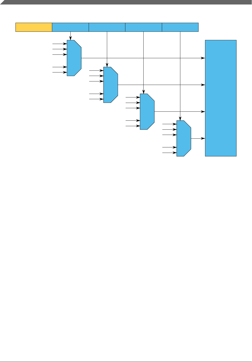
0
63
• • •
0
63
• • •
0
63
• • •
0
63
• • •
Module_A
LK SELx SELx SELx SELx
TRGMUX_Reg_ModuleA
Figure 19-1. TRGMUX structure example (64 inputs)
NOTE
Each TRGMUX control register supports up to four trigger
channels, but each module does not necessarily implement all
four triggers. Modules that need more than four trigger inputs
(such as for external output) have multiple control registers.
The following figures show the superset of trigger inputs, outputs, and control registers
for the S32K1xx series. See attached S32K1xx_Trigger_Muxing.xlsx for details on
recommendations which must be adhered while using the triggering scheme.
Chip-specific TRGMUX information
S32K1xx Series Reference Manual, Rev. 7, 04/2018
400 NXP Semiconductors

in64
FTM4_INIT_TRIG
FTM4_EXT_TRIG
FTM5_EXT_TRIG
FTM6_INIT_TRIG
FTM6_EXT_TRIG
FTM7_INIT_TRIG
FTM7_EXT_TRIG
Reserved
FTM5_INIT_TRIG
Reserved
Reserved
Reserved
Reserved --------->
---------> in65
---------> in66
LPI2C1_Master_TRIG ---------> in67
---------> in68
---------> in69
---------> in70
---------> in71
---------> in72
---------> in73
---------> in74
---------> in75
---------> in76
---------> in77
---------> in78
---------> in79
---------> in80
Reserved
Reserved
LPI2C1_Slave_TRIG
Y
Y
IN Register OUT
out0 DMA_CH0
1'b1 ---------> in1 TRGMUX_DMAMUX0 out1 DMA_CH1
TRGMUX_IN0 ---------> in2 out2 DMA_CH2
TRGMUX_IN1 ---------> in3 out3 DMA_CH3
TRGMUX_IN2 ---------> in4 out4 TRGMUX_OUT0
TRGMUX_IN3 ---------> in5 TRGMUX_EXTOUT0 out5 TRGMUX_OUT1
TRGMUX_IN4 ---------> in6 out6 TRGMUX_OUT2
TRGMUX_IN5 ---------> in7 out7 TRGMUX_OUT3
TRGMUX_IN6 ---------> in8 out8 TRGMUX_OUT4
TRGMUX_IN7 ---------> in9 TRGMUX_EXTOUT1 out9 TRGMUX_OUT5
TRGMUX_IN8 ---------> in10 out10 TRGMUX_OUT6
TRGMUX_IN9 ---------> in11 out11 TRGMUX_OUT7
TRGMUX_IN10 ---------> in12 out12
------>
TRGMUX_IN11 ---------> in13 TRGMUX_ADC0 out13
------>
------>
CMP0_COUT ---------> in14 out14
------>
out15
------>
out16
------>
LPIT_CH0 ---------> in17 Y TRGMUX_ADC1 out17
------>
------>
LPIT_CH1 ---------> in18 Y out18
------>
LPIT_CH2 ---------> in19 Y out19
------>
LPIT_CH3 ---------> in20 Y out20
LPTMR0 ---------> in21 out21
FTM0_INIT_TRIG ---------> in22 out22
FTM0_EXT_TRIG ---------> in23 out23
FTM1_INIT_TRIG ---------> in24 out24
FTM1_EXT_TRIG ---------> in25 out25 X
FTM2_INIT_TRIG ---------> in26 out26 X
FTM2_EXT_TRIG ---------> in27 out27 X
FTM3_INIT_TRIG ---------> in28 TRGMUX_CMP0 out28
FTM3_EXT_TRIG ---------> in29 out29 X
ADC0_SC1A[COCO]---------> in30 out30 X
ADC0_SC1B[COCO] ---------> in31 out31 X
ADC1_SC1A[COCO] ---------> in32 out32
ADC1_SC1B[COCO] ---------> in33 out33 X
PDB0_CH0_TRIG ---------> in34 out34 X
out35 X
PDB0_PULSE_OUT ---------> in36 out36
PDB1_CH0_TRIG ---------> in37 out37 X
out38 X
PDB1_PULSE_OUT ---------> in39 out39 X
out40 FTM0_HWTRIG0
TRGMUX_FTM0 out41 FTM0_FAULT0
out42 FTM0_FAULT1
RTC_alarm2---------> in43 out43 FTM0_FAULT2
RTC_second2---------> in44 out44 FTM1_HWTRIG0
FlexIO_TRIG0 ---------> in45 TRGMUX_FTM1 out45 FTM1_FAULT0
FlexIO_TRIG1 ---------> in46 out46 FTM1_FAULT1
FlexIO_TRIG2 ---------> in47 out47 FTM1_FAULT2
FlexIO_TRIG3 ---------> in48 out48 FTM2_HWTRIG0
LPUART0_RX_data ---------> in49 TRGMUX_FTM2 out49 FTM2_FAULT0
LPUART0_TX_data ---------> in50 out50 FTM2_FAULT1
LPUART0_RX_idle ---------> in51 out51 FTM2_FAULT2
LPUART1_RX_data ---------> in52 out52 FTM3_HWTRIG0
LPUART1_TX_data ---------> in53 TRGMUX_FTM3 out53 FTM3_FAULT0
LPUART1_RX_idle ---------> in54 out54 FTM3_FAULT1
LPI2C0_Master_trigger ---------> in55 out55 FTM3_FAULT2
LPI2C0_Slave_trigger ---------> in56 TRGMUX_PDB0 out56
out57 X
out58 X
LPSPI0_Frame ---------> in59 out59 X
LPSPI0_RX_data ---------> in60 TRGMUX_PDB1 out60
LPSPI1_Frame ---------> in61 out61 X
LPSPI1_RX_data ---------> in62 out62 X
SIM_SW_TRIG ---------> in63 out63 X
PDB0_trigger_in0---------------------->
---------------------->
TRGMUX
---------------------->
---------------------->
---------------------->
---------------------->
---------------------->
---------------------->
---------------------->
---------------------->
ADC1_ADHWT
---------------------->
---------------------->
---------------------->
---------------------->
---------------------->
---------------------->
---------------------->
---------------------->
ADC Trigger
ADC0_ADHWT
CMP0_SAMPLE
---------------------->
Trigger Source
----------------------> PDB1_trigger_in0
---------------------->
---------------------->
---------------------->
---------------------->
---------------------->
---------------------->
---------------------->
---------------------->
---------------------->
---------------------->
---------------------->
Target Module
X
X
X
X
X
X
X
and
Arbitration
Unit1
Latching
ADC Trigger
and
Arbitration
Unit1
Latching
1 In the ADC Configuration chapter, see the "Trigger Latching and Arbitration" section for details.
1'b0 ---------> in0
Pre-TRIG
OUT
Pre-TRIG
IN
Y
Y
Y
Y
Y
Y
2 Interrupt enable needs to be configured before expecting RTC_alarm and RTC_second trigger from TRGMUX.
Figure 19-2. Trigger interconnectivity (part 1 of 2: outputs 0-63)
Chapter 19 Trigger MUX Control (TRGMUX)
S32K1xx Series Reference Manual, Rev. 7, 04/2018
NXP Semiconductors 401

X
out108
X
X
X
out109
out110
out111
out112
X
X
X
out113
out114
out115
out120
X
X
X
out121
out122
out123
out124
X
X
X
out125
out126
out127
out116
X
X
X
out117
out118
out119
LPI2C1_TRG
---------------------->
TRGMUX_LPI2C1
---------------------->
---------------------->
---------------------->
---------------------->
FTM4_HWTRIG0
FTM5_HWTRIG0
FTM6_HWTRIG0
FTM7_HWTRIG0
TRGMUX_FTM5
TRGMUX_FTM4
TRGMUX_FTM6
TRGMUX_FTM7
Note: Above figure shows all the connections. Slots for an absent instance in a particular part are Reserved.
1 Interrupt enable needs to be configured before expecting RTC_alarm and RTC_second trigger from TRGMUX.
IN Pre-TRIG Register OUT
out64
1'b1 ---------> in1 out65 X
TRGMUX_IN0 ---------> in2 out66 X
TRGMUX_IN1 ---------> in3 out67 X
TRGMUX_IN2 ---------> in4 out68 FlexIO_TRG_TIM0
TRGMUX_IN3 ---------> in5 TRGMUX_FLEXIO out69 FlexIO_TRG_TIM1
TRGMUX_IN4 ---------> in6 out70 FlexIO_TRG_TIM2
TRGMUX_IN5 ---------> in7 out71 FlexIO_TRG_TIM3
TRGMUX_IN6 ---------> in8 out72 LPIT_TRG_CH0
TRGMUX_IN7 ---------> in9 TRGMUX_LPIT0 out73 LPIT_TRG_CH1
TRGMUX_IN8 ---------> in10 out74 LPIT_TRG_CH2
TRGMUX_IN9 ---------> in11 out75 LPIT_TRG_CH3
TRGMUX_IN10 ---------> in12 TRGMUX_LPUART0 out76 LPUART0_TRG
TRGMUX_IN11 ---------> in13 out77 X
CMP0_COUT ---------> in14 out78 X
out79 X
TRGMUX_LPUART1 out80 LPUART1_TRG
LPIT_CH0 ---------> in17 Y out81 X
LPIT_CH1 ---------> in18 Y out82 X
LPIT_CH2 ---------> in19 Y out83 X
LPIT_CH3 ---------> in20 Y TRGMUX_LPI2C0 out84 LPI2C0_TRG
LPTMR0 ---------> in21 out85 X
FTM0_INIT_TRIG ---------> in22 out86 X
FTM0_EXT_TRIG ---------> in23 out87 X
FTM1_INIT_TRIG ---------> in24 out88
FTM1_EXT_TRIG ---------> in25 out89 X
FTM2_INIT_TRIG ---------> in26 out90 X
FTM2_EXT_TRIG ---------> in27 out91 X
FTM3_INIT_TRIG ---------> in28 TRGMUX_LPSPI0 out92 LPSPI0_TRG
FTM3_EXT_TRIG ---------> in29 out93 X
ADC0_SC1A[COCO] ---------> in30 out94 X
---------> in31 out95 X
---------> in32 TRGMUX_LPSPI1 out96 LPSPI1_TRG
---------> in33 out97 X
PDB0_CH0_TRIG ---------> in34 out98 X
out99 X
PDB0_PULSE_OUT ---------> in36 TRGMUX_LPTMR0 out100 LPTMR0_ALT0
PDB1_CH0_TRIG ---------> in37 out101 X
out102 X
PDB1_PULSE_OUT ---------> in39 out103 X
RTC_alarm1---------> in43
RTC_second1---------> in44
FlexIO_TRIG0 ---------> in45
FlexIO_TRIG1 ---------> in46
FlexIO_TRIG2 ---------> in47
FlexIO_TRIG3 ---------> in48
LPUART0_RX_data ---------> in49
LPUART0_TX_data ---------> in50
LPUART0_RX_idle ---------> in51
LPUART1_RX_data ---------> in52
LPUART1_TX_data ---------> in53
LPUART1_RX_idle ---------> in54
LPI2C0_Master_trigger ---------> in55
LPI2C0_Slave_trigger ---------> in56
LPSPI0_Frame ---------> in59
LPSPI0_RX_data ---------> in60
LPSPI1_Frame ---------> in61
LPSPI1_RX_data ---------> in62
SIM_SW_TRIG ---------> in63
Trigger Source TRGMUX Target Module
---------------------->
---------------------->
---------------------->
---------------------->
---------------------->
---------------------->
---------------------->
---------------------->
---------------------->
---------------------->
---------------------->
---------------------->
---------------------->
---------------------->
X
out104
X
X
X
out105
out106
out107
X
ADC0_SC1B[COCO]
ADC1_SC1A[COCO]
ADC1_SC1B[COCO]
FTM4_INIT_TRIG
FTM4_EXT_TRIG
FTM5_EXT_TRIG
FTM6_INIT_TRIG
FTM6_EXT_TRIG
FTM7_INIT_TRIG
FTM7_EXT_TRIG
Reserved
FTM5_INIT_TRIG
Reserved
Reserved
Reserved
Reserved --------->
---------> in65
---------> in66
LPI2C1_Master_TRIG ---------> in67
---------> in68
---------> in69
---------> in70
---------> in71
---------> in72
---------> in73
---------> in74
---------> in75
---------> in76
---------> in77
---------> in78
---------> in79
---------> in80
Reserved
Reserved
LPI2C1_Slave_TRIG
in64
1'b0 ---------> in0
IN Pre-TRIG
OUT
Figure 19-3. Trigger interconnectivity (part 2 of 2: outputs 64-127)
Chip-specific TRGMUX information
S32K1xx Series Reference Manual, Rev. 7, 04/2018
402 NXP Semiconductors

NOTE
Additional details about ADC triggers include:
• For each ADC, the four triggers are ORed together to
provide a flexible scheme for the hardware trigger of each
ADC. The pretriggers are not ORed.
• Only LPIT supports pretriggers.
• If other peripherals require pretriggers, software pretriggers
must be used. See SIM_ADCOPT[ADCxSWPRETRG] for
configuring software pretriggers.
• See ADC Trigger Sources for more information about ADC
trigger implementation, including a PDB pretrigger scheme
that does not involve TRGMUX.
19.1.2 TRGMUX register information
Some TRGMUX registers and input connections are present only on some S32K1xx
products. Registers and input connections for instances unavailable in a particular variant
are Reserved.
19.2 Introduction
The trigger multiplexer (TRGMUX) module allows software to configure the trigger
inputs for various peripherals.
19.3 Features
The TRGMUX module allows software to select the trigger source for peripherals. The
block diagram below shows the trigger selection logic of the TRGMUX module.
Chapter 19 Trigger MUX Control (TRGMUX)
S32K1xx Series Reference Manual, Rev. 7, 04/2018
NXP Semiconductors 403
TRGMUX
Trigger input 1
Trigger input 2
Trigger input 6
Trigger input 3
[SELx]
...001
...010
...011
...100
...101
...110
...111
Trigger input 4
Trigger input 5
Trigger input 7
To peripheral
trigger inputs
Trigger disabled ...000
Up to four outputs per peripheral
Trigger input N*
* Up to 127 selectable trigger inputs may be available. See the chip-specific
TRGMUX information for the maximum number of trigger inputs supported on this device.
[SEL0] selects the trigger for output 0
[SEL1] selects the trigger for output 1
[SEL2] selects the trigger for output 2
[SEL3] selects the trigger for output 3
output x
Figure 19-4. TRGMUX block diagram
Each peripheral has its own dedicated TRGMUX register. See each peripheral's
TRGMUX register for details.
19.4 Memory map and register definition
The TRGMUX registers contain fields for selecting trigger sources for peripheral
modules.
TRGMUX registers can be written only in supervisor mode.
19.4.1 TRGMUX register descriptions
19.4.1.1 TRGMUX Memory map
Table 19-1. Select Bit Fields
Field Function
SELx This read/write field is used to configure the MUX select for the peripheral trigger inputs.
000_0000 - (0x00) -
000_0001 - (0x01) VDD
Memory map and register definition
S32K1xx Series Reference Manual, Rev. 7, 04/2018
404 NXP Semiconductors

Table 19-1. Select Bit Fields
Field Function
000_0010 - (0x02) TRGMUX_IN0
000_0011 - (0x03) TRGMUX_IN1
000_0100 - (0x04) TRGMUX_IN2
000_0101 - (0x05) TRGMUX_IN3
000_0110 - (0x06) TRGMUX_IN4
000_0111 - (0x07) TRGMUX_IN5
000_1000 - (0x08) TRGMUX_IN6
000_1001 - (0x09) TRGMUX_IN7
000_1010 - (0x0A) TRGMUX_IN8
000_1011 - (0x0B) TRGMUX_IN9
000_1100 - (0x0C) TRGMUX_IN10
000_1101 - (0x0D) TRGMUX_IN11
000_1110 - (0x0E) CMP0_OUT
000_1111 - (0x0F) Reserved
001_0000 - (0x10) Reserved
001_0001 - (0x11) LPIT_CH0
001_0010 - (0x12) LPIT_CH1
001_0011 - (0x13) LPIT_CH2
001_0100 - (0x14) LPIT_CH3
001_0101 - (0x15) LPTMR0
001_0110 - (0x16) FTM0_INIT_TRIG
001_0111 - (0x17) FTM0_EXT_TRIG
001_1000 - (0x18) FTM1_INIT_TRIG
001_1001 - (0x19) FTM1_EXT_TRIG
001_1010 - (0x1A) FTM2_INIT_TRIG
001_1011 - (0x1B) FTM2_EXT_TRIG
001_1100 - (0x1C) FTM3_INIT_TRIG
001_1101 - (0x1D) FTM3_EXT_TRIG
001_1110 - (0x1E) ADC0_SC1A[COCO]
001_1111 - (0x1F) ADC0_SC1B[COCO]
010_0000 - (0x20) ADC1_SC1A[COCO]
010_0001 - (0x21) ADC1_SC1B[COCO]
010_0010 - (0x22) PDB0_CH0_TRIG
010_0011 - (0x23) Reserved
010_0100 - (0x24) PDB0_PULSE_OUT
010_0101 - (0x25) PDB1_CH0_TRIG
010_0110 - (0x26) Reserved
010_0111 - (0x27) PDB1_PULSE_OUT
Chapter 19 Trigger MUX Control (TRGMUX)
S32K1xx Series Reference Manual, Rev. 7, 04/2018
NXP Semiconductors 405

Table 19-1. Select Bit Fields
Field Function
010_1000 - (0x28) Reserved
010_1001 - (0x29) Reserved
010_1010 - (0x2A) Reserved
010_1011 - (0x2B) RTC_alarm
010_1100 - (0x2C) RTC_second
010_1101 - (0x2D) FlexIO_TRIG0
010_1110 - (0x2E) FlexIO_TRIG1
010_1111 - (0x2F) FlexIO_TRIG2
011_0000 - (0x30) FlexIO_TRIG3
011_0001 - (0x31) LPUART0_RX_data
011_0010 - (0x32) LPUART0_TX_data
011_0011 - (0x33) LPUART0_RX_idle
011_0100 - (0x34) LPUART1_RX_data
011_0101 - (0x35) LPUART1_TX_data
011_0110 - (0x36) LPUART1_RX_idle
011_0111 - (0x37) LPI2C0_Master_trigger
011_1000 - (0x38) LPI2C0_Slave_trigger
011_1001 - (0x39) Reserved
011_1010 - (0x3A) Reserved
011_1011 - (0x3B) LPSPI0_Frame
011_1100 - (0x3C) LPSPI0_RX_data
011_1101 - (0x3D) LPSPI1_Frame
011_1110 - (0x3E) LPSPI1_RX_data
011_1111 - (0x3F) SIM_SW_TRIG
100_0000 - (0x40) Reserved
100_0001 - (0x41) Reserved
100_0010 - (0x42) Reserved
100_0011 - (0x43) LPI2C1_Master_trigger
100_0100 - (0x44) LPI2C1_Slave_trigger
100_0101 - (0x45) FTM4_INIT_TRIG
100_0110 - (0x46) FTM4_EXT_TRIG
100_0111 - (0x47) FTM5_INIT_TRIG
100_1000 - (0x48) FTM5_EXT_TRIG
100_1001 - (0x49) FTM6_INIT_TRIG
100_1010 - (0x4A) FTM6_EXT_TRIG
100_1011 - (0x4B) FTM7_INIT_TRIG
100_1100 - (0x4C) FTM7_EXT_TRIG
100_1101 - (0x4D) Reserved
Memory map and register definition
S32K1xx Series Reference Manual, Rev. 7, 04/2018
406 NXP Semiconductors

Table 19-1. Select Bit Fields
Field Function
100_1110 - (0x4E) Reserved
100_1111 - (0x4F) Reserved
101_0000 - (0x50) Reserved
101_0001 - (0x51) Reserved
101_0010 - (0x52) Reserved
101_0011 - (0x53) Reserved
101_0100 - (0x54) Reserved
101_0101 - (0x55) Reserved
101_0110 - (0x56) Reserved
101_0111 - (0x57) Reserved
101_1000 - (0x58) Reserved
101_1001 - (0x59) Reserved
101_1010 - (0x5A) Reserved
101_1011 - (0x5B) Reserved
101_1100 - (0x5C) Reserved
101_1101 - (0x5D) Reserved
101_1110 - (0x5E) Reserved
101_1111 - (0x5F) Reserved
110_0000 - (0x60) Reserved
110_0001 - (0x61) Reserved
110_0010 - (0x62) Reserved
110_0011 - (0x63) Reserved
110_0100 - (0x64) Reserved
110_0101 - (0x65) Reserved
110_0110 - (0x66) Reserved
110_0111 - (0x67) Reserved
110_1000 - (0x68) Reserved
110_1001 - (0x69) Reserved
110_1010 - (0x6A) Reserved
110_1011 - (0x6B) Reserved
110_1100 - (0x6C) Reserved
110_1101 - (0x6D) Reserved
110_1110 - (0x6E) Reserved
110_1111 - (0x6F) Reserved
111_0000 - (0x70) Reserved
111_0001 - (0x71) Reserved
111_0010 - (0x72) Reserved
111_0011 - (0x73) Reserved
Chapter 19 Trigger MUX Control (TRGMUX)
S32K1xx Series Reference Manual, Rev. 7, 04/2018
NXP Semiconductors 407

Table 19-1. Select Bit Fields
Field Function
111_0100 - (0x74) Reserved
111_0101 - (0x75) Reserved
111_0110 - (0x76) Reserved
111_0111 - (0x77) Reserved
111_1000 - (0x78) Reserved
111_1001 - (0x79) Reserved
111_1010 - (0x7A) Reserved
111_1011 - (0x7B) Reserved
111_1100 - (0x7C) Reserved
111_1101 - (0x7D) Reserved
111_1110 - (0x7E) Reserved
111_1111 - (0x7F) Reserved
TRGMUX base address: 4006_3000h
Offset Register Width
(In bits)
Access Reset value
0h TRGMUX DMAMUX0 Register (DMAMUX0) 32 RW 0000_0000h
4h TRGMUX EXTOUT0 Register (EXTOUT0) 32 RW 0000_0000h
8h TRGMUX EXTOUT1 Register (EXTOUT1) 32 RW 0000_0000h
Ch TRGMUX ADC0 Register (ADC0) 32 RW 0000_0000h
10h TRGMUX ADC1 Register (ADC1) 32 RW 0000_0000h
1Ch TRGMUX CMP0 Register (CMP0) 32 RW 0000_0000h
28h TRGMUX FTM0 Register (FTM0) 32 RW 0000_0000h
2Ch TRGMUX FTM1 Register (FTM1) 32 RW 0000_0000h
30h TRGMUX FTM2 Register (FTM2) 32 RW 0000_0000h
34h TRGMUX FTM3 Register (FTM3) 32 RW 0000_0000h
38h TRGMUX PDB0 Register (PDB0) 32 RW 0000_0000h
3Ch TRGMUX PDB1 Register (PDB1) 32 RW 0000_0000h
44h TRGMUX FLEXIO Register (FLEXIO) 32 RW 0000_0000h
48h TRGMUX LPIT0 Register (LPIT0) 32 RW 0000_0000h
4Ch TRGMUX LPUART0 Register (LPUART0) 32 RW 0000_0000h
50h TRGMUX LPUART1 Register (LPUART1) 32 RW 0000_0000h
54h TRGMUX LPI2C0 Register (LPI2C0) 32 RW 0000_0000h
5Ch TRGMUX LPSPI0 Register (LPSPI0) 32 RW 0000_0000h
60h TRGMUX LPSPI1 Register (LPSPI1) 32 RW 0000_0000h
64h TRGMUX LPTMR0 Register (LPTMR0) 32 RW 0000_0000h
6Ch TRGMUX LPI2C1 Register (LPI2C1) 32 RW 0000_0000h
Table continues on the next page...
Memory map and register definition
S32K1xx Series Reference Manual, Rev. 7, 04/2018
408 NXP Semiconductors

Offset Register Width
(In bits)
Access Reset value
70h TRGMUX FTM4 Register (FTM4) 32 RW 0000_0000h
74h TRGMUX FTM5 Register (FTM5) 32 RW 0000_0000h
78h TRGMUX FTM6 Register (FTM6) 32 RW 0000_0000h
7Ch TRGMUX FTM7 Register (FTM7) 32 RW 0000_0000h
19.4.1.2 TRGMUX DMAMUX0 Register (DMAMUX0)
19.4.1.2.1 Offset
Register Offset
DMAMUX0 0h
19.4.1.2.2 Function
TRGMUX Register
19.4.1.2.3 Diagram
Bits 31 30 29 28 27 26 25 24 23 22 21 20 19 18 17 16
RLK SEL3 0SEL2
W
Reset 0 0 0 0 0 0 0 0 0 0 0 0 0 0 0 0
Bits 15 14 13 12 11 10 9 8 7 6 5 4 3 2 1 0
R 0 SEL1 0SEL0
W
Reset 0 0 0 0 0 0 0 0 0 0 0 0 0 0 0 0
19.4.1.2.4 Fields
Field Function
31
LK
TRGMUX register lock.
This bit shows whether the register can be written or not. The LK bit can only be written once after any
system reset. Once LK is set, the SELx bits in this TRGMUX register cannot be changed until the next
system reset clears LK.
0b - Register can be written.
Table continues on the next page...
Chapter 19 Trigger MUX Control (TRGMUX)
S32K1xx Series Reference Manual, Rev. 7, 04/2018
NXP Semiconductors 409

Field Function
1b - Register cannot be written until the next system Reset.
30-24
SEL3
Trigger MUX Input 3 Source Select
This read/write bit field is used to configure the MUX select for peripheral trigger input 3. For the field
setting definitions, see Memory map and register definition.
23
—
This read-only bit field is reserved and always has the value 0.
22-16
SEL2
Trigger MUX Input 2 Source Select
This read/write bit field is used to configure the MUX select for peripheral trigger input 2. For the field
setting definitions, see Memory map and register definition.
15
—
This read-only bit field is reserved and always has the value 0.
14-8
SEL1
Trigger MUX Input 1 Source Select
This read/write bit field is used to configure the MUX select for peripheral trigger input 1. For the field
setting definitions, see Memory map and register definition.
7
—
This read-only bit field is reserved and always has the value 0.
6-0
SEL0
Trigger MUX Input 0 Source Select
This read/write bit field is used to configure the MUX select for peripheral trigger input 0. For the field
setting definitions, see Memory map and register definition.
19.4.1.3 TRGMUX EXTOUT0 Register (EXTOUT0)
19.4.1.3.1 Offset
Register Offset
EXTOUT0 4h
19.4.1.3.2 Function
TRGMUX Register
Memory map and register definition
S32K1xx Series Reference Manual, Rev. 7, 04/2018
410 NXP Semiconductors

19.4.1.3.3 Diagram
Bits 31 30 29 28 27 26 25 24 23 22 21 20 19 18 17 16
RLK SEL3 0SEL2
W
Reset 0 0 0 0 0 0 0 0 0 0 0 0 0 0 0 0
Bits 15 14 13 12 11 10 9 8 7 6 5 4 3 2 1 0
R 0 SEL1 0SEL0
W
Reset 0 0 0 0 0 0 0 0 0 0 0 0 0 0 0 0
19.4.1.3.4 Fields
Field Function
31
LK
TRGMUX register lock.
This bit shows whether the register can be written or not. The LK bit can only be written once after any
system reset. Once LK is set, the SELx bits in this TRGMUX register cannot be changed until the next
system reset clears LK.
0b - Register can be written.
1b - Register cannot be written until the next system Reset.
30-24
SEL3
Trigger MUX Input 3 Source Select
This read/write bit field is used to configure the MUX select for peripheral trigger input 3. For the field
setting definitions, see Memory map and register definition.
23
—
This read-only bit field is reserved and always has the value 0.
22-16
SEL2
Trigger MUX Input 2 Source Select
This read/write bit field is used to configure the MUX select for peripheral trigger input 2. For the field
setting definitions, see Memory map and register definition.
15
—
This read-only bit field is reserved and always has the value 0.
14-8
SEL1
Trigger MUX Input 1 Source Select
This read/write bit field is used to configure the MUX select for peripheral trigger input 1. For the field
setting definitions, see Memory map and register definition.
7
—
This read-only bit field is reserved and always has the value 0.
6-0
SEL0
Trigger MUX Input 0 Source Select
This read/write bit field is used to configure the MUX select for peripheral trigger input 0. For the field
setting definitions, see Memory map and register definition.
Chapter 19 Trigger MUX Control (TRGMUX)
S32K1xx Series Reference Manual, Rev. 7, 04/2018
NXP Semiconductors 411

19.4.1.4 TRGMUX EXTOUT1 Register (EXTOUT1)
19.4.1.4.1 Offset
Register Offset
EXTOUT1 8h
19.4.1.4.2 Function
TRGMUX Register
19.4.1.4.3 Diagram
Bits 31 30 29 28 27 26 25 24 23 22 21 20 19 18 17 16
RLK SEL3 0SEL2
W
Reset 0 0 0 0 0 0 0 0 0 0 0 0 0 0 0 0
Bits 15 14 13 12 11 10 9 8 7 6 5 4 3 2 1 0
R 0 SEL1 0SEL0
W
Reset 0 0 0 0 0 0 0 0 0 0 0 0 0 0 0 0
19.4.1.4.4 Fields
Field Function
31
LK
TRGMUX register lock.
This bit shows whether the register can be written or not. The LK bit can only be written once after any
system reset. Once LK is set, the SELx bits in this TRGMUX register cannot be changed until the next
system reset clears LK.
0b - Register can be written.
1b - Register cannot be written until the next system Reset.
30-24
SEL3
Trigger MUX Input 3 Source Select
This read/write bit field is used to configure the MUX select for peripheral trigger input 3. For the field
setting definitions, see Memory map and register definition.
23
—
This read-only bit field is reserved and always has the value 0.
22-16
SEL2
Trigger MUX Input 2 Source Select
This read/write bit field is used to configure the MUX select for peripheral trigger input 2. For the field
setting definitions, see Memory map and register definition.
Table continues on the next page...
Memory map and register definition
S32K1xx Series Reference Manual, Rev. 7, 04/2018
412 NXP Semiconductors

Field Function
15
—
This read-only bit field is reserved and always has the value 0.
14-8
SEL1
Trigger MUX Input 1 Source Select
This read/write bit field is used to configure the MUX select for peripheral trigger input 1. For the field
setting definitions, see Memory map and register definition.
7
—
This read-only bit field is reserved and always has the value 0.
6-0
SEL0
Trigger MUX Input 0 Source Select
This read/write bit field is used to configure the MUX select for peripheral trigger input 0. For the field
setting definitions, see Memory map and register definition.
19.4.1.5 TRGMUX ADC0 Register (ADC0)
19.4.1.5.1 Offset
Register Offset
ADC0 Ch
19.4.1.5.2 Function
TRGMUX Register
19.4.1.5.3 Diagram
Bits 31 30 29 28 27 26 25 24 23 22 21 20 19 18 17 16
RLK SEL3 0SEL2
W
Reset 0 0 0 0 0 0 0 0 0 0 0 0 0 0 0 0
Bits 15 14 13 12 11 10 9 8 7 6 5 4 3 2 1 0
R 0 SEL1 0SEL0
W
Reset 0 0 0 0 0 0 0 0 0 0 0 0 0 0 0 0
Chapter 19 Trigger MUX Control (TRGMUX)
S32K1xx Series Reference Manual, Rev. 7, 04/2018
NXP Semiconductors 413

19.4.1.5.4 Fields
Field Function
31
LK
TRGMUX register lock.
This bit shows whether the register can be written or not. The LK bit can only be written once after any
system reset. Once LK is set, the SELx bits in this TRGMUX register cannot be changed until the next
system reset clears LK.
0b - Register can be written.
1b - Register cannot be written until the next system Reset.
30-24
SEL3
Trigger MUX Input 3 Source Select
This read/write bit field is used to configure the MUX select for peripheral trigger input 3. For the field
setting definitions, see Memory map and register definition.
23
—
This read-only bit field is reserved and always has the value 0.
22-16
SEL2
Trigger MUX Input 2 Source Select
This read/write bit field is used to configure the MUX select for peripheral trigger input 2. For the field
setting definitions, see Memory map and register definition.
15
—
This read-only bit field is reserved and always has the value 0.
14-8
SEL1
Trigger MUX Input 1 Source Select
This read/write bit field is used to configure the MUX select for peripheral trigger input 1. For the field
setting definitions, see Memory map and register definition.
7
—
This read-only bit field is reserved and always has the value 0.
6-0
SEL0
Trigger MUX Input 0 Source Select
This read/write bit field is used to configure the MUX select for peripheral trigger input 0. For the field
setting definitions, see Memory map and register definition.
19.4.1.6 TRGMUX ADC1 Register (ADC1)
19.4.1.6.1 Offset
Register Offset
ADC1 10h
19.4.1.6.2 Function
TRGMUX Register
Memory map and register definition
S32K1xx Series Reference Manual, Rev. 7, 04/2018
414 NXP Semiconductors

19.4.1.6.3 Diagram
Bits 31 30 29 28 27 26 25 24 23 22 21 20 19 18 17 16
RLK SEL3 0SEL2
W
Reset 0 0 0 0 0 0 0 0 0 0 0 0 0 0 0 0
Bits 15 14 13 12 11 10 9 8 7 6 5 4 3 2 1 0
R 0 SEL1 0SEL0
W
Reset 0 0 0 0 0 0 0 0 0 0 0 0 0 0 0 0
19.4.1.6.4 Fields
Field Function
31
LK
TRGMUX register lock.
This bit shows whether the register can be written or not. The LK bit can only be written once after any
system reset. Once LK is set, the SELx bits in this TRGMUX register cannot be changed until the next
system reset clears LK.
0b - Register can be written.
1b - Register cannot be written until the next system Reset.
30-24
SEL3
Trigger MUX Input 3 Source Select
This read/write bit field is used to configure the MUX select for peripheral trigger input 3. For the field
setting definitions, see Memory map and register definition.
23
—
This read-only bit field is reserved and always has the value 0.
22-16
SEL2
Trigger MUX Input 2 Source Select
This read/write bit field is used to configure the MUX select for peripheral trigger input 2. For the field
setting definitions, see Memory map and register definition.
15
—
This read-only bit field is reserved and always has the value 0.
14-8
SEL1
Trigger MUX Input 1 Source Select
This read/write bit field is used to configure the MUX select for peripheral trigger input 1. For the field
setting definitions, see Memory map and register definition.
7
—
This read-only bit field is reserved and always has the value 0.
6-0
SEL0
Trigger MUX Input 0 Source Select
This read/write bit field is used to configure the MUX select for peripheral trigger input 0. For the field
setting definitions, see Memory map and register definition.
Chapter 19 Trigger MUX Control (TRGMUX)
S32K1xx Series Reference Manual, Rev. 7, 04/2018
NXP Semiconductors 415

19.4.1.7 TRGMUX CMP0 Register (CMP0)
19.4.1.7.1 Offset
Register Offset
CMP0 1Ch
19.4.1.7.2 Function
TRGMUX Register
19.4.1.7.3 Diagram
Bits 31 30 29 28 27 26 25 24 23 22 21 20 19 18 17 16
RLK 0 0 0
W
Reset 0 0 0 0 0 0 0 0 0 0 0 0 0 0 0 0
Bits 15 14 13 12 11 10 9 8 7 6 5 4 3 2 1 0
R 0 0 0 SEL0
W
Reset 0 0 0 0 0 0 0 0 0 0 0 0 0 0 0 0
19.4.1.7.4 Fields
Field Function
31
LK
TRGMUX register lock.
This bit shows whether the register can be written or not. The LK bit can only be written once after any
system reset. Once LK is set, the SELx bits in this TRGMUX register cannot be changed until the next
system reset clears LK.
0b - Register can be written.
1b - Register cannot be written until the next system Reset.
30-24
—
This read-only bit field is reserved and always has the value 0.
23
—
This read-only bit field is reserved and always has the value 0.
22-16
—
This read-only bit field is reserved and always has the value 0.
15
—
This read-only bit field is reserved and always has the value 0.
Table continues on the next page...
Memory map and register definition
S32K1xx Series Reference Manual, Rev. 7, 04/2018
416 NXP Semiconductors

Field Function
14-8
—
This read-only bit field is reserved and always has the value 0.
7
—
This read-only bit field is reserved and always has the value 0.
6-0
SEL0
Trigger MUX Input 0 Source Select
This read/write bit field is used to configure the MUX select for peripheral trigger input 0. For the field
setting definitions, see Memory map and register definition.
19.4.1.8 TRGMUX FTM0 Register (FTM0)
19.4.1.8.1 Offset
Register Offset
FTM0 28h
19.4.1.8.2 Function
TRGMUX Register
19.4.1.8.3 Diagram
Bits 31 30 29 28 27 26 25 24 23 22 21 20 19 18 17 16
RLK SEL3 0SEL2
W
Reset 0 0 0 0 0 0 0 0 0 0 0 0 0 0 0 0
Bits 15 14 13 12 11 10 9 8 7 6 5 4 3 2 1 0
R 0 SEL1 0SEL0
W
Reset 0 0 0 0 0 0 0 0 0 0 0 0 0 0 0 0
19.4.1.8.4 Fields
Field Function
31
LK
TRGMUX register lock.
Table continues on the next page...
Chapter 19 Trigger MUX Control (TRGMUX)
S32K1xx Series Reference Manual, Rev. 7, 04/2018
NXP Semiconductors 417

Field Function
This bit shows whether the register can be written or not. The LK bit can only be written once after any
system reset. Once LK is set, the SELx bits in this TRGMUX register cannot be changed until the next
system reset clears LK.
0b - Register can be written.
1b - Register cannot be written until the next system Reset.
30-24
SEL3
Trigger MUX Input 3 Source Select
This read/write bit field is used to configure the MUX select for peripheral trigger input 3. For the field
setting definitions, see Memory map and register definition.
23
—
This read-only bit field is reserved and always has the value 0.
22-16
SEL2
Trigger MUX Input 2 Source Select
This read/write bit field is used to configure the MUX select for peripheral trigger input 2. For the field
setting definitions, see Memory map and register definition.
15
—
This read-only bit field is reserved and always has the value 0.
14-8
SEL1
Trigger MUX Input 1 Source Select
This read/write bit field is used to configure the MUX select for peripheral trigger input 1. For the field
setting definitions, see Memory map and register definition.
7
—
This read-only bit field is reserved and always has the value 0.
6-0
SEL0
Trigger MUX Input 0 Source Select
This read/write bit field is used to configure the MUX select for peripheral trigger input 0. For the field
setting definitions, see Memory map and register definition.
19.4.1.9 TRGMUX FTM1 Register (FTM1)
19.4.1.9.1 Offset
Register Offset
FTM1 2Ch
19.4.1.9.2 Function
TRGMUX Register
Memory map and register definition
S32K1xx Series Reference Manual, Rev. 7, 04/2018
418 NXP Semiconductors

19.4.1.9.3 Diagram
Bits 31 30 29 28 27 26 25 24 23 22 21 20 19 18 17 16
RLK SEL3 0SEL2
W
Reset 0 0 0 0 0 0 0 0 0 0 0 0 0 0 0 0
Bits 15 14 13 12 11 10 9 8 7 6 5 4 3 2 1 0
R 0 SEL1 0SEL0
W
Reset 0 0 0 0 0 0 0 0 0 0 0 0 0 0 0 0
19.4.1.9.4 Fields
Field Function
31
LK
TRGMUX register lock.
This bit shows whether the register can be written or not. The LK bit can only be written once after any
system reset. Once LK is set, the SELx bits in this TRGMUX register cannot be changed until the next
system reset clears LK.
0b - Register can be written.
1b - Register cannot be written until the next system Reset.
30-24
SEL3
Trigger MUX Input 3 Source Select
This read/write bit field is used to configure the MUX select for peripheral trigger input 3. For the field
setting definitions, see Memory map and register definition.
23
—
This read-only bit field is reserved and always has the value 0.
22-16
SEL2
Trigger MUX Input 2 Source Select
This read/write bit field is used to configure the MUX select for peripheral trigger input 2. For the field
setting definitions, see Memory map and register definition.
15
—
This read-only bit field is reserved and always has the value 0.
14-8
SEL1
Trigger MUX Input 1 Source Select
This read/write bit field is used to configure the MUX select for peripheral trigger input 1. For the field
setting definitions, see Memory map and register definition.
7
—
This read-only bit field is reserved and always has the value 0.
6-0
SEL0
Trigger MUX Input 0 Source Select
This read/write bit field is used to configure the MUX select for peripheral trigger input 0. For the field
setting definitions, see Memory map and register definition.
Chapter 19 Trigger MUX Control (TRGMUX)
S32K1xx Series Reference Manual, Rev. 7, 04/2018
NXP Semiconductors 419

19.4.1.10 TRGMUX FTM2 Register (FTM2)
19.4.1.10.1 Offset
Register Offset
FTM2 30h
19.4.1.10.2 Function
TRGMUX Register
19.4.1.10.3 Diagram
Bits 31 30 29 28 27 26 25 24 23 22 21 20 19 18 17 16
RLK SEL3 0SEL2
W
Reset 0 0 0 0 0 0 0 0 0 0 0 0 0 0 0 0
Bits 15 14 13 12 11 10 9 8 7 6 5 4 3 2 1 0
R 0 SEL1 0SEL0
W
Reset 0 0 0 0 0 0 0 0 0 0 0 0 0 0 0 0
19.4.1.10.4 Fields
Field Function
31
LK
TRGMUX register lock.
This bit shows whether the register can be written or not. The LK bit can only be written once after any
system reset. Once LK is set, the SELx bits in this TRGMUX register cannot be changed until the next
system reset clears LK.
0b - Register can be written.
1b - Register cannot be written until the next system Reset.
30-24
SEL3
Trigger MUX Input 3 Source Select
This read/write bit field is used to configure the MUX select for peripheral trigger input 3. For the field
setting definitions, see Memory map and register definition.
23
—
This read-only bit field is reserved and always has the value 0.
22-16
SEL2
Trigger MUX Input 2 Source Select
This read/write bit field is used to configure the MUX select for peripheral trigger input 2. For the field
setting definitions, see Memory map and register definition.
Table continues on the next page...
Memory map and register definition
S32K1xx Series Reference Manual, Rev. 7, 04/2018
420 NXP Semiconductors

Field Function
15
—
This read-only bit field is reserved and always has the value 0.
14-8
SEL1
Trigger MUX Input 1 Source Select
This read/write bit field is used to configure the MUX select for peripheral trigger input 1. For the field
setting definitions, see Memory map and register definition.
7
—
This read-only bit field is reserved and always has the value 0.
6-0
SEL0
Trigger MUX Input 0 Source Select
This read/write bit field is used to configure the MUX select for peripheral trigger input 0. For the field
setting definitions, see Memory map and register definition.
19.4.1.11 TRGMUX FTM3 Register (FTM3)
19.4.1.11.1 Offset
Register Offset
FTM3 34h
19.4.1.11.2 Function
TRGMUX Register
19.4.1.11.3 Diagram
Bits 31 30 29 28 27 26 25 24 23 22 21 20 19 18 17 16
RLK SEL3 0SEL2
W
Reset 0 0 0 0 0 0 0 0 0 0 0 0 0 0 0 0
Bits 15 14 13 12 11 10 9 8 7 6 5 4 3 2 1 0
R 0 SEL1 0SEL0
W
Reset 0 0 0 0 0 0 0 0 0 0 0 0 0 0 0 0
Chapter 19 Trigger MUX Control (TRGMUX)
S32K1xx Series Reference Manual, Rev. 7, 04/2018
NXP Semiconductors 421

19.4.1.11.4 Fields
Field Function
31
LK
TRGMUX register lock.
This bit shows whether the register can be written or not. The LK bit can only be written once after any
system reset. Once LK is set, the SELx bits in this TRGMUX register cannot be changed until the next
system reset clears LK.
0b - Register can be written.
1b - Register cannot be written until the next system Reset.
30-24
SEL3
Trigger MUX Input 3 Source Select
This read/write bit field is used to configure the MUX select for peripheral trigger input 3. For the field
setting definitions, see Memory map and register definition.
23
—
This read-only bit field is reserved and always has the value 0.
22-16
SEL2
Trigger MUX Input 2 Source Select
This read/write bit field is used to configure the MUX select for peripheral trigger input 2. For the field
setting definitions, see Memory map and register definition.
15
—
This read-only bit field is reserved and always has the value 0.
14-8
SEL1
Trigger MUX Input 1 Source Select
This read/write bit field is used to configure the MUX select for peripheral trigger input 1. For the field
setting definitions, see Memory map and register definition.
7
—
This read-only bit field is reserved and always has the value 0.
6-0
SEL0
Trigger MUX Input 0 Source Select
This read/write bit field is used to configure the MUX select for peripheral trigger input 0. For the field
setting definitions, see Memory map and register definition.
19.4.1.12 TRGMUX PDB0 Register (PDB0)
19.4.1.12.1 Offset
Register Offset
PDB0 38h
19.4.1.12.2 Function
TRGMUX Register
Memory map and register definition
S32K1xx Series Reference Manual, Rev. 7, 04/2018
422 NXP Semiconductors

19.4.1.12.3 Diagram
Bits 31 30 29 28 27 26 25 24 23 22 21 20 19 18 17 16
RLK 0 0 0
W
Reset 0 0 0 0 0 0 0 0 0 0 0 0 0 0 0 0
Bits 15 14 13 12 11 10 9 8 7 6 5 4 3 2 1 0
R 0 0 0 SEL0
W
Reset 0 0 0 0 0 0 0 0 0 0 0 0 0 0 0 0
19.4.1.12.4 Fields
Field Function
31
LK
TRGMUX register lock.
This bit shows whether the register can be written or not. The LK bit can only be written once after any
system reset. Once LK is set, the SELx bits in this TRGMUX register cannot be changed until the next
system reset clears LK.
0b - Register can be written.
1b - Register cannot be written until the next system Reset.
30-24
—
This read-only bit field is reserved and always has the value 0.
23
—
This read-only bit field is reserved and always has the value 0.
22-16
—
This read-only bit field is reserved and always has the value 0.
15
—
This read-only bit field is reserved and always has the value 0.
14-8
—
This read-only bit field is reserved and always has the value 0.
7
—
This read-only bit field is reserved and always has the value 0.
6-0
SEL0
Trigger MUX Input 0 Source Select
This read/write bit field is used to configure the MUX select for peripheral trigger input 0. For the field
setting definitions, see Memory map and register definition.
19.4.1.13 TRGMUX PDB1 Register (PDB1)
Chapter 19 Trigger MUX Control (TRGMUX)
S32K1xx Series Reference Manual, Rev. 7, 04/2018
NXP Semiconductors 423

19.4.1.13.1 Offset
Register Offset
PDB1 3Ch
19.4.1.13.2 Function
TRGMUX Register
19.4.1.13.3 Diagram
Bits 31 30 29 28 27 26 25 24 23 22 21 20 19 18 17 16
RLK 0 0 0
W
Reset 0 0 0 0 0 0 0 0 0 0 0 0 0 0 0 0
Bits 15 14 13 12 11 10 9 8 7 6 5 4 3 2 1 0
R 0 0 0 SEL0
W
Reset 0 0 0 0 0 0 0 0 0 0 0 0 0 0 0 0
19.4.1.13.4 Fields
Field Function
31
LK
TRGMUX register lock.
This bit shows whether the register can be written or not. The LK bit can only be written once after any
system reset. Once LK is set, the SELx bits in this TRGMUX register cannot be changed until the next
system reset clears LK.
0b - Register can be written.
1b - Register cannot be written until the next system Reset.
30-24
—
This read-only bit field is reserved and always has the value 0.
23
—
This read-only bit field is reserved and always has the value 0.
22-16
—
This read-only bit field is reserved and always has the value 0.
15
—
This read-only bit field is reserved and always has the value 0.
14-8
—
This read-only bit field is reserved and always has the value 0.
Table continues on the next page...
Memory map and register definition
S32K1xx Series Reference Manual, Rev. 7, 04/2018
424 NXP Semiconductors

Field Function
7
—
This read-only bit field is reserved and always has the value 0.
6-0
SEL0
Trigger MUX Input 0 Source Select
This read/write bit field is used to configure the MUX select for peripheral trigger input 0. For the field
setting definitions, see Memory map and register definition.
19.4.1.14 TRGMUX FLEXIO Register (FLEXIO)
19.4.1.14.1 Offset
Register Offset
FLEXIO 44h
19.4.1.14.2 Function
TRGMUX Register
19.4.1.14.3 Diagram
Bits 31 30 29 28 27 26 25 24 23 22 21 20 19 18 17 16
RLK SEL3 0SEL2
W
Reset 0 0 0 0 0 0 0 0 0 0 0 0 0 0 0 0
Bits 15 14 13 12 11 10 9 8 7 6 5 4 3 2 1 0
R 0 SEL1 0SEL0
W
Reset 0 0 0 0 0 0 0 0 0 0 0 0 0 0 0 0
19.4.1.14.4 Fields
Field Function
31
LK
TRGMUX register lock.
This bit shows whether the register can be written or not. The LK bit can only be written once after any
system reset. Once LK is set, the SELx bits in this TRGMUX register cannot be changed until the next
system reset clears LK.
0b - Register can be written.
Table continues on the next page...
Chapter 19 Trigger MUX Control (TRGMUX)
S32K1xx Series Reference Manual, Rev. 7, 04/2018
NXP Semiconductors 425

Field Function
1b - Register cannot be written until the next system Reset.
30-24
SEL3
Trigger MUX Input 3 Source Select
This read/write bit field is used to configure the MUX select for peripheral trigger input 3. For the field
setting definitions, see Memory map and register definition.
23
—
This read-only bit field is reserved and always has the value 0.
22-16
SEL2
Trigger MUX Input 2 Source Select
This read/write bit field is used to configure the MUX select for peripheral trigger input 2. For the field
setting definitions, see Memory map and register definition.
15
—
This read-only bit field is reserved and always has the value 0.
14-8
SEL1
Trigger MUX Input 1 Source Select
This read/write bit field is used to configure the MUX select for peripheral trigger input 1. For the field
setting definitions, see Memory map and register definition.
7
—
This read-only bit field is reserved and always has the value 0.
6-0
SEL0
Trigger MUX Input 0 Source Select
This read/write bit field is used to configure the MUX select for peripheral trigger input 0. For the field
setting definitions, see Memory map and register definition.
19.4.1.15 TRGMUX LPIT0 Register (LPIT0)
19.4.1.15.1 Offset
Register Offset
LPIT0 48h
19.4.1.15.2 Function
TRGMUX Register
Memory map and register definition
S32K1xx Series Reference Manual, Rev. 7, 04/2018
426 NXP Semiconductors

19.4.1.15.3 Diagram
Bits 31 30 29 28 27 26 25 24 23 22 21 20 19 18 17 16
RLK SEL3 0SEL2
W
Reset 0 0 0 0 0 0 0 0 0 0 0 0 0 0 0 0
Bits 15 14 13 12 11 10 9 8 7 6 5 4 3 2 1 0
R 0 SEL1 0SEL0
W
Reset 0 0 0 0 0 0 0 0 0 0 0 0 0 0 0 0
19.4.1.15.4 Fields
Field Function
31
LK
TRGMUX register lock.
This bit shows whether the register can be written or not. The LK bit can only be written once after any
system reset. Once LK is set, the SELx bits in this TRGMUX register cannot be changed until the next
system reset clears LK.
0b - Register can be written.
1b - Register cannot be written until the next system Reset.
30-24
SEL3
Trigger MUX Input 3 Source Select
This read/write bit field is used to configure the MUX select for peripheral trigger input 3. For the field
setting definitions, see Memory map and register definition.
23
—
This read-only bit field is reserved and always has the value 0.
22-16
SEL2
Trigger MUX Input 2 Source Select
This read/write bit field is used to configure the MUX select for peripheral trigger input 2. For the field
setting definitions, see Memory map and register definition.
15
—
This read-only bit field is reserved and always has the value 0.
14-8
SEL1
Trigger MUX Input 1 Source Select
This read/write bit field is used to configure the MUX select for peripheral trigger input 1. For the field
setting definitions, see Memory map and register definition.
7
—
This read-only bit field is reserved and always has the value 0.
6-0
SEL0
Trigger MUX Input 0 Source Select
This read/write bit field is used to configure the MUX select for peripheral trigger input 0. For the field
setting definitions, see Memory map and register definition.
Chapter 19 Trigger MUX Control (TRGMUX)
S32K1xx Series Reference Manual, Rev. 7, 04/2018
NXP Semiconductors 427

19.4.1.16 TRGMUX LPUART0 Register (LPUART0)
19.4.1.16.1 Offset
Register Offset
LPUART0 4Ch
19.4.1.16.2 Function
TRGMUX Register
19.4.1.16.3 Diagram
Bits 31 30 29 28 27 26 25 24 23 22 21 20 19 18 17 16
RLK 0 0 0
W
Reset 0 0 0 0 0 0 0 0 0 0 0 0 0 0 0 0
Bits 15 14 13 12 11 10 9 8 7 6 5 4 3 2 1 0
R 0 0 0 SEL0
W
Reset 0 0 0 0 0 0 0 0 0 0 0 0 0 0 0 0
19.4.1.16.4 Fields
Field Function
31
LK
TRGMUX register lock.
This bit shows whether the register can be written or not. The LK bit can only be written once after any
system reset. Once LK is set, the SELx bits in this TRGMUX register cannot be changed until the next
system reset clears LK.
0b - Register can be written.
1b - Register cannot be written until the next system Reset.
30-24
—
This read-only bit field is reserved and always has the value 0.
23
—
This read-only bit field is reserved and always has the value 0.
22-16
—
This read-only bit field is reserved and always has the value 0.
15
—
This read-only bit field is reserved and always has the value 0.
Table continues on the next page...
Memory map and register definition
S32K1xx Series Reference Manual, Rev. 7, 04/2018
428 NXP Semiconductors

Field Function
14-8
—
This read-only bit field is reserved and always has the value 0.
7
—
This read-only bit field is reserved and always has the value 0.
6-0
SEL0
Trigger MUX Input 0 Source Select
This read/write bit field is used to configure the MUX select for peripheral trigger input 0. For the field
setting definitions, see Memory map and register definition.
19.4.1.17 TRGMUX LPUART1 Register (LPUART1)
19.4.1.17.1 Offset
Register Offset
LPUART1 50h
19.4.1.17.2 Function
TRGMUX Register
19.4.1.17.3 Diagram
Bits 31 30 29 28 27 26 25 24 23 22 21 20 19 18 17 16
RLK 0 0 0
W
Reset 0 0 0 0 0 0 0 0 0 0 0 0 0 0 0 0
Bits 15 14 13 12 11 10 9 8 7 6 5 4 3 2 1 0
R 0 0 0 SEL0
W
Reset 0 0 0 0 0 0 0 0 0 0 0 0 0 0 0 0
19.4.1.17.4 Fields
Field Function
31
LK
TRGMUX register lock.
Table continues on the next page...
Chapter 19 Trigger MUX Control (TRGMUX)
S32K1xx Series Reference Manual, Rev. 7, 04/2018
NXP Semiconductors 429

Field Function
This bit shows whether the register can be written or not. The LK bit can only be written once after any
system reset. Once LK is set, the SELx bits in this TRGMUX register cannot be changed until the next
system reset clears LK.
0b - Register can be written.
1b - Register cannot be written until the next system Reset.
30-24
—
This read-only bit field is reserved and always has the value 0.
23
—
This read-only bit field is reserved and always has the value 0.
22-16
—
This read-only bit field is reserved and always has the value 0.
15
—
This read-only bit field is reserved and always has the value 0.
14-8
—
This read-only bit field is reserved and always has the value 0.
7
—
This read-only bit field is reserved and always has the value 0.
6-0
SEL0
Trigger MUX Input 0 Source Select
This read/write bit field is used to configure the MUX select for peripheral trigger input 0. For the field
setting definitions, see Memory map and register definition.
19.4.1.18 TRGMUX LPI2C0 Register (LPI2C0)
19.4.1.18.1 Offset
Register Offset
LPI2C0 54h
19.4.1.18.2 Function
TRGMUX Register
Memory map and register definition
S32K1xx Series Reference Manual, Rev. 7, 04/2018
430 NXP Semiconductors

19.4.1.18.3 Diagram
Bits 31 30 29 28 27 26 25 24 23 22 21 20 19 18 17 16
RLK 0 0 0
W
Reset 0 0 0 0 0 0 0 0 0 0 0 0 0 0 0 0
Bits 15 14 13 12 11 10 9 8 7 6 5 4 3 2 1 0
R 0 0 0 SEL0
W
Reset 0 0 0 0 0 0 0 0 0 0 0 0 0 0 0 0
19.4.1.18.4 Fields
Field Function
31
LK
TRGMUX register lock.
This bit shows whether the register can be written or not. The LK bit can only be written once after any
system reset. Once LK is set, the SELx bits in this TRGMUX register cannot be changed until the next
system reset clears LK.
0b - Register can be written.
1b - Register cannot be written until the next system Reset.
30-24
—
This read-only bit field is reserved and always has the value 0.
23
—
This read-only bit field is reserved and always has the value 0.
22-16
—
This read-only bit field is reserved and always has the value 0.
15
—
This read-only bit field is reserved and always has the value 0.
14-8
—
This read-only bit field is reserved and always has the value 0.
7
—
This read-only bit field is reserved and always has the value 0.
6-0
SEL0
Trigger MUX Input 0 Source Select
This read/write bit field is used to configure the MUX select for peripheral trigger input 0. For the field
setting definitions, see Memory map and register definition.
19.4.1.19 TRGMUX LPSPI0 Register (LPSPI0)
Chapter 19 Trigger MUX Control (TRGMUX)
S32K1xx Series Reference Manual, Rev. 7, 04/2018
NXP Semiconductors 431

19.4.1.19.1 Offset
Register Offset
LPSPI0 5Ch
19.4.1.19.2 Function
TRGMUX Register
19.4.1.19.3 Diagram
Bits 31 30 29 28 27 26 25 24 23 22 21 20 19 18 17 16
RLK 0 0 0
W
Reset 0 0 0 0 0 0 0 0 0 0 0 0 0 0 0 0
Bits 15 14 13 12 11 10 9 8 7 6 5 4 3 2 1 0
R 0 0 0 SEL0
W
Reset 0 0 0 0 0 0 0 0 0 0 0 0 0 0 0 0
19.4.1.19.4 Fields
Field Function
31
LK
TRGMUX register lock.
This bit shows whether the register can be written or not. The LK bit can only be written once after any
system reset. Once LK is set, the SELx bits in this TRGMUX register cannot be changed until the next
system reset clears LK.
0b - Register can be written.
1b - Register cannot be written until the next system Reset.
30-24
—
This read-only bit field is reserved and always has the value 0.
23
—
This read-only bit field is reserved and always has the value 0.
22-16
—
This read-only bit field is reserved and always has the value 0.
15
—
This read-only bit field is reserved and always has the value 0.
14-8
—
This read-only bit field is reserved and always has the value 0.
Table continues on the next page...
Memory map and register definition
S32K1xx Series Reference Manual, Rev. 7, 04/2018
432 NXP Semiconductors

Field Function
7
—
This read-only bit field is reserved and always has the value 0.
6-0
SEL0
Trigger MUX Input 0 Source Select
This read/write bit field is used to configure the MUX select for peripheral trigger input 0. For the field
setting definitions, see Memory map and register definition.
19.4.1.20 TRGMUX LPSPI1 Register (LPSPI1)
19.4.1.20.1 Offset
Register Offset
LPSPI1 60h
19.4.1.20.2 Function
TRGMUX Register
19.4.1.20.3 Diagram
Bits 31 30 29 28 27 26 25 24 23 22 21 20 19 18 17 16
RLK 0 0 0
W
Reset 0 0 0 0 0 0 0 0 0 0 0 0 0 0 0 0
Bits 15 14 13 12 11 10 9 8 7 6 5 4 3 2 1 0
R 0 0 0 SEL0
W
Reset 0 0 0 0 0 0 0 0 0 0 0 0 0 0 0 0
19.4.1.20.4 Fields
Field Function
31
LK
TRGMUX register lock.
This bit shows whether the register can be written or not. The LK bit can only be written once after any
system reset. Once LK is set, the SELx bits in this TRGMUX register cannot be changed until the next
system reset clears LK.
0b - Register can be written.
Table continues on the next page...
Chapter 19 Trigger MUX Control (TRGMUX)
S32K1xx Series Reference Manual, Rev. 7, 04/2018
NXP Semiconductors 433

Field Function
1b - Register cannot be written until the next system Reset.
30-24
—
This read-only bit field is reserved and always has the value 0.
23
—
This read-only bit field is reserved and always has the value 0.
22-16
—
This read-only bit field is reserved and always has the value 0.
15
—
This read-only bit field is reserved and always has the value 0.
14-8
—
This read-only bit field is reserved and always has the value 0.
7
—
This read-only bit field is reserved and always has the value 0.
6-0
SEL0
Trigger MUX Input 0 Source Select
This read/write bit field is used to configure the MUX select for peripheral trigger input 0. For the field
setting definitions, see Memory map and register definition.
19.4.1.21 TRGMUX LPTMR0 Register (LPTMR0)
19.4.1.21.1 Offset
Register Offset
LPTMR0 64h
19.4.1.21.2 Function
TRGMUX Register
Memory map and register definition
S32K1xx Series Reference Manual, Rev. 7, 04/2018
434 NXP Semiconductors

19.4.1.21.3 Diagram
Bits 31 30 29 28 27 26 25 24 23 22 21 20 19 18 17 16
RLK 0 0 0
W
Reset 0 0 0 0 0 0 0 0 0 0 0 0 0 0 0 0
Bits 15 14 13 12 11 10 9 8 7 6 5 4 3 2 1 0
R 0 0 0 SEL0
W
Reset 0 0 0 0 0 0 0 0 0 0 0 0 0 0 0 0
19.4.1.21.4 Fields
Field Function
31
LK
TRGMUX register lock.
This bit shows whether the register can be written or not. The LK bit can only be written once after any
system reset. Once LK is set, the SELx bits in this TRGMUX register cannot be changed until the next
system reset clears LK.
0b - Register can be written.
1b - Register cannot be written until the next system Reset.
30-24
—
This read-only bit field is reserved and always has the value 0.
23
—
This read-only bit field is reserved and always has the value 0.
22-16
—
This read-only bit field is reserved and always has the value 0.
15
—
This read-only bit field is reserved and always has the value 0.
14-8
—
This read-only bit field is reserved and always has the value 0.
7
—
This read-only bit field is reserved and always has the value 0.
6-0
SEL0
Trigger MUX Input 0 Source Select
This read/write bit field is used to configure the MUX select for peripheral trigger input 0. For the field
setting definitions, see Memory map and register definition.
19.4.1.22 TRGMUX LPI2C1 Register (LPI2C1)
Chapter 19 Trigger MUX Control (TRGMUX)
S32K1xx Series Reference Manual, Rev. 7, 04/2018
NXP Semiconductors 435

19.4.1.22.1 Offset
Register Offset
LPI2C1 6Ch
19.4.1.22.2 Function
TRGMUX Register
19.4.1.22.3 Diagram
Bits 31 30 29 28 27 26 25 24 23 22 21 20 19 18 17 16
RLK 0 0 0
W
Reset 0 0 0 0 0 0 0 0 0 0 0 0 0 0 0 0
Bits 15 14 13 12 11 10 9 8 7 6 5 4 3 2 1 0
R 0 0 0 SEL0
W
Reset 0 0 0 0 0 0 0 0 0 0 0 0 0 0 0 0
19.4.1.22.4 Fields
Field Function
31
LK
TRGMUX register lock.
This bit shows whether the register can be written or not. The LK bit can only be written once after any
system reset. Once LK is set, the SELx bits in this TRGMUX register cannot be changed until the next
system reset clears LK.
0b - Register can be written.
1b - Register cannot be written until the next system Reset.
30-24
—
This read-only bit field is reserved and always has the value 0.
23
—
This read-only bit field is reserved and always has the value 0.
22-16
—
This read-only bit field is reserved and always has the value 0.
15
—
This read-only bit field is reserved and always has the value 0.
14-8
—
This read-only bit field is reserved and always has the value 0.
Table continues on the next page...
Memory map and register definition
S32K1xx Series Reference Manual, Rev. 7, 04/2018
436 NXP Semiconductors

Field Function
7
—
This read-only bit field is reserved and always has the value 0.
6-0
SEL0
Trigger MUX Input 0 Source Select
This read/write bit field is used to configure the MUX select for peripheral trigger input 0. For the field
setting definitions, see Memory map and register definition.
19.4.1.23 TRGMUX FTM4 Register (FTM4)
19.4.1.23.1 Offset
Register Offset
FTM4 70h
19.4.1.23.2 Function
TRGMUX Register
19.4.1.23.3 Diagram
Bits 31 30 29 28 27 26 25 24 23 22 21 20 19 18 17 16
RLK 0 0 0
W
Reset 0 0 0 0 0 0 0 0 0 0 0 0 0 0 0 0
Bits 15 14 13 12 11 10 9 8 7 6 5 4 3 2 1 0
R 0 0 0 SEL0
W
Reset 0 0 0 0 0 0 0 0 0 0 0 0 0 0 0 0
19.4.1.23.4 Fields
Field Function
31
LK
TRGMUX register lock.
This bit shows whether the register can be written or not. The LK bit can only be written once after any
system reset. Once LK is set, the SELx bits in this TRGMUX register cannot be changed until the next
system reset clears LK.
0b - Register can be written.
Table continues on the next page...
Chapter 19 Trigger MUX Control (TRGMUX)
S32K1xx Series Reference Manual, Rev. 7, 04/2018
NXP Semiconductors 437

Field Function
1b - Register cannot be written until the next system Reset.
30-24
—
This read-only bit field is reserved and always has the value 0.
23
—
This read-only bit field is reserved and always has the value 0.
22-16
—
This read-only bit field is reserved and always has the value 0.
15
—
This read-only bit field is reserved and always has the value 0.
14-8
—
This read-only bit field is reserved and always has the value 0.
7
—
This read-only bit field is reserved and always has the value 0.
6-0
SEL0
Trigger MUX Input 0 Source Select
This read/write bit field is used to configure the MUX select for peripheral trigger input 0. For the field
setting definitions, see Memory map and register definition.
19.4.1.24 TRGMUX FTM5 Register (FTM5)
19.4.1.24.1 Offset
Register Offset
FTM5 74h
19.4.1.24.2 Function
TRGMUX Register
Memory map and register definition
S32K1xx Series Reference Manual, Rev. 7, 04/2018
438 NXP Semiconductors

19.4.1.24.3 Diagram
Bits 31 30 29 28 27 26 25 24 23 22 21 20 19 18 17 16
RLK 0 0 0
W
Reset 0 0 0 0 0 0 0 0 0 0 0 0 0 0 0 0
Bits 15 14 13 12 11 10 9 8 7 6 5 4 3 2 1 0
R 0 0 0 SEL0
W
Reset 0 0 0 0 0 0 0 0 0 0 0 0 0 0 0 0
19.4.1.24.4 Fields
Field Function
31
LK
TRGMUX register lock.
This bit shows whether the register can be written or not. The LK bit can only be written once after any
system reset. Once LK is set, the SELx bits in this TRGMUX register cannot be changed until the next
system reset clears LK.
0b - Register can be written.
1b - Register cannot be written until the next system Reset.
30-24
—
This read-only bit field is reserved and always has the value 0.
23
—
This read-only bit field is reserved and always has the value 0.
22-16
—
This read-only bit field is reserved and always has the value 0.
15
—
This read-only bit field is reserved and always has the value 0.
14-8
—
This read-only bit field is reserved and always has the value 0.
7
—
This read-only bit field is reserved and always has the value 0.
6-0
SEL0
Trigger MUX Input 0 Source Select
This read/write bit field is used to configure the MUX select for peripheral trigger input 0. For the field
setting definitions, see Memory map and register definition.
19.4.1.25 TRGMUX FTM6 Register (FTM6)
Chapter 19 Trigger MUX Control (TRGMUX)
S32K1xx Series Reference Manual, Rev. 7, 04/2018
NXP Semiconductors 439

19.4.1.25.1 Offset
Register Offset
FTM6 78h
19.4.1.25.2 Function
TRGMUX Register
19.4.1.25.3 Diagram
Bits 31 30 29 28 27 26 25 24 23 22 21 20 19 18 17 16
RLK 0 0 0
W
Reset 0 0 0 0 0 0 0 0 0 0 0 0 0 0 0 0
Bits 15 14 13 12 11 10 9 8 7 6 5 4 3 2 1 0
R 0 0 0 SEL0
W
Reset 0 0 0 0 0 0 0 0 0 0 0 0 0 0 0 0
19.4.1.25.4 Fields
Field Function
31
LK
TRGMUX register lock.
This bit shows whether the register can be written or not. The LK bit can only be written once after any
system reset. Once LK is set, the SELx bits in this TRGMUX register cannot be changed until the next
system reset clears LK.
0b - Register can be written.
1b - Register cannot be written until the next system Reset.
30-24
—
This read-only bit field is reserved and always has the value 0.
23
—
This read-only bit field is reserved and always has the value 0.
22-16
—
This read-only bit field is reserved and always has the value 0.
15
—
This read-only bit field is reserved and always has the value 0.
14-8
—
This read-only bit field is reserved and always has the value 0.
Table continues on the next page...
Memory map and register definition
S32K1xx Series Reference Manual, Rev. 7, 04/2018
440 NXP Semiconductors

Field Function
7
—
This read-only bit field is reserved and always has the value 0.
6-0
SEL0
Trigger MUX Input 0 Source Select
This read/write bit field is used to configure the MUX select for peripheral trigger input 0. For the field
setting definitions, see Memory map and register definition.
19.4.1.26 TRGMUX FTM7 Register (FTM7)
19.4.1.26.1 Offset
Register Offset
FTM7 7Ch
19.4.1.26.2 Function
TRGMUX Register
19.4.1.26.3 Diagram
Bits 31 30 29 28 27 26 25 24 23 22 21 20 19 18 17 16
RLK 0 0 0
W
Reset 0 0 0 0 0 0 0 0 0 0 0 0 0 0 0 0
Bits 15 14 13 12 11 10 9 8 7 6 5 4 3 2 1 0
R 0 0 0 SEL0
W
Reset 0 0 0 0 0 0 0 0 0 0 0 0 0 0 0 0
19.4.1.26.4 Fields
Field Function
31
LK
TRGMUX register lock.
This bit shows whether the register can be written or not. The LK bit can only be written once after any
system reset. Once LK is set, the SELx bits in this TRGMUX register cannot be changed until the next
system reset clears LK.
0b - Register can be written.
Table continues on the next page...
Chapter 19 Trigger MUX Control (TRGMUX)
S32K1xx Series Reference Manual, Rev. 7, 04/2018
NXP Semiconductors 441

Field Function
1b - Register cannot be written until the next system Reset.
30-24
—
This read-only bit field is reserved and always has the value 0.
23
—
This read-only bit field is reserved and always has the value 0.
22-16
—
This read-only bit field is reserved and always has the value 0.
15
—
This read-only bit field is reserved and always has the value 0.
14-8
—
This read-only bit field is reserved and always has the value 0.
7
—
This read-only bit field is reserved and always has the value 0.
6-0
SEL0
Trigger MUX Input 0 Source Select
This read/write bit field is used to configure the MUX select for peripheral trigger input 0. For the field
setting definitions, see Memory map and register definition.
Memory map and register definition
S32K1xx Series Reference Manual, Rev. 7, 04/2018
442 NXP Semiconductors

Chapter 20
External Watchdog Monitor (EWM)
20.1 Chip-specific EWM information
S32K14x has one instance of EWM. Products in the S32K11x series do not have EWM.
20.1.1 EWM_OUT signal configuration
EWM_out signal shares its pad with other I/Os. To know the default state of that pad, see
IO Signal Description Input Multiplexing sheet(s) attached to the Reference Manual.
20.1.2 EWM Memory Map access
Only 8-bit access is supported.
20.1.3 EWM low-power modes
This table shows the EWM low-power modes and the corresponding chip low-power
modes.
Wait mode and power down mode is not supported. See Module operation in available
low power modes for details on available power modes.
20.2 Introduction
For safety, a redundant watchdog system, External Watchdog Monitor (EWM), is
designed to monitor external circuits, as well as the MCU software flow. This provides a
back-up mechanism to the internal watchdog that resets the MCU's CPU and peripherals.
S32K1xx Series Reference Manual, Rev. 7, 04/2018
NXP Semiconductors 443

The watchdog is generally used to monitor the flow and execution of embedded software
within an MCU. The watchdog consists of a counter that if allowed to overflow, forces an
internal reset (asynchronous) to all on-chip peripherals and optionally assert the
RESET_B pin to reset external devices/circuits. The overflow of the watchdog counter
must not occur if the software code works well and services the watchdog to re-start the
actual counter.
The EWM differs from the internal watchdog in that it does not reset the MCU's CPU
and peripherals. The EWM provides an independent EWM_OUT_b signal that when
asserted resets or places an external circuit into a safe mode. The EWM_OUT_b signal is
asserted upon the EWM counter time-out. An optional external input EWM_in is
provided to allow additional control of the assertion of EWM_OUT_b signal.
20.2.1 Features
Features of EWM module include:
• Independent LPO_CLK clock source
• Programmable time-out period specified in terms of number of EWM LPO_CLK
clock cycles.
• Windowed refresh option
• Provides robust check that program flow is faster than expected.
• Programmable window.
• Refresh outside window leads to assertion of EWM_OUT_b.
• Robust refresh mechanism
• Write values of 0xB4 and 0x2C to EWM Refresh Register within 15 peripheral
bus clock cycles.
• One output port, EWM_OUT_b, when asserted is used to reset or place the external
circuit into safe mode.
• One Input port, EWM_in, allows an external circuit to control the assertion of the
EWM_OUT_b signal.
20.2.2 Modes of Operation
This section describes the module's operating modes.
Introduction
S32K1xx Series Reference Manual, Rev. 7, 04/2018
444 NXP Semiconductors

20.2.2.1 Stop Mode
When the EWM is in stop mode, the CPU refreshes to the EWM cannot occur. On entry
to stop mode, the EWM's counter freezes.
There are two possible ways to exit from Stop mode:
• On exit from stop mode through a reset, the EWM remains disabled.
• On exit from stop mode by an interrupt, the EWM is re-enabled, and the counter
continues to be clocked from the same value prior to entry to stop mode.
Note the following if the EWM enters the stop mode during CPU refresh mechanism: At
the exit from stop mode by an interrupt, refresh mechanism state machine starts from the
previous state which means, if first refresh command is written correctly and EWM
enters the stop mode immediately, the next command has to be written within the next 15
peripheral bus clocks after exiting from stop mode. User must mask all interrupts prior to
executing EWM refresh instructions.
20.2.2.2 Debug Mode
Entry to debug mode has no effect on the EWM.
• If the EWM is enabled prior to entry of debug mode, it remains enabled.
• If the EWM is disabled prior to entry of debug mode, it remains disabled.
20.2.3 Block Diagram
This figure shows the EWM block diagram.
Chapter 20 External Watchdog Monitor (EWM)
S32K1xx Series Reference Manual, Rev. 7, 04/2018
NXP Semiconductors 445
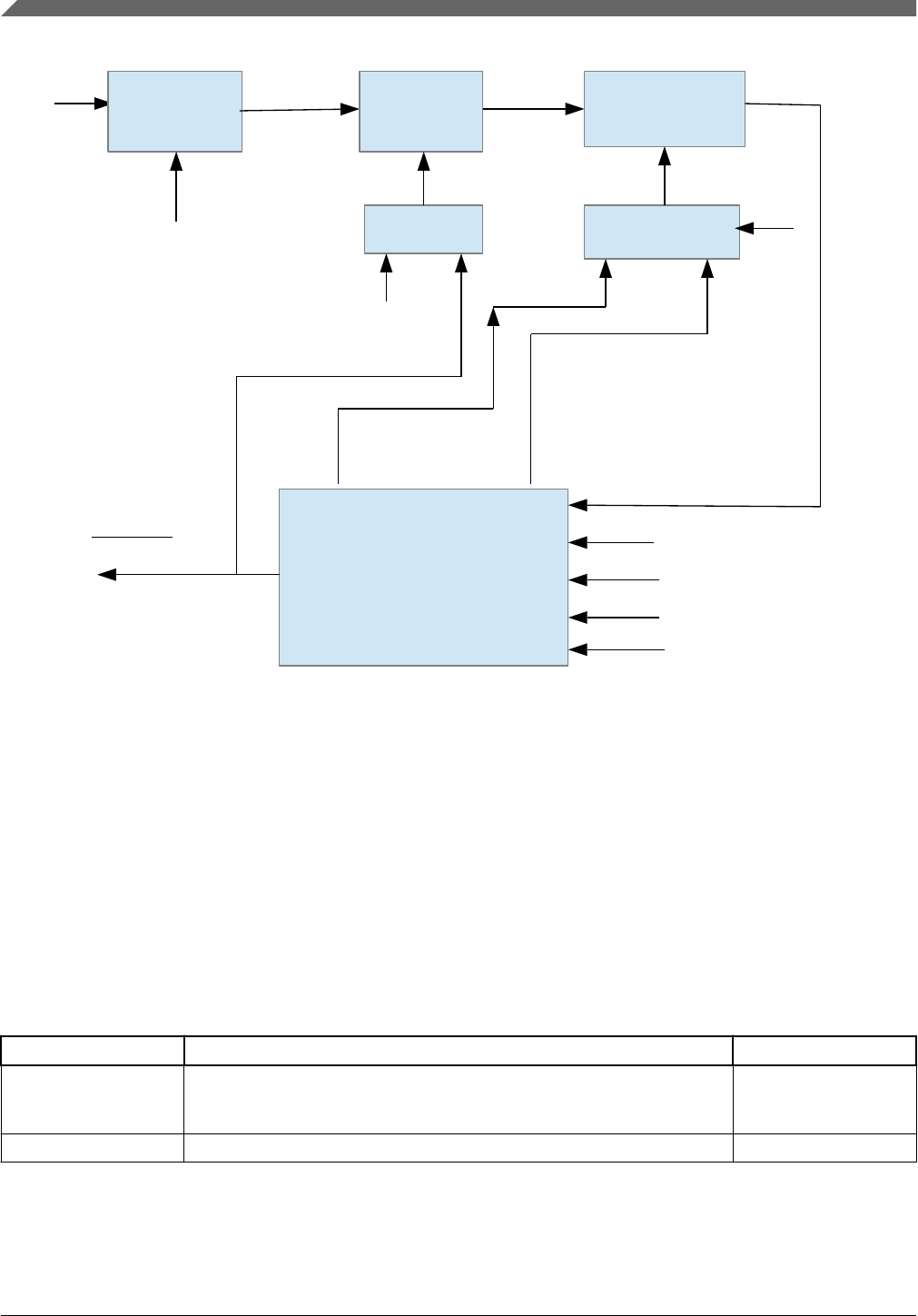
Clock Divider
Logic
LPO_CLK Low Power
Clock Clock Gating
Cell
AND
Enable
EWM_CTRL[EWMEN]
EWM_CLKPRESCALER[CLK_DIV]
8-bit Counter
OR
Counter Value
Reset to
Counter
EWM Refresh
And
/EWM_out Output
Control
Mechanism
EWM_CMPH[COMPAREH]
EWM_CMPL[COMPAREL]
EWM Refreshed
EWM_out
Counter
overflow
EWM_in
EWM Service Register
CPU
Reset
Figure 20-1. EWM Block Diagram
20.3 EWM Signal Descriptions
The EWM has two external signals, as shown in the following table.
NOTE
All active-low signals are now represented with the suffix "_b"
throughout the chapter.
Table 20-1. EWM Signal Descriptions
Signal Description I/O
EWM_in EWM input for safety status of external safety circuits. The polarity of
EWM_in is programmable using the EWM_CTRL[ASSIN] bit. The default
polarity is active low.
I
EWM_OUT_b EWM reset out signal O
EWM Signal Descriptions
S32K1xx Series Reference Manual, Rev. 7, 04/2018
446 NXP Semiconductors

20.4 Memory Map/Register Definition
This section contains the module memory map and registers.
NOTE
EWM only supports 8-bit register access. 16-bit and 32-bit
access are not possible.
20.4.1 EWM register descriptions
20.4.1.1 EWM Memory map
EWM base address: 4006_1000h
Offset Register Width
(In bits)
Access Reset value
0h Control Register (CTRL) 8 RW 00h
1h Service Register (SERV) 8 WORZ 00h
2h Compare Low Register (CMPL) 8 RWONC
E
00h
3h Compare High Register (CMPH) 8 RWONC
E
FFh
5h Clock Prescaler Register (CLKPRESCALER) 8 RWONC
E
00h
20.4.1.2 Control Register (CTRL)
20.4.1.2.1 Offset
Register Offset
CTRL 0h
20.4.1.2.2 Function
The CTRL register is cleared by any reset.
Chapter 20 External Watchdog Monitor (EWM)
S32K1xx Series Reference Manual, Rev. 7, 04/2018
NXP Semiconductors 447

NOTE
INEN, ASSIN and EWMEN bits can be written once after a
CPU reset. Modifying these bits more than once, generates a
bus transfer error.
20.4.1.2.3 Diagram
Bits 7 6 5 4 3 2 1 0
R
0
INTEN
INEN
ASSI
N
EWMEN
W
Reset 0 0 0 0 0 0 0 0
20.4.1.2.4 Fields
Field Function
7-4
—
Reserved
3
INTEN
Interrupt Enable.
This bit when set and EWM_OUT_b is asserted, an interrupt request is generated. To de-assert interrupt
request, user should clear this bit by writing 0.
2
INEN
Input Enable.
This bit when set, enables the EWM_in port.
1
ASSIN
EWM_in's Assertion State Select.
Default assert state of the EWM_in signal is logic zero. Setting the ASSIN bit inverts the assert state of
EWM_in signal to a logic one.
0
EWMEN
EWM enable.
This bit when set, enables the EWM module. This resets the EWM counter to zero and deasserts the
EWM_OUT_b signal. This bit when unset, keeps the EWM module disabled. It cannot be re-enabled until
a next reset, due to the write-once nature of this bit.
20.4.1.3 Service Register (SERV)
20.4.1.3.1 Offset
Register Offset
SERV 1h
Memory Map/Register Definition
S32K1xx Series Reference Manual, Rev. 7, 04/2018
448 NXP Semiconductors

20.4.1.3.2 Function
The SERV register provides the interface from the CPU to the EWM module. It is write-
only and reads of this register return zero.
20.4.1.3.3 Diagram
Bits 7 6 5 4 3 2 1 0
R 0
WSERVICE
Reset 0 0 0 0 0 0 0 0
20.4.1.3.4 Fields
Field Function
7-0
SERVICE
SERVICE
The EWM refresh mechanism requires the CPU to write two values to the SERV register: a first data byte
of 0xB4, followed by a second data byte of 0x2C. The EWM refresh is invalid if either of the following
conditions is true.
• The first or second data byte is not written correctly.
• The second data byte is not written within a fixed number of peripheral bus cycles of the first data
byte. This fixed number of cycles is called EWM_refresh_time.
15 peripheral bus clock cycles are required for EWM_refresh_time
20.4.1.4 Compare Low Register (CMPL)
20.4.1.4.1 Offset
Register Offset
CMPL 2h
20.4.1.4.2 Function
The CMPL register is reset to zero after a CPU reset. This provides no minimum time for
the CPU to refresh the EWM counter.
Chapter 20 External Watchdog Monitor (EWM)
S32K1xx Series Reference Manual, Rev. 7, 04/2018
NXP Semiconductors 449

NOTE
This register can be written only once after a CPU reset.
Writing this register more than once generates a bus transfer
error.
20.4.1.4.3 Diagram
Bits 7 6 5 4 3 2 1 0
RCOMPAREL
W
Reset 0 0 0 0 0 0 0 0
20.4.1.4.4 Fields
Field Function
7-0
COMPAREL
COMPAREL
To prevent runaway code from changing this field, software should write to this field after a CPU reset
even if the (default) minimum refresh time is required.
20.4.1.5 Compare High Register (CMPH)
20.4.1.5.1 Offset
Register Offset
CMPH 3h
20.4.1.5.2 Function
The CMPH register is reset to 0xFF after a CPU reset. This provides a maximum of 256
clocks time, for the CPU to refresh the EWM counter.
NOTE
This register can be written only once after a CPU reset.
Writing this register more than once generates a bus transfer
error.
Memory Map/Register Definition
S32K1xx Series Reference Manual, Rev. 7, 04/2018
450 NXP Semiconductors

NOTE
The valid values for CMPH are up to 0xFE because the EWM
counter never expires when CMPH = 0xFF. The expiration
happens only if EWM counter is greater than CMPH.
20.4.1.5.3 Diagram
Bits 7 6 5 4 3 2 1 0
RCOMPAREH
W
Reset 1 1 1 1 1 1 1 1
20.4.1.5.4 Fields
Field Function
7-0
COMPAREH
COMPAREH
To prevent runaway code from changing this field, software should write to this field after a CPU reset
even if the (default) maximum refresh time is required.
20.4.1.6 Clock Prescaler Register (CLKPRESCALER)
20.4.1.6.1 Offset
Register Offset
CLKPRESCALER 5h
20.4.1.6.2 Function
This CLKPRESCALER register is reset to 0x00 after a CPU reset.
NOTE
This register can be written only once after a CPU reset.
Writing this register more than once generates a bus transfer
error.
NOTE
Write the required prescaler value before enabling the EWM.
Chapter 20 External Watchdog Monitor (EWM)
S32K1xx Series Reference Manual, Rev. 7, 04/2018
NXP Semiconductors 451

NOTE
The implementation of this register is chip-specific. See the
Chip Configuration details.
20.4.1.6.3 Diagram
Bits 7 6 5 4 3 2 1 0
RCLK_DIV
W
Reset 0 0 0 0 0 0 0 0
20.4.1.6.4 Fields
Field Function
7-0
CLK_DIV
CLK_DIV
Selected low power clock source for running the EWM counter can be prescaled as below.
• Prescaled clock frequency = low power clock source frequency / ( 1 + CLK_DIV )
20.5 Functional Description
The following sections describe functional details of the EWM module.
NOTE
When the BUS_CLK is lost, then EWM module doesn't
generate the EWM_OUT_b signal and no refresh operation is
possible
20.5.1 The EWM_OUT_b Signal
The EWM_OUT_b is a digital output signal used to gate an external circuit (application
specific) that controls critical safety functions. For example, the EWM_OUT_b could be
connected to the high voltage transistors circuits that control an AC motor in a large
appliance.
The EWM_OUT_b signal remains deasserted when the EWM is being regularly
refreshed by the CPU within the programmable refresh window, indicating that the
application code is executed as expected.
Functional Description
S32K1xx Series Reference Manual, Rev. 7, 04/2018
452 NXP Semiconductors

The EWM_OUT_b signal is asserted in any of the following conditions:
• The EWM refresh occurs when the counter value is less than CMPL value.
• The EWM counter value reaches the CMPH value, and no EWM refresh has
occurred.
• If functionality of EWM_in pin is enabled and EWM_in pin is asserted while
refreshing the EWM.
• After any reset (by the virtue of the external pull-down mechanism on the
EWM_OUT_b pin)
The EWM_OUT_b is asserted after any reset by the virtue of the external pull-down
mechanism on the EWM_OUT_b signal. Then, to deassert the EWM_OUT_b signal, set
EWMEN bit in the CTRL register to enable the EWM.
If the EWM_OUT_b signal shares its pad with a digital I/O pin, on reset this actual pad
defers to being an input signal. The pad state is controlled by the EWM_OUT_b signal
only after the EWM is enabled by the EWMEN bit in the CTRL register.
Note
EWM_OUT_b pad must be in pull down state when EWM
functionality is used and when EWM is under Reset.
20.5.2 EWM_OUT_b pin state in low power modes
During Wait, Stop, and Power Down modes the EWM_OUT_b pin preserve its state
before entering Wait or Stop mode. When the CPU enters a Run mode from Wait or Stop
recovery, the pin resumes its previous state before entering Wait or Stop mode. When the
CPU enters Run mode from Power Down, the pin returns to its reset state.
20.5.3 The EWM_in Signal
The EWM_in is a digital input signal for safety status of external safety circuits, that
allows an external circuit to control the assertion of the EWM_OUT_b signal. For
example, in the application, an external circuit monitors a critical safety function, and if
there is fault with safety function, the external circuit can then actively initiate the
EWM_OUT_b signal that controls the gating circuit.
The EWM_in signal is ignored if the EWM is disabled, or if INEN bit of CTRL register
is cleared, as after any reset.
Chapter 20 External Watchdog Monitor (EWM)
S32K1xx Series Reference Manual, Rev. 7, 04/2018
NXP Semiconductors 453

On enabling the EWM (setting the CTRL[EWMEN] bit) and enabling EWM_in
functionality (setting the CTRL[INEN] bit), the EWM_in signal must be in the deasserted
state prior to the CPU start refreshing the EWM. This ensures that the EWM_OUT_b
stays in the deasserted state; otherwise, the EWM_OUT_b output signal is asserted.
Note
The user must update the CMPH and CMPL registers prior to
enabling the EWM. After enabling the EWM, the counter resets
to zero, therefore the user shall provide a reasonable time after a
power-on reset for the external monitoring circuit to stabilize.
The user shall also ensure that the EWM_in pin is deasserted.
20.5.4 EWM Counter
It is an 8-bit ripple counter fed from a clock source that is independent of the peripheral
bus clock source. As the preferred time-out is between 1 ms and 100 ms the actual clock
source should be in the kHz range.
The counter is reset to zero after the CPU reset, or when EWM refresh action completes,
or at counter overflow. The counter value is not accessible to the CPU.
20.5.5 EWM Compare Registers
The compare registers CMPL and CMPH are write-once after a CPU reset and cannot be
modified until another CPU reset occurs.
The EWM compare registers are used to create a refresh window to refresh the EWM
module.
It is illegal to program CMPL and CMPH with same value. In this case, as soon as
counter reaches (CMPL + 1), EWM_OUT_b is asserted.
20.5.6 EWM Refresh Mechanism
Other than the initial configuration of the EWM, the CPU can only access the EWM by
the EWM Service Register. The CPU must access the EWM service register with correct
write of unique data within the windowed time frame as determined by the CMPL and
CMPH registers for correct EWM refresh operation. Therefore, three possible conditions
can occur:
Functional Description
S32K1xx Series Reference Manual, Rev. 7, 04/2018
454 NXP Semiconductors

Table 20-2. EWM Refresh Mechanisms
Condition Mechanism
An EWM refresh action completes when:
CMPL < Counter < CMPH.
The software behaves as expected and the EWM counter is reset to zero. The
EWM_OUT_b output signal remains in the deasserted state if, during the EWM
refresh action, the EWM_in input has been in deasserted state..
An EWM refresh action completes when
Counter < CMPL
The software refreshes the EWM before the windowed time frame, the counter is
reset to zero and the EWM_OUT_b output signal is asserted irrespective of the
input EWM_in signal.
Counter value reaches CMPH prior to
completion of EWM refresh action.
Software has not refreshed the EWM. The EWM counter is reset to zero and the
EWM_OUT_b output signal is asserted irrespective of the input EWM_in signal.
20.5.7 EWM Interrupt
When EWM_OUT_b is asserted, an interrupt request is generated to indicate the
assertion of the EWM reset out signal. This interrupt is enabled when CTRL[INTEN] is
set. Clearing this bit clears the interrupt request but does not affect EWM_OUT_b. The
EWM_OUT_b signal can be deasserted only by forcing a system reset.
20.5.8 Counter clock prescaler
The EWM counter clock source can be prescaled by a clock divider, by programming
CLKPRESCALER[CLK_DIV]. This divided clock is used to run the EWM counter.
NOTE
The divided clock used to run the EWM counter must be no
more than half the frequency of the bus clock.
Chapter 20 External Watchdog Monitor (EWM)
S32K1xx Series Reference Manual, Rev. 7, 04/2018
NXP Semiconductors 455

Functional Description
S32K1xx Series Reference Manual, Rev. 7, 04/2018
456 NXP Semiconductors

Chapter 21
Error Injection Module (EIM)
21.1 Chip-specific EIM information
S32K1xx has one instance of the EIM.
21.1.1 EIM channel assignments
Each EIM channel corresponds to a specific RAM array target. The EIM channel can
inject errors on accesses to that specific RAM array. The following table shows the
channel assignments.
Table 21-1. RAM array targets of EIM channels
EIM channel RAM array target
S32K14x S32K11x
0 SRAM_L SRAM_U
1 SRAM_U Reserved
21.2 Introduction
The Error Injection Module (EIM) is mainly used for diagnostic purposes. It provides a
method for diagnostic coverage of the peripheral memories. See the chip-specific EIM
information to determine which peripheral memories are supported by this method.
S32K1xx Series Reference Manual, Rev. 7, 04/2018
NXP Semiconductors 457
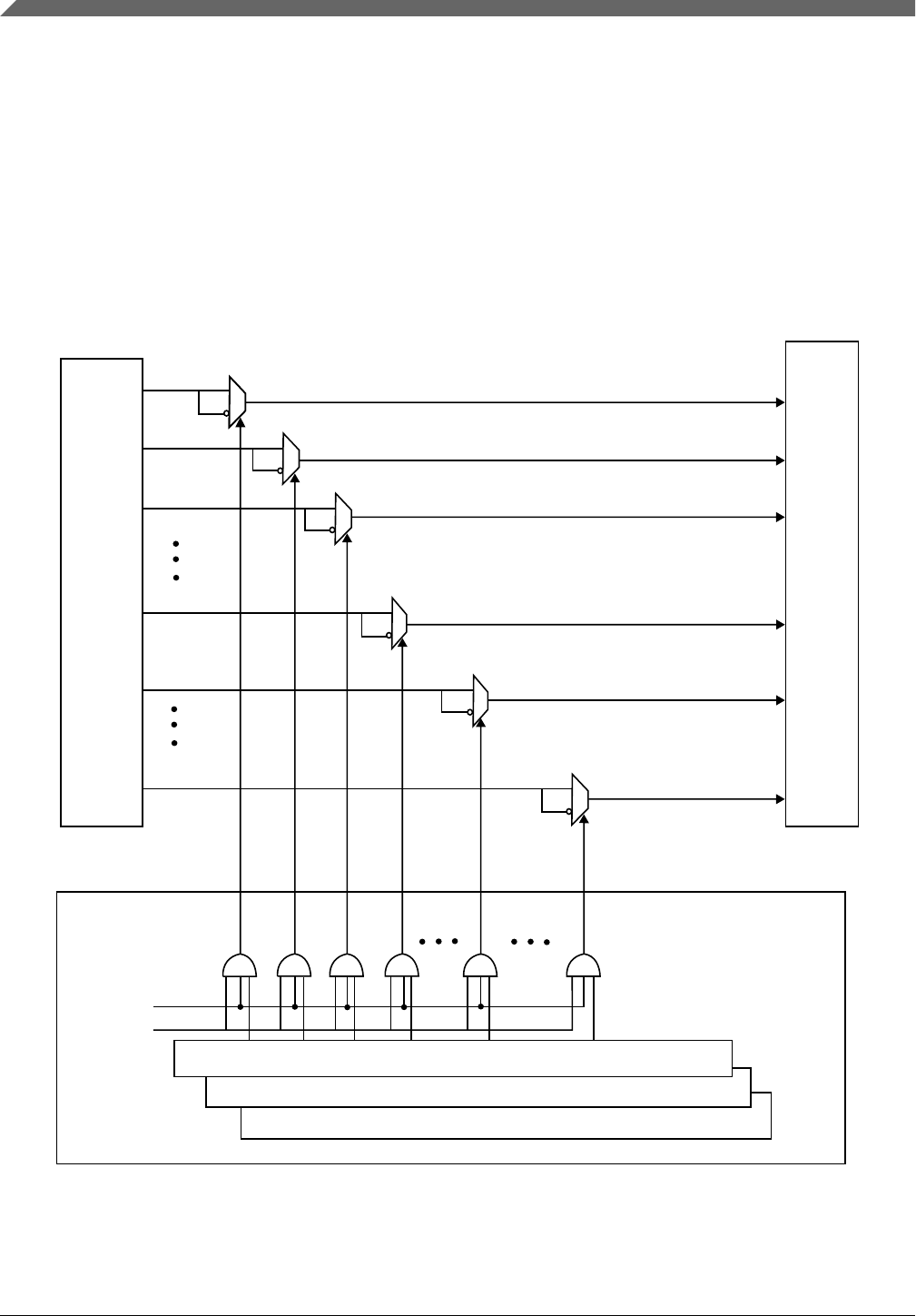
21.2.1 Overview
The Error Injection Module (EIM) provides support for inducing single-bit and multi-bit
inversions on read data when accessing peripheral RAMs. Injecting faults on memory
accesses can be used to exercise the SEC-DED ECC function of the related system.
NOTE
The following diagram shows an example of EIM
implementation with a 64-bit read data bus and an 8-bit
checkbit bus.
Module
rdata[63](MSB)
rdata[62]
rdata[61]
rdata[0](LSB)
chkbit[7]
chkbit[0]
EIM
EIMCR[GEIEN]
EICHEN[EICHnEN]
EICHDn_WORD0
EICHDn_WORD1
EICHDn_WORD2
RAM
array
Figure 21-1. EIM functional block diagram (64-bit read data bus and 8-bit check bit bus)
Introduction
S32K1xx Series Reference Manual, Rev. 7, 04/2018
458 NXP Semiconductors

21.2.2 Features
The EIM includes these features:
• Supports 2 error injection channels
• Protection against accidental enable and reconfiguration error injection function via
two-stage enable mechanism
21.3 EIM register descriptions
The EIM provides an IPS programming model mapped to an on-platform peripheral slot.
Programming model access
All system bus masters can access the programming model:
• Only in supervisor mode
• Using only 32-bit (word) accesses
Any of the following attempted references to the programming model generates an IPS
error termination:
• In user mode
• Using non-32-bit access sizes
• To undefined (reserved) addresses
Attempted updates to the programming model while the EIM is in the midst of an
operation result in non-deterministic behavior.
Error injection channel descriptor: function and structure
Each error injection channel descriptor:
• Specifies a mask that defines which bits of the read data and checkbit bus from target
RAM are inverted on a read access.
• Consists of a 128-bit (16-byte) structure, composed of four 32-bit words, in the EIM
programming model.
•The first word, Word0 (EICHDn_WORD0), defines the checkbit mask. See
Error Injection Channel Descriptor n, Word0 for details.
•The remaining words, Word1-3 (EICHDn_WORD1-3), define the data mask.
Word2 and Word3 are used only when required by the total width of the
Chapter 21 Error Injection Module (EIM)
S32K1xx Series Reference Manual, Rev. 7, 04/2018
NXP Semiconductors 459

channel's data mask. See Error injection channel descriptor: DATA_MASK
details and the individual registers' descriptions.
The multiple channel descriptors are organized sequentially.
Error injection channel descriptor: DATA_MASK details
For each channel: The following table shows the total width of DATA_MASK and the
distribution of its bits across the WORD registers.
Channel DATA_MASK total
width (bits)
Specific bits of DATA_MASK in
WORD1 WORD2 WORD3
0 32 31-0 — —
1 32 31-0 — —
21.3.1 EIM Memory map
EIM base address: 4001_9000h
Offset Register Width
(In bits)
Access Reset value
0h Error Injection Module Configuration Register (EIMCR) 32 RW 0000_0000h
4h Error Injection Channel Enable register (EICHEN) 32 RW 0000_0000h
100h Error Injection Channel Descriptor n, Word0 (EICHD0_WORD0) 32 RW 0000_0000h
104h Error Injection Channel Descriptor n, Word1 (EICHD0_WORD1) 32 RW 0000_0000h
200h Error Injection Channel Descriptor n, Word0 (EICHD1_WORD0) 32 RW 0000_0000h
204h Error Injection Channel Descriptor n, Word1 (EICHD1_WORD1) 32 RW 0000_0000h
21.3.2 Error Injection Module Configuration Register (EIMCR)
21.3.2.1 Offset
Register Offset
EIMCR 0h
EIM register descriptions
S32K1xx Series Reference Manual, Rev. 7, 04/2018
460 NXP Semiconductors

21.3.2.2 Function
The EIM Configuration Register is used to globally enable/disable the error injection
function.
21.3.2.3 Diagram
Bits 31 30 29 28 27 26 25 24 23 22 21 20 19 18 17 16
R 0
W
Reset 0 0 0 0 0 0 0 0 0 0 0 0 0 0 0 0
Bits 15 14 13 12 11 10 9 8 7 6 5 4 3 2 1 0
R
0
GEIE
N
W
Reset 0 0 0 0 0 0 0 0 0 0 0 0 0 0 0 0
21.3.2.4 Fields
Field Function
31-1
—
Reserved
0
GEIEN
Global Error Injection Enable
This bit globally enables or disables the error injection function of the EIM. This field is initialized by
hardware reset.
0b - Disabled
1b - Enabled
21.3.3 Error Injection Channel Enable register (EICHEN)
21.3.3.1 Offset
Register Offset
EICHEN 4h
Chapter 21 Error Injection Module (EIM)
S32K1xx Series Reference Manual, Rev. 7, 04/2018
NXP Semiconductors 461

21.3.3.2 Function
Each field of the Error Injection Channel Enable register (EICHEN) is used to enable or
disable the corresponding error injection channel.
NOTE
To enable an error injection channel, the Global Error Injection
Enable (EIMCR[GEIEN]) field must also be asserted.
21.3.3.3 Diagram
Bits 31 30 29 28 27 26 25 24 23 22 21 20 19 18 17 16
R
EICH0EN
EICH1EN
0
0
0
0
0
0
0
0
0
0
0
0
0
0
W
Reset 0 0 0 0 0 0 0 0 0 0 0 0 0 0 0 0
Bits 15 14 13 12 11 10 9 8 7 6 5 4 3 2 1 0
R0000000000000000
W
Reset 0 0 0 0 0 0 0 0 0 0 0 0 0 0 0 0
21.3.3.4 Fields
Field Function
31
EICH0EN
Error Injection Channel 0 Enable
This field enables the corresponding error injection channel. The Global Error Injection Enable
(EIMCR[GEIEN]) field must also be asserted to enable error injection.
After error injection is enabled, all subsequent read accesses incur one or more bit inversions as defined
in the corresponding EICHDn_WORD registers. Error injection remains in effect until the error injection
channel is manually disabled via software.
Any write to the corresponding EICHDn_WORD registers clears the corresponding EICHEN[EICHnEN]
field, disabling the error injection channel.
0b - Error injection is disabled on Error Injection Channel 0
1b - Error injection is enabled on Error Injection Channel 0
30
EICH1EN
Error Injection Channel 1 Enable
This field enables the corresponding error injection channel. The Global Error Injection Enable
(EIMCR[GEIEN]) field must also be asserted to enable error injection.
Table continues on the next page...
EIM register descriptions
S32K1xx Series Reference Manual, Rev. 7, 04/2018
462 NXP Semiconductors

Field Function
After error injection is enabled, all subsequent read accesses incur one or more bit inversions as defined
in the corresponding EICHDn_WORD registers. Error injection remains in effect until the error injection
channel is manually disabled via software.
Any write to the corresponding EICHDn_WORD registers clears the corresponding EICHEN[EICHnEN]
field, disabling the error injection channel.
0b - Error injection is disabled on Error Injection Channel 1
1b - Error injection is enabled on Error Injection Channel 1
29
—
Reserved
28
—
Reserved
27
—
Reserved
26
—
Reserved
25
—
Reserved
24
—
Reserved
23
—
Reserved
22
—
Reserved
21
—
Reserved
20
—
Reserved
19
—
Reserved
18
—
Reserved
17
—
Reserved
16
—
Reserved
15
—
Reserved
14
—
Reserved
13
—
Reserved
Table continues on the next page...
Chapter 21 Error Injection Module (EIM)
S32K1xx Series Reference Manual, Rev. 7, 04/2018
NXP Semiconductors 463

Field Function
12
—
Reserved
11
—
Reserved
10
—
Reserved
9
—
Reserved
8
—
Reserved
7
—
Reserved
6
—
Reserved
5
—
Reserved
4
—
Reserved
3
—
Reserved
2
—
Reserved
1
—
Reserved
0
—
Reserved
21.3.4 Error Injection Channel Descriptor n, Word0 (EICHD0_W
ORD0 - EICHD1_WORD0)
21.3.4.1 Offset
Register Offset
EICHD0_WORD0 100h
EICHD1_WORD0 200h
EIM register descriptions
S32K1xx Series Reference Manual, Rev. 7, 04/2018
464 NXP Semiconductors
21.3.4.2 Function
The first word of the Error Injection Channel Descriptor defines a left-justified mask
field: CHKBIT_MASK. Each bit of CHKBIT_MASK specifies whether the
corresponding bit of the checkbit bus from the target RAM should be inverted or remain
unmodified on read accesses. Successful write to this field clears the corresponding error
injection channel valid bit, EICHEN[EICHnEN].
21.3.4.3 Diagram
Bits 31 30 29 28 27 26 25 24 23 22 21 20 19 18 17 16
RCHKBIT_MASK 0
W
Reset 0 0 0 0 0 0 0 0 0 0 0 0 0 0 0 0
Bits 15 14 13 12 11 10 9 8 7 6 5 4 3 2 1 0
R 0
W
Reset 0 0 0 0 0 0 0 0 0 0 0 0 0 0 0 0
21.3.4.4 Fields
Field Function
31-25
CHKBIT_MASK
Checkbit Mask
This field defines a bit-mapped mask that specifies whether the corresponding bit of the checkbit bus
from the target RAM should be inverted or remain unmodified.
For any unique details about the mapping of CHKBIT_MASK's bits to a channel's target RAM, see the
chip-specific EIM information.
The following table shows the width and bit range of CHKBIT_MASK for each channel.
Channel CHKBIT_MASK width (bits) CHKBIT_MASK bit range
0 7 6-0
1 7 6-0
NOTE: Because CHKBIT_MASK is left-justified, the highest bit in the bit range is always in the position
of the most significant bit. For a CHKBIT_MASK that is 7 bits wide, CHKBIT_MASK[6] is in the
position of the most significant bit. For any CHKBIT_MASK with a smaller width, the highest bit
in that width's bit range is in the position of the most significant bit.
0b - The corresponding bit of the checkbit bus remains unmodified.
Table continues on the next page...
Chapter 21 Error Injection Module (EIM)
S32K1xx Series Reference Manual, Rev. 7, 04/2018
NXP Semiconductors 465

Field Function
1b - The corresponding bit of the checkbit bus is inverted.
24-0
—
Reserved.
21.3.5 Error Injection Channel Descriptor n, Word1 (EICHD0_W
ORD1 - EICHD1_WORD1)
21.3.5.1 Offset
Register Offset
EICHD0_WORD1 104h
EICHD1_WORD1 204h
21.3.5.2 Function
The second word of the Error Injection Channel Descriptor defines a right-justified mask
field. The bits in B0_3DATA_MASK correspond to bytes 0–3 of the read data bus. Each
bit specifies whether the corresponding bit of the read data bus from the target RAM
should be inverted or remain unmodified on read accesses. A successful write to this field
clears the corresponding error injection channel valid field, EICHEN[EICHnEN].
21.3.5.3 Diagram
Bits 31 30 29 28 27 26 25 24 23 22 21 20 19 18 17 16
RB0_3DATA_MASK
W
Reset 0 0 0 0 0 0 0 0 0 0 0 0 0 0 0 0
Bits 15 14 13 12 11 10 9 8 7 6 5 4 3 2 1 0
RB0_3DATA_MASK
W
Reset 0 0 0 0 0 0 0 0 0 0 0 0 0 0 0 0
EIM register descriptions
S32K1xx Series Reference Manual, Rev. 7, 04/2018
466 NXP Semiconductors

21.3.5.4 Fields
Field Function
31-0
B0_3DATA_MA
SK
Data Mask Bytes 0-3
This field defines a bit-mapped mask that specifies whether the corresponding bit of the read data bus
from the target RAM should be inverted or remain unmodified.
NOTE: For each channel: For the exact width of B0_3DATA_MASK and the specific DATA_MASK bits
to which B0_3DATA_MASK corresponds, see Error injection channel descriptor: DATA_MASK
details.
0b - The corresponding bit of bytes 0-3 on the read data bus remains unmodified.
1b - The corresponding bit of bytes 0-3 on the read data bus is inverted.
21.4 Functional description
The EIM provides protection against accidental enabling and reconfiguration of the error
injection function by enforcing a two-stage enablement mechanism. To properly enable
the error injection mechanism for a channel:
•Write 1 to the EICHEN[EICHnEN] field, where n denotes the channel number.
• Write 1 to EIMCR[GEIEN].
NOTE
When the use case for a channel requires writing any
EICHDn_WORD register, write the EICHDn_WORD register
before executing the two-stage enablement mechanism. A
successful write to any EICHDn_WORD register clears the
corresponding EICHEN[EICHnEN] field.
The EIM supports 2 error injection channels. Each channel:
• Is assigned to a single memory array interface.
• Intercepts the assigned memory read data bus and checkbit bus and injects errors by
inverting the value transmitted for selected bits on each bus line.
On a memory read access, the applicable EICHDn_WORD register defines which bit of
the read data and/or checkbit bus to invert.
Figure 21-1 depicts the interception and override of a 64-bit read data bus and an 8-bit
checkbit data bus for an example memory array.
Chapter 21 Error Injection Module (EIM)
S32K1xx Series Reference Manual, Rev. 7, 04/2018
NXP Semiconductors 467

21.4.1 Error injection scenarios
The EIM supports these cases of error injection:
• To generate a single-bit error, invert only 1 bit of the CHKBIT_MASK or
DATA_MASK in the EICHDn_WORD registers.
• To generate a multi-bit error, invert only 2 bits of the CHKBIT_MASK or
DATA_MASK in the EICHDn_WORD registers.
NOTE
An attempt to invert more than 2 bits in one operation might
result in undefined behavior.
Functional description
S32K1xx Series Reference Manual, Rev. 7, 04/2018
468 NXP Semiconductors

Chapter 22
Error Reporting Module (ERM)
22.1 Chip-specific ERM information
S32K1xx has one instance of the ERM.
22.1.1 Sources of memory error events
Each ERM channel n corresponds to a source of potential memory error events. The
following table shows the channel assignments.
Table 22-1. Memory error event sources for ERM channels
ERM channel nMemory n event source1
S32K14x S32K11x
0 SRAM_L SRAM_U
1 SRAM_U Reserved
1. Throughout this chapter, "Memory n" designates the memory array sourced by ERM channel n.
Introduction
22.2.1 Overview
The Error Reporting Module (ERM) provides information and optional interrupt
notification on memory error events associated with Error Correction Code (ECC). The
ERM collects ECC events on memory accesses for platform local memory arrays, such as
flash memory, system RAM, or peripheral RAMs. See the chip-specific ERM
information for details about supported memory sources and specific memory channel
assignments.
22.2
S32K1xx Series Reference Manual, Rev. 7, 04/2018
NXP Semiconductors 469

22.2.2 Features
The ERM includes these features:
• Capturing of address information on single-bit correction and non-correctable ECC
events
• Optional interrupt notification on captured ECC events
• Support for ECC event capturing for memory sources, with individual reporting
fields and interrupt configuration per memory channel
22.3 ERM register descriptions
The ERM provides an IPS programming model mapped to an on-platform peripheral slot.
All system bus masters can access the programming model:
• Only in supervisor mode
• Using only 32-bit (word) accesses
Any of the following attempted references to the programming model generates an IPS
error termination:
• In user mode
• Using non-32-bit access sizes
Attempted accesses to undefined (reserved) memory regions can result in undefined
behavior.
Attempted updates to the programming model when the ERM is in the middle of an
operation result in non-deterministic behavior.
22.3.1 ERM Memory map
ERM base address: 4001_8000h
Offset Register Width
(In bits)
Access Reset value
0h ERM Configuration Register 0 (CR0) 32 RW 0000_0000h
10h ERM Status Register 0 (SR0) 32 W1C 0000_0000h
Table continues on the next page...
ERM register descriptions
S32K1xx Series Reference Manual, Rev. 7, 04/2018
470 NXP Semiconductors

Offset Register Width
(In bits)
Access Reset value
100h ERM Memory n Error Address Register (EAR0) 32 RO 0000_0000h
110h ERM Memory n Error Address Register (EAR1) 32 RO 0000_0000h
22.3.2 ERM Configuration Register 0 (CR0)
22.3.2.1 Offset
Register Offset
CR0 0h
22.3.2.2 Function
This 32-bit control register configures the interrupt notification capability for each
supported memory channel between 0 and 7.
22.3.2.3 Diagram
Bits 31 30 29 28 27 26 25 24 23 22 21 20 19 18 17 16
R
ESCIE
0
ENCIE0
0
ESCIE
1
ENCIE1
0
Reserved
0
Reserved
0
W
Reset 0 0 0 0 0 0 0 0 0 0 0 0 0 0 0 0
Bits 15 14 13 12 11 10 9 8 7 6 5 4 3 2 1 0
R
Reserved
0
Reserved
0
Reserved
0
Reserved
0
W
Reset 0 0 0 0 0 0 0 0 0 0 0 0 0 0 0 0
Chapter 22 Error Reporting Module (ERM)
S32K1xx Series Reference Manual, Rev. 7, 04/2018
NXP Semiconductors 471

22.3.2.4 Fields
Field Function
31
ESCIE0
ESCIE0
Enable Memory 0 Single Correction Interrupt Notification
This field is initialized by hardware reset.
NOTE: See the chip-specific ERM information for details on Memory 0 mapping.
0b - Interrupt notification of Memory 0 single-bit correction events is disabled.
1b - Interrupt notification of Memory 0 single-bit correction events is enabled.
30
ENCIE0
ENCIE0
Enable Memory 0 Non-Correctable Interrupt Notification
This field is initialized by hardware reset.
NOTE: See the chip-specific ERM information for details on Memory 0 mapping.
0b - Interrupt notification of Memory 0 non-correctable error events is disabled.
1b - Interrupt notification of Memory 0 non-correctable error events is enabled.
29-28
—
Reserved
27
ESCIE1
ESCIE1
Enable Memory 1 Single Correction Interrupt Notification
This field is initialized by hardware reset.
NOTE: See the chip-specific ERM information for details on Memory 1 mapping.
0b - Interrupt notification of Memory 1 single-bit correction events is disabled.
1b - Interrupt notification of Memory 1 single-bit correction events is enabled.
26
ENCIE1
ENCIE1
Enable Memory 1 Non-Correctable Interrupt Notification
This field is initialized by hardware reset.
NOTE: See the chip-specific ERM information for details on Memory 1 mapping.
0b - Interrupt notification of Memory 1 non-correctable error events is disabled.
1b - Interrupt notification of Memory 1 non-correctable error events is enabled.
25-24
—
Reserved
23-22
—
Reserved
21-20
—
Reserved
19-18
—
Reserved
17-16
—
Reserved
15-14
—
Reserved
13-12 Reserved
Table continues on the next page...
ERM register descriptions
S32K1xx Series Reference Manual, Rev. 7, 04/2018
472 NXP Semiconductors

Field Function
—
11-10
—
Reserved
9-8
—
Reserved
7-6
—
Reserved
5-4
—
Reserved
3-2
—
Reserved
1-0
—
Reserved
22.3.3 ERM Status Register 0 (SR0)
22.3.3.1 Offset
Register Offset
SR0 10h
22.3.3.2 Function
This 32-bit register signals which types of ECC events have been detected for each
memory channel. The register signals the last memory event to be detected for each
supported memory channel between 0 and 7.
Chapter 22 Error Reporting Module (ERM)
S32K1xx Series Reference Manual, Rev. 7, 04/2018
NXP Semiconductors 473

22.3.3.3 Diagram
Bits 31 30 29 28 27 26 25 24 23 22 21 20 19 18 17 16
R
SBC0
NCE0
0
SBC1
NCE1
0
0
0
W
W1C
W1C
W1C
W1C
Reset 0 0 0 0 0 0 0 0 0 0 0 0 0 0 0 0
Bits 15 14 13 12 11 10 9 8 7 6 5 4 3 2 1 0
R 0 0 0 0
W
Reset 0 0 0 0 0 0 0 0 0 0 0 0 0 0 0 0
22.3.3.4 Fields
Field Function
31
SBC0
SBC0
Memory 0 Single-Bit Correction Event
This field is initialized by hardware reset.
Write 1 to clear this field. This write also clears the corresponding interrupt notification, if CR0[ESCIE0] is
enabled.
NOTE: See the chip-specific ERM information for details on Memory 0 mapping.
0b - No single-bit correction event on Memory 0 detected.
1b - Single-bit correction event on Memory 0 detected.
30
NCE0
NCE0
Memory 0 Non-Correctable Error Event
This field is initialized by hardware reset.
Write 1 to clear this field. This write also clears the corresponding interrupt notification, if CR0[ENCIE0] is
enabled.
NOTE: See the chip-specific ERM information for details on Memory 0 mapping.
0b - No non-correctable error event on Memory 0 detected.
1b - Non-correctable error event on Memory 0 detected.
29-28
—
Reserved
27
SBC1
SBC1
Memory 1 Single-Bit Correction Event
This field is initialized by hardware reset.
Write 1 to clear this field. This write also clears the corresponding interrupt notification, if CR0[ESCIE1] is
enabled.
NOTE: See the chip-specific ERM information for details on Memory 1 mapping.
Table continues on the next page...
ERM register descriptions
S32K1xx Series Reference Manual, Rev. 7, 04/2018
474 NXP Semiconductors

Field Function
0b - No single-bit correction event on Memory 1 detected.
1b - Single-bit correction event on Memory 1 detected.
26
NCE1
NCE1
Memory 1 Non-Correctable Error Event
This field is initialized by hardware reset.
Write 1 to clear this field. This write also clears the corresponding interrupt notification, if CR0[ENCIE1] is
enabled.
NOTE: See the chip-specific ERM information for details on Memory 1 mapping.
0b - No non-correctable error event on Memory 1 detected.
1b - Non-correctable error event on Memory 1 detected.
25-24
—
Reserved
23-20
—
Reserved
19-16
—
Reserved
15-12
—
Reserved
11-8
—
Reserved
7-4
—
Reserved
3-0
—
Reserved
22.3.4 ERM Memory n Error Address Register (EAR0 - EAR1)
22.3.4.1 Offset
Register Offset
EAR0 100h
EAR1 110h
Chapter 22 Error Reporting Module (ERM)
S32K1xx Series Reference Manual, Rev. 7, 04/2018
NXP Semiconductors 475

22.3.4.2 Function
Each ERM Memory n Error Address Register is a 32-bit register for capturing the address
of the last ECC event in Memory n, where n denotes the memory channel. Any attempted
write to EARn is ignored.
22.3.4.3 Diagram
Bits 31 30 29 28 27 26 25 24 23 22 21 20 19 18 17 16
REAR
W
Reset 0 0 0 0 0 0 0 0 0 0 0 0 0 0 0 0
Bits 15 14 13 12 11 10 9 8 7 6 5 4 3 2 1 0
REAR
W
Reset 0 0 0 0 0 0 0 0 0 0 0 0 0 0 0 0
22.3.4.4 Fields
Field Function
31-0
EAR
EAR
Memory n Error Address — This field contains the faulting system address of the last recorded ECC
event on Memory n.
NOTE: See the chip-specific ERM information for details on Memory n mapping.
Functional description
22.4.1 Single-bit correction events
When a single-bit correction event on Memory n is detected, the ERM:
22.4
Functional description
S32K1xx Series Reference Manual, Rev. 7, 04/2018
476 NXP Semiconductors

• Records the event by changing the value of the applicable Status Register bit
SRx[SBCn]to 1.
•Records the corresponding access address that initiated the event in the Memory n
Error Address Register: EARn (if this register is present for the channel).
The ERM holds event information only for the last reported event.
To clear the record of an event, write 1 to SRx[SBCn] to change its value to 0.
22.4.1.1 Optional interrupt notification for single-bit correction
events
The ERM provides an option to generate an interrupt notification upon the report of a
single-bit correction event. This sequence describes how to use the option:
1. To enable interrupt notification for single-bit correction events on Memory n, set
CRx[ESCIEn] to 1.
2. Subsequently, when a single-bit correction event on Memory n is detected, the ERM:
• Records the event and address, as usual.
• Additionally sends an interrupt notification corresponding to the event.
3. To clear both the record of an event and the corresponding interrupt notification,
write 1 to SRx[SBCn] to change its value to 0.
22.4.2 Non-correctable error events
When a non-correctable ECC error event on Memory n is detected, the ERM:
• Records the event by changing the value of the applicable Status Register bit:
SRx[NCEn]to 1.
•Records the corresponding access address that initiated the event in the Memory n
Error Address Register: EARn (if this register is present for the channel).
The ERM holds event information only for the last reported event.
To clear the record of an event, write 1 to SRx[NCEn] to change its value to 0.
Chapter 22 Error Reporting Module (ERM)
S32K1xx Series Reference Manual, Rev. 7, 04/2018
NXP Semiconductors 477

22.4.2.1 Optional interrupt notification for non-correctable error
events
The ERM provides an option to generate an interrupt notification upon the report of a
non-correctable ECC event. This sequence describes how to use the option:
1. To enable interrupt notifications for non-correctable error events on Memory n, set
CRx[ENCIEn] to 1.
2. Subsequently, when a non-correctable error event on Memory n is detected, the
ERM:
• Records the event and address as usual.
• Additionally sends an interrupt notification corresponding to the event.
3. To clear both the record of an event and the corresponding interrupt notification,
write 1 to SRx[NCEn] to change its value to 0.
22.5 Initialization
For each ERM channel, prepare the corresponding memory array before enabling ERM
interrupts about errors for that memory.
1. Initialize the memory to a known value so that the correct corresponding ECC
codeword is stored.
2. During the memory's initialization, if the ERM captures information about any ECC
error event, clear the corresponding SRx[SBCn] or SRx[NCEn] field that stores the
record of the event.
3. Program the applicable CRx[ESCIEn] and CRx[ENCIEn] fields to enable ERM
interrupts as desired.
Initialization
S32K1xx Series Reference Manual, Rev. 7, 04/2018
478 NXP Semiconductors

Chapter 23
Watchdog timer (WDOG)
Chip-specific WDOG information
23.1.1 WDOG clocks
The WDOG module has following selectable clock sources:
• Internal low power oscillator (LPO_CLK)
• Internal Slow IRC clock (SIRC)
• System oscillator clock (SOSC)
• Bus clock
NOTE
• For safety applications, WDOG should run on a different
clock than CMU.
• WDOG_CNT reset read value can vary depending on
timestamp, since it is a default running counter.
23.1.2 WDOG low-power modes
This table shows the WDOG low-power modes and the corresponding chip low-power
modes.
Wait mode is not supported in this device. See Module operation in available low power
modes for details on available power modes.
23.1
S32K1xx Series Reference Manual, Rev. 7, 04/2018
NXP Semiconductors 479

23.1.3 Default watchdog timeout
The timeout depends on the watchdog counter clock source. Following initial power on
the watchdog is clocked by the LPO128K_CLK and will issue a timeout after 1024
cycles. This results in the Watchdog timeout being generated after approximately 8 ms,
which will force a MCU reset. To avoid this condition, please ensure that the watchdog is
configured or refreshed before the 1024 cycles have elapsed.
23.2 Introduction
The Watchdog Timer (WDOG) module is an independent timer that is available for
system use. It provides a safety feature to ensure that software is executing as planned
and that the CPU is not stuck in an infinite loop or executing unintended code. If the
WDOG module is not serviced (refreshed) within a certain period, it resets the MCU.
23.2.1 Features
Features of the WDOG module include:
• Configurable clock source inputs independent from the bus clock
• Bus clock
• LPO clock
• INTCLK (internal clock)
• ERCLK (external reference clock)
• Programmable timeout period
• Programmable 16-bit timeout value
• Optional fixed 256 clock prescaler when longer timeout periods are needed
• Robust write sequence for counter refresh
• Refresh sequence of writing 0xA602 and then 0xB480
• Window mode option for the refresh mechanism
• Programmable 16-bit window value
Introduction
S32K1xx Series Reference Manual, Rev. 7, 04/2018
480 NXP Semiconductors
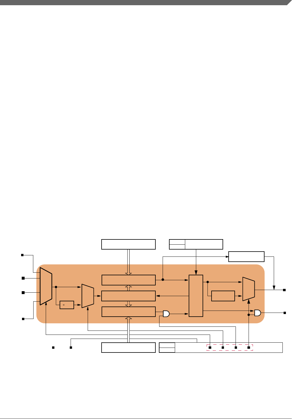
• Provides robust check that program flow is faster than expected
• Early refresh attempts trigger a reset.
• Optional timeout interrupt to allow post-processing diagnostics
• Interrupt request to CPU with interrupt vector for an interrupt service routine
(ISR)
• Forced reset occurs 128 bus clocks after the interrupt vector fetch.
• Configuration bits are write-once-after-reset to ensure watchdog configuration cannot
be mistakenly altered.
• Robust write sequence for unlocking write-once configuration bits
• Unlock sequence of writing 0xC520 and then 0xD928 for allowing updates to
write-once configuration bits
• Software must make updates within 128 bus clocks after unlocking and before
WDOG closing unlock window.
23.2.2 Block diagram
The following figure shows a block diagram of the WDOG module.
MUX
MUX
MUX
ERCLK
(external reference clock)
UPDATE
EN
CLK PRES WIN INT
BUS_CLK
256
16-bit Window Register
0xD928
0xC520
Control Status
Bus Cycle
Disable Protect
Bit Write Control
Protect
Window
Reset
Counter
Overflow
Counter
Write Control
0xA602
0xB480
16-bit Timeout Value Register
Refresh Sequence
Compare Logic
16-bit Counter Register
Compare Logic
Control
Logic
Bus
CPU Reset
IRQ Interrupt
Clock Delay
Backup Reset
LPO_CLK
INTCLK
(internal clock)
Figure 23-1. WDOG block diagram
Chapter 23 Watchdog timer (WDOG)
S32K1xx Series Reference Manual, Rev. 7, 04/2018
NXP Semiconductors 481

23.3 Memory map and register definition
23.3.1 WDOG register descriptions
23.3.1.1 WDOG Memory map
WDOG base address: 4005_2000h
Offset Register Width
(In bits)
Access Reset value
0h Watchdog Control and Status Register (CS) 32 RW 0000_2980h
4h Watchdog Counter Register (CNT) 32 RW 0000_0000h
8h Watchdog Timeout Value Register (TOVAL) 32 RW 0000_0400h
Ch Watchdog Window Register (WIN) 32 RW 0000_0000h
23.3.1.2 Watchdog Control and Status Register (CS)
23.3.1.2.1 Offset
Register Offset
CS 0h
23.3.1.2.2 Function
This section describes the function of Watchdog Control and Status Register.
NOTE
TST is cleared (0:0) on POR only. Any other reset does not
affect the value of this field.
Memory map and register definition
S32K1xx Series Reference Manual, Rev. 7, 04/2018
482 NXP Semiconductors

23.3.1.2.3 Diagram
Bits 31 30 29 28 27 26 25 24 23 22 21 20 19 18 17 16
R 0
W
Reset 0 0 0 0 0 0 0 0 0 0 0 0 0 0 0 0
Bits 15 14 13 12 11 10 9 8 7 6 5 4 3 2 1 0
R
WIN
FL
G
CMD32EN
PRE
S
ULK
RC
S
CLK
E
N
INT
UPDATE
TST
DBG
WAIT
STOP
W
W1C
Reset 0 0 1 0 1 0 0 1 1 0 0 0 0 0 0 0
23.3.1.2.4 Fields
Field Function
31-16
—
Reserved
15
WIN
Watchdog Window
This write-once bit enables window mode. See the Window mode section.
0b - Window mode disabled.
1b - Window mode enabled.
14
FLG
Watchdog Interrupt Flag
This bit is an interrupt indicator when INT is set in control and status register 1. Write 1 to clear it.
0b - No interrupt occurred.
1b - An interrupt occurred.
13
CMD32EN
Enables or disables WDOG support for 32-bit (otherwise 16-bit or 8-bit) refresh/unlock command write
words
This is write-once field, and the user needs to unlock WDOG after writing this field for reconfiguration.
0b - Disables support for 32-bit refresh/unlock command write words. Only 16-bit or 8-bit is
supported.
1b - Enables support for 32-bit refresh/unlock command write words. 16-bit or 8-bit is NOT
supported.
12
PRES
Watchdog prescaler
This write-once bit enables a fixed 256 pre-scaling of watchdog counter reference clock. (The block
diagram shows this clock divider option.)
0b - 256 prescaler disabled.
1b - 256 prescaler enabled.
11
ULK
Unlock status
This read-only bit indicates whether WDOG is unlocked or not.
0b - WDOG is locked.
1b - WDOG is unlocked.
10
RCS
Reconfiguration Success
Table continues on the next page...
Chapter 23 Watchdog timer (WDOG)
S32K1xx Series Reference Manual, Rev. 7, 04/2018
NXP Semiconductors 483

Field Function
This read-only bit indicates whether the reconfiguration is successful or not. Default reset value is 0.This
bit is set when new configuration takes effect, and is cleared by successful unlock command.
0b - Reconfiguring WDOG.
1b - Reconfiguration is successful.
9-8
CLK
Watchdog Clock
This write-once field indicates the clock source that feeds the watchdog counter. See the Clock source
section.
00b - Bus clock
01b - LPO clock
10b - INTCLK (internal clock)
11b - ERCLK (external reference clock)
7
EN
Watchdog Enable
This write-once bit enables the watchdog counter to start counting.
0b - Watchdog disabled.
1b - Watchdog enabled.
6
INT
Watchdog Interrupt
This write-once bit configures the watchdog to immediately generate an interrupt request upon a reset-
triggering event (timeout or illegal write to the watchdog), before forcing a reset. After the interrupt vector
fetch (which comes after the reset-triggering event), the reset occurs after a delay of 128 bus clocks.
0b - Watchdog interrupts are disabled. Watchdog resets are not delayed.
1b - Watchdog interrupts are enabled. Watchdog resets are delayed by 128 bus clocks from the
interrupt vector fetch.
5
UPDATE
Allow updates
This write-once bit allows software to reconfigure the watchdog without a reset.
0b - Updates not allowed. After the initial configuration, the watchdog cannot be later modified
without forcing a reset.
1b - Updates allowed. Software can modify the watchdog configuration registers within 128 bus
clocks after performing the unlock write sequence.
4-3
TST
Watchdog Test
Enables the fast test mode. The test mode allows software to exercise all bits of the counter to
demonstrate that the watchdog is functioning properly. See the Fast testing of the watchdog section.
This write-once field is cleared (0:0) on POR only. Any other reset does not affect the value of this field.
00b - Watchdog test mode disabled.
01b - Watchdog user mode enabled. (Watchdog test mode disabled.) After testing the watchdog,
software should use this setting to indicate that the watchdog is functioning normally in user mode.
10b - Watchdog test mode enabled, only the low byte is used. CNT[CNTLOW] is compared with
TOVAL[TOVALLOW].
11b - Watchdog test mode enabled, only the high byte is used. CNT[CNTHIGH] is compared with
TOVAL[TOVALHIGH].
2
DBG
Debug Enable
This write-once bit enables the watchdog to operate when the chip is in debug mode.
0b - Watchdog disabled in chip debug mode.
1b - Watchdog enabled in chip debug mode.
1
WAIT
Wait Enable
This write-once bit enables the watchdog to operate when the chip is in wait mode.
0b - Watchdog disabled in chip wait mode.
1b - Watchdog enabled in chip wait mode.
0
STOP
Stop Enable
This write-once bit enables the watchdog to operate when the chip is in stop mode.
Memory map and register definition
S32K1xx Series Reference Manual, Rev. 7, 04/2018
484 NXP Semiconductors

Field Function
0b - Watchdog disabled in chip stop mode.
1b - Watchdog enabled in chip stop mode.
23.3.1.3 Watchdog Counter Register (CNT)
23.3.1.3.1 Offset
Register Offset
CNT 4h
23.3.1.3.2 Function
This section describes the watchdog counter register.
The watchdog counter register provides access to the value of the free-running watchdog
counter. Software can read the counter register at any time.
Software cannot write directly to the watchdog counter; however, two write sequences to
these registers have special functions:
1. The refresh sequence resets the watchdog counter to 0x0000. See the "Refreshing the
Watchdog" section.
2. The unlock sequence allows the watchdog to be reconfigured without forcing a reset
(when CS[UPDATE] = 1). See the "Configure for reconfigurable" section.
NOTE
All other writes to this register are illegal and force a reset.
23.3.1.3.3 Diagram
Bits 31 30 29 28 27 26 25 24 23 22 21 20 19 18 17 16
R 0
W
Reset 0 0 0 0 0 0 0 0 0 0 0 0 0 0 0 0
Bits 15 14 13 12 11 10 9 8 7 6 5 4 3 2 1 0
RCNTHIGH CNTLOW
W
Reset 0 0 0 0 0 0 0 0 0 0 0 0 0 0 0 0
Chapter 23 Watchdog timer (WDOG)
S32K1xx Series Reference Manual, Rev. 7, 04/2018
NXP Semiconductors 485

23.3.1.3.4 Fields
Field Function
31-16
—
Reserved
15-8
CNTHIGH
High byte of the Watchdog Counter
7-0
CNTLOW
Low byte of the Watchdog Counter
23.3.1.4 Watchdog Timeout Value Register (TOVAL)
23.3.1.4.1 Offset
Register Offset
TOVAL 8h
23.3.1.4.2 Function
This section describes the watchdog timeout value register. TOVAL contains the 16-bit
value used to set the timeout period of the watchdog.
The watchdog counter (CNT) is continuously compared with the timeout value
(TOVAL). If the counter reaches the timeout value, the watchdog forces a reset triggering
event.
NOTE
Do not write 0 to the TOVAL register (if CS[TST]=11b, then
TOVALHIGH cannot be written as 0; if CS[TST]=10b, then
TOVALLOW cannot be 0); otherwise, the watchdog always
generates a reset.
Memory map and register definition
S32K1xx Series Reference Manual, Rev. 7, 04/2018
486 NXP Semiconductors

23.3.1.4.3 Diagram
Bits 31 30 29 28 27 26 25 24 23 22 21 20 19 18 17 16
R 0
W
Reset 0 0 0 0 0 0 0 0 0 0 0 0 0 0 0 0
Bits 15 14 13 12 11 10 9 8 7 6 5 4 3 2 1 0
RTOVALHIGH TOVALLOW
W
Reset 0 0 0 0 0 1 0 0 0 0 0 0 0 0 0 0
23.3.1.4.4 Fields
Field Function
31-16
—
Reserved
15-8
TOVALHIGH
High byte of the timeout value
7-0
TOVALLOW
Low byte of the timeout value
23.3.1.5 Watchdog Window Register (WIN)
23.3.1.5.1 Offset
Register Offset
WIN Ch
23.3.1.5.2 Function
This section describes the watchdog window register. When window mode is enabled
(CS[WIN] is set), The WIN register determines the earliest time that a refresh sequence is
considered valid. See the Watchdog refresh mechanism section.
The WIN register value must be less than the TOVAL register value.
Chapter 23 Watchdog timer (WDOG)
S32K1xx Series Reference Manual, Rev. 7, 04/2018
NXP Semiconductors 487

23.3.1.5.3 Diagram
Bits 31 30 29 28 27 26 25 24 23 22 21 20 19 18 17 16
R 0
W
Reset 0 0 0 0 0 0 0 0 0 0 0 0 0 0 0 0
Bits 15 14 13 12 11 10 9 8 7 6 5 4 3 2 1 0
RWINHIGH WINLOW
W
Reset 0 0 0 0 0 0 0 0 0 0 0 0 0 0 0 0
23.3.1.5.4 Fields
Field Function
31-16
—
Reserved
15-8
WINHIGH
High byte of Watchdog Window
7-0
WINLOW
Low byte of Watchdog Window
23.4 Functional description
The WDOG module provides a fail safe mechanism to ensure the system can be reset to a
known state of operation in case of system failure, such as the CPU clock stopping or
there being a run away condition in the software code. The watchdog counter runs
continuously off a selectable clock source and expects to be serviced (refreshed)
periodically. If it is not, it generates a reset triggering event.
23.4.1 Clock source
The watchdog counter has the following clock source options selected by programming
CS[CLK]:
• bus clock
• Low-Power Oscillator clock (LPO_CLK)
Functional description
S32K1xx Series Reference Manual, Rev. 7, 04/2018
488 NXP Semiconductors

• internal clock
• external clock
The options allow software to select a clock source independent of the bus clock for
applications that need to meet more robust safety requirements. Using a clock source
other than the bus clock ensures that the watchdog counter continues to run if the bus
clock is somehow halted; see Backup reset.
NOTE
The default clock source of WDOG should be enabled after its
funcitonal reset is deasserted, for the WDOG module to
function properly.
An optional fixed prescaler for all clock sources allows for longer timeout periods. When
CS[PRES] is set, the clock source is prescaled by 256 before clocking the watchdog
counter.
The following table summarizes the different watchdog timeout periods which could be
available, as an example.
Table 23-1. Watchdog timeout availability
Reference clock Prescaler Watchdog time-out availability
REF_CLK Pass through 1×RCP to 65535×RCP 1
Enable 256×RCP to 16776960×RCP
1. RCP means Reference Clock Period.
NOTE
When the programmer switches clock sources during
reconfiguration, the watchdog hardware holds the counter at
zero for 2.5 periods of the previous clock source and 2.5
periods of the new clock source after the configuration time
period ( 128 bus clocks) ends. This delay ensures a smooth
transition before restarting the counter with the new
configuration.
23.4.2 Watchdog refresh mechanism
The watchdog resets the MCU if the watchdog counter is not refreshed. A robust refresh
mechanism makes it very unlikely that the watchdog can be refreshed by runaway code.
Chapter 23 Watchdog timer (WDOG)
S32K1xx Series Reference Manual, Rev. 7, 04/2018
NXP Semiconductors 489

To refresh the watchdog counter, software must execute a refresh write sequence before
the timeout period expires. In addition, if window mode is used, software must not start
the refresh sequence until after the time value set in the WIN register. See the following
figure.
WDOG counter
WIN Refresh opportunity
in window mode
TOVAL
0Time
Refresh opportunity (not in window mode)
Figure 23-2. Refresh opportunity for the Watchdog counter
23.4.2.1 Window mode
Software finishing its main control loop faster than expected could be an indication of a
problem. Depending on the requirements of the application, the WDOG can be
programmed to force a reset when refresh attempts are early.
When Window mode is enabled, the watchdog must be refreshed after the counter has
reached a minimum expected time value; otherwise, the watchdog resets the MCU. The
minimum expected time value is specified in the WIN register. Setting CS[WIN] enables
Window mode.
Functional description
S32K1xx Series Reference Manual, Rev. 7, 04/2018
490 NXP Semiconductors

23.4.2.2 Refreshing the Watchdog
The refresh write sequence can be
• either two 16-bit writes ( 0xA602, 0xB480) or four 8-bit writes (0xA6, 0x02, 0xB4,
0x80) if WDOG_CS[CMD32EN] is 0;
• one 32-bit write (0xB480_A602) if WDOG_CS[CMD32EN] is 1.
to the CNT register. Both methods must occur before the WDG timeout; otherwise, the
watchdog resets the MCU.
Note
Before starting the refresh sequence, disable the global
interrupts. Otherwise, an interrupt could effectively invalidate
the refresh sequence, if the interrupt occurs before the refresh
writes finish. After the sequence finishes, restore the global
interrupt control state.
The example codes can be found at the end of this chapter.
Configuring the Watchdog
23.4.3.1 Configuring the Watchdog Once
All watchdog control bits, timeout value, and window value are write-once after
reset . This means that after a write has occurred they cannot be changed unless a
reset occurs. This is guaranteed by the user configuring the window and timeout value
first, followed by the other control bits, and ensuring that CS[UPDATE] is also set to 0.
This provides a robust mechanism to configure the watchdog and ensure that a runaway
condition cannot mistakenly disable or modify the watchdog configuration after
configured.
The new configuration takes effect only after all registers except CNT are written after
reset. Otherwise, the WDOG uses the reset values by default. If window mode is not used
(CS[WIN] is 0), writing to WIN is not required to make the new configuration take
effect.
23.4.3.2 Reconfiguring the Watchdog
In some cases (like when supporting a bootloader function), you may want to reconfigure
or disable the watchdog, without forcing a reset first.
23.4.3
Chapter 23 Watchdog timer (WDOG)
S32K1xx Series Reference Manual, Rev. 7, 04/2018
NXP Semiconductors 491

• By setting CS[UPDATE] to 1 on the initial configuration of the watchdog after a
reset, you can reconfigure the watchdog at any time by executing an unlock
sequence.
• Conversely, if CS[UPDATE] remains 0, the only way to reconfigure the watchdog is
by initiating a reset.
The unlock sequence is similar to the refresh sequence but uses different values.
23.4.3.2.1 Unlocking the Watchdog
The unlock sequence is a write to the CNT register of 0xC520 followed by 0xD928
within 16 bus clocks at any time after the watchdog has been configured. On completing
the unlock sequence, the user must reconfigure the watchdog within 128 bus clocks;
otherwise, the watchdog closes the unlock window.
NOTE
Due to the 128 bus clocks requirement for reconfiguring the
watchdog, some delays must be inserted before executing
STOP or WAIT instructions after reconfiguring the watchdog.
This ensures that the watchdog's new configuration takes effect
before the MCU enters low power mode. Otherwise, the MCU
may not be waken up from low power mode.
The example codes can be found at end of this chapter.
23.4.4 Using interrupts to delay resets
•When interrupts are enabled (CS[INT] = 1): After a reset-triggering event (like a
counter timeout or invalid refresh attempt), the watchdog first generates an interrupt
request. Next, the watchdog delays 128 bus clocks (from the interrupt vector fetch,
not the reset-triggering event) before forcing a reset, to allow the interrupt service
routine (ISR) to perform tasks (like analyzing the stack to debug code).
•When interrupts are disabled (CS[INT] = 0): the watchdog does not delay the
forcing a reset.
23.4.5 Backup reset
NOTE
A clock source other than the bus clock must be used as the
reference clock for the counter; otherwise, the backup reset
function is not available.
Configuring the Watchdog
S32K1xx Series Reference Manual, Rev. 7, 04/2018
492 NXP Semiconductors

The backup reset function is a safeguard feature that independently generates a reset in
case the main WDOG logic loses its clock (the bus clock) and can no longer monitor the
counter. If the watchdog counter overflows twice in succession (without an intervening
reset), the backup reset function takes effect and generates a reset.
Backup reset becomes valid when interrupt is enabled and the watchdog clock is from
non bus clock. If interrupt is enabled, once the bus clock is cut off before exiting interrupt
routine, the normal watchdog reset will be blocked. Under this case, the second overflow
will cause backup reset directly.
23.4.6 Functionality in debug and low-power modes
By default, the watchdog is not functional in Debug mode, Wait mode, or Stop mode.
However, the watchdog can remain functional in these modes as follows:
•For Debug mode, set CS[DBG]. (This way the watchdog is functional in Debug
mode even when the CPU is held by the Debug module.)
•For Wait mode, set CS[WAIT].
•For Stop mode, set CS[STOP], CS[WAIT], and ensure the clock source is active in
Stop mode.
NOTE
The watchdog can generate interrupt in Stop mode.
For Debug mode and Stop mode, in addition to the above
configurations, a clock source other than the bus clock must be
used as the reference clock for the counter; otherwise, the
watchdog cannot function.
23.4.7 Fast testing of the watchdog
Before executing application code in safety critical applications, users are required to test
that the watchdog works as expected and resets the MCU. Testing every bit of a 16-bit
counter by letting it run to the overflow value takes a relatively long time (64 k clocks).
To help minimize the startup delay for application code after reset, the watchdog has a
feature to test the watchdog more quickly by splitting the counter into its constituent
byte-wide stages. The low and high bytes are run independently and tested for timeout
against the corresponding byte of the timeout value register. (For complete coverage
Chapter 23 Watchdog timer (WDOG)
S32K1xx Series Reference Manual, Rev. 7, 04/2018
NXP Semiconductors 493

when testing the high byte of the counter, the test feature feeds the input clock via the 8th
bit of the low byte, thus ensuring that the overflow connection from the low byte to the
high byte is tested.)
Using this test feature reduces the test time to 512 clocks (not including overhead, such as
user configuration and reset vector fetches). To further speed testing, use a faster clock
(such as the bus clock) for the counter reference.
On a power-on reset, the POR bit in the system reset register is set, indicating the user
should perform the WDOG fast test.
23.4.7.1 Testing each byte of the counter
The test procedure follows these steps:
1. Program the preferred watchdog timeout value in the TOVAL register during the
watchdog configuration time period.
2. Select a byte of the counter to test using the CS[TST] = 10b for the low byte;
CS[TST] = 11b for the high byte.
3. Wait for the watchdog to timeout. Optionally, in the idle loop, increment RAM
locations as a parallel software counter for later comparison. Because the RAM is not
affected by a watchdog reset, the timeout period of the watchdog counter can be
compared with the software counter to verify the timeout period has occurred as
expected.
4. The watchdog counter times out and forces a reset.
5. Confirm the WDOG flag in the system reset register is set, indicating that the
watchdog caused the reset. (The POR flag remains clear.)
6. Confirm that CS[TST] shows a test (10b or 11b) was performed.
If confirmed, the count and compare functions work for the selected byte. Repeat the
procedure, selecting the other byte in step 2.
NOTE
CS[TST] is cleared by a POR only and not affected by other
resets.
23.4.7.2 Entering user mode
After successfully testing the low and high bytes of the watchdog counter, the user can
configure CS[TST] to 01b to indicate the watchdog is ready for use in application user
mode. Thus if a reset occurs again, software can recognize the reset trigger as a real
watchdog reset caused by runaway or faulty application code.
Configuring the Watchdog
S32K1xx Series Reference Manual, Rev. 7, 04/2018
494 NXP Semiconductors

As an ongoing test when using the default clock source, software can periodically read
the CNT register to ensure the counter is being incremented.
23.5 Application Information
The watchdog is enabled by default after reset. To disable or reconfigure the watchdog, it
is better to be done before the first watchdog timeout. It is suggested to disable or
reconfigure the watchdog at the very beginning of the software code, e.g. beginning of
the startup or main function.
NOTE
When the watchdog is configured by user, it needs at least 2.5
periods of watchdog clock to take effect. This means interval
between two configures by user must be larger than 2.5 clocks.
NOTE
When Chip startup from BOOT ROM then jump to flash, the
watchdog would be disabled in the beginning of bootloader,
and enabled when bootloader exits. If there is any code in the
flash program want to reconfigure the watchdog, it must be run
2.5 watchdog clocks later after the bootloader exits.
To disable or reconfigure the watchdog without forcing a reset, WDOG_CS[UPDATE]
bit must be set during the initial configuration of the WDOG module. Then, the unlock
sequence can be used at any time within the timeout limit to reconfigure the watchdog.
23.5.1 Disable Watchdog
To disable the watchdog, first do unlock sequence, then unset the WDOG_CS[EN] bit.
The code snippet below shows an example for 32-bit write.
DisableInterrupts; // disable global interrupt
WDOG_CNT = 0xD928C520; //unlock watchdog
WDOG_CS &= ~WDOG_CS_EN_MASK; //disable watchdog
EnableInterrupts; //enable global interrupt
23.5.2 Disable Watchdog after Reset
All of watchdog registers are unlocked by reset. Therefore, unlock sequence is
unnecessary, but it needs to write all of watchdog registers to make the new configuration
take effect. The code snippet below shows an example of disabling watchdog after reset.
Chapter 23 Watchdog timer (WDOG)
S32K1xx Series Reference Manual, Rev. 7, 04/2018
NXP Semiconductors 495

DisableInterrupts; // disable global interrupt
WDOG_CS &= ~WDOG_CS_EN_MASK; // disable watchdog
WDOG_TOVAL= 0xFFFF;
while(WDOG_CS[ULK]); // waiting for lock
while(~WDOG_CS[RCS]); // waiting for new configuration to take effect
EnableInterrupts; // enable global interrupt
23.5.3 Configure Watchdog
The watchdog can be configured once by set the WDOG_CS[UPDATE]=0. After that,
the watchdog cannot be reconfigured until a reset. If set WDOG_CS[UPDATE]=1 when
configuring the watchdog, the watchdog can be reconfigured without forcing a reset. The
following example code shows how to configure the watchdog without window mode,
clock source as LPO, interrupt enabled and timeout value to 256 clocks. The code snippet
below shows an example for 32-bit write.
Configure once
DisableInterrupts; // disable global interrupt
WDOG_CNT = 0xD928C520; //unlock watchdog
while(WDOG_CS[ULK]==0); //wait until registers are unlocked
WDOG_TOVAL = 256; //set timeout value
WDOG_CS = WDOG_CS_EN(1) | WDOG_CS_CLK(1) | WDOG_CS_INT(1) |
WDOG_CS_WIN(0) | WDOG_CS_UPDATE(0);
while(WDOG_CS[RCS]==0); //wait until new configuration takes effect
EnableInterrupts; //enable global interrupt
Configure for reconfigurable
DisableInterrupts; //disable global interrupt
WDOG_CNT = 0xD928C520; //unlock watchdog
while(WDOG_CS[ULK]==0); //wait until registers are unlocked
WDOG_TOVAL = 256; //set timeout value
WDOG_CS = WDOG_CS_EN(1) | WDOG_CS_CLK(1) | WDOG_CS_INT(1) |
WDOG_CS_WIN(0) | WDOG_CS_UPDATE(1);
while(WDOG_CS[RCS]==0); //wait until new configuration takes effect
EnableInterrupts; //enable global interrupt
23.5.4 Refreshing the Watchdog
To refresh the watchdog and reset the watchdog counter to zero, a refresh sequence is
required. The code snippet below shows an example for 32-bit write.
DisableInterrupts; // disable global interrupt
WDOG_CNT = 0xB480A602; // refresh watchdog
EnableInterrupts; // enable global interrupt
Application Information
S32K1xx Series Reference Manual, Rev. 7, 04/2018
496 NXP Semiconductors

Chapter 24
Cyclic Redundancy Check (CRC)
24.1 Chip-specific CRC information
NOTE
All input bytes need to be byte transposed. Any additional
transpose will be governed by the CRC protocol requirement.
24.2 Introduction
The cyclic redundancy check (CRC) module generates 16/32-bit CRC code for error
detection.
The CRC module provides a programmable polynomial and other parameters required to
implement a 16-bit or 32-bit CRC standard.
The 16/32-bit code is calculated for 32 bits of data at a time.
24.2.1 Features
Features of the CRC module include:
• Hardware CRC generator circuit using a 16-bit or 32-bit programmable shift register
• Programmable initial seed value and polynomial
• Option to transpose input data or output data (the CRC result) bitwise or bytewise.
This option is required for certain CRC standards. A bytewise transpose operation is
not possible when accessing the CRC data register via 8-bit accesses. In this case, the
user's software must perform the bytewise transpose function.
• Option for inversion of final CRC result
• 32-bit CPU register programming interface
S32K1xx Series Reference Manual, Rev. 7, 04/2018
NXP Semiconductors 497

24.2.2 Block diagram
The following is a block diagram of the CRC.
WAS
Polynomial
MUX
CRC Engine
NOT
Logic
Reverse
Logic
Reverse
Logic
[31:24][
[23:16]
[15:8]
[7:0] CRC Data
Seed
TOT TOTRFXOR
Combine
Logic
TCRC
[31:24]
[23:16]
[15:8]
[7:0]
16-/32-bit Select
CRC Data Register
CRC Polynomial
Register
[31:24]
[23:16]
[15:8]
[7:0]
CRC Data Register
Checksum
Data
Figure 24-1. Programmable cyclic redundancy check (CRC) block diagram
24.2.3 Modes of operation
Various MCU modes affect the CRC module's functionality.
24.2.3.1 Run mode
This is the basic mode of operation.
24.2.3.2 Low-power modes (Stop)
Any CRC calculation in progress stops when the MCU enters a low-power mode that
disables the module clock. It resumes after the clock is enabled or via the system reset for
exiting the low-power mode. Clock gating for this module is dependent on the MCU.
24.3 Memory map and register descriptions
24.3.1 CRC register descriptions
Memory map and register descriptions
S32K1xx Series Reference Manual, Rev. 7, 04/2018
498 NXP Semiconductors

24.3.1.1 CRC Memory map
CRC base address: 4003_2000h
Offset Register Width
(In bits)
Access Reset value
0h CRC Data register (DATA) 32 RW FFFF_FFFFh
4h CRC Polynomial register (GPOLY) 32 RW 0000_1021h
8h CRC Control register (CTRL) 32 RW 0000_0000h
24.3.1.2 CRC Data register (DATA)
24.3.1.2.1 Offset
Register Offset
DATA 0h
24.3.1.2.2 Function
The CRC Data register contains the value of the seed, data, and checksum. When
CTRL[WAS] is set, any write to the data register is regarded as the seed value. When
CTRL[WAS] is cleared, any write to the data register is regarded as data for general CRC
computation.
In 16-bit CRC mode, the HU and HL fields are not used for programming the seed value,
and reads of these fields return an indeterminate value. In 32-bit CRC mode, all fields are
used for programming the seed value.
When programming data values, the values can be written 8 bits, 16 bits, or 32 bits at a
time, provided all bytes are contiguous; with MSB of data value written first.
After all data values are written, the CRC result can be read from this data register. In 16-
bit CRC mode, the CRC result is available in the LU and LL fields. In 32-bit CRC mode,
all fields contain the result. Reads of this register at any time return the intermediate CRC
value, provided the CRC module is configured.
Chapter 24 Cyclic Redundancy Check (CRC)
S32K1xx Series Reference Manual, Rev. 7, 04/2018
NXP Semiconductors 499

24.3.1.2.3 Diagram
Bits 31 30 29 28 27 26 25 24 23 22 21 20 19 18 17 16
RHU HL
W
Reset 1 1 1 1 1 1 1 1 1 1 1 1 1 1 1 1
Bits 15 14 13 12 11 10 9 8 7 6 5 4 3 2 1 0
RLU LL
W
Reset 1 1 1 1 1 1 1 1 1 1 1 1 1 1 1 1
24.3.1.2.4 Fields
Field Function
31-24
HU
CRC High Upper Byte
In 16-bit CRC mode (CTRL[TCRC] is 0), this field is not used for programming a seed value. In 32-bit
CRC mode (CTRL[TCRC] is 1), values written to this field are part of the seed value when CTRL[WAS] is
1. When CTRL[WAS] is 0, data written to this field is used for CRC checksum generation in both 16-bit
and 32-bit CRC modes.
23-16
HL
CRC High Lower Byte
In 16-bit CRC mode (CTRL[TCRC] is 0), this field is not used for programming a seed value. In 32-bit
CRC mode (CTRL[TCRC] is 1), values written to this field are part of the seed value when CTRL[WAS] is
1. When CTRL[WAS] is 0, data written to this field is used for CRC checksum generation in both 16-bit
and 32-bit CRC modes.
15-8
LU
CRC Low Upper Byte
When CTRL[WAS] is 1, values written to this field are part of the seed value. When CTRL[WAS] is 0,
data written to this field is used for CRC checksum generation.
7-0
LL
CRC Low Lower Byte
When CTRL[WAS] is 1, values written to this field are part of the seed value. When CTRL[WAS] is 0,
data written to this field is used for CRC checksum generation.
24.3.1.3 CRC Polynomial register (GPOLY)
24.3.1.3.1 Offset
Register Offset
GPOLY 4h
Memory map and register descriptions
S32K1xx Series Reference Manual, Rev. 7, 04/2018
500 NXP Semiconductors

24.3.1.3.2 Function
This register contains the value of the polynomial for the CRC calculation. The HIGH
field contains the upper 16 bits of the CRC polynomial, which are used only in 32-bit
CRC mode. Writes to the HIGH field are ignored in 16-bit CRC mode. The LOW field
contains the lower 16 bits of the CRC polynomial, which are used in both 16- and 32-bit
CRC modes.
24.3.1.3.3 Diagram
Bits 31 30 29 28 27 26 25 24 23 22 21 20 19 18 17 16
RHIGH
W
Reset 0 0 0 0 0 0 0 0 0 0 0 0 0 0 0 0
Bits 15 14 13 12 11 10 9 8 7 6 5 4 3 2 1 0
RLOW
W
Reset 0 0 0 1 0 0 0 0 0 0 1 0 0 0 0 1
24.3.1.3.4 Fields
Field Function
31-16
HIGH
High Polynominal Half-word
Writable and readable in 32-bit CRC mode (CTRL[TCRC] is 1). This field is not writable in 16-bit CRC
mode (CTRL[TCRC] is 0).
15-0
LOW
Low Polynominal Half-word
Writable and readable in both 32-bit and 16-bit CRC modes.
24.3.1.4 CRC Control register (CTRL)
24.3.1.4.1 Offset
Register Offset
CTRL 8h
Chapter 24 Cyclic Redundancy Check (CRC)
S32K1xx Series Reference Manual, Rev. 7, 04/2018
NXP Semiconductors 501

24.3.1.4.2 Function
This register controls the configuration and working of the CRC module. Appropriate bits
must be set before starting a new CRC calculation. A new CRC calculation is initialized
by asserting CTRL[WAS] and then writing the seed into the CRC data register.
24.3.1.4.3 Diagram
Bits 31 30 29 28 27 26 25 24 23 22 21 20 19 18 17 16
R
TOT
TOTR
0
FXOR
WAS
TCRC
0
W
Reset 0 0 0 0 0 0 0 0 0 0 0 0 0 0 0 0
Bits 15 14 13 12 11 10 9 8 7 6 5 4 3 2 1 0
R 0
W
Reset 0 0 0 0 0 0 0 0 0 0 0 0 0 0 0 0
24.3.1.4.4 Fields
Field Function
31-30
TOT
Type Of Transpose For Writes
Defines the transpose configuration of the data written to the CRC data register. See the description of
the transpose feature for the available transpose options.
00b - No transposition.
01b - Bits in bytes are transposed; bytes are not transposed.
10b - Both bits in bytes and bytes are transposed.
11b - Only bytes are transposed; no bits in a byte are transposed.
29-28
TOTR
Type Of Transpose For Read
Identifies the transpose configuration of the value read from the CRC Data register. See the description of
the transpose feature for the available transpose options.
00b - No transposition.
01b - Bits in bytes are transposed; bytes are not transposed.
10b - Both bits in bytes and bytes are transposed.
11b - Only bytes are transposed; no bits in a byte are transposed.
27
—
Reserved
26
FXOR
Complement Read Of CRC Data Register
Some CRC protocols require the final checksum to be XORed with 0xFFFFFFFF or 0xFFFF. Asserting
this bit enables on the fly complementing of read data.
0b - No XOR on reading.
1b - Invert or complement the read value of the CRC Data register.
25
WAS
Write CRC Data Register As Seed
When asserted, a value written to the CRC data register is considered a seed value. When deasserted, a
value written to the CRC data register is taken as data for CRC computation.
Table continues on the next page...
Memory map and register descriptions
S32K1xx Series Reference Manual, Rev. 7, 04/2018
502 NXP Semiconductors

Field Function
0b - Writes to the CRC data register are data values.
1b - Writes to the CRC data register are seed values.
24
TCRC
TCRC
Width of CRC protocol.
0b - 16-bit CRC protocol.
1b - 32-bit CRC protocol.
23-0
—
Reserved
24.4 Functional description
24.4.1 CRC initialization/reinitialization
To enable the CRC calculation, the user must program CRC_CTRL[WAS],
CRC_GPOLY,necessary parameters for transposition and CRC result inversion in the
applicable registers. Asserting CRC_CTRL[WAS] enables the programming of the seed
value into the CRC_DATA register.
After a completed CRC calculation, the module can be reinitialized for a new CRC
computation by reasserting CRC_CTRL[WAS] and programming a new, or previously
used, seed value. All other parameters must be set before programming the seed value
and subsequent data values.
24.4.2 CRC calculations
In 16-bit and 32-bit CRC modes, data values can be programmed 8 bits, 16 bits, or 32 bits
at a time, provided all bytes are contiguous. Noncontiguous bytes can lead to an incorrect
CRC computation.
24.4.2.1 16-bit CRC
To compute a 16-bit CRC:
1. Clear CRC_CTRL[TCRC] to enable 16-bit CRC mode.
2. Program the transpose and complement options in the CTRL register as required for
the CRC calculation. See Transpose feature and CRC result complement for details.
Chapter 24 Cyclic Redundancy Check (CRC)
S32K1xx Series Reference Manual, Rev. 7, 04/2018
NXP Semiconductors 503

3. Write a 16-bit polynomial to the CRC_GPOLY[LOW] field. The
CRC_GPOLY[HIGH] field is not usable in 16-bit CRC mode.
4. Set CRC_CTRL[WAS] to program the seed value.
5. Write a 16-bit seed to CRC_DATA[LU:LL]. CRC_DATA[HU:HL] are not used.
6. Clear CRC_CTRL[WAS] to start writing data values.
7. Write data values into CRC_DATA[HU:HL:LU:LL]. A CRC is computed on every
data value write, and the intermediate CRC result is stored back into
CRC_DATA[LU:LL].
8. When all values have been written, read the final CRC result from
CRC_DATA[LU:LL].
Transpose and complement operations are performed on the fly while reading or writing
values. See Transpose feature and CRC result complement for details.
24.4.2.2 32-bit CRC
To compute a 32-bit CRC:
1. Set CRC_CTRL[TCRC] to enable 32-bit CRC mode.
2. Program the transpose and complement options in the CTRL register as required for
the CRC calculation. See Transpose feature and CRC result complement for details.
3. Write a 32-bit polynomial to CRC_GPOLY[HIGH:LOW].
4. Set CRC_CTRL[WAS] to program the seed value.
5. Write a 32-bit seed to CRC_DATA[HU:HL:LU:LL].
6. Clear CRC_CTRL[WAS] to start writing data values.
7. Write data values into CRC_DATA[HU:HL:LU:LL]. A CRC is computed on every
data value write, and the intermediate CRC result is stored back into
CRC_DATA[HU:HL:LU:LL].
8. When all values have been written, read the final CRC result from
CRC_DATA[HU:HL:LU:LL]. The CRC is calculated bytewise, and two clocks are
required to complete one CRC calculation.
Transpose and complement operations are performed on the fly while reading or writing
values. See Transpose feature and CRC result complement for details.
24.4.3 Transpose feature
By default, the transpose feature is not enabled. However, some CRC standards require
the input data and/or the final checksum to be transposed. The user software has the
option to configure each transpose operation separately, as desired by the CRC standard.
The data is transposed on the fly while being read or written.
Functional description
S32K1xx Series Reference Manual, Rev. 7, 04/2018
504 NXP Semiconductors
Some protocols use little endian format for the data stream to calculate a CRC. In this
case, the transpose feature usefully flips the bits. This transpose option is one of the types
supported by the CRC module.
24.4.3.1 Types of transpose
The CRC module provides several types of transpose functions to flip the bits and/or
bytes, for both writing input data and reading the CRC result, separately using the
CTRL[TOT] or CTRL[TOTR] fields, according to the CRC calculation being used.
The following types of transpose functions are available for writing to and reading from
the CRC data register:
1. CTRL[TOT] or CTRL[TOTR] is 00.
No transposition occurs.
2. CTRL[TOT] or CTRL[TOTR] is 01
Bits in a byte are transposed, while bytes are not transposed.
reg[31:0] becomes {reg[24:31], reg[16:23], reg[8:15], reg[0:7]}
15
15
8
7
0
0
7
8
31
31
24
23
16
16
23
24
Figure 24-2. Transpose type 01
3. CTRL[TOT] or CTRL[TOTR] is 10.
Both bits in bytes and bytes are transposed.
reg[31:0] becomes = {reg[0:7], reg[8:15],reg[16:23], reg[24:31]}
31
31 0
0
Figure 24-3. Transpose type 10
4. CTRL[TOT] or CTRL[TOTR] is 11.
Chapter 24 Cyclic Redundancy Check (CRC)
S32K1xx Series Reference Manual, Rev. 7, 04/2018
NXP Semiconductors 505
Bytes are transposed, but bits are not transposed.
reg[31:0] becomes {reg[7:0], reg[15:8], reg[23:16], reg[31:24]}
15
24 16
0
31
23
7
8
31
8
0
16
15
7
23
24
Figure 24-4. Transpose type 11
NOTE
For 8-bit and 16-bit write accesses to the CRC data register, the
data is transposed with zeros on the unused byte or bytes
(taking 32 bits as a whole), but the CRC is calculated on the
valid byte(s) only. When reading the CRC data register for a
16-bit CRC result and using transpose options 10 and 11, the
resulting value after transposition resides in the CRC[HU:HL]
fields. The user software must account for this situation when
reading the 16-bit CRC result, so reading 32 bits is preferred.
24.4.4 CRC result complement
When CTRL[FXOR] is set, the checksum is complemented. The CRC result complement
function outputs the complement of the checksum value stored in the CRC data register
every time the CRC data register is read. When CTRL[FXOR] is cleared, reading the
CRC data register accesses the raw checksum value.
Functional description
S32K1xx Series Reference Manual, Rev. 7, 04/2018
506 NXP Semiconductors

Chapter 25
Reset and Boot
25.1 Introduction
This table shows the reset sources that are supported.
Table 25-1. Reset sources
Reset sources Description
POR reset • Power-on reset (POR)
System resets • External pin reset (PIN)
•Low voltage detect (LVD)
•Watchdog reset
•Loss-of-clock (LOC) reset
•Loss-of-lock (LOL) reset
•Stop mode acknowledge error (SACKERR)
•Software reset (SW)
•Lockup reset (LOCKUP)
•MDM DAP system reset
Debug reset • JTAG reset
25.2 Reset
This section discusses basic reset mechanisms and sources. Some peripheral modules that
cause resets can be configured to cause interrupts instead. See the individual module
chapters for more information.
Each reset source has an associated field in the Reset Control Module (RCM) System
Reset Status (RCM_SRS) register. Besides immediate system reset, the RCM also
supports optional configurable delayed system reset while an interrupt is generated. This
provides software an option to perform a graceful shutdown.
The MCU exits reset in RUN mode where the CPU is executing code. See Boot for more
details.
S32K1xx Series Reference Manual, Rev. 7, 04/2018
NXP Semiconductors 507

25.2.1 Power-on reset (POR)
When power is initially applied to the MCU or when the supply voltage drops below the
POR detect voltage (VPOR), the POR circuit causes a POR reset condition.
As the supply voltage rises, the LVD circuit holds the MCU in reset until the supply has
risen above the LVD low voltage detect threshold (VLVD). Following a POR, the MCU
writes 1 to the POR and LVD fields in RCM_SRS register.
Out of POR, both RCM_SRS[POR] and RCM_SRS[LVD] are configured as 1 by MCU.
While normal operation, if device supply goes below VPOR, MCU writes 1 to both
RCM_SRS[POR] and RCM_SRS[LVD]. While normal operation, if device supply goes
below VLVD (provided LVD is enabled to generate a reset) or VLVR but above VPOR,
MCU writes 1 to RCM_SRS[LVD].
25.2.2 System reset sources
Resetting the MCU provides a way to start processing from a known set of initial
conditions. System reset begins with the on-chip regulator in full regulation and system
clocking generation from an internal reference. When the processor exits reset, it:
• Reads the start stack pointer (SP) (SP_main) from vector-table offset 0
• Reads the start program counter (PC) from vector-table offset 4
• Writes 0xFFFF_FFFF to the Link Register (LR)
The on-chip peripheral modules are disabled and the non-analog I/O pins are initially
configured as disabled. The pins with analog functions assigned to them are configured
for their analog functions after reset.
During and following a reset, the JTAG pins have their associated input pins configured
as:
• TDI as pullup (PU)
• TCK as pulldown (PD)
• TMS as pullup
and associated output pin configured as:
• TDO with no pull-down or pull-up
Reset
S32K1xx Series Reference Manual, Rev. 7, 04/2018
508 NXP Semiconductors

25.2.2.1 External pin reset
RESET_B is a shared pin (See IO Signal Description Input Multiplexing sheet(s)
attached to the Reference Manual). The user must configure the corresponding
PORT_PCR register prior to using this pin as RESET_B. On any reset event, the MCU
configures the corresponding pad as RESET_B pad. Asserting RESET_B wakes the
MCU from any mode. During a pin reset, the MCU writes 1 to RCM_SRS[PIN].
25.2.2.1.1 RESET_B pin filter
The RESET_B pin filter supports filtering from both the 128 kHz LPO clock and the bus
clock. RCM_RPC[RSTFLTSS], RCM_RPC[RSTFLTSRW], and
RCM_RPC[RSTFLTSEL] control this functionality. The filters are asynchronously reset
on chip POR. The reset value for each filter assumes the RESET_B pin is negated.
For all stop modes where LPO clock is still active, the only filtering option is the LPO
clock filter. The filtering logic either switches to bypass operation or has continued
filtering operation depending on the filtering mode selected as described in RCM_RPC
register.
The LPO filter has a fixed filter value. The pulses upto 2 LPO128K_CLK cycles will
always be filtered. The pulses longer than 3 LPO128K_CLK cycles will always get
passed and generate a RESET. The pulses in between 2 to 3 LPO128K_CLK cycles may
or may not generate reset based on reset alignment with clock edge.
25.2.2.2 Low voltage detect (LVD)
The chip includes a system for managing low voltage conditions to protect memory
contents and control MCU system states during supply voltage variations. The system
consists of a POR circuit and an LVD circuit. The LVD system is always enabled in
HSRUN and Normal Run. The LVD system is disabled when entering VLPx modes.
The LVD system can be configured to generate a reset upon detection of a low voltage
condition by writing 1 to PMC_LVDSC1[LVDRE] . After an LVD reset has occurred,
the LVD system holds the MCU in reset until the supply voltage has risen above the low
voltage detection threshold. The MCU writes 1 to RCM_SRS[LVD] bit is set following
either an LVD reset or POR.
Besides LVD operation, the device also supports LVR(Low Voltage Reset) operation. If
the supply voltage falls below the reset trip point (VLVR), a system reset will be
generated. LVR system is enabled in all modes. LVDRE has effect on LVD operation
only.
Chapter 25 Reset and Boot
S32K1xx Series Reference Manual, Rev. 7, 04/2018
NXP Semiconductors 509

Out of POR, both RCM_SRS[POR] and RCM_SRS[LVD] are configured as 1 by MCU.
While normal operation, if device supply goes below VPOR, MCU writes 1 to both
RCM_SRS[POR] and RCM_SRS[LVD]. While normal operation, if device supply goes
below VLVD (provided LVD is enabled to generate a reset) or VLVR but above VPOR,
MCU writes 1 to RCM_SRS[LVD].
25.2.2.3 Watchdog reset
Watchdog timer (WDOG) monitors the operation of the system by expecting periodic
communication from the software. This communication is generally known as servicing
or refreshing the watchdog. If this periodic refreshing does not occur, the watchdog
issues a system reset. The watchdog reset causes the MCU to write 1 to
RCM_SRS[WDOG] .
25.2.2.4 Loss-of-clock (LOC) reset
LOC reset is enabled when SOSC clock monitor is enabled (by writing 1 to SOSCCM)
and configured to generate a reset on error (by writing 1 to SOSCCMRE). If the error bit
(SOSCERR) is written to 1 and LOC reset is enabled (as mentioned above), the MCU
resets. The MCU writes 1 to the LOC field to indicate this reset source.
NOTE
To prevent unexpected loss of clock reset events, all clock
monitors should be disabled before entering any low power
modes, including VLPR.
25.2.2.5 Loss-of-lock (LOL) reset
LOL reset is enabled when PLL clock monitor is enabled (by writing 1 to
SCG_SPLLCSR[SPLLCM]) and configured to generate a reset on error (by writing 1 to
SCG_SPLLCSR[SPLLCMRE]). If the error bit (SCG_SPLLCSR[SPLLERR]) is written
to 1 and LOL reset is enabled (as mentioned above), the MCU resets. The MCU writes 1
to RCM_SRS[LOL] field is set to indicate this reset source.
NOTE
This reset source does not cause a reset if the chip is in any
Stop mode.
SPLL also flags LOL in case if the reference to SPLL goes faulty. So while using SPLL,
any failure in reference clock source, i.e., SOSC might lead to either LOC or LOL event.
Reset
S32K1xx Series Reference Manual, Rev. 7, 04/2018
510 NXP Semiconductors

25.2.2.6 Stop mode acknowledge error (SACKERR)
The Stop mode acknowledge error (SACKERR) reset is generated if the core attempts to
enter Stop mode, but not all modules acknowledge stop mode within (2^16 +1
(corresponding to 0.5s)) cycles of the LPO128K_CLK.
A module might not acknowledge the entry to Stop mode if an error condition occurs.
The error can be caused by a failure of an external clock input to a module.
The RCM_SRS[SACKERR] bit is written to 1 to indicate this reset source.
25.2.2.7 Software reset (SW)
The SYSRESETREQ bit in the NVIC application interrupt and reset control register can
be written to 1 to force a software reset. (See Arm's NVIC documentation for the full
description of the register fields, especially the VECTKEY field requirements.) Writing 1
to SYSRESETREQ generates a software reset request. This reset forces a system reset of
all major components except for the debug module. A software reset causes the MCU to
write 1 to RCM_SRS[SW] field.
25.2.2.8 Lockup reset (LOCKUP)
The LOCKUP gives immediate indication of seriously errant kernel software. This is the
result of the core being locked because of an unrecoverable exception following the
activation of the processor’s built in system state protection hardware.
The LOCKUP condition causes a system reset and also causes the MCU to write 1 to
RCM_SRS[LOCKUP] field.
25.2.2.9 MDM-AP system reset request
Writing 1 to the system reset request field in the MDM-AP control register initiates a
system reset. This is the primary method for resets via the JTAG/SWD interface. The
system reset is held until this field is written to 0.
Writing 1 to the core hold reset bit in the MDM-AP control register holds the core in
reset as the rest of the chip comes out of system reset.
Chapter 25 Reset and Boot
S32K1xx Series Reference Manual, Rev. 7, 04/2018
NXP Semiconductors 511

25.2.3 MCU Resets
A variety of resets are generated by the MCU to reset different modules.
25.2.3.1 POR Only
The POR Only reset asserts on the POR reset source only. It resets the PMC registers.
The POR Only reset also causes all other reset types to occur.
25.2.3.2 Chip POR
The Chip POR asserts on POR, LVR or LVD.
The Chip POR also causes the chip reset (including early chip reset) to occur.
25.2.3.3 Early chip reset
The early chip reset asserts on all reset sources. It resets only the flash memory module. It
deasserts before flash memory initialization begins (earlier than the chip reset
deassertion).
25.2.3.4 Chip reset
Chip reset asserts on all reset sources and only deasserts after flash memory initialization
has completed and the RESET_B pin has also negated.
25.2.3.5 Core reset
The core comes out of reset after one cycle of chip reset. The core can be held in reset
using the core hold reset bit in the MDM-AP control register as the rest of the chip comes
out of system reset.
25.2.4 Reset pin
For all reset sources, the RESET_B pin is driven low by the MCU for at least 128 bus
clock cycles and until flash memory initialization has completed.
Reset
S32K1xx Series Reference Manual, Rev. 7, 04/2018
512 NXP Semiconductors

After flash memory initialization has completed, the RESET_B pin is released and the
internal chip reset deasserts. Keeping the RESET_B pin asserted externally delays the
negation of the internal chip reset.
25.2.5 Debug resets
The following sections detail the debug resets.
25.2.5.1 JTAG reset
The JTAG module generate a system reset when certain IR codes are selected. This
functional reset is asserted when EXTEST, HIGHZ and CLAMP instructions are active.
The reset source from the JTAG module is released when any other IR code is selected.
A JTAG reset causes the MCU to write 1 to RCM_SRS[JTAG] field.
25.2.5.2 Resetting the debug subsystem
Use the CDBGRSTREQ field within the SWJ-DP CTRL/STAT register to reset the
debug modules. However the CDBGRSTREQ field does not reset all debug-related
registers.
CDBGRSTREQ resets only the debug-related registers within the following modules:
• SWJ-DP
• AHB-AP
• TPIU
• MDM-AP (MDM control and status registers)
CDBGRSTREQ does not reset the debug-related registers within these modules:
• CM4 core (core debug registers: DHCSR, DCRSR, DCRDR, DEMCR)
• FPB
• DWT
• ITM
• NVIC
• Crossbar bus switch
• Private peripheral bus
Chapter 25 Reset and Boot
S32K1xx Series Reference Manual, Rev. 7, 04/2018
NXP Semiconductors 513

25.3 Boot
This section describes the boot sequence, including sources and options.
25.3.1 Boot sources
This MCU supports cold booting from internal flash memory.
When the MCU boots from internal flash memory, the reset vectors are located at address
0x0 (initial SP_main) and 0x4 (initial PC).
The MCU also supports boot from RAM by relocating the exception vector table to
RAM. This is implemented through a programmable Vector Table Offset Register
(VTOR) in NVIC module.
The MCU supports serial code download via
• CAN
• LIN
• SPI etc.
The application developer can write their own flash memory based boot loaders or adapt
the ones available at http://www.nxp.com. These boot loaders are then used to configure
and use the communication protocol to perform mass serial download. For instance, the
CAN module can be used to transfer data into its own message buffers, then the DMA
module can be used to move the data into the main system RAM. Once the download is
completed, the core can be used to transfer the new downloaded code into the flash
memory area.
25.3.2 FOPT boot options
The FOPT register in the Flash Memory module allows the user to customize the
operation of the MCU at boot time. The register contains read-only bits that are loaded
from the NVM's option byte in the flash memory configuration field. The default setting
for all values in the FTFC_FOPT register is logic 1 since it is copied from the option byte
residing in flash memory, which has all bits as logic 1 in the flash memory erased state.
To configure for alternate settings, program the appropriate bits in the NVM option byte.
The new settings take effect on subsequent POR and any system reset. For more details
on programming the option byte, see the flash memory chapter.
Boot
S32K1xx Series Reference Manual, Rev. 7, 04/2018
514 NXP Semiconductors

The MCU uses FOPT to configure the MCU at reset as shown in this table.
Table 25-2. FTFC_FOPT definition
Bit
numb
er
Field Value Definition
7-6 Reserved Reserved for future expansion
5 Reserved Reserved
4 Reserved Reserved for future expansion
3 RESET_PIN_CFG Enables/disables control for the RESET pin.
0 RESET_B pin is disabled following a POR and cannot be enabled as reset
function. When this option is selected, there could be a short period of contention
during a POR ramp where the MCU drives the pin low prior to establishing the
setting of this option and releasing the reset function on the pin.
This bit is preserved through system resets and low-power modes. When
RESET_B pin function is disabled, it cannot be used as a source for low-power
mode wake-up.
1 The port is configured with pullup enabled, passive filter enabled.
2 NMI_PIN_CFG Enables/disables control for the NMI function.
0 NMI interrupts are always blocked. The associated pin continues to default to
NMI_b pin controls with internal pullup enabled. When NMI_b pin function is
disabled, it cannot be used as a source for low-power mode wake-up.
If the NMI function is not required, either for an interrupt or wake up source, it is
recommended that the NMI function be disabled by writing 0 to NMI_PIN_CFG.
1 NMI_b pin/interrupts reset default to enabled.
1 Reserved Reserved for future expansion.
0 LPBOOT Controls the reset value of clock divider of IRC 48 Mhz to feed the Core and platform
clocks. Larger divide value selections produce lower average power consumption during
POR and reset sequencing and after reset exit.
0 Core and system clock divider (OUTDIV1) is 0x1 (divide by 2).
1 Core and system clock divider (OUTDIV1) is 0x0 (divide by 1).
25.3.3 Boot sequence
At power up, the on-chip regulator holds the system in a POR state until the input supply
is above the POR threshold. The system continues to be held in this static state until the
internally regulated supplies have reached a safe operating voltage as determined by the
LVD. The mode controller reset logic then controls this sequence to exit reset:
1. A system reset is held on internal logic, the RESET_B pin is driven out low, and the
SCG is enabled in its default clocking mode.
2. Required clocks are enabled (core clock, system clock, flash clock, and any bus
clocks that do not have clock gate control reset to disabled).
Chapter 25 Reset and Boot
S32K1xx Series Reference Manual, Rev. 7, 04/2018
NXP Semiconductors 515

3. The system reset on internal logic continues to be held, but the flash controller is
released from reset and begins initialization operation while the reset control logic
continues to drive the RESET_B pin low.
4. Early in reset sequencing, the NVM option byte is read and stored to the flash
memory module's FOPT register. If the LPBOOT is programmed for an alternate
clock divider reset value, the system/core clock is switched to a slower clock speed.
5. When flash memory initialization completes, the RESET_B pin is released. If
RESET_B continues to be asserted (an indication of a slow rise time on the
RESET_B pin or external drive in low), the system continues to be held in reset.
Once the RESET_B pin is detected high, the core clock is enabled and the system is
released from reset.
6. When the system exits reset, the processor sets up the stack, program counter (PC),
and link register (LR). The processor reads the start SP (SP_main) from vector-table
offset 0. The core reads the start PC from vector-table offset 4. LR is written to
0xFFFF_FFFF.
7. If FlexNVM is enabled, the flash memory controller continues to restore the
FlexNVM data. This data is not available immediately out of reset and the system
should not access this data until the flash controller completes this initialization step
as indicated by the EEERDY flag.
Subsequent system resets follow this same reset flow.
Boot
S32K1xx Series Reference Manual, Rev. 7, 04/2018
516 NXP Semiconductors

Chapter 26
Reset Control Module (RCM)
26.1 Chip-specific RCM information
High voltage detect reset is not supported on this device. The SACKERR timing is 0.5 s.
On this device, LVD (Low voltage detect) and LVR (Low voltage reset) events trigger
LVD reset and hence Chip POR. Chip POR is triggered by POR, LVR or LVD events.
The PMC_LVDSC1[LVDRE] is used to gate LVD only, and has no effect on LVR
generation. With PMC_SC1[LVDRE] disabled, LVRs can still generate reset to system.
See Low Voltage Detect (LVD) System.
Wait mode is not supported on this device. See Module operation in available low power
modes for details on available power modes.
LPO128K_CLK is used as low power clock for reset pin filter.
26.1.1 RCM register information
RCM_PARAM_ECMU_LOC, RCM_SRS_CMU_LOC, RCM_SSRS_SCMU_LOC, and
RCM_SRIE_CMU_LOC details CMU reset source and are available in S32K11x
variants only.
26.2 Reset pin filter operation in STOP1/2 modes
The reset pins filtering in STOP1/2 mode is as follows:
• STOP1: Both RUN mode and STOP mode filters can operate. The filter with lower
pulse duration dominates.
• STOP2: RUN mode filter operates.
S32K1xx Series Reference Manual, Rev. 7, 04/2018
NXP Semiconductors 517

26.3 Introduction
Information found here describes the registers of the Reset Control Module (RCM). The
RCM implements many of the reset functions for the chip. See the chip's reset chapter for
more information.
See AN4503: Power Management for Kinetis and ColdFire+ MCUs for further details on
using the RCM.
26.4 Reset memory map and register descriptions
The RCM Memory Map/Register Definition can be found here.
The Reset Control Module (RCM) registers provide reset status information and reset
filter control.
NOTE
The RCM registers can be written only in supervisor mode.
Write accesses in user mode are blocked and will result in a bus
error.
RCM memory map
Address
offset (hex) Register name Width
(in bits) Access Reset value Section/
page
0 Version ID Register (RCM_VERID) 32 R 0300_0003h 26.4.1/518
4 Parameter Register (RCM_PARAM) 32 R See section 26.4.2/520
8 System Reset Status Register (RCM_SRS) 32 R 0000_0082h 26.4.3/522
C Reset Pin Control register (RCM_RPC) 32 R/W 0000_0000h 26.4.4/525
18 Sticky System Reset Status Register (RCM_SSRS) 32 R/W 0000_0082h 26.4.5/527
1C System Reset Interrupt Enable Register (RCM_SRIE) 32 R/W 0000_0000h 26.4.6/529
26.4.1 Version ID Register (RCM_VERID)
Address: 0h base + 0h offset = 0h
Bit 31 30 29 28 27 26 25 24 23 22 21 20 19 18 17 16 15 14 13 12 11 10 9 8 7 6 5 4 3 2 1 0
RMAJOR MINOR FEATURE
W
Reset 0 0 0 0 0 0 1 1 0 0 0 0 0 0 0 0 0 0 0 0 0 0 0 0 0 0 0 0 0 0 1 1
Introduction
S32K1xx Series Reference Manual, Rev. 7, 04/2018
518 NXP Semiconductors

RCM_VERID field descriptions
Field Description
31–24
MAJOR
Major Version Number
This read only field returns the major version number for the specification.
23–16
MINOR
Minor Version Number
This read only field returns the minor version number for the specification.
FEATURE Feature Specification Number
This read only field returns the feature set number.
0x0003 Standard feature set.
Chapter 26 Reset Control Module (RCM)
S32K1xx Series Reference Manual, Rev. 7, 04/2018
NXP Semiconductors 519

26.4.2 Parameter Register (RCM_PARAM)
Address: 0h base + 4h offset = 4h
Bit 31 30 29 28 27 26 25 24 23 22 21 20 19 18 17 16
R0
ECORE1
W
Reset 0 0 0 0 0 0 0 0 0 0 0 0 0 0 0 0
Bit 15 14 13 12 11 10 9 8 7 6 5 4 3 2 1 0
R
ETAMPER
0
ESACKERR
0
EMDM_AP
ESW
ELOCKUP
EJTAG
EPOR
EPIN
EWDOG
ECMU_LOC
ELOL
ELOC
ELVD
EWAKEUP
W
Reset 0 0 1 0 1 1 1 1 1 1 1 1 1 1 1 0
RCM_PARAM field descriptions
Field Description
31–17
Reserved
This field is reserved.
This read-only field is reserved and always has the value 0.
16
ECORE1
Existence of SRS[CORE1] status indication feature
Table continues on the next page...
Reset memory map and register descriptions
S32K1xx Series Reference Manual, Rev. 7, 04/2018
520 NXP Semiconductors

RCM_PARAM field descriptions (continued)
Field Description
This static bit states whether or not the feature is available on the device.
0 The feature is not available.
1 The feature is available.
15
ETAMPER
Existence of SRS[TAMPER] status indication feature
This static bit states whether or not the feature is available on the device.
0 The feature is not available.
1 The feature is available.
14
Reserved
This field is reserved.
This read-only field is reserved and always has the value 0.
13
ESACKERR
Existence of SRS[SACKERR] status indication feature
This static bit states whether or not the feature is available on the device.
0 The feature is not available.
1 The feature is available.
12
Reserved
This field is reserved.
This read-only field is reserved and always has the value 0.
11
EMDM_AP
Existence of SRS[MDM_AP] status indication feature
This static bit states whether or not the feature is available on the device.
0 The feature is not available.
1 The feature is available.
10
ESW
Existence of SRS[SW] status indication feature
This static bit states whether or not the feature is available on the device.
0 The feature is not available.
1 The feature is available.
9
ELOCKUP
Existence of SRS[LOCKUP] status indication feature
This static bit states whether or not the feature is available on the device.
0 The feature is not available.
1 The feature is available.
8
EJTAG
Existence of SRS[JTAG] status indication feature
This static bit states whether or not the feature is available on the device.
0 The feature is not available.
1 The feature is available.
7
EPOR
Existence of SRS[POR] status indication feature
This static bit states whether or not the feature is available on the device.
0 The feature is not available.
1 The feature is available.
Table continues on the next page...
Chapter 26 Reset Control Module (RCM)
S32K1xx Series Reference Manual, Rev. 7, 04/2018
NXP Semiconductors 521

RCM_PARAM field descriptions (continued)
Field Description
6
EPIN
Existence of SRS[PIN] status indication feature
This static bit states whether or not the feature is available on the device.
0 The feature is not available.
1 The feature is available.
5
EWDOG
Existence of SRS[WDOG] status indication feature
This static bit states whether or not the feature is available on the device.
0 The feature is not available.
1 The feature is available.
4
ECMU_LOC
Existence of SRS[CMU_LOC] status indication feature
This static bit states whether or not the feature is available on the device.
0 The feature is not available.
1 The feature is available.
3
ELOL
Existence of SRS[LOL] status indication feature
This static bit states whether or not the feature is available on the device.
0 The feature is not available.
1 The feature is available.
2
ELOC
Existence of SRS[LOC] status indication feature
This static bit states whether or not the feature is available on the device.
0 The feature is not available.
1 The feature is available.
1
ELVD
Existence of SRS[LVD] status indication feature
This static bit states whether or not the feature is available on the device.
0 The feature is not available.
1 The feature is available.
0
EWAKEUP
Existence of SRS[WAKEUP] status indication feature
This static bit states whether or not the feature is available on the device.
0 The feature is not available.
1 The feature is available.
26.4.3 System Reset Status Register (RCM_SRS)
This register includes read-only status flags to indicate the source of the most recent
reset. Note that multiple flags can be set if multiple reset events occur at the same time.
The reset state of these bits depends on what caused the MCU to reset.
Reset memory map and register descriptions
S32K1xx Series Reference Manual, Rev. 7, 04/2018
522 NXP Semiconductors

NOTE
The reset value of this register depends on the reset source:
• POR (including LVD) — 0x82
• LVD (without POR) — 0x02
• Other reset — a bit is set if its corresponding reset source
caused the reset
Address: 0h base + 8h offset = 8h
Bit 31 30 29 28 27 26 25 24 23 22 21 20 19 18 17 16
R0 0
W
Reset 0 0 0 0 0 0 0 0 0 0 0 0 0 0 0 0
Bit 15 14 13 12 11 10 9 8 7 6 5 4 3 2 1 0
R0 0
SACKERR
0
MDM_AP
SW
LOCKUP
JTAG
POR
PIN
WDOG
CMU_LOC
LOL
LOC
LVD
0
W
Reset 0 0 0 0 0 0 0 0 1 0 0 0 0 0 1 0
RCM_SRS field descriptions
Field Description
31–17
Reserved
This field is reserved.
This read-only field is reserved and always has the value 0.
16
Reserved
This field is reserved.
This read-only field is reserved and always has the value 0.
15
Reserved
This field is reserved.
This read-only field is reserved and always has the value 0.
Table continues on the next page...
Chapter 26 Reset Control Module (RCM)
S32K1xx Series Reference Manual, Rev. 7, 04/2018
NXP Semiconductors 523

RCM_SRS field descriptions (continued)
Field Description
14
Reserved
This field is reserved.
This read-only field is reserved and always has the value 0.
13
SACKERR
Stop Acknowledge Error
Indicates that after an attempt to enter Stop mode, a reset has been caused by a failure of one or more
peripherals to acknowledge within approximately one second to enter stop mode.
0 Reset not caused by peripheral failure to acknowledge attempt to enter stop mode
1 Reset caused by peripheral failure to acknowledge attempt to enter stop mode
12
Reserved
This field is reserved.
This read-only field is reserved and always has the value 0.
11
MDM_AP
MDM-AP System Reset Request
Indicates a reset has been caused by the host debugger system setting of the System Reset Request bit
in the MDM-AP Control Register.
0 Reset was not caused by host debugger system setting of the System Reset Request bit
1 Reset was caused by host debugger system setting of the System Reset Request bit
10
SW
Software
Indicates a reset has been caused by software setting of SYSRESETREQ bit in Application Interrupt and
Reset Control Register in the Arm core.
0 Reset not caused by software setting of SYSRESETREQ bit
1 Reset caused by software setting of SYSRESETREQ bit
9
LOCKUP
Core Lockup
Indicates a reset has been caused by the Arm core indication of a LOCKUP event.
0 Reset not caused by core LOCKUP event
1 Reset caused by core LOCKUP event
8
JTAG
JTAG generated reset
Indicates a reset has been caused by the JTAG selection of certain IR codes: EXTEST, HIGHZ, and
CLAMP.
0 Reset not caused by JTAG
1 Reset caused by JTAG
7
POR
Power-On Reset
Indicates a reset has been caused by the power-on detection logic. Because the internal supply voltage
was ramping up at the time, the low-voltage reset (LVD) status bit is also set to indicate that the reset
occurred while the internal supply was below the LVD threshold.
0 Reset not caused by POR
1 Reset caused by POR
6
PIN
External Reset Pin
Indicates a reset has been caused by an active-low level on the external RESET (RESET_b) pin.
0 Reset not caused by external reset pin
1 Reset caused by external reset pin
Table continues on the next page...
Reset memory map and register descriptions
S32K1xx Series Reference Manual, Rev. 7, 04/2018
524 NXP Semiconductors

RCM_SRS field descriptions (continued)
Field Description
5
WDOG
Watchdog
Indicates a reset has been caused by the watchdog timer timing out. This reset source can be blocked by
disabling the watchdog.
0 Reset not caused by watchdog timeout
1 Reset caused by watchdog timeout
4
CMU_LOC
CMU Loss-of-Clock Reset
Indicates a reset has been caused by the CMU loss-of-clock circuit. CMU_FC_GCR[FCE] must be set to
enable the frequency check circuit. See the CMU chapter for details.
0 Reset not caused by the CMU loss-of-clock circuit.
1 Reset caused by the CMU loss-of-clock circuit.
3
LOL
Loss-of-Lock Reset
Indicates a reset has been caused by a loss of lock in the SCG PLL/FLL.
0 Reset not caused by a loss of lock in the PLL/FLL
1 Reset caused by a loss of lock in the PLL/FLL
2
LOC
Loss-of-Clock Reset
Indicates a reset has been caused by a loss of external clock. The SCG SOSC clock monitor must be
enabled for a loss of clock to be detected. Refer to the detailed SCG description for information on
enabling the clock monitor.
0 Reset not caused by a loss of external clock.
1 Reset caused by a loss of external clock.
1
LVD
Low-Voltage Detect Reset or High-Voltage Detect Reset
If PMC_LVDSC1[LVDRE] is set and the supply drops below the LVD trip voltage, an LVD reset occurs. If
PMC_HVDSC1[HVDRE] is set and the supply rises above the HVD trip voltage, an HVD reset occurs.
This field is also set by POR.
0 Reset not caused by LVD trip, HVD trip or POR
1 Reset caused by LVD trip, HVD trip or POR
0
Reserved
This field is reserved.
This read-only field is reserved and always has the value 0.
26.4.4 Reset Pin Control register (RCM_RPC)
NOTE
This register is reset on Chip POR only, it is unaffected by
other reset types.
NOTE
The bus clock filter is reset when disabled or when entering
stop mode. The LPO filter is reset when disabled.
Chapter 26 Reset Control Module (RCM)
S32K1xx Series Reference Manual, Rev. 7, 04/2018
NXP Semiconductors 525

Address: 0h base + Ch offset = Ch
Bit 31 30 29 28 27 26 25 24 23 22 21 20 19 18 17 16
R0
W
Reset 0 0 0 0 0 0 0 0 0 0 0 0 0 0 0 0
Bit 15 14 13 12 11 10 9 8 7 6 5 4 3 2 1 0
R0
RSTFLTSEL
0
RSTFLTSS
RSTFLTSR
W
W
Reset 0 0 0 0 0 0 0 0 0 0 0 0 0 0 0 0
RCM_RPC field descriptions
Field Description
31–13
Reserved
This field is reserved.
This read-only field is reserved and always has the value 0.
12–8
RSTFLTSEL
Reset Pin Filter Bus Clock Select
Selects the reset pin bus clock filter width:
• Transition lengths less than RSTFLTSEL cycles are filtered.
• Transition lengths between RSTFLTSEL and (RSTFLTSEL+1) cycles (inclusive) may be filtered.
• Transition lengths greater than (RSTFLTSEL+1) cycles are not filtered.
7–3
Reserved
This field is reserved.
This read-only field is reserved and always has the value 0.
2
RSTFLTSS
Reset Pin Filter Select in Stop Mode
Selects how the reset pin filter is enabled in any stop mode.
0 All filtering disabled
1 LPO clock filter enabled
RSTFLTSRW Reset Pin Filter Select in Run and Wait Modes
Selects how the reset pin filter is enabled in run and wait modes.
00 All filtering disabled
01 Bus clock filter enabled for normal operation
10 LPO clock filter enabled for normal operation
11 Reserved
Reset memory map and register descriptions
S32K1xx Series Reference Manual, Rev. 7, 04/2018
526 NXP Semiconductors
26.4.5 Sticky System Reset Status Register (RCM_SSRS)
This register includes status flags to indicate all reset sources since the last POR or LVD
that have not been cleared by software. Software can clear the status flags by writing a
logic one to a flag.
Address: 0h base + 18h offset = 18h
Bit 31 30 29 28 27 26 25 24 23 22 21 20 19 18 17 16
R0 0
W
Reset 0 0 0 0 0 0 0 0 0 0 0 0 0 0 0 0
Bit 15 14 13 12 11 10 9 8 7 6 5 4 3 2 1 0
R0 0
SSACKERR
0
SMDM_AP
SSW
SLOCKUP
SJTAG
SPOR
SPIN
SWDOG
SCMU_LOC
SLOL
SLOC
SLVD
0
Ww1c w1c w1c w1c w1c w1c w1c w1c w1c w1c w1c w1c
Reset 0 0 0 0 0 0 0 0 1 0 0 0 0 0 1 0
RCM_SSRS field descriptions
Field Description
31–17
Reserved
This field is reserved.
This read-only field is reserved and always has the value 0.
16
Reserved
This field is reserved.
This read-only field is reserved and always has the value 0.
15
Reserved
This field is reserved.
This read-only field is reserved and always has the value 0.
14
Reserved
This field is reserved.
This read-only field is reserved and always has the value 0.
13
SSACKERR
Sticky Stop Acknowledge Error
Table continues on the next page...
Chapter 26 Reset Control Module (RCM)
S32K1xx Series Reference Manual, Rev. 7, 04/2018
NXP Semiconductors 527

RCM_SSRS field descriptions (continued)
Field Description
Indicates that after an attempt to enter Stop mode, a reset has been caused by a failure of one or more
peripherals to acknowledge within approximately one second to enter stop mode.
0 Reset not caused by peripheral failure to acknowledge attempt to enter stop mode
1 Reset caused by peripheral failure to acknowledge attempt to enter stop mode
12
Reserved
This field is reserved.
This read-only field is reserved and always has the value 0.
11
SMDM_AP
Sticky MDM-AP System Reset Request
Indicates a reset has been caused by the host debugger system setting of the System Reset Request bit
in the MDM-AP Control Register.
0 Reset was not caused by host debugger system setting of the System Reset Request bit
1 Reset was caused by host debugger system setting of the System Reset Request bit
10
SSW
Sticky Software
Indicates a reset has been caused by software setting of SYSRESETREQ bit in Application Interrupt and
Reset Control Register in the Arm core.
0 Reset not caused by software setting of SYSRESETREQ bit
1 Reset caused by software setting of SYSRESETREQ bit
9
SLOCKUP
Sticky Core Lockup
Indicates a reset has been caused by the Arm core indication of a LOCKUP event.
0 Reset not caused by core LOCKUP event
1 Reset caused by core LOCKUP event
8
SJTAG
Sticky JTAG generated reset
Indicates a reset has been caused by the JTAG selection of certain IR codes: EXTEST, HIGHZ, and
CLAMP.
0 Reset not caused by JTAG
1 Reset caused by JTAG
7
SPOR
Sticky Power-On Reset
Indicates a reset has been caused by the power-on detection logic. Because the internal supply voltage
was ramping up at the time, the low-voltage reset (LVD) status bit is also set to indicate that the reset
occurred while the internal supply was below the LVD threshold.
0 Reset not caused by POR
1 Reset caused by POR
6
SPIN
Sticky External Reset Pin
Indicates a reset has been caused by an active-low level on the external RESET (RESET_b) pin.
0 Reset not caused by external reset pin
1 Reset caused by external reset pin
5
SWDOG
Sticky Watchdog
Indicates a reset has been caused by the watchdog timer timing out. This reset source can be blocked by
disabling the watchdog.
Table continues on the next page...
Reset memory map and register descriptions
S32K1xx Series Reference Manual, Rev. 7, 04/2018
528 NXP Semiconductors

RCM_SSRS field descriptions (continued)
Field Description
0 Reset not caused by watchdog timeout
1 Reset caused by watchdog timeout
4
SCMU_LOC
Sticky CMU Loss-of-Clock Reset
Indicates a reset has been caused by the CMU loss-of-clock circuit. CMU_FC_GCR[FCE] must be set to
enable the frequency check circuit. See the CMU chapter for details.
0 Reset not caused by the CMU loss-of-clock circuit.
1 Reset caused by the CMU loss-of-clock circuit.
3
SLOL
Sticky Loss-of-Lock Reset
Indicates a reset has been caused by a loss of lock in the SCG PLL/FLL. See the SCG description for
information on the loss-of-lock event.
0 Reset not caused by a loss of lock in the PLL/FLL
1 Reset caused by a loss of lock in the PLL/FLL
2
SLOC
Sticky Loss-of-Clock Reset
Indicates a reset has been caused by a loss of external clock. The SCG SOSC clock monitor must be
enabled for a loss of clock to be detected. Refer to the detailed SCG description for information on
enabling the clock monitor.
0 Reset not caused by a loss of external clock.
1 Reset caused by a loss of external clock.
1
SLVD
Sticky Low-Voltage Detect Reset
If PMC_LVDSC1[LVDRE] is set and the supply drops below the LVD trip voltage, an LVD reset occurs.
This field is also set by POR.
0 Reset not caused by LVD trip or POR
1 Reset caused by LVD trip or POR
0
Reserved
This field is reserved.
This read-only field is reserved and always has the value 0.
26.4.6 System Reset Interrupt Enable Register (RCM_SRIE)
This register provides the option to delay the assertion of a system reset for a period of
time (DELAY field) while an interrupt is generated. When an interrupt for a reset source
is enabled, software has time to perform a graceful shutdown. A Chip POR source cannot
be delayed by this feature. The SRS updates only after the system reset occurs.
NOTE
The reset delay feature requires the LPO clock to remain active.
NOTE
This register is reset on Chip POR only, it is unaffected by
other reset types.
Chapter 26 Reset Control Module (RCM)
S32K1xx Series Reference Manual, Rev. 7, 04/2018
NXP Semiconductors 529

Address: 0h base + 1Ch offset = 1Ch
Bit 31 30 29 28 27 26 25 24 23 22 21 20 19 18 17 16
R0 0
W
Reset 0 0 0 0 0 0 0 0 0 0 0 0 0 0 0 0
Bit 15 14 13 12 11 10 9 8 7 6 5 4 3 2 1 0
R0 0
SACKERR
0
MDM_AP
SW
LOCKUP
JTAG GIE PIN
WDOG
CMU_LOC
LOL LOC DELAY
W
Reset 0 0 0 0 0 0 0 0 0 0 0 0 0 0 0 0
RCM_SRIE field descriptions
Field Description
31–17
Reserved
This field is reserved.
This read-only field is reserved and always has the value 0.
16
Reserved
This field is reserved.
This read-only field is reserved and always has the value 0.
15
Reserved
This field is reserved.
This read-only field is reserved and always has the value 0.
14
Reserved
This field is reserved.
This read-only field is reserved and always has the value 0.
13
SACKERR
Stop Acknowledge Error Interrupt
0 Interrupt disabled.
1 Interrupt enabled.
12
Reserved
This field is reserved.
This read-only field is reserved and always has the value 0.
11
MDM_AP
MDM-AP System Reset Request
0 Interrupt disabled.
1 Interrupt enabled.
10
SW
Software Interrupt
0 Interrupt disabled.
1 Interrupt enabled.
9
LOCKUP
Core Lockup Interrupt
NOTE: The LOCKUP bit is useful only in devices with more than one core processor.
0 Interrupt disabled.
1 Interrupt enabled.
8
JTAG
JTAG generated reset
0 Interrupt disabled.
1 Interrupt enabled.
Table continues on the next page...
Reset memory map and register descriptions
S32K1xx Series Reference Manual, Rev. 7, 04/2018
530 NXP Semiconductors

RCM_SRIE field descriptions (continued)
Field Description
7
GIE
Global Interrupt Enable
0 All interrupt sources disabled.
1 All interrupt sources enabled. Note that the individual interrupt-enable bits still need to be set to
generate interrupts.
6
PIN
External Reset Pin Interrupt
0 Reset not caused by external reset pin
1 Reset caused by external reset pin
5
WDOG
Watchdog Interrupt
0 Interrupt disabled.
1 Interrupt enabled.
4
CMU_LOC
CMU Loss-of-Clock Interrupt
0 Interrupt disabled.
1 Interrupt enabled.
3
LOL
Loss-of-Lock Interrupt
0 Interrupt disabled.
1 Interrupt enabled.
2
LOC
Loss-of-Clock Interrupt
0 Interrupt disabled.
1 Interrupt enabled.
DELAY Reset Delay Time
Configures the maximum reset delay time from when the interrupt is asserted and the system reset
occurs.
00 10 LPO cycles
01 34 LPO cycles
10 130 LPO cycles
11 514 LPO cycles
Chapter 26 Reset Control Module (RCM)
S32K1xx Series Reference Manual, Rev. 7, 04/2018
NXP Semiconductors 531

Reset memory map and register descriptions
S32K1xx Series Reference Manual, Rev. 7, 04/2018
532 NXP Semiconductors

Chapter 27
Clock Distribution
27.1 Introduction
This chapter presents the clock architecture overview of this device, clock distribution,
module clocks, and clock terminology. The System Clock Generator (SCG) module is
used to generate most of the clocks used by the device. The SCG module controls which
clock source (internal references, external crystals, external clocks) is used to derive
system clocks. The SCG also divides the selected clock source into a variety of clock
domains, including clocks for system bus masters, system bus slaves, and flash memory.
The clock generation circuitry provides several clock dividers and selectors allowing
different modules to be clocked at a frequency specific for that module. Clock generation
logic also implements module specific clock gating allowing modules to be individually
disabled. Thus, allowing optimization for performance or low power.
Various modules have specific clocks that can be generated from FIRC_CLK,
SIRC_CLK, SOSC_CLK, SPLL_CLK, or Power Management Controller (PMC) clock
signal (LPO128K_CLK). In addition, modules specific clocks that can be configured
from alternate sources. Clock selection for most modules is controlled by the PCC
module.
27.2 High level clocking diagram
The following diagram shows the high-level clocking architecture and various clock
sources for this device.
S32K1xx Series Reference Manual, Rev. 7, 04/2018
NXP Semiconductors 533
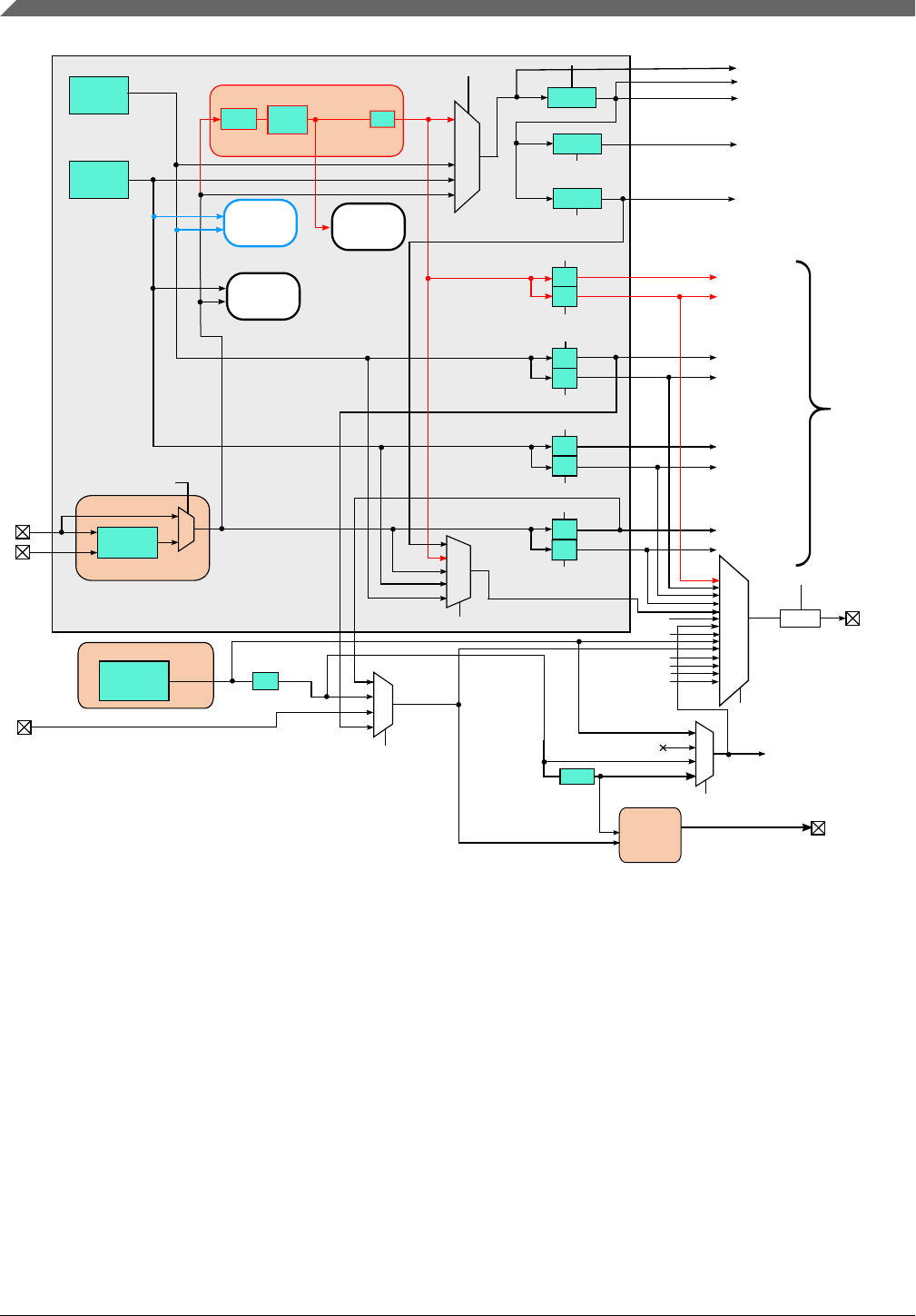
Fast
IRC
Slow
IRC
DIV1
DIV2
DIV1
DIV2
OSC
SOSC
System PLL3
SPLLDIV1_CLK
SPLLDIV2_CLK
FIRCDIV1_CLK
FIRCDIV2_CLK
SCG
EXTAL
XTAL
PMC
LPO
128Khz
RTC
RTC
CLKOUT
÷ 2
PREDIV Analog
SCG_CLKOUTCNFG[CLKOUTSEL]
Asynchronous
Peripheral
Sources
SCG_SOSCCFG[EREFS]
LPO128K_CLK
SIM_LPOCLKS[RTCCLKSEL]
SPLL_CLK
FIRC_CLK
SIRC_CLK
SOSC_CLK
SIM_LPOCLKS[LPOCLKSEL]
SIM_CHIPCTL[CLKOUTDIV]
SIM_CHIPCTL[CLKOUTSEL]
SIRCDIV1_CLK
SIRCDIV2_CLK
SOSCDIV1_CLK
SOSCDIV2_CLK
÷ 4
DIV
FLASH_CLK
BUS_CLK
CORE_CLK
SYS_CLK
LPO_CLK
LPO32K_CLK
LPO128K_CLK
LPO32K_CLK
00
01
10
11
1000
0110
0100
0010
0000
0111
1100
1001
1010
1110
0101
1011
1101
1111
00
01
10
11
RTC_CLKIN
0000
0110
0001
0010
0011
SCG_SLOW_CLK
0110
0011
0010
0001
LPO1K_CLK
RTC_CLK
VCO_CLK
SCG_SPLLDIV[SPLLDIV1]
SCG_SPLLDIV[SPLLDIV2]
DIV1
DIV2
SCG_FIRCDIV[FIRCDIV1]
SCG_FIRCDIV[FIRCDIV2]
DIV1
DIV2
SCG_SIRCDIV[SIRCDIV1]
SCG_SIRCDIV[SIRCDIV2]
SCG_CLKOUT
SCG_SOSCDIV[SOSCDIV1]
SCG_SOSCDIV[SOSCDIV2]
SCG_xCCR[DIVSLOW]
DIVSLOW
SCG_xCCR[DIVBUS]
DIVBUS
SCG_xCCR[DIVCORE]
DIVCORE
SPLL_CLK
System OSC
Clock Monitor
(Loss of clock)
System PLL
clock monitor
(Loss of lock)
(SOSC is monitored,
SIRC is module clock)
0
1
÷ 32
RTC_CLKOUT
1 kHz Clock
RTC_CLK
SCG_xCCR[SCS]
(where x = R, V, or H)
PREDIV_SYS_CLK
HCLK1
BUS_CLK1
QSPI_Module clock2
QSPI_2xSFIF_CLK2
QSPI_SFIF_CLK2
QSPI_SFIF_CLK_HYP_PREMUX2
1. The source of HCLK (to Arm® Cortex® modules) is CORE_CLK. See section 'Clock definitions' for CORE_CLK and BUS_CLK
2. QSPI clocks are applicable for S32K148 only and Reserved for others. See QuadSPI clicking diagram in table 'Peripheral module clocking'
3. For S32K11x, inputs and muxes connected to PCC are Reserved. Also SPLLDIVx_CLK are Reserved as indicated in RED
CMU4
(FIRC is monitored,
SIRC is reference clock)
4. Available only in S32K11x as indicated in BLUE
Figure 27-1. Clocking diagram
27.3 Clock definitions
The following table describes clocks shown in Figure 27-1 and other sections of this
document.
Clock definitions
S32K1xx Series Reference Manual, Rev. 7, 04/2018
534 NXP Semiconductors

Table 27-1. Clock descriptions
Clock name Related clock selector Related clock divider Description
PREDIV_SYS_C
LK 1SCG_xCCR[SCS] — Clocks the QSPI memory in HSRUN
80 mode.
CORE_CLK2SCG_xCCR[SCS] SCG_xCCR[DIVCORE]
(÷ 1...16) Clocks the Arm core, divided by
DIVCORE bits inside SCG.
SYS_CLK2SCG_xCCR[SCS] SCG_xCCR[DIVCORE]
(÷ 1...16) Clocks the Crossbar, NVIC, Flash
controller, FTM, PDB, and so on.
BUS_CLK SCG_xCCR[SCS] SCG_xCCR[DIVBUS]
(÷ 1...16) Clocks the chip peripherals.
FLASH_CLK 3
(SCG_SLOW_CL
K in SCG)
SCG_xCCR[SCS] SCG_xCCR[DIVSLOW]
(÷ 1...8) Clocks the flash module.
SPLL_CLK 4— — Output of PLL (VCO_CLK ÷ 2)
SIRC_CLK — — Output clock of Slow IRC.
FIRC_CLK — — Output clock of Fast IRC.
SOSC_CLK SCG_SOSCCFG[EREFS] — System oscillator clock. Can be either
the EXTAL pin or output of oscillator
(SOSC).
NOTE: ERCLK/OSCERCLK stands
for the same clock source, in
some module chapters.
RTC_CLKOUT — — RTC oscillator output driving external
pin.
LPO32K_CLK SIM_LPOCLKS[CLK32SEL] A fixed divide by 4 of LPO_CLK
drives 01b input of RTC_CLK
multiplexer.
Source clock for RTC.
LPO128K_CLK — — Always on low power oscillator clock
generated by PMC.
SCG_CLKOUT SCG_CLKOUTCNFG[CLKOUT
SEL]
— SCG output clock that can be driven by
SOSC_CLK, SIRC_CLK, FIRC_CLK,
SPLL_CLK4, or SCG_SLOW_CLK
(FLASH_CLK).
LPO_CLK SIM_LPOCLKS[LPOCLKSEL] — Clock output generated from one of
three LPO clocks sources
(LPO128K_CLK, LPO32K_CLK,
LPO1K_CLK).
CLKOUT SIM_CHIPCTL[CLKOUTSEL] SIM_CHIPCTL[CLKOUTDIV]
(÷ 1...8) Selected from one of eight internal
clock sources.
VCO_CLK 4— — VCO output clock within PLL. Its
frequency = SPLL_CLK × 2.
SPLLDIV1_CLK 4—SCG_SPLLDIV[SPLLDIV1]
(÷ 1, 2, 4, 8, 16, 32, 64, or
output disabled)
Divided SPLL_CLK
This should be configured to 80MHz or
less in RUN mode and to 112 MHz or
less in HSRUN mode.
SPLLDIV2_CLK
4
—SCG_SPLLDIV[SPLLDIV2]
(÷ 1, 2, 4, 8, 16, 32, 64, or
output disabled)
Divided SPLL_CLK
This should be configured to 40 MHz
or less in RUN mode and 56 MHz or
less in HSRUN mode.
Table continues on the next page...
Chapter 27 Clock Distribution
S32K1xx Series Reference Manual, Rev. 7, 04/2018
NXP Semiconductors 535

Table 27-1. Clock descriptions (continued)
Clock name Related clock selector Related clock divider Description
FIRCDIV1_CLK — SCG_FIRCDIV[FIRCDIV1]
(÷ 1, 2, 4, 8, 16, 32, 64, or
output disabled)
Divided FIRC_CLK
This should be configured to 48 MHz
or less in RUN/HSRUN mode.
FIRCDIV2_CLK — SCG_FIRCDIV[FIRCDIV2]
(÷ 1, 2, 4, 8, 16, 32, 64, or
output disabled)
Divided FIRC_CLK
This should be configured to 48 MHz
or less in RUN/HSRUN mode.
SIRCDIV1_CLK — SCG_SIRCDIV[SIRCDIV1]
(÷ 1, 2, 4, 8, 16, 32, 64, or
output disabled)
Divided SIRC_CLK
This should be configured to 8 MHz or
less in RUN/HSRUN mode and to 4
MHz or less in VLPR/VLPS mode.
SIRCDIV2_CLK — SCG_SIRCDIV[SIRCDIV2](÷
1, 2, 4, 8, 16, 32, 64, or
output disabled
)
Divided SIRC_CLK
This should be configured to 8 MHz or
less in RUN/HSRUN mode and to 4
MHz or less in VLPR/VLPS mode.
SOSCDIV1_CLK — SCG_SPLLDIV[SOSCDIV1]
(÷ 1, 2, 4, 8, 16, 32, 64, or
output disabled)
Divided SOSC_CLK
This should be configured to 40 MHz
or less in RUN/HSRUN mode.
SOSCDIV2_CLK — SCG_SPLLDIV[SOSCDIV2]
(÷ 1, 2, 4, 8, 16, 32, 64, or
output disabled)
Divided SOSC_CLK
This should be configured to 40 MHz
or less in RUN/HSRUN mode.
1. Only available in S32K148
2. SYS_CLK/CORE_CLK must not be configured to less than BUS_CLK.
3. For FLASH_CLK operating range during parallel boot see Device Boot modes
4. Only available in S32K14x series
27.4 Internal clocking requirements
The clock dividers are programmed via the SCG module’s clock divider registers. The
following requirements must be met when configuring the clocks for this chip:
• CORE_CLK and SYS_CLK clock frequency must be 112 MHz or less in HSRUN
mode and 80 MHz in normal RUN mode (but not configured to be less than
BUS_CLK).
• BUS_CLK frequency must be programmed to 56 MHz or less in HSRUN, 48 MHz
or less in RUN(when using PLL as system clock source maximum bus clock
frequency is 40 MHz. See Option 1 and 3 below ), and an integer divide of the
CORE_CLK.
• FLASH_CLK frequency must be programmed to 28 MHz or less in HSRUN, 26.67
MHz or less in RUN, and an integer divide of the CORE_CLK. The core clock to
flash clock ratio is limited to a max value of 8.
Internal clocking requirements
S32K1xx Series Reference Manual, Rev. 7, 04/2018
536 NXP Semiconductors

The following are a few of the common clock configurations for this chip in the four
clocking modes:
Option 1: Slow RUN (typically using the undivided FIRC)1, using the following
Memory Map/Register Definition register settings:
• SCG_RCCR[SCS] = 0011b
• SCG_RCCR[DIVCORE] = 0000b
• SCG_RCCR[DIVBUS] = 0000b
• SCG_RCCR[DIVSLOW] = 0001b
Table 27-2. Slow RUN example
Clock Frequency
CORE_CLK 48 MHz
SYS_CLK 48 MHz
BUS_CLK 48 MHz (max freq. in RUN mode)
FLASH_CLK 24 MHz
Option 2: Normal RUN (with VCO_CLK = 320 MHz, SPLL_CLK = 160 MHz), using
the following Memory Map/Register Definition register settings:
• SCG_RCCR[SCS] = 0110b
• SCG_RCCR[DIVCORE] = 0001b
• SCG_RCCR[DIVBUS] = 0001b
• SCG_RCCR[DIVSLOW] = 0010b
Table 27-3. Normal RUN example
Clock Frequency
CORE_CLK 80 MHz
SYS_CLK 80 MHz
BUS_CLK 40 MHz
FLASH_CLK 26.67 MHz (max freq. in RUN
mode)
Option 3: Normal RUN (with VCO_CLK = 256 MHz, SPLL_CLK = 128 MHz), using
the following Memory Map/Register Definition register settings:
• SCG_RCCR[SCS] = 0110b
• SCG_RCCR[DIVCORE] = 0001b
• SCG_RCCR[DIVBUS] = 0001b
• SCG_RCCR[DIVSLOW] = 0010b
1. Default configuration after reset. FIRC_CLK = 48 MHz.
Chapter 27 Clock Distribution
S32K1xx Series Reference Manual, Rev. 7, 04/2018
NXP Semiconductors 537

Table 27-4. Normal RUN example
Clock Frequency
CORE_CLK 64 MHz
SYS_CLK 64 MHz
BUS_CLK 32 MHz
FLASH_CLK 21.33 MHz
Option 4: High Speed RUN (with VCO_CLK = 224 MHz, SPLL_CLK = 112 MHz),
using the following Memory Map/Register Definition register settings:
• SCG_HCCR[SCS] = 0110b
• SCG_HCCR[DIVCORE] = 0000b
• SCG_HCCR[DIVBUS] = 0001b
• SCG_HCCR[DIVSLOW] = 0011b
Table 27-5. High Speed RUN example
Clock Frequency
CORE_CLK 112 MHz
SYS_CLK 112 MHz
BUS_CLK 56 MHz
FLASH_CLK 28 MHz
NOTE
All frequencies listed in table above are maximum for HSRUN
mode.
Option 5: High Speed RUN 80 (with VCO_CLK = 320 MHz, SPLL_CLK = 160 MHz),
using the following Memory Map/Register Definition register settings:
• SCG_HCCR[SCS] = 0110b
• SCG_HCCR[DIVCORE] = 0001b
• SCG_HCCR[DIVBUS] = 0001b
• SCG_HCCR[DIVSLOW] = 0010b
Table 27-6. High Speed RUN 80 example (mode used by QuadSPI only)
Clock Frequency
CORE_CLK 80 MHz
SYS_CLK 80 MHz
BUS_CLK 40 MHz
FLASH_CLK 26.67 MHz (maximum frequency
in RUN mode)
Internal clocking requirements
S32K1xx Series Reference Manual, Rev. 7, 04/2018
538 NXP Semiconductors

Option 6: Very Low Power RUN, VLPR (with SIRC_CLK = 8 MHz), using the
following Memory Map/Register Definition register settings:
• SCG_VCCR[SCS] = 0010b (SIRC_CLK)
• SCG_VCCR[DIVCORE] = 0001b
• SCG_VCCR[DIVBUS] = 0000b
• SCG_VCCR[DIVSLOW] = 0011b
Table 27-7. Very low power RUN example
Clock Frequency
CORE_CLK 4 MHz
SYS_CLK 4 MHz
BUS_CLK 4 MHz
FLASH_CLK 1 MHz
Following table summarizes the S32K14x/S32K11x maximum frequencies and example
configurations for each internal clock
Clock HSRUN RUN VLPR Notes
S32K14x only S32K14x S32K11x
CORE_CLK
SYS_CLK
112MHz 80MHz 48MHz 4MHz Must be configured to be more than or
equal to BUS_CLK.
BUS_CLK 56MHz 48MHz
(40MHz when
using PLL as
system clock
source)
48MHz 4MHz Must be integer divide of the
CORE_CLK.
FLASH_CLK 28MHz 26.67MHz 24MHz 1MHz Must be integer divide of the
CORE_CLK. The core clock to flash
clock ratio is limited to a max value of
8.
NOTE
All frequencies listed in table above are maximum for VLPR
mode.
NOTE
All asynchronous clock sources will also be restricted to 4 MHz
in VLPR/VLPS mode as configured in SCG_SIRCDIV.
Chapter 27 Clock Distribution
S32K1xx Series Reference Manual, Rev. 7, 04/2018
NXP Semiconductors 539

27.4.1 Clock divider values after reset
The default configuration out of reset has the CPU clocked by the Fast IRC
(FIRC_CLK). The clocks (for example, CORE_CLK, FLASH_CLK, and BUS_CLK) are
configured in the SCG module (see Memory Map/Register Definition).
27.4.2 HSRUN mode clocking
Clock dividers should not be modified while the chip is operating in HSRUN mode. They
must be configured prior to entering HSRUN mode to guarantee:
• CORE_CLK/SYS_CLK is less than or equal to 112MHz
• BUS_CLK is less than or equal to 56 MHz
• FLASH_CLK is less than or equal to 28 MHz
27.4.3 VLPR mode clocking
Clock dividers should not be modified while the chip is operating in VLPR mode. They
must be configured prior to entering VLPR mode to guarantee:
• CORE_CLK/SYS_CLK and BUS_CLK are less than or equal to 4 MHz
• FLASH_CLK is less than or equal to 1 MHz
NOTE
All asynchronous clock sources will also be restricted to 4 MHz
in VLPR/VLPS mode as configured in SCG_SIRCDIV.
27.4.4 VLPR/VLPS mode entry
When entering VLPR/VLPS mode, the system clock should be SIRC. The FIRC, SOSC,
and SPLL must be disabled by software in RUN mode before making any mode
transition. Ensure that CMU is gated by its PCC.CGC before entering STOP/VLPS/CPO
mode.
Internal clocking requirements
S32K1xx Series Reference Manual, Rev. 7, 04/2018
540 NXP Semiconductors

27.5 Clock Gating
The clock to each module can be individually gated on and off using the PCC module.
After any reset, PCC disables the clock to the corresponding module to conserve power.
Prior to initializing a module, set the corresponding clock gating control bits in PCC
register to enable the clock. Before turning off the clock, make sure to disable the
module.
Any bus access to a peripheral that has its clock disabled generates an error termination.
27.6 Module clocks
The following table summarizes the clocks that can be used by each of the modules.
Table 27-8. Peripheral clock summary
Module name Bus interface
clock 1
Bus interface
clock1 gating
Peripheral
functional clock
Additonal clocks Comments and
maximum frequencies
Gated by
[CGC] of
PCC
Clocks controlled
by [PCS] of PCC
Communications
LPUART BUS_CLK Yes
SPLLDIV2_CLK,
FIRCDIV2_CLK,
SIRCDIV2_CLK,
SOSCDIV2_CLK
—Maximum frequency
governed by BUS_CLK
LPSPI BUS_CLK Yes
SPLLDIV2_CLK,
FIRCDIV2_CLK,
SIRCDIV2_CLK,
SOSCDIV2_CLK
—Maximum frequency
governed by BUS_CLK
LPI2C BUS_CLK Yes
SPLLDIV2_CLK,
FIRCDIV2_CLK,
SIRCDIV2_CLK,
SOSCDIV2_CLK
—Maximum frequency
governed by BUS_CLK
FlexIO 3BUS_CLK Yes
SPLLDIV2_CLK,
FIRCDIV2_CLK,
SIRCDIV2_CLK,
SOSCDIV2_CLK
—Maximum frequency
governed by BUS_CLK
FlexCAN SYS_CLK Yes — SYS_CLK,
SOSCDIV2_CLK
Support 40 MHz from
OSC; SYS_CLK must be
> 1.5x the protocol clock;
while synchronous
operation (when protocol
clock is selected to
SYS_CLK) can be done at
1:1 clock frequency.4
Table continues on the next page...
Chapter 27 Clock Distribution
S32K1xx Series Reference Manual, Rev. 7, 04/2018
NXP Semiconductors 541

Table 27-8. Peripheral clock summary (continued)
Module name Bus interface
clock 1
Bus interface
clock1 gating
Peripheral
functional clock
Additonal clocks Comments and
maximum frequencies
Gated by
[CGC] of
PCC
Clocks controlled
by [PCS] of PCC
Timers
LPTMR BUS_CLK Yes
SPLLDIV2_CLK,
FIRCDIV2_CLK,
SIRCDIV2_CLK,
SOSCDIV2_CLK
RTC_CLK2,
SIRCDIV2_CLK,
LPO1K_CLK
Maximum frequency
governed by BUS_CLK
LPIT BUS_CLK Yes
SPLLDIV2_CLK,
FIRCDIV2_CLK,
SIRCDIV2_CLK,
SOSCDIV2_CLK
—Maximum frequency
governed by BUS_CLK
RTC BUS_CLK Yes — RTC_CLK2,
LPO1K_CLK Maximum frequency
governed by BUS_CLK
PDB SYS_CLK Yes — — Maximum frequency
governed by SYS_CLK
FlexTimer SYS_CLK Yes
SPLLDIV1_CLK,
FIRCDIV1_CLK,
SIRCDIV1_CLK,
SOSCDIV1_CLK
RTC_CLK2,
SYS_CLK,
TCLKx
Maximum frequency
governed by SYS_CLK
System Modules
WDOG BUS_CLK No —
LPO_CLK 5,
SOSC_CLK,
SIRC_CLK
Maximum frequency
governed by BUS_CLK
EWM BUS_CLK Yes — LPO_CLK5Maximum frequency
governed by BUS_CLK
PMC BUS_CLK No — — Maximum frequency
governed by BUS_CLK
SIM BUS_CLK No — — Maximum frequency
governed by BUS_CLK
RCM BUS_CLK No — LPO128K_CLK Maximum frequency
governed by BUS_CLK
CRC BUS_CLK Yes — — Maximum frequency
governed by BUS_CLK
PORT BUS_CLK Yes — LPO128K_CLK Maximum frequency
governed by BUS_CLK
GPIO SYS_CLK No — — Maximum frequency
governed by SYS_CLK
TRGMUX BUS_CLK No — — Maximum frequency
governed by BUS_CLK
DMAMUX BUS_CLK Yes — — Maximum frequency
governed by BUS_CLK
DMA SYS_CLK No — — Maximum frequency
governed by SYS_CLK
MPU SYS_CLK No — — Maximum frequency
governed by SYS_CLK
Table continues on the next page...
Module clocks
S32K1xx Series Reference Manual, Rev. 7, 04/2018
542 NXP Semiconductors

Table 27-8. Peripheral clock summary (continued)
Module name Bus interface
clock 1
Bus interface
clock1 gating
Peripheral
functional clock
Additonal clocks Comments and
maximum frequencies
Gated by
[CGC] of
PCC
Clocks controlled
by [PCS] of PCC
EIM SYS_CLK No — — Maximum frequency
governed by SYS_CLK
ERM SYS_CLK No — — Maximum frequency
governed by SYS_CLK
MSCM SYS_CLK No — — Maximum frequency
governed by SYS_CLK
CMU BUS_CLK Yes — FIRC_CLK
SIRC_CLK —
Memory Modules
FTFC6FLASH_CLK Yes — — Maximum frequency
governed by FLASH_CLK
System RAM SYS_CLK No — — Maximum frequency
governed by SYS_CLK
Analog Modules
ADC BUS_CLK Yes
SPLLDIV2_CLK,
FIRCDIV2_CLK,
SIRCDIV2_CLK,
SOSCDIV2_CLK
—
50 MHz7
CMP BUS_CLK Yes — — Maximum frequency
governed by BUS_CLK
QuadSPI BUS_CLK/
SYS_CLK Yes SPLLDIV1_CLK
FIRCDIV1_CLK — —
SAI BUS_CLK Yes — MCLK (from PAD)
BCLK (from PAD) —
ENET8SYS_CLK Yes
SPLLDIV1_CLK
SIRCDIV1_CLK
FIRCDIV1_CLK
SOSCDIV1_CLK
ENET_MII_RMII_TX_
CLK (from PAD)
MAC timestamp clock
period must be integer
nano-seconds.
1. Refers to module's interface clock and should not be misinterpreted as BUS_CLK
2. RTC_CLK is the output from the multiplexer that uses SIM_LPOCLKS[RTCCLKSEL] for source selection (See Figure 1 for
details).
3. FlexIO peripheral clock should not be more than twice of FlexIO bus interface clock. For fast access to FlexIO register
(FLEXIO_CTRL[FASTACC]=1), FlexIO peripheral clock can be twice of FlexIO Bus interface clock.
4. In S32K11x variants, 'SYS_CLK > 1.5x the protocol clock' requirement is not applicable but the software needs to maintain
following relationship:
• CAN bit time > (3 x CANCLK) + (3 x SYS_CLK)
5. LPO_CLK is the output from the multiplexer that uses SIM_LPOCLKS[LPOCLKSEL] for source selection (See Figure 1 for
details).
6. Do not change the clock control settings to the flash memory whilst simultaneously accessing the flash memory. Instead, it
is recommended to execute from SRAM when a change in frequency is needed.
7. The maximum conversion clock frequency is 50 MHz. At any time, the conversion clock frequency should be less than the
ADC bus interface clock frequency. See the device datasheet for ADC specifications.
8. Refer to External signal description for clocking restrictions.
Chapter 27 Clock Distribution
S32K1xx Series Reference Manual, Rev. 7, 04/2018
NXP Semiconductors 543
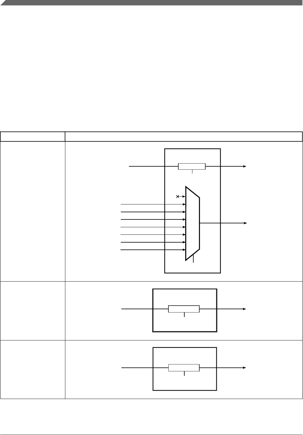
NOTE
The above clock selections are controlled in the PCC module
(column 4 of Table 27-8).
NOTE
• SIRC and LPO_CLK are the valid clock sources for VLP*
modes.
• SPLL and FIRC are the valid clock sources for HSRUN
mode.
The following table summarizes the clocks that can be used by each of the modules.
Table 27-9. Peripheral module clocking
Modules PCC multiplexer
LPSPI
LPIT
FlexIO
LPI2C
LPUART
PCC module
SOSCDIV2_CLK
SIRCDIV2_CLK
SPLLDIV2_CLK
FIRCDIV2_CLK
PCC_<module>[PCS]
000
001
010
011
100
101
110
111
Reserved
Reserved
Reserved
to module
Clock gate enable
PCC_<module>[CGC]
(where 1b = clock enabled)
BUS_CLK
to module
PDB
PCC module
Clock gate enable
PCC_<module>[CGC]
(where 1b = clock enabled)
SYS_CLK
to module
DMAMUX
CMP0
CRC
PCC module
Clock gate enable
PCC_<module>[CGC]
(where 1b = clock enabled)
BUS_CLK
to module
Table continues on the next page...
Module clocks
S32K1xx Series Reference Manual, Rev. 7, 04/2018
544 NXP Semiconductors
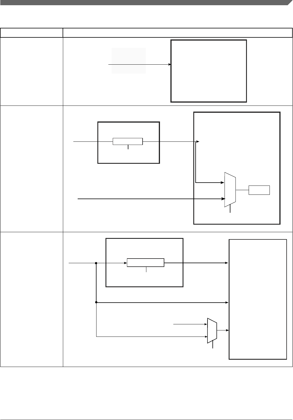
Table 27-9. Peripheral module clocking (continued)
Modules PCC multiplexer
GPIO
GPIO bus interface clock
GPIO
SYS_CLK
PORT
PORT[x]
bus clock
PORT_DFCR[CS]
0
1
lpo clock Filter
PCC module
Clock gate enable
PCC_<module>[CGC]
(where 1b = clock enabled)
BUS_CLK
LPO128K_CLK
bus clock
FlexCAN
SYS_CLK
FlexCANn module
0
1
Clock gate enable
PCC_FLEXCANn[CGC]
(where 1 = clock enabled)
PCC module
Module Clock
SOSCDIV2_CLK
SYS_CLK
CAN_CTRL1[CLKSRC]
CHI Clock
PE Clock
Table continues on the next page...
Chapter 27 Clock Distribution
S32K1xx Series Reference Manual, Rev. 7, 04/2018
NXP Semiconductors 545
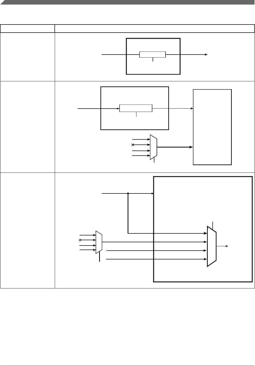
Table 27-9. Peripheral module clocking (continued)
Modules PCC multiplexer
EIM
ERM
MSCM
DMA
MPU
SYS_CLK
to module
Clock gate enable
SIM_PLATCGC[CGC<module>]
(where 1b = clock enabled)
SIM module
EWM
BUS_CLK
EWM module
Clock gate enable
PCC_EWM[CGC]
(where 1 = clock enabled)
PCC module
SIM_LPOCLKS[LPOCLKSEL]
LPO_CLK
LPO128K_CLK
LPO32K_CLK
00
01
10
11
LPO1K_CLK
Low power clock
Peripheral bus clock
WDOG
SOSC_CLK
SIRC_CLK
WDOG module
BUS_CLK
LPO_CLK
WDOG_CS[CLK]
00
01
10
11
WDOG clock
bus_clk
bus_clk
internal LPO clk
internal clk
external clk
SIM_LPOCLKS[LPOCLKSEL]
LPO128K_CLK
LPO32K_CLK
00
01
10
11
LPO1K_CLK
Table continues on the next page...
Module clocks
S32K1xx Series Reference Manual, Rev. 7, 04/2018
546 NXP Semiconductors
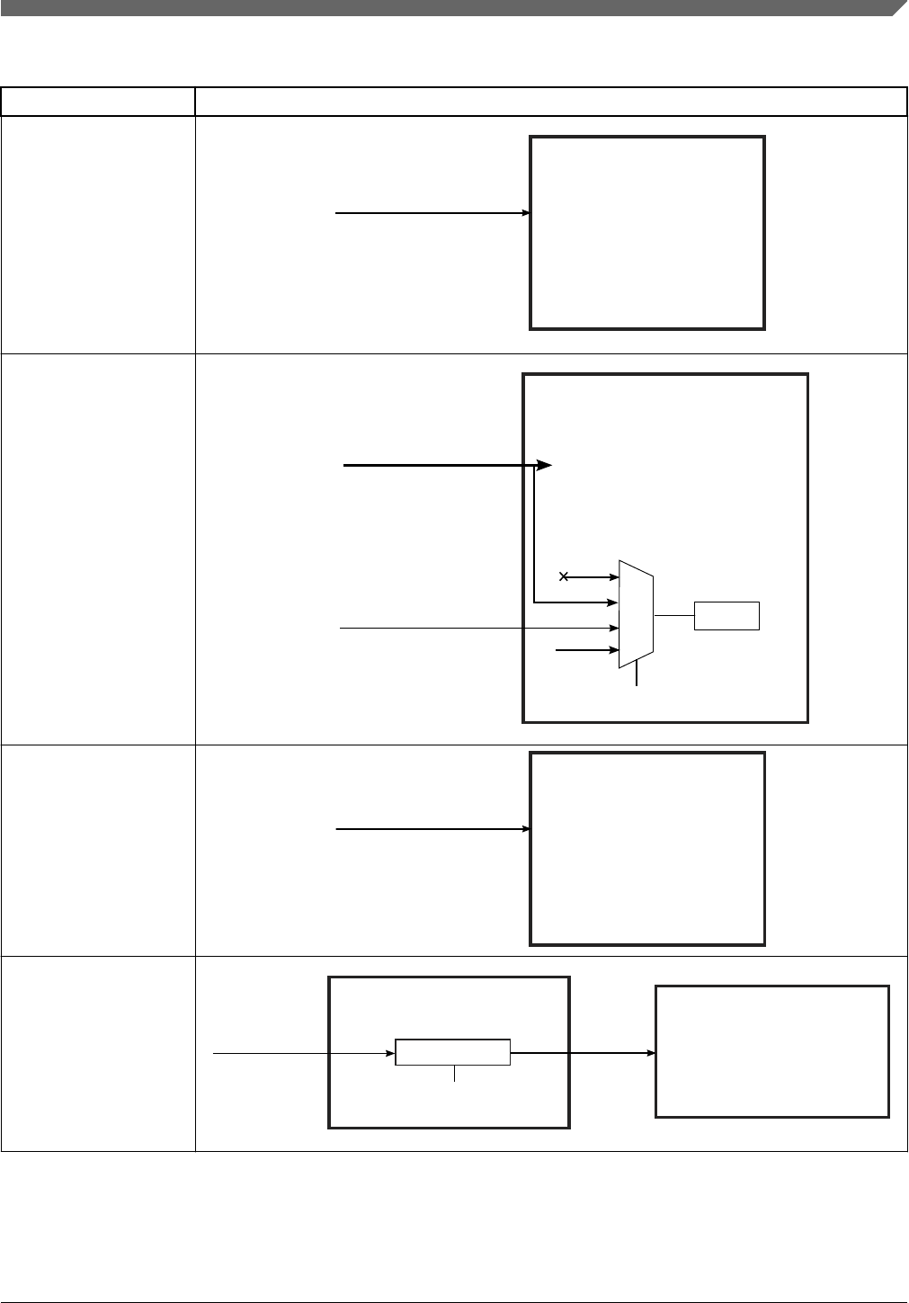
Table 27-9. Peripheral module clocking (continued)
Modules PCC multiplexer
SIM
PMC
TRGMUX
bus interface clock
SIM/PMC/TRGMUX
BUS_CLK
RCM
RCM
bus clock
RCM_RPC[RSTFLTSRW]
00
01
10
11
lpo clock Filter
BUS_CLK
LPO128K_CLK
Reserved
System RAM
memory clock
System RAM
SYS_CLK
FTFC
FLASH_CLK
FTFC
Clock gate enable
PCC_FTFC[CGC]
(where 1 = clock enabled)
PCC module
Table continues on the next page...
Chapter 27 Clock Distribution
S32K1xx Series Reference Manual, Rev. 7, 04/2018
NXP Semiconductors 547
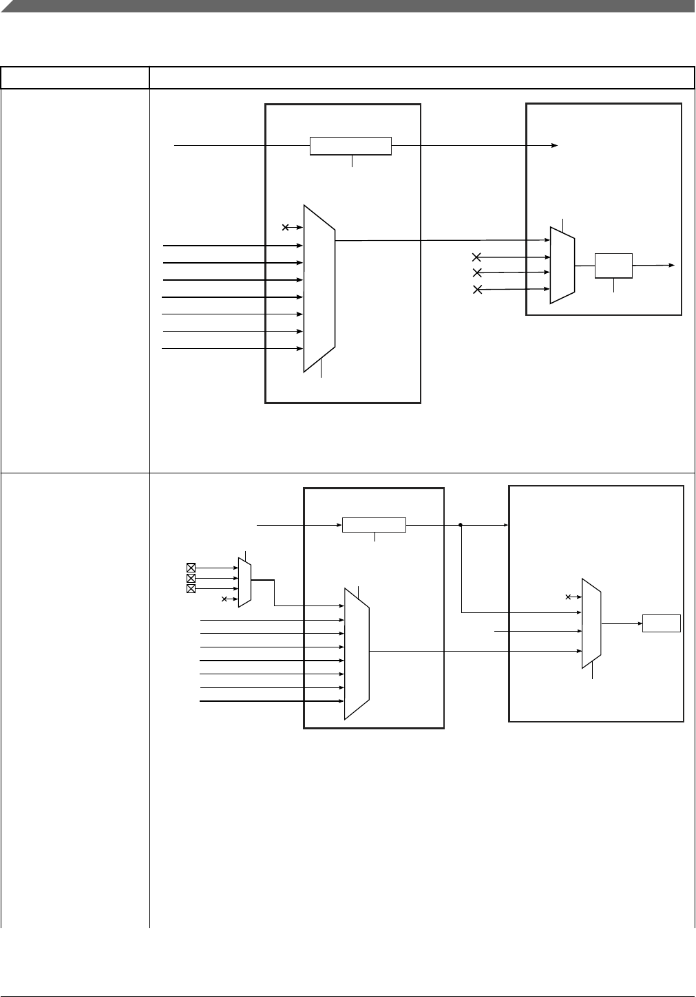
Table 27-9. Peripheral module clocking (continued)
Modules PCC multiplexer
ADC
PCC_ADCnADCn
BUS_CLK Module Clock
Clock
Divide
00
01
10
11
ALTCLK1
ALTCLK2
ALTCLK3
ALTCLK4
Clock gate enable
PCC_ADCn[CGC]
(where 1 = clock enabled)
see PCC chapter
for details
SOSCDIV2_CLK
SIRCDIV2_CLK
SPLLDIV2_CLK
FIRCDIV2_CLK
PCC_ADCn[PCS]
000
001
010
011
100
101
110
111
Reserved
Reserved
Reserved
ADC_CFG1[ADICLK]
ADCK
ADC_CFG1[ADIV]
Bus interface clk
The ADC has multiple clock sources. Selection is determined by the configuration of
PCC_ADCx[PCS]. The dividers should be configured such that the ADC conversion clock
frequency lies within the valid range as per the ADC requirement (see the Data Sheet).
FTM
Clock gate enable
PCC module FTMn module
SYS_CLK
FTMn_SC[CLKS]
see PCC chapter
for details
Counter
00
01
10
11
RTC_CLK
PCC_FLEXTMRn[CGC]
(where 1 = clock enabled)
SIM_FTMOPT0[FTMnCLKSEL]
SOSCDIV1_CLK
SIRCDIV1_CLK
SPLLDIV1_CLK
FIRCDIV1_CLK
000
001
010
011
100
101
110
111
Reserved
Reserved
Reserved
PCC_FLEXTMRn[PCS]
00
01
10
11
TCLK0
TCLK1
TCLK2
External clock
Fixed frequency clock
FTM_CLK
FTM System clock
FTM System clock
The FTM module is clocked by the internal SYS_CLK (the FTM module refers to it as system
clock) which could be up to CPU frequency, but the FTM counter allows to be clocked by three
clock sources:
• System clock (SYS_CLK) from PCC
• Internal fixed frequency clock
• External clocks from pins (TCLK[2:0])
The counter clock source selection is controlled by CLKS bits in FTMn_SC register. The
FTM_CLK is controlled by PCC module and could run up to CPU frequency and provide higher
resolution for the FTM timer.
The fixed frequency clock is a fixed clock driven by RTC_CLK. SIM_LPOCLKS[RTCCLKSEL] is
used to select the RTC_CLK source.
Table continues on the next page...
Module clocks
S32K1xx Series Reference Manual, Rev. 7, 04/2018
548 NXP Semiconductors
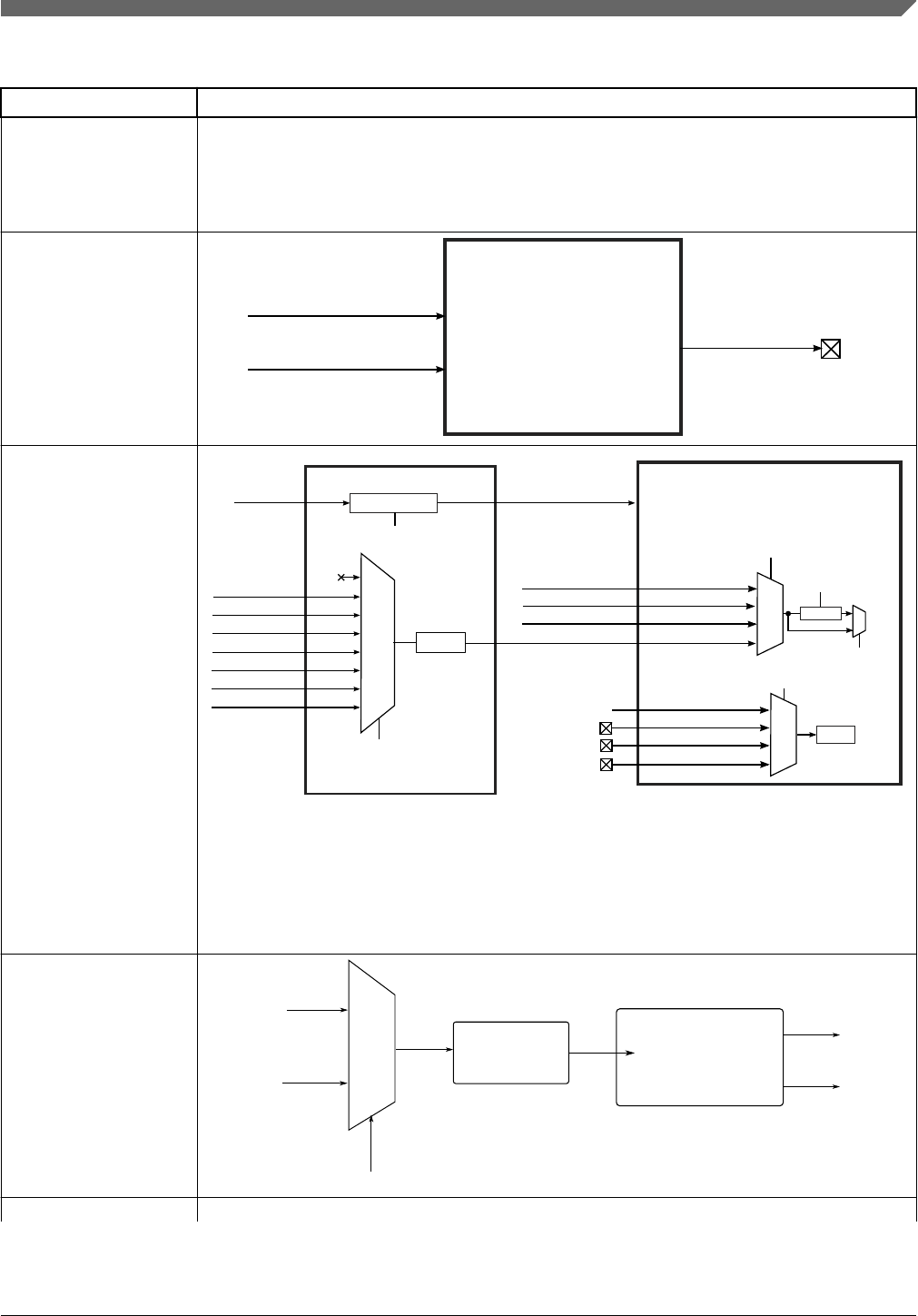
Table 27-9. Peripheral module clocking (continued)
Modules PCC multiplexer
There are three clocks that can be accessed externally to the chip (TCLK0, TCLK1, TCLK2). One
of these clocks are selected to drive the 000b input of the multiplexer in the PCC
(PCC_FLEXTMRn[PCS] = 000b) by configuring SIM_FTMOPT0[FTMnCLKSEL].
The fixed frequency clock and external clocks provide the user more clock options for FTM
counter.
RTC
1 kHz clock
RTC
LPO1K_CLK
RTC_CLK
RTC_CLKOUT
RTC_CLK
RTC_CLKOUT pin
LPTMR
PCC module LPTMR0 module
BUS_CLK
LPTMR0_PSR[PCS]
Module Clock
see PCC chapter
for details
00
01
10
11
SOSCDIV2_CLK
SIRCDIV2_CLK
SPLLDIV2_CLK
FIRCDIV2_CLK
PCC_LPTMR0[PCS]
000
001
010
011
100
101
110
111
Reserved
Reserved
Reserved
SIRCDIV2_CLK
RTC_CLK
LPO1K_CLK
LPTMR0_CSR[TPS]
Prescaler
00
01
10
11
TRGMUX_LPTMR0
LPTMR_ALT1
LPTMR_ALT2
LPTMR_ALT3
LPTMR0_PSR[PRESCALE]
LPTMR_PSR[PBYP]
0
1
Pulse
Counter
Divider
PCC_LPTMR0[PCD]
Prescaler/glitch filter clock0
Prescaler/glitch filter clock1
Prescaler/glitch filter clock2
Prescaler/glitch filter clock3
Pulse counter input0
Pulse counter input1
Pulse counter input2
Pulse counter input3
(see 'Clocking diagram' for details)
Clock gate enable
PCC_LPTMR0[CGC]
(where 1 = clock enabled)
The prescaler and glitch filter of the LPTMR0 module can be clocked from misc sources
determined by the PCC_LPTMR[PCS] control bitfield and LPTMR0_PSR[PCS] bitfield. The
LPTMR_PSR[PCS] bitfield is used for internal LPTMR to select the clock source. The supported
clock sources on this device are shown in following figure.
NOTE: The clock selected must remain enabled if the LPTMR is to continue operating in all
required low power modes.
TPIU
Core clk
Platform clk
SIM_CHIPCTL[12]
Divider
SIM_CLKDIV4[3:0]
TPIU Trace clk
SWO
0
1
SAI
Table continues on the next page...
Chapter 27 Clock Distribution
S32K1xx Series Reference Manual, Rev. 7, 04/2018
NXP Semiconductors 549
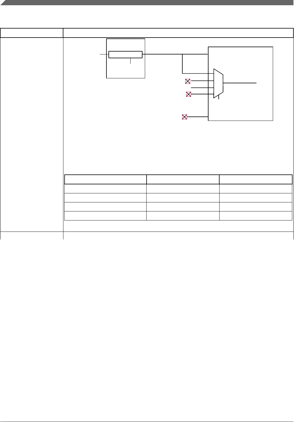
Table 27-9. Peripheral module clocking (continued)
Modules PCC multiplexer
SAIx_BCLK
PCC_SAIx
Module_clock SAIx
11
10
01
00
MCLK_SAI
SOSCDIV1
SAIx_MCLK
BUS_CLK
PCC
Clock gate enable
SAI_RCR2[MSEL]/
SAI_TCR2[MSEL]
SAIy_MCLK
The BCLK can either be externally provided through BCLK pin or can be internally generated in
internal bit clock mode using SAI internal divider by configuring SAIn_RCR2[MSEL]/
SAIn_TCR2[MSEL] and SAIn_RCR2[DIV]/SAIn_TCR2[DIV].
NOTE: BCLK should never be greater than the Bus interface clock as it will lead to underrun or
overflow of FIFO inside SAI.
Table 27-10. Clocking option
SAI instance MCLK source Description
SAI0 SAIx_MCLK SAI0 MCLK
SAI0 SAIy_MCLK SAI1 MCLK
SAI1 SAIx_MCLK SAI1 MCLK
SAI1 SAIy_MCLK SAI0 MCLK
QuadSPI
Table continues on the next page...
Module clocks
S32K1xx Series Reference Manual, Rev. 7, 04/2018
550 NXP Semiconductors
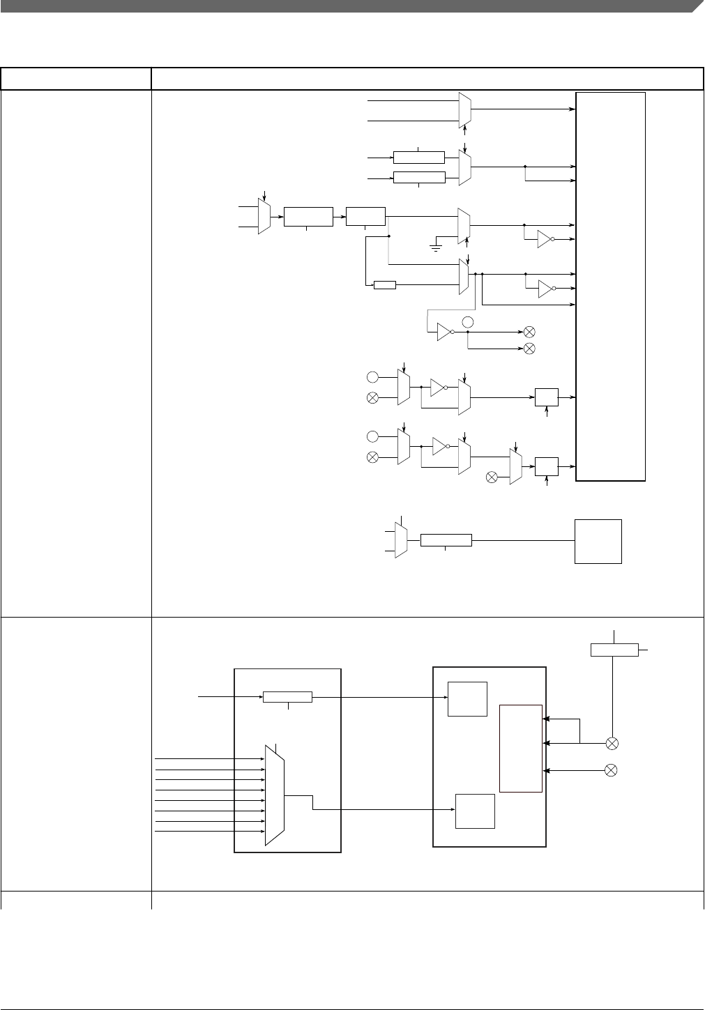
Table 27-9. Peripheral module clocking (continued)
Modules PCC multiplexer
QuadSPI_MCR[SCLKCFG][0]
SCKB
loopback
clock
A
DQS_B
0
1
0
10
RWDS
QuadSPI_MCR[SCLKCFG][5]
Delay
chain
QuadSPI_SOCCR[SOCCFG][15:8]
1
QuadSPI_MCR[SCLKCFG][2]
QuadSPI_MCR[SCLKCFG][3]
SCKA
loopback
clock
A
0
1
0
1Delay
chain
QuadSPI_SOCCR[SOCCFG][7:0]
DQS_A
Bus interface clock
Module clock
AHB read interface clock
1
0
QuadSPI_MCR[SCLKCFG][6]
1
0
BUS_CLK
SYS_CLK
Clock gate enable
BUS_CLK
SYS_CLK
QuadSPI_MCR[SCLKCFG][1]
QuadSPI
SCKA (PAD)
SCKB (PAD)
A
2xSFIF_CLK
2xSFIF_B_CLK
1
0
QuadSPI_MCR[SCLKCFG][5]
SFCK
Div by 2
0
1
SFIF_CLK
SFIF_B_CLK
0
1
QuadSPI_MCR[SCLKCFG][6] QuadSPI_AHB_Buffer
QuadSPI
Memory
128x7
(1 KB)
PREDIV_SYS_CLK
SYS_CLK
0
1
QuadSPI_MCR[SCLKCFG][4]
SPLLDIV1
FIRCDIV1
Clock gate enable1Programmable
Divider2
Clock gate enable
PCC_QSPI[CGC]
(where 1 = clock enabled)
PCC_QSPI[CGC]
(where 1 = clock enabled)
Clock gate enable
PCC_QSPI[CGC]
(where 1 = clock enabled)
SIM_MISCTRL0[QSPI_CLK_SEL]
(where 1 = clock enabled)
QuadSPI_SOCCR[SOCCFG]
QSPI_SFIF_CLK_HYP_PREMUX
NOTE: 1. Clock gate enable: SIM_MISCTRL0[QSPI_CLK_SEL]
2. For programmable divider configuration, see QuadSPI_SOCCR[SOCCFG]
implementation
ENET
Clock gate enable
PCC module ENET module
SYS_CLK
see PCC chapter
for details
PCC_ENET[CGC]
(where 1 = clock enabled)
SOSCDIV1_CLK
SIRCDIV1_CLK
SPLLDIV1_CLK
FIRCDIV1_CLK
000
001
010
011
100
101
110
111
Reserved
Reserved
Reserved
PCC_ENET[PCS]
SYS_CLK
X
ENET_1588_CLKIN Timers
DMA
Tx_clk (PAD)
Rx_clk (PAD)
RMII CLK
MII Tx CLK
MII Rx CLK
1
SOSCDIV1_CLK
SIM_MISCTRL0[25]
MAC
RMII CLK
MII Tx CLK
MII Rx CLK
MAC
Clock gate enable
NOTE: SIM_MISCTRL0 bit 24 and 25 are used to control which clock (external or internally
generated) is used by MAC in RMII mode only.
CMU
Chapter 27 Clock Distribution
S32K1xx Series Reference Manual, Rev. 7, 04/2018
NXP Semiconductors 551
Table 27-9. Peripheral module clocking
Modules PCC multiplexer
CMUx
MON_CLK
PCC module
Clock gate enable
PCC_<module>[CGC]
(where 1b = clock enabled)
FIRC_CLK
SIRC_CLK
PCC module
Clock gate enable
PCC_<module>[CGC]
(where 1b = clock enabled)
REF_CLK
PCC module
Clock gate enable
PCC_<module>[CGC]
(where 1b = clock enabled)
BUS_CLK Module clock
NOTE
While changing peripheral clock source/divider configuration,
the corresponding module should be disabled.
Module clocks
S32K1xx Series Reference Manual, Rev. 7, 04/2018
552 NXP Semiconductors

Chapter 28
System Clock Generator (SCG)
28.1 Chip-specific SCG information
Wait mode is not supported on this device. See Module operation in available low power
modes for details on available power modes.
NOTE
• SPLL and HSRUN mode is not available in S32K11x
series of devices.
• SCG_SIRCCSR[SIRCLPEN] bit field is applicable for
VLPS mode only.
• SCG_SIRCCSR[SIRCSTEN] bit field is not applicable and
should be ignored.
• For S32K11x variants, writing to SCG_HCCR will give
transfer error.
28.1.1 Supported frequency ranges
This section describes the supported frequency ranges.
1. SCG_SOSCCFG[RANGE]
• 00 Reserved
• 01 Reserved
• 10 Medium frequency range selected for the crystal oscillator of 4 MHz to 8
MHz.
• 11 High frequency range selected for the crystal oscillator of 8 MHz to 40 MHz.
2. SCG_FIRCCFG[RANGE]
• 00 Fast IRC is trimmed to 48 MHz
• 01 Reserved
• 10 Reserved
• 11 Reserved
S32K1xx Series Reference Manual, Rev. 7, 04/2018
NXP Semiconductors 553

NOTE
Software should not configure the
SCG_FIRCCFG[RANGE] to any value other than 00.
3. SCG_SIRCCFG[RANGE]
• 0 Reserved
• 1 Slow IRC high range clock (8 MHz )
28.1.2 Oscillator and SPLL guidelines
If PLL is used, then oscillator needs to be in high range only, SCG_SOSCCFG[RANGE]
on 11 as used in reference clock.
If the current system clock is SOSC, then following should be taken care by software:
• Configure all reset sources as 'Interrupt' (not as 'Reset') via RCM_SRIE
• The SOSC should be disabled via SCG_SOSCCSR[SOSCEN]
• After disabling SOSC, configure the reset source back to reset via RCM_SRIE
• When SPLL is enabled, both LOC and LOL must be configured as reset only
(SOSCCSR[SOSCCMRE] and SPLLCSR[SPLLCMRE] must be 1 and
RCM_SRIE[LOC], RCM_SRIE[LOL] must be 0). The only exception is during
standard clock switching, in which case the ‘clock switching sequence’ protocol must
be followed.
See note in section IO Signal Table
28.1.3 System clock switching
For any clock switching of system clock, follow the below steps:
• Before doing a clock switch, configure all reset sources to be ‘Reset' (not as
Interrupt) via RCM_SRIE.
• Program each reset source as Interrupt via RCM_SRIE for a minimum delay time of
10 LPO.
• Execute the clock switch
• Wait/Poll for the clock switch to complete
• Configure every reset source back to original intended reset configuration (Interrupt
or Reset) via RCM_SRIE
NOTE
LOC flag would be raised when SOSC pulses are not detected
for 8 to 16 clock cycles of SIRC/256. Hence, the LOC
Chip-specific SCG information
S32K1xx Series Reference Manual, Rev. 7, 04/2018
554 NXP Semiconductors

indication through reset to the system from the time when
oscillator is cut off will vary from 256 μs to 512 μs.
28.1.4 System clock and clock monitor requirement
1. System clock source XOSC/SPLL requirement: Ensure below sequence is
followed while switching system clock to XOSC/SPLL:
a. System clock source (XOSC/SPLL) is enabled
b. Clock monitors and their corresponding reset events are enabled for XOSC/
SPLL
c. XOSC/SPLL is selected as system clock source
2. XOSC/SPLL clock monitor disable sequence requirement: Ensure below
sequence for disabling clock monitors while switching system clock source from
XOSC/SPLL:
a. System clock source switched from XOSC/SPLL
b. Disable clock monitors and their corresponding reset events for XOSC/SPLL
It is imperative to follow the above guidelines to safeguard the device operation
against loss of clock scenarios if system clock source malfunction due to any reason.
28.2 Introduction
The system clock generator (SCG) module provides the system clocks of the MCU. The
SCG contains a system phase-locked loop (SPLL), a slow internal reference clock
(SIRC), a fast internal reference clock (FIRC), and the system oscillator clock (SOSC).
The SPLL is sourced by the SOSC reference clock. The SCG can select either the output
clock of the SPLL or a SCG reference clock (SIRC, FIRC, and SOSC) as the source for
the MCU system clocks. The SCG also supports operation with crystal oscillators, which
allows an external crystal, ceramic resonator, or another external clock source to produce
the external reference clock (which are also available as clock sources for the MCU
systems clocks).
28.2.1 Features
Key features of the SCG module are:
• System Phase-locked loop (SPLL):
• Voltage-controlled oscillator (VCO)
Chapter 28 System Clock Generator (SCG)
S32K1xx Series Reference Manual, Rev. 7, 04/2018
NXP Semiconductors 555

• External reference clock is used as the PLL source
• Modulo VCO frequency divider
• Phase/Frequency detector
• Integrated loop filter
• Can be selected as the clock source for the MCU system clocks
• 2 programmable post-dividers clock outputs, which can be used as clock sources
for other on-chip peripherals
• 2 Internal reference clock (IRC) generators:
• Fast IRC clock with programmable High and Low frequency range
• Either the slow or the fast clock can be selected as the clock source for the MCU
system clocks
• 2 programmable post-divider clock outputs for each IRC, which can be used as
clock sources for other on-chip peripherals
• System Crystal Oscillator:
• Used as the source for the System PLL
• Can be selected as the clock source for the MCU system clocks
• Clock monitor with reset and interrupt request capability for SPLL, SOSC, clocks
• Lock detector with interrupt request capability for use with the SPLL
• Each of the clock sources have reference dividers for clocking on-chip modules and
peripherals, namely:
• SPLLDIV1_CLK / SPLLDIV2_CLK
• FIRCDIV1_CLK / SCG_FIRCDIV2_CLK
• SIRCDIV1_CLK / SIRCDIV2_CLK
• SOSCDIV1_CLK / SOSCDIV2_CLK
See the Clock Distribution Chapter for more information.
28.3 Memory Map/Register Definition
This section includes the memory map and register definition.
Memory Map/Register Definition
S32K1xx Series Reference Manual, Rev. 7, 04/2018
556 NXP Semiconductors

The SCG registers can only be written when in supervisor mode. Write accesses when in
user mode will result in a bus transfer error. Read accesses may be performed in both
supervisor and user mode.
NOTE
For any writeable SCG registers, only 32-bit writes are allowed.
8-bit or 16-bit writes will result in transfer errors.
SCG memory map
Address
offset (hex) Register name Width
(in bits) Access Reset value Section/
page
0 Version ID Register (SCG_VERID) 32 R 0100_0000h 28.3.1/558
4 Parameter Register (SCG_PARAM) 32 R See section 28.3.2/558
10 Clock Status Register (SCG_CSR) 32 R See section 28.3.3/559
14 Run Clock Control Register (SCG_RCCR) 32 R/W See section 28.3.4/561
18 VLPR Clock Control Register (SCG_VCCR) 32 R/W See section 28.3.5/564
1C HSRUN Clock Control Register (SCG_HCCR) 32 R/W See section 28.3.6/566
20 SCG CLKOUT Configuration Register
(SCG_CLKOUTCNFG) 32 R/W 0300_0000h 28.3.7/568
100 System OSC Control Status Register (SCG_SOSCCSR) 32 R/W See section 28.3.8/569
104 System OSC Divide Register (SCG_SOSCDIV) 32 R/W 0000_0000h 28.3.9/571
108 System Oscillator Configuration Register (SCG_SOSCCFG) 32 R/W 0000_0010h 28.3.10/
572
200 Slow IRC Control Status Register (SCG_SIRCCSR) 32 R/W 0100_0005h 28.3.11/
574
204 Slow IRC Divide Register (SCG_SIRCDIV) 32 R/W 0000_0000h 28.3.12/
575
208 Slow IRC Configuration Register (SCG_SIRCCFG) 32 R/W 0000_0001h 28.3.13/
576
300 Fast IRC Control Status Register (SCG_FIRCCSR) 32 R/W See section 28.3.14/
577
304 Fast IRC Divide Register (SCG_FIRCDIV) 32 R/W 0000_0000h 28.3.15/
579
308 Fast IRC Configuration Register (SCG_FIRCCFG) 32 R/W 0000_0000h 28.3.16/
580
600 System PLL Control Status Register (SCG_SPLLCSR) 32 R/W 0000_0000h 28.3.17/
581
604 System PLL Divide Register (SCG_SPLLDIV) 32 R/W 0000_0000h 28.3.18/
583
608 System PLL Configuration Register (SCG_SPLLCFG) 32 R/W 0000_0000h 28.3.19/
584
Chapter 28 System Clock Generator (SCG)
S32K1xx Series Reference Manual, Rev. 7, 04/2018
NXP Semiconductors 557

28.3.1 Version ID Register (SCG_VERID)
Note: Writing to this register will result in a transfer error.
Address: 0h base + 0h offset = 0h
Bit 31 30 29 28 27 26 25 24 23 22 21 20 19 18 17 16 15 14 13 12 11 10 9 8 7 6 5 4 3 2 1 0
RVERSION
W
Reset 0 0 0 0 0 0 0 1 0 0 0 0 0 0 0 0 0 0 0 0 0 0 0 0 0 0 0 0 0 0 0 0
SCG_VERID field descriptions
Field Description
VERSION SCG Version Number
28.3.2 Parameter Register (SCG_PARAM)
Note: Writing to this register will result in a transfer error.
Address: 0h base + 4h offset = 4h
Bit 31 30 29 28 27 26 25 24 23 22 21 20 19 18 17 16 15 14 13 12 11 10 9 8 7 6 5 4 3 2 1 0
RDIVPRES 0 0 CLKPRES
W
Reset * * * * * 0 0 0 0 0 0 0 0 0 0 0 0 0 0 0 0 0 0 0 * * * * * * * *
* Notes:
DIVPRES field: The reset value is controlled by which SCG System Dividers are used by Soc.•
CLKPRES field: The reset value is controlled by which SCG Clock Sources are used by Soc. Please reference the
Reference manual clocking chapter.
•
SCG_PARAM field descriptions
Field Description
31–27
DIVPRES
Divider Present
Indicates which system clock dividers are present in this instance of SCG.
DIVPRES[27]=1 System DIVSLOW is present.
DIVPRES[28]=1 System DIVBUS is present
DIVPRES[31]=1 System DIVCORE is present
26–16
Reserved
This field is reserved.
This read-only field is reserved and always has the value 0.
15–8
Reserved
This field is reserved.
This read-only field is reserved and always has the value 0.
Table continues on the next page...
Memory Map/Register Definition
S32K1xx Series Reference Manual, Rev. 7, 04/2018
558 NXP Semiconductors

SCG_PARAM field descriptions (continued)
Field Description
CLKPRES Clock Present
Indicates which clock sources are present in this instance of SCG. Any bits not defined in this bit field are
Reserved and always has the value 0 when read.
CLKPRES[0] Reserved
CLKPRES[1]=1System OSC (SOSC) is present
CLKPRES[2]=1Slow IRC (SIRC) is present
CLKPRES[3]=1Fast IRC (FIRC) is present
CLKPRES[6]=1System PLL (SPLL) is present
28.3.3 Clock Status Register (SCG_CSR)
This register returns the currently configured system clock source and the system clock
dividers for the core (DIVCORE) and peripheral interface clock (DIVSLOW). The
SCG_CSR reflects the configuration set by one of three clock control registers
SCG_RCCR, SCG_VCCR, SCG_HCCR.
Note: Writing to this register will result in a transfer error.
Address: 0h base + 10h offset = 10h
Bit 31 30 29 28 27 26 25 24 23 22 21 20 19 18 17 16 15 14 13 12 11 10 9 8 7 6 5 4 3 2 1 0
R0 SCS 0 DIVCORE 0 0 DIVBUS DIVSLOW
W
Reset 0 0 0 0 0 0 1 1 0 0 0 0 * * * * 0 0 0 0 0 0 0 0 0 0 0 0 0 0 0 1
* Notes:
DIVCORE field: The reset value is controlled by user FOPT bits that get uploaded during reset. The valid reset values are
div-by-1 or div-by-2 when resetting into RUN mode or div-by-4 or div-by-8 when resetting into VLPR mode.
•
SCG_CSR field descriptions
Field Description
31–28
Reserved
This field is reserved.
This read-only field is reserved and always has the value 0.
27–24
SCS
System Clock Source
Returns the currently configured clock source generating the system clock.
0000 Reserved
0001 System OSC (SOSC_CLK)
0010 Slow IRC (SIRC_CLK)
0011 Fast IRC (FIRC_CLK)
0100 Reserved
0101 Reserved
Table continues on the next page...
Chapter 28 System Clock Generator (SCG)
S32K1xx Series Reference Manual, Rev. 7, 04/2018
NXP Semiconductors 559

SCG_CSR field descriptions (continued)
Field Description
0110 System PLL (SPLL_CLK)
0111 Reserved
23–20
Reserved
This field is reserved.
This read-only field is reserved and always has the value 0.
19–16
DIVCORE
Core Clock Divide Ratio
If SPLL is selected as system clock source, the maximum DIVCORE value is Divide-by-4.
0000 Divide-by-1
0001 Divide-by-2
0010 Divide-by-3
0011 Divide-by-4
0100 Divide-by-5
0101 Divide-by-6
0110 Divide-by-7
0111 Divide-by-8
1000 Divide-by-9
1001 Divide-by-10
1010 Divide-by-11
1011 Divide-by-12
1100 Divide-by-13
1101 Divide-by-14
1110 Divide-by-15
1111 Divide-by-16
15–12
Reserved
This field is reserved.
This read-only field is reserved and always has the value 0.
11–8
Reserved
This field is reserved.
This read-only field is reserved and always has the value 0.
7–4
DIVBUS
Bus Clock Divide Ratio
0000 Divide-by-1
0001 Divide-by-2
0010 Divide-by-3
0011 Divide-by-4
0100 Divide-by-5
0101 Divide-by-6
0110 Divide-by-7
0111 Divide-by-8
1000 Divide-by-9
1001 Divide-by-10
1010 Divide-by-11
1011 Divide-by-12
1100 Divide-by-13
1101 Divide-by-14
1110 Divide-by-15
1111 Divide-by-16
DIVSLOW Slow Clock Divide Ratio
Table continues on the next page...
Memory Map/Register Definition
S32K1xx Series Reference Manual, Rev. 7, 04/2018
560 NXP Semiconductors

SCG_CSR field descriptions (continued)
Field Description
0000 Divide-by-1
0001 Divide-by-2
0010 Divide-by-3
0011 Divide-by-4
0100 Divide-by-5
0101 Divide-by-6
0110 Divide-by-7
0111 Divide-by-8
1000 Reserved
1001 Reserved
1010 Reserved
1011 Reserved
1100 Reserved
1101 Reserved
1110 Reserved
1111 Reserved
28.3.4 Run Clock Control Register (SCG_RCCR)
This register controls the system clock source and the system clock dividers for the core,
platform, external and bus clock domains when in Run mode only. This register can only
be written using a 32-bit write. Selecting a different clock source when in RUN requires
that clock source to be enabled first and be valid before system clocks switch to that
clock source. If system clock divide ratios also change when selecting a different clock
mode when in RUN, new system clock divide ratios will not take affect until new clock
source is valid.
Address: 0h base + 14h offset = 14h
Bit 31 30 29 28 27 26 25 24 23 22 21 20 19 18 17 16 15 14 13 12 11 10 9 8 7 6 5 4 3 2 1 0
R0SCS 0DIVCORE Reserved 0DIVBUS DIVSLOW
W
Reset 0 0 0 0 0 0 1 1 0 0 0 0 * * * * 0 0 0 0 0 0 0 0 0 0 0 0 0 0 0 1
* Notes:
DIVCORE field: The reset value is controlled by user FOPT bits that get uploaded during reset. The two valid reset values
are div-by-1 and div-by-2
•
SCG_RCCR field descriptions
Field Description
31–28
Reserved
This field is reserved.
This read-only field is reserved and always has the value 0.
Table continues on the next page...
Chapter 28 System Clock Generator (SCG)
S32K1xx Series Reference Manual, Rev. 7, 04/2018
NXP Semiconductors 561

SCG_RCCR field descriptions (continued)
Field Description
27–24
SCS
System Clock Source
Selects the clock source generating the system clock in Run mode. Attempting to select a clock that is not
valid will be ignored. Selecting a different clock source when in Run mode requires that clock source to be
enabled first and be valid before system clocks are allowed to switch to that clock source.
0000 Reserved
0001 System OSC (SOSC_CLK)
0010 Slow IRC (SIRC_CLK)
0011 Fast IRC (FIRC_CLK)
0100 Reserved
0101 Reserved
0110 System PLL (SPLL_CLK)
0111 Reserved
23–20
Reserved
This field is reserved.
This read-only field is reserved and always has the value 0.
19–16
DIVCORE
Core Clock Divide Ratio
0000 Divide-by-1
0001 Divide-by-2
0010 Divide-by-3
0011 Divide-by-4
0100 Divide-by-5
0101 Divide-by-6
0110 Divide-by-7
0111 Divide-by-8
1000 Divide-by-9
1001 Divide-by-10
1010 Divide-by-11
1011 Divide-by-12
1100 Divide-by-13
1101 Divide-by-14
1110 Divide-by-15
1111 Divide-by-16
15–12
Reserved
This field is reserved. Software should write 0 to these bits to maintain compatibility.
This field is reserved.
11–8
Reserved
This field is reserved.
This read-only field is reserved and always has the value 0.
7–4
DIVBUS
Bus Clock Divide Ratio
0000 Divide-by-1
0001 Divide-by-2
0010 Divide-by-3
0011 Divide-by-4
0100 Divide-by-5
0101 Divide-by-6
0110 Divide-by-7
Table continues on the next page...
Memory Map/Register Definition
S32K1xx Series Reference Manual, Rev. 7, 04/2018
562 NXP Semiconductors

SCG_RCCR field descriptions (continued)
Field Description
0111 Divide-by-8
1000 Divide-by-9
1001 Divide-by-10
1010 Divide-by-11
1011 Divide-by-12
1100 Divide-by-13
1101 Divide-by-14
1110 Divide-by-15
1111 Divide-by-16
DIVSLOW Slow Clock Divide Ratio
0000 Divide-by-1
0001 Divide-by-2
0010 Divide-by-3
0011 Divide-by-4
0100 Divide-by-5
0101 Divide-by-6
0110 Divide-by-7
0111 Divide-by-8
1000 Reserved
1001 Reserved
1010 Reserved
1011 Reserved
1100 Reserved
1101 Reserved
1110 Reserved
1111 Reserved
Chapter 28 System Clock Generator (SCG)
S32K1xx Series Reference Manual, Rev. 7, 04/2018
NXP Semiconductors 563

28.3.5 VLPR Clock Control Register (SCG_VCCR)
This register controls the system clock source and the system clock dividers for the core,
platform, external and bus clock domains when in VLPR mode only. This register can
only be written using a 32-bit write. Selecting a different clock source when in VLPR
requires that clock source to be enabled first and be valid before system clocks switch to
that clock source. If system clock divide ratios also change when selecting a different
clock mode when in VLPR, new system clock divide ratios will not take affect until new
clock source is valid.
Address: 0h base + 18h offset = 18h
Bit 31 30 29 28 27 26 25 24 23 22 21 20 19 18 17 16 15 14 13 12 11 10 9 8 7 6 5 4 3 2 1 0
R0SCS 0DIVCORE Reserved 0DIVBUS DIVSLOW
W
Reset 0 0 0 0 0 0 1 0 0 0 0 0 * * * * 0 0 0 0 0 0 0 0 0 0 0 0 0 0 0 1
* Notes:
DIVCORE field: The reset value is controlled by user FOPT bits that get uploaded during reset. The two option reset values
are div-by-4 and div-by-8.
•
SCG_VCCR field descriptions
Field Description
31–28
Reserved
This field is reserved.
This read-only field is reserved and always has the value 0.
27–24
SCS
System Clock Source
Selects the clock source generating the system clock in VLPR mode. Attempting to select a clock that is
not valid will be ignored. Selects the clock source generating the system clock. Selecting a different clock
source when in VLPR mode requires that clock source to be enabled first and be valid before system
clocks switch to that clock source.
0000 Reserved
0001 Reserved
0010 Slow IRC (SIRC_CLK)
0011 Reserved
0100 Reserved
0101 Reserved
0110 Reserved
0111 Reserved
23–20
Reserved
This field is reserved.
This read-only field is reserved and always has the value 0.
19–16
DIVCORE
Core Clock Divide Ratio
0000 Divide-by-1
0001 Divide-by-2
0010 Divide-by-3
Table continues on the next page...
Memory Map/Register Definition
S32K1xx Series Reference Manual, Rev. 7, 04/2018
564 NXP Semiconductors

SCG_VCCR field descriptions (continued)
Field Description
0011 Divide-by-4
0100 Divide-by-5
0101 Divide-by-6
0110 Divide-by-7
0111 Divide-by-8
1000 Divide-by-9
1001 Divide-by-10
1010 Divide-by-11
1011 Divide-by-12
1100 Divide-by-13
1101 Divide-by-14
1110 Divide-by-15
1111 Divide-by-16
15–12
Reserved
This field is reserved. Software should write 0 to these bits to maintain compatibility.
This field is reserved.
11–8
Reserved
This field is reserved.
This read-only field is reserved and always has the value 0.
7–4
DIVBUS
Bus Clock Divide Ratio
0000 Divide-by-1
0001 Divide-by-2
0010 Divide-by-3
0011 Divide-by-4
0100 Divide-by-5
0101 Divide-by-6
0110 Divide-by-7
0111 Divide-by-8
1000 Divide-by-9
1001 Divide-by-10
1010 Divide-by-11
1011 Divide-by-12
1100 Divide-by-13
1101 Divide-by-14
1110 Divide-by-15
1111 Divide-by-16
DIVSLOW Slow Clock Divide Ratio
0000 Divide-by-1
0001 Divide-by-2
0010 Divide-by-3
0011 Divide-by-4
0100 Divide-by-5
0101 Divide-by-6
0110 Divide-by-7
0111 Divide-by-8
1000 Reserved
Table continues on the next page...
Chapter 28 System Clock Generator (SCG)
S32K1xx Series Reference Manual, Rev. 7, 04/2018
NXP Semiconductors 565

SCG_VCCR field descriptions (continued)
Field Description
1001 Reserved
1010 Reserved
1011 Reserved
1100 Reserved
1101 Reserved
1110 Reserved
1111 Reserved
28.3.6 HSRUN Clock Control Register (SCG_HCCR)
This register controls the system clock source and the system clock dividers for the core,
platform, external and bus clock domains when in HSRUN mode only. This register can
only be written using a 32-bit write. Selecting a different clock source when in HSRUN
requires that clock source to be enabled first and be valid before system clocks switch to
that clock source. If system clock divide ratios also change when selecting a different
clock mode when in HSRUN, new system clock divide ratios will not take affect until
new clock source is valid.
Address: 0h base + 1Ch offset = 1Ch
Bit 31 30 29 28 27 26 25 24 23 22 21 20 19 18 17 16 15 14 13 12 11 10 9 8 7 6 5 4 3 2 1 0
R0SCS 0DIVCORE Reserved 0DIVBUS DIVSLOW
W
Reset 0 0 0 0 0 0 1 1 0 0 0 0 0 0 0 0 0 0 0 0 0 0 0 0 0 0 0 0 0 0 0 1
SCG_HCCR field descriptions
Field Description
31–28
Reserved
This field is reserved.
This read-only field is reserved and always has the value 0.
27–24
SCS
System Clock Source
Selects the clock source generating the system clock in HSRUN mode. Attempting to select a clock that is
not valid will be ignored. Selecting a different clock source when in HSRUN mode will enable that clock
source and switch to that clock mode when it is valid.
0000 Reserved
0001 Reserved
0010 Reserved
0011 Fast IRC (FIRC_CLK)
0100 Reserved
0101 Reserved
0110 System PLL (SPLL_CLK)
0111 Reserved
Table continues on the next page...
Memory Map/Register Definition
S32K1xx Series Reference Manual, Rev. 7, 04/2018
566 NXP Semiconductors

SCG_HCCR field descriptions (continued)
Field Description
23–20
Reserved
This field is reserved.
This read-only field is reserved and always has the value 0.
19–16
DIVCORE
Core Clock Divide Ratio
0000 Divide-by-1
0001 Divide-by-2
0010 Divide-by-3
0011 Divide-by-4
0100 Divide-by-5
0101 Divide-by-6
0110 Divide-by-7
0111 Divide-by-8
1000 Divide-by-9
1001 Divide-by-10
1010 Divide-by-11
1011 Divide-by-12
1100 Divide-by-13
1101 Divide-by-14
1110 Divide-by-15
1111 Divide-by-16
15–12
Reserved
This field is reserved. Software should write 0 to these bits to maintain compatibility.
This field is reserved.
11–8
Reserved
This field is reserved.
This read-only field is reserved and always has the value 0.
7–4
DIVBUS
Bus Clock Divide Ratio
0000 Divide-by-1
0001 Divide-by-2
0010 Divide-by-3
0011 Divide-by-4
0100 Divide-by-5
0101 Divide-by-6
0110 Divide-by-7
0111 Divide-by-8
1000 Divide-by-9
1001 Divide-by-10
1010 Divide-by-11
1011 Divide-by-12
1100 Divide-by-13
1101 Divide-by-14
1110 Divide-by-15
1111 Divide-by-16
DIVSLOW Slow Clock Divide Ratio
0000 Divide-by-1
0001 Divide-by-2
0010 Divide-by-3
Table continues on the next page...
Chapter 28 System Clock Generator (SCG)
S32K1xx Series Reference Manual, Rev. 7, 04/2018
NXP Semiconductors 567

SCG_HCCR field descriptions (continued)
Field Description
0011 Divide-by-4
0100 Divide-by-5
0101 Divide-by-6
0110 Divide-by-7
0111 Divide-by-8
1000 Reserved
1001 Reserved
1010 Reserved
1011 Reserved
1100 Reserved
1101 Reserved
1110 Reserved
1111 Reserved
28.3.7 SCG CLKOUT Configuration Register (SCG_CLKOUTCNFG)
This register controls which SCG clock source is selected to be ported out to the
CLKOUT pin.
Address: 0h base + 20h offset = 20h
Bit 31 30 29 28 27 26 25 24 23 22 21 20 19 18 17 16 15 14 13 12 11 10 9 8 7 6 5 4 3 2 1 0
R0CLKOUTSEL 0
W
Reset 0 0 0 0 0 0 1 1 0 0 0 0 0 0 0 0 0 0 0 0 0 0 0 0 0 0 0 0 0 0 0 0
SCG_CLKOUTCNFG field descriptions
Field Description
31–28
Reserved
This field is reserved.
This read-only field is reserved and always has the value 0.
27–24
CLKOUTSEL
SCG Clkout Select
Selects the SCG system clock.
0000 SCG SLOW Clock
0001 System OSC (SOSC_CLK)
0010 Slow IRC (SIRC_CLK)
0011 Fast IRC (FIRC_CLK)
0100 Reserved
0101 Reserved
0110 System PLL (SPLL_CLK)
0111 Reserved
1111 Reserved
Reserved This field is reserved.
This read-only field is reserved and always has the value 0.
Memory Map/Register Definition
S32K1xx Series Reference Manual, Rev. 7, 04/2018
568 NXP Semiconductors
28.3.8 System OSC Control Status Register (SCG_SOSCCSR)
Address: 0h base + 100h offset = 100h
Bit 31 30 29 28 27 26 25 24 23 22 21 20 19 18 17 16
R0
SOSCERR
SOSCSEL
SOSCVLD
LK
0
SOSCCMRE
SOSCCM
Ww1c
Reset 0 0 0 0 0 * 0 0 0 0 0 0 0 0 0 0
Bit 15 14 13 12 11 10 9 8 7 6 5 4 3 2 1 0
R0
Reserved
Reserved
SOSCEN
W
Reset 0 0 0 0 0 0 0 0 0 0 0 0 0 0 0 0
* Notes:
SOSCERR field: This flag is reset on Chip POR only•
SCG_SOSCCSR field descriptions
Field Description
31–27
Reserved
This field is reserved.
This read-only field is reserved and always has the value 0.
26
SOSCERR
System OSC Clock Error
This flag is reset on Chip POR only, software can also clear this flag by writing a logic one.
0 System OSC Clock Monitor is disabled or has not detected an error
1 System OSC Clock Monitor is enabled and detected an error
Table continues on the next page...
Chapter 28 System Clock Generator (SCG)
S32K1xx Series Reference Manual, Rev. 7, 04/2018
NXP Semiconductors 569

SCG_SOSCCSR field descriptions (continued)
Field Description
25
SOSCSEL
System OSC Selected
0 System OSC is not the system clock source
1 System OSC is the system clock source
24
SOSCVLD
System OSC Valid
The SOSC is considered valid after 4096 xtal counts.
0 System OSC is not enabled or clock is not valid
1 System OSC is enabled and output clock is valid
23
LK
Lock Register
This bit field can be cleared/set at any time.
0 This Control Status Register can be written.
1 This Control Status Register cannot be written.
22–18
Reserved
This field is reserved.
This read-only field is reserved and always has the value 0.
17
SOSCCMRE
System OSC Clock Monitor Reset Enable
0 Clock Monitor generates interrupt when error detected
1 Clock Monitor generates reset when error detected
16
SOSCCM
System OSC Clock Monitor
Enables the clock monitor when SOSCVLD is set. If the clock source is disabled in a low power mode then
the clock monitor is also disabled in the low power mode. When the clock monitor is disabled in a low
power mode, it remains disabled until the clock valid flag is set following exit from the low power mode.
0 System OSC Clock Monitor is disabled
1 System OSC Clock Monitor is enabled
15–4
Reserved
This field is reserved.
This read-only field is reserved and always has the value 0.
3
Reserved
This field is reserved.
This field is reserved. Software should write 0 to these bits to maintain compatibility.
2–1
Reserved
This field is reserved.
This field is reserved. Software should write 0 to these bits to maintain compatibility.
0
SOSCEN
System OSC Enable
If this bit written during clock switching, it should be read back and confirmed before proceeding.
0 System OSC is disabled
1 System OSC is enabled
Memory Map/Register Definition
S32K1xx Series Reference Manual, Rev. 7, 04/2018
570 NXP Semiconductors

28.3.9 System OSC Divide Register (SCG_SOSCDIV)
The SCG_SOSCDIV register provides the control of 2 clock trees which can be used to
provide optional peripheral functional clocks, or alternative module clocks. Each clock
tree has optional dividers of the input SOSC clock. Changes to SOSCDIV should be done
when System OSC is disabled to prevent glitches to output divided clock.
Address: 0h base + 104h offset = 104h
Bit 31 30 29 28 27 26 25 24 23 22 21 20 19 18 17 16
R0Reserved
W
Reset 0 0 0 0 0 0 0 0 0 0 0 0 0 0 0 0
Bit 15 14 13 12 11 10 9 8 7 6 5 4 3 2 1 0
R0SOSCDIV2 0SOSCDIV1
W
Reset 0 0 0 0 0 0 0 0 0 0 0 0 0 0 0 0
SCG_SOSCDIV field descriptions
Field Description
31–19
Reserved
This field is reserved.
This read-only field is reserved and always has the value 0.
18–16
Reserved
This field is reserved.
This bit field is reserved. Software should write 0 to this bit field to maintain compatibility.
15–11
Reserved
This field is reserved.
This read-only field is reserved and always has the value 0.
10–8
SOSCDIV2
System OSC Clock Divide 2
Clock divider 2 for System OSC. Used by modules that need an asynchronous clock source.
000 Output disabled
001 Divide by 1
010 Divide by 2
011 Divide by 4
100 Divide by 8
101 Divide by 16
110 Divide by 32
111 Divide by 64
7–3
Reserved
This field is reserved.
This read-only field is reserved and always has the value 0.
SOSCDIV1 System OSC Clock Divide 1
Clock divider 1 for System OSC. Used to generate the clock source for modules that need an
asynchronous clock source.
000 Output disabled
Table continues on the next page...
Chapter 28 System Clock Generator (SCG)
S32K1xx Series Reference Manual, Rev. 7, 04/2018
NXP Semiconductors 571

SCG_SOSCDIV field descriptions (continued)
Field Description
001 Divide by 1
010 Divide by 2
011 Divide by 4
100 Divide by 8
101 Divide by 16
110 Divide by 32
111 Divide by 64
28.3.10 System Oscillator Configuration Register (SCG_SOSCCFG)
The SOSCCFG register cannot be changed when the System OSC is enabled. When the
System OSC is enabled, writes to this register are ignored, and there is no transfer error.
Address: 0h base + 108h offset = 108h
Bit 31 30 29 28 27 26 25 24 23 22 21 20 19 18 17 16
R0
W
Reset 0 0 0 0 0 0 0 0 0 0 0 0 0 0 0 0
Bit 15 14 13 12 11 10 9 8 7 6 5 4 3 2 1 0
R0
Reserved
0
RANGE HGO
EREFS
0
W
Reset 0 0 0 0 0 0 0 0 0 0 0 1 0 0 0 0
SCG_SOSCCFG field descriptions
Field Description
31–12
Reserved
This field is reserved.
This read-only field is reserved and always has the value 0.
11–8
Reserved
This field is reserved.
This bit is reserved. Software should write 0 to this bit field.
7–6
Reserved
This field is reserved.
This read-only field is reserved and always has the value 0.
5–4
RANGE
System OSC Range Select
Selects the frequency range for the system crystal oscillator (OSC)
See chip-specific information for supported crystal oscillator ranges.
00 Reserved
01 Low frequency range selected for the crystal oscillator
Table continues on the next page...
Memory Map/Register Definition
S32K1xx Series Reference Manual, Rev. 7, 04/2018
572 NXP Semiconductors

SCG_SOSCCFG field descriptions (continued)
Field Description
10 Medium frequency range selected for the crytstal oscillator
11 High frequency range selected for the crystal oscillator
3
HGO
High Gain Oscillator Select
Controls the crystal oscillator power mode of operations.
0 Configure crystal oscillator for low-gain operation
1 Configure crystal oscillator for high-gain operation
2
EREFS
External Reference Select
Selects the source for the external reference clock. This bit selects which clock is output from the System
OSC (SOSC) into the SCG, thus either the crystal oscillator or from an external clock input
0 External reference clock selected
1 Internal crystal oscillator of OSC selected.
Reserved This field is reserved.
This read-only field is reserved and always has the value 0.
Chapter 28 System Clock Generator (SCG)
S32K1xx Series Reference Manual, Rev. 7, 04/2018
NXP Semiconductors 573
28.3.11 Slow IRC Control Status Register (SCG_SIRCCSR)
Address: 0h base + 200h offset = 200h
Bit 31 30 29 28 27 26 25 24 23 22 21 20 19 18 17 16
R0
SIRCSEL
SIRCVLD
LK
Reserved
W
Reset 0 0 0 0 0 0 0 1 0 0 0 0 0 0 0 0
Bit 15 14 13 12 11 10 9 8 7 6 5 4 3 2 1 0
RReserved 0
SIRCLPEN
SIRCSTEN
SIRCEN
W
Reset 0 0 0 0 0 0 0 0 0 0 0 0 0 1 0 1
SCG_SIRCCSR field descriptions
Field Description
31–26
Reserved
This field is reserved.
This read-only field is reserved and always has the value 0.
25
SIRCSEL
Slow IRC Selected
0 Slow IRC is not the system clock source
1 Slow IRC is the system clock source
24
SIRCVLD
Slow IRC Valid
0 Slow IRC is not enabled or clock is not valid
1 Slow IRC is enabled and output clock is valid
23
LK
Lock Register
This bit field can be cleared/set at any time.
Table continues on the next page...
Memory Map/Register Definition
S32K1xx Series Reference Manual, Rev. 7, 04/2018
574 NXP Semiconductors

SCG_SIRCCSR field descriptions (continued)
Field Description
0 Control Status Register can be written.
1 Control Status Register cannot be written.
22–4
Reserved
This field is reserved and is always has the value 0
This field is reserved.
3
Reserved
This field is reserved and is always has the value 0
This field is reserved.
This read-only field is reserved and always has the value 0.
2
SIRCLPEN
Slow IRC Low Power Enable
0 Slow IRC is disabled in VLP modes
1 Slow IRC is enabled in VLP modes
1
SIRCSTEN
Slow IRC Stop Enable
0 Slow IRC is disabled in supported Stop modes
1 Slow IRC is enabled in supported Stop modes
0
SIRCEN
Slow IRC Enable
If this bit written during clock switching, it should be read back and confirmed before proceeding.
0 Slow IRC is disabled
1 Slow IRC is enabled
28.3.12 Slow IRC Divide Register (SCG_SIRCDIV)
To prevent glitches to the output divided clock, change SIRDIV when the Slow IRC is
disabled.
Address: 0h base + 204h offset = 204h
Bit 31 30 29 28 27 26 25 24 23 22 21 20 19 18 17 16 15 14 13 12 11 10 9 8 7 6 5 4 3 2 1 0
R0Reserved 0 SIRCDIV
2
0 SIRCDIV
1
W
Reset 0 0 0 0 0 0 0 0 0 0 0 0 0 0 0 0 0 0 0 0 0 0 0 0 0 0 0 0 0 0 0 0
SCG_SIRCDIV field descriptions
Field Description
31–19
Reserved
This field is reserved.
This read-only field is reserved and always has the value 0.
18–16
Reserved
This field is reserved.
This bit field is reserved. Software should write 0 to this bit field to maintain compatibility.
15–11
Reserved
This field is reserved.
This read-only field is reserved and always has the value 0.
10–8
SIRCDIV2
Slow IRC Clock Divide 2
Table continues on the next page...
Chapter 28 System Clock Generator (SCG)
S32K1xx Series Reference Manual, Rev. 7, 04/2018
NXP Semiconductors 575

SCG_SIRCDIV field descriptions (continued)
Field Description
Clock divider 2 for Slow IRC. Used by modules that need an asynchronous clock source.
000 Output disabled
001 Divide by 1
010 Divide by 2
011 Divide by 4
100 Divide by 8
101 Divide by 16
110 Divide by 32
111 Divide by 64
7–3
Reserved
This field is reserved.
This read-only field is reserved and always has the value 0.
SIRCDIV1 Slow IRC Clock Divide 1
Clock divider 1 for Slow IRC. Used to generate the clock source for modules that need an asynchronous
clock source.
000 Output disabled
001 Divide by 1
010 Divide by 2
011 Divide by 4
100 Divide by 8
101 Divide by 16
110 Divide by 32
111 Divide by 64
28.3.13 Slow IRC Configuration Register (SCG_SIRCCFG)
The SIRCCFG register cannot be changed when the slow IRC clock is enabled. When the
slow IRC clock is enabled, writes to this register are ignored, and there is no transfer
error.
Address: 0h base + 208h offset = 208h
Bit 31 30 29 28 27 26 25 24 23 22 21 20 19 18 17 16
R0
W
Reset 0 0 0 0 0 0 0 0 0 0 0 0 0 0 0 0
Bit 15 14 13 12 11 10 9 8 7 6 5 4 3 2 1 0
R0
RANGE
W
Reset 0 0 0 0 0 0 0 0 0 0 0 0 0 0 0 1
Memory Map/Register Definition
S32K1xx Series Reference Manual, Rev. 7, 04/2018
576 NXP Semiconductors

SCG_SIRCCFG field descriptions
Field Description
31–1
Reserved
This field is reserved.
This read-only field is reserved and always has the value 0.
0
RANGE
Frequency Range
See chip-specific information for supported frequency ranges.
0 Slow IRC low range clock (2 MHz)
1 Slow IRC high range clock (8 MHz )
28.3.14 Fast IRC Control Status Register (SCG_FIRCCSR)
Address: 0h base + 300h offset = 300h
Bit 31 30 29 28 27 26 25 24 23 22 21 20 19 18 17 16
R0
FIRCERR
FIRCSEL
FIRCVLD
LK
0
Ww1c
Reset 0 0 0 0 0 0 1 1 0 0 0 0 0 0 0 0
Bit 15 14 13 12 11 10 9 8 7 6 5 4 3 2 1 0
R0
Reserved
0
FIRCREGOFF
Reserved
FIRCEN
W
Reset 0 0 0 0 0 0 0 0 0 0 0 0 0 0 0 1
Chapter 28 System Clock Generator (SCG)
S32K1xx Series Reference Manual, Rev. 7, 04/2018
NXP Semiconductors 577

SCG_FIRCCSR field descriptions
Field Description
31–27
Reserved
This field is reserved.
This read-only field is reserved and always has the value 0.
26
FIRCERR
Fast IRC Clock Error
This flag is reset on Chip POR only, software can also clear this flag by writing a logic one
0 Error not detected with the Fast IRC trimming.
1 Error detected with the Fast IRC trimming.
25
FIRCSEL
Fast IRC Selected status
0 Fast IRC is not the system clock source
1 Fast IRC is the system clock source
24
FIRCVLD
Fast IRC Valid status
0 Fast IRC is not enabled or clock is not valid.
1 Fast IRC is enabled and output clock is valid. The clock is valid once there is an output clock from the
FIRC analog.
23
LK
Lock Register
This bit field can be cleared/set at any time.
0 Control Status Register can be written.
1 Control Status Register cannot be written.
22–10
Reserved
This field is reserved.
This read-only field is reserved and always has the value 0.
9–8
Reserved
This field is reserved.
This field is reserved. Software should write 0 to these bits to maintain compatibility.
7–4
Reserved
This field is reserved.
This read-only field is reserved and always has the value 0.
3
FIRCREGOFF
Fast IRC Regulator Enable
0 Fast IRC Regulator is enabled.
1 Fast IRC Regulator is disabled.
2–1
Reserved
This field is reserved. Software should write 0 to these bits to maintain compatibility.
This field is reserved.
0
FIRCEN
Fast IRC Enable
If this bit written during clock switching, it should be read back and confirmed before proceeding.
0 Fast IRC is disabled
1 Fast IRC is enabled
Memory Map/Register Definition
S32K1xx Series Reference Manual, Rev. 7, 04/2018
578 NXP Semiconductors

28.3.15 Fast IRC Divide Register (SCG_FIRCDIV)
Changes to FIRCDIV should be done when FAST IRC is disabled to prevent glitches to
output divided clock.
Address: 0h base + 304h offset = 304h
Bit 31 30 29 28 27 26 25 24 23 22 21 20 19 18 17 16 15 14 13 12 11 10 9 8 7 6 5 4 3 2 1 0
R0Reserved 0FIRCDIV2 0FIRCDIV1
W
Reset 0 0 0 0 0 0 0 0 0 0 0 0 0 0 0 0 0 0 0 0 0 0 0 0 0 0 0 0 0 0 0 0
SCG_FIRCDIV field descriptions
Field Description
31–19
Reserved
This field is reserved.
This read-only field is reserved and always has the value 0.
18–16
Reserved
This field is reserved.
This bit field is reserved. Software should write 0 to this bit field to maintain compatibility.
15–11
Reserved
This field is reserved.
This read-only field is reserved and always has the value 0.
10–8
FIRCDIV2
Fast IRC Clock Divide 2
Clock divider 2 for the Fast IRC. Used by modules that need an asynchronous clock source.
000 Output disabled
001 Divide by 1
010 Divide by 2
011 Divide by 4
100 Divide by 8
101 Divide by 16
110 Divide by 32
111 Divide by 64
7–3
Reserved
This field is reserved.
This read-only field is reserved and always has the value 0.
FIRCDIV1 Fast IRC Clock Divide 1
Clock divider 1 for Fast IRC. Used to generate the clock source for modules that need an asynchronous
clock source.
000 Output disabled
001 Divide by 1
010 Divide by 2
011 Divide by 4
100 Divide by 8
101 Divide by 16
110 Divide by 32
111 Divide by 64
Chapter 28 System Clock Generator (SCG)
S32K1xx Series Reference Manual, Rev. 7, 04/2018
NXP Semiconductors 579

28.3.16 Fast IRC Configuration Register (SCG_FIRCCFG)
The FIRCCFG register cannot be changed when the Fast IRC is enabled. When the Fast
IRC is enabled, writes to this register are ignored, and there is no transfer error.
Address: 0h base + 308h offset = 308h
Bit 31 30 29 28 27 26 25 24 23 22 21 20 19 18 17 16
R0
W
Reset 0 0 0 0 0 0 0 0 0 0 0 0 0 0 0 0
Bit 15 14 13 12 11 10 9 8 7 6 5 4 3 2 1 0
R0RANGE
W
Reset 0 0 0 0 0 0 0 0 0 0 0 0 0 0 0 0
SCG_FIRCCFG field descriptions
Field Description
31–2
Reserved
This field is reserved.
This read-only field is reserved and always has the value 0.
RANGE Frequency Range
See chip-specific information for supported frequency ranges.
00 Fast IRC is trimmed to 48 MHz
01 Fast IRC is trimmed to 52 MHz
10 Fast IRC is trimmed to 56 MHz
11 Fast IRC is trimmed to 60 MHz
Memory Map/Register Definition
S32K1xx Series Reference Manual, Rev. 7, 04/2018
580 NXP Semiconductors
28.3.17 System PLL Control Status Register (SCG_SPLLCSR)
Address: 0h base + 600h offset = 600h
Bit 31 30 29 28 27 26 25 24 23 22 21 20 19 18 17 16
R0
SPLLERR
SPLLSEL
SPLLVLD
LK
0
SPLLCMRE
SPLLCM
Ww1c
Reset 0 0 0 0 0 0 0 0 0 0 0 0 0 0 0 0
Bit 15 14 13 12 11 10 9 8 7 6 5 4 3 2 1 0
R0
Reserved
SPLLEN
W
Reset 0 0 0 0 0 0 0 0 0 0 0 0 0 0 0 0
SCG_SPLLCSR field descriptions
Field Description
31–27
Reserved
This field is reserved.
This read-only field is reserved and always has the value 0.
26
SPLLERR
System PLL Clock Error
This flag is reset on Chip POR only, software can also clear this flag by writing a logic one
NOTE: The LOL Flag is set when the PLL reference is out of range (Dunl in datasheet) and is constantly
modulated such that 3 consecutive un-locked samples of the reference clock are generated.
0 System PLL Clock Monitor is disabled or has not detected an error
1 System PLL Clock Monitor is enabled and detected an error. System PLL Clock Error flag will not set
when System OSC is selected as its source and SOSCERR has set.
25
SPLLSEL
System PLL Selected
0 System PLL is not the system clock source
1 System PLL is the system clock source
Table continues on the next page...
Chapter 28 System Clock Generator (SCG)
S32K1xx Series Reference Manual, Rev. 7, 04/2018
NXP Semiconductors 581

SCG_SPLLCSR field descriptions (continued)
Field Description
24
SPLLVLD
System PLL Valid
Indicates when the SPLL clock is valid. When the System PLL (SPLL) is disabled, the System PLL Valid
bit (SPLLVLD) will clear without causing the System PLL Clock Error bit (SPLLERR) to get set. In a similar
way, if the System PLL (SPLL) is using the System Oscillator (SOSC) as its reference clock, and a System
OSC Clock Error (SOSCCSR[SOSCERR]) is detected, then the System PLL Valid bit (SPLLVLD) will clear
without asserting a System PLL Clock Error (SPLLERR).
Lock detect is determined by a lock detect circuit. Three samples of lock detect determines whether or not
the clock is valid.
NOTE: The System PLL Valid bit (SPLLVLD) should only be used to verify that the SPLL is locked after
initialization. To monitor the SPLL clock, ensure that the System PLL Clock Monitor is enabled,
using the System PLL Clock Monitor bit (SPLLCM).
0 System PLL is not enabled or clock is not valid
1 System PLL is enabled and output clock is valid
23
LK
Lock Register
This bit field can be cleared/set at any time.
0 Control Status Register can be written.
1 Control Status Register cannot be written.
22–18
Reserved
This field is reserved.
This read-only field is reserved and always has the value 0.
17
SPLLCMRE
System PLL Clock Monitor Reset Enable
0 Clock Monitor generates interrupt when error detected
1 Clock Monitor generates reset when error detected
16
SPLLCM
System PLL Clock Monitor
Enables the clock monitor, if the clock source is disabled in a low power mode then the clock monitor is
also disabled in the low power mode. When the clock monitor is disabled in a low power mode, it remains
disabled until the clock valid flag is set following exit from the low power mode.
0 System PLL Clock Monitor is disabled
1 System PLL Clock Monitor is enabled
15–2
Reserved
This field is reserved.
This read-only field is reserved and always has the value 0.
1
Reserved
This field is reserved.
This field is reserved. Software should write 0 to this bit to maintain compatibility.
0
SPLLEN
System PLL Enable
NOTE: If this bit written during clock switching, it should be read back and confirmed before proceeding.
As the device exits reset, the SCG_RCCR register should be configured as per the supported
frequency ranges of the device BEFORE enabling the SPLL (SPLLEN =1).
0 System PLL is disabled
1 System PLL is enabled
Memory Map/Register Definition
S32K1xx Series Reference Manual, Rev. 7, 04/2018
582 NXP Semiconductors

28.3.18 System PLL Divide Register (SCG_SPLLDIV)
Changes to SPLLDIV should be done when System PLL is disabled to prevent glitches to
output divided clock.
Address: 0h base + 604h offset = 604h
Bit 31 30 29 28 27 26 25 24 23 22 21 20 19 18 17 16
R0Reserved
W
Reset 0 0 0 0 0 0 0 0 0 0 0 0 0 0 0 0
Bit 15 14 13 12 11 10 9 8 7 6 5 4 3 2 1 0
R0SPLLDIV2 0SPLLDIV1
W
Reset 0 0 0 0 0 0 0 0 0 0 0 0 0 0 0 0
SCG_SPLLDIV field descriptions
Field Description
31–19
Reserved
This field is reserved.
This read-only field is reserved and always has the value 0.
18–16
Reserved
This field is reserved.
This bit field is reserved. Software should write 0 to this bit field to maintain compatibility.
15–11
Reserved
This field is reserved.
This read-only field is reserved and always has the value 0.
10–8
SPLLDIV2
System PLL Clock Divide 2
Clock divider 2 for System PLL. Used by modules that need an asynchronous clock source.
000 Clock disabled
001 Divide by 1
010 Divide by 2
011 Divide by 4
100 Divide by 8
101 Divide by 16
110 Divide by 32
111 Divide by 64
7–3
Reserved
This field is reserved.
This read-only field is reserved and always has the value 0.
SPLLDIV1 System PLL Clock Divide 1
Clock divider 1 for System PLL. Used to generate the clock source for modules that need an
asynchronous clock source.
000 Clock disabled
001 Divide by 1
010 Divide by 2
011 Divide by 4
100 Divide by 8
Table continues on the next page...
Chapter 28 System Clock Generator (SCG)
S32K1xx Series Reference Manual, Rev. 7, 04/2018
NXP Semiconductors 583

SCG_SPLLDIV field descriptions (continued)
Field Description
101 Divide by 16
110 Divide by 32
111 Divide by 64
28.3.19 System PLL Configuration Register (SCG_SPLLCFG)
The SPLLCFG register cannot be changed when the System PLL is enabled. When the
System PLL is enabled, writes to this register are ignored, and there is no transfer error.
The below information applies to VCO_CLK.
The SPLL_CLK = (VCO_CLK)/2
The VCO_CLK = SPLL_SOURCE/(PREDIV + 1) X (MULT + 16)
SPLL_SOURCE is the clock source selected from the SOURCE bitfield of this register.
Address: 0h base + 608h offset = 608h
Bit 31 30 29 28 27 26 25 24 23 22 21 20 19 18 17 16
R0
MULT
W
Reset 0 0 0 0 0 0 0 0 0 0 0 0 0 0 0 0
Bit 15 14 13 12 11 10 9 8 7 6 5 4 3 2 1 0
R0
PREDIV
0
Reserved
W
Reset 0 0 0 0 0 0 0 0 0 0 0 0 0 0 0 0
SCG_SPLLCFG field descriptions
Field Description
31–21
Reserved
This field is reserved.
This read-only field is reserved and always has the value 0.
20–16
MULT
System PLL Multiplier
Table continues on the next page...
Memory Map/Register Definition
S32K1xx Series Reference Manual, Rev. 7, 04/2018
584 NXP Semiconductors

SCG_SPLLCFG field descriptions (continued)
Field Description
Multiplier for the System PLL. The MULT bits establish the multiplication factor applied to the PLL
reference clock frequency.
Table 28-1. PLL VCO Multiply Factor
MULT Multiply
Factor
MULT Multiply
Factor
MULT Multiply
Factor
MULT Multiply
Factor
00000 16 01000 24 10000 32 11000 40
00001 17 01001 25 10001 33 11001 41
00010 18 01010 26 10010 34 11010 42
00011 19 01011 27 10011 35 11011 43
00100 20 01100 28 10100 36 11100 44
00101 21 01101 29 10101 37 11101 45
00110 22 01110 30 10110 38 11110 46
00111 23 01111 31 10111 39 11111 47
15–11
Reserved
This field is reserved.
This read-only field is reserved and always has the value 0.
10–8
PREDIV
PLL Reference Clock Divider
Selects the amount to divide down the reference clock for the System PLL. The resulting frequency must
be in the range specified in the datasheet.
Table 28-2. System PLL Reference Divide Factor
PREDIV Divide Factor
000 1
001 2
010 3
011 4
100 5
101 6
110 7
111 8
7–1
Reserved
This field is reserved.
This read-only field is reserved and always has the value 0.
0
Reserved
This field is reserved.
This field is reserved. Software should write 0 to this bit to maintain compatibility.
Chapter 28 System Clock Generator (SCG)
S32K1xx Series Reference Manual, Rev. 7, 04/2018
NXP Semiconductors 585
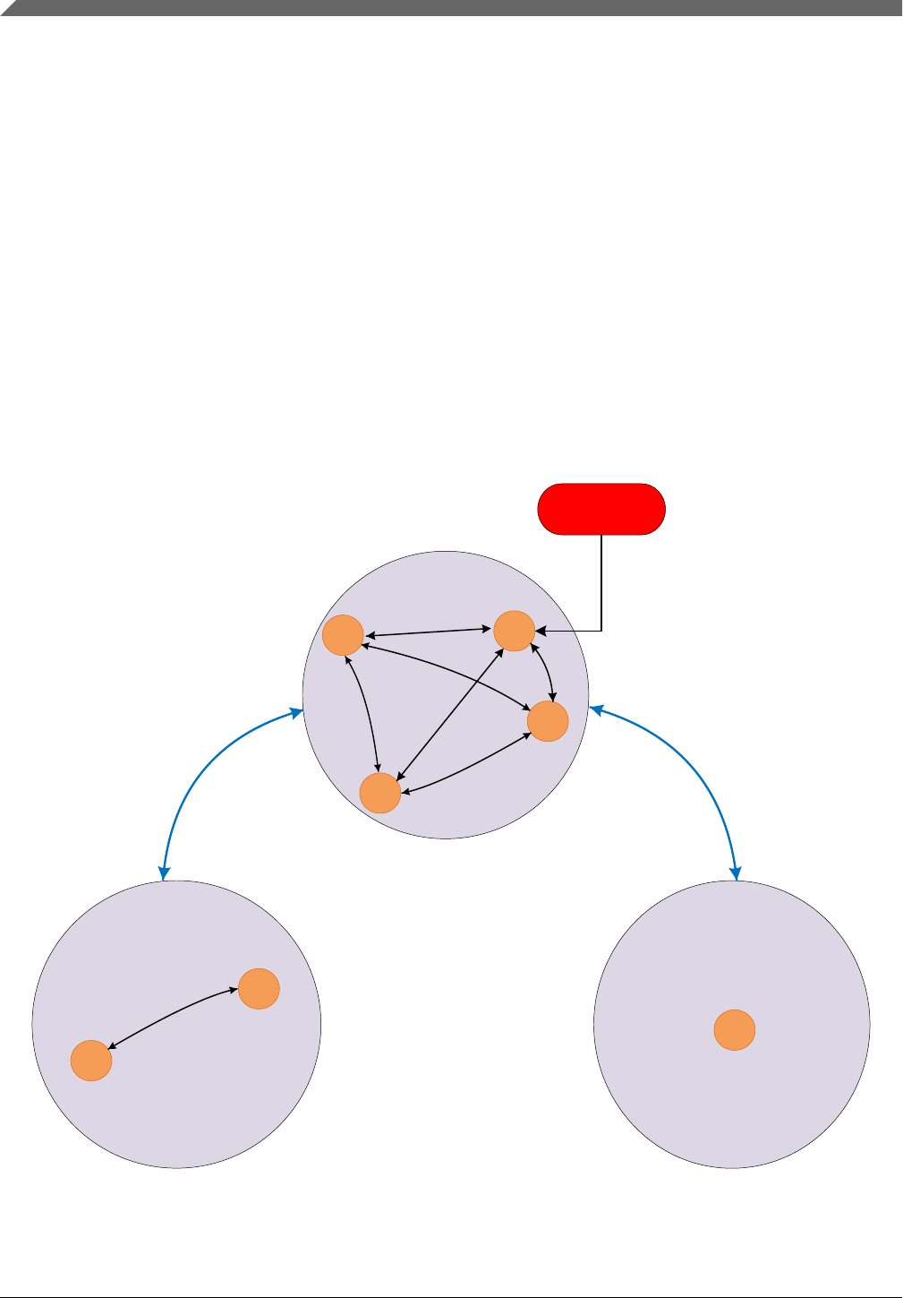
28.4 Functional description
28.4.1 SCG Clock Mode Transitions
The following figure shows the valid clock mode transitions supported by SCG.
Slow IRC (SIRC) boot mode is not supported on this device.
Reset
SIRC
RUN Valid
SCG Modes
HSRUN Valid
SCG Modes
FIRC
VLPRUN Valid
SCG Modes
SYS
PLL
SYS
PLL
SOSC
FIRC
SIRC
Run
Run
High Speed
Run
Very Low Power
SCG Valid Mode Transitions
Figure 28-1. SCG Valid Mode Transition Diagram
Functional description
S32K1xx Series Reference Manual, Rev. 7, 04/2018
586 NXP Semiconductors

NOTE
When a transition between run modes (RUN, HSRUN,
VLRUN) is required, the SCG should complete the switch to
the clock mode as defined in the SCG clock control register
first. Once the switch to the clock mode is completed, the
system can then initiate the request for the selected run mode.
For example, if a transition from RUN mode to VLRUN is
required, first complete any required clock change. Initiate the
VLRUN request after the clock change has completed.
The power modes are chip specific. For more details about power mode assignments, see
power management and system mode control information.
The modes of operation listed in the following table are the valid modes for this
implementation of the SCG.
Table 28-3. SCG modes of operation
Mode Description
System Oscillator Clock
(SOSC)
System Oscillator Clock (SOSC) mode is entered when all the following conditions occur:
• RUN MODE: 0001 is written to RCCR[SCS].
• SOSCEN = 1
• SOSCVLD = 1
In SOSC mode, SCGCLKOUT and system clocks are derived from the external System Oscillator
Clock (SOSC).
Slow Internal Reference
Clock (SIRC)
Slow Internal Reference Clock (SIRC) mode is entered when all the following conditions occur:
• RUN MODE: 0010 is written to RCCR[SCS].
VLRUN MODE: 0010 is written to VCCR[SCS] and 1 is written to SIRCCSR[SIRCLPEN].
• SIRCEN = 1
• SIRCVLD = 1
In SIRC mode, SCGCLKOUT and system clocks are derived from the slow internal reference clock.
Two frequency ranges are available for SIRC clock as described in the SIRCCFG[RANGE] register
definition. Changes to SIRC range settings will be ignored when SIRC clock is enabled.
Information regarding SIRC operation during normal and low power stop modes is found in the
"Stop" row of this table.
Fast Internal Reference
Clock (FIRC)
Fast Internal Reference Clock (FIRC) mode is the default clock mode of operation and is entered
when all the following conditions occur:
• RUN MODE: 0011 is written to RCCR[SCS].
HSRUN MODE: 0011 is written to HCCR[SCS].
• FIRCEN = 1
• FIRCVLD = 1
Table continues on the next page...
Chapter 28 System Clock Generator (SCG)
S32K1xx Series Reference Manual, Rev. 7, 04/2018
NXP Semiconductors 587

Table 28-3. SCG modes of operation (continued)
Mode Description
In FIRC mode, SCGCLKOUT and system clocks are derived from the fast internal reference clock.
Four frequency range settings are available for FIRC clock as described in the FIRC[RANGE]
register definition. Changes to FIRC range settings will be ignored when FIRC clock is enabled.
Sys PLL (SPLL) Sys PLL (SPLL) mode is entered when all the following conditions occur:
• RUN MODE: 0110 is written to RCCR[SCS].
HSRUN MODE: 0110 is written to HCCR[SCS].
• SPLLEN = 1
• SPLLVLD = 1
In SPLL mode, the SCGCLKOUT and system clocks are derived from the output of PLL which is
controlled by the System Oscillator (SOSC) clock. The selected PLL clock frequency locks to a
multiplication factor, as specified by its corresponding SCG_SPLLCFG[MULT], times the selected
PLL reference frequency. The PLL's programmable reference divider must be configured to produce
a valid PLL reference clock. This divide value is defined by the SCG_SPLLCFG[PREDIV] bits.
Stop Entered whenever the MCU enters a Stop state. The power modes are chip specific. For power
mode assignments, see the chapter that describes how modules are configured and SCG behaviour
during Stop recovery. Entering Stop mode, all SCG clock signals are static except the following
clocks which can continue to run and stay enabled in the following cases:
SIRCCLK is available in Normal Stop and VLPS mode when all the following conditions become
true:
• SIRCCSR[SIRCEN] = 1
• SIRCCSR[SIRCSTEN] = 1
• SIRCCSR[SIRCLPEN] = 1 in VLPS
Functional description
S32K1xx Series Reference Manual, Rev. 7, 04/2018
588 NXP Semiconductors

Chapter 29
Peripheral Clock Controller (PCC)
29.1 Chip-specific PCC information
For module specific clocking, see Module clocks.
NOTE
While changing a peripheral clock source, the corresponding
module should be disabled:
• Clock should be CGC gated
• Module should be disabled by MDIS bit, if available
After clock switching, the module should be soft reset using
soft reset bit (module software reset bit), if available.
SIM_SDID[FEATURES] bit field overrides the PCC.PR status for the chip.
29.1.1 PCC register information
The PCC Memory map shows a superset of registers implemented for the S32K1xx
series. Registers for instances unavailable in a particular variant are reserved.
S32K11x has two registers for CMU0 and CMU1 instances as described in the below
sections
29.1.1.1 PCC CMU0 Register (PCC_CMU0)
29.1.1.1.1 Offset
Register Offset
PCC_CMU0 F8h
S32K1xx Series Reference Manual, Rev. 7, 04/2018
NXP Semiconductors 589

29.1.1.1.2 Function
PCC Register
29.1.1.1.3 Diagram
Bits 31 30 29 28 27 26 25 24 23 22 21 20 19 18 17 16
R
P
R
CGC
Reserved
0
0
0
W
Reset 1 0 0 0 0 0 0 0 0 0 0 0 0 0 0 0
Bits 15 14 13 12 11 10 9 8 7 6 5 4 3 2 1 0
R 0 0 0
W
Reset 0 0 0 0 0 0 0 0 0 0 0 0 0 0 0 0
29.1.1.1.4 Fields
Field Function
31
PR
Present
This bit shows whether the peripheral is present on this device.
0b - Peripheral is not present.
1b - Peripheral is present.
30
CGC
Clock Gate Control
This read/write bit enables the clock for the peripheral.
0b - Clock disabled
1b - Clock enabled. The current clock selection and divider options are locked.
29
—
This read-only bit field is reserved. This bit can change values but is a don't-care.
28-27
—
This read-only bit field is reserved and always has the value 0.
26-24
—
This read-only bit field is reserved and always has the value 0.
23-4
—
This read-only bit field is reserved and always has the value 0.
3
—
This read-only bit field is reserved and always has the value 0.
2-0 This read-only bit field is reserved and always has the value 0.
Chip-specific PCC information
S32K1xx Series Reference Manual, Rev. 7, 04/2018
590 NXP Semiconductors

Field Function
—
29.1.1.2 PCC CMU1 Register (PCC_CMU1)
29.1.1.2.1 Offset
Register Offset
PCC_CMU1 FCh
29.1.1.2.2 Function
PCC Register
29.1.1.2.3 Diagram
Bits 31 30 29 28 27 26 25 24 23 22 21 20 19 18 17 16
R
P
R
CGC
Reserved
0
0
0
W
Reset 1 0 0 0 0 0 0 0 0 0 0 0 0 0 0 0
Bits 15 14 13 12 11 10 9 8 7 6 5 4 3 2 1 0
R 0 0 0
W
Reset 0 0 0 0 0 0 0 0 0 0 0 0 0 0 0 0
29.1.1.2.4 Fields
Field Function
31
PR
Present
This bit shows whether the peripheral is present on this device.
0b - Peripheral is not present.
1b - Peripheral is present.
30
CGC
Clock Gate Control
This read/write bit enables the clock for the peripheral.
Table continues on the next page...
Chapter 29 Peripheral Clock Controller (PCC)
S32K1xx Series Reference Manual, Rev. 7, 04/2018
NXP Semiconductors 591

Field Function
0b - Clock disabled
1b - Clock enabled. The current clock selection and divider options are locked.
29
—
This read-only bit field is reserved. This bit can change values but is a don't-care.
28-27
—
This read-only bit field is reserved and always has the value 0.
26-24
—
This read-only bit field is reserved and always has the value 0.
23-4
—
This read-only bit field is reserved and always has the value 0.
3
—
This read-only bit field is reserved and always has the value 0.
2-0
—
This read-only bit field is reserved and always has the value 0.
29.2 Introduction
The Peripheral Clock Control (PCC) module provides clock control and configuration for
on-chip peripherals. Each peripheral has its own clock control and configuration register.
29.3 Features
The PCC module enables software to configure the following clocking options for each
peripheral:
• Interface clock gating
• Functional clock source selection
• Functional clock divide values
Below is a block diagram of the PCC module:
Introduction
S32K1xx Series Reference Manual, Rev. 7, 04/2018
592 NXP Semiconductors
Interface clock control
Functional clock control (when available)
PCC
Clock option 1
Clock option 2
Clock option 6
Clock option 3
[PCS]
001
Clock option 4
Clock option 5
Clock option 7
to module
functional clock
Gate
[CGC]
Chip-specific clock
to module
interface clock
Divider
[FRAC, PCD]
OFF
External
clock
000
= Not all module functional clocks have a divider or an external clock option.
111
110
010
011
100
101
= Internal bus interface clock for module registers and logic
= Clock for module applications (Not all modules have functional clocks.)
Interface clock
Functional clock
Figure 29-1. PCC Block Diagram
29.4 Functional description
The PCC module provides on-chip peripherals (modules) their own dedicated PCC
registers for clock gating and configuration options. Each module's PCC register contains
a clock gating control bit (CGC) for the module's interface clock. Before a module can be
used, its interface clock must be enabled (CGC = 1) in the module's PCC register.
If a module has a functional clock, its PCC register may provide options for the clock
source, selected by programming the Peripheral Clock Select (PCS) field. Optionally, a
module may also have a clock divider, selected by programming the Peripheral Clock
Divider (PCD) field along with a Fraction (FRAC) field. Before configuring a functional
clock, the module's interface clock must be disabled (CGC = 0).
Chapter 29 Peripheral Clock Controller (PCC)
S32K1xx Series Reference Manual, Rev. 7, 04/2018
NXP Semiconductors 593

29.5 Memory map and register definition
Each module has its own dedicated PCC register, which controls the clock gating, clock
source and divider (when applicable) for that specific module. See each module's PCC
register for details.
PCC registers can be written only in supervisor mode using 32-bit accesses.
NOTE
To configure the clocking options available to a given module
or to modify an existing configuration, first disable the
module's interface clock by writing 0 to its CGC bit.
29.6 PCC register descriptions
29.6.1 PCC Memory map
PCC base address: 4006_5000h
Offset Register Width
(In bits)
Access Reset value
80h PCC FTFC Register (PCC_FTFC) 32 RW C000_0000h
84h PCC DMAMUX Register (PCC_DMAMUX) 32 RW 8000_0000h
90h PCC FlexCAN0 Register (PCC_FlexCAN0) 32 RW 8000_0000h
94h PCC FlexCAN1 Register (PCC_FlexCAN1) 32 RW 8000_0000h
98h PCC FTM3 Register (PCC_FTM3) 32 RW 8000_0000h
9Ch PCC ADC1 Register (PCC_ADC1) 32 RW 8000_0000h
ACh PCC FlexCAN2 Register (PCC_FlexCAN2) 32 RW 8000_0000h
B0h PCC LPSPI0 Register (PCC_LPSPI0) 32 RW 8000_0000h
B4h PCC LPSPI1 Register (PCC_LPSPI1) 32 RW 8000_0000h
B8h PCC LPSPI2 Register (PCC_LPSPI2) 32 RW 8000_0000h
C4h PCC PDB1 Register (PCC_PDB1) 32 RW 8000_0000h
C8h PCC CRC Register (PCC_CRC) 32 RW 8000_0000h
D8h PCC PDB0 Register (PCC_PDB0) 32 RW 8000_0000h
DCh PCC LPIT Register (PCC_LPIT) 32 RW 8000_0000h
E0h PCC FTM0 Register (PCC_FTM0) 32 RW 8000_0000h
E4h PCC FTM1 Register (PCC_FTM1) 32 RW 8000_0000h
Table continues on the next page...
Memory map and register definition
S32K1xx Series Reference Manual, Rev. 7, 04/2018
594 NXP Semiconductors

Offset Register Width
(In bits)
Access Reset value
E8h PCC FTM2 Register (PCC_FTM2) 32 RW 8000_0000h
ECh PCC ADC0 Register (PCC_ADC0) 32 RW 8000_0000h
F4h PCC RTC Register (PCC_RTC) 32 RW 8000_0000h
100h PCC LPTMR0 Register (PCC_LPTMR0) 32 RW 8000_0000h
124h PCC PORTA Register (PCC_PORTA) 32 RW 8000_0000h
128h PCC PORTB Register (PCC_PORTB) 32 RW 8000_0000h
12Ch PCC PORTC Register (PCC_PORTC) 32 RW 8000_0000h
130h PCC PORTD Register (PCC_PORTD) 32 RW 8000_0000h
134h PCC PORTE Register (PCC_PORTE) 32 RW 8000_0000h
150h PCC SAI0 Register (PCC_SAI0) 32 RW 8000_0000h
154h PCC SAI1 Register (PCC_SAI1) 32 RW 8000_0000h
168h PCC FlexIO Register (PCC_FlexIO) 32 RW 8000_0000h
184h PCC EWM Register (PCC_EWM) 32 RW 8000_0000h
198h PCC LPI2C0 Register (PCC_LPI2C0) 32 RW 8000_0000h
19Ch PCC LPI2C1 Register (PCC_LPI2C1) 32 RW 8000_0000h
1A8h PCC LPUART0 Register (PCC_LPUART0) 32 RW 8000_0000h
1ACh PCC LPUART1 Register (PCC_LPUART1) 32 RW 8000_0000h
1B0h PCC LPUART2 Register (PCC_LPUART2) 32 RW 8000_0000h
1B8h PCC FTM4 Register (PCC_FTM4) 32 RW 8000_0000h
1BCh PCC FTM5 Register (PCC_FTM5) 32 RW 8000_0000h
1C0h PCC FTM6 Register (PCC_FTM6) 32 RW 8000_0000h
1C4h PCC FTM7 Register (PCC_FTM7) 32 RW 8000_0000h
1CCh PCC CMP0 Register (PCC_CMP0) 32 RW 8000_0000h
1D8h PCC QSPI Register (PCC_QSPI) 32 RW 8000_0000h
1E4h PCC ENET Register (PCC_ENET) 32 RW 8000_0000h
29.6.2 PCC FTFC Register (PCC_FTFC)
29.6.2.1 Offset
Register Offset
PCC_FTFC 80h
Chapter 29 Peripheral Clock Controller (PCC)
S32K1xx Series Reference Manual, Rev. 7, 04/2018
NXP Semiconductors 595

29.6.2.2 Function
PCC Register
29.6.2.3 Diagram
Bits 31 30 29 28 27 26 25 24 23 22 21 20 19 18 17 16
R
P
R
CGC
Reserved
0
0
0
W
Reset 1 1 0 0 0 0 0 0 0 0 0 0 0 0 0 0
Bits 15 14 13 12 11 10 9 8 7 6 5 4 3 2 1 0
R 0 0 0
W
Reset 0 0 0 0 0 0 0 0 0 0 0 0 0 0 0 0
29.6.2.4 Fields
Field Function
31
PR
Present
This bit shows whether the peripheral is present on this device.
0b - Peripheral is not present.
1b - Peripheral is present.
30
CGC
Clock Gate Control
This read/write bit enables the clock for the peripheral.
0b - Clock disabled
1b - Clock enabled. The current clock selection and divider options are locked.
29
—
This read-only bit field is reserved. This bit can change values but is a don't-care.
28-27
—
This read-only bit field is reserved and always has the value 0.
26-24
—
This read-only bit field is reserved and always has the value 0.
23-4
—
This read-only bit field is reserved and always has the value 0.
3
—
This read-only bit field is reserved and always has the value 0.
Table continues on the next page...
PCC register descriptions
S32K1xx Series Reference Manual, Rev. 7, 04/2018
596 NXP Semiconductors

Field Function
2-0
—
This read-only bit field is reserved and always has the value 0.
29.6.3 PCC DMAMUX Register (PCC_DMAMUX)
29.6.3.1 Offset
Register Offset
PCC_DMAMUX 84h
29.6.3.2 Function
PCC Register
29.6.3.3 Diagram
Bits 31 30 29 28 27 26 25 24 23 22 21 20 19 18 17 16
R
P
R
CGC
Reserved
0
0
0
W
Reset 1 0 0 0 0 0 0 0 0 0 0 0 0 0 0 0
Bits 15 14 13 12 11 10 9 8 7 6 5 4 3 2 1 0
R 0 0 0
W
Reset 0 0 0 0 0 0 0 0 0 0 0 0 0 0 0 0
29.6.3.4 Fields
Field Function
31
PR
Present
This bit shows whether the peripheral is present on this device.
Table continues on the next page...
Chapter 29 Peripheral Clock Controller (PCC)
S32K1xx Series Reference Manual, Rev. 7, 04/2018
NXP Semiconductors 597

Field Function
0b - Peripheral is not present.
1b - Peripheral is present.
30
CGC
Clock Gate Control
This read/write bit enables the clock for the peripheral.
0b - Clock disabled
1b - Clock enabled. The current clock selection and divider options are locked.
29
—
This read-only bit field is reserved. This bit can change values but is a don't-care.
28-27
—
This read-only bit field is reserved and always has the value 0.
26-24
—
This read-only bit field is reserved and always has the value 0.
23-4
—
This read-only bit field is reserved and always has the value 0.
3
—
This read-only bit field is reserved and always has the value 0.
2-0
—
This read-only bit field is reserved and always has the value 0.
29.6.4 PCC FlexCAN0 Register (PCC_FlexCAN0)
29.6.4.1 Offset
Register Offset
PCC_FlexCAN0 90h
29.6.4.2 Function
PCC Register
PCC register descriptions
S32K1xx Series Reference Manual, Rev. 7, 04/2018
598 NXP Semiconductors

29.6.4.3 Diagram
Bits 31 30 29 28 27 26 25 24 23 22 21 20 19 18 17 16
R
P
R
CGC
Reserved
0
0
0
W
Reset 1 0 0 0 0 0 0 0 0 0 0 0 0 0 0 0
Bits 15 14 13 12 11 10 9 8 7 6 5 4 3 2 1 0
R 0 0 0
W
Reset 0 0 0 0 0 0 0 0 0 0 0 0 0 0 0 0
29.6.4.4 Fields
Field Function
31
PR
Present
This bit shows whether the peripheral is present on this device.
0b - Peripheral is not present.
1b - Peripheral is present.
30
CGC
Clock Gate Control
This read/write bit enables the clock for the peripheral.
0b - Clock disabled
1b - Clock enabled. The current clock selection and divider options are locked.
29
—
This read-only bit field is reserved. This bit can change values but is a don't-care.
28-27
—
This read-only bit field is reserved and always has the value 0.
26-24
—
This read-only bit field is reserved and always has the value 0.
23-4
—
This read-only bit field is reserved and always has the value 0.
3
—
This read-only bit field is reserved and always has the value 0.
2-0
—
This read-only bit field is reserved and always has the value 0.
Chapter 29 Peripheral Clock Controller (PCC)
S32K1xx Series Reference Manual, Rev. 7, 04/2018
NXP Semiconductors 599

29.6.5 PCC FlexCAN1 Register (PCC_FlexCAN1)
29.6.5.1 Offset
Register Offset
PCC_FlexCAN1 94h
29.6.5.2 Function
PCC Register
29.6.5.3 Diagram
Bits 31 30 29 28 27 26 25 24 23 22 21 20 19 18 17 16
R
P
R
CGC
Reserved
0
0
0
W
Reset 1 0 0 0 0 0 0 0 0 0 0 0 0 0 0 0
Bits 15 14 13 12 11 10 9 8 7 6 5 4 3 2 1 0
R 0 0 0
W
Reset 0 0 0 0 0 0 0 0 0 0 0 0 0 0 0 0
29.6.5.4 Fields
Field Function
31
PR
Present
This bit shows whether the peripheral is present on this device.
0b - Peripheral is not present.
1b - Peripheral is present.
30
CGC
Clock Gate Control
This read/write bit enables the clock for the peripheral.
Table continues on the next page...
PCC register descriptions
S32K1xx Series Reference Manual, Rev. 7, 04/2018
600 NXP Semiconductors

Field Function
0b - Clock disabled
1b - Clock enabled. The current clock selection and divider options are locked.
29
—
This read-only bit field is reserved. This bit can change values but is a don't-care.
28-27
—
This read-only bit field is reserved and always has the value 0.
26-24
—
This read-only bit field is reserved and always has the value 0.
23-4
—
This read-only bit field is reserved and always has the value 0.
3
—
This read-only bit field is reserved and always has the value 0.
2-0
—
This read-only bit field is reserved and always has the value 0.
29.6.6 PCC FTM3 Register (PCC_FTM3)
29.6.6.1 Offset
Register Offset
PCC_FTM3 98h
29.6.6.2 Function
PCC Register
Chapter 29 Peripheral Clock Controller (PCC)
S32K1xx Series Reference Manual, Rev. 7, 04/2018
NXP Semiconductors 601

29.6.6.3 Diagram
Bits 31 30 29 28 27 26 25 24 23 22 21 20 19 18 17 16
R
P
R
CGC
Reserved
0
PC
S
0
W
Reset 1 0 0 0 0 0 0 0 0 0 0 0 0 0 0 0
Bits 15 14 13 12 11 10 9 8 7 6 5 4 3 2 1 0
R 0 0 0
W
Reset 0 0 0 0 0 0 0 0 0 0 0 0 0 0 0 0
29.6.6.4 Fields
Field Function
31
PR
Present
This bit shows whether the peripheral is present on this device.
0b - Peripheral is not present.
1b - Peripheral is present.
30
CGC
Clock Gate Control
This read/write bit enables the clock for the peripheral.
0b - Clock disabled
1b - Clock enabled. The current clock selection and divider options are locked.
29
—
This read-only bit field is reserved. This bit can change values but is a don't-care.
28-27
—
This read-only bit field is reserved and always has the value 0.
26-24
PCS
Peripheral Clock Source Select
This read/write bit field is used for peripherals that support various clock selections.
This field can be written only when the clock is disabled (CGC = 0).
000b - Clock is off. An external clock can be enabled for this peripheral.
001b - Clock option 1
010b - Clock option 2
011b - Clock option 3
100b - Clock option 4
101b - Clock option 5
110b - Clock option 6
111b - Clock option 7
23-4 This read-only bit field is reserved and always has the value 0.
Table continues on the next page...
PCC register descriptions
S32K1xx Series Reference Manual, Rev. 7, 04/2018
602 NXP Semiconductors

Field Function
—
3
—
This read-only bit field is reserved and always has the value 0.
2-0
—
This read-only bit field is reserved and always has the value 0.
29.6.7 PCC ADC1 Register (PCC_ADC1)
29.6.7.1 Offset
Register Offset
PCC_ADC1 9Ch
29.6.7.2 Function
PCC Register
29.6.7.3 Diagram
Bits 31 30 29 28 27 26 25 24 23 22 21 20 19 18 17 16
R
P
R
CGC
Reserved
0
PC
S
0
W
Reset 1 0 0 0 0 0 0 0 0 0 0 0 0 0 0 0
Bits 15 14 13 12 11 10 9 8 7 6 5 4 3 2 1 0
R 0 0 0
W
Reset 0 0 0 0 0 0 0 0 0 0 0 0 0 0 0 0
Chapter 29 Peripheral Clock Controller (PCC)
S32K1xx Series Reference Manual, Rev. 7, 04/2018
NXP Semiconductors 603

29.6.7.4 Fields
Field Function
31
PR
Present
This bit shows whether the peripheral is present on this device.
0b - Peripheral is not present.
1b - Peripheral is present.
30
CGC
Clock Gate Control
This read/write bit enables the clock for the peripheral.
0b - Clock disabled
1b - Clock enabled. The current clock selection and divider options are locked.
29
—
This read-only bit field is reserved. This bit can change values but is a don't-care.
28-27
—
This read-only bit field is reserved and always has the value 0.
26-24
PCS
Peripheral Clock Source Select
This read/write bit field is used for peripherals that support various clock selections.
This field can be written only when the clock is disabled (CGC = 0).
000b - Clock is off.
001b - Clock option 1
010b - Clock option 2
011b - Clock option 3
100b - Clock option 4
101b - Clock option 5
110b - Clock option 6
111b - Clock option 7
23-4
—
This read-only bit field is reserved and always has the value 0.
3
—
This read-only bit field is reserved and always has the value 0.
2-0
—
This read-only bit field is reserved and always has the value 0.
29.6.8 PCC FlexCAN2 Register (PCC_FlexCAN2)
29.6.8.1 Offset
Register Offset
PCC_FlexCAN2 ACh
PCC register descriptions
S32K1xx Series Reference Manual, Rev. 7, 04/2018
604 NXP Semiconductors

29.6.8.2 Function
PCC Register
29.6.8.3 Diagram
Bits 31 30 29 28 27 26 25 24 23 22 21 20 19 18 17 16
R
P
R
CGC
Reserved
0
0
0
W
Reset 1 0 0 0 0 0 0 0 0 0 0 0 0 0 0 0
Bits 15 14 13 12 11 10 9 8 7 6 5 4 3 2 1 0
R 0 0 0
W
Reset 0 0 0 0 0 0 0 0 0 0 0 0 0 0 0 0
29.6.8.4 Fields
Field Function
31
PR
Present
This bit shows whether the peripheral is present on this device.
0b - Peripheral is not present.
1b - Peripheral is present.
30
CGC
Clock Gate Control
This read/write bit enables the clock for the peripheral.
0b - Clock disabled
1b - Clock enabled. The current clock selection and divider options are locked.
29
—
This read-only bit field is reserved. This bit can change values but is a don't-care.
28-27
—
This read-only bit field is reserved and always has the value 0.
26-24
—
This read-only bit field is reserved and always has the value 0.
23-4
—
This read-only bit field is reserved and always has the value 0.
3 This read-only bit field is reserved and always has the value 0.
Table continues on the next page...
Chapter 29 Peripheral Clock Controller (PCC)
S32K1xx Series Reference Manual, Rev. 7, 04/2018
NXP Semiconductors 605

Field Function
—
2-0
—
This read-only bit field is reserved and always has the value 0.
29.6.9 PCC LPSPI0 Register (PCC_LPSPI0)
29.6.9.1 Offset
Register Offset
PCC_LPSPI0 B0h
29.6.9.2 Function
PCC Register
29.6.9.3 Diagram
Bits 31 30 29 28 27 26 25 24 23 22 21 20 19 18 17 16
R
P
R
CGC
Reserved
0
PC
S
0
W
Reset 1 0 0 0 0 0 0 0 0 0 0 0 0 0 0 0
Bits 15 14 13 12 11 10 9 8 7 6 5 4 3 2 1 0
R 0 0 0
W
Reset 0 0 0 0 0 0 0 0 0 0 0 0 0 0 0 0
29.6.9.4 Fields
Field Function
31 Present
Table continues on the next page...
PCC register descriptions
S32K1xx Series Reference Manual, Rev. 7, 04/2018
606 NXP Semiconductors

Field Function
PR This bit shows whether the peripheral is present on this device.
0b - Peripheral is not present.
1b - Peripheral is present.
30
CGC
Clock Gate Control
This read/write bit enables the clock for the peripheral.
0b - Clock disabled
1b - Clock enabled. The current clock selection and divider options are locked.
29
—
This read-only bit field is reserved. This bit can change values but is a don't-care.
28-27
—
This read-only bit field is reserved and always has the value 0.
26-24
PCS
Peripheral Clock Source Select
This read/write bit field is used for peripherals that support various clock selections.
This field can be written only when the clock is disabled (CGC = 0).
000b - Clock is off.
001b - Clock option 1
010b - Clock option 2
011b - Clock option 3
100b - Clock option 4
101b - Clock option 5
110b - Clock option 6
111b - Clock option 7
23-4
—
This read-only bit field is reserved and always has the value 0.
3
—
This read-only bit field is reserved and always has the value 0.
2-0
—
This read-only bit field is reserved and always has the value 0.
29.6.10 PCC LPSPI1 Register (PCC_LPSPI1)
29.6.10.1 Offset
Register Offset
PCC_LPSPI1 B4h
Chapter 29 Peripheral Clock Controller (PCC)
S32K1xx Series Reference Manual, Rev. 7, 04/2018
NXP Semiconductors 607

29.6.10.2 Function
PCC Register
29.6.10.3 Diagram
Bits 31 30 29 28 27 26 25 24 23 22 21 20 19 18 17 16
R
P
R
CGC
Reserved
0
PC
S
0
W
Reset 1 0 0 0 0 0 0 0 0 0 0 0 0 0 0 0
Bits 15 14 13 12 11 10 9 8 7 6 5 4 3 2 1 0
R 0 0 0
W
Reset 0 0 0 0 0 0 0 0 0 0 0 0 0 0 0 0
29.6.10.4 Fields
Field Function
31
PR
Present
This bit shows whether the peripheral is present on this device.
0b - Peripheral is not present.
1b - Peripheral is present.
30
CGC
Clock Gate Control
This read/write bit enables the clock for the peripheral.
0b - Clock disabled
1b - Clock enabled. The current clock selection and divider options are locked.
29
—
This read-only bit field is reserved. This bit can change values but is a don't-care.
28-27
—
This read-only bit field is reserved and always has the value 0.
26-24
PCS
Peripheral Clock Source Select
This read/write bit field is used for peripherals that support various clock selections.
This field can be written only when the clock is disabled (CGC = 0).
000b - Clock is off.
001b - Clock option 1
010b - Clock option 2
011b - Clock option 3
Table continues on the next page...
PCC register descriptions
S32K1xx Series Reference Manual, Rev. 7, 04/2018
608 NXP Semiconductors

Field Function
100b - Clock option 4
101b - Clock option 5
110b - Clock option 6
111b - Clock option 7
23-4
—
This read-only bit field is reserved and always has the value 0.
3
—
This read-only bit field is reserved and always has the value 0.
2-0
—
This read-only bit field is reserved and always has the value 0.
29.6.11 PCC LPSPI2 Register (PCC_LPSPI2)
29.6.11.1 Offset
Register Offset
PCC_LPSPI2 B8h
29.6.11.2 Function
PCC Register
29.6.11.3 Diagram
Bits 31 30 29 28 27 26 25 24 23 22 21 20 19 18 17 16
R
P
R
CGC
Reserved
0
PC
S
0
W
Reset 1 0 0 0 0 0 0 0 0 0 0 0 0 0 0 0
Bits 15 14 13 12 11 10 9 8 7 6 5 4 3 2 1 0
R 0 0 0
W
Reset 0 0 0 0 0 0 0 0 0 0 0 0 0 0 0 0
Chapter 29 Peripheral Clock Controller (PCC)
S32K1xx Series Reference Manual, Rev. 7, 04/2018
NXP Semiconductors 609

29.6.11.4 Fields
Field Function
31
PR
Present
This bit shows whether the peripheral is present on this device.
0b - Peripheral is not present.
1b - Peripheral is present.
30
CGC
Clock Gate Control
This read/write bit enables the clock for the peripheral.
0b - Clock disabled
1b - Clock enabled. The current clock selection and divider options are locked.
29
—
This read-only bit field is reserved. This bit can change values but is a don't-care.
28-27
—
This read-only bit field is reserved and always has the value 0.
26-24
PCS
Peripheral Clock Source Select
This read/write bit field is used for peripherals that support various clock selections.
This field can be written only when the clock is disabled (CGC = 0).
000b - Clock is off.
001b - Clock option 1
010b - Clock option 2
011b - Clock option 3
100b - Clock option 4
101b - Clock option 5
110b - Clock option 6
111b - Clock option 7
23-4
—
This read-only bit field is reserved and always has the value 0.
3
—
This read-only bit field is reserved and always has the value 0.
2-0
—
This read-only bit field is reserved and always has the value 0.
29.6.12 PCC PDB1 Register (PCC_PDB1)
29.6.12.1 Offset
Register Offset
PCC_PDB1 C4h
PCC register descriptions
S32K1xx Series Reference Manual, Rev. 7, 04/2018
610 NXP Semiconductors
29.6.12.2 Function
PCC Register
29.6.12.3 Diagram
Bits 31 30 29 28 27 26 25 24 23 22 21 20 19 18 17 16
R
P
R
CGC
Reserved
0
0
0
W
Reset 1 0 0 0 0 0 0 0 0 0 0 0 0 0 0 0
Bits 15 14 13 12 11 10 9 8 7 6 5 4 3 2 1 0
R 0 0 0
W
Reset 0 0 0 0 0 0 0 0 0 0 0 0 0 0 0 0
29.6.12.4 Fields
Field Function
31
PR
Present
This bit shows whether the peripheral is present on this device.
0b - Peripheral is not present.
1b - Peripheral is present.
30
CGC
Clock Gate Control
This read/write bit enables the clock for the peripheral.
0b - Clock disabled
1b - Clock enabled. The current clock selection and divider options are locked.
29
—
This read-only bit field is reserved. This bit can change values but is a don't-care.
28-27
—
This read-only bit field is reserved and always has the value 0.
26-24
—
This read-only bit field is reserved and always has the value 0.
23-4
—
This read-only bit field is reserved and always has the value 0.
Table continues on the next page...
Chapter 29 Peripheral Clock Controller (PCC)
S32K1xx Series Reference Manual, Rev. 7, 04/2018
NXP Semiconductors 611

Field Function
3
—
This read-only bit field is reserved and always has the value 0.
2-0
—
This read-only bit field is reserved and always has the value 0.
29.6.13 PCC CRC Register (PCC_CRC)
29.6.13.1 Offset
Register Offset
PCC_CRC C8h
29.6.13.2 Function
PCC Register
29.6.13.3 Diagram
Bits 31 30 29 28 27 26 25 24 23 22 21 20 19 18 17 16
R
P
R
CGC
Reserved
0
0
0
W
Reset 1 0 0 0 0 0 0 0 0 0 0 0 0 0 0 0
Bits 15 14 13 12 11 10 9 8 7 6 5 4 3 2 1 0
R 0 0 0
W
Reset 0 0 0 0 0 0 0 0 0 0 0 0 0 0 0 0
PCC register descriptions
S32K1xx Series Reference Manual, Rev. 7, 04/2018
612 NXP Semiconductors

29.6.13.4 Fields
Field Function
31
PR
Present
This bit shows whether the peripheral is present on this device.
0b - Peripheral is not present.
1b - Peripheral is present.
30
CGC
Clock Gate Control
This read/write bit enables the clock for the peripheral.
0b - Clock disabled
1b - Clock enabled. The current clock selection and divider options are locked.
29
—
This read-only bit field is reserved. This bit can change values but is a don't-care.
28-27
—
This read-only bit field is reserved and always has the value 0.
26-24
—
This read-only bit field is reserved and always has the value 0.
23-4
—
This read-only bit field is reserved and always has the value 0.
3
—
This read-only bit field is reserved and always has the value 0.
2-0
—
This read-only bit field is reserved and always has the value 0.
29.6.14 PCC PDB0 Register (PCC_PDB0)
29.6.14.1 Offset
Register Offset
PCC_PDB0 D8h
29.6.14.2 Function
PCC Register
Chapter 29 Peripheral Clock Controller (PCC)
S32K1xx Series Reference Manual, Rev. 7, 04/2018
NXP Semiconductors 613

29.6.14.3 Diagram
Bits 31 30 29 28 27 26 25 24 23 22 21 20 19 18 17 16
R
P
R
CGC
Reserved
0
0
0
W
Reset 1 0 0 0 0 0 0 0 0 0 0 0 0 0 0 0
Bits 15 14 13 12 11 10 9 8 7 6 5 4 3 2 1 0
R 0 0 0
W
Reset 0 0 0 0 0 0 0 0 0 0 0 0 0 0 0 0
29.6.14.4 Fields
Field Function
31
PR
Present
This bit shows whether the peripheral is present on this device.
0b - Peripheral is not present.
1b - Peripheral is present.
30
CGC
Clock Gate Control
This read/write bit enables the clock for the peripheral.
0b - Clock disabled
1b - Clock enabled. The current clock selection and divider options are locked.
29
—
This read-only bit field is reserved. This bit can change values but is a don't-care.
28-27
—
This read-only bit field is reserved and always has the value 0.
26-24
—
This read-only bit field is reserved and always has the value 0.
23-4
—
This read-only bit field is reserved and always has the value 0.
3
—
This read-only bit field is reserved and always has the value 0.
2-0
—
This read-only bit field is reserved and always has the value 0.
PCC register descriptions
S32K1xx Series Reference Manual, Rev. 7, 04/2018
614 NXP Semiconductors

29.6.15 PCC LPIT Register (PCC_LPIT)
29.6.15.1 Offset
Register Offset
PCC_LPIT DCh
29.6.15.2 Function
PCC Register
29.6.15.3 Diagram
Bits 31 30 29 28 27 26 25 24 23 22 21 20 19 18 17 16
R
P
R
CGC
Reserved
0
PC
S
0
W
Reset 1 0 0 0 0 0 0 0 0 0 0 0 0 0 0 0
Bits 15 14 13 12 11 10 9 8 7 6 5 4 3 2 1 0
R 0 0 0
W
Reset 0 0 0 0 0 0 0 0 0 0 0 0 0 0 0 0
29.6.15.4 Fields
Field Function
31
PR
Present
This bit shows whether the peripheral is present on this device.
0b - Peripheral is not present.
1b - Peripheral is present.
30
CGC
Clock Gate Control
This read/write bit enables the clock for the peripheral.
Table continues on the next page...
Chapter 29 Peripheral Clock Controller (PCC)
S32K1xx Series Reference Manual, Rev. 7, 04/2018
NXP Semiconductors 615

Field Function
0b - Clock disabled
1b - Clock enabled. The current clock selection and divider options are locked.
29
—
This read-only bit field is reserved. This bit can change values but is a don't-care.
28-27
—
This read-only bit field is reserved and always has the value 0.
26-24
PCS
Peripheral Clock Source Select
This read/write bit field is used for peripherals that support various clock selections.
This field can be written only when the clock is disabled (CGC = 0).
000b - Clock is off.
001b - Clock option 1
010b - Clock option 2
011b - Clock option 3
100b - Clock option 4
101b - Clock option 5
110b - Clock option 6
111b - Clock option 7
23-4
—
This read-only bit field is reserved and always has the value 0.
3
—
This read-only bit field is reserved and always has the value 0.
2-0
—
This read-only bit field is reserved and always has the value 0.
29.6.16 PCC FTM0 Register (PCC_FTM0)
29.6.16.1 Offset
Register Offset
PCC_FTM0 E0h
29.6.16.2 Function
PCC Register
PCC register descriptions
S32K1xx Series Reference Manual, Rev. 7, 04/2018
616 NXP Semiconductors

29.6.16.3 Diagram
Bits 31 30 29 28 27 26 25 24 23 22 21 20 19 18 17 16
R
P
R
CGC
Reserved
0
PC
S
0
W
Reset 1 0 0 0 0 0 0 0 0 0 0 0 0 0 0 0
Bits 15 14 13 12 11 10 9 8 7 6 5 4 3 2 1 0
R 0 0 0
W
Reset 0 0 0 0 0 0 0 0 0 0 0 0 0 0 0 0
29.6.16.4 Fields
Field Function
31
PR
Present
This bit shows whether the peripheral is present on this device.
0b - Peripheral is not present.
1b - Peripheral is present.
30
CGC
Clock Gate Control
This read/write bit enables the clock for the peripheral.
0b - Clock disabled
1b - Clock enabled. The current clock selection and divider options are locked.
29
—
This read-only bit field is reserved. This bit can change values but is a don't-care.
28-27
—
This read-only bit field is reserved and always has the value 0.
26-24
PCS
Peripheral Clock Source Select
This read/write bit field is used for peripherals that support various clock selections.
This field can be written only when the clock is disabled (CGC = 0).
000b - Clock is off. An external clock can be enabled for this peripheral.
001b - Clock option 1
010b - Clock option 2
011b - Clock option 3
100b - Clock option 4
101b - Clock option 5
110b - Clock option 6
111b - Clock option 7
23-4 This read-only bit field is reserved and always has the value 0.
Table continues on the next page...
Chapter 29 Peripheral Clock Controller (PCC)
S32K1xx Series Reference Manual, Rev. 7, 04/2018
NXP Semiconductors 617

Field Function
—
3
—
This read-only bit field is reserved and always has the value 0.
2-0
—
This read-only bit field is reserved and always has the value 0.
29.6.17 PCC FTM1 Register (PCC_FTM1)
29.6.17.1 Offset
Register Offset
PCC_FTM1 E4h
29.6.17.2 Function
PCC Register
29.6.17.3 Diagram
Bits 31 30 29 28 27 26 25 24 23 22 21 20 19 18 17 16
R
P
R
CGC
Reserved
0
PC
S
0
W
Reset 1 0 0 0 0 0 0 0 0 0 0 0 0 0 0 0
Bits 15 14 13 12 11 10 9 8 7 6 5 4 3 2 1 0
R 0 0 0
W
Reset 0 0 0 0 0 0 0 0 0 0 0 0 0 0 0 0
PCC register descriptions
S32K1xx Series Reference Manual, Rev. 7, 04/2018
618 NXP Semiconductors

29.6.17.4 Fields
Field Function
31
PR
Present
This bit shows whether the peripheral is present on this device.
0b - Peripheral is not present.
1b - Peripheral is present.
30
CGC
Clock Gate Control
This read/write bit enables the clock for the peripheral.
0b - Clock disabled
1b - Clock enabled. The current clock selection and divider options are locked.
29
—
This read-only bit field is reserved. This bit can change values but is a don't-care.
28-27
—
This read-only bit field is reserved and always has the value 0.
26-24
PCS
Peripheral Clock Source Select
This read/write bit field is used for peripherals that support various clock selections.
This field can be written only when the clock is disabled (CGC = 0).
000b - Clock is off. An external clock can be enabled for this peripheral.
001b - Clock option 1
010b - Clock option 2
011b - Clock option 3
100b - Clock option 4
101b - Clock option 5
110b - Clock option 6
111b - Clock option 7
23-4
—
This read-only bit field is reserved and always has the value 0.
3
—
This read-only bit field is reserved and always has the value 0.
2-0
—
This read-only bit field is reserved and always has the value 0.
29.6.18 PCC FTM2 Register (PCC_FTM2)
29.6.18.1 Offset
Register Offset
PCC_FTM2 E8h
Chapter 29 Peripheral Clock Controller (PCC)
S32K1xx Series Reference Manual, Rev. 7, 04/2018
NXP Semiconductors 619

29.6.18.2 Function
PCC Register
29.6.18.3 Diagram
Bits 31 30 29 28 27 26 25 24 23 22 21 20 19 18 17 16
R
P
R
CGC
Reserved
0
PC
S
0
W
Reset 1 0 0 0 0 0 0 0 0 0 0 0 0 0 0 0
Bits 15 14 13 12 11 10 9 8 7 6 5 4 3 2 1 0
R 0 0 0
W
Reset 0 0 0 0 0 0 0 0 0 0 0 0 0 0 0 0
29.6.18.4 Fields
Field Function
31
PR
Present
This bit shows whether the peripheral is present on this device.
0b - Peripheral is not present.
1b - Peripheral is present.
30
CGC
Clock Gate Control
This read/write bit enables the clock for the peripheral.
0b - Clock disabled
1b - Clock enabled. The current clock selection and divider options are locked.
29
—
This read-only bit field is reserved. This bit can change values but is a don't-care.
28-27
—
This read-only bit field is reserved and always has the value 0.
26-24
PCS
Peripheral Clock Source Select
This read/write bit field is used for peripherals that support various clock selections.
This field can be written only when the clock is disabled (CGC = 0).
000b - Clock is off. An external clock can be enabled for this peripheral.
001b - Clock option 1
Table continues on the next page...
PCC register descriptions
S32K1xx Series Reference Manual, Rev. 7, 04/2018
620 NXP Semiconductors

Field Function
010b - Clock option 2
011b - Clock option 3
100b - Clock option 4
101b - Clock option 5
110b - Clock option 6
111b - Clock option 7
23-4
—
This read-only bit field is reserved and always has the value 0.
3
—
This read-only bit field is reserved and always has the value 0.
2-0
—
This read-only bit field is reserved and always has the value 0.
29.6.19 PCC ADC0 Register (PCC_ADC0)
29.6.19.1 Offset
Register Offset
PCC_ADC0 ECh
29.6.19.2 Function
PCC Register
Chapter 29 Peripheral Clock Controller (PCC)
S32K1xx Series Reference Manual, Rev. 7, 04/2018
NXP Semiconductors 621

29.6.19.3 Diagram
Bits 31 30 29 28 27 26 25 24 23 22 21 20 19 18 17 16
R
P
R
CGC
Reserved
0
PC
S
0
W
Reset 1 0 0 0 0 0 0 0 0 0 0 0 0 0 0 0
Bits 15 14 13 12 11 10 9 8 7 6 5 4 3 2 1 0
R 0 0 0
W
Reset 0 0 0 0 0 0 0 0 0 0 0 0 0 0 0 0
29.6.19.4 Fields
Field Function
31
PR
Present
This bit shows whether the peripheral is present on this device.
0b - Peripheral is not present.
1b - Peripheral is present.
30
CGC
Clock Gate Control
This read/write bit enables the clock for the peripheral.
0b - Clock disabled
1b - Clock enabled. The current clock selection and divider options are locked.
29
—
This read-only bit field is reserved. This bit can change values but is a don't-care.
28-27
—
This read-only bit field is reserved and always has the value 0.
26-24
PCS
Peripheral Clock Source Select
This read/write bit field is used for peripherals that support various clock selections.
This field can be written only when the clock is disabled (CGC = 0).
000b - Clock is off.
001b - Clock option 1
010b - Clock option 2
011b - Clock option 3
100b - Clock option 4
101b - Clock option 5
110b - Clock option 6
111b - Clock option 7
23-4 This read-only bit field is reserved and always has the value 0.
Table continues on the next page...
PCC register descriptions
S32K1xx Series Reference Manual, Rev. 7, 04/2018
622 NXP Semiconductors

Field Function
—
3
—
This read-only bit field is reserved and always has the value 0.
2-0
—
This read-only bit field is reserved and always has the value 0.
29.6.20 PCC RTC Register (PCC_RTC)
29.6.20.1 Offset
Register Offset
PCC_RTC F4h
29.6.20.2 Function
PCC Register
29.6.20.3 Diagram
Bits 31 30 29 28 27 26 25 24 23 22 21 20 19 18 17 16
R
P
R
CGC
Reserved
0
0
0
W
Reset 1 0 0 0 0 0 0 0 0 0 0 0 0 0 0 0
Bits 15 14 13 12 11 10 9 8 7 6 5 4 3 2 1 0
R 0 0 0
W
Reset 0 0 0 0 0 0 0 0 0 0 0 0 0 0 0 0
Chapter 29 Peripheral Clock Controller (PCC)
S32K1xx Series Reference Manual, Rev. 7, 04/2018
NXP Semiconductors 623

29.6.20.4 Fields
Field Function
31
PR
Present
This bit shows whether the peripheral is present on this device.
0b - Peripheral is not present.
1b - Peripheral is present.
30
CGC
Clock Gate Control
This read/write bit enables the clock for the peripheral.
0b - Clock disabled
1b - Clock enabled. The current clock selection and divider options are locked.
29
—
This read-only bit field is reserved. This bit can change values but is a don't-care.
28-27
—
This read-only bit field is reserved and always has the value 0.
26-24
—
This read-only bit field is reserved and always has the value 0.
23-4
—
This read-only bit field is reserved and always has the value 0.
3
—
This read-only bit field is reserved and always has the value 0.
2-0
—
This read-only bit field is reserved and always has the value 0.
29.6.21 PCC LPTMR0 Register (PCC_LPTMR0)
29.6.21.1 Offset
Register Offset
PCC_LPTMR0 100h
29.6.21.2 Function
PCC Register
PCC register descriptions
S32K1xx Series Reference Manual, Rev. 7, 04/2018
624 NXP Semiconductors

29.6.21.3 Diagram
Bits 31 30 29 28 27 26 25 24 23 22 21 20 19 18 17 16
R
P
R
CGC
Reserved
0
PC
S
0
W
Reset 1 0 0 0 0 0 0 0 0 0 0 0 0 0 0 0
Bits 15 14 13 12 11 10 9 8 7 6 5 4 3 2 1 0
R
0
FRAC
PCD
W
Reset 0 0 0 0 0 0 0 0 0 0 0 0 0 0 0 0
29.6.21.4 Fields
Field Function
31
PR
Present
This bit shows whether the peripheral is present on this device.
0b - Peripheral is not present.
1b - Peripheral is present.
30
CGC
Clock Gate Control
This read/write bit enables the clock for the peripheral.
0b - Clock disabled
1b - Clock enabled. The current clock selection and divider options are locked.
29
—
This read-only bit field is reserved. This bit can change values but is a don't-care.
28-27
—
This read-only bit field is reserved and always has the value 0.
26-24
PCS
Peripheral Clock Source Select
This read/write bit field is used for peripherals that support various clock selections.
This field can be written only when the clock is disabled (CGC = 0).
000b - Clock is off.
001b - Clock option 1
010b - Clock option 2
011b - Clock option 3
100b - Clock option 4
101b - Clock option 5
110b - Clock option 6
111b - Clock option 7
23-4 This read-only bit field is reserved and always has the value 0.
Table continues on the next page...
Chapter 29 Peripheral Clock Controller (PCC)
S32K1xx Series Reference Manual, Rev. 7, 04/2018
NXP Semiconductors 625

Field Function
—
3
FRAC
Peripheral Clock Divider Fraction
This read/write bit field sets the fraction multiply value for the fractional clock divider used as a clock
source. Divider output clock = Divider input clock x [(FRAC+1)/(PCD+1)].
This field can be written only when the clock is disabled (CGC = 0).
NOTE: When dividing by 1 (PCD = 000), do not set the FRAC bit; otherwise, the output clock is
disabled.
0b - Fractional value is 0.
1b - Fractional value is 1.
2-0
PCD
Peripheral Clock Divider Select
This read/write bit field is used for peripherals that require a clock divider. Divider output clock = Divider
input clock x [(FRAC+1)/(PCD+1)].
This field can be written only when the clock is disabled (CGC = 0).
000b - Divide by 1.
001b - Divide by 2.
010b - Divide by 3.
011b - Divide by 4.
100b - Divide by 5.
101b - Divide by 6.
110b - Divide by 7.
111b - Divide by 8.
29.6.22 PCC PORTA Register (PCC_PORTA)
29.6.22.1 Offset
Register Offset
PCC_PORTA 124h
29.6.22.2 Function
PCC Register
PCC register descriptions
S32K1xx Series Reference Manual, Rev. 7, 04/2018
626 NXP Semiconductors

29.6.22.3 Diagram
Bits 31 30 29 28 27 26 25 24 23 22 21 20 19 18 17 16
R
P
R
CGC
Reserved
0
0
0
W
Reset 1 0 0 0 0 0 0 0 0 0 0 0 0 0 0 0
Bits 15 14 13 12 11 10 9 8 7 6 5 4 3 2 1 0
R 0 0 0
W
Reset 0 0 0 0 0 0 0 0 0 0 0 0 0 0 0 0
29.6.22.4 Fields
Field Function
31
PR
Present
This bit shows whether the peripheral is present on this device.
0b - Peripheral is not present.
1b - Peripheral is present.
30
CGC
Clock Gate Control
This read/write bit enables the clock for the peripheral.
0b - Clock disabled
1b - Clock enabled. The current clock selection and divider options are locked.
29
—
This read-only bit field is reserved. This bit can change values but is a don't-care.
28-27
—
This read-only bit field is reserved and always has the value 0.
26-24
—
This read-only bit field is reserved and always has the value 0.
23-4
—
This read-only bit field is reserved and always has the value 0.
3
—
This read-only bit field is reserved and always has the value 0.
2-0
—
This read-only bit field is reserved and always has the value 0.
Chapter 29 Peripheral Clock Controller (PCC)
S32K1xx Series Reference Manual, Rev. 7, 04/2018
NXP Semiconductors 627

29.6.23 PCC PORTB Register (PCC_PORTB)
29.6.23.1 Offset
Register Offset
PCC_PORTB 128h
29.6.23.2 Function
PCC Register
29.6.23.3 Diagram
Bits 31 30 29 28 27 26 25 24 23 22 21 20 19 18 17 16
R
P
R
CGC
Reserved
0
0
0
W
Reset 1 0 0 0 0 0 0 0 0 0 0 0 0 0 0 0
Bits 15 14 13 12 11 10 9 8 7 6 5 4 3 2 1 0
R 0 0 0
W
Reset 0 0 0 0 0 0 0 0 0 0 0 0 0 0 0 0
29.6.23.4 Fields
Field Function
31
PR
Present
This bit shows whether the peripheral is present on this device.
0b - Peripheral is not present.
1b - Peripheral is present.
30
CGC
Clock Gate Control
This read/write bit enables the clock for the peripheral.
Table continues on the next page...
PCC register descriptions
S32K1xx Series Reference Manual, Rev. 7, 04/2018
628 NXP Semiconductors

Field Function
0b - Clock disabled
1b - Clock enabled. The current clock selection and divider options are locked.
29
—
This read-only bit field is reserved. This bit can change values but is a don't-care.
28-27
—
This read-only bit field is reserved and always has the value 0.
26-24
—
This read-only bit field is reserved and always has the value 0.
23-4
—
This read-only bit field is reserved and always has the value 0.
3
—
This read-only bit field is reserved and always has the value 0.
2-0
—
This read-only bit field is reserved and always has the value 0.
29.6.24 PCC PORTC Register (PCC_PORTC)
29.6.24.1 Offset
Register Offset
PCC_PORTC 12Ch
29.6.24.2 Function
PCC Register
Chapter 29 Peripheral Clock Controller (PCC)
S32K1xx Series Reference Manual, Rev. 7, 04/2018
NXP Semiconductors 629

29.6.24.3 Diagram
Bits 31 30 29 28 27 26 25 24 23 22 21 20 19 18 17 16
R
P
R
CGC
Reserved
0
0
0
W
Reset 1 0 0 0 0 0 0 0 0 0 0 0 0 0 0 0
Bits 15 14 13 12 11 10 9 8 7 6 5 4 3 2 1 0
R 0 0 0
W
Reset 0 0 0 0 0 0 0 0 0 0 0 0 0 0 0 0
29.6.24.4 Fields
Field Function
31
PR
Present
This bit shows whether the peripheral is present on this device.
0b - Peripheral is not present.
1b - Peripheral is present.
30
CGC
Clock Gate Control
This read/write bit enables the clock for the peripheral.
0b - Clock disabled
1b - Clock enabled. The current clock selection and divider options are locked.
29
—
This read-only bit field is reserved. This bit can change values but is a don't-care.
28-27
—
This read-only bit field is reserved and always has the value 0.
26-24
—
This read-only bit field is reserved and always has the value 0.
23-4
—
This read-only bit field is reserved and always has the value 0.
3
—
This read-only bit field is reserved and always has the value 0.
2-0
—
This read-only bit field is reserved and always has the value 0.
PCC register descriptions
S32K1xx Series Reference Manual, Rev. 7, 04/2018
630 NXP Semiconductors

29.6.25 PCC PORTD Register (PCC_PORTD)
29.6.25.1 Offset
Register Offset
PCC_PORTD 130h
29.6.25.2 Function
PCC Register
29.6.25.3 Diagram
Bits 31 30 29 28 27 26 25 24 23 22 21 20 19 18 17 16
R
P
R
CGC
Reserved
0
0
0
W
Reset 1 0 0 0 0 0 0 0 0 0 0 0 0 0 0 0
Bits 15 14 13 12 11 10 9 8 7 6 5 4 3 2 1 0
R 0 0 0
W
Reset 0 0 0 0 0 0 0 0 0 0 0 0 0 0 0 0
29.6.25.4 Fields
Field Function
31
PR
Present
This bit shows whether the peripheral is present on this device.
0b - Peripheral is not present.
1b - Peripheral is present.
30
CGC
Clock Gate Control
This read/write bit enables the clock for the peripheral.
Table continues on the next page...
Chapter 29 Peripheral Clock Controller (PCC)
S32K1xx Series Reference Manual, Rev. 7, 04/2018
NXP Semiconductors 631

Field Function
0b - Clock disabled
1b - Clock enabled. The current clock selection and divider options are locked.
29
—
This read-only bit field is reserved. This bit can change values but is a don't-care.
28-27
—
This read-only bit field is reserved and always has the value 0.
26-24
—
This read-only bit field is reserved and always has the value 0.
23-4
—
This read-only bit field is reserved and always has the value 0.
3
—
This read-only bit field is reserved and always has the value 0.
2-0
—
This read-only bit field is reserved and always has the value 0.
29.6.26 PCC PORTE Register (PCC_PORTE)
29.6.26.1 Offset
Register Offset
PCC_PORTE 134h
29.6.26.2 Function
PCC Register
PCC register descriptions
S32K1xx Series Reference Manual, Rev. 7, 04/2018
632 NXP Semiconductors

29.6.26.3 Diagram
Bits 31 30 29 28 27 26 25 24 23 22 21 20 19 18 17 16
R
P
R
CGC
Reserved
0
0
0
W
Reset 1 0 0 0 0 0 0 0 0 0 0 0 0 0 0 0
Bits 15 14 13 12 11 10 9 8 7 6 5 4 3 2 1 0
R 0 0 0
W
Reset 0 0 0 0 0 0 0 0 0 0 0 0 0 0 0 0
29.6.26.4 Fields
Field Function
31
PR
Present
This bit shows whether the peripheral is present on this device.
0b - Peripheral is not present.
1b - Peripheral is present.
30
CGC
Clock Gate Control
This read/write bit enables the clock for the peripheral.
0b - Clock disabled
1b - Clock enabled. The current clock selection and divider options are locked.
29
—
This read-only bit field is reserved. This bit can change values but is a don't-care.
28-27
—
This read-only bit field is reserved and always has the value 0.
26-24
—
This read-only bit field is reserved and always has the value 0.
23-4
—
This read-only bit field is reserved and always has the value 0.
3
—
This read-only bit field is reserved and always has the value 0.
2-0
—
This read-only bit field is reserved and always has the value 0.
Chapter 29 Peripheral Clock Controller (PCC)
S32K1xx Series Reference Manual, Rev. 7, 04/2018
NXP Semiconductors 633

29.6.27 PCC SAI0 Register (PCC_SAI0)
29.6.27.1 Offset
Register Offset
PCC_SAI0 150h
29.6.27.2 Function
PCC Register
29.6.27.3 Diagram
Bits 31 30 29 28 27 26 25 24 23 22 21 20 19 18 17 16
R
P
R
CGC
Reserved
0
0
0
W
Reset 1 0 0 0 0 0 0 0 0 0 0 0 0 0 0 0
Bits 15 14 13 12 11 10 9 8 7 6 5 4 3 2 1 0
R 0 0 0
W
Reset 0 0 0 0 0 0 0 0 0 0 0 0 0 0 0 0
29.6.27.4 Fields
Field Function
31
PR
Present
This bit shows whether the peripheral is present on this device.
0b - Peripheral is not present.
1b - Peripheral is present.
30
CGC
Clock Gate Control
This read/write bit enables the clock for the peripheral.
Table continues on the next page...
PCC register descriptions
S32K1xx Series Reference Manual, Rev. 7, 04/2018
634 NXP Semiconductors

Field Function
0b - Clock disabled
1b - Clock enabled. The current clock selection and divider options are locked.
29
—
This read-only bit field is reserved. This bit can change values but is a don't-care.
28-27
—
This read-only bit field is reserved and always has the value 0.
26-24
—
This read-only bit field is reserved and always has the value 0.
23-4
—
This read-only bit field is reserved and always has the value 0.
3
—
This read-only bit field is reserved and always has the value 0.
2-0
—
This read-only bit field is reserved and always has the value 0.
29.6.28 PCC SAI1 Register (PCC_SAI1)
29.6.28.1 Offset
Register Offset
PCC_SAI1 154h
29.6.28.2 Function
PCC Register
Chapter 29 Peripheral Clock Controller (PCC)
S32K1xx Series Reference Manual, Rev. 7, 04/2018
NXP Semiconductors 635

29.6.28.3 Diagram
Bits 31 30 29 28 27 26 25 24 23 22 21 20 19 18 17 16
R
P
R
CGC
Reserved
0
0
0
W
Reset 1 0 0 0 0 0 0 0 0 0 0 0 0 0 0 0
Bits 15 14 13 12 11 10 9 8 7 6 5 4 3 2 1 0
R 0 0 0
W
Reset 0 0 0 0 0 0 0 0 0 0 0 0 0 0 0 0
29.6.28.4 Fields
Field Function
31
PR
Present
This bit shows whether the peripheral is present on this device.
0b - Peripheral is not present.
1b - Peripheral is present.
30
CGC
Clock Gate Control
This read/write bit enables the clock for the peripheral.
0b - Clock disabled
1b - Clock enabled. The current clock selection and divider options are locked.
29
—
This read-only bit field is reserved. This bit can change values but is a don't-care.
28-27
—
This read-only bit field is reserved and always has the value 0.
26-24
—
This read-only bit field is reserved and always has the value 0.
23-4
—
This read-only bit field is reserved and always has the value 0.
3
—
This read-only bit field is reserved and always has the value 0.
2-0
—
This read-only bit field is reserved and always has the value 0.
PCC register descriptions
S32K1xx Series Reference Manual, Rev. 7, 04/2018
636 NXP Semiconductors

29.6.29 PCC FlexIO Register (PCC_FlexIO)
29.6.29.1 Offset
Register Offset
PCC_FlexIO 168h
29.6.29.2 Function
PCC Register
29.6.29.3 Diagram
Bits 31 30 29 28 27 26 25 24 23 22 21 20 19 18 17 16
R
P
R
CGC
Reserved
0
PC
S
0
W
Reset 1 0 0 0 0 0 0 0 0 0 0 0 0 0 0 0
Bits 15 14 13 12 11 10 9 8 7 6 5 4 3 2 1 0
R 0 0 0
W
Reset 0 0 0 0 0 0 0 0 0 0 0 0 0 0 0 0
29.6.29.4 Fields
Field Function
31
PR
Present
This bit shows whether the peripheral is present on this device.
0b - Peripheral is not present.
1b - Peripheral is present.
30
CGC
Clock Gate Control
This read/write bit enables the clock for the peripheral.
Table continues on the next page...
Chapter 29 Peripheral Clock Controller (PCC)
S32K1xx Series Reference Manual, Rev. 7, 04/2018
NXP Semiconductors 637

Field Function
0b - Clock disabled
1b - Clock enabled. The current clock selection and divider options are locked.
29
—
This read-only bit field is reserved. This bit can change values but is a don't-care.
28-27
—
This read-only bit field is reserved and always has the value 0.
26-24
PCS
Peripheral Clock Source Select
This read/write bit field is used for peripherals that support various clock selections.
This field can be written only when the clock is disabled (CGC = 0).
000b - Clock is off.
001b - Clock option 1
010b - Clock option 2
011b - Clock option 3
100b - Clock option 4
101b - Clock option 5
110b - Clock option 6
111b - Clock option 7
23-4
—
This read-only bit field is reserved and always has the value 0.
3
—
This read-only bit field is reserved and always has the value 0.
2-0
—
This read-only bit field is reserved and always has the value 0.
29.6.30 PCC EWM Register (PCC_EWM)
29.6.30.1 Offset
Register Offset
PCC_EWM 184h
29.6.30.2 Function
PCC Register
PCC register descriptions
S32K1xx Series Reference Manual, Rev. 7, 04/2018
638 NXP Semiconductors

29.6.30.3 Diagram
Bits 31 30 29 28 27 26 25 24 23 22 21 20 19 18 17 16
R
P
R
CGC
Reserved
0
0
0
W
Reset 1 0 0 0 0 0 0 0 0 0 0 0 0 0 0 0
Bits 15 14 13 12 11 10 9 8 7 6 5 4 3 2 1 0
R 0 0 0
W
Reset 0 0 0 0 0 0 0 0 0 0 0 0 0 0 0 0
29.6.30.4 Fields
Field Function
31
PR
Present
This bit shows whether the peripheral is present on this device.
0b - Peripheral is not present.
1b - Peripheral is present.
30
CGC
Clock Gate Control
This read/write bit enables the clock for the peripheral.
0b - Clock disabled
1b - Clock enabled. The current clock selection and divider options are locked.
29
—
This read-only bit field is reserved. This bit can change values but is a don't-care.
28-27
—
This read-only bit field is reserved and always has the value 0.
26-24
—
This read-only bit field is reserved and always has the value 0.
23-4
—
This read-only bit field is reserved and always has the value 0.
3
—
This read-only bit field is reserved and always has the value 0.
2-0
—
This read-only bit field is reserved and always has the value 0.
Chapter 29 Peripheral Clock Controller (PCC)
S32K1xx Series Reference Manual, Rev. 7, 04/2018
NXP Semiconductors 639

29.6.31 PCC LPI2C0 Register (PCC_LPI2C0)
29.6.31.1 Offset
Register Offset
PCC_LPI2C0 198h
29.6.31.2 Function
PCC Register
29.6.31.3 Diagram
Bits 31 30 29 28 27 26 25 24 23 22 21 20 19 18 17 16
R
P
R
CGC
Reserved
0
PC
S
0
W
Reset 1 0 0 0 0 0 0 0 0 0 0 0 0 0 0 0
Bits 15 14 13 12 11 10 9 8 7 6 5 4 3 2 1 0
R 0 0 0
W
Reset 0 0 0 0 0 0 0 0 0 0 0 0 0 0 0 0
29.6.31.4 Fields
Field Function
31
PR
Present
This bit shows whether the peripheral is present on this device.
0b - Peripheral is not present.
1b - Peripheral is present.
30
CGC
Clock Gate Control
This read/write bit enables the clock for the peripheral.
Table continues on the next page...
PCC register descriptions
S32K1xx Series Reference Manual, Rev. 7, 04/2018
640 NXP Semiconductors

Field Function
0b - Clock disabled
1b - Clock enabled. The current clock selection and divider options are locked.
29
—
This read-only bit field is reserved. This bit can change values but is a don't-care.
28-27
—
This read-only bit field is reserved and always has the value 0.
26-24
PCS
Peripheral Clock Source Select
This read/write bit field is used for peripherals that support various clock selections.
This field can be written only when the clock is disabled (CGC = 0).
000b - Clock is off.
001b - Clock option 1
010b - Clock option 2
011b - Clock option 3
100b - Clock option 4
101b - Clock option 5
110b - Clock option 6
111b - Clock option 7
23-4
—
This read-only bit field is reserved and always has the value 0.
3
—
This read-only bit field is reserved and always has the value 0.
2-0
—
This read-only bit field is reserved and always has the value 0.
29.6.32 PCC LPI2C1 Register (PCC_LPI2C1)
29.6.32.1 Offset
Register Offset
PCC_LPI2C1 19Ch
29.6.32.2 Function
PCC Register
Chapter 29 Peripheral Clock Controller (PCC)
S32K1xx Series Reference Manual, Rev. 7, 04/2018
NXP Semiconductors 641

29.6.32.3 Diagram
Bits 31 30 29 28 27 26 25 24 23 22 21 20 19 18 17 16
R
P
R
CGC
Reserved
0
PC
S
0
W
Reset 1 0 0 0 0 0 0 0 0 0 0 0 0 0 0 0
Bits 15 14 13 12 11 10 9 8 7 6 5 4 3 2 1 0
R 0 0 0
W
Reset 0 0 0 0 0 0 0 0 0 0 0 0 0 0 0 0
29.6.32.4 Fields
Field Function
31
PR
Present
This bit shows whether the peripheral is present on this device.
0b - Peripheral is not present.
1b - Peripheral is present.
30
CGC
Clock Gate Control
This read/write bit enables the clock for the peripheral.
0b - Clock disabled
1b - Clock enabled. The current clock selection and divider options are locked.
29
—
This read-only bit field is reserved. This bit can change values but is a don't-care.
28-27
—
This read-only bit field is reserved and always has the value 0.
26-24
PCS
Peripheral Clock Source Select
This read/write bit field is used for peripherals that support various clock selections.
This field can be written only when the clock is disabled (CGC = 0).
000b - Clock is off.
001b - Clock option 1
010b - Clock option 2
011b - Clock option 3
100b - Clock option 4
101b - Clock option 5
110b - Clock option 6
111b - Clock option 7
23-4 This read-only bit field is reserved and always has the value 0.
Table continues on the next page...
PCC register descriptions
S32K1xx Series Reference Manual, Rev. 7, 04/2018
642 NXP Semiconductors

Field Function
—
3
—
This read-only bit field is reserved and always has the value 0.
2-0
—
This read-only bit field is reserved and always has the value 0.
29.6.33 PCC LPUART0 Register (PCC_LPUART0)
29.6.33.1 Offset
Register Offset
PCC_LPUART0 1A8h
29.6.33.2 Function
PCC Register
29.6.33.3 Diagram
Bits 31 30 29 28 27 26 25 24 23 22 21 20 19 18 17 16
R
P
R
CGC
Reserved
0
PC
S
0
W
Reset 1 0 0 0 0 0 0 0 0 0 0 0 0 0 0 0
Bits 15 14 13 12 11 10 9 8 7 6 5 4 3 2 1 0
R 0 0 0
W
Reset 0 0 0 0 0 0 0 0 0 0 0 0 0 0 0 0
Chapter 29 Peripheral Clock Controller (PCC)
S32K1xx Series Reference Manual, Rev. 7, 04/2018
NXP Semiconductors 643

29.6.33.4 Fields
Field Function
31
PR
Present
This bit shows whether the peripheral is present on this device.
0b - Peripheral is not present.
1b - Peripheral is present.
30
CGC
Clock Gate Control
This read/write bit enables the clock for the peripheral.
0b - Clock disabled
1b - Clock enabled. The current clock selection and divider options are locked.
29
—
This read-only bit field is reserved. This bit can change values but is a don't-care.
28-27
—
This read-only bit field is reserved and always has the value 0.
26-24
PCS
Peripheral Clock Source Select
This read/write bit field is used for peripherals that support various clock selections.
This field can be written only when the clock is disabled (CGC = 0).
000b - Clock is off.
001b - Clock option 1
010b - Clock option 2
011b - Clock option 3
100b - Clock option 4
101b - Clock option 5
110b - Clock option 6
111b - Clock option 7
23-4
—
This read-only bit field is reserved and always has the value 0.
3
—
This read-only bit field is reserved and always has the value 0.
2-0
—
This read-only bit field is reserved and always has the value 0.
29.6.34 PCC LPUART1 Register (PCC_LPUART1)
29.6.34.1 Offset
Register Offset
PCC_LPUART1 1ACh
PCC register descriptions
S32K1xx Series Reference Manual, Rev. 7, 04/2018
644 NXP Semiconductors

29.6.34.2 Function
PCC Register
29.6.34.3 Diagram
Bits 31 30 29 28 27 26 25 24 23 22 21 20 19 18 17 16
R
P
R
CGC
Reserved
0
PC
S
0
W
Reset 1 0 0 0 0 0 0 0 0 0 0 0 0 0 0 0
Bits 15 14 13 12 11 10 9 8 7 6 5 4 3 2 1 0
R 0 0 0
W
Reset 0 0 0 0 0 0 0 0 0 0 0 0 0 0 0 0
29.6.34.4 Fields
Field Function
31
PR
Present
This bit shows whether the peripheral is present on this device.
0b - Peripheral is not present.
1b - Peripheral is present.
30
CGC
Clock Gate Control
This read/write bit enables the clock for the peripheral.
0b - Clock disabled
1b - Clock enabled. The current clock selection and divider options are locked.
29
—
This read-only bit field is reserved. This bit can change values but is a don't-care.
28-27
—
This read-only bit field is reserved and always has the value 0.
26-24
PCS
Peripheral Clock Source Select
This read/write bit field is used for peripherals that support various clock selections.
This field can be written only when the clock is disabled (CGC = 0).
000b - Clock is off.
001b - Clock option 1
Table continues on the next page...
Chapter 29 Peripheral Clock Controller (PCC)
S32K1xx Series Reference Manual, Rev. 7, 04/2018
NXP Semiconductors 645

Field Function
010b - Clock option 2
011b - Clock option 3
100b - Clock option 4
101b - Clock option 5
110b - Clock option 6
111b - Clock option 7
23-4
—
This read-only bit field is reserved and always has the value 0.
3
—
This read-only bit field is reserved and always has the value 0.
2-0
—
This read-only bit field is reserved and always has the value 0.
29.6.35 PCC LPUART2 Register (PCC_LPUART2)
29.6.35.1 Offset
Register Offset
PCC_LPUART2 1B0h
29.6.35.2 Function
PCC Register
PCC register descriptions
S32K1xx Series Reference Manual, Rev. 7, 04/2018
646 NXP Semiconductors

29.6.35.3 Diagram
Bits 31 30 29 28 27 26 25 24 23 22 21 20 19 18 17 16
R
P
R
CGC
Reserved
0
PC
S
0
W
Reset 1 0 0 0 0 0 0 0 0 0 0 0 0 0 0 0
Bits 15 14 13 12 11 10 9 8 7 6 5 4 3 2 1 0
R 0 0 0
W
Reset 0 0 0 0 0 0 0 0 0 0 0 0 0 0 0 0
29.6.35.4 Fields
Field Function
31
PR
Present
This bit shows whether the peripheral is present on this device.
0b - Peripheral is not present.
1b - Peripheral is present.
30
CGC
Clock Gate Control
This read/write bit enables the clock for the peripheral.
0b - Clock disabled
1b - Clock enabled. The current clock selection and divider options are locked.
29
—
This read-only bit field is reserved. This bit can change values but is a don't-care.
28-27
—
This read-only bit field is reserved and always has the value 0.
26-24
PCS
Peripheral Clock Source Select
This read/write bit field is used for peripherals that support various clock selections.
This field can be written only when the clock is disabled (CGC = 0).
000b - Clock is off.
001b - Clock option 1
010b - Clock option 2
011b - Clock option 3
100b - Clock option 4
101b - Clock option 5
110b - Clock option 6
111b - Clock option 7
23-4 This read-only bit field is reserved and always has the value 0.
Table continues on the next page...
Chapter 29 Peripheral Clock Controller (PCC)
S32K1xx Series Reference Manual, Rev. 7, 04/2018
NXP Semiconductors 647

Field Function
—
3
—
This read-only bit field is reserved and always has the value 0.
2-0
—
This read-only bit field is reserved and always has the value 0.
29.6.36 PCC FTM4 Register (PCC_FTM4)
29.6.36.1 Offset
Register Offset
PCC_FTM4 1B8h
29.6.36.2 Function
PCC Register
29.6.36.3 Diagram
Bits 31 30 29 28 27 26 25 24 23 22 21 20 19 18 17 16
R
P
R
CGC
Reserved
0
PC
S
0
W
Reset 1 0 0 0 0 0 0 0 0 0 0 0 0 0 0 0
Bits 15 14 13 12 11 10 9 8 7 6 5 4 3 2 1 0
R 0 0 0
W
Reset 0 0 0 0 0 0 0 0 0 0 0 0 0 0 0 0
PCC register descriptions
S32K1xx Series Reference Manual, Rev. 7, 04/2018
648 NXP Semiconductors

29.6.36.4 Fields
Field Function
31
PR
Present
This bit shows whether the peripheral is present on this device.
0b - Peripheral is not present.
1b - Peripheral is present.
30
CGC
Clock Gate Control
This read/write bit enables the clock for the peripheral.
0b - Clock disabled
1b - Clock enabled. The current clock selection and divider options are locked.
29
—
This read-only bit field is reserved. This bit can change values but is a don't-care.
28-27
—
This read-only bit field is reserved and always has the value 0.
26-24
PCS
Peripheral Clock Source Select
This read/write bit field is used for peripherals that support various clock selections.
This field can be written only when the clock is disabled (CGC = 0).
000b - Clock is off. An external clock can be enabled for this peripheral.
001b - Clock option 1
010b - Clock option 2
011b - Clock option 3
100b - Clock option 4
101b - Clock option 5
110b - Clock option 6
111b - Clock option 7
23-4
—
This read-only bit field is reserved and always has the value 0.
3
—
This read-only bit field is reserved and always has the value 0.
2-0
—
This read-only bit field is reserved and always has the value 0.
29.6.37 PCC FTM5 Register (PCC_FTM5)
29.6.37.1 Offset
Register Offset
PCC_FTM5 1BCh
Chapter 29 Peripheral Clock Controller (PCC)
S32K1xx Series Reference Manual, Rev. 7, 04/2018
NXP Semiconductors 649

29.6.37.2 Function
PCC Register
29.6.37.3 Diagram
Bits 31 30 29 28 27 26 25 24 23 22 21 20 19 18 17 16
R
P
R
CGC
Reserved
0
PC
S
0
W
Reset 1 0 0 0 0 0 0 0 0 0 0 0 0 0 0 0
Bits 15 14 13 12 11 10 9 8 7 6 5 4 3 2 1 0
R 0 0 0
W
Reset 0 0 0 0 0 0 0 0 0 0 0 0 0 0 0 0
29.6.37.4 Fields
Field Function
31
PR
Present
This bit shows whether the peripheral is present on this device.
0b - Peripheral is not present.
1b - Peripheral is present.
30
CGC
Clock Gate Control
This read/write bit enables the clock for the peripheral.
0b - Clock disabled
1b - Clock enabled. The current clock selection and divider options are locked.
29
—
This read-only bit field is reserved. This bit can change values but is a don't-care.
28-27
—
This read-only bit field is reserved and always has the value 0.
26-24
PCS
Peripheral Clock Source Select
This read/write bit field is used for peripherals that support various clock selections.
This field can be written only when the clock is disabled (CGC = 0).
000b - Clock is off. An external clock can be enabled for this peripheral.
001b - Clock option 1
Table continues on the next page...
PCC register descriptions
S32K1xx Series Reference Manual, Rev. 7, 04/2018
650 NXP Semiconductors

Field Function
010b - Clock option 2
011b - Clock option 3
100b - Clock option 4
101b - Clock option 5
110b - Clock option 6
111b - Clock option 7
23-4
—
This read-only bit field is reserved and always has the value 0.
3
—
This read-only bit field is reserved and always has the value 0.
2-0
—
This read-only bit field is reserved and always has the value 0.
29.6.38 PCC FTM6 Register (PCC_FTM6)
29.6.38.1 Offset
Register Offset
PCC_FTM6 1C0h
29.6.38.2 Function
PCC Register
Chapter 29 Peripheral Clock Controller (PCC)
S32K1xx Series Reference Manual, Rev. 7, 04/2018
NXP Semiconductors 651

29.6.38.3 Diagram
Bits 31 30 29 28 27 26 25 24 23 22 21 20 19 18 17 16
R
P
R
CGC
Reserved
0
PC
S
0
W
Reset 1 0 0 0 0 0 0 0 0 0 0 0 0 0 0 0
Bits 15 14 13 12 11 10 9 8 7 6 5 4 3 2 1 0
R 0 0 0
W
Reset 0 0 0 0 0 0 0 0 0 0 0 0 0 0 0 0
29.6.38.4 Fields
Field Function
31
PR
Present
This bit shows whether the peripheral is present on this device.
0b - Peripheral is not present.
1b - Peripheral is present.
30
CGC
Clock Gate Control
This read/write bit enables the clock for the peripheral.
0b - Clock disabled
1b - Clock enabled. The current clock selection and divider options are locked.
29
—
This read-only bit field is reserved. This bit can change values but is a don't-care.
28-27
—
This read-only bit field is reserved and always has the value 0.
26-24
PCS
Peripheral Clock Source Select
This read/write bit field is used for peripherals that support various clock selections.
This field can be written only when the clock is disabled (CGC = 0).
000b - Clock is off. An external clock can be enabled for this peripheral.
001b - Clock option 1
010b - Clock option 2
011b - Clock option 3
100b - Clock option 4
101b - Clock option 5
110b - Clock option 6
111b - Clock option 7
23-4 This read-only bit field is reserved and always has the value 0.
Table continues on the next page...
PCC register descriptions
S32K1xx Series Reference Manual, Rev. 7, 04/2018
652 NXP Semiconductors

Field Function
—
3
—
This read-only bit field is reserved and always has the value 0.
2-0
—
This read-only bit field is reserved and always has the value 0.
29.6.39 PCC FTM7 Register (PCC_FTM7)
29.6.39.1 Offset
Register Offset
PCC_FTM7 1C4h
29.6.39.2 Function
PCC Register
29.6.39.3 Diagram
Bits 31 30 29 28 27 26 25 24 23 22 21 20 19 18 17 16
R
P
R
CGC
Reserved
0
PC
S
0
W
Reset 1 0 0 0 0 0 0 0 0 0 0 0 0 0 0 0
Bits 15 14 13 12 11 10 9 8 7 6 5 4 3 2 1 0
R 0 0 0
W
Reset 0 0 0 0 0 0 0 0 0 0 0 0 0 0 0 0
Chapter 29 Peripheral Clock Controller (PCC)
S32K1xx Series Reference Manual, Rev. 7, 04/2018
NXP Semiconductors 653

29.6.39.4 Fields
Field Function
31
PR
Present
This bit shows whether the peripheral is present on this device.
0b - Peripheral is not present.
1b - Peripheral is present.
30
CGC
Clock Gate Control
This read/write bit enables the clock for the peripheral.
0b - Clock disabled
1b - Clock enabled. The current clock selection and divider options are locked.
29
—
This read-only bit field is reserved. This bit can change values but is a don't-care.
28-27
—
This read-only bit field is reserved and always has the value 0.
26-24
PCS
Peripheral Clock Source Select
This read/write bit field is used for peripherals that support various clock selections.
This field can be written only when the clock is disabled (CGC = 0).
000b - Clock is off. An external clock can be enabled for this peripheral.
001b - Clock option 1
010b - Clock option 2
011b - Clock option 3
100b - Clock option 4
101b - Clock option 5
110b - Clock option 6
111b - Clock option 7
23-4
—
This read-only bit field is reserved and always has the value 0.
3
—
This read-only bit field is reserved and always has the value 0.
2-0
—
This read-only bit field is reserved and always has the value 0.
29.6.40 PCC CMP0 Register (PCC_CMP0)
29.6.40.1 Offset
Register Offset
PCC_CMP0 1CCh
PCC register descriptions
S32K1xx Series Reference Manual, Rev. 7, 04/2018
654 NXP Semiconductors

29.6.40.2 Function
PCC Register
29.6.40.3 Diagram
Bits 31 30 29 28 27 26 25 24 23 22 21 20 19 18 17 16
R
P
R
CGC
Reserved
0
0
0
W
Reset 1 0 0 0 0 0 0 0 0 0 0 0 0 0 0 0
Bits 15 14 13 12 11 10 9 8 7 6 5 4 3 2 1 0
R 0 0 0
W
Reset 0 0 0 0 0 0 0 0 0 0 0 0 0 0 0 0
29.6.40.4 Fields
Field Function
31
PR
Present
This bit shows whether the peripheral is present on this device.
0b - Peripheral is not present.
1b - Peripheral is present.
30
CGC
Clock Gate Control
This read/write bit enables the clock for the peripheral.
0b - Clock disabled
1b - Clock enabled. The current clock selection and divider options are locked.
29
—
This read-only bit field is reserved. This bit can change values but is a don't-care.
28-27
—
This read-only bit field is reserved and always has the value 0.
26-24
—
This read-only bit field is reserved and always has the value 0.
23-4
—
This read-only bit field is reserved and always has the value 0.
3 This read-only bit field is reserved and always has the value 0.
Table continues on the next page...
Chapter 29 Peripheral Clock Controller (PCC)
S32K1xx Series Reference Manual, Rev. 7, 04/2018
NXP Semiconductors 655

Field Function
—
2-0
—
This read-only bit field is reserved and always has the value 0.
29.6.41 PCC QSPI Register (PCC_QSPI)
29.6.41.1 Offset
Register Offset
PCC_QSPI 1D8h
29.6.41.2 Function
PCC Register
29.6.41.3 Diagram
Bits 31 30 29 28 27 26 25 24 23 22 21 20 19 18 17 16
R
P
R
CGC
Reserved
0
0
0
W
Reset 1 0 0 0 0 0 0 0 0 0 0 0 0 0 0 0
Bits 15 14 13 12 11 10 9 8 7 6 5 4 3 2 1 0
R 0 0 0
W
Reset 0 0 0 0 0 0 0 0 0 0 0 0 0 0 0 0
29.6.41.4 Fields
Field Function
31 Present
Table continues on the next page...
PCC register descriptions
S32K1xx Series Reference Manual, Rev. 7, 04/2018
656 NXP Semiconductors

Field Function
PR This bit shows whether the peripheral is present on this device.
0b - Peripheral is not present.
1b - Peripheral is present.
30
CGC
Clock Gate Control
This read/write bit enables the clock for the peripheral.
0b - Clock disabled
1b - Clock enabled. The current clock selection and divider options are locked.
29
—
This read-only bit field is reserved. This bit can change values but is a don't-care.
28-27
—
This read-only bit field is reserved and always has the value 0.
26-24
—
This read-only bit field is reserved and always has the value 0.
23-4
—
This read-only bit field is reserved and always has the value 0.
3
—
This read-only bit field is reserved and always has the value 0.
2-0
—
This read-only bit field is reserved and always has the value 0.
29.6.42 PCC ENET Register (PCC_ENET)
29.6.42.1 Offset
Register Offset
PCC_ENET 1E4h
29.6.42.2 Function
PCC Register
Chapter 29 Peripheral Clock Controller (PCC)
S32K1xx Series Reference Manual, Rev. 7, 04/2018
NXP Semiconductors 657

29.6.42.3 Diagram
Bits 31 30 29 28 27 26 25 24 23 22 21 20 19 18 17 16
R
P
R
CGC
Reserved
0
PC
S
0
W
Reset 1 0 0 0 0 0 0 0 0 0 0 0 0 0 0 0
Bits 15 14 13 12 11 10 9 8 7 6 5 4 3 2 1 0
R
0
FRAC
PCD
W
Reset 0 0 0 0 0 0 0 0 0 0 0 0 0 0 0 0
29.6.42.4 Fields
Field Function
31
PR
Present
This bit shows whether the peripheral is present on this device.
0b - Peripheral is not present.
1b - Peripheral is present.
30
CGC
Clock Gate Control
This read/write bit enables the clock for the peripheral.
0b - Clock disabled
1b - Clock enabled. The current clock selection and divider options are locked.
29
—
This read-only bit field is reserved. This bit can change values but is a don't-care.
28-27
—
This read-only bit field is reserved and always has the value 0.
26-24
PCS
Peripheral Clock Source Select
This read/write bit field is used for peripherals that support various clock selections.
This field can be written only when the clock is disabled (CGC = 0).
000b - Clock is off.
001b - Clock option 1
010b - Clock option 2
011b - Clock option 3
100b - Clock option 4
101b - Clock option 5
110b - Clock option 6
111b - Clock option 7
23-4 This read-only bit field is reserved and always has the value 0.
Table continues on the next page...
PCC register descriptions
S32K1xx Series Reference Manual, Rev. 7, 04/2018
658 NXP Semiconductors

Field Function
—
3
FRAC
Peripheral Clock Divider Fraction
This read/write bit field sets the fraction multiply value for the fractional clock divider used as a clock
source. Divider output clock = Divider input clock x [(FRAC+1)/(PCD+1)].
This field can be written only when the clock is disabled (CGC = 0).
NOTE: When dividing by 1 (PCD = 000), do not set the FRAC bit; otherwise, the output clock is
disabled.
0b - Fractional value is 0.
1b - Fractional value is 1.
2-0
PCD
Peripheral Clock Divider Select
This read/write bit field is used for peripherals that require a clock divider. Divider output clock = Divider
input clock x [(FRAC+1)/(PCD+1)].
This field can be written only when the clock is disabled (CGC = 0).
000b - Divide by 1.
001b - Divide by 2.
010b - Divide by 3.
011b - Divide by 4.
100b - Divide by 5.
101b - Divide by 6.
110b - Divide by 7.
111b - Divide by 8.
Chapter 29 Peripheral Clock Controller (PCC)
S32K1xx Series Reference Manual, Rev. 7, 04/2018
NXP Semiconductors 659

PCC register descriptions
S32K1xx Series Reference Manual, Rev. 7, 04/2018
660 NXP Semiconductors

Chapter 30
Clock Monitoring Unit (CMU)
30.1 CMU chip-specific information
CMU is available in only S32K11x series of devices. Other products in the S32K1xx
series do not have CMU.
S32K11x has two instances of CMU: CMU0 and CMU1. It monitors FIRC which is the
main source of system clock. CMU needs to be enabled through software as it is not
enabled by default. CMU0 is used for reset generation on loss of clock detection, mapped
to RCM_SRS[4]. The loss of clock is indicated when FIRC goes below the threshold
programmed. Set FC_IER[FHHAEE] and FC_IER[FLLAEE] along with threshold
programming to enable reset functionality. CMU1 is used for interrupt generation when
FIRC goes below or above the programmed threshold limits. Set FC_IER[FHHIE] and
FC_IER[FLLIE] along with threshold programming in CMU1 to enable interrupt
functionality.
Following figure shows connection of CMU with the chip:
S32K1xx Series Reference Manual, Rev. 7, 04/2018
NXP Semiconductors 661
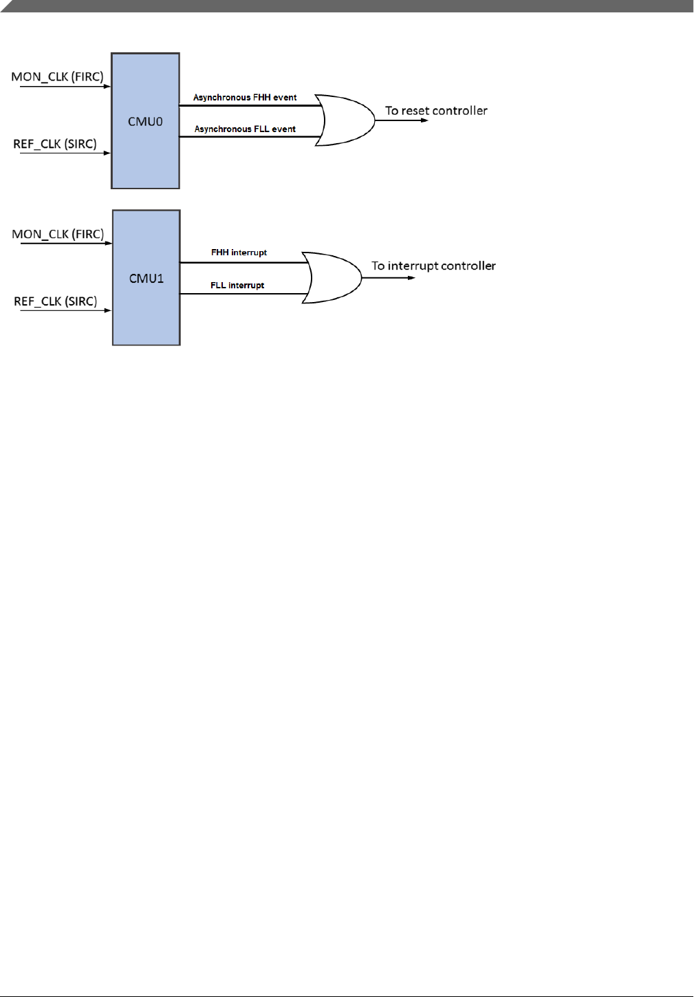
Figure 30-1. CMU on chip
Loss of Clock Indication Time Example: Conditions applied:
• CMU is enabled
• Monitored clock is lost
• 5 us LOC indication time requirement with
• bus clock at 48 MHz
• reference clock at 8 MHz
Formula for LOC indication time: ( 2*REF_CNT + 2 )*reference clock cycle + 3*bus
clock cycles
Calculation: 5 us > (2*REF_CNT + 2)*0.125 us + 3*0.0208 us
Result: REF_CNT < 18
Interpretation: The FLL REF_CNT should be programmed less than 18.
NOTE
• CMU needs to be disabled before disabling either FIRC or
SIRC. If system clock is FIRC, CMU cannot be enabled if
FIRC is not present from start, since system clock is
required to enable CMU.
• For safety applications , CMU should run on a different
clock than WDOG.
CMU chip-specific information
S32K1xx Series Reference Manual, Rev. 7, 04/2018
662 NXP Semiconductors

30.2 Introduction
CMU_FC modules are required to ensure clock signal integrity on the chip.
CMU_FC checks if the frequency of a monitored clock is within a programmable
frequency range specified by the user. If the frequency is outside the specified limits, it
could lead to performance, protocol, and timing failures. CMU_FC requires a clock that
is uses as a base reference for the frequency check operation. This reference clock must
be within documented limits for correct CMU_FC operation. If a reference clock is
outside operating parameters, CMU_FC behavior cannot be guaranteed.
30.2.1 Basic operation
CMU_FC counts clock cycles of the monitored clock during time duration of n clock
cycles of the reference clock. The number n reference cycles is user programmable. The
final count of the monitored clock after this time is compared against the user
programmable upper and lower threshold count limits. The cycle count is then checked to
see if it is within programmed limits. If the monitored clock count is not within
programmed limits, a register status field is set. If needed, an interrupt can be configured
to assert when the status flag sets.
CMU_FC cannot detect the following:
• Duty cycle variations of a monitored clock.
• Instantaneous monitored clock frequency variations which do not cross the upper or
lower measurement thresholds.
Chapter 30 Clock Monitoring Unit (CMU)
S32K1xx Series Reference Manual, Rev. 7, 04/2018
NXP Semiconductors 663
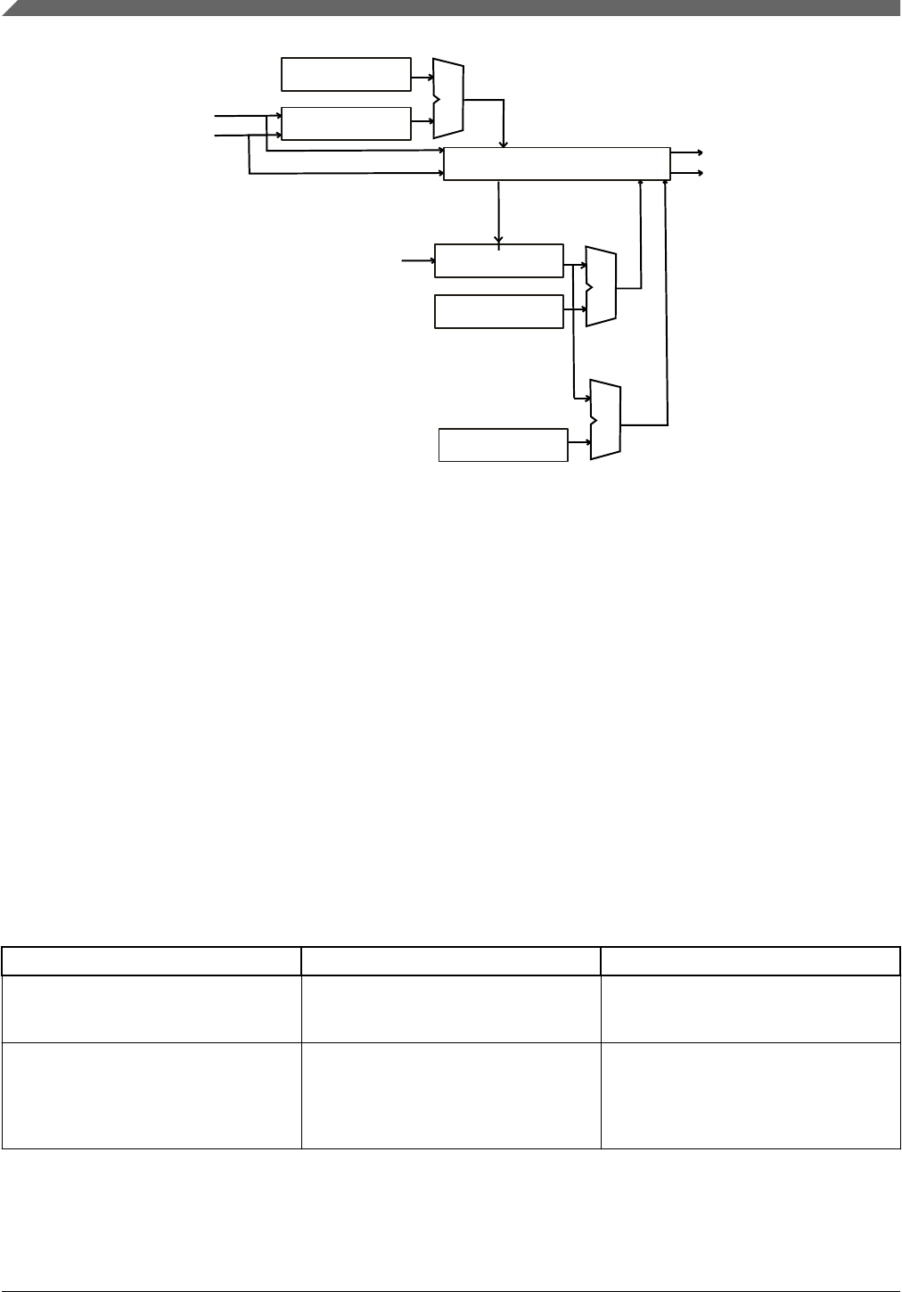
Checking Window
Reference Counter
=
Control Logic
Enable
ref_clk
Monitor Counter
High Threshold
mon_clk
Low Threshold
<
FHH
FLL
>
Figure 30-2. CMU_FC block diagram
30.2.2 Features
The CMU_FC features are:
• If a monitored clock frequency is higher than high frequency reference (FHH), an
event occurs.
• If a monitored clock frequency is lower than low frequency reference (FLL), an
event occurs.
• Programmable duration of reference clock cycles.
• Time out functionality to generate an FLL event when a monitored clock is lost.
• Masking of FHH interrupt.
• Masking of FLL interrupt.
Table 30-1. Clock description
Signal Name I/O Description
ref_clk I Reference Clock - Clock signal CMU_FC
uses as reference for evaluating
monitored clock.
mon_clk I Monitored Clock - Clock signal CMU_FC
compares to lower and higher frequency
limits to determine if the clock is
operating within defined frequency
range.
Introduction
S32K1xx Series Reference Manual, Rev. 7, 04/2018
664 NXP Semiconductors

NOTE
See the Clocking chapter for details of monitored and reference
clocks used on this chip.
30.3 CMU_FC register descriptions
30.3.1 CMU_FC Memory map
This section describes the address order of all the CMU_FC registers. Each description
includes a standard register diagram and associated field descriptions.
CMU0 base address: 4003_E000h
CMU1 base address: 4003_F000h
Offset Register Width
(In bits)
Access Reset value
0h Global Configuration Register (GCR) 32 RW 0000_0000h
4h Reference Count Configuration Register (RCCR) 32 RW 0000_0000h
8h High Threshold Configuration Register (HTCR) 32 RW 00FF_FFFFh
Ch Low Threshold Configuration Register (LTCR) 32 RW 0000_0000h
10h Status Register (SR) 32 W1C 0000_0000h
14h Interrupt Enable Register (IER) 32 RW 0000_0000h
30.3.2 Global Configuration Register (GCR)
30.3.2.1 Offset
Register Offset
GCR 0h
30.3.2.2 Function
GCR is used to control module level configurations.
Chapter 30 Clock Monitoring Unit (CMU)
S32K1xx Series Reference Manual, Rev. 7, 04/2018
NXP Semiconductors 665

30.3.2.3 Diagram
Bits 31 30 29 28 27 26 25 24 23 22 21 20 19 18 17 16
RReserved
W
Reset 0 0 0 0 0 0 0 0 0 0 0 0 0 0 0 0
Bits 15 14 13 12 11 10 9 8 7 6 5 4 3 2 1 0
RReserved FCE
W
Reset 0 0 0 0 0 0 0 0 0 0 0 0 0 0 0 0
30.3.2.4 Fields
Field Function
31-1
—
Reserved.
0
FCE
Frequency Check Enable.
This field enables CMU_FC. The default state of CMU_FC is disabled. When GCR[FCE] = 1, it must be
programmed to 0 only when SR[RS] = 1. It can be written 1 at any time.
0b - Frequency Check Disabled
1b - Frequency Check Enabled
30.3.3 Reference Count Configuration Register (RCCR)
30.3.3.1 Offset
Register Offset
RCCR 4h
30.3.3.2 Function
RCCR is used to program the reference count duration of the frequency check window.
CMU_FC register descriptions
S32K1xx Series Reference Manual, Rev. 7, 04/2018
666 NXP Semiconductors

NOTE
RCCR can be written only when GCR[FCE] = 0. If RCCR is
written when GCR[FCE] = 1, a hard fault is generated.
30.3.3.3 Diagram
Bits 31 30 29 28 27 26 25 24 23 22 21 20 19 18 17 16
RReserved
W
Reset 0 0 0 0 0 0 0 0 0 0 0 0 0 0 0 0
Bits 15 14 13 12 11 10 9 8 7 6 5 4 3 2 1 0
RREF_CNT
W
Reset 0 0 0 0 0 0 0 0 0 0 0 0 0 0 0 0
30.3.3.4 Fields
Field Function
31-16
—
Reserved.
15-0
REF_CNT
Reference clock count.
RCCR[REF_CNT] is the number of reference clock counts that the frequency check runs. This field
defines the duration of one frequency check window.
30.3.4 High Threshold Configuration Register (HTCR)
30.3.4.1 Offset
Register Offset
HTCR 8h
Chapter 30 Clock Monitoring Unit (CMU)
S32K1xx Series Reference Manual, Rev. 7, 04/2018
NXP Semiconductors 667

30.3.4.2 Function
HTCR is used to program high threshold limit of the monitored clock counter.
NOTE
HTCR can be written only when GCR[FCE] = 0. If HTCR is
written when GCR[FCE] = 1, a hard fault is generated.
30.3.4.3 Diagram
Bits 31 30 29 28 27 26 25 24 23 22 21 20 19 18 17 16
RReserved HFREF
W
Reset 0 0 0 0 0 0 0 0 1 1 1 1 1 1 1 1
Bits 15 14 13 12 11 10 9 8 7 6 5 4 3 2 1 0
RHFREF
W
Reset 1 1 1 1 1 1 1 1 1 1 1 1 1 1 1 1
30.3.4.4 Fields
Field Function
31-24
—
Reserved.
23-0
HFREF
High frequency reference threshold.
HCTR[HFREF] determines the high reference value for the monitored clock frequency. The
HCTR[HFREF] value is determined by the equation:
fMonitored_clock / fReference_clock ✕ RCCR[REF_CNT] + high threshold margin.
30.3.5 Low Threshold Configuration Register (LTCR)
30.3.5.1 Offset
Register Offset
LTCR Ch
CMU_FC register descriptions
S32K1xx Series Reference Manual, Rev. 7, 04/2018
668 NXP Semiconductors

30.3.5.2 Function
This register is used to program low threshold bound of the monitored clock counter.
NOTE
LTCR can be written only when GCR[FCE] = 0. If LTCR is
written when GCR[FCE] = 1, a hard fault is generated.
30.3.5.3 Diagram
Bits 31 30 29 28 27 26 25 24 23 22 21 20 19 18 17 16
RReserved LFREF
W
Reset 0 0 0 0 0 0 0 0 0 0 0 0 0 0 0 0
Bits 15 14 13 12 11 10 9 8 7 6 5 4 3 2 1 0
RLFREF
W
Reset 0 0 0 0 0 0 0 0 0 0 0 0 0 0 0 0
30.3.5.4 Fields
Field Function
31-24
—
Reserved.
23-0
LFREF
Low Frequency Reference Threshold.
LCTR[LFREF] determines the low reference value for the monitored clock frequency. The LCTR[LFREF]
value is determined by the equation: fMonitored_clock / fReference_clock ✕ RCCR[REF_CNT] – low threshold
margin.
30.3.6 Status Register (SR)
Chapter 30 Clock Monitoring Unit (CMU)
S32K1xx Series Reference Manual, Rev. 7, 04/2018
NXP Semiconductors 669

30.3.6.1 Offset
Register Offset
SR 10h
30.3.6.2 Function
SR shows the CMU_FC status.
30.3.6.3 Diagram
Bits 31 30 29 28 27 26 25 24 23 22 21 20 19 18 17 16
RReserved
W
Reset 0 0 0 0 0 0 0 0 0 0 0 0 0 0 0 0
Bits 15 14 13 12 11 10 9 8 7 6 5 4 3 2 1 0
RReserved RS STATE FHH FLL
W W1C W1C
Reset 0 0 0 0 0 0 0 0 0 0 0 0 0 0 0 0
30.3.6.4 Fields
Field Function
31-5
—
Reserved.
4
RS
Run Status
SR[RS] shows the running state of the CMU_FC internal logic. After enabling the frequency check
operation (GCR[FCE] = 1), a fixed delay is required before SR[RS] indicates the running status. If the
frequency check operation need to be disabled, software must read SR[RS] = 1 before writing
GCR[FCE] = 0.
0b - Frequency check stopped
1b - Frequency check running
3-2
STATE
Module state
These bits provide the internal state information.
00b - Configure state: Configuration registers and IER programming is getting done
01b - Initialization state: Register configurations are getting loaded internally.
10b - Initialization wait state: CMU_FC stays in this state for 1 bus clock cycle.
11b - Frequency check state: CMU_FC is ready to start frequency check operation in this state.
Table continues on the next page...
CMU_FC register descriptions
S32K1xx Series Reference Manual, Rev. 7, 04/2018
670 NXP Semiconductors

Field Function
1
FHH
Frequency higher than high frequency reference threshold event status.
This bit is set by hardware when the monitored clock frequency becomes higher than the high threshold
value in HTCR[HFREF]. SR[FHH] is cleared when written 1.
0b - No FHH event
1b - FHH event occured
0
FLL
Frequency lower than low frequency reference threshold event status.
This field is set by hardware when the fMonitored_clock is lower than the low threshold value in
LTCR[LFREF]. SR[FLL] is cleared when written 1.
0b - No FLL event
1b - FLL event captured
30.3.7 Interrupt Enable Register (IER)
30.3.7.1 Offset
Register Offset
IER 14h
30.3.7.2 Function
This register enables CMU_FC interrupts.
NOTE
• This register can only be written when GCR[FCE] = 0.
30.3.7.3 Diagram
Bits 31 30 29 28 27 26 25 24 23 22 21 20 19 18 17 16
RReserved
W
Reset 0 0 0 0 0 0 0 0 0 0 0 0 0 0 0 0
Bits 15 14 13 12 11 10 9 8 7 6 5 4 3 2 1 0
R
Reserved
FHHAIE
FLLAI
E
FHHIE
FLLI
E
W
Reset 0 0 0 0 0 0 0 0 0 0 0 0 0 0 0 0
Chapter 30 Clock Monitoring Unit (CMU)
S32K1xx Series Reference Manual, Rev. 7, 04/2018
NXP Semiconductors 671

30.3.7.4 Fields
Field Function
31-4
—
Reserved.
3
FHHAIE
Frequency Higher than High Frequency Reference Threshold Asynchronous Interrupt enable
This bit is used to enable/disable FHH asynchronous interrupt at the module boundary.
NOTE: This field is not supported in every instance. The following table includes only supported
registers.
Field supported in Field not supported in
CMU0_IER —
— CMU1_IER
0b - Asynchronous FHH interrupt disabled
1b - Asynchronous FHH interrupt enabled
2
FLLAIE
Frequency Lower than Low Frequency Reference Threshold Asynchronous Interrupt Enable
This bit is used to enable/disable FLL asynchronous interrupt at the module boundary.
NOTE: This field is not supported in every instance. The following table includes only supported
registers.
Field supported in Field not supported in
CMU0_IER —
— CMU1_IER
0b - Asynchronous FLL interrupt disabled
1b - Asynchronous FLL interrupt enabled
1
FHHIE
Frequency Higher than High Frequency Reference Threshold Synchronous Interrupt Enable
This bit is used to enable/disable FHH interrupt at the module boundary.
NOTE: This field is not supported in every instance. The following table includes only supported
registers.
Field supported in Field not supported in
— CMU0_IER
CMU1_IER —
0b - FHH synchronous interrupt disabled
1b - FHH synchronous interrupt enabled
0
FLLIE
Frequency Lower than Low Frequency Reference Threshold Synchronous Interrupt Enable
This bit is used to enable/disable FLL interrupt at the module boundary.
CMU_FC register descriptions
S32K1xx Series Reference Manual, Rev. 7, 04/2018
672 NXP Semiconductors

Field Function
NOTE: This field is not supported in every instance. The following table includes only supported
registers.
Field supported in Field not supported in
— CMU0_IER
CMU1_IER —
0b - FLL synchronous interrupt disabled
1b - FLL synchronous interrupt enabled
30.4 Functional description
Frequency checking starts when software writes GCR[FCE] = 1. The CMU_FC requires
a fixed number of reference clock cycles before hardware operations start. The status
field SR[RS] = 1 immediately after frequency check operation starts. Safety critical
applications must poll SR[RS] to determine when a check operation starts.
CMU_FC performs continuous periodic clock checking of the monitored clock. Each
checking window involves the following operations:
• Stage 1 – Reference clock counter runs for RCCR[REF_CNT] reference clock
cycles. Monitored clock counter runs in parallel for the same time duration as
reference clock counter.
• Stage 2 – After stage 1, the module compares the final monitored clock count against
the programmed thresholds.
If the monitored clock count is greater than the high threshold value in HTCR[HFREF],
an FHH event is generated.
If the monitored clock count is lower than the low threshold value in LTCR[LFREF], an
FLL event is generated.
30.4.1 Monitored clock lost
If monitored clock is lost before it can be evaluated (Stage 2, see Functional description),
CMU_FC waits for RCCR[REF_CNT] reference clock periods by extending Stage 2
before an FLL event is triggered.
Chapter 30 Clock Monitoring Unit (CMU)
S32K1xx Series Reference Manual, Rev. 7, 04/2018
NXP Semiconductors 673

NOTE
• Worst case FLL response time if monitored clock is already
absent when module is
enabled = (2 × RCCR[REF_CNT] + 12) ref_clk
cycles + 15 bus clock cycles.
• Worst case FLL response time if monitored clock stops
while the module is running = (2 × RCCR[REF_CNT] + 2)
ref_clk cycles + 3 bus clock cycles.
30.5 Programming guidelines
30.5.1 Programming HFREF and LFREF
HFREF/LFREF programming must be done considering the following:
• Tolerable monitored clock frequency variation.
• Maximum reference clock frequency variation.
• Inherent module inaccuracy.
The CMU_FC has an expected maximum deviation of +/- 3 ideal monitored clock cycles.
Example programming HTCR[HFREF] and HTCR[LFREF]:
•fReference_clock = 20 MHz
•fMonitored_clock = 200 MHz
• RCCR[REF_CNT] = 10
•Ideal Monitored Clock Count = (fMonitored_clock / fReference_clock) × REF_CNT = 100
Now, consider the combined spec variation of reference clock and monitored clock = +/-
5%.
• The inherent inaccuracy of CMU_FC is 3 cycles.
• Minimum Monitored Clock Count = (Ideal Monitored Clock Count × 0.95) -
3 = 92 (HTCR[LFREF])
• Maximum Monitored Clock Count = (Ideal Monitored Clock Count × 1.05) + 3 = 10
8 (HTCR[HFREF])
Programming guidelines
S32K1xx Series Reference Manual, Rev. 7, 04/2018
674 NXP Semiconductors

30.5.2 Programming RCCR[REF_CNT]
Programming RCCR[REF_CNT] must be done after considering application
requirements of event response time and required accuracy. Higher value of REF_CNT
results in longer checking window leading to better accuracy in monitored clock
measurement. Lower value of REF_CNT results in shorter checking window and faster
response.
Minimum RCCR[REF_CNT] = CEILING value of MAX (3 × (fReference_clock / fBus_clock),
or 6 + 3 × (fReference_clock / fMonitored_clock)).
Example to determine RCCR[REF_CNT]:
•fBus_clock= 8 MHz
•fReference_clock = 8 MHz
•fMonitored_clock= 48 MHz
•Formula #1: 3 × (fReference_clock / fBus_clock)
• 3 × (8 MHz / 8 MHz) = 3 MHz
•Formula #2: 6 + 3 × (fReference_clock / fMonitored_clock)
• 6 + 3 × (8 MHz / 48 MHz) = 6.5 MHz
• MAX (3 MHz, 6.5 MHz) = 6.5 MHz
• Then, CEILING value of MAX = 7 MHz (6.5 MHz rounded)
• Therefore, minimum RCCR[REF_CNT] = 7.
30.5.3 CMU_FC programming sequence
The recommended programming sequence of CMU_FC is:
1. In any order, do the following:
• Program RCCR[REF_CNT] to define the frequency check window duration in
reference clock cycles.
• Program LTCR[LFREF] and HTCR[HFREF] to set the permissible frequency
range of the monitored clock.
• If needed, program IER register to enable interrupt.
2. Once the above steps are complete, writing GCR[FCE] = 1 starts the frequency check
operation. The ability to write RCCR, LTCR[LFREF], and HTCR[HFREF] is
disabled after writing GCR[FCE] = 1. An attempted write to any of those registers
generates a bus transfer error.
3. To reconfigure RCCR, LTCR[LFREF], and HTCR[HFREF] registers, or to stop
frequency check operation, write GCR[FCE] = 0 after SR[RS] = 1.
Chapter 30 Clock Monitoring Unit (CMU)
S32K1xx Series Reference Manual, Rev. 7, 04/2018
NXP Semiconductors 675

Programming guidelines
S32K1xx Series Reference Manual, Rev. 7, 04/2018
676 NXP Semiconductors

Chapter 31
Memories and Memory Interfaces
31.1 Introduction
This chapter discusses the configuration of the memories and memory interfaces, such as
the flash memory, the Flash Memory Controller and the SRAM. Additional related
information can be found in the following chapters:
•MPU
•DMAMUX
•eDMA
•EIM
•ERM
31.2 Flash Memory Controller and flash memory modules
For details about these modules, see:
•Flash Memory Controller (FMC)
•Flash Memory Module (FTFC)
31.3 SRAM configuration
This section summarizes how the module has been configured in the chip.
Table 31-1. Reference links to related information
Topic Related module Reference
System memory map See attached S32K1xx_memory_map.xlsx
Clocking System Clock Generator Clock Distribution
Arm Cortex-M4 core Arm Cortex-M4F core
Table continues on the next page...
S32K1xx Series Reference Manual, Rev. 7, 04/2018
NXP Semiconductors 677

Table 31-1. Reference links to related information (continued)
Topic Related module Reference
Arm Cortex-M0+ core Arm Cortex-M0+ core
System MPU Memory Protection Unit (MPU)
31.3.1 SRAM sizes
This chip contains SRAM tightly coupled with the Arm Cortex-M4F core/Arm Cortex-
M0+ core. The on-chip SRAM is split into contiguous SRAM_L and SRAM_U regions
in the memory map:
• SRAM_L is anchored to 1FFF_FFFFh and occupies the space before this ending
address.
• SRAM_U is anchored to 2000_0000h and occupies the space after this beginning
address.
NOTE
Misaligned accesses across the 2000_0000h boundary are not
supported in the Arm Cortex-M4F architecture.
In the SIM, SDID[RAMSIZE] identifies the total amount of SRAM on a device. For each
chip in the series, the following table shows the size of each SRAM region within that
total.
Table 31-2. On-chip SRAM sizes
Chip SRAM_L (KB)1SRAM_U (KB)1FlexRAM (KB)1Total SRAM (KB)
S32K116 1214 2217
S32K118 1222 2225
S32K142 16 12 4 32
S32K144 32 28 4 64
28 16 4 48
S32K146 64 60 4 128
48 44 4 96
S32K148 128 124 4 256
96 92 4 192
1. See attached S32K1xx_memory_map.xlsx for specific addresses
2. 1 KB of for MTB. If not used for MTB, can be use as System RAM. Not ECC protected
NOTE
No ECC or access error is generated for FlexRAM used as
System RAM. The region of size equal to FlexRAM (4 KB)
SRAM configuration
S32K1xx Series Reference Manual, Rev. 7, 04/2018
678 NXP Semiconductors
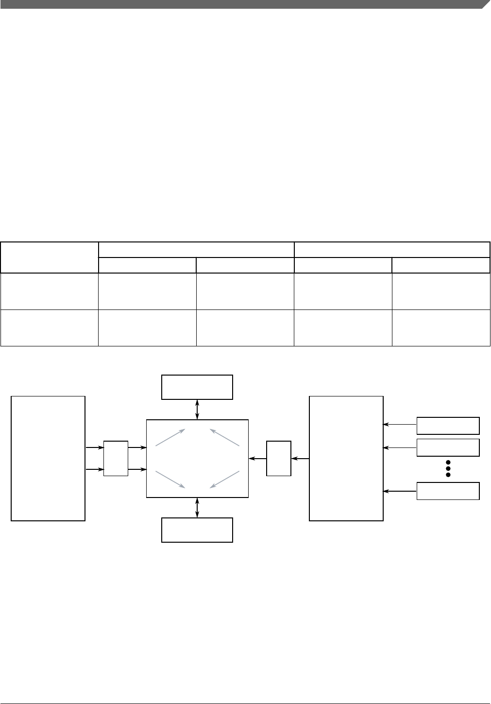
after SRAM_U end address is reserved, but no access error is
generated for this region.
31.3.2 SRAM accessibility
NOTE
This section is applicable for CM4 core only.
Both SRAM_L and SRAM_U have a frontdoor port and a backdoor port.
The following table summarizes the master access to and performance of accesses to each
port. The following figure illustrates the master access.
Table 31-3. SRAM accessibility and performance
SRAM region Frontdoor port Backdoor port
Master access Performance Master access Performance
SRAM_L Cortex-M4F core code
bus
Single-cycle access Non-core bus masters Minimum two cycles for
read and one cycle for
write
SRAM_U Cortex-M4F core
system bus
Single-cycle access Non-core bus masters Minimum two cycles for
read and one cycle for
write
Cortex-M4F core
Code bus
System bus
SRAM controller
Backdoor
SRAM_L
SRAM_U
Crossbar Switch
Non-core master
Non-core master
Non-core master
Frontdoor
System
MPU
System
MPU
Figure 31-1. SRAM accessibility
The following simultaneous accesses to SRAM_L and SRAM_U can occur:
• Core code bus access to SRAM_L and core system bus access to SRAM_U
• Core code bus access to SRAM_L and non-core bus master access to SRAM_U
• Core system bus access to SRAM_U and non-core bus master access to SRAM_L
Chapter 31 Memories and Memory Interfaces
S32K1xx Series Reference Manual, Rev. 7, 04/2018
NXP Semiconductors 679

The following table illustrates these scenarios.
Table 31-4. SRAM simultaneous accesses
Core code bus access Core system bus access Non-core bus master access
SRAM_L SRAM_U —
SRAM_L — SRAM_U
— SRAM_U SRAM_L
NOTE
Burst accesses cannot occur across the 2000_0000h boundary
that separates the two SRAM arrays. The two arrays should be
treated as separate memory ranges for burst accesses.
To supplement the main system RAM, FlexRAM can be used as system RAM. However,
FlexRAM accesses involve additional system latencies.
31.3.3 SRAM arbitration and priority control
The Core Platform Control Register (MCM_CPCR) controls the arbitration and priority
schemes for the two SRAM arrays.
31.3.4 SRAM retention: power modes and resets
Power to the SRAM is maintained in all power modes.
To retain and access SRAM contents across functional resets, write application code to
execute the following sequence:
1. Configure the System Reset Interrupt Enable Register (RCM_SRIE) to delay the
reset and instead generate an interrupt on every reset request.
2. On an interrupt for a reset request, application code configures the chip to enter Run
mode and then writes 0 to both SRAMU_RETEN and SRAML_RETEN in the Chip
Control register (CHIPCTL). This logic ensures that any attempted access to SRAM
is blocked after these bits are written, thereby preventing memory corruption during
reset assertion.
3. The chip remains in Run mode until the reset asserts.
NOTE
During software initialization, ensure that no accesses
occur to RAM with retained contents.
SRAM configuration
S32K1xx Series Reference Manual, Rev. 7, 04/2018
680 NXP Semiconductors


SRAM configuration
S32K1xx Series Reference Manual, Rev. 7, 04/2018
682 NXP Semiconductors
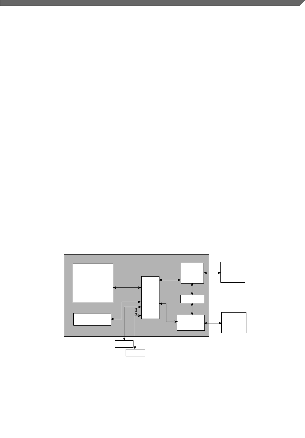
Chapter 32
PRAM Controller (PRAMC)
32.1 PRAMC chip-specific information
PRAMC is available in only S32K11x series of devices. Other products in the S32K1xx
series do not have PRAMC.
32.2 Introduction
The PRAM_CTL module is an asynchronous reset RAM array controller with integrated
error detection and correction.
Shown below in Figure 32-1 is a simplified block diagram of how the PRAM_CTL is
implemented:
Core
Complex A
X
B
S
PRAM
CTL
RAM
Array(s)
DMA2
Master
AIPS IPS
Slave(s)
Master n
MCM
Figure 32-1. Simplified block diagram
In the above figure, the AXBS is the AHB crossbar switch (arbiter) and the MCM is the
Miscellaneous Control Module where error detection information is stored. Refer to the
appropriate chapter for a complete description.
S32K1xx Series Reference Manual, Rev. 7, 04/2018
NXP Semiconductors 683

32.3 Memory map and register definition
The memory map for the PRAM memory space is determined by the system in which the
controller is implemented. There are no program-visible registers within the controller.
All ECC error reporting and forcing capabilities are implemented via program-visible
registers located in the Miscellaneous Control Module (MCM).
32.4 Functional description
32.4.1 Error Correcting Code (ECC)
32.4.1.1 Overview
The PRAM_CTL memory controller uses a 7-bit error correcting code (ECC) to correct
single-bit errors and detect multiple-bit errors within the 32-bit data field. Since the ECC
bits are written to and read from memory with the data, it is essential that each 32-bit
memory location be written to a known value before being read. If an uninitialized
memory address is read, it is likely the read will result in a multiple-bit ECC error and an
errored transaction on the AHB. Only 32-bit write transfers can be used to initialize the
memory as 16-bit or 8-bit writes will generate a read/modify/write scenario (see Less
than 32-bit writes).
The ECC is composed of two modules, the encoder and the decoder. The decode module
is shown in greater detail in Figure 32-2.
dec_bus_out[31:0] ecc_syndrome[5:0] ecc_parity
ecc_single_detect ecc_multiple_detect
pram_rdata[39:0] 39 bit codeword
32 data bits
Bit Correction Muxing
Syndrome
Decode
haddr[19:2]
18
Figure 32-2. Block Diagram: 39-bit ECC Decode
Memory map and register definition
S32K1xx Series Reference Manual, Rev. 7, 04/2018
684 NXP Semiconductors

The encoder logic is included in the write data path to the RAM and generates the 7-bit
ECC code, which is written to the RAM with the data. Together, the data bus and ECC
bits are called the code word.
The decoder logic is included in the read data path from the RAM back to the AHB bus.
The decoder uses the same algorithm as the encoder and generates 7 unique ECC bits, or
the syndrome[6:0], from the 39-bit code word (7 ECC and 32 data bits). This syndrome is
used to determine which bit within the 39-bit data bus caused the single-bit correctable
error. See the MCM block guide for more detail on which syndromes map to which bits.
Single-bit corrections cause the output ecc_single_error to be asserted. Multiple-bit
errors cause the ecc_multi_error output to be asserted as well as an AHB ERROR
response to be generated (see AMBA AHB spec 2.0, pg 3-23). AHB address attributes are
also saved and outputted for each case. These two flags are mutually exclusive.
The assertion of these two flags may cause an interrupt to be generated, the EER bit to be
set in the Miscellaneous Control Module (MCM), and the errored address, syndrome,
parity and master address to be saved in the MCM (See the MCM Block Guide for a
programming model). The effect of more than 2 simultaneous errors may produce
unexpected behavior.
32.4.2 Read/Write introduction
As stated earlier in Overview, it is essential that each memory address be written to a
known value before it is read. This includes reads generated from the read/modify/write
operation which occurs when a write transfer of less than 32 bits is requested (see Less
than 32-bit writes).
32.4.3 Reads
All read transfers, of any size, complete with a zero wait states response on the AHB.
32.4.3.1 Unaligned reads
Any unaligned read will execute as if the size of the transfer is equal to the corresponding
unaligned container size. For example, a 16-bit unaligned read will have a container of 32
bits and therefore the controller will execute the read as if it were a 32-bit read.
Chapter 32 PRAM Controller (PRAMC)
S32K1xx Series Reference Manual, Rev. 7, 04/2018
NXP Semiconductors 685

32.4.3.2 ECC errors on reads
A decoded multiple-bit ECC error will result in the termination of the corresponding
AHB transaction with the AHB two cycle ERROR response (hresp).
The array is left unchanged.
32.4.3.3 Optional read wait-state
The PRAM_CTL can be optionally programmed to insert one wait-state in the AHB
response on reads. Asserting the module-level input pram_add_one_ws will insert one
wait state in the AHB data phase as well as the ECC reporting interface to the MCM. The
state of pram_add_one_wait_state has no effect on writes nor reads less than 32-bit in
size.
32.4.3.4 Reads and ECC events
• RAM reads in which no ECC events are detected will incur 1 wait state.
• RAM reads in which a single-bit, correctable ECC event is detected will incur 1 wait
state
• RAM reads in which a multi-bit, non-correctable ECC error is detected will incur 2
wait states.
32.4.4 Writes
32.4.4.1 32-bit writes
Aligned 32-bit writes execute in a single AHB data phase cycle allowing for zero wait
states on back to back writes.
32.4.4.2 Less than 32-bit writes
Less than 32-bit writes require a three step process referred to as a read/modify/write
operation. Each 32-bit location must be initialized with a valid codeword created by the
ECC encode block. This codeword must be kept consistent with the entire 32-bit word.
Functional description
S32K1xx Series Reference Manual, Rev. 7, 04/2018
686 NXP Semiconductors

Therefore, for each less than 32-bit write, the array data must be read (read), the AHB
write data merged with the array data and the codeword regenerated (modify), before the
data can be stored (write).
32.4.4.3 Unaligned writes
It should be noted that unaligned writes always generate read/modify/write operations in
the pram controller in order to preserve the validity of the ECC codeword.
32.4.5 Late write hits
A late write hit occurs when the late write buffer is valid and the address of the late write
buffer matches haddr. The following table shows the possible late write hit scenarios and
the result of each.
Table 32-1. Late write hit cases
Access Type haddr lwb addr lwb size Action
Description Wait State?
1<=32-bit read A0 A0 32 hrdata = lwb
data 0 No
2<=32-bit read A0 A1 32
Not a hit,
actually a miss,
lwb held, normal
array read
No
332-bit write A0 - - Store during
address phase No
4<32-bit write A* A* *
Array read if
necessary
lwb/pram_rdata
merged
No
A0 : address bit A[2]=0
A1 : address bit A[2]=1
A* : address bit A[2]=either 1 or 0
* : any valid value can be substituted
lwb : late write buffer
In all late write hit cases, no additional wait states are inserted on the AHB.
Chapter 32 PRAM Controller (PRAMC)
S32K1xx Series Reference Manual, Rev. 7, 04/2018
NXP Semiconductors 687

32.5 Initialization / application information
It is essential that each memory address be written to a known value before it is read.
This includes reads generated from the read/modify/write operation which occurs when a
write transfer of less than 32 bits or unaligned write is requested (see Less than 32-bit
writes). Without writing an address to a known value first, a read from this address will
most likely generate an ECC multiple error.
The following Esys PowerPC assembly instructions, formed as a subroutine, is an
example of clearing PRAM memory space. This code clears 0x2000 bytes of memory.
enable_and_invalidate_cache();
asm ("li r14,0x2000"); // size to clear
asm ("lisr13,0x4000"); // RAM base address
asm ("clear_mem:");
asm ("subi r14,r14,0x20");
asm ("dcbz r14,r13");
asm ("dcbf r14,r13");
asm ("cmpwi r14,0x0");
asm ("beq continue");
asm ("b clear_mem");
Initialization / application information
S32K1xx Series Reference Manual, Rev. 7, 04/2018
688 NXP Semiconductors

Chapter 33
Local Memory Controller (LMEM)
33.1 Chip-specific LMEM information
Variants of S32K11x series do not have LMEM.
33.1.1 LMEM region description
See attached S32K1xx_memory_map.xlsx for LMEM regions.
NOTE
• Cache write buffer is not supported on S32K14x as the
memory region which is cacheable is read-only.
•PCCRMR[R2] should be programmed as 00b (Non-
Cacheable) as S32K148 FlexNVMs region is not
cacheable. The device may show unexpected behavior
when cache tries to access FlexNVM region.
33.1.2 LMEM SRAM sizes
SRAM sizes vary across the products in the S32K14x series. In this chapter, SRAM
Arrays documents the superset SRAM sizes.
For each S32K14x product's SRAM sizes and other details, see SRAM sizes.
33.2 Introduction
The Local Memory Controller provides the processor with tightly-coupled processor-
local memories and bus paths to all slave memory spaces.
S32K1xx Series Reference Manual, Rev. 7, 04/2018
NXP Semiconductors 689

33.2.1 Block Diagram
The processor has a modified 32-bit Harvard bus architecture. Using a 32-bit address
space, low-order addresses (0x0000_0000 through 0x1FFF_FFFF) use the Processor
Code (PC) bus, and high-order addresses (0x2000_0000 through 0xFFFF_FFFF) use the
Processor System (PS) bus. As the bus names imply, normal operation has code accesses
on the PC bus and data accesses on the PS bus.
This device has been augmented with tightly-coupled memories for the PC and PS buses.
The memories include RAMs and caches. These local memories provide zero wait state
access to RAM and cacheable address spaces.
The local memory controller includes three memory controllers and their attached
memories:
• SRAM lower (SRAM_L) controller via the PC bus
• SRAM upper (SRAM_U) controller via the PS bus
• Cache memory controller via the PC bus
The local memory controller has the following 32-bit AMBA_ AHB buses:
• Two inputs are for the processor's modified Harvard buses − the Processor Code
(PC) and the Processor System (PS) buses.
• One input is for the "backdoor" port used by all other bus masters to access the
SRAM controller space.
• Two output ports are the CCM (Core Code Master) bus used for PC accesses that do
not hit the PC cache or SRAM_L or are non-cacheable and the CSM (Core System
Master) bus used for PS references that do not hit the SRAM_U.
Introduction
S32K1xx Series Reference Manual, Rev. 7, 04/2018
690 NXP Semiconductors
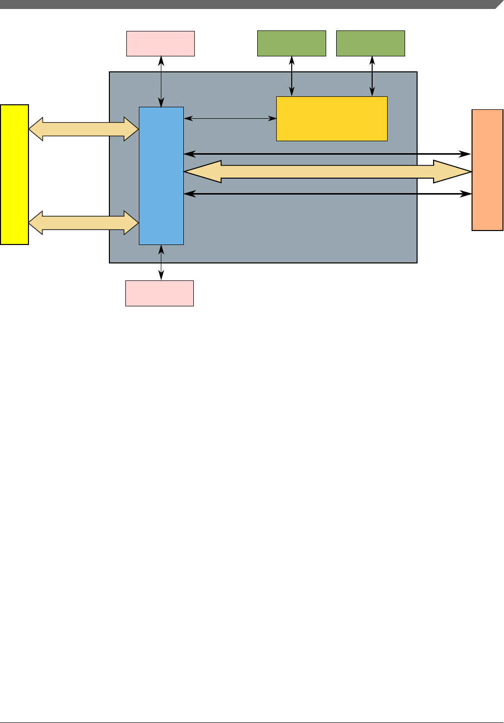
LMEM
Core System Master (CSM) bus
Processor System (PS) bus
Cache data arrays
Cache I&D code bus Code cache
controller
Core Code Master (CCM) bus
Processor Code (PC) bus
Cache tag arrays
Crossbar switch
Processor
Backdoor port
SRAM lower
SRAM upper
LMEM
controller
Figure 33-1. Local memory controller block diagram
NOTE
The SRAM and cache controllers reside within the LMEM, but
the single-port synchronous RAM arrays used by these
controllers are external.
The LMEM contains address decode logic for the PC and PS buses. This logic routes the
core's accesses to the various system resources. The address spaces are device-specific.
See the chip-specific LMEM information for the address space decode details.
33.2.2 Cache features
A cache is a block of high-speed memory locations containing address information
(commonly known as a tag) and the associated data. The purpose is to decrease the
average time of a memory access. Caches operate on two principles of locality:
• Spatial locality — An access to one location is likely to be followed by accesses
from adjacent locations (for example, sequential instruction execution or usage of a
data structure).
• Temporal locality — An access to an area of memory is likely to be repeated within a
short time period (for example, execution of a code loop).
Chapter 33 Local Memory Controller (LMEM)
S32K1xx Series Reference Manual, Rev. 7, 04/2018
NXP Semiconductors 691

To minimize the quantity of control information stored, the spatial locality property is
used to group several locations together under the same tag. This logical block is
commonly known as a cache line.
When data is loaded into a cache, access times for subsequent loads and stores are
reduced, resulting in overall performance benefits. An access to information already in a
cache is known as a cache hit, and other accesses are called cache misses.
Normally, caches are self-managing, with the updates occurring automatically. Whenever
the processor wants to access a cacheable location, the cache is checked. If the access is a
cache hit, the access occurs immediately. Otherwise, a location is allocated and the cache
line is loaded from memory. Different cache topologies and access policies are possible.
However, they must comply with the memory coherency model of the underlying
architecture.
Caches introduce a number of potential problems, mainly because of:
• memory accesses occurring at times other than when the programmer would
normally expect them,
• the existence of multiple physical locations where a data item can be held.
The local memory controller supports the following modes of operation:
1. Write-through — access to address spaces with this cache mode are cacheable.
• If all cacheable spaces are read-only spaces, the cache will contain read-only
data and all write to the cache will fault. See the chip-specific cacheable space
information.
• A write-through read miss on the input bus causes a line read on the output bus
of a 16-byte-aligned memory address containing the desired address. This miss
data is loaded into the cache and is marked as valid and not modified.
• A write-through read hit to a valid cache location returns data from the cache
with no output bus access.
• A write-through write miss bypasses the cache and writes to the output bus (no
allocate on write miss policy for write-through mode spaces).
• A write-through write hit updates the cache hit data and writes to the output bus.
• The caches are processor-local and do not support hardware cache coherency. If
the processor has accessed write-through regions and an external bus master
(such as DMA) then needs update these regions, software must first perform
explicit cache clears to any needed cache memory range to ensure all modified
cache lines update their associated memories before being modified by external
masters and subsequent processor accesses will get the updated memory.
2. Non-cacheable — access to address spaces with this cache mode are not cacheable.
These accesses bypass the cache and access the output bus.
Introduction
S32K1xx Series Reference Manual, Rev. 7, 04/2018
692 NXP Semiconductors

33.3 Memory Map/Register Definition
The cache programmer's model provides a variety of registers for configuring and
controlling the cache, as well as indirect access paths to all cache tag and data storage.
NOTE
The LMEM registers are accessible in supervisor mode
only.
33.3.1 LMEM register descriptions
33.3.1.1 LMEM Memory map
LMEM base address: E008_2000h
Offset Register Width
(In bits)
Access Reset value
0h Cache control register (PCCCR) 32 RW 0000_0000h
4h Cache line control register (PCCLCR) 32 RW 0000_0000h
8h Cache search address register (PCCSAR) 32 RW 0000_0000h
Ch Cache read/write value register (PCCCVR) 32 RW 0000_0000h
20h Cache regions mode register (PCCRMR) 32 RW AA0F_A000h
33.3.1.2 Cache control register (PCCCR)
33.3.1.2.1 Offset
Register Offset
PCCCR 0h
Chapter 33 Local Memory Controller (LMEM)
S32K1xx Series Reference Manual, Rev. 7, 04/2018
NXP Semiconductors 693

33.3.1.2.2 Diagram
Bits 31 30 29 28 27 26 25 24 23 22 21 20 19 18 17 16
R
GO
0
PUSHW1
INVW1
PUSHW0
INVW0
0
W
Reset 0 0 0 0 0 0 0 0 0 0 0 0 0 0 0 0
Bits 15 14 13 12 11 10 9 8 7 6 5 4 3 2 1 0
R
0
PCCR3
PCCR2
Reserved
ENCACHE
W
Reset 0 0 0 0 0 0 0 0 0 0 0 0 0 0 0 0
33.3.1.2.3 Fields
Field Function
31
GO
Initiate Cache Command
Setting this bit initiates the cache command indicated by bits 27-24. Reading this bit indicates if a
command is active
NOTE: This bit stays set until the command completes. Writing zero has no effect.
0b - Write: no effect. Read: no cache command active.
1b - Write: initiate command indicated by bits 27-24. Read: cache command active.
30-28
—
Reserved
27
PUSHW1
Push Way 1
0b - No operation
1b - When setting the GO bit, push all modified lines in way 1
26
INVW1
Invalidate Way 1
NOTE: If the PUSHW1 and INVW1 bits are set, then after setting the GO bit, push all modified lines in
way 1 and invalidate all lines in way 1 (clear way 1).
0b - No operation
1b - When setting the GO bit, invalidate all lines in way 1
25
PUSHW0
Push Way 0
0b - No operation
1b - When setting the GO bit, push all modified lines in way 0
24
INVW0
Invalidate Way 0
NOTE: If the PUSHW0 and INVW0 bits are set, then after setting the GO bit, push all modified lines in
way 0 and invalidate all lines in way 0 (clear way 0).
0b - No operation
1b - When setting the GO bit, invalidate all lines in way 0.
23-4
—
Reserved
3 Forces no allocation on cache misses (must also have PCCR2 asserted)
Table continues on the next page...
Memory Map/Register Definition
S32K1xx Series Reference Manual, Rev. 7, 04/2018
694 NXP Semiconductors

Field Function
PCCR3
2
PCCR2
Forces all cacheable spaces to write through
1
—
This field is reserved. Software should write 0 to this bit to maintain compatibility.
0
ENCACHE
Cache enable
0b - Cache disabled
1b - Cache enabled
33.3.1.3 Cache line control register (PCCLCR)
33.3.1.3.1 Offset
Register Offset
PCCLCR 4h
33.3.1.3.2 Function
This register defines specific line-sized cache operations to be performed using a specific
cache line address or a physical address.
If a physical address is specified, both ways of the cache are searched, and the command
is only performed on the way which hits.
33.3.1.3.3 Diagram
Bits 31 30 29 28 27 26 25 24 23 22 21 20 19 18 17 16
R
0
LACC
LADSE
L
LCMD
Reserved
LCWAY
LCIMB
LCIVB
0
TDSE
L
W
Reset 0 0 0 0 0 0 0 0 0 0 0 0 0 0 0 0
Bits 15 14 13 12 11 10 9 8 7 6 5 4 3 2 1 0
R
0
WSE
L
CACHEADDR
0
LGO
W
Reset 0 0 0 0 0 0 0 0 0 0 0 0 0 0 0 0
Chapter 33 Local Memory Controller (LMEM)
S32K1xx Series Reference Manual, Rev. 7, 04/2018
NXP Semiconductors 695

33.3.1.3.4 Fields
Field Function
31-28
—
Reserved
27
LACC
Line access type
0b - Read
1b - Write
26
LADSEL
Line Address Select
When using the cache address, the way must also be specified in CLCR[WSEL].
When using the physical address, both ways are searched and the command is performed only if a hit.
0b - Cache address
1b - Physical address
25-24
LCMD
Line Command
00b - Search and read or write
01b - Invalidate
10b - Push
11b - Clear
23
—
Reserved
22
LCWAY
Line Command Way
Indicates the way used by the line command.
Only applies if valid bit LCIVB = 1.
21
LCIMB
Line Command Initial Modified Bit
If command used cache address and way, then this bit shows the initial state of the modified bit
If command used physical address and a hit, then this bit shows the initial state of the modified bit. If a
miss, this bit reads zero.
20
LCIVB
Line Command Initial Valid Bit
If command used cache address and way, then this bit shows the initial state of the valid bit
If command used physical address and a hit, then this bit shows the initial state of the valid bit. If a miss,
this bit reads zero.
19-17
—
Reserved
16
TDSEL
Tag/Data Select
Selects tag or data for search and read or write commands.
0b - Data
1b - Tag
15
—
Reserved
14
WSEL
Way select
Selects the way for line commands.
0b - Way 0
Table continues on the next page...
Memory Map/Register Definition
S32K1xx Series Reference Manual, Rev. 7, 04/2018
696 NXP Semiconductors

Field Function
1b - Way 1
13-2
CACHEADDR
Cache address
CLCR[10:4] bits are used to access the tag arrays
CLCR[10:2] bits are used to access the data arrays
1
—
Reserved
0
LGO
Initiate Cache Line Command
Setting this bit initiates the cache line command indicated by bits 27-24. Reading this bit indicates if a line
command is active
NOTE: This bit stays set until the command completes. Writing zero has no effect.
NOTE: This bit is shared with CSAR[LGO]
0b - Write: no effect. Read: no line command active.
1b - Write: initiate line command indicated by bits 27-24. Read: line command active.
33.3.1.4 Cache search address register (PCCSAR)
33.3.1.4.1 Offset
Register Offset
PCCSAR 8h
33.3.1.4.2 Function
The CSAR register is used to define the explicit cache address or the physical address for
line-sized commands specified in the CLCR[LADSEL] bit.
33.3.1.4.3 Diagram
Bits 31 30 29 28 27 26 25 24 23 22 21 20 19 18 17 16
RPHYADDR
W
Reset 0 0 0 0 0 0 0 0 0 0 0 0 0 0 0 0
Bits 15 14 13 12 11 10 9 8 7 6 5 4 3 2 1 0
R
PHYADDR
Reserved
LGO
W
Reset 0 0 0 0 0 0 0 0 0 0 0 0 0 0 0 0
Chapter 33 Local Memory Controller (LMEM)
S32K1xx Series Reference Manual, Rev. 7, 04/2018
NXP Semiconductors 697

33.3.1.4.4 Fields
Field Function
31-2
PHYADDR
Physical Address
PHYADDR represents bits [31:2] of the system address.
CSAR[31:11] bits are used for tag compare
CSAR[10:4] bits are used to access the tag arrays
CSAR[10:2] bits are used to access the data arrays
1
—
Reserved
0
LGO
Initiate Cache Line Command
Setting this bit initiates the cache line command indicated by bits 27-24. Reading this bit indicates if a line
command is active
NOTE: This bit stays set until the command completes. Writing zero has no effect.
NOTE: This bit is shared with CLCR[LGO]
0b - Write: no effect. Read: no line command active.
1b - Write: initiate line command indicated by bits CLCR[27:24]. Read: line command active.
33.3.1.5 Cache read/write value register (PCCCVR)
33.3.1.5.1 Offset
Register Offset
PCCCVR Ch
33.3.1.5.2 Function
The CCVR register is used to source write data or return read data for the commands
specified in the CLCR register.
Memory Map/Register Definition
S32K1xx Series Reference Manual, Rev. 7, 04/2018
698 NXP Semiconductors

33.3.1.5.3 Diagram
Bits 31 30 29 28 27 26 25 24 23 22 21 20 19 18 17 16
RDATA
W
Reset 0 0 0 0 0 0 0 0 0 0 0 0 0 0 0 0
Bits 15 14 13 12 11 10 9 8 7 6 5 4 3 2 1 0
RDATA
W
Reset 0 0 0 0 0 0 0 0 0 0 0 0 0 0 0 0
33.3.1.5.4 Fields
Field Function
31-0
DATA
Cache read/write Data
For tag search, read or write:
• CCVR[31:11] bits are used for tag array R/W value
• CCVR[10:4] bits are used for tag set address on reads; unused on writes
• CCVR[3:2] bits are reserved
• CCVR[1] tag modify bit
• CCVR[0] tag valid bit
For data search, read or write:
• CCVR[31:0] bits are used for data array R/W value
33.3.1.6 Cache regions mode register (PCCRMR)
33.3.1.6.1 Offset
Register Offset
PCCRMR 20h
33.3.1.6.2 Function
The CRMR register allows you to demote the cache mode of various subregions within
the device's memory map. Demoting the cache mode reduces the cache function applied
to a memory region from write-back to write-through to non-cacheable. After a region is
demoted, its cache mode can only be raised by a reset, which returns it to its default state.
Chapter 33 Local Memory Controller (LMEM)
S32K1xx Series Reference Manual, Rev. 7, 04/2018
NXP Semiconductors 699

To maintain cache coherency, changes to the cache mode should be completed while the
address space being changed is not being accessed or the cache is disabled. Before a
cache mode change, complete a cache clear all command to push and invalidate any
cache entries that may have changed.
NOTE
The address/module assignment of the 16 subregions is device-
specific. See the chip-specific LMEM information for these
details. Some of the regions may not be used (non-cacheable),
and some regions may not be capable of write-back.
33.3.1.6.3 Diagram
Bits 31 30 29 28 27 26 25 24 23 22 21 20 19 18 17 16
RR0 R1 R2 R3 R4 R5 R6 R7
W
Reset 1 0 1 0 1 0 1 0 0 0 0 0 1 1 1 1
Bits 15 14 13 12 11 10 9 8 7 6 5 4 3 2 1 0
RR8 R9 R10 R11 R12 R13 R14 R15
W
Reset 1 0 1 0 0 0 0 0 0 0 0 0 0 0 0 0
33.3.1.6.4 Fields
Field Function
31-30
R0
Region 0 mode
Controls the cache mode for region 0
00b - Non-cacheable
01b - Non-cacheable
10b - Write-through
11b - Write-back
29-28
R1
Region 1 mode
Controls the cache mode for region 1
00b - Non-cacheable
01b - Non-cacheable
10b - Write-through
11b - Write-back
27-26
R2
Region 2 mode
Controls the cache mode for region 2
00b - Non-cacheable
01b - Non-cacheable
10b - Write-through
Table continues on the next page...
Memory Map/Register Definition
S32K1xx Series Reference Manual, Rev. 7, 04/2018
700 NXP Semiconductors

Field Function
11b - Write-back
25-24
R3
Region 3 mode
Controls the cache mode for region 3
00b - Non-cacheable
01b - Non-cacheable
10b - Write-through
11b - Write-back
23-22
R4
Region 4 mode
Controls the cache mode for region 4
00b - Non-cacheable
01b - Non-cacheable
10b - Write-through
11b - Write-back
21-20
R5
Region 5 mode
Controls the cache mode for region 5
00b - Non-cacheable
01b - Non-cacheable
10b - Write-through
11b - Write-back
19-18
R6
Region 6 mode
Controls the cache mode for region 6
00b - Non-cacheable
01b - Non-cacheable
10b - Write-through
11b - Write-back
17-16
R7
Region 7 mode
Controls the cache mode for region 7
00b - Non-cacheable
01b - Non-cacheable
10b - Write-through
11b - Write-back
15-14
R8
Region 8 mode
Controls the cache mode for region 8
00b - Non-cacheable
01b - Non-cacheable
10b - Write-through
11b - Write-back
13-12
R9
Region 9 mode
Controls the cache mode for region 9
00b - Non-cacheable
01b - Non-cacheable
10b - Write-through
11b - Write-back
11-10
R10
Region 10 mode
Controls the cache mode for region 10
00b - Non-cacheable
Table continues on the next page...
Chapter 33 Local Memory Controller (LMEM)
S32K1xx Series Reference Manual, Rev. 7, 04/2018
NXP Semiconductors 701

Field Function
01b - Non-cacheable
10b - Write-through
11b - Write-back
9-8
R11
Region 11 mode
Controls the cache mode for region 11
00b - Non-cacheable
01b - Non-cacheable
10b - Write-through
11b - Write-back
7-6
R12
Region 12 mode
Controls the cache mode for region 12
00b - Non-cacheable
01b - Non-cacheable
10b - Write-through
11b - Write-back
5-4
R13
Region 13 mode
Controls the cache mode for region 13
00b - Non-cacheable
01b - Non-cacheable
10b - Write-through
11b - Write-back
3-2
R14
Region 14 mode
Controls the cache mode for region 14
00b - Non-cacheable
01b - Non-cacheable
10b - Write-through
11b - Write-back
1-0
R15
Region 15 mode
Controls the cache mode for region 15
00b - Non-cacheable
01b - Non-cacheable
10b - Write-through
11b - Write-back
33.4 Functional Description
33.4.1 LMEM Function
The Local Memory Controller receives the following requests:
• Core master bus requests on the Processor Code (PC) bus,
Functional Description
S32K1xx Series Reference Manual, Rev. 7, 04/2018
702 NXP Semiconductors

• Core master bus requests on the Processor System (PS) bus, and
• SRAM controller requests from all other bus masters on the backdoor port.
The Local Memory Controller address decode logic routes these accesses and also
provides any crossbar switch slave target logic. Finally, the Local Memory controller
provides the needed MPU connections for checking all SRAM controller and cacheable
accesses.
The programming model for the Code Cache is accessed via the core's Private Peripheral
Bus (PPB).
33.4.1.1 Processor Code accesses
Processor Code accesses are routed to the SRAM_L if they are mapped to that space. All
other PC accesses are routed to the Code Cache Memory Controller. This controller then
processes the cacheable accesses as needed, while bypassing the non-cacheable, cache
write-through, cache miss, and cache maintenance accesses to the CCM bus and the
crossbar switch using the Master0 port.
33.4.1.2 Processor System accesses
Processor System accesses are routed to the SRAM_U if they are mapped to that space.
All other PS accesses are routed to the CCM bus and the crossbar switch using the
Master1 port.
33.4.1.3 Backdoor port accesses
All LMEM backdoor port accesses are for the SRAM controller. These accesses go to the
SRAM_L or the SRAM_U depending on their specific address.
33.4.2 SRAM Function
33.4.2.1 SRAM Configuration
The figure below shows how the SRAM controller is configured.
Chapter 33 Local Memory Controller (LMEM)
S32K1xx Series Reference Manual, Rev. 7, 04/2018
NXP Semiconductors 703

SRAM_L
SRAM_U
Code bus
System bus
Frontdoor
Backdoor Slave Port
Code Cache
Controller SRAM Controller
M1 Master Port (CSM)
M0 Master Port (CCM)
Tag Arrays
Cache
Data Arrays
Cache
LMEM
Figure 33-2. LMEM Interface to SRAM
33.4.2.2 SRAM Arrays
The on-chip SRAM is split into two logical arrays, SRAM_L and SRAM_U.
SRAM_L size is 128 KBytes.
SRAM_U size is 128 KBytes.
Valid address ranges for SRAM_L and SRAM_U are then defined as:
• SRAM_L = (0x20000_0000 - 128 KBytes) to 0x1fff_ffff
• SRAM_U = 0x2000_0000 to (0x2000_0000 + 128 KBytes)
SRAML_SIZE and SRAMU_SIZE do not have to be equal.
33.4.2.3 SRAM Accesses
The SRAM is split into two logical arrays that are 32-bits wide:
• SRAM_L — Accessible by the code bus of the core and by the backdoor port.
• SRAM_U — Accessible by the system bus of the core and by the backdoor port.
The backdoor port makes the SRAM accessible to the non-core bus masters (such as
DMA).
Functional Description
S32K1xx Series Reference Manual, Rev. 7, 04/2018
704 NXP Semiconductors

Figure 33-3 illustrates the SRAM accesses within the device.
SRAM controller
Backdoor
SRAM_L
SRAM_U
Frontdoor
Figure 33-3. SRAM access diagram
The following simultaneous accesses can be made to different logical halves of the
SRAM:
• Core code and core system
• Core code and non-core master
• Core system and non-core master
NOTE
Two non-core masters cannot access SRAM simultaneously.
The required arbitration and serialization is provided by the
crossbar switch. The SRAM_L and SRAM_U arbitration is
controlled by the SRAM controller based on the configuration
bits in the MCM module.
NOTE
Burst-access cannot occur across the 0x2000_0000 boundary
that separates the two SRAM arrays. The two arrays should be
treated as separate memory ranges for burst accesses.
33.4.3 Cache Function
The cache on this device is structured as follows. The cache has a 2-way set-associative
cache structure with a total size of 4 KBytes for the Code Cache. The cache has 32-bit
address and data paths and a 16-byte line size. The cache tags and data storage use single-
port, synchronous RAMs.
Chapter 33 Local Memory Controller (LMEM)
S32K1xx Series Reference Manual, Rev. 7, 04/2018
NXP Semiconductors 705

For the Code 4-KByte cache, each cache TAG function uses two 128 x 23-bit RAM
arrays and the cache DATA function uses two 512 x 32-bit RAM arrays. The cache TAG
entries store 21 bits of upper address as well as a modified and valid bit per cache line.
The cache DATA entries store four bytes of code or data.
All normal cache accesses use physical addresses. This leads to the following cache
address use:
CODE CACHE - 4 KByte size = (128 sets) x (16-byte lines) x (2-way set associative)
Table 33-1. Tag Cache Address Use
Tag Cache Address Use Code Cache
Tag Hit Address Range Address[31:11]
Tag Set Select Address Range Address[10:4] used to select 1 of 128 sets
Not Used Address[3:0]
Table 33-2. Data Cache Address Use
Data Cache Address Use Code Cache
Not Used Address[31:11]
Data Set Select Address Range Address[10:4] used to select one of 128 sets
32-bit word select Address[3:2] used to select one of four 32-bit
words within a set
Byte select Address[1:0] used to select the byte within the
32-bit word
33.4.4 Cache Control
The Code Cache is disabled at reset. Cache tag and data arrays are not cleared at reset.
Therefore, to enable the cache, cache commands must be done to clear and initialize the
required tag array bits and to configure and enable the caches.
33.4.4.1 Cache set commands
The cache set commands may operate on:
• all of way 0,
• all of way 1, or
• all of both ways (complete cache).
Functional Description
S32K1xx Series Reference Manual, Rev. 7, 04/2018
706 NXP Semiconductors

Cache set commands are initiated using the upper bits in the CCR register. Cache set
commands perform their operation on the cache independent of the cache enable bit,
CCR[ENCACHE].
A cache set command is initiated by setting the CCR[GO] bit. This bit also acts as a busy
bit for set commands. It stays set while the command is active and is cleared by the
hardware when the set command completes.
Supported cache set commands are given in Table 33-3. Set commands work as follows:
• Invalidate − Unconditionally clear valid and modify bits of a cache entry.
• Push − Push a cache entry if it is valid and modified, then clear the modify bit. If
entry not valid or not modified, leave as is.
• Clear − Push a cache entry if it is valid and modified, then clear the valid and modify
bits. If entry not valid or not modified, clear the valid bit.
Table 33-3. Cache Set Commands
CCR[27:24] Command
PUSHW1 INVW1 PUSHW0 INVW0
0 0 0 0 NOP
0 0 0 1 Invalidate all way 0
0 0 1 0 Push all way 0
0 0 1 1 Clear all way 0
0 1 0 0 Invalidate all way 1
0 1 0 1 Invalidate all way 1; invalidate all way 0 (invalidate cache)
0 1 1 0 Invalidate all way 1; push all way 0
0 1 1 1 Invalidate all way 1; clear all way 0
1 0 0 0 Push all way 1
1 0 0 1 Push all way 1; invalidate all way 0
1 0 1 0 Push all way 1; push all way 0 (push cache)
1 0 1 1 Push all way 1; clear all way 0
1 1 0 0 Clear all way 1
1 1 0 1 Clear all way 1; invalidate all way 0
1 1 1 0 Clear all way 1; push all way 0
1 1 1 1 Clear all way 1; clear all way 0 (clear cache)
After a reset, complete an invalidate cache command before using the cache. It is possible
to combine the cache invalidate command with the cache enable. That is, setting CCR to
0x8500_0001 will invalidate the cache and enable the cache.
Chapter 33 Local Memory Controller (LMEM)
S32K1xx Series Reference Manual, Rev. 7, 04/2018
NXP Semiconductors 707

33.4.4.2 Cache line commands
Cache line commands operate on a single line in the cache at a time. Cache line
commands can be performed using a physical or cache address.
• A cache address consists of a set address and a way select. The line command acts on
the specified cache line.
• Cache line commands with physical addresses first search both ways of the cache set
specified by the following physical address bits. If they hit, the commands perform
their action on the hit way:
• For Code Cache - [10:4]
Cache line commands are specified using the upper bits in the CLCR register. Cache line
commands perform their operation on the cache independent of the cache enable bit
(CCR[ENCACHE]). Using a cache address, the command can be completely specified
using the CLCR register. Using a physical address, the command must also use the
CSAR register to specify the physical address.
A line cache command is initiated by setting the line command go bit (CLCR[LGO] or
CSAR[LGO]). This bit also acts a a busy bit for line commands. It stays set while the
command is active and is cleared by the hardware when the command completes.
The CLCR[27:24] bits select the line command as follows:
Table 33-4. Cache Line Commands
CLCR[27:24] Command
LACC LADSEL LCMD
0 0 00 Search by cache address and way
0 0 01 Invalidate by cache address and way
0 0 10 Push by cache address and way
0 0 11 Clear by cache address and way
0 1 00 Search by physical address
0 1 01 Invalidate by physical address
0 1 10 Push by physical address
0 1 11 Clear by physical address
1 0 00 Write by cache address and way
1 0 01 Reserved, NOP
1 0 10 Reserved, NOP
1 0 11 Reserved, NOP
1 1 xx Reserved, NOP
Functional Description
S32K1xx Series Reference Manual, Rev. 7, 04/2018
708 NXP Semiconductors

33.4.4.2.1 Executing a series of line commands using cache addresses
A series of line commands with incremental cache addresses can be performed by just
writing to the CLCR.
• Place the command in CLCR[27:24],
• Set the way (CLCR[WSEL]) and tag/data (CLCR[TDSEL]) controls as needed,
• Place the cache address in CLCR[CACHEADDR], and
• Set the line command go bit (CLCR[LGO]).
When one line command completes, initiate the next command by following these steps:
• Increment the cache address (at bit 2 to step through data or at bit 4 to step through
lines), and
• Set the line command go bit (CLCR[LGO]).
33.4.4.2.2 Executing a series of line commands using physical addresses
Perform a series of line commands with incremental physical addresses using the
following steps:
• Write to the CLCR.
• Place the command in CLCR[27:24]
• Set the tag/data (CLCR[TDSEL]) control
• Place the physical address in CSAR[PHYADDR] and set the line command go bit
(CSAR[LGO]).
When one line command completes, initiate the next command by following these steps:
• Increment the physical address (at bit 2 to step through data or at bit 4 to step through
lines), and
• Set the line command go bit (CSAR[LGO]).
The line command go bit is shared between the CLCR and CSAR registers, so that the
above steps can be completed in a single write to the CSAR register.
33.4.4.2.3 Line command results
At completion of a line command, the CLCR register contains information on the initial
state of the line targeted by the command. For line commands with cache addresses, this
information is read before the line command action is performed from the targeted cache
line. For line commands with physical addresses, this information is read on a hit before
the line command action is performed from the hit cache line or has initial valid bit
Chapter 33 Local Memory Controller (LMEM)
S32K1xx Series Reference Manual, Rev. 7, 04/2018
NXP Semiconductors 709

cleared if the command misses. In general, if the valid indicator (CLCR[LCIVB] is
cleared, the targeted line was invalid at the start of the line command and no line
operation was performed.
Table 33-5. Line command results
CLCR[22:20] For cache address commands For physical address commands
LCWA
Y
LCIMB LCIVB
0 0 0 Way 0 line was invalid No hit
0 0 1 Way 0 valid, not modified Way 0 valid, not modified
0 1 0 Way 0 line was invalid No hit
0 1 1 Way 0 valid and modified Way 0 valid and modified
1 0 0 Way 1 line was invalid No hit
1 0 1 Way 1 valid, not modified Way 1 valid, not modified
1 1 0 Way 1 line was invalid No hit
1 1 1 Way 1 valid and modified Way 1 valid and modified
At completion of a line command other than a write, the CCVR (Cache R/W Value
Register) contains information on the initial state of the line tag or data targeted by the
command. For line commands, CLCR[TDSEL] selects between tag and data. If the line
command used a physical address and missed, the data is don't care. For write commands,
the CCVR holds the write data.
Functional Description
S32K1xx Series Reference Manual, Rev. 7, 04/2018
710 NXP Semiconductors

Chapter 34
Miscellaneous System Control Module (MSCM)
Chip-specific MSCM information
34.1.1 Chip-specific TMLSZ/TMUSZ information
The TMLSZ and TMUSZ fields of MSCM's CPxCFG2 register document the device's
TCMU (SRAM_U) and TCML (SRAM_L) sizes, respectively. However, for devices
with a total SRAM size smaller than 64 KB, these fields show the maximum possible
SRAM partition size for the device's part number. For example: On S32K144, TMUSZ
indicates an SRAM_U size of 32 KB, but the actual SRAM_U size is either 28 KB or 16
KB. On any given device: For the exact amount of total SRAM, see the SIM's
SDID[RAMSIZE]. For the exact amounts of SRAM_L and SRAM_U within that total,
see SRAM sizes.
NOTE
TCMU and TCML terms are interchangeable with SRAM_U
and SRAM_L.
34.1.2 Chip-specific register information
The reset values of some MSCM registers vary across the products in the S32K1xx
series. The following table shows these reset values for each product.
Table 34-1. MSCM register reset values
Register S32K116 S32K118 S32K142 S32K144 S32K146 S32K148
CPxCFG21NA NA 0601_0601 0701_0701 0801_0801 0901_0901
CP0CFG21NA NA 0601_0601 0701_0701 0801_0801 0901_0901
OCMDR0 C806_9000 C906_9000 C906_9000 CA08_9000 CB08_9000 CC08_9000
OCMDR1 C606_B000 C606_B000 C706_B000 C706_B000 C706_B000 CA08_B000
OCMDR2 C204_D000 C204_D000 C304_D000 C304_D000 C304_D000 C304_D000
34.1
S32K1xx Series Reference Manual, Rev. 7, 04/2018
NXP Semiconductors 711

1. This Register is Reserved/not available in S32K11x variants. For TCM sizes, see MCM chapter. Device specific reset
values of LMDR0 and LMDR1 registers are documented in Chip-specific MCM information.
NOTE
The DFLASH value indicated above for S32K148 is for non
EEE mode, i.e., complete FlexNVM (512 KB) being used as
DFLASH. For EEE mode, this size will be 448 KB.
34.2 Overview
The Miscellaneous System Control Module (MSCM) contains CPU configuration
registers and on-chip memory controller registers.
34.3 Chip Configuration and Boot
The device’s logical definition is controlled via chip-specific configuration bits,
supported memory sizes and packing options. Collectively, these configuration bits
define a reset configuration value (RCON).
Once the core has fetched the needed reset vector(s), it is expected that core and system
configuration information is read from a globally-accessible slave peripheral that
properly converts the information into more appropriate values. More specifically, the
core accesses configuration information from a common set of peripheral addresses and
the chip configuration logic properly evaluates based on the requesting processor and
returns the appropriate value for the given processor, including core identification.
As an example, there is a single 32-bit read-only location for the core identification. A
32-bit read from this location returns a 4-character ASCII string: 0x434D3401("Cortex-
M4").
The programming model associated with the core configuration information is included
as part of the Miscellaneous System Control Module (MSCM). It specifically includes
multiple views of the processor configuration; one view that is available generically to
the core, and other views that are available to any bus masters in the system.
34.4 MSCM Memory Map/Register Definition
Overview
S32K1xx Series Reference Manual, Rev. 7, 04/2018
712 NXP Semiconductors

34.4.1 CPU Configuration Memory Map and Registers
The CPU configuration portion of the MSCM module provides a set of memory-mapped
read-only addresses defining the processor set-up. This portion of the MSCM
programming model can only be accessed with privileged mode 32-bit read references;
any other access type or size is terminated with an error. If the processor is logically not
included in the chip configuration, then reads of its configuration registers return zeroes.
The CPU Configuration registers are organized based on the logical processor number
(not any type of physical port number) and partitioned into the following equal sections:
Table 34-2. CPU Configuration Register Sections
Offset addresses Function
0x000 - 0x01F Defines the generic processor "x" configuration. This region is only accessible to the processor core;
reads by non-core bus masters are treated as read-as-zero (RAZ) accesses.
0x020 - 0x03F Defines the configuration information for processor 0 (CP0). This region is accessible to any bus
master.
Attempted user mode or write accesses are terminated with an error.
34.4.2 MSCM register descriptions
34.4.2.1 MSCM Memory map
MSCM base address: 4000_1000h
Offset Register Width
(In bits)
Access Reset value
0h Processor X Type Register (CPxTYPE) 32 RO See
description.
4h Processor X Number Register (CPxNUM) 32 RO See
description.
8h Processor X Master Register (CPxMASTER) 32 RO See
description.
Ch Processor X Count Register (CPxCOUNT) 32 RO 0000_0000h
10h Processor X Configuration Register 0 (CPxCFG0) 32 RO See
description.
14h Processor X Configuration Register 1 (CPxCFG1) 32 RO See
description.
18h Processor X Configuration Register 2 (CPxCFG2) 32 RO See
description.
Table continues on the next page...
Chapter 34 Miscellaneous System Control Module (MSCM)
S32K1xx Series Reference Manual, Rev. 7, 04/2018
NXP Semiconductors 713

Offset Register Width
(In bits)
Access Reset value
1Ch Processor X Configuration Register 3 (CPxCFG3) 32 RO See
description.
20h Processor 0 Type Register (CP0TYPE) 32 RO 434D_3401h
24h Processor 0 Number Register (CP0NUM) 32 RO 0000_0000h
28h Processor 0 Master Register (CP0MASTER) 32 RO 0000_0000h
2Ch Processor 0 Count Register (CP0COUNT) 32 RO 0000_0000h
30h Processor 0 Configuration Register 0 (CP0CFG0) 32 RO 0400_0000h
34h Processor 0 Configuration Register 1 (CP0CFG1) 32 RO 0000_0000h
38h Processor 0 Configuration Register 2 (CP0CFG2) 32 RO 0901_0901h
3Ch Processor 0 Configuration Register 3 (CP0CFG3) 32 RO 0000_0101h
400h On-Chip Memory Descriptor Register (OCMDR0) 32 RW DC08_9000h
404h On-Chip Memory Descriptor Register (OCMDR1) 32 RW CA08_B000h
408h On-Chip Memory Descriptor Register (OCMDR2) 32 RW C304_D000h
34.4.2.2 Processor X Type Register (CPxTYPE)
34.4.2.2.1 Offset
Register Offset
CPxTYPE 0h
34.4.2.2.2 Function
The register provides a CPU-specific response indicating the personality of the core
making the access. The 32-bit response includes 3 ASCII characters that define the CPU
type, along with a byte that defines the logical revision number. The logical revision
number follows ARM’s rYpZ nomenclature.
NOTE
CPxTYPE value(s) for this device:
• If CPU0 is making the access = 0x434D3401
• If the read access is not from a CPU, then the value read is
0x00000000
MSCM Memory Map/Register Definition
S32K1xx Series Reference Manual, Rev. 7, 04/2018
714 NXP Semiconductors

34.4.2.2.3 Diagram
Bits 31 30 29 28 27 26 25 24 23 22 21 20 19 18 17 16
RPERSONALITY
W
Reset uuuuuuuuuuuuuuuu
Bits 15 14 13 12 11 10 9 8 7 6 5 4 3 2 1 0
RPERSONALITY RYPZ
W
Reset uuuuuuuuuuuuuuuu
34.4.2.2.4 Fields
Field Function
31-8
PERSONALITY
Processor x Personality
This read-only field defines the processor personality for CPUx
if CPUx = Cortex-M4, then PERSONALITY = 0x43_4D_34 ("CM4").
7-0
RYPZ
Processor x Revision
This read-only field defines the processor revision for CPUx:
0x00 corresponds to the r0p0 core release.
0x01 corresponds to the r0p1 core release.
...
34.4.2.3 Processor X Number Register (CPxNUM)
34.4.2.3.1 Offset
Register Offset
CPxNUM 4h
34.4.2.3.2 Function
The register provides a CPU-specific response indicating the logical processor number of
the core making the access. The logical processor number is always 0.
If the read access is not from a CPU, then the value read is 0x00000000.
Chapter 34 Miscellaneous System Control Module (MSCM)
S32K1xx Series Reference Manual, Rev. 7, 04/2018
NXP Semiconductors 715

34.4.2.3.3 Diagram
Bits 31 30 29 28 27 26 25 24 23 22 21 20 19 18 17 16
R 0
W
Reset 0 0 0 0 0 0 0 0 0 0 0 0 0 0 0 0
Bits 15 14 13 12 11 10 9 8 7 6 5 4 3 2 1 0
R 0 CPN
W
Reset 000000000000000u
34.4.2.3.4 Fields
Field Function
31-1
—
Reserved
0
CPN
Processor x Number
This zero-filled word defines the logical processor number for CPUx
If single core configuration, then CPN = 0
34.4.2.4 Processor X Master Register (CPxMASTER)
34.4.2.4.1 Offset
Register Offset
CPxMASTER 8h
34.4.2.4.2 Function
The register provides a CPU-specific response indicating the physical bus master number
of the core that is making the access. The 32-bit response defines the physical master
number for processor x.
• CPxMASTER = 0x00000000
MSCM Memory Map/Register Definition
S32K1xx Series Reference Manual, Rev. 7, 04/2018
716 NXP Semiconductors

NOTE
A privileged read from a CPU returns the appropriate processor
information. Reads from a non-CPU bus master returns all
zeroes. Attempted user mode or write accesses are terminated
with an error.
34.4.2.4.3 Diagram
Bits 31 30 29 28 27 26 25 24 23 22 21 20 19 18 17 16
R 0
W
Reset 0 0 0 0 0 0 0 0 0 0 0 0 0 0 0 0
Bits 15 14 13 12 11 10 9 8 7 6 5 4 3 2 1 0
R 0 PPMN
W
Reset 0000000000uuuuuu
34.4.2.4.4 Fields
Field Function
31-6
—
Reserved
5-0
PPMN
Processor x Physical Master Number
This read-only field defines the physical bus master number for CPUx.
PPMN = 0x00
34.4.2.5 Processor X Count Register (CPxCOUNT)
34.4.2.5.1 Offset
Register Offset
CPxCOUNT Ch
34.4.2.5.2 Function
The register indicates the total number of processor cores in the chip configuration.
Chapter 34 Miscellaneous System Control Module (MSCM)
S32K1xx Series Reference Manual, Rev. 7, 04/2018
NXP Semiconductors 717

34.4.2.5.3 Diagram
Bits 31 30 29 28 27 26 25 24 23 22 21 20 19 18 17 16
R 0
W
Reset 0 0 0 0 0 0 0 0 0 0 0 0 0 0 0 0
Bits 15 14 13 12 11 10 9 8 7 6 5 4 3 2 1 0
R 0 PCNT
W
Reset 0 0 0 0 0 0 0 0 0 0 0 0 0 0 0 0
34.4.2.5.4 Fields
Field Function
31-2
—
Reserved
1-0
PCNT
Processor Count
This read-only field defines the processor count for the chip configuration:
PCNT = 00 (Single Core)
34.4.2.6 Processor X Configuration Register 0 (CPxCFG0)
34.4.2.6.1 Offset
Register Offset
CPxCFG0 10h
34.4.2.6.2 Function
The CPxCFG0 register provides a CPU-specific response detailing configuration
information, in this case, information on the Level 1 caches (if present).
Access: Privileged read-only
NOTE
Reset values for the Processor X Configuration Register 0:
MSCM Memory Map/Register Definition
S32K1xx Series Reference Manual, Rev. 7, 04/2018
718 NXP Semiconductors

• For CPU0 - CPxCFG0 = 0x04000000
• If the read access is not from a CPU, then the value read is
0x00000000
34.4.2.6.3 Diagram
Bits 31 30 29 28 27 26 25 24 23 22 21 20 19 18 17 16
RICSZ ICWY
W
Reset uuuuuuuuuuuuuuuu
Bits 15 14 13 12 11 10 9 8 7 6 5 4 3 2 1 0
RDCSZ DCWY
W
Reset uuuuuuuuuuuuuuuu
34.4.2.6.4 Fields
Field Function
31-24
ICSZ
Level 1 Instruction Cache Size
This read-only field provides an encoded value of the Instruction Cache size. The capacity of the memory
is expressed as Size [bytes] = 2(8+ICSZ), where ICSZ is non-zero; a ICSZ = 0 indicates the memory is not
present.
• if no Instruction Cache, then ICSZ = 0x00
• if a 512 byte Instruction Cache, then ICSZ = 0x01
• if a 1 Kbyte Instruction Cache, then ICSZ = 0x02
• if a 2 Kbyte Instruction Cache, then ICSZ = 0x03
• if a 4 Kbyte Instruction Cache, then ICSZ = 0x04
• if an 8 Kbyte Instruction Cache, then ICSZ = 0x05
• if a 16 Kbyte Instruction Cache, then ICSZ = 0x06
• if a 32 Kbyte Instruction Cache, then ICSZ = 0x07
• if a 64 Kbyte Instruction Cache, then ICSZ = 0x08
23-16
ICWY
Level 1 Instruction Cache Ways
This read-only field provides the number of cache ways for the Instruction Cache. ICWY=0x00 indicates
not present.
15-8
DCSZ
Level 1 Data Cache Size
This read-only field provides an encoded value of the Data Cache size. The capacity of the memory is
expressed as Size [bytes] = 2(8+DCSZ) , where DCSZ is non-zero; a DCSZ = 0 indicates the memory is not
present.
• if no Data Cache, then DCSZ = 0x00
• if a 512 byte Data Cache, then DCSZ = 0x01
• if a 1 Kbyte Data Cache, then DCSZ = 0x02
• if a 2 Kbyte Data Cache, then DCSZ = 0x03
• if a 4 Kbyte Data Cache, then DCSZ = 0x04
• if an 8 Kbyte Data Cache, then DCSZ = 0x05
Table continues on the next page...
Chapter 34 Miscellaneous System Control Module (MSCM)
S32K1xx Series Reference Manual, Rev. 7, 04/2018
NXP Semiconductors 719

Field Function
• if a 16 Kbyte Data Cache, then DCSZ = 0x06
• if a 32 Kbyte Data Cache, then DCSZ = 0x07
• if a 64 Kbyte Data Cache, then DCSZ = 0x08
7-0
DCWY
Level 1 Data Cache Ways
This read-only field provides the number of cache ways for the Data Cache. DCWY=0x00 indicates not
present.
34.4.2.7 Processor X Configuration Register 1 (CPxCFG1)
34.4.2.7.1 Offset
Register Offset
CPxCFG1 14h
34.4.2.7.2 Function
The CPxCFG1 register provides a CPU-specific response detailing configuration
information, in this case, information on a Level 2 cache (if present).
Access: Privileged read-only
NOTE
Reset values for the Processor X Configuration Register 1:
• For CPU0 - CPxCFG1 = 0x00000000
• If the read access is not from a CPU, then the value read is
0x00000000
34.4.2.7.3 Diagram
Bits 31 30 29 28 27 26 25 24 23 22 21 20 19 18 17 16
RL2SZ L2WY
W
Reset uuuuuuuuuuuuuuuu
Bits 15 14 13 12 11 10 9 8 7 6 5 4 3 2 1 0
R 0
W
Reset 0 0 0 0 0 0 0 0 0 0 0 0 0 0 0 0
MSCM Memory Map/Register Definition
S32K1xx Series Reference Manual, Rev. 7, 04/2018
720 NXP Semiconductors

34.4.2.7.4 Fields
Field Function
31-24
L2SZ
Level 2 Instruction Cache Size
This read-only field provides an encoded value of the Instruction Cache size. The capacity of the memory
is expressed as Size [bytes] = 2(8+L2SZ), where L2SZ is non-zero; a L2SZ = 0 indicates the memory is not
present.
• if no Level 2 Cache, then L2SZ = 0x00
• if a 512 byte Level 2 Cache, then L2SZ = 0x01
• if a 1 Kbyte Level 2 Cache, then L2SZ = 0x02
• if a 2 Kbyte Level 2 Cache, then L2SZ = 0x03
• if a 4 Kbyte Level 2 Cache, then L2SZ = 0x04
• if an 8 Kbyte Level 2 Cache, then L2SZ = 0x05
• if a 16 Kbyte Level 2 Cache, then L2SZ = 0x06
• if a 32 Kbyte Level 2 Cache, then L2SZ = 0x07
• if a 64 Kbyte Level 2 Cache, then L2SZ = 0x08
23-16
L2WY
Level 2 Instruction Cache Ways
This read-only field provides the number of cache ways for the Instruction Cache. L2WY=0x00 indicates
not present.
15-0
—
Reserved
34.4.2.8 Processor X Configuration Register 2 (CPxCFG2)
34.4.2.8.1 Offset
Register Offset
CPxCFG2 18h
34.4.2.8.2 Function
The CPxCFG2 register provides a CPU-specific response detailing configuration
information, in this case, information on tightly-coupled local memories (if present).
NOTE
Reset values for the Processor X Configuration Register 2:
• For CPU0 - CPxCFG2 = 0x09010901
• If the read access is not from a CPU, then the value read is
0x00000000
Chapter 34 Miscellaneous System Control Module (MSCM)
S32K1xx Series Reference Manual, Rev. 7, 04/2018
NXP Semiconductors 721

34.4.2.8.3 Diagram
Bits 31 30 29 28 27 26 25 24 23 22 21 20 19 18 17 16
RTMLSZ Reserved
W
Reset uuuuuuuu00000001
Bits 15 14 13 12 11 10 9 8 7 6 5 4 3 2 1 0
RTMUSZ Reserved
W
Reset uuuuuuuu00000001
34.4.2.8.4 Fields
Field Function
31-24
TMLSZ
Tightly-coupled Memory Lower Size
This field provides an encoded value of the tightly-coupled local memory lower size. The capacity of the
memory is expressed as Size [bytes] = 2(8+TMLSZ), where TMLSZ is non-zero; a TMLSZ = 0 indicates the
memory is not present.
• if no TCML, then TMLSZ = 0x00
• if a 512 byte TCML, then TMLSZ = 0x01
• if a 1 Kbyte TCML, then TMLSZ = 0x02
• if a 2 Kbyte TCML, then TMLSZ = 0x03
• if a 4 Kbyte TCML, then TMLSZ = 0x04
• if an 8 Kbyte TCML, then TMLSZ = 0x05
• if a 16 Kbyte TCML, then TMLSZ = 0x06
• if a 32 Kbyte TCML, then TMLSZ = 0x07
• if a 64 Kbyte TCML, then TMLSZ = 0x08
• if a 128 Kbyte TCML, then TMLSZ = 0x09
23-16
—
Reserved.
15-8
TMUSZ
Tightly-coupled Memory Upper Size
This field provides an encoded value of the tightly-coupled local memory upper size. The capacity of the
memory is expressed as Size [bytes] = 2(8+TMUSZ), where TMUSZ is non-zero; a TMUSZ = 0 indicates the
memory is not present.
• if no TCMU, then TMUSZ = 0x00
• if a 512 byte TCMU, then TMUSZ = 0x01
• if a 1 Kbyte TCMU, then TMUSZ = 0x02
• if a 2 Kbyte TCMU, then TMUSZ = 0x03
• if a 4 Kbyte TCMU, then TMUSZ = 0x04
• if an 8 Kbyte TCMU, then TMUSZ = 0x05
• if a 16 Kbyte TCMU, then TMUSZ = 0x06
• if a 32 Kbyte TCMU, then TMUSZ = 0x07
• if a 64 Kbyte TCMU, then TMUSZ = 0x08
• if a 128 Kbyte TCMU, then TMUSZ = 0x09
7-0
—
Reserved.
MSCM Memory Map/Register Definition
S32K1xx Series Reference Manual, Rev. 7, 04/2018
722 NXP Semiconductors
34.4.2.9 Processor X Configuration Register 3 (CPxCFG3)
34.4.2.9.1 Offset
Register Offset
CPxCFG3 1Ch
34.4.2.9.2 Function
The CPxCFG3 register provides a CPU-specific response detailing configuration
information, in this case, information on processor options.
NOTE
Reset values for the Processor X Configuration Register 3:
• For CPU0 - CPxCFG3 = 0x00000101
• If the read access is not from a CPU, then the value read is
0x00000000
34.4.2.9.3 Diagram
Bits 31 30 29 28 27 26 25 24 23 22 21 20 19 18 17 16
R 0
W
Reset 0 0 0 0 0 0 0 0 0 0 0 0 0 0 0 0
Bits 15 14 13 12 11 10 9 8 7 6 5 4 3 2 1 0
R
0
SB
P
0
B
B
CMP
TZ
MMU
JAZ
SIMD
FPU
W
Reset 000000uu0uuuuuuu
34.4.2.9.4 Fields
Field Function
31-10
—
Reserved
9-8 System Bus Ports
Table continues on the next page...
Chapter 34 Miscellaneous System Control Module (MSCM)
S32K1xx Series Reference Manual, Rev. 7, 04/2018
NXP Semiconductors 723

Field Function
SBP This field defines the number of physical connections to the system bus fabric for this processor.
7
—
Reserved
6
BB
Bit Banding
This field defines if the processor supports "bit banding".
0b - Bit Banding is not supported.
1b - Bit Banding is supported.
5
CMP
Core Memory Protection unit
This field indicates if the core memory protection hardware is included in the processor.
0b - Core Memory Protection is not included.
1b - Core Memory Protection is included.
4
TZ
Trust Zone
This field indicates if the Trust Zone capabilities are supported in the processor..
0b - Trust Zone support is not included.
1b - Trust Zone support is included.
3
MMU
Memory Management Unit
Memory Management Unit. This field indicates if the virtual memory management capabilities are
supported in the processor.
0b - MMU support is not included.
1b - MMU support is included.
2
JAZ
Jazelle support
This field indicates if Jazelle hardware is supported in the processor.
0b - Jazelle support is not included.
1b - Jazelle support is included.
1
SIMD
SIMD/NEON instruction support
This field indicates if the instruction set extensions supporting SIMD and/or NEON capabilities are
supported in the processor.
0b - SIMD/NEON support is not included.
1b - SIMD/NEON support is included.
0
FPU
Floating Point Unit
This field indicates if hardware support for floating point capabilities are supported in the processor.
0b - FPU support is not included.
1b - FPU support is included.
34.4.2.10 Processor 0 Type Register (CP0TYPE)
34.4.2.10.1 Offset
Register Offset
CP0TYPE 20h
MSCM Memory Map/Register Definition
S32K1xx Series Reference Manual, Rev. 7, 04/2018
724 NXP Semiconductors

34.4.2.10.2 Function
The register provides the personality of Processor 0. The 32-bit response includes 3
ASCII characters defining the CPU type, along with a byte defining the logical revision
number. The logical revision number follows ARM’s rYpZ nomenclature.
34.4.2.10.3 Diagram
Bits 31 30 29 28 27 26 25 24 23 22 21 20 19 18 17 16
RPERSONALITY
W
Reset 0 1 0 0 0 0 1 1 0 1 0 0 1 1 0 1
Bits 15 14 13 12 11 10 9 8 7 6 5 4 3 2 1 0
RPERSONALITY RYPZ
W
Reset 0 0 1 1 0 1 0 0 0 0 0 0 0 0 0 1
34.4.2.10.4 Fields
Field Function
31-8
PERSONALITY
Processor 0 Personality
This read-only field defines the processor personality for CP0
CP0 = Cortex-M4, then PERSONALITY = 0x43_4D_34 ("CM4").
7-0
RYPZ
Processor 0 Revision
This read-only field defines the processor revision for CPU0:
0x00 corresponds to the r0p0 core release.
0x01 corresponds to the r0p1 core release.
...
34.4.2.11 Processor 0 Number Register (CP0NUM)
34.4.2.11.1 Offset
Register Offset
CP0NUM 24h
Chapter 34 Miscellaneous System Control Module (MSCM)
S32K1xx Series Reference Manual, Rev. 7, 04/2018
NXP Semiconductors 725

34.4.2.11.2 Function
The register provides the logical processor number of Processor 0. The logical processor
number is always 0.
34.4.2.11.3 Diagram
Bits 31 30 29 28 27 26 25 24 23 22 21 20 19 18 17 16
R 0
W
Reset 0 0 0 0 0 0 0 0 0 0 0 0 0 0 0 0
Bits 15 14 13 12 11 10 9 8 7 6 5 4 3 2 1 0
R 0 CPN
W
Reset 0 0 0 0 0 0 0 0 0 0 0 0 0 0 0 0
34.4.2.11.4 Fields
Field Function
31-1
—
Reserved
0
CPN
Processor 0 Number
This zero-filled word defines the logical processor number for CPU0
If single core configuration, then CPN = 0
34.4.2.12 Processor 0 Master Register (CP0MASTER)
34.4.2.12.1 Offset
Register Offset
CP0MASTER 28h
34.4.2.12.2 Function
The register provides the physical bus master number of Processor 0.
MSCM Memory Map/Register Definition
S32K1xx Series Reference Manual, Rev. 7, 04/2018
726 NXP Semiconductors

34.4.2.12.3 Diagram
Bits 31 30 29 28 27 26 25 24 23 22 21 20 19 18 17 16
R 0
W
Reset 0 0 0 0 0 0 0 0 0 0 0 0 0 0 0 0
Bits 15 14 13 12 11 10 9 8 7 6 5 4 3 2 1 0
R 0 PPMN
W
Reset 0 0 0 0 0 0 0 0 0 0 0 0 0 0 0 0
34.4.2.12.4 Fields
Field Function
31-6
—
Reserved
5-0
PPMN
Processor 0 Physical Master Number
This read-only field defines the physical bus master number for CPU0
34.4.2.13 Processor 0 Count Register (CP0COUNT)
34.4.2.13.1 Offset
Register Offset
CP0COUNT 2Ch
34.4.2.13.2 Function
The register indicates the total number of processor cores in the chip configuration.
Chapter 34 Miscellaneous System Control Module (MSCM)
S32K1xx Series Reference Manual, Rev. 7, 04/2018
NXP Semiconductors 727

34.4.2.13.3 Diagram
Bits 31 30 29 28 27 26 25 24 23 22 21 20 19 18 17 16
R 0
W
Reset 0 0 0 0 0 0 0 0 0 0 0 0 0 0 0 0
Bits 15 14 13 12 11 10 9 8 7 6 5 4 3 2 1 0
R 0 PCNT
W
Reset 0 0 0 0 0 0 0 0 0 0 0 0 0 0 0 0
34.4.2.13.4 Fields
Field Function
31-2
—
Reserved
1-0
PCNT
Processor Count
This read-only field defines the processor count for the chip configuration:
PCNT = 00 (Single Core)
34.4.2.14 Processor 0 Configuration Register 0 (CP0CFG0)
34.4.2.14.1 Offset
Register Offset
CP0CFG0 30h
34.4.2.14.2 Function
The CP0CFG0 register provides information on the CPU0 Level 1 caches (if present).
Access: Privileged read-only
NOTE
Reset values for the Processor 0 Configuration Register 0:
• CP0CFG0 = 0x04000000
MSCM Memory Map/Register Definition
S32K1xx Series Reference Manual, Rev. 7, 04/2018
728 NXP Semiconductors

34.4.2.14.3 Diagram
Bits 31 30 29 28 27 26 25 24 23 22 21 20 19 18 17 16
RICSZ ICWY
W
Reset 0 0 0 0 0 1 0 0 0 0 0 0 0 0 0 0
Bits 15 14 13 12 11 10 9 8 7 6 5 4 3 2 1 0
RDCSZ DCWY
W
Reset 0 0 0 0 0 0 0 0 0 0 0 0 0 0 0 0
34.4.2.14.4 Fields
Field Function
31-24
ICSZ
Level 1 Instruction Cache Size
This read-only field provides an encoded value of the Instruction Cache size. The capacity of the memory
is expressed as Size [bytes] = 2(8+ICSZ), where ICSZ is non-zero; a ICSZ = 0 indicates the memory is not
present.
• if no Instruction Cache, then ICSZ = 0x00
• if a 512 byte Instruction Cache, then ICSZ = 0x01
• if a 1 Kbyte Instruction Cache, then ICSZ = 0x02
• if a 2 Kbyte Instruction Cache, then ICSZ = 0x03
• if a 4 Kbyte Instruction Cache, then ICSZ = 0x04
• if an 8 Kbyte Instruction Cache, then ICSZ = 0x05
• if a 16 Kbyte Instruction Cache, then ICSZ = 0x06
• if a 32 Kbyte Instruction Cache, then ICSZ = 0x07
• if a 64 Kbyte Instruction Cache, then ICSZ = 0x08
23-16
ICWY
Level 1 Instruction Cache Ways
This read-only field provides the number of cache ways for the Instruction Cache. ICWY=0x00 indicates
not present.
15-8
DCSZ
Level 1 Data Cache Size
This read-only field provides an encoded value of the Data Cache size. The capacity of the memory is
expressed as Size [bytes] = 2(8+DCSZ) , where DCSZ is non-zero; a DCSZ = 0 indicates the memory is not
present.
• if no Data Cache, then DCSZ = 0x00
• if a 512 byte Data Cache, then DCSZ = 0x01
• if a 1 Kbyte Data Cache, then DCSZ = 0x02
• if a 2 Kbyte Data Cache, then DCSZ = 0x03
• if a 4 Kbyte Data Cache, then DCSZ = 0x04
• if an 8 Kbyte Data Cache, then DCSZ = 0x05
• if a 16 Kbyte Data Cache, then DCSZ = 0x06
• if a 32 Kbyte Data Cache, then DCSZ = 0x07
• if a 64 Kbyte Data Cache, then DCSZ = 0x08
7-0
DCWY
Level 1 Data Cache Ways
This read-only field provides the number of cache ways for the Data Cache. DCWY=0x00 indicates not
present.
Chapter 34 Miscellaneous System Control Module (MSCM)
S32K1xx Series Reference Manual, Rev. 7, 04/2018
NXP Semiconductors 729

34.4.2.15 Processor 0 Configuration Register 1 (CP0CFG1)
34.4.2.15.1 Offset
Register Offset
CP0CFG1 34h
34.4.2.15.2 Function
The CP0CFG1 register provides information on CPU0 Level 2 cache (if present).
Access: Privileged read-only
NOTE
Reset values for the Processor 0 Configuration Register 1:
• CP0CFG1 = 0x00000000
34.4.2.15.3 Diagram
Bits 31 30 29 28 27 26 25 24 23 22 21 20 19 18 17 16
RL2SZ L2WY
W
Reset 0 0 0 0 0 0 0 0 0 0 0 0 0 0 0 0
Bits 15 14 13 12 11 10 9 8 7 6 5 4 3 2 1 0
R 0
W
Reset 0 0 0 0 0 0 0 0 0 0 0 0 0 0 0 0
34.4.2.15.4 Fields
Field Function
31-24
L2SZ
Level 2 Instruction Cache Size
This read-only field provides an encoded value of the Instruction Cache size. The capacity of the memory
is expressed as Size [bytes] = 2(8+L2SZ), where L2SZ is non-zero; a L2SZ = 0 indicates the memory is not
present.
• if no Level 2 Cache, then L2SZ = 0x00
• if a 512 byte Level 2 Cache, then L2SZ = 0x01
• if a 1 Kbyte Level 2 Cache, then L2SZ = 0x02
• if a 2 Kbyte Level 2 Cache, then L2SZ = 0x03
Table continues on the next page...
MSCM Memory Map/Register Definition
S32K1xx Series Reference Manual, Rev. 7, 04/2018
730 NXP Semiconductors

Field Function
• if a 4 Kbyte Level 2 Cache, then L2SZ = 0x04
• if an 8 Kbyte Level 2 Cache, then L2SZ = 0x05
• if a 16 Kbyte Level 2 Cache, then L2SZ = 0x06
• if a 32 Kbyte Level 2 Cache, then L2SZ = 0x07
• if a 64 Kbyte Level 2 Cache, then L2SZ = 0x08
23-16
L2WY
Level 2 Instruction Cache Ways
This read-only field provides the number of cache ways for the Instruction Cache. L2WY=0x00 indicates
not present.
15-0
—
Reserved
34.4.2.16 Processor 0 Configuration Register 2 (CP0CFG2)
34.4.2.16.1 Offset
Register Offset
CP0CFG2 38h
34.4.2.16.2 Function
The CP0CFG2 register provides information on CPU0 tightly-coupled local memories (if
present).
NOTE
Reset values for the Processor 0 Configuration Register 2:
• CP0CFG2 = 0x09010901
34.4.2.16.3 Diagram
Bits 31 30 29 28 27 26 25 24 23 22 21 20 19 18 17 16
RTMLSZ Reserved
W
Reset 0 0 0 0 1 0 0 1 0 0 0 0 0 0 0 1
Bits 15 14 13 12 11 10 9 8 7 6 5 4 3 2 1 0
RTMUSZ Reserved
W
Reset 0 0 0 0 1 0 0 1 0 0 0 0 0 0 0 1
Chapter 34 Miscellaneous System Control Module (MSCM)
S32K1xx Series Reference Manual, Rev. 7, 04/2018
NXP Semiconductors 731

34.4.2.16.4 Fields
Field Function
31-24
TMLSZ
Tightly-coupled Memory Lower Size
This field provides an encoded value of the tightly-coupled local memory lower size. The capacity of the
memory is expressed as Size [bytes] = 2(8+TMLSZ), where TMLSZ is non-zero; a TMLSZ = 0 indicates the
memory is not present.
• if no TCML, then TMLSZ = 0x00
• if a 512 byte TCML, then TMLSZ = 0x01
• if a 1 Kbyte TCML, then TMLSZ = 0x02
• if a 2 Kbyte TCML, then TMLSZ = 0x03
• if a 4 Kbyte TCML, then TMLSZ = 0x04
• if an 8 Kbyte TCML, then TMLSZ = 0x05
• if a 16 Kbyte TCML, then TMLSZ = 0x06
• if a 32 Kbyte TCML, then TMLSZ = 0x07
• if a 64 Kbyte TCML, then TMLSZ = 0x08
• if a 128 Kbyte TCML, then TMLSZ = 0x09
23-16
—
Reserved.
15-8
TMUSZ
Tightly-coupled Memory Upper Size
This field provides an encoded value of the tightly-coupled local memory upper size. The capacity of the
memory is expressed as Size [bytes] = 2(8+TMUSZ), where TMUSZ is non-zero; a TMUSZ = 0 indicates the
memory is not present.
• if no TCMU, then TMUSZ = 0x00
• if a 512 byte TCMU, then TMUSZ = 0x01
• if a 1 Kbyte TCMU, then TMUSZ = 0x02
• if a 2 Kbyte TCMU, then TMUSZ = 0x03
• if a 4 Kbyte TCMU, then TMUSZ = 0x04
• if an 8 Kbyte TCMU, then TMUSZ = 0x05
• if a 16 Kbyte TCMU, then TMUSZ = 0x06
• if a 32 Kbyte TCMU, then TMUSZ = 0x07
• if a 64 Kbyte TCMU, then TMUSZ = 0x08
• if a 128 Kbyte TCMU, then TMUSZ = 0x09
7-0
—
Reserved.
34.4.2.17 Processor 0 Configuration Register 3 (CP0CFG3)
34.4.2.17.1 Offset
Register Offset
CP0CFG3 3Ch
MSCM Memory Map/Register Definition
S32K1xx Series Reference Manual, Rev. 7, 04/2018
732 NXP Semiconductors

34.4.2.17.2 Function
The CP0CFG3 register provides information on Processor 0 options.
NOTE
Reset values for the Processor 0 Configuration Register 3:
• CP0CFG3 = 0x00000101
34.4.2.17.3 Diagram
Bits 31 30 29 28 27 26 25 24 23 22 21 20 19 18 17 16
R 0
W
Reset 0 0 0 0 0 0 0 0 0 0 0 0 0 0 0 0
Bits 15 14 13 12 11 10 9 8 7 6 5 4 3 2 1 0
R
0
SB
P
0
B
B
CMP
TZ
MMU
JAZ
SIMD
FPU
W
Reset 0 0 0 0 0 0 0 1 0 0 0 0 0 0 0 1
34.4.2.17.4 Fields
Field Function
31-10
—
Reserved
9-8
SBP
System Bus Ports
This field defines the number of physical connections to the system bus fabric for this processor.
7
—
Reserved
6
BB
Bit Banding
This field defines if the processor supports "bit banding".
0b - Bit Banding is not supported.
1b - Bit Banding is supported.
5
CMP
Core Memory Protection unit
This field indicates if the core memory protection hardware is included in the processor.
0b - Core Memory Protection is not included.
1b - Core Memory Protection is included.
4
TZ
Trust Zone
This field indicates if the Trust Zone capabilities are supported in the processor..
0b - Trust Zone support is not included.
1b - Trust Zone support is included.
Table continues on the next page...
Chapter 34 Miscellaneous System Control Module (MSCM)
S32K1xx Series Reference Manual, Rev. 7, 04/2018
NXP Semiconductors 733

Field Function
3
MMU
Memory Management Unit
Memory Management Unit. This field indicates if the virtual memory management capabilities are
supported in the processor.
0b - MMU support is not included.
1b - MMU support is included.
2
JAZ
Jazelle support
This field indicates if Jazelle hardware is supported in the processor.
0b - Jazelle support is not included.
1b - Jazelle support is included.
1
SIMD
SIMD/NEON instruction support
This field indicates if the instruction set extensions supporting SIMD and/or NEON capabilities are
supported in the processor.
0b - SIMD/NEON support is not included.
1b - SIMD/NEON support is included.
0
FPU
Floating Point Unit
This field indicates if hardware support for floating point capabilities are supported in the processor.
0b - FPU support is not included.
1b - FPU support is included.
34.4.2.18 On-Chip Memory Descriptor Register (OCMDR0)
34.4.2.18.1 Offset
Register Offset
OCMDR0 400h
34.4.2.18.2 Function
This section of the programming model is an array of 32-bit generic on-chip memory
descriptor registers that provide static information about the attached memories, as well
as configurable controls (where appropriate).
• Privileged 32-bit reads from a processor core or the debugger return the appropriate
processor information.
• Reads from any other bus master return all zeroes.
• Privileged writes from a processor core or the debugger to writeable registers update
the appropriate fields.
• Privileged writes from other bus masters are ignored.
• Attempted user mode accesses or any access with a size other than 32 bits are
terminated with an error.
MSCM Memory Map/Register Definition
S32K1xx Series Reference Manual, Rev. 7, 04/2018
734 NXP Semiconductors

The following table describes the OCMDRn reset values and the associated memory
type:
OCMDRn Reset Value On-Chip Memory Type
OCMDR0 0xDC089000 Program Flash
OCMDR1 0xCA08B000 Data Flash
OCMDR2 0xC304D000 EEERAM
34.4.2.18.3 Diagram
Bits 31 30 29 28 27 26 25 24 23 22 21 20 19 18 17 16
R
V
Reserved
Reserved
OCMSZH
OCMSZ
Reserved
OCMW
RO
W
Reset 1 1 0 1 1 1 0 0 0 0 0 0 1 0 0 0
Bits 15 14 13 12 11 10 9 8 7 6 5 4 3 2 1 0
R
OCMT
OCMPU
Reserved
Reserved
OCM1
Reserved
W
Reset 1 0 0 1 0 0 0 0 0 0 0 0 0 0 0 0
34.4.2.18.4 Fields
Field Function
31
V
V
OCMEM Valid bit. This read-only field defines the validity (presence) of the on-chip memory
0b - OCMEMn is not present.
1b - OCMEMn is present.
30
—
Reserved
This Reserved field always has the value of 1.
29
—
Reserved
28
OCMSZH
OCMSZH
OCMEM Size “Hole”. For on-chip memories that are not fully populated, that is, include a memory “hole”
in the upper 25% of the address range, this bit is used.
0b - OCMEMn is a power-of-2 capacity.
1b - OCMEMn is not a power-of-2, with a capacity is 0.75 * OCMSZ.
Table continues on the next page...
Chapter 34 Miscellaneous System Control Module (MSCM)
S32K1xx Series Reference Manual, Rev. 7, 04/2018
NXP Semiconductors 735

Field Function
27-24
OCMSZ
OCMSZ
OCMEM Size. This read-only field provides an encoded value of the on-chip memory size.
0000b - no OCMEMn
0001b - 1KB OCMEMn
0010b - 2KB OCMEMn
0011b - 4KB OCMEMn
0100b - 8KB OCMEMn
0101b - 16KB OCMEMn
0110b - 32KB OCMEMn
0111b - 64KB OCMEMn
1000b - 128KB OCMEMn
1001b - 256KB OCMEMn
1010b - 512KB OCMEMn
1011b - 1MB OCMEMn
1100b - 2MB OCMEMn
1101b - 4MB OCMEMn
1110b - 8MB OCMEMn
1111b - 16MB OCMEMn
23-20
—
Reserved
19-17
OCMW
OCMW
OCMEM datapath Width. This read-only field defines the width of the on-chip memory:
000-001b - Reserved
010b - OCMEMn 32-bits wide
011b - OCMEMn 64-bits wide
100b - OCMEMn 128-bits wide
101b - OCMEMn 256-bits wide
110-111b - Reserved
16
RO
RO
Read-Only. This register bit provides a mechanism to “lock” the configuration state defined by
OCMDRn[11:0]. Once asserted, attempted writes to the OCMDRn[11:0] register are ignored until the next
reset clears the flag.
0b - Writes to the OCMDRn[11:0] are allowed
1b - Writes to the OCMDRn[11:0] are ignored
15-13
OCMT
OCMT
OCMEM Type. This field defines the type of the on-chip memory:
000b - Reserved
001b - Reserved
010b - Reserved
011b - Reserved
100b - OCMEMn is a Program Flash.
101b - OCMEMn is a Data Flash.
110b - OCMEMn is an EEE.
111b - Reserved
12
OCMPU
OCMPU
OCMEM Memory Protection Unit. This field is reserved for this device.
11-8
—
Reserved
7-6 Reserved
Table continues on the next page...
MSCM Memory Map/Register Definition
S32K1xx Series Reference Manual, Rev. 7, 04/2018
736 NXP Semiconductors

Field Function
—
5-4
OCM1
OCMEM Control Field 1
The flash controller needs to be idle when writing to an OCMDRn register associated with Flash memory.
This means no read/erase/execute/etc operations from the Flash memory should be made while writing
to the OCMDRn register associated with that memory. Changing controller configuration while active can
cause undesired results.
OCMDRn[4] or OCMDRn[5] bit controls whether prefetches (or speculative accesses) are initiated in
response to instruction fetches or data references, see section FMC speculative reads. Value 0 means
enable and value 1 means disable.
Flash Speculate
(OCMDRn bit 5)
Data Prefetch
(OCMDRn bit 4)
Result
Disabled Disabled All speculation disabled and speculation
buffer is cleared
Disabled Enabled
Enabled Disabled Speculation for Instruction enabled and
Speculation for Data disabled
Enabled Enabled Speculation for both Instruction and Data
enabled
3-0
—
Reserved
34.4.2.19 On-Chip Memory Descriptor Register (OCMDR1)
34.4.2.19.1 Offset
Register Offset
OCMDR1 404h
34.4.2.19.2 Function
This section of the programming model is an array of 32-bit generic on-chip memory
descriptor registers that provide static information about the attached memories, as well
as configurable controls (where appropriate).
• Privileged 32-bit reads from a processor core or the debugger return the appropriate
processor information.
• Reads from any other bus master return all zeroes.
• Privileged writes from a processor core or the debugger to writeable registers update
the appropriate fields.
Chapter 34 Miscellaneous System Control Module (MSCM)
S32K1xx Series Reference Manual, Rev. 7, 04/2018
NXP Semiconductors 737

• Privileged writes from other bus masters are ignored.
• Attempted user mode accesses or any access with a size other than 32 bits are
terminated with an error.
The following table describes the OCMDRn reset values and the associated memory
type:
OCMDRn Reset Value On-Chip Memory Type
OCMDR0 0xDC089000 Program Flash
OCMDR1 0xCA08B000 Data Flash
OCMDR2 0xC304D000 EEERAM
34.4.2.19.3 Diagram
Bits 31 30 29 28 27 26 25 24 23 22 21 20 19 18 17 16
R
V
Reserved
Reserved
OCMSZH
OCMSZ
Reserved
OCMW
RO
W
Reset 1 1 0 0 1 0 1 0 0 0 0 0 1 0 0 0
Bits 15 14 13 12 11 10 9 8 7 6 5 4 3 2 1 0
R
OCMT
OCMPU
Reserved
Reserved
OCM1
Reserved
W
Reset 1 0 1 1 0 0 0 0 0 0 0 0 0 0 0 0
34.4.2.19.4 Fields
Field Function
31
V
V
OCMEM Valid bit. This read-only field defines the validity (presence) of the on-chip memory
0b - OCMEMn is not present.
1b - OCMEMn is present.
30
—
Reserved
This Reserved field always has the value of 1.
29
—
Reserved
28 OCMSZH
Table continues on the next page...
MSCM Memory Map/Register Definition
S32K1xx Series Reference Manual, Rev. 7, 04/2018
738 NXP Semiconductors

Field Function
OCMSZH OCMEM Size “Hole”. For on-chip memories that are not fully populated, that is, include a memory “hole”
in the upper 25% of the address range, this bit is used.
0b - OCMEMn is a power-of-2 capacity.
1b - OCMEMn is not a power-of-2, with a capacity is 0.75 * OCMSZ.
27-24
OCMSZ
OCMSZ
OCMEM Size. This read-only field provides an encoded value of the on-chip memory size.
0000b - no OCMEMn
0001b - 1KB OCMEMn
0010b - 2KB OCMEMn
0011b - 4KB OCMEMn
0100b - 8KB OCMEMn
0101b - 16KB OCMEMn
0110b - 32KB OCMEMn
0111b - 64KB OCMEMn
1000b - 128KB OCMEMn
1001b - 256KB OCMEMn
1010b - 512KB OCMEMn
1011b - 1MB OCMEMn
1100b - 2MB OCMEMn
1101b - 4MB OCMEMn
1110b - 8MB OCMEMn
1111b - 16MB OCMEMn
23-20
—
Reserved
19-17
OCMW
OCMW
OCMEM datapath Width. This read-only field defines the width of the on-chip memory:
000-001b - Reserved
010b - OCMEMn 32-bits wide
011b - OCMEMn 64-bits wide
100b - OCMEMn 128-bits wide
101b - OCMEMn 256-bits wide
110-111b - Reserved
16
RO
RO
Read-Only. This register bit provides a mechanism to “lock” the configuration state defined by
OCMDRn[11:0]. Once asserted, attempted writes to the OCMDRn[11:0] register are ignored until the next
reset clears the flag.
0b - Writes to the OCMDRn[11:0] are allowed
1b - Writes to the OCMDRn[11:0] are ignored
15-13
OCMT
OCMT
OCMEM Type. This field defines the type of the on-chip memory:
000b - Reserved
001b - Reserved
010b - Reserved
011b - Reserved
100b - OCMEMn is a Program Flash.
101b - OCMEMn is a Data Flash.
110b - OCMEMn is an EEE.
111b - Reserved
12 OCMPU
Table continues on the next page...
Chapter 34 Miscellaneous System Control Module (MSCM)
S32K1xx Series Reference Manual, Rev. 7, 04/2018
NXP Semiconductors 739

Field Function
OCMPU OCMEM Memory Protection Unit. This field is reserved for this device.
11-8
—
Reserved
7-6
—
Reserved
5-4
OCM1
OCMEM Control Field 1
The flash controller needs to be idle when writing to an OCMDRn register associated with Flash memory.
This means no read/erase/execute/etc operations from the Flash memory should be made while writing
to the OCMDRn register associated with that memory. Changing controller configuration while active can
cause undesired results.
OCMDRn[4] or OCMDRn[5] bit controls whether prefetches (or speculative accesses) are initiated in
response to instruction fetches or data references, see section FMC speculative reads. Value 0 means
enable and value 1 means disable.
Flash Speculate
(OCMDRn bit 5)
Data Prefetch
(OCMDRn bit 4)
Result
Disabled Disabled All speculation disabled and speculation
buffer is cleared
Disabled Enabled
Enabled Disabled Speculation for Instruction enabled and
Speculation for Data disabled
Enabled Enabled Speculation for both Instruction and Data
enabled
3-0
—
Reserved
34.4.2.20 On-Chip Memory Descriptor Register (OCMDR2)
34.4.2.20.1 Offset
Register Offset
OCMDR2 408h
34.4.2.20.2 Function
This section of the programming model is an array of 32-bit generic on-chip memory
descriptor registers that provide static information about the attached memories, as well
as configurable controls (where appropriate).
• Privileged 32-bit reads from a processor core or the debugger return the appropriate
processor information.
MSCM Memory Map/Register Definition
S32K1xx Series Reference Manual, Rev. 7, 04/2018
740 NXP Semiconductors
• Reads from any other bus master return all zeroes.
• Privileged writes from a processor core or the debugger to writeable registers update
the appropriate fields.
• Privileged writes from other bus masters are ignored.
• Attempted user mode accesses or any access with a size other than 32 bits are
terminated with an error.
The following table describes the OCMDRn reset values and the associated memory
type:
OCMDRn Reset Value On-Chip Memory Type
OCMDR0 0xDC089000 Program Flash
OCMDR1 0xCA08B000 Data Flash
OCMDR2 0xC304D000 EEERAM
34.4.2.20.3 Diagram
Bits 31 30 29 28 27 26 25 24 23 22 21 20 19 18 17 16
R
V
Reserved
Reserved
OCMSZH
OCMSZ
Reserved
OCMW
RO
W
Reset 1 1 0 0 0 0 1 1 0 0 0 0 0 1 0 0
Bits 15 14 13 12 11 10 9 8 7 6 5 4 3 2 1 0
R
OCMT
OCMPU
Reserved
Reserved
Reserved
Reserved
W
Reset 1 1 0 1 0 0 0 0 0 0 0 0 0 0 0 0
34.4.2.20.4 Fields
Field Function
31
V
V
OCMEM Valid bit. This read-only field defines the validity (presence) of the on-chip memory
0b - OCMEMn is not present.
1b - OCMEMn is present.
30
—
Reserved
This Reserved field always has the value of 1.
Table continues on the next page...
Chapter 34 Miscellaneous System Control Module (MSCM)
S32K1xx Series Reference Manual, Rev. 7, 04/2018
NXP Semiconductors 741

Field Function
29
—
Reserved
28
OCMSZH
OCMSZH
OCMEM Size “Hole”. For on-chip memories that are not fully populated, that is, include a memory “hole”
in the upper 25% of the address range, this bit is used.
0b - OCMEMn is a power-of-2 capacity.
1b - OCMEMn is not a power-of-2, with a capacity is 0.75 * OCMSZ.
27-24
OCMSZ
OCMSZ
OCMEM Size. This read-only field provides an encoded value of the on-chip memory size.
0000b - no OCMEMn
0001b - 1KB OCMEMn
0010b - 2KB OCMEMn
0011b - 4KB OCMEMn
0100b - 8KB OCMEMn
0101b - 16KB OCMEMn
0110b - 32KB OCMEMn
0111b - 64KB OCMEMn
1000b - 128KB OCMEMn
1001b - 256KB OCMEMn
1010b - 512KB OCMEMn
1011b - 1MB OCMEMn
1100b - 2MB OCMEMn
1101b - 4MB OCMEMn
1110b - 8MB OCMEMn
1111b - 16MB OCMEMn
23-20
—
Reserved
19-17
OCMW
OCMW
OCMEM datapath Width. This read-only field defines the width of the on-chip memory:
000-001b - Reserved
010b - OCMEMn 32-bits wide
011b - OCMEMn 64-bits wide
100b - OCMEMn 128-bits wide
101b - OCMEMn 256-bits wide
110-111b - Reserved
16
RO
RO
Read-Only. This register bit provides a mechanism to “lock” the configuration state defined by
OCMDRn[11:0]. Once asserted, attempted writes to the OCMDRn[11:0] register are ignored until the next
reset clears the flag.
0b - Writes to the OCMDRn[11:0] are allowed
1b - Writes to the OCMDRn[11:0] are ignored
15-13
OCMT
OCMT
OCMEM Type. This field defines the type of the on-chip memory:
000b - Reserved
001b - Reserved
010b - Reserved
011b - Reserved
100b - OCMEMn is a Program Flash.
101b - OCMEMn is a Data Flash.
Table continues on the next page...
MSCM Memory Map/Register Definition
S32K1xx Series Reference Manual, Rev. 7, 04/2018
742 NXP Semiconductors

Field Function
110b - OCMEMn is an EEE.
111b - Reserved
12
OCMPU
OCMPU
OCMEM Memory Protection Unit. This field is reserved for this device.
11-8
—
Reserved
7-6
—
Reserved
5-4
—
Reserved
3-0
—
Reserved
Chapter 34 Miscellaneous System Control Module (MSCM)
S32K1xx Series Reference Manual, Rev. 7, 04/2018
NXP Semiconductors 743

MSCM Memory Map/Register Definition
S32K1xx Series Reference Manual, Rev. 7, 04/2018
744 NXP Semiconductors
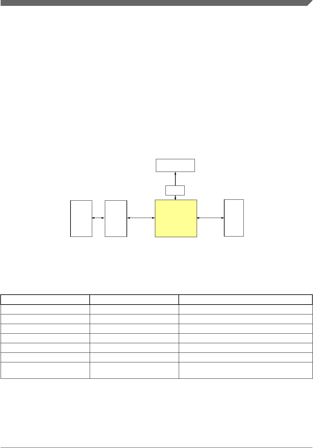
Chapter 35
Flash Memory Controller (FMC)
35.1 Chip-specific FMC information
This section summarizes how the module has been configured in the chip.
Register
access
Flash memory
controller
Transfers
Memory
protection
unit
Peripheral bus
controller 0
Transfers Flash
memory
Crossbar
switch
MSCM
Figure 35-1. Flash Memory Controller configuration
Wait/VLPW mode is not supported on this device. See Module operation in available low
power modes for details on available power modes.
Table 35-1. Reference links to related information
Topic Related module Reference
System memory map See attached S32K1xx_memory_map.xlsx
Clocking System Clock Generator Clock Distribution
Transfers Flash memory Flash Memory Module (FTFC)
Transfers System MPU Memory Protection Unit (MPU)
Transfers Crossbar Switch Crossbar Switch (AXBS-Lite)
Register access Peripheral Bridge Peripheral Bridge (AIPS-Lite)
Register controls MSCM OCMC1 field of MSCM registers On-Chip Memory
Descriptor Register (OCMDR0)
S32K1xx Series Reference Manual, Rev. 7, 04/2018
NXP Semiconductors 745

35.1.1 FMC masters
For master port assignments, see Crossbar Switch master assignments.
35.1.2 Program flash and Data flash port width
For Program flash and Data flash port widths, see Flash memory sizes.
35.2 Introduction
The Flash Memory Controller (FMC) is a memory acceleration unit that provides:
• an interface between the device and the dual-bank nonvolatile memory. Bank 0
consists of program flash memory, and bank 1 consists of FlexNVM.
• buffers that can accelerate flash memory and FlexNVM data transfers.
35.2.1 Overview
The Flash Memory Controller manages the interface between the device and the dual-
bank flash memory. The Program Flash is referred as Bank 0 and the Data Flash is
referred as Bank 1. The FMC receives status information detailing the configuration of
the memory and uses this information to ensure a proper interface. The following table
shows the supported read/write operations.
Flash memory type Read Write
Program flash memory 8-bit, 16-bit, and 32-bit reads —1
FlexNVM used as Data flash memory 8-bit, 16-bit, and 32-bit reads —1
FlexNVM and FlexRAM used as
emulated EEPROM
8-bit, 16-bit, and 32-bit reads 8-bit, 16-bit, and 32-bit writes
1. A write operation to program flash memory or to FlexNVM used as data flash memory results in a bus error.
In addition, for bank 0 and bank 1, the FMC provides separate mechanisms for
accelerating the interface between the device and the flash memory. A 128 (64 for bank1,
Data Flash)-bit speculation buffer can prefetch the next 128 (64 for bank1, Data Flash)-
bit flash memory location, and a single-entry 128 (64 for bank1, Data Flash)-bit buffer
can store previously accessed flash memory or FlexNVM data for quick access times.
35.2.2 Features
The FMC's features include:
Introduction
S32K1xx Series Reference Manual, Rev. 7, 04/2018
746 NXP Semiconductors

• Interface between the device and the dual-bank flash memory and FlexMemory:
• 8-bit, 16-bit, and 32-bit read operations to program flash memory and FlexNVM
used as data flash memory.
• 8-bit, 16-bit, and 32-bit read and write operations to FlexNVM and FlexRAM
used as emulated EEPROM.
• For bank 0 (Program Flash): The memory returns 128 bits, therefore read
accesses to consecutive 32-bit spaces in memory return the second, third, and
fourth read data with no wait states. For bank 1 (Data Flash): The memory
returns 64 bits, therefore read accesses to consecutive 32-bit spaces in memory
return the second read data with no wait states.
• For bank 0 and bank 1: Acceleration of data transfer from program flash memory and
FlexMemory to the device:
• 128 (64 for bank1, Data Flash)-bit prefetch speculation buffer with controls for
instruction/data access per master and bank
• Single-entry buffer per bank
35.3 Modes of operation
The FMC only operates when a bus master accesses the flash memory or FlexMemory.
In terms of device power modes, the FMC only operates in run modes, including VLPR
modes.
For any device power mode where the flash memory or FlexMemory cannot be accessed,
the FMC is disabled.
35.4 External signal description
The FMC has no external signals.
35.5 Functional description
The FMC is a flash acceleration unit with flexible buffers for user configuration.
Whenever a hit occurs for the prefetch speculation buffer, or the single-entry buffer, the
requested data is transferred within a single system clock.
Chapter 35 Flash Memory Controller (FMC)
S32K1xx Series Reference Manual, Rev. 7, 04/2018
NXP Semiconductors 747

35.5.1 Default configuration
Upon system reset, the FMC is configured to provide a significant level of buffering for
transfers from the flash memory or FlexMemory:
• For bank 0 and bank 1:
• Prefetch support for data and instructions is enabled.
• The single-entry buffer is enabled.
35.5.2 Speculative reads
The FMC has a single buffer that reads ahead to the next word in the flash memory if
there is an idle cycle. Speculative prefetching is programmable for each bank for
instruction and/or data accesses using MSCM_OCMDR0[5] and MSCM_OCMDR1[5]
(value 0 means "enables prefetches (or speculative accesses)"). Because many code
accesses are sequential, using the speculative prefetch buffer improves performance in
most cases.
When speculative reads are enabled, the FMC immediately requests the next sequential
address after a read completes. By requesting the next word immediately, speculative
reads can help to reduce or even eliminate wait states when accessing sequential code
and/or data.
For example, consider the following scenario:
• Assume a system with a 4:1 core-to-flash clock ratio and with speculative reads
enabled.
• The core requests four (for Data Flash, bank 1) or eight (for Program Flash, bank 0)
sequential longwords in back-to-back requests, meaning there are no core cycle
delays except for stalls waiting for flash memory data to be returned.
• None of the data is already stored in the cache or speculation buffer.
In this scenario, the sequence of events for accessing the four (for Data Flash, bank 1)
oreight (for Program Flash, bank 0) longwords is as follows:
1. The first longword read requires 4 to 7 core clocks.
2. Due to the 128-bit data bus of the flash memory, the second longword read takes
only 1 core clock because the data is already available inside the FMC. For the same
reason, the third and fourth longword reads each take only 1 core clock.
3. Per 64-bit for Data Flash (bank 1), accessing the third longword requires 3 core clock
cycles. The flash memory read itself takes 4 clocks, but the first clock overlaps with
the second longword read.
Functional description
S32K1xx Series Reference Manual, Rev. 7, 04/2018
748 NXP Semiconductors

4. Per 128-bit for Program Flash (bank 0), accessing the fifth longword requires 1 core
clock cycle. The flash memory read itself takes 4 clocks, but the access starts
immediately after the first read. As a result, 3 clocks for this access overlap with the
second, third, and fourth longword reads from the core.
5. Per 64-bit for Data Flash (bank 1), reading the fourth longword, like the second
longword, takes only 1 clock due to the 64-bit flash memory data bus.
6. Per 128-bit for Program Flash (bank 0), reading the sixth, seventh, and eighth
longwords takes only 1 clock each because the data is already available inside the
FMC.
35.6 Initialization and application information
The FMC does not require user initialization. Flash acceleration features are enabled by
default.
Chapter 35 Flash Memory Controller (FMC)
S32K1xx Series Reference Manual, Rev. 7, 04/2018
NXP Semiconductors 749

Initialization and application information
S32K1xx Series Reference Manual, Rev. 7, 04/2018
750 NXP Semiconductors
Chapter 36
Flash Memory Module (FTFC)
36.1 Chip-specific FTFC information
This section summarizes how the module has been configured in the chip.
Register
access
Flash memory
Transfers
Flash memory
controller
Peripheral bus
controller 0
Figure 36-1. Flash memory configuration
Wait mode is not supported on this device. See Module operation in available low power
modes for details on power modes.
Table 36-1. Reference links to related information
Topic Related module Reference
System memory map See attached S32K1xx_memory_map.xlsx
Clocking System Clock Generator Clock Distribution
Transfers Flash Memory Controller Flash Memory Controller (FMC)
Register access Peripheral Bridge Peripheral Bridge (AIPS-Lite)
36.1.1 Flash memory types
The chip contains these types of flash memory:
S32K1xx Series Reference Manual, Rev. 7, 04/2018
NXP Semiconductors 751

• Program flash memory: nonvolatile flash memory that can execute program code
• FlexMemory, which encompasses the following memory types:
• FlexNVM: nonvolatile flash memory that can
• Execute program code
• Store data
• Back up emulated EEPROM data
• FlexRAM: RAM that
• Can be used as SRAM or as high-endurance emulated EEPROM storage
• Accelerates flash-memory programming
NOTE
• PCC_FTFC[CGC] must be 1 during secure boot
and when FlexRAM is operating as System RAM.
• CSEc (Security) or EEPROM writes/erase will
trigger error flags in HSRUN mode (112 MHz)
because this use case is not allowed to execute
simultaneously. The device need to switch to RUN
mode (80 Mhz) to execute CSEc (Security) or
EEPROM writes/erase.
36.1.2 Flash memory sizes
The FTFC module is offered in various configurations. Each configuration consists of
one or more read partitions. A given read partition may only be occupied with one task at
a time. Having multiple read partitions allows for concurrent operations such as Read
While Write (RWW). Special consideration must be given to a partition with FlexNVM
in it as the FlexMEM feature is comprised of several aspects including Data Flash,
Emulated EEPROM backup, CSEc features (requires Emulated EEPROM to be enabled).
Thus, a single FlexMEM read partition could be requested to be read from, programmed,
erased, Emulated EEPROM update, or CSEc cryptographic operation, but only one of
these at one time.
The sizes of flash memory types on the chip are:
Chips Program Flash FlexNVM FlexRAM Program Flash
port width
Data Flash port
width
S32K116 128 KB 32 KB 2 KB 64 64
S32K118 256 KB 32 KB 2 KB 64 64
S32K142 256 KB 64 KB 4 KB 64 64
S32K144 512 KB 64 KB 4 KB 128 64
Table continues on the next page...
Chip-specific FTFC information
S32K1xx Series Reference Manual, Rev. 7, 04/2018
752 NXP Semiconductors

Chips Program Flash FlexNVM FlexRAM Program Flash
port width
Data Flash port
width
S32K146 1 M 64 KB 4 KB 128 64
S32K148 Up to 2 M Up to 512 KB14 KB 128 128
1. The available Program Flash is reduced by the size of FlexNVM. When the Program Flash is completely used, then
FlexNVM is not available.
NOTE
Size of speculative buffer for Program Flash is equal to size of
the Program Flash port width. Size of the speculative buffer for
Data Flash is equal to the size of the Data flash port width. For
details see FMC chapter
36.1.2.1 128 KB program flash / 32 KB FlexNVM / 2 KB FlexRAM
module
The 128 KB FTFC flash module consists of two NVM read partitions and one FlexRAM
block:
• One 128 KB program flash read partition (non-interleaved 1 × 128 KB)1
• One 32 KB FlexNVM read partition (non-interleaved 1 × 32 KB)1
• One 2 KB FlexRAM
Figure 36-2 shows the 128 KB flash module in various configurations.
NOTE
When the FlexNVM is configured for Emulated EEPROM, the
associated EFlash disappears from the memory map as shown
.
1. Non-interleaved blocks have a data width of 64-bits.
Chapter 36 Flash Memory Module (FTFC)
S32K1xx Series Reference Manual, Rev. 7, 04/2018
NXP Semiconductors 753

Analog Block
128 KB
P Flash
2 KB
System RAM
1 read
partition
1 read
partition
1 x 128 KB
(64-bit non-interleaved)
1 x 32 KB
(64-bit non-interleaved)
0
X
Y
32 KB
D Flash
16 KB
D Flash
2 KB
EERAM
128 bytes
PRAM
128 KB
P Flash
CSEc Enabled
(without CSEc, remove the PRAM)
128 bytes
PRAM
128 KB
P Flash
32 KB
E Flash
DEPART configuration command
2 KB
EERAM
16 KB
E Flash
Figure 36-2. 128 KB flash memory map
36.1.2.1.1 Emulated EEPROM data set size (EEESIZE)
Table 36-2. Emulated EEPROM data set size for 2 KB FlexRAM
Data flash IFR: 0x03FE
7 6 5 4 3 2 1 0
1 EEERST 1 1 EEESIZE
= Unimplemented or Reserved
Chip-specific FTFC information
S32K1xx Series Reference Manual, Rev. 7, 04/2018
754 NXP Semiconductors

Table 36-3. EEPROM Data Set Size Field Description
Field Description
7
Reserved
This read-only bitfield is reserved and must always be written as one.
6
EEERST
EEPROM Load on Reset — Determines whether the flash reset sequence takes time to load the
FlexRAM with valid EEPROM data.
'0' = FlexRAM is not loaded with valid EEPROM data during the flash reset sequence (see the Set
FlexRAM Function command to load the FlexRAM with valid EEPROM data)
'1' = FlexRAM is loaded with valid EEPROM data during the flash reset sequence
For CSEc enabled parts, the FlexRAM is always loaded with valid EEPROM data during the flash
reset sequence, and will include the inaccessible Key <n> addresses as applicable.
5-4 Reserved
3-0
EEESIZE
EEPROM Size — Encoding of the total available FlexRAM for emulated EEPROM use.
NOTE: 1. EEESIZE must be 0 bytes (1111b) when the FlexNVM partition code is set to 'No
EEPROM'.
2. For CSEc enabled parts, the EEE size must be '0011' - 2,048 Bytes
'0000' = Reserved
'0001' = Reserved
'0010' = Reserved
'0011' = 2,048 Bytes
'0100' = Reserved
'0101' = Reserved
'0110' = Reserved
'0111' = Reserved
'1000' = Reserved
'1001' = Reserved
'1010' = Reserved
'1011' = Reserved
'1100' = Reserved
'1101' = Reserved
'1110' = Reserved
'1111' = 0 Bytes
36.1.2.1.2 FlexNVM partition code (DEPART)
The FlexNVM partition code byte in the data flash 0 IFR supplies a code which specifies
how to split the FlexNVM block between data flash memory and emulated EEPROM
backup memory supporting emulated EEPROM functions. To program the DEPART
value, see the Program Partition command.
Table 36-4. FlexNVM partition code
Data Flash IFR: 0x03FC
7 6 5 4 3 2 1 0
1 1 1 1 DEPART
= Unimplemented or Reserved
Chapter 36 Flash Memory Module (FTFC)
S32K1xx Series Reference Manual, Rev. 7, 04/2018
NXP Semiconductors 755

Table 36-5. FlexNVM partition code field description
Field Description
7-4
Reserved
This read-only bitfield is reserved and must always be written as one.
3-0
DEPART
FlexNVM Partition Code — Encoding of the data flash / emulated EEPROM backup split within the
FlexNVM memory block. FlexNVM memory not partitioned for data flash is used to store EEPROM
records. For CSEc enabled parts - 32 KB of Data Flash.
DEPART Data flash size (KB) EEPROM backup size
(KB)
0000 32 0
0011 0 32
1000 0 32
1001 8 24
1011 32 0
36.1.2.2 256 KB program flash / 32 KB FlexNVM / 2 KB FlexRAM
module
This 256 KB FTFC flash module consists of two NVM read partitions and one FlexRAM
block:
• One 256 KB program flash read partition (non-interleaved 1 × 256 KB)2
• One 32 KB FlexNVM read partition (non-interleaved 1 × 32 KB)2
• One 2 KB FlexRAM
Figure 36-3 shows the 256 KB flash module in various configurations.
NOTE
When the FlexNVM is configured for Emulated EEPROM, the
associated EFlash disappears from the memory map as shown
.
2. Non-interleaved blocks have a data width of 64-bits.
Chip-specific FTFC information
S32K1xx Series Reference Manual, Rev. 7, 04/2018
756 NXP Semiconductors
Analog Block
256 KB
P Flash
2 KB
System RAM
1 read
partition
1 read
partition
1 x 256 KB
(64-bit non-interleaved)
1 x 32 KB
(64-bit non-interleaved)
0
X
Y
32 KB
D Flash
16 KB
D Flash
2 KB
EERAM
128 bytes
PRAM
256 KB
P Flash
CSEc Enabled
(without CSEc, remove the PRAM)
128 bytes
PRAM
256 KB
P Flash
32 KB
E Flash
DEPART configuration command
2 KB
EERAM
16 KB
E Flash
Figure 36-3. 256 KB flash memory map
36.1.2.2.1 Emulated EEPROM data set size (EEESIZE)
Table 36-6. Emulated EEPROM data set size for 2 KB FlexRAM
Data flash IFR: 0x03FE
7 6 5 4 3 2 1 0
1 EEERST 1 1 EEESIZE
= Unimplemented or Reserved
Chapter 36 Flash Memory Module (FTFC)
S32K1xx Series Reference Manual, Rev. 7, 04/2018
NXP Semiconductors 757

Table 36-7. EEPROM Data Set Size Field Description
Field Description
7
Reserved
This read-only bitfield is reserved and must always be written as one.
6
EEERST
EEPROM Load on Reset — Determines whether the flash reset sequence takes time to load the
FlexRAM with valid EEPROM data.
'0' = FlexRAM is not loaded with valid EEPROM data during the flash reset sequence (see the Set
FlexRAM Function command to load the FlexRAM with valid EEPROM data)
'1' = FlexRAM is loaded with valid EEPROM data during the flash reset sequence
For CSEc enabled parts, the FlexRAM is always loaded with valid EEPROM data during the flash
reset sequence, and will include the inaccessible Key <n> addresses as applicable.
5-4 Reserved
3-0
EEESIZE
EEPROM Size — Encoding of the total available FlexRAM for emulated EEPROM use.
NOTE: 1. EEESIZE must be 0 bytes (1111b) when the FlexNVM partition code is set to 'No
EEPROM'.
2. For CSEc enabled parts, the EEE size must be '0011' - 2,048 Bytes
'0000' = Reserved
'0001' = Reserved
'0010' = Reserved
'0011' = 2,048 Bytes
'0100' = Reserved
'0101' = Reserved
'0110' = Reserved
'0111' = Reserved
'1000' = Reserved
'1001' = Reserved
'1010' = Reserved
'1011' = Reserved
'1100' = Reserved
'1101' = Reserved
'1110' = Reserved
'1111' = 0 Bytes
36.1.2.2.2 FlexNVM partition code (DEPART)
The FlexNVM partition code byte in the data flash 0 IFR supplies a code which specifies
how to split the FlexNVM block between data flash memory and emulated EEPROM
backup memory supporting emulated EEPROM functions. To program the DEPART
value, see the Program Partition command.
Table 36-8. FlexNVM partition code
Data Flash IFR: 0x03FC
7 6 5 4 3 2 1 0
1 1 1 1 DEPART
= Unimplemented or Reserved
Chip-specific FTFC information
S32K1xx Series Reference Manual, Rev. 7, 04/2018
758 NXP Semiconductors

Table 36-9. FlexNVM partition code field description
Field Description
7-4
Reserved
This read-only bitfield is reserved and must always be written as one.
3-0
DEPART
FlexNVM Partition Code — Encoding of the data flash / emulated EEPROM backup split within the
FlexNVM memory block. FlexNVM memory not partitioned for data flash is used to store EEPROM
records. For CSEc enabled parts - 32 KB of Data Flash.
DEPART Data flash size (KB) EEPROM backup size
(KB)
0000 32 0
0011 0 32
1000 0 32
1001 8 24
1011 32 0
36.1.2.3 256 KB program flash / 64 KB FlexNVM / 4 KB FlexRAM
module
This 256 KB FTFC flash module consists of two NVM read partitions and one FlexRAM
block:
• One 256 KB program flash read partition (non-interleaved 1 × 256 KB)3
• One 64 KB FlexNVM read partition (non-interleaved 1 × 64 KB)3
• One 4 KB FlexRAM
Figure 36-4 shows the 256 KB flash module in various configurations.
NOTE
When the FlexNVM is configured for Emulated EEPROM, the
associated EFlash disappears from the memory map as shown
.
3. Non-interleaved blocks have a data width of 64-bits.
Chapter 36 Flash Memory Module (FTFC)
S32K1xx Series Reference Manual, Rev. 7, 04/2018
NXP Semiconductors 759
Analog Block
256 KB
P Flash
64 KB
D Flash
4 KB
System RAM
1 read
partition
1 read
partition
1 x 256 KB
(64-bit non-interleaved)
1 x 64 KB
(64-bit non-interleaved)
0
X
Y
32 KB
D Flash
2 KB
EERAM
128 bytes
PRAM
32 KB
E Flash
16 KB
D Flash
3 KB
EERAM
128 bytes
PRAM
48 KB
E Flash
4 KB
EERAM
CSEc Enabled
(without CSEc, remove the PRAM)
128 bytes
PRAM
64 KB
E Flash
DEPART configuration command
256 KB
P Flash 256 KB
P Flash 256 KB
P Flash
Figure 36-4. 256 KB flash memory map
36.1.2.3.1 Emulated EEPROM data set size (EEESIZE)
Table 36-10. Emulated EEPROM data set size for 4 KB FlexRAM
Data flash IFR: 0x03FE
7 6 5 4 3 2 1 0
1 EEERST 1 1 EEESIZE
= Unimplemented or Reserved
Chip-specific FTFC information
S32K1xx Series Reference Manual, Rev. 7, 04/2018
760 NXP Semiconductors

Table 36-11. EEPROM Data Set Size Field Description
Field Description
7
Reserved
This read-only bitfield is reserved and must always be written as one.
6
EEERST
EEPROM Load on Reset — Determines whether the flash reset sequence takes time to load the
FlexRAM with valid EEPROM data.
'0' = FlexRAM is not loaded with valid EEPROM data during the flash reset sequence (see the Set
FlexRAM Function command to load the FlexRAM with valid EEPROM data)
'1' = FlexRAM is loaded with valid EEPROM data during the flash reset sequence
For CSEc enabled parts, the FlexRAM is always loaded with valid EEPROM data during the flash
reset sequence, and will include the inaccessible Key <n> addresses as applicable.
5-4 Reserved
3-0
EEESIZE
EEPROM Size — Encoding of the total available FlexRAM for emulated EEPROM use.
NOTE: 1. EEESIZE must be 0 bytes (1111b) when the FlexNVM partition code is set to 'No
EEPROM'.
2. For CSEc enabled parts, the EEE size must be '0010' - 4,096 bytes
'0000' = Reserved
'0001' = Reserved
'0010' = 4,096 bytes
'0011' = Reserved
'0100' = Reserved
'0101' = Reserved
'0110' = Reserved
'0111' = Reserved
'1000' = Reserved
'1001' = Reserved
'1010' = Reserved
'1011' = Reserved
'1100' = Reserved
'1101' = Reserved
'1110' = Reserved
'1111' = 0 Bytes
36.1.2.3.2 FlexNVM partition code (DEPART)
The FlexNVM partition code byte in the data flash 0 IFR supplies a code which specifies
how to split the FlexNVM block between data flash memory and emulated EEPROM
backup memory supporting emulated EEPROM functions. To program the DEPART
value, see the Program Partition command.
Table 36-12. FlexNVM partition code
Data Flash IFR: 0x03FC
7 6 5 4 3 2 1 0
1 1 1 1 DEPART
= Unimplemented or Reserved
Chapter 36 Flash Memory Module (FTFC)
S32K1xx Series Reference Manual, Rev. 7, 04/2018
NXP Semiconductors 761

Table 36-13. FlexNVM partition code field description
Field Description
7-4
Reserved
This read-only bitfield is reserved and must always be written as one.
3-0
DEPART
FlexNVM Partition Code — Encoding of the data flash / emulated EEPROM backup split within the
FlexNVM memory block. FlexNVM memory not partitioned for data flash is used to store EEPROM
records. For CSEc enabled parts - 64 KB of Data Flash.
DEPART Data flash size (KB) EEPROM backup size
(KB)
0000 64 0
0011 32 32
0100 0 64
1000 0 64
1010 16 48
1011 32 32
1100 64 0
36.1.2.4 512 KB program flash / 64 KB FlexNVM / 4 KB FlexRAM
module
The 512 KB FTFC flash module consists of two NVM read partitions and one FlexRAM
block:
• One 512 KB program flash read partition (interleaved 2 × 256 KB)4
• One 64 KB FlexNVM read partition (non-interleaved 1 × 64 KB)5
• One 4 KB FlexRAM
Figure 36-5 shows the 512 KB flash module in various configurations.
NOTE
When the FlexNVM is configured for Emulated EEPROM, the
associated EFlash disappears from the memory map as shown
.
4. Interleaved blocks have a data width of 128-bits.
5. Non-interleaved blocks have a data width of 64-bits.
Chip-specific FTFC information
S32K1xx Series Reference Manual, Rev. 7, 04/2018
762 NXP Semiconductors

Analog Block
512 KB
P Flash
64 KB
D Flash
4 KB
System RAM
1 read
partition
1 read
partition
2 x 256 KB
(128-bit interleaved)
1 x 64 KB
(64-bit non-interleaved)
0
X
Y
32 KB
D Flash
2 KB
EERAM
128 bytes
PRAM
512 KB
P Flash
32 KB
E Flash
16 KB
D Flash
3 KB
EERAM
128 bytes
PRAM
512 KB
P Flash
48 KB
E Flash
4 KB
EERAM
CSEc Enabled
(without CSEc, remove the PRAM)
128 bytes
PRAM
512 KB
P Flash
64 KB
E Flash
DEPART configuration command
Figure 36-5. 512 KB flash memory map
36.1.2.4.1 Emulated EEPROM data set size (EEESIZE)
Table 36-14. Emulated EEPROM data set size for 4 KB FlexRAM
Data flash IFR: 0x03FE
7 6 5 4 3 2 1 0
1 EEERST 1 1 EEESIZE
= Unimplemented or Reserved
Chapter 36 Flash Memory Module (FTFC)
S32K1xx Series Reference Manual, Rev. 7, 04/2018
NXP Semiconductors 763

Table 36-15. EEPROM Data Set Size Field Description
Field Description
7
Reserved
This read-only bitfield is reserved and must always be written as one.
6
EEERST
EEPROM Load on Reset — Determines whether the flash reset sequence takes time to load the
FlexRAM with valid EEPROM data.
'0' = FlexRAM is not loaded with valid EEPROM data during the flash reset sequence (see the Set
FlexRAM Function command to load the FlexRAM with valid EEPROM data)
'1' = FlexRAM is loaded with valid EEPROM data during the flash reset sequence
For CSEc enabled parts, the FlexRAM is always loaded with valid EEPROM data during the flash
reset sequence, and will include the inaccessible Key <n> addresses as applicable.
5-4 Reserved
3-0
EEESIZE
EEPROM Size — Encoding of the total available FlexRAM for emulated EEPROM use.
NOTE: 1. EEESIZE must be 0 bytes (1111b) when the FlexNVM partition code is set to 'No
EEPROM'.
2. For CSEc enabled parts, the EEE size must be '0010' - 4,096 bytes
'0000' = Reserved
'0001' = Reserved
'0010' = 4,096 bytes
'0011' = Reserved
'0100' = Reserved
'0101' = Reserved
'0110' = Reserved
'0111' = Reserved
'1000' = Reserved
'1001' = Reserved
'1010' = Reserved
'1011' = Reserved
'1100' = Reserved
'1101' = Reserved
'1110' = Reserved
'1111' = 0 Bytes
36.1.2.4.2 FlexNVM partition code (DEPART)
The FlexNVM partition code byte in the data flash 0 IFR supplies a code which specifies
how to split the FlexNVM block between data flash memory and emulated EEPROM
backup memory supporting emulated EEPROM functions. To program the DEPART
value, see the Program Partition command.
Table 36-16. FlexNVM partition code
Data Flash IFR: 0x03FC
7 6 5 4 3 2 1 0
1 1 1 1 DEPART
= Unimplemented or Reserved
Chip-specific FTFC information
S32K1xx Series Reference Manual, Rev. 7, 04/2018
764 NXP Semiconductors

Table 36-17. FlexNVM partition code field description
Field Description
7-4
Reserved
This read-only bitfield is reserved and must always be written as one.
3-0
DEPART
FlexNVM Partition Code — Encoding of the data flash / emulated EEPROM backup split within the
FlexNVM memory block. FlexNVM memory not partitioned for data flash is used to store EEPROM
records. For CSEc enabled parts - 64 KB of Data Flash.
DEPART Data flash size (KB) EEPROM backup size
(KB)
0000 64 0
0011 32 32
0100 0 64
1000 0 64
1010 16 48
1011 32 32
1100 64 0
36.1.2.5 1 MB program flash / 256 KB FlexNVM / 4 KB FlexRAM
module
The 1 MB FTFC flash module consists of three NVM read partitions and one FlexRAM
block:
• Two 512 KB program flash read partitions (interleaved 2 × 256 KB)6
• One 64 KB FlexNVM read partition (non-interleaved 1 × 64 KB)7
• One 4 KB FlexRAM
Figure 36-6 shows the 1 MB flash module in various configurations.
NOTE
When the FlexNVM is configured for Emulated EEPROM, the
associated EFlash disappears from the memory map as shown
.
6. Interleaved blocks have a data width of 128-bits.
7. Non-interleaved blocks have a data width of 64-bits.
Chapter 36 Flash Memory Module (FTFC)
S32K1xx Series Reference Manual, Rev. 7, 04/2018
NXP Semiconductors 765
1st Analog Block
2nd Analog Block
1 MB
P Flash
64 KB
D Flash
4 KB
FlexRAM
2 read
partitions
1 read
partition
4 x 256 KB
(128-bit interleaved)
1 x 64 KB
(64-bit non-interleaved)
0
X
Y
32 KB
D Flash
2 KB
EERAM
128 bytes
PRAM
32 KB
E Flash
16 KB
D Flash
3 KB
EERAM
128 bytes
PRAM
48 KB
E Flash
4 KB
EERAM
CSEc Enabled
(without CSEc, remove the PRAM)
128 bytes
PRAM
64 KB
E Flash
DEPART configuration command
1 MB
P Flash 1 MB
P Flash 1 MB
P Flash
Figure 36-6. 1 MB flash memory map
36.1.2.5.1 Emulated EEPROM data set size (EEESIZE)
Table 36-18. Emulated EEPROM data set size for 4 KB FlexRAM
Data flash IFR: 0x03FE
7 6 5 4 3 2 1 0
1 EEERST 1 1 EEESIZE
= Unimplemented or Reserved
Table 36-19. EEPROM Data Set Size Field Description
Field Description
7 This read-only bitfield is reserved and must always be written as one.
Table continues on the next page...
Chip-specific FTFC information
S32K1xx Series Reference Manual, Rev. 7, 04/2018
766 NXP Semiconductors

Table 36-19. EEPROM Data Set Size Field Description (continued)
Field Description
Reserved
6
EEERST
EEPROM Load on Reset — Determines whether the flash reset sequence takes time to load the
FlexRAM with valid EEPROM data.
'0' = FlexRAM is not loaded with valid EEPROM data during the flash reset sequence (see the Set
FlexRAM Function command to load the FlexRAM with valid EEPROM data)
'1' = FlexRAM is loaded with valid EEPROM data during the flash reset sequence
For CSEc enabled parts, the FlexRAM is always loaded with valid EEPROM data during the flash
reset sequence, and will include the inaccessible Key <n> addresses as applicable.
5-4 Reserved
3-0
EEESIZE
EEPROM Size — Encoding of the total available FlexRAM for emulated EEPROM use.
NOTE: 1. EEESIZE must be 0 bytes (1111b) when the FlexNVM partition code is set to 'No
EEPROM'.
2. For CSEc enabled parts, the EEE size must be '0010' - 4,096 bytes
'0000' = Reserved
'0001' = Reserved
'0010' = 4,096 bytes
'0011' = Reserved
'0100' = Reserved
'0101' = Reserved
'0110' = Reserved
'0111' = Reserved
'1000' = Reserved
'1001' = Reserved
'1010' = Reserved
'1011' = Reserved
'1100' = Reserved
'1101' = Reserved
'1110' = Reserved
'1111' = 0 Bytes
36.1.2.5.2 FlexNVM partition code (DEPART)
The FlexNVM partition code byte in the data flash 0 IFR supplies a code which specifies
how to split the FlexNVM block between data flash memory and emulated EEPROM
backup memory supporting emulated EEPROM functions. To program the DEPART
value, see the Program Partition command.
Table 36-20. FlexNVM partition code
Data Flash IFR: 0x03FC
7 6 5 4 3 2 1 0
1 1 1 1 DEPART
= Unimplemented or Reserved
Chapter 36 Flash Memory Module (FTFC)
S32K1xx Series Reference Manual, Rev. 7, 04/2018
NXP Semiconductors 767

Table 36-21. FlexNVM partition code field description
Field Description
7-4
Reserved
This read-only bitfield is reserved and must always be written as one.
3-0
DEPART
FlexNVM Partition Code — Encoding of the data flash / emulated EEPROM backup split within the
FlexNVM memory block. FlexNVM memory not partitioned for data flash is used to store EEPROM
records. For CSEc enabled parts - 64 KB of Data Flash.
DEPART Data flash size (KB) EEPROM backup size
(KB)
0000 64 0
0011 32 32
0100 0 64
1000 0 64
1010 16 48
1011 32 32
1100 64 0
36.1.2.6 2 MB program flash / 256 KB FlexNVM / 4 KB FlexRAM
module
The 2 MB FTFC flash module consists of four NVM read partitions and one FlexRAM
block:
• Three 512 KB program flash read partitions (interleaved 2 × 256 KB)8
• One shared Program/Data Flash (FlexNVM) read partition (interleaved 2 ×
256 KB)8. This shared read partition consists of 448 KB PFlash (interleaved 2 ×
224 KB) and 64 KB FlexNVM (interleaved 2 × 32 KB) areas.
• One 4 KB FlexRAM
Figure 36-7 shows the 2 MB flash module in various configurations.
NOTE
1. The last partition (448 KB Program Flash and 64 KB Data
Flash/FlexMEM), being a single read partition which is
shared, needs consideration as code may not execute from
the 448 KB Program Flash area at the same time as the
64 KB Data Flash/FlexNVM area is being accessed.
8. Interleaved blocks have a data width of 128-bits.
Chip-specific FTFC information
S32K1xx Series Reference Manual, Rev. 7, 04/2018
768 NXP Semiconductors
2. Since the FlexNVM is configured for Emulated EEPROM
on the 2 MB module, DEPART values are limited to 64 KB
or none.
.
1st Analog Block
2nd Analog Block
448 KB
D Flash
4 KB
FlexRAM
3 read
partitions
1 read
partition
6 x 256 KB
(128-bit interleaved)
2 x 256 KB
(128-bit interleaved)
4 KB
EERAM
128 bytes
PRAM
0
X
Y
CSEc Enabled FlexMEM Enabled
1.5 MB
P Flash
1.5 MB
P Flash 1.5 MB
P Flash
448 KB
D (P) Flash
64 KB
D Flash
448 KB
D (P) Flash
4 KB
EERAM 4 KB
EERAM
Figure 36-7. 2 MB flash memory map
36.1.2.6.1 Emulated EEPROM data set size (EEESIZE)
Table 36-22. Emulated EEPROM data set size for 4 KB FlexRAM
Data flash IFR: 0x03FE
7 6 5 4 3 2 1 0
1 EEERST 1 1 EEESIZE
= Unimplemented or Reserved
Chapter 36 Flash Memory Module (FTFC)
S32K1xx Series Reference Manual, Rev. 7, 04/2018
NXP Semiconductors 769

Table 36-23. EEPROM Data Set Size Field Description
Field Description
7
Reserved
This read-only bitfield is reserved and must always be written as one.
6
EEERST
EEPROM Load on Reset — Determines whether the flash reset sequence takes time to load the
FlexRAM with valid EEPROM data.
'0' = FlexRAM is not loaded with valid EEPROM data during the flash reset sequence (see the Set
FlexRAM Function command to load the FlexRAM with valid EEPROM data)
'1' = FlexRAM is loaded with valid EEPROM data during the flash reset sequence
For CSEc enabled parts, the FlexRAM is always loaded with valid EEPROM data during the flash
reset sequence, and will include the inaccessible Key <n> addresses as applicable.
5-4 Reserved
3-0
EEESIZE
EEPROM Size — Encoding of the total available FlexRAM for emulated EEPROM use.
NOTE: 1. EEESIZE must be 0 bytes (1111b) when the FlexNVM partition code is set to 'No
EEPROM'.
2. For CSEc enabled parts, the EEE size must be '0010' - 4,096 bytes
'0000' = Reserved
'0001' = Reserved
'0010' = 4,096 bytes
'0011' = Reserved
'0100' = Reserved
'0101' = Reserved
'0110' = Reserved
'0111' = Reserved
'1000' = Reserved
'1001' = Reserved
'1010' = Reserved
'1011' = Reserved
'1100' = Reserved
'1101' = Reserved
'1110' = Reserved
'1111' = 0 Bytes
36.1.2.6.2 FlexNVM partition code (DEPART)
The FlexNVM partition code byte in the data flash 0 IFR supplies a code which specifies
how to split the FlexNVM block between data flash memory and emulated EEPROM
backup memory supporting emulated EEPROM functions. To program the DEPART
value, see the Program Partition command.
Table 36-24. FlexNVM partition code
Data Flash IFR: 0x03FC
7 6 5 4 3 2 1 0
1 1 1 1 DEPART
= Unimplemented or Reserved
Chip-specific FTFC information
S32K1xx Series Reference Manual, Rev. 7, 04/2018
770 NXP Semiconductors
Table 36-25. FlexNVM partition code field description
Field Description
7-4
Reserved
This read-only bitfield is reserved and must always be written as one.
3-0
DEPART
FlexNVM Partition Code — Encoding of the data flash / emulated EEPROM backup split within the
FlexNVM memory block. FlexNVM memory not partitioned for data flash is used to store EEPROM
records. For CSEc enabled parts - 512 KB of Data Flash.
DEPART Data flash size (KB) EEPROM backup size
(KB)
0000 512 KB 0
0100 DFlash size - EEPROM size
(512 KB - 64 KB = 448 KB
64
1111 512 KB 0
36.1.3 Flash memory map
The various types of flash memory and the registers for flash memory have different base
addresses, as the following figure shows. Each base address is specified in the attached
file S32K1xx_memory_map.xlsx.
Program flash
memory
Flash configuration field
FlexNVM base address
Program flash memory base address
Flash memory base address
Registers
FlexNVM
FlexRAM
FlexRAM base address
Figure 36-8. Flash memory map
36.1.4 Flash memory security
See Flash memory security.
Chapter 36 Flash Memory Module (FTFC)
S32K1xx Series Reference Manual, Rev. 7, 04/2018
NXP Semiconductors 771

36.1.5 Power mode restrictions on flash memory programming
The flash memory should not be programmed or erased while the chip is operating in:
• VLPR mode
• HSRUN mode
No FTFC commands of any type, including CSE commands (for CSEc parts), are
available when the chip is in these modes.
36.1.6 Flash memory modes
The FTFC module has two operating modes: NVM Normal and NVM Special.
• On this chip, the FTFC is always configured in NVM Normal mode.
• The chip has no operating conditions in which the FTFC is configured for NVM
Special mode.
36.1.7 Erase all contents of flash memory
An Erase All Blocks command can be launched by software through a series of
peripheral bus writes to FTFC registers.
In addition, the entire flash memory can be erased from the external SWJ-DP debug port
according to this sequence:
1. Set MDM-AP Control[0].
2. MDM-AP Status[0] sets to indicate the mass erase command has been accepted.
3. MDM-AP Status[0] clears when the mass erase completes.
36.1.8 Customize MCU operations via FTFC_FOPT register
The Flash Option Register (FOPT) allows you to customize the operation of the MCU at
boot time. For details about the meaning of FOPT values and how to program alternative
configuration options, see FOPT boot options.
Chip-specific FTFC information
S32K1xx Series Reference Manual, Rev. 7, 04/2018
772 NXP Semiconductors

36.1.9 Simultaneous operations on PFLASH read partitions
While executing from a particular PFLASH read partition , FTFC commands (except
parallel boot) cannot run over that PFLASH read partition. Below are number of
PFLASH read partitions in each device:
Table 36-26. PFLASH partitions
Chip No. of PFLASH read partitions
S32K116 1 (128 KB)
S32K118 1 (256 KB)
S32K142 1 (256 KB)
S32K144 1 (512 KB)
S32K146 2 (each 512 KB)
S32K148 3 (each 512 KB)
36.2 Introduction
The FTFC module includes the following accessible memory regions:
• Program flash memory for vector space and code store
• FlexNVM for data store and additional code store
• FlexRAM for high-endurance data store or traditional RAM
Flash memory is ideal for single-supply applications, permitting in-the-field erase and
reprogramming operations without the need for any external high voltage power sources.
The FTFC module includes a memory controller that executes commands to modify flash
memory contents. An erased bit reads '1' and a programmed bit reads '0'. The
programming operation is unidirectional; it can only move bits from the '1' state (erased)
to the '0' state (programmed). Only the erase operation restores bits from '0' to '1'; bits
cannot be programmed from a '0' to a '1'.
CAUTION
A flash memory location must be in the erased state before
being programmed. Cumulative programming of bits (back-to-
back program operations without an intervening erase) within a
flash memory location is not allowed. Re-programming of
existing 0s to 0 is not allowed as this overstresses the device.
The standard shipping condition for flash memory is erased
with security disabled. Data loss over time may occur due to
degradation of the erased ('1') states and/or programmed ('0')
Chapter 36 Flash Memory Module (FTFC)
S32K1xx Series Reference Manual, Rev. 7, 04/2018
NXP Semiconductors 773

states. Therefore, it is recommended that each flash block or
sector be re-erased immediately prior to factory programming
to ensure that the full data retention capability is achieved.
36.2.1 Features
The FTFC module includes the following features.
NOTE
See the device's Chip Configuration details for the exact
amount of flash memory available on your device.
36.2.1.1 Program flash memory features
• Sector size of 2 KB for non-interleaved configurations (i.e., 256 KB and less). 4 KB
for interleaved configurations (512 KB and greater)
• Program flash protection scheme prevents accidental program or erase of stored data
• Automated, built-in, program and erase algorithms with verify
• Section programming for faster bulk programming times
• Read access to the program flash block is possible while programming or erasing
data in the data flash block or FlexRAM
36.2.1.2 FlexNVM memory features
When FlexNVM is partitioned for data flash memory:
• Sector size of 2 KB for non-interleaved configurations (i.e., all configurations other
than the 2 MB configuration). 4 KB for interleaved configurations (2 MB)
• Protection scheme prevents accidental program or erase of stored data
• Automated, built-in program and erase algorithms with verify
• Section programming for faster bulk programming times
• Read access to the data flash block possible while programming or erasing data in the
program flash block
36.2.1.3 FlexRAM features
• Memory that can be used as traditional RAM or as high-endurance emulated
EEPROM storage
• Up to 4 KB of FlexRAM configured for emulated EEPROM or traditional RAM
operations
Introduction
S32K1xx Series Reference Manual, Rev. 7, 04/2018
774 NXP Semiconductors

• When configured for emulated EEPROM:
• Protection scheme prevents accidental modification for emulated EEPROM
• Built-in hardware emulation scheme to automate emulated EEPROM record
maintenance functions
• Programmable emulated EEPROM data set size and FlexNVM partition code
facilitating emulated EEPROM memory endurance trade-offs
• Supports FlexRAM aligned writes of 1, 2, or 4 bytes at a time
• Read access to FlexRAM possible while programming or erasing data in the
program or data flash memory
• When configured for traditional RAM:
• Read and write access possible to the FlexRAM while programming or erasing
data in the program or data flash memory
36.2.1.4 Cryptographic Services Engine (CSEc) module features
The FTFC module includes feature support for the SHE (Secure Hardware Extension)
specification.
• Secure cryptographic key storage (ranging from 3 to 17 user keys)
• AES-128 encryption and decryption
• AES-128 CMAC (Cipher-based Message Authentication Code) calculation and
authentication
• ECB (Electronic Cypher Book) Mode - encryption and decryption
• CBC (Cipher Block Chaining) Mode - encryption and decryption
• True and Pseudo random number generation
• Miyaguchi-Prenell compression function
• Secure Boot Mode (user configurable)
• Sequential Boot Mode
• Parallel Boot Mode
• Strict Sequential Boot Mode (unchangeable once set)
36.2.1.5 Other FTFC module features
• Internal high-voltage supply generator for flash memory program and erase
operations
• Optional interrupt generation upon flash command completion
Chapter 36 Flash Memory Module (FTFC)
S32K1xx Series Reference Manual, Rev. 7, 04/2018
NXP Semiconductors 775
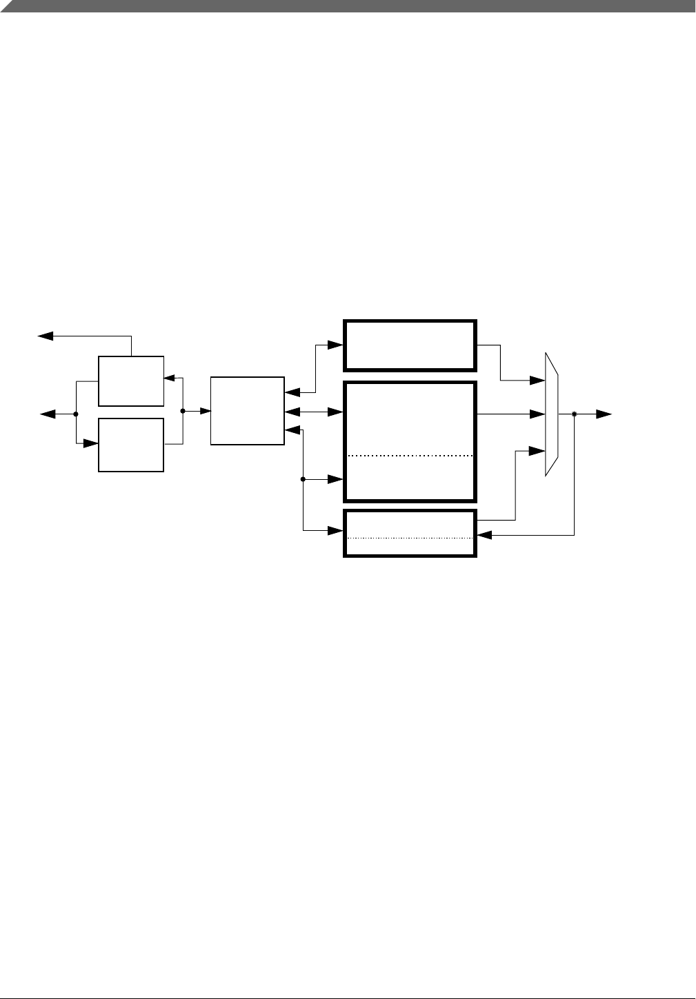
• Supports MCU security mechanisms which prevent unauthorized access to the flash
memory contents
• ECC Logic to correct single-bit faults and detect multi-bit faults in each NVM flash
phrase
36.2.2 Block diagram
The block diagram of the FTFC module is shown in the following figure.
FlexNVM
To MCU's
flash controller
Interrupt
Control
registers
Status
registers
Register
access Memory
controller
Program flash
FlexRAM
EEPROM backup
Data flash
PRAM
Figure 36-9. FTFC block diagram
36.2.3 Glossary
Command write sequence — A series of MCU writes to the Flash FCCOB register
group that initiates and controls the execution of Flash algorithms that are built into the
FTFC module.
Cryptographic Services Engine— CSEc - Feature set for various encryption,
decryption and authentication algorithms built to meet the SHE specification. This
(CSEc) is a 'compact' version of the CSE module
CSE_PRAM — RAM dedicated to the CSEc Parameter space. Used for all CSEc/SHE
command requests and related data input / output.
Data flash memory — Partitioned from the FlexNVM block, the data flash memory
provides nonvolatile storage for user data, boot code, and additional code store.
Introduction
S32K1xx Series Reference Manual, Rev. 7, 04/2018
776 NXP Semiconductors

Data flash sector — The data flash sector is the smallest portion of the data flash
memory that can be erased.
Double-Phrase — 128-bits of data with an aligned double-phrase having byte-
address[3:0] == 0000.
EEPROM — Using a built-in filing system, the FTFC module emulates the
characteristics of an EEPROM by effectively providing a high-endurance, byte-writeable
(program and erase) NVM.
EEPROM backup data header — The emulated EEPROM backup data header consists
of a 64-bit field found in emulated EEPROM backup data memory which contains
information used by the emulated EEPROM filing system to determine the status of a
specific emulated EEPROM backup flash sector.
EEPROM backup data record — Data record found in emulated EEPROM backup
data memory which is used by the emulated EEPROM filing system.
EEPROM backup data memory — Partitioned from the FlexNVM block, emulated
EEPROM backup data memory provides nonvolatile storage for the emulated EEPROM
filing system representing data written to the FlexRAM requiring highest endurance.
EEPROM backup data sector — The emulated EEPROM backup data sector contains
one emulated EEPROM header and up to 255 emulated EEPROM backup data records,
which are used by the emulated EEPROM filing system.
Endurance (cycling) — The number of times that a flash memory location can be erased
and reprogrammed.
FCCOB (Flash Common Command Object) — A group of flash registers that are used
to pass command, address, data, and any associated parameters to the memory controller
in the FTFC module.
Flash block — A macro within the FTFC module which provides the nonvolatile
memory storage.
FlexMemory — FTFC configuration that supports data flash, emulated EEPROM, and
FlexRAM.
FlexNVM Block — The FlexNVM block can be configured to be used as data flash
memory, emulated EEPROM backup flash memory, or a combination of both.
FlexRAM — The FlexRAM refers to a RAM, dedicated to the FTFC module, that can be
configured to store emulated EEPROM data or as traditional RAM. When configured for
emulated EEPROM, valid writes to the FlexRAM generates a new emulated EEPROM
backup data record stored in the emulated EEPROM backup flash memory.
Chapter 36 Flash Memory Module (FTFC)
S32K1xx Series Reference Manual, Rev. 7, 04/2018
NXP Semiconductors 777

FTFC Module — All flash blocks plus a flash management unit providing high-level
control and an interface to MCU buses.
HSRUN — An MCU power mode enabling temporary high-speed access to the memory
resources in the FTFC module. The user has no access to the Flash command set (no
FCCOB or CSEc commands, nor emulated EEPROM functions, nor FlexRAM access -
only system reads to NVM arrays) when the MCU is in HSRUN mode.
IFR — Nonvolatile information register found in each flash block, separate from the
main memory array.
Interleaved/Non-Interleaved — Interleaved (D or P Flash) refers to an internal data
path being 128-bits wide and addresses internally alternating between two 64-bit wide
datapath modules. While non-interleaved (D or P Flash) refers to an internal data path
being 64-bits wide. Interleaved DFlash (2MB macro) has different DEPART options than
the non-interleaved macros.
Longword — 32 bits of data with an aligned longword having byte-address[1:0] = 00.
NVM — Nonvolatile memory. A memory technology that maintains stored data during
power-off. The flash array is an NVM using NOR-type flash memory technology.
NVM Normal Mode — An NVM mode that provides basic user access to FTFC
resources. The CPU or other bus masters initiate flash program and erase operations (or
other flash commands) using writes to the FCCOB register group in the FTFC module.
Phrase — 64 bits of data with an aligned phrase having byte-address[2:0] = 000.
Program flash — The program flash memory provides nonvolatile storage for vectors
and code store.
Program flash sector — The smallest portion of the program flash memory (consecutive
addresses) that can be erased.
Quad-Phrase — 256 bits of data with an aligned quad-phrase having byte-address[4:0] =
00000.
RWW— Read-While-Write. The ability to simultaneously read from one memory
resource while commanded operations are active in another memory resource.
Section program buffer — Lower quarter of the FlexRAM allocated for storing large
amounts of data for programming via the Program Section command.
Secure — An MCU state conveyed to the FTFC module as described in the Chip
Configuration details for this device. In the secure state, reading and changing NVM
contents is restricted.
Word — 16 bits of data with an aligned word having byte-address[0] = 0.
Introduction
S32K1xx Series Reference Manual, Rev. 7, 04/2018
778 NXP Semiconductors

36.3 External signal description
The FTFC module contains no signals that connect off-chip.
36.4 Memory map and registers
This section describes the memory map and registers for the FTFC module. Data read
from unimplemented memory space in the FTFC module is undefined. Writes to
unimplemented or reserved memory space (registers) in the FTFC module are ignored.
36.4.1 Flash configuration field description
The program flash memory contains a 16-byte flash configuration field that stores default
protection settings (loaded on reset) and security information that allows the MCU to
restrict access to the FTFC module.
Flash Configuration Field Offset
Address Size (Bytes) Field Description
0x0_0400 - 0x0_0407 8 Backdoor Comparison Key. Refer to
Verify Backdoor Access Key command
and Un-securing the MCU using
backdoor key access.
0x0_0408 - 0x0_040B 4 Program flash protection bytes. Refer to
the description of the Program Flash
Protection Registers (FPROT0-3).
0x0_040F 1 Data flash protection byte. Refer to the
description of the Data Flash Protection
Register (FDPROT).
0x0_040E 1 EEPROM protection byte. Refer to the
description of the EEPROM Protection
Register (FEPROT).
0x0_040D 1 Flash nonvolatile option byte. Refer to
the description of the Flash Option
Register (FOPT).
0x0_040C 1 Flash security byte. Refer to the
description of the Flash Security
Register (FSEC).
Chapter 36 Flash Memory Module (FTFC)
S32K1xx Series Reference Manual, Rev. 7, 04/2018
NXP Semiconductors 779

36.4.2 Program flash 0 IFR map
The program flash 0 IFR is a 1 KB nonvolatile information memory, 64 bytes of which
can be read freely, but the user has no erase and limited program capabilities (see the
Read Once, and Program Once commands in Read Once command, and Program Once
command). The contents of the program flash 0 IFR are summarized in the following
table and further described in the subsequent paragraphs.
The program flash 0 IFR is located within the program flash 0 memory block.
Address Range Size (Bytes) Field Description
0x000 – 0x3BF 960 Reserved
0x3C0 – 0x3FF 64 Program Once Field
36.4.2.1 Program Once field
The Program Once field in the program flash 0 IFR provides 64 bytes of user data storage
separate from the program flash 0 main array. The user can program the Program Once
field one time only as there is no program flash IFR erase mechanism available to the
user. The Program Once field can be read any number of times. This section of the
program flash 0 IFR is accessed in 8 byte records using the Read Once and Program
Once commands (see Read Once command and Program Once command).
36.4.3 Data flash 0 IFR map
The data flash 0 IFR is a 1 KB nonvolatile information memory that can be erased, but
the user has limited program capabilities in the data flash 0 IFR (see the Program
Partition command in Program Partition command, the Erase All Blocks command in
Erase All Blocks command in The contents of the data flash 0 IFR are summarized in the
following table and further described in the subsequent paragraphs.
The data flash 0 IFR is located within the data flash 0 memory block.
Address Range Size (Bytes) Field Description
0x00 – 0x3FB, 0x3FE – 0x3FF 1022 Reserved
0x3FD 1 EEPROM Data Set Size
0x3FC 1 FlexNVM Partition Code
Memory map and registers
S32K1xx Series Reference Manual, Rev. 7, 04/2018
780 NXP Semiconductors

36.4.3.1 EEPROM data set size
The emulated EEPROM data set size byte in the data flash 0 IFR supplies information
which determines the amount of FlexRAM used in each of the available emulated
EEPROM subsystems and indicates whether the FlexRAM is loaded with valid emulated
EEPROM data during the flash reset sequence. To program the EEERST, EEESIZE
value, see the Program Partition command described in Program Partition command.
Also see the chip-specific information.
Refer to the SoC SIM (System Integration Module) for read values of this information
(EEERST, EEESIZE).
36.4.3.2 FlexNVM partition code
The FlexNVM partition code byte in the data flash 0 IFR supplies a code which specifies
how to split the FlexNVM block between data flash memory and emulated EEPROM
backup memory supporting emulated EEPROM functions. To program the DEPART
value, see the Program Partition command described in Program Partition command.
Also see the chip-specific information.
Refer to the SoC SIM (System Integration Module) for read values of this information
(DEPART).
36.4.4 Register descriptions
The FTFC module contains a set of memory-mapped control and status registers.
NOTE
While a command is running (FSTAT[CCIF]=0), register
writes are not accepted to any register except FCNFG, FSTAT,
FERCNFG and FERSTAT. The no-write rule is relaxed during
the start-up reset sequence, prior to the initial rise of CCIF.
During this initialization period the user may write any register.
All register writes are also disabled (except for registers
FCNFG, FSTAT, FERCNFG and FERSTAT) whenever an
erase suspend request is active (FCNFG[ERSSUSP]=1).
36.4.4.1 FTFC register descriptions
Chapter 36 Flash Memory Module (FTFC)
S32K1xx Series Reference Manual, Rev. 7, 04/2018
NXP Semiconductors 781

36.4.4.1.1 FTFC Memory map
FTFC base address: 4002_0000h
Offset Register Width
(In bits)
Access Reset value
0h Flash Status Register (FSTAT) 8 W1C 80h
1h Flash Configuration Register (FCNFG) 8 RW 02h
2h Flash Security Register (FSEC) 8 RO See
description.
3h Flash Option Register (FOPT) 8 RO See
description.
4h Flash Common Command Object Registers (FCCOB3) 8 RW 00h
5h Flash Common Command Object Registers (FCCOB2) 8 RW 00h
6h Flash Common Command Object Registers (FCCOB1) 8 RW 00h
7h Flash Common Command Object Registers (FCCOB0) 8 RW 00h
8h Flash Common Command Object Registers (FCCOB7) 8 RW 00h
9h Flash Common Command Object Registers (FCCOB6) 8 RW 00h
Ah Flash Common Command Object Registers (FCCOB5) 8 RW 00h
Bh Flash Common Command Object Registers (FCCOB4) 8 RW 00h
Ch Flash Common Command Object Registers (FCCOBB) 8 RW 00h
Dh Flash Common Command Object Registers (FCCOBA) 8 RW 00h
Eh Flash Common Command Object Registers (FCCOB9) 8 RW 00h
Fh Flash Common Command Object Registers (FCCOB8) 8 RW 00h
10h Program Flash Protection Registers (FPROT3) 8 RW See
description.
11h Program Flash Protection Registers (FPROT2) 8 RW See
description.
12h Program Flash Protection Registers (FPROT1) 8 RW See
description.
13h Program Flash Protection Registers (FPROT0) 8 RW See
description.
16h EEPROM Protection Register (FEPROT) 8 RW See
description.
17h Data Flash Protection Register (FDPROT) 8 RW See
description.
2Ch Flash CSEc Status Register (FCSESTAT) 8 RO 00h
2Eh Flash Error Status Register (FERSTAT) 8 W1C 00h
2Fh Flash Error Configuration Register (FERCNFG) 8 RW 00h
36.4.4.1.2 Flash Status Register (FSTAT)
Memory map and registers
S32K1xx Series Reference Manual, Rev. 7, 04/2018
782 NXP Semiconductors

36.4.4.1.2.1 Offset
Register Offset
FSTAT 0h
36.4.4.1.2.2 Function
The FSTAT register reports the operational status of the FTFC module.
The CCIF, RDCOLERR, ACCERR, and FPVIOL bits are readable and writable. The
MGSTAT0 bit is read only. The unassigned bits read 0 and are not writable.
NOTE
When set, the Access Error (ACCERR) and Flash Protection
Violation (FPVIOL) bits in this register prevent the launch of
any more commands or writes to the FlexRAM (when
EEERDY is set) until the flag is cleared (by writing a one to it).
36.4.4.1.2.3 Diagram
Bits 7 6 5 4 3 2 1 0
R
CCIF
RDCOLER
R
ACCERR
FPVIOL
0
MGSTAT0
W
W1C
W1C
W1C
W1C
Reset 1 0 0 0 0 0 0 0
36.4.4.1.2.4 Fields
Field Function
7
CCIF
Command Complete Interrupt Flag
The CCIF flag indicates that an FTFC/CSEc command or emulated EEPROM file system operation has
completed. The CCIF flag is cleared by writing a 1 to CCIF to launch a command, and CCIF stays low
until command completion or command violation. The CCIF flag is also cleared by a successful write to
FlexRAM while enabled for EEE, and CCIF stays low until the emulated EEPROM file system has
created the associated EEPROM data record. The CCIF flag will also clear upon execution of any CSEc
command,and will set upon completion.
The CCIF bit is reset to 0 but is set to 1 by the memory controller at the end of the reset initialization
sequence. Depending on how quickly the read occurs after reset release, the user may or may not see
the 0 hardware reset value.
0b - FTFC command or emulated EEPROM file system operation in progress
Table continues on the next page...
Chapter 36 Flash Memory Module (FTFC)
S32K1xx Series Reference Manual, Rev. 7, 04/2018
NXP Semiconductors 783

Field Function
1b - FTFC command or emulated EEPROM file system operation has completed
6
RDCOLERR
FTFC Read Collision Error Flag
The RDCOLERR error bit indicates that the MCU attempted a read from an FTFC resource that was
being manipulated by an FTFC command (CCIF=0). Any simultaneous access is detected as a collision
error by the block arbitration logic. The read data in this case cannot be guaranteed. The RDCOLERR bit
is cleared by writing a 1 to it. Writing a 0 to RDCOLERR has no effect.
0b - No collision error detected
1b - Collision error detected
5
ACCERR
Flash Access Error Flag
The ACCERR error bit indicates an illegal access has occurred to an FTFC resource caused by a
violation of the command write sequence or issuing an illegal FTFC command. While ACCERR is set, the
CCIF flag cannot be cleared to launch a command. The ACCERR bit is cleared by writing a 1 to
ACCERR while CCIF is set. Writing a 0 to the ACCERR bit has no effect.
0b - No access error detected
1b - Access error detected
4
FPVIOL
Flash Protection Violation Flag
The FPVIOL error bit indicates an attempt was made to program or erase an address in a protected area
of program flash or data flash memory during a command write sequence or a write was attempted to a
protected area of the FlexRAM while enabled for emulated EEPROM. While FPVIOL is set, the CCIF flag
cannot be cleared to launch a command. The FPVIOL bit is cleared by writing a 1 to FPVIOL while CCIF
is set. Writing a 0 to the FPVIOL bit has no effect.
0b - No protection violation detected
1b - Protection violation detected
3-1
—
Reserved
0
MGSTAT0
Memory Controller Command Completion Status Flag
The MGSTAT0 status flag is set if an error is detected during execution of an FTFC command or during
the flash reset sequence. As a status flag, this bit cannot (and need not) be cleared by the user like the
other error flags in this register.
The value of the MGSTAT0 bit for "command-N" is valid only at the end of the "command-N" execution
when CCIF=1 and before the next command has been launched. At some point during the execution of
"command-N+1," the previous result is discarded and any previous error is cleared.
36.4.4.1.3 Flash Configuration Register (FCNFG)
36.4.4.1.3.1 Offset
Register Offset
FCNFG 1h
36.4.4.1.3.2 Function
This register provides information on the current functional state of the FTFC module.
Memory map and registers
S32K1xx Series Reference Manual, Rev. 7, 04/2018
784 NXP Semiconductors

The erase control bits (ERSAREQ and ERSSUSP) have write restrictions. RAMRDY,
and EEERDY are read-only status bits. The reset values for the RAMRDY, and
EEERDY bits are determined during the reset sequence.
36.4.4.1.3.3 Diagram
Bits 7 6 5 4 3 2 1 0
R
CCIE
RDCOLLIE
ERSARE
Q
ERSSUS
P
0
0
RAMRDY
EEERD
Y
W
Reset 0 0 0 0 0 0 1 0
36.4.4.1.3.4 Fields
Field Function
7
CCIE
Command Complete Interrupt Enable
The CCIE bit controls interrupt generation when an FTFC/CSEc command completes.
0b - Command complete interrupt disabled
1b - Command complete interrupt enabled. An interrupt request is generated whenever the
FSTAT[CCIF] flag is set.
6
RDCOLLIE
Read Collision Error Interrupt Enable
The RDCOLLIE bit controls interrupt generation when an FTFC read collision error occurs.
0b - Read collision error interrupt disabled
1b - Read collision error interrupt enabled. An interrupt request is generated whenever an FTFC
read collision error is detected (see the description of FSTAT[RDCOLERR]).
5
ERSAREQ
Erase All Request
This bit issues a request to the memory controller to execute the Erase All Blocks command and release
MCU security. ERSAREQ is not directly writable but is under indirect user control. Refer to the device's
Chip Configuration details on how to request this command.
The ERSAREQ bit sets when an erase all request is triggered external to the FTFC and CCIF is set (no
command is currently being executed). ERSAREQ is cleared by the FTFC when the operation completes.
0b - No request or request complete
1b - Request to: (1) run the Erase All Blocks command, (2) verify the erased state, (3) program the
security byte in the Flash Configuration Field to the unsecure state, and (4) release MCU security
by setting the FSEC[SEC] field to the unsecure state.
4
ERSSUSP
Erase Suspend
The ERSSUSP bit allows the user to suspend (interrupt) the Erase Flash Sector command while it is
executing.
0b - No suspend requested
1b - Suspend the current Erase Flash Sector command execution
3
—
Reserved
Table continues on the next page...
Chapter 36 Flash Memory Module (FTFC)
S32K1xx Series Reference Manual, Rev. 7, 04/2018
NXP Semiconductors 785

Field Function
2
—
Reserved
1
RAMRDY
RAM Ready
This flag indicates the current status of the FlexRAM.
The state of the RAMRDY flag is normally controlled by the Set FlexRAM Function command. During the
reset sequence, the RAMRDY flag is cleared if the FlexNVM block is partitioned for emulated EEPROM
with the option to load the FlexRAM during the reset sequence and will be set if the FlexNVM block is not
partitioned for emulated EEPROM or if the FlexNVM block is partitioned for emulated EEPROM with the
option to not load the FlexRAM during the reset sequence. The RAMRDY flag is cleared if the Program
Partition command is run to partition the FlexNVM block for emulated EEPROM. The RAMRDY flag sets
after completion of the Erase All Blocks command or Erase All Blocks Unsecure command or execution
of the erase-all operation triggered external to the FTFC.
0b - FlexRAM is not available for traditional RAM access
1b - FlexRAM is available as traditional RAM only; writes to the FlexRAM do not trigger EEPROM
operations
0
EEERDY
EEERDY
This flag indicates if the EEPROM backup data has been copied to the FlexRAM and is therefore
available for read access. During the reset sequence, the EEERDY flag remains clear while CCIF=0 and
only sets if the FlexNVM block is partitioned for emulated EEPROM.
0b - FlexRAM is not available for emulated EEPROM operation
1b - FlexRAM is available for EEPROM operations where: (1) reads from the FlexRAM return data
previously written to the FlexRAM in emulated EEPROM mode and (2) writes launch an EEPROM
operation to store the written data in the FlexRAM and EEPROM backup.
36.4.4.1.4 Flash Security Register (FSEC)
36.4.4.1.4.1 Offset
Register Offset
FSEC 2h
36.4.4.1.4.2 Function
This read-only register holds all bits associated with the security of the MCU and FTFC
module.
During the reset sequence, the register is loaded with the contents of the flash security
byte in the Flash Configuration Field located in program flash memory.
Memory map and registers
S32K1xx Series Reference Manual, Rev. 7, 04/2018
786 NXP Semiconductors

36.4.4.1.4.3 Diagram
Bits 7 6 5 4 3 2 1 0
RKEYEN MEEN FSLACC SEC
W
Reset uuuuuuuu
36.4.4.1.4.4 Fields
Field Function
7-6
KEYEN
Backdoor Key Security Enable
These bits enable and disable backdoor key access to the FTFC module.
00b - Backdoor key access disabled
01b - Backdoor key access disabled (preferred KEYEN state to disable backdoor key access)
10b - Backdoor key access enabled
11b - Backdoor key access disabled
5-4
MEEN
Mass Erase Enable Bits
Enables and disables mass erase capability of the FTFC module. When the SEC field is set to unsecure,
the MEEN setting does not matter.
00b - Mass erase is enabled
01b - Mass erase is enabled
10b - Mass erase is disabled
11b - Mass erase is enabled
3-2
FSLACC
Factory Failure Analysis Access Code
These bits enable or disable access to the flash memory contents during returned part failure analysis at
the factory. When SEC is secure and FSLACC is denied, access to the program flash contents is denied
and any failure analysis performed during factory test must begin with a full erase to unsecure the part.
When access is granted (SEC is unsecure, or SEC is secure and FSLACC is granted), factory testing has
visibility of the current flash contents. The state of the FSLACC bits is only relevant when the SEC bits
are set to secure. When the SEC field is set to unsecure, the FSLACC setting does not matter.
00b - Factory access granted
01b - Factory access denied
10b - Factory access denied
11b - Factory access granted
1-0
SEC
Flash Security
These bits define the security state of the MCU. In the secure state, the MCU limits access to FTFC
module resources. The limitations are defined per device and are detailed in the Chip Configuration
details. If the FTFC module is unsecured using backdoor key access, the SEC bits are forced to 10b.
00b - MCU security status is secure
01b - MCU security status is secure
10b - MCU security status is unsecure (The standard shipping condition of the FTFC is unsecure.)
11b - MCU security status is secure
36.4.4.1.5 Flash Option Register (FOPT)
Chapter 36 Flash Memory Module (FTFC)
S32K1xx Series Reference Manual, Rev. 7, 04/2018
NXP Semiconductors 787

36.4.4.1.5.1 Offset
Register Offset
FOPT 3h
36.4.4.1.5.2 Function
The flash option register allows the MCU to customize its operations by examining the
state of these read-only bits, which are loaded from NVM at reset. The function of the
bits is defined in the device's Chip Configuration details.
All bits in the register are read-only.
During the reset sequence, the register is loaded from the flash nonvolatile option byte in
the Flash Configuration Field located in program flash memory.
36.4.4.1.5.3 Diagram
Bits 7 6 5 4 3 2 1 0
ROPT
W
Reset uuuuuuuu
36.4.4.1.5.4 Fields
Field Function
7-0
OPT
Nonvolatile Option
These bits are loaded from flash to this register at reset. Refer to the device's Chip Configuration details
for the definition and use of these bits.
36.4.4.1.6 Flash Common Command Object Registers (FCCOB0 - FCCO
BB)
36.4.4.1.6.1 Offset
Register Offset
FCCOB3 4h
FCCOB2 5h
Table continues on the next page...
Memory map and registers
S32K1xx Series Reference Manual, Rev. 7, 04/2018
788 NXP Semiconductors

Register Offset
FCCOB1 6h
FCCOB0 7h
FCCOB7 8h
FCCOB6 9h
FCCOB5 Ah
FCCOB4 Bh
FCCOBB Ch
FCCOBA Dh
FCCOB9 Eh
FCCOB8 Fh
36.4.4.1.6.2 Function
The FCCOB register group provides 12 bytes for command codes and parameters. The
individual bytes within the set append a 0-B hex identifier to the FCCOB register name:
FCCOB0, FCCOB1, ..., FCCOBB.
36.4.4.1.6.3 Diagram
Bits 7 6 5 4 3 2 1 0
RCCOBn
W
Reset 0 0 0 0 0 0 0 0
36.4.4.1.6.4 Fields
Field Function
7-0
CCOBn
CCOBn
The FCCOB register provides a command code and relevant parameters to the memory controller. The
individual registers that compose the FCCOB data set can be written in any order, but you must provide
all needed values, which vary from command to command. First, set up all required FCCOB fields and
then initiate the command’s execution by writing a 1 to the FSTAT[CCIF] bit. This clears the CCIF bit,
which locks all FCCOB parameter fields and they cannot be changed by the user until the command
completes (CCIF returns to 1). No command buffering or queueing is provided; the next command can be
loaded only after the current command completes.
Some commands return information to the FCCOB registers. Any values returned to FCCOB are
available for reading after the FSTAT[CCIF] flag returns to 1 by the memory controller.
The following table shows a generic FTFC command format. The first FCCOB register, FCCOB0, always
contains the command code. This 8-bit value defines the command to be executed. The command code
is followed by the parameters required for this specific FTFC command, typically an address and/or data
values.
Chapter 36 Flash Memory Module (FTFC)
S32K1xx Series Reference Manual, Rev. 7, 04/2018
NXP Semiconductors 789

Field Function
NOTE: The command parameter table is written in terms of FCCOB Number (which is equivalent to the
byte number). This number is a reference to the FCCOB register name and is not the register
address.
FCCOB Number Typical Command Parameter Contents [7:0]
0 FCMD (a code that defines the FTFC command)
1 Flash address [23:16]
2 Flash address [15:8]
3 Flash address [7:0]
4 Data Byte 0
5 Data Byte 1
6 Data Byte 2
7 Data Byte 3
8 Data Byte 4
9 Data Byte 5
A Data Byte 6
B Data Byte 7
1. Refers to FCCOB register name, not register address
FCCOB Endianness and Multi-Byte Access:
The FCCOB register group uses a big endian addressing convention. For all command parameter fields
larger than 1 byte, the most significant data resides in the lowest FCCOB register number. The FCCOB
register group may be read and written as individual bytes, aligned words (2 bytes) or aligned longwords
(4 bytes).
1. Refers to FCCOB register name, not register address
36.4.4.1.7 Program Flash Protection Registers (FPROT0 - FPROT3)
36.4.4.1.7.1 Offset
Register Offset
FPROT3 10h
FPROT2 11h
FPROT1 12h
FPROT0 13h
Memory map and registers
S32K1xx Series Reference Manual, Rev. 7, 04/2018
790 NXP Semiconductors

36.4.4.1.7.2 Function
The FPROT registers define which program flash regions are protected from program and
erase operations. Protected flash regions cannot have their content changed; that is, these
regions cannot be programmed and cannot be erased by any FTFC command (except
ERSALLU command and erase all that is triggered external to the FTFC). Unprotected
regions can be changed by program and erase operations.
If the configuration PFLash size isn't a 2^n multiple, round up to the next 2^n size for the
region_size. For example, the 2 MB macro is built with 1.5 MB PFLash plus 512 KB
mixed P/DFlash (448 KB/64 KB). For this calculation, the PFlash should use 2 MB as the
region_size.
The four FPROT registers allow up to 32 protectable regions of equal memory size. The
FPROT register bits are mapped to the protectable regions as follows:
•region_size = total_program_flash_size / 32
•Starting from the program flash base address, Region 0 refers to the first region_size
bytes, region 1 refers to the next region_size bytes, and so on.
In other words:
•region_n_start_address = program_flash_base_address + (n) * region_size
•region_n_end_address = program_flash_base_address + ((n+1) * region_size) -1
For example, if the total program flash size is 512 MB, the region_size is 16 KB. If the
lowest program flash address is 0x000A_0000, the regions are defined as follows:
Region Start Address End Address
0 0x000A_0000 0x000A_3FFF
1 0x000A_4000 0x000A_7FFF
2 0x000A_8000 0x000A_BFFF
3 0x000A_C000 0x000A_FFFF
. . . . . . . . .
32 0x0011_C000 0x0011_FFFF
• A '0' in an FPROT[PROT] bit indicates its corresponding flash protection region is
protected
• A '1' in an FPROT[PROT] bit indicates its corresponding flash protection region is
unprotected
Chapter 36 Flash Memory Module (FTFC)
S32K1xx Series Reference Manual, Rev. 7, 04/2018
NXP Semiconductors 791

Program flash protection register Program flash protection bits
FPROT0 PROT[31:24]
FPROT1 PROT[23:16]
FPROT2 PROT[15:8]
FPROT3 PROT[7:0]
During the reset sequence, the FPROT registers are loaded with the contents of the
program flash protection bytes in the Flash Configuration Field as indicated in the
following table.
Program flash protection register Flash Configuration Field offset address
FPROT0 0x000B
FPROT1 0x000A
FPROT2 0x0009
FPROT3 0x0008
To change the program flash protection that is loaded during the reset sequence,
unprotect the sector of program flash memory that contains the Flash Configuration
Field. Then, reprogram the program flash protection byte.
36.4.4.1.7.3 Diagram
Bits 7 6 5 4 3 2 1 0
RPROT
W
Reset uuuuuuuu
36.4.4.1.7.4 Fields
Field Function
7-0
PROT
Program Flash Region Protect
Each program flash region can be protected from program and erase operations by setting the associated
PROT bit to the protected state.
In NVM Normal mode: The protection can only be increased, meaning that currently unprotected
memory can be protected, but currently protected memory cannot be unprotected. Since unprotected
regions are marked with a 1 and protected regions use a 0, only writes changing 1s to 0s are accepted.
This 1-to-0 transition check is performed on a bit-by-bit basis. Those FPROT bits with 1-to-0 transitions
are accepted while all bits with 0-to-1 transitions are ignored.
Restriction: The user must never write to any FPROT register while a command is running (CCIF=0).
Memory map and registers
S32K1xx Series Reference Manual, Rev. 7, 04/2018
792 NXP Semiconductors

Field Function
Trying to alter data in any protected area in the program flash memory results in a protection violation
error and sets the FSTAT[FPVIOL] bit. A full block erase of a program flash block (except ERSALLU
command and erase all that is triggered external to the FTFC) is not possible if it contains any protected
region.
36.4.4.1.8 EEPROM Protection Register (FEPROT)
36.4.4.1.8.1 Offset
Register Offset
FEPROT 16h
36.4.4.1.8.2 Function
The FEPROT register defines which emulated EEPROM regions of the FlexRAM are
protected against program and erase operations. Protected EEPROM regions cannot have
their content changed by writing to it. Unprotected regions can be changed by writing to
the FlexRAM.
36.4.4.1.8.3 Diagram
Bits 7 6 5 4 3 2 1 0
REPROT
W
Reset uuuuuuuu
36.4.4.1.8.4 Fields
Field Function
7-0
EPROT
EEPROM Region Protect
Individual emulated EEPROM regions can be protected from alteration by setting the associated EPROT
bit to the protected state. The EPROT bits are not used when the FlexNVM Partition Code is set to data
flash only. When the FlexNVM Partition Code is set to data flash and EEPROM or EEPROM only, each
EPROT bit covers one-eighth of the configured EEPROM data (see the EEPROM Data Set Size
parameter description).
In NVM Normal mode: The protection can only be increased. This means that currently-unprotected
memory can be protected, but currently-protected memory cannot be unprotected. Since unprotected
regions are marked with a 1 and protected regions use a 0, only writes changing 1s to 0s are accepted.
This 1-to-0 transition check is performed on a bit-by-bit basis. Those FEPROT bits with 1-to-0 transitions
are accepted while all bits with 0-to-1 transitions are ignored.
Chapter 36 Flash Memory Module (FTFC)
S32K1xx Series Reference Manual, Rev. 7, 04/2018
NXP Semiconductors 793

Field Function
Restriction: Never write to the FEPROT register while a command is running (CCIF=0).
Reset: During the reset sequence, the FEPROT register is loaded with the contents of the EEPROM
protection byte in the Flash Configuration Field located in program flash. The flash basis for the reset
values is signified by X in the register diagram. To change the EEPROM protection that will be loaded
during the reset sequence, the sector of program flash that contains the Flash Configuration Field must
be unprotected; then the EEPROM protection byte must be erased and reprogrammed.
Trying to alter data by writing to any protected area in the emulated EEPROM results in a protection
violation error and sets the FSTAT[FPVIOL] bit.
00000000b - EEPROM region is protected
00000001b - EEPROM region is not protected
36.4.4.1.9 Data Flash Protection Register (FDPROT)
36.4.4.1.9.1 Offset
Register Offset
FDPROT 17h
36.4.4.1.9.2 Function
The FDPROT register defines which data flash regions are protected against program and
erase operations. Protected Flash regions cannot have their content changed; that is, these
regions cannot be programmed and cannot be erased by any FTFC command (except
ERSALLU command and erase all which is triggered external to the FTFC). Unprotected
regions can be changed by both program and erase operations.
36.4.4.1.9.3 Diagram
Bits 7 6 5 4 3 2 1 0
RDPROT
W
Reset uuuuuuuu
36.4.4.1.9.4 Fields
Field Function
7-0
DPROT
Data Flash Region Protect
Memory map and registers
S32K1xx Series Reference Manual, Rev. 7, 04/2018
794 NXP Semiconductors

Field Function
Individual data flash regions can be protected from program and erase operations by setting the
associated DPROT bit to the protected state. Each DPROT bit protects one-eighth of the partitioned data
flash memory space. The granularity of data flash protection cannot be less than the data flash sector
size. If an unused DPROT bit is set to the protected state, the Erase all Blocks command does not
execute and sets the FSTAT[FPVIOL] bit. Similar to FPROT, if the configuration DFlash size isn't a 2^n
multiple, round up to the next 2^n size for the region_size.
In NVM Normal mode: The protection can only be increased, meaning that currently unprotected
memory can be protected but currently protected memory cannot be unprotected. Since unprotected
regions are marked with a 1 and protected regions use a 0, only writes changing 1s to 0s are accepted.
This 1-to-0 transition check is performed on a bit-by-bit basis. Those FDPROT bits with 1-to-0 transitions
are accepted while all bits with 0-to-1 transitions are ignored.
Restriction: The user must never write to the FDPROT register while a command is running (CCIF=0).
Reset: During the reset sequence, the FDPROT register is loaded with the contents of the data flash
protection byte in the Flash Configuration Field located in program flash memory. The flash basis for the
reset values is signified by X in the register diagram. To change the data flash protection that will be
loaded during the reset sequence, unprotect the sector of program flash that contains the Flash
Configuration Field. Then, erase and reprogram the data flash protection byte.
Trying to alter data with the program and erase commands (except ERSALLU command and erase all
which is triggered external to the FTFC) in any protected area in the data flash memory results in a
protection violation error and sets the FSTAT[FPVIOL] bit. A block erase of any data flash memory block
(see the Erase Flash Block command description) is not possible if the data flash block contains any
protected region or if the FlexNVM memory has been partitioned for emulated EEPROM.
00000000b - Data Flash region is protected
00000001b - Data Flash region is not protected
36.4.4.1.10 Flash CSEc Status Register (FCSESTAT)
36.4.4.1.10.1 Offset
Register Offset
FCSESTAT 2Ch
36.4.4.1.10.2 Function
The FCSESTAT register reports the status of the CSEc cryptographic related feature set
operations.
Following is a quick reference mapping CSEc status flags from the FCSESTAT register.
Table 36-27. Boot/MAC map to CSEc Status Flags
SB BIN BFN BOK <err code>
No Boot Type 0 0 0 0 0
MAC is Empty 1 1 1 0 NO_ERR
Table continues on the next page...
Chapter 36 Flash Memory Module (FTFC)
S32K1xx Series Reference Manual, Rev. 7, 04/2018
NXP Semiconductors 795

Table 36-27. Boot/MAC map to CSEc Status Flags (continued)
SB BIN BFN BOK <err code>
MAC Mismatch 1 0 1 0 NO_ERR
MAC Match 1 0 0 1 NO_ERR
MAC_KEY is empty 0 0 1 0 NO_SECURE_BOOT
36.4.4.1.10.3 Diagram
Bits 7 6 5 4 3 2 1 0
RIDB EDB RIN BOK BFN BIN SB BSY
W
Reset 0 0 0 0 0 0 0 0
36.4.4.1.10.4 Fields
Field Function
7
IDB
Internal Debug
The IDB bit is set by the DBG_AUTH command when no flash keys are stored. It is cleared upon reset
and by the LOAD_KEY command.
0b - Internal debug functions are disabled
1b - Internal debugger functions are enabled
6
EDB
External Debug
The EDB bit is set when the CPU debug port (BDM/JTAG/etc.) is activated. It is cleared upon reset.
0b - External debugger not attached
1b - External debugger is attached
5
RIN
Random Number Generator Initialized
The RIN bit is set by the INIT_RNG command. It is cleared upon reset and by the DBG_AUTH command.
0b - Random number generator is not initialized.
1b - Random number generator is initialized.
4
BOK
Secure Boot OK
The BOK bit is set by the successful completion of the secure boot process. It is cleared upon reset or by
the BOOT_FAILURE command. This will remain cleared if BOOT_MAC/BOOT_MAC_KEY/boot flavor
selection is absent.
0b - Secure boot is not complete, or secure boot failure
1b - Secure boot was successful.
3
BFN
Secure Boot Finished
The BFN bit is set by the BOOT_FAILURE or BOOT_OK commands, or the secure boot process when
the BIN bit is set, an error has been encountered, or the BOOT_MAC value doesn't match. It assumes
BOOT_MAC_KEY is present and boot flavor is configured to a secure boot type (serial, parallel, strict). It
is cleared upon reset.
0b - Secure Boot is not finished.
Table continues on the next page...
Memory map and registers
S32K1xx Series Reference Manual, Rev. 7, 04/2018
796 NXP Semiconductors

Field Function
1b - Secure Boot has finished
2
BIN
Secure Boot Initialization
The BIN bit is set by the secure boot process if the BOOT_MAC memory slot is empty. It is cleared upon
reset. Assumes BOOT_MAC_KEY is present. (autonomous boot per SHE section 10.3)
0b - Secure boot personalization not completed.
1b - Secure boot personalization has completed
1
SB
Secure Boot
The SB bit is set by the secure boot process if the BOOT_MAC_KEY slot is not empty. It is cleared upon
reset. Assumes secure boot flavor is configured (serial, parallel or strict)
0b - Secure boot not activated
1b - Secure boot is activated
0
BSY
Busy
The BSY bit is set when a CSEc command is issued. It is cleared when the command process has
completed
0b - CSEc command processing has completed
1b - CSEc command processing is in progress
36.4.4.1.11 Flash Error Status Register (FERSTAT)
36.4.4.1.11.1 Offset
Register Offset
FERSTAT 2Eh
36.4.4.1.11.2 Function
This register reports the detection of uncorrected ECC errors during read access to the
FTFC module.
The DFDIF flag is readable and writable. The unassigned bits read 0 and are not writable.
36.4.4.1.11.3 Diagram
Bits 7 6 5 4 3 2 1 0
R
0
DFDIF
0
W
W1C
Reset 0 0 0 0 0 0 0 0
Chapter 36 Flash Memory Module (FTFC)
S32K1xx Series Reference Manual, Rev. 7, 04/2018
NXP Semiconductors 797

36.4.4.1.11.4 Fields
Field Function
7-2
—
Reserved
1
DFDIF
Double Bit Fault Detect Interrupt Flag
The DFDIF flag indicates an uncorrectable ECC fault was detected during a valid flash read access from
the platform flash controller. The DFDIF flag is cleared by writing a 1 to it. Writing a 0 to DFDIF has no
effect.
0b - Double bit fault not detected during a valid flash read access from the platform flash controller
1b - Double bit fault detected (or FERCNFG[FDFD] is set) during a valid flash read access from the
platform flash controller
0
—
Reserved
36.4.4.1.12 Flash Error Configuration Register (FERCNFG)
36.4.4.1.12.1 Offset
Register Offset
FERCNFG 2Fh
36.4.4.1.12.2 Function
This register enables the force and interrupt of uncorrected ECC errors detected during
read access to the FTFC module.
The FDFD and DFDIE bits are readable and writable. The unassigned bits read 0 and are
not writable.
36.4.4.1.12.3 Diagram
Bits 7 6 5 4 3 2 1 0
R
0
FDFD
0
DFDIE
0
W
Reset 0 0 0 0 0 0 0 0
Memory map and registers
S32K1xx Series Reference Manual, Rev. 7, 04/2018
798 NXP Semiconductors

36.4.4.1.12.4 Fields
Field Function
7-6
—
Reserved
5
FDFD
Force Double Bit Fault Detect
The FDFD bit enables the user to emulate the setting of the FERSTAT[DFDIF] flag to check the
associated interrupt routine. The FDFD bit is cleared by writing a 0 to FDFD.
0b - FERSTAT[DFDIF] sets only if a double bit fault is detected during read access from the
platform flash controller
1b - FERSTAT[DFDIF] sets during any valid flash read access from the platform flash controller. An
interrupt request is generated if the DFDIE bit is set.
4-2
—
Reserved
1
DFDIE
Double Bit Fault Detect Interrupt Enable
The DFDIE bit controls interrupt generation when an uncorrectable ECC fault is detected during a valid
flash read access from the platform flash controller.
0b - Double bit fault detect interrupt disabled
1b - Double bit fault detect interrupt enabled. An interrupt request is generated whenever the
FERSTAT[DFDIF] flag is set.
0
—
Reserved
36.5 Functional description
The following sections describe functional details of the FTFC module.
36.5.1 Flash protection
Individual regions within the flash memory can be protected from program and erase
operations. Protection is controlled by the following registers:
•FPROTn — Four registers protect 32 regions of the program flash memory as shown
in the following figure
Chapter 36 Flash Memory Module (FTFC)
S32K1xx Series Reference Manual, Rev. 7, 04/2018
NXP Semiconductors 799

Program flash size / 32
Program flash size / 32
Program flash size / 32
Program flash size / 32
Program flash size / 32
Program flash size / 32
Program flash size / 32
FPROT3[PROT0]
0x0_0000
FPROT3[PROT1]
FPROT3[PROT2]
FPROT3[PROT3]
FPROT0[PROT29]
FPROT0[PROT31]
FPROT0[PROT30]
Program flash
Last program flash address
Figure 36-10. Program flash protection
• FDPROT —
• For 2n data flash sizes, protects eight regions of the data flash memory as shown
in the following figure
Data flash size / 8 DPROT0
0x0_0000
DPROT1
DPROT2
DPROT3
DPROT5
DPROT7
DPROT6
FlexNVM
Last data flash address Data flash size / 8
Data flash size / 8
Data flash size / 8
Data flash size / 8
Data flash size / 8
Data flash size / 8
Data flash size / 8
DPROT4
EEPROM backup
EEPROM backup
size (DEPART)
Last FlexNVM address
Figure 36-11. Data flash protection (2n data flash sizes)
• FEPROT — Protects eight regions of the emulated EEPROM memory as shown in
the following figure
Functional description
S32K1xx Series Reference Manual, Rev. 7, 04/2018
800 NXP Semiconductors

EEPROM size / 8 EPROT0
0x0_0000
EPROT1
EPROT2
EPROT5
EPROT7
EPROT6
FlexRAM
Last EEPROM address EEPROM size / 8
EEPROM size / 8
EEPROM size / 8
EEPROM size / 8
EEPROM size / 8
EEPROM size / 8
EEPROM size / 8
EPROT3
EPROT4
EEPROM size (EESIZE)
Figure 36-12. EEPROM protection
36.5.2 FlexNVM description
This section describes the FlexNVM memory.
36.5.2.1 FlexNVM block partitioning for FlexRAM
The user can configure the FlexNVM block as:
• Basic data flash,
• EEPROM flash records to support the built-in emulated EEPROM feature, or
• A combination of both.
When using the CSEc feature set, the EEE Flash configuration must be selected.
The user's FlexNVM configuration choice is specified using the Program Partition
command described in Program Partition command.
CAUTION
While different partitions of the FlexNVM block are available,
the intention is that a single partition choice is used throughout
the entire lifetime of a given application. The FlexNVM
partition code choices affect the endurance and data retention
characteristics of the device.
Chapter 36 Flash Memory Module (FTFC)
S32K1xx Series Reference Manual, Rev. 7, 04/2018
NXP Semiconductors 801

36.5.2.2 EEPROM user perspective
The following figure shows the emulated EEPROM system. To handle varying customer
requirements, the FlexRAM and FlexNVM blocks can be split into partitions as shown.
File
system
handler
User access (effective
EEPROM)
FlexRAM EEPROM backup
with 2KByte
erase sectors
Figure 36-13. Top-level emulated EEPROM architecture
1. EEPROM partition (EEESIZE) — The amount of FlexRAM used for emulated
EEPROM can be set to either 0 Bytes (no EEPROM), or to the maximum FlexRAM
size. The emulated EEPROM partition grows from the bottom of the FlexRAM
address space. Utilizing fewer records will incease the ratio of RAM to NVM, thus
increasing the w/e endurance. For FlexRAM usage other than EEPROM (see Set
FlexRAM Function command.
2. Data flash partition (DEPART) — The amount of FlexNVM memory used for data
flash can be programmed from 0 bytes (all of the FlexNVM block is available for
emulated EEPROM backup) to the maximum size of the FlexNVM block.
3. FlexNVM EEPROM partition — The amount of FlexNVM memory used for
emulated EEPROM backup (see Figure 36-9). In order to achieve specified w/e cycle
endurance, the emulated EEPROM backup size must be at least 16 times the
emulated EEPROM partition size in FlexRAM. For parts other than the 2MB
configuration (with interleaved DFlash), the FlexNVM may be split according to the
Program Partition command, allowing for part EFlash and part DFlash. For example
a 64kB FlexNVM could be partitioned for 32kB emulated EEPROM and 32kB
DFlash. To maintain the full specified w/e endurance in the emulated EEPROM
system, the number of records stored in FlexRAM should be limited to maintain the
1:16 ratio of RAM to NVM. The management of total number of records is left to the
user.
The partition information (EEESIZE, DEPART) is stored in the data flash IFR and is
programmed using the Program Partition command (see Program Partition command).
Typically, the Program Partition command is executed only once in the lifetime of the
device.
Functional description
S32K1xx Series Reference Manual, Rev. 7, 04/2018
802 NXP Semiconductors

Data flash memory is useful for applications that need to quickly store large amounts of
data or store data that is static. The emulated EEPROM partition in FlexRAM is useful
for storing smaller amounts of data that will be changed often.
36.5.2.3 EEPROM implementation overview
Out of reset with the FSTAT[CCIF] bit clear, the partition settings (EEESIZE, DEPART)
are read from the data flash IFR and the emulated EEPROM file system is initialized
accordingly. The emulated EEPROM file system locates all valid EEPROM data records
in EEPROM backup and copies the newest data to FlexRAM. The FSTAT[CCIF] and
FCNFG[EEERDY] bits are set after data from all valid EEPROM data records is copied
to the FlexRAM. After the CCIF bit is set, the FlexRAM is available for read or write
access.
When configured for emulated EEPROM use, writes to an unprotected location in
FlexRAM invokes the emulated EEPROM file system to program a new EEPROM data
record in the emulated EEPROM backup memory in a round-robin fashion. As needed,
the emulated EEPROM file system identifies the emulated EEPROM backup sector that
is being erased for future use and partially erases that emulated EEPROM backup sector.
After a write to the FlexRAM, the FlexRAM is not accessible until the FSTAT[CCIF] bit
is set. The FCNFG[EEERDY] bit will also be set. If enabled, the interrupt associated
with the FSTAT[CCIF] bit can be used to determine when the FlexRAM is available for
read or write access.
After a sector in emulated EEPROM backup is full of EEPROM data records, EEPROM
data records from the sector holding the oldest data are gradually copied over to a
previously-erased emulated EEPROM backup sector. When the sector copy completes,
the emulated EEPROM backup sector holding the oldest data is tagged for erase.
CAUTION
Interrupting an emulated EEPROM operation (due to power
loss, reset, supplies out of specified operational ranges, or any
other reasons) will leave the contents in an indeterminate state.
The user must take appropriate counter measures to prevent
data loss in case of an interrupted emulated EEPROM
operation.
36.5.2.4 Write endurance to FlexRAM for emulated EEPROM
When the FlexNVM partition code is not set to full data flash, the emulated EEPROM
data set size should be set to the non-zero value.
Chapter 36 Flash Memory Module (FTFC)
S32K1xx Series Reference Manual, Rev. 7, 04/2018
NXP Semiconductors 803

The bytes not assigned to data flash via the FlexNVM partition code are used by the
FTFC to obtain an effective endurance increase for the EEPROM data. The built-in
emulated EEPROM record management system raises the number of program/erase
cycles that can be attained prior to device wear-out by cycling the EEPROM data through
a larger emulated EEPROM NVM storage space.
While different partitions of the FlexNVM are available, the intention is that a single
choice for the FlexNVM partition code and emulated EEPROM data set size is used
throughout the entire lifetime of a given application.
Normal EEE writes and quick writes should not be used in an aggressive brownout
environment (e.g., multiple back-to-back brownouts without recovery in between).
36.5.2.5 ECC implementation for FlexNVM
When the FlexNVM region is configured as Data Flash, any single-bit ECC errors are
automatically corrected, and any double-bit ECC errors are reflected onto
FERSTAT[DFDIF] flag at the read access from Data Flash.
When the FlexNVM region is configured as Emulated EEPROM, any single-bit ECC
errors are automatically corrected before copying data into EEERAM at the read access
from Emulated EEPROM, and any double-bit ECC errors on valid Emulated EEPROM
locations which containing data that need to be copied to EEERAM are reflected as the
corresponding data records left as all 1's in EEERAM.
36.5.3 Interrupts
The FTFC module can generate interrupt requests to the MCU upon the occurrence of
various FTFC events. These interrupt events and their associated status and control bits
are shown in the following table.
Table 36-28. FTFC interrupt sources
FTFC Event Readable
Status Bit
Interrupt
Enable Bit
FTFC Command and CSEc command Complete FSTAT[CCIF] FCNFG[CCIE]
FTFC Read Collision Error FSTAT[RDCOLERR] FCNFG[RDCOLLIE]
FTFC ECC Error Detection FERSTAT[DFDIF] FERCNFG[DFDIE]
Functional description
S32K1xx Series Reference Manual, Rev. 7, 04/2018
804 NXP Semiconductors

Note
Vector addresses and their relative interrupt priority are
determined at the MCU level.
36.5.4 Flash operation in low-power modes
36.5.4.1 Wait mode
When the MCU enters wait mode, the FTFC module is not affected. The FTFC module
can recover the MCU from wait via the command complete interrupt (see Interrupts).
36.5.4.2 Stop mode
When the MCU requests stop mode, if an FTFC command is active (CCIF = 0) the
command execution completes before the MCU is allowed to enter stop mode.
CAUTION
The MCU should never enter stop mode while any FTFC
command is running (CCIF = 0).
NOTE
While the MCU is in very-low-power modes (VLPR, VLPW,
VLPS), the FTFC module does not accept flash commands.
36.5.5 Functional modes of operation
The FTFC module has two operating modes: NVM Normal and NVM Special. The
operating mode affects the command set availability (see Table 36-29). Refer to the Chip
Configuration details of this device for how to activate each mode.
36.5.6 Flash memory reads and ignored writes
The FTFC module requires only the flash address to execute a flash memory read. MCU
read access is available to all flash memory.
Chapter 36 Flash Memory Module (FTFC)
S32K1xx Series Reference Manual, Rev. 7, 04/2018
NXP Semiconductors 805

The MCU must not read from the flash memory while commands are running (as
evidenced by CCIF=0) on that block. Read data cannot be guaranteed from a flash block
while any command is processing within that block. The block arbitration logic detects
any simultaneous access and reports this as a read collision error (see the
FSTAT[RDCOLERR] bit).
36.5.7 Read while write (RWW)
The following simultaneous accesses are allowed for devices with FlexNVM:
• The user may read from one partition of the program flash memory while commands
(typically program and erase operations) are active in another partition of the
program flash, the data flash, and FlexRAM memory space.
• The MCU can fetch instructions from program flash during both data flash program
and erase operations and while emulated EEPROM backup is maintained by the
EEPROM commands.
• Conversely, the user may read from data flash and FlexRAM while program and
erase commands are executing on the program flash.
• When configured as traditional RAM, writes to the FlexRAM are allowed during
data flash operations.
Simultaneous data flash operations and FlexRAM writes, when FlexRAM is used for
EEE, are not possible.
Simultaneous operations are further discussed in Allowed simultaneous flash operations.
36.5.8 Flash program and erase
All flash functions except read require the user to setup and launch an FTFC command
through a series of peripheral bus writes. The user cannot initiate any further FTFC
commands until notified that the current command has completed. The FTFC command
structure and operation are detailed in FTFC command operations.
CAUTION
Interrupting a program or erase operation (due to power loss,
reset, supplies out of specified operational ranges, or any other
reasons) will leave the contents in an indeterminate state. The
user must take appropriate counter measures to prevent data
loss in case of an interrupted program or erase operation.
Functional description
S32K1xx Series Reference Manual, Rev. 7, 04/2018
806 NXP Semiconductors

36.5.9 FTFC command operations
FTFC command (not related to CSEc) operations are typically used to modify flash
memory contents. The next sections describe:
• The command write sequence used to set FTFC command parameters and launch
execution
• A description of all FTFC commands available
NOTE
1. For CSEc/SHE commands, refer to Cryptographic Services
Engine (CSEc)
2. Warning: When running any FTFC command such as
ERSALL that changes the flash configuration content, care
must be taken with re-programming the configuration
information prior to reset. Otherwise, the part may get
locked up
36.5.9.1 Command write sequence
FTFC commands are specified using a command write sequence illustrated in Figure
36-14. The FTFC module performs various checks on the command (FCCOB) content
and continues with command execution if all requirements are fulfilled.
Before launching a command, the ACCERR and FPVIOL bits in the FSTAT register
must be zero and the CCIF flag must read 1 to verify that any previous command has
completed. If CCIF is zero, the previous command execution is still active, a new
command write sequence cannot be started, and all writes to the FCCOB registers are
ignored.
Attempts to launch an FTFC command in VLP mode will be ignored. Attempts to launch
any FTFC command (including SHE commands, FlexRAM/EEPROM accesses) in
HSRUN mode will be trapped with the ACCERR flag being set.
36.5.9.1.1 Load the FCCOB registers
The user must load the FCCOB registers with all parameters required by the desired
FTFC command. The individual registers that make up the FCCOB data set can be
written in any order. The user must be sure to provide all of the required parameters
(which may vary from command to command).
Chapter 36 Flash Memory Module (FTFC)
S32K1xx Series Reference Manual, Rev. 7, 04/2018
NXP Semiconductors 807

36.5.9.1.2 Launch the command by clearing CCIF
Once all relevant command parameters have been loaded, the user launches the command
by clearing the FSTAT[CCIF] bit by writing a '1' to it. The CCIF flag remains zero until
the FTFC command completes.
The FSTAT register contains a blocking mechanism, which prevents a new command
from launching (can't clear CCIF) if the previous command resulted in an access error
(FSTAT[ACCERR]=1) or a protection violation (FSTAT[FPVIOL]=1). In error
scenarios, two writes to FSTAT are required to initiate the next command: the first write
clears the error flags, the second write clears CCIF.
36.5.9.1.3 Command execution and error reporting
The command processing has several steps:
1. The FTFC reads the command code and performs a series of parameter checks and
protection checks, if applicable, which are unique to each command.
If the parameter check fails, the FSTAT[ACCERR] (access error) flag is set.
ACCERR reports invalid instruction codes and out-of bounds addresses. Usually,
access errors suggest that the command was not set-up with valid parameters in the
FCCOB register group.
Program and erase commands also check the address to determine if the operation is
requested to execute on protected areas. If the protection check fails, the
FSTAT[FPVIOL] (protection error) flag is set.
Command processing never proceeds to execution when the parameter or protection
step fails. Instead, command processing is terminated after setting the FSTAT[CCIF]
bit.
2. If the parameter and protection checks pass, the command proceeds to execution.
Run-time errors, such as failure to erase verify, may occur during the execution
phase. Run-time errors are reported in the FSTAT[MGSTAT0] bit. A command may
have access errors, protection errors, and run-time errors, but the run-time errors are
not seen until all access and protection errors have been corrected.
3. Command execution results, if applicable, are reported back to the user via the
FCCOB and FSTAT registers.
4. The FTFC sets the FSTAT[CCIF] bit signifying that the command has completed.
The flow for a generic command write sequence is illustrated in the following figure.
Functional description
S32K1xx Series Reference Manual, Rev. 7, 04/2018
808 NXP Semiconductors
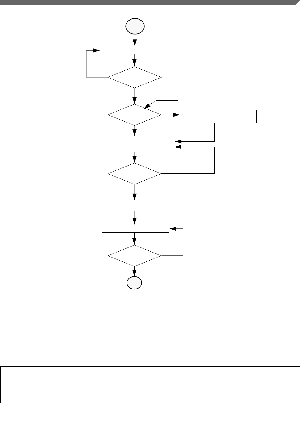
Clear the CCIF to launch the command
Write 0x80 to FSTAT register
Clear the old errors
Access Error and
Protection Violation
Check
FCCOB
ACCERR/
FPVIOL
Set?
EXIT
Write to the FCCOB registers
to load the required command parameter.
More
Parameters?
Availability Check
Results from previous command
Read: FSTAT register
Write 0x30 to FSTAT register
no
yes
no
yes
Previous command complete?
no CCIF
= ‘1’?
yes
START
CCIF
= ‘1’?
Read: FSTAT register
no
yes
Bit Polling for
Command Completion
Check
Figure 36-14. Generic flash command write sequence flowchart
36.5.9.2 Flash commands
The following table summarizes the function of all flash commands. If any column is
marked with an 'X', the flash command is relevant to that particular memory resource.
FCMD Command Program Flash FlexRAM Data Flash Function
0x00 Read 1s Block × × Verify that a
program flash or
data flash block is
erased. FlexNVM
Table continues on the next page...
Chapter 36 Flash Memory Module (FTFC)
S32K1xx Series Reference Manual, Rev. 7, 04/2018
NXP Semiconductors 809

FCMD Command Program Flash FlexRAM Data Flash Function
block must not be
partitioned for
emulated
EEPROM.
0x01 Read 1s Section × × Verify that a given
number of program
flash or data flash
locations from a
starting address
are erased.
0x02 Program Check × × Tests previously-
programmed
phrases at margin
read levels.
0x07 Program Phrase × × Program 8 bytes in
a program flash
block or a data
flash block.
0x08 Erase Flash Block × × Erase a program
flash block or data
flash block. An
erase of any flash
block is only
possible when
unprotected.
FlexNVM block
must not be
partitioned for
emulated
EEPROM.
0x09 Erase Flash Sector × × Erase all bytes in a
program flash or
data flash sector.
0x0B Program Section × × × Program data from
the Section
Program Buffer to
a program flash or
data flash block.
0x40 Read 1s All Blocks × × Verify that all
program flash,
data flash blocks,
emulated
EEPROM backup
data records, and
data flash IFR are
erased then
release MCU
security.
0x41 Read Once IFR Read 8 bytes of a
dedicated 64 byte
field in the program
flash 0 IFR.
0x43 Program Once IFR One-time program
of 8 bytes of a
Table continues on the next page...
Functional description
S32K1xx Series Reference Manual, Rev. 7, 04/2018
810 NXP Semiconductors

FCMD Command Program Flash FlexRAM Data Flash Function
dedicated 64-byte
field in the program
flash 0 IFR.
0x44 Erase All Blocks × × × Erase all program
flash blocks, data
flash blocks,
FlexRAM,
emulated
EEPROM backup
data records, and
data flash IFR.
Then, verify-erase.
The flash security
byte is left erased
(secured state).
NOTE: An erase is
only
possible
when all
memory
locations
are
unprotected.
0x45 Verify Backdoor
Access Key
× Release MCU
security after
comparing a set of
user-supplied
security keys to
those stored in the
program flash.
0x49 Erase All Blocks
Unsecure
× × × Erase all program
flash blocks, data
flash blocks,
FlexRAM,
emulated
EEPROM backup
data records, and
data flash IFR.
Then, verify-erase,
program the
security byte to the
unsecure state.
0x80 Program Partition IFR, × × Program the
FlexNVM Partition
Code and
emulated
EEPROM Data Set
Size into the data
flash IFR. format
all emulated
EEPROM backup
data sectors
allocated for
emulated
Table continues on the next page...
Chapter 36 Flash Memory Module (FTFC)
S32K1xx Series Reference Manual, Rev. 7, 04/2018
NXP Semiconductors 811

FCMD Command Program Flash FlexRAM Data Flash Function
EEPROM, initialize
the FlexRAM.
0x81 Set FlexRAM
Function
× × Switches FlexRAM
function between
RAM and emulated
EEPROM. When
switching to
emulated
EEPROM,
FlexNVM is not
available while
valid data records
are being copied
from emulated
EEPROM backup
to FlexRAM.
36.5.9.3 Flash commands by mode
The following table shows the flash commands that can be executed in each flash
operating mode.
Table 36-29. Flash commands by mode
FCMD Command Unsecure Secure MEEN=10
0x00 Read 1s Block × × ×
0x01 Read 1s Section × × ×
0x02 Program Check × × ×
0x07 Program Phrase × × ×
0x08 Erase Flash Block × × ×
0x09 Erase Flash Sector × × ×
0x0B Program Section × × ×
0x40 Read 1s All Blocks × × ×
0x41 Read Once × × ×
0x43 Program Once × × ×
0x44 Erase All Blocks × × ×
0x45 Verify Backdoor Access Key × × ×
0x49 Erase All Blocks Unsecure × × —
0x80 Program Partition × × ×
0x81 Set FlexRAM Function × × ×
Functional description
S32K1xx Series Reference Manual, Rev. 7, 04/2018
812 NXP Semiconductors

36.5.9.4 Allowed simultaneous flash operations
Only the operations marked 'OK' in the following table are permitted to run
simultaneously on the program flash, data flash, and FlexRAM memories. Some
operations cannot be executed simultaneously because certain hardware resources are
shared by the memories. The priority has been placed on permitting program flash reads
while program and erase operations execute on the FlexNVM and FlexRAM. This
provides read (program flash) while write (FlexNVM, FlexRAM) functionality. In
general, none of these CCOB commands may be executed simultaneously with any CSEc
command, and vise versa. See the CSEc chapter for details.
Table 36-30. Allowed simultaneous memory operations
Program flash X1Data flash FlexRAM/PRAM
Read Program
Phrase
Erase
Flash
Sector2Read Program
Phrase
Erase
Flash
Sector2Read EE-Write3RAM-
Write4
Program
flash Y1
Read OK OK OK OK OK
Program
Phrase OK OK OK OK
Erase
Flash
Sector2OK OK OK OK
Data flash
Read OK OK
Program
Phrase OK OK OK
Erase
Flash
Sector2OK OK OK
FlexRAM
Read OK OK OK OK
EE-Write3OK
RAM-
Write4OK OK OK OK
1. PFlash X refers to any of the PFlash partitions and PFlash Y refers to any of the PFlash partitions, but not the same block.
Thus, it is possible to read from any of the partitions while programming or erasing another. While it's impossible to read,
program or erase the same PFlash partition at the same time.
2. Also applies to Erase Flash Block
3. When FlexRAM configured for emulated EEPROM (EEERDY=1).
4. When FlexRAM configured as traditional RAM (RAMRDY=1); single cycle operation.
36.5.10 Margin read commands
The Read-1s commands (Read 1s All Blocks, Read 1s Block, Read 1s Section) and the
Program Check command have a margin choice parameter that allows the user to apply
non-standard read reference levels to the program flash and data flash array reads
performed by these commands. Using the preset 'user' and 'factory' margin levels, these
Chapter 36 Flash Memory Module (FTFC)
S32K1xx Series Reference Manual, Rev. 7, 04/2018
NXP Semiconductors 813

commands perform their associated read operations at tighter tolerances than a 'normal'
read. These non-standard read levels are applied only during the command execution. All
simple (un-commanded) flash array reads to the MCU always use the standard, un-
margined, read reference level.
Only the 'normal' read level should be employed during normal flash usage. The non-
standard, 'user' and 'factory' margin levels should be employed only in special cases.
They can be used during special diagnostic routines to gain confidence that the device is
not suffering from the end-of-life data loss customary of flash memory devices.
Erased ('1') and programmed ('0') bit states can degrade due to elapsed time and data
cycling (number of times a bit is erased and re-programmed). The lifetime of the erased
states is relative to the last erase operation. The lifetime of the programmed states is
measured from the last program time.
The 'user' and 'factory' levels become, in effect, a minimum margin, i.e., if the reads pass
at the tighter tolerances of the 'user' and 'factory' margins, then the 'normal' reads have at
least this much margin before they experience data loss.
The 'user' margin is a small delta to the normal read reference level. 'User' margin levels
can be employed to check that flash memory contents have adequate margin for normal
level read operations. If unexpected read results are encountered when checking flash
memory contents at the 'user' margin levels, loss of information might soon occur during
'normal' readout.
The 'factory' margin is a bigger deviation from the norm, a more stringent read criteria
that should only be attempted immediately (or very soon) after completion of an erase or
program command, early in the cycling life. 'Factory' margin levels can be used to check
that flash memory contents have adequate margin for long-term data retention at the
normal level setting. If unexpected results are encountered when checking flash memory
contents at 'factory' margin levels, the flash memory contents should be erased and
reprogrammed.
CAUTION
Factory margin levels must only be used during verify of the
initial factory programming.
36.5.11 Flash command descriptions
This section describes all flash commands that can be launched by a command write
sequence. The FTFC sets the FSTAT[ACCERR] bit and aborts the command execution if
any of the following illegal conditions occur:
Functional description
S32K1xx Series Reference Manual, Rev. 7, 04/2018
814 NXP Semiconductors

• There is an unrecognized command code in the FCCOB FCMD field.
• There is an error in a FCCOB field for the specific commands. Refer to the error
handling table provided for each command.
Ensure that the ACCERR and FPVIOL bits in the FSTAT register are cleared prior to
starting the command write sequence. As described in Launch the command by clearing
CCIF, a new command cannot be launched while these error flags are set.
Do not attempt to read a flash block while the FTFC is running a command (CCIF = 0)
on that same block. The FTFC may return invalid data to the MCU with the collision
error flag (FSTAT[RDCOLERR]) set.
When required by the command, address bit 23 selects between program flash memory
(=0) and data flash memory (=1).
CAUTION
Flash data must be in the erased state before being
programmed. Cumulative programming of bits (adding more
zeros) is not allowed.
36.5.11.1 Read 1s Block command
The Read 1s Block command checks to see if an entire program flash or data flash block
has been erased to the specified margin level. The FCCOB flash address bits determine
which block is erase-verified.
Table 36-31. Read 1s Block Command FCCOB requirements
FCCOB Number FCCOB Contents [7:0]
0 0x00 (RD1BLK)
1 Flash address [23:16] in the flash block to be verified
2 Flash address [15:8] in the flash block to be verified
3 Flash address [7:0]1 in the flash block to be verified
4 Read-1 Margin Choice
1. Must be 128-bit aligned (Flash address [3:0] = 0000) for interleaved flash, 64-bit aligned (Flash address [2:0] = 000) for
non-interleaved flash.
After clearing CCIF to launch the Read 1s Block command, the FTFC sets the read
margin for 1s according to Table 36-32 and then reads all locations within the selected
program flash or data flash block.
Chapter 36 Flash Memory Module (FTFC)
S32K1xx Series Reference Manual, Rev. 7, 04/2018
NXP Semiconductors 815

When the data flash is targeted, DEPART must be set for no EEPROM, else the Read 1s
Block command aborts setting the FSTAT[ACCERR] bit. If the FTFC fails to read all 1s
(i.e., the flash block is not fully erased), the FSTAT[MGSTAT0] bit is set. The CCIF flag
sets after the Read 1s Block operation has completed.
Table 36-32. Margin level choices for Read 1s Block
Read Margin Choice Margin Level Description
0x00 Use the 'normal' read level for 1s
0x01 Apply the 'User' margin to the normal read-1 level
0x02 Apply the 'Factory' margin to the normal read-1 level
Table 36-33. Read 1s Block Command error handling
Error Condition Error Bit
Command not available in current mode/security FSTAT[ACCERR]
An invalid margin choice is specified FSTAT[ACCERR]
Program flash is selected and the address is out of program flash range FSTAT[ACCERR]
Data flash is selected and the address is out of data flash range FSTAT[ACCERR]
Data flash is selected with emulated EEPROM enabled FSTAT[ACCERR]
Flash address is not 128-bit aligned for interleaved flash, 64-bit aligned for non-interleaved
flash FSTAT[ACCERR]
Read-1s fails FSTAT[MGSTAT0]
36.5.11.2 Read 1s Section command
The Read 1s Section command checks if a section of program flash or data flash memory
is erased to the specified read margin level. The Read 1s Section command defines the
starting address and the number of double-phrases to be verified for program flash,
phrases for data flash.
Table 36-34. Read 1s Section command FCCOB requirements
FCCOB Number FCCOB Contents [7:0]
0 0x01 (RD1SEC)
1 Flash address [23:16] of the first double-phrase to be verified
for interleaved flash, phrase for non-interleaved flash
2 Flash address [15:8] of the first double-phrase to be verified
for interleaved flash, phrase for non-interleaved flash
3 Flash address [7:0]1 of the first double-phrase to be verified
for interleaved flash, phrase for non-interleaved flash
4 Number of double-phrases to be verified for interleaved flash,
phrases for non-interleaved flash [15:8]
Table continues on the next page...
Functional description
S32K1xx Series Reference Manual, Rev. 7, 04/2018
816 NXP Semiconductors

Table 36-34. Read 1s Section command FCCOB requirements (continued)
FCCOB Number FCCOB Contents [7:0]
5 Number of double-phrases to be verified for interleaved flash,
phrases for non-interleaved flash [7:0]
6 Read-1 Margin Choice
1. Must be 128-bit aligned (Flash address [3:0] = 0000) for interleaved flash, 64-bit aligned (Flash address [2:0] = 000) for
non-interleaved flash.
Upon clearing CCIF to launch the Read 1s Section command, the FTFC sets the read
margin for 1s according to Table 36-35 and then reads all locations within the specified
section of flash memory.
If the FTFC fails to read all 1s (i.e., the flash section is not erased), the
FSTAT(MGSTAT0) bit is set. The CCIF flag sets after the Read 1s Section operation
completes.
Table 36-35. Margin level choices for Read 1s Section
Read Margin Choice Margin Level Description
0x00 Use the 'normal' read level for 1s
0x01 Apply the 'User' margin to the normal read-1 level
0x02 Apply the 'Factory' margin to the normal read-1 level
Table 36-36. Read 1s Section command error handling
Error Condition Error Bit
Command not available in current mode/security FSTAT[ACCERR]
An invalid margin code is supplied FSTAT[ACCERR]
An invalid flash address is supplied FSTAT[ACCERR]
Flash address is not 128-bit aligned for interleaved flash, 64-bit aligned for non-interleaved
flash FSTAT[ACCERR]
The requested section crosses a flash block boundary FSTAT[ACCERR]
The requested number of double-phrases for interleaved flash, phrases for non-interleaved
flash is zero FSTAT[ACCERR]
Read-1s fails FSTAT[MGSTAT0]
36.5.11.3 Program Check command
The Program Check command tests a previously programmed program flash or data flash
longword to see if it reads correctly at the specified margin level.
Chapter 36 Flash Memory Module (FTFC)
S32K1xx Series Reference Manual, Rev. 7, 04/2018
NXP Semiconductors 817

Table 36-37. Program Check command FCCOB requirements
FCCOB Number FCCOB Contents [7:0]
0 0x02 (PGMCHK)
1 Flash address [23:16]
2 Flash address [15:8]
3 Flash address [7:0]1
4 Margin Choice
8 Byte 0 expected data
9 Byte 1 expected data
A Byte 2 expected data
B Byte 3 expected data
1. Must be longword aligned (Flash address [1:0] = 00).
Upon clearing CCIF to launch the Program Check command, the FTFC sets the read
margin for 1s based on the provided margin choice according to Table 36-38. The
Program Check operation then reads the specified longword, and compares the actual
read data to the expected data provided by the FCCOB. If the comparison at margin-1
fails, the MGSTAT0 bit is set.
The FTFC will then set the read margin for 0s based on the provided margin choice. The
Program Check operation will then read the specified longword and compare the actual
read data to the expected data provided by the FCCOB. If the comparison at margin-0
fails, the MGSTAT0 bit will be set. The CCIF flag will set after the Program Check
operation has completed.
The starting address must be longword aligned (the lowest two bits of the byte address
must be 00):
• Byte 0 data is expected at the supplied 32-bit aligned address,
• Byte 1 data is expected at byte address specified + 0b01,
• Byte 2 data is expected at byte address specified + 0b10, and
• Byte 3 data is expected at byte address specified + 0b11.
NOTE
See the description of margin reads, Margin read commands
Table 36-38. Margin level choices for Program Check
Read Margin Choice Margin Level Description
0x01 Read at 'User' margin-1 and 'User' margin-0
0x02 Read at 'Factory' margin-1 and 'Factory' margin-0
Functional description
S32K1xx Series Reference Manual, Rev. 7, 04/2018
818 NXP Semiconductors

Table 36-39. Program Check command error handling
Error Condition Error Bit
Command not available in current mode/security FSTAT[ACCERR]
An invalid flash address is supplied FSTAT[ACCERR]
Flash address is not longword aligned FSTAT[ACCERR]
An invalid margin choice is supplied FSTAT[ACCERR]
Either of the margin reads does not match the expected data FSTAT[MGSTAT0]
36.5.11.4 Program Phrase command
The Program Phrase command programs eight previously-erased bytes in the program
flash memory or in the data flash memory using an embedded algorithm.
CAUTION
A Flash memory location must be in the erased state before
being programmed. Cumulative programming of bits (back-to-
back program operations without an intervening erase) within a
Flash memory location is not allowed. Re-programming of
existing 0s to 0 is not allowed as this overstresses the device.
Table 36-40. Program Phrase Command FCCOB requirements
FCCOB Number FCCOB Contents [7:0]
0 0x07 (PGM8)
1 Flash address [23:16]
2 Flash address [15:8]
3 Flash address [7:0]1
4 Byte 0 program value
5 Byte 1 program value
6 Byte 2 program value
7 Byte 3 program value
8 Byte 4 program value
9 Byte 5 program value
A Byte 6 program value
B Byte 7 program value
1. Must be 64-bit aligned (Flash address [2:0] = 000)
Upon clearing CCIF to launch the Program Phrase command, the FTFC programs the
data bytes into the flash using the supplied address. The protection status is always
checked. The targeted flash locations must be currently unprotected (see the description
of the FPROT registers) to permit execution of the Program Phrase operation.
Chapter 36 Flash Memory Module (FTFC)
S32K1xx Series Reference Manual, Rev. 7, 04/2018
NXP Semiconductors 819

The programming operation is unidirectional. It can only move NVM bits from the erased
state ('1') to the programmed state ('0'). Erased bits that fail to program to the '0' state are
flagged as errors in MGSTAT0. The CCIF flag is set after the Program Phrase operation
completes.
The starting address must be 64-bit aligned (flash address [2:0] = 000):
• Byte 0 data is written to the starting address ('start'),
• Byte 1 data is programmed to byte address start+0b01,
• Byte 2 data is programmed to byte address start+0b10, and
• Byte 3 data is programmed to byte address start+0b11, etc.
Table 36-41. Program Phrase command error handling
Error Condition Error Bit
Command not available in current mode/security FSTAT[ACCERR]
An invalid flash address is supplied FSTAT[ACCERR]
Flash address is not 64-bit aligned FSTAT[ACCERR]
Flash address points to a protected area FSTAT[FPVIOL]
Any errors have been encountered during the verify operation. FSTAT[MGSTAT0]
36.5.11.5 Erase Flash Block command
The Erase Flash Block operation erases all addresses in a single program flash or data
flash block.
Table 36-42. Erase Flash Block command FCCOB requirements
FCCOB Number FCCOB Contents [7:0]
0 0x08 (ERSBLK)
1 Flash address [23:16] in the flash block to be erased
2 Flash address [15:8] in the flash block to be erased
3 Flash address [7:0]1 in the flash block to be erased
1. Must be 128-bit aligned (Flash address [3:0] = 0000) for interleaved flash, 64-bit aligned (Flash address [2:0] = 000) for
non-interleaved flash.
Upon clearing CCIF to launch the Erase Flash Block command, the FTFC erases the
main array of the selected flash block and verifies that it is erased. When the data flash is
targeted, DEPART must be set for no EEPROM (see FlexNVM partition code) else the
Erase Flash Block command aborts setting the FSTAT[ACCERR] bit. The Erase Flash
Block command aborts and sets the FSTAT[FPVIOL] bit if any region within the block is
protected (see the description of the program flash protection (FPROT) registers and the
Functional description
S32K1xx Series Reference Manual, Rev. 7, 04/2018
820 NXP Semiconductors

data flash protection (FDPROT) registers). If the erase verify fails, the MGSTAT0 bit in
FSTAT is set. The CCIF flag will set after the Erase Flash Block operation has
completed.
Table 36-43. Erase Flash Block command error handling
Error Condition Error Bit
Command not available in current mode/security FSTAT[ACCERR]
Program flash is selected and the address is out of program flash range FSTAT[ACCERR]
Data flash is selected and the address is out of data flash range FSTAT[ACCERR]
Data flash is selected with emulated EEPROM enabled FSTAT[ACCERR]
Flash address is not 128-bit aligned for interleaved flash, 64-bit aligned for non-interleaved
flash FSTAT[ACCERR]
Any area of the selected flash block is protected FSTAT[FPVIOL]
Any errors have been encountered during the verify operation1FSTAT[MGSTAT0]
1. User margin read may be run using the Read 1s Block command to verify all bits are erased.
36.5.11.6 Erase Flash Sector command
The Erase Flash Sector operation erases all addresses in a flash sector.
Table 36-44. Erase Flash Sector command FCCOB requirements
FCCOB Number FCCOB Contents [7:0]
0 0x09 (ERSSCR)
1 Flash address [23:16] in the flash sector to be erased
2 Flash address [15:8] in the flash sector to be erased
3 Flash address [7:0]1 in the flash sector to be erased
1. Must be 128-bit aligned (Flash address [3:0] = 0000) for interleaved flash, 64-bit aligned (Flash address [2:0] = 000) for
non-interleaved flash.
After clearing CCIF to launch the Erase Flash Sector command, the FTFC erases the
selected program flash or data flash sector and then verifies that it is erased. The Erase
Flash Sector command aborts if the selected sector is protected (see the description of the
FPROT registers). If the erase-verify fails the FSTAT[MGSTAT0] bit is set. The CCIF
flag is set after the Erase Flash Sector operation completes. The Erase Flash Sector
command is suspendable (see the FCNFG[ERSSUSP] bit and Figure 36-15).
Table 36-45. Erase Flash Sector command error handling
Error Condition Error Bit
Command not available in current mode/security FSTAT[ACCERR]
An invalid Flash address is supplied FSTAT[ACCERR]
Table continues on the next page...
Chapter 36 Flash Memory Module (FTFC)
S32K1xx Series Reference Manual, Rev. 7, 04/2018
NXP Semiconductors 821

Table 36-45. Erase Flash Sector command error handling (continued)
Error Condition Error Bit
Flash address is not 128-bit aligned for interleaved flash, 64-bit aligned for non-interleaved
flash FSTAT[ACCERR]
The selected program flash or data flash sector is protected FSTAT[FPVIOL]
Any errors have been encountered during the verify operation1FSTAT[MGSTAT0]
1. User margin read may be run using the Read 1s Section command to verify all bits are erased.
36.5.11.6.1 Suspending an Erase Flash Sector operation
To suspend an Erase Flash Sector operation set the FCNFG[ERSSUSP] bit when CCIF,
ACCERR, and FPVIOL are clear and the CCOB command field holds the code for the
Erase Flash Sector command. During the Erase Flash Sector operation (see Erase Flash
Sector command), the flash samples the state of the ERSSUSP bit at convenient points. If
the FTFC detects that the ERSSUSP bit is set, the Erase Flash Sector operation is
suspended and the FTFC sets CCIF. While ERSSUSP is set, all writes to flash registers
are ignored except for writes to the FSTAT, FCNFG, FERCNFG and FERSTAT
registers.
If an Erase Flash Sector operation effectively completes before the FTFC detects that a
suspend request has been made, the FTFC clears the ERSSUSP bit prior to setting CCIF.
When an Erase Flash Sector operation has been successfully suspended, the FTFC sets
CCIF and leaves the ERSSUSP bit set. While CCIF is set, the ERSSUSP bit can only be
cleared to prevent the withdrawal of a suspend request before the FTFC has
acknowledged it.
36.5.11.6.2 Resuming a suspended Erase Flash Sector operation
If the ERSSUSP bit is still set when CCIF is cleared to launch the next command, the
previous Erase Flash Sector operation resumes. The FTFC acknowledges the request to
resume a suspended operation by clearing the ERSSUSP bit. A new suspend request can
then be made by setting ERSSUSP. A single Erase Flash Sector operation can be
suspended and resumed multiple times.
There is a minimum elapsed time limit of 4.3 msec between the request to resume the
Erase Flash Sector operation (CCIF is cleared) and the request to suspend the operation
again (ERSSUSP is set). This minimum time period is required to ensure that the Erase
Flash Sector operation will eventually complete. If the minimum period is continually
violated, i.e., the suspend requests come repeatedly and too quickly, no forward progress
is made by the Erase Flash Sector algorithm. The resume/suspend sequence runs
indefinitely without completing the erase.
Functional description
S32K1xx Series Reference Manual, Rev. 7, 04/2018
822 NXP Semiconductors

36.5.11.6.3 Aborting a suspended Erase Flash Sector operation
The user may choose to abort a suspended Erase Flash Sector operation by clearing the
ERSSUSP bit prior to clearing CCIF for the next command launch. When a suspended
operation is aborted, the FTFC starts the new command using the new FCCOB contents.
While FCNFG[ERSSUSP] is set, a write to the FlexRAM while FCNFG[EEERDY] is set
clears ERSSUSP and aborts the suspended operation. The FlexRAM write operation is
executed by the FTFC.
Note
Aborting the erase leaves the bitcells in an indeterminate,
partially-erased state. Data in this sector is not reliable until a
new erase command fully completes.
The following figure shows how to suspend and resume the Erase Flash Sector operation.
Chapter 36 Flash Memory Module (FTFC)
S32K1xx Series Reference Manual, Rev. 7, 04/2018
NXP Semiconductors 823
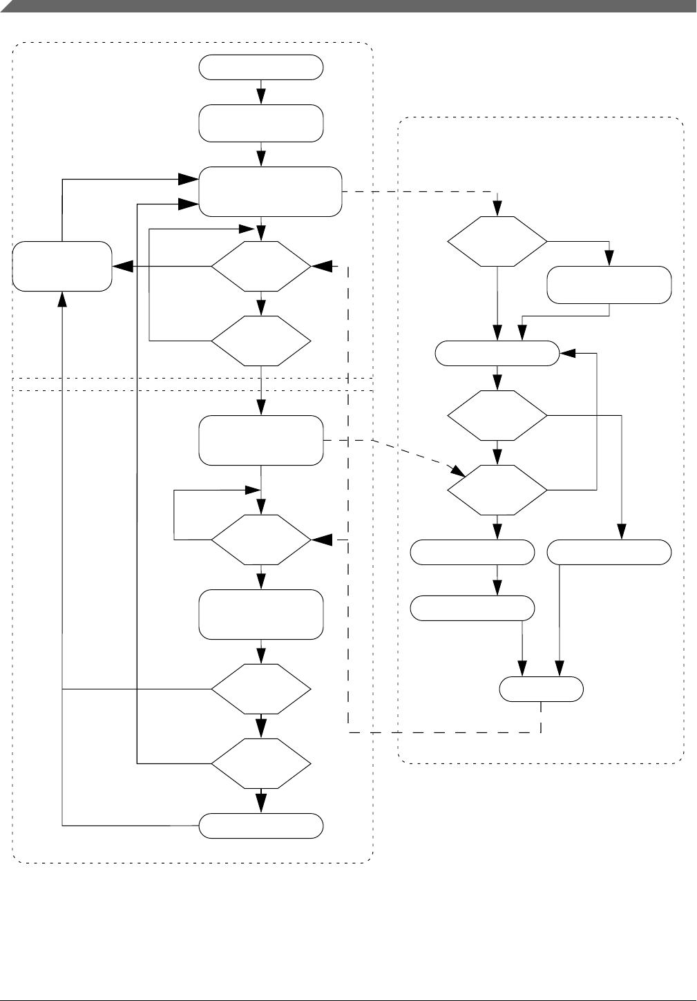
Restore Erase Algo
Clear SUSPACK = 0
ERSSCR Command
(Write FCCOB)
Launch/Resume Command
(Clear CCIF)
CCIF = 1?
Request Suspend
(Set ERSSUSP)
Interrupt?
CCIF = 1?
Service Interrupt
(Read Flash)
ERSSUSP=0?
Next Command
(Write FCCOB)
Clear ERSSUSP
Enter with CCIF = 1
Resume
ERSSCR
No
Memory Controller
Command Processing
SUSPACK=1
Clear ERSSUSP
Execute
Yes
DONE?
No
ERSSUSP=1?
Save Erase Algo
Set CCIF
No
Yes
Start
New
Resume Erase?
No, Abort
User Cmd Interrupt/Suspend
Set SUSPACK = 1
ERSSCR Suspended
Command Initiation
Yes
No
Yes
Yes
ERSSCR
Completed
ERSSCR Suspended
ERSSUSP=1
ERSSUSP: Bit in FCNFG register
SUSPACK: Internal Suspend Acknowledge
No
Yes
Yes
No
Yes
No
ERSSCR Completed
ERSSUSP=0
Figure 36-15. Suspend and resume of Erase Flash Sector operation
Functional description
S32K1xx Series Reference Manual, Rev. 7, 04/2018
824 NXP Semiconductors

36.5.11.7 Program Section command
The Program Section operation programs the data found in the section program buffer to
previously erased locations in the flash memory using an embedded algorithm. Data is
preloaded into the section program buffer by writing to the FlexRAM while it is set to
function as a programming acceleration RAM (see Flash sector programming).
The section program buffer is limited to the lower quarter of the programming
acceleration RAM (byte addresses 0x0000- 0x<1/4 * FlexRAM size>). Data written to
the remainder of the programming acceleration RAM is ignored and may be overwritten
during Program Section command execution.
CAUTION
A flash memory location must be in the erased state before
being programmed. Cumulative programming of bits (back-to-
back program operations without an intervening erase) within a
flash memory location is not allowed. Re-programming of
existing 0s to 0 is not allowed as this overstresses the device.
Table 36-46. Program Section command FCCOB requirements
FCCOB Number FCCOB Contents [7:0]
0 0x0B (PGMSEC)
1 Flash address [23:16]
2 Flash address [15:8]
3 Flash address [7:0]1
4Number of double-phrases (for interleaved blocks), phrases (for non-interleaved blocks) to program
[15:8]
5Number of double-phrases (for interleaved blocks), phrases (for non-interleaved blocks) to program
[7:0]
1. Must be 128-bit aligned (Flash address [3:0] = 0000) for interleaved flash, 64-bit aligned (Flash address [2:0] = 000) for
non-interleaved flash.
After clearing CCIF to launch the Program Section command, the FTFC will block
access to the FlexRAM and program the data residing in the Section Program Buffer into
the flash memory starting at the flash address provided.
The starting address must be unprotected (see the description of the FPROT registers) to
permit execution of the Program Section operation. Programming, which is not allowed
to cross a flash sector boundary, continues until all requested double-phrases (for
interleaved blocks), phrases (for non-interleaved blocks) have been programmed.
After the Program Section operation has completed, the CCIF flag will set and normal
access to the FlexRAM is restored. The contents of the Section Program Buffer is not
changed by the Program Section operation.
Chapter 36 Flash Memory Module (FTFC)
S32K1xx Series Reference Manual, Rev. 7, 04/2018
NXP Semiconductors 825

Table 36-47. Program Section command error handling
Error Condition Error Bit
Command not available in current mode/security FSTAT[ACCERR]
An invalid flash address is supplied FSTAT[ACCERR]
Flash address is not 128-bit aligned for interleaved flash, 64-bit aligned for non-interleaved
flash FSTAT[ACCERR]
The requested section crosses a program flash sector boundary FSTAT[ACCERR]
The requested number of double-phrases for interleaved flash, phrases for non-interleaved
flash is zero FSTAT[ACCERR]
The space required to store data for the requested number of double-phrases for interleaved
flash, phrases for non-interleaved flash is more than one quarter the size of the FlexRAM FSTAT[ACCERR]
The FlexRAM is not set to function as a traditional RAM, i.e., set if RAMRDY=0 FSTAT[ACCERR]
The flash address falls in a protected area FSTAT[FPVIOL]
Any errors have been encountered during the verify operation FSTAT[MGSTAT0]
36.5.11.7.1 Flash sector programming
The process of programming an entire flash sector using the Program Section command
is as follows:
1. If required, execute the Set FlexRAM Function command to make the FlexRAM
available as traditional RAM and initialize the FlexRAM to all ones.
2. Launch the Erase Flash Sector command to erase the flash sector to be programmed.
3. Beginning with the starting address of the FlexRAM, sequentially write enough data
to the RAM to fill an entire flash sector or one quarter of the FlexRAM, whichever is
less. This area of the RAM serves as the section program buffer.
NOTE
In step 1, the section program buffer was initialized to all
ones, the erased state of the flash memory.
The section program buffer can be written to while the operation launched in step 2
is executing, i.e., while CCIF = 0.
4. Execute the Program Section command to program the contents of the section
program buffer into the selected flash sector.
5. If a Flash sector is larger than one quarter of the FlexRAM, repeat steps 3 and 4 until
the sector has been completely programmed.
6. To program additional flash sectors, repeat steps 2 through 4.
7. To restore emulated EEPROM functionality, execute the Set FlexRAM Function
command to make the FlexRAM available for emulated EEPROM.
Functional description
S32K1xx Series Reference Manual, Rev. 7, 04/2018
826 NXP Semiconductors

36.5.11.8 Read 1s All Blocks command
The Read 1s All Blocks command checks if the program flash blocks, data flash blocks,
emulated EEPROM backup records, and data flash IFR have been erased to the specified
read margin level, if applicable, and releases security if the readout passes, i.e. all data
reads as '1'.
Table 36-48. Read 1s All Blocks command FCCOB requirements
FCCOB Number FCCOB Contents [7:0]
0 0x40 (RD1ALL)
1 Read-1 Margin Choice
After clearing CCIF to launch the Read 1s All Blocks command, the FTFC:
• sets the read margin for 1s according to Table 36-49,
• checks the contents of the program flash, data flash, emulated EEPROM backup
records, and data flash IFR are in the erased state.
If the FTFC confirms that these memory resources are erased, security is released by
setting the FSEC[SEC] field to the unsecure state. The security byte in the flash
configuration field (see Flash configuration field description) remains unaffected by the
Read 1s All Blocks command. If the read fails, i.e., all flash memory resources are not in
the fully erased state, the FSTAT[MGSTAT0] bit is set.
The EEERDY and RAMRDY bits are clear during the Read 1s All Blocks operation and
are restored at the end of the Read 1s All Blocks operation.
The CCIF flag sets after the Read 1s All Blocks operation has completed.
Table 36-49. Margin level choices for Read 1s All Blocks
Read Margin Choice Margin Level Description
0x00 Use the 'normal' read level for 1s
0x01 Apply the 'User' margin to the normal read-1 level
0x02 Apply the 'Factory' margin to the normal read-1 level
Table 36-50. Read 1s All Blocks command error handling
Error Condition Error Bit
An invalid margin choice is specified FSTAT[ACCERR]
Read-1s fails FSTAT[MGSTAT0]
Chapter 36 Flash Memory Module (FTFC)
S32K1xx Series Reference Manual, Rev. 7, 04/2018
NXP Semiconductors 827

36.5.11.9 Read Once command
The Read Once command provides read access to a reserved 64 -byte field located in the
program flash IFR (see Program flash 0 IFR map and Program Once field). Access to the
Program Once field is via 8 records, each 8 bytes long. The Program Once field is
programmed using the Program Once command described in Program Once command.
Table 36-51. Read Once command FCCOB requirements
FCCOB Number FCCOB Contents [7:0]
0 0x41 (RDONCE)
1 Program Once record index (0x00 - 0x07 )
Returned Values
4 Program Once byte 0 value
5 Program Once byte 1 value
6 Program Once byte 2 value
7 Program Once byte 3 value
8 Program Once byte 4 value
9 Program Once byte 5 value
A Program Once byte 6 value
B Program Once byte 7 value
After clearing CCIF to launch the Read Once command, an 8-byte Program Once record
is read from the program flash IFR and stored in the FCCOB register. The CCIF flag is
set after the Read Once operation completes. Valid record index values for the Read
Once command range from 0x00 to 0x07 . During execution of the Read Once command,
any attempt to read addresses within the program flash block containing this 64 -byte
field returns invalid data. The Read Once command can be executed any number of
times.
Table 36-52. Read Once command error handling
Error Condition Error Bit
Command not available in current mode/security FSTAT[ACCERR]
An invalid record index is supplied FSTAT[ACCERR]
Functional description
S32K1xx Series Reference Manual, Rev. 7, 04/2018
828 NXP Semiconductors

36.5.11.10 Program Once command
The Program Once command enables programming to a reserved 64 -byte field in the
program flash IFR (see Program flash 0 IFR map and Program Once field). Access to the
Program Once field is via 8 records, each 8 bytes long. The Program Once field can be
read using the Read Once command (see Read Once command). Each Program Once
record can be programmed only once since the program flash IFR cannot be erased.
Table 36-53. Program Once command FCCOB requirements
FCCOB Number FCCOB Contents [7:0]
0 0x43 (PGMONCE)
1 Program Once record index (0x00 - 0x07 )
2 Not Used
3 Not Used
4 Program Once Byte 0 value
5 Program Once Byte 1 value
6 Program Once Byte 2 value
7 Program Once Byte 3 value
8 Program Once Byte 4 value
9 Program Once Byte 5 value
A Program Once Byte 6 value
B Program Once Byte 7 value
After clearing CCIF to launch the Program Once command, the FTFC first verifies that
the selected record is erased. If erased, then the selected record is programmed using the
values provided. The Program Once command also verifies that the programmed values
read back correctly. The CCIF flag is set after the Program Once operation has
completed.
The reserved program flash IFR location accessed by the Program Once command cannot
be erased and any attempt to program one of these records when the existing value is not
Fs (erased) is not allowed. Valid record index values for the Program Once command
range from 0x00 to 0x07 . During execution of the Program Once command, any attempt
to read addresses within program flash returns invalid data.
Table 36-54. Program Once command error handling
Error Condition Error Bit
Command not available in current mode/security FSTAT[ACCERR]
An invalid record index is supplied FSTAT[ACCERR]
The requested record has already been programmed to a non-erased value1FSTAT[ACCERR]
Any errors have been encountered during the verify operation. FSTAT[MGSTAT0]
Chapter 36 Flash Memory Module (FTFC)
S32K1xx Series Reference Manual, Rev. 7, 04/2018
NXP Semiconductors 829

1. If a Program Once record is initially programmed to 0xFFFF_FFFF_FFFF_FFFF, the Program Once command is allowed
to execute again on that same record.
36.5.11.11 Erase All Blocks command
The Erase All Blocks operation erases all flash memory, initializes the FlexRAM, verifies
all memory contents, and releases MCU security.
Table 36-55. Erase All Blocks command FCCOB requirements
FCCOB Number FCCOB Contents [7:0]
0 0x44 (ERSALL)
After clearing CCIF to launch the Erase All Blocks command, the FTFC erases all
program flash memory, data flash memory, data flash IFR space, emulated EEPROM
backup memory, and FlexRAM, then verifies that all are erased.
If the FTFC verifies that all flash memories and the FlexRAM were properly erased,
MCU security is released by setting the FSEC[SEC] field to the unsecure state and the
FCNFG[RAMRDY] bit is set. The Erase All Blocks command aborts if any flash or
FlexRAM region is protected. The security byte and all other contents of the flash
configuration field (see Flash configuration field description) are erased by the Erase All
Blocks command. If the erase-verify fails, the FSTAT[MGSTAT0] bit is set. The CCIF
flag is set after the Erase All Blocks operation completes.
NOTE
For CSEc enabled parts, the presence of any (1 or more) Flash
Keys will prevent this command from executing. Refer to the
commands CMD_DBG_CHAL and CMD_DBG_AUTH for the
procedures to pass a challenge/authentication process which
will first remove the keys, then (assuming successful execution)
allow this command to be executed.
Table 36-56. Erase All Blocks command error handling
Error Condition Error Bit
Command not available in current mode/security, or CSEc key allocation being non-zero keys FSTAT[ACCERR]
Any region of the program flash memory, data flash memory, or FlexRAM is protected FSTAT[FPVIOL]
Any errors have been encountered during the verify operation1FSTAT[MGSTAT0]
1. User margin read may be run using the Read 1s All Blocks command to verify all bits are erased.
Functional description
S32K1xx Series Reference Manual, Rev. 7, 04/2018
830 NXP Semiconductors

36.5.11.11.1 Triggering an erase all external to the flash module
The functionality of the Erase All Blocks/Erase All Blocks Unsecure command is also
available in an un-commanded fashion outside of the flash memory. Refer to the device's
Chip Configuration details for information on this functionality.
Before invoking the external erase all function, the FCCOB0 register must not contain
0x44. When invoked, the erase-all function erases all program flash memory, data flash
memory, data flash IFR space, emulated EEPROM backup, and FlexRAM regardless of
the state of the FSTAT[ACCERR and FPVIOL] flags or the protection settings. If the
post-erase verify passes, the routine releases security by setting the FSEC[SEC] field
register to the unsecure state and the FCNFG[RAMRDY] bit sets. The security byte in
the Flash Configuration Field is also programmed to the unsecure state. The status of the
erase-all request is reflected in the FCNFG[ERSAREQ] bit. The FCNFG[ERSAREQ] bit
is cleared once the operation completes and the normal FSTAT error reporting, except
FPVIOL, is available as described in Erase All Blocks command.
36.5.11.12 Verify Backdoor Access Key command
The Verify Backdoor Access Key command only executes if the mode and security
conditions are satisfied (see Flash commands by mode). Execution of the Verify
Backdoor Access Key command is further qualified by the FSEC[KEYEN] bits. The
Verify Backdoor Access Key command releases security if user-supplied keys in the
FCCOB match those stored in the Backdoor Comparison Key bytes of the Flash
Configuration Field. The column labeled Flash Configuration Field offset address shows
the location of the matching byte in the Flash Configuration Field.
Table 36-57. Verify Backdoor Access Key command FCCOB requirements
FCCOB Number FCCOB Contents [7:0] Flash Configuration Field Offset Address
0 0x45 (VFYKEY)
1-3 Not Used
4 Key Byte 0 0x0_0003
5 Key Byte 1 0x0_0002
6 Key Byte 2 0x0_0001
7 Key Byte 3 0x0_0000
8 Key Byte 4 0x0_0007
9 Key Byte 5 0x0_0006
A Key Byte 6 0x0_0005
B Key Byte 7 0x0_0004
Chapter 36 Flash Memory Module (FTFC)
S32K1xx Series Reference Manual, Rev. 7, 04/2018
NXP Semiconductors 831

After clearing CCIF to launch the Verify Backdoor Access Key command, the FTFC
checks the FSEC[KEYEN] bits to verify that this command is enabled. If not enabled, the
FTFC sets the FSTAT[ACCERR] bit and terminates. If the command is enabled, the
FTFC compares the key provided in FCCOB to the backdoor comparison key in the Flash
Configuration Field. If the backdoor keys match, the FSEC[SEC] field is changed to the
unsecure state and security is released. If the backdoor keys do not match, security is not
released and all future attempts to execute the Verify Backdoor Access Key command are
immediately aborted and the FSTAT[ACCERR] bit is (again) set to 1 until a reset of the
FTFC module occurs. If the entire 8-byte key is all zeros or all ones, the Verify Backdoor
Access Key command fails with an access error. The CCIF flag is set after the Verify
Backdoor Access Key operation completes.
Table 36-58. Verify Backdoor Access Key command error handling
Error Condition Error Bit
Command not available in current mode/security FSTAT[ACCERR]
The supplied key is all-0s or all-Fs FSTAT[ACCERR]
An incorrect backdoor key is supplied FSTAT[ACCERR]
Backdoor key access has not been enabled (see the description of the FSEC register) FSTAT[ACCERR]
This command is launched and the backdoor key has mismatched since the last reset FSTAT[ACCERR]
36.5.11.13 Erase All Blocks Unsecure command
The Erase All Blocks Unsecure operation erases all flash memory, initializes the
FlexRAM, verifies all memory contents, programs the security byte in the Flash
Configuration Field to the unsecure state, and releases MCU security.
Table 36-59. Erase All Blocks Unsecure command FCCOB requirements
FCCOB Number FCCOB Contents [7:0]
0 0x49 (ERSALLU)
After clearing CCIF to launch the Erase All Blocks Unsecure command, the FTFC erases
all program flash memory, data flash memory, data flash IFR space, emulated EEPROM
backup memory, and FlexRAM, then verifies that all are erased.
If the FTFC verifies that all flash memories and the FlexRAM were properly erased,
security is released by setting the FSEC[SEC] field to the unsecure state, the security byte
(see Flash configuration field description) is programmed to the unsecure state by the
Erase All Blocks Unsecure command, and the FCNFG[RAMRDY] bit is set. If the erase
or program verify fails, the FSTAT[MGSTAT0] bit is set. The CCIF flag is set after the
Erase All Blocks Unsecure operation completes.
Functional description
S32K1xx Series Reference Manual, Rev. 7, 04/2018
832 NXP Semiconductors

NOTE
For CSEc enabled parts, the presence of any (1 or more) Flash
Keys will prevent this command from executing. Refer to the
commands CMD_DBG_CHAL and CMD_DBG_AUTH for the
procedures to pass a challenge/authentication process which
will first remove the keys, then (assuming successful execution)
allow this command to be executed.
Table 36-60. Erase All Blocks Unsecure command error handling
Error Condition Error Bit
Command not available in current mode/security, or key allocation being non-zero keys FSTAT[ACCERR]
Any errors have been encountered during erase or program verify operations FSTAT[MGSTAT0]
36.5.11.14 Program Partition command
The Program Partition command prepares the FlexNVM block for use as data flash,
emulated EEPROM backup, or a combination of both and initializes the FlexRAM. The
Program Partition command must not be launched from flash memory, since flash
memory resources are not accessible during Program Partition command execution.
Changes related to execution of the Program Partition command take effect after the next
reset.
CAUTION
While different partitions of the FlexNVM are available, the
intention is that a single partition choice is used throughout the
entire lifetime of a given application. The FlexNVM Partition
Code choices affect the endurance and data retention
characteristics of the device.
Table 36-61. Program Partition command FCCOB requirements
FCCOB Number FCCOB Contents [7:0]
0 0x80 (PGMPART)
1 CSEc Key Size
2 SFE
3
FlexRAM load during reset option (only bit 0 used):
0 - FlexRAM loaded with valid EEPROM data during reset sequence
1 - FlexRAM not loaded during reset sequence
4 EEPROM Data Set Size Code
5 FlexNVM Partition Code
Chapter 36 Flash Memory Module (FTFC)
S32K1xx Series Reference Manual, Rev. 7, 04/2018
NXP Semiconductors 833

Table 36-62. CSEc/SHE key size
FCCOB1 [1:0] Number of Flash Keys
({MASTER_ECU_KEY,
BOOT_MAC_KEY, BOOT_MAC,
KEY_<n>})
Number of Bytes (subtracts from the
total EEERAM space)
2'b00 Zero 0
2'b01 1 to 5 keys 128 Bytes
2'b10 1 to 10 keys 256 Bytes
2'b11 1 to 20 keys 512 Bytes
For non-CSEc enabled parts, the number of Flash Keys must be configured as 2'b00 (no
keys).
For CSEc enabled parts, the number of Flash Keys is user configurable, but the space will
assume that the MASTER_ECU_KEY, BOOT_MAC_KEY and BOOT_MAC are there
(if any keys are enabled), and thus will occupy 3 key slots of the available 20 key slot
space. This results in leaving key slots for a range of 1 to 17 User Key_<n> keys.
For non-CSEc enabled parts the key allocation must be set to Zero keys (2'b00),
otherwise the command will return an error.
NOTE
For CSEc enabled parts, once Flash Keys are allocated
(regardless of being initialized or not), the SHE spec
requirement of not erasing Flash Keys without authentication
will apply. This will mean Authentication (DBG_CHAL &
DBG_AUTH) commands must be run and pass (removing all
flash keys) before erase of the DFlash (all Flash Keys are
backed up in emulated EEPROM in DFlash). Thus Erase All
Blocks and Erase All Blocks Unsecure will not work, nor will
Erase Flash Block or Sector IF the selected Block/Sector
includes the DFlash where the keys are stored. Additionally if
any Flash Keys are write protected, they can't be erased/
removed, thus the DFlash can't be erased and the
Authentication process will not pass.
Table 36-63. Security Flag Extension (SFE)
SFE Results
SFE == 0x01 Flash Key 'Verify Only' attribute enabled
SFE == 0x00 Flash Key 'Verify Only' attribute not enabled
Functional description
S32K1xx Series Reference Manual, Rev. 7, 04/2018
834 NXP Semiconductors

The FCCOB[2] field is for the enhanced Security Flag Extension (SFE) is in a 8-bit field,
but only bit [0] is used (bits [7:1] are ignored). This feature is an extension to the SHE
specification. For standard SHE usage model, the user should configure this as 'not
enabled' (SFE == 0x00). This addition is to add capability to flag a key as
'VERIFY_ONLY'. That is, the user can configure SFE == 0x01 and then use the
LOAD_KEY command to add a new attribute to the key which would tell the
GENERATE_MAC command that the key is to be used only by the VERIFY_MAC
command (by configuring SFE as 'enabled' and then using LOAD_KEY to set the new
VERIFY_ONLY attribute on that key).
The VERIFY_ONLY attribute has no effect if the KEY_USAGE attribute is '0'.
See the CMD_LOAD_KEY command for more information on the new attribute.
Table 36-64. Valid emulated EEPROM data set size codes : 2 KB FlexRAM configurations
EEPROM Data Set Size Code (FCCOB4)1EEPROM Data Set Size (Bytes)
EEESIZE (FCCOB4[3:0])
0xF 02
0x3 2k
1. FCCOB4[7:4] = 0000
2. EEPROM Data Set Size must be set to 0 Bytes when the FlexNVM Partition Code is set for no EEPROM.
Table 36-65. Valid emulated EEPROM data set size codes : 4 KB FlexRAM configurations
EEPROM Data Set Size Code (FCCOB4)1EEPROM Data Set Size (Bytes)
EEESIZE (FCCOB4[3:0])
0xF 02
0x2 4k
1. FCCOB4[7:4] = 0000
2. EEPROM Data Set Size must be set to 0 Bytes when the FlexNVM Partition Code is set for no EEPROM.
Table 36-66. Valid FlexNVM partition codes : 128 KB and 256 KB configurations with 32 KB
FlexNVM
FlexNVM Partition Code DEPART
(FCCOB5[3:0])1Data flash Size (KB) EEPROM-backup Size (KB)
0000 32 0
0011 0 32
1000 0 32
1001 8 24
1011 32 0
1. FCCOB5[7:4] = 0000
Chapter 36 Flash Memory Module (FTFC)
S32K1xx Series Reference Manual, Rev. 7, 04/2018
NXP Semiconductors 835

Table 36-67. Valid FlexNVM partition codes : 256 KB, 512 KB and 1MB configurations with
64 KB FlexNVM
FlexNVM Partition Code DEPART
(FCCOB5[3:0])1Data flash Size (KB) EEPROM-backup Size (KB)
0000 64 0
0011 32 32
0100 0 64
1000 0 64
1010 16 48
1011 32 32
1100 64 0
1. FCCOB5[7:4] = 0000
NOTE
For the 2M configuration (where DFlash is implemented in
multiple blocks) the FlexNVM may only be configured into: all
Data flash, or 64 KB emulated EEPROM backup with the
remainder left as Data Flash. Thus there are only three valid
values for DEPART (FCCOB5[3:0]) : either 4'b0100 (64 KB
emulated EEPROM, remainder is DFlash) or 4'b0000, 4'b1111
(0 KB emulated EEPROM/all DFlash).
Table 36-68. Valid FlexNVM partition codes: 2 MB configurations
FlexNVM Partition Code DEPART
(FCCOB5[3:0])1Data flash Size (KB) EEPROM-backup Size (KB)
0000 DFlash size (512 KB) 0
0100 DFlash size - EEPROM size (512 KB -
64 KB = 448 KB)
64
1111 DFlash size (512 KB) 0
1. FCCOB5[7:4] = 0000
After clearing CCIF to launch the Program Partition command, the FTFC first verifies
that the EEPROM Data Set Size Code and FlexNVM Partition Code in the data flash IFR
are erased. If erased, the Program Partition command erases the contents of the FlexNVM
memory. If the FlexNVM is to be partitioned for emulated EEPROM backup, the
allocated emulated EEPROM backup sectors are formatted for emulated EEPROM use.
Finally, the partition codes are programmed into the data flash IFR using the values
provided. The Program Partition command also verifies that the partition codes read back
correctly after programming. The CCIF flag is set after the Program Partition operation
completes.
Functional description
S32K1xx Series Reference Manual, Rev. 7, 04/2018
836 NXP Semiconductors

Prior to launching the Program Partition command, the data flash IFR must be in an
erased state, which can be accomplished by executing the Erase All Blocks or Erase All
Blocks Unsecure commands or by an external request (see Triggering an erase all
external to the flash module).
Table 36-69. Program Partition command error handling
Error Condition Error Bit
Command not available in current mode/security FSTAT[ACCERR]
The EEPROM data size and FlexNVM partition code bytes are not initially 0xFFFF FSTAT[ACCERR]
Invalid EEPROM Data Set Size Code is entered (see Table 36-65 for valid codes) FSTAT[ACCERR]
Invalid FlexNVM Partition Code is entered (see Table 36-66 for valid codes) FSTAT[ACCERR]
FlexNVM Partition Code = full data flash (no emulated EEPROM) and EEPROM Data Set
Size Code allocates FlexRAM for emulated EEPROM FSTAT[ACCERR]
FlexNVM Partition Code allocates space for emulated EEPROM backup, but EEPROM Data
Set Size Code allocates no FlexRAM for emulated EEPROM FSTAT[ACCERR]
FCCOB1[7:0] > 0x3 FSTAT[ACCERR]
FCCOB1[7:0] > 0 for non-CSEc enabled parts FSTAT[ACCERR]
FCCOB1[7:0] > 0, when EEPROM-backup Size is 0 FSTAT[ACCERR]
FCCOB1[7:0] > 0, when SFE = 1 FSTAT[ACCERR]
FCCOB1[7:0] > 0, when FCCOB3[0] = 1 FSTAT[ACCERR]
FCCOB4[7:4] != 0000 FSTAT[ACCERR]
FCCOB5[7:4] != 0000 FSTAT[ACCERR]
Any errors have been encountered during the verify operation FSTAT[MGSTAT0]
36.5.11.15 Set FlexRAM Function command
The Set FlexRAM Function command changes the function of the FlexRAM:
• When not partitioned for emulated EEPROM, the FlexRAM is typically used as
traditional RAM.
• When partitioned for emulated EEPROM, the FlexRAM is typically used to store
EEPROM data.
Table 36-70. Set FlexRAM Function command FCCOB requirements
FCCOB Number FCCOB Contents [7:0]
0 0x81 (SETRAM)
1FlexRAM Function Control Code
(see Table 36-71)
2 Reserved
3 Reserved
4 Number of FlexRAM bytes allocated for EEPROM quick writes [15:8]
Table continues on the next page...
Chapter 36 Flash Memory Module (FTFC)
S32K1xx Series Reference Manual, Rev. 7, 04/2018
NXP Semiconductors 837

Table 36-70. Set FlexRAM Function command FCCOB requirements
(continued)
FCCOB Number FCCOB Contents [7:0]
5 Number of FlexRAM bytes allocated for EEPROM quick writes [7:0]
Returned Values
5
Brown-out (BO) Detection Codes
• 0x00 - No EEPROM issues detected
• 0x01 - BO detected before completing EEPROM quick write maintenance
• 0x02 - BO detected before completing EEPROM quick writes
• 0x04 - BO detected during normal EEPROM write activity
6 Number of EEPROM quick write records requiring maintenance [15:8]
7 Number of EEPROM quick write records requiring maintenance [7:0]
8 EEPROM sector erase count [15:8]
9 EEPROM sector erase count [7:0]
Table 36-71. FlexRAM Function control
FlexRAM Function
Control Code Action
0xFF
Make FlexRAM available as RAM:
• Clear the FCNFG[RAMRDY] and FCNFG[EEERDY] flags
• Write a background of ones to all FlexRAM locations
• Set the FCNFG[RAMRDY] flag
0xAA
Complete interrupted EEPROM quick write process
• Clear the FCNFG.EEERDY flag (and FCNFG.RAMRDY flag)
• Complete maintenance on interrupted EEPROM quick write operations
• Set the FCNFG.EEERDY flag
0x77
EEPROM quick write status query
• Clear the FCNFG.EEERDY flag (and FCNFG.RAMRDY flag)
• Report emulated EEPROM status
• Set the FCNFG.EERDY flag
0x55
Make FlexRAM available for EEPROM quick writes
• Clear the FCNFG.EERDY flash (and FCNFG.RAMRDY flag)
• Enable the emulated EEPROM system for EEPROM quick writes
• Set the FCNFG.EEERDY flag
0x00
Make FlexRAM available for emulated EEPROM:
• Clear the FCNFG[RAMRDY] and FCNFG[EEERDY] flags
• Write a background of ones to all FlexRAM locations
• Copy-down existing EEPROM data to FlexRAM
• Set the FCNFG[EEERDY] flag
After clearing CCIF to launch the Set FlexRAM Function command, the FTFC sets the
function of the FlexRAM based on the FlexRAM Function Control Code.
When making the FlexRAM available as traditional RAM, the FTFC clears the
FCNFG[EEERDY] and FCNFG[RAMRDY] flags, overwrites the contents of the entire
FlexRAM with a background pattern of all ones, and sets the FCNFG[RAMRDY] flag.
The state of the EPROT register does not prevent the FlexRAM from being overwritten.
Functional description
S32K1xx Series Reference Manual, Rev. 7, 04/2018
838 NXP Semiconductors

When the FlexRAM is set to function as a RAM, normal read and write accesses to the
FlexRAM are available. When large sections of flash memory need to be programmed,
e.g. during factory programming, the FlexRAM can be used as the Section Program
Buffer for the Program Section command (see Program Section command).
When the FlexRAM Function Control Code is 0x55 or 0xAA, after clearing the
EEERDY flag, all EEPROM normal or quick write activity not previously completed will
be processed. If the EEPROM quick write activity did not complete writing all requested
records, the records written will be cleared, effectively restoring previously valid records.
If all EEPROM quick write records were written but maintenance activities were not
completed, maintenance will complete on the remaining quick write records. The CCIF
and EEERDY flag will remain negated until all EEPROM maintenance activities have
been completed.
When the FlexRAM Function Control Code is 0x77, after clearing the EEERDY flag, the
emulated EEPROM system will be interrogated, and EEPROM cleanup requirements and
EEPROM sector erase count will be reported. If EEPROM normal write activity is
interrupted by a reset or loss of power before finalizing the record, BO detection code
0x04 will be returned. If the EEPROM quick write activity is interrupted by a reset before
writing all quick write records requested with control code 0x55, BO detection code 0x02
will be returned. If the interruption occurs after all quick writes requested have been
written but before quick write maintenance has completed, BO detection code 0x01 will
be returned. The CCIF and EEERDY flag will remain negated until the EEPROM status
has been loaded into the FCCOB registers.
When making the FlexRAM available for EEPROM quick writes, the contents of the
FlexRAM will be left as is and the emulated EEPROM system will be prepared for quick
write activities. After the EEERDY flag in the FCNFG register is set, the emulated
EEPROM system is ready for quick writes. When the FlexRAM is set to accept the
EEPROM quick writes, read and write access to the FlexRAM is available but each 32-
bit write to the FlexRAM will invoke EEPROM quick write activity. The CCIF and
EEERDY flag will deassert on each 32-bit write and assert after the associated EEPROM
quick write activity has completed. After the last 32-bit write to the FlexRAM, specified
by the contents of FCCOB4 and FCCOB5, the emulated EEPROM system will create the
data record for the last write (~150uSec) and begin the EEPROM maintenance activities
on the entire block of quick write data. The CCIF and EEERDY flag will remain negated
until all EEPROM quick write maintenance activities have completed.
For configurations with interleaved flash blocks for EEPROM backup, quick writes
should be restricted to either within the first half of EEERAM or within the second half
of EEERAM. Otherwise, FSTAT[ACCERR] will be returned.
Chapter 36 Flash Memory Module (FTFC)
S32K1xx Series Reference Manual, Rev. 7, 04/2018
NXP Semiconductors 839

When making the FlexRAM available for emulated EEPROM, the FTFC clears the
FCNFG[RAMRDY] and FCNFG[EEERDY] flags, overwrites the contents of the
FlexRAM allocated for emulated EEPROM with a background pattern of all ones, and
copies the existing EEPROM data from the EEPROM backup record space to the
FlexRAM. After completion of the EEPROM copy-down, the FCNFG[EEERDY] flag is
set. When the FlexRAM is set to function as emulated EEPROM, normal read and write
access to the FlexRAM is available, but writes to the FlexRAM also invoke emulated
EEPROM activity.
The CCIF flag will be set after the Set FlexRAM Function operation has completed.
Table 36-72. Set FlexRAM Function command error handling
Error Condition Error Bit
Command not available in current mode/security FSTAT[ACCERR]
FlexRAM Function Control Code is not defined FSTAT[ACCERR]
FlexRAM Function Control Code is set to make the FlexRAM available for emulated
EEPROM, but FlexNVM is not partitioned for emulated EEPROM FSTAT[ACCERR]
Set if FlexRAM Function Control Code is set to 0xAA, 0x77 or 0x55 but FCNFG.[EEERDY] =0
(FlexRAM not in emulated EEPROM mode) FSTAT[ACCERR]
Set if FlexRAM is in EEPROM quick write mode, i.e. all EEPROM quick writes to the
FlexRAM have not been completed FSTAT[ACCERR]
Set if FlexRAM Function Control Code is set to make FlexRAM available for EEPROM quick
writes but the number of bytes allocated for quick write is less than 16, more than 512, or not
divisible by 4 (only 32-bit quick writes are allowed)
FSTAT[ACCERR]
Set if emulated EEPROM system is in quick write mode and writes to the FlexRAM are not
32-bits FSTAT[ACCERR]
36.5.12 Security
The FTFC module provides security information to the MCU based on contents of the
FSEC security register. The MCU then limits access to FTFC resources as defined in the
device's Chip Configuration details. During reset, the FTFC module initializes the FSEC
register using data read from the security byte of the Flash Configuration Field (see Flash
configuration field description).
The following fields are available in the FSEC register. Details of the settings are
described in the FSEC register description.
Table 36-73. FSEC fields
FSEC field Description
KEYEN Backdoor Key Access
MEEN Mass Erase Capability
Table continues on the next page...
Functional description
S32K1xx Series Reference Manual, Rev. 7, 04/2018
840 NXP Semiconductors

Table 36-73. FSEC fields (continued)
FSEC field Description
FSLACC Factory Access
SEC MCU security
36.5.12.1 FTFC access by mode and security
The following table summarizes how access to the FTFC module is affected by security
and operating mode.
Table 36-74. FTFC access summary
Operating Mode MCU Security State
Unsecure Secure
NVM Normal Full command set
36.5.12.2 Changing the security state
The security state out of reset can be permanently changed by programming the security
byte of the flash configuration field. This assumes that you are starting from a mode
where the necessary program flash erase and program commands are available and that
the region of the program flash containing the flash configuration field is unprotected. If
the flash security byte is successfully programmed, its new value takes effect after the
next MCU reset.
36.5.12.2.1 Un-securing the MCU using backdoor key access
The MCU can be unsecured by using the backdoor key access feature which requires
knowledge of the contents of the 8-byte backdoor key value stored in the Flash
Configuration Field (see Flash configuration field description). If the FSEC[KEYEN] bits
are in the enabled state, the Verify Backdoor Access Key command (see Verify Backdoor
Access Key command) can be run which allows the user to present prospective keys for
comparison to the stored keys. If the keys match, the FSEC[SEC] bits are changed to
unsecure the MCU. The entire 8-byte key cannot be all 0s or all 1s, i.e.,
0x0000_0000_0000_0000 and 0xFFFF_FFFF_FFFF_FFFF are not accepted by the
Verify Backdoor Access Key command as valid comparison values. While the Verify
Backdoor Access Key command is active, program flash memory is not available for read
access and returns invalid data.
Chapter 36 Flash Memory Module (FTFC)
S32K1xx Series Reference Manual, Rev. 7, 04/2018
NXP Semiconductors 841

The user code stored in the program flash memory must have a method of receiving the
backdoor keys from an external stimulus. This external stimulus would typically be
through one of the on-chip serial ports.
If the KEYEN bits are in the enabled state, the MCU can be unsecured by the backdoor
key access sequence described below:
1. Follow the command sequence for the Verify Backdoor Access Key command as
explained in Verify Backdoor Access Key command
2. If the Verify Backdoor Access Key command is successful, the MCU is unsecured
and the FSEC[SEC] bits are forced to the unsecure state
An illegal key provided to the Verify Backdoor Access Key command prohibits future
use of the Verify Backdoor Access Key command. A reset of the MCU is the only
method to re-enable the Verify Backdoor Access Key command when a comparison fails.
After the backdoor keys have been correctly matched, the MCU is unsecured by changing
the FSEC[SEC] bits. A successful execution of the Verify Backdoor Access Key
command changes the security in the FSEC register only. It does not alter the security
byte or the keys stored in the Flash Configuration Field (Flash configuration field
description). After the next reset of the MCU, the security state of the FTFC module
reverts back to the Flash security byte in the Flash Configuration Field. The Verify
Backdoor Access Key command sequence has no effect on the program and erase
protections defined in the program flash protection registers.
If the backdoor keys successfully match, the unsecured MCU has full control of the
contents of the Flash Configuration Field. The MCU may erase the sector containing the
Flash Configuration Field and reprogram the flash security byte to the unsecure state and
change the backdoor keys to any desired value.
36.5.13 Cryptographic Services Engine (CSEc)
The FTFC module has added features to comply with the SHE9 specification. It is
assumed that the user is familiar with the SHE specification, therefore we do not replicate
the document here.
By using an embedded processor, firmware and hardware assisted AES-128 sub-block,
the FTFC macro enables encryption, decryption and message generation and
authentication algorithms for secure messaging applications. Additionally a TRNG and
Miyaguchi-Prenell compression sub-blocks enables true random number generation
(entropy generator for PRNG in AES sub-block).
9. HIS SHE Specification - Secure Hardware Extension Functional Specification; Version 1.0.1; Rev429 from 23.03.2009
Functional description
S32K1xx Series Reference Manual, Rev. 7, 04/2018
842 NXP Semiconductors

To access the command feature set, the part must be configured for EEE operation, using
the PGMPART command. See more in Program Partition command. By enabling
security features and configuring a number of CSEc keys, the total size of the EEERAM
will be reduced by the space required to store the keys. The key space will then be un-
addressable space in the EEERAM.
The CCOB command set is effectively extended to include SHE commands related to
ECB, CBC and CMAC features. Secure storage of security keys is enabled within the
FTFC module, including up to 17 user keys (MASTER_ECU_KEY, BOOT_MAC_KEY,
BOOT_MAC are assumed to be allocated ). These commands are referred to as the CSEc
command set. The CSEc command set requires input data and command to be entered as
described in User CSEc command interface and command set.
NOTE
1. It is not possible to concurrently execute : EEE operations,
CCOB commands related to Program, Erase (or other
standard FTFC flash commands), CSEc commands. Only
one operation (of any type) may be ongoing at any given
time.
2. Execution of a CSEc command while in Erase Suspend
(ERSSUSP) will result in the Suspended Erase operation
being aborted (not able to be resumed, also Aborted Erase
commands will leave the contents in an indeterminate
state).
3. It is also not possible to execute a different CSEc command
in the middle of a continuation of an ongoing CSEc
command.
4. It is possible to execute a FCCOB command in the middle
of a continuation of an ongoing CSEc command, BUT the
result is the existing CSEc command will be canceled.
5. Starting execution of CCOB commands or CSEc
commands will lock out the CCOB interface, the EEERAM
and the PRAM. The lock is in place until the requested
command completes.
CAUTION
Interrupting a CSEc key update operation (due to power loss,
reset, supplies out of specified operational ranges, or any other
reasons) will leave the contents in an indeterminate state. The
user must take appropriate counter measures to prevent data
loss in case of an interrupted CSEc key update operation.
Chapter 36 Flash Memory Module (FTFC)
S32K1xx Series Reference Manual, Rev. 7, 04/2018
NXP Semiconductors 843

For security reasons some features will be disabled upon any type of debugger (JTAG,
DP, SDB, etc.) connection to the SoC, per SHE specification requirements according to
user configurations.
All message data blocks are to be provided as 128-bit blocks. Minimum block size of
one. If data messages contain less than 128-bits, the message must be padded (according
to SHE spec) to the required 128-bit block size before passing data to the FTFC module.
Internal to the FTFC module are stored the required Secret Key and the Unique ID. Both
in unaddressable and unalterable space, and are programmed in Factory Final Test. Also
supported are the CSEc Keys as described. The flash keys are stored in the EEERAM
space, with a configurable amount of space for flash keys. The space is subtracted from
the end address range of the EEERAM. Anywhere from 1 to 20 (17 user keys) flash keys
may be configured as described in the Non-Volatile Key table. With the assumption that
the first three keys are occupied by MASTER_ECU_KEY, BOOT_MAC_KEY and
BOOT_MAC. Leaving anywhere from 1 to 17 KEY_<n> keys to be configured.
Table 36-75. Non-Volatile keys and RAM_KEY
Key Name {KBS, KeyIDx} Type Size
(Bytes)
Comments
SECRET_KEY X 0x0 ROM 16
UID X 0x0 ROM 15
MASTER_ECU_KEY X 0x1 Flash 16
BOOT_MAC_KEY X 0x2 Flash 16
BOOT_MAC X 0x3 Flash 16
KEY_01 - KEY_10 1’b0 0x4 - 0xD Flash 16 minimum 3 user keys -
max 17
KEY_11 - KEY_17 1’b1 0x4 - 0xA Flash 16
RESERVED 1’b1 0xB - 0xE RESERVED 16
RESERVED 1’b0 0xE RESERVED 16
RAM_KEY X 0xF Volatile (RAM_KEY) 16
Table 36-76. Other volatile keys
Key Name ADDRESS Type Size (Bytes) Comments
PRNG_KEY N/A RAM 16
PRNG_STATE N/A RAM 16
Table 36-77. ROM keys
Key Name ADDRESS Type Size (Bytes) Comments
SECRET_KEY N/A ROM 16
UID N/A ROM 15 accessible via the GET_ID
command
Functional description
S32K1xx Series Reference Manual, Rev. 7, 04/2018
844 NXP Semiconductors

36.5.13.1 Key/seed/random number generation
This is the high level flow in which to initialize and generate random numbers.
1. Run CMD_INIT_RNG to initialize a random seed from the internal TRNG
NOTE
a. CMD_INIT_RNG must be run after every POR, and
before the first execution of CMD_RND
b. If the seed is run through compression before the seed
is used in the PRNG, then CSESTAT[RIN] will be set
c. Note that if the next step (run CMD_RND) is run
without initializing the seed, an error
(ERC_RNG_SEED) will be set.
2. Run CMD_RND to generate a random number
The PRNG uses the PRNG_STATE/KEY and Seed per SHE spec and the AIS20
standard as follows:
• PRNG_STATEi = ENCECB, PRNG_KEY (PRNG_STATE i-1)
• RND = PRNG_STATEi
3. For additional random numbers the user may continue executing CMD_RND unless
a POR event occurred. Each time a POR occurs, the CMD_INT_RND command
must first be run before attempting to regenerate new random numbers
36.5.13.2 Secure boot mode
Three user selectable boot modes (as described in the SHE specification) are supported.
The boot modes are configured in the command 'CMD_BOOT_DEFINE'
• Sequential Boot Mode
a. Flash system comes out of RESET and main Core stays in RESET, or may
execute from ROM code
b. FTFC verifies customer firmware block ( via CMAC calculation)
c. Depending on the verification (CMAC verify pass/fail) FTFC and security keys
will be available for security tasks or not (per pass/fail results and individual key
attributes)
d. Main Core comes out of reset and starts execution of customer firmware
• Strict Sequential Boot Mode
a. Flash system comes out of RESET and main Core stays in RESET, or may
execute from ROM
Chapter 36 Flash Memory Module (FTFC)
S32K1xx Series Reference Manual, Rev. 7, 04/2018
NXP Semiconductors 845

b. FTFC verifies customer firmware block (via CMAC calculation)
c. Depending on the firmware verification result (CMAC verify pass/fail) FTFC
and security keys are available for security tasks or not (per pass/fail results and
individual key attributes)
d. If the MAC compare fails, then the Main Core stays in RESET (no customer
code is executed), or may execute ROM code.
NOTE
1. The correct BOOT_MAC must be stored before
selecting 'Strict' secure boot mode. Otherwise the
boot check will fail and the part will be stuck in
reset.
2. If any key is write protected then
DBG_CHALLANGE/AUTH will not pass due to
the write protected key blocking erase of all keys.
This also results in negating the capability of
Failure Analysis return is ever applicable. Care
must be taken if write protecting any keys is to be
used in the application.
• Parallel Boot Mode
a. FTFC system and Main Core come out of RESET.
b. Main Core starts execution of customer firmware
c. In parallel to Main Core code execution, the FTFC module verifies customer
block of firmware
d. Depending on the result of firmware verification (CMAC pass/fail), FTFC and
security keys are available for security related tasks or not (per pass/fail result
and individual key attributes).
Non-volatile keys may be disabled (each key has an attribute to decide the response for
that key) when secure boot detects manipulation of software or the secure boot process.
Boot failure sensitive memory slots will only be re-activated on the next successful boot.
Additionally, non-volatile keys may be disabled (again, each key has an attribute to
dictate this behavior) when a debugger is attached (JTAG, BDM, etc.), and will only be
re-activated upon the next successful boot.
36.5.13.3 User CSEc command interface and command set
The following sections will describe the SHE compliant commands implemented in the
CSEc command set, The command interface, data structure and protocol related to all
operations.
Functional description
S32K1xx Series Reference Manual, Rev. 7, 04/2018
846 NXP Semiconductors

The commands follow a similar protocol to the CCOB commands in that once a
command has started the CCOB interface will be locked and no further commands may
be initiated until completion of the ongoing command.
This results in one SHE command (CMD_CANCEL) not being implemented in the CSE
command feature set of this module. Also, the CMD_STATUS isn’t strictly supported as
we may not interrupt an ongoing command. But the intent of the CMD_STATUS
command is met by a user accessible status (FCSESTAT) register
All cryptographic functions are processed by an AES-128 engine. Encryption and
decryption of data are supported by Electronic Cipher Book (ECB) mode for single
blocks (128-bits) of data, and by Cipher Block Chaining (CBC) mode for Integer
Multiples of 128-bit block sized data.
Cipher-based Message Authentication Code (CMAC) generation and verification is also
supported by the AES-128 engine, in addition with use of Miyaguchi-Prenell
compression function.
Usage of (most of) the CSEc command set is constructed by writing the data (plain text
or cipher text) to the CSE_PRAM followed by writing the command word to the
CSE_PRAM at address offsets as specified below. The act of writing the ‘Command
Header’ word to the CSE_PRAM will trigger the CCOB interface to be locked down and
the command operation execution to start.
NOTE
1. The usage model requires writing the CSE_PRAM data
contents BEFORE writing the command header contents.
Write the Command Header LAST!
2. Writes to any Byte (bytes 0-3) in the Command Header will
lock out the interface.
3. In general, commands that start with Byte[2] of the
Command Header (continue) but is the first call to that
command, will result in a Sequence Error
(ERC_SEQUENCE_ERROR).
4. For continued commands (Command Header Byte[2]
=0x01) will ignore any data changes in Byte[1] (data type),
Byte[3] (key slot) and any MESSAGE_LENGTH,
PAGE_LENGTH, as these are only captured on the first
command execution.
Execution of CSEc commands can be thought of as transferring blocks of system
memory contents into CSE_PRAM space for command execution, then transferring
CSE_PRAM space contents back into system memory for use. Each transfer will consist
of data in the form of a number of ‘n’ 128-bit blocks followed by the command header.
Chapter 36 Flash Memory Module (FTFC)
S32K1xx Series Reference Manual, Rev. 7, 04/2018
NXP Semiconductors 847

The number ‘n’ may vary from none to 7, as there is space allocated in CSE_PRAM for
up to 7, 128-bit blocks of data. Additionally, 128-bits for the command header and
associated parameters (like message length) for the command. The format is graphically
shown in each of the command descriptions below.
The SHE specification lists a set of error codes and which error condition may apply to
which key.
Below is the overall general priority order in which the error codes are implemented in
this macro (highest priority to lowest). Additionally there is a rough list of examples that
may be the source of the error (Note that the list of examples is not exhaustive). Please
refer to each command to see which particular ERC_* codes apply to it:
• ERC_GENERAL_ERROR. Example: FuncID is not valid
• ERC_SEQUENCE_ERROR. Example: CalSeq invalid: continuation a command
error - changed command type
• ERC_GENERAL_ERROR. Example: Message Length is ==0
• ERC_KEY_INVALID. Example: key slot doesn't qualify per key map to command;
KeyID[7:5] are set; kBS==0 & KeyIDx==0xE
• ERC_KEY_NOT_AVAILABLE. Example: key has DBG Attached flag and
debugger is active
• ERC_KEY_EMPTY. Example: key slot is empty (not initialized)/not present or
higher slot (not partitioned) than partitioned; For RAM_KEY if plain attribute is set
• ERC_NO_SECURE_BOOT. N/A for FTFC - BOOT_DEFINE once configured, will
automatically run secure boot
• ERC_KEY_WRITE_PROTECTED. Example : update a write protected key slot, or
activate debugger with write protected key(s)
• ERC_KEY_UPDATE_ERROR. Example: key update authentication failed; for
LOAD_KEY : M3 =! M3* or UID is empty and AuthID isn't the same key slot
• ERC_RNG_SEED. Example: didn't initialize the seed using the TRNG, i.e.,
CSESTAT[RIN] != 1
• ERC_NO_DEBUGGING. Example: DEBUG command authentication failed
• ERC_BUSY. N/A for FTFC
• ERC_MEMORY_FAILURE. Example: general memory technology failure (multi-
bit ECC error, common fault detected)
• ERC_GENERAL_ERROR. Example: general catch all for error not defined above;
also for 'pointer method GENERATE_MAC if the message length would cause the
sequence to cross a read partition boundary (maximum CMAC can be calculated on
512KB program flash block)
• ERC_NO_ERROR. Example: No error - command will execute
Functional description
S32K1xx Series Reference Manual, Rev. 7, 04/2018
848 NXP Semiconductors

36.5.13.3.1 CSEc command header
Each command may have varying amounts of data associated with it, but each command
has a standard command header. The command word header is as follows:
Figure 36-16. CSEc command header
Bytes
012345
Command Word Error Bits
FuncID Func Format CallSeq KeyID
The FuncID (Function ID) is 8-bits long. Valid values range from 0x01 to 0x16. These
are the CSEc commands.
The FuncFormat (Function Format) specifies how the data is transferred to/from the
CSEc. There are two use cases. One (most common) is a copy all data and the command
function call method and the other is a pointer and function call method. In the ‘copy’
method, the main core or DMA will first copy the data and then the function call into the
CSE_PRAM. For the ‘pointer’ case (for the two CSEc MAC commands), the main core
or DMA will provide the pointer information followed by the command function call.
Copy method : 0x00
Pointer method : 0x01
The CallSeq (Call Sequence) specifies if the information is the first or a following
function call. The use case is to provide ongoing data in cases where the full data set can
not be provided to CSE_PRAM space along with one command function call. For
example a CMAC Verify of a set of 128-bit blocks where there are more than seven 128-
bit blocks.
0x00 : 1st Function Call
0x01 : 2nd through nth Function Call
The KeyID is divided into two parts. the KeyIDx which is a 4-bit value representing the
SHE specification key index. Then the KBS (Key Block Select - not used in all
commands) which is a 1-bit value allowing the customer to switch between key banks.
KEY_ID=KeyID[4:0]={KBS, KeyIDx[3:0]}.
NOTE
KeyIDx is a 4-bit value. Writing 1's to the upper 4-bits may
result in addressing the incorrect key index/slot.
Finally the command header also contains 16-bits of Error information.
Chapter 36 Flash Memory Module (FTFC)
S32K1xx Series Reference Manual, Rev. 7, 04/2018
NXP Semiconductors 849
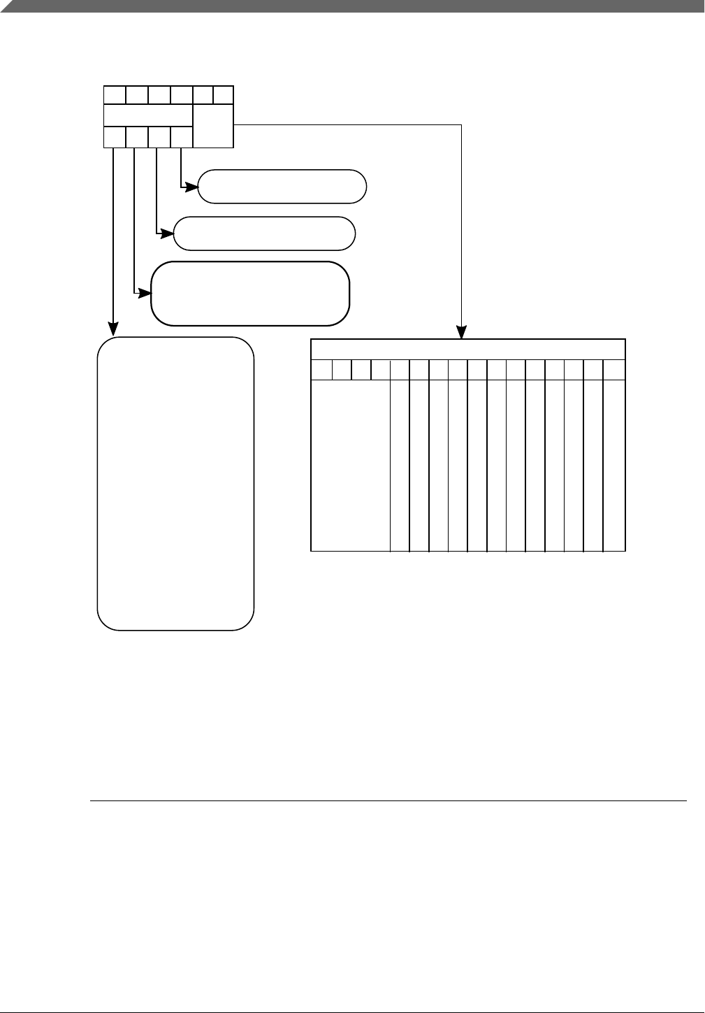
0x01 - ENC_ECB
0x02 - ENC_CBC
0x03 - DEC_ECB
0x05 - GENERATE_MAC
0x04 - DEC_CBC
0x06 - VERIFY_MAC
0x07 - LOAD_KEY
0x08 - LOAD_PLAIN_KEY
0x0A - INIT_RNG
0x09 - EXPORT_RAM_KEY
0x0B - EXTEND_SEED
0x0C - RND
0x0D - Reserved
0x0F - BOOT_OK
0x0E - BOOT_FAILURE
0x10 - GET_ID
0x11 - BOOT_DEFINE
0x12 - DBG_CHAL
0x14 - Reserved
0x13 - DBG_AUTH
0x15 - Reserved
0x16 - MP_COMPRESS
0x17 - 0xFF - Reserved
Command Header
(Bytes: as shown in table above)
0 1 2 3 4 5
15 14 13 12 11 10 9 8 7 6 5 4 3 2 1 0
Error Bits
RESERVED
ERC_GENERAL_ERROR
ERC_MEMORY_FAILURE
ERC_NO_DEBUGGING
ERC_RNG_SEED
ERC_KEY_UPDATE_ERROR
ERC_KEY_WRITE_PROTECTED
ERC_NO_SECURE_BOOT
ERC_KEY_EMPTY
ERC_KEY_INVALID
ERC_KEY_NOT_AVAILABLE
ERC_NO_ERROR
ERC_SEQUENCE_ERROR
• ERC_BUSY <— located in FCSESTAT register
{KBS[1-bit], KeyIDx[4-bits]}
0x00 - 1st Function Call
0x01 - 2nd to nth Function Call
0x00 = CSE command format
(all parameters are copied)
0x01 - CSE command format
(pointers to Flash space provided)
36.5.13.4 Generic PRAM interface description
The PRAM interface can be thought of a 128-bit wide SRAM with eight 128-bit pages.
The diagrams are shown in Big Endian. The first ‘page’ always starts with the command
header and this must be the last data written in a sequence of data written to the PRAM.
This is because writing to the command header (any write to any of the bytes 0-3)
triggers the macro to lock the PRAM interface so CSEc operation may start.
Figure 36-17. Generic PRAM interface
Functional description
S32K1xx Series Reference Manual, Rev. 7, 04/2018
850 NXP Semiconductors

Bits [127:0]
Bits 31:2
4
23:1
7
15:8 7:0 31:2
4
23:1
7
15:8 7:0 31:2
4
23:1
7
15:8 7:0 31:2
4
23:1
7
15:8 7:0
WD Word 0 Word 1 Word 2 Word 3
Byte
Page 0 1 2 3 4 5 6 7 8 9 A B C D E F
0 FuncI
D
Func
Form
at
CallS
eq
KeyID Error Bits Command Specific
1 Data Input to CSEc OR Data Output from CSEc
2
3
4
5
6
7
To setup a CSEc command, the user should first enter the data as required, in 128-bit
blocks, as many blocks as desired (within the seven pages allowed at one given time).
Followed by any associated control information such as ‘MESSAGE_LENGTH’.
Followed by the last write which is to the command header.
The operation will start as indicated by CCIF transitioning from 1 to 0. The operation will
complete and set CCIF to 1 again. At this point the user may read the PRAM to verify or
transfer results as applicable.
If the same command is to be continued, the user should write the remaining data in as
applicable, followed by updated Command Header information (same command but Byte
2 changed to indicate this is a continuation of the same command). For continuation of
any command, the KeyID, CSEc Format, and Message Length is only captured on the
first command written.
NOTE
1. If while continuing a command with a change in the CMD
field, a sequence error will occur. The CMD field must stay
consistent throughout the continuation of a command.
2. A general statement about all MAC and ENC/DEC
commands:
Per SHE specification, the User/Application must
manage any potential padding (blocks of bit length less
than the 128-bit block length) for all ENC/DEC
commands. While the CSEc module will manage all
potential padding for the MAC commands.
Chapter 36 Flash Memory Module (FTFC)
S32K1xx Series Reference Manual, Rev. 7, 04/2018
NXP Semiconductors 851

36.5.13.5 CMD_ENC_ECB
The Encrypt ECB command operates on a single 128-bit block of data. The function
encrypts a given PLAIN_TEXT (128-bits) with the key identified by the KEY_ID (5-
bits), and returns CIPHER_TEXT (128-bits). The ‘PAGE_LENGTH’ is use to tell the
operation how many 128-bit pages are to be processed. All data must be presented in
128-bit blocks (all padding must be done by the application). This command may also be
extended by using the CallSeq field to 0x01 for continued pages of data.
Table 36-78. Encrypt ECB command details
Parameter Direction Width
KEY_ID IN 5
PAGE_LENGTH IN 16
PLAIN_TEXT IN n * 128
CIPHER_TEXT OUT n * 128
CIPHER_TEXT = ENCECB,KEY, KEY_ID (PLAIN_TEXT)
Error Codes: ERC_NO_ERROR, ERC_SEQUENCE_ERROR, ERC_KEY_NOT_AVAILABLE,
ERC_KEY_INVALID,ERC_KEY_EMPTY, ERC_MEMORY_FAILURE, ERC_BUSY, ERC_GENERAL_ERROR
CSEc Command and Data Structure for CSE_PRAM content writes/reads is as follows:
Figure 36-18. Encrypt ECB input parameter format
Byte
Page 0 1 2 3 4 5 6 7 8 9 A B C D E F
0 0x01 0x00 0x00 KeyID Error Bits Reserved PAGE_LENG
TH
1 PLAIN_TEXT 1 [0:15]
2 PLAIN_TEXT 2 [0:15]
3 PLAIN_TEXT 3 [0:15]
4 PLAIN_TEXT 4 [0:15]
5 PLAIN_TEXT 5 [0:15]
6 PLAIN_TEXT 6 [0:15]
7 PLAIN_TEXT 7 [0:15]
Figure 36-19. Encrypt ECB output parameter format
0 1 2 3 4 5 6 7 8 9 A B C D E F
0 0x01 0x00 0x00 KeyID Error Bits Reserved
1 CIPHER_TEXT 1 [0:15]
Table continues on the next page...
Functional description
S32K1xx Series Reference Manual, Rev. 7, 04/2018
852 NXP Semiconductors

0 1 2 3 4 5 6 7 8 9 A B C D E F
2 CIPHER_TEXT 2 [0:15]
3 CIPHER_TEXT 3 [0:15]
4 CIPHER_TEXT 4 [0:15]
5 CIPHER_TEXT 5 [0:15]
6 CIPHER_TEXT 6 [0:15]
7 CIPHER_TEXT 7 [0:15]
36.5.13.6 CMD_ENC_CBC
The Encrypt CBC command operates on multiple 128-bit blocks of data. The function
encrypts a number of PLAIN_TEXT (128-bits) blocks with the key identified by the
KEY_ID (5-bits) and Initialization vector (IV), then returns CIPHER_TEXT (128-bits)
blocks for each input block.
All data presented must be in 128-bit blocks (any padding must be done by the
application).
Table 36-79. Encrypt CBC command details
Parameter Direction Width
KEY_ID IN 5
PAGE_LENGTH IN 16
IV IN 128
PLAIN_TEXT IN n * 128
CIPHER_TEXT OUT n* 128
CIPHER_TEXT = ENCCBC,KEY, KEY_ID,IV (PLAIN_TEXT)
Error Codes: ERC_NO_ERROR, ERC_SEQUENCE_ERROR, ERC_KEY_NOT_AVAILABLE,
ERC_KEY_INVALID,ERC_KEY_EMPTY, ERC_MEMORY_FAILURE, ERC_BUSY, ERC_GENERAL_ERROR
Figure 36-20. Encrypt CBC input parameter format
0 1 2 3 4 5 6 7 8 9 A B C D E F
0 0x02 0x00 0x00 KeyID Error Bits Reserved PAGE_LENG
TH
1 IV [0:15]
2 PLAIN_TEXT 1 [0:15]
3 PLAIN_TEXT 2 [0:15]
4 PLAIN_TEXT 3 [0:15]
5 PLAIN_TEXT 4 [0:15]
6 PLAIN_TEXT 5 [0:15]
7 PLAIN_TEXT 6 [0:15]
Chapter 36 Flash Memory Module (FTFC)
S32K1xx Series Reference Manual, Rev. 7, 04/2018
NXP Semiconductors 853

Figure 36-21. Encrypt CBC output parameter format
0 1 2 3 4 5 6 7 8 9 A B C D E F
0 0x02 0x00 0x00 KeyID Error Bits Reserved
1 IV [0:15]
2 CIPHER_TEXT 1 [0:15]
3 CIPHER_TEXT 2 [0:15]
4 CIPHER_TEXT 3 [0:15]
5 CIPHER_TEXT 4 [0:15]
6 CIPHER_TEXT 5 [0:15]
7 CIPHER_TEXT 6 [0:15]
Subsequent pages of information are provided, with the Byte 2 field of the CSEc
Command Header indicating an ongoing operation is to be continued (i.e., change the
CallSeq field from 0x00 to 0x01).
Figure 36-22. Continuation of input parameters
0 1 2 3 4 5 6 7 8 9 A B C D E F
0 0x02 0x00 0x01 KeyID Error Bits Reserved
1 PLAIN_TEXT 7 [0:15]
2 PLAIN_TEXT 8 [0:15]
3 PLAIN_TEXT 9 [0:15]
4 PLAIN_TEXT 10 [0:15]
5 PLAIN_TEXT 11 [0:15]
6 PLAIN_TEXT 12 [0:15]
7 PLAIN_TEXT 13 [0:15]
Figure 36-23. Continuation of output parameters
0 1 2 3 4 5 6 7 8 9 A B C D E F
0 0x02 0x00 0x01 KeyID Error Bits Reserved
1 CIPHER_TEXT 7 [0:15]
2 CIPHER_TEXT 8 [0:15]
3 CIPHER_TEXT 9 [0:15]
4 CIPHER_TEXT 10 [0:15]
5 CIPHER_TEXT 11 [0:15]
6 CIPHER_TEXT 12 [0:15]
7 CIPHER_TEXT 13 [0:15]
Then continue transferring data in and out until the full CBC operation is complete.
Functional description
S32K1xx Series Reference Manual, Rev. 7, 04/2018
854 NXP Semiconductors

36.5.13.7 CMD_DEC_ECB
The Decrypt ECB command operates on a single 128-bit block of data. The function
decrypts a given CYPHER_TEXT (128-bits) with the key identified by the KEY_ID (5-
bits), and returns PLAIN_TEXT (128-bits). This command may also be extended by
using the CallSeq field to 0x01 for continued pages of data.
All data presented must be in 128-bit blocks (any padding must be done by the
application).
Table 36-80. Decrypt ECB command details
Parameter Direction Width
KEY_ID IN 5
PAGE_LENGTH IN 16
CIPHER_TEXT IN n * 128
PLAIN_TEXT OUT n * 128
PLAIN_TEXT = DECECB,KEY, KEY_ID (CIPHER_TEXT)
Error Codes: ERC_NO_ERROR, ERC_SEQUENCE_ERROR, ERC_KEY_NOT_AVAILABLE, ERC_KEY_INVALID,
ERC_KEY_EMPTY, ERC_MEMORY_FAILURE, ERC_BUSY, ERC_GENERAL_ERROR
Figure 36-24. Decrypt ECB input parameter format
0 1 2 3 4 5 6 7 8 9 A B C D E F
0 0x03 0x00 0x00 KeyID Error Bits Reserved PAGE_LENG
TH
1 CIPHER_TEXT 1 [0:15]
2 CIPHER_TEXT 2 [0:15]
3 CIPHER_TEXT 3 [0:15]
4 CIPHER_TEXT 4 [0:15]
5 CIPHER_TEXT 5 [0:15]
6 CIPHER_TEXT 6 [0:15]
7 CIPHER_TEXT 7 [0:15]
Figure 36-25. Decrypt ECB output parameter format
0 1 2 3 4 5 6 7 8 9 A B C D E F
0 0x03 0x00 0x00 KeyID Error Bits Reserved
1 PLAIN_TEXT 1 [0:15]
2 PLAIN_TEXT 2 [0:15]
3 PLAIN_TEXT 3 [0:15]
Table continues on the next page...
Chapter 36 Flash Memory Module (FTFC)
S32K1xx Series Reference Manual, Rev. 7, 04/2018
NXP Semiconductors 855

0 1 2 3 4 5 6 7 8 9 A B C D E F
4 PLAIN_TEXT 4 [0:15]
5 PLAIN_TEXT 5 [0:15]
6 PLAIN_TEXT 6 [0:15]
7 PLAIN_TEXT 7 [0:15]
36.5.13.8 CMD_DEC_CBC
The Decrypt CBC command operates on multiple 128-bit blocks of data. The function
decrypts a number of CIPHER_TEXT (128-bits) blocks with the key identified by the
KEY_ID (5-bits) and Initialization vector (IV), then returns PLAIN_TEXT (128-bits)
blocks for each input block.
All data must be presented in 128-bit blocks (any padding must be done by the
application).
Table 36-81. Decrypt CBC command details
Parameter Direction Width
KEY_ID IN 5
PAGE_LENGTH IN 16
IV IN 128
CIPHER_TEXT IN n * 128
PLAIN_TEXT OUT n * 128
PLAIN_TEXT = DECCBC,KEY, KEY_ID,IV (CIPHER_TEXT)
Error Codes : ERC_NO_ERROR, ERC_SEQUENCE_ERROR, ERC_KEY_NOT_AVAILABLE,
ERC_KEY_INVALID,ERC_KEY_EMPTY, ERC_MEMORY_FAILURE, ERC_BUSY, ERC_GENERAL_ERROR
Figure 36-26. Decrypt CBC input parameters
0 1 2 3 4 5 6 7 8 9 A B C D E F
0 0x04 0x00 0x00 KeyID Error Bits Reserved PAGE_LENG
TH
1 IV [0:15]
2 CIPHER_TEXT 1 [0:15]
3 CIPHER_TEXT 2 [0:15]
4 CIPHER_TEXT 3 [0:15]
5 CIPHER_TEXT 4 [0:15]
6 CIPHER_TEXT 5 [0:15]
7 CIPHER_TEXT 6 [0:15]
Functional description
S32K1xx Series Reference Manual, Rev. 7, 04/2018
856 NXP Semiconductors

Figure 36-27. Decrypt CBC output parameters
0 1 2 3 4 5 6 7 8 9 A B C D E F
0 0x04 0x00 0x00 KeyID Error Bits Reserved
1 IV [0:15]
2 PLAIN_TEXT 1 [0:15]
3 PLAIN_TEXT 2 [0:15]
4 PLAIN_TEXT 3 [0:15]
5 PLAIN_TEXT 4 [0:15]
6 PLAIN_TEXT 5 [0:15]
7 PLAIN_TEXT 6 [0:15]
Subsequent pages of information are provided, with the Byte 2 field of the CSEc
Command Header indicating an ongoing operation is to be continued (i.e., change the
CallSeq field from 0x00 to 0x01).
Figure 36-28. Continuation of input parameters
0 1 2 3 4 5 6 7 8 9 A B C D E F
0 0x04 0x00 0x01 KeyID Error Bits Reserved
1 CIPHER_TEXT 7 [0:15]
2 CIPHER_TEXT 8 [0:15]
3 CIPHER_TEXT 9 [0:15]
4 CIPHER_TEXT 10 [0:15]
5 CIPHER_TEXT 11 [0:15]
6 CIPHER_TEXT 12 [0:15]
7 CIPHER_TEXT 13 [0:15]
Figure 36-29. Continuation of output parameters
0 1 2 3 4 5 6 7 8 9 A B C D E F
0 0x04 0x00 0x01 KeyID Error Bits Reserved
1 PLAIN_TEXT 7 [0:15]
2 PLAIN_TEXT 8 [0:15]
3 PLAIN_TEXT 9 [0:15]
4 PLAIN_TEXT 10 [0:15]
5 PLAIN_TEXT 11 [0:15]
6 PLAIN_TEXT 12 [0:15]
7 PLAIN_TEXT 13 [0:15]
Chapter 36 Flash Memory Module (FTFC)
S32K1xx Series Reference Manual, Rev. 7, 04/2018
NXP Semiconductors 857

36.5.13.9 CMD_GENERATE_MAC
The Generate MAC command operates on a MESSAGE of length in bits of
MESAGE_LENGTH. The function uses a key (KEY_ID) to encode a MAC value (128-
bits) for the full message body.
Data is processed in 128-bit blocks through MESSAGE_LENGH number of bits, with
padding done internally on the last block if not an integer divide by 128-bit.
Output does not reflect the CMAC value until the full message has been processed, at
which point it overwrites the second page of data as indicated in Figure 36-33.
Table 36-82. Generate MAC command details
Parameter Direction Width
KEY_ID IN 5
MESSAGE_LENGTH IN 32
MESSAGE (DATA <n>) IN n * 128
MAC OUT 128
MAC = CMACKEY, KEY_ID (MESSAGE, MESSAGE_LENGTH)
Error Codes: ERC_NO_ERROR, ERC_SEQUENCE_ERROR, ERC_KEY_NOT_AVAILABLE,
ERC_KEY_INVALID,ERC_KEY_EMPTY, ERC_MEMORY_FAILURE, ERC_BUSY, ERC_GENERAL_ERROR
Figure 36-30. Generate MAC input parameters
0 1 2 3 4 5 6 7 8 9 A B C D E F
0 0x05 0x00 0x00 KeyID Error Bits Reserved MESSAGE_LENGTH
1 DATA 1 [0:15]
2 DATA 2 [0:15]
3 DATA 3 [0:15]
4 DATA 4 [0:15]
5 DATA 5 [0:15]
6 DATA 6 [0:15]
7 DATA 7 [0:15]
Figure 36-31. Generate MAC output parameters
0 1 2 3 4 5 6 7 8 9 A B C D E F
0 0x05 0x00 0x00 KeyID Error Bits Reserved MESSAGE_LENGTH
1 DATA 1 [0:15]
2 DATA 2 [0:15]
Table continues on the next page...
Functional description
S32K1xx Series Reference Manual, Rev. 7, 04/2018
858 NXP Semiconductors

0 1 2 3 4 5 6 7 8 9 A B C D E F
3 DATA 3 [0:15]
4 DATA 4 [0:15]
5 DATA 5 [0:15]
6 DATA 6 [0:15]
7 DATA 7 [0:15]
Figure 36-32. Continuation of input parameters
0 1 2 3 4 5 6 7 8 9 A B C D E F
0 0x05 0x00 0x01 KeyID Error Bits Reserved MESSAGE_LENGTH
1 DATA 8[0:15]
2 DATA 9[0:15]
3 DATA 10 [0:15]
4 DATA 11 [0:15]
5 DATA 12 [0:15]
6 DATA 13 [0:15]
7 DATA 14 [0:15]
Figure 36-33. Continuation of output parameters
0 1 2 3 4 5 6 7 8 9 A B C D E F
0 0x05 0x00 0x01 KeyID Error Bits Reserved MESSAGE_LENGTH
1 DATA 8[0:15]
2 MAC[0:15]
3 DATA 10 [0:15]
4 DATA 11 [0:15]
5 DATA 12 [0:15]
6 DATA 13 [0:15]
7 DATA 14 [0:15]
36.5.13.10 CSEc format for CMD_GENERATE_MAC (pointer method)
For data that is contained fully within the NVM macro the ‘pointer’ method of
communication is used. For internal NVM space the maximum size of data is limited to
be no more that one read partition (512 KB max), or less if the starting address is not the
Chapter 36 Flash Memory Module (FTFC)
S32K1xx Series Reference Manual, Rev. 7, 04/2018
NXP Semiconductors 859

start of the read partition (i.e., the address sequence cannot cross boundaries of read
partitions). The 'Flash Start Address' must be 128-bit aligned (the same is true for
VERIFY_MAC pointer method).
Figure 36-34. CSEc format for GENERATE_MAC input parameters
0 1 2 3 4 5 6 7 8 9 A B C D E F
0 0x05 0x01 0x00 KeyID Error Bits Reserved MESSAGE_LENGTH
1 Flash Start Address Reserved
2 Reserved
3
4
5
6
7
Figure 36-35. CSEc format for CMD_GENERATE_MAC output parameters
0 1 2 3 4 5 6 7 8 9 A B C D E F
0 0x05 0x01 0x00 KeyID Error Bits Reserved MESSAGE_LENGTH
1 Flash Start Address Reserved
2 MAC [0:15]
3 Reserved
4
5
6
7
36.5.13.11 CMD_VERIFY_MAC
The Verify MAC command verifies a MAC of a given MESSAGE, which can be
multiple 128-bit blocks of data, against a provided for MAC. The MESSAGE to
compare, starting with the leftmost bit of the MAC, are given in the
MESSAGE_LENGTH. The value 0 is not allowed and is interpreted by SHE to compare
all bits of the MAC. The function returns an error if the length provided for message has
another length than stated in MESSAGE_LENGTH. Input DATA1-DATAn until all
messages are entered, with the expected MAC being the last entry after all DATA are
input, i.e., MAC will be the position of block N+1 for 'N' number of DATA blocks.
All padding is to be done according to SHE specification using MESSAGE_LENGTH.
Functional description
S32K1xx Series Reference Manual, Rev. 7, 04/2018
860 NXP Semiconductors

n = CEIL(MESSAGE_LENGTH / 128)
The first example shows 6 DATA blocks followed by the expected MAC, with the output
overwriting the DATA1 block at the end of the operation with the MAC verification
status.
The continuation examples show DATA1-10 by continuing from the first example but
DATA7 would be written in place of the CMAC from the first example, followed by
continuation with DATA8 which follows on the next page. Finally ending in DATA10
for this example, following with the expected CMAC value after the DATA 10 entry.
Table 36-83. Verify MAC command details
Parameter Direction Width
KEY_ID IN 5
MESSAGE_LENGTH IN 32
MESSAGE (DATA <n>) IN n * 128
MAC IN 128
MAC_LENGTH (MAC Length[6:0]) IN 7
VERIFICATION_STATUS (Verification Status[0]) OUT 1
MACcalc = TRUNCATE(CMACKEY, KEY_ID (MESSAGE, MESSAGE_LENGTH), MAC_LENGTH)
MACref = TRUNCATE (MAC, MAC_LENGTH)
VERIFICATION_STATUS = (0 ~= ( MACcalc - MACref ))
Error Codes: ERC_NO_ERROR, ERC_SEQUENCE_ERROR, ERC_KEY_NOT_AVAILABLE,
ERC_KEY_INVALID,ERC_KEY_EMPTY, ERC_MEMORY_FAILURE, ERC_BUSY, ERC_GENERAL_ERROR
Figure 36-36. Verify MAC input parameters
0 1 2 3 4 5 6 7 8 9 A B C D E F
0 0x06 0x00 0x00 KeyID Error Bits Reserved MAC Length Reserved MESSAGE_LENGTH
1 DATA 1 [0:15]
2 DATA 2 [0:15]
3 DATA 3 [0:15]
4 DATA 4 [0:15]
5 DATA 5 [0:15]
6 DATA 6 [0:15]
7 MAC [0:15]
Figure 36-37. Verify MAC output parameters
0 1 2 3 4 5 6 7 8 9 A B C D E F
0 0x06 0x00 0x00 KeyID Error Bits Reserved MAC Length Reserved MESSAGE_LENGTH
Table continues on the next page...
Chapter 36 Flash Memory Module (FTFC)
S32K1xx Series Reference Manual, Rev. 7, 04/2018
NXP Semiconductors 861

0 1 2 3 4 5 6 7 8 9 A B C D E F
1 Verification
Status
DATA 1 [6:15]
2 DATA 2 [0:15]
3 DATA 3 [0:15]
4 DATA 4 [0:15]
5 DATA 5 [0:15]
6 DATA 6 [0:15]
7 MAC [0:15]
Figure 36-38. Continuation of input parameters
0 1 2 3 4 5 6 7 8 9 A B C D E F
0 0x06 0x00 0x01 KeyID Error Bits Reserved MAC Length Reserved MESSAGE_LENGTH
1 DATA 8 [0:15]
2 DATA 9 [0:15]
3 DATA 10 [0:15]
4 MAC [0:15]
5
6
7
Figure 36-39. Continuation of output parameters
0 1 2 3 4 5 6 7 8 9 A B C D E F
0 0x06 0x00 0x01 KeyID Error Bits Reserved MAC Length Reserved MESSAGE_LENGTH
1 Verification
Status
Data 7 [ 6:15]
2 DATA 9 [0:15]
3 DATA 10 [0:15]
4 MAC [0:15]
5
6
7
36.5.13.12 CMD_VERIFY_MAC - CSEc format (pointer method)
Figure 36-40. Verify MAC (pointer method) input parameters
Functional description
S32K1xx Series Reference Manual, Rev. 7, 04/2018
862 NXP Semiconductors

0 1 2 3 4 5 6 7 8 9 A B C D E F
0 0x06 0x01 0x00 KeyID Error Bits Reserved MAC Length Reserved MESSAGE_LENGTH
1 Flash Start Address Reserved
2 MAC [0:15]
3 Reserved
4
5
6
7
Figure 36-41. Verify MAC (pointer method) output parameters
0 1 2 3 4 5 6 7 8 9 A B C D E F
0 0x06 0x01 0x00 KeyID Error Bits Reserved MAC Length Reserved MESSAGE_LENGTH
1 Flash Start Address Verification
Status
Reserved
2 MAC [0:15]
3 Reserved
4
5
6
7
36.5.13.13 CMD_LOAD_KEY
The LOAD KEY command updates an internal key per the SHE specification. If a
protected key is loaded into the RAM_KEY, the function has to disable the plain key
status bit.
Table 36-84. LOAD_KEY command details
Parameter Direction Width
KEY_ID IN 5
M1 IN 128
M2 IN 256
M3 IN 128
M4 OUT 256
M5 OUT 128
Error Codes: ERC_NO_ERROR, ERC_SEQUENCE_ERROR, ERC_KEY_NOT_AVAILABLE,
ERC_KEY_INVALID,ERC_KEY_WRITE_PROTECTED, ERC_KEY_UPDATE_ERROR, ERC_KEY_EMPTY,
ERC_MEMORY_FAILURE, ERC_BUSY, ERC_GENERAL_ERROR
Chapter 36 Flash Memory Module (FTFC)
S32K1xx Series Reference Manual, Rev. 7, 04/2018
NXP Semiconductors 863

NOTE
1. Due to extension of the maximum number of keys (beyond
SHE specification) and the usage of KBS to identify the
higher and lower order keys, M1 entry will follow the
traditional SHE specifications (requiring the two 4-bit ID
and AuthID entries along with UID), but the command will
need more information showing which KBS (0 or 1) is
requested. This will be communicated by an additional
requirement of entering the KEY_ID ({KBS,KeyIDx[3:0]}.
Lastly, the KeyIDx[3:0] in M1 must be consistent with the
KeyIDx[3:0] in the 5-bit KEY_ID entry in the command
header.
2. If the key AuthID is empty, the key update can work with
AuthID = ID and Auth_value = all F's; otherwise
ERC_KEY_UPDATE_ERROR is returned.
3. When updating BOOT_MAC, KBS must be set to 0
(KBS=1 will generate an error)
The PGMPART configuration (see Program Partition Command) allows for an extension
to the SHE specification in which the user may enable a VERIFY_ONLY flag for the
GENERATE_MAC to take into consideration. For the VERIFY_ONLY attribute, if set,
the associated memory key slot will be treated as invalid by the
CMD_GENERATE_MAC command (only valid for CMD_VERIFY_MAC). The
VERIFY_ONLY attribute has no effect if KEY_USAGE == 0.
The SHE specification defines M2 as:
M2 - ENCCBD,K1,IV=0 (CID'|FID'|"0...0"95 | KID') : SFE == 0x00
M2 - ENCCBD,K1,IV=0 (CID'|FID'|"0...0"94 | KID') : SFE == 0x01
Table 36-85. FID & zero fill in M2 w/ SFE
PGMPART SFE field M2 equation changes for LOAD_KEY FID
SFE == 0x00 (VERIFY_ONLY flag not
enabled, default SHE)
FID (5-bits)|"0...0"95 { WRITE_PROTECTION |
BOOT_PROTECTION |
DEBUGGER_PROTECTION |
KEY_USAGE | WILDCARD }
SFE == 0x01 (VERIFY_ONLY flag is
enabled, enhanced SHE)
FID (6-bits)|"0...0"94 { WRITE_PROTECTION |
BOOT_PROGECTION |
DEBUGGER_PROTECTION |
KEY_USAGE | WILDCARD |
VERIFY_ONLY }
Functional description
S32K1xx Series Reference Manual, Rev. 7, 04/2018
864 NXP Semiconductors

When the optional SFE bit is set in the PGMPART command to enable the
VERIFY_ONLY flag for CSEc keys, the FID field will be extended by one bit with the
VERIFY_ONLY flag, and the adjacent zero fill field is reduced by one bit to be a total of
94-bits.
If SFE enabled, then the VERIFY_ONLY flag should be set to 1'b1 for VERIFY_ONLY
attribute to be enabled, and cleared to 1'b0 for the VERIFY_ONLY attribute to be
disabled for the particular key.
Figure 36-42. Load key input parameters
0 1 2 3 4 5 6 7 8 9 A B C D E F
0 0x07 0x00 0x01 KeyID Error Bits Reserved
1 M1 [0:15]
2 M2 [0:31]
3
4 M3 [0:15]
5 Reserved
6
7
Figure 36-43. Load key output parameters
0 1 2 3 4 5 6 7 8 9 A B C D E F
0 0x07 0x00 0x01 KeyID Error Bits Reserved
1 M1 [0:15]
2 M2 [0:31]
3
4 M3 [0:15]
5 M4 [0:31]
6
7 M5 [0:15]
Chapter 36 Flash Memory Module (FTFC)
S32K1xx Series Reference Manual, Rev. 7, 04/2018
NXP Semiconductors 865

36.5.13.14 CMD_LOAD_PLAIN_KEY
The Load Plain Key command, loads a key ‘KEY’ without encryption and does a
verification of the key. The key is handed over in plain text. A plain key can only be
loaded into the RAM_KEY slot (per SHE specification). The command sets the plain key
status bit for the RAM_KEY. There is no return value. The command header fields in
Bytes [1,3] are ignored, while setting Byte[2] to 0x01 will create a sequence error.
Table 36-86. LOAD_PLAIN_KEY command details
Parameter Direction Width
KEY IN 128
KEYRAM_KEY = key
RAM_KEY_PLAIN = 1
Error Codes: ERC_NO_ERROR, ERC_SEQUENCE_ERROR, ERC_BUSY, ERC_GENERAL_ERROR
Figure 36-44. Load Plain Key input parameters
0 1 2 3 4 5 6 7 8 9 A B C D E F
0 0x08 0x00 0x00 KeyID Error Bits Reserved
1 Plain Key[0:15]
2 Reserved
3
4
5
6
7
This command has no return values
36.5.13.15 CMD_EXPORT_RAM_KEY
The Export RAM Key command exports the RAM_KEY into a format protected by the
SECRET_KEY. The key may be imported again by using the CMD_LOAD_KEY
command.
A RAM_KEY can only be exported if it was written as plain text, i.e., by
CMD_LOAD_PLAIN_KEY.
This command is for loading and unloading a RAM_KEY. The reserved fields for
security flags and the counter are set to ‘0’.
No values other than M1, may leave SHE/CSEc.
Functional description
S32K1xx Series Reference Manual, Rev. 7, 04/2018
866 NXP Semiconductors

NOTE
Due to setting the counter and flags to ‘0’ by definition in the
case of RAM_KEY updates, the first block of the encrypted
message M2 will become a constant ‘0’ block.
Table 36-87. Export RAM_KEY command details
Parameter Direction Width
M1 OUT 128
M2 OUT 256
M3 OUT 128
M4 OUT 256
M5 OUT 128
K1 = KDF(KEYSECRET_KEY, KEY_UPDATE_ENC_C)
K2 = KDF(KEYSECRET_KEY, KEY_UPDATE_MAC_C)
CID = 0 (28-bits)
FID = 0 (5-bits)
M1 = UID | IDRAM_KEY | IDSECRET_KEY
M2 = ENCCBC,K1,IV=0 (CID | FID | “0...0”95 | KEYRAM_KEY) = ENC CBC, K1, IV=0 (“0 ...0”128 | KEYRAM_KEY)
M3 = CMACK2 (M1 | M2)
K3 = KDF (KEYRAM_KEY , KEY_UPDATE_ENC_C)
K4 = KDF (KEYRAM_KEY , KEY_UPDATE_MAC_C)
M4 = UID| IDRAM_KEY | IDSECRET_KEY | ENC EBC, K3 (CID)
M5 = CMACK4(M4)
Error Codes: ERC_NO_ERROR, ERC_SEQUENCE_ERROR, ERC_KEY_INVALID, ERC_KEY_EMPTY,
ERC_MEMORY_FAILURE, ERC_BUSY, ERC_GENERAL_ERROR
Figure 36-45. Export RAM_KEY input parameters
0 1 2 3 4 5 6 7 8 9 A B C D E F
0 0x09 0x00 0x00 KeyID Error Bits Reserved
1 Reserved
2
3
4
5
6
7
Figure 36-46. Export RAM_KEY output parameters
Chapter 36 Flash Memory Module (FTFC)
S32K1xx Series Reference Manual, Rev. 7, 04/2018
NXP Semiconductors 867

0 1 2 3 4 5 6 7 8 9 A B C D E F
0 0x09 0x00 0x00 KeyID Error Bits Reserved
1 M1 [0:15]
2 M2 [0:31]
3
4 M3 [0:15]
5 M4 [ 0:31]
6
7 M5 [ 0:15]
36.5.13.16 CMD_INIT_RNG
The INIT_RNG command initializes and derives a key for the PRNG. It must be called
before the CMD_RND command and after every power cycle or reset. Bytes [1:3] of the
command header are ignored.
Table 36-88. INIT_RNG command details
Parameter Direction Width
NONE
The command has to ignore active debugger protection or secure boot protection flags on SECRET_KEY.
NOTE: The command may need several hundred ms to return
Error Codes : ERC_NO_ERROR, ERC_SEQUENCE_ERROR, ERC_MEMORY_FAILURE, ERC_BUSY,
ERC_GENERAL_ERROR
Figure 36-47. INIT_RNG input parameters
0 1 2 3 4 5 6 7 8 9 A B C D E F
0 0x0A 0x00 0x00 KeyID Error Bits Reserved
1 Reserved
2
3
4
5
6
7
The INIT_RNG command has no return values.
Functional description
S32K1xx Series Reference Manual, Rev. 7, 04/2018
868 NXP Semiconductors

36.5.13.17 CMD_EXTEND_SEED
The EXTEND_SEED command extends the seed of the PRNG by compressing the
former seed value and the supplied ENTROPY into a new seed. This new seed is then to
be used to generate a random number by invoking the CMD_RND command. The
random number generator must be initialized by CMD_INIT_RNG before the seed may
be extended
Table 36-89. EXTEND_SEED command details
Parameter Direction Width
ENTROPY IN 128
The command has to ignore active debugger protection or secure boot protection flags on SECRET_KEY.
NOTE: The command may need several hundred ms to return
Error Codes : ERC_NO_ERROR, ERC_SEQUENCE_ERROR, ERC_RNG_SEED, ERC_MEMORY_FAILURE, ERC_BUSY,
ERC_GENERAL_ERROR
Figure 36-48. EXTEND_SEED input parameters
0 1 2 3 4 5 6 7 8 9 A B C D E F
0 0x0B 0x00 0x00 KeyID Error Bits Reserved
1 ENTROPY [0:15]
2 Reserved
3
4
5
6
7
The EXTEND_SEED command has no return values.
36.5.13.18 CMD_RND
The CMD_RND command returns a vector of 128 random bits.
The random number generator has to be initialized by CMD_INIT_RNG before random
numbers can be supplied.
Chapter 36 Flash Memory Module (FTFC)
S32K1xx Series Reference Manual, Rev. 7, 04/2018
NXP Semiconductors 869

The command header fields in Bytes [1,3] are ignored, while setting Byte[2] to 0x01 will
generate a sequence error.
Table 36-90. CMD_RND command details
Parameter Direction Width
RND OUT 128
IF (SREGRND_INIT == 0)
PRNG_STATEi = ENCECB,KEY PRNG_KEY (PRNG_STATEi-1)
RND = PRNG_STATEi
END IF
Error Codes : ERC_NO_ERROR, ERC_SEQUENCE_ERROR, ERC_RNG_SEED, ERC_MEMORY_FAILURE, ERC_BUSY,
ERC_GENERAL_ERROR
Figure 36-49. CMD_RND input parameters
0 1 2 3 4 5 6 7 8 9 A B C D E F
0 0x0C 0x00 0x00 KeyID Error Bits Reserved
1 Reserved
2
3
4
5
6
7
Table 36-91. CMD_RND Output Parameters
0 1 2 3 4 5 6 7 8 9 A B C D E F
0 0x0C 0x00 0x00 KeyID Error Bits Reserved
1 RND [0:15]
2 Reserved
3
4
5
6
7
Functional description
S32K1xx Series Reference Manual, Rev. 7, 04/2018
870 NXP Semiconductors

36.5.13.19 CMD_SECURE_BOOT
This command is not supported by the FTFC/CSEc module. See the new command
'CMD_BOOT_DEFINE' which configures the type of secure boot to execute. Parts
enabled with the CSE feature will always execute the configured secure boot type upon
reset.
The CSEc feature runs autonomously, reading custom parameters from the flash and
verifies the MAC of the bootloader supplied in the DATA of the SIZE in bytes. On CSEc
enabled parts, secure boot is enabled by programming of the BOOT_MAC_KEY.
The secure boot parameters are entered via the CMD_BOOT_DEFINE command.
36.5.13.20 CMD_BOOT_FAILURE
This command may be used when checking additional blocks of information after the
autonomous secure boot finishes (per CMD_BOOT_DEFINE configuration).
Table 36-92. CMD_BOOT_FAILURE Command Details
Parameter Direction Width
NONE
The command will impose the same sanctions as if CMD_SECURE_BOOT would detect a failure, but can be used in later
stages of the boot process.
CMD_BOOT_FAILURE may only be called once after ever power cycle/reset and may only be called if SECURE_BOOT did
not detect any errors before and if CME_BOOT_OK was not called.
NOTE : CSEc module provides for the first autonomous stage of the secure boot process (if so configured with
BOOT_DEFINE), thus this function can be used during the following stages to provide the boot status to CSEc.
IF (SREG SECURE BOOT == 1 AND SREG BOOT OK == 1 AND SREG BOOT FINISHED == 0)
SREG BOOT FINISHED = 1
SREG BOOT OK = 0
END IF
Error Codes : ERC_NO_ERROR, ERC_SEQUENCE_ERROR, ERC_NO_SECURE_BOOT, ERC_BUSY,
ERC_GENERAL_ERROR
Table 36-93. CMD_BOOT_FAILURE Input Parameters
0 1 2 3 4 5 6 7 8 9 A B C D E F
0 0x0E 0x00 0x00 KeyID Error Bits Reserved
1 Reserved
2
3
4
Table continues on the next page...
Chapter 36 Flash Memory Module (FTFC)
S32K1xx Series Reference Manual, Rev. 7, 04/2018
NXP Semiconductors 871

Table 36-93. CMD_BOOT_FAILURE Input Parameters
(continued)
0 1 2 3 4 5 6 7 8 9 A B C D E F
5
6
7
36.5.13.21 CMD_BOOT_OK
This command may be used when checking additional blocks of information after the
autonomous secure boot finishes (per CMD_BOOT_DEFINE configuration).
Table 36-94. CMD_BOOT_OK Command Details
Parameter Direction Width
NONE
The command is used to mark successful boot verification for later stages than the autonomous SECURE_BOOT (operation
defined by CMD_BOOT_DEFINE). In particular it is meant to lock the command CMD_BOOT_FAILURE.
CMD_BOOT_OK may only be called once after ever power cycle/reset and may only be called if SECURE_BOOT did not
detect any errors before and if CME_BOOT_FAILIRE was not called.
NOTE : CSEc module provides for the first autonomous stage of the secure boot process (if so configured with
BOOT_DEFINE), thus this function can be used during the following stages to provide the boot status to CSEc.
IF (SREG SECURE BOOT == 1 AND SREG BOOT OK == 1 AND SREG BOOT FINISHED == 0)
SREG BOOT FINISHED = 1
END IF
Error Codes : ERC_NO_ERROR, ERC_SEQUENCE_ERROR, ERC_NO_SECURE_BOOT, ERC_BUSY,
ERC_GENERAL_ERROR
Table 36-95. CMD_BOOT_OK Input Parameters
0 1 2 3 4 5 6 7 8 9 A B C D E F
0 0x0F 0x00 0x00 KeyID Error Bits Reserved
1 Reserved
2
3
4
5
6
7
Functional description
S32K1xx Series Reference Manual, Rev. 7, 04/2018
872 NXP Semiconductors

36.5.13.22 CMD_GET_STATUS
This command is implemented via a STATUS register FCSESTAT
36.5.13.23 CMD_GET_ID
The GET_ID command returns the UID and the value of the status register (protected by
a MAC over a challenge and the data). If the MASTER_ECU_KEY is empty, the MAC
returned value is set to ‘0’.
The 'KeyID' input is ignored in this command, as the MASTER_ECU_KEY is the only
valid key to be considered.
Table 36-96. GET_ID command details
Parameter Direction Width
CHALLENGE IN 128
ID OUT 120
SREG OUT 8
MAC OUT 128
ID = UID
MAC = CMACKEY_MASTER_ECU_KEY(CHALLENGE | ID | SREG)
Error Codes : ERC_NO_ERROR, ERC_SEQUENCE_ERROR, ERC_KEY_NOT_AVAILABLE, ERC_MEMORY_FAILURE,
ERC_GENERAL_ERROR
Figure 36-50. GET_ID input parameters
0 1 2 3 4 5 6 7 8 9 A B C D E F
0 0x10 0x00 0x00 KeyID Error Bits Reser
ved
Reserved
1 CHALLENGE [0:15]
2 Reserved
3
4
5
6
7
Figure 36-51. GET_ID output parameters
Chapter 36 Flash Memory Module (FTFC)
S32K1xx Series Reference Manual, Rev. 7, 04/2018
NXP Semiconductors 873

0 1 2 3 4 5 6 7 8 9 A B C D E F
0 0x10 0x00 0x00 KeyID Error Bits Reserved
1 CHALLENGE [0:15]
2 ID [0:14] SRE
G
3 MAC [0:15]
4 Reserved
5
6
7
36.5.13.24 CMD_CANCEL
This command isn’t strictly supported by the FTFC module. The user should manage
software driven commands accordingly.
For any CSEc command that is executed in a series of continued commands, the
command may be 'cancelled' by one of a few mechanisms.
For example, streams of CBC encode data that is processed through continuations of
inputting data through the PRAM seven block input buffer, could be 'cancelled' by giving
an illegal continuation of the next segment of data. Such as clearing the CallSeq field in
the Command Header, or changing the FuncID to a different command. Each will
generate a sequence error, which will kill/cancel the ongoing command.
Additionally, starting any FCCOB command in one of the pauses of continuation of a
CSEc command will result in the FCCOB command executing to completion as
expected, but will kill/cancel the current CSEc command.
36.5.13.25 CMD_BOOT_DEFINE
This is a non-SHE specified command, and is used in CSEc implementation to allow the
user to define both the User BOOT_SIZE (boot code size of data is in the message length
in number of bits to run CMAC on each POR), and the ‘flavor’ of boot (strict, serial,
parallel, none).
The command header fields in Bytes [1:3] are ignored.
Functional description
S32K1xx Series Reference Manual, Rev. 7, 04/2018
874 NXP Semiconductors

NOTE
1. Warning: If the 'Strict Boot' option is chosen and the
CMAC supplied doesn't match the CMAC calculated, then
the part will be hung in reset. Additionally since the boot
flavor can't be changed once 'Strict' is chosen, this error
will not be able to be reversed. Make sure to verify the
CMAC and full boot process is completing and passing as
expected BEFORE selecting the 'Strict' boot flavor.
Additionally, even though Strict Boot may not be changed
once set, it is possible to change the CODE contents and
associated BOOT_MAC & SIZE. But if a reset or any
interruption of the part occurs between updating Code and
matching SIZE, BOOT_MAC with the 'Strict Boot' option
enabled, the result will be mismatch of BOOT_MAC to
calculated CMAC, thus the part stuck in reset.
2. The autonomous Secure Boot is run on the PFlash block
starting at address '0' and finishing at BOOT_SIZE # of bits
later. Subsequent Boot Code checks at other addresses may
be run later via CMD_VEFIFY_MAC command(s). With
the end of the secure boot process being followed by either
CMD_BOOT_OK or CMD_BOOT_FAILURE.
Table 36-97. BOOT_DEFINE command details
Parameter Direction Width
BOOT_SIZE (# Bytes * 8, or Number of Bits : maximum size is 512 KB) IN 32
Boot Flavor
2b’00 : Strict (SHE Optional boot - OTP : Once set can’t be changed)
2’b01 : Serial Boot method
2’b10 : Parallel Boot method
2’b11 : No Boot defined (MASTER_ECU_KEY) not initialized yet, or non-CSEc
enabled part
IN 8
Error Codes: ERC_NO_ERROR, ERC_SEQUENCE_ERROR, , ERC_KEY_INVALID,, ERC_MEMORY_FAILURE,
ERC_BUSY, ERC_GENERAL_ERROR
Figure 36-52. BOOT DEFINE input parameter format
0 1 2 3 4 5 6 7 8 9 A B C D E F
0 0x11 0x00 0x00 KeyID Error Bits Reserved
1 Reserved Boot
Flavor
BOOT_SIZE
Table continues on the next page...
Chapter 36 Flash Memory Module (FTFC)
S32K1xx Series Reference Manual, Rev. 7, 04/2018
NXP Semiconductors 875

0 1 2 3 4 5 6 7 8 9 A B C D E F
2 Reserved
3
4
5
6
7
36.5.13.26 CMD_DBG_CHAL
The SHE CMD_DEBUG command is modified and split into two steps in CSEc
commands: CMD_DBG_CHAL followed by CMD_DBG_AUTH. The
CMD_DBG_CHAL/AUTH command pair must be followed by a subsequent reset before
PGMPART command may be re-issued.
The CMD_DBG_CHAL command is issued to request a random number which the user
will use along with the MASTER_ECU_KEY and UID to return a authorization request
using the CMD_DBG_AUTH command.
NOTE
The CMD_DBG_CHAL command must be followed by the
CMD_DBG_AUTH command, otherwise the
CMD_DBG_CHAL command would be required to be re-
issued before continuing.
Table 36-98. DEBUG command details
Parameter Direction Width
CHALLENGE OUT 128
Error Codes : ERC_NO_ERROR, ERC_SEQUENCE_ERROR, ERC_WRITE_PROTECTED, ERC_RNG_SEED,
ERC_NO_DEBUGGING, ERC_MEMORY_FAILURE, ERC_BUSY, ERC_GENERAL_ERROR
Figure 36-53. DEBUG input parameters
0 1 2 3 4 5 6 7 8 9 A B C D E F
0 0x12 0x00 0x00 KeyID Error Bits Reserved
1 Reserved
2
3
4
5
Table continues on the next page...
Functional description
S32K1xx Series Reference Manual, Rev. 7, 04/2018
876 NXP Semiconductors

0 1 2 3 4 5 6 7 8 9 A B C D E F
6
7
Figure 36-54. DEBUG output parameters
0 1 2 3 4 5 6 7 8 9 A B C D E F
0 0x12 0x00 0x00 KeyID Error Bits Reserved
1 CHALLENGE [0:15]
2 Reserved
3
4
5
6
7
36.5.13.27 CMD_DBG_AUTH
The CMD_DBG_AUTH command erases all keys (actual and outdated) stored in NVM
memory.
NOTE
If the WRITE_PROTECTION flag has been set on any of the
keys, the CMD_DEBUG does not execute the erase of any
keys. This also implies that the ERSALL and ERSALLU and
erase all that is triggered external to the FTFC will not be able
to execute.
After CSEc confirms authentication, the Flash Keys are erased. If any key has the
WRITE_PROTECTION flag set, the command will stop and not offer any failure
analysis mode.
After SHE authentication of the process passes, the command will erase the Flash Keys
(DFlash), placing the part back into factory status.
The command cannot be executed if authentication fails.
The command ignores active debugger protection and secure boot protection flags as well
as empty keys.
Chapter 36 Flash Memory Module (FTFC)
S32K1xx Series Reference Manual, Rev. 7, 04/2018
NXP Semiconductors 877

After successful authentication the User IFR, (flash) keys (including DFLash & EERAM
space) have been erased. At this point, the FlexRAM is no longer configured as EEE and
is now available as System RAM (EEERDY == 0, RAMRDY ==1).
Table 36-99. CMD_DBG_AUTH
Parameter Direction Width
AUTHORIZATION IN 128
SHE & Backend:
K = KDF(KEYMASTER_ECU_KEY, DEBUG_KEY_C)
SHE:
CHALLENGE = CMD_RND()
Backend:
AUTHORIZATION = CMACK(CHALLENGE | UID)
Error Codes: ERC_NO_ERROR, ERC_SEQUENCE_ERROR, ERC_WRITE_PROTECTED, ERC_RNG_SEED,
ERC_NO_DEBUGGING, ERC_MEMORY_FAILURE, ERC_BUSY, ERC_GENERAL_ERROR
Figure 36-55. DBG_AUTH input parameters
0 1 2 3 4 5 6 7 8 9 A B C D E F
0 0x13 0x00 0x00 KeyID Error Bits Reserved
1 AUTHORIZATION [0:15]
2 Reserved
3
4
5
6
7
36.5.13.28 CMD_MP_COMPRESS
The MP_COMPRESS command accesses a Miyaguchi-Prenell compression feature with
in the CSEc feature set. This function, provided with the AES as a block cipher, is used
as a compression function. Messages must be pre-processed per SHE specification if they
do not already meet the full 128-bit block size requirement, i.e., the user/application is
responsible for padding if the message is not already 128-bits in length.
For this command the PAGE_LENGTH is to be input as the number of 128-bit pages,
and the KeyID input is a don't care.
Functional description
S32K1xx Series Reference Manual, Rev. 7, 04/2018
878 NXP Semiconductors

Table 36-100. MP Compress command details
Parameter Direction Width
DATA <n> IN n * 128
PAGE_LENGTH IN 16
MP_COMPRESS OUT 128
Error Codes : ERC_NO_ERROR, ERC_SEQUENCE_ERROR, ERC_GENERAL_ERROR
Figure 36-56. MP compress input parameters
0 1 2 3 4 5 6 7 8 9 A B C D E F
0 0x16 0x00 0x00 KeyID Error Bits Reserved PAGE_LEN
GTH
1 DATA 1 [0:15]
2 DATA 2 [0:15]
3 DATA 3 [0:15]
4 DATA 4 [0:15]
5 DATA 5 [0:15]
6 DATA 6 [0:15]
7 DATA 7 [0:15]
Figure 36-57. MP compress output parameters
0 1 2 3 4 5 6 7 8 9 A B C D E F
0 0x16 0x00 0x00 KeyID Error Bits Reserved PAGE_LENG
TH
1 MP_COMPRESS [0:15]
2 DATA 2 [0:15]
3 DATA 3 [0:15]
4 DATA 4 [0:15]
5 DATA 5 [0:15]
6 DATA 6 [0:15]
7 DATA 7 [0:15]
Figure 36-58. Continuation of input parameters
0 1 2 3 4 5 6 7 8 9 A B C D E F
0 0x16 0x00 0x01 KeyID Error Bits Reserved PAGE_LENG
TH
1 DATA 8[0:15]
2 DATA 9[0:15]
Table continues on the next page...
Chapter 36 Flash Memory Module (FTFC)
S32K1xx Series Reference Manual, Rev. 7, 04/2018
NXP Semiconductors 879

0 1 2 3 4 5 6 7 8 9 A B C D E F
3 DATA 10 [0:15]
4 DATA 11 [0:15]
5 DATA 12 [0:15]
6 DATA 13 [0:15]
7 DATA 14 [0:15]
Figure 36-59. Continuation of output parameters
0 1 2 3 4 5 6 7 8 9 A B C D E F
0 0x16 0x00 0x01 KeyID Error Bits Reserved PAGE_LENG
TH
1 MP_COMPRESS[0:15]
2 DATA 9 [0:15]
3 DATA 10 [0:15]
4 DATA 11 [0:15]
5 DATA 12 [0:15]
6 DATA 13 [0:15]
7 DATA 14 [0:15]
36.5.14 Reset sequence
On each system reset the FTFC module executes a sequence which establishes initial
values for the flash block configuration parameters, FPROT, FDPROT, FEPROT, FOPT,
and FSEC registers and the FCNFG[RAMRDY, EEERDY] bits.
Boot will proceed according to the configuration set by the BOOT_DEFINE command
(secure boot or not, and what type of secure boot).
CCIF is cleared throughout the reset sequence. The FTFC module holds off all CPU
access for a portion of the reset sequence. Flash reads are possible when the hold is
removed. Completion of the reset sequence is marked by setting CCIF which enables
flash user commands.
If a reset occurs while any FTFC command is in progress, that command is immediately
aborted. The state of the word being programmed or the sector/block being erased is not
guaranteed. Commands and operations do not automatically resume after exiting reset.
Functional description
S32K1xx Series Reference Manual, Rev. 7, 04/2018
880 NXP Semiconductors

Chapter 37
Quad Serial Peripheral Interface (QuadSPI)
Chip-specific QuadSPI information
37.1.1 Overview
S32K148 has one instance of QuadSPI. Other products in the S32K1xx series do not have
QuadSPI.
See the device Data Sheet for details about target frequencies.
The Quad Serial Peripheral Interface (QuadSPI) block acts as an interface to external
serial flash device. It supports SDR and HyperRAM modes upto 4 and 8 bidirectional
data lines respectively.
NOTE
The following are not supported:
• AHB Write
• Data learning feature
• Breakpoint and Watchpoint memory regions
37.1.2 Memory size requirement
QuadSPI memory size requirement for AHB Buffers is : 128x64 , i.e. 1 KB.
37.1.3 QuadSPI register reset values
Table 37-1. QuadSPI register reset values
Register Reset value
Module Configuration Register (QuadSPI_MCR) 000F_400C
Table continues on the next page...
37.1
S32K1xx Series Reference Manual, Rev. 7, 04/2018
NXP Semiconductors 881

Table 37-1. QuadSPI register reset values (continued)
Register Reset value
Buffer0 Configuration Register (QuadSPI_BUF0CR) 0000_0003
Buffer1 Configuration Register (QuadSPI_BUF1CR) 0000_0002
Buffer2 Configuration Register (QuadSPI_BUF2CR) 0000_0001
Buffer3 Configuration Register (QuadSPI_BUF3CR) 0000_0000
Serial Flash A1 Top Address (QuadSPI_SFA1AD) 6C00_0000
Serial Flash A2 Top Address (QuadSPI_SFA2AD) 6C00_0000
Serial Flash B1 Top Address (QuadSPI_SFB1AD) 7000_0000
Serial Flash B2 Top Address (QuadSPI_SFB2AD) 7000_0000
37.1.4 Use case
The primary application use-cases for the QuadSPI and external memory are:
• Handwriting recognition – External flash acts a store for font/character data.
• RDS Radio – External RAM used for temporary storage of RDS data.
37.1.5 Supported read modes
Read modes QuadSPI_MC
R[DDR_EN]
QuadSPI_MC
R[DQS_EN]
Mode
supported
Data learning
support
SDR Mode
(Flash A)
Internal sampling (N/1) 0 0 Yes No
DQS sampling
method
Internally
generated DQS
0 1 Yes No
External DQS 0 1 No No
Loopback DQS 0 1 Yes No
SDR Mode
(Flash B)
Internal sampling (N/1) 0 0 Yes No
DQS sampling
method
Internally
generated DQS
0 1 No No
External DQS 0 1 No No
Loopback DQS 0 1 No No
HyperRAM
(DDR)
Internal sampling (4x method) 1 0 No No
DQS sampling
method
Internally
generated DQS
1 1 No No
External DQS 1 1 Yes No
Loopback DQS 1 1 No No
Chip-specific QuadSPI information
S32K1xx Series Reference Manual, Rev. 7, 04/2018
882 NXP Semiconductors
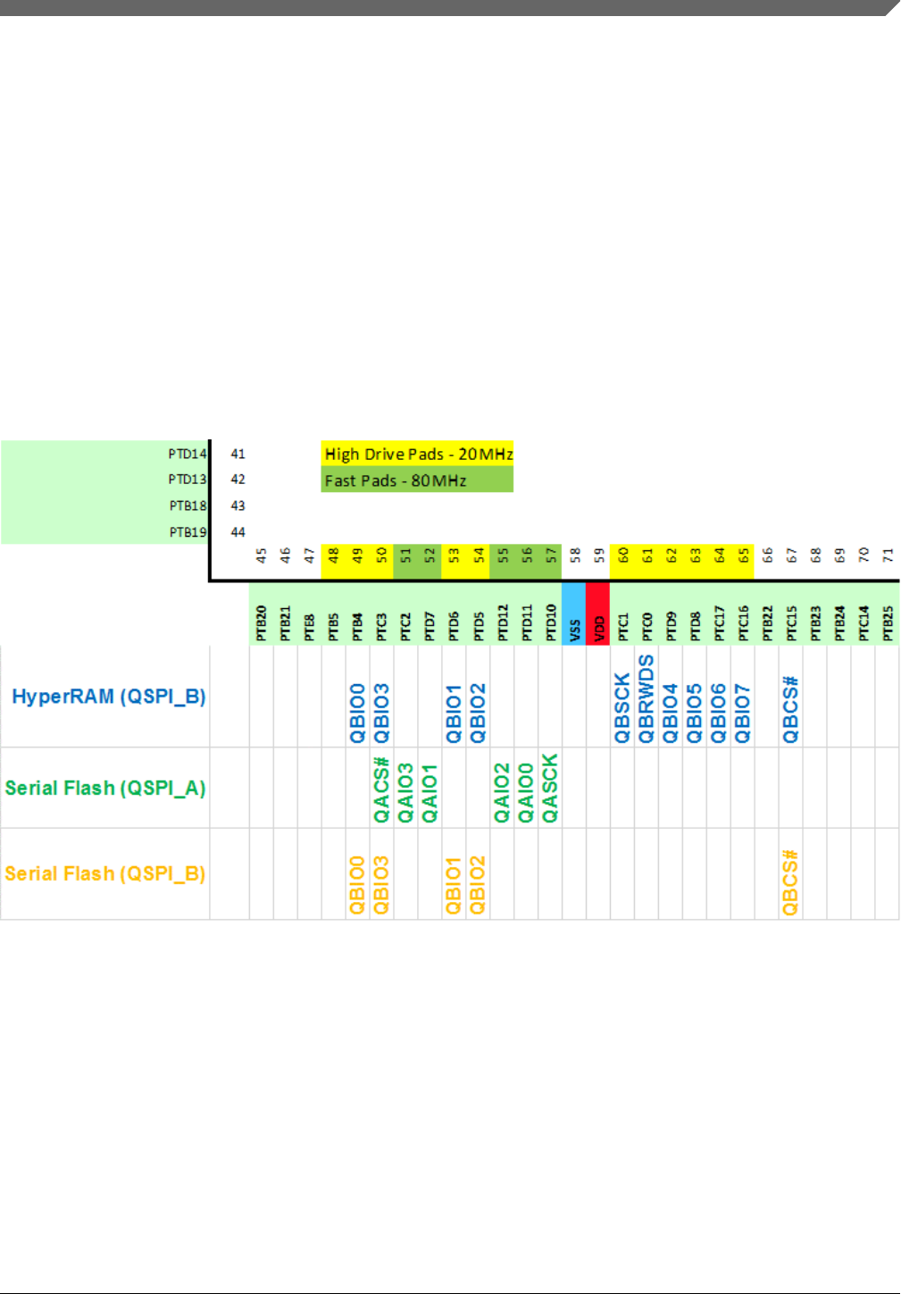
37.1.6 External memory options
The QuadSPI supports an A-side and a B-side. The A-side of the QuadSPI is connected
to the fast pads (80 mA) while the B-side connects to the 20 mA pads. See datasheet for
operating values.
Only one external memory will be supported in any given application and it will not be
permitted to run the A-side and the B-side of the QuadSPI simultaneously. As such the
following external memory options can be supported:
• A single Quad Flash on the A-side or
• A single HyperRAM on the B-side or
• A single Quad Flash on the B-side.
Figure 37-1. External memory options
37.1.7 Recommended software configuration
• QuadSPI operation is restricted to system clock as SPLL.
• When switching the system modes between HSRUN and RUN, QuadSPI should be
disabled and then re-enabled.
Chapter 37 Quad Serial Peripheral Interface (QuadSPI)
S32K1xx Series Reference Manual, Rev. 7, 04/2018
NXP Semiconductors 883

• The software configuration options provided for QuadSPI through registers
SOC_CONFIG and SCLK_CONFIG should be done before enabling clock of
QuadSPI.
• Configure the QuadSPI module before configuring the ALT mode selection for
selecting QuadSPI pads.
NOTE
• User should ensure that communication is complete on
QuadSPI before low power mode entry is initiated.
• Divider values of programmable divider (see QuadSPI
clocking diagram in Module clocks for details) should be
programmed before enabling it. The divider is enabled by
default.
37.1.8 Recommended programming sequence
Following is the recommended programming sequence:
1. Enable PCC_QSPI[CGC]
2. Program QuadSPI_MCR[SCLKCFG] and QuadSPI_SOCCR[SOCCFG]
3. Program QuadSPI_MCR[MDIS] to 0
37.1.9 Clock ratio between QuadSPI clocks
Below clock relationship should be maintained between SFIF_CLK (flash internal
reference clock ) and AHB read interface clock (bus clock) of QuadSPI :
• SFIF_CLK ≤ AHB read interface clock
37.1.10 QuadSPI_MCR[SCLKCFG] implementation
Table 37-2. QuadSPI_MCR[SCLKCFG] bit field description
Bit field name Bit field description
SCLKCFG[7] Enables input buffer of QSPI pads for SDR and HyperRAM modes
0: ibe of all QSPI pads disabled
1: ibe of all QSPI pads enabled
SCLKCFG[6] Quadspi Clocking mode selection. Always program SCLKCFG[6] twice while configuring mode
selection.
0: Selecting SYS_CLK as AHB read interface Clock and module clock. Mandatory for HSRUN
80/RUN 64/RUN 80 configurations.
Table continues on the next page...
Chip-specific QuadSPI information
S32K1xx Series Reference Manual, Rev. 7, 04/2018
884 NXP Semiconductors

Table 37-2. QuadSPI_MCR[SCLKCFG] bit field description
(continued)
Bit field name Bit field description
1: Selecting BUS_CLK as AHB read interface clock and module clock. Mandatory for HSRUN 112
configuration.
SCLKCFG[5] HyperRAM selection for Flash B - Reference clock selection for DQS for Flash-B
0: Clock from SCLKCFG [3] selected as DQS ( HyperRAM Disabled)
1: External RWDS from Flash B selected as DQS ( HyperRAM Enabled)
NOTE: When HyperRAM is enabled , the 2 x Internal reference clock clock is also required by
QuadSPI apart from sfif clock as HyperRAM is a DDR protocol. If user has configured
PLAT_CLK at 80 MHz then the PCC divider for Quadspi asynchronous clock selection
must be programmed to divby2 and SCLKCFG[5] must be programmed to 1 for
HyperRAM functional operation.
SCLKCFG[4] Internal reference clock (async clock domain) source selection for Quadspi
0: PLL_DIV1 is clock source of Quadspi Internal reference Clock
1: FIRC_DIV1 is clock source of Quadspi Internal reference Clock
SCLKCFG[3] Reference clock selection for DQS for Flash-B
0: Inverted Clock from SCLKCFG [2] selected as DQS
1: Clock from SCLKCFG [2] selected as DQS
SCLKCFG[2] Reference clock selection for DQS for Flash-B
0: Internal Reference Clock selected as DQS
1: Loopback clock from PAD SCKB selected as DQS
SCLKCFG[1] Reference clock selection for DQS for Flash-A
0: Inverted Clock from SCLKCFG [0] selected as DQS
1: Clock from SCLKCFG [0] selected as DQS
SCLKCFG[0] Reference clock selection for DQS for Flash-A
0: Internal Reference Clock selected as DQS
1: Loopback clock from PAD SCKA selected as DQS
37.1.11 QuadSPI_SOCCR[SOCCFG] implementation
Table 37-3. QuadSPI_SOCCR[SOCCFG] bit field
description
Bit field name Bit field description
SOCCFG[7:0] SOC configuration: Fine delay chain configuration for Flash A
7F: Delay of 127 buffers and 128 muxes
7E :Delay of 126 buffers and 127 muxes
7D :Delay of 125 buffers and 126 muxes
-
-
-
Table continues on the next page...
Chapter 37 Quad Serial Peripheral Interface (QuadSPI)
S32K1xx Series Reference Manual, Rev. 7, 04/2018
NXP Semiconductors 885

Table 37-3. QuadSPI_SOCCR[SOCCFG] bit field description
(continued)
Bit field name Bit field description
3F: Delay of 63 buffers and 64 muxes
3E: Delay of 62 buffers and 63 muxes
3D: Delay of 61 buffers and 62 muxes
-
-
-
0: Delay of 0 buffer and 1 mux
SOCCFG[15:8] SOC configuration: Fine delay chain configuration for Flash B
7F: Delay of 127 buffers and 128 muxes
7E :Delay of 126 buffers and 127 muxes
7D :Delay of 125 buffers and 126 muxes
-
-
-
3F: Delay of 63 buffers and 64 muxes
3E: Delay of 62 buffers and 63 muxes
3D: Delay of 61 buffers and 62 muxes
-
-
-
0: Delay of 0 buffer and 1 mux
SOCCFG[16] Pending read enable controls the bus gasket’s handling of pending read transactions.
0: Pending reads are disabled.
1: Pending reads are enabled, yielding a performance improvement through the gasket.
SOCCFG[17] Burst read enable controls the bus gasket’s handling of burst read transactions.
0: Burst reads are converted into a series of single transactions on the slave side of the gasket.
1: Burst reads are optimized for best system performance.
SOCCFG[18] Burst writes enable controls the bus gasket’s handling of burst read transactions.
0: Burst writes are converted into a series of single transactions on the slave side of the gasket.
1: Burst writes are optimized for best system performance. Note this setting treats writes as
“imprecise” such that an error response on any beat of the burst is reported on the last beat.
SOCCFG[28] Programmable Divider Disable.
0: Divider enabled
1: Divider disabled
SOCCFG[31:29] Programmable divider configuration selection.
000 : Div by 1
001 : Div by 2
Chip-specific QuadSPI information
S32K1xx Series Reference Manual, Rev. 7, 04/2018
886 NXP Semiconductors

Table 37-3. QuadSPI_SOCCR[SOCCFG] bit field
description
Bit field name Bit field description
010 : DIV by 3
011 : DIV by 4
100 : DIV by 5
101: DIV by 6
110: DIV by 7
111: DIV by 8
37.2 Introduction
The Quad Serial Peripheral Interface (QuadSPI) block acts as an interface to a single or
two external serial flash devices, each with up to eight bidirectional data lines.
37.2.1 Features
The QuadSPI supports the following features:
• Flexible sequence engine to support various flash vendor devices. As there is no
specific standard, the module supports various kind of flashes from different vendors.
Refer Serial Flash Devices for example sequences.
• Single, dual, quad and octal modes of operation.
• Double data rate (DDR)/Double trasfer rate (DTR) mode wherein the data is
generated on every edge of the serial flash clock.
• Support for flash data strobe signal for data sampling in DDR and Single data rate
(SDR) mode.
• Support for HyperRAM.
• AHB master to read RX Buffer data via AMBA AHB bus (64-bit width interface) or
IP registers space (32-bit access) and fill TX Buffer via IPS register space (32-bit
access).
• AHB master can be a DMA with configurable inner loop size.
• Multimaster accesses with priority
• Flexible and configurable buffer for each master
Chapter 37 Quad Serial Peripheral Interface (QuadSPI)
S32K1xx Series Reference Manual, Rev. 7, 04/2018
NXP Semiconductors 887

• Multiple interrupt conditions (see Table 37-12)
• All AHB accesses to flash devices are directly memory mapped to the chip system
memory.
• Programmable sequence engine to cater to future command/protocol changes and
able to support all existing vendor commands and operations. Software needs to
select the corresponding sequence according to the connected flash device.
• Supports all types of addressing.
37.2.2 Block Diagram
The following figure is a block diagram of the Quad Serial Peripheral Interface
(QuadSPI) module.
Introduction
S32K1xx Series Reference Manual, Rev. 7, 04/2018
888 NXP Semiconductors
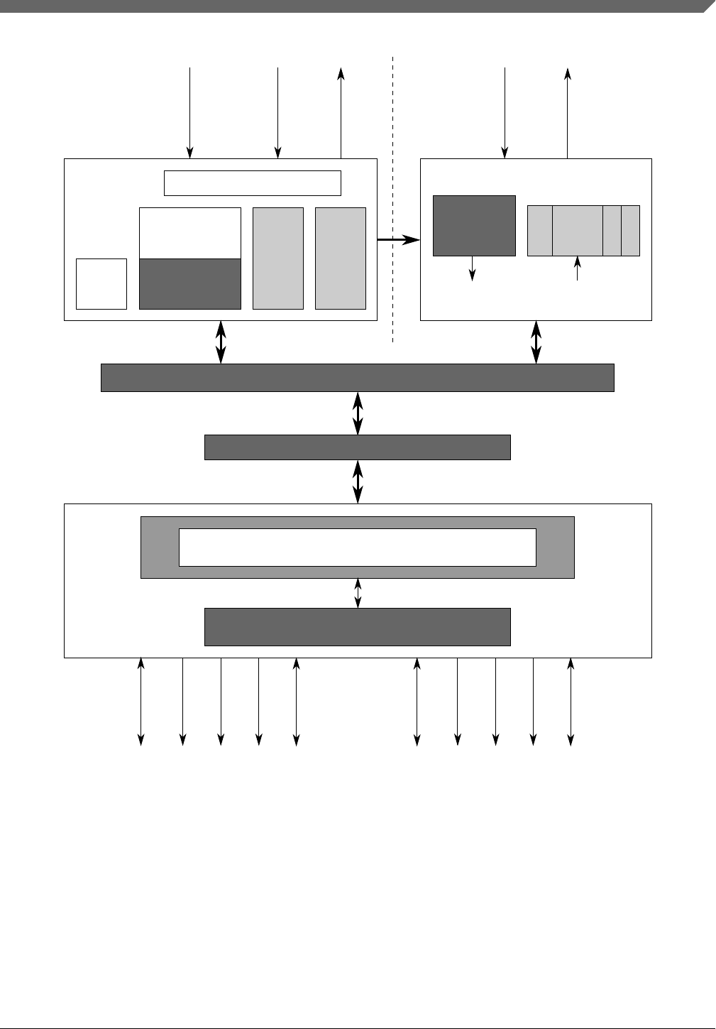
IP_Ctrl
command_build
& buffer control
TX
Buffer RX
Buffer
LUT
DMA and Interrupt Control
AHB_Serve
fetch
(addr, size, type)
AHB
Buffer
received
(Data)
AHB_ControlIP_Control
QSPI_IC_SFM
Clock Domain Crosser
QSPI_IF
Programmable sequence engine
SCLK clock domain
Flexible I/O controller
SCLK clock domain
SCKFB
PCSFB2
PCSFB1
DQSFB
IOFA[7:0]
SCKFA
PCSFA2
PCSFA1
QuadSPI Bus Flash A QuadSPI Bus Flash B
define
Peripheral Bus AHB Bus
(Addr, Cmd)
wr_data
(Data)
rd_data
(Data)
Registers
read
(Addr, Size)
read_done
(Data)
DQSFA
IOFB[7:0]
Figure 37-2. QuadSPI Block Diagram
37.2.3 QuadSPI Modes of Operation
For power management through IPS interface access and correct config register
programming sequences, QuadSPI supports three modes: normal, module disable and
stop mode.
Chapter 37 Quad Serial Peripheral Interface (QuadSPI)
S32K1xx Series Reference Manual, Rev. 7, 04/2018
NXP Semiconductors 889

• Normal Mode can be used for write or read accesses to an external serial flash
device.
• Serial Flash Write: Data can be programmed into the flash via the IP interface
only. Refer to Flash Programming for further details.
• Serial Flash Read: Read the contents of the serial flash device. Two separate read
channels are available via RX Buffer and AHB Buffer, see Flash Read.
• Stop Mode: The mode is used for power management. When a request is made to
enter Stop Mode, the QuadSPI block acknowledges the request and completes the
SFM Command in progress, then the system clocks to the QuadSPI block may be
shut off
• Module Disable Mode: The mode is used for power management. The clock to the
non-memory mapped logic in the QuadSPI can be stopped while in Module Disable
Mode. The module enters the mode by setting QSPI_MCR[MDIS] or when a request
is asserted by an external controller while QSPI_MCR[DOZE] is set.
37.2.4 Acronyms and Abbreviations
The following table contains acronyms and abbreviations used in this document.
Table 37-4. Acronyms and Abbreviations
Terms Description
AHB Advanced High-performance Bus, version of AMBA
AMBA Advanced Microcontroller Bus Architecture
BE Big Endian Byte Ordering
CS Chip Select
DMA Direct Memory Access
MB Megabyte. Each MB is 1024 * 1024 bytes
IFM Individual Flash Mode
LSB Least Significant Bit
MSB Most Significant Bit
PCS Peripheral Chip Select
QSPI, QuadSPI Quad Serial Peripheral Interface
SCK Serial Communications Clock
w1c Write 1 to clear, writing a 1 to this field resets the flag
I/O Input output. In this document, I/O lines are also referred as pads.
Introduction
S32K1xx Series Reference Manual, Rev. 7, 04/2018
890 NXP Semiconductors

37.2.5 Glossary for QuadSPI module
Table 37-5. Glossary
Term Definition
AHB Command An AHB Command is a SFM Command triggered by a read access to the address range belonging
to the memory mapped access defined in Table 37-10. Refer to AHB Commands for details.
Asserted A signal that is asserted is in its active state. An active low signal changes from logic level one to
logic level zero when asserted, and an active high signal changes from logic level zero to logic level
one.
Clear To clear a bit or bits means to establish logic level zero on the bit or bits.
Clock Phase Determines when the data should be sampled relative to the active edge of SCK
Clock Polarity Determines the idle state of the SCK signal.
Drain To remove entries from a FIFO by software or hardware.
Endianness Byte Ordering scheme.
Field Two or more register bits grouped together.
Fill To add entries to a FIFO by software or hardware.
Host Refers to another functional block in the device containing the QuadSPI module
Instruction Code 8 bits defining the type of command to be executed.
IP Command An IP Command is a SFM Command triggered by writing into the QSPI_IPCR[SEQID] field.
Logic level one The voltage that corresponds to Boolean true (1) state.
Logic level zero The voltage that corresponds to Boolean false (0) state.
Negated A signal that is negated is in its inactive state. An active low signal changes from logic level 0 to
logic level 1 when negated, and an active high signal changes from logic level 1 to logic level 0.
QSPI_AMBA_BASE The first address of the serial flash device as presented to the QuadSPI controller. This may be the
base of the serial flash in the system address map or it may be a remapping, for instance to 0x0,
done by the system. Refer to the system address map.
QSPI_ARDB_BASE First address of QuadSPI Rx Buffer on system memory map.
Set To set a bit or bits means to establish logic level one on the bit or bits.
RX Buffer PUSH Event Addition of valid entries into the RX Buffer. In the default case each Buffer PUSH Event adds 2
entries to the RX Buffer since the interface to the serial clock domain is 64 bits in width. Depending
on the number of bytes read from the serial flash device it is possible for the very last Buffer PUSH
Event that only one entry is added.
The QSPI_RBSR[RDBFL] field is incremented by the number of entries added to the RX Buffer.
RX Buffer POP Event Removal of valid entries from the RX Buffer. Each Buffer POP Event removes
(QSPI_RBCT[WMRK] + 1) valid entries from the buffer. The QSPI_RBSR[RDBFL] field is
decremented by the same number and the QSPI_RBSR[RDCTR] field is incremented accordingly.
Individual Flash Mode Access to a single, individual serial flash device. Refer to Serial Flash Access Schemes for details.
SFM Command Serial Flash Memory Command. A SFM command consists of an instruction code and all other
parameters (for example, size or mode bytes) needed for that specific instruction code. Triggering a
command either initiates a transaction on the external serial flash or results in an error. Refer to
Table 37-19 for details on errors.
Single/Dual/Quad/Octal
Instructions
Depending on the serial flash device connected to the QuadSPI module there will be instructions
using a different number of data lines.
• Single pad: Single line I/O with one data out and one data in line to/from the serial flash
device.
• Dual pad: Dual line I/O with two bidirectional I/O lines, driven alternatively by the serial flash
device or the QuadSPI module
Table continues on the next page...
Chapter 37 Quad Serial Peripheral Interface (QuadSPI)
S32K1xx Series Reference Manual, Rev. 7, 04/2018
NXP Semiconductors 891

Table 37-5. Glossary (continued)
Term Definition
• Quad pad: Quad line I/O with 4 bidirectional I/O lines, driven alternatively by the serial flash
device or the QuadSPI
• Octal pad: Octal line I/O with 8 bidirectional I/O lines, driven alternatively by the serial flash
device or the QuadSPI
Transaction A transaction consists of all flags, data and signals in either direction to execute a command for an
attached serial flash device. It is a combination of chip select, sclk, instruction code, address, mode-
and/or dummy bytes, transmit and/or receive data.
LUT Look-up table.
37.3 External Signal Description
This section provides the external signal information of the QuadSPI module.
The following table lists the external signals belonging to the module in conjunction with
the different modes of operation.
Table 37-6. Signal Properties
Signal
Name
Function Direction Description
PCSFA1 Peripheral Chip Select
Flash A1
O This signal is the chip select for the serial flash device A1. A1 represents
the first of the two flash devices that share IOFA.
PCSFA2 Peripheral Chip Select
Flash A2
O This signal is the chip select for the serial flash device A2. A2 represents
the the second of the two flash devices that share IOFA.
PCSFB1 Peripheral Chip Select
Flash B1
O This signal is the chip select for the serial flash device B1. B1 represents
the first of the two flash devices that share IOFB.
PCSFB2 Peripheral Chip Select
Flash B2
O This signal is the chip select for the serial flash device B2. B2 represents
the second of the two flash devices that share IOFB.
SCKFA Serial Clock Flash A O This signal is the serial clock output to the serial flash device A.
SCKFB Serial Clock Flash B O This signal is the serial clock output to the serial flash device B.
IOFA[7:0] Serial I/O Flash A I/O These signals are the data I/O lines to/from the serial flash device A. Refer
to Driving External Signals for details about the signal drive and timing
behavior. Note that the signal pins of the serial flash device may change
their function according to the SFM Command executed, leaving them as
control inputs when Single and Dual Instructions are executed. The
module supports driving these inputs to dedicated values. In single I/O
mode, QuadSPI drives data on IOFA[0] and expects data on IOFA[1].
IOFB[7:0] Serial I/O Flash B I/O These signals are the data I/O lines to/from the serial flash device B. Refer
to Driving External Signals for details about the signal drive and timing
behavior. Note that the signal pins of the serial flash device may change
their function according to the SFM Command executed, leaving them as
control inputs when Single and Dual Instructions are executed. The
module supports driving these inputs to dedicated values. In single I/O
mode, QuadSPI drives data on IOFB[0] and expects data on IOFB[1].
Table continues on the next page...
External Signal Description
S32K1xx Series Reference Manual, Rev. 7, 04/2018
892 NXP Semiconductors

Table 37-6. Signal Properties (continued)
Signal
Name
Function Direction Description
DQSFA Data Strobe signal
Flash A
I/O Data strobe signal for port A. Some flash vendors provide the DQS signal
to which the read data is aligned in DDR mode. It is also provided as an
output signal during write data phase.
DQSFB Data Strobe signal
Flash B
I/O Data strobe signal for port B. Some flash vendors provide the DQS signal
to which the read data is aligned in DDR mode. It is also provided as an
output signal during write data phase.
37.3.1 Driving External Signals
The different phases of the serial flash access scheme are shown in the following figure.
Chapter 37 Quad Serial Peripheral Interface (QuadSPI)
S32K1xx Series Reference Manual, Rev. 7, 04/2018
NXP Semiconductors 893
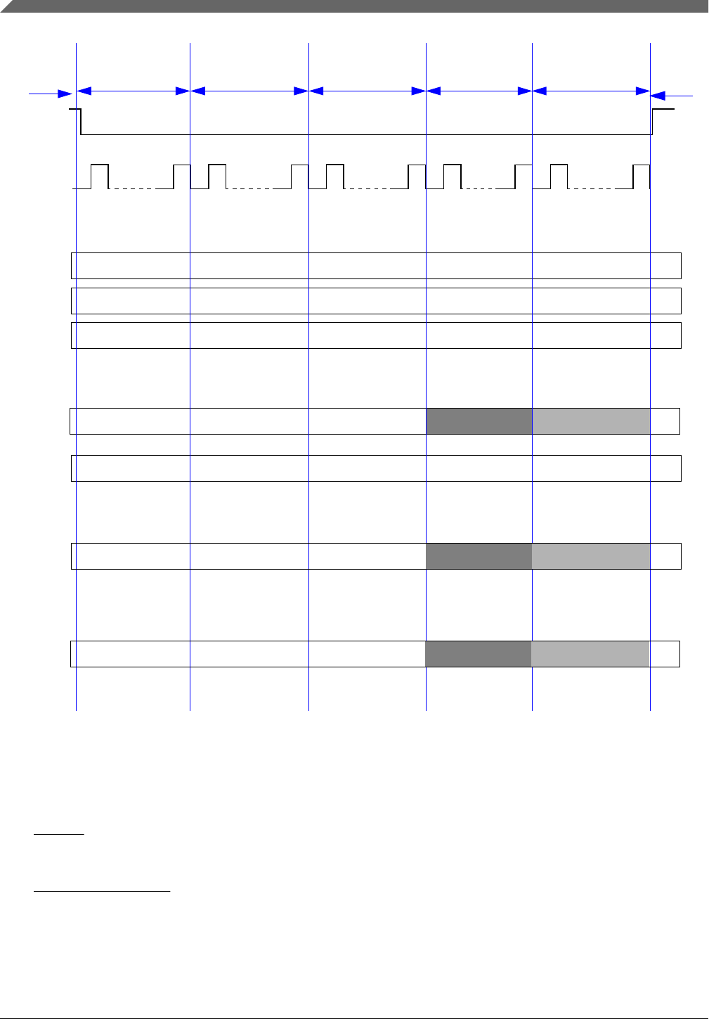
PCSFx
Single Pad(I/O) Instructions
Not Driven
SCKFx
IOFx[0]
IOFx[1]
IOFx[3:2]
IOFx[3:2]
IOFx[1:0]
(pad
Driven all the time, values taken according to phase
Driven all the time to logic level 1
Not Driven
IOFx[3:0]
Not Driven Driven for
Tx Instr. only
Driven for
Tx Instr. only
Dual Pad (I/O) Instructions
Quad Pad (I/O) Instructions
(pad
IDLE INSTRUCTION ADDRESS
IDLE
DATAMODE DUMMY
=
=
2'b0)
2'b01)
(pad =
2'b10)
Octal Pad (I/O) Instructions
(pad =
2'b11)
IOFx[7:0]
Not Driven Driven for
Tx Instr. only
Driven all the time to logic level 1
Figure 37-3. Serial Flash Access Scheme
The different phases and the I/O driving characteristics of the QuadSPI module are
characterized in the following way:
•IDLE: Serial flash device not selected. No interaction with the serial flash device. All
IOFx signals driven.
• INSTRUCTION: Serial flash device selected. The instruction is sent to the serial
flash device. All IOFx signals are driven.
External Signal Description
S32K1xx Series Reference Manual, Rev. 7, 04/2018
894 NXP Semiconductors

• ADDRESS: Serial Flash Address is sent to the device. All IOFx signals are driven.
Note that this phase is not applicable for all SFM Commands.
• MODE: Mode bytes are sent to the serial flash device. All IOFx signals are driven.
Note that this phase is not applicable for all SFM Commands.
• DUMMY: Dummy clocks are provided to the serial flash device. Refer to the Figure
37-3 for the IOFx signals driven. The actual data lines required for the SFM
Command executed are not driven for data read commands. Note that this phase is
not applicable for all SFM Commands.
• DATA: Serial flash data are sent to or received from the serial flash device. Refer to
the preceding figure for the IOFx signals driven. The actual data lines required for
the SFM Command executed are not driven for data read commands. Note that this
phase is not applicable for all SFM Commands.
The PCSFx and SCKFx signals are driven permanently throughout all the phases.
In Individual Flash Mode this applies to the selected flash device.
37.4 Memory Map and Register Definition
This section provides the memory map and register definitions of the QuadSPI module.
37.4.1 Register Write Access
This section describes the write access restriction terms that apply to all registers, which
can be one of the following:
•Register Write Access Restriction
For each register bit and register field, the write access conditions are specified in the
detailed register description. A description of the write access conditions is given in
the following table. If, for a specific register bit or field, none of the given write
access conditions is fulfilled, any write attempt to this register bit or field is ignored
without any notification. The values of the bits or fields are not changed.
The condition term [A or B] indicates that the register or field can be written to if at
least one of the conditions is fulfilled.
Chapter 37 Quad Serial Peripheral Interface (QuadSPI)
S32K1xx Series Reference Manual, Rev. 7, 04/2018
NXP Semiconductors 895

Table 37-7. Register Write Access
Restrictions
Condition Description
Anytime No write access restriction.
Disabled Mode Write access only if QSPI_MCR[MDIS] = 1.
Normal Mode Write access only if the module is in Normal Mode.
•Register Write Access Requirements
All registers can be accessed with 8-bit, 16-bit, and 32-bit wide operations. For some
of the registers, at least a 16/32-bit wide write access is required to ensure correct
operation. This write access requirement is stated in the detailed register description
for each register affected.
37.4.2 Peripheral Bus Register Descriptions
This section provides the memory map and register definitions of the QuadSPI module.
NOTE
Access to location and 0x190 does not give transfer error.
QuadSPI memory map
Address
offset (hex) Register name Width
(in bits) Access Reset value Section/
page
0 Module Configuration Register (QuadSPI_MCR) 32 R/W See section 37.4.2.1/
902
8 IP Configuration Register (QuadSPI_IPCR) 32 R/W 0000_0000h 37.4.2.2/
906
C Flash Configuration Register (QuadSPI_FLSHCR) 32 R/W 0000_0303h 37.4.2.3/
907
10 Buffer0 Configuration Register (QuadSPI_BUF0CR) 32 R/W See section 37.4.2.4/
908
14 Buffer1 Configuration Register (QuadSPI_BUF1CR) 32 R/W See section 37.4.2.5/
909
18 Buffer2 Configuration Register (QuadSPI_BUF2CR) 32 R/W See section 37.4.2.6/
909
1C Buffer3 Configuration Register (QuadSPI_BUF3CR) 32 R/W See section 37.4.2.7/
910
20 Buffer Generic Configuration Register
(QuadSPI_BFGENCR) 32 R/W 0000_0000h 37.4.2.8/
911
Table continues on the next page...
Memory Map and Register Definition
S32K1xx Series Reference Manual, Rev. 7, 04/2018
896 NXP Semiconductors

QuadSPI memory map (continued)
Address
offset (hex) Register name Width
(in bits) Access Reset value Section/
page
24 SOC Configuration Register (QuadSPI_SOCCR) 32 R/W 0000_0000h 37.4.2.9/
912
30 Buffer0 Top Index Register (QuadSPI_BUF0IND) 32 R/W 0000_0000h 37.4.2.10/
913
34 Buffer1 Top Index Register (QuadSPI_BUF1IND) 32 R/W 0000_0000h 37.4.2.11/
913
38 Buffer2 Top Index Register (QuadSPI_BUF2IND) 32 R/W 0000_0000h 37.4.2.12/
914
100 Serial Flash Address Register (QuadSPI_SFAR) 32 R/W 0000_0000h 37.4.2.13/
915
104 Serial Flash Address Configuration Register
(QuadSPI_SFACR) 32 R/W 0000_0000h 37.4.2.14/
915
108 Sampling Register (QuadSPI_SMPR) 32 R/W 0000_0000h 37.4.2.15/
916
10C RX Buffer Status Register (QuadSPI_RBSR) 32 R 0000_0000h 37.4.2.16/
918
110 RX Buffer Control Register (QuadSPI_RBCT) 32 R/W 0000_0000h 37.4.2.17/
918
150 TX Buffer Status Register (QuadSPI_TBSR) 32 R 0000_0000h 37.4.2.18/
920
154 TX Buffer Data Register (QuadSPI_TBDR) 32 R/W 0000_0000h 37.4.2.19/
920
158 Tx Buffer Control Register (QuadSPI_TBCT) 32 R/W 0000_0000h 37.4.2.20/
921
15C Status Register (QuadSPI_SR) 32 R 0200_3800h 37.4.2.21/
922
160 Flag Register (QuadSPI_FR) 32 w1c 0800_0000h 37.4.2.22/
925
164 Interrupt and DMA Request Select and Enable Register
(QuadSPI_RSER) 32 R/W 0000_0000h 37.4.2.23/
928
168 Sequence Suspend Status Register (QuadSPI_SPNDST) 32 R 0000_0000h 37.4.2.24/
931
16C Sequence Pointer Clear Register (QuadSPI_SPTRCLR) 32 R/W 0000_0000h 37.4.2.25/
933
180 Serial Flash A1 Top Address (QuadSPI_SFA1AD) 32 R/W See section 37.4.2.26/
934
184 Serial Flash A2 Top Address (QuadSPI_SFA2AD) 32 R/W See section 37.4.2.27/
934
188 Serial Flash B1 Top Address (QuadSPI_SFB1AD) 32 R/W See section 37.4.2.28/
935
18C Serial Flash B2 Top Address (QuadSPI_SFB2AD) 32 R/W See section 37.4.2.29/
935
200 RX Buffer Data Register (QuadSPI_RBDR0) 32 R 0000_0000h 37.4.2.30/
936
Table continues on the next page...
Chapter 37 Quad Serial Peripheral Interface (QuadSPI)
S32K1xx Series Reference Manual, Rev. 7, 04/2018
NXP Semiconductors 897

QuadSPI memory map (continued)
Address
offset (hex) Register name Width
(in bits) Access Reset value Section/
page
204 RX Buffer Data Register (QuadSPI_RBDR1) 32 R 0000_0000h 37.4.2.30/
936
208 RX Buffer Data Register (QuadSPI_RBDR2) 32 R 0000_0000h 37.4.2.30/
936
20C RX Buffer Data Register (QuadSPI_RBDR3) 32 R 0000_0000h 37.4.2.30/
936
210 RX Buffer Data Register (QuadSPI_RBDR4) 32 R 0000_0000h 37.4.2.30/
936
214 RX Buffer Data Register (QuadSPI_RBDR5) 32 R 0000_0000h 37.4.2.30/
936
218 RX Buffer Data Register (QuadSPI_RBDR6) 32 R 0000_0000h 37.4.2.30/
936
21C RX Buffer Data Register (QuadSPI_RBDR7) 32 R 0000_0000h 37.4.2.30/
936
220 RX Buffer Data Register (QuadSPI_RBDR8) 32 R 0000_0000h 37.4.2.30/
936
224 RX Buffer Data Register (QuadSPI_RBDR9) 32 R 0000_0000h 37.4.2.30/
936
228 RX Buffer Data Register (QuadSPI_RBDR10) 32 R 0000_0000h 37.4.2.30/
936
22C RX Buffer Data Register (QuadSPI_RBDR11) 32 R 0000_0000h 37.4.2.30/
936
230 RX Buffer Data Register (QuadSPI_RBDR12) 32 R 0000_0000h 37.4.2.30/
936
234 RX Buffer Data Register (QuadSPI_RBDR13) 32 R 0000_0000h 37.4.2.30/
936
238 RX Buffer Data Register (QuadSPI_RBDR14) 32 R 0000_0000h 37.4.2.30/
936
23C RX Buffer Data Register (QuadSPI_RBDR15) 32 R 0000_0000h 37.4.2.30/
936
240 RX Buffer Data Register (QuadSPI_RBDR16) 32 R 0000_0000h 37.4.2.30/
936
244 RX Buffer Data Register (QuadSPI_RBDR17) 32 R 0000_0000h 37.4.2.30/
936
248 RX Buffer Data Register (QuadSPI_RBDR18) 32 R 0000_0000h 37.4.2.30/
936
24C RX Buffer Data Register (QuadSPI_RBDR19) 32 R 0000_0000h 37.4.2.30/
936
250 RX Buffer Data Register (QuadSPI_RBDR20) 32 R 0000_0000h 37.4.2.30/
936
254 RX Buffer Data Register (QuadSPI_RBDR21) 32 R 0000_0000h 37.4.2.30/
936
258 RX Buffer Data Register (QuadSPI_RBDR22) 32 R 0000_0000h 37.4.2.30/
936
Table continues on the next page...
Memory Map and Register Definition
S32K1xx Series Reference Manual, Rev. 7, 04/2018
898 NXP Semiconductors

QuadSPI memory map (continued)
Address
offset (hex) Register name Width
(in bits) Access Reset value Section/
page
25C RX Buffer Data Register (QuadSPI_RBDR23) 32 R 0000_0000h 37.4.2.30/
936
260 RX Buffer Data Register (QuadSPI_RBDR24) 32 R 0000_0000h 37.4.2.30/
936
264 RX Buffer Data Register (QuadSPI_RBDR25) 32 R 0000_0000h 37.4.2.30/
936
268 RX Buffer Data Register (QuadSPI_RBDR26) 32 R 0000_0000h 37.4.2.30/
936
26C RX Buffer Data Register (QuadSPI_RBDR27) 32 R 0000_0000h 37.4.2.30/
936
270 RX Buffer Data Register (QuadSPI_RBDR28) 32 R 0000_0000h 37.4.2.30/
936
274 RX Buffer Data Register (QuadSPI_RBDR29) 32 R 0000_0000h 37.4.2.30/
936
278 RX Buffer Data Register (QuadSPI_RBDR30) 32 R 0000_0000h 37.4.2.30/
936
27C RX Buffer Data Register (QuadSPI_RBDR31) 32 R 0000_0000h 37.4.2.30/
936
300 LUT Key Register (QuadSPI_LUTKEY) 32 R/W 5AF0_5AF0h 37.4.2.31/
937
304 LUT Lock Configuration Register (QuadSPI_LCKCR) 32 R/W 0000_0002h 37.4.2.32/
937
310 Look-up Table register (QuadSPI_LUT0) 32 R/W See section 37.4.2.33/
938
314 Look-up Table register (QuadSPI_LUT1) 32 R/W See section 37.4.2.33/
938
318 Look-up Table register (QuadSPI_LUT2) 32 R/W See section 37.4.2.33/
938
31C Look-up Table register (QuadSPI_LUT3) 32 R/W See section 37.4.2.33/
938
320 Look-up Table register (QuadSPI_LUT4) 32 R/W See section 37.4.2.33/
938
324 Look-up Table register (QuadSPI_LUT5) 32 R/W See section 37.4.2.33/
938
328 Look-up Table register (QuadSPI_LUT6) 32 R/W See section 37.4.2.33/
938
32C Look-up Table register (QuadSPI_LUT7) 32 R/W See section 37.4.2.33/
938
330 Look-up Table register (QuadSPI_LUT8) 32 R/W See section 37.4.2.33/
938
334 Look-up Table register (QuadSPI_LUT9) 32 R/W See section 37.4.2.33/
938
338 Look-up Table register (QuadSPI_LUT10) 32 R/W See section 37.4.2.33/
938
Table continues on the next page...
Chapter 37 Quad Serial Peripheral Interface (QuadSPI)
S32K1xx Series Reference Manual, Rev. 7, 04/2018
NXP Semiconductors 899

QuadSPI memory map (continued)
Address
offset (hex) Register name Width
(in bits) Access Reset value Section/
page
33C Look-up Table register (QuadSPI_LUT11) 32 R/W See section 37.4.2.33/
938
340 Look-up Table register (QuadSPI_LUT12) 32 R/W See section 37.4.2.33/
938
344 Look-up Table register (QuadSPI_LUT13) 32 R/W See section 37.4.2.33/
938
348 Look-up Table register (QuadSPI_LUT14) 32 R/W See section 37.4.2.33/
938
34C Look-up Table register (QuadSPI_LUT15) 32 R/W See section 37.4.2.33/
938
350 Look-up Table register (QuadSPI_LUT16) 32 R/W See section 37.4.2.33/
938
354 Look-up Table register (QuadSPI_LUT17) 32 R/W See section 37.4.2.33/
938
358 Look-up Table register (QuadSPI_LUT18) 32 R/W See section 37.4.2.33/
938
35C Look-up Table register (QuadSPI_LUT19) 32 R/W See section 37.4.2.33/
938
360 Look-up Table register (QuadSPI_LUT20) 32 R/W See section 37.4.2.33/
938
364 Look-up Table register (QuadSPI_LUT21) 32 R/W See section 37.4.2.33/
938
368 Look-up Table register (QuadSPI_LUT22) 32 R/W See section 37.4.2.33/
938
36C Look-up Table register (QuadSPI_LUT23) 32 R/W See section 37.4.2.33/
938
370 Look-up Table register (QuadSPI_LUT24) 32 R/W See section 37.4.2.33/
938
374 Look-up Table register (QuadSPI_LUT25) 32 R/W See section 37.4.2.33/
938
378 Look-up Table register (QuadSPI_LUT26) 32 R/W See section 37.4.2.33/
938
37C Look-up Table register (QuadSPI_LUT27) 32 R/W See section 37.4.2.33/
938
380 Look-up Table register (QuadSPI_LUT28) 32 R/W See section 37.4.2.33/
938
384 Look-up Table register (QuadSPI_LUT29) 32 R/W See section 37.4.2.33/
938
388 Look-up Table register (QuadSPI_LUT30) 32 R/W See section 37.4.2.33/
938
38C Look-up Table register (QuadSPI_LUT31) 32 R/W See section 37.4.2.33/
938
390 Look-up Table register (QuadSPI_LUT32) 32 R/W See section 37.4.2.33/
938
Table continues on the next page...
Memory Map and Register Definition
S32K1xx Series Reference Manual, Rev. 7, 04/2018
900 NXP Semiconductors

QuadSPI memory map (continued)
Address
offset (hex) Register name Width
(in bits) Access Reset value Section/
page
394 Look-up Table register (QuadSPI_LUT33) 32 R/W See section 37.4.2.33/
938
398 Look-up Table register (QuadSPI_LUT34) 32 R/W See section 37.4.2.33/
938
39C Look-up Table register (QuadSPI_LUT35) 32 R/W See section 37.4.2.33/
938
3A0 Look-up Table register (QuadSPI_LUT36) 32 R/W See section 37.4.2.33/
938
3A4 Look-up Table register (QuadSPI_LUT37) 32 R/W See section 37.4.2.33/
938
3A8 Look-up Table register (QuadSPI_LUT38) 32 R/W See section 37.4.2.33/
938
3AC Look-up Table register (QuadSPI_LUT39) 32 R/W See section 37.4.2.33/
938
3B0 Look-up Table register (QuadSPI_LUT40) 32 R/W See section 37.4.2.33/
938
3B4 Look-up Table register (QuadSPI_LUT41) 32 R/W See section 37.4.2.33/
938
3B8 Look-up Table register (QuadSPI_LUT42) 32 R/W See section 37.4.2.33/
938
3BC Look-up Table register (QuadSPI_LUT43) 32 R/W See section 37.4.2.33/
938
3C0 Look-up Table register (QuadSPI_LUT44) 32 R/W See section 37.4.2.33/
938
3C4 Look-up Table register (QuadSPI_LUT45) 32 R/W See section 37.4.2.33/
938
3C8 Look-up Table register (QuadSPI_LUT46) 32 R/W See section 37.4.2.33/
938
3CC Look-up Table register (QuadSPI_LUT47) 32 R/W See section 37.4.2.33/
938
3D0 Look-up Table register (QuadSPI_LUT48) 32 R/W See section 37.4.2.33/
938
3D4 Look-up Table register (QuadSPI_LUT49) 32 R/W See section 37.4.2.33/
938
3D8 Look-up Table register (QuadSPI_LUT50) 32 R/W See section 37.4.2.33/
938
3DC Look-up Table register (QuadSPI_LUT51) 32 R/W See section 37.4.2.33/
938
3E0 Look-up Table register (QuadSPI_LUT52) 32 R/W See section 37.4.2.33/
938
3E4 Look-up Table register (QuadSPI_LUT53) 32 R/W See section 37.4.2.33/
938
3E8 Look-up Table register (QuadSPI_LUT54) 32 R/W See section 37.4.2.33/
938
Table continues on the next page...
Chapter 37 Quad Serial Peripheral Interface (QuadSPI)
S32K1xx Series Reference Manual, Rev. 7, 04/2018
NXP Semiconductors 901

QuadSPI memory map (continued)
Address
offset (hex) Register name Width
(in bits) Access Reset value Section/
page
3EC Look-up Table register (QuadSPI_LUT55) 32 R/W See section 37.4.2.33/
938
3F0 Look-up Table register (QuadSPI_LUT56) 32 R/W See section 37.4.2.33/
938
3F4 Look-up Table register (QuadSPI_LUT57) 32 R/W See section 37.4.2.33/
938
3F8 Look-up Table register (QuadSPI_LUT58) 32 R/W See section 37.4.2.33/
938
3FC Look-up Table register (QuadSPI_LUT59) 32 R/W See section 37.4.2.33/
938
400 Look-up Table register (QuadSPI_LUT60) 32 R/W See section 37.4.2.33/
938
404 Look-up Table register (QuadSPI_LUT61) 32 R/W See section 37.4.2.33/
938
408 Look-up Table register (QuadSPI_LUT62) 32 R/W See section 37.4.2.33/
938
40C Look-up Table register (QuadSPI_LUT63) 32 R/W See section 37.4.2.33/
938
37.4.2.1 Module Configuration Register (QuadSPI_MCR)
The QuadSPI_MCR holds configuration data associated with QuadSPI operation.
Write:
•SCLKCFG: Disabled Mode
•ISD3FB, ISD2FB,ISD3FA, ISD2FA: Disabled Mode
•All other fields: Anytime
Memory Map and Register Definition
S32K1xx Series Reference Manual, Rev. 7, 04/2018
902 NXP Semiconductors

Address: 0h base + 0h offset = 0h
Bit 31 30 29 28 27 26 25 24 23 22 21 20 19 18 17 16
R
SCLKCFG Reserved
ISD3FB
ISD2FB
ISD3FA
ISD2FA
W
Reset 0 0 0 0 0 0 0 0 0 0 0 0 1 1 1 1
Bit 15 14 13 12 11 10 9 8 7 6 5 4 3 2 1 0
R
DOZE
MDIS Reserved
0 0
Reserved
VAR_LAT_EN
DDR_EN
DQS_EN
DQS_LAT_EN
DQS_OUT_EN
END_CFG
SWRSTHD
SWRSTSD
W
CLR_TXF
CLR_RXF
Reset 0 1 0 0 0 0 0 0 0 0 0 0 * * 0 0
* Notes:
END_CFG field: See the module configuration for the device specific reset value.•
QuadSPI_MCR field descriptions
Field Description
31–24
SCLKCFG
Serial Clock Configuration. This field configuration is chip specific. For details, refer to chip-specific
QuadSPI information. It may be used for dividing clocks.
Table continues on the next page...
Chapter 37 Quad Serial Peripheral Interface (QuadSPI)
S32K1xx Series Reference Manual, Rev. 7, 04/2018
NXP Semiconductors 903

QuadSPI_MCR field descriptions (continued)
Field Description
23–20
Reserved
This field is reserved.
19
ISD3FB
Idle Signal Drive IOFB[3] Flash B. This bit determines the logic level the IOFB[3] output of the QuadSPI
module is driven to in the inactive state. Refer to Driving Flash Control Signals in Single and Dual Mode.
0 IOFB[3] is driven to logic L
1 IOFB[3] is driven to logic H
18
ISD2FB
Idle Signal Drive IOFB[2] Flash B. This bit determines the logic level the IOFB[2] output of the QuadSPI
module is driven to in the inactive state. Refer to Driving Flash Control Signals in Single and Dual Mode.
0 IOFB[2] is driven to logic L
1 IOFB[2] is driven to logic H
17
ISD3FA
Idle Signal Drive IOFA[3] Flash A. This bit determines the logic level the IOFA[3] output of the QuadSPI
module is driven to in the inactive state. Refer to Driving Flash Control Signals in Single and Dual Mode .
0 IOFA[3] is driven to logic L
1 IOFA[3] is driven to logic H
16
ISD2FA
Idle Signal Drive IOFA[2] Flash A. This bit determines the logic level the IOFA[2] output of the QuadSPI
module is driven to in the inactive state. Refer to Driving Flash Control Signals in Single and Dual Mode .
0 IOFA[2] is driven to logic L
1 IOFA[2] is driven to logic H
15
DOZE
Doze Enable. The DOZE bit provides support for externally controlled Doze Mode power-saving
mechanism.
0 A doze request will be ignored by the QuadSPI module
1 A doze request will be processed by the QuadSPI module
14
MDIS
Module Disable. The MDIS bit allows the clock to the non-memory mapped logic in the QuadSPI to be
stopped, putting the QuadSPI in a software controlled power-saving state.
0 Enable QuadSPI clocks.
1 Allow external logic to disable QuadSPI clocks.
13–12
Reserved
This field is reserved.
11
CLR_TXF
Clear TX FIFO/Buffer. Invalidates the TX Buffer content.
This is a self-clearing field.
0 No action.
1 Read and write pointers of the TX Buffer are reset to 0. QSPI_TBSR[TRCTR] is reset to 0.
10
CLR_RXF
Clear RX FIFO. Invalidates the RX Buffer.
This is a self-clearing field.
0 No action.
1 Read and write pointers of the RX Buffer are reset to 0. QSPI_RBSR[RDBFL] is reset to 0.
9
Reserved
This field is reserved.
8
VAR_LAT_EN
This field is used to enable variable latency feature in the controller. This field is valid for HyperRAM where
Data strobe acts as an output from the memory during the command and address (CA) cycles of a read or
Table continues on the next page...
Memory Map and Register Definition
S32K1xx Series Reference Manual, Rev. 7, 04/2018
904 NXP Semiconductors

QuadSPI_MCR field descriptions (continued)
Field Description
write transaction, to indicate whether additional initial access latency is needed to perform a dynamic
memory refresh operation. For more details, refer HyperRAM Support.
0 Fixed latency: Twice + 1 latency enable
1 Variable latency: 'once' or 'twice + 1' the initial latency based on Data strobe during CA phase. If
enabled also need to ensure QSPI_FLSHCR[TCSS] must be >= 2.
7
DDR_EN
DDR mode enable
0 2x clock are disabled for SDR instructions only
1 2x clock are enabled supports both SDR and DDR instruction.
6
DQS_EN
DQS enable. This field is valid for both SDR and DDR mode. For more details, refer to Data Strobe (DQS)
sampling method.
0 DQS disabled.
1 DQS enabled. When enabled, the incoming data is sampled on both the edges of DQS input when
QSPI_MCR[DDR_EN] is set, else, on only one edge when QSPI_MCR[DDR_EN] is 0. The
QSPI_SMPR[DDR_SMP] values are ignored.
5
DQS_LAT_EN
DQS Latency Enable. This field is valid when latency is included in between read access from flash
memory in cases when QSPI_MCR[DQS_EN] is 1. For more details, refer to Data Strobe (DQS) sampling
method.
0 DQS Latency disabled
1 DQS feature with latency included enabled
4
DQS_OUT_EN
This field is valid when Data Strobe is also used as an output from controller during Write data phase. This
is valid for HyperRAM where Data strobe acts as a Read Write Data Strobe (RWDS). For more details,
refer HyperRAM Support.
0 DQS as an output from controller is disabled
1 DQS as an output from controller is enabled
3–2
END_CFG
Defines the endianness of the QuadSPI module. For more details refer to Byte Ordering Endianess
1
SWRSTHD
Software reset for AHB domain
0 No action
1 AHB domain flops are reset. Does not reset configuration registers.
It is advisable to reset both the serial flash domain and AHB domain at the same time. Resetting only
one domain might lead to side effects.
NOTE: The software resets need the clock to be running to propagate to the design. The
MCR[MDIS] should therefore be set to 0 when the software reset bits are asserted. Also,
before they can be deasserted again (by setting MCR[SWRSTHD] to 0), it is recommended
to set the MCR[MDIS] bit to 1. Once the software resets have been deasserted, the normal
operation can be started by setting the MCR[MDIS] bit to 0.
0
SWRSTSD
Software reset for serial flash domain
0 No action
1 Serial Flash domain flops are reset. Does not reset configuration registers.
It is advisable to reset both the serial flash domain and AHB domain at the same time. Resetting only
one domain might lead to side effects.
Table continues on the next page...
Chapter 37 Quad Serial Peripheral Interface (QuadSPI)
S32K1xx Series Reference Manual, Rev. 7, 04/2018
NXP Semiconductors 905

QuadSPI_MCR field descriptions (continued)
Field Description
NOTE: The software resets need the clock to be running to propagate to the design. The
MCR[MDIS] should therefore be set to 0 when the software reset bits are asserted. Also,
before they can be deasserted again (by setting MCR[SWRSTSD] to 0), it is recommended to
set the MCR[MDIS] bit to 1. Once the software resets have been deasserted, the normal
operation can be started by setting the MCR[MDIS] bit to 0.
37.4.2.2 IP Configuration Register (QuadSPI_IPCR)
The IP configuration register provides all the configuration required for an IP initiated
command. An IP command can be triggered by writing in the SEQID field of this
register. If the SEQID field is written successfully, a new command to the external serial
flash is started as per the sequence pointed to by the SEQID field. Refer to Normal
Mode , for details about the command triggering and command execution.
Write:
•QSPI_SR[IP_ACC]=0
Address: 0h base + 8h offset = 8h
Bit 31 30 29 28 27 26 25 24 23 22 21 20 19 18 17 16
R
Reserved SEQID Reserved
Reserved
W
Reset 0 0 0 0 0 0 0 0 0 0 0 0 0 0 0 0
Bit 15 14 13 12 11 10 9 8 7 6 5 4 3 2 1 0
R
IDATSZ
W
Reset 0 0 0 0 0 0 0 0 0 0 0 0 0 0 0 0
QuadSPI_IPCR field descriptions
Field Description
31–28
Reserved
This field is reserved.
27–24
SEQID
Points to a sequence in the Look-up table. This field defines bits [6:2] of the LUT index. The bits [1:0] are
always assumed to be 0. Refer to Look-up Table for more details. A write to this field triggers a transaction
on the serial flash interface.
23–17
Reserved
This field is reserved.
16
Reserved
This field is reserved.
IDATSZ IP data transfer size. Defines the data transfer size in bytes of the IP command.
Memory Map and Register Definition
S32K1xx Series Reference Manual, Rev. 7, 04/2018
906 NXP Semiconductors

37.4.2.3 Flash Configuration Register (QuadSPI_FLSHCR)
The Flash configuration register contains the flash device specific timings that must be
met by the QuadSPI controller for the device to function correctly.
Write:
•QSPI_SR[AHB_ACC] = 0
•QSPI_SR[IP_ACC] = 0
Address: 0h base + Ch offset = Ch
Bit 31 30 29 28 27 26 25 24 23 22 21 20 19 18 17 16 15 14 13 12 11 10 9 8 7 6 5 4 3 2 1 0
RReserved TDH Reserved TCSH Reserved TCSS
W
Reset 0 0 0 0 0 0 0 0 0 0 0 0 0 0 0 0 0 0 0 0 0 0 1 1 0 0 0 0 0 0 1 1
QuadSPI_FLSHCR field descriptions
Field Description
31–18
Reserved
This field is reserved.
17–16
TDH
Serial flash data in hold time.
This helps in meeting the Data In Hold time requirement of a flash. This is valid only in DDR mode.
NOTE: This field should be set to 0x00 in SDR mode (QuadSPI_MCR[DDR_EN]=0).
Refer to Data input hold requirement of Flash for details.
The valid TDH programming options are shown below. Other combinations are invalid.
00 Data aligned with the posedge of Internal reference clock of QuadSPI
01 Data aligned with 2x serial flash half clock
15–12
Reserved
This field is reserved.
11–8
TCSH
Serial flash CS hold time in terms of serial flash clock cycles. Default value '3' should be used in case AHB
prefetch size is less than or equal to 32-bytes DDR/16-bytes SDR.
NOTE: The actual delay between chip select and clock is defined as:
• TCSH = 1 SCK clk if N= 0/1 else, N SCK clk if N>1, where N is the setting of TCSH.
7–4
Reserved
This field is reserved.
Reserved.
TCSS Serial flash CS setup time in terms of serial flash clock cycles.
NOTE: 1. The actual delay between chip select and clock is defined as:
• TCSS = 0.5 SCK clk if N= 0/1 else, N+0.5 SCK clk if N>1, where N is the setting of
TCSS.
2. Any update to the TCSS register bits is visible on the flash interface only from the second
transaction following the update.
Chapter 37 Quad Serial Peripheral Interface (QuadSPI)
S32K1xx Series Reference Manual, Rev. 7, 04/2018
NXP Semiconductors 907

37.4.2.4 Buffer0 Configuration Register (QuadSPI_BUF0CR)
This register provides the configuration for any access to buffer0. An access is routed to
buffer0 when the master port number of the incoming AHB request matches the
MSTRID field of BUF0CR. Any buffer "miss" leads to a serial flash transaction being
triggered as per the sequence pointed to the SEQID field. Buffer0 may also be configured
as a high priority buffer by setting the HP_EN field of this register.
Write:
•QSPI_SR[AHB_ACC] = 0
Address: 0h base + 10h offset = 10h
Bit 31 30 29 28 27 26 25 24 23 22 21 20 19 18 17 16
RHP_
EN Reserved
W
Reset 0 0 0 0 0 0 0 0 0 0 0 0 0 0 0 0
Bit 15 14 13 12 11 10 9 8 7 6 5 4 3 2 1 0
RADATSZ Reserved MSTRID
W
Reset 0 0 0 0 0 0 0 0 0 0 0 0 * * * *
* Notes:
MSTRID field: See the module configuration for reset value.•
QuadSPI_BUF0CR field descriptions
Field Description
31
HP_EN
High Priority Enable. When set, the master associated with this buffer is assigned a priority higher than the
rest of the masters. An access by a high priority master will suspend any ongoing prefetch by another AHB
master and will be serviced on high priority. Refer to Flexible AHB Buffers for details.
30–16
Reserved
This field is reserved.
15–8
ADATSZ
AHB data transfer size
Defines the data transfer size in 8 bytes of an AHB triggered access to serial flash. For example, a value
of 0x2 will set transfer size to 16 bytes. When ADATSZ = 0, the data size mentioned the sequence pointed
to by the SEQID field overrides this value. Software should ensure that this transfer size is not greater
than the size of this buffer.
7–4
Reserved
This field is reserved.
MSTRID Master ID. The ID of the AHB master associated with BUFFER0. Any AHB access with this master port
number is routed to this buffer. It must be ensured that the master IDs associated with all buffers must be
different.
Memory Map and Register Definition
S32K1xx Series Reference Manual, Rev. 7, 04/2018
908 NXP Semiconductors

37.4.2.5 Buffer1 Configuration Register (QuadSPI_BUF1CR)
This register provides the configuration for any access to buffer1. An access is routed to
buffer1 when the master port number of the incoming AHB request matches the
MSTRID field of BUF1CR. Any buffer "miss" leads to the buffer being flushed and a
serial flash transaction being triggered as per the sequence pointed to by the SEQID field.
Write:
•QSPI_SR[AHB_ACC] = 0
Address: 0h base + 14h offset = 14h
Bit 31 30 29 28 27 26 25 24 23 22 21 20 19 18 17 16 15 14 13 12 11 10 9 8 7 6 5 4 3 2 1 0
RReserved ADATSZ Reserved MSTRID
W
Reset 0 0 0 0 0 0 0 0 0 0 0 0 0 0 0 0 0 0 0 0 0 0 0 0 0 0 0 0 * * * *
* Notes:
MSTRID field: See the module configuration for reset value.•
QuadSPI_BUF1CR field descriptions
Field Description
31–16
Reserved
This field is reserved.
15–8
ADATSZ
AHB data transfer size
Defines the data transfer size in 8 bytes of an AHB triggered access to serial flash. For example, a value
of 0x2 will set transfer size to 16 bytes. When ADATSZ = 0, the data size mentioned the sequence pointed
to by the SEQID field overrides this value. Software should ensure that this transfer size is not greater
than the size of this buffer.
7–4
Reserved
This field is reserved.
MSTRID Master ID. The ID of the AHB master associated with BUFFER1. Any AHB access with this master port
number is routed to this buffer. It must be ensured that the master IDs associated with all buffers must be
different.
37.4.2.6 Buffer2 Configuration Register (QuadSPI_BUF2CR)
This register provides the configuration for any access to buffer2. An access is routed to
buffer2 when the master port number of the incoming AHB request matches the
MSTRID field of BUF2CR. Any buffer "miss" leads to the buffer being flushed and a
serial flash transaction being triggered as per the sequence pointed to by the SEQID field.
Write:
•QSPI_SR[AHB_ACC] = 0
Chapter 37 Quad Serial Peripheral Interface (QuadSPI)
S32K1xx Series Reference Manual, Rev. 7, 04/2018
NXP Semiconductors 909

Address: 0h base + 18h offset = 18h
Bit 31 30 29 28 27 26 25 24 23 22 21 20 19 18 17 16 15 14 13 12 11 10 9 8 7 6 5 4 3 2 1 0
RReserved ADATSZ Reserved MSTRID
W
Reset 0 0 0 0 0 0 0 0 0 0 0 0 0 0 0 0 0 0 0 0 0 0 0 0 0 0 0 0 * * * *
* Notes:
MSTRID field: See the module configuration for the device specific reset value.•
QuadSPI_BUF2CR field descriptions
Field Description
31–16
Reserved
This field is reserved.
Reserved.
15–8
ADATSZ
AHB data transfer size
Defines the data transfer size in 8 bytes of an AHB triggered access to serial flash. For example, a value
of 0x2 will set transfer size to 16 bytes. When ADATSZ = 0, the data size mentioned the sequence pointed
to by the SEQID field overrides this value. Software should ensure that this transfer size is not greater
than the size of this buffer.
7–4
Reserved
This field is reserved.
Reserved.
MSTRID Master ID. The ID of the AHB master associated with BUFFER2. Any AHB access with this master port
number is routed to this buffer. It must be ensured that the master IDs associated with all buffers must be
different.
37.4.2.7 Buffer3 Configuration Register (QuadSPI_BUF3CR)
This register provides the configuration for any access to buffer3. An access is routed to
buffer3 when the master port number of the incoming AHB request matches the
MSTRID field of BUF3CR. Any buffer "miss" leads to the buffer being flushed a serial
flash transaction being triggered as per the sequence pointed to by the SEQID field.
In the case that the ALLMST field is not set, any such transaction (where master port
number does not match any of the MSTRID fields) will be returned an ERROR response.
Write:
•QSPI_SR[AHB_ACC] = 0
Address: 0h base + 1Ch offset = 1Ch
Bit 31 30 29 28 27 26 25 24 23 22 21 20 19 18 17 16
R
ALLMST
Reserved
W
Reset 1 0 0 0 0 0 0 0 0 0 0 0 0 0 0 0
Memory Map and Register Definition
S32K1xx Series Reference Manual, Rev. 7, 04/2018
910 NXP Semiconductors

Bit 15 14 13 12 11 10 9 8 7 6 5 4 3 2 1 0
R
ADATSZ Reserved MSTRID
W
Reset 0 0 0 0 0 0 0 0 0 0 0 0 * * * *
* Notes:
MSTRID field: See the module configuration for the device specific reset value.•
QuadSPI_BUF3CR field descriptions
Field Description
31
ALLMST
All master enable. When set, buffer3 acts as an all-master buffer. Any AHB access with a master port
number not matching with the master ID of buffer0 or buffer1 or buffer2 is routed to buffer3. When set, the
MSTRID field of this register is ignored.
30–16
Reserved
This field is reserved.
Reserved.
15–8
ADATSZ
AHB data transfer size
Defines the data transfer size in 8 Bytes of an AHB triggered access to serial flash. When ADATSZ = 0,
the data size mentioned the sequence pointed to by the SEQID field overrides this value. Software should
ensure that this transfer size is not greater than the size of this buffer.
7–4
Reserved
This field is reserved.
MSTRID Master ID. The ID of the AHB master associated with BUFFER3. Any AHB access with this master port
number is routed to this buffer. It must be ensured that the master IDs associated with all buffers must be
different.
37.4.2.8 Buffer Generic Configuration Register (QuadSPI_BFGENCR)
This register provides the generic configuration to any of the buffer accesses. Any buffer
"miss" leads to the buffer being flushed and a serial flash transaction being triggered as
per the sequence pointed to by the SEQID field.
Write:
•QSPI_SR[AHB_ACC] = 0
Address: 0h base + 20h offset = 20h
Bit 31 30 29 28 27 26 25 24 23 22 21 20 19 18 17 16
R
Reserved
Reserved
W
Reset 0 0 0 0 0 0 0 0 0 0 0 0 0 0 0 0
Chapter 37 Quad Serial Peripheral Interface (QuadSPI)
S32K1xx Series Reference Manual, Rev. 7, 04/2018
NXP Semiconductors 911

Bit 15 14 13 12 11 10 9 8 7 6 5 4 3 2 1 0
R
SEQID Reserved
W
Reset 0 0 0 0 0 0 0 0 0 0 0 0 0 0 0 0
QuadSPI_BFGENCR field descriptions
Field Description
31–17
Reserved
This field is reserved.
16
Reserved
This field is reserved.
15–12
SEQID Points to a sequence in the Look-up-table. The SEQID defines the bits [6:2] of the LUT index. The bits
[1:0] are always assumed to be 0. Refer to Look-up Table.
NOTE: If the sequence pointer differs between the new and previous sequence then the user should
reset this. See QSPI_SPTRCLR for more information.
Reserved This field is reserved.
37.4.2.9 SOC Configuration Register (QuadSPI_SOCCR)
This register is programmed at chip level for QuadSPI delay chain configuration. For
details, refer to chip-specific QuadSPI information.
Write:
•QSPI_SR[AHB_ACC] = 0
Address: 0h base + 24h offset = 24h
Bit 31 30 29 28 27 26 25 24 23 22 21 20 19 18 17 16 15 14 13 12 11 10 9 8 7 6 5 4 3 2 1 0
RSOCCFG
W
Reset 0 0 0 0 0 0 0 0 0 0 0 0 0 0 0 0 0 0 0 0 0 0 0 0 0 0 0 0 0 0 0 0
QuadSPI_SOCCR field descriptions
Field Description
SOCCFG SOC Configuration
For details, refer to chip-specific QuadSPI information.
Memory Map and Register Definition
S32K1xx Series Reference Manual, Rev. 7, 04/2018
912 NXP Semiconductors

37.4.2.10 Buffer0 Top Index Register (QuadSPI_BUF0IND)
This register specifies the top index of buffer0, which defines its size. Note that that the 3
LSBs of this register are set to zero. This ensures that the buffer is 64-bit aligned, as each
buffer entry is 64 bits long.
The register value should be set to the desired number of bytes. For example, setting
BUF0IND[31:3] to 0 gives 0 bytes, 1 gives 8 bytes etc.
The size of buffer0 is the difference between BUF0IND and 0.
Software should ensure that BUF0IND value is not greater than the overall size of the
buffer. The hardware does not provide any protection against illegal programming.
Write:
•QSPI_SR[AHB_ACC] = 0
Address: 0h base + 30h offset = 30h
Bit 31 30 29 28 27 26 25 24 23 22 21 20 19 18 17 16 15 14 13 12 11 10 9 8 7 6 5 4 3 2 1 0
RTPINDX0 Reserved
W
Reset 0 0 0 0 0 0 0 0 0 0 0 0 0 0 0 0 0 0 0 0 0 0 0 0 0 0 0 0 0 0 0 0
QuadSPI_BUF0IND field descriptions
Field Description
31–3
TPINDX0
Top index of buffer 0.
Reserved This field is reserved.
Reserved.
37.4.2.11 Buffer1 Top Index Register (QuadSPI_BUF1IND)
This register specifies the top index of buffer1, which defines its size. Note that the 3
LSBs of this register are set to zero. This ensures that the buffer is 64-bit aligned as each
buffer entry is 64 bits long.
The size of buffer1 is the difference between BUF1IND and BUF0IND. The register
value should be entered in bytes. For example, If BUF0IND = 0x100 then setting
BUF1IND = 0x130 will set buffer1 size to 0x30 bytes.
It is the responsibility of the software to ensure that BUF1IND value is not greater than
the overall size of the buffer. The hardware does not provide any protection against
illegal programming.
Chapter 37 Quad Serial Peripheral Interface (QuadSPI)
S32K1xx Series Reference Manual, Rev. 7, 04/2018
NXP Semiconductors 913

Write:
•QSPI_SR[AHB_ACC] = 0
Address: 0h base + 34h offset = 34h
Bit 31 30 29 28 27 26 25 24 23 22 21 20 19 18 17 16 15 14 13 12 11 10 9 8 7 6 5 4 3 2 1 0
RTPINDX1 Reserved
W
Reset 0 0 0 0 0 0 0 0 0 0 0 0 0 0 0 0 0 0 0 0 0 0 0 0 0 0 0 0 0 0 0 0
QuadSPI_BUF1IND field descriptions
Field Description
31–3
TPINDX1
Top index of buffer 1.
Reserved This field is reserved.
37.4.2.12 Buffer2 Top Index Register (QuadSPI_BUF2IND)
This register specifies the top index of buffer2, which defines its size. Note that that the 3
LSBs of this register are set to zero. This ensures that the buffer is 64-bit aligned as each
buffer entry is 64 bits long.
The size of buffer2 is the difference between the BUF2IND and BUF1IND. The register
value should be entered in bytes. For example, if BUF1IND = 0x130 then setting
BUF2IND = 0x180 will set buffer2 size to 0x50 bytes.
It is the responsibility of the software to ensure that BUF2IND value is not greater than
the overall size of the buffer. The hardware does not provide any protection against
illegal programming.
Write:
•QSPI_SR[AHB_ACC] = 0
Address: 0h base + 38h offset = 38h
Bit 31 30 29 28 27 26 25 24 23 22 21 20 19 18 17 16 15 14 13 12 11 10 9 8 7 6 5 4 3 2 1 0
RTPINDX2 Reserved
W
Reset 0 0 0 0 0 0 0 0 0 0 0 0 0 0 0 0 0 0 0 0 0 0 0 0 0 0 0 0 0 0 0 0
QuadSPI_BUF2IND field descriptions
Field Description
31–3
TPINDX2
Top index of buffer 2.
Reserved This field is reserved.
Memory Map and Register Definition
S32K1xx Series Reference Manual, Rev. 7, 04/2018
914 NXP Semiconductors

37.4.2.13 Serial Flash Address Register (QuadSPI_SFAR)
The module automatically translates this address on the memory map to the address on
the flash itself. When operating in 24-bit mode, only bits 23-0 are sent to the flash. In 32-
bit mode, bits 27-0 are used with bits 31-28 driven to 0 when QSPI_SFACR[CAS] is set
to 0. Say, if QSPI_SFACR[CAS] is 3 then bits 26-3 are sent to flash as it page address in
case flash is operating in 24-bit mode. Total number of address bits request by flash as it
page and column address must not be more than 32 bit. Refer to Table 37-8 for the
mapping between the access mode and the QSPI_SFAR content and to Normal Mode for
details about the command triggering and command execution. The software should
ensure that the serial flash address provided in the QSPI_SFAR register lies in the valid
flash address range as defined in Table 37-8.
Write:
•QSPI_SR[IP_ACC] = 0
Address: 0h base + 100h offset = 100h
Bit 31 30 29 28 27 26 25 24 23 22 21 20 19 18 17 16 15 14 13 12 11 10 9 8 7 6 5 4 3 2 1 0
RSFADR
W
Reset 0 0 0 0 0 0 0 0 0 0 0 0 0 0 0 0 0 0 0 0 0 0 0 0 0 0 0 0 0 0 0 0
QuadSPI_SFAR field descriptions
Field Description
SFADR Serial Flash Address. The register content is used as byte address for all following IP Commands.
37.4.2.14 Serial Flash Address Configuration Register
(QuadSPI_SFACR)
This register contains the serial flash specific address requirements that must be
configured according to the flash connected, for the controller to function properly. The
module automatically translates the address QSPI_SFAR on the memory map or the
incoming address on the AHB bus to the column address on the flash itself. Say, a flash
needs 3 bits as its column address than only the lower 3 bits of QSPI_SFAR/AHB
address are send to flash as its column address. The software should ensure that the serial
flash address provided in the QSPI_SFAR register or the incoming AHB address lies in
the valid flash address range.
Write:
•QSPI_SR[IP_ACC] = 0
•QSPI_SR[AHB_ACC] = 0
Chapter 37 Quad Serial Peripheral Interface (QuadSPI)
S32K1xx Series Reference Manual, Rev. 7, 04/2018
NXP Semiconductors 915

Address: 0h base + 104h offset = 104h
Bit 31 30 29 28 27 26 25 24 23 22 21 20 19 18 17 16
RReserved WA
W
Reset 0 0 0 0 0 0 0 0 0 0 0 0 0 0 0 0
Bit 15 14 13 12 11 10 9 8 7 6 5 4 3 2 1 0
RReserved CAS
W
Reset 0 0 0 0 0 0 0 0 0 0 0 0 0 0 0 0
QuadSPI_SFACR field descriptions
Field Description
31–17
Reserved
This field is reserved.
16
WA
Word Addressable
Defines whether the serial flash is a byte addressable flash or a word addressable flash. According to this
bit configuration the address is re-mapped to the flash interface. Refer to Address scheme for details.
0 Byte addressable serial flash mode.
1 Word (2 byte) addressable serial flash mode.
15–4
Reserved
This field is reserved.
CAS Column Address Space
Defines the width of the column address. If the coulmn address is say [2:0] of QSPI_SFAR/AHB address,
then CAS must be 3. If there is no column address separation in any serial flash this bit must be
programmed to 0.
37.4.2.15 Sampling Register (QuadSPI_SMPR)
The Sampling Register allows configuration of how the incoming data from the external
serial flash devices are sampled in the QuadSPI module.
Write: Disabled Mode
Address: 0h base + 108h offset = 108h
Bit 31 30 29 28 27 26 25 24 23 22 21 20 19 18 17 16
R0
Reserved
W
Reset 0 0 0 0 0 0 0 0 0 0 0 0 0 0 0 0
Memory Map and Register Definition
S32K1xx Series Reference Manual, Rev. 7, 04/2018
916 NXP Semiconductors

Bit 15 14 13 12 11 10 9 8 7 6 5 4 3 2 1 0
R0
FSDLY
FSPHS
0
Reserved
W
Reset 0 0 0 0 0 0 0 0 0 0 0 0 0 0 0 0
QuadSPI_SMPR field descriptions
Field Description
31–19
Reserved
This field is reserved.
This read-only field is reserved and always has the value 0.
18–16
Reserved
This field is reserved.
15–7
Reserved
This field is reserved.
This read-only field is reserved and always has the value 0.
6
FSDLY
Full Speed Delay selection for SDR instructions. Select the delay with respect to the reference edge for
the sample point valid for full speed commands.
0 One clock cycle delay
1 Two clock cycles delay.
5
FSPHS
Full Speed Phase selection for SDR instructions.
Select the edge of the sampling clock valid for full speed commands.
0 Select sampling at non-inverted clock
1 Select sampling at inverted clock.
4–3
Reserved
This field is reserved.
This read-only field is reserved and always has the value 0.
Reserved This field is reserved.
Chapter 37 Quad Serial Peripheral Interface (QuadSPI)
S32K1xx Series Reference Manual, Rev. 7, 04/2018
NXP Semiconductors 917

37.4.2.16 RX Buffer Status Register (QuadSPI_RBSR)
This register contains information related to the receive data buffer.
Address: 0h base + 10Ch offset = 10Ch
Bit 31 30 29 28 27 26 25 24 23 22 21 20 19 18 17 16
RRDCTR
W
Reset 0 0 0 0 0 0 0 0 0 0 0 0 0 0 0 0
Bit 15 14 13 12 11 10 9 8 7 6 5 4 3 2 1 0
RReserved RDBFL Reserved
W
Reset 0 0 0 0 0 0 0 0 0 0 0 0 0 0 0 0
QuadSPI_RBSR field descriptions
Field Description
31–16
RDCTR
Read Counter. Indicates how many entries of 4 bytes have been removed from the RX Buffer. For
example, a value of 0x2 would indicate 8 bytes have been removed.
It is incremented by the number (QSPI_RBCT[WMRK] + 1) on RX Buffer POP event. The RX Buffer can
be popped using DMA or pop flag QSPI_FR[RBDF]. The QSPI_RSER[RBDDE] defines which pop has to
be done. For further details, refer to AHB RX Data Buffer (QSPI_ARDB0 to QSPI_ARDB31) and "Data
Transfer from the QuadSPI Module Internal Buffers" section in Flash Read.
15–14
Reserved
This field is reserved.
13–8
RDBFL
RX Buffer Fill Level. Indicates how many entries of 4 bytes are still available in the RX Buffer. For
example, a value of 0x2 would indicate 8 bytes are available.
Reserved This field is reserved.
37.4.2.17 RX Buffer Control Register (QuadSPI_RBCT)
This register contains control data related to the receive data buffer.
Write:
•QSPI_SR[IP_ACC] = 0
Memory Map and Register Definition
S32K1xx Series Reference Manual, Rev. 7, 04/2018
918 NXP Semiconductors

Address: 0h base + 110h offset = 110h
Bit 31 30 29 28 27 26 25 24 23 22 21 20 19 18 17 16
R
Reserved
W
Reset 0 0 0 0 0 0 0 0 0 0 0 0 0 0 0 0
Bit 15 14 13 12 11 10 9 8 7 6 5 4 3 2 1 0
R
Reserved
RXBRD
Reserved WMRK
W
Reset 0 0 0 0 0 0 0 0 0 0 0 0 0 0 0 0
QuadSPI_RBCT field descriptions
Field Description
31–9
Reserved
This field is reserved.
8
RXBRD
RX Buffer Readout. This field specifies the access scheme for the RX Buffer readout.
0 RX Buffer content is read using the AHB Bus registers QSPI_ARDB0 to QSPI_ARDB31.
For details, refer to Exclusive Access to Serial Flash for AHB Commands.
1 RX Buffer content is read using the IP Bus registers QSPI_RBDR0 to QSPI_RBDR31.
7–5
Reserved
This field is reserved.
WMRK RX Buffer Watermark. This field determines when the readout action of the RX Buffer is triggered. When
the number of valid entries in the RX Buffer is equal to or greater than the number given by (WMRK+1) the
QSPI_SR[RXWE] flag is asserted.The value should be entered as the number of 4-byte entries minus 1.
For example, a value of 0x0 would set the watermark to 4 bytes, 1 to 8 bytes, 2 to 12 bytes, and so on.
For details, refer to DMA Usage.
Chapter 37 Quad Serial Peripheral Interface (QuadSPI)
S32K1xx Series Reference Manual, Rev. 7, 04/2018
NXP Semiconductors 919

37.4.2.18 TX Buffer Status Register (QuadSPI_TBSR)
This register contains information related to the transmit data buffer.
Address: 0h base + 150h offset = 150h
Bit 31 30 29 28 27 26 25 24 23 22 21 20 19 18 17 16
RTRCTR
W
Reset 0 0 0 0 0 0 0 0 0 0 0 0 0 0 0 0
Bit 15 14 13 12 11 10 9 8 7 6 5 4 3 2 1 0
RReserved TRBFL Reserved
W
Reset 0 0 0 0 0 0 0 0 0 0 0 0 0 0 0 0
QuadSPI_TBSR field descriptions
Field Description
31–16
TRCTR
Transmit Counter. This field indicates how many entries of 4 bytes have been written into the TX Buffer by
host accesses. It is reset to 0 when a 1 is written to QSPI_MCR[CLR_TXF]. It is incremented on each
write access to the QSPI_TBDR register when another word has been pushed onto the TX Buffer. When it
is not cleared the TRCTR field wraps around to 0. Refer to TX Buffer Data Register (QuadSPI_TBDR) for
details.
15–14
Reserved
This field is reserved.
13–8
TRBFL
TX Buffer Fill Level. The TRBFL field contains the number of entries of 4 bytes each available in the TX
Buffer for the QuadSPI module to transmit to the serial flash device.
Reserved This field is reserved.
37.4.2.19 TX Buffer Data Register (QuadSPI_TBDR)
The QSPI_TBDR register provides access to the circular TX Buffer of depth 128 bytes.
This buffer provides the data written into it as write data for the page programming
commands to the serial flash device. Refer to Table 37-16 for the byte ordering scheme.
A write transaction on the flash with data size of less than 32 bits will lead to the removal
of four data entry from the TX buffer. The valid bits will be used and the rest of the bits
will be discarded.
Write:
•QSPI_SR[TXFULL] = 0
32-bit write access required
Memory Map and Register Definition
S32K1xx Series Reference Manual, Rev. 7, 04/2018
920 NXP Semiconductors

Address: 0h base + 154h offset = 154h
Bit 31 30 29 28 27 26 25 24 23 22 21 20 19 18 17 16 15 14 13 12 11 10 9 8 7 6 5 4 3 2 1 0
RTXDATA
W
Reset 0 0 0 0 0 0 0 0 0 0 0 0 0 0 0 0 0 0 0 0 0 0 0 0 0 0 0 0 0 0 0 0
QuadSPI_TBDR field descriptions
Field Description
TXDATA TX Data
On write access the data is written into the next available entry of the TX Buffer and the
QPSI_TBSR[TRBFL] field is updated accordingly.
On a read access, the last data written to the register is returned.
37.4.2.20 Tx Buffer Control Register (QuadSPI_TBCT)
This register contains control information for transmit data buffer.
Address: 0h base + 158h offset = 158h
Bit 31 30 29 28 27 26 25 24 23 22 21 20 19 18 17 16 15 14 13 12 11 10 9 8 7 6 5 4 3 2 1 0
RReserved WMRK
W
Reset 0 0 0 0 0 0 0 0 0 0 0 0 0 0 0 0 0 0 0 0 0 0 0 0 0 0 0 0 0 0 0 0
QuadSPI_TBCT field descriptions
Field Description
31–5
Reserved
This field is reserved.
WMRK Determines the watermark for the TX Buffer. When the number of available space in TX Buffer is greater
than the number given by (WMRK+1), QSPI_SR[TXWA] is asserted. The values should be entered as the
number of 4Bytes entries minus 1. For example, a value of 0x0 would set the watermark to 4 bytes, 1 to 8
bytes, 2 to 12 Bytes, and so on.For details, refer to DMA Usage.
Chapter 37 Quad Serial Peripheral Interface (QuadSPI)
S32K1xx Series Reference Manual, Rev. 7, 04/2018
NXP Semiconductors 921

37.4.2.21 Status Register (QuadSPI_SR)
The QSPI_SR register provides all available status information about SFM command
execution and arbitration, the RX Buffer, TX Buffer, and the AHB Buffer.
Address: 0h base + 15Ch offset = 15Ch
Bit 31 30 29 28 27 26 25 24 23 22 21 20 19 18 17 16
R
Reserved
Reserved
TXFULL
TXDMA
TXWA
TXEDA
RXDMA
Reserved
RXFULL
Reserved
RXWE
W
Reset 0 0 0 0 0 0 1 0 0 0 0 0 0 0 0 0
Memory Map and Register Definition
S32K1xx Series Reference Manual, Rev. 7, 04/2018
922 NXP Semiconductors

Bit 15 14 13 12 11 10 9 8 7 6 5 4 3 2 1 0
R
Reserved
AHB3FUL
AHB2FUL
AHB1FUL
AHB0FUL
AHB3NE
AHB2NE
AHB1NE
AHB0NE
AHBTRN
AHBGNT
Reserved
Reserved
AHB_ACC
IP_ACC
BUSY
W
Reset 0 0 1 1 1 0 0 0 0 0 0 0 0 0 0 0
QuadSPI_SR field descriptions
Field Description
31–29
Reserved
This field is reserved.
28
Reserved
This field is reserved.
27
TXFULL
TX Buffer Full. Asserted when no more data can be stored.
26
TXDMA
TXDMA
Asserted when TXFIFO fill via DMA is active i.e. DMA is requested or running
25
TXWA
TX Buffer watermark Available
Asserted when the number of available spaces in TX buffer is greater than or equal to the value give by
QSPI_TBCT[WMRK].
24
TXEDA
Tx Buffer Enough Data Available
Asserted when TX Buffer contains enough data for any pop operation to take place. There must be at
least 128 bit data available in TX FIFO for any pop operation; otherwise, QSPI_FR[TBUF] will be set.
23
RXDMA
RX Buffer DMA. Asserted when RX Buffer read out via DMA is active i.e DMA is requested or running.
Table continues on the next page...
Chapter 37 Quad Serial Peripheral Interface (QuadSPI)
S32K1xx Series Reference Manual, Rev. 7, 04/2018
NXP Semiconductors 923

QuadSPI_SR field descriptions (continued)
Field Description
22–20
Reserved
This field is reserved.
19
RXFULL
RX Buffer Full. Asserted when the RX Buffer is full, i.e. that QSPI_RBSR[RDBFL] field is equal to 32.
18–17
Reserved
This field is reserved.
16
RXWE
RX Buffer Watermark Exceeded. Asserted when the number of valid entries in the RX Buffer exceeds the
number given in the QSPI_RBCT[WMRK] field.
15
Reserved
This field is reserved.
14
AHB3FUL
AHB 3 Buffer Full. Asserted when AHB 3 buffer is full.
13
AHB2FUL
AHB 2 Buffer Full. Asserted when AHB 2 buffer is full.
12
AHB1FUL
AHB 1 Buffer Full. Asserted when AHB 1 buffer is full.
11
AHB0FUL
AHB 0 Buffer Full. Asserted when AHB 0 buffer is full.
10
AHB3NE
AHB 3 Buffer Not Empty. Asserted when AHB 3 buffer contains data.
9
AHB2NE
AHB 2 Buffer Not Empty. Asserted when AHB 2 buffer contains data.
8
AHB1NE
AHB 1 Buffer Not Empty. Asserted when AHB 1 buffer contains data.
7
AHB0NE
AHB 0 Buffer Not Empty. Asserted when AHB 0 buffer contains data.
6
AHBTRN
AHB Access Transaction pending. Asserted when there is a pending request on the AHB interface. Refer
to the AMBA specification for details.
5
AHBGNT
AHB Command priority Granted: Asserted when another module has been granted priority of AHB
Commands against IP Commands. For details refer to Command Arbitration.
4
Reserved
This field is reserved.
3
RESERVED
This field is reserved.
2
AHB_ACC
AHB Access. Asserted when the transaction currently executed was initiated by AHB bus.
1
IP_ACC
IP Access. Asserted when transaction currently executed was initiated by IP bus.
0
BUSY
Module Busy. Asserted when module is currently busy handling a transaction to an external flash device.
Memory Map and Register Definition
S32K1xx Series Reference Manual, Rev. 7, 04/2018
924 NXP Semiconductors

37.4.2.22 Flag Register (QuadSPI_FR )
The QSPI_FR register provides all available flags about SFM command execution and
arbitration which may serve as source for the generation of interrupt service requests.
Note that the error flags in this register do not relate directly to the execution of the
transaction in the serial flash device itself but only to the behavior and conditions visible
in the QuadSPI module.
Write: Enabled Mode
Address: 0h base + 160h offset = 160h
Bit 31 30 29 28 27 26 25 24 23 22 21 20 19 18 17 16
R
Reserved
Reserved
Reserved
TBFF
TBUF
Reserved
ILLINE
Reserved
RBOF
RBDF
Ww1c w1c w1c w1c w1c
Reset 0 0 0 0 1 0 0 0 0 0 0 0 0 0 0 0
Chapter 37 Quad Serial Peripheral Interface (QuadSPI)
S32K1xx Series Reference Manual, Rev. 7, 04/2018
NXP Semiconductors 925

Bit 15 14 13 12 11 10 9 8 7 6 5 4 3 2 1 0
R
ABSEF
AITEF
AIBSEF
ABOF
Reserved
Reserved
IPAEF
IPIEF
Reserved
IPGEF
Reserved
TFF
Ww1c w1c w1c w1c w1c w1c w1c w1c w1c
Reset 0 0 0 0 0 0 0 0 0 0 0 0 0 0 0 0
QuadSPI_FR field descriptions
Field Description
31
Reserved
This field is reserved.
30–29
RESERVED
This field is reserved.
28
Reserved
This field is reserved.
27
TBFF
TX Buffer Fill Flag. Before writing to the TX buffer, this bit should be cleared. Then this bit has to be read
back. If the bit is set, the TX Buffer can take more data. If the bit remains cleared, the TX buffer is full.
Refer to Tx Buffer Operation for details.
26
TBUF
TX Buffer Underrun Flag. Set when the module tried to pull data although TX Buffer was emptyor the
buffer contains less than 128 bits of data. The application must ensure that the buffer never goes empty
during a transaction except for the last data fetch. The IP Command leading to the TX Buffer underrun is
continued (data sent to the serial flash device is all F in case of valid TX underrun). Here valid 'underrun'
means that, it should have occurred during the transacting such that few bytes (i.e., less than 4 bytes) are
left in FIFO and remaining are filled with “FFFFh". Software should start TX transaction only when 128-bits
are written in TX buffer. The application must clear the TX Buffer in response to this event by writing a '1'
to the QSPI_MCR[CLR_TXF].
25–24
Reserved
This field is reserved.
23
ILLINE
Illegal Instruction Error Flag. Set when an illegal instruction is encountered by the controller in any of the
sequences. As soon as this flag is set, user should assert QSPI_MCR[SWRSTSD],
QSPI_MCR[SWRSTHD] and after software resets de-assertion in normal mode, QSPI_MCR[CLR_TXF]
and QSPI_MCR[CLR_RXF] should be set to clear any remaining data in buffers i.e., reset to flash and
AHB domain after re-configuring the correct sequence instruction. Refer to Table 37-14 for a list of legal
instructions.
22–18
Reserved
This field is reserved.
Table continues on the next page...
Memory Map and Register Definition
S32K1xx Series Reference Manual, Rev. 7, 04/2018
926 NXP Semiconductors

QuadSPI_FR field descriptions (continued)
Field Description
17
RBOF
RX Buffer Overflow Flag. Set when not all the data read from the serial flash device could be pushed into
the RX Buffer.
The IP Command leading to this condition is continued until the number of bytes according to the
QSPI_IPCR[IDATSZ] field has been read from the serial flash device.
The content of the RX Buffer is not changed.
16
RBDF
RX Buffer Drain Flag. Will be set if the QuadSPI_SR[RXWE] status bit is asserted.
Writing 1 into this bit triggers one of the following actions:
• If the RX Buffer has up to QuadSPI_RBCT[WMRK] valid entries then the flag is cleared.
• If the RX Buffer has more than QuadSPI_RBCT[WMRK] valid entries and the
QuadSPI_RSER[RBDDE] bit is not set (flag driven mode) a RX Buffer POP event is triggered.
The flag remains set if the RX Buffer contains more than QuadSPI_RBCT[WMRK] valid entries after the
RX Buffer POP event is finished.
The flag is cleared if the RX Buffer contains less than or equal to QuadSPI_RBCT[WMRK] valid entries
after the RX Buffer POP event is finished.
Refer to "Receive Buffer Drain Interrupt or DMA Request" section in Normal Mode Interrupt and DMA
Requests, for details.
15
ABSEF
AHB Sequence Error Flag. Set when the execution of an AHB Command is started with a WRITE or
WRITE_DDR Command in the sequence pointed to by the QSPI_BUFxCR register. (QSPI_BUFxCR
implies any one of QSPI_BUF0CR/QSPI_BUF1CR/QSPI_BUF2CR/QSPI_BUF3CR.)
Communication with the serial flash device is terminated before the execution of WRITE/WRITE_DDR
command by the QuadSPI module.
The AHB bus request which triggered this command is answered with an ERROR response.
14
AITEF
AHB Illegal transaction error flag. Set whenever there is no response generated from QSPI to AHB bus in
case of illegal transaction and the watchdog timer expires.The timer value is taken as parameter.
13
AIBSEF
AHB Illegal Burst Size Error Flag. Set whenever the total burst size (size x beat) of an AHB transaction is
greater than the prefetch data size. The prefecth data size is defined by QSPI_BUFxCR[ADATSZ] or data
size mentioned in the sequence pointed to by the SEQID field in case ADATSZ = 0. Refer to HBURST
Support for more details on HBURST feature.
12
ABOF
AHB Buffer Overflow Flag. Set when the size of the AHB access exceeds the size of the AHB buffer. This
condition can occur only if the QSPI_BUFxCR[ADATSZ] field is programmed incorrectly.
The AHB Command leading to this condition is continued until the number of entries according to the
QSPI_BUFxCR[ADATSZ] field has been read from the serial flash device.
The content of the AHB Buffer is not changed.
11
Reserved
This field is reserved.
10–8
Reserved
This field is reserved.
7
IPAEF
IP Command Trigger during AHB Access Error Flag. Set when the following condition occurs:
• A write access occurs to the QSPI_IPCR[SEQID] field and the QSPI_SR[AHB_ACC] bit is set. Any
command leading to the assertion of the IPAEF flag is ignored.
6
IPIEF
IP Command Trigger could not be executed Error Flag. Set when the QSPI_SR[IP_ACC] bit is set (i.e. an
IP triggered command is currently executing) and any of the following conditions occurs:
• Write access to the QSPI_IPCR register. Any command leading to the assertion of the IPIEF flag is
ignored
• Write access to the QSPI_SFAR register.
• Write access to the QSPI_RBCT register.
Table continues on the next page...
Chapter 37 Quad Serial Peripheral Interface (QuadSPI)
S32K1xx Series Reference Manual, Rev. 7, 04/2018
NXP Semiconductors 927

QuadSPI_FR field descriptions (continued)
Field Description
5
Reserved
This field is reserved.
4
IPGEF
IP Command Trigger during AHB Grant Error Flag. Set when the following condition occurs:
• A write access occurs to the QSPI_IPCR[SEQID] field and the QSPI_SR[AHBGNT] bit is set. Any
command leading to the assertion of the IPGEF flag is ignored.
3–1
Reserved
This field is reserved.
0
TFF
IP Command Transaction Finished Flag. Set when the QuadSPI module has finished a running IP
Command. If an error occurred the related error flags are valid, at the latest, in the same clock cycle when
the TFF flag is asserted.
37.4.2.23 Interrupt and DMA Request Select and Enable Register
(QuadSPI_RSER)
The QuadSPI_RSER register provides enables and selectors for the interrupts in the
QuadSPI module.
NOTE
Each flag of the QuadSPI_FR register enabled as source for an
interrupt prevents the QuadSPI module from entering Stop
Mode or Module Disable Mode when this flag is set.
Write: Anytime
Address: 0h base + 164h offset = 164h
Bit 31 30 29 28 27 26 25 24 23 22 21 20 19 18 17 16
R
Reserved
Reserved
Reserved
TBFIE
TBUIE
TBFDE
Reserved
ILLINIE
Reserved
RBDDE
Reserved
RBOIE
RBDIE
W
Reset 0 0 0 0 0 0 0 0 0 0 0 0 0 0 0 0
Memory Map and Register Definition
S32K1xx Series Reference Manual, Rev. 7, 04/2018
928 NXP Semiconductors

Bit 15 14 13 12 11 10 9 8 7 6 5 4 3 2 1 0
R
ABSEIE
AITIE
AIBSIE
ABOIE
Reserved
Reserved
IPAEIE
IPIEIE
Reserved
IPGEIE
Reserved TFIE
W
Reset 0 0 0 0 0 0 0 0 0 0 0 0 0 0 0 0
QuadSPI_RSER field descriptions
Field Description
31
Reserved
Reserved
This field is reserved.
30–29
Reserved
This field is reserved.
28
Reserved
This field is reserved.
27
TBFIE
TX Buffer Fill Interrupt Enable
0 No TBFF interrupt will be generated
1 TBFF interrupt will be generated
26
TBUIE
TX Buffer Underrun Interrupt Enable
0 No TBUF interrupt will be generated
1 TBUF interrupt will be generated
25
TBFDE
TX Buffer Fill DMA Enable
Enables generation of DMA requests for TX Buffer fill. When this is set DMA requests are generated as
long as the QSPI_SR[TXWA] status bit is set.
0 No DMA request will be generated
1 DMA request will be generated
24
Reserved
This field is reserved.
23
ILLINIE
Illegal Instruction Error Interrupt Enable. Triggered by ILLINE flag in QSPI_FR
0 No ILLINE interrupt will be generated
1 ILLINE interrupt will be generated
22
Reserved
This field is reserved.
21
RBDDE
RX Buffer Drain DMA Enable: Enables generation of DMA requests for RX Buffer Drain. When this bit is
set DMA requests are generated as long as the QSPI_SR[RXWE] status bit is set.
0 No DMA request will be generated
1 DMA request will be generated
20–18
Reserved
This field is reserved.
Table continues on the next page...
Chapter 37 Quad Serial Peripheral Interface (QuadSPI)
S32K1xx Series Reference Manual, Rev. 7, 04/2018
NXP Semiconductors 929

QuadSPI_RSER field descriptions (continued)
Field Description
17
RBOIE
RX Buffer Overflow Interrupt Enable
0 No RBOF interrupt will be generated
1 RBOF interrupt will be generated
16
RBDIE
RX Buffer Drain Interrupt Enable: Enables generation of IRQ requests for RX Buffer Drain. When this bit is
set the interrupt is asserted as long as the QuadSPI_SR[RBDF] flag is set.
0 No RBDF interrupt will be generated
1 RBDF Interrupt will be generated
15
ABSEIE
AHB Sequence Error Interrupt Enable: Triggered by ABSEF flags of QSPI_FR
0 No ABSEF interrupt will be generated
1 ABSEF interrupt will be generated
14
AITIE
AHB Illegal transaction interrupt enable.
0 No AITEF interrupt will be generated
1 AITEF interrupt will be generated
13
AIBSIE
AHB Illegal Burst Size Interrupt Enable
0 No AIBSEF interrupt will be generated
1 AIBSEF interrupt will be generated
12
ABOIE
AHB Buffer Overflow Interrupt Enable
0 No ABOF interrupt will be generated
1 ABOF interrupt will be generated
11
Reserved
This field is reserved.
10–8
Reserved
This field is reserved.
7
IPAEIE
IP Command Trigger during AHB Access Error Interrupt Enable
0 No IPAEF interrupt will be generated
1 IPAEF interrupt will be generated
6
IPIEIE
IP Command Trigger during IP Access Error Interrupt Enable
0 No IPIEF interrupt will be generated
1 IPIEF interrupt will be generated
5
Reserved
This field is reserved.
4
IPGEIE
IP Command Trigger during AHB Grant Error Interrupt Enable
0 No IPGEF interrupt will be generated
1 IPGEF interrupt will be generated
3–1
Reserved
This field is reserved.
Reserved.
0
TFIE
Transaction Finished Interrupt Enable
0 No TFF interrupt will be generated
1 TFF interrupt will be generated
Memory Map and Register Definition
S32K1xx Series Reference Manual, Rev. 7, 04/2018
930 NXP Semiconductors

37.4.2.24 Sequence Suspend Status Register (QuadSPI_SPNDST)
The sequence suspend status register provides information specific to any suspended
sequence. An AHB sequence may be suspended when a high priority AHB master makes
an access before the AHB sequence completes the data transfer requested.
Address: 0h base + 168h offset = 168h
Bit 31 30 29 28 27 26 25 24 23 22 21 20 19 18 17 16
R
Reserved
W
Reset 0 0 0 0 0 0 0 0 0 0 0 0 0 0 0 0
Chapter 37 Quad Serial Peripheral Interface (QuadSPI)
S32K1xx Series Reference Manual, Rev. 7, 04/2018
NXP Semiconductors 931

Bit 15 14 13 12 11 10 9 8 7 6 5 4 3 2 1 0
RDATLFT
Reserved
SPDBUF
Reserved
SUSPND
W
Reset 0 0 0 0 0 0 0 0 0 0 0 0 0 0 0 0
QuadSPI_SPNDST field descriptions
Field Description
31–16
Reserved
This field is reserved.
15–9
DATLFT
Data left: Provides information about the amount of data left to be read in the suspended sequence. Valid
only when SUSPND is set to 1'b1. Value in terms of 64 bits or 8 bytes
8
Reserved
This field is reserved.
7–6
SPDBUF
Suspended Buffer: Provides the suspended buffer number. Valid only when SUSPND is set to 1'b1
5–1
Reserved
This field is reserved.
0
SUSPND
When set, it signifies that a sequence is in suspended state
Memory Map and Register Definition
S32K1xx Series Reference Manual, Rev. 7, 04/2018
932 NXP Semiconductors

37.4.2.25 Sequence Pointer Clear Register (QuadSPI_SPTRCLR)
The sequence pointer clear register provides bits to reset the IP and Buffer sequence
pointers. The sequence pointer contains the index of which instruction within the LUT
entry is to be executed next. For example, if the LUT entry ends on a JMP_ON_CS value
of 2, the index will be stored as 2.
The software should reset the sequence pointers whenever the sequence ID is changed by
updating the SEQID field in QSPI_IPCR or QSPI_BFGENCR.
Address: 0h base + 16Ch offset = 16Ch
Bit 31 30 29 28 27 26 25 24 23 22 21 20 19 18 17 16
R
Reserved
W
Reset 0 0 0 0 0 0 0 0 0 0 0 0 0 0 0 0
Bit 15 14 13 12 11 10 9 8 7 6 5 4 3 2 1 0
R
Reserved
0
Reserved
0
W
IPPTRC
BFPTRC
Reset 0 0 0 0 0 0 0 0 0 0 0 0 0 0 0 0
QuadSPI_SPTRCLR field descriptions
Field Description
31–9
Reserved
This field is reserved.
8
IPPTRC
IP Pointer Clear:
1: Clears the sequence pointer for IP accesses as defined in QuadSPI_IPCR
This is a self-clearing field. This bit should be programmed two times to clear the sequence pointers.
7–1
Reserved
This field is reserved.
Reserved.
0
BFPTRC
Buffer Pointer Clear:
1: Clears the sequence pointer for AHB accesses as defined in QuadSPI_BFGENCR.
This is a self-clearing field. This bit should be programmed two times to clear the sequence pointers.
Chapter 37 Quad Serial Peripheral Interface (QuadSPI)
S32K1xx Series Reference Manual, Rev. 7, 04/2018
NXP Semiconductors 933

37.4.2.26 Serial Flash A1 Top Address (QuadSPI_SFA1AD)
The QSPI_SFA1AD register provides the address mapping for the serial flash A1.The
difference between QSPI_SFA1AD[TPADA1] and QSPI_AMBA_BASE defines the size
of the memory map for serial flash A1.
Write:
•QSPI_SR[IP_ACC] = 0
•QSPI_SR[AHB_ACC] = 0
Address: 0h base + 180h offset = 180h
Bit 31 30 29 28 27 26 25 24 23 22 21 20 19 18 17 16 15 14 13 12 11 10 9 8 7 6 5 4 3 2 1 0
RTPADA1 Reserved
W
Reset * * * * * * * * * * * * * * * * * * * * * * 0 0 0 0 0 0 0 0 0 0
* Notes:
TPADA1 field: See the module configuration for the device specific reset values.•
QuadSPI_SFA1AD field descriptions
Field Description
31–10
TPADA1
Top address for Serial Flash A1. In effect, TPADxx is the first location of the next memory.
Reserved This field is reserved.
37.4.2.27 Serial Flash A2 Top Address (QuadSPI_SFA2AD)
The QSPI_SFA2AD register provides the address mapping for the serial flash A2.The
difference between QSPI_SFA2AD[TPADA2] and QSPI_SFA1AD[TPADA1] defines
the size of the memory map for serial flash A2.
Write:
•QSPI_SR[IP_ACC] = 0
•QSPI_SR[AHB_ACC] = 0
Address: 0h base + 184h offset = 184h
Bit 31 30 29 28 27 26 25 24 23 22 21 20 19 18 17 16 15 14 13 12 11 10 9 8 7 6 5 4 3 2 1 0
RTPADA2 Reserved
W
Reset * * * * * * * * * * * * * * * * * * * * * * 0 0 0 0 0 0 0 0 0 0
* Notes:
TPADA2 field: See the module configuration for the device specific reset values.•
Memory Map and Register Definition
S32K1xx Series Reference Manual, Rev. 7, 04/2018
934 NXP Semiconductors
QuadSPI_SFA2AD field descriptions
Field Description
31–10
TPADA2
Top address for Serial Flash A2. In effect, TPxxAD is the first location of the next memory.
Reserved This field is reserved.
37.4.2.28 Serial Flash B1 Top Address (QuadSPI_SFB1AD)
The QSPI_SFB1AD register provides the address mapping for the serial flash B1.The
difference between QSPI_SFB1AD[TPADB1] and QSPI_SFA2AD[TPADA2] defines
the size of the memory map for serial flash B1.
Write:
•QSPI_SR[IP_ACC] = 0
•QSPI_SR[AHB_ACC] = 0
Address: 0h base + 188h offset = 188h
Bit 31 30 29 28 27 26 25 24 23 22 21 20 19 18 17 16 15 14 13 12 11 10 9 8 7 6 5 4 3 2 1 0
RTPADB1 Reserved
W
Reset * * * * * * * * * * * * * * * * * * * * * * 0 0 0 0 0 0 0 0 0 0
* Notes:
TPADB1 field: See the module configuration for the device specific reset values.•
QuadSPI_SFB1AD field descriptions
Field Description
31–10
TPADB1
Top address for Serial Flash B1.In effect, TPxxAD is the first location of the next memory.
Reserved This field is reserved.
37.4.2.29 Serial Flash B2 Top Address (QuadSPI_SFB2AD)
The QSPI_SFB2AD register provides the address mapping for the serial flash B2.The
difference between QSPI_SFB2AD[TPADB2] and QSPI_SFB1AD[TPADB1] defines
the size of the memory map for serial flash B2.
Write:
•QSPI_SR[IP_ACC] = 0
•QSPI_SR[AHB_ACC] = 0
Chapter 37 Quad Serial Peripheral Interface (QuadSPI)
S32K1xx Series Reference Manual, Rev. 7, 04/2018
NXP Semiconductors 935

Address: 0h base + 18Ch offset = 18Ch
Bit 31 30 29 28 27 26 25 24 23 22 21 20 19 18 17 16 15 14 13 12 11 10 9 8 7 6 5 4 3 2 1 0
RTPADB2 Reserved
W
Reset * * * * * * * * * * * * * * * * * * * * * * 0 0 0 0 0 0 0 0 0 0
* Notes:
TPADB2 field: See the module configuration for the device specific reset values.•
QuadSPI_SFB2AD field descriptions
Field Description
31–10
TPADB2
Top address for Serial Flash B2. In effect, TPxxAD is the first location of the next memory.
Reserved This field is reserved.
37.4.2.30 RX Buffer Data Register (QuadSPI_RBDRn)
The QuadSPI_RBDR registers provide access to the individual entries in the RX Buffer.
Refer to Table 37-16 for the byte ordering scheme.
QuadSPI_RBDR0 corresponds to the actual position of the read pointer within the RX
Buffer. The number of valid entries available depends from the number of RX Buffer
entries implemented and from the number of valid buffer entries available in the RX
Buffer.
Example 1, RX Buffer filled completely with 32 words: In this case the address range for
valid read access extends from QuadSPI_RBDR0 to QuadSPI_RBDR31.
Example 2, RX Buffer filled with 5 valid words: RX Buffer fill level
QuadSPI_RBSR[RDBFL] is 5. In this case an access to QuadSPI_RBDR4 provides the
last valid entry.
Any access beyond the range of valid RX Buffer entries provides undefined results.
Address: 0h base + 200h offset + (4d × i), where i=0d to 31d
Bit 31 30 29 28 27 26 25 24 23 22 21 20 19 18 17 16 15 14 13 12 11 10 9 8 7 6 5 4 3 2 1 0
RRXDATA
W
Reset 0 0 0 0 0 0 0 0 0 0 0 0 0 0 0 0 0 0 0 0 0 0 0 0 0 0 0 0 0 0 0 0
QuadSPI_RBDRn field descriptions
Field Description
RXDATA RX Data. The RXDATA field contains the data associated with the related RX Buffer entry. Data format
and byte ordering is given in Byte Ordering of Serial Flash Read Data .
Memory Map and Register Definition
S32K1xx Series Reference Manual, Rev. 7, 04/2018
936 NXP Semiconductors

37.4.2.31 LUT Key Register (QuadSPI_LUTKEY)
The LUT Key register contains the key to lock and unlock the Look-up-table. Refer to
Look-up Table for details.
Write: Anytime
Address: 0h base + 300h offset = 300h
Bit 31 30 29 28 27 26 25 24 23 22 21 20 19 18 17 16 15 14 13 12 11 10 9 8 7 6 5 4 3 2 1 0
RKEY
W
Reset 0 1 0 1 1 0 1 0 1 1 1 1 0 0 0 0 0 1 0 1 1 0 1 0 1 1 1 1 0 0 0 0
QuadSPI_LUTKEY field descriptions
Field Description
KEY The key to lock or unlock the LUT. The KEY is 0x5AF05AF0. The read value is always 0x5AF05AF0
37.4.2.32 LUT Lock Configuration Register (QuadSPI_LCKCR)
The LUT lock configuration register is used along with QSPI_LUTKEY register to lock
or unlock the LUT. This register has to be written immediately after QSPI_LUTKEY
register for the lock or unlock operation to be successful. Refer to Look-up Table for
details. Setting both the LOCK and UNLOCK bits as "00" or "11" is not allowed.
Write: Just after writing the LUT Key Register
(QSPI_LUTKEY)
Address: 0h base + 304h offset = 304h
Bit 31 30 29 28 27 26 25 24 23 22 21 20 19 18 17 16
R
Reserved
W
Reset 0 0 0 0 0 0 0 0 0 0 0 0 0 0 0 0
Bit 15 14 13 12 11 10 9 8 7 6 5 4 3 2 1 0
R
Reserved
UNLOCK
LOCK
W
Reset 0 0 0 0 0 0 0 0 0 0 0 0 0 0 1 0
Chapter 37 Quad Serial Peripheral Interface (QuadSPI)
S32K1xx Series Reference Manual, Rev. 7, 04/2018
NXP Semiconductors 937

QuadSPI_LCKCR field descriptions
Field Description
31–2
Reserved
This field is reserved.
1
UNLOCK
Unlocks the LUT when the following two conditions are met:
1. This register is written just after the LUT Key Register (QuadSPI_LUTKEY)
2. The LUT key register was written with 0x5AF05AF0 key
0
LOCK
Locks the LUT when the following condition is met:
1. This register is written just after the LUT Key Register (QuadSPI_LUTKEY)
2. The LUT key register was written with 0x5AF05AF0 key
37.4.2.33 Look-up Table register (QuadSPI_LUTn)
A sequence of instruction-operand pairs may be pre-populated in the LUT according to
the device connected on board. Each instruction-operand pair is of 16 bits (2 bytes) each.
Every sequence pre-programmed by Program Sequence Engine in the LUT is referred to
by its index. The LUT registers are a look-up-table for sequences of instructions. The
programmable sequence engine executes the instructions in these sequences to generate a
valid serial flash transaction. There are a total of 64 LUT registers. These 64 registers are
divided into groups of 4 registers that make a valid sequence. Therefore, QSPI_LUT[0],
QSPI_LUT[4], QSPI_LUT[8] ..... QSPI_LUT[60] are the starting registers of a valid
sequence. Each of these sets of 4 registers can have a maximum of 8 instructions. Reset
value of the register shown below is only applicable to LUT2 to LUT63. A maximum of
16 sequences can be defined at one time. Look-up Table describes the LUT registers in
detail.
NOTE
The reset values for LUT0 and LUT1 are 0818_0403h and
2400_1C08h, respectively.
Write: Once the LUT is unlocked
Address: 0h base + 310h offset + (4d × i), where i=0d to 63d
Bit 31 30 29 28 27 26 25 24 23 22 21 20 19 18 17 16
RINSTR1 PAD1 OPRND1
W
Reset 0* 0* 0* 0* 0* 0* 0* 0* 0* 0* 0* 0* 0* 0* 0* 0*
Bit 15 14 13 12 11 10 9 8 7 6 5 4 3 2 1 0
RINSTR0 PAD0 OPRND0
W
Reset 0* 0* 0* 0* 0* 0* 0* 0* 0* 0* 0* 0* 0* 0* 0* 0*
* Notes:
The reset values for LUT0 and LUT1 are 0818_0403h and 2400_1C08h respectively.•
Memory Map and Register Definition
S32K1xx Series Reference Manual, Rev. 7, 04/2018
938 NXP Semiconductors

QuadSPI_LUTn field descriptions
Field Description
31–26
INSTR1
Instruction 1
25–24
PAD1
Pad information for INSTR1.
00 1 Pad
01 2 Pads
10 4 Pads
11 8 Pads
23–16
OPRND1
Operand for INSTR1.
15–10
INSTR0
Instruction 0
9–8
PAD0
Pad information for INSTR0.
00 1 Pad
01 2 Pads
10 4 Pads
11 8 Pads
OPRND0 Operand for INSTR0.
37.4.3 Serial Flash Address Assignment
The serial flash address assignment may be modified by writing into Serial Flash A1 Top
Address (QuadSPI_SFA1AD) and Serial Flash A2 Top Address (QuadSPI_SFA2AD) for
device A and into Serial Flash B1 Top Address (QuadSPI_SFB1AD) and Serial Flash B2
Top Address (QuadSPI_SFB2AD) for device B. The following table shows how different
access modes are related to the address specified for the next SFM Command. Note that
this address assignment is valid for both IP and AHB commands.
Table 37-8. Serial Flash Address Assignment
Parameter Function Access Mode
QSPI_AMBA_BASE
((31:10) - 22 bits) QuadSPI AHB base address
TOP_ADDR_MEMA1(T
PADA1)
Top address for the external flash
A1 (the first of the two independent
flashes sharing the IOFA)
Any access to the address space between
TOP_ADDR_MEMA1 and QSPI_AMBA_BASE will be routed
to Serial Flash A1
TOP_ADDR_MEMA2(T
PADA2)
Top address for the external flash
A2 (the second of the two
independent flashes sharing the
IOFA).
Any access to the address space between
TOP_ADDR_MEMA2 and TOP_ADDR_MEMA1 will be
routed to Serial Flash A2
TOP_ADDR_MEMB1(T
PADB1)
Top address for the external flash
B1 (the first of the two independent
flashes sharing the IOFB)
Any access to the address space between
TOP_ADDR_MEMB1 and TOP_ADDR_MEMA2 will be
routed to Serial Flash B1
Table continues on the next page...
Chapter 37 Quad Serial Peripheral Interface (QuadSPI)
S32K1xx Series Reference Manual, Rev. 7, 04/2018
NXP Semiconductors 939

Table 37-8. Serial Flash Address Assignment (continued)
Parameter Function Access Mode
TOP_ADDR_MEMB2(T
PADB2)
Top address for the external flash
B2 (the second of the two
independent flashes sharing the
IOFB)
Any access to the address space between
TOP_ADDR_MEMB2 and TOP_ADDR_MEMB1 will be
routed to Serial Flash A2
37.5 Flash memory mapped AMBA bus
QSPI_AMBA_BASE defines the address to be used as start address of the serial flash
device as defined by the system memory map. Note that this may be a remapping of the
physical address of the serial flash in the system. Refer to the system address map. Note
that this may be a remapping of the physical address of the serial flash in the system.
Refer to the system address map.
Table 37-9. QuadSPI AMBA Bus Memory Map
Address Register Name
Memory Mapped Serial Flash Data - Individual Flash Mode on Flash A
QSPI_AMBA_BASE to (TOP_ADDR_MEMA2 -
0x01)
Memory Mapped Serial Flash Data - Individual Flash Mode on Flash A
Refer to Memory Mapped Serial Flash Data - Individual Flash Mode on
Flash A for details and to Table 37-16 and Table 37-17 for information
about the byte ordering.
Memory Mapped Serial Flash Data - Individual Flash Mode on Flash B
TOP_ADDR_MEMA2 to (TOP_ADDR_MEMB2 -
0x01)
Memory Mapped Serial Flash Data - Individual Flash Mode on Flash B
Refer to Memory Mapped Serial Flash Data - Individual Flash Mode on
Flash B for details and to Table 37-16 and Table 37-17 for information
about the byte ordering.
AHB RX Data Buffer (QSPI_ARDB0 to QSPI_ARDB31)
QSPI_ARDB_BASE to… (32 * 4 Byte)
QSPI_ARDB_BASE + 0x0000_01FF
AHB RX Data Buffer (QSPI_ARDB0 to QSPI_ARDB31) Refer to Table
37-16 and for information about the byte ordering.
Note
Any read access to non-implemented addresses will provide
undefined results.
In case of single-die flash devices, TOP_ADDR_MEMA2 and
TOP_ADDR_MEMB2 should be initialized/programmed to
TOP_ADDR_MEMA1 and TOP_ADDR_MEMB1 respectively
(in effect, setting the size of these devices to 0). This would
ensure that the complete memory map is assigned to only one
flash device.
Flash memory mapped AMBA bus
S32K1xx Series Reference Manual, Rev. 7, 04/2018
940 NXP Semiconductors

In 'Individual Flash Modes', the 3/4 address bytes (as
programmed in the instruction/operand in the sequence)
available for the flash address is determined by SFADR or
SFADR as given in the table above.
37.5.1 AHB Bus Access Considerations
It has to be noted that all logic in the QuadSPI module implementing the AHB Bus access
is designed to read the content of an external serial flash device. Therefore, the following
restrictions apply to the QuadSPI module with respect to accesses to the AHB bus.
• At present, the QuadSPI does not support AHB writes so any write access is
answered with the ERROR condition according to the AMBA AHB Specification.
No write occurs.
• Any AHB Command resulting in the assertion of the QSPI_FR[ABSEF] flag is
answered with the ERROR condition according to the AMBA_AHB specification.
The resulting AHB Command is ignored.
• AHB Bus access types fully supported are NONSEQ and BUSY.
• AHB access type SEQ is treated in the same way like NONSEQ. Refer to the AMBA
AHB Specification for further details.
37.5.2 Memory Mapped Serial Flash Data - Individual Flash Mode
on Flash A
Starting with address QSPI_AMBA_BASE the content of the first external serial flash
devices is mapped into the address space of the device containing the QuadSPI module.
Serial flash address byte address 0x0 corresponds to bus address QSPI_AMBA_BASE
with increasing order. Refer to the following table for the address mapping. The byte
ordering for 32 bit access is given in Table 37-16 and for 64 bit read access the byte
ordering is given in Table 37-17.
Table 37-10. Memory Mapped Individual Flash Mode - Flash A Address Scheme
Memory Mapped Address 32 Bit
Access
Memory Mapped Address 64 Bit
Access Serial Flash Byte Address Flash
Device
QSPI_AMBA_BASE + 0x00 QSPI_AMBA_BASE + 0x00 0x00_0000 to 0x00_0003 A1
QSPI_AMBA_BASE + 0x04 0x00_0004 to 0x00_0007
… … …
Table continues on the next page...
Chapter 37 Quad Serial Peripheral Interface (QuadSPI)
S32K1xx Series Reference Manual, Rev. 7, 04/2018
NXP Semiconductors 941

Table 37-10. Memory Mapped Individual Flash Mode - Flash A Address Scheme
(continued)
Memory Mapped Address 32 Bit
Access
Memory Mapped Address 64 Bit
Access Serial Flash Byte Address Flash
Device
TOP_ADDR_MEMA1 - 0x08
TOP_ADDR_MEMA1 - 0x08
(TOP_ADDR_MEMA1- 0x08) to
(TOP_ADDR_MEMA1 - 0x04 -0x01)
TOP_ADDR_MEMA1 - 0x04 (TOP_ADDR_MEMA1 - 0x04) to
(TOP_ADDR_MEMA1 - 0x01)
TOP_ADDR_MEMA1 + 0x00 TOP_ADDR_MEMA1 + 0x00_0000 0x00_0000 to 0x00_0003 A2
TOP_ADDR_MEMA1 + 0x04 0x00_0004 to 0x00_0007
….. … …
TOP_ADDR_MEMA2 - 0x08 TOP_ADDR_MEMA2 - 0x08 (TOP_ADDR_MEMA2 - 0x08) to
(TOP_ADDR_MEMA2 - 0x04 -
0x01)
TOP_ADDR_MEMA2 - 0x04 (TOP_ADDR_MEMA2 - 0x04) to
(TOP_ADDR_MEMA2 - 0x01)
The available address range depends from the size of the external serial flash device. Any
access beyond the size of the external serial flash provides undefined results.
For details concerning the read process refer to Flash Read.
37.5.3 Memory Mapped Serial Flash Data - Individual Flash Mode
on Flash B
Starting with address TOP_ADDR_MEMA2 the content of the first external serial flash
devices is mapped into the address space of the device containing the QuadSPI module.
Serial flash address byte address 0x0 corresponds to bus address TOP_ADDR_MEMA2
with increasing order. Refer the following table for the address mapping. The byte
ordering for 32 bit access is given in Table 37-16 and for 64 bit read access the byte
ordering is given in Table 37-17.
Table 37-11. Memory Mapped Individual Flash Mode - Flash B Address Scheme
Memory Mapped Address 32 Bit
Access
Memory Mapped Address 64 Bit
Access Serial Flash Byte Address Flash
Device
TOP_ADDR_MEMA2 + 0x00 TOP_ADDR_MEMA2 + 0x00 0x00_0000 to 0x00_0003 B1
TOP_ADDR_MEMA2 + 0x04 0x00_0004 to 0x00_0007
… … …
TOP_ADDR_MEMB1 - 0x08
TOP_ADDR_MEMB1 - 0x08
(TOP_ADDR_MEMB1-
TOP_ADDR_MEMA2 - 0x08) to
(TOP_ADDR_MEMB1 -
TOP_ADDR_MEMA2 - 0x04 -0x01)
Table continues on the next page...
Flash memory mapped AMBA bus
S32K1xx Series Reference Manual, Rev. 7, 04/2018
942 NXP Semiconductors

Table 37-11. Memory Mapped Individual Flash Mode - Flash B Address Scheme
(continued)
Memory Mapped Address 32 Bit
Access
Memory Mapped Address 64 Bit
Access Serial Flash Byte Address Flash
Device
TOP_ADDR_MEMB1 - 0x04 (TOP_ADDR_MEMB1-
TOP_ADDR_MEMA2 - 0x04) to
(TOP_ADDR_MEMB1-
TOP_ADDR_MEMA2- 0x01)
TOP_ADDR_MEMB1 + 0x00 TOP_ADDR_MEMB1 + 0x00_0000 0x00_0000 to 0x00_0003 B2
TOP_ADDR_MEMB1 + 0x04 0x00_0004 to 0x00_0007
….. … …
TOP_ADDR_MEMB2 - 0x08 TOP_ADDR_MEMA2 - 0x08 (TOP_ADDR_MEMB2 -
TOP_ADDR_MEMB1- 0x08) to
(TOP_ADDR_MEMB2 -
TOP_ADDR_MEMB1 - 0x04 - 0x01)
TOP_ADDR_MEMB2 - 0x04 (TOP_ADDR_MEMB2-
TOP_ADDR_MEMB1 - 0x04) to
(TOP_ADDR_MEMB2 -
TOP_ADDR_MEMB1 - 0x01)
The available address range depends from the size of the external serial flash device. Any
access beyond the size of the external serial flash provides undefined results.
For details concerning the read process refer to Flash Read.
37.5.4 AHB RX Data Buffer (QSPI_ARDB0 to QSPI_ARDB31)
NOTE
See the System Memory map in this document for the base
address of the QSPI AHB RX Data Buffer.
memory map
Address
offset (hex) Register name Width
(in bits) Access Reset value Section/
page
0 AHB RX Data Buffer register (ARDB0) 32 R/W 0000_0000h 37.5.4.1/943
4 AHB RX Data Buffer register (ARDB1) 32 R/W 0000_0000h 37.5.4.1/943
8 AHB RX Data Buffer register (ARDB2) 32 R/W 0000_0000h 37.5.4.1/943
C AHB RX Data Buffer register (ARDB3) 32 R/W 0000_0000h 37.5.4.1/943
10 AHB RX Data Buffer register (ARDB4) 32 R/W 0000_0000h 37.5.4.1/943
14 AHB RX Data Buffer register (ARDB5) 32 R/W 0000_0000h 37.5.4.1/943
18 AHB RX Data Buffer register (ARDB6) 32 R/W 0000_0000h 37.5.4.1/943
Table continues on the next page...
Chapter 37 Quad Serial Peripheral Interface (QuadSPI)
S32K1xx Series Reference Manual, Rev. 7, 04/2018
NXP Semiconductors 943

memory map (continued)
Address
offset (hex) Register name Width
(in bits) Access Reset value Section/
page
1C AHB RX Data Buffer register (ARDB7) 32 R/W 0000_0000h 37.5.4.1/943
20 AHB RX Data Buffer register (ARDB8) 32 R/W 0000_0000h 37.5.4.1/943
24 AHB RX Data Buffer register (ARDB9) 32 R/W 0000_0000h 37.5.4.1/943
28 AHB RX Data Buffer register (ARDB10) 32 R/W 0000_0000h 37.5.4.1/943
2C AHB RX Data Buffer register (ARDB11) 32 R/W 0000_0000h 37.5.4.1/943
30 AHB RX Data Buffer register (ARDB12) 32 R/W 0000_0000h 37.5.4.1/943
34 AHB RX Data Buffer register (ARDB13) 32 R/W 0000_0000h 37.5.4.1/943
38 AHB RX Data Buffer register (ARDB14) 32 R/W 0000_0000h 37.5.4.1/943
3C AHB RX Data Buffer register (ARDB15) 32 R/W 0000_0000h 37.5.4.1/943
40 AHB RX Data Buffer register (ARDB16) 32 R/W 0000_0000h 37.5.4.1/943
44 AHB RX Data Buffer register (ARDB17) 32 R/W 0000_0000h 37.5.4.1/943
48 AHB RX Data Buffer register (ARDB18) 32 R/W 0000_0000h 37.5.4.1/943
4C AHB RX Data Buffer register (ARDB19) 32 R/W 0000_0000h 37.5.4.1/943
50 AHB RX Data Buffer register (ARDB20) 32 R/W 0000_0000h 37.5.4.1/943
54 AHB RX Data Buffer register (ARDB21) 32 R/W 0000_0000h 37.5.4.1/943
58 AHB RX Data Buffer register (ARDB22) 32 R/W 0000_0000h 37.5.4.1/943
5C AHB RX Data Buffer register (ARDB23) 32 R/W 0000_0000h 37.5.4.1/943
60 AHB RX Data Buffer register (ARDB24) 32 R/W 0000_0000h 37.5.4.1/943
64 AHB RX Data Buffer register (ARDB25) 32 R/W 0000_0000h 37.5.4.1/943
68 AHB RX Data Buffer register (ARDB26) 32 R/W 0000_0000h 37.5.4.1/943
6C AHB RX Data Buffer register (ARDB27) 32 R/W 0000_0000h 37.5.4.1/943
70 AHB RX Data Buffer register (ARDB28) 32 R/W 0000_0000h 37.5.4.1/943
74 AHB RX Data Buffer register (ARDB29) 32 R/W 0000_0000h 37.5.4.1/943
78 AHB RX Data Buffer register (ARDB30) 32 R/W 0000_0000h 37.5.4.1/943
7C AHB RX Data Buffer register (ARDB31) 32 R/W 0000_0000h 37.5.4.1/943
37.5.4.1 AHB RX Data Buffer register (ARDBn)
The AHB RX Data Buffer register 0 to 31 can be used to read the buffer content of the
RX Buffer from successive addresses. QSPI_ARDB0 corresponds to the RX Buffer
register entry corresponding to the current value of the read pointer with increasing order.
The increment of the read pointer depends from the access scheme (DMA or flag-driven).
Refer to "Data Transfer from the QuadSPI Module Internal Buffers" section in Flash
Read section, RX Buffer, data read via register interface and AHB read, for the
description of successive accesses to the RX Buffer content. Refer also to Byte Ordering
of Serial Flash Read Data for the byte ordering scheme.
Flash memory mapped AMBA bus
S32K1xx Series Reference Manual, Rev. 7, 04/2018
944 NXP Semiconductors

Valid address range accessible in the QSPI_ARDBn range depends from the number of
RX Buffer entries implemented and from the number of valid buffer entries available in
the RX Buffer.
• Example 1, RX Buffer filled completely with 32 words: In this case the address
range for valid read access extends from QSPI_ARDB0 to QSPI_ARDB31.
• Example 2, RX Buffer filled with 5 valid words, RX Buffer fill level
QSPI_RBSR[RDBFL] is 5. In this case an access to QSPI_ARDB4 provides the last
valid entry.
Address: 0h base + 0h offset + (4d × i), where i=0d to 31d
Bit 31 30 29 28 27 26 25 24 23 22 21 20 19 18 17 16 15 14 13 12 11 10 9 8 7 6 5 4 3 2 1 0
RARXD
W
Reset 0 0 0 0 0 0 0 0 0 0 0 0 0 0 0 0 0 0 0 0 0 0 0 0 0 0 0 0 0 0 0 0
ARDBn field descriptions
Field Description
ARXD ARDB provided RX Buffer Data.
Byte order (endianness) is identical to the RX Buffer Data Registers.
37.6 Interrupt Signals
The interrupt request lines of the QuadSPI module are mapped to the internal flags
according to the following table.
Table 37-12. Assignment of Interrupt Request Lines
IRQ/DMA line QSPI_FR Flag Interrupt Description
ipi_int_tfff TBFF TX Buffer Fill
ipi_int_tcf TFF Peripheral Command Transaction Finished
ipi_int_rfdf RBDF RX Buffer Drain
ipi_int_overrun
Buffer Overflow/Underrun Error
Logical OR from:
RBOF RX Buffer Overrun
TBUF TX Buffer Underrun
ABOF AHB Buffer Overflow
ipi_int_cerr
Serial Flash Command Error
Logical OR from:
IPAEF Peripheral access while AHB busy Error
IPIEF Peripheral Command could not be triggered Error
IPGEF Peripheral access while AHB Grant Error
Table continues on the next page...
Chapter 37 Quad Serial Peripheral Interface (QuadSPI)
S32K1xx Series Reference Manual, Rev. 7, 04/2018
NXP Semiconductors 945

Table 37-12. Assignment of Interrupt Request Lines (continued)
IRQ/DMA line QSPI_FR Flag Interrupt Description
IUEF Peripheral Command Usage Error
ipi_int_ored TBFF, TFF, ILLINE,
RBDF, RBOF, TBUF,
ABSEF, ABOF, IPAEF,
IPIEF, IPGEF, IUEF,
AITEF,AIBSEF
Logical OR from all the QSPI_FR flags mentioned
37.7 Functional Description
This section provides the functional information of the QuadSPI module.
37.7.1 Serial Flash Access Schemes
The following access schemes are possible, depending on the serial flash devices attached
to the QuadSPI module.
Table 37-13. Access Schemes for Serial Flash Data Access
Access Scheme One Flash Device on
Port A
One Flash Device on
Port B
Two identical Flash
Devices connected
on Port A and Port B
Individual Flash Mode: Access to Flash A Yes N/a Yes
Individual Flash Mode: Access to Flash B N/a Yes Yes
Note
If two different flash devices are attached, they can be operated
only in Individual Flash Mode.
In the Individual Flash Mode, all supported commands are
available.
Unless explicitly noted, all the following descriptions relate to the Individual Flash Mode.
37.7.2 Normal Mode
This mode is used to allow communication with an external serial flash device.
Compared to the standard SPI protocol, this communication method uses up to 4
bidirectional data lines operating at high data rates. The communication to the external
Functional Description
S32K1xx Series Reference Manual, Rev. 7, 04/2018
946 NXP Semiconductors

serial flash device consists of an instruction code and optional address, mode, dummy
and data transfers. The flexible programmable core engine described below is immune to
a wide variety of command/protocol differences in the serial flash devices provided by
various flash vendors.
37.7.2.1 Programmable Sequence Engine
The core of the QuadSPI module is a programmable sequence engine that works on
"instruction-operand" pairs. The core controller executes each programmed instruction
sequentially. The complete list of instructions and the corresponding operands is given in
the following table.
Table 37-14. Instruction set
Instruction Instruction
encoding Pins Operand Action on Serial Flash(es)
CMD 6'd1 N=2'd{0,1,2,3}
2'd0 - One
pad
2'd1 - Two
pads
2'd2 - Four
pads
2'd3- Eight
pads
8 bit
command
value
Provide the serial flash with operand on the number of pads
specified
ADDR 6'd2 Number of
address bits
to be sent (for
example,
8'd24 => 24
address bits
required)
Provide the serial flash with address cycles according to the
operand on the number of pads specified. The actual address
to be provided will be derived from the incoming address in
case of AHB initiated transactions and the value of SFAR in
case of IPS initiated transactions , if QSPI_SFACR[CAS] is
set to 0, else the actual address will take CAS into
consideration.
DUMMY 6'd3 Number of
dummy clock
cycles (should
be <= 64
cycles)
Provide the serial flash with dummy cycles as per the
operand. The PAD information defines the number of pads in
input mode. (for example, one pad implies that pad 1 is not
driven, rest all are driven)
MODE 6'd4 8 bit mode
value
Provide the serial flash with 8 bit operand on the number of
pads specified
MODE2 6'd5 N=2'd{0,1} 2 bit mode
value
Provide the serial flash with 2 bit operand on the number of
pads1 specified
MODE4 6'd6 N=2'd{0,1,2} 4 bit mode
value
Provide the serial flash with 4 bit operand on the number of
pads2 specified
READ 6'd7 N=2'd{0,1,2,3}
2'd0 - One
pad
2'd1 - Two
pads
2'd2 - Four
pads
2'd3- Eight
pads
Read data
size in bytes
(for AHB
transactions,
the user's
application
should ensure
that data size
is a multiple of
8 bytes)
Read data from flash on the number of pads specified. The
data size may be overwritten by writing to the ADATSZ field of
the QSPI_BUFxCR registers for AHB initiated transactions
and IDATSZ field of IP Configuration Register
(QuadSPI_IPCR) for IP initiated transactions.
Table continues on the next page...
Chapter 37 Quad Serial Peripheral Interface (QuadSPI)
S32K1xx Series Reference Manual, Rev. 7, 04/2018
NXP Semiconductors 947

Table 37-14. Instruction set (continued)
Instruction Instruction
encoding Pins Operand Action on Serial Flash(es)
WRITE 6'd8 Write data
size in bytes
Write data on number of pads sepcified. The data size may
be overwritten by writing to the IDATSZ field of IP
Configuration Register (QuadSPI_IPCR) register
JMP_ON_CS 6'd9 NA Instruction
number
Every time the chip select (CS) is deasserted, jump to the
instruction pointed to by the operand. This instruction allows
the programmer to specify the behavior of the controller when
a new read transaction is initiated following a CS deassertion.
ADDR_DDR 6'd10 N=2'd{0,1,2,3}
2'd0 - One
pad
2'd1 - Two
pads
2'd2 - Four
pads
2'd3- Eight
pads
Number of
address bits
to be sent (for
example,
8'd24 => 24
address bits
required)
Provide the serial flash with address cycles according to the
operand on the number of pads specified at each clock edge
of serial flash clock. The actual address to be provided will be
derived from the incoming address in case of AHB initiated
transactions and the value of QSPI_SFAR in case of IPS
initiated transactions , if QSPI_SFACR[CAS] is set to 0, else
the actual address will take CAS into consideration.
MODE_DDR 6'd11 8 bit mode
value
Provide the serial flash with 8 bit operand on the number of
pads specified at each clock edge of serial flash.
MODE2_DDR 6'd12 N=2'd{0} 2 bit mode
value
Provide the serial flash with 2 bit operand on the number of
pads specified at each clock edge of serial flash3
MODE4_DDR 6'd13 N=2'd{0,1} 4 bit mode
value
Provide the serial flash with 4 bit operand on the number of
pads specified at each clock edge of serial flash4.
READ_DDR 6'd14 N=2'd{0,1,2,3}
2'd0 - One
pad
2'd1 - Two
pads
2'd2 - Four
pads
2'd3- Eight
pads
Read data
size in bytes
(for AHB
transactions,
the user's
application
should ensure
that data size
is in multiple
of 8 bytes)
Read data from flash on the number of pads specified at each
clock edge of serial flash. The data size may be overwritten
by writing to the ADATSZ field of the QSPI_BUFxCR registers
for AHB initiated transactions and IDATSZ field of IP
Configuration Register (QuadSPI_IPCR) for IP initiated
transactions
WRITE_DDR 6'd15 Write data
size in bytes
Write data on the number of pads specified at each clock
edge of serial flash. The data size may be overwritten by
writing to the IDATSZ field of IP Configuration Register
(QuadSPI_IPCR) register
CMD_DDR 6'd17 N=2'd{0,1,2,3}
2'd0 - One
pad
2'd1 - Two
pads
2'd2 - Four
pads
2'd3- Eight
pads
8 bit
command
value
Provide the serial flash with the operand with number of pads
specified at each clock edge of the serial flash
CADDR 6'd18 Number of
Column
address bits
to be
sent(8'd8
means 8 bits
of column
address is to
be sent)
Provide the serial flash with column address cycles according
to the operand on the number of pads specified. The actual
address to be provided to flash will depend on value of
QSPI_SFACR[CAS]. For example, if QSPI_SFACR[CAS] is 3,
then the address to flash will be [2:0] of incoming address in
case of AHB and the value of QSPI_SFAR in case of IP. This
will be appended with zero if QSPI_SFACR[CAS] is less than
number of pads for a Flash.
CADDR_DDR 6'd19 Number of
Column
address bits
Provide the serial flash with column address cycles according
to the operand on the number of pads specified at each clock
edge of the serial flash. The actual address to be provided to
Table continues on the next page...
Functional Description
S32K1xx Series Reference Manual, Rev. 7, 04/2018
948 NXP Semiconductors

Table 37-14. Instruction set (continued)
Instruction Instruction
encoding Pins Operand Action on Serial Flash(es)
to be
sent(8'd8
means 8 bits
of column
address is to
be sent)
flash will depend on value of QSPI_SFACR[CAS]. For
example, if CAS is 3, then the address to flash will be [2:0] of
incoming address in case of AHB and the value of
QSPI_SFAR in case of IP. This will be appended with zero if
CAS is less than number of pads for a Flash.
STOP 8'd0 NA NA Stop execution; deassert CS
1. For a one pad instruction, MODE2 will take 2 serial flash clock cycles on the flash interface.
2. For a one pad instruction, MODE4 will take 4 serial flash clock cycles on the flash interface. For a 4 pad instruction,
MODE4 will take 1 serial flash clock cycle on the flash interface.
3. For a one pad instruction, MODE2_DDR will take 1 serial flash clock cycle on the flash interface.
4. For a one pad instruction, MODE4_DDR will take 2 serial flash clock cycles on the flash interface. For a 4 pad instruction
MODE4_DDR will take half a cycle on the serial flash interface.
The programmable sequence engine allows the user to configure the QuadSPI module
according to the serial flash connected on board. The flexible structure is easily adaptable
to new command/protocol changes from different vendors.
37.7.2.2 Flexible AHB buffers
In order to reduce the latency of the reads for AHB masters, the data read from the serial
flash is buffered in flexible AHB buffers. There are four such flexible buffers. The size of
each of these buffers is configurable with the minimum size being 0 Bytes and maximum
size being the size of the complete buffer instantiated.The size of buffer 0 is defined as
being from 0 to QSPI_BUF0IND. The Size of buffer 1 is from QSPI_BUF0IND to
QSPI_BUF1IND, buffer2 is from QSPI_BUF1IND to QSPI_BUF2IND and buffer 3 is
from QSPI_BUF2IND to the size of the complete buffer, which is given in the chip-
specific QuadSPI information.
Each flexible AHB buffer is associated with the following
1. An AHB master. Optionally, buffer3 may be configured as an "all master" buffer by
setting the QSPI_BUF3CR[ALLMST] bit. When buffer3 is configured in such a
way, any access from a master not associated with any other buffer is routed to
buffer3.
2. A datasize field representing the amount of data to be fetched from the flash on every
"missed" access.
The master port number of every incoming request is checked and the data is returned/
fetched into the corresponding associated buffer. Every "missed" access to the buffer
causes the controller to clear the buffer and fetch QSPI_BUFxCR[ADATSZ] amount of
Chapter 37 Quad Serial Peripheral Interface (QuadSPI)
S32K1xx Series Reference Manual, Rev. 7, 04/2018
NXP Semiconductors 949
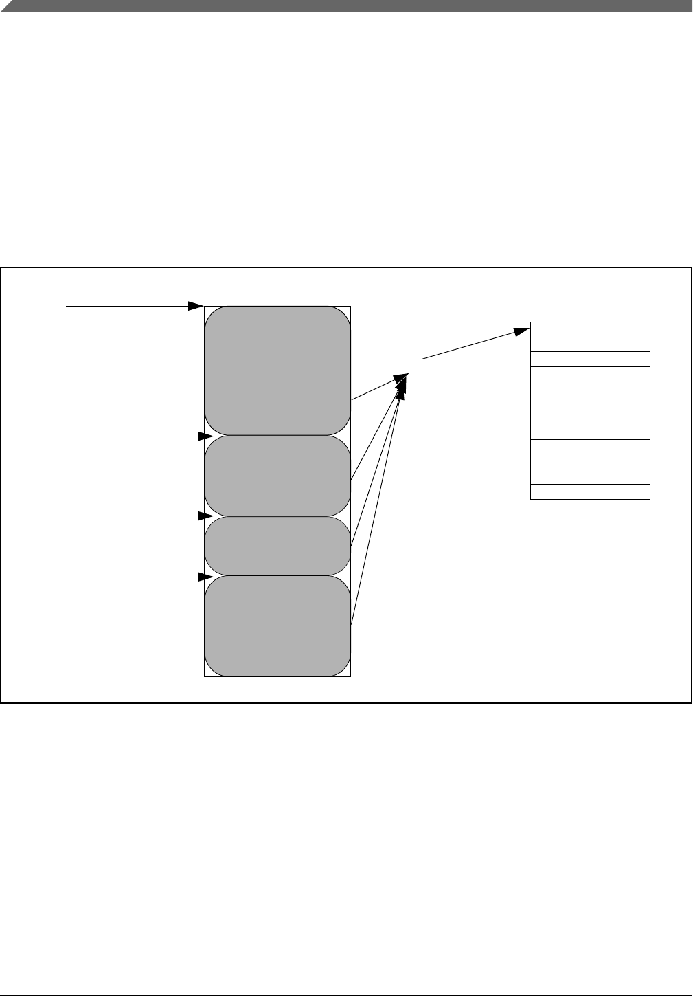
data from the serial flash.As such, there is no benefit in configuring a buffer size of
greater than ADATSZ, as the locations greater than ADATSZ will never be used. For any
AHB access, the sequence pointed to by the QSPI_BFGENCR[SEQID] field is used for
the flash transaction initiated. The data is returned to the master as soon as the requested
amount is read from the serial flash. The controller however, continues to prefetch the
rest of the data in anticipation of a next consecutive request. Figure 37-4 shows the
flexible AHB buffers.
The QSPI_BFGENCR[SEQID] field points to an index of the LUT. Refer to Look-up
Table for details.
Parametrizable max
size
BUF2IND
BUF1IND
BUF0IND
buffer3
buffer2
buffer1
buffer0
QSPI_BFGENCR[SEQID]
LUT
Figure 37-4. Flexible AHB Buffers
Buffer0 may optionally be configured to be associated with a high priority master by
setting the QSPU_BUF0CR[HP_EN] bit. An access by a high priority master suspends
any ongoing prefetch to any of the other buffers. The ongoing prefetch is suspended and
the high priority master is serviced first. Once the high priority masters access completes,
the suspended transaction is resumed (before any other AHB access is entertained). The
status of the suspended buffer can be read from Sequence Suspend Status Register
(QuadSPI_SPNDST).
Functional Description
S32K1xx Series Reference Manual, Rev. 7, 04/2018
950 NXP Semiconductors

37.7.2.3 Suspend-Abort Mechanism
Any low priority AHB access can be suspended by a high priority AHB master request.
The ongoing transaction is suspended at 64 bit boundary. The suspended transaction is
restarted after the high priority master is served and the high priority transaction
including data prefetch is completed. While a transaction is in suspended state, it may be
aborted if a transaction by the same suspended master is made to a location which is
different from the location of the suspended transaction.
Any ongoing transaction is aborted if a request from the same master arrives for a
location other than the location at which the transaction is going on. The abort can
happen at any point of time.
37.7.2.4 HBURST Support
QuadSPI controller supports HBURST and HSIZE on the AHB interface. HBURST
indicates if the transfer forms part of a burst. Four, eight and sixteen beat bursts are
supported and the burst may be either incrementing or wrapping. HSIZE indicates the
size of the transfer. 8, 16, 32 and 64 bit data size are supported. In case of WRAP
accesses, QuadSPI generates aligned accesses to Serial Flash if there is no buffer hit for
any incoming non-sequential AHB access. In case there is a buffer hit, the incoming
address in the haddr line is latched as it is. If the total burst size is more than the data
prefetch size an error response is generated and QSPI_FR[AIBSEF] is set. The data
perfetch size can be defined by QSPI_BUFxCR[ADATSZ] or data size mentioned in the
sequence pointed to by the SEQID field when ADATSZ is programmed as zero. A few
examples are shown in the figure below:
Chapter 37 Quad Serial Peripheral Interface (QuadSPI)
S32K1xx Series Reference Manual, Rev. 7, 04/2018
NXP Semiconductors 951

HADDR = 0x38
HBUST = WRAP4
HSIZE = 64 bits
Flash xsaction start = 0x20
HADDR = 0x50
HBUST = WRAP8
HSIZE = 64 bits
Flash xsaction start = 0x40
HADDR = 0x38
HBUST = INCR4
HSIZE = 64 bits
Flash xsaction start = 0x38
HADDR = 0xD0
HBUST = WRAP16
HSIZE = 64 bits
Flash xsaction start = 0x80
HADDR = 0xD4
HBUST = WRAP8
HSIZE = 32bits
Flash xsaction start = 0xC0
HADDR = 0x54
HBUST = INCR8
HSIZE = 32bits
Flash xsaction start = 0x54
Incoming AHB access= 0x50, 0x58, 0x60, 0x68, 0x70, 0x78, 0x40, 0x48
Incoming AHB access= 0x38, 0x20, 0x28, 0x30 Incoming AHB access= 0x38, 0x40, 0x48, 0x50
Incoming AHB access= 0xD0, 0xD8, 0xE0, ...0xF8, 0x80, 0x88, ... 0xC8
Incoming AHB access= 0xD4, 0xD8, 0xDC, 0xC0, 0xC4, 0xC8,0xCC, 0xD0
Incoming AHB access= 0x54, 0x58, 0x5C, 0x60, 0x64, 0x68,0x6C, 0x70
Figure 37-5. QuadSPI HBURST support
NOTE
The software must take care that the prefetch size should never
be set less than the minimum data needed by any external
interface to start processing.
37.7.2.5 Look-up Table
The Look-up-table or LUT consists of a number of pre-programmed sequences. Each
sequence is basically a sequence of instruction-operand pairs which when executed
sequentially generates a valid serial flash transaction. Each sequence can have a
maximum of 8 instruction-operand pairs. The LUT can hold a maximum of 16 sequences.
The figure below shows the basic structure of the sequence in the LUT.
Functional Description
S32K1xx Series Reference Manual, Rev. 7, 04/2018
952 NXP Semiconductors
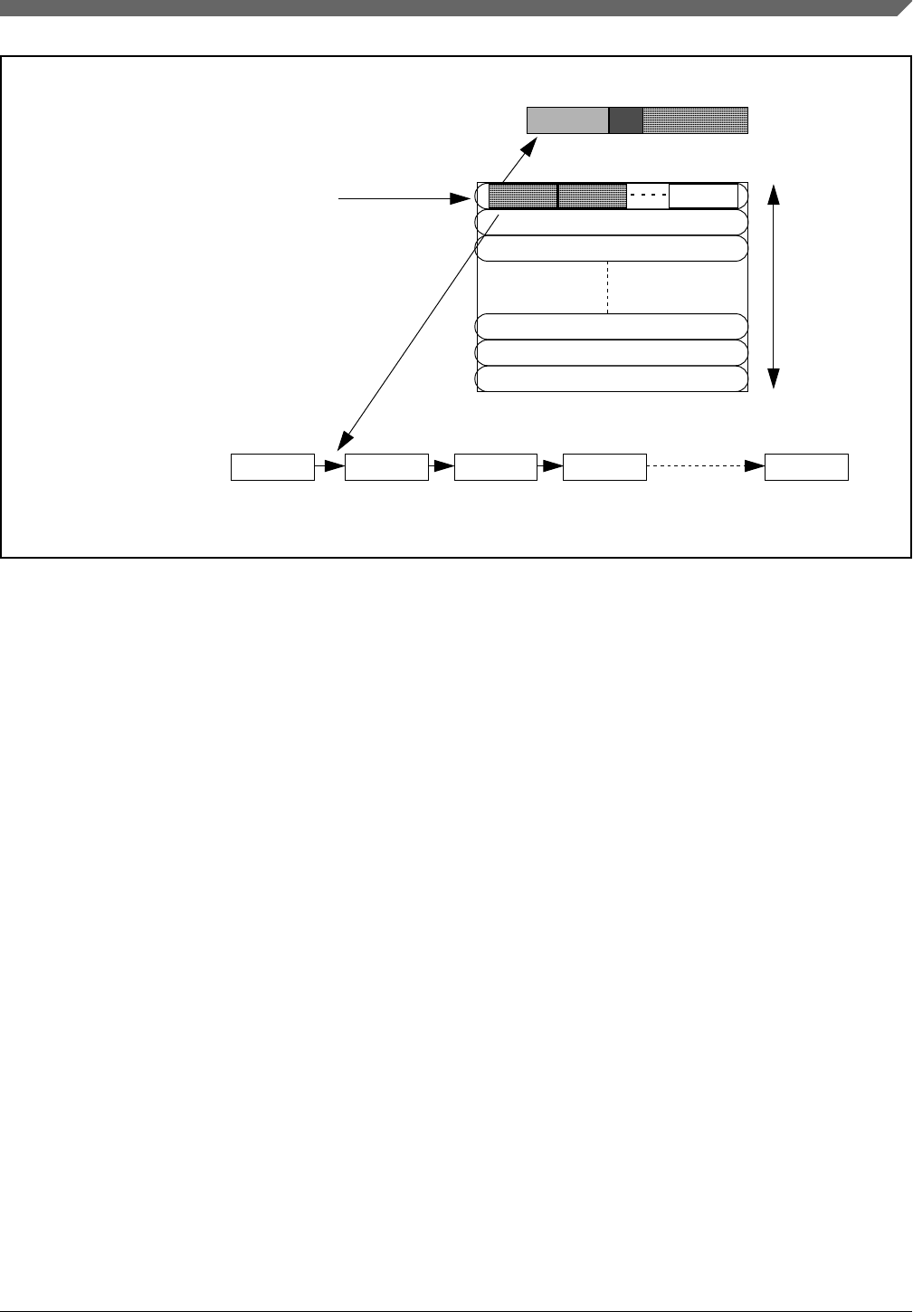
instr(6 bits)
LUT[4..7]
operand (8 bits)
pads (2 bits)
8 instruction-operand pairs
in one sequence(LUT[0..3])
LUT[8..11]
LUT[60..63]
16 possible
sequences
can be
programmed
in the
LUT
Look-up table
The instructions are executed sequentially until the last instruction or the
STOP instruction is encountered.
Figure 37-6. LUT and sequence structure
At reset, the index 0 of the look-up-table (LUT[0..3]) is programmed with a basic read
sequence as given in Table 37-15. After reset the complete LUT may be reprogrammed
according to the device connected on board.In order to protect its contents during a code
runover the LUT may be locked, after which a write to the LUT will not be successful
until it has been unlocked again.The key for locking or unlocking the LUT is
0x5AF05AF0. The process for locking and un-locking the LUT is as follows:
Locking the LUT
1. Write the key (0x5AF05AF0) in to the LUT Key Register (QuadSPI_LUTKEY).
2. Write 0b01 to the LUT Lock Configuration Register (QuadSPI_LCKCR). Note that
this IPS transaction should immediately follow the above IPS transaction (no other
IPS transaction can be issued in between). A successful write into this register locks
the LUT.
Unlocking the LUT
1. Write the key (0x5AF05AF0) into the LUT Key Register (QuadSPI_LUTKEY)
2. Write 0b10 to the LUT Lock Configuration Register (QuadSPI_LCKCR). Note that
this IPS transaction should immediately follow the above IPS transaction (no other
IPS transaction can be issued in between). A successful write into this register
unlocks the LUT.
Chapter 37 Quad Serial Peripheral Interface (QuadSPI)
S32K1xx Series Reference Manual, Rev. 7, 04/2018
NXP Semiconductors 953

The lock status of the LUT can be read from QSPI_LCKCR[UNLOCK] and
QSPI_LCKCR[LOCK] bit.
Some example sequences are defined in Example Sequences. The reset sequence at LUT
index 0 is given in the following table.
Table 37-15. Reset sequence
Instruction Pad Operand Comment
CMD 0x00 0x03 Read Data byte command on one pad
ADDR 0x00 0x18 24 Addr bits to be sent on one pad
READ 0x00 0x08 Read 64 bits
JMP_ON_CS 0x00 0x00 Jump to instruction 0 (CMD)
37.7.2.6 Issuing Serial Flash Memory (SFM) Commands
Each access to the external device follows the same sequence:
1. The user must pre-populate the LUT with the serial flash command sequences that
are required for the flash device being used.
2. The QuadSPI module starts executing the instructions in the sequence one by one.
The transaction starts and the status bit QSPI_SR[BUSY] is set.
3. Communication with the external serial flash device is started and the transaction is
executed.
4. When the transaction is finished (all transmit- and receive operations with the
external serial flash device are finished) the status bit QSPI_SR[BUSY] is reset. In
case of an IP Command the QSPI_FR[TFF] flag is asserted.
Further details are given in below in Flash Programming and Flash Read.
You can trigger the processing of SFM commands in the QuadSPI module in one of the
following ways:
•Using IP commands
For IP Commands the required components need to be written into the following
registers:
• Write the serial flash address to be used by the instruction into QSPI_SFAR,
refer to Serial Flash Address Register (QSPI_SFAR). For IP Commands not
related to specific addresses, the base address of the related flash need to be
Functional Description
S32K1xx Series Reference Manual, Rev. 7, 04/2018
954 NXP Semiconductors

programmed.For example, for an instruction which does not require an address
(i.e. write enable instruction) the SFAR should be programmed with the base
address of the memory the command is to be sent to.
• Write the sequence ID and data size details in the IP Configuration Register
(QSPI_IPCR).
• Note that the write into the QSPI_IPCR[SEQID] field must be the last step of the
sequence. It is possible to combine all fields of the QSPI_IPCR into one single
write. Refer to IP Configuration Register (QSPI_IPCR) for details.
Note that there are some conditions where no IP Command is executed after writing
the QSPI_IPCR[SEQID] field and the write operation itself is ignored. They are
described in Command Arbitration.
•Using AHB commands
Any AHB memory mapped access is routed to one of the buffers depending on the
master port number of the request. If the access is a "miss", a new serial flash
transaction is started. The transaction is based on the sequence pointed to by the
BFGENCR[SEQID] field as described in Flexible AHB buffers.
An AHB access is termed memory mapped when the access is to the memory
mapped serial flashes, as described in Memory Mapped Serial Flash Data -
Individual Flash Mode on Flash A and Memory Mapped Serial Flash Data -
Individual Flash Mode on Flash B.
Again the possible error conditions are described in Command Arbitration .
37.7.2.7 Flash Programming
In all cases the memory sector to be written needs to be erased first. The programming
sequence itself is then initiated in the following way:
1. Check QuadSPI_SR[BUSY] is de-asserted or '0'. Check that the TX buffer is empty.
If it is required to discard the data present in the TX buffer (QSPI_SR[TXEDA]) bit
is set, then the TX buffer must be cleared by writing '1' into the
QSPI_MCR[CLR_TXF] bit.
2. Program the address related to the command in the QSPI_SFAR register. Program
the QSPI_SFACR[CAS] if required to desired value else to 0. Program the
QSPI_SFACR[WA] to 1 if the serial flash is a word addressable flash else to 0 in
case serial flash is byte addressable.
Chapter 37 Quad Serial Peripheral Interface (QuadSPI)
S32K1xx Series Reference Manual, Rev. 7, 04/2018
NXP Semiconductors 955

3. Provide initial data for the program command into the circular buffer via register TX
Buffer Data Register (QSPI_TBDR) . At least four word of data must be written into
the TX Buffer up to a maximum of 32.
4. Program the QSPI_IPCR register to trigger the command. The QSPI_IPCR[SEQID]
should point to an index of the LUT which has the flash program sequence pre-
programmed.The IDATSZ field should be set to denote the size of the write.
5. Depending on the amount of data required, step 3 must be repeated until all the
required data have been written into the QSPI_TBDR register.The
QSPI_SR[TXFULL] can be used to check if the buffer is ready to receive more data.
At any time, the QSPI_TBSR[TRCTR] field can be read to check how many words
have been written actually into the TX Buffer.
Upon writing the QSPI_IPCR[SEQID] field (refer to step 4) the QuadSPI module will
start to execute the programmed sequence. It is the responsibility of the software to
ensure that a correct sequence is programmed into the LUT in accordance with the flash
memory connected to the module. The data is fetched from the TX Buffer. It consists of
32 entries of 32-bits and is organized as a circular FIFO, whose read pointer is
incremented by four after each fetch. When all data are transmitted, the QuadSPI module
will return from 'busy' to 'idle'. However, this is not true for the external device since the
internal programming is still ongoing. It is up to the user to monitor the relevant status
information available from the serial flash device and to ensure that the programming is
finished properly.
37.7.2.8 Flash Read
Host access to the data stored in the external serial flash device is done in two steps. First,
the data must be read into the internal buffers and in the second step these internal buffers
can be read by the host.
1. Reading Serial Flash Data into the QuadSPI Module Internal Buffers
A read access to the external serial flash device can be triggered in two different
ways:
•IP Command Read: For reading flash data into the RX Buffer the user must
provide the correct sequence ID in the QuadSPI_IPCR[SEQID] register. The
sequence ID points to a sequence in the LUT. It is the responsibility of the
software to ensure that a correct read sequence is programmed in the LUT in
accordance with the serial flash device connected on board. The user should
Functional Description
S32K1xx Series Reference Manual, Rev. 7, 04/2018
956 NXP Semiconductors

program the Serial Flash Address Register (QSPI_SFAR) , QSPI_SFACR[CAS]
and the IP Configuration Register (QSPI_IPCR) registers. All available read
commands supported by the external serial flash are possible.
Optionally it is possible to clear the RX Buffer pointer prior to triggering the IP
Command by writing a 1 into the QuadSPI_MCR[CLR_RXF] field.
From these inputs, the complete transaction is built when the
QSPI_IPCR[SEQID] field is written. The transaction related to the read access
starts and the requested number of bytes is fetched from the external serial flash
device into the RX Buffer. Since the read access is triggered by an IP command,
the IP_ACC status bit and the BUSY bit are both set (both are located in the
Status Register (QSPI_SR) ). A count of the number of entries currently in the
Rx Buffer can be obtained from QSPI_RBSR[RDBFL].
The communication with the external serial flash is stopped when the specified
number of bytes has been read (successful completion of the transaction).
•AHB Command Read: For reading flash data into the AHB Buffer the user
must set up a read access by a master to the address range in the system memory
map which the external serial flash devices are mapped to. The user should
program the QSPI_SFACR[CAS], if required, to desired value else to 0. The
user should also program the buffer registers corresponding to the AHB master
initiating the request, this is depends on the configuration of the
QSPI_RBCT[RXBRD]. The user should provide the correct sequence ID into
the buffer generic configuration register (QSPI_BFGENCR). It is the
responsibility of the software to ensure that a correct read sequence in
programmed in the LUT in accordance with the serial flash device connected on
board. Flash device selection and access mode are determined by the address
accessed in the AHB address space associated to the QuadSPI module (refer to
Memory Mapped Serial Flash Data - Individual Flash Mode on Flash A,
Memory Mapped Serial Flash Data - Individual Flash Mode on Flash B
On each AHB read access to the memory mapped area the valid data in the AHB
Buffer is checked against the address requested in the actual read. When the
AHB read request can't be served from the content of the AHB Buffer, the buffer
is flushed and the sequence pointed to by the sequence ID is executed by the
controller. The requested number of buffer entries defined in the
QSPI_BUFxCR[ADATSZ] field is then fetched from the external serial flash
device into the internal AHB Buffer. Since the read access is triggered via the
AHB bus, the QSPI_SR[AHB_ACC] status bit is set driving in turn the
Chapter 37 Quad Serial Peripheral Interface (QuadSPI)
S32K1xx Series Reference Manual, Rev. 7, 04/2018
NXP Semiconductors 957
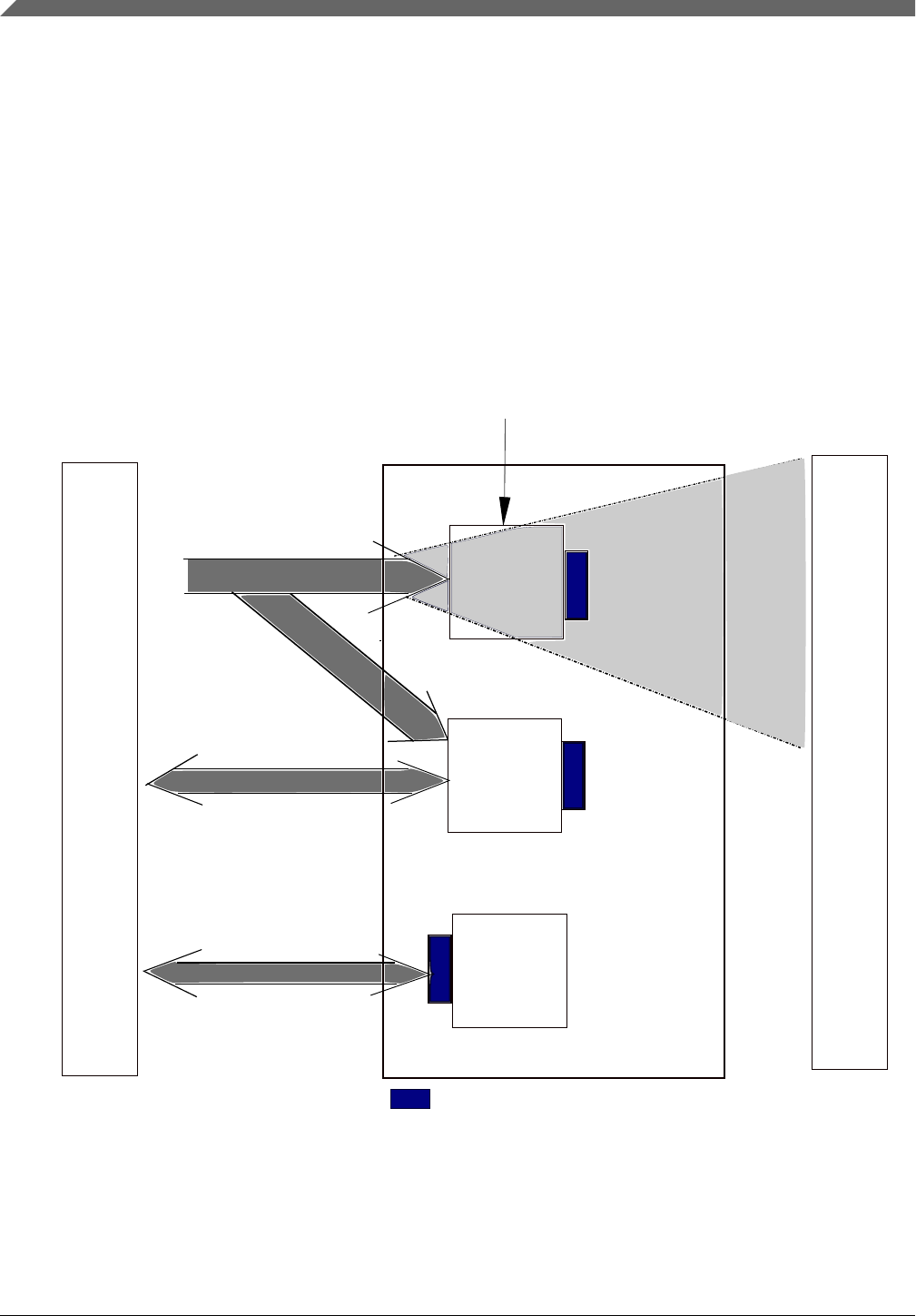
QSPI_SR[BUSY] bit until the transaction is finished. The communication with
the external serial flash is stopped when the specified number of entries has been
filled.
2. Data Transfer from the QuadSPI Module Internal Buffers
The data read out from the external serial flash device by the QuadSPI module is
stored in the internal buffers.The means of accessing the data from the buffer differs
depending on which buffer the data has been loaded to. Refer to Block Diagram for
details about the two available buffers, the RX Buffer and the AHB Buffer, in the
QuadSPI module:
Memory mapped access
Register access (RBDR)
RX
Buffer
TX
Buffer
Memory mapped access
ARDB access
This buffer is transparent to the user and is non-memory mapped.
See 'Flexible AHB Buffer' section for details.
AHB
Buffer
Byte Swapper for endianness
Note:
READ ACCESS
READ ACCESS
WRITE ACCESS
System AHB/IPS
External Flash
QuadSPI
Figure 37-7. QuadSPI memory map
• The RX Buffer is implemented as FIFO of depth 32 entries of 4 bytes. Its content
is accessible in two different address areas both referring to the identical data
and the same physical memory.
Functional Description
S32K1xx Series Reference Manual, Rev. 7, 04/2018
958 NXP Semiconductors

In the IPS address space in the area associated to QSPI_RBDR0 to QSPI_RBDR31
In the AHB address space in the area associated to QSPI_ARDB0 to QSPI_ARDB31. Two
successive entries are accessed with one single 64 bit AHB read operation.
RX Buffer operation can be summarized as follows: The QSPI_RBCT[WMRK]
field determines at which fill level the RXWE bit is asserted and how many
entries are removed from the RX Buffer on each Buffer POP operation. So the
QSPI_SR[RXWE] bit indicates that the configured number of data entries is
available in the RX Buffer and the QSPI_RBSR[RDBFL] field indicates how
many valid entries are available in total. Note that the first entry (QSPI_RBDR0
or QSPI_ARDB0) always corresponds to the first valid entry in the RX Buffer.
The software needs to manage the number of valid data bytes itself.
Further details can be found in RX Buffer Data Register (QuadSPI_RBDRn) and
in AHB RX Data Buffer (QSPI_ARDB0 to QSPI_ARDB31).
•Flag-based Data Read of the RX Buffer is done by polling the
QSPI_SR[RXWE] bit. When it is asserted the valid entries can be read either via
the IPS address space (QSPI_RBDRn) or the AHB address space
(QSPI_ARDBn). A Buffer POP operation must be triggered by the application
by writing a 1 into the QSPI_FR[RBDF] bit - this automatically updates the
FIFO to point to the next entry as defined by RBCT[WMRK]. For example, if
WMRK is set to 3, then the buffer will discard 16 bytes of data.
•DMA controlled Data Read of the RX Buffer is done by using the DMA
module.The application must ensure that the DMA controller of the related
device is programmed appropriately like it is described in DMA Usage.
DMA controlled read out is triggered fully automatically by the assertion of the
QSPI_SR[RXWE] bit. The related Buffer POP operation is also handled
completely inside the QuadSPI module. Like in the case above, accessing the RX
Buffer content either on QSPI_RBDRn or QSPI_ARDBn related addresses is
equivalent.
•AHB Buffer data read via memory mapped access: This kind of access is
done by reading one of the addresses assigned to the external serial flash
device(s) within the range given in Table 37-9 table under the condition that the
data requested are already present in the AHB Buffer or it is currently being
read from the serial flash device by the instruction in progress. If this is not the
case a memory mapped AHB command read is triggered as described above. If
the requested data is already available in the AHB Buffer they are provided
directly to the host.
Chapter 37 Quad Serial Peripheral Interface (QuadSPI)
S32K1xx Series Reference Manual, Rev. 7, 04/2018
NXP Semiconductors 959

When AHB access are made to the flash memory mapped address, the data will
be fetched and returned to the AHB interface. Till the data is being fetched the
AHB interface would be stalled. As soon as the data from the requested address
has been read by the QuadSPI module the AHB read access is served. So it is
possible to run sequential reads from the AHB buffer at arbitrary speed without
the need to monitor any information about the availability of the data.
Nevertheless this access scheme stalls the AHB bus for the time required to read
the data from the serial flash device. A better way is (when it is known the
access is sequential) to have a prefetch enabled (by programming the ADATSZ
field) such that before the next sequential AHB access come, the data is already
fetched into the buffer.
As long as the host restricts its accesses to the data already in the buffer and the
data currently fetched from the serial flash, it is possible to run the host read
from the AHB Buffer in parallel to the serial flash read into the AHB Buffer.
37.7.2.9 Byte Ordering of Serial Flash Read Data
In this paragraph the byte ordering of the serial flash data is given. The basic scheme is
that the first byte read out of the serial flash device - which is addressed by the
QSPI_SFAR[SFADR] field - corresponds to bit position QSPI_RBDR0[ ] register for IP
Command read. In contrast to that for AHB Command read the bytes are always
positioned according to the byte ordering of the AHB bus.
•Byte Ordering in Individual Flash Mode
The following table gives the byte ordering scheme of how the byte oriented data
space of the serial flash device is mapped into one single 32 bit entry of the RX
Buffer or the AHB Buffer. The table is valid within the following context:
• Flash A or Flash B in Individual Flash Mode
• All AHB data read commands with access size of 32 bit
Table 37-16. Byte Ordering in Individual Flash
Mode
Functional Description
S32K1xx Series Reference Manual, Rev. 7, 04/2018
960 NXP Semiconductors

Note
For IP Commands the read size can be given in number of
bytes. If this number is not a multiple of 4, then the last
buffer entry is not completely filled with the missing higher
numbered bytes at undefined values.
For AHB Commands, reads, starting from an address not aligned to 32 bit
boundaries, the requested bytes are given at the appropriate positions according to
the AMBA AHB specification.
•Buffer Entry Ordering for 64 Bit Read Access
For read access via the AHB interface 64 bit access is possible. Each 64 bit access
reads 2 32 bit entries simultaneously. The ordering of these 32 bit entries within the
64 bit word is given in the following table.
Table 37-17. 64 Bit Read Access Buffer Entry
Ordering
37.7.2.10 Normal Mode Interrupt and DMA Requests
The QuadSPI module has different flags that can only generate interrupt requests and one
flag that can generate interrupt as well as DMA requests. The following table lists the
eight conditions. Note that the flags mentioned in the table are related to the Flag Register
(QSPI_FR).
Table 37-18. Interrupt and DMA Request Conditions
Condition Flag(QSPI_FR) DMA
TX Buffer Fill TBFF -
TX Buffer Underrun TBUF -
Illegal Instruction Error ILLINE -
RX Buffer Drain RBDF X
RX Buffer Overflow RBOF -
AHB Buffer Overflow ABOF -
AHB Sequence Error ABSEF -
AHB Illegal Transaction Error AITEF -
AHB Illegal Burst Size Error AIBSEF -
IP Command Trigger during AHB
Access Error
IPAEF -
Table continues on the next page...
Chapter 37 Quad Serial Peripheral Interface (QuadSPI)
S32K1xx Series Reference Manual, Rev. 7, 04/2018
NXP Semiconductors 961

Table 37-18. Interrupt and DMA Request Conditions (continued)
Condition Flag(QSPI_FR) DMA
IP Command Trigger could not be
executed Error
IPIEF -
IP Access during AHB Grant Error IPGEF -
IP Command related Transaction
Finished
TFF -
Each condition has a flag bit in the Flag Register (QSPI_FR) and a Request Enable bit in
the DMA Request Select and Enable Register (QSPI_RSER) . The RX Buffer Drain Flag
(RBDF) has separate enable bits for generating IRQ and DMA requests. Note that not all
flags have an individual IRQ line. Check the devices Interrupt Vector Table for more
details.
• Transmit Buffer Fill Interrupt Request:
The Transmit Buffer Fill IRQ indicates that the TX Buffer can accept new data. It is
asserted if the QSPI_FR[TBFF] flag is asserted and if the corresponding enable bit
(QSIP_RSER[TBFIE]) is set. Refer to TX Buffer Operation, for details about the
assertion of the QSPI_FR[TBFF] flag.
Aside from IRQ it is possible to handle TX Buffer fill by DMA. If the
QSPI_RSER[TBFDE] bit is set, a DMA request will be triggered when the number
of available space in the TX Buffer is more than the QSPI_TBCT[WMRK] valid
entries and QSPI_SR[TXWA] is set. The application must set the environment
appropriately (eg. the DMA controller) for the DMA transfer.
• Receive Buffer Drain Interrupt or DMA Request:
The Receive Buffer Drain IRQ derived from the QSPI_FR[RBDF] flag indicates that
the RX Buffer of the QuadSPI module has data available from the serial flash device
to be read by the host. It remains set as long as the QSPI_RBSR[RXWE] bit is set.
The QSPI_RSER[RBDIE] bit enables the related IRQ.
Aside from the IRQ it is possible to handle RX Buffer drain by DMA. If the
QSPI_RSER[RBDDE] bit is set, a DMA request will be triggered when the RX
Buffer contains more than QSPI_RBCT[WMRK] valid entries.The application must
set the environment appropriately (for example, the DMA controller) for the DMA
transfers.
• Buffer Overflow/Underrun Interrupt Request:
The Buffer Overflow/Underrun IRQ is a combination of the following flags (all
located in the QSPI_FR register with the related enable bits in the QSPI_RSER
register):
Functional Description
S32K1xx Series Reference Manual, Rev. 7, 04/2018
962 NXP Semiconductors

• TBUF - TX Buffer Underrun, enabled by TBUIE
• RBOF - RX Buffer Overflow, enabled by RBOIE
• ABOF - AHB Buffer Overflow, enabled by ABOIE
The Transmit Buffer Underrun indicates that an underrun condition in the TX
Buffer has occurred. It is generated when a write instruction is triggered whilst
the Tx Buffer is empty and the QSPI_RSER[TBUIE] bit is set.
The Receive Buffer Overflow indicates that an overflow condition in the RX
Buffer has occurred. It is generated when the RX Buffer is full, an additional
read transfer attempts to write into the RX Buffer and the QSPI_RSER[RBOIE]
bit is set.
The AHB Buffer Overflow indicates that an overflow condition in the AHB
Buffer has occurred. It is generated when the AHB Buffer is full, an additional
read transfer attempts to write into the AHB Buffer and the
QSPI_RSER[ABOIE] bit is set.
The data from the transfers that generated the individual overflow conditions is
ignored.
• Serial Flash Command Error Interrupt Request
If the IPAEF, IPIEF, IPGEF flags in the QSPI_FR are set, and the related interrupt
enable bits in the QSPI_RSER are also set, then an interrupt is requested.
• Transaction Finished Interrupt Request
The IP Command Transaction Finished IRQ indicates the completion of the current
IP Command.It is triggered by the QSPI_FR[TFF] flag and is masked by the
QSPI_RSER[TFIE] bit.
37.7.2.11 TX Buffer Operation
The TX Buffer provides the data used for page programming. For proper operation it is
required to provide at least four entry in the TX Buffer prior to starting the execution of
the page programming command. The application must ensure that the required number
of data bytes is written into the TX Buffer fast enough as long as the command is
executed without a TX Buffer overflow or underrun.
The QuadSPI module sets the QSPI_FR[TBFF] flag so long as the TX Buffer is not full
and can accept more data.
Chapter 37 Quad Serial Peripheral Interface (QuadSPI)
S32K1xx Series Reference Manual, Rev. 7, 04/2018
NXP Semiconductors 963

When the QuadSPI module tries to pull data out of an empty TX Buffer the TX Buffer
underrun is signaled by the QSPI_FR[TBUF] flag.The TX buffer underrun flag is also
asserted when TX buffer contains less than 128 bits of data and QuadSPI module tries to
pull out data from it. The current IP Command leading to the underrun condition is
continued until the specified number of bytes has been sent to the serial flash device, in
the underrun condition when QuadSPI module tries to pull out data of empty TX buffer,
the data transferred is all F's i.e. once the underrun flag is set under this condition, it will
return F's until the required number of bytes are not sent. This has been done to ensure
that the software need not to erase whole sector after underrun, just reprogramming from
failure point will serve the purpose. When this Sequence Command is finished, the
QSPI_FR[TBFF] flag is asserted indicating that the Tx Buffer is ready to be written
again.
The TX Buffer overflow isn't signaled explicitly, but the TX Buffer fill level can be
monitored by the QSPI_TBSR[TRBFL] field.
Refer to TX Buffer Status Register (QuadSPI_TBSR) and Flag Register (QuadSPI_FR )
for details about the TX Buffer related registers.
37.7.2.12 Address scheme
Earlier serial flash memories supported only 24-bit address space hence restricting the
maximum memory size of the serial flash as 16 MB. The new memory specification
supports two types of 32-bit addressing mode in addition to legacy 24-bit address mode.
It also supports segregation of address programmed, into Row address and Column
address of the Flash, as per requirement.
•Extended Address Mode
In this mode, the legacy 24-bit commands are converted to accept 32-bit address
commands. The flash memory needs to be configured for 32-bit address mode. Also,
while programming the LUT sequence in QuadSPI for 32-bit mode, the ADDR and
ADDR_DDR command should be programmed with 8’d32 as the operand value with
QSPI_SFACR[CAS] programmed to 0. If a flash needs some bits of the address as
its column address, then it must always considered that the total bits required by the
Flash should not exceed 32, as maximum address supported by QuadSPI is 32 bits.
Each of the memory vendors have a different way of enabling this mode (Refer to the
memory specification from memory vendors). For example, the command B7h sent
to Macronix flash will enable it for 32-bit address mode.
•Extended Address register
Functional Description
S32K1xx Series Reference Manual, Rev. 7, 04/2018
964 NXP Semiconductors

In this mode, the upper 8-bit of the 32-bit address is provided by the Extended
address register in the memory itself. The memory provides a specific register which
is updated according to the address to be accessed. This effectively converts the
legacy 24-bit address command into 32-bit address commands. The memories greater
in size than 16 MB, consists of banks of 16 MB. The 8-bit written in the extended
address register effectively enables a bank. For example in Spansion memory, when
the extended address register is updated with a value of 0x01 with the help of the
command 17h, it will open Bank1 of the memory. The consequent 24-bit address
commands will lead to Bank1. The extended address register needs to be update with
the respective value for access to other banks. This effectively converts the legacy
24-bit address command into 32-bit address commands.
•Separation of address into row and column address
This mode has been introduced for flashes which needs addresses segregated into
Row and Column. The value in QSPI_SFACR[CAS] defines the width of the column
address required by a flash. The actual address to be provided will be derived from
the incoming address in case of AHB initiated transactions and the value of SFAR in
case of IPS initiated transactions , if QSPI_SFACR[CAS] is set to 0, else the actual
address will take CAS into consideration. If QSPI_SFACR[CAS] is 3 then bits 26-3
of the address programmed are sent to flash as it page address in case flash is
operating in 24bit mode and bits 2-0 are sent as its column address. If a flash
requirement for column address is less than the number of pads in which address has
to be sent than the remaining bits are appended with 0 by QuadSPI. The user must
program the operand value in CADDR and CADDR_DDR command accordingly. It
must be ensured that the total number of address bits request by flash as its page and
column address must not be more than 32 bits.
•Word addressable mode for Flash
This mode has been introduced for flashes which has word addressable memory i.e.
each address of the flash contains one word (two bytes) of data. The QSPI_SFACR
[WA] is set to 1 to enter this mode. QuadSPI internally divides the incoming address
in the AHB bus or the address in the QSPI_SFAR to map it to a valid flash location.
For example, if the incoming address is 0x2004, the controller re-maps this address
to access the flash location 0x1002. If not in this mode, the incoming address 0x2004
will be mapped to flash location 0x2004.
37.7.3 HyperRAM Support
The QuadSPI supports HyperRAM memories and by virtue of this protocol, QuadSPI
supports the following functionalities.
Chapter 37 Quad Serial Peripheral Interface (QuadSPI)
S32K1xx Series Reference Manual, Rev. 7, 04/2018
NXP Semiconductors 965

• Bidirectional data strobe/read write data strobe (RWDS)
• When QuadSPI is configured to use the HyperRAM mode, the RWDS pad
should be pulled down.
• Variable refresh latency
• If QuadSPI_MCR[VAR_LAT_EN] field is set, based on the status of RWDS
from HyperRAM during Command/Address phase, QuadSPI includes additional
initial access latency. If RWDS is high, QuadSPI will include twice + 1 the
latency mentioned in the DUMMY phase. If RWDS is low, latency mentioned in
the DUMMY phase will only be included.
• During QuadSPI configuration register read/write DUMMY will not be the part
of LUT programming and hence the status of RWDS will not be considered by
QuadSPI.
• If QuadSPI_MCR[VAR_LAT_EN] is not set, fixed latency mentioned in the
DUMMY phase will be included.
• Read data strobe to latch data from HyperRAM
• Data masking during write
• Enabled if QuadSPI_MCR[DQS_OUT_EN].
• RWDS is driven low by QuadSPI during Write data phase.
• Data masking is not supported as the write data size is supposed to be 16 bit
aligned.
37.8 Initialization/Application Information
This section provides the initialization and application information of the QuadSPI
module.
37.8.1 Power Up and Reset
Note that the serial flash devices connected to the QuadSPI module may require special
voltage characteristics of their inputs during power up or reset. It is the responsibility of
the application to ensure this.
37.8.2 Available Status/Flag Information
This paragraph gives an overview of the different status and flag information available
and their interdependencies for different use cases. Related registers are QSPI_SR and
QSPI_FR. Refer to the related descriptions how to set up the QuadSPI module
appropriately.
Initialization/Application Information
S32K1xx Series Reference Manual, Rev. 7, 04/2018
966 NXP Semiconductors

37.8.2.1 IP Commands
Refer to IP Configuration Register (QuadSPI_IPCR) for additional details not explicitly
covered in this paragraph.
•IP Commands - Normal Operation
Writing the QSPI_IPCR[SEQID] field triggers the execution of a new IP Command.
Given that this is a legal command the QSPI_SR[IPACC] and the QSPI_SR[BUSY]
bits are asserted simultaneously, immediately after the execution is started.
When the instruction on the serial flash device has been finished these bits are de-
asserted and the QSPI_FR[TFF] flag is set.
•IP Commands - Error Situations
Refer to Table 37-19 below.
37.8.2.2 AHB Commands
Refer to Section 1, Reading Serial Flash Data into the QuadSPI Module, in Flash Read
for additional details not explicitly covered in this paragraph.
•AHB Commands - Normal Operation
Memory mapped read access to a serial flash address not contained in the AHB
Buffer, triggers the execution of an AHB Command. Given that this is a legal
command the QSPI_SR[AHBACC] and the QSPI_SR[BUSY] bits are asserted
simultaneously immediately after the execution is started. When the instruction on
the serial flash device has been finished these bits are de-asserted.
•IP Commands - Error Situations
Refer to Table 37-19 below.
37.8.2.3 Overview of Error Flags
The following table gives an overview of the different error flags in the QSPI_FR register
and additional error-related details.
Chapter 37 Quad Serial Peripheral Interface (QuadSPI)
S32K1xx Series Reference Manual, Rev. 7, 04/2018
NXP Semiconductors 967

Table 37-19. Overview of QSPI_FR Error Flags
Error Category Error Flag in
QSPI_FR
Command Execution on Serial Flash
Device
TFF Behavior (in case of IP commands
only)
Description
AHB Error Flag ABSEF Flash transaction is aborted
AHB sequence contains
• WRITE instruction
• WRITE_DDR instruction
AHB Error Flag ABOF Flash transaction continues until it finishes
Set when the module tried to push
data into the AHB buffer that
exceeded the size of the AHB buffer.
Only occurs due to wrong
programming of the
QSPI_BUFxCR[ADATSZ].
AHB Error Flag AIBSEF Flash transaction is aborted Total burst size of AHB transaction
is greater than prefetch data size
AHB Error Flag AITEF Flash transaction is aborted
No response generated from QSPI
to AHB bus in case of illegal
transaction and the watchdog timer
expires
Miscellaneous Error
Flag ILLINE Flash transaction aborted
Illegal instruction Error Flag – Set
when an illegal instruction is
encountered by the controller in any
of the sequences.
Command Arbitration
Error IPIEF
TFF not asserted in conjunction with that
command
IP Command Error - caused when
IP access is currently in progress
(IP_ACC set) and
• write attempt to QSPI_IPCR
register.
• write attempt to QSPI_SFAR
register.
• write attempt to QSPI_RBCT
register.
Command Arbitration
Error IPAEF
• AHB Command already
running, another IP Command
could not be executed.
• AHB Command already
running, write attempt to
QSPI_IPCR[SEQID] field.
Command Arbitration
Error IPGEF
• Exclusive access to the serial
flash granted for AHB
Commands, write attempt to
QSPI_IPCR[SEQID] field.
Buffer Related Error RBOF
TFF is asserted on completion
• RX Buffer Overrun
Buffer Related Error TBUF • TX Buffer Underrun
Note that only the buffer related errors are related to a transaction on the external serial
flash. All the other errors do not trigger an actual transaction.
Initialization/Application Information
S32K1xx Series Reference Manual, Rev. 7, 04/2018
968 NXP Semiconductors

37.8.2.4 IP Bus and AHB Access Command Collisions
There are two flags related to this topic, the QSPI_FR[IPAEF] and QSPI_FR[IPIEF].
Refer to sub-section "Reading Serial Flash Data into the QuadSPI Module" of Flash
Read section, for a description of the flags and Command Arbitration , for details about
possible command collisions.
37.8.3 Exclusive Access to Serial Flash for AHB Commands
It is possible that several masters need to access the serial flash device connected to the
QuadSPI module separately, one master by triggering IP Commands and reading the RX
Buffer (via RBDRn register) and the other masters by triggering AHB Commands (via
ARDBn Registers). These two set of buffer (RBDR and ARDB Buffer) points to the
same physical buffer.Refer to Figure 37-7 To avoid command collisions resulting in
excessive latencies the QuadSPI module implements a request-handshake mechanism
between the master triggering AHB Commands and the QuadSPI module allowing this
specific master to request exclusive access to the serial flash device for AHB Commands.
If this exclusive access is granted the execution of IP Commands is blocked. This
resolves command collisions and excessive times where the AHB interface may be
blocked.
If this capability is used in the device there is additional status and flag information
available related to this mechanism. The QSPI_SR[AHBGNT] bit reflects the module-
internal state that the exclusive access mentioned above is granted, any attempt to trigger
an IP Command is rejected and results in the assertion of the QSPI_FR[IPGEF] flag.
Refer to the descriptions of the related bit and flag for details.
It is within the responsibility of the application to set up the master using this mechanism
appropriately, if used incorrectly no IP Commands at all can be triggered.
Two different cases can be distinguished:
37.8.3.1 RX Buffer Read via QSPI_ARDB Registers
In this case all masters share the AHB bus for RX Buffer as well as for AHB Buffer read.
In this case the access to the AHB interface by the master triggering AHB Commands
must be deferred until any pending IP Command has been finished and the RX Buffer
readout has been finished as well. The QSPI ARDB Buffers access the Rx buffer i.e the
Chapter 37 Quad Serial Peripheral Interface (QuadSPI)
S32K1xx Series Reference Manual, Rev. 7, 04/2018
NXP Semiconductors 969

data from the Rx Buffer is returned and no data from AHB Buffer is touched. This is the
conservative use case, corresponding to the reset value 0 of the QSPI_RBCT[RXBRD]
bit.
In this case the QSPI_SR[AHBGNT] bit is asserted not earlier than any running IP
Command has been finished (QSPI_SR[IP_ACC] is 0), the RX Buffer has been read out
completely (QSPI_RBSR[RDBFL] equal to 0) or no DMA read is pending
(QSPI_SR[RXDMA] equal to 0 and Rx Buffer readout is via
AHB(QSPI_RBCT[RXBRD]) equal to 1.
37.8.3.2 RX Buffer Read via QSPI_RBDR Registers
This is the preferred use case as an access to the AHB buffer (memory mapped flash)
does not interfere with any IPS access to read the RBDR buffer. It is not possible that a
pending AHB bus access triggered by an AHB Command stalls the AHB bus and blocks
the RX Buffer readout since the RX Buffer is read via the IP bus based registers
QSPI_RBDR0 to QSPI_RBDR31.
For this case it is recommended to program the QSPI_RBCT[RXBRD] bit to 1. The
QSPI_SR[AHBGNT] bit is asserted immediately after any running IP Command has
been finished (QSPI_SR[IP_ACC] is 0), the RX Buffer has been read out completely
(QSPI_RBSR[RDBFL] equal to 0) or no DMA read is pending (QSPI_SR[RXDMA]
equal to 0, allowing the master triggering AHB Commands to trigger AHB Commands as
soon as possible without the need to wait for the RX Buffer readout to be finished.
37.8.4 Command Arbitration
In case of overlapping commands, the arbitration scheme is described in the following
paragraphs under the assumption that the priority mechanism described in Exclusive
Access to Serial Flash for AHB Commands is not used:
• During the execution of an IP Command, the running IP Command can't be
terminated by issuing another IP Command or AHB Command. The
QSPI_FR[IPIEF] flag is asserted when the host tries to write into the QSPI_IPCR
register. When the host triggers an AHB Command (refer to sub-section "Reading
Serial Flash Data into the QuadSPI Module" of Flash Read section, for details), this
command is stalled until the currently running IP Command is finished.
• During the execution of an AHB Command, the running AHB Command can't be
terminated by issuing an IP Command. The command is ignored and the
QSPI_FR[IPAEF] flag is asserted. Refer to Flag Register (QuadSPI_FR ) for the
description of these flags.
Initialization/Application Information
S32K1xx Series Reference Manual, Rev. 7, 04/2018
970 NXP Semiconductors

When another AHB Command is triggered the address of the memory mapped access
is considered. If the requested address is currently read from the serial flash device,
the running command is continued. If this is not the case the currently running
command is terminated and another AHB Command related to the requested address
is executed. Refer to sub-section "Reading Serial Flash Data into the QuadSPI
Module" of Flash Read section, for further details.
In case of coinciding commands the IP Command is triggered and the AHB Command is
stalled until the IP Command has been finished (QSPI_SR[IP_ACC] has been
deasserted).
The IP Commands ignored in case of command collision will not result in the assertion of
the QSPI_FR[TFF] flag.
37.8.5 Flash Device Selection
Regardless of the SFM Command (IP or AHB) the access mode is selected by specifying
the 32 bit address value for the following SFM Command.
For IP Commands the access mode is selected with the address programmed into the
QSPI_SFAR register. Refer to Serial Flash Address Register (QuadSPI_SFAR) for
details.
For AHB Commands the access mode is determined by the memory mapped address
which is accessed Refer to Flash memory mapped AMBA bus for details.
37.8.6 DMA Usage
For the complete description of the DMA module refer to the related DMA Controller
chapter. In this paragraph only the details specific to the DMA usage related to the
QuadSPI module are given.
37.8.6.1 DMA Usage in Normal Mode
Chapter 37 Quad Serial Peripheral Interface (QuadSPI)
S32K1xx Series Reference Manual, Rev. 7, 04/2018
NXP Semiconductors 971

37.8.6.1.1 Bandwidth considerations
Careful consideration of the throughput rate of the entire chain (serial flash -> AHB bus /
IP Bus -> DMA controller) involved in the read/write data process is essential for proper
operation. Such analysis must take into account not only the data rate provided by the
serial flash but also the data rate of the AHB bus and the performance of the DMA
controller in reading/writing data from/to the RX/TX buffer.
Two figures must match for proper operation, that means that the data rate provided by
the serial flash device must not exceed the average RX Buffer readout data rate.
Otherwise, the longer this state persists, a RX Buffer overflow will result. Similarly, the
data consumed by the serial flash device must not exceed the average TX buffer fill rate.
If this persists, it would eventually lead to an underrun.
AHB Bus Side (data read):
The following table gives some examples for typical use cases:
Case 1: DMA need to read 4 bytes from SRAM and provide to QuadSPI. It costs total 4
BUS clock cycles. Then DMA handshake added additional 6 BUS clock cycles. Total [6
+ 4 * (32/4) = 38] BUS clock cycles.
Table 37-20. Access Duration Examples - Bus Clock Side
QSPI_TBCT[WMRK] Number of Bytes per DMA
Loop
Number of Bus Clock
cycles for DMA Minor Loop
Time Duration of DMA
Minor Loop for 60Mhz Bus
clock Frequency
3 16 6+(16/4)*4 = 22 ~366ns
7 32 6+(32/4)*4 = 38 ~633ns
11 48 6+(48/4)*4 = 54 ~900ns
15 64 6+(64/4)*4 = 70 ~1166ns
Case2: DMA need to read 32 bytes from SRAM and provide to QuadSPI DMA
handshake takes additional 6 BUS cycles, with 32byte DMA read from SRAM costs (8 +
3) CORE clock cycles. DMA write 32 byte to QSPI takes 2 * (32/4) = 16 BUS cycles
with one additional CPU access to QuadSPI, costing 2 BUS clock cycles. Total 6 +
(8+3)/2 + 2 * (32/4) +2 = 30 BUS clock cycles.
Table 37-21. Access Duration Examples - Bus Clock Side
QSPI_TBCT[WMRK] Number of Bytes per DMA
Loop >
Number of Bus Clock
cycles for DMA Minor Loop
Time Duration of DMA
Minor Loop for 80Mhz Bus
clock Frequency
3 16 6 + (4+3) /2 + (16/4)*2 + 2 =
20
~333ns
7 32 6 + (8+3) /2 + (32/4)*2 + 2 =
30
~500ns
Table continues on the next page...
Initialization/Application Information
S32K1xx Series Reference Manual, Rev. 7, 04/2018
972 NXP Semiconductors

Table 37-21. Access Duration Examples - Bus Clock Side (continued)
QSPI_TBCT[WMRK] Number of Bytes per DMA
Loop >
Number of Bus Clock
cycles for DMA Minor Loop
Time Duration of DMA
Minor Loop for 80Mhz Bus
clock Frequency
11 48 6 + (4+3)/2*3 + (48/4)*2 + 2 =
44
~733ns
15 64 6 + (8+3) + (64/4)*2 + 2 = 51 ~810ns
NOTE
The table figure represents ideal scenario, actual performance
will depend on how the system is integrated.
Serial Flash Device Side (data read):
The number of serial flash cycles can be determined in the following way:
• Number of serial flash clock cycles required to read 4 bytes, corresponding to one
RX Buffer entry (setup of command and address not considered): , 2 cycles for Octal
DDR mode (Hyperflash/HyperRAM) in individual flash mode , 8 cycles for Quad
Mode (SDR) instructions in Individual Flash Mode etc.
• Overhead due to clock domain crossing : 1 cycle.
The following table lists the number of clock cycles required to read the data from the
serial flash corresponding to the different settings of the QSPI_RBCT[WMRK] field:
Table 37-22. Access Duration Examples - Serial Flash side
QSPI_RBCT[WMR
K] setting
Num Bytes per
DMA Loop 1Num SCKFx for 80MHz SCKFx Time duration of Flash data readout
for 80MHz SCKFx (~12.5ns period)
IFM 2 Quad IFM Quad DDR IFM Quad IFM Quad DDR
0 4 8 4 ~100ns ~50ns
1 8 16 8 ~200ns ~100ns
3 16 32 16 ~400ns ~200ns
7 32 64 32 ~800ns ~400ns
11 48 96 48 ~1200ns ~600ns
1. DMA Loop means one Minor loop completion which is equivalent to one Major Loop iteration.
2. Individual flash mode.
NOTE
The table figure represents ideal scenario, actual performance
will depend on how the system is integrated.
A complementary example would be when the watermark is set to be too high. In such a
case, the time taken by the DMA to read out the RX buffer entries should be smaller than
the time taken by the controller to push in the remaining entries in the buffer.
Chapter 37 Quad Serial Peripheral Interface (QuadSPI)
S32K1xx Series Reference Manual, Rev. 7, 04/2018
NXP Semiconductors 973

IPS Bus Side (data write):
The total number of bus cycles for each DMA Minor Loop completion is added from the
following components:
• Overhead for each minor loop, given by DMA controller: Assume 10 cycles
• Overhead due to clock domain crossing: Assume 2 cycles
• Number of bus clock cycles required for 16 bytes (128 bit write size): Assume 4
cycles (read/write sequence of DMA controller)
Note that the size of the minor loop is determined by the size of the
QSPI_TBCT[WMRK] field, therefore the overhead given above distributes among
(QSPI_TBCT[WMRK]+1) write accesses of 32 bit each.
The following table gives some examples for typical use cases:
Table 37-23. Access Duration Examples - Bus Clock Side
QSPI_TBCT[WMRK] Number of Bytes per DMA
Loop 1Number of Bus Clock
cycles for DMA Minor Loop
Time Duration of DMA
Minor Loop for 80Mhz Bus
clock Frequency
3 16 12+4 = 16 ~200ns
7 32 12+8 = 20 ~250ns
11 48 12+12 = 24 ~300ns
15 64 12+16 = 28 ~350ns
19 80 12+20 = 32 ~400ns
1. DMA Loop means one Minor Loop Completion which is equivalent to one.
NOTE
The table figure represents ideal scenario, actual performance
will depend on how the system is integrated.
Serial Flash Device Side (data write):
The number of serial flash cycles can be determined in the following way:
• Number of serial flash clock cycles required to write 16 bytes, corresponding to four
TX Buffer entry(setup of command and address not considered): 8 cycles for Octal
DDR mode (Hyperflash/HyperRAM) instructions in Individual Flash Mode, 32
cycles for Quad SDR writes in individual flash mode.
• Overhead due to clock domain crossing : 1 cycle.
Initialization/Application Information
S32K1xx Series Reference Manual, Rev. 7, 04/2018
974 NXP Semiconductors

The following table lists the number of clock cycles required to read the data from the
serial flash corresponding to the different settings of the QSPI_TBCT[WMRK] field:
Table 37-24. Access Duration Examples - Serial Flash side
QSPI_TBCT[
WMRK]
setting
Num Bytes
per DMA
Loop 1
Num SCKFx Time duration for
consuming data at Flash
interface 100MHz SCKFx
(10ns period)2
Time for fifo to get empty3
IFM 4 Quad IFM Octal
DDR
IFM Quad IFM Octal
DDR
IFM Quad IFM Octal
DDR
3 16 32 8 320ns 80ns 2240ns 560ns
7 32 64 16 640ns 160ns 1920ns 480ns
15 64 128 32 1280ns 320ns 1280ns 320ns
23 96 192 48 1920ns 480ns 640ns 160ns
1. DMA Loop means one Minor loop completion which is equivalent to one Major Loop iteration.
2. Not all flash devices support writes at 100Mhz. Please refer to the flash datasheet for the actual page program frequency
supported.
3. The assumption for these timings is that the TX Fifo was full when the transaction was initiated
4. Individual flash mode.
NOTE
The tables mentioned above are only examples which must be
correlated with the DMA in the system.
From the examples given in the two tables above for TX fifo, it can be seen that
depending on the relationship between the Bus clock and Serial flash clock frequencies,
there are settings possible where the serial flash consumes data faster than the IPS bus
can write data in TX buffer. In these cases, a TX buffer underrun situation will occur. To
avoid TX Buffer underrun, the data transaction size should be large enough.
37.9 Byte Ordering - Endianness
QuadSPI provides support for swapping the flash read/write data based on the
configuration of the QSPI_MCR[END_CFG]. By default the data is always returned in
64 bit format on the AHB bus and 32 bit format on the IPS interface when read via the
RX buffer and written in 32 bit format when written via the TX buffer.
Chapter 37 Quad Serial Peripheral Interface (QuadSPI)
S32K1xx Series Reference Manual, Rev. 7, 04/2018
NXP Semiconductors 975

The table(QSPI_MCR[END_CFG]) below shows the complete bit ordering. BE signifies
Big Endian which means the high order bits of the associated data vectors are associated
with low order address positions. LE signifies Little Endian which means the lower order
bits of the associated data vectors are associated with low order address positions.Refer to
figure Figure 37-7
Table 37-25. QSPI_MCR[END_CFG]
00 64 bit BE
01 32 bit LE
10 32 bit BE
11 64 bit LE
The tables below (Byte ordering configuration in AHB) and (Byte ordering configuration
in IPS) show how this configuration is implemented in QSPI AHB and IPS interfaces
respectively. B in the table signifies Byte and the index 1-8 refers to the byte position i.e.
1 refer to bits[7:0], 8 refer to bits[63:56] and so on.
Table 37-26. Byte ordering configuration in AHB
64 bit BE B1 B2 B3 B4 B5 B6 B7 B8
64 bit LE B8 B7 B6 B5 B4 B3 B2 B1
32 bit BE B5 B6 B7 B8 B1 B2 B3 B4
32 bit LE B4 B3 B2 B1 B8 B7 B6 B5
Table 37-27. Byte ordering configuration in IPS
32BE B1 B2 B3 B4
32LE B4 B3 B2 B1
The examples below show the byte ordering in 64 bit BE configuration for AHB Buffer
and 32 bit BE for TX/RX Buffer:
37.9.1 Programming Flash Data
CPU write instructions to the QSPI_TBDR register like
• Write QSPI_TBDR -> 0x01_02_03_04
• Write QSPI_TBDR -> 0x05_06_07_08
result in the following content of the TX Buffer:
Byte Ordering - Endianness
S32K1xx Series Reference Manual, Rev. 7, 04/2018
976 NXP Semiconductors

Table 37-28. Example of QuadSPI TX Buffer
TX Buffer Entry Content
0 32'h01_02_03_04
1 32'h05_06_07_08
Programming the TX Buffer into the external serial flash device results in the following
byte order to be sent to the serial flash:
• 01…02…03…04…05…06…07…08
37.9.2 Reading Flash Data into the RX Buffer
Reading the content from the same address provides the following sequence of bytes,
identical to the write case:
• 01…02…03…04…05…06…07…08
This results in the RX Buffer filled with:
Table 37-29. Resulting RX Buffer Content
RX Buffer Entry Content
0 32'h01_02_03_04
1 32'h05_06_07_08
37.9.2.1 Readout of the RX Buffer via QSPI_RBDRn
The RX Buffer content appears at CPU read access via the Peripheral bus interface in the
following order:
• Read QSPI_RBDR0 <- 0x01_02_03_04
• Read QSPI_RBDR1 <- 0x05_06_07_08
37.9.2.2 Readout of the RX Buffer via ARDBn
The RX Buffer content appears at read access on the AMBA AHB interface at the
QuadSPI module boundary:
Chapter 37 Quad Serial Peripheral Interface (QuadSPI)
S32K1xx Series Reference Manual, Rev. 7, 04/2018
NXP Semiconductors 977

• (1a): 32 Bit Access: Read QSPI_ARDB0 <- 0x01_02_03_04
• (2a): 32 Bit Access: Read QSPI_ARDB1 <- 0x05_06_07_08
• (1b/2b): 64 Bit Access: Read QSPI_ARDB0 <- 0x01_02_03_04_05_06_07_08
37.9.3 Reading Flash Data into the AHB Buffer
Reading the content from the same address as it was written to provides the following
sequence of bytes, identical to the write case:
• 01…02…03…04…05…06…07…08
This results in the AHB Buffer filled with:
Table 37-30. Resulting AHB Buffer Content
AHB Buffer Entry Content
0 64'h01_02_03_04_05_06_07_08
37.9.3.1 Readout of the AHB Buffer via Memory Mapped Read
The AHB Buffer content appears at read access on the AMBA AHB interface at the
QuadSPI module boundary:
• (1a): 32 Bit Read Access: <- 0x01_02_03_04
• (2a): 32 Bit Read Access: <- 0x05_06_07_08
• (1/2): 64 Bit Read Access: <- 0x01_02_03_04_05_06_07_08
37.10 Driving Flash Control Signals in Single and Dual Mode
In single and dual mode the serial flash devices which can connect to the QuadSPI
module expect additional control signals on the inputs which are connected to IOFA[3],
IOFA[2], IOFB[3] and IOFB[2] in quad mode. For easy interfacing the outputs
IOFA[3:2] for Flash A and the IOFB[3:2] for Flash B are driven to the logic state given
by the configuration bits QSPI_MCR[ISD3FA], QSPI_MCR[ISD2FA],
QSPI_MCR[ISD3FB] and QSPI_MCR[ISD2FB].
Driving Flash Control Signals in Single and Dual Mode
S32K1xx Series Reference Manual, Rev. 7, 04/2018
978 NXP Semiconductors

These outputs are driven all the time to the logic level programmed in the QSPI_MCR
register except the time when quad commands of the serial flash are executed. Refer to
the specification of the related serial flash device for details about the inactive level.
37.11 Serial Flash Devices
Several different vendors make flash devices with a QuadSPI interface. At present there
is no set standard for the QuadSPI instruction set. Most common commands currently
have the same instruction code for all vendors, however some commands are unique to
specific vendors. Some example sequences are provided below.
37.11.1 Example Sequences
This section provides the example sequences of the QuadSPI module.
Table 37-31. Exit 4 x I/O Read Enhance Performance Mode (XIP) (Macronix) and Read
Status
INSTR PAD OPERAND COMMENT
CMD 0x0 0xEB 4xIO Read Command
ADDR 0x2 0x18 24 Bit address to be send on
4 pads
MODE 0x2 0x00 2 mode cycles (exit XIP)
DUMMY 0x0 0x04 4 dummy cycles
READ 0x2 0x08 Read 64 bits
CMD 0x0 0x05 Read Status register
READ 0x0 0x01 Status register data
STOP 0x0 0x00 STOP, Instruction over
37.11.1.1 Read Command (Spansion Hyperflash/HyperRAM)
This section provides the read command sequences (Spansion Hyperflash/HyperRAM) of
the QuadSPI module.
Table 37-32. Read Command (Spansion Hyperflash/HyperRAM)
INSTR PAD OPERAND COMMENT
CMD_DDR 0x3 0xA0 Read command with
continuous burst type
ADDR_DDR 0x3 0x18 24 bit row address
Table continues on the next page...
Chapter 37 Quad Serial Peripheral Interface (QuadSPI)
S32K1xx Series Reference Manual, Rev. 7, 04/2018
NXP Semiconductors 979

Table 37-32. Read Command (Spansion Hyperflash/HyperRAM) (continued)
CADDR_DDR 0x3 0x10 16 bit column address with
lower 3 bits valid rest 0
DUMMY 0x3 0x0F 15 dummy cycles
READ_DDR 0x3 0x4 32 bit data read on 8 pads
STOP 0x3 0x00 STOP, Instruction over
Hyperflash/HyperRAM is a word addressable flash i.e. each address accesses a word
wide (2 bytes) data value, the software should ensure that when Hyperflash/HyperRAM
is connected to the controller, the QSPI_SFACR [WA] bit must be set. If this bit is set the
controller remaps a byte addressable access to a word addressable access.
37.11.1.2 Read Status Register(Spansion Hyperflash/HyperRAM)
This section provides the read status register of the QuadSPI module.
Table 37-33. Read Status register (Spansion Hyperflash/HyperRAM)
INSTR INSTR SEQUENCE PAD OPERAND COMMENT
CMD_DDR Read Pre Comman 0x3 0x00 Write command with
wrapped burst type.
ADDR_DDR 0x3 0x18 24 bit row
address(0000AAh)
CADDR_DDR 0x3 0x10 16 bit column address
with lower 3 bits valid
rest 0(0005h),treated as
command
CMD_DDR 0x3 0x00 Write command with
wrapped burst type
CMD_DDR 0x3 0x70 Write data to be sent to
flash as pre-command
CMD_DDR Command phase
(fourth/final chip select
phase)
0x3 0xA0 Read command with
continuous burst type
ADDR_DDR 0x3 0x18 24 bit row address
CADDR_DDR 0x3 0x10 16 bit column address
with lower 3 bits valid
rest 0
DUMMY 0x3 0x0F 15 dummy cycles
READ_DDR 0x3 0x4 32 bit data read on 8
pads
STOP 0x3 0x00 STOP, Instruction over
Serial Flash Devices
S32K1xx Series Reference Manual, Rev. 7, 04/2018
980 NXP Semiconductors

37.11.1.3 Word Program (Spansion Hyperflash/HyperRAM)
This section provides the Word Program (Spansion Hyperflash/HyperRAM) of the
QuadSPI module.
Table 37-34. Word Program (Spansion Hyperflash/HyperRAM)
INSTR INSTR SEQUENCE PAD OPERAND COMMENT
CMD_DDR Unlock Sequence 1
(first chip select phase)
0x3 0x00 Write command with
wrapped burst type
CMD_DDR 0x3 0x00 8 bit address 00h
treated as command
CMD_DDR 0x3 0x00 8 bit address 00h
treated as command
CMD_DDR 0x3 0xAA 8 bit address AAh
treated as command
CADDR_DDR 0x3 0x10 16 bit column address
with lower 3 bits valid
rest 0(0005h),treated as
command
CMD_DDR 0x3 0x00 Write command with
wrapped burst type.
CMD_DDR 0x3 0xAA Write data to be sent to
flash as pre-command.
CMD_DDR Unlock Sequence 2
(second chip select
phase)
0x3 0x00 Write command with
wrapped burst type
CMD_DDR 0x3 0x00 8 bit address 00h
treated as command
CMD_DDR 0x3 0x00 8 bit address 00h
treated as command
CMD_DDR 0x3 0x55 8 bit address 55h
treated as command
CADDR_DDR 0x3 0x10 16 bit column address
with lower 3 bits valid
rest 0(0002h),treated as
command
CMD_DDR 0x3 0x00 Write command with
wrapped burst type
CMD_DDR 0x3 0x55 Write data to be sent to
flash as pre-command
CMD_DDR Program setup phase
(third chip select phase)
0x3 0x00 Write command with
wrapped burst type
CMD_DDR 0x3 0x00 8 bit address 00h
treated as command
CMD_DDR 0x3 0x00 8 bit address 00h
treated as command
CMD_DDR 0x3 0xAA 8 bit address AAh
treated as command
Table continues on the next page...
Chapter 37 Quad Serial Peripheral Interface (QuadSPI)
S32K1xx Series Reference Manual, Rev. 7, 04/2018
NXP Semiconductors 981

Table 37-34. Word Program (Spansion Hyperflash/HyperRAM) (continued)
CADDR_DDR 0x3 0x10 16 bit column address
with lower 3 bits valid
rest 0(0005h),treated as
command
CMD_DDR 0x3 0x00 Write command with
wrapped burst type
CMD_DDR 0x3 0xA0 Write data to be sent to
flash as pre-command
CMD_DDR Command phase
(fourth/final chip select
phase)
0x3 0x00 Write command with
wrapped burst type
ADDR_DDR 0x3 0x18 24 bit row address
CADDR_DDR 0x3 0x10 16 bit column address
with lower 3 bits valid
rest 0
WRITE_DDR 0x3 0x2 2 bytes data written on
8 pads (D1D2)
STOP 0x3 0x00 STOP, Instruction over
37.11.1.4 Fast Read Sequence (Macronix/Numonyx/Spansion/
Winbond)
The following table shows the fast read sequence for Macronix/Numonyx/Spansion/
Winbond flashes.
Table 37-35. Fast Read sequence
Instruction Pad Operand Comment
CMD 0x0 0x0B Fast Read command = 0x0B
ADDR 0x0 0x18 24 Addr bits to be sent on one pad
DUMMY 0x0 0x08 8 Dummy cycles
READ 0x0 0x04 Read 32 Bits on one pad
JMP_ON_CS 0x0 0x00 Jump to instruction 0 (CMD)
37.11.1.5 Fast Dual I/O DT Read Sequence (Macronix)
The following table shows the Fast Dual I/O DT read sequence for Macronix flashes.
Table 37-36. Fast Dual I/O DT Read sequence
Instruction Pad Operand Comment
CMD 0x0 0xBD Fast Dual I/O DT read command = 0xBD
Table continues on the next page...
Serial Flash Devices
S32K1xx Series Reference Manual, Rev. 7, 04/2018
982 NXP Semiconductors

Table 37-36. Fast Dual I/O DT Read sequence (continued)
Instruction Pad Operand Comment
ADDR_DDR 0x1 0x18 24 Addr bits to be sent on 2 pads in DDR mode
MODE4_DDR 0x1 0x00 P2=P0 or P3=P1 is necessary. Refer to Macronix
datasheet for details. One clock cycle for mode.
DUMMY 0x0 0x06 6 Dummy cycles
READ_DDR 0x1 0x04 Read 32 Bits on 2 pads in DDR mode
JMP_ON_CS 0x0 0x00 Jump to instruction 0 (CMD)
37.11.1.6 Fast Read Quad Output (Winbond)
The following table shows the Fast read quad output sequence for Winbond memories
Table 37-37. Fast Read Quad output sequence
Instruction Pad Operand Comment
CMD 0x0 0x6B Fast read quad output command = 0x6B
ADDR 0x0 0x18 24 Addr bits to be sent on 1 pad
DUMMY 0x0 0x08 8 Dummy cycles
READ 0x2 0x04 Read 32 Bits on 4 pads
JMP_ON_CS 0x0 0x00 Jump to instruction 0 (CMD)
37.11.1.7 4 x I/O Read Enhance Performance Mode (XIP) (Macronix)
The following table shows the 4 x I/O Read Enhance Performance Mode for Macronix
flashes. The enhanced performance mode is also known as XIP mode.
Table 37-38. Fast Read Quad output sequence
Instruction Pad Operand Comment
CMD 0x0 0xEB 4xI/O Read command = 0xEB
ADDR 0x2 0x18 24 Addr bits to be sent on 4 pads
MODE 0x2 0xA5 2 mode cycles
DUMMY 0x0 0x04 4 Dummy cycles
READ 0x2 0x04 Read 32 Bits on 4 pads
JMP_ON_CS 0x0 0x01 Jump to instruction 1 (ADDR)
When in XIP mode the software should ensure that all the flashes connected to the
controller are in XIP mode. As a part of initializing the controller, all the flashes may be
enabled with XIP by carrying out dummy reads.
Chapter 37 Quad Serial Peripheral Interface (QuadSPI)
S32K1xx Series Reference Manual, Rev. 7, 04/2018
NXP Semiconductors 983

37.11.1.8 Dual Command Page Program (Numonyx)
The following table shows the Dual command page program sequence for Numonyx
flashes.
Table 37-39. Dual Command Page Program sequence
Instruction Pad Operand Comment
CMD 0x1 0x02 Dual command page program = 0x02 on 2 pads
ADDR 0x1 0x18 24 Addr bits to be sent on 2 pads
WRITE 0x1 0x20 Write 32 Bytes on 2 pads
STOP 0x0 0x00 STOP, Instruction over
37.11.1.9 Sector Erase (Macronix/Spansion/Numonyx)
The following table shows the Sector erase sequence for Macronix/Spansion/Numonyx
flashes
Table 37-40. Sector Erase sequence
Instruction Pad Operand Comment
CMD 0x0 0xD8 Sector erase command = 0xD8
ADDR 0x0 0x18 24 Addr bits to be sent on 1 pad
STOP 0x0 0x00 STOP, Instruction over
37.11.1.10 Read Status Register (Macronix/Spansion/Numonyx/
Winbond)
The following table shows the Read status register sequence for Macronix/Spansion/
Numonyx/Winbond flashes.
Table 37-41. Read Status Register Sequence
Instruction Pad Operand Comment
CMD 0x0 0x05 Read status register command = 0x05
READ 0x0 0x01 Read status register data
STOP 0x0 0x00 STOP, Instruction over
Serial Flash Devices
S32K1xx Series Reference Manual, Rev. 7, 04/2018
984 NXP Semiconductors
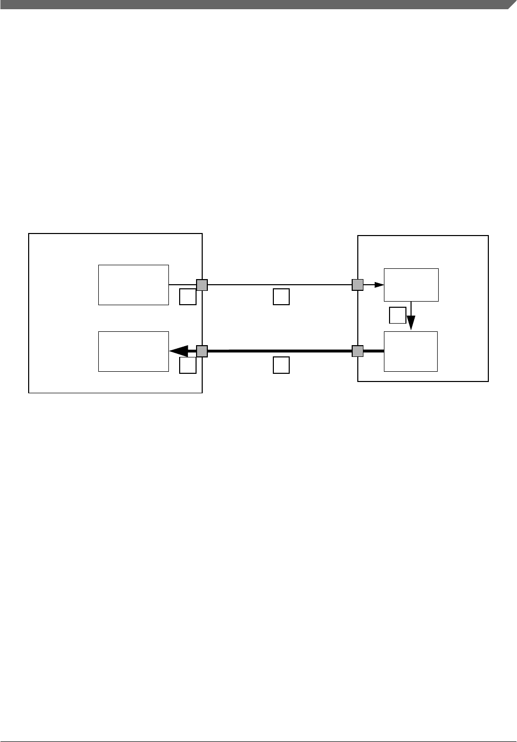
37.12 Sampling of Serial Flash Input Data
37.12.1 Basic Description
QuadSPI is used to read data from the serial flash device. Depending on the actual
implementation, there is a delay between the internal clocking in the QuadSPI module
and the external serial flash device. Refer to the following figure for an overview of this
scheme.
QUADSPI
Clock Gen
Sampling
Serial Flash
Clock
Data
Out
SCK - Serial Flash Clock
SI_IO[0:7] - Serial Flash Data
1
5
2
4
3
Figure 37-8. Serial Flash Sampling Clock Overview
The rising edge of the internal reference clock is taken as timing reference for the data
output of the serial flash. After a time of tDel,total the data arrives at the internal sampling
stage of the QuadSPI module. According to the Serial Flash Sampling Clock Overview
figure, the following parts of the delay chain contribute to tDel,total:
1. Output delay of the serial flash clock output of the device containing the QuadSPI
module
2. Wire delay of application/PCB from the device containing the QuadSPI module to
the external serial flash device
3. Clock to data out delay of the external serial flash device, including input and output
delays
4. Wire delay of application/PCB from the external serial flash device to the device
containing the QuadSPI module
5. Device delay corresponding to the input data
Chapter 37 Quad Serial Peripheral Interface (QuadSPI)
S32K1xx Series Reference Manual, Rev. 7, 04/2018
NXP Semiconductors 985

NOTE
The amount of total delay tDel,total is specific to the
characteristics of the actual implementation. Also, the serial
flash device clock (SCK) is inverted with respect to the
QuadSPI internal reference clock.
37.12.2 Supported read modes
Some modes listed here may not be available on this chip. See the chip-specific QuadSPI
information for the read modes that this chip supports.
37.12.2.1 SDR mode
Most flash memories operate in single data rate (SDR) mode. In SDR mode, the data is
transferred only on one edge of the clock signal. The SDR serial flash memories sample
the incoming data on the rising edge of serial flash clock and drive the output data on the
falling edge of the serial flash clock.
37.12.2.1.1 Internal sampling
NOTE
This mode may not be available on this chip. See the chip-
specific QuadSPI information for the read modes that this chip
supports.
QuadSPI uses different edges of the internal reference clock for sampling the input data
in SDR mode.
Sampling of Serial Flash Input Data
S32K1xx Series Reference Manual, Rev. 7, 04/2018
986 NXP Semiconductors
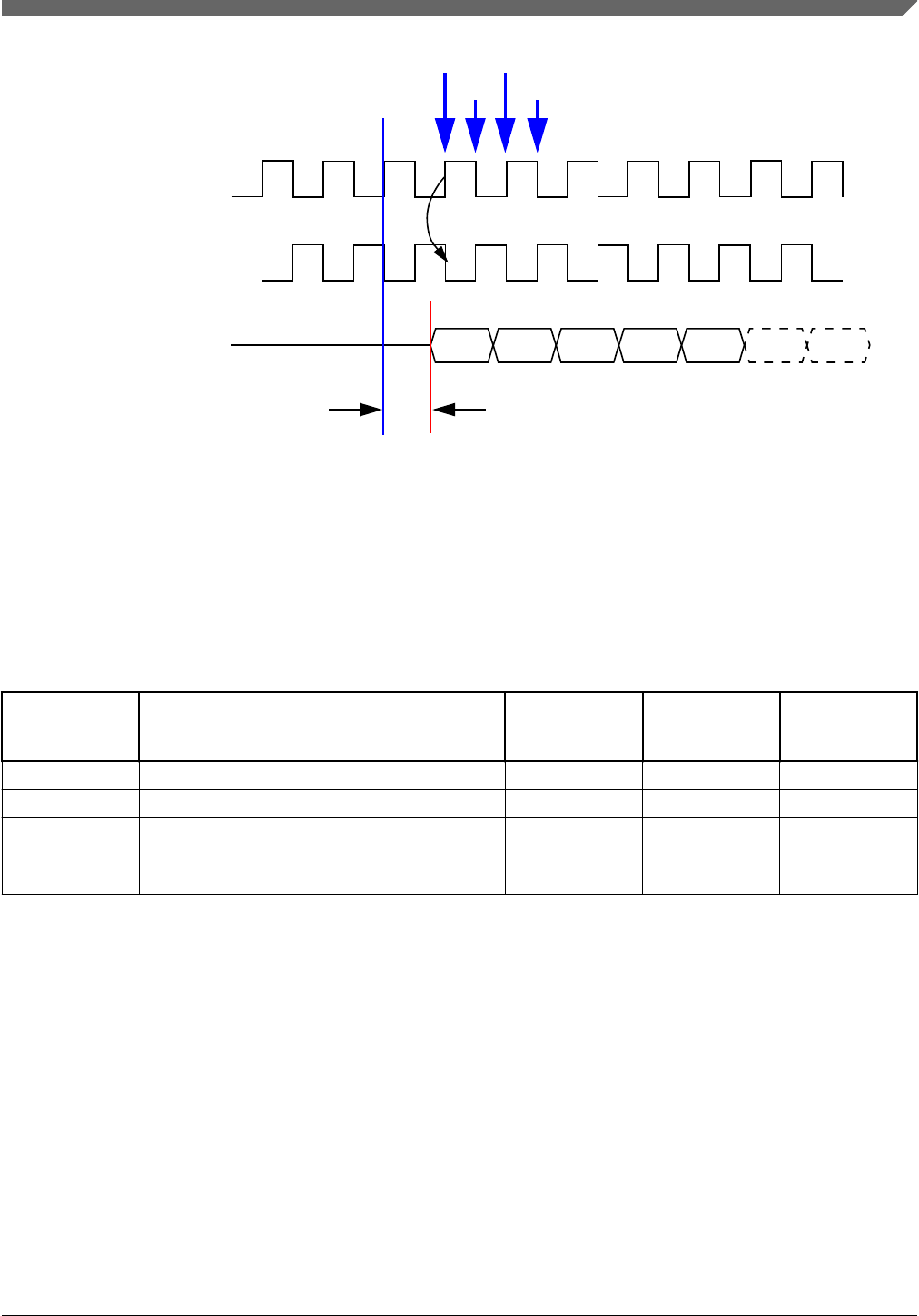
internal reference for serial flash data sampling
internal ref clock
SCK - serial flash clock
serial flash data
tDel,total
Possible Sampling Points
N/1 N/2
I/2
I/1
Figure 37-9. Internal sampling in SDR mode
The possible points in time for sampling incoming data are denoted as N/1, I/1, N/2 and
I/2 above. The sampling point relevant for the internal sampling is configured in the
QSPI_SMPR register. Refer to Sampling Register (QuadSPI_SMPR) for details. The
following table gives an overview of the available configurations for the commands
running at regular (full) speed:
Table 37-42. Sampling Configuration
Sampling Point Description Delay
[FSDLY]
Phase
[FSPHS]
QSPI_SMPR for
Full Speed
Setting1
N/1 sampling with non-inverted clock, 1 sample delay 0 0 0x0000000x
I/1 sampling with inverted clock, 1 sample delay 0 1 0x0000002x
N/2 sampling with non-inverted clock, 2 samples
delay 1 0 0x0000004x
I/2 sampling with inverted clock, 2 samples delay 1 1 0x0000006x
1. 'x' is not considered here
Depending on the actual delay and the serial flash clock frequency, the appropriate
sampling point can be chosen. The following remarks should be considered when
selecting the appropriate setting:
• Theoretically there should be two settings possible to capture the correct data, since
the serial flash output is valid for 1 clock cycle, disregarding rise and fall times and
timing uncertainties.
Chapter 37 Quad Serial Peripheral Interface (QuadSPI)
S32K1xx Series Reference Manual, Rev. 7, 04/2018
NXP Semiconductors 987

• Depending on the timing uncertainties, it may turn out in actual applications that only
one possible sample position remains. This is subject to careful consideration
depending on the actual implementation.
• The delay tDel,total is an absolute size to shift the point in time when the serial flash
data get valid at the QuadSPI input.
• For decreasing frequency of the serial flash clock the distance between the edges
increases. So for large differences in the frequency the required setting may change.
37.12.2.1.2 DQS sampling method
NOTE
This mode may not be available on this chip. See the chip-
specific QuadSPI information for the read modes that this chip
supports.
Data sampling in SDR mode can be supported using the DQS sampling method. Refer to
Data Strobe (DQS) sampling method for more details.
37.12.2.2 DDR Mode
The increasing requirement of improved throughput has introduced the double data rate
(DDR) mode. In DDR mode, the data is transferred on both the rising and falling edges of
the serial flash clock. The DDR serial flashes sample as well as drive the data on both
rising and falling edges of serial flash clock.
37.12.2.2.1 DQS sampling method
NOTE
This mode may not be available on this chip. See the chip-
specific QuadSPI information for the read modes that this chip
supports.
Data sampling in DDR mode can be supported using DQS method. Refer to Data Strobe
(DQS) sampling method for more details.
37.12.3 Data Strobe (DQS) sampling method
Sampling of Serial Flash Input Data
S32K1xx Series Reference Manual, Rev. 7, 04/2018
988 NXP Semiconductors
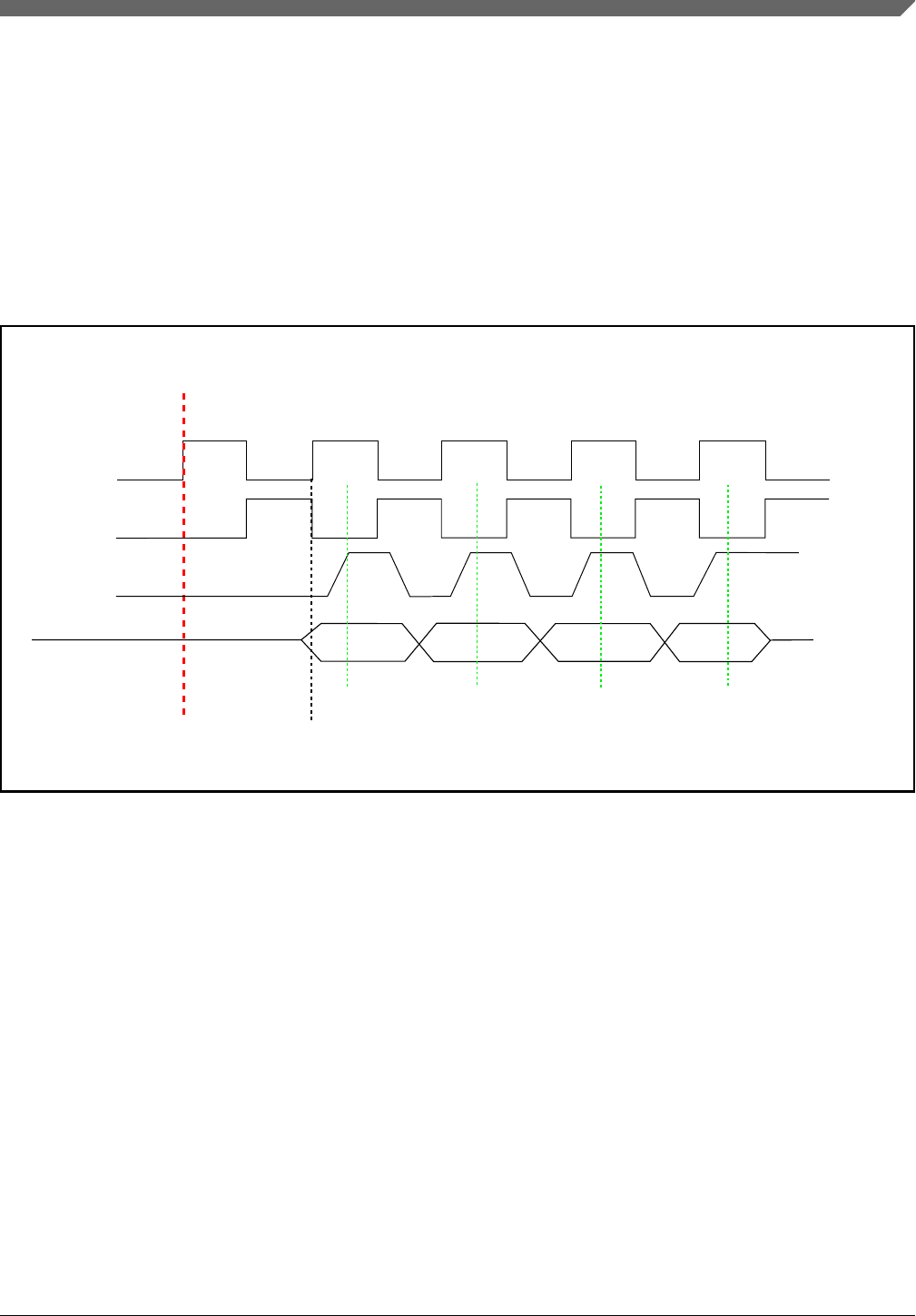
37.12.3.1 Basic Description
In DQS mode, the data strobe signal (DQS/RWDS) is used to sample the read data. Here,
both DQS and the data sent by the flash move in the same direction, so it is relatively
easier to achieve at higher frequencies.
When using DQS for SDR reads, QuadSPI internally samples the incoming data on rising
edge of the strobe signal.
The figure below shows sampling read data in SDR mode using DQS.
Internal Ref
clock
SCK
Data Strobe Signal
Data
internal reference for serial flash data sampling
Data sampled on only rising edge of Data Strobe Signal
Figure 37-10. Data Strobe functionality in SDR mode
When using DQS for DDR reads, QuadSPI internally samples the incoming data on both
the edges of the strobe signal. Refer to the figure below for more detail.
Chapter 37 Quad Serial Peripheral Interface (QuadSPI)
S32K1xx Series Reference Manual, Rev. 7, 04/2018
NXP Semiconductors 989
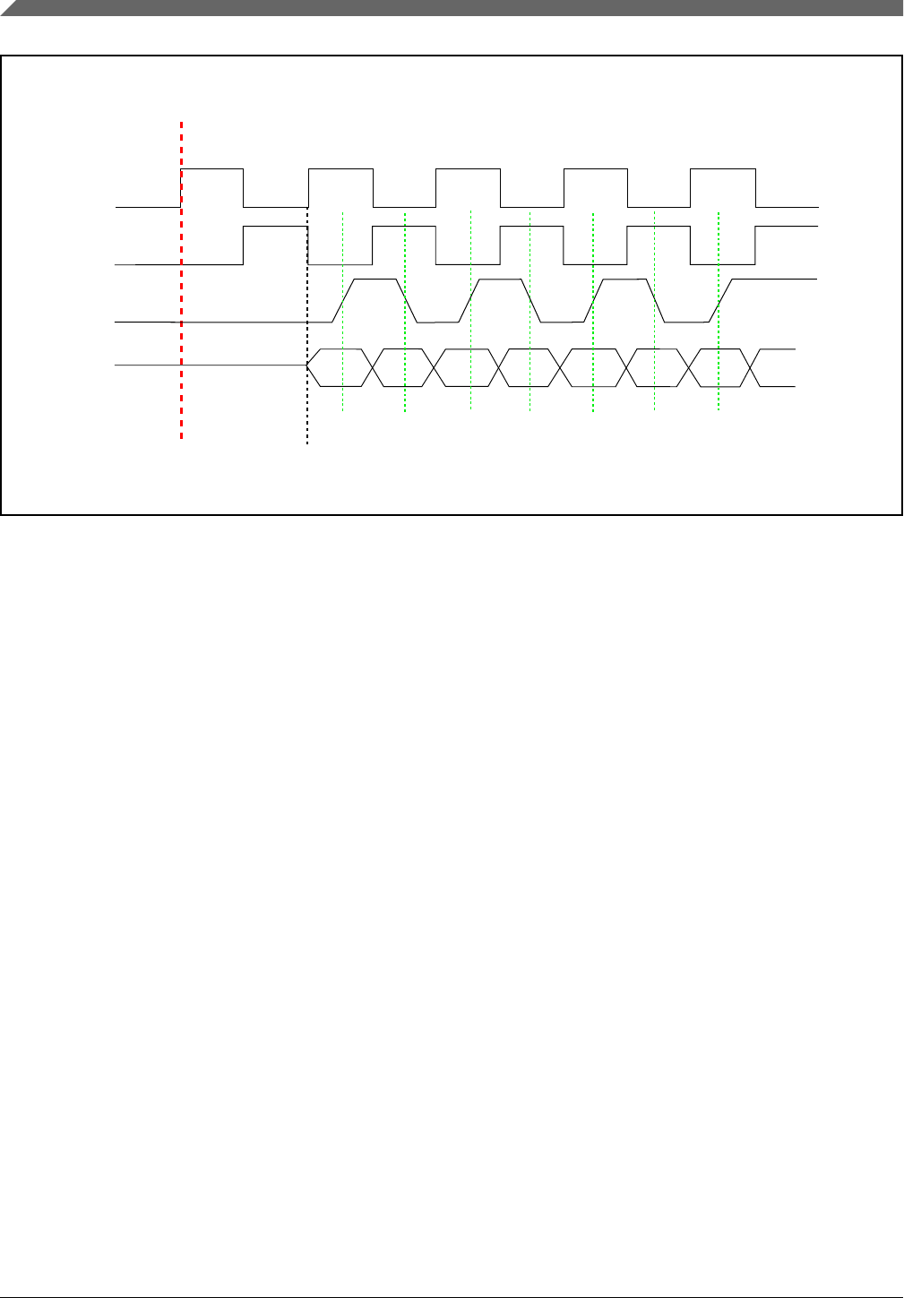
Internal Ref
clock
SCK
Data Strobe Signal
Data
internal reference for serial flash data sampling
Data sampled on both the edges of Data Strobe Signal
Figure 37-11. Data Strobe functionality in DDR mode
37.12.3.2 Internally generated DQS
NOTE
This mode may not be available on this chip. See the chip-
specific QuadSPI information for the read modes that this chip
supports.
In this mode, the internal reference clock is fed as a strobe to QuadSPI for read data
sampling. The data strobe must be generated in a way such that the data is correctly
sampled by the QuadSPI module. This internally generated data strobe signal can be used
by QuadSPI to capture the data in:
• SDR mode
• DDR mode
Refer to QuadSPI chip-specific information for additional details about internally
generated DQS.
Sampling of Serial Flash Input Data
S32K1xx Series Reference Manual, Rev. 7, 04/2018
990 NXP Semiconductors
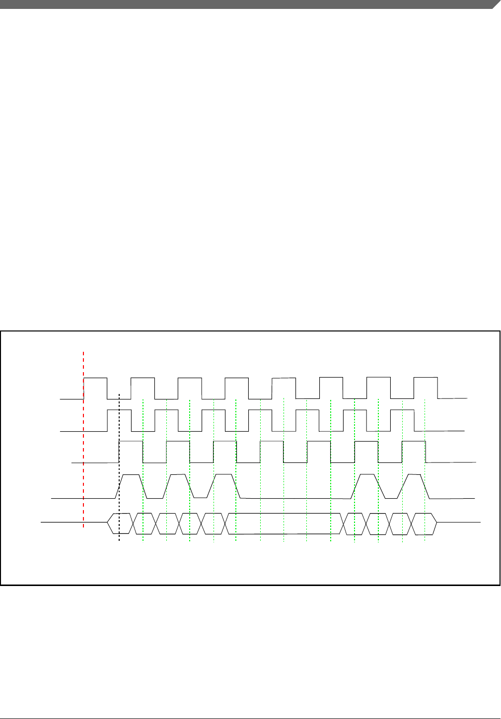
37.12.3.3 External DQS
NOTE
This mode may not be available on this chip. See the chip-
specific QuadSPI information for the read modes that this chip
supports.
In serial flash memories supporting DQS, the data strobe signal is an output from the
flash device that indicates when data is being transferred from the flash to the host
controller. The data is then captured by the controller on:
• Only one edge (either rising or falling edge) of DQS signal in SDR mode
• Both rising/falling edge of the DQS signal in DDR mode
Some serial flash memories (for example, HyperFlash) provide the data strobe output
(RWDS) with latency cycles included in between the ongoing read transaction. The data
is sampled on both the edges of this signal taking into consideration that when no signal
is provided by flash between ongoing transaction, data is not sampled then and at the end
of transaction the required number of data to be fetched remains the same. Refer to the
figure below for more detail.
*RWDS for Spansion's HyperFlash with latency in between
Internal Ref
clock
SCK
Data Strobe Signal*
Data
internal reference for serial flash data sampling
Data sampled on both the edges of Data Strobe Signal
90 degree phase
shifted to SCK
Figure 37-12. Data Strobe functionality with latency included
Chapter 37 Quad Serial Peripheral Interface (QuadSPI)
S32K1xx Series Reference Manual, Rev. 7, 04/2018
NXP Semiconductors 991
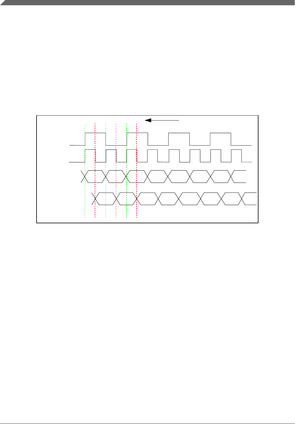
37.13 Data Input Hold Requirement of Flash
In DDR mode, the data is valid only for half clock cycle. It is difficult to meet the data
input hold time requirement of flash. QuadSPI internally delays the data sent to flash so
that it will be easy to meet the hold requirement. The QSPI_FLSHCR[TDH] is used for
this purpose. If QSPI_FLSHCR[TDH] is configured to 0, the data sent to flash is aligned
with the internal reference clock of QuadSPI, if it is 1, then, the data is aligned to 2x
internal reference half clock.
Internal Ref
clock
QSPI_FLSHCR[TDH]
2x Internal
Ref clock
010101
Data aligned to
internal Ref clock
Data aligned to
2x half clock
Figure 37-13. Data Hold
Data Input Hold Requirement of Flash
S32K1xx Series Reference Manual, Rev. 7, 04/2018
992 NXP Semiconductors

Chapter 38
Power Management
38.1 Introduction
This chapter describes the various chip power modes and functionality of the individual
modules in these modes.
38.2 Power modes description
The Power Management Controller (PMC) provides multiple power options allowing
users to optimize power consumption for the level of functionality needed.
Depending on the stop requirements of the user application, a variety of stop modes are
available that provide state retention, partial power down or full power down of certain
logic and/or memory. I/O states are maintained during all power modes. The following
table compares the various power modes available.
For Run and Very Low Power Run (VLPR) modes there are corresponding Stop modes.
Stop modes (VLPS, STOP1, STOP2) are similar to Arm sleep deep mode. VLPR
operating mode can reduce runtime power when maximum bus frequency is not required
to support application needs.
This chip cannot enter a stop mode directly from High Speed Run (HSRUN) mode. To
enter a stop mode from HSRUN, the chip must first transition to Normal Run mode.
After that, it can enter a stop mode.
The two primary modes of operation are Run, Stop. The Wait For Interrupt (WFI)
instruction invokes Stop modes for the chip. The available power modes allow an
application to consume only the power that is necessary for execution.
S32K1xx Series Reference Manual, Rev. 7, 04/2018
NXP Semiconductors 993

NOTE
See Arm documentation for more details on WFI instructions.
Table 38-1. Chip power modes
Chip mode Description Core mode Normal
recovery
method
Normal Run Default mode out of reset; on-chip voltage regulator is on. Run -
High Speed Run
(HSRUN)1Allows maximum performance of the chip. In this mode, the chip can
operate at a higher frequency as compared to Normal Run mode but
with restricted functionalities. See Module operation in available low
power modes for more details. See Internal clocking requirements for
more details.
Run -
Normal Stop (via
WFI instruction)
Places the chip in static state. In this power mode, all registers are
retained and LVD protection is maintained.
• NVIC is disabled.
• AWIC is used to wake up from interrupt.
• Some peripheral clocks are stopped.
See Module operation in available low power modes for more details.
Sleep Deep Interrupt
Very Low Power
Run (VLPR)
On-chip voltage regulator is in a low power mode that supplies only
enough power to run the chip at a reduced frequency.
• Reduced-frequency flash memory access mode (1 MHz)
• LVD off
• SIRC provides a low power 4 MHz source for the core, the bus,
and the peripheral clocks
Run -
Very Low Power
Stop (VLPS, via
WFI instruction)
Places the chip in a static state with Low Voltage Detect (LVD)
operation off. This is the lowest-power mode in which pin interrupts are
functional.
• Some peripheral clocks are stopped. See Module operation in
available low power modes.
• The LPTMR, RTC, and CMP can be used.
• The NVIC is disabled.
• The AWIC is used to wake from interrupt.
• The on-chip voltage regulator is in a low power mode that
supplies only the power needed to run the chip at a reduced
frequency.
• All SRAM is operational (content is retained and I/O states are
maintained).
Sleep Deep Interrupt
1. HSRUN mode is not available in S32K11x series of devices.
NOTE
Before disabling a module, its interrupts and DMA requests
should be disabled.
Power modes description
S32K1xx Series Reference Manual, Rev. 7, 04/2018
994 NXP Semiconductors

38.3 Entering and exiting power modes
The WFI instruction invokes stop modes for the chip. The processor exits the low-power
mode via an interrupt. See Nested Vectored Interrupt Controller (NVIC) Configuration
for a description of interrupt operation and which peripherals can cause interrupts.
38.4 Clocking modes
The following sections describe the supported clocking modes on this chip.
38.4.1 Clock gating
To conserve power, most module clocks can be turned off by configuring the CGC field
of the peripheral control registers in the PCC module. These fields are cleared after any
reset, which disables the Protocol clock of the corresponding module. Before initializing
a module, the corresponding field in the PCC peripheral control register needs to be set to
enable the module clock. Be sure to disable the module before turning off the clock (see
Clock Distribution and PCC for details).
38.4.2 Stop mode options
This chip has two Stop modes:
• STOP1
• STOP2
See the STOPO field in Stop Control Register (SMC_ STOPCTRL ) for more details.
When configured for STOP1, the core clocks, system clocks, and bus clocks are all gated.
When configured for STOP2, only the core and system clocks are gated, but the bus
clock remains active. The bus masters and bus slaves clocked by the system clock enter
Stop mode, but the bus slaves clocked by the bus clock remain in Run mode. The clock
generators in the SCG and the PMC's on-chip regulator also remain in Run mode. The
following can initiate an exit from STOP.
• Reset
• An asynchronous interrupt from a bus master (valid for STOP1)
• A synchronous interrupt from a bus slave clocked by the bus clock (valid for STOP2)
Chapter 38 Power Management
S32K1xx Series Reference Manual, Rev. 7, 04/2018
NXP Semiconductors 995

If configured, a DMA request (using the asynchronous DMA wake-up) can also be used
to exit Stop for the duration of a DMA transfer before the chip transitions back into
STOP2.
38.4.3 DMA wake-up
The DMA can be configured to wake up the device on a DMA request after it is placed in
Stop mode. If this is supported by a peripheral instance then it is said to support Async
DMA in the RM attachment 'S32K1xx_DMA_Interrupt_mapping.xlsx'. Wake-up is
configured per DMA channel and is supported in the following low-power modes:
• Compute Operation
• Stop
• VLPS
When a DMA wake-up is detected in Stop, or VLPS, the chip initiates a normal exit from
the low-power mode. This can include:
• Restoring the internal regulator and internal power switches
• Enabling the clock generators in the SCG
• Enabling the system, bus clocks and flash clock (but not the core clock)
• Negating the stop mode signal to the bus masters and bus slaves
The only difference is that the CPU will remain in low-power mode with the CPU clock
disabled.
During Compute Operation, a DMA wake-up will initiate a normal exit. This includes
enabling the clocks and negating the Stop mode signal to the bus masters and bus slaves.
The core clock always remains enabled during Compute Operation.
Since the DMA wake-up will enable clocks and negate Stop-mode signals to all bus
masters and slaves, software must ensure that bus masters and slaves that are not
involved with the DMA wake-up and transfer remain in a known state. This can be
accomplished by disabling the modules before entry into the low-power mode or by
setting the Doze enable bit in selected modules.
After the DMA request that initiated the wake-up negates, and the DMA completes the
current transfer, the chip transitions back to the original low-power mode. This includes
requesting all non-CPU bus masters to enter Stop mode, then requesting bus slaves to
enter Stop mode. In Stop and VLPS modes, the SCG and PMC would then also enter
their appropriate modes.
Clocking modes
S32K1xx Series Reference Manual, Rev. 7, 04/2018
996 NXP Semiconductors

NOTE
If the requested DMA transfer cannot cause the DMA request
to negate, the device will remain in a higher power state until
the low power mode is fully exited.
An enabled DMA wake-up can cause an aborted entry into low-power mode if the DMA
request asserts during the Stop-mode entry sequence (or reentry if the request asserts
during a DMA wake-up) and can cause the SMC to assert its Stop Abort flag in case
VLPS mode entry was happening. After the DMA wake-up completes, entry into low
power mode starts.
An interrupt that occurs during a DMA wake-up causes an immediate exit from the low-
power mode (this is optional for Compute Operation) without impacting the DMA
transfer.
A DMA wake-up can be generated by either a synchronous or asynchronous DMA
request. Not all peripherals can generate an asynchronous DMA request in stop modes. In
general, if a peripheral can generate synchronous DMA requests and also supports
asynchronous interrupts in stop modes, it can generate an asynchronous DMA request.
NOTE
DMA Enable Asynchronous Request in Stop Register
(DMA_EARS) is used to configure asynchronous DMA request
for each channel.
38.4.4 Compute Operation (CPO)
Compute Operation (CPO) is an execution or compute-only mode of operation that keeps
the CPU enabled with full access to the SRAM and flash memory read port, but places all
other bus masters and bus slaves into their stop mode. CPO can be enabled in Run,
HSRUN, or VLPR modes.
NOTE
Do not enter any stop mode without first exiting CPO. Before
entering to CPO mode, software should make sure that all
ongoing communication should be completed.
Because CPO reuses stop-mode logic (including the staged entry with bus masters
disabled before bus slaves), any bus master or bus slave that can remain functional in
Stop mode also remains functional in CPO. This includes generation of asynchronous
interrupts and DMA requests. When enabling CPO in Run mode, module functionality
for bus masters and slaves is the equivalent of Stop mode. When enabling CPO in VLPR
Chapter 38 Power Management
S32K1xx Series Reference Manual, Rev. 7, 04/2018
NXP Semiconductors 997

mode, module functionality for bus masters and slaves is the equivalent of VLPS mode.
CPO does not affect the SCG, PMC, SRAM, and flash memory read port, although the
flash memory register interface is disabled.
During CPO, the AIPS peripheral space is disabled, and attempted accesses generate bus
errors. The Private Peripheral Bus (PPB) — including the MCM, System Control Space
(SCS) (for NVIC), and SysTick — remains accessible during CPO. Although access to
the GPIO registers is supported, the GPIO port data input registers do not return valid
data since clocks to the Port Control and Interrupt modules are disabled. By writing to the
GPIO port data output registers, it is possible to control those GPIO ports that are
configured as output pins.
CPO is controlled by the MCM's CPO register, which can be accessed only by CPU in
K14x. DMA can also access it in K11x since MCM is out of PPB memory map of CM0+
Core in K11x. Setting or clearing the MCM's CPOREQ field initiates entry or exit into
CPO. CPO can also be configured to exit automatically when it detects an interrupt,
which is required in order to service most interrupts. Only the core system interrupts
(NMI and SysTick are exceptions) and any edge sensitive interrupts can be serviced
without exiting CPO.
When entering CPO, the CPOACK status field indicates when entry has completed.
When exiting CPO in Run mode, CPOACK negates immediately. When exiting CPO in
VLPR mode, the exit is delayed. This allows the PMC to manage the change in power
consumption. This delay means CPOACK is polled to determine when the AIPS
peripheral space can be accessed without generating a bus error.
The DMA wake-up is also supported during CPO and causes CPOACK status to clear
and the AIPS peripheral space to be accessible for the duration of the DMA wake-up.
After the DMA wake-up completes, the chip transitions back into CPO.
NOTE
Peripherals (like External QSPI flash memory) operating on
SYS_CLK should not be accessed in CPO mode.
38.4.5 Peripheral Doze
Several peripherals support Peripheral Doze mode. In this mode, a register field can be
used to disable the peripheral for the duration of a low-power mode.
Peripheral Doze is defined to include all of the modes of operation as follows:
Clocking modes
S32K1xx Series Reference Manual, Rev. 7, 04/2018
998 NXP Semiconductors
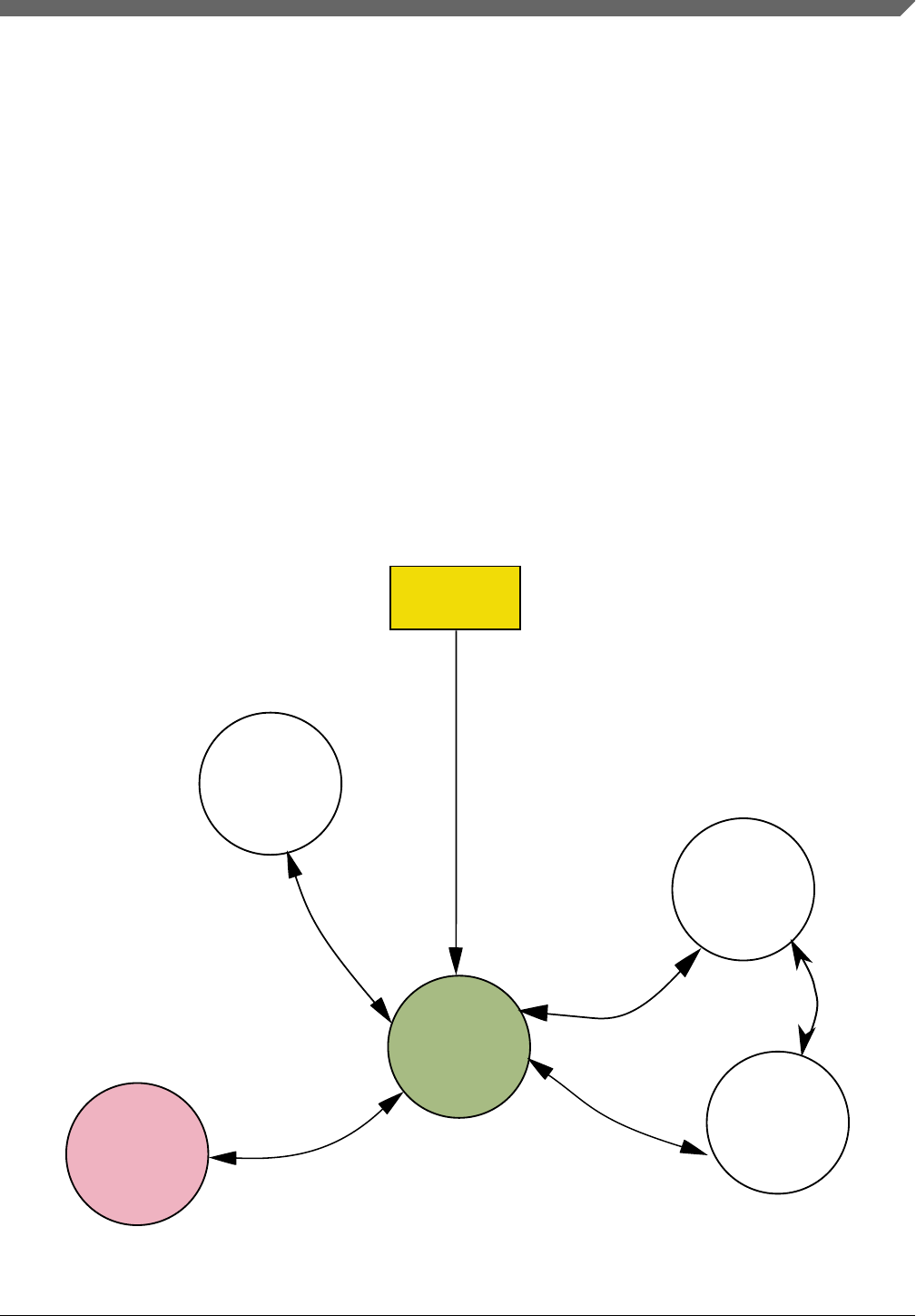
• The CPU is in Stop mode, including the entry sequence and for the duration of a
DMA wake-up.
• The CPU is in Compute Operation, including the entry sequence and for the duration
of a DMA wake-up.
It can also be used to disable selected bus slaves immediately on entry into any stop mode
(or CPO), instead of waiting for the bus masters to acknowledge the entry as part of the
stop entry sequence. Finally, it can be used to disable selected bus masters or slaves that
should remain inactive during a DMA wake-up.
38.5 Power mode transitions
The following figure shows the power mode transitions. Any reset always brings the chip
back to the Normal Run state. In run, stop modes active power regulation is enabled. The
VLPR modes offer a lower power operating mode than normal modes. VLPR is limited
in frequency.
STOP1/
STOP2
RUN
VLPS
VLPR
Any RESET
HSRUN
5
1
2
4
3
Figure 38-1. Power mode state transition diagram
Chapter 38 Power Management
S32K1xx Series Reference Manual, Rev. 7, 04/2018
NXP Semiconductors 999

NOTE
See Figure 39-1 in the SMC chapter for more detailed mode
transition conditions.
38.6 Shutdown sequencing for power modes
When entering stop or other low-power mode, clocks are shut off in an orderly sequence
to safely place the chip in the targeted low-power state. All low-power entry sequences
are initiated by the core executing a WFI instruction. The Arm core's outputs,
SLEEPDEEP and SLEEPING, trigger entry to the various low-power modes:
• Low power modes equate to: SLEEPING & SLEEPDEEP
When entering low power modes, the chip performs the following sequence:
Table 38-2. Low power entry sequence
Step Action
1 The chip immediately shuts off core and system clocks to the Arm Cortex-M4 core.
2 The chip polls the stop-acknowledge indications from the non-core crossbar masters (DMA), supporting
peripherals (SPI, PIT), and the flash memory controller for indications that system clocks, bus clock, and/or
flash memory clock need to be left enabled to complete a previously initiated operation, effectively stalling
entry to the targeted low power mode. When all acknowledges are detected, system clock, bus clock and
flash memory clock are turned off simultaneously.
3 The SCG and Mode Controller shut off clock sources and/or the internal supplies driven from the internal
regulator as defined for the targeted low power mode.
The debugger modules support transitions from Stop, VLPS back to a halted state when
the debugger is enabled. This transition is initiated by setting the Debug Request field in
the MDM-AP control register. As part of this transition, system clocking is reestablished
and is equivalent to Normal Run/VLPR mode clocking configuration.
38.7 Power mode restrictions on flash memory programming
The flash memory should not be programmed or erased while the chip is operating in:
• VLPR mode
• HSRUN mode
No FTFC commands of any type, including CSE commands (for CSEc parts), are
available when the chip is in these modes.
Shutdown sequencing for power modes
S32K1xx Series Reference Manual, Rev. 7, 04/2018
1000 NXP Semiconductors

38.8 Module operation in available low power modes
Table 38-4 illustrates module functionality in each of the available modes.
Debug modules are discussed separately; see Debug in low-power modes.
NOTE
S32K1xx device does not support WAIT, VLPW and low
leakage modes (power gating mode).
Table 38-3 defines some frequently-used terms and abbreviations in Table 38-4.
Table 38-3. Terms and abbreviations
Term Definition
Async operation Fully functional with alternate clock source (if the selected clock source remains enabled).
FF Full functionality. In VLPR the system frequency is limited, but if a module does not have a functional
limitation, it is still listed as FF.
Low power Memory is powered to retain contents in a lower-power state.
OFF Module and clock sources are disabled.
Powered Memory is powered to retain contents.
Wake-up Modules can serve as a wake-up source for the chip.
Table 38-4. Module operation in available low power modes
Modules VLPR1STOP(STOP1/
STOP2)
VLPS1RUN HSRUN
Core Modules
NVIC FF OFF OFF FF FF
System Modules
System Mode
Controller/ Power
Mangement Controller
FF FF FF FF FF
Regulator Low power mode
(LPM)
Full
performance
Mode (FPM)
Low power mode (LPM) Full
performance
Mode (FPM)
Full
performance
Mode (FPM)
LVD/LVR LVD Disabled/LVR
active
Both Active LVD Disabled/LVR Active Both Active Both Active
Brown-out Detection FF FF FF FF FF
DMA FF Async
operation
Async operation FF FF
Watchdog FF
(Only SIRC and
LPO Clock as
source)
Async
operation
(STOP bit
Async operation (STOP bit
needs to be set). Async
Wakeup
FF FF
Table continues on the next page...
Chapter 38 Power Management
S32K1xx Series Reference Manual, Rev. 7, 04/2018
NXP Semiconductors 1001

Table 38-4. Module operation in available low power modes (continued)
Modules VLPR1STOP(STOP1/
STOP2)
VLPS1RUN HSRUN
needs to be
set) STOP1, FF
in STOP2
EWM FF (LPO Clock as
source)
Static in
STOP1, FF in
STOP2
OFF FF FF
Clocks
128 kHz LPO FF FF FF FF FF
PLL OFF 2FF OFF 2FF FF
SIRC FF FF FF FF FF
FIRC OFF 2FF OFF 2FF FF
System oscillator (OSC) OFF 2FF OFF 2FF FF
SCG Only SIRC is
available
All clock
sources are
available
Only SIRC is available All clock
sources are
available
All clock
sources are
available
Core clock 4 MHz max (SIRC
as a source)
OFF OFF 80 MHz max
(PLL as a
source)/48 MHz
max (FIRC as a
source)
112 MHz max
(PLL as a
source)
Flash clock 1 MHz max (SIRC
as a source)
OFF in STOP1,
Available in
STOP2
OFF 26.67 MHz max
(PLL as a
source)/24 MHz
max (FIRC as a
source)
28 MHz max
(PLL as a
source)
System clock 4 MHz max
(SIRC as a source)
OFF OFF 80 MHz max
(PLL as a
source)/48 MHz
max (FIRC as a
source)
112 MHz max
(PLL as a
source)
Bus clock 4 MHz max (SIRC
as a source)
OFF in STOP1,
Available in
STOP2
OFF 48 MHz max
(FIRC as a
source)/40 MHz
max (PLL as a
source)
56 MHz max
(PLL as a
source)
Memory and memory interfaces
Flash memory Only read
operation can be
done (1 MHz max).
No FTFC
commands of any
type, including
CSE commands
(for CSEc parts),
are available.
Low power (no
read and
program/erase)
Low power (no read and
program/erase)
FF Only read
operation can
be done. No
FTFC
commands of
any type,
including CSE
commands (for
CSEc parts),
are available.
Table continues on the next page...
Module operation in available low power modes
S32K1xx Series Reference Manual, Rev. 7, 04/2018
1002 NXP Semiconductors

Table 38-4. Module operation in available low power modes (continued)
Modules VLPR1STOP(STOP1/
STOP2)
VLPS1RUN HSRUN
System RAM (SRAM_U
and SRAM_L)
Low power (read
and write
operation)
Low power (no
read and write)
Low power (no read and
write)
FF FF
Cache Low power (read
and write
operation)
Low power (no
read and write)
Low power (no read and
write)
FF FF
FlexMemory as
EEPROM Emulation
Low power (read
and write
operation). Only
read operation can
be done. No FTFC
commands.
Low power (no
read and write)
Low power (no read and
write)
FF Only read
operation can
be done. No
FTFC
commands.
FlexMemory (FlexRAM
as traditional SRAM)
Low power (read
and write
operation)
Low power (no
read and write)
Low power (no read and
write)
FF FF
ENET FF ( only SIRC as
a source)
Magic Packet
Wakeup
supported in
both STOP1
and STOP1
OFF FF FF
QuadSPI FF ( only SIRC as
a source)
OFF in
STOP1 , FF in
STOP2(when
BUS_CLK
clock source is
selected)
OFF FF FF
SAI FF ( only SIRC as
a source)
OFF in
STOP1 , FF in
STOP2
OFF FF FF
Communication interfaces
LPUART FF ( only SIRC as
a source)
Async
operation in
STOP1, FF in
STOP2
Async operation FF FF
LPSPI FF ( only SIRC as
a source)
Async
operation in
STOP1, FF in
STOP2
Async operation FF FF
LPI2C FF ( only SIRC as
a source)
Async
operation in
STOP1, FF in
STOP2
Async operation FF FF
FlexIO FF ( only SIRC as
a source)
Async
operation in
STOP1, FF in
STOP2
OFF FF FF
Table continues on the next page...
Chapter 38 Power Management
S32K1xx Series Reference Manual, Rev. 7, 04/2018
NXP Semiconductors 1003

Table 38-4. Module operation in available low power modes (continued)
Modules VLPR1STOP(STOP1/
STOP2)
VLPS1RUN HSRUN
CAN FF ( only SIRC as
a source)
PNET
supported in
both STOP1
and STOP2 for
CAN0
OFF FF FF
Safety
CRC FF OFF in STOP1
Available in
STOP2
OFF FF FF
Timers
FTM FF (Only SIRC as
a source)
OFF OFF FF FF
LPIT FF (Only SIRC as
a source)
Async
operation in
STOP1, FF in
STOP2
Async operation FF FF
PDB FF (Only SIRC as
source)
OFF OFF FF FF
LPTMR FF (Only SIRC as
a source)
Async
operation in
STOP1, FF in
STOP2
Async operation FF FF
RTC FF (Only SIRC as
a source)
Async
operation in
STOP1, FF in
STOP2
Async operation FF FF
Analog
12-bit ADC OFF OFF in STOP1,
FF in STOP2
OFF FF FF
CMP3LS compare only HS or LS
compare
FF in STOP2
LS compare only FF FF
Human Machine Interface
GPIO/PORT FF Async
operation in
STOP1, FF in
STOP2
OFF 4FF FF
1. PMC_REGSC[BIASEN] must be set to 1 when using VLP* modes.
2. Module must be disabled by software in RUN mode before any mode transition.
3. In Stop or VLPS modes, the CMP supports high-speed or low-speed external pin-to-pin or external-pin-to-DAC compares.
Windowed, sampled & filtered modes of operation are not available while in stop or VLPS modes.
4. Device can support ASYNC wakeup from VLPS through GPIO. Refer to table AWIC stop and VLPS wake-up sources for
details
Module operation in available low power modes
S32K1xx Series Reference Manual, Rev. 7, 04/2018
1004 NXP Semiconductors

38.9 QuadSPI, Ethernet, and SAI operation
The application should ensure that the voltage is in the range of 3.3 V ±10% during a
running application of QuadSPI, Ethernet, and SAI. If the external supply voltage is not
in the range of 3.3 V ±10%, then it could lead to erroneous communication. In case
S32K148 is being used for an application not using QuadSPI, Ethernet, and SAI, then the
on chip voltage monitor ensures the operation as per the specifications present in the
S32K1xx Datasheet (See table LVR, LVD and POR operating requirements).
Chapter 38 Power Management
S32K1xx Series Reference Manual, Rev. 7, 04/2018
NXP Semiconductors 1005

QuadSPI, Ethernet, and SAI operation
S32K1xx Series Reference Manual, Rev. 7, 04/2018
1006 NXP Semiconductors

Chapter 39
System Mode Controller (SMC)
39.1 Introduction
The System Mode Controller (SMC) is responsible for sequencing the system into and
out of all low-power Stop and Run modes.
Specifically, it monitors events to trigger transitions between power modes while
controlling the power, clocks, and memories of the system to achieve the power
consumption and functionality of that mode.
This chapter describes all the available low-power modes, the sequence followed to enter/
exit each mode, and the functionality available while in each of the modes.
The SMC is able to function during even the deepest low power modes.
See AN4503: Power Management for Kinetis MCUs for further details on using the
SMC.
39.2 Modes of operation
The Arm CPU has three primary modes of operation:
• Run
• Sleep
• Deep Sleep
The WFI instruction is used to invoke Sleep and Deep Sleep modes. Run and Stop are the
common terms used for the primary operating modes. The following table shows the
translation between the Arm CPU mode and the MCU power modes. RUN is mapped to
RUN/VLPR and Deep Sleep is mapped to STOP/VLPS.
S32K1xx Series Reference Manual, Rev. 7, 04/2018
NXP Semiconductors 1007

Arm CPU mode MCU mode
RUN RUN/VLPR
Deep Sleep Stop/VLPS
In addition, MCUs also augment Stop and Run modes in a number of ways. The power
management controller (PMC) contains a run and a stop mode regulator. Run regulation
is used in normal run and stop modes. Stop mode regulation is used during all very low
power and low leakage modes. During stop mode regulation, the bus frequencies are
limited in the very low power modes.
The SMC provides the user with multiple power options. The Very Low Power Run
(VLPR) mode can drastically reduce run time power when maximum bus frequency is
not required to handle the application needs. From Normal Run mode, the Run Mode
(RUNM) field can be modified to change the MCU into VLPR mode when limited
frequency is sufficient for the application. From VLPR mode, a corresponding stop
(VLPS) mode can be entered.
Depending on the needs of the user application, a variety of stop modes are available that
allow the state retention, partial power down or full power down of certain logic and/or
memory. I/O states are held in all modes of operation. Several registers are used to
configure the various modes of operation for the device.
The following table describes the power modes available for the device.
Table 39-1. Power modes
Mode Description
RUN The MCU can be run at full speed and the internal supply is fully regulated, that is, in run regulation.
This mode is also referred to as Normal Run mode.
HSRUN The MCU can be run at a faster frequency compared with RUN mode and the internal supply is fully
regulated. See the Power Management chapter for details about the maximum allowable
frequencies.
STOP The core clock is gated off. There are two variants of stop mode - STOP1 and STOP2 . In STOP1
system clock as well as bus clocks are gated . In STOP2 bus clocks keep running whereas system
clocks are gated.
VLPR The core, system, bus, and flash clock maximum frequencies are restricted in this mode. See the
Power Management chapter for details about the maximum allowable frequencies.
VLPS The core clock is gated off. System clocks to other masters and bus clocks are gated off after all
stop acknowledge signals from supporting peripherals are valid.
NOTE
If the system clock is changed during the mode transition, the
recommendation is to stall the communications for all the
peripherals.
Modes of operation
S32K1xx Series Reference Manual, Rev. 7, 04/2018
1008 NXP Semiconductors

39.3 Memory map and register descriptions
Information about the registers related to the system mode controller can be found here.
NOTE
Bit fields related to HSRUN are Reserved for S32K11x
variants.
Different SMC registers reset on different reset types. Each register's description provides
details. For more information about the types of reset on this chip, refer to the Reset
section details.
NOTE
The SMC registers can be written only in supervisor mode.
Write accesses in user mode are blocked and will result in a bus
error.
NOTE
Before executing the WFI instruction, the last register written to
must be read back. This ensures that all register writes
associated with setting up the low power mode being entered
have completed before the MCU enters the low power mode.
Failure to do this may result in the low power mode not being
entered correctly.
SMC memory map
Address
offset (hex) Register name Width
(in bits) Access Reset value Section/
page
0 SMC Version ID Register (SMC_VERID) 32 R 0100_0000h 39.3.1/1010
4 SMC Parameter Register (SMC_PARAM) 32 R See section 39.3.2/1011
8 Power Mode Protection register (SMC_PMPROT) 32 R/W 0000_0000h 39.3.3/1012
C Power Mode Control register (SMC_PMCTRL) 32 R/W 0000_0000h 39.3.4/1013
10 Stop Control Register (SMC_STOPCTRL) 32 R/W 0000_0003h 39.3.5/1015
14 Power Mode Status register (SMC_PMSTAT) 32 R 0000_0001h 39.3.6/1017
Chapter 39 System Mode Controller (SMC)
S32K1xx Series Reference Manual, Rev. 7, 04/2018
NXP Semiconductors 1009

39.3.1 SMC Version ID Register (SMC_VERID)
Address: 0h base + 0h offset = 0h
Bit 31 30 29 28 27 26 25 24 23 22 21 20 19 18 17 16 15 14 13 12 11 10 9 8 7 6 5 4 3 2 1 0
RMAJOR MINOR FEATURE
W
Reset 0 0 0 0 0 0 0 1 0 0 0 0 0 0 0 0 0 0 0 0 0 0 0 0 0 0 0 0 0 0 0 0
SMC_VERID field descriptions
Field Description
31–24
MAJOR
Major Version Number
This read only field returns the major version number for the module specification.
23–16
MINOR
Minor Version Number
This read only field returns the minor version number for the module specification.
FEATURE Feature Specification Number
This read only field returns the feature set number.
0x0000 Standard features implemented
Memory map and register descriptions
S32K1xx Series Reference Manual, Rev. 7, 04/2018
1010 NXP Semiconductors

39.3.2 SMC Parameter Register (SMC_PARAM)
Address: 0h base + 4h offset = 4h
Bit 31 30 29 28 27 26 25 24 23 22 21 20 19 18 17 16
R0
W
Reset 0 0 0 0 0 0 0 0 0 0 0 0 0 0 0 0
Bit 15 14 13 12 11 10 9 8 7 6 5 4 3 2 1 0
R0 0
EVLLS0
ELLS2
0
ELLS
0
EHSRUN
W
Reset 0 0 0 0 0 0 0 0 0 0 0 0 0 0 0 1
SMC_PARAM field descriptions
Field Description
31–8
Reserved
This field is reserved.
This read-only field is reserved and always has the value 0.
7
Reserved
This field is reserved.
This read-only field is reserved and always has the value 0.
6
EVLLS0
Existence of VLLS0 feature
This static bit states whether or not the feature is available on the device.
0 The feature is not available.
1 The feature is available.
5
ELLS2
Existence of LLS2 feature
This static bit states whether or not the feature is available on the device.
0 The feature is not available.
1 The feature is available.
Table continues on the next page...
Chapter 39 System Mode Controller (SMC)
S32K1xx Series Reference Manual, Rev. 7, 04/2018
NXP Semiconductors 1011

SMC_PARAM field descriptions (continued)
Field Description
4
Reserved
This field is reserved.
This read-only field is reserved and always has the value 0.
3
ELLS
Existence of LLS feature
This static bit states whether or not the feature is available on the device.
0 The feature is not available.
1 The feature is available.
2–1
Reserved
This field is reserved.
This read-only field is reserved and always has the value 0.
0
EHSRUN
Existence of HSRUN feature
This static bit states whether or not the feature is available on the device.
0 The feature is not available.
1 The feature is available.
39.3.3 Power Mode Protection register (SMC_PMPROT)
This register provides protection for entry into any low-power run or stop mode. The
enabling of the low-power run or stop mode occurs by configuring the Power Mode
Control register (PMCTRL).
The PMPROT register can be written only once after any system reset.
If the MCU is configured for a disallowed or reserved power mode, the MCU remains in
its current power mode. For example, if the MCU is in normal RUN mode and AVLP is
0, an attempt to enter VLPR mode using PMCTRL[RUNM] is blocked and
PMCTRL[RUNM] remains 00b, indicating the MCU is still in Normal Run mode.
NOTE
This register is reset on Chip Reset and by reset types that
trigger Chip Reset. It is unaffected by reset types that do not
trigger Chip Reset. See the Reset section details for more
information.
Address: 0h base + 8h offset = 8h
Bit 31 30 29 28 27 26 25 24 23 22 21 20 19 18 17 16
R0
W
Reset 0 0 0 0 0 0 0 0 0 0 0 0 0 0 0 0
Memory map and register descriptions
S32K1xx Series Reference Manual, Rev. 7, 04/2018
1012 NXP Semiconductors

Bit 15 14 13 12 11 10 9 8 7 6 5 4 3 2 1 0
R0
AHSRUN
0
AVLP
0 0 0 0 0
W
Reset 0 0 0 0 0 0 0 0 0 0 0 0 0 0 0 0
SMC_PMPROT field descriptions
Field Description
31–8
Reserved
This field is reserved.
This read-only field is reserved and always has the value 0.
7
AHSRUN
Allow High Speed Run mode
Provided the appropriate control bits are set up in PMCTRL, this write-once field allows the MCU to enter
High Speed Run mode (HSRUN).
0 HSRUN is not allowed
1 HSRUN is allowed
6
Reserved
This field is reserved.
This read-only field is reserved and always has the value 0.
5
AVLP
Allow Very-Low-Power Modes
Provided the appropriate control bits are set up in PMCTRL, this write-once field allows the MCU to enter
any very-low-power mode (VLPR and VLPS).
0 VLPR and VLPS are not allowed.
1 VLPR and VLPS are allowed.
4
Reserved
This field is reserved.
This read-only field is reserved and always has the value 0.
3
Reserved
This field is reserved.
This read-only field is reserved and always has the value 0.
2
Reserved
This field is reserved.
This read-only field is reserved and always has the value 0.
1
Reserved
This field is reserved.
This read-only field is reserved and always has the value 0.
0
Reserved
This field is reserved.
This read-only field is reserved and always has the value 0.
39.3.4 Power Mode Control register (SMC_PMCTRL)
The PMCTRL register controls entry into low-power Run and Stop modes, provided that
the selected power mode is allowed via an appropriate setting of the protection
(PMPROT) register.
NOTE
This register is reset on Chip POR and by reset types that
trigger Chip POR. It is unaffected by reset types that do not
Chapter 39 System Mode Controller (SMC)
S32K1xx Series Reference Manual, Rev. 7, 04/2018
NXP Semiconductors 1013

trigger Chip POR. See the Reset section details for more
information.
Address: 0h base + Ch offset = Ch
Bit 31 30 29 28 27 26 25 24 23 22 21 20 19 18 17 16
R0
W
Reset 0 0 0 0 0 0 0 0 0 0 0 0 0 0 0 0
Bit 15 14 13 12 11 10 9 8 7 6 5 4 3 2 1 0
R0
RUNM
0
VLPSA
STOPM
W
Reset 0 0 0 0 0 0 0 0 0 0 0 0 0 0 0 0
SMC_PMCTRL field descriptions
Field Description
31–7
Reserved
This field is reserved.
This read-only field is reserved and always has the value 0.
6–5
RUNM
Run Mode Control
When written, causes entry into the selected run mode. Writes to this field are blocked if the protection
level has not been enabled using the PMPROT register.
NOTE: RUNM may be set to VLPR only when PMSTAT=RUN. After being written to VLPR, RUNM
should not be written back to RUN until PMSTAT=VLPR.
NOTE: RUNM may be set to HSRUN only when PMSTAT=RUN. After being programmed to HSRUN,
RUNM should not be programmed back to RUN until PMSTAT=HSRUN. Also, stop mode entry
should not be attempted while RUNM=HSRUN or PMSTAT=HSRUN.
When in any mode, any reset clears RUNM and causes the system to exit to normal RUN mode after the
MCU exits its reset flow.
00 Normal Run mode (RUN)
01 Reserved
10 Very-Low-Power Run mode (VLPR)
11 High Speed Run mode (HSRUN)
Table continues on the next page...
Memory map and register descriptions
S32K1xx Series Reference Manual, Rev. 7, 04/2018
1014 NXP Semiconductors

SMC_PMCTRL field descriptions (continued)
Field Description
4
Reserved
This field is reserved.
This read-only field is reserved and always has the value 0.
3
VLPSA
Very Low Power Stop Aborted
When set, this read-only status bit indicates an interrupt occured during the previous stop mode entry
sequence, preventing the system from entering that mode. This field is cleared by reset or by hardware at
the beginning of any stop mode entry sequence and is set if the sequence was aborted.
NOTE: This bit will not get set if STOP1/STOP2 get aborted.
0 The previous stop mode entry was successful.
1 The previous stop mode entry was aborted.
STOPM Stop Mode Control
When written, controls entry into the selected stop mode when Sleep-Now or Sleep-On-Exit mode is
entered with SLEEPDEEP=1 . Writes to this field are blocked if the protection level has not been enabled
using the PMPROT register. After any system reset, this field is cleared by hardware on any successful
write to the PMPROT register.
NOTE: When set to STOP, the STOPO bits in the STOPCTRL register must be used to select the
variants of stop - STOP1/STOP2.
000 Normal Stop (STOP)
001 Reserved
010 Very-Low-Power Stop (VLPS)
011 Reserved
101 Reserved
110 Reseved
111 Reserved
39.3.5 Stop Control Register (SMC_ STOPCTRL )
The STOPCTRL register provides various control bits allowing the user to fine tune
power consumption during the stop mode selected by the STOPM field.
NOTE
This register is reset on Chip POR and by reset types that
trigger Chip POR. It is unaffected by reset types that do not
trigger Chip POR. See the Reset section details for more
information.
Chapter 39 System Mode Controller (SMC)
S32K1xx Series Reference Manual, Rev. 7, 04/2018
NXP Semiconductors 1015

Address: 0h base + 10h offset = 10h
Bit 31 30 29 28 27 26 25 24 23 22 21 20 19 18 17 16
R0
W
Reset 0 0 0 0 0 0 0 0 0 0 0 0 0 0 0 0
Bit 15 14 13 12 11 10 9 8 7 6 5 4 3 2 1 0
R0
STOPO
0 0
Reserved
0
W
Reset 0 0 0 0 0 0 0 0 0 0 0 0 0 0 1 1
SMC_STOPCTRL field descriptions
Field Description
31–8
Reserved
This field is reserved.
This read-only field is reserved and always has the value 0.
7–6
STOPO
Stop Option
These bits control stop operation when STOPM=STOP. When entering Stop mode from RUN mode, the
PMC, SCG and flash remain fully powered, allowing the device to wakeup almost instantaneously at the
expense of higher power consumption. In STOP2, only system clocks are gated allowing peripherals
running on bus clock to remain fully functional. In STOP1, both system and bus clocks are gated.
00 Reserved
01 STOP1 - Stop with both system and bus clocks disabled
10 STOP2 - Stop with system clock disabled and bus clock enabled
11 Reserved
5
Reserved
This field is reserved.
This read-only field is reserved and always has the value 0.
4
Reserved
This field is reserved.
This read-only field is reserved and always has the value 0.
3
Reserved
This field is reserved.
This bit is reserved for future expansion. Software should write 0 to this bit to maintain compatibility.
Reserved This field is reserved.
This read-only field is reserved and always has the value 0.
Memory map and register descriptions
S32K1xx Series Reference Manual, Rev. 7, 04/2018
1016 NXP Semiconductors

39.3.6 Power Mode Status register (SMC_PMSTAT)
PMSTAT is a read-only, one-hot register which indicates the current power mode of the
system.
NOTE
This register is reset on Chip POR and by reset types that
trigger Chip POR. It is unaffected by reset types that do not
trigger Chip POR. See the Reset section details for more
information.
When in any mode, any reset causes the system to exit to normal RUN mode after the
MCU exits its reset flow. The PMSTAT field is then automatically updated to show RUN
as the current power mode.
Address: 0h base + 14h offset = 14h
Bit 31 30 29 28 27 26 25 24 23 22 21 20 19 18 17 16 15 14 13 12 11 10 9 8 7 6 5 4 3 2 1 0
R0 PMSTAT
W
Reset 0 0 0 0 0 0 0 0 0 0 0 0 0 0 0 0 0 0 0 0 0 0 0 0 0 0 0 0 0 0 0 1
SMC_PMSTAT field descriptions
Field Description
31–8
Reserved
This field is reserved.
This read-only field is reserved and always has the value 0.
PMSTAT Power Mode Status
NOTE: When debug is enabled, the PMSTAT will not update to STOP or VLPS
NOTE: When a STOP mode is enabled, the PMSTAT will not update to STOP
0000_0001 Current power mode is RUN.
0000_0010 Reserved.
0000_0100 Current power mode is VLPR.
0000_1000 Reserved.
0001_0000 Current power mode is VLPS.
0010_0000 Reserved
0100_0000 Reserved
1000_0000 Current power mode is HSRUN
39.4 Functional description
Chapter 39 System Mode Controller (SMC)
S32K1xx Series Reference Manual, Rev. 7, 04/2018
NXP Semiconductors 1017
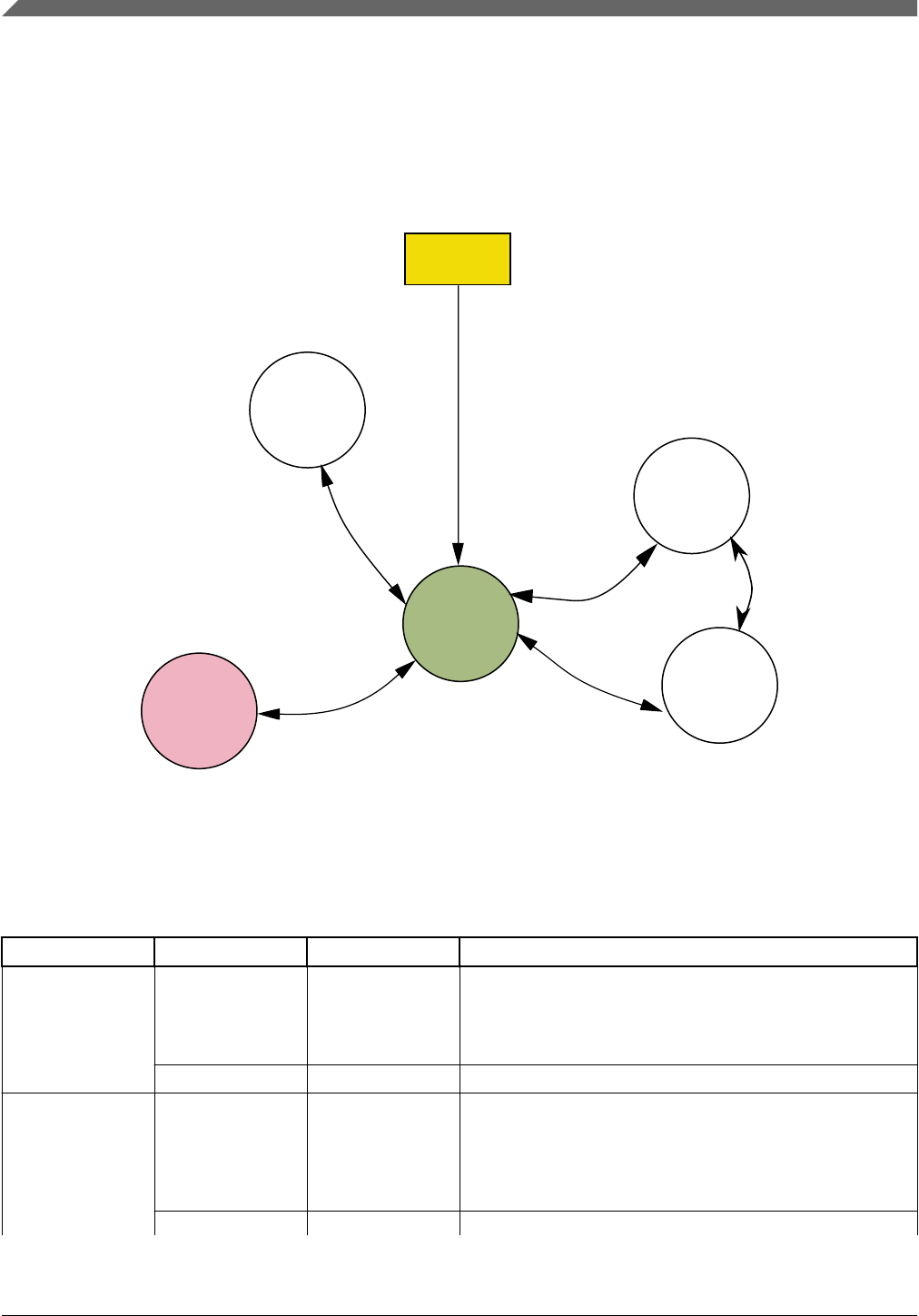
39.4.1 Power mode transitions
The following figure shows the power mode state transitions available on the chip. Any
reset always brings the MCU back to the normal RUN state.
STOP1/
STOP2
RUN
VLPS
VLPR
Any RESET
HSRUN
5
1
2
4
3
Figure 39-1. Power mode state diagram
The following table defines triggers for the various state transitions shown in the previous
figure.
Table 39-2. Power mode transition triggers
Transition # From To Trigger conditions
1 RUN STOP PMCTRL[RUNM]=00, PMCTRL[STOPM]=000 1
Sleep-now or sleep-on-exit modes entered with SLEEPDEEP
set, which is controlled in System Control Register in Arm
core.
STOP RUN Interrupt or Reset
2 RUN VLPR The core, system, bus and flash clock frequencies and SCG
clocking mode are restricted in this mode. See the Power
Management chapter for the maximum allowable frequencies
and SCG modes supported.
Set PMPROT[AVLP]=1, PMCTRL[RUNM]=10.
VLPR RUN Set PMCTRL[RUNM]=00 or
Table continues on the next page...
Functional description
S32K1xx Series Reference Manual, Rev. 7, 04/2018
1018 NXP Semiconductors

Table 39-2. Power mode transition triggers (continued)
Transition # From To Trigger conditions
Reset.
3 VLPR VLPS PMCTRL[STOPM]=000 or 010,
Sleep-now or sleep-on-exit modes entered with SLEEPDEEP
set, which is controlled in System Control Register in Arm
core.
VLPS VLPR Interrupt
NOTE: If VLPS was entered directly from RUN (transition
#4), hardware forces exit back to RUN and does not
allow a transition to VLPR.
4 RUN VLPS PMPROT[AVLP]=1, PMCTRL[STOPM]=010,
Sleep-now or sleep-on-exit modes entered with SLEEPDEEP
set, which is controlled in System Control Register in Arm
core.
VLPS RUN Interrupt and VLPS mode was entered directly from RUN or
Reset
5 RUN HSRUN Set PMPROT[AHSRUN]=1, PMCTRL[RUNM]=11.
HSRUN RUN Set PMCTRL[RUNM]=00 or
Reset
1. STOPO register must be configured to select the stop mode variant.
39.4.2 Power mode entry/exit sequencing
When entering or exiting low-power modes, the system must conform to an orderly
sequence to manage transitions safely.
The SMC manages the system's entry into and exit from all power modes. This diagram
illustrates the connections of the SMC with other system components in the chip that are
necessary to sequence the system through all power modes.
Chapter 39 System Mode Controller (SMC)
S32K1xx Series Reference Manual, Rev. 7, 04/2018
NXP Semiconductors 1019
System
Mode
Controller
(SMC)
System
Power
(PMC)
System
Clocks
(Generator)
LP exit
Flash
CPU
Clock
Control
Module
(CCM)
Module
Memory
Bus masters low power bus (non-CPU)
Bus slaves low power bus
Stop
CCM low power bus
Enable
PMC low power bus
Flash low power bus
Reset
Control
(RCM)
Module
Figure 39-2. Low-power system components and connections
39.4.2.1 VLPS/Stop mode entry sequence
Entry into a low-power stop mode (Stop, VLPS) is initiated by a CPU executing the WFI
instruction. After the instruction is executed, the following sequence occurs:
1. The CPU clock is gated off immediately.
2. Requests are made to all non-CPU bus masters to enter Stop mode.
3. After all masters have acknowledged they are ready to enter Stop mode, requests are
made to all bus slaves to enter Stop mode.
4. After all slaves have acknowledged they are ready to enter stop mode, system and
bus clocks are gated off depending on the target mode–VLPS/STOP1/STOP2. Note
that, in STOP2 mode bus clocks will not be gated.
5. Additionally, for VLPS mode, clock generators are disabled in the SCG unless
configured to be enabled. See SCG for the programming options.
Functional description
S32K1xx Series Reference Manual, Rev. 7, 04/2018
1020 NXP Semiconductors

6. The on-chip regulator in the PMC and internal power switches are configured to
meet the power consumption goals for the targeted low-power mode. This step is
valid only for VLPS and not for STOP as in STOP mode the PMC is in Run
regulation.
NOTE
Ensure that CMU is gated by its PCC.CGC before entering
STOP/VLPS/CPO mode.
39.4.2.2 VLPS/Stop mode exit sequence
Exit from a low-power stop mode is initiated either by a reset or an interrupt event. The
following sequence then executes to restore the system to a run mode (RUN or VLPR):
1. The on-chip regulator in the PMC, clock generators and internal power switches are
restored. This step is valid only for VLPS and not for STOP as in STOP mode the
PMC is in Run regulation.
2. System and bus clocks are enabled to all masters and slaves.
3. The CPU clock is enabled and the CPU begins servicing the reset or interrupt that
initiated the exit from the low-power stop mode.
39.4.2.3 Aborted very low power stop mode entry
If an interrupt occurs during a stop entry sequence, the SMC can abort the transition early
and return to RUN mode without completely entering the stop mode. An aborted entry is
possible only if the interrupt occurs before the PMC begins the transition to stop mode
regulation. After this point, the interrupt is ignored until the PMC has completed its
transition to stop mode regulation. When an aborted very low power stop mode entry
sequence occurs, SMC_PMCTRL[VLPSA] is set to 1.
39.4.2.4 Transition from stop modes to Debug mode
The debugger module supports a transition from STOP and VLPS back to a Halted state
when the debugger has been enabled. As part of this transition, system clocking is re-
established and is equivalent to the normal RUN and VLPR mode clocking configuration.
39.4.3 Run modes
The run modes supported by this device can be found here.
Chapter 39 System Mode Controller (SMC)
S32K1xx Series Reference Manual, Rev. 7, 04/2018
NXP Semiconductors 1021

• Run (RUN)
• Very Low-Power Run (VLPR)
• High Speed Run (HSRUN)
39.4.3.1 RUN mode
This is the normal operating mode for the device.
This mode is selected after any reset. When the Arm processor exits reset, it sets up the
stack, program counter (PC), and link register (LR):
• The processor reads the start SP (SP_main) from vector-table offset 0x000
• The processor reads the start PC from vector-table offset 0x004
• LR is set to 0xFFFF_FFFF.
To reduce power in this mode, disable the clocks to unused modules.
39.4.3.2 Very-Low Power Run (VLPR) mode
In VLPR mode, the on-chip voltage regulator is put into a stop mode regulation state. In
this state, the regulator is designed to supply enough current to the MCU over a reduced
frequency. To further reduce power in this mode, disable the clocks to unused modules
using their corresponding clock gating control bits in the PCC's registers.
Before entering this mode, the following conditions must be met:
• All clock monitors in the SCG must be disabled.
• The maximum frequencies of the system, bus, flash, and core are restricted. See the
Power Management details about which frequencies are supported.
• Mode protection must be set to allow VLP modes, that is, PMPROT[AVLP] is 1.
• PMCTRL[RUNM] must be set to 10b to enter VLPR.
• Flash programming/erasing is not allowed.
NOTE
Do not increase the clock frequency while in VLPR mode,
because the regulator is slow in responding and cannot manage
fast load transitions. In addition, do not modify the clock source
in the SCG module or any clock divider registers. Module clock
enables in the PCC can be set, but not cleared.
Functional description
S32K1xx Series Reference Manual, Rev. 7, 04/2018
1022 NXP Semiconductors

To reenter Normal Run mode, clear PMCTRL[RUNM]. PMSTAT is a read-only status
register that can be used to determine when the system has completed an exit to RUN
mode. When PMSTAT=RUN, the system is in run regulation and the MCU can run at
full speed in any clock mode. If a higher execution frequency is desired, poll PMSTAT
until it is set to RUN when returning from VLPR mode.
Any reset always causes an exit from VLPR and returns the device to RUN mode after
the MCU exits its reset flow.
39.4.3.3 High Speed Run (HSRUN) mode
In HSRUN mode, the on-chip voltage regulator remains in a run regulation state, but with
a slightly elevated voltage output. In this state, the MCU is able to operate at a faster
frequency compared to normal RUN mode. For the maximum allowable frequencies, see
the Power Management chapter.
While in this mode, the following restrictions must be adhered to:
• The maximum allowable change in frequency of the system, bus, flash or core clocks
is restricted to 3x (three times the frequency).
• Stop mode entry is not supported from HSRUN.
• Modifications to clock gating control bits are prohibited.
• Flash programming/erasing is not allowed.
To enter HSRUN mode (with 112 MHz SPLL as clock source):
1. Disable SPLL. Configure FIRC as the RUN mode and HSRUN mode clock source
by writing 0011 to SCG_RCCR[SCS] and SCG_HCCR[SCS].
2. Configure PMPROT[AHSRUN] to allow HSRUN.
3. Write 11 to SMC_PMCTRL[RUNM] to enter HSRUN. (Now system will enter
HSRUN mode with FIRC configured as system clock source).
4. Reconfigure PLL for 112MHz and enable it.
5. Switch to PLL as the clock source by configuring SCG_HCCR[SCS] as 0110.
Entry to HSRUN mode (with 80 MHz SPLL as clock source):
1. Configure SPLL at 80MHz as the RUN mode and HSRUN mode clock source by
writing 0110 to SCG_RCCR[SCS] and SCG_HCCR[SCS].
2. Configure PMPROT[AHSRUN] to allow HSRUN.
3. Write 11 to SMC_PMCTRL[RUNM] to enter HSRUN.
Before increasing clock frequencies, the PMSTAT register should be polled to determine
when the system has completed entry into HSRUN mode. To reenter normal RUN mode,
clear PMCTRL[RUNM]. Any reset also clears PMCTRL[RUNM] and causes the system
to exit to normal RUN mode after the MCU exits its reset flow.
Chapter 39 System Mode Controller (SMC)
S32K1xx Series Reference Manual, Rev. 7, 04/2018
NXP Semiconductors 1023

39.4.4 Stop modes
The various stop modes are selected by setting the appropriate fields in PMPROT and
PMCTRL. The selected stop mode is entered during the sleep-now or sleep-on-exit entry
with the SLEEPDEEP bit set in the System Control Register in the ARM core.
The available stop modes are:
• Normal Stop (STOP)
• Very-Low Power Stop (VLPS)
39.4.4.1 STOP mode
STOP mode is entered via the sleep-now or sleep-on-exit with the SLEEPDEEP bit set in
the System Control Register in the Arm core.
The SCG module can be configured to leave the reference clocks running.
A module capable of providing an asynchronous interrupt to the device takes the device
out of STOP mode and returns the device to normal RUN mode. Refer to the device's
Power Management chapter for peripheral, I/O, and memory operation in STOP mode.
When an interrupt request occurs, the CPU exits STOP mode and resumes processing,
beginning with the stacking operations leading to the interrupt service routine.
A system reset will cause an exit from STOP mode, returning the device to normal RUN
mode via an MCU reset.
39.4.4.2 Very-Low-Power Stop (VLPS) mode
The two ways in which VLPS mode can be entered are listed here.
• Entry into stop via the sleep-now or sleep-on-exit with the SLEEPDEEP bit set in the
System Control Register in the Arm core while the MCU is in VLPR mode and
PMCTRL[STOPM] = 010 or 000.
• Entry into stop via the sleep-now or sleep-on-exit with the SLEEPDEEP bit set in the
System Control Register in the Arm core while the MCU is in normal RUN mode
and PMCTRL[STOPM] = 010. When VLPS is entered directly from RUN mode, exit
to VLPR is disabled by hardware and the system will always exit back to RUN.
In VLPS, the on-chip voltage regulator remains in its stop regulation state as in VLPR.
Functional description
S32K1xx Series Reference Manual, Rev. 7, 04/2018
1024 NXP Semiconductors

A module capable of providing an asynchronous interrupt to the device takes the device
out of VLPS and returns the device to VLPR mode.
A system reset will also cause a VLPS exit, returning the device to normal RUN mode.
39.4.5 Debug in low power modes
When the MCU is secure, the device disables/limits debugger operation. When the MCU
is unsecure, the Arm debugger can assert two power-up request signals:
• System power up, via SYSPWR in the Debug Port Control/Stat register
• Debug power up, via CDBGPWRUPREQ in the Debug Port Control/Stat register
When asserted while in RUN or VLPR, the mode controller drives a corresponding
acknowledge for each signal, that is, both CDBGPWRUPACK and CSYSPWRUPACK.
When both requests are asserted, the mode controller handles attempts to enter STOP and
VLPS by entering an emulated stop state. In this emulated stop state:
• the regulator is in run regulation,
• the SCG-generated clock source is enabled,
• all system clocks, except the core clock, are disabled,
• the debug module has access to core registers, and
• access to the on-chip peripherals is blocked.
Chapter 39 System Mode Controller (SMC)
S32K1xx Series Reference Manual, Rev. 7, 04/2018
NXP Semiconductors 1025

Functional description
S32K1xx Series Reference Manual, Rev. 7, 04/2018
1026 NXP Semiconductors

Chapter 40
Power Management Controller (PMC)
Chip-specific PMC information
40.1.1 Modes supported
Wait and VLPW modes are not supported on this device. See Module operation in
available low power modes for details on available power modes.
40.2 Introduction
The PMC contains the internal voltage regulator, power on reset (POR) and the low
voltage detect (LVD) system.
40.3 Features
The PMC features include:
• Internal voltage regulator offering a variety of power modes
• Active POR providing brown-out detect
• Low voltage reset (LVR)
• Low voltage detect supporting two low voltage trip points and interrupt
• Low power oscillator (LPO) with a typical frequency of 128 kHz
40.4 Modes of Operation
40.1
S32K1xx Series Reference Manual, Rev. 7, 04/2018
NXP Semiconductors 1027

40.4.1 Full Performance Mode (FPM)
For the following Chip Power Modes, the internal voltage regulator is in full performance
mode: HSRUN, RUN, STOP1, STOP2.
40.4.2 Low Power Mode (LPM)
For the following Chip Power Modes, the internal voltage regulator is in low power
mode: VLPR and VLPS.
40.5 Low Voltage Detect (LVD) System
NOTE
The low voltage detect system (Low voltage detect flag, Low
voltage warning flag and Low voltage detect reset generation)
is disabled in low power mode.
This device includes a system to guard against low voltage conditions. This protects
memory contents and controls MCU system states during supply voltage variations. The
system is comprised of a power-on reset (POR) circuit and a LVD circuit with two trip
points. The LVD is disabled upon entering low power mode.
Two flags are available to indicate the status of the low voltage detect system:
• The low voltage detect flag (LVDF) operates in a level sensitive manner. The LVDF
bit is set when the supply voltage falls below the trip point (VLVD). The LVDF bit is
cleared by writing one to the LVDACK bit, but only if the internal supply has
returned above the trip point; otherwise, the LVDF bit remains set. This flag gets
cleared on reset. The flag is only valid after the device has come out of the reset, at
which point the flag will be set accordingly to the voltage level. If supply level is
higher than LVD threshold then this flag stay cleared, else this flag gets set.
• The low voltage warning flag (LVWF) operates in a level sensitive manner. The
LVWF bit is set when the supply voltage falls below the selected monitor trip point
(VLVW). The LVWF bit is cleared by writing one to the LVWACK bit, but only if the
internal supply has returned above the trip point; otherwise, the LVWF bit remains
set. This flag gets cleared on reset. The flag is only valid after the device has come
out of the reset, at which point the flag will be set accordingly to the voltage level. If
supply level is higher than LVW threshold then this flag stay cleared, else this flag
gets set.
Low Voltage Detect (LVD) System
S32K1xx Series Reference Manual, Rev. 7, 04/2018
1028 NXP Semiconductors

40.5.1 Low Voltage Reset (LVR) Operation
If the supply voltage falls below the reset trip point (VLVR), a system reset will be
generated.
If PMC_LVDSC1[LVDRE] is set and the supply voltage falls below VLVD, a system
reset will be generated.
PMC_LVDSC1[LVDF] will be cleared by system reset, so after recovery
PMC_LVDSC1[LVDF] will read zero. Usage of PMC_LVDSC1[LVDF] is intended for
LVD interrupt opteration only (for example, PMC_LVDSC1[LVDIE] = 1 and
PMC_LVDSC1[LVDRE] = 0).
40.5.2 LVD Interrupt Operation
By configuring the LVD circuit for interrupt operation (LVDIE set),
PMC_LVDSC1[LVDF] is set and an LVD interrupt request occurs upon detection of a
low voltage condition. The LVDF bit is cleared by writing one to the
PMC_LVDSC1[LVDACK] bit, when the supply returns to above the trip point.
40.5.3 Low-voltage warning (LVW) interrupt operation
The LVD system contains a low-voltage warning flag (LVWF) to indicate that the supply
voltage is approaching, but is above, the LVD voltage. The LVW also has an interrupt,
which is enabled by setting the PMC_LVDSC2[LVWIE] bit. If enabled, an LVW
interrupt request occurs when the LVWF is set. LVWF is cleared by writing one to the
PMC_LVDSC2[LVWACK] bit, when the supply returns to above the trip point.
40.6 Memory Map and Register Definition
This sections provides the detailed information of all registers for the PMC module.
40.6.1 PMC register descriptions
NOTE
Different portions of PMC registers are reset only by particular
reset types. Each register's description provides details.
Chapter 40 Power Management Controller (PMC)
S32K1xx Series Reference Manual, Rev. 7, 04/2018
NXP Semiconductors 1029

NOTE
The PMC registers can be written only in supervisor mode.
Write accesses in user mode are blocked and will result in a bus
error.
40.6.1.1 PMC Memory map
PMC base address: 4007_D000h
Offset Register Width
(In bits)
Access Reset value
0h Low Voltage Detect Status and Control 1 Register (LVDSC1) 8 RW See
description.
1h Low Voltage Detect Status and Control 2 Register (LVDSC2) 8 RW 00h
2h Regulator Status and Control Register (REGSC) 8 RW See
description.
4h Low Power Oscillator Trim Register (LPOTRIM) 8 RW See
description.
40.6.1.2 Low Voltage Detect Status and Control 1 Register (LVDSC1)
40.6.1.2.1 Offset
Register Offset
LVDSC1 0h
40.6.1.2.2 Function
This register contains status and control bits to support the low voltage detect function.
NOTE
When the internal voltage regulator is in lowe power mode, the
LVD system is disabled, regardless of the PMC_LVDSC1
settings.
Memory Map and Register Definition
S32K1xx Series Reference Manual, Rev. 7, 04/2018
1030 NXP Semiconductors

40.6.1.2.3 Diagram
Bits 7 6 5 4 3 2 1 0
R
LVDF
LVDIE
LVDR
E
0
W
LVDACK
Reset 0 0 0 u10000
1. LVDRE = 0b after POR. Unaffected by reset.
40.6.1.2.4 Fields
Field Function
7
LVDF
Low Voltage Detect Flag
This bit's read-only status bit indicates a low-voltage detect event. The threshold voltage is VLVD.
0b - Low-voltage event not detected
1b - Low-voltage event detected
6
LVDACK
Low Voltage Detect Acknowledge
This write-only bit is used to acknowledge low voltage detection errors. Write 1 to clear LVDF. Read
always return 0.
5
LVDIE
Low Voltage Detect Interrupt Enable
This bit enables hardware interrupt requests for LVDF.
0b - Hardware interrupt disabled (use polling)
1b - Request a hardware interrupt when LVDF = 1
4
LVDRE
Low Voltage Detect Reset Enable
This bit enables the low voltage detect events to generate a system reset.
0b - No system resets on low voltage detect events.
1b - If the supply voltage falls below VLVD, a system reset will be generated.
3-0
—
Reserved
40.6.1.3 Low Voltage Detect Status and Control 2 Register (LVDSC2)
40.6.1.3.1 Offset
Register Offset
LVDSC2 1h
Chapter 40 Power Management Controller (PMC)
S32K1xx Series Reference Manual, Rev. 7, 04/2018
NXP Semiconductors 1031

40.6.1.3.2 Function
This register contains status and control bits to support the low voltage warning (LVW)
function.
NOTE
When the internal voltage regulator is in low power mode, the
LVD system is disabled regardless of the PMC_LVDSC2
settings.
40.6.1.3.3 Diagram
Bits 7 6 5 4 3 2 1 0
R
LVWF
LVWIE
0
W
LVWACK
Reset 0 0 0 0 0 0 0 0
40.6.1.3.4 Fields
Field Function
7
LVWF
Low-Voltage Warning Flag
This bit read-only status bit indicates a low-voltage detect event. The threshold voltage is VLVW.
0b - Low-voltage warning event not detected
1b - Low-voltage warning event detected
6
LVWACK
Low-Voltage Warning Acknowledge
This write-only bit is used to acknowledge low voltage warning errors. Write 1 to clear LVWF. Reads
always return 0.
5
LVWIE
Low-Voltage Warning Interrupt Enable
This bit enables hardware interrupt requests for LVWF.
0b - Hardware interrupt disabled (use polling)
1b - Request a hardware interrupt when LVWF=1
4-0
—
Reserved
40.6.1.4 Regulator Status and Control Register (REGSC)
Memory Map and Register Definition
S32K1xx Series Reference Manual, Rev. 7, 04/2018
1032 NXP Semiconductors

40.6.1.4.1 Offset
Register Offset
REGSC 2h
40.6.1.4.2 Function
This register contains general control and status bits for the regulator and the LPO.
40.6.1.4.3 Diagram
Bits 7 6 5 4 3 2 1 0
R
LPODIS
LPOSTAT
0
REGFP
M
CLKBIASDIS
BIASE
N
W
Reset 01u000100
1. Cleared on power on reset, unaffected by other reset.
40.6.1.4.4 Fields
Field Function
7
LPODIS
LPO Disable Bit
This bit enables or disable the low power oscillator.
NOTE: After disabling the LPO a time of 2 LPO clock cycles is required before it is allowed to enable it
again. Violating this waiting time of 2 cycles can result in malfunction of the LPO.
0b - Low power oscillator enabled
1b - Low power oscillator disabled
6
LPOSTAT
LPO Status Bit
This bit shows the status of the LPO clock to be either in high phase (logic 1) or low phase (logic 0) of the
clock period. Software can poll this status bit to measure actual LPO clock frequency and eventually use
the LPOTRIM[4:0] register to change the LPO frequency.
0b - Low power oscillator in low phase
1b - Low power oscillator in high phase
5-3
—
Reserved
2
REGFPM
Regulator in Full Performance Mode Status Bit
This read-only bit provides the current status of the internal voltage regulator.
0b - Regulator is in low power mode or transition to/from
1b - Regulator is in full performance mode
1
CLKBIASDIS
Clock Bias Disable Bit
Table continues on the next page...
Chapter 40 Power Management Controller (PMC)
S32K1xx Series Reference Manual, Rev. 7, 04/2018
NXP Semiconductors 1033

Field Function
This bit disables the bias currents and reference voltages for some clock modules in order to further
reduce power consumption in VLPS mode.
Note: While using this bit, it must be ensured that respective clock modules are disabled in VLPS
mode. Else, severe malfunction of clock modules will happen.
0b - No effect
1b - In VLPS mode, the bias currents and reference voltages for the following clock modules are
disabled: SIRC, FIRC, PLL. (if available on device)
0
BIASEN
Bias Enable Bit
This bit enables source and well biasing for the core logic in low power mode. In full performance mode
this bit has no effect. This is useful to further reduce MCU power consumption in low power mode. This
bit must be set to 1 when using VLP* modes.
0b - Biasing disabled, core logic can run in full performance
1b - Biasing enabled, core logic is slower and there are restrictions in allowed system clock speed
(see Data Sheet for details)
40.6.1.5 Low Power Oscillator Trim Register (LPOTRIM)
40.6.1.5.1 Offset
Register Offset
LPOTRIM 4h
40.6.1.5.2 Function
This register contains the period trimming bits for the low power oscillator.
Table 40-1. Trimming effect of LPOTRIM[4:0]
LPOTRIM[4:0] Decimal Period of LPO clock
10000 –16 lowest
10001 –15 increasing
... ...
11110 –2
11111 –1
00000 0 typical 128 kHz
00001 +1 increasing
... ...
01110 +14
01111 +15 highest
Memory Map and Register Definition
S32K1xx Series Reference Manual, Rev. 7, 04/2018
1034 NXP Semiconductors

NOTE
The LPO trimming bits represent signed values. Starting from
-16 the period of the LPO clock will increase monotonically
(for example, frequency decreases monotonically).
40.6.1.5.3 Diagram
Bits 7 6 5 4 3 2 1 0
R 0 LPOTRIM
W
Reset 0 0 0 u1uuuu
1. Automatically loaded from flash memory IFR after any reset.
40.6.1.5.4 Fields
Field Function
7-5
—
Reserved
4-0
LPOTRIM
LPO trimming bits
These bits are used for trimming the frequency of the low power oscillator. See the table above for
trimming effect.
Chapter 40 Power Management Controller (PMC)
S32K1xx Series Reference Manual, Rev. 7, 04/2018
NXP Semiconductors 1035

Memory Map and Register Definition
S32K1xx Series Reference Manual, Rev. 7, 04/2018
1036 NXP Semiconductors

Chapter 41
ADC Configuration
41.1 Instantiation information
S32K14x contains two 12-bit ADC modules, ADC0 and ADC1.
S32K11x contains one 12-bit ADC modules, ADC0.
Wait/VLPW mode is not supported on this device. See Module operation in available low
power modes for details on available power modes.
NOTE
Bandgap voltage will not be available in VLP modes.
41.1.1 Number of ADC channels
Each ADC supports up to 32 external analog input channels, but the exact ADC channel
number present on the device is different with packages as indicated in following table.
For details regarding a specific ADC channel available on a particular package, see
Introduction.
Table 41-1. ADC external channels per package
Chip Package ADC0 ADC1
S32K116 32 QFN 9 NA
48 LQFP 13 NA
S32K118 48 LQFP 13 NA
64 LQFP 16 NA
S32K142 64 LQFP 16 11
100 LQFP 16 16
S32K144 64 LQFP 16 11
100 LQFP 16 16
100 MAPBGA 16 16
Table continues on the next page...
S32K1xx Series Reference Manual, Rev. 7, 04/2018
NXP Semiconductors 1037

Table 41-1. ADC external channels per package (continued)
Chip Package ADC0 ADC1
S32K146 64 LQFP 16 13
100 LQFP 16 16
144 LQFP 24 24
100 MAPBGA 16 16
S32K148 144 LQFP 32 32
100 MAPBGA 16 16
176 LQFP 32 32
ADCx_SC1n[ADCH] bit field configurations for a chip are as per the maximum channel
configuration for that chip across packages as mentioned in the below table:
Table 41-2. ADCx_SC1n[ADCH] field configurations
Chip ADCx_SC1n[ADCH] range ADCx_SC1n[ADCH] configuration for module
disabled
S32K116 00000 b - 11111 b 11111 b
S32K118 00000 b - 11111 b 11111 b
S32K142 00000 b - 11111 b 11111 b
S32K144 00000 b - 11111 b 11111 b
S32K146 000000 b - 111111 b 111111 b
S32K148 000000 b - 111111 b 111111 b
Unavailable channels in a particular package are Reserved for the corresponding package.
NOTE
See IO Signal Description Input Multiplexing sheet(s) attached
to the Reference Manual for channel details on specific
packages.
41.1.2 ADC Connections/Channel Assignment
See IO Signal Description Input Multiplexing sheet(s) attached to the Reference Manual
for details on ADC channel connectivity.
Note that ADCx ADy and ADCx_SEy both refer to Channel y of ADCx.
Instantiation information
S32K1xx Series Reference Manual, Rev. 7, 04/2018
1038 NXP Semiconductors

Table 41-3. Internal channel availability
ADC internal
channel
ADC0 ADC1
Channel 0 Used for supply monitoring (see ADC internal
supply monitoring for detials.)
Reserved
Channel 1 Reserved Reserved
Channel 2 Reserved Reserved
Channel 3 Reserved Reserved
41.2 Register implementation
Not all the registers shown in memory map of ADC are implemented in each variant of
S32K1xx. See the below table for register implementation.
Table 41-4. S32K1xx register implementation
Register/Offset S32K116/ S32K118/
S32K142/S32K144
S32K146 S32K148
aSC1A - aSC1P/108 -144
aRA - aRP / 188 - 1C4
Reserved/Not implemented Avaiable/Implemented Avaiable/Implemented
SC1Q - SC1X /148 - 164
RQ - RX / 1C8 - 1E4
Reserved/Not implemented Avaiable/Implemented Avaiable/Implemented
SC1Y - SC1AF / 168 - 184
RY - RAF / 1E8 - 204
Reserved/Not Implemented Reserved/Not Implemented Avaiable/Implemented
41.3 DMA Support on ADC
Applications may require continuous sampling of the ADC (4K samples/sec) that may
have considerable load on the CPU. Though using the Programmable Delay Block (PDB)
to trigger the ADC may reduce some CPU load, the ADC supports DMA request
functionality for higher performance when the ADC is sampled at a very high rate or in
cases where the PDB is bypassed. The ADC can trigger the DMA (via DMA request)
upon conversion completion.
For most cases, the DMA request can be directly triggered from ADC conversion
completion. The device also supports another way to trigger DMA: via the TRGMUX.
The TRGMUX will provide user a more flexible DMA triggering scheme using software
based on different application requirements, for example, the DMA can be triggered after
multiple ADC conversion completion instead of every ADC conversion completion.
Chapter 41 ADC Configuration
S32K1xx Series Reference Manual, Rev. 7, 04/2018
NXP Semiconductors 1039
41.4 ADC Hardware Interleaved Channels
On devices with two ADCs, there are several special ADC channels which support
hardware interleave between multiple ADCs. Taking ADC0_SE4 and ADC1_SE14
channels as an example, these two channels can work independently, but they can also be
hardware interleaved as following diagram. In the hardware interleaved mode, a signal on
the pin PTB0 can be sampled by both ADC0 and ADC1. The interleaved mode is enabled
by SIM_CHIPCTL[ADC_INTERLEAVE_EN] bits.
The hardware interleave implementation on this device is as following:
• ADC0_SE4 and ADC1_SE14 channels are interleaved on PTB0 pin
• ADC0_SE5 and ADC1_SE15 channels are interleaved on PTB1 pin
• ADC1_SE8 and ADC0_SE8 channels are interleaved on PTB13 pin
• ADC1_SE9 and ADC0_SE9 channels are interleaved on PTB14 pin
Figure 41-1. ADC0 and ADC1 hardware interleaved channels integration
ADC Hardware Interleaved Channels
S32K1xx Series Reference Manual, Rev. 7, 04/2018
1040 NXP Semiconductors

NOTE
ADC interleaving is not supported in S32K11x devices.
41.5 ADC internal supply monitoring
Internal supplies are monitored on ADC0 internal channel 0 (configured by selecting
ADC0_SC1n[ADCH] as 010101b). Please refer to SIM_CHIPCTL[ADC_SUPPLY] and
SIM_CHIPCTL[ADC_SUPPLYEN] bits.
41.6 ADC Reference Options
The ADC supports the following references:
• VREFH/VREFL - connected as the primary reference option
• VALTH/VREFL - connected as an alternate reference option
ADCx_SC2[REFSEL] bit selects the voltage reference sources for ADC. Refer to
REFSEL description in ADC chapter for more details.
In all S32K1xx devices, VALTH is same as VDDA. In packages where dedicated VREFH /
VREFL pins are not available, VREFH is connected in package to VDDA and VREFL to VSSA.
If externally available, the positive reference should be connected to the same potential as
VDDA or may be driven by an external source to a level between the minimum VREFH and
the VDDA potential. VREFH must never exceed VDDA. VREFL should be connected to the
same voltage potential as VSSA.
41.7 ADC Trigger Sources
• Triggers are connected through PDB or TRGMUX to provide flexible trigger
schemes
• PDB generate triggers and pre-triggers for ADC (the ADC and PDB operate in pairs,
as PDB0; ADC0 and PDB1; ADC1), each PDB channel will have up to 8 pre-
triggers for ADC channel control, which provides an automatically trigger scheme so
that the CPU involvement is not necessary.
• Minimum one external pin per ADC (supported via the TRGMUX)
• Software must determine relative priority
• Starts conversion after a single ongoing conversion complete
Chapter 41 ADC Configuration
S32K1xx Series Reference Manual, Rev. 7, 04/2018
NXP Semiconductors 1041

• CMP out, LPIT, RTC, and LPTMR are capable of triggering each ADC via
TRGMUX. See TRGMUX module interconnectivity in TRGMUX section for the
modules which are capable of triggering ADC.
• LPIT supports up to 4 pre-triggers, which are limited to be used only on the
ADHWTS0–ADHWTS3 of each ADC. For the rest of the peripherals, software
configuration is required to provide pre-triggers. See
SIM_ADCOPT[ADCxSWPRETRG] for configuring the software pre-trigger.
The following specification and diagram are just giving an example to help understanding
the ADC trigger scheme. Generally, the ADC supports two kinds of hardware triggering
schemes:
• The default hardware triggering scheme uses the PDB to trigger the ADC
(suggested).
• Another optional hardware triggering scheme is to use the TRGMUX.
• The SIM_ADCOPT[ADCxTRGSEL] field is used to control the ADC triggering
source/scheme.
• When ADCxTRGSEL=0, the ADC pre-trigger comes from PDB directly.
• When ADCxTRGSEL=1, the ADC pre-trigger comes from TRGMUX, as in the
case of LPIT.
NOTE
For the TRGMUX triggering, only up to 4 pre-triggers are
supported.
NOTE
Each PDB supports 4 slots/4 triggers channel, and each channel
supports 8 pre-triggers. The triggers of PDB channels can are
OR'ed together to support up to 32 pre-triggers if necessary.
ADC Trigger Sources
S32K1xx Series Reference Manual, Rev. 7, 04/2018
1042 NXP Semiconductors
PDB0 pulse out
PDB0 CH0 trigger
ADC0_SC1A:B[COCO]
TRGMUX_PDB0
63
•
•
•
1
0
out[15:12]
SIM_ADCOPT [ADC0PRETRGSEL]
SWTRG
PDB_SC[TRGSEL]
Channel 0
Channel 1
Pulse-out
Ch0
pretriggers[7:0]
out56
PDB0 Ch1
pretriggers[7:4]
PDB trigger
ACK[7:0]
ADHWTS I:P
ADC_SC1A:DD[COCO]
PDB0
TRGMUX_ADC0
63
•
•
•
1
0Pretriggers[3:0]
Triggers[3:0]
in36
in34
in[31:30]
Ch0 trigger
Trigger_in0
Ch1
pretriggers[7:0]
Pulse-out
trigger
ACK[15:8]
Ch1 trigger
PDB0 Ch1 pretriggers[3:0]
PDB pretriggers[3:0]
TRGMUX pretriggers[3:0]
SIM_ADCOPT [ADC0TRGSEL]
TRGMUX triggers[3:0]
PDB trigger
ADHWTS E:H
ADHWTS A:D
ADHWT
SIM_ADCOPT [ADC0SWPRETRG]
Trigger Latching and Arbitration Unit*
* The block depicts simplified schematic and doesn’t show detailed latching. See section 'Trigger Latching and Arbitration' of ADC chapter for details
Channel 2
Channel 3 ADHWTS Y:DD
ADHWTS Q:X
ADC0
TRGMUX
ACK[31:24]
ACK[23:16]
Figure 41-2. ADC0_PDB0 ADC Triggering scheme example
NOTE
While using TRGMUX, only LPIT supports pretriggers. For
other peripherals, software pretriggers need to be configured
using SIM_ADCOPT[ADCxSWPRETRG].
Chapter 41 ADC Configuration
S32K1xx Series Reference Manual, Rev. 7, 04/2018
NXP Semiconductors 1043

41.7.1 PDB triggering scheme
The PDB triggering scheme is the default and the suggested trigger method for the ADC.
One ADC and one PDB work as one pair: PDB0-ADC0, PDB1-ADC1. The trigger
sources for PDB0 and PDB1 can be configured through TRGMUX_PDB0 and
TRGMUX_PDB1, respectively. Here we take PDB0-ADC0 as an example to specify the
triggering scheme.
•Set SIM_ADCOPT[ADCxTRGSEL]=0. PDB0 channel 0 is selected as the ADC
trigger source.
• PDB0 pre-triggers will connect directly to the ADC0 ADHWTS port to control the
channels.
• The ADC0 COCO signals are fed directly back to PDB0 to deactivate the PDB lock
state.
The following figures illustrate typical cases for ADC triggering using the PDB:
Case 1:
ADC0
Trigger_source_A
Configured using TRGMUX_PDB0
Configured using TRGMUX_PDB1
PDB0
ADHWT
ADHWTS A:P
ADC_SC1A:P[COCO]
ADC1
Trigger_source_B
PDB1
trigger_in0
trigger_in0
ADHWT
ADHWTS A:P
ADC_SC1A:P[COCO]
Figure 41-3. ADCs triggering with independent sources
Case 2:
Trigger_source_A
Configured using TRGMUX_PDB0 and TRGMUX_PDB1
(Same configuration used for PDB0 and PDB1)
PDB0
PDB1
ADC0
ADHWT
ADHWTS A:P
ADC_SC1A:P[COCO]
ADC1
ADHWT
ADHWTS A:P
ADC_SC1A:P[COCO]
trigger_in0
trigger_in0
Figure 41-4. ADC triggering with same source
ADC Trigger Sources
S32K1xx Series Reference Manual, Rev. 7, 04/2018
1044 NXP Semiconductors

41.7.2 TRGMUX trigger scheme
TRGMUX supports many trigger sources. Here we take LPIT as a typical example, but
the trigger source can also be others which are mentioned above. LPIT supports up to 4
channels, with each channel having a trigger and a pre-trigger.
•Set SIM_ADCOPT[ADCxTRGSEL]=1. TRGMUX out is selected as the ADC
trigger source.
• Configure TRGMUX to select LPIT triggers as the ADC trigger and pre-trigger
sources.
• TRGMUX only supports up to 4 pre-triggers for each ADC (pre-trigger0–pre-
trigger3; the other pre-triggers cannot be used with TRGMUX).
• ADC COCO is not required in this case. Software must accommodate the
intermission time between each ADC conversion.
• Using TRGMUX allows a single LPIT to be used to trigger two ADCs
simultaneously. This is one of the benefits of using TRGMUX triggering instead of
PDB triggering.
NOTE
For trigger sources other than PDB and LPIT, software is
required to provide ADC pre-triggers.
41.8 Trigger Selection
Any combination of trigger enable and trigger can be selected; they are independent of
each other. But after it has been selected, it cannot be changed on-the-fly. There are
defined steps to change the trigger and enable sources (trigger and pretrigger source).
Changing of trigger source can be done anytime by any of the two ways below.
Way 1
1. Stop the current trigger generation unit .
2. Wait for a time period equals to total of 2.5 cycle of ADC operating clock and 1.5
cycles of ADC host interface clock, to give time to latch the last trigger, if any
3. Poll the status of ADC_SC2[TRGSTLAT] for all 0, it will come to 0 after
completing all conversions enqued till that time
4. Change the selections for desired source and then
5. Start the new trigger generation units
If it is required to switch immediately
1. Stop the current trigger generation unit
Chapter 41 ADC Configuration
S32K1xx Series Reference Manual, Rev. 7, 04/2018
NXP Semiconductors 1045

2. Flush all the queued triggers of trigger handler block by setting
ADC_CFG1[CLRLTRG], this will flush all queued triggers except the one under
process by ADC, if any
3. Wait for a time period equals to total of 2.5 cycle of ADC operating clock
4. Wait for the status of ADC_SC2[TRGSTLAT] to become all 0
5. Change the selections for desired source and then
6. Start the new trigger generation units
NOTE
If the above restriction is not followed then the trigger missed
by this process might not be reported.
41.9 Trigger Latching and Arbitration
The four lower triggers have the capability to be latched. Irrespective of which source
combination is selected, the trigger requests from that source are latched and processed.
Latched trigger requests are presented to the ADC one at a time. The next request is
given only when the processing of the current trigger request is completed by the ADC.
Therefore, only one request is processed at any given time and all other requests are
latched. If a trigger request appears again on any of the 0–3 enables/triggers while it is
either being processed by the ADC or already latched in the trigger handler, the new
request is ignored and an error is indicated for that trigger in register
ADC_SC2[TRGSTERR].
The relationship among the trigger requests from the selected source can randomly be (a)
one-hot, or (b) simultaneous. However, they will be serviced on a round-robin basis. For
example, after the Pth request is processed [0 < P <(N-1)], searching will resume with (P
+1), followed by (P+2), until the next latched request is found. This searching then rolls
over to 0 after (N-1)th trigger and continues until P is reached.
To work with the ADC using multiplexed triggers, you need to follow the below
sequences of programming for different cases:
Case 1: Initialization/start of conversion: a. Initialize/reprogram (in case of intermediate start) the SAR
ADC for desired operation (see the ADC section for details).
b. Select the trigger source for the trigger handler block
(configuration for this resides in a separate module on the
chip; refer to the SIM_ADCOPT register in the SIM chapter).
c. Configure and start the trigger generation module (PDB or
TRGMUX).
Case 2: Changing the trigger source/multiplexer control: a. Stop the trigger generation module (PDB or TRGMUX).
b. Do one of the following options:
Table continues on the next page...
Trigger Latching and Arbitration
S32K1xx Series Reference Manual, Rev. 7, 04/2018
1046 NXP Semiconductors

Option 1:
1. Wait for a duration equals to total of 2.5 cycle of ADC
operating clock and 1.5 cycles of ADC host interface
clock, to give time to latch the last trigger, if any
2. Wait for the latched triggers to be processed and trigger
handler to be idle (poll the status of
ADC_SC2[TRGSTLAT] for all 0).
Option 2:
1. Flush the latched trigger requests in trigger handler
block(Write a 1b to the ADC_CFG1[CLRLTRG]).
2. Wait for a time period equals to total of 2.5 cycle of
ADC operating clock
3. Wait for the idle status of trigger handler (poll the status
of ADC_SC2[TRGSTLAT] for all 0).
c. Reselect the trigger source for the trigger handler block
(configuration for this resides in a separate module on the
chip; see the chip-specific section).
d. Configure and start the trigger generation module (PDB or
TRGMUX).
Case 3: Stopping of conversion a. Stop the trigger generation module (PDB or TRGMUX).
b. Wait for a duration equals to total of 2.5 cycle of ADC
operating clock plus 1.5 cycles of ADC host interface clock, to
give time to latch the last trigger, if any.
c. Wait for the latched triggers to be processed and the trigger
handler to be idle (poll the status of ADC_SC2[TRGSTLAT]
for all 0s).
d. Stop the SAR ADC and clear interrupts after required
processing (see the ADC section for details).
Case 4: Changing trigger source/multiplexer control in case of
ongoing continuous conversion
a. Stop the trigger generation module (PDB or TRGMUX).
b. Read any configuration register of the ADC.
c. Write the read value from above in the same register.
d. This write will abort the ongoing continuous conversion.
e. Reselect the trigger source for the trigger handler block
(configuration for this resides in a separate module on the
chip; refer to the SIM_ADCOPT register in the SIM chapter).
f. Configure and start the trigger generation module (PDB or
TRIGMUX).
Case 5: Clearing the error status (applicable for the TRGMUX
case only)
a. Read the error status (ADC_SC2[TRGSTERR]).
b. If any above register bit is 1, then stop the trigger
generation module (TRGMUX).
c. Wait for a duration equals to total of 2.5 cycle of ADC
operating clock plus 1.5 cycles of ADC host interface clock, to
give time to latch the last trigger, if any.
d. Wait for the idle status of the trigger handler (poll the status
of ADC_SC2[TRGSTLAT] for all 0s).
e. Clear the above register bit by writing 1 to it.
f. Wait for the latched triggers to be processed and the trigger
handler to be idle (poll the status of ADC_SC2[TRGSTLAT]
for all 0s).
Table continues on the next page...
Chapter 41 ADC Configuration
S32K1xx Series Reference Manual, Rev. 7, 04/2018
NXP Semiconductors 1047

g. Reselect the trigger source for the trigger handler block
(configuration for this resides in a separate module on the
chip; refer to the SIM_ADCOPT register in the SIM chapter).
h. Configure and start the trigger generation module (PDB or
TRGMUX).
NOTE
Latched status clearing by writing 1 to
ADC_CFG1[CLRLTRG] should not be done while PDB
triggering through the trigger handler, as the PDB works in a
closed loop with the COCO flag from the ADC and provides
one trigger at a time. Clearing the latched status while it is
being processed within the trigger handler (before being
launched to the ADC) will stop its future conversion and there
will be no COCO flag. In such case, the PDB might enter an
indeterminate state.
41.10 ADC triggering configurations
The ADC supports two triggering schemes as already described in previous sections
through below two paths (See ADC0_PDB0 ADC triggering example):
1. Direct Triggering path through PDB on channel number 4 onward.
2. Multiplexed triggering path through PDB/TRGMUX on channels 0 to 3 through
trigger latching gasket.
Out of these, the user should either use direct triggering path on channel 4 onward with
PDB triggering on channels 0 to 3 or only TRGMUX path on channel 0 to 3. When using
direct triggering scheme through PDB, the pretriggers should be minimum 4 bus clock
cycles apart. Accordingly, following table shows the ADC triggering configurations and
behavior:
Table 41-5. ADC triggering configurations and behavior
S.No. Configuration Delay in
between
pretriggers, t
(in bus clk
cycles)
PDB triggering on all channels
(SIM_ADCOPT[ADC0TRGSEL] = 1’b0,
SIM_ADCOPT[ADC0PRETRGSEL] = 2’b00)
Triggering through
trigger latching
gasket on channel 0
to 3
(SIM_ADCOPT[ADC0T
RGSEL] = 1’b1,
SIM_ADCOPT[ADC0P
RETRGSEL] =
2’b01/2’b10)
Channel 0 to 3 Channel 4 onwards Channel 0 to 3
1 Zero pretrigger delay t = 0 No conversion No conversion No conversion
Table continues on the next page...
ADC triggering configurations
S32K1xx Series Reference Manual, Rev. 7, 04/2018
1048 NXP Semiconductors

Table 41-5. ADC triggering configurations and behavior (continued)
S.No. Configuration Delay in
between
pretriggers, t
(in bus clk
cycles)
PDB triggering on all channels
(SIM_ADCOPT[ADC0TRGSEL] = 1’b0,
SIM_ADCOPT[ADC0PRETRGSEL] = 2’b00)
Triggering through
trigger latching
gasket on channel 0
to 3
(SIM_ADCOPT[ADC0T
RGSEL] = 1’b1,
SIM_ADCOPT[ADC0P
RETRGSEL] =
2’b01/2’b10)
2 Pretrigger delay less
than 4 bus clk cycles
0 < t ≤ 4 ADC results are valid
(due to trigger latching
gasket) for both
conversions.
ADC results are
invalid for both
conversions.
ADC results are valid
(due to trigger latching
gasket) for both
conversions.
3 Pretrigger delay is
greater than 4 bus clk
cycles but less than
ADC conversion time
4 < t < t ADC
conversion
time
ADC results are valid
(due to trigger latching
gasket) for both
conversions.
ADC results are valid
for first conversion,
invalid for second.
ADC results are valid
(due to trigger latching
gasket) for both
conversions.
4 Pretrigger delay
configured greater
than ADC conversion
time
t > ADC
conversion
time
ADC results are valid
for both conversions
ADC results are valid
for both conversions
ADC results are valid for
both conversions.
(If ADC conversion time < 4 bus clk cycles, configuration 3 in the table above will not be
applicable)
NOTE
PDB provides sequence error only if the corresponding two
pretriggers belong to same PDB channel. When different PDB
channels are used, the software should ensure that the delays in
between two pretriggers is atleast four bus clock cycles apart,
otherwise the conversion results will be invalid for both
conversions.
The pretriggers, trigger, COCO, sequence error and result status are mentioned below for
different configurations mentioned in the table above:
1. Zero delay configured:
Trigger is not raised. The sequence error is reported on both the channels. The ADC
result register consists of junk information.
Chapter 41 ADC Configuration
S32K1xx Series Reference Manual, Rev. 7, 04/2018
NXP Semiconductors 1049
Figure 41-5.
2. Delay configured is less than 4 bus clk cycles:
a. Direct Triggering on channel number 4 onwards through same PDB channel:
Sequence error for second conversion, COCO might be received or might not.
Both the conversion results are invalid.
Figure 41-6.
ADC triggering configurations
S32K1xx Series Reference Manual, Rev. 7, 04/2018
1050 NXP Semiconductors
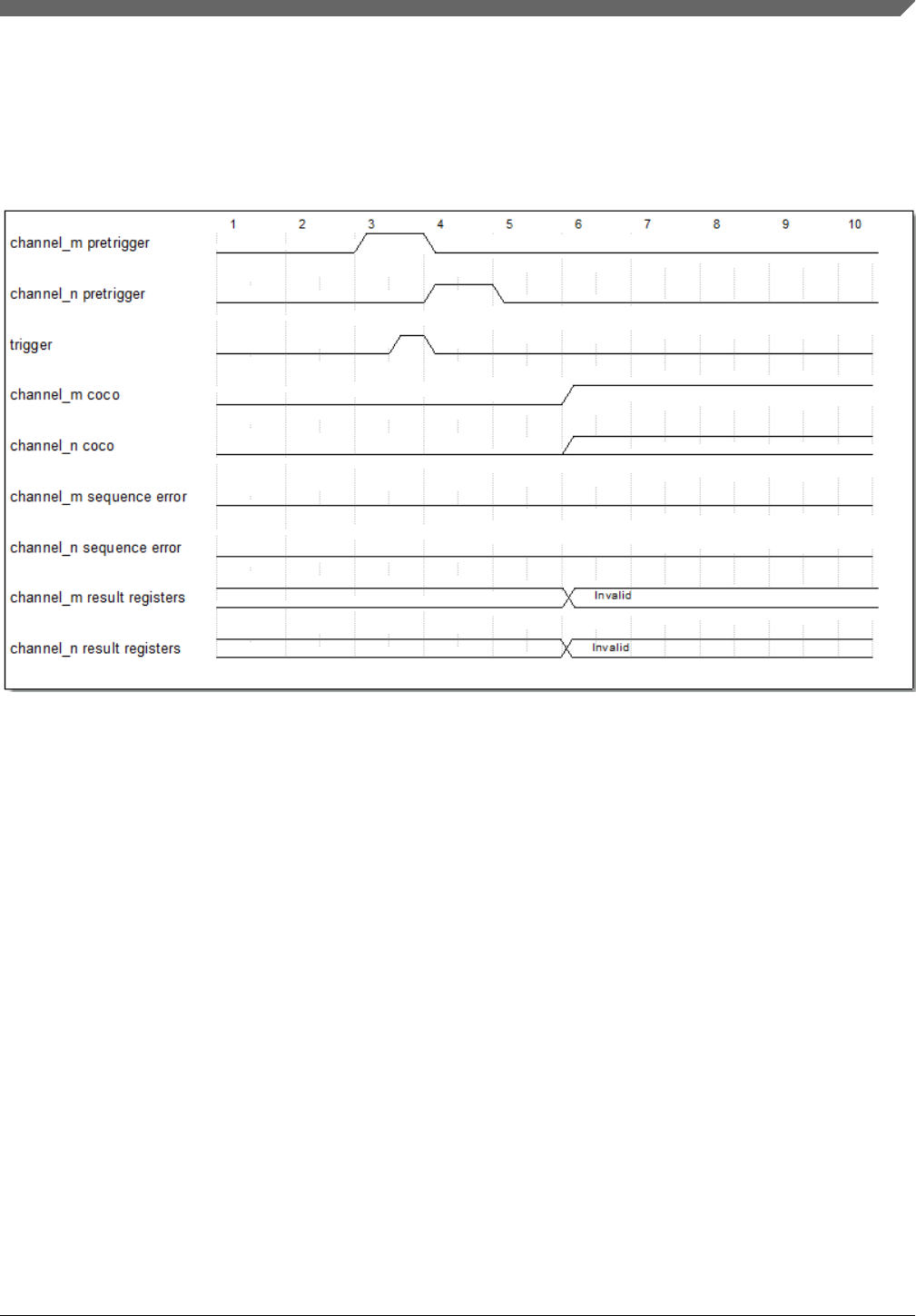
b. Direct Triggering on channel number 4 onwards through different PDB
channels:
Sequence error for second conversion is not reported, COCO might be received
or might not. Both the conversion results are invalid.
Figure 41-7.
c. Triggering on channels 0-3 through trigger latching gasket:
Sequence error for second conversion is reported, COCO will be received for
both channels. Both the conversion results are valid. This is due to the virtue of
trigger latching gasket, which latches the trigger requests.
Chapter 41 ADC Configuration
S32K1xx Series Reference Manual, Rev. 7, 04/2018
NXP Semiconductors 1051
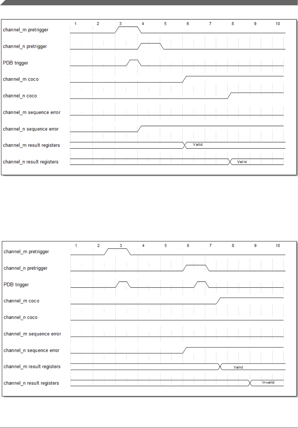
Figure 41-8.
3. Delay configured is less than ADC conversion time and greater than 4 bus clk cycles:
a. Direct Triggering on channel number 4 onwards through same PDB channel:
Sequence error for second conversion, COCO will not be received. First
conversion results are valid and second conversion results are invalid.
Figure 41-9.
ADC triggering configurations
S32K1xx Series Reference Manual, Rev. 7, 04/2018
1052 NXP Semiconductors
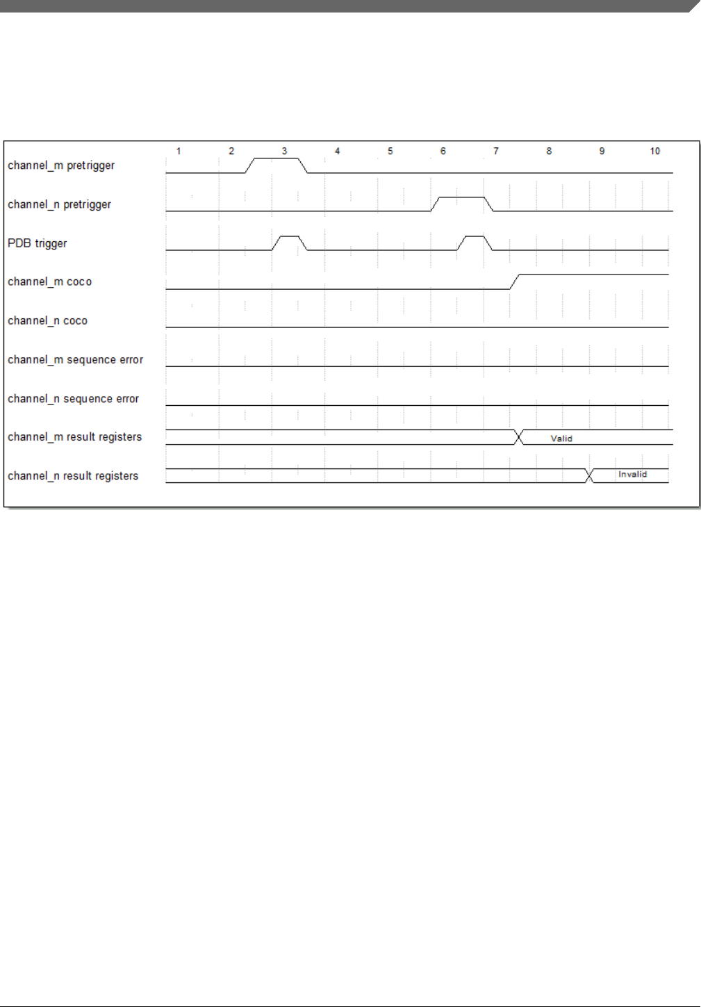
b. Direct Triggering on channel number 4 onwards through different PDB channel:
No sequence error for second conversion, COCO will not be received. First
conversion results are valid and second conversion results are invalid.
Figure 41-10.
c. Triggering on channels 0-3 through trigger latching gasket:
Sequence error for second conversion is reported, COCO will be received for
both channels. Both the conversion results are valid. This is due to the virtue of
trigger latching gasket, which latches the trigger requests.
Chapter 41 ADC Configuration
S32K1xx Series Reference Manual, Rev. 7, 04/2018
NXP Semiconductors 1053
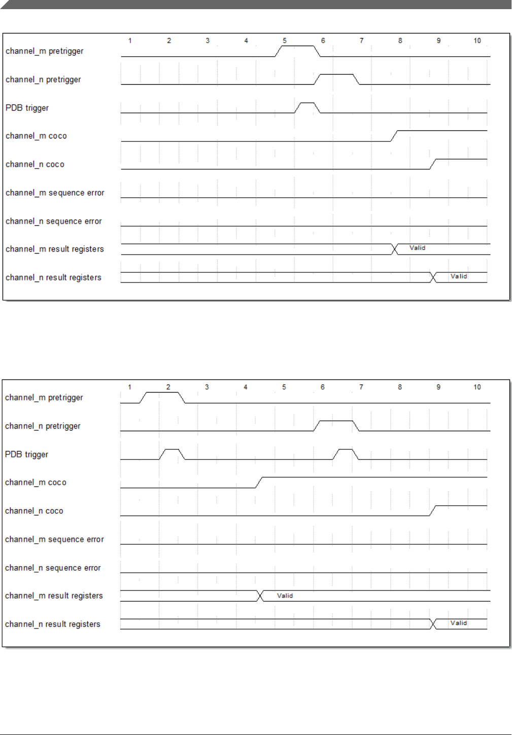
Figure 41-11.
4. Delay configured is greater than ADC conversion time:
No sequence error, Both COCOs received. Both conversions are valid.
Figure 41-12.
ADC triggering configurations
S32K1xx Series Reference Manual, Rev. 7, 04/2018
1054 NXP Semiconductors
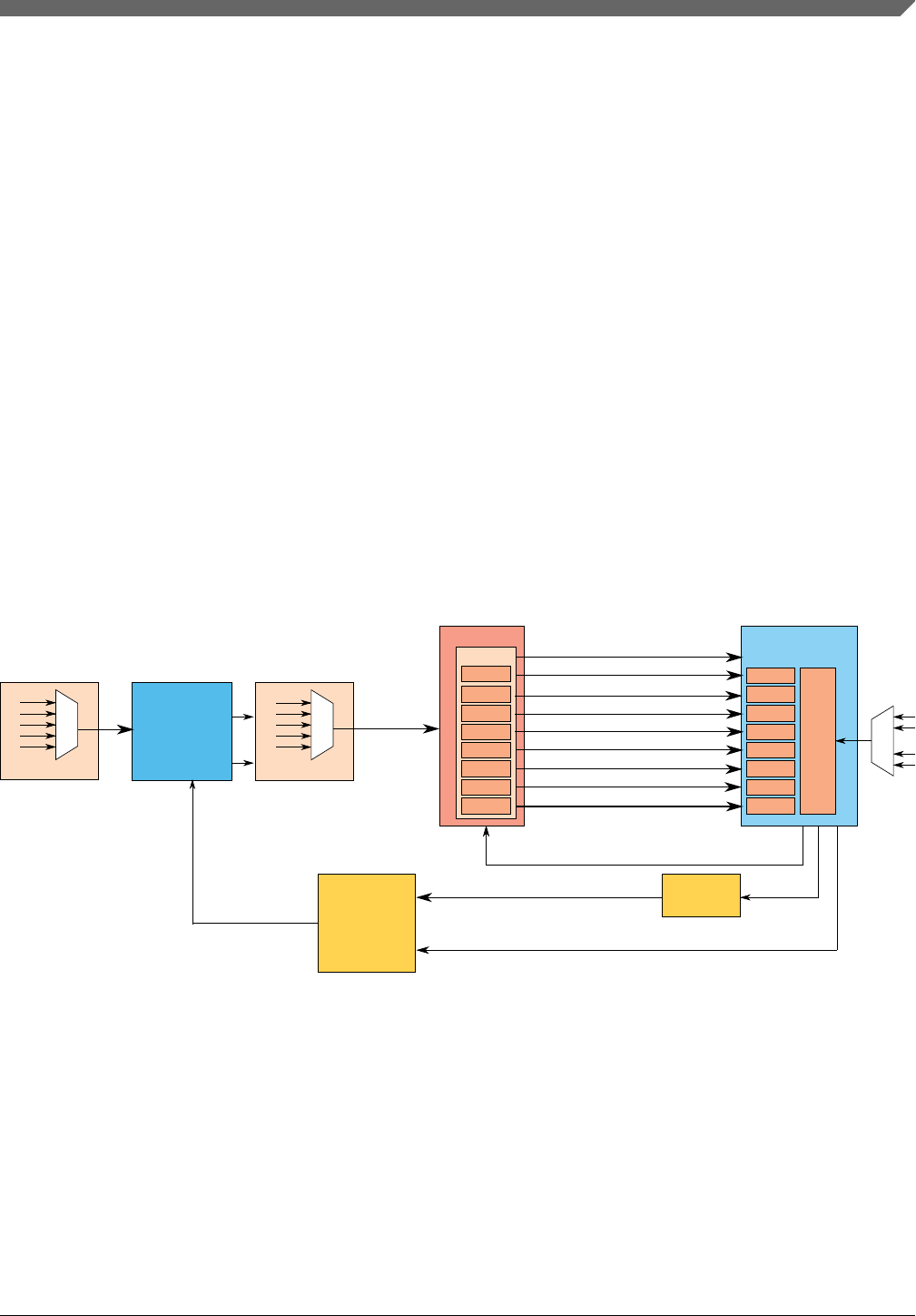
41.11 ADC low-power modes
The ADC will be available in STOP2 mode.
41.12 ADC Trigger Concept – Use Case
The FlexTimer Module (FTM) supports the counter init trigger and channel match
trigger, which could be used as a trigger input of the PDB. The PDB could then be used
to trigger other modules such as the ADC. Each ADC channel in the PDB module
supports up to 8 pre-triggers, which could be used as the ADC hardware channel
selection to precondition the ADC block prior to an actual trigger. After a pre-trigger, the
ADC trigger initiates the ADC conversion. The waveforms shown in the following
diagram illustrate the pre-trigger and trigger output of the PDB to ADC. When a PDB
pre-trigger and trigger output starts an ADC conversion, an internal lock associated with
the corresponding pre-trigger is activated. This lock becomes inactive when receiving the
COCO signal from the ADC.
HWTRIG0
INIT_TRIG
EXT_TRIG
FTM
TRGMUX_PDBx
pretrig0 ch0_pretrig0 ADC_R0
CH0
pretrig1
pretrig2
pretrig3
pretrig4
pretrig5
pretrig6
pretrig7
PDB
ch0_pretrig1
ch0_pretrig2
ch0_pretrig3
ch0_pretrig4
ch0_pretrig5
ch0_pretrig6
ch0_pretrig7
ADC_R1
ADC_R2
ADC_R3
ADC_R4
ADC_R5
ADC_R6
ADC_R7
S/H & Conversion
ADC_SC1 A:H [COCO]
CPU
DMA_REQ
INTERRUPT
ADC
ADC_CHx
•
•
•
DMA
pretrig0
ch0_trig ADHWT
ADHWTS A
ADHWTS B
ADHWTS C
ADHWTS D
ADHWTS E
ADHWTS F
ADHWTS G
ADHWTS H
ACK[0:15]
trigger_in0
TRGMUX_FTMn
Figure 41-13. PWM Load Diagnosis – ADC Trigger Concept (block diagram)
Chapter 41 ADC Configuration
S32K1xx Series Reference Manual, Rev. 7, 04/2018
NXP Semiconductors 1055
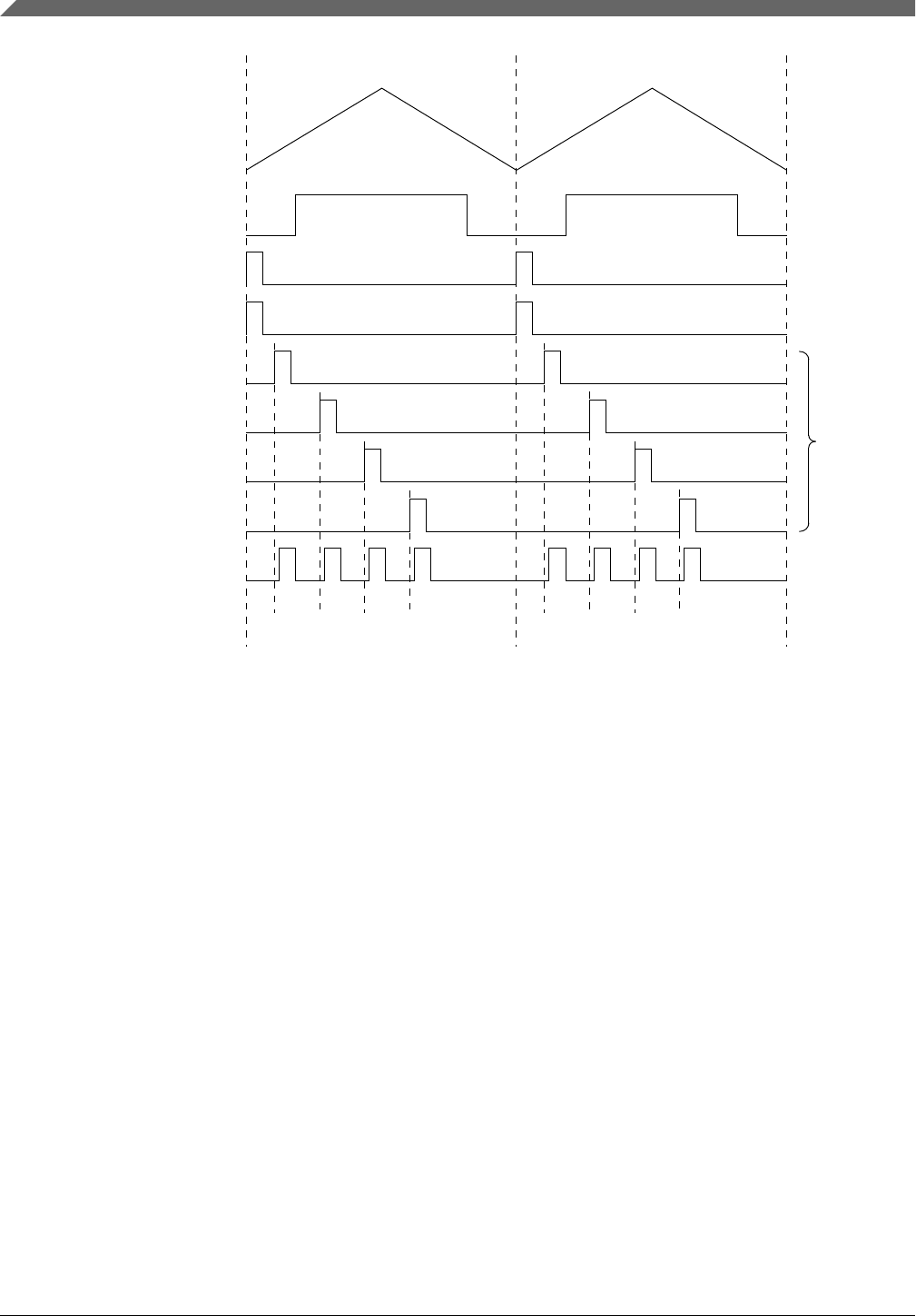
PDB_ch0_trigger/ADHWT
ADC channel
selection
PDB_ch0_pretrigger2/ADHWTS C
PDB_ch0_pretrigger1/ADHWTS B
PDB_ch0_pretrigger0/ADHWTS A
PDB_trigger_in0
FTM_init_trig
PWM
PDB_ch0_pretrigger3/ADHWTS D
ADHWT
Figure 41-14. Example: PWM Load Diagnosis – ADC Trigger Concept 1 (Timing)
ADC Trigger Concept – Use Case
S32K1xx Series Reference Manual, Rev. 7, 04/2018
1056 NXP Semiconductors
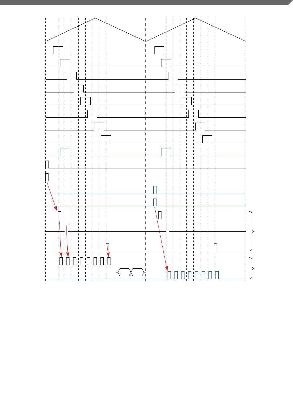
PWM_ch0
PWM_ch2
PWM_ch1
PWM_ch3
PWM_ch4
PWM_ch5
PWM_ch6
PWM_ch7
PWM_ch8
FTM_init_trig
PDB_trigger_in0
FTM_init_trig
PDB_trigger_in0
PDB_pretrigger0
PDB_pretrigger1
PDB_pretrigger7
PDB_trigger
PDB_trigger
•
•
•
ADC channel
selection
ADC trigger
ADC ch0 ch1 ch2 ch3 ch4 ch5 ch6 ch7 ADC ch8 ch9 ch10 ch11 ch12 ch13 ch14 ch15
ISR2ISR1
Figure 41-15. Example: PWM Load Diagnosis – ADC Trigger Concept 2 (Timing)
41.13 ADC calibration scheme
After a POR, and after the flash memory has been made available, the ADC calibration
must be executed by use of the CAL bit in the ADC_SC3 control register.
Chapter 41 ADC Configuration
S32K1xx Series Reference Manual, Rev. 7, 04/2018
NXP Semiconductors 1057

After the ADC has been configured and calibrated, no further calibration is required as
long as the power is maintained. Hence, upon subsequent exits from power mode STOP2,
re-calibration is not required. Since the power is continuous in all of the device power
modes (STOP2 RUN, and HSRUN), all of the ADC specifications are maintained as per
the data sheet.
ADC calibration scheme
S32K1xx Series Reference Manual, Rev. 7, 04/2018
1058 NXP Semiconductors

Chapter 42
Analog-to-Digital Converter (ADC)
42.1 Chip-specific ADC information
See the ADC Configuration chapter.
42.2 Introduction
The 12-bit analog-to-digital converter (ADC) is a successive approximation ADC
designed for operation within an integrated microcontroller system-on-chip.
NOTE
For the chip specific modes of operation, see the power
management information of the device.
42.2.1 Features
Following are the features of the ADC module:
• Linear successive approximation algorithm with up to 12-bit resolution
• Up to 32 single-ended external analog inputs
• Single-ended 12-bit, 10-bit, and 8-bit output modes
• Output in right-justified unsigned format for single-ended
• Single or continuous conversion modes
• Automatic return to idle after single conversion
• Configurable sample time and conversion speed/power
• Conversion complete/hardware average complete flag and interrupt
• Input clock selectable from up to four sources
• Operation in low-power modes for lower noise
• Selectable hardware conversion trigger with hardware channel select
S32K1xx Series Reference Manual, Rev. 7, 04/2018
NXP Semiconductors 1059
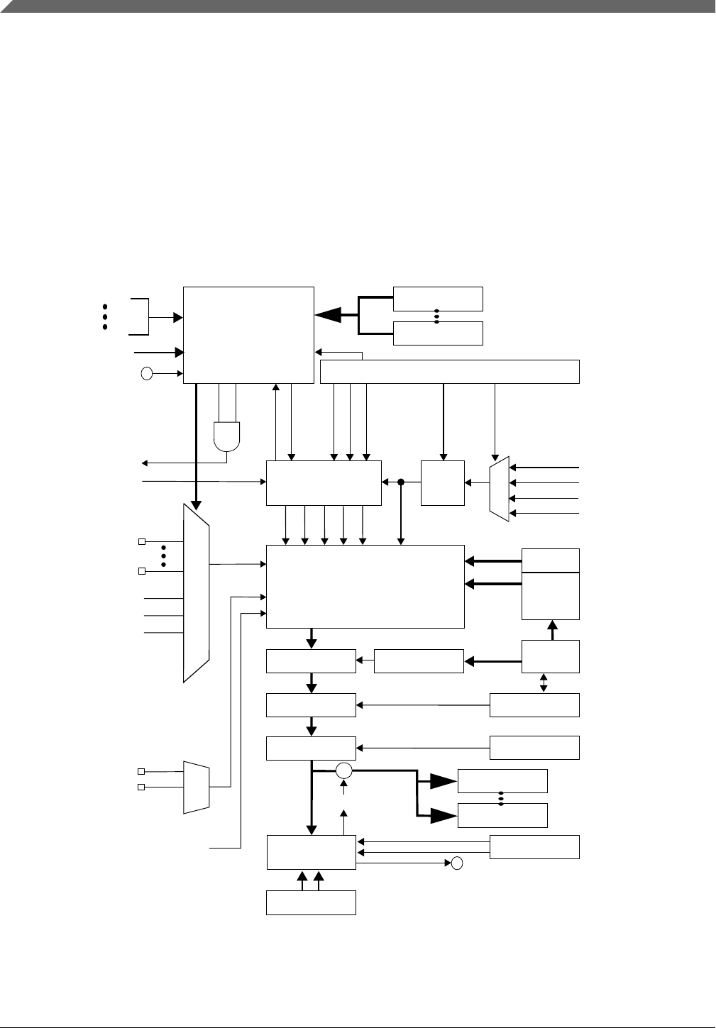
• Automatic compare with interrupt for less-than, greater-than or equal-to, within
range, or out-of-range, programmable value
• Hardware average function
• Selectable voltage reference: external or alternate
• Self-Calibration mode
42.2.2 Block diagram
The following figure is the ADC module block diagram.
SC1A
ADHWTSA
ADHWTSn
C o m p a re tru e
A D C H
c o m p le te
A D T R G
A D C O
Control Registers
SC1n
A D IV
A D IC L K
ALTCLK4
ALTCLK1
A D C K
M O D E
tra n s fe r
C V 2
CV1:CV2
Interrupt
1
A D V IN
A C F E
1
SC2
Rn
RA
CFG1,2
Compare true
Conversion
trigger
control
MCU STOP
ADHWT
AD0
ADn
V REFH
VALTH
AIEN
C O C O
tr ig g e r
CLPx
GGain
CLPx
Calibration
OFS
CAL
SC3
C V1
ACFGT, ACREN
D
AVGE, AVGS
ADCOFS
V REFSH
(SC2, CFG1, CFG2)
M O D E
ADLSMP/ADLSTS
Control sequencer Clock
divide ALTCLK2
SAR converter
Offset subtractor
Averager
Formatting
Compare
logic
initialize
sample
convert
transfer
abort
V REFL
BNGP
VREFH
VREFL
ALTCLK3
Figure 42-1. ADC block diagram
Introduction
S32K1xx Series Reference Manual, Rev. 7, 04/2018
1060 NXP Semiconductors

42.3 ADC signal descriptions
Each ADC module supports up to 32 single-ended inputs.
The ADC also requires four supply/reference/ground connections.
NOTE
For the number of channels supported on this device, see the
chip-specific ADC information.
The ADC does not produce any output signals.
Table 42-1. ADC input signal descriptions
Signal Description
ADnSingle-Ended Analog Channel Inputs
VREFSH Voltage Reference Select High
VREFSL Voltage Reference Select Low
VDDA Analog Power Supply
VSSA Analog Ground
42.3.1 Analog Power (VDDA)
The ADC analog portion uses VDDA as its power connection. In some packages, VDDA is
connected internally to VDD. If externally available, connect the VDDA pin to the same
voltage potential as VDD. External filtering may be necessary to ensure clean VDDA for
good results.
42.3.2 Analog Ground (VSSA)
The ADC analog portion uses VSSA as its ground connection.statement In some packages,
VSSA is connected internally to VSS.statement If externally available, connect the VSSA
pin to the same voltage potential as VSS.
42.3.3 Voltage Reference Select
VREFSH and VREFSL are the high and low reference voltages for the ADC module.
Chapter 42 Analog-to-Digital Converter (ADC)
S32K1xx Series Reference Manual, Rev. 7, 04/2018
NXP Semiconductors 1061

The ADC can be configured to accept one of the voltage reference pairs for VREFSH and
VREFSL by configuring VREFSH as VREFH or VALTH. Each pair contains a positive
reference that must be between the minimum Ref Voltage High and VDDA, and a ground
reference that must be at the same potential as VSSA. The two pairs are external (VREFH
and VREFL) alternate (VALTLH and VREFL). These voltage references are selected by
configuring SC2[REFSEL]. The alternate voltage reference, VALTH may select additional
external pin or internal source depending on MCU configuration. See the chip
configuration information on the Voltage References specific to this MCU.
In some packages, VREFH is internally connected to VDDA and VREFL to VSSA. If
externally available, the positive reference(s) may be connected to the same potential as
VDDA or may be driven by an external source to a level between the minimum VREFH and
the VDDA potential. VREFH must never exceed VDDA. Connect the ground references to
the same voltage potential as VSSA.
42.3.4 Analog Channel Inputs (ADx)
The ADC module supports up to 32 analog inputs. An analog input is selected for
conversion through the SC1[ADCH] channel select field.
42.4 ADC register descriptions
This section describes the ADC registers. All ADC registers support 8-bit, 16-bit, and 32-
bit reads, but only 32-bit writes are supported. Executing an 8-bit or a 16-bit write will
result in a transfer error.
42.4.1 ADC Memory map
ADC0 base address: 4003_B000h
ADC1 base address: 4002_7000h
Offset Register Width
(In bits)
Access Reset value
0h - 3Ch
(alias)
ADC Status and Control Register 1 (SC1A - SC1P) 32 RW 0000_003Fh
40h ADC Configuration Register 1 (CFG1) 32 RW 0000_0000h
Table continues on the next page...
ADC register descriptions
S32K1xx Series Reference Manual, Rev. 7, 04/2018
1062 NXP Semiconductors

Offset Register Width
(In bits)
Access Reset value
44h ADC Configuration Register 2 (CFG2) 32 RW 0000_000Ch
48h - 84h
(alias)
ADC Data Result Registers (RA - RP) 32 RO 0000_0000h
88h - 8Ch Compare Value Registers (CV1 - CV2) 32 RW 0000_0000h
90h Status and Control Register 2 (SC2) 32 RW 0000_0000h
94h Status and Control Register 3 (SC3) 32 RW 0000_0000h
98h BASE Offset Register (BASE_OFS) 32 RW 0000_0040h
9Ch ADC Offset Correction Register (OFS) 32 RW See
description.
A0h USER Offset Correction Register (USR_OFS) 32 RW 0000_0000h
A4h ADC X Offset Correction Register (XOFS) 32 RW 0000_0030h
A8h ADC Y Offset Correction Register (YOFS) 32 RW 0000_0037h
ACh ADC Gain Register (G) 32 RW See
description.
B0h ADC User Gain Register (UG) 32 RW 0000_0004h
B4h ADC General Calibration Value Register S (CLPS) 32 RW See
description.
B8h ADC Plus-Side General Calibration Value Register 3 (CLP3) 32 RW See
description.
BCh ADC Plus-Side General Calibration Value Register 2 (CLP2) 32 RW See
description.
C0h ADC Plus-Side General Calibration Value Register 1 (CLP1) 32 RW See
description.
C4h ADC Plus-Side General Calibration Value Register 0 (CLP0) 32 RW See
description.
C8h ADC Plus-Side General Calibration Value Register X (CLPX) 32 RW See
description.
CCh ADC Plus-Side General Calibration Value Register 9 (CLP9) 32 RW See
description.
D0h ADC General Calibration Offset Value Register S (CLPS_OFS) 32 RW 0000_0000h
D4h ADC Plus-Side General Calibration Offset Value Register 3 (CLP3_
OFS)
32 RW 0000_0000h
D8h ADC Plus-Side General Calibration Offset Value Register 2 (CLP2_
OFS)
32 RW 0000_0000h
DCh ADC Plus-Side General Calibration Offset Value Register 1 (CLP1_
OFS)
32 RW 0000_0000h
E0h ADC Plus-Side General Calibration Offset Value Register 0 (CLP0_
OFS)
32 RW 0000_0000h
E4h ADC Plus-Side General Calibration Offset Value Register X (CLPX_
OFS)
32 RW 0000_0440h
E8h ADC Plus-Side General Calibration Offset Value Register 9 (CLP9_
OFS)
32 RW 0000_0240h
108h - 144h
(alias)
ADC Status and Control Register 1 (aSC1A - aSC1P) 32 RW 0000_003Fh
Table continues on the next page...
Chapter 42 Analog-to-Digital Converter (ADC)
S32K1xx Series Reference Manual, Rev. 7, 04/2018
NXP Semiconductors 1063

Offset Register Width
(In bits)
Access Reset value
148h ADC Status and Control Register 1 (SC1Q) 32 RW 0000_003Fh
14Ch ADC Status and Control Register 1 (SC1R) 32 RW 0000_003Fh
150h ADC Status and Control Register 1 (SC1S) 32 RW 0000_003Fh
154h ADC Status and Control Register 1 (SC1T) 32 RW 0000_003Fh
158h ADC Status and Control Register 1 (SC1U) 32 RW 0000_003Fh
15Ch ADC Status and Control Register 1 (SC1V) 32 RW 0000_003Fh
160h ADC Status and Control Register 1 (SC1W) 32 RW 0000_003Fh
164h ADC Status and Control Register 1 (SC1X) 32 RW 0000_003Fh
168h ADC Status and Control Register 1 (SC1Y) 32 RW 0000_003Fh
16Ch ADC Status and Control Register 1 (SC1Z) 32 RW 0000_003Fh
170h ADC Status and Control Register 1 (SC1AA) 32 RW 0000_003Fh
174h ADC Status and Control Register 1 (SC1AB) 32 RW 0000_003Fh
178h ADC Status and Control Register 1 (SC1AC) 32 RW 0000_003Fh
17Ch ADC Status and Control Register 1 (SC1AD) 32 RW 0000_003Fh
180h ADC Status and Control Register 1 (SC1AE) 32 RW 0000_003Fh
184h ADC Status and Control Register 1 (SC1AF) 32 RW 0000_003Fh
188h - 1C4h
(alias)
ADC Data Result Registers (aRA - aRP) 32 RO 0000_0000h
1C8h ADC Data Result Registers (RQ) 32 RO 0000_0000h
1CCh ADC Data Result Registers (RR) 32 RO 0000_0000h
1D0h ADC Data Result Registers (RS) 32 RO 0000_0000h
1D4h ADC Data Result Registers (RT) 32 RO 0000_0000h
1D8h ADC Data Result Registers (RU) 32 RO 0000_0000h
1DCh ADC Data Result Registers (RV) 32 RO 0000_0000h
1E0h ADC Data Result Registers (RW) 32 RO 0000_0000h
1E4h ADC Data Result Registers (RX) 32 RO 0000_0000h
1E8h ADC Data Result Registers (RY) 32 RO 0000_0000h
1ECh ADC Data Result Registers (RZ) 32 RO 0000_0000h
1F0h ADC Data Result Registers (RAA) 32 RO 0000_0000h
1F4h ADC Data Result Registers (RAB) 32 RO 0000_0000h
1F8h ADC Data Result Registers (RAC) 32 RO 0000_0000h
1FCh ADC Data Result Registers (RAD) 32 RO 0000_0000h
200h ADC Data Result Registers (RAE) 32 RO 0000_0000h
204h ADC Data Result Registers (RAF) 32 RO 0000_0000h
42.4.2 ADC Status and Control Register 1 (SC1A - aSC1P)
ADC register descriptions
S32K1xx Series Reference Manual, Rev. 7, 04/2018
1064 NXP Semiconductors

42.4.2.1 Offset
For a = A to P (0 to 15):
Register Offset
SC1a 0h + (a × 4h)
aSC1a (alias for SC1a) 108h + (a × 4h)
42.4.2.2 Function
SC1A is used for both software and hardware trigger modes of operation.
At any one point in time, only one of the SC1n registers is actively controlling ADC
sequential conversions. Updating SC1A while SC1n is actively controlling a conversion
is allowed, and vice versa for any of the SC1n registers specific to this MCU.
Writing 111111 to the SC1A ADCH field while SC1A is actively controlling a
conversion aborts the current conversion. In Software Trigger mode (when
SC2[ADTRG]=0), writes to SC1A initiate a new conversion. This is valid for all values
of SC1A[ADCH] other than 111111 (module disabled).
Writing any of the SC1n registers while that specific SC1n register is actively controlling
a conversion aborts the current conversion. None of the SC1B-SC1n registers are used for
software trigger operation and therefore writes to the SC1BSC1n registers do not initiate
a new conversion.
42.4.2.3 Diagram
Bits 31 30 29 28 27 26 25 24 23 22 21 20 19 18 17 16
R 0
W
Reset 0 0 0 0 0 0 0 0 0 0 0 0 0 0 0 0
Bits 15 14 13 12 11 10 9 8 7 6 5 4 3 2 1 0
R
0
COCO
AIEN
ADCH
W
Reset 0 0 0 0 0 0 0 0 0 0 1 1 1 1 1 1
Chapter 42 Analog-to-Digital Converter (ADC)
S32K1xx Series Reference Manual, Rev. 7, 04/2018
NXP Semiconductors 1065

42.4.2.4 Fields
Field Function
31-8
—
Reserved
7
COCO
Conversion Complete Flag
This is a read-only field that is set each time a conversion is completed when one or more of the following
is true:
• The compare function is disabled
• SC2[ACFE]=0 and the hardware average function is disabled
• SC3[AVGE]=0
If the compare result is true, then COCO is set upon completion of a conversion if one or more of the
following is true:
• The compare function is enabled
• SC2[ACFE]=1
COCO is set upon completion of the selected number of conversions (determined by AVGS) if one or
more of the following is true:
• The hardware average function is enabled
• SC3[AVGE]=1
COCO in SC1A is also set at the completion of a calibration sequence.
COCO is cleared when one of the following is true:
• The respective SC1n register is written
• The respective Rn register is read
0b - Conversion is not completed.
1b - Conversion is completed.
6
AIEN
Interrupt Enable
Enables conversion complete interrupts. When COCO becomes set while the respective AIEN is high, an
interrupt is asserted.
0b - Conversion complete interrupt is disabled.
1b - Conversion complete interrupt is enabled.
5-0
ADCH
Input channel select
Selects one of the input channels.
NOTE: Some of the input channel options in the bitfield-setting descriptions might not be available for
your chip. For the actual ADC channel assignments for your device, see the chip-specific
information.
The successive approximation converter subsystem is turned off when the channel bits are all set (i.e.
ADCH set to all 1s). This feature allows explicit disabling of the ADC and isolation of the input channel
from all sources. Terminating continuous conversions this way prevents an additional single conversion
from being performed. It is not necessary to set ADCH to all 1s to place the ADC in a low-power state
when continuous conversions are not enabled because the module automatically enters a low-power
state when a conversion completes.
000000b - External channel 0 is selected as input.
000001b - External channel 1 is selected as input.
000010b - External channel 2 is selected as input.
000011b - External channel 3 is selected as input.
000100b - External channel 4 is selected as input.
000101b - External channel 5 is selected as input.
000110b - External channel 6 is selected as input.
ADC register descriptions
S32K1xx Series Reference Manual, Rev. 7, 04/2018
1066 NXP Semiconductors

Field Function
000111b - External channel 7 is selected as input.
001000b - External channel 8 is selected as input.
001001b - External channel 9 is selected as input.
001010b - External channel 10 is selected as input.
001011b - External channel 11 is selected as input.
001100b - External channel 12 is selected as input.
001101b - External channel 13 is selected as input.
001110b - External channel 14 is selected as input.
001111b - External channel 15 is selected as input.
010000b - Reserved
010001b - Reserved
010010b - Reserved
010011b - Reserved
010100b - Reserved
010101b - Internal channel 0 is selected as input.
010110b - Internal channel 1 is selected as input.
010111b - Internal channel 2 is selected as input.
011000b - Reserved
011001b - Reserved
011010b - Reserved
011011b - Band Gap
011100b - Internal channel 3 is selected as input.
011101b - VREFSH is selected as input. Voltage reference selected is determined by SC2[REFSEL].
011110b - VREFSL is selected as input. Voltage reference selected is determined by SC2[REFSEL].
011111b - Reserved
100000b - External channel 16 is selected as input.
100001b - External channel 17 is selected as input.
100010b - External channel 18 is selected as input.
100011b - External channel 19 is selected as input.
100100b - External channel 20 is selected as input.
100101b - External channel 21 is selected as input.
100110b - External channel 22 is selected as input.
100111b - External channel 23 is selected as input.
101000b - External channel 24 is selected as input.
101001b - External channel 25 is selected as input.
101010b - External channel 26 is selected as input.
101011b - External channel 27 is selected as input.
101100b - External channel 28 is selected as input.
101101b - External channel 29 is selected as input.
101110b - External channel 30 is selected as input.
101111b - External channel 31 is selected as input.
110000b - Reserved
110001b - Reserved
110010b - Reserved
110011b - Reserved
110100b - Reserved
110101b - Reserved
110110b - Reserved
110111b - Reserved
111000b - Reserved
111001b - Reserved
111010b - Reserved
111011b - Reserved
111100b - Reserved
111101b - Reserved
111110b - Reserved
111111b - Module is disabled
Chapter 42 Analog-to-Digital Converter (ADC)
S32K1xx Series Reference Manual, Rev. 7, 04/2018
NXP Semiconductors 1067

42.4.3 ADC Configuration Register 1 (CFG1)
42.4.3.1 Offset
Register Offset
CFG1 40h
42.4.3.2 Function
Configuration Register 1 (CFG1) selects the mode of operation, clock source, clock
divide.
42.4.3.3 Diagram
Bits 31 30 29 28 27 26 25 24 23 22 21 20 19 18 17 16
R 0
W
Reset 0 0 0 0 0 0 0 0 0 0 0 0 0 0 0 0
Bits 15 14 13 12 11 10 9 8 7 6 5 4 3 2 1 0
R
0
0
0
ADIV
0
MODE
ADICLK
W
CLRLTR
G
Reset 0 0 0 0 0 0 0 0 0 0 0 0 0 0 0 0
42.4.3.4 Fields
Field Function
31-9
—
Reserved
8
CLRLTRG
Clear Latch Trigger in Trigger Handler Block
Writing a 1 to this field clears all the latched triggers inside the trigger handler except the one under
processing. Writing 0 has no effect. This is a write-only-one bit that self-clears immediately.
Table continues on the next page...
ADC register descriptions
S32K1xx Series Reference Manual, Rev. 7, 04/2018
1068 NXP Semiconductors

Field Function
NOTE: You need to wait a time period equal to a total of 2.5 cycles of ADC operating clock after writing
1 to the CLRLTRG field to ensure that all latched triggers are cleared.
NOTE: This field is not supported in every instance. The following table includes only supported
registers.
Field supported in Field not supported in
— ADC0_CFG1
ADC1_CFG1 —
7
—
Reserved
6-5
ADIV
Clock Divide Select
Selects the divide ratio used by the ADC to generate the internal clock ADCK.
00b - The divide ratio is 1 and the clock rate is input clock.
01b - The divide ratio is 2 and the clock rate is (input clock)/2.
10b - The divide ratio is 4 and the clock rate is (input clock)/4.
11b - The divide ratio is 8 and the clock rate is (input clock)/8.
4
—
Reserved
3-2
MODE
Conversion mode selection
Selects the ADC resolution.
00b - 8-bit conversion.
01b - 12-bit conversion.
10b - 10-bit conversion.
11b - Reserved
1-0
ADICLK
Input Clock Select
Selects the input clock source to generate the internal clock, ADCK. See the clock distribution/clocking
chapter of your device for details on which alternate clocks are supported.
00b - Alternate clock 1 (ALTCLK1)
01b - Alternate clock 2 (ALTCLK2)
10b - Alternate clock 3 (ALTCLK3)
11b - Alternate clock 4 (ALTCLK4)
42.4.4 ADC Configuration Register 2 (CFG2)
42.4.4.1 Offset
Register Offset
CFG2 44h
Chapter 42 Analog-to-Digital Converter (ADC)
S32K1xx Series Reference Manual, Rev. 7, 04/2018
NXP Semiconductors 1069

42.4.4.2 Function
Configuration Register 2 (CFG2) selects the long sample time duration during long
sample mode.
NOTE
Writing 0 is not supported on this register.
42.4.4.3 Diagram
Bits 31 30 29 28 27 26 25 24 23 22 21 20 19 18 17 16
R 0
W
Reset 0 0 0 0 0 0 0 0 0 0 0 0 0 0 0 0
Bits 15 14 13 12 11 10 9 8 7 6 5 4 3 2 1 0
R 0 SMPLTS
W
Reset 0 0 0 0 0 0 0 0 0 0 0 0 1 1 0 0
42.4.4.4 Fields
Field Function
31-8
—
Reserved
7-0
SMPLTS
Sample Time Select
Selects a sample time of 2 to 256 ADCK clock cycles. The value written to this register field is the desired
sample time minus 1. A sample time of 1 is not supported. Allows higher impedance inputs to be
accurately sampled or conversion speed to be maximized for lower impedance inputs. Longer sample
times can also be used to lower overall power consumption when continuous conversions are enabled if
high conversion rates are not required.
42.4.5 ADC Data Result Registers (RA - aRP)
42.4.5.1 Offset
For a = A to P (0 to 15):
ADC register descriptions
S32K1xx Series Reference Manual, Rev. 7, 04/2018
1070 NXP Semiconductors
Register Offset
Ra 48h + (a × 4h)
aRa (alias for Ra) 188h + (a × 4h)
42.4.5.2 Function
The data result registers (Rn) contain the result of an ADC conversion of the channel
selected by the corresponding status and channel control register (SC1A:SC1n). For
every status and channel control register, there is a corresponding data result register.
Unused bits in Rn are cleared.
The following table describes the behavior of the data result registers in the different
modes of operation.
Table 42-2. Data result register description
Conversion mode D11 D10 D9 D8 D7 D6 D5 D4 D3 D2 D1 D0 Format
12-bit single-ended D Unsigned right-
justified
10-bit single-ended 0 D
8-bit single-ended 0 D
D: Data. The data result registers are read-only; writing to these registers generates a
transfer error.
42.4.5.3 Diagram
Bits 31 30 29 28 27 26 25 24 23 22 21 20 19 18 17 16
R 0
W
Reset 0 0 0 0 0 0 0 0 0 0 0 0 0 0 0 0
Bits 15 14 13 12 11 10 9 8 7 6 5 4 3 2 1 0
R 0 D
W
Reset 0 0 0 0 0 0 0 0 0 0 0 0 0 0 0 0
Chapter 42 Analog-to-Digital Converter (ADC)
S32K1xx Series Reference Manual, Rev. 7, 04/2018
NXP Semiconductors 1071

42.4.5.4 Fields
Field Function
31-12
—
Reserved
11-0
D
Data result
42.4.6 Compare Value Registers (CV1 - CV2)
42.4.6.1 Offset
For a = 1 to 2:
Register Offset
CVa 84h + (a × 4h)
42.4.6.2 Function
The Compare Value Registers (CV1 and CV2) contain a compare value used to compare
the conversion result when the compare function is enabled, that is, SC2[ACFE]=1. This
register is formatted in the same way as the Rn registers. Therefore, the compare function
uses only the CVn fields that are related to the ADC mode of operation. CV2 is used only
when the compare range function is enabled, that is, SC2[ACREN]=1.
42.4.6.3 Diagram
Bits 31 30 29 28 27 26 25 24 23 22 21 20 19 18 17 16
R 0
W
Reset 0 0 0 0 0 0 0 0 0 0 0 0 0 0 0 0
Bits 15 14 13 12 11 10 9 8 7 6 5 4 3 2 1 0
RCV
W
Reset 0 0 0 0 0 0 0 0 0 0 0 0 0 0 0 0
ADC register descriptions
S32K1xx Series Reference Manual, Rev. 7, 04/2018
1072 NXP Semiconductors

42.4.6.4 Fields
Field Function
31-16
—
Reserved
15-0
CV
Compare Value.
42.4.7 Status and Control Register 2 (SC2)
42.4.7.1 Offset
Register Offset
SC2 90h
42.4.7.2 Function
The status and control register 2 (SC2) contains the conversion active, hardware/software
trigger select, compare function, and voltage reference select of the ADC module.
42.4.7.3 Diagram
Bits 31 30 29 28 27 26 25 24 23 22 21 20 19 18 17 16
R 0 TRGSTERR 0TRGSTLAT
W
Reset 0 0 0 0 0 0 0 0 0 0 0 0 0 0 0 0
Bits 15 14 13 12 11 10 9 8 7 6 5 4 3 2 1 0
R
0
TRGPRNUM
0
ADACT
ADTRG
ACF
E
ACFGT
ACREN
DMAEN
REFSE
L
W
Reset 0 0 0 0 0 0 0 0 0 0 0 0 0 0 0 0
Chapter 42 Analog-to-Digital Converter (ADC)
S32K1xx Series Reference Manual, Rev. 7, 04/2018
NXP Semiconductors 1073

42.4.7.4 Fields
Field Function
31-28
—
Reserved
27-24
TRGSTERR
Error in Multiplexed Trigger Request
Each of these error signals indicate that a multiplexed hardware trigger request from a source has been
missed, in which case the request has already been latched or is being serviced. Each bit in this field can
be cleared by writing a 1 to it, and each bit corresponds to an individual trigger request:
• Bit 24 corresponds to trigger request 0
• Bit 25 corresponds to trigger request 1
• Bit 26 corresponds to trigger request 2
• Bit 27 corresponds to trigger request 3
The read value of each bit in this field is interpreted individually as follows:
NOTE: This field is not supported in every instance. The following table includes only supported
registers.
Field supported in Field not supported in
— ADC0_SC2
ADC1_SC2 —
0000b - No error has occurred
0001b - An error has occurred
23-20
—
Reserved
19-16
TRGSTLAT
Trigger Status
Each of these status bits indicate that a multiplexed hardware trigger request from a source has been
latched. Each bit in this field corresponds to an individual trigger request:
• Bit 16 corresponds to trigger request 0
• Bit 17 corresponds to trigger request 1
• Bit 18 corresponds to trigger request 2
• Bit 19 corresponds to trigger request 3
The read value of each bit in this field is interpreted individually as follows:
NOTE: This field is not supported in every instance. The following table includes only supported
registers.
Field supported in Field not supported in
— ADC0_SC2
ADC1_SC2 —
0000b - No trigger request has been latched
0001b - A trigger request has been latched
15 Reserved
Table continues on the next page...
ADC register descriptions
S32K1xx Series Reference Manual, Rev. 7, 04/2018
1074 NXP Semiconductors

Field Function
—
14-13
TRGPRNUM
Trigger Process Number
Indicates the trigger number that is being serviced. This has to be qualified with the 1-bit value for the
corresponding trigger latch status.
• TRGPRNUM=00 is valid only if TRGSTLAT[16]=1
• TRGPRNUM=01 is valid only if TRGSTLAT[17]=1
• TRGPRNUM=10 is valid only if TRGSTLAT[18]=1
• TRGPRNUM=11 is valid only if TRGSTLAT[19]=1
NOTE: This field is not supported in every instance. The following table includes only supported
registers.
Field supported in Field not supported in
— ADC0_SC2
ADC1_SC2 —
12-8
—
Reserved
7
ADACT
Conversion Active
Indicates that a conversion or hardware averaging is in progress. ADACT is set when a conversion is
initiated and cleared when a conversion is completed or aborted.
0b - Conversion not in progress.
1b - Conversion in progress.
6
ADTRG
Conversion Trigger Select
Selects the type of trigger used for initiating a conversion. Two types of triggers can be selected:
• Software trigger: When software trigger is selected, a conversion is initiated following a write to
SC1A.
• Hardware trigger: When hardware trigger is selected, a conversion is initiated following the
assertion of the ADHWT input after a pulse of the ADHWTSn input.
0b - Software trigger selected.
1b - Hardware trigger selected.
5
ACFE
Compare Function Enable
Enables the compare function.
0b - Compare function disabled.
1b - Compare function enabled.
4
ACFGT
Compare Function Greater Than Enable
Configures the compare function to check the conversion result relative to CV1 and CV2 based upon the
value of ACREN. ACFE must be set for ACFGT to have any effect. See Table 42-4 "Compare modes" for
further details.
3
ACREN
Compare Function Range Enable
Configures the compare function to check if the conversion result of the input being monitored is either
between or outside the range formed by CV1 and CV2 determined by the value of ACFGT. ACFE must
be set for ACFGT to have any effect. See Table 42-4 "Compare modes" for further details.
2
DMAEN
DMA Enable
0b - DMA is disabled.
1b - DMA is enabled and will assert the ADC DMA request during an ADC conversion complete
event , which is indicated when any SC1n[COCO] flag is asserted.
Table continues on the next page...
Chapter 42 Analog-to-Digital Converter (ADC)
S32K1xx Series Reference Manual, Rev. 7, 04/2018
NXP Semiconductors 1075

Field Function
1-0
REFSEL
Voltage Reference Selection
Selects the voltage reference source used for conversions.
00b - Default voltage reference pin pair, that is, external pins VREFH and VREFL
01b - Alternate reference voltage, that is, VALTH. This voltage may be additional external pin or
internal source depending on the MCU configuration. See the chip configuration information for
details specific to this MCU.
10b - Reserved
11b - Reserved
42.4.8 Status and Control Register 3 (SC3)
42.4.8.1 Offset
Register Offset
SC3 94h
42.4.8.2 Function
The Status and Control Register 3 (SC3) controls the calibration, continuous conversion,
and hardware averaging functions of the ADC module.
42.4.8.3 Diagram
Bits 31 30 29 28 27 26 25 24 23 22 21 20 19 18 17 16
R 0
W
Reset 0 0 0 0 0 0 0 0 0 0 0 0 0 0 0 0
Bits 15 14 13 12 11 10 9 8 7 6 5 4 3 2 1 0
R
0
CAL
0
ADCO
AVGE
AVGS
W
0
Reset 0 0 0 0 0 0 0 0 0 0 0 0 0 0 0 0
ADC register descriptions
S32K1xx Series Reference Manual, Rev. 7, 04/2018
1076 NXP Semiconductors

42.4.8.4 Fields
Field Function
31-8
—
Reserved
7
CAL
Calibration
When CAL=1, the ADC begins the calibration sequence. This field stays set while the calibration is in
progress and is cleared when the calibration sequence is completed. After it is started, the calibration
routine cannot be interrupted by writes to the ADC registers or the results will be invalid. Setting CAL will
abort any current conversion.
NOTE: For calibration, it is mandatory to use averaging and average number 32.
NOTE: If several ADCs are on a device, they should be calibrated sequentially. No parallel calibrations
of ADCs are allowed because they will disturb each other.
6
—
Reserved
5-4
—
Reserved
3
ADCO
Continuous Conversion Enable
Enables continuous conversions.
0b - One conversion will be performed (or one set of conversions, if AVGE is set) after a conversion
is initiated.
1b - Continuous conversions will be performed (or continuous sets of conversions, if AVGE is set)
after a conversion is initiated.
2
AVGE
Hardware Average Enable
Enables the hardware average function of the ADC.
0b - Hardware average function disabled.
1b - Hardware average function enabled.
1-0
AVGS
Hardware Average Select
Determines how many ADC conversions will be averaged to create the ADC average result.
00b - 4 samples averaged.
01b - 8 samples averaged.
10b - 16 samples averaged.
11b - 32 samples averaged.
42.4.9 BASE Offset Register (BASE_OFS)
42.4.9.1 Offset
Register Offset
BASE_OFS 98h
Chapter 42 Analog-to-Digital Converter (ADC)
S32K1xx Series Reference Manual, Rev. 7, 04/2018
NXP Semiconductors 1077

42.4.9.2 Function
The BASE Offset Register (BASE_OFS) contains the offset value used by the calibration
algorithm to determine the Offset Calibration Value (OFS).
42.4.9.3 Diagram
Bits 31 30 29 28 27 26 25 24 23 22 21 20 19 18 17 16
R 0
W
Reset 0 0 0 0 0 0 0 0 0 0 0 0 0 0 0 0
Bits 15 14 13 12 11 10 9 8 7 6 5 4 3 2 1 0
R 0 BA_OFS
W
Reset 0 0 0 0 0 0 0 0 0 1 0 0 0 0 0 0
42.4.9.4 Fields
Field Function
31-8
—
Reserved
7-0
BA_OFS
Base Offset Error Correction Value
42.4.10 ADC Offset Correction Register (OFS)
42.4.10.1 Offset
Register Offset
OFS 9Ch
ADC register descriptions
S32K1xx Series Reference Manual, Rev. 7, 04/2018
1078 NXP Semiconductors

42.4.10.2 Function
The ADC Offset Correction Register (OFS) contains the calibration-generated offset
error correction value (OFS). The value in BA_OFS is used in the calibration algorithm
to calculate the offset correction value that gets stored in the OFS register. The value in
OFS is subtracted from the conversion and the result is transferred into the result
registers, Rn. If the result is greater than the maximum or less than the minimum result
value, it is forced to the appropriate limit for the current mode of operation.
NOTE
If offset register is set to a negative value and it is lower than or
equal to 0xFFF8, the ADC will not result code 0. If offset
register is set to a negative value and it is lower than or equal to
0xFFF0, the ADC will not result code 1.
42.4.10.3 Diagram
Bits 31 30 29 28 27 26 25 24 23 22 21 20 19 18 17 16
R 0
W
Reset 0 0 0 0 0 0 0 0 0 0 0 0 0 0 0 0
Bits 15 14 13 12 11 10 9 8 7 6 5 4 3 2 1 0
ROFS
W
Reset u1uuuuuuuuuuuuuuu
1. Reset values are loaded out of IFR.
42.4.10.4 Fields
Field Function
31-16
—
Reserved
15-0
OFS
Offset Error Correction Value
Chapter 42 Analog-to-Digital Converter (ADC)
S32K1xx Series Reference Manual, Rev. 7, 04/2018
NXP Semiconductors 1079
42.4.11 USER Offset Correction Register (USR_OFS)
42.4.11.1 Offset
Register Offset
USR_OFS A0h
42.4.11.2 Function
The ADC USER Offset Correction Register (USR_OFS) contains the user defined offset
error correction value used in the conversion result error correction algorithm.
42.4.11.3 Diagram
Bits 31 30 29 28 27 26 25 24 23 22 21 20 19 18 17 16
R 0
W
Reset 0 0 0 0 0 0 0 0 0 0 0 0 0 0 0 0
Bits 15 14 13 12 11 10 9 8 7 6 5 4 3 2 1 0
R 0 USR_OFS
W
Reset 0 0 0 0 0 0 0 0 0 0 0 0 0 0 0 0
42.4.11.4 Fields
Field Function
31-8
—
Reserved
7-0
USR_OFS
USER Offset Error Correction Value
ADC register descriptions
S32K1xx Series Reference Manual, Rev. 7, 04/2018
1080 NXP Semiconductors
42.4.12 ADC X Offset Correction Register (XOFS)
42.4.12.1 Offset
Register Offset
XOFS A4h
42.4.12.2 Function
The ADC X Offset Correction Register (XOFS) contains the X offset used in the
conversion result error correction algorithm.
42.4.12.3 Diagram
Bits 31 30 29 28 27 26 25 24 23 22 21 20 19 18 17 16
R 0
W
Reset 0 0 0 0 0 0 0 0 0 0 0 0 0 0 0 0
Bits 15 14 13 12 11 10 9 8 7 6 5 4 3 2 1 0
R 0 XOFS
W
Reset 0 0 0 0 0 0 0 0 0 0 1 1 0 0 0 0
42.4.12.4 Fields
Field Function
31-6
—
Reserved
5-0
XOFS
X offset error correction value
Chapter 42 Analog-to-Digital Converter (ADC)
S32K1xx Series Reference Manual, Rev. 7, 04/2018
NXP Semiconductors 1081

42.4.13 ADC Y Offset Correction Register (YOFS)
42.4.13.1 Offset
Register Offset
YOFS A8h
42.4.13.2 Function
The ADC Y Offset Correction Register (YOFS) contains the Y offset used in the
conversion result error correction algorithm.
42.4.13.3 Diagram
Bits 31 30 29 28 27 26 25 24 23 22 21 20 19 18 17 16
R 0
W
Reset 0 0 0 0 0 0 0 0 0 0 0 0 0 0 0 0
Bits 15 14 13 12 11 10 9 8 7 6 5 4 3 2 1 0
R 0 YOFS
W
Reset 0 0 0 0 0 0 0 0 0 0 1 1 0 1 1 1
42.4.13.4 Fields
Field Function
31-8
—
Reserved
7-0
YOFS
Y offset error correction value
ADC register descriptions
S32K1xx Series Reference Manual, Rev. 7, 04/2018
1082 NXP Semiconductors

42.4.14 ADC Gain Register (G)
42.4.14.1 Offset
Register Offset
G ACh
42.4.14.2 Function
The Gain Register (G) contains the gain error correction for the overall conversion. G, a
11-bit real number in binary format, is the gain adjustment factor. This register value is
determined and uploaded by the calibration algorithm.
42.4.14.3 Diagram
Bits 31 30 29 28 27 26 25 24 23 22 21 20 19 18 17 16
R 0
W
Reset 0 0 0 0 0 0 0 0 0 0 0 0 0 0 0 0
Bits 15 14 13 12 11 10 9 8 7 6 5 4 3 2 1 0
R 0 G
W
Reset 0 0 0 0 0 u1u u u u u u u u u u
1. Reset values are loaded out of IFR.
42.4.14.4 Fields
Field Function
31-11
—
Reserved
10-0
G
G
Gain error adjustment factor for the overall conversion
Chapter 42 Analog-to-Digital Converter (ADC)
S32K1xx Series Reference Manual, Rev. 7, 04/2018
NXP Semiconductors 1083
42.4.15 ADC User Gain Register (UG)
42.4.15.1 Offset
Register Offset
UG B0h
42.4.15.2 Function
The User Gain Register (UG) contains the user gain error correction. It allows you to
adjust the final calibration gain value.
42.4.15.3 Diagram
Bits 31 30 29 28 27 26 25 24 23 22 21 20 19 18 17 16
R 0
W
Reset 0 0 0 0 0 0 0 0 0 0 0 0 0 0 0 0
Bits 15 14 13 12 11 10 9 8 7 6 5 4 3 2 1 0
R 0 UG
W
Reset 0 0 0 0 0 0 0 0 0 0 0 0 0 1 0 0
42.4.15.4 Fields
Field Function
31-10
—
Reserved
9-0
UG
UG
User gain error correction value
ADC register descriptions
S32K1xx Series Reference Manual, Rev. 7, 04/2018
1084 NXP Semiconductors
42.4.16 ADC General Calibration Value Register S (CLPS)
42.4.16.1 Offset
Register Offset
CLPS B4h
42.4.16.2 Function
The General Calibration Value Registers (CLPx) contain calibration information that is
generated by the calibration function. These registers contain seven signed calibration
values of varying widths in two's complement format. CLPx are automatically set when
the self-calibration sequence is done, that is, CAL is cleared. If these registers are written
by the user after calibration, the linearity error specifications may not be met.
42.4.16.3 Diagram
Bits 31 30 29 28 27 26 25 24 23 22 21 20 19 18 17 16
R 0
W
Reset 0 0 0 0 0 0 0 0 0 0 0 0 0 0 0 0
Bits 15 14 13 12 11 10 9 8 7 6 5 4 3 2 1 0
R 0 CLPS
W
Reset 0 0 0 0 0 0 0 0 0 u1u u u u u u
1. Reset values are loaded out of IFR.
42.4.16.4 Fields
Field Function
31-7
—
Reserved
Table continues on the next page...
Chapter 42 Analog-to-Digital Converter (ADC)
S32K1xx Series Reference Manual, Rev. 7, 04/2018
NXP Semiconductors 1085

Field Function
6-0
CLPS
CLPS
Calibration Value
42.4.17 ADC Plus-Side General Calibration Value Register 3
(CLP3)
42.4.17.1 Offset
Register Offset
CLP3 B8h
42.4.17.2 Diagram
Bits 31 30 29 28 27 26 25 24 23 22 21 20 19 18 17 16
R 0
W
Reset 0 0 0 0 0 0 0 0 0 0 0 0 0 0 0 0
Bits 15 14 13 12 11 10 9 8 7 6 5 4 3 2 1 0
R 0 CLP3
W
Reset 000000u1u u u u u u u u u
1. Reset values are loaded out of IFR.
42.4.17.3 Fields
Field Function
31-10
—
Reserved
9-0
CLP3
CLP3
Calibration Value
ADC register descriptions
S32K1xx Series Reference Manual, Rev. 7, 04/2018
1086 NXP Semiconductors

42.4.18 ADC Plus-Side General Calibration Value Register 2
(CLP2)
42.4.18.1 Offset
Register Offset
CLP2 BCh
42.4.18.2 Diagram
Bits 31 30 29 28 27 26 25 24 23 22 21 20 19 18 17 16
R 0
W
Reset 0 0 0 0 0 0 0 0 0 0 0 0 0 0 0 0
Bits 15 14 13 12 11 10 9 8 7 6 5 4 3 2 1 0
R 0 CLP2
W
Reset 000000u1u u u u u u u u u
1. Reset values are loaded out of IFR.
42.4.18.3 Fields
Field Function
31-10
—
Reserved
9-0
CLP2
CLP2
Calibration Value
42.4.19 ADC Plus-Side General Calibration Value Register 1
(CLP1)
Chapter 42 Analog-to-Digital Converter (ADC)
S32K1xx Series Reference Manual, Rev. 7, 04/2018
NXP Semiconductors 1087

42.4.19.1 Offset
Register Offset
CLP1 C0h
42.4.19.2 Diagram
Bits 31 30 29 28 27 26 25 24 23 22 21 20 19 18 17 16
R 0
W
Reset 0 0 0 0 0 0 0 0 0 0 0 0 0 0 0 0
Bits 15 14 13 12 11 10 9 8 7 6 5 4 3 2 1 0
R 0 CLP1
W
Reset 0 0 0 0 0 0 0 u1u u u u u u u u
1. Reset values are loaded out of IFR.
42.4.19.3 Fields
Field Function
31-9
—
Reserved
8-0
CLP1
CLP1
Calibration Value
42.4.20 ADC Plus-Side General Calibration Value Register 0
(CLP0)
42.4.20.1 Offset
Register Offset
CLP0 C4h
ADC register descriptions
S32K1xx Series Reference Manual, Rev. 7, 04/2018
1088 NXP Semiconductors

42.4.20.2 Diagram
Bits 31 30 29 28 27 26 25 24 23 22 21 20 19 18 17 16
R 0
W
Reset 0 0 0 0 0 0 0 0 0 0 0 0 0 0 0 0
Bits 15 14 13 12 11 10 9 8 7 6 5 4 3 2 1 0
R 0 CLP0
W
Reset 00000000u1u u u u u u u
1. Reset values are loaded out of IFR.
42.4.20.3 Fields
Field Function
31-8
—
Reserved
7-0
CLP0
CLP0
Calibration Value
42.4.21 ADC Plus-Side General Calibration Value Register X
(CLPX)
42.4.21.1 Offset
Register Offset
CLPX C8h
Chapter 42 Analog-to-Digital Converter (ADC)
S32K1xx Series Reference Manual, Rev. 7, 04/2018
NXP Semiconductors 1089

42.4.21.2 Diagram
Bits 31 30 29 28 27 26 25 24 23 22 21 20 19 18 17 16
R 0
W
Reset 0 0 0 0 0 0 0 0 0 0 0 0 0 0 0 0
Bits 15 14 13 12 11 10 9 8 7 6 5 4 3 2 1 0
R
0
Reserved
CLPX
W
Reset 0 0 0 0 0 0 0 0 0 u1u u u u u u
1. Reset values are loaded out of IFR.
42.4.21.3 Fields
Field Function
31-8
—
Reserved
7
—
Reserved
6-0
CLPX
CLPX
Calibration Value
42.4.22 ADC Plus-Side General Calibration Value Register 9
(CLP9)
42.4.22.1 Offset
Register Offset
CLP9 CCh
ADC register descriptions
S32K1xx Series Reference Manual, Rev. 7, 04/2018
1090 NXP Semiconductors

42.4.22.2 Diagram
Bits 31 30 29 28 27 26 25 24 23 22 21 20 19 18 17 16
R 0
W
Reset 0 0 0 0 0 0 0 0 0 0 0 0 0 0 0 0
Bits 15 14 13 12 11 10 9 8 7 6 5 4 3 2 1 0
R
0
Reserved
CLP9
W
Reset 0 0 0 0 0 0 0 0 0 u1u u u u u u
1. Reset values are loaded out of IFR.
42.4.22.3 Fields
Field Function
31-8
—
Reserved
7
—
Reserved
6-0
CLP9
CLP9
Calibration Value
42.4.23 ADC General Calibration Offset Value Register S (CLPS_
OFS)
42.4.23.1 Offset
Register Offset
CLPS_OFS D0h
Chapter 42 Analog-to-Digital Converter (ADC)
S32K1xx Series Reference Manual, Rev. 7, 04/2018
NXP Semiconductors 1091

42.4.23.2 Diagram
Bits 31 30 29 28 27 26 25 24 23 22 21 20 19 18 17 16
R 0
W
Reset 0 0 0 0 0 0 0 0 0 0 0 0 0 0 0 0
Bits 15 14 13 12 11 10 9 8 7 6 5 4 3 2 1 0
R 0 CLPS_OFS
W
Reset 0 0 0 0 0 0 0 0 0 0 0 0 0 0 0 0
42.4.23.3 Fields
Field Function
31-4
—
Reserved
3-0
CLPS_OFS
CLPS Offset
Capacitor offset correction value
42.4.24 ADC Plus-Side General Calibration Offset Value Register
3 (CLP3_OFS)
42.4.24.1 Offset
Register Offset
CLP3_OFS D4h
ADC register descriptions
S32K1xx Series Reference Manual, Rev. 7, 04/2018
1092 NXP Semiconductors

42.4.24.2 Diagram
Bits 31 30 29 28 27 26 25 24 23 22 21 20 19 18 17 16
R 0
W
Reset 0 0 0 0 0 0 0 0 0 0 0 0 0 0 0 0
Bits 15 14 13 12 11 10 9 8 7 6 5 4 3 2 1 0
R 0 CLP3_OFS
W
Reset 0 0 0 0 0 0 0 0 0 0 0 0 0 0 0 0
42.4.24.3 Fields
Field Function
31-4
—
Reserved
3-0
CLP3_OFS
CLP3 Offset
Capacitor offset correction value
42.4.25 ADC Plus-Side General Calibration Offset Value Register
2 (CLP2_OFS)
42.4.25.1 Offset
Register Offset
CLP2_OFS D8h
Chapter 42 Analog-to-Digital Converter (ADC)
S32K1xx Series Reference Manual, Rev. 7, 04/2018
NXP Semiconductors 1093

42.4.25.2 Diagram
Bits 31 30 29 28 27 26 25 24 23 22 21 20 19 18 17 16
R 0
W
Reset 0 0 0 0 0 0 0 0 0 0 0 0 0 0 0 0
Bits 15 14 13 12 11 10 9 8 7 6 5 4 3 2 1 0
R 0 CLP2_OFS
W
Reset 0 0 0 0 0 0 0 0 0 0 0 0 0 0 0 0
42.4.25.3 Fields
Field Function
31-4
—
Reserved
3-0
CLP2_OFS
CLP2 Offset
Capacitor offset correction value
42.4.26 ADC Plus-Side General Calibration Offset Value Register
1 (CLP1_OFS)
42.4.26.1 Offset
Register Offset
CLP1_OFS DCh
ADC register descriptions
S32K1xx Series Reference Manual, Rev. 7, 04/2018
1094 NXP Semiconductors

42.4.26.2 Diagram
Bits 31 30 29 28 27 26 25 24 23 22 21 20 19 18 17 16
R 0
W
Reset 0 0 0 0 0 0 0 0 0 0 0 0 0 0 0 0
Bits 15 14 13 12 11 10 9 8 7 6 5 4 3 2 1 0
R 0 CLP1_OFS
W
Reset 0 0 0 0 0 0 0 0 0 0 0 0 0 0 0 0
42.4.26.3 Fields
Field Function
31-4
—
Reserved
3-0
CLP1_OFS
CLP1 Offset
Capacitor offset correction value
42.4.27 ADC Plus-Side General Calibration Offset Value Register
0 (CLP0_OFS)
42.4.27.1 Offset
Register Offset
CLP0_OFS E0h
Chapter 42 Analog-to-Digital Converter (ADC)
S32K1xx Series Reference Manual, Rev. 7, 04/2018
NXP Semiconductors 1095

42.4.27.2 Diagram
Bits 31 30 29 28 27 26 25 24 23 22 21 20 19 18 17 16
R 0
W
Reset 0 0 0 0 0 0 0 0 0 0 0 0 0 0 0 0
Bits 15 14 13 12 11 10 9 8 7 6 5 4 3 2 1 0
R 0 CLP0_OFS
W
Reset 0 0 0 0 0 0 0 0 0 0 0 0 0 0 0 0
42.4.27.3 Fields
Field Function
31-4
—
Reserved
3-0
CLP0_OFS
CLP0 Offset
Capacitor offset correction value
42.4.28 ADC Plus-Side General Calibration Offset Value Register
X (CLPX_OFS)
42.4.28.1 Offset
Register Offset
CLPX_OFS E4h
ADC register descriptions
S32K1xx Series Reference Manual, Rev. 7, 04/2018
1096 NXP Semiconductors

42.4.28.2 Diagram
Bits 31 30 29 28 27 26 25 24 23 22 21 20 19 18 17 16
R 0
W
Reset 0 0 0 0 0 0 0 0 0 0 0 0 0 0 0 0
Bits 15 14 13 12 11 10 9 8 7 6 5 4 3 2 1 0
R 0 CLPX_OFS
W
Reset 0 0 0 0 0 1 0 0 0 1 0 0 0 0 0 0
42.4.28.3 Fields
Field Function
31-12
—
Reserved
11-0
CLPX_OFS
CLPX Offset
Capacitor offset correction value
42.4.29 ADC Plus-Side General Calibration Offset Value Register
9 (CLP9_OFS)
42.4.29.1 Offset
Register Offset
CLP9_OFS E8h
Chapter 42 Analog-to-Digital Converter (ADC)
S32K1xx Series Reference Manual, Rev. 7, 04/2018
NXP Semiconductors 1097

42.4.29.2 Diagram
Bits 31 30 29 28 27 26 25 24 23 22 21 20 19 18 17 16
R 0
W
Reset 0 0 0 0 0 0 0 0 0 0 0 0 0 0 0 0
Bits 15 14 13 12 11 10 9 8 7 6 5 4 3 2 1 0
R 0 CLP9_OFS
W
Reset 0 0 0 0 0 0 1 0 0 1 0 0 0 0 0 0
42.4.29.3 Fields
Field Function
31-12
—
Reserved
11-0
CLP9_OFS
CLP9 Offset
Capacitor offset correction value
42.4.30 ADC Status and Control Register 1 (SC1AA - SC1Z)
42.4.30.1 Offset
Register Offset
SC1Q 148h
SC1R 14Ch
SC1S 150h
SC1T 154h
SC1U 158h
SC1V 15Ch
SC1W 160h
SC1X 164h
SC1Y 168h
SC1Z 16Ch
Table continues on the next page...
ADC register descriptions
S32K1xx Series Reference Manual, Rev. 7, 04/2018
1098 NXP Semiconductors

Register Offset
SC1AA 170h
SC1AB 174h
SC1AC 178h
SC1AD 17Ch
SC1AE 180h
SC1AF 184h
42.4.30.2 Diagram
Bits 31 30 29 28 27 26 25 24 23 22 21 20 19 18 17 16
R 0
W
Reset 0 0 0 0 0 0 0 0 0 0 0 0 0 0 0 0
Bits 15 14 13 12 11 10 9 8 7 6 5 4 3 2 1 0
R
0
COCO
AIEN
ADCH
W
Reset 0 0 0 0 0 0 0 0 0 0 1 1 1 1 1 1
42.4.30.3 Fields
Field Function
31-8
—
Reserved
7
COCO
Conversion Complete Flag
0b - Conversion is not completed.
1b - Conversion is completed.
6
AIEN
Interrupt Enable
0b - Conversion complete interrupt is disabled.
1b - Conversion complete interrupt is enabled.
5-0
ADCH
Input channel select
000000b - External channel 0 is selected as input.
000001b - External channel 1 is selected as input.
000010b - External channel 2 is selected as input.
000011b - External channel 3 is selected as input.
000100b - External channel 4 is selected as input.
000101b - External channel 5 is selected as input.
000110b - External channel 6 is selected as input.
000111b - External channel 7 is selected as input.
Chapter 42 Analog-to-Digital Converter (ADC)
S32K1xx Series Reference Manual, Rev. 7, 04/2018
NXP Semiconductors 1099

Field Function
001000b - External channel 8 is selected as input.
001001b - External channel 9 is selected as input.
001010b - External channel 10 is selected as input.
001011b - External channel 11 is selected as input.
001100b - External channel 12 is selected as input.
001101b - External channel 13 is selected as input.
001110b - External channel 14 is selected as input.
001111b - External channel 15 is selected as input.
010000b - Reserved
010001b - Reserved
010010b - Reserved
010011b - Reserved
010100b - Reserved
010101b - Internal channel 0 is selected as input.
010110b - Internal channel 1 is selected as input.
010111b - Internal channel 2 is selected as input.
011000b - Reserved
011001b - Reserved
011010b - Reserved
011011b - Band Gap
011100b - Internal channel 3 is selected as input.
011101b - VREFSH is selected as input. Voltage reference selected is determined by SC2[REFSEL].
011110b - VREFSL is selected as input. Voltage reference selected is determined by SC2[REFSEL].
011111b - Reserved
100000b - External channel 16 is selected as input.
100001b - External channel 17 is selected as input.
100010b - External channel 18 is selected as input.
100011b - External channel 19 is selected as input.
100100b - External channel 20 is selected as input.
100101b - External channel 21 is selected as input.
100110b - External channel 22 is selected as input.
100111b - External channel 23 is selected as input.
101000b - External channel 24 is selected as input.
101001b - External channel 25 is selected as input.
101010b - External channel 26 is selected as input.
101011b - External channel 27 is selected as input.
101100b - External channel 28 is selected as input.
101101b - External channel 29 is selected as input.
101110b - External channel 30 is selected as input.
101111b - External channel 31 is selected as input.
110000b - Reserved
110001b - Reserved
110010b - Reserved
110011b - Reserved
110100b - Reserved
110101b - Reserved
110110b - Reserved
110111b - Reserved
111000b - Reserved
111001b - Reserved
111010b - Reserved
111011b - Reserved
111100b - Reserved
111101b - Reserved
111110b - Reserved
111111b - Module is disabled
ADC register descriptions
S32K1xx Series Reference Manual, Rev. 7, 04/2018
1100 NXP Semiconductors

42.4.31 ADC Data Result Registers (RAA - RZ)
42.4.31.1 Offset
Register Offset
RQ 1C8h
RR 1CCh
RS 1D0h
RT 1D4h
RU 1D8h
RV 1DCh
RW 1E0h
RX 1E4h
RY 1E8h
RZ 1ECh
RAA 1F0h
RAB 1F4h
RAC 1F8h
RAD 1FCh
RAE 200h
RAF 204h
42.4.31.2 Diagram
Bits 31 30 29 28 27 26 25 24 23 22 21 20 19 18 17 16
R 0
W
Reset 0 0 0 0 0 0 0 0 0 0 0 0 0 0 0 0
Bits 15 14 13 12 11 10 9 8 7 6 5 4 3 2 1 0
R 0 D
W
Reset 0 0 0 0 0 0 0 0 0 0 0 0 0 0 0 0
Chapter 42 Analog-to-Digital Converter (ADC)
S32K1xx Series Reference Manual, Rev. 7, 04/2018
NXP Semiconductors 1101

42.4.31.3 Fields
Field Function
31-12
—
Reserved
11-0
D
Data result
42.5 Functional description
The ADC module is disabled during reset, or when SC1n[ADCH] are all high; see the
power management information for details. The module is idle when a conversion has
completed and another conversion has not been initiated. When it is idle the module is in
its lowest power state. The ADC can perform an analog-to-digital conversion on any of
the software selectable channels. All modes perform conversion by a successive
approximation algorithm.
To meet accuracy specifications, the ADC module must be calibrated using the on-chip
calibration function.
See Calibration function for details on how to perform calibration.
When the conversion is completed, the result is placed in the Rn data registers. The
respective SC1n[COCO] is then set and an interrupt is generated if the respective
conversion complete interrupt has been enabled, or when SC1n[AIEN]=1.
The ADC module has the capability of automatically comparing the result of a
conversion with the contents of the CV1 and CV2 registers. The compare function is
enabled by setting SC2[ACFE] and operates in any of the conversion modes and
configurations.
The ADC module has the capability of automatically averaging the result of multiple
conversions. The hardware average function is enabled by setting SC3[AVGE] and
operates in any of the conversion modes and configurations.
NOTE
For the chip-specific modes of operation, see the power
management information of this chip.
Functional description
S32K1xx Series Reference Manual, Rev. 7, 04/2018
1102 NXP Semiconductors

42.5.1 Clock select and divide control
One of four clock sources can be selected as the clock source for the ADC module. This
clock source is then divided by a configurable value to generate the input clock ADCK,
to the module. The clock is selected by configuring CFG1[ADICLK]. ALTCLKx, as
defined for this MCU. See the chip configuration information. Conversions are possible
using ALTCLKx as the input clock source while the MCU is in Normal Stop mode.
ALTCLK1 is the default selection following reset.
Whichever clock is selected, its frequency must fall within the specified frequency range
for ADCK. If the available clocks are too slow, the ADC may not perform as in the
specifications. If the available clocks are too fast, the clock must be divided to the
appropriate frequency. This divider is specified by CFG1[ADIV] and can be divided by
1, 2, 4, or 8. The ADC bus clock frequency must be greater than or equal to the ADC
ALT clock frequency. Please refer to the device Data Sheet for ADC specifications.
42.5.2 Voltage reference selection
The ADC can be configured to accept one of the two voltage reference pairs as the
reference voltage (VREFSH and VREFSL) used for conversions.
Each pair contains a positive reference that must be between the minimum Ref Voltage
High and VDDA, and a ground reference that must be at the same potential as VSSA. The
two pairs are external (VREFH and VREFL) and alternate (VALTH). These voltage
references are selected using SC2[REFSEL]. The alternate VALTH voltage reference may
select additional external pin or internal source depending on MCU configuration. See
the chip configuration information for the voltage references specific to this MCU.
42.5.3 Hardware trigger and channel selects
The ADC module has a selectable asynchronous hardware conversion trigger, ADHWT,
that is enabled when SC2[ADTRG] is set and a hardware trigger select event,
ADHWTSn, has occurred. This source is not available on all MCUs. See the chip-
specific ADC information for information on the ADHWT source and the ADHWTSn
configurations specific to this MCU.
When an ADHWT source is available and hardware trigger is enabled, that is
SC2[ADTRG] = 1, a conversion is initiated on the rising edge of ADHWT after a
hardware trigger select event, ADHWTSn, has occurred. If a conversion is in progress
when a rising edge of a trigger occurs, the rising edge is ignored. In continuous
conversionn configuration, only the initial rising edge to launch continuous conversions
Chapter 42 Analog-to-Digital Converter (ADC)
S32K1xx Series Reference Manual, Rev. 7, 04/2018
NXP Semiconductors 1103

is observed, and until conversion is aborted, the ADC continues to do conversions on the
same SCn register that initiated the conversion. The hardware trigger function operates in
conjunction with any of the conversion modes and configurations.
The hardware trigger select event, ADHWTSn, must be set prior to the receipt of the
ADHWT signal. If these conditions are not met, the converter may ignore the trigger or
use an incorrect configuration. If a hardware trigger select event is asserted during a
conversion, it must stay asserted until the end of current conversion and remain set until
the receipt of the ADHWT signal to trigger a new conversion. The channel and status
fields selected for the conversion depend on the active trigger select signal:
• ADHWTSA active selects SC1A.
•ADHWTSn active selects SC1n.
When the conversion is completed, the result is placed in the Rn registers associated with
the ADHWTSn received. For example:
• ADHWTSA active selects RA register
•ADHWTSn active selects Rn register
The conversion complete flag associated with the ADHWTSn received, that is,
SC1n[COCO], is then set and an interrupt is generated if the respective conversion
complete interrupt has been enabled, that is, SC1[AIEN]=1.
42.5.4 Conversion control
Conversion mode is selected by configuring CFG1[MODE].
Conversions can be initiated by a software or hardware trigger.
In addition, the ADC module can be configured for:
• Low-power operation
• Long sample time
• Continuous conversion
• Hardware average
• Automatic compare of the conversion result to a software-determined compare value
42.5.4.1 Initiating conversions
A conversion is initiated:
• Following a write to SC1A, if software-triggered operation is selected, that is, when
SC2[ADTRG] = 0.
Functional description
S32K1xx Series Reference Manual, Rev. 7, 04/2018
1104 NXP Semiconductors

• Following a hardware trigger, or ADHWT event, if hardware-triggered operation is
selected, that is, SC2[ADTRG] = 1, and a hardware trigger select event, ADHWTSn,
has occurred. The channel and status fields that are selected depend on the active
trigger select signal:
• ADHWTSA active selects SC1A.
•ADHWTSn active selects SC1n.
• if neither is active, the off condition is selected
Note
Selecting more than one ADHWTSn prior to a conversion
completion will cause unpredictable results. To avoid this,
select only one ADHWTSn prior to a conversion
completion.
• Following the transfer of the result to the data registers when continuous conversion
is enabled, that is, when SC3[ADCO] = 1.
If continuous conversions are enabled, a new conversion is automatically initiated after
the completion of the current conversion. In software-triggered operation, that is, when
SC2[ADTRG] = 0, continuous conversions begin after SC1A is written and continue
until aborted. In hardware-triggered operation, that is, when SC2[ADTRG] = 1 and one
ADHWTSn event has occurred, continuous conversions begin after a hardware trigger
event and continue until aborted.
If hardware averaging is enabled, a new conversion is automatically initiated after the
completion of the current conversion until the correct number of conversions are
completed. In software-triggered operation, conversions begin after SC1A is written. In
hardware-triggered operation, conversions begin after a hardware trigger. If continuous
conversions are also enabled, a new set of conversions to be averaged are initiated
following the last of the selected number of conversions.
42.5.4.2 Completing conversions
A conversion is completed when the result of the conversion is transferred into the data
result registers, Rn, as indicated in the following table.
Table 42-3. Indication of conversion completion
Compare functions Hardware averaging Conversion status Is SC1n[COCO] set to 1, and is the
conversion result transferred into the data
result registers?
Disabled Disabled Not completed No
Disabled Disabled Completed Yes
Table continues on the next page...
Chapter 42 Analog-to-Digital Converter (ADC)
S32K1xx Series Reference Manual, Rev. 7, 04/2018
NXP Semiconductors 1105

Table 42-3. Indication of conversion completion (continued)
Compare functions Hardware averaging Conversion status Is SC1n[COCO] set to 1, and is the
conversion result transferred into the data
result registers?
Disabled Enabled Not completed No
Disabled Enabled Completed Yes, if the last of the selected number of
conversions is completed
Enabled Disabled Not completed No
Enabled Disabled Completed Yes, if the compare condition is true
Enabled Enabled Not completed No
Enabled Enabled Completed Yes, if [(the last of the selected number of
conversions is completed) AND (the compare
condition is true)]
An interrupt is generated if the respective SC1n[AIEN] is high at the time that the
respective SC1n[COCO] is set.
42.5.4.3 Aborting conversions
Any conversion in progress is aborted when:
• Writing to SC1A while it is actively controlling a conversion aborts the current
conversion. In Software Trigger mode, when SC2[ADTRG] = 0, a write to SC1A
initiates a new conversion if SC1A[ADCH] is equal to a value other than all 1s.
Writing to any of the SC1B-SC1n registers while that specific SC1B-SC1n register is
actively controlling a conversion aborts the current conversion. The SC1B-SC1n
registers are not used for software trigger operation and therefore writes to the SC1B-
SC1n registers do not initiate a new conversion.
•A write to any ADC register besides the SC1A-SC1n registers occurs. This indicates
that a change in mode of operation has occurred and the current conversion is
therefore invalid.
• The MCU is reset.
When a conversion is aborted, the contents of the data registers, Rn, are not altered. The
data registers continue to be the values transferred after the completion of the last
successful conversion. If the conversion was aborted by a reset, RA and Rn return to their
reset states.
Functional description
S32K1xx Series Reference Manual, Rev. 7, 04/2018
1106 NXP Semiconductors

42.5.4.4 Power control
The ADC module remains in its Idle state until a conversion is initiated. The Idle state
implies that ADC conversion routine is held in reset.
42.5.4.5 Sample time and total conversion time
The total conversion time depends upon:
• The sample time as determined by CFG2[SMPLTS]
• The MCU bus frequency
• The conversion mode, as determined by CFG1[MODE]
• The frequency of the conversion clock, that is, fADCK.
After the module becomes active, sampling of the input begins.
1. CFG2[SMPLTS] selects between sample times based on the conversion mode that is
selected.
2. When sampling is completed, the converter is isolated from the input channel and a
successive approximation algorithm is applied to determine the digital value of the
analog signal.
3. The result of the conversion is transferred to Rn upon completion of the conversion
algorithm.
The maximum total conversion time is determined by the clock source chosen and the
divide ratio selected. The clock source is selectable by CFG1[ADICLK], and the divide
ratio is specified by CFG1[ADIV]. To calculate total conversion time the following
formula is applied:
ADC TOTAL CONVERSION TIME = Sample Phase Time (set by SMPLTS + 1) + Hold
Phase (1 ADC Cycle) + Compare Phase Time (8-bit Mode = 20 ADC Cycles, 10-bit
Mode = 24 ADC Cycles, 12-bit Mode = 28 ADC Cycles) + Single or First continuous
time adder (5 ADC cycles + 5 bus clock cycles)
42.5.4.6 Hardware average function
The hardware average function can be enabled by setting SC3[AVGE] = 1 to perform a
hardware average of multiple conversions. The number of conversions is determined by
the AVGS[1:0] bits, which can select 4, 8, 16, or 32 conversions to be averaged. While
the hardware average function is in progress, SC2[ADACT] will be set.
Chapter 42 Analog-to-Digital Converter (ADC)
S32K1xx Series Reference Manual, Rev. 7, 04/2018
NXP Semiconductors 1107

After the selected input is sampled and converted, the result is placed in an accumulator
from which an average is calculated after the selected number of conversions have been
completed. When hardware averaging is selected, the completion of a single conversion
will not set SC1n[COCO].
If the compare function is either disabled or evaluates true, after the selected number of
conversions are completed, the average conversion result is transferred into the data
result registers, Rn, and SC1n[COCO] is set. An ADC interrupt is generated upon the
setting of SC1n[COCO] if the respective ADC interrupt is enabled, that is,
SC1n[AIEN] = 1.
Note
The hardware average function can perform conversions on a
channel while the MCU is in Wait or Normal Stop mode. The
ADC interrupt wakes the MCU when the hardware average is
completed if SC1n[AIEN] is set.
42.5.5 Automatic compare function
The compare function can be configured to check whether the result is less than or
greater-than-or-equal-to a single compare value, or, if the result falls within or outside a
range determined by two compare values.
The compare mode is determined by SC2[ACFGT], SC2[ACREN], and the values in the
Compare Value registers (CV1 and CV2). After the input is sampled and converted, the
compare values in CV1 and CV2 are used as described in the following table. There are
six Compare modes as shown in the following table.
Table 42-4. Compare modes
SC2[ACFGT] SC2[ACREN] CV1 relative
to CV2 Function Compare mode description
0 0 — Less than threshold Compare true if the result is less than the
CV1 registers.
1 0 — Greater than or equal to
threshold
Compare true if the result is greater than OR
equal to CV1 registers.
0 1 Less than or
equal
Outside range, not
inclusive
Compare true if the result is less than CV1
OR the result is greater than CV2.
0 1 Greater than Inside range, not inclusive Compare true if the result is less than CV1
AND the result is greater than CV2.
1 1 Less than or
equal
Inside range, inclusive Compare true if the result is greater than or
equal to CV1 AND the result is less than or
equal to CV2.
Table continues on the next page...
Functional description
S32K1xx Series Reference Manual, Rev. 7, 04/2018
1108 NXP Semiconductors

Table 42-4. Compare modes (continued)
SC2[ACFGT] SC2[ACREN] CV1 relative
to CV2 Function Compare mode description
1 1 Greater than Outside range, inclusive Compare true if the result is greater than or
equal to CV1 OR the result is less than or
equal to CV2.
With SC2[ACREN] = 1, and if the value of CV1 is less than or equal to the value of
CV2, then setting SC2[ACFGT] will select a trigger-if-inside-compare-range inclusive-
of-endpoints function. Clearing SC2[ACFGT] will select a trigger-if-outside-compare-
range, not-inclusive-of-endpoints function.
If CV1 is greater than CV2, setting SC2[ACFGT] will select a trigger-if-outside-
compare-range, inclusive-of-endpoints function. Clearing SC2[ACFGT] will select a
trigger-if-inside-compare-range, not-inclusive-of-endpoints function.
If the condition selected evaluates true, SC1n[COCO] is set.
Upon completion of a conversion while the compare function is enabled, if the compare
condition is not true, SC1n[COCO] is not set and the conversion result data will not be
transferred to the result register, Rn. If the hardware averaging function is enabled, the
compare function compares the averaged result to the compare values. The same compare
function definitions apply. An ADC interrupt is generated when SC1n[COCO] is set and
the respective ADC interrupt is enabled, that is, SC1n[AIEN] = 1.
Note
The compare function can monitor the voltage on a channel
while the MCU is in Wait or Normal Stop mode. The ADC
interrupt wakes the MCU when the compare condition is met.
42.5.6 Calibration function
The ADC is equipped with a calibration mechanism to provide high accuracy as specified
in the data sheet.
NOTE
It is mandatory to calibrate the ADC after power up or reset.
Not doing this can result in ADC conversion results with lower
than specified accuracy.
In order to calibrate the ADC correctly, the following has to be done:
• On startup, wait until the reference voltage (VREFH) has stabilized.
• ADC has to be recalibrated after each system reset.
Chapter 42 Analog-to-Digital Converter (ADC)
S32K1xx Series Reference Manual, Rev. 7, 04/2018
NXP Semiconductors 1109

• Calibrate only one ADC instance at a time. So, when calibrating instance ADC0, the
instances ADC1, ADC2, and so on, are required to be idle.
• Set ADCK (ADC clock) to a value less than or equal to half of the maximum
specified frequency.
• Before starting calibration, the calibration registers (CLPS, CLP3, CLP2, CLP1,
CLP0, CLPX, and CLP9) must be cleared by writing 0000_0000h into each of them.
• Start ADC calibration by writing SC3[CAL] = 1, SC3[AVGE] = 1, and SC3[AVGS]
= 11b.
• Wait for calibration to finish. This will be indicated by conversion complete flag
(SC1n[COCO] = 1).
• Now you can run ADC conversions with high accuracy in your application. Please
make sure to reconfigure the ADCK clock speed and reconfigure AVGE and AVGS
to your desired settings. (Maximum clock speed and no use of hardware averaging is
possible.)
The total calibration conversion time is: 12 × ( # of AVERAGE × [Sample time
(sample + 1) + 1 cycle for hold + 34 cycles for compare phase]) + 1st conversion
synchronization (~5 ADC cycles + 5 module clocks).
For high accuracy of the ADC (as specified in data sheet) on your application board
(PCB), the following requirements should be met:
• Bypass caps between VREFH and VREFL. Suggested cap sizes: 1 nF, 100 nF,
10 μF.
• Place caps on PCB as close as possible to the device pins VREFH and VREFL.
• Bypass caps between VDDA and VSSA. Suggested cap sizes: 1 nF, 100 nF, 10 μF.
• Place caps on PCB as close as possible to the device pins VDDA and VSSA.
• Routing of VDDA, VSSA, VREFH, and VREFL on PCB:
• Low impedance between the bypass caps and the MCU pins.
• Keep routing distant from noisy signal routes like switching I/Os.
42.5.7 User-defined offset function
OFS is a two's-complement, left-justified register that contains the calibration-generated
offset error correction value.
The value in OFS is subtracted from the conversion and the result is transferred into the
result registers, Rn. If the result is greater than the maximum or less than the minimum
result value, it is forced to the appropriate limit for the current mode of operation.
Functional description
S32K1xx Series Reference Manual, Rev. 7, 04/2018
1110 NXP Semiconductors

The formatting of OFS is different from the data result register, Rn, to preserve the
resolution of the calibration value regardless of the conversion mode selected. Lower
order bits are ignored in lower resolution modes. For example, in 8-bit single-ended
mode, OFS[14:7] are subtracted from D[7:0]; OFS[15] indicates the sign (negative
numbers are effectively added to the result) and OFS[6:0] are ignored.
OFS is automatically set according to calibration requirements after the self-calibration
sequence is done, that is, SC3[CAL] is cleared. You can write to OFS to override the
calibration result if desired. If you write an OFS value that is different from the
calibration value, the ADC error specifications may not be met. You should store the
value generated by the calibration function in memory before overwriting with a user-
specified value.
Note
There is an effective limit to the values of offset that you can
set. If the magnitude of the offset is too high, the results of the
conversions will cap off at the limits.
You can use the offset calibration function to remove application offsets or DC bias
values. USR_OFS may be written with a number in two's-complement format and this
offset will be subtracted from the result or hardware averaged value. To add an offset,
store the negative offset in two's-complement format and the effect will be an addition.
An offset correction that results in an out-of-range value will be forced to the minimum
or maximum value. The minimum value for single-ended conversions is 0000h.
42.5.8 MCU Normal Stop mode operation
Stop mode is a low-power consumption Standby mode during which most or all clock
sources on the MCU are disabled.
42.5.8.1 Normal Stop mode with Alternate clock sources enabled
If Alternate clock source selected for the conversion clock is enabled, the ADC continues
operation during Normal Stop mode. See the chip-specific ADC information for
configuration information for this device.
If a conversion is in progress when the MCU enters Normal Stop mode, it continues until
completion. Conversions can be initiated while the MCU is in Normal Stop mode by
means of the hardware trigger or if continuous conversions are enabled.
Chapter 42 Analog-to-Digital Converter (ADC)
S32K1xx Series Reference Manual, Rev. 7, 04/2018
NXP Semiconductors 1111

If the compare and hardware averaging functions are disabled, a conversion complete
event sets SC1n[COCO] and generates an ADC interrupt to wake the MCU from Normal
Stop mode if the respective ADC interrupt is enabled, that is, when SC1n[AIEN]=1. The
result register, Rn, will contain the data from the first completed conversion that occurred
during Normal Stop mode. If the hardware averaging function is enabled, SC1n[COCO]
will set, and generate an interrupt if enabled, when the selected number of conversions
are completed. If the compare function is enabled, SC1n[COCO] will set, and generate an
interrupt if enabled, only if the compare conditions are met. If a single conversion is
selected and the compare is not true, the ADC will return to its idle state and cannot wake
the MCU from Normal Stop mode unless a new conversion is initiated by another
hardware trigger.
Functional description
S32K1xx Series Reference Manual, Rev. 7, 04/2018
1112 NXP Semiconductors

Chapter 43
Comparator (CMP)
Chip-specific CMP information
43.1.1 Instantiation information
This chip has one analog comparator (CMP0). DAC output is not supported for
applications external to DAC on these devices.
• CMP0 has its own independent 8-bit DAC.
• CMP0 supports up to 8 analog inputs from external pins.
• CMP0 is able to convert an internal reference from the bandgap (1 V reference
voltage).
• CMP0 supports the round-robin sampling scheme. In summary, this allow the CMP
to operate independently in STOP1 and VLPS mode, whilst being triggered
periodically to sample up to 8 inputs. Only if an input changes state is a full wakeup
generated.
In section Trigger mode, RTC_CLK refers to LPTMR prescaler clock and STOP refers to
STOP1.
See Module operation in available low power modes for details on available power
modes.
43.1.2 CMP input connections
The following table shows the input connections to the CMP.
Table 43-1. CMP input connections
CMP Inputs CMP0
IN0 CMP0_IN0
Table continues on the next page...
43.1
S32K1xx Series Reference Manual, Rev. 7, 04/2018
NXP Semiconductors 1113

Table 43-1. CMP input connections (continued)
CMP Inputs CMP0
IN1 CMP0_IN1
IN2 CMP0_IN2
IN3 CMP0_IN3
IN4 CMP0_IN4
IN5 CMP0_IN5
IN6 CMP0_IN6
IN7 CMP0_IN7
NOTE
See IO Signal Description Input Multiplexing sheet(s) attached
to the Reference Manual for channel details on each device and
their specific packages.
43.1.3 CMP external references
The CMP could get external reference through the tightly integrated 8-bit DAC sub-
block. The 8-bit DAC sub-block supports selection of two references. For this device, the
references are connected as follows:
• Vin1: VDDA
• Vin2: PMC bandgap buffer out (1 V reference voltage) 1
43.1.4 External window/sample input
PDB and LPIT could be used to generate pulse output which can be used as sampling
windows of CMP block via TRGMUX.
43.1.5 CMP trigger mode
The CMP and 8-bit DAC sub-block supports trigger mode operation when the chip is in
STOP1 or VLPS mode. When trigger mode is enabled, the trigger source will provide a
low power clock and the triggers to the CMP. The trigger event will initiate a compare
sequence that must first enable the CMP and DAC prior to performing a CMP operation
and capturing the output. In this device, control for this two staged sequencing is
provided from the LPTMR. The LPTMR triggering output is always enabled when the
LPTMR is enabled. LPTMR trigger output is used as the trigger event and LPTM
1. 1 V reference voltage will not be available in VLP modes
Chip-specific CMP information
S32K1xx Series Reference Manual, Rev. 7, 04/2018
1114 NXP Semiconductors

prescaler clock acts as the low power clock to the CMP in trigger mode. The first signal
is supplied to enable the CMP and DAC and is asserted at the same time as the TCF flag
is set. The delay to the second signal that triggers the CMP to capture the result of the
compare operation is dependent on the LPTMR configuration. In Time Counter mode
with prescaler enabled, the delay is 1/2 Prescaler output period. In Time Counter mode
with prescaler bypassed, the delay is 1/2 Prescaler source clock period.
The delay between the first signal from LPTMR and the second signal from LPTMR
must be greater than the Analog comparator initialization delay as defined in the device
datasheet.
NOTE
When used in Round Robin mode, CMP0 outputs the enable
signal of comparator on CMP0_RRT pin, on each cycle of
comparator circuit. See IO Signal Description Input
Multiplexing sheet(s) attached to the Reference Manual for the
pins on which CMP0_RRT function is available.
43.1.6 Programming recommendation
Following sequence to be followed for CMP round robin operation:
1. Program LPTMR prescaler clock (round robin clock)
2. Write 1 to Clear register bit fields: CMP_C2[23:16]
3. Enable round robin mode CMP_C2[RRE]
43.2 Introduction
The comparator (CMP) module provides a circuit for comparing two analog input
voltages. The comparator circuit is designed to operate across the full range of the supply
voltage, known as rail-to-rail operation.
The Analog MUX (ANMUX) provides a circuit for selecting an analog input signal from
eight channels. One signal is provided by the 8-bit digital-to-analog converter (DAC).
The mux circuit is designed to operate across the full range of the supply voltage.
The DAC is a 256-tap resistor ladder network that provides a selectable voltage reference
for applications requiring a voltage reference. The 256-tap resistor ladder network divides
the supply reference Vin into 256 voltage levels. A 8-bit digital signal input selects the
output voltage level, which varies from Vin to Vin/256. Vin can be selected from two
voltage sources, Vin1 and Vin2. The DAC from a comparator is available as an on-chip
internal signal only and is not available externally to a pin.
Chapter 43 Comparator (CMP)
S32K1xx Series Reference Manual, Rev. 7, 04/2018
NXP Semiconductors 1115

43.3 Features
The following subsections list the features of the CMP, the DAC, and the ANMUX.
43.3.1 CMP features
The CMP has the following features:
• Operational over the entire supply range
• Inputs may range from rail to rail
• Programmable hysteresis control
• Selectable interrupt on rising-edge, falling-edge, or both rising or falling edges of the
comparator output
• Selectable inversion on comparator output
• Capability to produce a wide range of outputs such as:
• Sampled
• Windowed, which is ideal for certain PWM zero-crossing-detection applications
• Digitally filtered:
• Filter can be bypassed
• Can be clocked via external SAMPLE signal or scaled bus clock
• External hysteresis can be used at the same time that the output filter is used for
internal functions
• Two software selectable performance levels:
• Shorter propagation delay at the expense of higher power
• Low power, with longer propagation delay
• DMA transfer support
• A comparison event can be selected to trigger a DMA transfer
• Functional in all power modes available on this MCU
Features
S32K1xx Series Reference Manual, Rev. 7, 04/2018
1116 NXP Semiconductors

• The window and filter functions are not available in STOP modes
• The comparator can be triggered by other peripherals to work for only a small
fraction of the time
43.3.2 8-bit DAC key features
The DAC has the following features:
• 8-bit resolution
• Selectable supply reference source
• Power Down mode to conserve power when not in use
• Option to route the output to internal comparator input
43.3.3 ANMUX key features
The ANMUX has the following features:
• Two 8-to-1 channel MUXes
• Operational over the entire supply range
43.4 CMP, DAC, and ANMUX diagram
The following figure shows the block diagram for the High-Speed Comparator, DAC,
and ANMUX modules.
Chapter 43 Comparator (CMP)
S32K1xx Series Reference Manual, Rev. 7, 04/2018
NXP Semiconductors 1117
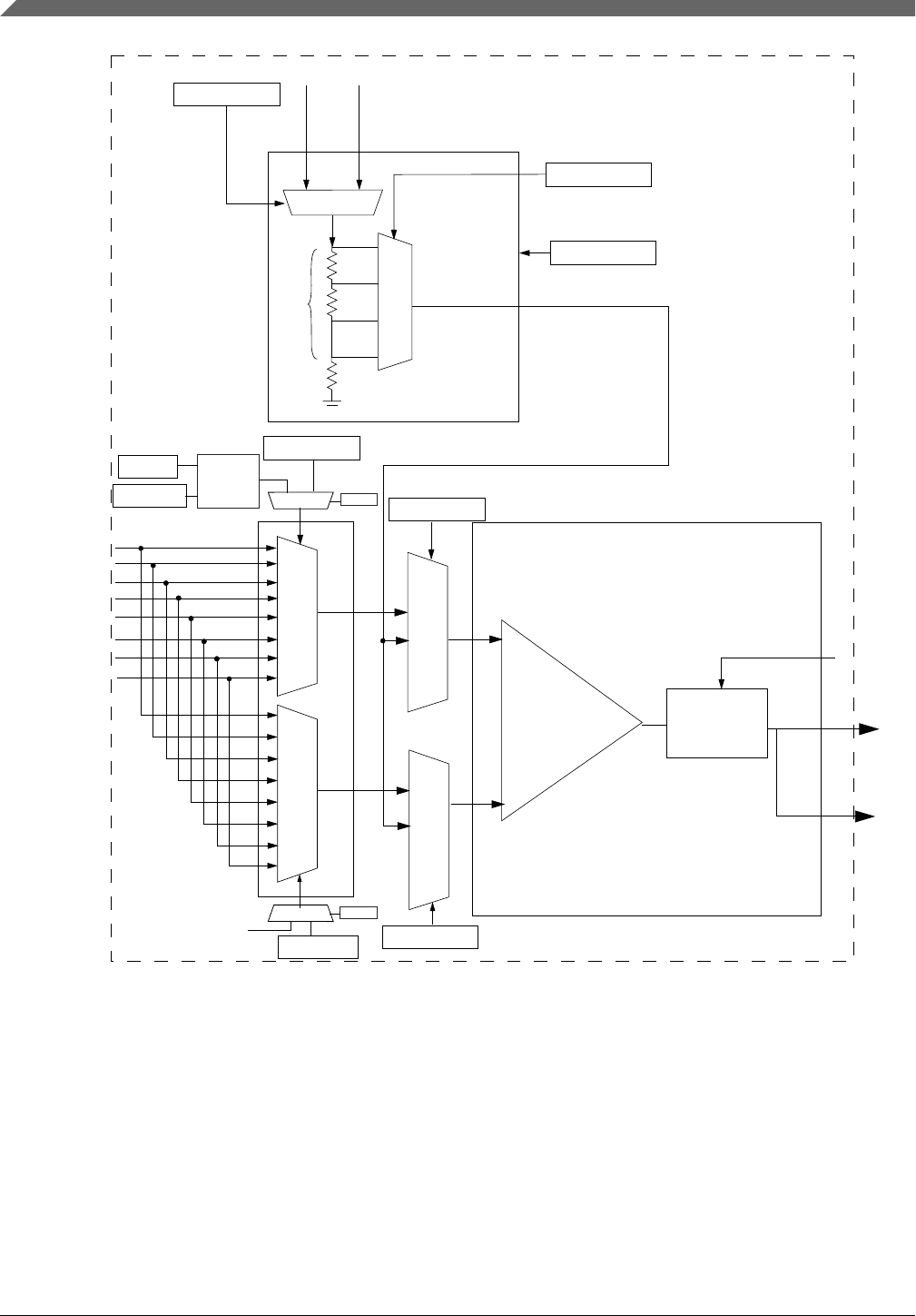
Sample input
VRSEL
VOSEL[7:0]
MUX
256-level
PSEL[2:0]
DAC
PMUXNMUX
IRQ
ANMUX
MSEL[2:0]
CMP
CMP
MUX
DAC output
DACEN
Vin1 Vin2
Window
and filter
control
CMPO
Reference Input 0
Reference Input 1
Reference Input 2
Reference Input 3
Reference Input 4
Reference Input 5
Reference Input 6
INP
INN
Reference Input 7
INPSEL[1:0]
INNSEL[1:0]
01
00
01
00
CHNxRound-
robin
switchFXMXCH[2:0] 1 0
From
round-robin
switch
1 0
RRE
RRE
Figure 43-1. CMP high level diagram
43.5 CMP block diagram
The following figure shows the block diagram for the CMP module.
CMP block diagram
S32K1xx Series Reference Manual, Rev. 7, 04/2018
1118 NXP Semiconductors
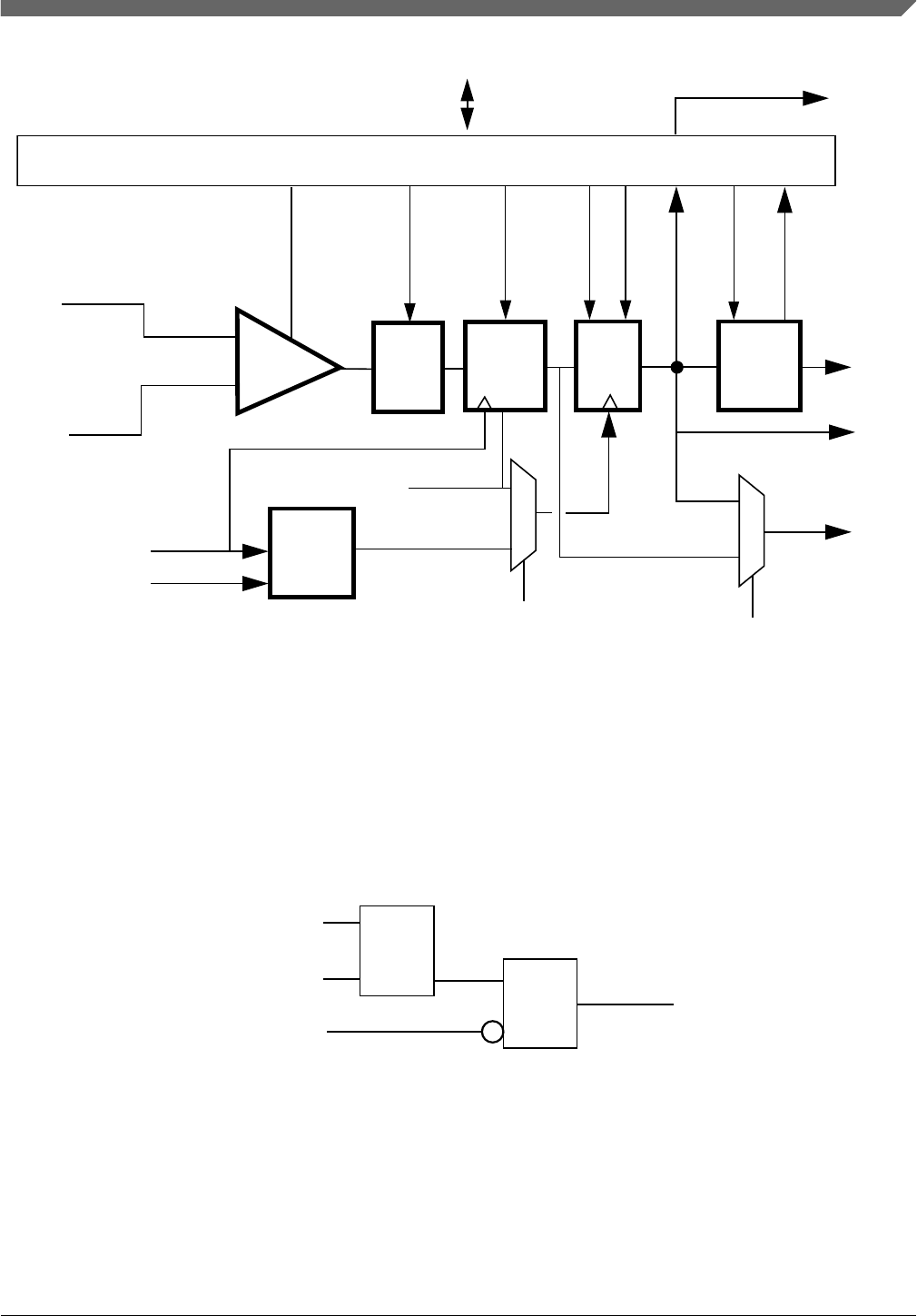
IRQ
INP
INM
FILTER_CNT
INV
COUT
COUT
OPE
SE
CMPO to
PAD
COUTA 1
WE
0
SE
CGMUX
COS
FILT_PER
+
-
FILT_PER
bus clock
COS
IER/F CFR/F
WINDOW/SAMPLE 1 0
EN,PMODE,HYSTCTR[1:0]
Interrupt
control
Filter
block
Window
control
Polarity
select
Clock
prescaler divided
bus
clock
CMPO
To other SOC functions
Internal bus
Figure 43-2. Comparator module block diagram
In the CMP block diagram:
• The Window Control block is bypassed when C0[WE] = 0.
• If C0[WE] = 1, the comparator output is sampled on every bus clock when
WINDOW=1 to generate COUTA. Sampling does NOT occur when WINDOW = 0.
• The Filter block is bypassed when not in use.
FILT_PER =
FILTER_CNT =
AND
SE
bypass_Filter_Block
OR
0x00
0x00
Figure 43-3. Filter block bypass logic
• The Filter block acts as a simple sampler if the filter is bypassed and
C0[FILTER_CNT] is set to 0x01.
• The Filter block filters based on multiple samples when the filter is bypassed and
C0[FILTER_CNT] is set greater than 0x01.
Chapter 43 Comparator (CMP)
S32K1xx Series Reference Manual, Rev. 7, 04/2018
NXP Semiconductors 1119

• If C0[SE] = 1, the external SAMPLE input is used as the sampling clock.
• IF C0[SE] = 0, the divided bus clock is used as the sampling clock.
• If enabled, the Filter block will incur up to one bus clock additional latency penalty
on COUT due to the fact that COUT, which crosses clock domain boundaries, must
be resynchronized to the bus clock.
• C0[WE] and C0[SE] are mutually exclusive.
• If enabled, the filter clock and the sample period must be at least 4 times slower than
the system clock to the comparator.
43.6 CMP pin descriptions
This section provides the comparator pin descriptions. The external inputs IN[7:0] are
muxed by CMP_C1[PSEL] and CMP_C1[MSEL] beforehand and multiplexed output
will then go to the second stage of multiplex with the input of 8-bit DAC and other two
internal reserved test signals, determined by CMP_C1[INPSEL] and CMP_C1[INNSEL]
the output of the second multiplex will finally go to the positive and negative ports of the
comparator respectively.
Table 43-2. CMP signal descriptions
Signal Description I/O
IN[7:0] Analog voltage inputs I
43.6.1 External pins
The CMP has two analog inputs: INP and INM. Each of these pins can accept an input
voltage that varies across the full operating range of the MCU. If the module is not
enabled, each pin can be used as a digital input or output. Consult the specific MCU
documentation to determine what functions are shared with these analog inputs.
The user can select either filtered or unfiltered comparator outputs for use on an external
I/O pad.
CMP pin descriptions
S32K1xx Series Reference Manual, Rev. 7, 04/2018
1120 NXP Semiconductors

43.7 CMP functional modes
There are three main sub-blocks to the CMP module:
• The comparator itself
• The window function
• The filter function
The filter, C0[FILTER_CNT], can be clocked from an internal or external clock source.
The filter is programmable with respect to the number of samples that must agree before
a change in the output is registered. In the simplest case, only one sample must agree. In
this case, the filter acts as a simple sampler.
The external sample input is enabled using C0[SE]. When set, the output of the
comparator is sampled only on rising edges of the sample input.
The "windowing mode" is enabled by setting C0[WE]. When set, the comparator output
is sampled only when WINDOW=1. This feature can be used to ignore the comparator
output during time periods in which the input voltages are not valid. This is especially
useful when implementing zero-crossing-detection for certain PWM applications.
The comparator filter and sampling features can be combined as shown in the following
table. Individual modes are discussed below.
Table 43-3. Comparator sample/filter controls
Mode # C0[EN] C0[WE] C0[SE] C0[FILTER_CN
T] C0[FPR] Operation
1 0 X X X X Disabled
See the Disabled mode (# 1).
2A 1 0 0 0x00 X Continuous Mode
See the Continuous mode (#s 2A &
2B).
2B 1 0 0 X 0x00
3A 1 0 1 0x01 X Sampled, Non-Filtered mode
See the Sampled, Non-Filtered
mode (#s 3A & 3B).
3B 1 0 0 0x01 > 0x00
4A 1 0 1 > 0x01 X Sampled, Filtered mode
See the Sampled, Filtered mode (#s
4A & 4B).
4B 1 0 0 > 0x01 > 0x04
5A 1 1 0 0x00 X Windowed mode
5B 1 1 0 X 0x00
Table continues on the next page...
Chapter 43 Comparator (CMP)
S32K1xx Series Reference Manual, Rev. 7, 04/2018
NXP Semiconductors 1121

Table 43-3. Comparator sample/filter controls (continued)
Mode # C0[EN] C0[WE] C0[SE] C0[FILTER_CN
T] C0[FPR] Operation
Comparator output is sampled on
every rising bus clock edge when
SAMPLE=1 to generate COUTA.
See the Windowed mode (#s 5A &
5B).
6 1 1 0 0x01 0x01–0xFF Windowed/Resampled mode
Comparator output is sampled on
every rising bus clock edge when
SAMPLE=1 to generate COUTA,
which is then resampled on an
interval determined by C0[FPR] to
generate COUT.
See the Windowed/Resampled
mode (# 6).
7 1 1 0 > 0x01 0x01–0xFF Windowed/Filtered mode
Comparator output is sampled on
every rising bus clock edge when
SAMPLE=1 to generate COUTA,
which is then resampled and filtered
to generate COUT.
See the Windowed/Filtered mode
(#7).
All other combinations of C0[EN], C0[WE], C0[SE], C0[FILTER_CNT], and C0[FPR] are illegal.
For cases where a comparator is used to drive a fault input, for example, for a motor-
control module such as FTM, it must be configured to operate in Continuous mode so
that an external fault can immediately pass through the comparator to the target fault
circuitry.
Note
Filtering and sampling settings must be changed only after
setting C0[SE]=0, C0[FPR] =0 and C0[FILTER_CNT]=0x00.
This resets the filter to a known state.
43.7.1 Disabled mode (# 1)
In Disabled mode, the analog comparator is non-functional and consumes no power.
CMPO is 0 in this mode.
CMP functional modes
S32K1xx Series Reference Manual, Rev. 7, 04/2018
1122 NXP Semiconductors
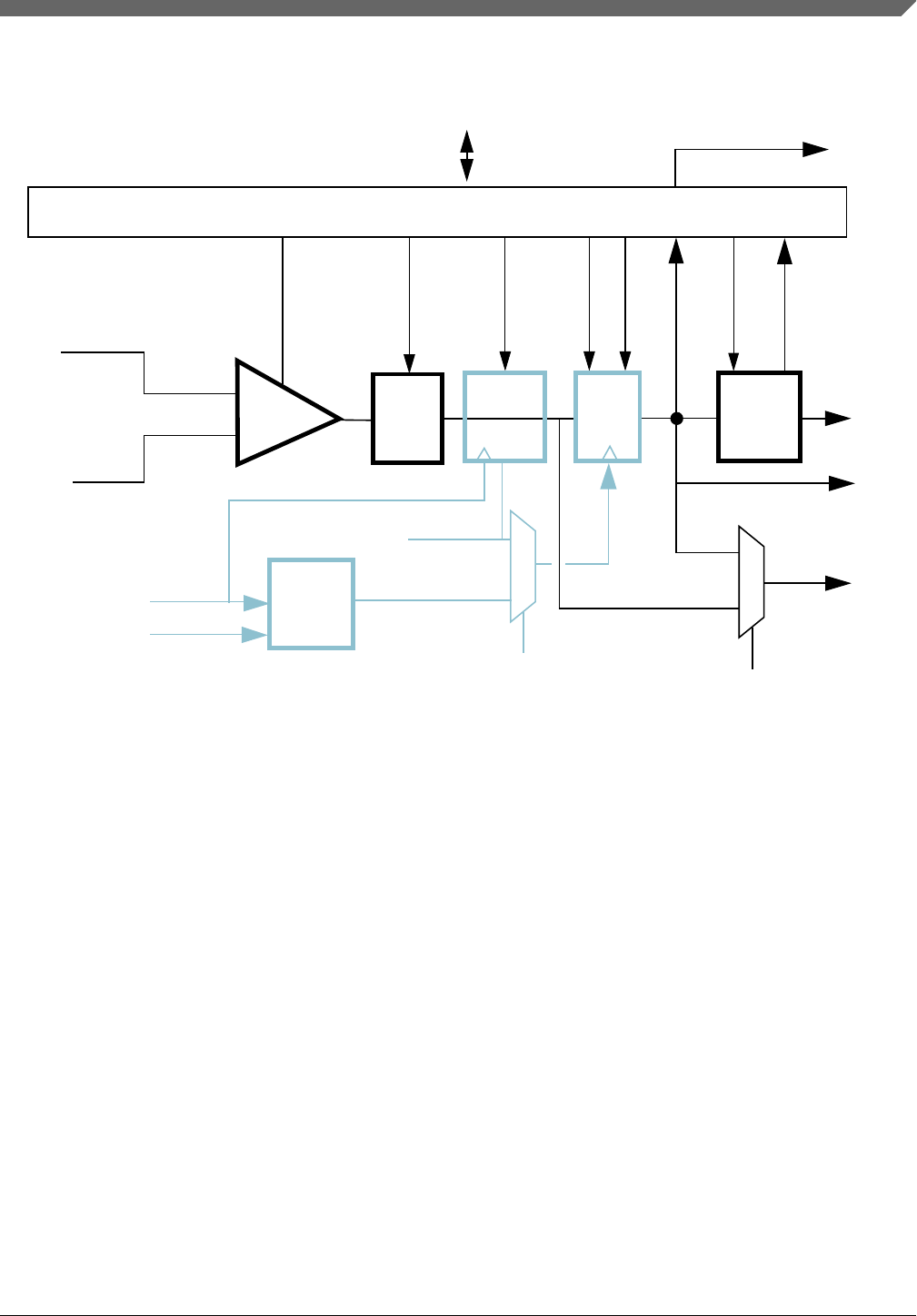
43.7.2 Continuous mode (#s 2A & 2B)
IRQ
Internal bus
INP
INM
FILTER_CNT
INV
COUT
COUT
OPE
SE
CMPO to
PAD
COUTA 1
WE
0
SE
CGMUX
COS
FILT_PER
0
+
-
FILT_PER
COS
IER/F CFR/F
WINDOW/SAMPLE 1 0
EN,PMODE,HYSTCTR[1:0]
divided
bus
clock
CMPO
bus clock
To other SOC functions
Polarity
select Window
control
Filter
block
Interrupt
control
Clock
prescaler
Figure 43-4. Comparator operation in Continuous mode
NOTE
See the chip configuration section for the source of sample/
window input.
The analog comparator block is powered and active. CMPO may be optionally inverted,
but is not subject to external sampling or filtering. Both window control and filter blocks
are completely bypassed (as the grey-colored parts in the figure). C0[COUT] is updated
continuously. The path from comparator input pins to output pin is operating in
combinational unclocked mode. COUT and COUTA are identical.
For control configurations that result in disabling the filter block, see Figure 43-3.
43.7.3 Sampled, Non-Filtered mode (#s 3A & 3B)
Chapter 43 Comparator (CMP)
S32K1xx Series Reference Manual, Rev. 7, 04/2018
NXP Semiconductors 1123

+
-
IRQ
INP
INM
FILTER_CNT
INV
COUT
COUT
OPE
SE
CMPO to
PAD
COUTA 1
WE
0
SE=1
CGMUX
COS
FILT_PER
1
0
FILT_PER
COS
0x01
IER/F CFR/F
WINDOW/SAMPLE 1 0
EN,PMODE,HYSTCTR[1:0]
divided
bus
clock
CMPO
bus clock
Internal bus
Polarity
select Window
control
Filter
block Interrupt
control
To other SOC functions
Clock
prescaler
Figure 43-5. Sampled, Non-Filtered (# 3A): sampling point externally driven
In Sampled, Non-Filtered mode, the analog comparator block is powered and active. The
path from analog inputs to COUTA is combinational unclocked. Windowing control is
completely bypassed. COUTA is sampled whenever a rising edge is detected on the filter
block clock input.
The only difference in operation between Sampled, Non-Filtered (# 3A) and Sampled,
Non-Filtered (# 3B) is in how the clock to the filter block is derived. In #3A, the clock to
filter block is externally derived while in #3B, the clock to filter block is internally
derived.
The comparator filter has no other function than sample/hold of the comparator output in
this mode (# 3B).
CMP functional modes
S32K1xx Series Reference Manual, Rev. 7, 04/2018
1124 NXP Semiconductors
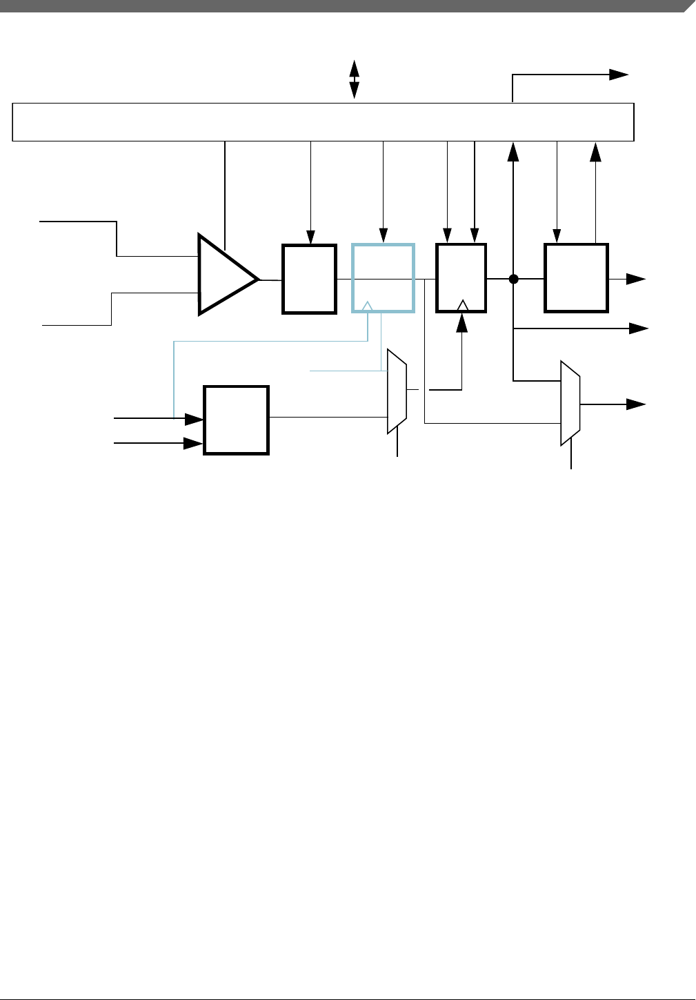
IRQ
INP
INM
FILTER_CNT
INV
COUT
COUT
OPE
SE
CMPO to
PAD
COUTA 1
WE
0
SE=0
CGMUX
COS
FILT_PER
0
0
+
-
FILT_PER
COS
0x01
IER/F CFR/F
WINDOW/SAMPLE 1 0
EN,PMODE,HYSTCTR[1:0]
divided bus clock
CMPO
bus clock
Internal bus
Polarity
select
Window
control
Filter
block
Interrupt
control
To other SOC functions
Clock
prescaler
Figure 43-6. Sampled, Non-Filtered (# 3B): sampling interval internally derived
43.7.4 Sampled, Filtered mode (#s 4A & 4B)
In Sampled, Filtered mode, the analog comparator block is powered and active. The path
from analog inputs to COUTA is combinational unclocked. Windowing control is
completely bypassed. COUTA is sampled whenever a rising edge is detected on the filter
block clock input.
The only difference in operation between Sampled, Non-Filtered (# 3A) and Sampled,
Filtered (# 4A) is that, now, C0[FILTER_CNT]>1, which activates filter operation.
Chapter 43 Comparator (CMP)
S32K1xx Series Reference Manual, Rev. 7, 04/2018
NXP Semiconductors 1125
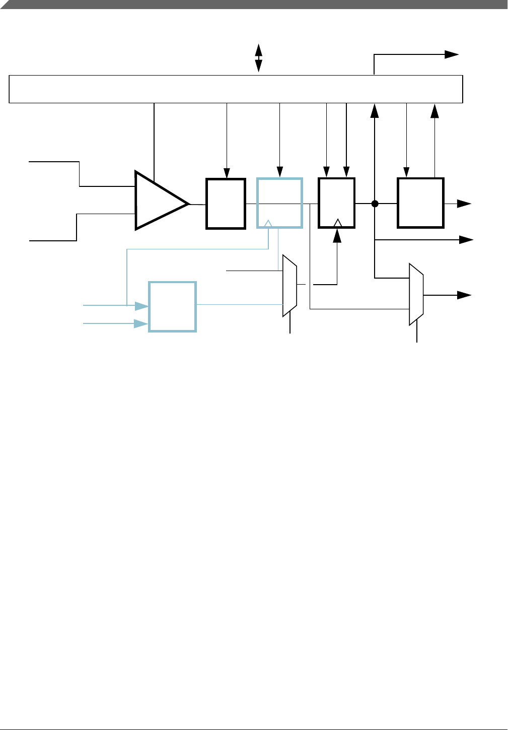
+
-
IRQ
INP
INM
FILTER_CNT
INV
COUT
COUT
OPE
SE
CMPO to
PAD
COUTA 1
WE
0
SE=1
CGMUX
COS
FILT_PER
1
0
FILT_PER
bus clock
COS
>
IER/F CFR/F
WINDOW/SAMPLE 1 0
EN, PMODE, HYSTCTR[1:0]
divided
bus
clock
CMPO
0x01
Internal bus
Polarity
select Window
control
Filter
block
Interrupt
control
Clock
prescaler
To other SOC functions
Figure 43-7. Sampled, Filtered (# 4A): sampling point externally driven
CMP functional modes
S32K1xx Series Reference Manual, Rev. 7, 04/2018
1126 NXP Semiconductors
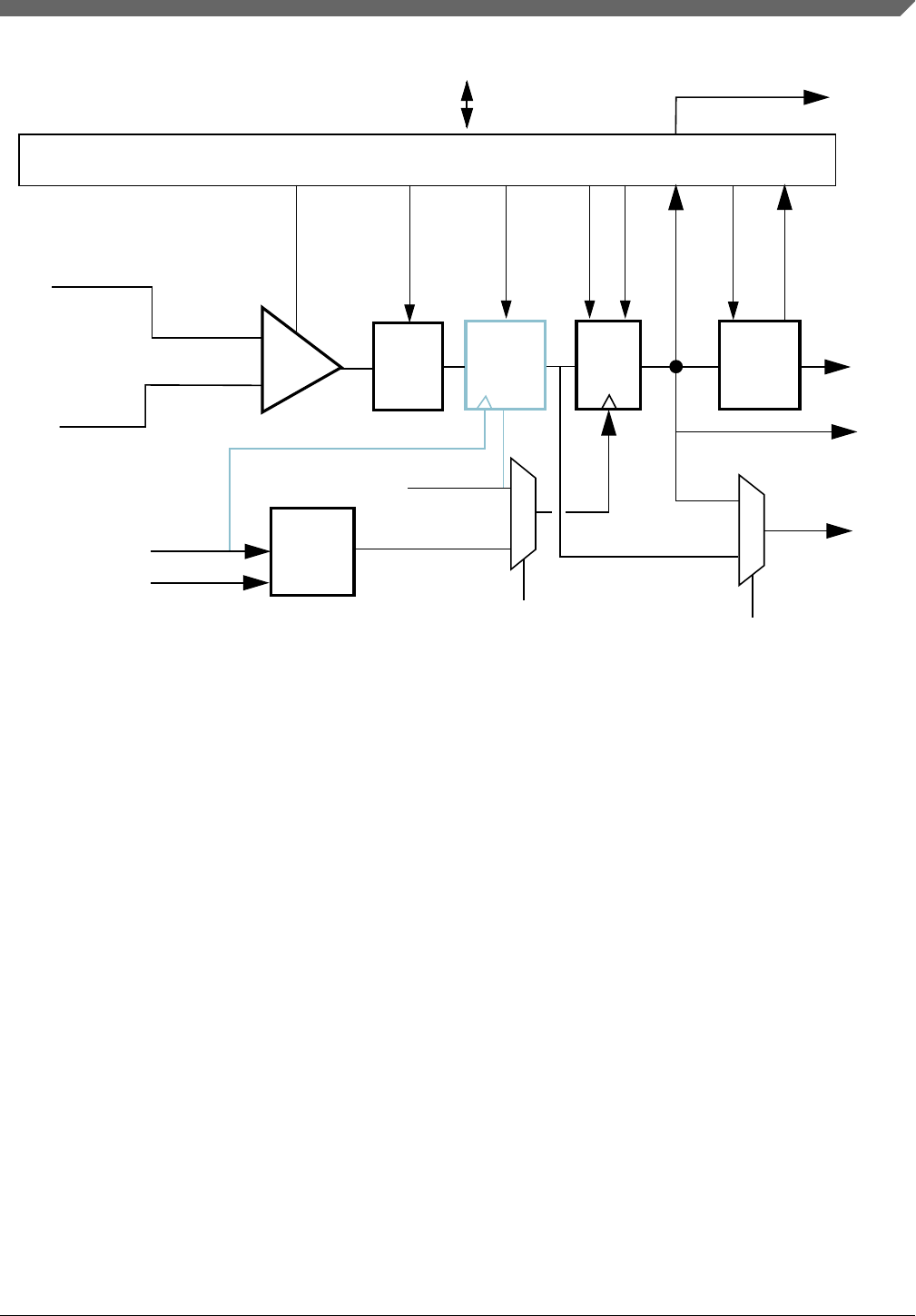
+
-
IRQ
INP
INM
FILTER_CNT
INV
COUT
COUT
OPE
SE
CMPO to
PAD
COUTA
0
1
WE
1
0
SE=0
CGMUX
COS
FILT_PER
1
0
FILT_PER
bus clock
COS
>
IER/F CFR/F
WINDOW/SAMPLE
EN, PMODE,HYSTCTR[1:0]
divided
bus
clock
CMPO
0x01
Internal bus
Polarity
select
Window
control
Filter
block Interrupt
control
Clock
prescaler
To other SOC functions
Figure 43-8. Sampled, Filtered (# 4B): sampling point internally derived
The only difference in operation between Sampled, Non-Filtered (# 3B) and Sampled,
Filtered (# 4B) is that now, C0[FILTER_CNT]>1, which activates filter operation.
43.7.5 Windowed mode (#s 5A & 5B)
The following figure illustrates comparator operation in the Windowed mode, ignoring
latency of the analog comparator, polarity select, and window control block. It also
assumes that the polarity select is set to non-inverting state.
NOTE
The analog comparator output is passed to COUTA only when
the WINDOW signal is high.
In actual operation, COUTA may lag the analog inputs by up to one bus clock cycle plus
the combinational path delay through the comparator and polarity select logic.
Chapter 43 Comparator (CMP)
S32K1xx Series Reference Manual, Rev. 7, 04/2018
NXP Semiconductors 1127
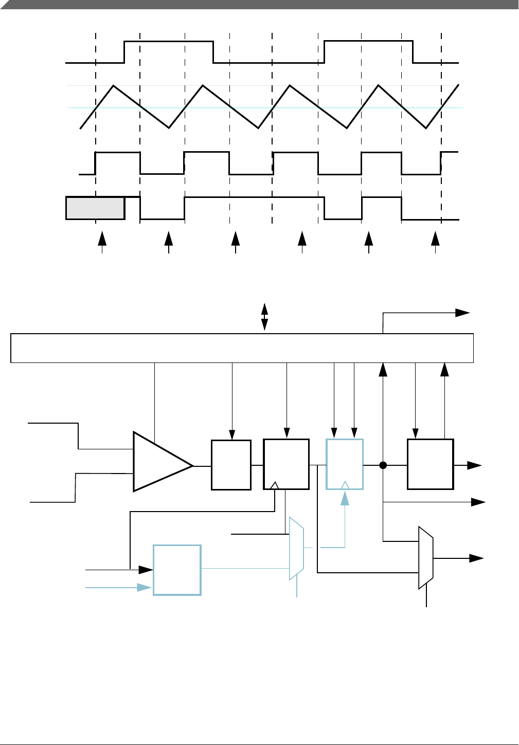
WINDOW
COUTA
CMPO
Minus input
Plus input
Figure 43-9. Windowed mode timing diagram
+
-
IRQ
EN, PMODE,HYSCTR[1:0]
INP
INM
FILTER_CNT
INV
COUT
COUT
OPE
SE
CMPO to
PAD
COUTA
0
1
WE
1
0
SE=0
CGMUX
COS
FILT_PER
0
FILT_PER
bus clock
COS
0x01
IER/F CFR/F
WINDOW/SAMPLE
Polarity
select Window
control Filter
block
Interrupt
control
divided
bus
clock
Clock
prescaler
CMPO
Internal bus
To other SOC functions
Figure 43-10. Windowed mode
For control configurations which result in disabling the filter block, see Figure 43-3.
When any windowed mode is active, COUTA is clocked by the bus clock whenever
WINDOW = 1. The last latched value is held when WINDOW = 0.
CMP functional modes
S32K1xx Series Reference Manual, Rev. 7, 04/2018
1128 NXP Semiconductors
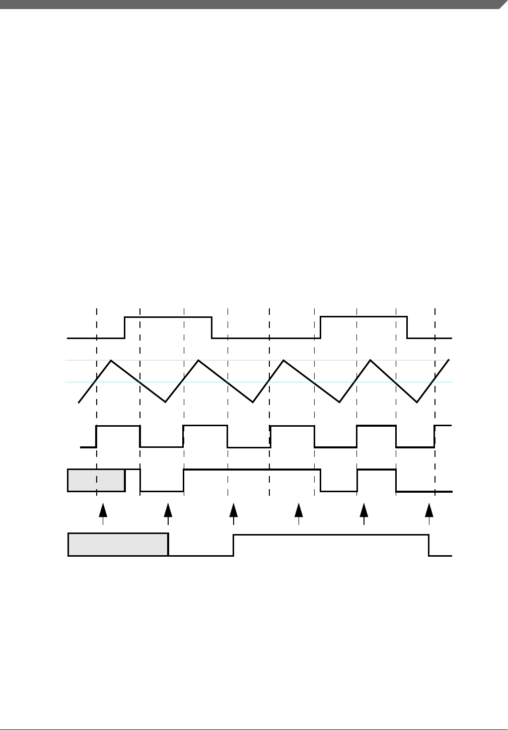
NOTE
The sample input must be high for ≥ 2.5 CMP bus clock cycles
to ensure no sampling event is missed.
43.7.6 Windowed/Resampled mode (# 6)
The following figure uses the same input stimulus shown in Figure 43-9, and adds
resampling of COUTA to generate COUT. Samples are taken at the time points indicated
by the arrows in the figure. Again, prop delays and latency are ignored for the sake of
clarity.
This example was generated solely to demonstrate operation of the comparator in
windowed/resampled mode, and does not reflect any specific application. Depending
upon the sampling rate and window placement, COUT may not see zero-crossing events
detected by the analog comparator. Sampling period and/or window placement must be
carefully considered for a given application.
WINDOW
COUTA
COUT
CMPO
Minus input
Plus input
Figure 43-11. Windowed/resampled mode operation
This mode of operation results in an unfiltered string of comparator samples where the
interval between the samples is determined by FPR[FILT_PER] and the bus clock rate.
Configuration for this mode is virtually identical to that for the Windowed/Filtered Mode
shown in the next section. The only difference is that the value of C0[FILTER_CNT]
must be 1.
Chapter 43 Comparator (CMP)
S32K1xx Series Reference Manual, Rev. 7, 04/2018
NXP Semiconductors 1129
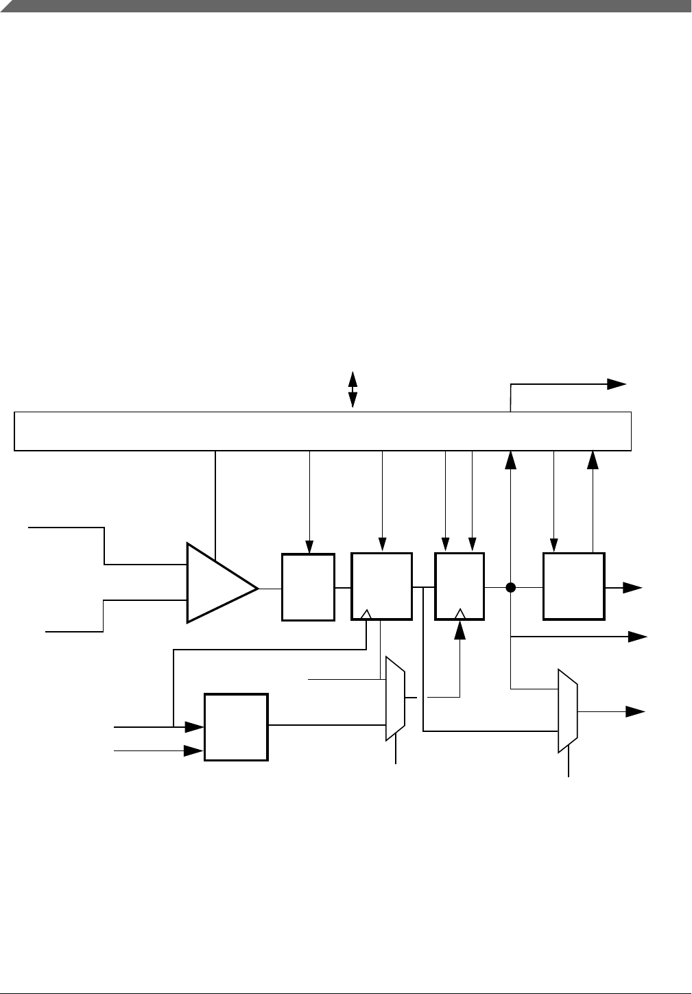
NOTE
The sample input must be high for ≥ 2.5 CMP bus clock cycles
to ensure no sampling event is missed.
43.7.7 Windowed/Filtered mode (#7)
This is the most complex mode of operation for the comparator block, as it uses both
windowing and filtering features. It also has the highest latency of any of the modes. This
can be approximated: up to 1 bus clock synchronization in the window function +
[(C0[FILTER_CNT] × C0[FPR]) + 1] × bus clock for the filter function.
When any windowed mode is active, COUTA is clocked by the bus clock whenever
WINDOW = 1. The last latched value is held when WINDOW = 0.
+
-
IRQ
EN, PMODE,HYSCTR[1:0]
INP
INM
FILTER_CNT
INV
COUT
COUT
OPE
SE
CMPO to
PAD
COUTA
0
1
WE
1
0
SE=0
CGMUX
COS
FILT_PER
01
FILT_PER
bus clock
COS
>
IER/F CFR/F
WINDOW/SAMPLE
Polarity
select
Window
control Filter
block
Interrupt
control
divided
bus
clock
Clock
prescaler
CMPO
0x01
To other SOC functions
Internal bus
Figure 43-12. Windowed/Filtered mode
The following figure shows the operation timing for this mode, considering uncertainty is
introduced by the internal synchronization for the filter block.
CMP functional modes
S32K1xx Series Reference Manual, Rev. 7, 04/2018
1130 NXP Semiconductors
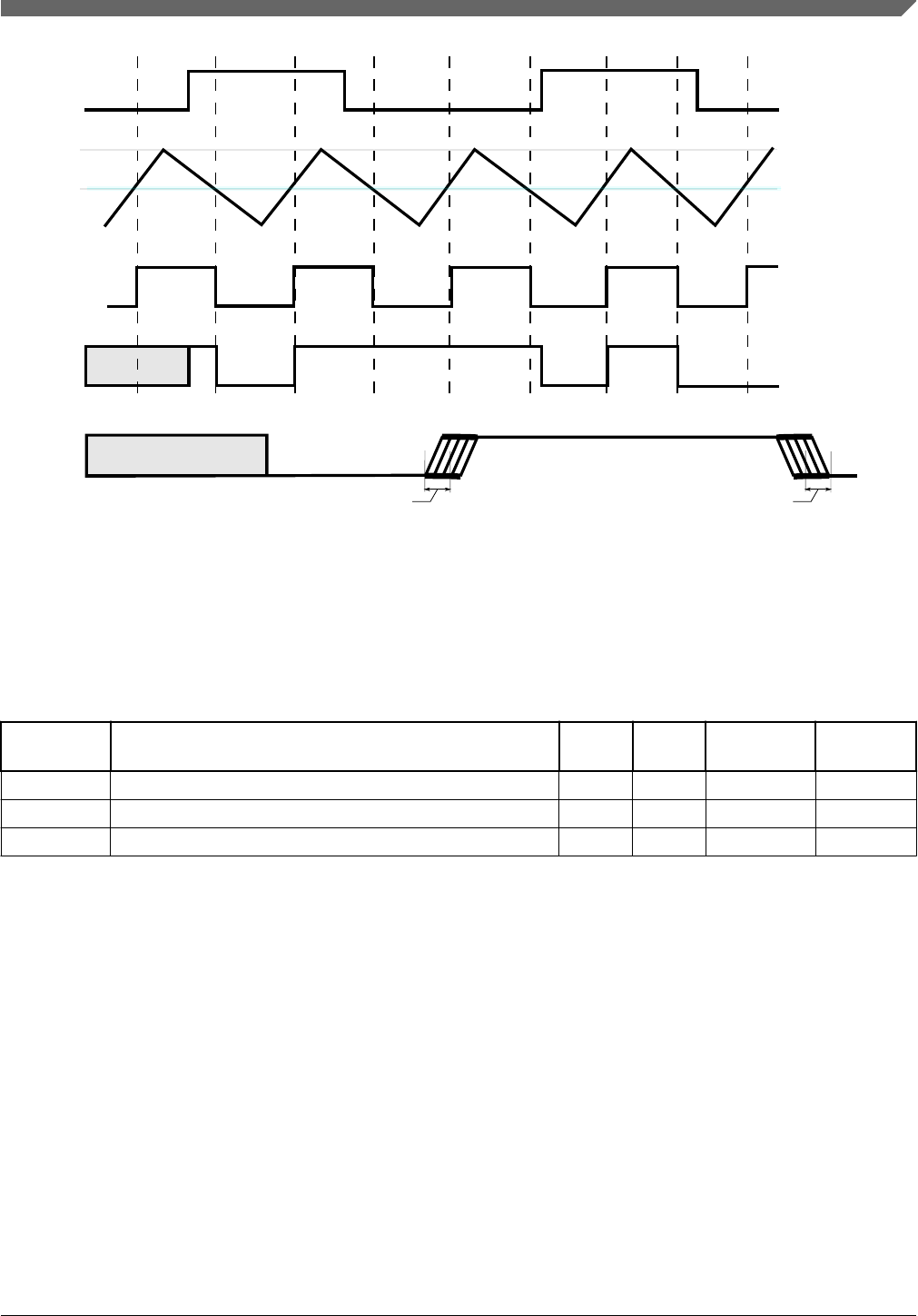
WINDOW
COUTA
COUT
CMPO
Minus input
Plus input
one filter
clock cycle
one filter
clock cycle
Figure 43-13. Windowed/Filtered mode operation
43.8 Memory map/register definitions
CMP memory map
Address
offset (hex) Register name Width
(in bits) Access Reset value Section/
page
0 CMP Control Register 0 (CMP_C0) 32 R/W 0000_0000h 43.8.1/1131
4 CMP Control Register 1 (CMP_C1) 32 R/W 0000_0000h 43.8.2/1135
8 CMP Control Register 2 (CMP_C2) 32 R/W 0000_0000h 43.8.3/1138
43.8.1 CMP Control Register 0 (CMP_C0)
Access:
• Supervisor read/write
• User read/write
Chapter 43 Comparator (CMP)
S32K1xx Series Reference Manual, Rev. 7, 04/2018
NXP Semiconductors 1131
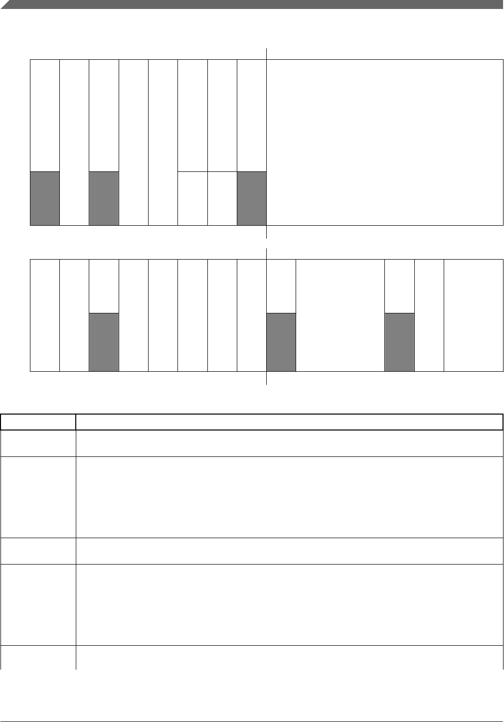
Address: 0h base + 0h offset = 0h
Bit 31 30 29 28 27 26 25 24 23 22 21 20 19 18 17 16
R0
DMAEN
0
IER IEF
CFR CFF
COUT
FPR
Ww1c w1c
Reset 0 0 0 0 0 0 0 0 0 0 0 0 0 0 0 0
Bit 15 14 13 12 11 10 9 8 7 6 5 4 3 2 1 0
R
SE WE
0
PMODE
INVT COS OPE EN
0
FILTER_CNT
0
OFFSET
HYSTCTR
W
Reset 0 0 0 0 0 0 0 0 0 0 0 0 0 0 0 0
CMP_C0 field descriptions
Field Description
31
Reserved
This field is reserved.
This read-only field is reserved and always has the value 0.
30
DMAEN
DMA Enable
Enables the DMA transfer triggered from the CMP module. When this field is set, a DMA request is
asserted when CFR or CFF is set.
0 DMA is disabled.
1 DMA is enabled.
29
Reserved
This field is reserved.
This read-only field is reserved and always has the value 0.
28
IER
Comparator Interrupt Enable Rising
Enables the CFR interrupt from the CMP. When this field is set, an interrupt will be asserted when CFR is
set.
0 Interrupt is disabled.
1 Interrupt is enabled.
27
IEF
Comparator Interrupt Enable Falling
Table continues on the next page...
Memory map/register definitions
S32K1xx Series Reference Manual, Rev. 7, 04/2018
1132 NXP Semiconductors

CMP_C0 field descriptions (continued)
Field Description
Enables the CFF interrupt from the CMP. When this field is set, an interrupt will be asserted when CFF is
set.
0 Interrupt is disabled.
1 Interrupt is enabled.
26
CFR
Analog Comparator Flag Rising
Detects a rising-edge on COUT, when set, during normal operation. CFR is cleared by writing 1 to it.
During Stop modes, CFR is level sensitive
0 A rising edge has not been detected on COUT.
1 A rising edge on COUT has occurred.
25
CFF
Analog Comparator Flag Falling
Detects a falling-edge on COUT, when set, during normal operation. CFF is cleared by writing 1 to it.
During Stop modes, CFF is level sensitive .
0 A falling edge has not been detected on COUT.
1 A falling edge on COUT has occurred.
24
COUT
Analog Comparator Output
Returns the current value of the Analog Comparator output, when read. The field is reset to 0 and will read
as C0[INVT] when the Analog Comparator module is disabled, that is, when C0[EN] = 0. Writes to this
field are ignored.
23–16
FPR
Filter Sample Period
Specifies the sampling period, in bus clock cycles, of the comparator output filter, when C0[SE] = 0.
Setting FPR to 0x0 disables the filter. Filter programming and latency details are provided in the CMP
functional description. This field has no effect when C0[SE ]= 1. In that case, the external SAMPLE signal
is used to determine the sampling period.
15
SE
Sample Enable
At any given time, either SE or WE can be set. If a write to this register attempts to set both, then SE is set
and WE is cleared. However, avoid writing ones to both bit locations because this "11" case is reserved.
0 Sampling mode is not selected.
1 Sampling mode is selected.
14
WE
Windowing Enable
At any given time, either SE or WE can be set. If a write to this register attempts to set both, then SE is set
and WE is cleared. However, avoid writing ones to both bit locations because this "11" case is reserved.
0 Windowing mode is not selected.
1 Windowing mode is selected.
13
Reserved
This field is reserved.
This read-only field is reserved and always has the value 0.
12
PMODE
Power Mode Select
0 Low Speed (LS) comparison mode is selected.
1 High Speed (HS) comparison mode is selected, in VLPx mode, or Stop mode switched to Low Speed
(LS) mode.
Table continues on the next page...
Chapter 43 Comparator (CMP)
S32K1xx Series Reference Manual, Rev. 7, 04/2018
NXP Semiconductors 1133

CMP_C0 field descriptions (continued)
Field Description
11
INVT
Comparator invert
This bit allows selecting the polarity of the analog comparator function. It is also driven to the COUT output
(on both the device pin and as C0[COUT]) when C0[OPE]=0.
0 Does not invert the comparator output.
1 Inverts the comparator output.
10
COS
Comparator Output Select
0 Set CMPO to equal COUT (filtered comparator output).
1 Set CMPO to equal COUTA (unfiltered comparator output).
9
OPE
Comparator Output Pin Enable
The OPE bit enables the path from the comparator output to a selected pin.
0 When OPE is 0, the comparator output (after window/filter settings dependent on software
configuration) is not available to a packaged pin.
1When OPE is 1, and if the software has configured the comparator to own a packaged pin, the
comparator is available in a packaged pin.
8
EN
Comparator Module Enable
The EN bit enables the Analog Comparator Module. When the module is not enabled, the analog part
remains in the off state, and consumes no power.
0 Analog Comparator is disabled.
1 Analog Comparator is enabled.
7
Reserved
This field is reserved.
This read-only field is reserved and always has the value 0.
6–4
FILTER_CNT
Filter Sample Count
This field specifies the number of consecutive samples that must agree prior to the comparator output filter
accepting a new output state. For information regarding filter programming and latency, please see the
Functional Description.
000 Filter is disabled. If SE = 1, then COUT is a logic zero (this is not a legal state, and is not
recommended). If SE = 0, COUT = COUTA.
001 1 consecutive sample must agree (comparator output is simply sampled).
010 2 consecutive samples must agree.
011 3 consecutive samples must agree.
100 4 consecutive samples must agree.
101 5 consecutive samples must agree.
110 6 consecutive samples must agree.
111 7 consecutive samples must agree.
3
Reserved
This field is reserved.
This read-only field is reserved and always has the value 0.
2
OFFSET
Comparator hard block offset control. See chip data sheet to get the actual offset value with each level
Table continues on the next page...
Memory map/register definitions
S32K1xx Series Reference Manual, Rev. 7, 04/2018
1134 NXP Semiconductors

CMP_C0 field descriptions (continued)
Field Description
NOTE: • If OFFSET = 1, then there will be no hysteresis in the case of INP crossing INN in the
positive direction (or INN crossing INP in the negative direction). A Half Hysteresis value
still exists for INP crossing INN in the falling direction.
• If OFFSET = 0, then the hysteresis selected by HYSTCTR is valid for both directions.
0 The comparator hard block output has level 0 offset internally.
1 The comparator hard block output has level 1 offset internally.
HYSTCTR Comparator hard block hysteresis control. See chip data sheet to get the actual hysteresis value with each
level
00 The hard block output has level 0 hysteresis internally.
01 The hard block output has level 1 hysteresis internally.
10 The hard block output has level 2 hysteresis internally.
11 The hard block output has level 3 hysteresis internally.
43.8.2 CMP Control Register 1 (CMP_C1)
Access:
• Supervisor read/write
• User read/write
Address: 0h base + 4h offset = 4h
Bit 31 30 29 28 27 26 25 24 23 22 21 20 19 18 17 16
R0 0
INPSEL
0
INNSEL
CHN7
CHN6
CHN5
CHN4
CHN3
CHN2
CHN1
CHN0
W
Reset 0 0 0 0 0 0 0 0 0 0 0 0 0 0 0 0
Bit 15 14 13 12 11 10 9 8 7 6 5 4 3 2 1 0
R
DACEN
VRSEL
PSEL MSEL VOSEL
W
Reset 0 0 0 0 0 0 0 0 0 0 0 0 0 0 0 0
CMP_C1 field descriptions
Field Description
31–30
Reserved
This field is reserved.
This read-only field is reserved and always has the value 0.
29
Reserved
This field is reserved.
This read-only field is reserved and always has the value 0.
Table continues on the next page...
Chapter 43 Comparator (CMP)
S32K1xx Series Reference Manual, Rev. 7, 04/2018
NXP Semiconductors 1135

CMP_C1 field descriptions (continued)
Field Description
28–27
INPSEL
Selection of the input to the positive port of the comparator
Determines which input is selected for the plus input of the comparator.
NOTE: These selections is used to select the final positive input to the comparator.
Note: For the round robin mode of operation, the MSEL and PSEL bitfields in CMPx_C1 register must
have different values.
00 IN0, from the 8-bit DAC output
01 IN1, from the analog 8-1 mux
10 Reserved
11 Reserved
26
Reserved
This field is reserved.
This read-only field is reserved and always has the value 0.
25–24
INNSEL
Selection of the input to the negative port of the comparator
Determines which input is selected for the plus input of the comparator.
NOTE: These selections is used to select the final negative input to the comparator.
Note: For the round robin mode of operation, the MSEL and PSEL bitfields in CMPx_C1 register must
have different values.
00 IN0, from the 8-bit DAC output
01 IN1, from the analog 8-1 mux
10 Reserved
11 Reserved
23
CHN7
Channel 7 input enable
Channel 7 of the input enable for the round-robin checker. If CHN7 is set, then the corresponding channel
to the non-fixed mux port is enabled to check its voltage value in the round-robin mode. If the same
channel is selected as the reference voltage, this bit has no effect.
22
CHN6
Channel 6 input enable
Channel 6 of the input enable for the round-robin checker. If CHN6 is set, then the corresponding channel
to the non-fixed mux port is enabled to check its voltage value in the round-robin mode. If the same
channel is selected as the reference voltage, this bit has no effect.
21
CHN5
Channel 5 input enable
Channel 5 of the input enable for the round-robin checker. If CHN5 is set, then the corresponding channel
to the non-fixed mux port is enabled to check its voltage value in the round-robin mode. If the same
channel is selected as the reference voltage, this bit has no effect.
20
CHN4
Channel 4 input enable
Channel 4 of the input enable for the round-robin checker. If CHN4 is set, then the corresponding channel
to the non-fixed mux port is enabled to check its voltage value in the round-robin mode. If the same
channel is selected as the reference voltage, this bit has no effect.
19
CHN3
Channel 3 input enable
Channel 3 of the input enable for the round-robin checker. If CHN3 is set, then the corresponding channel
to the non-fixed mux port is enabled to check its voltage value in the round-robin mode. If the same
channel is selected as the reference voltage, this bit has no effect.
Table continues on the next page...
Memory map/register definitions
S32K1xx Series Reference Manual, Rev. 7, 04/2018
1136 NXP Semiconductors

CMP_C1 field descriptions (continued)
Field Description
18
CHN2
Channel 2 input enable
Channel 2 of the input enable for the round-robin checker. If CHN2 is set, then the corresponding channel
to the non-fixed mux port is enabled to check its voltage value in the round-robin mode. If the same
channel is selected as the reference voltage, this bit has no effect.
17
CHN1
Channel 1 input enable
Channel 1 of the input enable for the round-robin checker. If CHN1 is set, then the corresponding channel
to the non-fixed mux port is enabled to check its voltage value in the round-robin mode. If the same
channel is selected as the reference voltage, this bit has no effect.
16
CHN0
Channel 0 input enable
Channel 0 of the input enable for the round-robin checker. If CHN0 is set, then the corresponding channel
to the non-fixed mux port is enabled to check its voltage value in the round-robin mode. If the same
channel is selected as the reference voltage, this bit has no effect.
15
DACEN
DAC Enable
This bit is used to enable the DAC. When the DAC is disabled, it is powered down to conserve power.
0 DAC is disabled.
1 DAC is enabled.
14
VRSEL
Supply Voltage Reference Source Select
0 Vin1 is selected as resistor ladder network supply reference Vin.
1 Vin2 is selected as resistor ladder network supply reference Vin.
13–11
PSEL
Plus Input MUX Control
Determines which input is selected for the plus mux.
NOTE: These bits are used to select the external 8 inputs for the plus mux, the actual input to the positive
port of the comparator is selected between this mux out and other inputs finally, see the definition in
INPSEL.
Note: For the round robin mode of operation, the MSEL and PSEL bitfields in CMPx_C1 register must
have different values.
000 IN0
001 IN1
010 IN2
011 IN3
100 IN4
101 IN5
110 IN6
111 IN7
10–8
MSEL
Minus Input MUX Control
Determines which input is selected for the minus mux.
NOTE: These bits are used to select the external 8 inputs for the minus mux, the actual input to the
negative port of the comparator is selected between this mux out and other inputs finally, see the definition
in INNSEL.
Note: For the round robin mode of operation, the MSEL and PSEL bitfields in CMPx_C1 register must
have different values.
Table continues on the next page...
Chapter 43 Comparator (CMP)
S32K1xx Series Reference Manual, Rev. 7, 04/2018
NXP Semiconductors 1137

CMP_C1 field descriptions (continued)
Field Description
000 IN0
001 IN1
010 IN2
011 IN3
100 IN4
101 IN5
110 IN6
111 IN7
VOSEL DAC Output Voltage Select
This bit selects an output voltage from one of 256 distinct levels. DACO = (Vin/256) × (VOSEL[7:0] + 1),
so the DACO range is from Vin/256 to Vin.
43.8.3 CMP Control Register 2 (CMP_C2)
Access:
• Supervisor read/write
• User read/write
Address: 0h base + 8h offset = 8h
Bit 31 30 29 28 27 26 25 24 23 22 21 20 19 18 17 16
R
RRE RRIE
FXMP
0
FXMXCH
0
CH7F
CH6F
CH5F
CH4F
CH3F
CH2F
CH1F
CH0F
Ww1c w1c w1c w1c w1c w1c w1c w1c
Reset 0 0 0 0 0 0 0 0 0 0 0 0 0 0 0 0
Bit 15 14 13 12 11 10 9 8 7 6 5 4 3 2 1 0
R
NSAM INITMOD ACOn
W
Reset 0 0 0 0 0 0 0 0 0 0 0 0 0 0 0 0
Memory map/register definitions
S32K1xx Series Reference Manual, Rev. 7, 04/2018
1138 NXP Semiconductors

CMP_C2 field descriptions
Field Description
31
RRE
Round-Robin Enable
This bit enables the round-robin operation.
0 Round-robin operation is disabled.
1 Round-robin operation is enabled.
30
RRIE
Round-Robin interrupt enable
This bit enables the interrupt/wake-up when the comparison result changes for a given channel.
0 The round-robin interrupt is disabled.
1 The round-robin interrupt is enabled when a comparison result changes from the last sample.
29
FXMP
Fixed MUX Port
This bit is used to fix the analog mux port for the round-robin mode.
0 The Plus port is fixed. Only the inputs to the Minus port are swept in each round.
1 The Minus port is fixed. Only the inputs to the Plus port are swept in each round.
28
Reserved
This field is reserved.
This read-only field is reserved and always has the value 0.
27–25
FXMXCH
Fixed channel selection
This field indicates which channel in the mux port is fixed in a given round-robin mode.
000 Channel 0 is selected as the fixed reference input for the fixed mux port.
001 Channel 1 is selected as the fixed reference input for the fixed mux port.
010 Channel 2 is selected as the fixed reference input for the fixed mux port.
011 Channel 3 is selected as the fixed reference input for the fixed mux port.
100 Channel 4 is selected as the fixed reference input for the fixed mux port.
101 Channel 5 is selected as the fixed reference input for the fixed mux port.
110 Channel 6 is selected as the fixed reference input for the fixed mux port.
111 Channel 7 is selected as the fixed reference input for the fixed mux port.
24
Reserved
This field is reserved.
This read-only field is reserved and always has the value 0.
23
CH7F
Channel 7 input changed flag. This bit is set if the channel 7 input changed from the last comparison with
the fixed mux port.
22
CH6F
Channel 6 input changed flag. This bit is set if the channel 6 input changed from the last comparison with
the fixed mux port.
21
CH5F
Channel 5 input changed flag. This bit is set if the channel 5 input changed from the last comparison with
the fixed mux port.
20
CH4F
Channel 4 input changed flag. This bit is set if the channel 4 input changed from the last comparison with
the fixed mux port.
19
CH3F
Channel 3 input changed flag. This bit is set if the channel 3 input changed from the last comparison with
the fixed mux port.
18
CH2F
Channel 2 input changed flag. This bit is set if the channel 2 input changed from the last comparison with
the fixed mux port.
17
CH1F
Channel 1 input changed flag. This bit is set if the channel 1 input changed from the last comparison with
the fixed mux port.
Table continues on the next page...
Chapter 43 Comparator (CMP)
S32K1xx Series Reference Manual, Rev. 7, 04/2018
NXP Semiconductors 1139

CMP_C2 field descriptions (continued)
Field Description
16
CH0F
Channel 0 input changed flag. This bit is set if the channel 0 input changed from the last comparison with
the fixed mux port.
15–14
NSAM
Number of sample clocks
For a given channel, this field specifies how many round-robin clock cycles later the sample takes place.
00 The comparison result is sampled as soon as the active channel is scanned in one round-robin clock.
01 The sampling takes place 1 round-robin clock cycle after the next cycle of the round-robin clock.
10 The sampling takes place 2 round-robin clock cycles after the next cycle of the round-robin clock.
11 The sampling takes place 3 round-robin clock cycles after the next cycle of the round-robin clock.
13–8
INITMOD
Comparator and DAC initialization delay modulus.
These values specify the round robin clock cycles used to determine the comparator and DAC initialization
delays specified by the datasheet. For example the initialization delay is 80us and the round robin clock is
100kHz, then INITMOD should be set to 80us/10us = 8.
000000 The modulus is set to 64 (same with 111111).
other values Initialization delay is set to INITMOD × round robin clock period
ACOn The result of the input comparison for channel n . This field stores the latest comparison result of the input
channel n with the fixed mux port. Reading this bit returns the latest comparison result. Writing this field
defines the pre-set state of channel n.
43.9 CMP functional description
The CMP module can be used to compare two analog input voltages applied to INP and
INM. CMPO is high when the non-inverting input is greater than the inverting input, and
is low when the non-inverting input is less than the inverting input. This signal can be
selectively inverted by setting C0[INVT] = 1.
C0[IER] and C0[IEF] are used to select the condition that causes the CMP module to
assert an interrupt to the processor. C0[CFF] is set on a falling edge, and C0[CFR] is set
on a rising edge of the comparator output. The optionally filtered CMPO can be read
directly through C0[COUT].
43.9.1 Initialization
A typical startup sequence is as follows.
CMP functional description
S32K1xx Series Reference Manual, Rev. 7, 04/2018
1140 NXP Semiconductors

The time required to stabilize COUT is the power-on delay of the comparators plus the
largest propagation delay from a selected analog source through the analog comparator,
windowing function, and filter. See the datasheet for power-on delays of the comparators.
The windowing function has a maximum of one bus clock period delay. The filter delay
is specified in the Low-pass filter section.
During operation, the propagation delay of the selected data paths must always be
considered. It may take many bus clock cycles for COUT and C0[CFR]/C0[CFF] to
reflect an input change or a configuration change to one of the components involved in
the data path.
When programmed for filtering modes, COUT initially equals 0 until sufficient clock
cycles have elapsed to fill all stages of the filter. This occurs even if COUTA is at a logic
1.
43.9.2 Low-pass filter
The low-pass filter operates on the unfiltered and unsynchronized and optionally inverted
comparator output COUTA and generates the filtered and synchronized output COUT.
Both COUTA and COUT can be configured as module outputs and are used for different
purposes within the system.
Synchronization and edge detection are always used to determine status register bit
values. They also apply to COUT for all sampling and windowed modes. Filtering can be
performed using an internal timebase defined by FPR[FILT_PER], or using an external
SAMPLE input to determine sample time.
The need for digital filtering and the amount of filtering is dependent on user
requirements. Filtering can become more useful in the absence of an external hysteresis
circuit. Without external hysteresis, high-frequency oscillations can be generated at
COUTA when the selected INM and INP input voltages differ by less than the offset
voltage of the differential comparator.
43.9.2.1 Enabling filter modes
Filter modes can be enabled by:
• Setting C0[FILTER_CNT] > 0x01 and
• Setting C0[FPR] to a nonzero value or setting C0[SE]=1
If using the divided bus clock to drive the filter, it samples COUTA every C0[FPR] bus
clock cycles.
Chapter 43 Comparator (CMP)
S32K1xx Series Reference Manual, Rev. 7, 04/2018
NXP Semiconductors 1141

The filter output is at logic 0 when first initalized, and subsequently changes when all the
consecutive C0[FILTER_CNT] samples agree that the output value has changed. In other
words, C0[COUT] is 0 for some initial period, even when COUTA is at logic 1.
Setting all of C0[SE], C0[FPR] and C0[FILTER_CNT] to 0 disables the filter and
eliminates switching current associated with the filtering process.
Note
Always switch to this setting prior to making any changes in
filter parameters. This resets the filter to a known state.
Switching C0[FILTER_CNT] on the fly without this
intermediate step can result in unexpected behavior.
If C0[SE]=1, the filter samples COUTA on each positive transition of the sample input.
The output state of the filter changes when all the consecutive C0[FILTER_CNT]
samples agree that the output value has changed.
43.9.2.2 Latency issues
The value of C0[FPR] or SAMPLE period must be set such that the sampling period is
just longer than the period of the expected noise. This way a noise spike will corrupt only
one sample. The value of C0[FILTER_CNT] must be chosen to reduce the probability of
noisy samples causing an incorrect transition to be recognized. The probability of an
incorrect transition is defined as the probability of an incorrect sample raised to the power
of C0[FILTER_CNT].
The values of C0[FPR] or SAMPLE period and C0[FILTER_CNT] must also be traded
off against the desire for minimal latency in recognizing actual comparator output
transitions. The probability of detecting an actual output change within the nominal
latency is the probability of a correct sample raised to the power of C0[FILTER_CNT].
The following table summarizes maximum latency values for the various modes of
operation in the absence of noise. Filtering latency is restarted each time an actual output
transition is masked by noise.
Table 43-4. Comparator sample/filter maximum latencies
Mode # C0[E
N]
C0[W
E]
C0[S
E]
C0[FILTER_
CNT] Co[FPR] Operation Maximum latency1
1 0 X X X X Disabled N/A
2A 1 0 0 0x00 X Continuous Mode TPD
2B 1 0 0 X 0x00
3A 1 0 1 0x01 X Sampled, Non-Filtered mode TPD + TSAMPLE + Tper
Table continues on the next page...
CMP functional description
S32K1xx Series Reference Manual, Rev. 7, 04/2018
1142 NXP Semiconductors

Table 43-4. Comparator sample/filter maximum latencies (continued)
Mode # C0[E
N]
C0[W
E]
C0[S
E]
C0[FILTER_
CNT] Co[FPR] Operation Maximum latency1
3B 1 0 0 0x01 > 0x00 TPD + (C0[FPR] * Tper) + Tper
4A 1 0 1 > 0x01 X Sampled, Filtered mode TPD + (C0[FILTER_CNT] *
TSAMPLE) + Tper
4B 1 0 0 > 0x01 > 0x00 TPD + (C0[FILTER_CNT] *
C0[FPR] x Tper) + Tper
5A 1 1 0 0x00 X Windowed mode TPD + Tper
5B 1 1 0 X 0x00 TPD + Tper
6 1 1 0 0x01 0x01 - 0xFF Windowed / Resampled
mode
TPD + (C0[FPR] * Tper) +
2Tper
7 1 1 0 > 0x01 0x01 - 0xFF Windowed / Filtered mode TPD + (C0[FILTER_CNT] *
C0[FPR] x Tper) + 2Tper
1. TPD represents the intrinsic delay of the analog component plus the polarity select logic. TSAMPLE is the clock period of the
external sample clock. Tper is the period of the bus clock.
43.10 Interrupts
The CMP module is capable of generating an interrupt on either the rising- or falling-
edge of the comparator output, or both. Assuming the CMP DMA enable bit is not set,
the following table gives the conditions in which the interrupt request is asserted and
deasserted.
Table 43-5. CMP interrupt generations
When Then
C0[IER] and C0[CFR] are set The interrupt request is asserted
C0[IEF] and C0[CFF] are set The interrupt request is asserted
C0[IER] and C0[CFR] are cleared for a rising-edge interrupt The interrupt request is deasserted
C0[IEF] and C0[CFF] are cleared for a falling-edge interrupt The interrupt request is deasserted
43.11 DMA support
Normally, the CMP generates a CPU interrupt if there is a change on the COUT. When
DMA support is enabled by setting C0[DMAEN] and the interrupt is enabled by setting
C0[IER], C0[IEF], or both, the corresponding change on COUT forces a DMA transfer
request rather than a CPU interrupt instead. When the DMA has completed the transfer, it
Chapter 43 Comparator (CMP)
S32K1xx Series Reference Manual, Rev. 7, 04/2018
NXP Semiconductors 1143
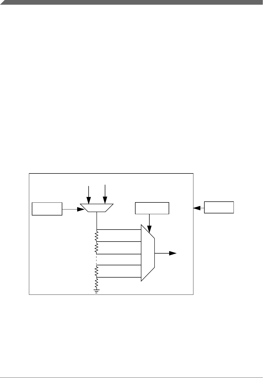
sends a transfer completing indicator signal that deasserts the DMA transfer request and
clears the flag to allow a subsequent change on comparator output to occur and force
another DMA request.
43.12 DAC functional description
This section provides DAC functional description.
43.12.1 Digital-to-analog converter block diagram
The following figure shows the block diagram of the DAC module. It contains a 256-tap
resistor ladder network and a 256-to-1 multiplexer, which selects an output voltage from
one of 256 distinct levels that outputs from DACO. It is controlled through the Control
register 1 (CMP_C1). Its supply reference source can be selected from two sources Vin1
and Vin2. The module can be powered down or disabled when not in use. When in the
Disabled mode, DACO is connected to the analog ground.
VOSEL[7:0]
DACO
MUX
MUX
DACEN
Vin
VRSEL
Vin1 Vin2
Figure 43-14. 8-bit DAC block diagram
43.12.2 DAC resets
This module has a single reset input, corresponding to the chip-wide peripheral reset.
DAC functional description
S32K1xx Series Reference Manual, Rev. 7, 04/2018
1144 NXP Semiconductors

43.12.3 DAC clocks
This module has a single clock input, the bus clock.
43.12.4 DAC interrupts
This module has no interrupts.
43.13 Trigger mode
The CMP and the 8-bit DAC are designed to support the trigger mode operation, which is
enabled when the MCU enters STOP modes with C2[RRE] and C0[EN] are set.
With this mode enabled, the trigger events that include the operation clock and a trigger
start signal will initiate a compare sequence that must first enable the CMP and DAC
prior to performing a CMP operation and capturing the output. A fixed channel for either
the plus-side mux or the minus-side mux is selected by software via C2[FXMP] and
C2[FXMXCH]. It is a mandatory request that the round-robin cycling period must be set
longer than the time that all the active channels complete the specified comparison cycles
set by C2[NSAM].
The active channels selected by C1[CHNn] are then routed to the non-fixed channel mux
and compared with the reference input in a round-robin manner. In order to meet the
comparator stabilization time, after the configurable number of operation clocks defined
by C2[NSAM], the comparison result is sampled for the selected channel. A software
pre-programmed state for each channel is configured by writing to C2[ACOn] field. After
all the active channels are sampled, if the comparison result changes from its pre-
programmed state, the corresponding flag in C2[CHnF] is set. If C2[RRIE] is set, an
asynchronous reset is asserted to bring the MCU out of STOP mode.
NOTE
These flags do not support generating a DMA transfer event.
This mode is active when the MCU is in STOP mode, so none of the window/filter
functions are available. A basic assumption of this mode is that the selected inputs are
changing at a much slower rate than the operation clock. It is suggested to configure the
comparator in low power comparison mode as well. In programming the C2[INITMOD]
registers, the INITMOD × round-robin clock period must be longer than the initialization
delay, which can be referred from the chip datasheet.
Chapter 43 Comparator (CMP)
S32K1xx Series Reference Manual, Rev. 7, 04/2018
NXP Semiconductors 1145
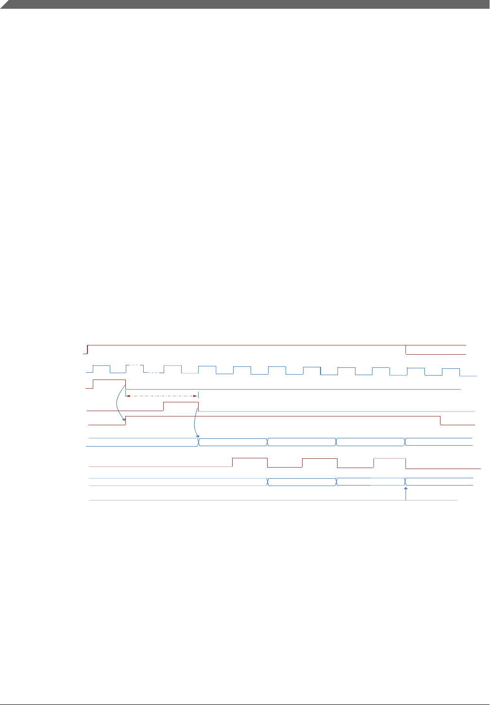
The following diagram shows the basic flow of this mode. In the diagram, C1[CHN1],
C1[CHN3], and C1[CHN7] are set, so channels #1, #3, and #7 are selected for round-
robin. C2[NSAM] is set to 2'b01, so one clock later the comparison result of the selected
channel is sampled. When channel #7 is compared, the result is sampled, and round-robin
ends. If any of the comparison results from channel #1, #3, or #7 changed from their
programmed value (written to C2[ACO1], C2[ACO3], and C2[ACO7]), an interrupt is
generated to wake up the MCU from the STOP mode. Software can then poll the
C2[CHnF] to see which channel input(s) changed value during the STOP mode.
NOTE
In round-robin mode, it should be ensured that the RTC_CLK
period is greater than the comparison time corresponding to the
value of C0[PMODE]. It is also required to not select the
internal reserved channels for round-robin by INPSEL and
INNSEL.
NOTE
In round-robin mode, it is suggested to always configure the
DAC output as the fixed port reference.
MCU
Round robin clock
(See chip configuration
chapters)
MCU
STOP
Trigger
(See chip configuration
chapters) CMP_C2[INITMOD]
Must be longer than the initialization delay
Round Robin Starts
CMP(and possible DAC)
enable
CH1
Idle CH3 CH7
enable
A
ctive channel selection
states
(
using channel 1, 3, 7 for
example)
Sample Channel comparison result
example)
ACO1 ACO1, ACO3 ACO1, ACO3, ACO7
Channel Results
Possible interrupt
Interrupt asserts here if any of the comparison
results is different from the values programmed to ACOn
This will wake up MCU from stop mode
Figure 43-15. Trigger mode
Trigger mode
S32K1xx Series Reference Manual, Rev. 7, 04/2018
1146 NXP Semiconductors

The following table shows the channel decoding in both functional mode and trigger
mode. Other cases not listed in the table are illegal.
Table 43-6. CMP channel decoding in functional mode and trigger mode
Mode RRE PSEL[
2:0]
MSEL[
2:0]
INPSE
L[1:0]
INNSE
L[1:0]
FIXP FXMX
CH[2:0
]
CHNxINP INN CMP
Behavior
Functional
Mode
0 x10~7 0 1 x x x DAC Channel
decoded
from
MSEL[2:0]
Channel 0~7
can be
compared
with DAC
0~7 x 1 0 x x x Channel
decoded
from
PSEL[2:0]
DAC Channel 0~7
can be
compared
with DAC
0~7 0~7 1 1 x x x Channel
decoded
from
PSEL[2:0]
Channel
decoded
from
MSEL[2:0]
Channel 0~7
can be
compared
with channel
0~72
Trigger
Mode
1 x x 0 1 0 x 0~7 DAC Channel
sweep
(CHNx)
Channel 0~7
can be swept
with DAC
x x 1 0 1 x 0~7 Channel
sweep
(CHNx)
DAC Channel 0~7
can be swept
with DAC
x x 1 1 0 0~7 0~7 Channel
fixed by
FXMXCH[
2:0]
Channel
sweep
(CHNx)
Channel 0~7
can be swept
with a fixed
channel
(0~7)3
x x 1 1 1 0~7 0~7 Channel
sweep
(CHNx)
Channel
fixed by
FXMXCH[
2:0]
Channel 0~7
can be swept
with a fixed
channel
(0~7)3
1. "x" means "do not care".
2. PSEL should not be set the same as MSEL.
3. Channel in the sweep side should not be the same as the fixed side.
Chapter 43 Comparator (CMP)
S32K1xx Series Reference Manual, Rev. 7, 04/2018
NXP Semiconductors 1147

Trigger mode
S32K1xx Series Reference Manual, Rev. 7, 04/2018
1148 NXP Semiconductors

Chapter 44
Programmable delay block (PDB)
Chip-specific PDB information
44.1.1 Instantiation Information
44.1.1.1 PDB output trigger connections
S32K14x contains two PDB modules. S32K11x contains one PDB module.
Table 44-1. PDB output trigger connections
Chip Number of slots on
PDB
Number of triggers
per slot
Number of Pulse Out Number of pre-
triggers slot
S32K116 2 1 1 8
S32K118 2 1 1 8
S32K142 2 1 1 8
S32K144 2 1 1 8
S32K146 3 1 1 8
S32K148 4 1 1 8
PDB has slots, also referred as PDB channels, for connectivity with chip. Each slot
consists of pulse out, triggers, and pre-triggers as mentioned in above table. See Figure
44-6 and Figure 41-2
44.1.1.2 PDB Input Trigger Connections
On this device, the PDB trigger source selection is implemented through the TRGMUX
module. For each PDB unit, there is only one trigger input from TRGMUX, but it
supports different trigger sources. The internal trigger mux inside PDB is not used
any more.
44.1
S32K1xx Series Reference Manual, Rev. 7, 04/2018
NXP Semiconductors 1149

Table 44-2. PDB input trigger connections
PDB Trigger PDB Input
0000 PDBn_trigger_in0
44.1.2 PDB trigger interconnections with ADC and TRGMUX
Besides the specific PDB-ADC triggering scheme (refer to ADC trigger source section),
the PDB channel triggers can also work as trigger source of TRGMUX module, which
can be used to trigger other modules besides ADC.
Following are PDB module interconnectivities:
Table 44-3. PDB trigger interconnections with ADC and TRGMUX
PDBx Trigger outputs Interconnectivity
Channel 0 triggers Trigger connects to both ADC and TRGMUX
Channel 1 trigger Trigger connects to ADC
Channel 2 trigger Trigger connects to ADC
Channel 3 trigger Trigger connects to ADC
Pulse-out Pulse-out connects to TRGMUX
44.1.3 Back-to-back acknowledgement connections
Back-to-back operation enables the ADC conversions complete to trigger the next PDB
channel pre-trigger and trigger output.
In this MCU, the following PDB back-to-back operation acknowledgment connections
are implemented based on SIM_CHIPCTL[PDB_BB_SEL] bit setting. The PDB back to
back operation is supported on all channels of each PDB. The PDB back to back forming
a ring is supported only for channel 0 of each PDB.
When SIM_CHIPCTL[PDB_BB_SEL]=0:
The PDB back-to-back operation acknowledgement connections are implemented inside
each PDB unit as a ring.
The back-to-back chain diagrams for PDB0 CH0, PDB1 CH1, and PDB0-PDB1 forming
a ring are shown below:
Chip-specific PDB information
S32K1xx Series Reference Manual, Rev. 7, 04/2018
1150 NXP Semiconductors
PDB0 CH 0
pre-trigger 0
PDB0 CH 0
pre-trigger 1
PDB0 CH 0
pre-trigger 2
PDB0 CH 0
pre-trigger 7
PDB0 CH 0
pre-trigger 6
PDB0 CH 0
pre-trigger 4
PDB0 CH 0
pre-trigger 5
PDB0 CH 0
pre-trigger 3
Figure 44-1. Example: PDB0 CH0 back-to-back chain
PDB1 CH 1
pre-trigger 0
PDB1 CH 1
pre-trigger 1
PDB1 CH 1
pre-trigger 2
PDB1 CH 1
pre-trigger 7
PDB1 CH 1
pre-trigger 6
PDB1 CH 1
pre-trigger 4
PDB1 CH 1
pre-trigger 5
PDB1 CH 1
pre-trigger 3
Figure 44-2. Example: PDB1 CH1 back-to-back chain
When SIM_CHIPCTL[PDB_BB_SEL]=1:
The PDB back-to-back operation acknowledgement connections are implemented with
all of the PDB units as a ring. The chain diagram is as follows:
Chapter 44 Programmable delay block (PDB)
S32K1xx Series Reference Manual, Rev. 7, 04/2018
NXP Semiconductors 1151
PDB0 CH 0
pre-trigger 0
PDB0 CH 0
pre-trigger 1
PDB0 CH 0
pre-trigger 2
PDB0 CH 0
pre-trigger 7
PDB0 CH 0
pre-trigger 6
PDB0 CH 0
pre-trigger 4
PDB0 CH 0
pre-trigger 5
PDB0 CH 0
pre-trigger 3
PDB1 CH 0
pre-trigger 0
PDB1 CH 0
pre-trigger 1
PDB1 CH 0
pre-trigger 2
PDB1 CH 0
pre-trigger 7
PDB1 CH 0
pre-trigger 6
PDB1 CH 0
pre-trigger 4
PDB1 CH 0
pre-trigger 5
PDB1 CH 0
pre-trigger 3
Figure 44-3. PDB back-to-back chain forming PDB0-PDB1 ring
The application code can set the PDBx_CHnC1[BB] bits to configure the PDB pre-
triggers as a single chain or several chains.
Chip-specific PDB information
S32K1xx Series Reference Manual, Rev. 7, 04/2018
1152 NXP Semiconductors

The pre-trigger for the beginning of the chain should be provided from PDB (for e.g., by
setting CHnDLY1 and CHnC1[EN] bit) with clearing PDBx_CHnC1[BB] bit.
Table 44-4. PDB-ADC back to back connection (Part 1 of 2)
PDB
Instance
PDB Channel Pre-Trigger # Ack Connection from
SIM_CHIPCTL[PDB_BB_SEL]=0 SIM_CHIPCTL[PDB_BB_SEL]=1
PDB0 CH0 0 ADC0 SC1H_COCO ADC1 SC1H_COCO
1 ADC0 SC1A_COCO ADC0 SC1A_COCO
2 ADC0 SC1B_COCO ADC0 SC1B_COCO
3 ADC0 SC1C_COCO ADC0 SC1C_COCO
4 ADC0 SC1D_COCO ADC0 SC1D_COCO
5 ADC0 SC1E_COCO ADC0 SC1E_COCO
6 ADC0 SC1F_COCO ADC0 SC1F_COCO
7 ADC0 SC1G_COCO ADC0 SC1G_COCO
PDB0 CH1 0 ADC0 SC1P_COCO 1
1 ADC0 SC1I_COCO
2 ADC0 SC1J_COCO
3 ADC0 SC1K_COCO
4 ADC0 SC1L_COCO
5 ADC0 SC1M_COCO
6 ADC0 SC1N_COCO
7 ADC0 SC1O_COCO
PDB0 CH2 0 ADC0 SC1X_COCO
1 ADC0 SC1Q_COCO
2 ADC0 SC1R_COCO
3 ADC0 SC1S_COCO
4 ADC0 SC1T_COCO
5 ADC0 SC1U_COCO
6 ADC0 SC1V_COCO
7 ADC0 SC1W_COCO
PDB0 CH3 0 ADC0 SC1FF_COCO
1 ADC0 SC1Y_COCO
2 ADC0 SC1Z_COCO
3 ADC0 SC1AA_COCO
4 ADC0 SC1BB_COCO
5 ADC0 SC1CC_COCO
6 ADC0 SC1DD_COCO
7 ADC0 SC1EE_COCO
Chapter 44 Programmable delay block (PDB)
S32K1xx Series Reference Manual, Rev. 7, 04/2018
NXP Semiconductors 1153

1. PDB back to back operation forming a ring is supported only on Channel 0
Table 44-5. PDB-ADC back to back connection (Part 2 of 2)
PDB
Instance
PDB Channel Pre-Trigger # Ack Connection from
SIM_CHIPCTL[PDB_BB_SEL]=0 SIM_CHIPCTL[PDB_BB_SEL]=1
PDB1 CH0 0 ADC1 SC1H_COCO ADC0 SC1H_COCO
1 ADC1 SC1A_COCO ADC1 SC1A_COCO
2 ADC1 SC1B_COCO ADC1 SC1B_COCO
3 ADC1 SC1C_COCO ADC1 SC1C_COCO
4 ADC1 SC1D_COCO ADC1 SC1D_COCO
5 ADC1 SC1E_COCO ADC1 SC1E_COCO
6 ADC1 SC1F_COCO ADC1 SC1F_COCO
7 ADC1 SC1G_COCO ADC1 SC1G_COCO
PDB1 CH1 0 ADC1 SC1P_COCO 1
1 ADC1 SC1I_COCO
2 ADC1 SC1J_COCO
3 ADC1 SC1K_COCO
4 ADC1 SC1L_COCO
5 ADC1 SC1M_COCO
6 ADC1 SC1N_COCO
7 ADC1 SC1O_COCO
PDB1 CH2 0 ADC1 SC1X_COCO
1 ADC1 SC1Q_COCO
2 ADC1 SC1R_COCO
3 ADC1 SC1S_COCO
4 ADC1 SC1T_COCO
5 ADC1 SC1U_COCO
6 ADC1 SC1V_COCO
7 ADC1 SC1W_COCO
PDB1 CH3 0 ADC1 SC1FF_COCO
1 ADC1 SC1Y_COCO
2 ADC1 SC1Z_COCO
3 ADC1 SC1AA_COCO
4 ADC1 SC1BB_COCO
5 ADC1 SC1CC_COCO
6 ADC1 SC1DD_COCO
7 ADC1 SC1EE_COCO
1. PDB back to back operation forming a ring is supported only on Channel 0
Chip-specific PDB information
S32K1xx Series Reference Manual, Rev. 7, 04/2018
1154 NXP Semiconductors
SIM_CHIPCTL[PDB_BB_SEL] SIM_CHIPCTL[PDB_BB_SEL]
PDB0 CH0 Pre-trigger 0
Ack Pre-trigger ADC0 SC1A
ADHWTS0 COCO PDB1 CH0 Pre-trigger 0
Ack Pre-trigger
0
1
ADC1 SC1A
ADHWTS0 COCO
0
1
PDB0 CH0 Pre-trigger 1
Ack Pre-trigger ADC0 SC1B
ADHWTS1 COCO PDB1 CH0 Pre-trigger 1
Ack Pre-trigger ADC1 SC1B
ADHWTS1 COCO
PDB0 CH0 Pre-trigger 2
Ack Pre-trigger ADC0 SC1C
ADHWTS2 COCO PDB1 CH0 Pre-trigger 2
Ack Pre-trigger ADC1 SC1C
ADHWTS2 COCO
PDB0 CH0 Pre-trigger 3
Ack Pre-trigger ADC0 SC1D
ADHWTS3 COCO PDB1 CH0 Pre-trigger 3
Ack Pre-trigger ADC1 SC1D
ADHWTS3 COCO
PDB0 CH0 Pre-trigger 4
Ack Pre-trigger ADC0 SC1E
ADHWTS4 COCO PDB1 CH0 Pre-trigger 4
Ack Pre-trigger ADC1 SC1E
ADHWTS4 COCO
PDB0 CH0 Pre-trigger 5
Ack Pre-trigger ADC0 SC1F
ADHWTS5 COCO PDB1 CH0 Pre-trigger 5
Ack Pre-trigger ADC1 SC1F
ADHWTS5 COCO
PDB0 CH0 Pre-trigger 6
Ack Pre-trigger ADC0 SC1G
ADHWTS6 COCO PDB1 CH0 Pre-trigger 6
Ack Pre-trigger ADC1 SC1G
ADHWTS6 COCO
PDB0 CH0 Pre-trigger 7
Ack Pre-trigger ADC0 SC1H
ADHWTS7 COCO PDB1 CH0 Pre-trigger 7
Ack Pre-trigger ADC1 SC1H
ADHWTS7 COCO
PDB0 CH1 Pre-trigger 0
Ack Pre-trigger ADC0 SC1I
ADHWTS8 COCO PDB1 CH1 Pre-trigger 0
Ack Pre-trigger ADC1 SC1I
ADHWTS8 COCO
PDB0 CH1 Pre-trigger 1
Ack Pre-trigger ADC0 SC1J
ADHWTS9 COCO PDB1 CH1 Pre-trigger 1
Ack Pre-trigger ADC1 SC1J
ADHWTS9 COCO
PDB0 CH1 Pre-trigger 2
Ack Pre-trigger ADC0 SC1K
ADHWTS10 COCO PDB1 CH1 Pre-trigger 2
Ack Pre-trigger ADC1 SC1K
ADHWTS10 COCO
PDB0 CH1 Pre-trigger 3
Ack Pre-trigger ADC0 SC1L
ADHWTS11 COCO PDB1 CH1 Pre-trigger 3
Ack Pre-trigger ADC1 SC1L
ADHWTS11 COCO
PDB0 CH1 Pre-trigger 4
Ack Pre-trigger ADC0 SC1M
ADHWTS12 COCO PDB1 CH1 Pre-trigger 4
Ack Pre-trigger ADC1 SC1M
ADHWTS12 COCO
PDB0 CH1 Pre-trigger 5
Ack Pre-trigger ADC0 SC1N
ADHWTS13 COCO PDB1 CH1 Pre-trigger 5
Ack Pre-trigger ADC1 SC1N
ADHWTS13 COCO
PDB0 CH1 Pre-trigger 6
Ack Pre-trigger ADC0 SC1O
ADHWTS14 COCO PDB1 CH1 Pre-trigger 6
Ack Pre-trigger ADC1 SC1O
ADHWTS14 COCO
PDB0 CH1 Pre-trigger 7
Ack Pre-trigger ADC0 SC1P
ADHWTS15 COCO PDB1 CH1 Pre-trigger 7
Ack Pre-trigger ADC1 SC1P
ADHWTS15 COCO
Figure 44-4. PDB-ADC back to back connection (Part 1 of 2)
Chapter 44 Programmable delay block (PDB)
S32K1xx Series Reference Manual, Rev. 7, 04/2018
NXP Semiconductors 1155
PDB0 CH2 Pre-trigger 0
Ack Pre-trigger ADC0 SC1Q
ADHWTS8 COCO PDB1 CH2 Pre-trigger 0
Ack Pre-trigger ADC1 SC1Q
ADHWTS8 COCO
PDB0 CH2 Pre-trigger 1
Ack Pre-trigger ADC0 SC1R
ADHWTS9 COCO PDB1 CH2 Pre-trigger 1
Ack Pre-trigger ADC1 SC1R
ADHWTS9 COCO
PDB0 CH2 Pre-trigger 2
Ack Pre-trigger ADC0 SC1S
ADHWTS10 COCO PDB1 CH2 Pre-trigger 2
Ack Pre-trigger ADC1 SC1S
ADHWTS10 COCO
PDB0 CH2 Pre-trigger 3
Ack Pre-trigger ADC0 SC1T
ADHWTS11 COCO PDB1 CH2 Pre-trigger 3
Ack Pre-trigger ADC1 SC1T
ADHWTS11 COCO
PDB0 CH2 Pre-trigger 4
Ack Pre-trigger ADC0 SC1U
ADHWTS12 COCO PDB1 CH2 Pre-trigger 4
Ack Pre-trigger ADC1 SC1U
ADHWTS12 COCO
PDB0 CH2 Pre-trigger 5
Ack Pre-trigger ADC0 SC1V
ADHWTS13 COCO PDB1 CH2 Pre-trigger 5
Ack Pre-trigger ADC1 SC1V
ADHWTS13 COCO
PDB0 CH2 Pre-trigger 6
Ack Pre-trigger ADC0 SC1W
ADHWTS14 COCO PDB1 CH2 Pre-trigger 6
Ack Pre-trigger ADC1 SC1W
ADHWTS14 COCO
PDB0 CH2 Pre-trigger 7
Ack Pre-trigger ADC0 SC1X
ADHWTS15 COCO PDB1 CH2 Pre-trigger 7
Ack Pre-trigger ADC1 SC1X
ADHWTS15 COCO
PDB0 CH3 Pre-trigger 0
Ack Pre-trigger ADC0 SC1Y
ADHWTS8 COCO PDB1 CH3 Pre-trigger 0
Ack Pre-trigger ADC1 SC1Y
ADHWTS8 COCO
PDB0 CH3 Pre-trigger 1
Ack Pre-trigger ADC0 SC1Z
ADHWTS9 COCO PDB1 CH3 Pre-trigger 1
Ack Pre-trigger ADC1 SC1Z
ADHWTS9 COCO
PDB0 CH3 Pre-trigger 2
Ack Pre-trigger ADC0 SC1AA
ADHWTS10 COCO PDB1 CH3 Pre-trigger 2
Ack Pre-trigger ADC1 SC1AA
ADHWTS10 COCO
PDB0 CH3 Pre-trigger 3
Ack Pre-trigger ADC0 SC1BB
ADHWTS11 COCO PDB1 CH3 Pre-trigger 3
Ack Pre-trigger ADC1 SC1BB
ADHWTS11 COCO
PDB0 CH3 Pre-trigger 4
Ack Pre-trigger ADC0 SC1CC
ADHWTS12 COCO PDB1 CH3 Pre-trigger 4
Ack Pre-trigger ADC1 SC1CC
ADHWTS12 COCO
PDB0 CH3 Pre-trigger 5
Ack Pre-trigger ADC0 SC1DD
ADHWTS13 COCO PDB1 CH3 Pre-trigger 5
Ack Pre-trigger ADC1 SC1DD
ADHWTS13 COCO
PDB0 CH3 Pre-trigger 6
Ack Pre-trigger ADC0 SC1EE
ADHWTS14 COCO PDB1 CH3 Pre-trigger 6
Ack Pre-trigger ADC1 SC1EE
ADHWTS14 COCO
PDB0 CH3 Pre-trigger 7
Ack Pre-trigger ADC0 SC1FF
ADHWTS15 COCO PDB1 CH3 Pre-trigger 7
Ack Pre-trigger ADC1 SC1FF
ADHWTS15 COCO
Figure 44-5. PDB-ADC back to back connection (Part 2 of 2)
Chip-specific PDB information
S32K1xx Series Reference Manual, Rev. 7, 04/2018
1156 NXP Semiconductors

44.1.4 Pulse-Out Enable Register Implementation
The following table shows the comparison of pulse-out enable register at the module and
chip level. In this device, each PDB unit will have one Pulse-Out channel. The Pulse-Out
is connecting to TRGMUX, which is then flexible to work as sample window for any
CMP module.
Table 44-6. PDB pulse-out enable register
Register Module implementation Chip implementation
POnEN 7:0 - POEN
31:8 - Reserved
0 - POEN[0] for CMP
31:1 - Reserved
44.2 Introduction
The Programmable Delay Block (PDB) provides controllable delays from either an
internal or an external trigger, or a programmable interval tick, to the hardware trigger
inputs of ADCs. The PDB can optionally provide pulse outputs (Pulse-Out's) that are
used as the sample window in the CMP block.
44.2.1 Features
• Up to 2 trigger input sources and one software trigger source
• Up to 8 configurable PDB channels for ADC hardware trigger
• One PDB channel is associated with one ADC
• One trigger output for ADC hardware trigger and up to 8 pre-trigger outputs for
ADC trigger select per PDB channel
• Trigger outputs can be enabled or disabled independently
• One 16-bit delay register per pre-trigger output
• Optional bypass of the delay registers of the pre-trigger outputs
• Operation in One-Shot or Continuous modes
• Optional back-to-back mode operation, which enables the ADC conversions
complete to trigger the next PDB channel
Chapter 44 Programmable delay block (PDB)
S32K1xx Series Reference Manual, Rev. 7, 04/2018
NXP Semiconductors 1157

• One programmable delay interrupt
• One sequence error interrupt
• One channel flag and one sequence error flag per pre-trigger
• DMA support
• Up to 8 pulse outputs (pulse-out's)
• Pulse-out's can be enabled or disabled independently
• Programmable pulse width
NOTE
The number of PDB input and output triggers are chip-specific.
See the chip-specific PDB information for details.
44.2.2 Implementation
In this section, the following letters refer to the number of output triggers:
• N—Total available number of PDB channels.
•n—PDB channel number, valid from 0 to N-1.
• M—Total available pre-trigger per PDB channel.
•m—Pre-trigger number, valid from 0 to M-1.
• Y—Total number of Pulse-Out's.
•y—Pulse-Out number, valid value is from 0 to Y-1.
NOTE
The number of module output triggers to core is chip-specific.
For module to core output triggers implementation, see the chip
configuration information.
44.2.3 Back-to-back acknowledgment connections
PDB back-to-back operation acknowledgment connections are chip-specific. For
implementation, see the chip configuration information.
Introduction
S32K1xx Series Reference Manual, Rev. 7, 04/2018
1158 NXP Semiconductors
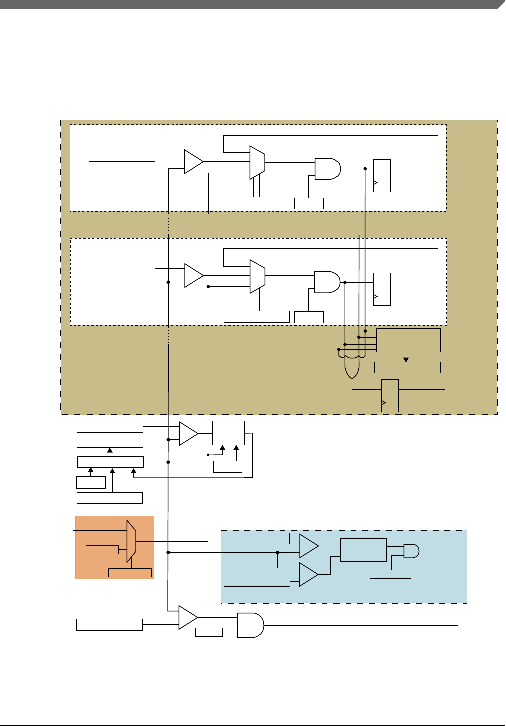
44.2.4 Block diagram
This diagram illustrates the major components of the PDB.
Ch n trigger
PDBCHnDLY0
PDBCHnDLYm
=
Ack 0
Pre-trigger 0
Ch n pre-trigger 0
Ch n pre-trigger m
=
BB[m], TOS[m]
BB[0], TOS[0]EN[0]
EN[m]
MULT
Ack m
Pre-trigger m
Sequence Error
Detection
ERR[M - 1:0]
PRESCALER
PDBCNT
PDBMOD =
CONT
PDBIDLY =PDB interrupt
TOEx
=
=
POyDLY2
POyDLY1
Pulse
Generation Pulse-Out y
PDBPOEN[y]
Pulse-Out y
Control
logic
PDB counter
Trigger-In 0
SWTRIG
TRIGSEL
trigger_In0
Figure 44-6. PDB block diagram
Chapter 44 Programmable delay block (PDB)
S32K1xx Series Reference Manual, Rev. 7, 04/2018
NXP Semiconductors 1159

In this diagram, only one PDB channel n, and one Pulse-Out y are shown. The PDB-
enabled control logic and the sequence error interrupt logic are not shown.
44.2.5 Modes of operation
PDB ADC trigger operates in the following modes:
• Disabled—Counter is off, all pre-trigger and trigger outputs are low if PDB is not in
back-to-back operation of Bypass mode.
• Debug—Counter is paused when processor is in Debug mode.
• Enabled One-Shot—Counter is enabled and restarted at count zero upon receiving a
positive edge on the selected trigger input source or software trigger is selected and
SC[SWTRIG] is written with 1. In each PDB channel, an enabled pre-trigger asserts
once per trigger input event. The trigger output asserts whenever any of the pre-
triggers is asserted.
• Enabled Continuous—Counter is enabled and restarted at count zero. The counter is
rolled over to zero again when the count reaches the value specified in the modulus
register, and the counting is restarted. This enables a continuous stream of pre-
triggers/trigger outputs as a result of a single trigger input event.
• Enabled Bypassed—The pre-trigger and trigger outputs assert immediately after a
positive edge on the selected trigger input source or software trigger is selected and
SC[SWTRIG] is written with 1, that is the delay registers are bypassed. It is possible
to bypass any one or more of the delay registers; therefore, this mode can be used in
conjunction with One-Shot or Continuous mode.
44.3 Memory map and register definition
PDB memory map
Address
offset (hex) Register name Width
(in bits) Access Reset value Section/
page
0 Status and Control register (PDB_SC) 32 R/W 0000_0000h 44.3.1/1162
4 Modulus register (PDB_MOD) 32 R/W 0000_FFFFh 44.3.2/1165
8 Counter register (PDB_CNT) 32 R 0000_0000h 44.3.3/1166
C Interrupt Delay register (PDB_IDLY) 32 R/W 0000_FFFFh 44.3.4/1166
10 Channel n Control register 1 (PDB_CH0C1) 32 R/W 0000_0000h 44.3.5/1167
14 Channel n Status register (PDB_CH0S) 32 R/W 0000_0000h 44.3.6/1168
18 Channel n Delay 0 register (PDB_CH0DLY0) 32 R/W 0000_0000h 44.3.7/1168
1C Channel n Delay 1 register (PDB_CH0DLY1) 32 R/W 0000_0000h 44.3.8/1169
Table continues on the next page...
Memory map and register definition
S32K1xx Series Reference Manual, Rev. 7, 04/2018
1160 NXP Semiconductors

PDB memory map (continued)
Address
offset (hex) Register name Width
(in bits) Access Reset value Section/
page
20 Channel n Delay 2 register (PDB_CH0DLY2) 32 R/W 0000_0000h 44.3.9/1170
24 Channel n Delay 3 register (PDB_CH0DLY3) 32 R/W 0000_0000h 44.3.10/
1170
28 Channel n Delay 4 register (PDB_CH0DLY4) 32 R/W 0000_0000h 44.3.11/
1171
2C Channel n Delay 5 register (PDB_CH0DLY5) 32 R/W 0000_0000h 44.3.12/
1172
30 Channel n Delay 6 register (PDB_CH0DLY6) 32 R/W 0000_0000h 44.3.13/
1172
34 Channel n Delay 7 register (PDB_CH0DLY7) 32 R/W 0000_0000h 44.3.14/
1173
38 Channel n Control register 1 (PDB_CH1C1) 32 R/W 0000_0000h 44.3.5/1167
3C Channel n Status register (PDB_CH1S) 32 R/W 0000_0000h 44.3.6/1168
40 Channel n Delay 0 register (PDB_CH1DLY0) 32 R/W 0000_0000h 44.3.7/1168
44 Channel n Delay 1 register (PDB_CH1DLY1) 32 R/W 0000_0000h 44.3.8/1169
48 Channel n Delay 2 register (PDB_CH1DLY2) 32 R/W 0000_0000h 44.3.9/1170
4C Channel n Delay 3 register (PDB_CH1DLY3) 32 R/W 0000_0000h 44.3.10/
1170
50 Channel n Delay 4 register (PDB_CH1DLY4) 32 R/W 0000_0000h 44.3.11/
1171
54 Channel n Delay 5 register (PDB_CH1DLY5) 32 R/W 0000_0000h 44.3.12/
1172
58 Channel n Delay 6 register (PDB_CH1DLY6) 32 R/W 0000_0000h 44.3.13/
1172
5C Channel n Delay 7 register (PDB_CH1DLY7) 32 R/W 0000_0000h 44.3.14/
1173
60 Channel n Control register 1 (PDB_CH2C1) 32 R/W 0000_0000h 44.3.5/1167
64 Channel n Status register (PDB_CH2S) 32 R/W 0000_0000h 44.3.6/1168
68 Channel n Delay 0 register (PDB_CH2DLY0) 32 R/W 0000_0000h 44.3.7/1168
6C Channel n Delay 1 register (PDB_CH2DLY1) 32 R/W 0000_0000h 44.3.8/1169
70 Channel n Delay 2 register (PDB_CH2DLY2) 32 R/W 0000_0000h 44.3.9/1170
74 Channel n Delay 3 register (PDB_CH2DLY3) 32 R/W 0000_0000h 44.3.10/
1170
78 Channel n Delay 4 register (PDB_CH2DLY4) 32 R/W 0000_0000h 44.3.11/
1171
7C Channel n Delay 5 register (PDB_CH2DLY5) 32 R/W 0000_0000h 44.3.12/
1172
80 Channel n Delay 6 register (PDB_CH2DLY6) 32 R/W 0000_0000h 44.3.13/
1172
84 Channel n Delay 7 register (PDB_CH2DLY7) 32 R/W 0000_0000h 44.3.14/
1173
88 Channel n Control register 1 (PDB_CH3C1) 32 R/W 0000_0000h 44.3.5/1167
8C Channel n Status register (PDB_CH3S) 32 R/W 0000_0000h 44.3.6/1168
Table continues on the next page...
Chapter 44 Programmable delay block (PDB)
S32K1xx Series Reference Manual, Rev. 7, 04/2018
NXP Semiconductors 1161

PDB memory map (continued)
Address
offset (hex) Register name Width
(in bits) Access Reset value Section/
page
90 Channel n Delay 0 register (PDB_CH3DLY0) 32 R/W 0000_0000h 44.3.7/1168
94 Channel n Delay 1 register (PDB_CH3DLY1) 32 R/W 0000_0000h 44.3.8/1169
98 Channel n Delay 2 register (PDB_CH3DLY2) 32 R/W 0000_0000h 44.3.9/1170
9C Channel n Delay 3 register (PDB_CH3DLY3) 32 R/W 0000_0000h 44.3.10/
1170
A0 Channel n Delay 4 register (PDB_CH3DLY4) 32 R/W 0000_0000h 44.3.11/
1171
A4 Channel n Delay 5 register (PDB_CH3DLY5) 32 R/W 0000_0000h 44.3.12/
1172
A8 Channel n Delay 6 register (PDB_CH3DLY6) 32 R/W 0000_0000h 44.3.13/
1172
AC Channel n Delay 7 register (PDB_CH3DLY7) 32 R/W 0000_0000h 44.3.14/
1173
190 Pulse-Out n Enable register (PDB_POEN) 32 R/W 0000_0000h 44.3.15/
1173
194 Pulse-Out n Delay register (PDB_PO0DLY) 32 R/W 0000_0000h 44.3.16/
1174
44.3.1 Status and Control register (PDB_SC)
Address: 0h base + 0h offset = 0h
Bit 31 30 29 28 27 26 25 24 23 22 21 20 19 18 17 16
R0
LDMOD
PDBEIE
0
W
SWTRIG
Reset 0 0 0 0 0 0 0 0 0 0 0 0 0 0 0 0
Bit 15 14 13 12 11 10 9 8 7 6 5 4 3 2 1 0
R
DMAEN
PRESCALER TRGSEL
PDBEN
PDBIF
PDBIE
0
MULT
CONT
LDOK
W
Reset 0 0 0 0 0 0 0 0 0 0 0 0 0 0 0 0
Memory map and register definition
S32K1xx Series Reference Manual, Rev. 7, 04/2018
1162 NXP Semiconductors

PDB_SC field descriptions
Field Description
31–20
Reserved
This field is reserved.
This read-only field is reserved and always has the value 0.
19–18
LDMOD
Load Mode Select
Selects the mode to load the MOD, IDLY, CHnDLYm, INTx, and POyDLY registers, after 1 is written to
LDOK.
00 The internal registers are loaded with the values from their buffers, immediately after 1 is written to
LDOK.
01 The internal registers are loaded with the values from their buffers when the PDB counter (CNT) =
MOD + 1 CNT delay elapsed, after 1 is written to LDOK.
10 The internal registers are loaded with the values from their buffers when a trigger input event is
detected, after 1 is written to LDOK.
11 The internal registers are loaded with the values from their buffers when either the PDB counter
(CNT) = MOD + 1 CNT delay elapsed, or a trigger input event is detected, after 1 is written to LDOK.
17
PDBEIE
PDB Sequence Error Interrupt Enable
Enables the PDB sequence error interrupt. When PDBEIE is set, any of the PDB channel sequence error
flags generates a PDB sequence error interrupt.
0 PDB sequence error interrupt disabled.
1 PDB sequence error interrupt enabled.
16
SWTRIG
Software Trigger
When PDB is enabled and the software trigger is selected as the trigger input source, writing 1 to SWTRIG
resets and restarts the counter. Writing 0 to SWTRIG has no effect. Reading SWTRIG yields 0.
15
DMAEN
DMA Enable
When DMA is enabled, the PDBIF flag generates a DMA request instead of an interrupt.
0 DMA disabled.
1 DMA enabled.
14–12
PRESCALER
Prescaler Divider Select
Counting uses the peripheral clock divided by the product of a factor (selected by MULT field) and an
integer factor (set by PRESCALAR field), or in other words, (peripheral clock)/(MULT x PRESCALAR).
000 Counting uses the peripheral clock divided by MULT (the multiplication factor).
001 Counting uses the peripheral clock divided by 2 x MULT (the multiplication factor).
010 Counting uses the peripheral clock divided by 4 x MULT (the multiplication factor).
011 Counting uses the peripheral clock divided by 8 x MULT (the multiplication factor).
100 Counting uses the peripheral clock divided by 16 x MULT (the multiplication factor).
101 Counting uses the peripheral clock divided by 32 x MULT (the multiplication factor).
110 Counting uses the peripheral clock divided by 64 x MULT (the multiplication factor).
111 Counting uses the peripheral clock divided by 128 x MULT (the multiplication factor).
11–8
TRGSEL
Trigger Input Source Select
Selects the trigger input source for the PDB. The trigger input source can be internal or external (EXTRG
pin), or the software trigger. Refer to chip configuration details for the actual PDB input trigger
connections.
0000 Trigger-In 0 is selected.
Table continues on the next page...
Chapter 44 Programmable delay block (PDB)
S32K1xx Series Reference Manual, Rev. 7, 04/2018
NXP Semiconductors 1163

PDB_SC field descriptions (continued)
Field Description
0001 Trigger-In 1 is selected.
0010 Trigger-In 2 is selected.
0011 Trigger-In 3 is selected.
0100 Trigger-In 4 is selected.
0101 Trigger-In 5 is selected.
0110 Trigger-In 6 is selected.
0111 Trigger-In 7 is selected.
1000 Trigger-In 8 is selected.
1001 Trigger-In 9 is selected.
1010 Trigger-In 10 is selected.
1011 Trigger-In 11 is selected.
1100 Trigger-In 12 is selected.
1101 Trigger-In 13 is selected.
1110 Trigger-In 14 is selected.
1111 Software trigger is selected.
7
PDBEN
PDB Enable
0 PDB disabled. Counter is off.
1 PDB enabled.
6
PDBIF
PDB Interrupt Flag
PDBIF is set when the counter value is equal to the IDLY register + 1.
• Write zero to clear PDBIF.
• Writing 1 to PDBIF has no effect.
5
PDBIE
PDB Interrupt Enable
Enables the PDB interrupt. When PDBIE is set and DMAEN is cleared, PDBIF generates a PDB interrupt.
0 PDB interrupt disabled.
1 PDB interrupt enabled.
4
Reserved
This field is reserved.
This read-only field is reserved and always has the value 0.
3–2
MULT
Multiplication Factor Select for Prescaler
Selects the multiplication factor of the prescaler divider for the counter clock.
00 Multiplication factor is 1.
01 Multiplication factor is 10.
10 Multiplication factor is 20.
11 Multiplication factor is 40.
1
CONT
Continuous Mode Enable
Enables the PDB operation in Continuous mode.
0 PDB operation in One-Shot mode
1 PDB operation in Continuous mode
0
LDOK
Load OK
Table continues on the next page...
Memory map and register definition
S32K1xx Series Reference Manual, Rev. 7, 04/2018
1164 NXP Semiconductors

PDB_SC field descriptions (continued)
Field Description
Writing 1 to LDOK bit updates the MOD, IDLY, CHnDLYm, and POyDLY registers with the values
previously written to their internal buffers (and stored there). The new values of MOD, IDLY, CHnDLYm,
and POyDLY registers will take effect according to the setting of the LDMOD field (Load Mode Select).
Before 1 is written to the LDOK field, the values in the internal buffers of these registers are not effective,
and new values cannot be written to the internal buffers until the existing values in the internal buffers are
loaded into their corresponding registers.
• LDOK can be written only when PDBEN is set, or LDOK can be written at the same time when
PDBEN is written to 1.
• LDOK is automatically cleared when the values in the internal buffers are loaded into the registers or
when PDBEN bit (PDB Enable) is cleared.
• Writing 0 to LDOK has no effect.
44.3.2 Modulus register (PDB_MOD)
Note: This register is internally buffered, and any values written to the register are
written to its internal buffer instead; in other words, the internal device bus does not write
directly to this register. The value in this register's internal buffer is loaded into this
register only after "1" is written to the SC[LDOK] bit.
Address: 0h base + 4h offset = 4h
Bit 31 30 29 28 27 26 25 24 23 22 21 20 19 18 17 16 15 14 13 12 11 10 9 8 7 6 5 4 3 2 1 0
R0MOD
W
Reset 0 0 0 0 0 0 0 0 0 0 0 0 0 0 0 0 1 1 1 1 1 1 1 1 1 1 1 1 1 1 1 1
PDB_MOD field descriptions
Field Description
31–16
Reserved
This field is reserved.
This read-only field is reserved and always has the value 0.
MOD PDB Modulus
Specifies the period of the counter. When the counter reaches this value, it will be reset back to zero. If the
PDB is in Continuous mode, the count begins anew. Reading this field returns the value of the internal
register that is effective for the current cycle of PDB.
Chapter 44 Programmable delay block (PDB)
S32K1xx Series Reference Manual, Rev. 7, 04/2018
NXP Semiconductors 1165

44.3.3 Counter register (PDB_CNT)
NOTE
Writing to this read-only register will not generate a transfer
error or hard fault.
Address: 0h base + 8h offset = 8h
Bit 31 30 29 28 27 26 25 24 23 22 21 20 19 18 17 16 15 14 13 12 11 10 9 8 7 6 5 4 3 2 1 0
R0 CNT
W
Reset 0 0 0 0 0 0 0 0 0 0 0 0 0 0 0 0 0 0 0 0 0 0 0 0 0 0 0 0 0 0 0 0
PDB_CNT field descriptions
Field Description
31–16
Reserved
This field is reserved.
This read-only field is reserved and always has the value 0.
CNT PDB Counter
Contains the current value of the counter.
44.3.4 Interrupt Delay register (PDB_IDLY)
Note: This register is internally buffered, and any values written to the register are
written to its internal buffer instead; in other words, the internal device bus does not write
directly to this register. The value in this register's internal buffer is loaded into this
register only after "1" is written to the SC[LDOK] bit.
Address: 0h base + Ch offset = Ch
Bit 31 30 29 28 27 26 25 24 23 22 21 20 19 18 17 16 15 14 13 12 11 10 9 8 7 6 5 4 3 2 1 0
R0IDLY
W
Reset 0 0 0 0 0 0 0 0 0 0 0 0 0 0 0 0 1 1 1 1 1 1 1 1 1 1 1 1 1 1 1 1
PDB_IDLY field descriptions
Field Description
31–16
Reserved
This field is reserved.
This read-only field is reserved and always has the value 0.
IDLY PDB Interrupt Delay
Table continues on the next page...
Memory map and register definition
S32K1xx Series Reference Manual, Rev. 7, 04/2018
1166 NXP Semiconductors

PDB_IDLY field descriptions (continued)
Field Description
Specifies the delay value to schedule the PDB interrupt. It can be used to schedule an independent
interrupt at some point in the PDB cycle. If enabled, a PDB interrupt is generated, when the counter is
equal to the IDLY. Reading this field returns the value of internal register that is effective for the current
cycle of the PDB.
44.3.5 Channel n Control register 1 (PDB_CHnC1)
Each PDB channel has one control register, CHnC1. The bits in this register control the
functionality of each PDB channel operation.
Address: 0h base + 10h offset + (40d × i), where i=0d to 3d
Bit 31 30 29 28 27 26 25 24 23 22 21 20 19 18 17 16 15 14 13 12 11 10 9 8 7 6 5 4 3 2 1 0
R0BB TOS EN
W
Reset 0 0 0 0 0 0 0 0 0 0 0 0 0 0 0 0 0 0 0 0 0 0 0 0 0 0 0 0 0 0 0 0
PDB_CHnC1 field descriptions
Field Description
31–24
Reserved
This field is reserved.
This read-only field is reserved and always has the value 0.
23–16
BB
PDB Channel Pre-Trigger Back-to-Back Operation Enable
These bits enable the PDB ADC pre-trigger operation as back-to-back mode. Only lower M pre-trigger bits
are implemented in this MCU. Back-to-back operation enables the ADC conversions complete to trigger
the next PDB channel pre-trigger and trigger output, so that the ADC conversions can be triggered on next
set of configuration and results registers. Application code must only enable the back-to-back operation of
the PDB pre-triggers at the leading of the back-to-back connection chain.
0 PDB channel's corresponding pre-trigger back-to-back operation disabled.
1 PDB channel's corresponding pre-trigger back-to-back operation enabled.
15–8
TOS
PDB Channel Pre-Trigger Output Select
These bits select the PDB ADC pre-trigger outputs. Only lower M pre-trigger bits are implemented in this
MCU.
0 PDB channel's corresponding pre-trigger is in bypassed mode. The pre-trigger asserts one peripheral
clock cycle after a rising edge is detected on selected trigger input source or software trigger is
selected and SWTRIG is written with 1.
1 PDB channel's corresponding pre-trigger asserts when the counter reaches the channel delay register
plus one peripheral clock cycle after a rising edge is detected on selected trigger input source or
software trigger is selected and SWTRIG is written with 1.
EN PDB Channel Pre-Trigger Enable
These bits enable the PDB ADC pre-trigger outputs. Only lower M pre-trigger bits are implemented in this
MCU.
0 PDB channel's corresponding pre-trigger disabled.
1 PDB channel's corresponding pre-trigger enabled.
Chapter 44 Programmable delay block (PDB)
S32K1xx Series Reference Manual, Rev. 7, 04/2018
NXP Semiconductors 1167

44.3.6 Channel n Status register (PDB_CHnS)
Address: 0h base + 14h offset + (40d × i), where i=0d to 3d
Bit 31 30 29 28 27 26 25 24 23 22 21 20 19 18 17 16 15 14 13 12 11 10 9 8 7 6 5 4 3 2 1 0
R0CF 0ERR
W
Reset 0 0 0 0 0 0 0 0 0 0 0 0 0 0 0 0 0 0 0 0 0 0 0 0 0 0 0 0 0 0 0 0
PDB_CHnS field descriptions
Field Description
31–24
Reserved
This field is reserved.
This read-only field is reserved and always has the value 0.
23–16
CF
PDB Channel Flags
The CF[m] field is set when the PDB counter (PDB_CNT) matches the value CHnDLYm + 1. Write 0 to
clear CF.
15–8
Reserved
This field is reserved.
This read-only field is reserved and always has the value 0.
ERR PDB Channel Sequence Error Flags
Only the lower M bits are implemented in this MCU.
0 Sequence error not detected on PDB channel's corresponding pre-trigger.
1 Sequence error detected on PDB channel's corresponding pre-trigger. ADCn block can be triggered
for a conversion by one pre-trigger from PDB channel n. When one conversion, which is triggered by
one of the pre-triggers from PDB channel n, is in progress, new trigger from PDB channel's
corresponding pre-trigger m cannot be accepted by ADCn, and ERR[m] is set. Writing 0’s to clear the
sequence error flags.
44.3.7 Channel n Delay 0 register (PDB_CHnDLY0)
Note: This register is internally buffered, and any values written to the register are
written to its internal buffer instead; in other words, the internal device bus does not write
directly to this register. The value in this register's internal buffer is loaded into this
register only after "1" is written to the SC[LDOK] bit.
Address: 0h base + 18h offset + (40d × i), where i=0d to 3d
Bit 31 30 29 28 27 26 25 24 23 22 21 20 19 18 17 16 15 14 13 12 11 10 9 8 7 6 5 4 3 2 1 0
R0DLY
W
Reset 0 0 0 0 0 0 0 0 0 0 0 0 0 0 0 0 0 0 0 0 0 0 0 0 0 0 0 0 0 0 0 0
Memory map and register definition
S32K1xx Series Reference Manual, Rev. 7, 04/2018
1168 NXP Semiconductors

PDB_CHnDLY0 field descriptions
Field Description
31–16
Reserved
This field is reserved.
This read-only field is reserved and always has the value 0.
DLY PDB Channel Delay
These bits specify the delay value for the channel's corresponding pre-trigger. The pre-trigger asserts
when the counter is equal to DLY. Reading these bits returns the value of internal register that is effective
for the current PDB cycle.
44.3.8 Channel n Delay 1 register (PDB_CHnDLY1)
Note: This register is internally buffered, and any values written to the register are
written to its internal buffer instead; in other words, the internal device bus does not write
directly to this register. The value in this register's internal buffer is loaded into this
register only after "1" is written to the SC[LDOK] bit.
Address: 0h base + 1Ch offset + (40d × i), where i=0d to 3d
Bit 31 30 29 28 27 26 25 24 23 22 21 20 19 18 17 16 15 14 13 12 11 10 9 8 7 6 5 4 3 2 1 0
R0DLY
W
Reset 0 0 0 0 0 0 0 0 0 0 0 0 0 0 0 0 0 0 0 0 0 0 0 0 0 0 0 0 0 0 0 0
PDB_CHnDLY1 field descriptions
Field Description
31–16
Reserved
This field is reserved.
This read-only field is reserved and always has the value 0.
DLY PDB Channel Delay
These bits specify the delay value for the channel's corresponding pre-trigger. The pre-trigger asserts
when the counter is equal to DLY. Reading these bits returns the value of internal register that is effective
for the current PDB cycle.
Chapter 44 Programmable delay block (PDB)
S32K1xx Series Reference Manual, Rev. 7, 04/2018
NXP Semiconductors 1169

44.3.9 Channel n Delay 2 register (PDB_CHnDLY2)
Note: This register is internally buffered, and any values written to the register are
written to its internal buffer instead; in other words, the internal device bus does not write
directly to this register. The value in this register's internal buffer is loaded into this
register only after "1" is written to the SC[LDOK] bit.
Address: 0h base + 20h offset + (40d × i), where i=0d to 3d
Bit 31 30 29 28 27 26 25 24 23 22 21 20 19 18 17 16 15 14 13 12 11 10 9 8 7 6 5 4 3 2 1 0
R0DLY
W
Reset 0 0 0 0 0 0 0 0 0 0 0 0 0 0 0 0 0 0 0 0 0 0 0 0 0 0 0 0 0 0 0 0
PDB_CHnDLY2 field descriptions
Field Description
31–16
Reserved
This field is reserved.
This read-only field is reserved and always has the value 0.
DLY PDB Channel Delay
These bits specify the delay value for the channel's corresponding pre-trigger. The pre-trigger asserts
when the counter is equal to DLY. Reading these bits returns the value of internal register that is effective
for the current PDB cycle.
44.3.10 Channel n Delay 3 register (PDB_CHnDLY3)
Note: This register is internally buffered, and any values written to the register are
written to its internal buffer instead; in other words, the internal device bus does not write
directly to this register. The value in this register's internal buffer is loaded into this
register only after "1" is written to the SC[LDOK] bit.
Address: 0h base + 24h offset + (40d × i), where i=0d to 3d
Bit 31 30 29 28 27 26 25 24 23 22 21 20 19 18 17 16 15 14 13 12 11 10 9 8 7 6 5 4 3 2 1 0
R0DLY
W
Reset 0 0 0 0 0 0 0 0 0 0 0 0 0 0 0 0 0 0 0 0 0 0 0 0 0 0 0 0 0 0 0 0
Memory map and register definition
S32K1xx Series Reference Manual, Rev. 7, 04/2018
1170 NXP Semiconductors

PDB_CHnDLY3 field descriptions
Field Description
31–16
Reserved
This field is reserved.
This read-only field is reserved and always has the value 0.
DLY PDB Channel Delay
These bits specify the delay value for the channel's corresponding pre-trigger. The pre-trigger asserts
when the counter is equal to DLY. Reading these bits returns the value of internal register that is effective
for the current PDB cycle.
44.3.11 Channel n Delay 4 register (PDB_CHnDLY4)
Note: This register is internally buffered, and any values written to the register are
written to its internal buffer instead; in other words, the internal device bus does not write
directly to this register. The value in this register's internal buffer is loaded into this
register only after "1" is written to the SC[LDOK] bit.
Address: 0h base + 28h offset + (40d × i), where i=0d to 3d
Bit 31 30 29 28 27 26 25 24 23 22 21 20 19 18 17 16 15 14 13 12 11 10 9 8 7 6 5 4 3 2 1 0
R0DLY
W
Reset 0 0 0 0 0 0 0 0 0 0 0 0 0 0 0 0 0 0 0 0 0 0 0 0 0 0 0 0 0 0 0 0
PDB_CHnDLY4 field descriptions
Field Description
31–16
Reserved
This field is reserved.
This read-only field is reserved and always has the value 0.
DLY PDB Channel Delay
These bits specify the delay value for the channel's corresponding pre-trigger. The pre-trigger asserts
when the counter is equal to DLY. Reading these bits returns the value of internal register that is effective
for the current PDB cycle.
Chapter 44 Programmable delay block (PDB)
S32K1xx Series Reference Manual, Rev. 7, 04/2018
NXP Semiconductors 1171

44.3.12 Channel n Delay 5 register (PDB_CHnDLY5)
Note: This register is internally buffered, and any values written to the register are
written to its internal buffer instead; in other words, the internal device bus does not write
directly to this register. The value in this register's internal buffer is loaded into this
register only after "1" is written to the SC[LDOK] bit.
Address: 0h base + 2Ch offset + (40d × i), where i=0d to 3d
Bit 31 30 29 28 27 26 25 24 23 22 21 20 19 18 17 16 15 14 13 12 11 10 9 8 7 6 5 4 3 2 1 0
R0DLY
W
Reset 0 0 0 0 0 0 0 0 0 0 0 0 0 0 0 0 0 0 0 0 0 0 0 0 0 0 0 0 0 0 0 0
PDB_CHnDLY5 field descriptions
Field Description
31–16
Reserved
This field is reserved.
This read-only field is reserved and always has the value 0.
DLY PDB Channel Delay
These bits specify the delay value for the channel's corresponding pre-trigger. The pre-trigger asserts
when the counter is equal to DLY. Reading these bits returns the value of internal register that is effective
for the current PDB cycle.
44.3.13 Channel n Delay 6 register (PDB_CHnDLY6)
Note: This register is internally buffered, and any values written to the register are
written to its internal buffer instead; in other words, the internal device bus does not write
directly to this register. The value in this register's internal buffer is loaded into this
register only after "1" is written to the SC[LDOK] bit.
Address: 0h base + 30h offset + (40d × i), where i=0d to 3d
Bit 31 30 29 28 27 26 25 24 23 22 21 20 19 18 17 16 15 14 13 12 11 10 9 8 7 6 5 4 3 2 1 0
R0DLY
W
Reset 0 0 0 0 0 0 0 0 0 0 0 0 0 0 0 0 0 0 0 0 0 0 0 0 0 0 0 0 0 0 0 0
Memory map and register definition
S32K1xx Series Reference Manual, Rev. 7, 04/2018
1172 NXP Semiconductors

PDB_CHnDLY6 field descriptions
Field Description
31–16
Reserved
This field is reserved.
This read-only field is reserved and always has the value 0.
DLY PDB Channel Delay
These bits specify the delay value for the channel's corresponding pre-trigger. The pre-trigger asserts
when the counter is equal to DLY. Reading these bits returns the value of internal register that is effective
for the current PDB cycle.
44.3.14 Channel n Delay 7 register (PDB_CHnDLY7)
Note: This register is internally buffered, and any values written to the register are
written to its internal buffer instead; in other words, the internal device bus does not write
directly to this register. The value in this register's internal buffer is loaded into this
register only after "1" is written to the SC[LDOK] bit.
Address: 0h base + 34h offset + (40d × i), where i=0d to 3d
Bit 31 30 29 28 27 26 25 24 23 22 21 20 19 18 17 16 15 14 13 12 11 10 9 8 7 6 5 4 3 2 1 0
R0DLY
W
Reset 0 0 0 0 0 0 0 0 0 0 0 0 0 0 0 0 0 0 0 0 0 0 0 0 0 0 0 0 0 0 0 0
PDB_CHnDLY7 field descriptions
Field Description
31–16
Reserved
This field is reserved.
This read-only field is reserved and always has the value 0.
DLY PDB Channel Delay
These bits specify the delay value for the channel's corresponding pre-trigger. The pre-trigger asserts
when the counter is equal to DLY. Reading these bits returns the value of internal register that is effective
for the current PDB cycle.
44.3.15 Pulse-Out n Enable register (PDB_POEN)
Address: 0h base + 190h offset = 190h
Bit 31 30 29 28 27 26 25 24 23 22 21 20 19 18 17 16 15 14 13 12 11 10 9 8 7 6 5 4 3 2 1 0
R0POEN
W
Reset 0 0 0 0 0 0 0 0 0 0 0 0 0 0 0 0 0 0 0 0 0 0 0 0 0 0 0 0 0 0 0 0
Chapter 44 Programmable delay block (PDB)
S32K1xx Series Reference Manual, Rev. 7, 04/2018
NXP Semiconductors 1173

PDB_POEN field descriptions
Field Description
31–8
Reserved
This field is reserved.
This read-only field is reserved and always has the value 0.
POEN PDB Pulse-Out Enable
Enables the pulse output. Only lower 8 bits are implemented in this MCU.
0 PDB Pulse-Out disabled
1 PDB Pulse-Out enabled
44.3.16 Pulse-Out n Delay register (PDB_POnDLY)
Note: This register is internally buffered, and any values written to the register are
written to its internal buffer instead; in other words, the internal device bus does not write
directly to this register. The value in this register's internal buffer is loaded into this
register only after "1" is written to the SC[LDOK] bit.
Address: 0h base + 194h offset + (4d × i), where i=0d to 0d
Bit 31 30 29 28 27 26 25 24 23 22 21 20 19 18 17 16 15 14 13 12 11 10 9 8 7 6 5 4 3 2 1 0
RDLY1 DLY2
W
Reset 0 0 0 0 0 0 0 0 0 0 0 0 0 0 0 0 0 0 0 0 0 0 0 0 0 0 0 0 0 0 0 0
PDB_POnDLY field descriptions
Field Description
31–16
DLY1
PDB Pulse-Out Delay 1
These bits specify the delay 1 value for the PDB Pulse-Out. Pulse-Out goes high when the PDB counter is
equal to the DLY1. Reading these bits returns the value of internal register that is effective for the current
PDB cycle.
DLY2 PDB Pulse-Out Delay 2
These bits specify the delay 2 value for the PDB Pulse-Out. Pulse-Out goes low when the PDB counter is
equal to the DLY2. Reading these bits returns the value of internal register that is effective for the current
PDB cycle.
44.4 Functional description
Functional description
S32K1xx Series Reference Manual, Rev. 7, 04/2018
1174 NXP Semiconductors

44.4.1 PDB pre-trigger and trigger outputs
The PDB contains a counter whose output is compared to several different digital values.
If the PDB is enabled, then a trigger input event will reset the counter and make it start to
count. A trigger input event is defined as a rising edge being detected on a selected
trigger input source, or if a software trigger is selected and the Software Trigger bit
(SC[SWTRIG]) is written with 1. For each channel, a delay m determines the time
between assertion of the trigger input event to the time at which changes in the pre-
trigger m output signal are started. The time is defined as:
•Trigger input event to pre-trigger m = (prescaler × multiplication factor × delay m) +
2 peripheral clock cycles
• Add 1 additional peripheral clock cycle to determine the time when the channel
trigger output changes.
Each channel is associated with 1 ADC block. PDB channel n pre-trigger outputs 0 to M;
each pre-trigger output is connected to ADC hardware trigger select and hardware trigger
inputs. The pre-triggers are used to precondition the ADC block before the actual trigger
occurs. When the ADC receives the rising edge of the trigger, the ADC will start the
conversion according to the precondition determined by the pre-triggers. The ADC
contains M sets of configuration and result registers, allowing it to alternate conversions
between M different analog sources (like a ping-pong game). The pre-trigger outputs are
used to specify which signal will be sampled next. When a pre-trigger m is asserted, the
ADC conversion is triggered with set m of the configuration and result registers.
The waveforms shown in the following diagram show the pre-trigger and trigger outputs
of PDB channel n. The delays can be independently set using the channel delay registers
(CHnDLYm), and the pre-triggers can be enabled or disabled using the PDB Channel
Pre-Trigger Enables (CHnC1[EN[m]]).
Trigger input event
Ch n pre-trigger 0
Ch n pre-trigger 1
Ch n pre-trigger M
Ch n trigger
... ... ... ...
Figure 44-7. Pre-trigger and trigger outputs
Chapter 44 Programmable delay block (PDB)
S32K1xx Series Reference Manual, Rev. 7, 04/2018
NXP Semiconductors 1175

The delay in the channel delay register (CHnDLYm) can be optionally bypassed, if the
PDB Channel Pre-Trigger Output Select (CHnC1[TOS[m]]) is cleared. In this case, when
the trigger input event occurs, the pre-trigger m is asserted after 2 peripheral clock cycles.
The PDB can be configured for back-to-back operation. Back-to-back operation enables
the ADC conversion completions to trigger the next PDB channel pre-trigger and trigger
outputs, so that the ADC conversions can be triggered on the next set of configuration
and results registers. When back-to-back operation is enabled by setting the PDB
Channel Pre-Trigger Back-to-Back Operation Enable (CHnC1[BB[m]]), then the delay m
is ignored and the pre-trigger m is asserted 2 peripheral cycles after the acknowledgment
m is received. The acknowledgment connections in this MCU are described in Back-to-
back acknowledgment connections.
When a pre-trigger from a PDB channel n is asserted, the associated lock of the pre-
trigger becomes active. The associated lock is released by the rising edge of the
corresponding ADCnSC1[COCO]; the ADCnSC1[COCO] should be cleared after the
conversion result is read, so that the next rising edge of ADCnSC1[COCO] can be
generated to clear the lock later. The lock becomes inactive when:
•the rising edge of corresponding ADCnSC1[COCO] occurs,
• or the corresponding PDB pre-trigger is disabled,
• or the PDB is disabled
The channel n trigger output is suppressed when any of the locks of the pre-triggers in
channel n is active.
•If a new pre-trigger m asserts when there is active lock in the PDB channel n, then a
PDB Channel Sequence Error Flag (CHnS[ERR[m]], associated with the pre-trigger
m) is set. If the PDB Sequence Error Interrupt Enable (SC[PDBEIE]) is set, then the
sequence error interrupt is generated. A sequence error typically happens because the
delay m is set too short and the pre-trigger m asserts before the previously triggered
ADC conversion finishes.
• If the pre-trigger delay is 0 cycles, then both channels will flag a PDB channel
sequence error and ADC will not perform a conversion.
The PDB reports PDB channel sequence errors only for pre-triggers in same PDB
channel. For situations when PDB triggering is done through different PDB channels,
software must ensure sufficient delays in between the pre-triggers.
When the PDB counter reaches the value (CNT + 1), the PDB Interrupt Flag
(SC[PDBIF]) is set. A PDB interrupt can be generated if the PDB Sequence Error
Interrupt Enable (SC[PDBEIE]) is set and the DMA Enable (SC[DMAEN]) is cleared. If
the DMA Enable (SC[DMAEN]) is set, then the PDB requests a DMA transfer when the
PDB Interrupt Flag (SC[PDBIF]) is set.
Functional description
S32K1xx Series Reference Manual, Rev. 7, 04/2018
1176 NXP Semiconductors

The modulus value in the Modulus register (MOD) is used to reset the counter back to
zero at the end of the count. If the Continuous Mode Enable (SC[CONT]) is set, then the
counter will then resume a new count; otherwise, the counter operation will stop until the
next trigger input event occurs.
44.4.2 PDB trigger input source selection
The PDB has up to 3 trigger input sources: software trigger, internal trigger, external
trigger (via a pin). They are connected to on-chip or off-chip event sources. The PDB can
be triggered by software through SC[SWTRIG].
For the trigger input sources implemented in this MCU, see chip configuration
information.
44.4.3 Pulse-Out's
PDB can generate pulse outputs of configurable width.
•When the PDB counter reaches the value set in POyDLY[DLY1], then the Pulse-Out
goes high.
•When the PDB counter reaches POyDLY[DLY2], then it goes low.
POyDLY[DLY2] can be set either greater or less than POyDLY[DLY1].
ADC pre-trigger/trigger outputs and Pulse-Out generation have the same time base,
because they both share the PDB counter. The pulse-out connections implemented in this
MCU are described in the device's chip configuration details.
Chapter 44 Programmable delay block (PDB)
S32K1xx Series Reference Manual, Rev. 7, 04/2018
NXP Semiconductors 1177
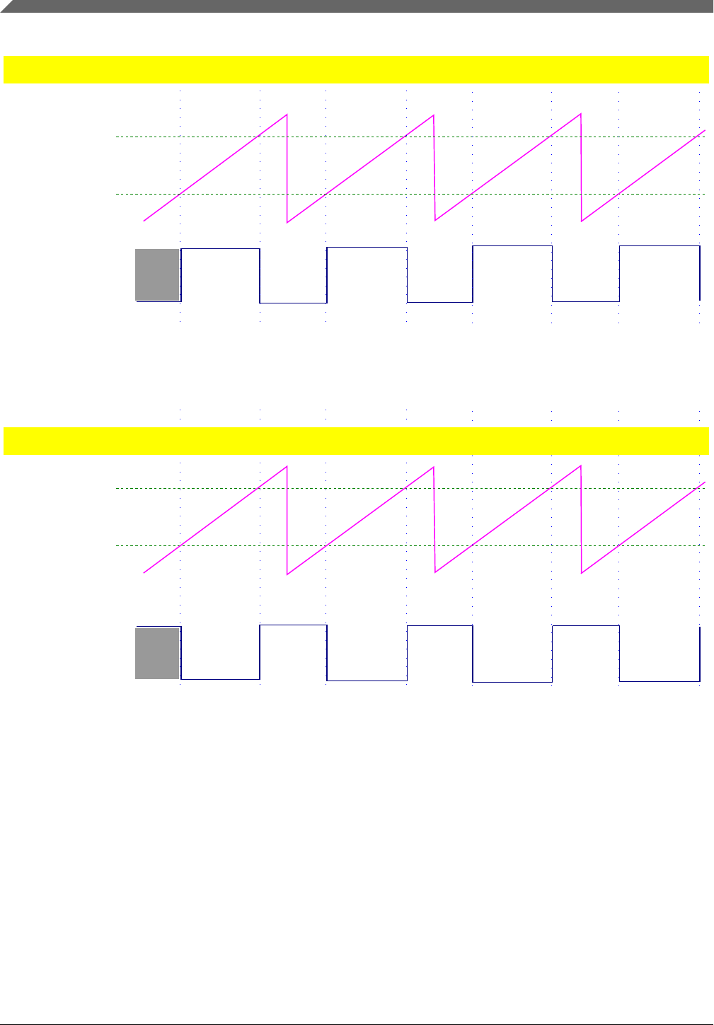
POyDLY[DLY2]
PDB Counter
Pulse-Out
Pulse-Out generation with DLY2 > DLY1
POyDLY[DLY1]
Pulse-Out
Pulse-Out generation with DLY1 > DLY2
POyDLY[DLY1]
PDB Counter
POyDLY[DLY2]
Figure 44-8. How Pulse Out is generated
44.4.4 Updating the delay registers
The following registers control the timing of the PDB operation; and in some of the
applications, they may need to become effective at the same time.
• PDB Modulus register (MOD)
• PDB Interrupt Delay register (IDLY)
Functional description
S32K1xx Series Reference Manual, Rev. 7, 04/2018
1178 NXP Semiconductors
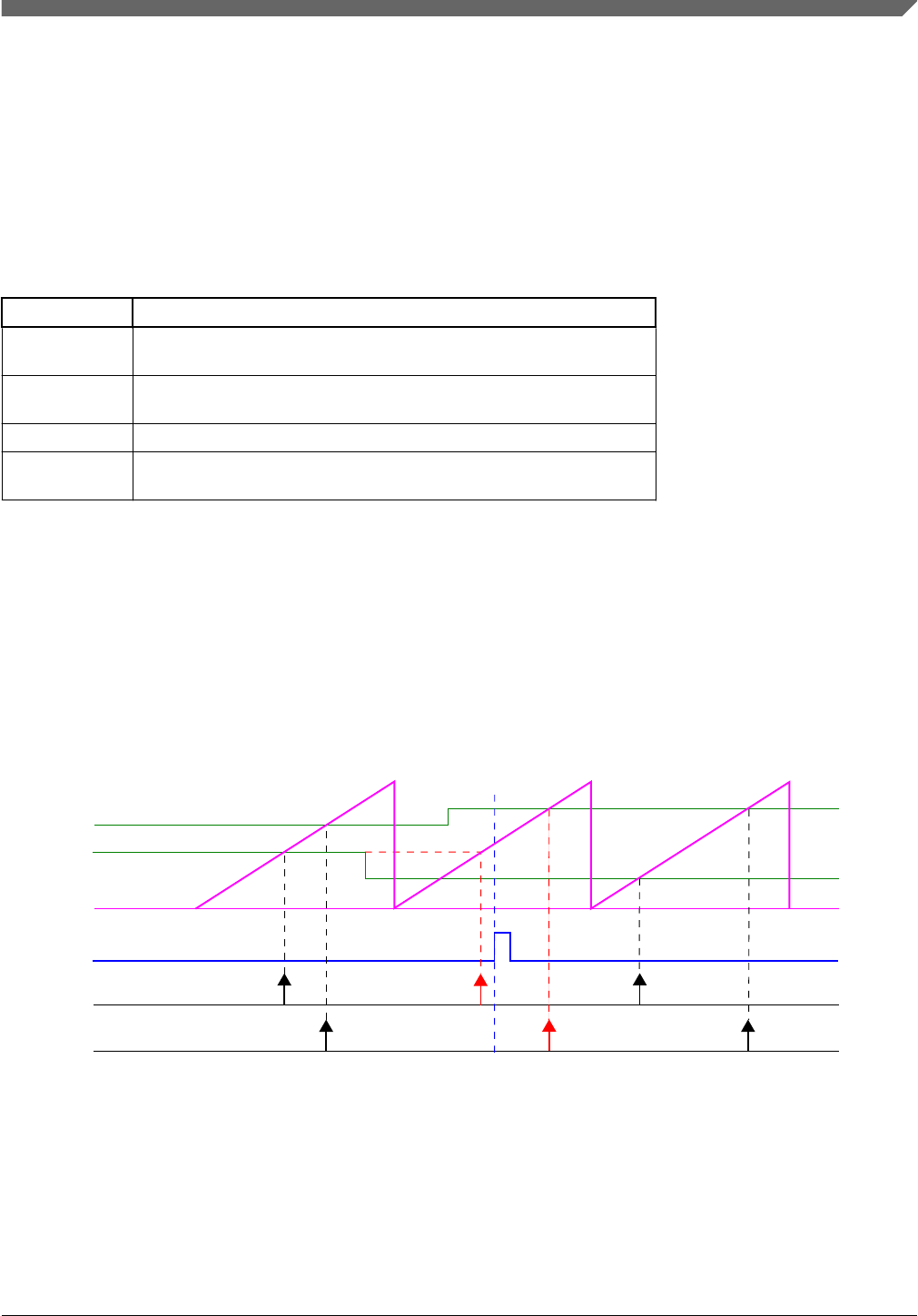
•PDB Channel n Delay m register (CHnDLYm)
•PDB Pulse-Out y Delay register (POyDLY)
The internal registers of them are buffered and any values written to them are written first
to their buffers. The circumstances that cause their internal registers to be updated with
the values from the buffers are summarized in the next table.
Table 44-7. When delay registers are updated
SC[LDMOD] Update to the delay registers
00 The internal registers are loaded with the values from their buffers
immediately after 1 is written to SC[LDOK].
01 The PDB counter reaches PDB_MOD[MOD] + 1 value, after 1 is
written to SC[LDOK].
10 A trigger input event is detected after 1 is written to SC[LDOK].
11 Either the PDB counter reaches PDB_MOD[MOD] + 1 value or a
trigger input event is detected, after 1 is written to SC[LDOK].
After 1 is written to SC[LDOK], the buffers cannot be written until the values in buffers
are loaded into their internal registers. SC[LDOK] is self-cleared when the internal
registers are loaded, so the application code can read it to determine the updates to the
internal registers.
The following diagrams show the cases of the internal registers being updated with
SC[LDMOD] is 00 and x1.
PDB counter
Ch n pre-trigger 0
Ch n pre-trigger 1
CHnDLY1
CHnDLY0
SC[LDOK]
Figure 44-9. Registers update with SC[LDMOD] = 00
Chapter 44 Programmable delay block (PDB)
S32K1xx Series Reference Manual, Rev. 7, 04/2018
NXP Semiconductors 1179
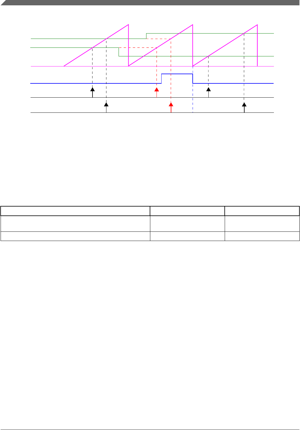
PDB counter
Ch n pre-trigger 0
Ch n pre-trigger 1
CHnDLY1
CHnDLY0
SC[LDOK]
Figure 44-10. Registers update with SC[LDMOD] = x1
44.4.5 Interrupts
PDB can generate two interrupts: PDB interrupt and PDB sequence error interrupt. The
following table summarizes the interrupts.
Table 44-8. PDB interrupt summary
Interrupt Flags Enable bit
PDB Interrupt SC[PDBIF] SC[PDBIE] = 1 and
SC[DMAEN] = 0
PDB Sequence Error Interrupt CHnS[ERRm] SC[PDBEIE] = 1
44.4.6 DMA
If SC[DMAEN] is set, PDB can generate a DMA transfer request when SC[PDBIF] is
set. When DMA is enabled, the PDB interrupt is not issued.
44.5 Application information
Application information
S32K1xx Series Reference Manual, Rev. 7, 04/2018
1180 NXP Semiconductors

44.5.1 Impact of using the prescaler and multiplication factor on
timing resolution
Use of prescaler and multiplication factor greater than 1 limits the count/delay accuracy
in terms of peripheral clock cycles (to the modulus of the prescaler X multiplication
factor). If the multiplication factor is set to 1 and the prescaler is set to 2 then the only
values of total peripheral clocks that can be detected are even values; if prescaler is set to
4 then the only values of total peripheral clocks that can be decoded as detected are
mod(4) and so forth. If the applications need a really long delay value and use a prescaler
set to 128, then the resolution would be limited to 128 peripheral clock cycles.
Therefore, use the lowest possible prescaler and multiplication factor for a given
application.
Chapter 44 Programmable delay block (PDB)
S32K1xx Series Reference Manual, Rev. 7, 04/2018
NXP Semiconductors 1181

Application information
S32K1xx Series Reference Manual, Rev. 7, 04/2018
1182 NXP Semiconductors

Chapter 45
FlexTimer Module (FTM)
Chip-specific FTM information
45.1.1 Instantiation Information
The following table lists the FTM instances each chip in the product series and
summarizes features that vary across the products and instances.
Table 45-1. FTM instances and features
Chips Instances Channels Fault inputs FTM
modulation
Quadrature
Decoder
Hall sensor
support
Dithering
S32K116 FTM0 8 1 Yes No No No
FTM1 8 3 No Yes Yes Yes
S32K118 FTM0 8 4 Yes No No No
FTM1 8 4 No Yes Yes Yes
S32K142 FTM0 8 4 Yes No No No
FTM1 8 4 No Yes Yes Yes
FTM2 8 4 No Yes Yes Yes
FTM3 8 4 Yes No No No
S32K144 FTM0 8 4 Yes No No No
FTM1 8 4 No Yes Yes No
FTM2 8 4 No Yes Yes No
FTM3 8 4 Yes No No No
S32K146 FTM0 8 4 Yes No No No
FTM1 8 4 No Yes Yes Yes
FTM2 8 4 No Yes Yes Yes
FTM3 8 4 Yes No No No
FTM4 8 2 No No No No
FTM5 8 2 No No No No
S32K148 FTM0 8 4 Yes No No No
FTM1 8 4 No Yes Yes Yes
Table continues on the next page...
45.1
S32K1xx Series Reference Manual, Rev. 7, 04/2018
NXP Semiconductors 1183

Table 45-1. FTM instances and features (continued)
Chips Instances Channels Fault inputs FTM
modulation
Quadrature
Decoder
Hall sensor
support
Dithering
FTM2 8 4 No Yes Yes Yes
FTM3 8 4 Yes No No No
FTM4 8 2 No No No No
FTM5 8 2 No No No No
FTM6 8 2 No No No No
FTM7 8 2 No No No No
NOTE
Not all the registers shown in memory map of FTM are
implemented in each variant/instance of S32K14x. See the
above table for available features and hence the register
implementation.
For all products in the series, all FTM instances have these features:
• Global time base
• Filters on input channel
• Filter on fault channel
• Half cycle reload
• Separate deadtime on channel pairs
FTM global load enable is implemented through SIM_FTMOPT1[FTMGLDOK]. Refer
to Global Load and SIM_FTMOPT1[FTMGLDOK].
Wait mode is not supported on this device. See Module operation in available low power
modes for details on available power modes.
45.1.2 FTM Interrupts
The FlexTimer has multiple sources of interrupt. Refer to the
DMA_Interrupt_mapping.xlsm attached with this Reference Manual. When an FTM
interrupt occurs, read the FTM status registers (FMS, SC, and STATUS) to determine the
exact interrupt source.
45.1.3 FTM Fault Detection Inputs
The following fault detection input options for the FTM modules are selected via the
SIM_FTMOPT0 register. The external pin option is selected by default.
Chip-specific FTM information
S32K1xx Series Reference Manual, Rev. 7, 04/2018
1184 NXP Semiconductors

• FTM0 FAULT0 = FTM0_FLT0 pin or TRGMUX output
• FTM0 FAULT1 = FTM0_FLT1 pin or TRGMUX output
• FTM0 FAULT2 = FTM0_FLT2 pin or TRGMUX output
• FTM0 FAULT3 = FTM0_FLT3 pin
• FTM1 FAULT0 = FTM1_FLT0 pin or TRGMUX output
• FTM1 FAULT1 = FTM1_FLT1 pin or TRGMUX output
• FTM1 FAULT2 = FTM1_FLT2 pin or TRGMUX output
• FTM1 FAULT3 = FTM1_FLT3 pin
• FTM2 FAULT0 = FTM2_FLT0 pin or TRGMUX output
• FTM2 FAULT1 = FTM2_FLT1 pin or TRGMUX output
• FTM2 FAULT2 = FTM2_FLT2 pin or TRGMUX output
• FTM2 FAULT3 = FTM2_FLT3 pin
• FTM3 FAULT0 = FTM3_FLT0 pin or TRGMUX output
• FTM3 FAULT1 = FTM3_FLT1 pin or TRGMUX output
• FTM3 FAULT2 = FTM3_FLT2 pin or TRGMUX output
• FTM3 FAULT3 = FTM3_FLT3 pin
• FTM4 FAULT0 = FTM4_FLT0 pin
• FTM4 FAULT1 = FTM4_FLT1 pin
• FTM5 FAULT0 = FTM5_FLT0 pin
• FTM5 FAULT1 = FTM5_FLT1 pin
• FTM6 FAULT0 = FTM6_FLT0 pin
• FTM6 FAULT1 = FTM6_FLT1 pin
• FTM7 FAULT0 = FTM7_FLT0 pin
• FTM7 FAULT1 = FTM7_FLT1 pin
Chapter 45 FlexTimer Module (FTM)
S32K1xx Series Reference Manual, Rev. 7, 04/2018
NXP Semiconductors 1185
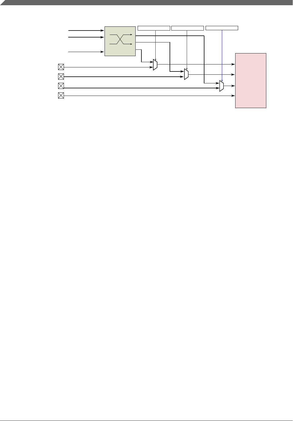
FTMx_FLT0
Trigger source_0
TRGMUX
Trigger source_1
Trigger source_n
.......
FTMx
FTMx_FLT1
FTMx_FLT2
FTMx_FLT3
FTMxFLT0SEL FTMxFLT1SEL FTMxFLT2SEL
FAULT0
FAULT1
FAULT2
FAULT3
from SIM_FTMOPT0 selection bitfield
Figure 45-1. Fault detection inputs
45.1.4 FTM Hardware Triggers and Synchronization
The FlexTimer support external hardware trigger input which can be used for timer
dynamic synchronization between multiple FlexTimers or counter reset. The FlexTimer
hardware trigger are implemented as following.
FTM0:
• FTM0 hardware trigger 0 = TRGMUX trigger output
• FTM0 hardware trigger 1 = SIM_FTMOPT1[FTM0SYNCBIT]
• FTM0 hardware trigger 2 = FTM0_FLT0 pin
FTM1:
• FTM1 hardware trigger 0 = TRGMUX trigger output
• FTM1 hardware trigger 1 = SIM_FTMOPT1[FTM1SYNCBIT]
• FTM1 hardware trigger 2 = FTM1_FLT0 pin
FTM2:
• FTM2 hardware trigger 0 = TRGMUX trigger output
• FTM2 hardware trigger 1 = SIM_FTMOPT1[FTM2SYNCBIT]
• FTM2 hardware trigger 2 = FTM2_FLT0 pin
FTM3:
• FTM3 hardware trigger 0 = TRGMUX trigger output
• FTM3 hardware trigger 1 = SIM_FTMOPT1[FTM3SYNCBIT]
• FTM3 hardware trigger 2 = FTM3_FLT0 pin
FTM4
Chip-specific FTM information
S32K1xx Series Reference Manual, Rev. 7, 04/2018
1186 NXP Semiconductors

• FTM4 hardware trigger 0 = TRGMUX trigger output
• FTM4 hardware trigger 1 = SIM_FTMOPT1[FTM4SYNCBIT]
• FTM4 hardware trigger 2 = FTM4_FLT0 pin
FTM5
• FTM5 hardware trigger 0 = TRGMUX trigger output
• FTM5 hardware trigger 1 = SIM_FTMOPT1[FTM5SYNCBIT]
• FTM5 hardware trigger 2 = FTM5_FLT0 pin
FTM6
• FTM6 hardware trigger 0 = TRGMUX trigger output
• FTM6 hardware trigger 1 = SIM_FTMOPT1[FTM6SYNCBIT]
• FTM6 hardware trigger 2 = FTM6_FLT0 pin
FTM7
• FTM7 hardware trigger 0 = TRGMUX trigger output
• FTM7 hardware trigger 1 = SIM_FTMOPT1[FTM7SYNCBIT]
• FTM7 hardware trigger 2 = FTM7_FLT0 pin
The hardware trigger source can be from many other modules via TRGMUX, like LPIT,
Low Power Timer, CMP, etc. It also supports FlexTimer's self trigger outputs, ex:
counter initialization trigger (init_trig) and channel match trigger (ext_trig), through the
flexible TRGMUX module.
Chapter 45 FlexTimer Module (FTM)
S32K1xx Series Reference Manual, Rev. 7, 04/2018
NXP Semiconductors 1187
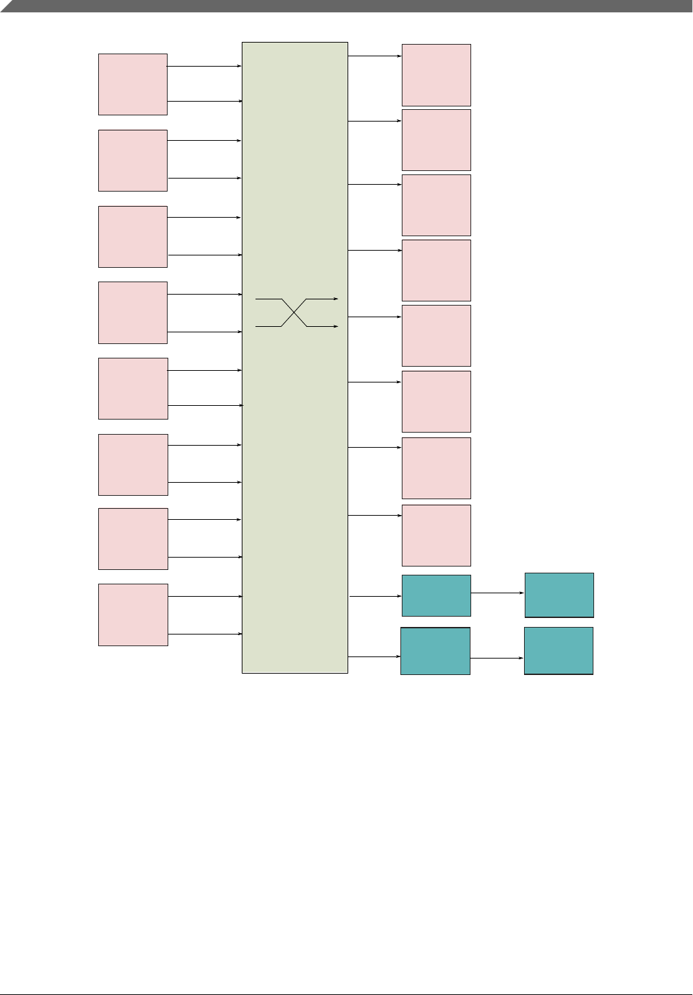
init_trig
hw_trig
ext_trig
FTM0
init_trig
hw_trig
ext_trig
FTM1
init_trig
hw_trig
ext_trig
FTM2
init_trig
hw_trig
ext_trig
FTM3
PDB0
PDB1
TRGMUX
init_trig
hw_trig
ext_trig
FTM0
init_trig
hw_trig
ext_trig
FTM1
init_trig
hw_trig
ext_trig
FTM2
init_trig
hw_trig
ext_trig
FTM3
ADC0
ADC1
init_trig
hw_trig
ext_trig
FTM4
init_trig
hw_trig
ext_trig
FTM5
init_trig
hw_trig
ext_trig
FTM6
init_trig
hw_trig
ext_trig
FTM7
init_trig
hw_trig
ext_trig
FTM4
init_trig
hw_trig
ext_trig
FTM5
init_trig
hw_trig
ext_trig
FTM6
init_trig
hw_trig
ext_trig
FTM7
Figure 45-2. Hardware triggers
The FlexTimer trigger outputs are also usually used as trigger source by other modules,
for example, the above diagram shows a case of triggering PDB and ADC. See
Instantiation Information and TRGMUX connectivity Module interconnectivity for
details.
45.1.5 FTM Input Capture Options
The following channel 0 input capture source options are selected via SIM_FTMOPT1.
The external pin option is selected by default.
Chip-specific FTM information
S32K1xx Series Reference Manual, Rev. 7, 04/2018
1188 NXP Semiconductors
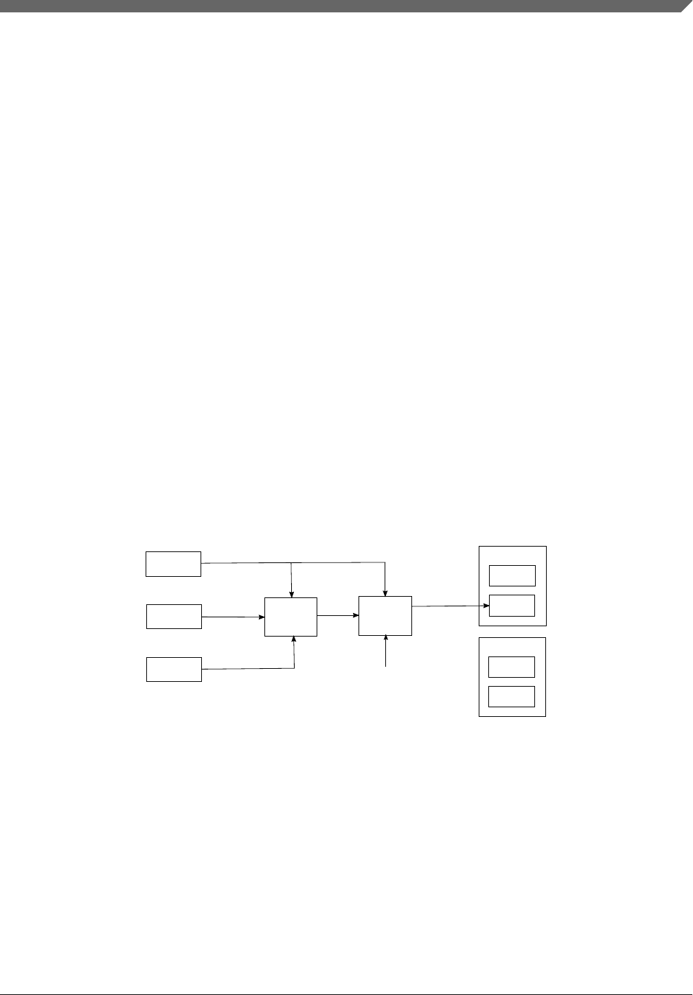
• FTM1 channel 0 input capture = FTM1_CH0 pin or CMP0 output
• FTM2 channel 0 input capture = FTM2_CH0 pin or CMP0 output
• FTM2 channel 1 input capture = FTM2_CH1 pin or exclusive OR of FTM2_CH0,
FTM2_CH1, and FTM1_CH1. See FTM Hall sensor support.
45.1.6 FTM Hall sensor support
For 3 phase motor control sensor-ed applications the use of Hall sensors, generally 3
sensors placed 120 degrees apart around the rotor, are deployed to detect position and
speed. Each of the 3 sensors provides a pulse that applied to an input capture pin, can
then be analyzed and both speed and position can be deduced. To simplify the
calculations required by the CPU on each hall sensor's input, if all 3 inputs are
"exclusively OR'd" into one timer channel and the free running counter is refreshed on
every edge then this can simplify the speed calculation.
Via the SIM module and SIM_FTMOPT1 register the FTM2CH1SEL bit provides the
choice of normal FTM2_CH1 input or the XOR of FTM2_CH0, FTM2_CH1 and
FTM1_CH1 pins that will be applied to FTM2_CH1.
NOTE
If the user utilizes FTM1_CH1 to be an input to FTM2_CH1,
FTM1_CH0 can still be utilized for other functions.
X OR
FTM2_CH1
FTM2_CH0
FTM1_CH1
Ch0
Ch1
FTM2
Ch0
Ch1
FTM1
SIM_FTMOPT1[FTM2CH1SEL]
Figure 45-3. FTM Hall Sensor Configuration
45.1.7 FTM Modulation Implementation
FTM0 and FTM3 support a modulation function where the output channels when
configured as PWM or Output Compare mode modulate another timer output when the
channel signal is asserted. Any of the 8 channels of FTM0 and any of the 8 channels of
FTM3 can be configured to support this modulation function.
Chapter 45 FlexTimer Module (FTM)
S32K1xx Series Reference Manual, Rev. 7, 04/2018
NXP Semiconductors 1189
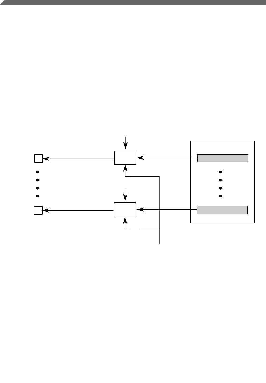
The SIM_FTMOPT1 register has control bits (FTMxCHySEL) that allow the user to
select normal PWM/Output Compare mode on the corresponding FTM timer channel or
modulate with FTM1_CH1. The diagram below shows the implementation for FTM0.
FTM3 has similar implementation controlled by SIM_FTMOPT1[FTM3CHySEL] on
each of its 8 channels with modulation possible via FTM2_CH1. See SIM chapter for
further information.
When FTM1_CH1 is used to modulate an FTM0 channel, then the user must configure
FTM1_CH1 to provide a signal that has a higher frequency than the modulated FTM0
channel output. Also it limits the use of the FTM1_CH0 function, as the FTM1_CH1 will
be programmed to provide a 50% duty PWM signal and limit the start and modulus
values for the free running counter. FTM2 has a similar restriction when FTM2_CH1 is
used for modulating an FTM3 channel.
FTM0
FTM0_CH7 &
SIM_FTMOPT1[FTM0CH7SEL]
CH7
FTM0_CH0 &
SIM_FTMOPT1[FTM0CH0SEL]
CH0
FTM1_CH1
Figure 45-4. FTM Output Modulation
45.1.8 FTM Global Time Base
This chip provides the optional FTM global time base feature, see Global time base
(GTB).
FTM supports global timer base through the GTB feature. Any of the FTM module could
be used as the GTB_EN source. The global timer base only allows the FTM counters to
start their operation synchronously, it does not automatically provide continuous
synchronization of FTM counters, meaning that the FTM counters may lose
synchronization during misc FTM operation.
Chip-specific FTM information
S32K1xx Series Reference Manual, Rev. 7, 04/2018
1190 NXP Semiconductors
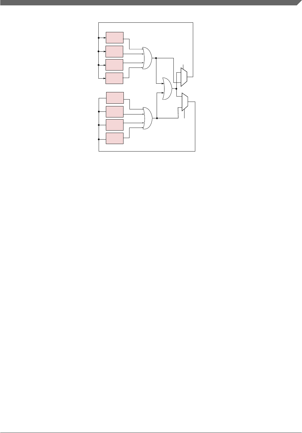
FTM0
FTM1
FTM2
FTM3
gtb_in
gtb_in
gtb_in
gtb_in
gtb_in
gtb_in
gtb_in
gtb_in
SIM_MISCTRL0[14]
SIM_MISCTRL0[14]
0
1
0
1
gtb_out
gtb_out
gtb_out
gtb_out
FTM4
FTM5
FTM6
FTM7
gtb_out
gtb_out
gtb_out
gtb_out
Figure 45-5. FTM global time base system interconnection
45.1.9 FTM BDM and debug halt mode
In the FTM chapter, references to the chip being in "BDM" are the same as the chip being
in “debug halt mode".
45.1.9.1 FTM output channel state retention
This device supports optional state retention of FTM channel in case of no clock
condition (CLKS=2'b00). See SIM_MISCTRL0[FTMx_OBE_CTRL] for enabling this
feature.
45.2 Introduction
The FlexTimer module (FTM) is a two-to-eight channel timer that supports input capture,
output compare, and the generation of PWM signals to control electric motor and power
management applications. The FTM time reference is a 16-bit counter that can be used as
an unsigned or signed counter.
Chapter 45 FlexTimer Module (FTM)
S32K1xx Series Reference Manual, Rev. 7, 04/2018
NXP Semiconductors 1191

45.2.1 FlexTimer philosophy
The FlexTimer is built upon a simple timer, the HCS08 Timer PWM Module – TPM,
used for many years on 8-bit microcontrollers. The FlexTimer extends the functionality
to meet the demands of motor control, digital lighting solutions, and power conversion,
while providing low cost and backwards compatibility with the TPM module.
Several key enhancements are made:
• Signed up counter
• Deadtime insertion hardware
• Fault control inputs
• Enhanced triggering functionality
• Initialization and polarity control
All of the features common with the TPM have fully backwards compatible register
assignments. The FlexTimer can also use code on the same core platform without change
to perform the same functions.
Motor control and power conversion features have been added through a dedicated set of
registers and defaults turn off all new features. The new features, such as hardware
deadtime insertion, polarity, fault control, output forcing and masking, greatly reduce
loading on the execution software and are usually each controlled by a group of registers.
FlexTimer input triggers can be from comparators, ADC, or other submodules to initiate
timer functions automatically. These triggers can be linked in a variety of ways during
integration of the sub modules so please note the options available for used FlexTimer
configuration.
More than one FlexTimers may be synchronized to provide a larger timer with their
counters incrementing in union, assuming the initialization, the input clocks, the initial
and final counting values are the same in each FlexTimer.
All main user access registers are buffered to ease the load on the executing software. A
number of trigger options exist to determine which registers are updated with this user
defined data.
45.2.2 Features
The FTM features include:
• FTM source clock is selectable
Introduction
S32K1xx Series Reference Manual, Rev. 7, 04/2018
1192 NXP Semiconductors

• Source clock can be the FTM input clock, the fixed frequency clock, or an
external clock
• Fixed frequency clock is an additional clock input to allow the selection of an on
chip clock source other than the FTM input clock
• Selecting external clock connects FTM clock to a chip level input pin therefore
allowing to synchronize the FTM counter with an off chip clock source
• Prescaler divide-by 1, 2, 4, 8, 16, 32, 64, or 128
• 16-bit counter
• It can be a free-running counter or a counter with initial and final value
• The counting can be up or up-down
• Each channel can be configured for input capture, output compare, or edge-aligned
PWM mode
• In Input Capture mode:
• The capture can occur on rising edges, falling edges or both edges
• An input filter can be selected for some channels. One unique prescaler is
available for all filters
• In Output Compare mode the output signal can be set, cleared, or toggled on match
• All channels can be configured for center-aligned PWM mode
• Each pair of channels can be combined to generate a PWM signal with independent
control of both edges of PWM signal
• The FTM channels can operate as pairs with equal outputs, pairs with
complementary outputs, or independent channels with independent outputs
• The deadtime insertion is available for each complementary pair
• Generation of match triggers
• Software control of PWM outputs
• Up to 4 fault inputs for global fault control
• The polarity of each channel is configurable
• The generation of an interrupt per channel
• The generation of an interrupt when the counter overflows
Chapter 45 FlexTimer Module (FTM)
S32K1xx Series Reference Manual, Rev. 7, 04/2018
NXP Semiconductors 1193

• The generation of an interrupt when the fault condition is detected
• The generation of an interrupt when a register reload point occurs
• Synchronized loading of write buffered FTM registers
• Half cycle and Full cycle register reload capacity
• Write protection for critical registers
• Backwards compatible with TPM
• Testing of input capture mode
• Direct access to input pin states
• Dual edge capture for pulse and period width measurement
• Quadrature decoder with input filters, relative position counting, and interrupt on
position count or capture of position count on external event
• The FTM channels can be selected to generate a trigger pulse on channel output
instead of a PWM
• Dithering capability to simulate fine edge control for both PWM period or PWM
duty cycle
45.2.3 Modes of operation
When the chip is in an active Debug mode, the FTM temporarily suspends all counting
until the chip returns to normal user operating mode. During Stop mode, all FTM input
clocks are stopped, so the FTM is effectively disabled until clocks resume. During Wait
mode, the FTM continues to operate normally. If the FTM does not need to produce a
real time reference or provide the interrupt sources needed to wake the chip from Wait
mode, the power can then be saved by disabling FTM functions before entering Wait
mode.
45.2.4 Block Diagram
The FTM uses one input/output (I/O) pin per channel, CHn (FTM channel (n)) where n is
the channel number (0–7).
NOTE
The number of channels supported can vary for each instance of
the FTM module on a chip. See the chip-specific FTM
Introduction
S32K1xx Series Reference Manual, Rev. 7, 04/2018
1194 NXP Semiconductors

information to see how many channels are supported for each
module instance. For example, if a module instance supports
only six channels, references to channel numbers 6 and 7 do not
apply for that instance.
The following figure shows the FTM structure. The central component of the FTM is the
16-bit counter with programmable initial and final values and its counting can be up or
up-down.
Chapter 45 FlexTimer Module (FTM)
S32K1xx Series Reference Manual, Rev. 7, 04/2018
NXP Semiconductors 1195
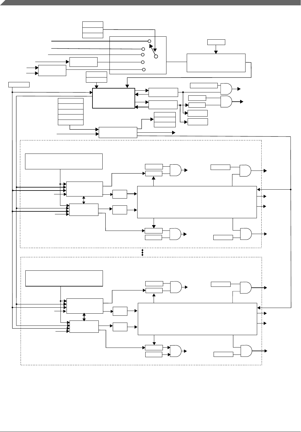
CAPTEST
no clock selected
(FTM counter disable)
FTM input clock
fixed frequency clock
external clock
phase A
phase B
CLKS
FTMEN
QUADEN
synchronizer
Quadrature
decoder QUADEN
CPWMS
PS
INITTRIGEN
TOIE
TOF
TOFDIR
QUADIR
CNTIN
MOD
FAULTIN
FAULTF
FAULTFn*
FTM counter
FAULTM[1:0]
FFVAL[3:0]
FAULTIE
FAULTnEN*
FFLTRnEN*
fault input n*
fault control
*where n = 3, 2, 1, 0
initialization
trigger
timer overflow
interrupt
fault condition
fault interrupt
pair channels 0 - channels 0 and 1
channel 1 input
C0V
C1V
CH1IE
CH0IE
CH1F
CH0F
channel 0
interrupt
channel 1
interrupt
channel 1
match trigger
channel 0
output signal
channel 0
match trigger
channel 1
output signal
CH1TRIG
CH0TRIG
(generation of channels 0 and 1 outputs signals in output
compare, EPWM, CPWM, Combine, and Modified Combine
PWM modes according to initialization, complementary mode,
inverting, software output control, deadtime insertion,
output mask, fault control and polarity control)
output modes logic
input capture
mode
prescaler
(1, 2, 4, 8, 16, 32, 64 or 128)
DECAPEN, MCOMBINE0, COMBINE0,
CPWMS, MS0B:MS0A, ELS0B:ELS0A,
MS1B:MS1A, ELS1B:ELS1A
dual edge capture
mode and input
capture mode
channel 0 input
pair channels 3 - channels 6 and 7
channel 7 input
C6V
C7V
CH7IE
CH6IE
CH7F
CH6F
channel 6
interrupt
channel 7
interrupt
channel 7
match trigger
channel 6
output signal
channel 6
match trigger
channel 7
output signal
CH7TRIG
CH6TRIG
(generation of channels 6 and 7 outputs signals in output
compare, EPWM, CPWM, Combine, and Modified Combine
PWM modes according to initialization, complementary mode,
inverting, software output control, deadtime insertion,
output mask, fault control and polarity control)
output modes logic
input capture
mode
DECAPEN, MCOMBINE3, COMBINE3,
CPWMS, MS6B:MS6A, ELS6B:ELS6A,
MS7B:MS7A, ELS7B:ELS7A
dual edge capture
mode and input
capture mode
channel 6 input
Figure 45-6. FTM Block Diagram
Introduction
S32K1xx Series Reference Manual, Rev. 7, 04/2018
1196 NXP Semiconductors

45.3 FTM signal descriptions
Table 45-2 shows the user-accessible signals for the FTM.
Table 45-2. FTM signal descriptions
Signal Description I/O Function
EXTCLK External clock. FTM external
clock can be selected to drive
the FTM counter.
I The external clock input signal is used as the FTM counter
clock if selected by CLKS[1:0] bits in the SC register. This
clock signal must not exceed 1/4 of FTM input clock
frequency. The FTM counter prescaler selection and settings
are also used when an external clock is selected.
CHn FTM channel (n), where n can
be 7-0
I/O Each FTM channel can be configured to operate either as
input or output. The direction associated with each channel,
input or output, is selected according to the mode assigned
for that channel.
FAULTj Fault input (j), where j can be
3-0
I The fault input signals are used to control the CHn channel
output state. If a fault is detected, the FAULTj signal is
asserted and the channel output is put in a safe state. The
behavior of the fault logic is defined by the FAULTM[1:0]
control bits in the MODE register and FAULTEN bit in the
COMBINE register. Note that each FAULTj input may affect
all channels selectively since FAULTM[1:0] and FAULTEN
control bits are defined for each pair of channels. Because
there are several FAULTj inputs, maximum of 4 for the FTM
module, each one of these inputs is activated by the
FAULTjEN bit in the FLTCTRL register.
PHA Quadrature decoder phase A
input. Input pin associated
with quadrature decoder
phase A.
I The quadrature decoder phase A input is used as the
Quadrature Decoder mode is selected. The phase A input
signal is one of the signals that control the FTM counter
increment or decrement in the Quadrature Decoder Mode.
PHB Quadrature decoder phase B
input. Input pin associated
with quadrature decoder
phase B.
I The quadrature decoder phase B input is used as the
Quadrature Decoder mode is selected. The phase B input
signal is one of the signals that control the FTM counter
increment or decrement in the Quadrature Decoder Mode.
45.4 Memory map and register definition
45.4.1 Memory map
This section presents a high-level summary of the FTM registers and how they are
mapped.
The registers and bits of an unavailable function in the FTM remain in the memory map
and in the reset value, but they have no active function.
Chapter 45 FlexTimer Module (FTM)
S32K1xx Series Reference Manual, Rev. 7, 04/2018
NXP Semiconductors 1197

NOTE
The number of channels supported can vary for each instance of
the FTM module on a chip. See the chip-specific FTM
information to see how many channels are supported for each
module instance.
Note
Do not write in the region from the CNTIN register when
FTMEN = 0.
45.4.2 Register descriptions
Accesses to reserved addresses result in transfer errors. Registers for absent channels are
considered reserved. Double buffered register writes must be done using 32-bit
operations.
45.4.3 FTM register descriptions
45.4.3.1 FTM Memory map
FTM0 base address: 4003_8000h
FTM1 base address: 4003_9000h
FTM2 base address: 4003_A000h
FTM3 base address: 4002_6000h
FTM4 base address: 4006_E000h
FTM5 base address: 4006_F000h
FTM6 base address: 4007_0000h
FTM7 base address: 4007_1000h
Offset Register Width
(In bits)
Access Reset value
0h Status And Control (SC) 32 RW 0000_0000h
4h Counter (CNT) 32 RW 0000_0000h
Table continues on the next page...
Memory map and register definition
S32K1xx Series Reference Manual, Rev. 7, 04/2018
1198 NXP Semiconductors

Offset Register Width
(In bits)
Access Reset value
8h Modulo (MOD) 32 RW 0000_0000h
Ch Channel (n) Status And Control (C0SC) 32 RW 0000_0000h
10h Channel (n) Value (C0V) 32 RW 0000_0000h
14h Channel (n) Status And Control (C1SC) 32 RW 0000_0000h
18h Channel (n) Value (C1V) 32 RW 0000_0000h
1Ch Channel (n) Status And Control (C2SC) 32 RW 0000_0000h
20h Channel (n) Value (C2V) 32 RW 0000_0000h
24h Channel (n) Status And Control (C3SC) 32 RW 0000_0000h
28h Channel (n) Value (C3V) 32 RW 0000_0000h
2Ch Channel (n) Status And Control (C4SC) 32 RW 0000_0000h
30h Channel (n) Value (C4V) 32 RW 0000_0000h
34h Channel (n) Status And Control (C5SC) 32 RW 0000_0000h
38h Channel (n) Value (C5V) 32 RW 0000_0000h
3Ch Channel (n) Status And Control (C6SC) 32 RW 0000_0000h
40h Channel (n) Value (C6V) 32 RW 0000_0000h
44h Channel (n) Status And Control (C7SC) 32 RW 0000_0000h
48h Channel (n) Value (C7V) 32 RW 0000_0000h
4Ch Counter Initial Value (CNTIN) 32 RW 0000_0000h
50h Capture And Compare Status (STATUS) 32 RW 0000_0000h
54h Features Mode Selection (MODE) 32 RW 0000_0004h
58h Synchronization (SYNC) 32 RW 0000_0000h
5Ch Initial State For Channels Output (OUTINIT) 32 RW 0000_0000h
60h Output Mask (OUTMASK) 32 RW 0000_0000h
64h Function For Linked Channels (COMBINE) 32 RW 0000_0000h
68h Deadtime Configuration (DEADTIME) 32 RW 0000_0000h
6Ch FTM External Trigger (EXTTRIG) 32 RW 0000_0000h
70h Channels Polarity (POL) 32 RW 0000_0000h
74h Fault Mode Status (FMS) 32 RW 0000_0000h
78h Input Capture Filter Control (FILTER) 32 RW 0000_0000h
7Ch Fault Control (FLTCTRL) 32 RW 0000_0000h
80h Quadrature Decoder Control And Status (QDCTRL) 32 RW 0000_0000h
84h Configuration (CONF) 32 RW 0000_0000h
88h FTM Fault Input Polarity (FLTPOL) 32 RW 0000_0000h
8Ch Synchronization Configuration (SYNCONF) 32 RW 0000_0000h
90h FTM Inverting Control (INVCTRL) 32 RW 0000_0000h
94h FTM Software Output Control (SWOCTRL) 32 RW 0000_0000h
98h FTM PWM Load (PWMLOAD) 32 RW 0000_0000h
9Ch Half Cycle Register (HCR) 32 RW 0000_0000h
A0h Pair 0 Deadtime Configuration (PAIR0DEADTIME) 32 RW 0000_0000h
A8h Pair 1 Deadtime Configuration (PAIR1DEADTIME) 32 RW 0000_0000h
Table continues on the next page...
Chapter 45 FlexTimer Module (FTM)
S32K1xx Series Reference Manual, Rev. 7, 04/2018
NXP Semiconductors 1199

Offset Register Width
(In bits)
Access Reset value
B0h Pair 2 Deadtime Configuration (PAIR2DEADTIME) 32 RW 0000_0000h
B8h Pair 3 Deadtime Configuration (PAIR3DEADTIME) 32 RW 0000_0000h
200h Mirror of Modulo Value (MOD_MIRROR) 32 RW 0000_0000h
204h - 220h Mirror of Channel (n) Match Value (C0V_MIRROR - C7V_MIRROR) 32 RW 0000_0000h
45.4.3.2 Status And Control (SC)
45.4.3.2.1 Offset
Register Offset
SC 0h
45.4.3.2.2 Function
SC contains the overflow status flag and control bits used to configure the interrupt
enable, FTM configuration, clock source, filter prescaler, and prescaler factor.
This register also contains the output enable control bits and the reload opportunity flag
control.
These controls relate to all channels within this module.
45.4.3.2.3 Diagram
Bits 31 30 29 28 27 26 25 24 23 22 21 20 19 18 17 16
R
0
FLTP
S
PWMEN7
PWMEN6
PWMEN5
PWMEN4
PWMEN3
PWMEN2
PWMEN1
PWMEN0
W
Reset 0 0 0 0 0 0 0 0 0 0 0 0 0 0 0 0
Bits 15 14 13 12 11 10 9 8 7 6 5 4 3 2 1 0
R
0
TOF
TOIE
R
F
RI
E
CPWMS
CLKS
P
S
W
0
0
Reset 0 0 0 0 0 0 0 0 0 0 0 0 0 0 0 0
Memory map and register definition
S32K1xx Series Reference Manual, Rev. 7, 04/2018
1200 NXP Semiconductors

45.4.3.2.4 Fields
Field Function
31-28
—
Reserved
27-24
FLTPS
Filter Prescaler
The bits FLTPS selects the clock prescaler used in the FTM filters:
• channel input filters
• fault inputs filters
Writing to the bits FLTPS has immediate effect.
0000b - Divide by 1
0001b - Divide by 2
0010b - Divide by 3
0011b - Divide by 4
0100b - Divide by 5
0101b - Divide by 6
0110b - Divide by 7
0111b - Divide by 8
1000b - Divide by 9
1001b - Divide by 10
1010b - Divide by 11
1011b - Divide by 12
1100b - Divide by 13
1101b - Divide by 14
1110b - Divide by 15
1111b - Divide by 16
23-16
PWMENn
Channel 0 PWM enable bit
This bit enables the PWM channel output. This bit should be set to 0 (output disabled) when an input
mode is used.
0b - Channel output port is disabled.
1b - Channel output port is enabled.
15-10
—
Reserved
9
TOF
Timer Overflow Flag
Set by hardware when the FTM counter passes the value in the MOD register. The TOF bit is cleared by
reading the SC register while TOF is set and then writing a 0 to TOF bit. Writing a 1 to TOF has no effect.
If another FTM overflow occurs between the read and write operations, the write operation has no effect;
therefore, TOF remains set indicating an overflow has occurred. In this case, a TOF interrupt request is
not lost due to the clearing sequence for a previous TOF.
0b - FTM counter has not overflowed.
1b - FTM counter has overflowed.
8
TOIE
Timer Overflow Interrupt Enable
Enables FTM overflow interrupts.
0b - Disable TOF interrupts. Use software polling.
1b - Enable TOF interrupts. An interrupt is generated when TOF equals one.
7
RF
Reload Flag
The RF bit is set at each selected reload point. See Reload Points.
Table continues on the next page...
Chapter 45 FlexTimer Module (FTM)
S32K1xx Series Reference Manual, Rev. 7, 04/2018
NXP Semiconductors 1201

Field Function
The RF bit is cleared by reading the SC register while RF is set and then writing a 0 to RF bit. Writing 1 to
RF has no effect. If another selected reload point happens between the read and write operations, the
write operation has no effect; therefore, RF remains set.
0b - A selected reload point did not happen.
1b - A selected reload point happened.
6
RIE
Reload Point Interrupt Enable
Enables the reload point interrupt.
0b - Reload point interrupt is disabled.
1b - Reload point interrupt is enabled.
5
CPWMS
Center-Aligned PWM Select
Selects CPWM mode. This mode configures the FTM to operate in Up-Down Counting mode.
This field is write protected. It can be written only when MODE[WPDIS] = 1.
0b - FTM counter operates in Up Counting mode.
1b - FTM counter operates in Up-Down Counting mode.
4-3
CLKS
Clock Source Selection
Selects one of the three FTM counter clock sources.
This field is write protected. It can be written only when MODE[WPDIS] = 1.
00b - No clock selected. This in effect disables the FTM counter.
01b - FTM input clock
10b - Fixed frequency clock
11b - External clock
2-0
PS
Prescale Factor Selection
Selects one of 8 division factors for the clock source selected by CLKS. The new prescaler factor affects
the clock source on the next FTM input clock cycle after the new value is updated into the register bits.
This field is write protected. It can be written only when MODE[WPDIS] = 1.
000b - Divide by 1
001b - Divide by 2
010b - Divide by 4
011b - Divide by 8
100b - Divide by 16
101b - Divide by 32
110b - Divide by 64
111b - Divide by 128
45.4.3.3 Counter (CNT)
45.4.3.3.1 Offset
Register Offset
CNT 4h
Memory map and register definition
S32K1xx Series Reference Manual, Rev. 7, 04/2018
1202 NXP Semiconductors

45.4.3.3.2 Function
The CNT register contains the FTM counter value.
Reset clears the CNT register. Writing any value to COUNT updates the counter with its
initial value, CNTIN.
45.4.3.3.3 Diagram
Bits 31 30 29 28 27 26 25 24 23 22 21 20 19 18 17 16
R 0
W
Reset 0 0 0 0 0 0 0 0 0 0 0 0 0 0 0 0
Bits 15 14 13 12 11 10 9 8 7 6 5 4 3 2 1 0
RCOUNT
W
Reset 0 0 0 0 0 0 0 0 0 0 0 0 0 0 0 0
45.4.3.3.4 Fields
Field Function
31-16
—
Reserved
15-0
COUNT
Counter Value
45.4.3.4 Modulo (MOD)
45.4.3.4.1 Offset
Register Offset
MOD 8h
Chapter 45 FlexTimer Module (FTM)
S32K1xx Series Reference Manual, Rev. 7, 04/2018
NXP Semiconductors 1203

45.4.3.4.2 Function
The Modulo register contains the modulo value for the FTM counter. After the FTM
counter reaches the modulo value, the overflow flag (TOF) becomes set at the next clock
cycle, and the next value of FTM counter depends on the selected counting method; see
Counter.
Writes to the MOD register are done on its write buffer. The MOD register is updated
with its write buffer value according to Registers updated from write buffers. If FTMEN
= 0, a write to SC register resets manually this write coherency mechanism.
Initialize the FTM counter, by writing to CNT, before writing to the MOD register to
avoid confusion about when the first counter overflow will occur.
45.4.3.4.3 Diagram
Bits 31 30 29 28 27 26 25 24 23 22 21 20 19 18 17 16
R 0
W
Reset 0 0 0 0 0 0 0 0 0 0 0 0 0 0 0 0
Bits 15 14 13 12 11 10 9 8 7 6 5 4 3 2 1 0
RMOD
W
Reset 0 0 0 0 0 0 0 0 0 0 0 0 0 0 0 0
45.4.3.4.4 Fields
Field Function
31-16
—
Reserved
15-0
MOD
MOD
Modulo Value
45.4.3.5 Channel (n) Status And Control (C0SC - C7SC)
45.4.3.5.1 Offset
For a = 0 to 7:
Memory map and register definition
S32K1xx Series Reference Manual, Rev. 7, 04/2018
1204 NXP Semiconductors

Register Offset
CaSC Ch + (a × 8h)
45.4.3.5.2 Function
CnSC contains channel (n) status bits and control bits that select the channel (n) mode
and its functionality.
45.4.3.5.3 Diagram
Bits 31 30 29 28 27 26 25 24 23 22 21 20 19 18 17 16
R 0
W
Reset 0 0 0 0 0 0 0 0 0 0 0 0 0 0 0 0
Bits 15 14 13 12 11 10 9 8 7 6 5 4 3 2 1 0
R
0
CHOV
CHIS
TRIGMODE
CHF
CHIE
MSB
MSA
ELS
B
ELS
A
ICRST
DMA
W
0
Reset 0 0 0 0 0 0 0 0 0 0 0 0 0 0 0 0
45.4.3.5.4 Fields
Field Function
31-11
—
Reserved
10
CHOV
Channel (n) Output Value
The CHOV bit has the final value of the channel (n) output.
NOTE: The CHOV bit should be ignored when the channel (n) is not in an output mode.
0b - The channel (n) output is zero.
1b - The channel (n) output is one.
9
CHIS
Channel (n) Input State
The CHIS bit has the value of the channel (n) input after the double-sampling or the filtering (if the
channel (n) filter is enabled) both them are inside the FTM.
NOTE: The CHIS bit should be ignored when the channel (n) is not in an input mode.
NOTE: When the pair channels is on dual edge mode, the channel (n+1) CHIS bit is the channel (n+1)
input value and not the channel (n) input value (this signal is the input signal used by the dual
edge mode).
0b - The channel (n) input is zero.
Table continues on the next page...
Chapter 45 FlexTimer Module (FTM)
S32K1xx Series Reference Manual, Rev. 7, 04/2018
NXP Semiconductors 1205

Field Function
1b - The channel (n) input is one.
8
TRIGMODE
Trigger mode control
This bit controls the trigger generation on FTM channel outputs. This mode is allowed only if when FTM
channel is configured to EPWM or CPWM modes. If a match in the channel occurs, a trigger pulse with
one FTM clock cycle width will be generated in the channel output. See Channel trigger output.
This field is write protected. It can be written only when MODE[WPDIS] = 1.
0b - Channel outputs will generate the normal PWM outputs without generating a pulse.
1b - If a match in the channel occurs, a trigger generation on channel output will happen. The
trigger pulse width has one FTM clock cycle.
7
CHF
Channel (n) Flag
Set by hardware when an event occurs on the channel (n). CHF is cleared by reading the CnSC register
while CHF is set and then writing a 0 to the CHF bit. Writing a 1 to CHF has no effect.
If another event occurs between the read and write operations, the write operation has no effect;
therefore, CHF remains set indicating an event has occurred. In this case a CHF interrupt request is not
lost due to the clearing sequence for a previous CHF.
0b - No channel (n) event has occurred.
1b - A channel (n) event has occurred.
6
CHIE
Channel (n) Interrupt Enable
Enables channel (n) interrupt.
0b - Disable channel (n) interrupt. Use software polling.
1b - Enable channel (n) interrupt.
5
MSB
Channel (n) Mode Select
Used on the selection of the channel (n) mode. See Channel Modes.
This field is write protected. It can be written only when MODE[WPDIS] = 1.
4
MSA
Channel (n) Mode Select
Used on the selection of the channel (n) mode. See Channel Modes.
This field is write protected. It can be written only when MODE[WPDIS] = 1.
3
ELSB
Channel (n) Edge or Level Select
Used on the selection of the channel (n) mode. See Channel Modes.
This field is write protected. It can be written only when MODE[WPDIS] = 1.
2
ELSA
Channel (n) Edge or Level Select
Used on the selection of the channel (n) mode. See Channel Modes.
This field is write protected. It can be written only when MODE[WPDIS] = 1.
1
ICRST
FTM counter reset by the selected input capture event.
FTM counter reset is driven by the selected event of the channel (n) in the Input Capture mode.
This field is write protected. It can be written only when MODE[WPDIS] = 1.
0b - FTM counter is not reset when the selected channel (n) input event is detected.
1b - FTM counter is reset when the selected channel (n) input event is detected.
0
DMA
DMA Enable
Enables DMA transfers for the channel.
0b - Disable DMA transfers.
1b - Enable DMA transfers.
Memory map and register definition
S32K1xx Series Reference Manual, Rev. 7, 04/2018
1206 NXP Semiconductors

45.4.3.6 Channel (n) Value (C0V - C7V)
45.4.3.6.1 Offset
For a = 0 to 7:
Register Offset
CaV 10h + (a × 8h)
45.4.3.6.2 Function
These registers contain the captured FTM counter value for the input modes or the match
value for the output modes.
In Input Capture, Capture Test, and Dual Edge Capture modes, any write to a CnV
register is ignored.
In output modes, writes to the CnV register are done on its write buffer. The CnV register
is updated with its write buffer value according to Registers updated from write buffers.
If FTMEN = 0, a write to CnSC register resets manually this write coherency mechanism.
45.4.3.6.3 Diagram
Bits 31 30 29 28 27 26 25 24 23 22 21 20 19 18 17 16
R 0
W
Reset 0 0 0 0 0 0 0 0 0 0 0 0 0 0 0 0
Bits 15 14 13 12 11 10 9 8 7 6 5 4 3 2 1 0
RVAL
W
Reset 0 0 0 0 0 0 0 0 0 0 0 0 0 0 0 0
45.4.3.6.4 Fields
Field Function
31-16
—
Reserved
Table continues on the next page...
Chapter 45 FlexTimer Module (FTM)
S32K1xx Series Reference Manual, Rev. 7, 04/2018
NXP Semiconductors 1207

Field Function
15-0
VAL
Channel Value
Captured FTM counter value of the input modes or the match value for the output modes
45.4.3.7 Counter Initial Value (CNTIN)
45.4.3.7.1 Offset
Register Offset
CNTIN 4Ch
45.4.3.7.2 Function
The Counter Initial Value register contains the initial value for the FTM counter.
Writing to the CNTIN register latches the value into a buffer. The CNTIN register is
updated with the value of its write buffer according to Registers updated from write
buffers.
When the FTM clock is initially selected, by writing a non-zero value to the CLKS bits,
the FTM counter starts with the value 0x0000. To avoid this behavior, before the first
write to select the FTM clock, write the new value to the the CNTIN register and then
initialize the FTM counter by writing any value to the CNT register.
45.4.3.7.3 Diagram
Bits 31 30 29 28 27 26 25 24 23 22 21 20 19 18 17 16
R 0
W
Reset 0 0 0 0 0 0 0 0 0 0 0 0 0 0 0 0
Bits 15 14 13 12 11 10 9 8 7 6 5 4 3 2 1 0
RINIT
W
Reset 0 0 0 0 0 0 0 0 0 0 0 0 0 0 0 0
Memory map and register definition
S32K1xx Series Reference Manual, Rev. 7, 04/2018
1208 NXP Semiconductors

45.4.3.7.4 Fields
Field Function
31-16
—
Reserved
15-0
INIT
INIT
Initial Value Of The FTM Counter
45.4.3.8 Capture And Compare Status (STATUS)
45.4.3.8.1 Offset
Register Offset
STATUS 50h
45.4.3.8.2 Function
The STATUS register contains a copy of the status flag CHF bit in CnSC for each FTM
channel for software convenience.
Each CHF bit in STATUS is a mirror of CHF bit in CnSC. All CHF bits can be checked
using only one read of STATUS. All CHF bits can be cleared by reading STATUS
followed by writing 0x00 to STATUS.
Hardware sets the individual channel flags when an event occurs on the channel. CHF is
cleared by reading STATUS while CHF is set and then writing a 0 to the CHF bit.
Writing a 1 to CHF has no effect.
If another event occurs between the read and write operations, the write operation has no
effect; therefore, CHF remains set indicating an event has occurred. In this case, a CHF
interrupt request is not lost due to the clearing sequence for a previous CHF.
Chapter 45 FlexTimer Module (FTM)
S32K1xx Series Reference Manual, Rev. 7, 04/2018
NXP Semiconductors 1209

45.4.3.8.3 Diagram
Bits 31 30 29 28 27 26 25 24 23 22 21 20 19 18 17 16
R 0
W
Reset 0 0 0 0 0 0 0 0 0 0 0 0 0 0 0 0
Bits 15 14 13 12 11 10 9 8 7 6 5 4 3 2 1 0
R
0
CH7F
CH6F
CH5F
CH4F
CH3F
CH2F
CH1F
CH0F
W
Reset 0 0 0 0 0 0 0 0 0 0 0 0 0 0 0 0
45.4.3.8.4 Fields
Field Function
31-8
—
Reserved
7-0
CHnF
Channel 0 Flag
See the register description.
0b - No channel event has occurred.
1b - A channel event has occurred.
45.4.3.9 Features Mode Selection (MODE)
45.4.3.9.1 Offset
Register Offset
MODE 54h
45.4.3.9.2 Function
This register contains the global enable bit for FTM-specific features and the control bits
used to configure:
• Fault control mode and interrupt
• Capture Test mode
• PWM synchronization
• Write protection
• Channel output initialization
Memory map and register definition
S32K1xx Series Reference Manual, Rev. 7, 04/2018
1210 NXP Semiconductors

These controls relate to all channels within this module.
45.4.3.9.3 Diagram
Bits 31 30 29 28 27 26 25 24 23 22 21 20 19 18 17 16
R 0
W
Reset 0 0 0 0 0 0 0 0 0 0 0 0 0 0 0 0
Bits 15 14 13 12 11 10 9 8 7 6 5 4 3 2 1 0
R
0
FAULTIE
FAULTM
CAPTEST
PWMSYNC
WPDIS
0
FTMEN
W
INIT
Reset 0 0 0 0 0 0 0 0 0 0 0 0 0 1 0 0
45.4.3.9.4 Fields
Field Function
31-8
—
Reserved
7
FAULTIE
Fault Interrupt Enable
Enables the generation of an interrupt when a fault is detected by FTM and the FTM fault control is
enabled.
0b - Fault control interrupt is disabled.
1b - Fault control interrupt is enabled.
6-5
FAULTM
Fault Control Mode
Defines the FTM fault control mode.
This field is write protected. It can be written only when MODE[WPDIS] = 1.
00b - Fault control is disabled for all channels.
01b - Fault control is enabled for even channels only (channels 0, 2, 4, and 6), and the selected
mode is the manual fault clearing.
10b - Fault control is enabled for all channels, and the selected mode is the manual fault clearing.
11b - Fault control is enabled for all channels, and the selected mode is the automatic fault
clearing.
4
CAPTEST
Capture Test Mode Enable
Enables the capture test mode.
This field is write protected. It can be written only when MODE[WPDIS] = 1.
0b - Capture test mode is disabled.
1b - Capture test mode is enabled.
3
PWMSYNC
PWM Synchronization Mode
Selects which triggers can be used by MOD, CnV, OUTMASK, and FTM counter synchronization. See
PWM synchronization. The PWMSYNC bit configures the synchronization when SYNCMODE is 0.
Table continues on the next page...
Chapter 45 FlexTimer Module (FTM)
S32K1xx Series Reference Manual, Rev. 7, 04/2018
NXP Semiconductors 1211

Field Function
0b - No restrictions. Software and hardware triggers can be used by MOD, CnV, OUTMASK, and
FTM counter synchronization.
1b - Software trigger can only be used by MOD and CnV synchronization, and hardware triggers
can only be used by OUTMASK and FTM counter synchronization.
2
WPDIS
Write Protection Disable
When write protection is enabled (WPDIS = 0), write protected bits cannot be written. When write
protection is disabled (WPDIS = 1), write protected bits can be written. The WPDIS bit is the negation of
the WPEN bit. WPDIS is cleared when 1 is written to WPEN. WPDIS is set when WPEN bit is read as a 1
and then 1 is written to WPDIS. Writing 0 to WPDIS has no effect.
0b - Write protection is enabled.
1b - Write protection is disabled.
1
INIT
Initialize The Channels Output
When a 1 is written to INIT bit the channels output is initialized according to the state of their
corresponding bit in the OUTINIT register. Writing a 0 to INIT bit has no effect.
The INIT bit is always read as 0.
0
FTMEN
FTM Enable
This field is write protected. It can be written only when MODE[WPDIS] = 1.
0b - TPM compatibility. Free running counter and synchronization compatible with TPM.
1b - Free running counter and synchronization are different from TPM behavior.
45.4.3.10 Synchronization (SYNC)
45.4.3.10.1 Offset
Register Offset
SYNC 58h
45.4.3.10.2 Function
This register configures the PWM synchronization.
A synchronization event can perform the synchronized update of MOD, CnV, and
OUTMASK registers with the value of their write buffer and the FTM counter
initialization.
Memory map and register definition
S32K1xx Series Reference Manual, Rev. 7, 04/2018
1212 NXP Semiconductors

NOTE
The software trigger, SWSYNC bit, and hardware triggers
TRIG0, TRIG1, and TRIG2 bits have a potential conflict if
used together when SYNCMODE = 0. Use only hardware or
software triggers but not both at the same time, otherwise
unpredictable behavior is likely to happen.
The selection of the loading point, CNTMAX and CNTMIN
bits, is intended to provide the update of MOD, CNTIN, and
CnV registers across all enabled channels simultaneously. The
use of the loading point selection together with SYNCMODE =
0 and hardware trigger selection, TRIG0, TRIG1, or TRIG2
bits, is likely to result in unpredictable behavior.
The synchronization event selection also depends on the
PWMSYNC (MODE register) and SYNCMODE (SYNCONF
register) bits. See PWM synchronization.
45.4.3.10.3 Diagram
Bits 31 30 29 28 27 26 25 24 23 22 21 20 19 18 17 16
R 0
W
Reset 0 0 0 0 0 0 0 0 0 0 0 0 0 0 0 0
Bits 15 14 13 12 11 10 9 8 7 6 5 4 3 2 1 0
R
0
SWSYN
C
TRIG2
TRIG1
TRIG0
SYNCHOM
REINIT
CNTMAX
CNTMIN
W
Reset 0 0 0 0 0 0 0 0 0 0 0 0 0 0 0 0
45.4.3.10.4 Fields
Field Function
31-8
—
Reserved
7
SWSYNC
PWM Synchronization Software Trigger
Selects the software trigger as the PWM synchronization trigger. The software trigger happens when a 1
is written to SWSYNC bit.
0b - Software trigger is not selected.
Table continues on the next page...
Chapter 45 FlexTimer Module (FTM)
S32K1xx Series Reference Manual, Rev. 7, 04/2018
NXP Semiconductors 1213

Field Function
1b - Software trigger is selected.
6
TRIG2
PWM Synchronization Hardware Trigger 2
Enables hardware trigger 2 to the PWM synchronization. Hardware trigger 2 happens when a rising edge
is detected at the trigger 2 input signal.
0b - Trigger is disabled.
1b - Trigger is enabled.
5
TRIG1
PWM Synchronization Hardware Trigger 1
Enables hardware trigger 1 to the PWM synchronization. Hardware trigger 1 happens when a rising edge
is detected at the trigger 1 input signal.
0b - Trigger is disabled.
1b - Trigger is enabled.
4
TRIG0
PWM Synchronization Hardware Trigger 0
Enables hardware trigger 0 to the PWM synchronization. Hardware trigger 0 occurs when a rising edge is
detected at the trigger 0 input signal.
0b - Trigger is disabled.
1b - Trigger is enabled.
3
SYNCHOM
Output Mask Synchronization
Selects when the OUTMASK register is updated with the value of its buffer.
0b - OUTMASK register is updated with the value of its buffer in all rising edges of the FTM input
clock.
1b - OUTMASK register is updated with the value of its buffer only by the PWM synchronization.
2
REINIT
FTM Counter Reinitialization by Synchronization
Determines if the FTM counter is reinitialized when the selected trigger for the synchronization is detected
(FTM counter synchronization). The REINIT bit configures the synchronization when SYNCMODE is
zero.
0b - FTM counter continues to count normally.
1b - FTM counter is updated with its initial value when the selected trigger is detected.
1
CNTMAX
Maximum Loading Point Enable
Selects the maximum loading point to PWM synchronization (Synchronization Points). If CNTMAX is 1,
the selected loading point is when the FTM counter reaches its maximum value (MOD register).
0b - The maximum loading point is disabled.
1b - The maximum loading point is enabled.
0
CNTMIN
Minimum Loading Point Enable
Selects the minimum loading point to PWM synchronization (Synchronization Points). If CNTMIN is 1, the
selected loading point is when the FTM counter reaches its minimum value (CNTIN register).
0b - The minimum loading point is disabled.
1b - The minimum loading point is enabled.
45.4.3.11 Initial State For Channels Output (OUTINIT)
45.4.3.11.1 Offset
Register Offset
OUTINIT 5Ch
Memory map and register definition
S32K1xx Series Reference Manual, Rev. 7, 04/2018
1214 NXP Semiconductors

45.4.3.11.2 Diagram
Bits 31 30 29 28 27 26 25 24 23 22 21 20 19 18 17 16
R 0
W
Reset 0 0 0 0 0 0 0 0 0 0 0 0 0 0 0 0
Bits 15 14 13 12 11 10 9 8 7 6 5 4 3 2 1 0
R
0
CH7OI
CH6OI
CH5OI
CH4OI
CH3OI
CH2OI
CH1OI
CH0OI
W
Reset 0 0 0 0 0 0 0 0 0 0 0 0 0 0 0 0
45.4.3.11.3 Fields
Field Function
31-8
—
Reserved
7-0
CHnOI
Channel 0 Output Initialization Value
Selects the value that is forced into the channel output when the initialization occurs.
0b - The initialization value is 0.
1b - The initialization value is 1.
45.4.3.12 Output Mask (OUTMASK)
45.4.3.12.1 Offset
Register Offset
OUTMASK 60h
45.4.3.12.2 Function
This register provides a mask for each FTM channel. The mask of a channel determines if
its output responds, that is, it is masked or not, when a match occurs. This feature is used
for BLDC control where the PWM signal is presented to an electric motor at specific
times to provide electronic commutation.
Chapter 45 FlexTimer Module (FTM)
S32K1xx Series Reference Manual, Rev. 7, 04/2018
NXP Semiconductors 1215

Any write to the OUTMASK register, stores the value in its write buffer. The register is
updated with the value of its write buffer according to PWM synchronization.
Output Mask bits must not be set for trigger mode.
45.4.3.12.3 Diagram
Bits 31 30 29 28 27 26 25 24 23 22 21 20 19 18 17 16
R 0
W
Reset 0 0 0 0 0 0 0 0 0 0 0 0 0 0 0 0
Bits 15 14 13 12 11 10 9 8 7 6 5 4 3 2 1 0
R
0
CH7OM
CH6OM
CH5OM
CH4OM
CH3OM
CH2OM
CH1OM
CH0OM
W
Reset 0 0 0 0 0 0 0 0 0 0 0 0 0 0 0 0
45.4.3.12.4 Fields
Field Function
31-8
—
Reserved
7-0
CHnOM
Channel 0 Output Mask
Defines if the channel output is masked or unmasked.
0b - Channel output is not masked. It continues to operate normally.
1b - Channel output is masked. It is forced to its inactive state.
45.4.3.13 Function For Linked Channels (COMBINE)
45.4.3.13.1 Offset
Register Offset
COMBINE 64h
45.4.3.13.2 Function
This register contains the configuration bits for each pair of channels.
Memory map and register definition
S32K1xx Series Reference Manual, Rev. 7, 04/2018
1216 NXP Semiconductors

45.4.3.13.3 Diagram
Bits 31 30 29 28 27 26 25 24 23 22 21 20 19 18 17 16
R
MCOMBINE3
FAULTEN3
SYNCEN3
DTEN3
DECAP3
DECAPEN3
COMP3
COMBINE3
MCOMBINE2
FAULTEN2
SYNCEN2
DTEN2
DECAP2
DECAPEN2
COMP2
COMBINE2
W
Reset 0 0 0 0 0 0 0 0 0 0 0 0 0 0 0 0
Bits 15 14 13 12 11 10 9 8 7 6 5 4 3 2 1 0
R
MCOMBINE1
FAULTEN1
SYNCEN1
DTEN1
DECAP1
DECAPEN1
COMP1
COMBINE1
MCOMBINE0
FAULTEN0
SYNCEN0
DTEN0
DECAP0
DECAPEN0
COMP0
COMBINE0
W
Reset 0 0 0 0 0 0 0 0 0 0 0 0 0 0 0 0
45.4.3.13.4 Fields
Field Function
31
MCOMBINE3
Modified Combine Mode For n = 6
Used on the selection of the modified combine mode for channels (n) and (n+1). See Channel Modes.
This field is write protected. It can be written only when MODE[WPDIS] = 1.
30
FAULTEN3
Fault Control Enable For n = 6
Enables the fault control in channels (n) and (n+1).
This field is write protected. It can be written only when MODE[WPDIS] = 1.
0b - The fault control in this pair of channels is disabled.
1b - The fault control in this pair of channels is enabled.
29
SYNCEN3
Synchronization Enable For n = 6
Enables PWM synchronization of registers C(n)V and C(n+1)V.
0b - The PWM synchronization in this pair of channels is disabled.
1b - The PWM synchronization in this pair of channels is enabled.
28
DTEN3
Deadtime Enable For n = 6
Enables the deadtime insertion in the channels (n) and (n+1).
This field is write protected. It can be written only when MODE[WPDIS] = 1.
0b - The deadtime insertion in this pair of channels is disabled.
1b - The deadtime insertion in this pair of channels is enabled.
27
DECAP3
Dual Edge Capture Mode Captures For n = 6
Enables the capture of the FTM counter value according to the channel (n) input event and the
configuration of the dual edge capture bits.
This field applies only when DECAPEN = 1.
Table continues on the next page...
Chapter 45 FlexTimer Module (FTM)
S32K1xx Series Reference Manual, Rev. 7, 04/2018
NXP Semiconductors 1217

Field Function
DECAP bit is cleared automatically by hardware if dual edge capture – one-shot mode is selected and
when the capture of channel (n+1) event is made.
0b - The dual edge captures are inactive.
1b - The dual edge captures are active.
26
DECAPEN3
Dual Edge Capture Mode Enable For n = 6
Enables the Dual Edge Capture mode in the channels (n) and (n+1). See Channel Modes.
This field is write protected. It can be written only when MODE[WPDIS] = 1.
25
COMP3
Complement Of Channel (n) for n = 6
In Complementary mode the channel (n+1) output is the inverse of the channel (n) output.
This field is write protected. It can be written only when MODE[WPDIS] = 1.
0b - The channel (n+1) output is the same as the channel (n) output.
1b - The channel (n+1) output is the complement of the channel (n) output.
24
COMBINE3
Combine Channels For n = 6
Used on the selection of the combine mode for channels (n) and (n+1). See Channel Modes.
This field is write protected. It can be written only when MODE[WPDIS] = 1.
23
MCOMBINE2
Modified Combine Mode For n = 4
Used on the selection of the modified combine mode for channels (n) and (n+1). See Channel Modes.
This field is write protected. It can be written only when MODE[WPDIS] = 1.
22
FAULTEN2
Fault Control Enable For n = 4
Enables the fault control in channels (n) and (n+1).
This field is write protected. It can be written only when MODE[WPDIS] = 1.
0b - The fault control in this pair of channels is disabled.
1b - The fault control in this pair of channels is enabled.
21
SYNCEN2
Synchronization Enable For n = 4
Enables PWM synchronization of registers C(n)V and C(n+1)V.
0b - The PWM synchronization in this pair of channels is disabled.
1b - The PWM synchronization in this pair of channels is enabled.
20
DTEN2
Deadtime Enable For n = 4
Enables the deadtime insertion in the channels (n) and (n+1).
This field is write protected. It can be written only when MODE[WPDIS] = 1.
0b - The deadtime insertion in this pair of channels is disabled.
1b - The deadtime insertion in this pair of channels is enabled.
19
DECAP2
Dual Edge Capture Mode Captures For n = 4
Enables the capture of the FTM counter value according to the channel (n) input event and the
configuration of the dual edge capture bits.
This field applies only when DECAPEN = 1.
DECAP bit is cleared automatically by hardware if dual edge capture – one-shot mode is selected and
when the capture of channel (n+1) event is made.
0b - The dual edge captures are inactive.
1b - The dual edge captures are active.
18
DECAPEN2
Dual Edge Capture Mode Enable For n = 4
Enables the Dual Edge Capture mode in the channels (n) and (n+1). See Channel Modes.
Table continues on the next page...
Memory map and register definition
S32K1xx Series Reference Manual, Rev. 7, 04/2018
1218 NXP Semiconductors

Field Function
This field is write protected. It can be written only when MODE[WPDIS] = 1.
17
COMP2
Complement Of Channel (n) For n = 4
In Complementary mode the channel (n+1) output is the inverse of the channel (n) output.
This field is write protected. It can be written only when MODE[WPDIS] = 1.
0b - The channel (n+1) output is the same as the channel (n) output.
1b - The channel (n+1) output is the complement of the channel (n) output.
16
COMBINE2
Combine Channels For n = 4
Used on the selection of the combine mode for channels (n) and (n+1). See Channel Modes.
This field is write protected. It can be written only when MODE[WPDIS] = 1.
15
MCOMBINE1
Modified Combine Mode For n = 2
Used on the selection of the modified combine mode for channels (n) and (n+1). See Channel Modes.
This field is write protected. It can be written only when MODE[WPDIS] = 1.
14
FAULTEN1
Fault Control Enable For n = 2
Enables the fault control in channels (n) and (n+1).
This field is write protected. It can be written only when MODE[WPDIS] = 1.
0b - The fault control in this pair of channels is disabled.
1b - The fault control in this pair of channels is enabled.
13
SYNCEN1
Synchronization Enable For n = 2
Enables PWM synchronization of registers C(n)V and C(n+1)V.
0b - The PWM synchronization in this pair of channels is disabled.
1b - The PWM synchronization in this pair of channels is enabled.
12
DTEN1
Deadtime Enable For n = 2
Enables the deadtime insertion in the channels (n) and (n+1).
This field is write protected. It can be written only when MODE[WPDIS] = 1.
0b - The deadtime insertion in this pair of channels is disabled.
1b - The deadtime insertion in this pair of channels is enabled.
11
DECAP1
Dual Edge Capture Mode Captures For n = 2
Enables the capture of the FTM counter value according to the channel (n) input event and the
configuration of the dual edge capture bits.
This field applies only when DECAPEN = 1.
DECAP bit is cleared automatically by hardware if Dual Edge Capture – One-Shot mode is selected and
when the capture of channel (n+1) event is made.
0b - The dual edge captures are inactive.
1b - The dual edge captures are active.
10
DECAPEN1
Dual Edge Capture Mode Enable For n = 2
Enables the Dual Edge Capture mode in the channels (n) and (n+1). See Channel Modes.
This field is write protected. It can be written only when MODE[WPDIS] = 1.
9
COMP1
Complement Of Channel (n) For n = 2
In Complementary mode the channel (n+1) output is the inverse of the channel (n) output.
This field is write protected. It can be written only when MODE[WPDIS] = 1.
0b - The channel (n+1) output is the same as the channel (n) output.
1b - The channel (n+1) output is the complement of the channel (n) output.
Table continues on the next page...
Chapter 45 FlexTimer Module (FTM)
S32K1xx Series Reference Manual, Rev. 7, 04/2018
NXP Semiconductors 1219

Field Function
8
COMBINE1
Combine Channels For n = 2
Used on the selection of the combine mode for channels (n) and (n+1). See Channel Modes.
This field is write protected. It can be written only when MODE[WPDIS] = 1.
7
MCOMBINE0
Modified Combine Mode For n = 0
Used on the selection of the modified combine mode for channels (n) and (n+1). See Channel Modes.
This field is write protected. It can be written only when MODE[WPDIS] = 1.
6
FAULTEN0
Fault Control Enable For n = 0
Enables the fault control in channels (n) and (n+1).
This field is write protected. It can be written only when MODE[WPDIS] = 1.
0b - The fault control in this pair of channels is disabled.
1b - The fault control in this pair of channels is enabled.
5
SYNCEN0
Synchronization Enable For n = 0
Enables PWM synchronization of registers C(n)V and C(n+1)V.
0b - The PWM synchronization in this pair of channels is disabled.
1b - The PWM synchronization in this pair of channels is enabled.
4
DTEN0
Deadtime Enable For n = 0
Enables the deadtime insertion in the channels (n) and (n+1).
This field is write protected. It can be written only when MODE[WPDIS] = 1.
0b - The deadtime insertion in this pair of channels is disabled.
1b - The deadtime insertion in this pair of channels is enabled.
3
DECAP0
Dual Edge Capture Mode Captures For n = 0
Enables the capture of the FTM counter value according to the channel (n) input event and the
configuration of the dual edge capture bits.
This field applies only when DECAPEN = 1.
DECAP bit is cleared automatically by hardware if dual edge capture – one-shot mode is selected and
when the capture of channel (n+1) event is made.
0b - The dual edge captures are inactive.
1b - The dual edge captures are active.
2
DECAPEN0
Dual Edge Capture Mode Enable For n = 0
Enables the Dual Edge Capture mode in the channels (n) and (n+1). See Channel Modes.
This field is write protected. It can be written only when MODE[WPDIS] = 1.
1
COMP0
Complement Of Channel (n) For n = 0
In Complementary mode the channel (n+1) output is the inverse of the channel (n) output.
This field is write protected. It can be written only when MODE[WPDIS] = 1.
0b - The channel (n+1) output is the same as the channel (n) output.
1b - The channel (n+1) output is the complement of the channel (n) output.
0
COMBINE0
Combine Channels For n = 0
Used on the selection of the combine mode for channels (n) and (n+1). See Channel Modes.
This field is write protected. It can be written only when MODE[WPDIS] = 1.
Memory map and register definition
S32K1xx Series Reference Manual, Rev. 7, 04/2018
1220 NXP Semiconductors

45.4.3.14 Deadtime Configuration (DEADTIME)
45.4.3.14.1 Offset
Register Offset
DEADTIME 68h
45.4.3.14.2 Function
This register selects the deadtime prescaler and value.
45.4.3.14.3 Diagram
Bits 31 30 29 28 27 26 25 24 23 22 21 20 19 18 17 16
R 0 DTVALEX
W
Reset 0 0 0 0 0 0 0 0 0 0 0 0 0 0 0 0
Bits 15 14 13 12 11 10 9 8 7 6 5 4 3 2 1 0
R 0 DTPS DTVAL
W
Reset 0 0 0 0 0 0 0 0 0 0 0 0 0 0 0 0
45.4.3.14.4 Fields
Field Function
31-20
—
Reserved
19-16
DTVALEX
Extended Deadtime Value
This field is a bit extension of the DTVAL field. It defines the 4 most significant bits of the deadtime value.
The maximum deadtime value is extended to 1023 using the concatenation {DTVALEX, DTVAL}.
Deadtime insert value = (DTPS × {DTVALEX, DTVAL}).
This field is write protected. It can be written only when MODE[WPDIS] = 1.
NOTE: If full compatibility is needed with previous software versions, write 0 to DTVALEX bits.
15-8
—
Reserved
7-6
DTPS
Deadtime Prescaler Value
Selects the division factor of the FTM input clock. This prescaled clock is used by the deadtime counter.
This field is write protected. It can be written only when MODE[WPDIS] = 1.
Table continues on the next page...
Chapter 45 FlexTimer Module (FTM)
S32K1xx Series Reference Manual, Rev. 7, 04/2018
NXP Semiconductors 1221

Field Function
0xb - Divide the FTM input clock by 1.
10b - Divide the FTM input clock by 4.
11b - Divide the FTM input clock by 16.
5-0
DTVAL
Deadtime Value
Selects the deadtime value.
This field is write protected. It can be written only when MODE[WPDIS] = 1.
45.4.3.15 FTM External Trigger (EXTTRIG)
45.4.3.15.1 Offset
Register Offset
EXTTRIG 6Ch
45.4.3.15.2 Function
This register:
• Indicates when the external trigger was generated
• Enables the generation of a trigger when the FTM counter is equal to its initial value
• Selects which channels are used in the generation of the external trigger
45.4.3.15.3 Diagram
Bits 31 30 29 28 27 26 25 24 23 22 21 20 19 18 17 16
R 0
W
Reset 0 0 0 0 0 0 0 0 0 0 0 0 0 0 0 0
Bits 15 14 13 12 11 10 9 8 7 6 5 4 3 2 1 0
R
0
CH7TRIG
CH6TRIG
TRIGF
INITTRIGEN
CH1TRIG
CH0TRIG
CH5TRIG
CH4TRIG
CH3TRIG
CH2TRIG
W
0
Reset 0 0 0 0 0 0 0 0 0 0 0 0 0 0 0 0
Memory map and register definition
S32K1xx Series Reference Manual, Rev. 7, 04/2018
1222 NXP Semiconductors

45.4.3.15.4 Fields
Field Function
31-10
—
Reserved
9
CH7TRIG
Channel 7 External Trigger Enable
Enables the generation of the external trigger when FTM counter = C7V.
0b - The generation of this external trigger is disabled.
1b - The generation of this external trigger is enabled.
8
CH6TRIG
Channel 6 External Trigger Enable
Enables the generation of the external trigger when FTM counter = C6V.
0b - The generation of this external trigger is disabled.
1b - The generation of this external trigger is enabled.
7
TRIGF
Channel Trigger Flag
Set by hardware when a channel trigger is generated. Clear TRIGF by reading EXTTRIG while TRIGF is
set and then writing a 0 to TRIGF. Writing a 1 to TRIGF has no effect.
If another channel trigger is generated before the clearing sequence is completed, the sequence is reset
so TRIGF remains set after the clear sequence is completed for the earlier TRIGF.
0b - No channel trigger was generated.
1b - A channel trigger was generated.
6
INITTRIGEN
Initialization Trigger Enable
Enables the generation of the trigger when the FTM counter is equal to the CNTIN register.
0b - The generation of initialization trigger is disabled.
1b - The generation of initialization trigger is enabled.
5
CH1TRIG
Channel 1 External Trigger Enable
Enables the generation of the external trigger when FTM counter = C1V.
0b - The generation of this external trigger is disabled.
1b - The generation of this external trigger is enabled.
4
CH0TRIG
Channel 0 External Trigger Enable
Enables the generation of the external trigger when FTM counter = C0V.
0b - The generation of this external trigger is disabled.
1b - The generation of this external trigger is enabled.
3
CH5TRIG
Channel 5 External Trigger Enable
Enables the generation of the external trigger when FTM counter = C5V.
0b - The generation of this external trigger is disabled.
1b - The generation of this external trigger is enabled.
2
CH4TRIG
Channel 4 External Trigger Enable
Enables the generation of the external trigger when FTM counter = C4V.
0b - The generation of this external trigger is disabled.
1b - The generation of this external trigger is enabled.
1
CH3TRIG
Channel 3 External Trigger Enable
Enables the generation of the external trigger when FTM counter = C3V.
0b - The generation of this external trigger is disabled.
1b - The generation of this external trigger is enabled.
0
CH2TRIG
Channel 2 External Trigger Enable
Enables the generation of the external trigger when FTM counter = C2V.
0b - The generation of this external trigger is disabled.
1b - The generation of this external trigger is enabled.
Chapter 45 FlexTimer Module (FTM)
S32K1xx Series Reference Manual, Rev. 7, 04/2018
NXP Semiconductors 1223
45.4.3.16 Channels Polarity (POL)
45.4.3.16.1 Offset
Register Offset
POL 70h
45.4.3.16.2 Function
This register defines the output polarity of the FTM channels.
NOTE
The channel safe value is the value of its POL bit.The channel
safe value is driven on the channel output when the fault control
is enabled and a fault condition is detected.
45.4.3.16.3 Diagram
Bits 31 30 29 28 27 26 25 24 23 22 21 20 19 18 17 16
R 0
W
Reset 0 0 0 0 0 0 0 0 0 0 0 0 0 0 0 0
Bits 15 14 13 12 11 10 9 8 7 6 5 4 3 2 1 0
R
0
POL7
POL6
POL5
POL4
POL3
POL2
POL1
POL0
W
Reset 0 0 0 0 0 0 0 0 0 0 0 0 0 0 0 0
45.4.3.16.4 Fields
Field Function
31-8
—
Reserved
7-0
POLn
Channel 0 Polarity
Defines the polarity of the channel output.
This field is write protected. It can be written only when MODE[WPDIS] = 1.
Memory map and register definition
S32K1xx Series Reference Manual, Rev. 7, 04/2018
1224 NXP Semiconductors

Field Function
0b - The channel polarity is active high.
1b - The channel polarity is active low.
45.4.3.17 Fault Mode Status (FMS)
45.4.3.17.1 Offset
Register Offset
FMS 74h
45.4.3.17.2 Function
This register contains:
• the write protection enable bit
• the fault detection flags
• the logic OR of the enabled fault inputs
45.4.3.17.3 Diagram
Bits 31 30 29 28 27 26 25 24 23 22 21 20 19 18 17 16
R 0
W
Reset 0 0 0 0 0 0 0 0 0 0 0 0 0 0 0 0
Bits 15 14 13 12 11 10 9 8 7 6 5 4 3 2 1 0
R
0
FAULTF
WPEN
FAULTIN
0
FAULTF3
FAULTF2
FAULTF1
FAULTF0
W
0
0
0
0
0
Reset 0 0 0 0 0 0 0 0 0 0 0 0 0 0 0 0
45.4.3.17.4 Fields
Field Function
31-8 Reserved
Table continues on the next page...
Chapter 45 FlexTimer Module (FTM)
S32K1xx Series Reference Manual, Rev. 7, 04/2018
NXP Semiconductors 1225

Field Function
—
7
FAULTF
Fault Detection Flag
Represents the logic OR of the FAULTF bit of each enabled fault input. Clear FAULTF by reading the
FMS register while FAULTF is set and then writing a 0 to FAULTF while there is no existing fault
condition at the enabled fault inputs. Writing a 1 to FAULTF has no effect.
If another fault condition is detected in an enabled fault input before the clearing sequence is completed,
the sequence is reset so FAULTF remains set after the clearing sequence is completed for the earlier
fault condition. FAULTF is also cleared when FAULTF bit of each enabled fault input is cleared.
0b - No fault condition was detected.
1b - A fault condition was detected.
6
WPEN
Write Protection Enable
The WPEN bit is the negation of the WPDIS bit. WPEN is set when 1 is written to it. WPEN is cleared
when WPEN bit is read as a 1 and then 1 is written to WPDIS. Writing 0 to WPEN has no effect.
0b - Write protection is disabled. Write protected bits can be written.
1b - Write protection is enabled. Write protected bits cannot be written.
5
FAULTIN
Fault Inputs
Represents the logic OR of the enabled fault inputs after their filter (if their filter is enabled) when fault
control is enabled.
0b - The logic OR of the enabled fault inputs is 0.
1b - The logic OR of the enabled fault inputs is 1.
4
—
Reserved
3
FAULTF3
Fault Detection Flag 3
Set by hardware when fault control is enabled, the corresponding fault input is enabled and a fault
condition is detected at the fault input.
Clear FAULTF3 by reading the FMS register while FAULTF3 is set and then writing a 0 to FAULTF3 while
there is no existing fault condition at the corresponding fault input. Writing a 1 to FAULTF3 has no effect.
FAULTF3 bit is also cleared when FAULTF bit is cleared.
If another fault condition is detected at the corresponding fault input before the clearing sequence is
completed, the sequence is reset so FAULTF3 remains set after the clearing sequence is completed for
the earlier fault condition.
NOTE: This field is not supported in every instance. The following table includes only supported
registers.
Field supported in Field not supported in
FTM0_FMS —
FTM1_FMS —
FTM2_FMS —
FTM3_FMS —
— FTM4_FMS
— FTM5_FMS
— FTM6_FMS
— FTM7_FMS
0b - No fault condition was detected at the fault input.
1b - A fault condition was detected at the fault input.
Table continues on the next page...
Memory map and register definition
S32K1xx Series Reference Manual, Rev. 7, 04/2018
1226 NXP Semiconductors

Field Function
2
FAULTF2
Fault Detection Flag 2
Set by hardware when fault control is enabled, the corresponding fault input is enabled and a fault
condition is detected at the fault input.
Clear FAULTF2 by reading the FMS register while FAULTF2 is set and then writing a 0 to FAULTF2 while
there is no existing fault condition at the corresponding fault input. Writing a 1 to FAULTF2 has no effect.
FAULTF2 bit is also cleared when FAULTF bit is cleared.
If another fault condition is detected at the corresponding fault input before the clearing sequence is
completed, the sequence is reset so FAULTF2 remains set after the clearing sequence is completed for
the earlier fault condition.
NOTE: This field is not supported in every instance. The following table includes only supported
registers.
Field supported in Field not supported in
FTM0_FMS —
FTM1_FMS —
FTM2_FMS —
FTM3_FMS —
— FTM4_FMS
— FTM5_FMS
— FTM6_FMS
— FTM7_FMS
0b - No fault condition was detected at the fault input.
1b - A fault condition was detected at the fault input.
1
FAULTF1
Fault Detection Flag 1
Set by hardware when fault control is enabled, the corresponding fault input is enabled and a fault
condition is detected at the fault input.
Clear FAULTF1 by reading the FMS register while FAULTF1 is set and then writing a 0 to FAULTF1 while
there is no existing fault condition at the corresponding fault input. Writing a 1 to FAULTF1 has no effect.
FAULTF1 bit is also cleared when FAULTF bit is cleared.
If another fault condition is detected at the corresponding fault input before the clearing sequence is
completed, the sequence is reset so FAULTF1 remains set after the clearing sequence is completed for
the earlier fault condition.
0b - No fault condition was detected at the fault input.
1b - A fault condition was detected at the fault input.
0
FAULTF0
Fault Detection Flag 0
Set by hardware when fault control is enabled, the corresponding fault input is enabled and a fault
condition is detected at the fault input.
Clear FAULTF0 by reading the FMS register while FAULTF0 is set and then writing a 0 to FAULTF0 while
there is no existing fault condition at the corresponding fault input. Writing a 1 to FAULTF0 has no effect.
FAULTF0 bit is also cleared when FAULTF bit is cleared.
If another fault condition is detected at the corresponding fault input before the clearing sequence is
completed, the sequence is reset so FAULTF0 remains set after the clearing sequence is completed for
the earlier fault condition.
0b - No fault condition was detected at the fault input.
1b - A fault condition was detected at the fault input.
Chapter 45 FlexTimer Module (FTM)
S32K1xx Series Reference Manual, Rev. 7, 04/2018
NXP Semiconductors 1227

45.4.3.18 Input Capture Filter Control (FILTER)
45.4.3.18.1 Offset
Register Offset
FILTER 78h
45.4.3.18.2 Function
This register selects the filter value for the inputs of channels.
Channels 4, 5, 6 and 7 do not have an input filter.
NOTE
Writing to the FILTER register has immediate effect and must
be done only when the channels 0, 1, 2, and 3 are not in input
modes. Failure to do this could result in a missing valid signal.
45.4.3.18.3 Diagram
Bits 31 30 29 28 27 26 25 24 23 22 21 20 19 18 17 16
R 0
W
Reset 0 0 0 0 0 0 0 0 0 0 0 0 0 0 0 0
Bits 15 14 13 12 11 10 9 8 7 6 5 4 3 2 1 0
RCH3FVAL CH2FVAL CH1FVAL CH0FVAL
W
Reset 0 0 0 0 0 0 0 0 0 0 0 0 0 0 0 0
45.4.3.18.4 Fields
Field Function
31-16
—
Reserved
15-12
CH3FVAL
Channel 3 Input Filter
Selects the filter value for the channel input.
The filter is disabled when the value is zero.
Table continues on the next page...
Memory map and register definition
S32K1xx Series Reference Manual, Rev. 7, 04/2018
1228 NXP Semiconductors

Field Function
11-8
CH2FVAL
Channel 2 Input Filter
Selects the filter value for the channel input.
The filter is disabled when the value is zero.
7-4
CH1FVAL
Channel 1 Input Filter
Selects the filter value for the channel input.
The filter is disabled when the value is zero.
3-0
CH0FVAL
Channel 0 Input Filter
Selects the filter value for the channel input.
The filter is disabled when the value is zero.
45.4.3.19 Fault Control (FLTCTRL)
45.4.3.19.1 Offset
Register Offset
FLTCTRL 7Ch
45.4.3.19.2 Function
This register contains:
• the state of channels output when a fault event happens
• the enable for each fault input
• the filter enable for each fault input
• the filter value for enabled fault inputs and with filter
Chapter 45 FlexTimer Module (FTM)
S32K1xx Series Reference Manual, Rev. 7, 04/2018
NXP Semiconductors 1229

45.4.3.19.3 Diagram
Bits 31 30 29 28 27 26 25 24 23 22 21 20 19 18 17 16
R 0
W
Reset 0 0 0 0 0 0 0 0 0 0 0 0 0 0 0 0
Bits 15 14 13 12 11 10 9 8 7 6 5 4 3 2 1 0
R
FSTAT
E
0
FFVAL
FFLTR3E
N
FFLTR2E
N
FFLTR1E
N
FFLTR0E
N
FAULT3EN
FAULT2EN
FAULT1EN
FAULT0EN
W
Reset 0 0 0 0 0 0 0 0 0 0 0 0 0 0 0 0
45.4.3.19.4 Fields
Field Function
31-16
—
Reserved
15
FSTATE
Fault output state
This configuration allows to put the FTM outputs tri-stated when a fault event is ongoing.
This field is write protected. It can be written only when MODE[WPDIS] = 1.
0b - FTM outputs will be placed into safe values when fault events in ongoing (defined by POL bits).
1b - FTM outputs will be tri-stated when fault event is ongoing
14-12
—
Reserved
11-8
FFVAL
Fault Input Filter
Selects the filter value for the fault inputs.
The fault filter is disabled when the value is zero.
NOTE: Writing to this field has immediate effect and must be done only when the fault control or all fault
inputs are disabled. Failure to do this could result in a missing fault detection.
7
FFLTR3EN
Fault Input 3 Filter Enable
Enables the filter for the fault input.
This field is write protected. It can be written only when MODE[WPDIS] = 1.
NOTE: This field is not supported in every instance. The following table includes only supported
registers.
Field supported in Field not supported in
FTM0_FLTCTRL —
FTM1_FLTCTRL —
FTM2_FLTCTRL —
FTM3_FLTCTRL —
Table continues on the next page...
Memory map and register definition
S32K1xx Series Reference Manual, Rev. 7, 04/2018
1230 NXP Semiconductors

Field Function
Field supported in Field not supported in
— FTM4_FLTCTRL
— FTM5_FLTCTRL
— FTM6_FLTCTRL
— FTM7_FLTCTRL
0b - Fault input filter is disabled.
1b - Fault input filter is enabled.
6
FFLTR2EN
Fault Input 2 Filter Enable
Enables the filter for the fault input.
This field is write protected. It can be written only when MODE[WPDIS] = 1.
NOTE: This field is not supported in every instance. The following table includes only supported
registers.
Field supported in Field not supported in
FTM0_FLTCTRL —
FTM1_FLTCTRL —
FTM2_FLTCTRL —
FTM3_FLTCTRL —
— FTM4_FLTCTRL
— FTM5_FLTCTRL
— FTM6_FLTCTRL
— FTM7_FLTCTRL
0b - Fault input filter is disabled.
1b - Fault input filter is enabled.
5
FFLTR1EN
Fault Input 1 Filter Enable
Enables the filter for the fault input.
This field is write protected. It can be written only when MODE[WPDIS] = 1.
0b - Fault input filter is disabled.
1b - Fault input filter is enabled.
4
FFLTR0EN
Fault Input 0 Filter Enable
Enables the filter for the fault input.
This field is write protected. It can be written only when MODE[WPDIS] = 1.
0b - Fault input filter is disabled.
1b - Fault input filter is enabled.
3
FAULT3EN
Fault Input 3 Enable
Enables the fault input.
This field is write protected. It can be written only when MODE[WPDIS] = 1.
NOTE: This field is not supported in every instance. The following table includes only supported
registers.
Table continues on the next page...
Chapter 45 FlexTimer Module (FTM)
S32K1xx Series Reference Manual, Rev. 7, 04/2018
NXP Semiconductors 1231

Field Function
Field supported in Field not supported in
FTM0_FLTCTRL —
FTM1_FLTCTRL —
FTM2_FLTCTRL —
FTM3_FLTCTRL —
— FTM4_FLTCTRL
— FTM5_FLTCTRL
— FTM6_FLTCTRL
— FTM7_FLTCTRL
0b - Fault input is disabled.
1b - Fault input is enabled.
2
FAULT2EN
Fault Input 2 Enable
Enables the fault input.
This field is write protected. It can be written only when MODE[WPDIS] = 1.
NOTE: This field is not supported in every instance. The following table includes only supported
registers.
Field supported in Field not supported in
FTM0_FLTCTRL —
FTM1_FLTCTRL —
FTM2_FLTCTRL —
FTM3_FLTCTRL —
— FTM4_FLTCTRL
— FTM5_FLTCTRL
— FTM6_FLTCTRL
— FTM7_FLTCTRL
0b - Fault input is disabled.
1b - Fault input is enabled.
1
FAULT1EN
Fault Input 1 Enable
Enables the fault input.
This field is write protected. It can be written only when MODE[WPDIS] = 1.
0b - Fault input is disabled.
1b - Fault input is enabled.
0
FAULT0EN
Fault Input 0 Enable
Enables the fault input.
This field is write protected. It can be written only when MODE[WPDIS] = 1.
0b - Fault input is disabled.
1b - Fault input is enabled.
Memory map and register definition
S32K1xx Series Reference Manual, Rev. 7, 04/2018
1232 NXP Semiconductors

45.4.3.20 Quadrature Decoder Control And Status (QDCTRL)
45.4.3.20.1 Offset
Register Offset
QDCTRL 80h
45.4.3.20.2 Function
This register has the control and status bits for the Quadrature Decoder mode.
NOTE
Each module instance supports a different number of registers.
Register supported Register not supported
— FTM0_
QDCT
RL
FTM1_
QDCT
RL
—
FTM2_
QDCT
RL
—
— FTM3_
QDCT
RL
FTM4_
QDCT
RL
—
— FTM5_
QDCT
RL
— FTM6_
QDCT
RL
— FTM7_
QDCT
RL
Chapter 45 FlexTimer Module (FTM)
S32K1xx Series Reference Manual, Rev. 7, 04/2018
NXP Semiconductors 1233

45.4.3.20.3 Diagram
Bits 31 30 29 28 27 26 25 24 23 22 21 20 19 18 17 16
R 0
W
Reset 0 0 0 0 0 0 0 0 0 0 0 0 0 0 0 0
Bits 15 14 13 12 11 10 9 8 7 6 5 4 3 2 1 0
R
0
PHAFLTREN
PHBFLTRE
N
PHAPOL
PHBPOL
QUADMODE
QUADIR
TOFDIR
QUADEN
W
Reset 0 0 0 0 0 0 0 0 0 0 0 0 0 0 0 0
45.4.3.20.4 Fields
Field Function
31-8
—
Reserved
7
PHAFLTREN
Phase A Input Filter Enable
Enables the filter for the quadrature decoder phase A input. The filter value for the phase A input is
defined by the CH0FVAL field of FILTER. The phase A filter is also disabled when CH0FVAL is zero.
NOTE: This field is not supported in every instance. The following table includes only supported
registers.
Field supported in Field not supported in
FTM1_QDCTRL —
FTM2_QDCTRL —
— FTM4_QDCTRL
0b - Phase A input filter is disabled.
1b - Phase A input filter is enabled.
6
PHBFLTREN
Phase B Input Filter Enable
Enables the filter for the quadrature decoder phase B input. The filter value for the phase B input is
defined by the CH1FVAL field of FILTER. The phase B filter is also disabled when CH1FVAL is zero.
NOTE: This field is not supported in every instance. The following table includes only supported
registers.
Field supported in Field not supported in
FTM1_QDCTRL —
FTM2_QDCTRL —
— FTM4_QDCTRL
Table continues on the next page...
Memory map and register definition
S32K1xx Series Reference Manual, Rev. 7, 04/2018
1234 NXP Semiconductors

Field Function
0b - Phase B input filter is disabled.
1b - Phase B input filter is enabled.
5
PHAPOL
Phase A Input Polarity
Selects the polarity for the quadrature decoder phase A input.
0b - Normal polarity. Phase A input signal is not inverted before identifying the rising and falling
edges of this signal.
1b - Inverted polarity. Phase A input signal is inverted before identifying the rising and falling edges
of this signal.
4
PHBPOL
Phase B Input Polarity
Selects the polarity for the quadrature decoder phase B input.
0b - Normal polarity. Phase B input signal is not inverted before identifying the rising and falling
edges of this signal.
1b - Inverted polarity. Phase B input signal is inverted before identifying the rising and falling edges
of this signal.
3
QUADMODE
Quadrature Decoder Mode
Selects the encoding mode used in the Quadrature Decoder mode.
0b - Phase A and phase B encoding mode.
1b - Count and direction encoding mode.
2
QUADIR
FTM Counter Direction In Quadrature Decoder Mode
Indicates the counting direction.
0b - Counting direction is decreasing (FTM counter decrement).
1b - Counting direction is increasing (FTM counter increment).
1
TOFDIR
Timer Overflow Direction In Quadrature Decoder Mode
Indicates if the TOF bit was set on the top or the bottom of counting.
0b - TOF bit was set on the bottom of counting. There was an FTM counter decrement and FTM
counter changes from its minimum value (CNTIN register) to its maximum value (MOD register).
1b - TOF bit was set on the top of counting. There was an FTM counter increment and FTM counter
changes from its maximum value (MOD register) to its minimum value (CNTIN register).
0
QUADEN
Quadrature Decoder Mode Enable
Enables the Quadrature Decoder mode. In this mode, the phase A and B input signals control the FTM
counter direction. The Quadrature Decoder mode has precedence over the other modes.
This field is write protected. It can be written only when MODE[WPDIS] = 1.
0b - Quadrature Decoder mode is disabled.
1b - Quadrature Decoder mode is enabled.
45.4.3.21 Configuration (CONF)
45.4.3.21.1 Offset
Register Offset
CONF 84h
Chapter 45 FlexTimer Module (FTM)
S32K1xx Series Reference Manual, Rev. 7, 04/2018
NXP Semiconductors 1235

45.4.3.21.2 Function
This register selects the frequency of the reload opportunities, the FTM behavior in
Debug mode, the use of an external global time base, and the global time base signal
generation.
This register also controls if initialization trigger should be generated when a reload point
is reached.
45.4.3.21.3 Diagram
Bits 31 30 29 28 27 26 25 24 23 22 21 20 19 18 17 16
R 0
W
Reset 0 0 0 0 0 0 0 0 0 0 0 0 0 0 0 0
Bits 15 14 13 12 11 10 9 8 7 6 5 4 3 2 1 0
R
0
ITRIGR
GTBEOUT
GTBEE
N
0
BDMMODE
0
LDFQ
W
Reset 0 0 0 0 0 0 0 0 0 0 0 0 0 0 0 0
45.4.3.21.4 Fields
Field Function
31-12
—
Reserved
11
ITRIGR
Initialization trigger on Reload Point
This bit controls whether an initialization trigger is generated when a reload point configured by
PWMLOAD register is reached considering the FTM_CONF[LDFQ] settings.
0b - Initialization trigger is generated on counter wrap events.
1b - Initialization trigger is generated when a reload point is reached.
10
GTBEOUT
Global Time Base Output
Enables the global time base signal generation to other FTMs.
0b - A global time base signal generation is disabled.
1b - A global time base signal generation is enabled.
9
GTBEEN
Global Time Base Enable
Configures the FTM to use an external global time base signal that is generated by another FTM.
0b - Use of an external global time base is disabled.
1b - Use of an external global time base is enabled.
8
—
Reserved
Table continues on the next page...
Memory map and register definition
S32K1xx Series Reference Manual, Rev. 7, 04/2018
1236 NXP Semiconductors

Field Function
7-6
BDMMODE
Debug Mode
Selects the FTM behavior in Debug mode. See Debug mode.
5
—
Reserved
4-0
LDFQ
Frequency of the Reload Opportunities
The LDFQ[4:0] bits define the number of enabled reload opportunities should happen until an enabled
reload opportunity becomes a reload point. See Reload Points
LDFQ = 0: All reload opportunities are reload points.
LDFQ = 1: There is a reload point each 2 reload oportunities.
LDFQ = 2: There is a reload point each 3 reload oportunities.
LDFQ = 3: There is a reload point each 4 reload oportunities.
This pattern continues up to a maximum of 32.
45.4.3.22 FTM Fault Input Polarity (FLTPOL)
45.4.3.22.1 Offset
Register Offset
FLTPOL 88h
45.4.3.22.2 Function
This register defines the fault inputs polarity.
45.4.3.22.3 Diagram
Bits 31 30 29 28 27 26 25 24 23 22 21 20 19 18 17 16
R 0
W
Reset 0 0 0 0 0 0 0 0 0 0 0 0 0 0 0 0
Bits 15 14 13 12 11 10 9 8 7 6 5 4 3 2 1 0
R
0
FLT3POL
FLT2POL
FLT1POL
FLT0POL
W
Reset 0 0 0 0 0 0 0 0 0 0 0 0 0 0 0 0
Chapter 45 FlexTimer Module (FTM)
S32K1xx Series Reference Manual, Rev. 7, 04/2018
NXP Semiconductors 1237

45.4.3.22.4 Fields
Field Function
31-4
—
Reserved
3
FLT3POL
Fault Input 3 Polarity
Defines the polarity of the fault input.
This field is write protected. It can be written only when MODE[WPDIS] = 1.
NOTE: This field is not supported in every instance. The following table includes only supported
registers.
Field supported in Field not supported in
FTM0_FLTPOL —
FTM1_FLTPOL —
FTM2_FLTPOL —
FTM3_FLTPOL —
— FTM4_FLTPOL
— FTM5_FLTPOL
— FTM6_FLTPOL
— FTM7_FLTPOL
0b - The fault input polarity is active high. A 1 at the fault input indicates a fault.
1b - The fault input polarity is active low. A 0 at the fault input indicates a fault.
2
FLT2POL
Fault Input 2 Polarity
Defines the polarity of the fault input.
This field is write protected. It can be written only when MODE[WPDIS] = 1.
NOTE: This field is not supported in every instance. The following table includes only supported
registers.
Field supported in Field not supported in
FTM0_FLTPOL —
FTM1_FLTPOL —
FTM2_FLTPOL —
FTM3_FLTPOL —
— FTM4_FLTPOL
— FTM5_FLTPOL
— FTM6_FLTPOL
— FTM7_FLTPOL
0b - The fault input polarity is active high. A 1 at the fault input indicates a fault.
1b - The fault input polarity is active low. A 0 at the fault input indicates a fault.
1Fault Input 1 Polarity
Table continues on the next page...
Memory map and register definition
S32K1xx Series Reference Manual, Rev. 7, 04/2018
1238 NXP Semiconductors

Field Function
FLT1POL Defines the polarity of the fault input.
This field is write protected. It can be written only when MODE[WPDIS] = 1.
0b - The fault input polarity is active high. A 1 at the fault input indicates a fault.
1b - The fault input polarity is active low. A 0 at the fault input indicates a fault.
0
FLT0POL
Fault Input 0 Polarity
Defines the polarity of the fault input.
This field is write protected. It can be written only when MODE[WPDIS] = 1.
0b - The fault input polarity is active high. A 1 at the fault input indicates a fault.
1b - The fault input polarity is active low. A 0 at the fault input indicates a fault.
45.4.3.23 Synchronization Configuration (SYNCONF)
45.4.3.23.1 Offset
Register Offset
SYNCONF 8Ch
45.4.3.23.2 Function
This register selects the PWM synchronization configuration, SWOCTRL, INVCTRL
and CNTIN registers synchronization, if FTM clears the TRIGj bit, where j = 0, 1, 2,
when the hardware trigger j is detected.
45.4.3.23.3 Diagram
Bits 31 30 29 28 27 26 25 24 23 22 21 20 19 18 17 16
R
0
HWSOC
HWINVC
HWOM
HWWRBUF
HWRSTCNT
W
Reset 0 0 0 0 0 0 0 0 0 0 0 0 0 0 0 0
Bits 15 14 13 12 11 10 9 8 7 6 5 4 3 2 1 0
R
0
SWSOC
SWINVC
SWOM
SWWRBU
F
SWRSTCNT
SYNCMODE
0
SWOC
INVC
0
CNTINC
0
HWTRIGMODE
W
Reset 0 0 0 0 0 0 0 0 0 0 0 0 0 0 0 0
Chapter 45 FlexTimer Module (FTM)
S32K1xx Series Reference Manual, Rev. 7, 04/2018
NXP Semiconductors 1239

45.4.3.23.4 Fields
Field Function
31-21
—
Reserved
20
HWSOC
Software output control synchronization is activated by a hardware trigger
0b - A hardware trigger does not activate the SWOCTRL register synchronization.
1b - A hardware trigger activates the SWOCTRL register synchronization.
19
HWINVC
Inverting control synchronization is activated by a hardware trigger
0b - A hardware trigger does not activate the INVCTRL register synchronization.
1b - A hardware trigger activates the INVCTRL register synchronization.
18
HWOM
Output mask synchronization is activated by a hardware trigger
0b - A hardware trigger does not activate the OUTMASK register synchronization.
1b - A hardware trigger activates the OUTMASK register synchronization.
17
HWWRBUF
MOD, HCR, CNTIN, and CV registers synchronization is activated by a hardware trigger
0b - A hardware trigger does not activate MOD, HCR, CNTIN, and CV registers synchronization.
1b - A hardware trigger activates MOD, HCR, CNTIN, and CV registers synchronization.
16
HWRSTCNT
FTM counter synchronization is activated by a hardware trigger
0b - A hardware trigger does not activate the FTM counter synchronization.
1b - A hardware trigger activates the FTM counter synchronization.
15-13
—
Reserved
12
SWSOC
Software output control synchronization is activated by the software trigger
0b - The software trigger does not activate the SWOCTRL register synchronization.
1b - The software trigger activates the SWOCTRL register synchronization.
11
SWINVC
Inverting control synchronization is activated by the software trigger
0b - The software trigger does not activate the INVCTRL register synchronization.
1b - The software trigger activates the INVCTRL register synchronization.
10
SWOM
Output mask synchronization is activated by the software trigger
0b - The software trigger does not activate the OUTMASK register synchronization.
1b - The software trigger activates the OUTMASK register synchronization.
9
SWWRBUF
MOD, HCR, CNTIN, and CV registers synchronization is activated by the software trigger
0b - The software trigger does not activate MOD, HCR, CNTIN, and CV registers synchronization.
1b - The software trigger activates MOD, HCR, CNTIN, and CV registers synchronization.
8
SWRSTCNT
FTM counter synchronization is activated by the software trigger
0b - The software trigger does not activate the FTM counter synchronization.
1b - The software trigger activates the FTM counter synchronization.
7
SYNCMODE
Synchronization Mode
Selects the PWM Synchronization mode.
0b - Legacy PWM synchronization is selected.
1b - Enhanced PWM synchronization is selected.
6
—
Reserved
5
SWOC
SWOCTRL Register Synchronization
0b - SWOCTRL register is updated with its buffer value at all rising edges of FTM input clock.
1b - SWOCTRL register is updated with its buffer value by the PWM synchronization.
4 INVCTRL Register Synchronization
Table continues on the next page...
Memory map and register definition
S32K1xx Series Reference Manual, Rev. 7, 04/2018
1240 NXP Semiconductors

Field Function
INVC 0b - INVCTRL register is updated with its buffer value at all rising edges of FTM input clock.
1b - INVCTRL register is updated with its buffer value by the PWM synchronization.
3
—
Reserved
2
CNTINC
CNTIN Register Synchronization
0b - CNTIN register is updated with its buffer value at all rising edges of FTM input clock.
1b - CNTIN register is updated with its buffer value by the PWM synchronization.
1
—
Reserved
0
HWTRIGMODE
Hardware Trigger Mode
0b - FTM clears the TRIGj bit when the hardware trigger j is detected, where j = 0, 1,2.
1b - FTM does not clear the TRIGj bit when the hardware trigger j is detected, where j = 0, 1,2.
45.4.3.24 FTM Inverting Control (INVCTRL)
45.4.3.24.1 Offset
Register Offset
INVCTRL 90h
45.4.3.24.2 Function
This register controls when the channel (n) output becomes the channel (n+1) output, and
channel (n+1) output becomes the channel (n) output. Each INVmEN bit enables the
inverting operation for the corresponding pair channels m.
This register has a write buffer. The INVmEN bit is updated by the INVCTRL register
synchronization.
Chapter 45 FlexTimer Module (FTM)
S32K1xx Series Reference Manual, Rev. 7, 04/2018
NXP Semiconductors 1241

45.4.3.24.3 Diagram
Bits 31 30 29 28 27 26 25 24 23 22 21 20 19 18 17 16
R 0
W
Reset 0 0 0 0 0 0 0 0 0 0 0 0 0 0 0 0
Bits 15 14 13 12 11 10 9 8 7 6 5 4 3 2 1 0
R
0
INV3EN
INV2EN
INV1EN
INV0EN
W
Reset 0 0 0 0 0 0 0 0 0 0 0 0 0 0 0 0
45.4.3.24.4 Fields
Field Function
31-4
—
Reserved
3
INV3EN
Pair Channels 3 Inverting Enable
0b - Inverting is disabled.
1b - Inverting is enabled.
2
INV2EN
Pair Channels 2 Inverting Enable
0b - Inverting is disabled.
1b - Inverting is enabled.
1
INV1EN
Pair Channels 1 Inverting Enable
0b - Inverting is disabled.
1b - Inverting is enabled.
0
INV0EN
Pair Channels 0 Inverting Enable
0b - Inverting is disabled.
1b - Inverting is enabled.
45.4.3.25 FTM Software Output Control (SWOCTRL)
45.4.3.25.1 Offset
Register Offset
SWOCTRL 94h
Memory map and register definition
S32K1xx Series Reference Manual, Rev. 7, 04/2018
1242 NXP Semiconductors

45.4.3.25.2 Function
This register enables software control of channel (n) output and defines the value forced
to the channel (n) output:
• The CH(n)OC bits enable the control of the corresponding channel (n) output by
software.
• The CH(n)OCV bits select the value that is forced at the corresponding channel (n)
output.
This register has a write buffer. The fields are updated by the SWOCTRL register
synchronization.
45.4.3.25.3 Diagram
Bits 31 30 29 28 27 26 25 24 23 22 21 20 19 18 17 16
R 0
W
Reset 0 0 0 0 0 0 0 0 0 0 0 0 0 0 0 0
Bits 15 14 13 12 11 10 9 8 7 6 5 4 3 2 1 0
R
CH7OCV
CH6OCV
CH5OCV
CH4OCV
CH3OCV
CH2OCV
CH1OCV
CH0OCV
CH7OC
CH6OC
CH5OC
CH4OC
CH3OC
CH2OC
CH1OC
CH0OC
W
Reset 0 0 0 0 0 0 0 0 0 0 0 0 0 0 0 0
45.4.3.25.4 Fields
Field Function
31-16
—
Reserved
15-8
CHnOCV
Channel 0 Software Output Control Value
0b - The software output control forces 0 to the channel output.
1b - The software output control forces 1 to the channel output.
7-0
CHnOC
Channel 0 Software Output Control Enable
0b - The channel output is not affected by software output control.
1b - The channel output is affected by software output control.
45.4.3.26 FTM PWM Load (PWMLOAD)
Chapter 45 FlexTimer Module (FTM)
S32K1xx Series Reference Manual, Rev. 7, 04/2018
NXP Semiconductors 1243
45.4.3.26.1 Offset
Register Offset
PWMLOAD 98h
45.4.3.26.2 Function
Enables the reload of the MOD, HCR, CNTIN, C(n)V, and C(n+1)V registers with the
values of their write buffers when the FTM counter changes from the MOD register value
to its next value or when a channel (j) match occurs. A match occurs for channel (j) when
FTM counter = C(j)V. A reload can also occurs when FTM counter = HCR register at a
half cycle match. This register also controls the local and global load mechanisms.
45.4.3.26.3 Diagram
Bits 31 30 29 28 27 26 25 24 23 22 21 20 19 18 17 16
R 0
W
Reset 0 0 0 0 0 0 0 0 0 0 0 0 0 0 0 0
Bits 15 14 13 12 11 10 9 8 7 6 5 4 3 2 1 0
R
0
0
GLE
N
LDOK
HCSE
L
CH7SE
L
CH6SE
L
CH5SE
L
CH4SE
L
CH3SE
L
CH2SE
L
CH1SE
L
CH0SE
L
W
GLDOK
Reset 0 0 0 0 0 0 0 0 0 0 0 0 0 0 0 0
45.4.3.26.4 Fields
Field Function
31-12
—
Reserved
11
GLDOK
Global Load OK
This bit controls the global load mechanism. It generates a pulse at FTM module global load output with
one FTM clock cycle width, which is used to set LDOK bits of FTM and other modules (including other
FTMs). This bit is self-cleared and read value is always zero.
The global load mechanism depends on SoC specific information. Refer to FTM SoC specific information
to more details.
0b - No action.
1b - LDOK bit is set.
10 Global Load Enable
Table continues on the next page...
Memory map and register definition
S32K1xx Series Reference Manual, Rev. 7, 04/2018
1244 NXP Semiconductors

Field Function
GLEN This bit enables the global load mechanism implemented by GLDOK. If GLEN bit is set, then an external
event on the FTM global load input sets the LDOK bit. The clear of the LDOK bit is done by CPU writes '0'
to the bit.
0b - Global Load Ok disabled.
1b - Global Load OK enabled. A pulse event on the module global load input sets the LDOK bit.
9
LDOK
Load Enable
Enables the loading of the MOD, CNTIN, HCR and CV registers with the values of their buffers.
The LDOK bit can also be set by the Global Load mechanism if GLEN bit is enabled.
0b - Loading updated values is disabled.
1b - Loading updated values is enabled.
8
HCSEL
Half Cycle Select
This bit enables the half cycle match as a reload oportunity. A half cycle is defined by when the FTM
counter matches the HCR register.
0b - Half cycle reload is disabled and it is not considered as a reload opportunity.
1b - Half cycle reload is enabled and it is considered as a reload opportunity.
7-0
CHnSEL
Channel 0 Select
0b - Channel match is not included as a reload opportunity.
1b - Channel match is included as a reload opportunity.
45.4.3.27 Half Cycle Register (HCR)
45.4.3.27.1 Offset
Register Offset
HCR 9Ch
45.4.3.27.2 Function
The Half Cycle Register contains the match value for FTM half cycle reload feature.
After FTM counter reaches this value, a reload opportunity is generated if
FTM_PWMLOAD[HCSEL] is enabled.
Writing to the HCR register latches the value into a buffer. The HCR register is updated
with the value of its write buffer according to Registers updated from write buffers.
Chapter 45 FlexTimer Module (FTM)
S32K1xx Series Reference Manual, Rev. 7, 04/2018
NXP Semiconductors 1245

45.4.3.27.3 Diagram
Bits 31 30 29 28 27 26 25 24 23 22 21 20 19 18 17 16
R 0
W
Reset 0 0 0 0 0 0 0 0 0 0 0 0 0 0 0 0
Bits 15 14 13 12 11 10 9 8 7 6 5 4 3 2 1 0
RHCVAL
W
Reset 0 0 0 0 0 0 0 0 0 0 0 0 0 0 0 0
45.4.3.27.4 Fields
Field Function
31-16
—
Reserved
15-0
HCVAL
Half Cycle Value
45.4.3.28 Pair 0 Deadtime Configuration (PAIR0DEADTIME)
45.4.3.28.1 Offset
Register Offset
PAIR0DEADTIME A0h
45.4.3.28.2 Function
This register selects the deadtime prescaler and value for the pair 0.
Memory map and register definition
S32K1xx Series Reference Manual, Rev. 7, 04/2018
1246 NXP Semiconductors

45.4.3.28.3 Diagram
Bits 31 30 29 28 27 26 25 24 23 22 21 20 19 18 17 16
R 0 DTVALEX
W
Reset 0 0 0 0 0 0 0 0 0 0 0 0 0 0 0 0
Bits 15 14 13 12 11 10 9 8 7 6 5 4 3 2 1 0
R 0 DTPS DTVAL
W
Reset 0 0 0 0 0 0 0 0 0 0 0 0 0 0 0 0
45.4.3.28.4 Fields
Field Function
31-20
—
Reserved
19-16
DTVALEX
Extended Deadtime Value
This field is a bit extension of the DTVAL field. It defines the 4 most significant bits of the deadtime value.
The maximum deadtime value is extended to 1023 using the concatenation {DTVALEX, DTVAL}.
Deadtime insert value = (DTPS × {DTVALEX, DTVAL}).
This field is write protected. It can be written only when MODE[WPDIS] = 1.
15-8
—
Reserved
7-6
DTPS
Deadtime Prescaler Value
Selects the division factor of the FTM input clock. This prescaled clock is used by the deadtime counter.
This field is write protected. It can be written only when MODE[WPDIS] = 1.
0xb - Divide the FTM input clock by 1.
10b - Divide the FTM input clock by 4.
11b - Divide the FTM input clock by 16.
5-0
DTVAL
Deadtime Value
Selects the deadtime value.
This field is write protected. It can be written only when MODE[WPDIS] = 1.
45.4.3.29 Pair 1 Deadtime Configuration (PAIR1DEADTIME)
Chapter 45 FlexTimer Module (FTM)
S32K1xx Series Reference Manual, Rev. 7, 04/2018
NXP Semiconductors 1247

45.4.3.29.1 Offset
Register Offset
PAIR1DEADTIME A8h
45.4.3.29.2 Function
This register selects the deadtime prescaler and value for the pair 1.
45.4.3.29.3 Diagram
Bits 31 30 29 28 27 26 25 24 23 22 21 20 19 18 17 16
R 0 DTVALEX
W
Reset 0 0 0 0 0 0 0 0 0 0 0 0 0 0 0 0
Bits 15 14 13 12 11 10 9 8 7 6 5 4 3 2 1 0
R 0 DTPS DTVAL
W
Reset 0 0 0 0 0 0 0 0 0 0 0 0 0 0 0 0
45.4.3.29.4 Fields
Field Function
31-20
—
Reserved
19-16
DTVALEX
Extended Deadtime Value
This field is a bit extension of the DTVAL field. It defines the 4 most significant bits of the deadtime value.
The maximum deadtime value is extended to 1023 using the concatenation {DTVALEX, DTVAL}.
Deadtime insert value = (DTPS × {DTVALEX, DTVAL}).
This field is write protected. It can be written only when MODE[WPDIS] = 1.
15-8
—
Reserved
7-6
DTPS
Deadtime Prescaler Value
Selects the division factor of the FTM input clock. This prescaled clock is used by the deadtime counter.
This field is write protected. It can be written only when MODE[WPDIS] = 1.
0xb - Divide the FTM input clock by 1.
10b - Divide the FTM input clock by 4.
11b - Divide the FTM input clock by 16.
5-0 Deadtime Value
Memory map and register definition
S32K1xx Series Reference Manual, Rev. 7, 04/2018
1248 NXP Semiconductors

Field Function
DTVAL Selects the deadtime value.
This field is write protected. It can be written only when MODE[WPDIS] = 1.
45.4.3.30 Pair 2 Deadtime Configuration (PAIR2DEADTIME)
45.4.3.30.1 Offset
Register Offset
PAIR2DEADTIME B0h
45.4.3.30.2 Function
This register selects the deadtime prescaler and value for the pair 2.
45.4.3.30.3 Diagram
Bits 31 30 29 28 27 26 25 24 23 22 21 20 19 18 17 16
R 0 DTVALEX
W
Reset 0 0 0 0 0 0 0 0 0 0 0 0 0 0 0 0
Bits 15 14 13 12 11 10 9 8 7 6 5 4 3 2 1 0
R 0 DTPS DTVAL
W
Reset 0 0 0 0 0 0 0 0 0 0 0 0 0 0 0 0
45.4.3.30.4 Fields
Field Function
31-20
—
Reserved
19-16
DTVALEX
Extended Deadtime Value
This field is a bit extension of the DTVAL field. It defines the 4 most significant bits of the deadtime value.
The maximum deadtime value is extended to 1023 using the concatenation {DTVALEX, DTVAL}.
Deadtime insert value = (DTPS × {DTVALEX, DTVAL}).
This field is write protected. It can be written only when MODE[WPDIS] = 1.
Table continues on the next page...
Chapter 45 FlexTimer Module (FTM)
S32K1xx Series Reference Manual, Rev. 7, 04/2018
NXP Semiconductors 1249

Field Function
15-8
—
Reserved
7-6
DTPS
Deadtime Prescaler Value
Selects the division factor of the FTM input clock. This prescaled clock is used by the deadtime counter.
This field is write protected. It can be written only when MODE[WPDIS] = 1.
0xb - Divide the FTM input clock by 1.
10b - Divide the FTM input clock by 4.
11b - Divide the FTM input clock by 16.
5-0
DTVAL
Deadtime Value
Selects the deadtime value.
This field is write protected. It can be written only when MODE[WPDIS] = 1.
45.4.3.31 Pair 3 Deadtime Configuration (PAIR3DEADTIME)
45.4.3.31.1 Offset
Register Offset
PAIR3DEADTIME B8h
45.4.3.31.2 Function
This register selects the deadtime prescaler and value for the pair 3.
45.4.3.31.3 Diagram
Bits 31 30 29 28 27 26 25 24 23 22 21 20 19 18 17 16
R 0 DTVALEX
W
Reset 0 0 0 0 0 0 0 0 0 0 0 0 0 0 0 0
Bits 15 14 13 12 11 10 9 8 7 6 5 4 3 2 1 0
R 0 DTPS DTVAL
W
Reset 0 0 0 0 0 0 0 0 0 0 0 0 0 0 0 0
Memory map and register definition
S32K1xx Series Reference Manual, Rev. 7, 04/2018
1250 NXP Semiconductors

45.4.3.31.4 Fields
Field Function
31-20
—
Reserved
19-16
DTVALEX
Extended Deadtime Value
This field is a bit extension of the DTVAL field. It defines the 4 most significant bits of the deadtime value.
The maximum deadtime value is extended to 1023 using the concatenation {DTVALEX, DTVAL}.
Deadtime insert value = (DTPS × {DTVALEX, DTVAL}).
This field is write protected. It can be written only when MODE[WPDIS] = 1.
15-8
—
Reserved
7-6
DTPS
Deadtime Prescaler Value
Selects the division factor of the FTM input clock. This prescaled clock is used by the deadtime counter.
This field is write protected. It can be written only when MODE[WPDIS] = 1.
0xb - Divide the FTM input clock by 1.
10b - Divide the FTM input clock by 4.
11b - Divide the FTM input clock by 16.
5-0
DTVAL
Deadtime Value
Selects the deadtime value.
This field is write protected. It can be written only when MODE[WPDIS] = 1.
45.4.3.32 Mirror of Modulo Value (MOD_MIRROR)
45.4.3.32.1 Offset
Register Offset
MOD_MIRROR 200h
45.4.3.32.2 Function
This register contains the integer and fractional modulo value for the FTM counter.
NOTE
Each module instance supports a different number of registers.
Chapter 45 FlexTimer Module (FTM)
S32K1xx Series Reference Manual, Rev. 7, 04/2018
NXP Semiconductors 1251

Register supported Register not supported
— FTM0_
MOD_
MIRR
OR
FTM1_
MOD_
MIRR
OR
—
FTM2_
MOD_
MIRR
OR
—
— FTM3_
MOD_
MIRR
OR
— FTM4_
MOD_
MIRR
OR
— FTM5_
MOD_
MIRR
OR
— FTM6_
MOD_
MIRR
OR
— FTM7_
MOD_
MIRR
OR
45.4.3.32.3 Diagram
Bits 31 30 29 28 27 26 25 24 23 22 21 20 19 18 17 16
RMOD
W
Reset 0 0 0 0 0 0 0 0 0 0 0 0 0 0 0 0
Bits 15 14 13 12 11 10 9 8 7 6 5 4 3 2 1 0
RFRACMOD 0
W
Reset 0 0 0 0 0 0 0 0 0 0 0 0 0 0 0 0
Memory map and register definition
S32K1xx Series Reference Manual, Rev. 7, 04/2018
1252 NXP Semiconductors

45.4.3.32.4 Fields
Field Function
31-16
MOD
Mirror of the Modulo Integer Value
See the field MOD of the register MOD.
15-11
FRACMOD
Modulo Fractional Value
The modulo fractional value is used in the PWM period dithering. This value is added to an internal
accumulator at the end of each PWM period.
Writes to the field FRACMOD are done on its write buffer. The FRACMOD is updated with its write buffer
value according to Registers updated from write buffers. If FTMEN = 0, a write to SC register resets
manually this write coherency mechanism.
10-0
—
Reserved
45.4.3.33 Mirror of Channel (n) Match Value (C0V_MIRROR - C7V_
MIRROR)
45.4.3.33.1 Offset
For a = 0 to 7:
Register Offset
CaV_MIRROR 204h + (a × 4h)
45.4.3.33.2 Function
This register contains the integer and fractional value of the channel (n) match.
NOTE
Each module instance supports a different number of registers.
Register supported Register not supported
— FTM0_C
0V_
MIRR
OR–
C7V_
MIRR
OR
Table continues on the next page...
Chapter 45 FlexTimer Module (FTM)
S32K1xx Series Reference Manual, Rev. 7, 04/2018
NXP Semiconductors 1253

Register supported Register not supported
FTM1_C
0V_
MIRR
OR–
C7V_
MIRR
OR
—
FTM2_C
0V_
MIRR
OR–
C7V_
MIRR
OR
—
— FTM3_C
0V_
MIRR
OR–
C7V_
MIRR
OR
— FTM4_C
0V_
MIRR
OR–
C7V_
MIRR
OR
— FTM5_C
0V_
MIRR
OR–
C7V_
MIRR
OR
— FTM6_C
0V_
MIRR
OR–
C7V_
MIRR
OR
— FTM7_C
0V_
MIRR
OR–
C7V_
MIRR
OR
Memory map and register definition
S32K1xx Series Reference Manual, Rev. 7, 04/2018
1254 NXP Semiconductors

45.4.3.33.3 Diagram
Bits 31 30 29 28 27 26 25 24 23 22 21 20 19 18 17 16
RVAL
W
Reset 0 0 0 0 0 0 0 0 0 0 0 0 0 0 0 0
Bits 15 14 13 12 11 10 9 8 7 6 5 4 3 2 1 0
RFRACVAL 0
W
Reset 0 0 0 0 0 0 0 0 0 0 0 0 0 0 0 0
45.4.3.33.4 Fields
Field Function
31-16
VAL
Mirror of the Channel (n) Match Integer Value
See the field VAL of the register CnV.
15-11
FRACVAL
Channel (n) Match Fractional Value
The channel (n) match fractional value is used in the PWM edge dithering. This value is added to the
channel (n) internal accumulator at the end of each PWM period.
Writes to the field FRACVAL are done on its write buffer. The FRACVAL is updated with its write buffer
value according to Registers updated from write buffers. If FTMEN = 0, a write to CnSC register resets
manually this write coherency mechanism.
10-0
—
Reserved
45.5 Functional Description
45.5.1 Clock source
The FTM has only one clock domain: the FTM input clock.
45.5.1.1 Counter clock source
The CLKS[1:0] bits select one of three possible clock sources for the FTM counter or
disable the FTM counter. After any chip reset, CLKS[1:0] = 0:0 so no clock source is
selected.
Chapter 45 FlexTimer Module (FTM)
S32K1xx Series Reference Manual, Rev. 7, 04/2018
NXP Semiconductors 1255

The CLKS[1:0] bits may be read or written at any time. Disabling the FTM counter by
writing 0:0 to the CLKS[1:0] bits does not affect the FTM counter value or other
registers.
The fixed frequency clock is an alternative clock source for the FTM counter that allows
the selection of a clock other than the FTM input clock or an external clock. This clock
input is defined by chip integration. Refer to the chip specific documentation for further
information. Due to FTM hardware implementation limitations, the frequency of the
fixed frequency clock must not exceed 1/2 of the FTM input clock frequency.
The external clock passes through a synchronizer clocked by the FTM input clock to
assure that counter transitions are properly aligned to FTM input clock
transitions.Therefore, to meet Nyquist criteria considering also jitter, the frequency of the
external clock source must not exceed 1/4 of the FTM input clock frequency.
45.5.2 Prescaler
The selected counter clock source passes through a prescaler that is a 7-bit counter. The
value of the prescaler is selected by the PS[2:0] bits. The following figure shows an
example of the prescaler counter and FTM counter.
FTM counter
0
0
0
00
0 0
0 00 0 0
1
1 1
2 2
3 3
1
11 1 11 1 1
1
selected input clock
prescaler counter
FTM counting is up.
PS[2:0] = 001
CNTIN = 0x0000
MOD = 0x0003
Figure 45-7. Example of the prescaler counter
45.5.3 Counter
The FTM has a 16-bit counter that is used by the channels either for input or output
modes. The FTM counter clock is the selected clock divided by the prescaler.
The FTM counter has these modes of operation:
•Up counting
•Up-down counting
•Quadrature Decoder Mode
Functional Description
S32K1xx Series Reference Manual, Rev. 7, 04/2018
1256 NXP Semiconductors
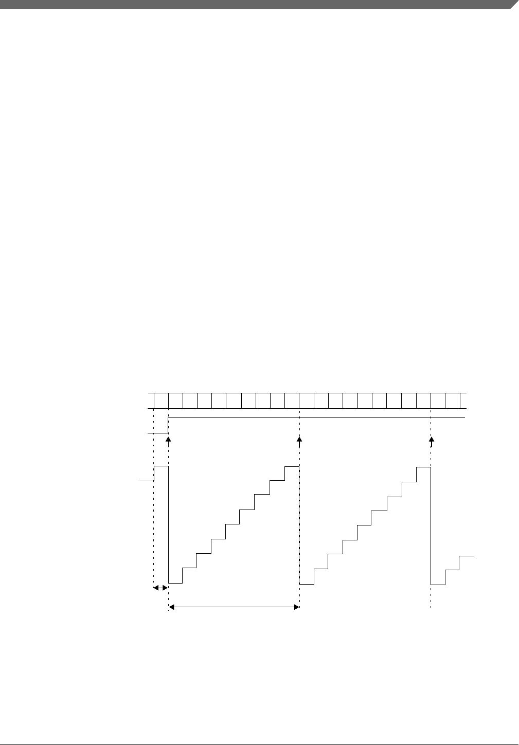
45.5.3.1 Up counting
Up counting is selected when:
• QUADEN = 0, and
• CPWMS = 0
CNTIN defines the starting value of the count and MOD defines the final value of the
count, see the following figure. The value of CNTIN is loaded into the FTM counter, and
the counter increments until the value of MOD is reached, at which point the counter is
reloaded with the value of CNTIN.
The FTM period when using up counting is (MOD – CNTIN + 0x0001) × period of the
FTM counter clock.
The TOF bit is set when the FTM counter changes from MOD to CNTIN.
A counter event happens at the same time of TOF bit set when the FTM counter changes
from MOD to CNTIN. See Counter events for more details.
FTM counting is up.
FTM counter (in decimal values)
period of FTM counter clock
MOD = 0x0004
TOF bit
set TOF bit
set TOF bit set TOF bit
4-4 -3 -2 -1 -4 -3 -2 -1
0 1 234 0 1 23 4 -4 -3
CNTIN = 0xFFFC (in two's complement is equal to -4)
period of counting = (MOD - CNTIN + 0x0001) x period of FTM counter clock
counter event counter event counter event
Figure 45-8. Example of FTM up and signed counting
Chapter 45 FlexTimer Module (FTM)
S32K1xx Series Reference Manual, Rev. 7, 04/2018
NXP Semiconductors 1257
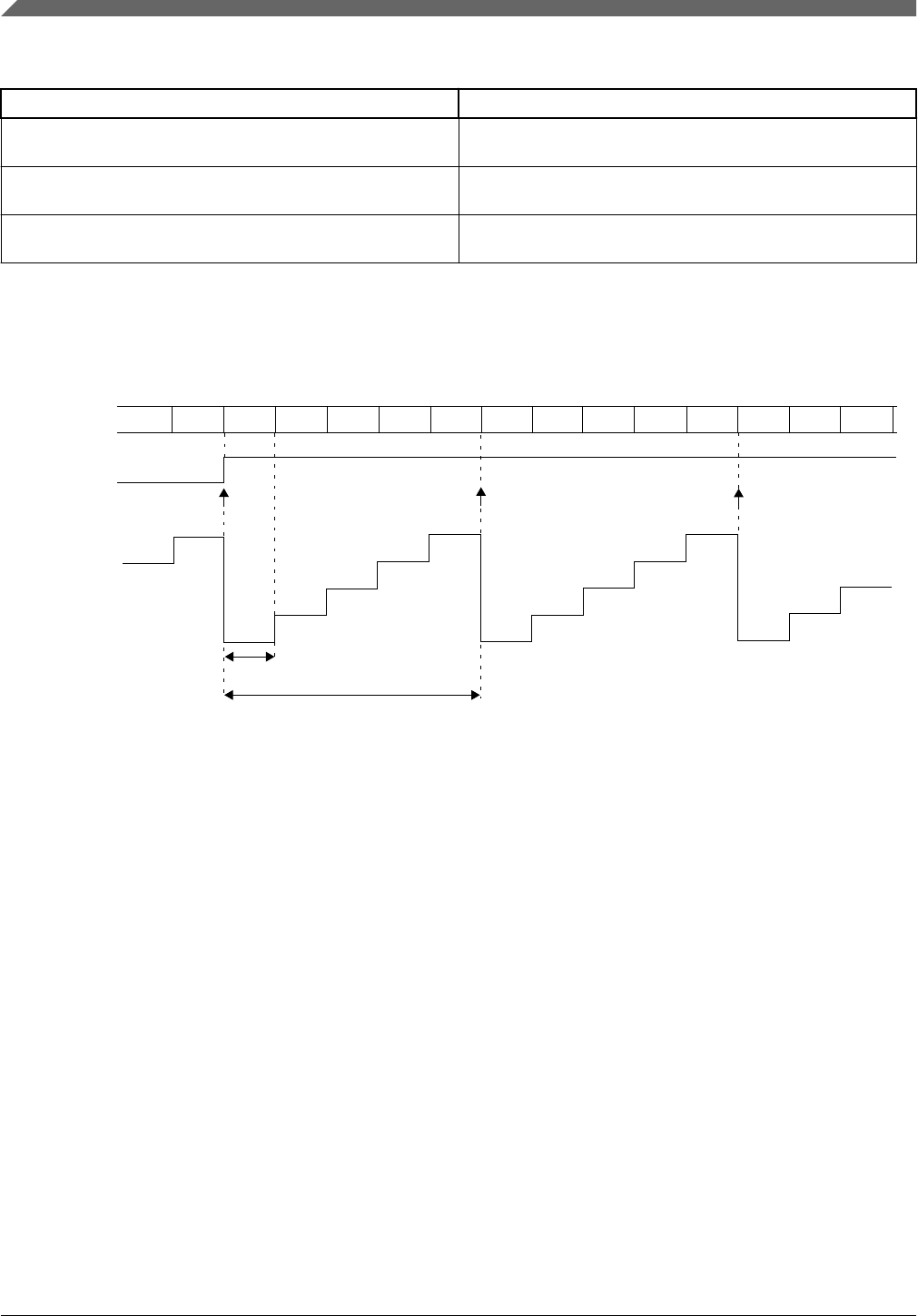
Table 45-3. FTM counting based on CNTIN value
When Then
CNTIN = 0x0000 The FTM counting is equivalent to TPM up counting, that is,
up and unsigned counting. See the following figure.
CNTIN[15] = 1 The initial value of the FTM counter is a negative number in
two's complement, so the FTM counting is up and signed.
CNTIN[15] = 0 and CNTIN ≠ 0x0000 The initial value of the FTM counter is a positive number, so
the FTM counting is up and unsigned.
CNTIN = 0x0000
MOD = 0x0004
FTM counting is up
TOF bit
3400
1 12 2
3 3
44012
FTM counter
set TOF bit
period of FTM counter clock
period of counting = (MOD - CNTIN + 0x0001) x period of FTM counter clock
set TOF bit set TOF bit
= (MOD + 0x0001) x period of FTM counter clock
counter event counter event
counter event
Figure 45-9. Example of FTM up counting with CNTIN = 0x0000
Note
• FTM operation is only valid when the value of the CNTIN
register is less than the value of the MOD register, either in
the unsigned counting or signed counting. It is the
responsibility of the software to ensure that the values in
the CNTIN and MOD registers meet this requirement. Any
values of CNTIN and MOD that do not satisfy this criteria
can result in unpredictable behavior.
• MOD = CNTIN is a redundant condition. In this case, the
FTM counter is always equal to MOD and the TOF bit is
set in each rising edge of the FTM counter clock.
Functional Description
S32K1xx Series Reference Manual, Rev. 7, 04/2018
1258 NXP Semiconductors

• When MOD = 0x0000, CNTIN = 0x0000, for example
after reset, and FTMEN = 1, the FTM counter remains
stopped at 0x0000 until a non-zero value is written into the
MOD or CNTIN registers.
• Setting CNTIN to be greater than the value of MOD is not
recommended as this unusual setting may make the FTM
operation difficult to comprehend. However, there is no
restriction on this configuration, and an example is shown
in the following figure.
FTM counter ...
...
FTM counting is up
TOF bit
0x0005 0x0015 0x0016 0xFFFE 0xFFFF 0x0000 0x0001 0x0002 0x0003 0x0004 0x0005 0x0015 0x0016
MOD = 0x0005
CNTIN = 0x0015
set TOF bit set TOF bit
load of CNTIN load of CNTIN
...
counter event counter event
Figure 45-10. Example of up counting when the value of CNTIN is greater than the value
of MOD
45.5.3.2 Up-down counting
Up-down counting is selected when:
• QUADEN = 0, and
• CPWMS = 1
CNTIN defines the starting value of the count and MOD defines the final value of the
count. The value of CNTIN is loaded into the FTM counter, and the counter increments
until the value of MOD is reached, at which point the counter is decremented until it
returns to the value of CNTIN and the up-down counting restarts.
The FTM period when using up-down counting is 2 × (MOD – CNTIN) × period of the
FTM counter clock.
The TOF bit is set when the FTM counter changes from MOD to (MOD – 1).
If (CNTIN = 0x0000), the FTM counting is equivalent to TPM up-down counting, that is,
up-down and unsigned counting. See the following figure.
Chapter 45 FlexTimer Module (FTM)
S32K1xx Series Reference Manual, Rev. 7, 04/2018
NXP Semiconductors 1259
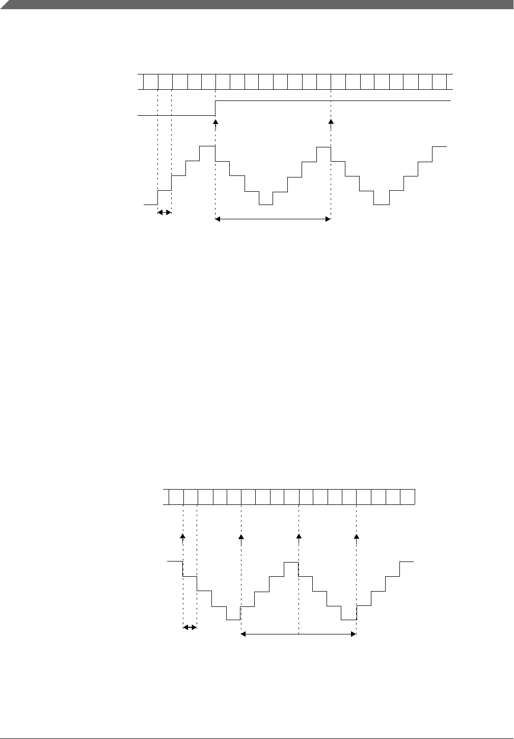
FTM counter
0 0 0
1 1 11 1
2 2 22 23 3 33 34 4 4
FTM counting is up-down
TOF bit
set TOF bit set TOF bit
period of FTM counter clock
period of counting = 2 x (MOD - CNTIN) x period of FTM counter clock
= 2 x MOD x period of FTM counter clock
CNTIN = 0x0000
MOD = 0x0004
Figure 45-11. Example of up-down counting when CNTIN = 0x0000
Note
When CNTIN is different from zero in the up-down counting, a
valid CPWM signal is generated:
• if CnV > CNTIN, or
• if CnV = 0 or if CnV[15] = 1. In this case, 0% CPWM is
generated.
The figure below shows the possible counter events when in up-down counting mode.
See Counter events for more details.
FTM counter 00
11
1 1
22
22
3 3
33
444
FTM counting is up-down
period of FTM counter clock period of counting = 2 x (MOD - CNTIN) x period of FTM counter clock
= 2 x MOD x period of FTM counter clock
CNTIN = 0x0000
MOD = 0x0004
counter event counter event counter event
counter event
Figure 45-12. Example of counter events in up-down counting mode when CNTIN =
0x0000
Functional Description
S32K1xx Series Reference Manual, Rev. 7, 04/2018
1260 NXP Semiconductors

45.5.3.3 Free running counter
If (FTMEN = 0) and (MOD = 0x0000 or MOD = 0xFFFF), the FTM counter is a free
running counter. In this case, the FTM counter runs free from 0x0000 through 0xFFFF
and the TOF bit is set when the FTM counter changes from 0xFFFF to 0x0000. See the
following figure.
A counter event occurs at the same time of TOF bit set when the FTM counter changes
from 0xFFFF to 0x0000. See Counter events for more details.
FTM counter 0x00040x0004 0xFFFE 0xFFFF
0x0003 0x0000 0x0001 0x0002 0x0003 0x0005 0x0006
TOF bit
... ... ...
FTMEN = 0
set TOF bit
MOD = 0x0000
counter event
Figure 45-13. Example when the FTM counter is free running
The FTM counter is also a free running counter when:
• FTMEN = 1
• QUADEN = 0
• CPWMS = 0
• CNTIN = 0x0000, and
• MOD = 0xFFFF
45.5.3.4 Counter reset
Any one of the following cases resets the FTM counter to the value in the CNTIN register
and the channels output to its initial value, except for channels in Output Compare mode.
• Any write to CNT.
•FTM counter synchronization.
• A channel in Input Capture mode with ICRST = 1 (FTM Counter Reset in Input
Capture Mode).
Note that reseting the counter also generates a counter event. See Counter events for
more details.
Chapter 45 FlexTimer Module (FTM)
S32K1xx Series Reference Manual, Rev. 7, 04/2018
NXP Semiconductors 1261

45.5.3.5 Counter events
Counter events can be used as reload opportunities to FTM register sychronization
mechanism. See Reload Points for more details. There are some possible counter events
depending on the counter mode. Please see the table below for more details.
Table 45-4. FTM counter events
When Then
FTM counter is in up counting mode or freerunning • A counter event happens at the same time of TOF bit
set when the FTM counter changes from MOD to
CNTIN (counter wrap). Figure at Up counting shows the
counter event generation.
• When in freerunning, there is a counter event when
FTM counter changes from 0xFFFF to 0x0000. Figure
at Free running counter shows the counter event
generation.
FTM counter is in up-down counting mode • In up-down counting mode, there are two possible
counter events when FTM counter turns from down to
up counting and when counter turns from up to down
counting. User can select which point will be used to
generate the counter event. Figure at Up-down counting
shows the possible counter events.
FTM counter is reseted (see Counter reset) or a value
different from zero is written at CLKS field
• In up-counting mode, all counter reset events or a write
in the CLKS with a value different from zero generates
a counter event.
• In up-down counting mode, counter reset events only
generates a counter event if the minimum load point
when FTM counter turns from down to up counting is
configured. A write in the CLKS with a value different
from zero always generates a counter event in up-down
counting mode.
45.5.4 Channel Modes
The following table shows the channel modes selection.
Table 45-5. Channel Modes Selection
DECAPEN MCOMBINE COMBINE CPWMS MSB:MSA ELSB:ELSA Mode Configuratio
n
X X X X XX 00 Pin not used for FTM—revert
the channel pin to general
purpose I/O or other
peripheral control
0 0 0 0 00 01 Input Capture Capture on
Rising Edge
Only
Table continues on the next page...
Functional Description
S32K1xx Series Reference Manual, Rev. 7, 04/2018
1262 NXP Semiconductors

Table 45-5. Channel Modes Selection (continued)
DECAPEN MCOMBINE COMBINE CPWMS MSB:MSA ELSB:ELSA Mode Configuratio
n
10 Capture on
Falling Edge
Only
11 Capture on
Rising or
Falling Edge
01 01 Output
Compare
Toggle Output
on match
10 Clear Output
on match
11 Set Output on
match
1X 10 Edge-Aligned
PWM
High-true
pulses (clear
Output on
match)
X1 Low-true
pulses (set
Output on
match)
1 XX 10 Center-
Aligned PWM
High-true
pulses (clear
Output on
match-up)
X1 Low-true
pulses (set
Output on
match-up)
1 0 XX 10 Combine
PWM
High-true
pulses (set on
channel (n)
match, and
clear on
channel (n+1)
match)
X1 Low-true
pulses (clear
on channel (n)
match, and
set on
channel (n+1)
match)
1 0 X XX XX Reserved for future use
1 1 0 XX 10 Modified
Combine
PWM
High-true
pulses (set on
channel (n)
match, and
Table continues on the next page...
Chapter 45 FlexTimer Module (FTM)
S32K1xx Series Reference Manual, Rev. 7, 04/2018
NXP Semiconductors 1263

Table 45-5. Channel Modes Selection (continued)
DECAPEN MCOMBINE COMBINE CPWMS MSB:MSA ELSB:ELSA Mode Configuratio
n
clear on
channel (n+1)
match)
X1 Low-true
pulses (clear
on channel (n)
match, and
set on
channel (n+1)
match)
1 0 0 0 X0 See Table
45-6.
Dual Edge
Capture
One-Shot
Capture mode
X1 Continuous
Capture mode
Table 45-6. Dual Edge Capture Mode — Edge Polarity Selection
ELSB ELSA Channel Port Enable Detected Edges
0 0 Disabled No edge
0 1 Enabled Rising edge
1 0 Enabled Falling edge
1 1 Enabled Rising and falling edges
45.5.5 Input Capture Mode
The Input Capture mode is selected when:
• DECAPEN = 0
• MCOMBINE = 0
• COMBINE = 0
• CPWMS = 0
• MSB:MSA = 0:0, and
• ELSB:ELSA ≠ 0:0
When a selected edge occurs on the channel input, the current value of the FTM counter
is captured into the CnV register, at the same time the CHF bit is set and the channel
interrupt is generated if enabled by CHIE = 1. See the following figure.
When a channel is configured for input capture, the FTMxCHn pin is an edge-sensitive
input. ELSB:ELSA bits determine which edge, falling or rising, triggers input-capture
event.
Functional Description
S32K1xx Series Reference Manual, Rev. 7, 04/2018
1264 NXP Semiconductors
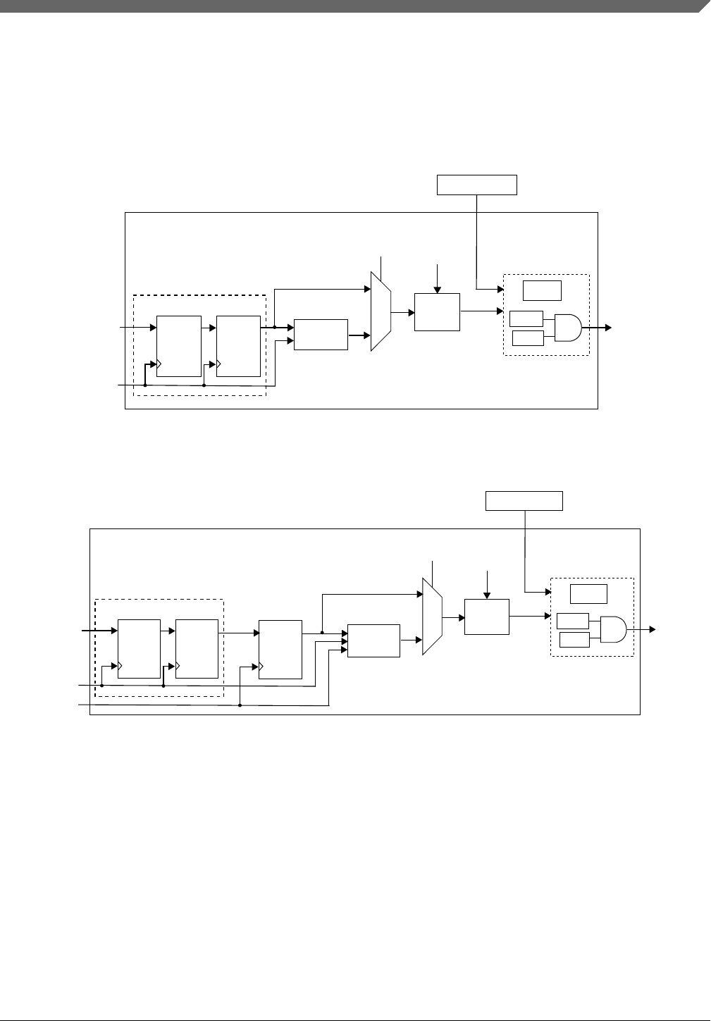
Writes to the CnV register are ignored in input capture mode.
While in Debug mode, the input capture function works as configured. When a selected
edge event occurs, the FTM counter value, which is frozen because of Debug, is captured
into the CnV register and the CHF bit is set.
channel (n) input
synchronizer
1
is filter
enabled?
edge
detector
D
CLK
D
CLK
FTM input clock
filter
0
Note: The filter is only available for the channels 0, 1, 2, and 3 inputs.
QQ
FTM counter
selected
edge
channel (n)
interrupt
CnV
CHIE
CHF
channel (n)
Figure 45-14. Diagram for Input Capture Mode when FLTPS[3:0] = 0
channel (n) input
synchronizer
1
is filter
enabled?
D
CLK
D
CLK
FTM input clock
filter
0
Note: The filter is only available for the channels 0, 1, 2, and 3 inputs.
QQD
CLK
Q
FTM filter clock
edge
detector
FTM counter
selected
edge
channel (n)
interrupt
CnV
CHIE
CHF
channel (n)
Figure 45-15. Diagram for Input Capture Mode when FLTPS[3:0] ≠ 0
45.5.5.1 Filter for Input Capture Mode
The filter is only available on channels 0, 1, 2, and 3.
If FLTPS[3:0] = 0, the channel input after being synchronized by FTM input clock
(Figure 45-14) is the filter input.
Chapter 45 FlexTimer Module (FTM)
S32K1xx Series Reference Manual, Rev. 7, 04/2018
NXP Semiconductors 1265
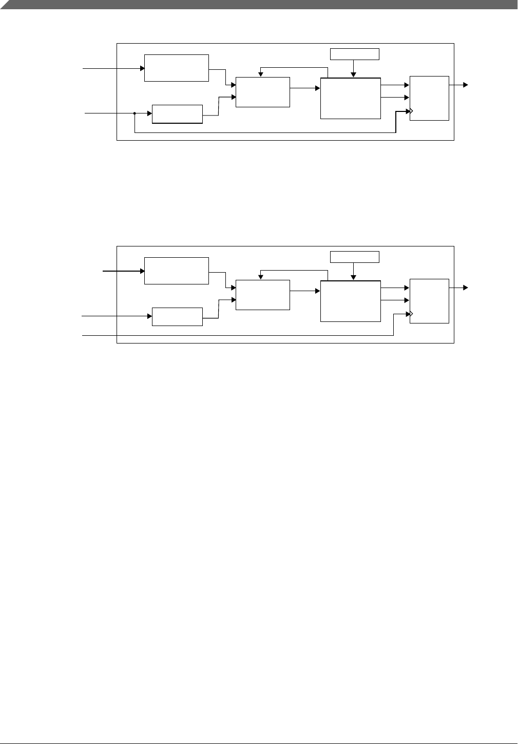
FTM input clock
filter counter logic to define
the filter output
filter output
divided by 4
channel (n) input after
being synchronized by
FTM input clock
logic to control
the filter counter
CHnFVAL[3:0]
C
SQ
CLK
Figure 45-16. Channel Input Filter when FLTPS[3:0] = 0
If FLTPS[3:0] ≠ 0, the channel input after being synchronized by FTM input clock and
being sampled by FTM filter clock (Figure 45-15) is the filter input.
FTM filter clock
filter counter logic to define
the filter output
filter output
divided by 4
channel (n) input after being
synchronized by FTM input
clock and being sampled
by FTM filter clock
logic to control
the filter counter
CHnFVAL[3:0]
C
SQ
CLK
FTM input clock
Figure 45-17. Channel Input Filter when FLTPS[3:0] ≠ 0
NOTE
The maximum frequency for the channel input to be detected
correctly is FTM filter clock divided by 4, which is required to
meet Nyquist criteria for signal sampling.
When there is a state change in the channel input, the counter is reset and starts counting
up. As long as the new state is stable on the channel input, the counter continues to
increment. When the counter is equal to CHnFVAL[3:0], the new channel input signal
value is validated. It is then transmitted as a pulse to the edge detector.
If the opposite edge appears on the channel input signal before it can be validated, the
counter is reset. At the next input transition, the counter starts counting again. If a pulse is
sampled as a value less than (CHnFVAL[3:0] x 4) consecutive rising edges of FTM filter
clock, it is regarded as a glitch and is not passed on to the edge detector.
Functional Description
S32K1xx Series Reference Manual, Rev. 7, 04/2018
1266 NXP Semiconductors
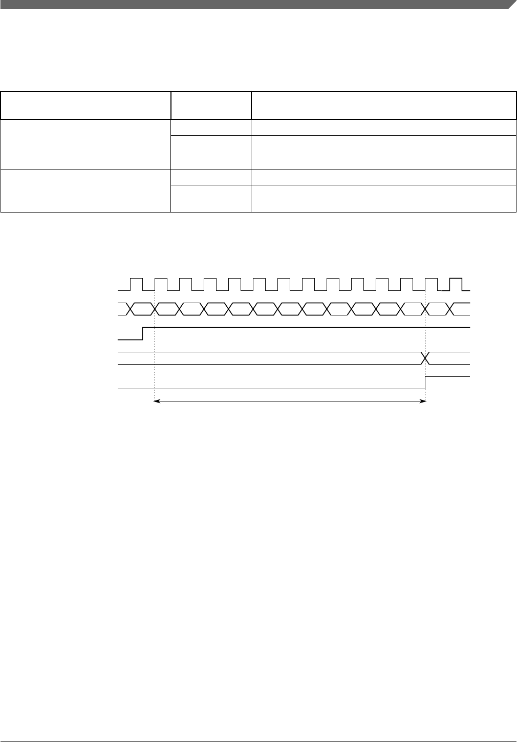
The table below shows the delay that is added by the FTM channel input filter according
to its configuration.
Table 45-7. FTM Channel Input Filter Delay
FTM channel input filter FLTPS[3:0] bits Number of rising edges between the selected edge on
channel input and setting CHF bit
• channel does not have the input
filter, or
• channel input filter is disabled
(CHnFVAL[3:0] = 0)
FLTPS[3:0] = 0 • 3 rising edges of FTM input clock
FLTPS[3:0] ≠ 0 • 3 rising edges of FTM input clock, plus
• 1 rising edge of FTM filter clock
• channel has the input filter, and
• channel input filter is enabled
(CHnFVAL[3:0] ≠ 0)
FLTPS[3:0] = 0 • (4 + 4 × CHnFVAL[3:0]) rising edges of FTM input clock
FLTPS[3:0] ≠ 0 • 4 rising edges of FTM input clock, plus
• (1 + 4 × CHnFVAL[3:0]) rising edges of FTM filter clock
The following figures illustrate two examples of channel input filter.
FTM input clock
FTM counter
CnV register
CHF bit
Note:
PS[2:0] = 3'b000
channel (n) in input capture mode with capture only on rising edges
CHnFVAL[3:0] = 4'h2 (channel (n) input filter is enabled)
53
channel (n) input
54 55 56 57 58 59 60 61 62 63 64 65
(4 + 4 x CHnFVAL) = 12 rising edges of FTM input clock
64xx
Figure 45-18. Example of Channel Input Filter when FLTPS[3:0] = 0
Chapter 45 FlexTimer Module (FTM)
S32K1xx Series Reference Manual, Rev. 7, 04/2018
NXP Semiconductors 1267

FTM input clock
FTM counter
CnV register
CHF bit
Note:
PS[2:0] = 3'b000
channel (n) in input capture mode with capture only on rising edges
CHnFVAL[3:0] = 4'h1 (channel (n) input filter is enabled)
FLTPS[3:0] = 4'h2 (divide by 3)
53
channel (n) input
54 55 56 57 58 59 60 61 62 63 64 65
4 rising edges of FTM input clock + (1 + 4 x CHnFVAL) rising edges of FTM filter clock =
4 rising edges of FTM input clock + 5 rising edges of FTM filter clock
70xx
FTM filter clock
66 67 68 69 70 71
2 rising edges
of FTM input clock (1 + 4 x CHnFVAL) = 5 rising edges of FTM filter counter 2 rising edges
of FTM input clock
Figure 45-19. Example of Channel Input Filter when FLTPS[3:0] ≠ 0
45.5.5.2 FTM Counter Reset in Input Capture Mode
If the channel (n) is in input capture mode and CnSC[ICRST = 1], then when the selected
input capture event occurs in the channel (n) input signal, the current value of the FTM
counter is captured into the CnV register, the CHF bit is set, the channel (n) interrupt is
generated (if CHIE = 1) and the FTM counter is reset to the CNTIN register value.
This allows the FTM to measure a period/pulse being applied to the channel (n) input
(number of the FTM input clocks) without having to implement a subtraction calculation
in software subsequent to the event occurring.
The figure below shows the FTM counter reset when the selected input capture event is
detected in a channel in input capture mode with ICRST = 1.
Functional Description
S32K1xx Series Reference Manual, Rev. 7, 04/2018
1268 NXP Semiconductors

FTM input clock
CNT
channel (n) input
CHF bit
C(n)V XX 0x27
selected channel (n) input event: rising edge
NOTE
Channel (n) input after its synchronizer and filter
MOD = 0xFFFF
CNTIN = 0x0000
PS[2:0] = 3'b000
ICRST = 1'b1
... 0x27 ...
0x00 0x01 0x02 0x030x260x250x240x230x220x210x20
Figure 45-20. Example of the Input Capture mode with ICRST = 1
NOTE
• It is expected that the ICRST bit be set only when the
channel is in input capture mode.
• If the FTM counter is reset because the channel is in input
capture mode with ICRST = 1, then the prescaler counter
(Prescaler) is also reset.
45.5.6 Output Compare mode
The Output Compare mode is selected when:
• DECAPEN = 0
• MCOMBINE = 0
• COMBINE = 0
• CPWMS = 0, and
• MSB:MSA = 0:1
In Output Compare mode, the FTM can generate timed pulses with programmable
position, polarity, duration, and frequency. When the counter matches the value in the
CnV register of an output compare channel, the channel (n) output can be set, cleared, or
toggled.
When a channel is initially configured to Toggle mode, the previous value of the channel
output is held until the first output compare event occurs.
The CHF bit is set and the channel (n) interrupt is generated if CHIE = 1 at the channel
(n) match (FTM counter = CnV).
Chapter 45 FlexTimer Module (FTM)
S32K1xx Series Reference Manual, Rev. 7, 04/2018
NXP Semiconductors 1269
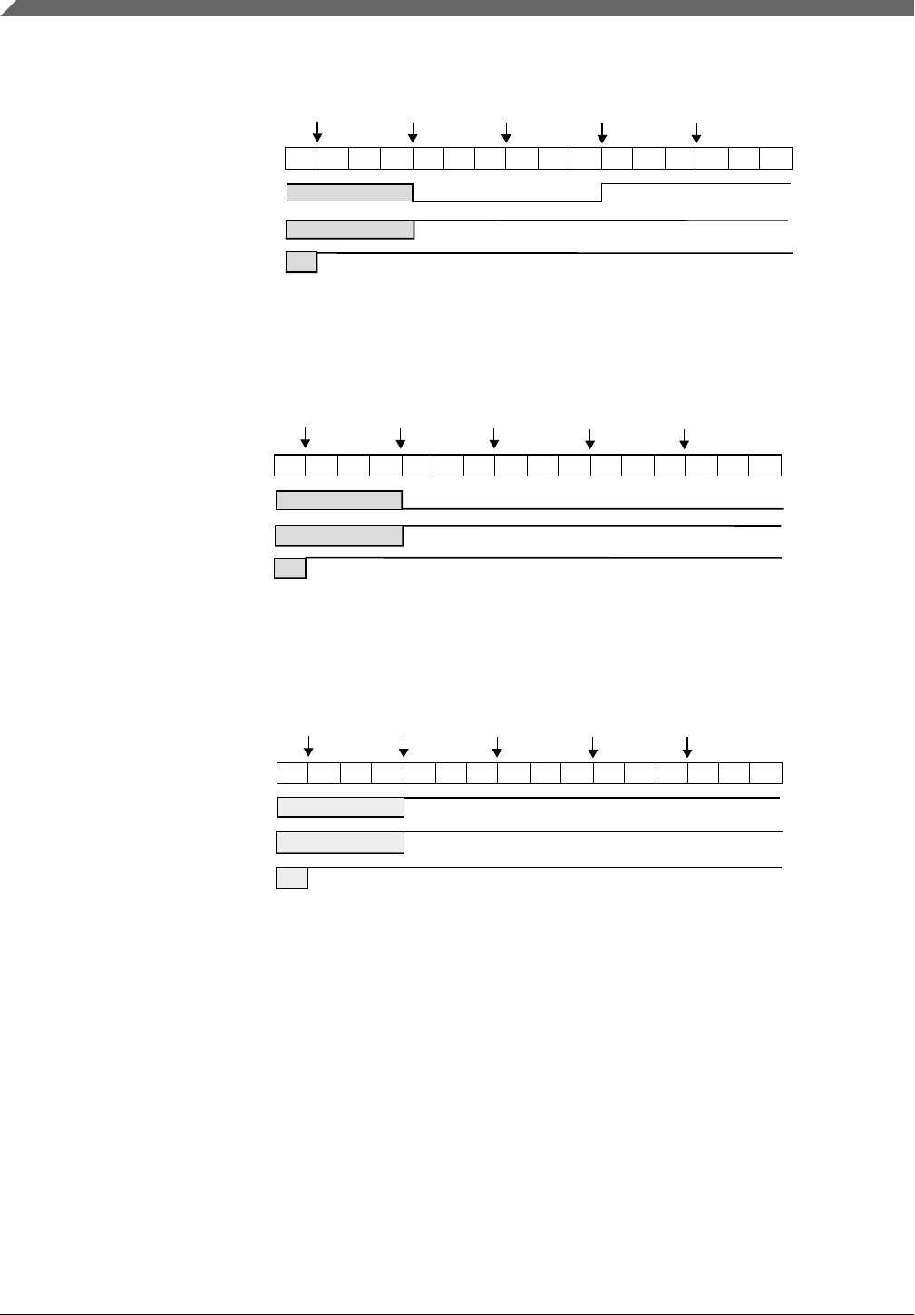
TOF bit
...
... 01 1 1
22
3 3
4 45 5
0 0
previous value
previous value
channel (n) output
counter
overflow
counter
overflow
counter
overflow
channel (n)
match
channel (n)
match
CNT
MOD = 0x0005
CnV = 0x0003
CHF bit
Figure 45-21. Example of the Output Compare mode when the match toggles the
channel output
TOF bit
...
... 01 1 1
22
3 3
4 45 5
0 0
previous value
previous value
channel (n) output
counter
overflow counter
overflow counter
overflow
channel (n)
match channel (n)
match
CNT
MOD = 0x0005
CnV = 0x0003
CHF bit
Figure 45-22. Example of the Output Compare mode when the match clears the channel
output
channel (n) output
CHF bit
TOF bit
CNT
MOD = 0x0005
CnV = 0x0003
counter
overflow
channel (n)
match
counter
overflow
channel (n)
match
counter
overflow
... 0123 4 5 01234501...
previous value
previous value
Figure 45-23. Example of the Output Compare mode when the match sets the channel
output
If (ELSB:ELSA = 0:0) when the counter reaches the value in the CnV register, the CHF
bit is set and the channel (n) interrupt is generated if CHIE = 1, however the channel (n)
output is not modified and controlled by FTM.
45.5.7 Edge-Aligned PWM (EPWM) mode
The Edge-Aligned mode is selected when:
• QUADEN = 0
Functional Description
S32K1xx Series Reference Manual, Rev. 7, 04/2018
1270 NXP Semiconductors
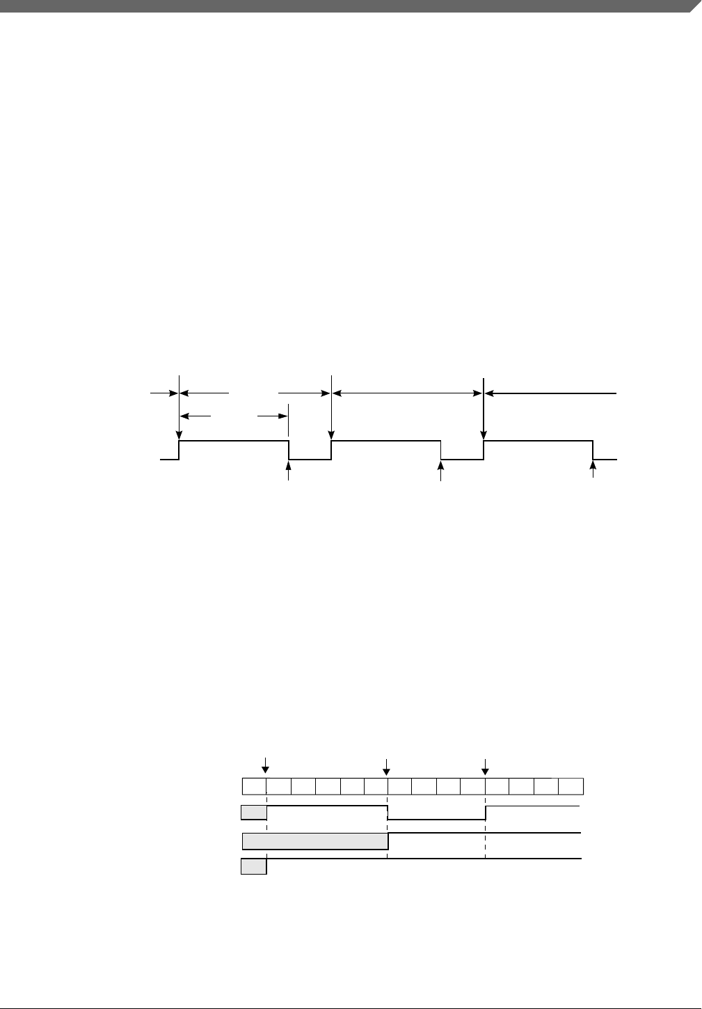
• DECAPEN = 0
• MCOMBINE = 0
• COMBINE = 0
• CPWMS = 0, and
• MSB = 1
The EPWM period is determined by (MOD − CNTIN + 0x0001) and the pulse width
(duty cycle) is determined by (CnV − CNTIN).
The CHF bit is set and the channel (n) interrupt is generated if CHIE = 1 at the channel
(n) match (FTM counter = CnV), that is, at the end of the pulse width.
This type of PWM signal is called edge-aligned because the leading edges of all PWM
signals are aligned with the beginning of the period, which is the same for all channels
within an FTM.
period
counter overflow counter overflow counter overflow
channel (n) output
channel (n) match channel (n) match channel (n) match
pulse
width
Figure 45-24. EPWM period and pulse width with ELSB:ELSA = 1:0
If (ELSB:ELSA = 0:0) when the counter reaches the value in the CnV register, the CHF
bit is set and the channel (n) interrupt is generated if CHIE = 1, however the channel (n)
output is not controlled by FTM.
If (ELSB:ELSA = 1:0), then the channel (n) output is forced high at the counter overflow
when the CNTIN register value is loaded into the FTM counter, and it is forced low at the
channel (n) match (FTM counter = CnV). See the following figure.
TOF bit
CHF bit
CNT
channel (n) output
MOD = 0x0008
CnV = 0x0005
counter
overflow channel (n)
match counter
overflow
...
0 1 2345678012
...
previous value
Figure 45-25. EPWM signal with ELSB:ELSA = 1:0
Chapter 45 FlexTimer Module (FTM)
S32K1xx Series Reference Manual, Rev. 7, 04/2018
NXP Semiconductors 1271

If (ELSB:ELSA = X:1), then the channel (n) output is forced low at the counter overflow
when the CNTIN register value is loaded into the FTM counter, and it is forced high at
the channel (n) match (FTM counter = CnV). See the following figure.
TOF bit
CHF bit
CNT
channel (n) output
MOD = 0x0008
CnV = 0x0005 counter
overflow channel (n)
match counter
overflow
...
0 1 2345678012
...
previous value
Figure 45-26. EPWM signal with ELSB:ELSA = X:1
If (CnV = 0x0000), then the channel (n) output is a 0% duty cycle EPWM signal and
CHF bit is not set even when there is the channel (n) match.
If (CnV > MOD), then the channel (n) output is a 100% duty cycle EPWM signal and
CHF bit is not set. Therefore, MOD must be less than 0xFFFF in order to get a 100%
duty cycle EPWM signal.
Note
When CNTIN is different from zero the following EPWM
signals can be generated:
• 0% EPWM signal if CnV = CNTIN,
• EPWM signal between 0% and 100% if CNTIN < CnV <=
MOD,
• 100% EPWM signal when CNTIN > CnV or CnV > MOD.
45.5.8 Center-Aligned PWM (CPWM) mode
The Center-Aligned mode is selected when:
• QUADEN = 0
• DECAPEN = 0
• MCOMBINE = 0
• COMBINE = 0, and
• CPWMS = 1
Functional Description
S32K1xx Series Reference Manual, Rev. 7, 04/2018
1272 NXP Semiconductors

The CPWM pulse width (duty cycle) is determined by 2 × (CnV − CNTIN) and the
period is determined by 2 × (MOD − CNTIN). See the following figure. MOD must be
kept in the range of 0x0001 to 0x7FFF because values outside this range can produce
ambiguous results.
In the CPWM mode, the FTM counter counts up until it reaches MOD and then counts
down until it reaches CNTIN.
The CHF bit is set and channel (n) interrupt is generated (if CHIE = 1) at the channel (n)
match (FTM counter = CnV) when the FTM counting is down (at the begin of the pulse
width) and when the FTM counting is up (at the end of the pulse width).
This type of PWM signal is called center-aligned because the pulse width centers for all
channels are aligned with the value of CNTIN.
The other channel modes are not compatible with the up-down counter (CPWMS = 1).
Therefore, all FTM channels must be used in CPWM mode when (CPWMS = 1).
pulse width
counter overflow
FTM counter =
MOD
period
2 x (CnV - CNTIN)
2 x (MOD - CNTIN)
FTM counter = CNTIN
channel (n) match
(FTM counting
is down)
channel (n) match
(FTM counting
is up)
counter overflow
FTM counter =
MOD
channel (n) output
Figure 45-27. CPWM period and pulse width with ELSB:ELSA = 1:0
If (ELSB:ELSA = 0:0) when the FTM counter reaches the value in the CnV register, the
CHF bit is set and the channel (n) interrupt is generated (if CHIE = 1), however the
channel (n) output is not controlled by FTM.
If (ELSB:ELSA = 1:0), then the channel (n) output is forced high at the channel (n)
match (FTM counter = CnV) when counting down, and it is forced low at the channel (n)
match when counting up. See the following figure.
Chapter 45 FlexTimer Module (FTM)
S32K1xx Series Reference Manual, Rev. 7, 04/2018
NXP Semiconductors 1273
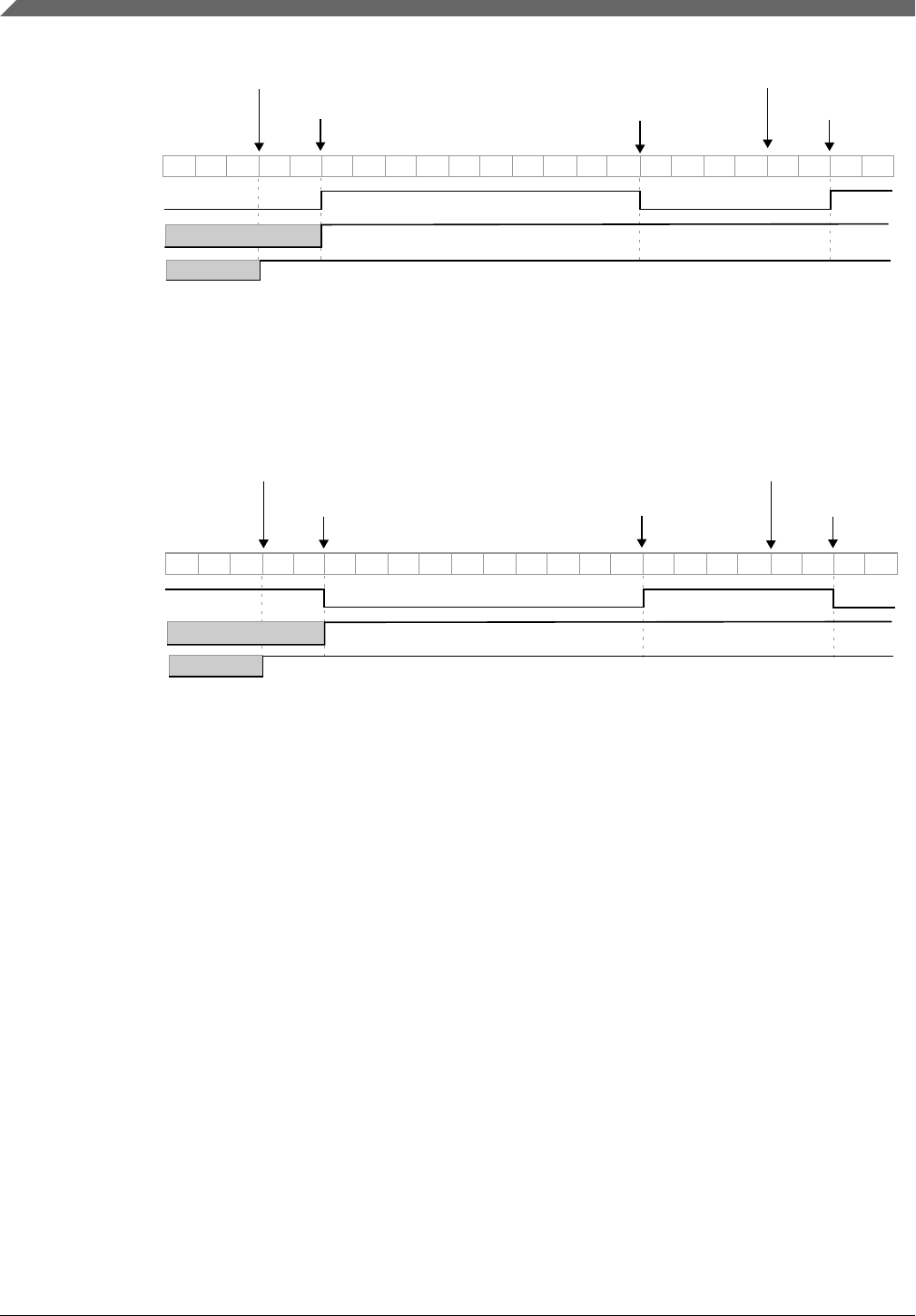
TOF bit
... 78 8
7 7 7
6 6 6
5 5 54 43 3
2 21 01...
previous value
CNT
channel (n) output
counter
overflow
channel (n) match in
down counting channel (n) match in
up counting channel (n) match in
down counting
counter
overflow
CHF bit
MOD = 0x0008
CnV = 0x0005
Figure 45-28. CPWM signal with ELSB:ELSA = 1:0
If (ELSB:ELSA = X:1), then the channel (n) output is forced low at the channel (n)
match (FTM counter = CnV) when counting down, and it is forced high at the channel (n)
match when counting up. See the following figure.
TOF bit
... 78 8
7 7 7
6 6 6
5 5 54 43 3
2 21 01...
previous value
CNT
channel (n) output
counter
overflow
channel (n) match in
down counting channel (n) match in
up counting channel (n) match in
down counting
counter
overflow
CHF bit
MOD = 0x0008
CnV = 0x0005
Figure 45-29. CPWM signal with ELSB:ELSA = X:1
If (CnV = 0x0000) or CnV is a negative value, that is (CnV[15] = 1), then the channel (n)
output is a 0% duty cycle CPWM signal and CHF bit is not set even when there is the
channel (n) match.
If CnV is a positive value, that is (CnV[15] = 0), (CnV ≥ MOD), and (MOD ≠ 0x0000),
then the channel (n) output is a 100% duty cycle CPWM signal and CHF bit is not set
even when there is the channel (n) match. This implies that the usable range of periods
set by MOD is 0x0001 through 0x7FFE, 0x7FFF if you do not need to generate a 100%
duty cycle CPWM signal. This is not a significant limitation because the resulting period
is much longer than required for normal applications.
The CPWM mode must not be used when the FTM counter is a free running counter.
45.5.9 Combine mode
The Combine mode is selected when:
• QUADEN = 0
Functional Description
S32K1xx Series Reference Manual, Rev. 7, 04/2018
1274 NXP Semiconductors

• DECAPEN = 0
• MCOMBINE = 0
• COMBINE = 1, and
• CPWMS = 0
In Combine mode, an even channel (n) and adjacent odd channel (n+1) are combined to
generate a PWM signal in the channel (n) output.
In the Combine mode, the PWM period is determined by (MOD − CNTIN + 0x0001) and
the PWM pulse width (duty cycle) is determined by (|C(n+1)V − C(n)V|).
The channel (n) CHF bit is set and its interrupt is generated, if channel (n) CHIE = 1, at
the channel (n) match (FTM counter = C(n)V). The channel (n+1) CHF bit is set and its
interrupt is generated, if channel (n+1) CHIE = 1, at the channel (n+1) match (FTM
counter = C(n+1)V).
If channel (n) ELSB:ELSA = 1:0, then the channel (n) output is forced low at the
beginning of the period (FTM counter = CNTIN) and at the channel (n+1) match (FTM
counter = C(n+1)V). It is forced high at the channel (n) match (FTM counter = C(n)V).
See the following figure.
If channel (n) ELSB:ELSA = X:1, then the channel (n) output is forced high at the
beginning of the period (FTM counter = CNTIN) and at the channel (n+1) match (FTM
counter = C(n+1)V). It is forced low at the channel (n) match (FTM counter = C(n)V).
See the following figure.
In Combine mode, the channel (n+1) ELSB:ELSA bits are not used in the generation of
the channels (n) and (n+1) output. However, if channel (n) ELSB:ELSA = 0:0, then the
channel (n) output is not controlled by FTM, and if channel (n+1) ELSB:ELSA = 0:0,
then the channel (n+1) output is not controlled by FTM.
FTM counter
channel (n) match
channel (n) output
with ELSB:ELSA = X:1
with ELSB:ELSA = 1:0
channel (n) output
channel (n+1) match
Figure 45-30. Combine mode
The following figures illustrate the PWM signals generation using Combine mode.
Chapter 45 FlexTimer Module (FTM)
S32K1xx Series Reference Manual, Rev. 7, 04/2018
NXP Semiconductors 1275
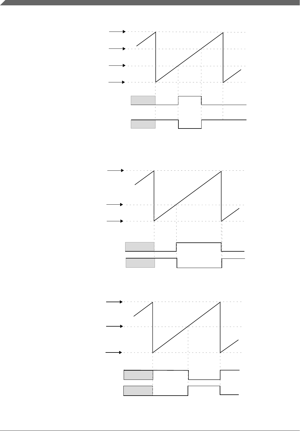
FTM counter
channel (n) output
channel (n) output
MOD
C(n)V
CNTIN
C(n+1)V
with ELSB:ELSA = 1:0
with ELSB:ELSA = X:1
Figure 45-31. Channel (n) output if (CNTIN < C(n)V < MOD) and (CNTIN < C(n+1)V < MOD)
and (C(n)V < C(n+1)V)
FTM counter
channel (n) output
with ELSB:ELSA = 1:0
channel (n) output
with ELSB:ELSA = X:1
MOD = C(n+1)V
C(n)V
CNTIN
Figure 45-32. Channel (n) output if (CNTIN < C(n)V < MOD) and (C(n+1)V = MOD)
FTM counter
C(n+1)V
channel (n) output
with ELSB:ELSA = 1:0
channel (n) output
with ELSB:ELSA = X:1
MOD
C(n)V = CNTIN
Figure 45-33. Channel (n) output if (C(n)V = CNTIN) and (CNTIN < C(n+1)V < MOD)
Functional Description
S32K1xx Series Reference Manual, Rev. 7, 04/2018
1276 NXP Semiconductors
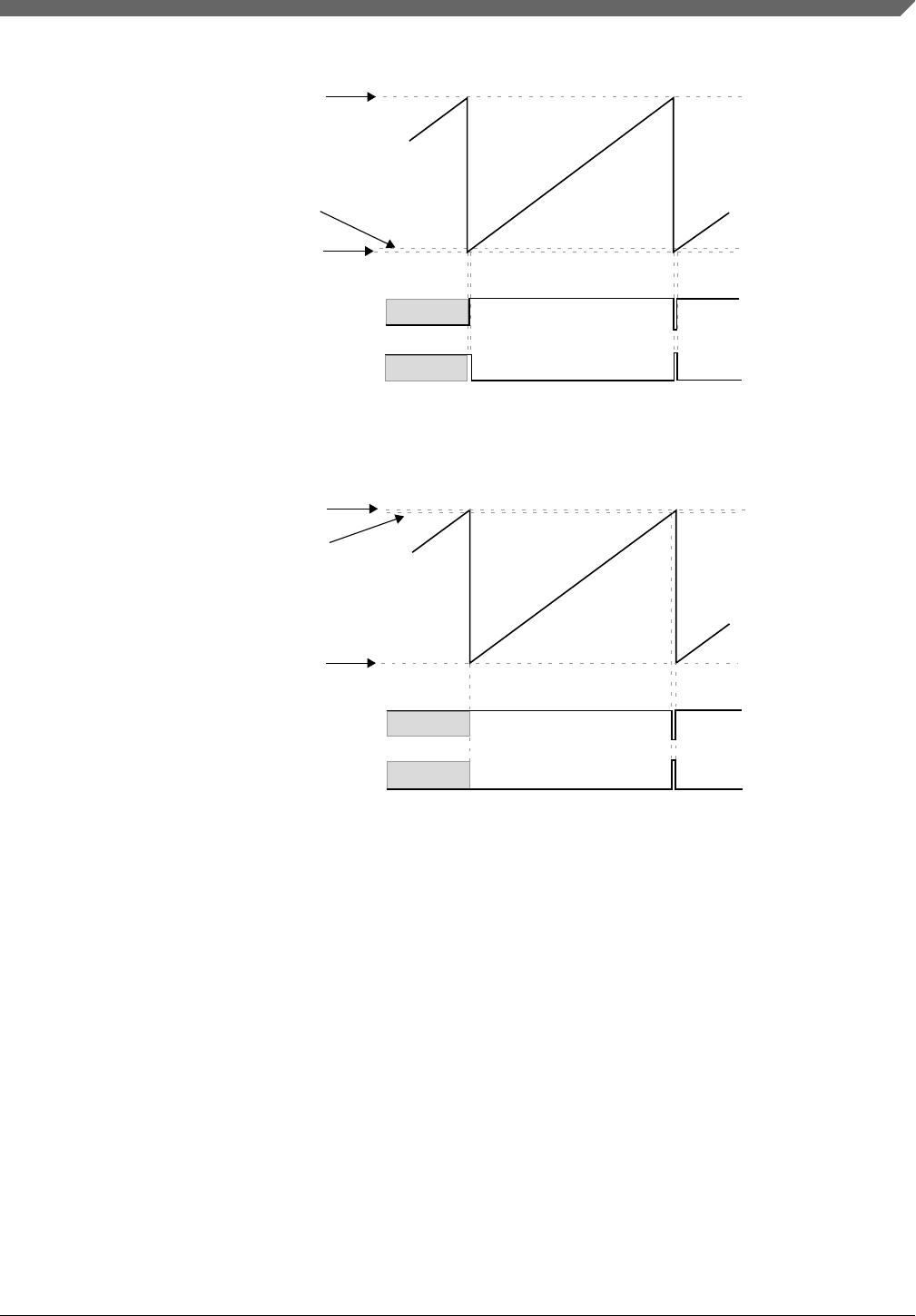
FTM counter
not fully 100% duty cycle
channel (n) output
with ELSB:ELSA = 1:0
not fully 0% duty cycle
channel (n) output
with ELSB:ELSA = X:1
MOD = C(n+1)V
C(n)V
CNTIN
Figure 45-34. Channel (n) output if (CNTIN < C(n)V < MOD) and (C(n)V is Almost Equal to
CNTIN) and (C(n+1)V = MOD)
FTM counter
not fully 100% duty cycle
channel (n) output
with ELSB:ELSA = 1:0
channel (n) output
with ELSB:ELSA = X:1 not fully 0% duty cycle
MOD
C(n)V = CNTIN
C(n+1)V
Figure 45-35. Channel (n) output if (C(n)V = CNTIN) and (CNTIN < C(n+1)V < MOD) and
(C(n+1)V is Almost Equal to MOD)
Chapter 45 FlexTimer Module (FTM)
S32K1xx Series Reference Manual, Rev. 7, 04/2018
NXP Semiconductors 1277
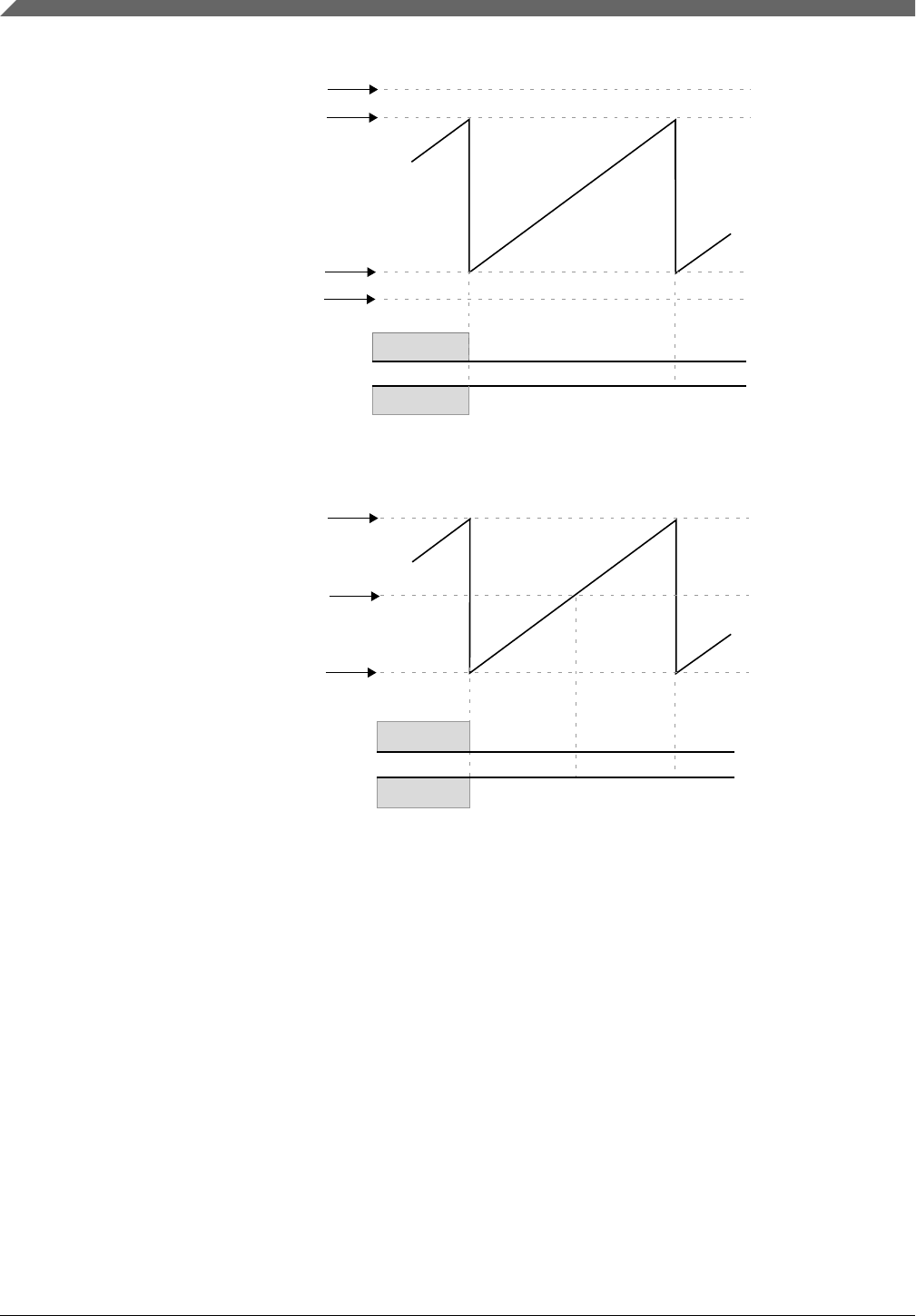
FTM counter
0% duty cycle
channel (n) output
with ELSB:ELSA = 1:0
100% duty cycle
channel (n) output
with ELSB:ELSA = X:1
C(n)V
MOD
CNTIN
C(n+1)V
Figure 45-36. Channel (n) output if C(n)V and C(n+1)V are not between CNTIN and MOD
FTM counter
0% duty cycle
channel (n) output
with ELSB:ELSA = 1:0
channel (n) output
with ELSB:ELSA = X:1 100% duty cycle
MOD
CNTIN
C(n+1)V = C(n)V
Figure 45-37. Channel (n) output if (CNTIN < C(n)V < MOD) and (CNTIN < C(n+1)V < MOD)
and (C(n)V = C(n+1)V)
Functional Description
S32K1xx Series Reference Manual, Rev. 7, 04/2018
1278 NXP Semiconductors
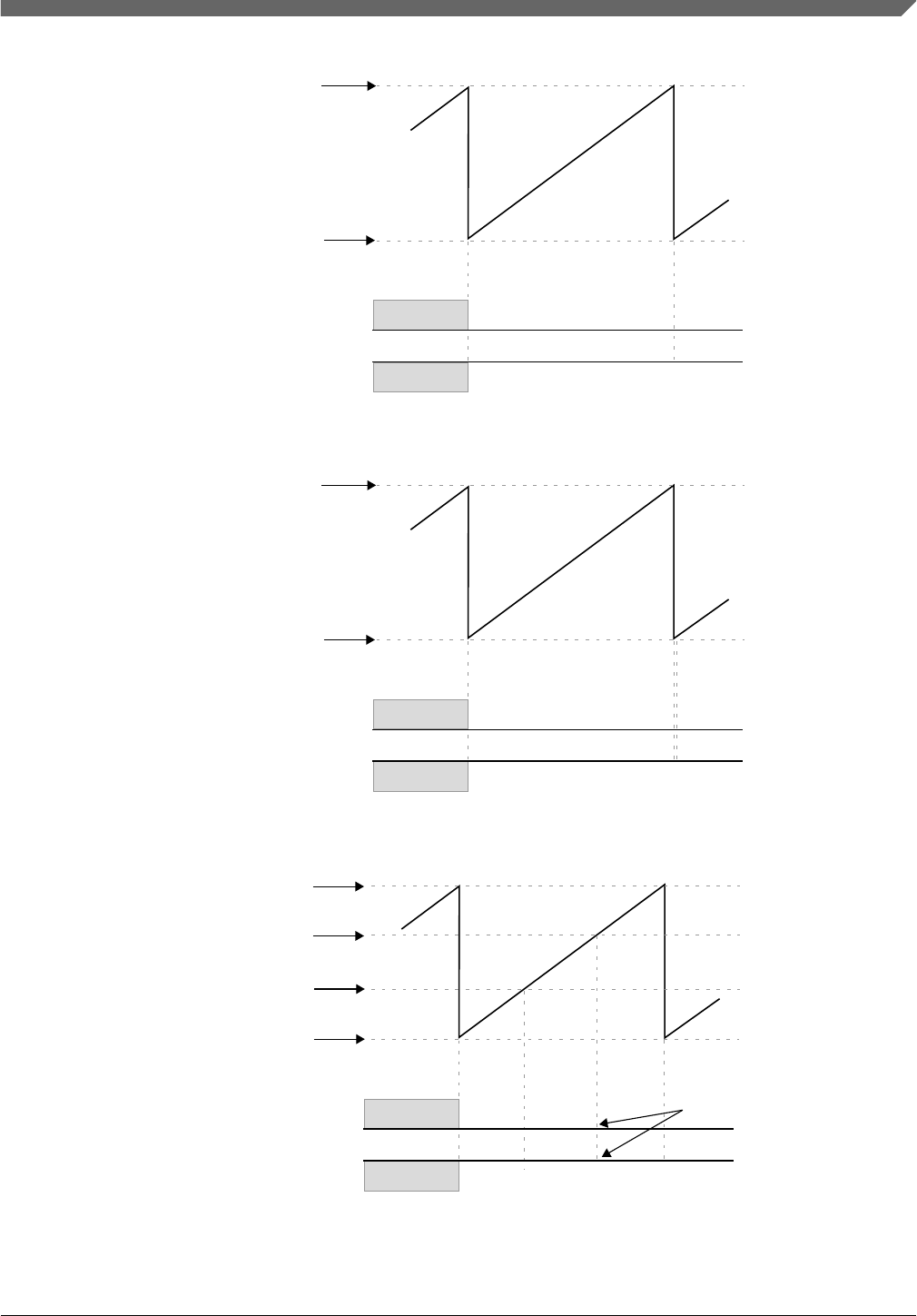
FTM counter
C(n)V =
C(n+1)V = CNTIN
channel (n) output
with ELSB:ELSA = 1:0
channel (n) output
with ELSB:ELSA = X:1 100% duty cycle
0% duty cycle
MOD
Figure 45-38. Channel (n) output if (C(n)V = C(n+1)V = CNTIN)
FTM counter
CNTIN
channel (n) output
with ELSB:ELSA = 1:0
channel (n) output
with ELSB:ELSA = X:1 100% duty cycle
0% duty cycle
MOD =
C(n+1)V =
C(n)V
Figure 45-39. Channel (n) output if (C(n)V = C(n+1)V = MOD)
channel (n) match
is ignored
FTM counter
channel (n) output
with ELSB:ELSA = 1:0
channel (n) output
with ELSB:ELSA = X:1 100% duty cycle
0% duty cycle
MOD
C(n)V
CNTIN
C(n+1)V
Figure 45-40. Channel (n) output if (CNTIN < C(n)V < MOD) and (CNTIN < C(n+1)V < MOD)
and (C(n)V > C(n+1)V)
Chapter 45 FlexTimer Module (FTM)
S32K1xx Series Reference Manual, Rev. 7, 04/2018
NXP Semiconductors 1279
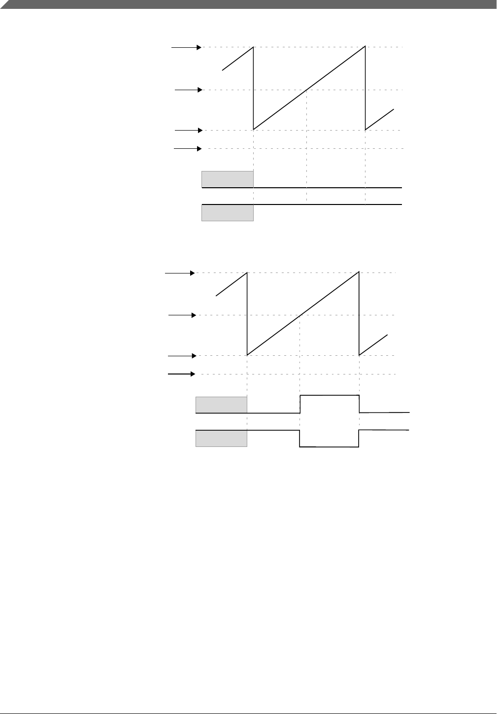
FTM counter
C(n)V
channel (n) output
with ELSB:ELSA = 1:0
channel (n) output
with ELSB:ELSA = X:1
0% duty cycle
100% duty cycle
MOD
C(n+1)V
CNTIN
Figure 45-41. Channel (n) output if (C(n)V < CNTIN) and (CNTIN < C(n+1)V < MOD)
C(n+1)V
channel (n) output
with ELSB:ELSA = X:1
FTM counter
CNTIN
channel (n) output
with ELSB:ELSA = 1:0
C(n)V
MOD
Figure 45-42. Channel (n) output if (C(n+1)V < CNTIN) and (CNTIN < C(n)V < MOD)
Functional Description
S32K1xx Series Reference Manual, Rev. 7, 04/2018
1280 NXP Semiconductors
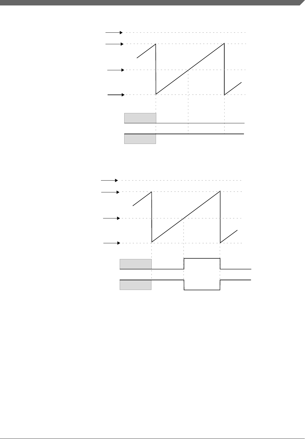
FTM counter
channel (n) output
with ELSB:ELSA = 1:0
channel (n) output
with ELSB:ELSA = X:1 100% duty cycle
0% duty cycle
MOD
C(n)V
C(n+1)V
CNTIN
Figure 45-43. Channel (n) output if (C(n)V > MOD) and (CNTIN < C(n+1)V < MOD)
C(n)V
CNTIN
channel (n) output
with ELSB:ELSA = X:1
channel (n) output
with ELSB:ELSA = 1:0
FTM counter
C(n+1)V
MOD
Figure 45-44. Channel (n) output if (C(n+1)V > MOD) and (CNTIN < C(n)V < MOD)
Chapter 45 FlexTimer Module (FTM)
S32K1xx Series Reference Manual, Rev. 7, 04/2018
NXP Semiconductors 1281
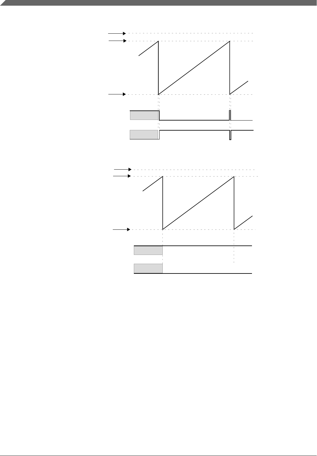
FTM counter
CNTIN
C(n+1)V
not fully 0% duty cycle
channel (n) output
with ELSB:ELSA = 1:0
not fully 100% duty cycle
channel (n) output
with ELSB:ELSA = X:1
MOD = C(n)V
Figure 45-45. Channel (n) output if (C(n+1)V > MOD) and (CNTIN < C(n)V = MOD)
FTM counter
100% duty cycle
channel (n) output
with ELSB:ELSA = 1:0
channel (n) output
with ELSB:ELSA = X:1 0% duty cycle
MOD
C(n)V = CNTIN
C(n+1)V
Figure 45-46. Channel (n) output if (C(n)V = CNTIN) and (C(n+1)V > MOD)
45.5.9.1 Asymmetrical PWM
In Combine mode and Modified Combine PWM Mode, the PWM first edge (channel (n)
match: FTM counter = C(n)V) is independent of the PWM second edge (channel (n+1)
match: FTM counter = C(n+1)V).
45.5.10 Modified Combine PWM Mode
The Modified Combine PWM mode is selected when:
• QUADEN = 0
• DECAPEN = 0
Functional Description
S32K1xx Series Reference Manual, Rev. 7, 04/2018
1282 NXP Semiconductors

• MCOMBINE = 1
• COMBINE = 1, and
• CPWMS = 0
The Modified Combine PWM mode is intended to support the generation of PWM
signals where the period is not modified while the signal is being generated, but the duty
cycle will be varied. In this mode, an even channel (n) and adjacent odd channel (n+1)
are combined to generate a PWM signal in the channel (n) output. Thus, the channel (n)
match edge is fixed and the channel (n+1) match edge can be varied.
When a pair of channels is in Modified Combine PWM mode, it is recommend that the
other pairs also be in Modified Combine PWM mode.
In the Modified Combine PWM mode, assuming that CNTIN ≥ 0, MOD > 0, and CNTIN
< MOD:
• The PWM period is determined by (MOD - CNTIN + 0x0001);
• The channel (n) PWM duty cycle is calculated according to the following table.
Table 45-8. Modified Combine PWM Mode - Duty Cycles
Channel (n) PWM Duty Cycle Condition
0% duty cycle For CNTIN ≤ (C(n)V and C(n+1)V) ≤ MOD: C(n)V = C(n+1)V
duty cyle between 0% and 100% For CNTIN ≤ (C(n)V and C(n+1)V) ≤ MOD:
• if (C(n)V < C(n+1)V), then the duty cycle is (C(n+1)V -
C(n)V)
• if (C(n)V > C(n+1)V), then the duty cycle is [(MOD -
C(n)V) + (C(n+1)V - CNTIN) + 1]
100% duty cyle CNTIN ≤ C(n)V ≤ MOD and C(n+1)V > MOD
The channel (n) CHF bit is set and its interrupt is generated, if channel (n) CHIE = 1, at
the channel (n) match (FTM counter = C(n)V). The channel (n+1) CHF bit is set and its
interrupt is generated, if channel (n+1) CHIE = 1, at the channel (n+1) match (FTM
counter = C(n+1)V).
If channel (n) ELSB:ELSA = 1:0, then the channel (n) output is forced high at the
channel (n) match (FTM counter = C(n)V) and it is forced low at the channel (n+1)
match (FTM counter = C(n+1)V).
If channel (n) ELSB:ELSA = X:1, then the channel (n) output is forced low at the
channel (n) match (FTM counter = C(n)V) and it is forced high at the channel (n+1)
match (FTM counter = C(n+1)V).
Chapter 45 FlexTimer Module (FTM)
S32K1xx Series Reference Manual, Rev. 7, 04/2018
NXP Semiconductors 1283
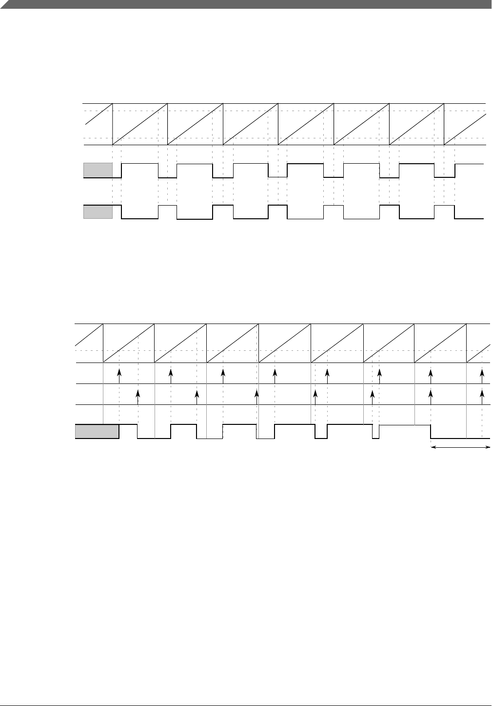
In Modified Combine PWM mode, the channel (n+1) ELSB:ELSA bits are not used in
the generation of the channels (n) and (n+1) output. However, if channel (n) ELSB:ELSA
= 0:0, then the channel (n) output is not controlled by FTM, and if channel (n+1)
ELSB:ELSA = 0:0, then the channel (n+1) output is not controlled by FTM.
FTM counter
channel (n) match
channel (n) output
with ELSB:ELSA = 1:0
with ELSB:ELSA = X:1
channel (n) output
channel (n+1) match
Figure 45-47. Modified Combine PWM Mode
The Modified Combine PWM mode allows the offset addition of the duty cyle, thus, in
some cases, the C(n+1)V match can happen on the next FTM counter period. For CNTIN
≥ 0, MOD > 0, and CNTIN < MOD, this situation happens when C(n)V > C(n+1)V.
FTM counter
C(n)V match
(C(n)V is fixed)
channel (n) output
with ELSB:ELSA = 1:0
C(n+1)V is updated
with its write buffer
C(n+1)V match
0% duty cycle
Figure 45-48. Modified Combine PWM Mode Examples
If more than one pair of channels are configured in Modified Combine PWM Mode, it is
possible to fix an offset for the channel (n) match edge of each pair with respect to other
pairs. This behavior is useful in the generation of lighting PWM control signals where it
is desirable that edges are not coincident with each other pair to help eliminate noise
generation. The C(n)V register value is the shift of the PWM pulse with respect to the
beginning of FTM counter period (FTM counter = CNTIN).
Functional Description
S32K1xx Series Reference Manual, Rev. 7, 04/2018
1284 NXP Semiconductors

FTM counter = C5V
FTM counter = C7V
FTM counter = C0V
FTM counter = C2V
FTM counter = C4V
FTM counter = C6V
FTM counter = C1V
FTM counter = C3V
CNTIN
MOD
channel 0 output
(ELS0B:ELS0A = 1:0)
channel 2 output
(ELS2B:ELS2A = 1:0)
channel 4 output
(ELS4B:ELS4A = 1:0)
channel 6 output
(ELS6B:ELS6A = 1:0)
Figure 45-49. Example of Four Pairs of Channels in Modified Combine PWM Mode
45.5.10.1 Synchronization
In the Modified Combine Mode, the following registers should be updated when the FTM
counter clock is disabled (CLKS[1:0] = 0:0).
• CNTIN (CNTIN register update)
• MOD (MOD and HCR registers update)
• C(n)V and C(n+1)V (CnV register update)
In the Modified Combine Mode, if (FTMEN = 1), (CLKS[1:0] ≠ 0:0), and there was a
write to the register C(n+1)V, then the register C(n+1)V is updated with its write buffer
value on the next channel (n) match (FTM counter = C(n)V). This feature allows to vary
the PWM duty cycle value in this mode.
NOTE
In the Modified Combine Mode, the bit SYNCEN(n) should be
zero bit for the channels (n) and (n+1). So, the following
features are not available for this mode.
•C(n)V and C(n+1)V register synchronization
•Reload Points
•Global Load
Chapter 45 FlexTimer Module (FTM)
S32K1xx Series Reference Manual, Rev. 7, 04/2018
NXP Semiconductors 1285
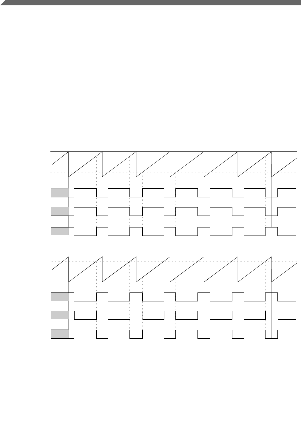
45.5.11 Complementary Mode
The Complementary mode is selected when:
• QUADEN = 0
• DECAPEN = 0
• COMP = 1
In Complementary mode, the channel (n+1) output is the inverse of the channel (n)
output.
So, the channel (n+1) output is the same as the channel (n) output when:
• QUADEN = 0
• DECAPEN = 0
• COMP = 0
FTM counter
channel (n+1) match
channel (n+1) output
with COMP = 1
channel (n+1) output
with COMP = 0
channel (n) output
with ELSB:ELSA = 1:0
channel (n) match
Figure 45-50. Channel (n+1) output in Complementary mode with (ELSB:ELSA = 1:0)
FTM counter
channel (n+1) match
channel (n+1) output
with COMP = 1
channel (n+1) output
with COMP = 0
channel (n) output
with ELSB:ELSA = X:1
channel (n) match
Figure 45-51. Channel (n+1) output in Complementary mode with (ELSB:ELSA = X:1)
NOTE
The Complementary Mode is not available on Output Compare
mode.
Functional Description
S32K1xx Series Reference Manual, Rev. 7, 04/2018
1286 NXP Semiconductors

45.5.12 Registers updated from write buffers
45.5.12.1 CNTIN register update
The following table describes when CNTIN register is updated:
Table 45-9. CNTIN register update
When Then CNTIN register is updated
CLKS[1:0] = 0:0 When CNTIN register is written, independent of FTMEN bit.
• FTMEN = 0, or
• CNTINC = 0
At the next FTM input clock after CNTIN was written.
• FTMEN = 1,
• SYNCMODE = 1, and
• CNTINC = 1
By the CNTIN register synchronization.
• CNTINC = 1, and
• LDOK = 1
By the Reload Points.
45.5.12.2 MOD and HCR registers update
The following table describes when MOD or HCR registers are updated:
Table 45-10. MOD and HCR updates
When Then MOD or HCR is updated
CLKS[1:0] = 0:0 When MOD (or HCR) is written, independent of FTMEN bit.
• CLKS[1:0] ≠ 0:0, and
• FTMEN = 0
According to the CPWMS bit, that is:
• If the selected mode is not CPWM then MOD (or HCR) is updated after MOD
(or HCR) register was written and the FTM counter changes from MOD to
CNTIN. If the FTM counter is at free-running counter mode then this update
occurs when the FTM counter changes from 0xFFFF to 0x0000.
• If the selected mode is CPWM then MOD (or HCR) register is updated after
MOD (or HCR) register was written and the FTM counter changes from MOD
to (MOD – 0x0001).
• CLKS[1:0] ≠ 0:0, and
• FTMEN = 1
By the MOD register synchronization. HCR follows the same procedure of MOD
register in this case.
• LDOK = 1 By the Reload Points.
45.5.12.3 CnV register update
The following table describes when CnV register is updated:
Chapter 45 FlexTimer Module (FTM)
S32K1xx Series Reference Manual, Rev. 7, 04/2018
NXP Semiconductors 1287

Table 45-11. CnV register update
When Then CnV register is updated
CLKS[1:0] = 0:0 When CnV register is written, independent of FTMEN bit.
• CLKS[1:0] ≠ 0:0, and
• FTMEN = 0
According to the selected mode, that is:
• If the selected mode is Output Compare, then CnV register is updated on the
next FTM counter change, end of the prescaler counting, after CnV register
was written.
• If the selected mode is EPWM, then CnV register is updated after CnV
register was written and the FTM counter changes from MOD to CNTIN. If
the FTM counter is at free-running counter mode then this update occurs
when the FTM counter changes from 0xFFFF to 0x0000.
• If the selected mode is CPWM, then CnV register is updated after CnV
register was written and the FTM counter changes from MOD to (MOD –
0x0001).
• CLKS[1:0] ≠ 0:0, and
• FTMEN = 1
According to the selected mode, that is:
• If the selected mode is output compare then CnV register is updated
according to the SYNCEN bit. If (SYNCEN = 0) then CnV register is updated
after CnV register was written at the next change of the FTM counter, the
end of the prescaler counting. If (SYNCEN = 1) then CnV register is updated
by the C(n)V and C(n+1)V register synchronization.
• If the selected mode is not output compare and (SYNCEN = 1) then CnV
register is updated by the C(n)V and C(n+1)V register synchronization.
• SYNCEN = 1, and
• LDOK = 1
By the Reload Points.
45.5.13 PWM synchronization
The PWM synchronization provides an opportunity to update the MOD, HCR, CNTIN,
CnV, OUTMASK, INVCTRL and SWOCTRL registers with their buffered value and
force the FTM counter to the CNTIN register value.
Note
The legacy PWM synchronization (SYNCMODE = 0) is a
subset of the enhanced PWM synchronization (SYNCMODE =
1). Thus, only the enhanced PWM synchronization must be
used.
Functional Description
S32K1xx Series Reference Manual, Rev. 7, 04/2018
1288 NXP Semiconductors
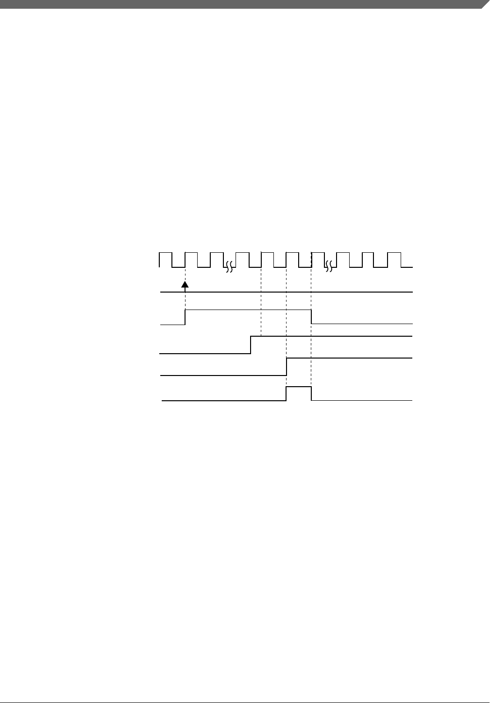
45.5.13.1 Hardware trigger
Three hardware trigger signal inputs of the FTM module are enabled when TRIGn = 1,
where n = 0, 1 or 2 corresponding to each one of the input signals, respectively. The
hardware trigger input n is synchronized by the FTM input clock. The PWM
synchronization with hardware trigger is initiated when a rising edge is detected at the
enabled hardware trigger inputs.
If (HWTRIGMODE = 0) then the TRIGn bit is cleared when 0 is written to it or when the
trigger n event is detected.
In this case, if two or more hardware triggers are enabled (for example, TRIG0 and
TRIG1 = 1) and only trigger 1 event occurs, then only TRIG1 bit is cleared. If a trigger n
event occurs together with a write setting TRIGn bit, then the synchronization is initiated,
but TRIGn bit remains set due to the write operation.
write 1 to TRIG0 bit
FTM input clock
synchronized trigger_0
by FTM input clock
trigger 0 event
Note
TRIG0 bit
trigger_0 input
All hardware trigger inputs have the same behavior.
Figure 45-52. Hardware trigger event with HWTRIGMODE = 0
If HWTRIGMODE = 1, then the TRIGn bit is only cleared when 0 is written to it.
NOTE
The HWTRIGMODE bit must be 1 only with enhanced PWM
synchronization (SYNCMODE = 1).
45.5.13.2 Software trigger
A software trigger event occurs when 1 is written to the SYNC[SWSYNC] bit. The
SWSYNC bit is cleared when 0 is written to it or when the PWM synchronization,
initiated by the software event, is completed.
Chapter 45 FlexTimer Module (FTM)
S32K1xx Series Reference Manual, Rev. 7, 04/2018
NXP Semiconductors 1289
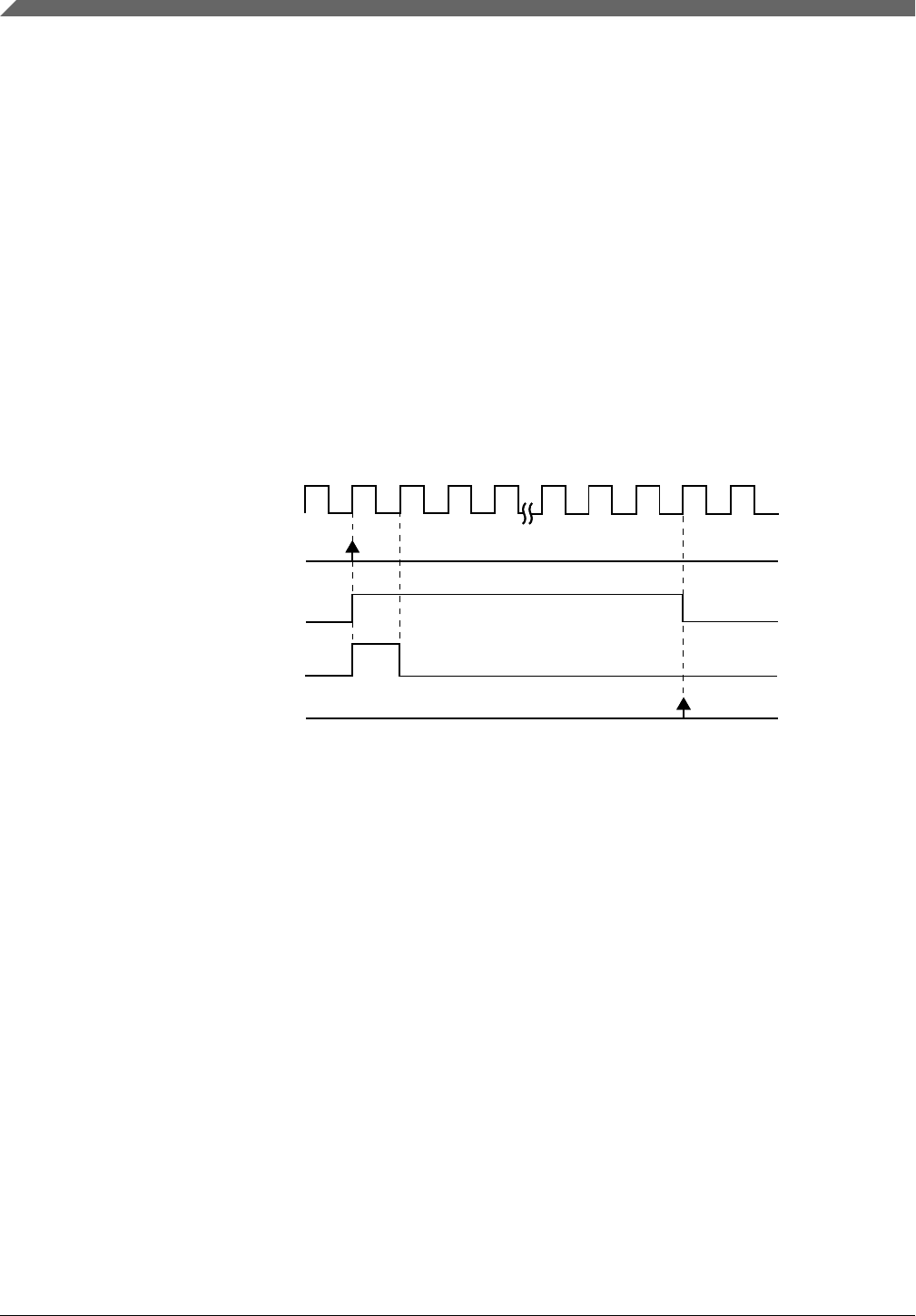
If another software trigger event occurs (by writing another 1 to the SWSYNC bit) at the
same time the PWM synchronization initiated by the previous software trigger event is
ending, a new PWM synchronization is started and the SWSYNC bit remains equal to 1.
If SYNCMODE = 0 then the SWSYNC bit is also cleared by FTM according to
PWMSYNC and REINIT bits. In this case if (PWMSYNC = 1) or (PWMSYNC = 0 and
REINIT = 0) then SWSYNC bit is cleared at the next selected loading point after that the
software trigger event occurred; see Synchronization Points and the following figure. If
(PWMSYNC = 0) and (REINIT = 1) then SWSYNC bit is cleared when the software
trigger event occurs.
If SYNCMODE = 1 then the SWSYNC bit is also cleared by FTM according to the
SWRSTCNT bit. If SWRSTCNT = 0 then SWSYNC bit is cleared at the next selected
loading point after that the software trigger event occurred; see the following figure. If
SWRSTCNT = 1 then SWSYNC bit is cleared when the software trigger event occurs.
FTM input clock
selected loading point
PWM synchronization
SWSYNC bit
software trigger event
write 1 to SWSYNC bit
Figure 45-53. Software trigger event
45.5.13.3 Synchronization Points
The synchronization points are points where the registers can be updated with their write
buffer by PWM synchronization. These synchronization points are safe points because
guarantee smooth transitions in the generated PWM signals.
In Up counting, the synchronization points are when the FTM counter changes from
MOD to CNTIN. In this case, the synchronization points are enabled if (CNTMIN = 1) or
(CNTMAX = 1).
In Up-down counting, the synchronization points are:
• if (CNTMAX = 1), when the FTM counter changes from (MOD) to (MOD - 1);
• if (CNTMIN = 1), when the FTM counter changes from (CNTIN) to (CNTIN + 1).
Functional Description
S32K1xx Series Reference Manual, Rev. 7, 04/2018
1290 NXP Semiconductors
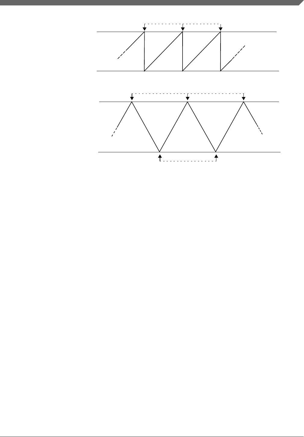
FTM counter changes from
(MOD) to (MOD - 1)
FTM counter changes from
(CNTIN) to (CNTIN + 1)
synchronization points if (CNTMIN = 1)
synchronization points if (CNTMAX = 1)
up-down counting mode
FTM counter changes from
MOD to CNTIN
synchronization points if (CNTMAX) = 1 or (CNTMIN = 1)
up counting mode
Figure 45-54. Synchronization Points
45.5.13.4 MOD register synchronization
The MOD register synchronization updates the MOD register with its buffer value. This
synchronization is enabled if (FTMEN = 1).
The MOD register synchronization can be done by either the enhanced PWM
synchronization (SYNCMODE = 1) or the legacy PWM synchronization (SYNCMODE
= 0). However, it is expected that the MOD register be synchronized only by the
enhanced PWM synchronization.
In the case of enhanced PWM synchronization, the MOD register synchronization
depends on SWWRBUF, SWRSTCNT, HWWRBUF, and HWRSTCNT bits according to
this flowchart:
Chapter 45 FlexTimer Module (FTM)
S32K1xx Series Reference Manual, Rev. 7, 04/2018
NXP Semiconductors 1291
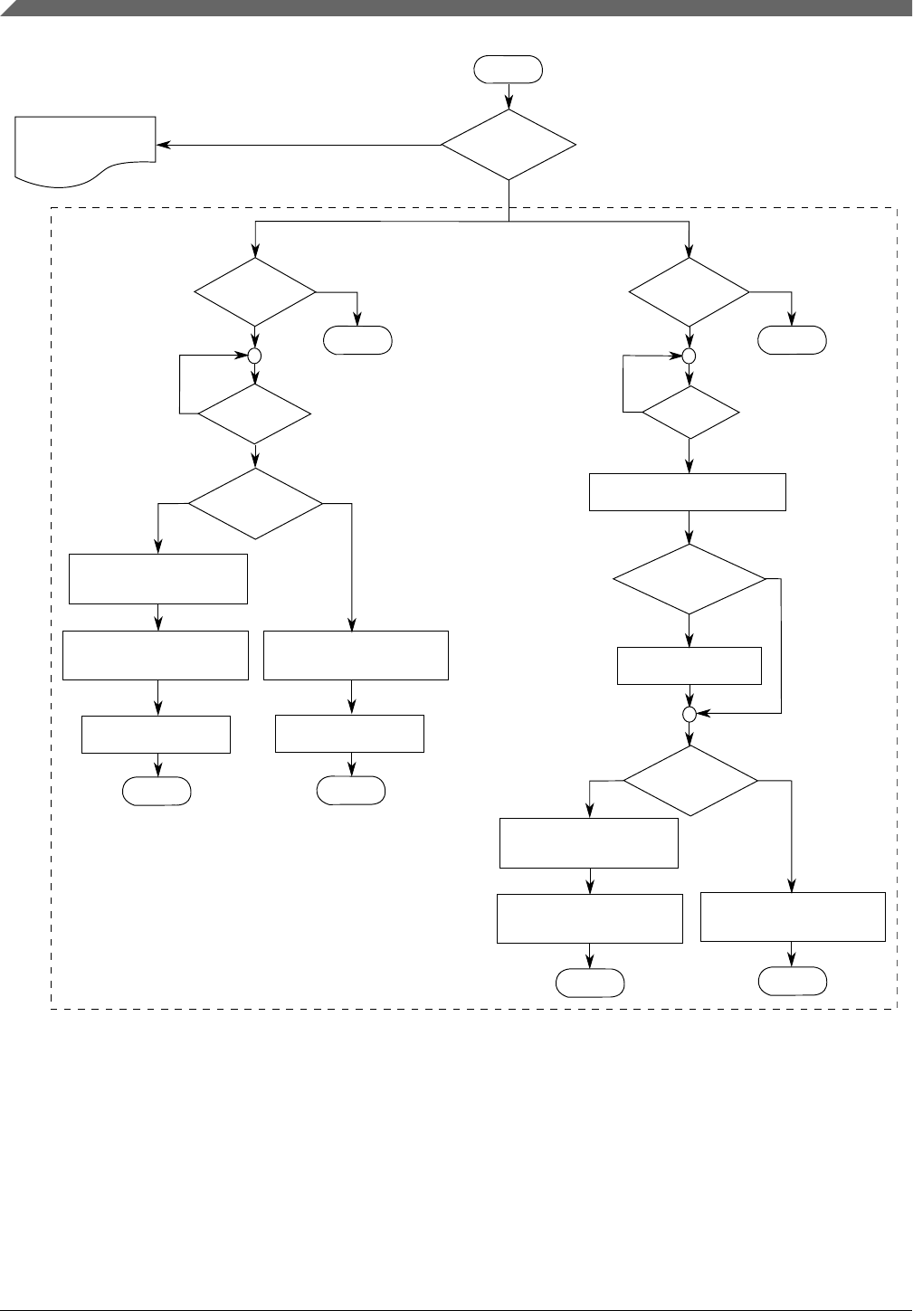
legacy
PWM synchronization
end
= 0
enhanced PWM synchronization
begin
= 1
SYNCMODE
bit ?
= 0
end
end
end
end end
= 1
= 1
0 =
= 1
= 0
= 1
0 =
= 1
= 1
= 1
= 0
= 0
= 0
MOD register is
updated by software trigger MOD register is
updated by hardware trigger
software
trigger
hardware
trigger
FTM counter is reset by
software trigger
FTM counter is reset by
hardware trigger
SWWRBUF
bit ?
HWWRBUF
bit ?
SWSYNC
bit ?
SWRSTCNT
bit ?
wait the next selected
loading point
update MOD with
its buffer value
clear SWSYNC bit clear SWSYNC bit
update MOD with
its buffer value
TRIGn
bit ?
wait hardware trigger n
HWTRIGMODE
bit ?
clear TRIGn bit
wait the next selected
loading point
update MOD with
its buffer value
update MOD with
its buffer value
HWRSTCNT
bit ?
Figure 45-55. MOD register synchronization flowchart
In the case of legacy PWM synchronization, the MOD register synchronization depends
on PWMSYNC and REINIT bits according to the following description.
If (SYNCMODE = 0), (PWMSYNC = 0), and (REINIT = 0), then this synchronization is
made on the next selected loading point after an enabled trigger event takes place. If the
trigger event was a software trigger, then the SWSYNC bit is cleared on the next selected
Functional Description
S32K1xx Series Reference Manual, Rev. 7, 04/2018
1292 NXP Semiconductors
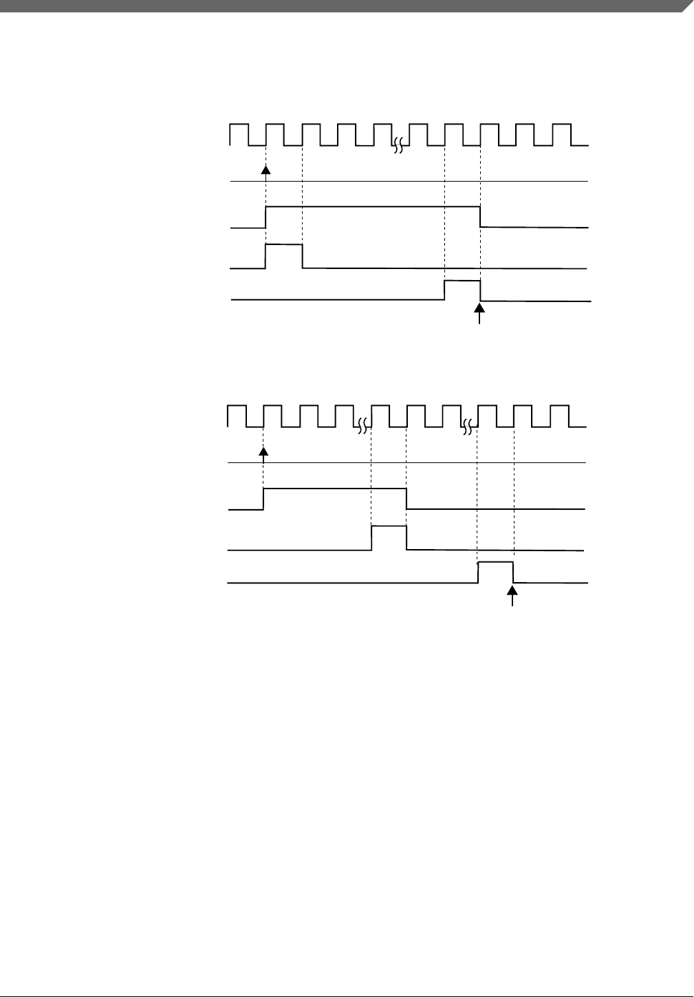
loading point. If the trigger event was a hardware trigger, then the trigger enable bit
(TRIGn) is cleared according to Hardware trigger. Examples with software and hardware
triggers follow.
selected loading point
MOD register is updated
write 1 to SWSYNC bit
SWSYNC bit
software trigger event
FTM input clock
Figure 45-56. MOD synchronization with (SYNCMODE = 0), (PWMSYNC = 0), (REINIT =
0), and software trigger was used
selected loading point
MOD register is updated
write 1 to TRIG0 bit
TRIG0 bit
trigger 0 event
FTM input clock
Figure 45-57. MOD synchronization with (SYNCMODE = 0), (HWTRIGMODE = 0),
(PWMSYNC = 0), (REINIT = 0), and a hardware trigger was used
If (SYNCMODE = 0), (PWMSYNC = 0), and (REINIT = 1), then this synchronization is
made on the next enabled trigger event. If the trigger event was a software trigger, then
the SWSYNC bit is cleared according to the following example. If the trigger event was a
hardware trigger, then the TRIGn bit is cleared according to Hardware trigger. Examples
with software and hardware triggers follow.
Chapter 45 FlexTimer Module (FTM)
S32K1xx Series Reference Manual, Rev. 7, 04/2018
NXP Semiconductors 1293
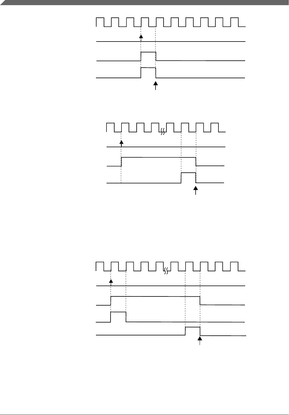
MOD register is updated
write 1 to SWSYNC bit
SWSYNC bit
software trigger event
FTM input clock
Figure 45-58. MOD synchronization with (SYNCMODE = 0), (PWMSYNC = 0), (REINIT =
1), and software trigger was used
MOD register is updated
FTM input clock
TRIG0 bit
trigger 0 event
write 1 to TRIG0 bit
Figure 45-59. MOD synchronization with (SYNCMODE = 0), (HWTRIGMODE = 0),
(PWMSYNC = 0), (REINIT = 1), and a hardware trigger was used
If (SYNCMODE = 0) and (PWMSYNC = 1), then this synchronization is made on the
next selected loading point after the software trigger event takes place. The SWSYNC bit
is cleared on the next selected loading point:
selected loading point
MOD register is updated
write 1 to SWSYNC bit
SWSYNC bit
software trigger event
FTM input clock
Figure 45-60. MOD synchronization with (SYNCMODE = 0) and (PWMSYNC = 1)
Functional Description
S32K1xx Series Reference Manual, Rev. 7, 04/2018
1294 NXP Semiconductors

45.5.13.5 CNTIN register synchronization
The CNTIN register synchronization updates the CNTIN register with its buffer value.
This synchronization is enabled if (FTMEN = 1), (SYNCMODE = 1), and (CNTINC =
1). The CNTIN register synchronization can be done only by the enhanced PWM
synchronization (SYNCMODE = 1). The synchronization mechanism is the same as the
MOD register synchronization done by the enhanced PWM synchronization; see MOD
register synchronization.
45.5.13.6 C(n)V and C(n+1)V register synchronization
The C(n)V and C(n+1)V registers synchronization updates the C(n)V and C(n+1)V
registers with their buffer values.
This synchronization is enabled if (FTMEN = 1) and (SYNCEN = 1). The
synchronization mechanism is the same as the MOD register synchronization. However,
it is expected that the C(n)V and C(n+1)V registers be synchronized only by the
enhanced PWM synchronization (SYNCMODE = 1).
45.5.13.7 OUTMASK register synchronization
The OUTMASK register synchronization updates the OUTMASK register with its buffer
value.
The OUTMASK register can be updated at each rising edge of FTM input clock
(SYNCHOM = 0), by the enhanced PWM synchronization (SYNCHOM = 1 and
SYNCMODE = 1) or by the legacy PWM synchronization (SYNCHOM = 1 and
SYNCMODE = 0). However, it is expected that the OUTMASK register be synchronized
only by the enhanced PWM synchronization.
In the case of enhanced PWM synchronization, the OUTMASK register synchronization
depends on SWOM and HWOM bits. See the following flowchart:
Chapter 45 FlexTimer Module (FTM)
S32K1xx Series Reference Manual, Rev. 7, 04/2018
NXP Semiconductors 1295
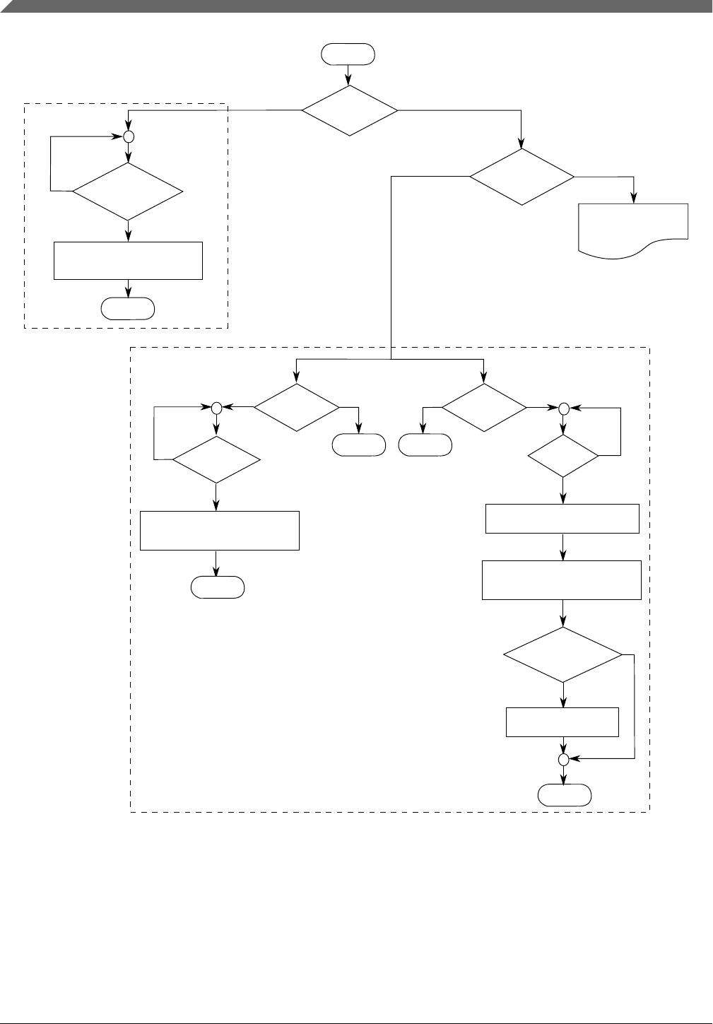
end
= 0
update OUTMASK register at
each rising edge of FTM input clock
begin
software
trigger
endend
end
end
= 0
= 0
= 1
= 1
= 1
= 1
= 0
= 1
0 =
0 =
1 =
1 =
0 =
legacy
PWM synchronization
SYNCHOM
bit ?
update OUTMASK register by
PWM synchronization
update OUTMASK
with its buffer value
SYNCMODE
bit ?
clear TRIGn bit
HWTRIGMODE
bit ?
update OUTMASK
with its buffer value
wait hardware trigger n
TRIGn
bit ?
HWOM
bit ?
SWOM
bit ?
SWSYNC
bit ?
rising edge
of FTM input
clock ?
update OUTMASK
with its buffer value
hardware
trigger
OUTMASK is updated
by software trigger
OUTMASK is updated
by hardware trigger
enhanced PWM synchronization
= yes
no =
Figure 45-61. OUTMASK register synchronization flowchart
In the case of legacy PWM synchronization, the OUTMASK register synchronization
depends on PWMSYNC bit according to the following description.
Functional Description
S32K1xx Series Reference Manual, Rev. 7, 04/2018
1296 NXP Semiconductors
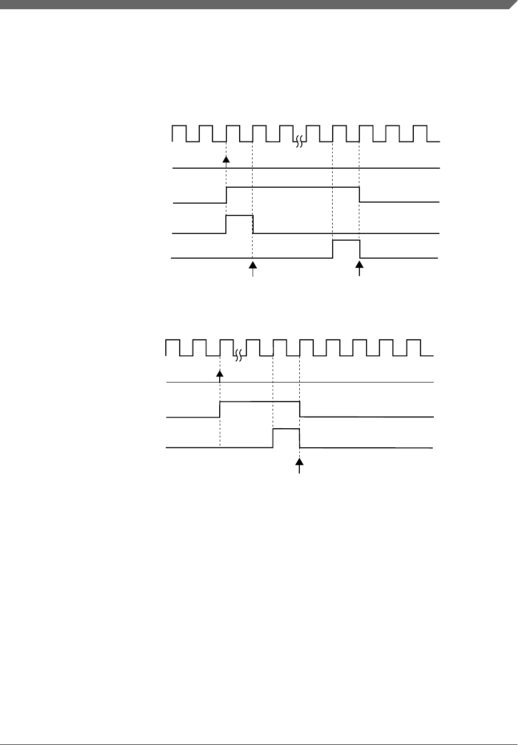
If (SYNCMODE = 0), (SYNCHOM = 1), and (PWMSYNC = 0), then this
synchronization is done on the next enabled trigger event. If the trigger event was a
software trigger, then the SWSYNC bit is cleared on the next selected loading point. If
the trigger event was a hardware trigger, then the TRIGn bit is cleared according to
Hardware trigger. Examples with software and hardware triggers follow.
OUTMASK register is updated
selected loading point
SWSYNC bit is cleared
write 1 to SWSYNC bit
SWSYNC bit
software trigger event
FTM input clock
Figure 45-62. OUTMASK synchronization with (SYNCMODE = 0), (SYNCHOM = 1),
(PWMSYNC = 0) and software trigger was used
write 1 to TRIG0 bit
TRIG0 bit
trigger 0 event
OUTMASK register is updated and
TRIG0 bit is cleared
FTM input clock
Figure 45-63. OUTMASK synchronization with (SYNCMODE = 0), (HWTRIGMODE = 0),
(SYNCHOM = 1), (PWMSYNC = 0), and a hardware trigger was used
If (SYNCMODE = 0), (SYNCHOM = 1), and (PWMSYNC = 1), then this
synchronization is made on the next enabled hardware trigger. The TRIGn bit is cleared
according to Hardware trigger. An example with a hardware trigger follows.
Chapter 45 FlexTimer Module (FTM)
S32K1xx Series Reference Manual, Rev. 7, 04/2018
NXP Semiconductors 1297

OUTMASK register is updated and
TRIG0 bit is cleared
write 1 to TRIG0 bit
TRIG0 bit
trigger 0 event
FTM input clock
Figure 45-64. OUTMASK synchronization with (SYNCMODE = 0), (HWTRIGMODE = 0),
(SYNCHOM = 1), (PWMSYNC = 1), and a hardware trigger was used
45.5.13.8 INVCTRL register synchronization
The INVCTRL register synchronization updates the INVCTRL register with its buffer
value.
The INVCTRL register can be updated at each rising edge of FTM input clock (INVC =
0) or by the enhanced PWM synchronization (INVC = 1 and SYNCMODE = 1)
according to the following flowchart.
In the case of enhanced PWM synchronization, the INVCTRL register synchronization
depends on SWINVC and HWINVC bits.
Functional Description
S32K1xx Series Reference Manual, Rev. 7, 04/2018
1298 NXP Semiconductors
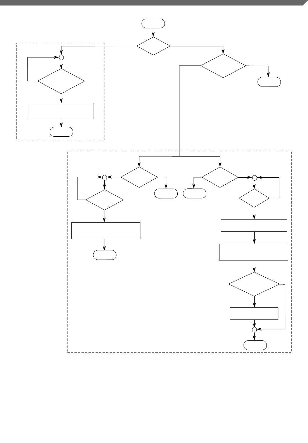
end
begin
= 1
= 0
end end
end
end
end
= 1
= 0
= 1
= 1
= 0
= 0
= 1
INVCTRL is updated
by software trigger
software
trigger
hardware
trigger
INVCTRL is updated
by hardware trigger
enhanced PWM synchronization
update INVCTRL register by
PWM synchronization
update INVCTRL register at
each rising edge of FTM input clock
= yes
0 =
1 = 0 =
0 =
no =
1 =
INVC
bit ?
SYNCMODE
bit ?
rising edge
of FTM input
clock ?
update INVCTRL
with its buffer value
update INVCTRL
with its buffer value
HWINVC
bit ?
TRIGn
bit ?
wait hardware trigger n
update INVCTRL
with its buffer value
HWTRIGMODE
bit ?
clear TRIGn bit
SWINVC
bit ?
SWSYNC
bit ?
Figure 45-65. INVCTRL register synchronization flowchart
45.5.13.9 SWOCTRL register synchronization
The SWOCTRL register synchronization updates the SWOCTRL register with its buffer
value.
Chapter 45 FlexTimer Module (FTM)
S32K1xx Series Reference Manual, Rev. 7, 04/2018
NXP Semiconductors 1299
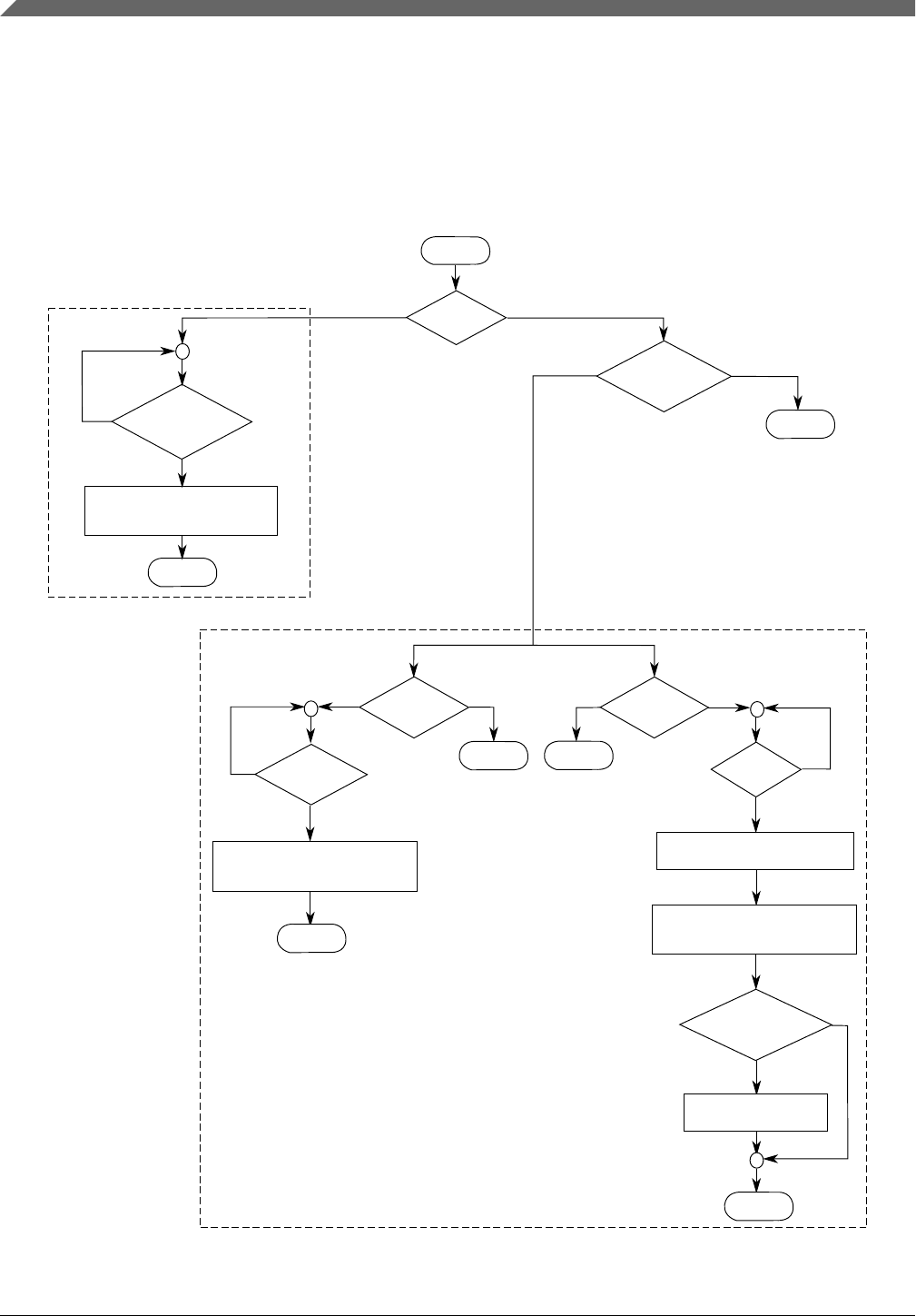
The SWOCTRL register can be updated at each rising edge of FTM input clock (SWOC
= 0) or by the enhanced PWM synchronization (SWOC = 1 and SYNCMODE = 1)
according to the following flowchart.
In the case of enhanced PWM synchronization, the SWOCTRL register synchronization
depends on SWSOC and HWSOC bits.
end
begin
= 1
= 0
end end
end
end
end
= 1
= 0
= 1
= 1
= 0
= 0
= 1
SWOCTRL is updated
by software trigger
software
trigger
hardware
trigger
SWOCTRL is updated
by hardware trigger
enhanced PWM synchronization
update SWOCTRL register by
PWM synchronization
update SWOCTRL register at
each rising edge of FTM input clock
= yes
0 =
1 = 0 =
0 =
no =
1 =
SWOC
bit ?
SYNCMODE
bit ?
rising edge
of FTM input
clock ?
update SWOCTRL
with its buffer value
update SWOCTRL
with its buffer value
HWSOC
bit ?
TRIGn
bit ?
wait hardware trigger n
update SWOCTRL
with its buffer value
HWTRIGMODE
bit ?
clear TRIGn bit
SWSOC
bit ?
SWSYNC
bit ?
Figure 45-66. SWOCTRL register synchronization flowchart
Functional Description
S32K1xx Series Reference Manual, Rev. 7, 04/2018
1300 NXP Semiconductors
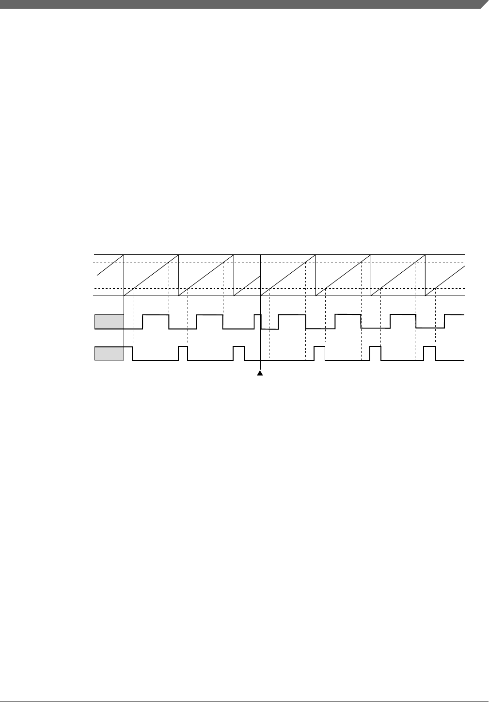
45.5.13.10 FTM counter synchronization
The FTM counter synchronization is a mechanism that allows the FTM to restart the
PWM generation at a certain point in the PWM period. The channels outputs are forced
to their initial value, except for channels in Output Compare mode, and the FTM counter
is forced to its initial counting value defined by CNTIN register.
The following figure shows the FTM counter synchronization. Note that after the
synchronization event occurs, the channel (n) is set to its initial value and the channel (n
+1) is not set to its initial value due to a specific timing of this figure in which the
deadtime insertion prevents this channel output from transitioning to 1. If no deadtime
insertion is selected, then the channel (n+1) transitions to logical value 1 immediately
after the synchronization event occurs.
synchronization event
channel (n+1) match
FTM counter
channel (n) match
channel (n) output
(after deadtime
insertion)
channel (n+1) output
(after deadtime
insertion)
Figure 45-67. FTM counter synchronization
The FTM counter synchronization can be done by either the enhanced PWM
synchronization (SYNCMODE = 1) or the legacy PWM synchronization (SYNCMODE
= 0). However, the FTM counter must be synchronized only by the enhanced PWM
synchronization.
In the case of enhanced PWM synchronization, the FTM counter synchronization
depends on SWRSTCNT and HWRSTCNT bits according to the following flowchart.
Chapter 45 FlexTimer Module (FTM)
S32K1xx Series Reference Manual, Rev. 7, 04/2018
NXP Semiconductors 1301
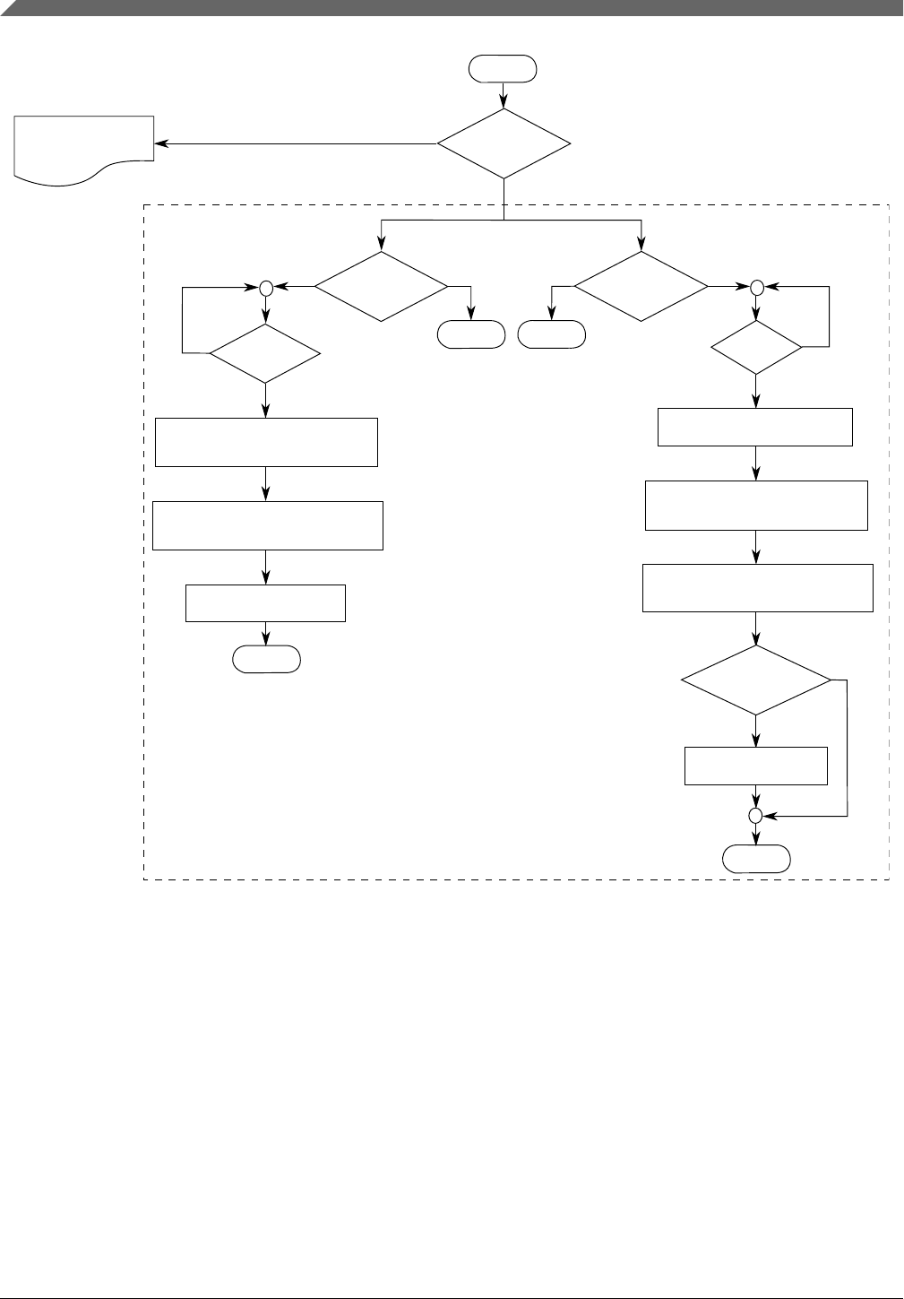
update FTM counter with
CNTIN register value
update the channels outputs
with their initial value
clear SWSYNC bit
end
FTM counter is reset by
software trigger
legacy
PWM synchronization
end
clear TRIGn bit
HWTRIGMODE
bit ?
= 1
= 0
update the channels outputs
with their initial value
update FTM counter with
CNTIN register value
wait hardware trigger n
enhanced PWM synchronization
FTM counter is reset by
hardware trigger
begin
= 1
= 1
= 1
= 1
end
end
HWRSTCNT
bit ?
SWRSTCNT
bit ?
SWSYNC
bit ?
software
trigger
SYNCMODE
bit ?
hardware
trigger
TRIGn
bit ?
= 0
= 0
= 0
= 0
= 0
1 =
Figure 45-68. FTM counter synchronization flowchart
In the case of legacy PWM synchronization, the FTM counter synchronization depends
on REINIT and PWMSYNC bits according to the following description.
If (SYNCMODE = 0), (REINIT = 1), and (PWMSYNC = 0) then this synchronization is
made on the next enabled trigger event. If the trigger event was a software trigger then
the SWSYNC bit is cleared according to the following example. If the trigger event was a
hardware trigger then the TRIGn bit is cleared according to Hardware trigger. Examples
with software and hardware triggers follow.
Functional Description
S32K1xx Series Reference Manual, Rev. 7, 04/2018
1302 NXP Semiconductors
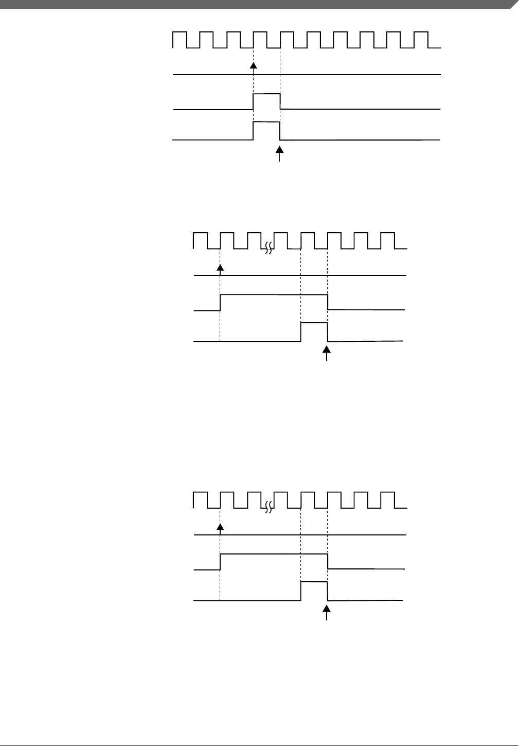
FTM counter is updated with the CNTIN register value
and channel outputs are forced to their initial value
write 1 to SWSYNC bit
SWSYNC bit
software trigger event
FTM input clock
Figure 45-69. FTM counter synchronization with (SYNCMODE = 0), (REINIT = 1),
(PWMSYNC = 0), and software trigger was used
TRIG0 bit
trigger 0 event
FTM counter is updated with the CNTIN register value
and channel outputs are forced to their initial value
FTM input clock
write 1 to TRIG0 bit
Figure 45-70. FTM counter synchronization with (SYNCMODE = 0), (HWTRIGMODE = 0),
(REINIT = 1), (PWMSYNC = 0), and a hardware trigger was used
If (SYNCMODE = 0), (REINIT = 1), and (PWMSYNC = 1) then this synchronization is
made on the next enabled hardware trigger. The TRIGn bit is cleared according to
Hardware trigger.
write 1 to TRIG0 bit
TRIG0 bit
trigger 0 event
FTM counter is updated with the CNTIN register value
and channel outputs are forced to their initial value
FTM input clock
Figure 45-71. FTM counter synchronization with (SYNCMODE = 0), (HWTRIGMODE = 0),
(REINIT = 1), (PWMSYNC = 1), and a hardware trigger was used
Chapter 45 FlexTimer Module (FTM)
S32K1xx Series Reference Manual, Rev. 7, 04/2018
NXP Semiconductors 1303
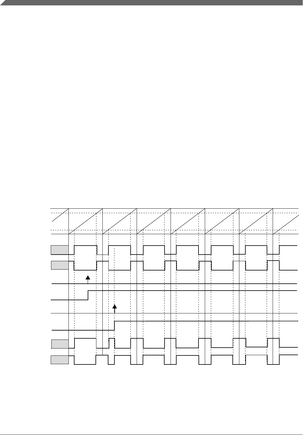
45.5.14 Inverting
The invert functionality swaps the signals between channel (n) and channel (n+1)
outputs. The inverting operation is selected when:
• QUADEN = 0
• DECAPEN = 0
• COMP = 1, and
• INVm = 1 (where m represents a channel pair)
The INVm bit in INVCTRL register is updated with its buffer value according to
INVCTRL register synchronization.
In combine mode with channel (n) ELSB:ELSA = 1:0, the channel (n) output is forced
low at the beginning of the period (FTM counter = CNTIN), forced high at the channel
(n) match and forced low at the channel (n+1) match. If the inverting is selected, the
channel (n) output behavior is changed to force high at the beginning of the PWM period,
force low at the channel (n) match and force high at the channel (n+1) match. See the
following figure.
NOTE
channel (n+1) match
FTM counter
channel (n) match
channel (n+1) output
before the inverting
write 1 to INV(m) bit
INV(m) bit buffer
INVCTRL register
synchronization
INV(m) bit
channel (n) output
after the inverting
channel (n+1) output
after the inverting
INV(m) bit selects the inverting to the pair channels (n) and (n+1).
channel (n) output
before the inverting
Figure 45-72. Channels (n) and (n+1) outputs after the inverting in combine mode with
channel (n) ELSB:ELSA = 1:0
Functional Description
S32K1xx Series Reference Manual, Rev. 7, 04/2018
1304 NXP Semiconductors
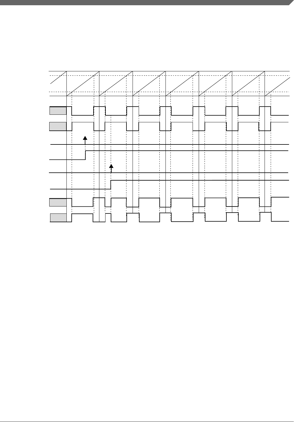
Note that the channel (n) ELSB:ELSA bits should be considered because they define the
active state of the channels outputs. In combine mode with channel (n) ELSB:ELSA = X:
1, the channel (n) output is forced high at the beginning of the period, forced low at the
channel (n) match and forced high at the channel (n+1) match. When inverting is
selected, the channels (n) and (n+1) present waveforms as shown in the following figure.
NOTE
channel (n+1) match
FTM counter
channel (n) match
channel (n+1) output
before the inverting
write 1 to INV(m) bit
INV(m) bit buffer
INVCTRL register
synchronization
INV(m) bit
channel (n) output
after the inverting
channel (n+1) output
after the inverting
INV(m) bit selects the inverting to the pair channels (n) and (n+1).
channel (n) output
before the inverting
Figure 45-73. Channels (n) and (n+1) outputs after the inverting in combine mode with
channel (n) ELSB:ELSA = X:1
NOTE
The Inverting is not available in Output Compare mode and
Modified Combine PWM Mode.
45.5.15 Software Output Control Mode
The software output control forces the channel output according to software defined
values at a specific time in the PWM generation.
The software output control is selected when:
• QUADEN = 0
• DECAPEN = 0, and
• CH(n)OC = 1
Chapter 45 FlexTimer Module (FTM)
S32K1xx Series Reference Manual, Rev. 7, 04/2018
NXP Semiconductors 1305
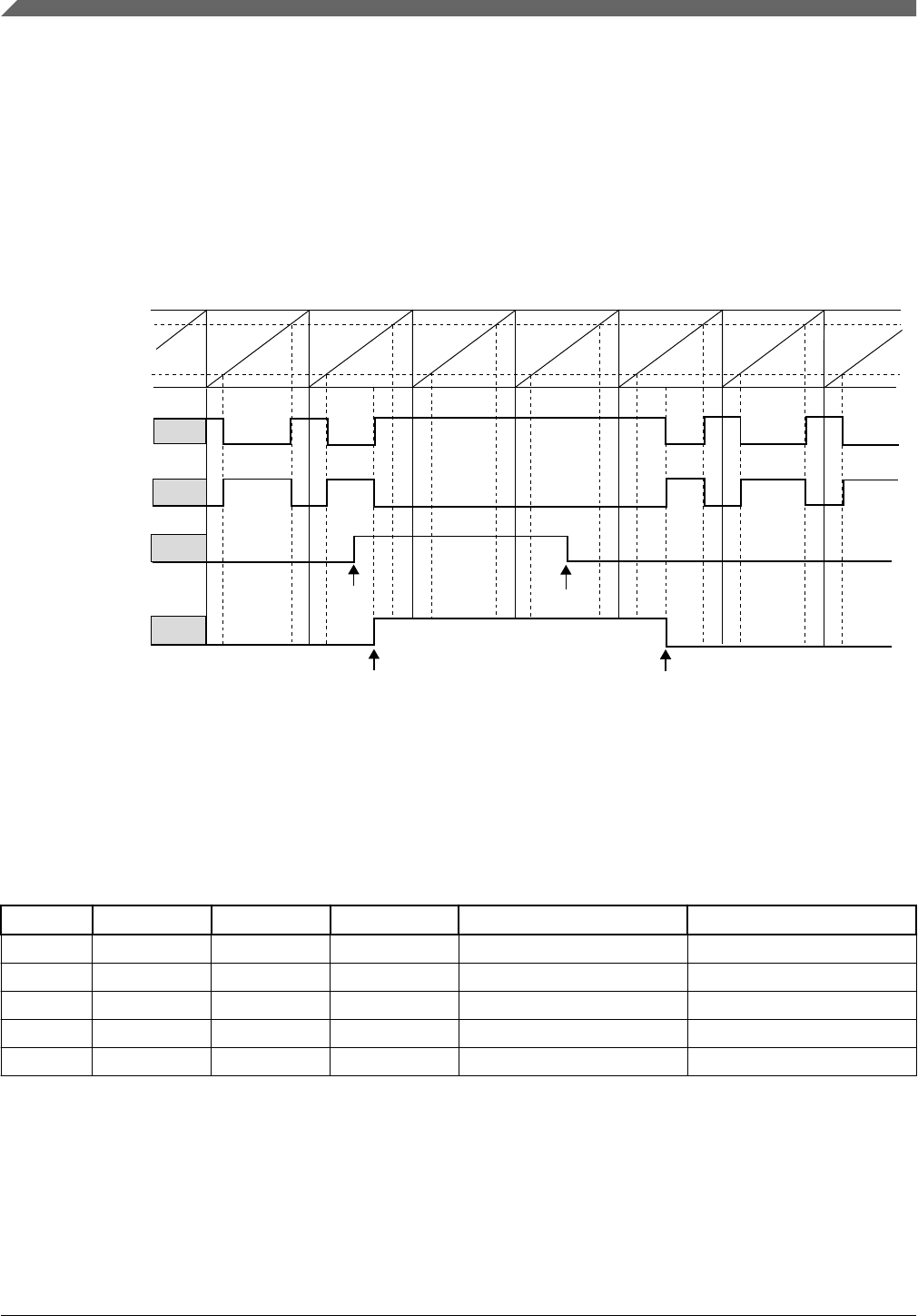
The CH(n)OC bit enables the software output control for a specific channel output and
the CH(n)OCV selects the value that is forced to this channel output.
Both CH(n)OC and CH(n)OCV bits in SWOCTRL register are buffered and updated with
their buffer value according to SWOCTRL register synchronization.
The following figure shows the channels (n) and (n+1) outputs signals when the software
output control is used. In this case the channels (n) and (n+1) are set to Combine and
Complementary mode.
channel (n+1) match
FTM counter
channel (n) match
channel (n) output
after the software
output control
channel (n+1) output
after the software
output control
CH(n)OC buffer
CH(n+1)OC buffer
CH(n)OC bit
CH(n+1)OC bit
NOTE
Channel (n) ELSB:ELSA = X:1, CH(n)OCV = 1 and CH(n+1)OCV = 0.
SWOCTRL register synchronization SWOCTRL register synchronization
write to SWOCTRL register write to SWOCTRL register
Figure 45-74. Example of software output control in Combine and Complementary mode
Software output control forces the following values on channels (n) and (n+1) when the
COMP bit is zero.
Table 45-12. Software ouput control behavior when (COMP = 0)
CH(n)OC CH(n+1)OC CH(n)OCV CH(n+1)OCV Channel (n) Output Channel (n+1) Output
0 0 X X is not modified by SWOC is not modified by SWOC
1 1 0 0 is forced to zero is forced to zero
1 1 0 1 is forced to zero is forced to one
1 1 1 0 is forced to one is forced to zero
1 1 1 1 is forced to one is forced to one
Software output control forces the following values on channels (n) and (n+1) when the
COMP bit is one.
Functional Description
S32K1xx Series Reference Manual, Rev. 7, 04/2018
1306 NXP Semiconductors

Table 45-13. Software ouput control behavior when (COMP = 1)
CH(n)OC CH(n+1)OC CH(n)OCV CH(n+1)OCV Channel (n) Output Channel (n+1) Output
0 0 X X is not modified by SWOC is not modified by SWOC
1 1 0 0 is forced to zero is forced to zero
1 1 0 1 is forced to zero is forced to one
1 1 1 0 is forced to one is forced to zero
1 1 1 1 is forced to one is forced to zero
Note
• The CH(n)OC and CH(n+1)OC bits should be equal.
• The COMP bit must not be modified when software output
control is enabled, that is, CH(n)OC = 1 and/or CH(n
+1)OC = 1.
• Software output control has the same behavior with
disabled or enabled FTM counter (see the CLKS field
description in the Status and Control register).
45.5.16 Deadtime insertion
The deadtime insertion is enabled when DTEN is set and the concatenation
{DTVALEX[3:0], DTVAL[5:0]} is non-zero.
DEADTIME register defines the deadtime delay that can be used for all FTM channels.
The clock for the DEADTIME delay is the FTM input clock divided by DTPS bits, and
the {DTVALEX[3:0], DTVAL[5:0]} bits define the deadtime modulo, that is, the
number of the deadtime prescaler clocks.
The deadtime delay insertion ensures that no two complementary signals (channels (n)
and (n+1)) drive the active state at the same time.
If POL(n) = 0, POL(n+1) = 0, and the deadtime is enabled, then when the channel (n)
match (FTM counter = C(n)V) occurs, the channel (n) output remains at the low value
until the end of the deadtime delay when the channel (n) output is set. Similarly, when the
channel (n+1) match (FTM counter = C(n+1)V) occurs, the channel (n+1) output remains
at the low value until the end of the deadtime delay when the channel (n+1) output is set.
See the following figures.
If POL(n) = 1, POL(n+1) = 1, and the deadtime is enabled, then when the channel (n)
match (FTM counter = C(n)V) occurs, the channel (n) output remains at the high value
until the end of the deadtime delay when the channel (n) output is cleared. Similarly,
Chapter 45 FlexTimer Module (FTM)
S32K1xx Series Reference Manual, Rev. 7, 04/2018
NXP Semiconductors 1307
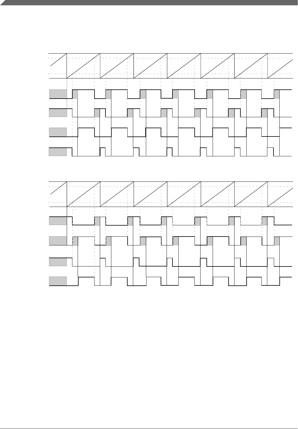
when the channel (n+1) match (FTM counter = C(n+1)V) occurs, the channel (n+1)
output remains at the high value until the end of the deadtime delay when the channel (n
+1) output is cleared.
FTM counter
channel (n+1) match
channel (n) match
channel (n) output
(before deadtime
insertion)
channel (n+1) output
(before deadtime
insertion)
channel (n) output
(after deadtime
insertion)
channel (n+1) output
(after deadtime
insertion)
Figure 45-75. Deadtime insertion with ELSB:ELSA = 1:0, POL(n) = 0, and POL(n+1) = 0
FTM counter
channel (n+1) match
channel (n) output
(before deadtime
insertion)
channel (n+1) output
(before deadtime
insertion)
channel (n) output
(after deadtime
insertion)
channel (n+1) output
(after deadtime
insertion)
channel (n) match
Figure 45-76. Deadtime insertion with ELSB:ELSA = X:1, POL(n) = 0, and POL(n+1) = 0
NOTE
• The deadtime feature must be used only in Complementary
mode.
• The deadtime feature is not available in Output Compare
mode.
45.5.16.1 Separated Deadtime by Pair of Channels
The separated deadtime value by pair of channels allows that each pair of channels has its
own deadtime value (i.e., bits DTVALEX[3:0], DTPS[1:0], and DTVAL[5:0]).
Functional Description
S32K1xx Series Reference Manual, Rev. 7, 04/2018
1308 NXP Semiconductors
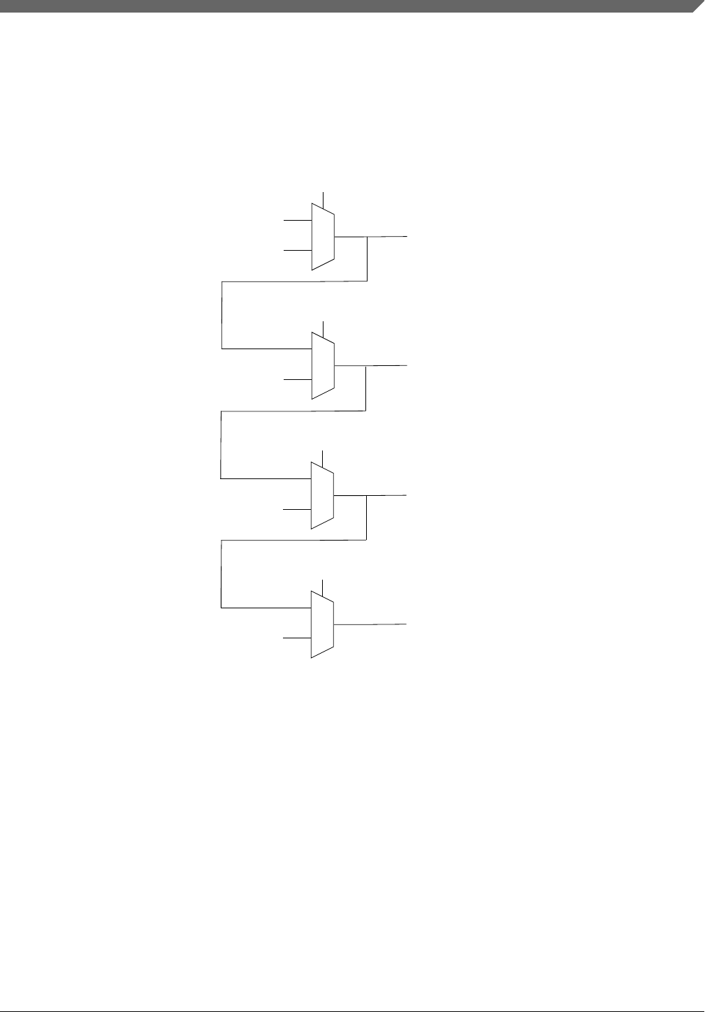
The registers PAIR0DEADTIME, PAIR1DEADTIME, PAIR2DEADTIME, and
PAIR3DEADTIME are available according to the FTM configuration.
The figure below describes how the deadtime value is defined by each pair according to
the FTM configuration.
0
1
Does the pair 0 have separated
deadtime value?
register DEADTIME
register PAIR0DEADTIME
pair 0 DTVALEX[3:0],
DTPS[1:0], and DTVAL[5:0]
0
1
Does the pair 1 have separated
deadtime value?
register PAIR1DEADTIME
pair 1 DTVALEX[3:0],
DTPS[1:0], and DTVAL[5:0]
0
1
Does the pair 2 have separated
deadtime value?
register PAIR2DEADTIME
pair 2 DTVALEX[3:0],
DTPS[1:0], and DTVAL[5:0]
0
1
Does the pair 3 have separated
deadtime value?
register PAIR3DEADTIME
pair 3 DTVALEX[3:0],
DTPS[1:0], and DTVAL[5:0]
Figure 45-77. Separated Deadtime by Pair of Channels
The writes to the register DEADTIME also update the available registers
PAIR(j)DEADTIME (where j is the pair of channels). Because of this, the write to the
register DEADTIME should be done before the writes to the registers
PAIR(j)DEADTIME.
If the pair 0 of channels has separated deadtime value, then the reads of the register
DEADTIME return the read value of the register PAIR0DEADTIME. Otherwise, the
read value is the value of the register DEADTIME.
Chapter 45 FlexTimer Module (FTM)
S32K1xx Series Reference Manual, Rev. 7, 04/2018
NXP Semiconductors 1309
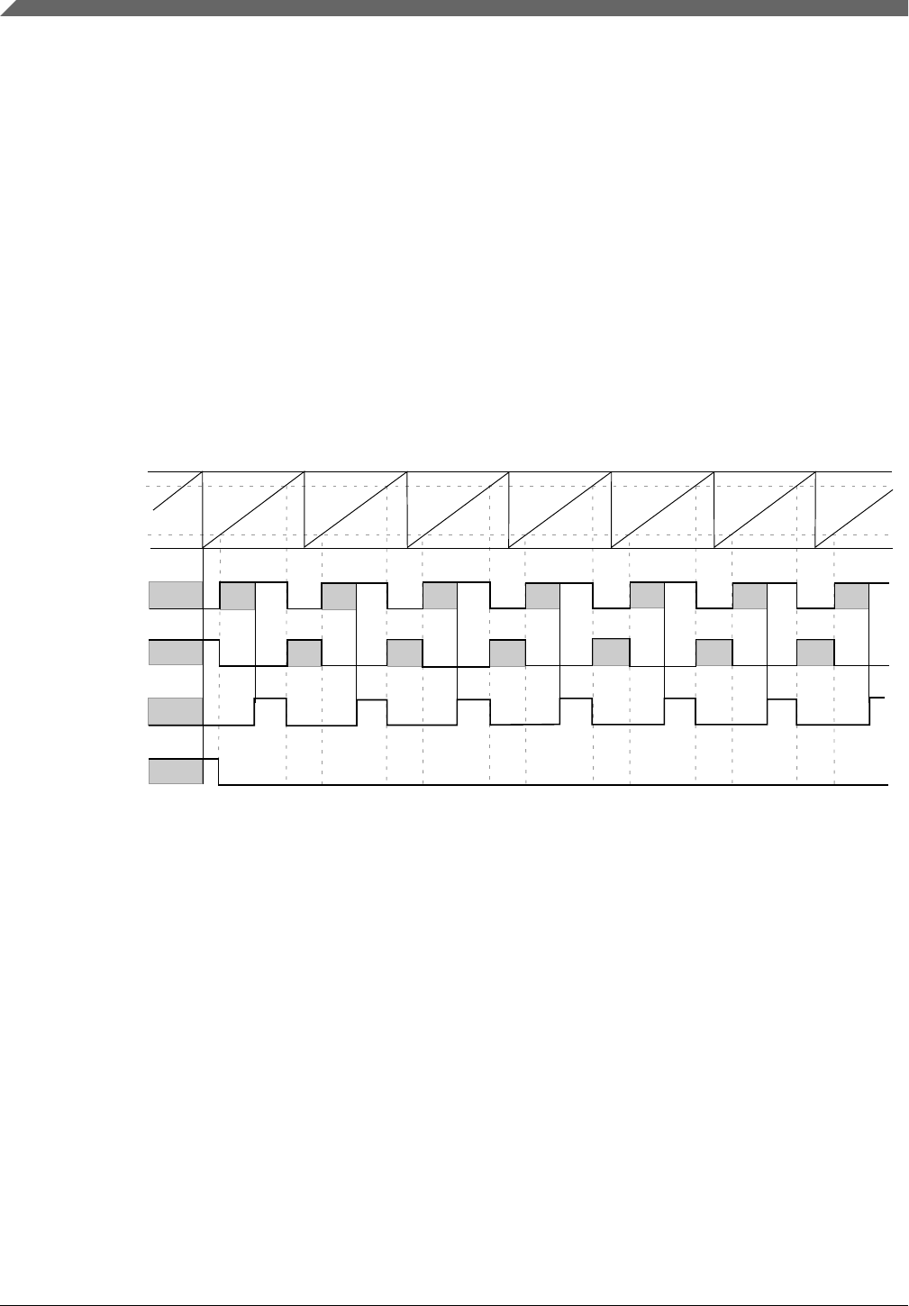
45.5.16.2 Deadtime insertion corner cases
If (PS[2:0] is cleared), (DTPS[1:0] = 0:0 or DTPS[1:0] = 0:1):
• and the deadtime delay is greater than or equal to the channel (n) duty cycle ((C(n
+1)V – C(n)V) × FTM input clock), then the channel (n) output is always the
inactive value (POL(n) bit value).
• and the deadtime delay is greater than or equal to the channel (n+1) duty cycle
((MOD – CNTIN + 1 – (C(n+1)V – C(n)V) ) × FTM input clock), then the channel
(n+1) output is always the inactive value (POL(n+1) bit value).
Although, in most cases the deadtime delay is not comparable to channels (n) and (n+1)
duty cycle, the following figures show examples where the deadtime delay is comparable
to the duty cycle.
FTM counter
channel (n+1) match
channel (n) match
channel (n) output
(before deadtime
insertion)
channel (n) output
(after deadtime
insertion)
channel (n+1) output
(before deadtime
insertion)
channel (n+1) output
(after deadtime
insertion)
Figure 45-78. Example of the deadtime insertion (channel (n) ELSB:ELSA = 1:0, POL(n) =
0, and POL(n+1) = 0) when the deadtime delay is comparable to channel (n+1) duty cycle
Functional Description
S32K1xx Series Reference Manual, Rev. 7, 04/2018
1310 NXP Semiconductors

FTM counter
channel (n+1) match
channel (n) match
channel (n) output
(before deadtime
insertion)
channel (n) output
(after deadtime
insertion)
channel (n+1) output
(before deadtime
insertion)
channel (n+1) output
(after deadtime
insertion)
Figure 45-79. Example of the deadtime insertion (channel (n) ELSB:ELSA = 1:0, POL(n) =
0, and POL(n+1) = 0) when the deadtime delay is comparable to channels (n) and (n+1)
duty cycle
45.5.17 Output mask
The output mask can be used to force channels output to their inactive state through
software. For example: to control a BLDC motor.
Any write to the OUTMASK register updates its write buffer. The OUTMASK register is
updated with its buffer value by PWM synchronization; see OUTMASK register
synchronization.
If CH(n)OM = 1, then the channel (n) output is forced to its inactive state (POLn bit
value). If CH(n)OM = 0, then the channel (n) output is unaffected by the output mask.
See the following figure.
Chapter 45 FlexTimer Module (FTM)
S32K1xx Series Reference Manual, Rev. 7, 04/2018
NXP Semiconductors 1311
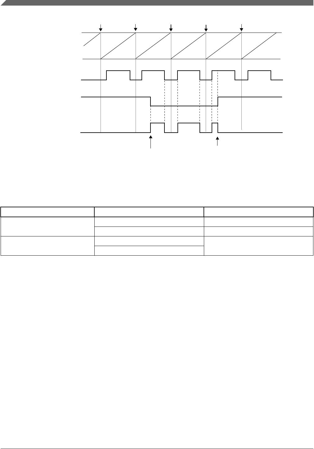
FTM counter
channel (n) output
(before output mask)
channel (n) output
(after output mask)
the beginning of new PWM cycles
configured PWM signal starts
to be available in the channel (n) output
channel (n) output is disabled
CH(n)OM bit
Figure 45-80. Output mask with POLn = 0
The following table shows the output mask result before the polarity control.
Table 45-14. Output mask result for channel (n) before the polarity control
CH(n)OM Output Mask Input Output Mask Result
0 inactive state inactive state
active state active state
1 inactive state inactive state
active state
45.5.18 Fault Control
The fault control is enabled if FAULTM[1:0] ≠ 0:0.
FTM can have up to four fault inputs. FAULTnEN bit (where n = 0, 1, 2, 3) enables the
fault input n and FFLTRnEN bit enables the fault input n filter. FFVAL[3:0] bits select
the value of the enabled filter in each enabled fault input.
If FLTPS[3:0] = 0, the fault input after being synchronized by FTM input clock is the
filter input.
Functional Description
S32K1xx Series Reference Manual, Rev. 7, 04/2018
1312 NXP Semiconductors
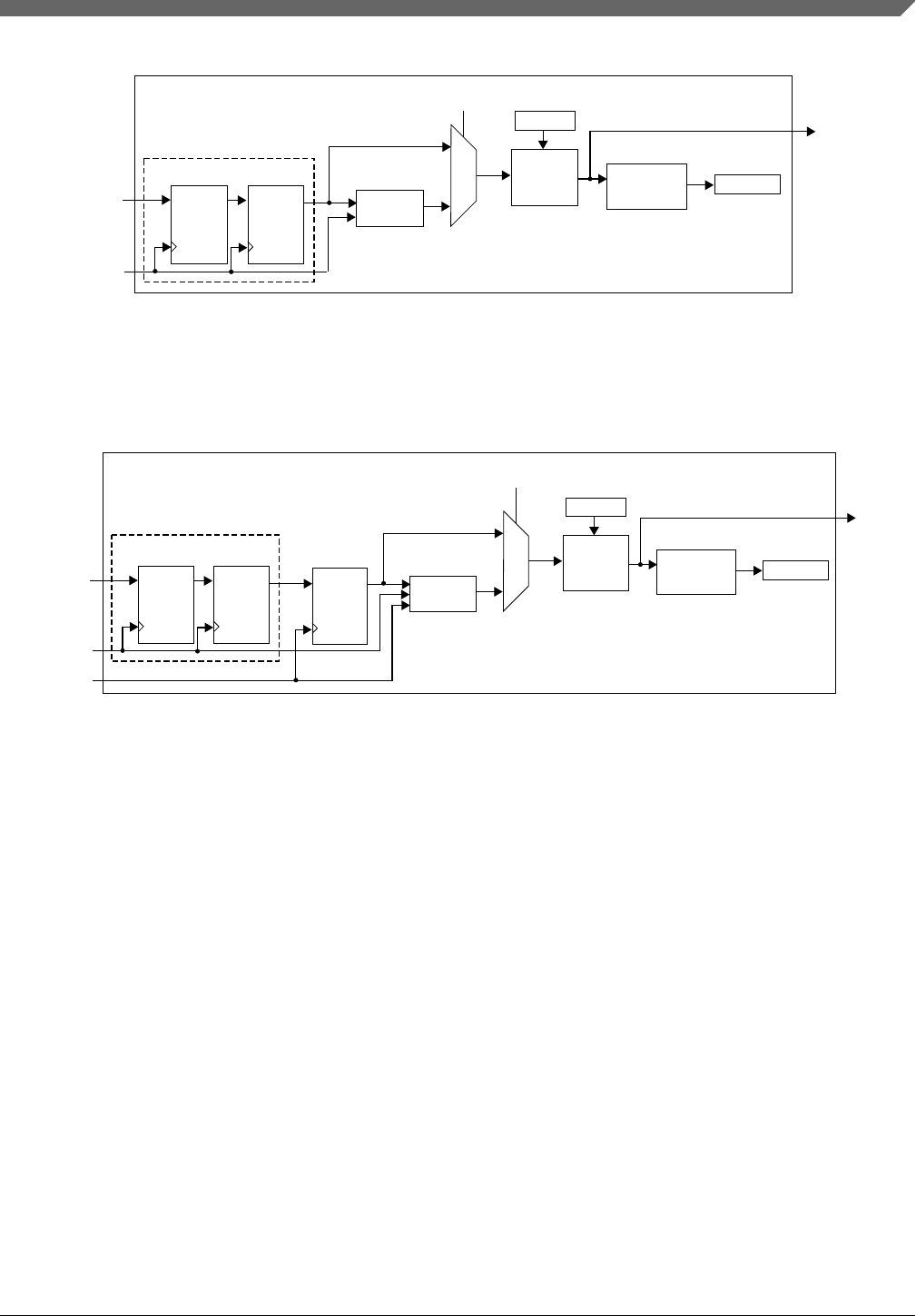
fault input (n)
synchronizer
fault input
(n) value
FAULTFn
0
1
rising edge
detector
fault input
polarity
control
filter
CLK CLK
D D Q
Q
FLTnPOL
is filter
enabled?
FTM input clock
Figure 45-81. Diagram for Fault Control when FLTPS[3:0] = 0
If FLTPS[3:0] ≠ 0, the fault input after being synchronized by FTM input clock and being
sampled by FTM filter clock is the filter input.
fault input (n)
synchronizer
fault input
(n) value
FAULTFn
0
1
rising edge
detector
fault input
polarity
control
filter
CLK CLK
D D Q
Q
FLTnPOL
is filter
enabled?
FTM input clock
CLK
DQ
FTM filter clock
Figure 45-82. Diagram for Fault Control when FLTPS[3:0] ≠ 0
When there is a state change in the fault input (n), the counter is reset and starts counting
up. As long as the new state is stable on the fault input (n), the counter continues to
increment. When the counter is equal to FFVAL[3:0] bits, the new fault input (n) value is
validated. It is then transmitted as a pulse to the edge detector.
If the opposite edge appears on the fault input (n) before it can be validated, the counter is
reset. At the next input transition, the counter starts counting again. If a pulse is sampled
as a value less than FFVAL[3:0] consecutive rising edges of FTM filter clock, it is
regarded as a glitch and is not passed on to the edge detector.
Chapter 45 FlexTimer Module (FTM)
S32K1xx Series Reference Manual, Rev. 7, 04/2018
NXP Semiconductors 1313
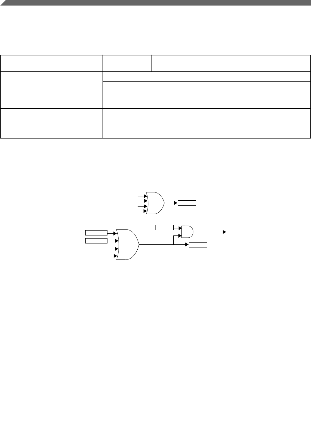
The table below shows the delay that is added by the FTM fault input filter according to
its configuration.
Table 45-15. FTM Fault Input Filter Delay
FTM fault input filter FLTPS[3:0] bits Number of rising edges between the selected edge on fault
input and forcing the channels outputs to their safe values
• fault input does not have the input
filter, or
• fault input filter is disabled
(FFLTRnEN = 0 or FFVAL[3:0] =
0)
FLTPS[3:0] = 0 • 3 rising edges of FTM input clock
FLTPS[3:0] ≠ 0 • 3 rising edges of FTM input clock, plus
• 1 rising edge of FTM filter clock
• fault inputl has the input filter, and
• fault input filter is enabled
(FFLTRnEN = 1 and FFVAL[3:0] ≠
0)
FLTPS[3:0] = 0 • (4 + FFVAL[3:0]) rising edges of FTM input clock
FLTPS[3:0] ≠ 0 • 4 rising edges of FTM input clock, plus
• (1 + FFVAL[3:0]) rising edges of FTM filter clock
If the fault control and fault input (n) are enabled, and the selected edge at the fault input
(n) is detected, then a fault condition has occurred and the FAULTFn bit is set. The
FAULTF bit is the logic OR of FAULTFn[3:0] bits. See the following figure.
fault interrupt
FAULTIE
FAULTIN
fault input 0 value
fault input 1 value
fault input 2 value
fault input 3 value
FAULTF
FAULTF0
FAULTF1
FAULTF2
FAULTF3
Figure 45-83. FAULTF and FAULTIN bits and fault interrupt
If the fault control is enabled (FAULTM[1:0] ≠ 0:0), a fault condition has occurred, and
(FAULTENj = 1, where j is the pair j of the channels), then the channels (n) and (n+1)
outputs are forced to their safe values:
• channel (n) output takes the POL(n) bit value
• channel (n+1) output takes the POL(n+1) bit value
The fault interrupt is generated when (FAULTF = 1) and (FAULTIE = 1). This interrupt
request remains set until:
• Software clears the FAULTF bit by reading FAULTF bit as 1 and writing 0 to it
• Software clears the FAULTIE bit
• A reset occurs
Functional Description
S32K1xx Series Reference Manual, Rev. 7, 04/2018
1314 NXP Semiconductors
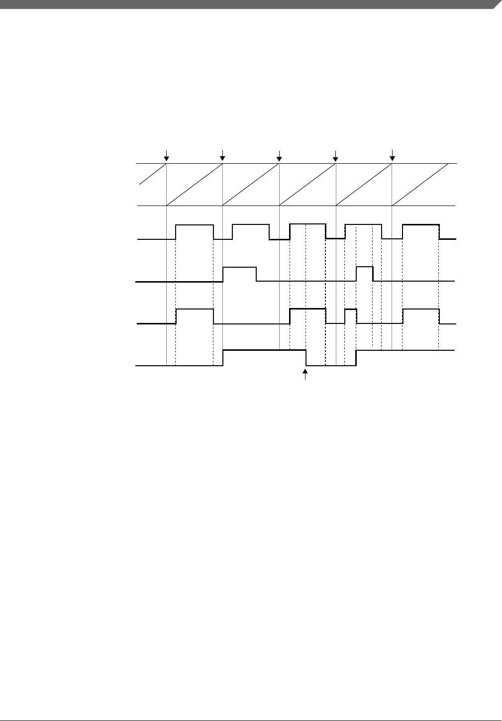
45.5.18.1 Automatic fault clearing
If the automatic fault clearing is selected (FAULTM[1:0] = 1:1), then the channels output
disabled by fault control is again enabled when the fault input signal (FAULTIN) returns
to zero and a new PWM cycle begins. See the following figure.
FTM counter
channel (n) output
(before fault control)
FAULTIN bit
channel (n) output
the beginning of new PWM cycles
FAULTF bit
FAULTF bit is cleared
The channel (n) output is after the fault control with automatic fault clearing and POLn = 0.
NOTE
Figure 45-84. Fault control with automatic fault clearing
45.5.18.2 Manual fault clearing
If the manual fault clearing is selected (FAULTM[1:0] = 0:1 or 1:0), then the channels
output disabled by fault control is again enabled when the FAULTF bit is cleared and a
new PWM cycle begins. See the following figure.
Chapter 45 FlexTimer Module (FTM)
S32K1xx Series Reference Manual, Rev. 7, 04/2018
NXP Semiconductors 1315
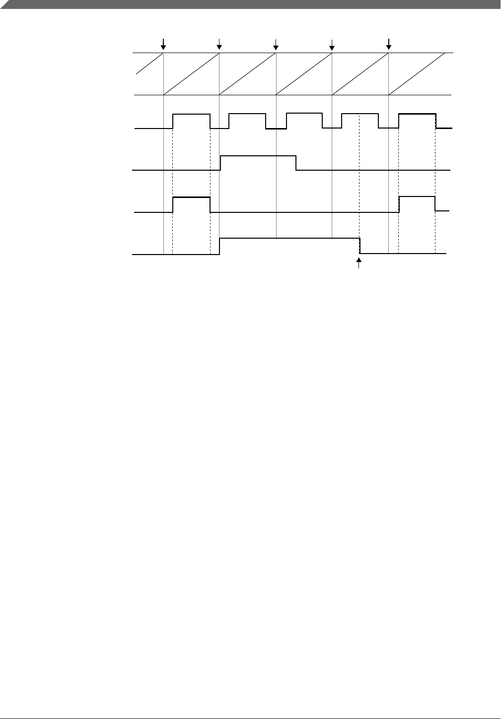
FTM counter
channel (n) output
(before fault control)
FAULTIN bit
channel (n) output
the beginning of new PWM cycles
FAULTF bit
FAULTF bit is cleared
The channel (n) output is after the fault control with manual fault clearing and POLn = 0.
NOTE
Figure 45-85. Fault control with manual fault clearing
45.5.18.3 Fault inputs polarity control
The FLTjPOL bit selects the fault input j polarity, where j = 0, 1, 2, 3:
• If FLTjPOL = 0, the fault j input polarity is high, so the logical one at the fault input j
indicates a fault.
• If FLTjPOL = 1, the fault j input polarity is low, so the logical zero at the fault input j
indicates a fault.
45.5.19 Polarity Control
The POLn bit selects the channel (n) output polarity:
• If POLn = 0, the channel (n) output polarity is high, so the logical one is the active
state and the logical zero is the inactive state.
• If POLn = 1, the channel (n) output polarity is low, so the logical zero is the active
state and the logical one is the inactive state.
Functional Description
S32K1xx Series Reference Manual, Rev. 7, 04/2018
1316 NXP Semiconductors

45.5.20 Initialization
The initialization forces the CH(n)OI bit value to the channel (n) output when 1 is written
to the INIT bit.
The initialization depends on COMP and DTEN bits. The following table shows the
values that channels (n) and (n+1) are forced by initialization when the COMP and
DTEN bits are zero.
Table 45-16. Initialization behavior when (COMP = 0 and DTEN = 0)
CH(n)OI CH(n+1)OI Channel (n) Output Channel (n+1) Output
0 0 is forced to zero is forced to zero
0 1 is forced to zero is forced to one
1 0 is forced to one is forced to zero
1 1 is forced to one is forced to one
The following table shows the values that channels (n) and (n+1) are forced by
initialization when (COMP = 1) or (DTEN = 1).
Table 45-17. Initialization behavior when (COMP = 1 or DTEN = 1)
CH(n)OI CH(n+1)OI Channel (n) Output Channel (n+1) Output
0 X is forced to zero is forced to one
1 X is forced to one is forced to zero
Note
The initialization feature must be used only with disabled FTM
counter. See the description of the CLKS field in the Status and
Control register.
45.5.21 Features Priority
The following figure shows the priority of the features used at the generation of channels
(n) and (n+1) outputs signals.
Chapter 45 FlexTimer Module (FTM)
S32K1xx Series Reference Manual, Rev. 7, 04/2018
NXP Semiconductors 1317
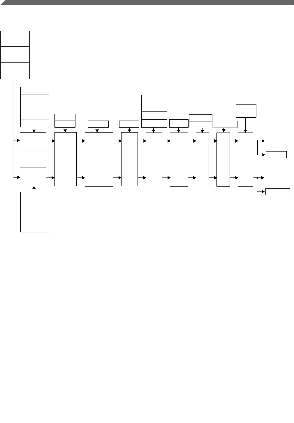
Note:
Pair channels (m) - channels (n) and (n+1)
initialization
complementary
mode
inverting
software
output
control
deadtime
insertion output
mask
fault
control
polarity
control
FTM counter
QUADEN
DECAPEN(m)
COMBINE(m)
CPWMS
C(n)V
channel (n)
ELSB
generation of
channel (n)
output signal
generation of
channel (n+1)
output signal
C(n+1)V
channel (n+1)
output
CH(n)OI
CH(n+1)OI COMP(m) INV(m)EN
CH(n)OC
CH(n)OCV
CH(n+1)OC
CH(n+1)OCV DTEN(m)
CH(n)OM
CH(n+1)OM
FAULTEN(m)
POL(n)
POL(n+1)
MCOMBINE(m)
The channels (n) and (n+1) are in Output Compare, EPWM, CPWM, Combine or Modified Combine PWM modes.
channel (n)
output
channel (n)
ELSA
channel (n)
MSA
channel (n)
MSB
channel (n+1)
MSB
channel (n+1)
MSA
channel (n+1)
ELSB
channel (n+1)
ELSA
channel (n)
CHOV
channel (n+1)
CHOV
Figure 45-86. Priority of the features used at the generation of channels (n) and (n+1)
output
NOTE
The Initialization must not be used with Inverting and Software
Output Control Mode.
45.5.22 External Trigger
If the CH(n)TRIG bit (register EXTTRIG) is set, where n = 0, 1, 2, 3, 4, 5, 6 or 7, then
the FTM generates a trigger when the channel (n) match occurs (FTM counter = C(n)V)
at the FTM external trigger output.
The width of a channel (n) trigger is one FTM input clock and the FTM is able to
generate multiple triggers in one PWM period. See the figure below.
Functional Description
S32K1xx Series Reference Manual, Rev. 7, 04/2018
1318 NXP Semiconductors
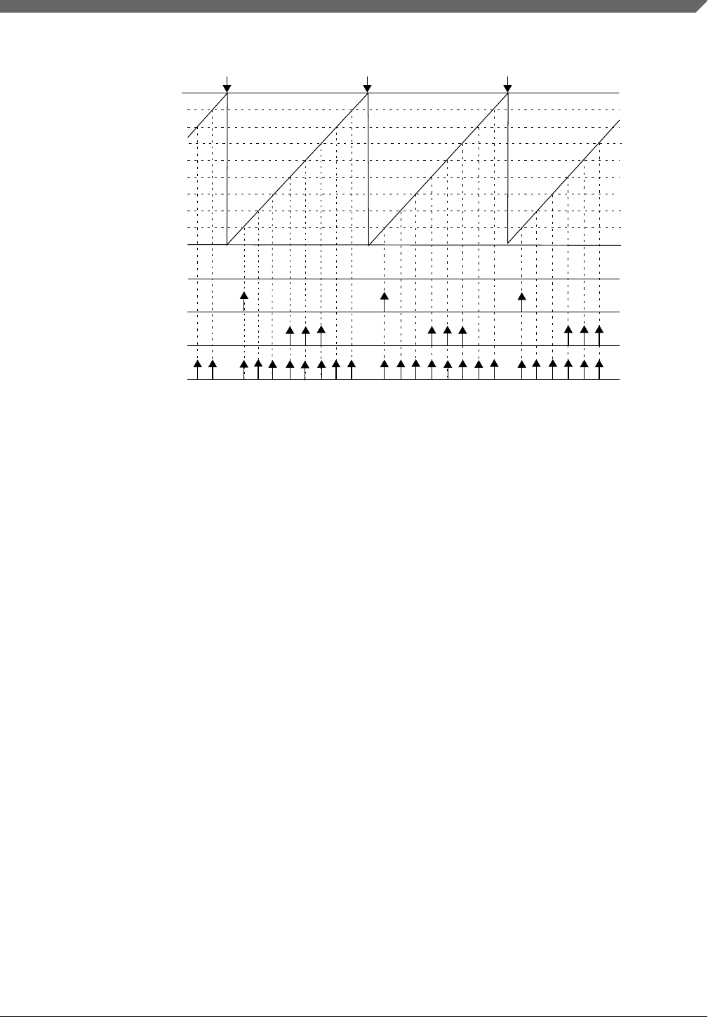
(a) CH0TRIG = 0, CH1TRIG = 0, CH2TRIG = 0, CH3TRIG = 0, CH4TRIG = 0, CH5TRIG = 0, CH6TRIG = 0, CH7TRIG = 0
(b) CH0TRIG = 1, CH1TRIG = 0, CH2TRIG = 0, CH3TRIG = 0, CH4TRIG = 0, CH5TRIG = 0, CH6TRIG = 0, CH7TRIG = 0
(c) CH0TRIG = 0, CH1TRIG = 0, CH2TRIG = 0, CH3TRIG = 1, CH4TRIG = 1, CH5TRIG = 1, CH6TRIG = 0, CH7TRIG = 0
(d) CH0TRIG = 1, CH1TRIG = 1, CH2TRIG = 1, CH3TRIG = 1, CH4TRIG = 1, CH5TRIG = 1, CH6TRIG = 1, CH7TRIG = 1
MOD
FTM counter = C5V
FTM counter = C4V
FTM counter = C3V
FTM counter = C2V
FTM counter = C1V
FTM counter = C0V
CNTIN
(a)
(b)
(c)
(d)
FTM counter = C6V
FTM counter = C7V
Note
the beginning of new PWM periods
Figure 45-87. External Trigger
45.5.23 Initialization Trigger
Initialization trigger allows FTM to generate a trigger in some specific points of FTM
counter cycle. This feature is controlled by the bits INITTRIGEN and ITRIGR. The
INITTRIGEN bit enables the initialization trigger generation and the ITRIGR bit selects
when the initialization trigger is generated.
If INITTRIGEN = 1 and ITRIGR = 1, then the initialization trigger is generated when
FTM counter reaches a reload point according to the frequency of the reload
opportunities (Reload Points).
NOTE
For this configuration of initilization trigger and in CPWM
mode, the bits CNTMAX and CNTMIN select where the
initialization trigger is generated.
If INITTRIGEN = 1 and ITRIGR = 0, then the initialization trigger is generated when
FTM counter is updated with the CNTIN register value. See the cases below.
1. When FTM counter is updated with CNTIN register value automatically.
Chapter 45 FlexTimer Module (FTM)
S32K1xx Series Reference Manual, Rev. 7, 04/2018
NXP Semiconductors 1319
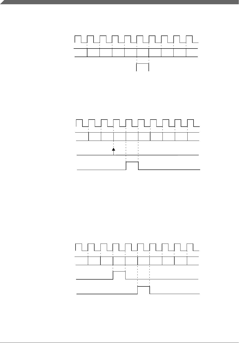
CPWMS = 0
0x0C 0x0D 0x0E 0x0F 0x00 0x01 0x02 0x03 0x04 0x05
initialization trigger
FTM counter
FTM input clock
CNTIN = 0x0000
MOD = 0x000F
INITTRIGEN = 0
ITRIGR = 0
Figure 45-88. Example of the generation of the initialization trigger in the case 1.
2. When there is a write to CNT register.
0x04 0x05 0x06 0x00 0x01 0x02 0x03 0x04 0x05 0x06
initialization trigger
write to CNT
FTM counter
FTM input clock
CPWMS = 0
CNTIN = 0x0000
MOD = 0x000F
INITTRIGEN = 0
ITRIGR = 0
Figure 45-89. Example of the generation of the initialization trigger in the case 2.
NOTE
This behavior is not available in CPWM mode.
3. When there is the FTM counter synchronization.
0x04 0x05 0x06 0x07 0x00 0x01 0x02 0x03 0x04 0x05
initialization trigger
FTM counter
synchronization
FTM counter
FTM input clock
CPWMS = 0
CNTIN = 0x0000
MOD = 0x000F
INITTRIGEN = 0
ITRIGR = 0
Figure 45-90. Example of the generation of the initialization trigger in the case 3.
NOTE
This behavior is not available in CPWM mode.
Functional Description
S32K1xx Series Reference Manual, Rev. 7, 04/2018
1320 NXP Semiconductors
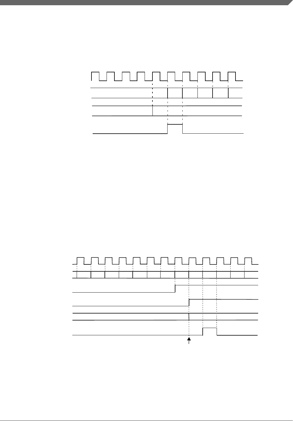
4. If (CNT = CNTIN), (CLKS[1:0] = 0:0), and a value different from zero is written to
CLKS[1:0] bits.
0x00
00 01
0x01 0x02 0x03 0x04 0x05
initialization trigger
CLKS[1:0] bits
FTM counter
FTM input clock
CPWMS = 0
CNTIN = 0x0000
MOD = 0x000F
INITTRIGEN = 0
ITRIGR = 0
Figure 45-91. Example of the generation of the initialization trigger in the case 4.
NOTE
This behavior is not available in CPWM mode.
5. If the channel (n) is in Input Capture mode, (ICRST = 1) and the selected input
capture event occurs in the channel (n) input.
FTM input clock
FTM counter
channel (n) input
CHF bit
C(n)V XX 0x27
selected channel (n) input event: rising edge
channel (n) input after its synchronizer and filter
CNTIN = 0x0000
MOD = 0xFFFF
PS[2:0] = 0
ICRST = 1
CPWMS = 0
INITTRIGEN = 0
ITRIGR = 0
... 0x27 ...
0x00 0x01 0x02 0x030x260x250x240x230x220x210x20
initialization trigger
Figure 45-92. Example of the generation of the initialization trigger in the case 5.
Chapter 45 FlexTimer Module (FTM)
S32K1xx Series Reference Manual, Rev. 7, 04/2018
NXP Semiconductors 1321
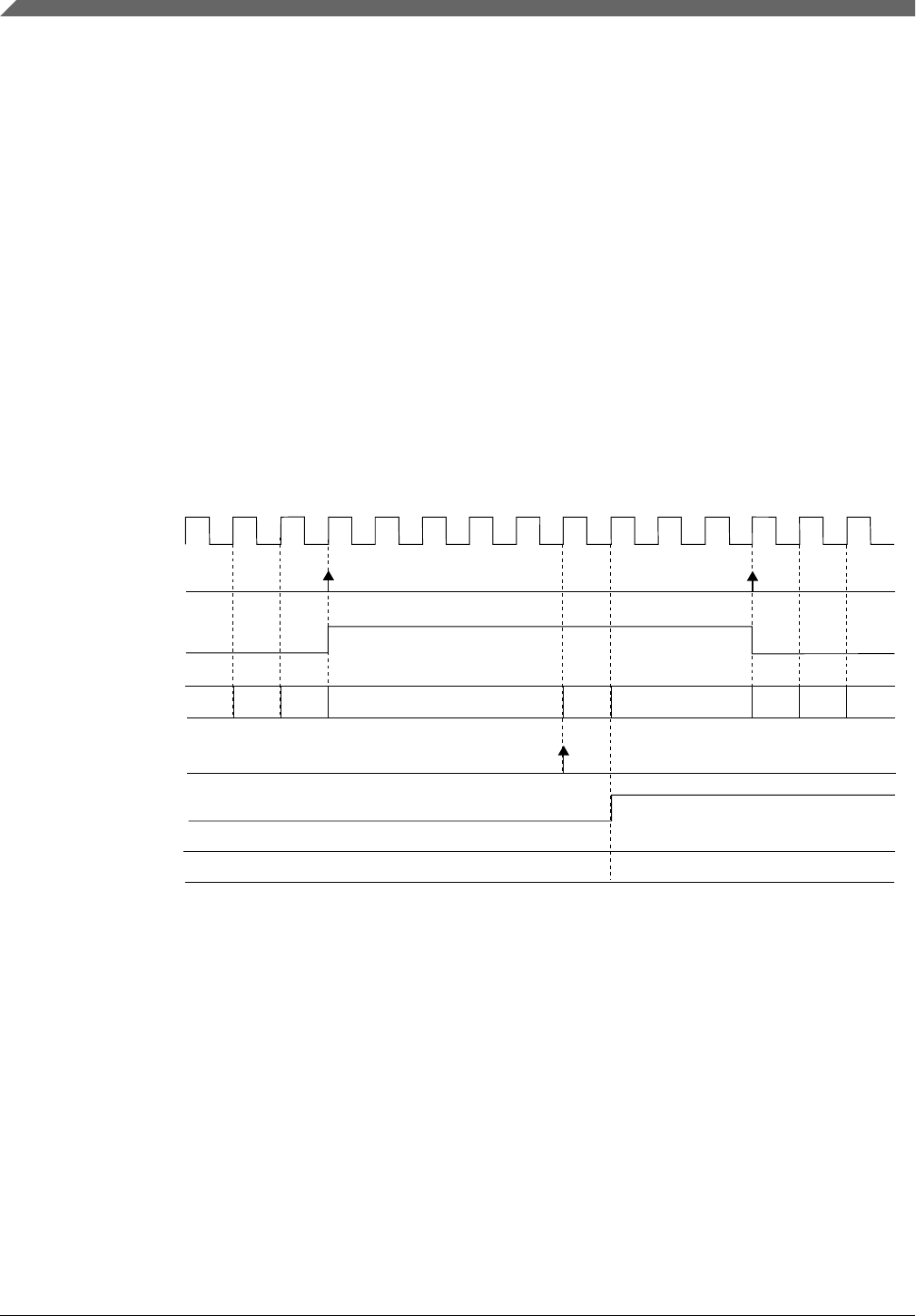
45.5.24 Capture Test Mode
The Capture Test mode allows to test the CnV registers, the FTM counter and the
interconnection logic between the FTM counter and CnV registers.
In this test mode, all channels must be configured for Input Capture Mode and FTM
counter must be configured to the Up counting.
When the Capture Test mode is enabled (CAPTEST = 1), the FTM counter is frozen and
any write to CNT register updates directly the FTM counter; see the following figure.
After it was written, all CnV registers are updated with the written value to CNT register
and CHF bits are set. Therefore, the FTM counter is updated with its next value
according to its configuration. Its next value depends on CNTIN, MOD, and the written
value to FTM counter.
The next reads of CnV registers return the written value to the FTM counter and the next
reads of CNT register return FTM counter next value.
FTM counter clock
write to MODE
CAPTEST bit
FTM counter
write to CNT
CHF bit
CnV
Note:
- FTM counter is in free running
- FTMEN = 1
- FTM channel (n) is in Input Capture Mode
0x0300
0x78AC
set CAPTEST clear CAPTEST
write 0x78AC
0x1056
0x1053 0x1055
0x1054 0x78AC 0x78AD 0x78AE 0x78AF 0x78B0
Figure 45-93. Capture Test Mode
45.5.25 DMA
The channel generates a DMA transfer request according to DMA and CHIE bits. See the
following table.
Functional Description
S32K1xx Series Reference Manual, Rev. 7, 04/2018
1322 NXP Semiconductors
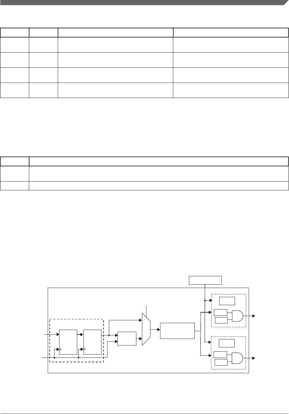
Table 45-18. Channel DMA transfer request
DMA CHIE Channel DMA Transfer Request Channel Interrupt
0 0 The channel DMA transfer request is not
generated.
The channel interrupt is not generated.
0 1 The channel DMA transfer request is not
generated.
The channel interrupt is generated if (CHF = 1).
1 0 The channel DMA transfer request is not
generated.
The channel interrupt is not generated.
1 1 The channel DMA transfer request is generated if
(CHF = 1).
The channel interrupt is not generated.
If DMA = 1, the CHF bit is cleared either by channel DMA transfer done or reading
CnSC while CHF is set and then writing a zero to CHF bit according to CHIE bit. See the
following table.
Table 45-19. Clear CHF bit when DMA = 1
CHIE How CHF Bit Can Be Cleared
0 CHF bit is cleared either when the channel DMA transfer is done or by reading CnSC while CHF is set and then
writing a 0 to CHF bit.
1 CHF bit is cleared when the channel DMA transfer is done.
45.5.26 Dual Edge Capture Mode
The dual edge capture mode is enabled if DECAPEN = 1. This mode allows to measure a
pulse width or period of the channel (n) input where n = 0, 2, 4 or 6. The channel (n)
filter can be enabled for n = 0 or 2.
channel (n) input
synchronizer
filter
dual edge capture
mode logic
is filter
enabled?
FTM counter
CLK CLK
DQDQ
0
1
FTM input clock
channel (n)
interrupt
CnV
CHIE
CHF
channel (n)
channel (n+1)
interrupt
CnV
CHIE
CHF
channel (n+1)
Figure 45-94. Diagram for Dual Edge Capture Mode when FLTPS[3:0] = 0
Chapter 45 FlexTimer Module (FTM)
S32K1xx Series Reference Manual, Rev. 7, 04/2018
NXP Semiconductors 1323
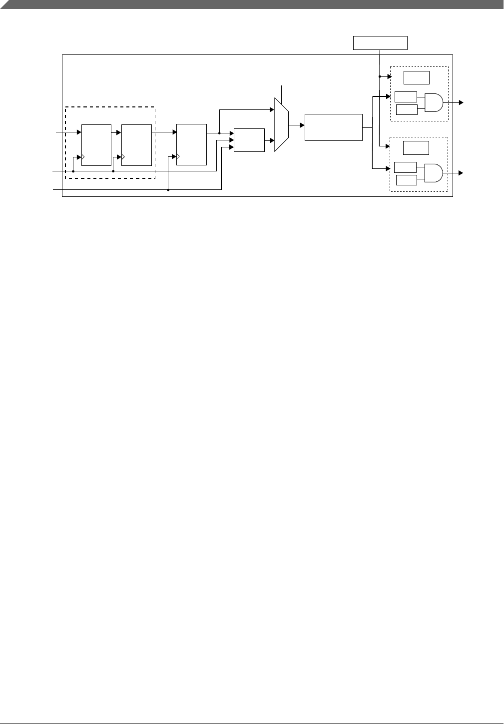
channel (n) input
synchronizer
filter
dual edge capture
mode logic
is filter
enabled?
FTM counter
CLK CLK
DQDQ
0
1
FTM input clock
CLK
DQ
FTM filter clock
channel (n)
interrupt
CnV
CHIE
CHF
channel (n)
channel (n+1)
interrupt
CnV
CHIE
CHF
channel (n+1)
Figure 45-95. Diagram for Dual Edge Capture Mode when FLTPS[3:0] ≠ 0
The channel (n) MSA bit defines if the dual edge capture mode is one-shot or continuous.
The channel (n) ELSB:ELSA bits select the edge that is captured by channel (n), and
channel (n+1) ELSB:ELSA bits select the edge that is captured by channel (n+1). If both
channel (n) ELSB:ELSA and channel (n+1) ELSB:ELSA bits select the same edge, then
it is the period measurement. If these bits select different edges, then it is a pulse width
measurement.
In the dual edge capture mode, only channel (n) input is used and channel (n+1) input is
ignored.
If the selected edge by channel (n) bits is detected at channel (n) input, then channel (n)
CHF bit is set and the channel (n) interrupt is generated (if channel (n) CHIE = 1). If the
selected edge by channel (n+1) bits is detected at channel (n) input and (channel (n) CHF
= 1), then channel (n+1) CHF bit is set and the channel (n+1) interrupt is generated (if
channel (n+1) CHIE = 1).
The C(n)V register stores the FTM counter value when the selected edge by channel (n)
is detected at channel (n) input. The C(n+1)V register stores the FTM counter value when
the selected edge by channel (n+1) is detected at channel (n) input.
In this mode, a coherency mechanism (for channels (n) and (n+1)) ensures coherent data
when the C(n)V and C(n+1)V registers are read. The only requirement is that C(n)V must
be read before C(n+1)V.
Note
• The dual edge capture mode must be used with channel (n)
ELSB:ELSA = 0:1 or 1:0, channel (n+1) ELSB:ELSA =
0:1 or 1:0 and the FTM counter in Free running counter.
Functional Description
S32K1xx Series Reference Manual, Rev. 7, 04/2018
1324 NXP Semiconductors

45.5.26.1 One-Shot Capture mode
The One-Shot Capture mode is selected when (DECAPEN = 1), and (channel (n) MSA =
0). In this capture mode, only one pair of edges at the channel (n) input is captured. The
channel (n) ELSB:ELSA bits select the first edge to be captured, and channel (n+1)
ELSB:ELSA bits select the second edge to be captured.
The edge captures are enabled while DECAP bit is set. For each new measurement in
One-Shot Capture mode, first the channel (n) CHF and channel (n+1) CHF bits must be
cleared, and then the DECAP bit must be set.
In this mode, the DECAP bit is automatically cleared by FTM when the edge selected by
channel (n+1) is captured. Therefore, while DECAP bit is set, the one-shot capture is in
process. When this bit is cleared, both edges were captured and the captured values are
ready for reading in the C(n)V and C(n+1)V registers.
Similarly, when the channel (n+1) CHF bit is set, both edges were captured and the
captured values are ready for reading in the C(n)V and C(n+1)V registers.
45.5.26.2 Continuous Capture mode
The Continuous Capture mode is selected when (DECAPEN = 1), and (channel (n) MSA
= 1). In this capture mode, the edges at the channel (n) input are captured continuously.
The channel (n) ELSB:ELSA bits select the initial edge to be captured, and channel (n+1)
ELSB:ELSA bits select the final edge to be captured.
The edge captures are enabled while DECAP bit is set. For the initial use, first the
channel (n) CHF and channel (n+1) CHF bits must be cleared, and then DECAP bit must
be set to start the continuous measurements.
When the channel (n+1) CHF bit is set, both edges were captured and the captured values
are ready for reading in the C(n)V and C(n+1)V registers. The latest captured values are
always available in these registers even after the DECAP bit is cleared.
In this mode, it is possible to clear only the channel (n+1) CHF bit. Therefore, when the
channel (n+1) CHF bit is set again, the latest captured values are available in C(n)V and
C(n+1)V registers.
For a new sequence of the measurements in the Dual Edge Capture – Continuous mode,
clear the channel (n) CHF and channel (n+1) CHF bits to start new measurements.
Chapter 45 FlexTimer Module (FTM)
S32K1xx Series Reference Manual, Rev. 7, 04/2018
NXP Semiconductors 1325

45.5.26.3 Pulse width measurement
If the channel (n) is configured to capture rising edges (channel (n) ELSB:ELSA = 0:1)
and the channel (n+1) to capture falling edges (channel (n+1) ELSB:ELSA = 1:0), then
the positive polarity pulse width is measured. If the channel (n) is configured to capture
falling edges (channel (n) ELSB:ELSA = 1:0) and the channel (n+1) to capture rising
edges (channel (n+1) ELSB:ELSA = 0:1), then the negative polarity pulse width is
measured.
The pulse width measurement can be made in One-Shot Capture mode or Continuous
Capture mode.
The following figure shows an example of the Dual Edge Capture – One-Shot mode used
to measure the positive polarity pulse width. The DECAPEN bit selects the Dual Edge
Capture mode, so it remains set. The DECAP bit is set to enable the measurement of next
positive polarity pulse width. The channel (n) CHF bit is set when the first edge of this
pulse is detected, that is, the edge selected by channel (n) ELSB:ELSA bits. The channel
(n+1) CHF bit is set and DECAP bit is cleared when the second edge of this pulse is
detected, that is, the edge selected by channel (n+1) ELSB:ELSA bits. Both DECAP and
channel (n+1) CHF bits indicate when two edges of the pulse were captured and the
C(n)V and C(n+1)V registers are ready for reading.
Functional Description
S32K1xx Series Reference Manual, Rev. 7, 04/2018
1326 NXP Semiconductors
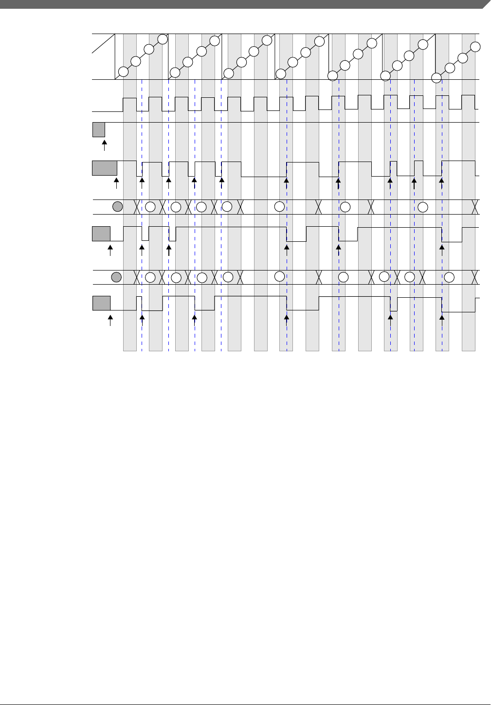
channel (n) input
(after the filter
DECAPEN bit
C(n+1)V
FTM counter
clear channel (n+1) CHF
problem 1 problem 2
2
1
2
3
channel input)
DECAP bit
set DECAPEN
set DECAP
5
6
7
8
10
3
4 6
5
Note
- The commands set DECAPEN, set DECAP, clear channel (n) CHF, and clear channel (n+1) CHF are made by the user.
4
9
11
12
13
14
9
10
7
8
15
16
17
18
19
20
21
22
23
24
25
26
27
28
15
16
19
20 22 24
- Problem 1: channel (n) input = 1, set DECAP, not clear channel (n) CHF, and clear channel (n+1) CHF.
- Problem 2: channel (n) input = 1, set DECAP, not clear channel (n) CHF, and not clear channel (n+1) CHF.
C(n)V
channel (n+1) CHF bit
channel (n) CHF bit
clear channel (n) CHF
1
Figure 45-96. Dual Edge Capture – One-Shot mode for positive polarity pulse width
measurement
The following figure shows an example of the Dual Edge Capture – Continuous mode
used to measure the positive polarity pulse width. The DECAPEN bit selects the Dual
Edge Capture mode, so it remains set. While the DECAP bit is set the configured
measurements are made. The channel (n) CHF bit is set when the first edge of the
positive polarity pulse is detected, that is, the edge selected by channel (n) ELSB:ELSA
bits. The channel (n+1) CHF bit is set when the second edge of this pulse is detected, that
is, the edge selected by channel (n+1) ELSB:ELSA bits. The channel (n+1) CHF bit
indicates when two edges of the pulse were captured and the C(n)V and C(n+1)V
registers are ready for reading.
Chapter 45 FlexTimer Module (FTM)
S32K1xx Series Reference Manual, Rev. 7, 04/2018
NXP Semiconductors 1327
channel (n) input
(after the filter
DECAPEN bit
C(n+1)V
FTM counter
clear channel (n+1) CHF
2
1
2
3
channel input)
DECAP bit
set DECAPEN
set DECAP
5
6
7
8
10
3
46
5
Note
- The commands set DECAPEN, set DECAP, clear channel (n) CHF, and clear channel (n+1) CHF are made by the user.
4
9
11
12
13
14
9
10
7
15
16
17
18
19
20
21
22
23
24
25
26
27
28
15
16 20
C(n)V
channel (n+1) CHF bit
channel (n) CHF bit
clear channel (n) CHF
1
812 22 24
11 19 21 23
Figure 45-97. Dual Edge Capture – Continuous mode for positive polarity pulse width
measurement
45.5.26.4 Period measurement
If the channels (n) and (n+1) are configured to capture consecutive edges of the same
polarity, then the period of the channel (n) input signal is measured. If both channels (n)
and (n+1) are configured to capture rising edges (channel (n) ELSB:ELSA = 0:1 and
channel (n+1) ELSB:ELSA = 0:1), then the period between two consecutive rising edges
is measured. If both channels (n) and (n+1) are configured to capture falling edges
(channel (n) ELSB:ELSA = 1:0 and channel (n+1) ELSB:ELSA = 1:0), then the period
between two consecutive falling edges is measured.
The period measurement can be made in One-Shot Capture mode or Continuous Capture
mode.
Functional Description
S32K1xx Series Reference Manual, Rev. 7, 04/2018
1328 NXP Semiconductors
The following figure shows an example of the Dual Edge Capture – One-Shot mode used
to measure the period between two consecutive rising edges. The DECAPEN bit selects
the Dual Edge Capture mode, so it remains set. The DECAP bit is set to enable the
measurement of next period. The channel (n) CHF bit is set when the first rising edge is
detected, that is, the edge selected by channel (n) ELSB:ELSA bits. The channel (n+1)
CHF bit is set and DECAP bit is cleared when the second rising edge is detected, that is,
the edge selected by channel (n+1) ELSB:ELSA bits. Both DECAP and channel (n+1)
CHF bits indicate when two selected edges were captured and the C(n)V and C(n+1)V
registers are ready for reading.
channel (n) input
(after the filter
DECAPEN bit
C(n+1)V
FTM counter
clear channel (n+1) CHF
problem 2
2
1
2
3
channel input)
DECAP bit
set DECAPEN
set DECAP
5
6
7
8
10
3
46
5
Note
- The commands set DECAPEN, set DECAP, clear channel (n) CHF, and clear channel (n+1) CHF are made by the user.
4
9
11
12
13
14
6
15
16
17
18
19
20
21
22
23
24
25
26
27
28
17 20
15 20 23
C(n)V
channel (n+1) CHF bit
channel (n) CHF bit
clear channel (n) CHF
1
- Problem 1: channel (n) input = 0, set DECAP, not clear channel (n) CHF, and not clear channel (n+1) CHF.
- Problem 2: channel (n) input = 1, set DECAP, not clear channel (n) CHF, and clear channel (n+1) CHF.
- Problem 3: channel (n) input = 1, set DECAP, not clear channel (n) CHF, and not clear channel (n+1) CHF.
problem 3
problem 1
7918 26
18
14 27
7
Figure 45-98. Dual Edge Capture – One-Shot mode to measure of the period between
two consecutive rising edges
The following figure shows an example of the Dual Edge Capture – Continuous mode
used to measure the period between two consecutive rising edges. The DECAPEN bit
selects the Dual Edge Capture mode, so it remains set. While the DECAP bit is set the
configured measurements are made. The channel (n) CHF bit is set when the first rising
Chapter 45 FlexTimer Module (FTM)
S32K1xx Series Reference Manual, Rev. 7, 04/2018
NXP Semiconductors 1329
edge is detected, that is, the edge selected by channel (n) ELSB:ELSA bits. The channel
(n+1) CHF bit is set when the second rising edge is detected, that is, the edge selected by
channel (n+1) ELSB:ELSA bits. The channel (n+1) CHF bit indicates when two edges of
the period were captured and the C(n)V and C(n+1)V registers are ready for reading.
channel (n) input
(after the filter
DECAPEN bit
C(n+1)V
FTM counter
clear channel (n+1) CHF
2
1
2
3
channel input)
DECAP bit
set DECAPEN
set DECAP
5
6
7
8
10
3
46
5
Note
- The commands set DECAPEN, set DECAP, clear channel (n) CHF, and clear channel (n+1) CHF are made by the user.
4
9
11
12
13
14
9
10
7
15
16
17
18
19
20
22
23
24
26
27
28
15
16 21
C(n)V
channel (n+1) CHF bit
channel (n) CHF bit
clear channel (n) CHF
1
812 22 24
11 19 21 23
25 27
23
20
19
17
7911 13 15
6810 12 1614 24
22
20
18 26
25
21
Figure 45-99. Dual Edge Capture – Continuous mode to measure of the period between
two consecutive rising edges
45.5.26.5 Read coherency mechanism
The Dual Edge Capture mode implements a read coherency mechanism between the
FTM counter value captured in C(n)V and C(n+1)V registers. The read coherency
mechanism is illustrated in the following figure. In this example, the channels (n) and (n
+1) are in Dual Edge Capture – Continuous mode for positive polarity pulse width
measurement. Thus, the channel (n) is configured to capture the FTM counter value when
there is a rising edge at channel (n) input signal, and channel (n+1) to capture the FTM
counter value when there is a falling edge at channel (n) input signal.
Functional Description
S32K1xx Series Reference Manual, Rev. 7, 04/2018
1330 NXP Semiconductors
When a rising edge occurs in the channel (n) input signal, the FTM counter value is
captured into channel (n) capture buffer. The channel (n) capture buffer value is
transferred to C(n)V register when a falling edge occurs in the channel (n) input signal.
C(n)V register has the FTM counter value when the previous rising edge occurred, and
the channel (n) capture buffer has the FTM counter value when the last rising edge
occurred.
When a falling edge occurs in the channel (n) input signal, the FTM counter value is
captured into channel (n+1) capture buffer. The channel (n+1) capture buffer value is
transferred to C(n+1)V register when the C(n)V register is read.
In the following figure, the read of C(n)V returns the FTM counter value when the event
1 occurred and the read of C(n+1)V returns the FTM counter value when the event 2
occurred.
read C(n+1)V
FTM counter
channel (n) input
(after the filter
channel input)
channel (n)
capture buffer
C(n)V
C(n+1)V
channel (n+1)
capture buffer
event 1
event 2
event 3
event 4
event 5
event 6 event 7
event 8
event 9
12 3 45 6 7 8 9
9
137
5
68
4
2
2
135 7
read C(n)V
Figure 45-100. Dual Edge Capture mode read coherency mechanism
C(n)V register must be read prior to C(n+1)V register in dual edge capture one-shot and
continuous modes for the read coherency mechanism works properly.
45.5.27 Quadrature Decoder Mode
The quadrature decoder mode is enabled if QUADEN = 1. The quadrature decoder mode
uses the input signals phase A and B to control the FTM counter increment and
decrement.
Chapter 45 FlexTimer Module (FTM)
S32K1xx Series Reference Manual, Rev. 7, 04/2018
NXP Semiconductors 1331
phase A input
phase B input
synchronizer
filtered phase A signal
PHAPOL PHBPOL
filtered phase B signal
synchronizer
CLK
DQ
CLK
DQ
CLK
DQ
CLK
DQ
filter
FTM counter
direction logic
FTM counter
0
1
FTM input clock
is filter
enabled?
filter
0
1
is filter
enabled?
FTM input clock
Figure 45-101. Diagram for Quadrature Decoder when FLTPS[3:0] = 0
phase A input
phase B input
synchronizer
filtered phase A signal
PHAPOL PHBPOL
filtered phase B signal
synchronizer
CLK
DQ
CLK
DQ
CLK
DQ
CLK
DQ
filter
FTM counter
direction logic
FTM counter
0
1
FTM input clock
is filter
enabled?
FTM input clock
CLK
D
CLK
DQ
FTM filter clock
filter
0
1
is filter
enabled?
Q
FTM filter clock
Figure 45-102. Diagram for Quadrature Decoder when FLTPS[3:0] ≠ 0
Each one of input signals phase A and B has a filter that is equivalent to the channel input
filter (Filter for Input Capture Mode). The phase A input filter is enabled by
PHAFLTREN bit and its value is defined by CH0FVAL[3:0] bits. The phase B input
filter is enabled by PHBFLTREN bit and its value is defined by CH1FVAL[3:0] bits.
Except for CH0FVAL[3:0] and CH1FVAL[3:0] bits, no channel logic is used in
quadrature decoder mode.
Functional Description
S32K1xx Series Reference Manual, Rev. 7, 04/2018
1332 NXP Semiconductors
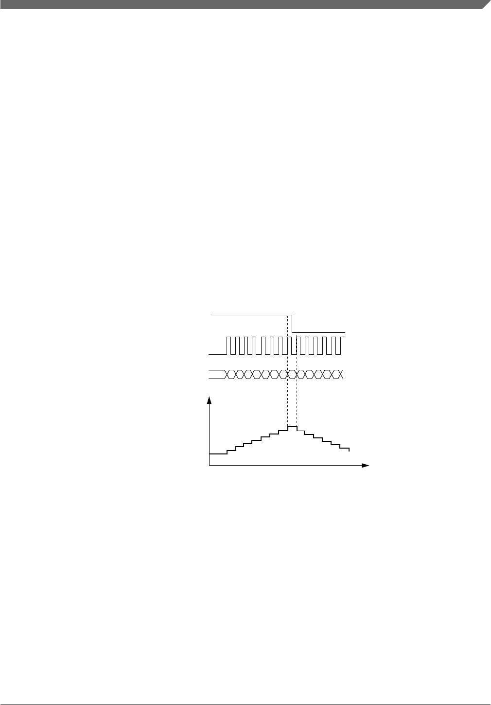
Note
The FTM counter is clocked by the phase A and B input signals
when quadrature decoder mode is enabled. Therefore it is
expected that the quadrature decoder mode be used only with
the FTM channels in input capture or output compare modes.
Note
An edge at phase A must not occur together an edge at phase B
and vice-versa.
The PHAPOL bit selects the polarity of the phase A input, and the PHBPOL bit selects
the polarity of the phase B input.
The QUADMODE selects the encoding mode used in the quadrature decoder mode. If
QUADMODE = 1, then the count and direction encoding mode is enabled; see the
following figure. In this mode, the phase B input value indicates the counting direction,
and the phase A input defines the counting rate. The FTM counter is updated when there
is a rising edge at phase A input signal.
phase B (counting direction)
phase A (counting rate)
FTM counter
increment/decrement
FTM counter
MOD
CNTIN
0x0000
Time
+1 +1 +1 +1 +1 +1 +1 +1 -1 -1 -1 -1 -1
Figure 45-103. Quadrature Decoder – Count and Direction Encoding mode
If QUADMODE = 0, then the phase A and phase B Encoding mode is enabled; see the
following figure. In this mode, the relationship between phase A and B signals indicates
the counting direction, and phase A and B signals define the counting rate. The FTM
counter is updated when there is an edge either at the phase A or phase B signals.
If PHAPOL = 0 and PHBPOL = 0, then the FTM counter increment happens when:
• there is a rising edge at phase A signal and phase B signal is at logic zero;
• there is a rising edge at phase B signal and phase A signal is at logic one;
Chapter 45 FlexTimer Module (FTM)
S32K1xx Series Reference Manual, Rev. 7, 04/2018
NXP Semiconductors 1333
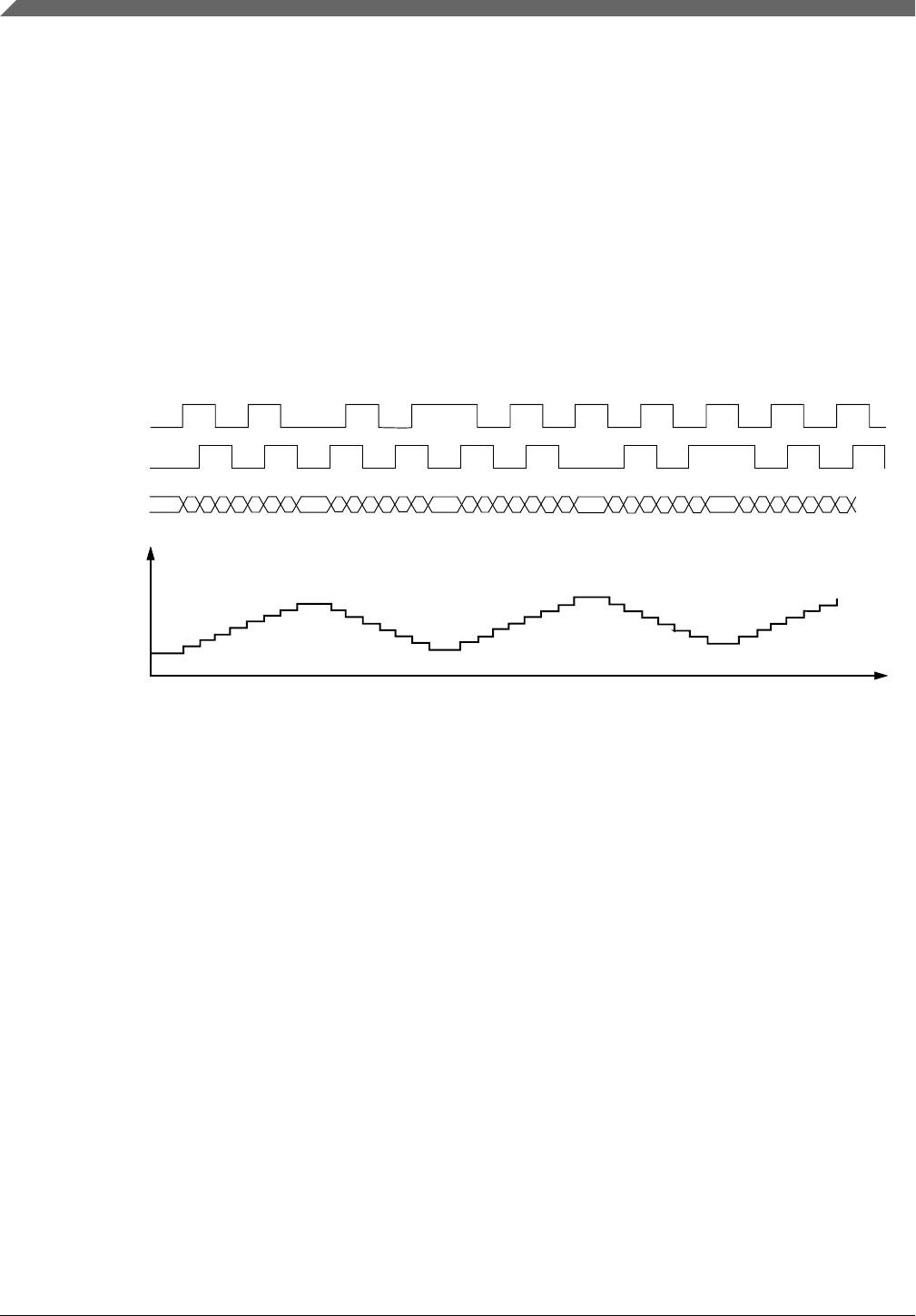
• there is a falling edge at phase B signal and phase A signal is at logic zero;
• there is a falling edge at phase A signal and phase B signal is at logic one;
and the FTM counter decrement happens when:
• there is a falling edge at phase A signal and phase B signal is at logic zero;
• there is a falling edge at phase B signal and phase A signal is at logic one;
• there is a rising edge at phase B signal and phase A signal is at logic zero;
• there is a rising edge at phase A signal and phase B signal is at logic one.
phase A
phase B
FTM counter
increment/decrement
FTM counter
MOD
CNTIN
0x0000
Time
+1 +1 +1 +1 +1 +1 +1 +1 -1 -1 -1 -1 -1
-1 -1 +1 +1 +1 +1 +1 +1 +1 +1 +1 +1 +1 +1 +1 +1 +1
-1 -1 -1 -1 -1
-1 -1
Figure 45-104. Quadrature Decoder – Phase A and Phase B Encoding Mode
The following figure shows the FTM counter overflow in up counting. In this case, when
the FTM counter changes from MOD to CNTIN, TOF and TOFDIR bits are set. TOF bit
indicates the FTM counter overflow occurred. TOFDIR indicates the counting was up
when the FTM counter overflow occurred.
Functional Description
S32K1xx Series Reference Manual, Rev. 7, 04/2018
1334 NXP Semiconductors
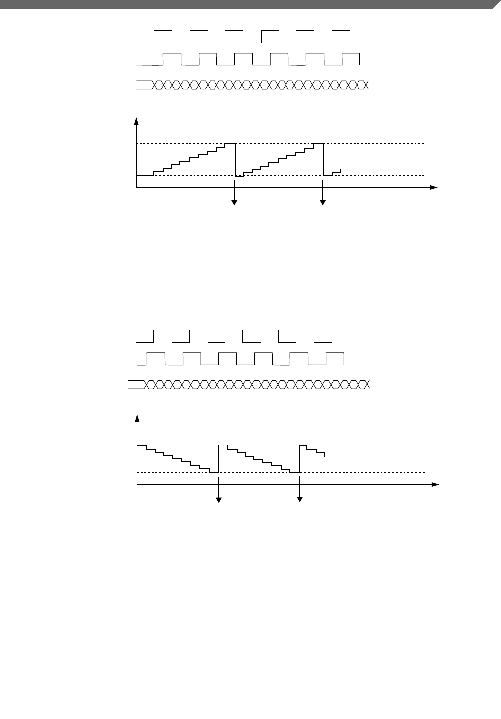
phase A
phase B
FTM counter
increment/decrement
FTM counter
MOD
CNTIN
0x0000
Time
+1 +1 +1 +1 +1 +1 +1
set TOF
set TOFDIR
set TOF
set TOFDIR
+1 +1 +1 +1 +1 +1 +1 +1 +1 +1 +1 +1 +1 +1 +1 +1 +1
Figure 45-105. FTM Counter Overflow in Up Counting for Quadrature Decoder Mode
The following figure shows the FTM counter overflow in down counting. In this case,
when the FTM counter changes from CNTIN to MOD, TOF bit is set and TOFDIR bit is
cleared. TOF bit indicates the FTM counter overflow occurred. TOFDIR indicates the
counting was down when the FTM counter overflow occurred.
phase A
phase B
FTM counter
increment/decrement
FTM counter
MOD
CNTIN
0x0000
Time
set TOF
clear TOFDIR
-1
set TOF
clear TOFDIR
-1
-1
-1
-1
-1
-1
-1
-1
-1-1
-1
-1
-1
-1
-1-1
-1
-1
-1
-1
-1
-1
-1
-1
Figure 45-106. FTM Counter Overflow in Down Counting for Quadrature Decoder Mode
45.5.27.1 Quadrature Decoder boundary conditions
The following figures show the FTM counter responding to motor jittering typical in
motor position control applications.
Chapter 45 FlexTimer Module (FTM)
S32K1xx Series Reference Manual, Rev. 7, 04/2018
NXP Semiconductors 1335
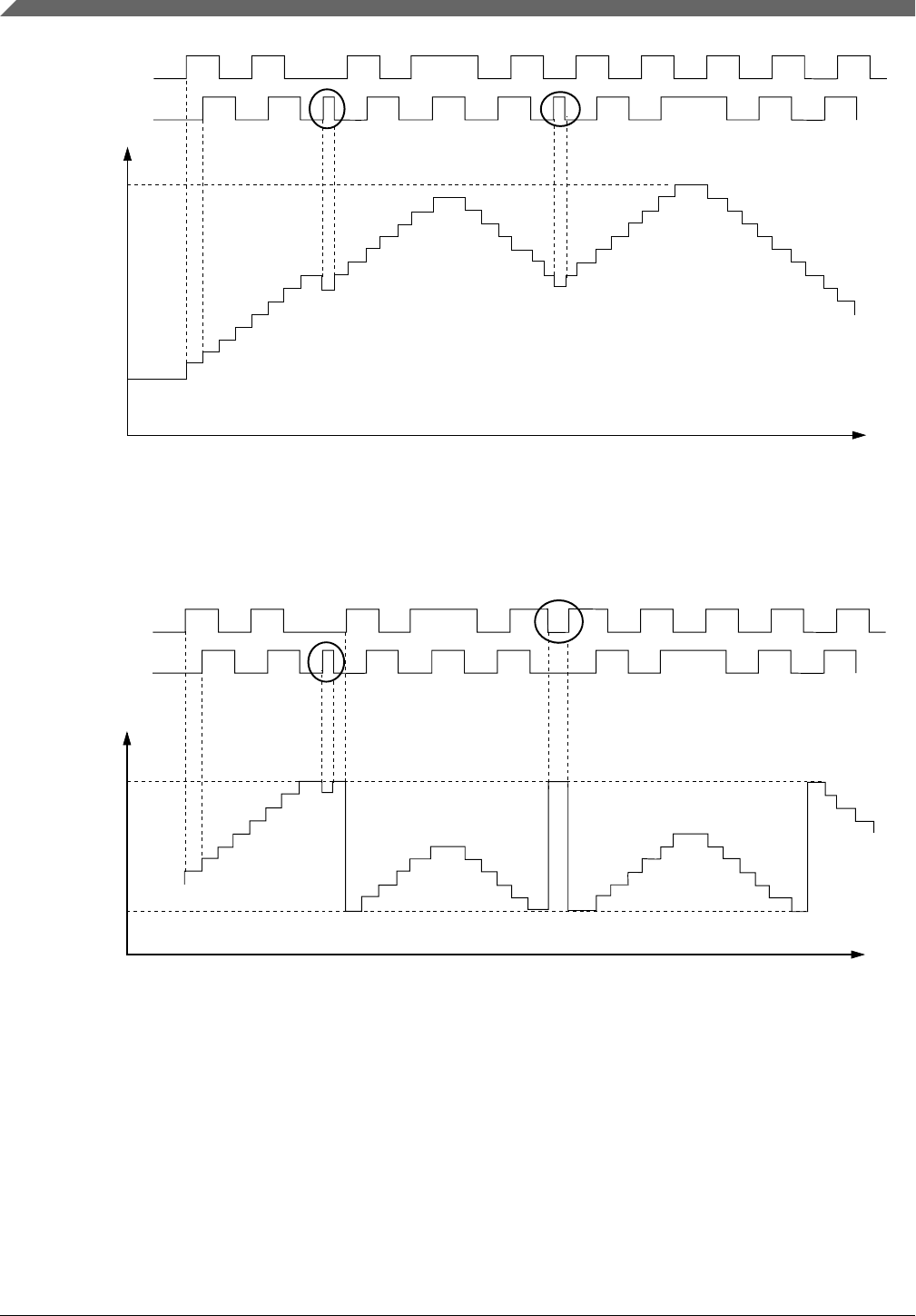
phase A
phase B
FTM counter
MOD
CNTIN
0x0000
Time
Figure 45-107. Motor position jittering in a mid count value
The following figure shows motor jittering produced by the phase B and A pulses
respectively:
phase A
phase B
FTM counter
MOD
CNTIN
0x0000
Time
Figure 45-108. Motor position jittering near maximum and minimum count value
The first highlighted transition causes a jitter on the FTM counter value near the
maximum count value (MOD). The second indicated transition occurs on phase A and
causes the FTM counter transition between the maximum and minimum count values
which are defined by MOD and CNTIN registers.
Functional Description
S32K1xx Series Reference Manual, Rev. 7, 04/2018
1336 NXP Semiconductors

The appropriate settings of the phase A and phase B input filters are important to avoid
glitches that may cause oscillation on the FTM counter value. The preceding figures
show examples of oscillations that can be caused by poor input filter setup. Thus, it is
important to guarantee a minimum pulse width to avoid these oscillations.
45.5.28 Debug mode
When the chip is in Debug mode, the BDMMODE[1:0] bits select the behavior of the
FTM counter, the channel (n) CHF bit, the channels output, and the writes to the MOD,
CNTIN, and C(n)V registers according to the following table.
Table 45-20. FTM behavior when the chip Is in Debug mode
BDMMODE FTM
Counter
channel (n)
CHF bit FTM Channels Output Writes to MOD, CNTIN, and C(n)V Registers
00 Stopped can be set Functional mode Writes to these registers bypass the registers
buffers
01 Stopped is not set The channels outputs are forced
to their safe value according to
POLn bit
Writes to these registers bypass the registers
buffers
10 Stopped is not set The channels outputs are frozen
when the chip enters in Debug
mode
Writes to these registers bypass the registers
buffers
11 Functional
mode
can be set Functional mode Functional mode
Note that if BDMMODE[1:0] = 2’b00 then the channels outputs remain at the value
when the chip enters in Debug mode, because the FTM counter is stopped. However, the
following situations modify the channels outputs in this Debug mode.
• Write any value to CNT register; see Counter reset. In this case, the FTM counter is
updated with the CNTIN register value and the channels outputs are updated to the
initial value – except for those channels set to Output Compare mode.
• FTM counter is reset by PWM Synchronization mode; see FTM counter
synchronization. In this case, the FTM counter is updated with the CNTIN register
value and the channels outputs are updated to the initial value – except for channels
in Output Compare mode.
• In the channels outputs initialization, the channel (n) output is forced to the CH(n)OI
bit value when the value 1 is written to INIT bit. See Initialization.
Chapter 45 FlexTimer Module (FTM)
S32K1xx Series Reference Manual, Rev. 7, 04/2018
NXP Semiconductors 1337

Note
The BDMMODE[1:0] = 2’b00 must not be used with the Fault
Control. Even if the fault control is enabled and a fault
condition exists, the channels outputs are updated as above.
Note
If CLKS[1:0] = 2'b00 in Debug, a non-zero value is written to
CLKS in Debug, and CnV = CNTIN when the Debug is
disabled, then the CHF bit is set (since if the channel is a 0%
EPWM signal) when the Debug is disabled.
45.5.29 Reload Points
This feature allows to update the registers CNTIN, HCR, MOD and C(n)V with the value
of their write buffer at the selected reload point.
NOTE
• This feature is independent of the PWM synchronization.
• At these reload points neither the channels outputs nor the
FTM counter are changed. Software must select these
reload points at the safe points in time.
45.5.29.1 Reload Opportunities
The reload opportunities are:
1. At the half cycle
This reload opportunity is enabled if (HCSEL = 1) and it happens at the half cycle
(FTM counter = HCR register). The software should calculate the half cycle value
according to the FTM counter configuration, then writes this value to the register
HCR.
2. At the channel (n) match
This reload opportunity is enabled if (CH(n)SEL = 1) and it happens at the channel
(n) match (FTM counter = C(n)V).
3. When the FTM counter is an up counter
This reload opportunity is when the FTM counter changes from (MOD) to (CNTIN -
1) and it is always enabled.
Functional Description
S32K1xx Series Reference Manual, Rev. 7, 04/2018
1338 NXP Semiconductors

The following figure shows an example of the reload opportunities at the half cycle,
at the channels match, and when the FTM counter is an up counter.
MOD
FTM counter = C3V
FTM counter = HCR
CNTIN
FTM counter = C2V
reload opportunities
(they are always enabled)
reload opportunities if (CH2SEL = 1)
reload opportunities if (HCSEL = 1)
reload opportunities if (CH3SEL = 1)
Figure 45-109. Reload opportunities when the FTM counter is an up counter
4. When the FTM counter is an up-down counter
In this case, the reload opportunities are enabled by the bits CNTMAX and CNTMIN
according to Table 45-21.
Table 45-21. Reload opportunities enabled by the bits CNTMAX and CNTMIN when the
FTM counter is up-down counter
CNTMAX CNTMIN Reload Opportunities
0 0 when the FTM counter changes from (MOD) to (MOD - 1)
0 1 when the FTM counter changes from (CNTMIN) to (CNTMIN + 1)
1 0 when the FTM counter changes from (MOD) to (MOD - 1)
1 1 • when the FTM counter changes from (MOD) to (MOD - 1), and
• when the FTM counter changes from (CNTMIN) to (CNTMIN + 1)
The following figure shows an example of the reload opportunities at the half cycle,
at the channels match, and when the FTM counter is an up-down counter.
Chapter 45 FlexTimer Module (FTM)
S32K1xx Series Reference Manual, Rev. 7, 04/2018
NXP Semiconductors 1339
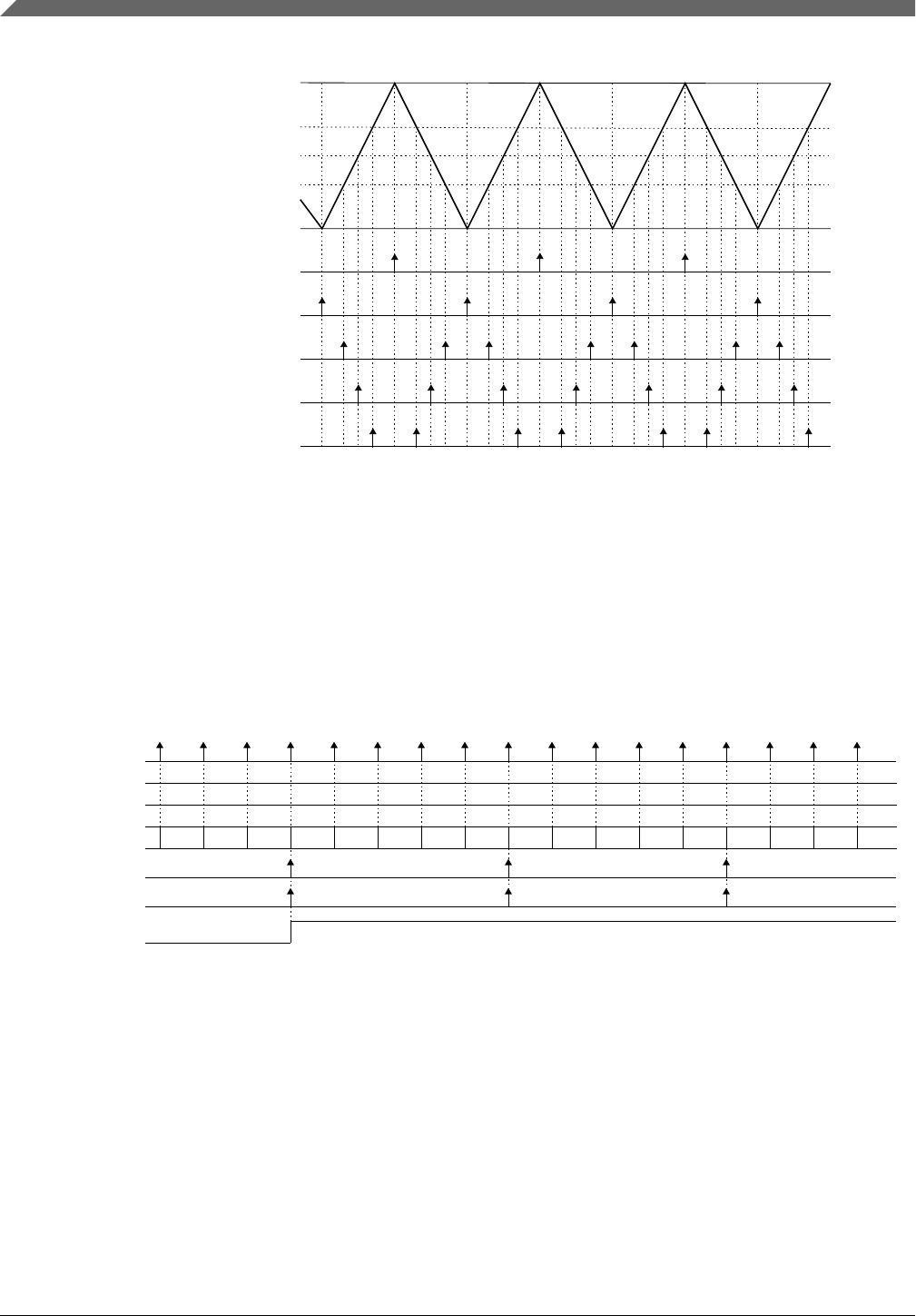
MOD
FTM counter = C3V
FTM counter = HCR
CNTIN
FTM counter = C2V
reload opportunities
if (CNTMAX = 1 or CNTMIN = 0)
reload opportunities if (CNTMIN = 1)
reload opportunities if (CH2SEL = 1)
reload opportunities if (HCSEL = 1)
reload opportunities if (CH3SEL = 1)
Figure 45-110. Reload opportunities when the FTM counter is an up-down counter
45.5.29.2 Frequency of Reload Opportunities
The LDFQ[4:0] bits define the number of enabled reload opportunities should happen
until an enabled reload opportunity becomes a reload point. The following figure shows
an example when the LDFQ[4:0] = 4.
4
enabled reload
opportunities
LDFQ[4:0]
counter of the reload
opportunities
2 3 4 0 1 2 3 4 0 1 2 3 4 0 1 2 3
reload point
set RF bit
RF bit
Figure 45-111. Frequency of Reload Opportunities with LDFQ[4:0] = 4
If LDFQ[4:0] = 0, then all reload opportunities are reload points.
The counter of the reload opportunities is reset when there is a write to the register CNT.
The RF bit is set at each reload point (see the figure above) independent of LDOK bit
value. The reload point interrupt is generated when (RF = 1) and (RIE = 1).
Functional Description
S32K1xx Series Reference Manual, Rev. 7, 04/2018
1340 NXP Semiconductors
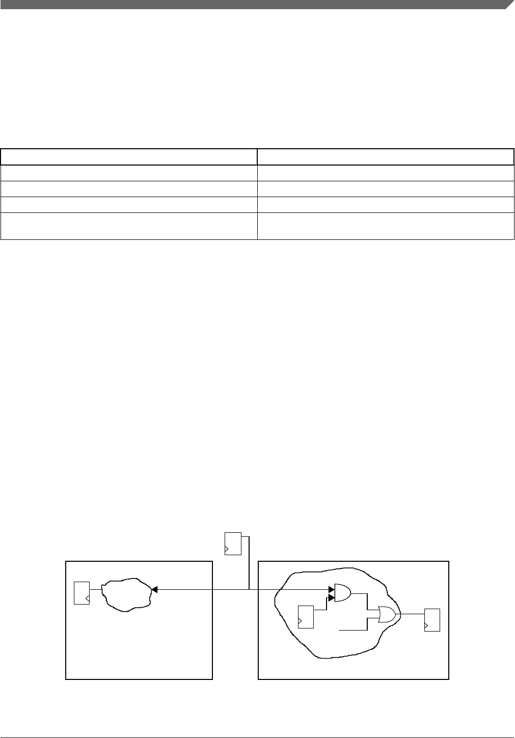
45.5.29.3 Update of the Registers
After writing new value to the registers with write buffer, selecting which of them will be
updated (according to Table 45-22), selecting the reload opportunities, selecting the
frequency of the reload opportunities, thus the LDOK bit should be set to enable the
update of these registers at the next reload point.
Table 45-22. Additional conditions to update the registers
Register Additional Condition
CNTIN CNTINC = 1
HCR -
MOD -
C(n)V and C(n+1)V SYNCENm = 1, where m is the pair of the channels (n) and (n
+1)
45.5.30 Global Load
The global load mechanism allows several modules to have their double buffered
registers synchronously reloaded after a synchronization event if a write to one operation
is performed in the global load OK (GLDOK) bit in the PWMLOAD register. Global
load may be enabled or disabled configuring the global load enable (GLEN) bit in the
PWMLOAD register. Writing one in the GLDOK bit with GLEN enabled has the same
effect of writing one in the LDOK bit. Refer to SoC specific information about global
load connections.
Global load mechanism allows MOD, HCR, CNTIN, and C(n)V registers to be updated
with the content of the register buffer at configurable reload point. The figure below
shows an example of connection between FTM global load inputs and outputs
considering that GLDOK bit is implemented outside from FTM module.
ftm_global_ldok_in ftm_global_ldok_in
FTM module A
FTM B or other peripheral
GLEN bit
Local LDOK
logic
GLDOK bit
Local LDOK
set (internal)
LDOK bit
Local LDOK logic
LDOK bit
Figure 45-112. Global load logic
Chapter 45 FlexTimer Module (FTM)
S32K1xx Series Reference Manual, Rev. 7, 04/2018
NXP Semiconductors 1341
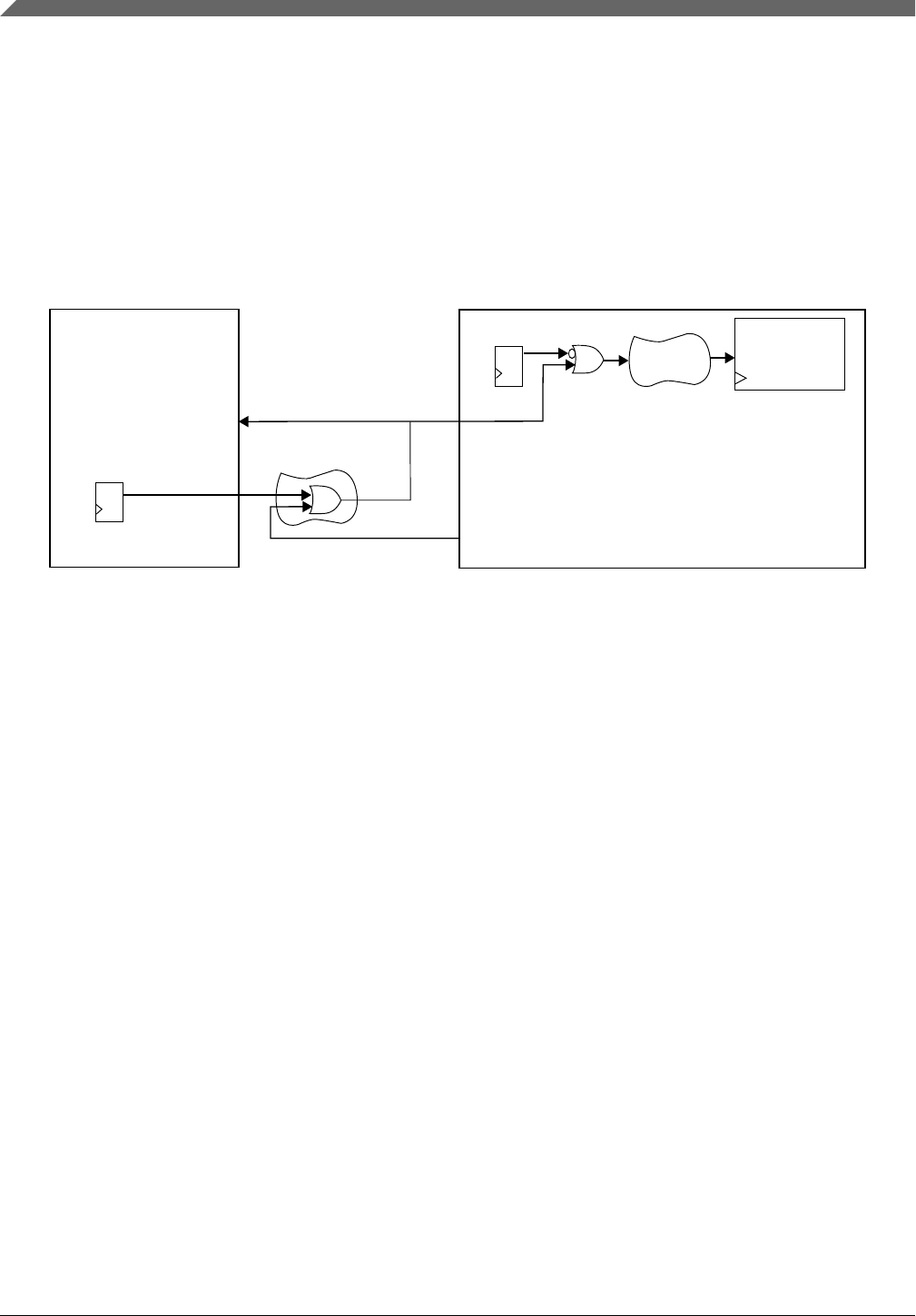
45.5.31 Global time base (GTB)
The global time base (GTB) is a FTM function that allows the synchronization of
multiple FTM modules on a chip. The following figure shows an example of the GTB
feature used to synchronize two FTM modules. In this case, the FTM A and B channels
can behave as if just one FTM module was used, that is, a global time base.
GTBEOUT bit
gtb_in
gtb_out
gtb_in
example glue logic
FTM module B
FTM module A
GTBEEN bit
FTM counter
enable logic
FTM counter
enable
gtb_out
Figure 45-113. Global time base (GTB) block diagram
The GTB functionality is implemented by the GTBEEN and GTBEOUT bits in the
CONF register, the input signal gtb_in, and the output signal gtb_out. The GTBEEN bit
enables gtb_in to control the FTM counter enable signal:
• If GTBEEN = 0, each one of FTM modules works independently according to their
configured mode.
• If GTBEEN = 1, the FTM counter update is enabled only when gtb_in is 1.
In the configuration described in the preceding figure, FTM modules A and B have their
FTM counters enabled if at least one of the gtb_out signals from one of the FTM modules
is 1. There are several possible configurations for the interconnection of the gtb_in and
gtb_out signals, represented by the example glue logic shown in the figure. Note that
these configurations are chip-dependent and implemented outside of the FTM modules.
See the chip-specific FTM information for the chip's specific implementation.
NOTE
• In order to use the GTB signals to synchronize the FTM
counter of different FTM modules, the configuration of
each FTM module should guarantee that its FTM counter
starts counting as soon as the gtb_in signal is 1.
• The GTB feature does not provide continuous
synchronization of FTM counters, meaning that the FTM
counters may lose synchronization during FTM operation.
Functional Description
S32K1xx Series Reference Manual, Rev. 7, 04/2018
1342 NXP Semiconductors

The GTB feature only allows the FTM counters to start
their operation synchronously.
45.5.31.1 Enabling the global time base (GTB)
To enable the GTB feature, follow these steps for each participating FTM module:
1. Stop the FTM counter: Write 00b to SC[CLKS].
2. Program the FTM to the intended configuration. The FTM counter mode needs to be
consistent across all participating modules.
3. Write 1 to CONF[GTBEEN] and write 0 to CONF[GTBEOUT] at the same time.
4. Select the intended FTM counter clock source in SC[CLKS]. The clock source needs
to be consistent across all participating modules.
5. Reset the FTM counter: Write any value to the CNT register.
To initiate the GTB feature in the configuration described in the preceding figure, write 1
to CONF[GTBEOUT] in the FTM module used as the time base.
45.5.32 Channel trigger output
The channel trigger output provides a trigger signal which has one FTM input clock
period width in the channel (n) output.
If the TRIGMODE bit of the CnSC register is set (TRIGMODE = 1), a trigger pulse with
one FTM input clock width is generated in the channel (n) output when a match occurs. It
is only allowed to use trigger mode when channel (n) is in EPWM or CPWM modes.
The figures below show some cases of channel (n) trigger generation in the channel (n)
output.
0x05 0x00 0x01 0x02 0x03 0x04 0x05 0x00 0x01 0x02 0x03 0x04
FTM input clock
FTM counter
Channel (n) output
MOD = 0x0005
CnV = 0x0003
PS[2:0] = 001
TRIGMODE = 1
Figure 45-114. Example of channel (n) trigger at the channel (n) output in EPWM mode
Chapter 45 FlexTimer Module (FTM)
S32K1xx Series Reference Manual, Rev. 7, 04/2018
NXP Semiconductors 1343
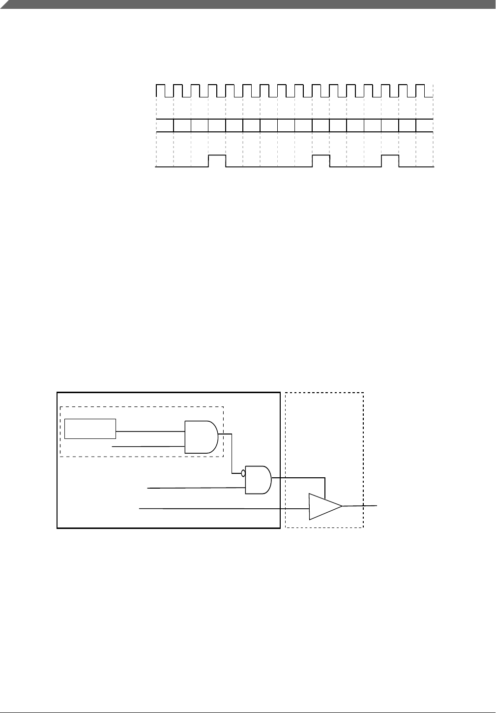
45432 1 2
3
4
5
4
3
21
0...
FTM input clock
FTM counter
Channel (n) output
MOD = 0x0005
CnV = 0x0003
PS[2:0] = 000
TRIGMODE = 1
CPWM mode
Figure 45-115. Example of channel (n) trigger at the channel (n) output in CPWM mode
45.5.33 External Control of Channels Output
The channel (n) PWMEN bit can be used in an FTM external logic to control the final
value of the channel (n) output. This same logic can also control the channel (n) output
when FSTATE = 1 and the channel (n) output is disabled by the Fault Control. The
following figure shows an example of this external logic.
The term "channel (n) output" means the channel (n) output value after the Polarity
Control. See Features Priority and Polarity Control for more details.
channel (n) output
FTM module
FSTATE bit
channel (n) PWMEN bit
disable
channel (n) output
Fault Control
Example of an FTM
external logic
final value of the
channel (n) output
Figure 45-116. Example of the External Control of the Channel (n) Output
45.5.34 Dithering
FTM implements a fractional delay to achieve fine resolution on the generated PWM
signals using dithering. The dithering can be used by applications where more resolution
than one unit of the FTM counter is needed.
Functional Description
S32K1xx Series Reference Manual, Rev. 7, 04/2018
1344 NXP Semiconductors

Two kinds of dithering are available: PWM period dithering and edge dithering.
45.5.34.1 PWM Period Dithering
The PWM period dithering is enabled when a non-zero value is written to FRACMOD.
The internal accumulator used in the PWM period dithering is reset when:
• the field MOD of the register MOD_MIRROR is updated with the value of its write
buffer,
• the FRACMOD is updated with the value of its write buffer, or
• the FTM counter is stopped.
NOTE
For the PWM period dithering, the register MOD_MIRROR
should be used instead of the register MOD.
To avoid inconsistencies, the field FRACMOD is cleared when
the field MOD of the register MOD is updated with the value of
its write buffer.
The PWM period dithering is not available:
• when the FTM counter is a free running counter
• when the FTM is in quadrature decoder mode
45.5.34.1.1 Up Counting
When the FTM counter is an up counter and the PWM period dithering is enabled, at the
end of each PWM period, the FRACMOD value is added to an internal 5-bit
accumulator. When this accumulator overflows (that is, the result of the adding is greater
or equal than 0x20), then one unit of FTM counter is added to the end of the current
PWM period, and the accumulator remains with the rest of the subtraction: (the result of
this adding - 0x20).
Due to one unit of FTM counter that can be added to the PWM period, the largest valid
value for MOD is 0xFFFE for PWM period dithering with unsigned counting and
0x7FFE for PWM period dithering with signed counting.
The following figures show some examples of PWM period dithering when the FTM
counter is an up counter.
Chapter 45 FlexTimer Module (FTM)
S32K1xx Series Reference Manual, Rev. 7, 04/2018
NXP Semiconductors 1345
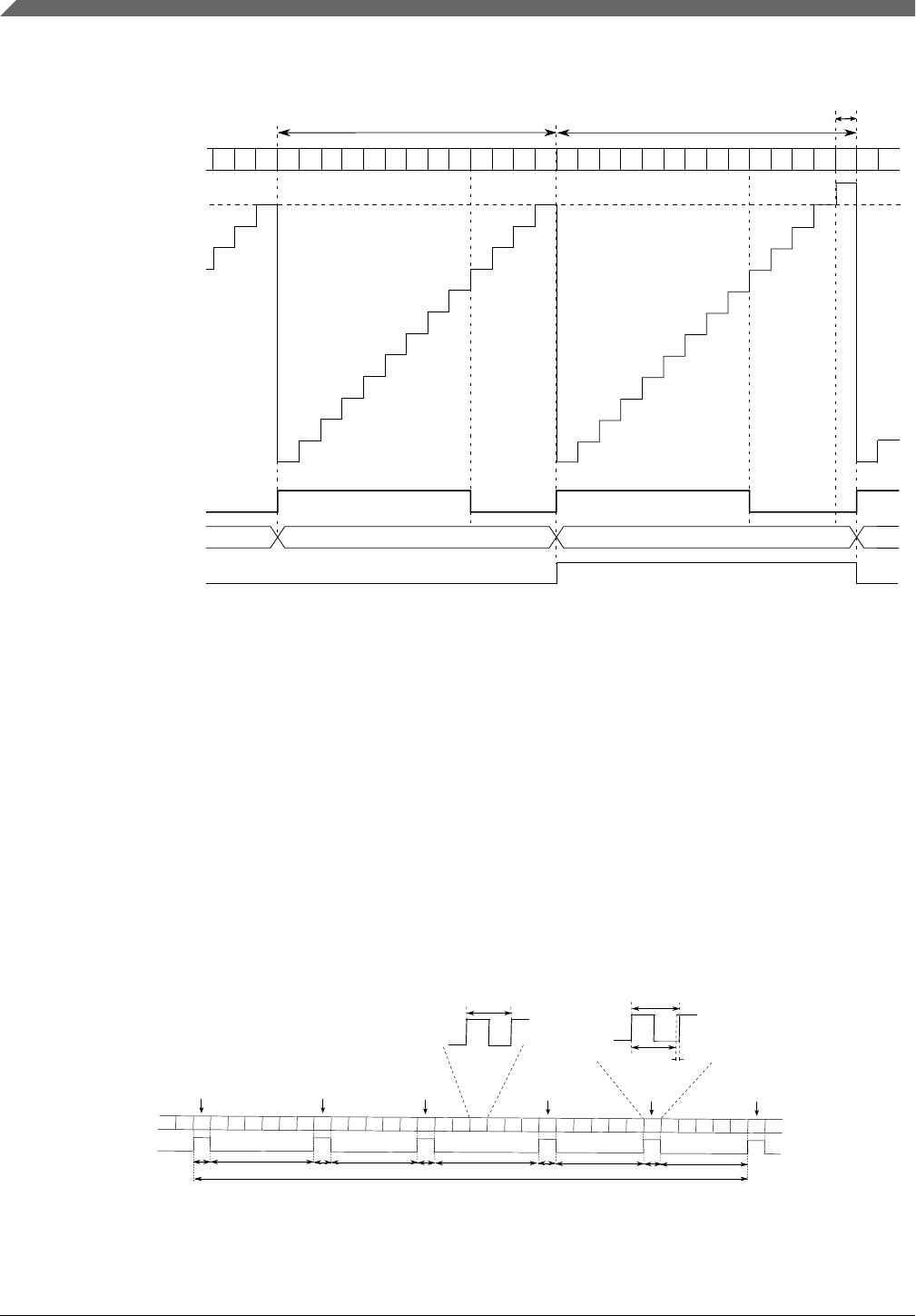
0 1 2 3 4 5 6 7 89 A B C 0 1 234 5 678 9 ABC
dithering
(one unit of
FTM counter)
channel (n) output
FTM counter
accumulator 0x1B 0x1E
overflow
0x01
0
D
CB
A1
channel (n) is in EPWM with high-true pulses
channel (n) ELSB:ELSA = 2'b10
CNTIN = 0x0000
MOD = 0x000C
FRACMOD = 0x03
C(n)V = 0x0009
T is the period of one unit of FTM counter
PWM period T1 =
(MOD - CNTIN + 0x0001) x T =
0x000D x T
PWM period T2 =
(MOD - CNTIN + 0x0001 + 0x0001) x T =
0x000E x T
Figure 45-117. PWM Period Dithering with Up Counting
Assuming:
• the FTM counter is an up counter,
• T is one unit of FTM counter,
• the PWM period without period dithering is [(MOD - CNTIN + 1) x T],
• the number of PWM periods with period dithering is FRACMOD,
• the PWM period with period dithering is [(MOD - CNTIN + 1 + 1) x T],
thus, the average period (in decimal) is [(MOD - CNTIN + 1) + (FRACMOD/32)] x T,
where the integer value is (MOD - CNTIN + 1) and the fractional value is (FRACMOD/
32). See the example below.
0x16
0x1B 0x00 0x05 0x0A 0x0F 0x14 0x19 0x1E 0x03 0x08 0x0D 0x12 0x17 0x1C 0x01 0x06 0x0B 0x10 0x15 0x1A 0x1F 0x04 0x09 0x0E 0x13 0x18 0x1D 0x02 0x07 0x0C 0x11 0x16 0x1B 0x00 0x05
PWM period T1 =
(MOD - CNTIN + 1) x T
PWM period T2 =
(MOD - CNTIN + 1 + 1) x T
T1
one unit of
FTM counter
accumulator
overflow
32 x PWM periods
T2 T2 T2 T2 T2
6 x T1 6 x T1
5 x T1 5 x T1 5 x T1
PWM period
dithering
channel (n) output channel (n) output
channel (n) is in EPWM
CNTIN = 0x0000
MOD = 0x0063
FRACMOD = 0x05
PS[2:0] = 3'b000
T is the period of one unit of FTM counter
Thus, the values (in decimal) are:
T1 = 100 x T
T2 = 101 x T
average period = (100 + 5/32) x T = 100.15625 x T
PWM period
dithering PWM period
dithering
PWM period
dithering
PWM period
dithering
PWM period
dithering
Figure 45-118. Example of Average Period when the PWM Period Dithering is used with
the Up Counting
Functional Description
S32K1xx Series Reference Manual, Rev. 7, 04/2018
1346 NXP Semiconductors

NOTE
For the generation of 100% PWM signal in the channel (n)
(with channel (n) ELSB:ELSA = 2'b10) using EPWM mode
and PWM Period Dithering, it is recommended to use (C(n) >
MOD + 1).
For the generation of PWM signals in the channel (n) (with
channel (n) ELSB:ELSA = 2'b10) using Combine mode and
PWM Period Dithering, it is recommended to use:
• For 0% PWM signal: (C(n)V > MOD + 1) and (C(n+1)V >
MOD + 1);
• For 100% PWM signal: (C(n)V = CNTIN) and (C(n+1)V >
MOD + 1).
For the generation of PWM signals in the channel (n) (with
channel (n) ELSB:ELSA = 2'b10) using Modified Combine
PWM mode and PWM Period Dithering, it is recommended to
use:
• For 0% PWM signal: (C(n)V > MOD + 1) and (CNTIN ≤
C(n+1)V ≤ MOD);
• For 100% PWM signal: (CNTIN ≤ C(n)V ≤ MOD) and
(C(n+1)V > MOD + 1).
45.5.34.1.2 Up-Down Counting
When the FTM counter is an up-down counter and the PWM period dithering is enabled,
at the end of each PWM period, the FRACMOD value is added to an internal 5-bit
accumulator. When this accumulator overflows (that is, the result of the adding is greater
or equal than 0x20), then one unit of FTM counter is added to the end of the current
PWM period and other unit is added to the begin of the next PWM period (see the figure
below). After the accumulator overflows, the accumulator remains with the rest of the
subtraction: (the result of this adding - 0x20).
Due to one unit of FTM counter that can be added to the PWM period, the largest valid
value for MOD is 0x7FFE for PWM period dithering in up-down counting (CPWM
mode).
Chapter 45 FlexTimer Module (FTM)
S32K1xx Series Reference Manual, Rev. 7, 04/2018
NXP Semiconductors 1347

5 4 32 1 0 1 2 3 4 5 6 5 43 2 1012 3 456 7 6
channel (n) output
FTM counter
accumulator 0x1B 0x1E
overflow
0x01
4
5
channel (n) is in CPWM with high-true pulses
channel (n) ELSB:ELSA = 2'b10
CNTIN = 0x0000
MOD = 0x0006
FRACMOD = 0x03
C(n)V = 0x0003
T is the period of one unit of FTM counter
6
5
4
PWM period T1 =
2 x (MOD - CNTIN) x T =
0x000C x T
32 1 01 2 34565 4 32
PWM period T2 =
[2 x (MOD - CNTIN) + 0x0001] x T =
0x000D x T
PWM period T2 =
[2 x (MOD - CNTIN) + 0x0001] x T =
0x000D x T
dithering
(two units of
FTM counter)
0x04 0x07
Figure 45-119. PWM Period Dithering with Up-Down Counting
NOTE
For the generation of 100% PWM signal in the channel (n)
(with channel (n) ELSB:ELSA = 2'b10) using CPWM mode
and PWM Period Dithering, it is recommended to use
(C(n)V[15] = 0) and (C(n)V > MOD + 1) and (MOD ≠
0x0000).
45.5.34.2 PWM Edge Dithering
The channel (n) internal accumulator used in the PWM edge dithering is reset when:
• the field VAL of the register C(n)V_MIRROR is updated with the value of its write
buffer,
• the FRACVAL is updated with the value of its write buffer, or
• the FTM counter is stopped.
NOTE
For the PWM edge dithering, the register C(n)V_MIRROR
should be used instead of the register C(n)V.
To avoid inconsistencies, the field FRACVAL is cleared when
the field VAL of the register C(n)V is updated with the value of
its write buffer.
The PWM edge dithering is not available:
• to the channel in input modes, and
• to the channel in output compare mode.
Functional Description
S32K1xx Series Reference Manual, Rev. 7, 04/2018
1348 NXP Semiconductors
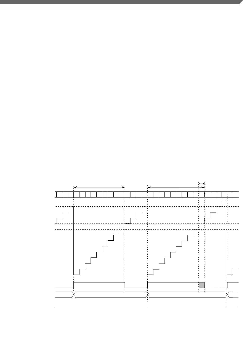
45.5.34.2.1 EPWM Mode
The PWM edge dithering for channel (n) in EPWM mode is enabled when a non-zero
value is written to the channel (n) FRACVAL.
If the channel (n) is in EPWM mode and the PWM edge dithering is enabled, at the end
of each EPWM period, the channel (n) FRACVAL value is added to the channel (n)
internal 5-bit accumulator. When this accumulator overflows (that is, the result of the
adding is greater or equal than 0x20), the accumulator remains with the rest of the
subtraction: (the result of this adding - 0x20).
In this configuration, the initial edge of EPWM duty cycle happens when (FTM counter =
CNTIN), its position is not modified by the PWM edge dithering. If there was not the
overflow of the channel (n) accumulator in the current EPWM period, then the final edge
of EPWM duty cycle happens on the channel (n) match (FTM counter = C(n)V), that is,
its position is not modified by the edge dithering. However, if there was the overflow of
the channel (n) accumulator in the current EPWM period, then the final edge of EPWM
duty cycle happens when (FTM counter = C(n)V + 0x0001).
The following figures show some examples of PWM edge dithering when the channel (n)
is in EPWM mode.
0 1 2 3 4 5 6 7 89 A B C 0 1 234 5 678 9 ABC
dithering
(one unit of
FTM counter)
channel (n) output
FTM counter
accumulator 0x1B 0x1E
overflow
0x01
0
D
CB
A1
channel (n) is in EPWM with high-true pulses
channel (n) ELSB:ELSA = 2'b10
CNTIN = 0x0000
MOD = 0x000C
C(n)V = 0x0009
channel (n) FRACVAL = 0x03
T is the period of one unit of FTM counter
EPWM duty cycle DC1 =
(C(n)V - CNTIN) x T =
0x0009 x T
EPWM duty cycle DC2 =
(C(n)V - CNTIN + 0x0001) x T =
0x000A x T
Figure 45-120. Channel (n) is in EPWM Mode with PWM Edge Dithering
Assuming:
Chapter 45 FlexTimer Module (FTM)
S32K1xx Series Reference Manual, Rev. 7, 04/2018
NXP Semiconductors 1349
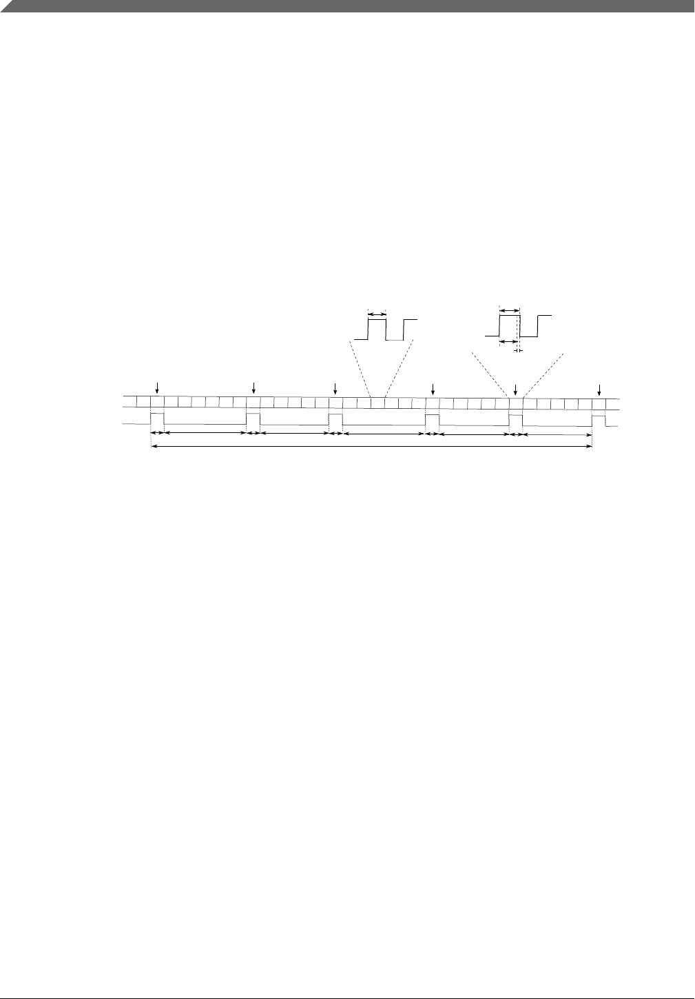
• the channel (n) is in EPWM mode,
• T is one unit of FTM counter,
• the EPWM duty cycle without edge dithering is [(C(n)V - CNTIN) x T],
• the number of PWM periods which duty cycle that has edge dithering is FRACVAL,
• the EWM duty cycle with edge dithering is [(C(n)V - CNTIN + 1) x T],
thus, the average duty cycle (in decimal) is [(C(n)V - CNTIN) + (FRACVAL/32)] x T,
where the integer value is (C(n)V - CNTIN) and the fractional value is (FRACVAL/32).
See the example below.
0x16
0x1B 0x00 0x05 0x0A 0x0F 0x14 0x19 0x1E 0x03 0x08 0x0D 0x12 0x17 0x1C 0x01 0x06 0x0B 0x10 0x15 0x1A 0x1F 0x04 0x09 0x0E 0x13 0x18 0x1D 0x02 0x07 0x0C 0x11 0x16 0x1B 0x00 0x05
EPWM duty cycle DC1 =
(C(n)V - CNTIN) x T
EPWM duty cycle DC2 =
(C(n)V - CNTIN + 1) x T
DC1
one unit of FTM counter
accumulator
overflow
32 x PWM periods
DC2 DC2 DC2 DC2 DC2
6 x DC1 6 x DC1
5 x DC1 5 x DC1 5 x DC1
PWM edge
dithering
channel (n) output channel (n) output
channel (n) is in EPWM with high-true pulses
CNTIN = 0x0000
MOD = 0x0063
PS[2:0] = 3'b000
channel (n) ELSB:ELSA = 2'b10
C(n)V = 0x0032
channel (n) FRACVAL = 0x05
T is the period of one unit of FTM counter
Thus, the values (in decimal) are:
DC1 = 50 x T
DC2 = 51 x T
average duty cycle = (50 + 5/32) x T = 50.15625 x T
PWM edge
dithering
PWM edge
dithering PWM edge
dithering PWM edge
dithering PWM edge
dithering
Figure 45-121. Example of Average Duty Cyle when the Channel (n) is in EPWM Mode
with PWM Edge Dithering
45.5.34.2.2 CPWM Mode
The PWM edge dithering for channel (n) in CPWM mode is enabled when a non-zero
value is written to the channel (n) FRACVAL.
If the channel (n) is in CPWM mode and the PWM edge dithering is enabled, at the end
of each CPWM period, the channel (n) FRACVAL value is added to the channel (n)
internal 5-bit accumulator. When this accumulator overflows (that is, the result of the
adding is greater or equal than 0x20), the accumulator remains with the rest of the
subtraction: (the result of this adding - 0x20).
In this configuration, if there was not the overflow of the channel (n) accumulator in the
current CPWM period, then the duty cycle is not modified by the PWM edge dithering,
that is, the initial edge of CPWM duty cycle happens on channel (n) match (FTM counter
= C(n)V) when the FTM counter is decrementing, and the final edge of CPWM duty
cycle on channel (n) match when the FTM counter is incrementing.
Functional Description
S32K1xx Series Reference Manual, Rev. 7, 04/2018
1350 NXP Semiconductors
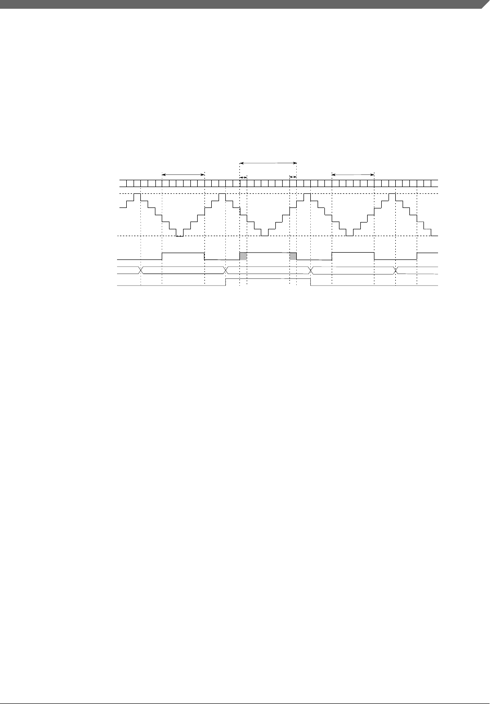
However, if there was the overflow of the channel (n) accumulator in the current CPWM
period, then the initial edge of CPWM duty cycle happens when (FTM counter = C(n)V
+ 0x0001) and the FTM counter is decrementing, and the final edge of CPWM duty cycle
when (FTM counter = C(n)V + 0x0001) and the FTM counter is incrementing.
The following figure shows an example of PWM edge dithering when the channel (n) is
in CPWM mode.
5 4 32 1 0 1 2 3 4 5 6 5 43 2 1012 3 456 5 4
channel (n) output
FTM counter
accumulator 0x1B 0x1E
overflow
0x01
2
3
channel (n) is in CPWM with high-true pulses
channel (n) ELSB:ELSA = 2'b10
CNTIN = 0x0000
MOD = 0x0006
C(n)V = 0x0003
channel (n) FRACVAL = 0x03
T is the period of one unit of FTM counter
6
5
4
CPWM duty cycle DC1 =
2 x (C(n)V - CNTIN) x T =
0x0006 x T
10 1 23 4 56543 2 10
CPWM duty cycle DC2 =
2 x (C(n)V - CNTIN + 0x0001) x T =
0x0008 x T
dithering (one unit of
FTM counter)
0x04 0x07
dithering (one unit of
FTM counter)
CPWM duty cycle DC1 =
2 x (C(n)V - CNTIN) x T =
0x0006 x T
Figure 45-122. Channel (n) is in CPWM Mode with PWM Edge Dithering
45.5.34.2.3 Combine Mode
In the Combine mode, the PWM edge dithering can be done:
• in the channel (n) match (FTM counter = C(n)V) edge or
• in the channel (n+1) match (FTM counter = C(n+1)V) edge.
The channel (n) match edge dithering is enabled when a non-zero value is written to the
channel (n) FRACVAL.
For the channel (n) match edge dithering, the channel (n) has an internal 5-bit
accumulator. At the end of each PWM period, the channel (n) FRACVAL value is added
to the channel (n) accumulator. When this accumulator overflows (that is, the result of the
adding is greater or equal than 0x20), the accumulator remains with the rest of the
subtraction: (the result of this adding - 0x20).
If there was not the overflow of the channel (n) accumulator in the current PWM period,
the channel (n) match edge is not modified, that is, it happens on channel (n) match.
However, if there was the overflow of the channel (n) accumulator, the channel (n) match
edge happens when (FTM counter = C(n)V + 0x0001).
The following figure shows an example of the channel (n) match edge dithering when the
channels (n) and (n+1) are in Combine mode.
Chapter 45 FlexTimer Module (FTM)
S32K1xx Series Reference Manual, Rev. 7, 04/2018
NXP Semiconductors 1351
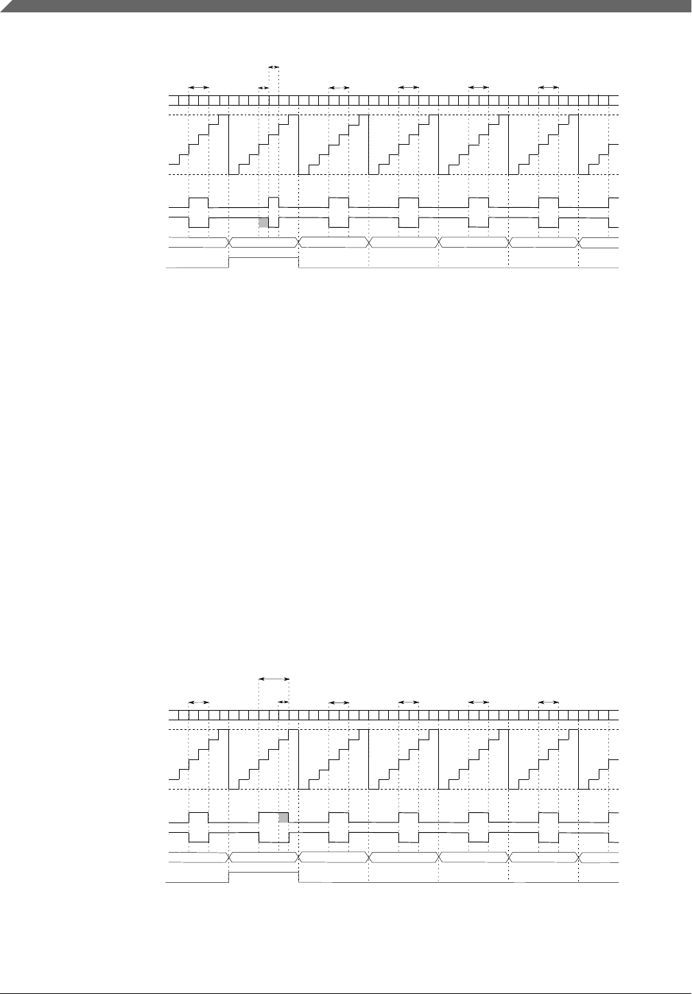
4 5 60 1 2 3 4 5 6 0 1 2 34 5 6012 3 456 0 1
channel (n) output
FTM counter
accumulator 0x1E 0x01
overflow
0x04
3
2
channels (n) and (n+1) are in
Combine Mode with high-true pulses
and Complementary
channel (n) ELSB:ELSA = 2'b10
CNTIN = 0x0000
MOD = 0x0006
C(n)V = 0x0002
channel (n) FRACVAL = 0x03
C(n+1)V = 0x0004
channel (n+1) FRACVAL = 0x00
T is the period of one unit of FTM counter
3
2
1
Combine duty cycle DC1 =
(C(n)V - C(n+1)V) x T =
0x0002 x T
45 6 01 2 34560 1 23
dithering
(one unit of
FTM counter)
0x07 0x0A
channel (n+1) output
0x0D 0x10
Combine duty cycle DC2 =
(C(n)V - C(n+1)V - 0x0001) x T =
0x0001 x T
Combine duty cycle DC1 =
(C(n)V - C(n+1)V) x T =
0x0002 x T
Combine duty cycle DC1 =
(C(n)V - C(n+1)V) x T =
0x0002 x T
Combine duty cycle DC1 =
(C(n)V - C(n+1)V) x T =
0x0002 x T
Combine duty cycle DC1 =
(C(n)V - C(n+1)V) x T =
0x0002 x T
Figure 45-123. Channel (n) Match Edge Dithering in Combine Mode
The channel (n+1) match edge dithering is enabled when a non-zero value is written to
the channel (n+1) FRACVAL.
For the channel (n+1) match edge dithering, the channel (n+1) has an internal 5-bit
accumulator. At the end of each PWM period, the channel (n+1) FRACVAL value is
added to the channel (n+1) accumulator. When this accumulator overflows (that is, the
result of the adding is greater or equal than 0x20), the accumulator remains with the rest
of the subtraction: (the result of this adding - 0x20).
If there was not the overflow of the channel (n+1) accumulator in the current PWM
period, the channel (n+1) match edge is not modified, that is, it happens on channel (n+1)
match. However, if there was the overflow of the channel (n+1) accumulator, the channel
(n+1) match edge happens when (FTM counter = C(n+1)V + 0x0001).
The following figure shows an example of the channel (n+1) match edge dithering when
the channels (n) and (n+1) are in Combine mode.
4 5 60 1 2 3 4 5 6 0 1 2 34 5 6012 3 456 0 1
channel (n) output
FTM counter
accumulator 0x1E 0x01
overflow
0x04
3
2
channels (n) and (n+1) are in
Combine Mode with high-true pulses
and Complementary
channel (n) ELSB:ELSA = 2'b10
CNTIN = 0x0000
MOD = 0x0006
C(n)V = 0x0002
channel (n) FRACVAL = 0x00
C(n+1)V = 0x0004
channel (n+1) FRACVAL = 0x03
T is the period of one unit of FTM counter
3
2
1
Combine duty cycle DC1 =
(C(n)V - C(n+1)V) x T =
0x0002 x T
45 6 01 2 34560 1 23
dithering
(one unit of
FTM counter)
0x07 0x0A
channel (n+1) output
0x0D 0x10
Combine duty cycle DC2 =
(C(n)V - C(n+1)V + 0x0001) x T =
0x0003 x T
Combine duty cycle DC1 =
(C(n)V - C(n+1)V) x T =
0x0002 x T
Combine duty cycle DC1 =
(C(n)V - C(n+1)V) x T =
0x0002 x T
Combine duty cycle DC1 =
(C(n)V - C(n+1)V) x T =
0x0002 x T
Combine duty cycle DC1 =
(C(n)V - C(n+1)V) x T =
0x0002 x T
Figure 45-124. Channel (n+1) Match Edge Dithering in Combine Mode
Functional Description
S32K1xx Series Reference Manual, Rev. 7, 04/2018
1352 NXP Semiconductors

NOTE
It is recommended to use only one PWM Edge Dithering
(channel (n) PWM Edge Dithering or channel (n+1) PWM
Edge Dithering) at a time.
For the generation of 0% PWM in the channel (n) (with channel
(n) ELSB:ELSA = 2'b10) using Combine mode and PWM Edge
Dithering, it is recommended to use:
• (C(n)V < CNTIN or C(n)V > MOD) and (channel (n)
FRACVAL is zero) and
• (channel (n+1) FRACVAL is zero).
For the generation of 100% PWM in the channel (n) (with
channel (n) ELSB:ELSA = 2'b10) using Combine mode and
PWM Edge Dithering, it is recommended to use:
• (C(n)V = CNTIN) and (channel (n) FRACVAL is zero) and
• (C(n+1)V < CNTIN or C(n+1)V > MOD) and (channel (n
+1) FRACVAL is zero).
45.5.34.2.4 Modified Combine PWM Mode
In the Modified Combine PWM mode, the PWM edge dithering can be done:
• in the channel (n) match (FTM counter = C(n)V) edge or
• in the channel (n+1) match (FTM counter = C(n+1)V) edge.
The channel (n) match edge dithering is enabled when a non-zero value is written to the
channel (n) FRACVAL.
For the channel (n) match edge dithering, the channel (n) has an internal 5-bit
accumulator. At the end of each PWM period, the channel (n) FRACVAL value is added
to the channel (n) accumulator. When this accumulator overflows (that is, the result of the
adding is greater or equal than 0x20), the accumulator remains with the rest of the
subtraction: (the result of this adding - 0x20).
If there was not the overflow of the channel (n) accumulator in the current PWM period,
the channel (n) match edge is not modified, that is, it happens on channel (n) match.
However, if there was the overflow of the channel (n) accumulator, the channel (n) match
edge happens when (FTM counter = C(n)V + 0x0001).
The following figure shows an example of the channel (n) match edge dithering when the
channels (n) and (n+1) are in Modified Combine PWM mode.
Chapter 45 FlexTimer Module (FTM)
S32K1xx Series Reference Manual, Rev. 7, 04/2018
NXP Semiconductors 1353
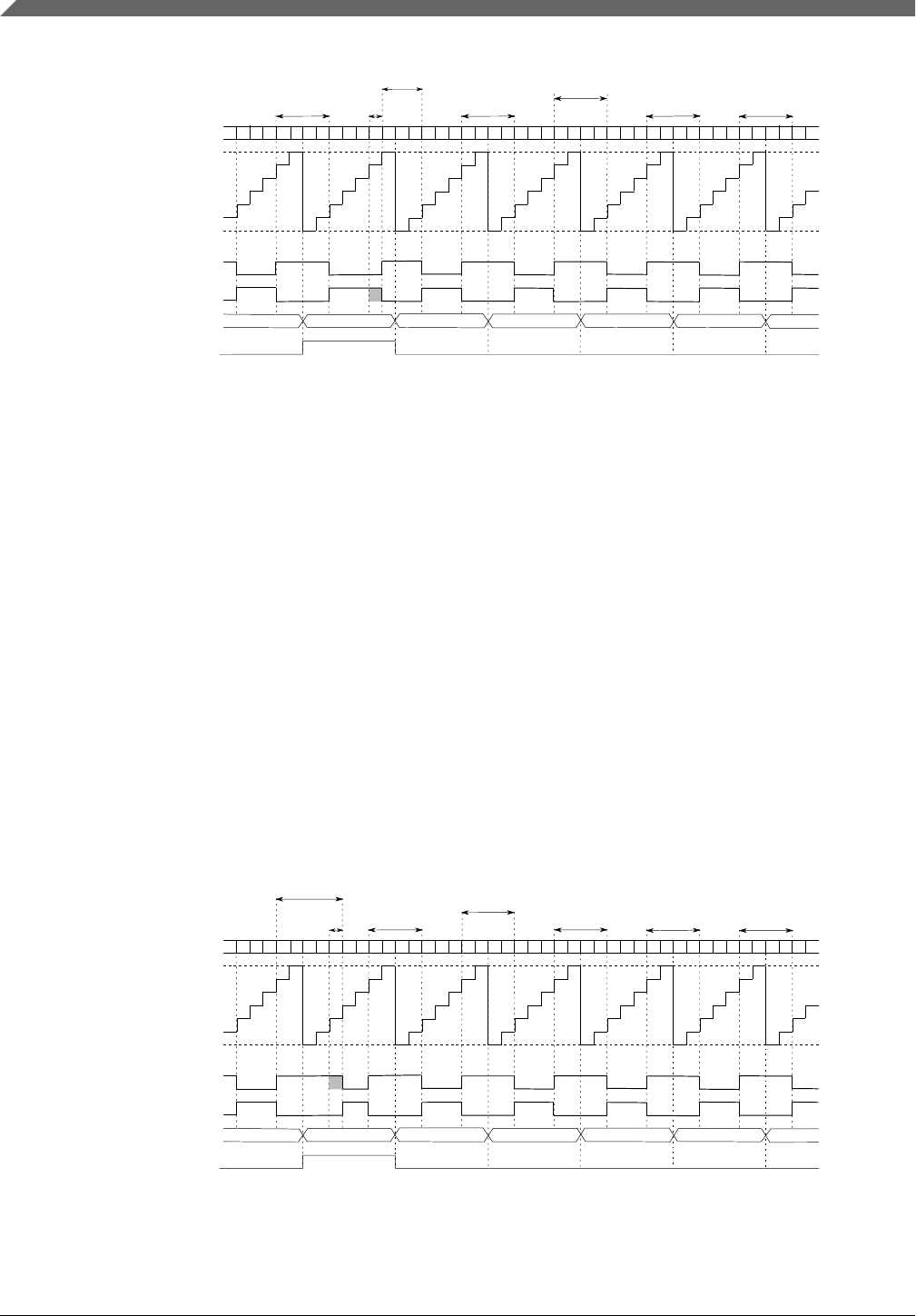
4 5 60 1 2 3 4 5 6 0 1 2 34 5 60123456 0 1
channel (n) output
FTM counter
accumulator 0x1E 0x01
overflow
0x04
3
2
channels (n) and (n+1) are in
Modified Combine PWM Mode with
high-true pulses and Complementary
channel (n) ELSB:ELSA = 2'b10
CNTIN = 0x0000
MOD = 0x0006
C(n)V = 0x0004
channel (n) FRACVAL = 0x03
C(n+1)V = 0x0001
channel (n+1) FRACVAL = 0x00
T is the period of one unit of FTM counter
3
2
1
Modified Combine PWM duty cycle DC1 =
[(MOD - C(n)V) + (C(n+1)V - CNTIN) + 0x0001] x T =
0x0004 x T
45 6 01 2 34560 1 23
dithering
(one unit of
FTM counter)
0x07 0x0A
channel (n+1) output
0x0D 0x10
Modified Combine PWM duty cycle with Edge Dithering
DC2 = (DC1 - 0x0001 x T) = 0x0003 x T
DC1 = 0x0004 x T DC1 = 0x0004 x T
DC1 = 0x0004 x T
DC1 = 0x0004 x T
Figure 45-125. Channel (n) Match Edge Dithering in Modified Combine PWM Mode
The channel (n+1) match edge dithering is enabled when a non-zero value is written to
the channel (n+1) FRACVAL.
For the channel (n+1) match edge dithering, the channel (n+1) has an internal 5-bit
accumulator. At the end of each PWM period, the channel (n+1) FRACVAL value is
added to the channel (n+1) accumulator. When this accumulator overflows (that is, the
result of the adding is greater or equal than 0x20), the accumulator remains with the rest
of the subtraction: (the result of this adding - 0x20).
If there was not the overflow of the channel (n+1) accumulator in the current PWM
period, the channel (n+1) match edge is not modified, that is, it happens on channel (n+1)
match. However, if there was the overflow of the channel (n+1) accumulator, the channel
(n+1) match edge happens when (FTM counter = C(n+1)V + 0x0001).
The following figure shows an example of the channel (n+1) match edge dithering when
the channels (n) and (n+1) are in Modified Combine PWM mode.
4 5 60 1 2 3 4 5 6 0 1 2 34 5 60123456 0 1
channel (n) output
FTM counter
accumulator 0x1E 0x01
overflow
0x04
3
2
channels (n) and (n+1) are in
Modified Combine PWM Mode with
high-true pulses and Complementary
channel (n) ELSB:ELSA = 2'b10
CNTIN = 0x0000
MOD = 0x0006
C(n)V = 0x0004
channel (n) FRACVAL = 0x00
C(n+1)V = 0x0001
channel (n+1) FRACVAL = 0x03
T is the period of one unit of FTM counter
3
2
1
Modified Combine PWM duty cycle DC1 =
[(MOD - C(n)V) + (C(n+1)V - CNTIN) + 0x0001] x T =
0x0004 x T
45 6 01 2 34560 1 23
dithering
(one unit of
FTM counter)
0x07 0x0A
channel (n+1) output
0x0D 0x10
Modified Combine PWM duty cycle with Edge Dithering
DC2 = (DC1 + 0x0001 x T) = 0x0005 x T
DC1 = 0x0004 x T DC1 = 0x0004 x T
DC1 = 0x0004 x T DC1 = 0x0004 x T
Figure 45-126. Channel (n+1) Match Edge Dithering in Modified Combine PWM Mode
Functional Description
S32K1xx Series Reference Manual, Rev. 7, 04/2018
1354 NXP Semiconductors

NOTE
It is recommended to use only one PWM Edge Dithering
(channel (n) PWM Edge Dithering or channel (n+1) PWM
Edge Dithering) at a time.
For the generation of 0% PWM in the channel (n) (with channel
(n) ELSB:ELSA = 2'b10) using Modified Combine PWM mode
and PWM Edge Dithering, it is recommended to use:
• (C(n)V < CNTIN or C(n)V > MOD) and (channel (n)
FRACVAL is zero) and
• (CNTIN ≤ C(n+1)V ≤ MOD) and (channel (n+1)
FRACVAL is zero).
For the generation of 100% PWM in the channel (n) (with
channel (n) ELSB:ELSA = 2'b10) using Modified Combine
PWM mode and PWM Edge Dithering, it is recommended to
use:
• (CNTIN ≤ C(n)V ≤ MOD) and (channel (n) FRACVAL is
zero) and
• (C(n+1)V < CNTIN or C(n+1)V > MOD) and (channel (n
+1) FRACVAL is zero).
45.6 Reset Overview
The FTM is reset whenever any chip reset occurs.
When the FTM exits from reset:
• the FTM counter and the prescaler counter are zero and are stopped (CLKS[1:0] =
2'b00);
• the timer overflow interrupt is zero (Timer Overflow Interrupt);
• the channels interrupts are zero (Channel (n) Interrupt);
• the fault interrupt is zero (Fault Interrupt);
• the channels are in input capture mode (Input Capture Mode);
• the channels outputs are zero;
• the channels ELSB:ELSA = 0:0 (Channel Modes) and PWMEN = 0 (External
Control of Channels Output).
The following figure shows the FTM behavior after the reset. At the reset (item 1), the
FTM counter is disabled (CLKS[1:0] = 2'b00), its value is updated to zero and the pins
are not controlled by FTM (Channel Modes).
Chapter 45 FlexTimer Module (FTM)
S32K1xx Series Reference Manual, Rev. 7, 04/2018
NXP Semiconductors 1355
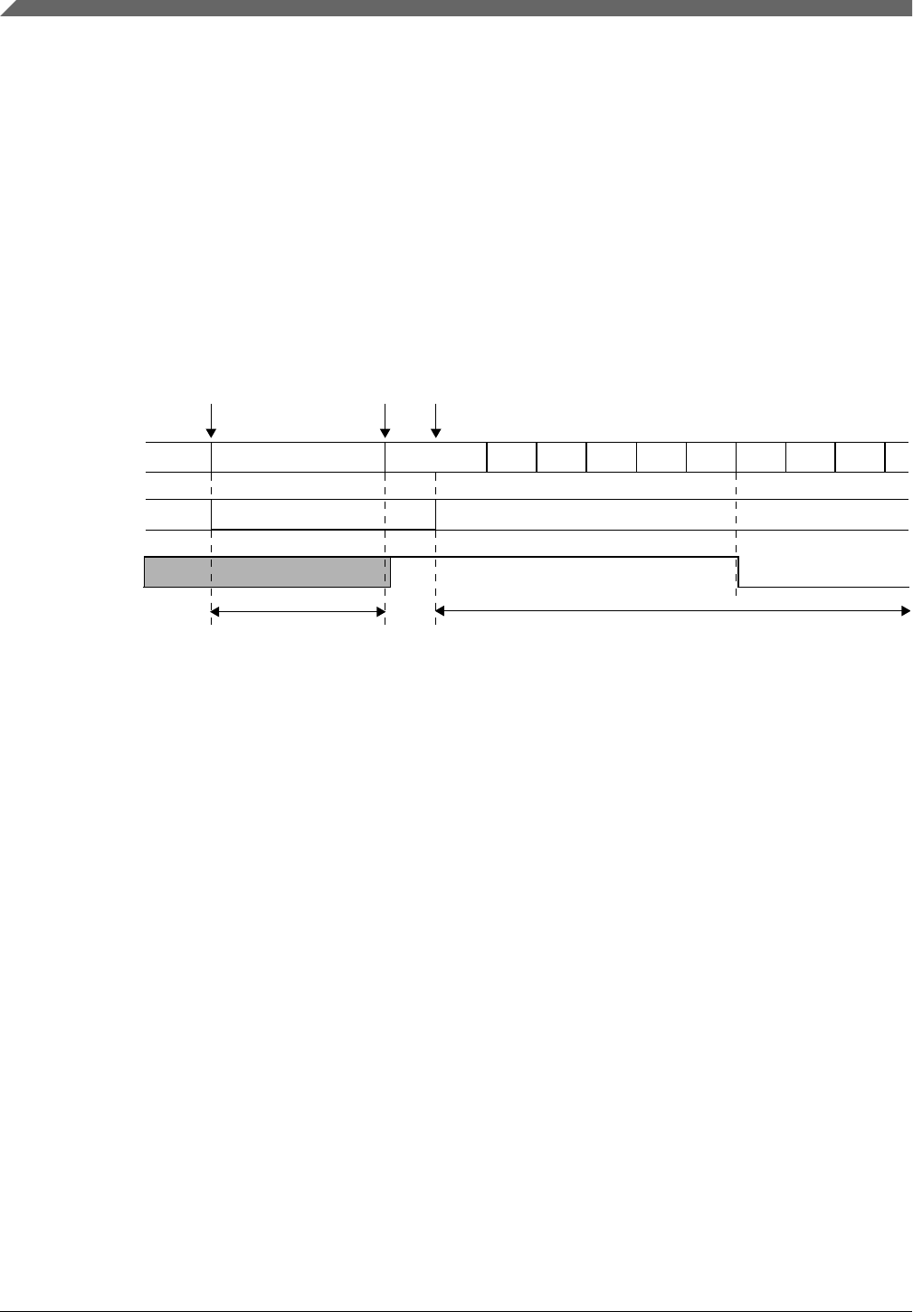
After the reset, the FTM should be configurated (item 2). It is necessary to define the
FTM counter mode, the FTM counting limits (MOD and CNTIN registers value), the
channels mode and CnV registers value according to the channels mode.
Thus, it is recommended to write any value to CNT register (item 3). This write updates
the FTM counter with the CNTIN register value and the channels output with its initial
value (except for channels in output compare mode) (Counter reset).
The next step is to select the FTM counter clock by the CLKS[1:0] bits (item 4). It is
important to highlight that the pins are only controlled by FTM when CLKS[1:0] bits are
different from zero.
(1) FTM reset
0x0016 0x0015 0x0014 0x0013 0x0011 . . . 0x0010 0x0018 0x0017 XXXX 0x0000 0x0012
FTM counter
CLKS[1:0]
channel (n) output
(4) write 1 to SC[CLKS]
(3) write any value
to CNT register
(2) FTM configuration channel (n) pin is controlled by FTM
NOTES:
– CNTIN = 0x0010
– Channel (n) is in low-true combine mode with CNTIN < C(n)V < C(n+1)V < MOD
– C(n)V = 0x0015
00
XX 01
Figure 45-127. FTM behavior after reset when the channel (n) is in Combine mode
The following figure shows an example when the channel (n) is in Output Compare mode
and the channel (n) output is toggled when there is a match. In the Output Compare
mode, the channel output is not updated to its initial value when there is a write to CNT
register (item 3). In this case, use the software output control (Software Output Control
Mode) or the initialization (Initialization) to update the channel output to the selected
value (item 4).
Reset Overview
S32K1xx Series Reference Manual, Rev. 7, 04/2018
1356 NXP Semiconductors

(1) FTM reset
0x0015 0x0014 0x0013 0x0012 . . . 0x0010 0x0017 0x0016 XXXX 0x0000 0x0011
FTM counter
CLKS[1:0]
channel (n) output
(5) write 1 to SC[CLKS]
(3) write any value
to CNT register
(2) FTM configuration channel (n) pin is controlled by FTM
NOTES:
– CNTIN = 0x0010
– Channel (n) is in output compare and the channel (n) output is toggled when there is a match
– C(n)V = 0x0014
00
XX 01
(4) use of software output control or initialization
to update the channel output to the zero
Figure 45-128. FTM behavior after reset when the channel (n) is in Output Compare
mode
45.7 FTM Interrupts
45.7.1 Timer Overflow Interrupt
The timer overflow interrupt is generated when (TOIE = 1) and (TOF = 1).
45.7.2 Reload Point Interrupt
The Reload Point interrupt is generated when (RIE = 1) and (RF = 1).
45.7.3 Channel (n) Interrupt
The channel (n) interrupt is generated when (CHIE = 1) and (CHF = 1).
45.7.4 Fault Interrupt
The fault interrupt is generated when (FAULTIE = 1) and (FAULTF = 1).
Chapter 45 FlexTimer Module (FTM)
S32K1xx Series Reference Manual, Rev. 7, 04/2018
NXP Semiconductors 1357

45.8 Initialization Procedure
The following initialization procedure is recommended to configure the FlexTimer. This
procedure can also be used to do a new configuration.
1. Define the POL bits.
2. Mask the channels outputs using SYNCHOM = 0. Two clocks after the write to
OUTMASK, the channels outputs are in the safe value.
3. (Re)Configuration FTM counter and channels to generation of periodic signals:
a. Disable the clock. Disable the Quadrature Decoder mode.
b. Examples of (re)configuration:
• Write to MOD
• Write to CNTIN
• Configure the channels that will be used
• Write to CnV for the channels in output modes
• (Re)Configure deadtime and fault control
• Do not use the SWOC without SW synchronization (see item 6)
• Do not use the Inverting without SW synchronization (see item 6)
• Do not use the Initialization
• Do not change the polarity control
• Do not configure the HW synchronization
4. Write any value to CNT. The FTM Counter is reset and the channels outputs are
updated according to new configuration.
5. Enable the clock. Write to CLKS[1:0] bits a value different from zero. Enable the
Quadrature Decoder mode (if it is desired).
6. Configure the SW synchronization for SWOC (if it is necessary), Inverting (if it is
necessary) and Output Mask (always)
a. Select synchronization for Output Mask
• Write to SYNC (SWSYNC = 0, TRIG2 = 0, TRIG1 = 0, TRIG0 = 0,
SYNCHOM = 1, REINIT = 0, CNTMAX = 0, CNTMIN = 0)
b. Write to SYNCONF
• HW Synchronization can not be enabled (HWSOC = 0, HWINVC = 0,
HWOM = 0, HWWRBUF = 0, HWRSTCNT = 0, HWTRIGMODE = 0)
• SW Synchronization for SWOC (if it is necessary): SWSOC = [0/1] and
SWOC = [0/1]
• SW Synchronization for Inverting (if it is necessary): SWINVC = [0/1] and
INVC = [0/1]
• SW Synchronization for SWOM (always): SWOM = 1
Initialization Procedure
S32K1xx Series Reference Manual, Rev. 7, 04/2018
1358 NXP Semiconductors

• No enable the SW Synchronization for write buffers (because the writes to
registers with write buffer are done using CLKS[1:0] = 2’b00): SWWRBUF
= 0 and CNTINC = 0
• SW Synchronization for counter reset (always): SWRSTCNT = 1
• Enhanced synchronization (always): SYNCMODE = 1
c. If the SWOC is used (SWSOC = 1 and SWOC = 1), then write to SWOCTRL
register.
d. If the Inverting is used (SWINVC = 1 and INVC = 1), then write to INVCTRL
register.
e. Write to OUTMASK to enable the masked channels.
7. Generate the Software Trigger
• Write to SYNC (SWSYNC = 1, TRIG2 = 0, TRIG1 = 0, TRIG0 = 0,
SYNCHOM = 1, REINIT = 0, CNTMAX = 0, CNTMIN = 0)
8. Configure PWMEN bits (External Control of Channels Output).
Chapter 45 FlexTimer Module (FTM)
S32K1xx Series Reference Manual, Rev. 7, 04/2018
NXP Semiconductors 1359

Initialization Procedure
S32K1xx Series Reference Manual, Rev. 7, 04/2018
1360 NXP Semiconductors

Chapter 46
Low Power Interrupt Timer (LPIT)
Chip-specific LPIT information
46.1.1 Instantiation Information
S32K1xx contains one LPIT module with four channels. Low leakage mode and Wait
mode is not supported in this device. See Module operation in available low power
modes for details on available power modes.
Accessing LPIT when its functional clock is disabled may give transfer error.
46.1.2 LPIT/DMA Periodic Trigger Assignments
The LPIT generates periodic trigger events to the DMAMUX as shown in the table
below.
Table 46-1. LPIT channel assignments for periodic DMA triggering
DMA Channel Number LPIT Channel
0 0
1 1
2 2
3 3
46.1
S32K1xx Series Reference Manual, Rev. 7, 04/2018
NXP Semiconductors 1361

46.1.3 LPIT input triggers
LPIT is designed to capture small pulses at its input trigger irrespective of its clock
frequency as mentioned in S32K14x_Trigger_Muxing.xlsx attached to the Reference
manual. But for reliable back to back operation these triggers should be spaced apart by
at least 10 LPIT bus clock cycles.
46.1.4 LPIT/ADC Trigger
The LPIT could be used as an alternate ADC hardware trigger source, the implementation
is through TRGMUX. Each LPIT channel supports one pre-trigger and one trigger. The
LPIT channels are implemented based on independent counters. When used as ADC
trigger source, the channel outputs generate the ADC hardware triggers and pre-triggers.
The following diagram shows an example of using LPIT triggering ADC0.
The LPIT triggers can also have multiple sources. Refer to ADC Trigger Sources.
Chip-specific LPIT information
S32K1xx Series Reference Manual, Rev. 7, 04/2018
1362 NXP Semiconductors
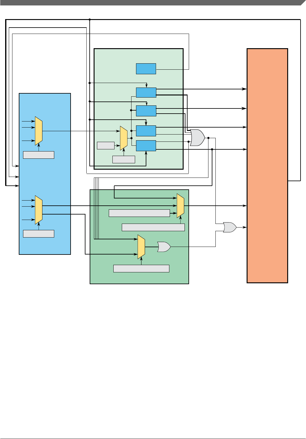
PDB0 pulse out
PDB0 CH0 trigger
ADC0_SC1A:B[COCO]
TRGMUX_PDB0
63
•
•
•
1
0
out[15:12]
SIM_ADCOPT [ADC0PRETRGSEL]
SWTRG
PDB_SC[TRGSEL]
Channel 0
Channel 1
Pulse-out
Ch0
pretriggers[7:0]
out56
PDB0 Ch1
pretriggers[7:4]
PDB trigger
ACK[7:0]
ADHWTS I:P
ADC_SC1A:DD[COCO]
PDB0
TRGMUX_ADC0
63
•
•
•
1
0Pretriggers[3:0]
Triggers[3:0]
in36
in34
in[31:30]
Ch0 trigger
Trigger_in0
Ch1
pretriggers[7:0]
Pulse-out
trigger
ACK[15:8]
Ch1 trigger
PDB0 Ch1 pretriggers[3:0]
PDB pretriggers[3:0]
TRGMUX pretriggers[3:0]
SIM_ADCOPT [ADC0TRGSEL]
TRGMUX triggers[3:0]
PDB trigger
ADHWTS E:H
ADHWTS A:D
ADHWT
SIM_ADCOPT [ADC0SWPRETRG]
Trigger Latching and Arbitration Unit*
* The block depicts simplified schematic and doesn’t show detailed latching. See section 'Trigger Latching and Arbitration' of ADC chapter for details
Channel 2
Channel 3 ADHWTS Y:DD
ADHWTS Q:X
ADC0
TRGMUX
ACK[31:24]
ACK[23:16]
Figure 46-1. ADC triggering scheme
46.2 Introduction
46.2.1 Overview
LPIT is a low power periodic interrupt timer with multiple timer channels. After a timer
reaches a programmed count, the respective timer channel will generate pre-trigger and
trigger output signals, and these pre-trigger and trigger outputs can be used to trigger
other modules on the device.
Chapter 46 Low Power Interrupt Timer (LPIT)
S32K1xx Series Reference Manual, Rev. 7, 04/2018
NXP Semiconductors 1363
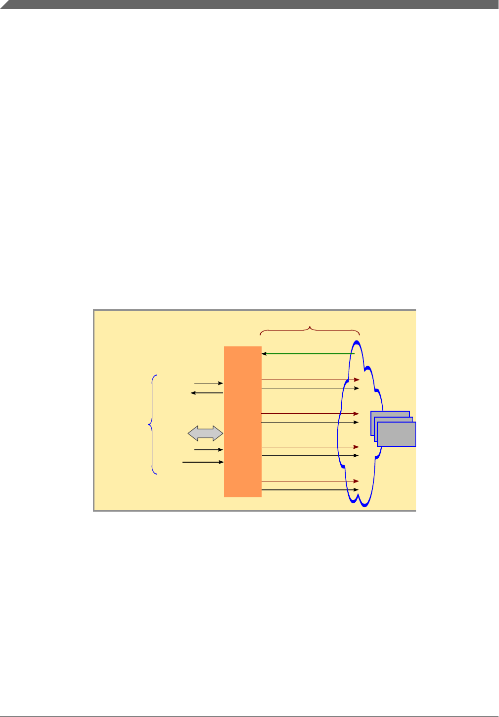
• Timers can be configured to be controlled using:
• external triggers (triggers from outside the LPIT module)
• or internal triggers (triggers from other timer channels inside the LPIT module).
• The timer channels can be chained together, to form a larger width timer.
• Depending on the timer modes, the timer channels may reload and count again, or
stop after reaching the programmed count.
The next figure shows the interface of an LPIT module to the other modules on the SoC.
• The CPU interface provides the clock, reset, register read/write bus interface and
handles interrupts from an LPIT.
• The trigger output signals from an LPIT may trigger other modules on the SoC, like
the DMA, ADC, and other modules.
• Similarly, other timer modules may provide trigger inputs to an LPIT module, to
control when an LPIT timer channel starts.
For the exact module interactions, see the SoC Configuration chapter in your device's
hardware Reference Manual (RM).
Interrupt
Bus Clock
IPS Bus
Async Reset
External
(per channel)
Trig Out 0
Pre-Trig Out 0
Trig Out 1
Pre-Trig Out 1
Trig Out 2
Pre-Trig Out 2
Trig Out n-1
Pre-Trig Out n-1
Trigger Inputs
LPIT
Async
Peripheral Clock
System-on-a-Chip (SoC)
Modules
Triggering
CPU
Interface
Figure 46-2. LPIT Interface in SoC
Each timer channel in LPIT can be configured to work in either compare modes or
capture modes.
•In compare mode: the timers decrement when enabled and generate an output pre-
trigger and trigger output. The trigger output is 1 clock cycle delayed of the pre-
trigger pulse. Each timer channel start, reload and restart can be controlled via
control bits. The timer can be configured to always decrement from a programmed
Introduction
S32K1xx Series Reference Manual, Rev. 7, 04/2018
1364 NXP Semiconductors

start value, or decrement on selected trigger inputs or previous channel timeout
(when channels are chained). By chaining timer channels, applications can achieve
larger timeout durations.
•In capture mode: the timer can be used to perform measurements as the timer value
is captured (in the timer value register) when a selected trigger input is asserted. The
timer can support once-off or multiple measurements (like frequency measurements).
The timer channels operate on an asynchronous clock, which is independent from the
register read/write access clock. Clock synchronization between the clock domains
ensures normal operations.
46.2.2 Block Diagram
The next figure shows a detailed block diagram for an LPIT module. The programming
model comprises of a global register set (common to all timer channels), and registers for
each timer channel (that control their respective timer channels). Access to these registers
gets synchronized to the asynchronous peripheral clock, then affects the timer channel
registers.
• Each timer channel contains a 32-bit counter that loads the starting value and down
counts on every peripheral clock's positive edge.
• After reaching a zero value (a channel timer timeout), a trigger output is generated.
• The counter enable is controlled using a timer enable register control bit, external or
internal triggers or via previous channel timeout (when using timer chaining).
• After a channel timer timeout, an interrupt bit is also set, to tell the CPU about the
timer timeout.
For more details, see the functional description section.
Chapter 46 Low Power Interrupt Timer (LPIT)
S32K1xx Series Reference Manual, Rev. 7, 04/2018
NXP Semiconductors 1365
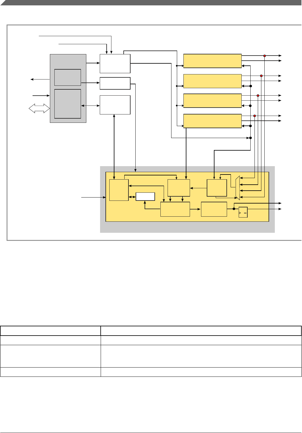
LPIT
IPS Bus
Interface
Global
Registers
Channel
Registers
Interrupt
Bus Clock
IPS Bus
Global
Synchronizers
Timer
Freeze
Trig Out 0
Pre-Trig Out 0
Low Power
Clock Gate
Timer Channel 0
Timer Channel 1
Timer Channel 2
Timer Channel n-1
Trig Out 1
Pre-Trig Out 1
Trig Out 2
Pre-Trig Out 2
Trig Out n-1
Pre-Trig Out n-1
Pre-Trig Out n
Trig Out n
Previous
Channel
Timeout
Channel
Registers
Async IRQ bit
32-bit Counter
Trigger Out
Generation
Trigger Rising
Edge
Trigger
Select
Logic that is in every Timer Channel
Counter
Control
Peripheral Clock
DQ
Q
Access
Interface
Async Reset
External Trigger Inputs
(per channel) Sync'ed Reset to all Timer channels
Channel Registers
Access Synchronizer
Counter Value
Timeout
Load Enable
Sync'ed
External
Triggers
(per channel)
Timer Channel n
Figure 46-3. Detailed Block Diagram
46.3 Modes of operation
The LPIT module supports the following chip modes.
Table 46-2. Chip modes supported by the LPIT module
Chip mode LPIT Operation
Run Normal operation
Stop Can continue operating, if the Doze Enable bit (MCR[DOZE_EN]) is set and the
LPIT is using an external or internal clock source that remains operating during
stop mode.
Debug Can continue operating provided the Debug Enable bit (MCR[DBG_EN]) is set.
Modes of operation
S32K1xx Series Reference Manual, Rev. 7, 04/2018
1366 NXP Semiconductors

Memory Map and Registers
46.4.1 LPIT register descriptions
The memory map comprises of 32-bit aligned registers, which can be accessed via 8-bit,
16-bit, or 32-bit accesses.
• Write access to reserved locations will generate a transfer error.
• Read access to reserved locations will also generate a transfer error, and the read data
bus will show all 0s.
NOTE
• The Memory Map and complete module is in Big Endian
format.
• The LPIT module will not check if programmed values in
the registers are correct; software must ensure that correct
programmed values are being written.
46.4.1.1 LPIT Memory map
LPIT base address: 4003_7000h
Offset Register Width
(In bits)
Access Reset value
0h Version ID Register (VERID) 32 RO 0100_0000h
4h Parameter Register (PARAM) 32 RO 0000_0404h
8h Module Control Register (MCR) 32 RW 0000_0000h
Ch Module Status Register (MSR) 32 W1C 0000_0000h
10h Module Interrupt Enable Register (MIER) 32 RW 0000_0000h
14h Set Timer Enable Register (SETTEN) 32 RW 0000_0000h
18h Clear Timer Enable Register (CLRTEN) 32 WORZ 0000_0000h
20h Timer Value Register (TVAL0) 32 RW 0000_0000h
24h Current Timer Value (CVAL0) 32 RO FFFF_FFFFh
28h Timer Control Register (TCTRL0) 32 RW 0000_0000h
30h Timer Value Register (TVAL1) 32 RW 0000_0000h
34h Current Timer Value (CVAL1) 32 RO FFFF_FFFFh
38h Timer Control Register (TCTRL1) 32 RW 0000_0000h
40h Timer Value Register (TVAL2) 32 RW 0000_0000h
Table continues on the next page...
46.4
Chapter 46 Low Power Interrupt Timer (LPIT)
S32K1xx Series Reference Manual, Rev. 7, 04/2018
NXP Semiconductors 1367
Offset Register Width
(In bits)
Access Reset value
44h Current Timer Value (CVAL2) 32 RO FFFF_FFFFh
48h Timer Control Register (TCTRL2) 32 RW 0000_0000h
50h Timer Value Register (TVAL3) 32 RW 0000_0000h
54h Current Timer Value (CVAL3) 32 RO FFFF_FFFFh
58h Timer Control Register (TCTRL3) 32 RW 0000_0000h
46.4.1.2 Version ID Register (VERID)
46.4.1.2.1 Offset
Register Offset
VERID 0h
46.4.1.2.2 Diagram
Bits 31 30 29 28 27 26 25 24 23 22 21 20 19 18 17 16
RMAJOR MINOR
W
Reset 0 0 0 0 0 0 0 1 0 0 0 0 0 0 0 0
Bits 15 14 13 12 11 10 9 8 7 6 5 4 3 2 1 0
RFEATURE
W
Reset 0 0 0 0 0 0 0 0 0 0 0 0 0 0 0 0
46.4.1.2.3 Fields
Field Function
31-24
MAJOR
Major Version Number
Returns the major version number for the module design specification. Read-only field.
23-16
MINOR
Minor Version Number
Returns the minor version number for the module design specification. Read-only field.
15-0
FEATURE
Feature Number
Returns the feature set number. Read-only field.
Memory Map and Registers
S32K1xx Series Reference Manual, Rev. 7, 04/2018
1368 NXP Semiconductors

46.4.1.3 Parameter Register (PARAM)
46.4.1.3.1 Offset
Register Offset
PARAM 4h
46.4.1.3.2 Function
Provides details on the parameter settings that were used while incorporating this module
into the device.
46.4.1.3.3 Diagram
Bits 31 30 29 28 27 26 25 24 23 22 21 20 19 18 17 16
R 0
W
Reset 0 0 0 0 0 0 0 0 0 0 0 0 0 0 0 0
Bits 15 14 13 12 11 10 9 8 7 6 5 4 3 2 1 0
REXT_TRIG CHANNEL
W
Reset 0 0 0 0 0 1 0 0 0 0 0 0 0 1 0 0
46.4.1.3.4 Fields
Field Function
31-16
—
This read-only field is reserved and always has the value 0
15-8
EXT_TRIG
Number of External Trigger Inputs
Number of external triggers implemented in this device
7-0
CHANNEL
Number of Timer Channels
Number of timer channels implemented in this device
Chapter 46 Low Power Interrupt Timer (LPIT)
S32K1xx Series Reference Manual, Rev. 7, 04/2018
NXP Semiconductors 1369

46.4.1.4 Module Control Register (MCR)
46.4.1.4.1 Offset
Register Offset
MCR 8h
46.4.1.4.2 Diagram
Bits 31 30 29 28 27 26 25 24 23 22 21 20 19 18 17 16
R 0
W
Reset 0 0 0 0 0 0 0 0 0 0 0 0 0 0 0 0
Bits 15 14 13 12 11 10 9 8 7 6 5 4 3 2 1 0
R
0
DBG_E
N
DOZE_EN
SW_RS
T
M_CEN
W
Reset 0 0 0 0 0 0 0 0 0 0 0 0 0 0 0 0
46.4.1.4.3 Fields
Field Function
31-4
—
This read-only field is reserved and always has the value 0
3
DBG_EN
Debug Enable Bit
Stops the timer channels when the device enters Debug mode
0b - Stop timer channels in Debug mode
1b - Allow timer channels to continue to run in Debug mode
2
DOZE_EN
DOZE Mode Enable Bit
Stops the timer channels when the device enters DOZE mode
0b - Stop timer channels in DOZE mode
1b - Allow timer channels to continue to run in DOZE mode
1
SW_RST
Software Reset Bit
Resets all channels and registers, except the Module Control Register. The Software Reset bit remains
set until cleared by software.
NOTE: Before clearing the Software Reset bit, software must wait for 4 peripheral clocks (for clock
synchronization and reset propagation).
0b - Timer channels and registers are not reset
1b - Reset timer channels and registers
0 Module Clock Enable
Memory Map and Registers
S32K1xx Series Reference Manual, Rev. 7, 04/2018
1370 NXP Semiconductors

Field Function
M_CEN Enables the peripheral clock to the module timers.
• The Module Clock Enable bit must be asserted when writing to these registers:
• Module Status Register (MSR)
• Set Timer Enable Register (SETTEN)
• Clear Timer Enable Register (CLRTEN)
• Timer Control Registers (TCTRLn)
• Timer Value Registers (TVALn)
• To allow for clock synchronization and updating of register bits in the LPIT module, both the bus
clock and peripheral clock must be enabled.
• Writing to the MSR, SETTEN , CLRTEN, TCTRL, and TVAL registers while the Module Clock
Enable bit (M_CEN) = 0, will assert a transfer error for that bus cycle.
• Writing to Current Timer Value (CVALn) registers and Reserved registers will always generate a
transfer error.
NOTE: There may be additional clock gating bits in your device that gate the peripheral clock to the
LPIT module. Ensure that those additional clock gating bits are configured appropriately, to
enable the peripheral clock to the LPIT module.
0b - Disable peripheral clock to timers
1b - Enable peripheral clock to timers
46.4.1.5 Module Status Register (MSR)
46.4.1.5.1 Offset
Register Offset
MSR Ch
46.4.1.5.2 Function
NOTE
Unless the Module Clock Enable bit (MCR[M_CEN]) is set
(=1, peripheral clock to timers is enabled), reading or writing
the Module Status register will generate a transfer error.
Chapter 46 Low Power Interrupt Timer (LPIT)
S32K1xx Series Reference Manual, Rev. 7, 04/2018
NXP Semiconductors 1371

46.4.1.5.3 Diagram
Bits 31 30 29 28 27 26 25 24 23 22 21 20 19 18 17 16
R 0
W
Reset 0 0 0 0 0 0 0 0 0 0 0 0 0 0 0 0
Bits 15 14 13 12 11 10 9 8 7 6 5 4 3 2 1 0
R
0
TIF3
TIF2
TIF1
TIF0
W
W1C
W1C
W1C
W1C
Reset 0 0 0 0 0 0 0 0 0 0 0 0 0 0 0 0
46.4.1.5.4 Fields
Field Function
31-4
—
This read-only field is reserved and always has the value 0
3
TIF3
Channel 3 Timer Interrupt Flag
• In compare modes: at the end of the timer period, the channel timer interrupt flag is set to 1
• In capture modes: when the trigger asserts, the channel timer interrupt flag is set to 1
• To clear a channel timer interrupt flag, write logic 1 to it
• Writing 0 to a channel timer interrupt flag has no effect
0b - Timer has not timed out
1b - Timeout has occurred (timer has timed out)
2
TIF2
Channel 2 Timer Interrupt Flag
• In compare modes: at the end of the timer period, the channel timer interrupt flag is set to 1
• In capture modes: when the trigger asserts, the channel timer interrupt flag is set to 1
• To clear a channel timer interrupt flag, write logic 1 to it
• Writing 0 to a channel timer interrupt flag has no effect
0b - Timer has not timed out
1b - Timeout has occurred (timer has timed out)
1
TIF1
Channel 1 Timer Interrupt Flag
• In compare modes: at the end of the timer period, the channel timer interrupt flag is set to 1
• In capture modes: when the trigger asserts, the channel timer interrupt flag is set to 1
• To clear a channel timer interrupt flag, write logic 1 to it
• Writing 0 to a channel timer interrupt flag has no effect
0b - Timer has not timed out
1b - Timeout has occurred (timer has timed out)
0
TIF0
Channel 0 Timer Interrupt Flag
• In compare modes: at the end of the timer period, the channel timer interrupt flag is set to 1
• In capture modes: when the trigger asserts, the channel timer interrupt flag is set to 1
• To clear a channel timer interrupt flag, write logic 1 to it
• Writing 0 to a channel timer interrupt flag has no effect
Memory Map and Registers
S32K1xx Series Reference Manual, Rev. 7, 04/2018
1372 NXP Semiconductors

Field Function
0b - Timer has not timed out
1b - Timeout has occurred (timer has timed out)
46.4.1.6 Module Interrupt Enable Register (MIER)
46.4.1.6.1 Offset
Register Offset
MIER 10h
46.4.1.6.2 Diagram
Bits 31 30 29 28 27 26 25 24 23 22 21 20 19 18 17 16
R 0
W
Reset 0 0 0 0 0 0 0 0 0 0 0 0 0 0 0 0
Bits 15 14 13 12 11 10 9 8 7 6 5 4 3 2 1 0
R
0
TIE3
TIE2
TIE1
TIE0
W
Reset 0 0 0 0 0 0 0 0 0 0 0 0 0 0 0 0
46.4.1.6.3 Fields
Field Function
31-4
—
This read-only field is reserved and always has the value 0
3
TIE3
Channel 3 Timer Interrupt Enable
Enables interrupt generation when:
• the Channel 3 Timer Interrupt Enable bit (TIE3) is set to 1
• and if the corresponding Timer Interrupt Flag (MSR[TIF3]) is asserted (=1, timeout has occurred)
0b - Disabled
1b - Enabled
2
TIE2
Channel 2 Timer Interrupt Enable
Enables interrupt generation when:
• the Channel 2 Timer Interrupt Enable bit (TIE2) is set to 1
• and if the corresponding Timer Interrupt Flag (MSR[TIF2]) is asserted (=1, timeout has occurred)
Table continues on the next page...
Chapter 46 Low Power Interrupt Timer (LPIT)
S32K1xx Series Reference Manual, Rev. 7, 04/2018
NXP Semiconductors 1373

Field Function
0b - Disabled
1b - Enabled
1
TIE1
Channel 1 Timer Interrupt Enable
Enables interrupt generation when:
• the Channel 1 Timer Interrupt Enable bit (TIE1) is set to 1
• and if the corresponding Timer Interrupt Flag (MSR[TIF1]) is asserted (=1, timeout has occurred)
0b - Disabled
1b - Enabled
0
TIE0
Channel 0 Timer Interrupt Enable
Enables interrupt generation when:
• the Channel 0 Timer Interrupt Enable bit (TIE0) is set to 1
• and if the corresponding Timer Interrupt Flag (MSR[TIF0]) is asserted (=1, timeout has occurred)
0b - Disabled
1b - Enabled
46.4.1.7 Set Timer Enable Register (SETTEN)
46.4.1.7.1 Offset
Register Offset
SETTEN 14h
46.4.1.7.2 Function
The Set Timer Enable register allows the simultaneous enabling of timer channels.
• Timer channels can be enabled by
• either by writing '1' to Timer Enable bit (T_EN) in the respective TCTRLn
register,
•or by setting the corresponding Set Timer Enable bit (SET_T_EN_n) in the Set
Timer Enable register (SETTEN).
• To disable timer channels simultaneously, use the Clear Timer Enable register
(CLRTEN).
• Writing a '0' to the Set Timer Enable register has no effect.
NOTE
Unless the Module Clock Enable bit (MCR[M_CEN]) is set
(=1, peripheral clock to timers is enabled)), reading or writing
the Set Timer Enable register will generate a transfer error.
Memory Map and Registers
S32K1xx Series Reference Manual, Rev. 7, 04/2018
1374 NXP Semiconductors

46.4.1.7.3 Diagram
Bits 31 30 29 28 27 26 25 24 23 22 21 20 19 18 17 16
R 0
W
Reset 0 0 0 0 0 0 0 0 0 0 0 0 0 0 0 0
Bits 15 14 13 12 11 10 9 8 7 6 5 4 3 2 1 0
R
0
SET_T_EN_
3
SET_T_EN_
2
SET_T_EN_
1
SET_T_EN_
0
W
Reset 0 0 0 0 0 0 0 0 0 0 0 0 0 0 0 0
46.4.1.7.4 Fields
Field Function
31-4
—
This read-only field is reserved and always has the value 0
3
SET_T_EN_3
Set Timer 3 Enable
To enable timer channel 3, write '1' to Set Timer 3 Enable bit.
• The Set Timer 3 Enable bit can be used in addition to the Timer Enable bit (T_EN) in TCTRL3
register.
• Writing a 0 to Set Timer 3 Enable bit will not disable the counter.
• The Set Timer 3 Enable bit will be cleared
• when Timer Enable bit (TCTRL3[T_EN]) is set to 0
• or when '1' is written to the Clear Timer 3 Enable bit (CLRTEN[CLR_T_EN_3]).
0b - No effect
1b - Enables Timer Channel 3
2
SET_T_EN_2
Set Timer 2 Enable
To enable timer channel 2, write '1' to Set Timer 2 Enable bit.
• The Set Timer 2 Enable bit can be used in addition to the Timer Enable bit (T_EN) in TCTRL2
register.
• Writing a 0 to Set Timer 2 Enable bit will not disable the counter.
• The Set Timer 2 Enable bit will be cleared
• when Timer Enable bit (TCTRL2[T_EN]) is set to 0
• or when '1' is written to the Clear Timer 2 Enable bit (CLRTEN[CLR_T_EN_2]).
0b - No Effect
1b - Enables Timer Channel 2
1
SET_T_EN_1
Set Timer 1 Enable
To enable timer channel 1, write '1' to Set Timer 1 Enable bit.
• The Set Timer 1 Enable bit can be used in addition to the Timer Enable bit (T_EN) in TCTRL1
register.
• Writing a 0 to Set Timer 1 Enable bit will not disable the counter.
• The Set Timer 1 Enable bit will be cleared
Table continues on the next page...
Chapter 46 Low Power Interrupt Timer (LPIT)
S32K1xx Series Reference Manual, Rev. 7, 04/2018
NXP Semiconductors 1375

Field Function
• when Timer Enable bit (TCTRL1[T_EN]) is set to 0
• or when '1' is written to the Clear Timer 1 Enable bit (CLRTEN[CLR_T_EN_1]).
0b - No Effect
1b - Enables Timer Channel 1
0
SET_T_EN_0
Set Timer 0 Enable
To enable timer channel 0, write '1' to Set Timer 0 Enable bit.
• The Set Timer 0 Enable bit can be used in addition to the Timer Enable bit (T_EN) in TCTRL0
register.
• Writing a 0 to Set Timer 0 Enable bit will not disable the counter.
• The Set Timer 0 Enable bit will be cleared
• when Timer Enable bit (TCTRL0[T_EN]) is set to 0
• or when '1' is written to the Clear Timer 0 Enable bit (CLRTEN[CLR_T_EN_0]).
0b - No effect
1b - Enables Timer Channel 0
46.4.1.8 Clear Timer Enable Register (CLRTEN)
46.4.1.8.1 Offset
Register Offset
CLRTEN 18h
46.4.1.8.2 Function
NOTE
Unless the Module Clock Enable bit (MCR[M_CEN]) is set
(=1, peripheral clock to timers is enabled), reading or writing
the Clear Timer Enable register will generate a transfer error.
Memory Map and Registers
S32K1xx Series Reference Manual, Rev. 7, 04/2018
1376 NXP Semiconductors

46.4.1.8.3 Diagram
Bits 31 30 29 28 27 26 25 24 23 22 21 20 19 18 17 16
R 0
W
Reset 0 0 0 0 0 0 0 0 0 0 0 0 0 0 0 0
Bits 15 14 13 12 11 10 9 8 7 6 5 4 3 2 1 0
R
0
0
0
0
0
W
CLR_T_EN_3
CLR_T_EN_2
CLR_T_EN_1
CLR_T_EN_0
Reset 0 0 0 0 0 0 0 0 0 0 0 0 0 0 0 0
46.4.1.8.4 Fields
Field Function
31-4
—
This read-only field is reserved and always has the value 0
3
CLR_T_EN_3
Clear Timer 3 Enable
• To disable timer channel 3, write '1' to Clear Timer 3 Enable bit.
• The Clear Timer 3 Enable bit can be used in addition to Timer Enable bit (T_EN) in TCTRL3
register.
• Writing a 1 to Clear Timer 3 Enable bit will not enable the counter.
• The Clear Timer 3 Enable bit is self-clearing, which means that the Clear Timer 3 Enable bit will
always read 0.
0b - No Action
1b - Clear the Timer Enable bit (TCTRL3[T_EN]) for Timer Channel 3
2
CLR_T_EN_2
Clear Timer 2 Enable
• To disable timer channel 2, write '1' to Clear Timer 2 Enable bit.
• The Clear Timer 2 Enable bit can be used in addition to Timer Enable bit (T_EN) in TCTRL2
register.
• Writing a 1 to Clear Timer 2 Enable bit will not enable the counter.
• The Clear Timer 2 Enable bit is self-clearing, which means that the Clear Timer 2 Enable bit will
always read 0.
0b - No Action
1b - Clear the Timer Enable bit (TCTRL2[T_EN]) for Timer Channel 2
1
CLR_T_EN_1
Clear Timer 1 Enable
• To disable timer channel 1, write '1' to Clear Timer 1 Enable bit.
• The Clear Timer 1 Enable bit can be used in addition to Timer Enable bit (T_EN) in TCTRL1
register.
• Writing a 1 to Clear Timer 1 Enable bit will not enable the counter.
• The Clear Timer 1 Enable bit is self-clearing, which means that the Clear Timer 1 Enable bit will
always read 0.
Table continues on the next page...
Chapter 46 Low Power Interrupt Timer (LPIT)
S32K1xx Series Reference Manual, Rev. 7, 04/2018
NXP Semiconductors 1377

Field Function
0b - No Action
1b - Clear the Timer Enable bit (TCTRL1[T_EN]) for Timer Channel 1
0
CLR_T_EN_0
Clear Timer 0 Enable
• To disable timer channel 0, write '1' to Clear Timer 0 Enable bit.
• The Clear Timer 0 Enable bit can be used in addition to Timer Enable bit (T_EN) in TCTRL0
register.
• Writing a 1 to Clear Timer 0 Enable bit will not enable the counter.
• The Clear Timer 0 Enable bit is self-clearing, which means that the Clear Timer 0 Enable bit will
always read 0.
0b - No action
1b - Clear the Timer Enable bit (TCTRL0[T_EN]) for Timer Channel 0
46.4.1.9 Timer Value Register (TVAL0 - TVAL3)
46.4.1.9.1 Offset
For n = 0 to 3:
Register Offset
TVALn 20h + (n × 10h)
46.4.1.9.2 Function
•In compare modes: the Timer Value Registers (TVALn) select the timeout period for
the timer channels.
•In capture modes: the Timer Value Registers (TVALn) are loaded with the value of
the counter when the trigger asserts.
NOTE
Unless the Module Clock Enable bit (MCR[M_CEN]) is set
(=1, peripheral clock to timers is enabled), then reading or
writing the TVALn register will generate a transfer error.
Memory Map and Registers
S32K1xx Series Reference Manual, Rev. 7, 04/2018
1378 NXP Semiconductors

46.4.1.9.3 Diagram
Bits 31 30 29 28 27 26 25 24 23 22 21 20 19 18 17 16
RTMR_VAL
W
Reset 0 0 0 0 0 0 0 0 0 0 0 0 0 0 0 0
Bits 15 14 13 12 11 10 9 8 7 6 5 4 3 2 1 0
RTMR_VAL
W
Reset 0 0 0 0 0 0 0 0 0 0 0 0 0 0 0 0
46.4.1.9.4 Fields
Field Function
31-0
TMR_VAL
Timer Value
• In compare mode: Timer Value (TMR_VAL) is the timer channel start value.
• The timer will count down until the timer reaches 0, then the timer will generate an interrupt
and load the Timer Value register (TVALn) value again.
• Writing a new value to the Timer Value register (TVALn) will not restart the timer channel;
instead the new value will be loaded after the timer expires.
• To abort the current timer cycle and start a timer period with a new value, the timer channel
must be disabled and enabled again.
• In capture mode: whenever the trigger asserts, the Timer Value register stores the inverse of the
counter value.
00000000000000000000000000000000b - Invalid load value in compare mode
00000000000000000000000000000001b - Invalid load value in compare mode
00000000000000000000000000000010-11111111111111111111111111111111b - In compare
mode: the value to be loaded; in capture mode, the value of the timer
46.4.1.10 Current Timer Value (CVAL0 - CVAL3)
46.4.1.10.1 Offset
For n = 0 to 3:
Register Offset
CVALn 24h + (n × 10h)
46.4.1.10.2 Function
The Current Timer Value registers indicate the current timer counter value.
Chapter 46 Low Power Interrupt Timer (LPIT)
S32K1xx Series Reference Manual, Rev. 7, 04/2018
NXP Semiconductors 1379

46.4.1.10.3 Diagram
Bits 31 30 29 28 27 26 25 24 23 22 21 20 19 18 17 16
RTMR_CUR_VAL
W
Reset 1 1 1 1 1 1 1 1 1 1 1 1 1 1 1 1
Bits 15 14 13 12 11 10 9 8 7 6 5 4 3 2 1 0
RTMR_CUR_VAL
W
Reset 1 1 1 1 1 1 1 1 1 1 1 1 1 1 1 1
46.4.1.10.4 Fields
Field Function
31-0
TMR_CUR_VAL
Current Timer Value
Represents the current timer value, if the timer is enabled.
46.4.1.11 Timer Control Register (TCTRL0 - TCTRL3)
46.4.1.11.1 Offset
For n = 0 to 3:
Register Offset
TCTRLn 28h + (n × 10h)
46.4.1.11.2 Function
The Timer Control registers contain the control bits for each timer channel.
NOTE
• Unless the peripheral clock to the timers is enabled
(Module Clock Enable bit (MCR[M_CEN]) is set (=1)),
Memory Map and Registers
S32K1xx Series Reference Manual, Rev. 7, 04/2018
1380 NXP Semiconductors

then reading or writing the Timer Control register will
generate a transfer error.
• Timer controls should only be updated when the timer is
disabled. In the Timer Control Register TCTRLn, these
timer controls include:
• Trigger Select TRG_SEL
• Trigger Source TRG_SRC
• Timer Reload On Trigger TROT
• Timer Stop On Interrupt TSOI
• Timer Start On Trigger TSOT
• Timer Operation Mode MODE
• Chain Channel CHAIN
There are 2 ways to disable a timer: write 1 to the specific
timer's Clear Timer Enable register bit
(CLRTEN[CLR_T_EN_n]) or set the timer enable bit
(TCTRLn[T_EN]) = 0 for that channel.
46.4.1.11.3 Diagram
Bits 31 30 29 28 27 26 25 24 23 22 21 20 19 18 17 16
R
0
TRG_SE
L
TRG_SR
C
0
TROT
TSOI
TSOT
W
Reset 0 0 0 0 0 0 0 0 0 0 0 0 0 0 0 0
Bits 15 14 13 12 11 10 9 8 7 6 5 4 3 2 1 0
R
0
MODE
CHAIN
T_E
N
W
Reset 0 0 0 0 0 0 0 0 0 0 0 0 0 0 0 0
46.4.1.11.4 Fields
Field Function
31-28
—
This read-only field is reserved and always has the value 0
27-24
TRG_SEL
Trigger Select
Selects the trigger to use for starting and/or reloading the LPIT timer.
• The TRG_SEL field selects one trigger from the set of internal or external triggers that are selected
by the Trigger Source bit (TRG_SRC)
• Recall that the TRG_SRC bit selects between internal and external trigger signals for each channel
Table continues on the next page...
Chapter 46 Low Power Interrupt Timer (LPIT)
S32K1xx Series Reference Manual, Rev. 7, 04/2018
NXP Semiconductors 1381

Field Function
NOTE: The Trigger Select field should only be changed when the LPIT timer channel is disabled.
0000-0011b - Timer channel 0 - 3 trigger source is selected
0100-1111b - Reserved
23
TRG_SRC
Trigger Source
Selects between internal or external trigger sources. The trigger to be used is selected using the
TRG_SRC and TRG_SEL bits.
Refer to the chip configuration section for available external trigger options. If a channel does not have an
associated external trigger, then set the Trigger Source bit (TRG_SRC) = 1.
0b - Selects external triggers
1b - Selects internal triggers
22-19
—
This read-only field is reserved and always has the value 0
18
TROT
Timer Reload On Trigger
When set, the LPIT timer will reload when a rising edge is detected on the selected trigger input. The
trigger input is ignored if the LPIT is disabled during debug mode (DBGEN = 0) or DOZE mode
(DOZE_EN = 0)
0b - Timer will not reload on the selected trigger
1b - Timer will reload on the selected trigger
17
TSOI
Timer Stop On Interrupt
Controls whether the channel timer will stop after it (the channel timer) times out or not.
0b - The channel timer does not stop after timeout
1b - The channel timer will stop after a timeout, and the channel timer will restart based on Timer
Start On Trigger bit (TSOT). When TSOT = 0, the channel timer will restart after a rising edge on
the Timer Enable bit (T_EN) is detected (which means that the timer channel is disabled and then
enabled). When TSOT = 1, the channel timer will restart after a rising edge on the selected trigger
is detected.
16
TSOT
Timer Start On Trigger
Controls when the timer starts decrementing.
0b - Timer starts to decrement immediately based on the restart condition (controlled by the Timer
Stop On Interrupt bit (TSOI))
1b - Timer starts to decrement when a rising edge on a selected trigger is detected
15-4
—
This read-only field is reserved and always has the value 0
3-2
MODE
Timer Operation Mode
Configures the channel timer's mode of operation. The MODE bits control how the timer decrements.
00b - 32-bit Periodic Counter
01b - Dual 16-bit Periodic Counter
10b - 32-bit Trigger Accumulator
11b - 32-bit Trigger Input Capture
1
CHAIN
Chain Channel
When enabled, the timer channel will decrement when timer channel N-1 trigger asserts. Timer channel 0
cannot be chained.
0b - Channel Chaining is disabled. The channel timer runs independently.
1b - Channel Chaining is enabled. The timer decrements on the previous channel's timeout.
0
T_EN
Timer Enable
Enables or disables the Timer Channel
0b - Timer Channel is disabled
1b - Timer Channel is enabled
Memory Map and Registers
S32K1xx Series Reference Manual, Rev. 7, 04/2018
1382 NXP Semiconductors
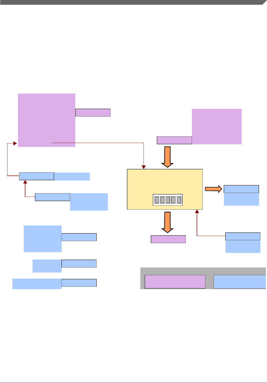
46.5 Functional description
46.5.1 LPIT programming model
Low Power Periodic Interrupt Timer (LPIT)
32/16-bit Counter
Module Control
MCR[...]
Module Status
MSR[...]
Version ID
VERID[...]
Parameter
PARAM[...]
Module Interrupt Enable
MIER[...]
Set Timer Enable
SETTEN[...]
Clear Timer Enable
CLRTEN[...]
Timer Value
TVALn[...]
Current Timer
CVALn[...]
Value
Timer Control
TCTRLn[...]
Number of timers
Number of external
Debug mode
Doze mode
Timer interrupt
flags
Timer interrupt
enables
Timer enables
Disable timers
by clearing
Compare modes:
Timeout period
Counter modes
Chaining channels
Programming Model
trigger inputs
Module clock
Software reset
timer enables
Capture modes:
Timer value when
trigger is asserted
Select Trigger
Select Trigger sources
Timer enables
Timer Reload on Trigger
Timer Stop on Interrupt
Timer Start on Trigger
Device
Identifiers
or Trigger Accumulator
or Trigger Input Capture
12
3
4
5
Load a
Read
starting
value
Timer Enable T_EN
Sets T_EN bit
in Timer Control Register
Interrupt Enable
TIE_n
Channel n Timer
Channel registers must
be set for each channel Global registers must
only be set once
Figure 46-4. Programming Model
Global registers need only be set once:
• Version ID Register (VERID)
• Parameter Register (PARAM)
• Module Control Register (MCR)
• Module Status Register (MSR)
• Module Interrupt Enable Register (MIER)
Chapter 46 Low Power Interrupt Timer (LPIT)
S32K1xx Series Reference Manual, Rev. 7, 04/2018
NXP Semiconductors 1383

• Set Timer Enable Register (SETTEN)
• Clear Timer Enable Register (CLRTEN)
Channel registers must be set for each channel:
• Timer Value Register (TVAL0 - TVAL3)
• Current Timer Value (CVAL0 - CVAL3)
• Timer Control Register (TCTRL0 - TCTRL3)
46.5.2 Initialization
Table 46-3. Initializing the LPIT module
Step How? Why?
1 Enable the peripheral clock by setting the Module Clock Enable bit (M_CEN) in the Module Control Register
(MCR) register.
NOTE: • Writing to certain registers (MSR, SETTEN, CLRTEN, TVAL, and
TCTRL) while M_CEN = 0 will lead to assertion of a transfer error for
that bus access.
• Writing to CVAL and Reserved registers will generate a transfer
error, regardless of the value of the Module Clock Enable bit
(M_CEN) bit.
• Reads to CVAL and Reserved registers can happen regardless
of the M_CEN bit value.
• There might be additional clock gating bits in the device that gate the
peripheral clock to this module. When enabling the clock to this
module, ensure that software is configuring those additional clock
gating bits (in addition to M_CEN bit).
2 Wait for 4 peripheral clock
cycles
to allow time for clock synchronization and reset de-assertion.
3 Configure timer control bits for each timer channel that is to be enabled:
• timer mode of operation bits TCTRLn[MODE]
• trigger source selection bits TCTRLn[TRG_SEL, TRG_SRC]
• trigger control bits TCTRLn[TROT, TSOT, TSOI]
NOTE: Timer controls should only be updated when the timer is disabled. There are
2 ways to disable a timer: write 1 to the specific timer's Clear Timer Enable
register bit (CLRTEN[CLR_T_EN_n]) or set the timer enable bit
(TCTRLn[T_EN]) = 0 for that channel.
4 Configure the channels that
are to be chained
by setting the CHAIN bit in the corresponding channel's TCTRLn register.
5 Set the timer timeout value for channels configured in Compare Mode, by programming the appropriate value in
TVAL register for those channels.
6 Configure TIEn bits in MIER
register
for those channels that are required to generate interrupts on timer timeouts.
7 Configure the low power
modes of the module
by setting the DBG_EN and DOZE_EN bits in the MCR register. This is common to all
timer channels.
8 Enable the channel timers by setting the corresponding T_EN bit in the corresponding channel's TCRTLn
register.
Functional description
S32K1xx Series Reference Manual, Rev. 7, 04/2018
1384 NXP Semiconductors

Also:
• For channels configured in Capture Mode, the timer value can be read from TVALn
register when a channel timeout occurs.
• At any time, the current value of the timer for any channel can be read by reading the
corresponding channel's CVALn register.
• The timer interrupt flag bits (TIFn) in MSR register get asserted on timer timeout. To
clear these timer interrupt flag bits, write '1' to them.
46.5.3 Timer Modes
The timer mode is configured by setting an appropriate value in the MODE bits in
TCTRLn register.
Table 46-4. Timer modes that are supported
Timer Mode Operation
32-bit Periodic Counter • The counter will load, decrement down to 0
• which will set the timer interrupt flag and assert the output pre-trigger.
Dual 16-bit Periodic
Counter
• The counter will load, then the lower 16-bits will decrement down to 0
• which will assert the output pre-trigger.
• The upper 16-bits will then decrement down to 0
• which will set the timer interrupt flag and then negate the output pre-trigger.
32-bit Trigger
Accumulator
• The counter will load on the 1st trigger rising edge and then decrement down to 0 on each
trigger rising edge
• which will set the timer interrupt flag and assert the output pre-trigger.
32-bit Trigger Input
Capture
• The counter will load with 0xFFFF_FFFF and then decrement down to 0.
• If a trigger rising edge is detected,
• then it will store the inverse of the current counter value in the timer value register
• which will set the timer interrupt flag and assert the output pre-trigger.
The timer operation is controlled by Trigger Control bits (TSOT, TSOI, TROT) which
control the timer load, reload, start and restart of the timers.
NOTE
• The trigger output is asserted one Peripheral Timer Clock
cycle later than pre-trigger output. The trigger output and
the pre-trigger output de-assert at the same time.
• The pre-trigger output is asserted for 2 clock cycles and the
trigger output is asserted for 1 clock cycle (except in 16-bit
Periodic Counter mode, where both pre-trigger and trigger
are asserted for many cycles depending on
TMR_VAL[31:16]).
•Timer changes that are based on external triggers take
effect after 4 peripheral clocks after the actual external
Chapter 46 Low Power Interrupt Timer (LPIT)
S32K1xx Series Reference Manual, Rev. 7, 04/2018
NXP Semiconductors 1385

trigger assertion (due to clock synchronization, rise edge
detection and timer update).
46.5.4 Trigger Control for Timers
Various programmable bits control how the trigger inputs and the timer operate.
TRG_SEL and TRG_SRC select the timer triggers:
• Trigger Select (TRG_SEL) selects the input trigger for the channel from all of the
other channel's trigger outputs.
• Trigger Source (TRG_SRC) selects between the internal trigger and the external
trigger inputs to the channel.
The selected trigger affects how the timer operates, using the configuration of the TROT,
TSOI and TSOT bits.
Table 46-5. How bits control timer operations
If = Then
TSOI
Timer Stop On
Interrupt
1 then the counter stops on a Timer Interrupt flag (MSR[TIFn]) assertion. To reload and
decrement, it requires:
• a trigger (if TSOT = 1)
• a T_EN rising edge (if TSOT = 0)
0 then the counter does not stop after timeout
TROT
Timer Reload On
Trigger
1 then the counter is loaded on each trigger
0 then the counter is loaded on every T_EN rising edge or timeout rising edge (timeout not
used in Capture modes)
TSOT
Timer Start On
Trigger
1 then the counter will start to decrement on a trigger. Subsequent triggers are ignored until
the counter times out.
0 then the counter decrements immediately on the next clock edge. When channel is
Chained or in Capture mode, TSOT has no effect.
In different timer modes, these programmable bits affect the timer operation differently:
Table 46-6. Time modes and programmable bits
Mode Which programmable bits affect timer operations
32-bit Periodic Counter All bits (TSOT, TSOI, TROT) affect the timer operation as described previously.
Dual 16-bit Periodic
Counter
32-bit Trigger
Accumulator
• Only the TSOI bit controls the timer function.
• TROT and TSOT bits have no effect on timer operations.
32-bit Input Trigger
Capture
• Only TSOI and TROT bits control the timer function.
• TSOT bit has no effect on timer operations.
Functional description
S32K1xx Series Reference Manual, Rev. 7, 04/2018
1386 NXP Semiconductors

46.5.5 Channel Chaining
Individual timer channels can be chained together to achieve a larger value of timeout.
Chaining the timer channel causes them to work in a 'nested loop' manner thereby leading
to an effective timeout value of TVALCHn × (TVALCHn-1 + 1).
The channels are chained by setting the CHAIN bit in corresponding channel's
TCTRLCHn register. When a channel is chained, that channel's timer decrements on
previous channel's timeout pulse, regardless of the timer mode (MODE bits). The TSOT
bit does not have any effect if the channel timer (Channel 'n') is chained to previous
channel's timer (Channel 'n-1').
46.5.6 Detailed timing
NOTE
The timing diagrams in these sections are not cycle-accurate
(i.e., some cycles may not be shown), but the timing diagrams
do show the timer channel behavior across several clock cycles.
Table 46-7. Timing diagrams list
Mode Timing Diagram TSOT TROT TSOI CHAIN
32-bit periodic
counter (compare
mode)
00 Figure 46-5 0 0 0 0
Figure 46-6 0 0 1 0
Figure 46-7 0 1 0 0
Figure 46-8 0 1 1 0
Figure 46-9 1 0 0 0
Figure 46-10 1 0 1 0
Figure 46-11 1 1 0 0
Figure 46-12 1 1 1 0
16-bit dual periodic
counter (compare
mode)
01 Figure 46-13 0 0 0 0
32-bit trigger
accumulator mode
10 Figure 46-14 X X 0 0
Figure 46-15 X X 1 0
32-bit trigger capture
mode
11 Figure 46-16 X 0 0 0
Figure 46-17 X 1 0 0
Figure 46-18 X 0 1 0
Timer chaining:
effects on timing
operations
-Figure 46-19 - - - -
Chapter 46 Low Power Interrupt Timer (LPIT)
S32K1xx Series Reference Manual, Rev. 7, 04/2018
NXP Semiconductors 1387
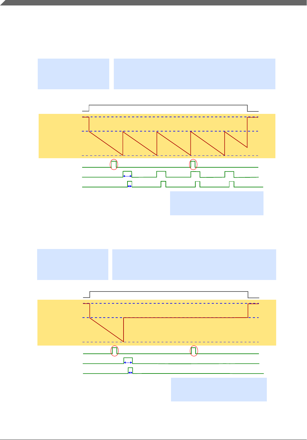
46.5.6.1 Mode=00: 32-bit periodic counter (compare mode)
Mode=00
Mode00Case1.svg
Case 1: TSOT=0,TROT=0,TSOI=0,CHAIN=0
32-bit Periodic Counter
Operation:
-In Mode=00, the counter will load
and then decrement down to zero
-The counter will next set the timer interrrupt flag
and assert the output pre-trigger
T_EN
0xFFFF_FFFF
TMR_VAL
TMR_CUR_VAL
0x0000_0000
IN_TRIG
PRE_TRIG_OUT
TRIG_OUT
Trigger is
ignored
Countdown
is based on the
selected clock
Trigger is
ignored
1 clock
TSOT=0
TROT=0
TSOI=0
CHAIN=0
-For a use case requiring repeated interrupts with reload
-Trigger outputs will have equal periods
2 clocks
TMR_VAL is in TVALn register
TMR_CUR_VAL is in CVALn register
(Compare Mode)
Figure 46-5. Case 1: TSOT = 0, TROT = 0, TSOI = 0, CHAIN = 0
Mode00Case2.svg
Case 2: TSOT=0,TROT=0,TSOI=1,CHAIN=0
Operation:
-In Mode=00, the counter will load
and then decrement down to zero
-The counter will next set the timer interrrupt flag
and assert the output pre-trigger
-Useful for a one-shot trigger mode
-Timer will start again when T_EN is made to 1
T_EN
0xFFFF_FFFF
TMR_VAL
TMR_CUR_VAL
0x0000_0000
IN_TRIG
PRE_TRIG_OUT
TRIG_OUT
Trigger is
ignored
Countdown
is based on the
selected clock
Trigger is
ignored
1 clock
TSOT=0
TROT=0
TSOI=1
CHAIN=0
Timer reloads
and stops after timeout Timer resets
when T_EN=0
2 clocks
TMR_VAL is in TVALn register
TMR_CUR_VAL is in CVALn register
Mode=00
32-bit Periodic Counter
(Compare Mode)
Figure 46-6. Case 2: TSOT = 0, TROT = 0, TSOI = 1, CHAIN = 0
Functional description
S32K1xx Series Reference Manual, Rev. 7, 04/2018
1388 NXP Semiconductors
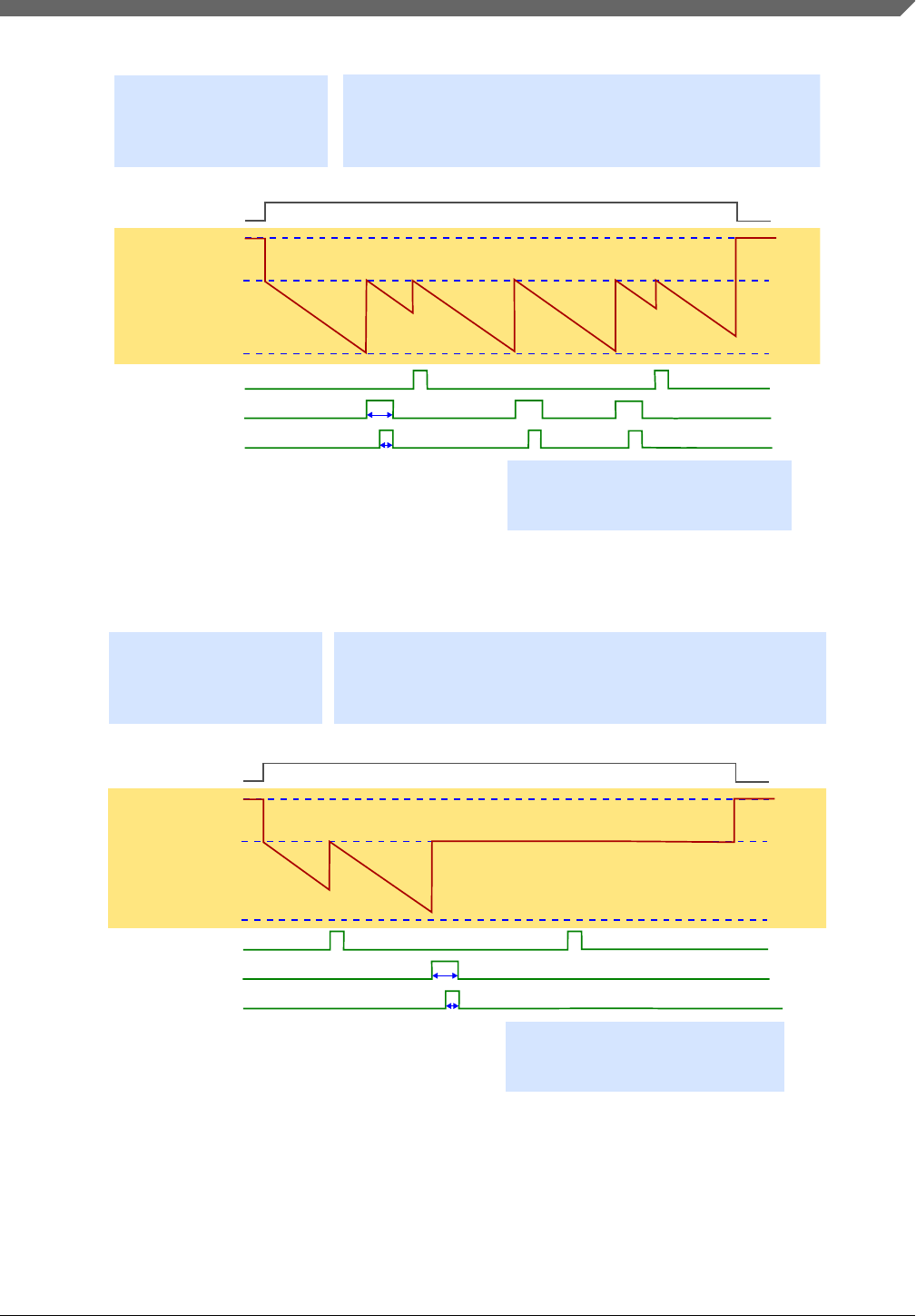
Mode00Case3.svg
Case 3: TSOT=0,TROT=1,TSOI=0,CHAIN=0
Operation:
-In Mode=00, the counter will load
and then decrement down to zero
-The counter will next set the timer interrrupt flag
and assert the output pre-trigger
-For a use case requiring repeated interrupts with reload
-Trigger outputs will have unequal periods
T_EN
0xFFFF_FFFF
TMR_VAL
TMR_CUR_VAL
0x0000_0000
IN_TRIG
PRE_TRIG_OUT
TRIG_OUT
Countdown
is based on the
selected clock
1 clock
TSOT=0
TROT=1
TSOI=0
CHAIN=0
Trigger reloads value
on input trigger
Trigger reloads value
on input trigger
Timer resets
when T_EN=0
2 clocks
TMR_VAL is in TVALn register
TMR_CUR_VAL is in CVALn register
Mode=00
32-bit Periodic Counter
(Compare Mode)
Figure 46-7. Case 3: TSOT = 0, TROT = 1, TSOI = 0, CHAIN = 0
Mode00Case4.svg
Case 4: TSOT=0,TROT=1,TSOI=1,CHAIN=0
Operation:
-In Mode=00, the counter will load
and then decrement down to zero
-The counter will next set the timer interrrupt flag
and assert the output pre-trigger
-For a one-shot timer with reload before timeout of timer mode
-Timer will start again when T_EN is made to 1
T_EN
0xFFFF_FFFF
TMR_VAL
TMR_CUR_VAL
0x0000_0000
IN_TRIG
PRE_TRIG_OUT
TRIG_OUT
Countdown
is based on the
selected clock
1 clock
TSOT=0
TROT=1
TSOI=1
CHAIN=0
Trigger reloads value
on input trigger
Trigger reloads value
and stops after timeout
Timer resets
when T_EN=0
2 clocks
TMR_VAL is in TVALn register
TMR_CUR_VAL is in CVALn register
Mode=00
32-bit Periodic Counter
(Compare Mode)
Figure 46-8. Case 4: TSOT = 0, TROT = 1, TSOI = 1, CHAIN = 0
Chapter 46 Low Power Interrupt Timer (LPIT)
S32K1xx Series Reference Manual, Rev. 7, 04/2018
NXP Semiconductors 1389
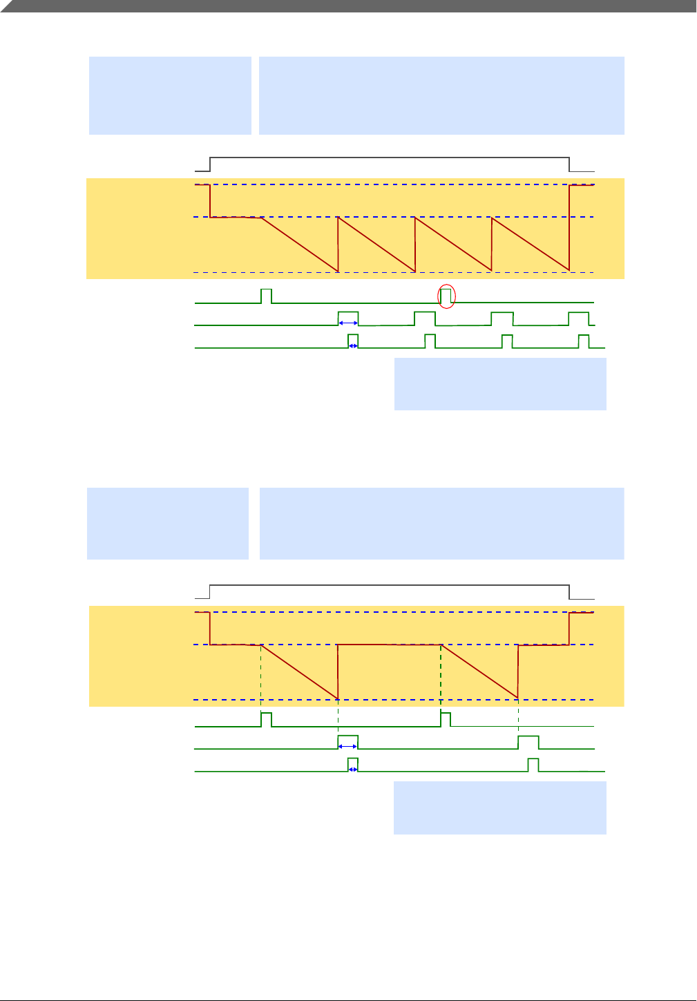
Mode00Case5.svg
Case 5: TSOT=1,TROT=0,TSOI=0,CHAIN=0
Operation:
-In Mode=00, the counter will load
and then decrement down to zero
-The counter will next set the timer interrrupt flag
and assert the output pre-trigger
T_EN
0xFFFF_FFFF
TMR_VAL
TMR_CUR_VAL
0x0000_0000
IN_TRIG
PRE_TRIG_OUT
TRIG_OUT
Countdown
is based on the
selected clock
Trigger is
ignored
1 clock
TSOT=1
TROT=0
TSOI=0
CHAIN=0
-Useful for generating periodic interrupts after a predefined
-Output triggers will have equal periods
2 clocks
TMR_VAL is in TVALn register
TMR_CUR_VAL is in CVALn register
Mode=00
32-bit Periodic Counter
(Compare Mode)
event (input trigger)
Figure 46-9. Case 5: TSOT = 1, TROT = 0, TSOI = 0, CHAIN = 0
Mode00Case6.svg
Case 6: TSOT=1,TROT=0,TSOI=1,CHAIN=0
Operation:
-In Mode=00, the counter will load
and then decrement down to zero
-The counter will next set the timer interrrupt flag
and assert the output pre-trigger
T_EN
0xFFFF_FFFF
TMR_VAL
TMR_CUR_VAL
0x0000_0000
IN_TRIG
PRE_TRIG_OUT
TRIG_OUT
Countdown
is based on the
selected clock
1 clock
TSOT=1
TROT=0
TSOI=1
CHAIN=0
-Triggered one-shot timer mode
-Output trigger period will depend on input trigger
Timer reloads
and stops after timeout Timer reloads
and stops after timeout
Timer resets
when T_EN=0
Timer starts on trigger Timer starts on trigger
2 clocks
TMR_VAL is in TVALn register
TMR_CUR_VAL is in CVALn register
Mode=00
32-bit Periodic Counter
(Compare Mode)
Figure 46-10. Case 6: TSOT = 1, TROT = 0, TSOI = 1, CHAIN = 0
Functional description
S32K1xx Series Reference Manual, Rev. 7, 04/2018
1390 NXP Semiconductors
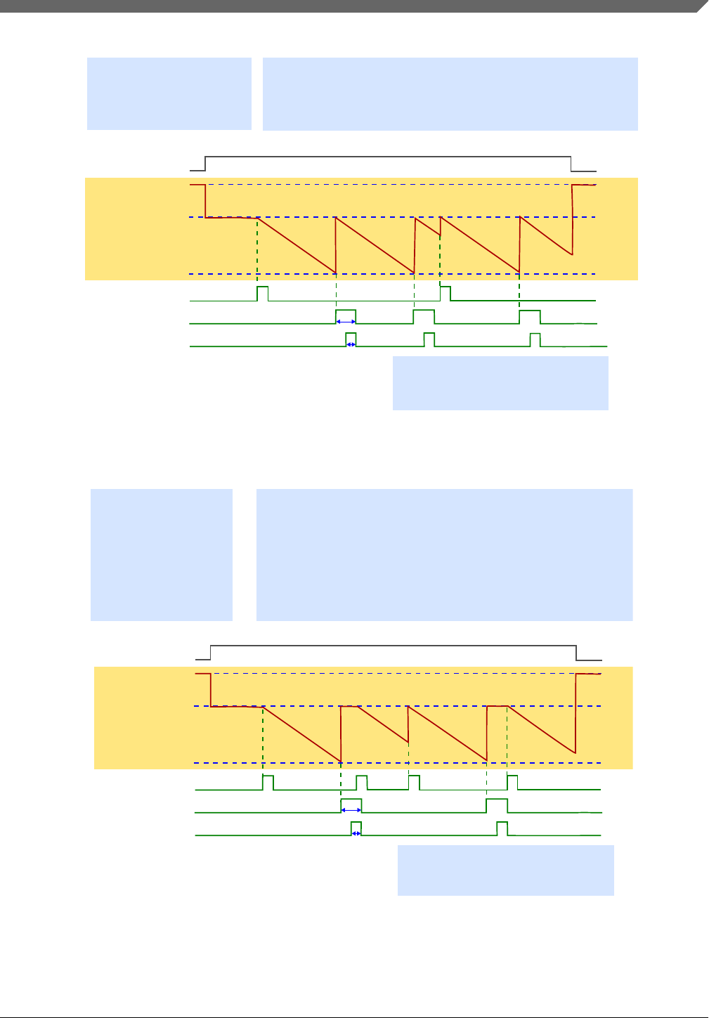
Mode00Case7.svg
Case 7: TSOT=1,TROT=1,TSOI=0,CHAIN=0
Operation:
-In Mode=00, the counter will load
and then decrement down to zero
-The counter will next set the timer interrrupt flag
and assert the output pre-trigger
T_EN
0xFFFF_FFFF
TMR_VAL
TMR_CUR_VAL
0x0000_0000
IN_TRIG
PRE_TRIG_OUT
TRIG_OUT 1 clock
TSOT=1
TROT=1
TSOI=0
CHAIN=0
-Repeated interrupts with reload timer mode
-Output triggers will have unequal periods
Timer resets
when T_EN=0
Timer starts on trigger
Timer reloads
on input trigger
2 clocks
Countdown
is based on the
selected clock
TMR_VAL is in TVALn register
TMR_CUR_VAL is in CVALn register
Mode=00
32-bit Periodic Counter
(Compare Mode)
Figure 46-11. Case 7: TSOT = 1, TROT = 1, TSOI = 0, CHAIN = 0
Mode00Case8.svg
Case 8: TSOT=1,TROT=1,TSOI=1,CHAIN=0
Operation:
-In Mode=00, the counter will load
and then decrement down to zero
-The counter will next set the timer interrrupt flag
and assert the output pre-trigger
T_EN
0xFFFF_FFFF
TMR_VAL
TMR_CUR_VAL
0x0000_0000
IN_TRIG
PRE_TRIG_OUT
TRIG_OUT 1 clock
TSOT=1
TROT=1
TSOI=1
CHAIN=0
-Case shown for a non-periodic input trigger
-If input trigger is periodic and greater than timer timeout
Timer resets
when T_EN=0
Timer starts on trigger
Timer reloads
on input trigger
then this will be the same as TROT=0
-If input trigger is periodic and less than timer timeout,
then timer will never time out,
and will always reload on input trigger (not a valid usecase)
Timer starts on trigger Timer starts on trigger
2 clocks
Countdown
is based on the
selected clock
TMR_VAL is in TVALn register
TMR_CUR_VAL is in CVALn register
Mode=00
32-bit
(Compare Mode)
(might not be a usecase)
Periodic Counter
Figure 46-12. Case 8: TSOT = 1, TROT = 1, TSOI = 1, CHAIN = 0
Chapter 46 Low Power Interrupt Timer (LPIT)
S32K1xx Series Reference Manual, Rev. 7, 04/2018
NXP Semiconductors 1391
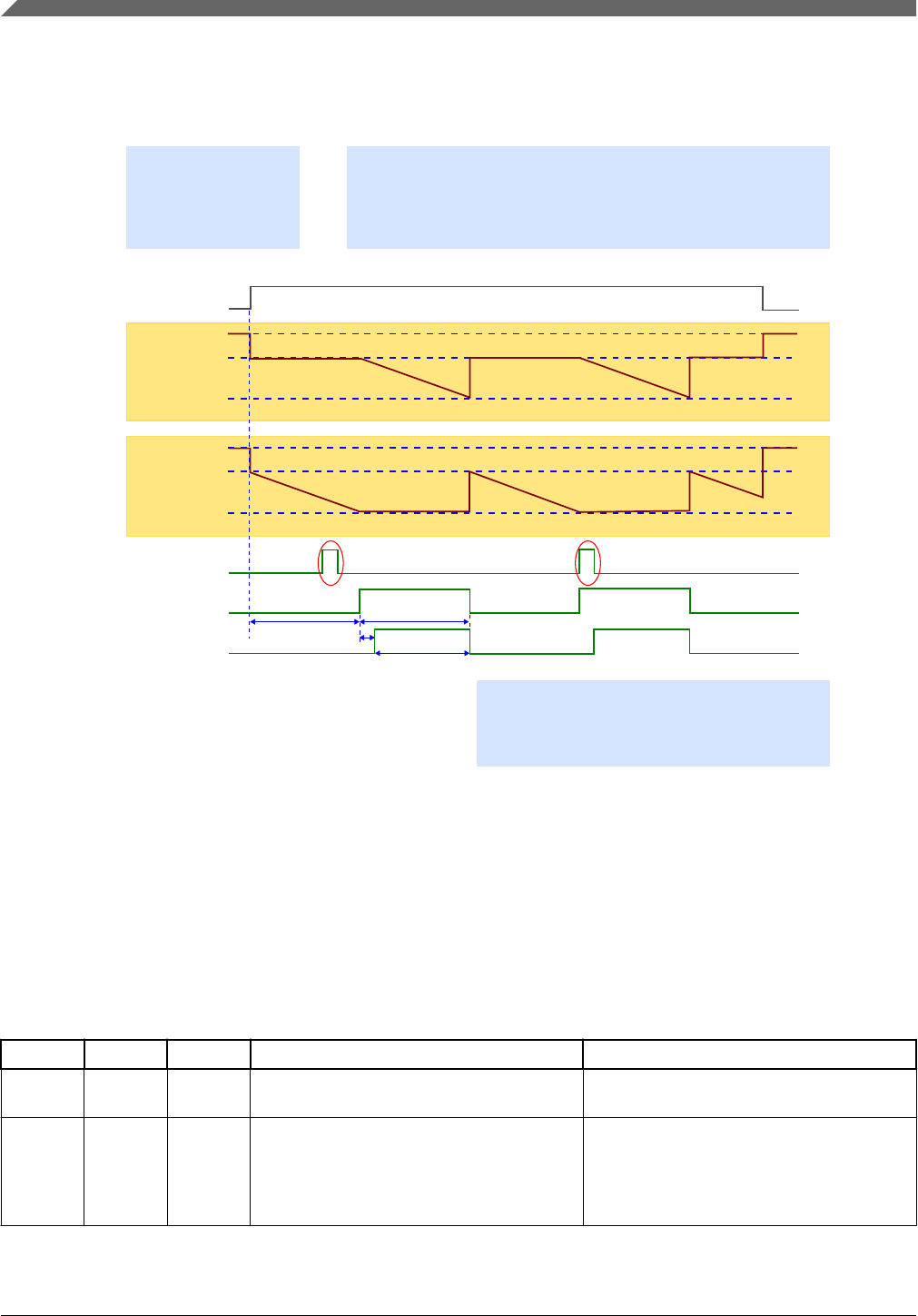
46.5.6.2 Mode=01: 16-bit dual periodic counter (compare mode)
Case 1: TSOT=0,TROT=0,TSOI=0,CHAIN=0
-Effect of TSOT, TROT, and TSOI is the same as Mode=00
(32-bit Counter Compare Mode)
-Both halves of the counter are affected in the same way
Mode01Case1.svg
Operation:
-In Mode=01, the counter will load,
the lower 16 bits will decrement down to zero,
-The upper 16 bits will then decrement down to zero,
and which will de-assert the output pre-trigger and trigger,
T_EN
0xFFFF
TMR_VAL_H TMR_CUR_VAL
0x0000
IN_TRIG
PRE_TRIG_OUT
TRIG_OUT
Countdown
is based on the
selected clock
TSOT=0
TROT=0
TSOI=0
CHAIN=0
Timer resets
when T_EN=0
Timer High counts down
which will assert the output pre-trigger and trigger(after 1 clock)
and set the timer interrupt flag
1 clock
TMR_VAL_L clocks
(TMR_VAL_H - 1) clocks
TMR_VAL_H clocks
Trigger
is ignored
Trigger
is ignored
Timer resets
when T_EN=0
Timer reloads
on timeout
Timer reloads
on timeout
after Timer Low times out
Countdown
is based on the
selected clock
TMR_VAL_L
0x0000
0xFFFF TMR_CUR_VAL
Mode=01
16-bit Dual
(Compare Mode)
Periodic Counter
Figure 46-13. Case 1: TSOT = 0, TROT = 0, TSOI = 0, CHAIN = 0
Effect of Timer Control Bits in Mode=01:
• Effect of timer control bits are the same as for Mode=00. Refer to the individual
figures of Mode=00.
• The Timer Interrupt (timeout) asserts when {TMR_H,TMR_L} = 0x0000_0000.
• Behavior for Mode = 01 is explained in the next table.
Table 46-8. Mode=01 timer control bits
TSOT TROT TSOI Function Effect on Timer
0 0 0 • For repeated interrupts with reload
• Trigger outputs will have equal periods
Similar to Figure 46-13.
0 0 1 One-shot mode • Both timers stop after first count down
and then time out
• Timers will not count again until T_EN
is made 1 again
• Similar to Figure 46-6.
Table continues on the next page...
Functional description
S32K1xx Series Reference Manual, Rev. 7, 04/2018
1392 NXP Semiconductors

Table 46-8. Mode=01 timer control bits (continued)
TSOT TROT TSOI Function Effect on Timer
0 1 0 • For repeated interrupts with reload
• Trigger outputs will have unequal
periods
• Both timers will reload TMR_VAL on
trigger rise edge
• Output triggers will clear on reload, if
asserted
• Similar to Figure 46-7.
0 1 1 Reloadable one-shot mode • If a trigger occurs before timeout, then
both timers reload and count down (as
shown); the timers stop after timeout
• A trigger assertion after timeout simply
reloads TMR_VAL into the timers
• The timers will not count again until
T_EN is set to 1 again
• Similar to Figure 46-8.
1 0 0 • For generating periodic interrupts after
a predefined event (input trigger)
• Output triggers will have equal periods
After T_EN rises, the timers do not start until
the first trigger's rising edge
• Subsequent triggers will have no effect
• Similar to Figure 46-9.
1 0 1 • Triggered one-shot timer mode
• Output trigger period will depend on
input trigger
After T_EN rises, the timers do not start until
the first trigger's rising edge.
• The timer stops counting after a
timeout assertion (a timeout is
asserted)
• The timer does not start counting
again until a new trigger's rising edge
is detected
• Similar to Figure 46-10.
1 1 0 • For repeated interrupts with reload
timer mode
• Output triggers will have unequal
periods
After T_EN rises, the timers do not start until
the first trigger's rising edge
• Subsequent triggers will cause the
timer to reload TMR_VAL into both
counters
• The output triggers will clear after a
reload, if asserted
• Similar to Figure 46-11.
1 1 1 • For a non-periodic input trigger
• If input trigger is periodic and greater
than timer timeout, then this will be the
same as TROT=0 (which is triggered
one-shot timer mode; output trigger
period will depend on input trigger)
After T_EN rises, the timers do not start until
the first trigger's rising edge
• The timers stops counting after a
timeout assertion (a timeout is
asserted)
• A trigger's rising edge will cause the
timers to reload and then count down
• Similar to Figure 46-12.
Chapter 46 Low Power Interrupt Timer (LPIT)
S32K1xx Series Reference Manual, Rev. 7, 04/2018
NXP Semiconductors 1393
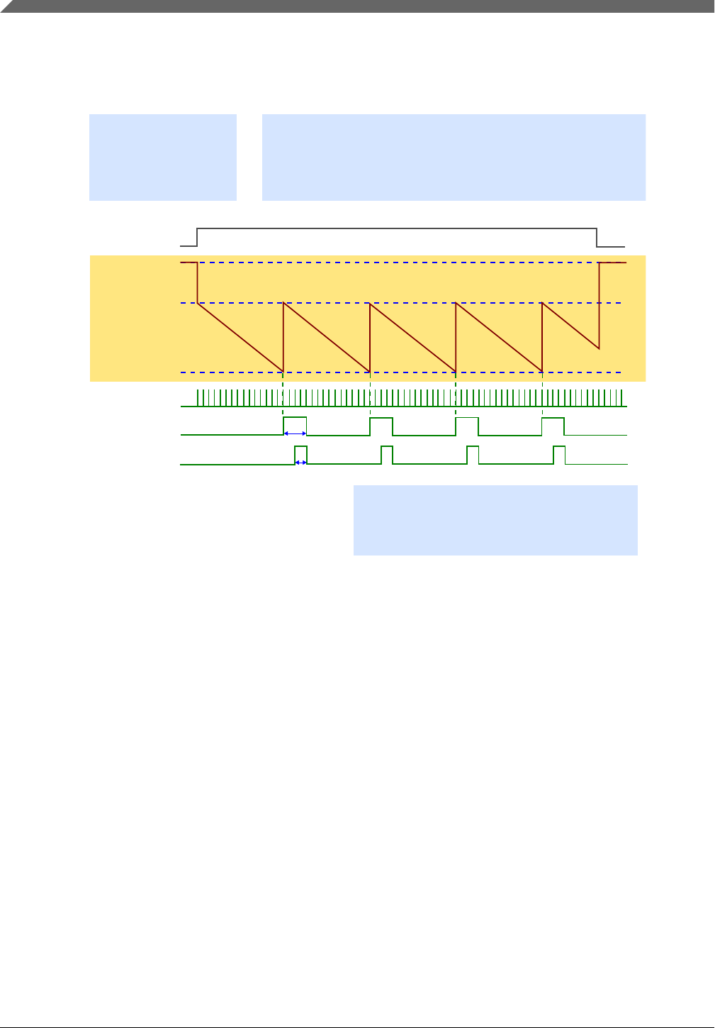
46.5.6.3 Mode=10: 32-bit trigger accumulator mode
Case 1: TSOI=0, CHAIN=0 (TSOT,TROT=X)
-Trigger and timeout generated
after programmed number of pulses have been accumulated
-Useful for a continuous pulse counting mode
Mode10Case1.svg
Operation:
-In Mode=10, the counter will load on the first trigger rising edge,
and then decrement down to zero on each trigger's rising edge
-It will then set the timer interrupt flag,
and assert the output pre-trigger and trigger
T_EN
IN_TRIG
PRE_TRIG_OUT
TRIG_OUT
Countdown
is based on the
selected clock
TSOT=X
TROT=X
TSOI=0
CHAIN=0
Timer resets
when T_EN=0
1 clock
TMR_CUR_VAL
2 clocks
0xFFFF_FFFF
TMR_VAL
0x0000_0000
Timer reloads on trigger after timeout
and decrements on
subsequent triggers
Timer loads on 1st trigger
and decrements on
subsequent triggers
TMR_VAL is in TVALn register
TMR_CUR_VAL is in CVALn register
Mode=10
Accumulator Mode
32-bit Trigger
Figure 46-14. Case 1: TSOT = X, TROT = X, TSOI = 0, CHAIN = 0
Functional description
S32K1xx Series Reference Manual, Rev. 7, 04/2018
1394 NXP Semiconductors
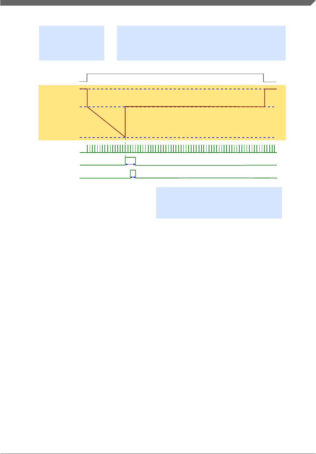
Case 2: TSOI=1, CHAIN=0 (TSOT,TROT=X)
-Trigger and timeout generated
after programmed number of pulses have been accumulated
-Useful for a ones-hot pulse counting mode
Mode10Case2.svg
Operation:
T_EN
IN_TRIG
PRE_TRIG_OUT
TRIG_OUT
Countdown
is based on the
selected clock
TSOT=X
TROT=X
TSOI=1
CHAIN=0
Timer resets
when T_EN=0
1 clock
TMR_CUR_VAL
2 clocks
0xFFFF_FFFF
TMR_VAL
0x0000_0000
Timer reloads on trigger after timeout
and decrements on
subsequent triggers
Timer loads on 1st trigger
and decrements on
subsequent triggers
-In Mode=10, the counter will load on the first trigger rising edge,
and then decrement down to zero on each trigger's rising edge
-It will then set the timer interrupt flag,
and assert the output pre-trigger and trigger
Mode=10
Accumulator Mode
32-bit Trigger
Figure 46-15. Case 2: TSOT = X, TROT = X, TSOI = 1, CHAIN = 0
Chapter 46 Low Power Interrupt Timer (LPIT)
S32K1xx Series Reference Manual, Rev. 7, 04/2018
NXP Semiconductors 1395
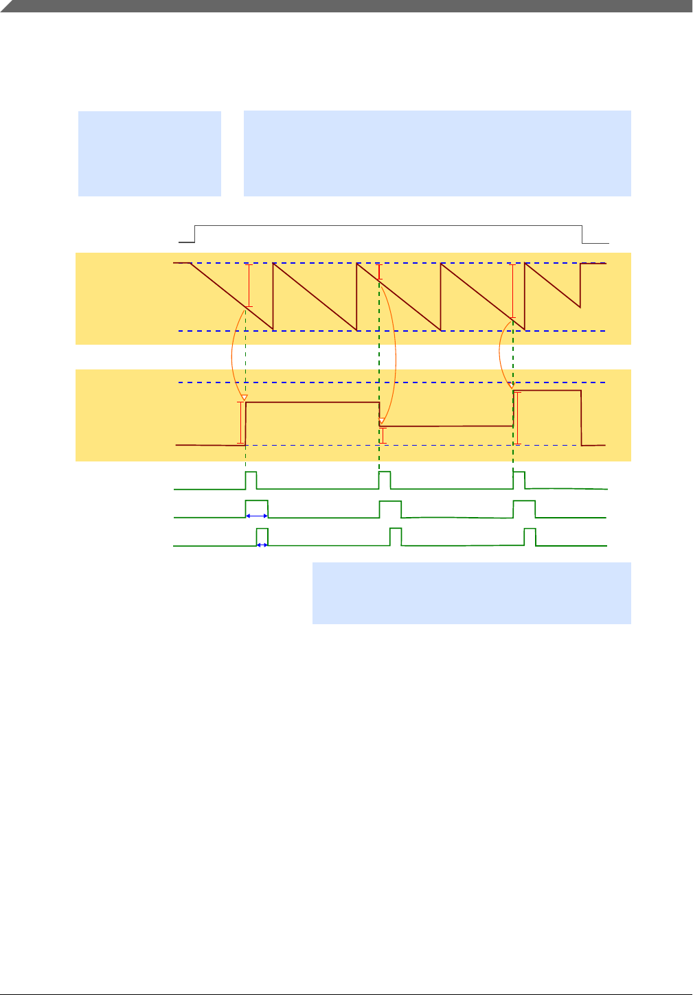
46.5.6.4 Mode=11: 32-bit trigger capture mode
Case 1: TSOI=0, TROT=0, CHAIN=0 (TSOT=X)
-Proper clock selection can ensure that the timer does not rollover
more than once between 2 pulses
-Useful for determining duration between pulses
Mode11Case1.svg
Operation:
-In Mode=11, the counter will load with 0xFFFF_FFFF,
and then decrement down to zero
-If a trigger rising edge is detected,
then it will store the inverse of the current counter in the load value register,
T_EN
IN_TRIG
PRE_TRIG_OUT
TRIG_OUT
Countdown
is based on the
selected clock
TSOT=X
TROT=0
TSOI=0
CHAIN=0
Timer resets
when T_EN=0
set the timer interrupt flag
1 clock
2 clocks
0xFFFF_FFFF
TMR_CUR_VAL
0x0000_0000
and assert the output pre-trigger and trigger
0xFFFF_FFFF
0x0000_0000
TMR_VAL
(read value)
Inverse value is
stored on trigger
Inverse value is
stored on trigger
Inverse value is
stored on trigger
Count value middle
Count value small
Count value big
TMR_VAL is in TVALn register
TMR_CUR_VAL is in CVALn register
Mode=11
Capture Mode
32-bit Trigger
Figure 46-16. Case 1: TSOT = X, TROT = 0, TSOI = 0, CHAIN = 0
Functional description
S32K1xx Series Reference Manual, Rev. 7, 04/2018
1396 NXP Semiconductors
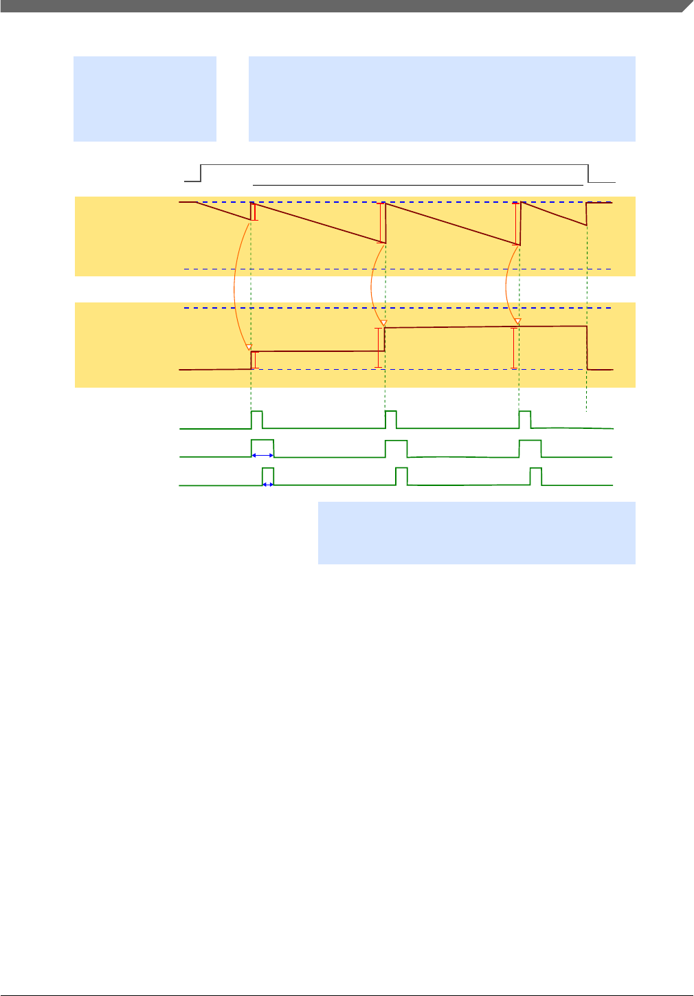
Case 2: TSOI=0, TROT=1, CHAIN=0 (TSOT=X)
-Selecting a fast timer clock provides accurate measurements
but it can also cause timer rollover inbetween pulses
-Useful for determining duration between pulses
Mode11Case2.svg
Operation:
-In Mode=11, the counter will load with 0xFFFF_FFFF,
and then decrement down to zero
-If a trigger rising edge is detected,
then it will store the inverse of the current counter in the load value register,
T_EN
IN_TRIG
PRE_TRIG_OUT
TRIG_OUT
Countdown
is based on the
selected clock
TSOT=X
TROT=1
TSOI=0
CHAIN=0
Timer resets
when T_EN=0
set the timer interrupt flag
1 clock
2 clocks
0xFFFF_FFFF
TMR_CUR_VAL
0x0000_0000
and assert the output pre-trigger and trigger
0xFFFF_FFFF
0x0000_0000
TMR_VAL
(read value)
Inverse value is
stored on trigger
Inverse value is
stored on trigger
Inverse value is
stored on trigger
Timer will not rollover if
proper clock is selected
TMR_VAL is in TVALn register
TMR_CUR_VAL is in CVALn register
Mode=11
Capture Mode
32-bit Trigger
Figure 46-17. Case 2: TSOT = X, TROT = 1, TSOI = 0, CHAIN = 0
Chapter 46 Low Power Interrupt Timer (LPIT)
S32K1xx Series Reference Manual, Rev. 7, 04/2018
NXP Semiconductors 1397
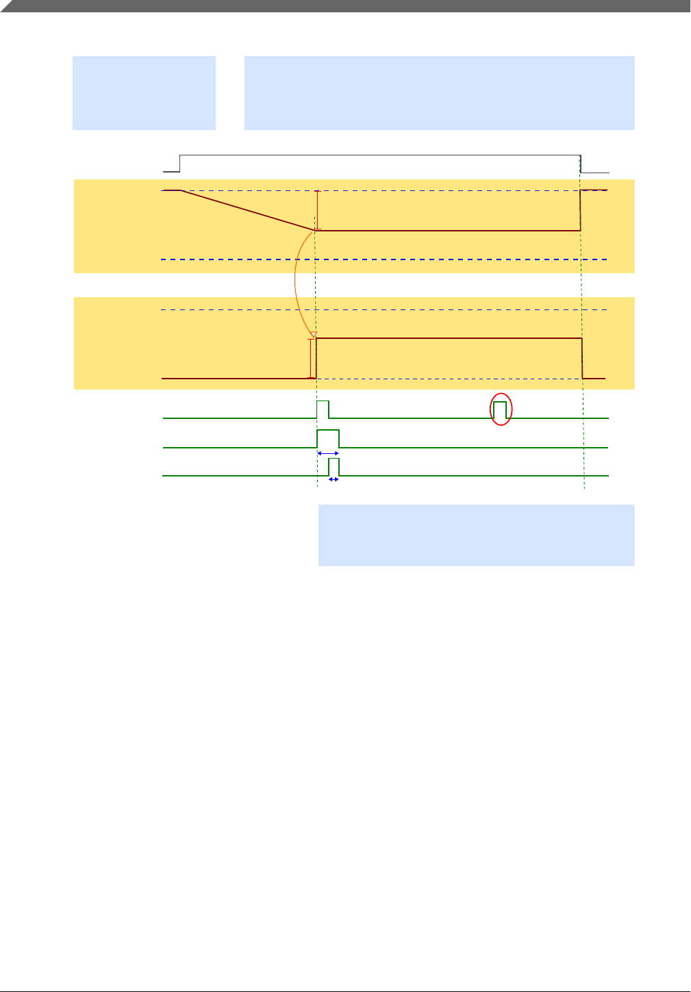
Case 3: TSOI=1, TROT=0, CHAIN=0 (TSOT=X)
-Can be enabled again by making T_EN=1
-One-shot timer count mode
Mode11Case3.svg
Operation:
-In Mode=11, the counter will load with 0xFFFF_FFFF,
and then decrement down to zero
-If a trigger rising edge is detected,
then it will store the inverse of the current counter in the load value register,
T_EN
IN_TRIG
PRE_TRIG_OUT
TRIG_OUT
Countdown
is based on the
selected clock
TSOT=X
TROT=0
TSOI=1
CHAIN=0
Timer resets
when T_EN=0
set the timer interrupt flag
1 clock
2 clocks
0xFFFF_FFFF
TMR_CUR_VAL
0x0000_0000
and assert the output pre-trigger and trigger
TMR_VAL
(read value)
Timer stops
after timer interrrupt
TMR_VAL is in TVALn register
TMR_CUR_VAL is in CVALn register
0xFFFF_FFFF
0x0000_0000
Trigger
is ignored
Inverse value is
stored on trigger
Mode=11
Capture Mode
32-bit Trigger
Figure 46-18. Case 3: TSOT = X, TROT = 0, TSOI = 1, CHAIN = 0
Case 4: TSOT = X, TROT = 1, TSOI = 1, CHAIN = 0
Same as previous case (Case 3), except that the timer reloads to 0xFFFF_FFFF and then
stops. The timer does not start until T_EN is made 1 again. Case 4 is not a very useful
case, because Case 3 covers this.
Functional description
S32K1xx Series Reference Manual, Rev. 7, 04/2018
1398 NXP Semiconductors
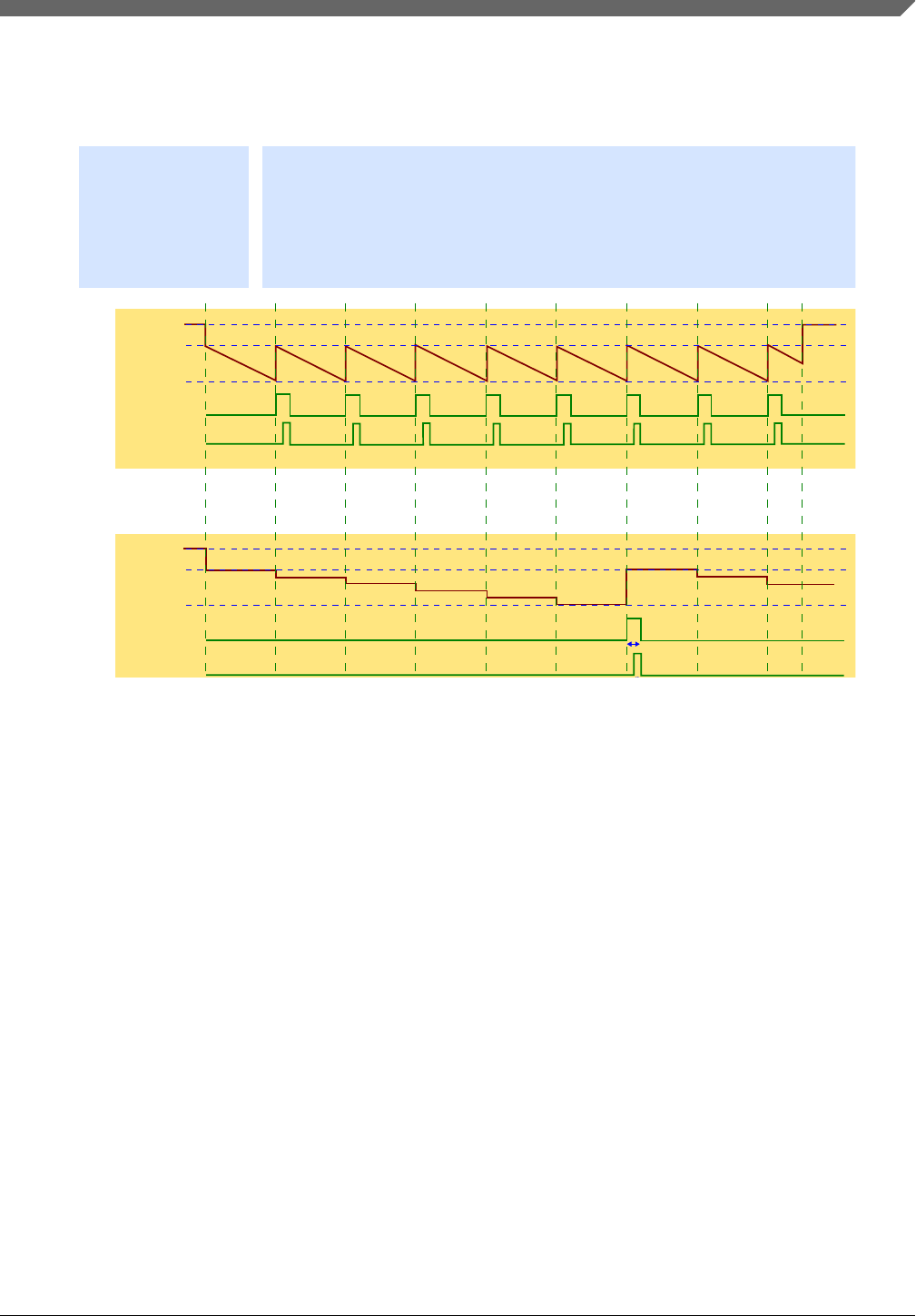
46.5.6.5 Timer chaining
-Timers “n” and “n – 1” effectively form a larger width timer (64-bits)
-Chaining causes Timer “n” to decrement on every timeout pulse (trigger output pulse)
EffectofChaining.svg
from Timer “n – 1”, regardless of what mode is configured in Timer “n”
-More than 2 timer channels (or all timer channels) can be chained
-It is preferred to have the same trigger source and timer controls
0xFFFF
TMR_VAL
0x0000
PRE_TRIG_OUT
TRIG_OUT
TMR_VAL
0xFFFF
0x0000
PRE_TRIG_OUT
TRIG_OUT
(Timer"n")
(Timer"n")
(Timer"n-1")
(Timer"n-1")
TMR_CUR_VAL
(Timer"n") (Timer"n-1")
TMR_CUR_VAL
Timer resets
when T_EN=0
1 clock
2 clocks
Countdown
is based on the
selected clock
Effect of Chaining
configured for chained channels
Figure 46-19. Chaining Effects
Chapter 46 Low Power Interrupt Timer (LPIT)
S32K1xx Series Reference Manual, Rev. 7, 04/2018
NXP Semiconductors 1399

Functional description
S32K1xx Series Reference Manual, Rev. 7, 04/2018
1400 NXP Semiconductors

Chapter 47
Low Power Timer (LPTMR)
Chip-specific LPTMR information
47.1.1 Instantiation Information
S32K1xx contains one LPTMR module with either a 1 channel 16-bit time counter or a 1
channel 16-bit pulse counter.
47.1.1.1 LPT/HSCMP0 pulse counting
LPTMR_ALT0 input is the selectable source to count pulses resulting from HSCMP0
Output (LPT_ALT0 = HSCMP0 Output) via TRGMUX.
NOTE
• Low leakage mode and Wait mode are not supported in this
device. See Module operation in available low power
modes for details on available power modes.
• For LPTMR_PSR[PCS] bit options refer to table:
Peripheral module clocking in section Module clocks.
• fLPTMR referred in the chapter refers to fBUS parameter in
the datasheet.
47.1.2 LPTMR pulse counter input options
The LPTMR_CSR[TPS] bitfield configures the input source used in pulse counter mode.
The following table shows the chip-specific input assignments for this bitfield.
47.1
S32K1xx Series Reference Manual, Rev. 7, 04/2018
NXP Semiconductors 1401

Table 47-1. Pulse counter input options
LPTMR_CSR[TPS] Pulse counter input number Chip input
00 0 TRGMUX output
01 1 LPTMR_ALT1 pin
10 2 LPTMR_ALT2 pin
11 3 LPTMR_ALT3 pin
47.2 Introduction
The low-power timer (LPTMR) can be configured to operate as a time counter with
optional prescaler, or as a pulse counter with optional glitch filter, across all power
modes, including the low-leakage modes. It can also continue operating through most
system reset events, allowing it to be used as a time of day counter.
47.2.1 Features
The features of the LPTMR module include:
• 16-bit time counter or pulse counter with compare
• Optional interrupt can generate asynchronous wakeup from any low-power mode
• Hardware trigger output
• Counter supports free-running mode or reset on compare
• Configurable clock source for prescaler/glitch filter
• Configurable input source for pulse counter
• Rising-edge or falling-edge
47.2.2 Modes of operation
The following table describes the operation of the LPTMR module in various modes.
Table 47-2. Modes of operation
Modes Description
Run The LPTMR operates normally.
Wait
The LPTMR continues to operate normally and
can be configured to exit the low-power mode by
generating an interrupt request.
Table continues on the next page...
Introduction
S32K1xx Series Reference Manual, Rev. 7, 04/2018
1402 NXP Semiconductors

Table 47-2. Modes of operation (continued)
Modes Description
Stop
The LPTMR continues to operate normally and
can be configured to exit the low-power mode by
generating an interrupt request.
Low-Leakage
The LPTMR continues to operate normally and
can be configured to exit the low-power mode by
generating an interrupt request.
Debug
The LPTMR operates normally in Pulse Counter
mode, but the counter does not increment in
Time Counter mode.
47.3 LPTMR signal descriptions
Table 47-3. LPTMR signal descriptions
Signal I/O Description
LPTMR_ALTnI Pulse Counter Input pin
47.3.1 Detailed signal descriptions
Table 47-4. LPTMR interface—detailed signal descriptions
Signal I/O Description
LPTMR_ALTnI Pulse Counter Input
The LPTMR can select one of the input pins to be used in Pulse Counter mode.
State meaning Assertion—If configured for pulse counter mode with
active-high input, then assertion causes the CNR to
increment.
Deassertion—If configured for pulse counter mode with
active-low input, then deassertion causes the CNR to
increment.
Timing Assertion or deassertion may occur at any time; input may
assert asynchronously to the bus clock.
47.4 Memory map and register definition
NOTE
The LPTMR registers are reset only on a POR or LVD event.
See LPTMR power and reset for more details.
Chapter 47 Low Power Timer (LPTMR)
S32K1xx Series Reference Manual, Rev. 7, 04/2018
NXP Semiconductors 1403
47.4.1 LPTMR register descriptions
47.4.1.1 LPTMR Memory map
LPTMR0 base address: 4004_0000h
Offset Register Width
(In bits)
Access Reset value
0h Low Power Timer Control Status Register (CSR) 32 RW 0000_0000h
4h Low Power Timer Prescale Register (PSR) 32 RW 0000_0000h
8h Low Power Timer Compare Register (CMR) 32 RW 0000_0000h
Ch Low Power Timer Counter Register (CNR) 32 RW 0000_0000h
47.4.1.2 Low Power Timer Control Status Register (CSR)
47.4.1.2.1 Offset
Register Offset
CSR 0h
47.4.1.2.2 Diagram
Bits 31 30 29 28 27 26 25 24 23 22 21 20 19 18 17 16
R 0
W
Reset 0 0 0 0 0 0 0 0 0 0 0 0 0 0 0 0
Bits 15 14 13 12 11 10 9 8 7 6 5 4 3 2 1 0
R
0
TDR
E
TCF
TI
E
TP
S
TPP
TFC
TMS
TEN
W
W1C
Reset 0 0 0 0 0 0 0 0 0 0 0 0 0 0 0 0
Memory map and register definition
S32K1xx Series Reference Manual, Rev. 7, 04/2018
1404 NXP Semiconductors

47.4.1.2.3 Fields
Field Function
31-9
—
Reserved
8
TDRE
Timer DMA Request Enable
When TDRE is set, the LPTMR DMA Request is generated whenever TCF is also set and the TCF is
cleared when the DMA Controller is done.
0b - Timer DMA Request disabled.
1b - Timer DMA Request enabled.
7
TCF
Timer Compare Flag
TCF is set when the LPTMR is enabled and the CNR equals the CMR and increments. TCF is cleared
when the LPTMR is disabled or a logic 1 is written to it.
0b - The value of CNR is not equal to CMR and increments.
1b - The value of CNR is equal to CMR and increments.
6
TIE
Timer Interrupt Enable
When TIE is set, the LPTMR Interrupt is generated whenever TCF is also set.
0b - Timer interrupt disabled.
1b - Timer interrupt enabled.
5-4
TPS
Timer Pin Select
Configures the input source to be used in Pulse Counter mode. TPS must be altered only when the
LPTMR is disabled. The input connections vary by device. See the chip configuration information about
connections to these inputs.
00b - Pulse counter input 0 is selected.
01b - Pulse counter input 1 is selected.
10b - Pulse counter input 2 is selected.
11b - Pulse counter input 3 is selected.
3
TPP
Timer Pin Polarity
Configures the polarity of the input source in Pulse Counter mode. TPP must be changed only when the
LPTMR is disabled.
0b - Pulse Counter input source is active-high, and the CNR will increment on the rising-edge.
1b - Pulse Counter input source is active-low, and the CNR will increment on the falling-edge.
2
TFC
Timer Free-Running Counter
When clear, TFC configures the CNR to reset whenever TCF is set. When set, TFC configures the CNR
to reset on overflow. TFC must be altered only when the LPTMR is disabled.
0b - CNR is reset whenever TCF is set.
1b - CNR is reset on overflow.
1
TMS
Timer Mode Select
Configures the mode of the LPTMR. TMS must be altered only when the LPTMR is disabled.
0b - Time Counter mode.
1b - Pulse Counter mode.
0
TEN
Timer Enable
When TEN is clear, it resets the LPTMR internal logic, including the CNR and TCF. When TEN is set, the
LPTMR is enabled. While writing 1 to this field, CSR[5:1] must not be altered.
0b - LPTMR is disabled and internal logic is reset.
1b - LPTMR is enabled.
Chapter 47 Low Power Timer (LPTMR)
S32K1xx Series Reference Manual, Rev. 7, 04/2018
NXP Semiconductors 1405

47.4.1.3 Low Power Timer Prescale Register (PSR)
47.4.1.3.1 Offset
Register Offset
PSR 4h
47.4.1.3.2 Diagram
Bits 31 30 29 28 27 26 25 24 23 22 21 20 19 18 17 16
R 0
W
Reset 0 0 0 0 0 0 0 0 0 0 0 0 0 0 0 0
Bits 15 14 13 12 11 10 9 8 7 6 5 4 3 2 1 0
R
0
PRESCAL
E
PBY
P
PC
S
W
Reset 0 0 0 0 0 0 0 0 0 0 0 0 0 0 0 0
47.4.1.3.3 Fields
Field Function
31-7
—
Reserved
6-3
PRESCALE
Prescale Value
Configures the size of the Prescaler in Time Counter mode or width of the glitch filter in Pulse Counter
mode. The width of the glitch filter can vary by 1 cycle due to synchronization of the pulse counter input.
PRESCALE must be altered only when the LPTMR is disabled.
0000b - Prescaler divides the prescaler clock by 2; glitch filter does not support this configuration.
0001b - Prescaler divides the prescaler clock by 4; glitch filter recognizes change on input pin after
2 rising clock edges.
0010b - Prescaler divides the prescaler clock by 8; glitch filter recognizes change on input pin after
4 rising clock edges.
0011b - Prescaler divides the prescaler clock by 16; glitch filter recognizes change on input pin
after 8 rising clock edges.
0100b - Prescaler divides the prescaler clock by 32; glitch filter recognizes change on input pin
after 16 rising clock edges.
0101b - Prescaler divides the prescaler clock by 64; glitch filter recognizes change on input pin
after 32 rising clock edges.
0110b - Prescaler divides the prescaler clock by 128; glitch filter recognizes change on input pin
after 64 rising clock edges.
Table continues on the next page...
Memory map and register definition
S32K1xx Series Reference Manual, Rev. 7, 04/2018
1406 NXP Semiconductors

Field Function
0111b - Prescaler divides the prescaler clock by 256; glitch filter recognizes change on input pin
after 128 rising clock edges.
1000b - Prescaler divides the prescaler clock by 512; glitch filter recognizes change on input pin
after 256 rising clock edges.
1001b - Prescaler divides the prescaler clock by 1024; glitch filter recognizes change on input pin
after 512 rising clock edges.
1010b - Prescaler divides the prescaler clock by 2048; glitch filter recognizes change on input pin
after 1024 rising clock edges.
1011b - Prescaler divides the prescaler clock by 4096; glitch filter recognizes change on input pin
after 2048 rising clock edges.
1100b - Prescaler divides the prescaler clock by 8192; glitch filter recognizes change on input pin
after 4096 rising clock edges.
1101b - Prescaler divides the prescaler clock by 16,384; glitch filter recognizes change on input pin
after 8192 rising clock edges.
1110b - Prescaler divides the prescaler clock by 32,768; glitch filter recognizes change on input pin
after 16,384 rising clock edges.
1111b - Prescaler divides the prescaler clock by 65,536; glitch filter recognizes change on input pin
after 32,768 rising clock edges.
2
PBYP
Prescaler Bypass
When PBYP is set, the selected prescaler clock in Time Counter mode or selected input source in Pulse
Counter mode directly clocks the CNR. When PBYP is clear, the CNR is clocked by the output of the
prescaler/glitch filter. PBYP must be altered only when the LPTMR is disabled.
0b - Prescaler/glitch filter is enabled.
1b - Prescaler/glitch filter is bypassed.
1-0
PCS
Prescaler Clock Select
Selects the clock to be used by the LPTMR prescaler/glitch filter. In time counter mode, this field selects
the input clock to the prescaler. In pulse counter mode, this field selects the input clock to the glitch filter.
PCS must be altered only when the LPTMR is disabled. The clock connections vary by device.
NOTE: See the chip configuration details for information on the connections to these inputs.
00b - Prescaler/glitch filter clock 0 selected.
01b - Prescaler/glitch filter clock 1 selected.
10b - Prescaler/glitch filter clock 2 selected.
11b - Prescaler/glitch filter clock 3 selected.
47.4.1.4 Low Power Timer Compare Register (CMR)
47.4.1.4.1 Offset
Register Offset
CMR 8h
Chapter 47 Low Power Timer (LPTMR)
S32K1xx Series Reference Manual, Rev. 7, 04/2018
NXP Semiconductors 1407

47.4.1.4.2 Diagram
Bits 31 30 29 28 27 26 25 24 23 22 21 20 19 18 17 16
R 0
W
Reset 0 0 0 0 0 0 0 0 0 0 0 0 0 0 0 0
Bits 15 14 13 12 11 10 9 8 7 6 5 4 3 2 1 0
RCOMPARE
W
Reset 0 0 0 0 0 0 0 0 0 0 0 0 0 0 0 0
47.4.1.4.3 Fields
Field Function
31-16
—
Reserved
15-0
COMPARE
Compare Value
When the LPTMR is enabled and the CNR equals the value in the CMR and increments, TCF is set and
the hardware trigger asserts until the next time the CNR increments. If the CMR is 0, the hardware trigger
will remain asserted until the LPTMR is disabled. If the LPTMR is enabled, the CMR must be altered only
when TCF is set.
47.4.1.5 Low Power Timer Counter Register (CNR)
47.4.1.5.1 Offset
Register Offset
CNR Ch
Memory map and register definition
S32K1xx Series Reference Manual, Rev. 7, 04/2018
1408 NXP Semiconductors

47.4.1.5.2 Diagram
Bits 31 30 29 28 27 26 25 24 23 22 21 20 19 18 17 16
R 0
W
Reset 0 0 0 0 0 0 0 0 0 0 0 0 0 0 0 0
Bits 15 14 13 12 11 10 9 8 7 6 5 4 3 2 1 0
RCOUNTER
W
Reset 0 0 0 0 0 0 0 0 0 0 0 0 0 0 0 0
47.4.1.5.3 Fields
Field Function
31-16
—
Reserved
15-0
COUNTER
Counter Value
The CNR returns the current value of the LPTMR counter at the time this register was last written.
47.5 Functional description
47.5.1 LPTMR power and reset
The LPTMR remains powered in all power modes, including low-leakage modes. If the
LPTMR is not required to remain operating during a low-power mode, then it must be
disabled before entering the mode.
The LPTMR is reset only on global Power On Reset (POR) or Low Voltage Detect
(LVD). When configuring the LPTMR registers, the CSR must be initially written with
the timer disabled, before configuring the PSR and CMR. Then, CSR[TIE] must be set as
the last step in the initialization. This ensures the LPTMR is configured correctly and the
LPTMR counter is reset to zero following a warm reset.
47.5.2 LPTMR clocking
The LPTMR prescaler/glitch filter can be clocked by one of the four clocks. The clock
source must be enabled before the LPTMR is enabled.
Chapter 47 Low Power Timer (LPTMR)
S32K1xx Series Reference Manual, Rev. 7, 04/2018
NXP Semiconductors 1409

NOTE
The clock source selected by PSR[PCS] may need to be
configured to remain enabled in low-power modes, otherwise
the LPTMR will not operate during low-power modes.
In Pulse Counter mode with the prescaler/glitch filter bypassed, the selected input source
directly clocks the CNR and no other clock source is required. To minimize power in this
case, configure the prescaler clock source for a clock that is not toggling.
NOTE
The clock source or pulse input source selected for the LPTMR
should not exceed the frequency fLPTMR defined in the device
datasheet.
47.5.3 LPTMR prescaler/glitch filter
The LPTMR prescaler and glitch filter share the same logic which operates as a prescaler
in Time Counter mode and as a glitch filter in Pulse Counter mode.
NOTE
The prescaler/glitch filter configuration must not be altered
when the LPTMR is enabled.
47.5.3.1 Prescaler enabled
In Time Counter mode, when the prescaler is enabled, the output of the prescaler directly
clocks the CNR. When the LPTMR is enabled, the CNR will increment every 22 to 216
prescaler clock cycles. After the LPTMR is enabled, the first increment of the CNR will
take an additional one or two prescaler clock cycles due to synchronization logic.
47.5.3.2 Prescaler bypassed
In Time Counter mode, when the prescaler is bypassed, the selected prescaler clock
increments the CNR on every clock cycle. When the LPTMR is enabled, the first
increment will take an additional one or two prescaler clock cycles due to
synchronization logic.
Functional description
S32K1xx Series Reference Manual, Rev. 7, 04/2018
1410 NXP Semiconductors

47.5.3.3 Glitch filter
In Pulse Counter mode, when the glitch filter is enabled, the output of the glitch filter
directly clocks the CNR. When the LPTMR is first enabled, the output of the glitch filter
is asserted, that is, logic 1 for active-high and logic 0 for active-low. The following table
shows the change in glitch filter output with the selected input source.
If Then
The selected input source remains deasserted for at least 21
to 215 consecutive prescaler clock rising edges
The glitch filter output will also deassert.
The selected input source remains asserted for at least 21 to
215 consecutive prescaler clock rising-edges
The glitch filter output will also assert.
NOTE
The input is only sampled on the rising clock edge.
The CNR will increment each time the glitch filter output asserts. In Pulse Counter mode,
the maximum rate at which the CNR can increment is once every 22 to 216 prescaler
clock edges. When first enabled, the glitch filter will wait an additional one or two
prescaler clock edges due to synchronization logic.
47.5.3.4 Glitch filter bypassed
In Pulse Counter mode, when the glitch filter is bypassed, the selected input source
increments the CNR every time it asserts. Before the LPTMR is first enabled, the selected
input source is forced to be asserted. This prevents the CNR from incrementing if the
selected input source is already asserted when the LPTMR is first enabled.
47.5.4 LPTMR compare
When the CNR equals the value of the CMR and increments, the following events occur:
• CSR[TCF] is set.
• LPTMR interrupt is generated if CSR[TIE] is also set.
• LPTMR hardware trigger is generated.
• CNR is reset if CSR[TFC] is clear.
When the LPTMR is enabled, the CMR can be altered only when CSR[TCF] is set. When
updating the CMR, the CMR must be written and CSR[TCF] must be cleared before the
LPTMR counter has incremented past the new LPTMR compare value.
Chapter 47 Low Power Timer (LPTMR)
S32K1xx Series Reference Manual, Rev. 7, 04/2018
NXP Semiconductors 1411

47.5.5 LPTMR counter
The CNR increments by one on every:
• Prescaler clock in Time Counter mode with prescaler bypassed
• Prescaler output in Time Counter mode with prescaler enabled
• Input source assertion in Pulse Counter mode with glitch filter bypassed
• Glitch filter output in Pulse Counter mode with glitch filter enabled
The CNR is reset when the LPTMR is disabled or if the counter register overflows. If
CSR[TFC] is cleared, then the CNR is also reset whenever CSR[TCF] is set.
When the core is halted in Debug mode:
• If configured for Pulse Counter mode, the CNR continues incrementing.
• If configured for Time Counter mode, the CNR stops incrementing.
The CNR cannot be initialized, but can be read at any time. On each read of the CNR,
software must first write to the CNR with any value. This will synchronize and register
the current value of the CNR into a temporary register. The contents of the temporary
register are returned on each read of the CNR.
When reading the CNR, the bus clock must be at least two times faster than the rate at
which the LPTMR counter is incrementing, otherwise incorrect data may be returned.
47.5.6 LPTMR hardware trigger
The LPTMR hardware trigger asserts at the same time the CSR[TCF] is set and can be
used to trigger hardware events in other peripherals without software intervention. The
hardware trigger is always enabled.
When Then
The CMR is set to 0 with CSR[TFC] clear The LPTMR hardware trigger will assert on the first compare
and does not deassert.
The CMR is set to a nonzero value, or, if CSR[TFC] is set The LPTMR hardware trigger will assert on each compare
and deassert on the following increment of the CNR.
47.5.7 LPTMR interrupt
The LPTMR interrupt is generated whenever CSR[TIE] and CSR[TCF] are set.
CSR[TCF] is cleared by disabling the LPTMR or by writing a logic 1 to it.
CSR[TIE] can be altered and CSR[TCF] can be cleared while the LPTMR is enabled.
Functional description
S32K1xx Series Reference Manual, Rev. 7, 04/2018
1412 NXP Semiconductors

The LPTMR interrupt is generated asynchronously to the system clock and can be used to
generate a wakeup from any low-power mode, including the low-leakage modes,
provided the LPTMR is enabled as a wakeup source.
Chapter 47 Low Power Timer (LPTMR)
S32K1xx Series Reference Manual, Rev. 7, 04/2018
NXP Semiconductors 1413

Functional description
S32K1xx Series Reference Manual, Rev. 7, 04/2018
1414 NXP Semiconductors

Chapter 48
Real Time Clock (RTC)
Chip-specific RTC information
48.1.1 RTC instantiation
The wakeup pin is not available for RTC on this device, therefore the related register
bitfields are not applicable (e.g. RTC_CR[WPS], RTC_CR[WPE], and
RTC_IER[WPON]). Also there is no integrated capacitor for this device, therefore no
tunable capacitors (included in the crystal oscillator) can be configured by software.
NOTE
There is no internal 32.768 kHz crystal oscillator available on
this device. All references to 32.768 kHz clock in this chapter
refers to RTC_CLK. See RTC clocking in Table 27-9 for
available clock sources.
48.1.2 RTC interrupts
Interrupts from RTC are enabled at reset as described in RTC_IER register. Interrupt may
occur as soon as they are enabled in NVIC.
48.1.3 Software recommendation
Software reset should be provided to RTC before enabling it.
48.2 Introduction
48.1
S32K1xx Series Reference Manual, Rev. 7, 04/2018
NXP Semiconductors 1415

48.2.1 Features
The RTC module features include:
• 32-bit seconds counter with roll-over protection and 32-bit alarm
• 16-bit prescaler with compensation that can correct errors between 0.12 ppm and
3906 ppm
• Option to increment prescaler using a 1 kHz LPO (prescaler increments by 32 every
clock edge)
• Register write protection
• Lock register requires POR or software reset to enable write access
• Configurable 1, 2, 4, 8, 16, 32, 64 or 128 Hz square wave output with optional
interrupt
48.2.2 Modes of operation
The RTC remains functional in all low power modes and can generate an interrupt to exit
any low power mode.
48.2.3 RTC signal descriptions
Table 48-1. RTC signal descriptions
Signal Description I/O
RTC_CLKOUT Prescaler square-wave output or RTC
32.768 kHz clock
O
48.2.3.1 RTC clock output
The RTC_CLKOUT signal can output either a square wave prescaler output
(configurable to 1, 2, 4, 8, 16, 32, 64 or 128 Hz) or the RTC 32.768 kHz clock.
Introduction
S32K1xx Series Reference Manual, Rev. 7, 04/2018
1416 NXP Semiconductors

48.3 Register definition
All registers must be accessed using 32-bit writes and all register accesses incur three
wait states.
Write accesses to any register by non-supervisor mode software, when the supervisor
access bit in the control register is clear, will terminate with a bus error.
Read accesses by non-supervisor mode software complete as normal.
Writing to a register protected by the lock register does not generate a bus error, but the
write will not complete.
48.3.1 RTC register descriptions
48.3.1.1 RTC Memory map
RTC base address: 4003_D000h
Offset Register Width
(In bits)
Access Reset value
0h RTC Time Seconds Register (TSR) 32 RW 0000_0000h
4h RTC Time Prescaler Register (TPR) 32 RW 0000_0000h
8h RTC Time Alarm Register (TAR) 32 RW 0000_0000h
Ch RTC Time Compensation Register (TCR) 32 RW 0000_0000h
10h RTC Control Register (CR) 32 RW 0000_0000h
14h RTC Status Register (SR) 32 RW 0000_0001h
18h RTC Lock Register (LR) 32 RW 0000_00FFh
1Ch RTC Interrupt Enable Register (IER) 32 RW 0000_0007h
48.3.1.2 RTC Time Seconds Register (TSR)
Chapter 48 Real Time Clock (RTC)
S32K1xx Series Reference Manual, Rev. 7, 04/2018
NXP Semiconductors 1417

48.3.1.2.1 Offset
Register Offset
TSR 0h
48.3.1.2.2 Diagram
Bits 31 30 29 28 27 26 25 24 23 22 21 20 19 18 17 16
RTSR
W
Reset 0 0 0 0 0 0 0 0 0 0 0 0 0 0 0 0
Bits 15 14 13 12 11 10 9 8 7 6 5 4 3 2 1 0
RTSR
W
Reset 0 0 0 0 0 0 0 0 0 0 0 0 0 0 0 0
48.3.1.2.3 Fields
Field Function
31-0
TSR
Time Seconds Register
When the time counter is enabled, the TSR is read only and increments once a second provided
SR[TOF] or SR[TIF] are not set. The time counter will read as zero when SR[TOF] or SR[TIF] are set.
When the time counter is disabled, the TSR can be read or written. Writing to the TSR when the time
counter is disabled will clear the SR[TOF] and/or the SR[TIF]. Writing to TSR with zero is supported, but
not recommended because TSR will read as zero when SR[TIF] or SR[TOF] are set (indicating the time is
invalid).
48.3.1.3 RTC Time Prescaler Register (TPR)
48.3.1.3.1 Offset
Register Offset
TPR 4h
Register definition
S32K1xx Series Reference Manual, Rev. 7, 04/2018
1418 NXP Semiconductors

48.3.1.3.2 Diagram
Bits 31 30 29 28 27 26 25 24 23 22 21 20 19 18 17 16
R 0
W
Reset 0 0 0 0 0 0 0 0 0 0 0 0 0 0 0 0
Bits 15 14 13 12 11 10 9 8 7 6 5 4 3 2 1 0
RTPR
W
Reset 0 0 0 0 0 0 0 0 0 0 0 0 0 0 0 0
48.3.1.3.3 Fields
Field Function
31-16
—
Reserved
15-0
TPR
Time Prescaler Register
When the time counter is enabled, the TPR is read only and increments every 32.768 kHz clock cycle.
The time counter will read as zero when SR[TOF] or SR[TIF] are set. When the time counter is disabled,
the TPR can be read or written. The TSR[TSR] increments when bit 14 of the TPR transitions from a logic
one to a logic zero.
48.3.1.4 RTC Time Alarm Register (TAR)
48.3.1.4.1 Offset
Register Offset
TAR 8h
Chapter 48 Real Time Clock (RTC)
S32K1xx Series Reference Manual, Rev. 7, 04/2018
NXP Semiconductors 1419

48.3.1.4.2 Diagram
Bits 31 30 29 28 27 26 25 24 23 22 21 20 19 18 17 16
RTAR
W
Reset 0 0 0 0 0 0 0 0 0 0 0 0 0 0 0 0
Bits 15 14 13 12 11 10 9 8 7 6 5 4 3 2 1 0
RTAR
W
Reset 0 0 0 0 0 0 0 0 0 0 0 0 0 0 0 0
48.3.1.4.3 Fields
Field Function
31-0
TAR
Time Alarm Register
When the time counter is enabled, the SR[TAF] is set whenever the TAR[TAR] equals the TSR[TSR] and
the TSR[TSR] increments. Writing to the TAR clears the SR[TAF].
48.3.1.5 RTC Time Compensation Register (TCR)
48.3.1.5.1 Offset
Register Offset
TCR Ch
48.3.1.5.2 Diagram
Bits 31 30 29 28 27 26 25 24 23 22 21 20 19 18 17 16
RCIC TCV
W
Reset 0 0 0 0 0 0 0 0 0 0 0 0 0 0 0 0
Bits 15 14 13 12 11 10 9 8 7 6 5 4 3 2 1 0
RCIR TCR
W
Reset 0 0 0 0 0 0 0 0 0 0 0 0 0 0 0 0
Register definition
S32K1xx Series Reference Manual, Rev. 7, 04/2018
1420 NXP Semiconductors

48.3.1.5.3 Fields
Field Function
31-24
CIC
Compensation Interval Counter
Current value of the compensation interval counter. If the compensation interval counter equals zero then
it is loaded with the contents of the CIR. If the CIC does not equal zero then it is decremented once a
second. Reading this register at the same time as the seconds counter is incrementing can result in an
incorrect value being read.
23-16
TCV
Time Compensation Value
Current value used by the compensation logic for the present second interval. Updated once a second if
the CIC equals 0 with the contents of the TCR field. If the CIC does not equal zero then it is loaded with
zero (compensation is not enabled for that second increment). Reading this register at the same time as
the seconds counter is incrementing can result in an incorrect value being read.
15-8
CIR
Compensation Interval Register
Configures the compensation interval in seconds from 1 to 256 to control how frequently the TCR should
adjust the number of 32.768 kHz cycles in each second. The value written should be one less than the
number of seconds. For example, write zero to configure for a compensation interval of one second. This
register is double buffered and writes do not take affect until the end of the current compensation interval.
7-0
TCR
Time Compensation Register
Configures the number of 32.768 kHz clock cycles in each second, equal to 32,768 - TCR (where TCR is
a twos complement sign extended value). This register is double buffered and writes do not take affect
until the end of the current compensation interval. Some example values are show below.
00000000b - Time Prescaler Register overflows every 32768 clock cycles.
00000001b - Time Prescaler Register overflows every 32767 clock cycles.
01111110b - Time Prescaler Register overflows every 32642 clock cycles.
01111111b - Time Prescaler Register overflows every 32641 clock cycles.
10000000b - Time Prescaler Register overflows every 32896 clock cycles.
10000001b - Time Prescaler Register overflows every 32895 clock cycles.
11111111b - Time Prescaler Register overflows every 32769 clock cycles.
48.3.1.6 RTC Control Register (CR)
48.3.1.6.1 Offset
Register Offset
CR 10h
Chapter 48 Real Time Clock (RTC)
S32K1xx Series Reference Manual, Rev. 7, 04/2018
NXP Semiconductors 1421

48.3.1.6.2 Diagram
Bits 31 30 29 28 27 26 25 24 23 22 21 20 19 18 17 16
R
0
CP
E
0
Reserved
W
0
Reset 0 0 0 0 0 0 0 0 0 0 0 0 0 0 0 0
Bits 15 14 13 12 11 10 9 8 7 6 5 4 3 2 1 0
R
Reserved
Reserved
Reserved
Reserved
Reserved
Reserved
CLKO
Reserved
LPO
S
0
CP
S
Reserved
UM
SU
P
Reserved
SW
R
W
0
0
0
0
0
0
0
0
0
Reset 0 0 0 0 0 0 0 0 0 0 0 0 0 0 0 0
48.3.1.6.3 Fields
Field Function
31-25
—
Reserved
24
CPE
Clock Pin Enable
0b - The RTC_CLKOUT function is disabled.
1b - Enable RTC_CLKOUT function.
23-18
—
Reserved
17-16
—
Reserved
15
—
Reserved
14
—
Reserved
13
—
Reserved
12
—
Reserved
11
—
Reserved
10
—
Reserved
9 Clock Output
Table continues on the next page...
Register definition
S32K1xx Series Reference Manual, Rev. 7, 04/2018
1422 NXP Semiconductors

Field Function
CLKO 0b - The 32 kHz clock is output to other peripherals.
1b - The 32 kHz clock is not output to other peripherals.
8
—
Reserved
7
LPOS
LPO Select
When set, the RTC prescaler increments using the LPO 1 kHz clock and not the RTC 32.768 kHz clock.
The LPO increments the prescaler from bit TPR[5] (TPR[4:0] are ignored), supporting close to 1 second
increment of the seconds register. Although compensation is supported when clocked from the LPO,
TCR[4:0] of the compensation register are also ignored and only TCR[7:5] set the compensation value
(can overflow after 1020 to 1027 cycles).
0b - RTC prescaler increments using 32.768 kHz clock.
1b - RTC prescaler increments using 1 kHz LPO, bits [4:0] of the prescaler are ignored.
6
—
Reserved
5
CPS
Clock Pin Select
0b - The prescaler output clock (as configured by TSIC) is output on RTC_CLKOUT.
1b - The RTC 32.768 kHz clock is output on RTC_CLKOUT, provided it is output to other
peripherals.
4
—
Reserved
3
UM
Update Mode
Allows SR[TCE] to be written even when the Status Register is locked. When set, the SR[TCE] can be
written if the SR[TIF] or SR[TOF] are set or if the SR[TCE] is clear. Whenever both SR[TCE] and CR[UM]
are set, then SR[TCE] should only be written once either SR[TIF] or SR[TOF] are set.
0b - Registers cannot be written when locked.
1b - Registers can be written when locked under limited conditions.
2
SUP
Supervisor Access
0b - Non-supervisor mode write accesses are not supported and generate a bus error.
1b - Non-supervisor mode write accesses are supported.
1
—
Reserved
0
SWR
Software Reset
0b - No effect.
1b - Resets all RTC registers except for the SWR bit . The SWR bit is cleared by POR and by
software explicitly clearing it.
48.3.1.7 RTC Status Register (SR)
48.3.1.7.1 Offset
Register Offset
SR 14h
Chapter 48 Real Time Clock (RTC)
S32K1xx Series Reference Manual, Rev. 7, 04/2018
NXP Semiconductors 1423

48.3.1.7.2 Diagram
Bits 31 30 29 28 27 26 25 24 23 22 21 20 19 18 17 16
R 0
W
Reset 0 0 0 0 0 0 0 0 0 0 0 0 0 0 0 0
Bits 15 14 13 12 11 10 9 8 7 6 5 4 3 2 1 0
R 0 0 0 TCE 0TAF TOF TIF
W
Reset 0 0 0 0 0 0 0 0 0 0 0 0 0 0 0 1
48.3.1.7.3 Fields
Field Function
31-8
—
Reserved
7
—
Reserved
6-5
—
Reserved
4
TCE
Time Counter Enable
When time counter is disabled the TSR register and TPR register are writeable, but do not increment.
When time counter is enabled the TSR register and TPR register are not writeable, but increment.
0b - Time counter is disabled.
1b - Time counter is enabled.
3
—
Reserved
2
TAF
Time Alarm Flag
Time alarm flag is set when the TAR[TAR] equals the TSR[TSR] and the TSR[TSR] increments. This bit
is cleared by writing the TAR register.
0b - Time alarm has not occurred.
1b - Time alarm has occurred.
1
TOF
Time Overflow Flag
Time overflow flag is set when the time counter is enabled and overflows. The TSR and TPR do not
increment and read as zero when this bit is set. This bit is cleared by writing the TSR register when the
time counter is disabled.
0b - Time overflow has not occurred.
1b - Time overflow has occurred and time counter is read as zero.
0
TIF
Time Invalid Flag
The time invalid flag is set on POR or software reset. The TSR and TPR do not increment and read as
zero when this bit is set. This bit is cleared by writing the TSR register when the time counter is disabled.
0b - Time is valid.
1b - Time is invalid and time counter is read as zero.
Register definition
S32K1xx Series Reference Manual, Rev. 7, 04/2018
1424 NXP Semiconductors
48.3.1.8 RTC Lock Register (LR)
48.3.1.8.1 Offset
Register Offset
LR 18h
48.3.1.8.2 Diagram
Bits 31 30 29 28 27 26 25 24 23 22 21 20 19 18 17 16
R 0
W
Reset 0 0 0 0 0 0 0 0 0 0 0 0 0 0 0 0
Bits 15 14 13 12 11 10 9 8 7 6 5 4 3 2 1 0
R 0 1 LRL SRL CRL TCL 1
W
Reset 0 0 0 0 0 0 0 0 1 1 1 1 1 1 1 1
48.3.1.8.3 Fields
Field Function
31-8
—
Reserved
7
—
Reserved
6
LRL
Lock Register Lock
After being cleared, this bit can be set only by POR or software reset.
0b - Lock Register is locked and writes are ignored.
1b - Lock Register is not locked and writes complete as normal.
5
SRL
Status Register Lock
After being cleared, this bit can be set only by POR or software reset.
0b - Status Register is locked and writes are ignored.
1b - Status Register is not locked and writes complete as normal.
4
CRL
Control Register Lock
After being cleared, this bit can only be set by POR.
0b - Control Register is locked and writes are ignored.
1b - Control Register is not locked and writes complete as normal.
Table continues on the next page...
Chapter 48 Real Time Clock (RTC)
S32K1xx Series Reference Manual, Rev. 7, 04/2018
NXP Semiconductors 1425

Field Function
3
TCL
Time Compensation Lock
After being cleared, this bit can be set only by POR or software reset.
0b - Time Compensation Register is locked and writes are ignored.
1b - Time Compensation Register is not locked and writes complete as normal.
2-0
—
Reserved
48.3.1.9 RTC Interrupt Enable Register (IER)
48.3.1.9.1 Offset
Register Offset
IER 1Ch
48.3.1.9.2 Diagram
Bits 31 30 29 28 27 26 25 24 23 22 21 20 19 18 17 16
R 0 TSIC
W
Reset 0 0 0 0 0 0 0 0 0 0 0 0 0 0 0 0
Bits 15 14 13 12 11 10 9 8 7 6 5 4 3 2 1 0
R
0
Reserved
Reserved
TSI
E
Reserved
TAIE
TOIE
TIIE
W
0
0
Reset 0 0 0 0 0 0 0 0 0 0 0 0 0 1 1 1
48.3.1.9.3 Fields
Field Function
31-19
—
Reserved
18-16
TSIC
Timer Seconds Interrupt Configuration
Configures the frequency of the RTC Seconds interrupt and the RTC_CLKOUT prescaler output. This
field should only be altered when TSIE is clear.
Table continues on the next page...
Register definition
S32K1xx Series Reference Manual, Rev. 7, 04/2018
1426 NXP Semiconductors

Field Function
000b - 1 Hz.
001b - 2 Hz.
010b - 4 Hz.
011b - 8 Hz.
100b - 16 Hz.
101b - 32 Hz.
110b - 64 Hz.
111b - 128 Hz.
15-8
—
Reserved
7
—
Reserved
6-5
—
Reserved
4
TSIE
Time Seconds Interrupt Enable
The seconds interrupt is an edge-sensitive interrupt with a dedicated interrupt vector. It is generated at
least once a second and requires no software overhead (there is no corresponding status flag to clear).
The frequency of the seconds interrupt is configured by TSIC.
0b - Seconds interrupt is disabled.
1b - Seconds interrupt is enabled.
3
—
Reserved
2
TAIE
Time Alarm Interrupt Enable
0b - Time alarm flag does not generate an interrupt.
1b - Time alarm flag does generate an interrupt.
1
TOIE
Time Overflow Interrupt Enable
0b - Time overflow flag does not generate an interrupt.
1b - Time overflow flag does generate an interrupt.
0
TIIE
Time Invalid Interrupt Enable
0b - Time invalid flag does not generate an interrupt.
1b - Time invalid flag does generate an interrupt.
48.4 Functional description
48.4.1 Power, clocking, and reset
The RTC is an always powered block that remains active in all low power modes.
The time counter within the RTC is clocked by default from a 32.768 kHz clock.
Alternatively, the time counter can be clocked by a LPO 1 kHz clock and the prescaler
will increment by 32 for each LPO clock.
The power-on-reset signal initializes all RTC registers to their default state. A software
reset bit can also initialize all RTC registers.
Chapter 48 Real Time Clock (RTC)
S32K1xx Series Reference Manual, Rev. 7, 04/2018
NXP Semiconductors 1427

48.4.1.1 Oscillator control
The 32.768 kHz crystal oscillator is disabled at POR and must be enabled by software.
After enabling the cystal oscillator, wait the oscillator startup time before setting
SR[TCE] or using the oscillator clock external to the RTC.
The crystal oscillator includes tunable capacitors that can be configured by software. Do
not change the capacitance unless the oscillator is disabled.
48.4.1.2 Software reset
Writing 1 to CR[SWR] forces the equivalent of a POR to the rest of the RTC module.
CR[SWR] is not affected by the software reset and must be cleared by software.
48.4.1.3 Supervisor access
When the supervisor access control bit is clear, only supervisor mode software can write
to the RTC registers, non-supervisor mode software will generate a bus error. Both
supervisor and non-supervisor mode software can always read the RTC registers.
48.4.2 Time counter
The time counter consists of a 32-bit seconds counter that increments once every second
and a 16-bit prescaler register that increments once every 32.768 kHz clock cycle. There
is also the option to clock the prescaler using a 1 kHz LPO that increments the prescaler
by 32 on every clock cycle.
Reading the time counter (either seconds or prescaler) while it is incrementing may return
invalid data due to synchronization of the read data bus. If it is necessary for software to
read the prescaler or seconds counter when they could be incrementing, it is
recommended that two read accesses are performed and that software verifies that the
same data was returned for both reads.
The time seconds register and time prescaler register can be written only when SR[TCE]
is clear. Always write to the prescaler register before writing to the seconds register,
because the seconds register increments on the falling edge of bit 14 of the prescaler
register.
Functional description
S32K1xx Series Reference Manual, Rev. 7, 04/2018
1428 NXP Semiconductors

The time prescaler register increments provided SR[TCE] is set, SR[TIF] is clear,
SR[TOF] is clear, and the 32.768 kHz (or 1 kHz) clock source is present. After enabling
the oscillator, wait the oscillator startup time before setting SR[TCE] to allow time for
the oscillator clock output to stabilize.
If the time seconds register overflows then the SR[TOF] will set and the time prescaler
register will stop incrementing. Clear SR[TOF] by initializing the time seconds register.
The time seconds register and time prescaler register read as zero whenever SR[TOF] is
set.
SR[TIF] is set on POR and software reset and is cleared by initializing the time seconds
register. The time seconds register and time prescaler register read as zero whenever
SR[TIF] is set.
48.4.3 Compensation
The compensation logic provides an accurate and wide compensation range and can
correct errors as high as 3906 ppm and as low as 0.12 ppm. The compensation factor
must be calculated externally to the RTC and supplied by software to the compensation
register. The RTC itself does not calculate the amount of compensation that is required,
although the 1 Hz clock is output to an external pin in support of external calibration
logic.
Crystal compensation can be supported by using firmware and crystal characteristics to
determine the compensation amount. Temperature compensation can be supported by
firmware that periodically measures the external temperature via ADC and updates the
compensation register based on a look-up table that specifies the change in crystal
frequency over temperature.
The compensation logic alters the number of 32.768 kHz clock cycles it takes for the
prescaler register to overflow and increment the time seconds counter. The time
compensation value is used to adjust the number of clock cycles between -127 and +128.
Cycles are added or subtracted from the prescaler register when the prescaler register
equals 0x3FFF and then increments. The compensation interval is used to adjust the
frequency at which the time compensation value is used, that is, from once a second to
once every 256 seconds.
Updates to the time compensation register will not take effect until the next time the time
seconds register increments and provided the previous compensation interval has expired.
When the compensation interval is set to other than once a second then the compensation
is applied in the first second interval and the remaining second intervals receive no
compensation.
Chapter 48 Real Time Clock (RTC)
S32K1xx Series Reference Manual, Rev. 7, 04/2018
NXP Semiconductors 1429

Compensation is disabled by configuring the time compensation register to zero.
When the prescaler is configured to increment using the 1 kHz LPO, the effective
compensation value is divided by 32 and can only adjust the number of clock cycles
between -4 and +3.
48.4.4 Time alarm
The Time Alarm register (TAR), SR[TAF], and IER[TAIE] allow the RTC to generate an
interrupt at a predefined time. The 32-bit TAR is compared with the 32-bit Time Seconds
register (TSR) each time it increments. SR[TAF] will set when TAR equals TSR and
TSR increments.
SR[TAF] is cleared by writing TAR. This will usually be the next alarm value, although
writing a value that is less than TSR, such as 0, will prevent SR[TAF] from setting again.
SR[TAF] cannot otherwise be disabled, although the interrupt it generates is enabled or
disabled by IER[TAIE].
48.4.5 Update mode
The Update Mode field in the Control register (CR[UM]) configures software write
access to the Time Counter Enable (SR[TCE]) field. When CR[UM] is clear, SR[TCE]
can be written only when LR[SRL] is set. When CR[UM] is set, SR[TCE] can also be
written when SR[TCE] is clear or when SR[TIF] or SR[TOF] are set. This allows the
time seconds and prescaler registers to be initialized whenever time is invalidated, while
preventing the time seconds and prescaler registers from being changed on the fly. When
LR[SRL] is set, CR[UM] has no effect on SR[TCE].
48.4.6 Register lock
The Lock register (LR) can be used to block write accesses to certain registers until the
next POR or software reset. Locking the Control register (CR) will disable the software
reset. Locking LR will block future updates to LR.
Write accesses to a locked register are ignored and do not generate a bus error.
Functional description
S32K1xx Series Reference Manual, Rev. 7, 04/2018
1430 NXP Semiconductors

48.4.7 Interrupt
The RTC interrupt is asserted whenever a status flag and the corresponding interrupt
enable bit are both set. It is always asserted on POR, and software reset. The RTC
interrupt is enabled at the chip level by enabling the chip-specific RTC clock gate control
bit. The RTC interrupt can be used to wakeup the chip from any low-power mode.
The RTC seconds interrupt is an edge-sensitive interrupt with a dedicated interrupt vector
that is generated once a second and requires no software overhead (there is no
corresponding status flag to clear). It is enabled in the RTC by the time seconds interrupt
enable bit and enabled at the chip level by setting the chip-specific RTC clock gate
control bit. The frequency of the seconds interrupt defaults to 1 Hz, but can instead be
configured to trigger every 2, 4, 8, 16, 32, 64 or 128 Hz.
Chapter 48 Real Time Clock (RTC)
S32K1xx Series Reference Manual, Rev. 7, 04/2018
NXP Semiconductors 1431

Functional description
S32K1xx Series Reference Manual, Rev. 7, 04/2018
1432 NXP Semiconductors

Chapter 49
Low Power Serial Peripheral Interface (LPSPI)
Chip-specific LPSPI information
49.1.1 Instantiation Information
The following table summarizes the implementation of this module for each chip in the
product series.
Table 49-1. LPSPI configuration
Chip Instances TX FIFO (word) RX FIFO (word) Chip selects
S32K116 LPSPI0 4 4 1
S32K118 LPSPI0 4 4
LPSPI1 4 4
S32K142 LPSPI0 4 4
LPSPI1 4 4
S32K144 LPSPI0 4 4
LPSPI1 4 4
LPSPI2 4 4
S32K146 LPSPI0 4 4
LPSPI1 4 4
LPSPI2 4 4
S32K148 LPSPI0 4 4
LPSPI1 4 4
LPSPI2 4 4
1. The chip selects of LPSPI are package specific per S32K1xx variant. See tab 'PeripheralSummaries' of 'IO Signal
Description Input Multiplexing' sheet attached to the Reference Manual for information on available chip selects.
The exact number of chip selects for each module depends on the package; not all chip
selects are available on different packages. LPSPI2 does not support any TRGMUX-
related feature, such as HREQ source from TRGMUX or any trigger to TRGMUX.
49.1
S32K1xx Series Reference Manual, Rev. 7, 04/2018
NXP Semiconductors 1433
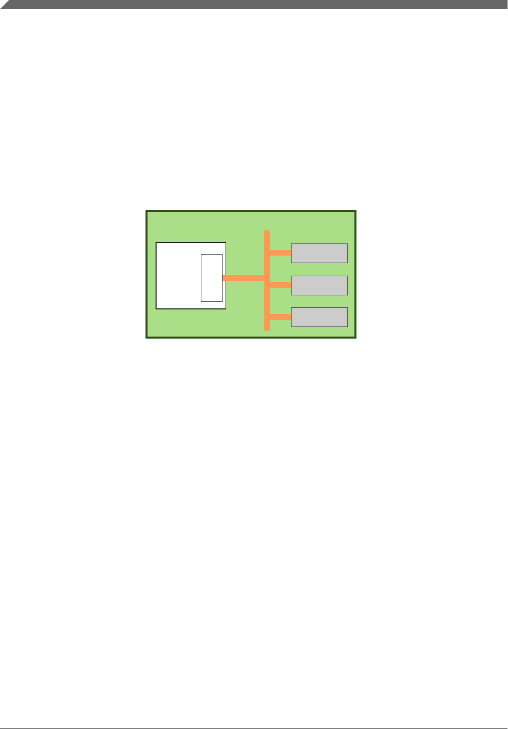
All documented LPSPI registers are present for all LPSPI instances on the device.
Low leakage and Wait modes are not supported in this device. See Module operation in
available low power modes for details on available power modes.
NOTE
Quad-data mode is not supported in S32K11x series of devices.
49.2 Introduction
Peripheral
Printed Circuit Board (PCB)
MCU
LPSPI
Microcontroller SoC
SPI Bus (Serial Peripheral Interface)
Peripheral
Peripheral
Figure 49-1. SPI bus connects MCU to peripherals on PCB
The LPSPI is a low power Serial Peripheral Interface (SPI) module that supports an
efficient interface to an SPI bus, either as a master and/or as a slave.
• The LPSPI is designed to use little CPU overhead, with DMA offloading of FIFO
register accesses.
• The LPSPI can continue operating in stop modes, if an appropriate clock is available.
NOTE
The Serial Peripheral Interface bus (SPI) is a synchronous serial
communication interface used in embedded systems, typically
to perform short distance communications between
microcontrollers and peripheral devices, on printed circuit
boards. Typical applications include interfacing to Secure
Digital cards and LCD displays.
• SPI devices communicate in full duplex mode using a
master-slave scheme with a single master. This enables
communication in both directions to happen
simultaneously.
Introduction
S32K1xx Series Reference Manual, Rev. 7, 04/2018
1434 NXP Semiconductors
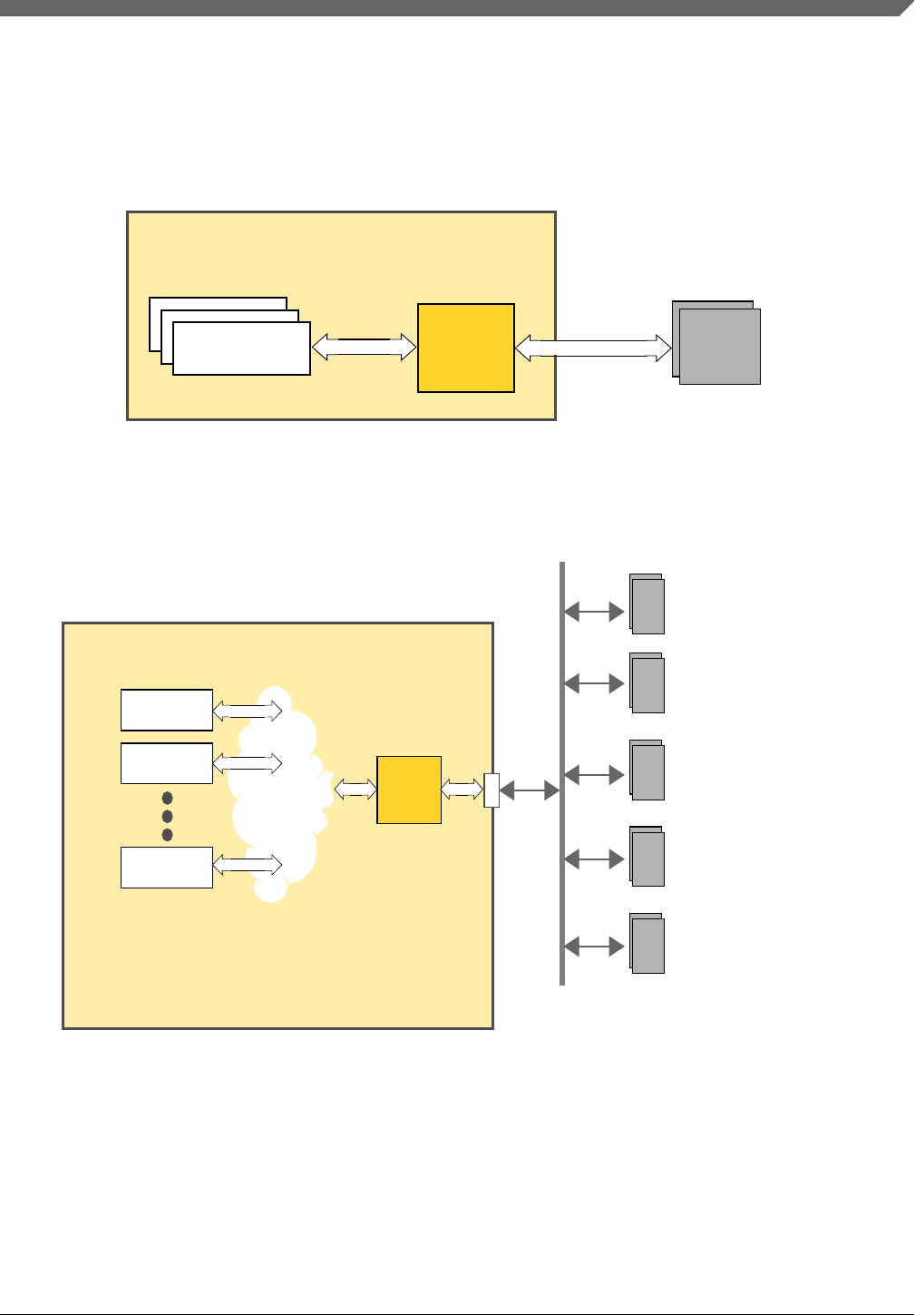
• Multiple slave devices are selected using individual slave
select (SS) lines.
• The master device originates the frame for reading and
writing.
LPSPI
External devices
Or DMA Slaves
MCU System-on-a-Chip (SoC)
Cores or DMA in an MCU SoC use LPSPI to communicate
with external devices over a serial bus.
SPI bus
Cores
Masters
Figure 49-2. LPSPI connects masters in MCU to external slaves on PCB
Communications
LPSPI
Liquid crystal
Flash, EEPROM
Memories
SPI bus
Cores and DMA modules in MCU SoC use LPSPI
Slave-only devices
Synchronous
Sensors
ADC, touchscreens,
MCU System-on-a-Chip (SoC)
DMA
Core 1
Core N
Masters
to connect to external peripherals that use an SPI bus.
Many devices can be connected to the LPSPI,
but only 1 device can be accessed at a time.
to external clock
Bus
Fabric
Bus fabric can be crossbar switches, NICs, or combinations
of crossbar switches, NICs, and similar modules.
Secure digital cards
Ethernet, USB, CAN,
MMC, SD, SDIO
displays (LCD)
USART
temperature
Figure 49-3. Typical LPSPI connection scheme
• SPI accesses are always synchronous to the external clock.
• Each SPI can only assert one chip select at a time, but technically there can be
multiple SPI slaves sharing the same chip select (in the form of a larger shift
register). This requires:
• the SDO of the master to connect to the SDI of the first slave,
Chapter 49 Low Power Serial Peripheral Interface (LPSPI)
S32K1xx Series Reference Manual, Rev. 7, 04/2018
NXP Semiconductors 1435

• the SDO of first slave to connect to the SDI of the next slave,
• and the SDO of last slave to connect to the SDI of the LPSPI master.
Note that some SPI modules use MISO/MOSI for the input/output data.
• The LPSPI supports DMA accesses and generates a DMA request.
49.2.1 Features
The LPSPI supports:
• Word size = 32 bits
• Configurable clock polarity and clock phase
• Master operation supporting up to 4 peripheral chip select
• Slave operation
• Command/transmit FIFO of 4 words
• Receive FIFO of 4 words
• Flexible timing parameters in master mode, including SCK frequency and delays
between PCS and SCK edges
• Support for full duplex transfers supporting 1-bit transmit and receive on each clock
edge
• Support for half duplex transfers supporting 1-bit transmit or receive on each clock
edge
• Support for half duplex transfers supporting 2-bit or 4-bit transmit or receive on each
clock edge (master only)
• Host request input can be used to control the start time of an SPI bus transfer (master
only)
• Receive data match logic supporting wakeup on data match
Introduction
S32K1xx Series Reference Manual, Rev. 7, 04/2018
1436 NXP Semiconductors
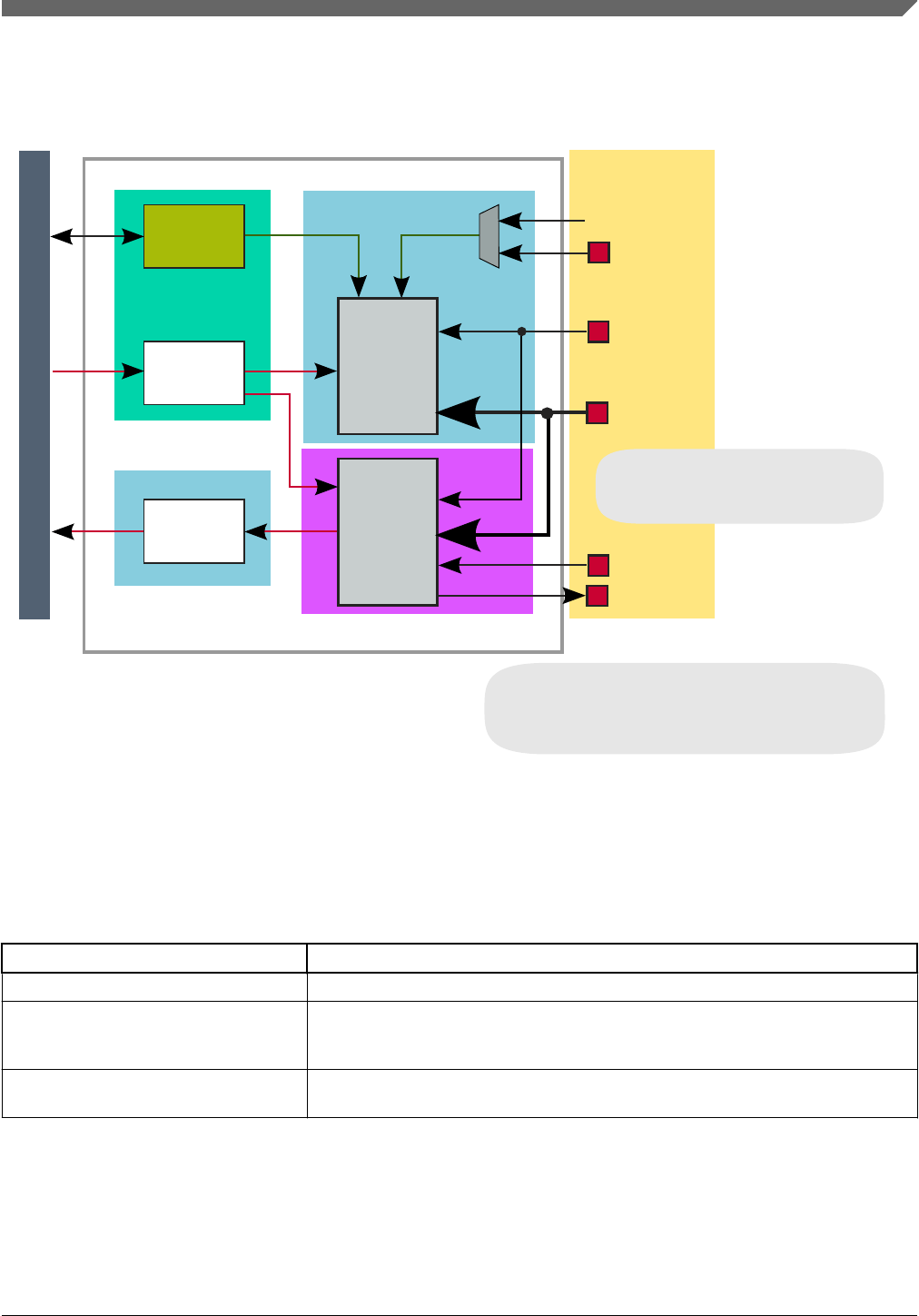
49.2.2 Block Diagram
LPSPI
Configuration
Registers
Internal SoC
HREQ
Trigger
Control
Logic
SIN
SOUT
Bus Clock
External Clock
Functional Clock
Clock Domains
Command /
TX
FIFO
RX
FIFO
Shift
Register
SCK
PCS[3:0]
(Everywhere else)
SCK and PCS[3:0]
are inputs in slave mode,
and are outputs in master mode.
By default, SIN is input and SOUT is output,
but SIN/SOUT can be configured differently.
Either SIN or SOUT can be used for single wire.
SPI Interface
Peripheral Bus
External
Figure 49-4. Block Diagram
49.2.3 Modes of operation
Table 49-2. Chip modes supported by the LPSPI module
Chip mode LPSPI Operation
Run Normal operation
Stop Can continue operating in stop mode if the Doze Enable bit (CR[DOZEN]) is clear
and the LPSPI is using an external or internal clock source that remains operating
during stop mode.
Debug (the core is in Debug/Halted
mode)
Can continue operating in debug mode, if the Debug Enable bit (CR[DBGEN]) is
set.
Chapter 49 Low Power Serial Peripheral Interface (LPSPI)
S32K1xx Series Reference Manual, Rev. 7, 04/2018
NXP Semiconductors 1437

49.2.4 Signal Descriptions
Table 49-3. Signals
Signal Name Description I/O
SCK Serial clock • Input in slave mode
• Output in master mode
I/O
PCS[0] Peripheral Chip Select • Input in slave mode
• Output in master mode
I/O
PCS[1] / HREQ Peripheral Chip Select
or
Host Request
Host Request pin is selected when HREN=1 and
HRSEL=0
• Input in either slave mode or when used as
Host Request
• Output in master mode
I/O
PCS[2] /
DATA[2]
Peripheral Chip Select
or
data pin 2 during quad-data
transfers
• Input in slave mode
• Output in master mode
• Input in quad-data receive transfers
• Output in quad-data transmit transfers
I/O
PCS[3] /
DATA[3]
Peripheral Chip Select
or
data pin 3 during quad-data
transfers
• Input in slave mode
• Output in master mode
• Input in quad-data receive transfers
• Output in quad-data transmit transfers
I/O
SOUT / DATA[0] Serial Data Output Can be configured as serial data input signal
• Used as data pin 0 in quad-data transfers
• Used as data pin 0 in dual-data transfers
I/O
SIN / DATA[1] Serial Data Input Can be configured as serial data output signal
• Used as data pin 1 in quad-data transfers
• Used as data pin 1 in dual-data transfers
I/O
49.2.5 Wiring options
LPSPI can be used to implement typical (dedicated slave select lines) or daisy-chain
(shared slave select lines) SPI busses.
Introduction
S32K1xx Series Reference Manual, Rev. 7, 04/2018
1438 NXP Semiconductors
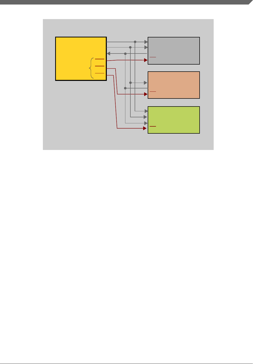
SCLK
MOSI
MISO
SS
SPI
Slave
SCLK
MOSI
MISO
SS1
SS2
SS3
Slave select
lines
SPI
Master
SCLK
MOSI
MISO
SS
SPI
Slave
SCLK
MOSI
MISO
SS
SPI
Slave
Each SPI slave has
SPI master has a
separate slave select
pin for each slave
its own separately wired
slave select line
3 independent SPI slaves
Slaves are considered
Typical SPI bus scheme
independent of each other
Figure 49-5. Dedicated slave select lines scheme
Chapter 49 Low Power Serial Peripheral Interface (LPSPI)
S32K1xx Series Reference Manual, Rev. 7, 04/2018
NXP Semiconductors 1439
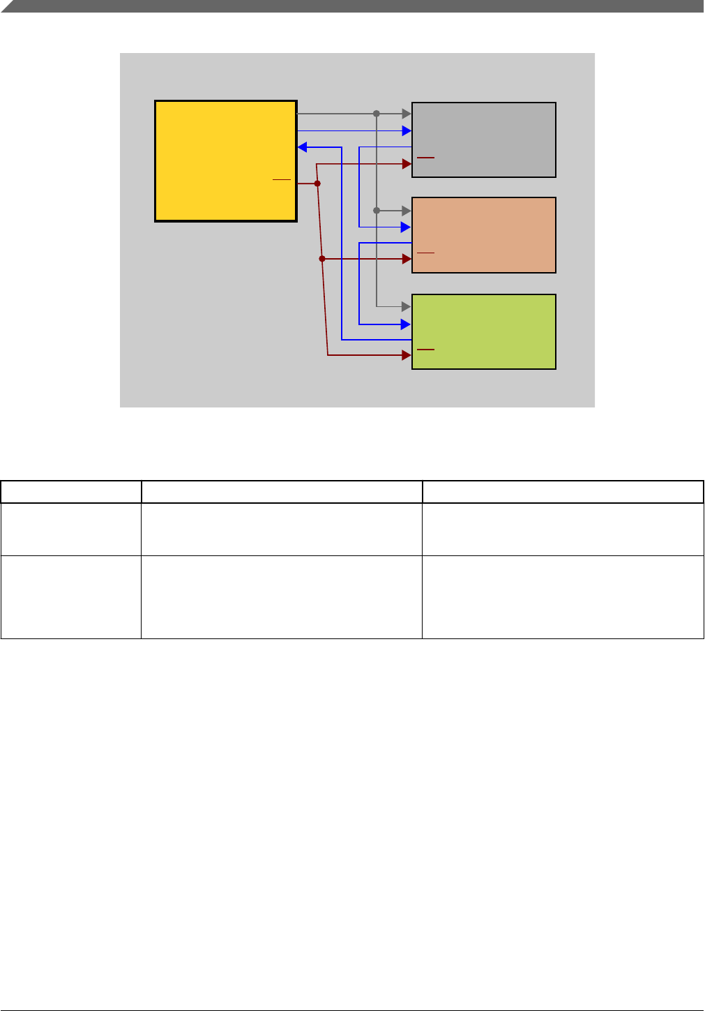
SCLK
MOSI
MISO
SS
SPI
Slave
SCLK
MOSI
MISO
SS
SPI
Slave
SCLK
MOSI
MISO
SS
SPI
Slave
SCLK
MOSI
MISO
SS
Slave select
line
SPI
Master
Each SPI slave
shares the same wired
slave select line The slaves have to
3 cooperative SPI slaves
SPI master has a
single slave select
pin for all slaves
Daisy-chain SPI bus scheme
cooperate with each other
Figure 49-6. Shared slave select lines (daisy-chain) scheme
Table 49-4. Wiring Scheme Differences
Item Dedicated slave select lines Shared slave select lines (daisy-chain)
slave select lines (pins
on the master device)
• 1 slave select line (pin) for each slave; the
scheme is limited by how many lines (pins)
that the master device can support
• 1 slave select line (pin) for multiple slaves
data flow from master
device to slave devices
• Master sends data directly to the slave that
the data is for; the slaves for whom the
data is not intended, simply ignore the
data; this implies that those slaves could
be asleep (if desired)
• Master sends data and multiple slaves
have to forward the data through the daisy
chain; this implies that all slaves must be
on and awake when the master sends data
to any slave
49.3 Memory Map and Registers
NOTE
Writing a Read-Only (RO) register or reading a Write-Only
(WO) register can cause bus errors. This module will not check
if programmed values in the registers are correct; the
application software must ensure that valid programmed values
are being written.
Memory Map and Registers
S32K1xx Series Reference Manual, Rev. 7, 04/2018
1440 NXP Semiconductors

49.3.1 LPSPI register descriptions
49.3.1.1 LPSPI Memory map
LPSPI0 base address: 4002_C000h
LPSPI1 base address: 4002_D000h
LPSPI2 base address: 4002_E000h
Offset Register Width
(In bits)
Access Reset value
0h Version ID Register (VERID) 32 RO 0100_0004h
4h Parameter Register (PARAM) 32 RO 0000_0202h
10h Control Register (CR) 32 RW 0000_0000h
14h Status Register (SR) 32 W1C 0000_0001h
18h Interrupt Enable Register (IER) 32 RW 0000_0000h
1Ch DMA Enable Register (DER) 32 RW 0000_0000h
20h Configuration Register 0 (CFGR0) 32 RW 0000_0000h
24h Configuration Register 1 (CFGR1) 32 RW 0000_0000h
30h Data Match Register 0 (DMR0) 32 RW 0000_0000h
34h Data Match Register 1 (DMR1) 32 RW 0000_0000h
40h Clock Configuration Register (CCR) 32 RW 0000_0000h
58h FIFO Control Register (FCR) 32 RW 0000_0000h
5Ch FIFO Status Register (FSR) 32 RO 0000_0000h
60h Transmit Command Register (TCR) 32 RW 0000_001Fh
64h Transmit Data Register (TDR) 32 WO 0000_0000h
70h Receive Status Register (RSR) 32 RO 0000_0002h
74h Receive Data Register (RDR) 32 RO 0000_0000h
49.3.1.2 Version ID Register (VERID)
49.3.1.2.1 Offset
Register Offset
VERID 0h
Chapter 49 Low Power Serial Peripheral Interface (LPSPI)
S32K1xx Series Reference Manual, Rev. 7, 04/2018
NXP Semiconductors 1441

49.3.1.2.2 Diagram
Bits 31 30 29 28 27 26 25 24 23 22 21 20 19 18 17 16
RMAJOR MINOR
W
Reset 0 0 0 0 0 0 0 1 0 0 0 0 0 0 0 0
Bits 15 14 13 12 11 10 9 8 7 6 5 4 3 2 1 0
RFEATURE
W
Reset 0 0 0 0 0 0 0 0 0 0 0 0 0 1 0 0
49.3.1.2.3 Fields
Field Function
31-24
MAJOR
Major Version Number
Returns the major version number for the module specification. Read-only field.
23-16
MINOR
Minor Version Number
Returns the minor version number for the module specification. Read-only field.
15-0
FEATURE
Module Identification Number
Returns the feature set number. Read-only field.
0000000000000100b - Standard feature set supporting a 32-bit shift register.
49.3.1.3 Parameter Register (PARAM)
49.3.1.3.1 Offset
Register Offset
PARAM 4h
Memory Map and Registers
S32K1xx Series Reference Manual, Rev. 7, 04/2018
1442 NXP Semiconductors

49.3.1.3.2 Diagram
Bits 31 30 29 28 27 26 25 24 23 22 21 20 19 18 17 16
R 0 0
W
Reset 0 0 0 0 0 0 0 0 0 0 0 0 0 0 0 0
Bits 15 14 13 12 11 10 9 8 7 6 5 4 3 2 1 0
RRXFIFO TXFIFO
W
Reset 0 0 0 0 0 0 1 0 0 0 0 0 0 0 1 0
49.3.1.3.3 Fields
Field Function
31-24
—
Reserved
23-16
—
Reserved
15-8
RXFIFO
Receive FIFO Size
Sets the maximum number of words in the receive FIFO, which is 2RXFIFO
7-0
TXFIFO
Transmit FIFO Size
Sets the maximum number of words in the transmit FIFO, which is 2TXFIFO
49.3.1.4 Control Register (CR)
49.3.1.4.1 Offset
Register Offset
CR 10h
Chapter 49 Low Power Serial Peripheral Interface (LPSPI)
S32K1xx Series Reference Manual, Rev. 7, 04/2018
NXP Semiconductors 1443

49.3.1.4.2 Diagram
Bits 31 30 29 28 27 26 25 24 23 22 21 20 19 18 17 16
R 0
W
Reset 0 0 0 0 0 0 0 0 0 0 0 0 0 0 0 0
Bits 15 14 13 12 11 10 9 8 7 6 5 4 3 2 1 0
R
0
0
DBGE
N
DOZEN
RS
T
MEN
W
RR
F
RT
F
Reset 0 0 0 0 0 0 0 0 0 0 0 0 0 0 0 0
49.3.1.4.3 Fields
Field Function
31-10
—
Reserved
9
RRF
Reset Receive FIFO
0b - No effect
1b - Receive FIFO is reset
8
RTF
Reset Transmit FIFO
0b - No effect
1b - Transmit FIFO is reset
7-4
—
Reserved
3
DBGEN
Debug Enable
Enables or disables the LPSPI module in debug mode. Debug Enable bit should be updated only when
the LPSPI module is disabled.
0b - LPSPI module is disabled in debug mode
1b - LPSPI module is enabled in debug mode
2
DOZEN
Doze Mode Enable
Enables or disables the LPSPI module in Doze mode. Doze Mode Enable bit should be updated only
when the LPSPI module is disabled.
0b - LPSPI module is enabled in Doze mode
1b - LPSPI module is disabled in Doze mode
1
RST
Software Reset
Reset all internal logic and registers, except the Control Register. RST remains set until cleared by
software.
0b - Module is not reset
1b - Module is reset
0
MEN
Module Enable
0b - Module is disabled
1b - Module is enabled
Memory Map and Registers
S32K1xx Series Reference Manual, Rev. 7, 04/2018
1444 NXP Semiconductors
49.3.1.5 Status Register (SR)
49.3.1.5.1 Offset
Register Offset
SR 14h
49.3.1.5.2 Diagram
Bits 31 30 29 28 27 26 25 24 23 22 21 20 19 18 17 16
R 0 MBF 0
W
Reset 0 0 0 0 0 0 0 0 0 0 0 0 0 0 0 0
Bits 15 14 13 12 11 10 9 8 7 6 5 4 3 2 1 0
R 0 DMF REF TEF TCF FCF WCF 0RDF TDF
W W1C W1C W1C W1C W1C W1C
Reset 0 0 0 0 0 0 0 0 0 0 0 0 0 0 0 1
49.3.1.5.3 Fields
Field Function
31-25
—
Reserved
24
MBF
Module Busy Flag
0b - LPSPI is idle
1b - LPSPI is busy
23-14
—
Reserved
13
DMF
Data Match Flag
Indicates that the received data has matched the MATCH0 and/or MATCH1 fields (as configured by
CFGR1[MATCFG], Configuration Register 1).
0b - Have not received matching data
1b - Have received matching data
12
REF
Receive Error Flag
The Receive Error Flag will set when the Receiver FIFO overflows. When the Receive Error Flag is set, it
is recommended to first end the transfer, empty the Receive FIFO, clear the Receive Error Flag and then
restart the transfer from the beginning.
0b - Receive FIFO has not overflowed
Table continues on the next page...
Chapter 49 Low Power Serial Peripheral Interface (LPSPI)
S32K1xx Series Reference Manual, Rev. 7, 04/2018
NXP Semiconductors 1445

Field Function
1b - Receive FIFO has overflowed
11
TEF
Transmit Error Flag
The Transmit Error Flag will set when the Transmit FIFO underruns. When the Transmit Error Flag is set,
it is recommended to first end the transfer, clear the Transmit Error Flag and then restart the transfer from
the beginning.
0b - Transmit FIFO underrun has not occurred
1b - Transmit FIFO underrun has occurred
10
TCF
Transfer Complete Flag
In master mode when the LPSPI returns to idle state with the transmit FIFO empty, the Transfer
Complete Flag will set.
0b - All transfers have not completed
1b - All transfers have completed
9
FCF
Frame Complete Flag
The Frame Complete Flag will set at the end of each frame transfer, when the PCS negates.
0b - Frame transfer has not completed
1b - Frame transfer has completed
8
WCF
Word Complete Flag
The Word Complete Flag will set when the last bit of a received word is sampled.
0b - Transfer of a received word has not yet completed
1b - Transfer of a received word has completed
7-2
—
Reserved
1
RDF
Receive Data Flag
The Receive Data Flag is set whenever the number of words in the receive FIFO is greater than
FCR[RXWATER] (FIFO Control Register)
0b - Receive Data is not ready
1b - Receive data is ready
0
TDF
Transmit Data Flag
The Transmit Data Flag is set whenever the number of words in the transmit FIFO is equal or less than
FCR[TXWATER] (FIFO Control Register)
0b - Transmit data not requested
1b - Transmit data is requested
49.3.1.6 Interrupt Enable Register (IER)
49.3.1.6.1 Offset
Register Offset
IER 18h
Memory Map and Registers
S32K1xx Series Reference Manual, Rev. 7, 04/2018
1446 NXP Semiconductors

49.3.1.6.2 Diagram
Bits 31 30 29 28 27 26 25 24 23 22 21 20 19 18 17 16
R 0
W
Reset 0 0 0 0 0 0 0 0 0 0 0 0 0 0 0 0
Bits 15 14 13 12 11 10 9 8 7 6 5 4 3 2 1 0
R
0
DMIE
REI
E
TEI
E
TCIE
FCI
E
WCIE
0
RDI
E
TDIE
W
Reset 0 0 0 0 0 0 0 0 0 0 0 0 0 0 0 0
49.3.1.6.3 Fields
Field Function
31-14
—
Reserved
13
DMIE
Data Match Interrupt Enable
0b - Disabled
1b - Enabled
12
REIE
Receive Error Interrupt Enable
0b - Disabled
1b - Enabled
11
TEIE
Transmit Error Interrupt Enable
0b - Disabled
1b - Enabled
10
TCIE
Transfer Complete Interrupt Enable
0b - Disabled
1b - Enabled
9
FCIE
Frame Complete Interrupt Enable
0b - Disabled
1b - Enabled
8
WCIE
Word Complete Interrupt Enable
0b - Disabled
1b - Enabled
7-2
—
Reserved
1
RDIE
Receive Data Interrupt Enable
0b - Disabled
1b - Enabled
0
TDIE
Transmit Data Interrupt Enable
0b - Disabled
1b - Enabled
Chapter 49 Low Power Serial Peripheral Interface (LPSPI)
S32K1xx Series Reference Manual, Rev. 7, 04/2018
NXP Semiconductors 1447

49.3.1.7 DMA Enable Register (DER)
49.3.1.7.1 Offset
Register Offset
DER 1Ch
49.3.1.7.2 Diagram
Bits 31 30 29 28 27 26 25 24 23 22 21 20 19 18 17 16
R 0
W
Reset 0 0 0 0 0 0 0 0 0 0 0 0 0 0 0 0
Bits 15 14 13 12 11 10 9 8 7 6 5 4 3 2 1 0
R
0
RDD
E
TDDE
W
Reset 0 0 0 0 0 0 0 0 0 0 0 0 0 0 0 0
49.3.1.7.3 Fields
Field Function
31-2
—
Reserved
1
RDDE
Receive Data DMA Enable
0b - DMA request is disabled
1b - DMA request is enabled
0
TDDE
Transmit Data DMA Enable
0b - DMA request is disabled
1b - DMA request is enabled
49.3.1.8 Configuration Register 0 (CFGR0)
49.3.1.8.1 Offset
Register Offset
CFGR0 20h
Memory Map and Registers
S32K1xx Series Reference Manual, Rev. 7, 04/2018
1448 NXP Semiconductors

49.3.1.8.2 Diagram
Bits 31 30 29 28 27 26 25 24 23 22 21 20 19 18 17 16
R 0
W
Reset 0 0 0 0 0 0 0 0 0 0 0 0 0 0 0 0
Bits 15 14 13 12 11 10 9 8 7 6 5 4 3 2 1 0
R
0
RDMO
CIRFIFO
0
HRSE
L
HRPOL
HRE
N
W
Reset 0 0 0 0 0 0 0 0 0 0 0 0 0 0 0 0
49.3.1.8.3 Fields
Field Function
31-10
—
Reserved
9
RDMO
Receive Data Match Only
When Receive Data Match Only is enabled, all received data that does not cause the Data Match Flag
(SR[DMF]) to set is discarded.
• Receive Data Match Only bit should be set when the LPSPI is idle and the Data Match Flag is clear
• After the Data Match Flag (DMF) is set, the Receive Data Match Only bit configuration is ignored
• When disabling RDMO and to ensure that no receive data is lost, before clearing the Data Match
Flag, first clear Receive Data Match Only (RDMO)
0b - Received data is stored in the receive FIFO as in normal operations
1b - Received data is discarded unless the Data Match Flag (DMF) is set
8
CIRFIFO
Circular FIFO Enable
When enabled, the transmit FIFO read pointer is saved to a temporary register. The transmit FIFO will be
emptied as it normally is, but after the LPSPI is idle and the transmit FIFO is empty, then the read pointer
value will be restored from the temporary register. This restoring of the read pointer will cause the
contents of the transmit FIFO to be cycled through repeatedly.
0b - Circular FIFO is disabled
1b - Circular FIFO is enabled
7-3
—
Reserved
2
HRSEL
Host Request Select
Selects the source of the host request input. When the host request function is enabled with the
LPSPI_HREQ pin, the LPSPI_PCS[1] function is disabled.
0b - Host request input is the LPSPI_HREQ pin
1b - Host request input is the input trigger
1
HRPOL
Host Request Polarity
Configures the polarity of the host request pin.
0b - Active low
Table continues on the next page...
Chapter 49 Low Power Serial Peripheral Interface (LPSPI)
S32K1xx Series Reference Manual, Rev. 7, 04/2018
NXP Semiconductors 1449

Field Function
1b - Active high
0
HREN
Host Request Enable
When enabled in master mode, the LPSPI will only start a new SPI bus transfer if the host request input
is asserted. When the LPSPI is busy, the host request input is ignored.
0b - Host request is disabled
1b - Host request is enabled
49.3.1.9 Configuration Register 1 (CFGR1)
49.3.1.9.1 Offset
Register Offset
CFGR1 24h
49.3.1.9.2 Function
The CFGR1 should only be written when the LPSPI is disabled.
49.3.1.9.3 Diagram
Bits 31 30 29 28 27 26 25 24 23 22 21 20 19 18 17 16
R
0
PCSCF
G
OUTCFG
PINCFG
0
MATCFG
W
Reset 0 0 0 0 0 0 0 0 0 0 0 0 0 0 0 0
Bits 15 14 13 12 11 10 9 8 7 6 5 4 3 2 1 0
R
0
PCSPOL
0
NOSTALL
AUTOPCS
SAMPLE
MASTER
W
Reset 0 0 0 0 0 0 0 0 0 0 0 0 0 0 0 0
49.3.1.9.4 Fields
Field Function
31-28 Reserved
Table continues on the next page...
Memory Map and Registers
S32K1xx Series Reference Manual, Rev. 7, 04/2018
1450 NXP Semiconductors

Field Function
—
27
PCSCFG
Peripheral Chip Select Configuration
If performing 4-bit transfers, the Peripheral Chip Select Configuration bit must be set.
0b - PCS[3:2] are enabled
1b - PCS[3:2] are disabled
26
OUTCFG
Output Config
Configures if the output data is tristated between accesses (LPSPI_PCS is negated).
0b - Output data retains last value when chip select is negated
1b - Output data is tristated when chip select is negated
25-24
PINCFG
Pin Configuration
Configures which pins are used for input and output data during single bit transfers.
00b - SIN is used for input data and SOUT is used for output data
01b - SIN is used for both input and output data
10b - SOUT is used for both input and output data
11b - SOUT is used for input data and SIN is used for output data
23-19
—
Reserved
18-16
MATCFG
Match Configuration
Configures the condition that will cause the DMF to set.
NOTE: Syntax: * is boolean AND, + is boolean OR
000b - Match is disabled
001b - Reserved
010b - 010b - Match is enabled, if 1st data word equals MATCH0 OR MATCH1, i.e., (1st data word
= MATCH0 + MATCH1)
011b - 011b - Match is enabled, if any data word equals MATCH0 OR MATCH1, i.e., (any data
word = MATCH0 + MATCH1)
100b - 100b - Match is enabled, if 1st data word equals MATCH0 AND 2nd data word equals
MATCH1, i.e., [(1st data word = MATCH0) * (2nd data word = MATCH1)]
101b - 101b - Match is enabled, if any data word equals MATCH0 AND the next data word equals
MATCH1, i.e., [(any data word = MATCH0) * (next data word = MATCH1)]
110b - 110b - Match is enabled, if (1st data word AND MATCH1) equals (MATCH0 AND MATCH1),
i.e., [(1st data word * MATCH1) = (MATCH0 * MATCH1)]
111b - 111b - Match is enabled, if (any data word AND MATCH1) equals (MATCH0 AND
MATCH1), i.e., [(any data word * MATCH1) = (MATCH0 * MATCH1)]
15-12
—
Reserved
11-8
PCSPOL
Peripheral Chip Select Polarity
Configures the polarity of each Peripheral Chip Select pin.
0000b - The Peripheral Chip Select pin PCSx is active low
0001b - The Peripheral Chip Select pin PCSx is active high
7-4
—
Reserved
3
NOSTALL
No Stall
In master mode, the LPSPI will stall transfers when the transmit FIFO is empty or when the receive FIFO
is full, ensuring that no transmit FIFO underrun or receive FIFO overrun can occur. Setting the No Stall bit
will disable this functionality.
0b - Transfers will stall when the transmit FIFO is empty or the receive FIFO is full
1b - Transfers will not stall, allowing transmit FIFO underruns or receive FIFO overruns to occur
Table continues on the next page...
Chapter 49 Low Power Serial Peripheral Interface (LPSPI)
S32K1xx Series Reference Manual, Rev. 7, 04/2018
NXP Semiconductors 1451

Field Function
2
AUTOPCS
Automatic PCS
For correct operations, the LPSPI slave normally requires the PCS to negate between frames. Setting the
Automatic PCS bit will cause the LPSPI to generate an internal PCS signal at the end of each transfer
word when the Clock Phase bit TCR[CPHA] = 1.
• When the Automatic PCS bit is set, the SCK must remain idle for at least 4 LPSPI functional clock
cycles (divided by the Prescaler Value TCR[PRESCALE] configuration) between each word, to
ensure correct operations
• In master mode, the Automatic PCS bit is ignored
0b - Automatic PCS generation is disabled
1b - Automatic PCS generation is enabled
1
SAMPLE
Sample Point
When set, the LPSPI master will sample the input data on a delayed LPSPI_SCK edge, which improves
the setup time when sampling data.
• The input data setup time in master mode with delayed LPSPI_SCK edge is equal to the input data
setup time in slave mode
• In slave mode, the SAMPLE bit is ignored
0b - Input data is sampled on SCK edge
1b - Input data is sampled on delayed SCK edge
0
MASTER
Master Mode
Configures the LPSPI in master or slave mode. The Master Mode bit directly controls the direction of the
LPSPI_SCK and LPCPI_PCS pins.
0b - Slave mode
1b - Master mode
49.3.1.10 Data Match Register 0 (DMR0)
49.3.1.10.1 Offset
Register Offset
DMR0 30h
Memory Map and Registers
S32K1xx Series Reference Manual, Rev. 7, 04/2018
1452 NXP Semiconductors

49.3.1.10.2 Diagram
Bits 31 30 29 28 27 26 25 24 23 22 21 20 19 18 17 16
RMATCH0
W
Reset 0 0 0 0 0 0 0 0 0 0 0 0 0 0 0 0
Bits 15 14 13 12 11 10 9 8 7 6 5 4 3 2 1 0
RMATCH0
W
Reset 0 0 0 0 0 0 0 0 0 0 0 0 0 0 0 0
49.3.1.10.3 Fields
Field Function
31-0
MATCH0
Match 0 Value
When Receive Data Match Only (CFGR0[RDMO]) is enabled, the Match 0 Value is compared against the
received data.
49.3.1.11 Data Match Register 1 (DMR1)
49.3.1.11.1 Offset
Register Offset
DMR1 34h
49.3.1.11.2 Diagram
Bits 31 30 29 28 27 26 25 24 23 22 21 20 19 18 17 16
RMATCH1
W
Reset 0 0 0 0 0 0 0 0 0 0 0 0 0 0 0 0
Bits 15 14 13 12 11 10 9 8 7 6 5 4 3 2 1 0
RMATCH1
W
Reset 0 0 0 0 0 0 0 0 0 0 0 0 0 0 0 0
Chapter 49 Low Power Serial Peripheral Interface (LPSPI)
S32K1xx Series Reference Manual, Rev. 7, 04/2018
NXP Semiconductors 1453

49.3.1.11.3 Fields
Field Function
31-0
MATCH1
Match 1 Value
When Receive Data Match Only (CFGR0[RDMO]) is enabled, the Match 1 Value is compared against the
received data.
49.3.1.12 Clock Configuration Register (CCR)
49.3.1.12.1 Offset
Register Offset
CCR 40h
49.3.1.12.2 Function
The Clock Configuration Register is only used in master mode, and the Clock
Configuration Register cannot be changed when the LPSPI is enabled.
49.3.1.12.3 Diagram
Bits 31 30 29 28 27 26 25 24 23 22 21 20 19 18 17 16
RSCKPCS PCSSCK
W
Reset 0 0 0 0 0 0 0 0 0 0 0 0 0 0 0 0
Bits 15 14 13 12 11 10 9 8 7 6 5 4 3 2 1 0
RDBT SCKDIV
W
Reset 0 0 0 0 0 0 0 0 0 0 0 0 0 0 0 0
49.3.1.12.4 Fields
Field Function
31-24
SCKPCS
SCK-to-PCS Delay
In master mode: configures the delay from the last SCK edge to the PCS negation.
Table continues on the next page...
Memory Map and Registers
S32K1xx Series Reference Manual, Rev. 7, 04/2018
1454 NXP Semiconductors

Field Function
• The delay is equal to (SCKPCS + 1) cycles of the LPSPI functional clock divided by the Prescaler
Value TCR[PRESCALE] configuration.
• The minimum delay is 1 cycle.
23-16
PCSSCK
PCS-to-SCK Delay
In master mode: configures the delay from the PCS assertion to the first SCK edge.
• The delay is equal to (PCSSCK + 1) cycles of the LPSPI functional clock divided by the Prescaler
Value TCR[PRESCALE] configuration.
• The minimum delay is 1 cycle.
15-8
DBT
Delay Between Transfers
In master mode:
• Configures the delay from the PCS negation to the next PCS assertion.
• The delay is equal to (DBT + 2) cycles of the LPSPI functional clock divided by the Prescaler
Value TCR[PRESCALE] configuration.
• The minimum delay is 2 cycles.
• Half of the delay occurs before PCS assertion and the other half of the delay occurs after
PCS negation. If the command word is updated between 2 transfers, then the command word
is updated half-way between the PCS negation of the last transfer and PCS assertion of the
next transfer.
• The command word sets which PCS signal is used (of PCS[3:0]}, the polarity/phase of the
SCK signal, and the Prescaler Value.
• Configures the delay from the last SCK edge of a transfer word and the first SCK edge of the next
transfer word, in a continuous transfer.
• The delay is equal to (DBT + 1) cycles of the LPSPI functional clock divided by the Prescaler
Value TCR[PRESCALE] configuration.
• The minimum delay is 1 cycle.
7-0
SCKDIV
SCK Divider
In master mode, the SCK Divider configures the divide ratio of the SCK pin.
• The SCK period is equal to (SCKDIV+2) cycles of the LPSPI functional clock divided by the
Prescaler Value TCR[PRESCALE] configuration.
• The minimum SCK period is 2 cycles.
• If the SCK period is an odd number of cycles, then the 1st half of the SCK period will be 1 cycle
longer than the 2nd half of the SCK period.
49.3.1.13 FIFO Control Register (FCR)
49.3.1.13.1 Offset
Register Offset
FCR 58h
Chapter 49 Low Power Serial Peripheral Interface (LPSPI)
S32K1xx Series Reference Manual, Rev. 7, 04/2018
NXP Semiconductors 1455

49.3.1.13.2 Diagram
Bits 31 30 29 28 27 26 25 24 23 22 21 20 19 18 17 16
R
0
0
RXWATER
W
Reset 0 0 0 0 0 0 0 0 0 0 0 0 0 0 0 0
Bits 15 14 13 12 11 10 9 8 7 6 5 4 3 2 1 0
R
0
0
TXWATER
W
Reset 0 0 0 0 0 0 0 0 0 0 0 0 0 0 0 0
49.3.1.13.3 Fields
Field Function
31-24
—
Reserved
23-18
—
Reserved
17-16
RXWATER
Receive FIFO Watermark
The Receive Data Flag is set whenever the number of words in the receive FIFO is greater than
RXWATER. Writing a value equal or greater than the FIFO size will be truncated.
15-8
—
Reserved
7-2
—
Reserved
1-0
TXWATER
Transmit FIFO Watermark
The Transmit Data Flag is set whenever the number of words in the transmit FIFO is equal or less than
TXWATER. Writing a value equal or greater than the FIFO size will be truncated.
49.3.1.14 FIFO Status Register (FSR)
49.3.1.14.1 Offset
Register Offset
FSR 5Ch
Memory Map and Registers
S32K1xx Series Reference Manual, Rev. 7, 04/2018
1456 NXP Semiconductors

49.3.1.14.2 Diagram
Bits 31 30 29 28 27 26 25 24 23 22 21 20 19 18 17 16
R 0 0 RXCOUNT
W
Reset 0 0 0 0 0 0 0 0 0 0 0 0 0 0 0 0
Bits 15 14 13 12 11 10 9 8 7 6 5 4 3 2 1 0
R 0 0 TXCOUNT
W
Reset 0 0 0 0 0 0 0 0 0 0 0 0 0 0 0 0
49.3.1.14.3 Fields
Field Function
31-24
—
Reserved
23-19
—
Reserved
18-16
RXCOUNT
Receive FIFO Count
Returns the number of words currently stored in the receive FIFO.
15-8
—
Reserved
7-3
—
Reserved
2-0
TXCOUNT
Transmit FIFO Count
Returns the number of words currently stored in the transmit FIFO.
49.3.1.15 Transmit Command Register (TCR)
49.3.1.15.1 Offset
Register Offset
TCR 60h
Chapter 49 Low Power Serial Peripheral Interface (LPSPI)
S32K1xx Series Reference Manual, Rev. 7, 04/2018
NXP Semiconductors 1457

49.3.1.15.2 Function
Writes to either the Transmit Command Register or Transmit Data Register will push the
data into the transmit FIFO, in the order that the data are written. Command Register
writes will be tagged and cause the command register to update, after that entry reaches
the top of the FIFO. This allows changes to the command word and the transmit data
itself to be interleaved. Changing the command word will cause all subsequent SPI bus
transfers to be performed using the new command word.
•In master mode, writing a new command word does not initiate a new transfer,
unless TXMSK is set. Transfers are initiated by transmit data in the transmit FIFO, or
by a new command word (with TXMSK set). Hardware will clear TXMSK when the
LPSPI_PCS negates.
•In master mode, if the command word is changed before an existing frame has
completed, then the existing frame will terminate and the command word will then
update. The command word can be changed during a continuous transfer, if CONTC
of the new command word is set and the command word is written on a frame size
boundary.
•In slave mode, the command word should be changed only when the LPSPI is idle
and there is no SPI bus transfer.
Avoid register reading problems: Reading the Transmit Command Register will return
the current state of the command register. Reading the Transmit Command Register at the
same time that the Transmit Command Register is loaded from the transmit FIFO, can
return an incorrect Transmit Command Register value. It is recommended:
• to either read the Transmit Command Register when the transmit FIFO is empty,
• or to read the Transmit Command Register more than once and then compare the
returned values.
49.3.1.15.3 Diagram
Bits 31 30 29 28 27 26 25 24 23 22 21 20 19 18 17 16
R
CPOL
CPHA
PRESCAL
E
Reserved
PC
S
LSB
F
BYS
W
CONT
CONTC
RXMSK
TXMSK
WIDTH
W
Reset 0 0 0 0 0 0 0 0 0 0 0 0 0 0 0 0
Bits 15 14 13 12 11 10 9 8 7 6 5 4 3 2 1 0
RReserved FRAMESZ
W
Reset 0 0 0 0 0 0 0 0 0 0 0 1 1 1 1 1
Memory Map and Registers
S32K1xx Series Reference Manual, Rev. 7, 04/2018
1458 NXP Semiconductors

49.3.1.15.4 Fields
Field Function
31
CPOL
Clock Polarity
The Clock Polarity field is only updated between frames.
0b - The inactive state value of SCK is low
1b - The inactive state value of SCK is high
30
CPHA
Clock Phase
The Clock Phase field is only updated between frames.
0b - Data is captured on the leading edge of SCK and changed on the following edge of SCK
1b - Data is changed on the leading edge of SCK and captured on the following edge of SCK
29-27
PRESCALE
Prescaler Value
For all SPI bus transfers, the Prescaler value applied to the clock configuration register. The Prescaler
Value field is only updated between frames.
000b - Divide by 1
001b - Divide by 2
010b - Divide by 4
011b - Divide by 8
100b - Divide by 16
101b - Divide by 32
110b - Divide by 64
111b - Divide by 128
26
—
Reserved
25-24
PCS
Peripheral Chip Select
Configures the peripheral chip select used for the transfer. The Peripheral Chip Select field is only
updated between frames.
00b - Transfer using LPSPI_PCS[0]
01b - Transfer using LPSPI_PCS[1]
10b - Transfer using LPSPI_PCS[2]
11b - Transfer using LPSPI_PCS[3]
23
LSBF
LSB First
0b - Data is transferred MSB first
1b - Data is transferred LSB first
22
BYSW
Byte Swap
Byte swap will swap the contents of [31:24] with [7:0] and [23:16] with [15:8] for each transmit data word
read from the FIFO and for each received data word stored to the FIFO (or compared with match
registers).
0b - Byte swap is disabled
1b - Byte swap is enabled
21
CONT
Continuous Transfer
• In master mode, continuous transfer will keep the PCS asserted at the end of the frame size, until a
command word is received that starts a new frame.
• In slave mode, when continuous transfer is enabled, the LPSPI will only transmit the first
FRAMESZ bits; after which the LPSPI will transmit received data (assuming a 32-bit shift register).
0b - Continuous transfer is disabled
1b - Continuous transfer is enabled
20
CONTC
Continuing Command
Table continues on the next page...
Chapter 49 Low Power Serial Peripheral Interface (LPSPI)
S32K1xx Series Reference Manual, Rev. 7, 04/2018
NXP Semiconductors 1459

Field Function
In master mode, the Continuing Command bit allows the command word to be changed within a
continuous transfer.
• The initial command word must enable continuous transfer (CONT=1),
• the continuing command must set this bit (CONTC=1),
• and the continuing command word must be loaded on a frame size boundary.
For example, if the continuous transfer has a frame size of 64-bits, then a continuing command word
must be loaded on a 64-bit boundary.
0b - Command word for start of new transfer
1b - Command word for continuing transfer
19
RXMSK
Receive Data Mask
When set, receive data is masked (receive data is not stored in receive FIFO).
0b - Normal transfer
1b - Receive data is masked
18
TXMSK
Transmit Data Mask
When set, transmit data is masked (no data is loaded from transmit FIFO and output pin is tristated). In
master mode, the Transmit Data Mask bit will initiate a new transfer which cannot be aborted by another
command word; the Transmit Data Mask bit will be cleared by hardware at the end of the transfer.
0b - Normal transfer
1b - Mask transmit data
17-16
WIDTH
Transfer Width
For 2-bit or 4-bit transfers, either Receive Data Mask (RXMSK) or Transmit Data Mask (TXMSK) must be
set.
00b - 1 bit transfer
01b - 2 bit transfer
10b - 4 bit transfer
11b - Reserved
15-12
—
Reserved. Software should only write zero to this field.
11-0
FRAMESZ
Frame Size
Configures the frame size in number of bits equal to (FRAMESZ + 1).
• The minimum frame size is 8 bits
• The minimum word size is 2 bits; a frame size of 33 bits (or similar) is not supported.
• If the frame size is larger than 32 bits, then the frame is divided into multiple words of 32-bits; each
word is loaded from the transmit FIFO and stored in the receive FIFO separately.
• If the size of the frame is not divisible by 32, then the last load of the transmit FIFO and store of the
receive FIFO will contain the remainder bits. For example, a 72-bit transfer will consist of 3 words:
the 1st and 2nd words are 32 bits, and the 3rd word is 8 bits.
49.3.1.16 Transmit Data Register (TDR)
49.3.1.16.1 Offset
Register Offset
TDR 64h
Memory Map and Registers
S32K1xx Series Reference Manual, Rev. 7, 04/2018
1460 NXP Semiconductors

49.3.1.16.2 Function
Writes to either the Transmit Command Register or Transmit Data Register will push the
data into the transmit FIFO, in the order that it (the data) was written.
49.3.1.16.3 Diagram
Bits 31 30 29 28 27 26 25 24 23 22 21 20 19 18 17 16
R
WDATA
Reset 0 0 0 0 0 0 0 0 0 0 0 0 0 0 0 0
Bits 15 14 13 12 11 10 9 8 7 6 5 4 3 2 1 0
R
WDATA
Reset 0 0 0 0 0 0 0 0 0 0 0 0 0 0 0 0
49.3.1.16.4 Fields
Field Function
31-0
DATA
Transmit Data
Both 8-bit and 16-bit writes of transmit data will zero-extend the data written and push the data into the
transmit FIFO. To zero-extend 8-bit and 16-bit writes (to 32 bits), means that the higher order (most
significant) empty parts of the 8-bit and 16-bit writes are filled with zeroes.
49.3.1.17 Receive Status Register (RSR)
49.3.1.17.1 Offset
Register Offset
RSR 70h
Chapter 49 Low Power Serial Peripheral Interface (LPSPI)
S32K1xx Series Reference Manual, Rev. 7, 04/2018
NXP Semiconductors 1461

49.3.1.17.2 Diagram
Bits 31 30 29 28 27 26 25 24 23 22 21 20 19 18 17 16
R 0
W
Reset 0 0 0 0 0 0 0 0 0 0 0 0 0 0 0 0
Bits 15 14 13 12 11 10 9 8 7 6 5 4 3 2 1 0
R
0
RXEMPTY
SO
F
W
Reset 0 0 0 0 0 0 0 0 0 0 0 0 0 0 1 0
49.3.1.17.3 Fields
Field Function
31-2
—
Reserved
1
RXEMPTY
RX FIFO Empty
0b - RX FIFO is not empty
1b - RX FIFO is empty
0
SOF
Start Of Frame
Indicates that this is the first data word received after LPSPI_PCS assertion.
0b - Subsequent data word received after LPSPI_PCS assertion
1b - First data word received after LPSPI_PCS assertion
49.3.1.18 Receive Data Register (RDR)
49.3.1.18.1 Offset
Register Offset
RDR 74h
Memory Map and Registers
S32K1xx Series Reference Manual, Rev. 7, 04/2018
1462 NXP Semiconductors

49.3.1.18.2 Diagram
Bits 31 30 29 28 27 26 25 24 23 22 21 20 19 18 17 16
RDATA
W
Reset 0 0 0 0 0 0 0 0 0 0 0 0 0 0 0 0
Bits 15 14 13 12 11 10 9 8 7 6 5 4 3 2 1 0
RDATA
W
Reset 0 0 0 0 0 0 0 0 0 0 0 0 0 0 0 0
49.3.1.18.3 Fields
Field Function
31-0
DATA
Receive Data
49.4 Functional description
49.4.1 Clocking and resets
Table 49-5. Clocks
LPSPI Functional clock • The LPSPI functional clock is asynchronous to the bus clock.
• If the LPSPI functional clock remains enabled in low power modes, then LPSPI can perform
SPI bus transfers and low power wakeups, in both master and slave modes.
• The LPSPI divides the functional clock by a prescaler; the resulting frequency must be at least
2 times faster than the SPI external clock frequency (LPSPI_SCK).
External clock • The LPSPI shift register is clocked directly by the LPSPI_SCK clock.
• How the LPSPI_SCK clock is generated or supplied depends upon the mode (master or
slave):
• in master mode: the LPSPI_SCK clock is generated internally.
• in slave mode: the LPSPI_SCK clock is supplied externally.
Bus clock The bus clock is only used for bus accesses to the LPSPI control and configuration registers. The
bus clock frequency must be high enough to support the data bandwidth requirements of the LPSPI
registers, including the FIFOs.
Table 49-6. Resets
Chip reset Resets the LPSPI logic and registers to their default state.
Table continues on the next page...
Chapter 49 Low Power Serial Peripheral Interface (LPSPI)
S32K1xx Series Reference Manual, Rev. 7, 04/2018
NXP Semiconductors 1463

Table 49-6. Resets (continued)
Software reset • Resets the LPSPI logic and registers to their default state, except for the Control Register.
• The LPSPI software reset is in the Control Register CR[RST].
FIFO resets • Resets the transmit/command FIFO and the receive FIFO.
• Control Register CR[RTF](Reset Transmit FIFO) and CR[RRF] (Reset Receive FIFO) are
write-only bits.
• After being reset,a FIFO is empty.
49.4.2 Master Mode
49.4.2.1 Transmit and Command FIFO commands
The transmit and command FIFO is a combined FIFO that includes both transmit data
words and command words.
• Transmit data words are stored to the transmit/command FIFO, by writing the
Transmit Data Register (TDR).
• Command words are stored to the transmit/command FIFO, by writing the Transmit
Command Register (TCR).
When a command word is at the top of the transmit/command FIFO, the actions that can
occur depend upon whether the LPSPI module is either busy or between frames, the
Continuous Transfer bit (TCR[CONT]), and the Continuing Command bit
(TCR[CONTC]).
Table 49-7. Possible actions when a command word is at the top of the transmit/command
FIFO
Condition Action
If the LPSPI is between frames then the command word is pulled from the FIFO, and that command word controls
all subsequent transfers.
If LPSPI is busy and the Continuous
Transfer bit (TCR[CONT]) is set or
cleared and the Continuing Command
bit (TCR[CONTC]) is cleared
then the SPI frame will complete at the end of the existing word, ignoring the
FRAMESZ configuration. The command word is then pulled from the FIFO and that
command word controls all subsequent transfers (or until the next update to the
command word). Note that a command word with CONTC=0 will always terminate
(stop) the existing transfer regardless of the previous CONT value.
If the LPSPI is busy and the existing
Continuous Transfer bit (TCR[CONT]) is
set or cleared and the new Continuing
Command bit (TCR[CONTC]) value is
set
then the command word must be updated at the frame boundary. The command
word is pulled from the FIFO during the last LPSPI_SCK pulse of the existing
frame (based on the FRAMESZ configuration), and the frame continues using the
new command value for the rest of the frame (or until the next update to the
command word). When the Continuing Command bit (TCR[CONTC]) is set, only
the lower 24-bits of the command word are updated. If the command word is
updated at a word boundary, then the transfer halts (stops) after that word.
Functional description
S32K1xx Series Reference Manual, Rev. 7, 04/2018
1464 NXP Semiconductors

NOTE
About the Continuous Transfer bit (CONT) and Continuing
Command bit (CONTC):
• Continuous Transfer bit (CONT)=1 is used to keep PCS
asserted at end of frame, allowing the transfer to continue.
• Continuing Command bit (CONTC)=1 is used to indicate
that this command word should not terminate the existing
frame, and the transfer can continue using the new
command word.
The Continuing Command bit (CONTC)=1 is restricted in the
sense that the new command must load on a frame boundary,
and the only way for a transfer to continue from a frame
boundary, is when the previous command has the Continuous
Transfer bit (CONT)=1.
The current state of the existing command word can be read by reading the Transmit
Command Register (TCR). It requires at least 3 LPSPI functional clock cycles for the
transmit command register to update after the transmit command register is written
(assuming an empty FIFO) and the LPSPI must be enabled (Module Enable CR[MEN]
bit is set).
Writing the transmit command register does not initiate a SPI bus transfer, unless the
Transmit Data Mask (TCR[TXMSK]) bit is set. When the Transmit Data Mask bit is set,
a new command word will not be loaded until the end of the existing frame (based on
FRAMESZ configuration); at the end of the transfer, the TXMSK bit will be cleared.
In master mode, the LPSPI command word in the Transmit Command Register (TCR)
controls SPI attributes (using bits and fields in registers).
Table 49-8. LPSPI Command Word in Master Mode
Transmit Command Register
(TCR)
Description Can this bit/
field be
modified
during a
data
transfer?
Bit/Field Name
CPOL Clock Polarity Configures the polarity of the LPSPI_SCK pin. Any change of CPOL
value will cause a transition on the LPSPI_SCK pin.
N
CPHA Clock Phase Configures the clock phase of the transfer. N
PRESCALE Prescaler Value Configures a prescaler used to divide the LPSPI functional clock, to
generate the timing parameters of the SPI bus transfer. Changing
PRESCALE in conjunction with PCS enables the LPSPI module to
connect to different slave devices at different frequencies.
N
Table continues on the next page...
Chapter 49 Low Power Serial Peripheral Interface (LPSPI)
S32K1xx Series Reference Manual, Rev. 7, 04/2018
NXP Semiconductors 1465

Table 49-8. LPSPI Command Word in Master Mode (continued)
Transmit Command Register
(TCR)
Description Can this bit/
field be
modified
during a
data
transfer?
Bit/Field Name
PCS Peripheral Chip
Select
Configures which LPSPI_PCS asserts for the transfer; the polarity of
LPSPI_PCS is static and configured by PCSPOL. If PCSCFG is set, then
PCS[3:2] should not be selected.
N
LSBF LSB First Configures if LSB (bit 0) or MSB (bit 31 for a 32-bit word) is transmitted
or received first.
Y
BYSW Byte Swap Enables byte swap on each 32-bit word when transmitting and receiving
data. Byte swapping can be useful when interfacing to devices that
organize data as big-endian.
Y
CONT Continuous Transfer Configures for a continuous transfer that keeps PCS asserted between
frames (as configured by FRAMESZ). A new command word is required
to cause PCS to negate. Also supports changing the command word at
the frame size boundaries.
Y
CONTC Continuing
Command
Indicates that this is a new command word for the existing continuous
transfer. The CONTC bit when set must only be written to the transmit/
command FIFO on a frame bounday.
Y
RXMSK Receive Data Mask Masks the receive data and does not store the masked receive data to
the receive FIFO or perform receive data matching. Useful for half-duplex
transfers or to configure which fields are compared during receive data
matching.
Y
TXMSK Transmit Data Mask Masks the transmit data, so that masked transmit data is not pulled from
transmit FIFO, and the output data pin is tristated (unless configured by
Output Config CFGR1[OUTCFG]). Useful for half-duplex transfers.
Y
WIDTH Transfer Width Configures the number of bits shifted on each LPSPI_SCK pulse.
• 1-bit transfers support traditional SPI bus transfers in either half-
duplex or full-duplex data formats.
• 2-bit and 4-bit transfers are useful for interfacing to QuadSPI
memory devices, and only support half-duplex data formats, and at
least one bit (Transmit Data Mask (TCR[TXMSK] or Receive Data
Mask TCR[RXMSK]) must also be set.
Y
FRAMESZ Frame Size Configures the frame size in number of bits equal to (FRAMESZ + 1).
• The minimum frame size is 8 bits.
• The minimum word size is 2 bits; a frame size of 33 bits (or similar)
is not supported.
• If the frame size is larger than 32 bits, then the frame is divided into
multiple words of 32-bits; each word is loaded from the transmit
FIFO and stored in the receive FIFO separately.
• If the size of the frame is not divisible by 32, then the last load of
the transmit FIFO and store of the receive FIFO will contain the
remainder bits. For example, a 72-bit transfer will consist of 3
words: the 1st and 2nd words are 32-bit, and the 3rd word is 8-bit.
Y
SPI bus transfers:
• The LPSPI initiates a SPI bus transfer when:
• data is written to the transmit FIFO
Functional description
S32K1xx Series Reference Manual, Rev. 7, 04/2018
1466 NXP Semiconductors

• and the HREQ pin is asserted (or disabled)
• and the LPSPI is enabled
• To perform the SPI bus transfer, LPSPI uses the attributes configured in the Transmit
Command Register (TCR) and uses the timing parameters in the Clock Configuration
Register (CCR).
• The SPI bus transfer ends after the FRAMESZ configuration is reached, or at the end
of a word when a new transmit command word is at the top of the transmit/command
FIFO.
• The HREQ input is only checked on the next time that the LPSPI goes idle (the
LPSPI completes the current transfer and the Transmit Command Register (TCR) is
empty).
Circular FIFO: The transmit/command FIFO also supports a Circular FIFO feature,
which enables the LPSPI master to (periodically) repeat a short data transfer that can fit
within the transmit/command FIFO, without requiring additional FIFO accesses. When
the circular FIFO is enabled, the current state of the FIFO read pointer is saved and the
status flags do not update. After the transmit/command FIFO is considered empty and the
LPSPI is idle, the FIFO read pointer is restored with the saved version, so the contents of
the transmit/command FIFO are not permanently pulled from the FIFO while circular
FIFO mode is enabled.
49.4.2.2 Receive FIFO and Data Match
The receive FIFO is used to store receive data during SPI bus transfers. When the
Receive Data Mask TCR[RXMSK] bit is set, the receive data is discarded instead of
being stored in the receive FIFO.
• The receive data is written to the receive FIFO at the end of the frame.
• During a multiple word or continuous transfer, the receive data is also written to the
receive FIFO at the same time as the new transmit data is read from the transmit
FIFO.
• During a continuous transfer, if the transmit FIFO is empty, then the receive data is
only written to the receive FIFO after the transmit FIFO is written or after the
Transmit Command Register (TCR) is written to end the frame.
Receive data supports a receive data match function that can match received data against
one of two words or against a masked data word. The receive data match function can
also be configured to compare only the first one or two received data words since the start
of the frame.
• Received data that is already discarded due to the Receive Data Mask TCR[RXMSK]
bit cannot cause the data match to set, and will delay the receive data match on the
first received data word, until all discarded data is received.
Chapter 49 Low Power Serial Peripheral Interface (LPSPI)
S32K1xx Series Reference Manual, Rev. 7, 04/2018
NXP Semiconductors 1467

• The receiver data match function can also be configured to discard all received data
until a data match is detected, using the Receive Data Match Only CFGR0[RDMO]
bit.
• After a receive data match, to allow all subsequent data to be received, first clear the
Receive Data Match Only CFGR0[RDMO] bit, then clear the Data Match Flag
SR[DMF] bit.
49.4.2.3 Timing Parameters
The timing parameters that are used for all SPI bus transfers are relative to the LPSPI
functional clock divided by the PRESCALE configuration. Although the Clock
Configuration Register (CCR) cannot be changed when the LPSPI module is busy, to
support interfacing to different slave devices at different frequencies, the Prescaler Value
TCR[PRESCALE] configuration can be changed between SPI bus transfers using the
Transmit Command Register (TCR).
Table 49-9. LPSPI Timing Parameters
Clock Configuration Register
(CCR)
Description Min Max
Bit/Field Name
SCKDIV SCK Divider Configures the LPSPI_SCK clock period to (SCKDIV
+2) cycles. When SCK Divider is configured to an
odd number of cycles, the first half of the
LPSPI_SCK cycle is one cycle longer than the
second half of the LPSPI_SCK cycle.
0 (2 cycles) 255 (257 cycles)
DBT Delay Between
Transfers
Configures the minimum delay between PCS
negation and the next PCS assertion to (DBT + 2)
cycles. When the command word is updated
between transfers, there is a minimum of (DBT/2)+1
cycles between the command word update and any
change on LPSPI_PCS pins.
0 (2 cycles) 255 (257 cycles)
DBT Delay Between
Transfers
Configures the delay during a continuous transfer
between the last SCK edge of a frame and the first
SCK edge of the continuing frame to (DBT + 1)
cycles. This is useful when the external slave
requires a large delay between different words of an
SPI bus transfer.
0 (1 cycle) 255 (256 cycles)
PCSSCK PCS-to-SCK
Delay
Configures the minimum delay between PCS
assertion and the first SCK edge to (PCSSCK + 1)
cycles.
0 (1 cycle) 255 (256 cycles)
SCKPCS SCK-to-PCS
Delay
Configures the minimum delay between the last SCK
edge and the PCS assertion to (SCKPCS + 1)
cycles.
0 (1 cycle) 255 (256 cycles)
Functional description
S32K1xx Series Reference Manual, Rev. 7, 04/2018
1468 NXP Semiconductors

49.4.2.4 Pin Configuration
• To swap directions or support half-duplex transfers on the same pin, the LPSPI_SIN
and LPSPI_SOUT pins can be configured using the Pin Configuration
CFGR1[PINCFG].
• To determine if an output data pin (like LPSPI_SOUT) will tristate when the
LPSPI_PCS is negated, or if the output data pin will simply retain the last value, use
the Output Config CFGR1[OUTCFG].
• When configuring for half-duplex transfers using the same data pin in single-bit
transfer mode, or when configuring any transfer in 2-bit and 4-bit transfer modes, the
output data pins must be configured to tristate when LPSPI_PCS is negated; use the
Output Config CFGR1[OUTCFG].
• When performing quad-data transfers, the Peripheral Chip Select Configuration
CFGR1[PCSCFG] must be enabled. The Peripheral Chip Select Configuration
CFGR1[PCSCFG] is also used to disable LPSPI_PCS[3:2] functions.
49.4.2.5 Clock Loopback
The LPSPI master can be configured to use 1 of 2 clocks to sample the input data (for
example, LPSPI_SIN):
• either the LPSPI_SCK output clock directly
• or a delayed version of the LPSPI_SCK output clock
The delayed version of the LPSPI_SCK is delayed by the LPSPI_SCK pin output delay,
plus the LPSPI_SCK pin input delay, and is configured by setting CFGR1[SAMPLE].
Enabling the loopback version of the LPSPI_SCK can improve the setup time of the input
data from the slave.
Chapter 49 Low Power Serial Peripheral Interface (LPSPI)
S32K1xx Series Reference Manual, Rev. 7, 04/2018
NXP Semiconductors 1469
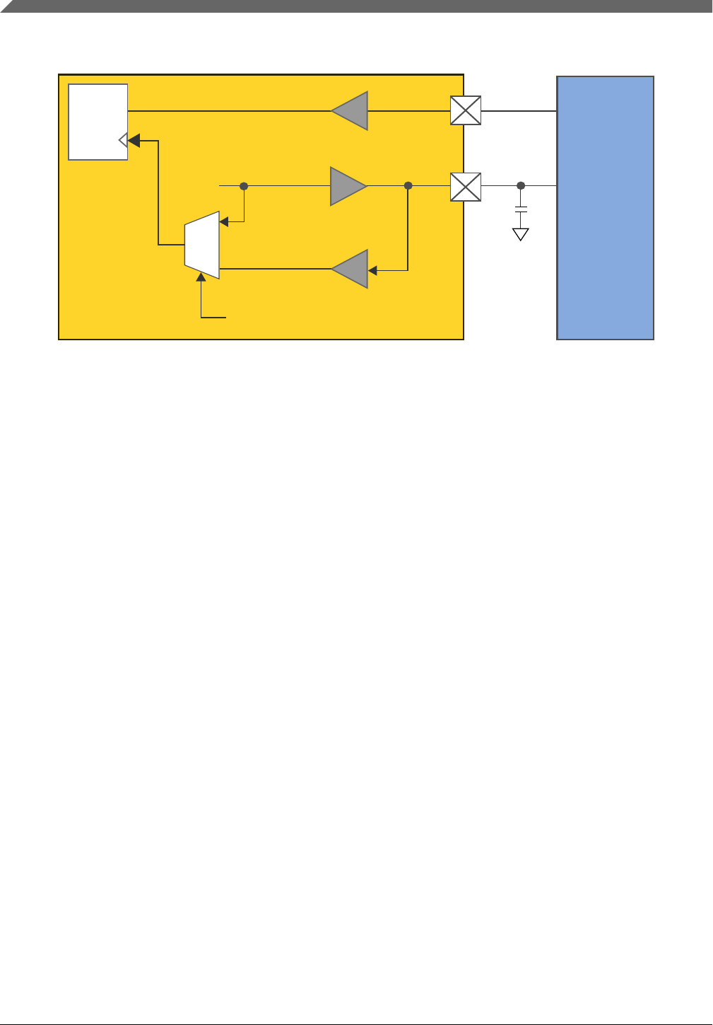
0
1
SPI Slave
MISO
SCK input
delayed LPSPISCK
LPSPI_CFGR1[SAMPLE]
LPSPI_SCK
LPSPI_SIN
LPSPI Master
Figure 49-7. Clock Loopback
See the device datasheet for the specific input setup time in master loopback mode.
49.4.3 Slave Mode
LPSPI slave mode:
• uses the same shift register and logic that master mode uses
• does not use the Clock Configuration Register (CCR)
• during SPI bus transfers, requires that the Transmit Command Register (TCR)
remain static (unchanging)
49.4.3.1 Transmit and Command FIFO commands
Before enabling the LPSPI in slave mode, the Transmit Command Register (TCR) should
be initialized, although the Transmit Command Register register will not update until
after the LPSPI is enabled. After being enabled, the Transmit Command Register should
only be changed if the LPSPI is idle. In slave mode, the LPSPI command word in the
Transmit Command Register (TCR) controls SPI attributes (using bits and fields in
registers). Before the LPSPI_PCS input asserts, the transmit FIFO must be filled with
transmit data, or the transmit error flag will set.
Functional description
S32K1xx Series Reference Manual, Rev. 7, 04/2018
1470 NXP Semiconductors

Table 49-10. LPSPI Command Word in Slave Mode
Transmit Command Register
(TCR)
Description
Bit/Field Name
CPOL Clock Polarity Configures the polarity of the external LPSPI_SCK input.
CPHA Clock Phase Configures the clock phase of transfer.
PRESCALE Prescaler Value Configures the LPSPI functional clock prescaler.
PCS Peripheral Chip
Select
Configures which LPSPI_PCS is used, the polarity of LPSPI_PCS is static and
configured by PCSPOL. If PCSCFG is set, then PCS[3:2] should not be selected.
LSBF LSB First Configures if LSB (bit 0) or MSB (bit 31 for a 32-bit word) is transmitted or received first.
BYSW Byte Swap Enables byte swap on each 32-bit word when transmitting and receiving data. Byte
swapping can be useful when interfacing to devices that organize data as big-endian.
CONT Continuous Transfer When Continuous Transfer is set, only the first FRAMSZ bits will be transmitted/
received by the LPSPI module.
CONTC Continuing
Command
CONTC bit is reserved (in slave mode).
RXMSK Receive Data Mask Masks the receive data and does not store the masked receive data to the receive FIFO
or perform receive data matching. Useful for half-duplex transfers or to configure which
fields are compared during receive data matching.
TXMSK Transmit Data Mask Masks the transmit data, so that the masked transmit data is not pulled from transmit
FIFO, and the output data pin is tristated (unless configured by Output Config
CFGR1[OUTCFG]). Useful for half-duplex transfers.
WIDTH Transfer Width Configures the number of bits shifted on each LPSPI_SCK pulse.
• 1-bit transfers support traditional SPI bus transfers in either half-duplex or full-
duplex data formats.
• 2-bit and 4-bit transfers are useful for interfacing to QuadSPI memory devices,
and only support half-duplex data formats, and at least one bit (Transmit Data
Mask TCR[TXMSK] or Receive Data Mask (TCR[RXMSK]) must also be set.
FRAMESZ Frame Size Configures the frame size in number of bits equal to (FRAMESZ + 1).
• The minimum frame size is 8 bits.
• The minimum word size is 2 bits; a frame size of 33 bits (or similar) is not
supported.
• If the frame size is larger than 32 bits, then the frame is divided into multiple
words of 32-bits; each word is loaded from the transmit FIFO and stored in the
receive FIFO separately.
• If the size of the frame is not divisible by 32, then the last load of the transmit
FIFO and store of the receive FIFO will contain the remainder bits. For example, a
72-bit transfer will consist of 3 words: the 1st and 2nd words are 32-bit, and the
3rd word is 8-bit.
49.4.3.2 Receive FIFO and Data Match
The receive FIFO is used to store received data during SPI bus transfers. When the
Receive Data Mask TCR[RXMSK] is set, the received data is discarded (instead of
storing the received data in the receive FIFO).
Chapter 49 Low Power Serial Peripheral Interface (LPSPI)
S32K1xx Series Reference Manual, Rev. 7, 04/2018
NXP Semiconductors 1471

Receive data supports a receive data match function that can match received data against
one of two words or against a masked data word. The data match function can also be
configured to compare only the first one or two received data words since the start of the
frame.
• Received data that is already discarded (because the Receive Data Mask
TCR[RXMSK] is set) cannot cause the data match to set, and will delay the match on
the first received data word, until all discarded data is received.
• The receiver match function can also be configured to discard all received data until
a data match is detected, using the Receive Data Match Only CFGR0[RDMO] bit.
• After a receive data match, to allow all subsequent data to be received, first clear the
Receive Data Match Only CFGR0[RDMO] bit, then clear the Data Match Flag
SR[DMF] bit.
49.4.3.3 Clocked Interface
The LPSPI module supports interfacing to external masters that provide only clock and
data pins (LPSPI_PCS is not required). This interface requires:
• using Clock Phase TCR[CPHA] = 1 (data is changed on the leading edge of SCK and
captured on the following edge)
• configuring the LPSPI_PCS input to be always asserted (configure the Peripheral
Chip Select Polarity CFGR1[PCSPOL[n]] = 1). For example, to configure PCS[0] to
be always asserted, set PCSPOL[0] = 1, and don’t configure PCS[0] in the pin
muxing.
• setting the Automatic PCS CFGR1[AUTOPCS] bit = 1 (Automatic PCS generation
is enabled). When Automatic PCS generation (AUTOPCS) is set, a minimum of 4
LPSPI functional clock cycles (divided by PRESCALE configuration) is required
between the last LPSPI_SCK edge of one word and the first LPSPI_SCK edge of the
next word.
49.4.4 Interrupts and DMA Requests
The next table lists the slave mode sources (status flags) that can generate LPSPI
interrupts and LPSPI slave transmit/receive DMA requests.
Functional description
S32K1xx Series Reference Manual, Rev. 7, 04/2018
1472 NXP Semiconductors

Table 49-11. LPSPI Interrupts and DMA Requests
Status Register (SR) Description Can generate
Status Flag Name Interrupt? DMA
Request?
Low Power
Wakeup?
TDF Transmit Data
Flag
Data can be written to transmit FIFO, as
configured by the Transmit FIFO Watermark
FCR[TXWATER]
Y TX Y
RDF Receive Data
Flag
Data can be read from the receive FIFO, as
configured by the Receive FIFO Watermark
FCR[RXWATER]
Y RX Y
WCF Word
Complete
Flag
Word is complete, the last bit of the word has
been sampled
Y N Y
FCF Frame
Complete
Flag
Frame is complete, and PCS has negated Y N Y
TCF Transfer
Complete
Flag
Transfer is complete, PCS has negated, and
the transmit/command FIFO is empty
Y N Y
TEF Transmit Error
Flag
Indicates a transmit/command FIFO underrun.
In master mode when the No Stall
CFGR1[NOSTALL] bit is clear (0, transfers
will stall when transmit FIFO is empty or
receive FIFO is full), the Transmit Error Flag
bit cannot set.
Y N Y
REF Receive Error
Flag
Receive error flag, indicates a receive FIFO
overflow. In master mode when the No Stall
CFGR1[NOSTALL] bit is clear (0, transfers
will stall when transmit FIFO is empty or
receive FIFO is full), the Receive Error Flag
bit cannot set.
Y N Y
DMF Data Match
Flag
Indicates that the received data has matched
the configured data match value
Y N Y
MBF Module Busy
Flag
LPSPI is busy performing a SPI bus transfer N N N
49.4.5 Peripheral Triggers
The connection of the LPSPI peripheral triggers to other peripherals depend upon the
specific device being used.
Table 49-12. LPSPI Triggers
Trigger Description
Frame Output Trigger The frame output trigger:
• asserts at the end of each frame (when PCS negates)
• remains asserted until PCS next asserts
Word Output Trigger The word output trigger:
Table continues on the next page...
Chapter 49 Low Power Serial Peripheral Interface (LPSPI)
S32K1xx Series Reference Manual, Rev. 7, 04/2018
NXP Semiconductors 1473

Table 49-12. LPSPI Triggers (continued)
Trigger Description
• asserts at the end of each received word
• remains asserted for 1 LPSPI_SCK period
The LPSPI generates 2
output triggers that can
be connected to other
peripherals on the
device.
Input Trigger To control the start of a LPSPI bus transfer, the LPSPI input trigger can be
selected instead of the LPSPI_HREQ input.
• The LPSPI input trigger is synchronized, and must assert for at least
2 cycles of the LPSPI functional clock divided by the PRESCALE
configuration, so that the input trigger can be detected.
• When the LPSPI module is busy, the LPSPI_HREQ input (and
therefore the LPSPI input trigger) is ignored .
Functional description
S32K1xx Series Reference Manual, Rev. 7, 04/2018
1474 NXP Semiconductors

Chapter 50
Low Power Inter-Integrated Circuit (LPI2C)
Chip-specific LPI2C information
50.1.1 Instantiation information
The following table summarizes the implementation of this module for each chip in the
product series.
Table 50-1. LPI2C configuration
Chip Instances TX FIFO (word) RX FIFO (word) SMBus Slave mode
enable
S32K116 LPI2C0 4 4 Yes Yes
S32K118 LPI2C0 4 4 Yes Yes
S32K142 LPI2C0 4 4 Yes Yes
S32K144 LPI2C0 4 4 Yes Yes
S32K146 LPI2C0 4 4 Yes Yes
S32K148 LPI2C0 4 4 Yes Yes
LPI2C1 4 4 Yes Yes
Low leakage and Wait mode is not supported in this device. See Module operation in
available low power modes for details on available power modes.
HS-Mode (baud-rates above 400 kbps) is not supported on this device.
The LPI2C module includes SMBus support and DMA support.
NOTE
• Only SIRC is the valid clock source in VLP modes. As the
SIRC supports the LPI2C data rates, it is recommended to
50.1
S32K1xx Series Reference Manual, Rev. 7, 04/2018
NXP Semiconductors 1475
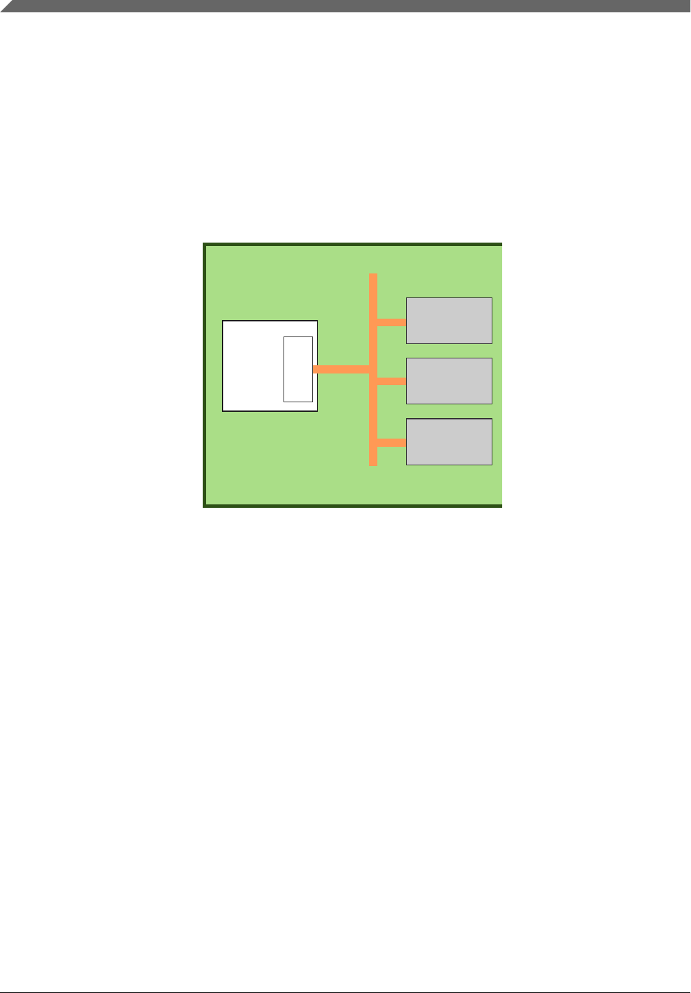
use SIRC for LPI2C to avoid clock reconfiguration and
switching times.
• HREQ is not supported in S32K116 (32-pin QFN and 48-
pin LQFP package).
50.2 Introduction
Low speed
peripheral
Printed Circuit Board (PCB)
Short distances on a small PCB
MCU
LPI2C
Microcontroller SoC
I²C (Inter-Integrated Circuit) Serial Bus
Low speed
peripheral
Low speed
peripheral
Figure 50-1. I2C bus connects MCU to low speed peripherals on PCB
The LPI2C is a low power Inter-Integrated Circuit (I2C) module that supports an efficient
interface to an I2C bus as a master and/or as a slave.
• The LPI2C implements logic support for standard-mode, fast-mode, fast-mode plus
and ultra-fast modes of operation.
• The LPI2C is designed to use little CPU overhead, with DMA offloading of FIFO
register accesses.
• The LPI2C can continue operating in stop modes if an appropriate clock is available.
The LPI2C module also complies with the System Management Bus (SMBus)
Specification, version 2. The SMBus is a single-ended simple two-wire bus, which is
typically used for low bandwidth communications.
NOTE
The I2C (Inter-Integrated Circuit) serial bus is multi-master,
multi-slave, packet-switched, and single-ended, and is often
used to attach microcontroller ICs to lower-speed peripheral
ICs.
Introduction
S32K1xx Series Reference Manual, Rev. 7, 04/2018
1476 NXP Semiconductors
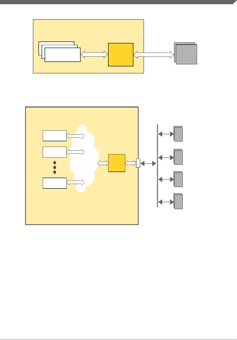
LPI2C
External devices
Masters Slaves
Modules
MCU System-on-a-Chip (SoC)
Modules in an MCU SoC use LPI2C to communicate
with external devices over an I²C bus.
I²C bus
Figure 50-2. LPI2C connects masters in MCU to external slaves on PCB
DACs, ADCs
LPI2C OLED, LCD displays
EEPROMs, NVRAM
Memories
I²C bus
Other internal modules in an MCU SoC use LPI2C
Slave-only devices
Synchronous
Hardware monitors,
MCU System-on-a-Chip (SoC)
CPU
DMA
USB
Masters
to connect to external peripherals that use an I²C bus.
Many devices can be connected to the I²C bus,
but only 1 device can be accessed at a time.
or Asynchronous
Bus
Fabric
Bus fabric can be crossbar switches, NICs, or combinations
of crossbar switches, NICs, and similar modules.
Low speed
sensors
Figure 50-3. Typical LPI2C connection scheme
50.2.1 Features
The LPI2C supports:
• Standard, Fast, Fast+ and Ultra Fast modes are supported
• High speed mode (HS) in slave mode
• High speed mode (HS) in master mode, if SCL pin implements current source pull-
up (device-specific)
Chapter 50 Low Power Inter-Integrated Circuit (LPI2C)
S32K1xx Series Reference Manual, Rev. 7, 04/2018
NXP Semiconductors 1477

• Multi-master support, including synchronization and arbitration. Multi-master means
any number of master nodes can be present. Additionally, master and slave roles may
be changed between messages (after a STOP is sent).
• Clock stretching: Sometimes multiple I2C nodes may be driving the lines at the same
time. If any I2C node is driving a line low, then that line will be low. I2C nodes that
are starting to transmit a logical one (by letting the line float high) can detect that the
line is low, and thereby know that another I2C node is active at the same time.
•When node detection is used on the SCL line, it is called clock stretching, and
clock stretching is used as a I2C flow control mechanism for multiple laves.
•When node detection is used on the SDA line, it is called arbitration, and
arbitration ensures that there is only one I2C node transmitter at a time.
• General call, 7-bit and 10-bit addressing
• Software reset, START byte and Device ID (also require software support)
The LPI2C master supports:
• Command/transmit FIFO of 4words.
• Receive FIFO of 4words.
• Command FIFO will wait for idle I2C bus before initiating transfer
• Command FIFO can initiate (repeated) START and STOP conditions and one or
more master-receiver transfers
• STOP condition can be generated from command FIFO, or generated automatically
when the transmit FIFO is empty
• Host request input to control the start time of an I2C bus transfer
• Flexible receive data match can generate interrupt on data match and/or discard
unwanted data
• Flag and optional interrupt to signal Repeated START condition, STOP condition,
loss of arbitration, unexpected NACK, and command word errors
• Supports configurable bus idle timeout and pin-stuck-low timeout
The LPI2C slave supports:
• Separate I2C slave registers to minimize software overhead because of master/slave
switching
• Support for 7-bit or 10-bit addressing, address range, SMBus alert and general call
address
• Transmit data register that supports interrupt or DMA requests
• Receive data register that supports interrupt or DMA requests
• Software-controllable ACK or NACK, with optional clock stretching on ACK/
NACK bit
• Configurable clock stretching, to avoid transmit FIFO underrun and receive FIFO
overrun errors
• Flag and optional interrupt at end of packet, STOP condition, or bit error detection
Introduction
S32K1xx Series Reference Manual, Rev. 7, 04/2018
1478 NXP Semiconductors
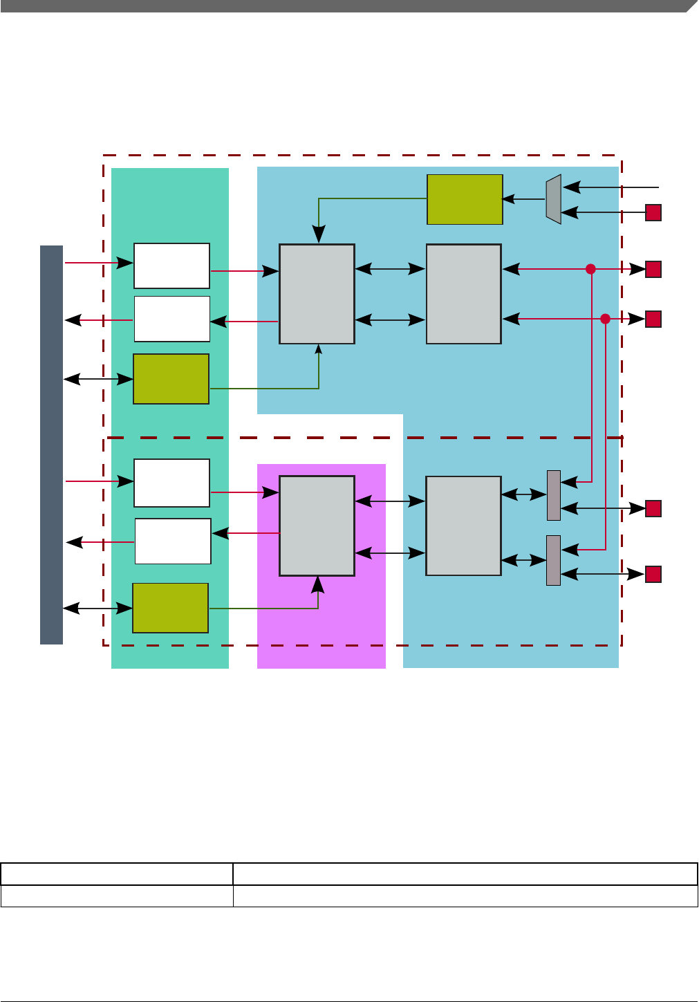
50.2.2 Block Diagram
LPI2C
Configuration
Registers
Peripheral
Bus
Master
Logic
Prescaler HREQ
SDA
SCL
Trigger
Glitch
Filter
Master
Slave
TX
Data
RX Data /
Address
Configuration
Registers
Slave
Logic
SDAS
SCLS
Glitch
Filter
Bus Clock External Clock Functional Clock
Clock Domains
Command /
RX FIFO
TX FIFO
Internal SoC
Figure 50-4. LPI2C block diagram
50.2.3 Modes of operation
Table 50-2. Chip modes supported by the LPI2C module
Chip mode LPI2C Operation
Run Normal operations
Table continues on the next page...
Chapter 50 Low Power Inter-Integrated Circuit (LPI2C)
S32K1xx Series Reference Manual, Rev. 7, 04/2018
NXP Semiconductors 1479

Table 50-2. Chip modes supported by the LPI2C module (continued)
Chip mode LPI2C Operation
Stop Can continue operating in stop mode if the Doze Enable bit (MCR[DOZEN]) is
clear and the LPI2C is using an external or internal clock source that remains
operating during stop mode.
Debug Can continue operating in debug mode if the Debug Enable bit (MCR[DBGE]) is
set.
50.2.4 Signal Descriptions
Table 50-3. Signals
Signal Name 2-Wire Scheme 4-Wire Scheme I/O
SCL LPI2C clock
line
SCL In 4-wire mode, this is the SCL input pin. I/O
SDA LPI2C data
line
SDA In 4-wire mode, this is the SDA input pin. I/O
HREQ Host request If host request is asserted and the I2C bus is idle, then it will initiate an LPI2C
master transfer.
I
SCLS Secondary
I2C clock line
Not used In 4-wire mode, this is the SCLS output pin. If
LPI2C master/slave are configured to use
separate pins, then this the LPI2C slave SCL
pin.
I/O
SDAS Secondary
I2C data line
Not used In 4-wire mode, this is the SDAS output pin. If
LPI2C master/slave are configured to use
separate pins, then this the LPI2C slave SDA
pin.
I/O
50.2.5 Wiring options
LPI2C can be used to implement 2-wire or 4-wire I2C serial busses.
Introduction
S32K1xx Series Reference Manual, Rev. 7, 04/2018
1480 NXP Semiconductors
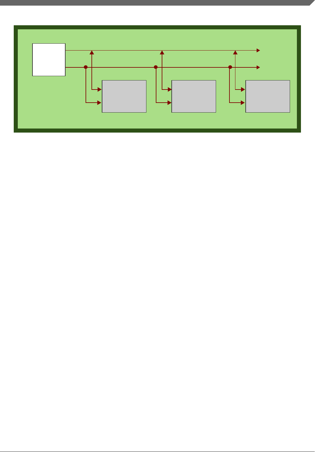
Printed Circuit Board (PCB)
I²C (Inter-Integrated Circuit) 2-Wire Serial Bus
Microcontroller 2-wire
peripheral
device #1
2-wire
peripheral
device #2
2-wire
peripheral
device #3
Data (SDA)
Clock (SCL)
MCU
Slave Slave Slave
Figure 50-5. 2-Wire scheme
Some applications can provide a lot of load and noise on the I2C bus; to ensure robust I2C
operations, a 4-wire interface with the MCU can be used, splitting the 2 lines into inputs
and outputs. Using a few transistors, resistors and diodes, designers can make their own
inexpensive line drivers.
Chapter 50 Low Power Inter-Integrated Circuit (LPI2C)
S32K1xx Series Reference Manual, Rev. 7, 04/2018
NXP Semiconductors 1481
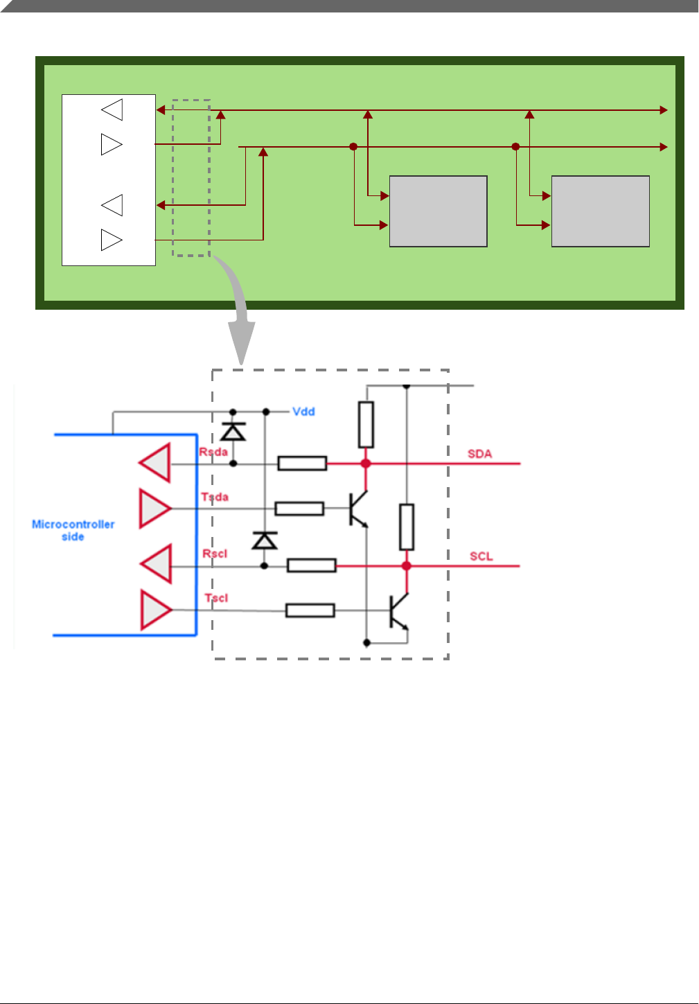
Printed Circuit Board (PCB)
I²C (Inter-Integrated Circuit) 4-Wire Serial Bus
Microcontroller
2-wire
peripheral
device #1
2-wire
peripheral
device #2
Data (SDA)
Clock (SCL)
MCU
Slave Slave
+
–
+
–
SCL
SCLS
+
–
+
–
SDA
SDAS
Simple Line Drivers
Figure 50-6. 4-Wire scheme
50.3 Memory Map and Registers
NOTE
Writing a Read-Only (RO) register or reading a Write-Only
(WO) register can cause bus errors. This module will not check
if programmed values in the registers are correct; the
application software must ensure that valid programmed values
are being written.
Memory Map and Registers
S32K1xx Series Reference Manual, Rev. 7, 04/2018
1482 NXP Semiconductors

50.3.1 LPI2C register descriptions
50.3.1.1 LPI2C Memory map
LPI2C0 base address: 4006_6000h
LPI2C1 base address: 4006_7000h
Offset Register Width
(In bits)
Access Reset value
0h Version ID Register (VERID) 32 RO 0100_0003h
4h Parameter Register (PARAM) 32 RO 0000_0202h
10h Master Control Register (MCR) 32 RW 0000_0000h
14h Master Status Register (MSR) 32 W1C 0000_0001h
18h Master Interrupt Enable Register (MIER) 32 RW 0000_0000h
1Ch Master DMA Enable Register (MDER) 32 RW 0000_0000h
20h Master Configuration Register 0 (MCFGR0) 32 RW 0000_0000h
24h Master Configuration Register 1 (MCFGR1) 32 RW 0000_0000h
28h Master Configuration Register 2 (MCFGR2) 32 RW 0000_0000h
2Ch Master Configuration Register 3 (MCFGR3) 32 RW 0000_0000h
40h Master Data Match Register (MDMR) 32 RW 0000_0000h
48h Master Clock Configuration Register 0 (MCCR0) 32 RW 0000_0000h
50h Master Clock Configuration Register 1 (MCCR1) 32 RW 0000_0000h
58h Master FIFO Control Register (MFCR) 32 RW 0000_0000h
5Ch Master FIFO Status Register (MFSR) 32 RO 0000_0000h
60h Master Transmit Data Register (MTDR) 32 WO 0000_0000h
70h Master Receive Data Register (MRDR) 32 RO 0000_4000h
110h Slave Control Register (SCR) 32 RW 0000_0000h
114h Slave Status Register (SSR) 32 W1C 0000_0000h
118h Slave Interrupt Enable Register (SIER) 32 RW 0000_0000h
11Ch Slave DMA Enable Register (SDER) 32 RW 0000_0000h
124h Slave Configuration Register 1 (SCFGR1) 32 RW 0000_0000h
128h Slave Configuration Register 2 (SCFGR2) 32 RW 0000_0000h
140h Slave Address Match Register (SAMR) 32 RW 0000_0000h
150h Slave Address Status Register (SASR) 32 RO 0000_4000h
154h Slave Transmit ACK Register (STAR) 32 RW 0000_0000h
160h Slave Transmit Data Register (STDR) 32 WO 0000_0000h
170h Slave Receive Data Register (SRDR) 32 RO 0000_4000h
Chapter 50 Low Power Inter-Integrated Circuit (LPI2C)
S32K1xx Series Reference Manual, Rev. 7, 04/2018
NXP Semiconductors 1483

50.3.1.2 Version ID Register (VERID)
50.3.1.2.1 Offset
Register Offset
VERID 0h
50.3.1.2.2 Function
.
50.3.1.2.3 Diagram
Bits 31 30 29 28 27 26 25 24 23 22 21 20 19 18 17 16
RMAJOR MINOR
W
Reset 0 0 0 0 0 0 0 1 0 0 0 0 0 0 0 0
Bits 15 14 13 12 11 10 9 8 7 6 5 4 3 2 1 0
RFEATURE
W
Reset 0 0 0 0 0 0 0 0 0 0 0 0 0 0 1 1
50.3.1.2.4 Fields
Field Function
31-24
MAJOR
Major Version Number
Returns the major version number for the module design specification. Read-only field.
23-16
MINOR
Minor Version Number
Returns the minor version number for the module design specification. Read-only field.
15-0
FEATURE
Feature Specification Number
Returns the feature set number. Read-only field.
0000000000000010b - Master only, with standard feature set
0000000000000011b - Master and slave, with standard feature set
Memory Map and Registers
S32K1xx Series Reference Manual, Rev. 7, 04/2018
1484 NXP Semiconductors

50.3.1.3 Parameter Register (PARAM)
50.3.1.3.1 Offset
Register Offset
PARAM 4h
50.3.1.3.2 Function
.
50.3.1.3.3 Diagram
Bits 31 30 29 28 27 26 25 24 23 22 21 20 19 18 17 16
R 0
W
Reset 0 0 0 0 0 0 0 0 0 0 0 0 0 0 0 0
Bits 15 14 13 12 11 10 9 8 7 6 5 4 3 2 1 0
R 0 MRXFIFO 0MTXFIFO
W
Reset 0 0 0 0 0 0 1 0 0 0 0 0 0 0 1 0
50.3.1.3.4 Fields
Field Function
31-16
—
Reserved
15-12
—
Reserved
11-8
MRXFIFO
Master Receive FIFO Size
Configures the number of words in the master receive FIFO to 2MRXFIFO
7-4
—
Reserved
3-0
MTXFIFO
Master Transmit FIFO Size
Configures the number of words in the master transmit FIFO to 2MTXFIFO
Chapter 50 Low Power Inter-Integrated Circuit (LPI2C)
S32K1xx Series Reference Manual, Rev. 7, 04/2018
NXP Semiconductors 1485
50.3.1.4 Master Control Register (MCR)
50.3.1.4.1 Offset
Register Offset
MCR 10h
50.3.1.4.2 Diagram
Bits 31 30 29 28 27 26 25 24 23 22 21 20 19 18 17 16
R 0
W
Reset 0 0 0 0 0 0 0 0 0 0 0 0 0 0 0 0
Bits 15 14 13 12 11 10 9 8 7 6 5 4 3 2 1 0
R
0
0
0
0
DBGE
N
DOZEN
RS
T
MEN
W
RR
F
RT
F
Reset 0 0 0 0 0 0 0 0 0 0 0 0 0 0 0 0
50.3.1.4.3 Fields
Field Function
31-10
—
Reserved
9
RRF
Reset Receive FIFO
0b - No effect
1b - Receive FIFO is reset
8
RTF
Reset Transmit FIFO
0b - No effect
1b - Transmit FIFO is reset
7-4
—
Reserved
3
DBGEN
Debug Enable
0b - Master is disabled in debug mode
1b - Master is enabled in debug mode
2
DOZEN
Doze mode enable
Enables or disables the master in Doze mode
0b - Master is enabled in Doze mode
1b - Master is disabled in Doze mode
1 Software Reset
Table continues on the next page...
Memory Map and Registers
S32K1xx Series Reference Manual, Rev. 7, 04/2018
1486 NXP Semiconductors

Field Function
RST Reset all internal master logic and registers, except the Master Control Register. RST remains set until
cleared by software.
0b - Master logic is not reset
1b - Master logic is reset
0
MEN
Master Enable
0b - Master logic is disabled
1b - Master logic is enabled
50.3.1.5 Master Status Register (MSR)
50.3.1.5.1 Offset
Register Offset
MSR 14h
50.3.1.5.2 Diagram
Bits 31 30 29 28 27 26 25 24 23 22 21 20 19 18 17 16
R 0 BBF MBF 0
W
Reset 0 0 0 0 0 0 0 0 0 0 0 0 0 0 0 0
Bits 15 14 13 12 11 10 9 8 7 6 5 4 3 2 1 0
R
0
DMF
PLT
F
FE
F
ALF
NDF
SD
F
EP
F
0
RD
F
TDF
W
W1C
W1C
W1C
W1C
W1C
W1C
W1C
Reset 0 0 0 0 0 0 0 0 0 0 0 0 0 0 0 1
50.3.1.5.3 Fields
Field Function
31-26
—
Reserved
25
BBF
Bus Busy Flag
0b - I2C Bus is idle
1b - I2C Bus is busy
24 Master Busy Flag
Table continues on the next page...
Chapter 50 Low Power Inter-Integrated Circuit (LPI2C)
S32K1xx Series Reference Manual, Rev. 7, 04/2018
NXP Semiconductors 1487

Field Function
MBF 0b - I2C Master is idle
1b - I2C Master is busy
23-15
—
Reserved
14
DMF
Data Match Flag
Indicates that the received data has matched the MATCH0 and/or MATCH1 fields (as configured by
MCFGR1[MATCFG], Match Configuration). Received data that is discarded due to CMD field does not
cause Data Match Flag to set.
0b - Have not received matching data
1b - Have received matching data
13
PLTF
Pin Low Timeout Flag
Will set when the SCL and/or SDA input is low for more than PINLOW cycles (Pin Low Timeout,
MCFGR3[PINLOW]), even when the LPI2C master is idle.
• Software is responsible for resolving the pin low condition.
• Pin Low Timeout Flag cannot be cleared as long as the pin low timeout continues.
• Before the LPI2C can initiate a START condition, the Pin Low Timeout Flag must be cleared.
0b - Pin low timeout has not occurred or is disabled
1b - Pin low timeout has occurred
12
FEF
FIFO Error Flag
Detects an attempt to send or receive data without first generating a (repeated) START condition. This
can occur if the transmit FIFO underflows when the AUTOSTOP bit is set. When FIFO Error Flag is set,
the LPI2C master will send a STOP condition (if busy), and will not initiate a new START condition until
FIFO Error Flag has been cleared.
0b - No error
1b - Master sending or receiving data without a START condition
11
ALF
Arbitration Lost Flag
Set:
• if the LPI2C master transmits a logic one and detects a logic zero on the I2C bus
• or if the LPI2C master detects a START or STOP condition while the LPI2C master is transmitting
data
When the Arbitration Lost Flag sets, the LPI2C master will release the I2C bus (go idle), and the LPI2C
master will not initiate a new START condition until the Arbitration Lost Flag has been cleared.
0b - Master has not lost arbitration
1b - Master has lost arbitration
10
NDF
NACK Detect Flag
Set if the LPI2C master detects a NACK when transmitting an address or data. When set, the master will
transmit a STOP condition and will not initiate a new START condition until NACK Detect Flag has been
cleared. If a NACK is expected for a given address (as configured by the command word), then the NACK
Detect Flag will set if a NACK is not generated.
0b - Unexpected NACK was not detected
1b - Unexpected NACK was detected
9
SDF
STOP Detect Flag
Set when the LPI2C master generates a STOP condition.
0b - Master has not generated a STOP condition
1b - Master has generated a STOP condition
8
EPF
End Packet Flag
Set when the LPI2C master generates either a repeated START condition or a STOP condition. Does not
set when the master first generates a START condition.
Table continues on the next page...
Memory Map and Registers
S32K1xx Series Reference Manual, Rev. 7, 04/2018
1488 NXP Semiconductors
Field Function
0b - Master has not generated a STOP or Repeated START condition
1b - Master has generated a STOP or Repeated START condition
7-2
—
Reserved
1
RDF
Receive Data Flag
The Receive Data Flag is set whenever the number of words in the receive FIFO is greater than
RXWATER.
0b - Receive Data is not ready
1b - Receive data is ready
0
TDF
Transmit Data Flag
The Transmit Data Flag is set whenever the number of words in the transmit FIFO is equal or less than
TXWATER.
0b - Transmit data is not requested
1b - Transmit data is requested
50.3.1.6 Master Interrupt Enable Register (MIER)
50.3.1.6.1 Offset
Register Offset
MIER 18h
50.3.1.6.2 Diagram
Bits 31 30 29 28 27 26 25 24 23 22 21 20 19 18 17 16
R 0
W
Reset 0 0 0 0 0 0 0 0 0 0 0 0 0 0 0 0
Bits 15 14 13 12 11 10 9 8 7 6 5 4 3 2 1 0
R
0
DMIE
PLTI
E
FEI
E
ALIE
NDIE
SDI
E
EPI
E
0
RDI
E
TDIE
W
Reset 0 0 0 0 0 0 0 0 0 0 0 0 0 0 0 0
50.3.1.6.3 Fields
Field Function
31-15 Reserved
Table continues on the next page...
Chapter 50 Low Power Inter-Integrated Circuit (LPI2C)
S32K1xx Series Reference Manual, Rev. 7, 04/2018
NXP Semiconductors 1489

Field Function
—
14
DMIE
Data Match Interrupt Enable
0b - Disabled
1b - Enabled
13
PLTIE
Pin Low Timeout Interrupt Enable
0b - Disabled
1b - Enabled
12
FEIE
FIFO Error Interrupt Enable
0b - Enabled
1b - Disabled
11
ALIE
Arbitration Lost Interrupt Enable
0b - Disabled
1b - Enabled
10
NDIE
NACK Detect Interrupt Enable
0b - Disabled
1b - Enabled
9
SDIE
STOP Detect Interrupt Enable
0b - Disabled
1b - Enabled
8
EPIE
End Packet Interrupt Enable
0b - Disabled
1b - Enabled
7-2
—
Reserved
1
RDIE
Receive Data Interrupt Enable
0b - Disabled
1b - Enabled
0
TDIE
Transmit Data Interrupt Enable
0b - Disabled
1b - Enabled
50.3.1.7 Master DMA Enable Register (MDER)
50.3.1.7.1 Offset
Register Offset
MDER 1Ch
Memory Map and Registers
S32K1xx Series Reference Manual, Rev. 7, 04/2018
1490 NXP Semiconductors

50.3.1.7.2 Diagram
Bits 31 30 29 28 27 26 25 24 23 22 21 20 19 18 17 16
R 0
W
Reset 0 0 0 0 0 0 0 0 0 0 0 0 0 0 0 0
Bits 15 14 13 12 11 10 9 8 7 6 5 4 3 2 1 0
R
0
RDD
E
TDDE
W
Reset 0 0 0 0 0 0 0 0 0 0 0 0 0 0 0 0
50.3.1.7.3 Fields
Field Function
31-2
—
Reserved
1
RDDE
Receive Data DMA Enable
0b - DMA request is disabled
1b - DMA request is enabled
0
TDDE
Transmit Data DMA Enable
0b - DMA request is disabled
1b - DMA request is enabled
50.3.1.8 Master Configuration Register 0 (MCFGR0)
50.3.1.8.1 Offset
Register Offset
MCFGR0 20h
Chapter 50 Low Power Inter-Integrated Circuit (LPI2C)
S32K1xx Series Reference Manual, Rev. 7, 04/2018
NXP Semiconductors 1491

50.3.1.8.2 Diagram
Bits 31 30 29 28 27 26 25 24 23 22 21 20 19 18 17 16
R 0
W
Reset 0 0 0 0 0 0 0 0 0 0 0 0 0 0 0 0
Bits 15 14 13 12 11 10 9 8 7 6 5 4 3 2 1 0
R
0
RDMO
CIRFIFO
0
HRSE
L
HRPOL
HRE
N
W
Reset 0 0 0 0 0 0 0 0 0 0 0 0 0 0 0 0
50.3.1.8.3 Fields
Field Function
31-10
—
Reserved
9
RDMO
Receive Data Match Only
When enabled, all received data that does not cause the Data Match Flag (MSR[DMF]) to set is
discarded. After the Data Match Flag is set, the RDMO configuration is ignored. When disabling RDMO,
clear RDMO before clearing the Data Match Flag, to ensure that no receive data is lost.
0b - Received data is stored in the receive FIFO
1b - Received data is discarded unless the the Data Match Flag (MSR[DMF]) is set
8
CIRFIFO
Circular FIFO Enable
When enabled, the transmit FIFO read pointer is saved to a temporary register. The transmit FIFO will be
emptied as normal, but after the LPI2C master is idle and the transmit FIFO is empty, then the read
pointer value will be restored from the temporary register. This will cause the contents of the transmit
FIFO to be cycled through repeatedly. If AUTOSTOP is set, then a STOP condition will be sent whenever
the transmit FIFO is empty and the read pointer is restored.
0b - Circular FIFO is disabled
1b - Circular FIFO is enabled
7-3
—
Reserved
2
HRSEL
Host Request Select
Selects the source of the host request input. When host request input is enabled, the Host Request
Select field should remain static (the Host Request Select should not change).
0b - Host request input is pin HREQ
1b - Host request input is input trigger
1
HRPOL
Host Request Polarity
Configures the polarity of the host request input pin. When host request input is enabled, the Host
Request Polarity field should remain static (Host Request Polarity should not change).
0b - Active low
1b - Active high
0
HREN
Host Request Enable
Memory Map and Registers
S32K1xx Series Reference Manual, Rev. 7, 04/2018
1492 NXP Semiconductors

Field Function
When enabled, the LPI2C master will only initiate a START condition if the host request input is asserted
and the bus is idle. A repeated START is not affected by the host request.
0b - Host request input is disabled
1b - Host request input is enabled
50.3.1.9 Master Configuration Register 1 (MCFGR1)
50.3.1.9.1 Offset
Register Offset
MCFGR1 24h
50.3.1.9.2 Function
The MCFGR1 should only be written when the I2C Master is disabled.
50.3.1.9.3 Diagram
Bits 31 30 29 28 27 26 25 24 23 22 21 20 19 18 17 16
R 0 PINCFG 0MATCFG
W
Reset 0 0 0 0 0 0 0 0 0 0 0 0 0 0 0 0
Bits 15 14 13 12 11 10 9 8 7 6 5 4 3 2 1 0
R
0
TIMECFG
IGNACK
AUTOSTOP
0
PRESCAL
E
W
Reset 0 0 0 0 0 0 0 0 0 0 0 0 0 0 0 0
50.3.1.9.4 Fields
Field Function
31-27
—
Reserved
26-24
PINCFG
Pin Configuration
Table continues on the next page...
Chapter 50 Low Power Inter-Integrated Circuit (LPI2C)
S32K1xx Series Reference Manual, Rev. 7, 04/2018
NXP Semiconductors 1493

Field Function
Configures the pin mode for LPI2C.
Table 50-4. 2-pin / 4-pin pin configurations for masters and slaves
PINCFG SCL / SDA pins SCLS / SDAS pins
000 Bi-directional open drain for master and
slave
Not used
001 Output-only (ultra-fast mode) open drain for
master and slave
Not used
010 Bi-directional push-pull for master and slave Not used
011 Input only for master and slave Output-only push-pull for master and slave
100 Bi-directional open drain for master Bi-directional open drain for slave
101 Output-only (ultra-fast mode) open drain for
master
Output-only open drain for slave
110 Bi-directional push-pull for master Bi-directional push-pull for slave
111 Input only for master and slave Inverted output-only push-pull for master
and slave
000b - 2-pin open drain mode
001b - 2-pin output only mode (ultra-fast mode)
010b - 2-pin push-pull mode
011b - 4-pin push-pull mode
100b - 2-pin open drain mode with separate LPI2C slave
101b - 2-pin output only mode (ultra-fast mode) with separate LPI2C slave
110b - 2-pin push-pull mode with separate LPI2C slave
111b - 4-pin push-pull mode (inverted outputs)
23-19
—
Reserved
18-16
MATCFG
Match Configuration
Configures the condition that will cause the DMF to set.
000b - Match is disabled
001b - Reserved
010b - Match is enabled (1st data word equals MATCH0 OR MATCH1)
011b - Match is enabled (any data word equals MATCH0 OR MATCH1)
100b - Match is enabled (1st data word equals MATCH0 AND 2nd data word equals MATCH1)
101b - Match is enabled (any data word equals MATCH0 AND next data word equals MATCH1)
110b - Match is enabled (1st data word AND MATCH1 equals MATCH0 AND MATCH1)
111b - Match is enabled (any data word AND MATCH1 equals MATCH0 AND MATCH1)
15-11
—
Reserved
10
TIMECFG
Timeout Configuration
0b - Pin Low Timeout Flag will set if SCL is low for longer than the configured timeout
1b - Pin Low Timeout Flag will set if either SCL or SDA is low for longer than the configured timeout
9
IGNACK
IGNACK
When set, the received NACK field is ignored and assumed to be ACK. IGNACK bit is required to be set
in Ultra-Fast Mode.
0b - LPI2C Master will receive ACK and NACK normally
1b - LPI2C Master will treat a received NACK as if it (NACK) was an ACK
Table continues on the next page...
Memory Map and Registers
S32K1xx Series Reference Manual, Rev. 7, 04/2018
1494 NXP Semiconductors

Field Function
8
AUTOSTOP
Automatic STOP Generation
When enabled, a STOP condition is generated whenever the LPI2C master is busy and the transmit FIFO
is empty. The STOP condition can also be generated using a transmit FIFO command.
0b - No effect
1b - STOP condition is automatically generated whenever the transmit FIFO is empty and the
LPI2C master is busy
7-3
—
Reserved
2-0
PRESCALE
Prescaler
Configures the clock prescaler used for all LPI2C master logic, except for the digital glitch filters.
000b - Divide by 1
001b - Divide by 2
010b - Divide by 4
011b - Divide by 8
100b - Divide by 16
101b - Divide by 32
110b - Divide by 64
111b - Divide by 128
50.3.1.10 Master Configuration Register 2 (MCFGR2)
50.3.1.10.1 Offset
Register Offset
MCFGR2 28h
50.3.1.10.2 Function
The Master Configuration Register 2 should only be written when the I2C Master is
disabled.
Chapter 50 Low Power Inter-Integrated Circuit (LPI2C)
S32K1xx Series Reference Manual, Rev. 7, 04/2018
NXP Semiconductors 1495

50.3.1.10.3 Diagram
Bits 31 30 29 28 27 26 25 24 23 22 21 20 19 18 17 16
R 0 FILTSDA 0FILTSCL
W
Reset 0 0 0 0 0 0 0 0 0 0 0 0 0 0 0 0
Bits 15 14 13 12 11 10 9 8 7 6 5 4 3 2 1 0
R 0 BUSIDLE
W
Reset 0 0 0 0 0 0 0 0 0 0 0 0 0 0 0 0
50.3.1.10.4 Fields
Field Function
31-28
—
Reserved
27-24
FILTSDA
Glitch Filter SDA
Configures the I2C master digital glitch filters for SDA input.
• A configuration of 0 will disable the glitch filter
• Glitches equal to or less than FILTSDA cycles long will be filtered out and ignored
• The latency through the glitch filter is equal to FILTSDA cycles, and must be configured to be less
than the minimum SCL low or high period
• The glitch filter cycle count is not affected by the PRESCALE configuration, and the glitch filter
cycle count is automatically bypassed in High Speed mode
23-20
—
Reserved
19-16
FILTSCL
Glitch Filter SCL
Configures the I2C master digital glitch filters for SCL input.
• A configuration of 0 will disable the glitch filter
• Glitches equal to or less than FILTSCL cycles long will be filtered out and ignored
• The latency through the glitch filter is equal to FILTSCL cycles, and must be configured to be less
than the minimum SCL low or high period
• The glitch filter cycle count is not affected by the PRESCALE configuration, and the glitch filter
cycle count is automatically bypassed in High Speed mode
15-12
—
Reserved
11-0
BUSIDLE
Bus Idle Timeout
Configures the bus idle timeout period in clock cycles.
• If both SCL and SDA are high for longer than BUSIDLE cycles, then the I2C bus is assumed to be
idle and the master can generate a START condition
• When Bus Idle Timeout is set to zero, the Bus Idle Timeout is disabled
Memory Map and Registers
S32K1xx Series Reference Manual, Rev. 7, 04/2018
1496 NXP Semiconductors

50.3.1.11 Master Configuration Register 3 (MCFGR3)
50.3.1.11.1 Offset
Register Offset
MCFGR3 2Ch
50.3.1.11.2 Function
The MCFGR3 should only be written when the I2C Master is disabled.
50.3.1.11.3 Diagram
Bits 31 30 29 28 27 26 25 24 23 22 21 20 19 18 17 16
R 0 PINLOW
W
Reset 0 0 0 0 0 0 0 0 0 0 0 0 0 0 0 0
Bits 15 14 13 12 11 10 9 8 7 6 5 4 3 2 1 0
RPINLOW 0
W
Reset 0 0 0 0 0 0 0 0 0 0 0 0 0 0 0 0
50.3.1.11.4 Fields
Field Function
31-20
—
Reserved
19-8
PINLOW
Pin Low Timeout
Configures the pin low timeout flag in clock cycles.
• If SCL or, either SCL or SDA, is low for longer than (PINLOW * 256) cycles, then PLTF is set
• When Pin Low Timeout is set to zero, the Pin Low Timeout feature is disabled
7-0
—
Reserved
50.3.1.12 Master Data Match Register (MDMR)
Chapter 50 Low Power Inter-Integrated Circuit (LPI2C)
S32K1xx Series Reference Manual, Rev. 7, 04/2018
NXP Semiconductors 1497

50.3.1.12.1 Offset
Register Offset
MDMR 40h
50.3.1.12.2 Function
The MDMR should only be written when the I2C Master is disabled or idle.
50.3.1.12.3 Diagram
Bits 31 30 29 28 27 26 25 24 23 22 21 20 19 18 17 16
R 0 MATCH1
W
Reset 0 0 0 0 0 0 0 0 0 0 0 0 0 0 0 0
Bits 15 14 13 12 11 10 9 8 7 6 5 4 3 2 1 0
R 0 MATCH0
W
Reset 0 0 0 0 0 0 0 0 0 0 0 0 0 0 0 0
50.3.1.12.4 Fields
Field Function
31-24
—
Reserved
23-16
MATCH1
Match 1 Value
Compared against the received data when receive data match is enabled.
15-8
—
Reserved
7-0
MATCH0
Match 0 Value
Compared against the received data when receive data match is enabled.
50.3.1.13 Master Clock Configuration Register 0 (MCCR0)
Memory Map and Registers
S32K1xx Series Reference Manual, Rev. 7, 04/2018
1498 NXP Semiconductors

50.3.1.13.1 Offset
Register Offset
MCCR0 48h
50.3.1.13.2 Function
The MCCR0 cannot be changed when the I2C master is enabled and is used for standard,
fast, fast-mode plus and ultra-fast transfers.
50.3.1.13.3 Diagram
Bits 31 30 29 28 27 26 25 24 23 22 21 20 19 18 17 16
R 0 DATAVD 0SETHOLD
W
Reset 0 0 0 0 0 0 0 0 0 0 0 0 0 0 0 0
Bits 15 14 13 12 11 10 9 8 7 6 5 4 3 2 1 0
R 0 CLKHI 0CLKLO
W
Reset 0 0 0 0 0 0 0 0 0 0 0 0 0 0 0 0
50.3.1.13.4 Fields
Field Function
31-30
—
Reserved
29-24
DATAVD
Data Valid Delay
Minimum number of cycles (minus one) that is used as the data hold time for SDA. Must be configured
less than the minimum SCL low period.
23-22
—
Reserved
21-16
SETHOLD
Setup Hold Delay
Minimum number of cycles (minus one) that is used by the master
• as the hold time for a START condition
• as the setup and hold time for a repeated START condition
• as the setup time for a STOP condition
The setup time is extended by the time it takes to detect a rising edge on the external SCL pin. Ignoring
any additional board delay due to external loading, this time is equal to (2 + FILTSCL) / 2^PRESCALE
cycles.
15-14 Reserved
Table continues on the next page...
Chapter 50 Low Power Inter-Integrated Circuit (LPI2C)
S32K1xx Series Reference Manual, Rev. 7, 04/2018
NXP Semiconductors 1499

Field Function
—
13-8
CLKHI
Clock High Period
Minimum number of cycles (minus one) that the SCL clock is driven high by the master. The SCL high
time is extended by the time it takes to detect a rising edge on the external SCL pin. Ignoring any
additional board delay due to external loading, this time is equal to (2 + FILTSCL) / 2^PRESCALE cycles.
7-6
—
Reserved
5-0
CLKLO
Clock Low Period
Minimum number of cycles (minus one) that the SCL clock is driven low by the master. The Clock Low
Period value is also used for the minimum bus free time between a STOP and a START condition; this is
extended by the time it takes to detect a rising edge on the external SCL pin. Ignoring any additional
board delay due to external loading, this time is equal to (2 + FILTSCL) / 2^PRESCALE cycles.
50.3.1.14 Master Clock Configuration Register 1 (MCCR1)
50.3.1.14.1 Offset
Register Offset
MCCR1 50h
50.3.1.14.2 Function
The MCCR1 cannot be changed when the I2C master is enabled and is used for high
speed mode transfers. The separate clock configuration for high speed mode allows
arbitration to take place in Fast mode (with timing configured by MCCR0), before
switching to high speed mode (with timing configured by MCCR1).
50.3.1.14.3 Diagram
Bits 31 30 29 28 27 26 25 24 23 22 21 20 19 18 17 16
R 0 DATAVD 0SETHOLD
W
Reset 0 0 0 0 0 0 0 0 0 0 0 0 0 0 0 0
Bits 15 14 13 12 11 10 9 8 7 6 5 4 3 2 1 0
R 0 CLKHI 0CLKLO
W
Reset 0 0 0 0 0 0 0 0 0 0 0 0 0 0 0 0
Memory Map and Registers
S32K1xx Series Reference Manual, Rev. 7, 04/2018
1500 NXP Semiconductors

50.3.1.14.4 Fields
Field Function
31-30
—
Reserved
29-24
DATAVD
Data Valid Delay
Minimum number of cycles (minus one) that is used as the data hold time for SDA. The Data Valid Delay
must be configured to be less than the minimum SCL low period.
23-22
—
Reserved
21-16
SETHOLD
Setup Hold Delay
Minimum number of cycles (minus one) that is used by the master
• as the hold time for a START condition
• as the setup and hold time for a repeated START condition
• as the setup time for a STOP condition
The setup time is extended by the time it takes to detect a rising edge on the external SCL pin. Ignoring
any additional board delay due to external loading, this time is equal to (2 + FILTSCL) / 2^PRESCALE
cycles.
15-14
—
Reserved
13-8
CLKHI
Clock High Period
Minimum number of cycles (minus one) that the SCL clock is driven high by the master. The SCL high
time is extended by the time it takes to detect a rising edge on the external SCL pin. Ignoring any
additional board delay due to external loading, this time is equal to (2 + FILTSCL) / 2^PRESCALE cycles.
7-6
—
Reserved
5-0
CLKLO
Clock Low Period
Minimum number of cycles (minus one) that the SCL clock is driven low by the master. The Clock Low
Period value is also used for the minimum bus free time between a STOP and a START condition; this is
extended by the time it takes to detect a rising edge on the external SCL pin. Ignoring any additional
board delay due to external loading, this time is equal to (2 + FILTSCL) / 2^PRESCALE cycles.
50.3.1.15 Master FIFO Control Register (MFCR)
50.3.1.15.1 Offset
Register Offset
MFCR 58h
Chapter 50 Low Power Inter-Integrated Circuit (LPI2C)
S32K1xx Series Reference Manual, Rev. 7, 04/2018
NXP Semiconductors 1501

50.3.1.15.2 Function
The Master FIFO control register is only used in Stop mode when the MFCR register is
static (i.e., the MFCR register is not changing).
50.3.1.15.3 Diagram
Bits 31 30 29 28 27 26 25 24 23 22 21 20 19 18 17 16
R
0
RXWATER
W
Reset 0 0 0 0 0 0 0 0 0 0 0 0 0 0 0 0
Bits 15 14 13 12 11 10 9 8 7 6 5 4 3 2 1 0
R
0
TXWATER
W
Reset 0 0 0 0 0 0 0 0 0 0 0 0 0 0 0 0
50.3.1.15.4 Fields
Field Function
31-18
—
Reserved
17-16
RXWATER
Receive FIFO Watermark
The Receive Data Flag is set whenever the number of words in the receive FIFO is greater than
RXWATER. Writing a value equal to or greater than the FIFO size will be truncated.
15-2
—
Reserved
1-0
TXWATER
Transmit FIFO Watermark
The Transmit Data Flag is set whenever the number of words in the transmit FIFO is equal or less than
TXWATER. Writing a value equal to or greater than the FIFO size will be truncated.
50.3.1.16 Master FIFO Status Register (MFSR)
50.3.1.16.1 Offset
Register Offset
MFSR 5Ch
Memory Map and Registers
S32K1xx Series Reference Manual, Rev. 7, 04/2018
1502 NXP Semiconductors

50.3.1.16.2 Diagram
Bits 31 30 29 28 27 26 25 24 23 22 21 20 19 18 17 16
R 0 RXCOUNT
W
Reset 0 0 0 0 0 0 0 0 0 0 0 0 0 0 0 0
Bits 15 14 13 12 11 10 9 8 7 6 5 4 3 2 1 0
R 0 TXCOUNT
W
Reset 0 0 0 0 0 0 0 0 0 0 0 0 0 0 0 0
50.3.1.16.3 Fields
Field Function
31-19
—
Reserved
18-16
RXCOUNT
Receive FIFO Count
Returns the number of words in the receive FIFO.
15-3
—
Reserved
2-0
TXCOUNT
Transmit FIFO Count
Returns the number of words in the transmit FIFO.
50.3.1.17 Master Transmit Data Register (MTDR)
50.3.1.17.1 Offset
Register Offset
MTDR 60h
50.3.1.17.2 Function
• An 8-bit write to the CMD field will store the data in the Command FIFO, but does
not increment the FIFO write pointer.
Chapter 50 Low Power Inter-Integrated Circuit (LPI2C)
S32K1xx Series Reference Manual, Rev. 7, 04/2018
NXP Semiconductors 1503

• An 8-bit write to the DATA field will zero extend the CMD field, unless the CMD
field has been written separately since the last FIFO write; it (the 8-bit write) also
increments the FIFO write pointer.
• A 16-bit or 32-bit will write both the CMD and DATA fields and increment the
FIFO.
50.3.1.17.3 Diagram
Bits 31 30 29 28 27 26 25 24 23 22 21 20 19 18 17 16
R 0
W
Reset 0 0 0 0 0 0 0 0 0 0 0 0 0 0 0 0
Bits 15 14 13 12 11 10 9 8 7 6 5 4 3 2 1 0
R 0
WCMD DATA
Reset 0 0 0 0 0 0 0 0 0 0 0 0 0 0 0 0
50.3.1.17.4 Fields
Field Function
31-11
—
Reserved
10-8
CMD
Command Data
000b - Transmit DATA[7:0]
001b - Receive (DATA[7:0] + 1) bytes
010b - Generate STOP condition
011b - Receive and discard (DATA[7:0] + 1) bytes
100b - Generate (repeated) START and transmit address in DATA[7:0]
101b - Generate (repeated) START and transmit address in DATA[7:0]. This transfer expects a
NACK to be returned.
110b - Generate (repeated) START and transmit address in DATA[7:0] using high speed mode
111b - Generate (repeated) START and transmit address in DATA[7:0] using high speed mode.
This transfer expects a NACK to be returned.
7-0
DATA
Transmit Data
Performing an 8-bit write to DATA will zero extend the CMD field.
50.3.1.18 Master Receive Data Register (MRDR)
Memory Map and Registers
S32K1xx Series Reference Manual, Rev. 7, 04/2018
1504 NXP Semiconductors

50.3.1.18.1 Offset
Register Offset
MRDR 70h
50.3.1.18.2 Diagram
Bits 31 30 29 28 27 26 25 24 23 22 21 20 19 18 17 16
R 0
W
Reset 0 0 0 0 0 0 0 0 0 0 0 0 0 0 0 0
Bits 15 14 13 12 11 10 9 8 7 6 5 4 3 2 1 0
R
0
RXEMPTY
0
DATA
W
Reset 0 1 0 0 0 0 0 0 0 0 0 0 0 0 0 0
50.3.1.18.3 Fields
Field Function
31-15
—
Reserved
14
RXEMPTY
RX Empty
0b - Receive FIFO is not empty
1b - Receive FIFO is empty
13-8
—
Reserved
7-0
DATA
Receive Data
Reading the Receive Data register returns the data received by the I2C master that has not been
discarded. Receive data can be discarded due to the CMD field, or the master can be configured to
discard non-matching data.
50.3.1.19 Slave Control Register (SCR)
Chapter 50 Low Power Inter-Integrated Circuit (LPI2C)
S32K1xx Series Reference Manual, Rev. 7, 04/2018
NXP Semiconductors 1505
50.3.1.19.1 Offset
Register Offset
SCR 110h
50.3.1.19.2 Diagram
Bits 31 30 29 28 27 26 25 24 23 22 21 20 19 18 17 16
R 0
W
Reset 0 0 0 0 0 0 0 0 0 0 0 0 0 0 0 0
Bits 15 14 13 12 11 10 9 8 7 6 5 4 3 2 1 0
R
0
0
0
0
FILTDZ
FILTE
N
0
RS
T
SE
N
W
RR
F
RT
F
Reset 0 0 0 0 0 0 0 0 0 0 0 0 0 0 0 0
50.3.1.19.3 Fields
Field Function
31-10
—
Reserved
9
RRF
Reset Receive FIFO
0b - No effect
1b - Receive Data Register is now empty
8
RTF
Reset Transmit FIFO
0b - No effect
1b - Transmit Data Register is now empty
7-6
—
Reserved
5
FILTDZ
Filter Doze Enable
Filter Doze Enable bit should only be updated when the I2C Slave is disabled.
0b - Filter remains enabled in Doze mode
1b - Filter is disabled in Doze mode
4
FILTEN
Filter Enable
Filter Enable bit should only be updated when the I2C Slave is disabled.
0b - Disable digital filter and output delay counter for slave mode
1b - Enable digital filter and output delay counter for slave mode
3-2
—
Reserved
1 Software Reset
Table continues on the next page...
Memory Map and Registers
S32K1xx Series Reference Manual, Rev. 7, 04/2018
1506 NXP Semiconductors
Field Function
RST 0b - Slave mode logic is not reset
1b - Slave mode logic is reset
0
SEN
Slave Enable
0b - I2C Slave mode is disabled
1b - I2C Slave mode is enabled
50.3.1.20 Slave Status Register (SSR)
50.3.1.20.1 Offset
Register Offset
SSR 114h
50.3.1.20.2 Diagram
Bits 31 30 29 28 27 26 25 24 23 22 21 20 19 18 17 16
R 0 BBF SBF 0
W
Reset 0 0 0 0 0 0 0 0 0 0 0 0 0 0 0 0
Bits 15 14 13 12 11 10 9 8 7 6 5 4 3 2 1 0
R
SAR
F
GCF
AM1F
AM0F
FE
F
BE
F
SD
F
RS
F
0
TAF
AVF
RD
F
TDF
W
W1C
W1C
W1C
W1C
Reset 0 0 0 0 0 0 0 0 0 0 0 0 0 0 0 0
50.3.1.20.3 Fields
Field Function
31-26
—
Reserved
25
BBF
Bus Busy Flag
Indicates if an I2C bus is idle or busy.
0b - I2C Bus is idle
1b - I2C Bus is busy
24 Slave Busy Flag
Table continues on the next page...
Chapter 50 Low Power Inter-Integrated Circuit (LPI2C)
S32K1xx Series Reference Manual, Rev. 7, 04/2018
NXP Semiconductors 1507

Field Function
SBF Indicates if an I2C slave is idle or busy.
0b - I2C Slave is idle
1b - I2C Slave is busy
23-16
—
Reserved
15
SARF
SMBus Alert Response Flag
• SMBus Alert Response Flag is cleared by reading the Address Status Register
• SMBus Alert Response Flag cannot generate an asynchronous wakeup
0b - SMBus Alert Response is disabled or not detected
1b - SMBus Alert Response is enabled and detected
14
GCF
General Call Flag
Indicates whether a slave has detected the General Call Address.
• General Call Flag is cleared by reading the Address Status Register
• General Call Flag cannot generate an asynchronous wakeup
0b - Slave has not detected the General Call Address or the General Call Address is disabled
1b - Slave has detected the General Call Address
13
AM1F
Address Match 1 Flag
Indicates that the received address has matched the ADDR1 field or ADDR0 to ADDR1 range as
configured by ADDRCFG.
• Address Match 1 Flag is cleared by reading the Address Status Register
• Address Match 1 Flag cannot generate an asynchronous wakeup
0b - Have not received an ADDR1 or ADDR0/ADDR1 range matching address
1b - Have received an ADDR1 or ADDR0/ADDR1 range matching address
12
AM0F
Address Match 0 Flag
Indicates that the received address has matched the ADDR0 field as configured by ADDRCFG.
• Address Match 0 Flag is cleared by reading the Address Status Register
• Address Match 0 Flag cannot generate an asynchronous wakeup
0b - Have not received an ADDR0 matching address
1b - Have received an ADDR0 matching address
11
FEF
FIFO Error Flag
FIFO error flag can only be set when clock stretching is disabled.
0b - FIFO underflow or overflow was not detected
1b - FIFO underflow or overflow was detected
10
BEF
Bit Error Flag
Bit Error Flag will set if the LPI2C slave transmits a logic one and detects a logic zero on the I2C bus. The
slave will ignore the rest of the transfer until the next (repeated) START condition.
0b - Slave has not detected a bit error
1b - Slave has detected a bit error
9
SDF
STOP Detect Flag
STOP Detect Flag will set when the LPI2C slave detects a STOP condition and if the LPI2C slave
matched the last address byte.
0b - Slave has not detected a STOP condition
1b - Slave has detected a STOP condition
8
RSF
Repeated Start Flag
Table continues on the next page...
Memory Map and Registers
S32K1xx Series Reference Manual, Rev. 7, 04/2018
1508 NXP Semiconductors

Field Function
Repeated Start Flag will set when the LPI2C slave detects a repeated START condition and if the LPI2C
slave matched the last address byte. The Repeated Start Flag does not set when the slave first detects a
START condition.
0b - Slave has not detected a Repeated START condition
1b - Slave has detected a Repeated START condition
7-4
—
Reserved
3
TAF
Transmit ACK Flag
Transmit ACK Flag is cleared by writing the Transmit ACK register.
0b - Transmit ACK/NACK is not required
1b - Transmit ACK/NACK is required
2
AVF
Address Valid Flag
Address Valid Flag is cleared by reading the address status register. When Receive Data Configuration
(SCFGR1[RXCFG]) is set, the Address Valid Flag is also cleared by reading the Receive Data register.
0b - Address Status Register is not valid
1b - Address Status Register is valid
1
RDF
Receive Data Flag
Receive Data Flag is cleared by reading the receive data register. When Receive Data Configuration
(SCFGR1[RXCFG]) is set, the Receive Data Flag is not cleared when reading the Receive Data register
and if AVF is set.
0b - Receive data is not ready
1b - Receive data is ready
0
TDF
Transmit Data Flag
Transmit Data Flag is cleared by writing the Transmit Data register. When Transmit Flag Configuration
(TXCFG) is clear, and if a NACK or Repeated START or STOP condition is detected, then Transmit Data
Flag is also cleared.
0b - Transmit data not requested
1b - Transmit data is requested
50.3.1.21 Slave Interrupt Enable Register (SIER)
50.3.1.21.1 Offset
Register Offset
SIER 118h
Chapter 50 Low Power Inter-Integrated Circuit (LPI2C)
S32K1xx Series Reference Manual, Rev. 7, 04/2018
NXP Semiconductors 1509

50.3.1.21.2 Diagram
Bits 31 30 29 28 27 26 25 24 23 22 21 20 19 18 17 16
R 0
W
Reset 0 0 0 0 0 0 0 0 0 0 0 0 0 0 0 0
Bits 15 14 13 12 11 10 9 8 7 6 5 4 3 2 1 0
R
SARI
E
GCI
E
AM1F
AM0IE
FEI
E
BEI
E
SDI
E
RSI
E
0
TAIE
AVIE
RDI
E
TDIE
W
Reset 0 0 0 0 0 0 0 0 0 0 0 0 0 0 0 0
50.3.1.21.3 Fields
Field Function
31-16
—
Reserved
15
SARIE
SMBus Alert Response Interrupt Enable
0b - Disabled
1b - Enabled
14
GCIE
General Call Interrupt Enable
0b - Disabled
1b - Enabled
13
AM1F
Address Match 1 Interrupt Enable
0b - Disabled
1b - Enabled
12
AM0IE
Address Match 0 Interrupt Enable
0b - Enabled
1b - Disabled
11
FEIE
FIFO Error Interrupt Enable
0b - Disabled
1b - Enabled
10
BEIE
Bit Error Interrupt Enable
0b - Disabled
1b - Enabled
9
SDIE
STOP Detect Interrupt Enable
0b - Disabled
1b - Enabled
8
RSIE
Repeated Start Interrupt Enable
0b - Disabled
1b - Enabled
7-4
—
Reserved
3
TAIE
Transmit ACK Interrupt Enable
0b - Disabled
1b - Enabled
Table continues on the next page...
Memory Map and Registers
S32K1xx Series Reference Manual, Rev. 7, 04/2018
1510 NXP Semiconductors

Field Function
2
AVIE
Address Valid Interrupt Enable
0b - Disabled
1b - Enabled
1
RDIE
Receive Data Interrupt Enable
0b - Disabled
1b - Enabled
0
TDIE
Transmit Data Interrupt Enable
0b - Disabled
1b - Enabled
50.3.1.22 Slave DMA Enable Register (SDER)
50.3.1.22.1 Offset
Register Offset
SDER 11Ch
50.3.1.22.2 Diagram
Bits 31 30 29 28 27 26 25 24 23 22 21 20 19 18 17 16
R 0
W
Reset 0 0 0 0 0 0 0 0 0 0 0 0 0 0 0 0
Bits 15 14 13 12 11 10 9 8 7 6 5 4 3 2 1 0
R
0
AVDE
RDD
E
TDDE
W
Reset 0 0 0 0 0 0 0 0 0 0 0 0 0 0 0 0
50.3.1.22.3 Fields
Field Function
31-3
—
Reserved
2
AVDE
Address Valid DMA Enable
Table continues on the next page...
Chapter 50 Low Power Inter-Integrated Circuit (LPI2C)
S32K1xx Series Reference Manual, Rev. 7, 04/2018
NXP Semiconductors 1511

Field Function
The Address Valid DMA request is shared with the Receive Data DMA request. If both Address Valid
DMA request and Receive Data DMA request are enabled, then set Receive Data Configuration
(SCFGR1[RXCFG]), to allow the DMA to read the address from the Receive Data Register.
0b - DMA request is disabled
1b - DMA request is enabled
1
RDDE
Receive Data DMA Enable
0b - DMA request is disabled
1b - DMA request is enabled
0
TDDE
Transmit Data DMA Enable
0b - DMA request is disabled
1b - DMA request is enabled
50.3.1.23 Slave Configuration Register 1 (SCFGR1)
50.3.1.23.1 Offset
Register Offset
SCFGR1 124h
50.3.1.23.2 Function
The Slave Configuration Register 1 should only be written when the I2C Slave is
disabled.
50.3.1.23.3 Diagram
Bits 31 30 29 28 27 26 25 24 23 22 21 20 19 18 17 16
R 0 ADDRCFG
W
Reset 0 0 0 0 0 0 0 0 0 0 0 0 0 0 0 0
Bits 15 14 13 12 11 10 9 8 7 6 5 4 3 2 1 0
R
0
HSMEN
IGNACK
RXCF
G
TXCFG
SAE
N
GCEN
0
ACKSTALL
TXDSTALL
RXSTAL
L
ADRSTALL
W
Reset 0 0 0 0 0 0 0 0 0 0 0 0 0 0 0 0
Memory Map and Registers
S32K1xx Series Reference Manual, Rev. 7, 04/2018
1512 NXP Semiconductors

50.3.1.23.4 Fields
Field Function
31-19
—
Reserved
18-16
ADDRCFG
Address Configuration
Configures the condition that will cause an address to match.
000b - Address match 0 (7-bit)
001b - Address match 0 (10-bit)
010b - Address match 0 (7-bit) or Address match 1 (7-bit)
011b - Address match 0 (10-bit) or Address match 1 (10-bit)
100b - Address match 0 (7-bit) or Address match 1 (10-bit)
101b - Address match 0 (10-bit) or Address match 1 (7-bit)
110b - From Address match 0 (7-bit) to Address match 1 (7-bit)
111b - From Address match 0 (10-bit) to Address match 1 (10-bit)
15-14
—
Reserved
13
HSMEN
High Speed Mode Enable
Enables detection of the High-Speed Mode master code of slave address 0000_1XX, but does not cause
an address match on this code. When set and any HS-mode master code is detected, the FILTEN and
ACKSTALL bits are ignored until the next STOP condition is detected.
0b - Disables detection of HS-mode master code
1b - Enables detection of HS-mode master code
12
IGNACK
Ignore NACK
When Ignore NACK is set, the LPI2C slave will continue transfers after a NACK is detected. Ignore NACK
bit is required to be set in Ultra-Fast Mode.
0b - Slave will end transfer when NACK is detected
1b - Slave will not end transfer when NACK detected
11
RXCFG
Receive Data Configuration
0b - Reading the Receive Data register will return received data and clear the Receive Data flag
(MSR[RDF]).
1b - Reading the Receive Data register when the Address Valid flag (SSR[AVF])is set, will return
the Address Status register and clear the Address Valid flag. Reading the Receive Data register
when the Address Valid flag is clear, will return received data and clear the Receive Data flag
(MSR[RDF]).
10
TXCFG
Transmit Flag Configuration
The transmit data flag will always assert before a NACK is detected at the end of a slave-transmit
transfer. This can cause an extra word to be written to the transmit data FIFO.
• When TXCFG=0, the Transmit Data register is automatically emptied when a slave-transmit
transfer is detected. This causes the transmit data flag to assert whenever a slave-transmit transfer
is detected, and causes the transmit data flag to negate at the end of the slave-transmit transfer.
• When TXCFG=1, the Transmit Data flag will assert whenver the Transmit Data register is empty,
and the Transmit Data flag will negate when the Transmit Data register is full. This allows the
Transmit Data register to be filled before a slave-transmit transfer is detected, but can cause the
Transmit Data register to be written before a NACK is detected on the last byte of a slave transmit
transfer.
0b - Transmit Data Flag will only assert during a slave-transmit transfer when the Transmit Data
register is empty
1b - Transmit Data Flag will assert whenever the Transmit Data register is empty
9SMBus Alert Enable
Table continues on the next page...
Chapter 50 Low Power Inter-Integrated Circuit (LPI2C)
S32K1xx Series Reference Manual, Rev. 7, 04/2018
NXP Semiconductors 1513

Field Function
SAEN 0b - Disables match on SMBus Alert
1b - Enables match on SMBus Alert
8
GCEN
General Call Enable
0b - General Call address is disabled
1b - General Call address is enabled
7-4
—
Reserved
3
ACKSTALL
ACK SCL Stall
Enables SCL clock stretching during slave-transmit address byte(s) and slave-receiver address and data
byte(s), to allow software to write the Transmit ACK Register before the ACK or NACK is transmitted.
Clock stretching occurs when transmitting the 9th bit, and is therefore not compatible with high speed
mode.
When ACKSTALL is enabled, there is no need to set either RX SCL Stall (SCFGR1[RXSTALL]) or
Address SCL Stall (SCFGR1[ADRSTALL]).
0b - Clock stretching is disabled
1b - Clock stretching is enabled
2
TXDSTALL
TX Data SCL Stall
Enables SCL clock stretching when the Transmit Data flag (SSR[TDF]) is set during a slave-transmit
transfer. Clock stretching occurs following the 9th bit, and is therefore compatible with high speed mode.
0b - Clock stretching is disabled
1b - Clock stretching is enabled
1
RXSTALL
RX SCL Stall
Enables SCL clock stretching when the Receive Data flag (SSR[RDF]) is set during a slave-receive
transfer. Clock stretching occurs following the 9th bit, and is therefore compatible with high speed mode.
0b - Clock stretching is disabled
1b - Clock stretching is enabled
0
ADRSTALL
Address SCL Stall
Enables SCL clock stretching when the Address Valid Flag (SSR[AVF]) is asserted. Clock stretching only
occurs following the 9th bit, and is therefore compatible with high speed mode.
0b - Clock stretching is disabled
1b - Clock stretching is enabled
50.3.1.24 Slave Configuration Register 2 (SCFGR2)
50.3.1.24.1 Offset
Register Offset
SCFGR2 128h
50.3.1.24.2 Function
The Slave Configuration Register 2 should only be written when the I2C Slave is
disabled.
Memory Map and Registers
S32K1xx Series Reference Manual, Rev. 7, 04/2018
1514 NXP Semiconductors

50.3.1.24.3 Diagram
Bits 31 30 29 28 27 26 25 24 23 22 21 20 19 18 17 16
R 0 FILTSDA 0FILTSCL
W
Reset 0 0 0 0 0 0 0 0 0 0 0 0 0 0 0 0
Bits 15 14 13 12 11 10 9 8 7 6 5 4 3 2 1 0
R 0 DATAVD 0CLKHOLD
W
Reset 0 0 0 0 0 0 0 0 0 0 0 0 0 0 0 0
50.3.1.24.4 Fields
Field Function
31-28
—
Reserved
27-24
FILTSDA
Glitch Filter SDA
Configures the I2C slave digital glitch filters for SDA input.
• A configuration of 0 will disable the glitch filter
• Glitches equal to or less than FILTSDA cycles long will be filtered out and ignored
• The latency through the glitch filter is equal to FILTSDA+3 cycles, and must be configured to be
less than the minimum SCL low or high period
• The glitch filter cycle count is not affected by the PRESCALE configuration, and the glitch filter
cycle count is disabled in high speed mode
23-20
—
Reserved
19-16
FILTSCL
Glitch Filter SCL
Configures the I2C slave digital glitch filters for SCL input.
• A configuration of 0 will disable the glitch filter
• Glitches equal to or less than FILTSCL cycles long will be filtered out and ignored
• The latency through the glitch filter is equal to FILTSCL+3 cycles, and must be configured to be
less than the minimum SCL low or high period
• The glitch filter cycle count is not affected by the PRESCALE configuration, and the glitch filter
cycle count is disabled in high speed mode
15-14
—
Reserved
13-8
DATAVD
Data Valid Delay
Configures the SDA data valid delay time for the I2C slave, and is equal to FILTSCL+DATAVD+3 cycles.
• The data valid delay must be configured to be less than the minimum SCL low period
• The I2C slave data valid delay time is not affected by the PRESCALE configuration, and the I2C
slave data valid delay time is disabled in high speed mode
7-4
—
Reserved
Table continues on the next page...
Chapter 50 Low Power Inter-Integrated Circuit (LPI2C)
S32K1xx Series Reference Manual, Rev. 7, 04/2018
NXP Semiconductors 1515
Field Function
3-0
CLKHOLD
Clock Hold Time
Configures the minimum clock hold time for the I2C slave, when clock stretching is enabled.
• The minimum hold time is equal to CLKHOLD+3 cycles
• The I2C slave clock hold time is not affected by the PRESCALE configuration, and the I2C slave
clock hold time is disabled in high speed mode
50.3.1.25 Slave Address Match Register (SAMR)
50.3.1.25.1 Offset
Register Offset
SAMR 140h
50.3.1.25.2 Function
The SAMR should only be written when the I2C Slave is disabled.
50.3.1.25.3 Diagram
Bits 31 30 29 28 27 26 25 24 23 22 21 20 19 18 17 16
R 0 ADDR1 0
W
Reset 0 0 0 0 0 0 0 0 0 0 0 0 0 0 0 0
Bits 15 14 13 12 11 10 9 8 7 6 5 4 3 2 1 0
R 0 ADDR0 0
W
Reset 0 0 0 0 0 0 0 0 0 0 0 0 0 0 0 0
50.3.1.25.4 Fields
Field Function
31-27
—
Reserved
26-17
ADDR1
Address 1 Value
Compared against the received address to detect the Slave Address.
Table continues on the next page...
Memory Map and Registers
S32K1xx Series Reference Manual, Rev. 7, 04/2018
1516 NXP Semiconductors

Field Function
• In 10-bit mode, the first address byte is compared to { 11110, ADDR1[26:25] } and the second
address byte is compared to ADDR1[24:17]
• In 7-bit mode, the address is compared to ADDR1[23:17]
16-11
—
Reserved
10-1
ADDR0
Address 0 Value
Compared against the received address to detect the Slave Address.
• In 10-bit mode, the first address byte is compared to { 11110, ADDR0[10:9] } and the second
address byte is compared to ADDR0[8:1]
• In 7-bit mode, the address is compared to ADDR0[7:1]
•
0
—
Reserved
50.3.1.26 Slave Address Status Register (SASR)
50.3.1.26.1 Offset
Register Offset
SASR 150h
50.3.1.26.2 Diagram
Bits 31 30 29 28 27 26 25 24 23 22 21 20 19 18 17 16
R 0
W
Reset 0 0 0 0 0 0 0 0 0 0 0 0 0 0 0 0
Bits 15 14 13 12 11 10 9 8 7 6 5 4 3 2 1 0
R 0 ANV 0RADDR
W
Reset 0 1 0 0 0 0 0 0 0 0 0 0 0 0 0 0
50.3.1.26.3 Fields
Field Function
31-15 Reserved
Table continues on the next page...
Chapter 50 Low Power Inter-Integrated Circuit (LPI2C)
S32K1xx Series Reference Manual, Rev. 7, 04/2018
NXP Semiconductors 1517

Field Function
—
14
ANV
Address Not Valid
0b - Received Address (RADDR) is valid
1b - Received Address (RADDR) is not valid
13-11
—
Reserved
10-0
RADDR
Received Address
The Received Address updates whenever the AMF is set; the AMF is cleared by reading the Slave
Address Status register.
• In 7-bit mode, the address byte is store in RADDR[7:0]
• In 10-bit mode, the first address byte is { 11110, RADDR[10:9], RADDR[0] } and the second
address byte is RADDR[8:1]. The R/W bit is therefore always stored in RADDR[0]
50.3.1.27 Slave Transmit ACK Register (STAR)
50.3.1.27.1 Offset
Register Offset
STAR 154h
50.3.1.27.2 Function
The Slave Transmit ACK Register can only be written when the ACK SCL Stall bit is set
in Slave Configuration Register 1 (SCFGR1[ACKSTALL].
• The ACKSTALL bit will enable clock stretching during the ACK/NACK bit slot,
and during this time, the STAR register can be written by software.
• The logic ensures that the clock stretching continues for at least 1 bus clock cycle
after the STAR register is updated.
• This clock stretching time can be extended more using the Clock Hold Time field
(SCFGR2[CLKHOLD], Slave Configuration Register 2).
Memory Map and Registers
S32K1xx Series Reference Manual, Rev. 7, 04/2018
1518 NXP Semiconductors

50.3.1.27.3 Diagram
Bits 31 30 29 28 27 26 25 24 23 22 21 20 19 18 17 16
R 0
W
Reset 0 0 0 0 0 0 0 0 0 0 0 0 0 0 0 0
Bits 15 14 13 12 11 10 9 8 7 6 5 4 3 2 1 0
R
0
TXNACK
W
Reset 0 0 0 0 0 0 0 0 0 0 0 0 0 0 0 0
50.3.1.27.4 Fields
Field Function
31-1
—
Reserved
0
TXNACK
Transmit NACK
After receiving each word, software can transmit either an ACK (logic 0) or a NACK (logic 1); Transmit
NACK selects which to use: ACK or NACK.
• When ACKSTALL is set, a Transmit NACK must be written once for each matching address byte
and each received word. ACKSTALL must be set, because that will stall the data transfer until
software reads the received word (and decides whether to respond with an ACK or NACK).
• To configure the default ACK/NACK, Transmit NACK can also be written when LPI2C Slave is
disabled or idle.
0b - Write a Transmit ACK for each received word
1b - Write a Transmit NACK for each received word
50.3.1.28 Slave Transmit Data Register (STDR)
50.3.1.28.1 Offset
Register Offset
STDR 160h
Chapter 50 Low Power Inter-Integrated Circuit (LPI2C)
S32K1xx Series Reference Manual, Rev. 7, 04/2018
NXP Semiconductors 1519

50.3.1.28.2 Function
Clock stretching (enabled or disabled) affects when the transmit data is transferred. The
TXDSTALL bit will enable clock stretching during the 1st data bit of a slave-transmit
transfer.
•If clock stretching is enabled (TXDSTALL=1), then the transmit data transfer is
stalled until the Slave Transmit register (STDR) is updated. Clock stretching is
extended by at least 1 bus clock cycle after the Slave Transmit Data Register (STDR)
is updated, and clock stretching can be delayed even more using the Clock Hold
Time field (SCFGR2[CLKHOLD], Slave Configuration Register 2).
•If clock stretching is disabled (TXDSTALL=0), then the transmit data should be
written before the start of the slave-transmit transfer; otherwise (i.e., if the transmit
data is not written before the start of the slave-transmit transfer), the FIFO Error Flag
(SSR[FEF]) will be set.
50.3.1.28.3 Diagram
Bits 31 30 29 28 27 26 25 24 23 22 21 20 19 18 17 16
R 0
W
Reset 0 0 0 0 0 0 0 0 0 0 0 0 0 0 0 0
Bits 15 14 13 12 11 10 9 8 7 6 5 4 3 2 1 0
R 0
WDATA
Reset 0 0 0 0 0 0 0 0 0 0 0 0 0 0 0 0
50.3.1.28.4 Fields
Field Function
31-8
—
Reserved
7-0
DATA
Transmit Data
Writing to the Slave Transmit Data Register (STDR) will store I2C slave transmit data in the Slave
Transmit Data Register
50.3.1.29 Slave Receive Data Register (SRDR)
Memory Map and Registers
S32K1xx Series Reference Manual, Rev. 7, 04/2018
1520 NXP Semiconductors

50.3.1.29.1 Offset
Register Offset
SRDR 170h
50.3.1.29.2 Diagram
Bits 31 30 29 28 27 26 25 24 23 22 21 20 19 18 17 16
R 0
W
Reset 0 0 0 0 0 0 0 0 0 0 0 0 0 0 0 0
Bits 15 14 13 12 11 10 9 8 7 6 5 4 3 2 1 0
R
SO
F
RXEMPTY
0
DATA
W
Reset 0 1 0 0 0 0 0 0 0 0 0 0 0 0 0 0
50.3.1.29.3 Fields
Field Function
31-16
—
Reserved
15
SOF
Start Of Frame
0b - Indicates this is not the first data word since a (repeated) START or STOP condition
1b - Indicates this is the first data word since a (repeated) START or STOP condition
14
RXEMPTY
RX Empty
0b - The Receive Data Register is not empty
1b - The Receive Data Register is empty
13-8
—
Reserved
7-0
DATA
Receive Data
Reading the Slave Receive Data Register returns the data received by the I2C slave
50.4 Functional description
Chapter 50 Low Power Inter-Integrated Circuit (LPI2C)
S32K1xx Series Reference Manual, Rev. 7, 04/2018
NXP Semiconductors 1521

50.4.1 Clocking and Resets
Table 50-5. Clocks
LPI2C Functional clock The LPI2C functional clock is asynchronous to the bus clock and can remain enabled in low power
modes to support I2C bus transfers by the LPI2C master. The functional clock is also used by the
LPI2C slave to support digital filter and data hold time configurations. The LPI2C master divides the
functional clock by a prescaler and the resulting frequency must be at least 8 times faster than the
I2C bus bandwidth.
External clock The LPI2C slave logic is clocked directly from the external pins SCL and SDA (or SCLS and SDAS
if master and slave are implemented on separate pins). This allows the LPI2C slave to remain
operational, even when the LPI2C functional clock is disabled.
NOTE: The LPI2C slave digital filter must be disabled if the LPI2C functional clock is disabled, and
this can affect compliance with some of the timing parameters of the I2C specification,
such as the data hold time.
Bus clock The bus clock is only used for bus accesses to the control and configuration registers. The bus
clock frequency must be sufficient to support the data bandwidth requirements of the LPI2C master
and slave registers.
Table 50-6. Resets
Chip reset The logic and registers for the LPI2C master and slave are reset to their default state on a chip
reset.
Software reset • The LPI2C master implements a software reset bit in its Control Register. The MCR[RST] will
reset all master logic and registers to their default state, except for the MCR itself.
• The LPI2C slave implements a software reset bit in its Control Register. The SCR[RST] will
reset all slave logic and registers to their default state, except for the SCR itself.
FIFO reset • The LPI2C master implements write-only control bits that reset the transmit FIFO (MCR[RTF])
and receive FIFO (MCR[RRF]). After a FIFO is reset, that FIFO is empty.
• The LPI2C slave implements write-only control bits that reset the transmit data register
(SCR[RTF] and receive data register (SCR[RRF]). After a data register is reset, that data
register is empty.
50.4.2 Master Mode
The LPI2C master logic operates independently from the slave logic to perform all
master mode transfers on the I2C bus.
50.4.2.1 Transmit and Command FIFO commands
The transmit FIFO stores command data to initiate the various I2C operations. The
following operations can be initiated through commands in the transmit FIFO:
• START or Repeated START condition with address byte and expecting ACK or
NACK.
• Transmit data (this is the default for zero extended byte writes to the transmit FIFO).
Functional description
S32K1xx Series Reference Manual, Rev. 7, 04/2018
1522 NXP Semiconductors

• Receive 1-256 bytes of data (can also be configured to discard receive data and not
store in receive FIFO).
• STOP condition (can also be configured to send STOP condition when transmit FIFO
is empty).
Multiple transmit and receive commands can be inserted between the START condition
and STOP conditon; transmit and receive commands must not be interleaved (to comply
with the I2C specification). The receive data command and the receive data and discard
commands can be interleaved, to ensure that only the desired received data is stored in
the receive FIFO (or compared with the data match logic).
The LPI2C master will automatically transmit a NACK on the last byte of a receive data
command unless the next command in the FIFO is also a receive data command. A
NACK is also automatically transmitted if the transmit FIFO is empty when a receive
data command completes.
The LPI2C master supports 10-bit addressing through a (repeated) START condition,
followed by a transmit data byte containing the second address byte, followed by any
number of data bytes with the master-transmit data.
A START or Repeated START condition that is expecting a NACK (for example,HS-
mode master code) must be followed by a STOP or (repeated) START condition.
50.4.2.2 Master operations
Whenever the LPI2C is enabled, it monitors the I2C bus to detect when the I2C bus is
idle (MSR[BBF]). The I2C bus is no longer considered idle if either SCL or SDA are
low, and the I2C bus becomes idle if a STOP condition is detected or if a bus idle timeout
is detected (as configured by MCFGR2[BUSIDLE]). After the I2C bus is idle, the
transmit FIFO is not empty, and the host request is either asserted or disabled, then the
LPI2C master will initiate a transfer on the I2C bus. This involves the following steps:
• Wait the bus idle time equal to (MCCR0[CLKLO] + 1) multiplied by the prescaler
(MCFGR1[PRESCALE]).
• Transmit a START condition and address byte using the timing configuration in the
Master Clock Configuration Register 0 (MCCR0); if a high speed mode transfer is
configured, then the timing configuration from Master Clock Configuration Register
1 (MCCR1) is used instead.
• Perform master-transmit or master-receive transfers, as configured by the transmit
FIFO.
Chapter 50 Low Power Inter-Integrated Circuit (LPI2C)
S32K1xx Series Reference Manual, Rev. 7, 04/2018
NXP Semiconductors 1523

• Transmit NACK on the last byte of a master-receive transfer, unless the next
command in the transmit FIFO is also a receive data command and the transmit FIFO
is not empty.
• Transmit a Repeated START or STOP condition as configured by the transmit FIFO
and/or MCFGR1[AUTOSTOP]. A repeated START can change which timing
configuration register is used.
When the LPI2C master is disabled (either due to MCR[MEN] being clear or
automatically due to mode entry), the LPI2C will continue to empty the transmit FIFO
until a STOP condition is transmitted. However, the LPI2C will no longer stall the I2C
bus waiting for the transmit or receive FIFO, and after the transmit FIFO is empty, the
LPI2C will generate a STOP condition automatically.
The LPI2C master can stall the I2C bus under certain conditions; this will result in SCL
pulled low continuously on the first bit of a byte, until the condition is removed:
• LPI2C master is enabled and busy, the transmit FIFO is empty, and
MCFGR1[AUTOSTOP] is clear.
• LPI2C master is enabled and receiving data, receive data is not being discarded (due
to command or receive data match), and the receive FIFO is full.
50.4.2.3 Receive FIFO and Data Matching
The receive FIFO is used to store receive data during master-receiver transfers. Receive
data can also be configured to discard receive data instead of storing in the receive FIFO;
this is configured by the command word in the transmit FIFO.
Receive data supports a receive data match function that can match received data against
one of two bytes or against a masked data byte. The data match function can also be
configured to compare only the first one or two received data words since the last
(repeated) START condition. Receive data that is already discarded due to the command
word cannot cause the data match to set, and will delay the match on the first received
data word until after the discarded data is received. The receiver match function can also
be configured to discard all receive data until a data match is detected, using the
MCFGR0[RDMO] control bit. When clearing the MCFGR0[RDMO] control bit
following a data match, clear MCFGR0[RDMO] before clearing MSR[DMF], to allow
all subsequent data to be received.
Functional description
S32K1xx Series Reference Manual, Rev. 7, 04/2018
1524 NXP Semiconductors

50.4.2.4 Timing Parameters
The following timing parameters can be configured by the LPI2C master. Parameters are
configured separately for high speed mode (MCCR1) and other modes (MCCR0). This
allows the high speed mode master code to be sent using the regular timing parameters,
and then switch to the high speed mode timing (following a repeated START) until the
next STOP condition.
The LPI2C master timing parameters in LPI2C functional clock cycles are configured as
follows. They must be configured to meet the I2C timing specification for the required
mode.
Table 50-7. Timing Parameters
I2C Specification Timing Parameter I2C Specification Timing
Symbol
LPI2C Timing Parameter (LPI2C functional
clock cycles)
hold time (repeated) START condition tHD:STA (SETHOLD +1) x (2 ^ PRESCALE)
LOW period of the SCL clock tLOW (CLKLO + 1) x (2 ^ PRESCALE)
HIGH period of the SCL clock tHIGH (CLKHI + 1 + SCL_LATENCY) x (2 ^ PRESCALE)
setup time for a repeated START
condition or STOP condition
tSU:STA, tSU:STO (SETHOLD + 1 + SCL_LATENCY) x (2 ^
PRESCALE)
data hold time tHD:DAT (DATAVD + 1) x (2 ^ PRESCALE)
data setup time tSU:DAT (SDA_LATENCY + 1) x (2 ^ PRESCALE)
bus free time between a STOP and
START condition
tBUF (CLKLO + 1 + SDA_LATENCY) x (2 ^
PRESCALE)
data valid time, data valid acknowledge
time
tVD:DAT, tVD:ACK (DATAVD + 1) x (2 ^ PRESCALE)
The latency parameters are defined in the following table, these parameters assume the
risetime is less than one LPI2C functional clock cycle. The risetime depends on a number
of factors, including the I2C bus loading and external pull-up resistor sizing. A larger
risetime will increase the number of cycles that the signal takes to propagate through the
synchronizer (and glitch filter), which increases the latency.
Table 50-8. Synchronization Latency
Timing Parameter Timing Definition
SCL_LATENCY ROUNDDOWN ( (2 + FILTSCL + SCL_RISETIME) / (2 ^ PRESCALE) )
SDA_LATENCY ROUNDDOWN ( (2 + FILTSDA + SDA_RISETIME) / (2 ^ PRESCALE) )
The following timing restrictions must be enforced to avoid unexpected START or STOP
conditions on the I2C bus, or to avoid unexpected START or STOP conditions detected
by the LPI2C master. The timing restrictions can be summarized as SDA cannot change
when SCL is high outside of a transmitted (repeated) START or STOP condition.
Chapter 50 Low Power Inter-Integrated Circuit (LPI2C)
S32K1xx Series Reference Manual, Rev. 7, 04/2018
NXP Semiconductors 1525

Table 50-9. LPI2C Timing Parameter Restrictions
Timing Parameter Minimum Maximum Comment
CLKLO 0x03 - Also: CLKLO x (2 ^ PRESCALE) >
SCL_LATENCY
CLKHI 0x01 - Configure CLKHI to meet the duty cycle
requirements in the I2C specification
SETHOLD 0x02 -
DATAVD 0x01 CLKLO - SDA_LATENCY
- 1
Configure DATAVD to meet the data
hold requirement in the I2C specification
FILTSCL 0x00 [CLKLO x (2 ^
PRESCALE)] - 3
FILTSCL and FILTSDA are the only
parameters not multiplied by (2 ^
PRESCALE)
FILTSDA FILTSCL [CLKLO x (2 ^
PRESCALE)] - 3
Configuring FILTSDA greater than
FILTSCL can delay the SDA input to
compensate for board level skew
BUSIDLE (CLKLO+SETHOLD+2) x
2
- Must also be greater than (CLKHI+1)
The timing parameters must be configured to meet the requirements of the I2C
specification; this will depend on the mode being supported and the LPI2C functional
clock frequency. When switching between two modes using the different clock
configuration registers (for example, Fast and HS-mode), the PRESCALE factor must
remain constant between the modes. Some example timing configurations are provided
below.
Table 50-10. LPI2C Example Timing Configurations
I2C Mode Clock
Frequency
Baud
Rate
PRESCALE FILTSCL /
FILTSDA
SETHOLD CLKLO CLKHI DATAVD
Fast 8 MHz 400 kbps 0x0 0x0/0x0 0x04 0x0B 0x05 0x02
Fast+ 8 MHz 1 Mbps 0x0 0x0/0x0 0x02 0x03 0x01 0x01
Fast 48 MHz 400 kbps 0x0 0x1/0x1 0x1D 0x3E 0x35 0x0F
Fast 48 MHz 400 kbps 0x2 0x1/0x1 0x07 0x11 0x0B 0x03
Fast+ 48 MHz 1 Mbps 0x2 0x1/0x1 0x03 0x06 0x04 0x04
HS-mode 48 MHz 3.2 Mbps 0x0 0x0/0x0 0x07 0x08 0x03 0x01
Fast 60 MHz 400 kbps 0x1 0x2/0x2 0x11 0x28 0x1F 0x08
Fast+ 60 MHz 1 Mbps 0x1 0x2/0x2 0x07 0x0F 0x0B 0x01
HS-mode 60 MHz 3.33 Mbps 0x1 0x0/0x0 0x04 0x04 0x02 0x01
Functional description
S32K1xx Series Reference Manual, Rev. 7, 04/2018
1526 NXP Semiconductors

50.4.2.5 Error Conditions
The LPI2C master will monitor for errors while it is active, the following conditions will
generate an error flag and block a new START condition from being sent, until the flag is
cleared by software:
• A START or STOP condition is detected and is not generated by the LPI2C master
(sets MSR[ALF]).
• Transmitting data on SDA and different values are being received (sets MSR[ALF]).
• NACK is detected when transmitting data, and MCFGR1[IGNACK] is clear (sets
MSR[NDF]).
• NACK is detected and is expecting ACK for the address byte, and
MCFGR1[IGNACK] is clear (sets MSR[NDF]).
• ACK is detected and is expecting NACK for the address byte, and
MCFGR1[IGNACK] is clear (sets MSR[NDF]).
• Transmit FIFO is requesting to transmit or receive data without a START condition
(sets MSR[FEF]).
• SCL (or SDA if MCFGR1[TIMECFG] is set) is low for (MCFGR2[TIMELOW] *
256) prescaler cycles without a pin transition (sets MSR[PLTF]).
Software must respond to the MSR[PTLF] flag to terminate the existing command either
cleanly (by clearing MCR[MEN]), or abruptly (by setting MCR[SWRST]).
The MCFGR2[BUSIDLE] field can be used to force the I2C bus to be considered idle
when SCL and SDA remain high for (BUSIDLE+1) prescaler cycles. The I2C bus is
normally considered idle when the LPI2C master is first enabled, but when BUSIDLE is
configured greater than zero then SCL and/or SDA must be high for (BUSIDLE+1)
prescaler cycles before the I2C bus is first considered idle.
50.4.2.6 Pin Configuration
•Open-drain support: The LPI2C master defaults to open-drain configuration of the
SDA and SCL pins. Support for true open drain depends on the specific device, and
requires the pins where LPI2C pins are muxed to support true open drain.
•High Speed mode support: Support for high speed mode also depends on the
specific device, and requires the SCL pin to support the current source pull-up
required in the I2C specification.
•Ultra-Fast mode support: The LPI2C master also supports the output-only push-
pull function required for I2C ultra-fast mode using the SDA and SCL pins. Support
for ultra-fast mode also requires the IGNACK bit to be set.
•Push-pull 2-wire support: A push-pull 2-wire configuration is also available to the
LPI2C master that may support a partial high speed mode, if the LPI2C is the only
Chapter 50 Low Power Inter-Integrated Circuit (LPI2C)
S32K1xx Series Reference Manual, Rev. 7, 04/2018
NXP Semiconductors 1527

master and all I2C pins on the bus are at the same voltage. This will configure the
SCL pin as push-pull for every clock except the 9th clock pulse, to allow high speed
mode compatible slaves to perform clock stretching. In this mode, the SDA pin is
tristated for master-receive data bits and master-transmit ACK/NACK bits, and is
configured as push-pull at other times. To avoid the risk of contention when SDA is
push-pull, the pin can be configured for open-drain operation, as part of the device-
specific configuration.
•Push-pull 4-wire support: The push-pull 4-wire configuration separates the SCL
input data and output data into separate pins, and separates the SDA input data and
output data into separate pins. The SCL/SDA pins are used for input data; the SCLS/
SDAS pins are used for output data, with configurable polarity. This simplifies
external connections when connecting the LPI2C to the I2C bus through external
level shifters or discrete components. When using this 4-wire configuration, the
LPI2C master logic and LPI2C slave logic are not able to connect to separate I2C
buses.
50.4.3 Slave Mode
To perform all slave mode transfers on the I2C bus, the LPI2C slave logic operates
independently from the LPI2C master logic.
50.4.3.1 Address Matching
The LPI2C slave can be configured:
• to match one of two addresses, using either 7-bit or 10-bit addressing modes for each
address
• to match a range of addresses in either 7-bit or 10-bit addressing modes
• to match the General Call Address, and generate appropriate flags
• to match the SMBus Alert Address, and generate appropriate flags
• to detect the high speed mode master code, and to disable the digital filters and
output valid delay time until the next STOP condition is detected
After a valid address is matched, the LPI2C slave will automatically perform slave-
transmit or slave-receive transfers until:
• a NACK is detected (unless IGNACK is set)
• a bit error is detected (the LPI2C slave is driving SDA, but a different value is
sampled)
• a (repeated) START or STOP condition is detected
Functional description
S32K1xx Series Reference Manual, Rev. 7, 04/2018
1528 NXP Semiconductors

50.4.3.2 Transmit and Receive Data
• The Transmit and Receive Data registers are double-buffered and only update during
a slave-transmit and slave-receive transfer, respectively.
•The slave address that was received can be configured to be read from either the
Receive Data register (for example, when using DMA to transfer data), or from the
Address Status register.
• The Transmit Data register can be configured to only request data after a slave-
transmit transfer is detected, or to request new data whenever the Transmit Data
register is empty.
• The Transmit Data register should only be written when the Transmit Data flag is set.
• The Receive Data register should only be read when the Received Data flag is set (or
the Address Valid flag is set and RXCFG=1).
• The Address Status register should only be read when the Address Valid flag is set.
50.4.3.3 Clock Stretching
The LPI2C slave supports many configurable options for when clock stretching is
performed. The following conditions can be configured to perform clock stretching:
• During the 9th clock pulse of the address byte and the Address Valid flag is set.
• During the 9th clock pulse of a slave-transmit transfer and the Transmit Data flag is
set.
• During the 9th clock pulse of a slave-receive transfer and the Receive Data flag is
set.
• During the 8th clock pulse of an address byte or a slave-receive transfer and the
Transmit ACK flag is set. In high speed mode, this is disabled.
• Clock stretching can also be extended for CLKHOLD cycles, to allow additional
setup time to sample the SDA pin externally. In high speed mode, this is disabled.
Unless extended by the CLKHOLD configuration, clock stretching will extend for one
peripheral bus clock cycle after SDA updates when clock stretching is enabled.
50.4.3.4 Timing Parameters
The LPI2C slave can configure the following timing parameters. These parameters are
disabled when SCR[FILTEN] is clear, when SCR[FILTDZ] is set in Doze mode, and
when LPI2C slave detects high speed mode. When disabled, the LPI2C slave is clocked
directly from the I2C bus, and may not satisfy all timing requirements of the I2C
specification (such as SDA minimum hold time in Standard/Fast mode).
Chapter 50 Low Power Inter-Integrated Circuit (LPI2C)
S32K1xx Series Reference Manual, Rev. 7, 04/2018
NXP Semiconductors 1529

• SDA data valid time from SCL negation to SDA update
• SCL hold time when clock stretching is enabled to increase setup time when
sampling SDA externally
• SCL glitch filter time
• SDA glitch filter time
The LPI2C slave imposes the following restrictions on the timing parameters.
• FILTSDA must be configured to greater than or equal to FILTSCL (unless
compensating for board level skew between SDA and SCL).
• DATAVD must be configured less than the minimum SCL low period.
50.4.3.5 Error Conditions
The LPI2C slave can detect the following error conditions:
• Bit error flag will set when the LPI2C slave is driving SDA, but samples a different
value than what is expected.
• FIFO error flag will set due to a transmit data underrun or a receive data overrun. To
eliminate the possibility of underrun and overrun occurring, enable clock stretching.
• FIFO error flag will also set due to an address overrun when RXCFG is set,
otherwise an address overrun is not flagged. To eliminate the possibility of overrun
occurring, enable clock stretching.
The LPI2C slave does not implement a timeout due to SCL and/or SDA being stuck low.
If this detection is required, then the LPI2C master logic should be used and so software
can reset the LPI2C slave when this condition is detected.
50.4.4 Interrupts and DMA Requests
Depending on the specific device, interrupts and DMA requests can be combined in some
ways:
• The LPI2C master and slave interrupts may be combined
• The LPI2C master and slave transmit DMA requests may be combined
• The LPI2C master and slave receive DMA requests may be combined
50.4.4.1 Master mode
The next table lists the master mode sources that can generate LPI2C master interrupts
and LPI2C master transmit/receive DMA requests.
Functional description
S32K1xx Series Reference Manual, Rev. 7, 04/2018
1530 NXP Semiconductors

Table 50-11. Master Interrupts and DMA Requests
Master Status Register
(MSR)
Description Can generate
Flag Name Interrupt? DMA
Request?
Low Power
Wakeup?
TDF Transmit Data
Flag
Data can be written to Transmit FIFO, as
configured by the Transmit FIFO Watermark
MFCR[TXWATER]
Y TX Y
RDF Receive Data
Flag
Data can be read from the Receive FIFO, as
configured by the Receive FIFO Watermark
MFCR[RXWATER]
Y RX Y
EPF End Packet
Flag
Master has transmitted a Repeated START or
STOP condition
Y N Y
SDF STOP Detect
Flag
Master has transmitted a STOP condition Y N Y
NDF NACK Detect
Flag
• During an address byte, the master
expected an ACK but detected a NACK
• During an address byte, the master
expected a NACK but detected an ACK
• During a master-transmitter data byte,
the master detected a NACK
Y N Y
ALF Arbitration
Lost Flag
• The master lost arbitration due to a
START/STOP condition detected at the
wrong time
• Or the master was transmitting data but
received different data than the data
that was transmitted
Y N Y
FEF FIFO Error
Flag
The master is expecting a START condition in
the Command FIFO, but the next entry in the
Command FIFO is not a START condition
Y N Y
PLTF Pin Low
Timeout Flag
Pin low timeout is enabled and SCL (or SDA if
configured) is low for longer than the
configured timeout
Y N Y
DMF Data Match
Flag
The received data matches the configured
data match, but the received data is not
discarded due to a command FIFO entry
Y N Y
MBF Master Busy
Flag
LPI2C master is busy transmitting/receiving
data
NNN
BBF Bus Busy Flag LPI2C master is enabled and activity is
detected on I2C bus, but a STOP condition
has not been detected and a bus idle timeout
(if enabled) has not occurred.
NNN
50.4.4.2 Slave mode
The next table lists the slave mode sources that can generate LPI2C slave interrupts and
the LPI2C slave transmit/receive DMA requests.
Chapter 50 Low Power Inter-Integrated Circuit (LPI2C)
S32K1xx Series Reference Manual, Rev. 7, 04/2018
NXP Semiconductors 1531

Table 50-12. Slave Interrupts and DMA Requests
Slave Status Register
(SSR)
Description Can generate
Flag Name Interrupt? DMA
Request?
Low Power
Wakeup?
TDF Transmit Data
Flag
Data can be written to the Slave Transmit
Data Register (STDR)
Y TX Y
RDF Receive Data
Flag
Data can be read from the Slave Receive
Data Register (SRDR)
Y RX Y
AVF Address Valid
Flag
Address can be read from the Slave Address
Status Register (SASR)
Y RX Y
TAF Transmit ACK
Flag
ACK/NACK can be written to the Slave
Transmit ACK Register (STAR)
Y N Y
RSF Repeated
Start Flag
Slave has detected an address match
followed by a Repeated START condition
Y N Y
SDF STOP Detect
Flag
Slave has detected an address match
followed by a STOP condition
Y N Y
BEF Bit Error Flag Slave was transmitting data, but received
different data than what was transmitted
Y N Y
FEF FIFO Error
Flag
• Transmit data underrun
• Receive data overrun
• Address status overrun (when Receive
Data Configuration SCFGR1[RXCFG] =
1, )
FEF flag can only set when clock stretching is
disabled.
Y N Y
AM0F Address
Match 0 Flag
Slave detected an address match with
SAMR[ADDR0] field
Y N N
AM1F Address
Match 1 Flag
Slave detected an address match with
SAMR[ADDR1] field or using an address
range
Y N N
GCF General Call
Flag
Slave detected an address match with the
General Call address
Y N N
SARF SMBus Alert
Response
Flag
Slave detected an address match with the
SMBus Alert address
Y N N
SBF Slave Busy
Flag
LPI2C slave is busy receiving an address byte
or is transmitting/receiving data
NNN
BBF Bus Busy Flag LPI2C slave is enabled and a START
condition is detected on I2C bus, but a STOP
condition has not been detected
NNN
Functional description
S32K1xx Series Reference Manual, Rev. 7, 04/2018
1532 NXP Semiconductors

50.4.5 Peripheral Triggers
The connection of the LPI2C peripheral triggers to other peripherals depend upon the
specific device being used.
Table 50-13. LPI2C Triggers
Trigger Description
Master Output Trigger The LPI2C master generates an output trigger that can be connected to other peripherals on the
device. The master output trigger asserts on both a Repeated START or STOP condition, and the
master output trigger remains asserted for one cycle of the LPI2C functional clock divided by the
prescaler.
Slave Output Trigger The LPI2C slave generates an output trigger that can be connected to other peripherals on the
device. The slave output trigger asserts on both a Repeated START or STOP condition that occurs
after a slave address match, and the slave output trigger remains asserted until the next slave SCL
pin negation.
Input Trigger To control the start of a LPI2C bus transfer, the LPI2C input trigger can be selected instead of the
HREQ input. The input trigger is synchronized and to be detected, the input trigger must assert for
at least 2 cycles of the LPI2C functional clock divided by the PRESCALE configuration. When the
LPI2C is busy, the HREQ input (and therefore the input trigger) is ignored.
Chapter 50 Low Power Inter-Integrated Circuit (LPI2C)
S32K1xx Series Reference Manual, Rev. 7, 04/2018
NXP Semiconductors 1533

Functional description
S32K1xx Series Reference Manual, Rev. 7, 04/2018
1534 NXP Semiconductors

Chapter 51
Low Power Universal Asynchronous Receiver/
Transmitter (LPUART)
Chip-specific LPUART information
51.1.1 Instantiation Information
The LPUART module supports basic UART with DMA interface function and ×4 to ×32
oversampling of baud-rate. The following tables summarizes the implementation of this
module for each chip in the product series.
Table 51-1. LPUART instances and features
Chip Instances TX FIFO (word) RX FIFO (word)
S32K116 LPUART0 4 4
LPUART1 4 4
S32K118 LPUART0 4 4
LPUART1 4 4
S32K142 LPUART0 4 4
LPUART1 4 4
S32K144 LPUART0 4 4
LPUART1 4 4
LPUART2 4 4
S32K146 LPUART0 4 4
LPUART1 4 4
LPUART2 4 4
S32K148 LPUART0 4 4
LPUART1 4 4
LPUART2 4 4
This module supports LIN master and slave operation.
51.1
S32K1xx Series Reference Manual, Rev. 7, 04/2018
NXP Semiconductors 1535

Low leakage and Wait mode is not supported in this device. RTS and CTS features are
not supported to used in VLPS mode. See Module operation in available low power
modes for details on available power modes.
51.2 Introduction
51.2.1 Features
Features of the LPUART module include:
• Full-duplex, standard non-return-to-zero (NRZ) format
• Programmable baud rates (13-bit modulo divider) with configurable oversampling
ratio from 4x to 32x
• Transmit and receive baud rate can operate asynchronous to the bus clock:
• Baud rate can be configured independently of the bus clock frequency
• Supports operation in Stop modes
• Interrupt, DMA or polled operation:
• Transmit data register empty and transmission complete
• Receive data register full
• Receive overrun, parity error, framing error, and noise error
• Idle receiver detect
• Active edge on receive pin
• Break detect supporting LIN
• Receive data match
• Hardware parity generation and checking
• Programmable 7-bit, 8-bit, 9-bit or 10-bit character length
• Programmable 1-bit or 2-bit stop bits
• Three receiver wakeup methods:
• Idle line wakeup
• Address mark wakeup
• Receive data match
• Automatic address matching to reduce ISR overhead:
• Address mark matching
• Idle line address matching
• Address match start, address match end
• Optional 13-bit break character generation / 11-bit break character detection
• Configurable idle length detection supporting 1, 2, 4, 8, 16, 32, 64 or 128 idle
characters
• Selectable transmitter output and receiver input polarity
Introduction
S32K1xx Series Reference Manual, Rev. 7, 04/2018
1536 NXP Semiconductors

• Hardware flow control support for request to send (RTS) and clear to send (CTS)
signals
• Selectable IrDA 1.4 return-to-zero-inverted (RZI) format with programmable pulse
width
• Independent FIFO structure for transmit and receive
• Separate configurable watermark for receive and transmit requests
• Option for receiver to assert request after a configurable number of idle
characters if receive FIFO is not empty
51.2.2 Modes of operation
51.2.2.1 Stop mode
The LPUART will remain functional during Stop mode, provided the CTRL[DOZEEN]
bit is clear and the asynchronous transmit and receive clock remain enabled. The
LPUART can generate an interrupt or DMA request to cause a wakeup from Stop mode.
If the LPUART is disabled in Stop mode, then it can generate a wakeup via the
STAT[RXEDGIF] flag if the receiver detects an active edge.
51.2.2.2 Debug mode
The LPUART remains functional in debug mode.
51.2.3 Signal Descriptions
Signal Description I/O
TXD Transmit data. This pin is normally an
output, but is an input (tristated) in single
wire mode whenever the transmitter is
disabled or transmit direction is
configured for receive data.
I/O
RXD Receive data. I
CTS_B Clear to send. I
RTS_B Request to send. O
Chapter 51 Low Power Universal Asynchronous Receiver/Transmitter (LPUART)
S32K1xx Series Reference Manual, Rev. 7, 04/2018
NXP Semiconductors 1537
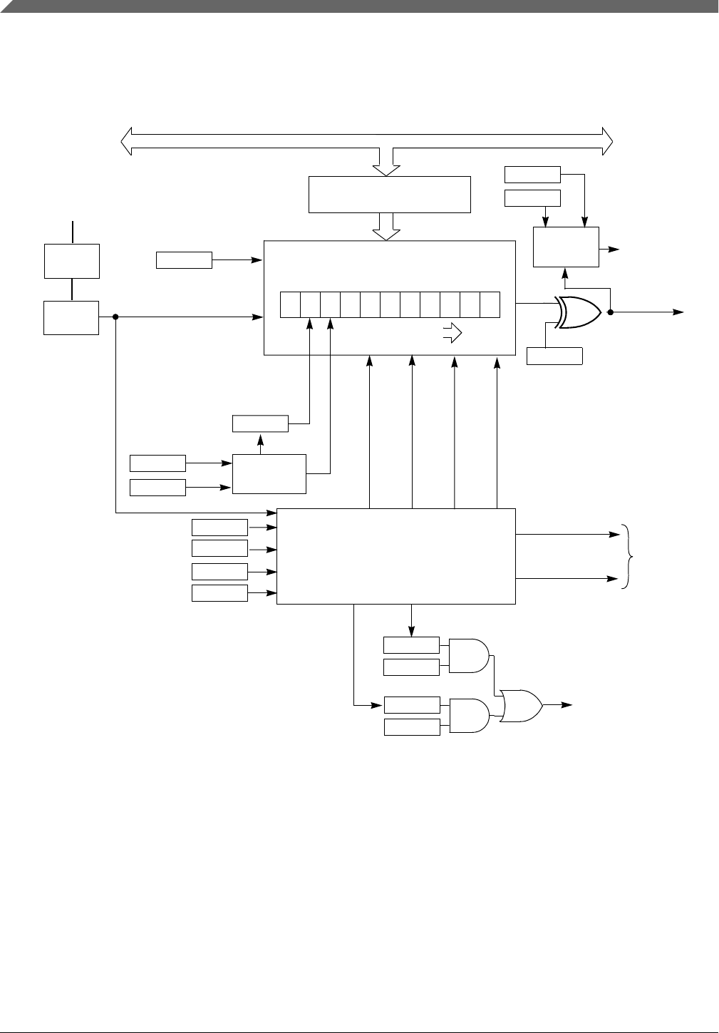
51.2.4 Block diagram
The following figure shows the transmitter portion of the LPUART.
H 8 7 6 5 4 3 2 1 0 L
LPUART_D – Tx Buffer
(Write-Only)
Internal Bus
Stop
11-BIT Transmit Shift Register
Start
SHIFT DIRECTION
lsb
Parity
Generation
Transmit Control
Shift Enable
Preamble (All 1s)
Break (All 0s)
LPUART Controls TxD
TxD Direction
TO TxD
Pin Logic
Loop
Control To Receive
Data In
To TxD Pin
Tx Interrupt
Request
LOOPS
RSRC
TIE
TC
TDRE
M
PT
PE
TCIE
TE
SBK
T8
TXDIR
Load From LPUARTx_D
TXINV
BRK13
ASYNCH
MODULE
CLOCK
BAUD
Divider
OSR
Divider
Figure 51-1. LPUART transmitter block diagram
The following figure shows the receiver portion of the LPUART.
Introduction
S32K1xx Series Reference Manual, Rev. 7, 04/2018
1538 NXP Semiconductors
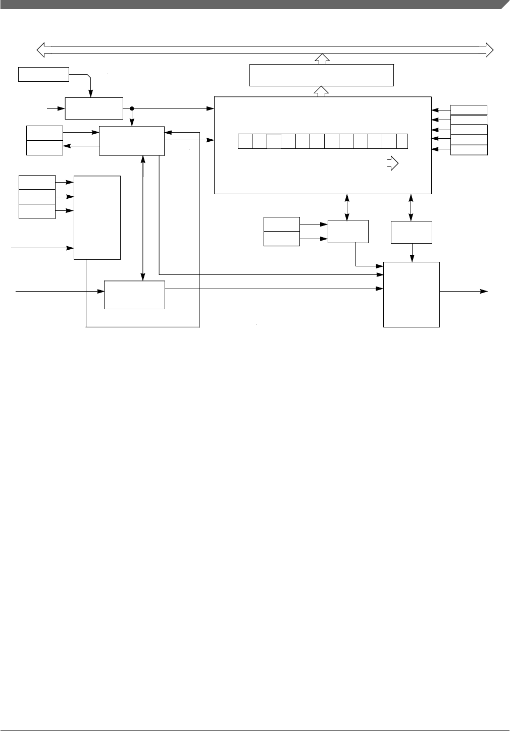
M
PE
PT
RE
VARIABLE 12-BIT RECEIVE
STOP
START
RECEIVE
WAKEUP
DATA BUFFER
INTERNAL BUS
SBR12:0
BAUDRATE
CLOCK
RAF
LOGIC
SHIFT DIRECTION
ACTIVE EDGE
DETECT
LBKDE
MSBF
GENERATOR SHIFT REGISTER M10
RXINV
IRQ / DMA
LOGIC
DMA Requests
IRQ Requests
PARITY
LOGIC
CONTROL
RxD
RxD
LOOPS
RSRC
From Transmitter
RECEIVER
SOURCE
CONTROL
MODULE
ASYNCH
Figure 51-2. LPUART receiver block diagram
51.3 Register definition
The LPUART includes registers to control baud rate, select options, report status, and
store transmit/receive data. Access to an address outside the valid memory map will
generate a bus error.
NOTE
Writing a Read-Only (RO) register or reading a Write-Only
(WO) register can cause bus errors. This module will not check
if programmed values in the registers are correct; the
application software must ensure that valid programmed values
are being written.
51.3.1 LPUART register descriptions
Chapter 51 Low Power Universal Asynchronous Receiver/Transmitter (LPUART)
S32K1xx Series Reference Manual, Rev. 7, 04/2018
NXP Semiconductors 1539

51.3.1.1 LPUART Memory map
LPUART0 base address: 4006_A000h
LPUART1 base address: 4006_B000h
LPUART2 base address: 4006_C000h
Offset Register Width
(In bits)
Access Reset value
0h Version ID Register (VERID) 32 RO 0401_0003h
4h Parameter Register (PARAM) 32 RO 0000_0202h
8h LPUART Global Register (GLOBAL) 32 RW 0000_0000h
Ch LPUART Pin Configuration Register (PINCFG) 32 RW 0000_0000h
10h LPUART Baud Rate Register (BAUD) 32 RW 0F00_0004h
14h LPUART Status Register (STAT) 32 RW 00C0_0000h
18h LPUART Control Register (CTRL) 32 RW 0000_0000h
1Ch LPUART Data Register (DATA) 32 RW 0000_1000h
20h LPUART Match Address Register (MATCH) 32 RW 0000_0000h
24h LPUART Modem IrDA Register (MODIR) 32 RW 0000_0000h
28h LPUART FIFO Register (FIFO) 32 RW 00C0_0011h
2Ch LPUART Watermark Register (WATER) 32 RW 0000_0000h
51.3.1.2 Version ID Register (VERID)
51.3.1.2.1 Offset
Register Offset
VERID 0h
51.3.1.2.2 Function
The Version ID register indicates the version integrated for this instance on the device
and also indicates inclusion/exclusion of several optional features.
Register definition
S32K1xx Series Reference Manual, Rev. 7, 04/2018
1540 NXP Semiconductors

51.3.1.2.3 Diagram
Bits 31 30 29 28 27 26 25 24 23 22 21 20 19 18 17 16
RMAJOR MINOR
W
Reset 0 0 0 0 0 1 0 0 0 0 0 0 0 0 0 1
Bits 15 14 13 12 11 10 9 8 7 6 5 4 3 2 1 0
RFEATURE
W
Reset 0 0 0 0 0 0 0 0 0 0 0 0 0 0 1 1
51.3.1.2.4 Fields
Field Function
31-24
MAJOR
Major Version Number
This read only field returns the major version number for the module specification.
23-16
MINOR
Minor Version Number
This read only field returns the minor version number for the module specification.
15-0
FEATURE
Feature Identification Number
This read only field returns the feature set number.
0000000000000001b - Standard feature set.
0000000000000011b - Standard feature set with MODEM/IrDA support.
51.3.1.3 Parameter Register (PARAM)
51.3.1.3.1 Offset
Register Offset
PARAM 4h
51.3.1.3.2 Function
The Parameter register indicates the parameter configuration for this instance on the
device
Chapter 51 Low Power Universal Asynchronous Receiver/Transmitter (LPUART)
S32K1xx Series Reference Manual, Rev. 7, 04/2018
NXP Semiconductors 1541

51.3.1.3.3 Diagram
Bits 31 30 29 28 27 26 25 24 23 22 21 20 19 18 17 16
R 0
W
Reset 0 0 0 0 0 0 0 0 0 0 0 0 0 0 0 0
Bits 15 14 13 12 11 10 9 8 7 6 5 4 3 2 1 0
RRXFIFO TXFIFO
W
Reset 0 0 0 0 0 0 1 0 0 0 0 0 0 0 1 0
51.3.1.3.4 Fields
Field Function
31-16
—
Reserved
15-8
RXFIFO
Receive FIFO Size
The number of words in the receive FIFO is 2^RXFIFO.
7-0
TXFIFO
Transmit FIFO Size
The number of words in the transmit FIFO is 2^TXFIFO.
51.3.1.4 LPUART Global Register (GLOBAL)
51.3.1.4.1 Offset
Register Offset
GLOBAL 8h
Register definition
S32K1xx Series Reference Manual, Rev. 7, 04/2018
1542 NXP Semiconductors

51.3.1.4.2 Diagram
Bits 31 30 29 28 27 26 25 24 23 22 21 20 19 18 17 16
R 0
W
Reset 0 0 0 0 0 0 0 0 0 0 0 0 0 0 0 0
Bits 15 14 13 12 11 10 9 8 7 6 5 4 3 2 1 0
R 0 RST 0
W
Reset 0 0 0 0 0 0 0 0 0 0 0 0 0 0 0 0
51.3.1.4.3 Fields
Field Function
31-2
—
Reserved
1
RST
Software Reset
Resets all internal logic and registers, except the Global Register. Remains set until cleared by software.
0b - Module is not reset.
1b - Module is reset.
0
—
Reserved
51.3.1.5 LPUART Pin Configuration Register (PINCFG)
51.3.1.5.1 Offset
Register Offset
PINCFG Ch
Chapter 51 Low Power Universal Asynchronous Receiver/Transmitter (LPUART)
S32K1xx Series Reference Manual, Rev. 7, 04/2018
NXP Semiconductors 1543

51.3.1.5.2 Diagram
Bits 31 30 29 28 27 26 25 24 23 22 21 20 19 18 17 16
R 0
W
Reset 0 0 0 0 0 0 0 0 0 0 0 0 0 0 0 0
Bits 15 14 13 12 11 10 9 8 7 6 5 4 3 2 1 0
R 0 TRGSEL
W
Reset 0 0 0 0 0 0 0 0 0 0 0 0 0 0 0 0
51.3.1.5.3 Fields
Field Function
31-2
—
Reserved
1-0
TRGSEL
Trigger Select
Configures the input trigger usage. This field should only be changed when the transmitter and receiver
are both disabled.
00b - Input trigger is disabled.
01b - Input trigger is used instead of RXD pin input.
10b - Input trigger is used instead of CTS_B pin input.
11b - Input trigger is used to modulate the TXD pin output. The TXD pin output (after TXINV
configuration) is ANDed with the input trigger.
51.3.1.6 LPUART Baud Rate Register (BAUD)
51.3.1.6.1 Offset
Register Offset
BAUD 10h
Register definition
S32K1xx Series Reference Manual, Rev. 7, 04/2018
1544 NXP Semiconductors

51.3.1.6.2 Diagram
Bits 31 30 29 28 27 26 25 24 23 22 21 20 19 18 17 16
R
MAEN1
MAEN2
M10
OS
R
TDMAE
0
RDMAE
RIDMAE
MATCFG
BOTHEDGE
RESYNCDI
S
W
Reset 0 0 0 0 1 1 1 1 0 0 0 0 0 0 0 0
Bits 15 14 13 12 11 10 9 8 7 6 5 4 3 2 1 0
R
LBKDIE
RXEDGI
E
SBN
S
SB
R
W
Reset 0 0 0 0 0 0 0 0 0 0 0 0 0 1 0 0
51.3.1.6.3 Fields
Field Function
31
MAEN1
Match Address Mode Enable 1
0b - Normal operation.
1b - Enables automatic address matching or data matching mode for MATCH[MA1].
30
MAEN2
Match Address Mode Enable 2
0b - Normal operation.
1b - Enables automatic address matching or data matching mode for MATCH[MA2].
29
M10
10-bit Mode select
The M10 bit causes a tenth bit to be part of the serial transmission. This bit should only be changed when
the transmitter and receiver are both disabled.
0b - Receiver and transmitter use 7-bit to 9-bit data characters.
1b - Receiver and transmitter use 10-bit data characters.
28-24
OSR
Oversampling Ratio
This field configures the oversampling ratio for the receiver. This field should only be changed when the
transmitter and receiver are both disabled.
00000b - Writing 0 to this field will result in an oversampling ratio of 16
00001b - Reserved
00010b - Reserved
00011b - Oversampling ratio of 4, requires BOTHEDGE to be set.
00100b - Oversampling ratio of 5, requires BOTHEDGE to be set.
00101b - Oversampling ratio of 6, requires BOTHEDGE to be set.
00110b - Oversampling ratio of 7, requires BOTHEDGE to be set.
00111b - Oversampling ratio of 8.
01000b - Oversampling ratio of 9.
01001b - Oversampling ratio of 10.
01010b - Oversampling ratio of 11.
01011b - Oversampling ratio of 12.
01100b - Oversampling ratio of 13.
01101b - Oversampling ratio of 14.
01110b - Oversampling ratio of 15.
01111b - Oversampling ratio of 16.
10000b - Oversampling ratio of 17.
Table continues on the next page...
Chapter 51 Low Power Universal Asynchronous Receiver/Transmitter (LPUART)
S32K1xx Series Reference Manual, Rev. 7, 04/2018
NXP Semiconductors 1545

Field Function
10001b - Oversampling ratio of 18.
10010b - Oversampling ratio of 19.
10011b - Oversampling ratio of 20.
10100b - Oversampling ratio of 21.
10101b - Oversampling ratio of 22.
10110b - Oversampling ratio of 23.
10111b - Oversampling ratio of 24.
11000b - Oversampling ratio of 25.
11001b - Oversampling ratio of 26.
11010b - Oversampling ratio of 27.
11011b - Oversampling ratio of 28.
11100b - Oversampling ratio of 29.
11101b - Oversampling ratio of 30.
11110b - Oversampling ratio of 31.
11111b - Oversampling ratio of 32.
23
TDMAE
Transmitter DMA Enable
TDMAE configures the transmit data register empty flag, STAT[TDRE], to generate a DMA request.
0b - DMA request disabled.
1b - DMA request enabled.
22
—
Reserved
21
RDMAE
Receiver Full DMA Enable
RDMAE configures the receiver data register full flag, STAT[RDRF], to generate a DMA request.
0b - DMA request disabled.
1b - DMA request enabled.
20
RIDMAE
Receiver Idle DMA Enable
RIDMAE configures the receiver idle flag, STAT[IDLE], to generate a DMA request. When this bit is set,
reading the DATA register when either DATA[RXEMPT] or DATA[IDLINE] bit is set, will generate an End
Of Packet response until the completion of the existing DMA transfer. During an End of Packet response,
reading the DATA register will return 0x0000_33FF and does not pull data from the FIFO.
0b - DMA request disabled.
1b - DMA request enabled.
19-18
MATCFG
Match Configuration
Configures the match addressing mode used. This field should only be changed when the transmitter and
receiver are both disabled.
00b - Address Match Wakeup
01b - Idle Match Wakeup
10b - Match On and Match Off
11b - Enables RWU on Data Match and Match On/Off for transmitter CTS input
17
BOTHEDGE
Both Edge Sampling
Enables sampling of the received data on both edges of the baud rate clock, effectively doubling the
number of times the receiver samples the input data for a given oversampling ratio. This bit must be set
for oversampling ratios between x4 and x7 and is optional for higher oversampling ratios. This bit should
only be changed when the receiver is disabled.
0b - Receiver samples input data using the rising edge of the baud rate clock.
1b - Receiver samples input data using the rising and falling edge of the baud rate clock.
16
RESYNCDIS
Resynchronization Disable
When set, disables the resynchronization of the received data word when a data one followed by data
zero transition is detected. This bit should only be changed when the receiver is disabled.
0b - Resynchronization during received data word is supported
1b - Resynchronization during received data word is disabled
Table continues on the next page...
Register definition
S32K1xx Series Reference Manual, Rev. 7, 04/2018
1546 NXP Semiconductors

Field Function
15
LBKDIE
LIN Break Detect Interrupt Enable
LBKDIE enables the LIN break detect flag, STAT[LBKDIF], to generate interrupt requests.
0b - Hardware interrupts from STAT[LBKDIF] flag are disabled (use polling).
1b - Hardware interrupt requested when STAT[LBKDIF] flag is 1.
14
RXEDGIE
RX Input Active Edge Interrupt Enable
Enables the receive input active edge, STAT[RXEDGIF], to generate interrupt requests. Changing
CTRL[LOOP] or CTRL[RSRC] when RXEDGIE is set can cause the STAT[RXEDGIF] flag to set.
0b - Hardware interrupts from STAT[RXEDGIF] are disabled.
1b - Hardware interrupt is requested when STAT[RXEDGIF] flag is 1.
13
SBNS
Stop Bit Number Select
SBNS determines whether data characters have one or two stop bits. This bit should only be changed
when the transmitter and receiver are both disabled.
0b - One stop bit.
1b - Two stop bits.
12-0
SBR
Baud Rate Modulo Divisor.
The 13 bits in SBR[12:0] set the modulo divide rate for the baud rate generator. When SBR is 1 - 8191,
the baud rate equals "baud clock / ((OSR+1) × SBR)". The 13-bit baud rate setting [SBR12:SBR0] must
be updated only when the transmitter and receiver are both disabled (CTRL[RE] and CTRL[TE] are both
0).
51.3.1.7 LPUART Status Register (STAT)
51.3.1.7.1 Offset
Register Offset
STAT 14h
Chapter 51 Low Power Universal Asynchronous Receiver/Transmitter (LPUART)
S32K1xx Series Reference Manual, Rev. 7, 04/2018
NXP Semiconductors 1547

51.3.1.7.2 Diagram
Bits 31 30 29 28 27 26 25 24 23 22 21 20 19 18 17 16
R
LBKDIF
RXEDGI
F
MSBF
RXINV
RWUID
BRK13
LBKDE
RAF
TDR
E
TC
RDR
F
IDL
E
OR
NF
F
E
P
F
W
W1C
W1C
W1C
W1C
W1C
W1C
W1C
Reset 0 0 0 0 0 0 0 0 1 1 0 0 0 0 0 0
Bits 15 14 13 12 11 10 9 8 7 6 5 4 3 2 1 0
R
MA1F
MA2F
0
W
W1C
W1C
Reset 0 0 0 0 0 0 0 0 0 0 0 0 0 0 0 0
51.3.1.7.3 Fields
Field Function
31
LBKDIF
LIN Break Detect Interrupt Flag
LBKDIF is set when the LIN break detect circuitry is enabled and a LIN break character is detected.
LBKDIF is cleared by writing a 1 to it.
0b - No LIN break character has been detected.
1b - LIN break character has been detected.
30
RXEDGIF
RXD Pin Active Edge Interrupt Flag
RXEDGIF is set whenever the receiver is enabled and an active edge, falling if RXINV = 0, rising if
RXINV=1, on the RXD pin occurs. RXEDGIF is cleared by writing a 1 to it.
0b - No active edge on the receive pin has occurred.
1b - An active edge on the receive pin has occurred.
29
MSBF
MSB First
Setting this bit reverses the order of the bits that are transmitted and received on the wire. This bit does
not affect the polarity of the bits, the location of the parity bit or the location of the start or stop bits. This
bit should only be changed when the transmitter and receiver are both disabled.
0b - LSB (bit0) is the first bit that is transmitted following the start bit. Further, the first bit received
after the start bit is identified as bit0.
1b - MSB (bit9, bit8, bit7 or bit6) is the first bit that is transmitted following the start bit depending on
the setting of CTRL[M], CTRL[PE] and BAUD[M10]. Further, the first bit received after the start bit
is identified as bit9, bit8, bit7 or bit6 depending on the setting of CTRL[M] and CTRL[PE].
28
RXINV
Receive Data Inversion
Setting this bit reverses the polarity of the received data input. This bit should only be changed when the
receiver is disabled.
NOTE: Setting RXINV inverts the RXD input for all cases: data bits, start and stop bits, break, and idle.
0b - Receive data not inverted.
1b - Receive data inverted.
27 Receive Wake Up Idle Detect
Table continues on the next page...
Register definition
S32K1xx Series Reference Manual, Rev. 7, 04/2018
1548 NXP Semiconductors

Field Function
RWUID For RWU on idle character, RWUID controls whether the idle character that wakes up the receiver sets
the IDLE bit. For address match wakeup, RWUID controls if the IDLE bit is set when the address does
not match. This bit should only be changed when the receiver is disabled.
0b - During receive standby state (RWU = 1), the IDLE bit does not get set upon detection of an
idle character. During address match wakeup, the IDLE bit does not set when an address does not
match.
1b - During receive standby state (RWU = 1), the IDLE bit gets set upon detection of an idle
character. During address match wakeup, the IDLE bit does set when an address does not match.
26
BRK13
Break Character Generation Length
BRK13 selects a longer transmitted break character length. Detection of a framing error is not affected by
the state of this bit. This bit should only be changed when the transmitter is disabled. A break character
can be sent by setting CTRL[SBK] or by writing the transmit FIFO with DATA[FRETSC] set and
DATA[R9T9] clear.
0b - Break character is transmitted with length of 9 to 13 bit times.
1b - Break character is transmitted with length of 12 to 15 bit times.
25
LBKDE
LIN Break Detection Enable
LBKDE selects a longer break character detection length. While LBKDE is set, receive data is not stored
in the receive data buffer.
0b - LIN break detect is disabled, normal break character can be detected.
1b - LIN break detect is enabled. LIN break character is detected at length of 11 bit times (if M = 0)
or 12 (if M = 1) or 13 (M10 = 1).
24
RAF
Receiver Active Flag
RAF is set when the receiver detects the beginning of a valid start bit, and RAF is cleared automatically
when the receiver detects an idle line.
0b - LPUART receiver idle waiting for a start bit.
1b - LPUART receiver active (RXD input not idle).
23
TDRE
Transmit Data Register Empty Flag
When the transmit FIFO is enabled, TDRE will set when the number of datawords in the transmit FIFO
(DATA register) is equal to or less than the number indicated by WATER[TXWATER]). To clear TDRE,
write to the DATA register until the number of words in the transmit FIFO is greater than the number
indicated by WATER[TXWATER]. When the transmit FIFO is disabled,TDRE will set when the transmit
DATA register is empty. To clear TDRE, write to the DATA register.
TDRE is not affected by a character that is in the process of being transmitted; it is updated at the start of
each transmitted character.
0b - Transmit data buffer full.
1b - Transmit data buffer empty.
22
TC
Transmission Complete Flag
TC is cleared when there is a transmission in progress or when a preamble or break character is loaded.
TC is set when the transmit buffer is empty and no data, preamble, or break character is being
transmitted. When TC is set, the transmit data output signal becomes idle (logic 1). TC is cleared by
writing to the DATA register to transmit new data, queuing a preamble by clearing and then setting
CTRL[TE], queuing a break character by writing 1 to CTRL[SBK].
0b - Transmitter active (sending data, a preamble, or a break).
1b - Transmitter idle (transmission activity complete).
21
RDRF
Receive Data Register Full Flag
When the receive FIFO is enabled, RDRF is set when the number of datawords in the receive buffer is
greater than the number indicated by WATER[RXWATER]. To clear RDRF, read the DATA register until
the number of datawords in the receive data buffer is equal to or less than the number indicated by
WATER[RXWATER]. When the receive FIFO is disabled, RDRF is set when the receive buffer (the DATA
register) is full. To clear RDRF, read the DATA register.
Table continues on the next page...
Chapter 51 Low Power Universal Asynchronous Receiver/Transmitter (LPUART)
S32K1xx Series Reference Manual, Rev. 7, 04/2018
NXP Semiconductors 1549

Field Function
A character that is in the process of being received does not cause a change in RDRF until the entire
character is received. Even if RDRF is set, the character will continue to be received until an overrun
condition occurs once the entire character is received.
0b - Receive data buffer empty.
1b - Receive data buffer full.
20
IDLE
Idle Line Flag
IDLE is set when the LPUART receive line becomes idle for a full character time after a period of activity.
When CTRL[ILT] is cleared, the receiver starts counting idle bit times after the start bit. If the receive
character is all 1s, these bit times and the stop bits time count toward the full character time of logic high,
10 to 13 bit times, needed for the receiver to detect an idle line. When CTRL[ILT] is set, the receiver
doesn't start counting idle bit times until after the stop bits. The stop bits and any logic high bit times at
the end of the previous character do not count toward the full character time of logic high needed for the
receiver to detect an idle line.
To clear IDLE, write logic 1 to the IDLE flag. After IDLE has been cleared, it cannot be set again until after
a new character has been stored in the receive buffer or a LIN break character has set the LBKDIF flag .
IDLE is set only once even if the receive line remains idle for an extended period.
0b - No idle line detected.
1b - Idle line was detected.
19
OR
Receiver Overrun Flag
OR is set when software fails to prevent the receive data register from overflowing with data. The OR bit
is set immediately after the stop bit has been completely received for the dataword that overflows the
buffer and all the other error flags (FE, NF, and PF) are prevented from setting. The data in the shift
register is lost, but the data already in the LPUART data registers is not affected. If LBKDE is enabled
and a LIN Break is detected, the OR field asserts if LBKDIF is not cleared before the next data character
is received.
While the OR flag is set, no additional data is stored in the data buffer even if sufficient room exists. To
clear OR, write logic 1 to the OR flag.
0b - No overrun.
1b - Receive overrun (new LPUART data lost).
18
NF
Noise Flag
The advanced sampling technique used in the receiver takes three samples in each of the received bits.
If any of these samples disagrees with the rest of the samples within any bit time in the frame then noise
is detected for that character. NF is set whenever the next character to be read from the DATA register
was received with noise detected within the character. To clear NF, write logic 1 to the NF field.
0b - No noise detected.
1b - Noise detected in the received character in the DATA register.
17
FE
Framing Error Flag
FE is set whenever the next character to be read from the DATA register was received with logic 0
detected where a stop bit was expected. To clear FE, write logic 1 to the FE field.
0b - No framing error detected. This does not guarantee the framing is correct.
1b - Framing error.
16
PF
Parity Error Flag
PF is set whenever the next character to be read from the DATA register was received when parity is
enabled (PE = 1) and the parity bit in the received character does not agree with the expected parity
value. To clear PF, write a logic 1 to the PF field.
0b - No parity error.
1b - Parity error.
15
MA1F
Match 1 Flag
Table continues on the next page...
Register definition
S32K1xx Series Reference Manual, Rev. 7, 04/2018
1550 NXP Semiconductors

Field Function
MA1F is set whenever the next character to be read from the DATA register matches MA1. To clear
MA1F, write a logic 1 to the MA1F field.
0b - Received data is not equal to MA1
1b - Received data is equal to MA1
14
MA2F
Match 2 Flag
MA2F is set whenever the next character to be read from the DATA register matches MA2. To clear
MA2F, write a logic 1 to the MA2F field.
0b - Received data is not equal to MA2
1b - Received data is equal to MA2
13-0
—
Reserved
51.3.1.8 LPUART Control Register (CTRL)
51.3.1.8.1 Offset
Register Offset
CTRL 18h
51.3.1.8.2 Function
This read/write register controls various optional features of the LPUART system. This
register should only be altered when the transmitter and receiver are both disabled.
51.3.1.8.3 Diagram
Bits 31 30 29 28 27 26 25 24 23 22 21 20 19 18 17 16
R
R8T9
R9T8
TXDIR
TXINV
ORI
E
NEI
E
FEI
E
PEI
E
TI
E
TCIE
RI
E
ILI
E
T
E
R
E
RWU
SB
K
W
Reset 0 0 0 0 0 0 0 0 0 0 0 0 0 0 0 0
Bits 15 14 13 12 11 10 9 8 7 6 5 4 3 2 1 0
R
MA1IE
MA2IE
0
M7
IDLECF
G
LOOPS
DOZEEN
RSR
C
M
WAKE
ILT
P
E
PT
W
Reset 0 0 0 0 0 0 0 0 0 0 0 0 0 0 0 0
Chapter 51 Low Power Universal Asynchronous Receiver/Transmitter (LPUART)
S32K1xx Series Reference Manual, Rev. 7, 04/2018
NXP Semiconductors 1551

51.3.1.8.4 Fields
Field Function
31
R8T9
Receive Bit 8 / Transmit Bit 9
R8 is the ninth data bit received when the LPUART is configured for 9-bit or 10-bit data formats. When
reading 9-bit or 10-bit data, read R8 before reading the DATA register.
T9 is the tenth data bit transmitted when the LPUART is configured for 10-bit data formats. When writing
10-bit data, write T9 before writing the DATA register. If T9 does not need to change from its previous
value, such as when it is used to generate address mark or parity, they it need not be written each time
the DATA register is written.
NOTE: R8 is a read-only bit and T9 is a write-only bit, the value read is different from the value written.
30
R9T8
Receive Bit 9 / Transmit Bit 8
R9 is the tenth data bit received when the LPUART is configured for 10-bit data formats. When reading
10-bit data, read R9 before reading the DATA register
T8 is the ninth data bit transmitted when the LPUART is configured for 9-bit or 10-bit data formats. When
writing 9-bit or 10-bit data, write T8 before writing the DATA register. If T8 does not need to change from
its previous value, such as when it is used to generate address mark or parity, then it need not be written
each time the DATA register is written.
NOTE: R9 is a read-only bit and T8 is a write-only bit, the value read is different from the value written.
29
TXDIR
TXD Pin Direction in Single-Wire Mode
When the LPUART is configured for single-wire half-duplex operation (LOOPS = RSRC = 1), this bit
determines the direction of data at the TXD pin. When clearing TXDIR, the transmitter will finish receiving
the current character (if any) before the receiver starts receiving data from the TXD pin.
0b - TXD pin is an input in single-wire mode.
1b - TXD pin is an output in single-wire mode.
28
TXINV
Transmit Data Inversion
Setting this bit reverses the polarity of the transmitted data output.
NOTE: Setting TXINV inverts the TXD output for all cases: data bits, start and stop bits, break, and idle.
0b - Transmit data not inverted.
1b - Transmit data inverted.
27
ORIE
Overrun Interrupt Enable
This bit enables the overrun flag (OR) to generate hardware interrupt requests.
0b - OR interrupts disabled; use polling.
1b - Hardware interrupt requested when OR is set.
26
NEIE
Noise Error Interrupt Enable
This bit enables the noise flag (NF) to generate hardware interrupt requests.
0b - NF interrupts disabled; use polling.
1b - Hardware interrupt requested when NF is set.
25
FEIE
Framing Error Interrupt Enable
This bit enables the framing error flag (FE) to generate hardware interrupt requests.
0b - FE interrupts disabled; use polling.
1b - Hardware interrupt requested when FE is set.
24
PEIE
Parity Error Interrupt Enable
This bit enables the parity error flag (PF) to generate hardware interrupt requests.
0b - PF interrupts disabled; use polling).
1b - Hardware interrupt requested when PF is set.
23 Transmit Interrupt Enable
Table continues on the next page...
Register definition
S32K1xx Series Reference Manual, Rev. 7, 04/2018
1552 NXP Semiconductors

Field Function
TIE Enables STAT[TDRE] to generate interrupt requests.
0b - Hardware interrupts from TDRE disabled; use polling.
1b - Hardware interrupt requested when TDRE flag is 1.
22
TCIE
Transmission Complete Interrupt Enable for
TCIE enables the transmission complete flag, TC, to generate interrupt requests.
0b - Hardware interrupts from TC disabled; use polling.
1b - Hardware interrupt requested when TC flag is 1.
21
RIE
Receiver Interrupt Enable
Enables STAT[RDRF] to generate interrupt requests.
0b - Hardware interrupts from RDRF disabled; use polling.
1b - Hardware interrupt requested when RDRF flag is 1.
20
ILIE
Idle Line Interrupt Enable
ILIE enables the idle line flag, STAT[IDLE], to generate interrupt requests.
0b - Hardware interrupts from IDLE disabled; use polling.
1b - Hardware interrupt requested when IDLE flag is 1.
19
TE
Transmitter Enable
Enables the LPUART transmitter. TE can also be used to queue an idle preamble by clearing and then
setting TE. When TE is cleared, this register bit will read as 1 until the transmitter has completed the
current character and the TXD pin is tristated.
A single idle character can also be queued by writing to the transmit FIFO with DATA[FRETSC] set and
DATA[R9T9] set.
0b - Transmitter disabled.
1b - Transmitter enabled.
18
RE
Receiver Enable
Enables the LPUART receiver. When RE is written to 0, this register bit will read as 1 until the receiver
finishes receiving the current character (if any).
0b - Receiver disabled.
1b - Receiver enabled.
17
RWU
Receiver Wakeup Control
This field can be set to place the LPUART receiver in a standby state. RWU automatically clears when an
RWU event occurs, that is, an IDLE event when CTRL[WAKE] is clear or an address match when
CTRL[WAKE] is set with STAT[RWUID] is clear.
NOTE: RWU must be set only with CTRL[WAKE] = 0 (wakeup on idle) if the channel is currently not
idle. This can be determined by STAT[RAF]. If the flag is set to wake up an IDLE event and the
channel is already idle, it is possible that the LPUART will discard data. This is because the data
must be received or a LIN break detected after an IDLE is detected before IDLE is allowed to be
reasserted.
0b - Normal receiver operation.
1b - LPUART receiver in standby waiting for wakeup condition.
16
SBK
Send Break
Writing a 1 and then a 0 to SBK queues a break character in the transmit data stream. Additional break
characters of 9 to 13 bits, or 12 to 15 bits if STAT[BRK13] is set, bit times of logic 0 are queued as long
as SBK is set. Depending on the timing of the set and clear of SBK relative to the character currently
being transmitted, a second break character may be queued before software clears SBK.
A single break character can also be queued by writing to the transmit FIFO with DATA[FRETSC] set and
DATA[R9T9] clear.
0b - Normal transmitter operation.
1b - Queue break character(s) to be sent.
Table continues on the next page...
Chapter 51 Low Power Universal Asynchronous Receiver/Transmitter (LPUART)
S32K1xx Series Reference Manual, Rev. 7, 04/2018
NXP Semiconductors 1553

Field Function
15
MA1IE
Match 1 Interrupt Enable
0b - MA1F interrupt disabled
1b - MA1F interrupt enabled
14
MA2IE
Match 2 Interrupt Enable
0b - MA2F interrupt disabled
1b - MA2F interrupt enabled
13-12
—
Reserved
11
M7
7-Bit Mode Select
This bit should only be changed when the transmitter and receiver are both disabled.
0b - Receiver and transmitter use 8-bit to 10-bit data characters.
1b - Receiver and transmitter use 7-bit data characters.
10-8
IDLECFG
Idle Configuration
Configures the number of idle characters that must be received before the IDLE flag is set.
000b - 1 idle character
001b - 2 idle characters
010b - 4 idle characters
011b - 8 idle characters
100b - 16 idle characters
101b - 32 idle characters
110b - 64 idle characters
111b - 128 idle characters
7
LOOPS
Loop Mode Select
When LOOPS is set, the RXD pin is disconnected from the LPUART and the transmitter output is
internally connected to the receiver input. The transmitter and the receiver must be enabled to use the
loop function.
0b - Normal operation - RXD and TXD use separate pins.
1b - Loop mode or single-wire mode where transmitter outputs are internally connected to receiver
input (see RSRC bit).
6
DOZEEN
Doze Enable
0b - LPUART is enabled in Doze mode.
1b - LPUART is disabled in Doze mode.
5
RSRC
Receiver Source Select
This field has no meaning or effect unless the LOOPS field is set. When LOOPS is set, the RSRC field
determines the source for the receiver shift register input.
0b - Provided LOOPS is set, RSRC is cleared, selects internal loop back mode and the LPUART
does not use the RXD pin.
1b - Single-wire LPUART mode where the TXD pin is connected to the transmitter output and
receiver input.
4
M
9-Bit or 8-Bit Mode Select
0b - Receiver and transmitter use 8-bit data characters.
1b - Receiver and transmitter use 9-bit data characters.
3
WAKE
Receiver Wakeup Method Select
Determines which condition wakes the LPUART when RWU=1:
• Address mark in the bit preceding the stop bit (or bit preceding the parity bit when parity is enabled)
of the received data character, or
• An idle condition on the receive pin input signal.
0b - Configures RWU for idle-line wakeup.
1b - Configures RWU with address-mark wakeup.
Table continues on the next page...
Register definition
S32K1xx Series Reference Manual, Rev. 7, 04/2018
1554 NXP Semiconductors

Field Function
2
ILT
Idle Line Type Select
Determines when the receiver starts counting logic 1s as idle character bits. The count begins either after
a valid start bit or after the stop bit. If the count begins after the start bit, then a string of logic 1s
preceding the stop bit can cause false recognition of an idle character. Beginning the count after the stop
bit avoids false idle character recognition, but requires properly synchronized transmissions.
NOTE: In case the LPUART is programmed with ILT = 1, a logic 0 is automatically shifted after a
received stop bit, therefore resetting the idle count.
0b - Idle character bit count starts after start bit.
1b - Idle character bit count starts after stop bit.
1
PE
Parity Enable
Enables hardware parity generation and checking. When parity is enabled, the bit immediately before the
stop bit is treated as the parity bit.
0b - No hardware parity generation or checking.
1b - Parity enabled.
0
PT
Parity Type
Provided parity is enabled (PE = 1), this bit selects even or odd parity. Odd parity means the total number
of 1s in the data character, including the parity bit, is odd. Even parity means the total number of 1s in the
data character, including the parity bit, is even.
0b - Even parity.
1b - Odd parity.
51.3.1.9 LPUART Data Register (DATA)
51.3.1.9.1 Offset
Register Offset
DATA 1Ch
51.3.1.9.2 Function
NOTE
This register is two separate registers. Reads return the contents
of the read-only receive data buffer and writes go to the write-
only transmit data buffer.
Reads and writes of this register are also involved in the automatic flag clearing
mechanisms for some of the LPUART status flags.
Chapter 51 Low Power Universal Asynchronous Receiver/Transmitter (LPUART)
S32K1xx Series Reference Manual, Rev. 7, 04/2018
NXP Semiconductors 1555

51.3.1.9.3 Diagram
Bits 31 30 29 28 27 26 25 24 23 22 21 20 19 18 17 16
R 0
W
Reset 0 0 0 0 0 0 0 0 0 0 0 0 0 0 0 0
Bits 15 14 13 12 11 10 9 8 7 6 5 4 3 2 1 0
R
NOISY
PARITYE
FRETS
C
RXEMPT
IDLINE
0
R9T9
R8T8
R7T7
R6T6
R5T5
R4T4
R3T3
R2T2
R1T1
R0T0
W
Reset 0 0 0 1 0 0 0 0 0 0 0 0 0 0 0 0
51.3.1.9.4 Fields
Field Function
31-16
—
Reserved
15
NOISY
NOISY
The current received dataword contained in DATA[R9:R0] was received with noise.
0b - The dataword was received without noise.
1b - The data was received with noise.
14
PARITYE
PARITYE
The current received dataword contained in DATA[R9:R0] was received with a parity error.
0b - The dataword was received without a parity error.
1b - The dataword was received with a parity error.
13
FRETSC
Frame Error / Transmit Special Character
For reads, indicates the current received dataword contained in DATA[R9:R0] was received with a frame
error. For writes, indicates a break or idle character is to be transmitted instead of the contents in
DATA[T9:T0]. T9 is used to indicate a break character when 0 and a idle character when 1, the contents
of DATA[T8:T0] should be zero.
0b - The dataword was received without a frame error on read, or transmit a normal character on
write.
1b - The dataword was received with a frame error, or transmit an idle or break character on
transmit.
12
RXEMPT
Receive Buffer Empty
Asserts when there is no data in the receive buffer. This field does not take into account data that is in the
receive shift register.
0b - Receive buffer contains valid data.
1b - Receive buffer is empty, data returned on read is not valid.
11
IDLINE
Idle Line
Indicates the receiver line was idle before receiving the character in DATA[9:0]. Unlike the IDLE flag, this
bit can set for the first character received when the receiver is first enabled.
0b - Receiver was not idle before receiving this character.
1b - Receiver was idle before receiving this character.
Table continues on the next page...
Register definition
S32K1xx Series Reference Manual, Rev. 7, 04/2018
1556 NXP Semiconductors

Field Function
10
—
Reserved
9
R9T9
R9T9
Read receive data buffer 9 or write transmit data buffer 9.
8
R8T8
R8T8
Read receive data buffer 8 or write transmit data buffer 8.
7
R7T7
R7T7
Read receive data buffer 7 or write transmit data buffer 7.
6
R6T6
R6T6
Read receive data buffer 6 or write transmit data buffer 6.
5
R5T5
R5T5
Read receive data buffer 5 or write transmit data buffer 5.
4
R4T4
R4T4
Read receive data buffer 4 or write transmit data buffer 4.
3
R3T3
R3T3
Read receive data buffer 3 or write transmit data buffer 3.
2
R2T2
R2T2
Read receive data buffer 2 or write transmit data buffer 2.
1
R1T1
R1T1
Read receive data buffer 1 or write transmit data buffer 1.
0
R0T0
R0T0
Read receive data buffer 0 or write transmit data buffer 0.
51.3.1.10 LPUART Match Address Register (MATCH)
51.3.1.10.1 Offset
Register Offset
MATCH 20h
Chapter 51 Low Power Universal Asynchronous Receiver/Transmitter (LPUART)
S32K1xx Series Reference Manual, Rev. 7, 04/2018
NXP Semiconductors 1557

51.3.1.10.2 Diagram
Bits 31 30 29 28 27 26 25 24 23 22 21 20 19 18 17 16
R 0 MA2
W
Reset 0 0 0 0 0 0 0 0 0 0 0 0 0 0 0 0
Bits 15 14 13 12 11 10 9 8 7 6 5 4 3 2 1 0
R 0 MA1
W
Reset 0 0 0 0 0 0 0 0 0 0 0 0 0 0 0 0
51.3.1.10.3 Fields
Field Function
31-26
—
Reserved
25-16
MA2
Match Address 2
The MA1 and MA2 fields are compared to input data addresses when the most significant bit is set and
the associated BAUD[MAEN] bit is set. If a match occurs, the following data is transferred to the DATA
register. If a match fails, the following data is discarded. Software should only write a MAx field when the
associated BAUD[MAEN] bit is clear.
15-10
—
Reserved
9-0
MA1
Match Address 1
The MA1 and MA2 fields are compared to input data addresses when the most significant bit is set and
the associated BAUD[MAEN] bit is set. If a match occurs, the following data is transferred to the DATA
register. If a match fails, the following data is discarded. Software should only write a MAx field when the
associated BAUD[MAEN] bit is clear.
51.3.1.11 LPUART Modem IrDA Register (MODIR)
51.3.1.11.1 Offset
Register Offset
MODIR 24h
51.3.1.11.2 Function
The MODEM register controls options for setting the modem configuration.
Register definition
S32K1xx Series Reference Manual, Rev. 7, 04/2018
1558 NXP Semiconductors

51.3.1.11.3 Diagram
Bits 31 30 29 28 27 26 25 24 23 22 21 20 19 18 17 16
R
0
IRE
N
TNP
W
Reset 0 0 0 0 0 0 0 0 0 0 0 0 0 0 0 0
Bits 15 14 13 12 11 10 9 8 7 6 5 4 3 2 1 0
R
0
RTSWATE
R
0
TXCTSSR
C
TXCTSC
RXRTS
E
TXRTSPOL
TXRTS
E
TXCTS
E
W
Reset 0 0 0 0 0 0 0 0 0 0 0 0 0 0 0 0
51.3.1.11.4 Fields
Field Function
31-19
—
Reserved
18
IREN
Infrared enable
Enables/disables the infrared modulation/demodulation. This bit should only be changed when the
transmitter and receiver are both disabled.
0b - IR disabled.
1b - IR enabled.
17-16
TNP
Transmitter narrow pulse
Configures whether the LPUART transmits a 1/OSR, 2/OSR, 3/OSR or 4/OSR narrow pulse when IR is
enabled. This bit should only be changed when the transmitter and receiver are both disabled.
The IR pulse width should be configured to less than half of the oversampling ratio. Common pulse
widths are 3/16, 1/16, 1/32 or 1/4 of the bit length. These can be configured by selecting the appropriate
oversample ratio and pulse width.
00b - 1/OSR.
01b - 2/OSR.
10b - 3/OSR.
11b - 4/OSR.
15-10
—
Reserved
9-8
RTSWATER
Receive RTS Configuration
Configures the assertion and negation of the RX RTS_B output. The RX RTS_B output negates when the
number of empty words in the receive FIFO is greater or equal to RTSWATER. If RTSWATER is
configured to zero, RTS_B negates when the receive FIFO is full. For the purpose of RX RTS_B
generation, the number of words in the receive FIFO updates when a start bit is detected. This supports
additional latency between RTS_B negation and the external transmitter ceasing transmission. If both RX
RTS_B and address/data matching is enabled, then RTS_B could assert at the end of a character if there
is not a match.
Table continues on the next page...
Chapter 51 Low Power Universal Asynchronous Receiver/Transmitter (LPUART)
S32K1xx Series Reference Manual, Rev. 7, 04/2018
NXP Semiconductors 1559

Field Function
This field should only be changed when the receiver is disabled.
7-6
—
Reserved
5
TXCTSSRC
Transmit CTS Source
Configures the source of the CTS input.
0b - CTS input is the CTS_B pin.
1b - CTS input is the inverted Receiver Match result.
4
TXCTSC
Transmit CTS Configuration
Configures if the CTS state is checked at the start of each character or only when the transmitter is idle.
0b - CTS input is sampled at the start of each character.
1b - CTS input is sampled when the transmitter is idle.
3
RXRTSE
Receiver request-to-send enable
Allows the RTS output to control the CTS input of the transmitting device to prevent receiver overrun.
This bit should only be changed when the receiver is disabled.
NOTE: Do not set both RXRTSE and TXRTSE.
0b - The receiver has no effect on RTS.
1b - RTS is deasserted if the receiver data register is full or a start bit has been detected that would
cause the receiver data register to become full. RTS is asserted if the receiver data register is not
full and has not detected a start bit that would cause the receiver data register to become full.
2
TXRTSPOL
Transmitter request-to-send polarity
Controls the polarity of the transmitter RTS. TXRTSPOL does not affect the polarity of the receiver RTS.
RTS will remain negated in the active low state unless TXRTSE is set. This bit should only be changed
when the transmitter is disabled.
0b - Transmitter RTS is active low.
1b - Transmitter RTS is active high.
1
TXRTSE
Transmitter request-to-send enable
Controls RTS before and after a transmission. This bit should only be changed when the transmitter is
disabled.
0b - The transmitter has no effect on RTS.
1b - When a character is placed into an empty transmitter data buffer , RTS asserts one bit time
before the start bit is transmitted. RTS deasserts one bit time after all characters in the transmitter
data buffer and shift register are completely sent, including the last stop bit.
0
TXCTSE
Transmitter clear-to-send enable
TXCTSE controls the operation of the transmitter. TXCTSE can be set independently from the state of
TXRTSE and RXRTSE.
0b - CTS has no effect on the transmitter.
1b - Enables clear-to-send operation. The transmitter checks the state of CTS each time it is ready
to send a character. If CTS is asserted, the character is sent. If CTS is deasserted, the signal TXD
remains in the mark state and transmission is delayed until CTS is asserted. Changes in CTS as a
character is being sent do not affect its transmission.
51.3.1.12 LPUART FIFO Register (FIFO)
Register definition
S32K1xx Series Reference Manual, Rev. 7, 04/2018
1560 NXP Semiconductors

51.3.1.12.1 Offset
Register Offset
FIFO 28h
51.3.1.12.2 Function
This register provides the ability for the programmer to turn on and off FIFO
functionality. It also provides the size of the FIFO that has been implemented. This
register may be read at any time. This register must be written only when CTRL[RE] and
CTRL[TE] are cleared/not set and when the data buffer/FIFO is empty.
51.3.1.12.3 Diagram
Bits 31 30 29 28 27 26 25 24 23 22 21 20 19 18 17 16
R
0
TXEMPT
RXEMPT
0
TXOF
RXU
F
W
W1C
W1C
Reset 0 0 0 0 0 0 0 0 1 1 0 0 0 0 0 0
Bits 15 14 13 12 11 10 9 8 7 6 5 4 3 2 1 0
R
0
0
0
RXIDEN
TXOF
E
RXUF
E
TXF
E
TXFIFOSIZ
E
RXF
E
RXFIFOSIZ
E
W
TXFLUS
H
RXFLUS
H
Reset 0 0 0 0 0 0 0 0 0 0 0 1 0 0 0 1
51.3.1.12.4 Fields
Field Function
31-24
—
Reserved
23
TXEMPT
Transmit Buffer/FIFO Empty
Asserts when there is no data in the Transmit FIFO/buffer. This field does not take into account data that
is in the transmit shift register.
0b - Transmit buffer is not empty.
Table continues on the next page...
Chapter 51 Low Power Universal Asynchronous Receiver/Transmitter (LPUART)
S32K1xx Series Reference Manual, Rev. 7, 04/2018
NXP Semiconductors 1561

Field Function
1b - Transmit buffer is empty.
22
RXEMPT
Receive Buffer/FIFO Empty
Asserts when there is no data in the receive FIFO/Buffer. This field does not take into account data that is
in the receive shift register.
0b - Receive buffer is not empty.
1b - Receive buffer is empty.
21-18
—
Reserved
17
TXOF
Transmitter Buffer Overflow Flag
Indicates that more data has been written to the transmit buffer than it can hold. This field will assert
regardless of the value of TXOFE. However, an interrupt will be issued to the host only if TXOFE is set.
This flag is cleared by writing a 1.
0b - No transmit buffer overflow has occurred since the last time the flag was cleared.
1b - At least one transmit buffer overflow has occurred since the last time the flag was cleared.
16
RXUF
Receiver Buffer Underflow Flag
Indicates that more data has been read from the receive buffer than was present. This field will assert
regardless of the value of RXUFE. However, an interrupt will be issued to the host only if RXUFE is set.
This flag is cleared by writing a 1.
0b - No receive buffer underflow has occurred since the last time the flag was cleared.
1b - At least one receive buffer underflow has occurred since the last time the flag was cleared.
15
TXFLUSH
Transmit FIFO/Buffer Flush
Writing to this field causes all data that is stored in the transmit FIFO/buffer to be flushed. This does not
affect data that is in the transmit shift register.
0b - No flush operation occurs.
1b - All data in the transmit FIFO/Buffer is cleared out.
14
RXFLUSH
Receive FIFO/Buffer Flush
Writing to this field causes all data that is stored in the receive FIFO/buffer to be flushed. This does not
affect data that is in the receive shift register.
0b - No flush operation occurs.
1b - All data in the receive FIFO/buffer is cleared out.
13
—
Reserved
12-10
RXIDEN
Receiver Idle Empty Enable
When set, enables the assertion of RDRF when the receiver is idle for a number of idle characters and
the FIFO is not empty.
000b - Disable RDRF assertion due to partially filled FIFO when receiver is idle.
001b - Enable RDRF assertion due to partially filled FIFO when receiver is idle for 1 character.
010b - Enable RDRF assertion due to partially filled FIFO when receiver is idle for 2 characters.
011b - Enable RDRF assertion due to partially filled FIFO when receiver is idle for 4 characters.
100b - Enable RDRF assertion due to partially filled FIFO when receiver is idle for 8 characters.
101b - Enable RDRF assertion due to partially filled FIFO when receiver is idle for 16 characters.
110b - Enable RDRF assertion due to partially filled FIFO when receiver is idle for 32 characters.
111b - Enable RDRF assertion due to partially filled FIFO when receiver is idle for 64 characters.
9
TXOFE
Transmit FIFO Overflow Interrupt Enable
When this field is set, the TXOF flag generates an interrupt to the host.
0b - TXOF flag does not generate an interrupt to the host.
1b - TXOF flag generates an interrupt to the host.
8 Receive FIFO Underflow Interrupt Enable
Table continues on the next page...
Register definition
S32K1xx Series Reference Manual, Rev. 7, 04/2018
1562 NXP Semiconductors

Field Function
RXUFE When this field is set, the RXUF flag generates an interrupt to the host.
0b - RXUF flag does not generate an interrupt to the host.
1b - RXUF flag generates an interrupt to the host.
7
TXFE
Transmit FIFO Enable
When this field is set, the built-in FIFO structure for the transmit buffer is enabled. The size of the FIFO
structure is indicated by TXFIFOSIZE. If this field is not set, the transmit buffer operates as a FIFO of
depth one dataword regardless of the value in TXFIFOSIZE. Both CTRL[TE] and CTRL[RE] must be
cleared prior to changing this field.
0b - Transmit FIFO is not enabled. Buffer is depth 1.
1b - Transmit FIFO is enabled. Buffer is depth indicated by TXFIFOSIZE.
6-4
TXFIFOSIZE
Transmit FIFO Buffer Depth
The maximum number of transmit datawords that can be stored in the transmit buffer. This field is read
only.
000b - Transmit FIFO/Buffer depth = 1 dataword.
001b - Transmit FIFO/Buffer depth = 4 datawords.
010b - Transmit FIFO/Buffer depth = 8 datawords.
011b - Transmit FIFO/Buffer depth = 16 datawords.
100b - Transmit FIFO/Buffer depth = 32 datawords.
101b - Transmit FIFO/Buffer depth = 64 datawords.
110b - Transmit FIFO/Buffer depth = 128 datawords.
111b - Transmit FIFO/Buffer depth = 256 datawords
3
RXFE
Receive FIFO Enable
When this field is set, the built-in FIFO structure for the receive buffer is enabled. The size of the FIFO
structure is indicated by the RXFIFOSIZE field. If this field is not set, the receive buffer operates as a
FIFO of depth one dataword regardless of the value in RXFIFOSIZE. Both CTRL[TE] and CTRL[RE] must
be cleared prior to changing this field.
0b - Receive FIFO is not enabled. Buffer is depth 1.
1b - Receive FIFO is enabled. Buffer is depth indicted by RXFIFOSIZE.
2-0
RXFIFOSIZE
Receive FIFO Buffer Depth
The maximum number of receive datawords that can be stored in the receive buffer before an overrun
occurs. This field is read only.
000b - Receive FIFO/Buffer depth = 1 dataword.
001b - Receive FIFO/Buffer depth = 4 datawords.
010b - Receive FIFO/Buffer depth = 8 datawords.
011b - Receive FIFO/Buffer depth = 16 datawords.
100b - Receive FIFO/Buffer depth = 32 datawords.
101b - Receive FIFO/Buffer depth = 64 datawords.
110b - Receive FIFO/Buffer depth = 128 datawords.
111b - Receive FIFO/Buffer depth = 256 datawords.
51.3.1.13 LPUART Watermark Register (WATER)
51.3.1.13.1 Offset
Register Offset
WATER 2Ch
Chapter 51 Low Power Universal Asynchronous Receiver/Transmitter (LPUART)
S32K1xx Series Reference Manual, Rev. 7, 04/2018
NXP Semiconductors 1563

51.3.1.13.2 Function
This register provides the ability to set a programmable threshold for notification of
needing additional transmit data. This register may be read at any time but must be
written only when CTRL[TE] is not set.
51.3.1.13.3 Diagram
Bits 31 30 29 28 27 26 25 24 23 22 21 20 19 18 17 16
R
0
RXCOUNT
0
RXWATER
W
Reset 0 0 0 0 0 0 0 0 0 0 0 0 0 0 0 0
Bits 15 14 13 12 11 10 9 8 7 6 5 4 3 2 1 0
R
0
TXCOUNT
0
TXWATER
W
Reset 0 0 0 0 0 0 0 0 0 0 0 0 0 0 0 0
51.3.1.13.4 Fields
Field Function
31-27
—
Reserved
26-24
RXCOUNT
Receive Counter
The value in this register indicates the number of datawords that are in the receive FIFO/buffer. If a
dataword is being received, that is, in the receive shift register, it is not included in the count. This value
may be used in conjunction with FIFO[RXFIFOSIZE] to calculate how much room is left in the receive
FIFO/buffer.
23-18
—
Reserved
17-16
RXWATER
Receive Watermark
When the number of datawords in the receive FIFO/buffer is greater than the value in this register field,
an interrupt or a DMA request is generated. For proper operation, the value in RXWATER must be set to
be less than the receive FIFO/buffer size as indicated by FIFO[RXFIFOSIZE] and FIFO[RXFE] and must
be greater than 0.
15-11
—
Reserved
Table continues on the next page...
Register definition
S32K1xx Series Reference Manual, Rev. 7, 04/2018
1564 NXP Semiconductors
Field Function
10-8
TXCOUNT
Transmit Counter
The value in this register indicates the number of datawords that are in the transmit FIFO/buffer. If a
dataword is being transmitted, that is, in the transmit shift register, it is not included in the count. This
value may be used in conjunction with FIFO[TXFIFOSIZE] to calculate how much room is left in the
transmit FIFO/buffer.
7-2
—
Reserved
1-0
TXWATER
Transmit Watermark
When the number of datawords in the transmit FIFO/buffer is equal to or less than the value in this
register field, an interrupt or a DMA request is generated. For proper operation, the value in TXWATER
must be set to be less than the size of the transmit buffer/FIFO size as indicated by FIFO[TXFIFOSIZE]
and FIFO[TXFE].
51.4 Functional description
The LPUART supports full-duplex, asynchronous, NRZ serial communication and
comprises a baud rate generator, transmitter, and receiver block. The transmitter and
receiver operate independently, although they use the same baud rate generator. The
following describes each of the blocks of the LPUART.
51.4.1 Baud rate generation
A 13-bit modulus counter in the baud rate generator derives the baud rate for both the
receiver and the transmitter. The value from 1 to 8191 written to BAUD[SBR]
determines the baud clock divisor for the asynchronous LPUART baud clock. The baud
rate clock drives the receiver, while the transmitter is driven by a bit clock which is
generated from baud rate clock divided by the over sampling ratio. Depending on the
over sampling ratio, the receiver has an acquisition rate of 4 to 32 samples per bit time.
Rx Sampling Clock
[(OSR+1) × Baud Rate]
Baud Rate =
Modulo Divide By
(1 through 8191)
LPUART ASYNCH
Module Clock
LPUART ASYNCH Module Clock
Divide By
(OSR+1)
OSR
SBR[12:0]
Baud Rate Generator
Off If [SBR12:SBR0] =0
SBR[12:0] × (OSR+1)
Tx Baud Rate
Figure 51-3. LPUART baud rate generation
Chapter 51 Low Power Universal Asynchronous Receiver/Transmitter (LPUART)
S32K1xx Series Reference Manual, Rev. 7, 04/2018
NXP Semiconductors 1565

Baud rate generation is subject to two sources of error:
• Integer division of the asynchronous LPUART baud clock may not give the exact
target frequency.
• Synchronization with the asynchronous LPUART baud clock can cause phase shift.
The baud rate generation is a free-running counter that continues whenever the
transmitter or receiver is enabled. The transmitter bit clock continues whenever the
transmitter is enabled, each transmitted character will align to the next edge of the
transmit bit clock.
51.4.2 Transmitter functional description
This section describes the overall block diagram for the LPUART transmitter, as well as
specialized functions for sending break and idle characters.
The transmitter output (TXD) idle state defaults to logic high, CTRL[TXINV] is cleared
following reset. The transmitter output is inverted by setting CTRL[TXINV]. The
transmitter is enabled by setting the CTRL[TE] bit. This queues a preamble character that
is one full character frame of the idle state. The transmitter then remains idle until data is
available in the transmit data buffer. Programs store data into the transmit data buffer by
writing to the DATA register.
The central element of the LPUART transmitter is the transmit shift register that is 9-bit
to 13 bits long depending on the setting in the CTRL[M], CTRL[M7], BAUD[M10] and
BAUD[SBNS] control bits. For the remainder of this section, assume CTRL[M],
CTRL[M7], BAUD[M10] and BAUD[SBNS] are cleared, selecting the normal 8-bit data
mode. In 8-bit data mode, the shift register holds a start bit, eight data bits, and a stop bit.
When the transmit shift register is available for a new character, the value waiting in the
transmit data register is transferred to the shift register, synchronized with the baud rate
clock, and the transmit data register empty (STAT[TDRE]) status flag is set to indicate
another character may be written to the transmit data buffer at the DATA register.
If no new character is waiting in the transmit data buffer after a stop bit is shifted out the
TXD pin, the transmitter sets the transmit complete flag and enters an idle mode, with
TXD high, waiting for more characters to transmit.
Writing 0 to CTRL[TE] does not immediately disable the transmitter. The current
transmit activity in progress must first be completed (that could include a data character,
idle character or break character), although the transmitter will not start transmitting
another character.
Functional description
S32K1xx Series Reference Manual, Rev. 7, 04/2018
1566 NXP Semiconductors

51.4.2.1 Send break and queued idle
The CTRL[SBK] bit sends break characters originally used to gain the attention of old
teletype receivers. Break characters are a full character time of logic 0, 9-bit to 12-bit
times including the start and stop bits. A longer break of 13-bit times can be enabled by
setting STAT[BRK13]. Normally, a program would wait for STAT[TDRE] to become set
to indicate the last character of a message has moved to the transmit shifter, write 1, and
then write 0 to the CTRL[SBK] bit. This action queues a break character to be sent as
soon as the shifter is available. If CTRL[SBK] remains 1 when the queued break moves
into the shifter, synchronized to the baud rate clock, an additional break character is
queued. When the LPUART is the receiving device, a break character is received as 0s in
all data bits and a framing error (STAT[FE] = 1) is detected.
A break character can also be transmitted by writing to the DATA register with bit 13 set
and the data bits clear. This supports transmitting the break character as part of the
normal data stream and also allows the DMA to transmit a break character.
When idle-line wakeup is used, a full character time of idle (logic 1) is needed between
messages to wake up any sleeping receivers. Normally, a program would wait for
STAT[TDRE] to become set to indicate the last character of a message has moved to the
transmit shifter, then write 0 and then write 1 to the CTRL[TE] bit. This action queues an
idle character to be sent as soon as the shifter is available. As long as the character in the
shifter does not finish while CTRL[TE] is cleared, the LPUART transmitter never
actually releases control of the TXD pin.
An idle character can also be transmitted by writing to the DATA register with bit 13 set
and the data bits also set. This supports transmitting the idle character as part of the
normal data stream and also allows the DMA to transmit a idle character.
The length of the break character is affected by the STAT[BRK13], CTRL[M],
CTRL[M7], BAUD[M10] and BAUD[SNBS] bits as shown below.
Table 51-2. Break character length
BRK13 M M10 M7 SBNS Break character
length
0 0 0 0 0 10 bit times
0 0 0 0 1 11 bit times
0 0 0 1 0 9 bit times
0 0 0 1 1 10 bit times
0 1 0 X 0 11 bit times
0 1 0 X 1 12 bit times
0 X 1 X 0 12 bit times
Table continues on the next page...
Chapter 51 Low Power Universal Asynchronous Receiver/Transmitter (LPUART)
S32K1xx Series Reference Manual, Rev. 7, 04/2018
NXP Semiconductors 1567

Table 51-2. Break character length (continued)
BRK13 M M10 M7 SBNS Break character
length
0 X 1 X 1 13 bit times
1 0 0 0 0 13 bit times
1 0 0 0 1 13 bit times
1 0 0 1 0 12 bit times
1 0 0 1 1 12 bit times
1 1 0 X 0 14 bit times
1 1 0 X 1 14 bit times
1 X 1 X 0 15 bit times
1 X 1 X 1 15 bit times
51.4.2.2 Hardware flow control
The transmitter supports hardware flow control by gating the transmission with the value
of CTS_B. If the clear-to-send operation is enabled, the character is transmitted when
CTS_B is asserted. If CTS_B is deasserted in the middle of a transmission with
characters remaining in the transmitter data buffer, the character in the shift register is
sent and TXD remains in the mark state until CTS_B is reasserted. The CTS_B pin must
assert for longer than one bit period to guarantee a new transmission is started when the
transmitter is idle with data to send.
If the clear-to-send operation is disabled, the transmitter ignores the state of CTS_B.
The transmitter's CTS_B signal can also be enabled even if the same LPUART receiver's
RTS_B signal is disabled.
51.4.2.3 Transceiver driver enable
The transmitter can use RTS_B as an enable signal for the driver of an external
transceiver. See Transceiver driver enable using RTS_B for details. If the request-to-send
operation is enabled, when a character is placed into an empty transmitter data buffer,
RTS_B asserts one bit time before the start bit is transmitted. RTS_B remains asserted for
the whole time that the transmitter data buffer has any characters. RTS_B deasserts one
bit time after all characters in the transmitter data buffer and shift register are completely
sent, including the last stop bit. Transmitting a break character also asserts RTS_B, with
the same assertion and deassertion timing as having a character in the transmitter data
buffer.
Functional description
S32K1xx Series Reference Manual, Rev. 7, 04/2018
1568 NXP Semiconductors
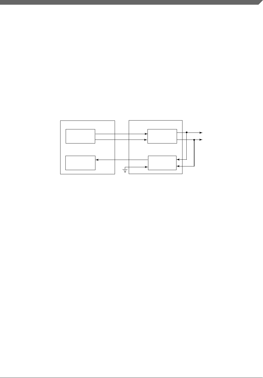
The transmitter's RTS_B signal asserts only when the transmitter is enabled. However,
the transmitter's RTS_B signal is unaffected by its CTS_B signal. RTS_B will remain
asserted until the transfer is completed, even if the transmitter is disabled mid-way
through a data transfer.
51.4.2.4 Transceiver driver enable using RTS_B
RS-485 is a multiple drop communication protocol in which the LPUART transceiver's
driver is 3-stated unless the LPUART is driving. The RTS_B signal can be used by the
transmitter to enable the driver of a transceiver. The polarity of RTS_B can be matched to
the polarity of the transceiver's driver enable signal.
TRANSMITTER
LPUART
RECEIVER
DRIVER
RS-485 TRANSCEIVER
RECEIVER
TXD
RTS_B
RXD
DI
DE
RO
RE_B
Y
Z
A
B
Figure 51-4. Transceiver driver enable using RTS_B
In the figure, the receiver enable signal is asserted. Another option for this connection is
to connect RTS_B to both DE and RE_B. The transceiver's receiver is disabled while
driving. A pullup can pull RXD to a non-floating value during this time. This option can
be refined further by operating the LPUART in single wire mode, freeing the RXD pin
for other uses.
51.4.3 Receiver functional description
In this section, the receiver block diagram is a guide for the overall receiver functional
description. Next, the data sampling technique used to reconstruct receiver data is
described in more detail. Finally, different variations of the receiver wakeup function are
explained.
The receiver input is inverted by setting STAT[RXINV]. The receiver is enabled by
setting the CTRL[RE] bit. Character frames consist of a start bit of logic 0, seven to ten
data bits (msb or lsb first), and one or two stop bits of logic 1. For information about 7-
bit, 9-bit or 10-bit data mode, refer to Data Modes. For the remainder of this discussion,
assume the LPUART is configured for normal 8-bit data mode.
Chapter 51 Low Power Universal Asynchronous Receiver/Transmitter (LPUART)
S32K1xx Series Reference Manual, Rev. 7, 04/2018
NXP Semiconductors 1569

After receiving the stop bit into the receive shifter, and provided the receive data register
is not already full, the data character is transferred to the receive data register and the
receive data register full (STAT[RDRF]) status flag is set. If [RDRF] was already set
indicating the receive data register (buffer) was already full, the overrun (OR) status flag
is set and the new data is lost. Because the LPUART receiver is double-buffered, the
program has one full character time after [RDRF] is set before the data in the receive data
buffer must be read to avoid a receiver overrun.
When a program detects that the receive data register is full (STAT[RDRF] = 1), it gets
the data from the receive data register by reading the DATA register. Refer to Interrupts
and status flags for details about flag clearing.
51.4.3.1 Data sampling technique
The LPUART receiver supports a configurable oversampling rate of between 4× and 32×
of the baud rate clock for sampling. The receiver starts by taking logic level samples at
the oversampling rate times the baud rate to search for a falling edge on the RXD serial
data input pin. A falling edge is defined as a logic 0 sample after three consecutive logic
1 samples. The oversampling baud rate clock divides the bit time into 4 to 32 segments
from 1 to OSR (where OSR is the configured oversampling ratio). When a falling edge is
located, three more samples are taken at (OSR/2), (OSR/2)+1, and (OSR/2)+2 to make
sure this was a real start bit and not merely noise. If at least two of these three samples
are 0, the receiver assumes it is synchronized to a received character. If another falling
edge is detected before the receiver is considered synchronized, the receiver restarts the
sampling from the first segment.
The receiver then samples each bit time, including the start and stop bits, at (OSR/2),
(OSR/2)+1, and (OSR/2)+2 to determine the logic level for that bit. The logic level is
interpreted to be that of the majority of the samples taken during the bit time. If any
sample in any bit time, including the start and stop bits, in a character frame fails to agree
with the logic level for that bit, the noise flag (STAT[NF]) is set when the received
character is transferred to the receive data buffer.
When the LPUART receiver is configured to sample on both edges of the baud rate
clock, the number of segments in each received bit is effectively doubled (from 1 to
OSR×2). The start and data bits are then sampled at OSR, OSR+1 and OSR+2. Sampling
on both edges of the clock must be enabled for oversampling rates of 4× to 7× and is
optional for higher oversampling rates.
Functional description
S32K1xx Series Reference Manual, Rev. 7, 04/2018
1570 NXP Semiconductors

The falling edge detection logic continuously looks for falling edges. If an edge is
detected, the sample clock is resynchronized to bit times (unless resynchronization has
been disabled). This improves the reliability of the receiver in the presence of noise or
mismatched baud rates. It does not improve worst case analysis because some characters
do not have any extra falling edges anywhere in the character frame.
In the case of a framing error, provided the received character was not a break character,
the sampling logic that searches for a falling edge is filled with three logic 1 samples so
that a new start bit can be detected almost immediately.
51.4.3.2 Receiver wakeup operation
Receiver wakeup and receiver address matching is a hardware mechanism that allows an
LPUART receiver to ignore the characters in a message intended for a different receiver.
During receiver wakeup, all receivers evaluate the first character(s) of each message, and
as soon as they determine the message is intended for a different receiver, they write
logic 1 to the receiver wake up control bit (CTRL[RWU]). When CTRL[RWU] and
STAT[RWUID] bit are set, the status flags associated with the receiver, with the
exception of the idle bit, STAT[IDLE], are inhibited from setting, thus eliminating the
software overhead for handling the unimportant message characters. At the end of a
message, or at the beginning of the next message, all receivers automatically force
CTRL[RWU] to 0 so all receivers wake up in time to look at the first character(s) of the
next message.
During receiver address matching, the address matching is performed in hardware and the
LPUART receiver will ignore all characters that do not meet the address match
requirements.
Table 51-3. Receiver Wakeup Options
RWU MA1 | MA2 MATCFG WAKE:RWUID Receiver Wakeup
0 0 X X Normal operation
1 0 00 00 Receiver wakeup on
idle line, IDLE flag not
set
1 0 00 01 Receiver wakeup on
idle line, IDLE flag set
1 0 00 10 Receiver wakeup on
address mark
1 1 11 10 Receiver wakeup on
data match
0 1 00 X0 Address mark address
match, IDLE flag not set
Table continues on the next page...
Chapter 51 Low Power Universal Asynchronous Receiver/Transmitter (LPUART)
S32K1xx Series Reference Manual, Rev. 7, 04/2018
NXP Semiconductors 1571

Table 51-3. Receiver Wakeup Options (continued)
RWU MA1 | MA2 MATCFG WAKE:RWUID Receiver Wakeup
for discarded
characters
0 1 00 X1 Address mark address
match, IDLE flag set for
discarded characters
0 1 01 X0 Idle line address match
0 1 10 X0 Address match on and
address match off,
IDLE flag not set for
discarded characters
0 1 10 X1 Address match on and
address match off,
IDLE flag set for
discarded characters
51.4.3.2.1 Idle-line wakeup
When wake is cleared, the receiver is configured for idle-line wakeup. In this mode,
CTRL[RWU] is cleared automatically when the receiver detects a full character time of
the idle-line level. The CTRL[M], CTRL[M7] and BAUD[M10] control bit selects 7-bit
to 10-bit data mode and the BAUD[SBNS] bit selects 1-bit or 2-bit stop bit number that
determines how many bit times of idle are needed to constitute a full character time, 9 to
13 bit times because of the start and stop bits.
When CTRL[RWU] is one and STAT[RWUID] is 0, the idle condition that wakes up the
receiver does not set the STAT[IDLE] flag. The receiver wakes up and waits for the first
data character of the next message that sets the STAT[RDRF] flag and generates an
interrupt if enabled. When STAT[RWUID] is 1, any idle condition sets the STAT[IDLE]
flag and generates an interrupt if enabled, regardless of whether CTRL[RWU] is 0 or 1.
The idle-line type (CTRL[ILT]) control bit selects one of two ways to detect an idle line.
When CTRL[ILT] is cleared, the idle bit counter starts after the start bit so the stop bit
and any logic 1s at the end of a character count toward the full character time of idle.
When CTRL[ILT] is set, the idle bit counter does not start until after the stop bit time, so
the idle detection is not affected by the data in the last character of the previous message.
51.4.3.2.2 Address-mark wakeup
When CTRL[WAKE] is set, the receiver is configured for address-mark wakeup. In this
mode, CTRL[RWU] is cleared automatically when the receiver detects a logic 1 in the
most significant bit of the received character. When parity is enabled, the second most
significant bit is used for address-mark wakeup.
Functional description
S32K1xx Series Reference Manual, Rev. 7, 04/2018
1572 NXP Semiconductors

Address-mark wakeup allows messages to contain idle characters, but requires one bit be
reserved for use in address frames. The logic 1 in the most significant bit (or second most
significant bit when parity is enabled) of an address frame clears the CTRL[RWU] bit
and sets the STAT[RDRF] flag. In this case, the character with the address-mark bit is
received even though the receiver was sleeping during most of this character time.
51.4.3.2.3 Data match wakeup
When CTRL[RWU] is set, CTRL[WAKE] is set and BAUD[MATCFG] equals 11, the
receiver is configured for data match wakeup. In this mode, CTRL[RWU] is cleared
automatically when the receiver detects a character that matches MATCH[MA1] field
when BAUD[MAEN1] is set, or that matches MATCH[MA2] when BAUD[MAEN2] is
set.
51.4.3.2.4 Address Match operation
Address match operation is enabled when the BAUD[MAEN1] or BAUD[MAEN2] bit is
set and BAUD[MATCFG] is equal to 00. In this function, a character received by the
RXD pin with a logic 1 in the most significant bit (or second most significant bit when
parity is enabled) is considered an address and is compared with the associated
MATCH[MA1] or MATCH[MA2] field. The character is only transferred to the receive
buffer, and STAT[RDRF] is set, if the comparison matches. All subsequent characters
received with a logic 0 in the most significant bit (or second most significant bit when
parity is enabled) are considered to be data associated with the address and are transferred
to the receive data buffer. If no marked address match occurs then no transfer is made to
the receive data buffer, and all following characters with logic zero in the most
significant bit (or second most significant bit when parity is enabled) are also discarded.
If both the BAUD[MAEN1] and BAUD[MAEN2] bits are negated, the receiver operates
normally and all data received is transferred to the receive data buffer.
Address match operation functions in the same way for both MATCH[MA1] and
MATCH[MA2] fields.
• If only one of BAUD[MAEN1] and BAUD[MAEN2] is asserted, a marked address
is compared only with the associated match register field and data is transferred to
the receive data buffer only on a match.
• If BAUD[MAEN1] and BAUD[MAEN2] are asserted, a marked address is compared
with both match registers and data is transferred only on a match with either of the
MATCH[MA1] or MATCH[MA2] fields.
Chapter 51 Low Power Universal Asynchronous Receiver/Transmitter (LPUART)
S32K1xx Series Reference Manual, Rev. 7, 04/2018
NXP Semiconductors 1573

51.4.3.2.5 Idle Match operation
Idle match operation is enabled when the BAUD[MAEN1] or BAUD[MAEN2] bit is set
and BAUD[MATCFG] is equal to 01. In this function, the first character received by the
RXD pin after an idle line condition is considered an address and is compared with the
associated MATCH[MA1] or MATCH[MA2] field. The character is only transferred to
the receive buffer, and STAT[RDRF] is set, if the comparison matches. All subsequent
characters are considered to be data associated with the address and are transferred to the
receive data buffer until the next idle line condition is detected. If no address match
occurs then no transfer is made to the receive data buffer, and all following frames until
the next idle condition are also discarded. If both the BAUD[MAEN1] and
BAUD[MAEN2] bits are negated, the receiver operates normally and all data received is
transferred to the receive data buffer.
Idle match operation functions in the same way for both MATCH[MA1] or
MATCH[MA2] fields.
• If only one of BAUD[MAEN1] and BAUD[MAEN2] is asserted, the first character
after an idle line is compared only with the associated match register and data is
transferred to the receive data buffer only on a match.
• If BAUD[MAEN1] and BAUD[MAEN2] are asserted, the first character after an idle
line is compared with both MATCH[MA1] or MATCH[MA2] fields and data is
transferred only on a match with either of the fields.
51.4.3.2.6 Match On Match Off operation
Match on, match off operation is enabled when both BAUD[MAEN1] and
BAUD[MAEN2] are set and BAUD[MATCFG] is equal to 10. In this function, a
character received by the RXD pin that matches MATCH[MA1] is received and
transferred to the receive buffer, and STAT[RDRF] is set. All subsequent characters are
considered to be data and are also transferred to the receive data buffer, until a character
is received that matches MATCH[MA2] field. The character that matches
MATCH[MA2] and all following characters are discarded; this continues until another
character that matches MATCH[MA1] is received. If both the BAUD[MAEN1] and
BAUD[MAEN2] bits are negated, the receiver operates normally and all data received is
transferred to the receive data buffer.
NOTE
Match on, match off operation requires both BAUD[MAEN1]
and BAUD[MAEN2] to be asserted.
Functional description
S32K1xx Series Reference Manual, Rev. 7, 04/2018
1574 NXP Semiconductors

51.4.3.3 Hardware flow control
To support hardware flow control, the receiver can be programmed to automatically
deassert and assert RTS_B.
• RTS_B remains asserted until the transfer is complete, even if the transmitter is
disabled midway through a data transfer. See Transceiver driver enable using RTS_B
for more details.
• If the receiver request-to-send functionality is enabled, the receiver automatically
deasserts RTS_B if the number of characters in the receiver data register is full or a
start bit is detected that will cause the receiver data register to be full.
• The receiver asserts RTS_B when the number of characters in the receiver data
register is not full and has not detected a start bit that will cause the receiver data
register to be full. It is not affected if STAT[RDRF] is asserted.
• Even if RTS_B is deasserted, the receiver continues to receive characters until the
receiver data buffer is overrun.
• If the receiver request-to-send functionality is disabled, the receiver RTS_B remains
deasserted.
51.4.3.4 Infrared decoder
The infrared decoder converts the received character from the IrDA format to the NRZ
format used by the receiver. It also has a OSR oversampling baud rate clock counter that
filters noise and indicates when a 1 is received.
51.4.3.4.1 Start bit detection
When STAT[RXINV] is cleared, the first falling edge of the received character
corresponds to the start bit. The infrared decoder resets its counter. At this time, the
receiver also begins its start bit detection process. After the start bit is detected, the
receiver synchronizes its bit times to this start bit time. For the rest of the character
reception, the infrared decoder's counter and the receiver's bit time counter count
independently from each other.
51.4.3.4.2 Noise filtering
Any further rising edges detected during the first half of the infrared decoder counter are
ignored by the decoder. Any pulses less than one oversampling baud clock can be
undetected by it regardless of whether it is seen in the first or second half of the count.
Chapter 51 Low Power Universal Asynchronous Receiver/Transmitter (LPUART)
S32K1xx Series Reference Manual, Rev. 7, 04/2018
NXP Semiconductors 1575

51.4.3.4.3 Low-bit detection
During the second half of the decoder count, a rising edge is decoded as a 0, which is sent
to the receiver. The decoder counter is also reset.
51.4.3.4.4 High-bit detection
At OSR oversampling baud rate clocks after the previous rising edge, if a rising edge is
not seen, then the decoder sends a 1 to the receiver.
If the next bit is a 0, which arrives late, then a low-bit is detected according to Low-bit
detection. The value sent to the receiver is changed from 1 to a 0. Then, if a noise pulse
occurs outside the receiver's bit time sampling period, then the delay of a 0 is not
recorded as noise.
51.4.4 Additional LPUART functions
The following sections describe additional LPUART functions.
51.4.4.1 Data Modes
The LPUART transmitter and receiver can be configured to operate in 7-bit data mode by
setting CTRL[M7], 9-bit data mode by setting the CTRL[M] or 10-bit data mode by
setting BAUD[M10]. In 9-bit mode, there is a ninth data bit and in 10-bit mode, there is a
tenth data bit. For the transmit data buffer, these bits are stored in CTRL[T8] and
CTRL[T9]. For the receiver, these bits are held in CTRL[R8] and CTRL[R9]. They are
also accessible via 16-bit or 32-bit accesses to the DATA register.
For coherent 8-bit writes to the transmit data buffer, write to CTRL[T8] and CTRL[T9]
before writing to DATA[7:0]. For 16-bit and 32-bit writes to the DATA register, all 10
transmit bits are written to the transmit data buffer at the same time.
If the bit values to be transmitted as the ninth and tenth bit of a new character are the
same as for the previous character, it is not necessary to write to CTRL[T8] and
CTRL[T9] again. When data is transferred from the transmit data buffer to the transmit
shifter, the value in CTRL[T8] and CTRL[T9] is copied at the same time data is
transferred from DATA[7:0] to the shifter.
The 9-bit data mode is typically used with parity to allow eight bits of data plus the parity
in the ninth bit, or it is used with address-mark wakeup so the ninth data bit can serve as
the wakeup bit. The 10-bit data mode is typically used with parity and address-mark
Functional description
S32K1xx Series Reference Manual, Rev. 7, 04/2018
1576 NXP Semiconductors

wakeup so the ninth data bit can serve as the wakeup bit and the tenth bit as the parity bit.
In custom protocols, the ninth and/or tenth bits can also serve as software-controlled
markers.
51.4.4.2 Idle length
An idle character is a character where the start bit, all data bits and stop bits are in the
mark position. The CTRL[ILT] bit can be configured to start detecting an idle character
from the previous start bit (any data bits and stop bits count towards the idle character
detection) or from the previous stop bit.
The number of idle characters that must be received before an idle line condition is
detected can also be configured using the CTRL[IDLECFG] field. This field configures
the number of idle characters that must be received before the STAT[IDLE] flag is set,
the STAT[RAF] flag is cleared and the DATA[IDLINE] flag is set with the next received
character.
Idle-line wakeup and idle match operation are also affected by the CTRL[IDLECFG]
field. When address match or match on/off operation is enabled, setting the
STAT[RWUID] bit will cause any discarded characters to be treated as if they were idle
characters.
51.4.4.3 Loop mode
When CTRL[LOOPS] is set, the CTRL[RSRC] bit chooses between loop mode
(CTRL[RSRC] = 0) or single-wire mode (CTRL[RSRC] = 1). Loop mode is sometimes
used to check software, independent of connections in the external system, to help isolate
system problems. In this mode, the transmitter output is internally connected to the
receiver input and the RXD pin is not used by the LPUART.
51.4.4.4 Single-wire operation
When CTRL[LOOPS] is set, the CTRL[RSRC] bit chooses between loop mode
(CTRL[RSRC] = 0) or single-wire mode (CTRL[RSRC] = 1). Single-wire mode
implements a half-duplex serial connection. The receiver is internally connected to the
transmitter output and to the TXD pin (the RXD pin is not used).
In single-wire mode, the CTRL[TXDIR] bit controls the direction of serial data on the
TXD pin. When CTRL[TXDIR] is cleared, the TXD pin is an input to the receiver and
the transmitter is temporarily disconnected from the TXD pin so an external device can
Chapter 51 Low Power Universal Asynchronous Receiver/Transmitter (LPUART)
S32K1xx Series Reference Manual, Rev. 7, 04/2018
NXP Semiconductors 1577

send serial data to the receiver. When CTRL[TXDIR] is set, the TXD pin is an output
driven by the transmitter, the internal loop back connection is disabled, and as a result the
receiver cannot receive characters that are sent out by the transmitter.
51.4.5 Infrared interface
The LPUART provides the capability of transmitting narrow pulses to an IR LED and
receiving narrow pulses and transforming them to serial bits, which are sent to the
LPUART. The IrDA physical layer specification defines a half-duplex infrared
communication link for exchanging data. The full standard includes data rates up to 16
Mbits/s. This module covers data rates only between 2.4 kbits/s and 115.2 kbits/s.
The LPUART has an infrared transmit encoder and receive decoder. The LPUART
transmits serial bits of data that are encoded by the infrared submodule to transmit a
narrow pulse for every zero bit. No pulse is transmitted for every one bit. When receiving
data, the IR pulses are detected using an IR photo diode and transformed to CMOS levels
by the IR receive decoder, external from the LPUART. The narrow pulses are then
stretched by the infrared receive decoder to get back to a serial bit stream to be received
by the LPUART. The polarity of transmitted pulses and expected receive pulses can be
inverted so that a direct connection can be made to external IrDA transceiver modules
that use active high pulses.
The infrared submodule receives its clock sources from the LPUART. One of these two
clocks are selected in the infrared submodule to generate either 1/OSR, 2/OSR, 3/OSR, or
4/OSR narrow pulses during transmission.
51.4.5.1 Infrared transmit encoder
The infrared transmit encoder converts serial bits of data from transmit shift register to
the TXD signal. A narrow pulse is transmitted for a 0 bit and no pulse for a 1 bit. The
narrow pulse is sent at the start of the bit with a duration of 1/OSR, 2/OSR, 3/OSR, or
4/OSR of a bit time. A narrow low pulse is transmitted for a 0 bit when CTRL[TXINV] is
cleared, while a narrow high pulse is transmitted for a 0 bit when CTRL[TXINV] is set.
51.4.5.2 Infrared receive decoder
The infrared receive block converts data from the RXD signal to the receive shift register.
A narrow pulse is expected for each 0 received and no pulse is expected for each 1
received. A narrow low pulse is expected for a 0 bit when STAT[RXINV] is cleared,
Functional description
S32K1xx Series Reference Manual, Rev. 7, 04/2018
1578 NXP Semiconductors

while a narrow high pulse is expected for a 0 bit when STAT[RXINV] is set. This receive
decoder meets the edge jitter requirement as defined by the IrDA serial infrared physical
layer specification.
51.4.6 Interrupts and status flags
The LPUART transmitter has two status flags that can optionally generate hardware
interrupt requests. Transmit data register empty STAT[TDRE]) indicates when there is
room in the transmit data buffer to write another transmit character to the DATA register.
If the transmit interrupt enable CTRL[TIE]) bit is set, a hardware interrupt is requested
when STAT[TDRE] is set. Transmit complete (STAT[TC]) indicates that the transmitter
is finished transmitting all data, preamble, and break characters and is idle with TXD at
the inactive level. This flag is often used in systems with modems to determine when it is
safe to turn off the modem. If the transmit complete interrupt enable (CTRL[TCIE]) bit is
set, a hardware interrupt is requested when STAT[TC] is set. Instead of hardware
interrupts, software polling may be used to monitor the STAT[TDRE] and STAT[TC]
status flags if the corresponding CTRL[TIE] or CTRL[TCIE] local interrupt masks are
cleared.
When a program detects that the receive data register is full (STAT[RDRF] = 1), it gets
the data from the receive data register by reading the DATA register. The STAT[RDRF]
flag is cleared by reading the DATA register.
The IDLE status flag includes logic that prevents it from getting set repeatedly when the
RXD line remains idle for an extended period of time. IDLE is cleared by writing 1 to the
STAT[IDLE] flag. After STAT[IDLE] has been cleared, it cannot become set again until
the receiver has received at least one new character and has set STAT[RDRF].
If the associated error was detected in the received character that caused STAT[RDRF] to
be set, the error flags - noise flag (STAT[NF]), framing error (STAT[FE]), and parity
error flag (STAT[PF]) - are set at the same time as STAT[RDRF]. These flags are not set
in overrun cases.
If STAT[RDRF] was already set when a new character is ready to be transferred from the
receive shifter to the receive data buffer, the overrun (STAT[OR]) flag is set instead of
the data along with any associated NF, FE, or PF condition is lost.
If the received character matches the contents of MATCH[MA1] and/or MATCH[MA2]
then the STAT[MA1F] and/or STAT[MA2F] flags are set at the same time that
STAT[RDRF] is set.
Chapter 51 Low Power Universal Asynchronous Receiver/Transmitter (LPUART)
S32K1xx Series Reference Manual, Rev. 7, 04/2018
NXP Semiconductors 1579

At any time, an active edge on the RXD serial data input pin causes the
STAT[RXEDGIF] flag to set. The STAT[RXEDGIF] flag is cleared by writing a 1 to it.
This function depends on the receiver being enabled (CTRL[RE] = 1).
51.4.7 Peripheral Triggers
The connection of the LPUART peripheral triggers with other peripherals are device
specific.
51.4.7.1 Output Triggers
The LPUART generates three output triggers that can be connected to other peripherals
on the device.
• The transmit word trigger asserts at the end of each transmitted word, it negates after
one bit period.
• The receive word trigger asserts at the end of each received word that is written to
the receive FIFO, for one oversampling clock period.
• The receive idle trigger asserts at when the idle flag would set, for one oversampling
clock period.
51.4.7.2 Input Trigger
The LPUART supports one peripheral input trigger, that can be configured in one of the
following ways.
• The input trigger can be connected in place of the CTS_B pin input. The input trigger
must assert for longer than one bit clock period when the transmitter is idle with data
to send to guarantee a new transmission.
• The input trigger can modulate the transmit data output (trigger is logically ANDed
with the TXD output). The input trigger is expected to be generated from a PWM
source with a period that is less than the bit clock frequency.
• The input trigger can be connected in place of the RXD pin input. The input trigger is
expected to be generated from a receive data source, such as analog comparator or
external pin.
Functional description
S32K1xx Series Reference Manual, Rev. 7, 04/2018
1580 NXP Semiconductors

Chapter 52
Flexible I/O (FlexIO)
Chip-specific FlexIO information
52.1.1 FlexIO Configuration
Table 52-1. FlexIO Configuration
Timers Shifters Pins
Number 4 4 8
Low leakage and Wait mode is not supported in this device. See Module operation in
available low power modes for details on available power modes.
NOTE
Accessing FlexIO registers with FlexIO peripheral clock
(FlexIO clock) disabled will result in transfer error or stall the
bus.
52.2 Introduction
52.2.1 Overview
The FlexIO is a highly configurable module providing a wide range of functionality
including:
• Emulation of a variety of serial communication protocols
• Flexible 16-bit timers with support for a variety of trigger, reset, enable and disable
conditions
52.1
S32K1xx Series Reference Manual, Rev. 7, 04/2018
NXP Semiconductors 1581

52.2.2 Features
The FlexIO module is capable of supporting a wide range of protocols including, but not
limited to:
• UART
• I2C
• SPI
• I2S
• PWM/Waveform generation
The following key features are provided:
• Array of 32-bit shift registers with transmit, receive and data match modes
• Double buffered shifter operation for continuous data transfer
• Shifter concatenation to support large transfer sizes
• Automatic start/stop bit generation
• Interrupt, DMA or polled transmit/receive operation
• Programmable baud rates independent of bus clock frequency, with support for
asynchronous operation during stop modes
• Highly flexible 16-bit timers with support for a variety of internal or external trigger,
reset, enable and disable conditions
52.2.3 Block Diagram
The following diagram gives a high-level overview of the configuration of FlexIO timers
and shifters.
Introduction
S32K1xx Series Reference Manual, Rev. 7, 04/2018
1582 NXP Semiconductors
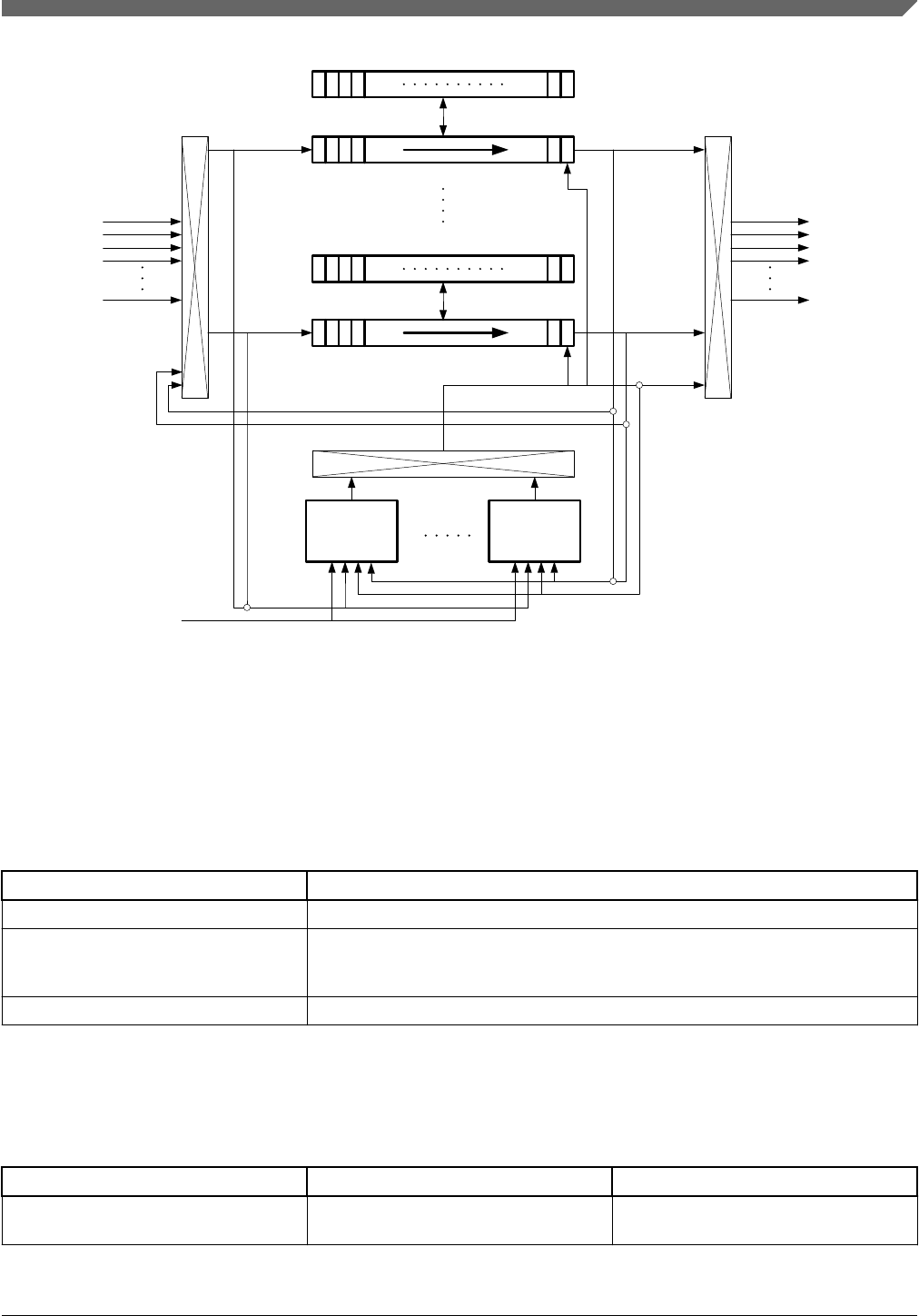
31 0SHIFTBUF0
SHIFTER0
31 0
SHIFTBUFi
SHIFTERi
FXIO_Dn
out/outen
FXIO_Dn
in
TIMER0 TIMERi
External Triggers
Input
Selection
Output
Selection
Timer
Selection
Figure 52-1. FlexIO block diagram
52.2.4 Modes of operation
The FlexIO module supports the chip modes described in the following table.
Table 52-2. Chip modes supported by the FlexIO module
Chip mode FlexIO Operation
Run Normal operation
Stop Can continue operating provided the Doze Enable bit (CTRL[DOZEN]) is clear and
the FlexIO is using an external or internal clock source which remains operating
during stop modes.
Debug Can continue operating provided the Debug Enable bit (CTRL[DBGE]) is set.
52.2.5 FlexIO Signal Descriptions
Signal Description I/O
FXIO_Dn (n=0...7) Bidirectional FlexIO Shifter and Timer
pin inputs/outputs
I/O
Chapter 52 Flexible I/O (FlexIO)
S32K1xx Series Reference Manual, Rev. 7, 04/2018
NXP Semiconductors 1583

Memory Map and Registers
52.3.1 FLEXIO register descriptions
NOTE
An invalid register access will result in a bus error. This
includes reading a write-only register, writing a read-only
register or accessing an invalid address.
52.3.1.1 FLEXIO Memory map
FlexIO base address: 4005_A000h
Offset Register Width
(In bits)
Access Reset value
0h Version ID Register (VERID) 32 RO 0101_0000h
4h Parameter Register (PARAM) 32 RO 0408_0404h
8h FlexIO Control Register (CTRL) 32 RW 0000_0000h
Ch Pin State Register (PIN) 32 RO 0000_0000h
10h Shifter Status Register (SHIFTSTAT) 32 W1C 0000_0000h
14h Shifter Error Register (SHIFTERR) 32 W1C 0000_0000h
18h Timer Status Register (TIMSTAT) 32 W1C 0000_0000h
20h Shifter Status Interrupt Enable (SHIFTSIEN) 32 RW 0000_0000h
24h Shifter Error Interrupt Enable (SHIFTEIEN) 32 RW 0000_0000h
28h Timer Interrupt Enable Register (TIMIEN) 32 RW 0000_0000h
30h Shifter Status DMA Enable (SHIFTSDEN) 32 RW 0000_0000h
80h - 8Ch Shifter Control N Register (SHIFTCTL0 - SHIFTCTL3) 32 RW 0000_0000h
100h - 10Ch Shifter Configuration N Register (SHIFTCFG0 - SHIFTCFG3) 32 RW 0000_0000h
200h - 20Ch Shifter Buffer N Register (SHIFTBUF0 - SHIFTBUF3) 32 RW 0000_0000h
280h - 28Ch Shifter Buffer N Bit Swapped Register (SHIFTBUFBIS0 - SHIFTBUF
BIS3)
32 RW 0000_0000h
300h - 30Ch Shifter Buffer N Byte Swapped Register (SHIFTBUFBYS0 - SHIF
TBUFBYS3)
32 RW 0000_0000h
380h - 38Ch Shifter Buffer N Bit Byte Swapped Register (SHIFTBUFBBS0 - SHIF
TBUFBBS3)
32 RW 0000_0000h
400h - 40Ch Timer Control N Register (TIMCTL0 - TIMCTL3) 32 RW 0000_0000h
480h - 48Ch Timer Configuration N Register (TIMCFG0 - TIMCFG3) 32 RW 0000_0000h
Table continues on the next page...
52.3
Memory Map and Registers
S32K1xx Series Reference Manual, Rev. 7, 04/2018
1584 NXP Semiconductors

Offset Register Width
(In bits)
Access Reset value
500h - 50Ch Timer Compare N Register (TIMCMP0 - TIMCMP3) 32 RW 0000_0000h
52.3.1.2 Version ID Register (VERID)
52.3.1.2.1 Offset
Register Offset
VERID 0h
52.3.1.2.2 Diagram
Bits 31 30 29 28 27 26 25 24 23 22 21 20 19 18 17 16
RMAJOR MINOR
W
Reset 0 0 0 0 0 0 0 1 0 0 0 0 0 0 0 1
Bits 15 14 13 12 11 10 9 8 7 6 5 4 3 2 1 0
RFEATURE
W
Reset 0 0 0 0 0 0 0 0 0 0 0 0 0 0 0 0
52.3.1.2.3 Fields
Field Function
31-24
MAJOR
Major Version Number
This read only field returns the major version number for the module specification.
23-16
MINOR
Minor Version Number
This read only field returns the minor version number for the module specification.
15-0
FEATURE
Feature Specification Number
This read only field returns the feature set number.
0000000000000000b - Standard features implemented.
0000000000000001b - Supports state, logic and parallel modes.
Chapter 52 Flexible I/O (FlexIO)
S32K1xx Series Reference Manual, Rev. 7, 04/2018
NXP Semiconductors 1585

52.3.1.3 Parameter Register (PARAM)
52.3.1.3.1 Offset
Register Offset
PARAM 4h
52.3.1.3.2 Diagram
Bits 31 30 29 28 27 26 25 24 23 22 21 20 19 18 17 16
RTRIGGER PIN
W
Reset 0 0 0 0 0 1 0 0 0 0 0 0 1 0 0 0
Bits 15 14 13 12 11 10 9 8 7 6 5 4 3 2 1 0
RTIMER SHIFTER
W
Reset 0 0 0 0 0 1 0 0 0 0 0 0 0 1 0 0
52.3.1.3.3 Fields
Field Function
31-24
TRIGGER
Trigger Number
Number of external triggers implemented.
23-16
PIN
Pin Number
Number of Pins implemented.
15-8
TIMER
Timer Number
Number of Timers implemented.
7-0
SHIFTER
Shifter Number
Number of Shifters implemented.
52.3.1.4 FlexIO Control Register (CTRL)
Memory Map and Registers
S32K1xx Series Reference Manual, Rev. 7, 04/2018
1586 NXP Semiconductors

52.3.1.4.1 Offset
Register Offset
CTRL 8h
52.3.1.4.2 Diagram
Bits 31 30 29 28 27 26 25 24 23 22 21 20 19 18 17 16
R
DOZEN
DBG
E
0
W
Reset 0 0 0 0 0 0 0 0 0 0 0 0 0 0 0 0
Bits 15 14 13 12 11 10 9 8 7 6 5 4 3 2 1 0
R
0
FASTACC
SWRS
T
FLEXE
N
W
Reset 0 0 0 0 0 0 0 0 0 0 0 0 0 0 0 0
52.3.1.4.3 Fields
Field Function
31
DOZEN
Doze Enable
Disables FlexIO operation in Doze modes.
0b - FlexIO enabled in Doze modes.
1b - FlexIO disabled in Doze modes.
30
DBGE
Debug Enable
Enables FlexIO operation in Debug mode.
0b - FlexIO is disabled in debug modes.
1b - FlexIO is enabled in debug modes
29-3
—
Reserved.
2
FASTACC
Fast Access
Enables fast register accesses to FlexIO registers, but requires the FlexIO functional clock to be at least
twice the frequency of the bus clock.
0b - Configures for normal register accesses to FlexIO
1b - Configures for fast register accesses to FlexIO
1
SWRST
Software Reset
The FlexIO Control Register is not affected by the software reset, all other logic in the FlexIO is affected
by the software reset and register accesses are ignored until this bit is cleared. This register bit will
remain set until cleared by software, and the reset has cleared in the FlexIO clock domain.
0b - Software reset is disabled
1b - Software reset is enabled, all FlexIO registers except the Control Register are reset.
Table continues on the next page...
Chapter 52 Flexible I/O (FlexIO)
S32K1xx Series Reference Manual, Rev. 7, 04/2018
NXP Semiconductors 1587

Field Function
0
FLEXEN
FlexIO Enable
0b - FlexIO module is disabled.
1b - FlexIO module is enabled.
52.3.1.5 Pin State Register (PIN)
52.3.1.5.1 Offset
Register Offset
PIN Ch
52.3.1.5.2 Diagram
Bits 31 30 29 28 27 26 25 24 23 22 21 20 19 18 17 16
R 0
W
Reset 0 0 0 0 0 0 0 0 0 0 0 0 0 0 0 0
Bits 15 14 13 12 11 10 9 8 7 6 5 4 3 2 1 0
R 0 PDI
W
Reset 0 0 0 0 0 0 0 0 0 0 0 0 0 0 0 0
52.3.1.5.3 Fields
Field Function
31-8
—
Reserved.
7-0
PDI
Pin Data Input
Returns the input data on each of the FlexIO pins.
52.3.1.6 Shifter Status Register (SHIFTSTAT)
Memory Map and Registers
S32K1xx Series Reference Manual, Rev. 7, 04/2018
1588 NXP Semiconductors

52.3.1.6.1 Offset
Register Offset
SHIFTSTAT 10h
52.3.1.6.2 Diagram
Bits 31 30 29 28 27 26 25 24 23 22 21 20 19 18 17 16
R 0
W
Reset 0 0 0 0 0 0 0 0 0 0 0 0 0 0 0 0
Bits 15 14 13 12 11 10 9 8 7 6 5 4 3 2 1 0
R 0 SSF
W W1C
Reset 0 0 0 0 0 0 0 0 0 0 0 0 0 0 0 0
52.3.1.6.3 Fields
Field Function
31-4
—
Reserved.
3-0
SSF
Shifter Status Flag
The shifter status flag is updated when one of the following events occurs:
For SMOD=Receive, the status flag is set when SHIFTBUF has been loaded with data from Shifter
(SHIFTBUF is full), and the status flag is cleared when SHIFTBUF register is read.
For SMOD=Transmit, the status flag is set when SHIFTBUF data has been transferred to the Shifter
(SHIFTBUF is empty) or when initially configured for SMOD=Transmit, and the status flag is cleared
when the SHIFTBUF register is written.
For SMOD=Match Store, the status flag is set when a match has occured between SHIFTBUF and
Shifter, and the status flag is cleared when the SHIFTBUF register is read.
For SMOD=Match Continuous, returns the current match result between the SHIFTBUF and Shifter.
The status flag can also be cleared by writing a logic one to the flag for all modes except Match
Continuous.
0b - Status flag is clear.
1b - Status flag is set.
52.3.1.7 Shifter Error Register (SHIFTERR)
Chapter 52 Flexible I/O (FlexIO)
S32K1xx Series Reference Manual, Rev. 7, 04/2018
NXP Semiconductors 1589

52.3.1.7.1 Offset
Register Offset
SHIFTERR 14h
52.3.1.7.2 Diagram
Bits 31 30 29 28 27 26 25 24 23 22 21 20 19 18 17 16
R 0
W
Reset 0 0 0 0 0 0 0 0 0 0 0 0 0 0 0 0
Bits 15 14 13 12 11 10 9 8 7 6 5 4 3 2 1 0
R 0 SEF
W W1C
Reset 0 0 0 0 0 0 0 0 0 0 0 0 0 0 0 0
52.3.1.7.3 Fields
Field Function
31-4
—
Reserved.
3-0
SEF
Shifter Error Flags
The shifter error flag is set when one of the following events occurs:
For SMOD=Receive, indicates Shifter was ready to store new data into SHIFTBUF before the previous
data was read from SHIFTBUF (SHIFTBUF Overrun), or indicates that the received start or stop bit does
not match the expected value.
For SMOD=Transmit, indicates Shifter was ready to load new data from SHIFTBUF before new data had
been written into SHIFTBUF (SHIFTBUF Underrun).
For SMOD=Match Store, indicates a match event occured before the previous match data was read from
SHIFTBUF (SHIFTBUF Overrun).
For SMOD=Match Continuous, the error flag is set when a match has occured between SHIFTBUF and
Shifter.
Can be cleared by writing logic one to the flag. For SMOD=Match Continuous, can also be cleared when
the SHIFTBUF register is read.
0b - Shifter Error Flag is clear.
1b - Shifter Error Flag is set.
Memory Map and Registers
S32K1xx Series Reference Manual, Rev. 7, 04/2018
1590 NXP Semiconductors

52.3.1.8 Timer Status Register (TIMSTAT)
52.3.1.8.1 Offset
Register Offset
TIMSTAT 18h
52.3.1.8.2 Diagram
Bits 31 30 29 28 27 26 25 24 23 22 21 20 19 18 17 16
R 0
W
Reset 0 0 0 0 0 0 0 0 0 0 0 0 0 0 0 0
Bits 15 14 13 12 11 10 9 8 7 6 5 4 3 2 1 0
R 0 TSF
W W1C
Reset 0 0 0 0 0 0 0 0 0 0 0 0 0 0 0 0
52.3.1.8.3 Fields
Field Function
31-4
—
Reserved.
3-0
TSF
Timer Status Flags
The timer status flag sets depending on the timer mode, and can be cleared by writing logic one to the
flag.
In 8-bit baud counter mode, the timer status flag is set when the upper 8-bit counter equals zero and
decrements.
In 8-bit high PWM mode, the timer status flag is set when the upper 8-bit counter equals zero and
decrements.
In 16-bit counter mode, the timer status flag is set when the 16-bit counter equals zero and decrements.
0b - Timer Status Flag is clear.
1b - Timer Status Flag is set.
52.3.1.9 Shifter Status Interrupt Enable (SHIFTSIEN)
Chapter 52 Flexible I/O (FlexIO)
S32K1xx Series Reference Manual, Rev. 7, 04/2018
NXP Semiconductors 1591

52.3.1.9.1 Offset
Register Offset
SHIFTSIEN 20h
52.3.1.9.2 Diagram
Bits 31 30 29 28 27 26 25 24 23 22 21 20 19 18 17 16
R 0
W
Reset 0 0 0 0 0 0 0 0 0 0 0 0 0 0 0 0
Bits 15 14 13 12 11 10 9 8 7 6 5 4 3 2 1 0
R 0 SSIE
W
Reset 0 0 0 0 0 0 0 0 0 0 0 0 0 0 0 0
52.3.1.9.3 Fields
Field Function
31-4
—
Reserved.
3-0
SSIE
Shifter Status Interrupt Enable
Enables interrupt generation when corresponding SSF is set.
0b - Shifter Status Flag interrupt disabled.
1b - Shifter Status Flag interrupt enabled.
52.3.1.10 Shifter Error Interrupt Enable (SHIFTEIEN)
52.3.1.10.1 Offset
Register Offset
SHIFTEIEN 24h
Memory Map and Registers
S32K1xx Series Reference Manual, Rev. 7, 04/2018
1592 NXP Semiconductors

52.3.1.10.2 Diagram
Bits 31 30 29 28 27 26 25 24 23 22 21 20 19 18 17 16
R 0
W
Reset 0 0 0 0 0 0 0 0 0 0 0 0 0 0 0 0
Bits 15 14 13 12 11 10 9 8 7 6 5 4 3 2 1 0
R 0 SEIE
W
Reset 0 0 0 0 0 0 0 0 0 0 0 0 0 0 0 0
52.3.1.10.3 Fields
Field Function
31-4
—
Reserved.
3-0
SEIE
Shifter Error Interrupt Enable
Enables interrupt generation when corresponding SEF is set.
0b - Shifter Error Flag interrupt disabled.
1b - Shifter Error Flag interrupt enabled.
52.3.1.11 Timer Interrupt Enable Register (TIMIEN)
52.3.1.11.1 Offset
Register Offset
TIMIEN 28h
Chapter 52 Flexible I/O (FlexIO)
S32K1xx Series Reference Manual, Rev. 7, 04/2018
NXP Semiconductors 1593

52.3.1.11.2 Diagram
Bits 31 30 29 28 27 26 25 24 23 22 21 20 19 18 17 16
R 0
W
Reset 0 0 0 0 0 0 0 0 0 0 0 0 0 0 0 0
Bits 15 14 13 12 11 10 9 8 7 6 5 4 3 2 1 0
R 0 TEIE
W
Reset 0 0 0 0 0 0 0 0 0 0 0 0 0 0 0 0
52.3.1.11.3 Fields
Field Function
31-4
—
Reserved.
3-0
TEIE
Timer Status Interrupt Enable
Enables interrupt generation when corresponding TSF is set.
0b - Timer Status Flag interrupt is disabled.
1b - Timer Status Flag interrupt is enabled.
52.3.1.12 Shifter Status DMA Enable (SHIFTSDEN)
52.3.1.12.1 Offset
Register Offset
SHIFTSDEN 30h
Memory Map and Registers
S32K1xx Series Reference Manual, Rev. 7, 04/2018
1594 NXP Semiconductors

52.3.1.12.2 Diagram
Bits 31 30 29 28 27 26 25 24 23 22 21 20 19 18 17 16
R 0
W
Reset 0 0 0 0 0 0 0 0 0 0 0 0 0 0 0 0
Bits 15 14 13 12 11 10 9 8 7 6 5 4 3 2 1 0
R 0 SSDE
W
Reset 0 0 0 0 0 0 0 0 0 0 0 0 0 0 0 0
52.3.1.12.3 Fields
Field Function
31-4
—
Reserved.
3-0
SSDE
Shifter Status DMA Enable
Enables DMA request generation when corresponding SSF is set.
0b - Shifter Status Flag DMA request is disabled.
1b - Shifter Status Flag DMA request is enabled.
52.3.1.13 Shifter Control N Register (SHIFTCTL0 - SHIFTCTL3)
52.3.1.13.1 Offset
For a = 0 to 3:
Register Offset
SHIFTCTLa 80h + (a × 4h)
Chapter 52 Flexible I/O (FlexIO)
S32K1xx Series Reference Manual, Rev. 7, 04/2018
NXP Semiconductors 1595

52.3.1.13.2 Diagram
Bits 31 30 29 28 27 26 25 24 23 22 21 20 19 18 17 16
R
0
TIMSEL
TIMPOL
0
PINCFG
W
Reset 0 0 0 0 0 0 0 0 0 0 0 0 0 0 0 0
Bits 15 14 13 12 11 10 9 8 7 6 5 4 3 2 1 0
R
0
PINSE
L
PINPOL
0
SMOD
W
Reset 0 0 0 0 0 0 0 0 0 0 0 0 0 0 0 0
52.3.1.13.3 Fields
Field Function
31-26
—
Reserved.
25-24
TIMSEL
Timer Select
Selects which Timer is used for controlling the logic/shift register and generating the Shift clock.
TIMSEL=i will select TIMERi.
23
TIMPOL
Timer Polarity
0b - Shift on posedge of Shift clock
1b - Shift on negedge of Shift clock
22-18
—
Reserved.
17-16
PINCFG
Shifter Pin Configuration
For pins configured as an output (PINCFG=11), this field will take effect when the register is written.
00b - Shifter pin output disabled
01b - Shifter pin open drain or bidirectional output enable
10b - Shifter pin bidirectional output data
11b - Shifter pin output
15-11
—
Reserved.
10-8
PINSEL
Shifter Pin Select
Selects which pin is used by the Shifter input or output. PINSEL=i will select the FXIO_Di pin. For pins
configured as an output (PINCFG=11), this field will take effect when the register is written.
7
PINPOL
Shifter Pin Polarity
For pins configured as an output (PINCFG=11), this field will take effect when the register is written.
0b - Pin is active high
1b - Pin is active low
6-3
—
Reserved.
Table continues on the next page...
Memory Map and Registers
S32K1xx Series Reference Manual, Rev. 7, 04/2018
1596 NXP Semiconductors

Field Function
2-0
SMOD
Shifter Mode
Configures the mode of the Shifter.
000b - Disabled.
001b - Receive mode. Captures the current Shifter content into the SHIFTBUF on expiration of the
Timer.
010b - Transmit mode. Load SHIFTBUF contents into the Shifter on expiration of the Timer.
011b - Reserved.
100b - Match Store mode. Shifter data is compared to SHIFTBUF content on expiration of the
Timer.
101b - Match Continuous mode. Shifter data is continuously compared to SHIFTBUF contents.
110b - Reserved.
111b - Reserved.
52.3.1.14 Shifter Configuration N Register (SHIFTCFG0 - SHIFTCFG3)
52.3.1.14.1 Offset
For a = 0 to 3:
Register Offset
SHIFTCFGa 100h + (a × 4h)
52.3.1.14.2 Diagram
Bits 31 30 29 28 27 26 25 24 23 22 21 20 19 18 17 16
R 0 0
W
Reset 0 0 0 0 0 0 0 0 0 0 0 0 0 0 0 0
Bits 15 14 13 12 11 10 9 8 7 6 5 4 3 2 1 0
R
0
0
INSRC
0
0
SSTO
P
0
SSTAR
T
W
Reset 0 0 0 0 0 0 0 0 0 0 0 0 0 0 0 0
52.3.1.14.3 Fields
Field Function
31-19 Reserved.
Table continues on the next page...
Chapter 52 Flexible I/O (FlexIO)
S32K1xx Series Reference Manual, Rev. 7, 04/2018
NXP Semiconductors 1597

Field Function
—
18-16
—
Reserved.
15-10
—
Reserved.
9
—
Reserved.
8
INSRC
Input Source
Selects the input source for the shifter. Configuring INSRC=1 is not supported for the last shifter.
0b - Pin
1b - Shifter N+1 Output
7
—
Reserved.
6
—
Reserved.
5-4
SSTOP
Shifter Stop bit
For SMOD=Transmit, this field allows automatic stop bit insertion if the selected timer has also enabled a
stop bit.
For SMOD=Receive or Match Store, this field allows automatic stop bit checking if the selected timer has
also enabled a stop bit.
00b - Stop bit disabled for transmitter/receiver/match store
01b - Reserved for transmitter/receiver/match store
10b - Transmitter outputs stop bit value 0 on store, receiver/match store sets error flag if stop bit is
not 0
11b - Transmitter outputs stop bit value 1 on store, receiver/match store sets error flag if stop bit is
not 1
3-2
—
Reserved.
1-0
SSTART
Shifter Start bit
For SMOD=Transmit, this field allows automatic start bit insertion if the selected timer has also enabled a
start bit.
For SMOD=Receive or Match Store, this field allows automatic start bit checking if the selected timer has
also enabled a start bit.
00b - Start bit disabled for transmitter/receiver/match store, transmitter loads data on enable
01b - Start bit disabled for transmitter/receiver/match store, transmitter loads data on first shift
10b - Transmitter outputs start bit value 0 before loading data on first shift, receiver/match store
sets error flag if start bit is not 0
11b - Transmitter outputs start bit value 1 before loading data on first shift, receiver/match store
sets error flag if start bit is not 1
52.3.1.15 Shifter Buffer N Register (SHIFTBUF0 - SHIFTBUF3)
Memory Map and Registers
S32K1xx Series Reference Manual, Rev. 7, 04/2018
1598 NXP Semiconductors

52.3.1.15.1 Offset
For a = 0 to 3:
Register Offset
SHIFTBUFa 200h + (a × 4h)
52.3.1.15.2 Diagram
Bits 31 30 29 28 27 26 25 24 23 22 21 20 19 18 17 16
RSHIFTBUF
W
Reset 0 0 0 0 0 0 0 0 0 0 0 0 0 0 0 0
Bits 15 14 13 12 11 10 9 8 7 6 5 4 3 2 1 0
RSHIFTBUF
W
Reset 0 0 0 0 0 0 0 0 0 0 0 0 0 0 0 0
52.3.1.15.3 Fields
Field Function
31-0
SHIFTBUF
Shift Buffer
Shift buffer data is used for a variety of functions depending on the SMOD setting:
For SMOD=Receive, Shifter data is transferred into SHIFTBUF at the expiration of Timer. The SHIFTBUF
register should only be read when the corresponding shifter status flag is set, indicating new Shifter data
is available.
For SMOD=Transmit, SHIFTBUF data is transferred into the Shifter before the Timer begins.
For SMOD=Match Store, SHIFTBUF[31:16] contains the data to be matched with the Shifter contents and
SHIFTBUF[15:0] can be used to mask the match result (1=mask, 0=no mask). The Match is checked
when the Timer expires and Shifter data [31:16] is written to SHIFTBUF[31:16] whenever a match event
occurs. The SHIFTBUF register should only be read when the corresponding shifter status flag is set,
indicating new Shifter data is available.
For SMOD=Match Continuous, SHIFTBUF[31:16] contains the data to be matched with the Shifter
contents and SHIFTBUF[15:0] can be used to mask the match result (1=mask, 0=no mask).
52.3.1.16 Shifter Buffer N Bit Swapped Register (SHIFTBUFBIS0 -
SHIFTBUFBIS3)
Chapter 52 Flexible I/O (FlexIO)
S32K1xx Series Reference Manual, Rev. 7, 04/2018
NXP Semiconductors 1599

52.3.1.16.1 Offset
For a = 0 to 3:
Register Offset
SHIFTBUFBISa 280h + (a × 4h)
52.3.1.16.2 Diagram
Bits 31 30 29 28 27 26 25 24 23 22 21 20 19 18 17 16
RSHIFTBUFBIS
W
Reset 0 0 0 0 0 0 0 0 0 0 0 0 0 0 0 0
Bits 15 14 13 12 11 10 9 8 7 6 5 4 3 2 1 0
RSHIFTBUFBIS
W
Reset 0 0 0 0 0 0 0 0 0 0 0 0 0 0 0 0
52.3.1.16.3 Fields
Field Function
31-0
SHIFTBUFBIS
Shift Buffer
Alias to SHIFTBUF register, except reads/writes to this register are bit swapped. Reads return
SHIFTBUF[0:31].
52.3.1.17 Shifter Buffer N Byte Swapped Register (SHIFTBUFBYS0 -
SHIFTBUFBYS3)
52.3.1.17.1 Offset
For a = 0 to 3:
Register Offset
SHIFTBUFBYSa 300h + (a × 4h)
Memory Map and Registers
S32K1xx Series Reference Manual, Rev. 7, 04/2018
1600 NXP Semiconductors

52.3.1.17.2 Diagram
Bits 31 30 29 28 27 26 25 24 23 22 21 20 19 18 17 16
RSHIFTBUFBYS
W
Reset 0 0 0 0 0 0 0 0 0 0 0 0 0 0 0 0
Bits 15 14 13 12 11 10 9 8 7 6 5 4 3 2 1 0
RSHIFTBUFBYS
W
Reset 0 0 0 0 0 0 0 0 0 0 0 0 0 0 0 0
52.3.1.17.3 Fields
Field Function
31-0
SHIFTBUFBYS
Shift Buffer
Alias to SHIFTBUF register, except reads/writes to this register are byte swapped. Reads return
{ SHIFTBUF[7:0], SHIFTBUF[15:8], SHIFTBUF[23:16], SHIFTBUF[31:24] }.
52.3.1.18 Shifter Buffer N Bit Byte Swapped Register (SHIFTBUF
BBS0 - SHIFTBUFBBS3)
52.3.1.18.1 Offset
For a = 0 to 3:
Register Offset
SHIFTBUFBBSa 380h + (a × 4h)
Chapter 52 Flexible I/O (FlexIO)
S32K1xx Series Reference Manual, Rev. 7, 04/2018
NXP Semiconductors 1601

52.3.1.18.2 Diagram
Bits 31 30 29 28 27 26 25 24 23 22 21 20 19 18 17 16
RSHIFTBUFBBS
W
Reset 0 0 0 0 0 0 0 0 0 0 0 0 0 0 0 0
Bits 15 14 13 12 11 10 9 8 7 6 5 4 3 2 1 0
RSHIFTBUFBBS
W
Reset 0 0 0 0 0 0 0 0 0 0 0 0 0 0 0 0
52.3.1.18.3 Fields
Field Function
31-0
SHIFTBUFBBS
Shift Buffer
Alias to SHIFTBUF register, except reads/writes to this register are bit swapped within each byte. Reads
return { SHIFTBUF[24:31], SHIFTBUF[16:23], SHIFTBUF[8:15], SHIFTBUF[0:7] }.
52.3.1.19 Timer Control N Register (TIMCTL0 - TIMCTL3)
52.3.1.19.1 Offset
For a = 0 to 3:
Register Offset
TIMCTLa 400h + (a × 4h)
Memory Map and Registers
S32K1xx Series Reference Manual, Rev. 7, 04/2018
1602 NXP Semiconductors

52.3.1.19.2 Diagram
Bits 31 30 29 28 27 26 25 24 23 22 21 20 19 18 17 16
R
0
TRGSE
L
TRGPOL
TRGSR
C
0
PINCFG
W
Reset 0 0 0 0 0 0 0 0 0 0 0 0 0 0 0 0
Bits 15 14 13 12 11 10 9 8 7 6 5 4 3 2 1 0
R
0
PINSE
L
PINPOL
0
TIMOD
W
Reset 0 0 0 0 0 0 0 0 0 0 0 0 0 0 0 0
52.3.1.19.3 Fields
Field Function
31-28
—
Reserved.
27-24
TRGSEL
Trigger Select
The valid values for TRGSEL will depend on the FLEXIO_PARAM register.
• When TRGSRC = 1, the valid values for N will depend on PIN, TIMER, SHIFTER fields in the
FLEXIO_PARAM register.
• When TRGSRC = 0, the valid values for N will depend on TRIGGER field in FLEXIO_PARAM
register.
Refer to the chip-specific FlexIO information for external trigger selection.
NOTE: For a pin, N=0 to 7. For a Shifter, N=0 to 3. For a Timer, N=0 to 3.
When TRGSRC = 0 the trigger selection is configured as follows:
• N - External trigger N input
When TRGSRC = 1 the internal trigger can be configured to select an input pin as follows:
• 2*N - Pin N input
When TRGSRC = 1 the internal trigger can be configured to select a shifter/timer signal as follows:
• 4*N+1 - Shifter N status flag
• 4*N+3 - Timer N trigger output
In other words, the expanded internal trigger selection (TRGSRC = 1) is as follows:
• 0000 = Pin 0
• 0001 = Shifter 0 Flag
• 0010 = Pin 1
• 0011 = Timer 0 Trigger
• 0100 = Pin 2
• 0101 = Shifter 1 Flag
• 0110 = Pin 3
• 0111 = Timer 1 Trigger
• ...
• This continues up to the Pin 7, Shifter 3 and Timer 3.
23 Trigger Polarity
Table continues on the next page...
Chapter 52 Flexible I/O (FlexIO)
S32K1xx Series Reference Manual, Rev. 7, 04/2018
NXP Semiconductors 1603

Field Function
TRGPOL 0b - Trigger active high
1b - Trigger active low
22
TRGSRC
Trigger Source
0b - External trigger selected
1b - Internal trigger selected
21-18
—
Reserved.
17-16
PINCFG
Timer Pin Configuration
Configures the direction of the Timer pin. For pins configured as an output (PINCFG=11), this field will
take effect when the register is written.
00b - Timer pin output disabled
01b - Timer pin open drain or bidirectional output enable
10b - Timer pin bidirectional output data
11b - Timer pin output
15-11
—
Reserved.
10-8
PINSEL
Timer Pin Select
Selects which pin is used by the Timer input or output. PINSEL=i will select the FXIO_Di pin. For pins
configured as an output (PINCFG=11), this field will take effect when the register is written.
7
PINPOL
Timer Pin Polarity
For pins configured as an output (PINCFG=11), this field will take effect when the register is written.
0b - Pin is active high
1b - Pin is active low
6-2
—
Reserved.
1-0
TIMOD
Timer Mode
In 8-bit baud counter mode, the lower 8-bits of the counter and compare register are used to configure
the baud rate of the timer shift clock, and the upper 8-bits are used to configure the shifter bit count.
In 8-bit PWM high mode, the lower 8-bits of the counter and compare register are used to configure the
high period of the timer shift clock, and the upper 8-bits are used to configure the low period of the timer
shift clock. The shifter bit count is configured using another timer or external signal.
In 16-bit counter mode, the full 16-bits of the counter and compare register are used to configure either
the baud rate of the shift clock or the shifter bit count.
00b - Timer Disabled.
01b - Dual 8-bit counters baud mode.
10b - Dual 8-bit counters PWM high mode.
11b - Single 16-bit counter mode.
52.3.1.20 Timer Configuration N Register (TIMCFG0 - TIMCFG3)
52.3.1.20.1 Offset
For a = 0 to 3:
Memory Map and Registers
S32K1xx Series Reference Manual, Rev. 7, 04/2018
1604 NXP Semiconductors

Register Offset
TIMCFGa 480h + (a × 4h)
52.3.1.20.2 Function
The options to enable or disable the timer using the Timer N-1 enable or disable are
reserved when N is evenly divisible by 4 (eg: Timer 0).
NOTE
The pin and trigger level/edges specified below refer to the
signal state after being modified by the PINPOL or TRGPOL
setting in the TIMCTL register. For example, "Trigger low"
means a trigger is actually at logic level 1 if the TRGPOL is set
to 1 (active low).
52.3.1.20.3 Diagram
Bits 31 30 29 28 27 26 25 24 23 22 21 20 19 18 17 16
R 0 TIMOUT 0TIMDEC 0TIMRST
W
Reset 0 0 0 0 0 0 0 0 0 0 0 0 0 0 0 0
Bits 15 14 13 12 11 10 9 8 7 6 5 4 3 2 1 0
R
0
TIMDIS
0
TIMENA
0
TSTOP
0
TSTART
0
W
Reset 0 0 0 0 0 0 0 0 0 0 0 0 0 0 0 0
52.3.1.20.4 Fields
Field Function
31-26
—
Reserved.
25-24
TIMOUT
Timer Output
Configures the initial state of the Timer Output and whether it is affected by the Timer reset.
00b - Timer output is logic one when enabled and is not affected by timer reset
01b - Timer output is logic zero when enabled and is not affected by timer reset
10b - Timer output is logic one when enabled and on timer reset
11b - Timer output is logic zero when enabled and on timer reset
23-22
—
Reserved.
Table continues on the next page...
Chapter 52 Flexible I/O (FlexIO)
S32K1xx Series Reference Manual, Rev. 7, 04/2018
NXP Semiconductors 1605

Field Function
21-20
TIMDEC
Timer Decrement
Configures the source of the Timer decrement and the source of the Shift clock.
00b - Decrement counter on FlexIO clock, Shift clock equals Timer output.
01b - Decrement counter on Trigger input (both edges), Shift clock equals Timer output.
10b - Decrement counter on Pin input (both edges), Shift clock equals Pin input.
11b - Decrement counter on Trigger input (both edges), Shift clock equals Trigger input.
19
—
Reserved.
18-16
TIMRST
Timer Reset
Configures the condition that causes the timer counter (and optionally the timer output) to be reset. In 8-
bit counter mode, the timer reset will only reset the lower 8-bits that configure the baud rate. In all other
modes, the timer reset will reset the full 16-bits of the counter.
000b - Timer never reset
001b - Reserved
010b - Timer reset on Timer Pin equal to Timer Output
011b - Timer reset on Timer Trigger equal to Timer Output
100b - Timer reset on Timer Pin rising edge
101b - Reserved
110b - Timer reset on Trigger rising edge
111b - Timer reset on Trigger rising or falling edge
15
—
Reserved.
14-12
TIMDIS
Timer Disable
Configures the condition that causes the Timer to be disabled and stop decrementing.
000b - Timer never disabled
001b - Timer disabled on Timer N-1 disable
010b - Timer disabled on Timer compare (upper 8-bits match and decrement)
011b - Timer disabled on Timer compare (upper 8-bits match and decrement) and Trigger Low
100b - Timer disabled on Pin rising or falling edge
101b - Timer disabled on Pin rising or falling edge provided Trigger is high
110b - Timer disabled on Trigger falling edge
111b - Reserved
11
—
Reserved.
10-8
TIMENA
Timer Enable
Configures the condition that causes the Timer to be enabled and start decrementing.
000b - Timer always enabled
001b - Timer enabled on Timer N-1 enable
010b - Timer enabled on Trigger high
011b - Timer enabled on Trigger high and Pin high
100b - Timer enabled on Pin rising edge
101b - Timer enabled on Pin rising edge and Trigger high
110b - Timer enabled on Trigger rising edge
111b - Timer enabled on Trigger rising or falling edge
7-6
—
Reserved.
5-4
TSTOP
Timer Stop Bit
The stop bit can be added on a timer compare (between each word) or on a timer disable. When stop bit
is enabled, configured shifters will output the contents of the stop bit when the timer is disabled. When
Table continues on the next page...
Memory Map and Registers
S32K1xx Series Reference Manual, Rev. 7, 04/2018
1606 NXP Semiconductors

Field Function
stop bit is enabled on timer disable, the timer remains disabled until the next rising edge of the shift clock.
If configured for both timer compare and timer disable, only one stop bit is inserted on timer disable.
00b - Stop bit disabled
01b - Stop bit is enabled on timer compare
10b - Stop bit is enabled on timer disable
11b - Stop bit is enabled on timer compare and timer disable
3-2
—
Reserved.
1
TSTART
Timer Start Bit
When start bit is enabled, configured shifters will output the contents of the start bit when the timer is
enabled and the timer counter will reload from the compare register on the first rising edge of the shift
clock.
0b - Start bit disabled
1b - Start bit enabled
0
—
Reserved.
52.3.1.21 Timer Compare N Register (TIMCMP0 - TIMCMP3)
52.3.1.21.1 Offset
For a = 0 to 3:
Register Offset
TIMCMPa 500h + (a × 4h)
52.3.1.21.2 Diagram
Bits 31 30 29 28 27 26 25 24 23 22 21 20 19 18 17 16
R 0
W
Reset 0 0 0 0 0 0 0 0 0 0 0 0 0 0 0 0
Bits 15 14 13 12 11 10 9 8 7 6 5 4 3 2 1 0
RCMP
W
Reset 0 0 0 0 0 0 0 0 0 0 0 0 0 0 0 0
Chapter 52 Flexible I/O (FlexIO)
S32K1xx Series Reference Manual, Rev. 7, 04/2018
NXP Semiconductors 1607

52.3.1.21.3 Fields
Field Function
31-16
—
Reserved.
15-0
CMP
Timer Compare Value
The timer compare value is loaded into the timer counter when the timer is first enabled, when the timer is
reset and when the timer decrements down to zero.
In 8-bit baud counter mode, the lower 8-bits configure the baud rate divider equal to (CMP[7:0] + 1) * 2.
The upper 8-bits configure the number of bits in each word equal to (CMP[15:8] + 1) / 2.
In 8-bit PWM high mode, the lower 8-bits configure the high period of the output to (CMP[7:0] + 1) and
the upper 8-bits configure the low period of the output to (CMP[15:8] + 1).
In 16-bit counter mode, the compare value can be used to generate the baud rate divider (if shift clock
source is timer output) to equal (CMP[15:0] + 1) * 2. When the shift clock source is a pin or trigger input,
the compare register is used to set the number of bits in each word equal to (CMP[15:0] + 1) / 2.
52.4 Functional description
52.4.1 Clocking and Resets
52.4.1.1 Functional clock
The FlexIO functional clock is asynchronous to the bus clock and can remain enabled in
low power modes. The FlexIO functional clock must be enabled before accessing any
FlexIO registers. Provided the FlexIO functional clock is at least two times faster than the
bus clock, the CTRL[FASTACC] bit can be set to support fast register accesses.
52.4.1.2 Bus clock
The bus clock is only used for bus accesses to the control and configuration registers.
52.4.1.3 Chip reset
The logic and registers for the FlexIO are reset to their default state on a chip reset.
Functional description
S32K1xx Series Reference Manual, Rev. 7, 04/2018
1608 NXP Semiconductors
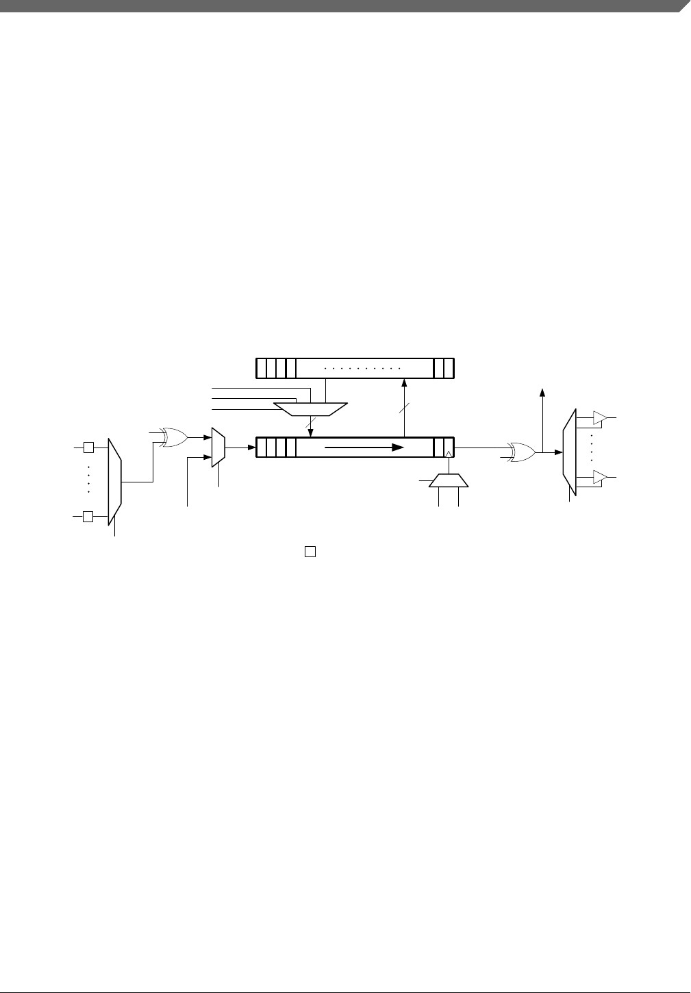
52.4.1.4 Software reset
The FlexIO implements a software reset bit in its Control Register. The CTRL[RST] will
reset all logic and registers to their default state, except for the CTRL itself.
52.4.2 Shifter operation
Shifters are responsible for buffering and shifting data into or out of the FlexIO. The
timing of shift, load and store events are controlled by the Timer assigned to the Shifter
via the SHIFTCTL[TIMSEL] register. The Shifters are designed to support either DMA,
interrupt or polled operation. The following block diagram provides a detailed view of
the Shifter microarchitecture.
31 0SHIFTBUFi
SHIFTERi
SSTOP
SSTART
timer_load_data/start/stop timer_store_data
timer_shift_pos
S
FXIO_D0
S
FXIO_Dn
S= synchronizer
PINSEL
SHIFTERi+1
out
INSRC
PINPOL
PINPOL
SHIFTERi
out
FXIO_D0
FXIO_Dn
timer_shift_neg
TIMPOL
PINSEL,
PINCFG
Figure 52-2. Shifter Microarchitecture
52.4.2.1 Transmit Mode
When configured for Transmit mode (SHIFTCTL[SMOD]=Transmit), the shifter will
load data from the SHIFTBUF register and shift data out when a load event is signalled
by the assigned Timer. An optional start/stop bit can also be automatically loaded before/
after SHIFTBUF data by configuring the SHIFTCFG[SSTART], TIMCFG[TSTART] or
SHIFTCFG[SSTOP], TIMCFG[TSTOP] registers in the Shifter and Timer. Note that the
shifter will immediately load a stop bit when the Shifter is initially configured for
Transmit mode if a stop bit is enabled.
The Shifter Status Flag (SHIFTSTAT[SSF]) and any enabled interrupts or DMA requests
will set when data has been loaded from the SHIFTBUF register into the Shifter or when
the Shifter is initially configured into Transmit mode. The flag will clear when new data
has been written into the SHIFTBUF register.
Chapter 52 Flexible I/O (FlexIO)
S32K1xx Series Reference Manual, Rev. 7, 04/2018
NXP Semiconductors 1609

The Shifter Error Flag (SHIFTERR[SEF]) and any enabled interrupts will set when an
attempt to load data from an empty SHIFTBUF register occurs (buffer underrun). The
flag can be cleared by writing it with logic 1.
52.4.2.2 Receive Mode
When configured for Receive mode (SHIFTCTL[SMOD]=Receive), the shifter will shift
data in and store data into the SHIFTBUF register when a store event is signalled by the
assigned Timer. Checking for a start/stop bit can be enabled before/after shifter data is
sampled by configuring the SHIFTCFG[SSTART], TIMCFG[TSTART] or
SHIFTCFG[SSTOP], TIMCFG[TSTOP] registers in the Shifter and Timer.
The Shifter Status Flag (SHIFTSTAT[SSF]) and any enabled interrupts or DMA requests
will set when data has been stored into the SHIFTBUF register from the Shifter. The flag
will clear when the data has been read from the SHIFTBUF register.
The Shifter Error Flag (SHIFTERR[SEF]) and any enabled interrupts will set when an
attempt to store data into a full SHIFTBUF register occurs (buffer overrun) or when a
mismatch occurs on a start/stop bit check. The flag can be cleared by writing it with logic
1.
52.4.2.3 Match Store Mode
When configured for Match Store mode (SHIFTCTL[SMOD]=Match Store), the shifter
will shift data in, check for a match result and store matched data into the SHIFTBUF
register when a store event is signalled by the assigned Timer. Checking for a start/stop
bit can be enabled before/after shifter data is sampled by configuring the
SHIFTCFG[SSTART], TIMCFG[TSTART] or SHIFTCFG[SSTOP], TIMCFG[TSTOP]
registers in the Shifter and Timer. Up to 16-bits of data can be compared using
SHIFTBUF[31:16] to configure the data to be matched and SHIFTBUF[15:0] to mask the
match result.
The Shifter Status Flag (SHIFTSTAT[SSF]) and any enabled interrupts or DMA requests
will set when a match occurs and matched data has been stored into the SHIFTBUF
register from the Shifter. The flag will clear when the matched data has been read from
the SHIFTBUF register.
The Shifter Error Flag (SHIFTERR[SEF]) and any enabled interrupts will set when an
attempt to store matched data into a full SHIFTBUF register occurs (buffer overrun) or
when a mismatch occurs on a start/stop bit check. The flag can be cleared by writing it
with logic 1.
Functional description
S32K1xx Series Reference Manual, Rev. 7, 04/2018
1610 NXP Semiconductors

52.4.2.4 Match Continuous Mode
When configured for Match Continuous mode (SHIFTCTL[SMOD]=Match Continuous),
the shifter will shift data in and continuously check for a match result whenever a shift
event is signalled by the assigned Timer. Up to 16-bits of data can be compared using
SHIFTBUF[31:16] to configure the data to be matched and SHIFTBUF[15:0] to mask the
match result.
The Shifter Status Flag (SHIFTSTAT[SSF]) and any enabled interrupts or DMA requests
will set when a match occurs. The flag will clear automatically as soon as there is no
longer a match between Shifter data and SHIFTBUF register.
The Shifter Error Flag (SHIFTERR[SEF]) and any enabled interrupts will set when a
match occurs. The flag will clear when there is a read from the SHIFTBUF register or it
written with logic 1.
52.4.3 Timer Operation
The FlexIO 16-bit timers control the loading, shifting and storing of the shift registers,
the counters load the contents of the compare register and decrement down to zero on the
FlexIO clock. They can perform generic timer functions such as generating a clock or
select output or a PWM waveform. Timers can be configured to enable in response to a
trigger, pin or shifter condition; decrement always or only on a trigger or pin edge; reset
in response to a trigger or pin condition; and disable on a trigger or pin condition or on a
timer compare. Timers can optionally include a start condition and/or stop condition.
Each timer operates independently, although a timer can be configured to enable or
disable at the same time as the previous timer (eg: timer1 can enable or disable at the
same time as timer 0) and a timer output can be used to trigger any other timer. The
trigger used by each timer is configured independently and can be configured to be a
timer output, shifter status flag, pin input or an external trigger input (refer to the chip-
specific FlexIO information for details on the external trigger connections). The trigger
configuration is separate from the pin configuration, which can be configured for input,
output data or output enable.
The Timer Configuration Register (TIMCFGn) should be configured before setting the
Timer Mode (TIMOD).
Chapter 52 Flexible I/O (FlexIO)
S32K1xx Series Reference Manual, Rev. 7, 04/2018
NXP Semiconductors 1611

52.4.3.1 Timer 8-bit Baud Counter Mode
In 8-bit Baud Counter Mode, the 16-bit counter is divided into two 8-bit counters. The
lower 8-bits are used to configure the baud rate of the shift clock and the upper 8-bits are
used to configure the number of shift clock edges in the transfer. When the lower 8-bits
decrement to zero, the timer output is toggled and the lower 8-bits reload from the
compare register. The upper 8-bits decrement when the lower 8-bits equal zero and
decrement.
Note that a timer reset event in 8-bit Baud Counter Mode will only reset the lower 8-bit
counter, the upper 8-bit counter is not affected and can decrement if the timer reset is
configured to update the state of the timer output, and the timer output toggles as a result
of the timer reset event.
A timer compare event occurs when the upper 8-bits equal zero and decrements. The
timer status flag is set on a timer compare event.
52.4.3.2 Timer 8-bit High PWM Mode
In 8-bit High PWM Mode, the 16-bit counter is divided into two 8-bit counters. The
lower 8-bits are used to configure the timer output high period and the upper 8-bits are
used to configure the timer output low period. The lower 8-bits decrement when the
output is high. When the lower 8-bits equal zero and decrement, the timer output is
cleared and the lower 8-bits are reloaded from the compare register. The upper 8-bits
decrement when the output is low. When the upper 8-bits equal zero and decrement, the
timer output is set and the upper 8-bits are reloaded from the compare register.
A timer compare event occurs when the upper 8-bits equal zero and decrements. The
timer status flag is set on a timer compare event.
52.4.3.3 Timer 16-bit Counter Mode
In 16-bit Counter Mode, the 16-bit counter can be used to configure either the baud rate
of the shift clock (eg: TIMDEC[1:0] != 10 or 11) or the number of shift clock edges in
the transfer (eg: TIMDEC[1:0] = 10 or 11). When the 16-bit counter equals zero and
decrements, the timer output toggles and the counter reloads from the compare register.
A timer compare event occurs when the 16-bit counter equals zero and decrements. The
timer status flag is set on a timer compare event.
Functional description
S32K1xx Series Reference Manual, Rev. 7, 04/2018
1612 NXP Semiconductors

52.4.3.4 Timer Enable and Start Bit
When the TIMOD is configured for the desired mode, and the condition configured by
timer enable (TIMENA) is detected then the following events occur.
• Timer counter will load the current value of the compare Register and start
decrementing as configured by TIMDEC.
• Timer output may update to its initial state depending on the TIMOUT configuration.
Shifters that are controlled by this timer do not see this as a rising edge on the timer
shift clock.
• Transmit shifters controlled by this timer will either output their start bit value, or
load the shift register from the shift buffer and output the first bit, as configured by
SSTART.
If the Timer start bit is enabled, the timer counter will reload with the compare register on
the first rising edge of the shift clock after the timer starts decrementing. If there is no
falling edge on the shift clock before the first rising edge (for example, when
TIMOUT=1), a shifter that is configured to shift on falling edge and load on the first shift
will not load correctly.
52.4.3.5 Timer Decrement and Reset
The Timer will then generate the timer output and timer shift clock depending on the
TIMOD and TIMDEC fields. The shifter clock is either equal to the timer output (when
TIMDEC != 10 or 11) or equal to the decrement clock (when TIMDEC = 10 or 11).
When TIMDEC is configured to decrement from a pin or trigger, the timer will
decrement on both rising and falling edges.
When the Timer is configured to reset as configured in the TIMRST field then the Timer
counter will load the current value of the compare register again. The timer output and
timer shift clock can be configured to update on timer reset, as configured by TIMOUT.
This can result in a timer shift clock edge if the timer output toggles as a result of the
timer reset. In 8-bit Baud Counter mode this would also decrement the upper 8-bits of the
counter.
In general, when the timer counter decrements to zero a timer compare event is triggered.
The timer compare event will cause the timer counter to load the contents of the timer
compare register, the timer output to toggle, any configured transmit shift registers to
load, and any configured receive shift registers to store. Depending on the timer mode,
the timer status flag may also be set.
Chapter 52 Flexible I/O (FlexIO)
S32K1xx Series Reference Manual, Rev. 7, 04/2018
NXP Semiconductors 1613

52.4.3.6 Timer Disable and Stop Bit
When the is Timer is configured to add a stop bit on each compare, the following
additional events will occur.
• Transmit shifters controlled by this timer will output their stop bit value (if
configured by SSTOP).
• Receive shifters controlled by this timer will store the contents of the shift register in
their shift buffer, as configured by SSTOP.
• On the first rising edge of the shifter clock after the compare, the timer counter will
reload the current value of the Compare Register.
Transmit shifters must be configured to load on the first shift when the timer is
configured to insert a stop bit on each compare.
When the condition configured by timer disable (TIMDIS) is detected, the following
events occur.
• Timer counter will reload the current value of the Compare Register and start
decrementing as configured by TIMDEC.
• Timer output will clear. Shifters that are controlled by this timer do not see this as a
falling edge on the timer shift clock, but can generate a shift event if the timer shift
clock would otherwise generate one.
• Transmit shifters controlled by this timer will output their stop bit value (if
configured by SSTOP).
• Receive shifters controlled by this timer will store the contents of the shift register in
their shift buffer, as configured by SSTOP.
If the timer stop bit is enabled, the timer counter will continue decrementing until the
next rising edge of the shift clock is detected, at which point it will finish. Although the
timer output is forced low during the stop bit, the timer shift clock can toggle during the
stop bit, but does not generate shift events.
A timer enable condition can be detected in the same cycle as a timer disable condition (if
timer stop bit is disabled), or on the first rising edge of the shift clock after the disable
condition (if stop bit is enabled). Receive shift registers with stop bit enabled will store
the contents of the shift register into the shift buffer and verify the state of the input data
on the configured shift edge while the timer is in the stop state condition. If there is no
configured edge between the timer disable and the next rising edge of the shift clock then
the final store and verify do not occur.
Functional description
S32K1xx Series Reference Manual, Rev. 7, 04/2018
1614 NXP Semiconductors

52.4.4 Pin operation
The pin configuration for each timer and shifter can be configured to use any FlexIO pin
with either polarity. Each timer and shifter can be configured as an input, output data,
output enable or bidirectional output. A pin configured for output enable can be used as
an open drain (with inverted polarity, since the output enable assertion would cause logic
zero to be output on the pin) or to control the enable on the bidirectional output. Any
timer or shifter could be configured to control the output enable for a pin where the
bidirectional output data is driven by another timer or shifter.
52.4.4.1 Pin Synchronization
When configuring a pin as an input (this includes a timer trigger configured as a pin
input), the input signal is first synchronized to the FlexIO clock before the signal is used
by a timer or shifter. This introduces a small latency of between 0.5 to 1.5 FlexIO clock
cycles when using an external pin input to generate an output or control a shifter. This
sets the maximum setup time at 1.5 FlexIO clock cycles.
If an input is used by more than one timer or shifter then the synchronization occurs once
to ensure any edge is seen on the same cycle by all timers and shifters using that input.
Note that FlexIO pins are also connected internally, configuring a FlexIO shifter or timer
to output data on an unused pin will make an internal connection that allows other
shifters and timer to use this pin as an input. This allows a shifter output to be used to
trigger a timer or a timer output to be shifted into a shifter. This path is also synchronized
to the FlexIO clock and therefore incurs a 1 cycle latency.
So when using a Pin input as a Timer Trigger, Timer Clock or Shifter Data Input, the
following synchronization delays occur:
1. 0.5 to 1.5 FlexIO clock cycles for external pin
2. 1 FlexIO clock cycle for an internally driven pin
For timing considerations such as output valid time and input setup time for specific
applications (SPI Master, SPI Slave, I2C Master, I2S Master, I2S Slave) please refer to
the FlexIO Application Information Section.
52.4.5 Interrupts and DMA Requests
The following table illustrates the status flags that can generate the FlexIO interrupt and
DMA requests.
Chapter 52 Flexible I/O (FlexIO)
S32K1xx Series Reference Manual, Rev. 7, 04/2018
NXP Semiconductors 1615

Table 52-3. FlexIO Interrupts and DMA Requests
Flag Description Interrupt DMA Request Low Power Wakeup
SSF Shifter Status Flag. Y Y Y
SEF Shifter Error Flag. Y N Y
TSF Timer Status Flag. Y N Y
52.4.6 Peripheral Triggers
The connection of the FlexIO peripheral triggers with other peripherals are device
specific.
52.4.6.1 Output Triggers
Each FlexIO Timer generates an output trigger equal to the timer output. The output
trigger is not affected by the timer pin polarity configuration.
52.4.6.2 Input Trigger
FlexIO supports multiple external trigger inputs that can be used to trigger one or more
FlexIO timers. The external triggers are synchronized to the FlexIO functional clock and
must assert for at least two cycles of the FlexIO functional clock to be sampled correctly.
52.5 Application Information
This section provides examples for a variety of FlexIO module applications.
52.5.1 UART Transmit
UART transmit can be supported using one Timer, one Shifter and one Pin (two Pins if
supporting CTS). The start and stop bit insertion is handled automatically and multiple
transfers can be supported using DMA controller. The timer status flag can be used to
indicate when the stop bit of each word is transmitted.
Break and idle characters require software intervention, before transmitting a break or
idle character the SSTART and SSTOP fields should be altered to transmit the required
state and the data to transmit must equal 0xFF or 0x00. Supporting a second stop bit
Application Information
S32K1xx Series Reference Manual, Rev. 7, 04/2018
1616 NXP Semiconductors

requires the stop bit to be inserted into the data stream using software (and increasing the
number of bits to transmit). Note that when performing byte writes to SHIFTBUFn (or
SHIFTBUFBIS for transmitting MSB first), the rest of the register remains unaltered
allowing an address mark bit or additional stop bit to remain undisturbed.
FlexIO does not support automatic insertion of parity bits.
Table 52-4. UART Transmit Configuration
Register Value Comments
SHIFTCFGn 0x0000_0032 Configure start bit of 0 and stop bit of 1.
SHIFTCTLn 0x0003_0002 Configure transmit using Timer 0 on
posedge of clock with output data on Pin
0. Can invert output data by setting
PINPOL, or can support open drain by
setting PINPOL=0x1 and PINCFG=0x1.
TIMCMPn 0x0000_0F01 Configure 8-bit transfer with baud rate of
divide by 4 of the FlexIO clock. Set
TIMCMP[15:8] = (number of bits x 2) - 1.
Set TIMCMP[7:0] = (baud rate divider /
2) - 1.
TIMCFGn 0x0000_2222 Configure start bit, stop bit, enable on
trigger asserted and disable on
compare. Can support CTS by
configuring TIMEN=0x3.
TIMCTLn 0x01C0_0001 Configure dual 8-bit counter using
Shifter 0 status flag as inverted internal
trigger source. Can support CTS by
configuring PINSEL=0x1 (for Pin 1) and
PINPOL=0x1.
SHIFTBUFn Data to transmit Transmit data can be written to
SHIFTBUF[7:0] to initiate an 8-bit
transfer, use the Shifter Status Flag to
indicate when data can be written using
interrupt or DMA request. Can support
MSB first transfer by writing to
SHIFTBUFBBS[7:0] register instead.
52.5.2 UART Receive
UART receive can be supported using one Timer, one Shifter and one Pin (two Timers
and two Pins if supporting RTS). The start and stop bit verification is handled
automatically and multiple transfers can be supported using the DMA controller. The
timer status flag can be used to indicate when the stop bit of each word is received.
Chapter 52 Flexible I/O (FlexIO)
S32K1xx Series Reference Manual, Rev. 7, 04/2018
NXP Semiconductors 1617

Triple voting of the received data is not supported by FlexIO, data is sampled only once
in the middle of each bit. Another timer can be used to implement a glitch filter on the
incoming data, another Timer can also be used to detect an idle line of programmable
length. Break characters will cause the error flag to set and the shifter buffer register will
return 0x00.
FlexIO does not support automatic verification of parity bits.
Table 52-5. UART Receiver Configuration
Register Value Comments
SHIFTCFGn 0x0000_0032 Configure start bit of 0 and stop bit of 1.
SHIFTCTLn 0x0080_0001 Configure receive using Timer 0 on
negedge of clock with input data on Pin
0. Can invert input data by setting
PINPOL.
TIMCMPn 0x0000_0F01 Configure 8-bit transfer with baud rate of
divide by 4 of the FlexIO clock. Set
TIMCMP[15:8] = (number of bits x 2) - 1.
Set TIMCMP[7:0] = (baud rate divider /
2) - 1.
TIMCFGn 0x0204_2422 Configure start bit, stop bit, enable on
pin posedge and disable on compare.
Enable resynchronization to received
data with TIMOUT=0x2 and
TIMRST=0x4.
TIMCTLn 0x0000_0081 Configure dual 8-bit counter using
inverted Pin 0 input.
SHIFTBUFn Data to receive Received data can be read from
SHIFTBUFBYS[7:0], use the Shifter
Status Flag to indicate when data can be
read using interrupt or DMA request.
Can support MSB first transfer by
reading from SHIFTBUFBIS[7:0] register
instead.
The UART Receiver with RTS configuration uses a 2nd Timer to generate the RTS
output. The RTS will assert when the start bit is detected and negate when the data is read
from the shifter buffer register. No start bit will be detected while the RTS is asserted, the
received data is simply ignored.
Table 52-6. UART Receiver with RTS Configuration
Register Value Comments
SHIFTCFGn 0x0000_0032 Configure start bit of 0 and stop bit of 1.
SHIFTCTLn 0x0080_0001 Configure receive using Timer 0 on
negedge of clock with input data on Pin
0. Can invert input data by setting
PINPOL.
Table continues on the next page...
Application Information
S32K1xx Series Reference Manual, Rev. 7, 04/2018
1618 NXP Semiconductors

Table 52-6. UART Receiver with RTS Configuration (continued)
Register Value Comments
TIMCMPn 0x0000_0F01 Configure 8-bit transfer with baud rate of
divide by 4 of the FlexIO clock. Set
TIMCMP[15:8] = (number of bits x 2) - 1.
Set TIMCMP[7:0] = (baud rate divider /
2) - 1.
TIMCFGn 0x0204_2522 Configure start bit, stop bit, enable on
pin posedge with trigger asserted and
disable on compare. Enable
resynchronization to received data with
TIMOUT=0x2 and TIMRST=0x4.
TIMCTLn 0x02C0_0081 Configure dual 8-bit counter using
inverted Pin 0 input. Trigger is internal
using inverted Pin 1 input.
TIMCMP(n+1) 0x0000_FFFF Never compare.
TIMCFG(n+1) 0x0030_6100 Enable on Timer N enable and disable
on trigger falling edge. Decrement on
trigger to ensure no compare.
TIMCTL(n+1) 0x0143_0003 Configure 16-bit counter and output on
Pin 1. Trigger is internal using Shifter 0
flag.
SHIFTBUFn Data to receive Received data can be read from
SHIFTBUFBYS[7:0], use the Shifter
Status Flag to indicate when data can be
read using interrupt or DMA request.
Can support MSB first transfer by
reading from SHIFTBUFBIS[7:0] register
instead.
52.5.3 SPI Master
SPI master mode can be supported using two Timers, two Shifters and four Pins. Either
CPHA=0 or CPHA=1 can be supported and transfers can be supported using the DMA
controller. For CPHA=1, the select can remain asserted for multiple transfers and the
timer status flag can be used to indicate the end of the transfer.
The stop bit is used to guarantee a minimum of 1 clock cycle between the slave select
negating and before the next transfer. Writing to the transmit buffer by either core or
DMA is used to initiate each transfer.
Due to synchronization delays, the setup time for the serial input data is 1.5 FlexIO clock
cycles, so the maximum baud rate is divide by 4 of the FlexIO clock frequency.
Chapter 52 Flexible I/O (FlexIO)
S32K1xx Series Reference Manual, Rev. 7, 04/2018
NXP Semiconductors 1619

Table 52-7. SPI Master (CPHA=0) Configuration
Register Value Comments
SHIFTCFGn 0x0000_0000 Start and stop bit disabled.
SHIFTCTLn 0x0083_0002 Configure transmit using Timer 0 on
negedge of clock with output data on Pin
0.
SHIFTCFG(n+1) 0x0000_0000 Start and stop bit disabled.
SHIFTCTL(n+1) 0x0000_0101 Configure receive using Timer 0 on
posedge of clock with input data on Pin
1.
TIMCMPn 0x0000_3F01 Configure 32-bit transfer with baud rate
of divide by 4 of the FlexIO clock. Set
TIMCMP[15:8] = (number of bits x 2) - 1.
Set TIMCMP[7:0] = (baud rate divider /
2) - 1.
TIMCFGn 0x0100_2222 Configure start bit, stop bit, enable on
trigger high and disable on compare,
initial clock state is logic 0.
TIMCTLn 0x01C3_0201 Configure dual 8-bit counter using Pin 2
output (shift clock), with Shifter 0 flag as
the inverted trigger. Set PINPOL to
invert the output shift clock.
TIMCMP(n+1) 0x0000_FFFF Never compare.
TIMCFG(n+1) 0x0000_1100 Enable when Timer 0 is enabled and
disable when Timer 0 is disabled.
TIMCTL(n+1) 0x0003_0383 Configure 16-bit counter (never
compare) using inverted Pin 3 output (as
slave select).
SHIFTBUFn Data to transmit Transmit data can be written to
SHIFTBUF, use the Shifter Status Flag
to indicate when data can be written
using interrupt or DMA request. Can
support MSB first transfer by writing to
SHIFTBUFBBS register instead.
SHIFTBUF(n+1) Data to receive Received data can be read from
SHIFTBUFBYS, use the Shifter Status
Flag to indicate when data can be read
using interrupt or DMA request. Can
support MSB first transfer by reading
from SHIFTBUFBIS register instead.
Table 52-8. SPI Master (CPHA=1) Configuration
Register Value Comments
SHIFTCFGn 0x0000_0021 Start bit loads data on first shift.
SHIFTCTLn 0x0003_0002 Configure transmit using Timer 0 on
posedge of clock with output data on Pin
0.
SHIFTCFG(n+1) 0x0000_0000 Start and stop bit disabled.
Table continues on the next page...
Application Information
S32K1xx Series Reference Manual, Rev. 7, 04/2018
1620 NXP Semiconductors

Table 52-8. SPI Master (CPHA=1) Configuration (continued)
Register Value Comments
SHIFTCTL(n+1) 0x0080_0101 Configure receive using Timer 0 on
negedge of clock with input data on Pin
1.
TIMCMPn 0x0000_3F01 Configure 32-bit transfer with baud rate
of divide by 4 of the FlexIO clock. Set
TIMCMP[15:8] = (number of bits x 2) - 1.
Set TIMCMP[7:0] = (baud rate divider /
2) - 1.
TIMCFGn 0x0100_2222 Configure start bit, stop bit, enable on
trigger high and disable on compare,
initial clock state is logic 0.
TIMCTLn 0x01C3_0201 Configure dual 8-bit counter using Pin 2
output (shift clock), with Shifter 0 flag as
the inverted trigger. Set PINPOL to
invert the output shift clock. Set
TIMDIS=3 to keep slave select asserted
for as long as there is data in the
transmit buffer.
TIMCMP(n+1) 0x0000_FFFF Never compare.
TIMCFG(n+1) 0x0000_1100 Enable when Timer 0 is enabled and
disable when Timer 0 is disabled.
TIMCTL(n+1) 0x0003_0383 Configure 16-bit counter (never
compare) using inverted Pin 3 output (as
slave select).
SHIFTBUFn Data to transmit Transmit data can be written to
SHIFTBUF, use the Shifter Status Flag
to indicate when data can be written
using interrupt or DMA request. Can
support MSB first transfer by writing to
SHIFTBUFBBS register instead.
SHIFTBUF(n+1) Data to receive Received data can be read from
SHIFTBUFBYS, use the Shifter Status
Flag to indicate when data can be read
using interrupt or DMA request. Can
support MSB first transfer by reading
from SHIFTBUFBIS register instead.
52.5.4 SPI Slave
SPI slave mode can be supported using one Timer, two Shifters and four Pins. Either
CPHA=0 or CPHA=1 can be supported and transfers can be supported using the DMA
controller. For CPHA=1, the select can remain asserted for multiple transfers and the
timer status flag can be used to indicate the end of the transfer.
The transmit data must be written to the transmit buffer register before the external slave
select asserts, otherwise the shifter error flag will be set.
Chapter 52 Flexible I/O (FlexIO)
S32K1xx Series Reference Manual, Rev. 7, 04/2018
NXP Semiconductors 1621

Due to synchronization delays, the output valid time for the serial output data is 2.5
FlexIO clock cycles, so the maximum baud rate is divide by 6 of the FlexIO clock
frequency.
Table 52-9. SPI Slave (CPHA=0) Configuration
Register Value Comments
SHIFTCFGn 0x0000_0000 Start and stop bit disabled.
SHIFTCTLn 0x0083_0002 Configure transmit using Timer 0 on
falling edge of shift clock with output
data on Pin 0.
SHIFTCFG(n+1) 0x0000_0000 Start and stop bit disabled.
SHIFTCTL(n+1) 0x0000_0101 Configure receive using Timer 0 on
rising edge of shift clock with input data
on Pin 1.
TIMCMPn 0x0000_003F Configure 32-bit transfer. Set
TIMCMP[15:0] = (number of bits x 2) - 1.
TIMCFGn 0x0120_6000 Configure enable on trigger rising edge,
initial clock state is logic 0 and
decrement on pin input.
TIMCTLn 0x06C0_0203 Configure 16-bit counter using Pin 2
input (shift clock), with Pin 3 input (slave
select) as the inverted trigger.
SHIFTBUFn Data to transmit Transmit data can be written to
SHIFTBUF, use the Shifter Status Flag
to indicate when data can be written
using interrupt or DMA request. Can
support MSB first transfer by writing to
SHIFTBUFBBS register instead.
SHIFTBUF(n+1) Data to receive Received data can be read from
SHIFTBUFBYS, use the Shifter Status
Flag to indicate when data can be read
using interrupt or DMA request. Can
support MSB first transfer by reading
from SHIFTBUFBIS register instead.
Table 52-10. SPI Slave (CPHA=1) Configuration
Register Value Comments
SHIFTCFGn 0x0000_0001 Shifter configured to load on first shift
and stop bit disabled.
SHIFTCTLn 0x0003_0002 Configure transmit using Timer 0 on
rising edge of shift clock with output data
on Pin 0.
SHIFTCFG(n+1) 0x0000_0000 Start and stop bit disabled.
SHIFTCTL(n+1) 0x0080_0101 Configure receive using Timer 0 on
falling edge of shift clock with input data
on Pin 1.
TIMCMPn 0x0000_003F Configure 32-bit transfer. Set
TIMCMP[15:0] = (number of bits x 2) - 1.
Table continues on the next page...
Application Information
S32K1xx Series Reference Manual, Rev. 7, 04/2018
1622 NXP Semiconductors

Table 52-10. SPI Slave (CPHA=1) Configuration (continued)
Register Value Comments
TIMCFGn 0x0120_6602 Configure start bit, enable on trigger
rising edge, disable on trigger falling
edge, initial clock state is logic 0 and
decrement on pin input.
TIMCTLn 0x06C0_0203 Configure 16-bit counter using Pin 2
input (shift clock), with Pin 3 input (slave
select) as the inverted trigger.
SHIFTBUFn Data to transmit Transmit data can be written to
SHIFTBUF, use the Shifter Status Flag
to indicate when data can be written
using interrupt or DMA request. Can
support MSB first transfer by writing to
SHIFTBUFBBS register instead.
SHIFTBUF(n+1) Data to receive Received data can be read from
SHIFTBUFBYS, use the Shifter Status
Flag to indicate when data can be read
using interrupt or DMA request. Can
support MSB first transfer by reading
from SHIFTBUFBIS register instead.
52.5.5 I2C Master
I2C master mode can be supported using two Timers, two Shifters and two Pins. One
timer is used to generate the SCL output and one timer is used to control the shifters. The
two shifters are used to transmit and receive for every word, when receiving the
transmitter must transmit 0xFF to tristate the output. FlexIO inserts a stop bit after every
word to generate/verify the ACK/NACK. FlexIO waits for the first write to the transmit
data buffer before enabling SCL generation. Data transfers can be supported using the
DMA controller and the shifter error flag will set on transmit underrun or receive
overflow.
The first timer generates the bit clock for the entire packet (START to Repeated START/
STOP), so the compare register needs to be programmed with the total number of clock
edges in the packet (minus one). The timer supports clock stretching using the reset
counter when pin equal to output (although this increases both the clock high and clock
low periods by at least 1 FlexIO clock cycle each). The second timer uses the SCL input
pin to control the transmit/receive shift registers, this enforces an SDA data hold time by
an extra 2 FlexIO clock cycles.
Both the transmit and receive shifters need to be serviced for each word in the transfer,
the transmit shifter must transmit 0xFF when receiving and the receive shifter returns the
data actually present on the SDA pin. The transmit shifter will load 1 additional word on
Chapter 52 Flexible I/O (FlexIO)
S32K1xx Series Reference Manual, Rev. 7, 04/2018
NXP Semiconductors 1623

the last falling edge of SCL pin, this word should be 0x00 if generating a STOP condition
or 0xFF if generating a repeated START condition. During the last word of a master-
receiver transfer, the transmit SSTOP bit should be set by software to generate a NACK.
The receive shift register will assert an error interrupt if a NACK is detected, but software
is responsible for generating the STOP or repeated START condition. If a NACK is
detected during master-transmit, the interrupt routine should immediately write the
transmit shifter register with 0x00 (if generating STOP) or 0xFF (if generating repeated
START). Software should then wait for the next rising edge on SCL and then disable
both timers. The transmit shifter should then be disabled after waiting the setup delay for
a repeated START or STOP condition.
Due to synchronization delays, the data valid time for the transmit output is 2 FlexIO
clock cycles, so the maximum baud rate is divide by 6 of the FlexIO clock frequency.
The I2C master data valid is delayed 2 cycles because the clock output is passed through
a synchronizer before clocking the transmit/receive shifter (to guarantee some SDA hold
time). Since the SCL output is synchronous with FlexIO clock, the synchronization delay
is 1 cycle and then 1 cycle to generate the output.
Table 52-11. I2C Master Configuration
Register Value Comments
SHIFTCFGn 0x0000_0032 Start bit enabled (logic 0) and stop bit
enabled (logic 1).
SHIFTCTLn 0x0101_0082 Configure transmit using Timer 1 on
rising edge of clock with inverted output
enable (open drain output) on Pin 0.
SHIFTCFG(n+1) 0x0000_0020 Start bit disabled and stop bit enabled
(logic 0) for ACK/NACK detection.
SHIFTCTL(n+1) 0x0180_0001 Configure receive using Timer 1 on
falling edge of clock with input data on
Pin 0.
TIMCMPn 0x0000_2501 Configure 2 word transfer with baud rate
of divide by 4 of the FlexIO clock. Set
TIMCMP[15:8] = (number of words x 18)
+ 1. Set TIMCMP[7:0] = (baud rate
divider / 2) - 1.
TIMCFGn 0x0102_2222 Configure start bit, stop bit, enable on
trigger high, disable on compare, reset if
output equals pin. Initial clock state is
logic 0 and is not affected by reset.
TIMCTLn 0x01C1_0101 Configure dual 8-bit counter using Pin 1
output enable (SCL open drain), with
Shifter 0 flag as the inverted trigger.
TIMCMP(n+1) 0x0000_000F Configure 8-bit transfer. Set
TIMCMP[15:0] = (number of bits x 2) - 1.
TIMCFG(n+1) 0x0020_1112 Enable when Timer 0 is enabled, disable
when Timer 0 is disabled, enable start
Table continues on the next page...
Application Information
S32K1xx Series Reference Manual, Rev. 7, 04/2018
1624 NXP Semiconductors

Table 52-11. I2C Master Configuration (continued)
Register Value Comments
bit and stop bit at end of each word,
decrement on pin input.
TIMCTL(n+1) 0x01C0_0183 Configure 16-bit counter using inverted
Pin 1 input (SCL).
SHIFTBUFn Data to transmit Transmit data can be written to
SHIFTBUFBBS[7:0], use the Shifter
Status Flag to indicate when data can be
written using interrupt or DMA request.
SHIFTBUF(n+1) Data to receive Received data can be read from
SHIFTBUFBIS[7:0], use the Shifter
Status Flag to indicate when data can be
read using interrupt or DMA request.
52.5.6 I2S Master
I2S master mode can be supported using two Timers, two Shifters and four Pins. One
timer is used to generate the bit clock and control the shifters and one timer is used to
generate the frame sync. FlexIO waits for the first write to the transmit data buffer before
enabling bit clock and frame sync generation. Data transfers can be supported using the
DMA controller and the shifter error flag will set on transmit underrun or receive
overflow.
The bit clock frequency is an even integer divide of the FlexIO clock frequency, and the
initial frame sync assertion occurs at the same time as the first bit clock edge. The timer
uses the start bit to ensure the frame sync is generated one clock cycle before the first
output data.
Due to synchronization delays, the setup time for the receiver input is 1.5 FlexIO clock
cycles, so the maximum baud rate is divide by 4 of the FlexIO clock frequency.
Table 52-12. I2S Master Configuration
Register Value Comments
SHIFTCFGn 0x0000_0001 Load transmit data on first shift and stop
bit disabled.
SHIFTCTLn 0x0003_0002 Configure transmit using Timer 0 on
rising edge of clock with output data on
Pin 0.
SHIFTCFG(n+1) 0x0000_0000 Start and stop bit disabled.
SHIFTCTL(n+1) 0x0080_0101 Configure receive using Timer 0 on
falling edge of clock with input data on
Pin 1.
Table continues on the next page...
Chapter 52 Flexible I/O (FlexIO)
S32K1xx Series Reference Manual, Rev. 7, 04/2018
NXP Semiconductors 1625

Table 52-12. I2S Master Configuration (continued)
Register Value Comments
TIMCMPn 0x0000_3F01 Configure 32-bit transfer with baud rate
of divide by 4 of the FlexIO clock. Set
TIMCMP[15:8] = (number of bits x 2) - 1.
Set TIMCMP[7:0] = (baud rate divider /
2) - 1.
TIMCFGn 0x0000_0202 Configure start bit, enable on trigger high
and never disable. Initial clock state is
logic 1.
TIMCTLn 0x01C3_0201 Configure dual 8-bit counter using Pin 2
output (bit clock), with Shifter 0 flag as
the inverted trigger. Set PINPOL to
invert the output shift clock.
TIMCMP(n+1) 0x0000_007F Configure 32-bit transfer with baud rate
of divide by 4 of the FlexIO clock. Set
TIMCMP[15:0] = (number of bits x baud
rate divider) - 1.
TIMCFG(n+1) 0x0000_0100 Enable when Timer 0 is enabled and
never disable.
TIMCTL(n+1) 0x0003_0383 Configure 16-bit counter using inverted
Pin 3 output (as frame sync).
SHIFTBUFn Data to transmit Transmit data can be written to
SHIFTBUFBIS, use the Shifter Status
Flag to indicate when data can be
written using interrupt or DMA request.
Can support LSB first transfer by writing
to SHIFTBUF register instead.
SHIFTBUF(n+1) Data to receive Received data can be read from
SHIFTBUFBIS, use the Shifter Status
Flag to indicate when data can be read
using interrupt or DMA request. Can
support LSB first transfer by reading
from SHIFTBUF register instead.
52.5.7 I2S Slave
I2S slave mode can be supported using three Timers, two Shifters and four Pins (for
single transmit and single receive, other combinations of transmit and receive are
possible).
The transmit data must be written to the transmit buffer register before the external frame
sync asserts, otherwise the shifter error flag will be set.
Due to synchronization delays, the output valid time for the serial output data is 2.5
FlexIO clock cycles, so the maximum baud rate is divide by 6 of the FlexIO clock
frequency.
Application Information
S32K1xx Series Reference Manual, Rev. 7, 04/2018
1626 NXP Semiconductors

The output valid time of I2S slave is max 2.5 cycles because there is a maximum 1.5
cycle delay on the clock synchronization plus 1 cycle to output the data
Timer 2 detects the falling edge of frame sync (start of new frame) and asserts output
until falling edge of bit clock (when frame sync is normally sampled). Timer 0 detects
falling edge of bit clock with Timer 2 output asserted and asserts output for length of
frame. Timer 1 detects rising edge of bit clock with Timer 0 output asserted and controls
shift registers for 32-bit transfers.
Table 52-13. I2S Slave Configuration
Register Value Comments
SHIFTCFGn 0x0000_0000 Start and stop bit disabled.
SHIFTCTLn 0x0103_0002 Configure transmit using Timer 1 on
rising edge of shift clock with output data
on Pin 0.
SHIFTCFG(n+1) 0x0000_0000 Start and stop bit disabled.
SHIFTCTL(n+1) 0x0180_0101 Configure receive using Timer 1 on
falling edge of shift clock with input data
on Pin 1.
TIMCMPn 0x0000_007F Configure two 32-bit transfers per frame.
Set TIMCMP[15:0] = (number of bits x 4)
- 1.
TIMCFGn 0x0020_2500 Configure enable on pin rising edge
(inverted bit clock) with trigger high
(Timer 2) and disable on compare, initial
clock state is logic 1 and decrement on
pin input (bit clock).
TIMCTLn 0x0B40_0283 Configure 16-bit counter using inverted
Pin 2 input (bit clock), with Timer 2
output as the trigger.
TIMCMP(n+1) 0x0000_003F Configure 32-bit transfers. Set
TIMCMP[15:0] = (number of bits x 2) - 1.
TIMCFG(n+1) 0x0020_2500 Configure enable on pin (bit clock) rising
edge with trigger (Timer 0) high and
disable on compare, initial clock state is
logic 1 and decrement on pin input (bit
clock).
TIMCTL(n+1) 0x0340_0283 Configure 16-bit counter using inverted
Pin 2 input (bit clock), with Timer 0
output as the trigger.
TIMCMP(n+2) 0x0000_0000 Compare on zero (first edge).
TIMCFG(n+2) 0x0020_6400 Configure enable on inverted pin (frame
sync) rising edge and disable on trigger
falling edge (bit clock), initial clock state
is logic 1 and decrement on inverted pin
input (frame sync).
TIMCTL(n+2) 0x0440_0383 Configure 16-bit counter using inverted
Pin 3 input (frame sync), with Pin 2 input
(bit clock) as the trigger.
Table continues on the next page...
Chapter 52 Flexible I/O (FlexIO)
S32K1xx Series Reference Manual, Rev. 7, 04/2018
NXP Semiconductors 1627

Table 52-13. I2S Slave Configuration (continued)
Register Value Comments
SHIFTBUFn Data to transmit Transmit data can be written to
SHIFTBUFBIS, use the Shifter Status
Flag to indicate when data can be
written using interrupt or DMA request.
Can support LSB first transfer by writing
to SHIFTBUF register instead.
SHIFTBUF(n+1) Data to receive Received data can be read from
SHIFTBUFBIS, use the Shifter Status
Flag to indicate when data can be read
using interrupt or DMA request. Can
support LSB first transfer by reading
from SHIFTBUF register instead.
Application Information
S32K1xx Series Reference Manual, Rev. 7, 04/2018
1628 NXP Semiconductors

Chapter 53
FlexCAN
Chip-specific FlexCAN information
53.1.1 Instantiation information
The following table summarizes the implementation of this module for each chip in the
product series.
Table 53-1. FlexCAN instances and features
Chip Instances Number of
Message
Buffers (MB)
ISO CAN FD
feature 1PNET feature External time
tick
CTRL2 register
2 reset value
S32K116 FlexCAN0 32 MBs Yes Yes Yes 0x00A0_0000
S32K118 FlexCAN0 32 MBs Yes Yes Yes 0x00A0_0000
S32K142 FlexCAN0 32 MBs Yes Yes Yes 0x00A0_0000
FlexCAN1 16 MBs No No No 0x00B0_0000
S32K144 FlexCAN0 32 MBs Yes Yes Yes 0x00A0_0000
FlexCAN1 16 MBs No No No 0x00B0_0000
FlexCAN2 16 MBs No No No 0x00B0_0000
S32K146 FlexCAN0 32 MBs Yes Yes Yes 0x00A0_0000
FlexCAN1 32 MBs Yes No No 0x00A0_0000
FlexCAN2 16 MBs No No No 0x00B0_0000
S32K148 FlexCAN0 32 MBs Yes Yes Yes 0x00A0_0000
FlexCAN1 32 MBs Yes No No 0x00A0_0000
FlexCAN2 32 MBs Yes No No 0x00A0_0000
1. Feature only available for the products with SIM_SDID[6]=1. The entire number of Message Buffers are still available for
the products with SIM_SDID[6]=0 under CAN classical mode.
2. Bit fields CTRL2[PREXCEN] and CTRL2[EDFLTDIS] are implemented in instances supporting ISO CAN FD feature only.
53.1
S32K1xx Series Reference Manual, Rev. 7, 04/2018
NXP Semiconductors 1629

53.1.2 Reset value of MDIS bit
The CAN_MCR[MDIS] bit is set after reset. Therefore, FlexCAN module is disabled
following a reset.
53.1.3 FlexCAN external time tick
On this device, LPIT channel 0 trigger output acts as external time tick source for
FlexCAN0.
53.1.4 FlexCAN Interrupts
The FlexCAN has multiple sources of interrupt requests. However, some of these sources
are OR'd together to generate a single interrupt request. See below for the mapping of the
individual interrupt sources to the interrupt request:
Table 53-2. FlexCAN Interrupts
Request For CAN with FD For CAN without FD
Message Buffer Message buffers 0-31 Message buffers 0-15
Bus off Bus off Bus off
Error • Bit1 error or Bit1 error in Data
Phase of CAN FD frames
• Bit0 error or Bit0 error in Data
Phase of CAN FD frames
• Acknowledge error
• Cyclic redundancy check error or
Cyclic redundancy in Data Phase
of CAN FD frames
• Form error or Form error in Data
Phase of CAN FD frames
• Stuffing error or Stuffing error in
Data Phase of CAN FD frames
• Transmit error warning
• Receive error warning
• CAN-FD error
• Bit1 error
• Bit0 error
• Acknowledge error
• Cyclic redundancy check (CRC)
error
• Form error
• Stuffing error
• Transmit error warning
• Receive error warning
Transmit Warning Transmit Warning Transmit Warning
Receive Warning Receive Warning Receive Warning
Chip-specific FlexCAN information
S32K1xx Series Reference Manual, Rev. 7, 04/2018
1630 NXP Semiconductors

53.1.5 FlexCAN Operation in Low Power Modes
The FlexCAN module is operational in VLPR mode. With the 4 MHz system clock (in
VLPR mode), the fastest supported FlexCAN transfer rate is 250 kbps. The bit timing
parameters in the module must be adjusted for the new frequency, but full functionality is
possible.
See Module operation in available low power modes for details on available power
modes.
53.1.6 FlexCAN oscillator clock
FlexCAN oscillator clock is SOSCDIV2_CLK as mentioned in section Table 27-9
53.1.7 Supported baud rate
The following table details the supported baud rate for each chip in the product series.:
Chip PE clock CHI clock Number of MB Maximum achievable baud
rate
S32K14x 16 MHz 80 MHz 32 3.2 Mbps
16 1 Mbps
S32K14x 80 MHz 80 MHz 32 8 Mbps
16 1 Mbps
S32K11x 16 MHz 48 MHz 32 3.2 Mbps
S32K11x 48 MHz 32 8 Mbps
53.1.8 Requirements for entering FlexCAN modes: Freeze,
Disable, Stop
Follow the procedure described in Freeze mode entry to place the FlexCAN module in
that mode.
On this chip, the FlexCAN module cannot directly enter:
• Module Disable mode
• Stop mode
Chapter 53 FlexCAN
S32K1xx Series Reference Manual, Rev. 7, 04/2018
NXP Semiconductors 1631

To enter these modes, the FlexCAN module must first enter Freeze mode.To enter this
mode, the FlexCAN module must first enter Freeze mode. See the following information
about each of the modes.
53.1.8.1 Freeze mode entry
See Freeze mode for details about this mode.
On this chip, the procedure to enter Freeze mode is:
1. Set both CAN_MCR[FRZ] (Freeze Enable) and CAN_MCR[HALT] (Halt) to 1.
2. Check whether CAN_MCR[MDIS] (Module Disable) is set to 1. If it is, clear it to 0.
3. Poll the MCR register until CAN_MCR[FRZACK] (Freeze Mode Acknowledge) is
set to 1 or the timeout is reached.
NOTE
The minimum timeout duration must be equivalent to:
a. 730 CAN Nominal bits if CAN_MCR[FDEN] (CAN
FD Operation Enable) is set to 1 (CAN bits calculated
at arbitration bit rate),
b. 180 CAN bits if CAN_MCR[FDEN] is cleared to 0.
4. If CAN_MCR[FRZACK] is set to 1, no further action is required. Skip steps 5 to 8.
5. If the timeout is reached because CAN_MCR[FRZACK] remains cleared to 0, then
set CAN_MCR[SOFTRST] (Soft Reset) to 1.
6. Poll MCR until CAN_MCR[SOFTRST] is cleared to 0.
7. Reconfigure the Module Control register (CAN_MCR).
8. Reconfigure all the Interrupt Mask registers (CAN_IMASKn).
After these steps are complete, the module is in Freeze mode.
53.1.8.2 Module Disable mode entry
See Module Disable mode for details about this mode.
CAUTION
In the detailed description of this mode, the list of FlexCAN
behavior that begins with "If the module is disabled during
transmission or reception" does not apply to this chip.
On this chip, the procedure to enter Module Disable mode is:
Chip-specific FlexCAN information
S32K1xx Series Reference Manual, Rev. 7, 04/2018
1632 NXP Semiconductors

1. Enter Freeze mode by following the procedure described in Freeze mode entry.
2. Request Module Disable mode by setting CAN_MCR[MDIS] to 1.
3. Poll CAN_MCR until CAN_MCR[LPMACK] is set to 1. The minimum timeout
duration for setting CAN_MCR[LPMACK] is 2 CAN Nominal bits.
53.1.8.3 Stop mode entry
See Stop mode for details about this mode.
CAUTION
In the detailed description of this mode, the list of FlexCAN
behavior that begins with "If Stop mode is requested during
transmission or reception" does not apply to this chip.
On this chip, the procedure to enter Stop mode is:
1. Enter Freeze mode by following the procedure described in Freeze mode entry.
2. Request Stop mode.
3. Poll MCR until CAN_MCR[LPMACK] is set to 1. The minimum timeout duration
for setting CAN_MCR[LPMACK] is 2 CAN Nominal bits.
53.2 Introduction
The FlexCAN module is a communication controller implementing the CAN protocol
according to the ISO 11898-1 standard and CAN 2.0 B protocol specifications. A general
block diagram is shown in the following figure, which describes the main subblocks
implemented in the FlexCAN module, including one associated memory for storing
message buffers, Receive Global Mask registers, Receive Individual Mask registers,
Receive FIFO filters, and Receive FIFO ID filters. The functions of the submodules are
described in subsequent sections.
NOTE
Rx FIFO cannot be used in FD mode.
Chapter 53 FlexCAN
S32K1xx Series Reference Manual, Rev. 7, 04/2018
NXP Semiconductors 1633
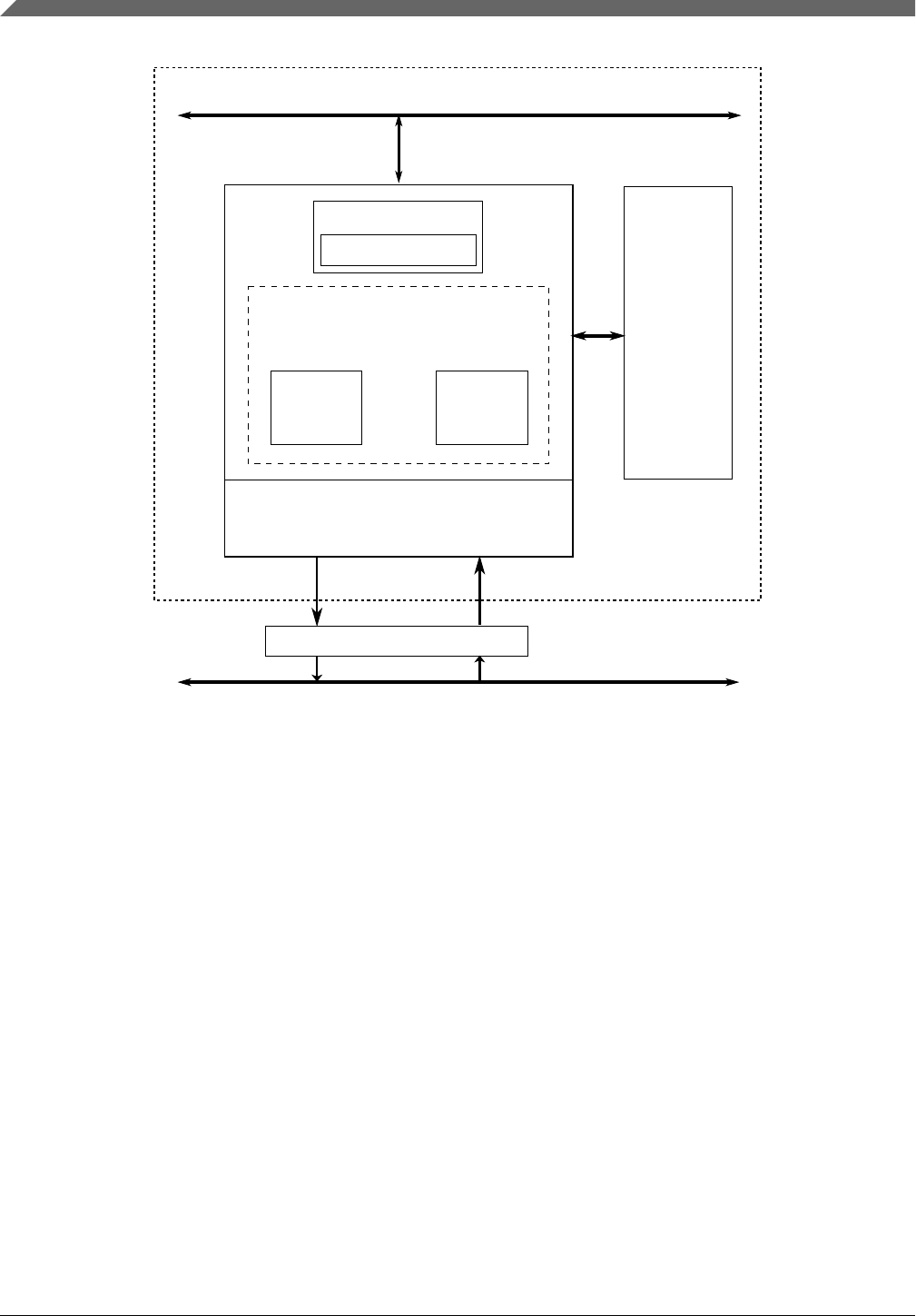
CAN Rx
RAM
Rx
Matching
CAN Tx
Bus InterfaceUnit
Controller
Host Interface
Protocol Engine
Tx
Arbitration
Message
Buffers
(MBs)
Peripheral Bus Interface
Address, Data, Clocks, Interrupts
FlexCAN
CAN Bus
CAN Transceiver
Registers
Figure 53-1. FlexCAN block diagram
53.2.1 Overview
The CAN protocol was primarily designed to be used as a vehicle serial data bus, meeting
the specific requirements of this field:
• Real-time processing
• Reliable operation in the EMI environment of a vehicle
• Cost-effectiveness
• Required bandwidth
The FlexCAN module is a full implementation of the CAN protocol specification, the
CAN with Flexible Data rate (CAN FD) protocol and the CAN 2.0 version B protocol,
which supports both standard and extended message frames and long payloads up to 64
bytes transferred at faster rates up to 8 Mbps. The message buffers are stored in an
embedded RAM dedicated to the FlexCAN module. See the chip configuration details for
the actual number of message buffers configured in the chip.
Introduction
S32K1xx Series Reference Manual, Rev. 7, 04/2018
1634 NXP Semiconductors

The Protocol Engine (PE) submodule manages the serial communication on the CAN
bus:
• Requesting RAM access for receiving and transmitting message frames
• Validating received messages
• Performing error handling
• Detecting CAN FD messages
The Controller Host Interface (CHI) sub-module handles message buffer selection for
reception and transmission, taking care of arbitration and ID matching algorithms for
both CAN FD and non-CAN FD message formats.
The Bus Interface Unit (BIU) sub-module controls the access to and from the internal
interface bus, in order to establish connection to the CPU and to other blocks. Clocks,
address and data buses, interrupt outputs, DMA and test signals are accessed through the
BIU.
53.2.2 FlexCAN module features
The FlexCAN module includes these distinctive features:
• Full implementation of the CAN with Flexible Data Rate (CAN FD) protocol
specification and CAN protocol specification, Version 2.0 B
• Standard data frames
• Extended data frames
• Zero to sixty four bytes data length
• Programmable bit rate (see the chip-specific FlexCAN information for the
specific maximum rate configuration)
• Content-related addressing
• Compliant with the ISO 11898-1 standard
• Flexible mailboxes configurable to store 0 to 8, 16, 32 or 64 bytes data length
• Each mailbox configurable as receive or transmit, all supporting standard and
extended messages
• Individual Rx Mask registers per mailbox
• Full-featured Rx FIFO with storage capacity for up to six frames and automatic
internal pointer handling with DMA support
Chapter 53 FlexCAN
S32K1xx Series Reference Manual, Rev. 7, 04/2018
NXP Semiconductors 1635

• Transmission abort capability
• Flexible message buffers (MBs), totaling 32 message buffers of 8 bytes data length
each, configurable as Rx or Tx
• Programmable clock source to the CAN Protocol Interface, either peripheral clock or
oscillator clock
• RAM not used by reception or transmission structures can be used as general purpose
RAM space
• Listen-Only mode capability
• Programmable Loop-Back mode supporting self-test operation
• Programmable transmission priority scheme: lowest ID, lowest buffer number, or
highest priority
• Time stamp based on 16-bit free-running timer, with an optional external time tick
• Global network time, synchronized by a specific message
• Maskable interrupts
• Independence from the transmission medium (an external transceiver is assumed)
• Short latency time due to an arbitration scheme for high-priority messages
• Low power modes or matching with received frames (Pretended Networking)
• Transceiver Delay Compensation feature when transmitting CAN FD messages at
faster data rates
• Remote request frames may be handled automatically or by software
• CAN bit time settings and configuration bits can only be written in Freeze mode
• Tx mailbox status (Lowest priority buffer or empty buffer)
• Identifier Acceptance Filter Hit Indicator (IDHIT) register for received frames
• SYNCH bit available in Error in Status 1 register to inform that the module is
synchronous with CAN bus
• CRC status for transmitted message
• Rx FIFO Global Mask register
• Selectable priority between mailboxes and Rx FIFO during matching process
Introduction
S32K1xx Series Reference Manual, Rev. 7, 04/2018
1636 NXP Semiconductors

• Powerful Rx FIFO ID filtering, capable of matching incoming IDs against either 128
extended, 256 standard, or 512 partial (8 bit) IDs, with up to 32 individual masking
capability
• 100% backward compatibility with previous FlexCAN version
• Supports Pretended Networking functionality in low power: Stop mode
53.2.3 Modes of operation
The FlexCAN module has these functional modes:
• Normal mode (User or Supervisor):
In Normal mode, the module operates receiving and/or transmitting message frames,
errors are handled normally, and all CAN Protocol functions are enabled. User and
Supervisor Modes differ in the access to some restricted control registers.
• Freeze mode:
Freeze mode is enabled when the FRZ bit in MCR is asserted. If enabled, Freeze
mode is entered when MCR[HALT] is set or when Debug mode is requested at chip
level and MCR[FRZ_ACK ] is asserted by the FlexCAN. In this mode, no
transmission or reception of frames is done and synchronicity to the CAN bus is lost.
See Freeze mode for more information.
• Loop-Back mode:
The module enters this mode when the LPB field in the Control 1 Register is
asserted. In this mode, FlexCAN performs an internal loop back that can be used for
self-test operation. The bit stream output of the transmitter is internally fed back to
the receiver input. The Rx CAN input pin is ignored and the Tx CAN output goes to
the recessive state (logic '1'). FlexCAN behaves as it normally does when
transmitting and treats its own transmitted message as a message received from a
remote node. In this mode, FlexCAN ignores the bit sent during the ACK slot in the
CAN frame acknowledge field to ensure proper reception of its own message. Both
transmit and receive interrupts are generated.
• Listen-Only mode:
The module enters this mode when the LOM field in the Control 1 Register is
asserted. In this mode, transmission is disabled, all error counters are frozen, and the
module operates in a CAN Error Passive mode. Only messages acknowledged by
Chapter 53 FlexCAN
S32K1xx Series Reference Manual, Rev. 7, 04/2018
NXP Semiconductors 1637

another CAN station will be received. If FlexCAN detects a message that has not
been acknowledged, it will flag a BIT0 error (without changing the REC), as if it was
trying to acknowledge the message.
• CAN FD Active mode:
In this mode, FlexCAN is capable of transmitting and receiving all messages
formatted according to the CAN FD Protocol and CAN 2.0 Protocol 2.0 in a
interleaved fashion. The CPU can set the FlexCAN into CAN FD Active mode by
configuring the MCR[FDEN] bit field in Freeze Mode.
It is important to know which features are available in CAN FD active mode. This
table lists the differences between FD and classical modes.
Table 53-3. Differences between CAN classical and CAN
FD
Feature CAN classical CAN FD
Rx FIFO DMA Yes No
Rx FIFO Yes No
Pretended network support Yes No
For low-power operation, the FlexCAN module has:
• Module Disable mode:
This low-power mode is entered when the MDIS bit in the MCR Register is asserted
by the CPU and the LPM_ACK is asserted by the FlexCAN. When disabled, the
module requests to disable the clocks to the CAN Protocol Engine and Controller
Host Interface submodules. Exit from this mode is done by negating the MDIS bit in
the MCR register. See Module Disable mode for more information.
• Stop mode:
This low power mode is entered when Stop mode is requested at chip level and the
LPM_ACK bit in the MCR Register is asserted by the FlexCAN. When in Stop
Mode, the module puts itself in an inactive state and then informs the CPU that the
clocks can be shut down globally. Exit from this mode happens when the Stop mode
request is removed. See Stop mode for more information.
• Pretended Network Mode:
This mode can be selected to operate together with Stop mode. Before entering in
one of these low power modes the PNET_EN bit in MCR Register must be asserted.
Once in low power mode, CHI sub-block clocks are shut down and CAN_PE sub-
block is kept clocked, so that the Rx receive process is still active to filter incoming
Introduction
S32K1xx Series Reference Manual, Rev. 7, 04/2018
1638 NXP Semiconductors

messages (see Receive Process under Pretended Networking Mode) as defined by the
configuration registers (see Pretended Networking Control 1 Register (CTRL1_PN)).
Upon detecting a wake up event, a Wake Up interrupt is issued to the system.
53.3 FlexCAN signal descriptions
The FlexCAN module has two I/O signals connected to the external chip pins. These
signals are summarized in the following table and described in more detail in the next
subsections.
Table 53-4. FlexCAN signal descriptions
Signal Description I/O
CAN Rx CAN Receive Pin Input
CAN Tx CAN Transmit Pin Output
53.3.1 CAN Rx
This pin is the receive pin from the CAN bus transceiver. Dominant state is represented
by logic level 0. Recessive state is represented by logic level 1.
53.3.2 CAN Tx
This pin is the transmit pin to the CAN bus transceiver. Dominant state is represented by
logic level 0. Recessive state is represented by logic level 1.
53.4 Memory map/register definition
This section describes the registers and data structures in the FlexCAN module. The base
address of the module depends on the particular memory map of the chip.
53.4.1 FlexCAN memory mapping
The memory map for the FlexCAN module is shown in the following table.
Chapter 53 FlexCAN
S32K1xx Series Reference Manual, Rev. 7, 04/2018
NXP Semiconductors 1639

The address space occupied by FlexCAN has 128 bytes for registers starting at the
module base address, followed by embedded RAM starting at address offset 0x0080.
Each individual register is identified by its complete name and the corresponding
mnemonic. The access type can be Supervisor (S) or Unrestricted (U). Most of the
registers can be configured to have either Supervisor or Unrestricted access by
programming the SUPV field in the MCR register. These registers are identified as S/U
in the Access column of Table 53-5.
NOTE
An invalid register access will result in a bus error. This
includes reading a write-only register, writing a read-only
register or accessing an invalid address.
Table 53-5. Register access and reset information
Register Access type Affected by
hard reset
Affected by
soft reset
Module Configuration Register (CAN_MCR) S Yes Yes
Control 1 register (CAN_CTRL1) S/U Yes No
Free Running Timer register (CAN_TIMER) S/U Yes Yes
Rx Mailboxes Global Mask register (CAN_RXMGMASK) S/U No No
Rx Buffer 14 Mask register (CAN_RX14MASK) S/U No No
Rx Buffer 15 Mask register (CAN_RX15MASK) S/U No No
Error Counter Register (CAN_ECR) S/U Yes Yes
Error and Status 1 Register (CAN_ESR1) S/U Yes Yes
Interrupt Masks 1 register (CAN_IMASK1) S/U Yes Yes
Interrupt Flags 1 register (CAN_IFLAG1) S/U Yes Yes
Control 2 Register (CAN_CTRL2) S/U Yes No
Error and Status 2 Register (CAN_ESR2) S/U Yes Yes
CRC Register (CAN_CRCR) S/U Yes Yes
Rx FIFO Global Mask register (CAN_RXFGMASK) S/U No No
Rx FIFO Information Register (CAN_RXFIR) S/U No No
CAN Bit Timing Register (CAN_CBT) S/U Yes No
Message buffers S/U No No
Rx Individual Mask Registers S/U No No
Pretended Networking Control 1 register (CAN_CTRL1_PN) S/U Yes Yes
Pretended Networking Control 2 register (CAN_CTRL2_PN) S/U Yes Yes
Pretended Networking Wake Up Match register (CAN_WU_MTC) S/U Yes Yes
Pretended Networking ID Filter 1 Register (CAN_FLT_ID1) S/U Yes Yes
Pretended Networking DLC Filter register (CAN_FLT_DLC) S/U Yes Yes
Pretended Networking Payload Low Filter 1 register (CAN_PL1_LO) S/U Yes Yes
Pretended Networking Payload High Filter 1 register (CAN_PL1_HI) S/U Yes Yes
Table continues on the next page...
Memory map/register definition
S32K1xx Series Reference Manual, Rev. 7, 04/2018
1640 NXP Semiconductors

Table 53-5. Register access and reset information (continued)
Register Access type Affected by
hard reset
Affected by
soft reset
Pretended Networking ID Filter 2 Register / ID Mask register
(CAN_FLT_ID2_IDMASK) S/U Yes Yes
Pretended Networking Payload Low Filter 2 Register / Payload Low Mask
Register (CAN_PL2_PLMASK_LO) S/U Yes Yes
Pretended Networking Payload High Filter 2 Register / Payload High Mask
Register (CAN_PL2_PLMASK_HI) S/U Yes Yes
Pretended Networking Wake Up Message Buffer 0 register (CAN_WMB0) S/U Yes No
Pretended Networking Wake Up Message Buffer 1 register (CAN_WMB1) S/U Yes No
Pretended Networking Wake Up Message Buffer 2 register (CAN_WMB2) S/U Yes No
Pretended Networking Wake Up Message Buffer 3 register (CAN_WMB3) S/U Yes No
CAN FD Control register (CAN_FDCTRL) S/U Yes No
CAN FD Bit Timing register (CAN_FDCBT) S/U Yes No
CAN FD CRC register (CAN_FDCRC) S/U Yes Yes
The FlexCAN module can store CAN messages for transmission and reception using
mailboxes and Rx FIFO structures.
53.4.2 CAN register descriptions
The table below shows the FlexCAN memory map.
The address range from offset 0x80 to 0x27F allocates the thirty-two 128-bit Message
Buffers (MBs).
The memory maps for the message buffers are in FlexCAN message buffer memory map.
53.4.2.1 CAN Memory map
FlexCAN0 base address: 4002_4000h
FlexCAN1 base address: 4002_5000h
FlexCAN2 base address: 4002_B000h
Offset Register Width
(In bits)
Access Reset value
0h Module Configuration Register (MCR) 32 RW D890_000Fh
Table continues on the next page...
Chapter 53 FlexCAN
S32K1xx Series Reference Manual, Rev. 7, 04/2018
NXP Semiconductors 1641

Offset Register Width
(In bits)
Access Reset value
4h Control 1 register (CTRL1) 32 RW 0000_0000h
8h Free Running Timer (TIMER) 32 RW 0000_0000h
10h Rx Mailboxes Global Mask Register (RXMGMASK) 32 RW See
description.
14h Rx 14 Mask register (RX14MASK) 32 RW See
description.
18h Rx 15 Mask register (RX15MASK) 32 RW See
description.
1Ch Error Counter (ECR) 32 RW 0000_0000h
20h Error and Status 1 register (ESR1) 32 W1C 0000_0000h
28h Interrupt Masks 1 register (IMASK1) 32 RW 0000_0000h
30h Interrupt Flags 1 register (IFLAG1) 32 W1C 0000_0000h
34h Control 2 register (CTRL2) 32 RW 00A0_0000h
38h Error and Status 2 register (ESR2) 32 RO 0000_0000h
44h CRC Register (CRCR) 32 RO 0000_0000h
48h Rx FIFO Global Mask register (RXFGMASK) 32 RW See
description.
4Ch Rx FIFO Information Register (RXFIR) 32 RO See
description.
50h CAN Bit Timing Register (CBT) 32 RW 0000_0000h
880h - 8FCh Rx Individual Mask Registers (RXIMR0 - RXIMR31) 32 RW See
description.
B00h Pretended Networking Control 1 Register (CTRL1_PN) 32 RW 0000_0100h
B04h Pretended Networking Control 2 Register (CTRL2_PN) 32 RW 0000_0000h
B08h Pretended Networking Wake Up Match Register (WU_MTC) 32 W1C 0000_0000h
B0Ch Pretended Networking ID Filter 1 Register (FLT_ID1) 32 RW 0000_0000h
B10h Pretended Networking DLC Filter Register (FLT_DLC) 32 RW 0000_0008h
B14h Pretended Networking Payload Low Filter 1 Register (PL1_LO) 32 RW 0000_0000h
B18h Pretended Networking Payload High Filter 1 Register (PL1_HI) 32 RW 0000_0000h
B1Ch Pretended Networking ID Filter 2 Register / ID Mask Register (FLT_
ID2_IDMASK)
32 RW 0000_0000h
B20h Pretended Networking Payload Low Filter 2 Register / Payload Low
Mask Register (PL2_PLMASK_LO)
32 RW 0000_0000h
B24h Pretended Networking Payload High Filter 2 low order bits / Payload
High Mask Register (PL2_PLMASK_HI)
32 RW 0000_0000h
B40h Wake Up Message Buffer Register for C/S (WMB0_CS) 32 RO 0000_0000h
B44h Wake Up Message Buffer Register for ID (WMB0_ID) 32 RO 0000_0000h
B48h Wake Up Message Buffer Register for Data 0-3 (WMB0_D03) 32 RO 0000_0000h
B4Ch Wake Up Message Buffer Register Data 4-7 (WMB0_D47) 32 RO 0000_0000h
B50h Wake Up Message Buffer Register for C/S (WMB1_CS) 32 RO 0000_0000h
B54h Wake Up Message Buffer Register for ID (WMB1_ID) 32 RO 0000_0000h
B58h Wake Up Message Buffer Register for Data 0-3 (WMB1_D03) 32 RO 0000_0000h
Table continues on the next page...
Memory map/register definition
S32K1xx Series Reference Manual, Rev. 7, 04/2018
1642 NXP Semiconductors

Offset Register Width
(In bits)
Access Reset value
B5Ch Wake Up Message Buffer Register Data 4-7 (WMB1_D47) 32 RO 0000_0000h
B60h Wake Up Message Buffer Register for C/S (WMB2_CS) 32 RO 0000_0000h
B64h Wake Up Message Buffer Register for ID (WMB2_ID) 32 RO 0000_0000h
B68h Wake Up Message Buffer Register for Data 0-3 (WMB2_D03) 32 RO 0000_0000h
B6Ch Wake Up Message Buffer Register Data 4-7 (WMB2_D47) 32 RO 0000_0000h
B70h Wake Up Message Buffer Register for C/S (WMB3_CS) 32 RO 0000_0000h
B74h Wake Up Message Buffer Register for ID (WMB3_ID) 32 RO 0000_0000h
B78h Wake Up Message Buffer Register for Data 0-3 (WMB3_D03) 32 RO 0000_0000h
B7Ch Wake Up Message Buffer Register Data 4-7 (WMB3_D47) 32 RO 0000_0000h
C00h CAN FD Control Register (FDCTRL) 32 RW 8000_0100h
C04h CAN FD Bit Timing Register (FDCBT) 32 RW 0000_0000h
C08h CAN FD CRC Register (FDCRC) 32 RO 0000_0000h
53.4.2.2 Module Configuration Register (MCR)
53.4.2.2.1 Offset
Register Offset
MCR 0h
53.4.2.2.2 Function
This register defines global system configurations, such as the module operation modes
and the maximum message buffer configuration.
Chapter 53 FlexCAN
S32K1xx Series Reference Manual, Rev. 7, 04/2018
NXP Semiconductors 1643

53.4.2.2.3 Diagram
Bits 31 30 29 28 27 26 25 24 23 22 21 20 19 18 17 16
R
MDIS
FR
Z
RFE
N
HALT
NOTRDY
Reserved
SOFTRS
T
FRZACK
SUPV
Reserved
WRNEN
LPMACK
Reserved
Reserved
SRXDI
S
IRMQ
W
Reset 1 1 0 1 1 0 0 0 1 0 0 1 0 0 0 0
Bits 15 14 13 12 11 10 9 8 7 6 5 4 3 2 1 0
R
DMA
PNET_E
N
LPRIOEN
AEN
FDE
N
0
IDAM
0
MAXMB
W
Reset 0 0 0 0 0 0 0 0 0 0 0 0 1 1 1 1
53.4.2.2.4 Fields
Field Function
31
MDIS
Module Disable
This bit controls whether FlexCAN is enabled or not. When disabled, FlexCAN disables the clocks to the
CAN Protocol Engine and Controller Host Interface sub-modules. This bit is not affected by soft reset.
0b - Enable the FlexCAN module.
1b - Disable the FlexCAN module.
30
FRZ
Freeze Enable
The FRZ bit specifies the FlexCAN behavior when CAN_MCR[HALT] is set or when Debug mode is
requested at chip level. When FRZ is asserted, FlexCAN is enabled to enter Freeze mode. Negation of
this bit field causes FlexCAN to exit from Freeze mode.
0b - Not enabled to enter Freeze mode.
1b - Enabled to enter Freeze mode.
29
RFEN
Rx FIFO Enable
This bit controls whether the Rx FIFO feature is enabled or not. When RFEN is set, MBs 0 to 5 cannot be
used for normal reception and transmission because the corresponding memory region (0x80-0xDC) is
used by the FIFO engine as well as additional MBs (up to 32, depending on CAN_CTRL2[RFFN] setting)
which are used as Rx FIFO ID Filter Table elements. RFEN also impacts the definition of the minimum
number of peripheral clocks per CAN bit as described in the table "Minimum Ratio Between Peripheral
Clock Frequency and CAN Bit Rate" (see Arbitration and matching timing). This bit can be written in
Freeze mode only because it is blocked by hardware in other modes.
NOTE: This bit cannot be set when CAN FD operation is enabled (see FDEN bit).
0b - Rx FIFO not enabled.
1b - Rx FIFO enabled.
28
HALT
Halt FlexCAN
Assertion of this bit puts the FlexCAN module into Freeze mode. The CPU should clear it after initializing
the Message Buffers and the Control Registers CTRL1 and CTRL2. No reception or transmission is
performed by FlexCAN before this bit is cleared. Freeze mode cannot be entered while FlexCAN is in a
low power mode.
0b - No Freeze mode request.
Table continues on the next page...
Memory map/register definition
S32K1xx Series Reference Manual, Rev. 7, 04/2018
1644 NXP Semiconductors

Field Function
1b - Enters Freeze mode if the FRZ bit is asserted.
27
NOTRDY
FlexCAN Not Ready
This read-only bit indicates that FlexCAN is either in Disable mode, Stop mode or Freeze mode. It is
negated once FlexCAN has exited these modes. This bit is not affected by soft reset.
0b - FlexCAN module is either in Normal mode, Listen-Only mode or Loop-Back mode.
1b - FlexCAN module is either in Disable mode, Stop mode or Freeze mode.
26
—
Reserved
When writing to this field, always write the reset value.
25
SOFTRST
Soft Reset
When this bit is asserted, FlexCAN resets its internal state machines and some of the memory mapped
registers.
The SOFTRST bit can be asserted directly by the CPU when it writes to the MCR Register. Because soft
reset is synchronous and has to follow a request/acknowledge procedure across clock domains, it may
take some time to fully propagate its effect. The SOFTRST bit remains asserted while reset is pending,
and is automatically negated when reset completes. Therefore, software can poll this bit to know when
the soft reset has completed.
Soft reset cannot be applied while clocks are shut down in a low power mode. The module should be first
removed from low power mode, and then soft reset can be applied. This bit is not affected by soft reset.
0b - No reset request.
1b - Resets the registers affected by soft reset.
24
FRZACK
Freeze Mode Acknowledge
This read-only bit indicates that FlexCAN is in Freeze mode and its prescaler is stopped. The Freeze
mode request cannot be granted until current transmission or reception processes have finished.
Therefore the software can poll the FRZACK bit to know when FlexCAN has actually entered Freeze
mode. If Freeze Mode request is negated, then this bit is negated after the FlexCAN prescaler is running
again. If Freeze mode is requested while FlexCAN is in a low power mode, then the FRZACK bit will be
set only when the low-power mode is exited. See Section "Freeze Mode". This bit is not affected by soft
reset.
NOTE: FRZACK will be asserted within 178 CAN bits from the freeze mode request by the CPU, and
negated within 2 CAN bits after the freeze mode request removal (see Protocol timing.
0b - FlexCAN not in Freeze mode, prescaler running.
1b - FlexCAN in Freeze mode, prescaler stopped.
23
SUPV
Supervisor Mode
This bit configures the FlexCAN to be either in Supervisor or User mode. The registers affected by this bit
are marked as S/U in the Access Type column of the module memory map. Reset value of this bit is 1, so
the affected registers start with Supervisor access allowance only. This bit can be written only in Freeze
mode because it is blocked by hardware in other modes.
0b - FlexCAN is in User mode. Affected registers allow both Supervisor and Unrestricted accesses.
1b - FlexCAN is in Supervisor mode. Affected registers allow only Supervisor access. Unrestricted
access behaves as though the access was done to an unimplemented register location.
22
—
Reserved
When writing to this field, always write the reset value.
21
WRNEN
Warning Interrupt Enable
When asserted, this bit enables the generation of the TWRNINT and RWRNINT flags in the Error and
Status Register 1 (ESR1). If WRNEN is negated, the TWRNINT and RWRNINT flags will always be zero,
independent of the values of the error counters, and no warning interrupt will ever be generated. This bit
can be written in Freeze mode only because it is blocked by hardware in other modes.
0b - TWRNINT and RWRNINT bits are zero, independent of the values in the error counters.
Table continues on the next page...
Chapter 53 FlexCAN
S32K1xx Series Reference Manual, Rev. 7, 04/2018
NXP Semiconductors 1645

Field Function
1b - TWRNINT and RWRNINT bits are set when the respective error counter transitions from less
than 96 to greater than or equal to 96.
20
LPMACK
Low-Power Mode Acknowledge
This read-only bit indicates that FlexCAN is in a low-power mode (Disable mode, Stop mode). A low-
power mode cannot be entered until all current transmission or reception processes have finished, so the
CPU can poll the LPMACK bit to know when FlexCAN has actually entered low power mode. This bit is
not affected by soft reset.
NOTE: LPMACK will be asserted within 180 CAN bits from the low-power mode request by the CPU,
and negated within 2 CAN bits after the low-power mode request removal (see Protocol timing).
When FlexCAN is in Pretended Networking mode LPMACK will be negated within 180 CAN bits
after the low-power mode request removal.
0b - FlexCAN is not in a low-power mode.
1b - FlexCAN is in a low-power mode.
19
—
Reserved
When writing to this field, always write the reset value.
18
—
Reserved
When writing to this field, always write the reset value.
17
SRXDIS
Self Reception Disable
This bit defines whether FlexCAN is allowed to receive frames transmitted by itself. If this bit is asserted,
frames transmitted by the module will not be stored in any MB, regardless if the MB is programmed with
an ID that matches the transmitted frame, and no interrupt flag or interrupt signal will be generated due to
the frame reception. This bit can be written only in Freeze mode because it is blocked by hardware in
other modes.
0b - Self reception enabled.
1b - Self reception disabled.
16
IRMQ
Individual Rx Masking And Queue Enable
This bit indicates whether Rx matching process will be based either on individual masking and queue or
on masking scheme with RXMGMASK, RX14MASK, RX15MASK and RXFGMASK. This bit can be
written in Freeze mode only because it is blocked by hardware in other modes.
0b - Individual Rx masking and queue feature are disabled. For backward compatibility with legacy
applications, the reading of C/S word locks the MB even if it is EMPTY.
1b - Individual Rx masking and queue feature are enabled.
15
DMA
DMA Enable
The DMA Enable bit controls whether the DMA feature is enabled or not. The DMA feature can only be
used in Rx FIFO, consequently CAN_MCR[RFEN] must be asserted. When DMA and RFEN are set,
CAN_IFLAG1[BUF5I] generates the DMA request and no RX FIFO interrupt is generated. This bit can be
written in Freeze mode only as it is blocked by hardware in other modes.
0b - DMA feature for RX FIFO disabled.
1b - DMA feature for RX FIFO enabled.
14
PNET_EN
Pretended Networking Enable
This bit enables the Pretended Networking functionality. Once in Stop mode, CAN_PE sub-block is kept
operational, able to process Rx message filtering as defined by the Pretended Networking configuration
registers. See Receive Process under Pretended Networking Mode. This bit can be written in Freeze
mode only.
NOTE: This field is not supported in every instance. The following table includes only supported
registers.
Table continues on the next page...
Memory map/register definition
S32K1xx Series Reference Manual, Rev. 7, 04/2018
1646 NXP Semiconductors

Field Function
Field supported in Field not supported in
FlexCAN0_MCR —
— FlexCAN1_MCR
— FlexCAN2_MCR
0b - Pretended Networking mode is disabled.
1b - Pretended Networking mode is enabled.
13
LPRIOEN
Local Priority Enable
This bit is provided for backwards compatibility with legacy applications. It controls whether the local
priority feature is enabled or not. It is used to expand the ID used during the arbitration process. With this
expanded ID concept, the arbitration process is done based on the full 32-bit word, but the actual
transmitted ID still has 11-bit for standard frames and 29-bit for extended frames. This bit can be written
only in Freeze mode because it is blocked by hardware in other modes.
0b - Local Priority disabled.
1b - Local Priority enabled.
12
AEN
Abort Enable
When asserted, this bit enables the Tx abort mechanism. This mechanism guarantees a safe procedure
for aborting a pending transmission, so that no frame is sent in the CAN bus without notification. This bit
can be written only in Freeze mode because it is blocked by hardware in other modes.
NOTE: When CAN_MCR[AEN] is asserted, only the abort mechanism (see Transmission abort
mechanism) must be used for updating Mailboxes configured for transmission.
CAUTION: Writing the Abort code into Rx Mailboxes can cause unpredictable results when
CAN_MCR[AEN] is asserted.
0b - Abort disabled.
1b - Abort enabled.
11
FDEN
CAN FD operation enable
This bit enables the CAN with Flexible Data rate (CAN FD) operation. This bit can be written in Freeze
mode only.
NOTE: FlexCAN is able to transmit FD frame format according to ISO 11898-1.
NOTE: The Rx FIFO Enable (RFEN) bit cannot be set if FDEN is asserted.
0b - CAN FD is disabled. FlexCAN is able to receive and transmit messages in CAN 2.0 format.
1b - CAN FD is enabled. FlexCAN is able to receive and transmit messages in both CAN FD and
CAN 2.0 formats.
10
—
Reserved
9-8
IDAM
ID Acceptance Mode
This 2-bit field identifies the format of the Rx FIFO ID Filter Table elements. Note that all elements of the
table are configured at the same time by this field (they are all the same format). See Section "Rx FIFO
Structure". This field can be written only in Freeze mode because it is blocked by hardware in other
modes.
00b - Format A: One full ID (standard and extended) per ID Filter Table element.
01b - Format B: Two full standard IDs or two partial 14-bit (standard and extended) IDs per ID Filter
Table element.
10b - Format C: Four partial 8-bit Standard IDs per ID Filter Table element.
11b - Format D: All frames rejected.
7
—
Reserved
Table continues on the next page...
Chapter 53 FlexCAN
S32K1xx Series Reference Manual, Rev. 7, 04/2018
NXP Semiconductors 1647

Field Function
6-0
MAXMB
Number Of The Last Message Buffer
This 7-bit field defines the number of the last Message Buffers that will take part in the matching and
arbitration processes. The reset value (0x0F) is equivalent to a 16 MB configuration. This field can be
written only in Freeze mode because it is blocked by hardware in other modes.
Number of the last MB = MAXMB
NOTE: MAXMB must be programmed with a value smaller than or equal to the number of available
Message Buffers, as described in FlexCAN Memory Partition for CAN FD.
Additionally, the definition of MAXMB value must take into account the region of MBs occupied by Rx
FIFO and its ID filters table space defined by CAN_CTRL2[RFFN]. MAXMB also impacts the definition of
the minimum number of peripheral clocks per CAN bit as described in Table "Minimum Ratio Between
Peripheral Clock Frequency and CAN Bit Rate" (see Arbitration and matching timing).
53.4.2.3 Control 1 register (CTRL1)
53.4.2.3.1 Offset
Register Offset
CTRL1 4h
53.4.2.3.2 Function
This register is defined for specific FlexCAN control features related to the CAN bus,
such as bit-rate, programmable sampling point within an Rx bit, Loop Back mode,
Listen-Only mode, Bus Off recovery behavior and interrupt enabling (Bus-Off, Error,
Warning). It also determines the Division Factor for the clock prescaler.
The CAN bit timing variables (PRESDIV, PROPSEG, PSEG1, PSEG2 and RJW) can
also be configured in the CBT register, which extends the range of all these variables. If
CAN_CBT[BTF] is set, PRESDIV, PROPSEG, PSEG1, PSEG2 and RJW fields of
CAN_CTRL1 become read only.
NOTE
When the CAN FD feature is enabled, do not use the
PRESDIV, RJW, PSEG1, PSEG2, and PROPSEG fields of the
CTRL1 register for CAN bit timing. Instead use the CBT
register's EPRESDIV, ERJW, EPSEG1, EPSEG2, and
EPROPSEG fields.
The contents of this register are not affected by soft reset.
Memory map/register definition
S32K1xx Series Reference Manual, Rev. 7, 04/2018
1648 NXP Semiconductors

NOTE
The CAN bit variables in CTRL1 and in CBT are stored in the
same register.
53.4.2.3.3 Diagram
Bits 31 30 29 28 27 26 25 24 23 22 21 20 19 18 17 16
RPRESDIV RJW PSEG1 PSEG2
W
Reset 0 0 0 0 0 0 0 0 0 0 0 0 0 0 0 0
Bits 15 14 13 12 11 10 9 8 7 6 5 4 3 2 1 0
R
BOFFMSK
ERRMS
K
CLKSRC
LP
B
TWRNMSK
RWRNMSK
Reserved
Reserved
SMP
BOFFRE
C
TSY
N
LBU
F
LOM
PROPSE
G
W
Reset 0 0 0 0 0 0 0 0 0 0 0 0 0 0 0 0
53.4.2.3.4 Fields
Field Function
31-24
PRESDIV
Prescaler Division Factor
This 8-bit field defines the ratio between the PE clock frequency and the Serial Clock (Sclock) frequency.
The Sclock period defines the time quantum of the CAN protocol. For the reset value, the Sclock
frequency is equal to the PE clock frequency. The Maximum value of this field is 0xFF, that gives a
minimum Sclock frequency equal to the PE clock frequency divided by 256. See Protocol timing. This
field can be written only in Freeze mode because it is blocked by hardware in other modes.
Sclock frequency = PE clock frequency / (PRESDIV + 1)
23-22
RJW
Resync Jump Width
This 2-bit field defines the maximum number of time quanta that a bit time can be changed by one re-
synchronization. One time quantum is equal to the Sclock period. The valid programmable values are 0–
3. This field can be written only in Freeze mode because it is blocked by hardware in other modes.
Resync Jump Width = RJW + 1.
21-19
PSEG1
Phase Segment 1
This 3-bit field defines the length of Phase Segment 1 in the bit time. The valid programmable values are
0–7. This field can be written only in Freeze mode because it is blocked by hardware in other modes.
Phase Buffer Segment 1 = (PSEG1 + 1) × Time-Quanta.
18-16
PSEG2
Phase Segment 2
This 3-bit field defines the length of Phase Segment 2 in the bit time. The valid programmable values are
1–7. This field can be written only in Freeze mode because it is blocked by hardware in other modes.
Phase Buffer Segment 2 = (PSEG2 + 1) × Time-Quanta.
15
BOFFMSK
Bus Off Interrupt Mask
This bit provides a mask for the Bus Off Interrupt CAN_ESR1[BOFFINT].
Table continues on the next page...
Chapter 53 FlexCAN
S32K1xx Series Reference Manual, Rev. 7, 04/2018
NXP Semiconductors 1649

Field Function
0b - Bus Off interrupt disabled.
1b - Bus Off interrupt enabled.
14
ERRMSK
Error Interrupt Mask
This bit provides a mask for the Error Interrupt CAN_ESR1[ERRINT].
0b - Error interrupt disabled.
1b - Error interrupt enabled.
13
CLKSRC
CAN Engine Clock Source
This bit selects the clock source to the CAN Protocol Engine (PE) to be either the peripheral clock or the
oscillator clock. The selected clock is the one fed to the prescaler to generate the Serial Clock (Sclock). In
order to guarantee reliable operation, this bit can be written only in Disable mode because it is blocked by
hardware in other modes. See Protocol timing.
NOTE: The user must ensure the protocol engine clock tolerance according to the CAN Protocol
standard (ISO 11898-1).
NOTE: See the clock distribution chapter (module clocks table) to identify the proper clock source.
0b - The CAN engine clock source is the oscillator clock. Under this condition, the oscillator clock
frequency must be lower than the bus clock.
1b - The CAN engine clock source is the peripheral clock.
12
LPB
Loop Back Mode
This bit configures FlexCAN to operate in Loop-Back mode. In this mode, FlexCAN performs an internal
loop back that can be used for self test operation. The bit stream output of the transmitter is fed back
internally to the receiver input. The Rx CAN input pin is ignored and the Tx CAN output goes to the
recessive state (logic 1). FlexCAN behaves as it normally does when transmitting, and treats its own
transmitted message as a message received from a remote node.
In this mode, FlexCAN ignores the bit sent during the ACK slot in the CAN frame acknowledge field,
generating an internal acknowledge bit to ensure proper reception of its own message. Both transmit and
receive interrupts are generated. This bit can be written only in Freeze mode because it is blocked by
hardware in other modes.
NOTE: In this mode, CAN_MCR[SRXDIS] cannot be asserted because this will impede the self
reception of a transmitted message.
NOTE: CAN_FDCTRL[TDCEN] must be disabled when LPB is asserted.
0b - Loop Back disabled.
1b - Loop Back enabled.
11
TWRNMSK
Tx Warning Interrupt Mask
This bit provides a mask for the Tx Warning Interrupt associated with the TWRNINT flag in the Error and
Status Register 1 (ESR1). This bit is read as zero when CAN_MCR[WRNEN] is negated. This bit can be
written only if CAN_MCR[WRNEN] is asserted.
0b - Tx Warning Interrupt disabled.
1b - Tx Warning Interrupt enabled.
10
RWRNMSK
Rx Warning Interrupt Mask
This bit provides a mask for the Rx Warning Interrupt associated with the RWRNINT flag in the Error and
Status Register 1 (ESR1). This bit is read as zero when MCR[WRNEN] bit is negated. This bit can be
written only if CAN_MCR[WRNEN] bit is asserted.
0b - Rx Warning Interrupt disabled.
1b - Rx Warning Interrupt enabled.
9
—
Reserved
8
—
Reserved
7 CAN Bit Sampling
Table continues on the next page...
Memory map/register definition
S32K1xx Series Reference Manual, Rev. 7, 04/2018
1650 NXP Semiconductors

Field Function
SMP This bit defines the sampling mode of CAN bits at the Rx input. It can be written in Freeze mode only
because it is blocked by hardware in other modes.
NOTE: For proper operation, to assert SMP it is necessary to guarantee a minimum value of 2 TQs in
CAN_CTRL1[PSEG1] (or CAN_CBT[EPSEG1]).This bit cannot be asserted when CAN FD is
enabled (CAN_MCR[FDEN] = 1).
0b - Just one sample is used to determine the bit value.
1b - Three samples are used to determine the value of the received bit: the regular one (sample
point) and 2 preceding samples; a majority rule is used.
6
BOFFREC
Bus Off Recovery
This bit defines how FlexCAN recovers from Bus Off state. If this bit is negated, automatic recovering
from Bus Off state occurs according to the CAN Specification 2.0B. If the bit is asserted, automatic
recovering from Bus Off is disabled and the module remains in Bus Off state until the bit is negated by the
user. If the negation occurs before 128 sequences of 11 recessive bits are detected on the CAN bus,
then Bus Off recovery happens as if the BOFFREC bit had never been asserted. If the negation occurs
after 128 sequences of 11 recessive bits occurred, then FlexCAN will re-synchronize to the bus by
waiting for 11 recessive bits before joining the bus. After negation, the BOFFREC bit can be re-asserted
again during Bus Off, but it will be effective only the next time the module enters Bus Off. If BOFFREC
was negated when the module entered Bus Off, asserting it during Bus Off will not be effective for the
current Bus Off recovery.
NOTE: Refer to Bus off in the CAN Protocol standard (ISO 11898-1) for details.
0b - Automatic recovering from Bus Off state enabled.
1b - Automatic recovering from Bus Off state disabled.
5
TSYN
Timer Sync
This bit enables a mechanism that resets the free-running timer each time a message is received in
Message Buffer 0. This feature provides means to synchronize multiple FlexCAN stations with a special
“SYNC” message, that is, global network time. If CAN_MCR[RFEN] is set (Rx FIFO enabled), the first
available Mailbox, according to CAN_CTRL2[RFFN] setting, is used for timer synchronization instead of
MB0. This bit can be written in Freeze mode only because it is blocked by hardware in other modes.
0b - Timer Sync feature disabled
1b - Timer Sync feature enabled
4
LBUF
Lowest Buffer Transmitted First
This bit defines the ordering mechanism for Message Buffer transmission. When asserted,
CAN_MCR[LPRIOEN] does not affect the priority arbitration. This bit can be written in Freeze mode only
because it is blocked by hardware in other modes.
0b - Buffer with highest priority is transmitted first.
1b - Lowest number buffer is transmitted first.
3
LOM
Listen-Only Mode
This bit configures FlexCAN to operate in Listen-Only mode. In this mode, transmission is disabled, all
error counters described in the ECR register are frozen and the module operates in a CAN Error Passive
mode. Only messages acknowledged by another CAN station will be received. If FlexCAN detects a
message that has not been acknowledged, it will flag a BIT0 error without changing the receive error
counter (CAN_ECR[RXERRCNT]), as if it was trying to acknowledge the message.
Listen-Only mode is acknowledged by the state of CAN_ESR1[FLTCONF] field indicating Passive Error.
There can be some delay between the Listen-Only mode request and acknowledge.
This bit can be written in Freeze mode only because it is blocked by hardware in other modes.
0b - Listen-Only mode is deactivated.
1b - FlexCAN module operates in Listen-Only mode.
2-0
PROPSEG
Propagation Segment
Chapter 53 FlexCAN
S32K1xx Series Reference Manual, Rev. 7, 04/2018
NXP Semiconductors 1651

Field Function
This 3-bit field defines the length of the Propagation Segment in the bit time. The valid programmable
values are 0–7. This field can be written only in Freeze mode because it is blocked by hardware in other
modes.
Propagation Segment Time = (PROPSEG + 1) × Time-Quanta.
Time-Quantum = one Sclock period.
53.4.2.4 Free Running Timer (TIMER)
53.4.2.4.1 Offset
Register Offset
TIMER 8h
53.4.2.4.2 Function
This register represents a 16-bit free running counter that can be read and written by the
CPU. The timer starts from 0x0 after Reset, counts linearly to 0xFFFF, and wraps around.
When CAN_CTRL2[TIMER_SRC] is asserted, the timer is continuously incremented by
an external time tick. The time tick must be synchronous to the Peripheral Clock, with a
minimum pulse width of one clock cycle.
When CAN_CTRL2[TIMER_SRC] is negated, the timer is incremented by the CAN bit
clock, which defines the baud rate on the CAN bus. During a message transmission/
reception, it increments by one for each bit that is received or transmitted. When there is
no message on the bus, it counts using the previously programmed baud rate. The timer is
not incremented during Disable, Stop, Pretended Networking and Freeze modes.
The timer value is captured when the second bit of the identifier field of any frame is on
the CAN bus. This captured value is written into the Time Stamp entry in a message
buffer after a successful reception or transmission of a message.
If CTRL1[TSYN] is asserted, the Timer is reset whenever a message is received in the
first available Mailbox, according to CAN_CTRL2[RFFN] setting.
The CPU can write to this register anytime. However, if the write occurs at the same time
that the Timer is being reset by a reception in the first Mailbox, then the write value is
discarded.
Memory map/register definition
S32K1xx Series Reference Manual, Rev. 7, 04/2018
1652 NXP Semiconductors

Reading this register affects the Mailbox Unlocking procedure, see Section "Mailbox
Lock Mechanism".
53.4.2.4.3 Diagram
Bits 31 30 29 28 27 26 25 24 23 22 21 20 19 18 17 16
R 0
W
Reset 0 0 0 0 0 0 0 0 0 0 0 0 0 0 0 0
Bits 15 14 13 12 11 10 9 8 7 6 5 4 3 2 1 0
RTIMER
W
Reset 0 0 0 0 0 0 0 0 0 0 0 0 0 0 0 0
53.4.2.4.4 Fields
Field Function
31-16
—
Reserved
15-0
TIMER
Timer Value
Contains the free-running counter value.
53.4.2.5 Rx Mailboxes Global Mask Register (RXMGMASK)
53.4.2.5.1 Offset
Register Offset
RXMGMASK 10h
53.4.2.5.2 Function
This register is located in RAM.
RXMGMASK is provided for legacy application support.
Chapter 53 FlexCAN
S32K1xx Series Reference Manual, Rev. 7, 04/2018
NXP Semiconductors 1653

• When CAN_MCR[IRMQ] is negated, RXMGMASK is always in effect (the bits in
the MG field will mask the Mailbox filter bits).
• When CAN_MCR[IRMQ] is asserted, RXMGMASK has no effect (the bits in the
MG field will not mask the Mailbox filter bits).
RXMGMASK is used to mask the filter fields of all Rx MBs, excluding MBs 14-15,
which have individual mask registers.
This register can only be written in Freeze mode as it is blocked by hardware in other
modes.
53.4.2.5.3 Diagram
Bits 31 30 29 28 27 26 25 24 23 22 21 20 19 18 17 16
RMG
W
Reset uuuuuuuuuuuuuuuu
Bits 15 14 13 12 11 10 9 8 7 6 5 4 3 2 1 0
RMG
W
Reset uuuuuuuuuuuuuuuu
53.4.2.5.4 Fields
Field Function
31-0
MG
Rx Mailboxes Global Mask Bits
These bits mask the Mailbox filter bits. Note that the alignment with the ID word of the Mailbox is not
perfect as the two most significant MG bits affect the fields RTR and IDE, which are located in the Control
and Status word of the Mailbox. The following table shows in detail which MG bits mask each Mailbox
filter field.
CAN_SMB[RT
R]
CAN_CTRL2[
RRS]
CAN_CTRL2[
EACEN]
Mailbox filter fields
MB[RTR] MB[IDE] MB[ID] Reserved
0 - 0 note note MG[28:0] MG[31:29]
0 - 1 MG[31] MG[30] MG[28:0] MG[29]
1 0 - - - - MG[31:0]
1 1 0 - - MG[28:0] MG[31:29]
1 1 1 MG[31] MG[30] MG[28:0] MG[29]
1. RTR bit of the Incoming Frame. It is saved into an auxiliary MB called Rx Serial Message Buffer (Rx
SMB).
2. If the CAN_CTRL2[EACEN] bit is negated, the RTR bit of Mailbox is never compared with the RTR bit
of the incoming frame.
Memory map/register definition
S32K1xx Series Reference Manual, Rev. 7, 04/2018
1654 NXP Semiconductors

Field Function
3. If CAN_CTRL2[EACEN] is negated, the IDE bit of Mailbox is always compared with the IDE bit of the
incoming frame.
0b - The corresponding bit in the filter is "don't care."
1b - The corresponding bit in the filter is checked.
1. RTR bit of the Incoming Frame. It is saved into an auxiliary MB called Rx Serial Message Buffer (Rx SMB).
2. If the CAN_CTRL2[EACEN] bit is negated, the RTR bit of Mailbox is never compared with the RTR bit of the incoming
frame.
3. If CAN_CTRL2[EACEN] is negated, the IDE bit of Mailbox is always compared with the IDE bit of the incoming frame.
53.4.2.6 Rx 14 Mask register (RX14MASK)
53.4.2.6.1 Offset
Register Offset
RX14MASK 14h
53.4.2.6.2 Function
This register is located in RAM.
RX14MASK is provided for legacy application support. When CAN_MCR[IRMQ] is
asserted, RX14MASK has no effect.
RX14MASK is used to mask the filter fields of Message Buffer 14.
This register can only be programmed while the module is in Freeze mode as it is blocked
by hardware in other modes.
53.4.2.6.3 Diagram
Bits 31 30 29 28 27 26 25 24 23 22 21 20 19 18 17 16
RRX14M
W
Reset uuuuuuuuuuuuuuuu
Bits 15 14 13 12 11 10 9 8 7 6 5 4 3 2 1 0
RRX14M
W
Reset uuuuuuuuuuuuuuuu
Chapter 53 FlexCAN
S32K1xx Series Reference Manual, Rev. 7, 04/2018
NXP Semiconductors 1655

53.4.2.6.4 Fields
Field Function
31-0
RX14M
Rx Buffer 14 Mask Bits
Each mask bit masks the corresponding Mailbox 14 filter field in the same way that RXMGMASK masks
other Mailboxes' filters. See the description of the RXMGMASK register.
0b - The corresponding bit in the filter is "don't care."
1b - The corresponding bit in the filter is checked.
53.4.2.7 Rx 15 Mask register (RX15MASK)
53.4.2.7.1 Offset
Register Offset
RX15MASK 18h
53.4.2.7.2 Function
This register is located in RAM.
RX15MASK is provided for legacy application support. When CAN_MCR[IRMQ] is
asserted, RX15MASK has no effect.
RX15MASK is used to mask the filter fields of Message Buffer 15.
This register can be programmed only while the module is in Freeze mode because it is
blocked by hardware in other modes.
53.4.2.7.3 Diagram
Bits 31 30 29 28 27 26 25 24 23 22 21 20 19 18 17 16
RRX15M
W
Reset uuuuuuuuuuuuuuuu
Bits 15 14 13 12 11 10 9 8 7 6 5 4 3 2 1 0
RRX15M
W
Reset uuuuuuuuuuuuuuuu
Memory map/register definition
S32K1xx Series Reference Manual, Rev. 7, 04/2018
1656 NXP Semiconductors

53.4.2.7.4 Fields
Field Function
31-0
RX15M
Rx Buffer 15 Mask Bits
Each mask bit masks the corresponding Mailbox 15 filter field in the same way that RXMGMASK masks
other Mailboxes' filters. See the description of the CAN_RXMGMASK register.
0b - The corresponding bit in the filter is "don't care."
1b - The corresponding bit in the filter is checked.
53.4.2.8 Error Counter (ECR)
53.4.2.8.1 Offset
Register Offset
ECR 1Ch
53.4.2.8.2 Function
This register has four 8-bit fields reflecting the value of the FlexCAN error counters:
• Transmit Error Counter (TXERRCNT field)
• Receive Error Counter (RXERRCNT field)
• Transmit Error Counter for errors detected in the Data Phase of CAN FD messages
with the BRS bit set (TXERRCNT_FAST field)
• Receive Error Counter for errors detected in the Data Phase of CAN FD messages
with the BRS bit set (RXERRCNT_FAST field)
The TXERRCNT and RXERRCNT counters take into account all errors in both CAN FD
and non-FD message formats. TXERRCNT_FAST and RXERRCNT_FAST are
dedicated to count only the errors occurred in the Data Phase of CAN FD frames with the
BRS bit set.
The Fault Confinement State (FLTCONF field in Error and Status Register 1 -
CAN_ESR1) is updated based on TXERRCNT and RXERRCNT counters only.
TXERRCNT and RXERRCNT counters can be written in Freeze mode only.
TXERRCNT_FAST and RXERRCNT_FAST counters are read-only except in Freeze
mode where the CPU can write value zero. The rules for increasing and decreasing these
counters are described in the CAN protocol and are completely implemented in the
FlexCAN module.
Chapter 53 FlexCAN
S32K1xx Series Reference Manual, Rev. 7, 04/2018
NXP Semiconductors 1657

The following are the basic rules for FlexCAN bus state transitions:
• If the value of TXERRCNT or RXERRCNT increases to be greater than or equal to
128, the FLTCONF field in the Error and Status Register is updated to reflect "Error
Passive" state.
• If the FlexCAN state is "Error Passive", and either TXERRCNT or RXERRCNT
decrements to a value less than or equal to 127 while the other already satisfies this
condition, the FLTCONF field in the Error and Status Register is updated to reflect
"Error Active" state.
• If the value of TXERRCNT increases to be greater than 255, the FLTCONF field in
the Error and Status Register is updated to reflect "Bus Off" state, and an interrupt
may be issued. The value of TXERRCNT is then reset to zero.
• If FlexCAN is in "Bus Off' state, then TXERRCNT is cascaded together with another
internal counter to count the 128th occurrences of 11 consecutive recessive bits on
the bus. Hence, TXERRCNT is reset to zero and counts in a manner where the
internal counter counts 11 such bits and then wraps around while incrementing the
TXERRCNT. When TXERRCNT reaches the value of 128, the FLTCONF field in
the Error and Status Register is updated to be "Error Active" and both error counters
are reset to zero. At any instance of dominant bit following a stream of less than 11
consecutive recessive bits, the internal counter resets itself to zero without affecting
the TXERRCNT value. The TXERRCNT_FAST counter is frozen during busoff.
• If during system start-up, only one node is operating, then its TXERRCNT increases
in each message it is trying to transmit, as a result of acknowledge errors (indicated
by the ACKERR bit in the Error and Status Register). After the transition to "Error
Passive" state, the TXERRCNT does not increment anymore by acknowledge errors.
Therefore the device never goes to the "Bus Off" state.
• If the RXERRCNT increases to a value greater than 127, it is not incremented
further, even if more errors are detected while being a receiver. At the next
successful message reception, the counter is set to a value between 119 and 127 to
resume to "Error Active" state.
• TXERRCNT_FAST and RXERRCNT_FAST error counters values increment and
decrement based on errors detected only in the Data Phase of CAN FD frames with
the BRS bit set, following the same increment and decrement rules as TXERRCNT
and RXERRCNT counters. These counters do not wrap around and get stuck at their
maximum value (255). They stop counting and keep their values frozen while
FlexCAN is in "Bus Off" state. They are reset when FlexCAN leaves "Bus Off" state
and restart counting once FlexCAN resumes to "Error Active" state.
• When FlexCAN is in Pretended Networking mode, the RXERRCNT and
RXERRCNT_FAST keep counting errors and error flags are stored. The
TXERRCNT and TXERRCNT_FAST preserve their values and do not change, since
no transmission occurs under Pretended Networking mode. Error counters and error
flags that changed values while in Pretended Networking mode are updated in
Memory map/register definition
S32K1xx Series Reference Manual, Rev. 7, 04/2018
1658 NXP Semiconductors

CAN_ECR and CAN_ESR1 when FlexCAN resumes back to Normal mode. The
FAST error flags in CAN_ESR1 register will not be set if FlexCAN is in Pretended
Networking mode.
NOTE
Refer to Fault confinement in the CAN Protocol standard (ISO
11898-1) for details.
53.4.2.8.3 Diagram
Bits 31 30 29 28 27 26 25 24 23 22 21 20 19 18 17 16
RRXERRCNT_FAST TXERRCNT_FAST
W 0 0
Reset 0 0 0 0 0 0 0 0 0 0 0 0 0 0 0 0
Bits 15 14 13 12 11 10 9 8 7 6 5 4 3 2 1 0
RRXERRCNT TXERRCNT
W
Reset 0 0 0 0 0 0 0 0 0 0 0 0 0 0 0 0
53.4.2.8.4 Fields
Field Function
31-24
RXERRCNT_FA
ST
Receive Error Counter for fast bits
Receive Error Counter for errors detected in the Data Phase of received CAN FD messages with the BRS
bit set. The RXERRCNT_FAST counter is read-only except in Freeze mode, where the CPU can write a
8-bit zero value only.
23-16
TXERRCNT_FA
ST
Transmit Error Counter for fast bits
Transmit Error Counter for errors detected in the Data Phase of transmitted CAN FD messages with the
BRS bit set. The TXERRCNT_FAST counter is read-only except in Freeze mode, where the CPU can
write a 8-bit zero value only.
15-8
RXERRCNT
Receive Error Counter
Receive Error Counter for all errors detected in received messages. The RXERRCNT counter is read-
only except in Freeze mode, where it can be written by the CPU.
7-0
TXERRCNT
Transmit Error Counter
Transmit Error Counter for all errors detected in transmitted messages. The TXERRCNT counter is read-
only except in Freeze mode, where it can be written by the CPU.
53.4.2.9 Error and Status 1 register (ESR1)
Chapter 53 FlexCAN
S32K1xx Series Reference Manual, Rev. 7, 04/2018
NXP Semiconductors 1659

53.4.2.9.1 Offset
Register Offset
ESR1 20h
53.4.2.9.2 Function
This register reports various error conditions detected in the reception and transmission of
a CAN frame, some general status of the device and it is the source of some interrupts to
the CPU.
The reported error conditions are BIT1ERR, BIT0ERR, ACKKERR, CRCERR,
FRMERR and STFERR, for errors detected in CAN frames of any format, and
BIT1ERR_FAST, BIT0ERR_FAST, CRCERR_FAST, FRMERR_FAST and
STFERR_FAST for errors detected in the Data Phase of CAN FD frames with the BRS
bit set only.
An error detected in a single CAN frame may be reported by one or more error flags.
Also, error reporting is cumulative in case more error events happen in the next frames
while the CPU does not attempt to read this register.
TXWRN, RXWRN, IDLE, TX, FLTCONF, RX and SYNCH are status bits.
BOFFINT, BOFFDONEINT, ERRINT, ERRINT_FAST, TWRNINT, and RWRNINT
are interrupt bits. It is recommended the CPU to use the following procedure when
servicing interrupt requests generated by these bits:
• Read this register to capture all error condition and status bits. This action clear the
respective bits that were set since the last read access.
• Write 1 to clear the interrupt bit that has triggered the interrupt request.
• Write 1 to clear the ERR_OVR bit if it is set.
Starting from all error flags cleared, a first error event sets either the ERRINT or the
ERRINT_FAST (provided the corresponding mask bit is asserted). If other error events
in subsequent frames happen before the CPU to serve the interrupt request, the
ERR_OVR bit is set to indicate that errors from different frames had accumulated.
SYNCH IDLE TX RX FlexCAN State
0 0 0 0 Not synchronized to
CAN bus
1 1 x x Idle
1 0 1 0 Transmitting
1 0 0 1 Receiving
Memory map/register definition
S32K1xx Series Reference Manual, Rev. 7, 04/2018
1660 NXP Semiconductors

NOTE
Refer to Fault confinement in the CAN Protocol standard (ISO
11898-1) for details.
53.4.2.9.3 Diagram
Bits 31 30 29 28 27 26 25 24 23 22 21 20 19 18 17 16
R
BIT1ERR_FAS
T
BIT0ERR_FAS
T
0
CRCERR_FAS
T
FRMERR_FAS
T
STFERR_FAS
T
0
ERROV
R
ERRINT_FAS
T
BOFFDONEINT
SYNCH
TWRNINT
RWRNINT
W
W1C
W1C
W1C
W1C
W1C
Reset 0 0 0 0 0 0 0 0 0 0 0 0 0 0 0 0
Bits 15 14 13 12 11 10 9 8 7 6 5 4 3 2 1 0
R
BIT1ER
R
BIT0ER
R
ACKERR
CRCER
R
FRMER
R
STFER
R
TXWRN
RXWRN
IDL
E
TX
FLTCONF
R
X
BOFFINT
ERRIN
T
0
W
W1C
W1C
Reset 0 0 0 0 0 0 0 0 0 0 0 0 0 0 0 0
53.4.2.9.4 Fields
Field Function
31
BIT1ERR_FAST
Bit1 Error in the Data Phase of CAN FD frames with the BRS bit set
This bit indicates when an inconsistency occurs between the transmitted and the received bit in the Data
Phase of CAN FD frames with the BRS bit set.
0b - No such occurrence.
1b - At least one bit sent as recessive is received as dominant.
30
BIT0ERR_FAST
Bit0 Error in the Data Phase of CAN FD frames with the BRS bit set
This bit indicates when an inconsistency occurs between the transmitted and the received bit in the Data
Phase of CAN FD frames with the BRS bit set.
0b - No such occurrence.
1b - At least one bit sent as dominant is received as recessive.
29
—
Reserved
28
CRCERR_FAST
Cyclic Redundancy Check Error in the CRC field of CAN FD frames with the BRS bit set
This bit indicates that a CRC Error has been detected by the receiver node in the CRC field of CAN FD
frames with the BRS bit set, that is, the calculated CRC is different from the received.
0b - No such occurrence.
1b - A CRC error occurred since last read of this register.
Table continues on the next page...
Chapter 53 FlexCAN
S32K1xx Series Reference Manual, Rev. 7, 04/2018
NXP Semiconductors 1661

Field Function
27
FRMERR_FAST
Form Error in the Data Phase of CAN FD frames with the BRS bit set
This bit indicates that a Form Error has been detected by the receiver node in the Data Phase of CAN FD
frames with the BRS bit set, that is, a fixed-form bit field contains at least one illegal bit.
0b - No such occurrence.
1b - A Form Error occurred since last read of this register.
26
STFERR_FAST
Stuffing Error in the Data Phase of CAN FD frames with the BRS bit set
This bit indicates that a Stuffing Error has been detected in the Data Phase of CAN FD frames with the
BRS bit set.
0b - No such occurrence.
1b - A Stuffing Error occurred since last read of this register.
25-22
—
Reserved
21
ERROVR
Error Overrun bit
This bit indicates that an error condition occurred when any error flag is already set. This bit is cleared by
writing it to 1.
0b - Overrun has not occurred.
1b - Overrun has occurred.
20
ERRINT_FAST
Error Interrupt for errors detected in the Data Phase of CAN FD frames with the BRS bit set
This bit indicates that at least one of the Error Bits detected in the Data Phase of CAN FD frames with the
BRS bit set (BIT1ERR_FAST, BIT0ERR_FAST, CRCERR_FAST, FRMERR_FAST or STFERR_FAST) is
set. If the corresponding mask bit CAN_CTRL2[ERRMSK_FAST] is set, an interrupt is generated to the
CPU. This bit is cleared by writing it to 1. Writing 0 has no effect.
0b - No such occurrence.
1b - Indicates setting of any Error Bit detected in the Data Phase of CAN FD frames with the BRS
bit set.
19
BOFFDONEINT
Bus Off Done Interrupt
This bit is set when the Tx Error Counter (TXERRCNT) has finished counting 128 occurrences of 11
consecutive recessive bits on the CAN bus and is ready to leave Bus Off. If the corresponding mask bit in
the Control 2 Register (BOFFDONEMSK) is set, an interrupt is generated to the CPU. This bit is cleared
by writing it to 1. Writing 0 has no effect.
0b - No such occurrence.
1b - FlexCAN module has completed Bus Off process.
18
SYNCH
CAN Synchronization Status
This read-only flag indicates whether the FlexCAN is synchronized to the CAN bus and able to participate
in the communication process. It is set and cleared by the FlexCAN. See the table in the overall
CAN_ESR1 register description.
0b - FlexCAN is not synchronized to the CAN bus.
1b - FlexCAN is synchronized to the CAN bus.
17
TWRNINT
Tx Warning Interrupt Flag
If the WRNEN bit in CAN_MCR is asserted, the TWRNINT bit is set when the TXWRN flag transitions
from 0 to 1, meaning that the Tx error counter reached 96. If the corresponding mask bit in the Control 1
Register (CAN_CTRL1[TWRNMSK]) is set, an interrupt is generated to the CPU. This bit is cleared by
writing it to 1. When WRNEN is negated, this flag is masked. CPU must clear this flag before disabling
the bit. Otherwise it will be set when the WRNEN is set again. Writing 0 has no effect. This flag is not
generated during Bus Off state. This bit is not updated during Freeze mode.
When FlexCAN returns to Normal mode from Pretended Network mode (see Receive Process under
Pretended Networking Mode), this bit is not updated.
0b - No such occurrence.
1b - The Tx error counter transitioned from less than 96 to greater than or equal to 96.
Table continues on the next page...
Memory map/register definition
S32K1xx Series Reference Manual, Rev. 7, 04/2018
1662 NXP Semiconductors

Field Function
16
RWRNINT
Rx Warning Interrupt Flag
If the WRNEN bit in CAN_MCR is asserted, the RWRNINT bit is set when the RXWRN flag transitions
from 0 to 1, meaning that the Rx error counters reached 96. If the corresponding mask bit in the Control 1
Register (CAN_CTRL1[RWRNMSK]) is set, an interrupt is generated to the CPU. This bit is cleared by
writing it to 1. When WRNEN is negated, this flag is masked. CPU must clear this flag before disabling
the bit. Otherwise it will be set when the WRNEN is set again. Writing 0 has no effect. This bit is not
updated during Freeze mode.
When FlexCAN returns to Normal mode from Pretended Network mode (see Receive Process under
Pretended Networking Mode), this bit is updated to reflect the Rx error counter state.
0b - No such occurrence.
1b - The Rx error counter transitioned from less than 96 to greater than or equal to 96.
15
BIT1ERR
Bit1 Error
This bit indicates when an inconsistency occurs between the transmitted and the received bit in a non-
CAN FD message or in the arbitration or data phase of a CAN FD message.
This bit is updated when FlexCAN returns to Normal mode from Pretended Network mode.
NOTE: This bit is not set by a transmitter in case of arbitration field or ACK slot, or in case of a node
sending a passive error flag that detects dominant bits.
0b - No such occurrence.
1b - At least one bit sent as recessive is received as dominant.
14
BIT0ERR
Bit0 Error
This bit indicates when an inconsistency occurs between the transmitted and the received bit in a non-
CAN FD message or in the arbitration or data phase of a CAN FD message.
This bit is updated when FlexCAN returns to Normal mode from Pretended Network mode.
0b - No such occurrence.
1b - At least one bit sent as dominant is received as recessive.
13
ACKERR
Acknowledge Error
This bit indicates that an Acknowledge Error has been detected by the transmitter node, that is, a
dominant bit has not been detected during the ACK SLOT.
This bit is updated when FlexCAN returns to Normal mode from Pretended Network mode.
0b - No such occurrence.
1b - An ACK error occurred since last read of this register.
12
CRCERR
Cyclic Redundancy Check Error
This bit indicates that a CRC Error has been detected by the receiver node either in a non-FD message
or in the arbitration or data phase of a frame in CAN FD format, that is, the calculated CRC is different
from the received.
This bit is updated when FlexCAN returns to Normal mode from Pretended Network mode.
0b - No such occurrence.
1b - A CRC error occurred since last read of this register.
11
FRMERR
Form Error
This bit indicates that a Form Error has been detected in a non-FD message or else in an FD message's
arbitration or data phase by the receiver node, that is, a fixed-form bit field contains at least one illegal bit.
This bit is updated when FlexCAN returns to Normal mode from Pretended Network mode.
0b - No such occurrence.
1b - A Form Error occurred since last read of this register.
10 Stuffing Error
Table continues on the next page...
Chapter 53 FlexCAN
S32K1xx Series Reference Manual, Rev. 7, 04/2018
NXP Semiconductors 1663

Field Function
STFERR This bit indicates that a Stuffing Error has been detected in a non-FD message or else in an FD
message's arbitration or data phase by the receiver node.
This bit is updated when FlexCAN returns to Normal mode from Pretended Network mode.
0b - No such occurrence.
1b - A Stuffing Error occurred since last read of this register.
9
TXWRN
TX Error Warning
This bit indicates when repetitive errors are occurring during message transmission and is affected by the
value of TXERRCNT in CAN_ECR register only. This bit is not updated during Freeze mode.
0b - No such occurrence.
1b - TXERRCNT is greater than or equal to 96.
8
RXWRN
Rx Error Warning
This bit indicates when repetitive errors are occurring during message reception and is affected by the
value of RXERRCNT in CAN_ECR register only. This bit is not updated during Freeze mode.
Additionally, it is updated when FlexCAN returns to Normal mode from Pretended Networking mode.
0b - No such occurrence.
1b - RXERRCNT is greater than or equal to 96.
7
IDLE
IDLE
This bit indicates when CAN bus is in IDLE state. See the table in the overall CAN_ESR1 register
description.
0b - No such occurrence.
1b - CAN bus is now IDLE.
6
TX
FlexCAN In Transmission
This bit indicates if FlexCAN is transmitting a message. See the table in the overall CAN_ESR1 register
description.
0b - FlexCAN is not transmitting a message.
1b - FlexCAN is transmitting a message.
5-4
FLTCONF
Fault Confinement State
This 2-bit field indicates the Confinement State of the FlexCAN module.
If the LOM bit in the Control Register 1 is asserted, after some delay that depends on the CAN bit timing
the FLTCONF field will indicate “Error Passive”. The very same delay affects the way how FLTCONF
reflects an update to CAN_ECR register by the CPU. It may be necessary up to one CAN bit time to get
them coherent again.
This bit field is affected by soft reset, but if the LOM bit is asserted, its reset value lasts just one CAN bit.
After this time, FLTCONF reports "Error Passive".
00b - Error Active
01b - Error Passive
1xb - Bus Off
3
RX
FlexCAN In Reception
This bit indicates if FlexCAN is receiving a message. See the table in the overall CAN_ESR1 register
description.
0b - FlexCAN is not receiving a message.
1b - FlexCAN is receiving a message.
2
BOFFINT
Bus Off Interrupt
Table continues on the next page...
Memory map/register definition
S32K1xx Series Reference Manual, Rev. 7, 04/2018
1664 NXP Semiconductors

Field Function
This bit is set when FlexCAN enters ‘Bus Off’ state. If the corresponding mask bit in the Control Register
1 (CAN_CTRL1[BOFFMSK]) is set, an interrupt is generated to the CPU. This bit is cleared by writing it to
1. Writing 0 has no effect.
0b - No such occurrence.
1b - FlexCAN module entered Bus Off state.
1
ERRINT
Error Interrupt
This bit indicates that at least one of the Error Bits (BIT1ERR, BIT0ERR, ACKERR. CRCERR, FRMERR
or STFERR) is set. If the corresponding mask bit CAN_CTRL1[ERRMSK] is set, an interrupt is generated
to the CPU. This bit is cleared by writing it to 1. Writing 0 has no effect.
0b - No such occurrence.
1b - Indicates setting of any Error Bit in the Error and Status Register.
0
—
Reserved
53.4.2.10 Interrupt Masks 1 register (IMASK1)
53.4.2.10.1 Offset
Register Offset
IMASK1 28h
53.4.2.10.2 Function
This register allows any number of a range of the 32 Message Buffer Interrupts to be
enabled or disabled for MB31 to MB0. It contains one interrupt mask bit per buffer,
enabling the CPU to determine which buffer generates an interrupt after a successful
transmission or reception, that is, when the corresponding CAN_IFLAG1 bit is set.
53.4.2.10.3 Diagram
Bits 31 30 29 28 27 26 25 24 23 22 21 20 19 18 17 16
RBUF31TO0M
W
Reset 0 0 0 0 0 0 0 0 0 0 0 0 0 0 0 0
Bits 15 14 13 12 11 10 9 8 7 6 5 4 3 2 1 0
RBUF31TO0M
W
Reset 0 0 0 0 0 0 0 0 0 0 0 0 0 0 0 0
Chapter 53 FlexCAN
S32K1xx Series Reference Manual, Rev. 7, 04/2018
NXP Semiconductors 1665

53.4.2.10.4 Fields
Field Function
31-0
BUF31TO0M
Buffer MB i Mask
Each bit enables or disables the corresponding FlexCAN Message Buffer Interrupt for MB31 to MB0.
NOTE: Setting or clearing a bit in the CAN_IMASK1 Register can assert or negate an interrupt request,
if the corresponding IFLAG1 bit is set.
0b - The corresponding buffer Interrupt is disabled.
1b - The corresponding buffer Interrupt is enabled.
53.4.2.11 Interrupt Flags 1 register (IFLAG1)
53.4.2.11.1 Offset
Register Offset
IFLAG1 30h
53.4.2.11.2 Function
This register defines the flags for the 32 Message Buffer interrupts for MB31 to MB0. It
contains one interrupt flag bit per buffer. Each successful transmission or reception sets
the corresponding CAN_IFLAG1 bit. If the corresponding CAN_IMASK1 bit is set, an
interrupt will be generated. The interrupt flag must be cleared by writing 1 to it. Writing 0
has no effect. There is an exception when DMA for Rx FIFO is enabled, as described
below.
The BUF7I to BUF5I flags are also used to represent FIFO interrupts when the Rx FIFO
is enabled. When the bit CAN_MCR[RFEN] is set and the bit CAN_MCR[DMA] is
negated, the function of the 8 least significant interrupt flags changes: BUF7I, BUF6I and
BUF5I indicate operating conditions of the FIFO, BUF0I is used to empty FIFO, and
BUF4I to BUF1I bits are reserved.
Before enabling the CAN_MCR[RFEN], the CPU must service the IFLAG bits asserted
in the Rx FIFO region; see Section "Rx FIFO". Otherwise, these IFLAG bits will
mistakenly show the related MBs now belonging to FIFO as having contents to be
serviced. When the CAN_MCR[RFEN] bit is negated, the FIFO flags must be cleared.
The same care must be taken when an CAN_CTRL2[RFFN] value is selected extending
Rx FIFO filters beyond MB7. For example, when RFFN is 0x8, the MB0-23 range is
occupied by Rx FIFO filters and related IFLAG bits must be cleared.
Memory map/register definition
S32K1xx Series Reference Manual, Rev. 7, 04/2018
1666 NXP Semiconductors

When both the CAN_MCR[RFEN] and CAN_MCR[DMA] bits are asserted (DMA
feature for Rx FIFO enabled), the function of the 8 least significant interrupt flags
(BUF7I - BUF0I) are changed to support the DMA operation. BUF7I and BUF6I are not
used, as well as, BUF4I to BUF1I. BUF5I indicates operating condition of FIFO, and
BUF0I is used to empty FIFO. Moreover, BUF5I does not generate a CPU interrupt, but
generates a DMA request. IMASK1 bits in Rx FIFO region are not considered when bit
CAN_MCR[DMA] is enabled. In addition the CPU must not clear the flag BUF5I when
DMA is enabled. Before enabling the bit CAN_MCR[DMA], the CPU must service the
IFLAGs asserted in the Rx FIFO region. When the bit CAN_MCR[DMA] is negated, the
FIFO must be empty.FIFO must be disabled when FDEN bit in CAN_MCR register is
enabled.
Before updating CAN_MCR[MAXMB] field, CPU must service the CAN_IFLAG1 bits
whose MB value is greater than the CAN_MCR[MAXMB] to be updated; otherwise,
they will remain set and be inconsistent with the number of MBs available.
53.4.2.11.3 Diagram
Bits 31 30 29 28 27 26 25 24 23 22 21 20 19 18 17 16
RBUF31TO8I
W W1C
Reset 0 0 0 0 0 0 0 0 0 0 0 0 0 0 0 0
Bits 15 14 13 12 11 10 9 8 7 6 5 4 3 2 1 0
R
BUF31TO8I
BUF7I
BUF6I
BUF5I
BUF4TO1I
BUF0I
W
W1C
W1C
W1C
W1C
W1C
W1C
Reset 0 0 0 0 0 0 0 0 0 0 0 0 0 0 0 0
53.4.2.11.4 Fields
Field Function
31-8
BUF31TO8I
Buffer MBi Interrupt
Each bit flags the corresponding FlexCAN Message Buffer interrupt for MB31 to MB8.
0b - The corresponding buffer has no occurrence of successfully completed transmission or
reception.
1b - The corresponding buffer has successfully completed transmission or reception.
7 Buffer MB7 Interrupt Or "Rx FIFO Overflow"
Table continues on the next page...
Chapter 53 FlexCAN
S32K1xx Series Reference Manual, Rev. 7, 04/2018
NXP Semiconductors 1667

Field Function
BUF7I When the RFEN bit in the CAN_MCR register is cleared (Rx FIFO disabled), this bit flags the interrupt for
MB7.
NOTE: This flag is cleared by the FlexCAN whenever the bit CAN_MCR[RFEN] is changed by CPU
writes.
The BUF7I flag represents "Rx FIFO Overflow" when CAN_MCR[RFEN] is set. In this case, the flag
indicates that a message was lost because the Rx FIFO is full. Note that the flag will not be asserted
when the Rx FIFO is full and the message was captured by a Mailbox.
0b - No occurrence of MB7 completing transmission/reception when CAN_MCR[RFEN]=0, or of Rx
FIFO overflow when CAN_MCR[RFEN]=1
1b - MB7 completed transmission/reception when CAN_MCR[RFEN]=0, or Rx FIFO overflow when
CAN_MCR[RFEN]=1
6
BUF6I
Buffer MB6 Interrupt Or "Rx FIFO Warning"
When the RFEN bit in the CAN_MCR register is cleared (Rx FIFO disabled), this bit flags the interrupt for
MB6.
NOTE: This flag is cleared by the FlexCAN whenever the bit CAN_MCR[RFEN] is changed by CPU
writes.
The BUF6I flag represents "Rx FIFO Warning" when CAN_MCR[RFEN] is set. In this case, the flag
indicates when the number of unread messages within the Rx FIFO is increased to 5 from 4 due to the
reception of a new one, meaning that the Rx FIFO is almost full. Note that if the flag is cleared while the
number of unread messages is greater than 4, it does not assert again until the number of unread
messages within the Rx FIFO is decreased to be equal to or less than 4.
0b - No occurrence of MB6 completing transmission/reception when CAN_MCR[RFEN]=0, or of Rx
FIFO almost full when CAN_MCR[RFEN]=1
1b - MB6 completed transmission/reception when CAN_MCR[RFEN]=0, or Rx FIFO almost full
when CAN_MCR[RFEN]=1
5
BUF5I
Buffer MB5 Interrupt Or "Frames available in Rx FIFO"
When the RFEN bit in the MCR is cleared (Rx FIFO disabled), this bit flags the interrupt for MB5.
NOTE: This flag is cleared by the FlexCAN whenever the bit CAN_MCR[RFEN] is changed by CPU
writes.
When CAN_MCR[RFEN] is set (Rx FIFO enabled), the BUF5I flag represents "Frames available in Rx
FIFO" and indicates that at least one frame is available to be read from the Rx FIFO. When the
CAN_MCR[DMA] bit is enabled, this flag generates a DMA request and the CPU must not clear this bit by
writing 1 in BUF5I.
0b - No occurrence of MB5 completing transmission/reception when CAN_MCR[RFEN]=0, or of
frame(s) available in the FIFO, when CAN_MCR[RFEN]=1
1b - MB5 completed transmission/reception when CAN_MCR[RFEN]=0, or frame(s) available in the
Rx FIFO when CAN_MCR[RFEN]=1. It generates a DMA request in case of CAN_MCR[RFEN] and
CAN_MCR[DMA] are enabled.
4-1
BUF4TO1I
Buffer MB i Interrupt Or "reserved"
When the RFEN bit in the CAN_MCR register is cleared (Rx FIFO disabled), these bits flag the interrupts
for MB4 to MB1.
NOTE: These flags are cleared by the FlexCAN whenever the bit CAN_MCR[RFEN] is changed by CPU
writes.
The BUF4TO1I flags are reserved when CAN_MCR[RFEN] is set.
0b - The corresponding buffer has no occurrence of successfully completed transmission or
reception when CAN_MCR[RFEN]=0.
1b - The corresponding buffer has successfully completed transmission or reception when
CAN_MCR[RFEN]=0.
Table continues on the next page...
Memory map/register definition
S32K1xx Series Reference Manual, Rev. 7, 04/2018
1668 NXP Semiconductors

Field Function
0
BUF0I
Buffer MB0 Interrupt Or Clear FIFO bit
When the RFEN bit in MCR is cleared (Rx FIFO disabled), this bit flags the interrupt for MB0. If the Rx
FIFO is enabled, this bit is used to trigger the clear FIFO operation. This operation empties FIFO
contents. Before performing this operation the CPU must service all FIFO related IFLAGs. When the bit
CAN_MCR[DMA] is enabled this operation also clears the BUF5I flag and consequently abort the DMA
request. The clear FIFO operation occurs when the CPU writes 1 in BUF0I. It is only allowed in Freeze
Mode and is blocked by hardware in other conditions.
0b - The corresponding buffer has no occurrence of successfully completed transmission or
reception when CAN_MCR[RFEN]=0.
1b - The corresponding buffer has successfully completed transmission or reception when
CAN_MCR[RFEN]=0.
53.4.2.12 Control 2 register (CTRL2)
53.4.2.12.1 Offset
Register Offset
CTRL2 34h
53.4.2.12.2 Function
This register complements Control1 Register providing control bits for memory write
access in Freeze Mode, for extending FIFO filter quantity, and for adjust the operation of
internal FlexCAN processes like matching and arbitration.
The contents of this register are not affected by soft reset.
This table shows how the Rx FIFO filter structure is determined by the value of
CAN_CTRL2[RFFN]. See the CAN_CTRL2[RFFN] field description for more
information.
Table 53-6. Rx FIFO filter: possible structures
RFFN[3:0] Number of
Rx FIFO
filter
elements
Message Buffers
occupied by Rx
FIFO and ID Filter
Table
Remaining
Available
Mailboxes
Rx FIFO ID Filter Table
Elements Affected by
Rx Individual Masks
Rx FIFO ID Filter Table
Elements Affected by
Rx FIFO Global Mask
0x0 8 MB 0-7 MB 8-31 Elements 0-7 none
0x1 16 MB 0-9 MB 10-31 Elements 0-9 Elements 10-15
0x2 24 MB 0-11 MB 12-31 Elements 0-11 Elements 12-23
0x3 32 MB 0-13 MB 14-31 Elements 0-13 Elements 14-31
Table continues on the next page...
Chapter 53 FlexCAN
S32K1xx Series Reference Manual, Rev. 7, 04/2018
NXP Semiconductors 1669
Table 53-6. Rx FIFO filter: possible structures (continued)
RFFN[3:0] Number of
Rx FIFO
filter
elements
Message Buffers
occupied by Rx
FIFO and ID Filter
Table
Remaining
Available
Mailboxes
Rx FIFO ID Filter Table
Elements Affected by
Rx Individual Masks
Rx FIFO ID Filter Table
Elements Affected by
Rx FIFO Global Mask
0x4 40 MB 0-15 MB 16-31 Elements 0-15 Elements 16-39
0x5 48 MB 0-17 MB 18-31 Elements 0-17 Elements 18-47
0x6 56 MB 0-19 MB 20-31 Elements 0-19 Elements 20-55
0x7 64 MB 0-21 MB 22-31 Elements 0-21 Elements 22-63
0x8 72 MB 0-23 MB 24-31 Elements 0-23 Elements 24-71
0x9 80 MB 0-25 MB 26-31 Elements 0-25 Elements 26-79
0xA 88 MB 0-27 MB 28-31 Elements 0-27 Elements 28-87
0xB 96 MB 0-29 MB 30-31 Elements 0-29 Elements 30-95
0xC 104 MB 0-31 none Elements 0-31 Elements 32-103
53.4.2.12.3 Diagram
Bits 31 30 29 28 27 26 25 24 23 22 21 20 19 18 17 16
R
ERRMSK_FAS
T
BOFFDONEMSK
0
0
RFF
N
TASD
MRP
RR
S
EACE
N
W
Reset 0 0 0 0 0 0 0 0 1 0 1 0 0 0 0 0
Bits 15 14 13 12 11 10 9 8 7 6 5 4 3 2 1 0
R
TIMER_SRC
PREXCE
N
0
ISOCANFDEN
EDFLTDI
S
0
0
0
W
Reset 0 0 0 0 0 0 0 0 0 0 0 0 0 0 0 0
53.4.2.12.4 Fields
Field Function
31
ERRMSK_FAST
Error Interrupt Mask for errors detected in the Data Phase of fast CAN FD frames
This bit provides a mask for the ERRINT_FAST Interrupt in CAN_ESR1 register.
0b - ERRINT_FAST Error interrupt disabled.
1b - ERRINT_FAST Error interrupt enabled.
30 Bus Off Done Interrupt Mask
Table continues on the next page...
Memory map/register definition
S32K1xx Series Reference Manual, Rev. 7, 04/2018
1670 NXP Semiconductors

Field Function
BOFFDONEMS
K
This bit provides a mask for the Bus Off Done Interrupt in CAN_ESR1 register.
0b - Bus Off Done interrupt disabled.
1b - Bus Off Done interrupt enabled.
29
—
Reserved
28
—
Reserved
27-24
RFFN
Number Of Rx FIFO Filters
This 4-bit field defines the number of Rx FIFO filters, as shown in Table 53-6. The maximum selectable
number of filters is determined by the chip. This field can only be written in Freeze mode as it is blocked
by hardware in other modes. This field must not be programmed with values that make the number of
Message Buffers occupied by Rx FIFO and ID Filter exceed the number of Mailboxes present, defined by
CAN_MCR[MAXMB].
NOTE: Each group of eight filters occupies a memory space equivalent to two Message Buffers which
means that the more filters are implemented the less Mailboxes will be available.
Considering that the Rx FIFO occupies the memory space originally reserved for MB0-5, RFFN
should be programmed with a value corresponding to a number of filters not greater than the
number of available memory words which can be calculated as follows:
(SETUP_MB - 6) × 4
where SETUP_MB is the least between the parameter NUMBER_OF_MB and
CAN_MCR[MAXMB].
The number of remaining Mailboxes available will be:
(SETUP_MB - 8) - (RFFN × 2)
If the Number of Rx FIFO Filters programmed through RFFN exceeds the SETUP_MB value
(memory space available) the exceeding ones will not be functional.
NOTE: • The number of the last remaining available mailboxes is defined by the least value
between the NUMBER_OF_MB minus 1 and the CAN_MCR[MAXMB] field.
• If Rx Individual Mask Registers are not enabled then all Rx FIFO filters are affected by the
Rx FIFO Global Mask.
23-19
TASD
Tx Arbitration Start Delay
This 5-bit field indicates how many CAN bits the Tx arbitration process start point can be delayed from
the first bit of CRC field on CAN bus. See Tx Arbitration start delay for more details. This field can be
written only in Freeze mode because it is blocked by hardware in other modes.
18
MRP
Mailboxes Reception Priority
If this bit is set the matching process starts from the Mailboxes and if no match occurs the matching
continues on the Rx FIFO. This bit can be written only in Freeze mode because it is blocked by hardware
in other modes.
0b - Matching starts from Rx FIFO and continues on Mailboxes.
1b - Matching starts from Mailboxes and continues on Rx FIFO.
17
RRS
Remote Request Storing
If this bit is asserted Remote Request Frame is submitted to a matching process and stored in the
corresponding Message Buffer in the same fashion of a Data Frame. No automatic Remote Response
Frame will be generated.
If this bit is negated the Remote Request Frame is submitted to a matching process and an automatic
Remote Response Frame is generated if a Message Buffer with CODE=0b1010 is found with the same
ID.
This bit can be written only in Freeze mode because it is blocked by hardware in other modes.
Table continues on the next page...
Chapter 53 FlexCAN
S32K1xx Series Reference Manual, Rev. 7, 04/2018
NXP Semiconductors 1671

Field Function
0b - Remote Response Frame is generated.
1b - Remote Request Frame is stored.
16
EACEN
Entire Frame Arbitration Field Comparison Enable For Rx Mailboxes
This bit controls the comparison of IDE and RTR bits within Rx Mailboxes filters with their corresponding
bits in the incoming frame by the matching process. This bit does not affect matching for Rx FIFO. This
bit can be written only in Freeze mode because it is blocked by hardware in other modes.
0b - Rx Mailbox filter’s IDE bit is always compared and RTR is never compared despite mask bits.
1b - Enables the comparison of both Rx Mailbox filter’s IDE and RTR bit with their corresponding
bits within the incoming frame. Mask bits do apply.
15
TIMER_SRC
Timer Source
Selects the time tick source used for incrementing the Free Running Timer counter. This bit can be
written in Freeze mode only.
NOTE: This field is not supported in every instance. The following table includes only supported
registers.
Field supported in Field not supported in
FlexCAN0_CTRL2 —
— FlexCAN1_CTRL2
— FlexCAN2_CTRL2
0b - The Free Running Timer is clocked by the CAN bit clock, which defines the baud rate on the
CAN bus.
1b - The Free Running Timer is clocked by an external time tick. The period can be either adjusted
to be equal to the baud rate on the CAN bus, or a different value as required. See the device
specific section for details about the external time tick.
14
PREXCEN
Protocol Exception Enable
This bit enables the Protocol Exception feature.
This field is writable only in Freeze mode.
NOTE: Refer to Protocol exception event in the CAN Protocol standard (ISO 11898-1) for details.
0b - Protocol Exception is disabled.
1b - Protocol Exception is enabled.
13
—
Reserved
12
ISOCANFDEN
ISO CAN FD Enable
This field enables the CAN FD protocol according to ISO specification (ISO 11898-1) (see CAN FD ISO
compliance).
This field is writable only in Freeze mode.
NOTE: FlexCAN is able to transmit FD frame format according to CAN Protocol standard (ISO 11898-1).
0b - FlexCAN operates using the non-ISO CAN FD protocol.
1b - FlexCAN operates using the ISO CAN FD protocol (ISO 11898-1).
11
EDFLTDIS
Edge Filter Disable
This bit disables the Edge Filter used during the bus integration state.
Table continues on the next page...
Memory map/register definition
S32K1xx Series Reference Manual, Rev. 7, 04/2018
1672 NXP Semiconductors

Field Function
When the Edge Filter is enabled, two consecutive nominal time quanta with dominant bus state are
required to detect an edge that causes synchronization. When synchronization occurs, the counting of the
sequence of eleven consecutive recessive bits is restarted. The Edge Filter prevents the dominant pulses
that are shorter than a nominal bit time (present during the data phase of an FD Frame) from being
mistaken for an idle condition.
This field is writable only in Freeze mode.
NOTE: Refer to Bus Integration state in the CAN Protocol standard (ISO 11898-1) for details.
0b - Edge Filter is enabled
1b - Edge Filter is disabled
10
—
Reserved
9-6
—
Reserved
5-0
—
Reserved
53.4.2.13 Error and Status 2 register (ESR2)
53.4.2.13.1 Offset
Register Offset
ESR2 38h
53.4.2.13.2 Function
This register reports some general status information.
53.4.2.13.3 Diagram
Bits 31 30 29 28 27 26 25 24 23 22 21 20 19 18 17 16
R 0 LPTM
W
Reset 0 0 0 0 0 0 0 0 0 0 0 0 0 0 0 0
Bits 15 14 13 12 11 10 9 8 7 6 5 4 3 2 1 0
R 0 VPS IMB 0
W
Reset 0 0 0 0 0 0 0 0 0 0 0 0 0 0 0 0
Chapter 53 FlexCAN
S32K1xx Series Reference Manual, Rev. 7, 04/2018
NXP Semiconductors 1673

53.4.2.13.4 Fields
Field Function
31-23
—
Reserved
22-16
LPTM
Lowest Priority Tx Mailbox
If CAN_ESR2[VPS] is asserted, this field indicates the lowest number inactive Mailbox (see the
CAN_ESR2[IMB] bit description). If there is no inactive Mailbox then the Mailbox indicated depends on
CAN_CTRL1[LBUF] bit value. If CAN_CTRL1[LBUF] bit is negated then the Mailbox indicated is the one
that has the greatest arbitration value (see the "Highest priority Mailbox first" section). If
CAN_CTRL1[LBUF] bit is asserted then the Mailbox indicated is the highest number active Tx Mailbox. If
a Tx Mailbox is being transmitted it is not considered in LPTM calculation. If CAN_ESR2[IMB] is not
asserted and a frame is transmitted successfully, LPTM is updated with its Mailbox number.
15
—
Reserved
14
VPS
Valid Priority Status
This bit indicates whether CAN_ESR2[IMB] and CAN_ESR2[LPTM] contents are currently valid or not. It
is asserted upon every complete Tx arbitration process unless the CPU writes to Control and Status word
of a Mailbox that has already been scanned, that is, it is behind Tx Arbitration Pointer, during the Tx
arbitration process. If there is no inactive Mailbox and only one Tx Mailbox that is being transmitted then
VPS is not asserted. This bit is negated upon the start of every Tx arbitration process or upon a write to
Control and Status word of any Mailbox.
NOTE: CAN_ESR2[VPS] is not affected by any CPU write into Control Status (C/S) of a MB that is
blocked by abort mechanism. When CAN_MCR[AEN] is asserted, the abort code write in C/S of
a MB that is being transmitted (pending abort), or any write attempt into a Tx MB with
CAN_IFLAG set is blocked.
0b - Contents of IMB and LPTM are invalid.
1b - Contents of IMB and LPTM are valid.
13
IMB
Inactive Mailbox
If CAN_ESR2[VPS] is asserted, this bit indicates whether there is any inactive Mailbox (CODE field is
either 0b1000 or 0b0000). This bit is asserted in the following cases:
• During arbitration, if an CAN_ESR2[LPTM] is found and it is inactive.
• If CAN_ESR2[IMB] is not asserted and a frame is transmitted successfully.
This bit is cleared in all start of arbitration (see Section "Arbitration process").
NOTE: CAN_ESR2[LPTM] mechanism have the following behavior: if an MB is successfully transmitted
and CAN_ESR2[IMB]=0 (no inactive Mailbox), then CAN_ESR2[VPS] and CAN_ESR2[IMB] are
asserted and the index related to the MB just transmitted is loaded into CAN_ESR2[LPTM].
0b - If CAN_ESR2[VPS] is asserted, the CAN_ESR2[LPTM] is not an inactive Mailbox.
1b - If CAN_ESR2[VPS] is asserted, there is at least one inactive Mailbox. LPTM content is the
number of the first one.
12-0
—
Reserved
53.4.2.14 CRC Register (CRCR)
Memory map/register definition
S32K1xx Series Reference Manual, Rev. 7, 04/2018
1674 NXP Semiconductors

53.4.2.14.1 Offset
Register Offset
CRCR 44h
53.4.2.14.2 Function
This register provides information about the CRC of transmitted messages for non FD
messages. This register only reports the 15 low order bits of CRC calculations for
messages in CAN FD format that require either 17 or 21 bits. For CAN FD format
frames, the CAN_FDCRC register must be used. This register is updated at the same time
the Tx Interrupt Flag is asserted.
NOTE
Refer to CRC sequence calculation in the CAN Protocol
standard (ISO 11898-1) for details.
53.4.2.14.3 Diagram
Bits 31 30 29 28 27 26 25 24 23 22 21 20 19 18 17 16
R 0 MBCRC
W
Reset 0 0 0 0 0 0 0 0 0 0 0 0 0 0 0 0
Bits 15 14 13 12 11 10 9 8 7 6 5 4 3 2 1 0
R 0 TXCRC
W
Reset 0 0 0 0 0 0 0 0 0 0 0 0 0 0 0 0
53.4.2.14.4 Fields
Field Function
31-23
—
Reserved
22-16
MBCRC
CRC Mailbox
This field indicates the number of the Mailbox corresponding to the value in CAN_CRCR[TXCRC] field.
15
—
Reserved
14-0 Transmitted CRC value
Chapter 53 FlexCAN
S32K1xx Series Reference Manual, Rev. 7, 04/2018
NXP Semiconductors 1675

Field Function
TXCRC This field indicates the CRC value of the last transmitted message for non-FD frames. For FD frames,
CRC value is reported in CAN_FDCRC register.
53.4.2.15 Rx FIFO Global Mask register (RXFGMASK)
53.4.2.15.1 Offset
Register Offset
RXFGMASK 48h
53.4.2.15.2 Function
This register is located in RAM.
If Rx FIFO is enabled, RXFGMASK is used to mask the Rx FIFO ID Filter Table
elements that do not have a corresponding RXIMR according to CAN_CTRL2[RFFN]
field setting.
This register can only be written in Freeze mode as it is blocked by hardware in other
modes.
The following table shows how the FGM bits correspond to each IDAF field.
Table 53-7. Correspondence of Rx FIFO global mask bits to IDF fields
Rx FIFO ID Filter
Table Elements
Format
(CAN_MCR[IDA
M])
Identifier Acceptance Filter Fields
RTR IDE RXIDA RXIDB 1RXIDC 2Reserved
A FGM[31] FGM[30] FGM[29:1] - - FGM[0]
B FGM[31],
FGM[15]
FGM[30],
FGM[14]
- FGM[29:16],
FGM[13:0]
-
C - - - FGM[31:24],
FGM[23:16],
FGM[15:8],
FGM[7:0]
1. If CAN_MCR[IDAM] field is equivalent to the format B only the fourteen most significant bits of the Identifier of the incoming
frame are compared with the Rx FIFO filter.
2. If CAN_MCR[IDAM] field is equivalent to the format C only the eight most significant bits of the Identifier of the incoming
frame are compared with the Rx FIFO filter.
Memory map/register definition
S32K1xx Series Reference Manual, Rev. 7, 04/2018
1676 NXP Semiconductors

53.4.2.15.3 Diagram
Bits 31 30 29 28 27 26 25 24 23 22 21 20 19 18 17 16
RFGM
W
Reset uuuuuuuuuuuuuuuu
Bits 15 14 13 12 11 10 9 8 7 6 5 4 3 2 1 0
RFGM
W
Reset uuuuuuuuuuuuuuuu
53.4.2.15.4 Fields
Field Function
31-0
FGM
Rx FIFO Global Mask Bits
These bits mask the ID Filter Table elements bits in a perfect alignment.
0b - The corresponding bit in the filter is "don’t care."
1b - The corresponding bit in the filter is checked.
53.4.2.16 Rx FIFO Information Register (RXFIR)
53.4.2.16.1 Offset
Register Offset
RXFIR 4Ch
53.4.2.16.2 Function
RXFIR provides information on Rx FIFO.
This register is the port through which the CPU accesses the output of the RXFIR FIFO
located in RAM. The RXFIR FIFO is written by the FlexCAN whenever a new message
is moved into the Rx FIFO as well as its output is updated whenever the output of the Rx
FIFO is updated with the next message. See Section "Rx FIFO" for instructions on
reading this register.
Chapter 53 FlexCAN
S32K1xx Series Reference Manual, Rev. 7, 04/2018
NXP Semiconductors 1677

53.4.2.16.3 Diagram
Bits 31 30 29 28 27 26 25 24 23 22 21 20 19 18 17 16
R 0
W
Reset uuuuuuuuuuuuuuuu
Bits 15 14 13 12 11 10 9 8 7 6 5 4 3 2 1 0
R 0 IDHIT
W
Reset uuuuuuuuuuuuuuuu
53.4.2.16.4 Fields
Field Function
31-9
—
Reserved
8-0
IDHIT
Identifier Acceptance Filter Hit Indicator
This field indicates which Identifier Acceptance Filter was hit by the received message that is in the output
of the Rx FIFO. If multiple filters match the incoming message ID then the first matching IDAF found
(lowest number) by the matching process is indicated. This field is valid only while the
CAN_IFLAG1[BUF5I] is asserted.
53.4.2.17 CAN Bit Timing Register (CBT)
53.4.2.17.1 Offset
Register Offset
CBT 50h
53.4.2.17.2 Function
This register is an alternative way to store the CAN bit timing variables described in
CAN_CTRL1 register. EPRESDIV, EPROPSEG, EPSEG1, EPSEG2 and ERJW are
extended versions of PRESDIV, PROPSEG, PSEG1, PSEG2 and RJW bit fields
respectively.
The BTF bit selects the use of the timing variables defined in this register.
Memory map/register definition
S32K1xx Series Reference Manual, Rev. 7, 04/2018
1678 NXP Semiconductors

The contents of this register are not affected by soft reset.
NOTE
The CAN bit variables in CAN_CTRL1 and in CAN_CBT are
stored in the same register.
NOTE
When the CAN FD feature is enabled (CAN_MCR[FDEN] is
set), always set CAN_CBT[BTF].
NOTE
The user must ensure bit time settings and protocol engine
tolerance are in compliance with the CAN Protocol standard
(ISO 11898-1).
53.4.2.17.3 Diagram
Bits 31 30 29 28 27 26 25 24 23 22 21 20 19 18 17 16
RBTF EPRESDIV ERJW
W
Reset 0 0 0 0 0 0 0 0 0 0 0 0 0 0 0 0
Bits 15 14 13 12 11 10 9 8 7 6 5 4 3 2 1 0
REPROPSEG EPSEG1 EPSEG2
W
Reset 0 0 0 0 0 0 0 0 0 0 0 0 0 0 0 0
53.4.2.17.4 Fields
Field Function
31
BTF
Bit Timing Format Enable
Enables the use of extended CAN bit timing fields EPRESDIV, EPROPSEG, EPSEG1, EPSEG2 and
ERJW replacing the CAN bit timing variables defined in CAN_CTRL1 register. This field can be written in
Freeze mode only.
0b - Extended bit time definitions disabled.
1b - Extended bit time definitions enabled.
30-21
EPRESDIV
Extended Prescaler Division Factor
This 10-bit field defines the ratio between the PE clock frequency and the Serial Clock (Sclock) frequency
when CAN_CBT[BTF] bit is asserted, otherwise it has no effect. It extends the CAN_CTRL1[PRESDIV]
value range.
The Sclock period defines the time quantum of the CAN protocol. For the reset value, the Sclock
frequency is equal to the PE clock frequency (see Protocol timing). This field can be written only in
Freeze mode because it is blocked by hardware in other modes.
Sclock frequency = PE clock frequency / (EPRESDIV + 1)
Table continues on the next page...
Chapter 53 FlexCAN
S32K1xx Series Reference Manual, Rev. 7, 04/2018
NXP Semiconductors 1679

Field Function
20-16
ERJW
Extended Resync Jump Width
This 5-bit field defines the maximum number of time quanta that a bit time can be changed by one re-
synchronization when CAN_CBT[BTF] bit is asserted, otherwise it has no effect. It extends the
CAN_CTRL1[RJW] value range.
One time quantum is equal to the Sclock period. This field can be written only in Freeze mode because it
is blocked by hardware in other modes.
Resync Jump Width = ERJW + 1.
15-10
EPROPSEG
Extended Propagation Segment
This 6-bit field defines the length of the Propagation Segment in the bit time when CAN_CBT[BTF] bit is
asserted, otherwise it has no effect. It extends the CAN_CTRL1[PROPSEG] value range. This field can
be written only in Freeze mode because it is blocked by hardware in other modes.
Propagation Segment Time = (EPROPSEG + 1) × Time-Quanta.
Time-Quantum = one Sclock period.
9-5
EPSEG1
Extended Phase Segment 1
This 5-bit field defines the length of Phase Segment 1 in the bit time when CAN_CBT[BTF] bit is
asserted, otherwise it has no effect. It extends the CAN_CTRL1[PSEG1] value range. This field can be
written only in Freeze mode because it is blocked by hardware in other modes.
Phase Buffer Segment 1 = (EPSEG1 + 1) × Time-Quanta.
Time-Quantum = one Sclock period.
4-0
EPSEG2
Extended Phase Segment 2
This 5-bit field defines the length of Phase Segment 2 in the bit time when CAN_CBT[BTF] bit is
asserted, otherwise it has no effect. It extends the CAN_CTRL1[PSEG2] value range. This field can be
written only in Freeze mode because it is blocked by hardware in other modes.
Phase Buffer Segment 1 = (EPSEG2 + 1) × Time-Quanta.
Time-Quantum = one Sclock period.
53.4.2.18 Rx Individual Mask Registers (RXIMR0 - RXIMR31)
53.4.2.18.1 Offset
For n = 0 to 31:
Register Offset
RXIMRn 880h + (n × 4h)
53.4.2.18.2 Function
The RX Individual Mask Registers are used to store the acceptance masks for ID filtering
in Rx MBs and the Rx FIFO.
Memory map/register definition
S32K1xx Series Reference Manual, Rev. 7, 04/2018
1680 NXP Semiconductors

When the Rx FIFO is disabled (CAN_MCR[RFEN] bit is negated), an individual mask is
provided for each available Rx Mailbox on a one-to-one correspondence. When the Rx
FIFO is enabled (CAN_MCR[RFEN] bit is asserted), an individual mask is provided for
each Rx FIFO ID Filter Table Element on a one-to-one correspondence depending on the
setting of CAN_CTRL2[RFFN] (see Rx FIFO).
CAN_RXIMR0 stores the individual mask associated to either MB0 or ID Filter Table
Element 0, CAN_RXIMR1 stores the individual mask associated to either MB1 or ID
Filter Table Element 1 and so on.
CAN_RXIMR registers can only be accessed by the CPU while the module is in Freeze
mode, otherwise, they are blocked by hardware. These registers are not affected by reset.
They are located in RAM and must be explicitly initialized prior to any reception.
It is possible for the RXIMR memory region to be accessed as general purpose memory.
See Bus interface for more information.
53.4.2.18.3 Diagram
Bits 31 30 29 28 27 26 25 24 23 22 21 20 19 18 17 16
RMI
W
Reset uuuuuuuuuuuuuuuu
Bits 15 14 13 12 11 10 9 8 7 6 5 4 3 2 1 0
RMI
W
Reset uuuuuuuuuuuuuuuu
53.4.2.18.4 Fields
Field Function
31-0
MI
Individual Mask Bits
Each Individual Mask Bit masks the corresponding bit in both the Mailbox filter and Rx FIFO ID Filter
Table element in distinct ways.
For Mailbox filters, see the RXMGMASK register description.
For Rx FIFO ID Filter Table elements, see the RXFGMASK register description.
0b - The corresponding bit in the filter is "don't care."
1b - The corresponding bit in the filter is checked.
Chapter 53 FlexCAN
S32K1xx Series Reference Manual, Rev. 7, 04/2018
NXP Semiconductors 1681

53.4.2.19 Pretended Networking Control 1 Register (CTRL1_PN)
53.4.2.19.1 Offset
Register Offset
CTRL1_PN B00h
53.4.2.19.2 Function
This register contains control bits for Pretended Networking mode filtering selection.
Configure this register with the filter criteria to be used to receive wake up messages. It
can be written in Freeze mode only, except WTOF_MSK and WUMF_MSK bits.
NOTE
Each module instance supports a different number of registers.
Register supported Register not supported
FlexCA
N0_CTR
L1_PN
—
— FlexCA
N1_CTR
L1_PN
— FlexCA
N2_CTR
L1_PN
Memory map/register definition
S32K1xx Series Reference Manual, Rev. 7, 04/2018
1682 NXP Semiconductors

53.4.2.19.3 Diagram
Bits 31 30 29 28 27 26 25 24 23 22 21 20 19 18 17 16
R
Reserved
WTOF_MSK
WUMF_MSK
W
Reset 0 0 0 0 0 0 0 0 0 0 0 0 0 0 0 0
Bits 15 14 13 12 11 10 9 8 7 6 5 4 3 2 1 0
R
NMATCH
Reserved
PLF
S
IDF
S
FC
S
W
Reset 0 0 0 0 0 0 0 1 0 0 0 0 0 0 0 0
53.4.2.19.4 Fields
Field Function
31-18
—
Reserved
17
WTOF_MSK
Wake Up by Timeout Flag Mask Bit
This bit masks the generation of a wake up event originated by a timeout.
0b - Timeout wake up event is disabled
1b - Timeout wake up event is enabled
16
WUMF_MSK
Wake Up by Match Flag Mask Bit
This bit masks the generation of a wake up event originated by a successful filtered Rx message.
0b - Wake up match event is disabled
1b - Wake up match event is enabled
15-8
NMATCH
Number of Messages Matching the Same Filtering Criteria
This 8-bit field defines the number of times a given message must match the predefined filtering criteria
for ID and/or PL before generating a wake up event. This quantity can be configured in the 1 to 255 range
by using values from 0x01 to 0xFF, respectively.
00000001b - Received message must match the predefined filtering criteria for ID and/or PL once
before generating a wake up event.
00000010b - Received message must match the predefined filtering criteria for ID and/or PL twice
before generating a wake up event.
11111111b - Received message must match the predefined filtering criteria for ID and/or PL 255
times before generating a wake up event.
7-6
—
Reserved
5-4
PLFS
Payload Filtering Selection
This 2-bit field selects the level of payload filtering to be applied when FlexCAN is under Pretended
Networking mode. Filtering does not accept remote messages (RTR=1) when payload filtering is active.
00b - Match upon a payload contents against an exact target value
01b - Match upon a payload value greater than or equal to a specified target value
Table continues on the next page...
Chapter 53 FlexCAN
S32K1xx Series Reference Manual, Rev. 7, 04/2018
NXP Semiconductors 1683

Field Function
10b - Match upon a payload value smaller than or equal to a specified target value
11b - Match upon a payload value inside a range, greater than or equal to a specified lower limit
and smaller than or equal a specified upper limit
3-2
IDFS
ID Filtering Selection
This 2-bit field selects the level of ID filtering to be applied when FlexCAN is under Pretended Networking
mode. In ID filtering, the IDE and RTR bits are also considered as part of reception filter if IDE_MSK and
RTR_MSK bits in the CAN_FLT_ID2_IDMASK register are set.
00b - Match upon a ID contents against an exact target value
01b - Match upon a ID value greater than or equal to a specified target value
10b - Match upon a ID value smaller than or equal to a specified target value
11b - Match upon a ID value inside a range, greater than or equal to a specified lower limit and
smaller than or equal a specified upper limit
1-0
FCS
Filtering Combination Selection
This 2-bit field selects the filtering criteria to be applied when FlexCAN is under Pretended Networking
mode. See Receive Process under Pretended Networking Mode for more details.
00b - Message ID filtering only
01b - Message ID filtering and payload filtering
10b - Message ID filtering occurring a specified number of times.
11b - Message ID filtering and payload filtering a specified number of times
53.4.2.20 Pretended Networking Control 2 Register (CTRL2_PN)
53.4.2.20.1 Offset
Register Offset
CTRL2_PN B04h
53.4.2.20.2 Function
This register contains configuration bits for the timeout value under Pretended
Networking mode. It can be written in Freeze mode only.
NOTE
Each module instance supports a different number of registers.
Register supported Register not supported
FlexCA
N0_CTR
L2_PN
—
Table continues on the next page...
Memory map/register definition
S32K1xx Series Reference Manual, Rev. 7, 04/2018
1684 NXP Semiconductors

Register supported Register not supported
— FlexCA
N1_CTR
L2_PN
— FlexCA
N2_CTR
L2_PN
53.4.2.20.3 Diagram
Bits 31 30 29 28 27 26 25 24 23 22 21 20 19 18 17 16
RReserved
W
Reset 0 0 0 0 0 0 0 0 0 0 0 0 0 0 0 0
Bits 15 14 13 12 11 10 9 8 7 6 5 4 3 2 1 0
RMATCHTO
W
Reset 0 0 0 0 0 0 0 0 0 0 0 0 0 0 0 0
53.4.2.20.4 Fields
Field Function
31-16
—
Reserved
15-0
MATCHTO
Timeout for No Message Matching the Filtering Criteria
This 16-bit field defines a timeout value that generates a wake up event if CAN_MCR[PNET_EN] is
asserted. If the timeout counter reaches the target value, when FlexCAN is under Pretended Networking
mode, then a wake up event is generated. The timeout limit can be configured from 1 to 65535 to control
an internal 16-bit up-count timer to produce a trigger upon reaching this configured value. The internal
timer is incremented based on periodic time ticks, which period is 64 times the CAN Bit Time unit. When
MATCHTO is configured with 0x0000 the timeout is disabled.
53.4.2.21 Pretended Networking Wake Up Match Register (WU_MTC)
53.4.2.21.1 Offset
Register Offset
WU_MTC B08h
Chapter 53 FlexCAN
S32K1xx Series Reference Manual, Rev. 7, 04/2018
NXP Semiconductors 1685

53.4.2.21.2 Function
This read-only register contains wake up information related to the matching processes
performed while FlexCAN receives frames under Pretended Networking mode.
NOTE
Each module instance supports a different number of registers.
Register supported Register not supported
FlexCA
N0_WU
_MTC
—
— FlexCA
N1_WU
_MTC
— FlexCA
N2_WU
_MTC
53.4.2.21.3 Diagram
Bits 31 30 29 28 27 26 25 24 23 22 21 20 19 18 17 16
R
Reserved
WTOF
WUMF
W
W1C
W1C
Reset 0 0 0 0 0 0 0 0 0 0 0 0 0 0 0 0
Bits 15 14 13 12 11 10 9 8 7 6 5 4 3 2 1 0
RMCOUNTER Reserved
W
Reset 0 0 0 0 0 0 0 0 0 0 0 0 0 0 0 0
53.4.2.21.4 Fields
Field Function
31-18
—
Reserved
17 Wake Up by Timeout Flag Bit
Table continues on the next page...
Memory map/register definition
S32K1xx Series Reference Manual, Rev. 7, 04/2018
1686 NXP Semiconductors

Field Function
WTOF This bit identifies whether the FlexCAN has detected a timeout event during a time interval defined by
CAN_CTRL2_PN[MATCHTO]. This flag generates a wake up event if CAN_CTRL1_PN[WTOF_MSK] is
enabled.
0b - No wake up by timeout event detected
1b - Wake up by timeout event detected
16
WUMF
Wake Up by Match Flag Bit
This bit identifies whether the FlexCAN has detected a matching Rx incoming message, which passed
the filtering criteria specified in CAN_CTRL1_PN register. This flag generates a wake up event if
CAN_CTRL1_PN[WUMF_MSK] is enabled.
0b - No wake up by match event detected
1b - Wake up by match event detected
15-8
MCOUNTER
Number of Matches while in Pretended Networking
This 8-bit field reports the number of times a given message have been matched the predefined filtering
criteria for ID and/or PL before a wake up event. This register is reset by FlexCAN when it enters in
Pretended Networking mode, and is not affected by soft reset.
7-0
—
Reserved
53.4.2.22 Pretended Networking ID Filter 1 Register (FLT_ID1)
53.4.2.22.1 Offset
Register Offset
FLT_ID1 B0Ch
53.4.2.22.2 Function
This register contains FLT_ID1 target value, as well as, IDE and RTR target values used
to filter incoming message ID. The FLT_ID1 is used either for equal to, smaller than,
greater than comparisons, or as the lower limit value in a ID range detection. It can be
written in Freeze mode only.
NOTE
Each module instance supports a different number of registers.
Register supported Register not supported
FlexCA
N0_FLT
_ID1
—
Table continues on the next page...
Chapter 53 FlexCAN
S32K1xx Series Reference Manual, Rev. 7, 04/2018
NXP Semiconductors 1687

Register supported Register not supported
— FlexCA
N1_FLT
_ID1
— FlexCA
N2_FLT
_ID1
53.4.2.22.3 Diagram
Bits 31 30 29 28 27 26 25 24 23 22 21 20 19 18 17 16
R
Reserved
FLT_ID
E
FLT_RT
R
FLT_ID1
W
Reset 0 0 0 0 0 0 0 0 0 0 0 0 0 0 0 0
Bits 15 14 13 12 11 10 9 8 7 6 5 4 3 2 1 0
RFLT_ID1
W
Reset 0 0 0 0 0 0 0 0 0 0 0 0 0 0 0 0
53.4.2.22.4 Fields
Field Function
31
—
Reserved
30
FLT_IDE
ID Extended Filter
This bit identifies whether the frame format is standard or extended. It is used as part of the ID reception
filter.
0b - Accept standard frame format
1b - Accept extended frame format
29
FLT_RTR
Remote Transmission Request Filter
This bit identifies whether the frame is remote or not. It is used as part of the ID reception filter.
0b - Reject remote frame (accept data frame)
1b - Accept remote frame
28-0
FLT_ID1
ID Filter 1 for Pretended Networking filtering
This 29-bit field defines either the 29 bits of a extended frame format, considering all bits, or the 11 bits of
a standard frame format, considering just the 11 leftmost bits.
Memory map/register definition
S32K1xx Series Reference Manual, Rev. 7, 04/2018
1688 NXP Semiconductors

53.4.2.23 Pretended Networking DLC Filter Register (FLT_DLC)
53.4.2.23.1 Offset
Register Offset
FLT_DLC B10h
53.4.2.23.2 Function
This register contains the DLC inside range target values (FLT_DLC_LO and
FLT_DLC_HI) used to filter incoming message. The DLC range is used only for payload
filtering. It can be written in Freeze mode only.
NOTE
When a fixed quantity of data bytes is required, both
FLT_DLC_LO and FLT_DLC_HI need to be configured with
the same value, otherwise a range of DLC is considered for
filtering (see Receive Process under Pretended Networking
Mode).
NOTE
Each module instance supports a different number of registers.
Register supported Register not supported
FlexCA
N0_FLT
_DLC
—
— FlexCA
N1_FLT
_DLC
— FlexCA
N2_FLT
_DLC
Chapter 53 FlexCAN
S32K1xx Series Reference Manual, Rev. 7, 04/2018
NXP Semiconductors 1689

53.4.2.23.3 Diagram
Bits 31 30 29 28 27 26 25 24 23 22 21 20 19 18 17 16
RReserved FLT_DLC_LO
W
Reset 0 0 0 0 0 0 0 0 0 0 0 0 0 0 0 0
Bits 15 14 13 12 11 10 9 8 7 6 5 4 3 2 1 0
RReserved FLT_DLC_HI
W
Reset 0 0 0 0 0 0 0 0 0 0 0 0 1 0 0 0
53.4.2.23.4 Fields
Field Function
31-20
—
Reserved
19-16
FLT_DLC_LO
Lower Limit for Length of Data Bytes Filter
This field specifies the lower limit for the number of data bytes considered valid for payload comparison. It
is used as part of payload reception filter.
15-4
—
Reserved
3-0
FLT_DLC_HI
Upper Limit for Length of Data Bytes Filter
This field specifies the upper limit for the number of data bytes considered valid for payload comparison.
It is used as part of payload reception filter.
53.4.2.24 Pretended Networking Payload Low Filter 1 Register (PL1_
LO)
53.4.2.24.1 Offset
Register Offset
PL1_LO B14h
53.4.2.24.2 Function
This register contains Payload Filter 1 low order bits of the target value used to filter
incoming message payload. It is used either for “equal to”, “smaller than or equal”,
Memory map/register definition
S32K1xx Series Reference Manual, Rev. 7, 04/2018
1690 NXP Semiconductors

“greater than or equal” comparisons, or as the lower limit value in a payload range
detection. It can be written in Freeze mode only.
NOTE
Each module instance supports a different number of registers.
Register supported Register not supported
FlexCA
N0_PL1
_LO
—
— FlexCA
N1_PL1
_LO
— FlexCA
N2_PL1
_LO
53.4.2.24.3 Diagram
Bits 31 30 29 28 27 26 25 24 23 22 21 20 19 18 17 16
RData_byte_0 Data_byte_1
W
Reset 0 0 0 0 0 0 0 0 0 0 0 0 0 0 0 0
Bits 15 14 13 12 11 10 9 8 7 6 5 4 3 2 1 0
RData_byte_2 Data_byte_3
W
Reset 0 0 0 0 0 0 0 0 0 0 0 0 0 0 0 0
53.4.2.24.4 Fields
Field Function
31-24
Data_byte_0
Payload Filter 1 low order bits for Pretended Networking payload filtering corresponding to the data byte
0.
23-16
Data_byte_1
Payload Filter 1 low order bits for Pretended Networking payload filtering corresponding to the data byte
1.
15-8
Data_byte_2
Payload Filter 1 low order bits for Pretended Networking payload filtering corresponding to the data byte
2.
7-0
Data_byte_3
Payload Filter 1 low order bits for Pretended Networking payload filtering corresponding to the data byte
3.
Chapter 53 FlexCAN
S32K1xx Series Reference Manual, Rev. 7, 04/2018
NXP Semiconductors 1691

53.4.2.25 Pretended Networking Payload High Filter 1 Register (PL1_
HI)
53.4.2.25.1 Offset
Register Offset
PL1_HI B18h
53.4.2.25.2 Function
This register contains Payload Filter 1 high order bits of the target value used to filter
incoming message payload. It is used either for “equal to”, “smaller than or equal to”,
“greater than or equal to” comparisons, or as the lower limit value in a payload range
detection. It can be written in Freeze mode only.
NOTE
Each module instance supports a different number of registers.
Register supported Register not supported
FlexCA
N0_PL1
_HI
—
— FlexCA
N1_PL1
_HI
— FlexCA
N2_PL1
_HI
Memory map/register definition
S32K1xx Series Reference Manual, Rev. 7, 04/2018
1692 NXP Semiconductors

53.4.2.25.3 Diagram
Bits 31 30 29 28 27 26 25 24 23 22 21 20 19 18 17 16
RData_byte_4 Data_byte_5
W
Reset 0 0 0 0 0 0 0 0 0 0 0 0 0 0 0 0
Bits 15 14 13 12 11 10 9 8 7 6 5 4 3 2 1 0
RData_byte_6 Data_byte_7
W
Reset 0 0 0 0 0 0 0 0 0 0 0 0 0 0 0 0
53.4.2.25.4 Fields
Field Function
31-24
Data_byte_4
Payload Filter 1 high order bits for Pretended Networking payload filtering corresponding to the data byte
4.
23-16
Data_byte_5
Payload Filter 1 high order bits for Pretended Networking payload filtering corresponding to the data byte
5.
15-8
Data_byte_6
Payload Filter 1 high order bits for Pretended Networking payload filtering corresponding to the data byte
6.
7-0
Data_byte_7
Payload Filter 1 high order bits for Pretended Networking payload filtering corresponding to the data byte
7.
53.4.2.26 Pretended Networking ID Filter 2 Register / ID Mask
Register (FLT_ID2_IDMASK)
53.4.2.26.1 Offset
Register Offset
FLT_ID2_IDMASK B1Ch
53.4.2.26.2 Function
This register contains FLT_ID2 target value used only as the upper limit value in ID
range detection. Also, when exact ID filtering criteria is selected, this register is used to
store the ID mask. IDE_MSK and RTR_MSK bits are used in both ID filtering (exact and
Chapter 53 FlexCAN
S32K1xx Series Reference Manual, Rev. 7, 04/2018
NXP Semiconductors 1693

range) to enable FLT_IDE and FLT_RTR respectively to be used as part of ID reception
filter. This register can be written in Freeze mode only.
NOTE
Each module instance supports a different number of registers.
Register supported Register not supported
FlexCA
N0_FLT
_ID2_
IDMASK
—
— FlexCA
N1_FLT
_ID2_
IDMASK
— FlexCA
N2_FLT
_ID2_
IDMASK
53.4.2.26.3 Diagram
Bits 31 30 29 28 27 26 25 24 23 22 21 20 19 18 17 16
R
Reserved
IDE_MSK
RTR_MSK
FLT_ID2_IDMASK
W
Reset 0 0 0 0 0 0 0 0 0 0 0 0 0 0 0 0
Bits 15 14 13 12 11 10 9 8 7 6 5 4 3 2 1 0
RFLT_ID2_IDMASK
W
Reset 0 0 0 0 0 0 0 0 0 0 0 0 0 0 0 0
53.4.2.26.4 Fields
Field Function
31
—
Reserved
Table continues on the next page...
Memory map/register definition
S32K1xx Series Reference Manual, Rev. 7, 04/2018
1694 NXP Semiconductors

Field Function
30
IDE_MSK
ID Extended Mask Bit
This bit indicates whether the frame format (standard / extended) is used as part of the ID reception filter.
0b - The corresponding bit in the filter is “don’t care”
1b - The corresponding bit in the filter is checked
29
RTR_MSK
Remote Transmission Request Mask Bit
This bit indicates whether the frame type (data / remote) is part of the ID reception filter.
0b - The corresponding bit in the filter is “don’t care”
1b - The corresponding bit in the filter is checked
28-0
FLT_ID2_IDMA
SK
ID Filter 2 for Pretended Networking Filtering / ID Mask Bits for Pretended Networking ID Filtering
This register is used to define either the ID filter value in extended frame format (29 bits), considering the
FLT_ID2[28:0], or the ID filter value in standard frame format (11 bits), considering the FLT_ID2[28:18]
(other bits in the [17:0] range have no meaning). Used only in range of ID filtering.
It can also be used to define either the mask values for the extended frame format (29 bits), considering
the IDMASK[28:0], or for the standard frame format (11 bits), considering the IDMASK[28:18] (other bits
in the [17:0] range have no meaning). Used only in exact ID filtering.
53.4.2.27 Pretended Networking Payload Low Filter 2 Register /
Payload Low Mask Register (PL2_PLMASK_LO)
53.4.2.27.1 Offset
Register Offset
PL2_PLMASK_LO B20h
53.4.2.27.2 Function
This register has two functions. First, it contains the low order bits for the Payload Filter
2 used only as the upper limit value in a payload range detection. Second, when exact
payload filtering criteria is selected, this register is used as payload mask. Otherwise, this
register is unused. It can be written in Freeze mode only.
NOTE
Each module instance supports a different number of registers.
Register supported Register not supported
FlexCA
N0_PL2
—
Table continues on the next page...
Chapter 53 FlexCAN
S32K1xx Series Reference Manual, Rev. 7, 04/2018
NXP Semiconductors 1695

Register supported Register not supported
_PLMA
SK_LO
— FlexCA
N1_PL2
_PLMA
SK_LO
— FlexCA
N2_PL2
_PLMA
SK_LO
53.4.2.27.3 Diagram
Bits 31 30 29 28 27 26 25 24 23 22 21 20 19 18 17 16
RData_byte_0 Data_byte_1
W
Reset 0 0 0 0 0 0 0 0 0 0 0 0 0 0 0 0
Bits 15 14 13 12 11 10 9 8 7 6 5 4 3 2 1 0
RData_byte_2 Data_byte_3
W
Reset 0 0 0 0 0 0 0 0 0 0 0 0 0 0 0 0
53.4.2.27.4 Fields
Field Function
31-24
Data_byte_0
Payload Filter 2 low order bits / Payload Mask low order bits for Pretended Networking payload filtering
corresponding to the data byte 0.
23-16
Data_byte_1
Payload Filter 2 low order bits / Payload Mask low order bits for Pretended Networking payload filtering
corresponding to the data byte 1.
15-8
Data_byte_2
Payload Filter 2 low order bits / Payload Mask low order bits for Pretended Networking payload filtering
corresponding to the data byte 2.
7-0
Data_byte_3
Payload Filter 2 low order bits / Payload Mask low order bits for Pretended Networking payload filtering
corresponding to the data byte 3.
53.4.2.28 Pretended Networking Payload High Filter 2 low order bits /
Payload High Mask Register (PL2_PLMASK_HI)
Memory map/register definition
S32K1xx Series Reference Manual, Rev. 7, 04/2018
1696 NXP Semiconductors

53.4.2.28.1 Offset
Register Offset
PL2_PLMASK_HI B24h
53.4.2.28.2 Function
This register has two functions. First, it contains the high order bits for the Payload Filter
2 used only as the upper limit value in a payload range detection. Second, when exact
payload filtering criteria is selected, this register is used as payload mask. Otherwise, this
register is unused. It can be written in Freeze mode only.
NOTE
Each module instance supports a different number of registers.
Register supported Register not supported
FlexCA
N0_PL2
_PLMA
SK_HI
—
— FlexCA
N1_PL2
_PLMA
SK_HI
— FlexCA
N2_PL2
_PLMA
SK_HI
53.4.2.28.3 Diagram
Bits 31 30 29 28 27 26 25 24 23 22 21 20 19 18 17 16
RData_byte_4 Data_byte_5
W
Reset 0 0 0 0 0 0 0 0 0 0 0 0 0 0 0 0
Bits 15 14 13 12 11 10 9 8 7 6 5 4 3 2 1 0
RData_byte_6 Data_byte_7
W
Reset 0 0 0 0 0 0 0 0 0 0 0 0 0 0 0 0
Chapter 53 FlexCAN
S32K1xx Series Reference Manual, Rev. 7, 04/2018
NXP Semiconductors 1697

53.4.2.28.4 Fields
Field Function
31-24
Data_byte_4
Payload Filter 2 high order bits / Payload Mask high order bits for Pretended Networking payload filtering
corresponding to the data byte 4.
23-16
Data_byte_5
Payload Filter 2 high order bits / Payload Mask high order bits for Pretended Networking payload filtering
corresponding to the data byte 5.
15-8
Data_byte_6
Payload Filter 2 high order bits / Payload Mask high order bits for Pretended Networking payload filtering
corresponding to the data byte 6.
7-0
Data_byte_7
Payload Filter 2 high order bits / Payload Mask high order bits for Pretended Networking payload filtering
corresponding to the data byte 7.
53.4.2.29 Wake Up Message Buffer Register for C/S (WMB0_CS -
WMB3_CS)
53.4.2.29.1 Offset
For a = 0 to 3:
Register Offset
WMBa_CS B40h + (a × 10h)
53.4.2.29.2 Function
Each of the four WMBs contains a register to store the Control Status (C/S) information
(IDE, RTR and DLC fields) of an incoming Rx message.
NOTE
The C/S registers are located at 0xB40 for WMB0, 0xB50 for
WMB1, 0xB60 for WMB2, and 0xB70 for WMB3.
NOTE
Each module instance supports a different number of registers.
Register supported Register not supported
FlexCA
N0_WM
B0_CS–
—
Table continues on the next page...
Memory map/register definition
S32K1xx Series Reference Manual, Rev. 7, 04/2018
1698 NXP Semiconductors

Register supported Register not supported
WMB3_
CS
— FlexCA
N1_WM
B0_CS–
WMB3_
CS
— FlexCA
N2_WM
B0_CS–
WMB3_
CS
53.4.2.29.3 Diagram
Bits 31 30 29 28 27 26 25 24 23 22 21 20 19 18 17 16
RReserved SRR IDE RTR DLC
W
Reset 0 0 0 0 0 0 0 0 0 0 0 0 0 0 0 0
Bits 15 14 13 12 11 10 9 8 7 6 5 4 3 2 1 0
RReserved
W
Reset 0 0 0 0 0 0 0 0 0 0 0 0 0 0 0 0
53.4.2.29.4 Fields
Field Function
31-23
—
Reserved
22
SRR
Substitute Remote Request
This bit can be received either recessive or dominant.
21
IDE
ID Extended Bit
This bit identifies whether the frame format is standard or extended
0b - Frame format is standard
1b - Frame format is extended
20
RTR
Remote Transmission Request Bit
This bit identifies whether the frame is remote or not.
0b - Frame is data one (not remote)
1b - Frame is a remote one
19-16
DLC
Length of Data in Bytes
Table continues on the next page...
Chapter 53 FlexCAN
S32K1xx Series Reference Manual, Rev. 7, 04/2018
NXP Semiconductors 1699

Field Function
This 4-bit field is the length (in bytes) of the Rx data received when FlexCAN is in Pretended Networking
mode. This 4-bit field is written by the FlexCAN module, copied from the DLC (Data Length Code) field of
the received frame. The DLC field indicates which data bytes are valid.
15-0
—
Reserved
53.4.2.30 Wake Up Message Buffer Register for ID (WMB0_ID - WMB3
_ID)
53.4.2.30.1 Offset
For a = 0 to 3:
Register Offset
WMBa_ID B44h + (a × 10h)
53.4.2.30.2 Function
Each of the four WMBs contains a register to store the ID information of an incoming Rx
message.
NOTE
The ID registers are located at 0xB44 for WMB0, 0xB54 for
WMB1, 0xB64 for WMB2, and 0xB74 for WMB3.
NOTE
Each module instance supports a different number of registers.
Register supported Register not supported
FlexCA
N0_WM
B0_ID–
WMB3_
ID
—
— FlexCA
N1_WM
B0_ID–
Table continues on the next page...
Memory map/register definition
S32K1xx Series Reference Manual, Rev. 7, 04/2018
1700 NXP Semiconductors

Register supported Register not supported
WMB3_
ID
— FlexCA
N2_WM
B0_ID–
WMB3_
ID
53.4.2.30.3 Diagram
Bits 31 30 29 28 27 26 25 24 23 22 21 20 19 18 17 16
RReserved ID
W
Reset 0 0 0 0 0 0 0 0 0 0 0 0 0 0 0 0
Bits 15 14 13 12 11 10 9 8 7 6 5 4 3 2 1 0
RID
W
Reset 0 0 0 0 0 0 0 0 0 0 0 0 0 0 0 0
53.4.2.30.4 Fields
Field Function
31-29
—
Reserved
28-0
ID
Received ID under Pretended Networking mode
This register stores either the 29 bits of the extended frame format (considering the ID[28:0] field), or the
11 bits of the standard frame format (considering the ID[28:18] field only, the remaining bits in the
ID[17:0] range have no meaning).
53.4.2.31 Wake Up Message Buffer Register for Data 0-3 (WMB0_D03
- WMB3_D03)
53.4.2.31.1 Offset
For a = 0 to 3:
Chapter 53 FlexCAN
S32K1xx Series Reference Manual, Rev. 7, 04/2018
NXP Semiconductors 1701

Register Offset
WMBa_D03 B48h + (a × 10h)
53.4.2.31.2 Function
Each of the four WMBs contains a register to store the data bytes 0 to 3 of the payload
information of an incoming Rx message. This register's content is cleared when the
incoming matched message is either a remote frame (RTR=1) or a data frame with
DLC=0.
NOTE
The Data 0-3 registers are located at 0xB48 for WMB0, 0xB58
for WMB1, 0xB68 for WMB2, and 0xB78 for WMB3.
NOTE
Each module instance supports a different number of registers.
Register supported Register not supported
FlexCA
N0_WM
B0_
D03–
WMB3_
D03
—
— FlexCA
N1_WM
B0_
D03–
WMB3_
D03
— FlexCA
N2_WM
B0_
D03–
WMB3_
D03
Memory map/register definition
S32K1xx Series Reference Manual, Rev. 7, 04/2018
1702 NXP Semiconductors

53.4.2.31.3 Diagram
Bits 31 30 29 28 27 26 25 24 23 22 21 20 19 18 17 16
RData_byte_0 Data_byte_1
W
Reset 0 0 0 0 0 0 0 0 0 0 0 0 0 0 0 0
Bits 15 14 13 12 11 10 9 8 7 6 5 4 3 2 1 0
RData_byte_2 Data_byte_3
W
Reset 0 0 0 0 0 0 0 0 0 0 0 0 0 0 0 0
53.4.2.31.4 Fields
Field Function
31-24
Data_byte_0
Received payload corresponding to the data byte 0 under Pretended Networking mode
23-16
Data_byte_1
Received payload corresponding to the data byte 1 under Pretended Networking mode
15-8
Data_byte_2
Received payload corresponding to the data byte 2 under Pretended Networking mode
7-0
Data_byte_3
Received payload corresponding to the data byte 3 under Pretended Networking mode
53.4.2.32 Wake Up Message Buffer Register Data 4-7 (WMB0_D47 -
WMB3_D47)
53.4.2.32.1 Offset
For a = 0 to 3:
Register Offset
WMBa_D47 B4Ch + (a × 10h)
Chapter 53 FlexCAN
S32K1xx Series Reference Manual, Rev. 7, 04/2018
NXP Semiconductors 1703

53.4.2.32.2 Function
Each of the four WMBs contains a register to store the data bytes 4 to 7 of the payload
information of an incoming Rx message. This register's content is cleared when the
incoming matched message is either a remote frame (RTR=1) or a data frame with
DLC=0.
NOTE
The Data 4-7 registers are located at 0xB4C for WMB0, 0xB5C
for WMB1, 0xB6C for WMB2, and 0xB7C for WMB3.
NOTE
Each module instance supports a different number of registers.
Register supported Register not supported
FlexCA
N0_WM
B0_
D47–
WMB3_
D47
—
— FlexCA
N1_WM
B0_
D47–
WMB3_
D47
— FlexCA
N2_WM
B0_
D47–
WMB3_
D47
53.4.2.32.3 Diagram
Bits 31 30 29 28 27 26 25 24 23 22 21 20 19 18 17 16
RData_byte_4 Data_byte_5
W
Reset 0 0 0 0 0 0 0 0 0 0 0 0 0 0 0 0
Bits 15 14 13 12 11 10 9 8 7 6 5 4 3 2 1 0
RData_byte_6 Data_byte_7
W
Reset 0 0 0 0 0 0 0 0 0 0 0 0 0 0 0 0
Memory map/register definition
S32K1xx Series Reference Manual, Rev. 7, 04/2018
1704 NXP Semiconductors

53.4.2.32.4 Fields
Field Function
31-24
Data_byte_4
Received payload corresponding to the data byte 4 under Pretended Networking mode
23-16
Data_byte_5
Received payload corresponding to the data byte 5 under Pretended Networking mode
15-8
Data_byte_6
Received payload corresponding to the data byte 6 under Pretended Networking mode
7-0
Data_byte_7
Received payload corresponding to the data byte 7 under Pretended Networking mode
53.4.2.33 CAN FD Control Register (FDCTRL)
53.4.2.33.1 Offset
Register Offset
FDCTRL C00h
53.4.2.33.2 Function
This register contains control bits for the CAN FD operation. It also defines the data size
of Message Buffers allocated in different partitions of RAM (memory blocks) as
described in the table below.
When 8 bytes payload is selected:
• Block R0 allocates MB0 to MB31.
• Block R1 allocates MB32 to MB63.
When more than 8 bytes payload is selected, the maximum number of MBs in a block is
limited as described below:
Table 53-8. Number of Message Buffers
Payload Size Maximum number of Message Buffers per RAM block
8 bytes 32
Table continues on the next page...
Chapter 53 FlexCAN
S32K1xx Series Reference Manual, Rev. 7, 04/2018
NXP Semiconductors 1705

Table 53-8. Number of Message Buffers (continued)
Payload Size Maximum number of Message Buffers per RAM block
16 bytes 21
32 bytes 12
64 bytes 7
NOTE
One memory block fits exactly 32 MBs with 8 bytes payload.
For the other options of payload sizes, empty memory may
exist between last MB in a block and the beginning of the next
block. This empty memory corresponds to less than one MB,
and must not be used.
The contents of this register are not affected by soft reset.
53.4.2.33.3 Diagram
Bits 31 30 29 28 27 26 25 24 23 22 21 20 19 18 17 16
R
FDRATE
Reserved
Reserved
Reserved
Reserved
Reserved
Reserved
Reserved
MBDSR0
W
Reset 1 0 0 0 0 0 0 0 0 0 0 0 0 0 0 0
Bits 15 14 13 12 11 10 9 8 7 6 5 4 3 2 1 0
R
TDCEN
TDCFAIL
Reserved
TDCOFF
Reserved
TDCVAL
W
W1C
Reset 0 0 0 0 0 0 0 1 0 0 0 0 0 0 0 0
53.4.2.33.4 Fields
Field Function
31
FDRATE
Bit Rate Switch Enable
This bit enables the effect of the Bit Rate Switch (BRS bit) during the data phase of Tx messages.
The CPU can write this bit any time. However, its effect turns active only when the CAN bus is in Wait for
Bus Idle, Bus Idle or Bus Off state, or when the current frame under reception or transmission reaches
the interframe space.
By negating the CAN_FDCTRL[FDRATE] bit, the CPU can force all bits in CAN FD messages to be
transmitted in nominal bit rate, despite of the value in the BRS bit of the Tx MBs.
Table continues on the next page...
Memory map/register definition
S32K1xx Series Reference Manual, Rev. 7, 04/2018
1706 NXP Semiconductors

Field Function
0b - Transmit a frame in nominal rate. The BRS bit in the Tx MB has no effect.
1b - Transmit a frame with bit rate switching if the BRS bit in the Tx MB is recessive.
30-27
—
Reserved
26-25
—
Reserved
24
—
Reserved
23-22
—
Reserved
21
—
Reserved
20-19
—
Reserved
18
—
Reserved
17-16
MBDSR0
Message Buffer Data Size for Region 0
This two bit field selects the data size (8, 16, 32 or 64 bytes) for the region R0 of Message Buffers
allocated in RAM.
It can be written in Freeze Mode only.
00b - Selects 8 bytes per Message Buffer.
01b - Selects 16 bytes per Message Buffer.
10b - Selects 32 bytes per Message Buffer.
11b - Selects 64 bytes per Message Buffer.
15
TDCEN
Transceiver Delay Compensation Enable
This bit can be used to enable and disable the TDC feature. It can be written in Freeze mode only.
NOTE: Refer to Transmitter delay compensation in the CAN Protocol standard (ISO 11898-1) for details.
NOTE: TDC must be disabled when the Loop Back Mode is enabled (see CAN_CTRL1[LPB] register).
0b - TDC is disabled
1b - TDC is enabled
14
TDCFAIL
Transceiver Delay Compensation Fail
This bit indicates when the Transceiver Delay Compensation (TDC) mechanism is out of range, unable to
compensate the transceiver's loop delay and successfully compare the delayed received bits to the
transmitted ones (see Transceiver Delay Compensation. TDCFAIL sets in the first time FlexCAN detects
the out of range condition. The CPU needs to write 1 to clear it.
0b - Measured loop delay is in range.
1b - Measured loop delay is out of range.
13
—
Reserved
12-8
TDCOFF
Transceiver Delay Compensation Offset
This bit field contains the offset value to be added to the measured transceiver's loop delay in order to
define the position of the delayed comparison point when bit rate switching is active. See Transceiver
Delay Compensation for more details on how the loop delay measurement is performed.
Table continues on the next page...
Chapter 53 FlexCAN
S32K1xx Series Reference Manual, Rev. 7, 04/2018
NXP Semiconductors 1707

Field Function
TDCOFF can be written in Freeze mode only. Its value can be defined in Protocol Engine (PE) Clock
periods (CANCLK, see Protocol timing for more details), and must be selected to be smaller than the
CAN bit duration in the data bit rate for proper operation.
NOTE: It is not recommended to use TDCOFF equal to zero.
7-6
—
Reserved
5-0
TDCVAL
Transceiver Delay Compensation Value
This register contains the value of the transceiver loop delay measured from the transmitted EDL to R0
transition edge to the respective received one added to the TDCOFF value specified in the
CAN_FDCTRL register. This value is an integer multiple of the Protocol Engine (PE) Clock period
(CANCLK).
See Protocol timing for more details on how the loop delay measurement is performed.
53.4.2.34 CAN FD Bit Timing Register (FDCBT)
53.4.2.34.1 Offset
Register Offset
FDCBT C04h
53.4.2.34.2 Function
This register stores the CAN bit timing variables used in the data phase of CAN FD
messages when the CAN_FDCTRL[FDRATE] is set, compatible with CAN FD
specification. FPRESDIV, FPROPSEG, FPSEG1, FPSEG2 and FRJW are used to define
the time quantum duration, the number of time quanta per CAN bit and the sample point
position for the data bit rate portion of a CAN FD message with the BRS bit set.
The contents of this register are not affected by soft reset.
NOTE
The sum of the Fast Propagation Segment (FPROPSEG) and
Fast Phase Segment 1 (FPSEG1) must be at least two time
quanta.
NOTE
The user must ensure bit time settings and protocol engine
tolerance are in compliance with the CAN Protocol standard
(ISO 11898-1).
Memory map/register definition
S32K1xx Series Reference Manual, Rev. 7, 04/2018
1708 NXP Semiconductors

53.4.2.34.3 Diagram
Bits 31 30 29 28 27 26 25 24 23 22 21 20 19 18 17 16
R
Reserved
FPRESDI
V
Reserved
FRJ
W
W
Reset 0 0 0 0 0 0 0 0 0 0 0 0 0 0 0 0
Bits 15 14 13 12 11 10 9 8 7 6 5 4 3 2 1 0
R
Reserved
FPROPSE
G
Reserved
FPSEG
1
Reserved
FPSEG
2
W
Reset 0 0 0 0 0 0 0 0 0 0 0 0 0 0 0 0
53.4.2.34.4 Fields
Field Function
31-30
—
Reserved
29-20
FPRESDIV
Fast Prescaler Division Factor
This 10-bit field defines the ratio between the PE clock frequency and the Serial Clock (Sclock) frequency
in the data bit rate portion of a CAN FD message with the BRS bit set.
The Sclock period defines the time quantum of the CAN FD protocol for the data bit rate. This field can be
written only in Freeze mode because it is blocked by hardware in other modes.
Sclock frequency = PE clock frequency / (FPRESDIV + 1).
NOTE: To minimize errors when processing FD frames, use the same value for FPRESDIV and
PRESDIV (in CAN_CBT or CAN_CTRL1). For more details refer to the first NOTE in section
CAN FD frames.
19
—
Reserved
18-16
FRJW
Fast Resync Jump Width
This 3-bit field defines the maximum number of time quanta that a bit time can be changed by one re-
synchronization in the data bit rate portion of a CAN FD message with the BRS bit set.
One time quantum is equal to the Sclock period. This field can be written only in Freeze mode because it
is blocked by hardware in other modes.
Resync Jump Width = FSJW + 1.
15
—
Reserved
14-10
FPROPSEG
Fast Propagation Segment
Table continues on the next page...
Chapter 53 FlexCAN
S32K1xx Series Reference Manual, Rev. 7, 04/2018
NXP Semiconductors 1709

Field Function
This 5-bit field defines the length of the Propagation Segment in the bit time in the data bit rate portion of
a CAN FD message with the BRS bit set. This field can be written only in Freeze mode because it is
blocked by hardware in other modes.
Propagation Segment Time = FPROPSEG × Time-Quanta.
Time-Quantum = one Sclock period.
9-8
—
Reserved
7-5
FPSEG1
Fast Phase Segment 1
This 3-bit field defines the length of Phase Segment 1 in the bit time in the data bit rate portion of a CAN
FD message with the BRS bit set. This field can be written only in Freeze mode because it is blocked by
hardware in other modes.
Phase Segment 1 = (FPSEG1 + 1) × Time-Quanta.
Time-Quantum = one Sclock period.
4-3
—
Reserved
2-0
FPSEG2
Fast Phase Segment 2
This 3-bit field defines the length of Phase Segment 2 in the data bit rate portion of a CAN FD message
with the BRS bit set. This field can be written only in Freeze mode because it is blocked by hardware in
other modes.
Phase Segment 2 = (FPSEG2 + 1) × Time-Quanta.
Time-Quantum = one Sclock period.
53.4.2.35 CAN FD CRC Register (FDCRC)
53.4.2.35.1 Offset
Register Offset
FDCRC C08h
53.4.2.35.2 Function
This register provides information about the CRC of transmitted messages.
FlexCAN uses different CRC polynomials for different frame formats, as shown below.
Memory map/register definition
S32K1xx Series Reference Manual, Rev. 7, 04/2018
1710 NXP Semiconductors

The CRC_15 polynomial is used for all frames in CAN format. The CRC_17 polynomial
is used for frames in CAN FD format with a DATA FIELD up to sixteen bytes. The
CRC_21 polynomial is used for frames in CAN FD format with a DATA FIELD longer
than sixteen bytes. Each polynomial shown below results in a Hamming Distance of 6.
This register is updated at the same time the Tx Interrupt Flag is asserted.
CRC_21 = 0x302899: (x21 +x20 +x13 +x11 +x7 +x4 +x3 +1)
CRC_17 = 0x3685B: (x17 +x16 +x14 +x13 +x11 +x6 +x4 +x3 +x1 +1)
CRC_15 = 0xC599: (x15 +x14 +x10 +x8 +x7 +x4 +x3 +1)
NOTE
Refer to CRC sequence calculation in the CAN Protocol
standard (ISO 11898-1) for details.
53.4.2.35.3 Diagram
Bits 31 30 29 28 27 26 25 24 23 22 21 20 19 18 17 16
R
Reserved
FD_MBCRC
Reserved
FD_TXCRC
W
Reset 0 0 0 0 0 0 0 0 0 0 0 0 0 0 0 0
Bits 15 14 13 12 11 10 9 8 7 6 5 4 3 2 1 0
RFD_TXCRC
W
Reset 0 0 0 0 0 0 0 0 0 0 0 0 0 0 0 0
53.4.2.35.4 Fields
Field Function
31
—
Reserved
30-24
FD_MBCRC
CRC Mailbox Number for FD_TXCRC
This field indicates the number of the Mailbox corresponding to the value in FD_TXCRC field, for both FD
and non-FD frames.
Table continues on the next page...
Chapter 53 FlexCAN
S32K1xx Series Reference Manual, Rev. 7, 04/2018
NXP Semiconductors 1711

Field Function
It reports the same information as in MBCRC bit field in CAN_CRCR register.
23-21
—
Reserved
20-0
FD_TXCRC
Extended Transmitted CRC value
This 21-bit field contains the CRC value calculated over the most recent transmitted message. Different
CRC polynomials are used for different frame formats. A 15-bit polynomial, CRC_15, is used for all
frames in CAN format. The second 17-bit polynomial, CRC_17, is used for frames in CAN FD format with
a data field up to sixteen bytes long. The third 21-bit polynomial, CRC_21, is used for frames in CAN FD
format with a data field longer than sixteen bytes.
For CRC_15 and CRC_17, the 6 most significant bits and the 4 most significant bits are reported as
zeros, respectively.
For CRC_15, this register has the same content as CRC Register.
53.4.3 Message buffer structure
The message buffer structure used by the FlexCAN module is represented in the
following figure. Both Extended (29-bit identifier) and Standard (11-bit identifier) frames
used in the CAN specification (Version 2.0 Part B) are represented. Each individual MB
is formed by 16, 24, 40 or 72 bytes, depending on the quantity of data bytes allocated for
the message payload: 8, 16, 32 or 64 data bytes, respectively.
The memory area from 0x80 to 0x27F is used by the mailboxes. When CAN FD is
enabled, the exact address for each MB depends on the size of its payload. See FlexCAN
Memory Partition for CAN FD for more detailed information.
Table 53-9. Message buffer structure - example with 64 bytes payload
31 30 29 28 27 24 23 22 21 20 19 18 17 16 15 8 7 0
0x0 EDL BRS ESI CODE SRR IDE RTR DLC TIME STAMP
0x4 PRIO ID (Standard/Extended) ID (Extended)
0x8 Data Byte 0 Data Byte 1 Data Byte 2 Data Byte 3
0xC Data Byte 4 Data Byte 5 Data Byte 6 Data Byte 7
0x10 Data Byte 8 Data Byte 9 Data Byte 10 Data Byte 11
0x14 Data Byte 12 Data Byte 13 Data Byte 14 Data Byte 15
0x18 Data Byte 16 Data Byte 17 Data Byte 18 Data Byte 19
0x1C Data Byte 20 Data Byte 21 Data Byte 22 Data Byte 23
0x20 Data Byte 24 Data Byte 25 Data Byte 26 Data Byte 27
0x24 Data Byte 28 Data Byte 29 Data Byte 30 Data Byte 31
0x28 Data Byte 32 Data Byte 33 Data Byte 34 Data Byte 35
0x2C Data Byte 36 Data Byte 37 Data Byte 38 Data Byte 39
0x30 Data Byte 40 Data Byte 41 Data Byte 42 Data Byte 43
Table continues on the next page...
Memory map/register definition
S32K1xx Series Reference Manual, Rev. 7, 04/2018
1712 NXP Semiconductors

Table 53-9. Message buffer structure - example with 64 bytes payload (continued)
0x34 Data Byte 44 Data Byte 45 Data Byte 46 Data Byte 47
0x38 Data Byte 48 Data Byte 49 Data Byte 50 Data Byte 51
0x3C Data Byte 52 Data Byte 53 Data Byte 54 Data Byte 55
0x40 Data Byte 56 Data Byte 57 Data Byte 58 Data Byte 59
0x44 Data Byte 60 Data Byte 61 Data Byte 62 Data Byte 63
= Unimplemented or Reserved
EDL - Extended Data Length
This bit distinguishes between CAN format and CAN FD format frames. The EDL bit
must not be set for Message Buffers configured to RANSWER with code field 0b1010
(see Table below).
BRS - Bit Rate Switch
This bit defines whether the bit rate is switched inside a CAN FD format frame.
ESI - Error State Indicator
This bit indicates if the transmitting node is error active or error passive.
CODE - Message Buffer Code
This 4-bit field can be accessed (read or write) by the CPU and by the FlexCAN module
itself, as part of the message buffer matching and arbitration process. The encoding is
shown in Table 53-10 and Table 53-11. See Functional description for additional
information.
Table 53-10. Message buffer code for Rx buffers
CODE
description
Rx code BEFORE
receive new
frame
SRV1Rx code AFTER
successful
reception2
RRS3Comment
0b0000: INACTIVE
- MB is not active.
INACTIVE - - - MB does not
participate in the
matching process.
0b0100: EMPTY -
MB is active and
empty.
EMPTY - FULL - When a frame is
received
successfully (after
the Move-in)
process), the
CODE field is
automatically
updated to FULL.
0b0010: FULL - MB
is full.
FULL Yes FULL - The act of reading
the C/S word
followed by
Table continues on the next page...
Chapter 53 FlexCAN
S32K1xx Series Reference Manual, Rev. 7, 04/2018
NXP Semiconductors 1713

Table 53-10. Message buffer code for Rx buffers (continued)
CODE
description
Rx code BEFORE
receive new
frame
SRV1Rx code AFTER
successful
reception2
RRS3Comment
unlocking the MB
(SRV) does not
make the code
return to EMPTY. It
remains FULL. If a
new frame is
moved to the MB
after the MB was
serviced, the code
still remains FULL.
See Matching
process for
matching details
related to FULL
code.
No OVERRUN - If the MB is FULL
and a new frame is
moved to this MB
before the CPU
services it, the
CODE field is
automatically
updated to
OVERRUN. See
Matching process
for details about
overrun behavior.
0b0110:
OVERRUN - MB is
being overwritten
into a full buffer.
OVERRUN Yes FULL - If the CODE field
indicates
OVERRUN and
CPU has serviced
the MB, when a
new frame is
moved to the MB
then the code
returns to FULL.
No OVERRUN - If the CODE field
already indicates
OVERRUN, and
another new frame
must be moved, the
MB will be
overwritten again,
and the code will
remain OVERRUN.
See Matching
process for details
about overrun
behavior.
0b1010:
RANSWER4 - A
frame was
RANSWER - TANSWER(0b1110
)
0 A Remote Answer
was configured to
recognize a remote
Table continues on the next page...
Memory map/register definition
S32K1xx Series Reference Manual, Rev. 7, 04/2018
1714 NXP Semiconductors

Table 53-10. Message buffer code for Rx buffers (continued)
CODE
description
Rx code BEFORE
receive new
frame
SRV1Rx code AFTER
successful
reception2
RRS3Comment
configured to
recognize a
Remote Request
Frame and transmit
a Response Frame
in return., 5
request frame
received. After that
an MB is set to
transmit a response
frame. The code is
automatically
changed to
TANSWER
(0b1110). See
Matching process
for details. If
CAN_CTRL2[RRS]
is negated, transmit
a response frame
whenever a remote
request frame with
the same ID is
received.
-- 1 This code is
ignored during
matching and
arbitration process.
See Matching
process for details.
CODE[0]=1: BUSY
- FlexCAN is
updating the
contents of the MB.
The CPU must not
access the MB.
BUSY6- FULL - Indicates that the
MB is being
updated. It will be
negated
automatically and
does not interfere
with the next
CODE.
- OVERRUN -
1. SRV: Serviced MB. MB was read and unlocked by reading TIMER or other MB.
2. A frame is considered a successful reception after the frame to be moved to MB (move-in process). See Move-in for
details.
3. Remote Request Stored bit, see "Control 2 Register (CAN_CTRL2)" for details.
4. Code 0b1010 is not considered Tx and an MB with this code should not be aborted.
5. Code 0b1010 must be used in Message Buffers configured in CAN FD format, having the EDL bit set.
6. Note that for Tx MBs, the BUSY bit should be ignored upon read, except when AEN bit is set in the MCR register. If this bit
is asserted, the corresponding MB does not participate in the matching process.
Table 53-11. Message buffer code for Tx buffers
CODE Description Tx Code BEFORE tx
frame
MB RTR Tx Code AFTER
successful
transmission
Comment
0b1000: INACTIVE -
MB is not active
INACTIVE - - MB does not participate
in arbitration process.
0b1001: ABORT - MB
is aborted
ABORT - - MB does not participate
in arbitration process.
Table continues on the next page...
Chapter 53 FlexCAN
S32K1xx Series Reference Manual, Rev. 7, 04/2018
NXP Semiconductors 1715

Table 53-11. Message buffer code for Tx buffers (continued)
CODE Description Tx Code BEFORE tx
frame
MB RTR Tx Code AFTER
successful
transmission
Comment
0b1100: DATA - MB is
a Tx Data Frame (MB
RTR must be 0)
DATA 0 INACTIVE Transmit data frame
unconditionally once.
After transmission, the
MB automatically
returns to the
INACTIVE state.
0b1100: REMOTE - MB
is a Tx Remote
Request Frame (MB
RTR must be 1)
REMOTE 1 EMPTY Transmit remote
request frame
unconditionally once.
After transmission, the
MB automatically
becomes an Rx Empty
MB with the same ID.
0b1110: TANSWER -
MB is a Tx Response
Frame from an
incoming Remote
Request Frame
TANSWER - RANSWER This is an intermediate
code that is
automatically written to
the MB by the CHI as a
result of a match to a
remote request frame.
The remote response
frame will be
transmitted
unconditionally once,
and then the code will
automatically return to
RANSWER (0b1010).
The CPU can also write
this code with the same
effect. The remote
response frame can be
either a data frame or
another remote request
frame depending on the
RTR bit value. See
Matching process and
Arbitration process for
details.
SRR - Substitute Remote Request
Fixed recessive bit, used only in extended format. It must be set to one by the user for
transmission (Tx Buffers) and will be stored with the value received on the CAN bus for
Rx receiving buffers. It can be received as either recessive or dominant. If FlexCAN
receives this bit as dominant, then it is interpreted as an arbitration loss.
1 = Recessive value is compulsory for transmission in extended format frames
0 = Dominant is not a valid value for transmission in extended format frames
IDE - ID Extended Bit
Memory map/register definition
S32K1xx Series Reference Manual, Rev. 7, 04/2018
1716 NXP Semiconductors

This field identifies whether the frame format is standard or extended.
1 = Frame format is extended
0 = Frame format is standard
RTR - Remote Transmission Request
This bit affects the behavior of remote frames and is part of the reception filter. See Table
53-10, Table 53-11, and the description of the RRS bit in Control 2 Register
(CAN_CTRL2) for additional details.
If FlexCAN transmits this bit as '1' (recessive) and receives it as '0' (dominant), it is
interpreted as an arbitration loss. If this bit is transmitted as '0' (dominant), then if it is
received as '1' (recessive), the FlexCAN module treats it as a bit error. If the value
received matches the value transmitted, it is considered a successful bit transmission.
1 = Indicates the current MB may have a remote request frame to be transmitted if MB is
Tx. If the MB is Rx then incoming remote request frames may be stored.
0 = Indicates the current MB has a data frame to be transmitted. In Rx MB it may be
considered in matching processes.
NOTE
When configuring CAN FD frames, the RTR bit must be
negated.
DLC - Length of Data in Bytes
This 4-bit field is the length (in bytes) of the Rx or Tx data, which is located in offset 0x8
through 0xF of the MB space (see Table 53-9). In reception, this field is written by the
FlexCAN module, copied from the DLC (Data Length Code) field of the received frame.
In transmission, this field is written by the CPU and corresponds to the DLC field value
of the frame to be transmitted. When RTR = 1, the frame to be transmitted is a remote
frame and does not include the data field, regardless of the DLC field (see Table 53-12).
TIME STAMP - Free-Running Counter Time Stamp
This 16-bit field is a copy of the Free-Running Timer, captured for Tx and Rx frames at
the time when the beginning of the Identifier field appears on the CAN bus.
PRIO - Local priority
This 3-bit field is used only when LPRIO_EN bit is set in CAN_MCR, and it only makes
sense for Tx mailboxes. These bits are not transmitted. They are appended to the regular
ID to define the transmission priority. See Arbitration process.
ID - Frame Identifier
Chapter 53 FlexCAN
S32K1xx Series Reference Manual, Rev. 7, 04/2018
NXP Semiconductors 1717

In standard frame format, only the 11 most significant bits (28 to 18) are used for frame
identification in both receive and transmit cases. The 18 least significant bits are ignored.
In extended frame format, all bits are used for frame identification in both receive and
transmit cases.
DATA BYTE 0 to 63 - Data Field
Up to sixty four bytes can be used for a data frame, depending on the size of payload
selected for the Message Buffers.
For Rx frames, the data is stored as it is received from the CAN bus. DATA BYTE (n) is
valid only if n is less than DLC as shown in the table below.
Table 53-12. DATA BYTEs validity
DLC Valid DATA BYTEs
0 none
1 DATA BYTE 0
2 DATA BYTE 0 to 1
3 DATA BYTE 0 to 2
4 DATA BYTE 0 to 3
5 DATA BYTE 0 to 4
6 DATA BYTE 0 to 5
7 DATA BYTE 0 to 6
8 DATA BYTE 0 to 7
9 DATA BYTE 0 to 11
10 DATA BYTE 0 to 15
11 DATA BYTE 0 to 19
12 DATA BYTE 0 to 23
13 DATA BYTE 0 to 31
14 DATA BYTE 0 to 47
15 DATA BYTE 0 to 63
53.4.4 FlexCAN Memory Partition for CAN FD
When CAN FD is enabled, the FlexCAN RAM can be partitioned in blocks of 512 bytes.
Each block can accommodate a number of Message Buffers which depends on the
configuration provided by CAN_FDCTRL[MBDSRn] bit fields as shown in table below.
Memory map/register definition
S32K1xx Series Reference Manual, Rev. 7, 04/2018
1718 NXP Semiconductors

Table 53-13. RAM partition
RAM block Number of MBs with 8
bytes (default range)
Size control bit field in
CAN_FDCTRL register
Number of MBs of different
sizes, per block
0 0 to 31 MBDSR0 MBDSR0=00, 32 MBs with 8
bytes payload
MBDSR0=01, 21 MBs with 16
bytes payload
MBDSR0=10, 12 MBs with 32
bytes payload
MBDSR0=11, 7 MBs with 64
bytes payload
When payload sizes of 16, 32 or 64 bytes are configured in some or all RAM blocks, the
total number of MBs and its respective number order may differ from the default
configuration of 8 bytes. For example, suppose Block0 is configured to 8 bytes payload,
Block1 to 16 bytes, than the following table indicates how the Message Buffers will be
arranged into RAM.
Table 53-14. RAM partition example
RAM block Payload size Number of MBs in the RAM
block
Message Buffer range
0 CAN_FDCTRL[MBDSR0]=00,
8 bytes payload
32 0 to 31
53.4.5 FlexCAN message buffer memory map
The FlexCAN memory buffers are allocated in memory according to the tables below.
Table 53-15. 8-byte message buffers
Address offset (hex) MBDSR=b00
8-byte payload
0080 MB0
0090 MB1
00A0 MB2
00B0 MB3
00C0 MB4
00D0 MB5
00E0 MB6
00F0 MB7
0100 MB8
Table continues on the next page...
Chapter 53 FlexCAN
S32K1xx Series Reference Manual, Rev. 7, 04/2018
NXP Semiconductors 1719

Table 53-15. 8-byte message buffers (continued)
Address offset (hex) MBDSR=b00
8-byte payload
0110 MB9
0120 MB10
0130 MB11
0140 MB12
0150 MB13
0160 MB14
0170 MB15
0180 MB16
0190 MB17
01A0 MB18
01B0 MB19
01C0 MB20
01D0 MB21
01E0 MB22
01F0 MB23
0200 MB24
0210 MB25
0220 MB26
0230 MB27
0240 MB28
0250 MB29
0260 MB30
0270 MB31
Table 53-16. 16-byte message buffers
Address offset (hex) MBDSR=b01
16-byte payload
0080 MB0
0098 MB1
00B0 MB2
00C8 MB3
00E0 MB4
00F8 MB5
0110 MB6
0128 MB7
0140 MB8
0158 MB9
Table continues on the next page...
Memory map/register definition
S32K1xx Series Reference Manual, Rev. 7, 04/2018
1720 NXP Semiconductors

Table 53-16. 16-byte message buffers (continued)
Address offset (hex) MBDSR=b01
16-byte payload
0170 MB10
0188 MB11
01A0 MB12
01B8 MB13
01D0 MB14
01E8 MB15
0200 MB16
0218 MB17
0230 MB18
0248 MB19
0260 MB20
Table 53-17. 32-byte message buffers
Address offset (hex) MBDSR=b10
32-byte payload
0080 MB0
00A8 MB1
00D0 MB2
00F8 MB3
0120 MB4
0148 MB5
0170 MB6
0198 MB7
01C0 MB8
01E8 MB9
0210 MB10
0238 MB11
Table 53-18. 64-byte message buffers
Address offset (hex) MBDSR=b11
64-byte payload
0080 MB0
00C8 MB1
0110 MB2
0158 MB3
01A0 MB4
Table continues on the next page...
Chapter 53 FlexCAN
S32K1xx Series Reference Manual, Rev. 7, 04/2018
NXP Semiconductors 1721

Table 53-18. 64-byte message buffers (continued)
Address offset (hex) MBDSR=b11
64-byte payload
01E8 MB5
0230 MB6
53.4.6 Rx FIFO structure
When the CAN_MCR[RFEN] bit is set, the memory area from 0x80 to 0xDC (which is
normally occupied by MBs 0–5) is used by the reception FIFO engine.
The region 0x80-0x8C contains the output of the FIFO which must be read by the CPU as
a message buffer. This output contains the oldest message that has been received but not
yet read. The region 0x90-0xDC is reserved for internal use of the FIFO engine.
An additional memory area, which starts at 0xE0 and may extend up to 0x2DC (normally
occupied by MBs 6–37) depending on the CAN_CTRL2[RFFN] field setting, contains
the ID filter table (configurable from 8 to 128 table elements) that specifies filtering
criteria for accepting frames into the FIFO.
Out of reset, the ID filter table flexible memory area defaults to 0xE0 and extends only to
0xFC, which corresponds to MBs 6 to 7 for RFFN = 0, for backward compatibility with
previous versions of FlexCAN.
The following shows the Rx FIFO data structure.
Table 53-19. Rx FIFO structure
31 28 24 23 22 21 20 19 18 17 16 15 8 7 0
0x80 IDHIT SRR IDE RTR DLC TIME STAMP
0x84 ID standard ID extended
0x88 Data byte 0 Data byte 1 Data byte 2 Data byte 3
0x8C Data byte 4 Data byte 5 Data byte 6 Data byte 7
0x90
to
0xDC
Reserved
0xE0 ID filter table element 0
0xE4 ID filter table element 1
0xE8
to
0x2D4
ID filter table elements 2 to 125
Table continues on the next page...
Memory map/register definition
S32K1xx Series Reference Manual, Rev. 7, 04/2018
1722 NXP Semiconductors

Table 53-19. Rx FIFO structure (continued)
0x2D8 ID filter table element 126
0x2DC ID filter table element 127
= Unimplemented or reserved
Each ID filter table element occupies an entire 32-bit word and can be compounded by
one, two, or four Identifier Acceptance Filters (IDAF) depending on the
CAN_MCR[IDAM] field setting. The following figures show the IDAF indexation.
The following table shows the three different formats of the ID table elements. Note that
all elements of the table must have the same format. See Rx FIFO for more information.
Table 53-20. ID table structure
Format 31 30 29 24 23 16 15 14 13 8 7 1 0
A RTR IDE RXIDA
(standard = 29–19, extended = 29–1)
B RTR IDE RXIDB_0
(standard = 29–19, extended = 29–16) RTR IDE RXIDB_1
(standard = 13–3, extended = 13–0)
CRXIDC_0
(std/ext = 31–24)
RXIDC_1
(std/ext = 23–16)
RXIDC_2
(std/ext = 15–8)
RXIDC_3
(std/ext = 7–0)
= Unimplemented or Reserved
RTR — Remote Frame
This bit specifies if Remote Frames are accepted into the FIFO if they match the target
ID.
1 = Remote Frames can be accepted and data frames are rejected
0 = Remote Frames are rejected and data frames can be accepted
IDE — Extended Frame
Specifies whether extended or standard frames are accepted into the FIFO if they match
the target ID.
1 = Extended frames can be accepted and standard frames are rejected
0 = Extended frames are rejected and standard frames can be accepted
RXIDA — Rx Frame Identifier (Format A)
Chapter 53 FlexCAN
S32K1xx Series Reference Manual, Rev. 7, 04/2018
NXP Semiconductors 1723

Specifies an ID to be used as acceptance criteria for the FIFO. In the standard frame
format, only the 11 most significant bits (29 to 19) are used for frame identification. In
the extended frame format, all bits are used.
RXIDB_0, RXIDB_1 — Rx Frame Identifier (Format B)
Specifies an ID to be used as acceptance criteria for the FIFO. In the standard frame
format, the 11 most significant bits (a full standard ID) (29 to 19 and 13 to 3) are used for
frame identification. In the extended frame format, all 14 bits of the field are compared to
the 14 most significant bits of the received ID.
RXIDC_0, RXIDC_1, RXIDC_2, RXIDC_3 — Rx Frame Identifier (Format C)
Specifies an ID to be used as acceptance criteria for the FIFO. In both standard and
extended frame formats, all 8 bits of the field are compared to the 8 most significant bits
of the received ID.
IDHIT — Identifier Acceptance Filter Hit Indicator
This 9-bit field indicates which Identifier Acceptance Filter was hit by the received
message that is in the output of the Rx FIFO. See Rx FIFO for more information.
53.5 Functional description
The FlexCAN module is a CAN protocol engine with a very flexible mailbox system for
transmitting and receiving CAN frames. The mailbox system is composed by a set of
Message Buffers (MB) that store configuration and control data, time stamp, message ID
and data (see Message buffer structure). The memory corresponding to the first 38 MBs
can be configured to support a FIFO reception scheme with a powerful ID filtering
mechanism, capable of checking incoming frames against a table of IDs (up to 128
extended IDs or 256 standard IDs or 512 8-bit ID slices), with individual mask register
for up to 32 ID Filter Table elements.
For Classical CAN frames, simultaneous reception through FIFO and mailbox is
supported. For CAN FD frames, reception is supported through mailboxes only. For
mailbox reception, a matching algorithm makes it possible to store received frames only
into MBs that have the same ID programmed on its ID field. A masking scheme makes it
possible to match the ID programmed on the MB with a range of IDs on received CAN
frames. For transmission, an arbitration algorithm decides the prioritization of MBs to be
transmitted based on the message ID (optionally augmented by 3 local priority bits) or the
MB ordering.
Functional description
S32K1xx Series Reference Manual, Rev. 7, 04/2018
1724 NXP Semiconductors

Before proceeding with the functional description, an important concept must be
explained. A Message Buffer is said to be "active" at a given time if it can participate in
both the Matching and Arbitration processes. An Rx MB with a 0b0000 code is inactive
(refer to Table 53-10). Similarly, a Tx MB with a 0b1000 or 0b1001 code is also inactive
(refer to Table 53-11).
The FlexCAN module is also able to receive and transmit messages in CAN FD format.
The Message Buffers are sized to adequately store the quantity of data bytes selected by
the MBDSRn bit fields in CAN_FDCTRL register. The quantity of FD MBs available for
a given quantity of data bytes is described CAN_FDCTRL register. See also FlexCAN
Memory Partition for CAN FD.
53.5.1 Transmit process
To transmit a CAN frame, the CPU must prepare a Message Buffer for transmission by
executing the following procedure:
1. Check whether the respective interrupt bit is set and clear it.
2. If the MB is active (transmission pending), write the ABORT code (0b1001) to the
CODE field of the Control and Status word to request an abort of the transmission.
3. Wait for the corresponding IFLAG bit to be asserted by polling the CAN_IFLAG
register, or by the interrupt request if enabled by the respective IMASK bit.
4. Read back the CODE field to check if the transmission was aborted or transmitted
(see Transmission abort mechanism).
5. Clear the corresponding interrupt flag.
6. Write the ID register (containing the local priority if enabled via MCR[LPRIO_EN]).
7. Write payload data bytes.
8. Configure the Control and Status word with the desired configuration.
• Set ID type via MB_CS[IDE].
• Set Remote Transmission Request (if needed) via MB_CS[RTR].
• If CAN_MCR[FDEN] is enabled, also configure the MB_CS[EDL] and
MB_CS[BRS] fields. For details about the relationship between the written value
and transmitted value of the MB_CS[ESI] field, see Table 53-25.1
• Activate the message buffer to transmit the CAN frame by setting
MB_CS[CODE] to 0xC.
• Set Data Length Code in bytes via MB_CS[DLC]. See Table 53-12 for detailed
information.
1. The ESI field does not need to be written, and will automatically be transmitted dominant by error active
nodes and recessive by error passive nodes. Note that there is an exception if the FlexCAN is operating as a
network gateway: In that case, the CPU writes the MB_CS[ESI] bit according to the error status of the node
which sent the message.
Chapter 53 FlexCAN
S32K1xx Series Reference Manual, Rev. 7, 04/2018
NXP Semiconductors 1725

When the MB is activated, it participates in the arbitration process and is eventually
transmitted according to its priority. When the DLC value stored in the MB selected for
transmission is larger than the respective MB payload size, FlexCAN adds the necessary
number of bytes with constant 0xCC pattern to complete the expected DLC.
At the end of the successful transmission:
• The value of the Free Running Timer is written into the Time Stamp field.
• The CODE field in the Control and Status word is updated.
• Both CAN_CRC and CAN_FDCRC registers are updated.
• A status flag is set in the Interrupt Flag register.
• An interrupt is generated if allowed by the corresponding Interrupt Mask Register
bit.
The new CODE field after transmission depends on the code that was used to activate the
MB (see Table 53-10 and Table 53-11 in Message buffer structure).
When the Abort feature is enabled (CAN_MCR[AEN] is asserted), after the Interrupt
Flag is asserted for a Mailbox configured as transmit buffer, the Mailbox is blocked.
Therefore the CPU is not able to update it until the Interrupt Flag is negated by the CPU.
This means that the CPU must clear the corresponding IFLAG bit before starting to
prepare this MB for a new transmission or reception.
NOTE
If backwards compatibility is desired (CAN_MCR[AEN] bit is
negated), write the INACTIVE code (0b1000) to the CODE
field to inactivate the MB. However, in this case the pending
frame may be transmitted without notification (see Mailbox
inactivation).
53.5.2 Arbitration process
The arbitration process scans the Mailboxes searching the Tx one that holds the message
to be sent in the next opportunity. This Mailbox is called the arbitration winner.
The scan starts from the lowest number Mailbox and runs toward the higher ones.
The arbitration process is triggered in the following events:
• From the CRC field of the CAN frame. The start point depends on the
CAN_CTRL2[TASD] field value.
• During the Error Delimiter field of a CAN frame.
• During the Overload Delimiter field of a CAN frame.
Functional description
S32K1xx Series Reference Manual, Rev. 7, 04/2018
1726 NXP Semiconductors

• When the winner is inactivated and the CAN bus has still not reached the first bit of
the Intermission field.
• When there is CPU write to the C/S word of a winner MB and the CAN bus has still
not reached the first bit of the Intermission field.
• When CHI is in Idle state and the CPU writes to the C/S word of any MB.
• When FlexCAN exits Bus Off state.
• Upon leaving Freeze mode or Low Power mode.
If the arbitration process does not manage to evaluate all Mailboxes before the CAN bus
has reached the first bit of the Intermission field the temporary arbitration winner is
invalidated and the FlexCAN will not compete for the CAN bus in the next opportunity.
The arbitration process selects the winner among the active Tx Mailboxes at the end of
the scan according to both CAN_CTRL1[LBUF] and CAN_MCR[LPRIOEN] bits
settings.
53.5.2.1 Lowest-number Mailbox first
If CAN_CTRL1[LBUF] bit is asserted the first (lowest number) active Tx Mailbox found
is the arbitration winner. CAN_MCR[LPRIOEN] bit has no effect when
CAN_CTRL1[LBUF] is asserted.
53.5.2.2 Highest-priority Mailbox first
If CAN_CTRL1[LBUF] bit is negated, then the arbitration process searches the active Tx
Mailbox with the highest priority, which means that this Mailbox’s frame would have a
higher probability to win the arbitration on CAN bus when multiple external nodes
compete for the bus at the same time.
The sequence of bits considered for this arbitration is called the arbitration value of the
Mailbox. The highest-priority Tx Mailbox is the one that has the lowest arbitration value
among all Tx Mailboxes.
If two or more Mailboxes have equivalent arbitration values, the Mailbox with the lowest
number is the arbitration winner.
The composition of the arbitration value depends on CAN_MCR[LPRIOEN] bit setting.
Chapter 53 FlexCAN
S32K1xx Series Reference Manual, Rev. 7, 04/2018
NXP Semiconductors 1727

53.5.2.2.1 Local Priority disabled
If CAN_MCR[LPRIOEN] bit is negated the arbitration value is built in the exact
sequence of bits as they would be transmitted in a CAN frame (see the following table) in
such a way that the Local Priority is disabled.
Table 53-21. Composition of the arbitration value when Local Priority is disabled
Format Mailbox Arbitration Value (32 bits)
Standard (IDE = 0) Standard ID (11
bits)
RTR (1 bit) IDE (1 bit) - (18 bits) - (1 bit)
Extended (IDE = 1) Extended ID[28:18]
(11 bits)
SRR (1 bit) IDE (1 bit) Extended ID[17:0]
(18 bits)
RTR (1 bit)
53.5.2.2.2 Local Priority enabled
If Local Priority is desired CAN_MCR[LPRIOEN] must be asserted. In this case the
Mailbox PRIO field is included at the very left of the arbitration value (see the following
table).
Table 53-22. Composition of the arbitration value when Local Priority is enabled
Format Mailbox Arbitration Value (35 bits)
Standard (IDE =
0)
PRIO (3 bits) Standard ID (11
bits)
RTR (1 bit) IDE (1 bit) - (18 bits) - (1 bit)
Extended (IDE =
1)
PRIO (3 bits) Extended
ID[28:18] (11
bits)
SRR (1 bit) IDE (1 bit) Extended
ID[17:0] (18 bits)
RTR (1 bit)
As the PRIO field is the most significant part of the arbitration value Mailboxes with low
PRIO values have higher priority than Mailboxes with high PRIO values regardless the
rest of their arbitration values.
Note that the PRIO field is not part of the frame on the CAN bus. Its purpose is only to
affect the internal arbitration process.
53.5.2.3 Arbitration process (continued)
After the arbitration winner is found, its content is copied to a hidden auxiliary MB called
Tx Serial Message Buffer (Tx SMB), which has the same structure as a normal MB but is
not user accessible. This operation is called move-out and after it is done, write access to
the C/S word of the corresponding MB is blocked (if the AEN bit in CAN_MCR register
is asserted). Write access is restored in the following events:
Functional description
S32K1xx Series Reference Manual, Rev. 7, 04/2018
1728 NXP Semiconductors

• After the MB is transmitted and the corresponding IFLAG bit is cleared by the CPU
• FlexCAN enters in Freeze mode or Bus Off
• FlexCAN loses the bus arbitration or there is an error during the transmission
At the first opportunity window on the CAN bus, the message on the Tx SMB is
transmitted according to the CAN protocol rules.
Arbitration process can be triggered in the following situations:
• During Rx and Tx frames from CAN CRC field to end of frame.
CAN_CTRL2[TASD] bit value may be changed to optimize the arbitration start
point.
• During CAN BusOff state from TX_ERR_CNT=124 to 128. CAN_CTRL2[TASD]
bit value may be changed to optimize the arbitration start point.
• During C/S write by CPU in BusIdle. First C/S write starts arbitration process and a
second C/S write during this same arbitration restarts the process. If other C/S writes
are performed, Tx arbitration process is pending. If there is no arbitration winner
after the arbitration process has finished, then the TX arbitration machine begins a
new arbitration process. If there is a pending arbitration and BusIdle state starts then
an arbitration process is triggered. In this case the first and second C/S write in
BusIdle will not restart the arbitration process. It is possible that there is not enough
time to finish arbitration in WaitForBusIdle state and the next state is Idle. In this
case the scan is not interrupted, and it is completed during BusIdle state. During this
arbitration C/S write does not cause arbitration restart.
• Arbitration winner deactivation during a valid arbitration window.
• Upon exiting Freeze mode (first bit of the WaitForBusIdle state). If there is a re-
synchronization during WaitForBusIdle, the arbitration process is restarted.
Arbitration process stops in the following situations:
• All Mailboxes were scanned
• A Tx active Mailbox is found in case of Lowest Buffer feature enabled
• Arbitration winner inactivation or abort during any arbitration process
• There was not enough time to finish Tx arbitration process (for instance, when a
deactivation was performed near the end of frame). In this case arbitration process is
pending.
• Error or Overload flag in the bus
• Low Power or Freeze mode request in Idle state
Arbitration is considered pending as described below:
• It was not possible to finish arbitration process in time
• C/S write during arbitration if write is performed in a MB whose number is lower
than the Tx arbitration pointer
Chapter 53 FlexCAN
S32K1xx Series Reference Manual, Rev. 7, 04/2018
NXP Semiconductors 1729

• Any C/S write if there is no Tx Arbitration process in progress
• Rx Match has just updated a Rx Code to Tx Code
• Entering Busoff state
C/S write during arbitration has the following effect:
• If C/S write is performed in the arbitration winner, a new process is restarted
immediately.
• If C/S write is performed in a MB whose number is higher than the Tx arbitration
pointer, the ongoing arbitration process will scan this MB as normal.
53.5.3 Receive process
To be able to receive CAN frames into a Mailbox, the CPU must prepare it for reception
by executing the following steps:
1. If the Mailbox is active (either Tx or Rx) inactivate the Mailbox (see Mailbox
inactivation), preferably with a safe inactivation (see Transmission abort
mechanism).
2. Write the ID word
3. Write the EMPTY code (0b0100) to the CODE field of the Control and Status word
to activate the Mailbox. No setup is required for EDL, BRS and ESI bits, they are
overwritten by the respective bit fields in the received message.
After the MB is activated, it will be able to receive frames that match the programmed
filter. At the end of a successful reception, the Mailbox is updated by the move-in process
(see Move-in) as follows:
1. The received Data field (8 bytes at most for Classical CAN message format and up to
64 bytes for CAN FD message format) is stored.
2. The received Identifier field is stored.
3. The value of the Free Running Timer at the time of the second bit of frame's
Identifier field is written into the Mailbox's Time Stamp field.
4. The received SRR, IDE, RTR, EDL, BRS, ESI and DLC fields are stored.
5. The CODE field in the Control and Status word is updated (see Table 53-10 and
Table 53-11 in Section Message buffer structure).
6. A status flag is set in the Interrupt Flag Register and an interrupt is generated if
allowed by the corresponding Interrupt Mask Register bit.
Functional description
S32K1xx Series Reference Manual, Rev. 7, 04/2018
1730 NXP Semiconductors

The recommended way for CPU servicing (read) the frame received in an Mailbox is
using the following procedure:
1. Read the Control and Status word of that Mailbox.
2. Check if the BUSY bit is deasserted, indicating that the Mailbox is locked. Repeat
step 1) while it is asserted. See Mailbox lock mechanism.
3. Read the contents of the Mailbox. Once Mailbox is locked now, its contents won't be
modified by FlexCAN Move-in processes. See Move-in.
4. Acknowledge the proper flag at IFLAG registers.
5. Read the Free Running Timer. It is optional but recommended to unlock Mailbox as
soon as possible and make it available for reception.
The CPU should poll for frame reception by the status flag bit for the specific Mailbox in
one of the IFLAG Registers and not by the CODE field of that Mailbox. Polling the
CODE field does not work because once a frame was received and the CPU services the
Mailbox (by reading the C/S word followed by unlocking the Mailbox), the CODE field
will not return to EMPTY. It will remain FULL, as explained in Table 53-10. If the CPU
tries to workaround this behavior by writing to the C/S word to force an EMPTY code
after reading the Mailbox without a prior safe inactivation, a newly received frame
matching the filter of that Mailbox may be lost.
CAUTION
In summary: never do polling by reading directly the C/S word
of the Mailboxes. Instead, read the IFLAG registers.
Note that the received frame's Identifier field is always stored in the matching Mailbox,
thus the contents of the ID field in an Mailbox may change if the match was due to
masking. When CAN_MCR[SRXDIS] bit is asserted, FlexCAN will not store frames
transmitted by itself in any MB, even if it contains a matching Rx Mailbox, and no
interrupt flag or interrupt signal will be generated. Otherwise, when
CAN_MCR[SRXDIS] bit is deasserted, FlexCAN can receive frames transmitted by
itself if there exists a matching Rx Mailbox.
To be able to receive CAN frames through the Rx FIFO, the CPU must enable and
configure the Rx FIFO during Freeze mode (see Rx FIFO). Upon receiving the Frames
Available in Rx FIFO interrupt (see the description of the BUF5I bit "Frames available in
Rx FIFO" bit in the CAN_IFLAG1 register), the CPU should service the received frame
using the following procedure:
Chapter 53 FlexCAN
S32K1xx Series Reference Manual, Rev. 7, 04/2018
NXP Semiconductors 1731

1. Read the Control and Status word (optional: needed only if a mask was used for IDE
and RTR bits)
2. Read the ID field (optional: needed only if a mask was used)
3. Read the Data field
4. Read the CAN_RXFIR register (optional)
5. Clear the Frames Available in Rx FIFO interrupt by writing 1 to
CAN_IFLAG1[BUF5I] bit (mandatory: releases the MB and allows the CPU to read
the next Rx FIFO entry)
When CAN_MCR[DMA] is asserted, upon receiving a frame in FIFO,
CAN_IFLAG1[BUF5I] generates a DMA request and does not generate a CPU interrupt
(see Rx FIFO under DMA Operation). The CAN_IMASK1 bits in Rx FIFO region are
not used.
The DMA controller must service the received frame using the following procedure:
1. Read the Control and Status word (read 0x80 address, optional)
2. Read the ID field (read 0x84 address, optional)
3. Read all Data Bytes (start read at 0x88 address, optional)
4. Read the last Data Bytes (read 0x8C address is mandatory)
53.5.4 Matching process
The matching process scans the MB memory looking for Rx MBs programmed with the
same ID as the one received from the CAN bus. If the FIFO is enabled, the priority of
scanning can be selected between Mailboxes and FIFO filters. The matching starts from
the lowest number Message Buffer toward the higher ones. If no match is found within
the first structure then the other is scanned subsequently. In the event that the FIFO is
full, the matching algorithm always looks for a matching MB outside the FIFO region.
As the frame is being received, it is stored in a hidden auxiliary MB called Rx Serial
Message Buffer (Rx SMB).
The matching process start point depends on the following conditions:
• If the received frame is a remote frame, the start point is the CRC field of the frame
Functional description
S32K1xx Series Reference Manual, Rev. 7, 04/2018
1732 NXP Semiconductors

• If the received frame is a data frame with DLC field equal to zero, the start point is
the CRC field of the frame
• If the received frame is a data frame with DLC field different than zero, the start
point is the DATA field of the frame
If a matching ID is found in the FIFO table or in one of the Mailboxes, the contents of the
Rx SMB are transferred to the FIFO or to the matched Mailbox by the move-in process.
If any CAN protocol error is detected then no match results are transferred to the FIFO or
to the matched Mailbox at the end of reception.
The matching process scans all matching elements of both Rx FIFO (if enabled) and the
active Rx Mailboxes (CODE is EMPTY, FULL, OVERRUN or RANSWER) in search of
a successful comparison with the matching elements of the Rx SMB that is receiving the
frame on the CAN bus. The Rx SMB has the same structure of a Mailbox. The reception
structures (Rx FIFO or Mailboxes) associated with the matching elements that had a
successful comparison are the matched structures. The matching winner is selected at the
end of the scan among those matched structures and depends on conditions described
ahead. See the following table.
Table 53-23. Matching architecture
Structure SMB[RTR] CTRL2[RRS] CTRL2[EAC
EN]
MB[IDE] MB[RTR] MB[ID1] MB[CODE]
Mailbox 0 - 0 cmp2no_cmp3cmp_msk4EMPTY or
FULL or
OVERRUN
Mailbox 0 - 1 cmp_msk cmp_msk cmp_msk EMPTY or
FULL or
OVERRUN
Mailbox 1 0 - cmp no_cmp cmp RANSWER
Mailbox 1 1 0 cmp no_cmp cmp_msk EMPTY or
FULL or
OVERRUN
Mailbox 1 1 1 cmp_msk cmp_msk cmp_msk EMPTY or
FULL or
OVERRUN
FIFO5- - - cmp_msk cmp_msk cmp_msk -
1. For Mailbox structure, If SMB[IDE] is asserted, the ID is 29 bits (ID Standard + ID Extended). If SMB[IDE] is negated, the
ID is only 11 bits (ID Standard). For FIFO structure, the ID depends on IDAM.
2. cmp: Compares the Rx SMB contents with the MB contents regardless the masks.
3. no_cmp: The Rx SMB contents are not compared with the MB contents.
4. cmp_msk: Compares the Rx SMB contents with MB contents taking into account the masks.
5. SMB[IDE] and SMB[RTR] are not taken into account when IDAM is type C.
A reception structure is free-to-receive when any of the following conditions is satisfied:
• The CODE field of the Mailbox is EMPTY
Chapter 53 FlexCAN
S32K1xx Series Reference Manual, Rev. 7, 04/2018
NXP Semiconductors 1733

• The CODE field of the Mailbox is either FULL or OVERRUN and it has already
been serviced (the C/S word was read by the CPU and unlocked as described in
Mailbox lock mechanism)
• The CODE field of the Mailbox is either FULL or OVERRUN and an inactivation
(see Mailbox inactivation) is performed
• The Rx FIFO is not full
The scan order for Mailboxes and Rx FIFO is from the matching element with lowest
number to the higher ones.
The matching winner search for Mailboxes is affected by the CAN_MCR[IRMQ] bit. If it
is negated, the matching winner is the first matched Mailbox regardless if it is free-to-
receive or not. If it is asserted, the matching winner is selected according to the priority
below:
1. the first free-to-receive matched Mailbox;
2. the last non free-to-receive matched Mailbox.
It is possible to select the priority of scan between Mailboxes and Rx FIFO by the
CAN_CTRL2[MRP] bit.
If the selected priority is Rx FIFO first:
• If the Rx FIFO is a matched structure and is free-to-receive, then the Rx FIFO is the
matching winner regardless of the scan for Mailboxes
• Otherwise (the Rx FIFO is not a matched structure or is not free-to-receive), then the
matching winner is searched among Mailboxes as described above
If the selected priority is Mailboxes first:
• If a free-to-receive matched Mailbox is found, it is the matching winner regardless of
the scan for Rx FIFO
• If no matched Mailbox is found, then the matching winner is searched in the scan for
the Rx FIFO
• If both conditions above are not satisfied and a non free-to-receive matched Mailbox
is found, then the matching winner determination is conditioned by the
CAN_MCR[IRMQ] bit:
• • If CAN_MCR[IRMQ] bit is negated, the matching winner is the first matched
Mailbox
• If CAN_MCR[IRMQ] bit is asserted, the matching winner is the Rx FIFO if it is
a free-to-receive matched structure; otherwise, the matching winner is the last
non free-to-receive matched Mailbox
See the following table for a summary of matching possibilities.
Functional description
S32K1xx Series Reference Manual, Rev. 7, 04/2018
1734 NXP Semiconductors

Table 53-24. Matching possibilities and resulting reception structures
RFEN IRMQ MRP Matched in MB Matched in
FIFO
Reception
structure
Description
No FIFO, only MB, match is always MB first
0 0 X1None2-3None Frame lost by
no match
0 0 X Free4- FirstMB
0 1 X None - None Frame lost by
no match
0 1 X Free - FirstMb
0 1 X NotFree - LastMB Overrun
FIFO enabled, no match in FIFO is as if FIFO does not exist
1 0 X None None5None Frame lost by
no match
1 0 X Free None FirstMB
1 1 X None None None Frame lost by
no match
1 1 X Free None FirstMb
1 1 X NotFree None LastMB Overrun
FIFO enabled, Queue disabled
1 0 0 X NotFull6FIFO
1 0 0 None Full7None Frame lost by
FIFO full (FIFO
Overflow)
1 0 0 Free Full FirstMB
1 0 0 NotFree Full FirstMB
1 0 1 None NotFull FIFO
1 0 1 None Full None Frame lost by
FIFO full (FIFO
Overflow)
1 0 1 Free X FirstMB
1 0 1 NotFree X FirtsMb Overrun
FIFO enabled, Queue enabled
1 1 0 X NotFull FIFO
1 1 0 None Full None Frame lost by
FIFO full (FIFO
Overflow)
1 1 0 Free Full FirstMB
1 1 0 NotFree Full LastMb Overrun
1 1 1 None NotFull FIFO
1 1 1 Free X FirstMB
1 1 1 NotFree NotFull FIFO
1 1 1 NotFree Full LastMb Overrun
1. This is a don't care condition.
2. Matched in MB "None" means that the frame has not matched any MB (free-to-receive or non-free-to-receive).
Chapter 53 FlexCAN
S32K1xx Series Reference Manual, Rev. 7, 04/2018
NXP Semiconductors 1735

3. This is a forbidden condition.
4. Matched in MB "Free" means that the frame matched at least one MB free-to-receive regardless of whether it has matched
MBs non-free-to-receive.
5. Matched in FIFO "None" means that the frame has not matched any filter in FIFO. It is as if the FIFO didn't exist
(CAN_CTRL2[RFEN]=0).
6. Matched in FIFO "NotFull" means that the frame has matched a FIFO filter and has empty slots to receive it.
7. Matched in FIFO "Full" means that the frame has matched a FIFO filter but couldn't store it because it has no empty slots
to receive it.
If a non-safe Mailbox inactivation (see Mailbox inactivation) occurs during matching
process and the Mailbox inactivated is the temporary matching winner, then the
temporary matching winner is invalidated. The matching elements scan is not stopped nor
restarted, it continues normally. The consequence is that the current matching process
works as if the matching elements compared before the inactivation did not exist,
therefore a message may be lost.
Suppose, for example, that the FIFO is disabled, IRMQ is enabled and there are two MBs
with the same ID, and FlexCAN starts receiving messages with that ID. Let us say that
these MBs are the second and the fifth in the array. When the first message arrives, the
matching algorithm finds the first match in MB number 2. The code of this MB is
EMPTY, so the message is stored there. When the second message arrives, the matching
algorithm finds MB number 2 again, but it is not "free-to-receive", so it keeps looking,
finds MB number 5 and stores the message there. If yet another message with the same
ID arrives, the matching algorithm finds out that there are no matching MBs that are
"free-to-receive", so it decides to overwrite the last matched MB, which is number 5. In
doing so, it sets the CODE field of the MB to indicate OVERRUN.
The ability to match the same ID in more than one MB can be exploited to implement a
reception queue (in addition to the full featured FIFO) to allow more time for the CPU to
service the MBs. By programming more than one MB with the same ID, received
messages are queued into the MBs. The CPU can examine the Time Stamp field of the
MBs to determine the order in which the messages arrived.
Matching to a range of IDs is possible by using ID Acceptance Masks. FlexCAN
supports individual masking per MB. See the description of the Rx Individual Mask
Registers (CAN_RXIMRx). During the matching algorithm, if a mask bit is asserted,
then the corresponding ID bit is compared. If the mask bit is negated, the corresponding
ID bit is a "don't care". Note that the Individual Mask Registers are implemented in
RAM, so they are not initialized out of reset. Also, they can only be programmed while
the module is in Freeze mode; otherwise, they are blocked by hardware.
FlexCAN also supports an alternate masking scheme with only four mask registers
(CAN_RXFGMASK, CAN_RXMGMASK, CAN_RX14MASK and
CAN_RX15MASK) for backwards compatibility with legacy applications. This alternate
masking scheme is enabled when the IRMQ bit in the CAN_MCR Register is negated.
Functional description
S32K1xx Series Reference Manual, Rev. 7, 04/2018
1736 NXP Semiconductors

53.5.5 Receive Process under Pretended Networking Mode
Pretended Networking mode adds specific wake up functionality in low power mode
(Stop mode). When Pretended Network mode (PN) is enabled by asserting the PNET_EN
bit in the Module Configuration Register (CAN_MCR)), FlexCAN continues processing
Rx CAN messages under low power mode, able to detect specific wake up messages by
filtering them against ID and payload target values using a pre-selected matching criteria.
Wake up functionality is not available for messages in CAN FD format. While in
Pretended Networking mode, CAN FD format messages are ignored.
PN registers are located in the 0x0B00 - 0x0B7C address range and can be written only in
Freeze mode. These registers are used for writing PN configuration (both control and
target values) prior entering to Pretended Networking mode, and for reading wake up
flags and the received message ID and data when returning back to normal mode after
wake up. The CPU must wait for CAN_MCR[LPMACK] to be negated before
performing any access to FlexCAN PN registers.
PN control registers are described in Pretended Networking Control 1 Register
(CAN_CTRL1_PN) and Pretended Networking Control 2 Register (CAN_CTRL2_PN).
The control bit fields that configure the filtering criteria are:
• PLFS: payload filtering selection.
• IDFS: ID filtering selection.
• FCS: filtering combination selection.
PN target values are:
• FLT_IDE: IDE target value used to filter the incoming message by its format
(standard or extended).
• FLT_RTR: RTR target value used to filter the incoming message by its type (data or
remote frame).
• FLT_DLC_HI and FLT_DLC_LO: target DLC range used to filter the size of
payload part of an incoming message.
• FLT_ID1: ID target value used to filter the incoming message ID (equal to, smaller
than or equal, greater than or equal, or the lower limit value in an ID range).
• FLT_ID2: ID target value used as the upper limit in an ID range.
• PL1: Payload target value used to filter the incoming message payload (equal to,
smaller than or equal, greater than or equal, or the lower limit value in a payload
range).
• PL2: Payload target value used as the upper limit in a payload range.
Chapter 53 FlexCAN
S32K1xx Series Reference Manual, Rev. 7, 04/2018
NXP Semiconductors 1737

IDE, RTR, ID and payload filters have their respective masks. These masks determine
which bits are taken into account in equality comparisons ("1's" in certain mask
positions) and which ones are don't care ("0's" in other mask positions). ID and payload
masks are used only for exact ID and/or exact Payload comparisons.
The ID of Rx incoming messages can be filtered based on the following criteria:
• A match with the exact ID value by detecting the equality between the ID field of the
incoming message and the content of target CAN_FLT_ID1 register. The ID mask is
used.
• A match with the maximum range of ID, i.e. any message with ID value smaller than
or equal to the content of target CAN_FLT_ID1 register is accepted. The ID mask is
not used.
• A match with the minimum range of ID, i.e. any message with ID value greater than
or equal to the content of target CAN_FLT_ID1 register is accepted. The ID mask is
not used.
• A match inside a range of IDs, i.e. any message with an ID value that is greater than
or equal to the content of target CAN_FLT_ID1 register and smaller than or equal to
the content of target CAN_FLT_ID2_IDMASK register is accepted. The ID mask is
not used.
See CAN_CTRL1_PN[IDFS] in Pretended Networking Control 1 Register
(CAN_CTRL1_PN).
The above criteria for ID filtering must be coherent with FLT_IDE and FLT_RTR target
values in CAN_FLT_ID1 register. Only Rx frames that match the respective IDE and
RTR bits to the contents of FLT_IDE and FLT_RTR bit fields will be compared. When
range of IDs is selected (CAN_CTRL1_PN[IDFS] = 11), both FLT_ID1 and FLT_ID2
are referred to the same FLT_IDE and FLT_RTR bits in CAN_FLT_ID1 register.
The ID mask is applied only to the exact ID comparison filtering option
(CAN_CTRL1_PN[IDFS] = 00) to determine which bits are taken into account in the
comparison. For the exact match option, the mask can select any bit within the ID field.
For maximum range, minimum range and inside range comparisons, the ID mask is not
considered.
The IDE and RTR masks are applied in both exact and range ID comparison filtering
options to determine which bits are taken into account in comparison.
Similarly to the ID criteria, 64-bit data or payloads (PL) of Rx incoming messages can be
filtered based on the following criteria:
• A match with the exact payload value by detecting the equality between the payload
field of the incoming message and the content of PL1 register. The payload mask is
used.
Functional description
S32K1xx Series Reference Manual, Rev. 7, 04/2018
1738 NXP Semiconductors

• A match with the maximum range of payload, i.e. any message with payload value
smaller than or equal to the content of PL1 register is accepted. The payload mask is
not used.
• A match with the minimum range of payload, i.e. any message with payload value
greater than or equal to the content of PL1 register is accepted. The payload mask is
not used.
• A match inside a range of payloads, i.e. any message with a payload value that is
greater than or equal to the content of PL1 register and smaller than or equal to the
content of PL2 register is accepted. The payload mask is not used.
See CAN_CTRL1_PN[PLFS] in Pretended Networking Control 1 Register
(CAN_CTRL1_PN).
The above criteria for payload filtering must be coherent with FLT_DLC upper and lower
limit values in CAN_FLT_DLC register. The payload of a Rx incoming message is
filtered in accordance to the selected criteria only if the DLC value of the Rx incoming
message is inside a DLC range:
• greater than or equal to the FLT_DLC_LO (lower limit) and
• lower than or equal to the FLT_DLC_HI (upper limit).
Conversely, a DLC value out of the specified range results in mismatch. By making
FLT_DLC_LO = FLT_DLC_HI, only payloads of specified quantity of bytes will be
filtered. DLC is not maskable.
When the inside range of payloads option is selected (CAN_CTRL1_PN[PLFS] = 11),
both PL1 and PL2 are considered with the 8-byte data length. All the data bytes excluded
by the DLC of the received message are considered with value zero.
Payload mask is only used in the exact match option (CAN_CTRL1_PN[PLFS] = 00) to
select which bits or bytes in the 8-byte data field of both Rx incoming message and the
contents of PL1 register are selected for matching. Mask length must be in accordance to
the expected range of DLC values. For maximum range, minimum range and inside range
comparisons, the payload mask is not considered.
When a remote frame is received by FlexCAN and the CAN_CTRL1[FCS] bit is
configured to select the payload comparison, the payload filtering is not considered and
the comparison results in a mismatch.
Rx incoming messages can also be filtered based upon the quantity and rate of message
reception, specifically:
Chapter 53 FlexCAN
S32K1xx Series Reference Manual, Rev. 7, 04/2018
NXP Semiconductors 1739

• Several messages that match the filtering criteria for ID or payload a predefined
quantity of times. This quantity can be configured in the 1 to 255 range. See the
Pretended Networking Control 1 Register (CAN_CTRL1_PN).
• No message matching the filtering criteria for ID or payload up to a timeout trigger.
That is, non-reception of a matching message for a defined quantity of time. See the
Pretended Networking Control 2 Register (CAN_CTRL2_PN).
FlexCAN can generate a wake up timeout event from an internal timer with associated
comparator circuitry capable to generate a timeout flag when the counting reaches the
pre-defined timeout value, as specified in CAN_CTRL2_PN[MATCHTO].
The above filtering criteria can be used together as follows:
• Message ID filtering only.
• Message ID filtering and Payload filtering.
• Message ID filtering only occurring N times.
• Message ID filtering and Payload filtering occurring N times.
The timeout counter runs concurrently with the reception filtering process. Both engines,
timeout counter and message filtering, are independent. If an incoming message matches
the selected filter criteria, the timeout counter keeps counting until the CPU wakes-up.
Conversely, if the timeout counter reaches the target value then the message filtering
process continue to filter incoming messages until the CPU wakes-up. The
CAN_WU_MTC[MCOUNTER] field will report the number of matched messages
occurred under Pretended Networking mode up to the moment the CPU wakes up.
Under Pretended Networking mode, the wake up event that may occur will set the
respective wake up flag (see Pretended Networking Wake Up Match Register
(CAN_WU_MTC)):
• In case of a successful matching in accordance to the selected filtering criteria, the
CAN_WU_MTC[WUMF].
• In case of a timeout trigger, the CAN_WU_MTC[WTOF].
Any of these flags will generate interrupts to the CPU, provided the respective mask bits
are enabled (WUMF_MSK or WTOF_MSK in CAN_CTRL1_PN register).
There are four WMB's (Wake up Message Buffers) used to store incoming messages in
Pretended Networking mode. Up to four messages can be stored (see Pretended
Networking Wake Up Message Buffer Registers (CAN_WMB0 - CAN_WMB3)). When
CTRL1_PN[NMATCH] value is 1, just one message is received if matching the filtering
criteria, and this message is stored in CAN_WMB0. If NMATCH value is between 2 and
4, CAN_WMB1, CAN_WMB2 and CAN_WMB3 are used to store the second,third and
fourth matching messages, respectively. If NMATCH is greater than 4, the last four
matching messages are stored in the WMBs, respecting the WMB index to indicate the
Functional description
S32K1xx Series Reference Manual, Rev. 7, 04/2018
1740 NXP Semiconductors

arrival order, the latest is stored in CAN_WMB3. Only the valid data bytes of the
incoming match message is stored in data field of WMBs. The non-valid data bytes is
read as zero. In case of DLC=0 and RTR=1 the data field is filled with zero. In any of the
above cases, the wake up interrupt is generated just when the filtering criteria is
completed and CAN_CTRL1_PN[WUMF_MSK] is enabled.
When a non-match wake-up event occurs (timeout or external) and MCOUNTER register
is equal or greater than 4, the message stored in WMB0 does not have a valid content.
The CAN_WMB0 is used as buffer for the current message in CAN bus. Messages
received during Pretended Networkig mode don't have timestamps and respective field in
the WMB structure must be ignored.
Under low power mode(Stop), all processes are shut down except for the PN
functionality inside CAN_PE sub-block, that is kept clocked by the Oscillator clock (see
Clock domains and restrictions). FlexCAN continues to receive Rx incoming messages
and just compares them against the predefined target values and in accordance to the
selected filtering criteria. The matching, arbitration, move-in and move-out processes,
normally available in Normal mode, are not performed under Pretended Networking
mode.
The FlexCAN under Pretended Networking reacts to messages on the CAN bus in the
same manner as in Normal mode (i.e. generates acknowledge bits, detect and count
errors, etc.).
53.5.6 Move process
There are two types of move process: move-in and move-out.
53.5.6.1 Move-in
The move-in process is the copy of a message received by an Rx SMB to a Rx Mailbox
or FIFO that has matched it. If the move destination is the Rx FIFO, attributes of the
message are also copied to the CAN_RXFIR FIFO. Each Rx SMB has its own move-in
process, but only one is performed at a given time as described ahead. The move-in starts
only when the message held by the Rx SMB has a corresponding matching winner (see
Matching process) and all of the following conditions are true:
• The CAN bus has reached or let past either:
• The second bit of Intermission field next to the frame that carried the message
that is in the Rx SMB
• The first bit of an overload frame next to the frame that carried the message that
is in the Rx SMB
Chapter 53 FlexCAN
S32K1xx Series Reference Manual, Rev. 7, 04/2018
NXP Semiconductors 1741

• There is no ongoing matching process
• The destination Mailbox is not locked by the CPU
• There is no ongoing move-in process from another Rx SMB. If more than one move-
in processes are to be started at the same time both are performed and the newest
substitutes the oldest.
The term pending move-in is used throughout the documentation and stands for a move-
to-be that still does not satisfy all of the aforementioned conditions.
The move-in is cancelled and the Rx SMB is able to receive another message if any of
the following conditions is satisfied:
• The destination Mailbox is inactivated after the CAN bus has reached the first bit of
Intermission field next to the frame that carried the message and its matching process
has finished
• There is a previous pending move-in to the same destination Mailbox
• The Rx SMB is receiving a frame transmitted by the FlexCAN itself and the self-
reception is disabled (CAN_MCR[SRXDIS] bit is asserted)
• Any CAN protocol error is detected
Note that the pending move-in is not cancelled if the module enters Freeze or Low-Power
mode. It only stays on hold waiting for exiting Freeze and Low-Power mode and to be
unlocked. If an MB is unlocked during Freeze mode, the move-in happens immediately.
The move-in process is the execution by the FlexCAN of the following steps:
1. Push IDHIT into the RXFIR FIFO if the message is destined to the Rx FIFO.
2. Read all data words from the Rx SMB in accordance to the selected payload size for
the Rx storage element.
3. Write all data words to the Rx Mailbox in accordance to the selected payload size for
the Rx storage element. If the data size of the storage element is smaller than the
original payload size described in the message's DLC field, the payload is truncated
and the high order bytes that do not fit the destination size are lost.
4. Read the Control/Status and ID words from the Rx SMB.
5. Write Control/Status and ID words to the Rx Mailbox, and update the CODE field.
The move-in process is not atomic, in such a way that it is immediately cancelled by the
inactivation of the destination Mailbox (see Mailbox inactivation) and in this case the
Mailbox may be left partially updated, thus incoherent. The exception is if the move-in
destination is a Rx FIFO Message Buffer, then the process cannot be cancelled.
The BUSY Bit (least significant bit of the CODE field) of the destination Message Buffer
is asserted while the move-in is being performed to alert the CPU that the Message
Buffer content is temporarily incoherent.
Functional description
S32K1xx Series Reference Manual, Rev. 7, 04/2018
1742 NXP Semiconductors

53.5.6.2 Move-out
The move-out process is the copy of the content from a Tx Mailbox to the Tx SMB when
a message for transmission is available (see Section "Arbitration process"). The move-out
occurs in the following conditions:
• The first bit of Intermission field
• During Bus Off state when TX Error Counter is in the 124 to 128 range
• During Bus Idle state
• During Wait For Bus Idle state
The move-out process is not atomic. Only the CPU has priority to access the memory
concurrently out of Bus Idle state. In Bus Idle, the move-out has the lowest priority to the
concurrent memory accesses.
53.5.7 Data coherence
In order to maintain data coherency and FlexCAN proper operation, the CPU must obey
the rules described in Transmit process and Receive process.
53.5.7.1 Transmission abort mechanism
The abort mechanism provides a safe way to request the abortion of a pending
transmission. A feedback mechanism is provided to inform the CPU if the transmission
was aborted or if the frame could not be aborted and was transmitted instead.
Two primary conditions must be fulfilled in order to abort a transmission:
• CAN_MCR[AEN] bit must be asserted
• The first CPU action must be the writing of abort code (0b1001) into the CODE field
of the Control and Status word.
Active MBs configured for transmission must be aborted first before they can be updated.
If the abort code is written to a Mailbox that is currently being transmitted or to a
Mailbox that was already loaded into the Tx SMB for transmission, the write operation is
blocked and the transmission is not disturbed. However, the abort request is captured and
kept pending until one of the following conditions is satisfied:
• The module loses the bus arbitration
• There is an error during the transmission
• The module is put into Freeze mode
Chapter 53 FlexCAN
S32K1xx Series Reference Manual, Rev. 7, 04/2018
NXP Semiconductors 1743

• The module enters the BusOff state
• There is an overload frame
If none of the conditions above are reached, the MB is transmitted correctly, the interrupt
flag is set in the IFLAG register, and an interrupt to the CPU is generated (if enabled).
The abort request is automatically cleared when the interrupt flag is set. On the other
hand, if one of the above conditions is reached, the frame is not transmitted; therefore, the
abort code is written into the CODE field, the interrupt flag is set in the IFLAG, and an
interrupt is (optionally) generated to the CPU.
If the CPU writes the abort code before the transmission begins internally, then the write
operation is not blocked; therefore, the MB is updated and the interrupt flag is set. In this
way the CPU just needs to read the abort code to make sure the active MB was safely
inactivated. Although the AEN bit is asserted and the CPU wrote the abort code, in this
case the MB is inactivated and not aborted, because the transmission did not start yet.
One Mailbox is only aborted when the abort request is captured and kept pending until
one of the previous conditions are satisfied.
53.5.7.2 Mailbox inactivation
Inactivation is a mechanism provided to protect the Mailbox against updates by the
FlexCAN internal processes, thus allowing the CPU to rely on Mailbox data coherence
after having updated it, even in Normal mode.
Inactivation of transmission Mailboxes must be performed just when MCR[AEN] bit is
deasserted.
If a Mailbox is inactivated, it participates in neither the arbitration process nor the
matching process until it is reactivated. See Transmit process and Receive process for
more detailed instructions on how to inactivate and reactivate a Mailbox.
To inactivate a Mailbox, the CPU must update its CODE field to INACTIVE (either
0b0000 or 0b1000).
Because the user is not able to synchronize the CODE field update with the FlexCAN
internal processes, an inactivation can have the following consequences:
• A frame in the bus that matches the filtering of the inactivated Rx Mailbox may be
lost without notice, even if there are other Mailboxes with the same filter
• A frame containing the message within the inactivated Tx Mailbox may be
transmitted without setting the respective IFLAG
Functional description
S32K1xx Series Reference Manual, Rev. 7, 04/2018
1744 NXP Semiconductors

In order to perform a safe inactivation and avoid the above consequences for Tx
Mailboxes, the CPU must use the Transmission Abort mechanism (see Transmission
abort mechanism).
The inactivation automatically unlocks the Mailbox (see Mailbox lock mechanism).
NOTE
Message Buffers that are part of the Rx FIFO cannot be
inactivated. There is no write protection on the FIFO region by
FlexCAN. CPU must maintain data coherency in the FIFO
region when RFEN is asserted.
53.5.7.3 Mailbox lock mechanism
Other than Mailbox inactivation, FlexCAN has another data coherence mechanism for the
receive process. When the CPU reads the Control and Status word of an Rx MB with
codes FULL or OVERRUN, FlexCAN assumes that the CPU wants to read the whole
MB in an atomic operation, and therefore it sets an internal lock flag for that MB. The
lock is released when the CPU reads the Free Running Timer (global unlock operation),
or when it reads the Control and Status word of another MB regardless of its code. A
CPU write into the C/S word also unlocks the MB, but this procedure is not
recommended for normal unlock use because it cancels a pending-move and potentially
may lose a received message. The MB locking prevents a new frame from being written
into the MB while the CPU is reading it.
NOTE
The locking mechanism applies only to Rx MBs that are not
part of the FIFO and have a code different than INACTIVE
(0b0000) or EMPTY1 (0b0100). Also, Tx MBs can not be
locked.
Suppose, for example, that the FIFO is disabled and the second and the fifth MBs of the
array are programmed with the same ID, and FlexCAN has already received and stored
messages into these two MBs. Suppose now that the CPU decides to read MB number 5
and at the same time another message with the same ID is arriving. When the CPU reads
the Control and Status word of MB number 5, this MB is locked. The new message
arrives and the matching algorithm finds out that there are no "free-to-receive" MBs, so it
decides to override MB number 5. However, this MB is locked, so the new message can
not be written there. It will remain in the Rx SMB waiting for the MB to be unlocked,
and only then will be written to the MB.
1. In previous FlexCAN versions, reading the C/S word locked the MB even if it was
EMPTY. This behavior is maintained when the IRMQ bit is negated.
Chapter 53 FlexCAN
S32K1xx Series Reference Manual, Rev. 7, 04/2018
NXP Semiconductors 1745

If the MB is not unlocked in time and yet another new message with the same ID arrives,
then the new message overwrites the one on the Rx SMB and there will be no indication
of lost messages either in the CODE field of the MB or in the Error and Status Register.
While the message is being moved-in from the Rx SMB to the MB, the BUSY bit on the
CODE field is asserted. If the CPU reads the Control and Status word and finds out that
the BUSY bit is set, it should defer accessing the MB until the BUSY bit is negated.
Note
If the BUSY bit is asserted or if the MB is empty, then reading
the Control and Status word does not lock the MB.
Inactivation takes precedence over locking. If the CPU inactivates a locked Rx MB, then
its lock status is negated and the MB is marked as invalid for the current matching round.
Any pending message on the Rx SMB will not be transferred anymore to the MB. An
MB is unlocked when the CPU reads the Free Running Timer Register (see Section "Free
Running Timer Register (CAN_TIMER)"), or the C/S word of another MB.
Lock and unlock mechanisms have the same functionality in both Normal and Freeze
modes.
An unlock during Normal or Freeze mode results in the move-in of the pending message.
However, the move-in is postponed if an unlock occurs during a low power mode (see
Modes of operation), and it takes place only when the module resumes to Normal or
Freeze modes.
53.5.8 Rx FIFO
The Rx FIFO is receive-only and is enabled by asserting the CAN_MCR[RFEN] bit. The
reset value of this bit is zero to maintain software backward compatibility with previous
versions of the module that did not have the FIFO feature.
CAUTION
Rx FIFO must not be enabled when CAN FD feature is
enabled.
The FIFO is 6-message deep. The memory region occupied by the FIFO structure (both
Message Buffers and FIFO engine) is described in Rx FIFO structure. The CPU can read
the received messages sequentially, in the order they were received, by repeatedly
reading a Message Buffer structure at the output of the FIFO.
Functional description
S32K1xx Series Reference Manual, Rev. 7, 04/2018
1746 NXP Semiconductors

The CAN_IFLAG1[BUF5I] (Frames available in Rx FIFO) is asserted when there is at
least one frame available to be read from the FIFO. An interrupt is generated if it is
enabled by the corresponding mask bit. Upon receiving the interrupt, the CPU can read
the message (accessing the output of the FIFO as a Message Buffer) and the
CAN_RXFIR register and then clear the interrupt. If there are more messages in the FIFO
the act of clearing the interrupt updates the output of the FIFO with the next message and
update the CAN_RXFIR with the attributes of that message, reissuing the interrupt to the
CPU. Otherwise, the flag remains negated. The output of the FIFO is only valid whilst
the CAN_IFLAG1[BUF5I] is asserted.
The CAN_IFLAG1[BUF6I] (Rx FIFO Warning) is asserted when the number of unread
messages within the Rx FIFO is increased to 5 from 4 due to the reception of a new one,
meaning that the Rx FIFO is almost full. The flag remains asserted until the CPU clears
it.
The CAN_IFLAG1[BUF7I] (Rx FIFO Overflow) is asserted when an incoming message
was lost because the Rx FIFO is full. Note that the flag will not be asserted when the Rx
FIFO is full and the message was captured by a Mailbox. The flag remains asserted until
the CPU clears it.
Clearing one of those three flags does not affect the state of the other two.
An interrupt is generated if an IFLAG bit is asserted and the corresponding mask bit is
asserted too.
A powerful filtering scheme is provided to accept only frames intended for the target
application, reducing the interrupt servicing work load. The filtering criteria is specified
by programming a table of up to 128 32-bit registers, according to CAN_CTRL2[RFFN]
setting, that can be configured to one of the following formats (see also Rx FIFO
structure):
• Format A: 128 IDAFs (extended or standard IDs including IDE and RTR)
• Format B: 256 IDAFs (standard IDs or extended 14-bit ID slices including IDE and
RTR)
• Format C: 512 IDAFs (standard or extended 8-bit ID slices)
Note
A chosen format is applied to all entries of the filter table. It is
not possible to mix formats within the table.
Every frame available in the FIFO has a corresponding IDHIT (Identifier Acceptance
Filter Hit Indicator) that can read in the IDHIT field from C/S word, as shown in the Rx
FIFO Structure description. Another way the CPU can obtain this information is by
Chapter 53 FlexCAN
S32K1xx Series Reference Manual, Rev. 7, 04/2018
NXP Semiconductors 1747

accessing the CAN_RXFIR register. The CAN_RXFIR[IDHIT] field refers to the
message at the output of the FIFO and is valid while the CAN_IFLAG1[BUF5I] flag is
asserted. The CAN_RXFIR register must be read only before clearing the flag, which
guarantees that the information refers to the correct frame within the FIFO.
Up to 32 elements of the filter table are individually affected by the Individual Mask
Registers (CAN_RXIMRx), according to the setting of CAN_CTRL2[RFFN], allowing
very powerful filtering criteria to be defined. If the CAN_MCR[IRMQ] bit is negated,
then the FIFO filter table is affected by CAN_RXFGMASK.
NOTE
For more information about the difference between FD and
non-FD regarding this feature, see Table 53-3.
53.5.8.1 Rx FIFO under DMA Operation
The receive-only FIFO can support DMA, this feature is enabled by asserting both the
CAN_MCR[RFEN] and CAN_MCR[DMA] bits. The reset value of CAN_MCR[DMA]
bit is zero to maintain backward compatibility with previous versions of the module that
did not have the DMA feature.
The DMA controller can read the received message by reading a Message Buffer
structure at the FIFO output port at the 0x80-0x8C address range.
When CAN_MCR[DMA] is asserted the CPU must not access the FIFO output port
address range. Before enabling the CAN_MCR[DMA], the CPU must service the
IFLAGs asserted in the Rx FIFO region. Otherwise, these IFLAGs may show that the
FIFO has data to be serviced, and mistakenly generate a DMA request. Before disabling
the CAN_MCR[DMA], the CPU must perform a clear FIFO operation.
The CAN_IFLAG1[BUF5I] (Frames available in Rx FIFO) is asserted when there is at
least one frame available to be read from the FIFO, consequently a DMA request is
generated simultaneously. Upon receiving the request, the DMA controller can read the
message (accessing the output of the FIFO as a Message Buffer). The DMA reading
process must end by reading address 0x8C, which clears the CAN_IFLAG1[BUF5I] and
updates both the FIFO output with the next message (if FIFO is not empty) and the
CAN_RXFIR register with the attributes of the new message. If there are more messages
stored in the FIFO, the CAN_IFLAG1[BUF5I] will be re-asserted and another DMA
request is issued. Otherwise, the flag remains negated.
NOTE
CAN_RXFIR register contents cannot be read after DMA
completes the FIFO read. The IDHIT information is also
Functional description
S32K1xx Series Reference Manual, Rev. 7, 04/2018
1748 NXP Semiconductors

available in the C/S word at address 0x080 (see Rx FIFO
structure.
The CAN_IFLAG1[BUF6I] and CAN_IFLAG1[BUF7I] are not used when the DMA
feature is enabled.
When FlexCAN is working with DMA, the CPU does not receive any Rx FIFO
interruption and must not clear the related IFLAGs. In addition, the related IMASKs are
not used to mask the generation of DMA requests.
NOTE
For more information about the difference between FD and
non-FD regarding this feature, see Table 53-3.
53.5.8.2 Clear FIFO Operation
When CAN_MCR[RFEN] is asserted, the clear FIFO operation is a feature used to empty
FIFO contents. With CAN_MCR[RFEN] asserted the Clear FIFO occurs when the CPU
writes 1 in CAN_IFLAG1[BUF0I]. This operation can only be performed in Freeze
Mode and is blocked by hardware in other modes. This operation does not clear the FIFO
IFLAGs, consequently the CPU must service all FIFO IFLAGs before execute the clear
FIFO task.
When Rx FIFO is working with DMA, the clear FIFO operation clears the
CAN_IFLAG1[BUF5I] and the DMA request is canceled.
CAUTION
Clear FIFO operation does not clear IFLAGs, except when
CAN_MCR[DMA] is asserted, in this case only the
CAN_IFLAG1[BUF5I] is cleared.
53.5.9 CAN protocol related features
This section describes the CAN protocol related features.
53.5.9.1 CAN FD ISO compliance
The CAN FD protocol has been improved to increase the failure detection capability that
was in the original CAN FD protocol, which is also called non-ISO CAN FD by CAN in
Automation (CiA). A three-bit stuff counter and a parity bit have been introduced in the
improved CAN FD protocol, now called ISO CAN FD. The CRC calculation has also
Chapter 53 FlexCAN
S32K1xx Series Reference Manual, Rev. 7, 04/2018
NXP Semiconductors 1749

been modified. All these improvements make the ISO CAN FD protocol incompatible
with the non-FD CAN FD protocol. The non-ISO CAN FD is still supported by FlexCAN
so that it can be used mainly during an intermediate phase, for evaluation and
development purposes.
Therefore, it is strongly recommended to configure FlexCAN to the ISO CAN FD
protocol by setting the ISOCANFDEN field in the CAN_CTRL2 register.
53.5.9.2 CAN FD frames
The ISO 11898-1 standard specifies the Classical Frame format compliant to ISO
11898-1 (2003) and introduces the CAN Flexible Data Rate Frame format. The Classical
Frame format allows bit rates up to 1 Mbit/s and payloads up to 8 bytes per frame. The
Flexible Data Rate Frame format allows bit rates higher than 1 Mbit/s and payloads
longer than 8 bytes per frame. FlexCAN can receive and transmit CAN FD messages
interleaved with Classical CAN messages.
There are three additional control bits in the CAN FD frame. The Extended Data Length
(EDL) bit enables a longer data payload with different data length coding. The Bit Rate
Switch (BRS) bit decides whether the bit rate is switched inside a CAN FD format frame.
The Error State Indicator (ESI) flag is transmitted dominant by error active nodes, and
recessive by error passive nodes. There is no Remote Frames (see Remote frames) in the
CAN FD format. A message configured to transmit a Remote Frame is always sent out in
the Classical CAN format. When a FD frame is received and matches a mailbox, the RTR
bit in the receiving message buffer is negated. The RTR bit must be considered in
classical frames only.
CAN FD messages may be formatted as long frames where the data field exceeds 8 bytes,
and may range from 12 up to 64 bytes. They can also be configured to support bit rate
switching, where the control field, the data field, and the CRC field of a CAN frame are
transmitted with a higher bit rate than the beginning and the end of the frame. Messages
in Classical CAN format are limited to transport a maximum payload of 8 bytes at
nominal rate. The following figure illustrates the message formats for Classical and FD
frames with either standard or extended ID.
Functional description
S32K1xx Series Reference Manual, Rev. 7, 04/2018
1750 NXP Semiconductors
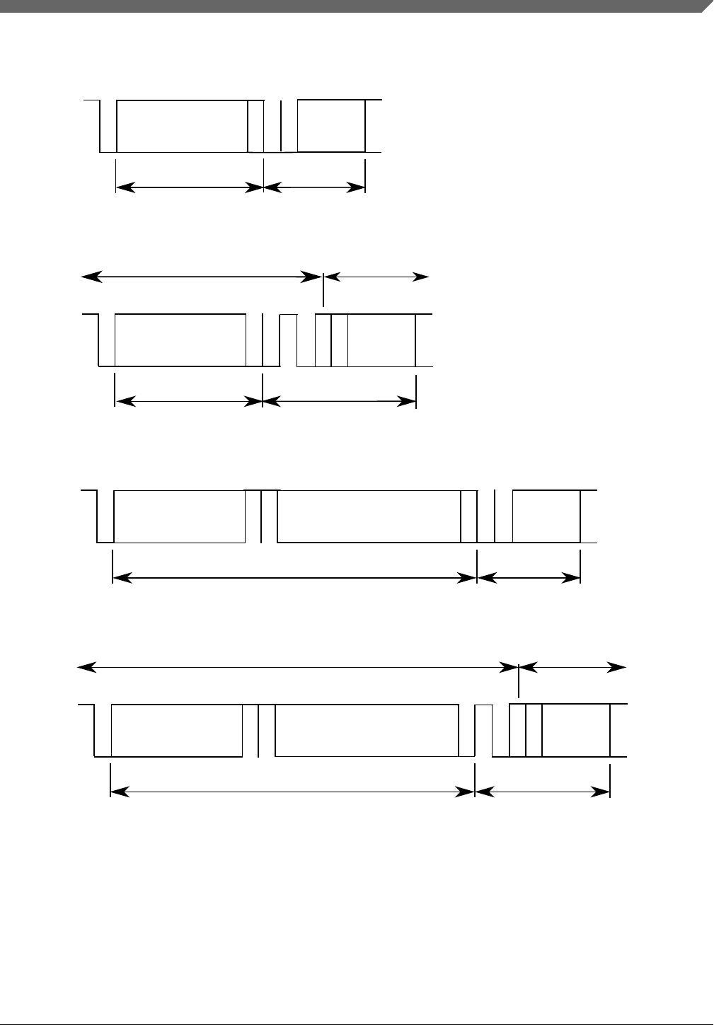
DLC
Arbitration Phase Data Phase
Arbitration Field Control Field
DLC
ID EXTENDED
Arbitration Field Control Field
CAN FD Extended Format
CAN Extended Format
DLC
Arbitration Phase Data Phase
Arbitration Field Control Field
CAN FD Standard Format
ID STANDARD
DLC
Arbitration Field Control Field
CAN Standard Format
ID STANDARD
ID STANDARD
ID STANDARD ID EXTENDED
S
O
F
S
O
F
S
O
F
S
O
F
R
T
R
I
D
E
R
0
R
R
S
E
D
L
B
R
S
E
S
I
I
D
E
r
e
s
S
R
R
I
D
E
R
T
R
R
1
R
0
S
R
R
I
D
E
R
R
S
r
e
s
E
D
L
B
R
S
E
S
I
Figure 53-2. CAN message formats
The ability to receive and transmit CAN FD messages is enabled by the
CAN_MCR[FDEN] bit. Either a recessive R0 bit in CAN frames with 11-bit identifiers
or a recessive R1 bit in CAN frames with 29-bit identifiers are decoded as an EDL bit
(not a reserved one). A CAN FD frame is recognized by a recessive EDL bit, while a
Chapter 53 FlexCAN
S32K1xx Series Reference Manual, Rev. 7, 04/2018
NXP Semiconductors 1751

Classical CAN frame is recognized by a dominant EDL bit. The BRS bit specifies
whether this frame switches the bit rate in its data phase. A long frame is decoded in
accordance to the DLC field value (see DLC definition in Message buffer structure).
CAN FD messages can be transmitted with two different bit rates. The first part of a
CAN FD frame, from the Start Of Frame (SOF) bit until the Bit Rate Switch (BRS) bit,
also called the arbitration phase, is transmitted with the nominal bit rate based on a set of
nominal CAN bit timing configuration values. The second part, from the BRS bit until
the CRC Delimiter bit, also named the data phase, is transmitted with the data bit rate
defined by a second set of CAN data bit timing configuration values. Finally, from the
CRC Delimiter until the Intermission bits, the transmission resumes to nominal bit rate.
In CAN FD frames with bit rate switching, the bit timing is changed inside the frame at
the sample point of the BRS bit if this bit is recessive. Before the BRS bit, in the CAN
FD arbitration phase, the nominal CAN bit timing is used as defined by the CAN_CBT
register (also by CAN_CTRL1 register for backward compatibility). Upon detecting a
recessive BRS bit, the CAN data bit timing is used as defined by the CAN_FDCBT
register.
NOTE
If the length of the time quantum in the nominal bit timing and
the length of the time quantum in the data bit timing are not
identical, a quantization error of up to one time quantum of the
arbitration phase may be present as a phase error. This situation
can occur after the switch from arbitration to data phase and
will last until the next synchronization event. Thus, the length
of the time quantum should be the same in nominal and data bit
timing in order to minimize the chance of error frames on the
CAN bus, and to optimize the clock tolerance in networks that
use FD frames.
CAN_FDCTRL[FDRATE] enables the transmission of all frames with bit rate switching
if the BRS bit in the selected Tx MB is set. If FDRATE is negated, the transmission is
performed at nominal rate regardless of the BRS bit value. The
CAN_FDCTRL[FDRATE] bit can be written any time but takes effect only for the next
message transmitted or received.
The nominal bit timing is resumed at either the sample point of the CRC Delimiter bit or
when an error is detected, whichever occurs first. The following figure describes the
mechanism for entering and leaving the data phase when BRS bit is recessive.
Functional description
S32K1xx Series Reference Manual, Rev. 7, 04/2018
1752 NXP Semiconductors

DATA
Arbitration Phase Data Phase
Arbitration Field Control Field
CAN FD Frame
ID
S
O
F
B
R
S
S
O
F
CRC
A
C
K
A
C
K
D
E
L
C
R
C
D
E
L
EOF
Data Field CRC Field
Arbitration Phase
PROPSEG
S
Y
N
C PSEG1 PSEG2
Sample Point
Nominal Bit Time
FPROPSEG FPSEG1 FPSEG2
Sample Point
Data Bit Time
S
Y
N
C
PROPSEG
S
Y
N
C PSEG1 PSEG2
Sample Point
BRS Bit
FPROPSEG FPSEG1
FPSEG2
Sample Point
CRC Delimiter Bit
S
Y
N
C
Figure 53-3. Bit rate switching mechanism for CAN FD messages
NOTE
In Classical CAN frames, the CRC delimiter is one single
recessive bit. In CAN FD frames, the CRC delimiter may
consist of one or two recessive bits. FlexCAN sends only one
recessive bit as the CRC delimiter, but it accepts two recessive
bits before the edge from recessive to dominant that starts the
acknowledge slot. As a receiver, FlexCAN sends its
acknowledge bit after the first CRC delimiter bit. In CAN FD
frames, FlexCAN accepts a two-bit dominant ACK slot as a
valid ACK to compensate for phase shifts between the
receivers.
The maximum configurable bit rate in the CAN FD data phase depends on the clock
frequency of CAN_PE sub-block. For example, with a CAN_PE clock frequency of
40MHz and the shortest configurable bit time of 5 time quanta, the bit rate in the data
phase is 8 Mbit/s.3
Chapter 53 FlexCAN
S32K1xx Series Reference Manual, Rev. 7, 04/2018
NXP Semiconductors 1753

The value of the ESI bit is determined either by the transmitter's error state at the start of
the transmission, if the frame is originated in the FlexCAN node, or by the original
transmitting node in case FlexCAN is acting as a gateway for the message. If the
transmitter is error passive, ESI is transmitted recessive; otherwise, it is transmitted
dominant. The permutations of the relationship between the written value and the
transmitted value of the ESI are shown in this table.
Table 53-25. Written versus transmitted values of ESI field
FlexCAN fault confinement status at
start of frame
ESI bit Of Tx MB Transmitted ESI
Error active 0 0 (Error Active)
Error passive 0 1 (Error Passive)
Error active 1 1 (Error Passive)
Error passive 1 1 (Error Passive)
There are different CRC polynomials for different CAN frame formats. The first
polynomial, CRC_15, is used for all frames in Classical CAN format. The second,
CRC_17, is used for frames in CAN FD format with a data field up to sixteen bytes long.
The third, CRC_21, is used for frames in CAN FD format with a data field longer than
sixteen bytes. Each polynomial results in a Hamming Distance of 6. At the start of the
frame, all three CRC polynomials are calculated concurrently. The CRC sequence to be
transmitted is selected by the values of the EDL bit and the DLC bit field. When
receiving a message, FlexCAN decodes EDL and DLC to select the adequate CRC
polynomial to check for a CRC error.
In CAN FD format frames, stuff bits are included in the bit stream for CRC calculation.
In Classical CAN format frames, stuff bits are not included. After the transmission of the
last bit relevant to the CRC calculation, the CAN_FDCRC register stores the calculated
CRC for the transmitted message, with the adequate length in accordance to the type of
message, for both CAN FD and non-FD messages. The CAN_CRCR register reports a
valid CRC for Classical CAN messages only.
In CAN FD format frames, the CAN bit stuffing method is changed for the CRC
sequence so that the stuff bits are inserted at fixed positions. When FlexCAN is
transmitting a CAN FD frame, a fixed stuff bit is inserted just before the first bit of the
CRC sequence, even if the last bits of the preceding field do not fulfill the CAN stuff
condition. Additional stuff bits are inserted after each fourth bit of the CRC sequence.
The value of any fixed stuff bit is the inverse value of its preceding bit. When FlexCAN
3. The frequency used in this example may not be supported on this chip; it is shown only to demonstrate how the maximum
configurable bit rate is calculated.
Functional description
S32K1xx Series Reference Manual, Rev. 7, 04/2018
1754 NXP Semiconductors

is receiving a CAN FD frame, it discards the fixed stuff bits from the bit stream for the
CRC check. A Stuff Error is detected if the fixed stuff bit has the same value as its
preceding bit.
FlexCAN detects errors in CAN FD frames the same way as in Classical CAN frames.
The error counters RXERRCNT and TXERRCNT in the CAN_ECR register accumulate
the counts of Rx and Tx errors, respectively, for both FD and non-FD frames indistinctly.
There are two extra error counters (RXERRCNT_FAST and TXERRCNT_FAST) that
accumulate Rx and Tx errors occurring in the data phase of CAN FD frames with the
BRS bit set only. The rules for updating the error counters are the same for both CAN FD
and non-FD frames (see CAN_ECR register).
Error Flags BITERR1, BITERR0, ACKERR, CRCERR, FRMERR and STFERR in the
ESR1 register report errors in both CAN FD and non-FD frames. They also generate the
ERRINT interrupt if CAN_CTRL1[ERRMSK] is asserted. The CAN_ESR1 register has
additional error flags (BITERR1_FAST, BITERR0_FAST, CRCERR_FAST,
FRMERR_FAST and STFERR_FAST) to individually indicate the occurrence of errors
in the data phase of CAN FD frames with the BRS bit set. There is no ACKERR detected
in the data phase of a CAN FD frame. Fault confinement status reported in
CAN_ESR1[FLTCONF] is the same for both CAN FD and Classical CAN frames, and is
based on RXERRCNT and TXERRCNT error counters only. Information contained in
RXERRCNT_FAST and TXERRCNT_FAST counters may be considered as status to
help detect the error nature related to the bit rate value.
When FlexCAN is in the data phase, either transmitting or receiving a CAN FD message,
and detects an error, it immediately switches back to the arbitration phase and to the
nominal rate to start an Error Flag.
Resynchronization and Hard Synchronization occur in CAN FD frames in the same way
as in Classical CAN ones. Additionally, a Hard Synchronization is also performed at the
recessive to dominant edge from EDL to R0 in CAN FD format frames. FlexCAN does
not resynchronize while transmitting in the CAN FD data phase.
53.5.9.3 Transceiver Delay Compensation
The CAN FD protocol allows the transmission and reception of data at a higher bit rate
than the nominal rate used in the arbitration phase when the message's BRS bit is set.
This feature enables the use of rates up to 8 Mbps.
During the data phase of a CAN FD frame, the Transmitter detects a bit error if it cannot
receive its own latest transmitted bit at the sample point of that bit. When bit rate
switching is enabled (BRS bit is asserted), the length of the CAN bit time in the data
Chapter 53 FlexCAN
S32K1xx Series Reference Manual, Rev. 7, 04/2018
NXP Semiconductors 1755

phase can become shorter than the transceiver's loop delay, thus impeding the correct
comparison between the transmitted bit and the received bit within the current CAN bit
time interval.
Note that the TDC process defines a secondary sample point where the transmitted bit is
correctly compared with the received bit in order to check for bit errors.
The TDC mechanism can be enabled by the CAN_FDCTRL[TDCEN] bit and is effective
only during the data phase of FD frames having the BRS bit set. It has no effect either on
non-FD frames, or on FD frames transmitted at normal bit rate. The TDC is active from
the sample point of the BRS bit until the sample point of the CRC Delimiter bit, provided
the respective message under transmission has the BRS bit set. When it is active, a
comparison is done between the real received bit and the delayed transmitted bit, where
the delay is calculated based on the measured transceiver loop delay.
NOTE
The actual value of the CRC Delimiter bit is disregarded by
transmitters using the Transceiver Delay Compensation
mechanism. A global error at the end of the CRC Field will
cause the receivers to send error frames that the transmitter will
detect during Acknowledge or End of Frame.
For every transmitted FD frame having the BRS bit set, the delay measurement is
triggered by the transition from the recessive EDL bit to the dominant R0 bit (as shown in
the next figure). The loop delay is measured in Protocol Engine (PE) clock periods
(CANCLK, see Protocol timing), from the transmitted EDL-R0 edge to the received
EDL-R0 edge. The position of the secondary sample point is defined by the measured
loop delay time added to an offset value specified in CAN_FDCTRL[TDCOFF].
CAN_FDCTRL[TDCVAL] bit field stores the result of this calculation. The TDCVAL
value saturates at its maximum value of 63 CANCLK when the delay measurement is too
long.
Functional description
S32K1xx Series Reference Manual, Rev. 7, 04/2018
1756 NXP Semiconductors
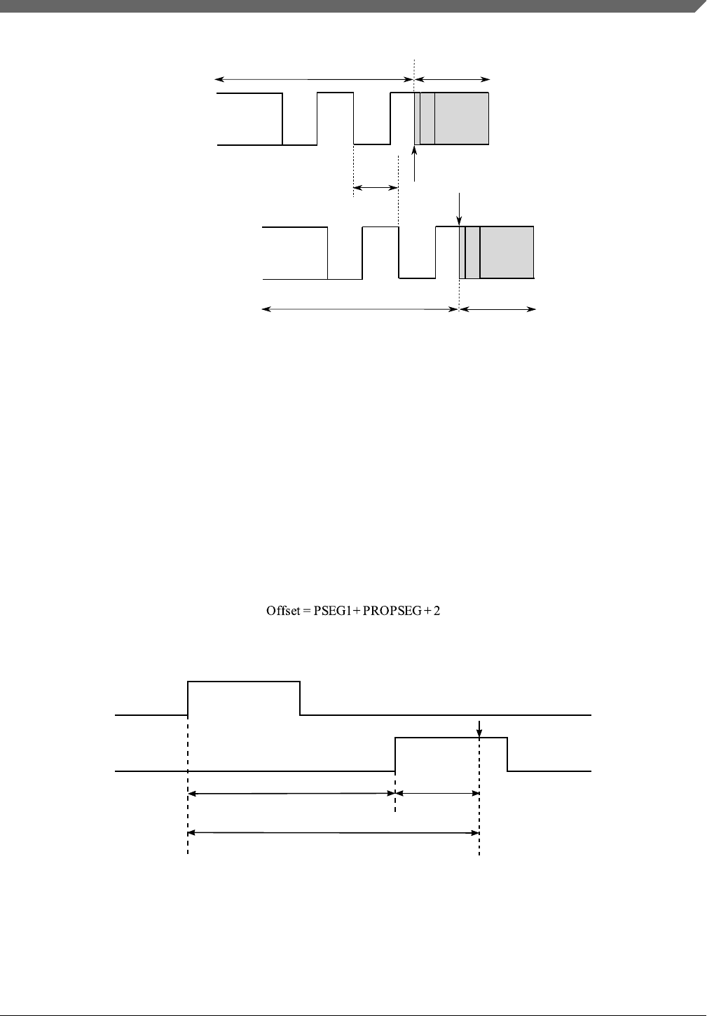
DLC
Arbitration Phase Data Phase
E
D
L
B
R
S
E
S
I
r
e
s
DLC
Arbitration Phase Data Phase
E
D
L
B
R
S
E
S
I
r
e
s
Loop delay
Tx output
Rx input
Rate Switch Point
Figure 53-4. Transceiver loop delay measurement
The measured loop delay is not enough to be used to define the secondary sample point
because it relates to the CAN bit edges. The transceiver delay compensation offset
TDCOFF is used to shift the secondary sample point from the edge to an intermediate
point inside the bit time, far away from its edges. Therefore, the TDCOFF value cannot
be larger than the CAN bit duration in the data phase.
If the secondary sample point is set very near the CAN bit edge (SYNC field), then
problems may occur during the bit sampling in the data phase. For the TDC to work
reliably, the offset has to use optimal settings. To be sure the bit sampling is performed in
the best region, the TDC offset should be configured as shown in this equation:
The following figure shows the SSP position when these settings are used.
TDC measurement TDC Offset
SSP position
SSP
TX output
RX input
Figure 53-5. SSP position with optimal values
During the data phase of CAN FD frames with bit rate switching enabled, at the onset of
every Tx CAN bit, the transmitted Tx bit value is temporarily stored in a buffer and a
time countdown based on TDCVAL is started which ends with the comparison of the
Chapter 53 FlexCAN
S32K1xx Series Reference Manual, Rev. 7, 04/2018
NXP Semiconductors 1757

received Rx bit (delayed by the external loop delay plus the specified offset) with the
stored Tx bit. If a bit error is detected at the secondary sample point, the FlexCAN issues
an error flag to the CAN bus at the next sample point.
During the arbitration phase the delay compensation is always disabled. The maximum
delay which can be compensated by the FlexCAN's transceiver delay compensation
during the data phase is 3 CAN bit times - 2 Tq. Beyond this limit, the
CAN_FDCTRL[TDCFAIL] flag is set to indicate when the Transceiver Delay
Compensation mechanism is out of range, unable to compensate the transceiver loop
delay.
53.5.9.4 Remote frames
Remote frame is a special kind of frame. The user can program a mailbox to be a Remote
Request Frame by configuring the mailbox as Transmit with the RTR bit set to '1'. After
the remote request frame is transmitted successfully, the mailbox becomes a Receive
Message Buffer, with the same ID as before.
When a remote request frame is received by FlexCAN, it can be treated in three ways,
depending on Remote Request Storing (CTRL2[RRS]) and Rx FIFO Enable
(MCR[RFEN]) bits:
• If RRS is negated the frame's ID is compared to the IDs of the Transmit Message
Buffers with the CODE field 0b1010. If there is a matching ID, then this mailbox
frame will be transmitted. Note that if the matching mailbox has the RTR bit set, then
FlexCAN will transmit a remote frame as a response. The received remote request
frame is not stored in a receive buffer. It is only used to trigger a transmission of a
frame in response. The mask registers are not used in remote frame matching, and all
ID bits (except RTR) of the incoming received frame should match. In the case that a
remote request frame is received and matches a mailbox, this message buffer
immediately enters the internal arbitration process, but is considered as a normal Tx
mailbox, with no higher priority. The data length of this frame is independent of the
DLC field in the remote frame that initiated its transmission.
• If RRS is asserted the frame's ID is compared to the IDs of the receive mailboxes
with the CODE field 0b0100, 0b0010 or 0b0110. If there is a matching ID, then this
mailbox will store the remote frame in the same fashion of a data frame. No
automatic remote response frame will be generated. The mask registers are used in
the matching process.
• If RFEN is asserted FlexCAN will not generate an automatic response for remote
request frames that match the FIFO filtering criteria. If the remote frame matches one
of the target IDs, it will be stored in the FIFO and presented to the CPU. Note that for
Functional description
S32K1xx Series Reference Manual, Rev. 7, 04/2018
1758 NXP Semiconductors

filtering formats A and B, it is possible to select whether remote frames are accepted
or not. For format C, remote frames are always accepted (if they match the ID).
Remote Request Frames are considered as normal frames, and generate a FIFO
overflow when a successful reception occurs and the FIFO is already full.
NOTE
There is no remote frame in the CAN FD format. The RTR bit
is replaced by a fixed dominant RRS bit. FlexCAN receives and
transmits remote frames in the Classical CAN format.
53.5.9.5 Overload frames
FlexCAN does transmit overload frames due to detection of following conditions on
CAN bus:
• Detection of a dominant bit in the first/second bit of Intermission
• Detection of a dominant bit at the 7th bit (last) of End of Frame field (Rx frames)
• Detection of a dominant bit at the 8th bit (last) of Error Frame Delimiter or Overload
Frame Delimiter
53.5.9.6 Time stamp
The value of the Free Running Timer is sampled at the beginning of the Identifier field on
the CAN bus, and is stored at the end of "move-in" in the TIME STAMP field, providing
network behavior with respect to time.
When the TIMER_SRC bit in CAN_CTRL2 register is asserted, the Free Running Timer
is continuously clocked by an external time tick.
When the TIMER_SRC bit in CAN_CTRL2 register is negated, the Free Running Timer
is clocked by the FlexCAN bit-clock, which defines the baud rate on the CAN bus.
During a message transmission/reception, it increments by one for each bit that is
received or transmitted. When there is no message on the bus, it counts using the
previously programmed baud rate.
The Free Running Timer is not incremented during Disable, Stop, and Freeze modes. It
can be reset upon a specific frame reception, enabling network time synchronization. See
the TSYN description in Control 1 Register (CAN_CTRL1).
Chapter 53 FlexCAN
S32K1xx Series Reference Manual, Rev. 7, 04/2018
NXP Semiconductors 1759
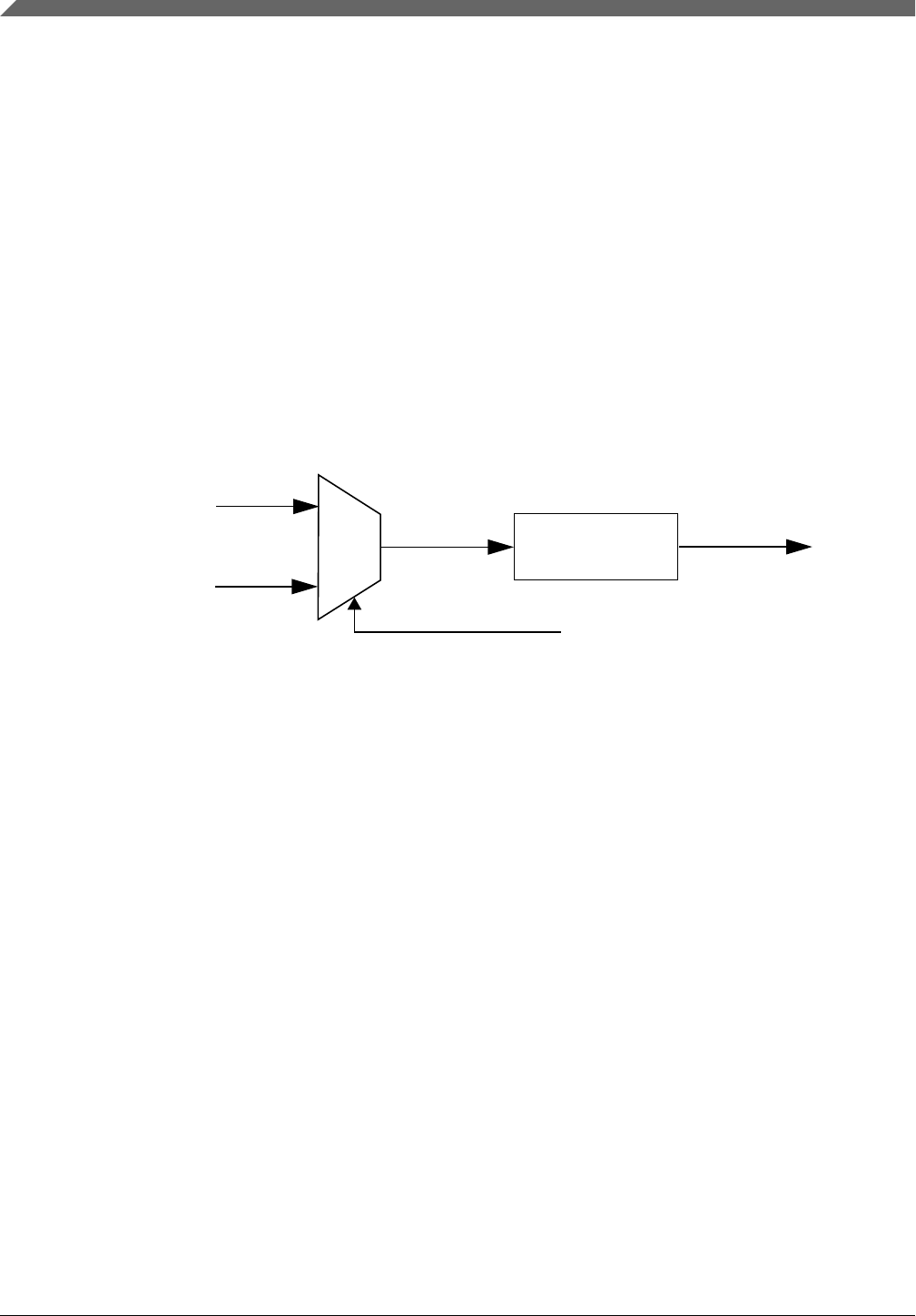
53.5.9.7 Protocol timing
The following figure shows the structure of the clock generation circuitry that feeds the
CAN Protocol Engine (PE) submodule. The clock source bit CLKSRC in the
CAN_CTRL1 Register defines whether the internal clock is connected to the output of a
crystal oscillator (Oscillator Clock) or to the Peripheral Clock. In order to guarantee
reliable operation, the clock source should be selected while the module is in Disable
Mode (MDIS bit set in the Module Configuration Register).
NOTE
Please refer to the clock distribution chapter (module clocks
table) to identify the proper clock source.
CAN_CTRL1[CLKSRC]
Sclock
CANCLK
Prescaler
Peripheral Clock
Oscillator Clock
(Tq)
1
0
Figure 53-6. CAN engine clocking scheme
The oscillator clock should be selected whenever a tight tolerance (up to 0.1%) is
required in the CAN bus timing. The crystal oscillator clock has better jitter performance
than the peripheral clock.
The FlexCAN module supports a variety of means to setup bit timing parameters that are
required by the CAN protocol. The Control 1 Register (CAN_CTRL1) has various fields
used to control bit timing parameters: PRESDIV, PROPSEG, PSEG1, PSEG2 and RJW.
The CAN Bit Timing register (CAN_CBT) extends the range of the CAN bit timing
variables in CAN_CTRL1. The CAN FD Bit Timing register (CAN_FDCBT) provides a
second set of CAN bit timing variables to be applied at the data phase of CAN FD frames
with the Bit Rate Switch (BRS) set.
NOTE
When the CAN FD feature is enabled, always set
CAN_CBT[BTF] and configure the CAN bit timing variables
in CAN_CBT. See CAN Bit Timing Register (CBT).
Functional description
S32K1xx Series Reference Manual, Rev. 7, 04/2018
1760 NXP Semiconductors

The PRESDIV field (as well as its extended range EPRESDIV and FDPRESDIV for the
data phase bits of CAN FD messages) defines the Prescaler Value (see the equation
below) that generates the Serial Clock (Sclock), whose period defines the 'time quantum'
used to compose the CAN waveform. A time quantum (Tq) is the atomic unit of time
handled by the CAN engine.
Tq =fCANCLK
( PRESDIV + 1 )
The bit rate, which defines the rate the CAN message is either received or transmitted, is
given by the formula:
CAN Bit Time = (Number of Time Quanta in 1 bit time) * Tq
Bit Rate = CAN Bit Time
1
A bit time is subdivided into three segments1 (see Figure 53-7, Figure 53-8 and Table
53-26):
• SYNC_SEG: This segment has a fixed length of one time quantum. Signal edges are
expected to happen within this section
• Time Segment 1: This segment includes the Propagation Segment and the Phase
Segment 1 of the CAN standard. It can be programmed by setting the PROPSEG and
the PSEG1 fields of the CAN_CTRL1 Register so that their sum (plus 2) is in the
range of 2 to 16 time quanta. When CAN_CBT[BTF] bit is asserted, FlexCAN uses
EPROPSEG and EPSEG1 fields from CAN_CBT register so that their sum (plus 2)
is in the range of 2 to 96 time quanta. For messages in CAN FD format with the BRS
bit set, FlexCAN uses FDPROPSEG and FDPSEG1 from CAN_FDCBT instead, so
that their sum (plus 1) is in the range of 2 to 39 time quanta.
• Time Segment 2: This segment represents the Phase Segment 2 of the CAN standard.
It can be programmed by setting the PSEG2 field of the CAN_CTRL1 Register (plus
1) to be 2 to 8 time quanta long. When CAN_CBT[BTF] bit is asserted, FlexCAN
uses EPSEG2 fields of CAN_CBT register so that its value (plus 1) is in the range of
2 to 32 time quanta. For messages in CAN FD format with the BRS bit set, FlexCAN
1. For further explanation of the underlying concepts, see ISO 11898-1. See also the CAN 2.0A/B protocol specification for
bit timing.
Chapter 53 FlexCAN
S32K1xx Series Reference Manual, Rev. 7, 04/2018
NXP Semiconductors 1761
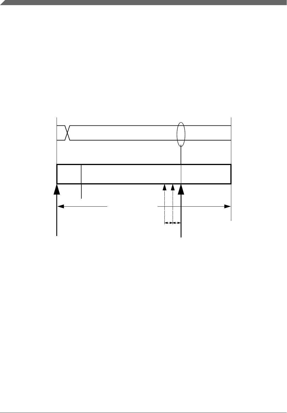
uses FDPSEG2 from CAN_FDCBT instead, so that its value (plus 1) is in the range
of 2 to 8 time quanta. The Time Segnment 2 cannot be smaller than the Information
Processing Time (IPT), which value is 2 time quanta in FlexCAN.
NOTE
The bit time defined by the above time segments must not be
smaller than 5 time quanta. For bit time calculations, use an
Information Processing Time (IPT) of 2, which is the value
implemented in the FlexCAN module.
S Y N C _ S E G
Time Segment 2
2 ... 8
8 ... 25 Time Quanta
= 1 Bit Time
Sample Point
(single or triple sampling)
Transmit Point
Time Segment 1
1 2 ... 16
NRZ Signal
Tq Tq
(PROPSEG + PSEG1 + 2) (PSEG2 + 1)
Figure 53-7. Segments within the bit time (example using CAN_CTRL1 bit timing
variables for Classical CAN format)
Functional description
S32K1xx Series Reference Manual, Rev. 7, 04/2018
1762 NXP Semiconductors
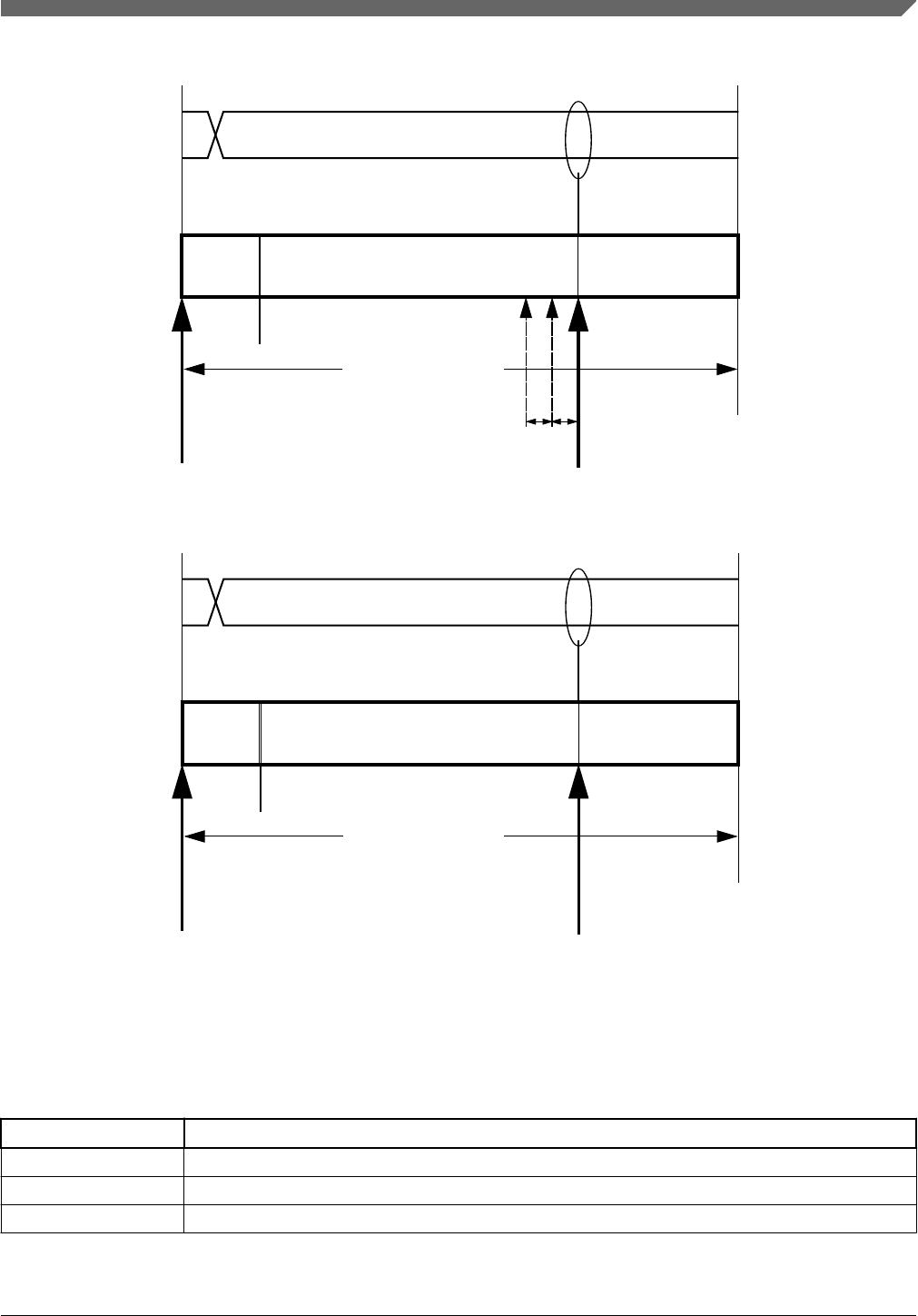
S Y N C _ S E G
Time Segment 2
Sample Point
(single sampling)
Transmit Point
Time Segment 1
NRZ Signal
(FPROPSEG + FPSEG1 + 1) (FPSEG2 + 1)
S Y N C _ S E G
Time Segment 2
Sample Point
(single or triple sampling)
Transmit Point
Time Segment 1
NRZ Signal
Tq Tq
(EPROPSEG + EPSEG1 + 2) (EPSEG2 + 1)
2 ... 96 2 ... 32
1
12 ... 39 2 ... 8
8 ... 129 Time Quanta
= 1 Bit Time
5 ... 48 Time Quanta
= 1 Bit Time
Figure 53-8. Segments within the bit time (example using CAN_CBT and CAN_FDCBT
bit timing variables for CAN FD format)
Table 53-26. Time segment syntax
Syntax Description
SYNC_SEG System expects transitions to occur on the bus during this period.
TSEG1 Corresponds to the sum of PROPSEG and PSEG1.
TSEG2 Corresponds to the PSEG2 value.
Table continues on the next page...
Chapter 53 FlexCAN
S32K1xx Series Reference Manual, Rev. 7, 04/2018
NXP Semiconductors 1763

Table 53-26. Time segment syntax (continued)
Syntax Description
Transmit Point A node in transmit mode transfers a new value to the CAN bus at this point.
Sample Point A node samples the bus at this point. If the three samples per bit option is selected, then this point
marks the position of the third sample.
The following table gives some examples of the CAN compliant segment settings for
Classical CAN format (Bosch CAN 2.0B) (non-FD) messages.
Table 53-27. Bosch CAN 2.0B standard compliant bit time segment settings
Time segment 1 Time segment 2 Re-synchronization jump width
5 .. 10 2 1 .. 2
4 .. 11 3 1 .. 3
5 .. 12 4 1 .. 4
6 .. 13 5 1 .. 4
7 .. 14 6 1 .. 4
8 .. 15 7 1 .. 4
9 .. 16 8 1 .. 4
Note
The user must ensure the bit time settings are in compliance
with the CAN Protocol standard (ISO 11898-1).
Whenever CAN bit is used as a measure of time duration (e.g. estimating the occurrence
of a CAN bit event in a message), the number of peripheral clocks in one CAN bit
(NumClkBit) can be calculated as:
NumClkBit =fCANCLK
fSYS X (PRESDIV + 1) X (PROPSEG + PSEG1 + PSEG2 + 4)
where:
• NumClkBit is the number of peripheral clocks in one CAN bit;
• fCANCLK is the Protocol Engine (PE) Clock (see Figure "CAN Engine Clocking
Scheme"), in Hz;
• fSYS is the frequency of operation of the system (CHI) clock, in Hz;
• PSEG1 is the value in CAN_CTRL1[PSEG1] field;
• PSEG2 is the value in CAN_CTRL1[PSEG2] field;
• PROPSEG is the value in CAN_CTRL1[PROPSEG] field;
• PRESDIV is the value in CAN_CTRL1[PRESDIV] field.
Functional description
S32K1xx Series Reference Manual, Rev. 7, 04/2018
1764 NXP Semiconductors
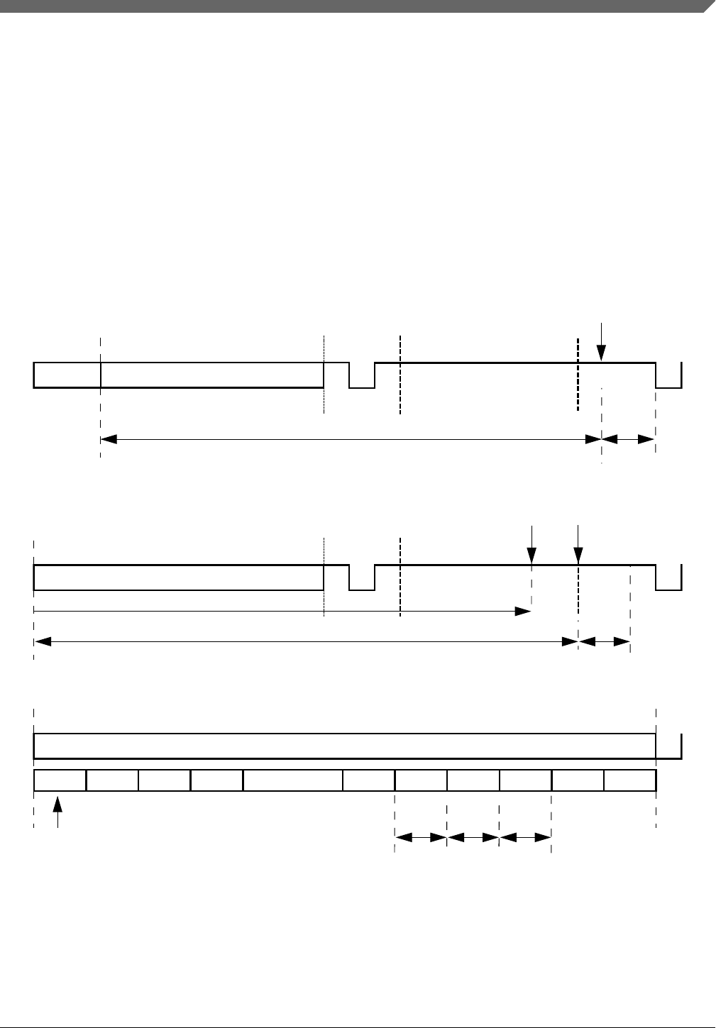
The formula above is also applicable to the alternative CAN bit timing variables
described in the CAN Bit Timing Register (CAN_CBT) and also to the CAN FD Bit
Timing Register (CAN_FDCBT).
For example, 180 CAN bits = (180 x NumClkBit) peripheral clock periods.
53.5.9.8 Arbitration and matching timing
During normal reception and transmission, the matching, arbitration, move-in and move-
out processes are executed during certain time windows inside the CAN frame, as shown
in the following figures.
Interm
Start Move
Move-in
Window
EOF
(bit 2)
Matching Window (26 to 90 CAN bits)
DATA and/or CRC
DLC
Figure 53-9. Matching and move-in time windows
CRC Interm
Start Move
(bit 1)
Window
Start Arbitration
(delayed by TASD)
EOF Move-out
Process
Arb
Arbitration Window (25 CAN bits)
Figure 53-10. Arbitration and move-out time windows
BusOff
128
...
126125124123
...
3210
Window
Move-out
Process
Arb
Count
TASD
Internal Counter
counting 128 occurrences of 11 recessive CAN bits
Figure 53-11. Arbitration at the end of bus off and move-out time windows
NOTE
In the preceding figures, the matching and arbitration timing
does not take into account the delay caused by the concurrent
Chapter 53 FlexCAN
S32K1xx Series Reference Manual, Rev. 7, 04/2018
NXP Semiconductors 1765
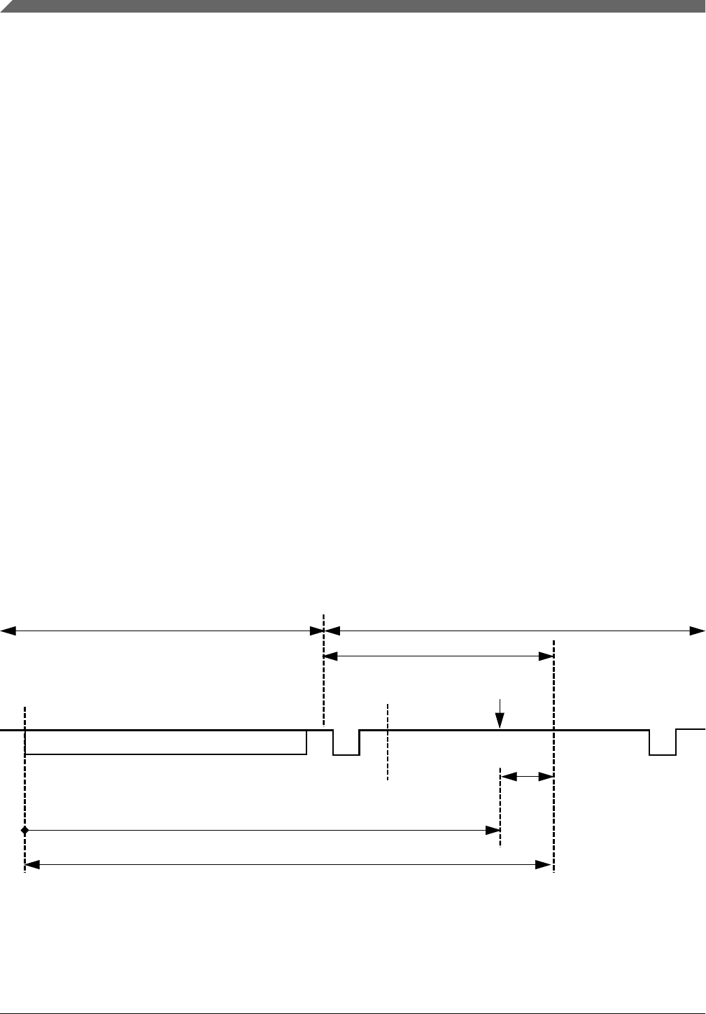
memory access due to the CPU or other internal FlexCAN sub-
blocks.
53.5.9.9 Tx Arbitration start delay
The Tx Arbitration Start Delay (TASD) bit field in Control 2 register
(CAN_CTRL2[TASD]) is a variable that indicates the number of CAN bits used by
FlexCAN to delay the Tx Arbitration process start point from the first bit of CRC field of
the current frame. This variable can be written only in Freeze mode because it is blocked
by hardware in other modes.
The transmission performance is impacted by the ability of the CPU to reconfigure
Message Buffers (MBs) for transmission after the end of the internal Arbitration process,
where FlexCAN finds the winner MB for transmission (see Arbitration process). If the
Arbitration ends too early before the first bit of Intermission field, then there is a chance
that the CPU reconfigures some Tx MBs and the winner MB is no longer the best
candidate to be transmitted.
TASD is useful to optimize the transmission performance by defining the Arbitration
start point, as shown in the next figure, based on factors such as:
• The peripheral-to-oscillator clock ratio
• CAN bit timing variables that determine the CAN bit rate
• The number of Message Buffers (MBs) in use by the Matching and Arbitration
processes.
Intermission
start point
Arbitration
TASD countdown
S
O
F
Process
Arbitration
A
C
K
CRC EOF
Data bit rate when CAN FD is enabled Nominal bit rate
9 last CAN bits
Arbitration window (25 to 31 CAN bits)
Figure 53-12. Optimal Tx Arbitration start point
Functional description
S32K1xx Series Reference Manual, Rev. 7, 04/2018
1766 NXP Semiconductors

The duration of an Arbitration process, in terms of CAN bits, is directly proportional to
the number of available MBs and to the CAN bit rate, and inversely proportional to the
peripheral clock frequency.
The optimal Arbitration timing is that in which the last MB is scanned right before the
first bit of the Intermission field of a CAN frame. For instance, if there are few MBs and
the peripheral/oscillator clock ratio is high and the CAN baud rate is low, then the
Arbitration can be placed closer to the frame's end, adding more delay to its start point,
and vice-versa.
If TASD is set to 0 then the Arbitration start is not delayed and more time is reserved for
Arbitration. On the other hand, if TASD is close to 24 then the CPU can configure a Tx
MB later and less time is reserved for Arbitration. If too little time is reserved for
Arbitration the FlexCAN may be not be able to find a winner MB in time to be
transmitted with the best chance to win the bus arbitration against external nodes on the
CAN bus.
The optimal TASD value can be calculated as follows:
TASD = 25 -
For CAN FD frames and (MAXMB + 1) < NMBEND
TASD = 31 - 2 * ( MAXMB + 1 ) + 4
CPCBN
TASD = 22 -
2 * ( MAXMB + 1 ) - NMBEND
CPCBF
2 * ( MAXMB + 1 ) + 4
CPCB
For CAN FD frames and (MAXMB + 1) > NMBEND
For non-FD frames
where:
Chapter 53 FlexCAN
S32K1xx Series Reference Manual, Rev. 7, 04/2018
NXP Semiconductors 1767

CPCBF =
CPCB = CPCBN
NMBEND =
( 9 * CPCBN ) - 4
2
fSYS
CPCBN =
[1 + (EPSEG1 + 1) + (EPSEG2 + 1) + (EPROPSEG + 1) ] x (EPRESDIV + 1)
fCANCLK
BITRATEN =
[1 + (FPSEG1 + 1) + (FPSEG2 + 1) + FPROPSEG] x (FPRESDIV + 1)
fCANCLK
BITRATEF =
BITRATEN
fSYS
BITRATEF
• MAXMB is the value in CAN_CTRL1[MAXMB] field
• NMBEND is the number of Message Buffers that can be scanned by the Arbitration
process during the 9 last CAN bits at the end of a frame, see the figure above
• BITRATEN is the CAN bit rate in bits per second calculated by the nominal CAN bit
time variables
• BITRATEF is the CAN bit rate in bits per second calculated by the data CAN bit
time variables
• CPCBN is the number of peripheral clocks per CAN bit in nominal bit rate for CAN
FD frames
• CPCBF is the number of peripheral clocks per CAN bit in data bit rate for CAN FD
frames
• CPCB is the number of peripheral clocks per CAN bit for non-FD frames
• fCANCLK is the oscillator clock, in Hz
• fSYS is the peripheral clock, in Hz
• EPSEG1 is the value in CAN_CBT[EPSEG1] field (CAN_CTRL1[PSEG1] can also
be used)
• EPSEG2 is the value in CAN_CBT[EPSEG2] field (CAN_CTRL1[PSEG2] can also
be used)
• EPROPSEG is the value in CAN_CBT[EPROPSEG] field
(CAN_CTRL1[PROPSEG] can also be used)
Functional description
S32K1xx Series Reference Manual, Rev. 7, 04/2018
1768 NXP Semiconductors

• EPRESDIV is the value in CAN_CBT[EPRESDIV] field (CAN_CTRL1[PRESDIV]
can also be used)
• FPSEG1 is the value in CAN_FDCBT[FPSEG1] field
• FPSEG2 is the value in CAN_FDCBT[FPSEG2] field
• FPROPSEG is the value in CAN_FDCBT[FPROPSEG] field
• FPRESDIV is the value in CAN_FDCBT[FPRESDIV] field
See also Protocol timing for more details.
The following tables give the TASD value calculated for some configuration cases.
Case 1:
• Clock ratio = 2:1 (example: peripheral clock 80 MHz and oscillator clock 40 MHz)
• Bit rate in arbitration phase = 1 Mbaud
Table 53-28. TASD values:
Number of Message Buffers TASD value Maximum Bit Rate in Data Phase
(Mbaud)
16 24 Invalid
32 24 8.0
Case 2:
• Clock ratio = 1:1 (example: peripheral clock 40 MHz and oscillator clock 40 MHz)
• Bit rate in arbitration phase = 1 Mbaud
Table 53-29. TASD values:
Number of Message Buffers TASD value Maximum Bit Rate in Data Phase
(Mbaud)
16 24 Invalid
32 23 6.67
Case 3:
• Clock ratio = 2:1 (example: peripheral clock 40 MHz and oscillator clock 20 MHz)
• Bit rate in arbitration phase = 1 Mbaud
Table 53-30. TASD values:
Number of Message Buffers TASD value Maximum Bit Rate in Data Phase
(Mbaud)
16 24 Invalid
32 23 4.0
Chapter 53 FlexCAN
S32K1xx Series Reference Manual, Rev. 7, 04/2018
NXP Semiconductors 1769

53.5.10 Clock domains and restrictions
The FlexCAN module has two clock domains asynchronous to each other:
• The Bus Domain feeds the Control Host Interface (CHI) submodule and is derived
from the peripheral clock.
• The Oscillator Domain feeds the CAN Protocol Engine (PE) submodule and is
derived directly from a crystal oscillator clock, so that very low jitter performance
can be achieved on the CAN bus.
When CAN_CTRL1[CLKSRC] bit is set, synchronous operation occurs because both
domains are connected to the peripheral clock (creating a 1:1 ratio between the peripheral
and oscillator clocks).
When the two domains are connected to clocks with different frequencies and/or phases,
there are restrictions on the frequency relationship between the two clock domains. In the
case of asynchronous operation, the Bus Domain clock frequency must always be greater
than the Oscillator Domain clock frequency.
NOTE
Asynchronous operation with a 1:1 ratio between peripheral
and oscillator clocks is not allowed.
When doing matching and arbitration, FlexCAN needs to scan the whole Message Buffer
memory during the time slot of one CAN frame, comprised of a number of CAN bits. In
order to have sufficient time to do that, the following requirements must be observed:
• The peripheral clock frequency can not be smaller than the oscillator clock frequency
• There must be a minimum number of peripheral clocks per CAN bit, as specified in
the table shown below
Table 53-31. Minimum number of peripheral clocks per CAN bit for Classical CAN format
Number of Mailboxes Value of CAN_MCR[RFEN] Minimum number of peripheral
clocks per CAN bit
16 0 16
32 0 16
16 1 16
32 1 17
For classical frame format, the minimum number of peripheral clocks per CAN bit
specified in the preceding table determines the minimum peripheral clock frequency for a
given number of Mailboxes and for an expected CAN bit rate. The CAN bit rate depends
Functional description
S32K1xx Series Reference Manual, Rev. 7, 04/2018
1770 NXP Semiconductors

on the number of time quanta in a CAN bit, that can be defined by adjusting one or more
of the bit timing values contained in either the Control 1 Register (CAN_CTRL1) or
CAN Bit Time register (CAN_CBT). The time quantum (Tq) is defined in Protocol
timing. The minimum number of time quanta per CAN bit must be 8; therefore, the
oscillator clock frequency should be at least 8 times the CAN bit rate.
For CAN FD frame format, there are some constraints that need to be satisfied. The
number of peripheral clocks per CAN bit in nominal bit rate (NumClkNomBit) can be
calculated by the equation below.
NumClkNomBit =fCANCLK
fSYS X (PRESDIV + 1) X (PROPSEG + PSEG1 + PSEG2 + 4)
=fSYS
NomBitRate
where PRESDIV, PSEG1 and PSEG2 are CAN bit time values in CTRL1 register.
Alternatively, EPRESDIV, EPSEG1 and EPSEG2 values in CBT register can be used
instead. NumClkNomBit can also be calculated as a function of the expected nominal bit
rate used in the Arbitration Phase (NomBitRate) as shown in the equation above.
The number of CAN bits in the Data Phase of a FD Frames with the BRS bit set (fast
CAN bits, in short) depends on the number of data bytes in the payload. The number of
fast CAN bits (NumOfFastBits) can be determined in the table below. The less the
number of data bytes, the less the number of fast CAN bits, and less time is available for
FlexCAN to scan the whole Message Buffer memory during the internal matching and
arbitration processes.
Table 53-32. Number of fast CAN bits in a CAN FD frame
Minimum number of data bytes DLC field NumOfFastBits
0 0x0 21
1 0x1 29
2 0x2 37
3 0x3 45
4 0x4 53
5 0x5 61
6 0x6 69
7 0x7 77
8 0x8 85
12 0x9 117
16 0xA 149
Table continues on the next page...
Chapter 53 FlexCAN
S32K1xx Series Reference Manual, Rev. 7, 04/2018
NXP Semiconductors 1771

Table 53-32. Number of fast CAN bits in a CAN FD frame (continued)
Minimum number of data bytes DLC field NumOfFastBits
20 0xB 186
24 0xC 218
32 0xD 282
48 0xE 410
64 0xF 538
The critical part of a CAN FD frame is during the Data Phase, where the CAN bit rate is
faster than in the Arbitration Phase. The minimum number of peripheral clocks per fast
CAN bit (MinNumClkFastBit) can be calculated to guarantee that enough time is
available for FlexCAN to scan the Message Buffer memory during reception and
transmission. The equation below calculates this constraint.
MinNumClkFastBit NumOfFastBits
( 8.5 x MaxNumOfMb ) + 64 - ( 9 x NumClkNomBit )
=
A
where MaxNumOfMb is the maximum number of available Mailboxes defined in
CAN_MCR[MAXMB].
The clock domain crossing circuit between the CHI and PE sub-blocks also imposes a
minimum number of peripheral clocks per fast CAN bit for the handshake mechanism to
work properly without loosing status information through the interface, as shown in the
equation below.
MinNumClkFastBit = 3 x
B fCANCLK
fSYS
1 +
Therefore, the minimum number of peripheral clocks per fast CAN bit
(MinNumClkFastBit) is determined by the larger of the two values calculated above.
MinNumClkFastBit = B
Maximum ( MinNumClkFastBit , MinNumClkFastBit )
A
Then, the maximum CAN bit rate in the Data Phase of CAN FD frames
(DataBitRateMAX) can be calculated as below.
Functional description
S32K1xx Series Reference Manual, Rev. 7, 04/2018
1772 NXP Semiconductors

DataBitRate =
MAX
fSYS
fCANCLK
fCANCLK
MinNumClkFastBit x
ROUNDUP
The peripheral and oscillator clock frequencies, the maximum number of mailboxes and
the expected nominal bit rate affect the maximum data bit rate attainable by FlexCAN in
CAN FD mode. Besides, the data bit rate depends on the minimum payload size of FD
frames used in a given application.
To illustrate how the CAN FD bit rate is affected by the configuration of FlexCAN
variables, an application example with the peripheral and oscillator clock frequencies set
to 50 MHz and 40 MHz, respectively, is considered.
Step 1 - Considering the nominal bit rate as 1 Mbps, the number of peripheral clocks per
CAN bit in nominal bit rate is calculated as below.
NumClkNomBit =50 x 106
1 x 106
= 50
Step 2 - The number of fast CAN bits (NumOfFastBits) is determined in the table
presented above. For example, if the minimum payload in FD frames is 8 bytes, then
there are 85 CAN bits in the Data Phase.
Step 3 - Assuming the maximum number of mailboxes is 96, the minimum number of
peripheral clocks per fast CAN bit (MinNumClkFastBit) can be calculated.
MinNumClkFastBit 85
(8.5 X 96) + 64 - (9 X 50)
=
A = 5.06
MinNumClkFastBit = 3 x
B 40
1 +
50 = 6.75
MinNumClkFastBit =Maximum ( 5.06, 6.75 ) = 6.75
Chapter 53 FlexCAN
S32K1xx Series Reference Manual, Rev. 7, 04/2018
NXP Semiconductors 1773

Step 4 - The maximum CAN bit rate in the Data Phase can be finally found.
DataBitRate =
MAX
50 x 106
40 x 106
6.75 x 40 x 106
ROUNDUP
= 6.667 Mbps
As demonstrated in this example, even though the oscillator clock frequency (40 MHz) is
adequate to generate a data rate of 8 Mbps in CAN FD mode, the specific FlexCAN
configuration limits this rate to 6.667 Mbps. This limitation is mainly due to the low
peripheral clock frequency that imposes the MinNumClkFastBitB bound.
The table below shows the maximum data rate for CAN FD according to clock
frequencies, payload size and number of available mailboxes. See in this table that, for
some cases, if the number of available mailboxes is reduced, the FlexCAN can then
achieve a data rate up to 8 Mbps.
Table 53-33. Maximum CAN bit rate in Data Phase on CAN FD frames
Peripheral clock frequency
(MHz) Payload size Number of available
mailboxes Maximum data rate (Mbps)
40 8 94 6.667
40 8 114 5.0
40 12 117 6.667
40 12 128 5.714
50 12 to 64 128 6.667
60 8 126 8.0
60 12 128 8.0
67 6 128 8.0
80 3 128 8.0
100 0 128 8.0
53.5.11 Modes of operation details
The FlexCAN module has functional modes and low-power modes. See Modes of
operation for an introductory description of all the modes of operation. The following
sub-sections contain functional details on Freeze mode and the low-power modes.
Functional description
S32K1xx Series Reference Manual, Rev. 7, 04/2018
1774 NXP Semiconductors

CAUTION
"Permanent Dominant" failure on CAN Bus line is not
supported by FlexCAN. If a Low-Power request or Freeze
mode request is done during a "Permanent Dominant", the
corresponding acknowledge can never be asserted.
53.5.11.1 Freeze mode
This mode is requested either by the CPU through the assertion of the HALT bit in the
CAN_MCR Register or when the chip is put into Debug mode. In both cases it is also
necessary that the FRZ bit is asserted in the CAN_MCR Register and the module is not in
a low-power mode.
The acknowledgement is obtained through the assertion by the FlexCAN of FRZ_ACK
bit in the same register. The CPU must only consider the FlexCAN in Freeze mode when
both request and acknowledgement conditions are satisfied.
When Freeze mode is requested, FlexCAN does the following:
• Waits to be in either Intermission, Passive Error, Bus Off or Idle state
• Waits for all internal activities like arbitration, matching, move-in and move-out to
finish. A pending move-in does not prevent going to Freeze mode.
• Ignores the Rx input pin and drives the Tx pin as recessive
• Stops the prescaler, thus halting all CAN protocol activities
• Grants write access to the Error Counters Register, which is read-only in other modes
• Sets the NOT_RDY and FRZ_ACK bits in CAN_MCR
After requesting Freeze mode, the user must wait for the FRZ_ACK bit to be asserted in
CAN_MCR before executing any other action, otherwise FlexCAN may operate in an
unpredictable way. In Freeze mode, all memory mapped registers are accessible, except
for CAN_CTRL1[CLKSRC] bit that can be read but cannot be written.
Exiting Freeze mode is done in one of the following ways:
• CPU negates the FRZ bit in the CAN_MCR Register
• The chip is removed from Debug Mode and/or the HALT bit is negated
Chapter 53 FlexCAN
S32K1xx Series Reference Manual, Rev. 7, 04/2018
NXP Semiconductors 1775

The FRZ_ACK bit is negated after the protocol engine recognizes the negation of the
freeze request. When out of Freeze mode, FlexCAN tries to re-synchronize to the CAN
bus by waiting for 11 consecutive recessive bits.
53.5.11.2 Module Disable mode
This low power mode is normally used to temporarily disable a complete FlexCAN
block, with no power consumption. It is requested by the CPU through the assertion of
the CAN_MCR[MDIS] bit, and the acknowledgement is obtained through the assertion
by the FlexCAN of the CAN_MCR[LPMACK] bit. The CPU must only consider the
FlexCAN in Disable mode when both request and acknowledgement conditions are
satisfied.
If the module is disabled during Freeze mode, it requests to disable the clocks to the PE
and CHI sub-modules, sets the LPMACK bit and negates the FRZACK bit.
It is not recommended to use Module Disable mode under Pretended Networking mode.
Negate the MDIS bit and wait for LPMACK to negate before setting
CAN_MCR[PNET_EN].
If the module is disabled during transmission or reception, FlexCAN does the following:
• Waits to be in either Idle or Bus Off state, or else waits for the third bit of --
>Intermission and then checks it to be recessive
• Waits for all internal activities like arbitration, matching, move-in and move-out to
finish. A pending move-in is not taken into account.
• Ignores its Rx input pin and drives its Tx pin as recessive
• Shuts down the clocks to the PE and CHI sub-modules
• Sets the NOTRDY and LPMACK bits in CAN_MCR
The Bus Interface Unit continues to operate, enabling the CPU to access memory mapped
registers, except the Rx Mailboxes Global Mask Registers, the Rx Buffer 14 Mask
Register, the Rx Buffer 15 Mask Register, the Rx FIFO Global Mask Register. The Rx
FIFO Information Register, the Message Buffers, the Rx Individual Mask Registers, and
the reserved words within RAM may not be accessed when the module is in Disable
Mode. Exiting from this mode is done by negating the MDIS bit by the CPU, which
causes the FlexCAN to request to resume the clocks and negate the LPMACK bit after
the CAN protocol engine recognizes the negation of disable mode requested by the CPU.
Functional description
S32K1xx Series Reference Manual, Rev. 7, 04/2018
1776 NXP Semiconductors

53.5.11.3 Stop mode
This is a system low-power mode in which all chip clocks can be stopped for maximum
power savings. The Stop mode is globally requested by the CPU and the
acknowledgement is obtained through the assertion by the FlexCAN of a Stop
Acknowledgement signal. The CPU must only consider the FlexCAN in Stop mode when
both request and acknowledgement conditions are satisfied.
If FlexCAN receives the global Stop mode request during Freeze mode, it sets the
LPMACK bit, negates the FRZACK bit and then sends the Stop Acknowledge signal to
the CPU, in order to shut down the clocks globally.
If Stop mode is requested during transmission or reception, FlexCAN does the following:
• Waits to be in either Idle or Bus Off state, or else waits for the third bit of
Intermission and checks it to be recessive
• Waits for all internal activities like arbitration, matching, move-in and move-out to
finish. A pending move-in is not taken into account.
• Ignores its Rx input pin and drives its Tx pin as recessive
• Sets the NOTRDY and LPMACK bits in CAN_MCR
• Sends a Stop Acknowledge signal to the CPU, so that it can shut down the clocks
globally
Stop mode is exited when the CPU resumes the clocks and removes the Stop Mode
request.
After the CAN protocol engine recognizes the negation of the Stop mode request, the
FlexCAN negates the LPMACK bit. FlexCAN will then wait for 11 consecutive
recessive bits to synchronize to the CAN bus.
53.5.11.4 Pretended Networking Mode
This is a special low power mode used to receive wake up messages with low power
consumption. This mode can be selected to operate together with Stop mode. Before
entering in one of these low power modes, the PNET_EN bit in CAN_MCR Register
must be asserted. Once in low power mode, CHI sub-block is shut down and CAN_PE
sub-block is kept active, so that the Rx receive process is still active to filter incoming
messages (see Receive Process under Pretended Networking Mode) as defined by the
configuration registers (see Pretended Networking Control 1 Register
(CAN_CTRL1_PN)). Upon detecting a wake up event, a Wake Up interrupt is issued to
the system.
Chapter 53 FlexCAN
S32K1xx Series Reference Manual, Rev. 7, 04/2018
NXP Semiconductors 1777

To enter in Pretended Networking mode FlexCAN must be in normal mode (neither in
Freeze, nor in Disable mode). Under Pretended Networking mode, FlexCAN keeps itself
synchronized with the CAN BUS in Stop mode. Then, when Stop mode is requested,
FlexCAN performs the following steps:
• Waits to be in Idle state, or else waits for the third bit of Intermission, and then
checks it to be recessive.
• Sets the LPM_ACK bit in CAN_MCR Register.
• Requests the shutdown of the CHI sub-module clock, while keeping the PE sub-
module clock active.
FlexCAN can exit Pretended Networking mode by the following ways:
• The CPU removing the Stop Mode request.
• FlexCAN will wait until Bus Idle or third bit of Intermission state to negate
CAN_MCR[LPM_ACK] bit.
The above exit ways can be triggered either by the FlexCAN action upon detecting a
wake up event and issuing the respective interrupt, or by the CPU itself upon being
waked up by another mean. In consequence, FlexCAN will wait until the Bus Idle state or
until the third bit of Intermission state to negate CAN_MCR[LPM_ACK] bit and resume
to the Normal mode. This procedure ensures that FlexCAN will be synchronized to the
CAN bus after exiting the Pretended Networking mode. The CPU must wait for the
CAN_MCR[LPM_ACK] bit to be negated before performing any access to FlexCAN.
NOTE
For more information about the difference between FD and
non-FD regarding this feature, see Table 53-3.
53.5.12 Interrupts
The module has many interrupt sources: interrupts due to message buffers and interrupts
due to the ORed interrupts from MBs, Bus Off, Bus Off Done, Error, Error Fast (errors
detected in the data phase of CAN FD format messages with the BRS bit set), Wake Up
Match, Wake Up Timeout, Tx Warning, and Rx Warning.
Each one of the message buffers can be an interrupt source, if its corresponding IMASK
bit is set. There is no distinction between Tx and Rx interrupts for a particular buffer,
under the assumption that the buffer is initialized for either transmission or reception.
Each of the buffers has an assigned flag bit in the CAN_IFLAG registers. The bit is set
when the corresponding buffer completes a successful transfer and is cleared when the
CPU writes it to 1 (unless another interrupt is generated at the same time).
Functional description
S32K1xx Series Reference Manual, Rev. 7, 04/2018
1778 NXP Semiconductors

Note
It must be guaranteed that the CPU clears only the bit causing
the current interrupt. For this reason, bit manipulation
instructions (BSET) must not be used to clear interrupt flags.
These instructions may cause accidental clearing of interrupt
flags which are set after entering the current interrupt service
routine.
If the Rx FIFO is enabled (CAN_MCR[RFEN] = 1) and DMA is disabled
(CAN_MCR[DMA] = 0), the interrupts corresponding to MBs 0 to 7 have different
meanings. Bit 7 of the CAN_IFLAG1 register becomes the "FIFO Overflow" flag; bit 6
becomes the "FIFO Warning" flag, bit 5 becomes the "Frames Available in FIFO" flag
and bits 4-0 are unused. See the description of the Interrupt Flags 1 Register
(CAN_IFLAG1) for more information.
If both Rx FIFO and DMA are enabled (CAN_MCR[RFEN] and CAN_MCR[DMA] = 1)
the FlexCAN does not generate any FIFO interrupt. Bit 5 of the CAN_IFLAG1 register
still indicates "Frames Available in FIFO" and generates a DMA request. Bits 7, 6, 4-0
are unused.
CAUTION
FIFO cannot be enabled when CAN FD feature is enabled.
For a combined interrupt where multiple MB interrupt sources are OR'd together, the
interrupt is generated when any of the associated MBs (or FIFO, if applicable) generates
an interrupt. In this case, the CPU must read the CAN_IFLAG registers to determine
which MB or FIFO source caused the interrupt.
The interrupt sources for Bus Off, Bus Off Done, Error, Error Fast, Tx Warning and Rx
Warning generate interrupts like the MB interrupt sources, and can be read from
CAN_ESR1 register. The Bus Off, Error, Tx Warning, and Rx Warning interrupt mask
bits are located in the CAN_CTRL1 Register.
The interrupt sources for Pretended Networking (Wake up by Match Flag and Wake up
by Timeout Flag) can be read in the CAN_WU_MTC Register and the respective
interrupts masks bits are located in CAN_CTRL1_PN Register.
53.5.13 Bus interface
The CPU access to FlexCAN registers are subject to the following rules:
• Unrestricted read and write access to supervisor registers (registers identified with
S/U in Table "Module Memory Map" in Supervisor Mode or with S only) results in
access error.
Chapter 53 FlexCAN
S32K1xx Series Reference Manual, Rev. 7, 04/2018
NXP Semiconductors 1779

• Read and write access to implemented reserved address space results in access error.
• Write access to positions whose bits are all currently read-only results in access error.
If at least one of the bits is not read-only then no access error is issued. Write
permission to positions or some of their bits can change depending on the mode of
operation or transitory state. Refer to register and bit descriptions for details.
• Read and write access to unimplemented address space results in access error.
• Read and write access to RAM located positions during Low Power Mode results in
access error.
• It is possible for the RXIMR memory region to be considered as general purpose
memory and available for access. There are two ways of doing this:
a. If CAN_MCR[IRMQ] is cleared, the individual masks (RXIMR) are disabled. In
this case the RXIMR memory region is considered as general purpose memory.
b. If CAN_MCR[MAXMB] is programmed with a value smaller than the available
number of MBs, then the unused memory space can be used as general purpose
RAM space. Note that reserved words within RAM cannot be used. As an
example, suppose FlexCAN's RAM can support up to 16 MBs,
CAN_CTRL2[RFFN] is 0x0, and CAN_MCR[MAXMB] is programmed with
zero. The maximum number of MBs in this case becomes one. The RAM starts
at 0x0080, and the space from 0x0080 to 0x008F is used by the one MB. The
memory space from 0x0090 to 0x017F is available. The space between 0x0180
and 0x087F is reserved. The space from 0x0880 to 0x0883 is used by the one
Individual Mask and the available memory in the Mask Registers space would be
from 0x0884 to 0x08BF. From 0x08C0 through 0x09DF there are reserved
words for internal use which cannot be used as general purpose RAM. As a
general rule, free memory space for general purpose depends only on MAXMB.
53.6 Initialization/application information
This section provide instructions for initializing the FlexCAN module.
53.6.1 FlexCAN initialization sequence
The FlexCAN module may be reset in three ways:
• Chip level hard reset, which resets all memory mapped registers asynchronously
• SOFTRST bit in MCR, which resets some of the memory mapped registers
synchronously. See Table 53-5 to see what registers are affected by soft reset.
Initialization/application information
S32K1xx Series Reference Manual, Rev. 7, 04/2018
1780 NXP Semiconductors

Soft reset is synchronous and has to follow an internal request/acknowledge procedure
across clock domains. Therefore, it may take some time to fully propagate its effects. The
CAN_MCR[SOFTRST] bit remains asserted while soft reset is pending, so software can
poll this bit to know when the reset has completed. Also, soft reset can not be applied
while clocks are shut down in a low power mode. The low power mode should be exited
and the clocks resumed before applying soft reset.
The clock source should be selected while the module is in Disable mode (see
CAN_CTRL1[CLKSRC] bit). After the clock source is selected and the module is
enabled (CAN_MCR[MDIS] bit negated), FlexCAN automatically goes to Freeze mode.
In Freeze mode, FlexCAN is un-synchronized to the CAN bus, the HALT and FRZ bits
in CAN_MCR Register are set, the internal state machines are disabled and the FRZACK
and NOTRDY bits in the CAN_MCR Register are set. The Tx pin is in recessive state
and FlexCAN does not initiate any transmission or reception of CAN frames. Note that
the Message Buffers and the Rx Individual Mask Registers are not affected by reset, so
they are not automatically initialized.
For any configuration change/initialization it is required that FlexCAN is put into Freeze
mode (see Freeze mode). The following is a generic initialization sequence applicable to
the FlexCAN module:
• Initialize the Module Configuration Register (CAN_MCR)
• Enable the individual filtering per MB and reception queue features by setting
the IRMQ bit
• Enable the warning interrupts by setting the WRNEN bit
• If required, disable frame self reception by setting the SRXDIS bit
• Enable the Rx FIFO by setting the RFEN bit
• If Rx FIFO is enabled and DMA is required, set DMA bit
• If Pretended Networking mode is required, set PNET_EN bit
• Enable the abort mechanism by setting the AEN bit
• Enable the local priority feature by setting the LPRIOEN bit
• Initialize the Control 1 Register (CAN_CTRL1) and optionally the CAN Bit Timing
Register (CAN_CBT). Initialize also the CAN FD CAN Bit Timing Register
(CAN_FDCBT).
• Determine the bit timing parameters: PROPSEG, PSEG1, PSEG2, RJW
Chapter 53 FlexCAN
S32K1xx Series Reference Manual, Rev. 7, 04/2018
NXP Semiconductors 1781

• Optionally determine the bit timing parameters: EPROPSEG, EPSEG1,
EPSEG2, ERJW
• Determine the CAN FD bit timing parameters: FPROPSEG, FPSEG1, FPSEG2,
FRJW
• Determine the bit rate by programming the PRESDIV field and optionally the
EPRESDIV field
• Determine the CAN FD bit rate by programming the FPRESDIV field
• Determine the internal arbitration mode (LBUF bit)
• Initialize the Message Buffers
• The Control and Status word of all Message Buffers must be initialized
• If Rx FIFO was enabled, the ID filter table must be initialized
• Other entries in each Message Buffer should be initialized as required
• Initialize the Rx Individual Mask Registers (CAN_RXIMRn)
• Set required interrupt mask bits in the CAN_IMASK Registers (for all MB
interrupts) and in CAN_CTRL1 / CAN_CTRL2 Registers (for Bus Off and Error
interrupts)
• If Pretended Networking mode is enabled, configure the necessary registers for
selective Wake Up
• Negate the HALT bit in CAN_MCR
After the last step listed above, FlexCAN attempts to synchronize to the CAN bus.
Initialization/application information
S32K1xx Series Reference Manual, Rev. 7, 04/2018
1782 NXP Semiconductors

Chapter 54
Synchronous Audio Interface (SAI)
54.1 Chip-specific SAI information
S32K148 has two instances of the SAI module. Other products in the S32K1xx series do
not have the SAI module.
54.1.1 SAI configuration
• S32K148 has 2 SAI modules: SAI0, SAI1.
• SAI0 and SAI1 will always operate asynchronously with respect to each other,
which means that SAI0 will operate asynchronously with respect to SAI1, and
SAI1 will operate asynchronously with respect to SAI0.
• The SAI_BCLK (SAI_TX_BCLK, SAI_RX_BCLK), SAI_SYNC
(SAI_TX_SYNC, SAI_RX_SYNC), and SAI_DATA (SAI_TX_DATA,
SAI_RX_DATA) pins are shared between each module instance's (SAI0, SAI1)
receiver and transmitter on S32K148 devices. See the IO Signal Description
Input Multiplexing sheet(s) attached to this Reference Manual for details. At any
specific time, either the SAI receiver or the SAI transmitter should be active or
they should operate synchronously (only one active at a time). The SAI
transmitter and SAI receiver should not be configured to operate simultaneously
with inconsistent configurations (as mentioned previously).
• Other devices in the S32K14x series do not have any SAI modules; only S32K148
devices have SAI modules.
Table 54-1. SAI module configurations
Feature SAI0 module SAI1 module
Channels supported 4 1
FIFO size 8 words 8 words
FRAME length Maximum = 16 words per frame Maximum = 16 words per frame
Frame Synchronization I2S, AC97, and CODEC/DSP interfaces I2S, AC97, and CODEC/DSP interfaces
S32K1xx Series Reference Manual, Rev. 7, 04/2018
NXP Semiconductors 1783
NOTE
• SAI functionality is not supported in STOP/VLPS modes.
• Before using SAI_TX_DATAx (SAI_Dx), SAI_SYNC, or
SAI_BCLK for input configurations, GPIO_PDDR must be
configured for the corresponding pins.
• To correctly generate the SAI’s internal bit clock when
TCR2[BCI] bit is set, TCR2[SYNC] must be set to 0x01 in
either receiver or transmitter configuration.
• If the SAI_BCLK is enabled with bit fields RCR2[DIV]/
TCR2[DIV] > 0 and then disabled by either software or
stop mode entry, a software reset of SAI must be issued
when enabling the SAI_BCLK. Otherwise, SAI_BCLK
will not be generated correctly.
Transmitter
Bus
Audio
SAI_Dn
SAI_BCLK
SAI_SYNC
Write
FIFO
Control
Read
FIFO
Control
Shift
Register
FIFO
Registers
Control
Bit Clock
Generation
Frame
Sync
Control
Clock
Clock Synchronous
Bus
Read
FIFO
Control
Write
FIFO
Control
Shift
Register
FIFO
Registers
Control
Bit Clock
Generation
Frame
Sync
Control
Clock
Receiver
Bit Clock
Bit Clock
Mode
Figure 54-1. S32K148 SAI Block Diagram
Chip-specific SAI information
S32K1xx Series Reference Manual, Rev. 7, 04/2018
1784 NXP Semiconductors

54.1.2 Chip-specific register information
The reset value of the PARAM register varies for the two SAI module instances. The
following table shows the instance-specific reset values.
Table 54-2. SAI register reset values
Instance PARAM reset value Comment
SAI0 0004_0304 PARAM[DATALINE] reflects support for 4 channels
SAI1 0004_0301 PARAM[DATALINE] reflects support for 1 channel
54.2 Introduction
The I2S (or I2S) module provides a synchronous audio interface (SAI) that supports full-
duplex serial interfaces with frame synchronization such as I2S, AC97, TDM, and
codec/DSP interfaces.
54.2.1 Features
Note that some of the features are not supported across all SAI instances; see the chip-
specific information in the first section of this chapter.
• Transmitter with independent bit clock and frame sync supporting 4 data lines
• Receiver with independent bit clock and frame sync supporting 4 data lines
• Each data line can support a maximum Frame size of 16 words
• Word size of between 8-bits and 32-bits
• Word size configured separately for first word and remaining words in frame
• Asynchronous 8 × 32-bit FIFO for each transmit and receive data line
• Supports graceful restart after FIFO error
• Supports automatic restart after FIFO error without software intervention
• Supports packing of 8-bit and 16-bit data into each 32-bit FIFO word
• Supports combining multiple data line FIFOs into single data line FIFO
54.2.2 Block diagram
The following block diagram also shows the module clocks.
Chapter 54 Synchronous Audio Interface (SAI)
S32K1xx Series Reference Manual, Rev. 7, 04/2018
NXP Semiconductors 1785
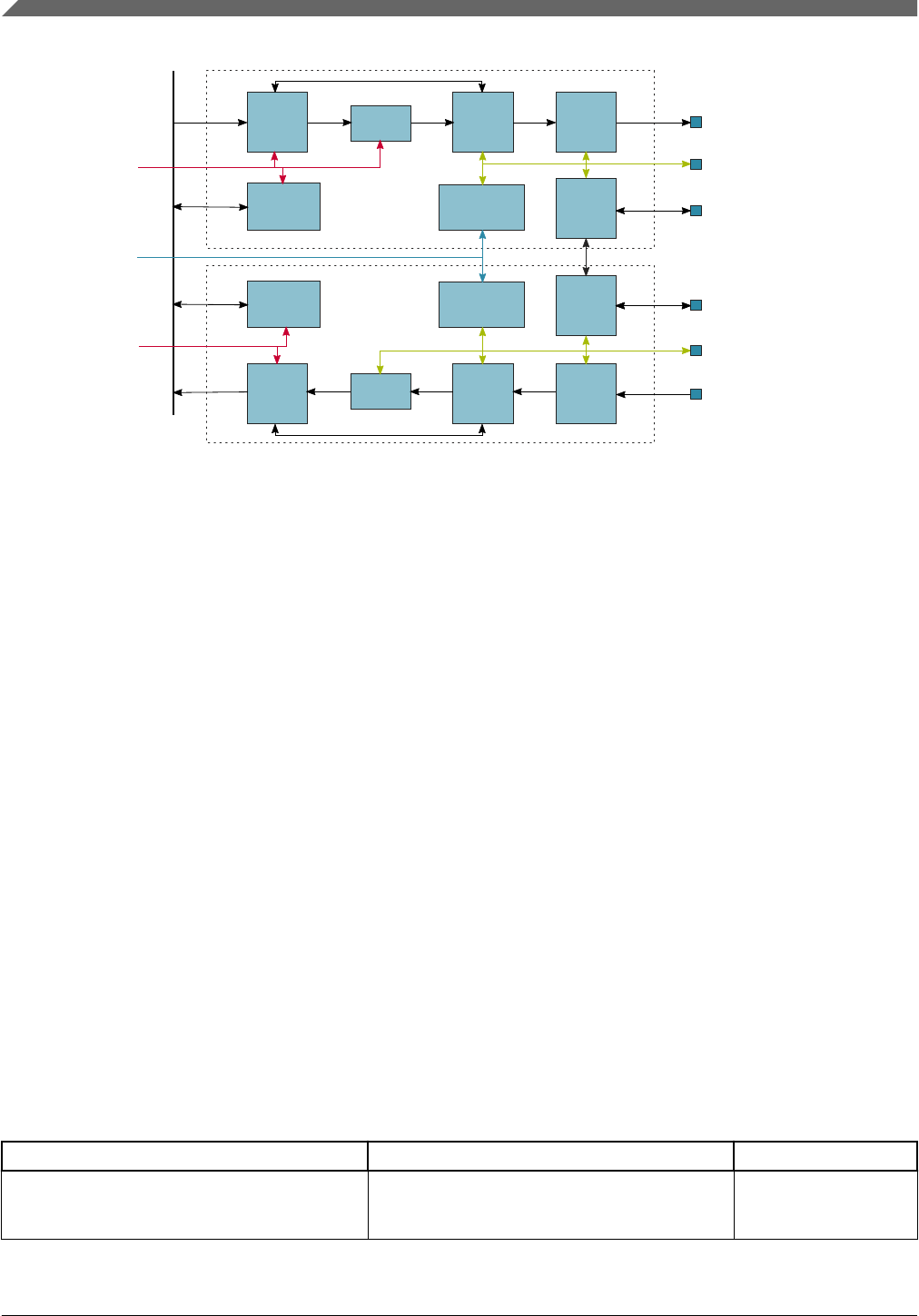
Write
FIFO
Control
FIFO
Read
FIFO
Control
Shift
Register
Control
Registers
Bit Clock
Generation
Frame
Sync
Control
Control
Registers
Bit Clock
Generation
Frame
Sync
Control
Read
FIFO
Control
FIFO
Write
FIFO
Control
Shift
Register
Bus
Clock
Audio
Clock
Bit
Clock
Bus
Clock
Transmitter
Receiver
Synchronous Mode
SAI_TX_DATA
SAI_TX_BCLK
SAI_TX_SYNC
SAI_RX_SYNC
SAI_RX_BCLK
SAI_RX_DATA
Bit
Clock
Figure 54-2. I2S/SAI block diagram
54.2.3 Modes of operation
Module power modes include Run mode, and Debug mode.
54.2.3.1 Run mode
In Run mode, the SAI transmitter and receiver operate normally.
54.2.3.2 Debug mode
In Debug mode, the SAI transmitter and/or receiver can continue operating provided the
Debug Enable bit is set. When TCSR[DBGE] or RCSR[DBGE] bit is clear and Debug
mode is entered, the SAI is disabled after completing the current transmit or receive
frame. The transmitter and receiver bit clocks are not affected by Debug mode.
54.3 External signals
Name Function I/O
SAI_TX_BCLK Transmit Bit Clock. The bit clock is an input when
externally generated and an output when
internally generated.
I/O
Table continues on the next page...
External signals
S32K1xx Series Reference Manual, Rev. 7, 04/2018
1786 NXP Semiconductors

Name Function I/O
SAI_TX_SYNC Transmit Frame Sync. The frame sync is an input
sampled synchronously by the bit clock when
externally generated and an output generated
synchronously by the bit clock when internally
generated.
I/O
SAI_TX_DATA[3:0] Transmit Data. The transmit data is generated
synchronously by the bit clock and is tristated
whenever not transmitting a word.
O
SAI_RX_BCLK Receive Bit Clock. The bit clock is an input when
externally generated and an output when
internally generated.
I/O
SAI_RX_SYNC Receive Frame Sync. The frame sync is an input
sampled synchronously by the bit clock when
externally generated and an output generated
synchronously by the bit clock when internally
generated.
I/O
SAI_RX_DATA[3:0] Receive Data. The receive data is sampled
synchronously by the bit clock.
I
54.4 Memory map and register definition
A read or write access to an address from offset 0x100 and above will result in a bus
error.
54.4.1 I2S register descriptions
54.4.1.1 I2S Memory map
SAI0 base address: 4005_4000h
Offset Register Width
(In bits)
Access Reset value
0h Version ID Register (VERID) 32 RO 0300_0000h
4h Parameter Register (PARAM) 32 RO 0004_0304h
8h SAI Transmit Control Register (TCSR) 32 RW 0000_0000h
Ch SAI Transmit Configuration 1 Register (TCR1) 32 RW 0000_0000h
10h SAI Transmit Configuration 2 Register (TCR2) 32 RW 0000_0000h
14h SAI Transmit Configuration 3 Register (TCR3) 32 RW 0000_0000h
Table continues on the next page...
Chapter 54 Synchronous Audio Interface (SAI)
S32K1xx Series Reference Manual, Rev. 7, 04/2018
NXP Semiconductors 1787

Offset Register Width
(In bits)
Access Reset value
18h SAI Transmit Configuration 4 Register (TCR4) 32 RW 0000_0000h
1Ch SAI Transmit Configuration 5 Register (TCR5) 32 RW 0000_0000h
20h - 2Ch SAI Transmit Data Register (TDR0 - TDR3) 32 WORZ 0000_0000h
40h - 4Ch SAI Transmit FIFO Register (TFR0 - TFR3) 32 RO 0000_0000h
60h SAI Transmit Mask Register (TMR) 32 RW 0000_0000h
88h SAI Receive Control Register (RCSR) 32 RW 0000_0000h
8Ch SAI Receive Configuration 1 Register (RCR1) 32 RW 0000_0000h
90h SAI Receive Configuration 2 Register (RCR2) 32 RW 0000_0000h
94h SAI Receive Configuration 3 Register (RCR3) 32 RW 0000_0000h
98h SAI Receive Configuration 4 Register (RCR4) 32 RW 0000_0000h
9Ch SAI Receive Configuration 5 Register (RCR5) 32 RW 0000_0000h
A0h - ACh SAI Receive Data Register (RDR0 - RDR3) 32 RO 0000_0000h
C0h - CCh SAI Receive FIFO Register (RFR0 - RFR3) 32 RO 0000_0000h
E0h SAI Receive Mask Register (RMR) 32 RW 0000_0000h
54.4.1.2 Version ID Register (VERID)
54.4.1.2.1 Offset
Register Offset
VERID 0h
54.4.1.2.2 Function
.
54.4.1.2.3 Diagram
Bits 31 30 29 28 27 26 25 24 23 22 21 20 19 18 17 16
RMAJOR MINOR
W
Reset 0 0 0 0 0 0 1 1 0 0 0 0 0 0 0 0
Bits 15 14 13 12 11 10 9 8 7 6 5 4 3 2 1 0
RFEATURE
W
Reset 0 0 0 0 0 0 0 0 0 0 0 0 0 0 0 0
Memory map and register definition
S32K1xx Series Reference Manual, Rev. 7, 04/2018
1788 NXP Semiconductors

54.4.1.2.4 Fields
Field Function
31-24
MAJOR
Major Version Number
This read only field returns the major version number for the specification.
23-16
MINOR
Minor Version Number
This read only field returns the minor version number for the specification.
15-0
FEATURE
Feature Specification Number
This read only field returns the feature set number.
0000000000000000b - Standard feature set.
54.4.1.3 Parameter Register (PARAM)
54.4.1.3.1 Offset
Register Offset
PARAM 4h
54.4.1.3.2 Function
.
54.4.1.3.3 Diagram
Bits 31 30 29 28 27 26 25 24 23 22 21 20 19 18 17 16
R 0 FRAME
W
Reset 0 0 0 0 0 0 0 0 0 0 0 0 0 1 0 0
Bits 15 14 13 12 11 10 9 8 7 6 5 4 3 2 1 0
R 0 FIFO 0DATALINE
W
Reset 0 0 0 0 0 0 1 1 0 0 0 0 0 1 0 0
Chapter 54 Synchronous Audio Interface (SAI)
S32K1xx Series Reference Manual, Rev. 7, 04/2018
NXP Semiconductors 1789

54.4.1.3.4 Fields
Field Function
31-20
—
Reserved
19-16
FRAME
Frame Size
The maximum number of slots per frame is 2^FRAME.
15-12
—
Reserved
11-8
FIFO
FIFO Size
The number of words in each FIFO is 2^FIFO.
7-4
—
Reserved
3-0
DATALINE
Number of Datalines
The number of datalines implemented.
54.4.1.4 SAI Transmit Control Register (TCSR)
54.4.1.4.1 Offset
Register Offset
TCSR 8h
54.4.1.4.2 Diagram
Bits 31 30 29 28 27 26 25 24 23 22 21 20 19 18 17 16
R
T
E
Reserved
DBG
E
BC
E
0
0
S
R
0
WS
F
SE
F
FE
F
FW
F
FR
F
W
F
R
W1C
W1C
W1C
Reset 0 0 0 0 0 0 0 0 0 0 0 0 0 0 0 0
Bits 15 14 13 12 11 10 9 8 7 6 5 4 3 2 1 0
R
0
WSI
E
SEI
E
FEI
E
FWI
E
FRI
E
0
0
FWD
E
FRD
E
W
Reset 0 0 0 0 0 0 0 0 0 0 0 0 0 0 0 0
Memory map and register definition
S32K1xx Series Reference Manual, Rev. 7, 04/2018
1790 NXP Semiconductors

54.4.1.4.3 Fields
Field Function
31
TE
Transmitter Enable
Enables/disables the transmitter. When software clears this field, the transmitter remains enabled, and
this bit remains set, until the end of the current frame.
0b - Transmitter is disabled.
1b - Transmitter is enabled, or transmitter has been disabled and has not yet reached end of frame.
30
—
Reserved. Software should only write zero to this reserved bit.
29
DBGE
Debug Enable
Enables/disables transmitter operation in Debug mode. The transmit bit clock is not affected by debug
mode.
0b - Transmitter is disabled in Debug mode, after completing the current frame.
1b - Transmitter is enabled in Debug mode.
28
BCE
Bit Clock Enable
Enables the transmit bit clock, separately from the TE. This field is automatically set whenever TE is set.
When software clears this field, the transmit bit clock remains enabled, and this bit remains set, until the
end of the current frame.
0b - Transmit bit clock is disabled.
1b - Transmit bit clock is enabled.
27-26
—
Reserved
25
FR
FIFO Reset
Empties the FIFO, and sets the FIFO read and write pointers to the same value, which may or may not be
zero. Reading this field will always return zero. FIFO pointers should only be reset when the transmitter is
disabled or the FIFO error flag is set.
0b - No effect.
1b - FIFO reset.
24
SR
Software Reset
When set, resets the internal transmitter logic including the FIFO read and write pointers. Software-visible
registers are not affected, except for the status registers.
0b - No effect.
1b - Software reset.
23-21
—
Reserved
20
WSF
Word Start Flag
Indicates that the start of the configured word has been detected. Write a logic 1 to this field to clear this
flag.
0b - Start of word not detected.
1b - Start of word detected.
19
SEF
Sync Error Flag
Indicates that an error in the externally-generated frame sync has been detected. Write a logic 1 to this
field to clear this flag.
0b - Sync error not detected.
1b - Frame sync error detected.
18
FEF
FIFO Error Flag
Indicates that an enabled transmit FIFO has underrun. Write a logic 1 to this field to clear this flag.
Table continues on the next page...
Chapter 54 Synchronous Audio Interface (SAI)
S32K1xx Series Reference Manual, Rev. 7, 04/2018
NXP Semiconductors 1791

Field Function
0b - Transmit underrun not detected.
1b - Transmit underrun detected.
17
FWF
FIFO Warning Flag
Indicates that an enabled transmit FIFO is empty.
0b - No enabled transmit FIFO is empty.
1b - Enabled transmit FIFO is empty.
16
FRF
FIFO Request Flag
Indicates that the number of words in an enabled transmit channel FIFO is less than or equal to the
transmit FIFO watermark.
0b - Transmit FIFO watermark has not been reached.
1b - Transmit FIFO watermark has been reached.
15-13
—
Reserved
12
WSIE
Word Start Interrupt Enable
Enables/disables word start interrupts.
0b - Disables interrupt.
1b - Enables interrupt.
11
SEIE
Sync Error Interrupt Enable
Enables/disables sync error interrupts.
0b - Disables interrupt.
1b - Enables interrupt.
10
FEIE
FIFO Error Interrupt Enable
Enables/disables FIFO error interrupts.
0b - Disables the interrupt.
1b - Enables the interrupt.
9
FWIE
FIFO Warning Interrupt Enable
Enables/disables FIFO warning interrupts.
0b - Disables the interrupt.
1b - Enables the interrupt.
8
FRIE
FIFO Request Interrupt Enable
Enables/disables FIFO request interrupts.
0b - Disables the interrupt.
1b - Enables the interrupt.
7-5
—
Reserved
4-2
—
Reserved
1
FWDE
FIFO Warning DMA Enable
Enables/disables DMA requests.
0b - Disables the DMA request.
1b - Enables the DMA request.
0
FRDE
FIFO Request DMA Enable
Enables/disables DMA requests.
0b - Disables the DMA request.
1b - Enables the DMA request.
Memory map and register definition
S32K1xx Series Reference Manual, Rev. 7, 04/2018
1792 NXP Semiconductors

54.4.1.5 SAI Transmit Configuration 1 Register (TCR1)
54.4.1.5.1 Offset
Register Offset
TCR1 Ch
54.4.1.5.2 Diagram
Bits 31 30 29 28 27 26 25 24 23 22 21 20 19 18 17 16
R 0
W
Reset 0 0 0 0 0 0 0 0 0 0 0 0 0 0 0 0
Bits 15 14 13 12 11 10 9 8 7 6 5 4 3 2 1 0
R 0 TFW
W
Reset 0 0 0 0 0 0 0 0 0 0 0 0 0 0 0 0
54.4.1.5.3 Fields
Field Function
31-3
—
Reserved
2-0
TFW
Transmit FIFO Watermark
Configures the watermark level for all enabled transmit channels.
54.4.1.6 SAI Transmit Configuration 2 Register (TCR2)
54.4.1.6.1 Offset
Register Offset
TCR2 10h
Chapter 54 Synchronous Audio Interface (SAI)
S32K1xx Series Reference Manual, Rev. 7, 04/2018
NXP Semiconductors 1793

54.4.1.6.2 Function
This register must not be altered when TCSR[TE] is set.
54.4.1.6.3 Diagram
Bits 31 30 29 28 27 26 25 24 23 22 21 20 19 18 17 16
RSYNC 0BCI MSEL BCP BCD 0
W
Reset 0 0 0 0 0 0 0 0 0 0 0 0 0 0 0 0
Bits 15 14 13 12 11 10 9 8 7 6 5 4 3 2 1 0
R 0 DIV
W
Reset 0 0 0 0 0 0 0 0 0 0 0 0 0 0 0 0
54.4.1.6.4 Fields
Field Function
31-30
SYNC
Synchronous Mode
Configures between asynchronous and synchronous modes of operation. When configured for a
synchronous mode of operation, the receiver must be configured for asynchronous operation.
00b - Asynchronous mode.
01b - Synchronous with receiver.
10b - Reserved.
11b - Reserved.
29
—
Reserved
28
BCI
Bit Clock Input
When this field is set and using an internally generated bit clock in either synchronous or asynchronous
mode, the bit clock actually used by the transmitter is delayed by the pad output delay (the transmitter is
clocked by the pad input as if the clock was externally generated). This has the effect of decreasing the
data input setup time, but increasing the data output valid time.
The slave mode timing from the datasheet should be used for the transmitter when this bit is set. In
synchronous mode, this bit allows the transmitter to use the slave mode timing from the datasheet, while
the receiver uses the master mode timing. This field has no effect when configured for an externally
generated bit clock .
0b - No effect.
1b - Internal logic is clocked as if bit clock was externally generated.
27-26
MSEL
MCLK Select
Selects the audio Master Clock option used to generate an internally generated bit clock. This field has
no effect when configured for an externally generated bit clock.
NOTE: Depending on the device, some Master Clock options might not be available. See the chip-
specific information for the meaning of each option.
Table continues on the next page...
Memory map and register definition
S32K1xx Series Reference Manual, Rev. 7, 04/2018
1794 NXP Semiconductors

Field Function
00b - Bus Clock selected.
01b - Master Clock (MCLK) 1 option selected.
10b - Master Clock (MCLK) 2 option selected.
11b - Master Clock (MCLK) 3 option selected.
25
BCP
Bit Clock Polarity
Configures the polarity of the bit clock.
0b - Bit clock is active high with drive outputs on rising edge and sample inputs on falling edge.
1b - Bit clock is active low with drive outputs on falling edge and sample inputs on rising edge.
24
BCD
Bit Clock Direction
Configures the direction of the bit clock.
0b - Bit clock is generated externally in Slave mode.
1b - Bit clock is generated internally in Master mode.
23-8
—
Reserved
7-0
DIV
Bit Clock Divide
Divides down the audio master clock to generate the bit clock when configured for an internal bit clock.
The division value is (DIV + 1) * 2.
54.4.1.7 SAI Transmit Configuration 3 Register (TCR3)
54.4.1.7.1 Offset
Register Offset
TCR3 14h
54.4.1.7.2 Diagram
Bits 31 30 29 28 27 26 25 24 23 22 21 20 19 18 17 16
R 0 0 0 TCE
WCFR
Reset 0 0 0 0 0 0 0 0 0 0 0 0 0 0 0 0
Bits 15 14 13 12 11 10 9 8 7 6 5 4 3 2 1 0
R 0 WDFL
W
Reset 0 0 0 0 0 0 0 0 0 0 0 0 0 0 0 0
Chapter 54 Synchronous Audio Interface (SAI)
S32K1xx Series Reference Manual, Rev. 7, 04/2018
NXP Semiconductors 1795

54.4.1.7.3 Fields
Field Function
31-28
—
Reserved
27-24
CFR
Channel FIFO Reset
Resets the FIFO pointers for a specific channel. Reading this field will always return zero. FIFO pointers
should only be reset when a channel is disabled or the FIFO error flag is set.
The width of CFR field = the number of transmit channels (call it N). For example, if CFR is 2 bits wide,
then bit position 24 refers to transmit channel 1 FIFO pointer and bit position 25 refers to transmit channel
2 FIFO pointer. Setting bit 24 resets transmit channel 1 FIFO pointer, and setting bit 25 enables transmit
channel 2 FIFO pointer. Setting bit N will reset transmit channel N FIFO pointer.
0b - No effect.
1b - Transmit data channel N FIFO is reset.
23-20
—
Reserved
19-16
TCE
Transmit Channel Enable
Enables the corresponding data channel for transmit operation. Changing TCE field will take effect
immediately for generating the FIFO request and warning flags, but at the end of each frame for transmit
operation.
The width of TCE field = the number of transmit channels (call it N). For example, if TCE field is 2 bits
wide, then bit position 16 refers to transmit channel 1 and bit position 17 refers to transmit channel 2.
Setting bit 16 enables transmit channel 1, and setting bit 17 enables transmit channel 2. Setting bit N will
enable transmit channel N.
0b - Transmit data channel N is disabled.
1b - Transmit data channel N is enabled.
15-4
—
Reserved
3-0
WDFL
Word Flag Configuration
Configures which word sets the start of word flag. The value written must be one less than the word
number. For example, writing 0 configures the first word in the frame. When configured to a value greater
than TCR4[FRSZ], then the start of word flag is never set.
54.4.1.8 SAI Transmit Configuration 4 Register (TCR4)
54.4.1.8.1 Offset
Register Offset
TCR4 18h
Memory map and register definition
S32K1xx Series Reference Manual, Rev. 7, 04/2018
1796 NXP Semiconductors

54.4.1.8.2 Function
This register must not be altered when TCSR[TE] is set.
54.4.1.8.3 Diagram
Bits 31 30 29 28 27 26 25 24 23 22 21 20 19 18 17 16
R
0
FCONT
FCOMB
FPACK
0
FRS
Z
W
Reset 0 0 0 0 0 0 0 0 0 0 0 0 0 0 0 0
Bits 15 14 13 12 11 10 9 8 7 6 5 4 3 2 1 0
R
0
SYWD
0
CHMOD
MF
FS
E
ONDEM
FS
P
FS
D
W
Reset 0 0 0 0 0 0 0 0 0 0 0 0 0 0 0 0
54.4.1.8.4 Fields
Field Function
31-29
—
Reserved
28
FCONT
FIFO Continue on Error
Configures when the SAI will continue transmitting after a FIFO error has been detected.
0b - On FIFO error, the SAI will continue from the start of the next frame after the FIFO error flag
has been cleared.
1b - On FIFO error, the SAI will continue from the same word that caused the FIFO error to set after
the FIFO warning flag has been cleared.
27-26
FCOMB
FIFO Combine Mode
When FIFO combine mode is enabled for FIFO writes, software writing to any FIFO data register will
alternate the write among the enabled data channel FIFOs. For example, if two data channels are
enabled then the first write will be performed to the first enabled data channel FIFO and the second write
will be performed to the second enabled data channel FIFO. Reseting the FIFO or disabling FIFO
combine mode for FIFO writes will reset the pointer back to the first enabled data channel.
When FIFO combine mode is enabled for FIFO reads from the transmit shift registers, the transmit data
channel output will alternate between the enabled data channel FIFOs. For example, if two data channels
are enabled then the first unmasked word will be transmitted from the first enabled data channel FIFO
and the second unmasked word will be transmitted from the second enabled data channel FIFO. Since
the first word of the frame is always transmitted from the first enabled data channel FIFO, it is
recommended that the number of unmasked words per frame is evenly divisible by the number of
enabled data channels.
00b - FIFO combine mode disabled.
01b - FIFO combine mode enabled on FIFO reads (from transmit shift registers).
10b - FIFO combine mode enabled on FIFO writes (by software).
11b - FIFO combine mode enabled on FIFO reads (from transmit shift registers) and writes (by
software).
Table continues on the next page...
Chapter 54 Synchronous Audio Interface (SAI)
S32K1xx Series Reference Manual, Rev. 7, 04/2018
NXP Semiconductors 1797

Field Function
25-24
FPACK
FIFO Packing Mode
Enables packing of 8-bit data or 16-bit data into each 32-bit FIFO word. If the word size is greater than 8-
bit or 16-bit then only the first 8-bit or 16-bits are loaded from the FIFO. The first word in each frame
always starts with a new 32-bit FIFO word and the first bit shifted must be configured within the first
packed word. When FIFO packing is enabled, the FIFO write pointer will only increment when the full 32-
bit FIFO word has been written by software.
00b - FIFO packing is disabled
01b - Reserved
10b - 8-bit FIFO packing is enabled
11b - 16-bit FIFO packing is enabled
23-20
—
Reserved
19-16
FRSZ
Frame size
Configures the number of words in each frame. The value written must be one less than the number of
words in the frame. For example, write 0 for one word per frame. The maximum supported frame size is
16 words.
15-13
—
Reserved
12-8
SYWD
Sync Width
Configures the length of the frame sync in number of bit clocks. The value written must be one less than
the number of bit clocks. For example, write 0 for the frame sync to assert for one bit clock only. The sync
width cannot be configured longer than the first word of the frame.
7-6
—
Reserved
5
CHMOD
Channel Mode
Configures if transmit data pins are configured for TDM mode or Output mode.
0b - TDM mode, transmit data pins are tri-stated when slots are masked or channels are disabled.
1b - Output mode, transmit data pins are never tri-stated and will output zero when slots are
masked or channels are disabled.
4
MF
MSB First
Configures whether the LSB or the MSB is transmitted first.
0b - LSB is transmitted first.
1b - MSB is transmitted first.
3
FSE
Frame Sync Early
0b - Frame sync asserts with the first bit of the frame.
1b - Frame sync asserts one bit before the first bit of the frame.
2
ONDEM
On Demand Mode
When set, and the frame sync is generated internally, a frame sync is only generated when the FIFO
warning flag is clear.
0b - Internal frame sync is generated continuously.
1b - Internal frame sync is generated when the FIFO warning flag is clear.
1
FSP
Frame Sync Polarity
Configures the polarity of the frame sync.
0b - Frame sync is active high.
1b - Frame sync is active low.
0
FSD
Frame Sync Direction
Configures the direction of the frame sync.
Memory map and register definition
S32K1xx Series Reference Manual, Rev. 7, 04/2018
1798 NXP Semiconductors

Field Function
0b - Frame sync is generated externally in Slave mode.
1b - Frame sync is generated internally in Master mode.
54.4.1.9 SAI Transmit Configuration 5 Register (TCR5)
54.4.1.9.1 Offset
Register Offset
TCR5 1Ch
54.4.1.9.2 Function
This register must not be altered when TCSR[TE] is set.
54.4.1.9.3 Diagram
Bits 31 30 29 28 27 26 25 24 23 22 21 20 19 18 17 16
R 0 WNW 0W0W
W
Reset 0 0 0 0 0 0 0 0 0 0 0 0 0 0 0 0
Bits 15 14 13 12 11 10 9 8 7 6 5 4 3 2 1 0
R 0 FBT 0
W
Reset 0 0 0 0 0 0 0 0 0 0 0 0 0 0 0 0
54.4.1.9.4 Fields
Field Function
31-29
—
Reserved
28-24
WNW
Word N Width
Configures the number of bits in each word, for each word except the first in the frame. The value written
must be one less than the number of bits per word. Word width of less than 8 bits is not supported.
23-21
—
Reserved
Table continues on the next page...
Chapter 54 Synchronous Audio Interface (SAI)
S32K1xx Series Reference Manual, Rev. 7, 04/2018
NXP Semiconductors 1799

Field Function
20-16
W0W
Word 0 Width
Configures the number of bits in the first word in each frame. The value written must be one less than the
number of bits in the first word. Word width of less than 8 bits is not supported if there is only one word
per frame.
15-13
—
Reserved
12-8
FBT
First Bit Shifted
Configures the bit index for the first bit transmitted for each word in the frame. If configured for MSB First,
the index of the next bit transmitted is one less than the current bit transmitted. If configured for LSB First,
the index of the next bit transmitted is one more than the current bit transmitted. The value written must
be greater than or equal to the word width when configured for MSB First. The value written must be less
than or equal to 31-word width when configured for LSB First.
7-0
—
Reserved
54.4.1.10 SAI Transmit Data Register (TDR0 - TDR3)
54.4.1.10.1 Offset
For a = 0 to 3:
Register Offset
TDRa 20h + (a × 4h)
54.4.1.10.2 Diagram
Bits 31 30 29 28 27 26 25 24 23 22 21 20 19 18 17 16
R 0
WTDR
Reset 0 0 0 0 0 0 0 0 0 0 0 0 0 0 0 0
Bits 15 14 13 12 11 10 9 8 7 6 5 4 3 2 1 0
R 0
WTDR
Reset 0 0 0 0 0 0 0 0 0 0 0 0 0 0 0 0
Memory map and register definition
S32K1xx Series Reference Manual, Rev. 7, 04/2018
1800 NXP Semiconductors

54.4.1.10.3 Fields
Field Function
31-0
TDR
Transmit Data Register
Writes to this register when the transmit FIFO is not full will push the data written into the transmit data
FIFO. Writes to this register when the transmit FIFO is full are ignored.
54.4.1.11 SAI Transmit FIFO Register (TFR0 - TFR3)
54.4.1.11.1 Offset
For a = 0 to 3:
Register Offset
TFRa 40h + (a × 4h)
54.4.1.11.2 Function
The MSB of the read and write pointers is used to distinguish between FIFO full and
empty conditions. If the read and write pointers are identical, then the FIFO is empty. If
the read and write pointers are identical except for the MSB, then the FIFO is full.
54.4.1.11.3 Diagram
Bits 31 30 29 28 27 26 25 24 23 22 21 20 19 18 17 16
RWCP 0WFP
W
Reset 0 0 0 0 0 0 0 0 0 0 0 0 0 0 0 0
Bits 15 14 13 12 11 10 9 8 7 6 5 4 3 2 1 0
R 0 RFP
W
Reset 0 0 0 0 0 0 0 0 0 0 0 0 0 0 0 0
54.4.1.11.4 Fields
Field Function
31 Write Channel Pointer
Table continues on the next page...
Chapter 54 Synchronous Audio Interface (SAI)
S32K1xx Series Reference Manual, Rev. 7, 04/2018
NXP Semiconductors 1801

Field Function
WCP When FIFO Combine mode is enabled for writes, indicates that this data channel is the next FIFO to be
written.
0b - No effect.
1b - FIFO combine is enabled for FIFO writes and this FIFO will be written on the next FIFO write.
30-20
—
Reserved
19-16
WFP
Write FIFO Pointer
FIFO write pointer for transmit data channel.
15-4
—
Reserved
3-0
RFP
Read FIFO Pointer
FIFO read pointer for transmit data channel.
54.4.1.12 SAI Transmit Mask Register (TMR)
54.4.1.12.1 Offset
Register Offset
TMR 60h
54.4.1.12.2 Function
This register is double-buffered and updates:
1. When TCSR[TE] is first set
2. At the end of each frame.
This allows the masked words in each frame to change from frame to frame.
Memory map and register definition
S32K1xx Series Reference Manual, Rev. 7, 04/2018
1802 NXP Semiconductors

54.4.1.12.3 Diagram
Bits 31 30 29 28 27 26 25 24 23 22 21 20 19 18 17 16
R 0
W
Reset 0 0 0 0 0 0 0 0 0 0 0 0 0 0 0 0
Bits 15 14 13 12 11 10 9 8 7 6 5 4 3 2 1 0
RTWM
W
Reset 0 0 0 0 0 0 0 0 0 0 0 0 0 0 0 0
54.4.1.12.4 Fields
Field Function
31-16
—
Reserved
15-0
TWM
Transmit Word Mask
Configures whether the transmit word is masked (transmit data pins are tri-stated or drive zero and
transmit data not read from FIFO) for the corresponding word in the frame.
0000000000000000b - Word N is enabled.
0000000000000001b - Word N is masked. The transmit data pins are tri-stated or drive zero when
masked.
54.4.1.13 SAI Receive Control Register (RCSR)
54.4.1.13.1 Offset
Register Offset
RCSR 88h
Chapter 54 Synchronous Audio Interface (SAI)
S32K1xx Series Reference Manual, Rev. 7, 04/2018
NXP Semiconductors 1803

54.4.1.13.2 Diagram
Bits 31 30 29 28 27 26 25 24 23 22 21 20 19 18 17 16
R
R
E
Reserved
DBG
E
BC
E
0
0
S
R
0
WS
F
SE
F
FE
F
FW
F
FR
F
W
F
R
W1C
W1C
W1C
Reset 0 0 0 0 0 0 0 0 0 0 0 0 0 0 0 0
Bits 15 14 13 12 11 10 9 8 7 6 5 4 3 2 1 0
R
0
WSI
E
SEI
E
FEI
E
FWI
E
FRI
E
0
0
FWD
E
FRD
E
W
Reset 0 0 0 0 0 0 0 0 0 0 0 0 0 0 0 0
54.4.1.13.3 Fields
Field Function
31
RE
Receiver Enable
Enables/disables the receiver. When software clears this field, the receiver remains enabled, and this bit
remains set, until the end of the current frame.
0b - Receiver is disabled.
1b - Receiver is enabled, or receiver has been disabled and has not yet reached end of frame.
30
—
Reserved. Software should only write zero to this reserved bit.
29
DBGE
Debug Enable
Enables/disables receiver operation in Debug mode. The receive bit clock is not affected by Debug mode.
0b - Receiver is disabled in Debug mode, after completing the current frame.
1b - Receiver is enabled in Debug mode.
28
BCE
Bit Clock Enable
Enables the receive bit clock, separately from RE. This field is automatically set whenever RE is set.
When software clears this field, the receive bit clock remains enabled, and this field remains set, until the
end of the current frame.
0b - Receive bit clock is disabled.
1b - Receive bit clock is enabled.
27-26
—
Reserved
25
FR
FIFO Reset
Empties the FIFO, and sets the FIFO read and write pointers to the same value, which may or may not be
zero. Reading this field will always return zero. FIFO pointers should only be reset when the receiver is
disabled or the FIFO error flag is set.
0b - No effect.
1b - FIFO reset.
24
SR
Software Reset
Resets the internal receiver logic including the FIFO pointers. Software-visible registers are not affected,
except for the status registers.
0b - No effect.
Table continues on the next page...
Memory map and register definition
S32K1xx Series Reference Manual, Rev. 7, 04/2018
1804 NXP Semiconductors

Field Function
1b - Software reset.
23-21
—
Reserved
20
WSF
Word Start Flag
Indicates that the start of the configured word has been detected. Write a logic 1 to this field to clear this
flag.
0b - Start of word not detected.
1b - Start of word detected.
19
SEF
Sync Error Flag
Indicates that an error in the externally-generated frame sync has been detected. Write a logic 1 to this
field to clear this flag.
0b - Sync error not detected.
1b - Frame sync error detected.
18
FEF
FIFO Error Flag
Indicates that an enabled receive FIFO has overflowed. Write a logic 1 to this field to clear this flag.
0b - Receive overflow not detected.
1b - Receive overflow detected.
17
FWF
FIFO Warning Flag
Indicates that an enabled receive FIFO is full.
0b - No enabled receive FIFO is full.
1b - Enabled receive FIFO is full.
16
FRF
FIFO Request Flag
Indicates that the number of words in an enabled receive channel FIFO is greater than the receive FIFO
watermark.
0b - Receive FIFO watermark not reached.
1b - Receive FIFO watermark has been reached.
15-13
—
Reserved
12
WSIE
Word Start Interrupt Enable
Enables/disables word start interrupts.
0b - Disables interrupt.
1b - Enables interrupt.
11
SEIE
Sync Error Interrupt Enable
Enables/disables sync error interrupts.
0b - Disables interrupt.
1b - Enables interrupt.
10
FEIE
FIFO Error Interrupt Enable
Enables/disables FIFO error interrupts.
0b - Disables the interrupt.
1b - Enables the interrupt.
9
FWIE
FIFO Warning Interrupt Enable
Enables/disables FIFO warning interrupts.
0b - Disables the interrupt.
1b - Enables the interrupt.
8
FRIE
FIFO Request Interrupt Enable
Enables/disables FIFO request interrupts.
Table continues on the next page...
Chapter 54 Synchronous Audio Interface (SAI)
S32K1xx Series Reference Manual, Rev. 7, 04/2018
NXP Semiconductors 1805

Field Function
0b - Disables the interrupt.
1b - Enables the interrupt.
7-5
—
Reserved
4-2
—
Reserved
1
FWDE
FIFO Warning DMA Enable
Enables/disables DMA requests.
0b - Disables the DMA request.
1b - Enables the DMA request.
0
FRDE
FIFO Request DMA Enable
Enables/disables DMA requests.
0b - Disables the DMA request.
1b - Enables the DMA request.
54.4.1.14 SAI Receive Configuration 1 Register (RCR1)
54.4.1.14.1 Offset
Register Offset
RCR1 8Ch
54.4.1.14.2 Diagram
Bits 31 30 29 28 27 26 25 24 23 22 21 20 19 18 17 16
R 0
W
Reset 0 0 0 0 0 0 0 0 0 0 0 0 0 0 0 0
Bits 15 14 13 12 11 10 9 8 7 6 5 4 3 2 1 0
R 0 RFW
W
Reset 0 0 0 0 0 0 0 0 0 0 0 0 0 0 0 0
Memory map and register definition
S32K1xx Series Reference Manual, Rev. 7, 04/2018
1806 NXP Semiconductors
54.4.1.14.3 Fields
Field Function
31-3
—
Reserved
2-0
RFW
Receive FIFO Watermark
Configures the watermark level for all enabled receiver channels.
54.4.1.15 SAI Receive Configuration 2 Register (RCR2)
54.4.1.15.1 Offset
Register Offset
RCR2 90h
54.4.1.15.2 Function
This register must not be altered when RCSR[RE] is set.
54.4.1.15.3 Diagram
Bits 31 30 29 28 27 26 25 24 23 22 21 20 19 18 17 16
RSYNC 0BCI MSEL BCP BCD 0
W
Reset 0 0 0 0 0 0 0 0 0 0 0 0 0 0 0 0
Bits 15 14 13 12 11 10 9 8 7 6 5 4 3 2 1 0
R 0 DIV
W
Reset 0 0 0 0 0 0 0 0 0 0 0 0 0 0 0 0
54.4.1.15.4 Fields
Field Function
31-30
SYNC
Synchronous Mode
Configures between asynchronous and synchronous modes of operation. When configured for a
synchronous mode of operation, the transmitter must be configured for asynchronous operation.
00b - Asynchronous mode.
Table continues on the next page...
Chapter 54 Synchronous Audio Interface (SAI)
S32K1xx Series Reference Manual, Rev. 7, 04/2018
NXP Semiconductors 1807

Field Function
01b - Synchronous with transmitter.
10b - Reserved.
11b - Reserved.
29
—
Reserved
28
BCI
Bit Clock Input
When this field is set and using an internally generated bit clock in either synchronous or asynchronous
mode, the bit clock actually used by the receiver is delayed by the pad output delay (the receiver is
clocked by the pad input as if the clock was externally generated). This has the effect of decreasing the
data input setup time, but increasing the data output valid time.
The slave mode timing from the datasheet should be used for the receiver when this bit is set. In
synchronous mode, this bit allows the receiver to use the slave mode timing from the datasheet, while the
transmitter uses the master mode timing. This field has no effect when configured for an externally
generated bit clock .
0b - No effect.
1b - Internal logic is clocked as if bit clock was externally generated.
27-26
MSEL
MCLK Select
Selects the audio Master Clock option used to generate an internally generated bit clock. This field has
no effect when configured for an externally generated bit clock.
NOTE: Depending on the device, some Master Clock options might not be available. See the chip-
specific information for the availability and chip-specific meaning of each option.
00b - Bus Clock selected.
01b - Master Clock (MCLK) 1 option selected.
10b - Master Clock (MCLK) 2 option selected.
11b - Master Clock (MCLK) 3 option selected.
25
BCP
Bit Clock Polarity
Configures the polarity of the bit clock.
0b - Bit Clock is active high with drive outputs on rising edge and sample inputs on falling edge.
1b - Bit Clock is active low with drive outputs on falling edge and sample inputs on rising edge.
24
BCD
Bit Clock Direction
Configures the direction of the bit clock.
0b - Bit clock is generated externally in Slave mode.
1b - Bit clock is generated internally in Master mode.
23-8
—
Reserved
7-0
DIV
Bit Clock Divide
Divides down the audio master clock to generate the bit clock when configured for an internal bit clock.
The division value is (DIV + 1) * 2.
54.4.1.16 SAI Receive Configuration 3 Register (RCR3)
Memory map and register definition
S32K1xx Series Reference Manual, Rev. 7, 04/2018
1808 NXP Semiconductors

54.4.1.16.1 Offset
Register Offset
RCR3 94h
54.4.1.16.2 Diagram
Bits 31 30 29 28 27 26 25 24 23 22 21 20 19 18 17 16
R 0 0 0 RCE
WCFR
Reset 0 0 0 0 0 0 0 0 0 0 0 0 0 0 0 0
Bits 15 14 13 12 11 10 9 8 7 6 5 4 3 2 1 0
R 0 WDFL
W
Reset 0 0 0 0 0 0 0 0 0 0 0 0 0 0 0 0
54.4.1.16.3 Fields
Field Function
31-28
—
Reserved
27-24
CFR
Channel FIFO Reset
Resets the FIFO pointers for a specific channel. Reading this field will always return zero. FIFO pointers
should only be reset when a channel is disabled or the FIFO error flag is set.
The width of CFR field = the number of receive channels (call it N). For example, if CFR is 2 bits wide,
then bit position 24 refers to receive channel 1 FIFO pointer and bit position 25 refers to receive channel
2 FIFO pointer. Setting bit 24 resets receive channel 1 FIFO pointer, and setting bit 25 enables receive
channel 2 FIFO pointer. Setting bit N will reset receive channel N FIFO pointer.
0b - No effect.
1b - Receive data channel N FIFO is reset.
23-20
—
Reserved
19-16
RCE
Receive Channel Enable
Enables the corresponding data channel for receive operation. Changing this field will take effect
immediately for generating the FIFO request and warning flags, but at the end of each frame for receive
operation.
The width of RCE field = the number of receive channels (call it N). For example, if RCE field is 2 bits
wide, then bit position 16 refers to receive channel 1 and bit position 17 refers to receive channel 2.
Setting bit 16 enables receive channel 1, and setting bit 17 enables receive channel 2. Setting bit N will
enable receive channel N.
0b - Receive data channel N is disabled.
Table continues on the next page...
Chapter 54 Synchronous Audio Interface (SAI)
S32K1xx Series Reference Manual, Rev. 7, 04/2018
NXP Semiconductors 1809

Field Function
1b - Receive data channel N is enabled.
15-4
—
Reserved
3-0
WDFL
Word Flag Configuration
Configures which word the start of word flag is set. The value written should be one less than the word
number (for example, write zero to configure for the first word in the frame). When configured to a value
greater than the Frame Size field, then the start of word flag is never set.
54.4.1.17 SAI Receive Configuration 4 Register (RCR4)
54.4.1.17.1 Offset
Register Offset
RCR4 98h
54.4.1.17.2 Function
This register must not be altered when RCSR[RE] is set.
54.4.1.17.3 Diagram
Bits 31 30 29 28 27 26 25 24 23 22 21 20 19 18 17 16
R
0
FCONT
FCOMB
FPACK
0
FRS
Z
W
Reset 0 0 0 0 0 0 0 0 0 0 0 0 0 0 0 0
Bits 15 14 13 12 11 10 9 8 7 6 5 4 3 2 1 0
R
0
SYWD
0
Reserved
MF
FS
E
ONDEM
FS
P
FS
D
W
Reset 0 0 0 0 0 0 0 0 0 0 0 0 0 0 0 0
54.4.1.17.4 Fields
Field Function
31-29 Reserved
Table continues on the next page...
Memory map and register definition
S32K1xx Series Reference Manual, Rev. 7, 04/2018
1810 NXP Semiconductors

Field Function
—
28
FCONT
FIFO Continue on Error
Configures when the SAI will continue receiving after a FIFO error has been detected.
0b - On FIFO error, the SAI will continue from the start of the next frame after the FIFO error flag
has been cleared.
1b - On FIFO error, the SAI will continue from the same word that caused the FIFO error to set after
the FIFO warning flag has been cleared.
27-26
FCOMB
FIFO Combine Mode
When FIFO combine mode is enabled for FIFO reads, software reading any FIFO data register will
alternate the read among the enabled data channel FIFOs. For example, if two data channels are
enabled then the first read will be performed to the first enabled data channel FIFO and the second read
will be performed to the second enabled data channel FIFO. Reseting the FIFO or disabling FIFO
combine mode for FIFO reads will reset the pointer back to the first enabled data channel.
When FIFO combine mode is enabled for FIFO writes from the receive shift registers, the first enabled
data channel input will alternate between the enabled data channel FIFOs. For example, if two data
channels are enabled then the first unmasked received word will be stored in the first enabled data
channel FIFO and the second unmasked received word will be stored in the second enabled data
channel FIFO. Since the first word of the frame is always stored in the first enabled data channel FIFO, it
is recommended that the number of unmasked words per frame is evenly divisible by the number of
enabled data channels.
00b - FIFO combine mode disabled.
01b - FIFO combine mode enabled on FIFO writes (from receive shift registers).
10b - FIFO combine mode enabled on FIFO reads (by software).
11b - FIFO combine mode enabled on FIFO writes (from receive shift registers) and reads (by
software).
25-24
FPACK
FIFO Packing Mode
Enables packing of 8-bit data or 16-bit data into each 32-bit FIFO word. If the word size is greater than 8-
bit or 16-bit then only the first 8-bit or 16-bits are stored to the FIFO. The first word in each frame always
starts with a new 32-bit FIFO word and the first bit shifted must be configured within the first packed word.
When FIFO packing is enabled, the FIFO read pointer will only increment when the full 32-bit FIFO word
has been read by software.
00b - FIFO packing is disabled
01b - Reserved.
10b - 8-bit FIFO packing is enabled
11b - 16-bit FIFO packing is enabled
23-20
—
Reserved
19-16
FRSZ
Frame Size
Configures the number of words in each frame. The value written must be one less than the number of
words in the frame. For example, write 0 for one word per frame. The maximum supported frame size is
16 words.
15-13
—
Reserved
12-8
SYWD
Sync Width
Configures the length of the frame sync in number of bit clocks. The value written must be one less than
the number of bit clocks. For example, write 0 for the frame sync to assert for one bit clock only. The sync
width cannot be configured longer than the first word of the frame.
7-6
—
Reserved
Table continues on the next page...
Chapter 54 Synchronous Audio Interface (SAI)
S32K1xx Series Reference Manual, Rev. 7, 04/2018
NXP Semiconductors 1811

Field Function
5
—
Reserved. Software should only write zero to this bit.
4
MF
MSB First
Configures whether the LSB or the MSB is received first.
0b - LSB is received first.
1b - MSB is received first.
3
FSE
Frame Sync Early
0b - Frame sync asserts with the first bit of the frame.
1b - Frame sync asserts one bit before the first bit of the frame.
2
ONDEM
On Demand Mode
When set, and the frame sync is generated internally, a frame sync is only generated when the FIFO
warning flag is clear.
0b - Internal frame sync is generated continuously.
1b - Internal frame sync is generated when the FIFO warning flag is clear.
1
FSP
Frame Sync Polarity
Configures the polarity of the frame sync.
0b - Frame sync is active high.
1b - Frame sync is active low.
0
FSD
Frame Sync Direction
Configures the direction of the frame sync.
0b - Frame Sync is generated externally in Slave mode.
1b - Frame Sync is generated internally in Master mode.
54.4.1.18 SAI Receive Configuration 5 Register (RCR5)
54.4.1.18.1 Offset
Register Offset
RCR5 9Ch
54.4.1.18.2 Function
This register must not be altered when RCSR[RE] is set.
Memory map and register definition
S32K1xx Series Reference Manual, Rev. 7, 04/2018
1812 NXP Semiconductors

54.4.1.18.3 Diagram
Bits 31 30 29 28 27 26 25 24 23 22 21 20 19 18 17 16
R 0 WNW 0W0W
W
Reset 0 0 0 0 0 0 0 0 0 0 0 0 0 0 0 0
Bits 15 14 13 12 11 10 9 8 7 6 5 4 3 2 1 0
R 0 FBT 0
W
Reset 0 0 0 0 0 0 0 0 0 0 0 0 0 0 0 0
54.4.1.18.4 Fields
Field Function
31-29
—
Reserved
28-24
WNW
Word N Width
Configures the number of bits in each word, for each word except the first in the frame. The value written
must be one less than the number of bits per word. Word width of less than 8 bits is not supported.
23-21
—
Reserved
20-16
W0W
Word 0 Width
Configures the number of bits in the first word in each frame. The value written must be one less than the
number of bits in the first word. Word width of less than 8 bits is not supported if there is only one word
per frame.
15-13
—
Reserved
12-8
FBT
First Bit Shifted
Configures the bit index for the first bit received for each word in the frame. If configured for MSB First,
the index of the next bit received is one less than the current bit received. If configured for LSB First, the
index of the next bit received is one more than the current bit received. The value written must be greater
than or equal to the word width when configured for MSB First. The value written must be less than or
equal to 31-word width when configured for LSB First.
7-0
—
Reserved
54.4.1.19 SAI Receive Data Register (RDR0 - RDR3)
Chapter 54 Synchronous Audio Interface (SAI)
S32K1xx Series Reference Manual, Rev. 7, 04/2018
NXP Semiconductors 1813

54.4.1.19.1 Offset
For a = 0 to 3:
Register Offset
RDRa A0h + (a × 4h)
54.4.1.19.2 Diagram
Bits 31 30 29 28 27 26 25 24 23 22 21 20 19 18 17 16
RRDR
W
Reset 0 0 0 0 0 0 0 0 0 0 0 0 0 0 0 0
Bits 15 14 13 12 11 10 9 8 7 6 5 4 3 2 1 0
RRDR
W
Reset 0 0 0 0 0 0 0 0 0 0 0 0 0 0 0 0
54.4.1.19.3 Fields
Field Function
31-0
RDR
Receive Data Register
Reads from this register when the receive FIFO is not empty will return the data from the top of the
receive FIFO. Reads from this register when the receive FIFO is empty are ignored.
54.4.1.20 SAI Receive FIFO Register (RFR0 - RFR3)
54.4.1.20.1 Offset
For a = 0 to 3:
Register Offset
RFRa C0h + (a × 4h)
Memory map and register definition
S32K1xx Series Reference Manual, Rev. 7, 04/2018
1814 NXP Semiconductors

54.4.1.20.2 Function
The MSB of the read and write pointers is used to distinguish between FIFO full and
empty conditions. If the read and write pointers are identical, then the FIFO is empty. If
the read and write pointers are identical except for the MSB, then the FIFO is full.
54.4.1.20.3 Diagram
Bits 31 30 29 28 27 26 25 24 23 22 21 20 19 18 17 16
R 0 WFP
W
Reset 0 0 0 0 0 0 0 0 0 0 0 0 0 0 0 0
Bits 15 14 13 12 11 10 9 8 7 6 5 4 3 2 1 0
RRCP 0RFP
W
Reset 0 0 0 0 0 0 0 0 0 0 0 0 0 0 0 0
54.4.1.20.4 Fields
Field Function
31-20
—
Reserved
19-16
WFP
Write FIFO Pointer
FIFO write pointer for receive data channel.
15
RCP
Receive Channel Pointer
When FIFO Combine mode is enabled for reads, indicates that this data channel is the next FIFO to be
read.
0b - No effect.
1b - FIFO combine is enabled for FIFO reads and this FIFO will be read on the next FIFO read.
14-4
—
Reserved
3-0
RFP
Read FIFO Pointer
FIFO read pointer for receive data channel.
54.4.1.21 SAI Receive Mask Register (RMR)
Chapter 54 Synchronous Audio Interface (SAI)
S32K1xx Series Reference Manual, Rev. 7, 04/2018
NXP Semiconductors 1815

54.4.1.21.1 Offset
Register Offset
RMR E0h
54.4.1.21.2 Function
This register is double-buffered and updates:
1. When RCSR[RE] is first set
2. At the end of each frame
This allows the masked words in each frame to change from frame to frame.
54.4.1.21.3 Diagram
Bits 31 30 29 28 27 26 25 24 23 22 21 20 19 18 17 16
R 0
W
Reset 0 0 0 0 0 0 0 0 0 0 0 0 0 0 0 0
Bits 15 14 13 12 11 10 9 8 7 6 5 4 3 2 1 0
RRWM
W
Reset 0 0 0 0 0 0 0 0 0 0 0 0 0 0 0 0
54.4.1.21.4 Fields
Field Function
31-16
—
Reserved
15-0
RWM
Receive Word Mask
Configures whether the receive word is masked (received data ignored and not written to receive FIFO)
for the corresponding word in the frame.
0000000000000000b - Word N is enabled.
0000000000000001b - Word N is masked.
Memory map and register definition
S32K1xx Series Reference Manual, Rev. 7, 04/2018
1816 NXP Semiconductors

54.5 Functional description
This section provides a complete functional description of the block.
54.5.1 SAI clocking
The SAI clocks include:
• The audio master clock
• The bit clock
• The bus clock
54.5.1.1 Audio master clock
The audio master clock is used to generate the bit clock when the receiver or transmitter
is configured for an internally generated bit clock. The transmitter and receiver can
independently select between the bus clock and up to three audio master clocks to
generate the bit clock.
The audio master clock generation and selection is chip-specific. Refer to chip-specific
clocking information about how the audio master clocks are generated.
54.5.1.2 Bit clock
The SAI transmitter and receiver support asynchronous free-running bit clocks that can
be generated internally from an audio master clock or supplied externally. There is also
the option for synchronous bit clock and frame sync operation between the receiver and
transmitter or between multiple SAI peripherals.
• If both transmitter and receiver are configured for asynchronous operation, then the
transmitter and receiver will each use their own bit clock and frame sync.
•If the transmitter is configured for asynchronous mode and the receiver is configured
for synchronous mode, then both transmitter and receiver will use the transmitter bit
clock and frame sync.
•If the receiver is configured for asynchronous mode and the transmitter is configured
for synchronous mode, then both transmitter and receiver will use the receiver bit
clock and frame sync.
Chapter 54 Synchronous Audio Interface (SAI)
S32K1xx Series Reference Manual, Rev. 7, 04/2018
NXP Semiconductors 1817

Note that the software configures synchronous or asynchronous mode, and that choice
selects the bit clock/frame sync used.
Externally generated bit clocks must be:
• Enabled before the SAI transmitter or receiver is enabled
• Disabled after the SAI transmitter or receiver is disabled and completes its current
frames
If the SAI transmitter or receiver is using an externally generated bit clock in
asynchronous mode and that bit clock is generated by an SAI that is disabled in stop
mode, then the transmitter or receiver should be disabled by software before entering stop
mode. This issue does not apply when the transmitter or receiver is in a synchronous
mode because all synchronous SAIs are enabled and disabled simultaneously.
54.5.1.3 Bus clock
The bus clock is used by the control and configuration registers and to generate
synchronous interrupts and DMA requests.
NOTE
Although there is no specific minimum bus clock frequency
specified, the bus clock frequency must be fast enough (relative
to the bit clock frequency) to ensure that the FIFOs can be
serviced, without generating either a transmitter FIFO underrun
or receiver FIFO overflow condition.
54.5.2 SAI resets
The SAI is asynchronously reset on system reset. The SAI has a software reset and a
FIFO reset.
54.5.2.1 Software reset
The SAI transmitter includes a software reset that resets all transmitter internal logic,
including the bit clock generation, status flags, and FIFO pointers. It does not reset the
configuration registers. The software reset remains asserted until cleared by software.
The SAI receiver includes a software reset that resets all receiver internal logic, including
the bit clock generation, status flags and FIFO pointers. It does not reset the configuration
registers. The software reset remains asserted until cleared by software.
Functional description
S32K1xx Series Reference Manual, Rev. 7, 04/2018
1818 NXP Semiconductors

54.5.2.2 FIFO reset
The SAI transmitter includes a FIFO reset that synchronizes the FIFO write pointer to the
same value as the FIFO read pointer. This empties the FIFO contents and is to be used
after TCSR[FEF] is set, and before the FIFO is re-initialized and TCSR[FEF] is cleared.
The FIFO reset is asserted for one cycle only.
The SAI transmitter can also reset the FIFO of individual data channels by setting the
appropriate TCR3[CFR] bit. This should only be done when the corresponding
TCR3[TCE] bit is clear.
The SAI receiver includes a FIFO reset that synchronizes the FIFO read pointer to the
same value as the FIFO write pointer. This empties the FIFO contents and is to be used
after the RCSR[FEF] is set and any remaining data has been read from the FIFO, and
before the RCSR[FEF] is cleared. The FIFO reset is asserted for one cycle only.
The SAI receiver can also reset the FIFO of individual data channels by setting the
appropriate RCR3[CFR] bit. This should only be done when the corresponding
RCR3[RCE] bit is clear.
54.5.3 Synchronous modes
The SAI transmitter and receiver can operate synchronously to each other.
54.5.3.1 Synchronous mode
The SAI transmitter and receiver can be configured to operate with synchronous bit clock
and frame sync.
If the transmitter bit clock and frame sync are to be used by both the transmitter and
receiver:
• The transmitter must be configured for asynchronous operation and the receiver for
synchronous operation.
• In synchronous mode, the receiver is enabled only when both the transmitter and
receiver are enabled.
• It is recommended that the transmitter is the last enabled and the first disabled.
If the receiver bit clock and frame sync are to be used by both the transmitter and
receiver:
Chapter 54 Synchronous Audio Interface (SAI)
S32K1xx Series Reference Manual, Rev. 7, 04/2018
NXP Semiconductors 1819

• The receiver must be configured for asynchronous operation and the transmitter for
synchronous operation.
• In synchronous mode, the transmitter is enabled only when both the receiver and
transmitter are both enabled.
• It is recommended that the receiver is the last enabled and the first disabled.
When operating in synchronous mode, only the bit clock, frame sync, and transmitter/
receiver enable are shared. The transmitter and receiver otherwise operate independently,
although configuration registers must be configured consistently across both the
transmitter and receiver.
54.5.4 Frame sync configuration
When enabled, the SAI continuously transmits and/or receives frames of data. Each
frame consists of a fixed number of words and each word consists of a fixed number of
bits. Within each frame, any given word can be masked causing the receiver to ignore
that word and the transmitter to tri-state for the duration of that word.
The frame sync signal is used to indicate the start of each frame. A valid frame sync
requires a rising edge (if active high) or falling edge (if active low) to be detected and the
transmitter or receiver cannot be busy with a previous frame. A valid frame sync is also
ignored (slave mode) or not generated (master mode) for the first four bit clock cycles
after enabling the transmitter or receiver.
The transmitter and receiver frame sync can be configured independently with any of the
following options:
• Externally generated or internally generated
• Active high or active low
• Assert with the first bit in frame or asserts one bit early
• Assert for a duration between 1 bit clock and the first word length
• Frame length from 1 to 16 words per frame
• Word length to support 8 to 32 bits per word
• First word length and remaining word lengths can be configured separately
• Words can be configured to transmit/receive MSB first or LSB first
These configuration options cannot be changed after the SAI transmitter or receiver is
enabled.
Functional description
S32K1xx Series Reference Manual, Rev. 7, 04/2018
1820 NXP Semiconductors
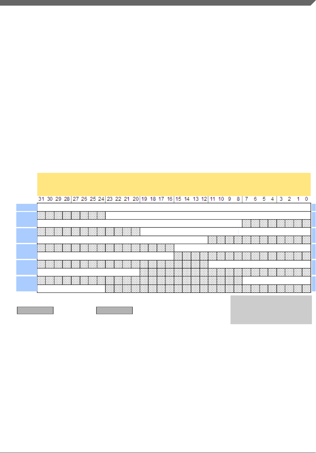
54.5.5 Data FIFO
Each transmit and receive channel includes a FIFO of size 8 × 32-bit. The FIFO data is
accessed using the SAI Transmit/Receive Data Registers.
54.5.5.1 Data alignment
Data in the FIFO can be aligned anywhere within the 32-bit wide register through the use
of the First Bit Shifted configuration field, which selects the bit index (between 31 and 0)
of the first bit shifted.
Examples of supported data alignment and the required First Bit Shifted configuration are
illustrated in Figure 54-3 for LSB First configurations and Figure 54-4 for MSB First
configurations.
Or
First Bit Shifted (FBT)
RX Config 5 Register
RCRL5[FBT]
First Bit Shifted (FBT)
TX Config 5 Register
RCRL5[FBT]
LSB first
00000
00000
01000
00000
01100
00000
10000
00000
10100
00000
11000
DATA[31:0]
DATA[23:0]
DATA[23:0]
DATA[19:0]
DATA[19:0]
DATA[15:0]
DATA[11:0]
DATA[7:0]
DATA[15:0]
DATA[11:0]
DATA[7:0]
shown above:
24-bit data
20-bit data
16-bit data
12-bit data
8-bit data
How data is written to the FIFO, using First Bit Shifted field (FBT)
Number of bits being transferred
LSB first
for
FBT values
Figure 54-3. SAI first bit shifted, LSB first
Chapter 54 Synchronous Audio Interface (SAI)
S32K1xx Series Reference Manual, Rev. 7, 04/2018
NXP Semiconductors 1821
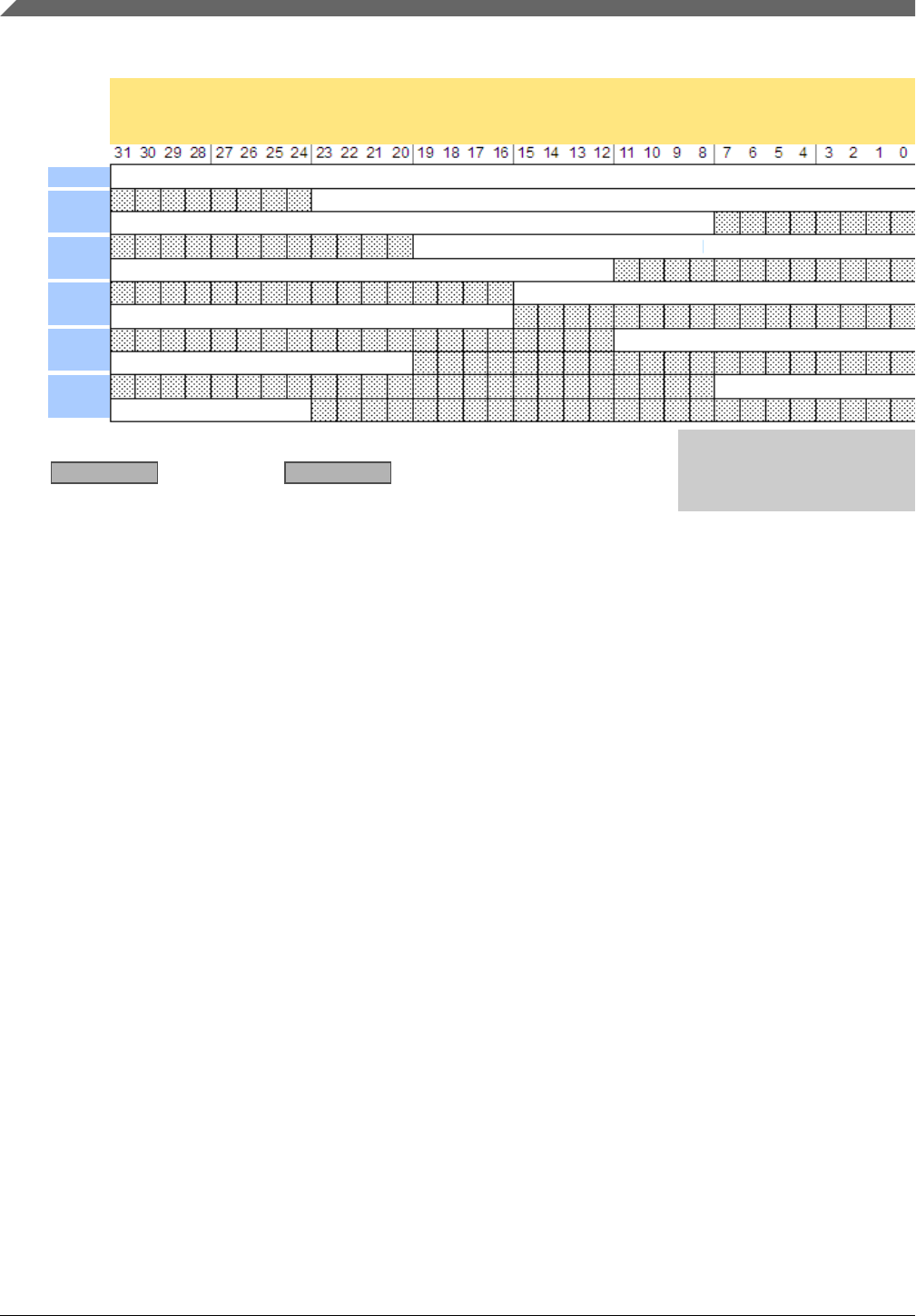
Or
First Bit Shifted (FBT)
RX Config 5 Register
RCRL5[FBT]
First Bit Shifted (FBT)
TX Config 5 Register
RCRL5[FBT]
11111
10111
11111
10011
11111
01111
11111
01011
11111
00111
11111
DATA[31:0]
DATA[23:0]
DATA[23:0]
DATA[19:0]
DATA[19:0]
DATA[15:0]
DATA[11:0]
DATA[7:0]
DATA[15:0]
DATA[11:0]
DATA[7:0]
shown above:
24-bit data
20-bit data
16-bit data
12-bit data
8-bit data
How data is written to the FIFO, using First Bit Shifted field (FBT)
Number of bits being transferred
MSB first
MSB first
for
FBT values
Figure 54-4. SAI first bit shifted, MSB first
54.5.5.2 FIFO pointers
When writing to a Transmit Data Register (TDRn), the Write FIFO Pointer (WFP) of the
corresponding Transmit FIFO Register (TFRn) increments after each valid write. The
SAI supports 8-bit, 16-bit and 32-bit writes to the Transmit Data Register and the FIFO
pointer will increment after each individual write. Note that 8-bit writes should only be
used when transmitting up to 8-bit data; 16-bit writes should only be used when
transmitting up to 16-bit data.
• If the Transmit FIFO is full, then writes to a Transmit Data Register are ignored.
• If the Transmit FIFO is empty, then to avoid a FIFO underrun, the Transmit Data
Register must be written at least 3 bit clocks before the start of the next unmasked
word. Before enabling the transmitter, the Transmit FIFO should be initialized with
data (since after the transmitter is enabled, the transmitter will start a new frame, and
if no data is in the FIFO, then the transmitter will immediately give an error).
When reading a Receive Data Register (RDRn), the Read FIFO Pointer (RFP) of the
corresponding Receive FIFO Register (RFRn) increments after each valid read. The SAI
supports 8-bit, 16-bit and 32-bit reads from the RDR and the FIFO pointer will increment
after each individual read. Note that 8-bit reads should only be used when receiving up to
8-bit data; 16-bit reads should only be used when receiving up to 16-bit data.
Functional description
S32K1xx Series Reference Manual, Rev. 7, 04/2018
1822 NXP Semiconductors

• If the Receive FIFO is empty, then reads from a Receive Data Register are ignored.
• If the Receive FIFO is full, then to avoid a FIFO overrun, the Receive Data Register
must be read at least 3 bit clocks before the end of an unmasked word.
54.5.5.3 FIFO packing
FIFO packing supports storing multiple 8-bit or 16-bit data words in one 32-bit FIFO
word for the transmitter and/or receiver. While this can be emulated by adjusting the
number of bits per word and number of words per frame (for example, one 32-bit word
per frame versus two 16-bit words per frame), FIFO packing does not require even
multiples of words per frame and fully supports word masking. When FIFO packing is
enabled, the FIFO pointers only increment when the full 32-bit FIFO word has been
written (transmit) or read (receive) by software, supporting scenarios where different
words within each frame are loaded/stored in different areas of memory.
When 16-bit FIFO packing is enabled for transmit, the transmit shift register is loaded at
the start of each frame and after every second unmasked transmit word. The first word
transmitted is taken from 16-bit word at byte offset $0 (first bit is selected by
TCFG5[FBT] must be configured within this 16-bit word) and the second word
transmitted is taken from the 16-bit word at byte offset $2 (first bit is selected by
TCSR5[FBT][3:0]). The transmitter will transmit logic zero until the start of the next
word once the 16-bit word has been transmitted.
When 16-bit FIFO packing is enabled for receive, the receive shift register is stored after
every second unmasked received word, and at the end of each frame if there is an odd
number of unmasked received words in each frame. The first word received is stored in
the 16-bit word at byte offset $0 (first bit is selected by RCFG5[FBT] and must be
configured within this 16-bit word) and the second word received is stored in the 16-bit
word at byte offset $2 (first bit is selected by RCSR5[FBT][3:0]). The receiver will
ignore received data until the start of the next word once the 16-bit word has been
received.
The 8-bit FIFO packing is similar to 16-bit packing except four words are loaded or
stored into each 32-bit FIFO word. The first word is loaded/stored in byte offset $0,
second word in byte offset $1, third word in byte offset $2 and fourth word in byte offset
$3. The TCFG5[FBT] and/or RCFG5[FBT] must be configured within byte offset $0.
Chapter 54 Synchronous Audio Interface (SAI)
S32K1xx Series Reference Manual, Rev. 7, 04/2018
NXP Semiconductors 1823

54.5.5.4 FIFO Combine
FIFO combining mode allows the separate FIFOs for multiple data channels to be used as
a single FIFO for either software accesses or a single data channel or both. Note that the
enabled data channels must be contiguous and data channel 0 must be enabled when
FIFO Combine mode is enabled.
Combining FIFOs for software access (writing transmit FIFO registers, reading receive
FIFO registers) allows a DMA controller or software to read or write multiple FIFOs
without incrementing the address that is accessed. Once enabled, the first software access
to a FIFO register will access the first enabled channel FIFO, while the second access to a
FIFO register will access the second enabled channel FIFO. This continues until software
accesses the last enabled channel FIFO and the pointer resets back to the first enabled
channel FIFO. To reset the pointer manually, software can reset the FIFOs or disable the
FIFO combining on software accesses.
Combining FIFOs for transmit data channels allows one data channel to use the FIFOs of
all enabled channel FIFOs, with identical data output on each enabled data channel. The
transmit shift registers for all enabled data channels are loaded at the start of each frame
and every N unmasked words (where N is the number of enabled data channels). The first
word transmitted is loaded from the first enabled channel FIFO, while the second word
transmitted is loaded from the second enabled channel FIFO, and so on until the end of
the frame. Since the first word in each frame is always loaded from the first enabled data
channel, it is recommended that the number of unmasked words in each frame is evenly
divisible by the number of enabled data channels.
Combining FIFOs for receive data channels allows one data channel to use the FIFOs of
all enabled channel FIFOs, with received data from channel 0 stored into each enabled
data channel. The receive shift register for all enabled data channels are stored after every
N unmasked words (where N is the number of enabled data channels). The first word
received is stored to the first enabled channel FIFO, while the second word received is
stored to the second enabled channel FIFO, and so on until the end of the frame. Since
the first word in each frame is always stored the first enabled data channel, it is
recommended that the number of unmasked words in each frame is evenly divisible by
the number of enabled data channels.
Note that combining FIFOs for data channels will load or store each channel FIFO at the
same time. This means that FIFO error conditions are only checked every N words
(where N is the number of enabled data channels) and that the FIFO warning and request
flags will assert if any of the enabled data channel meets the warning flag or request flag
conditions.
Functional description
S32K1xx Series Reference Manual, Rev. 7, 04/2018
1824 NXP Semiconductors

54.5.6 Word mask register
The SAI transmitter and receiver each contain a word mask register, namely TMR and
RMR, that can be used to mask any word in the frame. Because the word mask register is
double buffered, software can update it before the end of each frame to mask a particular
word in the next frame.
The TMR causes the Transmit Data pin to be tri-stated for the length of each selected
word and the transmit FIFO is not read for masked words.
The RMR causes the received data for each selected word to be discarded and not written
to the receive FIFO.
54.5.7 Interrupts and DMA requests
The SAI transmitter and receiver generate separate interrupts and separate DMA requests,
but support the same status flags.
54.5.7.1 FIFO request flag
The FIFO request flag is set based on the number of entries in the FIFO and the FIFO
watermark configuration.
The transmit FIFO request flag is set when the number of entries in any of the enabled
transmit FIFOs is less than or equal to the transmit FIFO watermark configuration and is
cleared when the number of entries in each enabled transmit FIFO is greater than the
transmit FIFO watermark configuration.
The receive FIFO request flag is set when the number of entries in any of the enabled
receive FIFOs is greater than the receive FIFO watermark configuration and is cleared
when the number of entries in each enabled receive FIFO is less than or equal to the
receive FIFO watermark configuration.
The FIFO request flag can generate an interrupt or a DMA request.
54.5.7.2 FIFO warning flag
The FIFO warning flag is set based on the number of entries in the FIFO.
The transmit warning flag is set when the number of entries in any of the enabled
transmit FIFOs is empty and is cleared when the number of entries in each enabled
transmit FIFO is not empty.
Chapter 54 Synchronous Audio Interface (SAI)
S32K1xx Series Reference Manual, Rev. 7, 04/2018
NXP Semiconductors 1825

The receive warning flag is set when the number of entries in any of the enabled receive
FIFOs is full and is cleared when the number of entries in each enabled receive FIFO is
not full.
The FIFO warning flag can generate an Interrupt or a DMA request.
54.5.7.3 FIFO error flag
The transmit FIFO error flag is set when the any of the enabled transmit FIFOs
underflow. After it is set, all enabled transmit channels will transmit zero data before
TCSR[FEF] is cleared.
When TCR4[FCONT] is set, the FIFO will continue transmitting data following an
underflow without software intervention. To ensure that data is transmitted in the correct
order, the transmitter will continue from the same word number in the frame that caused
the FIFO to underflow, but only after new data has been written to the transmit FIFO.
Software should still clear the TCSR[FEF] flag, but without reinitializing the transmit
FIFOs.
RCSR[FEF] is set when the any of the enabled receive FIFOs overflow. After it is set, all
enabled receive channels discard received data until RCSR[FEF] is cleared and the next
next receive frame starts. All enabled receive FIFOs should be emptied before
RCSR[FEF] is cleared.
When RCR4[FCONT] is set, the FIFO will continue receiving data following an
overflow without software intervention. To ensure that data is received in the correct
order, the receiver will continue from the same word number in the frame that caused the
FIFO to overflow, but only after data has been read from the receive FIFO. Software
should still clear the RCSR[FEF] flag, but without emptying the receive FIFOs.
The FIFO error flag can generate only an interrupt.
54.5.7.4 Sync error flag
The sync error flag, TCSR[SEF] or RCSR[SEF], is set when configured for an externally
generated frame sync and the external frame sync asserts when the transmitter or receiver
is busy with the previous frame. The external frame sync assertion is ignored and the
sync error flag is set. When the sync error flag is set, the transmitter or receiver continues
checking for frame sync assertion when idle or at the end of each frame.
The sync error flag can generate an interrupt only.
Functional description
S32K1xx Series Reference Manual, Rev. 7, 04/2018
1826 NXP Semiconductors

54.5.7.5 Word start flag
The word start flag is set at the start of the second bit clock for the selected word, as
configured by the Word Flag register field.
The word start flag can generate an interrupt only.
Chapter 54 Synchronous Audio Interface (SAI)
S32K1xx Series Reference Manual, Rev. 7, 04/2018
NXP Semiconductors 1827

Functional description
S32K1xx Series Reference Manual, Rev. 7, 04/2018
1828 NXP Semiconductors

Chapter 55
Ethernet MAC (ENET)
55.1 Chip-specific ENET information
S32K148 has one instance of the ENET module. Other products in the S32K1xx series do
not have the ENET module.
NOTE
• Prior to using ENET_MDIO or ENET_TMRx,
GPIO_PDDR needs to be configured for the corresponding
pins.
• Enable the Drive strength for the transmitting pads of
ENET by setting DSE field of PORT_PCRn register
• Wakeup through magic packet is supported only from
STOPx modes and not from VLPS mode. This wakeup is
independent of EIMR[WAKEUP] bit field.
• For RMII mode, MII_RMII_TX_CLK in IO Signal
Description Input Multiplexing sheet is referred as
RMII_REF_CLK.
55.1.1 Software guideline during ENET operation
System frequency must not be changed during ENET operation as this can cause FIFO
Underrun condition.
55.2 Introduction
The MAC-NET core, in conjunction with a 10/100-Mbit/s MAC, implements layer 3
network acceleration functions. These functions are designed to accelerate the processing
of various common networking protocols, such as IP, TCP, UDP, and ICMP, providing
wire speed services to client applications.
S32K1xx Series Reference Manual, Rev. 7, 04/2018
NXP Semiconductors 1829

55.3 Overview
The core implements a dual-speed 10/100-Mbit/s Ethernet MAC compliant with the
IEEE802.3-2002 standard. The MAC layer provides compatibility with half- or full-
duplex 10/100-Mbit/s Ethernet LANs.
The MAC operation is fully programmable and can be used in Network Interface Card
(NIC), bridging, or switching applications. The core implements the remote network
monitoring (RMON) counters according to IETF RFC 2819.
The core also implements a hardware acceleration block to optimize the performance of
network controllers providing TCP/IP, UDP, and ICMP protocol services. The
acceleration block performs critical functions in hardware, which are typically
implemented with large software overhead.
The core implements programmable embedded FIFOs that can provide buffering on the
receive path for lossless flow control.
Advanced power management features are available with magic packet detection and
programmable power-down modes.
A unified DMA (uDMA), internal to the ENET module, optimizes data transfer between
the ENET core and the SoC, and supports an enhanced buffer descriptor programming
model to support IEEE 1588 functionality.
The programmable Ethernet MAC with IEEE 1588 integrates a standard IEEE 802.3
Ethernet MAC with a time-stamping module. The IEEE 1588 standard provides accurate
clock synchronization for distributed control nodes for industrial automation applications.
55.3.1 Features
55.3.1.1 Ethernet MAC features
• Implements the full 802.3 specification with preamble/SFD generation, frame
padding generation, CRC generation and checking
• Supports zero-length preamble
• Dynamically configurable to support 10/100-Mbit/s operation
• Supports 10/100 Mbit/s full-duplex and configurable half-duplex operation
• Compliant with the AMD magic packet detection with interrupt for node remote
power management
• Seamless interface to commercial ethernet PHY devices via one of the following:
Overview
S32K1xx Series Reference Manual, Rev. 7, 04/2018
1830 NXP Semiconductors

• a 4-bit Media Independent Interface (MII) operating at 2.5/25 MHz.
• a 4-bit non-standard MII-Lite (MII without the CRS and COL signals) operating
at 2.5/25 MHz.
• a 2-bit Reduced MII (RMII) operating at 50 MHz.
• Simple 64-Bit FIFO user-application interface
• CRC-32 checking at full speed with optional forwarding of the frame check sequence
(FCS) field to the client
• CRC-32 generation and append on transmit or forwarding of user application
provided FCS selectable on a per-frame basis
• In full-duplex mode:
• Implements automated pause frame (802.3 x31A) generation and termination,
providing flow control without user application intervention
• Pause quanta used to form pause frames — dynamically programmable
• Pause frame generation additionally controllable by user application offering
flexible traffic flow control
• Optional forwarding of received pause frames to the user application
• Implements standard flow-control mechanism
• In half-duplex mode: provides full collision support, including jamming, backoff,
and automatic retransmission
• Supports VLAN-tagged frames according to IEEE 802.1Q
• Programmable MAC address: Insertion on transmit; discards frames with
mismatching destination address on receive (except broadcast and pause frames)
• Programmable promiscuous mode support to omit MAC destination address
checking on receive
• Multicast and unicast address filtering on receive based on 64-entry hash table,
reducing higher layer processing load
• Programmable frame maximum length providing support for any standard or
proprietary frame length
• Statistics indicators for frame traffic and errors (alignment, CRC, length) and pause
frames providing for IEEE 802.3 basic and mandatory management information
database (MIB) package and remote network monitoring (RFC 2819)
• Simple handshake user application FIFO interface with fully programmable depth
and threshold levels
• Provides separate status word for each received frame on the user interface providing
information such as frame length, frame type, VLAN tag, and error information
• Multiple internal loopback options
• MDIO master interface for PHY device configuration and management supports two
programmable MDIO base addresses, and standard (IEEE 802.3 Clause 22) and
extended (Clause 45) MDIO frame formats
• Supports legacy FEC buffer descriptors
Chapter 55 Ethernet MAC (ENET)
S32K1xx Series Reference Manual, Rev. 7, 04/2018
NXP Semiconductors 1831

55.3.1.2 IP protocol performance optimization features
• Operates on TCP/IP and UDP/IP and ICMP/IP protocol data or IP header only
• Enables wire-speed processing
• Supports IPv4 and IPv6
• Transparent passing of frames of other types and protocols
• Supports VLAN tagged frames according to IEEE 802.1q with transparent
forwarding of VLAN tag and control field
• Automatic IP-header and payload (protocol specific) checksum calculation and
verification on receive
• Automatic IP-header and payload (protocol specific) checksum generation and
automatic insertion on transmit configurable on a per-frame basis
• Supports IP and TCP, UDP, ICMP data for checksum generation and checking
• Supports full header options for IPv4 and TCP protocol headers
• Provides IPv6 support to datagrams with base header only — datagrams with
extension headers are passed transparently unmodifed/unchecked
• Provides statistics information for received IP and protocol errors
• Configurable automatic discard of erroneous frames
• Configurable automatic host-to-network (RX) and network-to-host (TX) byte order
conversion for IP and TCP/UDP/ICMP headers within the frame
• Configurable padding remove for short IP datagrams on receive
• Configurable Ethernet payload alignment to allow for 32-bit word-aligned header
and payload processing
• Programmable store-and-forward operation with clock and rate decoupling FIFOs
55.3.1.3 IEEE 1588 features
• Supports all IEEE 1588 frames.
• Allows reference clock to be chosen independently of network speed.
• Software-programmable precise time-stamping of ingress and egress frames
Overview
S32K1xx Series Reference Manual, Rev. 7, 04/2018
1832 NXP Semiconductors
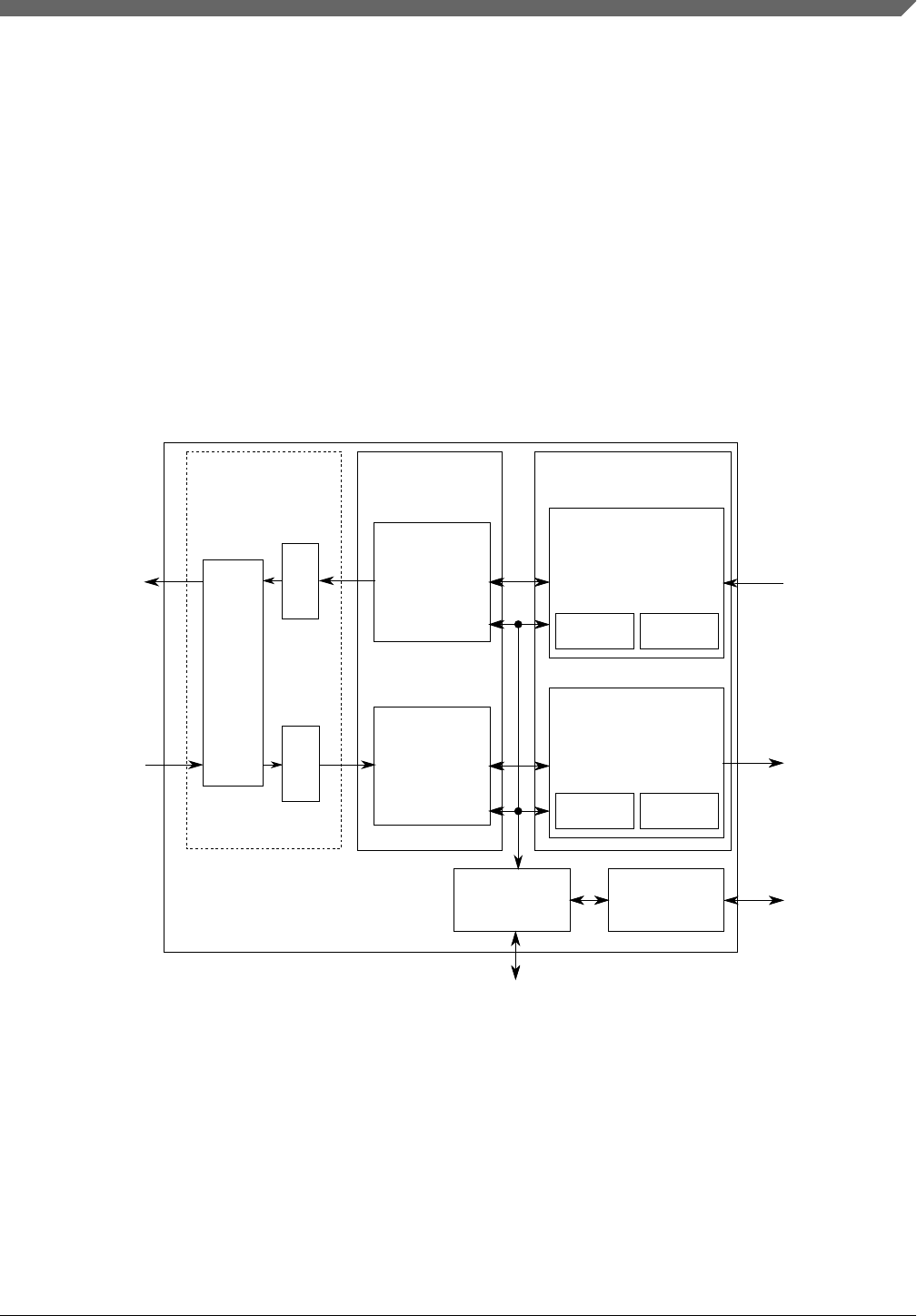
• Timer monitoring capabilities for system calibration and timing accuracy
management
• Precise time-stamping of external events with programmable interrupt generation
• Programmable event and interrupt generation for external system control
• Supports hardware- and software-controllable timer synchronization.
• Provides a 4-channel IEEE 1588 timer. Each channel supports input capture and
output compare using the 1588 counter.
55.3.2 Block diagram
RX control
Pause frame
terminate
TCP offload
engine (TOE)
functions
TX control
Pause frame
generate
Configuration
statistics
MDIO
master
Register interface
management
Transmit
application
interface
MII/RMII MII/RMII
PHY
interface transmit
interface
interface
receive
CRC
generate
CRC
TCP/IP
performance
optimization
MAC
TCP/IP
performance
optimization
Receive
application
interface
uDMA
AHB
system
bus I/F
RX
FIFO
TX
FIFO
Figure 55-1. Ethernet MAC-NET core block diagram
55.4 External signal description
NOTE
The MII column pertains only to devices that support MII.
Chapter 55 Ethernet MAC (ENET)
S32K1xx Series Reference Manual, Rev. 7, 04/2018
NXP Semiconductors 1833

MII RMII Description I/O
MII_COL — Asserted upon detection of a
collision and remains
asserted while the collision
persists. This signal is not
defined for full-duplex mode.
I
MII_CRS — Carrier sense. When
asserted, indicates transmit
or receive medium is not idle.
In RMII mode, this signal is
present on the
RMII_CRS_DV pin.
I
MII_MDC RMII_MDC Output clock provides a
timing reference to the PHY
for data transfers on the
MDIO signal.
O
MII_MDIO RMII_MDIO Transfers control information
between the external PHY
and the media-access
controller. Data is
synchronous to MDC. This
signal is an input after reset.
I/O
MII_RXCLK — In MII mode, provides a
timing reference for RXDV,
RXD[3:0], and RXER.
I
MII_RXDV RMII_CRS_DV Asserting this input indicates
the PHY has valid nibbles
present on the MII. RXDV
must remain asserted from
the first recovered nibble of
the frame through to the last
nibble. Asserting RXDV must
start no later than the SFD
and exclude any EOF.
In RMII mode, this pin also
generates the CRS signal.
I
MII_RXD[3:0] RMII_RXD[1:0] Contains the Ethernet input
data transferred from the
PHY to the media-access
controller when RXDV is
asserted.
I
MII_RXER RMII_RXER When asserted with RXDV,
indicates the PHY detects an
error in the current frame.
I
MII_TXCLK — Input clock, which provides a
timing reference for TXEN,
TXD[3:0], and TXER.
I
MII_TXD[3:0] RMII_TXD[1:0] Serial output Ethernet data.
Only valid during TXEN
assertion.
O
MII_TXEN RMII_TXEN Indicates when valid nibbles
are present on the MII. This
signal is asserted with the
O
Table continues on the next page...
External signal description
S32K1xx Series Reference Manual, Rev. 7, 04/2018
1834 NXP Semiconductors

MII RMII Description I/O
first nibble of a preamble and
is deasserted before the first
TXCLK following the final
nibble of the frame.
MII_TXER — When asserted for one or
more clock cycles while
TXEN is also asserted, PHY
sends one or more illegal
symbols.
O
— RMII_REF_CLK In RMII mode, this signal is
the reference clock for
receive, transmit, and the
control interface.
I
1588_TMRn1588_TMRnCapture/Compare block
input/output event bus.
When configured for capture
and a rising edge is detected,
the current timer value is
latched and transferred into
the corresponding
ENET_TCCRn register for
inspection by software.
When configured for
compare, the corresponding
signal 1588_TMRn is
asserted for one cycle when
the timer reaches the
compare value programmed
in ENET_TCCRn.
An interrupt can be triggered
if ENET_TCSRn[TIE] is set.
A DMA request can be
triggered if
ENET_TCSRn[TDRE] is set.
I/O
ENET_1588_CLKIN ENET_1588_CLKIN Alternate IEEE 1588 Ethernet
clock input; Clock period
should be an integer number
of nanoseconds
I
55.5 Memory map/register definition
ENET registers must be read or written with 32-bit accesses. Non-32 bit accesses will
terminate with an error.
Reserved bits should be written with 0 and ignored on read. Unused registers read zero
and a write has no effect.
This table shows Ethernet registers organization.
Chapter 55 Ethernet MAC (ENET)
S32K1xx Series Reference Manual, Rev. 7, 04/2018
NXP Semiconductors 1835

Table 55-1. Register map summary
Offset Address Section Description
0x0000 – 0x01FF Configuration Core control and status registers
0x0200 – 0x03FF Statistics counters MIB and Remote Network Monitoring (RFC 2819) registers
0x0400 – 0x0430 1588 control 1588 adjustable timer (TSM) and 1588 frame control
0x0600 – 0x07FC Capture/Compare block Registers for the Capture/Compare block
ENET memory map
Address
offset (hex) Register name Width
(in bits) Access Reset value Section/
page
4 Interrupt Event Register (ENET_EIR) 32 w1c 0000_0000h 55.5.1/1840
8 Interrupt Mask Register (ENET_EIMR) 32 R/W 0000_0000h 55.5.2/1843
10 Receive Descriptor Active Register (ENET_RDAR) 32 R/W 0000_0000h 55.5.3/1846
14 Transmit Descriptor Active Register (ENET_TDAR) 32 R/W 0000_0000h 55.5.4/1847
24 Ethernet Control Register (ENET_ECR) 32 R/W F000_0000h 55.5.5/1848
40 MII Management Frame Register (ENET_MMFR) 32 R/W 0000_0000h 55.5.6/1850
44 MII Speed Control Register (ENET_MSCR) 32 R/W 0000_0000h 55.5.7/1850
64 MIB Control Register (ENET_MIBC) 32 R/W C000_0000h 55.5.8/1853
84 Receive Control Register (ENET_RCR) 32 R/W 05EE_0001h 55.5.9/1854
C4 Transmit Control Register (ENET_TCR) 32 R/W 0000_0000h 55.5.10/
1857
E4 Physical Address Lower Register (ENET_PALR) 32 R/W 0000_0000h 55.5.11/
1859
E8 Physical Address Upper Register (ENET_PAUR) 32 R/W 0000_8808h 55.5.12/
1859
EC Opcode/Pause Duration Register (ENET_OPD) 32 R/W 0001_0000h 55.5.13/
1860
118 Descriptor Individual Upper Address Register (ENET_IAUR) 32 R/W 0000_0000h 55.5.14/
1860
11C Descriptor Individual Lower Address Register (ENET_IALR) 32 R/W 0000_0000h 55.5.15/
1861
120 Descriptor Group Upper Address Register (ENET_GAUR) 32 R/W 0000_0000h 55.5.16/
1861
124 Descriptor Group Lower Address Register (ENET_GALR) 32 R/W 0000_0000h 55.5.17/
1862
144 Transmit FIFO Watermark Register (ENET_TFWR) 32 R/W 0000_0000h 55.5.18/
1862
180 Receive Descriptor Ring Start Register (ENET_RDSR) 32 R/W 0000_0000h 55.5.19/
1863
184 Transmit Buffer Descriptor Ring Start Register
(ENET_TDSR) 32 R/W 0000_0000h 55.5.20/
1864
188 Maximum Receive Buffer Size Register (ENET_MRBR) 32 R/W 0000_0000h 55.5.21/
1865
Table continues on the next page...
Memory map/register definition
S32K1xx Series Reference Manual, Rev. 7, 04/2018
1836 NXP Semiconductors

ENET memory map (continued)
Address
offset (hex) Register name Width
(in bits) Access Reset value Section/
page
190 Receive FIFO Section Full Threshold (ENET_RSFL) 32 R/W 0000_0000h 55.5.22/
1866
194 Receive FIFO Section Empty Threshold (ENET_RSEM) 32 R/W 0000_0000h 55.5.23/
1866
198 Receive FIFO Almost Empty Threshold (ENET_RAEM) 32 R/W 0000_0004h 55.5.24/
1867
19C Receive FIFO Almost Full Threshold (ENET_RAFL) 32 R/W 0000_0004h 55.5.25/
1867
1A0 Transmit FIFO Section Empty Threshold (ENET_TSEM) 32 R/W 0000_0000h 55.5.26/
1868
1A4 Transmit FIFO Almost Empty Threshold (ENET_TAEM) 32 R/W 0000_0004h 55.5.27/
1868
1A8 Transmit FIFO Almost Full Threshold (ENET_TAFL) 32 R/W 0000_0008h 55.5.28/
1869
1AC Transmit Inter-Packet Gap (ENET_TIPG) 32 R/W 0000_000Ch 55.5.29/
1869
1B0 Frame Truncation Length (ENET_FTRL) 32 R/W 0000_07FFh 55.5.30/
1870
1C0 Transmit Accelerator Function Configuration (ENET_TACC) 32 R/W 0000_0000h 55.5.31/
1870
1C4 Receive Accelerator Function Configuration (ENET_RACC) 32 R/W 0000_0000h 55.5.32/
1871
200 Reserved Statistic Register (ENET_RMON_T_DROP) 32 R 0000_0000h 55.5.33/
1872
204 Tx Packet Count Statistic Register
(ENET_RMON_T_PACKETS) 32 R 0000_0000h 55.5.34/
1873
208 Tx Broadcast Packets Statistic Register
(ENET_RMON_T_BC_PKT) 32 R 0000_0000h 55.5.35/
1873
20C Tx Multicast Packets Statistic Register
(ENET_RMON_T_MC_PKT) 32 R 0000_0000h 55.5.36/
1874
210 Tx Packets with CRC/Align Error Statistic Register
(ENET_RMON_T_CRC_ALIGN) 32 R 0000_0000h 55.5.37/
1874
214 Tx Packets Less Than Bytes and Good CRC Statistic
Register (ENET_RMON_T_UNDERSIZE) 32 R 0000_0000h 55.5.38/
1874
218 Tx Packets GT MAX_FL bytes and Good CRC Statistic
Register (ENET_RMON_T_OVERSIZE) 32 R 0000_0000h 55.5.39/
1875
21C Tx Packets Less Than 64 Bytes and Bad CRC Statistic
Register (ENET_RMON_T_FRAG) 32 R 0000_0000h 55.5.40/
1875
220 Tx Packets Greater Than MAX_FL bytes and Bad CRC
Statistic Register (ENET_RMON_T_JAB) 32 R 0000_0000h 55.5.41/
1876
224 Tx Collision Count Statistic Register (ENET_RMON_T_COL) 32 R 0000_0000h 55.5.42/
1876
228 Tx 64-Byte Packets Statistic Register
(ENET_RMON_T_P64) 32 R 0000_0000h 55.5.43/
1876
Table continues on the next page...
Chapter 55 Ethernet MAC (ENET)
S32K1xx Series Reference Manual, Rev. 7, 04/2018
NXP Semiconductors 1837

ENET memory map (continued)
Address
offset (hex) Register name Width
(in bits) Access Reset value Section/
page
22C Tx 65- to 127-byte Packets Statistic Register
(ENET_RMON_T_P65TO127) 32 R 0000_0000h 55.5.44/
1877
230 Tx 128- to 255-byte Packets Statistic Register
(ENET_RMON_T_P128TO255) 32 R 0000_0000h 55.5.45/
1877
234 Tx 256- to 511-byte Packets Statistic Register
(ENET_RMON_T_P256TO511) 32 R 0000_0000h 55.5.46/
1878
238 Tx 512- to 1023-byte Packets Statistic Register
(ENET_RMON_T_P512TO1023) 32 R 0000_0000h 55.5.47/
1878
23C Tx 1024- to 2047-byte Packets Statistic Register
(ENET_RMON_T_P1024TO2047) 32 R 0000_0000h 55.5.48/
1879
240 Tx Packets Greater Than 2048 Bytes Statistic Register
(ENET_RMON_T_P_GTE2048) 32 R 0000_0000h 55.5.49/
1879
244 Tx Octets Statistic Register (ENET_RMON_T_OCTETS) 32 R 0000_0000h 55.5.50/
1879
248 Reserved Statistic Register (ENET_IEEE_T_DROP) 32 R 0000_0000h 55.5.51/
1880
24C Frames Transmitted OK Statistic Register
(ENET_IEEE_T_FRAME_OK) 32 R 0000_0000h 55.5.52/
1880
250 Frames Transmitted with Single Collision Statistic Register
(ENET_IEEE_T_1COL) 32 R 0000_0000h 55.5.53/
1881
254 Frames Transmitted with Multiple Collisions Statistic
Register (ENET_IEEE_T_MCOL) 32 R 0000_0000h 55.5.54/
1881
258 Frames Transmitted after Deferral Delay Statistic Register
(ENET_IEEE_T_DEF) 32 R 0000_0000h 55.5.55/
1881
25C Frames Transmitted with Late Collision Statistic Register
(ENET_IEEE_T_LCOL) 32 R 0000_0000h 55.5.56/
1882
260 Frames Transmitted with Excessive Collisions Statistic
Register (ENET_IEEE_T_EXCOL) 32 R 0000_0000h 55.5.57/
1882
264 Frames Transmitted with Tx FIFO Underrun Statistic
Register (ENET_IEEE_T_MACERR) 32 R 0000_0000h 55.5.58/
1883
268 Frames Transmitted with Carrier Sense Error Statistic
Register (ENET_IEEE_T_CSERR) 32 R 0000_0000h 55.5.59/
1883
26C Reserved Statistic Register (ENET_IEEE_T_SQE) 32 R (reads
0) 0000_0000h 55.5.60/
1883
270 Flow Control Pause Frames Transmitted Statistic Register
(ENET_IEEE_T_FDXFC) 32 R 0000_0000h 55.5.61/
1884
274 Octet Count for Frames Transmitted w/o Error Statistic
Register (ENET_IEEE_T_OCTETS_OK) 32 R 0000_0000h 55.5.62/
1884
284 Rx Packet Count Statistic Register
(ENET_RMON_R_PACKETS) 32 R 0000_0000h 55.5.63/
1885
288 Rx Broadcast Packets Statistic Register
(ENET_RMON_R_BC_PKT) 32 R 0000_0000h 55.5.64/
1885
28C Rx Multicast Packets Statistic Register
(ENET_RMON_R_MC_PKT) 32 R 0000_0000h 55.5.65/
1885
Table continues on the next page...
Memory map/register definition
S32K1xx Series Reference Manual, Rev. 7, 04/2018
1838 NXP Semiconductors

ENET memory map (continued)
Address
offset (hex) Register name Width
(in bits) Access Reset value Section/
page
290 Rx Packets with CRC/Align Error Statistic Register
(ENET_RMON_R_CRC_ALIGN) 32 R 0000_0000h 55.5.66/
1886
294 Rx Packets with Less Than 64 Bytes and Good CRC
Statistic Register (ENET_RMON_R_UNDERSIZE) 32 R 0000_0000h 55.5.67/
1886
298 Rx Packets Greater Than MAX_FL and Good CRC Statistic
Register (ENET_RMON_R_OVERSIZE) 32 R 0000_0000h 55.5.68/
1887
29C Rx Packets Less Than 64 Bytes and Bad CRC Statistic
Register (ENET_RMON_R_FRAG) 32 R 0000_0000h 55.5.69/
1887
2A0 Rx Packets Greater Than MAX_FL Bytes and Bad CRC
Statistic Register (ENET_RMON_R_JAB) 32 R 0000_0000h 55.5.70/
1887
2A4 Reserved Statistic Register (ENET_RMON_R_RESVD_0) 32 R (reads
0) 0000_0000h 55.5.71/
1888
2A8 Rx 64-Byte Packets Statistic Register
(ENET_RMON_R_P64) 32 R 0000_0000h 55.5.72/
1888
2AC Rx 65- to 127-Byte Packets Statistic Register
(ENET_RMON_R_P65TO127) 32 R 0000_0000h 55.5.73/
1889
2B0 Rx 128- to 255-Byte Packets Statistic Register
(ENET_RMON_R_P128TO255) 32 R 0000_0000h 55.5.74/
1889
2B4 Rx 256- to 511-Byte Packets Statistic Register
(ENET_RMON_R_P256TO511) 32 R 0000_0000h 55.5.75/
1889
2B8 Rx 512- to 1023-Byte Packets Statistic Register
(ENET_RMON_R_P512TO1023) 32 R 0000_0000h 55.5.76/
1890
2BC Rx 1024- to 2047-Byte Packets Statistic Register
(ENET_RMON_R_P1024TO2047) 32 R 0000_0000h 55.5.77/
1890
2C0 Rx Packets Greater than 2048 Bytes Statistic Register
(ENET_RMON_R_P_GTE2048) 32 R 0000_0000h 55.5.78/
1891
2C4 Rx Octets Statistic Register (ENET_RMON_R_OCTETS) 32 R 0000_0000h 55.5.79/
1891
2C8 Frames not Counted Correctly Statistic Register
(ENET_IEEE_R_DROP) 32 R 0000_0000h 55.5.80/
1891
2CC Frames Received OK Statistic Register
(ENET_IEEE_R_FRAME_OK) 32 R 0000_0000h 55.5.81/
1892
2D0 Frames Received with CRC Error Statistic Register
(ENET_IEEE_R_CRC) 32 R 0000_0000h 55.5.82/
1892
2D4 Frames Received with Alignment Error Statistic Register
(ENET_IEEE_R_ALIGN) 32 R 0000_0000h 55.5.83/
1893
2D8 Receive FIFO Overflow Count Statistic Register
(ENET_IEEE_R_MACERR) 32 R 0000_0000h 55.5.84/
1893
2DC Flow Control Pause Frames Received Statistic Register
(ENET_IEEE_R_FDXFC) 32 R 0000_0000h 55.5.85/
1893
2E0 Octet Count for Frames Received without Error Statistic
Register (ENET_IEEE_R_OCTETS_OK) 32 R 0000_0000h 55.5.86/
1894
400 Adjustable Timer Control Register (ENET_ATCR) 32 R/W 0000_0000h 55.5.87/
1894
Table continues on the next page...
Chapter 55 Ethernet MAC (ENET)
S32K1xx Series Reference Manual, Rev. 7, 04/2018
NXP Semiconductors 1839

ENET memory map (continued)
Address
offset (hex) Register name Width
(in bits) Access Reset value Section/
page
404 Timer Value Register (ENET_ATVR) 32 R/W 0000_0000h 55.5.88/
1896
408 Timer Offset Register (ENET_ATOFF) 32 R/W 0000_0000h 55.5.89/
1897
40C Timer Period Register (ENET_ATPER) 32 R/W 3B9A_CA00h 55.5.90/
1897
410 Timer Correction Register (ENET_ATCOR) 32 R/W 0000_0000h 55.5.91/
1898
414 Time-Stamping Clock Period Register (ENET_ATINC) 32 R/W 0000_0000h 55.5.92/
1898
418 Timestamp of Last Transmitted Frame (ENET_ATSTMP) 32 R 0000_0000h 55.5.93/
1899
604 Timer Global Status Register (ENET_TGSR) 32 R/W 0000_0000h 55.5.94/
1899
608 Timer Control Status Register (ENET_TCSR0) 32 R/W 0000_0000h 55.5.95/
1900
60C Timer Compare Capture Register (ENET_TCCR0) 32 R/W 0000_0000h 55.5.96/
1901
610 Timer Control Status Register (ENET_TCSR1) 32 R/W 0000_0000h 55.5.95/
1900
614 Timer Compare Capture Register (ENET_TCCR1) 32 R/W 0000_0000h 55.5.96/
1901
618 Timer Control Status Register (ENET_TCSR2) 32 R/W 0000_0000h 55.5.95/
1900
61C Timer Compare Capture Register (ENET_TCCR2) 32 R/W 0000_0000h 55.5.96/
1901
620 Timer Control Status Register (ENET_TCSR3) 32 R/W 0000_0000h 55.5.95/
1900
624 Timer Compare Capture Register (ENET_TCCR3) 32 R/W 0000_0000h 55.5.96/
1901
55.5.1 Interrupt Event Register (ENET_EIR)
When an event occurs that sets a bit in EIR, an interrupt occurs if the corresponding bit in
the interrupt mask register (EIMR) is also set. Writing a 1 to an EIR bit clears it; writing
0 has no effect. This register is cleared upon hardware reset.
NOTE
TxBD[INT] and RxBD[INT] must be set to 1 to allow setting
the corresponding EIR register flags in enhanced mode,
ENET_ECR[EN1588] = 1. Legacy mode does not require these
flags to be enabled.
Memory map/register definition
S32K1xx Series Reference Manual, Rev. 7, 04/2018
1840 NXP Semiconductors

Address: 0h base + 4h offset = 4h
Bit 31 30 29 28 27 26 25 24 23 22 21 20 19 18 17 16
R0
BABR
BABT
GRA
TXF TXB RXF RXB MII
EBERR
LC
RL
UN
PLR
WAKEUP
TS_AVAIL
Ww1c w1c w1c w1c w1c w1c w1c w1c w1c w1c w1c w1c w1c w1c w1c
Reset 0 0 0 0 0 0 0 0 0 0 0 0 0 0 0 0
Bit 15 14 13 12 11 10 9 8 7 6 5 4 3 2 1 0
R
TS_TIMER
W w1c 0 0 0 0 0
Reset 0 0 0 0 0 0 0 0 0 0 0 0 0 0 0 0
ENET_EIR field descriptions
Field Description
31
Reserved
This field is reserved.
This read-only field is reserved and always has the value 0.
30
BABR
Babbling Receive Error
Indicates a frame was received with length in excess of RCR[MAX_FL] bytes.
29
BABT
Babbling Transmit Error
Indicates the transmitted frame length exceeds RCR[MAX_FL] bytes. Usually this condition is caused
when a frame that is too long is placed into the transmit data buffer(s). Truncation does not occur.
28
GRA
Graceful Stop Complete
This interrupt is asserted after the transmitter is put into a pause state after completion of the frame
currently being transmitted. See Graceful Transmit Stop (GTS) for conditions that lead to graceful stop.
NOTE: The GRA interrupt is asserted only when the TX transitions into the stopped state. If this bit is
cleared by writing 1 and the TX is still stopped, the bit is not set again.
27
TXF
Transmit Frame Interrupt
Indicates a frame has been transmitted and the last corresponding buffer descriptor has been updated.
26
TXB
Transmit Buffer Interrupt
Indicates a transmit buffer descriptor has been updated.
25
RXF
Receive Frame Interrupt
Indicates a frame has been received and the last corresponding buffer descriptor has been updated.
Table continues on the next page...
Chapter 55 Ethernet MAC (ENET)
S32K1xx Series Reference Manual, Rev. 7, 04/2018
NXP Semiconductors 1841

ENET_EIR field descriptions (continued)
Field Description
24
RXB
Receive Buffer Interrupt
Indicates a receive buffer descriptor is not the last in the frame has been updated.
23
MII
MII Interrupt.
Indicates that the MII has completed the data transfer requested.
22
EBERR
Ethernet Bus Error
Indicates a system bus error occurred when a uDMA transaction is underway. When this bit is set,
ECR[ETHEREN] is cleared, halting frame processing by the MAC. When this occurs, software must
ensure proper actions, possibly resetting the system, to resume normal operation.
21
LC
Late Collision
Indicates a collision occurred beyond the collision window (slot time) in half-duplex mode. The frame
truncates with a bad CRC and the remainder of the frame is discarded.
20
RL
Collision Retry Limit
Indicates a collision occurred on each of 16 successive attempts to transmit the frame. The frame is
discarded without being transmitted and transmission of the next frame commences. This error can only
occur in half-duplex mode.
19
UN
Transmit FIFO Underrun
Indicates the transmit FIFO became empty before the complete frame was transmitted.
NOTE: In situations where the device has various masters generating high traffic, a FIFO underrun can
occur on the transmit FIFO. To avoid transmit FIFO underrun, store and forward can be enabled
in ENET_TFWR[STRFWD]. See STRFWD. Also, a higher priority can be set for ENET traffic
using available means on the central bus fabric connecting the ENET module.
18
PLR
Payload Receive Error
Indicates a frame was received with a payload length error. See Frame Length/Type Verification: Payload
Length Check for more information.
17
WAKEUP
Node Wakeup Request Indication
Read-only status bit to indicate that a magic packet has been detected. Will act only if ECR[MAGICEN] is
set.
16
TS_AVAIL
Transmit Timestamp Available
Indicates that the timestamp of the last transmitted timing frame is available in the ATSTMP register.
15
TS_TIMER
Timestamp Timer
The adjustable timer reached the period event. A period event interrupt can be generated if
ATCR[PEREN] is set and the timer wraps according to the periodic setting in the ATPER register. Set the
timer period value before setting ATCR[PEREN].
14–13
Reserved
This field is reserved.
This write-only field is reserved. It must always be written with the value 0.
12
Reserved
This field is reserved.
This write-only field is reserved. It must always be written with the value 0.
11–9
Reserved
This field is reserved.
This write-only field is reserved. It must always be written with the value 0.
Table continues on the next page...
Memory map/register definition
S32K1xx Series Reference Manual, Rev. 7, 04/2018
1842 NXP Semiconductors
ENET_EIR field descriptions (continued)
Field Description
8
Reserved
This field is reserved.
This write-only field is reserved. It must always be written with the value 0.
Reserved This field is reserved.
This write-only field is reserved. It must always be written with the value 0.
55.5.2 Interrupt Mask Register (ENET_EIMR)
EIMR controls which interrupt events are allowed to generate actual interrupts. A
hardware reset clears this register. If the corresponding bits in the EIR and EIMR
registers are set, an interrupt is generated. The interrupt signal remains asserted until a 1
is written to the EIR field (write 1 to clear) or a 0 is written to the EIMR field.
Address: 0h base + 8h offset = 8h
Bit 31 30 29 28 27 26 25 24 23 22 21 20 19 18 17 16
R
BABR BABT GRA TXF TXB RXF RXB MII
EBERR
LC RL UN PLR
WAKEUP
TS_AVAIL
W0
Reset 0 0 0 0 0 0 0 0 0 0 0 0 0 0 0 0
Bit 15 14 13 12 11 10 9 8 7 6 5 4 3 2 1 0
R
TS_TIMER
W0 0 0 0 0
Reset 0 0 0 0 0 0 0 0 0 0 0 0 0 0 0 0
ENET_EIMR field descriptions
Field Description
31
Reserved
This field is reserved.
This write-only field is reserved. It must always be written with the value 0.
30
BABR
BABR Interrupt Mask
Corresponds to interrupt source EIR[BABR] and determines whether an interrupt condition can generate
an interrupt. At every module clock, the EIR samples the signal generated by the interrupting source. The
corresponding EIR BABR field reflects the state of the interrupt signal even if the corresponding EIMR field
is cleared.
0 The corresponding interrupt source is masked.
1 The corresponding interrupt source is not masked.
29
BABT
BABT Interrupt Mask
Table continues on the next page...
Chapter 55 Ethernet MAC (ENET)
S32K1xx Series Reference Manual, Rev. 7, 04/2018
NXP Semiconductors 1843

ENET_EIMR field descriptions (continued)
Field Description
Corresponds to interrupt source EIR[BABT] and determines whether an interrupt condition can generate
an interrupt. At every module clock, the EIR samples the signal generated by the interrupting source. The
corresponding EIR BABT field reflects the state of the interrupt signal even if the corresponding EIMR field
is cleared.
0 The corresponding interrupt source is masked.
1 The corresponding interrupt source is not masked.
28
GRA
GRA Interrupt Mask
Corresponds to interrupt source EIR[GRA] and determines whether an interrupt condition can generate an
interrupt. At every module clock, the EIR samples the signal generated by the interrupting source. The
corresponding EIR GRA field reflects the state of the interrupt signal even if the corresponding EIMR field
is cleared.
0 The corresponding interrupt source is masked.
1 The corresponding interrupt source is not masked.
27
TXF
TXF Interrupt Mask
Corresponds to interrupt source EIR[TXF] and determines whether an interrupt condition can generate an
interrupt. At every module clock, the EIR samples the signal generated by the interrupting source. The
corresponding EIR TXF field reflects the state of the interrupt signal even if the corresponding EIMR field
is cleared.
0 The corresponding interrupt source is masked.
1 The corresponding interrupt source is not masked.
26
TXB
TXB Interrupt Mask
Corresponds to interrupt source EIR[TXB] and determines whether an interrupt condition can generate an
interrupt. At every module clock, the EIR samples the signal generated by the interrupting source. The
corresponding EIR TXF field reflects the state of the interrupt signal even if the corresponding EIMR field
is cleared.
0 The corresponding interrupt source is masked.
1 The corresponding interrupt source is not masked.
25
RXF
RXF Interrupt Mask
Corresponds to interrupt source EIR[RXF] and determines whether an interrupt condition can generate an
interrupt. At every module clock, the EIR samples the signal generated by the interrupting source. The
corresponding EIR RXF field reflects the state of the interrupt signal even if the corresponding EIMR field
is cleared.
24
RXB
RXB Interrupt Mask
Corresponds to interrupt source EIR[RXB] and determines whether an interrupt condition can generate an
interrupt. At every module clock, the EIR samples the signal generated by the interrupting source. The
corresponding EIR RXB field reflects the state of the interrupt signal even if the corresponding EIMR field
is cleared.
23
MII
MII Interrupt Mask
Corresponds to interrupt source EIR[MII] and determines whether an interrupt condition can generate an
interrupt. At every module clock, the EIR samples the signal generated by the interrupting source. The
corresponding EIR MII field reflects the state of the interrupt signal even if the corresponding EIMR field is
cleared.
Table continues on the next page...
Memory map/register definition
S32K1xx Series Reference Manual, Rev. 7, 04/2018
1844 NXP Semiconductors

ENET_EIMR field descriptions (continued)
Field Description
22
EBERR
EBERR Interrupt Mask
Corresponds to interrupt source EIR[EBERR] and determines whether an interrupt condition can generate
an interrupt. At every module clock, the EIR samples the signal generated by the interrupting source. The
corresponding EIR EBERR field reflects the state of the interrupt signal even if the corresponding EIMR
field is cleared.
21
LC
LC Interrupt Mask
Corresponds to interrupt source EIR[LC] and determines whether an interrupt condition can generate an
interrupt. At every module clock, the EIR samples the signal generated by the interrupting source. The
corresponding EIR LC field reflects the state of the interrupt signal even if the corresponding EIMR field is
cleared.
20
RL
RL Interrupt Mask
Corresponds to interrupt source EIR[RL] and determines whether an interrupt condition can generate an
interrupt. At every module clock, the EIR samples the signal generated by the interrupting source. The
corresponding EIR RL field reflects the state of the interrupt signal even if the corresponding EIMR field is
cleared.
19
UN
UN Interrupt Mask
Corresponds to interrupt source EIR[UN] and determines whether an interrupt condition can generate an
interrupt. At every module clock, the EIR samples the signal generated by the interrupting source. The
corresponding EIR UN field reflects the state of the interrupt signal even if the corresponding EIMR field is
cleared.
18
PLR
PLR Interrupt Mask
Corresponds to interrupt source EIR[PLR] and determines whether an interrupt condition can generate an
interrupt. At every module clock, the EIR samples the signal generated by the interrupting source. The
corresponding EIR PLR field reflects the state of the interrupt signal even if the corresponding EIMR field
is cleared.
17
WAKEUP
WAKEUP Interrupt Mask
Corresponds to interrupt source EIR[WAKEUP] register and determines whether an interrupt condition can
generate an interrupt. At every module clock, the EIR samples the signal generated by the interrupting
source. The corresponding EIR WAKEUP field reflects the state of the interrupt signal even if the
corresponding EIMR field is cleared.
16
TS_AVAIL
TS_AVAIL Interrupt Mask
Corresponds to interrupt source EIR[TS_AVAIL] register and determines whether an interrupt condition
can generate an interrupt. At every module clock, the EIR samples the signal generated by the interrupting
source. The corresponding EIR TS_AVAIL field reflects the state of the interrupt signal even if the
corresponding EIMR field is cleared.
15
TS_TIMER
TS_TIMER Interrupt Mask
Corresponds to interrupt source EIR[TS_TIMER] register and determines whether an interrupt condition
can generate an interrupt. At every module clock, the EIR samples the signal generated by the interrupting
source. The corresponding EIR TS_TIMER field reflects the state of the interrupt signal even if the
corresponding EIMR field is cleared.
14–13
Reserved
This field is reserved.
This write-only field is reserved. It must always be written with the value 0.
12
Reserved
This field is reserved.
This write-only field is reserved. It must always be written with the value 0.
Table continues on the next page...
Chapter 55 Ethernet MAC (ENET)
S32K1xx Series Reference Manual, Rev. 7, 04/2018
NXP Semiconductors 1845

ENET_EIMR field descriptions (continued)
Field Description
11–9
Reserved
This field is reserved.
This write-only field is reserved. It must always be written with the value 0.
8
Reserved
This field is reserved.
This write-only field is reserved. It must always be written with the value 0.
Reserved This field is reserved.
This write-only field is reserved. It must always be written with the value 0.
55.5.3 Receive Descriptor Active Register (ENET_RDAR)
RDAR is a command register, written by the user, to indicate that the receive descriptor
ring has been updated, that is, that the driver produced empty receive buffers with the
empty bit set.
Address: 0h base + 10h offset = 10h
Bit 31 30 29 28 27 26 25 24 23 22 21 20 19 18 17 16
R0
RDAR
0
W
Reset 0 0 0 0 0 0 0 0 0 0 0 0 0 0 0 0
Bit 15 14 13 12 11 10 9 8 7 6 5 4 3 2 1 0
R0
W
Reset 0 0 0 0 0 0 0 0 0 0 0 0 0 0 0 0
ENET_RDAR field descriptions
Field Description
31–25
Reserved
This field is reserved.
This read-only field is reserved and always has the value 0.
24
RDAR
Receive Descriptor Active
Always set to 1 when this register is written, regardless of the value written. This field is cleared by the
MAC device when no additional empty descriptors remain in the receive ring. It is also cleared when
ECR[ETHEREN] transitions from set to cleared or when ECR[RESET] is set.
Reserved This field is reserved.
This read-only field is reserved and always has the value 0.
Memory map/register definition
S32K1xx Series Reference Manual, Rev. 7, 04/2018
1846 NXP Semiconductors

55.5.4 Transmit Descriptor Active Register (ENET_TDAR)
The TDAR is a command register that the user writes to indicate that the transmit
descriptor ring has been updated, that is, that transmit buffers have been produced by the
driver with the ready bit set in the buffer descriptor.
The TDAR register is cleared at reset, when ECR[ETHEREN] transitions from set to
cleared, or when ECR[RESET] is set.
Address: 0h base + 14h offset = 14h
Bit 31 30 29 28 27 26 25 24 23 22 21 20 19 18 17 16
R0
TDAR
0
W
Reset 0 0 0 0 0 0 0 0 0 0 0 0 0 0 0 0
Bit 15 14 13 12 11 10 9 8 7 6 5 4 3 2 1 0
R0
W
Reset 0 0 0 0 0 0 0 0 0 0 0 0 0 0 0 0
ENET_TDAR field descriptions
Field Description
31–25
Reserved
This field is reserved.
This read-only field is reserved and always has the value 0.
24
TDAR
Transmit Descriptor Active
Always set to 1 when this register is written, regardless of the value written. This bit is cleared by the MAC
device when no additional ready descriptors remain in the transmit ring. Also cleared when
ECR[ETHEREN] transitions from set to cleared or when ECR[RESET] is set.
Reserved This field is reserved.
This read-only field is reserved and always has the value 0.
Chapter 55 Ethernet MAC (ENET)
S32K1xx Series Reference Manual, Rev. 7, 04/2018
NXP Semiconductors 1847

55.5.5 Ethernet Control Register (ENET_ECR)
ECR is a read/write user register, though hardware may also alter fields in this register. It
controls many of the high level features of the Ethernet MAC, including legacy FEC
support through the EN1588 field.
Address: 0h base + 24h offset = 24h
Bit 31 30 29 28 27 26 25 24 23 22 21 20 19 18 17 16
R
Reserved Reserved
W
Reset 1 1 1 1 0 0 0 0 0 0 0 0 0 0 0 0
Bit 15 14 13 12 11 10 9 8 7 6 5 4 3 2 1 0
R
Reserved
Reserved
Reserved
Reserved
DBSWP
Reserved
DBGEN
EN1588
SLEEP
MAGICEN
ETHEREN
RESET
W0
Reset 0 0 0 0 0 0 0 0 0 0 0 0 0 0 0 0
ENET_ECR field descriptions
Field Description
31–18
Reserved
This field is reserved.
Always write 11110000000000b to this field.
17–12
Reserved
This field is reserved.
Always write 0 to this field.
11
Reserved
This field is reserved.
Always write 0 to this field.
10
Reserved
This field is reserved.
Always write 0 to this field.
9
Reserved
This field is reserved.
Always write 0 to this field.
8
DBSWP
Descriptor Byte Swapping Enable
Swaps the byte locations of the buffer descriptors.
NOTE: This field must be written to 1 after reset.
0 The buffer descriptor bytes are not swapped to support big-endian devices.
1 The buffer descriptor bytes are swapped to support little-endian devices.
7
Reserved
This field is reserved.
Always write 0 to this field.
6
DBGEN
Debug Enable
Enables the MAC to enter hardware freeze mode when the device enters debug mode.
Table continues on the next page...
Memory map/register definition
S32K1xx Series Reference Manual, Rev. 7, 04/2018
1848 NXP Semiconductors

ENET_ECR field descriptions (continued)
Field Description
0 MAC continues operation in debug mode.
1 MAC enters hardware freeze mode when the processor is in debug mode.
5
Reserved
This field is reserved.
This write-only field is reserved. It must always be written with the value 0.
4
EN1588
EN1588 Enable
Enables enhanced functionality of the MAC.
0 Legacy FEC buffer descriptors and functions enabled.
1 Enhanced frame time-stamping functions enabled.
3
SLEEP
Sleep Mode Enable
0 Normal operating mode.
1 Sleep mode.
2
MAGICEN
Magic Packet Detection Enable
Enables/disables magic packet detection.
NOTE: MAGICEN is relevant only if the SLEEP field is set. If MAGICEN is set, changing the SLEEP field
enables/disables sleep mode and magic packet detection.
NOTE: EIMR[WAKEUP] must be written to one if Magic packet wakeup is programed to wake up the chip
from low power mode.
0 Magic detection logic disabled.
1 The MAC core detects magic packets and asserts EIR[WAKEUP] when a frame is detected.
1
ETHEREN
Ethernet Enable
Enables/disables the Ethernet MAC. When the MAC is disabled, the buffer descriptors for an aborted
transmit frame are not updated. The uDMA, buffer descriptor, and FIFO control logic are reset, including
the buffer descriptor and FIFO pointers.
Hardware clears this field under the following conditions:
• RESET is set by software
• An error condition causes the EBERR field to set.
NOTE: • ETHEREN must be set at the very last step during ENET configuration/setup/initialization,
only after all other ENET-related registers have been configured.
• If ETHEREN is cleared to 0 by software then next time ETHEREN is set, the EIR interrupts
must cleared to 0 due to previous pending interrupts.
0 Reception immediately stops and transmission stops after a bad CRC is appended to any currently
transmitted frame.
1 MAC is enabled, and reception and transmission are possible.
0
RESET
Ethernet MAC Reset
When this field is set, it clears the ETHEREN field.
Chapter 55 Ethernet MAC (ENET)
S32K1xx Series Reference Manual, Rev. 7, 04/2018
NXP Semiconductors 1849

55.5.6 MII Management Frame Register (ENET_MMFR)
Writing to MMFR triggers a management frame transaction to the PHY device unless
MSCR is programmed to zero.
If MSCR is changed from zero to non-zero during a write to MMFR, an MII frame is
generated with the data previously written to the MMFR. This allows MMFR and MSCR
to be programmed in either order if MSCR is currently zero.
If the MMFR register is written while frame generation is in progress, the frame contents
are altered. Software must use the EIR[MII] interrupt indication to avoid writing to the
MMFR register while frame generation is in progress.
Address: 0h base + 40h offset = 40h
Bit 31 30 29 28 27 26 25 24 23 22 21 20 19 18 17 16 15 14 13 12 11 10 9 8 7 6 5 4 3 2 1 0
RST OP PA RA TA DATA
W
Reset 0 0 0 0 0 0 0 0 0 0 0 0 0 0 0 0 0 0 0 0 0 0 0 0 0 0 0 0 0 0 0 0
ENET_MMFR field descriptions
Field Description
31–30
ST
Start Of Frame Delimiter
See Table 55-39 (Clause 22) or Table 55-41 (Clause 45) for correct value.
29–28
OP
Operation Code
See Table 55-39 (Clause 22) or Table 55-41 (Clause 45) for correct value.
27–23
PA
PHY Address
See Table 55-39 (Clause 22) or Table 55-41 (Clause 45) for correct value.
22–18
RA
Register Address
See Table 55-39 (Clause 22) or Table 55-41 (Clause 45) for correct value.
17–16
TA
Turn Around
This field must be programmed to 10 to generate a valid MII management frame.
DATA Management Frame Data
This is the field for data to be written to or read from the PHY register.
55.5.7 MII Speed Control Register (ENET_MSCR)
MSCR provides control of the MII clock (MDC pin) frequency and allows a preamble
drop on the MII management frame.
Memory map/register definition
S32K1xx Series Reference Manual, Rev. 7, 04/2018
1850 NXP Semiconductors
The MII_SPEED field must be programmed with a value to provide an MDC frequency
of less than or equal to 2.5 MHz to be compliant with the IEEE 802.3 MII specification.
The MII_SPEED must be set to a non-zero value to source a read or write management
frame. After the management frame is complete, the MSCR register may optionally be
cleared to turn off MDC. The MDC signal generated has a 50% duty cycle except when
MII_SPEED changes during operation. This change takes effect following a rising or
falling edge of MDC.
For example, if the internal module clock (that is, peripheral bus clock) is 25 MHz,
programming MII_SPEED to 0x4 results in an MDC as given in the following equation:
MII clock frequency = 25 MHz / ((4 + 1) x 2) = 2.5 MHz
The following table shows the optimum values for MII_SPEED as a function of IPS bus
clock frequency.
Table 55-2. Programming Examples for MSCR
Internal module clock frequency MSCR [MII_SPEED] MDC frequency
25 MHz 0x4 2.50 MHz
33 MHz 0x6 2.36 MHz
40 MHz 0x7 2.50 MHz
50 MHz 0x9 2.50 MHz
66 MHz 0xD 2.36 MHz
Address: 0h base + 44h offset = 44h
Bit 31 30 29 28 27 26 25 24 23 22 21 20 19 18 17 16
R0
W
Reset 0 0 0 0 0 0 0 0 0 0 0 0 0 0 0 0
Bit 15 14 13 12 11 10 9 8 7 6 5 4 3 2 1 0
R0HOLDTIME DIS_
PRE MII_SPEED 0
W
Reset 0 0 0 0 0 0 0 0 0 0 0 0 0 0 0 0
ENET_MSCR field descriptions
Field Description
31–11
Reserved
This field is reserved.
This read-only field is reserved and always has the value 0.
10–8
HOLDTIME
Hold time On MDIO Output
IEEE802.3 clause 22 defines a minimum of 10 ns for the hold time on the MDIO output. Depending on the
host bus frequency, the setting may need to be increased.
000 1 internal module clock cycle
001 2 internal module clock cycles
Table continues on the next page...
Chapter 55 Ethernet MAC (ENET)
S32K1xx Series Reference Manual, Rev. 7, 04/2018
NXP Semiconductors 1851

ENET_MSCR field descriptions (continued)
Field Description
010 3 internal module clock cycles
111 8 internal module clock cycles
7
DIS_PRE
Disable Preamble
Enables/disables prepending a preamble to the MII management frame. The MII standard allows the
preamble to be dropped if the attached PHY devices do not require it.
0 Preamble enabled.
1 Preamble (32 ones) is not prepended to the MII management frame.
6–1
MII_SPEED
MII Speed
Controls the frequency of the MII management interface clock (MDC) relative to the internal module clock.
A value of 0 in this field turns off MDC and leaves it in low voltage state. Any non-zero value results in the
MDC frequency of:
1/((MII_SPEED + 1) x 2) of the internal module clock frequency
0
Reserved
This field is reserved.
This read-only field is reserved and always has the value 0.
Memory map/register definition
S32K1xx Series Reference Manual, Rev. 7, 04/2018
1852 NXP Semiconductors

55.5.8 MIB Control Register (ENET_MIBC)
MIBC is a read/write register controlling and observing the state of the MIB block.
Access this register to disable the MIB block operation or clear the MIB counters. The
MIB_DIS field resets to 1.
Address: 0h base + 64h offset = 64h
Bit 31 30 29 28 27 26 25 24 23 22 21 20 19 18 17 16
R
MIB_DIS
MIB_IDLE
MIB_CLEAR
0
W
Reset 1 1 0 0 0 0 0 0 0 0 0 0 0 0 0 0
Bit 15 14 13 12 11 10 9 8 7 6 5 4 3 2 1 0
R0
W
Reset 0 0 0 0 0 0 0 0 0 0 0 0 0 0 0 0
ENET_MIBC field descriptions
Field Description
31
MIB_DIS
Disable MIB Logic
If this control field is set,
0 MIB logic is enabled.
1 MIB logic is disabled. The MIB logic halts and does not update any MIB counters.
Table continues on the next page...
Chapter 55 Ethernet MAC (ENET)
S32K1xx Series Reference Manual, Rev. 7, 04/2018
NXP Semiconductors 1853

ENET_MIBC field descriptions (continued)
Field Description
30
MIB_IDLE
MIB Idle
0 The MIB block is updating MIB counters.
1 The MIB block is not currently updating any MIB counters.
29
MIB_CLEAR
MIB Clear
NOTE: This field is not self-clearing. To clear the MIB counters set and then clear this field.
0 See note above.
1 All statistics counters are reset to 0.
Reserved This field is reserved.
This read-only field is reserved and always has the value 0.
55.5.9 Receive Control Register (ENET_RCR)
Address: 0h base + 84h offset = 84h
Bit 31 30 29 28 27 26 25 24 23 22 21 20 19 18 17 16
R
GRS
NLC MAX_FL
W
Reset 0 0 0 0 0 1 0 1 1 1 1 0 1 1 1 0
Bit 15 14 13 12 11 10 9 8 7 6 5 4 3 2 1 0
R
CFEN
CRCFWD
PAUFWD
PADEN
RMII_10T
RMII_MODE
FCE BC_
REJ
PROM
MII_MODE
DRT
LOOP
W0 0 0
Reset 0 0 0 0 0 0 0 0 0 0 0 0 0 0 0 1
Memory map/register definition
S32K1xx Series Reference Manual, Rev. 7, 04/2018
1854 NXP Semiconductors

ENET_RCR field descriptions
Field Description
31
GRS
Graceful Receive Stopped
Read-only status indicating that the MAC receive datapath is stopped.
30
NLC
Payload Length Check Disable
Enables/disables a payload length check.
0 The payload length check is disabled.
1 The core checks the frame's payload length with the frame length/type field. Errors are indicated in the
EIR[PLR] field.
29–16
MAX_FL
Maximum Frame Length
Resets to decimal 1518. Length is measured starting at DA and includes the CRC at the end of the frame.
Transmit frames longer than MAX_FL cause the BABT interrupt to occur. Receive frames longer than
MAX_FL cause the BABR interrupt to occur and set the LG field in the end of frame receive buffer
descriptor. The recommended default value to be programmed is 1518 or 1522 if VLAN tags are
supported.
15
CFEN
MAC Control Frame Enable
Enables/disables the MAC control frame.
0 MAC control frames with any opcode other than 0x0001 (pause frame) are accepted and forwarded to
the client interface.
1 MAC control frames with any opcode other than 0x0001 (pause frame) are silently discarded.
14
CRCFWD
Terminate/Forward Received CRC
Specifies whether the CRC field of received frames is transmitted or stripped.
NOTE: If padding function is enabled (PADEN = 1), CRCFWD is ignored and the CRC field is checked
and always terminated and removed.
0 The CRC field of received frames is transmitted to the user application.
1 The CRC field is stripped from the frame.
13
PAUFWD
Terminate/Forward Pause Frames
Specifies whether pause frames are terminated or forwarded.
0 Pause frames are terminated and discarded in the MAC.
1 Pause frames are forwarded to the user application.
12
PADEN
Enable Frame Padding Remove On Receive
Specifies whether the MAC removes padding from received frames.
0 No padding is removed on receive by the MAC.
1 Padding is removed from received frames.
11–10
Reserved
This field is reserved.
This write-only field is reserved. It must always be written with the value 0.
9
RMII_10T
Enables 10-Mbit/s mode of the RMII .
0 100-Mbit/s operation.
1 10-Mbit/s operation.
Table continues on the next page...
Chapter 55 Ethernet MAC (ENET)
S32K1xx Series Reference Manual, Rev. 7, 04/2018
NXP Semiconductors 1855

ENET_RCR field descriptions (continued)
Field Description
8
RMII_MODE
RMII Mode Enable
Specifies whether the MAC is configured for MII mode or RMII operation .
0 MAC configured for MII mode.
1 MAC configured for RMII operation.
7
Reserved
This field is reserved.
This write-only field is reserved. It must always be written with the value 0.
6
Reserved
This field is reserved.
This write-only field is reserved. It must always be written with the value 0.
5
FCE
Flow Control Enable
If set, the receiver detects PAUSE frames. Upon PAUSE frame detection, the transmitter stops
transmitting data frames for a given duration.
4
BC_REJ
Broadcast Frame Reject
If set, frames with destination address (DA) equal to 0xFFFF_FFFF_FFFF are rejected unless the PROM
field is set. If BC_REJ and PROM are set, frames with broadcast DA are accepted and the MISS (M) is set
in the receive buffer descriptor.
3
PROM
Promiscuous Mode
All frames are accepted regardless of address matching.
0 Disabled.
1 Enabled.
2
MII_MODE
Media Independent Interface Mode
This field must always be set.
0 Reserved.
1 MII or RMII mode, as indicated by the RMII_MODE field.
1
DRT
Disable Receive On Transmit
0 Receive path operates independently of transmit (i.e., full-duplex mode). Can also be used to monitor
transmit activity in half-duplex mode.
1 Disable reception of frames while transmitting. (Normally used for half-duplex mode.)
0
LOOP
Internal Loopback
This is an MII internal loopback, therefore MII_MODE must be written to 1 and RMII_MODE must be
written to 0.
0 Loopback disabled.
1 Transmitted frames are looped back internal to the device and transmit MII output signals are not
asserted. DRT must be cleared.
Memory map/register definition
S32K1xx Series Reference Manual, Rev. 7, 04/2018
1856 NXP Semiconductors

55.5.10 Transmit Control Register (ENET_TCR)
TCR is read/write and configures the transmit block. This register is cleared at system
reset. FDEN can only be modified when ECR[ETHEREN] is cleared.
Address: 0h base + C4h offset = C4h
Bit 31 30 29 28 27 26 25 24 23 22 21 20 19 18 17 16
R0
W
Reset 0 0 0 0 0 0 0 0 0 0 0 0 0 0 0 0
Bit 15 14 13 12 11 10 9 8 7 6 5 4 3 2 1 0
R0
Reserved
CRCFWD
ADDINS
ADDSEL
RFC_PAUSE
TFC_PAUSE
FDEN
GTS
W0
Reset 0 0 0 0 0 0 0 0 0 0 0 0 0 0 0 0
ENET_TCR field descriptions
Field Description
31–11
Reserved
This field is reserved.
This read-only field is reserved and always has the value 0.
10
Reserved
This field is reserved.
This field is read/write and must be set to 0.
9
CRCFWD
Forward Frame From Application With CRC
Table continues on the next page...
Chapter 55 Ethernet MAC (ENET)
S32K1xx Series Reference Manual, Rev. 7, 04/2018
NXP Semiconductors 1857

ENET_TCR field descriptions (continued)
Field Description
0 TxBD[TC] controls whether the frame has a CRC from the application.
1 The transmitter does not append any CRC to transmitted frames, as it is expecting a frame with CRC
from the application.
8
ADDINS
Set MAC Address On Transmit
0 The source MAC address is not modified by the MAC.
1 The MAC overwrites the source MAC address with the programmed MAC address according to
ADDSEL.
7–5
ADDSEL
Source MAC Address Select On Transmit
If ADDINS is set, indicates the MAC address that overwrites the source MAC address.
000 Node MAC address programmed on PADDR1/2 registers.
100 Reserved.
101 Reserved.
110 Reserved.
4
RFC_PAUSE
Receive Frame Control Pause
This status field is set when a full-duplex flow control pause frame is received and the transmitter pauses
for the duration defined in this pause frame. This field automatically clears when the pause duration is
complete.
3
TFC_PAUSE
Transmit Frame Control Pause
Pauses frame transmission. When this field is set, EIR[GRA] is set. With transmission of data frames
stopped, the MAC transmits a MAC control PAUSE frame. Next, the MAC clears TFC_PAUSE and
resumes transmitting data frames. If the transmitter pauses due to user assertion of GTS or reception of a
PAUSE frame, the MAC may continue transmitting a MAC control PAUSE frame.
0 No PAUSE frame transmitted.
1 The MAC stops transmission of data frames after the current transmission is complete.
2
FDEN
Full-Duplex Enable
If this field is set, frames transmit independent of carrier sense and collision inputs. Only modify this bit
when ECR[ETHEREN] is cleared.
1
Reserved
This field is reserved.
This write-only field is reserved. It must always be written with the value 0.
0
GTS
Graceful Transmit Stop
When this field is set, MAC stops transmission after any frame currently transmitted is complete and
EIR[GRA] is set. If frame transmission is not currently underway, the GRA interrupt is asserted
immediately. After transmission finishes, clear GTS to restart. The next frame in the transmit FIFO is then
transmitted. If an early collision occurs during transmission when GTS is set, transmission stops after the
collision. The frame is transmitted again after GTS is cleared. There may be old frames in the transmit
FIFO that transmit when GTS is reasserted. To avoid this, clear ECR[ETHEREN] following the GRA
interrupt.
Memory map/register definition
S32K1xx Series Reference Manual, Rev. 7, 04/2018
1858 NXP Semiconductors

55.5.11 Physical Address Lower Register (ENET_PALR)
PALR contains the lower 32 bits (bytes 0, 1, 2, 3) of the 48-bit address used in the
address recognition process to compare with the destination address (DA) field of receive
frames with an individual DA. In addition, this register is used in bytes 0 through 3 of the
six-byte source address field when transmitting PAUSE frames.
Address: 0h base + E4h offset = E4h
Bit 31 30 29 28 27 26 25 24 23 22 21 20 19 18 17 16 15 14 13 12 11 10 9 8 7 6 5 4 3 2 1 0
RPADDR1
W
Reset 0 0 0 0 0 0 0 0 0 0 0 0 0 0 0 0 0 0 0 0 0 0 0 0 0 0 0 0 0 0 0 0
ENET_PALR field descriptions
Field Description
PADDR1 Pause Address
Bytes 0 (bits 31:24), 1 (bits 23:16), 2 (bits 15:8), and 3 (bits 7:0) of the 6-byte individual address are used
for exact match and the source address field in PAUSE frames.
55.5.12 Physical Address Upper Register (ENET_PAUR)
PAUR contains the upper 16 bits (bytes 4 and 5) of the 48-bit address used in the address
recognition process to compare with the destination address (DA) field of receive frames
with an individual DA. In addition, this register is used in bytes 4 and 5 of the six-byte
source address field when transmitting PAUSE frames. Bits 15:0 of PAUR contain a
constant type field (0x8808) for transmission of PAUSE frames.
Address: 0h base + E8h offset = E8h
Bit 31 30 29 28 27 26 25 24 23 22 21 20 19 18 17 16 15 14 13 12 11 10 9 8 7 6 5 4 3 2 1 0
RPADDR2 TYPE
W
Reset 0 0 0 0 0 0 0 0 0 0 0 0 0 0 0 0 1 0 0 0 1 0 0 0 0 0 0 0 1 0 0 0
ENET_PAUR field descriptions
Field Description
31–16
PADDR2
Bytes 4 (bits 31:24) and 5 (bits 23:16) of the 6-byte individual address used for exact match, and the
source address field in PAUSE frames.
TYPE Type Field In PAUSE Frames
These fields have a constant value of 0x8808.
Chapter 55 Ethernet MAC (ENET)
S32K1xx Series Reference Manual, Rev. 7, 04/2018
NXP Semiconductors 1859

55.5.13 Opcode/Pause Duration Register (ENET_OPD)
OPD is read/write accessible. This register contains the 16-bit opcode and 16-bit pause
duration fields used in transmission of a PAUSE frame. The opcode field is a constant
value, 0x0001. When another node detects a PAUSE frame, that node pauses
transmission for the duration specified in the pause duration field. The lower 16 bits of
this register are not reset and you must initialize it.
Address: 0h base + ECh offset = ECh
Bit 31 30 29 28 27 26 25 24 23 22 21 20 19 18 17 16 15 14 13 12 11 10 9 8 7 6 5 4 3 2 1 0
ROPCODE PAUSE_DUR
W
Reset 0 0 0 0 0 0 0 0 0 0 0 0 0 0 0 1 0 0 0 0 0 0 0 0 0 0 0 0 0 0 0 0
ENET_OPD field descriptions
Field Description
31–16
OPCODE
Opcode Field In PAUSE Frames
These fields have a constant value of 0x0001.
PAUSE_DUR Pause Duration
Pause duration field used in PAUSE frames.
55.5.14 Descriptor Individual Upper Address Register (ENET_IAUR)
IAUR contains the upper 32 bits of the 64-bit individual address hash table. The address
recognition process uses this table to check for a possible match with the destination
address (DA) field of receive frames with an individual DA. This register is not reset and
you must initialize it.
Address: 0h base + 118h offset = 118h
Bit 31 30 29 28 27 26 25 24 23 22 21 20 19 18 17 16 15 14 13 12 11 10 9 8 7 6 5 4 3 2 1 0
RIADDR1
W
Reset 0 0 0 0 0 0 0 0 0 0 0 0 0 0 0 0 0 0 0 0 0 0 0 0 0 0 0 0 0 0 0 0
ENET_IAUR field descriptions
Field Description
IADDR1 Contains the upper 32 bits of the 64-bit hash table used in the address recognition process for receive
frames with a unicast address. Bit 31 of IADDR1 contains hash index bit 63. Bit 0 of IADDR1 contains
hash index bit 32.
Memory map/register definition
S32K1xx Series Reference Manual, Rev. 7, 04/2018
1860 NXP Semiconductors

55.5.15 Descriptor Individual Lower Address Register (ENET_IALR)
IALR contains the lower 32 bits of the 64-bit individual address hash table. The address
recognition process uses this table to check for a possible match with the DA field of
receive frames with an individual DA. This register is not reset and you must initialize it.
Address: 0h base + 11Ch offset = 11Ch
Bit 31 30 29 28 27 26 25 24 23 22 21 20 19 18 17 16 15 14 13 12 11 10 9 8 7 6 5 4 3 2 1 0
RIADDR2
W
Reset 0 0 0 0 0 0 0 0 0 0 0 0 0 0 0 0 0 0 0 0 0 0 0 0 0 0 0 0 0 0 0 0
ENET_IALR field descriptions
Field Description
IADDR2 Contains the lower 32 bits of the 64-bit hash table used in the address recognition process for receive
frames with a unicast address. Bit 31 of IADDR2 contains hash index bit 31. Bit 0 of IADDR2 contains
hash index bit 0.
55.5.16 Descriptor Group Upper Address Register (ENET_GAUR)
GAUR contains the upper 32 bits of the 64-bit hash table used in the address recognition
process for receive frames with a multicast address. You must initialize this register.
Address: 0h base + 120h offset = 120h
Bit 31 30 29 28 27 26 25 24 23 22 21 20 19 18 17 16 15 14 13 12 11 10 9 8 7 6 5 4 3 2 1 0
RGADDR1
W
Reset 0 0 0 0 0 0 0 0 0 0 0 0 0 0 0 0 0 0 0 0 0 0 0 0 0 0 0 0 0 0 0 0
ENET_GAUR field descriptions
Field Description
GADDR1 Contains the upper 32 bits of the 64-bit hash table used in the address recognition process for receive
frames with a multicast address. Bit 31 of GADDR1 contains hash index bit 63. Bit 0 of GADDR1 contains
hash index bit 32.
Chapter 55 Ethernet MAC (ENET)
S32K1xx Series Reference Manual, Rev. 7, 04/2018
NXP Semiconductors 1861

55.5.17 Descriptor Group Lower Address Register (ENET_GALR)
GALR contains the lower 32 bits of the 64-bit hash table used in the address recognition
process for receive frames with a multicast address. You must initialize this register.
Address: 0h base + 124h offset = 124h
Bit 31 30 29 28 27 26 25 24 23 22 21 20 19 18 17 16 15 14 13 12 11 10 9 8 7 6 5 4 3 2 1 0
RGADDR2
W
Reset 0 0 0 0 0 0 0 0 0 0 0 0 0 0 0 0 0 0 0 0 0 0 0 0 0 0 0 0 0 0 0 0
ENET_GALR field descriptions
Field Description
GADDR2 Contains the lower 32 bits of the 64-bit hash table used in the address recognition process for receive
frames with a multicast address. Bit 31 of GADDR2 contains hash index bit 31. Bit 0 of GADDR2 contains
hash index bit 0.
55.5.18 Transmit FIFO Watermark Register (ENET_TFWR)
If TFWR[STRFWD] is cleared, TFWR[TFWR] controls the amount of data required in
the transmit FIFO before transmission of a frame can begin. This allows you to minimize
transmit latency (TFWR = 00 or 01) or allow for larger bus access latency (TFWR = 11)
due to contention for the system bus. Setting the watermark to a high value minimizes the
risk of transmit FIFO underrun due to contention for the system bus. The byte counts
associated with the TFWR field may need to be modified to match a given system
requirement, for example, worst-case bus access latency by the transmit data uDMA
channel.
When the FIFO level reaches the value the TFWR field and when the STR_FWD is set to
‘0’, the MAC transmit control logic starts frame transmission even before the end-of-
frame is available in the FIFO (cut-through operation).
If a complete frame has a size smaller than the threshold programmed with TFWR, the
MAC also transmits the Frame to the line.
To enable store and forward on the Transmit path, set STR_FWD to ‘1’. In this case, the
MAC starts to transmit data only when a complete frame is stored in the Transmit FIFO.
Memory map/register definition
S32K1xx Series Reference Manual, Rev. 7, 04/2018
1862 NXP Semiconductors

Address: 0h base + 144h offset = 144h
Bit 31 30 29 28 27 26 25 24 23 22 21 20 19 18 17 16
R0
W
Reset 0 0 0 0 0 0 0 0 0 0 0 0 0 0 0 0
Bit 15 14 13 12 11 10 9 8 7 6 5 4 3 2 1 0
R0
STRFWD
0
TFWR
W
Reset 0 0 0 0 0 0 0 0 0 0 0 0 0 0 0 0
ENET_TFWR field descriptions
Field Description
31–9
Reserved
This field is reserved.
This read-only field is reserved and always has the value 0.
8
STRFWD
Store And Forward Enable
0 Reset. The transmission start threshold is programmed in TFWR[TFWR].
1 Enabled.
7–6
Reserved
This field is reserved.
This read-only field is reserved and always has the value 0.
TFWR Transmit FIFO Write
If TFWR[STRFWD] is cleared, this field indicates the number of bytes, in steps of 64 bytes, written to the
transmit FIFO before transmission of a frame begins.
NOTE: If a frame with less than the threshold is written, it is still sent independently of this threshold
setting. The threshold is relevant only if the frame is larger than the threshold given.
000000 64 bytes written.
000001 64 bytes written.
000010 128 bytes written.
000011 192 bytes written.
... ...
011111 1984 bytes written.
55.5.19 Receive Descriptor Ring Start Register (ENET_RDSR)
RDSR points to the beginning of the circular receive buffer descriptor queue in external
memory. This pointer must be 64-bit aligned (bits 2–0 must be zero); however, it is
recommended to be 128-bit aligned, that is, evenly divisible by 16.
NOTE
This register must be initialized prior to operation
Chapter 55 Ethernet MAC (ENET)
S32K1xx Series Reference Manual, Rev. 7, 04/2018
NXP Semiconductors 1863
Address: 0h base + 180h offset = 180h
Bit 31 30 29 28 27 26 25 24 23 22 21 20 19 18 17 16
RR_DES_START
W
Reset 0 0 0 0 0 0 0 0 0 0 0 0 0 0 0 0
Bit 15 14 13 12 11 10 9 8 7 6 5 4 3 2 1 0
RR_DES_START 0
W0
Reset 0 0 0 0 0 0 0 0 0 0 0 0 0 0 0 0
ENET_RDSR field descriptions
Field Description
31–3
R_DES_START
Pointer to the beginning of the receive buffer descriptor queue.
2
Reserved
This field is reserved.
This write-only field is reserved. It must always be written with the value 0.
Reserved This field is reserved.
This read-only field is reserved and always has the value 0.
55.5.20 Transmit Buffer Descriptor Ring Start Register (ENET_TDSR)
TDSR provides a pointer to the beginning of the circular transmit buffer descriptor queue
in external memory. This pointer must be 64-bit aligned (bits 2–0 must be zero);
however, it is recommended to be 128-bit aligned, that is, evenly divisible by 16.
NOTE
This register must be initialized prior to operation.
Address: 0h base + 184h offset = 184h
Bit 31 30 29 28 27 26 25 24 23 22 21 20 19 18 17 16
RX_DES_START
W
Reset 0 0 0 0 0 0 0 0 0 0 0 0 0 0 0 0
Bit 15 14 13 12 11 10 9 8 7 6 5 4 3 2 1 0
RX_DES_START 0
W0
Reset 0 0 0 0 0 0 0 0 0 0 0 0 0 0 0 0
ENET_TDSR field descriptions
Field Description
31–3
X_DES_START
Pointer to the beginning of the transmit buffer descriptor queue.
Table continues on the next page...
Memory map/register definition
S32K1xx Series Reference Manual, Rev. 7, 04/2018
1864 NXP Semiconductors

ENET_TDSR field descriptions (continued)
Field Description
2
Reserved
This field is reserved.
This write-only field is reserved. It must always be written with the value 0.
Reserved This field is reserved.
This read-only field is reserved and always has the value 0.
55.5.21 Maximum Receive Buffer Size Register (ENET_MRBR)
The MRBR is a user-programmable register that dictates the maximum size of all receive
buffers. This value should take into consideration that the receive CRC is always written
into the last receive buffer.
• R_BUF_SIZE is concatentated with the four least-significant bits of this register and
are used as the maximum receive buffer size.
• To allow one maximum size frame per buffer, MRBR must be set to RCR[MAX_FL]
or larger.
• To properly align the buffer, MRBR must be evenly divisible by 16. To ensure this,
the lower four bits are set to zero by the device.
• To minimize bus usage (descriptor fetches), set MRBR greater than or equal to 256
bytes.
NOTE
This register must be initialized before operation.
Address: 0h base + 188h offset = 188h
Bit 31 30 29 28 27 26 25 24 23 22 21 20 19 18 17 16 15 14 13 12 11 10 9 8 7 6 5 4 3 2 1 0
R0R_BUF_SIZE 0
W
Reset 0 0 0 0 0 0 0 0 0 0 0 0 0 0 0 0 0 0 0 0 0 0 0 0 0 0 0 0 0 0 0 0
ENET_MRBR field descriptions
Field Description
31–14
Reserved
This field is reserved.
This read-only field is reserved and always has the value 0.
13–4
R_BUF_SIZE
Receive buffer size in bytes. This value, concatenated with the four least-significant bits of this register
(which are always zero), is the effective maximum receive buffer size.
Reserved This field, which is always zero, is the four least-significant bits of the maximum receive buffer size.
This field is reserved.
This read-only field is reserved and always has the value 0.
Chapter 55 Ethernet MAC (ENET)
S32K1xx Series Reference Manual, Rev. 7, 04/2018
NXP Semiconductors 1865

55.5.22 Receive FIFO Section Full Threshold (ENET_RSFL)
Address: 0h base + 190h offset = 190h
Bit 31 30 29 28 27 26 25 24 23 22 21 20 19 18 17 16 15 14 13 12 11 10 9 8 7 6 5 4 3 2 1 0
R0RX_SECTION_FULL
W
Reset 0 0 0 0 0 0 0 0 0 0 0 0 0 0 0 0 0 0 0 0 0 0 0 0 0 0 0 0 0 0 0 0
ENET_RSFL field descriptions
Field Description
31–8
Reserved
This field is reserved.
This read-only field is reserved and always has the value 0.
RX_SECTION_
FULL
Value Of Receive FIFO Section Full Threshold
Value, in 64-bit words, of the receive FIFO section full threshold. Clear this field to enable store and
forward on the RX FIFO. When programming a value greater than 0 (cut-through operation), it must be
greater than RAEM[RX_ALMOST_EMPTY].
When the FIFO level reaches the value in this field, data is available in the Receive FIFO (cut-through
operation).
55.5.23 Receive FIFO Section Empty Threshold (ENET_RSEM)
Address: 0h base + 194h offset = 194h
Bit 31 30 29 28 27 26 25 24 23 22 21 20 19 18 17 16 15 14 13 12 11 10 9 8 7 6 5 4 3 2 1 0
R0 STAT_
SECTION_
EMPTY
0
RX_SECTION_EMPTY
W
Reset 0 0 0 0 0 0 0 0 0 0 0 0 0 0 0 0 0 0 0 0 0 0 0 0 0 0 0 0 0 0 0 0
ENET_RSEM field descriptions
Field Description
31–21
Reserved
This field is reserved.
This read-only field is reserved and always has the value 0.
20–16
STAT_
SECTION_
EMPTY
RX Status FIFO Section Empty Threshold
Defines number of frames in the receive FIFO, independent of its size, that can be accepted. If the limit is
reached, reception will continue normally, however a pause frame will be triggered to indicate a possible
congestion to the remote device to avoid FIFO overflow. A value of 0 disables automatic pause frame
generation
15–8
Reserved
This field is reserved.
This read-only field is reserved and always has the value 0.
RX_SECTION_
EMPTY
Value Of The Receive FIFO Section Empty Threshold
Value, in 64-bit words, of the receive FIFO section empty threshold. When the FIFO has reached this
level, a pause frame will be issued.
Table continues on the next page...
Memory map/register definition
S32K1xx Series Reference Manual, Rev. 7, 04/2018
1866 NXP Semiconductors

ENET_RSEM field descriptions (continued)
Field Description
A value of 0 disables automatic pause frame generation.
When the FIFO level goes below the value programmed in this field, an XON pause frame is issued to
indicate the FIFO congestion is cleared to the remote Ethernet client.
NOTE: The section-empty threshold indications from both FIFOs are OR'ed to cause XOFF pause frame
generation.
55.5.24 Receive FIFO Almost Empty Threshold (ENET_RAEM)
Address: 0h base + 198h offset = 198h
Bit 31 30 29 28 27 26 25 24 23 22 21 20 19 18 17 16 15 14 13 12 11 10 9 8 7 6 5 4 3 2 1 0
R0RX_ALMOST_EMPTY
W
Reset 0 0 0 0 0 0 0 0 0 0 0 0 0 0 0 0 0 0 0 0 0 0 0 0 0 0 0 0 0 1 0 0
ENET_RAEM field descriptions
Field Description
31–8
Reserved
This field is reserved.
This read-only field is reserved and always has the value 0.
RX_ALMOST_
EMPTY
Value Of The Receive FIFO Almost Empty Threshold
Value, in 64-bit words, of the receive FIFO almost empty threshold. When the FIFO level reaches the
value programmed in this field and the end-of-frame has not been received for the frame yet, the core
receive read control stops FIFO read (and subsequently stops transferring data to the MAC client
application). It continues to deliver the frame, if again more data than the threshold or the end-of-frame is
available in the FIFO. A minimum value of 4 should be set.
55.5.25 Receive FIFO Almost Full Threshold (ENET_RAFL)
Address: 0h base + 19Ch offset = 19Ch
Bit 31 30 29 28 27 26 25 24 23 22 21 20 19 18 17 16 15 14 13 12 11 10 9 8 7 6 5 4 3 2 1 0
R0RX_ALMOST_FULL
W
Reset 0 0 0 0 0 0 0 0 0 0 0 0 0 0 0 0 0 0 0 0 0 0 0 0 0 0 0 0 0 1 0 0
ENET_RAFL field descriptions
Field Description
31–8
Reserved
This field is reserved.
This read-only field is reserved and always has the value 0.
RX_ALMOST_
FULL
Value Of The Receive FIFO Almost Full Threshold
Table continues on the next page...
Chapter 55 Ethernet MAC (ENET)
S32K1xx Series Reference Manual, Rev. 7, 04/2018
NXP Semiconductors 1867

ENET_RAFL field descriptions (continued)
Field Description
Value, in 64-bit words, of the receive FIFO almost full threshold. When the FIFO level comes close to the
maximum, so that there is no more space for at least RX_ALMOST_FULL number of words, the MAC
stops writing data in the FIFO and truncates the received frame to avoid FIFO overflow. The
corresponding error status will be set when the frame is delivered to the application. A minimum value of 4
should be set.
55.5.26 Transmit FIFO Section Empty Threshold (ENET_TSEM)
Address: 0h base + 1A0h offset = 1A0h
Bit 31 30 29 28 27 26 25 24 23 22 21 20 19 18 17 16 15 14 13 12 11 10 9 8 7 6 5 4 3 2 1 0
R0TX_SECTION_EMPTY
W
Reset 0 0 0 0 0 0 0 0 0 0 0 0 0 0 0 0 0 0 0 0 0 0 0 0 0 0 0 0 0 0 0 0
ENET_TSEM field descriptions
Field Description
31–8
Reserved
This field is reserved.
This read-only field is reserved and always has the value 0.
TX_SECTION_
EMPTY
Value Of The Transmit FIFO Section Empty Threshold
Value, in 64-bit words, of the transmit FIFO section empty threshold. See Transmit FIFO for more
information.
55.5.27 Transmit FIFO Almost Empty Threshold (ENET_TAEM)
Address: 0h base + 1A4h offset = 1A4h
Bit 31 30 29 28 27 26 25 24 23 22 21 20 19 18 17 16 15 14 13 12 11 10 9 8 7 6 5 4 3 2 1 0
R0TX_ALMOST_EMPTY
W
Reset 0 0 0 0 0 0 0 0 0 0 0 0 0 0 0 0 0 0 0 0 0 0 0 0 0 0 0 0 0 1 0 0
ENET_TAEM field descriptions
Field Description
31–8
Reserved
This field is reserved.
This read-only field is reserved and always has the value 0.
TX_ALMOST_
EMPTY
Value of Transmit FIFO Almost Empty Threshold
Value, in 64-bit words, of the transmit FIFO almost empty threshold.
When the FIFO level reaches the value programmed in this field, and no end-of-frame is available for the
frame, the MAC transmit logic, to avoid FIFO underflow, stops reading the FIFO and transmits a frame
with an MII error indication. See Transmit FIFO for more information.
A minimum value of 4 should be set.
Memory map/register definition
S32K1xx Series Reference Manual, Rev. 7, 04/2018
1868 NXP Semiconductors

55.5.28 Transmit FIFO Almost Full Threshold (ENET_TAFL)
Address: 0h base + 1A8h offset = 1A8h
Bit 31 30 29 28 27 26 25 24 23 22 21 20 19 18 17 16 15 14 13 12 11 10 9 8 7 6 5 4 3 2 1 0
R0TX_ALMOST_FULL
W
Reset 0 0 0 0 0 0 0 0 0 0 0 0 0 0 0 0 0 0 0 0 0 0 0 0 0 0 0 0 1 0 0 0
ENET_TAFL field descriptions
Field Description
31–8
Reserved
This field is reserved.
This read-only field is reserved and always has the value 0.
TX_ALMOST_
FULL
Value Of The Transmit FIFO Almost Full Threshold
Value, in 64-bit words, of the transmit FIFO almost full threshold. A minimum value of six is required . A
recommended value of at least 8 should be set allowing a latency of two clock cycles to the application. If
more latency is required the value can be increased as necessary (latency = TAFL - 5).
When the FIFO level comes close to the maximum, so that there is no more space for at least
TX_ALMOST_FULL number of words, the pin ff_tx_rdy is deasserted. If the application does not react on
this signal, the FIFO write control logic, to avoid FIFO overflow, truncates the current frame and sets the
error status. As a result, the frame will be transmitted with an GMII/MII error indication. See Transmit FIFO
for more information.
NOTE: A FIFO overflow is a fatal error and requires a global reset on the transmit datapath or at least
deassertion of ETHEREN.
55.5.29 Transmit Inter-Packet Gap (ENET_TIPG)
Address: 0h base + 1ACh offset = 1ACh
Bit 31 30 29 28 27 26 25 24 23 22 21 20 19 18 17 16 15 14 13 12 11 10 9 8 7 6 5 4 3 2 1 0
R0IPG
W
Reset 0 0 0 0 0 0 0 0 0 0 0 0 0 0 0 0 0 0 0 0 0 0 0 0 0 0 0 0 1 1 0 0
ENET_TIPG field descriptions
Field Description
31–5
Reserved
This field is reserved.
This read-only field is reserved and always has the value 0.
IPG Transmit Inter-Packet Gap
Indicates the IPG, in bytes, between transmitted frames. Valid values range from 8 to 26. If the written
value is less than 8 or greater than 26, the internal (effective) IPG is 12.
NOTE: The IPG value read will be the value that was written, even if it is out of range.
Chapter 55 Ethernet MAC (ENET)
S32K1xx Series Reference Manual, Rev. 7, 04/2018
NXP Semiconductors 1869

55.5.30 Frame Truncation Length (ENET_FTRL)
Address: 0h base + 1B0h offset = 1B0h
Bit 31 30 29 28 27 26 25 24 23 22 21 20 19 18 17 16 15 14 13 12 11 10 9 8 7 6 5 4 3 2 1 0
R0TRUNC_FL
W
Reset 0 0 0 0 0 0 0 0 0 0 0 0 0 0 0 0 0 0 0 0 0 1 1 1 1 1 1 1 1 1 1 1
ENET_FTRL field descriptions
Field Description
31–14
Reserved
This field is reserved.
This read-only field is reserved and always has the value 0.
TRUNC_FL Frame Truncation Length
Indicates the value a receive frame is truncated, if it is greater than this value. Must be greater than or
equal to RCR[MAX_FL].
NOTE: Truncation happens at TRUNC_FL. However, when truncation occurs, the application (FIFO) may
receive less data, guaranteeing that it never receives more than the set limit.
55.5.31 Transmit Accelerator Function Configuration (ENET_TACC)
TACC controls accelerator actions when sending frames. The register can be changed
before or after each frame, but it must remain unmodified during frame writes into the
transmit FIFO.
The TFWR[STRFWD] field must be set to use the checksum feature.
Address: 0h base + 1C0h offset = 1C0h
Bit 31 30 29 28 27 26 25 24 23 22 21 20 19 18 17 16
R
W0
Reset 0 0 0 0 0 0 0 0 0 0 0 0 0 0 0 0
Bit 15 14 13 12 11 10 9 8 7 6 5 4 3 2 1 0
R
PROCHK
IPCHK
SHIFT16
W0 0
Reset 0 0 0 0 0 0 0 0 0 0 0 0 0 0 0 0
Memory map/register definition
S32K1xx Series Reference Manual, Rev. 7, 04/2018
1870 NXP Semiconductors

ENET_TACC field descriptions
Field Description
31–5
Reserved
This field is reserved.
This write-only field is reserved. It must always be written with the value 0.
4
PROCHK
Enables insertion of protocol checksum.
0 Checksum not inserted.
1 If an IP frame with a known protocol is transmitted, the checksum is inserted automatically into the
frame. The checksum field must be cleared. The other frames are not modified.
3
IPCHK
Enables insertion of IP header checksum.
0 Checksum is not inserted.
1 If an IP frame is transmitted, the checksum is inserted automatically. The IP header checksum field
must be cleared. If a non-IP frame is transmitted the frame is not modified.
2–1
Reserved
This field is reserved.
This write-only field is reserved. It must always be written with the value 0.
0
SHIFT16
TX FIFO Shift-16
0 Disabled.
1 Indicates to the transmit data FIFO that the written frames contain two additional octets before the
frame data. This means the actual frame begins at bit 16 of the first word written into the FIFO. This
function allows putting the frame payload on a 32-bit boundary in memory, as the 14-byte Ethernet
header is extended to a 16-byte header.
55.5.32 Receive Accelerator Function Configuration (ENET_RACC)
Address: 0h base + 1C4h offset = 1C4h
Bit 31 30 29 28 27 26 25 24 23 22 21 20 19 18 17 16
R
W0
Reset 0 0 0 0 0 0 0 0 0 0 0 0 0 0 0 0
Bit 15 14 13 12 11 10 9 8 7 6 5 4 3 2 1 0
R
SHIFT16
LINEDIS
PRODIS
IPDIS
PADREM
W0 0
Reset 0 0 0 0 0 0 0 0 0 0 0 0 0 0 0 0
ENET_RACC field descriptions
Field Description
31–8
Reserved
This field is reserved.
This write-only field is reserved. It must always be written with the value 0.
Table continues on the next page...
Chapter 55 Ethernet MAC (ENET)
S32K1xx Series Reference Manual, Rev. 7, 04/2018
NXP Semiconductors 1871

ENET_RACC field descriptions (continued)
Field Description
7
SHIFT16
RX FIFO Shift-16
When this field is set, the actual frame data starts at bit 16 of the first word read from the RX FIFO aligning
the Ethernet payload on a 32-bit boundary.
NOTE: This function only affects the FIFO storage and has no influence on the statistics, which use the
actual length of the frame received.
0 Disabled.
1 Instructs the MAC to write two additional bytes in front of each frame received into the RX FIFO.
6
LINEDIS
Enable Discard Of Frames With MAC Layer Errors
0 Frames with errors are not discarded.
1 Any frame received with a CRC, length, or PHY error is automatically discarded and not forwarded to
the user application interface.
5–3
Reserved
This field is reserved.
This write-only field is reserved. It must always be written with the value 0.
2
PRODIS
Enable Discard Of Frames With Wrong Protocol Checksum
0 Frames with wrong checksum are not discarded.
1 If a TCP/IP, UDP/IP, or ICMP/IP frame is received that has a wrong TCP, UDP, or ICMP checksum,
the frame is discarded. Discarding is only available when the RX FIFO operates in store and forward
mode (RSFL cleared).
1
IPDIS
Enable Discard Of Frames With Wrong IPv4 Header Checksum
0 Frames with wrong IPv4 header checksum are not discarded.
1 If an IPv4 frame is received with a mismatching header checksum, the frame is discarded. IPv6 has no
header checksum and is not affected by this setting. Discarding is only available when the RX FIFO
operates in store and forward mode (RSFL cleared).
0
PADREM
Enable Padding Removal For Short IP Frames
0 Padding not removed.
1 Any bytes following the IP payload section of the frame are removed from the frame.
55.5.33 Reserved Statistic Register (ENET_RMON_T_DROP)
Address: 0h base + 200h offset = 200h
Bit 31 30 29 28 27 26 25 24 23 22 21 20 19 18 17 16 15 14 13 12 11 10 9 8 7 6 5 4 3 2 1 0
RReserved
W
Reset 0 0 0 0 0 0 0 0 0 0 0 0 0 0 0 0 0 0 0 0 0 0 0 0 0 0 0 0 0 0 0 0
ENET_RMON_T_DROP field descriptions
Field Description
Reserved This read-only field always has the value 0.
This field is reserved.
Memory map/register definition
S32K1xx Series Reference Manual, Rev. 7, 04/2018
1872 NXP Semiconductors

55.5.34 Tx Packet Count Statistic Register
(ENET_RMON_T_PACKETS)
Address: 0h base + 204h offset = 204h
Bit 31 30 29 28 27 26 25 24 23 22 21 20 19 18 17 16 15 14 13 12 11 10 9 8 7 6 5 4 3 2 1 0
R0 TXPKTS
W
Reset 0 0 0 0 0 0 0 0 0 0 0 0 0 0 0 0 0 0 0 0 0 0 0 0 0 0 0 0 0 0 0 0
ENET_RMON_T_PACKETS field descriptions
Field Description
31–16
Reserved
This field is reserved.
This read-only field is reserved and always has the value 0.
TXPKTS Packet count
Transmit packet count
55.5.35 Tx Broadcast Packets Statistic Register
(ENET_RMON_T_BC_PKT)
RMON Tx Broadcast Packets
Address: 0h base + 208h offset = 208h
Bit 31 30 29 28 27 26 25 24 23 22 21 20 19 18 17 16 15 14 13 12 11 10 9 8 7 6 5 4 3 2 1 0
R0 TXPKTS
W
Reset 0 0 0 0 0 0 0 0 0 0 0 0 0 0 0 0 0 0 0 0 0 0 0 0 0 0 0 0 0 0 0 0
ENET_RMON_T_BC_PKT field descriptions
Field Description
31–16
Reserved
This field is reserved.
This read-only field is reserved and always has the value 0.
TXPKTS Broadcast packets
Chapter 55 Ethernet MAC (ENET)
S32K1xx Series Reference Manual, Rev. 7, 04/2018
NXP Semiconductors 1873

55.5.36 Tx Multicast Packets Statistic Register
(ENET_RMON_T_MC_PKT)
Address: 0h base + 20Ch offset = 20Ch
Bit 31 30 29 28 27 26 25 24 23 22 21 20 19 18 17 16 15 14 13 12 11 10 9 8 7 6 5 4 3 2 1 0
R0 TXPKTS
W
Reset 0 0 0 0 0 0 0 0 0 0 0 0 0 0 0 0 0 0 0 0 0 0 0 0 0 0 0 0 0 0 0 0
ENET_RMON_T_MC_PKT field descriptions
Field Description
31–16
Reserved
This field is reserved.
This read-only field is reserved and always has the value 0.
TXPKTS Multicast packets
55.5.37 Tx Packets with CRC/Align Error Statistic Register
(ENET_RMON_T_CRC_ALIGN)
Address: 0h base + 210h offset = 210h
Bit 31 30 29 28 27 26 25 24 23 22 21 20 19 18 17 16 15 14 13 12 11 10 9 8 7 6 5 4 3 2 1 0
R0 TXPKTS
W
Reset 0 0 0 0 0 0 0 0 0 0 0 0 0 0 0 0 0 0 0 0 0 0 0 0 0 0 0 0 0 0 0 0
ENET_RMON_T_CRC_ALIGN field descriptions
Field Description
31–16
Reserved
This field is reserved.
This read-only field is reserved and always has the value 0.
TXPKTS Packets with CRC/align error
55.5.38 Tx Packets Less Than Bytes and Good CRC Statistic Register
(ENET_RMON_T_UNDERSIZE)
Address: 0h base + 214h offset = 214h
Bit 31 30 29 28 27 26 25 24 23 22 21 20 19 18 17 16 15 14 13 12 11 10 9 8 7 6 5 4 3 2 1 0
R0 TXPKTS
W
Reset 0 0 0 0 0 0 0 0 0 0 0 0 0 0 0 0 0 0 0 0 0 0 0 0 0 0 0 0 0 0 0 0
Memory map/register definition
S32K1xx Series Reference Manual, Rev. 7, 04/2018
1874 NXP Semiconductors

ENET_RMON_T_UNDERSIZE field descriptions
Field Description
31–16
Reserved
This field is reserved.
This read-only field is reserved and always has the value 0.
TXPKTS Number of transmit packets less than 64 bytes with good CRC
55.5.39 Tx Packets GT MAX_FL bytes and Good CRC Statistic
Register (ENET_RMON_T_OVERSIZE)
Address: 0h base + 218h offset = 218h
Bit 31 30 29 28 27 26 25 24 23 22 21 20 19 18 17 16 15 14 13 12 11 10 9 8 7 6 5 4 3 2 1 0
R0 TXPKTS
W
Reset 0 0 0 0 0 0 0 0 0 0 0 0 0 0 0 0 0 0 0 0 0 0 0 0 0 0 0 0 0 0 0 0
ENET_RMON_T_OVERSIZE field descriptions
Field Description
31–16
Reserved
This field is reserved.
This read-only field is reserved and always has the value 0.
TXPKTS Number of transmit packets greater than MAX_FL bytes with good CRC
55.5.40 Tx Packets Less Than 64 Bytes and Bad CRC Statistic
Register (ENET_RMON_T_FRAG)
.
Address: 0h base + 21Ch offset = 21Ch
Bit 31 30 29 28 27 26 25 24 23 22 21 20 19 18 17 16 15 14 13 12 11 10 9 8 7 6 5 4 3 2 1 0
R0 TXPKTS
W
Reset 0 0 0 0 0 0 0 0 0 0 0 0 0 0 0 0 0 0 0 0 0 0 0 0 0 0 0 0 0 0 0 0
ENET_RMON_T_FRAG field descriptions
Field Description
31–16
Reserved
This field is reserved.
This read-only field is reserved and always has the value 0.
TXPKTS Number of packets less than 64 bytes with bad CRC
Chapter 55 Ethernet MAC (ENET)
S32K1xx Series Reference Manual, Rev. 7, 04/2018
NXP Semiconductors 1875

55.5.41 Tx Packets Greater Than MAX_FL bytes and Bad CRC
Statistic Register (ENET_RMON_T_JAB)
Address: 0h base + 220h offset = 220h
Bit 31 30 29 28 27 26 25 24 23 22 21 20 19 18 17 16 15 14 13 12 11 10 9 8 7 6 5 4 3 2 1 0
R0 TXPKTS
W
Reset 0 0 0 0 0 0 0 0 0 0 0 0 0 0 0 0 0 0 0 0 0 0 0 0 0 0 0 0 0 0 0 0
ENET_RMON_T_JAB field descriptions
Field Description
31–16
Reserved
This field is reserved.
This read-only field is reserved and always has the value 0.
TXPKTS Number of transmit packets greater than MAX_FL bytes and bad CRC
55.5.42 Tx Collision Count Statistic Register (ENET_RMON_T_COL)
Address: 0h base + 224h offset = 224h
Bit 31 30 29 28 27 26 25 24 23 22 21 20 19 18 17 16 15 14 13 12 11 10 9 8 7 6 5 4 3 2 1 0
R0 TXPKTS
W
Reset 0 0 0 0 0 0 0 0 0 0 0 0 0 0 0 0 0 0 0 0 0 0 0 0 0 0 0 0 0 0 0 0
ENET_RMON_T_COL field descriptions
Field Description
31–16
Reserved
This field is reserved.
This read-only field is reserved and always has the value 0.
TXPKTS Number of transmit collisions
55.5.43 Tx 64-Byte Packets Statistic Register (ENET_RMON_T_P64)
.
Address: 0h base + 228h offset = 228h
Bit 31 30 29 28 27 26 25 24 23 22 21 20 19 18 17 16 15 14 13 12 11 10 9 8 7 6 5 4 3 2 1 0
R0 TXPKTS
W
Reset 0 0 0 0 0 0 0 0 0 0 0 0 0 0 0 0 0 0 0 0 0 0 0 0 0 0 0 0 0 0 0 0
Memory map/register definition
S32K1xx Series Reference Manual, Rev. 7, 04/2018
1876 NXP Semiconductors

ENET_RMON_T_P64 field descriptions
Field Description
31–16
Reserved
This field is reserved.
This read-only field is reserved and always has the value 0.
TXPKTS Number of 64-byte transmit packets
55.5.44 Tx 65- to 127-byte Packets Statistic Register
(ENET_RMON_T_P65TO127)
Address: 0h base + 22Ch offset = 22Ch
Bit 31 30 29 28 27 26 25 24 23 22 21 20 19 18 17 16 15 14 13 12 11 10 9 8 7 6 5 4 3 2 1 0
R0 TXPKTS
W
Reset 0 0 0 0 0 0 0 0 0 0 0 0 0 0 0 0 0 0 0 0 0 0 0 0 0 0 0 0 0 0 0 0
ENET_RMON_T_P65TO127 field descriptions
Field Description
31–16
Reserved
This field is reserved.
This read-only field is reserved and always has the value 0.
TXPKTS Number of 65- to 127-byte transmit packets
55.5.45 Tx 128- to 255-byte Packets Statistic Register
(ENET_RMON_T_P128TO255)
Address: 0h base + 230h offset = 230h
Bit 31 30 29 28 27 26 25 24 23 22 21 20 19 18 17 16 15 14 13 12 11 10 9 8 7 6 5 4 3 2 1 0
R0 TXPKTS
W
Reset 0 0 0 0 0 0 0 0 0 0 0 0 0 0 0 0 0 0 0 0 0 0 0 0 0 0 0 0 0 0 0 0
ENET_RMON_T_P128TO255 field descriptions
Field Description
31–16
Reserved
This field is reserved.
This read-only field is reserved and always has the value 0.
TXPKTS Number of 128- to 255-byte transmit packets
Chapter 55 Ethernet MAC (ENET)
S32K1xx Series Reference Manual, Rev. 7, 04/2018
NXP Semiconductors 1877

55.5.46 Tx 256- to 511-byte Packets Statistic Register
(ENET_RMON_T_P256TO511)
Address: 0h base + 234h offset = 234h
Bit 31 30 29 28 27 26 25 24 23 22 21 20 19 18 17 16 15 14 13 12 11 10 9 8 7 6 5 4 3 2 1 0
R0 TXPKTS
W
Reset 0 0 0 0 0 0 0 0 0 0 0 0 0 0 0 0 0 0 0 0 0 0 0 0 0 0 0 0 0 0 0 0
ENET_RMON_T_P256TO511 field descriptions
Field Description
31–16
Reserved
This field is reserved.
This read-only field is reserved and always has the value 0.
TXPKTS Number of 256- to 511-byte transmit packets
55.5.47 Tx 512- to 1023-byte Packets Statistic Register
(ENET_RMON_T_P512TO1023)
.
Address: 0h base + 238h offset = 238h
Bit 31 30 29 28 27 26 25 24 23 22 21 20 19 18 17 16 15 14 13 12 11 10 9 8 7 6 5 4 3 2 1 0
R0 TXPKTS
W
Reset 0 0 0 0 0 0 0 0 0 0 0 0 0 0 0 0 0 0 0 0 0 0 0 0 0 0 0 0 0 0 0 0
ENET_RMON_T_P512TO1023 field descriptions
Field Description
31–16
Reserved
This field is reserved.
This read-only field is reserved and always has the value 0.
TXPKTS Number of 512- to 1023-byte transmit packets
Memory map/register definition
S32K1xx Series Reference Manual, Rev. 7, 04/2018
1878 NXP Semiconductors

55.5.48 Tx 1024- to 2047-byte Packets Statistic Register
(ENET_RMON_T_P1024TO2047)
Address: 0h base + 23Ch offset = 23Ch
Bit 31 30 29 28 27 26 25 24 23 22 21 20 19 18 17 16 15 14 13 12 11 10 9 8 7 6 5 4 3 2 1 0
R0 TXPKTS
W
Reset 0 0 0 0 0 0 0 0 0 0 0 0 0 0 0 0 0 0 0 0 0 0 0 0 0 0 0 0 0 0 0 0
ENET_RMON_T_P1024TO2047 field descriptions
Field Description
31–16
Reserved
This field is reserved.
This read-only field is reserved and always has the value 0.
TXPKTS Number of 1024- to 2047-byte transmit packets
55.5.49 Tx Packets Greater Than 2048 Bytes Statistic Register
(ENET_RMON_T_P_GTE2048)
Address: 0h base + 240h offset = 240h
Bit 31 30 29 28 27 26 25 24 23 22 21 20 19 18 17 16 15 14 13 12 11 10 9 8 7 6 5 4 3 2 1 0
R0 TXPKTS
W
Reset 0 0 0 0 0 0 0 0 0 0 0 0 0 0 0 0 0 0 0 0 0 0 0 0 0 0 0 0 0 0 0 0
ENET_RMON_T_P_GTE2048 field descriptions
Field Description
31–16
Reserved
This field is reserved.
This read-only field is reserved and always has the value 0.
TXPKTS Number of transmit packets greater than 2048 bytes
55.5.50 Tx Octets Statistic Register (ENET_RMON_T_OCTETS)
Address: 0h base + 244h offset = 244h
Bit 31 30 29 28 27 26 25 24 23 22 21 20 19 18 17 16 15 14 13 12 11 10 9 8 7 6 5 4 3 2 1 0
RTXOCTS
W
Reset 0 0 0 0 0 0 0 0 0 0 0 0 0 0 0 0 0 0 0 0 0 0 0 0 0 0 0 0 0 0 0 0
Chapter 55 Ethernet MAC (ENET)
S32K1xx Series Reference Manual, Rev. 7, 04/2018
NXP Semiconductors 1879

ENET_RMON_T_OCTETS field descriptions
Field Description
TXOCTS Number of transmit octets
55.5.51 Reserved Statistic Register (ENET_IEEE_T_DROP)
Address: 0h base + 248h offset = 248h
Bit 31 30 29 28 27 26 25 24 23 22 21 20 19 18 17 16 15 14 13 12 11 10 9 8 7 6 5 4 3 2 1 0
RReserved
W
Reset 0 0 0 0 0 0 0 0 0 0 0 0 0 0 0 0 0 0 0 0 0 0 0 0 0 0 0 0 0 0 0 0
ENET_IEEE_T_DROP field descriptions
Field Description
Reserved This read-only field always has the value 0.
This field is reserved.
55.5.52 Frames Transmitted OK Statistic Register
(ENET_IEEE_T_FRAME_OK)
Address: 0h base + 24Ch offset = 24Ch
Bit 31 30 29 28 27 26 25 24 23 22 21 20 19 18 17 16 15 14 13 12 11 10 9 8 7 6 5 4 3 2 1 0
R0 COUNT
W
Reset 0 0 0 0 0 0 0 0 0 0 0 0 0 0 0 0 0 0 0 0 0 0 0 0 0 0 0 0 0 0 0 0
ENET_IEEE_T_FRAME_OK field descriptions
Field Description
31–16
Reserved
This field is reserved.
This read-only field is reserved and always has the value 0.
COUNT Number of frames transmitted OK
NOTE: Does not increment for the broadcast frames when broadcast reject is enabled and promiscuous
mode is disabled within the receive control register (RCR).
Memory map/register definition
S32K1xx Series Reference Manual, Rev. 7, 04/2018
1880 NXP Semiconductors

55.5.53 Frames Transmitted with Single Collision Statistic Register
(ENET_IEEE_T_1COL)
Address: 0h base + 250h offset = 250h
Bit 31 30 29 28 27 26 25 24 23 22 21 20 19 18 17 16 15 14 13 12 11 10 9 8 7 6 5 4 3 2 1 0
R0 COUNT
W
Reset 0 0 0 0 0 0 0 0 0 0 0 0 0 0 0 0 0 0 0 0 0 0 0 0 0 0 0 0 0 0 0 0
ENET_IEEE_T_1COL field descriptions
Field Description
31–16
Reserved
This field is reserved.
This read-only field is reserved and always has the value 0.
COUNT Number of frames transmitted with one collision
55.5.54 Frames Transmitted with Multiple Collisions Statistic
Register (ENET_IEEE_T_MCOL)
Address: 0h base + 254h offset = 254h
Bit 31 30 29 28 27 26 25 24 23 22 21 20 19 18 17 16 15 14 13 12 11 10 9 8 7 6 5 4 3 2 1 0
R0 COUNT
W
Reset 0 0 0 0 0 0 0 0 0 0 0 0 0 0 0 0 0 0 0 0 0 0 0 0 0 0 0 0 0 0 0 0
ENET_IEEE_T_MCOL field descriptions
Field Description
31–16
Reserved
This field is reserved.
This read-only field is reserved and always has the value 0.
COUNT Number of frames transmitted with multiple collisions
55.5.55 Frames Transmitted after Deferral Delay Statistic Register
(ENET_IEEE_T_DEF)
Address: 0h base + 258h offset = 258h
Bit 31 30 29 28 27 26 25 24 23 22 21 20 19 18 17 16 15 14 13 12 11 10 9 8 7 6 5 4 3 2 1 0
R0 COUNT
W
Reset 0 0 0 0 0 0 0 0 0 0 0 0 0 0 0 0 0 0 0 0 0 0 0 0 0 0 0 0 0 0 0 0
Chapter 55 Ethernet MAC (ENET)
S32K1xx Series Reference Manual, Rev. 7, 04/2018
NXP Semiconductors 1881

ENET_IEEE_T_DEF field descriptions
Field Description
31–16
Reserved
This field is reserved.
This read-only field is reserved and always has the value 0.
COUNT Number of frames transmitted with deferral delay
55.5.56 Frames Transmitted with Late Collision Statistic Register
(ENET_IEEE_T_LCOL)
Address: 0h base + 25Ch offset = 25Ch
Bit 31 30 29 28 27 26 25 24 23 22 21 20 19 18 17 16 15 14 13 12 11 10 9 8 7 6 5 4 3 2 1 0
R0 COUNT
W
Reset 0 0 0 0 0 0 0 0 0 0 0 0 0 0 0 0 0 0 0 0 0 0 0 0 0 0 0 0 0 0 0 0
ENET_IEEE_T_LCOL field descriptions
Field Description
31–16
Reserved
This field is reserved.
This read-only field is reserved and always has the value 0.
COUNT Number of frames transmitted with late collision
55.5.57 Frames Transmitted with Excessive Collisions Statistic
Register (ENET_IEEE_T_EXCOL)
Address: 0h base + 260h offset = 260h
Bit 31 30 29 28 27 26 25 24 23 22 21 20 19 18 17 16 15 14 13 12 11 10 9 8 7 6 5 4 3 2 1 0
R0 COUNT
W
Reset 0 0 0 0 0 0 0 0 0 0 0 0 0 0 0 0 0 0 0 0 0 0 0 0 0 0 0 0 0 0 0 0
ENET_IEEE_T_EXCOL field descriptions
Field Description
31–16
Reserved
This field is reserved.
This read-only field is reserved and always has the value 0.
COUNT Number of frames transmitted with excessive collisions
Memory map/register definition
S32K1xx Series Reference Manual, Rev. 7, 04/2018
1882 NXP Semiconductors

55.5.58 Frames Transmitted with Tx FIFO Underrun Statistic Register
(ENET_IEEE_T_MACERR)
Address: 0h base + 264h offset = 264h
Bit 31 30 29 28 27 26 25 24 23 22 21 20 19 18 17 16 15 14 13 12 11 10 9 8 7 6 5 4 3 2 1 0
R0 COUNT
W
Reset 0 0 0 0 0 0 0 0 0 0 0 0 0 0 0 0 0 0 0 0 0 0 0 0 0 0 0 0 0 0 0 0
ENET_IEEE_T_MACERR field descriptions
Field Description
31–16
Reserved
This field is reserved.
This read-only field is reserved and always has the value 0.
COUNT Number of frames transmitted with transmit FIFO underrun
55.5.59 Frames Transmitted with Carrier Sense Error Statistic
Register (ENET_IEEE_T_CSERR)
Address: 0h base + 268h offset = 268h
Bit 31 30 29 28 27 26 25 24 23 22 21 20 19 18 17 16 15 14 13 12 11 10 9 8 7 6 5 4 3 2 1 0
R0 COUNT
W
Reset 0 0 0 0 0 0 0 0 0 0 0 0 0 0 0 0 0 0 0 0 0 0 0 0 0 0 0 0 0 0 0 0
ENET_IEEE_T_CSERR field descriptions
Field Description
31–16
Reserved
This field is reserved.
This read-only field is reserved and always has the value 0.
COUNT Number of frames transmitted with carrier sense error
55.5.60 Reserved Statistic Register (ENET_IEEE_T_SQE)
Address: 0h base + 26Ch offset = 26Ch
Bit 31 30 29 28 27 26 25 24 23 22 21 20 19 18 17 16 15 14 13 12 11 10 9 8 7 6 5 4 3 2 1 0
R0 COUNT
W
Reset 0 0 0 0 0 0 0 0 0 0 0 0 0 0 0 0 0 0 0 0 0 0 0 0 0 0 0 0 0 0 0 0
Chapter 55 Ethernet MAC (ENET)
S32K1xx Series Reference Manual, Rev. 7, 04/2018
NXP Semiconductors 1883

ENET_IEEE_T_SQE field descriptions
Field Description
31–16
Reserved
This field is reserved.
This read-only field is reserved and always has the value 0.
COUNT This read-only field is reserved and always has the value 0.
NOTE: Counter not implemented as no SQE information is available.
55.5.61 Flow Control Pause Frames Transmitted Statistic Register
(ENET_IEEE_T_FDXFC)
Address: 0h base + 270h offset = 270h
Bit 31 30 29 28 27 26 25 24 23 22 21 20 19 18 17 16 15 14 13 12 11 10 9 8 7 6 5 4 3 2 1 0
R0 COUNT
W
Reset 0 0 0 0 0 0 0 0 0 0 0 0 0 0 0 0 0 0 0 0 0 0 0 0 0 0 0 0 0 0 0 0
ENET_IEEE_T_FDXFC field descriptions
Field Description
31–16
Reserved
This field is reserved.
This read-only field is reserved and always has the value 0.
COUNT Number of flow-control pause frames transmitted
55.5.62 Octet Count for Frames Transmitted w/o Error Statistic
Register (ENET_IEEE_T_OCTETS_OK)
Address: 0h base + 274h offset = 274h
Bit 31 30 29 28 27 26 25 24 23 22 21 20 19 18 17 16 15 14 13 12 11 10 9 8 7 6 5 4 3 2 1 0
RCOUNT
W
Reset 0 0 0 0 0 0 0 0 0 0 0 0 0 0 0 0 0 0 0 0 0 0 0 0 0 0 0 0 0 0 0 0
ENET_IEEE_T_OCTETS_OK field descriptions
Field Description
COUNT Octet count for frames transmitted without error
NOTE
Counts total octets (includes header and FCS fields).
Memory map/register definition
S32K1xx Series Reference Manual, Rev. 7, 04/2018
1884 NXP Semiconductors

55.5.63 Rx Packet Count Statistic Register
(ENET_RMON_R_PACKETS)
Address: 0h base + 284h offset = 284h
Bit 31 30 29 28 27 26 25 24 23 22 21 20 19 18 17 16 15 14 13 12 11 10 9 8 7 6 5 4 3 2 1 0
R0 COUNT
W
Reset 0 0 0 0 0 0 0 0 0 0 0 0 0 0 0 0 0 0 0 0 0 0 0 0 0 0 0 0 0 0 0 0
ENET_RMON_R_PACKETS field descriptions
Field Description
31–16
Reserved
This field is reserved.
This read-only field is reserved and always has the value 0.
COUNT Number of packets received
55.5.64 Rx Broadcast Packets Statistic Register
(ENET_RMON_R_BC_PKT)
Address: 0h base + 288h offset = 288h
Bit 31 30 29 28 27 26 25 24 23 22 21 20 19 18 17 16 15 14 13 12 11 10 9 8 7 6 5 4 3 2 1 0
R0 COUNT
W
Reset 0 0 0 0 0 0 0 0 0 0 0 0 0 0 0 0 0 0 0 0 0 0 0 0 0 0 0 0 0 0 0 0
ENET_RMON_R_BC_PKT field descriptions
Field Description
31–16
Reserved
This field is reserved.
This read-only field is reserved and always has the value 0.
COUNT Number of receive broadcast packets
55.5.65 Rx Multicast Packets Statistic Register
(ENET_RMON_R_MC_PKT)
Address: 0h base + 28Ch offset = 28Ch
Bit 31 30 29 28 27 26 25 24 23 22 21 20 19 18 17 16 15 14 13 12 11 10 9 8 7 6 5 4 3 2 1 0
R0 COUNT
W
Reset 0 0 0 0 0 0 0 0 0 0 0 0 0 0 0 0 0 0 0 0 0 0 0 0 0 0 0 0 0 0 0 0
Chapter 55 Ethernet MAC (ENET)
S32K1xx Series Reference Manual, Rev. 7, 04/2018
NXP Semiconductors 1885

ENET_RMON_R_MC_PKT field descriptions
Field Description
31–16
Reserved
This field is reserved.
This read-only field is reserved and always has the value 0.
COUNT Number of receive multicast packets
55.5.66 Rx Packets with CRC/Align Error Statistic Register
(ENET_RMON_R_CRC_ALIGN)
Address: 0h base + 290h offset = 290h
Bit 31 30 29 28 27 26 25 24 23 22 21 20 19 18 17 16 15 14 13 12 11 10 9 8 7 6 5 4 3 2 1 0
R0 COUNT
W
Reset 0 0 0 0 0 0 0 0 0 0 0 0 0 0 0 0 0 0 0 0 0 0 0 0 0 0 0 0 0 0 0 0
ENET_RMON_R_CRC_ALIGN field descriptions
Field Description
31–16
Reserved
This field is reserved.
This read-only field is reserved and always has the value 0.
COUNT Number of receive packets with CRC or align error
55.5.67 Rx Packets with Less Than 64 Bytes and Good CRC Statistic
Register (ENET_RMON_R_UNDERSIZE)
Address: 0h base + 294h offset = 294h
Bit 31 30 29 28 27 26 25 24 23 22 21 20 19 18 17 16 15 14 13 12 11 10 9 8 7 6 5 4 3 2 1 0
R0 COUNT
W
Reset 0 0 0 0 0 0 0 0 0 0 0 0 0 0 0 0 0 0 0 0 0 0 0 0 0 0 0 0 0 0 0 0
ENET_RMON_R_UNDERSIZE field descriptions
Field Description
31–16
Reserved
This field is reserved.
This read-only field is reserved and always has the value 0.
COUNT Number of receive packets with less than 64 bytes and good CRC
Memory map/register definition
S32K1xx Series Reference Manual, Rev. 7, 04/2018
1886 NXP Semiconductors

55.5.68 Rx Packets Greater Than MAX_FL and Good CRC Statistic
Register (ENET_RMON_R_OVERSIZE)
Address: 0h base + 298h offset = 298h
Bit 31 30 29 28 27 26 25 24 23 22 21 20 19 18 17 16 15 14 13 12 11 10 9 8 7 6 5 4 3 2 1 0
R0 COUNT
W
Reset 0 0 0 0 0 0 0 0 0 0 0 0 0 0 0 0 0 0 0 0 0 0 0 0 0 0 0 0 0 0 0 0
ENET_RMON_R_OVERSIZE field descriptions
Field Description
31–16
Reserved
This field is reserved.
This read-only field is reserved and always has the value 0.
COUNT Number of receive packets greater than MAX_FL and good CRC
55.5.69 Rx Packets Less Than 64 Bytes and Bad CRC Statistic
Register (ENET_RMON_R_FRAG)
Address: 0h base + 29Ch offset = 29Ch
Bit 31 30 29 28 27 26 25 24 23 22 21 20 19 18 17 16 15 14 13 12 11 10 9 8 7 6 5 4 3 2 1 0
R0 COUNT
W
Reset 0 0 0 0 0 0 0 0 0 0 0 0 0 0 0 0 0 0 0 0 0 0 0 0 0 0 0 0 0 0 0 0
ENET_RMON_R_FRAG field descriptions
Field Description
31–16
Reserved
This field is reserved.
This read-only field is reserved and always has the value 0.
COUNT Number of receive packets with less than 64 bytes and bad CRC
55.5.70 Rx Packets Greater Than MAX_FL Bytes and Bad CRC
Statistic Register (ENET_RMON_R_JAB)
Address: 0h base + 2A0h offset = 2A0h
Bit 31 30 29 28 27 26 25 24 23 22 21 20 19 18 17 16 15 14 13 12 11 10 9 8 7 6 5 4 3 2 1 0
R0 COUNT
W
Reset 0 0 0 0 0 0 0 0 0 0 0 0 0 0 0 0 0 0 0 0 0 0 0 0 0 0 0 0 0 0 0 0
Chapter 55 Ethernet MAC (ENET)
S32K1xx Series Reference Manual, Rev. 7, 04/2018
NXP Semiconductors 1887

ENET_RMON_R_JAB field descriptions
Field Description
31–16
Reserved
This field is reserved.
This read-only field is reserved and always has the value 0.
COUNT Number of receive packets greater than MAX_FL and bad CRC
55.5.71 Reserved Statistic Register (ENET_RMON_R_RESVD_0)
Address: 0h base + 2A4h offset = 2A4h
Bit 31 30 29 28 27 26 25 24 23 22 21 20 19 18 17 16 15 14 13 12 11 10 9 8 7 6 5 4 3 2 1 0
R0 0
W
Reset 0 0 0 0 0 0 0 0 0 0 0 0 0 0 0 0 0 0 0 0 0 0 0 0 0 0 0 0 0 0 0 0
ENET_RMON_R_RESVD_0 field descriptions
Field Description
31–16
Reserved
This field is reserved.
This read-only field is reserved and always has the value 0.
Reserved This field is reserved.
This read-only field is reserved and always has the value 0.
55.5.72 Rx 64-Byte Packets Statistic Register (ENET_RMON_R_P64)
Address: 0h base + 2A8h offset = 2A8h
Bit 31 30 29 28 27 26 25 24 23 22 21 20 19 18 17 16 15 14 13 12 11 10 9 8 7 6 5 4 3 2 1 0
R0 COUNT
W
Reset 0 0 0 0 0 0 0 0 0 0 0 0 0 0 0 0 0 0 0 0 0 0 0 0 0 0 0 0 0 0 0 0
ENET_RMON_R_P64 field descriptions
Field Description
31–16
Reserved
This field is reserved.
This read-only field is reserved and always has the value 0.
COUNT Number of 64-byte receive packets
Memory map/register definition
S32K1xx Series Reference Manual, Rev. 7, 04/2018
1888 NXP Semiconductors

55.5.73 Rx 65- to 127-Byte Packets Statistic Register
(ENET_RMON_R_P65TO127)
Address: 0h base + 2ACh offset = 2ACh
Bit 31 30 29 28 27 26 25 24 23 22 21 20 19 18 17 16 15 14 13 12 11 10 9 8 7 6 5 4 3 2 1 0
R0 COUNT
W
Reset 0 0 0 0 0 0 0 0 0 0 0 0 0 0 0 0 0 0 0 0 0 0 0 0 0 0 0 0 0 0 0 0
ENET_RMON_R_P65TO127 field descriptions
Field Description
31–16
Reserved
This field is reserved.
This read-only field is reserved and always has the value 0.
COUNT Number of 65- to 127-byte recieve packets
55.5.74 Rx 128- to 255-Byte Packets Statistic Register
(ENET_RMON_R_P128TO255)
Address: 0h base + 2B0h offset = 2B0h
Bit 31 30 29 28 27 26 25 24 23 22 21 20 19 18 17 16 15 14 13 12 11 10 9 8 7 6 5 4 3 2 1 0
R0 COUNT
W
Reset 0 0 0 0 0 0 0 0 0 0 0 0 0 0 0 0 0 0 0 0 0 0 0 0 0 0 0 0 0 0 0 0
ENET_RMON_R_P128TO255 field descriptions
Field Description
31–16
Reserved
This field is reserved.
This read-only field is reserved and always has the value 0.
COUNT Number of 128- to 255-byte recieve packets
55.5.75 Rx 256- to 511-Byte Packets Statistic Register
(ENET_RMON_R_P256TO511)
Address: 0h base + 2B4h offset = 2B4h
Bit 31 30 29 28 27 26 25 24 23 22 21 20 19 18 17 16 15 14 13 12 11 10 9 8 7 6 5 4 3 2 1 0
R0 COUNT
W
Reset 0 0 0 0 0 0 0 0 0 0 0 0 0 0 0 0 0 0 0 0 0 0 0 0 0 0 0 0 0 0 0 0
Chapter 55 Ethernet MAC (ENET)
S32K1xx Series Reference Manual, Rev. 7, 04/2018
NXP Semiconductors 1889

ENET_RMON_R_P256TO511 field descriptions
Field Description
31–16
Reserved
This field is reserved.
This read-only field is reserved and always has the value 0.
COUNT Number of 256- to 511-byte recieve packets
55.5.76 Rx 512- to 1023-Byte Packets Statistic Register
(ENET_RMON_R_P512TO1023)
Address: 0h base + 2B8h offset = 2B8h
Bit 31 30 29 28 27 26 25 24 23 22 21 20 19 18 17 16 15 14 13 12 11 10 9 8 7 6 5 4 3 2 1 0
R0 COUNT
W
Reset 0 0 0 0 0 0 0 0 0 0 0 0 0 0 0 0 0 0 0 0 0 0 0 0 0 0 0 0 0 0 0 0
ENET_RMON_R_P512TO1023 field descriptions
Field Description
31–16
Reserved
This field is reserved.
This read-only field is reserved and always has the value 0.
COUNT Number of 512- to 1023-byte recieve packets
55.5.77 Rx 1024- to 2047-Byte Packets Statistic Register
(ENET_RMON_R_P1024TO2047)
Address: 0h base + 2BCh offset = 2BCh
Bit 31 30 29 28 27 26 25 24 23 22 21 20 19 18 17 16 15 14 13 12 11 10 9 8 7 6 5 4 3 2 1 0
R0 COUNT
W
Reset 0 0 0 0 0 0 0 0 0 0 0 0 0 0 0 0 0 0 0 0 0 0 0 0 0 0 0 0 0 0 0 0
ENET_RMON_R_P1024TO2047 field descriptions
Field Description
31–16
Reserved
This field is reserved.
This read-only field is reserved and always has the value 0.
COUNT Number of 1024- to 2047-byte recieve packets
Memory map/register definition
S32K1xx Series Reference Manual, Rev. 7, 04/2018
1890 NXP Semiconductors

55.5.78 Rx Packets Greater than 2048 Bytes Statistic Register
(ENET_RMON_R_P_GTE2048)
Address: 0h base + 2C0h offset = 2C0h
Bit 31 30 29 28 27 26 25 24 23 22 21 20 19 18 17 16 15 14 13 12 11 10 9 8 7 6 5 4 3 2 1 0
R0 COUNT
W
Reset 0 0 0 0 0 0 0 0 0 0 0 0 0 0 0 0 0 0 0 0 0 0 0 0 0 0 0 0 0 0 0 0
ENET_RMON_R_P_GTE2048 field descriptions
Field Description
31–16
Reserved
This field is reserved.
This read-only field is reserved and always has the value 0.
COUNT Number of greater-than-2048-byte recieve packets
55.5.79 Rx Octets Statistic Register (ENET_RMON_R_OCTETS)
Address: 0h base + 2C4h offset = 2C4h
Bit 31 30 29 28 27 26 25 24 23 22 21 20 19 18 17 16 15 14 13 12 11 10 9 8 7 6 5 4 3 2 1 0
RCOUNT
W
Reset 0 0 0 0 0 0 0 0 0 0 0 0 0 0 0 0 0 0 0 0 0 0 0 0 0 0 0 0 0 0 0 0
ENET_RMON_R_OCTETS field descriptions
Field Description
COUNT Number of receive octets
55.5.80 Frames not Counted Correctly Statistic Register
(ENET_IEEE_R_DROP)
Counter increments if a frame with invalid or missing SFD character is detected and has
been dropped. None of the other counters increments if this counter increments.
Address: 0h base + 2C8h offset = 2C8h
Bit 31 30 29 28 27 26 25 24 23 22 21 20 19 18 17 16 15 14 13 12 11 10 9 8 7 6 5 4 3 2 1 0
R0 COUNT
W
Reset 0 0 0 0 0 0 0 0 0 0 0 0 0 0 0 0 0 0 0 0 0 0 0 0 0 0 0 0 0 0 0 0
Chapter 55 Ethernet MAC (ENET)
S32K1xx Series Reference Manual, Rev. 7, 04/2018
NXP Semiconductors 1891

ENET_IEEE_R_DROP field descriptions
Field Description
31–16
Reserved
This field is reserved.
This read-only field is reserved and always has the value 0.
COUNT Frame count
55.5.81 Frames Received OK Statistic Register
(ENET_IEEE_R_FRAME_OK)
Address: 0h base + 2CCh offset = 2CCh
Bit 31 30 29 28 27 26 25 24 23 22 21 20 19 18 17 16 15 14 13 12 11 10 9 8 7 6 5 4 3 2 1 0
R0 COUNT
W
Reset 0 0 0 0 0 0 0 0 0 0 0 0 0 0 0 0 0 0 0 0 0 0 0 0 0 0 0 0 0 0 0 0
ENET_IEEE_R_FRAME_OK field descriptions
Field Description
31–16
Reserved
This field is reserved.
This read-only field is reserved and always has the value 0.
COUNT Number of frames received OK
55.5.82 Frames Received with CRC Error Statistic Register
(ENET_IEEE_R_CRC)
Address: 0h base + 2D0h offset = 2D0h
Bit 31 30 29 28 27 26 25 24 23 22 21 20 19 18 17 16 15 14 13 12 11 10 9 8 7 6 5 4 3 2 1 0
R0 COUNT
W
Reset 0 0 0 0 0 0 0 0 0 0 0 0 0 0 0 0 0 0 0 0 0 0 0 0 0 0 0 0 0 0 0 0
ENET_IEEE_R_CRC field descriptions
Field Description
31–16
Reserved
This field is reserved.
This read-only field is reserved and always has the value 0.
COUNT Number of frames received with CRC error
Memory map/register definition
S32K1xx Series Reference Manual, Rev. 7, 04/2018
1892 NXP Semiconductors

55.5.83 Frames Received with Alignment Error Statistic Register
(ENET_IEEE_R_ALIGN)
Address: 0h base + 2D4h offset = 2D4h
Bit 31 30 29 28 27 26 25 24 23 22 21 20 19 18 17 16 15 14 13 12 11 10 9 8 7 6 5 4 3 2 1 0
R0 COUNT
W
Reset 0 0 0 0 0 0 0 0 0 0 0 0 0 0 0 0 0 0 0 0 0 0 0 0 0 0 0 0 0 0 0 0
ENET_IEEE_R_ALIGN field descriptions
Field Description
31–16
Reserved
This field is reserved.
This read-only field is reserved and always has the value 0.
COUNT Number of frames received with alignment error
55.5.84 Receive FIFO Overflow Count Statistic Register
(ENET_IEEE_R_MACERR)
Address: 0h base + 2D8h offset = 2D8h
Bit 31 30 29 28 27 26 25 24 23 22 21 20 19 18 17 16 15 14 13 12 11 10 9 8 7 6 5 4 3 2 1 0
R0 COUNT
W
Reset 0 0 0 0 0 0 0 0 0 0 0 0 0 0 0 0 0 0 0 0 0 0 0 0 0 0 0 0 0 0 0 0
ENET_IEEE_R_MACERR field descriptions
Field Description
31–16
Reserved
This field is reserved.
This read-only field is reserved and always has the value 0.
COUNT Receive FIFO overflow count
55.5.85 Flow Control Pause Frames Received Statistic Register
(ENET_IEEE_R_FDXFC)
Address: 0h base + 2DCh offset = 2DCh
Bit 31 30 29 28 27 26 25 24 23 22 21 20 19 18 17 16 15 14 13 12 11 10 9 8 7 6 5 4 3 2 1 0
R0 COUNT
W
Reset 0 0 0 0 0 0 0 0 0 0 0 0 0 0 0 0 0 0 0 0 0 0 0 0 0 0 0 0 0 0 0 0
Chapter 55 Ethernet MAC (ENET)
S32K1xx Series Reference Manual, Rev. 7, 04/2018
NXP Semiconductors 1893

ENET_IEEE_R_FDXFC field descriptions
Field Description
31–16
Reserved
This field is reserved.
This read-only field is reserved and always has the value 0.
COUNT Number of flow-control pause frames received
55.5.86 Octet Count for Frames Received without Error Statistic
Register (ENET_IEEE_R_OCTETS_OK)
Address: 0h base + 2E0h offset = 2E0h
Bit 31 30 29 28 27 26 25 24 23 22 21 20 19 18 17 16 15 14 13 12 11 10 9 8 7 6 5 4 3 2 1 0
RCOUNT
W
Reset 0 0 0 0 0 0 0 0 0 0 0 0 0 0 0 0 0 0 0 0 0 0 0 0 0 0 0 0 0 0 0 0
ENET_IEEE_R_OCTETS_OK field descriptions
Field Description
COUNT Number of octets for frames received without error
NOTE: Counts total octets (includes header and FCS fields). Does not increment for the broadcast
frames when broadcast reject is enabled and promiscuous mode is disabled within the receive
control register (RCR).
55.5.87 Adjustable Timer Control Register (ENET_ATCR)
ATCR command fields can trigger the corresponding events directly. It is not necessary
to preserve any of the configuration fields when a command field is set in the register,
that is, no read-modify-write is required.
NOTE
The CAPTURE and RESTART fields and bits 12 and 10 must
be 0 in order to write to the other fields in this register.
Address: 0h base + 400h offset = 400h
Bit 31 30 29 28 27 26 25 24 23 22 21 20 19 18 17 16
R0
W
Reset 0 0 0 0 0 0 0 0 0 0 0 0 0 0 0 0
Memory map/register definition
S32K1xx Series Reference Manual, Rev. 7, 04/2018
1894 NXP Semiconductors

Bit 15 14 13 12 11 10 9 8 7 6 5 4 3 2 1 0
R0
SLAVE
Reserved
CAPTURE
Reserved
RESTART
PINPER
PEREN
OFFRST
OFFEN
EN
W0 0 1 0
Reset 0 0 0 0 0 0 0 0 0 0 0 0 0 0 0 0
ENET_ATCR field descriptions
Field Description
31–14
Reserved
This field is reserved.
This read-only field is reserved and always has the value 0.
13
SLAVE
Enable Timer Slave Mode
0 The timer is active and all configuration fields in this register are relevant.
1 The internal timer is disabled and the externally provided timer value is used. All other fields, except
CAPTURE, in this register have no effect. CAPTURE can still be used to capture the current timer
value.
12
Reserved
This field is reserved.
Always write 0 to this field.
11
CAPTURE
Capture Timer Value
When this field is set, all other fields are ignored during a write. This field automatically clears to 0 after the
command completes.
NOTE: To ensure that the correct time value is read from the ATVR register, a minimum amount of time
must elapse from issuing this command to reading the ATVR register. This minimum time is
defined by the greater of either six register clock cycles or six 1588/timestamp clock cycles.
0 No effect.
1 The current time is captured and can be read from the ATVR register.
10
Reserved
This field is reserved.
Always write 0 to this field.
9
RESTART
Reset Timer
Resets the timer to zero. This has no effect on the counter enable. If the counter is enabled when this field
is set, the timer is reset to zero and starts counting from there. When set, all other fields are ignored during
a write. This field automatically clears to 0 after the command completes. RESTART should be used when
the timer is enabled.
NOTE: The Reset Timer command requires at least 6 clock cycles of either the register clock or the
1588/timestamp clock, whichever is greater, to complete.
8
Reserved
This field is reserved.
7
PINPER
Enables event signal output assertion on period event.
NOTE: Not all devices contain the event signal output. See the chip configuration details.
0 Disable.
1 Enable.
6
Reserved
This field is reserved.
Table continues on the next page...
Chapter 55 Ethernet MAC (ENET)
S32K1xx Series Reference Manual, Rev. 7, 04/2018
NXP Semiconductors 1895

ENET_ATCR field descriptions (continued)
Field Description
5
Reserved
This field is reserved.
NOTE: This field must be written always with one.
4
PEREN
Enable Periodical Event
0 Disable.
1 A period event interrupt can be generated (EIR[TS_TIMER]) and the event signal output is asserted
when the timer wraps around according to the periodic setting ATPER. The timer period value must be
set before setting this bit.
NOTE: Not all devices contain the event signal output. See the chip configuration details.
3
OFFRST
Reset Timer On Offset Event
0 The timer is not affected and no action occurs, besides clearing OFFEN, when the offset is reached.
1 If OFFEN is set, the timer resets to zero when the offset setting is reached. The offset event does not
cause a timer interrupt.
2
OFFEN
Enable One-Shot Offset Event
0 Disable.
1 The timer can be reset to zero when the given offset time is reached (offset event). The field is cleared
when the offset event is reached, so no further event occurs until the field is set again. The timer offset
value must be set before setting this field.
1
Reserved
This field is reserved.
0
EN
Enable Timer
0 The timer stops at the current value.
1 The timer starts incrementing.
55.5.88 Timer Value Register (ENET_ATVR)
Address: 0h base + 404h offset = 404h
Bit 31 30 29 28 27 26 25 24 23 22 21 20 19 18 17 16 15 14 13 12 11 10 9 8 7 6 5 4 3 2 1 0
RATIME
W
Reset 0 0 0 0 0 0 0 0 0 0 0 0 0 0 0 0 0 0 0 0 0 0 0 0 0 0 0 0 0 0 0 0
ENET_ATVR field descriptions
Field Description
ATIME A write sets the timer. A read returns the last captured value. To read the current value, issue a capture
command (i.e., set ATCR[CAPTURE]) prior to reading this register.
Memory map/register definition
S32K1xx Series Reference Manual, Rev. 7, 04/2018
1896 NXP Semiconductors

55.5.89 Timer Offset Register (ENET_ATOFF)
Address: 0h base + 408h offset = 408h
Bit 31 30 29 28 27 26 25 24 23 22 21 20 19 18 17 16 15 14 13 12 11 10 9 8 7 6 5 4 3 2 1 0
ROFFSET
W
Reset 0 0 0 0 0 0 0 0 0 0 0 0 0 0 0 0 0 0 0 0 0 0 0 0 0 0 0 0 0 0 0 0
ENET_ATOFF field descriptions
Field Description
OFFSET Offset value for one-shot event generation. When the timer reaches the value, an event can be generated
to reset the counter. If the increment value in ATINC is given in true nanoseconds, this value is also given
in true nanoseconds.
55.5.90 Timer Period Register (ENET_ATPER)
Address: 0h base + 40Ch offset = 40Ch
Bit 31 30 29 28 27 26 25 24 23 22 21 20 19 18 17 16 15 14 13 12 11 10 9 8 7 6 5 4 3 2 1 0
RPERIOD
W
Reset 0 0 1 1 1 0 1 1 1 0 0 1 1 0 1 0 1 1 0 0 1 0 1 0 0 0 0 0 0 0 0 0
ENET_ATPER field descriptions
Field Description
PERIOD Value for generating periodic events. Each instance the timer reaches this value, the period event occurs
and the timer restarts. If the increment value in ATINC is given in true nanoseconds, this value is also
given in true nanoseconds. The value should be initialized to 1,000,000,000 (1✕109) to represent a timer
wrap around of one second. The increment value set in ATINC should be set to the true nanoseconds of
the period of clock ts_clk, hence implementing a true 1 second counter.
NOTE: The value of PERIOD has the following constraint:
232 − ENET_ATINC[INC_COR] − 3✕ENET_ATINC[INC] ≥ PERIOD > 0.
Chapter 55 Ethernet MAC (ENET)
S32K1xx Series Reference Manual, Rev. 7, 04/2018
NXP Semiconductors 1897

55.5.91 Timer Correction Register (ENET_ATCOR)
Address: 0h base + 410h offset = 410h
Bit 31 30 29 28 27 26 25 24 23 22 21 20 19 18 17 16
R0COR
W
Reset 0 0 0 0 0 0 0 0 0 0 0 0 0 0 0 0
Bit 15 14 13 12 11 10 9 8 7 6 5 4 3 2 1 0
RCOR
W
Reset 0 0 0 0 0 0 0 0 0 0 0 0 0 0 0 0
ENET_ATCOR field descriptions
Field Description
31
Reserved
This field is reserved.
This read-only field is reserved and always has the value 0.
COR Correction Counter Wrap-Around Value
Defines after how many timer clock cycles (ts_clk) the correction counter should be reset and trigger a
correction increment on the timer. The amount of correction is defined in ATINC[INC_CORR]. A value of 0
disables the correction counter and no corrections occur.
NOTE: This value is given in clock cycles, not in nanoseconds as all other values.
55.5.92 Time-Stamping Clock Period Register (ENET_ATINC)
Address: 0h base + 414h offset = 414h
Bit 31 30 29 28 27 26 25 24 23 22 21 20 19 18 17 16
R0
W
Reset 0 0 0 0 0 0 0 0 0 0 0 0 0 0 0 0
Bit 15 14 13 12 11 10 9 8 7 6 5 4 3 2 1 0
R0INC_CORR 0INC
W
Reset 0 0 0 0 0 0 0 0 0 0 0 0 0 0 0 0
ENET_ATINC field descriptions
Field Description
31–15
Reserved
This field is reserved.
This read-only field is reserved and always has the value 0.
14–8
INC_CORR
Correction Increment Value
This value is added every time the correction timer expires (every clock cycle given in ATCOR). A value
less than INC slows down the timer. A value greater than INC speeds up the timer.
Table continues on the next page...
Memory map/register definition
S32K1xx Series Reference Manual, Rev. 7, 04/2018
1898 NXP Semiconductors

ENET_ATINC field descriptions (continued)
Field Description
7
Reserved
This field is reserved.
This read-only field is reserved and always has the value 0.
INC Clock Period Of The Timestamping Clock (ts_clk) In Nanoseconds
The timer increments by this amount each clock cycle. For example, set to 10 for 100 MHz, 8 for 125 MHz,
5 for 200 MHz.
NOTE: For highest precision, use a value that is an integer fraction of the period set in ATPER.
55.5.93 Timestamp of Last Transmitted Frame (ENET_ATSTMP)
Address: 0h base + 418h offset = 418h
Bit 31 30 29 28 27 26 25 24 23 22 21 20 19 18 17 16 15 14 13 12 11 10 9 8 7 6 5 4 3 2 1 0
RTIMESTAMP
W
Reset 0 0 0 0 0 0 0 0 0 0 0 0 0 0 0 0 0 0 0 0 0 0 0 0 0 0 0 0 0 0 0 0
ENET_ATSTMP field descriptions
Field Description
TIMESTAMP Timestamp of the last frame transmitted by the core that had TxBD[TS] set . This register is only valid
when EIR[TS_AVAIL] is set.
55.5.94 Timer Global Status Register (ENET_TGSR)
Address: 0h base + 604h offset = 604h
Bit 31 30 29 28 27 26 25 24 23 22 21 20 19 18 17 16
R0
W
Reset 0 0 0 0 0 0 0 0 0 0 0 0 0 0 0 0
Bit 15 14 13 12 11 10 9 8 7 6 5 4 3 2 1 0
R0 TF3 TF2 TF1 TF0
Ww1c w1c w1c w1c
Reset 0 0 0 0 0 0 0 0 0 0 0 0 0 0 0 0
ENET_TGSR field descriptions
Field Description
31–4
Reserved
This field is reserved.
This read-only field is reserved and always has the value 0.
Table continues on the next page...
Chapter 55 Ethernet MAC (ENET)
S32K1xx Series Reference Manual, Rev. 7, 04/2018
NXP Semiconductors 1899
ENET_TGSR field descriptions (continued)
Field Description
3
TF3
Copy Of Timer Flag For Channel 3
0 Timer Flag for Channel 3 is clear
1 Timer Flag for Channel 3 is set
2
TF2
Copy Of Timer Flag For Channel 2
0 Timer Flag for Channel 2 is clear
1 Timer Flag for Channel 2 is set
1
TF1
Copy Of Timer Flag For Channel 1
0 Timer Flag for Channel 1 is clear
1 Timer Flag for Channel 1 is set
0
TF0
Copy Of Timer Flag For Channel 0
0 Timer Flag for Channel 0 is clear
1 Timer Flag for Channel 0 is set
55.5.95 Timer Control Status Register (ENET_TCSRn)
Address: 0h base + 608h offset + (8d × i), where i=0d to 3d
Bit 31 30 29 28 27 26 25 24 23 22 21 20 19 18 17 16
R0
W
Reset 0 0 0 0 0 0 0 0 0 0 0 0 0 0 0 0
Bit 15 14 13 12 11 10 9 8 7 6 5 4 3 2 1 0
RReserved 0 TF TIE TMODE 0TDRE
Ww1c
Reset 0 0 0 0 0 0 0 0 0 0 0 0 0 0 0 0
ENET_TCSRn field descriptions
Field Description
31–16
Reserved
This field is reserved.
This read-only field is reserved and always has the value 0.
15–11
Reserved
This field is reserved.
This field must be written with 0.
10–8
Reserved
This field is reserved.
This read-only field is reserved and always has the value 0.
7
TF
Timer Flag
Sets when input capture or output compare occurs. This flag is double buffered between the module clock
and 1588 clock domains. When this field is 1, it can be cleared to 0 by writing 1 to it.
Table continues on the next page...
Memory map/register definition
S32K1xx Series Reference Manual, Rev. 7, 04/2018
1900 NXP Semiconductors

ENET_TCSRn field descriptions (continued)
Field Description
0 Input Capture or Output Compare has not occurred.
1 Input Capture or Output Compare has occurred.
6
TIE
Timer Interrupt Enable
0 Interrupt is disabled
1 Interrupt is enabled
5–2
TMODE
Timer Mode
Updating the Timer Mode field takes a few cycles to register because it is synchronized to the 1588 clock.
The version of Timer Mode returned on a read is from the 1588 clock domain. When changing Timer
Mode, always disable the channel and read this register to verify the channel is disabled first.
0000 Timer Channel is disabled.
0001 Timer Channel is configured for Input Capture on rising edge.
0010 Timer Channel is configured for Input Capture on falling edge.
0011 Timer Channel is configured for Input Capture on both edges.
0100 Timer Channel is configured for Output Compare - software only.
0101 Timer Channel is configured for Output Compare - toggle output on compare.
0110 Timer Channel is configured for Output Compare - clear output on compare.
0111 Timer Channel is configured for Output Compare - set output on compare.
1000 Reserved
1010 Timer Channel is configured for Output Compare - clear output on compare, set output on
overflow.
10X1 Timer Channel is configured for Output Compare - set output on compare, clear output on
overflow.
110X Reserved
1110 Timer Channel is configured for Output Compare - pulse output low on compare for one 1588-
clock cycle.
1111 Timer Channel is configured for Output Compare - pulse output high on compare for one 1588-
clock cycle.
1
Reserved
This field is reserved.
This read-only field is reserved and always has the value 0.
0
TDRE
Timer DMA Request Enable
0 DMA request is disabled
1 DMA request is enabled
55.5.96 Timer Compare Capture Register (ENET_TCCRn)
Address: 0h base + 60Ch offset + (8d × i), where i=0d to 3d
Bit 31 30 29 28 27 26 25 24 23 22 21 20 19 18 17 16 15 14 13 12 11 10 9 8 7 6 5 4 3 2 1 0
RTCC
W
Reset 0 0 0 0 0 0 0 0 0 0 0 0 0 0 0 0 0 0 0 0 0 0 0 0 0 0 0 0 0 0 0 0
Chapter 55 Ethernet MAC (ENET)
S32K1xx Series Reference Manual, Rev. 7, 04/2018
NXP Semiconductors 1901

ENET_TCCRn field descriptions
Field Description
TCC Timer Capture Compare
This register is double buffered between the module clock and 1588 clock domains.
When configured for compare, the 1588 clock domain updates with the value in the module clock domain
whenever the Timer Channel is first enabled and on each subsequent compare. Write to this register with
the first compare value before enabling the Timer Channel. When the Timer Channel is enabled, write the
second compare value either immediately, or at least before the first compare occurs. After each compare,
write the next compare value before the previous compare occurs and before clearing the Timer Flag.
The compare occurs one 1588 clock cycle after the IEEE 1588 Counter increments past the compare
value in the 1588 clock domain. If the compare value is less than the value of the 1588 Counter when the
Timer Channel is first enabled, then the compare does not occur until following the next overflow of the
1588 Counter. If the compare value is greater than the IEEE 1588 Counter when the 1588 Counter
overflows, or the compare value is less than the value of the IEEE 1588 Counter after the overflow, then
the compare occurs one 1588 clock cycle following the overflow.
When configured for capture, the value of the IEEE 1588 Counter is captured into the 1588 clock domain
and then updated into the module clock domain, provided the Timer Flag is clear. Always read the capture
value before clearing the Timer Flag.
55.6 Functional description
This section provides a complete functional description of the MAC-NET core.
55.6.1 Ethernet MAC frame formats
• Minimum length of 64 bytes
• Maximum length of 1518 bytes excluding the preamble and the start frame delimiter
(SFD) bytes
An Ethernet frame consists of the following fields:
• Seven bytes preamble
• Start frame delimiter (SFD)
• Two address fields
• Length or type field
• Data field
• Frame check sequence (CRC value)
Functional description
S32K1xx Series Reference Manual, Rev. 7, 04/2018
1902 NXP Semiconductors
Frame check sequence (FCS)
Payload Length
Frame Length
Preamble
1 octet
Destination address
Source address
Length/type
Payload data
0–46 octets
4 octets
Pad
0–1500/9000 octets
2 octets
7 octets
SFD
6 octets
6 octets
Figure 55-2. MAC frame format overview
Optionally, MAC frames can be VLAN-tagged with an additional four-byte field inserted
between the MAC source address and the type/length field. VLAN tagging is defined by
the IEEE P802.1q specification. VLAN-tagged frames have a maximum length of 1522
bytes, excluding the preamble and the SFD bytes.
Frame check sequence (FCS)
Payload Length
Frame Length
Preamble
1 octet
Destination address
Source address
Length/type
Payload data
4 octets
Pad
0–1500/9000 octets
2 octets
7 octets
SFD
6 octets
6 octets
0–42 octets
2 octets
2 octets
VLAN tag (0x8100)
VLAN info
Figure 55-3. VLAN-tagged MAC frame format overview
Table 55-3. MAC frame definition
Term Description
Frame length Defines the length, in octets, of the complete frame without preamble and SFD. A frame has a valid
length if it contains at least 64 octets and does not exceed the programmed maximum length.
Payload length The length/type field indicates the length of the frame's payload section. The most significant byte is
sent/received first.
• If the length/type field is set to a value less than 46, the payload is padded so that the
minimum frame length requirement (64 bytes) is met. For VLAN-tagged frames, a value less
than 42 indicates a padded frame.
• If the length/type field is set to a value larger than the programmed frame maximum length
(e.g. 1518) it is interpreted as a type field.
Destination and source
address
48-bit MAC addresses. The least significant byte is sent/received first and the first two least
significant bits of the MAC address distinguish MAC frames, as detailed in MAC address check.
Chapter 55 Ethernet MAC (ENET)
S32K1xx Series Reference Manual, Rev. 7, 04/2018
NXP Semiconductors 1903

Note
Although the IEEE specification defines a maximum frame
length, the MAC core provides the flexibility to program any
value for the frame maximum length.
55.6.1.1 Pause Frames
The receiving device generates a pause frame to indicate a congestion to the emitting
device, which should stop sending data.
Pause frames are indicated by the length/type set to 0x8808. The two first bytes of a
pause frame following the type, defines a 16-bit opcode field set to 0x0001 always. A 16-
bit pause quanta is defined in the frame payload bytes 2 (P1) and 3 (P2) as defined in the
following table. The P1 pause quanta byte is the most significant.
Table 55-4. Pause Frame Format (Values in Hex)
1 2 3 4 5 6 7 8 9 10 11 12 13 14
55 55 55 55 55 55 55 D5 01 80 C2 00 00 01
Preamble SFD Multicast Destination Address
15 16 17 18 19 20 21 22 23 24 25 26 27 –68
00 00 00 00 00 00 88 08 00 01 hi lo 00
Source Address Type Opcode P1 P2 pad (42)
69 70 71 72
26 6B AE 0A
CRC-32
There is no payload length field found within a pause frame and a pause frame is always
padded with 42 bytes (0x00).
If a pause frame with a pause value greater than zero (XOFF condition) is received, the
MAC stops transmitting data as soon the current frame transfer is completed. The MAC
stops transmitting data for the value defined in pause quanta. One pause quanta fraction
refers to 512 bit times.
If a pause frame with a pause value of zero (XON condition) is received, the transmitter
is allowed to send data immediately (see Full-duplex flow control operation for details).
55.6.1.2 Magic packets
A magic packet is a unicast, multicast, or broadcast packet, which carries a defined
sequence in the payload section.
Functional description
S32K1xx Series Reference Manual, Rev. 7, 04/2018
1904 NXP Semiconductors

Magic packets are received and inspected only under specific conditions.
The defined sequence to decode a magic packet is formed with a synchronization stream
which consists of six consecutive 0xFF bytes, and is followed by sequence of sixteen
consecutive unicast MAC addresses of the node to be awakened.
This sequence can be located anywhere in the magic packet payload. The magic packet is
formed with a standard Ethernet header, optional padding, and CRC.
55.6.2 IP and higher layers frame format
For example, an IP datagram specifies the payload section of an Ethernet frame. A TCP
datagram specifies the payload section within an IP datagram.
55.6.2.1 Ethernet types
IP datagrams are carried in the payload section of an Ethernet frame. The Ethernet frame
type/length field discriminates several datagram types.
The following table lists the types of interest:
Table 55-5. Ethernet type value examples
Type Description
0x8100 VLAN-tagged frame. The actual type is found 4 octets later in the frame.
0x0800 IPv4
0x0806 ARP
0x86DD IPv6
55.6.2.2 IPv4 datagram format
The following figure shows the IP Version 4 (IPv4) header, which is located at the
beginning of an IP datagram. It is organized in 32-bit words. The first byte sent/received
is the leftmost byte of the first word (in other words, version/IHL field).
The IP header can contain further options, which are always padded if necessary to
guarantee the payload following the header is aligned to a 32-bit boundary.
The IP header is immediately followed by the payload, which can contain further
protocol headers (for example, TCP or UDP, as indicated by the protocol field value).
The complete IP datagram is transported in the payload section of an Ethernet frame.
Chapter 55 Ethernet MAC (ENET)
S32K1xx Series Reference Manual, Rev. 7, 04/2018
NXP Semiconductors 1905

Table 55-6. IPv4 header format
31 30 29 28 27 26 25 24 23 22 21 20 19 18 17 16 15 14 13 12 11 10 9 8 7 6 5 4 3 2 1 0
Version IHL TOS Length
Fragment ID Flags Fragment offset
TTL Protocol Header checksum
Source address
Destination address
Options
Table 55-7. IPv4 header fields
Field name Description
Version 4-bit IP version information. 0x4 for IPv4 frames.
IHL 4-bit Internet header length information. Determines number of 32-bit words found within the
IP header. If no options are present, the default value is 0x5.
TOS Type of service/DiffServ field.
Length Total length of the datagram in bytes, including all octets of header and payload.
Fragment ID, flags, fragment
offset
Fields used for IP fragmentation.
TTL Time-to-live. In effect, is decremented at each router arrival. If zero, datagram must be
discarded.
Protocol Identifier of protocol that follows in the datagram.
Header checksum Checksum of IP header. For computational purposes, this field's value is zero.
Source address Source IP address.
Destination address Destination IP address.
55.6.2.3 IPv6 datagram format
The following figure shows the IP version 6 (IPv6) header, which is located at the
beginning of an IP datagram. It is organized in 32-bit words and has a fixed length of ten
words (40 bytes). The next header field identifies the type of the header that follows the
IPv6 header. It is defined similar to the protocol identifier within IPv4, with new
definitions for identifying extension headers. These headers can be inserted between the
IPv6 header and the protocol header, which will shift the protocol header accordingly.The
accelerator currently only supports IPv6 without extension headers (in other words, the
next header specifies TCP, UDP, or IMCP).
The first byte sent/received is the leftmost byte of the first word (in other words, version/
traffic class fields).
Functional description
S32K1xx Series Reference Manual, Rev. 7, 04/2018
1906 NXP Semiconductors

31 30 29 28 27 26 25 24 23 22 21 20 19 18 17 16 15 14 13 12 11 10 9 8765432 1 0
Version Traffic class Flow label
Payload length Next header Hop limit
Source address
Destination address
Start of next header/payload
Figure 55-4. IPv6 header format
Table 55-8. IPv6 header fields
Field name Description
Version 4-bit IP version information. 0x6 for all IPv6 frames.
Traffic class 8-bit field defining the traffic class.
Flow label 20-bit flow label identifying frames of the same flow.
Payload length 16-bit length of the datagram payload in bytes. It includes all octets following the IPv6 header.
Next header Identifies the header that follows the IPv6 header. This can be the protocol header or any IPv6
defined extension header.
Hop limit Hop counter, decremented by one by each station that forwards the frame. If hop limit is 0 the frame
must be discarded.
Source address 128-bit IPv6 source address.
Destination address 128-bit IPv6 destination address.
55.6.2.4 Internet Control Message Protocol (ICMP) datagram format
An internet control message protocol (ICMP) is found following the IP header, if the
protocol identifier is 1. The ICMP datagram has a four-octet header followed by
additional message data.
Table 55-9. ICMP header format
31 30 29 28 27 26 25 24 23 22 21 20 19 18 17 16 15 14 13 12 11 10 9 8 7 6 5 4 3 2 1 0
Type Code Checksum
ICMP message data
Table 55-10. IP header fields
Field name Description
Type 8-bit type information
Code 8-bit code that is related to the message type
Table continues on the next page...
Chapter 55 Ethernet MAC (ENET)
S32K1xx Series Reference Manual, Rev. 7, 04/2018
NXP Semiconductors 1907

Table 55-10. IP header fields (continued)
Field name Description
Checksum 16-bit one's complement checksum over the complete ICMP datagram
55.6.2.5 User Datagram Protocol (UDP) datagram format
A user datagram protocol header is found after the IP header, when the protocol identifier
is 17.
The payload of the datagram is after the UDP header. The header byte order follows the
conventions given for the IP header above.
Table 55-11. UDP header format
31 30 29 28 27 26 25 24 23 22 21 20 19 18 17 16 15 14 13 12 11 10 9 8 7 6 5 4 3 2 1 0
Source port Destination port
Length Checksum
Table 55-12. UDP header fields
Field name Description
Source port Source application port
Destination port Destination application port
Length Length of user data which immediately follows the header, including the UDP header (that is,
minimum value is 8)
Checksum Checksum over the complete datagram and some IP header information
55.6.2.6 TCP datagram format
A TCP header is found following the IP header, when the protocol identifier has a value
of 6.
The TCP payload immediately follows the TCP header.
Table 55-13. TCP header format
31 30 29 28 27 26 25 24 23 22 21 20 19 18 17 16 15 14 13 12 11 10 9 8 7 6 5 4 3 2 1 0
Source port Destination port
Sequence number
Acknowledgement number
Table continues on the next page...
Functional description
S32K1xx Series Reference Manual, Rev. 7, 04/2018
1908 NXP Semiconductors

Table 55-13. TCP header format (continued)
Offset Reserved Flags Window
Checksum Urgent pointer
Options
Table 55-14. TCP header fields
Field name Description
Source port Source application port
Destination port Destination application port
Sequence
number
Transmit sequence number
Ack. number Receive sequence number
Offset Data offset, which is number of 32-bit words within TCP header — if no options selected, defaults to
value of 5
Flags URG, ACK, PSH, RST, SYN, FIN flags
Window TCP receive window size information
Checksum Checksum over the complete datagram (TCP header and data) and IP header information
Options Additional 32-bit words for protocol options
55.6.3 IEEE 1588 message formats
The following sections describe the IEEE 1588 message formats.
55.6.3.1 Transport encapsulation
The precision time protocol (PTP) datagrams are encapsulated in Ethernet frames using
the UDP/IP transport mechanism, or optionally, with the newer 1588v2 directly in
Ethernet frames (layer 2).
Typically, multicast addresses are used to allow efficient distribution of the
synchronization messages.
55.6.3.1.1 UDP/IP
The 1588 messages (v1 and v2) can be transported using UDP/IP multicast messages.
Chapter 55 Ethernet MAC (ENET)
S32K1xx Series Reference Manual, Rev. 7, 04/2018
NXP Semiconductors 1909

Table 55-15 shows IP multicast groups defined for PTP. The table also shows their
respective MAC layer multicast address mapping according to RFC 1112 (last three
octets of IP follow the fixed value of 01-00-5E).
Table 55-15. UDP/IP multicast domains
Name IP Address MAC Address mapping
DefaultPTPdomain 224.0.1.129 01-00-5E-00-01-81
AlternatePTPdomain1 224.0.1.130 01-00-5E-00-01-82
AlternatePTPdomain2 224.0.1.131 01-00-5E-00-01-83
AlternatePTPdomain3 224.0.1.132 01-00-5E-00-01-84
Table 55-16. UDP port numbers
Message type UDP port Note
Event 319 Used for SYNC and DELAY_REQUEST messages
General 320 All other messages (for example, follow-up, delay-response)
55.6.3.1.2 Native Ethernet (PTPv2)
In addition to using UDP/IP frames, IEEE 1588v2 defines a native Ethernet frame format
that uses ethertype = 0x88F7. The payload of the Ethernet frame immediately contains
the PTP datagram, starting with the PTPv2 header.
Besides others, version 2 adds a peer delay mechanism to allow delay measurements
between individual point-to-point links along a path over multiple nodes. The following
multicast domains are also defined in PTPv2.
Table 55-17. PTPv2 multicast domains
Name MAC address
Normal messages 01-1B-19-00-00-00
Peer delay messages 01-80-C2-00-00-0E
55.6.3.2 PTP header
All PTP frames contain a common header that determines the protocol version and the
type of message, which defines the remaining content of the message.
All multi-octet fields are transmitted in big-endian order (the most significant byte is
transmitted/received first).
Functional description
S32K1xx Series Reference Manual, Rev. 7, 04/2018
1910 NXP Semiconductors

The last four bits of versionPTP are at the same position (second byte) for PTPv1 and
PTPv2 headers. This allows accurate identification by inspecting the first two bytes of the
message.
55.6.3.2.1 PTPv1 header
Table 55-18. Common PTPv1 message header
Offset Octets Bits
7 6 5 4 3 2 1 0
0 2 versionPTP = 0x0001
2 2 versionNetwork
4 16 subdomain
20 1 messageType
21 1 sourceCommunicationTechnology
22 6 sourceUuid
28 2 sourcePortId
30 2 sequenceId
32 1 control
33 1 0x00
34 2 flags
36 4 reserved
The type of message is encoded in the messageType and control fields as shown in Table
55-19 :
Table 55-19. PTPv1 message type identification
messageType control Message Name Message
0x01 0x0 SYNC Event message
0x01 0x1 DELAY_REQ Event message
0x02 0x2 FOLLOW_UP General message
0x02 0x3 DELAY_RESP General message
0x02 0x4 MANAGEMENT General message
other other — Reserved
The field sequenceId is used to non-ambiguously identify a message.
Chapter 55 Ethernet MAC (ENET)
S32K1xx Series Reference Manual, Rev. 7, 04/2018
NXP Semiconductors 1911

55.6.3.2.2 PTPv2 header
Table 55-20. Common PTPv2 message header
Offset Octets Bits
7 6 5 4 3 2 1 0
0 1 transportSpecific messageId
1 1 reserved versionPTP = 0x2
2 2 messageLength
4 1 domainNumber
5 1 reserved
6 2 flags
8 8 correctionField
16 4 reserved
20 10 sourcePortIdentity
30 2 sequenceId
32 1 control
33 1 logMeanMessageInterval
The type of message is encoded in the field messageId as follows:
Table 55-21. PTPv2 message type identification
messageId Message name Message
0x0 SYNC Event message
0x1 DELAY_REQ Event message
0x2 PATH_DELAY_REQ Event message
0x3 PATH_DELAY_RESP Event message
0x4–0x7 — Reserved
0x8 FOLLOW_UP General message
0x9 DELAY_RESP General message
0xa PATH_DELAY_FOLLOW_UP General message
0xb ANNOUNCE General message
0xc SIGNALING General message
0xd MANAGEMENT General message
The PTPv2 flags field contains further details on the type of message, especially if one-
step or two-step implementations are used. The one- or two-step implementation is
controlled by the TWO_STEP bit in the first octet of the flags field as shown below.
Reserved bits are cleared.
Functional description
S32K1xx Series Reference Manual, Rev. 7, 04/2018
1912 NXP Semiconductors

Table 55-22. PTPv2 message flags field definitions
Bit Name Description
0 ALTERNATE_MASTER See IEEE 1588 Clause 17.4
1 TWO_STEP 1 Two-step clock
0 One-step clock
2 UNICAST 1 Transport layer address uses a unicast destination address
0 Multicast is used
3 — Reserved
4 — Reserved
5 Profile specific
6 Profile specific
7 — Reserved
55.6.4 MAC receive
• Check frame framing
• Remove frame preamble and frame SFD field
• Discard frame based on frame destination address field
• Terminate pause frames
• Check frame length
• Remove payload padding if it exists
• Calculate and verify CRC-32
• Write received frames in the core receive FIFO
If the MAC is programmed to operate in half-duplex mode, it will also check if the frame
is received with a collision.
Chapter 55 Ethernet MAC (ENET)
S32K1xx Series Reference Manual, Rev. 7, 04/2018
NXP Semiconductors 1913
Discard
Discard
Discard
Discard Detect Preamble
Collision
Compare destination address
with local/multicast/broadcast
Discriminate length/type
information
Receive payload
Remove padding
Verify CRC
Verify frame length
Write data FIFO
and frame status
Half duplex only
Figure 55-5. MAC receive flow
55.6.4.1 Collision detection in half-duplex mode
If the packet is received with a collision detected during reception of the first 64 bytes,
the packet is discarded (if frame size was less than ~14 octets) or transmitted to the user
application with an error and RxBD[CE] set.
55.6.4.2 Preamble processing
The IEEE 802.3 standard allows a maximum size of 56 bits (seven bytes) for the
preamble, while the MAC core allows any preamble length, including zero length
preamble.
The MAC core checks for the start frame delimiter (SFD) byte. If the next byte of the
preamble, which is different from 0x55, is not 0xD5, the frame is discarded.
Although the IEEE specification dictates that the inner-packet gap should be at least 96
bits, the MAC core is designed to accept frames separated by only 64 10/100-Mbit/s
operation (MII) bits.
The MAC core removes the preamble and SFD bytes.
Functional description
S32K1xx Series Reference Manual, Rev. 7, 04/2018
1914 NXP Semiconductors

55.6.4.3 MAC address check
The destination address bit 0 differentiates between multicast and unicast addresses.
• If bit 0 is 0, the MAC address is an individual (unicast) address.
• If bit 0 is 1, the MAC address defines a group (multicast) address.
• If all 48 bits of the MAC address are set, it indicates a broadcast address.
55.6.4.3.1 Unicast address check
If a unicast address is received, the destination MAC address is compared to the node
MAC address programmed by the host in the PADDR1/2 registers.
If the destination address matches any of the programmed MAC addresses, the frame is
accepted.
If Promiscuous mode is enabled (RCR[PROM] = 1) no address checking is performed
and all unicast frames are accepted.
55.6.4.3.2 Multicast and unicast address resolution
The hash table algorithm used in the group and individual hash filtering operates as
follows.
• The 48-bit destination address is mapped into one of 64 bits, represented by 64 bits in
ENETn_GAUR/GALR (group address hash match) or ENETn_IAUR/IALR
(individual address hash match).
• This mapping is performed by passing the 48-bit address through the on-chip 32-bit
CRC generator and selecting the six most significant bits of the CRC-encoded result
to generate a number between 0 and 63.
•The msb of the CRC result selects ENETn_GAUR (msb = 1) or ENETn_GALR
(msb = 0).
• The five lsbs of the hash result select the bit within the selected register.
• If the CRC generator selects a bit set in the hash table, the frame is accepted; else, it
is rejected.
For example, if eight group addresses are stored in the hash table and random group
addresses are received, the hash table prevents roughly 56/64 (or 87.5%) of the group
address frames from reaching memory. Those that do reach memory must be further
filtered by the processor to determine if they truly contain one of the eight desired
addresses.
Chapter 55 Ethernet MAC (ENET)
S32K1xx Series Reference Manual, Rev. 7, 04/2018
NXP Semiconductors 1915

The effectiveness of the hash table declines as the number of addresses increases.
The user must initialize the hash table registers. Use this CRC32 polynomial to compute
the hash:
• FCS(x) = x32+ x26+ x23+ x22+ x16+ x12+ x11+ x10+ x8+ x7+ x5+ x4+ x2+ x1+ 1
If Promiscuous mode is enabled (ENETn_RCR[PROM] = 1) all unicast and multicast
frames are accepted regardless of ENETn_GAUR/GALR and ENETn_IAUR/IALR
settings.
55.6.4.3.3 Broadcast address reject
All broadcast frames are accepted if BC_REJ is cleared or ENETn_RCR[PROM] is set.
If PROM is cleared when ENETn_RCR[BC_REJ] is set, all broadcast frames are
rejected.
Table 55-23. Broadcast address reject programming
PROM BC_REJ Broadcast frames
0 0 Accepted
0 1 Rejected
1 0 Accepted
1 1 Accepted
55.6.4.3.4 Miss-bit implementation
For higher layer filtering purposes, RxBD[M] indicates an address miss when the MAC
operates in promiscuous mode and accepts a frame that would otherwise be rejected.
If a group/individual hash or exact match does not occur and Promiscuous mode is
enabled (RCR[PROM] = 1), the frame is accepted and the M bit is set in the buffer
descriptor; otherwise, the frame is rejected.
This means the status bit is set in any of the following conditions during Promiscuous
mode:
• A broadcast frame is received when BC_REJ is set
• A unicast is received that does not match either:
Functional description
S32K1xx Series Reference Manual, Rev. 7, 04/2018
1916 NXP Semiconductors

• Node address (PALR[PADDR1] and PAUR[PADDR2])
• Hash table for unicast (IAUR[IADDR1] and IALR[IADDR2])
• A multicast is received that does not match the GAUR[GADDR1] and
GALR[GADDR2] hash table entries
55.6.4.4 Frame length/type verification: payload length check
If the length/type is less than 0x600 and NLC is set, the MAC checks the payload length
and reports any error in the frame status word and interrupt bit PLR.
If the length/type is greater than or equal to 0x600, the MAC interprets the field as a type
and no payload length check is performed.
The length check is performed on VLAN and stacked VLAN frames. If a padded frame is
received, no length check can be performed due to the extended frame payload because
padded frames can never have a payload length error.
55.6.4.5 Frame length/type verification: frame length check
When the receive frame length exceeds MAX_FL bytes, the BABR interrupt is generated
and the RxBD[LG] bit is set.
The frame is not truncated unless the frame length exceeds the value programmed in
ENETn_FTRL[TRUNC_FL]. If the frame is truncated, RxBD[TR] is set. In addition, a
truncated frame always has the CRC error indication set (RxBD[CR]).
55.6.4.6 VLAN frames processing
VLAN frames have a length/type field set to 0x8100 immediately followed by a 16-Bit
VLAN control information field.
VLAN-tagged frames are received as normal frames because the VLAN tag is not
interpreted by the MAC function, and are pushed complete with the VLAN tag to the user
application. If the length/type field of the VLAN-tagged frame, which is found four
octets later in the frame, is less than 42, the padding is removed. In addition, the frame
status word (RxBD[NO]) indicates that the current frame is VLAN tagged.
Chapter 55 Ethernet MAC (ENET)
S32K1xx Series Reference Manual, Rev. 7, 04/2018
NXP Semiconductors 1917

55.6.4.7 Pause frame termination
The receive engine terminates pause frames and does not transfer them to the receive
FIFO. The quanta is extracted and sent to the MAC transmit path via a small internal
clock rate decoupling asynchronous FIFO.
The quanta is written only if a correct CRC and frame length are detected by the control
state machine. If not, the quanta is discarded and the MAC transmit path is not paused.
Good pause frames are ignored if ENETn_RCR[FCE] is cleared and are forwarded to the
client interface when ENETn_RCR[PAUFWD] is set.
55.6.4.8 CRC check
The CRC-32 field is checked and forwarded to the core FIFO interface if
ENETn_RCR[CRCFWD] is cleared and ENETn_RCR[PADEN] is cleared.
When CRCFWD is set (regardless of PADEN), the CRC-32 field is checked and
terminated (not transmitted to the FIFO).
The CRC polynomial, as specified in the 802.3 standard, is:
• FCS(x) = x32+ x26+ x23+ x22+ x16+ x12+ x11+ x10+ x8+ x7+ x5+ x4+ x2+ x1+ 1
The 32 bits of the CRC value are placed in the frame check sequence (FCS) field with the
x31 term as right-most bit of the first octet. The CRC bits are thus received in the
following order: x31, x30,..., x1, x0.
If a CRC error is detected, the frame is marked invalid and RxBD[CR] is set.
55.6.4.9 Frame padding removal
When a frame is received with a payload length field set to less than 46 (42 for VLAN-
tagged frames and 38 for frames with stacked VLANs), the zero padding can be removed
before the frame is written into the data FIFO depending on the setting of
ENETn_RCR[PADEN].
Note
If a frame is received with excess padding (in other words, the
length field is set as mentioned above, but the frame has more
than 64 octets) and padding removal is enabled, then the
Functional description
S32K1xx Series Reference Manual, Rev. 7, 04/2018
1918 NXP Semiconductors

padding is removed as normal and no error is reported if the
frame is otherwise correct (for example: good CRC, less than
maximum length, and no other error).
55.6.5 MAC transmit
Frame transmission starts when the transmit FIFO holds enough data.
After a transfer starts, the MAC transmit function performs the following tasks:
• Generates preamble and SFD field before frame transmission
• Generates XOFF pause frames if the receive FIFO reports a congestion or if
ENETn_TCR[TFC_PAUSE] is set with ENETn_OPD[PAUSE_DUR] set to a non-
zero value
• Generates XON pause frames if the receive FIFO congestion condition is cleared or
if TFC_PAUSE is set with PAUSE_DUR cleared
• Suspends Ethernet frame transfer (XOFF) if a non-zero pause quanta is received
from the MAC receive path
• Adds padding to the frame if required
• Calculates and appends CRC-32 to the transmitted frame
• Sends the frame with correct inter-packet gap (IPG) (deferring)
When the MAC is configured to operate in half-duplex mode, the following additional
tasks are performed:
• Collision detection
• Frame retransmit after back-off timer expires
Chapter 55 Ethernet MAC (ENET)
S32K1xx Series Reference Manual, Rev. 7, 04/2018
NXP Semiconductors 1919

Send Preamble
Send destination address
Send local MAC address
Send payload
(overwrite FIFO data)
Send padding
(if necessary)
Send CRC
Figure 55-6. Frame transmit overview
55.6.5.1 Frame payload padding
The IEEE specification defines a minimum frame length of 64 bytes.
If the frame sent to the MAC from the user application has a size smaller than 60 bytes,
the MAC automatically adds padding bytes (0x00) to comply with the Ethernet minimum
frame length specification. Transmit padding is always performed and cannot be
disabled.
If the MAC is not allowed to append a CRC (TxBD[TC] = 1), the user application is
responsible for providing frames with a minimum length of 64 octets.
55.6.5.2 MAC address insertion
On each frame received from the core transmit FIFO interface, the source MAC address
is either:
• Replaced by the address programmed in the PADDR1/2 fields
(ENETn_TCR[ADDINS] = 1)
•Transparently forwarded to the Ethernet line (ENETn_TCR[ADDINS] = 0)
55.6.5.3 CRC-32 generation
The CRC-32 field is optionally generated and appended at the end of a frame.
Functional description
S32K1xx Series Reference Manual, Rev. 7, 04/2018
1920 NXP Semiconductors

The CRC polynomial, as specified in the 802.3 standard, is:
• FCS(x) = x32+ x26+ x23+ x22+ x16+ x12+ x11+ x10+ x8+ x7+ x5+ x4+ x2+ x1+ 1
The 32 bits of the CRC value are placed in the FCS field so that the x31 term is the right-
most bit of the first octet. The CRC bits are thus transmitted in the following order: x31,
x30,..., x1, x0.
55.6.5.4 Inter-packet gap (IPG)
In full-duplex mode, after frame transmission and before transmission of a new frame, an
IPG (programmed in ENETn_TIPG) is maintained. The minimum IPG can be
programmed between 8 and 26 byte-times (64 and 208 bit-times).
In half-duplex mode, the core constantly monitors the line. Actual transmission of the
data onto the network occurs only if it has been idle for a 96-bit time period, and any
back-off time requirements have been satisfied. In accordance with the standard, the core
begins to measure the IPG from CRS de-assertion.
55.6.5.5 Collision detection and handling — half-duplex operation
only
A collision occurs on a half-duplex network when concurrent transmissions from two or
more nodes take place. During transmission, the core monitors the line condition and
detects a collision when the PHY device asserts COL.
When the core detects a collision while transmitting, it stops transmission of the data and
transmits a 32-bit jam pattern. If the collision is detected during the preamble or the SFD
transmission, the jam pattern is transmitted after completing the SFD, which results in a
minimum 96-bit fragment. The jam pattern is a fixed pattern that is not compared to the
actual frame CRC, and has a very low probability (0.532) of having a jam pattern
identical to the CRC.
If a collision occurs before transmission of 64 bytes (including preamble and SFD), the
MAC core waits for the backoff period and retransmits the packet data (stored in a 64-
byte re-transmit buffer) that has already been sent on the line. The backoff period is
generated from a pseudo-random process (truncated binary exponential backoff).
If a collision occurs after transmission of 64 bytes (including preamble and SFD), the
MAC discards the remainder of the frame, optionally sets the LC interrupt bit, and sets
TxBD[LCE].
Chapter 55 Ethernet MAC (ENET)
S32K1xx Series Reference Manual, Rev. 7, 04/2018
NXP Semiconductors 1921
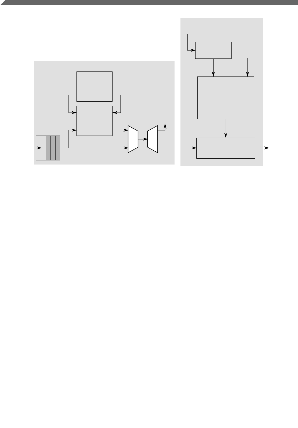
Buffer
Retransmit
64x8
Buffer
Transmit FIFO
Interface
Retransmit
Control
read
address
write
address
Frame
Discard
Period
Backoff
Control
MAC Transmit
Datapath
MAC Transmit
PHY
Control
MAC Tx Engine
Enable
PHY
Interface
MAC FIFO
Figure 55-7. Packet re-transmit overview
The backoff time is represented by an integer multiple of slot times. One slot is equal to a
512-bit time period. The number of the delay slot times, before the nth re-transmission
attempt, is chosen as a uniformly-distributed random integer in the range:
• 0 < r < 2k
•k = min(n, N); where n is the number of retransmissions and N = 10
For example, after the first collision, the backoff period is 0 or 1 slot time. If a collision
occurs on the first retransmission, the backoff period is 0, 1, 2, or 3, and so on.
The maximum backoff time (in 512-bit time slots) is limited by N = 10 as specified in the
IEEE 802.3 standard.
If a collision occurs after 16 consecutive retransmissions, the core reports an excessive
collision condition (ENETn_EIR[RL] interrupt field and TxBD[EE]) and discards the
current packet from the FIFO.
In networks violating the standard requirements, a collision may occur after transmission
of the first 64 bytes. In this case, the core stops the current packet transmission and
discards the rest of the packet from the transmit FIFO. The core resumes transmission
with the next packet available in the core transmit FIFO.
warning
Ethernet PHYs that support the SQE Test, or "heartbeat,"
feature must disable this feature. When this feature is enabled,
Functional description
S32K1xx Series Reference Manual, Rev. 7, 04/2018
1922 NXP Semiconductors

the PHY asserts the collision signal after a frame is transmitted
to indicate to the ENET that the PHY's collision logic is
working. This may cause data corruption in the next frame from
the ENET. This corrupted frame contains up to 21 zero bytes
which start somewhere within the MAC destination address
field. The ENET, however, will still generate a good FCS
(CRC-32) but with corrupted data.
55.6.6 Full-duplex flow control operation
Three conditions are handled by the core's flow control engine:
• Remote device congestion — The remote device connected to the same Ethernet
segment as the core reports congestion and requests that the core stop sending data.
• Core FIFO congestion — When the core's receive FIFO reaches a user-
programmable threshold (RX section empty), the core sends a pause frame back to
the remote device requesting the data transfer to stop.
• Local device congestion — Any device connected to the core can request (typically,
via the host processor) the remote device to stop transmitting data.
55.6.6.1 Remote device congestion
When the MAC transmit control gets a valid pause quanta from the receive path and if
ENETn_RCR[FCE] is set, the MAC transmit logic:
• Completes the transfer of the current frame.
• Stops sending data for the amount of time specified by the pause quanta in 512 bit
time increments.
•Sets ENETn_TCR[RFC_PAUSE].
Frame transfer resumes when the time specified by the quanta expires and if no new
quanta value is received, or if a new pause frame with a quanta value set to 0x0000 is
received. The MAC also resets RFC_PAUSE to zero.
If ENETn_RCR[FCE] cleared, the MAC ignores received pause frames.
Optionally and independent of ENETn_RCR[FCE], pause frames are forwarded to the
client interface if PAUFWD is set.
Chapter 55 Ethernet MAC (ENET)
S32K1xx Series Reference Manual, Rev. 7, 04/2018
NXP Semiconductors 1923
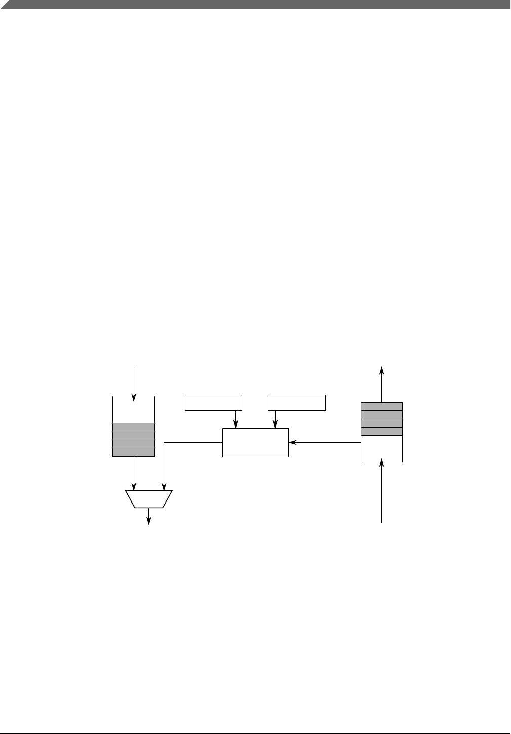
55.6.6.2 Local device/FIFO congestion
The MAC transmit engine generates pause frames when the local receive FIFO is not
able to receive more than a pre-defined number of words (FIFO programmable threshold)
or when pause frame generation is requested by the local host processor.
•To generate a pause frame, the host processor sets ENETn_TCR[TFC_PAUSE]. A
single pause frame is generated when the current frame transfer is completed and
TFC_PAUSE is automatically cleared. Optionally, an interrupt is generated.
• An XOFF pause frame is generated when the receive FIFO asserts its section empty
flag (internal). An XOFF pause frame is generated automatically, when the current
frame transfer completes.
• An XON pause frame is generated when the receive FIFO deasserts its section empty
flag (internal). An XON pause frame is generated automatically, when the current
frame transfer completes.
When an XOFF pause frame is generated, the pause quanta (payload byte P1 and P2) is
filled with the value programmed in ENETn_OPD[PAUSE_DUR].
Pause frame generation
PAUSE_DUR
From Ethernet line
Programmable
threshold
To Ethernet line
TFC_PAUSE
Figure 55-8. Pause frame generation overview
Note
Although the flow control mechanism should prevent any FIFO
overflow on the MAC core receive path, the core receive FIFO
is protected. When an overflow is detected on the receive FIFO,
the current frame is truncated with an error indication set in the
frame status word. The frame should subsequently be discarded
by the user application.
Functional description
S32K1xx Series Reference Manual, Rev. 7, 04/2018
1924 NXP Semiconductors

55.6.7 Magic packet detection
Magic packet detection wakes a node that is put in power-down mode by the node
management agent. Magic packet detection is supported only if the MAC is configured in
sleep mode.
55.6.7.1 Sleep mode
To put the MAC in Sleep mode, set ENETn_ECR[SLEEP]. At the same time
ENETn_ECR[MAGICEN] should also be set to enable magic packet detection.
In addition, if ENET is enabled, write 1 to ENETn_ECR[SLEEP] before entering into
low power mode.
When the MAC is in Sleep mode:
• The transmit logic is disabled.
• The FIFO receive/transmit functions are disabled.
• The receive logic is kept in Normal mode, but it ignores all traffic from the line
except magic packets. They are detected so that a remote agent can wake the node.
55.6.7.2 Magic packet detection
The core is designed to detect magic packets with the destination address set to:
• Any multicast address
• The broadcast address
• The unicast address programmed in PADDR1/2
When a magic packet is detected, EIR[WAKEUP] is set and none of the statistic registers
are incremented.
Chapter 55 Ethernet MAC (ENET)
S32K1xx Series Reference Manual, Rev. 7, 04/2018
NXP Semiconductors 1925

55.6.7.3 Wakeup
When a magic packet is detected, indicated by ENETn_EIR[WAKEUP],
ENETn_ECR[SLEEP] should be cleared to resume normal operation of the MAC.
Clearing the SLEEP bit automatically masks ENETn_ECR[MAGICEN], disabling magic
packet detection.
55.6.8 IP accelerator functions
55.6.8.1 Checksum calculation
The IP and ICMP, TCP, UDP checksums are calculated with one's complement
arithmetic summing up 16-bit values.
• For ICMP, the checksum is calculated over the complete ICMP datagram, in other
words without IP header.
• For TCP and UDP, the checksums contain the header and data sections and values
from the IP header, which can be seen as a pseudo-header that is not actually present
in the data stream.
Table 55-24. IPv4 pseudo-header for checksum calculation
31 30 29 28 27 26 25 24 23 22 21 20 19 18 17 16 15 14 13 12 11 10 9 8 7 6 5 4 3 2 1 0
Source address
Destination address
Zero Protocol TCP/UDP length
Table 55-25. IPv6 pseudo-header for checksum calculation
31 30 29 28 27 26 25 24 23 22 21 20 19 18 17 16 15 14 13 12 11 10 9 8 7 6 5 4 3 2 1 0
Source address
Destination address
TCP/UDP length
Zero Next header
The TCP/UDP length value is the length of the TCP or UDP datagram, which is equal to
the payload of an IP datagram. It is derived by subtracting the IP header length from the
complete IP datagram length that is given in the IP header (IPv4), or directly taken from
the IP header (IPv6). The protocol field is the corresponding value from the IP header.
The Zero fields are all zeroes.
Functional description
S32K1xx Series Reference Manual, Rev. 7, 04/2018
1926 NXP Semiconductors

For IPv6, the complete 128-bit addresses are considered. The next header value identifies
the upper layer protocol as either TCP or UDP. It may differ from the next header value
of the IPv6 header if extension headers are inserted before the protocol header.
The checksum calculation uses 16-bit words in network byte order: The first byte sent/
received is the MSB, and the second byte sent/received is the LSB of the 16-bit value to
add to the checksum. If the frame ends on an odd number of bytes, a zero byte is
appended for checksum calculation only, and is not actually transmitted.
55.6.8.2 Additional padding processing
According to IEEE 802.3, any Ethernet frame must have a minimum length of 64 octets.
The MAC usually removes padding on receive when a frame with length information is
received. Because IP frames have a type value instead of length, the MAC does not
remove padding for short IP frames, as it is not aware of the frame contents.
The IP accelerator function can be configured to remove the Ethernet padding bytes that
might follow the IP datagram.
On transmit, the MAC automatically adds padding as necessary to fill any frame to a 64-
byte length.
55.6.8.3 32-bit Ethernet payload alignment
The data FIFOs allow inserting two additional arbitrary bytes in front of a frame. This
extends the 14-byte Ethernet header to a 16-byte header, which leads to alignment of the
Ethernet payload, following the Ethernet header, on a 32-bit boundary.
This function can be enabled for transmit and receive independently with the
corresponding SHIFT16 bits in the ENETn_TACC and ENETn_RACC registers.
When enabled, the valid frame data is arranged as shown in Table 55-26.
Table 55-26. 64-bit interface data structure with SHIFT16 enabled
63 56 55 48 47 40 39 32 31 24 23 16 15 8 7 0
Byte 5 Byte 4 Byte 3 Byte 2 Byte 1 Byte 0 Any value Any value
Byte 13 Byte 12 Byte 11 Byte 10 Byte 9 Byte 8 Byte 7 Byte 6
...
Chapter 55 Ethernet MAC (ENET)
S32K1xx Series Reference Manual, Rev. 7, 04/2018
NXP Semiconductors 1927

55.6.8.3.1 Receive processing
When ENETn_RACC[SHIFT16] is set, each frame is received with two additional bytes
in front of the frame.
The user application must ignore these first two bytes and find the first byte of the frame
in bits 23–16 of the first word from the RX FIFO.
Note
SHIFT16 must be set during initialization and kept set during
the complete operation, because it influences the FIFO write
behavior.
55.6.8.3.2 Transmit processing
When ENETn_TACC[SHIFT16] is set, the first two bytes of the first word written (bits
15–0) are discarded immediately by the FIFO write logic.
The SHIFT16 bit can be enabled/disabled for each frame individually if required, but can
be changed only between frames.
55.6.8.4 Received frame discard
Because the receive FIFO must be operated in store and forward mode (ENETn_RSFL
cleared), received frames can be discarded based on the following errors:
• The MAC function receives the frame with an error:
• The frame has an invalid payload length
• Frame length is greater than MAX_FL
• Frame received with a CRC-32 error
• Frame truncated due to receive FIFO overflow
• Frame is corrupted as PHY signaled an error (RX_ERR asserted during
reception)
• An IP frame is detected and the IP header checksum is wrong
• An IP frame with a valid IP header and a valid IP header checksum is detected, the
protocol is known but the protocol-specific checksum is wrong
Functional description
S32K1xx Series Reference Manual, Rev. 7, 04/2018
1928 NXP Semiconductors

If one of the errors occurs and the IP accelerator function is configured to discard frames
(ENETn_RACC), the frame is automatically discarded. Statistics are maintained
normally and are not affected by this discard function.
55.6.8.5 IPv4 fragments
When an IPv4 IP fragment frame is received, only the IP header is inspected and its
checksum verified. 32-bit alignment operates the same way on fragments as it does on
normal IP frames.
The IP fragment frame payload is not inspected for any protocol headers. As such, a
protocol header would only exist in the very first fragment. To assist in protocol-specific
checksum verification, the one's-complement sum is calculated on the IP payload (all
bytes following the IP header) and provided with the frame status word.
The frame fragment status field (RxBD[FRAG]) is set to indicate a fragment reception,
and the one's-complement sum of the IP payload is available in RxBD[Payload
checksum].
Note
After all fragments have been received and reassembled, the
application software can take advantage of the payload
checksum delivered with the frame's status word to calculate
the protocol-specific checksum of the datagram.
For example, if a TCP payload is delivered by multiple IP
fragments, the application software can calculate the pseudo-
header checksum value from the first fragment, and add the
payload checksums delivered with the status for all fragments
to verify the TCP datagram checksum.
55.6.8.6 IPv6 support
The following sections describe the IPv6 support.
55.6.8.6.1 Receive processing
An Ethernet frame of type 0x86DD identifies an IP Version 6 frame (IPv6) frame. If an
IPv6 frame is received, the first IP header is inspected (first ten words), which is
available in every IPv6 frame.
Chapter 55 Ethernet MAC (ENET)
S32K1xx Series Reference Manual, Rev. 7, 04/2018
NXP Semiconductors 1929

If the receive SHIFT16 function is enabled, the IP header is aligned on a 32-bit boundary
allowing more efficient processing.
For TCP and UDP datagrams, the pseudo-header checksum calculation is performed and
verified.
To assist in protocol-specific checksum verification, the one's-complement sum is always
calculated on the IP payload (all bytes following the IP header) and provided with the
frame status word. For example, if extension headers were present, their sums can be
subtracted in software from the checksum to isolate the TCP/UDP datagram checksum, if
required.
55.6.8.6.2 Transmit processing
For IPv6 transmission, the SHIFT16 function is supported to process 32-bit aligned
datagrams.
IPv6 has no IP header checksum; therefore, the IP checksum insertion configuration is
ignored.
The protocol checksum is inserted only if the next header of the IP header is a known
protocol (TCP, UDP, or ICMP). If a known protocol is detected, the checksum over all
bytes following the IP header is calculated and inserted in the correct position.
The pseudo-header checksum calculation is performed for TCP and UDP datagrams
accordingly.
55.6.9 Resets and stop controls
55.6.9.1 Hardware reset
To reset the Ethernet module, set ENETn_ECR[RESET].
55.6.9.2 Soft reset
When ENETn_ECR[ETHER_EN] is cleared during operation, the following occurs:
• uDMA, buffer descriptor, and FIFO control logic are reset, including the buffer
descriptor and FIFO pointers.
• A currently ongoing transmit is terminated by asserting TXER to the PHY.
Functional description
S32K1xx Series Reference Manual, Rev. 7, 04/2018
1930 NXP Semiconductors

• A currently ongoing transmit FIFO write from the application is terminated by
stopping the write to the FIFO, and all further data from the application is ignored.
All subsequent writes are ignored until re-enabled.
• A currently ongoing receive FIFO read is terminated. The RxBD has arbitrary values
in this case.
55.6.9.3 Hardware freeze
When the processor enters debug mode and ECR[DBGEN] is set, the MAC enters a
freeze state where it stops all transmit and receive activities gracefully.
The following happens when the MAC enters hardware freeze:
• A currently ongoing receive transaction on the receive application interface is
completed as normal. No further frames are read from the FIFO.
• A currently ongoing transmit transaction on the transmit application interface is
completed as normal (in other words, until writing end-of-packet (EOP)).
• A currently ongoing frame receive is completed normally, after which no further
frames are accepted from the MII.
• A currently ongoing frame transmit is completed normally, after which no further
frames are transmitted.
55.6.9.4 Graceful stop
During a graceful stop, any currently ongoing transactions are completed normally and
no further frames are accepted. The MAC can resume from a graceful stop without the
need for a reset (for example, clearing ETHER_EN is not required).
The following conditions lead to a graceful stop of the MAC transmit or receive
datapaths.
55.6.9.4.1 Graceful transmit stop (GTS)
When gracefully stopped, the MAC is no longer reading frame data from the transmit
FIFO and has completed any ongoing transmission.
In any of the following conditions, the transmit datapath stops after an ongoing frame
transmission has been completed normally.
Chapter 55 Ethernet MAC (ENET)
S32K1xx Series Reference Manual, Rev. 7, 04/2018
NXP Semiconductors 1931

•ENETn_TCR[GTS] is set by software.
•ENETn_TCR[TFC_PAUSE] is set by software requesting a pause frame
transmission. The status (and register bit) is cleared after the pause frame has been
sent.
• A pause frame was received stopping the transmitter. The stopped situation is
terminated when the pause timer expires or a pause frame with zero quanta is
received.
• MAC is placed in Sleep mode by software or the processor entering Stop mode (see
Sleep mode).
• The MAC is in Hardware Freeze mode.
When the transmitter has reached its stopped state, the following events occur:
• The GRA interrupt is asserted, when transitioned into stopped.
• In Hardware Freeze mode, the GRA interrupt does not wait for the application write
completion and asserts when the transmit state machine (in other words, line side of
TX FIFO) reaches its stopped state.
55.6.9.4.2 Graceful receive stop (GRS)
When gracefully stopped, the MAC is no longer writing frames into the receive FIFO.
The receive datapath stops after any ongoing frame reception has been completed
normally, if any of the following conditions occur:
• MAC is placed in Sleep mode either by the software or the processor is in Stop
mode). The MAC continues to receive frames and search for magic packets if
enabled (see Magic packet detection). However, no frames are written into the
receive FIFO, and therefore are not forwarded to the application.
• The MAC is in Hardware Freeze mode. The MAC does not accept any frames from
the MII.
When the receive datapath is stopped, the following events occur:
• If the RX is in the stopped state, RCR[GRS] is set
Functional description
S32K1xx Series Reference Manual, Rev. 7, 04/2018
1932 NXP Semiconductors

• The GRA interrupt is asserted when the transmitter and receiver are stopped
• Any ongoing receive transaction to the application (RX FIFO read) continues
normally until the frame end of package (EOP) is reached. After this, the following
occurs:
• When Sleep mode is active, all further frames are discarded, flushing the RX
FIFO
• In Hardware Freeze mode, no further frames are delivered to the application and
they stay in the receive FIFO.
Note
The assertion of GRS does not wait for an ongoing FIFO read
transaction on the application side of the FIFO (FIFO read).
55.6.9.4.3 Graceful stop interrupt (GRA)
The graceful stopped interrupt (GRA) is asserted for the following conditions:
• In Sleep mode, the interrupt asserts only after both TX and RX datapaths are stopped.
• In Hardware Freeze mode, the interrupt asserts only after both TX and RX datapaths
are stopped.
• The MAC transmit datapath is stopped for any other condition (GTS, TFC_PAUSE,
pause received).
The GRA interrupt is triggered only once when the stopped state is entered. If the
interrupt is cleared while the stop condition persists, no further interrupt is triggered.
Chapter 55 Ethernet MAC (ENET)
S32K1xx Series Reference Manual, Rev. 7, 04/2018
NXP Semiconductors 1933
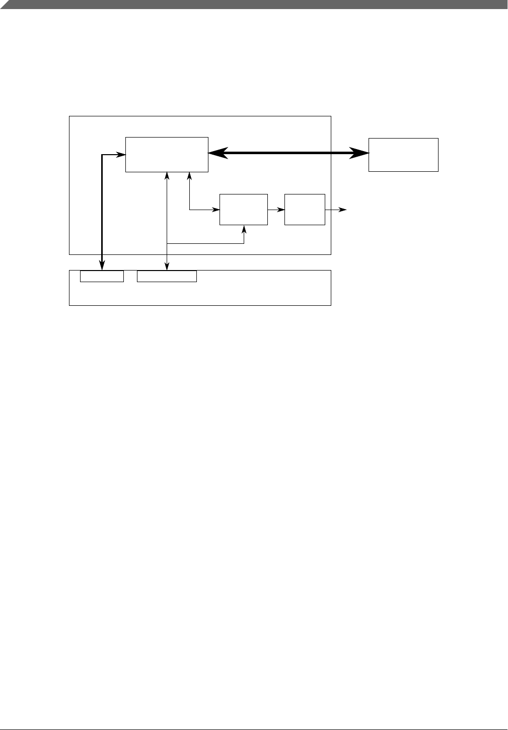
55.6.10 IEEE 1588 functions
To allow for IEEE 1588 or similar time synchronization protocol implementations, the
MAC is combined with a time-stamping module to support precise time-stamping of
incoming and outgoing frames. Set ENETn_ECR[EN1588] to enable 1588 support.
Adjustable
timer
module
Events
generator
User application
ControlData
10/100 MAC
MAC with 1588
PHY
Control/status
Frame data
n pulses/sec (pps)
Control/status
Timing
Figure 55-9. IEEE 1588 functions overview
55.6.10.1 Adjustable timer module
The adjustable timer module (TSM) implements the free-running counter (FRC), which
generates the timestamps. The FRC operates with the time-stamping clock, which can be
set to any value depending on your system requirements.
Through dedicated correction logic, the timer can be adjusted to allow synchronization to
a remote master and provide a synchronized timing reference to the local system. The
timer can be configured to cause an interrupt after a fixed time period, to allow
synchronization of software timers or perform other synchronized system functions.
The timer is typically used to implement a period of one second; hence, its value ranges
from 0 to (1 × 10⁹)-1. The period event can trigger an interrupt, and software can
maintain the seconds and hours time values as necessary.
55.6.10.1.1 Adjustable timer implementation
The adjustable timer consists of a programmable counter/accumulator and a correction
counter. The periods of both counters and their increment rates are freely configurable,
allowing very fine tuning of the timer.
Functional description
S32K1xx Series Reference Manual, Rev. 7, 04/2018
1934 NXP Semiconductors
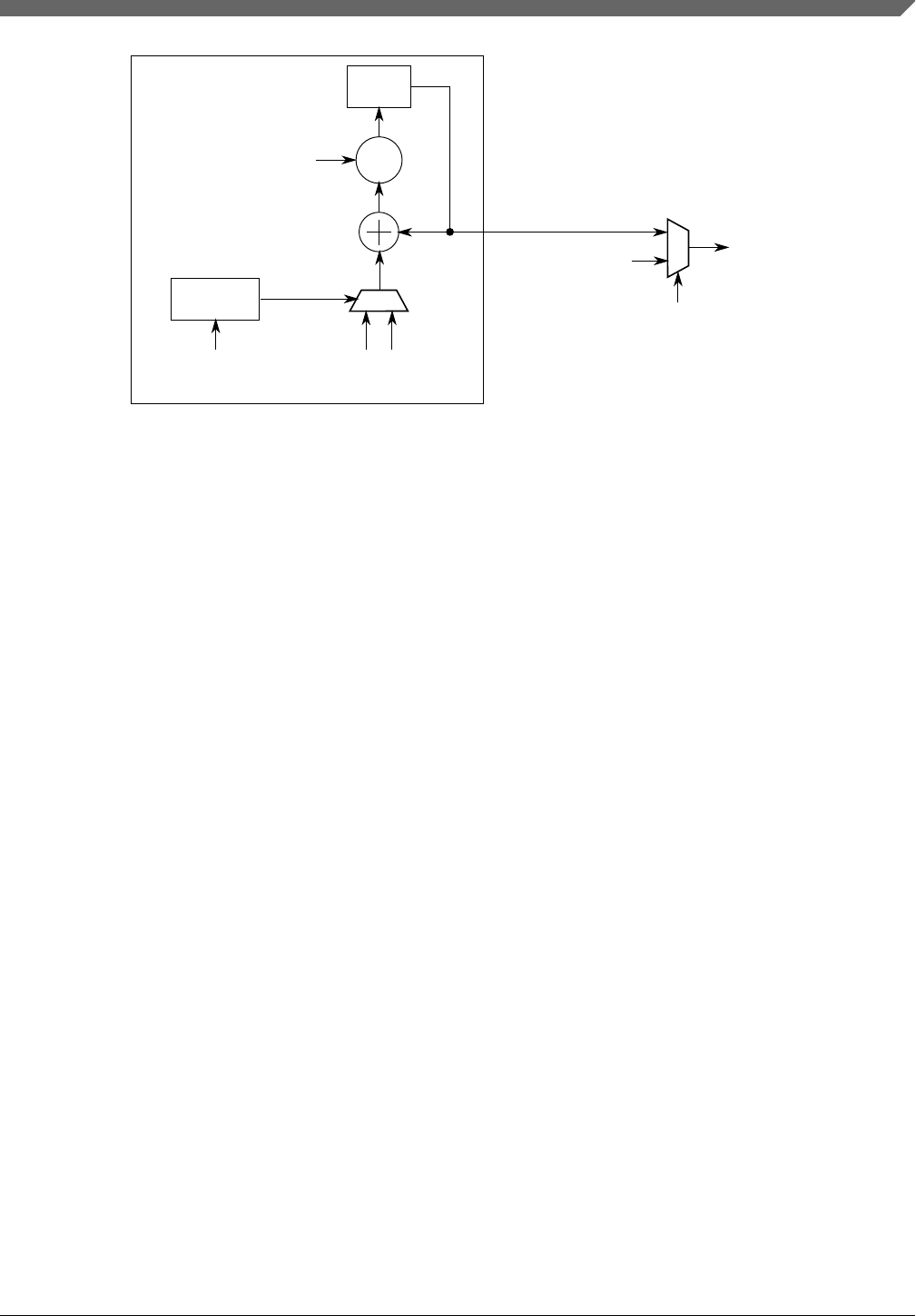
mod
Counter
Correction
counter
[INC_CORR] [INC]
[SLAVE]
Adjustable timer
External free-running
counter
ENET_ATPER
ENET_ATCOR
ENET_ATCR
ENET_ATINC ENET_ATINC
To MAC
Figure 55-10. Adjustable timer implementation detail
The counter produces the current time. During each time-stamping clock cycle, a constant
value is added to the current time as programmed in ENETn_ATINC. The value depends
on the chosen time-stamping clock frequency. For example, if it operates at 125 MHz,
setting the increment to eight represents 8 ns.
The period, configured in ENETn_ATPER, defines the modulo when the counter wraps.
In a typical implementation, the period is set to 1 × 10⁹ so that the counter wraps every
second, and hence all timestamps represent the absolute nanoseconds within the one
second period. When the period is reached, the counter wraps to start again respecting the
period modulo. This means it does not necessarily start from zero, but instead the counter
is loaded with the value (Current + Inc –(1 × 10⁹)), assuming the period is set to 1 × 10⁹.
The correction counter operates fully independently, and increments by one with each
time-stamping clock cycle. When it reaches the value configured in ENETn_ATCOR, it
restarts and instructs the timer once to increment by the correction value, instead of the
normal value.
The normal and correction increments are configured in ENETn_ATINC. To speed up
the timer, set the correction increment more than the normal increment value. To slow
down the timer, set the correction increment less than the normal increment value.
The correction counter only defines the distance of the corrective actions, not the amount.
This allows very fine corrections and low jitter (in the range of 1 ns) independent of the
chosen clock frequency.
By enabling slave mode (ENETn_ATCR[SLAVE] = 1), the timer is ignored and the
current time is externally provided from one of the external modules. See the Chip
Configuration details for which clock source is used. This is useful if multiple modules
Chapter 55 Ethernet MAC (ENET)
S32K1xx Series Reference Manual, Rev. 7, 04/2018
NXP Semiconductors 1935

within the system must operate from a single timer. When slave mode is enabled, you
still must set ENETn_ATINC[INC] to the value of the master, since it is used for internal
comparisons.
55.6.10.2 Transmit timestamping
Only 1588 event frames need to be time-stamped on transmit. The client application (for
example, the MAC driver) should detect 1588 event frames and set TxBD[TS] together
with the frame.
If TxBD[TS] is set, the MAC records the timestamp for the frame in ENETn_ATSTMP.
ENETn_EIR[TS_AVAIL] is set to indicate that a new timestamp is available.
Software implements a handshaking procedure by setting TxBD[TS] when it transmits
the frame for which a timestamp is needed, and then waits for ENETn_EIR[TS_AVAIL]
to determine when the timestamp is available. The timestamp is then read from
ENETn_ATSTMP. This is done for all event frames. Other frames do not use TxBD[TS]
and, therefore, do not interfere with the timestamp capture.
55.6.10.3 Receive timestamping
When a frame is received, the MAC latches the value of the timer when the frame's start
of frame delimiter (SFD) field is detected, and provides the captured timestamp on
RxBD[1588 timestamp]. This is done for all received frames.
55.6.10.4 Time synchronization
The adjustable timer module is available to synchronize the local clock of a node to a
remote master. It implements a free running 32-bit counter, and also contains an
additional correction counter.
The correction counter increases or decreases the rate of the free running counter,
enabling very fine granular changes of the timer for synchronization, yet adding only
very low jitter when performing corrections.
The application software implements, in a slave scenario, the required control algorithm,
setting the correction to compensate for local oscillator drifts and locking the timer to the
remote master clock on the network.
Functional description
S32K1xx Series Reference Manual, Rev. 7, 04/2018
1936 NXP Semiconductors

The timer and all timestamp-related information should be configured to show the true
nanoseconds value of a second (in other words, the timer is configured to have a period
of one second). Hence, the values range from 0 to (1 × 10⁹)–1. In this application, the
seconds counter is implemented in software using an interrupt function that is executed
when the nanoseconds counter wraps at 1 × 10⁹.
55.6.10.5 Input Capture and Output Compare
The Input Capture Output Compare block can be used to provide precise hardware timing
for input and output events.
55.6.10.5.1 Input capture
The TCCRn capture registers latch the time value when the corresponding external event
occurs. An event can be a rising-, falling-, or either-edge of one of the 1588_TMRn
signals. An event will cause the corresponding TCSRn[TF] timer flag to be set, indicating
that an input capture has occurred. If the corresponding interrupt is enabled with the
TCSRn[TIE] field, an interrupt can be generated.
55.6.10.5.2 Output compare
The TCCRn compare registers are loaded with the time at which the corresponding event
should occur. When the ENET free-running counter value matches the output compare
reference value in the TCCRn register, the corresponding flag, TCSRn[TF], is set,
indicating that an output compare has occurred. The corresponding interrupt, if enabled
by TCSRn[TIE], will be generated.The corresponding 1588_TMRn output signal will be
asserted according to TCSRn[TMODE].
NOTE
If TSCRn[TMODE] is set to 10X1b or 1010b then the timer
output pin toggle-on-overflow will occur only when PINPER,
PEREN, and EN bits of the ATCR register are one.
55.6.10.5.3 DMA requests
A DMA request can be enabled by setting TCSRn[TDRE]. The corresponding DMA
request is generated when the TCSRn[TF] timer flag is set. When the DMA has
completed, the corresponding TCSRn[TF] flag is cleared.
Chapter 55 Ethernet MAC (ENET)
S32K1xx Series Reference Manual, Rev. 7, 04/2018
NXP Semiconductors 1937

55.6.11 FIFO thresholds
The core FIFO thresholds are fully programmable to dynamically change the FIFO
operation.
For example, store and forward transfer can be enabled by a simple change in the FIFO
threshold registers.
The thresholds are defined in 64-bit words.
The receive and transmit FIFOs both have a depth of 256 words.
55.6.11.1 Receive FIFO
Four programmable thresholds are available, which can be set to any value to control the
core operation.
Table 55-27. Receive FIFO thresholds definition
Register Description
ENETn_RSFL
[RX_SECTION_F
ULL]
When the FIFO level reaches the ENETn_RSFL value, the MAC status signal is asserted to indicate that
data is available in the receive FIFO (cut-through operation). Once asserted, if the FIFO empties below the
threshold set with ENETn_RAEM and if the end-of-frame is not yet stored in the FIFO, the status signal is
deasserted again.
If a frame has a size smaller than the threshold (in other words, an end-of-frame is available for the
frame), the status is also asserted.
To enable store and forward on the receive path, clear ENETn_RSFL. The MAC status signal is asserted
only when a complete frame is stored in the receive FIFO.
When programming a non-zero value to ENETn_RSFL (cut-through operation) it should be greater than
ENETn_RAEM.
ENETn_RAEM
[RX_ALMOST_E
MPTY]
When the FIFO level reaches the ENETn_RAEM value, and the end-of-frame has not been received, the
core receive read control stops the FIFO read (and subsequently stops transferring data to the MAC client
application).
It continues to deliver the frame, if again more data than the threshold or the end-of-frame is available in
the FIFO.
Set ENETn_RAEM to a minimum of six.
ENETn_RAFL
[RX_ALMOST_F
ULL]
When the FIFO level approaches the maximum and there is no more space remaining for at least
ENETn_RAFL number of words, the MAC control logic stops writing data in the FIFO and truncates the
receive frame to avoid FIFO overflow.
The corresponding error status is set when the frame is delivered to the application.
Set ENETn_RAFL to a minimum of 4.
ENETn_RSEM
[RX_SECTION_E
MPTY]
When the FIFO level reaches the ENETn_RSEM value, an indication is sent to the MAC transmit logic,
which generates an XOFF pause frame. This indicates FIFO congestion to the remote Ethernet client.
When the FIFO level goes below the value programmed in ENETn_RSEM, an indication is sent to the
MAC transmit logic, which generates an XON pause frame. This indicates the FIFO congestion is cleared
to the remote Ethernet client.
Clearing ENETn_RSEM disables any pause frame generation.
Functional description
S32K1xx Series Reference Manual, Rev. 7, 04/2018
1938 NXP Semiconductors

RSFL - Section full
(Core FIFO status)
MAC receive
FIFO read control
RAFL - Almost full
(FIFO write protection)
RSEM - Section empty
RAEM - Almost empty
(FIFO read control)
(Pause frame
generation)
Figure 55-11. Receive FIFO overview
55.6.11.2 Transmit FIFO
Four programmable thresholds are available which control the core operation.
Table 55-28. Transmit FIFO thresholds definition
Register Description
ENETn_TAEM
[TX_ALMOST
_EMPTY]
When the FIFO level reaches the ENETn_TAEM value and no end-of-frame is available for the frame, the
MAC transmit logic avoids a FIFO underflow by stopping FIFO reads and transmitting the Ethernet frame
with an MII error indication.
Set ENETn_TAEM to a minimum of 4.
ENETn_TAFL
[TX_ALMOST
_FULL]
When the FIFO level approaches the maximum, so that there is no more space for at least ENETn_TAFL
number of words, the MAC deasserts its control signal to the application.
If the application does not react on this signal, the FIFO write control logic avoids FIFO overflow by
truncating the current frame and setting the error status. As a result, the frame is transmitted with an MII
error indication.
Set ENETn_TAFL to a minimum of 4. Larger values allow more latency for the application to react on the
MAC control signal deassertion, before the frame is truncated. A typical setting is 8, which offers 3–4 clock
cycles of latency to the application to react on the MAC control signal deassertion.
ENETn_TSEM
[TX_SECTION
_EMPTY]
When the FIFO level reaches the ENETn_TSEM value, a MAC status signal is deasserted to indicate that
the transmit FIFO is getting full. This gives the ENET module an indication to slow or stop its write
transaction to avoid a buffer overflow. This is a pure indication function to the application. It has no effect
within the MAC.
When ENETn_TSEM is 0, the signal is never deasserted.
ENETn_TFWR When the FIFO level reaches the ENETn_TFWR value and when STRFWD is cleared, the MAC transmit
control logic starts frame transmission before the end-of-frame is available in the FIFO (cut-through
operation).
Chapter 55 Ethernet MAC (ENET)
S32K1xx Series Reference Manual, Rev. 7, 04/2018
NXP Semiconductors 1939
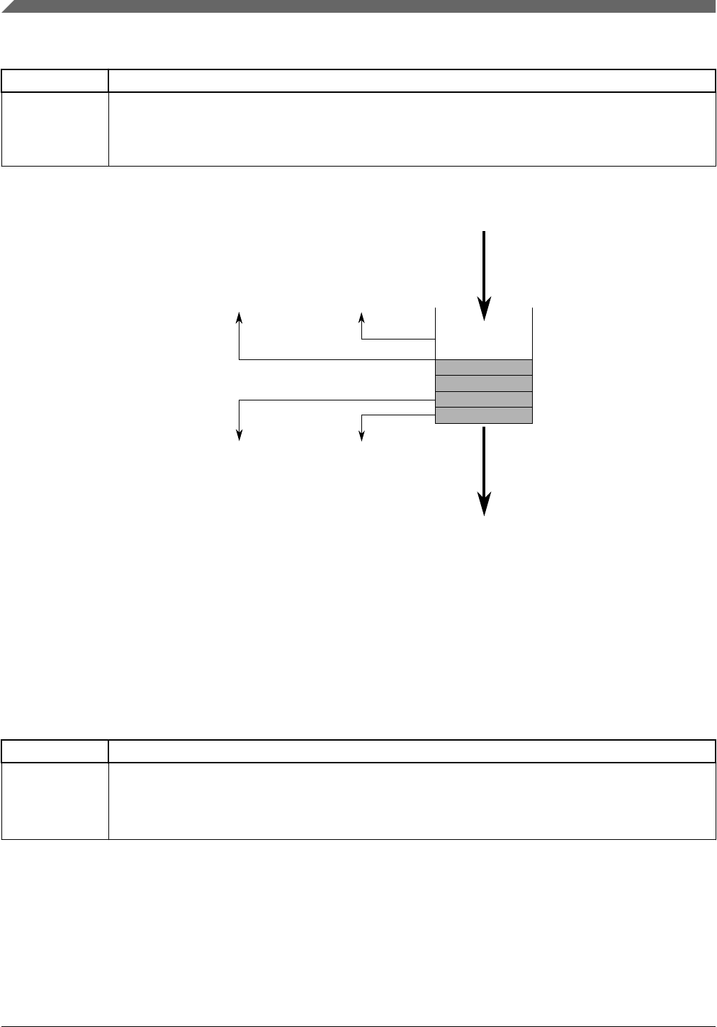
Table 55-28. Transmit FIFO thresholds definition
Register Description
If a complete frame has a size smaller than the ENETn_TFWR threshold, the MAC also transmits the
frame to the line.
To enable store and forward on the transmit path, set STRFWD. In this case, the MAC starts to transmit
data only when a complete frame is stored in the transmit FIFO.
MAC transmit
FIFO write control
(FIFO write control)
TAFL - Almost full
TAEM - Almost empty
TSEM - Section empty
TFWR - Section full
(MAC read control)
(Core FIFO status)
(MAC transmit start)
Figure 55-12. Transmit FIFO overview
55.6.12 Loopback options
The core implements external and internal loopback options, which are controlled by the
ENETn_RCR register fields found here.
Table 55-29. Loopback options
Register field Description
LOOP Internal MII loopback. The MAC transmit is returned to the MAC receive. No data is transmitted to the
external interfaces.
In MII internal loopback, MII_TXCLK and MII_RXCLK must be provided with a clock signal (2.5 MHz for 10
Mbit/s, and 25 MHz for 100 Mbit/s))
Functional description
S32K1xx Series Reference Manual, Rev. 7, 04/2018
1940 NXP Semiconductors
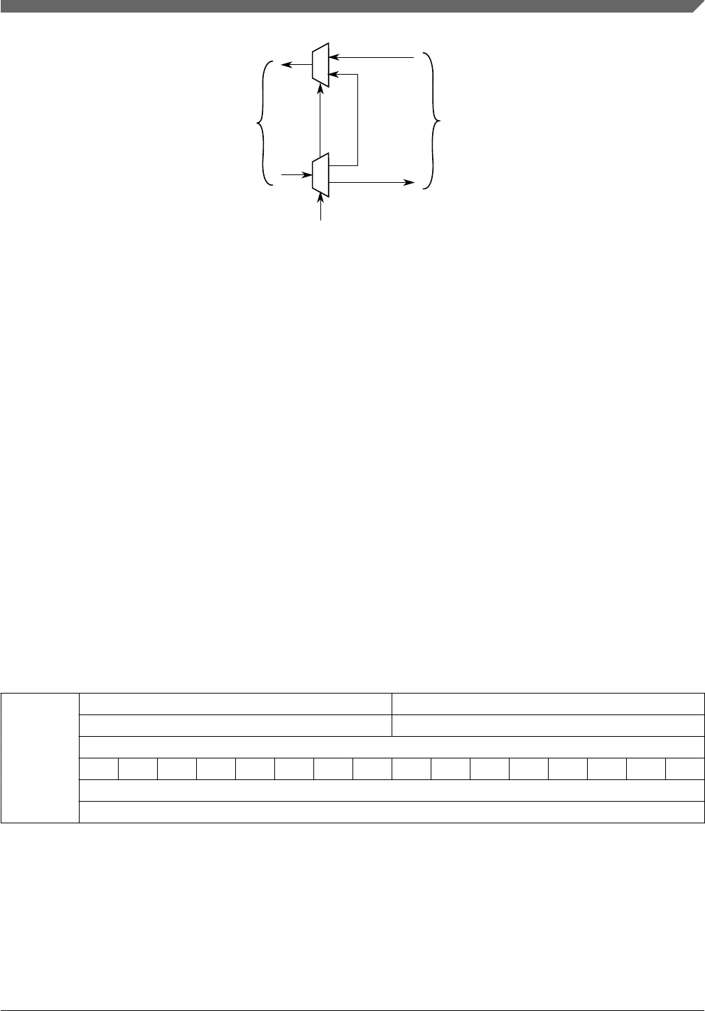
Line interface
MAC interface
ENETn_RCR[LOOP],
Figure 55-13. Loopback options
55.6.13 Legacy buffer descriptors
To support the Ethernet controller on previous chips, legacy FEC buffer descriptors are
available. To enable legacy support, write 0 to ENETn_ECR[1588EN].
NOTE
• The legacy buffer descriptor tables show the byte order for
little-endian chips. DBSWP must be set to 1 after reset to
enable little-endian mode.
55.6.13.1 Legacy receive buffer descriptor
The following table shows the legacy FEC receive buffer descriptor. Table 55-33
contains the descriptions for each field.
Table 55-30. Legacy FEC receive buffer descriptor (RxBD)
Byte 1 Byte 0
15 14 13 12 11 10 9 8 7 6 5 4 3 2 1 0
Offset + 0 Data length
Offset + 2 E RO1 W RO2 L — — M BC MC LG NO — CR OV TR
Offset + 4 Rx data buffer pointer — low halfword
Offset + 6 Rx data buffer pointer — high halfword
Chapter 55 Ethernet MAC (ENET)
S32K1xx Series Reference Manual, Rev. 7, 04/2018
NXP Semiconductors 1941

55.6.13.2 Legacy transmit buffer descriptor
The following table shows the legacy FEC transmit buffer descriptor. Table 55-35
contains the descriptions for each field.
Table 55-31. Legacy FEC transmit buffer descriptor (TxBD)
Byte 1 Byte 0
15 14 13 12 11 10 9 8 7 6 5 4 3 2 1 0
Offset + 0 Data Length
Offset + 2 R TO1 W TO2 L TC ABC1—————————
Offset + 4 Tx Data Buffer Pointer — low halfword
Offset + 6 Tx Data Buffer Pointer — high halfword
1. This field is not supported by the uDMA.
55.6.14 Enhanced buffer descriptors
This section provides a description of the enhanced operation of the driver/uDMA via the
buffer descriptors.
It is followed by a detailed description of the receive and transmit descriptor fields. To
enable the enhanced features, set ENETn_ECR[1588EN].
NOTE
The enhanced buffer descriptor tables show the byte order for
little-endian chips. DBSWP must be set to 1 after reset to
enable little-endian mode.
55.6.14.1 Enhanced receive buffer descriptor
The following table shows the enhanced uDMA receive buffer descriptor. Table 55-33
contains the descriptions for each field.
Table 55-32. Enhanced uDMA receive buffer descriptor (RxBD)
Byte 1 Byte 0
15 14 13 12 11 10 9 8 7 6 5 4 3 2 1 0
Offset + 0 Data length
Offset + 2 E RO1 W RO2 L — — M BC MC LG NO — CR OV TR
Offset + 4 Rx data buffer pointer – low halfword
Offset + 6 Rx data buffer pointer – high halfword
Table continues on the next page...
Functional description
S32K1xx Series Reference Manual, Rev. 7, 04/2018
1942 NXP Semiconductors

Table 55-32. Enhanced uDMA receive buffer descriptor (RxBD) (continued)
Offset + 8 VPCP — — — — — — — ICE PCR — VLA
NIPV6 FRA
G
Offset + A ME — — — — PE CE UC INT — — — — — — —
Offset + C Payload checksum
Offset + E Header length — — — Protocol type
Offset + 10————————————————
Offset + 12 BDU — — — — — — — — — — — — — — —
Offset + 14 1588 timestamp – low halfword
Offset + 16 1588 timestamp – high halfword
Offset + 18————————————————
Offset + 1A————————————————
Offset + 1C————————————————
Offset + 1E ————————————————
Table 55-33. Receive buffer descriptor field definitions
Word Field Description
Offset + 0 15–0
Data
Length
Data length. Written by the MAC. Data length is the number of octets written by the MAC into
this BD's data buffer if L is cleared (the value is equal to EMRBR), or the length of the frame
including CRC if L is set. It is written by the MAC once as the BD is closed.
Offset + 2 15
E
Empty. Written by the MAC (= 0) and user (= 1).
0 The data buffer associated with this BD is filled with received data, or data reception has
aborted due to an error condition. The status and length fields have been updated as
required.
1 The data buffer associated with this BD is empty, or reception is currently in progress.
Offset + 2 14
RO1
Receive software ownership. This field is reserved for use by software. This read/write field is
not modified by hardware, nor does its value affect hardware.
Offset + 2 13
W
Wrap. Written by user.
0 The next buffer descriptor is found in the consecutive location.
1 The next buffer descriptor is found at the location defined in ENETn_RDSR.
Offset + 2 12
RO2
Receive software ownership. This field is reserved for use by software. This read/write field is
not modified by hardware, nor does its value affect hardware.
Offset + 2 11
L
Last in frame. Written by the uDMA.
0 The buffer is not the last in a frame.
1 The buffer is the last in a frame.
Offset + 2 10–9 Reserved, must be cleared.
Offset + 2 8
M
Miss. Written by the MAC. This field is set by the MAC for frames accepted in promiscuous
mode, but flagged as a miss by the internal address recognition. Therefore, while in
promiscuous mode, you can use the this field to quickly determine whether the frame was
destined to this station. This field is valid only if the L and PROM bits are set.
0 The frame was received because of an address recognition hit.
1 The frame was received because of promiscuous mode.
Table continues on the next page...
Chapter 55 Ethernet MAC (ENET)
S32K1xx Series Reference Manual, Rev. 7, 04/2018
NXP Semiconductors 1943

Table 55-33. Receive buffer descriptor field definitions (continued)
Word Field Description
The information needed for this field comes from the promiscuous_miss(ff_rx_err_stat[26])
sideband signal.
Offset + 2 7
BC
Set if the DA is broadcast (FFFF_FFFF_FFFF).
Offset + 2 6
MC
Set if the DA is multicast and not BC.
Offset + 2 5
LG
Receive frame length violation. Written by the MAC. A frame length greater than
RCR[MAX_FL] was recognized. This field is valid only if the L field is set. The receive data is
not altered in any way unless the length exceeds TRUNC_FL bytes.
Offset + 2 4
NO
Receive non-octet aligned frame. Written by the MAC. A frame that contained a number of
bits not divisible by 8 was received, and the CRC check that occurred at the preceding byte
boundary generated an error or a PHY error occurred. This field is valid only if the L field is
set. If this field is set, the CR field is not set.
Offset + 2 3 Reserved, must be cleared.
Offset + 2 2
CR
Receive CRC or frame error. Written by the MAC. This frame contains a PHY or CRC error
and is an integral number of octets in length. This field is valid only if the L field is set.
Offset + 2 1
OV
Overrun. Written by the MAC. A receive FIFO overrun occurred during frame reception. If this
field is set, the other status fields, M, LG, NO, and CR, lose their normal meaning and are
zero. This field is valid only if the L field is set.
Offset + 2 0
TR
Set if the receive frame is truncated (frame length >TRUNC_FL). If the TR field is set, the
frame must be discarded and the other error fields must be ignored because they may be
incorrect.
Offset + 4 15–0
Data buffer
pointer low
Receive data buffer pointer, low halfword
0ffset + 6 15–0
Data buffer
pointer
high
Receive data buffer pointer, high halfword1
Offset + 8 15–13
VPCP
VLAN priority code point. This field is written by the uDMA to indicate the frame priority level.
Valid values are from 0 (best effort) to 7 (highest). This value can be used to prioritize
different classes of traffic (e.g., voice, video, data). This field is only valid if the L field is set.
Offset + 8 12–6 Reserved, must be cleared.
Offset + 8 5
ICE
IP header checksum error. This is an accelerator option. This field is written by the uDMA. Set
when either a non-IP frame is received or the IP header checksum was invalid. An IP frame
with less than 3 bytes of payload is considered to be an invalid IP frame. This field is only
valid if the L field is set.
Offset + 8 4
PCR
Protocol checksum error. This is an accelerator option. This field is written by the uDMA. Set
when the checksum of the protocol is invalid or an unknown protocol is found and
checksumming could not be performed. This field is only valid if the L field is set.
Offset + 8 3 Reserved, must be cleared.
Offset + 8 2
VLAN
VLAN. This is an accelerator option. This field is written by the uDMA. It means that the frame
has a VLAN tag. This field is valid only if the L field is set.
Table continues on the next page...
Functional description
S32K1xx Series Reference Manual, Rev. 7, 04/2018
1944 NXP Semiconductors

Table 55-33. Receive buffer descriptor field definitions (continued)
Word Field Description
Offset + 8 1
IPV6
IPV6 Frame. This field is written by the uDMA. This field indicates that the frame has an IPv6
frame type. If this field is not set it means that an IPv4 or other protocol frame was received.
This field is valid only if the L field is set.
Offset + 8 0
FRAG
IPv4 Fragment.This is an accelerator option.This field is written by the uDMA. It indicates that
the frame is an IPv4 fragment frame. This field is only valid when the L field is set.
Offset + A 15
ME
MAC error. This field is written by the uDMA. This field means that the frame stored in the
system memory was received with an error (typically, a receive FIFO overflow). This field is
only valid when the L field is set.
Offset + A 14–11 Reserved, must be cleared.
Offset + A 10
PE
PHY Error. This field is written by the uDMA. Set to "1"when the frame was received with an
Error character on the PHY interface. The frame is invalid. This field is valid only when the L
field is set.
Offset + A 9
CE
Collision. This field is written by the uDMA. Set when the frame was received with a collision
detected during reception. The frame is invalid and sent to the user application. This field is
valid only when the L field is set.
Offset + A 8
UC
Unicast. This field is written by the uDMA, and means that the frame is unicast. This field is
valid regardless of whether the L field is set.
Offset + A 7
INT
Generate RXB/RXF interrupt. This field is set by the user to indicate that the uDMA is to
generate an interrupt on the dma_int_rxb / dma_int_rxfevent.
Offset + A 6–0 Reserved, must be cleared.
Offset + C 15–0
Payload
checksum
Internet payload checksum. This is an accelerator option. It is the one's complement sum of
the payload section of the IP frame. The sum is calculated over all data following the IP
header until the end of the IP payload. This field is valid only when the L field is set.
Offset + E 15–11
Header
length
Header length. This is an accelerator option. This field is written by the uDMA. This field is the
sum of 32-bit words found within the IP and its following protocol headers. If an IP datagram
with an unknown protocol is found, then the value is the length of the IP header. If no IP
frame or an erroneous IP header is found, the value is 0. The following values are minimum
values if no header options exist in the respective headers:
• ICMP/IP: 6 (5 IP header, 1 ICMP header)
• UDP/IP: 7 (5 IP header, 2 UDP header)
• TCP/IP: 10 (5 IP header, 5 TCP header)
This field is only valid if the L field is set.
Offset + E 10–8 Reserved, must be cleared.
Offset + E 7–0
Protocol
type
Protocol type. This is an accelerator option. The 8-bit protocol field found within the IP header
of the frame. It is valid only when ICE is cleared. This field is valid only when the L field is set.
Offset + 10 15–0 Reserved, must be cleared.
Offset + 12 15
BDU
Last buffer descriptor update done. Indicates that the last BD data has been updated by
uDMA. This field is written by the user (=0) and uDMA (=1).
Offset + 12 14–0 Reserved, must be cleared.
Offset + 14 15–0 This value is written by the uDMA. It is only valid if the L field is set.
Offset + 16
Table continues on the next page...
Chapter 55 Ethernet MAC (ENET)
S32K1xx Series Reference Manual, Rev. 7, 04/2018
NXP Semiconductors 1945

Table 55-33. Receive buffer descriptor field definitions (continued)
Word Field Description
1588
timestamp
Offset + 18
–
Offset + 1E
15–0 Reserved, must be cleared.
1. The receive buffer pointer, containing the address of the associated data buffer, must always be evenly divisible by 16.
The buffer must reside in memory external to the MAC. The Ethernet controller never modifies this value.
55.6.14.2 Enhanced transmit buffer descriptor
Table 55-34. Enhanced transmit buffer descriptor (TxBD)
Byte 1 Byte 0
15 14 13 12 11 10 9 8 7 6 5 4 3 2 1 0
Offset + 0 Data length
Offset + 2 R TO1 W TO2 L TC — — — — — — — — — —
Offset + 4 Tx Data Buffer Pointer – low halfword
Offset + 6 Tx Data Buffer Pointer – high halfword
Offset + 8 TXE — UE EE FE LCE OE TSE — — — — — — — —
Offset + A — INT TS PINS IINS — — — — — — — — — — —
Offset + C————————————————
Offset + E————————————————
Offset + 10————————————————
Offset + 12 BDU — — — — — — — — — — — — — — —
Offset + 14 1588 timestamp – low halfword
Offset + 16 1588 timestamp – high halfword
Offset + 18————————————————
Offset + 1A————————————————
Offset + 1C————————————————
Offset + 1E ————————————————
Table 55-35. Enhanced transmit buffer descriptor field definitions
Word Field Description
Offset + 0 15–0
Data Length
Data length, written by user.
Data length is the number of octets the MAC should transmit from this BD's data
buffer. It is never modified by the MAC.
Offset + 2 15
R
Ready. Written by the MAC and you.
Table continues on the next page...
Functional description
S32K1xx Series Reference Manual, Rev. 7, 04/2018
1946 NXP Semiconductors

Table 55-35. Enhanced transmit buffer descriptor field definitions (continued)
Word Field Description
0 The data buffer associated with this BD is not ready for transmission. You
are free to manipulate this BD or its associated data buffer. The MAC
clears this field after the buffer has been transmitted or after an error
condition is encountered.
1 The data buffer, prepared for transmission by you, has not been
transmitted or currently transmits. You may write no fields of this BD after
this field is set.
Offset + 2 14
TO1
Transmit software ownership. This field is reserved for software use. This read/
write field is not modified by hardware and its value does not affect hardware.
Offset + 2 13
W
Wrap. Written by user.
0 The next buffer descriptor is found in the consecutive location
1 The next buffer descriptor is found at the location defined in ETDSR.
Offset + 2 12
TO2
Transmit software ownership. This field is reserved for use by software. This
read/write field is not modified by hardware and its value does not affect
hardware.
Offset + 2 11
L
Last in frame. Written by user.
0 The buffer is not the last in the transmit frame
1 The buffer is the last in the transmit frame
Offset + 2 10
TC
Transmit CRC. Written by user, and valid only when L is set.
0 End transmission immediately after the last data byte
1 Transmit the CRC sequence after the last data byte
This field is valid only when the L field is set.
Offset + 2 9
ABC
Append bad CRC.
Note: This field is not supported by the uDMA and is ignored.
Offset + 2 8–0 Reserved, must be cleared.
Offset + 4 15–0
Data buffer
pointer low
Tx data buffer pointer, low halfword
Offset + 6 15–0
Data buffer
pointer high
Tx data buffer pointer, high halfword. The transmit buffer pointer, containing the
address of the associated data buffer, must always be evenly divisible by 8. The
buffer must reside in memory external to the MAC. This value is never modified
by the Ethernet controller.
Offset + 8 15
TXE
Transmit error occurred. This field is written by the uDMA. This field indicates
that there was a transmit error of some sort reported with the frame. Effectively
this field is an OR of the other error fields including UE, EE, FE, LCE, OE, and
TSE. This field is valid only when the L field is set.
Offset + 8 14 Reserved, must be cleared.
Offset + 8 13
UE
Underflow error. This field is written by the uDMA. This field indicates that the
MAC reported an underflow error on transmit. This field is valid only when the L
field is set.
Offset + 8 12
EE
Excess Collision error. This field is written by the uDMA. This field indicates that
the MAC reported an excess collision error on transmit. This field is valid only
when the L field is set.
Table continues on the next page...
Chapter 55 Ethernet MAC (ENET)
S32K1xx Series Reference Manual, Rev. 7, 04/2018
NXP Semiconductors 1947

Table 55-35. Enhanced transmit buffer descriptor field definitions (continued)
Word Field Description
Offset + 8 11
FE
Frame with error. This field is written by the uDMA. This field indicates that the
MAC reported that the uDMA reported an error when providing the packet. This
field is valid only when the L field is set.
Offset + 8 10
LCE
Late collision error. This field is written by the uDMA. This field indicates that the
MAC reported that there was a Late Collision on transmit. This field is valid only
when the L field is set.
Offset + 8 9
OE
Overflow error. This field is written by the uDMA. This field indicates that the
MAC reported that there was a FIFO overflow condition on transmit. This field is
only valid when the L field is set.
Offset + 8 8
TSE
Timestamp error. This field is written by the uDMA. This field indicates that the
MAC reported a different frame type then a timestamp frame. This field is valid
only when the L field is set.
Offset + 8 7–0 Reserved, must be cleared.
Offset + A 15 Reserved, must be cleared.
Offset + A 14
INT
Generate interrupt flags. This field is written by the user. This field is valid
regardless of the L field and must be the same for all EBD for a given frame. The
uDMA does not update this value.
Offset + A 13
TS
Timestamp. This field is written by the user. This indicates that the uDMA is to
generate a timestamp frame to the MAC. This field is valid regardless of the L
field and must be the same for all EBD for the given frame. The uDMA does not
update this value.
Offset + A 12
PINS
Insert protocol specific checksum. This field is written by the user. If set, the
MAC's IP accelerator calculates the protocol checksum and overwrites the
corresponding checksum field with the calculated value. The checksum field
must be cleared by the application generating the frame. The uDMA does not
update this value. This field is valid regardless of the L field and must be the
same for all EBD for a given frame.
Offset + A 11
IINS
Insert IP header checksum. This field is written by the user. If set, the MAC's IP
accelerator calculates the IP header checksum and overwrites the corresponding
header field with the calculated value. The checksum field must be cleared by
the application generating the frame. The uDMA does not update this value. This
field is valid regardless of the L field and must be the same for all EBD for a
given frame.
Offset + A 10–0 Reserved, must be cleared.
Offset + C 15–0 Reserved, must be cleared.
Offset + E 15–0 Reserved, must be cleared.
Offset + 10 15–0 Reserved, must be cleared.
Offset + 12 15
BDU
Last buffer descriptor update done. Indicates that the last BD data has been
updated by uDMA. This field is written by the user (=0) and uDMA (=1).
Offset + 12 14–0 Reserved, must be cleared.
Offset + 14 15–0
1588 timestamp
This value is written by the uDMA . It is valid only when the L field is set.
Offset + 16
Offset + 18–Offset + 1E 15–0 Reserved, must be cleared.
Functional description
S32K1xx Series Reference Manual, Rev. 7, 04/2018
1948 NXP Semiconductors

55.6.15 Client FIFO application interface
The FIFO interface is completely asynchronous from the Ethernet line, and the transmit
and receive interface can operate at a different clock rate.
All transfers to/from the user application are handled independently of the core operation,
and the core provides a simple interface to user applications based on a two-signal
handshake.
55.6.15.1 Data structure description
The data structure defined in the following tables for the FIFO interface must be
respected to ensure proper data transmission on the Ethernet line. Byte 0 is sent to and
received from the line first.
Table 55-36. FIFO interface data structure
63 56 55 48 47 40 39 32 31 24 23 16 15 8 7 0
Word 0 Byte 7 Byte 6 Byte 5 Byte 4 Byte 3 Byte 2 Byte 1 Byte 0
Word 1 Byte 15 Byte 14 Byte 13 Byte 12 Byte 11 Byte 10 Byte 9 Byte 8
... ...
The size of a frame on the FIFO interface may not be a modulo of 64-bit.
The user application may not care about the Ethernet frame formats in full detail. It needs
to provide and receive an Ethernet frame with the following structure:
• Ethernet MAC destination address
• Ethernet MAC source address
• Optional 802.1q VLAN tag (VLAN type and info field)
• Ethernet length/type field
• Payload
Frames on the FIFO interface do not contain preamble and SFD fields, which are inserted
and discarded by the MAC on transmit and receive, respectively.
• On receive, CRC and frame padding can be stripped or passed through transparently.
• On transmit, padding and CRC can be provided by the user application, or appended
automatically by the MAC independently for each frame. No size restrictions apply.
Chapter 55 Ethernet MAC (ENET)
S32K1xx Series Reference Manual, Rev. 7, 04/2018
NXP Semiconductors 1949

Note
On transmit, if ENETn_TCR[ADDINS] is set, bytes 6–11 of
each frame can be set to any value, since the MAC overwrites
the bytes with the MAC address programmed in the
ENETn_PAUR and ENETn_PALR registers.
Table 55-37. FIFO interface frame format
Byte number Field
0–5 Destination MAC address
6–11 Source MAC address
12–13 Length/type field
14–N Payload data
VLAN-tagged frames are supported on both transmit and receive, and implement
additional information (VLAN type and info).
Table 55-38. FIFO interface VLAN frame format
Byte number Field
0–5 Destination MAC address
6–11 Source MAC address
12–15 VLAN tag and info
16–17 Length/type field
18–N Payload data
Note
The standard defines that the LSB of the MAC address is sent/
received first, while for all the other header fields — in other
words, length/type, VLAN tag, VLAN info, and pause quanta
— the MSB is sent/received first.
55.6.15.2 Data structure examples
Functional description
S32K1xx Series Reference Manual, Rev. 7, 04/2018
1950 NXP Semiconductors

Bits 0–7
transmitted
first
Word 0
1
2
3
N
Destination address
Source address (cont.)
Payload (cont.)
Payload (cont.)
Payload
(last-2)
63 55 47 39 31 23 15 7
Source address
Payload Length
(low)
Length
(high)
Unused (0x00) Payload
(last)
Payload
(last-1)
Figure 55-14. Normal Ethernet frame 64-bit mapping example
Bits 0–7
transmitted
first
Word 0
1
2
3
N
Destination address
Source address (cont.)
Payload
Payload (cont.)
Payload
(last-2)
63 55 47 39 31 23 15 7
Source address
Length
(low) Length
(high)
Unused (0x00) Payload
(last)
Payload
(last-1)
VLAN tag
(0x81)
VLAN info
(low) VLAN info
(high) VLAN tag
(0x00)
Figure 55-15. VLAN-tagged frame 64-bit mapping example
If CRC forwarding is enabled (CRCFWD = 0), the last four valid octets of the frame
contain the FCS field. The non-significant bytes of the last word can have any value.
55.6.15.3 Frame status
A MAC layer status word and an accelerator status word is available in the receive buffer
descriptor.
The status is available with each frame with the last data of the frame.
If the frame status contains a MAC layer error (for example, CRC or length error),
RxBD[ME] is also set with the last data of the frame.
55.6.16 FIFO protection
Chapter 55 Ethernet MAC (ENET)
S32K1xx Series Reference Manual, Rev. 7, 04/2018
NXP Semiconductors 1951
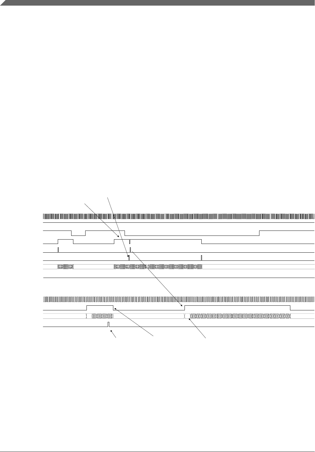
55.6.16.1 Transmit FIFO underflow
During a frame transfer, when the transmit FIFO reaches the almost empty threshold with
no end-of-frame indication stored in the FIFO, the MAC logic:
• Stops reading data from the FIFO
• Asserts the MII error signal (MII_TXER) (1 in Figure 55-16) to indicate that the
fragment already transferred is not valid
• Deasserts the MII transmit enable signal (MII_TXEN) to terminate the frame transfer
(2)
After an underflow, when the application completes the frame transfer (3), the MAC
transmit logic discards any new data available in the FIFO until the end of packet is
reached (4) and sets the enhanced TxBD[UE] field.
The MAC starts to transfer data on the MII interface when the application sends a new
frame with a start of frame indication (5).
Transmit FIFO
MII Transmit
3
4
125
55 55
TX CLK
TX ready
Write enable
Start of packet
End of packet
TX data
TX error status
MII_TXCLK
MII_TXEN
MII_TXD[3:0]
MII_TXER
FIFO data
section empty
Internal signalsExternal signals
Figure 55-16. Transmit FIFO underflow protection
55.6.16.2 Transmit FIFO overflow
On the transmit path, when the FIFO reaches the programmable almost full threshold, the
internal MAC ready signal is deasserted. The application should stop sending new data.
Functional description
S32K1xx Series Reference Manual, Rev. 7, 04/2018
1952 NXP Semiconductors
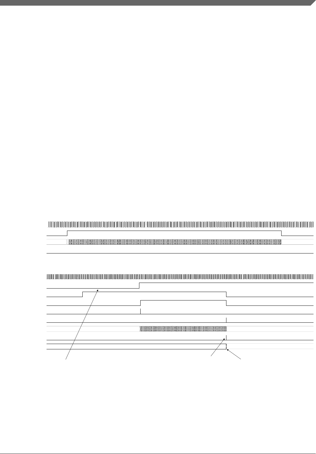
However, if the application keeps sending data, the transmit FIFO overflows, corrupting
contents that were previously stored. The core logic sets the enhanced TxBD[OE] field
for the next frame transmitted to indicate this overflow occurence.
Note
Overflow is a fatal error and must be addressed by resetting the
core or clearing ENETn_ECR[ETHER_EN], to clear the FIFOs
and prepare for normal operation again.
55.6.16.3 Receive FIFO overflow
During a frame reception, if the client application is not able to receive data (1), the MAC
receive control truncates the incoming frame when the FIFO reaches the programmable
almost-full threshold to avoid an overflow.
The frame is subsequently received on the FIFO interface with an error indication
(enhanced RxBD[ME] field set together with receive end-of-packet) (2) with the
truncation error status field set (3).
MII Receive
MII_RXCLK
MII_RXD[3:0]
MII_RXDV
MII_RXER
Receive FIFO
RX CLK
RX ready
Frame available
Data valid
Start of packet
End of packet
RX data
RX error
RX error status
23
1
External signalsInternal signals
Figure 55-17. Receive FIFO overflow protection
55.6.17 Reference clock
The input clocks to the ENET module must meet the specifications in the following table.
Chapter 55 Ethernet MAC (ENET)
S32K1xx Series Reference Manual, Rev. 7, 04/2018
NXP Semiconductors 1953

Ethernet speed mode Ethernet bus clock Minimum ENET system clock
10 Mbit/s 2.5 MHz 5 MHz
100 Mbit/s 25.0 MHz 50 MHz
55.6.18 PHY management interface
The MDIO interface is a two-wire management interface. The MDIO management
interface implements a standardized method to access the PHY device management
registers.
The core implements a master MDIO interface, which can be connected to up to 32 PHY
devices.
55.6.18.1 MDIO clause 22 frame format
The core MDIO master controller communicates with the slave (PHY device) using
frames that are defined in the following table.
A complete frame has a length of 64 bits made up of an optional 32-bit preamble, 14-bit
command, 2-bit bus direction change, and 16-bit data. Each bit is transferred on the rising
edge of the MDIO clock (MDC signal). The MDIO data signal is tri-stated between
frames.
The core PHY management interface supports the standard MDIO specification (IEEE
802.3 Clause 22).
Table 55-39. MDIO clause 22 frame structure
ST OP PHYADR REGADR TA DATA
Table 55-40. MDIO frame field descriptions
Field Description
ST
(2 bits)
Start indication field, programmed with ENETn_MMFR[ST] and equal to 01 for Standard MDIO
(Clause 22).
OP
(2 bits)
Opcode defines type of operation. Programmed with ENETn_MMFR[OP].
01 Write operation
10 Read operation
PHYADR
(5 bits)
Five-bit PHY device address, programmed with ENETn_MMFR[PA]. Up to 32 devices can be
addressed.
Table continues on the next page...
Functional description
S32K1xx Series Reference Manual, Rev. 7, 04/2018
1954 NXP Semiconductors

Table 55-40. MDIO frame field descriptions (continued)
Field Description
REGADR
(5 bits)
Five-bit register address, programmed with ENETn_MMFR[RA]. Each PHY can implement up to 32
registers.
TA
(2 bits)
Turnaround time, programmed with ENETn_MMFR[TA]. Two bit-times are reserved for read
operations to switch the data bus from write to read. The PHY device presents its register contents
in the data phase and drives the bus from the second bit of the turnaround phase.
Data
(16 bits)
Data, set by ENETn_MMFR[DATA]. Written to or read from the PHY
55.6.18.2 MDIO clause 45 frame format
The extended MDIO frame structure defined in IEEE 802.3 Clause 45 introduces indirect
addressing. First, a write transaction to an address register is done, followed by a write or
read transaction which will put the 16-bit data in the register or retrieve the register
contents respectively. A preamble of 32 bits of logical ones is sent prior to every
transaction. The MDIO data signal is tri-stated between frames.
The extended MDIO defines four transactions, which are determined by the two-bit
opcode field.
Table 55-41. MDIO clause 45 frame structure
ST OP PRTAD DEVAD TA ADDR/DATA
All bits are transmitted from left to right (Preamble bits first) and all fields have their
Most-Significant bit sent first (leftmost in above table). The complete frame has a length
of 64 bits (32-bit preamble, 14-bit command, 2-bit bus direction change, 16-bit data).
Each bit is transferred with the rising edge of the MDIO clock (MDC).
The fields and transactions are summarized in the following tables.
Table 55-42. MDIO clause 45 frame field descriptions
Field Description
ST Start indication. Indicates the end of the preamble and start of the frame. This value is 00 for
extended MDIO (Clause 45) frames.
OP Opcode defines if a read or write operation is performed and is programmed with
ENETn_MMFR[OP]. See Table 55-43 for more information.
00 Address write
01 Write operation
10 Read inc. operation
Table continues on the next page...
Chapter 55 Ethernet MAC (ENET)
S32K1xx Series Reference Manual, Rev. 7, 04/2018
NXP Semiconductors 1955

Table 55-42. MDIO clause 45 frame field descriptions (continued)
Field Description
11 Read operation
PRTAD The port address specifies a MDIO port. Each Port can have up to 32 devices which each can have
a separate set of registers.
DEVAD Device address. Up to 32 devices can be addressed (within a port).
TA Turnaround time, programmed with ENETn_MMFR[TA]. Two bit-times are reserved for read
operations to switch the data bus from write to read. The PHY device presents its register contents
in the data phase and drives the bus from the second bit of the turnaround phase.
ADDR/DATA 16-bit address (for address write) or data, set by ENETn_MMFR[DATA], written to or read from the
PHY.
Table 55-43. MDIO Clause 45 Transactions
Transaction Type Description
Address A write transaction to the internal address register of the device/port. The data section of the frame
contains the value to be stored in the device's internal address "pointer" register for further
transactions.
Write Data write to a register. The 16 bit data will be written to the register identified by the device-internal
address.
Read Data is read from the register identified by the device-internal address.
Read inc. Read with address postincrement. The register identified by the device-internal address is read.
After this, the device-internal address is incremented. If the address register is all '1' (0xFFFF) no
increment is done (i.e. increment does not wrap around).
55.6.18.3 MDIO clock generation
The MDC clock is generated from the internal bus clock (i.e., IPS bus clock) divided by
the value programmed in ENETn_MSCR[MII_SPEED].
Functional description
S32K1xx Series Reference Manual, Rev. 7, 04/2018
1956 NXP Semiconductors
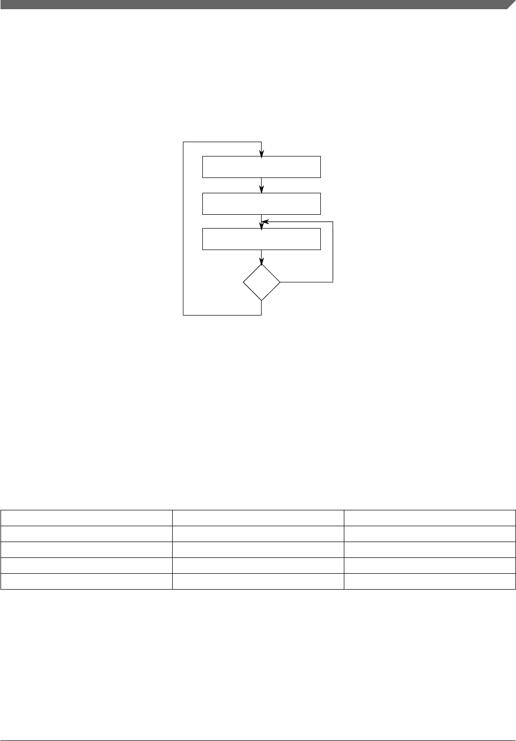
55.6.18.4 MDIO operation
To perform an MDIO access, set the MDIO command register (ENETn_MMFR)
according to the description provided in MII Management Frame Register
(ENETn_MMFR).
To check when the programmed access completes, read the ENETn_EIR[MII] field.
Start
Load ENETn_MMFR register
Read ENETn_EIR
MII = 1? N
Y
Figure 55-18. MDIO access overview
55.6.19 Ethernet interfaces
The following Ethernet interfaces are implemented:
• Fast Ethernet MII (Media Independent Interface)
• RMII 10/100 using interface converters/gaskets
The following table shows how to configure ENET registers to select each interface.
Mode RCR[RMII_10T] RCR[RMII_MODE]
MII - 10 Mbit/s — 0
MII - 100 Mbit/s — 0
RMII - 10 Mbit/s 1 1
RMII - 100 Mbit/s 0 1
55.6.19.1 RMII interface
In RMII receive mode, for normal reception following assertion of CRS_DV, RXD[1:0]
is 00 until the receiver determines that the receive event has a proper start-of-stream
delimiter (SSD).
Chapter 55 Ethernet MAC (ENET)
S32K1xx Series Reference Manual, Rev. 7, 04/2018
NXP Semiconductors 1957
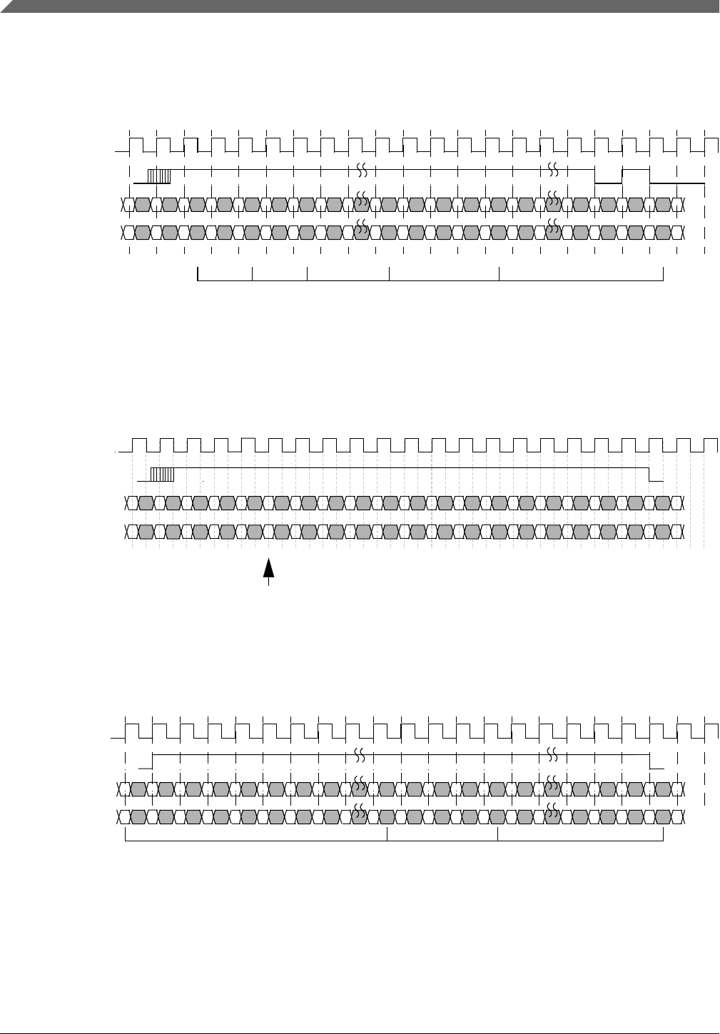
The preamble appears (RXD[1:0]=01) and the MACs begin capturing data following
detection of SFD.
/J/ /K / Preamble SFD D ata
RMII_REF_CLK
RMII_CRS_DV
0 0 0 0 0 0 0 0 0 0 0 0 0 1 x x x x x x 0
RMII_RXD1
0 0 0 0 0 0 0 1 1 1 1 1 1 1 x x x x x x 0
RMII_RXD0
Figure 55-19. RMII receive operation
If a false carrier is detected (bad SSD), then RXD[1:0] is 10 until the end of the receive
event. This is a unique pattern since a false carrier can only occur at the beginning of a
packet where the preamble is decoded (RXD[1:0] = 01).
RMII_REF_CLK
RMII_CRS_DV
0 0 0 0 0 1 1 1 1 1 1 1 1 1 1 1 1 1 1 1 0
RMII_RXD1
0 0 0 0 0 0 0 0 0 0 0 0 0 0 0 0 0 0 0 0 0
RMII_RXD0
False carrier detected
Figure 55-20. RMII receive operation with false carrier
In RMII transmit mode, TXD[1:0] provides valid data for each REF_CLK period while
TXEN is asserted.
Pream ble SFD D ata
RMII_REF_CLK
RMII_TXEN
0 0 0 0 0 0 0 0 0 0 0 0 0 1 x x x x x x 0
RMII_TXD1
0 1 1 1 1 1 1 1 1 1 1 1 1 1 x x x x x x 0
RMII_TXD0
Figure 55-21. RMII transmit operation
Functional description
S32K1xx Series Reference Manual, Rev. 7, 04/2018
1958 NXP Semiconductors
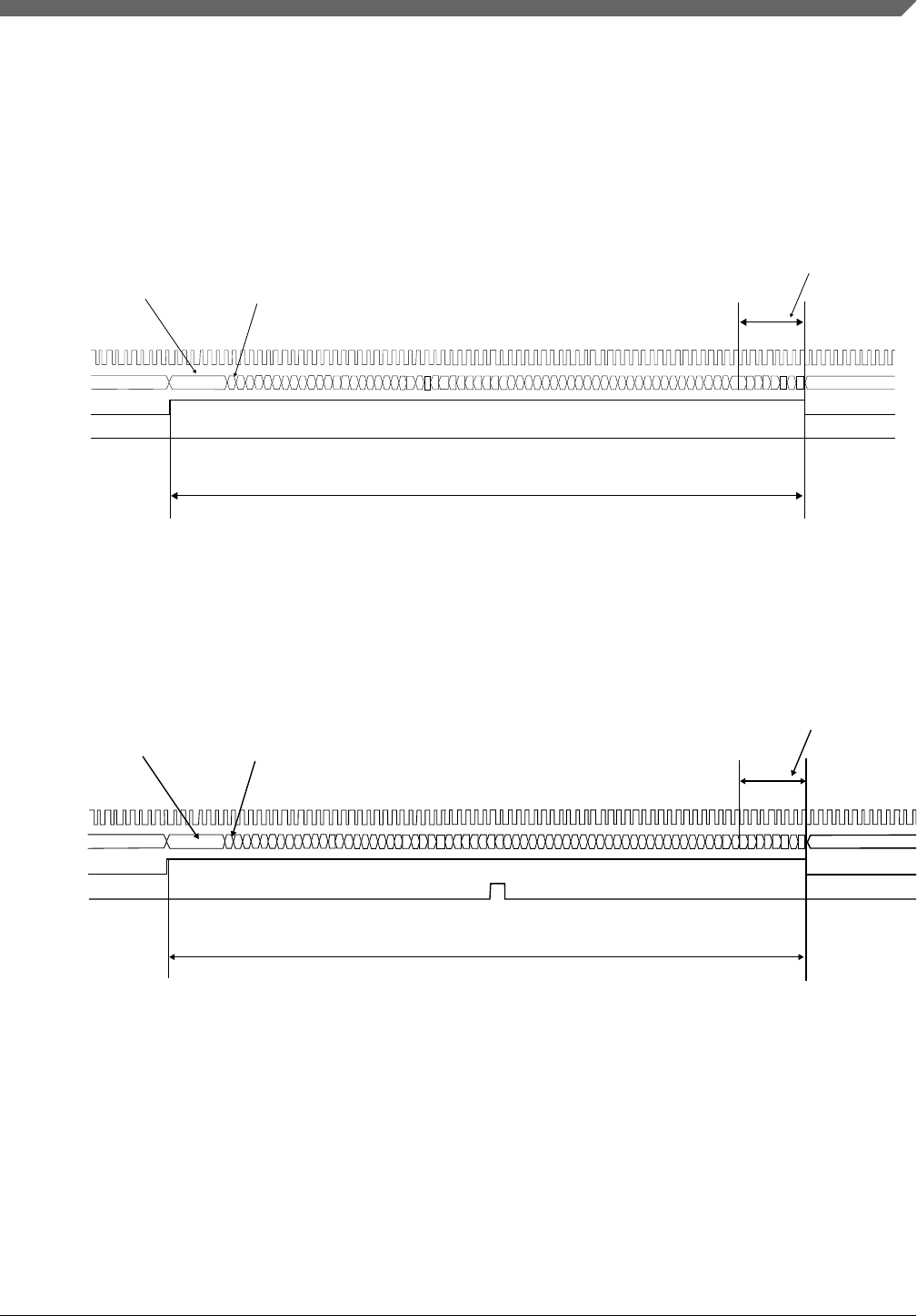
55.6.19.2 MII Interface — transmit
On transmit, all data transfers are synchronous to MII_TXCLK rising edge. The MII data
enable signal MII_TXEN is asserted to indicate the start of a new frame, and remains
asserted until the last byte of the frame is present on the MII_TXD[3:0] bus.
Between frames, MII_TXEN remains deasserted.
CRC-32
SFD
Preamble
5
04 05 06 07 08 09 0A 0F 10 11 12 13 14 15 16 17 18 19 1A 1C 1E 1F 20 21 22 23 24 25 26 27 28 29 2B 2E 2F 30 31 32 33 34 35 36 37 38 39 3B 3F 40 99 80 28
MII_TXER
MII_TXCLK
MII_TXD[3:0]
MII_TXEN
Figure 55-22. MII transmit operation
If a frame is received on the FIFO interface with an error (for example, RxBD[ME] set)
the frame is subsequently transmitted with the MII_TXER error signal for one clock
cycle at any time during the packet transfer.
CRC-32
SFD
MII_TXCLK
MII_TXD[3:0]
MII_TXEN
MII_TXER
Preamble
5
Figure 55-23. MII transmit operation — errored frame
Chapter 55 Ethernet MAC (ENET)
S32K1xx Series Reference Manual, Rev. 7, 04/2018
NXP Semiconductors 1959
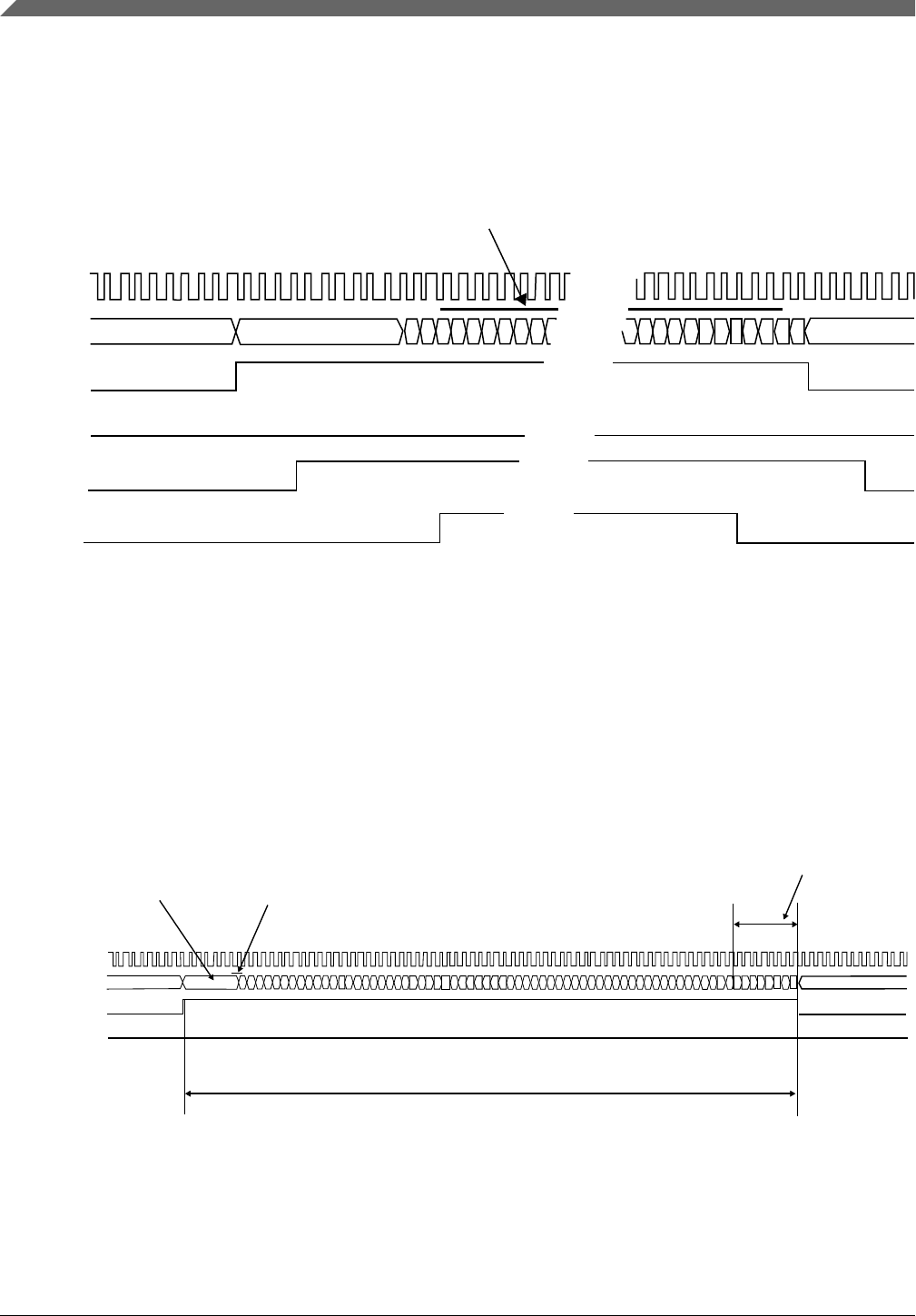
55.6.19.2.1 Transmit with collision — half-duplex
When a collision is detected during a frame transmission (MII_COL asserted), the MAC
stops the current transmission, sends a 32-bit jam pattern, and re-transmits the current
frame.
Jam
MII_TXCLK
MII_TXD[3:0]
MII_TXEN
MII_TXER
MII_CRS
MII_COL
5
Figure 55-24. MII transmit operation — transmission with collision
55.6.19.3 MII interface — receive
On receive, all signals are sampled on the MII_RXCLK rising edge. The MII data enable
signal, MII_RXDV, is asserted by the PHY to indicate the start of a new frame and
remains asserted until the last byte of the frame is present on MII_RXD[3:0] bus.
Between frames, MII_RXDV remains deasserted.
CRC-32
SFD
Preamble
5
MII_RXER
MII_RXCLK
MII_RXD[3:0]
MII_RXDV
Figure 55-25. MII receive operation
Functional description
S32K1xx Series Reference Manual, Rev. 7, 04/2018
1960 NXP Semiconductors

If the PHY detects an error on the frame received from the line, the PHY asserts the MII
error signal, MII_RXER, for at least one clock cycle at any time during the packet
transfer.
CRC-32
SFD
Preamble
5
MII_RXER
MII_RXCLK
MII_RXD[3:0]
MII_RXDV
Figure 55-26. MII receive operation — errored frame
A frame received on the MII interface with a PHY error indication is subsequently
transferred on the FIFO interface with RxBD[ME] set.
Chapter 55 Ethernet MAC (ENET)
S32K1xx Series Reference Manual, Rev. 7, 04/2018
NXP Semiconductors 1961

Functional description
S32K1xx Series Reference Manual, Rev. 7, 04/2018
1962 NXP Semiconductors

Chapter 56
Debug
56.1 Introduction
The debug capability on this device is based on the Arm CoreSight™ architecture and is
configured on each device to provide the maximum flexibility as allowed by the
restrictions of the pinout and other available resources.
Table 56-1. Supported debug interfaces
Chip Supported debug interfaces
IEEE 1149.1 JTAG Serial Wire
Debug(SWD)
SWO 4-pin parallel trace
port1
S32K116 No 2Yes No No3
S32K118 No2Yes No No3
S32K142 Yes Yes Yes No
S32K146 Yes Yes Yes No
S32K144 Yes Yes Yes No
S32K148 Yes Yes Yes Yes
1. Overrides the value of Supported Port Size Register of TPIU (at location 0x000)
2. JTAG protocol available only for Boundary Scan
3. 1 KB of MTB RAM present to store trace data
The basic Cortex debug architecture is very flexible. The following diagrams shows the
topology of the core debug architecture and its components.
S32K1xx Series Reference Manual, Rev. 7, 04/2018
NXP Semiconductors 1963
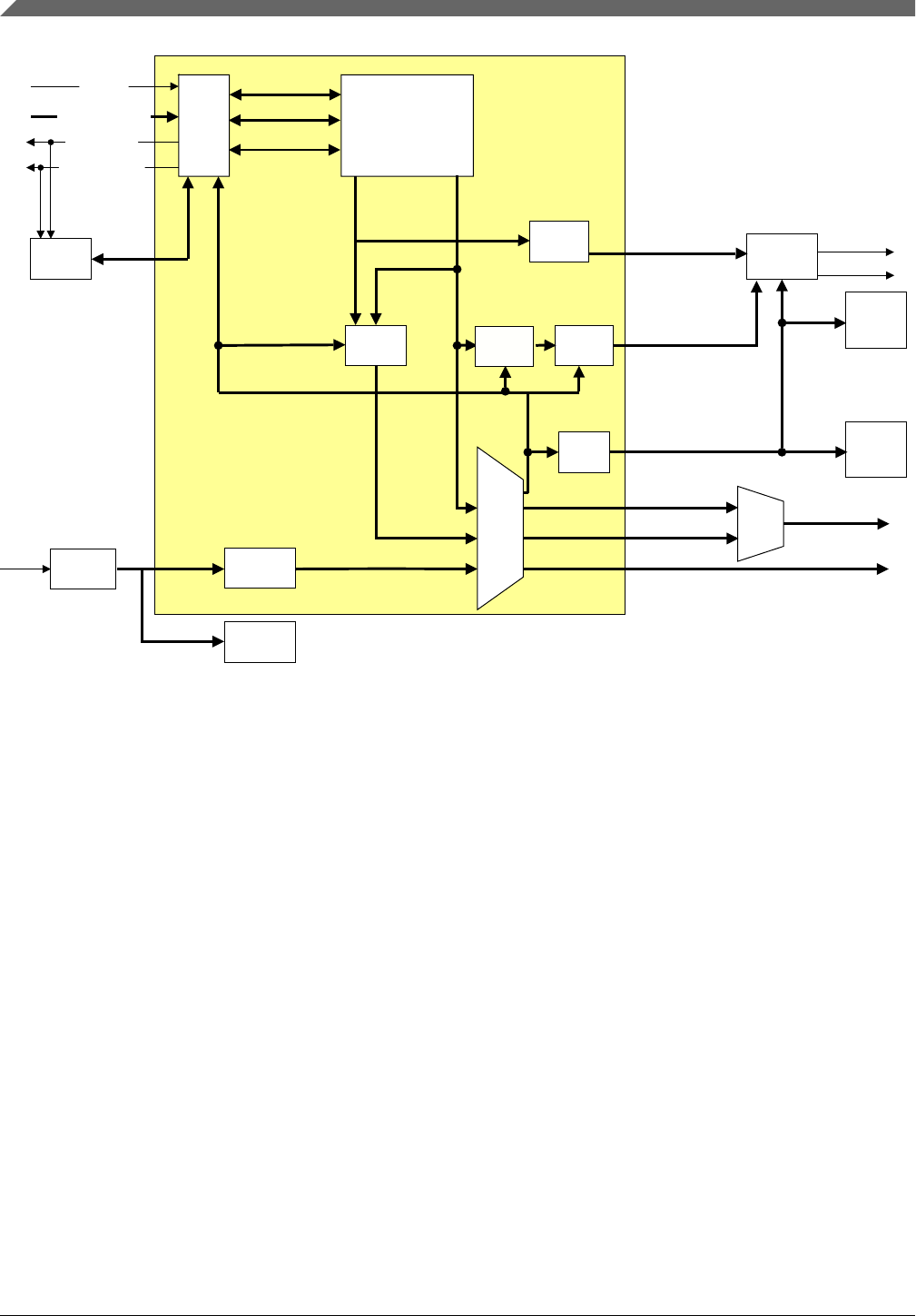
Private Peripheral Bus
(internal)
ITM
TPIU
Core
FPB
AHB-AP
NVIC
SWJ-DP
Bus
Matrix
APB
i/f
Cortex-M4
SW/
JTAG
Debug
Sleep
Interrupts
INTNMI
SLEEPING
SLEEPDEEP
INTISR[239:0]
AWIC
ROM
Table
Instr. Data
MCM
I-code bus
D-code bus
System bus
Code bus
MDM-AP
DWT
4 bit TracePort
1bit SWO
ETM
Figure 56-1. Cortex-M4 debug topology
Introduction
S32K1xx Series Reference Manual, Rev. 7, 04/2018
1964 NXP Semiconductors
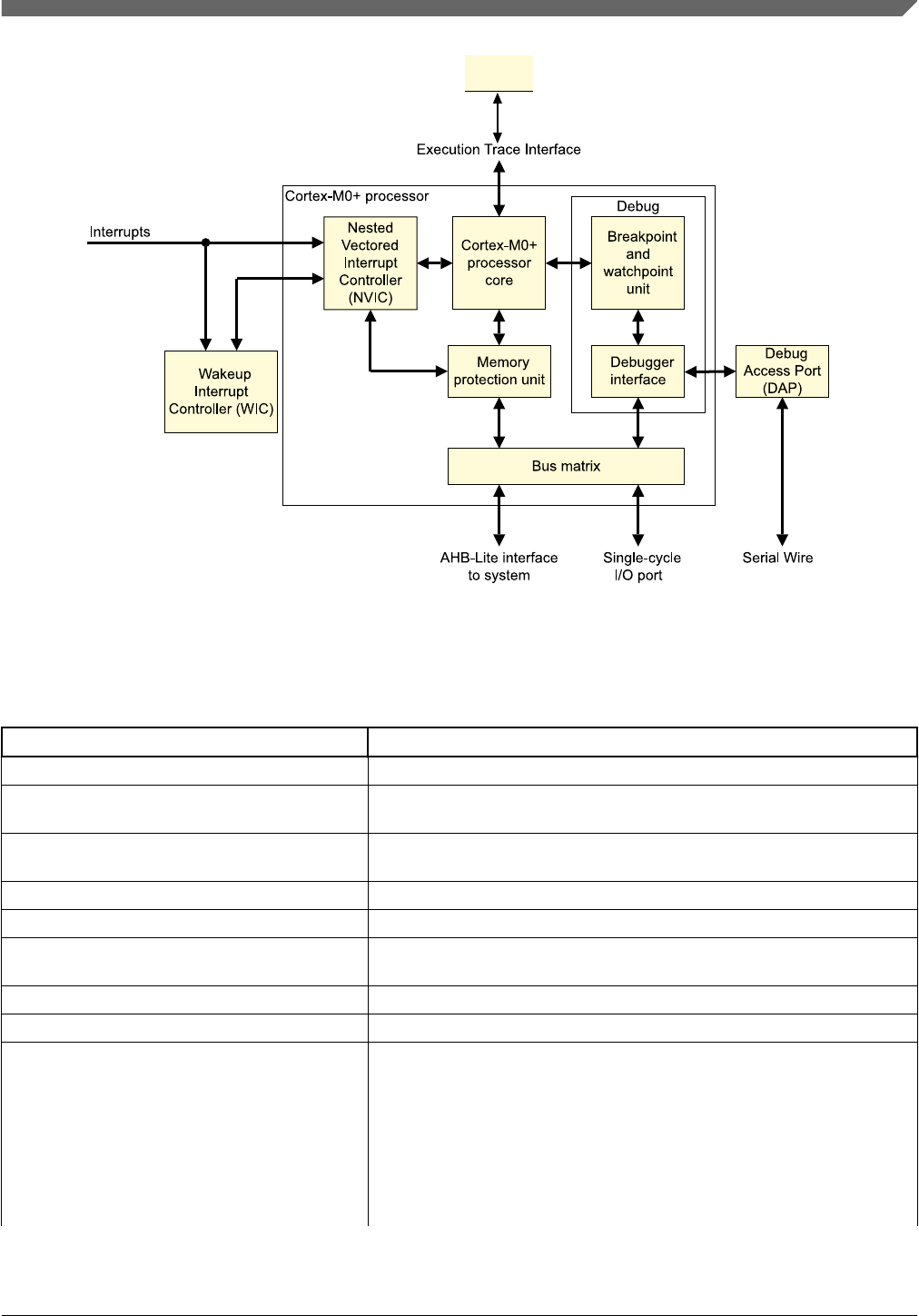
MTB
Figure 56-2. Cortex-M0+ debug topology
The following table presents a brief description of each of the debug components.
Table 56-2. Debug components description
Module Description
SWJ-DP (Serial Wire and JTAG - Debug Port) Modified Debug Port with support for SWD, JTAG
AHB-AP (AMBA High-performance Bus - Access
Port)
AHB Master Interface from JTAG to debug module and SOC system
memory maps
MDM-AP (Miscellaneous Debug Module - Access
Port)
Provides centralized control and status registers for an external debugger
to control the device.
ROM Table Identifies which debug IP is available.
Core Debug Singlestep, Register Access, Run, Core Status
ITM (Instruction Trace Macrocell) S/W Instrumentation Messaging + Simple Data Trace Messaging +
Watchpoint Messaging
ETM (Embedded Trace Macrocell) Used for instruction trace
DWT (Data and Address Watchpoints) 4 data and address watchpoints
FPB (Flash Patch and Breakpoints) The FPB implements hardware breakpoints and patches code and data
from code space to system space.
The FPB unit contains two literal comparators for matching against literal
loads from Code space, and remapping to a corresponding area in System
space.
The FPB also contains six instruction comparators for matching against
instruction fetches from Code space, and remapping to a corresponding
area in System space. Alternatively, the six instruction comparators can
Table continues on the next page...
Chapter 56 Debug
S32K1xx Series Reference Manual, Rev. 7, 04/2018
NXP Semiconductors 1965

Table 56-2. Debug components description (continued)
Module Description
individually configure the comparators to return a Breakpoint Instruction
(BKPT) to the processor core on a match, providing hardware breakpoint
capability.
TPIU (Trace Port Interface Unit) Asynchronous Mode (1-pin) = TRACE_SWO (available on JTAG_TDO).
Supports 4 pin trace output and a single pin SWO.
MTB Logs trace information of JUMP instructions and stores it in MTB RAM.
56.2 CM4 and CM0+ ROM table
The ROM table is used to hold the information about the debug components.
Table 56-3. Bit assignments in the ROM table
Bits Name Description
[31:12] Address offset Base address of the component, relative to the ROM address. Negative values are
permitted using two's complement.
ComponentAddress = ROMAddress + (AddressOffset SHL 12).
[11:2] - Reserved SBZ.
[1] Format 1 = 32-bit format. In the DAP Debug ROM this is set to 1.
0 = 8-bit format.
[0] Entry present Set HIGH to indicate an entry is present.
Table 56-4. CM4 ROM table
Component Base address
SCS 0xE000E000
DWT 0xE0001000
FPB 0xE0002000
ITM 0xE0000000
TPIU + SWO 0xE0040000
ETM 10xE0041000
1. Present in S32K148 variant only
Table 56-5. CM0+ ROM table
Component Base address
MTB 0xF0000000
MTB_DWT 0xF0001000
CM0 + SCU 0xE000E000
Table continues on the next page...
CM4 and CM0+ ROM table
S32K1xx Series Reference Manual, Rev. 7, 04/2018
1966 NXP Semiconductors
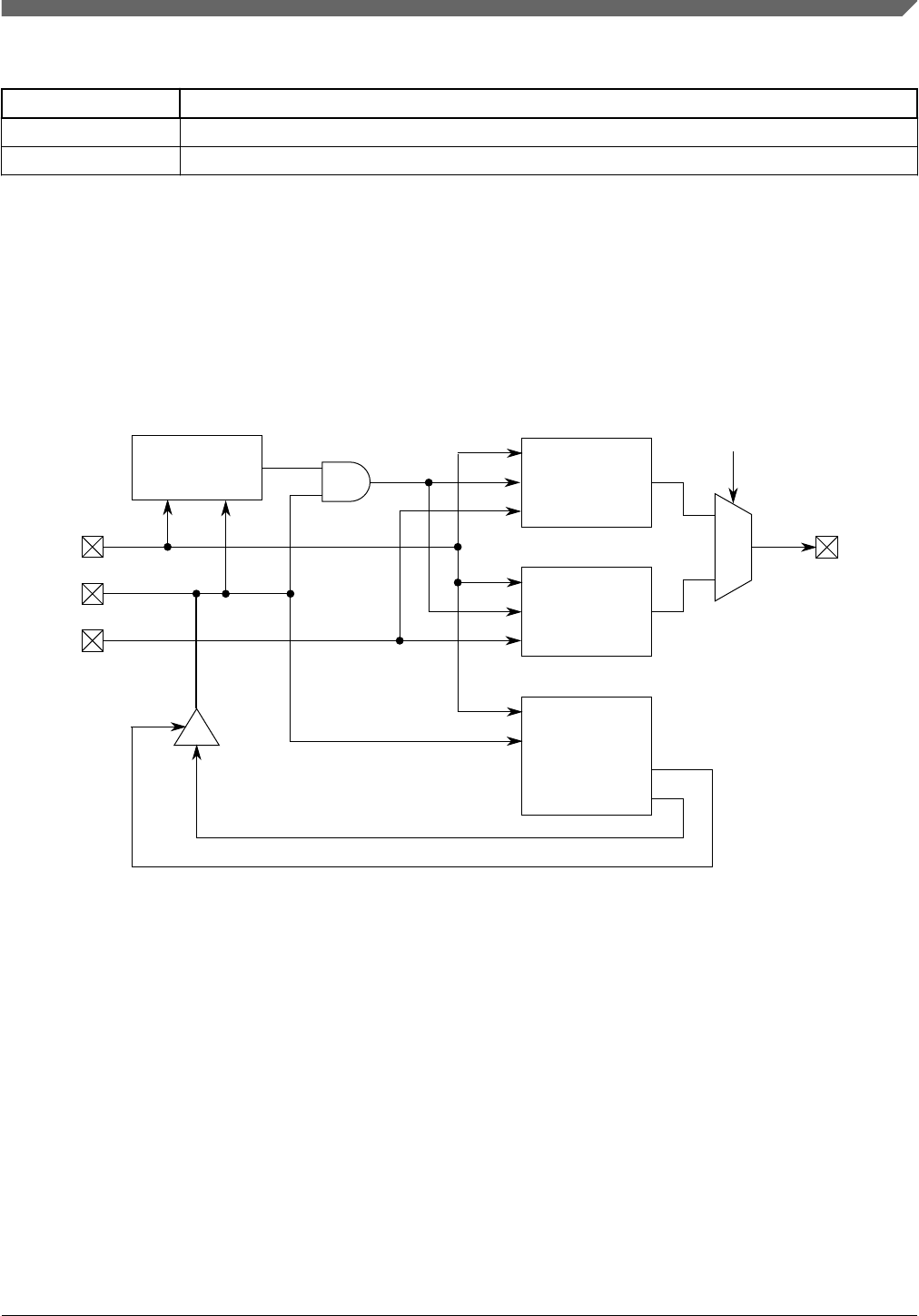
Table 56-5. CM0+ ROM table (continued)
Component Base address
CM0 + DWT 0xE0001000
CM0 + BPU 0xE0002000
56.3 Debug port
The configuration of the JTAG controller, and debug port, is illustrated in the following
figure.
TCK
JTAGC
TMS
TDI
TDO
JTAG-DP
TCK
TMS
TDI
TDO
1
0
SWD-DP
DBGCLK
DBGDI
DBGDOEN
SWD-JTAG
SWITCHER
TCK
JTAG-mode
DBGDO
TDI
TMS
Arm JTAG-DP
instruction loaded
TDO
Figure 56-3. Modified debug port for CM4 core
Chapter 56 Debug
S32K1xx Series Reference Manual, Rev. 7, 04/2018
NXP Semiconductors 1967
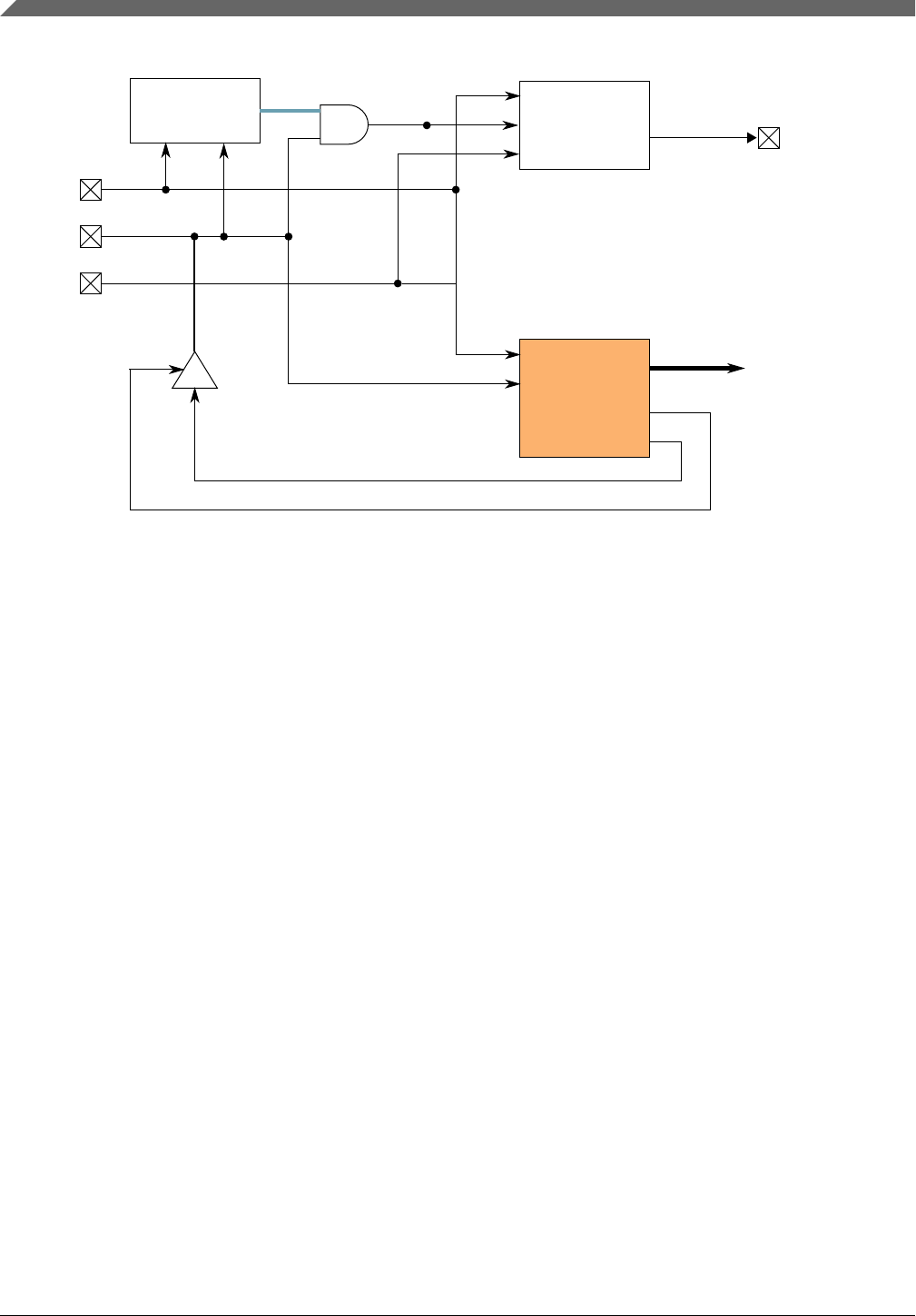
TCK
JTAGC
TMS
TDI
TDO
SWD-DP
DBGCLK
DBGDI
DBGDOEN
SWD-JTAG
SWITCHER
TCK
JTAG-mode
DBGDO
TDI
TMS
TDO
To Core Debug
coponents
Figure 56-4. Modified debug port for CM0+ core
The debug port comes out of reset in standard JTAG mode and is switched into SWD
mode by the following sequences. Once the mode has been changed, unused debug pins
can be reassigned to any of their alternative muxed functions.
NOTE
AP Abort command is not supported in S32K11x. For stalled
AP transaction, reset needs to be issued.
56.3.1 JTAG-to-SWD change sequence
1. Send more than 50 TCK cycles with TMS (SWDIO) =1
2. Send the 16-bit sequence on TMS (SWDIO) = 0111_1001_1110_0111 (MSB
transmitted first)
3. Send more than 50 TCK cycles with TMS (SWDIO) =1
NOTE
See the Arm documentation for the CoreSight DAP Lite for
restrictions.
Debug port
S32K1xx Series Reference Manual, Rev. 7, 04/2018
1968 NXP Semiconductors

56.4 Debug port pin descriptions
After POR, all debug port pins default to their JTAG functionality and can later be
reassigned to their alternate functionalities. In SWD mode, JTAG_TDI can be configured
for alternate GPIO functions.
Table 56-6. Debug port pins
Pin name JTAG debug port SWD debug port Internal pull-up/
down
Type Description Type Description
JTAG_TMS/
SWD_DIO
I/O JTAG Test Mode
Selection
I/O Serial Wire Data Pull-up
JTAG_TCLK/
SWD_CLK
I JTAG Test Clock I Serial Wire Clock Pull-down
JTAG_TDI I JTAG Test Data
Input
- - Pull-up
JTAG_TDO/
TRACE_SWO
O JTAG Test Data
Output
O Trace output over a
single pin
N/C
56.5 System TAP connection
The system JTAG controller is connected in parallel to the Arm Test Access Port (TAP)
controller. The system JTAG controller Instruction Register (IR) codes overlay the Arm
JTAG controller IR codes without conflict. Refer to the IR codes table for a list of the
available IR codes. The output of the TAPs (TDO) are muxed based on the IR code
which is selected. This design is fully JTAG compliant and appears to the JTAG chain as
a single TAP. At power on reset, Arm's IDCODE (IR = 1110b) is selected.
56.5.1 IR codes
Table 56-7. JTAG instructions
Instruction Code[3:0] Instruction summary
IDCODE10000 Selects device identification register for shift
SAMPLE/PRELOAD 0010 Selects boundary scan register for shifting, sampling, and
preloading without disturbing functional operation
SAMPLE 0011 Selects boundary scan register for shifting and sampling
without disturbing functional operation
EXTEST 0100 Selects boundary scan register while applying preloaded
values to output pins and asserting functional reset
Table continues on the next page...
Chapter 56 Debug
S32K1xx Series Reference Manual, Rev. 7, 04/2018
NXP Semiconductors 1969

Table 56-7. JTAG instructions (continued)
Instruction Code[3:0] Instruction summary
HIGHZ 1001 Selects bypass register while three-stating all output pins and
asserting functional reset
CLAMP 1100 Selects bypass register while applying preloaded values to
output pins and asserting functional reset
Arm_IDCODE21110 Arm JTAG-DP Instruction
BYPASS 1111 Selects bypass register for data operations
Factory debug reserved 0101, 0110, 0111, 1101 Intended for factory debug only
Arm JTAG-DP Reserved 21000, 1010, 1011, 1110 These instructions will go the Arm JTAG-DP controller.
Please see the Arm JTAG-DP documentation for more
information on these instructions.
Reserved 3All other opcodes Decoded to select bypass register
1. Device IDCODE can only be read in JTAG mode.
2. Reserved for S32K11x variants
3. The manufacturer reserves the right to change the decoding of reserved instruction codes in the future
56.6 MDM-AP status and control registers
Through the Arm Debug Access Port (DAP), the debugger has access to the status and
control elements, implemented as registers on the DAP bus as shown in Figure 56-5.
These registers provide additional control and status for low power mode recovery and
typical run-control scenarios. The status register bits also allow the debugger to get
updated status of the core without having to initiate a bus transaction across the crossbar
switch, thus remaining less intrusive during a debug session.
These DAP control and status registers are not memory mapped within the system
memory map and are only accessible via the DAP using JTAG or SWD. The MDM-AP is
accessible as Debug Access Port 1 with the available registers shown in the table below.
Table 56-8. MDM-AP register summary
Address Register Description
0x0100_0000 Status See MDM-AP Status Register
0x0100_0004 Control See MDM-AP Control Register
0x0100_00FC ID Read-only identification register that always reads as 0x001C_0000
MDM-AP status and control registers
S32K1xx Series Reference Manual, Rev. 7, 04/2018
1970 NXP Semiconductors
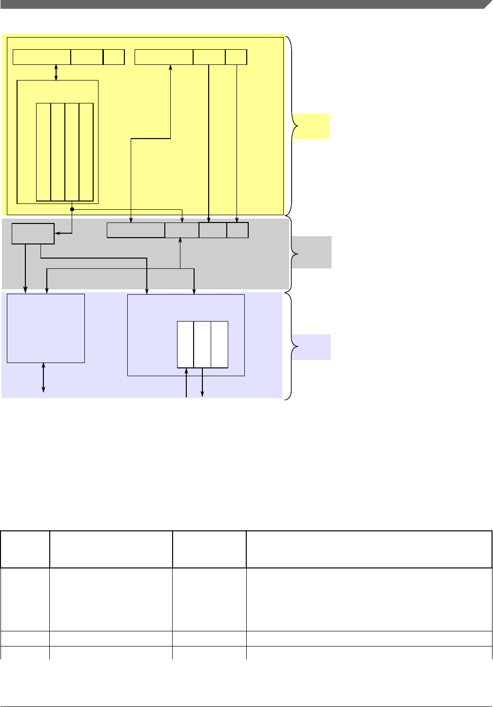
SWJ-DP
SELECT[31:24] (APSEL) selects the AP
SELECT[7:4] (APBANKSEL) selects the bank
A[3:2] from the APACC selects the register
within the bank
AHB Access Port
(AHB-AP) MDM-AP
Status 0x00
Control 0x01
IDR 0x3F
AHB-AP
SELECT[31:24] = 0x00 selects the AHB-AP
See Arm documentation for further details
MDM-AP
SELECT[31:24] = 0x01 selects the MDM-AP
SELECT[7:4] = 0x0 selects the bank with Status and Ctrl
A[3:2] = 2’b00 selects the Status Register
A[3:2] = 2’b01 selects the Control Register
SELECT[7:4] = 0xF selects the bank with IDR
A[3:2] = 2’b11 selects the IDR Register
(IDR register reads 0x001C_0000)
Bus Matrix See Control and Status Register
Descriptions
Data[31:0] A[7:4] A[3:2] RnW
APSEL
Decode
Debug Port ID Register (DPIDR)
Control/Status (CTRL/STAT)
AP Select (SELECT)
Read Buffer (REBUFF)
DP Registers
0x00
0x04
0x08
0x0C
Data[31:0] A[3:2] RnW
DPACC
Data[31:0] A[3:2] RnW
APACC
Debug Port
(DP)
Generic
See the Arm Debug Interface v5p1 Supplement.
Debug
Port
Internal
Bus
Access
Port
Figure 56-5. MDM AP addressing
56.6.1 MDM-AP Control Register
Table 56-9. MDM-AP Control Register assignments
Bit Name Command
available in
secure mode?
Description
0 Flash memory mass erase in
progress
Yes Set to cause mass erase. Cleared by hardware after mass
erase operation completes.
When mass erase is disabled (via MEEN and SEC settings),
the erase request does not occur and the Flash Mass Erase
in Progress bit continues to assert until the next system reset.
1 Debug disable No Set to disable debug. Clear to allow debug operation.
2 Debug request No Set to force the core to halt.
Table continues on the next page...
Chapter 56 Debug
S32K1xx Series Reference Manual, Rev. 7, 04/2018
NXP Semiconductors 1971

Table 56-9. MDM-AP Control Register assignments (continued)
Bit Name Command
available in
secure mode?
Description
If the core is in a stop mode, this bit can be used to wake up
the core and transition to a halted state.
3 System reset request No Set to force a system reset. The system remains held in reset
until this bit is cleared.
4 Core hold reset No Configuration bit to control core operation at the end of
system reset sequencing.
0: Normal operation - Release the core from reset along with
the rest of the system at the end of system reset sequencing.
1: Suspend operation - Hold the core in reset at the end of
reset sequencing. After the system enters this suspended
state, clearing this control bit immediately releases the core
from reset and CPU operation begins.
5 – 7 Reserved No
8 Timestamp disable1No Set this bit to disable the 48-bit global trace timestamp
counter during debug halt mode when the core is halted.
0: The timestamp counter continues to count assuming trace
is enabled. (default)
1: The timestamp counter freezes when the core has halted
(debug halt mode).
9 – 31 Reserved for future use No
1. Reserved for S32K11x variants
56.6.2 MDM-AP Status Register
Table 56-10. MDM-AP Status Register assignments
Bit Name Description
0 Flash memory mass erase
acknowledge
This bit is cleared on debug reset. The bit is also cleared at the launch of a
mass erase command due to writing the Mass Erase in Progress bit in the
MDM AP Control Register. This bit is set after the flash memory control
logic has started the mass erase operation.
When mass erase is disabled (via MEEN and SEC settings), an erase
request due to setting the bit is not acknowledged.
1 Flash memory ready Indicates flash memory has been initialized and the debugger can be
configured even if the system is continuing to be held in reset via the
debugger.
2 System security Indicates the security state. When secure, the debugger does not have
access to the system bus or any memory mapped peripherals. This bit
indicates when the part is locked and no system bus access is possible.
3 System reset Indicates the system reset state.
0: System is in reset
1: System is not in reset
Table continues on the next page...
MDM-AP status and control registers
S32K1xx Series Reference Manual, Rev. 7, 04/2018
1972 NXP Semiconductors

Table 56-10. MDM-AP Status Register assignments (continued)
Bit Name Description
4 Reserved
5 Mass erase enable Indicates whether the MCU can be mass erased
0: Mass erase is disabled
1: Mass erase is enabled
6 Backdoor access key enable Indicates whether the MCU has the backdoor access key enabled. See the
FTFE_FSEC[KEYEN] bit for more information.
0: Disabled
1: Enabled
7 LP enabled Decode of LPLLSM control bits to indicate that VLPS is the selected power
mode the next time the Arm core enters Deep Sleep.
0: Low Power Stop Mode is not enabled
1: Low Power Stop Mode is enabled
Usage is intended for debug operation in which Run to VLPS is attempted.
Per debug definition, the system actually enters the Stop state. A
debugger should interpret deep sleep indication (with SLEEPDEEP and
SLEEPING asserted) in conjunction with this bit asserted as the debugger-
VLPS status indication.
8 Very low power mode Indicates current power mode is VLPx. This bit is not ‘sticky’ and should
always represent whether VLPx is enabled or not.
This bit is used by the debugger to throttle JTAG TCK frequency up/down.
9 – 10 Reserved Always reads as 0.
11 – 15 Reserved for future use Always read as 0.
16 Core halted Indicates the core has entered debug halt mode
17 Core SLEEPDEEP Indicates the core has entered a low power mode
SLEEPING==1 and SLEEPDEEP==1 indicates stop or VLPS mode.
18 Core SLEEPING
19 – 31 Reserved for future use Always reads as 0.
56.7 Debug resets
The debug system receives the following sources of reset:
• Debug reset (CDBGRSTREQ bit within the SWJ-DP CTRL/STAT register) in the
TCLK domain that allows the debugger to reset the debug logic 1
• System POR reset
Conversely, the debug system is capable of generating system reset using the following
mechanism:
1. This reset is not available in S32K11x variants.
Chapter 56 Debug
S32K1xx Series Reference Manual, Rev. 7, 04/2018
NXP Semiconductors 1973

• A system reset in the DAP control register which allows the debugger to hold the
system in reset
• SYSRESETREQ bit in the NVIC application interrupt and reset control register
56.8 AHB-AP
AHB-AP provides the debugger access to all memory and registers in the system,
including processor registers through the NVIC. System access is independent of the
processor status. AHB-AP does not perform back-to-back transactions on the bus, so all
transactions are non-sequential. AHB-AP can perform unaligned and bit-band
transactions. AHB-AP transactions bypass the FPB, so the FPB cannot remap AHB-AP
transactions. SWJ/SW-DP-initiated transaction aborts drive an AHB-AP-supported
sideband signal called HABORT. This signal is driven into the Bus Matrix, which resets
the Bus Matrix state, so that AHB-AP can access the Private Peripheral Bus for last ditch
debugging such as read/stop/reset the core. AHB-AP transactions are little-endian.
The MPU includes default settings and protections for the Region Descriptor 0 (RGD0)
such that the Debugger always has access to the entire address space and those rights
cannot be changed by the core or any other bus master.
For a short period at the start of a system reset event, the system security status is being
determined and debugger access to all AHB-AP transactions is blocked. The MDM-AP
Status register is accessible and can be monitored to determine when this initial period is
completed. After this initial period, if system reset is held via assertion of the RESET_b
pin, the debugger has access via the bus matrix to the private peripheral bus to configure
the debug IP even while system reset is asserted. While in system reset, access to other
memory and register resources, accessed over the crossbar switch, is blocked.
56.9 ITM
The Instrumentation Trace Macrocell (ITM) is an application-driven trace source that
supports printf style debugging to trace operating system and application events, and
emits diagnostic system information. The ITM emits trace information as packets. There
are four sources that can generate packets. If multiple sources generate packets at the
same time, the ITM arbitrates the order in which packets are output. The four sources in
decreasing order of priority are:
1. Software trace: Software can write directly to ITM stimulus registers. This emits
packets.
2. Hardware trace: The DWT generates these packets, and the ITM emits them.
AHB-AP
S32K1xx Series Reference Manual, Rev. 7, 04/2018
1974 NXP Semiconductors

3. Time stamping: Timestamps are emitted relative to packets. The ITM contains a 21-
bit counter to generate the timestamp. The counter is clocked either by the Cortex-
M4 clock or by the bit clock rate of the Serial Wire Viewer (SWV) output.
4. Global system timestamping: Timestamps can optionally be generated using a
system-wide 48-bit count value.
56.10 Core trace connectivity
Following table provides Core trace connectivity across S32K1xx devices.
Table 56-11. Core Trace Connectivity
Chip Feature
S32K116, S32K118 Trace data generated by the CM0+ core can be stored in
MTB RAM.
S32K142, S32K144, S32K146 DWT and ITM trace data can traced out only through SWO
interface.
S32K148 DWT, ETM and ITM trace data can be traced out through
SWO or 4 pin parallel trace port.
56.11 TPIU
The TPIU is a trace data drain that acts as a bridge between the on-chip tracedata to a
data stream that is captured by a Trace Port Analyzer (TPA).
Table 56-12. S32K14x TPIU
Chip Feature
S32K16, 118 Not present
S32K142, S32K144, S32K146 The TPIU in the device supports a limited subset of the full
TPIU functionality (only SWO mode), to minimize gatecount
for a simple debug solution.
S32K148 For applications which require high trace bandwidth, 4 pin
trace interface can be used.
SWO mode can be used only in SWD mode as it uses the
same pin as JTAG TDO.
Maximum trace clock for SWO is 20 MHz. Maximum trace clock for 4-pin trace
interface mapped to:
• Fast pads is 80 MHz
• Slow pads is 20 MHz
Chapter 56 Debug
S32K1xx Series Reference Manual, Rev. 7, 04/2018
NXP Semiconductors 1975

This can be configured through System Clock Divider Register 4 (CLKDIV4) register.
56.12 DWT
The DWT provides debug functionality. It contains four comparators, each of which can
be configured as a hardware watchpoint, a PC sampler event trigger, or a data address
sampler event trigger. The first comparator, DWT_COMP0, can also compare against the
clock cycle counter, CYCCNT. The second comparator, DWT_COMP1, can also be used
as a data comparator. DWT also contains counters for:
• Clock cycles (CYCCNT)
• Folded instructions
• Load store unit (LSU) operations
• Sleep cycles
• CPI (all instruction cycles except for the first cycle)
• Interrupt overhead
An event is emitted each time a counter overflows.
The DWT can be configured to emit PC samples at defined intervals, and to emit
interrupt event information.
NOTE
The MTB_DWT_FCT[FUNCTION]=0100 (i.e. Instruction
Fetch) is only valid when DATAVMATCH=0.
56.13 MTB
The Micro Trace Buffer (MTB) provides a simple execution trace capability for the
Cortex-M0+ processor. When enabled, the MTB records changes in program flow
reported by the Cortex-M0+ processor, via the execution trace interface, into a
configurable region of the MTB SRAM. Subsequently, an off-chip debugger may extract
the trace information, which would allow reconstruction of an instruction flow trace. The
MTB does not include any form of load/store data trace capability or tracing of any other
information. In addition to providing the trace capability, the MTB also operates as a
simple AHB-Lite SRAM controller. The system bus masters, including the processor,
have read/write access to all of the SRAM via the AHB-Lite interface, allowing the
memory to be also used to store program and data information. The MTB simultaneously
stores the trace information into an attached SRAM and allows bus masters to access the
memory. The MTB ensures that trace information write accesses to the SRAM take
priority over accesses from the AHB-Lite interface.
DWT
S32K1xx Series Reference Manual, Rev. 7, 04/2018
1976 NXP Semiconductors

The MTB includes trace control registers for configuring and triggering the MTB
functions. The MTB also supports triggering via TSTART and TSTOP control functions
in the MTB DWT module.
56.14 Debug in low-power modes
In low-power modes, in which the debug modules are kept static or powered off, the
debugger cannot gather any debug data for the duration of the low-power mode. In the
case that the debugger is held static, the debug port returns to full functionality as soon as
the low-power mode exits and the system returns to a state with active debug. In the case
that the debugger logic is powered off, the debugger is reset upon recovery and must be
reconfigured after the low power mode is exited.
Debug Power Up and System Power Up signals from the debug port are monitored by the
power mode entry logic as indications that a debugger is active. These signals can be
changed in RUN and VLPR. If the debug signal is active and the system attempts to enter
stop or VLPS, FCLK continues to run to support core register access. In these modes in
which FCLK is left active, the debug modules have access to core registers but not to
system memory resources accessed via the crossbar switch.
With debug enabled, transitions from Run directly to VLPS are not allowed and result in
the system entering Stop mode instead. Status bits within the MDM-AP Status register
can be evaluated to determine this pseudo-VLPS state. Note that with debug enabled,
transitions from Run→VLPR→VLPS are still possible but also result in the system
entering Stop mode instead.
56.14.1 Debug module state in low-power modes
The following table shows the state of the debug modules in low power modes. These
terms are used:
• FF = Full functionality. In VLPR the system frequency is limited, but if a module
does not have a limitation in its functionality, it is still listed as FF.
• static = Module register states and associated memories are retained.
• OFF = Modules are powered off; module is in reset state upon wakeup.
Table 56-13. Debug module state in low-power modes
Module STOP 1VLPR VLPS
Debug Port FF FF OFF
AHB-AP FF FF OFF
Table continues on the next page...
Chapter 56 Debug
S32K1xx Series Reference Manual, Rev. 7, 04/2018
NXP Semiconductors 1977

Table 56-13. Debug module state in low-power modes (continued)
Module STOP 1VLPR VLPS
ITM FF FF OFF
TPIU FF FF OFF
DWT FF FF OFF
ETM FF FF OFF
MTB FF FF OFF
1. Debugger state in STOP1 and STOP2 is same as in STOP.
56.15 Debug and security
When security is enabled (FSEC[SEC] != 10), the debug port capabilities are limited to
prevent exploitation of secure data. In the secure state, the debugger still has access to the
MDM-AP Status Register and can determine the current security state of the device. In
the case of a secure device, the debugger also has the capability of performing a mass
erase operation via writes to the MDM-AP Control Register. In the case of a secure
device that has mass erase disabled (FSEC[MEEN] = 10), attempts to mass erase via the
debug interface are blocked.
Debug and security
S32K1xx Series Reference Manual, Rev. 7, 04/2018
1978 NXP Semiconductors

Chapter 57
JTAG Controller (JTAGC)
57.1 Chip-specific JTAGC information
In the JTAGC's Device identification register, the value of the Part Identification Number
(PIN) field varies across the products in the S32K1xx series. The following table
provides the PIN value for each product.
Table 57-1. JTAG ID register's PIN value
Chip PIN value
S32K116 0b0100110100
S32K118 0b0100110000
S32K142 0b0100111000
S32K144 0b0100111101
S32K146 0b0101000100
S32K148 0b0101010000
57.2 Introduction
The JTAGC block provides the means to test chip functionality and connectivity while
remaining transparent to system logic when not in test mode. Testing is performed via a
boundary scan technique, as defined in the IEEE 1149.1-2001 standard. All data input to
and output from the JTAGC block is communicated in serial format.
57.2.1 Block diagram
The following is a simplified block diagram of the JTAG Controller (JTAGC) block. See
the chip-specific configuration information as well as Register description for more
information about the JTAGC registers.
S32K1xx Series Reference Manual, Rev. 7, 04/2018
NXP Semiconductors 1979
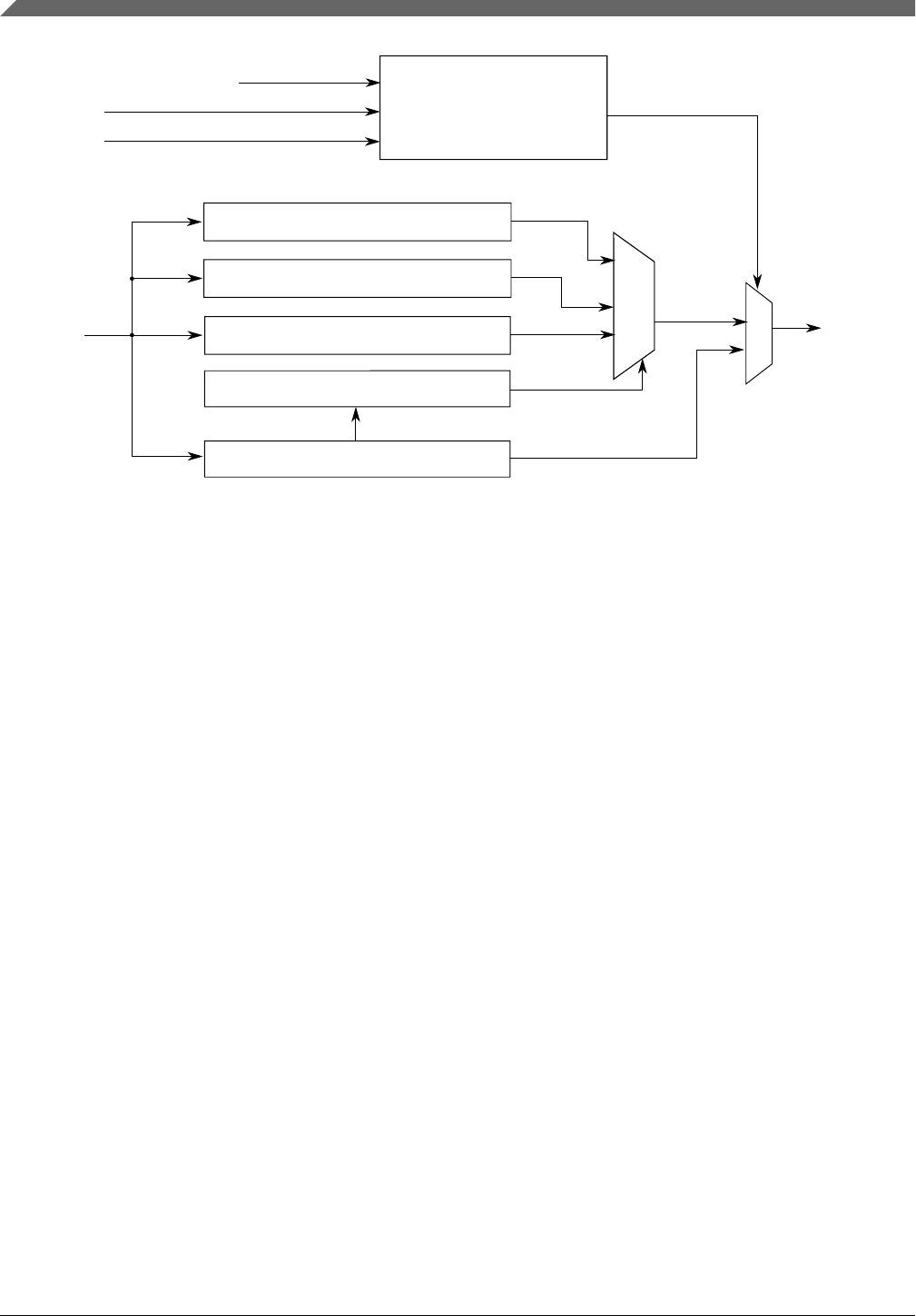
Power-on reset
TMS
TCK
TDI
1-bit Bypass Register
32-bit Device Identification Register
Boundary Scan Register
TAP Instruction Decoder
TAP Instruction Register
TDO
Test Access Port (TAP)
Controller
Figure 57-1. JTAG (IEEE 1149.1) block diagram
57.2.2 Features
The JTAGC block is compliant with the IEEE 1149.1-2001 standard, and supports the
following features:
• IEEE 1149.1-2001 Test Access Port (TAP) interface
• Four pins (TDI, TMS, TCK, and TDO)
• Instruction register that supports several IEEE 1149.1–2001 defined instructions as
well as several public and private device-specific instructions (see JTAGC block
instructions for a list of supported instructions).
• Bypass register, boundary scan register, and device identification register
• TAP controller state machine that controls the operation of the data registers,
instruction register, and associated circuitry
57.2.3 Modes of operation
The JTAGC block uses a power-on reset indication as its primary reset signals. Several
IEEE 1149.1–2001 defined test modes are supported, as well as a bypass mode.
Introduction
S32K1xx Series Reference Manual, Rev. 7, 04/2018
1980 NXP Semiconductors

57.2.3.1 Reset
The JTAGC block is placed in reset when:
• Power-on reset is asserted
• TMS input is held high for enough consecutive rising edges of TCK to sequence the
TAP controller state machine into the Test-Logic-Reset state
Holding TMS high for five consecutive rising edges of TCK guarantees entry into the
Test-Logic-Reset state regardless of the current TAP controller state. Asserting power-on
reset results in asynchronous entry into the reset state.
When in reset, the following actions occur:
• The TAP controller is forced into the Test-Logic-Reset state, thereby disabling the
test logic and allowing normal operation of the on-chip system logic to continue
unhindered.
• The instruction register is loaded with the IDCODE instruction.
57.2.3.2 IEEE 1149.1–2001 defined test modes
The JTAGC block supports several IEEE 1149.1–2001 defined test modes. A test mode
is selected by loading the appropriate instruction into the instruction register when the
JTAGC is enabled. Supported test instructions include EXTEST, HIGHZ, CLAMP,
SAMPLE, and SAMPLE/PRELOAD.
Each instruction defines the set of data register(s) that may operate and interact with the
on-chip system logic when the instruction is current. Only one test data register path is
enabled to shift data between TDI and TDO for each instruction.
The boundary scan register is enabled for serial access between TDI and TDO when the
EXTEST, SAMPLE, or SAMPLE/PRELOAD instructions are active. The single-bit
bypass register shift stage is enabled for serial access between TDI and TDO when the
following instructions are active:
• BYPASS
• HIGHZ
• CLAMP
The functionality of each test mode is explained in more detail in JTAGC block
instructions.
Chapter 57 JTAG Controller (JTAGC)
S32K1xx Series Reference Manual, Rev. 7, 04/2018
NXP Semiconductors 1981

57.2.3.3 Bypass mode
When no test operation is required, the BYPASS instruction can be loaded to place the
JTAGC block into bypass mode. When in bypass mode, the single-bit bypass shift
register is used to provide a minimum-length serial path to shift data between TDI and
TDO.
57.3 External signal description
The JTAGC consists of a set of signals that connect to off-chip development tools and
allow access to test support functions. The JTAGC signals are outlined in the following
table and described in the following sections.
Table 57-2. JTAG signal properties
Name I/O Function Reset state
TCK Input Test clock Weak pulldown
TDI Input Test data in Weak pullup
TDO Output Test data out High Z1
TMS Input Test mode select Weak pullup
1. TDO output buffer enable is negated when the JTAGC is not in the Shift-IR or Shift-DR states. A weak pull may be
implemented at the TDO pad for use when JTAGC is inactive.
57.3.1 Test clock input (TCK)
Test Clock Input (TCK) is an input pin used to synchronize the test logic and control
register access through the TAP.
57.3.2 Test data input (TDI)
Test Data Input (TDI) is an input pin that receives serial test instructions and data. TDI is
sampled on the rising edge of TCK.
57.3.3 Test data output (TDO)
Test Data Output (TDO) is an output pin that transmits serial output for test instructions
and data. TDO is tristateable and is actively driven only in the Shift-IR and Shift-DR
states of the TAP controller state machine, which is described in TAP controller state
machine.
External signal description
S32K1xx Series Reference Manual, Rev. 7, 04/2018
1982 NXP Semiconductors

57.3.4 Test mode select (TMS)
Test Mode Select (TMS) is an input pin used to sequence the IEEE 1149.1-2001 test
control state machine. TMS is sampled on the rising edge of TCK.
57.4 Register description
This section provides a detailed description of the JTAGC block registers accessible
through the TAP interface, including data registers and the instruction register. Individual
bit-level descriptions and reset states of each register are included. These registers are not
memory-mapped and can only be accessed through the TAP.
57.4.1 Instruction register
The JTAGC block uses a 4-bit instruction register as shown in the following figure.
The instruction register allows instructions to be loaded into the block to select the test to
be performed, or the test data register to be accessed, or both. Instructions are shifted in
through TDI when the TAP controller is in the Shift-IR state, and latched on the falling
edge of TCK in the Update-IR state. The latched instruction value can only be changed in
the Update-IR and Test-Logic-Reset TAP controller states.
Synchronous entry into the Test-Logic-Reset state results in the IDCODE instruction
being loaded on the falling edge of TCK. Asynchronous entry into the Test-Logic-Reset
state results in asynchronous loading of the IDCODE instruction. During the Capture-IR
TAP controller state, the instruction shift register is loaded with the value 0b1, making
this value the register's read value when the TAP controller is sequenced into the Shift-IR
state.
3 2 1 0
0 0 0 1
0 0 0 1
R
W
Reset:
Instruction Code
Figure 57-2. Instruction register
57.4.2 Bypass register
The bypass register is a single-bit shift register path selected for serial data transfer
between TDI and TDO when the following instructions are active:
Chapter 57 JTAG Controller (JTAGC)
S32K1xx Series Reference Manual, Rev. 7, 04/2018
NXP Semiconductors 1983

• BYPASS
• HIGHZ
• CLAMP
After entry into the Capture-DR state, the single-bit shift register is set to a logic 0.
Therefore, the first bit shifted out after selecting the bypass register is always a logic 0.
57.4.3 Device identification register
The device identification (JTAG ID) register, shown in the following figure, allows the
revision number, part number, manufacturer, and design center responsible for the design
of the part to be determined through the TAP.
The device identification register is selected for serial data transfer between TDI and
TDO when the IDCODE instruction is active. Entry into the Capture-DR state when the
device identification register is selected loads the IDCODE into the shift register to be
shifted out on TDO in the Shift-DR state. No action occurs in the Update-DR state.
31 30 29 28 27 26 25 24 23 22 21 20 19 18 17 16
R Part Revision Number Design Center Part Identification Number
W
Reset PRN DC PIN
15 14 13 12 11 10 9 8 7 6 5 4 3 2 1 0
R Part Identification Number Manufacturer Identity Code 1
W
Reset PIN (contd.) MIC 1
The following table describes the device identification register functions.
Table 57-3. Device identification register field descriptions
Field Description
PRN Part Revision Number. Contains the revision number of the part. Value is 0000.
DC Design Center. Indicates the design center. Value is 0x26.
PIN Part Identification Number. Contains the part number of the device. Value is 0b0101010000.
MIC Manufacturer Identity Code. Contains the reduced Joint Electron Device Engineering Council (JEDEC) ID.
Value is 0x00E.
IDCODE ID IDCODE Register ID. Identifies this register as the device identification register and not the bypass
register. Always set to 1.
Register description
S32K1xx Series Reference Manual, Rev. 7, 04/2018
1984 NXP Semiconductors

57.4.4 Boundary scan register
The boundary scan register is connected between TDI and TDO when the EXTEST,
SAMPLE, or SAMPLE/PRELOAD instructions are active. It is used to:
• Capture input pin data
• Force fixed values on output pins
• Select a logic value and direction for bidirectional pins
Each bit of the boundary scan register represents a separate boundary scan register cell,
as described in the IEEE 1149.1-2001 standard and discussed in Boundary scan. The size
of the boundary scan register and bit ordering is device-dependent and can be found in
the device BSDL file.
57.5 Functional description
This section explains the JTAGC functional description.
57.5.1 JTAGC reset configuration
When in reset, the TAP controller is forced into the Test-Logic-Reset state, thus disabling
the test logic and allowing normal operation of the on-chip system logic. In addition, the
instruction register is loaded with the IDCODE instruction.
57.5.2 IEEE 1149.1-2001 (JTAG) TAP
The JTAGC block uses the IEEE 1149.1-2001 TAP for accessing registers. This port can
be shared with other TAP controllers on the MCU. Ownership of the port is determined
by the value of the currently loaded instruction.
Data is shifted between TDI and TDO through the selected register starting with the least
significant bit, as illustrated in the following figure. This applies for the instruction
register, test data registers, and the bypass register.
Selected register
LSB
MSB
TDI
TDO
Figure 57-3. Shifting data through a register
Chapter 57 JTAG Controller (JTAGC)
S32K1xx Series Reference Manual, Rev. 7, 04/2018
NXP Semiconductors 1985

57.5.3 TAP controller state machine
The TAP controller is a synchronous state machine that interprets the sequence of logical
values on the TMS pin.
The following figure shows the machine's states. The value shown next to each state is
the value of the TMS signal sampled on the rising edge of the TCK signal. As the figure
shows, holding TMS at logic 1 when clocking TCK through a sufficient number of rising
edges also causes the state machine to enter the Test-Logic-Reset state.
Functional description
S32K1xx Series Reference Manual, Rev. 7, 04/2018
1986 NXP Semiconductors
The value shown adjacent to each state transition in this figure represents the value of TMS at the time
of a rising edge of TCK.
TEST LOGIC
RESET
RUN-TEST/IDLE SELECT-DR-SCAN SELECT-IR-SCAN
CAPTURE-DR CAPTURE-IR
SHIFT-IR
SHIFT-DR
EXIT1-DR EXIT1-IR
PAUSE-DR PAUSE-IR
EXIT2-IR
EXIT2-DR
UPDATE-DR UPDATE-IR
1
1
1
1
1
1
11
1
1
1
1
11
11
0
0
00
0
0
00
0
0
00
0
0
0
0
Figure 57-4. IEEE 1149.1-2001 TAP controller finite state machine
57.5.3.1 Enabling the TAP controller
The JTAGC TAP controller is enabled by setting the JTAGC enable to a logic 1 value.
Chapter 57 JTAG Controller (JTAGC)
S32K1xx Series Reference Manual, Rev. 7, 04/2018
NXP Semiconductors 1987

57.5.3.2 Selecting an IEEE 1149.1-2001 register
Access to the JTAGC data registers is achieved by loading the instruction register with
any of the JTAGC block instructions when the JTAGC is enabled. Instructions are shifted
in via the Select-IR-Scan path and loaded in the Update-IR state. At this point, all data
register access is performed via the Select-DR-Scan path.
The Select-DR-Scan path is used to read or write the register data by shifting in the data
(LSB first) during the Shift-DR state. When reading a register, the register value is loaded
into the IEEE 1149.1-2001 shifter during the Capture-DR state. When writing a register,
the value is loaded from the IEEE 1149.1-2001 shifter to the register during the Update-
DR state. When reading a register, there is no requirement to shift out the entire register
contents. Shifting may be terminated after the required number of bits have been
acquired.
57.5.4 JTAGC block instructions
The JTAGC block implements the IEEE 1149.1-2001 defined instructions listed in the
following table. This section gives an overview of each instruction. See the IEEE
1149.1-2001 standard for more details. All undefined opcodes are reserved.
Table 57-4. 4-bit JTAG instructions
Instruction Code[3:0] Instruction summary
IDCODE 0000 Selects device identification register for shift
SAMPLE/PRELOAD 0010 Selects boundary scan register for shifting, sampling, and
preloading without disturbing functional operation
SAMPLE 0011 Selects boundary scan register for shifting and sampling
without disturbing functional operation
EXTEST 0100 Selects boundary scan register and applies preloaded values
to output pins.
NOTE: Execution of this instruction asserts functional reset.
Factory debug reserved 0101 Intended for factory debug only
Factory debug reserved 0110 Intended for factory debug only. See chip-specific information
for possible alternate usage of this code.
Factory debug reserved 0111 Intended for factory debug only
ARM JTAG-DP Reserved 1000 This instruction goes the ARM JTAG-DP controller. See the
ARM JTAG-DP documentation for more information.
HIGHZ 1001 Selects bypass register and tristates all output pins.
NOTE: Execution of this instruction asserts functional reset.
ARM JTAG-DP Reserved 1010 This instruction goes the ARM JTAG-DP controller. See the
ARM JTAG-DP documentation for more information.
Table continues on the next page...
Functional description
S32K1xx Series Reference Manual, Rev. 7, 04/2018
1988 NXP Semiconductors

Table 57-4. 4-bit JTAG instructions (continued)
Instruction Code[3:0] Instruction summary
ARM JTAG-DP Reserved 1011 This instruction goes the ARM JTAG-DP controller. See the
ARM JTAG-DP documentation for more information.
CLAMP 1100 Selects bypass register and applies preloaded values to
output pins.
NOTE: Execution of this instruction asserts functional reset.
ARM JTAG-DP Reserved 1110 This instruction goes the ARM JTAG-DP controller. See the
ARM JTAG-DP documentation for more information.
BYPASS 1111 Selects bypass register for data operations
57.5.4.1 IDCODE instruction
IDCODE selects the 32-bit device identification register as the shift path between TDI
and TDO. This instruction allows interrogation of the MCU to determine its version
number and other part identification data. IDCODE is the instruction placed into the
instruction register when the JTAGC block is reset.
57.5.4.2 SAMPLE/PRELOAD instruction
The SAMPLE/PRELOAD instruction has two functions:
• The SAMPLE portion of the instruction obtains a sample of the system data and
control signals present at the MCU input pins, and just before the boundary scan
register cells at the output pins. This sampling occurs on the rising edge of TCK in
the Capture-DR state when the SAMPLE/PRELOAD instruction is active. The
sampled data is viewed by shifting it through the boundary scan register to the TDO
output during the Shift-DR state. Both the data capture and the shift operation are
transparent to system operation.
• The PRELOAD portion of the instruction initializes the boundary scan register cells
before selecting the EXTEST or CLAMP instructions to perform boundary scan
tests. This is achieved by shifting in initialization data to the boundary scan register
during the Shift-DR state. The initialization data is transferred to the parallel outputs
of the boundary scan register cells on the falling edge of TCK in the Update-DR
state. The data is applied to the external output pins by the EXTEST or CLAMP
instruction. System operation is not affected.
Chapter 57 JTAG Controller (JTAGC)
S32K1xx Series Reference Manual, Rev. 7, 04/2018
NXP Semiconductors 1989

57.5.4.3 SAMPLE instruction
The SAMPLE instruction obtains a sample of the system data and control signals present
at the MCU input pins, and just before the boundary scan register cells at the output pins.
This sampling occurs on the rising edge of TCK in the Capture-DR state when the
SAMPLE instruction is active. The sampled data is viewed by shifting it through the
boundary scan register to the TDO output during the Shift-DR state. There is no defined
action in the Update-DR state. Both the data capture and the shift operation are
transparent to system operation.
57.5.4.4 EXTEST external test instruction
EXTEST selects the boundary scan register as the shift path between TDI and TDO. It
allows testing of off-chip circuitry and board-level interconnections by driving preloaded
data contained in the boundary scan register onto the system output pins. Typically, the
preloaded data is loaded into the boundary scan register using the SAMPLE/PRELOAD
instruction before the selection of EXTEST. EXTEST asserts the internal system reset for
the MCU to force a predictable internal state when performing external boundary scan
operations.
57.5.4.5 ENABLE_SOC_DATA1 instruction
The ENABLE_SOC_DATA1 instruction captures SoC data and selects the SOC_DATA
register for connection as the shift path between TDI and TDO.
57.5.4.6 HIGHZ instruction
HIGHZ selects the bypass register as the shift path between TDI and TDO. When
HIGHZ is active all output drivers are placed in an inactive drive state (for example, high
impedance). HIGHZ also asserts the internal system reset for the MCU to force a
predictable internal state.
57.5.4.7 CLAMP instruction
CLAMP allows the state of signals driven from MCU pins to be determined from the
boundary scan register when the bypass register is selected as the serial path between TDI
and TDO. CLAMP enhances test efficiency by reducing the overall shift path to a single
Functional description
S32K1xx Series Reference Manual, Rev. 7, 04/2018
1990 NXP Semiconductors

bit (the bypass register) when conducting an EXTEST type of instruction through the
boundary scan register. CLAMP also asserts the internal system reset for the MCU to
force a predictable internal state.
57.5.4.8 BYPASS instruction
BYPASS selects the bypass register, creating a single-bit shift register path between TDI
and TDO. BYPASS enhances test efficiency by reducing the overall shift path when no
test operation of the MCU is required. This allows more rapid movement of test data to
and from other components on a board that are required to perform test functions. When
the BYPASS instruction is active the system logic operates normally.
57.5.5 Boundary scan
The boundary scan technique allows signals at component boundaries to be controlled
and observed through the shift-register stage associated with each pad. Each stage is part
of a larger boundary scan register cell, and cells for each pad are interconnected serially
to form a shift-register chain around the border of the design. The boundary scan register
consists of this shift-register chain, and is connected between TDI and TDO when the
EXTEST, SAMPLE, or SAMPLE/PRELOAD instructions are loaded. The shift-register
chain contains a serial input and serial output, as well as clock and control signals.
57.6 Initialization/application information
The test logic is a static logic design, and TCK can be stopped in either a high or low
state without loss of data. However, the system clock is not synchronized to TCK
internally. Any mixed operation using both the test logic and the system functional logic
requires external synchronization.
To initialize the JTAGC block and enable access to registers, the following sequence is
required:
1. Place the JTAGC in reset through TAP controller state machine transitions controlled
by TMS.
2. Load the appropriate instruction for the test or action to be performed.
Chapter 57 JTAG Controller (JTAGC)
S32K1xx Series Reference Manual, Rev. 7, 04/2018
NXP Semiconductors 1991

Initialization/application information
S32K1xx Series Reference Manual, Rev. 7, 04/2018
1992 NXP Semiconductors

Appendix A
Release Notes for Revision 7
A.1 General changes
• No substantial content changes
A.2 About This Manual changes
• Updated Audience to add note 'S32K116 and S32K118 specific information ... '
A.3 Introduction changes
• In S32K14x :
• Added footnote to EEPROM, HSRUN, Ambient operating temperature ranges
• Replaced 'Cosmic Software' with 'Arm Software'
• In Feature summary :
• Added footnote to Temperature range, Maximum CPU frequency
• Moved content to footnote for 'EEPROM emulated by FlexRAM' for S32K148, Data flash (D-flash)/emulated
EEPROM
• In Block diagram :
• Added footnote to CSEc
• Moved content to footnote for 'EEPROM emulated by FlexRAM' for S32K148, Data flash (D-flash)/emulated
EEPROM
• In Feature comparison :
• Minor editorial updates
• Updated the starting paragraph of section
• Updated 'Frequency' and 'ystem RAM (including FlexRAM and MTB)' for S32K14x
• Updated '12-bit SAR ADC (1 Msps each)' for S32K116
• Added footnote to 'HSRUN mode', changed 'HW security module' to 'Cryptographic Services Engine' and
updated its footnote, updated footnote related to BSR, added footnote to 'Packages'
• In Applications, added note: 'See S32K1xx Safety Manual ...'
S32K1xx Series Reference Manual, Rev. 7, 04/2018
NXP Semiconductors 1993

A.4 Memory map changes
• No substantial content changes
A.5 Signal multiplexing changes
• No substantial content changes
A.6 Security Overview changes
• No substantial content changes
A.7 Safety Overview changes
• No substantial content changes
A.8 CM0+ Overview changes
• Added reference of Devices Generic User Guide
• In Wake-up sources, updated table: AWIC stop and VLPS wake-up sources
A.9 CM4 Overview changes
• Added reference of Devices Generic User Guide
• In Wake-up sources, updated table: AWIC stop and VLPS wake-up sources
A.10 MTB changes
• Added new chapter
Memory map changes
S32K1xx Series Reference Manual, Rev. 7, 04/2018
1994 NXP Semiconductors

MCM changes
A.11.1 Chip-specific MCM information changes
• In Chip-specific MCM information
• Added table: MCM register offset
A.11.2 MCM changes
• In Memory map/register descriptions
• Added note 'This bit field is Reserved and Read-Only 0 for S32K11x variants ... ' for LMDR0[CF0] for S32K11x
variants
SIM changes
A.12.1 Chip-specific SIM information changes
• No substantial content changes
A.12.2 SIM changes
• No substantial content changes
PORT changes
A.13.1 Chip-specific PORT information changes
• No substantial content changes
A.11
A.12
A.13
Appendix A Release Notes for Revision 7
S32K1xx Series Reference Manual, Rev. 7, 04/2018
NXP Semiconductors 1995

A.13.2 Port Control and Interrupts (PORT) changes
• No substantial content changes
GPIO changes
A.14.1 Chip-specific GPIO information changes
• In GPIO ports memory map
• Updated note 'In S32K11x, when in GPIO mode ... '
A.14.2 GPIO module changes
• No substantial content changes
AXBS-Lite changes
A.15.1 Chip-specific AXBS-Lite information changes
• No substantial content changes
A.15.2 AXBS_Lite module changes
• Changed module abbreviation to AXBS_Lite.
A.14
A.15
GPIO changes
S32K1xx Series Reference Manual, Rev. 7, 04/2018
1996 NXP Semiconductors

MPU changes
A.16.1 Chip-specific MPU information changes
• In MPU Slave Port Assignments, updated table: MPU Slave Port Assignments for S32K11x serie for 'Crossbar slave
port 1'
• In MPU Logical Bus Master Assignments, in table: MPU Logical Bus Master Assignments added '4-7 Not
implemented ... '
A.16.2 MPU module changes
No substantial content changes.
AIPS-Lite changes
A.17.1 Chip-specific AIPS information changes
• Added Register information
A.17.2 AIPS_Lite module changes
• No substantial content changes
DMAMUX changes
A.18.1 Chip-specific DMAMUX information changes
• No substantial content changes
A.16
A.17
A.18
Appendix A Release Notes for Revision 7
S32K1xx Series Reference Manual, Rev. 7, 04/2018
NXP Semiconductors 1997

A.18.2 DMAMUX module changes
• Changed the offset addresses of CHCFGn registers in the section DMAMUX register descriptions to depict little
endianness.
• Updated Enabling and configuring sources for addresses
eDMA changes
A.19.1 Chip-specific eDMA information changes
• In Chip-specific eDMA information
• Added note 'For S32K11x variants, when executing a large, ... '
A.19.2 eDMA2 module changes
• In Suspend/resume a DMA channel with active hardware service requests : Changed Sigma Delta Analog to Digital
Convertor (SDADC) to ADC.
TRGMUX changes
A.20.1 Chip-specific TRGMUX information changes
• No substantial content changes
A.20.2 TRGMUX module changes
No substantial content changes.
A.19
A.20
eDMA changes
S32K1xx Series Reference Manual, Rev. 7, 04/2018
1998 NXP Semiconductors

EWM changes
A.21.1 Chip-specific EWM information changes
• No substantial content changes
A.21.2 EWM module changes
No substantial content changes.
EIM changes
A.22.1 Chip-specific EIM information changes
• No substantial content changes
A.22.2 EIM changes
Editorial updates
ERM changes
A.23.1 Chip-specific ERM information changes
• No substantial content changes
A.23.2 ERM module changes
• Editorial updates
A.21
A.22
A.23
Appendix A Release Notes for Revision 7
S32K1xx Series Reference Manual, Rev. 7, 04/2018
NXP Semiconductors 1999

WDOG changes
A.24.1 Chip-specific WDOG information changes
• No substantial content changes
A.24.2 WDOG module changes
• Minor update in the "Configuring the Watchdog Once" section.
• Updated the "Watchdog timeout availability" table.
A.25 CRC module changes
No sunstantial content changes
A.26 Reset and Boot changes
• No substantial content changes
RCM changes
A.27.1 Chip-specific RCM information changes
• No substantial content changes
A.27.2 RCM changes
• No substantial content changes
A.24
A.27
WDOG changes
S32K1xx Series Reference Manual, Rev. 7, 04/2018
2000 NXP Semiconductors

A.28 Clock Distribution changes
• Updated Clocking diagram in High level clocking diagram :
• Added color coding for S32K14x and S32K11x
• Updated footnote "The source of HCLK ... "
• In Clock definitions, added footnotes to PREDIV_SYS_CLK, SPLL_CLK, VCO_CLK, and SPLLDIV2_CLK
• Added table for S32K14x/S32K11x maximum frequencies and example configurations
• Updated section VLPR/VLPS mode entry, added 'Ensure that CMU is gated ... '
SCG changes
A.29.1 Chip-specific SCG information changes
• In Chip-specific SCG information, added notes ' SCG_SIRCCSR[SIRCLPEN] bit ...' and 'SCG_SIRCCSR[SIRCSTEN]
bit field ... '
A.29.2 SCG changes
• In System PLL Control Status Register (SCG_SPLLCSR), in System PLL Valid bit (SPLLVLD), added a note and
made the description more clear.
PCC changes
A.30.1 Chip-specific PCC information changes
• No substantial content changes
A.30.2 PCC module changes
• No substantial content changes
A.29
A.30
Appendix A Release Notes for Revision 7
S32K1xx Series Reference Manual, Rev. 7, 04/2018
NXP Semiconductors 2001

A.31 CMU changes
• No substantial content changes
A.32 Memories and memory interfaces changes
• No substantial content changes
A.33 PRAMC changes
• No substantial content changes
LMEM changes
A.34.1 Chip-specific LMEM information changes
• No substantial content changes
A.34.2 LMEM module changes
No substantial content changes.
MSCM changes
A.35.1 Chip-specific MSCM information changes
• No substantial content changes
A.34
A.35
CMU changes
S32K1xx Series Reference Manual, Rev. 7, 04/2018
2002 NXP Semiconductors

A.35.2 MSCM changes
• No substantial content changes
FMC changes
A.36.1 Chip-specific FMC changes
• No substantial content changes
A.36.2 FMC changes
• No substantial content changes
FTFC changes
A.37.1 Chip-specific FTFC information changes
• In Flash memory types
• Added note 'CSEc (Security) or EEPROM writes ... '
A.37.2 FTFC changes
• In FlexRAM features, updated 'Protection scheme prevents ...'
• In Block diagram, updated FTFC block diagram to include PRAMC
• In Glossary :
• Updated 'Double-Phrase'
• Removed 'NVM Special Mode'
• Updated Program flash 0 IFR map
• Updated Data flash 0 IFR map
• Updated the note under Register descriptions
• Updated the descriptions of FSTAT[CCIF] and FSTAT[CCIE] to add CSEc
• Updated the description of FCNFG[RAMRDY]
• Updated the description of FPROT, FEPROT, FDPROT,
• Updated the description of FCSESTAT[IDB], FCSESTAT[BSY]
• In Flash protection, updated figure EEPROM protection
• In Interrupts, updated table: FTFC interrupt sources to include 'and CSEc command Complete' in first row
A.36
A.37
Appendix A Release Notes for Revision 7
S32K1xx Series Reference Manual, Rev. 7, 04/2018
NXP Semiconductors 2003

• In FTFC command operations, added Warning 'When running any ... '
• In Flash commands :
• Added Data Flash column in table
• Removed row for 0x03
• In Flash commands by mode, removed content for NVM Special from table 'Flash commands by mode'
• In Allowed simultaneous flash operations, updated table Allowed simultaneous memory operations
• In Read 1s Block command :
• Updated footnote 1 of table Read 1s Block Command FCCOB requirements
• Updated Error condition 'Flash address is not ... ' of table Read 1s Block Command error handling
• Updated table Read 1s Section command FCCOB requirements
• Updated table Read 1s Section command error handling
• In Program Check command :
• Updated footnote 1 of table Erase Flash Block command FCCOB requirements
• In Program Phrase command"
• Removed note 'For CSEc enabled parts ...'
• In Erase Flash Block command
• Updated Error condition 'Flash address is not ... ' of table Erase Flash Block command error handling
• Updated footnote 1 of table Erase Flash Sector command FCCOB requirements
• In Suspending an Erase Flash Sector operation, updated sentence 'While ERSSUSP is set ...' to include FCNFG,
FERCNFG and FERSTAT registers.
• In Program Section command :
• Updated footnote 1 of table Program Section command FCCOB requirements
• Updated Error condition 'Flash address is not ... ' of table Program Section command error handling
• Updated point 3 and 5 in Flash sector programming
• Added note 'For CSEc enabled parts, the presence ...' in Erase All Blocks command
• Added note 'For CSEc enabled parts, the presence ...' in Erase All Blocks Unsecure command
• In Program Partition command
• Updated table CSEc/SHE key size
• Updated the wordings of note 'For CSEc enabled parts ... '
• Minor update in table Security Flag Extension (SFE)
• Updated sentence 'Prior to launching the Program Partition ... ' above table Program Partition command error
handling
• Updated table 'Program Partition command error handling' for FCCOB1
• In Set FlexRAM Function command,
• Updated paragraph 'When the FlexRAM Function Control ... ' , 'When the FlexRAM Function ...' , 'When making
the FlexRAM ...', 'For configurations with ... '
• Updated Error Condition 'Set if FlexRAM Function Control Code ...' in table Set FlexRAM Function command
error handling
• In Cryptographic Services Engine (CSEc),
• Updated paragraph 'To access the command ... ' and 'Internal to the FTFC module ... '
• Renamed and updated table 'Non-Volatile keys and RAM_KEY'
• In CSEc command header, updated the paragraph 'The KeyID is divided into ... '
• In table Encrypt CBC command details, added IV
• In table Decrypt CBC command details, removed PAGE_LENGTH, and added PLAIN_TEXT
• In table Generate MAC command details, updated MESSAGE_LENGTH and MESSAGE
• Updated CMD_VERIFY_MAC
• In table Verify MAC command details, updated MESSAGE, MAC_LENGTH, VERIFICATION_STATUS
• Updated CMD_DBG_AUTH
• In table MP Compress command details, added MP_COMPRESS
• In figure Continuation of input parameters, Continuation of output parameters and Reset sequence changed
MESSAGE_LENGTH to PAGE_LENGTH
FTFC changes
S32K1xx Series Reference Manual, Rev. 7, 04/2018
2004 NXP Semiconductors

QSPI changes
A.38.1 Chip-specific QSPI information changes
• No substantial content changes
A.38.2 QuadSPI changes
• No substantial content changes
A.39 Power Management changes
• In Power modes description
• Updated description of 'Very Low Power Stop (VLPS, via WFI instruction)', added RTC
• In Compute Operation (CPO), updated paragraph 'CPO is controlled by the MCM's ... '
• In Module operation in available low power modes, added footnote to PLL, FIRC, System oscillator in table Module
operation in available low power modes
• In Module operation in available low power modes, updated Core clock, Flash clock, System clock, and Bus clock in
table Module operation in available low power modes
• In Module operation in available low power modes, updated LPUAT, LPSPI, LPI2C, LPIT, RTC, in table Module
operation in available low power modes
A.40 SMC changes
• Added note 'Ensure that CMU is ...' in VLPS/Stop mode entry sequence
PMC changes
A.41.1 Chip-specific PMC changes
• No substantial content changes
A.38
A.41
Appendix A Release Notes for Revision 7
S32K1xx Series Reference Manual, Rev. 7, 04/2018
NXP Semiconductors 2005

A.41.2 PMC module changes
No substantial content changes
A.42 ADC Configuration changes
• In Number of ADC channels
• Updated package information for S32K11x in table 'ADC external channels per package'
• Added S32K146 package information in table 'ADC external channels per package'
• In ADC Trigger Sources, updated note 'Each PDB supports 4 slots/4 ... '
• Minor editorial updates in Figure ADC0_PDB0 ADC Triggering scheme example
ADC changes
A.43.1 Chip-specific ADC information changes
• No substantial content changes
A.43.2 ADC module changes
• No substantial content change
CMP changes
A.44.1 Chip-specific CMP changes
• In CMP input connections, added note 'See IO Signal Description ... '
A.44.2 CMP changes
• Minor update in the "CMP high level diagram" figure.
• Added "CMP channel decoding in functional mode and trigger mode" table in the "Trigger mode" section.
A.43
A.44
ADC Configuration changes
S32K1xx Series Reference Manual, Rev. 7, 04/2018
2006 NXP Semiconductors

PDB changes
A.45.1 Chip-specific PDB information changes
• No substantial content changes
A.45.2 PDB changes
• No substantial content changes
FTM changes
A.46.1 Chip-specific FTM information changes
• No substantial content changes
A.46.2 FTM module changes
• Removed the example in the Memory map note.
• Changed the access of Capture And Compare Status (STATUS) register from ROWZ to RW
• Combined bit fields SC[PWMENn]
• Changed the access of STATUS[CHnF] bit fields to RW
• Combined bit fields OUTINIT[CHnOI]
• Combined bit fields OUTMASK[CHnOM]
• Combined bit fields POL[POLn]
• Combined bit fields SWOCTRL[CHnOCV], SWOCTRL[CHnOC]
• Combined bit fields PWMLOAD[CHnSEL]
LPIT changes
A.47.1 Chip-specific LPIT information changes
• No substantial content changes
A.45
A.46
A.47
Appendix A Release Notes for Revision 7
S32K1xx Series Reference Manual, Rev. 7, 04/2018
NXP Semiconductors 2007

A.47.2 LPIT module changes
• No substantial content changes
LPTMR changes
A.48.1 Chip-specific LPTMR information changes
• No substantial content changes
A.48.2 LPTMR module changes
No substantial content changes.
RTC changes
A.49.1 Chip-specific RTC changes
• No substantial content changes
A.49.2 RTC module changes
• No substantial content changes.
LPSPI changes
A.50.1 Chip-specific LPSPI information changes
• No substantial content changes
A.48
A.49
A.50
LPTMR changes
S32K1xx Series Reference Manual, Rev. 7, 04/2018
2008 NXP Semiconductors

A.50.2 LPSPI module changes
• Added note 'Writing a Read-Only (RO) register ... ' in memory map section
• Updated the description of CR[DBGEN], CR[DOZEN], CR[RST]
LPI2C changes
A.51.1 Chip-specific LPI2C information changes
• Updated Instantiation information
A.51.2 LPI2C module changes
• Added note 'Writing a Read-Only (RO) register ... ' in memory map.
LPUART changes
A.52.1 Chip-specific LPUART information changes
• Updated Instantiation Information
A.52.2 LPUART module changes
• In the section "Register definition," added the note "Writing a Read-Only (RO) register or reading a Write-Only (WO)
register can cause bus errors. This module will not check if programmed values in the registers are correct; the
application software must ensure that valid programmed values are being written"
• Clarified operation of data match wakeup.
• Minor editorial updates
A.51
A.52
Appendix A Release Notes for Revision 7
S32K1xx Series Reference Manual, Rev. 7, 04/2018
NXP Semiconductors 2009

FlexIO changes
A.53.1 Chip-specific FlexIO changes
• No substantial content changes
A.53.2 FLEXIO module changes
• No substantial content changes
FlexCAN changes
A.54.1 Chip-specific FlexCAN information changes
• No substantial content changes
A.54.2 FlexCAN module changes
• In FlexCAN memory mapping "An invalid register access will result in a bus error. This includes reading a write-only
register, writing a read-only register or accessing an invalid address." is added as note
• Added note 'See the clock distribution chapter ... ' in CTRL1[CLKSRC] bit field
SAI changes
A.55.1 Chip-specific SAI changes
• Added SAI block diagram for S32K148
A.55.2 SAI module changes
• No substantial content changes
A.53
A.54
A.55
FlexIO changes
S32K1xx Series Reference Manual, Rev. 7, 04/2018
2010 NXP Semiconductors

ENETchanges
A.56.1 Chip-specific ENET changes
• No substantial content changes
A.56.2 ENET module changes
• No substantial content changes
A.57 Debug changes
• In DWT , added note 'The MTB_DWT_FCT ... '
JTAGC changes
A.58.1 Chip-specific JTAGC information changes
• No substantial content changes
A.58.2 JTAGC module changes
• No substantial content changes
A.56
A.58
S32K1xx Series Reference Manual, Rev. 7, 04/2018
NXP Semiconductors 2011

S32K1xx Series Reference Manual, Rev. 7, 04/2018
2012 NXP Semiconductors

How to Reach Us:
Home Page:
nxp.com
Web Support:
nxp.com/support
Information in this document is provided solely to enable system and software
implementers to use NXP products. There are no express or implied copyright
licenses granted hereunder to design or fabricate any integrated circuits based
on the information in this document. NXP reserves the right to make changes
without further notice to any products herein.
NXP makes no warranty, representation, or guarantee regarding the suitability of
its products for any particular purpose, nor does NXP assume any liability arising
out of the application or use of any product or circuit, and specifically disclaims
any and all liability, including without limitation consequential or incidental
damages. “Typical” parameters that may be provided in NXP data sheets and/or
specifications can and do vary in different applications, and actual performance
may vary over time. All operating parameters, including “typicals,” must be
validated for each customer application by customerʼs technical experts. NXP
does not convey any license under its patent rights nor the rights of others. NXP
sells products pursuant to standard terms and conditions of sale, which can be
found at the following address: nxp.com/SalesTermsandConditions.
NXP, the NXP logo, NXP SECURE CONNECTIONS FOR A SMARTER
WORLD, COOLFLUX, EMBRACE, GREENCHIP, HITAG, I2C BUS, ICODE,
JCOP, LIFE VIBES, MIFARE, MIFARE CLASSIC, MIFARE DESFire, MIFARE
PLUS, MIFARE FLEX, MANTIS, MIFARE ULTRALIGHT, MIFARE4MOBILE,
MIGLO, NTAG, ROADLINK, SMARTLX, SMARTMX, STARPLUG, TOPFET,
TRENCHMOS, UCODE, Freescale, the Freescale logo, AltiVec, C-5, CodeTest,
CodeWarrior, ColdFire, ColdFire+, C-Ware, the Energy Efficient Solutions logo,
Kinetis, Layerscape, MagniV, mobileGT, PEG, PowerQUICC, Processor Expert,
QorIQ, QorIQ Qonverge, Ready Play, SafeAssure, the SafeAssure logo,
StarCore, Symphony, VortiQa, Vybrid, Airfast, BeeKit, BeeStack, CoreNet,
Flexis, MXC, Platform in a Package, QUICC Engine, SMARTMOS, Tower,
TurboLink, and UMEMS are trademarks of NXP B.V. All other product or service
names are the property of their respective owners. ARM, AMBA, ARM Powered,
Artisan, Cortex, Jazelle, Keil, SecurCore, Thumb, TrustZone, and μVision are
registered trademarks of ARM Limited (or its subsidiaries) in the EU and/or
elsewhere. ARM7, ARM9, ARM11, big.LITTLE, CoreLink, CoreSight,
DesignStart, Mali, mbed, NEON, POP, Sensinode, Socrates, ULINK and
Versatile are trademarks of ARM Limited (or its subsidiaries) in the EU and/or
elsewhere. All rights reserved. Oracle and Java are registered trademarks of
Oracle and/or its affiliates. The Power Architecture and Power.org word marks
and the Power and Power.org logos and related marks are trademarks and
service marks licensed by Power.org.
© 2015–2018 NXP B.V.
Document Number S32K1XXRM
Revision 7, 04/2018
